BCM56980 12.8 Tb/s Multilayer Switch - Broadcom Inc.
93
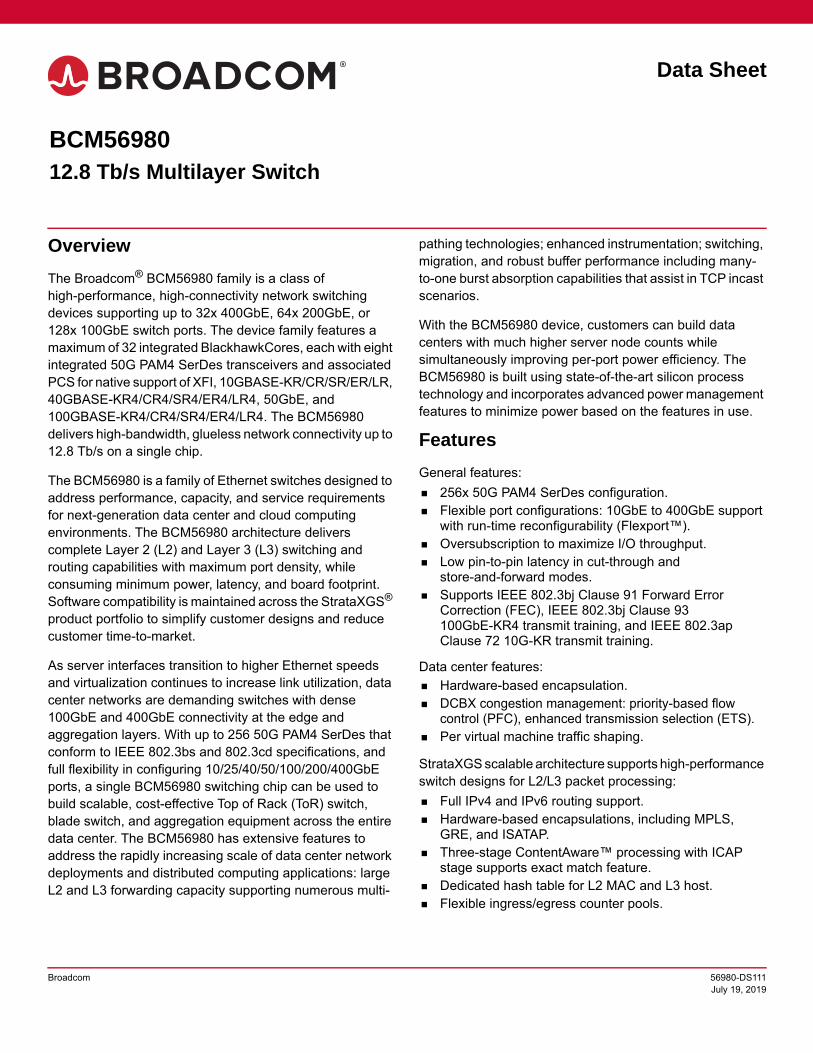
Data Sheet Broadcom 56980-DS111 July 19, 2019 Overview The Broadcom ® BCM56980 family is a class of high-performance, high-connectivity network switching devices supporting up to 32x 400GbE, 64x 200GbE, or 128x 100GbE switch ports. The device family features a maximum of 32 integrated BlackhawkCores, each with eight integrated 50G PAM4 SerDes transceivers and associated PCS for native support of XFI, 10GBASE-KR/CR/SR/ER/LR, 40GBASE-KR4/CR4/SR4/ER4/LR4, 50GbE, and 100GBASE-KR4/CR4/SR4/ER4/LR4. The BCM56980 delivers high-bandwidth, glueless network connectivity up to 12.8 Tb/s on a single chip. The BCM56980 is a family of Ethernet switches designed to address performance, capacity, and service requirements for next-generation data center and cloud computing environments. The BCM56980 architecture delivers complete Layer 2 (L2) and Layer 3 (L3) switching and routing capabilities with maximum port density, while consuming minimum power, latency, and board footprint. Software compatibility is maintained across the StrataXGS ® product portfolio to simplify customer designs and reduce customer time-to-market. As server interfaces transition to higher Ethernet speeds and virtualization continues to increase link utilization, data center networks are demanding switches with dense 100GbE and 400GbE connectivity at the edge and aggregation layers. With up to 256 50G PAM4 SerDes that conform to IEEE 802.3bs and 802.3cd specifications, and full flexibility in configuring 10/25/40/50/100/200/400GbE ports, a single BCM56980 switching chip can be used to build scalable, cost-effective Top of Rack (ToR) switch, blade switch, and aggregation equipment across the entire data center. The BCM56980 has extensive features to address the rapidly increasing scale of data center network deployments and distributed computing applications: large L2 and L3 forwarding capacity supporting numerous multi- pathing technologies; enhanced instrumentation; switching, migration, and robust buffer performance including many- to-one burst absorption capabilities that assist in TCP incast scenarios. With the BCM56980 device, customers can build data centers with much higher server node counts while simultaneously improving per-port power efficiency. The BCM56980 is built using state-of-the-art silicon process technology and incorporates advanced power management features to minimize power based on the features in use. Features General features: 256x 50G PAM4 SerDes configuration. Flexible port configurations: 10GbE to 400GbE support with run-time reconfigurability (Flexport™). Oversubscription to maximize I/O throughput. Low pin-to-pin latency in cut-through and store-and-forward modes. Supports IEEE 802.3bj Clause 91 Forward Error Correction (FEC), IEEE 802.3bj Clause 93 100GbE-KR4 transmit training, and IEEE 802.3ap Clause 72 10G-KR transmit training. Data center features: Hardware-based encapsulation. DCBX congestion management: priority-based flow control (PFC), enhanced transmission selection (ETS). Per virtual machine traffic shaping. StrataXGS scalable architecture supports high-performance switch designs for L2/L3 packet processing: Full IPv4 and IPv6 routing support. Hardware-based encapsulations, including MPLS, GRE, and ISATAP. Three-stage ContentAware™ processing with ICAP stage supports exact match feature. Dedicated hash table for L2 MAC and L3 host. Flexible ingress/egress counter pools. BCM56980 12.8 Tb/s Multilayer Switch
-
Upload
khangminh22 -
Category
Documents
-
view
5 -
download
0
Transcript of BCM56980 12.8 Tb/s Multilayer Switch - Broadcom Inc.
Data Sheet
Broadcom 56980-DS111July 19, 2019
OverviewThe Broadcom® BCM56980 family is a class of high-performance, high-connectivity network switching devices supporting up to 32x 400GbE, 64x 200GbE, or 128x 100GbE switch ports. The device family features a maximum of 32 integrated BlackhawkCores, each with eight integrated 50G PAM4 SerDes transceivers and associated PCS for native support of XFI, 10GBASE-KR/CR/SR/ER/LR, 40GBASE-KR4/CR4/SR4/ER4/LR4, 50GbE, and 100GBASE-KR4/CR4/SR4/ER4/LR4. The BCM56980 delivers high-bandwidth, glueless network connectivity up to 12.8 Tb/s on a single chip.
The BCM56980 is a family of Ethernet switches designed to address performance, capacity, and service requirements for next-generation data center and cloud computing environments. The BCM56980 architecture delivers complete Layer 2 (L2) and Layer 3 (L3) switching and routing capabilities with maximum port density, while consuming minimum power, latency, and board footprint. Software compatibility is maintained across the StrataXGS® product portfolio to simplify customer designs and reduce customer time-to-market.
As server interfaces transition to higher Ethernet speeds and virtualization continues to increase link utilization, data center networks are demanding switches with dense 100GbE and 400GbE connectivity at the edge and aggregation layers. With up to 256 50G PAM4 SerDes that conform to IEEE 802.3bs and 802.3cd specifications, and full flexibility in configuring 10/25/40/50/100/200/400GbE ports, a single BCM56980 switching chip can be used to build scalable, cost-effective Top of Rack (ToR) switch, blade switch, and aggregation equipment across the entire data center. The BCM56980 has extensive features to address the rapidly increasing scale of data center network deployments and distributed computing applications: large L2 and L3 forwarding capacity supporting numerous multi-
pathing technologies; enhanced instrumentation; switching, migration, and robust buffer performance including many-to-one burst absorption capabilities that assist in TCP incast scenarios.
With the BCM56980 device, customers can build data centers with much higher server node counts while simultaneously improving per-port power efficiency. The BCM56980 is built using state-of-the-art silicon process technology and incorporates advanced power management features to minimize power based on the features in use.
FeaturesGeneral features: 256x 50G PAM4 SerDes configuration. Flexible port configurations: 10GbE to 400GbE support
with run-time reconfigurability (Flexport™). Oversubscription to maximize I/O throughput. Low pin-to-pin latency in cut-through and
store-and-forward modes. Supports IEEE 802.3bj Clause 91 Forward Error
Correction (FEC), IEEE 802.3bj Clause 93 100GbE-KR4 transmit training, and IEEE 802.3ap Clause 72 10G-KR transmit training.
Data center features: Hardware-based encapsulation. DCBX congestion management: priority-based flow
control (PFC), enhanced transmission selection (ETS). Per virtual machine traffic shaping.
StrataXGS scalable architecture supports high-performance switch designs for L2/L3 packet processing: Full IPv4 and IPv6 routing support. Hardware-based encapsulations, including MPLS,
GRE, and ISATAP. Three-stage ContentAware™ processing with ICAP
stage supports exact match feature. Dedicated hash table for L2 MAC and L3 host. Flexible ingress/egress counter pools.
BCM56980 12.8 Tb/s Multilayer Switch
Broadcom 56980-DS1112
BCM56980 Data Sheet 12.8 Tb/s Multilayer Switch
Features (continued)Buffering and traffic management: Integrated high-performance SmartBuffer memory for
maximum burst absorption and service guarantees. Full Quality of Service (QoS) support: Weighted random early discard (WRED). srTCM and trTCM color marking and metering. Congestion management capabilities including ECN. Dynamic load balancing (DLB) for ECMP groups. Packetized MMU statistics. Network monitoring. Elephant trap monitors. DLB monitors. Latency distribution histogram. Network congestion detection. sFlow redirect. Visibility and packet tracing. Enhanced load balancing. Enhanced trunk hashing capabilities: RTAG7,
symmetric hash, flex hash, and resilient hash. Support for jumbo frames up to 9416 bytes. High-speed vector-based scheduler with 12 queues per
port and scheduling algorithms: SP, RR, WRR, and WDRR.
Additional features: In-band telemetry. Elephant trap. Comprehensive time synchronization support:
– Integrated IEEE 1588v2 processor.– IEEE 802.1AS support.– Synchronous Ethernet.– Ingress and egress per packet time stamping.
sFlow support includes ingress, egress, and flex sampler. Option to forward truncated sFlow packets to remote agent.
Packet sampling (PSAMP) ingress-based mirroring with option to truncate as well as zero out the payload at different offset.
Two dedicated 1G/10G auxiliary Ethernet ports x4 PCI Express (PCIe) Gen 3.0 interface to support a
local CPU. Adjustable voltage scaling (AVS) for reduced average
and peak power.
Applications Data center ToR, blade, and aggregation switching. Mobile core switches. Cloud computing. Large-scale enterprise campus backbone. Service provider core switching.
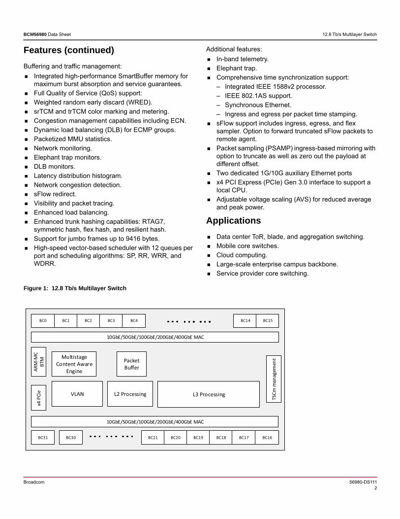
Figure 1: 12.8 Tb/s Multilayer Switch
10GbE/50GbE/100GbE/200GbE/400GbE MAC
BC31 BC30 BC19 BC18 BC17 BC16
BC0 BC1 BC2 BC3 BC14 BC15
10GbE/50GbE/100GbE/200GbE/400GbE MAC
Multistage Content Aware
Engine
Packet Buffer
VLAN L2 Processing L3 Processing
ARM
-MC
BTM
x4 P
CIe
BC4
BC21 BC20
TSCm
man
agem
ent
Broadcom 56980-DS1113
BCM56980 Data Sheet 12.8 Tb/s Multilayer Switch
Table of Contents
Chapter 1: Introduction ...................................................................................................................... 6Chapter 2: Device Overview .............................................................................................................. 7
2.1 Feature List ................................................................................................................................................................72.2 Target Applications.................................................................................................................................................14
2.2.1 100GbE/200GbE/400GbE Aggregation Switch ..............................................................................................14
Chapter 3: System Interfaces .......................................................................................................... 153.1 BlackhawkCore SerDes ..........................................................................................................................................163.2 BlackhawkCore Octal SerDes Configuration Guidelines ....................................................................................20
3.2.1 Flexport Configuration.....................................................................................................................................203.3 10G Quad MerlinCore SerDes ................................................................................................................................203.4 PCIe ..........................................................................................................................................................................213.5 LED ...........................................................................................................................................................................213.6 MIIM ..........................................................................................................................................................................223.7 Broadcom Serial Controller ...................................................................................................................................223.8 JTAG.........................................................................................................................................................................233.9 BroadSync ...............................................................................................................................................................23
3.9.1 Slave Mode – BroadSync Signals as Inputs ...................................................................................................243.9.2 Master Mode – BroadSync Signals as Outputs ..............................................................................................24
Chapter 4: Signal Descriptions ....................................................................................................... 254.1 Pin Description ........................................................................................................................................................264.2 BCM56980 Pin List by Ball Number.......................................................................................................................424.3 Device Differences ..................................................................................................................................................42
Chapter 5: Electrical Specifications ................................................................................................ 435.1 Operating Conditions .............................................................................................................................................435.2 Absolute Maximum Ratings ...................................................................................................................................445.3 Power-Up and Power-Down Specifications ..........................................................................................................445.4 Device Power Supply Requirement .......................................................................................................................455.5 DC Characteristics ..................................................................................................................................................46
5.5.1 Standard 3.3V Signals ....................................................................................................................................465.5.2 Management Interface ....................................................................................................................................465.5.3 BSC Interface..................................................................................................................................................465.5.4 Reference Clocks............................................................................................................................................47
5.5.4.1 Core PLL Reference Clock (CORE_PLL_FREF) .................................................................................485.5.4.2 TimeSync PLL Reference Clock (TS_PLL_FREF) ...............................................................................495.5.4.3 BroadSync PLL Reference Clocks (BS_PLL0_REFCLK / BS_PLL1_REFCLK) ..................................505.5.4.4 PCI Express PLL Reference Clock (PCIe_REFCLK) ...........................................................................515.5.4.5 BlackhawkCore PLL Reference Clocks (BC*_REFCLK) ......................................................................52
Broadcom 56980-DS1114
BCM56980 Data Sheet 12.8 Tb/s Multilayer Switch
5.5.4.6 MerlinCore PLL Reference Clock (MGMT_REFCLK)...........................................................................535.5.5 PCIe ................................................................................................................................................................54
5.6 AC Characteristics ..................................................................................................................................................555.6.1 Reset Timing...................................................................................................................................................555.6.2 Reference Clocks............................................................................................................................................56
5.6.2.1 Core PLL Reference Clock (CORE_PLL_FREF) .................................................................................565.6.2.2 TimeSync PLL Reference Clock (TS_PLL_FREF) ...............................................................................575.6.2.3 BroadSync PLL Reference Clocks (BS_PLL0_FREF / BS_PLL1_FREF)............................................575.6.2.4 PCI Express PLL Reference Clock (PCIe_REFCLK) ...........................................................................575.6.2.5 BlackhawkCore PLL Reference Clocks (BC*_REFCLK) ......................................................................585.6.2.6 MerlinCore PLL Reference Clocks (MGMT_REFCLK).........................................................................58
5.6.3 BlackhawkCore (50G) Interface......................................................................................................................595.6.4 MerlinCore (TSC4-M) Interface.......................................................................................................................59
5.6.4.1 MerlinCore Receiver .............................................................................................................................595.6.4.2 MerlinCore Transmitter .........................................................................................................................60
5.6.5 PCIe Interface .................................................................................................................................................615.6.5.1 PCIe Receiver Input..............................................................................................................................615.6.5.2 PCIe Transmitter Output.......................................................................................................................61
5.6.6 BroadSync Interface .......................................................................................................................................625.6.7 BSC Interface..................................................................................................................................................635.6.8 LED Interface ..................................................................................................................................................655.6.9 Management Interface (MIIM).........................................................................................................................665.6.10 Synchronous Ethernet Interface ...................................................................................................................67
5.6.10.1 L1_RCVRD_CLK and L1_RCVRD_CLK_BKUP Output Timing.........................................................675.6.11 JTAG Interface..............................................................................................................................................675.6.12 QSPI Interface ..............................................................................................................................................685.6.13 SPI Interface .................................................................................................................................................70
Chapter 6: Standard Electrical Characteristics ............................................................................. 726.1 PAM4 Electrical Characteristics ............................................................................................................................726.2 40G XLAUI Electrical Characteristics....................................................................................................................72
6.2.1 Transmitter......................................................................................................................................................726.2.2 Receiver..........................................................................................................................................................73
6.3 10GBASE-KR Electrical Characteristics ...............................................................................................................756.3.1 Transmitter......................................................................................................................................................756.3.2 Receiver..........................................................................................................................................................75
Chapter 7: Thermal Specifications .................................................................................................. 767.1 Thermal Requirements ...........................................................................................................................................767.2 Package Thermal Specifications ...........................................................................................................................777.3 Heat Sink ..................................................................................................................................................................78
Broadcom 56980-DS1115
BCM56980 Data Sheet 12.8 Tb/s Multilayer Switch
7.3.1 Heat Sink Selection.........................................................................................................................................787.3.2 Heat Sink Attachment .....................................................................................................................................78
7.4 On-Die Thermal Monitors .......................................................................................................................................78
Chapter 8: Mechanical Information ................................................................................................. 808.1 4344-Ball FCBGA.....................................................................................................................................................80
Chapter 9: Ordering Information ..................................................................................................... 819.1 PB-Free Packaging .................................................................................................................................................81
Glossary ............................................................................................................................................ 82Related Documents .......................................................................................................................... 86Revision History ............................................................................................................................... 87
56980-DS111; July 19, 2019.......................................................................................................................................... 8756980-DS110; March 27, 2019 ...................................................................................................................................... 8756980-DS109; January 17, 2019 ................................................................................................................................... 8756980-DS108; October 16, 2018 ................................................................................................................................... 8756980-DS107; July 5, 2018............................................................................................................................................ 8856980-DS106; June 11, 2018 ........................................................................................................................................ 8856980-DS105; May 17, 2018.......................................................................................................................................... 8956980-DS104; March 23, 2018 ...................................................................................................................................... 8956980-DS103; January 4, 2018 ..................................................................................................................................... 8956980-DS102; November 6, 2017 ................................................................................................................................. 9156980-DS101; August 31, 2017 .................................................................................................................................... 9256980-DS100; July 13, 2017.......................................................................................................................................... 92
Broadcom 56980-DS1116
BCM56980 Data Sheet 12.8 Tb/s Multilayer Switch
Chapter 1: Introduction
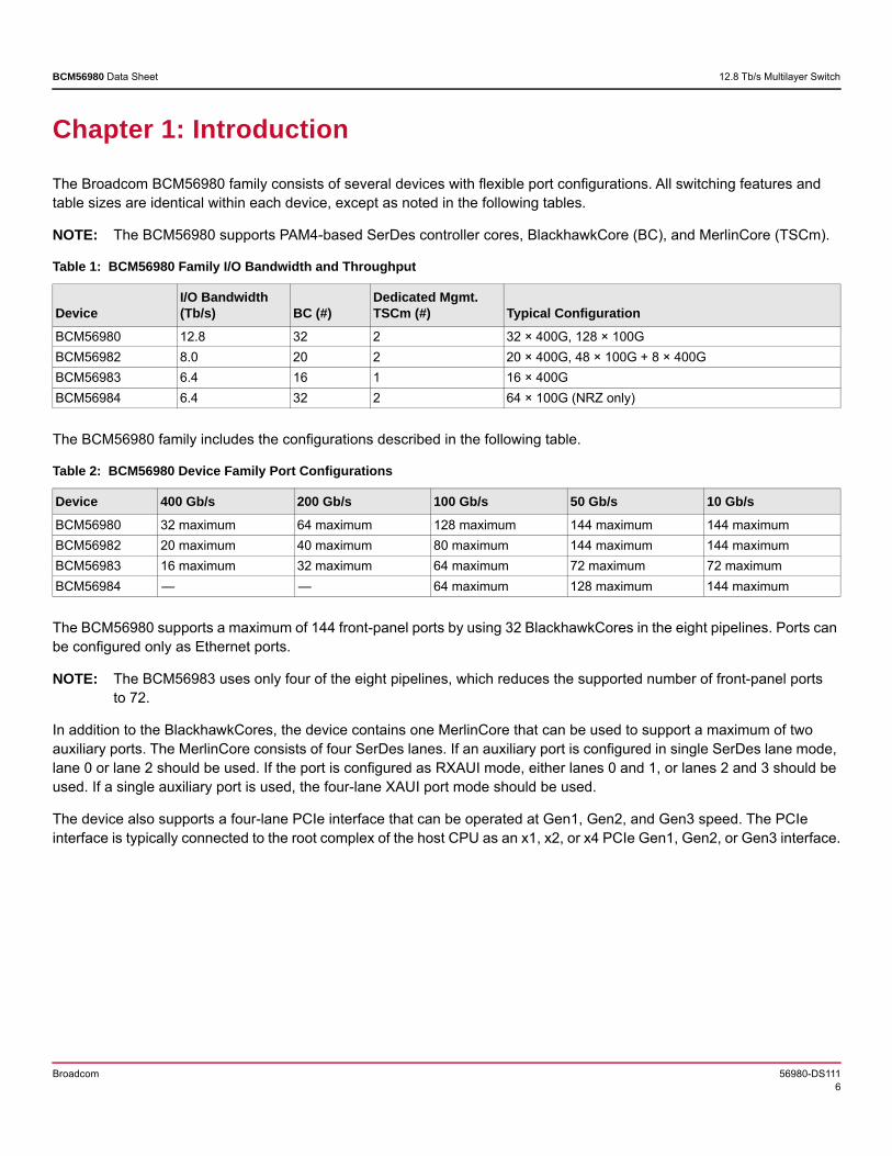
The Broadcom BCM56980 family consists of several devices with flexible port configurations. All switching features and table sizes are identical within each device, except as noted in the following tables.
NOTE: The BCM56980 supports PAM4-based SerDes controller cores, BlackhawkCore (BC), and MerlinCore (TSCm).
The BCM56980 family includes the configurations described in the following table.
The BCM56980 supports a maximum of 144 front-panel ports by using 32 BlackhawkCores in the eight pipelines. Ports can be configured only as Ethernet ports.
NOTE: The BCM56983 uses only four of the eight pipelines, which reduces the supported number of front-panel ports to 72.
In addition to the BlackhawkCores, the device contains one MerlinCore that can be used to support a maximum of two auxiliary ports. The MerlinCore consists of four SerDes lanes. If an auxiliary port is configured in single SerDes lane mode, lane 0 or lane 2 should be used. If the port is configured as RXAUI mode, either lanes 0 and 1, or lanes 2 and 3 should be used. If a single auxiliary port is used, the four-lane XAUI port mode should be used.
The device also supports a four-lane PCIe interface that can be operated at Gen1, Gen2, and Gen3 speed. The PCIe interface is typically connected to the root complex of the host CPU as an x1, x2, or x4 PCIe Gen1, Gen2, or Gen3 interface.
Table 1: BCM56980 Family I/O Bandwidth and Throughput
DeviceI/O Bandwidth (Tb/s) BC (#)
Dedicated Mgmt. TSCm (#) Typical Configuration
BCM56980 12.8 32 2 32 × 400G, 128 × 100GBCM56982 8.0 20 2 20 × 400G, 48 × 100G + 8 × 400GBCM56983 6.4 16 1 16 × 400GBCM56984 6.4 32 2 64 × 100G (NRZ only)
Table 2: BCM56980 Device Family Port Configurations
Device 400 Gb/s 200 Gb/s 100 Gb/s 50 Gb/s 10 Gb/sBCM56980 32 maximum 64 maximum 128 maximum 144 maximum 144 maximumBCM56982 20 maximum 40 maximum 80 maximum 144 maximum 144 maximumBCM56983 16 maximum 32 maximum 64 maximum 72 maximum 72 maximumBCM56984 — — 64 maximum 128 maximum 144 maximum
Broadcom 56980-DS1117
BCM56980 Data Sheet 12.8 Tb/s Multilayer Switch
Chapter 2: Device Overview
The BCM56980 has a modular, high-performance packet-switching architecture and provides the following benefits: Flexible port configurations Scalable throughput Scalable packet processing features Low pin-to-pin latency
2.1 Feature ListThe BCM56980 features are listed in the following table.
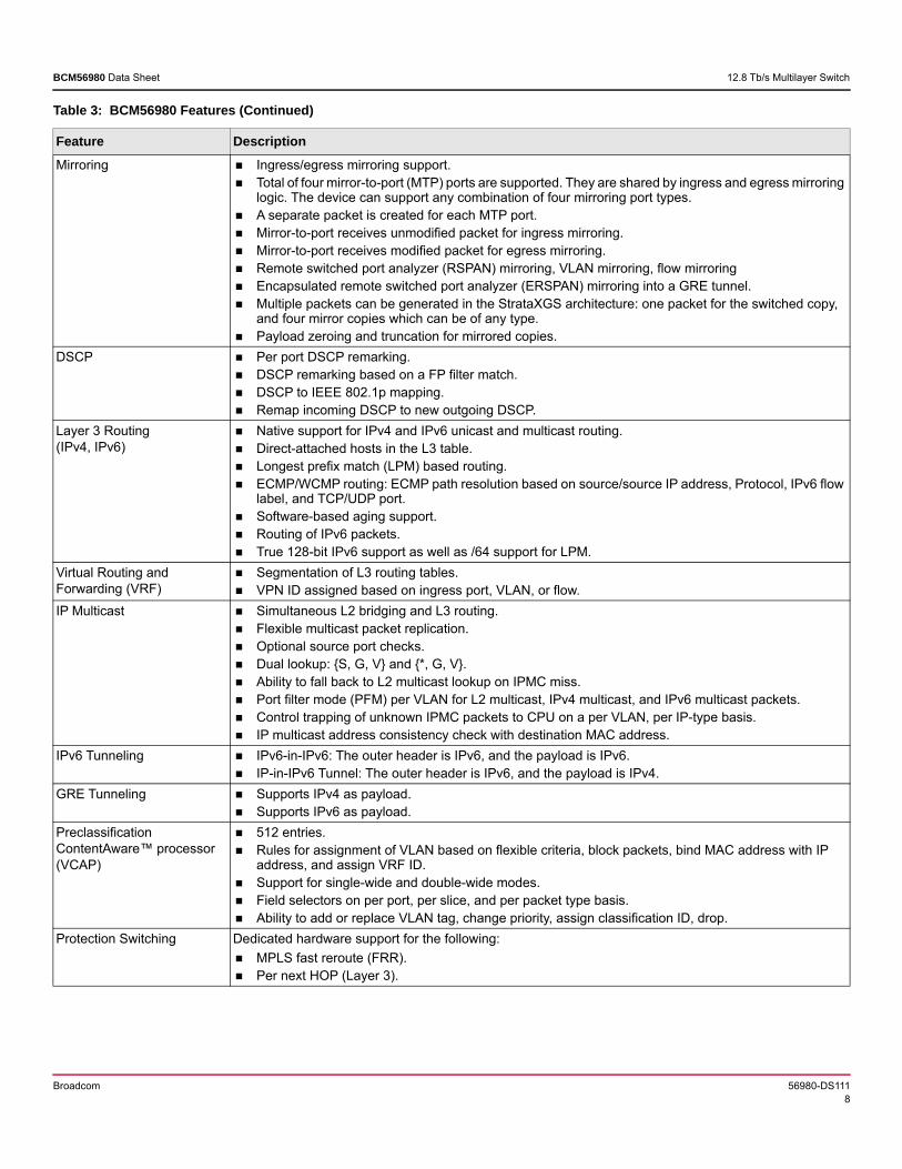
Table 3: BCM56980 Features
Feature DescriptionConfiguration 10/25/40/50/100/200/400GbE multilayer Ethernet switch.
All ports operate in oversubscription mode. Flexible SerDes contains eight SerDes lanes per BlackhawkCore, configured to operate in any of the
following configurations:– 25GbE (1-lane)– 40GbE (2-lane)– 40GbE (4-lane)– 50GbE (1-lane)– 50GbE (2-lane)– 100GbE (2-lane)– 100GbE (4-lane)– 200GbE (4-lane)– 400GbE (8-lane)
L2 Switching L2 learn cache for software based learning. Software-based MAC address aging. Supports Ethernet/IEEE 802.3 packet sizes (64 bytes to 1522 bytes) and jumbo packets up to
9416 bytes. Reserved MAC address table for CPU control packets, bridge protocol data units (BPDUs), and the
ability to perform shared VLAN switching.Switching Supports Ethernet/IEEE 802.3 packet sizes (64 bytes to 1522 bytes) and jumbo packets up to
9416 bytes.L2 Multicast Three port filtering modes (PFM) to control multicast packet behavior.VLAN Supports 4K VLANs.
Supports up to 128 VLAN profiles on a per VLAN basis.VLAN Assign VLAN for untagged and priority tagged packets based on the following:
– Port-based VLANs. Supports up to 128 VLAN profiles on a per VLAN basis. Ingress filtering for IEEE 802.1Q VLAN security.
Spanning Tree Group Table Indicates spanning tree state of each port for each spanning tree group.
Broadcom 56980-DS1118
BCM56980 Data Sheet 12.8 Tb/s Multilayer Switch
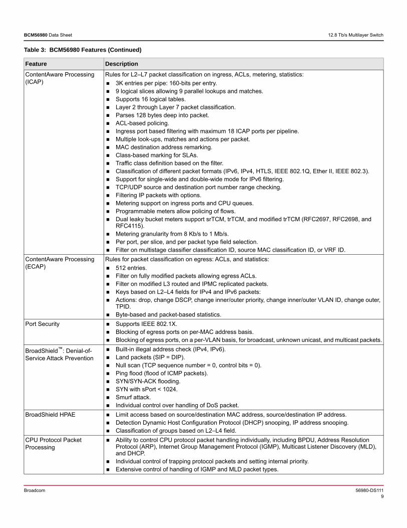
Mirroring Ingress/egress mirroring support. Total of four mirror-to-port (MTP) ports are supported. They are shared by ingress and egress mirroring
logic. The device can support any combination of four mirroring port types. A separate packet is created for each MTP port. Mirror-to-port receives unmodified packet for ingress mirroring. Mirror-to-port receives modified packet for egress mirroring. Remote switched port analyzer (RSPAN) mirroring, VLAN mirroring, flow mirroring Encapsulated remote switched port analyzer (ERSPAN) mirroring into a GRE tunnel. Multiple packets can be generated in the StrataXGS architecture: one packet for the switched copy,
and four mirror copies which can be of any type. Payload zeroing and truncation for mirrored copies.
DSCP Per port DSCP remarking. DSCP remarking based on a FP filter match. DSCP to IEEE 802.1p mapping. Remap incoming DSCP to new outgoing DSCP.
Layer 3 Routing (IPv4, IPv6)
Native support for IPv4 and IPv6 unicast and multicast routing. Direct-attached hosts in the L3 table. Longest prefix match (LPM) based routing. ECMP/WCMP routing: ECMP path resolution based on source/source IP address, Protocol, IPv6 flow
label, and TCP/UDP port. Software-based aging support. Routing of IPv6 packets. True 128-bit IPv6 support as well as /64 support for LPM.
Virtual Routing and Forwarding (VRF)
Segmentation of L3 routing tables. VPN ID assigned based on ingress port, VLAN, or flow.
IP Multicast Simultaneous L2 bridging and L3 routing. Flexible multicast packet replication. Optional source port checks. Dual lookup: S, G, V and *, G, V. Ability to fall back to L2 multicast lookup on IPMC miss. Port filter mode (PFM) per VLAN for L2 multicast, IPv4 multicast, and IPv6 multicast packets. Control trapping of unknown IPMC packets to CPU on a per VLAN, per IP-type basis. IP multicast address consistency check with destination MAC address.
IPv6 Tunneling IPv6-in-IPv6: The outer header is IPv6, and the payload is IPv6. IP-in-IPv6 Tunnel: The outer header is IPv6, and the payload is IPv4.
GRE Tunneling Supports IPv4 as payload. Supports IPv6 as payload.
Preclassification ContentAware™ processor (VCAP)
512 entries. Rules for assignment of VLAN based on flexible criteria, block packets, bind MAC address with IP
address, and assign VRF ID. Support for single-wide and double-wide modes. Field selectors on per port, per slice, and per packet type basis. Ability to add or replace VLAN tag, change priority, assign classification ID, drop.
Protection Switching Dedicated hardware support for the following: MPLS fast reroute (FRR). Per next HOP (Layer 3).
Table 3: BCM56980 Features (Continued)
Feature Description
Broadcom 56980-DS1119
BCM56980 Data Sheet 12.8 Tb/s Multilayer Switch
ContentAware Processing (ICAP)
Rules for L2–L7 packet classification on ingress, ACLs, metering, statistics: 3K entries per pipe: 160-bits per entry. 9 logical slices allowing 9 parallel lookups and matches. Supports 16 logical tables. Layer 2 through Layer 7 packet classification. Parses 128 bytes deep into packet. ACL-based policing. Ingress port based filtering with maximum 18 ICAP ports per pipeline. Multiple look-ups, matches and actions per packet. MAC destination address remarking. Class-based marking for SLAs. Traffic class definition based on the filter. Classification of different packet formats (IPv6, IPv4, HTLS, IEEE 802.1Q, Ether II, IEEE 802.3). Support for single-wide and double-wide mode for IPv6 filtering. TCP/UDP source and destination port number range checking. Filtering IP packets with options. Metering support on ingress ports and CPU queues. Programmable meters allow policing of flows. Dual leaky bucket meters support srTCM, trTCM, and modified trTCM (RFC2697, RFC2698, and
RFC4115). Metering granularity from 8 Kb/s to 1 Mb/s. Per port, per slice, and per packet type field selection. Filter on multistage classifier classification ID, source MAC classification ID, or VRF ID.
ContentAware Processing (ECAP)
Rules for packet classification on egress: ACLs, and statistics: 512 entries. Filter on fully modified packets allowing egress ACLs. Filter on modified L3 routed and IPMC replicated packets. Keys based on L2–L4 fields for IPv4 and IPv6 packets: Actions: drop, change DSCP, change inner/outer priority, change inner/outer VLAN ID, change outer,
TPID. Byte-based and packet-based statistics.
Port Security Supports IEEE 802.1X. Blocking of egress ports on per-MAC address basis. Blocking of egress ports, on a per-VLAN basis, for broadcast, unknown unicast, and multicast packets.
BroadShield™: Denial-of-Service Attack Prevention
Built-in illegal address check (IPv4, IPv6). Land packets (SIP = DIP). Null scan (TCP sequence number = 0, control bits = 0). Ping flood (flood of ICMP packets). SYN/SYN-ACK flooding. SYN with sPort < 1024. Smurf attack. Individual control over handling of DoS packet.
BroadShield HPAE Limit access based on source/destination MAC address, source/destination IP address. Detection Dynamic Host Configuration Protocol (DHCP) snooping, IP address snooping. Classification of groups based on L2–L4 field.
CPU Protocol Packet Processing
Ability to control CPU protocol packet handling individually, including BPDU, Address Resolution Protocol (ARP), Internet Group Management Protocol (IGMP), Multicast Listener Discovery (MLD), and DHCP.
Individual control of trapping protocol packets and setting internal priority. Extensive control of handling of IGMP and MLD packet types.
Table 3: BCM56980 Features (Continued)
Feature Description
Broadcom 56980-DS11110
BCM56980 Data Sheet 12.8 Tb/s Multilayer Switch
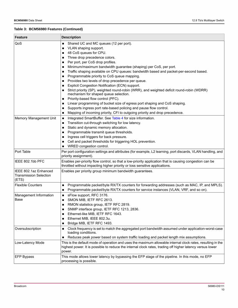
QoS Shared UC and MC queues (12 per port). VLAN shaping support. 48 CoS queues for CPU. Three drop precedence colors. Per port, per CoS drop profiles. Minimum/maximum bandwidth guarantee (shaping) per CoS, per port. Traffic shaping available on CPU queues: bandwidth based and packet-per-second based. Programmable priority to CoS queue mapping. Provides two levels of drop precedence per queue. Explicit Congestion Notification (ECN) support. Strict priority (SP), weighted round-robin (WRR), and weighted deficit round-robin (WDRR)
mechanism for shaped queue selection. Priority-based flow control (PFC). Linear programming of bucket size of egress port shaping and CoS shaping. Supports ingress port rate-based policing and pause flow control. Mapping of incoming priority, CFI to outgoing priority and drop precedence.
Memory Management Unit Integrated SmartBuffer. See Table 4 for size information. Transition cut-through switching for low latency. Static and dynamic memory allocation. Programmable transmit queue thresholds. Ingress cell triggers for back pressure. Cell and packet thresholds for triggering HOL prevention. WRED congestion control.
Port Table Per port configuration settings and attributes (for example, L2 learning, port discards, VLAN handling, and priority assignment).
IEEE 802.1bb PFC Enables per-priority flow control, so that a low-priority application that is causing congestion can be throttled without impacting higher priority or loss sensitive applications.
IEEE 802.1az Enhanced Transmission Selection (ETS)
Enables per priority group minimum bandwidth guarantees.
Flexible Counters Programmable packet/byte RX/TX counters for forwarding addresses (such as MAC, IP, and MPLS). Programmable packet/byte RX/TX counters for service instances (VLAN, VRF, and so on).
Management Information Base
sFlow support, RFC 3176. SMON MIB, IETF RFC 2613. RMON statistics group, IETF RFC 2819. SNMP interface group, IETF RFC 1213, 2836. Ethernet-like MIB, IETF RFC 1643. Ethernet MIB, IEEE 802.3u. Bridge MIB, IETF RFC 1493.
Oversubscription Clock frequency is set to match the aggregated port bandwidth assumed under application-worst-case loading conditions.
Reduces peak power based on system traffic loading and packet length mix assumptions.Low-Latency Mode This is the default mode of operation and uses the maximum allowable internal clock rates, resulting in the
highest power. It is possible to reduce the internal clock rates, trading off higher latency versus lower power.
EFP Bypass This mode allows lower latency by bypassing the EFP stage of the pipeline. In this mode, no EFP processing is possible.
Table 3: BCM56980 Features (Continued)
Feature Description
Broadcom 56980-DS11111
BCM56980 Data Sheet 12.8 Tb/s Multilayer Switch
IP Multicast Simultaneous L2 bridging and L3 routing. Flexible multicast packet replication. Optional source port checks. Dual lookup: S, G, V and *,G, V. PIM-SM, PIM-DM, and PIM-SSM (encapsulation). DVMRP on a per-VLAN basis. Reverse path forwarding checks. Ability to fall back to L2 multicast lookup on IPMC miss. Port filtering mode (PFM) per VLAN for L2 multicast, IPv4 multicast, and IPv6 multicast packets. Control trapping of unknown IPMC packets to CPU on a per VLAN, per IP-type basis. IP multicast address consistency check with destination MAC address.
Tunnel Encapsulation and Deencapsulation
Supports the following: IPv6 to IPv4. ISATAP. Configured tunnels. IP-IP (mobile-IP) tunnels. MPLS.
Network Time Sync Packet-based time synchronization (IEEE 1588 and IEEE 802.1AS): Integrated IEEE 1588 v2 processor for running PTP stack and clock recovery servo. One-step and two-step time stamping. High-precision frequency synthesizer. Synchronous Ethernet layer-one clock recovery.Precision Time Protocol (PTP): Transparent clock. Boundary clock.
Resilient Hashing Provide the same Resource Isolation attributes of consistent hashing. Minimize the imbalance among resources within the same resource group when adding/deleting load
balancing resources.Overtemperature Protection Supports real time temperature monitoring, and ability to set temperature for interrupt.Elephant Trap Identify and trap flows that transfer large amount of data based on user specified criteria.In-band Network Telemetry Supports insertion of meta-data in packets for identifying network faults and isolating their location,
transient failures, congestion information and latency. PSAMP Samples of packets from a network device, and the transmission of samples to a collector device, with
the appropriate meta-data.ECMP Group Dynamic Load Balancing with Flow Monitoring
Randomly sample packets undergoing DLB and Copy to CPU. Sample the packet to mirror or the CPU when macroflow assignment or re-assignment occurs.
Stacking/Chassis Supports HiGig3™ in transit mode only.
Table 3: BCM56980 Features (Continued)
Feature Description
Broadcom 56980-DS11112
BCM56980 Data Sheet 12.8 Tb/s Multilayer Switch
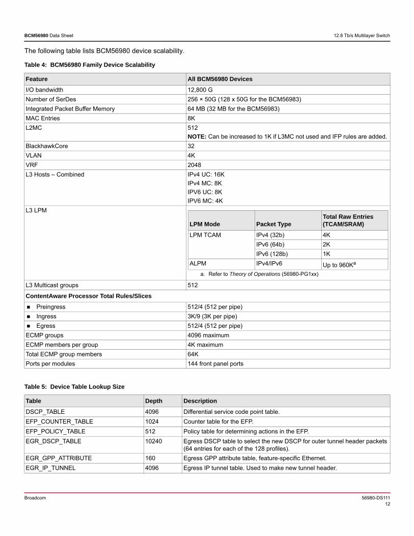
The following table lists BCM56980 device scalability.
Table 4: BCM56980 Family Device Scalability
Feature All BCM56980 DevicesI/O bandwidth 12,800 GNumber of SerDes 256 × 50G (128 x 50G for the BCM56983)Integrated Packet Buffer Memory 64 MB (32 MB for the BCM56983)MAC Entries 8KL2MC 512
NOTE: Can be increased to 1K if L3MC not used and IFP rules are added. BlackhawkCore 32VLAN 4KVRF 2048L3 Hosts – Combined IPv4 UC: 16K
IPv4 MC: 8KIPV6 UC: 8KIPV6 MC: 4K
L3 LPM
L3 Multicast groups 512
ContentAware Processor Total Rules/Slices Preingress 512/4 (512 per pipe) Ingress 3K/9 (3K per pipe) Egress 512/4 (512 per pipe)ECMP groups 4096 maximumECMP members per group 4K maximumTotal ECMP group members 64K Ports per modules 144 front panel ports
Table 5: Device Table Lookup Size
Table Depth DescriptionDSCP_TABLE 4096 Differential service code point table.EFP_COUNTER_TABLE 1024 Counter table for the EFP.EFP_POLICY_TABLE 512 Policy table for determining actions in the EFP.EGR_DSCP_TABLE 10240 Egress DSCP table to select the new DSCP for outer tunnel header packets
(64 entries for each of the 128 profiles).EGR_GPP_ATTRIBUTE 160 Egress GPP attribute table, feature-specific Ethernet.EGR_IP_TUNNEL 4096 Egress IP tunnel table. Used to make new tunnel header.
LPM Mode Packet TypeTotal Raw Entries (TCAM/SRAM)
LPM TCAM IPv4 (32b) 4KIPv6 (64b) 2KIPv6 (128b) 1K
ALPM IPv4/IPv6 Up to 960Ka
a. Refer to Theory of Operations (56980-PG1xx)
Broadcom 56980-DS11113
BCM56980 Data Sheet 12.8 Tb/s Multilayer Switch
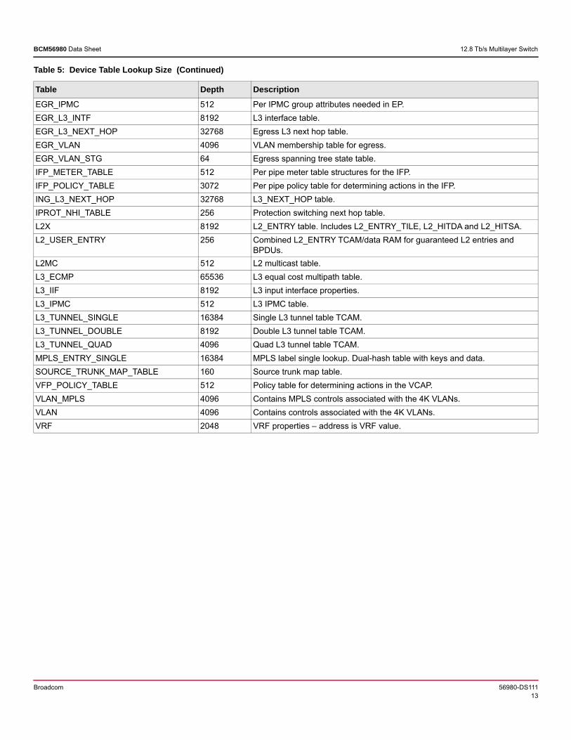
EGR_IPMC 512 Per IPMC group attributes needed in EP.EGR_L3_INTF 8192 L3 interface table.EGR_L3_NEXT_HOP 32768 Egress L3 next hop table.EGR_VLAN 4096 VLAN membership table for egress.EGR_VLAN_STG 64 Egress spanning tree state table.IFP_METER_TABLE 512 Per pipe meter table structures for the IFP.IFP_POLICY_TABLE 3072 Per pipe policy table for determining actions in the IFP.ING_L3_NEXT_HOP 32768 L3_NEXT_HOP table.IPROT_NHI_TABLE 256 Protection switching next hop table.L2X 8192 L2_ENTRY table. Includes L2_ENTRY_TILE, L2_HITDA and L2_HITSA.L2_USER_ENTRY 256 Combined L2_ENTRY TCAM/data RAM for guaranteed L2 entries and
BPDUs.L2MC 512 L2 multicast table.L3_ECMP 65536 L3 equal cost multipath table.L3_IIF 8192 L3 input interface properties.L3_IPMC 512 L3 IPMC table.L3_TUNNEL_SINGLE 16384 Single L3 tunnel table TCAM.L3_TUNNEL_DOUBLE 8192 Double L3 tunnel table TCAM.L3_TUNNEL_QUAD 4096 Quad L3 tunnel table TCAM.MPLS_ENTRY_SINGLE 16384 MPLS label single lookup. Dual-hash table with keys and data.SOURCE_TRUNK_MAP_TABLE 160 Source trunk map table.VFP_POLICY_TABLE 512 Policy table for determining actions in the VCAP.VLAN_MPLS 4096 Contains MPLS controls associated with the 4K VLANs.VLAN 4096 Contains controls associated with the 4K VLANs.VRF 2048 VRF properties – address is VRF value.
Table 5: Device Table Lookup Size (Continued)
Table Depth Description
Broadcom 56980-DS11114
BCM56980 Data Sheet 12.8 Tb/s Multilayer Switch
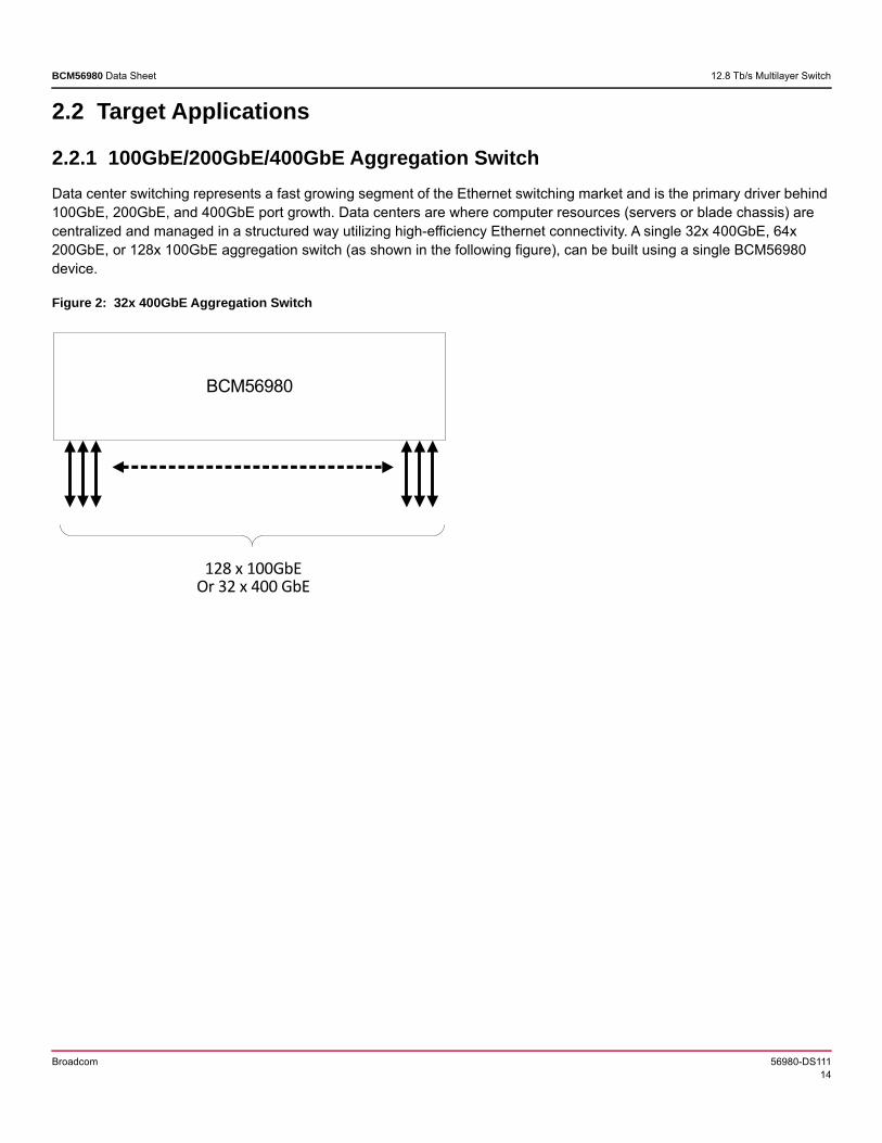
2.2 Target Applications
2.2.1 100GbE/200GbE/400GbE Aggregation SwitchData center switching represents a fast growing segment of the Ethernet switching market and is the primary driver behind 100GbE, 200GbE, and 400GbE port growth. Data centers are where computer resources (servers or blade chassis) are centralized and managed in a structured way utilizing high-efficiency Ethernet connectivity. A single 32x 400GbE, 64x 200GbE, or 128x 100GbE aggregation switch (as shown in the following figure), can be built using a single BCM56980 device.
Figure 2: 32x 400GbE Aggregation Switch
128 x 100GbEOr 32 x 400 GbE
BCM56980
Broadcom 56980-DS11115
BCM56980 Data Sheet 12.8 Tb/s Multilayer Switch
Chapter 3: System Interfaces
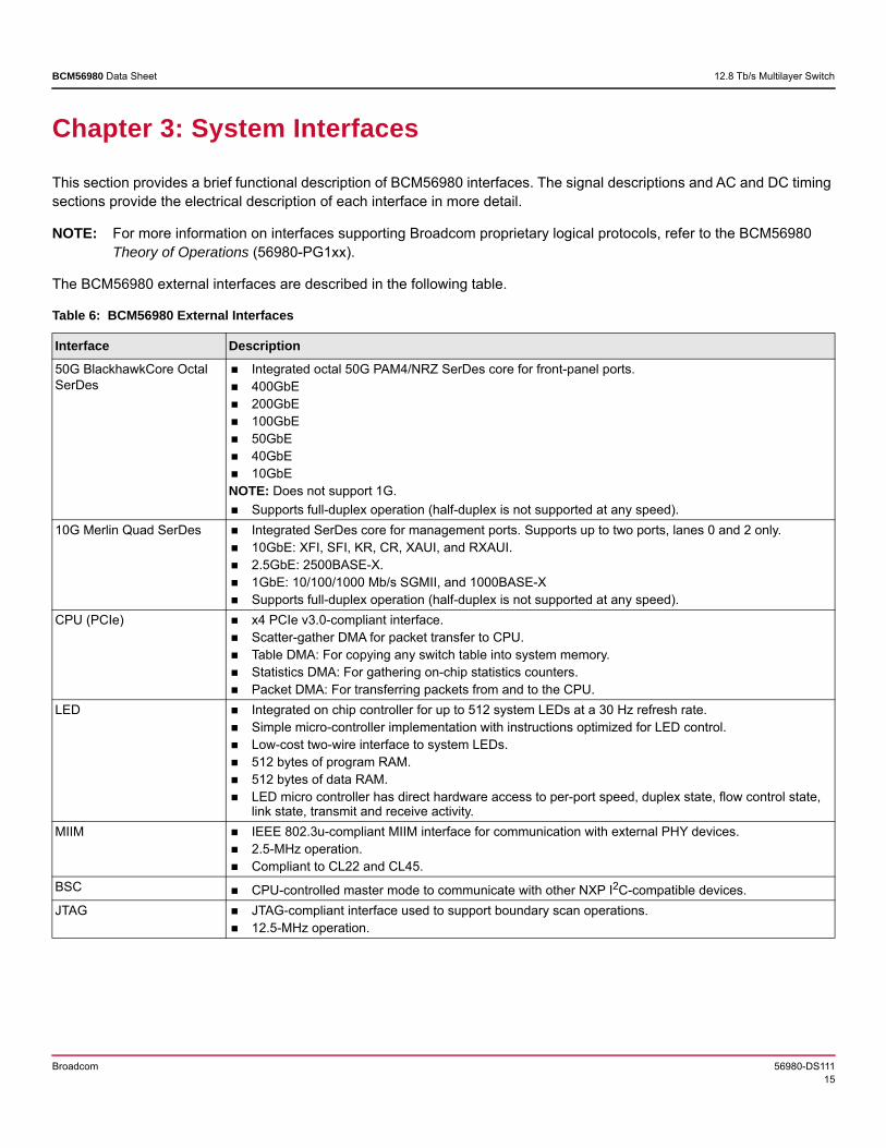
This section provides a brief functional description of BCM56980 interfaces. The signal descriptions and AC and DC timing sections provide the electrical description of each interface in more detail.
NOTE: For more information on interfaces supporting Broadcom proprietary logical protocols, refer to the BCM56980 Theory of Operations (56980-PG1xx).
The BCM56980 external interfaces are described in the following table.
Table 6: BCM56980 External Interfaces
Interface Description50G BlackhawkCore Octal SerDes
Integrated octal 50G PAM4/NRZ SerDes core for front-panel ports. 400GbE 200GbE 100GbE 50GbE 40GbE 10GbENOTE: Does not support 1G. Supports full-duplex operation (half-duplex is not supported at any speed).
10G Merlin Quad SerDes Integrated SerDes core for management ports. Supports up to two ports, lanes 0 and 2 only. 10GbE: XFI, SFI, KR, CR, XAUI, and RXAUI. 2.5GbE: 2500BASE-X. 1GbE: 10/100/1000 Mb/s SGMII, and 1000BASE-X Supports full-duplex operation (half-duplex is not supported at any speed).
CPU (PCIe) x4 PCIe v3.0-compliant interface. Scatter-gather DMA for packet transfer to CPU. Table DMA: For copying any switch table into system memory. Statistics DMA: For gathering on-chip statistics counters. Packet DMA: For transferring packets from and to the CPU.
LED Integrated on chip controller for up to 512 system LEDs at a 30 Hz refresh rate. Simple micro-controller implementation with instructions optimized for LED control. Low-cost two-wire interface to system LEDs. 512 bytes of program RAM. 512 bytes of data RAM. LED micro controller has direct hardware access to per-port speed, duplex state, flow control state,
link state, transmit and receive activity.MIIM IEEE 802.3u-compliant MIIM interface for communication with external PHY devices.
2.5-MHz operation. Compliant to CL22 and CL45.
BSC CPU-controlled master mode to communicate with other NXP I2C-compatible devices.JTAG JTAG-compliant interface used to support boundary scan operations.
12.5-MHz operation.
Broadcom 56980-DS11116
BCM56980 Data Sheet 12.8 Tb/s Multilayer Switch
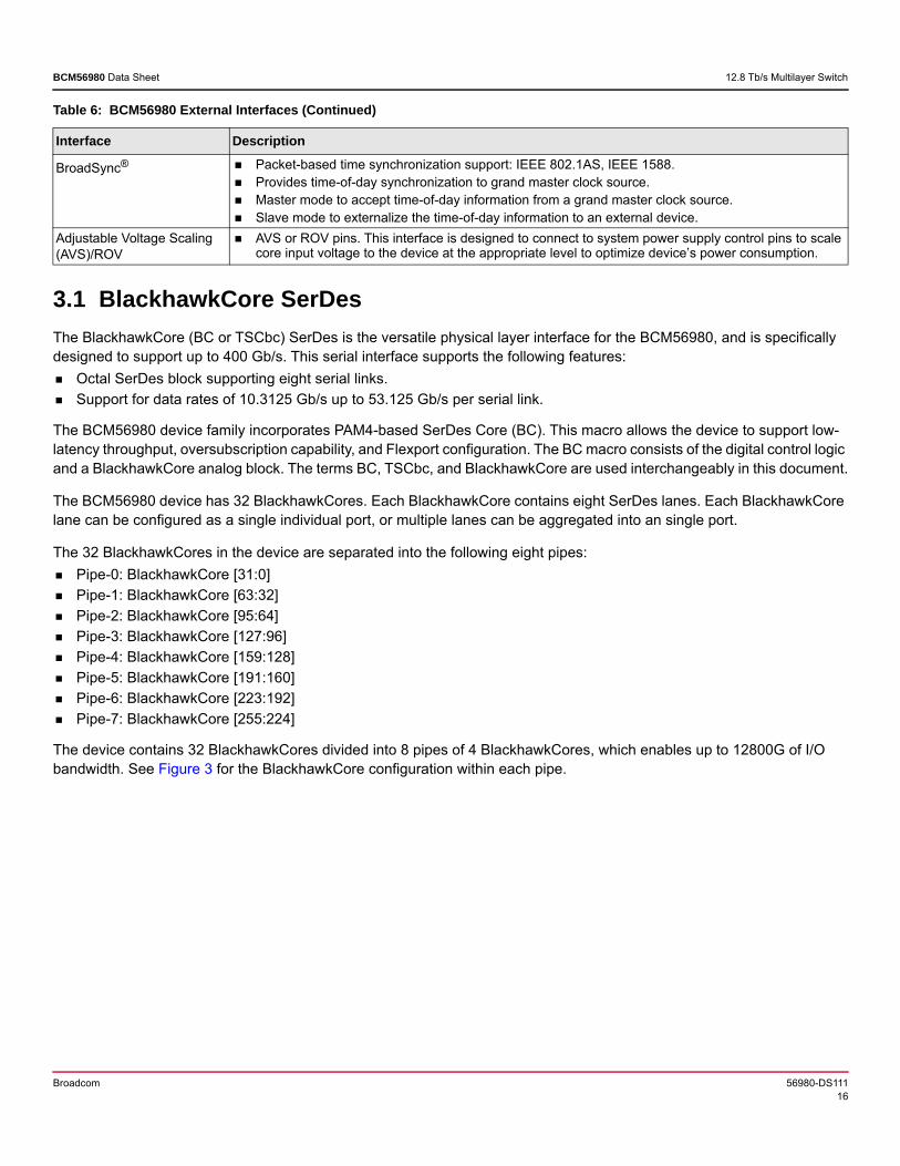
3.1 BlackhawkCore SerDesThe BlackhawkCore (BC or TSCbc) SerDes is the versatile physical layer interface for the BCM56980, and is specifically designed to support up to 400 Gb/s. This serial interface supports the following features: Octal SerDes block supporting eight serial links. Support for data rates of 10.3125 Gb/s up to 53.125 Gb/s per serial link.
The BCM56980 device family incorporates PAM4-based SerDes Core (BC). This macro allows the device to support low-latency throughput, oversubscription capability, and Flexport configuration. The BC macro consists of the digital control logic and a BlackhawkCore analog block. The terms BC, TSCbc, and BlackhawkCore are used interchangeably in this document.
The BCM56980 device has 32 BlackhawkCores. Each BlackhawkCore contains eight SerDes lanes. Each BlackhawkCore lane can be configured as a single individual port, or multiple lanes can be aggregated into an single port.
The 32 BlackhawkCores in the device are separated into the following eight pipes: Pipe-0: BlackhawkCore [31:0] Pipe-1: BlackhawkCore [63:32] Pipe-2: BlackhawkCore [95:64] Pipe-3: BlackhawkCore [127:96] Pipe-4: BlackhawkCore [159:128] Pipe-5: BlackhawkCore [191:160] Pipe-6: BlackhawkCore [223:192] Pipe-7: BlackhawkCore [255:224]
The device contains 32 BlackhawkCores divided into 8 pipes of 4 BlackhawkCores, which enables up to 12800G of I/O bandwidth. See Figure 3 for the BlackhawkCore configuration within each pipe.
BroadSync® Packet-based time synchronization support: IEEE 802.1AS, IEEE 1588. Provides time-of-day synchronization to grand master clock source. Master mode to accept time-of-day information from a grand master clock source. Slave mode to externalize the time-of-day information to an external device.
Adjustable Voltage Scaling (AVS)/ROV
AVS or ROV pins. This interface is designed to connect to system power supply control pins to scale core input voltage to the device at the appropriate level to optimize device’s power consumption.
Table 6: BCM56980 External Interfaces (Continued)
Interface Description
Broadcom 56980-DS11117
BCM56980 Data Sheet 12.8 Tb/s Multilayer Switch
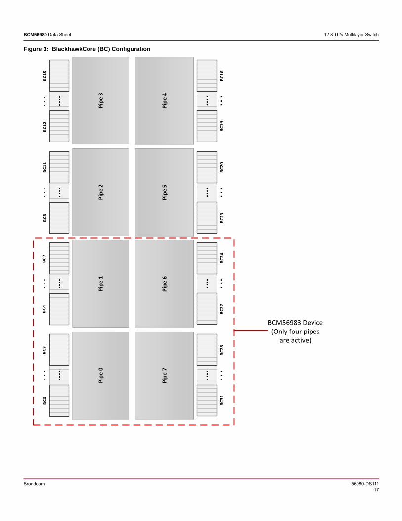
Figure 3: BlackhawkCore (BC) Configuration
Broadcom 56980-DS11118
BCM56980 Data Sheet 12.8 Tb/s Multilayer Switch
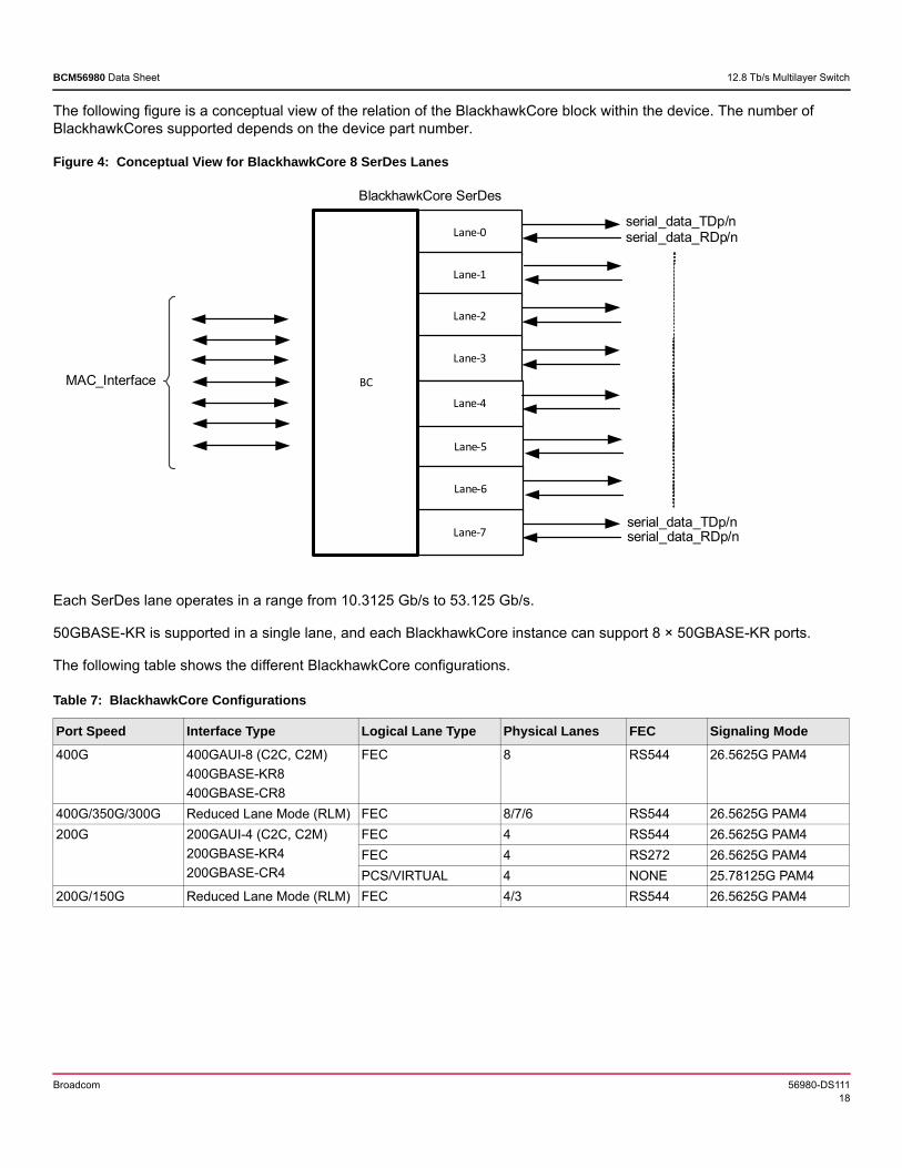
The following figure is a conceptual view of the relation of the BlackhawkCore block within the device. The number of BlackhawkCores supported depends on the device part number.
Figure 4: Conceptual View for BlackhawkCore 8 SerDes Lanes
Each SerDes lane operates in a range from 10.3125 Gb/s to 53.125 Gb/s.
50GBASE-KR is supported in a single lane, and each BlackhawkCore instance can support 8 × 50GBASE-KR ports.
The following table shows the different BlackhawkCore configurations.
Table 7: BlackhawkCore Configurations
Port Speed Interface Type Logical Lane Type Physical Lanes FEC Signaling Mode400G 400GAUI-8 (C2C, C2M)
400GBASE-KR8400GBASE-CR8
FEC 8 RS544 26.5625G PAM4
400G/350G/300G Reduced Lane Mode (RLM) FEC 8/7/6 RS544 26.5625G PAM4200G 200GAUI-4 (C2C, C2M)
200GBASE-KR4200GBASE-CR4
FEC 4 RS544 26.5625G PAM4 FEC 4 RS272 26.5625G PAM4 PCS/VIRTUAL 4 NONE 25.78125G PAM4
200G/150G Reduced Lane Mode (RLM) FEC 4/3 RS544 26.5625G PAM4
MAC_Interface
BlackhawkCore SerDes
Lane‐0
Lane‐1
Lane‐2
Lane‐3
serial_data_TDp/nserial_data_RDp/n
serial_data_TDp/nserial_data_RDp/n
Lane‐5
Lane‐6
Lane‐7
Lane‐4
BC
Broadcom 56980-DS11119
BCM56980 Data Sheet 12.8 Tb/s Multilayer Switch
100G 100GAUI-2 (C2C, C2M)100GBASE-KR2100GBASE-CR2
FEC 2 RS544 26.5625G PAM4 FEC 2 RS272 26.5625G PAM4 PCS/Virtual 2 NONE 25.78125G PAM4 FEC 2 RS528 25.78125G PAM4
100GAUI-4 (C2C, C2M)100GBASE-KR4100GBASE-CR4
FEC 4 RS544 26.5625G NRZ FEC 4 RS528 25.78125G NRZ PCS/VIRTUAL 4 NONE 25.78125G NRZ
50G 50GAUI-1 (C2C, C2M)50GBASE-CR50GBASE-KR
FEC 1 RS544 26.5625G PAM4 FEC 1 RS272 26.5625G PAM4 FEC 1 RS528 25.78125G PAM4
LAUI-2 (C2C, C2M)50GAUI-2 (C2C, C2M)50GBASE-KR250GBASE-CR2
FEC 2 RS544 26.5625G NRZ FEC 2 RS528 25.78125G NRZ PCS/VIRTUAL 2 NONE 25.78125G NRZ
40G XLAUIXLPPI40GBASE-CR440GBASE-KR4
PCS/VIRTUAL 4 BASE-R 10.3125G NRZ PCS/VIRTUAL 4 NONE 10.3125G NRZ
XLAUI2 PCS/VIRTUAL 2 NONE 20.625G NRZ25G 25GAUI (C2C, C2M)
25GBASE-C25GBASE-CR-S25GBASE-CR25GBASE-KR
FEC 1 RS528 25.78125G NRZ PCS/VIRTUAL 1 BASE-R 25.78125G NRZ PCS/VIRTUAL 1 NONE 25.78125G NRZ
10G 10G-KRSFIXFI
PCS/VIRTUAL 1 BASE-R 10.3125G NRZ PCS/VIRTUAL 1 NONE 10.3125G NRZ
NOTE: The lane-swapping mode is configurable.For PAM4 modes without FEC (single lane 50G, dual lane 100G, 200G) or using RS528 FEC (single lane 50G, dual lane 100G), the lane speed is 51.5625G.RS272 FEC is a Broadcom proprietary protocol to achieve lower latency. When operating in RS272, all ports within the upper- or lower-half four lanes of a BlackhawkCore must operate at the same FEC (RS272). For example, in a 2 × 100G configuration (each 100G port is 2 × 50G), one 100G port cannot operate at RS544 FEC while the other operates at RS272 FEC.NOTE: The BCM56980 supports simultaneous operation of all seven port speeds (also called speed modes) listed in this table across various ports of the chip. However, within a single BlackhawkCore, there are restrictions on which port modes can coexist. For more information, refer to the BCM56980 Hardware Design Guide (56980-DG1xx).
Table 7: BlackhawkCore Configurations (Continued)
Port Speed Interface Type Logical Lane Type Physical Lanes FEC Signaling Mode
Broadcom 56980-DS11120
BCM56980 Data Sheet 12.8 Tb/s Multilayer Switch
3.2 BlackhawkCore Octal SerDes Configuration GuidelinesEach device has up to 32 BlackhawkCores, depending on the device part number. The BlackhawkCores are organized into eight pipes. None of the eight pipes can exceed 1/8 of the total switching throughput. In configurations where not all ports are active, bandwidth should be balanced across all eight pipelines.
A physical port consists of one or more SerDes lane in the device. There are up to 32 BlackhawkCores, each with eight physical SerDes lanes. A logical port is defined as a front-panel, CPU, or loopback port. The total number of logical ports per device is 160. Out of 160, up to 144 ports, excluding the management port, can be assigned as front-panel ports. The rest are used as CPU and internal loopback ports.
NOTE: The BCM56983 device supports 72 front-panel ports because only four pipes are active. Each pipe supports up to 18 general ports.
Physical-port to logical-port numbering limitations exist across pipes that are integrated into the SDK software.
3.2.1 Flexport ConfigurationThe BlackhawkCore supports the ability to change a port configuration (speed and number of lanes per port) at runtime without affecting the operation of the other ports or requiring the device to be reset. If the SerDes continue to be associated with the same logical ports, then the Flexport configuration amounts to a speed change and can be handled automatically by the BlackhawkCore driver. Logical ports can be added, removed, or associated with a different number of SerDes through user API calls. The configuration of two SerDes within a BlackhawkCore can be changed without affecting the ports) using the remaining SerDes.
Two PLLs are in a BlackhawkCore: PLL0 (secondary) and PLL1 (primary). Each of the two PLLs can generate one of the three basic port frequencies: 10G-NRZ (20.625 GHz), 25G-NRZ (25.78125 GHz), or 50G-PAM4 (26.5625 GHz). The SDK software sets the primary PLL frequency after collecting all available port speeds allocated within a BlackhawkCore. Changing the secondary VCO without a reset is allowed if no other port in the BlackhawkCore is using the secondary VCO. However, changing the primary VCO requires a BlackhawkCore reset.
3.3 10G Quad MerlinCore SerDesThe MerlinCore SerDes is the management-port physical-layer interface for the BCM56980 specifically designed to support up to two 10 Gb/s management ports on the single MerlinCore. This serial interface supports the following features: The MerlinCore SerDes has four serial links and can support the following:
– Two ports in single-lane mode.– Two ports in RXAUI mode.– One port in XAUI mode.
Single-lane mode supports 1000BASE-x, SGMII, 2500BASE-X, SFI, XFI, or 10GBASE-KR. Two-lane mode supports RXAUI. Four-lane mode supports XAUI. There is no support for mixing a two-lane and a four-lane port with any other port type. All single-lane port types can be mixed.
NOTE: When a 2500BASE-X port is mixed with a SFI, XFI, or 10GBASE-KR port, the transmit jitter on the 2500BASE-X port violates the IEEE specification.
Broadcom 56980-DS11121
BCM56980 Data Sheet 12.8 Tb/s Multilayer Switch
3.4 PCIeThe PCIe interface provided by the BCM56980 switch conforms to the PCIe Gen3 specification and supports Gen1 and Gen2. The BCM56980 PCIe interface supports x1, x2, or x4 wide connections (8.0G link speed or 7.88 Gb/s data rate in each direction). No external glue logic is required to support this interface. The protocols and electrical requirements of the PCIe specifications are strictly implemented.
The device provides strap signals to limit the maximum link speed and link width of the PCIe interface. The internal pulls on the strap signals cause the device to default to allowing a maximum link width of x4 and PCIe Gen3 link speeds.
For all PCIe speeds, the design requires QSPI flash memory programmed with Broadcom-provided firmware to be connected to the IP_QSPI interface on the device, and the device must be strapped to perform a download from this memory. This is required because the firmware configures the PCIe interface into a mode that is functional and compliant to the Gen3 specification. The exact strap settings and design requirements are as follows: BOOT_DEV[2:0] = 3’b000 MHOST0_BOOT_DEV = 1’b1 PCIE_FORCE_GENTYPE[1:0] = 2’b00 QSPI flash memory is programmed with Broadcom provided firmware QSPI flash memory is connected to IP_QSPI interface
NOTE: Design requirements include a QSPI flash memory that contains the Broadcom-provided PCIe firmware for all PCIe operating modes.The device must also be strapped to download and execute the code from this flash memory for the PCIe interface to be functional.
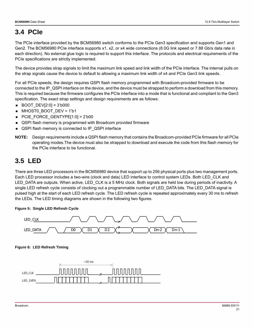
3.5 LEDThere are three LED processors in the BCM56980 device that support up to 256 physical ports plus two management ports. Each LED processor includes a two-wire (clock and data) LED interface to control system LEDs. Both LED_CLK and LED_DATA are outputs. When active, LED_CLK is a 5 MHz clock. Both signals are held low during periods of inactivity. A single LED refresh cycle consists of clocking out a programmable number of LED_DATA bits. The LED_DATA signal is pulsed high at the start of each LED refresh cycle. The LED refresh cycle is repeated approximately every 30 ms to refresh the LEDs. The LED timing diagrams are shown in the following two figures.
Figure 5: Single LED Refresh Cycle
Figure 6: LED Refresh Timing
D0 D1 D2 Dn-1Dn-2
LED_CLK
LED_DATA
~30 ms
LED_CLK
LED_DATA
Broadcom 56980-DS11122
BCM56980 Data Sheet 12.8 Tb/s Multilayer Switch
3.6 MIIMThe CPU Management Interface Controller (CMIC) supports the IEEE 802.3u standard MIIM interface: a two-wire serial bus controlled by the CMIC that allows register access to all the PHYs in the system. Data from the PHY can be read/write using this interface. The two signals for MIIM are MDC (clock) and MDIO (bidirectional data). The CPU uses this interface to program the internal and external PHY registers. The MIIM interface can be configured to support Clause 45.
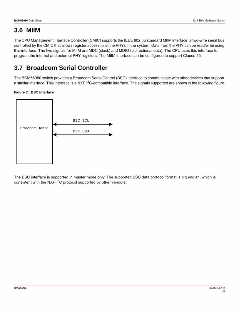
3.7 Broadcom Serial ControllerThe BCM56980 switch provides a Broadcom Serial Control (BSC) interface to communicate with other devices that support a similar interface. This interface is a NXP I2C-compatible interface. The signals supported are shown in the following figure.
Figure 7: BSC Interface
The BSC interface is supported in master mode only. The supported BSC data protocol format is big endian, which is consistent with the NXP I2C protocol supported by other vendors.
BSC_SCL
BSC_SDABroadcom Device
Broadcom 56980-DS11123
BCM56980 Data Sheet 12.8 Tb/s Multilayer Switch
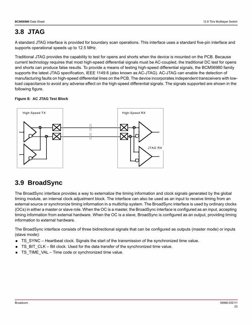
3.8 JTAGA standard JTAG interface is provided for boundary scan operations. This interface uses a standard five-pin interface and supports operational speeds up to 12.5 MHz.
Traditional JTAG provides the capability to test for opens and shorts when the device is mounted on the PCB. Because current technology requires that most high-speed differential signals must be AC-coupled, the traditional DC test for opens and shorts can produce false results. To provide a means of testing high-speed differential signals, the BCM56980 family supports the latest JTAG specification, IEEE 1149.6 (also known as AC-JTAG). AC-JTAG can enable the detection of manufacturing faults on high-speed differential lines on the PCB. The device incorporates independent transceivers with low-load capacitance to avoid any adverse effect on the high-speed differential signals. The signals supported are shown in the following figure.
Figure 8: AC JTAG Test Block
3.9 BroadSyncThe BroadSync interface provides a way to externalize the timing information and clock signals generated by the global timing module, an internal clock adjustment block. The interface can also be used as an input to receive timing from an external source or synchronize timing information in a multichip system. The BroadSync interface is used by ordinary clocks (OCs) in either a master or slave role. When the OC is a master, the BroadSync interface is configured as an input, accepting timing information from external hardware. When the OC is a slave, BroadSync is configured as an output, providing timing information to external hardware.
The BroadSync interface consists of three bidirectional signals that can be configured as outputs (master mode) or inputs (slave mode): TS_SYNC – Heartbeat clock. Signals the start of the transmission of the synchronized time value. TS_BIT_CLK – Bit clock. Used for the data transfer of the synchronized time value. TS_TIME_VAL – Time code or synchronized time value.
H igh_Speed T x High_Speed Rx
JTAG Rx
High-Speed TX High-Speed RX
JTAG RX
Broadcom 56980-DS11124
BCM56980 Data Sheet 12.8 Tb/s Multilayer Switch
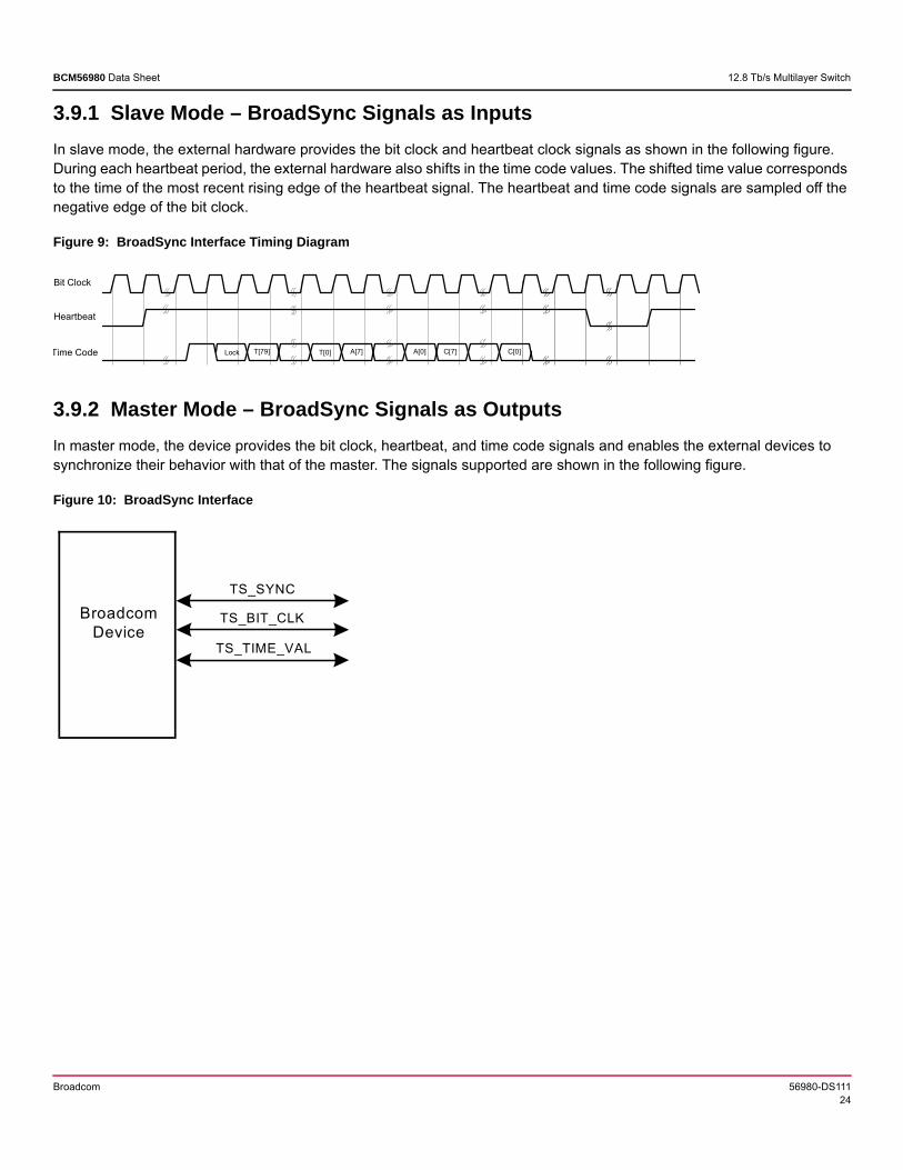
3.9.1 Slave Mode – BroadSync Signals as InputsIn slave mode, the external hardware provides the bit clock and heartbeat clock signals as shown in the following figure. During each heartbeat period, the external hardware also shifts in the time code values. The shifted time value corresponds to the time of the most recent rising edge of the heartbeat signal. The heartbeat and time code signals are sampled off the negative edge of the bit clock.
Figure 9: BroadSync Interface Timing Diagram
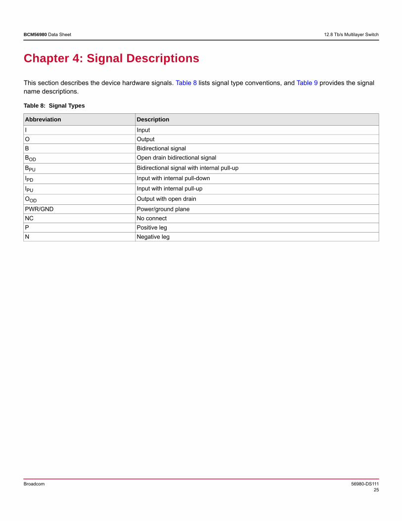
3.9.2 Master Mode – BroadSync Signals as OutputsIn master mode, the device provides the bit clock, heartbeat, and time code signals and enables the external devices to synchronize their behavior with that of the master. The signals supported are shown in the following figure.
Figure 10: BroadSync Interface
Bit Clock
Heartbeat
Time Code Lock T[79] T[0] A[7] A[0] C[7] C[0]
TS_SYNC
TS_BIT_CLK
TS_TIME_VAL
Broadcom Device
Broadcom 56980-DS11125
BCM56980 Data Sheet 12.8 Tb/s Multilayer Switch
Chapter 4: Signal Descriptions
This section describes the device hardware signals. Table 8 lists signal type conventions, and Table 9 provides the signal name descriptions.
Table 8: Signal Types
Abbreviation DescriptionI InputO OutputB Bidirectional signalBOD Open drain bidirectional signal
BPU Bidirectional signal with internal pull-up
IPD Input with internal pull-down
IPU Input with internal pull-up
OOD Output with open drain
PWR/GND Power/ground planeNC No connectP Positive legN Negative leg
Broadcom 56980-DS11126
BCM56980 Data Sheet 12.8 Tb/s Multilayer Switch
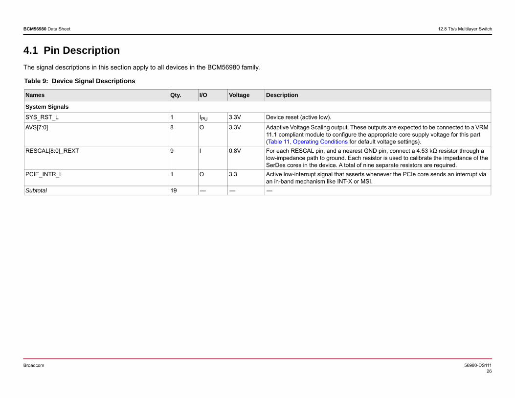
4.1 Pin DescriptionThe signal descriptions in this section apply to all devices in the BCM56980 family.
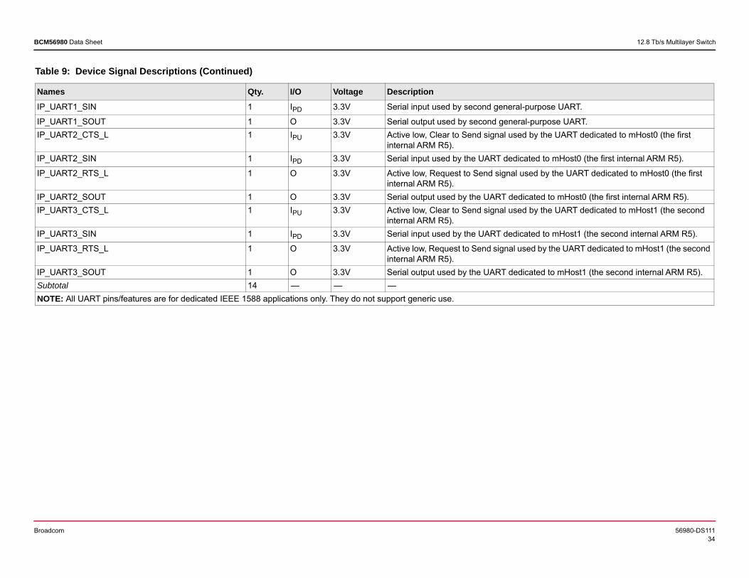
Table 9: Device Signal Descriptions
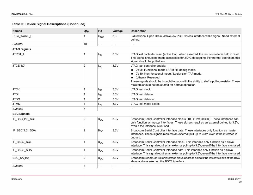
Names Qty. I/O Voltage Description
System SignalsSYS_RST_L 1 IPU 3.3V Device reset (active low).
AVS[7:0] 8 O 3.3V Adaptive Voltage Scaling output. These outputs are expected to be connected to a VRM 11.1 compliant module to configure the appropriate core supply voltage for this part (Table 11, Operating Conditions for default voltage settings).
RESCAL[8:0]_REXT 9 I 0.8V For each RESCAL pin, and a nearest GND pin, connect a 4.53 kΩ resistor through a low-impedance path to ground. Each resistor is used to calibrate the impedance of the SerDes cores in the device. A total of nine separate resistors are required.
PCIE_INTR_L 1 O 3.3 Active low-interrupt signal that asserts whenever the PCIe core sends an interrupt via an in-band mechanism like INT-X or MSI.
Subtotal 19 — — —
Broadcom 56980-DS11127
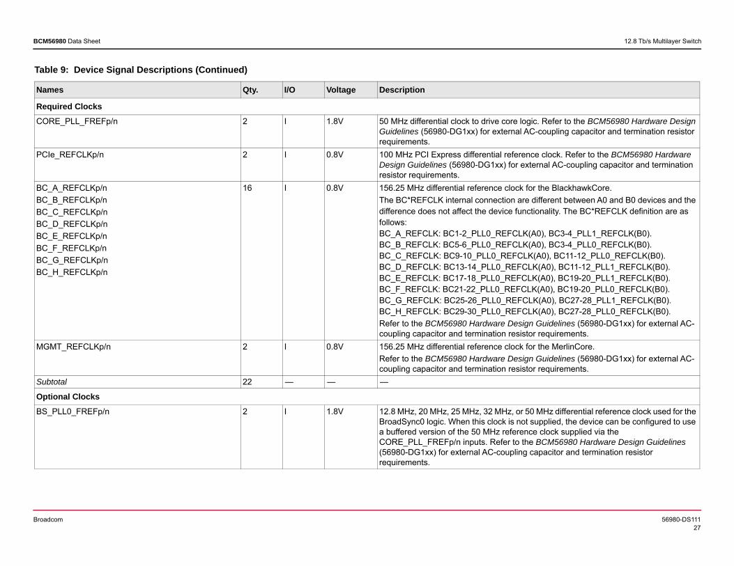
BCM56980 Data Sheet 12.8 Tb/s Multilayer Switch
Required ClocksCORE_PLL_FREFp/n 2 I 1.8V 50 MHz differential clock to drive core logic. Refer to the BCM56980 Hardware Design
Guidelines (56980-DG1xx) for external AC-coupling capacitor and termination resistor requirements.
PCIe_REFCLKp/n 2 I 0.8V 100 MHz PCI Express differential reference clock. Refer to the BCM56980 Hardware Design Guidelines (56980-DG1xx) for external AC-coupling capacitor and termination resistor requirements.
BC_A_REFCLKp/nBC_B_REFCLKp/nBC_C_REFCLKp/nBC_D_REFCLKp/nBC_E_REFCLKp/nBC_F_REFCLKp/nBC_G_REFCLKp/nBC_H_REFCLKp/n
16 I 0.8V 156.25 MHz differential reference clock for the BlackhawkCore.The BC*REFCLK internal connection are different between A0 and B0 devices and the difference does not affect the device functionality. The BC*REFCLK definition are as follows:BC_A_REFCLK: BC1-2_PLL0_REFCLK(A0), BC3-4_PLL1_REFCLK(B0).BC_B_REFCLK: BC5-6_PLL0_REFCLK(A0), BC3-4_PLL0_REFCLK(B0).BC_C_REFCLK: BC9-10_PLL0_REFCLK(A0), BC11-12_PLL0_REFCLK(B0).BC_D_REFCLK: BC13-14_PLL0_REFCLK(A0), BC11-12_PLL1_REFCLK(B0).BC_E_REFCLK: BC17-18_PLL0_REFCLK(A0), BC19-20_PLL1_REFCLK(B0).BC_F_REFCLK: BC21-22_PLL0_REFCLK(A0), BC19-20_PLL0_REFCLK(B0).BC_G_REFCLK: BC25-26_PLL0_REFCLK(A0), BC27-28_PLL1_REFCLK(B0).BC_H_REFCLK: BC29-30_PLL0_REFCLK(A0), BC27-28_PLL0_REFCLK(B0).Refer to the BCM56980 Hardware Design Guidelines (56980-DG1xx) for external AC-coupling capacitor and termination resistor requirements.
MGMT_REFCLKp/n 2 I 0.8V 156.25 MHz differential reference clock for the MerlinCore.Refer to the BCM56980 Hardware Design Guidelines (56980-DG1xx) for external AC-coupling capacitor and termination resistor requirements.
Subtotal 22 — — —
Optional ClocksBS_PLL0_FREFp/n 2 I 1.8V 12.8 MHz, 20 MHz, 25 MHz, 32 MHz, or 50 MHz differential reference clock used for the
BroadSync0 logic. When this clock is not supplied, the device can be configured to use a buffered version of the 50 MHz reference clock supplied via the CORE_PLL_FREFp/n inputs. Refer to the BCM56980 Hardware Design Guidelines (56980-DG1xx) for external AC-coupling capacitor and termination resistor requirements.
Table 9: Device Signal Descriptions (Continued)
Names Qty. I/O Voltage Description
Broadcom 56980-DS11128
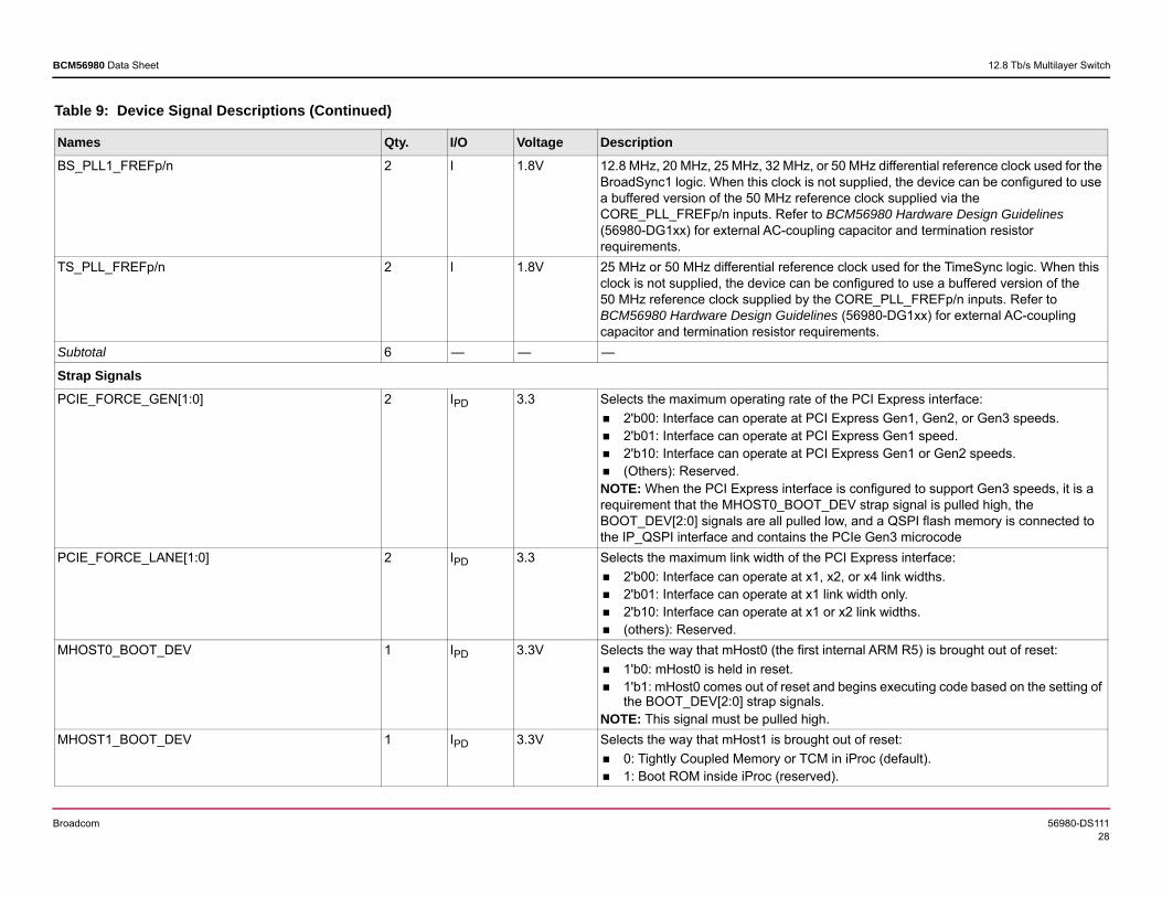
BCM56980 Data Sheet 12.8 Tb/s Multilayer Switch
BS_PLL1_FREFp/n 2 I 1.8V 12.8 MHz, 20 MHz, 25 MHz, 32 MHz, or 50 MHz differential reference clock used for the BroadSync1 logic. When this clock is not supplied, the device can be configured to use a buffered version of the 50 MHz reference clock supplied via the CORE_PLL_FREFp/n inputs. Refer to BCM56980 Hardware Design Guidelines (56980-DG1xx) for external AC-coupling capacitor and termination resistor requirements.
TS_PLL_FREFp/n 2 I 1.8V 25 MHz or 50 MHz differential reference clock used for the TimeSync logic. When this clock is not supplied, the device can be configured to use a buffered version of the 50 MHz reference clock supplied by the CORE_PLL_FREFp/n inputs. Refer to BCM56980 Hardware Design Guidelines (56980-DG1xx) for external AC-coupling capacitor and termination resistor requirements.
Subtotal 6 — — —
Strap SignalsPCIE_FORCE_GEN[1:0] 2 IPD 3.3 Selects the maximum operating rate of the PCI Express interface:
2'b00: Interface can operate at PCI Express Gen1, Gen2, or Gen3 speeds. 2'b01: Interface can operate at PCI Express Gen1 speed. 2'b10: Interface can operate at PCI Express Gen1 or Gen2 speeds. (Others): Reserved.NOTE: When the PCI Express interface is configured to support Gen3 speeds, it is a requirement that the MHOST0_BOOT_DEV strap signal is pulled high, the BOOT_DEV[2:0] signals are all pulled low, and a QSPI flash memory is connected to the IP_QSPI interface and contains the PCIe Gen3 microcode
PCIE_FORCE_LANE[1:0] 2 IPD 3.3 Selects the maximum link width of the PCI Express interface: 2'b00: Interface can operate at x1, x2, or x4 link widths. 2'b01: Interface can operate at x1 link width only. 2'b10: Interface can operate at x1 or x2 link widths. (others): Reserved.
MHOST0_BOOT_DEV 1 IPD 3.3V Selects the way that mHost0 (the first internal ARM R5) is brought out of reset: 1'b0: mHost0 is held in reset. 1'b1: mHost0 comes out of reset and begins executing code based on the setting of
the BOOT_DEV[2:0] strap signals.NOTE: This signal must be pulled high.
MHOST1_BOOT_DEV 1 IPD 3.3V Selects the way that mHost1 is brought out of reset: 0: Tightly Coupled Memory or TCM in iProc (default). 1: Boot ROM inside iProc (reserved).
Table 9: Device Signal Descriptions (Continued)
Names Qty. I/O Voltage Description
Broadcom 56980-DS11129
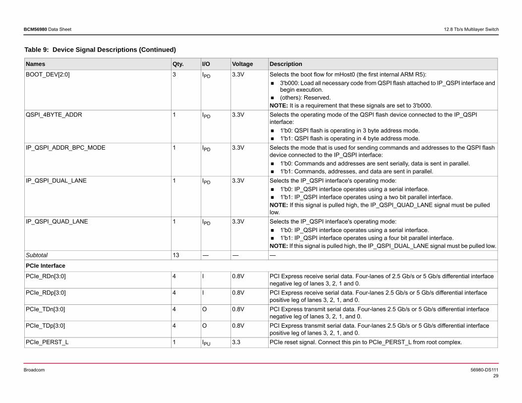
BCM56980 Data Sheet 12.8 Tb/s Multilayer Switch
BOOT_DEV[2:0] 3 IPD 3.3V Selects the boot flow for mHost0 (the first internal ARM R5): 3'b000: Load all necessary code from QSPI flash attached to IP_QSPI interface and
begin execution. (others): Reserved.NOTE: It is a requirement that these signals are set to 3'b000.
QSPI_4BYTE_ADDR 1 IPD 3.3V Selects the operating mode of the QSPI flash device connected to the IP_QSPI interface: 1'b0: QSPI flash is operating in 3 byte address mode. 1'b1: QSPI flash is operating in 4 byte address mode.
IP_QSPI_ADDR_BPC_MODE 1 IPD 3.3V Selects the mode that is used for sending commands and addresses to the QSPI flash device connected to the IP_QSPI interface: 1'b0: Commands and addresses are sent serially, data is sent in parallel. 1'b1: Commands, addresses, and data are sent in parallel.
IP_QSPI_DUAL_LANE 1 IPD 3.3V Selects the IP_QSPI interface's operating mode: 1'b0: IP_QSPI interface operates using a serial interface. 1'b1: IP_QSPI interface operates using a two bit parallel interface.NOTE: If this signal is pulled high, the IP_QSPI_QUAD_LANE signal must be pulled low.
IP_QSPI_QUAD_LANE 1 IPD 3.3V Selects the IP_QSPI interface's operating mode: 1'b0: IP_QSPI interface operates using a serial interface. 1'b1: IP_QSPI interface operates using a four bit parallel interface.NOTE: If this signal is pulled high, the IP_QSPI_DUAL_LANE signal must be pulled low.
Subtotal 13 — — —
PCIe InterfacePCIe_RDn[3:0] 4 I 0.8V PCI Express receive serial data. Four-lanes of 2.5 Gb/s or 5 Gb/s differential interface
negative leg of lanes 3, 2, 1 and 0. PCIe_RDp[3:0] 4 I 0.8V PCI Express receive serial data. Four-lanes 2.5 Gb/s or 5 Gb/s differential interface
positive leg of lanes 3, 2, 1, and 0.PCIe_TDn[3:0] 4 O 0.8V PCI Express transmit serial data. Four-lanes 2.5 Gb/s or 5 Gb/s differential interface
negative leg of lanes 3, 2, 1, and 0.PCIe_TDp[3:0] 4 O 0.8V PCI Express transmit serial data. Four-lanes 2.5 Gb/s or 5 Gb/s differential interface
positive leg of lanes 3, 2, 1, and 0.PCIe_PERST_L 1 IPU 3.3 PCIe reset signal. Connect this pin to PCIe_PERST_L from root complex.
Table 9: Device Signal Descriptions (Continued)
Names Qty. I/O Voltage Description
Broadcom 56980-DS11130
BCM56980 Data Sheet 12.8 Tb/s Multilayer Switch
PCIe_WAKE_L 1 OOD 3.3 Bidirectional Open Drain, active-low PCI Express interface wake signal. Need external pull-up.
Subtotal 18 — — —
JTAG SignalsJTRST_L 1 IPU 3.3V JTAG test controller reset (active low). When asserted, the test controller is held in reset.
This signal should be made accessible for JTAG debugging. For normal operation, this signal should be pulled low.
JTCE[1:0] 2 IPD 3.3V JTAG test controller enable: 2'b0x: Functional mode / ARM R5 debug mode. 2'b10: Non-functional mode / Logicvision TAP mode. (others): Reserved.These signals should be brought to pads with the ability to stuff a pull up resistor. These resistors should not be stuffed for normal operation.
JTCK 1 IPD 3.3V JTAG test clock.
JTDI 1 IPU 3.3V JTAG test data in.
JTDO 1 O 3.3V JTAG test data out.JTMS 1 IPU 3.3V JTAG test mode select.
Subtotal 7 — — —
BSC SignalsIP_BSC[1:0]_SCL 2 BOD 3.3V Broadcom Serial Controller interface clocks (100 kHz/400 kHz). These interfaces can
only function as master interfaces. These signals requires an external pull-up to 3.3V, even if the interface is unused.
IP_BSC[1:0]_SDA 2 BOD 3.3V Broadcom Serial Controller interface data. These interfaces only function as master interfaces. These signals requires an external pull-up to 3.3V, even if the interface is unused.
IP_BSC2_SCL 1 BOD 3.3V Broadcom Serial Controller interface clock. This interface only function as a slave interface. This signal requires an external pull-up to 3.3V, even if the interface is unused.
IP_BSC2_SDA 1 BOD 3.3V Broadcom Serial Controller interface data. This interface only function as a slave interface. This signal requires an external pull-up to 3.3V, even if the interface is unused.
BSC_SA[1:0] 2 BOD 3.3V Broadcom Serial Controller interface slave address selects the lower two bits of the BSC slave address used on the BSC2 interface.
Subtotal 8 — — —
Table 9: Device Signal Descriptions (Continued)
Names Qty. I/O Voltage Description
Broadcom 56980-DS11131
BCM56980 Data Sheet 12.8 Tb/s Multilayer Switch
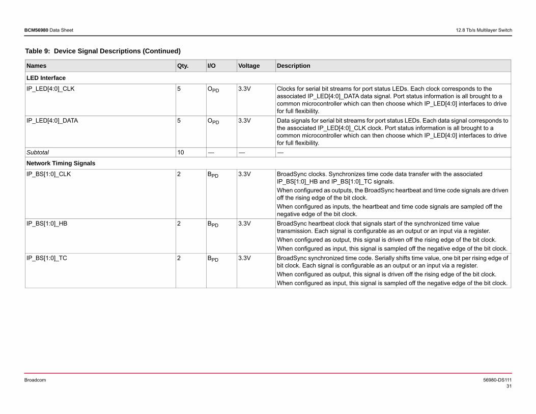
LED InterfaceIP_LED[4:0]_CLK 5 OPD 3.3V Clocks for serial bit streams for port status LEDs. Each clock corresponds to the
associated IP_LED[4:0]_DATA data signal. Port status information is all brought to a common microcontroller which can then choose which IP_LED[4:0] interfaces to drive for full flexibility.
IP_LED[4:0]_DATA 5 OPD 3.3V Data signals for serial bit streams for port status LEDs. Each data signal corresponds to the associated IP_LED[4:0]_CLK clock. Port status information is all brought to a common microcontroller which can then choose which IP_LED[4:0] interfaces to drive for full flexibility.
Subtotal 10 — — —
Network Timing SignalsIP_BS[1:0]_CLK 2 BPD 3.3V BroadSync clocks. Synchronizes time code data transfer with the associated
IP_BS[1:0]_HB and IP_BS[1:0]_TC signals.When configured as outputs, the BroadSync heartbeat and time code signals are driven off the rising edge of the bit clock.When configured as inputs, the heartbeat and time code signals are sampled off the negative edge of the bit clock.
IP_BS[1:0]_HB 2 BPD 3.3V BroadSync heartbeat clock that signals start of the synchronized time value transmission. Each signal is configurable as an output or an input via a register.When configured as output, this signal is driven off the rising edge of the bit clock. When configured as input, this signal is sampled off the negative edge of the bit clock.
IP_BS[1:0]_TC 2 BPD 3.3V BroadSync synchronized time code. Serially shifts time value, one bit per rising edge of bit clock. Each signal is configurable as an output or an input via a register.When configured as output, this signal is driven off the rising edge of the bit clock. When configured as input, this signal is sampled off the negative edge of the bit clock.
Table 9: Device Signal Descriptions (Continued)
Names Qty. I/O Voltage Description
Broadcom 56980-DS11132
BCM56980 Data Sheet 12.8 Tb/s Multilayer Switch
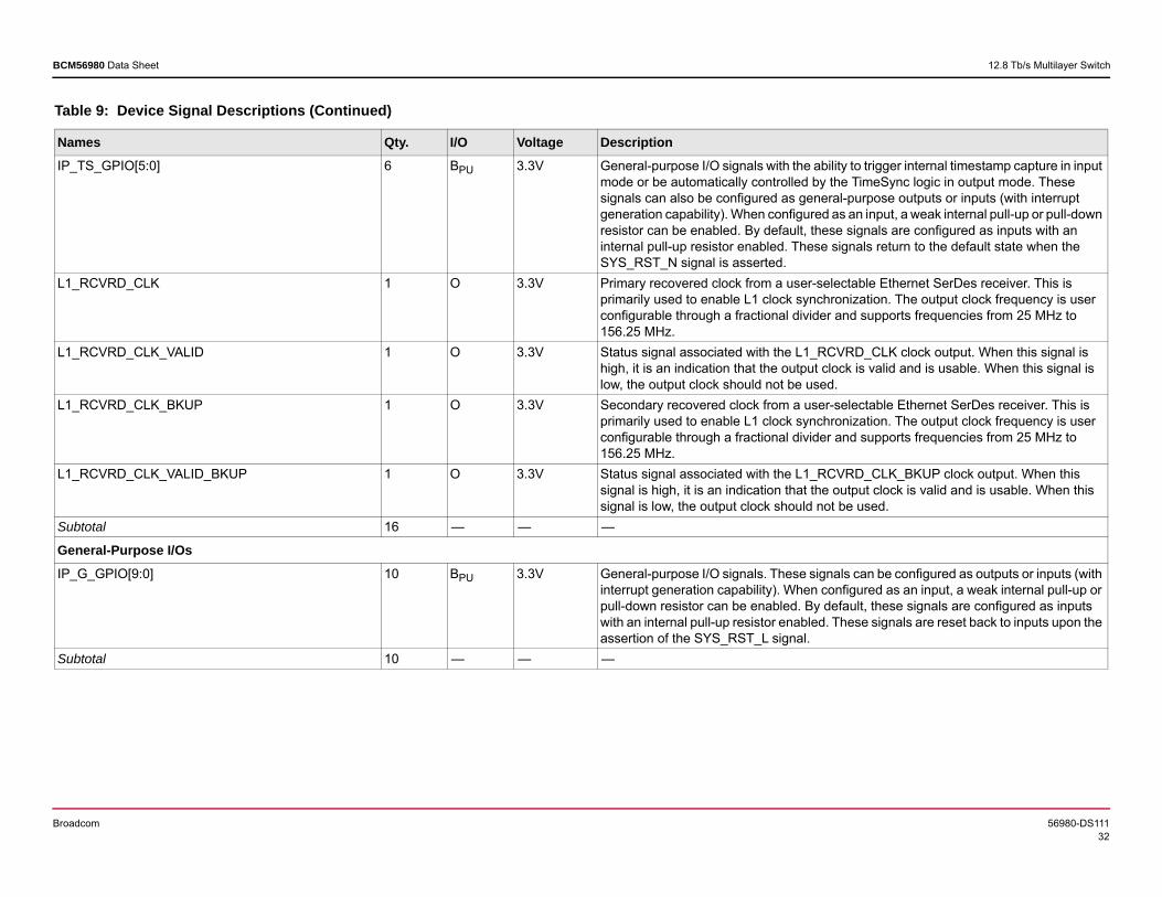
IP_TS_GPIO[5:0] 6 BPU 3.3V General-purpose I/O signals with the ability to trigger internal timestamp capture in input mode or be automatically controlled by the TimeSync logic in output mode. These signals can also be configured as general-purpose outputs or inputs (with interrupt generation capability). When configured as an input, a weak internal pull-up or pull-down resistor can be enabled. By default, these signals are configured as inputs with an internal pull-up resistor enabled. These signals return to the default state when the SYS_RST_N signal is asserted.
L1_RCVRD_CLK 1 O 3.3V Primary recovered clock from a user-selectable Ethernet SerDes receiver. This is primarily used to enable L1 clock synchronization. The output clock frequency is user configurable through a fractional divider and supports frequencies from 25 MHz to 156.25 MHz.
L1_RCVRD_CLK_VALID 1 O 3.3V Status signal associated with the L1_RCVRD_CLK clock output. When this signal is high, it is an indication that the output clock is valid and is usable. When this signal is low, the output clock should not be used.
L1_RCVRD_CLK_BKUP 1 O 3.3V Secondary recovered clock from a user-selectable Ethernet SerDes receiver. This is primarily used to enable L1 clock synchronization. The output clock frequency is user configurable through a fractional divider and supports frequencies from 25 MHz to 156.25 MHz.
L1_RCVRD_CLK_VALID_BKUP 1 O 3.3V Status signal associated with the L1_RCVRD_CLK_BKUP clock output. When this signal is high, it is an indication that the output clock is valid and is usable. When this signal is low, the output clock should not be used.
Subtotal 16 — — —
General-Purpose I/OsIP_G_GPIO[9:0] 10 BPU 3.3V General-purpose I/O signals. These signals can be configured as outputs or inputs (with
interrupt generation capability). When configured as an input, a weak internal pull-up or pull-down resistor can be enabled. By default, these signals are configured as inputs with an internal pull-up resistor enabled. These signals are reset back to inputs upon the assertion of the SYS_RST_L signal.
Subtotal 10 — — —
Table 9: Device Signal Descriptions (Continued)
Names Qty. I/O Voltage Description
Broadcom 56980-DS11133
BCM56980 Data Sheet 12.8 Tb/s Multilayer Switch
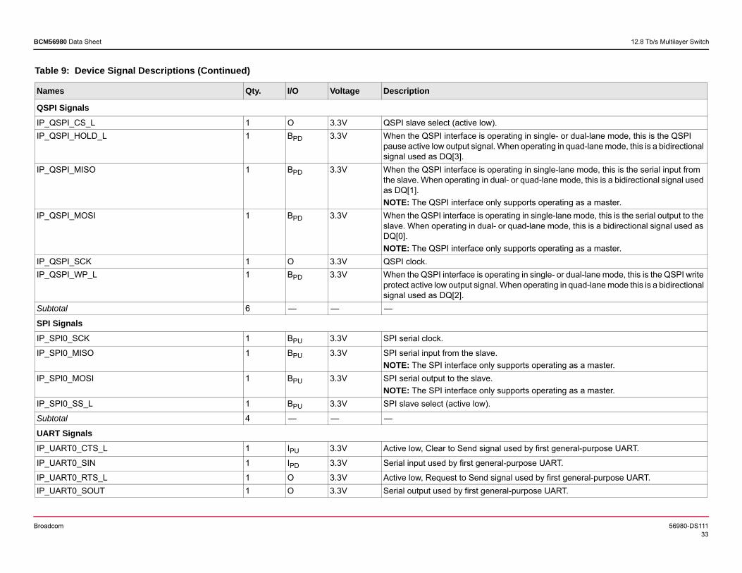
QSPI SignalsIP_QSPI_CS_L 1 O 3.3V QSPI slave select (active low).IP_QSPI_HOLD_L 1 BPD 3.3V When the QSPI interface is operating in single- or dual-lane mode, this is the QSPI
pause active low output signal. When operating in quad-lane mode, this is a bidirectional signal used as DQ[3].
IP_QSPI_MISO 1 BPD 3.3V When the QSPI interface is operating in single-lane mode, this is the serial input from the slave. When operating in dual- or quad-lane mode, this is a bidirectional signal used as DQ[1].NOTE: The QSPI interface only supports operating as a master.
IP_QSPI_MOSI 1 BPD 3.3V When the QSPI interface is operating in single-lane mode, this is the serial output to the slave. When operating in dual- or quad-lane mode, this is a bidirectional signal used as DQ[0].NOTE: The QSPI interface only supports operating as a master.
IP_QSPI_SCK 1 O 3.3V QSPI clock.IP_QSPI_WP_L 1 BPD 3.3V When the QSPI interface is operating in single- or dual-lane mode, this is the QSPI write
protect active low output signal. When operating in quad-lane mode this is a bidirectional signal used as DQ[2].
Subtotal 6 — — —
SPI SignalsIP_SPI0_SCK 1 BPU 3.3V SPI serial clock.
IP_SPI0_MISO 1 BPU 3.3V SPI serial input from the slave.NOTE: The SPI interface only supports operating as a master.
IP_SPI0_MOSI 1 BPU 3.3V SPI serial output to the slave.NOTE: The SPI interface only supports operating as a master.
IP_SPI0_SS_L 1 BPU 3.3V SPI slave select (active low).
Subtotal 4 — — —
UART Signals IP_UART0_CTS_L 1 IPU 3.3V Active low, Clear to Send signal used by first general-purpose UART.
IP_UART0_SIN 1 IPD 3.3V Serial input used by first general-purpose UART.
IP_UART0_RTS_L 1 O 3.3V Active low, Request to Send signal used by first general-purpose UART.IP_UART0_SOUT 1 O 3.3V Serial output used by first general-purpose UART.
Table 9: Device Signal Descriptions (Continued)
Names Qty. I/O Voltage Description
Broadcom 56980-DS11134
BCM56980 Data Sheet 12.8 Tb/s Multilayer Switch
IP_UART1_SIN 1 IPD 3.3V Serial input used by second general-purpose UART.
IP_UART1_SOUT 1 O 3.3V Serial output used by second general-purpose UART.IP_UART2_CTS_L 1 IPU 3.3V Active low, Clear to Send signal used by the UART dedicated to mHost0 (the first
internal ARM R5).IP_UART2_SIN 1 IPD 3.3V Serial input used by the UART dedicated to mHost0 (the first internal ARM R5).
IP_UART2_RTS_L 1 O 3.3V Active low, Request to Send signal used by the UART dedicated to mHost0 (the first internal ARM R5).
IP_UART2_SOUT 1 O 3.3V Serial output used by the UART dedicated to mHost0 (the first internal ARM R5).IP_UART3_CTS_L 1 IPU 3.3V Active low, Clear to Send signal used by the UART dedicated to mHost1 (the second
internal ARM R5).IP_UART3_SIN 1 IPD 3.3V Serial input used by the UART dedicated to mHost1 (the second internal ARM R5).
IP_UART3_RTS_L 1 O 3.3V Active low, Request to Send signal used by the UART dedicated to mHost1 (the second internal ARM R5).
IP_UART3_SOUT 1 O 3.3V Serial output used by the UART dedicated to mHost1 (the second internal ARM R5).Subtotal 14 — — —NOTE: All UART pins/features are for dedicated IEEE 1588 applications only. They do not support generic use.
Table 9: Device Signal Descriptions (Continued)
Names Qty. I/O Voltage Description
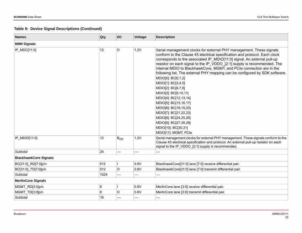
Broadcom 56980-DS11135
BCM56980 Data Sheet 12.8 Tb/s Multilayer Switch
MIIM SignalsIP_MDC[11:0] 12 O 1.2V Serial management clocks for external PHY management. These signals
conform to the Clause 45 electrical specification and protocol. Each clock corresponds to the associated IP_MDIO[11:0] signal. An external pull-up resistor on each signal to the IP_VDDO_[2:1] supply is recommended. The internal MDIO to BlackhawkCore, MGMT, and PCIe connection are in the following list. The external PHY mapping can be configured by SDK software.MDIO[0]: BC[0,1,2]MDIO[1]: BC[3,4,5]MDIO[2]: BC[6,7,8]MDIO[3]: BC[9,10,11]MDIO[4]: BC[12,13,14]MDIO[5]: BC[15,16,17]MDIO[6]: BC[18,19,20]MDIO[7]: BC[21,22,23]MDIO[8]: BC[24,25,26]MDIO[9]: BC[27,28,29]MDIO[10]: BC[30,31]MDIO[11]: MGMT, PCIe
IP_MDIO[11:0] 12 BOD 1.2V Serial management clocks for external PHY management. These signals conform to the Clause 45 electrical specification and protocol. An external pull-up resistor on each signal to the IP_VDDO_[2:1] supply is recommended.
Subtotal 24 — — —
BlackhawkCore Signals BC[31:0]_RD[7:0]p/n 512 I 0.8V BlackhawkCore[31:0] lane [7:0] receive differential pair.BC[31:0]_TD[7:0]p/n 512 O 0.8V BlackhawkCore[31:0] lane [7:0] transmit differential pair.Subtotal 1024 — — —
MerlinCore SignalsMGMT_RD[3:0]p/n 8 I 0.8V MerlinCore lane [3:0] receive differential pair.MGMT_TD[3:0]p/n 8 O 0.8V MerlinCore lane [3:0] transmit differential pair.Subtotal 16 — — —
Table 9: Device Signal Descriptions (Continued)
Names Qty. I/O Voltage Description
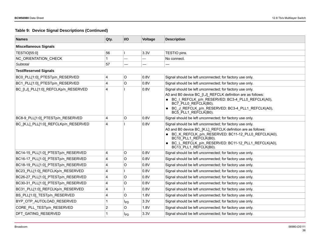
Broadcom 56980-DS11136
BCM56980 Data Sheet 12.8 Tb/s Multilayer Switch
Miscellaneous SignalsTESTIO[55:0] 56 I 3.3V TESTIO pins.NC_ORIENTATION_CHECK 1 — — No connect.Subtotal 57 — — —
Test/Reserved SignalsBC0_PLL[1:0]_PTESTp/n_RESERVED 4 O 0.8V Signal should be left unconnected; for factory use only.BC1_PLL[1:0]_PTESTp/n_RESERVED 4 O 0.8V Signal should be left unconnected; for factory use only.BC_[I,J]_PLL[1:0]_REFCLKp/n_RESERVED 4 I 0.8V Signal should be left unconnected; for factory use only.
A0 and B0 device BC_[I,J]_REFCLK definition are as follows: BC_I_REFCLK_p/n_RESERVED: BC3-4_PLL0_REFCLK(A0),
BC7_PLL0_REFCLK(B0). BC_J_REFCLK_p/n_RESERVED: BC3-4_PLL1_REFCLK(A0),
BC5_PLL1_REFCLK(B0).BC8-9_PLL[1:0]_PTESTp/n_RESERVED 4 O 0.8V Signal should be left unconnected; for factory use only.BC_[K,L]_PLL[1:0]_REFCLKp/n_RESERVED 4 I 0.8V Signal should be left unconnected; for factory use only.
A0 and B0 device BC_[K,L]_REFCLK definition are as follows: BC_K_REFCLK_p/n_RESERVED: BC11-12_PLL0_REFCLK(A0),
BC10_PLL1_REFCLK(B0). BC_L_REFCLK_p/n_RESERVED: BC11-12_PLL1_REFCLK(A0),
BC13_PLL1_REFCLK(B0).BC14-15_PLL[1:0]_PTESTp/n_RESERVED 4 O 0.8V Signal should be left unconnected; for factory use only.BC16-17_PLL[1:0]_PTESTp/n_RESERVED 4 O 0.8V Signal should be left unconnected; for factory use only.BC18-19_PLL[1:0]_PTESTp/n_RESERVED 4 O 0.8V Signal should be left unconnected; for factory use only.BC23_PLL[1:0]_REFCLKp/n_RESERVED 4 I 0.8V Signal should be left unconnected; for factory use only.BC26-27_PLL[1:0]_PTESTp/n_RESERVED 4 O 0.8V Signal should be left unconnected; for factory use only.BC30-31_PLL[1:0]_PTESTp/n_RESERVED 4 O 0.8V Signal should be left unconnected; for factory use only.BC31_PLL[1:0]_REFCLKp/n_RESERVED 4 I 0.8V Signal should be left unconnected; for factory use only.BS_PLL[1:0]_TESTp/n_RESERVED 4 O 1.8V Signal should be left unconnected; for factory use only.BYP_OTP_AUTOLOAD_RESERVED 1 IPD 3.3V Signal should be left unconnected; for factory use only.
CORE_PLL_TESTp/n_RESERVED 2 O 1.8V Signal should be left unconnected; for factory use only.DFT_GATING_RESERVED 1 IPD 3.3V Signal should be left unconnected; for factory use only.
Table 9: Device Signal Descriptions (Continued)
Names Qty. I/O Voltage Description
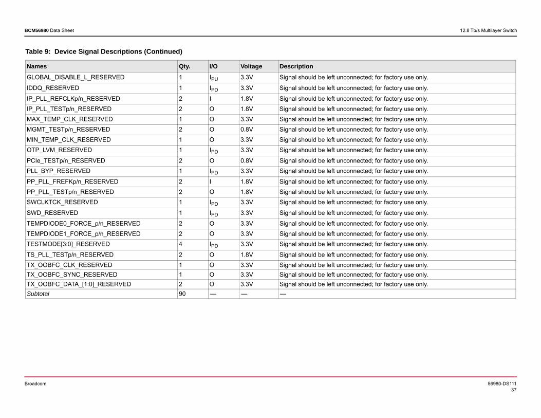
Broadcom 56980-DS11137
BCM56980 Data Sheet 12.8 Tb/s Multilayer Switch
GLOBAL_DISABLE_L_RESERVED 1 IPU 3.3V Signal should be left unconnected; for factory use only.
IDDQ_RESERVED 1 IPD 3.3V Signal should be left unconnected; for factory use only.
IP_PLL_REFCLKp/n_RESERVED 2 I 1.8V Signal should be left unconnected; for factory use only.IP_PLL_TESTp/n_RESERVED 2 O 1.8V Signal should be left unconnected; for factory use only.MAX_TEMP_CLK_RESERVED 1 O 3.3V Signal should be left unconnected; for factory use only.MGMT_TESTp/n_RESERVED 2 O 0.8V Signal should be left unconnected; for factory use only.MIN_TEMP_CLK_RESERVED 1 O 3.3V Signal should be left unconnected; for factory use only.OTP_LVM_RESERVED 1 IPD 3.3V Signal should be left unconnected; for factory use only.
PCIe_TESTp/n_RESERVED 2 O 0.8V Signal should be left unconnected; for factory use only.PLL_BYP_RESERVED 1 IPD 3.3V Signal should be left unconnected; for factory use only.
PP_PLL_FREFKp/n_RESERVED 2 I 1.8V Signal should be left unconnected; for factory use only.PP_PLL_TESTp/n_RESERVED 2 O 1.8V Signal should be left unconnected; for factory use only.SWCLKTCK_RESERVED 1 IPD 3.3V Signal should be left unconnected; for factory use only.
SWD_RESERVED 1 IPD 3.3V Signal should be left unconnected; for factory use only.
TEMPDIODE0_FORCE_p/n_RESERVED 2 O 3.3V Signal should be left unconnected; for factory use only.TEMPDIODE1_FORCE_p/n_RESERVED 2 O 3.3V Signal should be left unconnected; for factory use only.TESTMODE[3:0]_RESERVED 4 IPD 3.3V Signal should be left unconnected; for factory use only.
TS_PLL_TESTp/n_RESERVED 2 O 1.8V Signal should be left unconnected; for factory use only.TX_OOBFC_CLK_RESERVED 1 O 3.3V Signal should be left unconnected; for factory use only.TX_OOBFC_SYNC_RESERVED 1 O 3.3V Signal should be left unconnected; for factory use only.TX_OOBFC_DATA_[1:0]_RESERVED 2 O 3.3V Signal should be left unconnected; for factory use only.Subtotal 90 — — —
Table 9: Device Signal Descriptions (Continued)
Names Qty. I/O Voltage Description
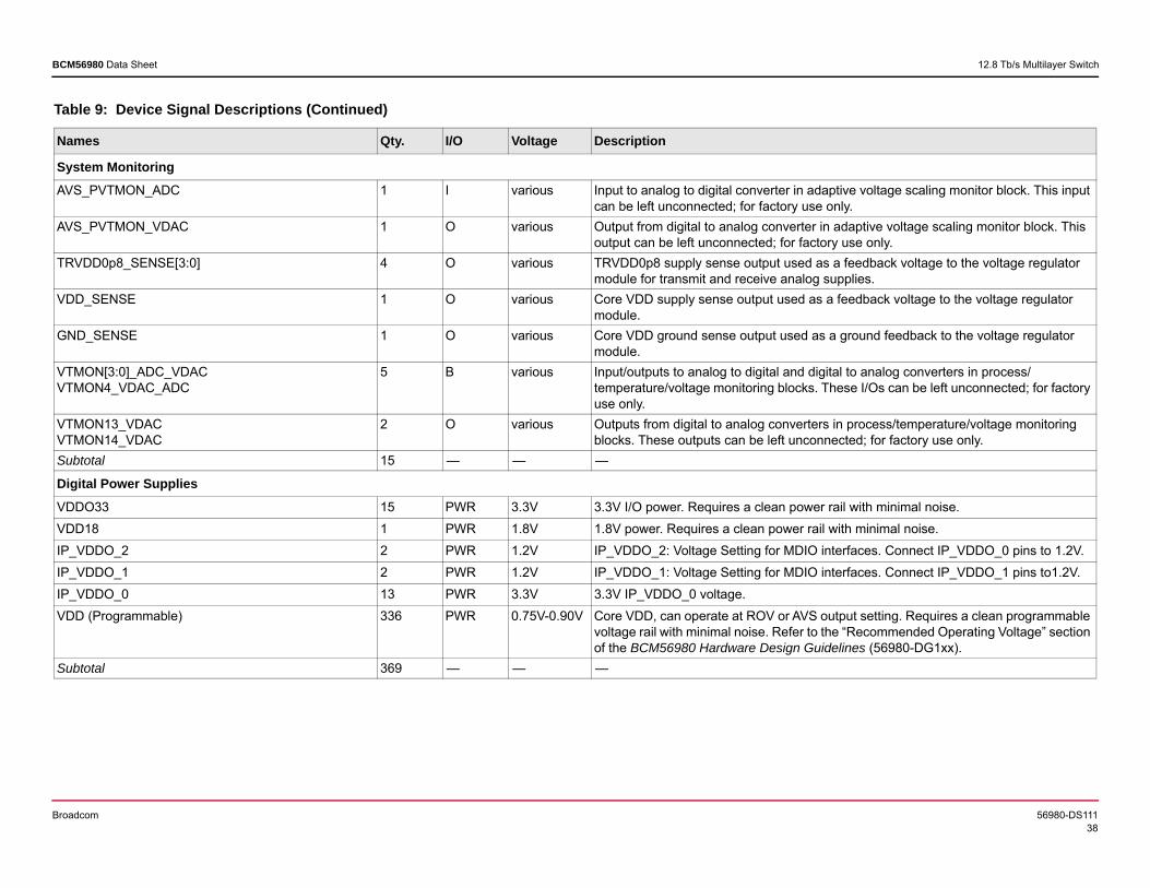
Broadcom 56980-DS11138
BCM56980 Data Sheet 12.8 Tb/s Multilayer Switch
System MonitoringAVS_PVTMON_ADC 1 I various Input to analog to digital converter in adaptive voltage scaling monitor block. This input
can be left unconnected; for factory use only.AVS_PVTMON_VDAC 1 O various Output from digital to analog converter in adaptive voltage scaling monitor block. This
output can be left unconnected; for factory use only.TRVDD0p8_SENSE[3:0] 4 O various TRVDD0p8 supply sense output used as a feedback voltage to the voltage regulator
module for transmit and receive analog supplies.VDD_SENSE 1 O various Core VDD supply sense output used as a feedback voltage to the voltage regulator
module.GND_SENSE 1 O various Core VDD ground sense output used as a ground feedback to the voltage regulator
module.VTMON[3:0]_ADC_VDACVTMON4_VDAC_ADC
5 B various Input/outputs to analog to digital and digital to analog converters in process/ temperature/voltage monitoring blocks. These I/Os can be left unconnected; for factory use only.
VTMON13_VDACVTMON14_VDAC
2 O various Outputs from digital to analog converters in process/temperature/voltage monitoring blocks. These outputs can be left unconnected; for factory use only.
Subtotal 15 — — —
Digital Power SuppliesVDDO33 15 PWR 3.3V 3.3V I/O power. Requires a clean power rail with minimal noise.VDD18 1 PWR 1.8V 1.8V power. Requires a clean power rail with minimal noise.IP_VDDO_2 2 PWR 1.2V IP_VDDO_2: Voltage Setting for MDIO interfaces. Connect IP_VDDO_0 pins to 1.2V.IP_VDDO_1 2 PWR 1.2V IP_VDDO_1: Voltage Setting for MDIO interfaces. Connect IP_VDDO_1 pins to1.2V.IP_VDDO_0 13 PWR 3.3V 3.3V IP_VDDO_0 voltage.VDD (Programmable) 336 PWR 0.75V-0.90V Core VDD, can operate at ROV or AVS output setting. Requires a clean programmable
voltage rail with minimal noise. Refer to the “Recommended Operating Voltage” section of the BCM56980 Hardware Design Guidelines (56980-DG1xx).
Subtotal 369 — — —
Table 9: Device Signal Descriptions (Continued)
Names Qty. I/O Voltage Description
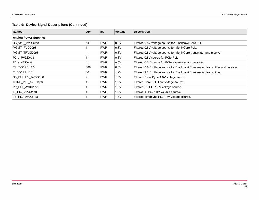
Broadcom 56980-DS11139
BCM56980 Data Sheet 12.8 Tb/s Multilayer Switch
Analog Power SuppliesBC[63:0]_PVDD0p8 64 PWR 0.8V Filtered 0.8V voltage source for BlackhawkCore PLL.MGMT_PVDD0p8 1 PWR 0.8V Filtered 0.8V voltage source for MerlinCore PLL.MGMT_TRVDD0p8 4 PWR 0.8V Filtered 0.8V voltage source for MerlinCore transmitter and receiver.PCIe_PVDD0p8 1 PWR 0.8V Filtered 0.8V source for PCIe PLL.PCIe_VDD0p8 4 PWR 0.8V Filtered 0.8V source for PCIe transmitter and receiver.TRVDD0P8_[3:0] 388 PWR 0.8V Filtered 0.8V voltage source for BlackhawkCore analog transmitter and receiver.TVDD1P2_[3:0] 66 PWR 1.2V Filtered 1.2V voltage source for BlackhawkCore analog transmitter.BS_PLL[1:0]_AVDD1p8 2 PWR 1.8V Filtered BroadSync 1.8V voltage source.CORE_PLL_AVDD1p8 1 PWR 1.8V Filtered Core PLL 1.8V voltage source.PP_PLL_AVDD1p8 1 PWR 1.8V Filtered PP PLL 1.8V voltage source.IP_PLL_AVDD1p8 1 PWR 1.8V Filtered IP PLL 1.8V voltage source.TS_PLL_AVDD1p8 1 PWR 1.8V Filtered TimeSync PLL 1.8V voltage source.
Table 9: Device Signal Descriptions (Continued)
Names Qty. I/O Voltage Description
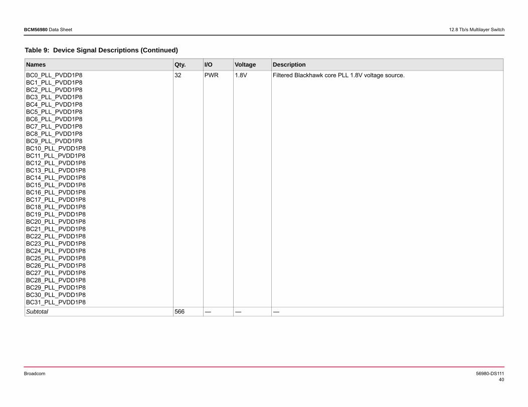
Broadcom 56980-DS11140
BCM56980 Data Sheet 12.8 Tb/s Multilayer Switch
BC0_PLL_PVDD1P8BC1_PLL_PVDD1P8BC2_PLL_PVDD1P8BC3_PLL_PVDD1P8BC4_PLL_PVDD1P8BC5_PLL_PVDD1P8BC6_PLL_PVDD1P8BC7_PLL_PVDD1P8BC8_PLL_PVDD1P8BC9_PLL_PVDD1P8BC10_PLL_PVDD1P8BC11_PLL_PVDD1P8BC12_PLL_PVDD1P8BC13_PLL_PVDD1P8BC14_PLL_PVDD1P8BC15_PLL_PVDD1P8BC16_PLL_PVDD1P8BC17_PLL_PVDD1P8BC18_PLL_PVDD1P8BC19_PLL_PVDD1P8BC20_PLL_PVDD1P8BC21_PLL_PVDD1P8BC22_PLL_PVDD1P8BC23_PLL_PVDD1P8BC24_PLL_PVDD1P8BC25_PLL_PVDD1P8BC26_PLL_PVDD1P8BC27_PLL_PVDD1P8BC28_PLL_PVDD1P8BC29_PLL_PVDD1P8BC30_PLL_PVDD1P8BC31_PLL_PVDD1P8
32 PWR 1.8V Filtered Blackhawk core PLL 1.8V voltage source.
Subtotal 566 — — —
Table 9: Device Signal Descriptions (Continued)
Names Qty. I/O Voltage Description
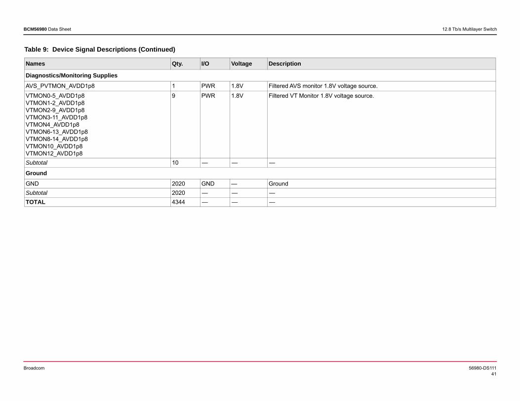
Broadcom 56980-DS11141
BCM56980 Data Sheet 12.8 Tb/s Multilayer Switch
Diagnostics/Monitoring SuppliesAVS_PVTMON_AVDD1p8 1 PWR 1.8V Filtered AVS monitor 1.8V voltage source.VTMON0-5_AVDD1p8VTMON1-2_AVDD1p8VTMON2-9_AVDD1p8VTMON3-11_AVDD1p8VTMON4_AVDD1p8VTMON6-13_AVDD1p8VTMON8-14_AVDD1p8VTMON10_AVDD1p8VTMON12_AVDD1p8
9 PWR 1.8V Filtered VT Monitor 1.8V voltage source.
Subtotal 10 — — —
GroundGND 2020 GND — GroundSubtotal 2020 — — —TOTAL 4344 — — —
Table 9: Device Signal Descriptions (Continued)
Names Qty. I/O Voltage Description
Broadcom 56980-DS11142
BCM56980 Data Sheet 12.8 Tb/s Multilayer Switch
4.2 BCM56980 Pin List by Ball NumberThe pin list and ballout diagram for all devices in the BCM56980 family are provided in spreadsheet form. Broadcom provides customer access to technical documentation and software through its Customer Support Portal (CSP) and Downloads and Support site. The spreadsheet serves as the official document containing the device’s signal mapping. Refer to BCM56980_ballout_revxx (see Related Documents).
4.3 Device DifferencesThe following table shows which ports are enabled for devices in the BCM56980 device family.
Table 10: BCM56980, BCM56982, BCM56983, and BCM56984 Differences
P/N BCM56980/BCM56984 BCM56982 BCM56983BlackhawkCore0 Enable Disable EnableBlackhawkCore1 Enable Disable EnableBlackhawkCore2 Enable Enable EnableBlackhawkCore3 Enable Enable EnableBlackhawkCore4 Enable Enable EnableBlackhawkCore5 Enable Enable EnableBlackhawkCore6 Enable Enable EnableBlackhawkCore7 Enable Disable EnableBlackhawkCore8 Enable Disable DisableBlackhawkCore9 Enable Enable DisableBlackhawkCore10 Enable Enable DisableBlackhawkCore11 Enable Enable DisableBlackhawkCore12 Enable Enable DisableBlackhawkCore13 Enable Enable DisableBlackhawkCore14 Enable Disable DisableBlackhawkCore15 Enable Disable DisableBlackhawkCore16 Enable Disable DisableBlackhawkCore17 Enable Disable DisableBlackhawkCore18 Enable Enable DisableBlackhawkCore19 Enable Enable DisableBlackhawkCore20 Enable Enable DisableBlackhawkCore21 Enable Enable DisableBlackhawkCore22 Enable Enable DisableBlackhawkCore23 Enable Disable DisableBlackhawkCore24 Enable Disable EnableBlackhawkCore25 Enable Enable EnableBlackhawkCore26 Enable Enable EnableBlackhawkCore27 Enable Enable EnableBlackhawkCore28 Enable Enable EnableBlackhawkCore29 Enable Enable EnableBlackhawkCore30 Enable Disable EnableBlackhawkCore31 Enable Disable Enable
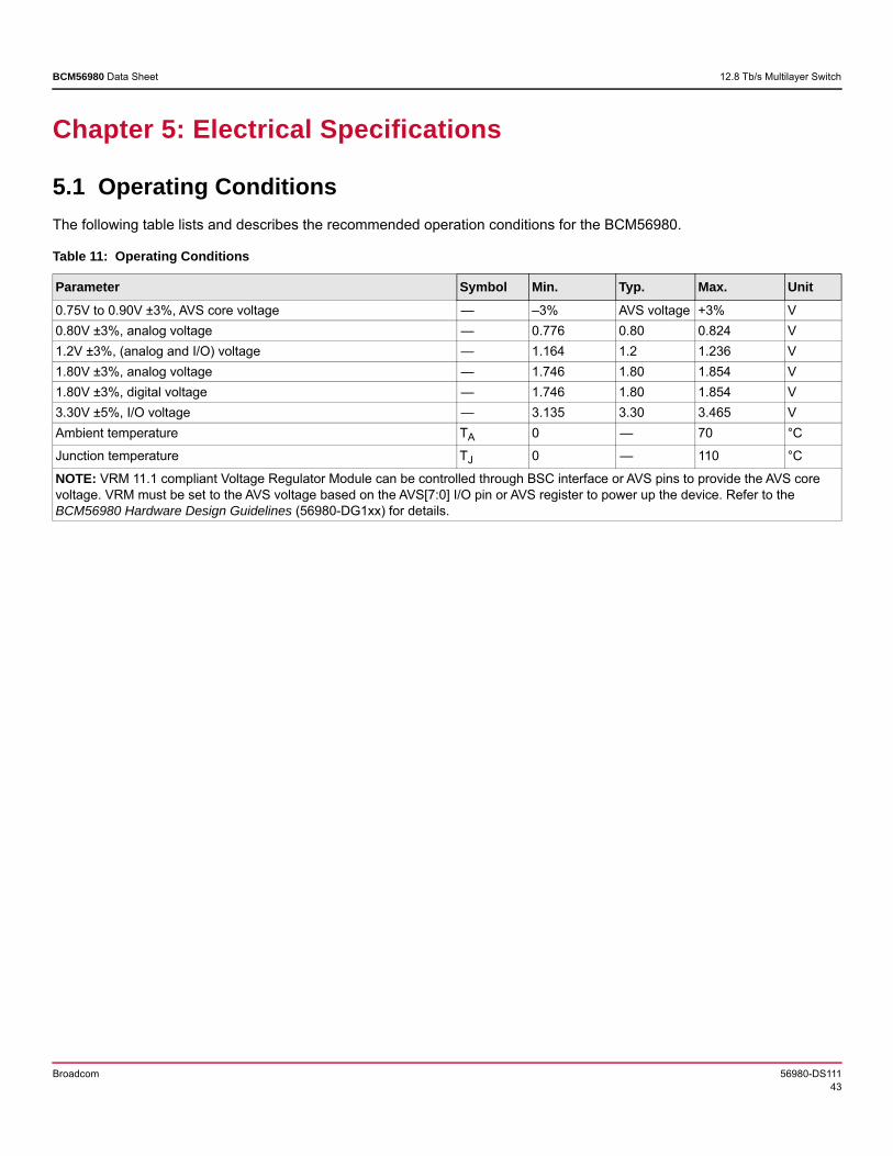
Broadcom 56980-DS11143
BCM56980 Data Sheet 12.8 Tb/s Multilayer Switch
Chapter 5: Electrical Specifications
5.1 Operating ConditionsThe following table lists and describes the recommended operation conditions for the BCM56980.
Table 11: Operating Conditions
Parameter Symbol Min. Typ. Max. Unit0.75V to 0.90V ±3%, AVS core voltage — –3% AVS voltage +3% V0.80V ±3%, analog voltage — 0.776 0.80 0.824 V1.2V ±3%, (analog and I/O) voltage — 1.164 1.2 1.236 V1.80V ±3%, analog voltage — 1.746 1.80 1.854 V1.80V ±3%, digital voltage — 1.746 1.80 1.854 V3.30V ±5%, I/O voltage — 3.135 3.30 3.465 VAmbient temperature TA 0 — 70 °C
Junction temperature TJ 0 — 110 °C
NOTE: VRM 11.1 compliant Voltage Regulator Module can be controlled through BSC interface or AVS pins to provide the AVS core voltage. VRM must be set to the AVS voltage based on the AVS[7:0] I/O pin or AVS register to power up the device. Refer to the BCM56980 Hardware Design Guidelines (56980-DG1xx) for details.
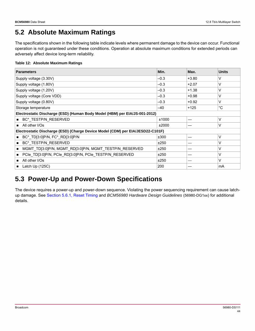
Broadcom 56980-DS11144
BCM56980 Data Sheet 12.8 Tb/s Multilayer Switch
5.2 Absolute Maximum RatingsThe specifications shown in the following table indicate levels where permanent damage to the device can occur. Functional operation is not guaranteed under these conditions. Operation at absolute maximum conditions for extended periods can adversely affect device long-term reliability.
5.3 Power-Up and Power-Down SpecificationsThe device requires a power-up and power-down sequence. Violating the power sequencing requirement can cause latch-up damage. See Section 5.6.1, Reset Timing and BCM56980 Hardware Design Guidelines (56980-DG1xx) for additional details.
Table 12: Absolute Maximum Ratings
Parameters Min. Max. UnitsSupply voltage (3.30V) –0.3 +3.80 VSupply voltage (1.80V) –0.3 +2.07 VSupply voltage (1.20V) –0.3 +1.38 VSupply voltage (Core VDD) –0.3 +0.98 VSupply voltage (0.80V) –0.3 +0.92 VStorage temperature –40 +125 °CElectrostatic Discharge (ESD) (Human Body Model (HBM) per EIA/JS-001-2012) BC*_TESTP/N_RESERVED ±1000 — V All other I/Os ±2000 — VElectrostatic Discharge (ESD) (Charge Device Model (CDM) per EIA/JESD22-C101F) BC*_TD[3:0]P/N, FC*_RD[3:0]P/N ±300 — V BC*_TESTP/N_RESERVED ±250 — V MGMT_TD[3:0]P/N, MGMT_RD[3:0]P/N, MGMT_TESTP/N_RESERVED ±250 — V PCIe_TD[3:0]P/N, PCIe_RD[3:0]P/N, PCIe_TESTP/N_RESERVED ±250 — V All other I/Os ±250 — V Latch Up (125C) 200 — mA
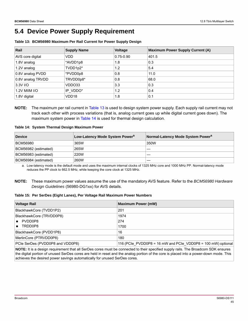
Broadcom 56980-DS11145
BCM56980 Data Sheet 12.8 Tb/s Multilayer Switch
5.4 Device Power Supply Requirement
NOTE: The maximum per rail current in Table 13 is used to design system power supply. Each supply rail current may not track each other with process variations (that is, analog current goes up while digital current goes down). The maximum system power in Table 14 is used for thermal design calculation.
NOTE: These maximum power values assume the use of the mandatory AVS feature. Refer to the BCM56980 Hardware Design Guidelines (56980-DG1xx) for AVS details.
Table 13: BCM56980 Maximum Per Rail Current for Power Supply Design
Rail Supply Name Voltage Maximum Power Supply Current (A)AVS core digital VDD 0.75-0.90 401.51.8V analog *AVDD1p8 1.8 0.31.2V analog TVDD1p2* 1.2 5.40.8V analog PVDD *PVDD0p8 0.8 11.00.8V analog TRVDD TRVDD0p8* 0.8 68.03.3V I/O VDDO33 3.3 0.31.2V MIIM I/O IP_VDDO* 1.2 0.41.8V digital VDD18 1.8 0.1
Table 14: System Thermal Design Maximum Power
Device Low-Latency Mode System Powera
a. Low-latency mode is the default mode and uses the maximum internal clocks of 1325 MHz core and 1000 MHz PP. Normal-latency mode reduces the PP clock to 662.5 MHz, while keeping the core clock at 1325 MHz.
Normal-Latency Mode System Powera
BCM56980 365W 350WBCM56982 (estimated) 265W —BCM56983 (estimated) 220W —BCM56984 (estimated) 260W —
Table 15: Per SerDes (Eight Lanes), Per Voltage Rail Maximum Power Numbers
Voltage Rail Maximum Power (mW)BlackhawkCore (TVDD1P2) 201BlackhawkCore (TRVDD0P8) PVDD0P8 TRDD0P8
19742741700
BlackhawkCore (PVDD1P8) 16MerlinCore (PTRVDD0P8) 180PCIe SerDes (PVDD0P8 and VDD0P8) 116 (PCIe_PVDD0P8 = 16 mW and PCIe_VDD0P8 = 100 mW) optionalNOTE: It is a design requirement that all SerDes cores must be connected to their specified supply rails. The Broadcom SDK ensures the digital portion of unused SerDes cores are held in reset and the analog portion of the core is placed into a power-down mode. This achieves the desired power savings automatically for unused SerDes cores.
Broadcom 56980-DS11146
BCM56980 Data Sheet 12.8 Tb/s Multilayer Switch
5.5 DC Characteristics
5.5.1 Standard 3.3V SignalsThe specifications shown in the following table apply to all CMOS 3.3V general I/O signals along with synchronous Ethernet interface, BroadSync, UART, GPIO, JTAG, and LED signals, except for BSC and MDIO/MDC.
5.5.2 Management Interface
5.5.3 BSC Interface
Table 16: Standard 3.3V Signals
Parameter Symbol Min. Typ. Max. UnitInput voltage VIN 0.0 — +3.63 V
Input low voltage VIL 0.0 — 0.8 V
Input high voltage VIH 2.0 — +3.63 V
Output low voltage VOL — — 0.4 V
Output high voltage VOH VDDO33 – 0.4 — — V
Pull-up or pull-down resistor Rp — ~50 — k
Output low current IOL 8.0 — — mAOutput high current IOH -8.0 — — mA
Table 17: MIIM (XG), Clause 45 Electrical Characteristics
Parameter Symbol Condition Min. Typ. Max. UnitInput voltage VIN — –0.3 — 1.5 V
Input low voltage VIL — –0.3 — 0.36 V
Input high voltage VIH — 0.84 — 1.5 V
Output low voltage VOL IOL = 100 A –0.3 — 0.20 V
Output low current IOL VOL = 0.2V 4.0 — — mA
Output high voltage VOH IOH = –100 A 1.0 — 1.5 V
Output high current IOH VOH = IP_VDDO–0.2V — — –4.0 mA
Table 18: BSC Electrical Characteristics
Parameter Symbol Condition Min. Typ. Max. UnitInput voltage VIN — –0.3 — 3.63 V
Input low voltage VIL — –0.3 — 0.8 V
Input high voltage VIH — VDDO33 × 0.7 — 3.63 V
Output low voltage VOL IOL = 6 mA — — 0.4 V
Output low current IOL VOL = 0.4V 6.0 — — mA
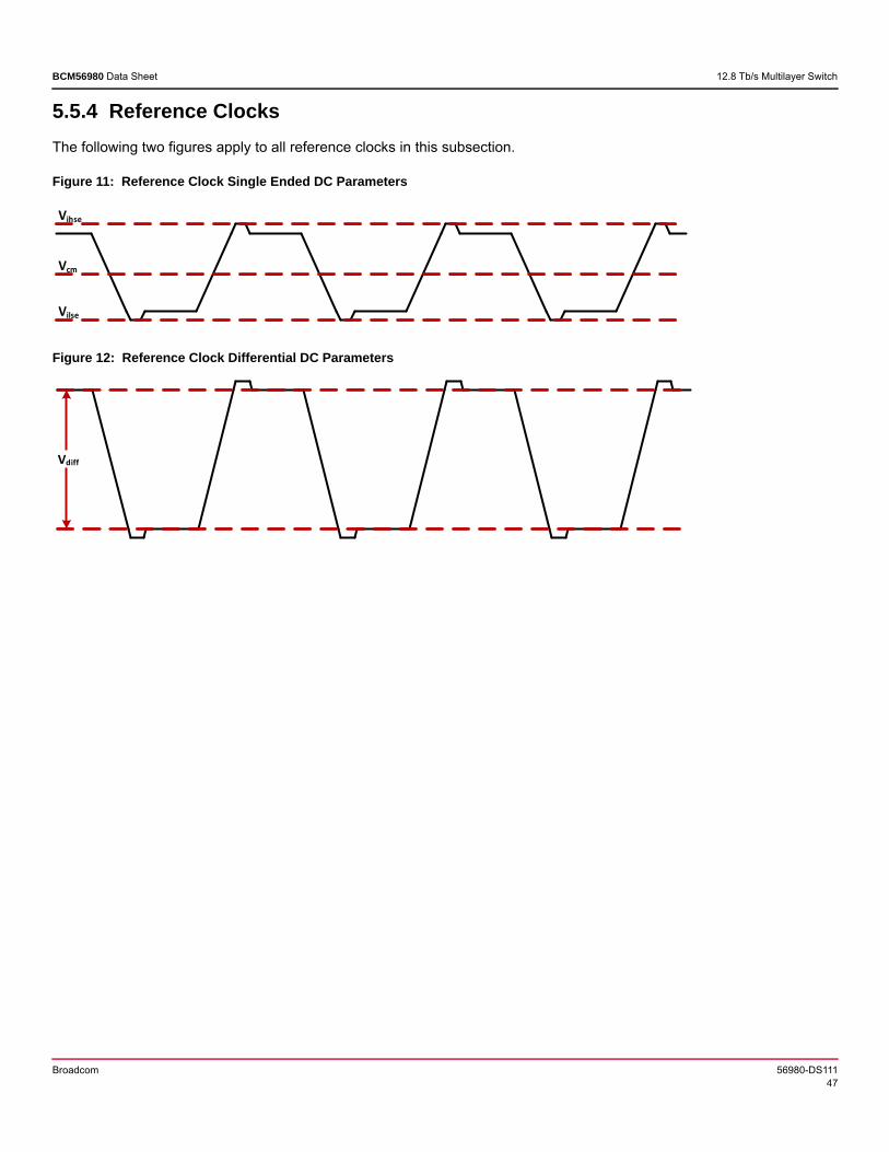
Broadcom 56980-DS11147
BCM56980 Data Sheet 12.8 Tb/s Multilayer Switch
5.5.4 Reference ClocksThe following two figures apply to all reference clocks in this subsection.
Figure 11: Reference Clock Single Ended DC Parameters
Figure 12: Reference Clock Differential DC Parameters
Vihse
Vcm
Vilse
Vdiff
Broadcom 56980-DS11148
BCM56980 Data Sheet 12.8 Tb/s Multilayer Switch
5.5.4.1 Core PLL Reference Clock (CORE_PLL_FREF)
The core PLL clocks all switching and iProc logic and has the input structure shown in following figure.
Figure 13: Core PLL Input Structure
Table 19: Core PLL Reference Clock DC Parameters
Parameter Symbol Min. Typ. Max. UnitCommon mode voltage Vcm — 900 — mVsea
a. mVse denotes mV single-ended.
Single ended swing Vilse / Vihse 0 — 1800 mVse
Differential swing Vdiff 500 — 1800 mVppdb
b. mVppd denotes mV peak-to-peak differential.
Internal AC couplingc
c. There is no on-die AC coupling, so external AC coupling is required. The recommended AC coupling capacitor value is 10 nF.
Cac — — — pF
Internal differential termination Rterm — 100 — Ω
Internal bias resistors Rb1 / Rb2 — 5520 — Ω
PLL
PVDD1P8
Rb2
REFCLK_P
REFCLK_N
Rterm
Rb2
Rb1 Rb1
Broadcom 56980-DS11149
BCM56980 Data Sheet 12.8 Tb/s Multilayer Switch
5.5.4.2 TimeSync PLL Reference Clock (TS_PLL_FREF)
The TimeSync PLL clocks the TimeSync and timestamp logic distributed throughout the device. It has the input structure shown in the following figure.
Figure 14: TimeSync PLL Input Structure
Table 20: TimeSync PLL Reference Clock DC Parameters
Parameter Symbol Min. Typ. Max. UnitCommon mode voltage Vcm — 900 — mVse
Single ended swing Vilse / Vihse 0 — 1800 mVse
Differential swing Vdiff 500 — 1800 mVppd
Internal AC couplinga
a. There is no on-die AC coupling, so external AC coupling is required. The recommended AC coupling capacitor value is 10 nF.
Cac — — — pF
Internal differential termination Rterm — 100 — Ω
Internal bias resistors Rb1 / Rb2 — 5520 — Ω
PLL
PVDD1P8
Rb2
REFCLK_P
REFCLK_N
Rterm
Rb2
Rb1 Rb1
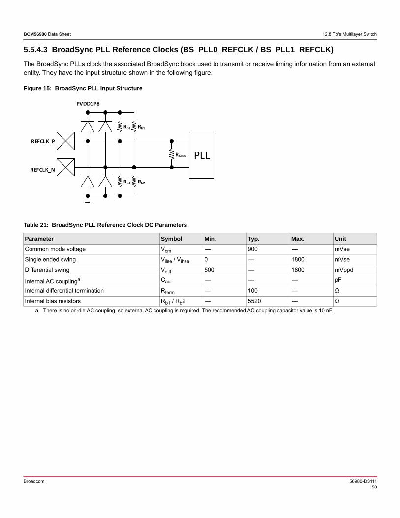
Broadcom 56980-DS11150
BCM56980 Data Sheet 12.8 Tb/s Multilayer Switch
5.5.4.3 BroadSync PLL Reference Clocks (BS_PLL0_REFCLK / BS_PLL1_REFCLK)
The BroadSync PLLs clock the associated BroadSync block used to transmit or receive timing information from an external entity. They have the input structure shown in the following figure.
Figure 15: BroadSync PLL Input Structure
Table 21: BroadSync PLL Reference Clock DC Parameters
Parameter Symbol Min. Typ. Max. UnitCommon mode voltage Vcm — 900 — mVse
Single ended swing Vilse / Vihse 0 — 1800 mVse
Differential swing Vdiff 500 — 1800 mVppd
Internal AC couplinga
a. There is no on-die AC coupling, so external AC coupling is required. The recommended AC coupling capacitor value is 10 nF.
Cac — — — pF
Internal differential termination Rterm — 100 — Ω
Internal bias resistors Rb1 / Rb2 — 5520 — Ω
PLL
PVDD1P8
Rb2
REFCLK_P
REFCLK_N
Rterm
Rb2
Rb1 Rb1
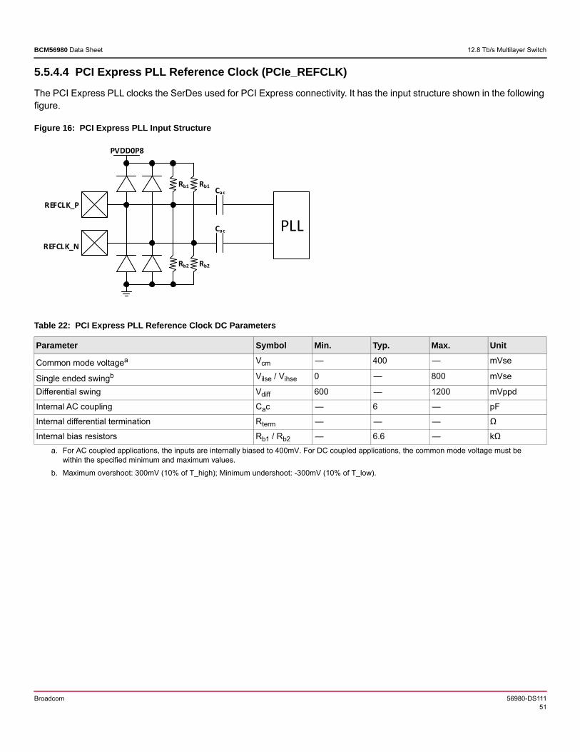
Broadcom 56980-DS11151
BCM56980 Data Sheet 12.8 Tb/s Multilayer Switch
5.5.4.4 PCI Express PLL Reference Clock (PCIe_REFCLK)
The PCI Express PLL clocks the SerDes used for PCI Express connectivity. It has the input structure shown in the following figure.
Figure 16: PCI Express PLL Input Structure
Table 22: PCI Express PLL Reference Clock DC Parameters
Parameter Symbol Min. Typ. Max. Unit
Common mode voltagea
a. For AC coupled applications, the inputs are internally biased to 400mV. For DC coupled applications, the common mode voltage must be within the specified minimum and maximum values.
Vcm — 400 — mVse
Single ended swingb
b. Maximum overshoot: 300mV (10% of T_high); Minimum undershoot: -300mV (10% of T_low).
Vilse / Vihse 0 — 800 mVse
Differential swing Vdiff 600 — 1200 mVppd
Internal AC coupling Cac — 6 — pF
Internal differential termination Rterm — — — Ω
Internal bias resistors Rb1 / Rb2 — 6.6 — kΩ
PLL
PVDD0P8
Rb2
Cac
REFCLK_P
REFCLK_N
Rb2
Rb1 Rb1
Cac
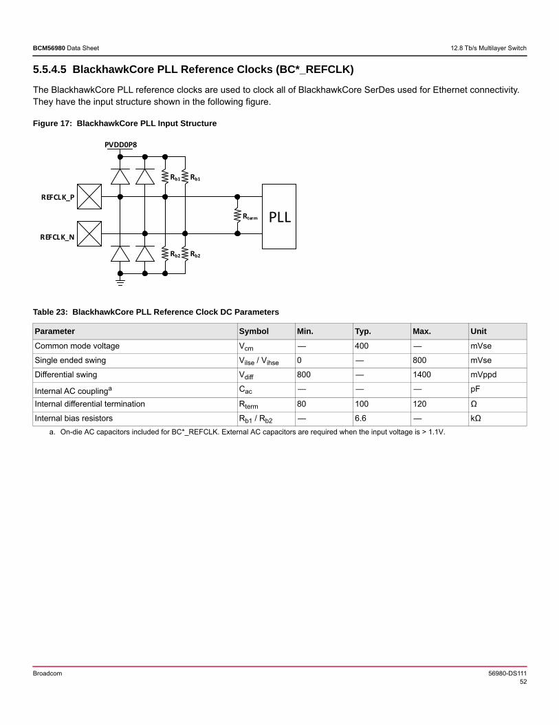
Broadcom 56980-DS11152
BCM56980 Data Sheet 12.8 Tb/s Multilayer Switch
5.5.4.5 BlackhawkCore PLL Reference Clocks (BC*_REFCLK)
The BlackhawkCore PLL reference clocks are used to clock all of BlackhawkCore SerDes used for Ethernet connectivity. They have the input structure shown in the following figure.
Figure 17: BlackhawkCore PLL Input Structure
Table 23: BlackhawkCore PLL Reference Clock DC Parameters
Parameter Symbol Min. Typ. Max. UnitCommon mode voltage Vcm — 400 — mVse
Single ended swing Vilse / Vihse 0 — 800 mVse
Differential swing Vdiff 800 — 1400 mVppd
Internal AC couplinga
a. On-die AC capacitors included for BC*_REFCLK. External AC capacitors are required when the input voltage is > 1.1V.
Cac — — — pF
Internal differential termination Rterm 80 100 120 Ω
Internal bias resistors Rb1 / Rb2 — 6.6 — kΩ
PLL
PVDD0P8
Rb2
REFCLK_P
REFCLK_N
Rterm
Rb2
Rb1 Rb1
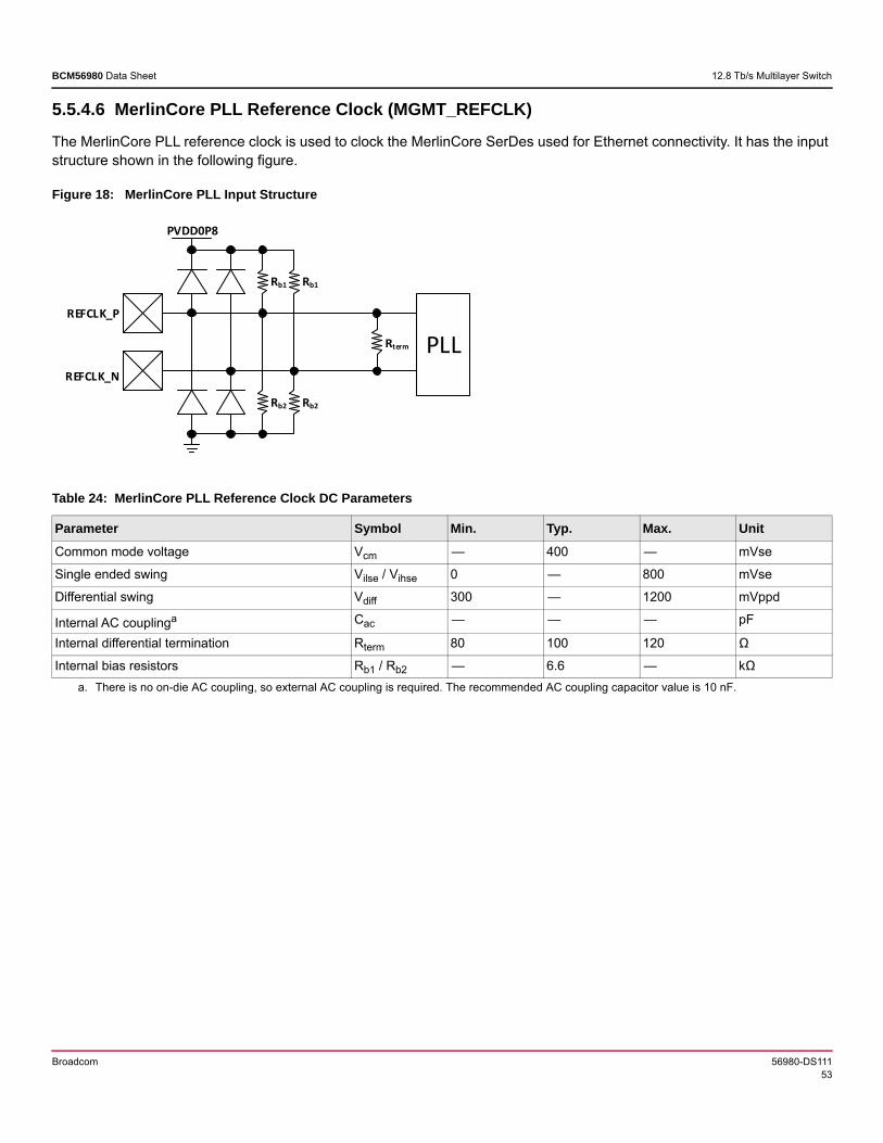
Broadcom 56980-DS11153
BCM56980 Data Sheet 12.8 Tb/s Multilayer Switch
5.5.4.6 MerlinCore PLL Reference Clock (MGMT_REFCLK)
The MerlinCore PLL reference clock is used to clock the MerlinCore SerDes used for Ethernet connectivity. It has the input structure shown in the following figure.
Figure 18: MerlinCore PLL Input Structure
Table 24: MerlinCore PLL Reference Clock DC Parameters
Parameter Symbol Min. Typ. Max. UnitCommon mode voltage Vcm — 400 — mVse
Single ended swing Vilse / Vihse 0 — 800 mVse
Differential swing Vdiff 300 — 1200 mVppd
Internal AC couplinga
a. There is no on-die AC coupling, so external AC coupling is required. The recommended AC coupling capacitor value is 10 nF.
Cac — — — pF
Internal differential termination Rterm 80 100 120 Ω
Internal bias resistors Rb1 / Rb2 — 6.6 — kΩ
PLL
PVDD0P8
Rb2
REFCLK_P
REFCLK_N
Rterm
Rb2
Rb1 Rb1
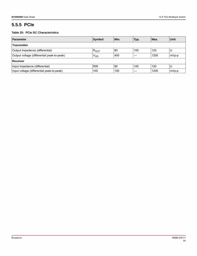
Broadcom 56980-DS11154
BCM56980 Data Sheet 12.8 Tb/s Multilayer Switch
5.5.5 PCIeTable 25: PCIe DC Characteristics
Parameter Symbol Min. Typ. Max. Unit
TransmitterOutput impedance (differential) ROUT 80 100 120
Output voltage (differential peak-to-peak) VOD 400 — 1200 mVp-p
ReceiverInput impedance (differential) RIN 80 100 120
Input voltage (differential peak-to-peak) VID 100 — 1200 mVp-p
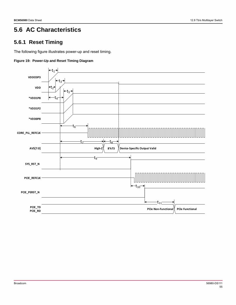
Broadcom 56980-DS11155
BCM56980 Data Sheet 12.8 Tb/s Multilayer Switch
5.6 AC Characteristics
5.6.1 Reset TimingThe following figure illustrates power-up and reset timing.
Figure 19: Power-Up and Reset Timing Diagram
VDDO3P3
VDD
*VDD1P8
*VDD1P2
*VDD0P8
CORE_PLL_REFCLK
SYS_RST_N
t1
t2
t3
t5t4
t7 t8
PCIE_REFCLK
AVS[7:0] High‐Z 8'h73 Device‐Specific Output Valid
t6
t9
PCIE_PERST_N
t10
PCIE_TDPCIE_RD
PCIe Non‐Functional PCIe Functional
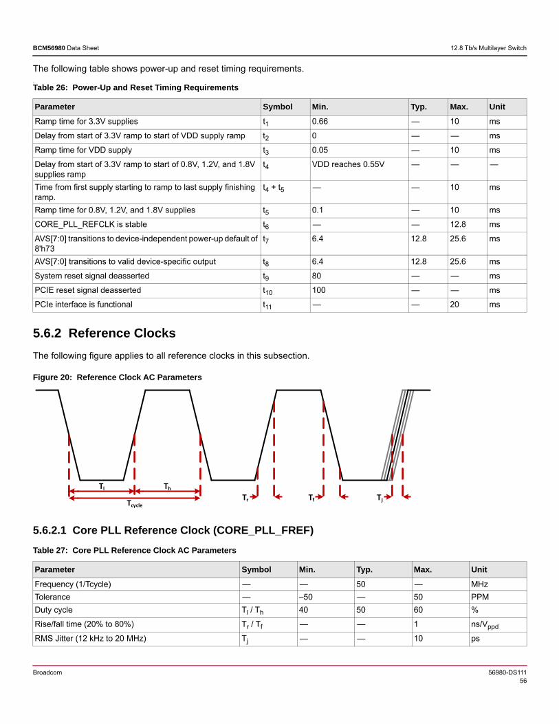
Broadcom 56980-DS11156
BCM56980 Data Sheet 12.8 Tb/s Multilayer Switch
The following table shows power-up and reset timing requirements..
5.6.2 Reference ClocksThe following figure applies to all reference clocks in this subsection.
Figure 20: Reference Clock AC Parameters
5.6.2.1 Core PLL Reference Clock (CORE_PLL_FREF)
Table 26: Power-Up and Reset Timing Requirements
Parameter Symbol Min. Typ. Max. UnitRamp time for 3.3V supplies t1 0.66 — 10 ms
Delay from start of 3.3V ramp to start of VDD supply ramp t2 0 — — ms
Ramp time for VDD supply t3 0.05 — 10 ms
Delay from start of 3.3V ramp to start of 0.8V, 1.2V, and 1.8V supplies ramp
t4 VDD reaches 0.55V — — —
Time from first supply starting to ramp to last supply finishing ramp.
t4 + t5 — — 10 ms
Ramp time for 0.8V, 1.2V, and 1.8V supplies t5 0.1 — 10 ms
CORE_PLL_REFCLK is stable t6 — — 12.8 ms
AVS[7:0] transitions to device-independent power-up default of 8'h73
t7 6.4 12.8 25.6 ms
AVS[7:0] transitions to valid device-specific output t8 6.4 12.8 25.6 ms
System reset signal deasserted t9 80 — — ms
PCIE reset signal deasserted t10 100 — — ms
PCIe interface is functional t11 — — 20 ms
Table 27: Core PLL Reference Clock AC Parameters
Parameter Symbol Min. Typ. Max. UnitFrequency (1/Tcycle) — — 50 — MHzTolerance — –50 — 50 PPMDuty cycle Tl / Th 40 50 60 %
Rise/fall time (20% to 80%) Tr / Tf — — 1 ns/Vppd
RMS Jitter (12 kHz to 20 MHz) Tj — — 10 ps
Tl Th
TcycleTr Tf Tj
Broadcom 56980-DS11157
BCM56980 Data Sheet 12.8 Tb/s Multilayer Switch
5.6.2.2 TimeSync PLL Reference Clock (TS_PLL_FREF)
5.6.2.3 BroadSync PLL Reference Clocks (BS_PLL0_FREF / BS_PLL1_FREF)
5.6.2.4 PCI Express PLL Reference Clock (PCIe_REFCLK)
Table 28: TimeSync PLL Reference Clock AC Parameters
Parameter Symbol Min. Typ. Max. Unit
Frequency (1/Tcycle)a
a. The Broadcom SDK automatically programs the PLL appropriately for the provided reference clock frequency.
— — 25 — MHz
Frequency (1/Tcycle)a — — 50 — MHz
Tolerance — –50 — 50 PPMDuty cycle Tl / Th 40 50 60 %
Rise/fall time (20% to 80%) Tr / Tf — — 1 ns/Vppd
RMS Jitter (12 kHz to 20 MHz) Tj — — 10 ps
Table 29: BroadSync PLL Reference Clock AC Parameters
Parameter Symbol Min. Typ. Max. Unit
Frequency (1 / Tcycle)a
a. The Broadcom SDK automatically programs the PLL appropriately for the provided reference clock frequency.
— — 12.8 — MHz
Frequency (1 / Tcycle)a — — 20 — MHz
Frequency (1 / Tcycle)a — — 25 — MHz
Frequency (1 / Tcycle)a — — 32 — MHz
Frequency (1 / Tcycle)a — — 50 — MHz
Tolerance — –50 — 50 PPMDuty cycle Tl / Th 40 50 60 %
Rise/fall time (20% to 80%) Tr / Tf — — 1 ns/Vppd
RMS Jitter (12 kHz to 20 MHz) Tj — — 10 ps
Table 30: PCI Express PLL Reference Clock AC Parameters
Parameter Symbol Min. Typ. Max. UnitFrequency (1 / Tcycle) — — 100 — MHzTolerance — –300 — 300 PPMDuty cycle Tl / Th 40 50 60 %
Rise/fall time (20% to 80%) Tr / Tf — — 0.9 ns
RMS Jitter (10 kHz to 1.5 MHz) (Gen3 – 8 Gb/s) Tj — — 1.0 ps
RMS Jitter (10 kHz to 1.5 MHz) (Gen2 – 5 Gb/s) Tj — — 3.0 ps
RMS jitter (Cycle-to-Cycle) (Gen1 – 2.5 Gb/s) Tj — — 150 ps
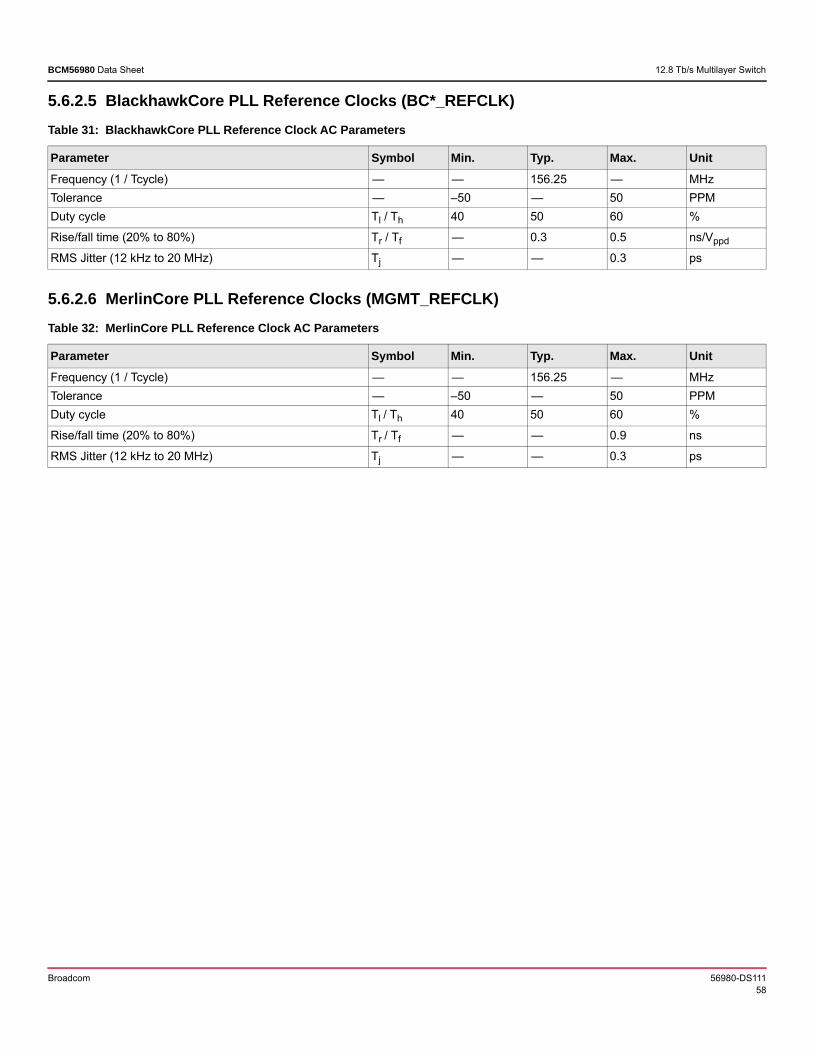
Broadcom 56980-DS11158
BCM56980 Data Sheet 12.8 Tb/s Multilayer Switch
5.6.2.5 BlackhawkCore PLL Reference Clocks (BC*_REFCLK)
5.6.2.6 MerlinCore PLL Reference Clocks (MGMT_REFCLK)
Table 31: BlackhawkCore PLL Reference Clock AC Parameters
Parameter Symbol Min. Typ. Max. UnitFrequency (1 / Tcycle) — — 156.25 — MHzTolerance — –50 — 50 PPMDuty cycle Tl / Th 40 50 60 %
Rise/fall time (20% to 80%) Tr / Tf — 0.3 0.5 ns/Vppd
RMS Jitter (12 kHz to 20 MHz) Tj — — 0.3 ps
Table 32: MerlinCore PLL Reference Clock AC Parameters
Parameter Symbol Min. Typ. Max. UnitFrequency (1 / Tcycle) — — 156.25 — MHzTolerance — –50 — 50 PPMDuty cycle Tl / Th 40 50 60 %
Rise/fall time (20% to 80%) Tr / Tf — — 0.9 ns
RMS Jitter (12 kHz to 20 MHz) Tj — — 0.3 ps
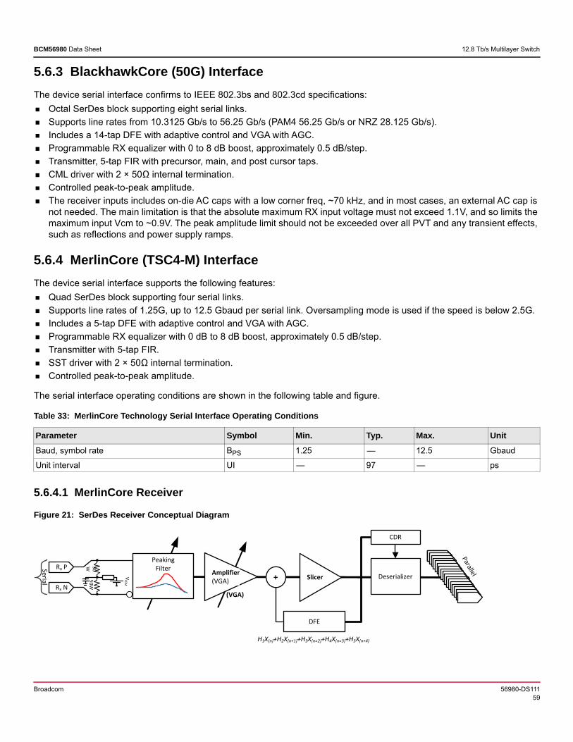
Broadcom 56980-DS11159
BCM56980 Data Sheet 12.8 Tb/s Multilayer Switch
5.6.3 BlackhawkCore (50G) InterfaceThe device serial interface confirms to IEEE 802.3bs and 802.3cd specifications: Octal SerDes block supporting eight serial links. Supports line rates from 10.3125 Gb/s to 56.25 Gb/s (PAM4 56.25 Gb/s or NRZ 28.125 Gb/s). Includes a 14-tap DFE with adaptive control and VGA with AGC. Programmable RX equalizer with 0 to 8 dB boost, approximately 0.5 dB/step. Transmitter, 5-tap FIR with precursor, main, and post cursor taps. CML driver with 2 × 50Ω internal termination. Controlled peak-to-peak amplitude. The receiver inputs includes on-die AC caps with a low corner freq, ~70 kHz, and in most cases, an external AC cap is
not needed. The main limitation is that the absolute maximum RX input voltage must not exceed 1.1V, and so limits the maximum input Vcm to ~0.9V. The peak amplitude limit should not be exceeded over all PVT and any transient effects, such as reflections and power supply ramps.
5.6.4 MerlinCore (TSC4-M) InterfaceThe device serial interface supports the following features: Quad SerDes block supporting four serial links. Supports line rates of 1.25G, up to 12.5 Gbaud per serial link. Oversampling mode is used if the speed is below 2.5G. Includes a 5-tap DFE with adaptive control and VGA with AGC. Programmable RX equalizer with 0 dB to 8 dB boost, approximately 0.5 dB/step. Transmitter with 5-tap FIR. SST driver with 2 × 50Ω internal termination. Controlled peak-to-peak amplitude.
The serial interface operating conditions are shown in the following table and figure.
5.6.4.1 MerlinCore Receiver
Figure 21: SerDes Receiver Conceptual Diagram
Table 33: MerlinCore Technology Serial Interface Operating Conditions
Parameter Symbol Min. Typ. Max. UnitBaud, symbol rate BPS 1.25 — 12.5 Gbaud
Unit interval UI — 97 — ps
Rx P
DFE
Rx N
50W
50W
VICM
+ Deserializer
CDR
Parallel
Slicer
Serial
H1X(n)+H2X(n+1)+H3X(n=2)+H4X(n=3)+H5X(n+4)
PeakingFilter
Amplifier (VGA)
(VGA)
Broadcom 56980-DS11160
BCM56980 Data Sheet 12.8 Tb/s Multilayer Switch
The serial interface receive characteristics are shown in the following table and figure.
5.6.4.2 MerlinCore Transmitter
Figure 22: SerDes Transmitter Conceptual Diagram
The serial interface transmit characteristics are shown in the following table.
Table 34: Serial Interface Receive Characteristics
Parameter Symbol Description Min. Typ. Max. UnitJitter tolerance ΔtRXtot Total, peak-to-peak — — 0.65 UI
ΔtRXdet Deterministic, peak-to-peak — — 0.42 UI
Table 35: Serial Interface Transmit Characteristics
Parameter Symbol Description Min. Typ. Max. UnitOutput voltage fall time tfall 80% to 20% (based on 10GBASE-KR waveform,
8–1s, 8–0s)24 — 36 ps
Output voltage rise time trise 20% to 80% (based on 10GBASE-KR waveform, 8–1s, 8–0s)
24 — 36 ps
Output differential skew tskewo 50% rising/falling versus 50% falling/rising edge — — 5 ps
Transmit output jitter ΔtTXRND Random, wideband, RMS — 0.008 0.130 UI
ΔtTXtot Total, peak-to-peak — — 0.18 UI
ΔtTXdet Deterministic, peak-to-peak — 0.05 — UI
Tx PSSTD river
Tx NSeria lize r
Para llel
Serial
50W
50W
TVD D10
+ Q D
Q D
Q D
Q D
Post2 Post1 Main Pre
(1 - - ) - .Z +1 - .Z -1 - .Z -2
Broadcom 56980-DS11161
BCM56980 Data Sheet 12.8 Tb/s Multilayer Switch
5.6.5 PCIe Interface
5.6.5.1 PCIe Receiver Input
Figure 23: PCIe_RX Timing Diagram
5.6.5.2 PCIe Transmitter Output
Figure 24: PCIe_TX Timing Diagram
Table 36: PCIe_RX
Parameters Symbol Min. Typ. Max. UnitBaud rate FREQ — 2.5, 5.0, or 8.0 — GbaudMinimum RX total jitter TJ 0.6 — — UI
NOTE: Includes on-chip AC coupling capacitors.
Table 37: PCIe_Transmitter Output Timing
Parameters Symbol Condition Min. Typ. Max. UnitBaud rate FREQ — — 2.5, 5.0, or 8.0 — GbaudOutput rise/fall time (20% to 80%) TR/TF — 30 — 90 ps
Output deemphasisa
a. The output deemphasis values listed in this table are the default settings. TX deemphasis can be software configured in the range of 0 db to 8 dB, overriding the defaults.
VOEQ Gen1 2.5 Gb/sGen1 5.0 Gb/s
–3.0–5.5
–3.5–6.0
–4.0–6.5
dB
Minimum TX total jitter TJ — 0.75 — — UI
PCIE_RXP/N
TR TF
PCIE_TXP/N
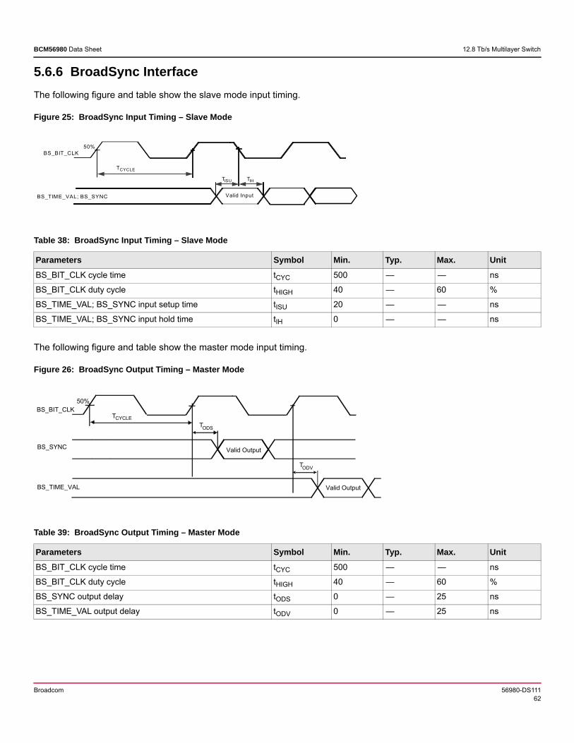
Broadcom 56980-DS11162
BCM56980 Data Sheet 12.8 Tb/s Multilayer Switch
5.6.6 BroadSync InterfaceThe following figure and table show the slave mode input timing.
Figure 25: BroadSync Input Timing – Slave Mode
The following figure and table show the master mode input timing.
Figure 26: BroadSync Output Timing – Master Mode
Table 38: BroadSync Input Timing – Slave Mode
Parameters Symbol Min. Typ. Max. UnitBS_BIT_CLK cycle time tCYC 500 — — ns
BS_BIT_CLK duty cycle tHIGH 40 — 60 %
BS_TIME_VAL; BS_SYNC input setup time tISU 20 — — ns
BS_TIME_VAL; BS_SYNC input hold time tIH 0 — — ns
Table 39: BroadSync Output Timing – Master Mode
Parameters Symbol Min. Typ. Max. UnitBS_BIT_CLK cycle time tCYC 500 — — ns
BS_BIT_CLK duty cycle tHIGH 40 — 60 %
BS_SYNC output delay tODS 0 — 25 ns
BS_TIME_VAL output delay tODV 0 — 25 ns
50%BS_BIT_CLK
TCYCLE
BS_TIME_VAL; BS_SYNC
TISU
Valid Input
TIH
50%BS_BIT_CLK
TCYCLE
BS_SYNC
TODS
Valid Output
BS_TIME_VAL Valid Output
TODV
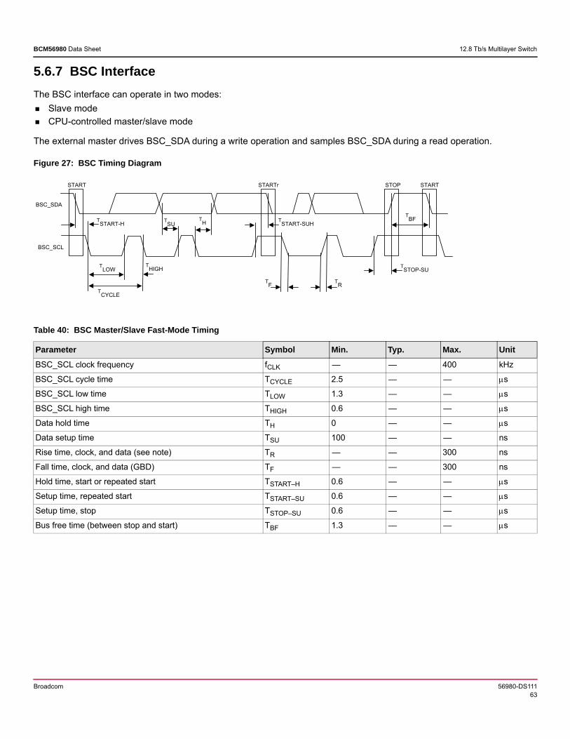
Broadcom 56980-DS11163
BCM56980 Data Sheet 12.8 Tb/s Multilayer Switch
5.6.7 BSC InterfaceThe BSC interface can operate in two modes: Slave mode CPU-controlled master/slave mode
The external master drives BSC_SDA during a write operation and samples BSC_SDA during a read operation.
Figure 27: BSC Timing Diagram
Table 40: BSC Master/Slave Fast-Mode Timing
Parameter Symbol Min. Typ. Max. UnitBSC_SCL clock frequency fCLK — — 400 kHz
BSC_SCL cycle time TCYCLE 2.5 — — s
BSC_SCL low time TLOW 1.3 — — s
BSC_SCL high time THIGH 0.6 — — s
Data hold time TH 0 — — s
Data setup time TSU 100 — — ns
Rise time, clock, and data (see note) TR — — 300 ns
Fall time, clock, and data (GBD) TF — — 300 ns
Hold time, start or repeated start TSTART–H 0.6 — — s
Setup time, repeated start TSTART–SU 0.6 — — s
Setup time, stop TSTOP–SU 0.6 — — s
Bus free time (between stop and start) TBF 1.3 — — s
BSC_SCL
BSC_SDA
TSTART-H
START STARTr STOP START
TSUTBFTSTART-SUH
TH
TSTOP-SUTLOW
TCYCLE
THIGH
TF TR
Broadcom 56980-DS11164
BCM56980 Data Sheet 12.8 Tb/s Multilayer Switch
NOTE: BSC_SCL and BSC_SDA are open-drain outputs. The rise time is dependent on the strength of the external pull-up resistor, which must be selected to meet the rise-time requirement.
The device drives the BSC_SCL clock with a programmable speed of 100 kHz or 400 kHz based on the mode bit called MODE_400. The device drives BSC_SDA during a write operation and samples BSC_SDA during a read operation.
Table 41: BSC Master/Slave Standard-Mode Timing
Parameter Symbol Min. Typ. Max. UnitBSC_SCL clock frequency fCLK — — 100 kHz
BSC_SCL cycle time TCYCLE 10 — — s
BSC_SCL low time TLOW 4.7 — — s
BSC_SCL high time THIGH 4.0 — — s
Data hold time TH 0.0 — — s
Data setup time TSU 250 — — ns
Rise time, clock, and data (see note) TR — — 1000 ns
Fall time, clock, and data (GBD) TF — — 300 ns
Hold time, start, or repeated start TSTART–H 4.0 — — s
Setup time, repeated start TSTART–SU 4.7 — — s
Setup time, stop TSTOP–SU 4.0 — — s
Bus free time (between stop and start) TBF 4.7 — — s
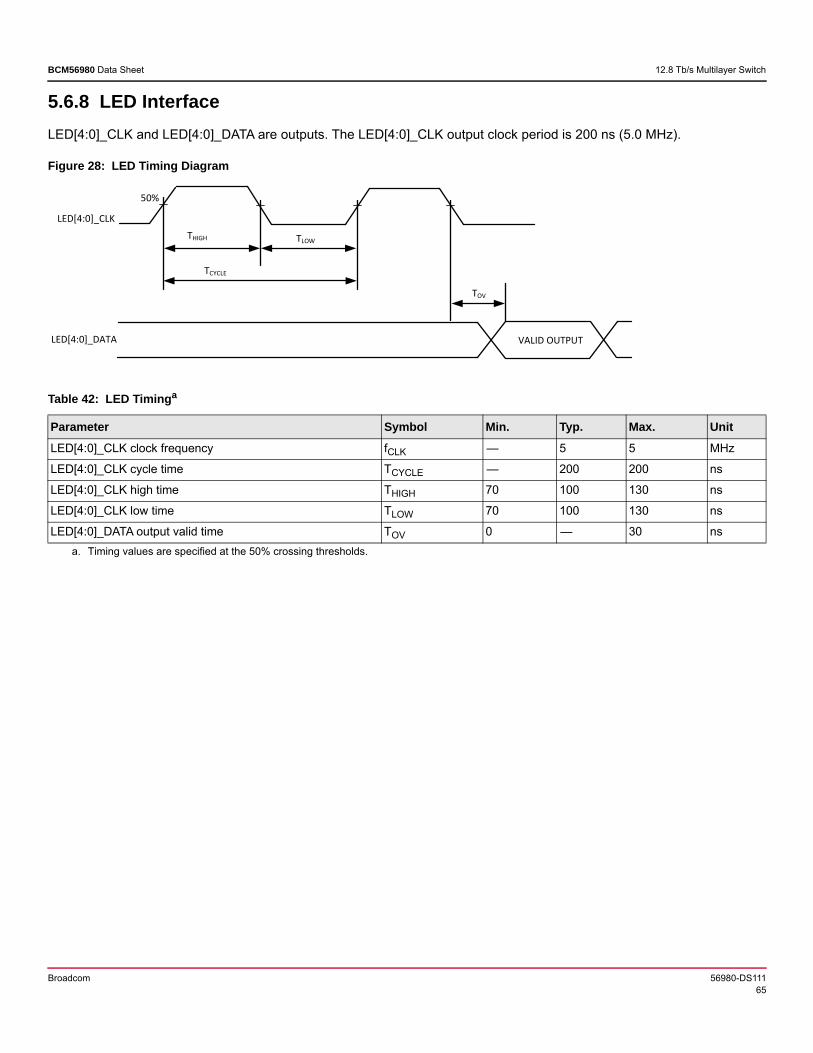
Broadcom 56980-DS11165
BCM56980 Data Sheet 12.8 Tb/s Multilayer Switch
5.6.8 LED InterfaceLED[4:0]_CLK and LED[4:0]_DATA are outputs. The LED[4:0]_CLK output clock period is 200 ns (5.0 MHz).
Figure 28: LED Timing Diagram
Table 42: LED Timinga
a. Timing values are specified at the 50% crossing thresholds.
Parameter Symbol Min. Typ. Max. UnitLED[4:0]_CLK clock frequency fCLK — 5 5 MHz
LED[4:0]_CLK cycle time TCYCLE — 200 200 ns
LED[4:0]_CLK high time THIGH 70 100 130 ns
LED[4:0]_CLK low time TLOW 70 100 130 ns
LED[4:0]_DATA output valid time TOV 0 — 30 ns
LED[4:0]_CLK
50%
THIGH
TCYCLE
TLOW
LED[4:0]_DATA
TOV
VALID OUTPUT
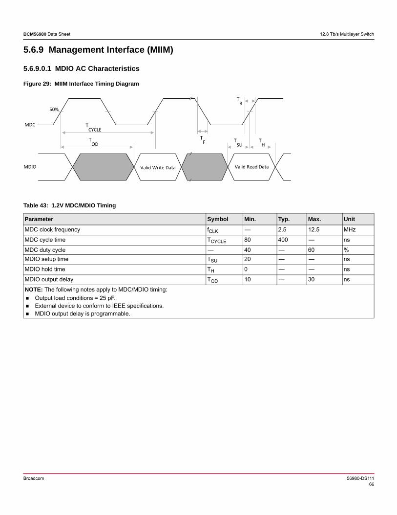
Broadcom 56980-DS11166
BCM56980 Data Sheet 12.8 Tb/s Multilayer Switch
5.6.9 Management Interface (MIIM)
5.6.9.0.1 MDIO AC Characteristics
Figure 29: MIIM Interface Timing Diagram
Table 43: 1.2V MDC/MDIO Timing
Parameter Symbol Min. Typ. Max. UnitMDC clock frequency fCLK — 2.5 12.5 MHz
MDC cycle time TCYCLE 80 400 — ns
MDC duty cycle — 40 — 60 %MDIO setup time TSU 20 — — ns
MDIO hold time TH 0 — — ns
MDIO output delay TOD 10 — 30 ns
NOTE: The following notes apply to MDC/MDIO timing: Output load conditions = 25 pF. External device to conform to IEEE specifications. MDIO output delay is programmable.
MDC
MDIO
50%
TCYCLE
TOD
Valid Write Data Valid Read Data
TR
TH
TSU
TF
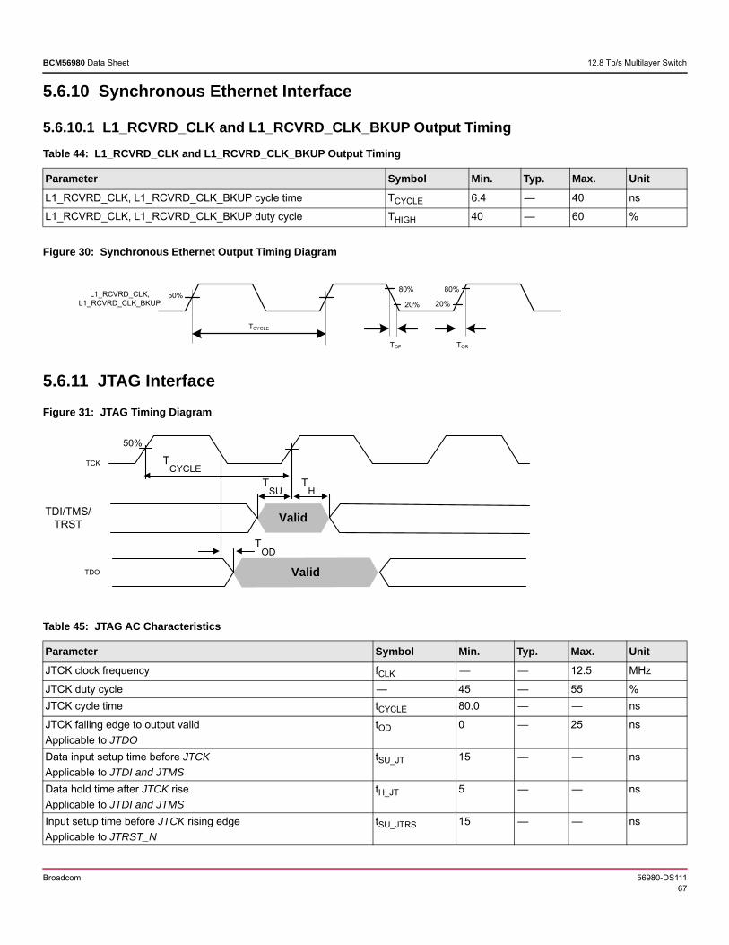
Broadcom 56980-DS11167
BCM56980 Data Sheet 12.8 Tb/s Multilayer Switch
5.6.10 Synchronous Ethernet Interface
5.6.10.1 L1_RCVRD_CLK and L1_RCVRD_CLK_BKUP Output Timing
Figure 30: Synchronous Ethernet Output Timing Diagram
5.6.11 JTAG InterfaceFigure 31: JTAG Timing Diagram
Table 44: L1_RCVRD_CLK and L1_RCVRD_CLK_BKUP Output Timing
Parameter Symbol Min. Typ. Max. UnitL1_RCVRD_CLK, L1_RCVRD_CLK_BKUP cycle time TCYCLE 6.4 — 40 ns
L1_RCVRD_CLK, L1_RCVRD_CLK_BKUP duty cycle THIGH 40 — 60 %
Table 45: JTAG AC Characteristics
Parameter Symbol Min. Typ. Max. UnitJTCK clock frequency fCLK — — 12.5 MHz
JTCK duty cycle — 45 — 55 %JTCK cycle time tCYCLE 80.0 — — ns
JTCK falling edge to output validApplicable to JTDO
tOD 0 — 25 ns
Data input setup time before JTCKApplicable to JTDI and JTMS
tSU_JT 15 — — ns
Data hold time after JTCK riseApplicable to JTDI and JTMS
tH_JT 5 — — ns
Input setup time before JTCK rising edgeApplicable to JTRST_N
tSU_JTRS 15 — — ns
TCYCLE
L1_RCVRD_CLK, L1_RCVRD_CLK_BKUP
50%20%20%
80% 80%
TOF TOR
TCK
TDI/TMS/TRST
TDO
Valid
Valid
TCYCLE
TSU
TH
TOD
50%
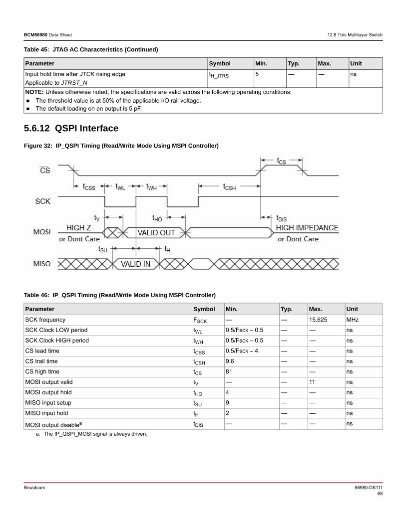
Broadcom 56980-DS11168
BCM56980 Data Sheet 12.8 Tb/s Multilayer Switch
5.6.12 QSPI InterfaceFigure 32: IP_QSPI Timing (Read/Write Mode Using MSPI Controller)
Input hold time after JTCK rising edgeApplicable to JTRST_N
tH_JTRS 5 — — ns
NOTE: Unless otherwise noted, the specifications are valid across the following operating conditions: The threshold value is at 50% of the applicable I/O rail voltage. The default loading on an output is 5 pF.
Table 46: IP_QSPI Timing (Read/Write Mode Using MSPI Controller)
Parameter Symbol Min. Typ. Max. UnitSCK frequency FSCK — — 15.625 MHz
SCK Clock LOW period tWL 0.5/Fsck – 0.5 — — ns
SCK Clock HIGH period tWH 0.5/Fsck – 0.5 — — ns
CS lead time tCSS 0.5/Fsck – 4 — — ns
CS trail time tCSH 9.6 — — ns
CS high time tCS 81 — — ns
MOSI output valid tV — — 11 ns
MOSI output hold tHO 4 — — ns
MISO input setup tSU 9 — — ns
MISO input hold tH 2 — — ns
MOSI output disablea
a. The IP_QSPI_MOSI signal is always driven.
tDIS — — — ns
Table 45: JTAG AC Characteristics (Continued)
Parameter Symbol Min. Typ. Max. Unit
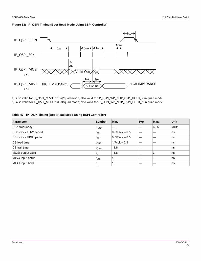
Broadcom 56980-DS11169
BCM56980 Data Sheet 12.8 Tb/s Multilayer Switch
Figure 33: IP_QSPI Timing (Boot Read Mode Using BSPI Controller)
Table 47: IP_QSPI Timing (Boot Read Mode Using BSPI Controller)
Parameter Symbol Min. Typ. Max. UnitSCK frequency FSCK — — 62.5 MHz
SCK clock LOW period tWL 0.5/Fsck – 0.5 — — ns
SCK clock HIGH period tWH 0.5/Fsck – 0.5 — — ns
CS lead time tCSS 1/Fsck – 2.9 — — ns
CS trail time tCSH –1.6 — — ns
MOSI output valid tV –1.6 — 3 ns
MISO input setup tSU 4 — — ns
MISO input hold tH 1 — — ns
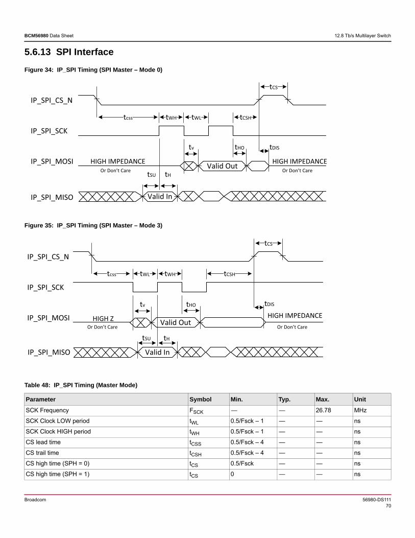
Broadcom 56980-DS11170
BCM56980 Data Sheet 12.8 Tb/s Multilayer Switch
5.6.13 SPI InterfaceFigure 34: IP_SPI Timing (SPI Master – Mode 0)
Figure 35: IP_SPI Timing (SPI Master – Mode 3)
Table 48: IP_SPI Timing (Master Mode)
Parameter Symbol Min. Typ. Max. UnitSCK Frequency FSCK — — 26.78 MHz
SCK Clock LOW period tWL 0.5/Fsck – 1 — — ns
SCK Clock HIGH period tWH 0.5/Fsck – 1 — — ns
CS lead time tCSS 0.5/Fsck – 4 — — ns
CS trail time tCSH 0.5/Fsck – 4 — — ns
CS high time (SPH = 0) tCS 0.5/Fsck — — ns
CS high time (SPH = 1) tCS 0 — — ns
Broadcom 56980-DS11171
BCM56980 Data Sheet 12.8 Tb/s Multilayer Switch
MOSI output valid tV — — 4 ns
MOSI output hold tHO –4 — — ns
MISO input setup tSU — — 9 ns
MISO input hold tH 0 — — ns
MOSI output disable tDIS — — 4 ns
Table 48: IP_SPI Timing (Master Mode) (Continued)
Parameter Symbol Min. Typ. Max. Unit
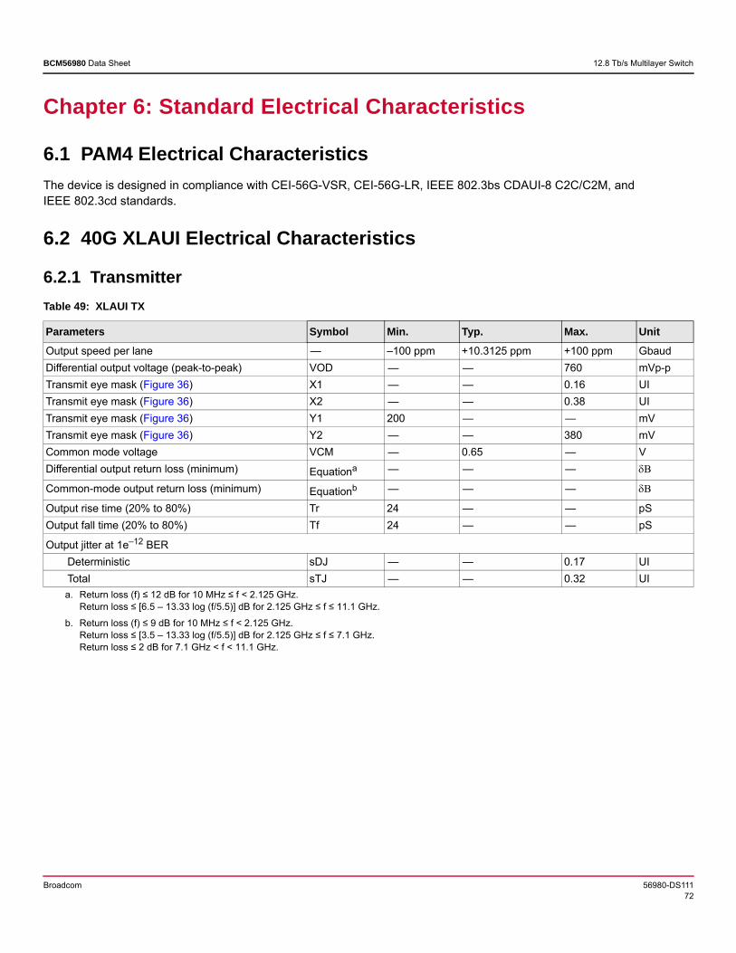
Broadcom 56980-DS11172
BCM56980 Data Sheet 12.8 Tb/s Multilayer Switch
Chapter 6: Standard Electrical Characteristics
6.1 PAM4 Electrical CharacteristicsThe device is designed in compliance with CEI-56G-VSR, CEI-56G-LR, IEEE 802.3bs CDAUI-8 C2C/C2M, and IEEE 802.3cd standards.
6.2 40G XLAUI Electrical Characteristics
6.2.1 TransmitterTable 49: XLAUI TX
Parameters Symbol Min. Typ. Max. UnitOutput speed per lane — –100 ppm +10.3125 ppm +100 ppm GbaudDifferential output voltage (peak-to-peak) VOD — — 760 mVp-pTransmit eye mask (Figure 36) X1 — — 0.16 UITransmit eye mask (Figure 36) X2 — — 0.38 UITransmit eye mask (Figure 36) Y1 200 — — mVTransmit eye mask (Figure 36) Y2 — — 380 mVCommon mode voltage VCM — 0.65 — VDifferential output return loss (minimum) Equationa
a. Return loss (f) ≤ 12 dB for 10 MHz ≤ f < 2.125 GHz.Return loss ≤ [6.5 – 13.33 log (f/5.5)] dB for 2.125 GHz ≤ f ≤ 11.1 GHz.
— — —
Common-mode output return loss (minimum) Equationb
b. Return loss (f) ≤ 9 dB for 10 MHz ≤ f < 2.125 GHz.Return loss ≤ [3.5 – 13.33 log (f/5.5)] dB for 2.125 GHz ≤ f ≤ 7.1 GHz.Return loss ≤ 2 dB for 7.1 GHz < f < 11.1 GHz.
— — —
Output rise time (20% to 80%) Tr 24 — — pSOutput fall time (20% to 80%) Tf 24 — — pS
Output jitter at 1e–12 BERDeterministic sDJ — — 0.17 UITotal sTJ — — 0.32 UI
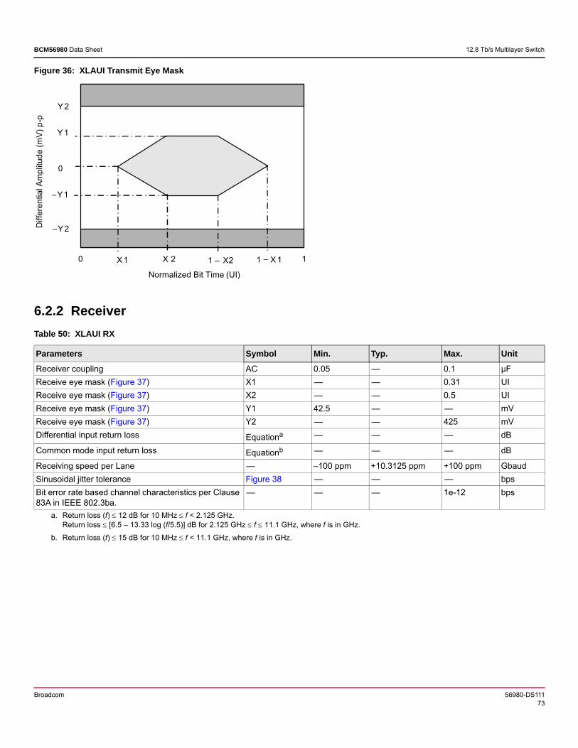
Broadcom 56980-DS11173
BCM56980 Data Sheet 12.8 Tb/s Multilayer Switch
Figure 36: XLAUI Transmit Eye Mask
6.2.2 ReceiverTable 50: XLAUI RX
Parameters Symbol Min. Typ. Max. UnitReceiver coupling AC 0.05 — 0.1 μFReceive eye mask (Figure 37) X1 — — 0.31 UIReceive eye mask (Figure 37) X2 — — 0.5 UIReceive eye mask (Figure 37) Y1 42.5 — — mVReceive eye mask (Figure 37) Y2 — — 425 mVDifferential input return loss Equationa
a. Return loss (f) 12 dB for 10 MHz f < 2.125 GHz. Return loss [6.5 – 13.33 log (f/5.5)] dB for 2.125 GHz f 11.1 GHz, where f is in GHz.
— — — dB
Common mode input return loss Equationb
b. Return loss (f) 15 dB for 10 MHz f < 11.1 GHz, where f is in GHz.
— — — dB
Receiving speed per Lane — –100 ppm +10.3125 ppm +100 ppm GbaudSinusoidal jitter tolerance Figure 38 — — — bpsBit error rate based channel characteristics per Clause 83A in IEEE 802.3ba.
— — — 1e-12 bps
Diff
eren
tial A
mpl
itude
(mV)
p-p
Y 2
0
Y 1
–Y1
–Y2
X 1 X 2 1 – X2 1 – X 1
Normalized Bit Time (UI)
0 1
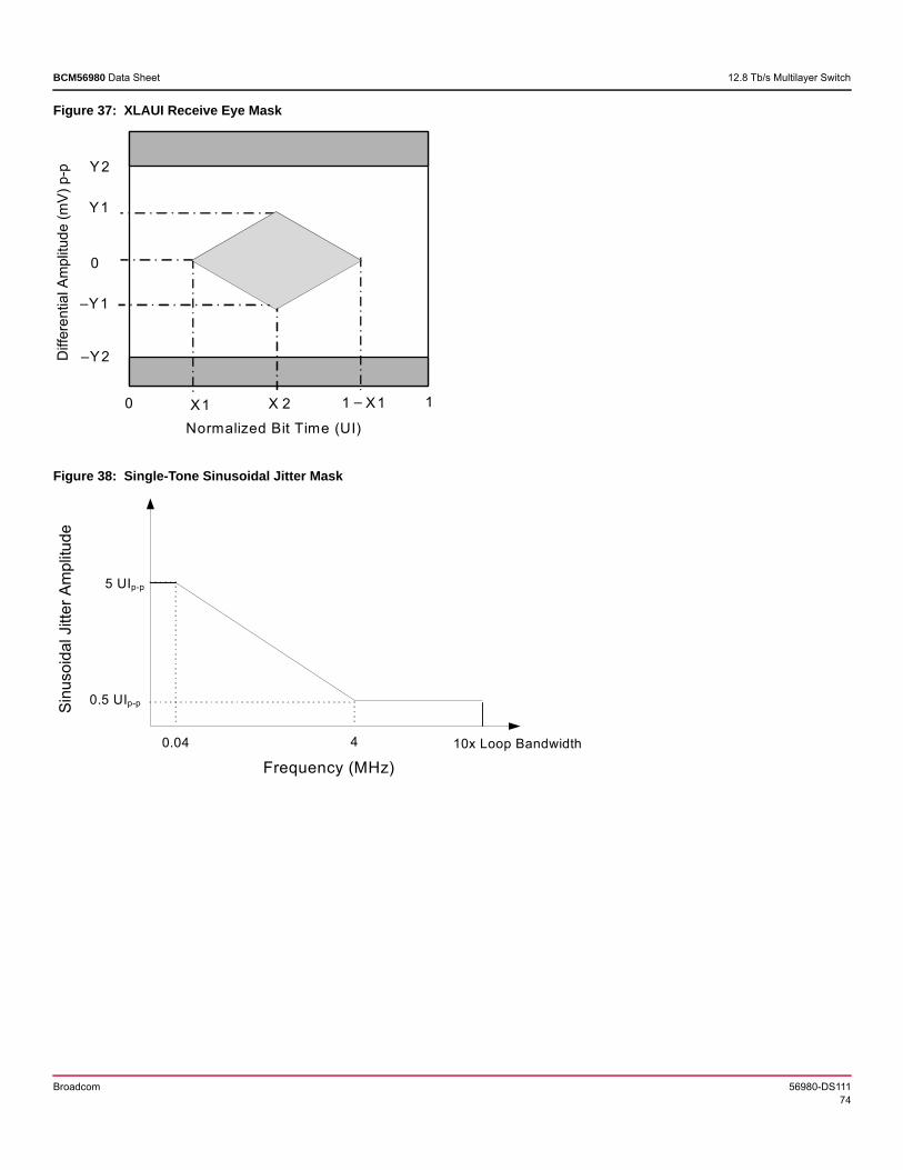
Broadcom 56980-DS11174
BCM56980 Data Sheet 12.8 Tb/s Multilayer Switch
Figure 37: XLAUI Receive Eye Mask
Figure 38: Single-Tone Sinusoidal Jitter Mask
Diff
eren
tial A
mpl
itude
(mV)
p-p Y 2
0
Y1
–Y1
–Y2
X1 X 2
Normalized Bit Time (UI)
0 11 – X1
Frequency (MHz)
Sinu
soid
al J
itter
Am
plitu
de
5 UIp-p
0.04 4 10x Loop Bandwidth
0.5 UIp-p
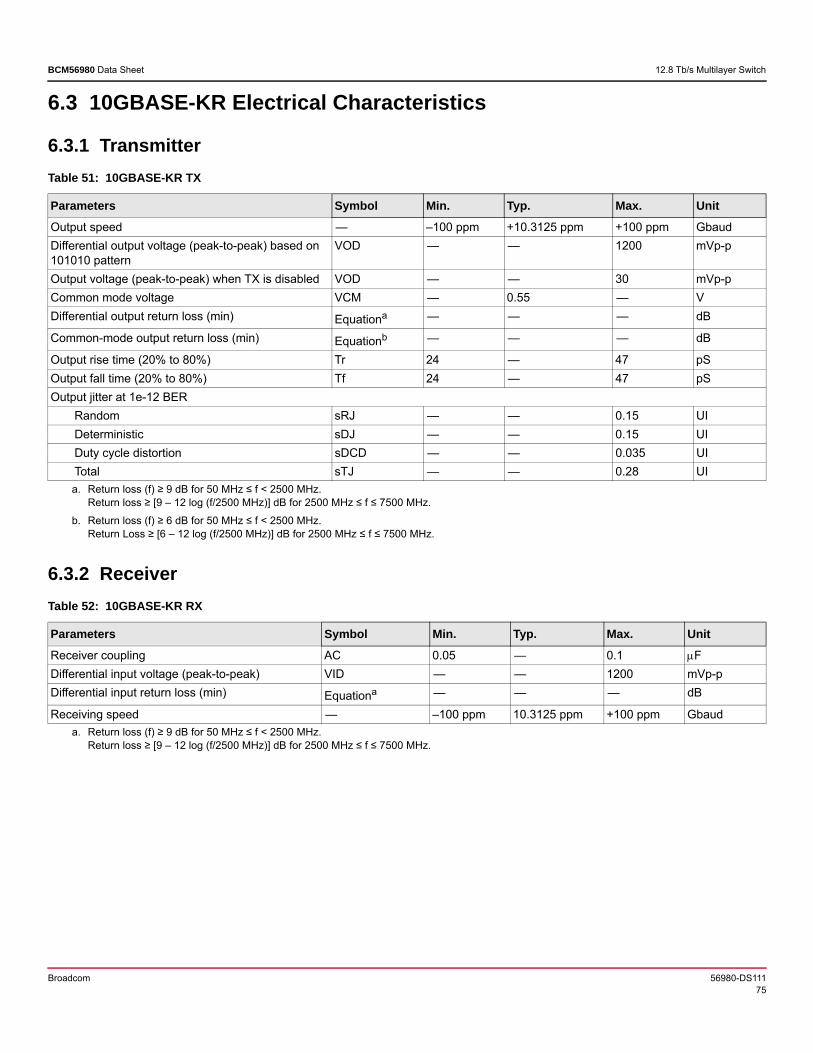
Broadcom 56980-DS11175
BCM56980 Data Sheet 12.8 Tb/s Multilayer Switch
6.3 10GBASE-KR Electrical Characteristics
6.3.1 Transmitter
6.3.2 Receiver
Table 51: 10GBASE-KR TX
Parameters Symbol Min. Typ. Max. UnitOutput speed — –100 ppm +10.3125 ppm +100 ppm GbaudDifferential output voltage (peak-to-peak) based on 101010 pattern
VOD — — 1200 mVp-p
Output voltage (peak-to-peak) when TX is disabled VOD — — 30 mVp-pCommon mode voltage VCM — 0.55 — VDifferential output return loss (min) Equationa
a. Return loss (f) ≥ 9 dB for 50 MHz ≤ f < 2500 MHz.Return loss ≥ [9 – 12 log (f/2500 MHz)] dB for 2500 MHz ≤ f ≤ 7500 MHz.
— — — dB
Common-mode output return loss (min) Equationb
b. Return loss (f) ≥ 6 dB for 50 MHz ≤ f < 2500 MHz.Return Loss ≥ [6 – 12 log (f/2500 MHz)] dB for 2500 MHz ≤ f ≤ 7500 MHz.
— — — dB
Output rise time (20% to 80%) Tr 24 — 47 pSOutput fall time (20% to 80%) Tf 24 — 47 pSOutput jitter at 1e-12 BER
Random sRJ — — 0.15 UIDeterministic sDJ — — 0.15 UIDuty cycle distortion sDCD — — 0.035 UITotal sTJ — — 0.28 UI
Table 52: 10GBASE-KR RX
Parameters Symbol Min. Typ. Max. UnitReceiver coupling AC 0.05 — 0.1 FDifferential input voltage (peak-to-peak) VID — — 1200 mVp-pDifferential input return loss (min) Equationa
a. Return loss (f) ≥ 9 dB for 50 MHz ≤ f < 2500 MHz.Return loss ≥ [9 – 12 log (f/2500 MHz)] dB for 2500 MHz ≤ f ≤ 7500 MHz.
— — — dB
Receiving speed — –100 ppm 10.3125 ppm +100 ppm Gbaud
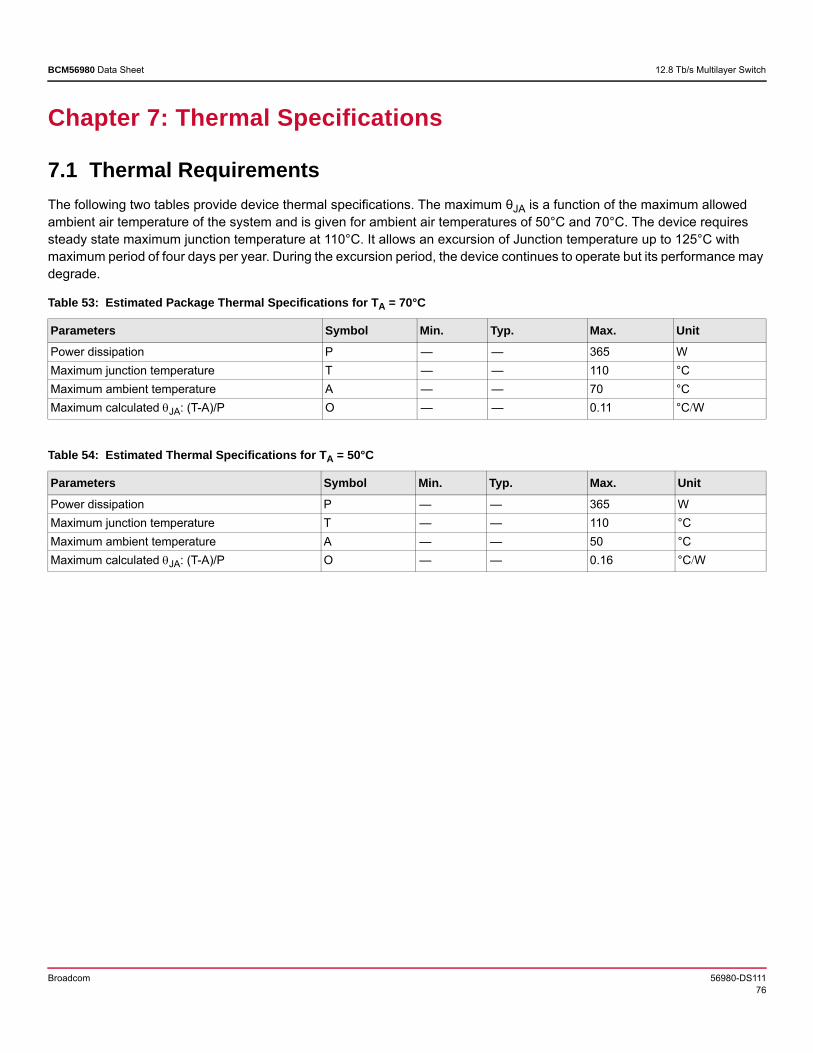
Broadcom 56980-DS11176
BCM56980 Data Sheet 12.8 Tb/s Multilayer Switch
Chapter 7: Thermal Specifications
7.1 Thermal RequirementsThe following two tables provide device thermal specifications. The maximum θJA is a function of the maximum allowed ambient air temperature of the system and is given for ambient air temperatures of 50°C and 70°C. The device requires steady state maximum junction temperature at 110°C. It allows an excursion of Junction temperature up to 125°C with maximum period of four days per year. During the excursion period, the device continues to operate but its performance may degrade.
Table 53: Estimated Package Thermal Specifications for TA = 70°C
Parameters Symbol Min. Typ. Max. UnitPower dissipation P — — 365 WMaximum junction temperature T — — 110 °CMaximum ambient temperature A — — 70 °CMaximum calculated JA: (T-A)/P O — — 0.11 °CW
Table 54: Estimated Thermal Specifications for TA = 50°C
Parameters Symbol Min. Typ. Max. UnitPower dissipation P — — 365 WMaximum junction temperature T — — 110 °CMaximum ambient temperature A — — 50 °CMaximum calculated JA: (T-A)/P O — — 0.16 °CW
Broadcom 56980-DS11177
BCM56980 Data Sheet 12.8 Tb/s Multilayer Switch
7.2 Package Thermal SpecificationsThe following table shows the preliminary package thermal specifications with a heat sink for various airflow levels. To maintain a junction temperature below the maximum specified junction temperature, the θJA must be smaller than the maximum calculated θJA for the device. A heat sink and airflow is required (see Section 7.3, Heat Sink).
NOTE: The package thermal number is based on a 220 mm × 160 mm × 29 mm heat sink with a vapor chamber base. The data in Table 55 is intended as a starting point for thermal analysis. Further simulation is required for each specific application.
Table 55: Estimated Package Thermal Specifications (220x160x29 mm Heat Sink with Vapor Chamber, 2s2p PCB)
Parameters Symbol Value UnitJB (junction-to-board) JB 0.24 °CW
JC (junction-to-case) JC 0.06 °CW
JA (junction-to-ambient), 200 LFM JA 0.22 °CW
JA (junction-to-ambient), 400 LFM JA 0.16 °CW
JA (junction-to-ambient), 600 LFM JA 0.14 °CW
JA (junction-to-ambient), 800 LFM JA 0.14 °CW
JA (junction-to-ambient), 1000 LFM JA 0.13 °C/W
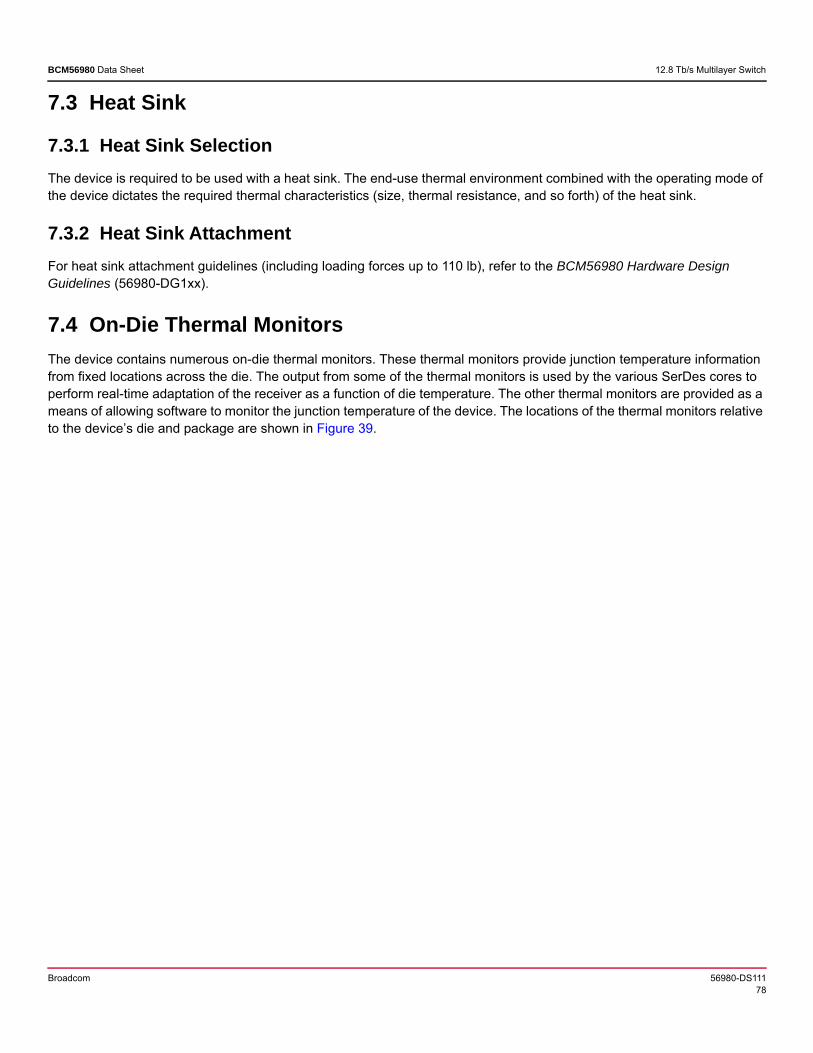
Broadcom 56980-DS11178
BCM56980 Data Sheet 12.8 Tb/s Multilayer Switch
7.3 Heat Sink
7.3.1 Heat Sink SelectionThe device is required to be used with a heat sink. The end-use thermal environment combined with the operating mode of the device dictates the required thermal characteristics (size, thermal resistance, and so forth) of the heat sink.
7.3.2 Heat Sink AttachmentFor heat sink attachment guidelines (including loading forces up to 110 lb), refer to the BCM56980 Hardware Design Guidelines (56980-DG1xx).
7.4 On-Die Thermal MonitorsThe device contains numerous on-die thermal monitors. These thermal monitors provide junction temperature information from fixed locations across the die. The output from some of the thermal monitors is used by the various SerDes cores to perform real-time adaptation of the receiver as a function of die temperature. The other thermal monitors are provided as a means of allowing software to monitor the junction temperature of the device. The locations of the thermal monitors relative to the device’s die and package are shown in Figure 39.
Broadcom 56980-DS11179
BCM56980 Data Sheet 12.8 Tb/s Multilayer Switch
Figure 39: BCM56980 On-Die Thermal MonitorsBC0……….BC6
BC6/BC7
BC8/BC9
VTMON7
VTMON1
VTMON8
VTMON6
VTMON5 VTMON4 VTMON11
VTMON3
VTMON13
VTMON0
VTMON12
VTMON10
VTMON2
VTMON9
VTMON15
TEMPDIODE0
TEMPDIODE1
VTMON14
MGMT/PCIe
BC10……….BC15
BC16……….BC21
BC22/BC23
BC24/BC25
BC26…
…….BC31
AVS
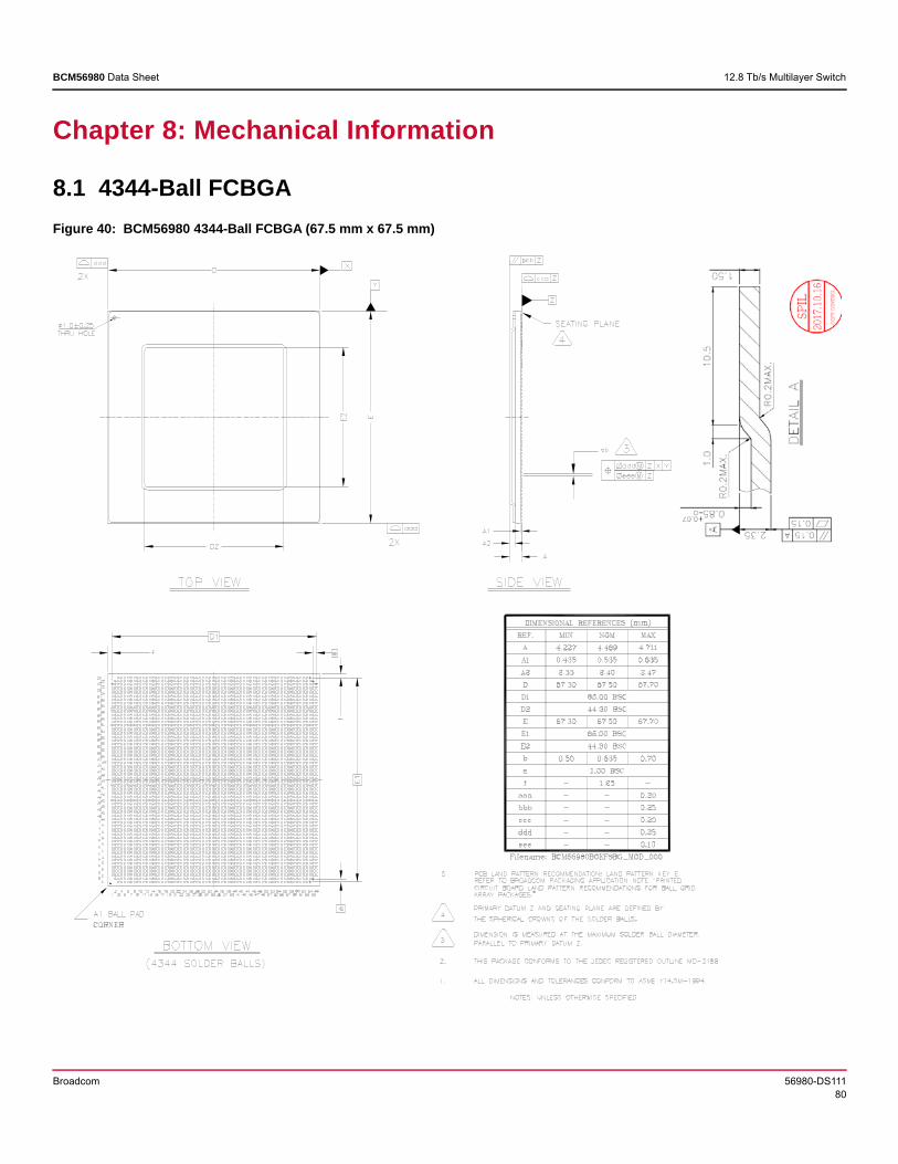
Broadcom 56980-DS11180
BCM56980 Data Sheet 12.8 Tb/s Multilayer Switch
Chapter 8: Mechanical Information
8.1 4344-Ball FCBGAFigure 40: BCM56980 4344-Ball FCBGA (67.5 mm x 67.5 mm)
Broadcom 56980-DS11181
BCM56980 Data Sheet 12.8 Tb/s Multilayer Switch
Chapter 9: Ordering Information
The following table lists the product part numbers available for order, their descriptions, and selected specifications.
9.1 PB-Free PackagingBroadcom offers Pb-free package. Pb-free parts have a letter G added to the top line of the part marking. Refer to the Reflow Process Guidelines for Surface Mount Assemblies application note (PACKAGING-AN1xx) for details. Broadcom Pb-free parts comply with RoHS and Waste Electrical and Electronic Equipment (WEEE) directives. Broadcom Pb-free parts are fully RoHS 6/6 compatible and require no exemption to comply with European limitations on hazardous substances. The following table shows the solder ball composition and maximum reflow temperature Pb-free parts.
For more information, refer to the BCM56980 SMT Preliminary Recommendations (BCM56980-SMT-Guide_xxx).
Table 56: Device Ordering Information
Part Number Package DescriptionI/O Bandwidth Temp
BCM56980B0KFSBG 4344-ball, 67.5 mm × 67.5 mmRoHS-compliant
32 × 400GbE, RoHS 6/6-compliant
12,800G 0°C to 70°C
BCM56983B0KFSBG 4344-ball, 67.5 mm × 67.5 mmRoHS-compliant
16 × 400GbERoHS 6/6-compliant
6,400G 0°C to 70°C
Table 57: Solder Ball Composition and Recommended and Maximum Reflow Temperature
Part Number Solder Ball CompositionRecommended Reflow Peak Temperature
Maximum Allowed Reflow Peak Temperature
Pb-free RoHS-compliant package 95.5% Sn, 3% Ag, 0.5% Cu 232°C to 237°C 245°C
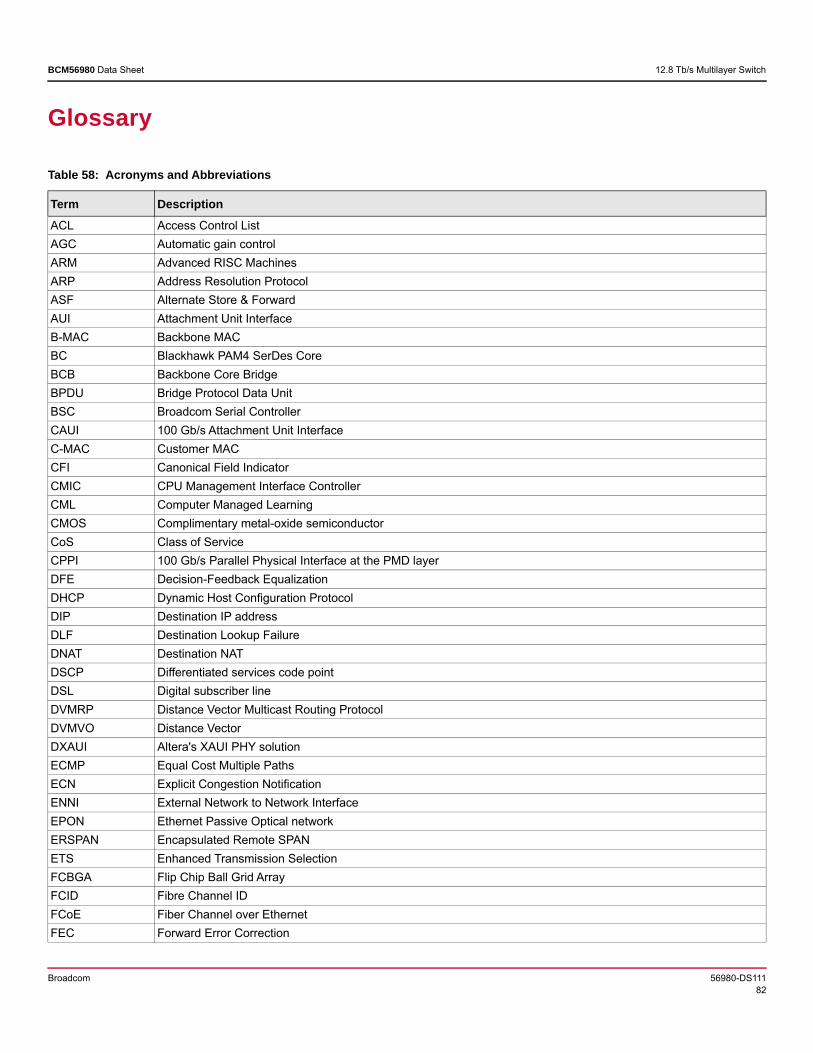
Broadcom 56980-DS11182
BCM56980 Data Sheet 12.8 Tb/s Multilayer Switch
Glossary
Table 58: Acronyms and Abbreviations
Term DescriptionACL Access Control ListAGC Automatic gain controlARM Advanced RISC MachinesARP Address Resolution ProtocolASF Alternate Store & Forward AUI Attachment Unit InterfaceB-MAC Backbone MACBC Blackhawk PAM4 SerDes CoreBCB Backbone Core BridgeBPDU Bridge Protocol Data Unit BSC Broadcom Serial ControllerCAUI 100 Gb/s Attachment Unit InterfaceC-MAC Customer MACCFI Canonical Field IndicatorCMIC CPU Management Interface ControllerCML Computer Managed LearningCMOS Complimentary metal-oxide semiconductorCoS Class of ServiceCPPI 100 Gb/s Parallel Physical Interface at the PMD layerDFE Decision-Feedback EqualizationDHCP Dynamic Host Configuration Protocol DIP Destination IP addressDLF Destination Lookup FailureDNAT Destination NATDSCP Differentiated services code pointDSL Digital subscriber lineDVMRP Distance Vector Multicast Routing ProtocolDVMVO Distance Vector DXAUI Altera's XAUI PHY solution ECMP Equal Cost Multiple PathsECN Explicit Congestion NotificationENNI External Network to Network InterfaceEPON Ethernet Passive Optical network ERSPAN Encapsulated Remote SPANETS Enhanced Transmission SelectionFCBGA Flip Chip Ball Grid ArrayFCID Fibre Channel IDFCoE Fiber Channel over EthernetFEC Forward Error Correction
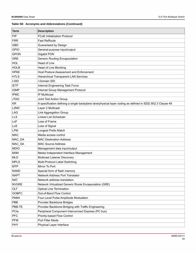
Broadcom 56980-DS11183
BCM56980 Data Sheet 12.8 Tb/s Multilayer Switch
FIP FCoE Initialization Protocol FRR Fast ReRouteGBD Guaranteed by DesignGPIO General-purpose input/outputGPON Gigabit PONGRE Generic Routing Encapsulation HOL Head of LineHOLB Head of Line BlockingHPAE Host Posture Assessment and Enforcement HTLS Hierarchical Transparent LAN ServicesI-SID I Domain SIDIETF Internet Engineering Task ForceIGMP Internet Group Management Protocol IPMC IP MuliticastJTAG Joint Test Action GroupKR A specification defining a single backplane lane/physical layer coding as defined in IEEE 802.3 Clause 49L2MC Layer 2 MulticastLAG Link Aggregation GroupLLS Linked List Scheduler LoF Loss of FrameLoS Loss of SignalLPM Longest Prefix MatchMAC Media access controlMAC_DA MAC Destination AddressMAC_SA MAC Source AddressMDIO Management data input/outputMIIM Media Independent Interface Management MLD Multicast Listener Discovery MPLS Multi-Protocol Label SwitchingMTP Mirror To PortNAND Special form of flash memoryNAPT Network Address Port TranslatorNAT Network address translationNVGRE Network Virtualized Generic Route Encapsulation (GRE)OLT Optical Line Termination OOBFC Out-of-Band Flow ControlPAM4 Four-Level Pulse Amplitude ModulationPBB Provider Backbone BridgesPBB-TE Provider Backbone Bridging with Traffic EngineeringPCIe Peripheral Component Interconnect Express (PC bus)PFC Priority-based Flow Control PFM Port Filter Mode PHY Physical Layer Interface
Table 58: Acronyms and Abbreviations (Continued)
Term Description

Broadcom 56980-DS11184
BCM56980 Data Sheet 12.8 Tb/s Multilayer Switch
PIM Protocol-Independent MulticastPIM-BIDR Protocol-Independent Multicast BiDirectional PIM-DM Protocol-Independent Multicast Dense ModePIM-SM Protocol-Independent Multicast Sparse ModePIM-SSM Protocol-Independent Multicast Single Source MulticastPLL Phase Loop LockQCN Quantized Congestion Notification/NotifierQoS Quality of ServiceQSGMII Quad Serial Gigabit Media Independent Interface RIOT Routing In and Out of TunnelRMON MIB Remote MONitoring Management Information BaseRSPAN Remote Switched Port AnalyzerRSSI Receive Signal Strength IndicationRX ReceiverRXAUI Reduced XAUIS-VID Service VLAN IDSAFC Service Aware Flow ControlSerDes Serialize DeserializeSFI SerDes Framer InterfaceSGMII Serial Gigabit Media Independent InterfaceSIP Source IP addressSLA Service Level AgreementSMON MIB Switched network MONitoring Management Information BaseSNAT Source NATSNMP Simple Network Management ProtocolSP Strict Priority srTCM single rate Three Color Marker/Marking SSTL Stub Series Terminated LogicTCAM Ternary Content Addressable MemoryTDM Time Division MultiplexorToR Top of RackTPID Tag Protocol IDTRILL Transparent Interconnection of Lots of LinkstrTCM two rate Three Color Marker/MarkingTSC TDM SerDes CoreTX TransmitterUART Universal Asynchronous Receiver/TransmitteruRPF unicast Reverse Path ForwardingVCO Voltage Controlled OscillatorVFI Virtual Forwarding InstanceVFP VLAN Filter Processor (or VCAP) VLAN Virtual Local Area NetworkVOQ Virtual Output Queue
Table 58: Acronyms and Abbreviations (Continued)
Term Description
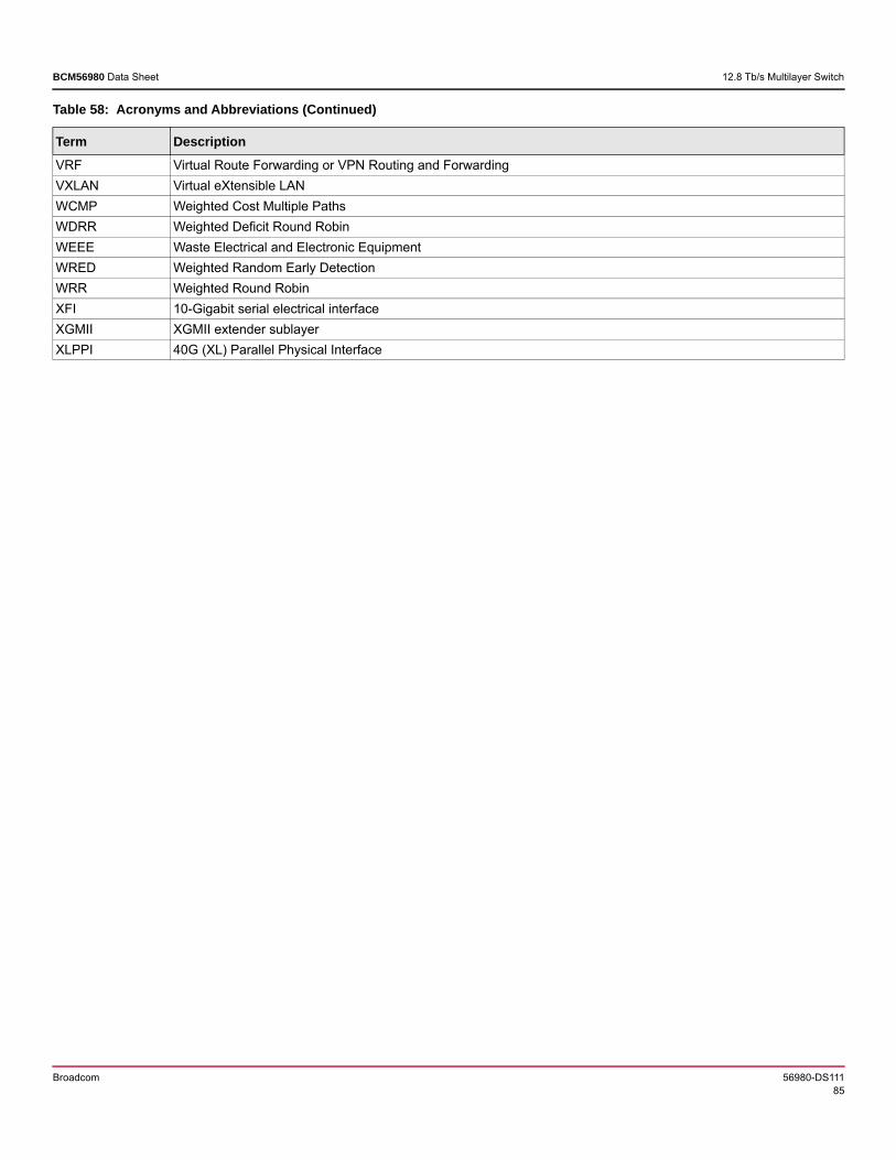
Broadcom 56980-DS11185
BCM56980 Data Sheet 12.8 Tb/s Multilayer Switch
VRF Virtual Route Forwarding or VPN Routing and ForwardingVXLAN Virtual eXtensible LANWCMP Weighted Cost Multiple PathsWDRR Weighted Deficit Round Robin WEEE Waste Electrical and Electronic EquipmentWRED Weighted Random Early DetectionWRR Weighted Round Robin XFI 10-Gigabit serial electrical interfaceXGMII XGMII extender sublayerXLPPI 40G (XL) Parallel Physical Interface
Table 58: Acronyms and Abbreviations (Continued)
Term Description
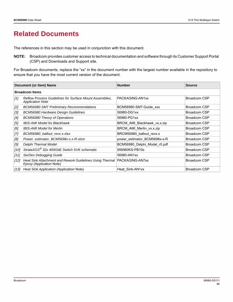
Broadcom 56980-DS11186
BCM56980 Data Sheet 12.8 Tb/s Multilayer Switch
Related Documents
The references in this section may be used in conjunction with this document.
NOTE: Broadcom provides customer access to technical documentation and software through its Customer Support Portal (CSP) and Downloads and Support site.
For Broadcom documents, replace the “xx” in the document number with the largest number available in the repository to ensure that you have the most current version of the document.
Document (or Item) Name Number Source
Broadcom Items[1] Reflow Process Guidelines for Surface Mount Assemblies,
Application NotePACKAGING-AN1xx Broadcom CSP
[2] BCM56980 SMT Preliminary Recommendations BCM56980-SMT-Guide_xxx Broadcom CSP[3] BCM56980 Hardware Design Guidelines 56980-DG1xx Broadcom CSP[4] BCM56980 Theory of Operations 56980-PG1xx Broadcom CSP[5] IBIS-AMI Model for Blackhawk BRCM_AMI_Blackhawk_vx.x.zip Broadcom CSP[6] IBIS-AMI Model for Merlin BRCM_AMI_Merlin_vx.x.zip Broadcom CSP[7] BCM56980_ballout_revx.x.xlsx BRCM56980_ballout_revx.x Broadcom CSP[8] Power_estimator_BCM5698x-x.x-R.xlsm power_estimator_BCM5698x-x-R Broadcom CSP[9] Delphi Thermal Model BCM56980_Delphi_Model_r0.pdf Broadcom CSP[10] StrataXGS® 32x 400GbE Switch SVK schematic 956980KS-PB10x Broadcom CSP[11] SerDes Debugging Guide 56980-AN1xx Broadcom CSP[12] Heat Sink Attachment and Rework Guidelines Using Thermal
Epoxy (Application Note)PACKAGING-AN7xx Broadcom CSP
[13] Heat Sink Application (Application Note) Heat_Sink-AN1xx Broadcom CSP
Broadcom 56980-DS11187
BCM56980 Data Sheet 12.8 Tb/s Multilayer Switch
Revision History
56980-DS111; July 19, 2019 Updated Table 3, BCM56980 Features to remove the MMU size and added a reference to Table 4, BCM56980 Family
Device Scalability. Updated Table 4, BCM56980 Family Device Scalability title to include all devices in the BCM56980 family and to add
the following:– Number of SerDes for the BCM56983.– Integrated Packet Buffer Memory for the BCM56983.
Updated Table 15, Per SerDes (Eight Lanes), Per Voltage Rail Maximum Power Numbers to show the PCIe SerDes maximum power option.
Updated the following tables to correct a unit typo for duty cycle from ns to %:– Table 38, BroadSync Input Timing – Slave Mode– Table 39, BroadSync Output Timing – Master Mode
56980-DS110; March 27, 2019 Updated the BCM56983 device’s typical configuration in Table 1, BCM56980 Family I/O Bandwidth and Throughput. Updated the BCM56983 device's maximum number of front-panel ports from 128 to 72 in the following locations:
– Table 2, BCM56980 Device Family Port Configurations.– Section 3.2, BlackhawkCore Octal SerDes Configuration Guidelines.
Updated Figure 3, BlackhawkCore (BC) Configuration, to add the BCM56983 device BC/pipeline restriction. Updated Table 7, BlackhawkCore Configurations, to remove support for 50G PAM4 non-FEC mode. Updated Table 9, Device Signal Descriptions:
– Corrected the typo from BroadSync0 to BroadSync1 for the BS_PLL1_FREFp/n pin description.– Clarified the description for the MHOST1_BOOT_DEV pin.
Updated Table 56, Device Ordering Information:– Modified the BCM56983 description.– Removed the BCM56982 and BCM56984 SKUs.
56980-DS109; January 17, 2019 Updated Table 15, Per SerDes (Eight Lanes), Per Voltage Rail Maximum Power Numbers, to clarify PCIe SerDes rail
names. Updated Section 7.3.2, Heat Sink Attachment, to provide additional information and to correct the typo in the Hardware
Design Guidelines document number.
56980-DS108; October 16, 2018 Removed “Advance” designation from data sheet because the BCM56980B0KFSBG is now production qualified. All
SKUs other than the BCM56980B0KFSBG are still pre-production. Updated the Features section on the cover page to remove Unified Forwarding Database with High-Density LPM Route
Table because this is an unsupported mode of operation. Updated Table 1, BCM56980 Family I/O Bandwidth and Throughput, to add BCM56983 device information. Updated Table 2, BCM56980 Device Family Port Configurations, to add BCM56983 device information.
Broadcom 56980-DS11188
BCM56980 Data Sheet 12.8 Tb/s Multilayer Switch
Updated Table 3, BCM56980 Features:– For the port configuration, 40GbE can also be 2-lane.– Removed Unified Forwarding Database with High-Density LPM Route Table because this is an unsupported mode of
operation.– Added low-latency mode.– Added EFP bypass– Added stacking/chassis information.
Updated Table 4, BCM56980 Device Scalability, to remove the footnote regarding unsupported operation mode that increases the MAC address feature.
Updated Table 7, BlackhawkCore Configurations:– Added support for reduced lane mode for 400G and 200G speeds.– Added note regarding condition for operating RS272 FEC.– Added note regarding restrictions for port-mode coexistence.
Updated Table 9, Device Signal Descriptions, to require the PCIe_PERST_L signal to be connected for Gen2 and Gen3 PCIe.
Updated Table 10, BCM56980, BCM56982, BCM56983, and BCM56984 Differences, to add BCM56983 device information.
Updated Table 14, System Thermal Design Maximum Power:– Added preliminary power values for the BCM56982, BCM56983, and BCM56984 devices.– Added footnote.
Updated Figure 19, Power-Up and Reset Timing Diagram, to clarify AVS output time frame. Updated Table 26, Power-Up and Reset Timing Requirements:
– Added t4 + t5 parameter.– Clarified AVS output time frame.
Updated Table 56, Device Ordering Information:– Removed A0 devices (only B0 silicon is going to production).– Added the BCM56983 SKU.
56980-DS107; July 5, 2018 Removed information regarding the Out-of-Band Flow Control feature. Due to lack of customer demand, the Out-of-
Band Flow Control feature has been deprecated. OOBFC information has been removed from:– Chapter 3, System Interfaces (note in beginning of chapter and Section 3.10 Out-of-Band Flow Control in previous
data sheet).– Table 9, BCM56980 Signal Descriptions.– Table 16, Standard 3.3V Signals.– Section 5.6, AC Characteristics (Section 5.6.12 OOBFC Interface in previous data sheet).
Removed heat sink attachment information. This information has been moved to the Hardware Design Guidelines document (56980-DG1xx).
Updated Section 8.1, 4344-Ball FCBGA package drawing dimension A from (3.637mm–4.121mm) to (4.227mm–4.711mm).
56980-DS106; June 11, 2018 Removed 32x200G support for BCM56984 in Table 2, BCM56980 Device Family Port Configurations. Corrected the VCO frequency from 25.78125G to 20.625G for 40G XLAUI2 mode in Table 7, BlackhawkCore
Configurations.
Broadcom 56980-DS11189
BCM56980 Data Sheet 12.8 Tb/s Multilayer Switch
Separated Table 13: BCM56980 Per Voltage Rail Maximum Power Numbers into Table 13, BCM56980 Maximum Per Rail Current for Power Supply Design and Table 14, BCM56980 Maximum System Power used for system thermal design. Added note to clarify the differences.
Updated Table 54, Estimated Package Thermal Specifications for TA = 70°C and Table 55, Estimated Thermal Specifications for TA = 50°C with updated power.
Added package lid dimension to Figure 41, BCM56980 4344-Ball FCBGA (67.5 mm x 67.5 mm).
56980-DS105; May 17, 2018 Added 40G XLAUI2 support in Table 7, BlackhawkCore Configurations. Changed names of BC*PLL*_REFCLK* pins in Table 9, BCM56980 Signal Descriptions. Changes do not affect the
functionality of the device. Changed VDD to 0.75V-0.90V +/- 3% tolerance in Table 11, Operating Conditions. Updated estimated power in Table 13, BCM56980 Per Voltage Rail Maximum Power Numbers. Changed footnote to indicate there is an on-die capacitor included in Table 26, BlackhawkCore PLL Reference Clock
DC Parameters. Corrected the max swing to 1200 mV per specification in Table 27, MerlinCore PLL Reference Clock DC Parameters. Corrected the PCIE REFCLK Tr/Tf max swing to 0.9ns in Table 33, PCI Express PLL Reference Clock AC Parameters. Corrected the typo for BC*REFCLK typical Rise/Fall time to 0.3ns and max Rise/Fall time to 0.5ns in
Table 34, BlackhawkCore PLL Reference Clock AC Parameters. Corrected the MGMT_REFCLK Tr/Tf max swing to 0.9ns in Table 35, MerlinCore PLL Reference Clock AC Parameters. Changed the maximum frequency to 62.5 MHz for IP_QSPI_SCK pin in Table 51, IP_QSPI Timing (Boot Read Mode
Using BSPI Controller). Added B0 devices in Table 60, Device Ordering Information and Table 10, BCM56980 and BCM56982 Differences.
56980-DS104; March 23, 2018 Added 50GBASE-KR2 and 50GBASE-CR2 interface types for 50G in Table 7, BlackhawkCore Configurations. Added 40GBASE-KR4 interface types for 40G in Table 7, BlackhawkCore Configurations. Changed PCIe_WAKE_L signal I/O type from BOD to OOD in Table 9, BCM56980 Signal Descriptions. Updated PCIe_WAKE_L, JTRST_L, IP_BSC[1:0]_SCL, BSC_SA[1:0], L1_RCVRD_CLK, L1_RCVRD_CLK_VALID,
L1_RCVRD_CLK_BKUP, L1_RCVRD_CLK_VALID_BKUP, IP_G_GPIO[9:0], IP_QSPI_WP_L, IP_MDC[11:0], IP_MDIO[11:0], TX_OOBFC_CLK, TX_OOBFC_SYNC, and TX_OOBFC_DATA_[1:0] signal descriptions to reflect up to date information in Table 9, BCM56980 Signal Descriptions.
Updated footnote in Table 18, Core PLL Reference Clock DC Parameters. Added Section 7.4, On-Die Thermal Monitors. Changed VDD AVS voltage range from 0.81V-0.89V to 0.76V-0.89V in Table 11, Operating Conditions and
Table 9, BCM56980 Signal Descriptions. Added additional note on AVS voltage range in Table 11, Operating Conditions. Added new BCM56984 part number in Table 1, BCM56980 Family I/O Bandwidth and Throughput, Table 2, BCM56980
Device Family Port Configurations, Table 10, BCM56980 and BCM56982 Differences, and Table 56, Device Ordering Information.
56980-DS103; January 4, 2018 Added new BCM56982 part number in Table 1, BCM56980 Family I/O Bandwidth and Throughput, Table 2, BCM56980
Device Family Port Configurations, and Table 56, Device Ordering Information. Removed duplicity in Protocols and added 25GbE speed in Configuration row of Table 3, BCM56980 Features.
Broadcom 56980-DS11190
BCM56980 Data Sheet 12.8 Tb/s Multilayer Switch
Clarify supported protocol in Table 6, BCM56980 External Interfaces. Removed Laneswap restriction for 2-lane and 4-lane port in Table 7, BlackhawkCore Configurations. Changed the name of the Protocol column to Interface Type with additional interfaces in Table 7, BlackhawkCore
Configurations. Rephrased Mixed port speed in Section 3.2.1, Flexport Configuration and removed Table 8: BlackhawkCore PLL
Restrictions. Added additional requirement in Section 3.4, PCIe to emphasize on requirement of QSPI interface with Flash. Add “The external PHY mapping can be configured by SDK software” in description of IP_MDC[11:0] in
Table 9, BCM56980 Signal Descriptions. Added AVS pin default voltage reference in Table 9, BCM56980 Signal Descriptions. Clarified MHOST0_BOOT_DEV pin usage in regard to boot up in Table 9, BCM56980 Signal Descriptions. Added 25MHz as a supporting frequency to TS_PLL_FREFp/n pin description in Table 9, BCM56980 Signal
Descriptions. Changed the Note in BOOT_DEV[2:0] in regard to strapping while in boot up in Table 9, BCM56980 Signal
Descriptions. Changed AVS_PVTMON_ADC, AVS_PVTMON_VDAC, VTMON[3:0]_ADC_VDAC, VTMON4_VDAC_ADC,
VTMON13_VDAC and VTMON14_VDAC description as for factory use only in Table 9, BCM56980 Signal Descriptions. Added Section 4.3, Device Differences to illustrate different device port usage. Corrected the typo of Master and Slave in Section 3.9.1, Slave Mode – BroadSync Signals as Inputs and
Section 3.9.2, Master Mode – BroadSync Signals as Outputs title headings. Added additional Note for VRM default voltage requirement for power up in Section 11, Operating Conditions. Added ESD and latchup specification in Table 12, Absolute Maximum Ratings. Added Current specs for Table 15, Standard 3.3V Signals. Corrected typo from “IP_VDDO o.2” to “1” in Table 16, MIIM (XG), Clause 45 Electrical Characteristics row Output High
Voltage. Corrected typo from “-200” to “0” and “2000” to “1800” in Table 18, Core PLL Reference Clock DC Parameters row
Single Ended Swing. Corrected typo from “950” to “5520” in Table 18, Core PLL Reference Clock DC Parameters row Internal Bias
Resistors. Corrected typo from “-200” to “0” and “2000” to “1800” in Table 19, TimeSync PLL Reference Clock DC Parameters row
Single Ended Swing. Corrected typo from “950” to “5520” in Table 19, TimeSync PLL Reference Clock DC Parameters row Internal Bias
Resistors. Corrected typo from “-200” to “0” and “2000” to “1800” in Table 20, BroadSync PLL Reference Clock DC Parameters
row Single Ended Swing. Corrected typo from “950” to “5520” in Table 20, BroadSync PLL Reference Clock DC Parameters row Internal Bias
Resistors. Corrected typo from “-200” to “0” and “1000” to “800” in Table 22, BlackhawkCore PLL Reference Clock DC Parameters
row Single Ended Swing. Corrected typo from “-200” to “0” and “1000” to “800” in Table 23, MerlinCore PLL Reference Clock DC Parameters row
Single Ended Swing. Corrected typo of “a” to superscript font in Table 18, Table 19, Table 20, Table 21, Table 22, Table 23, Table 27, and
Table 28. Corrected typo from “0.6” to “0.5” in Table 29, PCI Express PLL Reference Clock AC Parameters row Rise/fall time
(20% - 80%). Corrected typo from “-” to “2.5” and “2.5” to “12.5” in Table 42, 1.2V MDC/MDIO Timing row MDC Clock Frequency. Corrected typo from “400” to “80” and “-” to “400” in Table 42, 1.2V MDC/MDIO Timing row MDC Cycle Time. Corrected typo from “100” to “20” in Table 42, 1.2V MDC/MDIO Timing row MDIO Setup Time.
Broadcom 56980-DS11191
BCM56980 Data Sheet 12.8 Tb/s Multilayer Switch
Corrected typo from “35” to “30” in Table 42, 1.2V MDC/MDIO Timing row MDIO Output Delay. Corrected typo from “45” to “40” and “55” to “60” in Table 43, L1_RCVRD_CLK and L1_RCVRD_CLK_BKUP Output
Timing row L1_RCVRD_CLK, L1_RCVRD_CLK_BKUP duty cycle. Added requirement for undershoot and overshoot as part of PCIe specification under footnote in Table 21, PCI Express
PLL Reference Clock DC Parameters. Corrected PCIe_REFCLK Differential swing from 800/1400 to 600/1200 mV, single ended swing from -200/1000 to 0/
800 mV in Table 21, PCI Express PLL Reference Clock DC Parameters. Changed the max differential swing from 1200 to 1600 and notation on internal termination in Table 23, MerlinCore PLL
Reference Clock DC Parameters. Added cycle-to-cycle RMS jitter specification in Section 5.6.2.4, PCI Express PLL Reference Clock (PCIe_REFCLK). Added Section 5.6.4, MerlinCore (TSC4-M) Interface timing specification. Added Section 5.6.13, QSPI Interface and Section 5.6.14, SPI Interface specification. Change “Base” to “BASE” throughout the data sheet.
56980-DS102; November 6, 2017 Corrected typo from “A total of four” to “A total of nine” in RESCAL[8:0]_REXT row of Table 9, BCM56980 Signal
Descriptions. Corrected typo from 13.3V to 3.3V in row IP_VDDO_0 (Digital Power Supplies) of Table 9, BCM56980 Signal
Descriptions. Corrected typo from 337 to 388 in row TRVDD0P8_[3:0] (Analog Power Supplies) of Table 9, BCM56980 Signal
Descriptions. Corrected QTY typo from 50 to 66 in row TVDD1P2_[3:0] (Analog Power Supplies) of Table 9, BCM56980 Signal
Descriptions. Corrected typo from Subtotal from 499 to 566 under Analog Power Supplies in Table 9, BCM56980 Signal Descriptions. Corrected typo from 1 to 5 for IP_LED[4:0]_CLK and IP_LED[4:0]_DATA of Table 9, BCM56980 Signal Descriptions. Added up to date description for IP_MDC[11:0] signal of Table 9, BCM56980 Signal Descriptions. Replaced Table 8, BlackhawkCore PLL Restrictions with a new formated table. Updated PLL0, PLL1 restriction in Flexport Configuration. Created Table 8, BlackhawkCore PLL Restrictions. Replaced Table 7, BlackhawkCore Configurations with a newly formated table. Updated Description for AVS[7:0], RESCAL[8:0]_REXT and Optional Clocks in Table 9, BCM56980 Signal
Descriptions. Removed not supported 3.3V supply from IP_VDDO_1/2 in Table 9, BCM56980 Signal Descriptions. Removed not supported previous Table 17: MIIM, Clause 22 Electrical Characteristics. Updated estimated thermal values from "TBD" in Table 47, Estimated Package Thermal Specifications (220x160x29
mm Heat Sink with Vapor Chamber, 2s2p PCB). Removed not supported description bullet from L2 Multicast line of Table 3, BCM56980 Features. Replaced BCM56980 column information in line L3 LPM with updated route and type in Table 4, BCM56980 Device
Scalability. Added 2.5G and 1G support to Description of line 10G Merlin Quad SerDes in Table 6, BCM56980 External Interfaces. Reworded and added 2.5G and 1G support under 10G Quad MerlinCore SerDes. Replaced BCM56980 Per Voltage Rail Maximum Power Numbers (Estimated). Updated Max power number and deleted “Typical Power” column from Per SerDes (Eight Lanes), Per Voltage Rail
Maximum Power Numbers (Estimated). Replaced Figure 19, Power-Up and Reset Timing Diagram with new requirements. Replaced Table 24, Power-Up and Reset Timing Requirements with new requirements.
Broadcom 56980-DS11192
BCM56980 Data Sheet 12.8 Tb/s Multilayer Switch
Changed Max column specs in Table 45, Estimated Package Thermal Specifications for TA = 70°C and Table 46, Estimated Thermal Specifications for TA = 50°C.
Removed text about about axuiliary ports from note under Table 2, BCM56980 Device Family Port Configurations. Added new bullets to line “10G Merlin Quad SerDes” in Table 6, BCM56980 External Interfaces. Updated “Maximum Power” column with latest power in Per SerDes (Eight Lanes), Per Voltage Rail Maximum Power
Numbers (Estimated). Changed BCM56980 column data for lines L2MC for clarification in Table 4, BCM56980 Device Scalability. Updated beginning of line beneath the bullets with corrected port configuration in BlackhawkCore SerDes. Changed the mis-typed number of ports from 128 to 256 in first line under LED. Changed "N" and "P" typo in the first column of last two lines in Table 8, Signal Types. Corrected the mistakes in I/O and Descriptions of lines PCIe_PERST_L (from O to Ipu), PCIe_WAKE_L (from Ipu to
Bod), JTRST_L from "should be pulled low" to "can be No Connect"), IP_QSPI_HOLD_L (from Bpu to Bpd), IP_QSPI_MOSI (from Bpu to Bpd), IP_QSPI_SCK (from Bpu to O), P_QSPI_WP_L (from Bpu to Bpd). IP_MDC[11:0] (remove 3.3V), updated following reserved pin voltage IP_PLL_REFCLKp/n_RESERVED/IP_PLL_TESTp/n_RESERVED/PP_PLL_FREFKp/n_RESERVED/PP_PLL_TESTp/n_RESERVED/TS_PLL_TESTp/n_RESERVED to 1.8V instead of 0.8V, and corrected the I/O type for BC3-4/BC23/BC31_PLL[1:0]_REFCLKp/n_RESERVED from O to I., in Table 9, BCM56980 Signal Descriptions.
Replaced sections 5.5.4, 5.5.5, 5.5.6, 5.5.7, 5.5.8, 5.5.9 with new formated Reference Clock section. Additional spec: TS/BS_PLL_FREF Vdiff 500-1800mVppd, BC*_REFCLK Vdiff 800-1400mVppd, and MGMT_REFCLK spec.
Deleted Figure OOBFC Input Timing Diagram, Table OOBFC Input Timing and Section OOBSTAT Interface Timing as device do not support these modes.
Replace Reference Clocks with new formated Reference Clock section. Corrected PCIE_REFCLK min Vref to 0.3Vppd, BC*_REFCLK rise/fall time to 0.4ns, and added MGMT_REFCLK spec.
Updated the AVS operation voltage from "0.96V–0.88V" to "0.81V-0.89V" in Table 8, Signal Types and Table 10, Operating Conditions.
56980-DS101; August 31, 2017 Changed Maximum Power Number to TBD due to incorrect placeholder numbers. Updated Table 11, BCM56980 Signal Descriptions. Updated Table 15, BCM56980 Per Voltage Rail Maximum Power Numbers (Estimated). Updated Table 16, Per SerDes (Eight Lanes), Per Voltage Rail Maximum Power Numbers (Estimated). Updated Table 54, Estimated Package Thermal Specifications for TA = 70°C. Updated Table 55, Estimated Thermal Specifications for TA = 50°C.
56980-DS100; July 13, 2017Initial release.

Broadcom, the pulse logo, Connecting everything, Avago Technologies, Avago, the A logo, BroadShield, BroadSync, ContentAware, Flexport, HiGig3, and StrataXGS are among the trademarks of Broadcom and/or its affiliates in the United States, certain other countries, and/or the EU.
Copyright © 2017–2019 Broadcom. All Rights Reserved.
The term “Broadcom” refers to Broadcom Inc. and/or its subsidiaries. For more information, please visit www.broadcom.com.
Broadcom reserves the right to make changes without further notice to any products or data herein to improve reliability, function, or design. Information furnished by Broadcom is believed to be accurate and reliable. However, Broadcom does not assume any liability arising out of the application or use of this information, nor the application or use of any product or circuit described herein, neither does it convey any license under its patent rights nor the rights of others.