
Simulations of Charge Gain and Collection Efficiency from Diamond Amplifiers
Upload
khangminh22Category
view
7download
0
ANALYSIS AND COMPARISON OF EFFICIENCY AND
VOLTAGE GAIN OF SEPIC WITH IGBT AND SNUBBER
CIRCUIT AS SWITCHING DEVICE
Thesis Report for the degree of
Bachelor of Science
in
Electrical, Electronic and Communication Engineering
Submitted by
Tahsina Tamanna ID - 201416018
Farzana Amin ID - 201416041
Maliha Maliat ID - 201416090
Under the Supervision of
Major Md. Ali Azam Khan
Associate Professor
Faculty of Electrical, Electronic and Communication Engineering, MIST
Department of Electrical, Electronic and Communication Engineering
MILITARY INSTITUTE OF SCIENCE AND TECHNOLOGY
Dhaka, Bangladesh
i
CERTIFICATION
The thesis titled “Analysis and Comparison of efficiency and voltage gain of SEPIC with
IGBT and snubber circuit as switching device” submitted by the group as mentioned below
has been accepted as satisfactory in partial fulfillment of the requirement for the degree of
B.Sc. in Electrical, Electronic and Communication Engineering on December 2017.
Group Members
Tahsina Tamanna
Farzana Amin
Maliha Maliat
SUPERVISOR
-------------------------------------
Major Md. Ali Azam Khan
Associate Professor
Faculty of Electrical, Electronic and Communication Engineering (EECE)
Military Institute of Science and Technology (MIST)
ii
DECLARATION
It is hereby declared the work presented in this thesis titled “Analysis and Comparison of
efficiency and voltage gain of SEPIC with IGBT and snubber circuit as switching device” is
an outcome of the study, analysis, simulation and research work carried out by the undersigned
group of students of Electrical, Electronic and Communication Engineering (EECE), Military
Institute of Science and Technology (MIST), under the supervision of Major Md Ali Azam
Khan, Faculty of Electrical, Electronic and Communication Engineering(EECE),Military
Institute of Science and Technology(MIST). This thesis, neither in the whole nor in part has
been previously submitted for any degree.
AUTHORS
-----------------------------------------
Tahsina Tamanna
Student ID: 201416018
EECE-12, MIST
-----------------------------------------
Farzana Amin
Student ID: 201416041
EECE-12, MIST
-----------------------------------------
Maliha Maliat
Student ID: 201416090
EECE-12, MIST

iii
ACKNOWLEDGEMENT
First of all, thanks to Almighty Allah for his grace for the successful completion of our thesis.
Secondly, we would like to express our deepest gratitude to our supervisor Major Md Ali Azam
Khan, Faculty of Electrical, Electronic and Communication Engineering (EECE), Military
Institute of Science and Technology (MIST), for the great mentorship and guidance he has
provided us throughout the year. Completing this work would have been impossible if it
were not for his constant supervision and support. We are honored to have been under his
guidance who has helped us in every aspect a student can be helped.
Additionally, we are grateful to all other Teachers and Staff of the Department of Electrical,
Electronic and Communication Engineering (EECE) of Military Institute of Science
Technology (MIST) for their co-operation and necessary supports, which were indispensable
for our work.
We are also thankful to our families and dear mates for their encouragement and support to
achieve our goals.
Tahsina Tamanna
Dhaka Farzana Amin
December 2017 Maliha Maliat

iv
ABSTRACT
This research aims at modifying conventional DC-DC switch mode Single Ended Primary
Inductor Converter (SEPIC) with additional snubber circuit across the switching device for
various number of inductors so that the converter can operate at acceptable efficiency at
different duty cycles. In a practical DC-DC SEPIC circuit, the efficiency is a function of the
duty cycle D of the control signal of the static switch of the converter. Since the converter
voltage will be stepped up as necessary, the desired higher voltage gain of the SEPIC converter
will be attained by using snubber circuit across the switching device.
In previous work an alternative for the implementation of high step-up structures was proposed
with the use of hybrid multiple inductor multiplier cell integrated with the conventional DC-
DC converter. The usage of the multiple inductor multiplier cell in the conventional Boost
converter and the conventional SEPIC added a new operational characteristics with the
resultant structure showing higher voltage gain and efficiency. Our main purpose of this thesis
is to increase the overall efficiency of SEPIC converter more and to achieve higher voltage
gain by using snubber circuit across the switching device. The snubber circuit limits the spike
and ripple voltage which decreases switching loss and increases overall output power as well
as the overall efficiency and voltage gain of SEPIC. We have successfully achieved the goal of
attaining higher efficiency and gain for SEPIC.
The proposed circuit will provide higher voltage gain as well as higher efficiency to the next
stage of the DC-DC Single Ended Primary Converter than the DC –DC Boost converter and
the SEPIC with IGBT as switching device.
v
TABLE OF CONTENTS
CERTIFICATION……………………………………………………………………………i
DECLARATION……………………………………………………………………………..ii
ACKNOWLEDGEMENT…………………………………………………………………..iii
ABSTRACT………………………………………………………………………………….iv
TABLE OF CONTENTS…………………………………………………………………….v
LIST OF FIGURES……………………………………………………………………......viii
LIST OF TABLES…………………………………………………………………………..xi
Chapter 1 INTRODUCTION ................................................................................................ 1
1.1 Background Study ................................................................................................ 2
1.2 DC-DC Converter ................................................................................................ 2
1.3 Applications of DC-DC Converter ...................................................................... 3
1.4 Switching Consideration of DC-DC Converter ................................................... 3
1.5 Types of DC-DC Converter ................................................................................. 4
1.5.1 Study of DC-DC Converter .................................................................. 4
1.5.2 Buck Converter ..................................................................................... 4
1.5.3 Boost Converter .................................................................................... 6
1.5.4 Buck-Boost Converter .......................................................................... 8
1.5.5 Cuk Converter ..................................................................................... 11
1.5.6 Single-ended primary-inductor Converter (SEPIC) ........................... 13
1.6 Objectives of the Research ................................................................................. 14
1.7 Outline of the Thesis .......................................................................................... 14

vi
Chapter 2 HIGH GAIN SEPIC WITH SNUBBER CIRCUIT ......................................... 15
2.1 Introduction ....................................................................................................... 15
2.2 Single-ended primary-inductor Converter ......................................................... 15
2.3 Working Principle .............................................................................................. 16
2.4 Voltage Gain ...................................................................................................... 23
2.5 Efficiency ........................................................................................................... 23
2.6 Snubber Circuit .................................................................................................. 28
2.7 Types of Snubbers.............................................................................................. 29
2.8 RC Snubber ........................................................................................................ 30
2.9 RC Snubber Design............................................................................................ 32
2.9.1 Optimized RC Snubber............................................................................ 35
2.9.2 Capacitor Selection .................................................................................. 36
2.9.3 Resistance Selection ............................................................................... 36
2.10 High Gain Hybrid Boost DC-DC Converter Circuit (Reference Circuit) ...... 37
2.11 SEPIC with Snubber Circuit (Proposed Circuit) ............................................ 41
2.12.1 SEPIC Circuit with IGBT for One Inductor ................................................... 42
2.12.2 SEPIC Circuit with IGBT for Two Inductors ................................................. 46
2.12.3 SEPIC Circuit with IGBT for Three Inductors ............................................... 50
2.12.4 SEPIC Circuit with IGBT for Four Inductors ................................................. 54
2.12.5 SEPIC with Snubber Circuit for One Inductor (Proposed) ............................ 58
2.12.6 SEPIC with Snubber Circuit for Two Inductors (Proposed) ......................... 62
2.12.7 SEPIC with Snubber Circuit for Three Inductors (Proposed) ....................... 66
2.12.8 SEPIC with Snubber Circuit for Four Inductors (Proposed) ......................... 70
2.13.1 Graphical Comparison between SEPIC with IGBT and Proposed SEPIC
with Snubber Circuit (For One Inductor) ....................................................... 74
2.13.2 Graphical Comparison between SEPIC with IGBT and Proposed SEPIC
with Snubber Circuit (For Two Inductors) .................................................... 75
vii
2.13.3 Graphical Comparison between SEPIC with IGBT and Proposed SEPIC
with Snubber Circuit (For Three Inductors) .................................................. 76
2.13.4 Graphical Comparison between SEPIC with IGBT and Proposed SEPIC
with Snubber Circuit (Using Four Inductors) ................................................ 77
Chapter 3 RESULT AND DISCUSSION ........................................................................... 78
3.1.1 Simulation Result and Discussion of Proposed SEPIC with Snubber Circuit
for One Inductor .................................................................................................. 78
3.1.2 Simulation Result and Discussion of Proposed SEPIC with Snubber Circuit
for Two Inductors ................................................................................................ 80
3.1.3 Simulation Result and Discussion of Proposed SEPIC with Snubber Circuit
for Three Inductors .............................................................................................. 82
3.1.4 Simulation Result and Discussion of Proposed SEPIC with Snubber Circuit
for Four Inductors ................................................................................................ 84
3.1.5 Comparison of Voltage Gain and Efficiency between SEPIC with IGBT
and with Snubber Circuit for Different Number of Inductors ............................. 86
3.1.6 Comparison of Voltage Gain between Reference High Gain Hybrid Boost
DC- DC Converter Circuit, SEPIC with IGBT and Proposed SEPIC with
Snubber Circuit for Different Duty Cycles ......................................................... 89
3.1.7 Comparison of Efficiency between Reference High Gain Hybrid Boost
DC-DC Converter Circuit, SEPIC With IGBT and Proposed SEPIC With
Snubber Circuit for Different Duty Cycles .......................................................... 91
viii
Chapter 4 POSSIBLE FUTURE WORKS AND CONCLUSION ................................... 93
4.1 Importance of High Efficient DC-DC Converter............................................... 93
4.2 Applications and Achievements ........................................................................ 93
4.3 Future Research Scope ....................................................................................... 94
4.4 Conclusion ......................................................................................................... 95
REFERENCES ....................................................................................................................... 96
LIST OF FIGURES
Figure 1.1 Buck DC-DC Converter ........................................................................................... 5
Figure 1.2 Boost DC –DC Converter ......................................................................................... 7
Figure 1.3 Buck-Boost Converter .............................................................................................. 9
Figure 1.4 Buck Converter Working ....................................................................................... 10
Figure 1.5 Boost Converter Working....................................................................................... 11
Figure 1.6 Cuk Converter ........................................................................................................ 12
Figure 2.1 (a) SEPIC circuit (b) Circuit with the switch closed and the diode off (c) Circuit
with the switch open and the diode on. ........................................................................ 17
Figure 2.2 Currents in the SEPIC converter (a) L1 (b) L2 (c) C1 (d) C2 (e) switch (f) diode .. 22
Figure 2.3 (a) Step up DC-DC converter, (b) Equivalent charge circuit, (c) Equivalent
discharge circuit ........................................................................................................... 24
Figure 2.4 Power conversion efficiency of step up DC-DC converter .................................... 26
Figure 2.5 The power conversion efficiencies ηsw and ηlin and the corresponding EEF and
EEF as a function of Pout ............................................................................................ 27
Figure 2.6 Forward-Polarized RC Snubber Circuit ................................................................. 31
Figure 2.7 Reverse Polarized RC Snubber Circuit .................................................................. 31
Figure 2.8 A non-polarized RC snubber circuit ....................................................................... 32
Figure 2.9 (a) Simplified power switching circuit, (b) Ideal switching waveform. ................ 33
ix
Figure 2.10 Voltage overshoot at the MOSFET switch turn-off transient. ............................. 33
Figure 2.11 Resistor-capacitor snubber configuration. ............................................................ 34
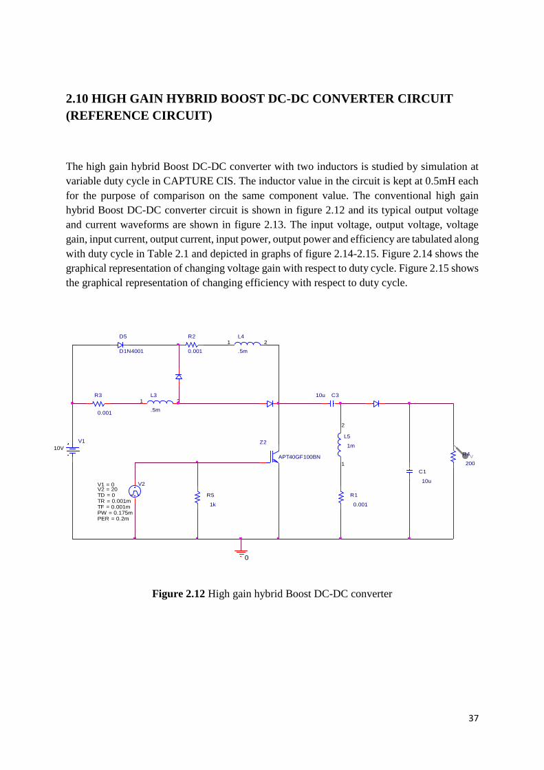
Figure 2.12 High gain hybrid Boost DC-DC converter ........................................................... 37
Figure 2.13 Output voltage and current waveforms of Boost DC-DC converter of Figure 2.12
...................................................................................................................................... 38
Figure 2.14 Voltage gain vs Duty Cycle curve of Hybrid Boost DC-DC Converter of Figure
2.12............................................................................................................................... 40
Figure 2.15 Efficiency vs Duty Cycle curve of Hybrid Boost DC-DC Converter of Figure
2.12............................................................................................................................... 40
Figure 2.16 Proposed SEPIC with Snubber Circuit ................................................................. 41
Figure 2.17 SEPIC Circuit with IGBT for One Inductor ......................................................... 42
Figure 2.18 Output voltage and current waveforms of SEPIC Circuit with IGBT for one
inductor of Figure 2.17 ................................................................................................ 43
Figure 2.19 Voltage gain vs Duty Cycle curve of SEPIC Circuit with IGBT for One Inductor
of Figure 2.17 ............................................................................................................... 45
Figure 2.20 Efficiency vs Duty Cycle curve of SEPIC Circuit with IGBT for One Inductor of
Figure 2.17 ................................................................................................................... 45
Figure 2.21 SEPIC Circuit with IGBT for Two Inductors....................................................... 46
Figure 2.22 Output voltage and current waveforms of SEPIC Circuit with IGBT for two
inductors of Figure 2.21 ............................................................................................... 47
Figure 2.23 Voltage gain vs Duty Cycle curve of SEPIC Circuit with IGBT for Two
Inductors of Figure 2.21 ............................................................................................... 49
Figure 2.24 Efficiency vs Duty Cycle curve of SEPIC Circuit with IGBT for Two Inductors
of Figure 2.21 ............................................................................................................... 49
Figure 2.25 SEPIC Circuit with IGBT for Three Inductors..................................................... 50
Figure 2.26 Output voltage and current waveforms of SEPIC Circuit with IGBT for three
inductors of Figure 2.25 ............................................................................................... 51
Figure 2.27 Voltage gain vs Duty Cycle curve of SEPIC Circuit with IGBT for Three
Inductors of Figure 2.25 ............................................................................................... 53
Figure 2.28 Efficiency vs Duty Cycle curve of SEPIC Circuit with IGBT for Three Inductors
of Figure 2.25 ............................................................................................................... 53
Figure 2.29 SEPIC Circuit with IGBT for Four Inductors ...................................................... 54
Figure 2.30 Output voltage and current waveforms of SEPIC Circuit with IGBT for four
inductors of Figure 2.31 ............................................................................................... 55
Figure 2.31 Voltage gain vs Duty Cycle curve of SEPIC Circuit with IGBT for Four
Inductors of Figure 2.29 ............................................................................................... 57
x
Figure 2.32 Efficiency vs Duty Cycle curve of SEPIC Circuit with IGBT for Four Inductors
of Figure 2.29 ............................................................................................................... 57
Figure 2.33 SEPIC with Snubber Circuit for One Inductor ..................................................... 58
Figure 2.34 Output voltage and current waveforms of SEPIC with Snubber Circuit for one
inductor of Figure 2.33 ................................................................................................ 59
Figure 2.35 Voltage gain vs Duty Cycle curve of SEPIC with Snubber Circuit for One
Inductor of Figure 2.33 ................................................................................................ 61
Figure 2.36 Efficiency vs Duty Cycle curve of SEPIC with Snubber Circuit for One Inductor
of Figure 2.33 ............................................................................................................... 61
Figure 2.37 SEPIC with Snubber Circuit for Two Inductors................................................... 62
Figure 2.38 Output voltage and current waveforms of SEPIC with Snubber Circuit for two
inductors of Figure 2.37 ............................................................................................... 63
Figure 2.39 Voltage gain vs Duty Cycle curve of SEPIC with Snubber Circuit for Two
Inductors of Figure 2.37 ............................................................................................... 65
Figure 2.40 Efficiency vs Duty Cycle curve of SEPIC with Snubber Circuit for Two
Inductors of Figure 2.37 ............................................................................................... 65
Figure 2.41 SEPIC with Snubber Circuit for Three Inductors ................................................. 66
Figure 2.42 Output voltage and current waveforms of SEPIC with Snubber Circuit for three
inductors of Figure 2.41 ............................................................................................... 67
Figure 2.43 Voltage gain vs Duty Cycle curve of SEPIC with Snubber Circuit for Three
Inductors of Figure 2.41 ............................................................................................... 69
Figure 2.44 Efficiency vs Duty Cycle curve of SEPIC with Snubber Circuit for Three
Inductors of Figure 2.41 ............................................................................................... 69
Figure 2.45 SEPIC with Snubber Circuit for Four Inductors .................................................. 70
Figure 2.46 Output voltage and current waveforms of SEPIC with Snubber Circuit for two
inductors of Figure 2.45 ............................................................................................... 71
Figure 2.47 Voltage gain vs Duty Cycle curve of SEPIC with Snubber Circuit for Four
Inductors of Figure 2.45 ............................................................................................... 73
Figure 2.48 Voltage gain vs Duty Cycle curve of SEPIC with Snubber Circuit for Four
Inductors of Figure 2.45 ............................................................................................... 73
Figure 2.49 Comparative efficiency vs duty cycle curve of the normal and proposed circuit 74
Figure 2.50 Comparative efficiency vs duty cycle curve of the normal and proposed circuit 75
Figure 2.51 Comparative efficiency vs duty cycle curve of the normal and proposed circuit 76
Figure 2.52 Comparative efficiency vs duty cycle curve of the normal and proposed circuit 77
xi
Figure 3.1 Comparative efficiency vs duty cycle curve of the normal and proposed circuit .. 79
Figure 3.2 Comparative efficiency vs duty cycle curve of the normal and proposed circuit .. 81
Figure 3.3 Comparative efficiency vs duty cycle curve of the normal and proposed circuit .. 83
Figure 3.4 Comparative efficiency vs duty cycle curve of the normal and proposed circuit .. 85
Figure 3.5 Comparative voltage gain vs number of inductors curve of the normal and
proposed circuit ............................................................................................................ 87
Figure 3.6 Comparative efficiency vs number of inductors curve of the normal and proposed
circuit ........................................................................................................................... 88
Figure 3.7 Comparative voltage gain vs duty cycle curve of the reference, normal and
proposed circuit ............................................................................................................ 90
Figure 3.8 Comparative efficiency vs duty cycle curve of the reference, normal and proposed
circuit ........................................................................................................................... 92
LIST OF TABLES
Table 2.1 Performance of High Gain Hybrid Boost DC-DC Converter of Figure 2.12 .......... 39
Table 2. 2 Performance of SEPIC Circuit with IGBT for One Inductor of Figure 2.17 ......... 44
Table 2.3 Performance of SEPIC Circuit with IGBT for Two Inductors of Figure 2.21 ........ 48
Table 2.4 Performance of SEPIC Circuit with IGBT for Three Inductors of Figure 2.25 ...... 52
Table 2.5 Performance of SEPIC Circuit with IGBT for Four Inductors of Figure 2.31 ........ 56
Table 2.6 Performance of SEPIC with Snubber Circuit for One Inductor of Figure 2.33 ....... 60
Table 2.7 Performance of SEPIC with Snubber Circuit for Two Inductors of Figure 2.37 .. 64
Table 2.8 Performance of SEPIC with Snubber Circuit for Three Inductors of Figure 2.33 .. 68
Table 2.9 Performance of SEPIC with Snubber Circuit for Four Inductors of Figure 2.45 .... 72
Table 2.10 Comparison in efficiency between the normal and proposed circuit for different
duty cycle ..................................................................................................................... 74
Table 2.11 Comparison in efficiency between the normal and proposed circuit for different
duty cycle ..................................................................................................................... 75
Table 2.12 Comparison in efficiency between the normal and proposed circuit for different
duty cycle ..................................................................................................................... 76
Table 2.13 Comparison in efficiency between the normal and proposed circuit for different
duty cycle ..................................................................................................................... 77

xii
Table 3.1 Comparison in efficiency between normal and proposed circuit for different duty
cycle ............................................................................................................................. 78
Table 3.2 Comparison in efficiency between normal and proposed circuit for different duty
cycle ............................................................................................................................. 80
Table 3.3 Comparison in efficiency between normal and proposed circuit for different duty
cycle ............................................................................................................................. 82
Table 3.4 Comparison in efficiency between normal and proposed circuit for different duty
cycle ............................................................................................................................. 84
Table 3.5 Comparison in voltage gain and efficiency between the normal and proposed circuit
for different number of inductors ................................................................................. 86
Table 3.6 Comparison in voltage gain between the reference, normal and proposed circuit for
different duty cycles ..................................................................................................... 89
Table 3.7 Comparison in efficiency between the reference, normal and proposed circuit for
different duty cycles ..................................................................................................... 91
1
Chapter-1
INTRODUCTION
Voltage regulators are one of the most common electronic components, since a power supply
frequently produces raw current that would otherwise damage one of the components in the
circuit. Voltage regulators have a variety of specific functions, depending on their particular
application. Voltage regulator, any electrical or electronic device that maintains the voltage of
a power source within acceptable limits. The voltage regulator is needed to keep voltages
within the prescribed range that can be tolerated by the electrical equipment using that voltage.
A voltage regulator generates a fixed output voltage of a preset magnitude that remains constant
regardless of changes to its input voltage or load conditions.
A linear regulator employs an active (BJT or MOSFET) pass device (series or shunt) controlled
by a high gain differential amplifier. It compares the output voltage with a precise reference
voltage and adjusts the pass device to maintain a constant output voltage.
A switching regulator converts the dc input voltage to a switched voltage applied to a power
MOSFET or BJT switch. The filtered power switch output voltage is fed back to a circuit that
controls the power switch on and off times so that the output voltage remains constant
regardless of input voltage or load current changes.
Electronic switched-mode DC-to-DC converters convert one level/voltage of DC into another
level/voltage of DC. DC-to-DC converters prevents characteristics degradation and
malfunction. The advantages of this regulation over linear regulation are higher efficiency and
low heat generation. DC-DC converters provide small, efficient power conversion. Designing
efficient DC-DC converters can be tricky, even when using off-the-shelf controllers. Efficiency
is important for extending battery life in battery-powered applications and because it reduces
the amount of heat that must be dissipated, reducing package size and extended the life of the
electrical components in the system. MOSFETs have conduction losses (P=I2R) related to the
conduction when they’re fully on. Using a MOSFET with low RDS (ON) will reduce these
losses. They also have switching losses, which are harder to quantify. Using a high-current gate
driver ensures that MOSFETs operate quickly and efficiently—those with lower gate
capacitance switch faster and more efficiently. Diodes have a forward voltage drop of about
0.7 V (P=VI). Using a SCHOTTKY helps to reduce voltage drop losses and also switching
losses, which are harder to quantify. To achieve high voltage output gain, the converter output
terminal and boost output terminal can be connected serially with the coupled inductor.
Behavioral modelling of the IC system represents the functionality of an IC with macro models
rather than actual implementation of the circuit using more efficient modelling techniques. For
simulation, each software is having its advantages and limitations. ORCAD, PSPICE is used
2
in this paper. ORCAD provides a complete set of tools to achieve the desired results. From the
initial schematic to the final artwork, the platform delivers a complete, integrated workflow.
The study undertaken in this thesis develops a system level design approach for switching
voltage regulators of three major control schemes. The basic converter topologies and their
waveforms are reviewed. Voltage control and current control scheme is used mainly. System
level models are implemented using ORCAD. The following study provides details of
methodologies for designing each components or blocks mainly the SEPIC used in the
switching regulator. Finally, practical results and simulation are presented for voltage and
current schemes and specified the proper design to get expected values to run the processor.
1.1 BACKGROUND STUDY
Practical electronic converters use switching techniques. Switched-mode DC-to-DC converters
convert one DC voltage level to another, which may be higher or lower, by storing the input
energy temporarily and then releasing that energy to the output at a different voltage. The
storage may be in either magnetic field storage components (inductors, transformers) or electric
field storage components (capacitors). This conversion method can increase or decrease
voltage. Switching conversion is more power efficient (often 75% to 98%) than linear voltage
control which has a slow transient response due to bandwidth but DC-DC converter is
inherently a high ripple system. To reduce this ripple, current mood control is used for better
operation. So for further analysis frequency and pulse width modulation (PWM) remains
constant.
1.2 DC-DC CONVERTER
A DC-DC converter is provided with a DC power source, a reference voltage generating circuit,
an amplifier which receives an electric power from the DC power source and outputs an electric
power of which voltage is controlled so as to assume a target voltage value by stepping down
the voltage of the electric power from the DC power source depending on a difference between
the reference voltage and a detection voltage, an oscillation circuit which generates signals
having a specific frequency, a voltage boosting circuit which receives the output of the
amplifier and the output of the oscillation circuit, causes switching of the output of the amplifier
at the specific frequency to charge a first capacitor and performs voltage boosting by
transferring the electric charges-charged in the first capacitor through complementary ON-OFF
switching with respect to the former switching into a second capacitor after raising substantially
up to 𝑛
𝑚 time voltage (where n>m and n and m are integers equal to or more than 2) and charging
the same therewith; and an output voltage detection circuit which generates the detection

3
voltage depending on the output voltage of the boosting circuit, whereby a voltage of
substantially 𝑛
𝑚 times of the target voltage value is generated from the voltage boosting circuit.
1.3 APPLICATION OF DC-DC CONVERTERS
Dc converters can be used in regenerative braking of dc motors to return energy back into the
supply and this feature results in energy savings for transportation system with frequent stops.
As for example,
(a) Marine Hoists
(b) Mine Haulers
(c) Trolley cars
(d) Forklift trucks
(e) Traction motor control
Also used in DC voltage regulators and also are used in conjunction with an inductor to
generate a dc current source especially for the current source inverter.
1.4 SWITCHING CONSIDERATION OF DC-DC CONVERTERS
The converter switch can be implemented by using
(a) Power Bipolar Junction Transistor (BJT)
(b) Power Metal Oxide Semiconductor Field Effect Transistor (MOSFET)
(c) Gate Turn Off Thyristor (GTO)
(d) Insulated Gate Bipolar Transistor (IGBT)
Practical devices have a finite voltage drop ranging from 0.5V to 2V but during the calculations
for the sake of simplicity of the understanding, these switches are considered lossless.
4
1.5 TYPES OF DC-DC CONVERTER
DC-DC converters can be,
1. Buck Converter
2. Boost Converter
3. Buck-boost Converter
4. Cuk Converter
5. SEPIC
1.5.1 STUDY OF DC-DC CONVERTERS
These five converters from above list are to be described and these converters have non
isolated input output terminals basically.
1.5.2 BUCK CONVERTER
A Buck Converter is a DC-DC converter whose output voltage is less than the input voltage
(𝑉𝑖𝑛>𝑉𝑜𝑢𝑡). It follows that the output current is greater the input current. It is also called as step
down converter. A typical circuit diagram of buck converter is illustrated at fig 1.1.
5
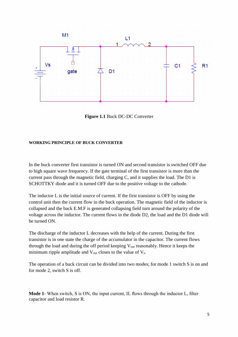
Figure 1.1 Buck DC-DC Converter
WORKING PRINCIPLE OF BUCK CONVERTER
In the buck converter first transistor is turned ON and second transistor is switched OFF due
to high square wave frequency. If the gate terminal of the first transistor is more than the
current pass through the magnetic field, charging C, and it supplies the load. The D1 is
SCHOTTKY diode and it is turned OFF due to the positive voltage to the cathode.
The inductor L is the initial source of current. If the first transistor is OFF by using the
control unit then the current flow in the buck operation. The magnetic field of the inductor is
collapsed and the back E.M.F is generated collapsing field turn around the polarity of the
voltage across the inductor. The current flows in the diode D2, the load and the D1 diode will
be turned ON.
The discharge of the inductor L decreases with the help of the current. During the first
transistor is in one state the charge of the accumulator in the capacitor. The current flows
through the load and during the off period keeping Vout reasonably. Hence it keeps the
minimum ripple amplitude and Vout closes to the value of Vs.
The operation of a buck circuit can be divided into two modes; for mode 1 switch S is on and
for mode 2, switch S is off.
Mode 1- When switch, S is ON, the input current, IL flows through the inductor L, filter
capacitor and load resistor R.
6
Mode 2- When switch, S is OFF, the freewheeling diode, D gets conducted due to the energy
stored in the inductor and the inductor current continues to flow through L, C, R, and diode D.
The equation for output voltage for a buck converter is,
VO=DVS ; where D is the duty cycle
1.5.3 BOOST CONVERTER
A Boost converter is a DC to DC converter in which the output voltage is greater than the input
voltage. It is also called as step up converter. The name step up converter comes from the fact
that analogous to step up transformer the input voltage is stepped up to a level greater than the
input voltage. By law of conservation of energy the input power has to be equal to output
power.
Input power (Pin) = Output power (Pout)
Since Vin<Vout in a boost converter, it follows then that the output current is less than the input
current. Therefore in boost converter
Vin <Vout and Iin>Iout
WORKING PRINCIPLE OF BOOST CONVERTER
In this converter the first transistor in figure 1.2 is switched ON continually and for the second
transistor the square wave of high frequency is applied to the gate terminal. The second
transistor is in conducting when the on state and the input current flow from the inductor L
through the second transistor. The negative terminal charging up the magnetic field around the
inductor. The D2 diode cannot conduct because the anode is on the potential ground by highly
conducting the second transistor.
.
7
Figure 1.2 Boost DC –DC Converter
By charging the capacitor C the load is applied to the entire circuit in the ON State and it can
construct earlier oscillator cycles. During the ON period the capacitor C can discharge regularly
and the amount of high ripple frequency on the output voltage.
During the OFF period of second transistor the inductor L is charged and the capacitor C is
discharged. The inductor L can produce the back EMF and the values are depending up on the
rate of change of current of the second transistor switch. The amount of inductance the coil can
occupy. Hence the back EMF can produce any different voltage through a wide range and
determined by the design of the circuit. Hence the polarity of voltage across the inductor L has
reversed now.
The input voltage gives the output voltage and at least equal to or higher than the input voltage.
The diode D2 is in forward biased and the current applied to the load current and it recharges
the capacitors and it is ready for the second transistor.
The function of boost converter can be divided into two modes, Mode 1 and Mode 2.
Mode 1- This begins when transistor S is switched on at time t=0. The input current rises and
flows through inductor L and transistor S.
8
Mode 2- This begins when transistor S is switched off at time t=t1. The input current now
flows through L, C, load, and diode D. The inductor current falls until the next cycle. The
energy stored in inductor L flows through the load.
The equation for output voltage for a boost converter is:
VO=𝑉𝑠
1−𝐷
1.5.4 BUCK-BOOST CONVERTER
DC-DC converter circuit (also known as chopper circuit) is connected to the DC power supply
and the load, it becomes the uncontrollable DC input into a controllable DC output converter
by controlling voltage. Traditional buck-boost Converter with simple structure, easy to
implement, etc has been widely used in various occasions. But in recent years, with the
switching frequency increases, the switching of power also becomes light and small, but the
switching frequency and switching losses is proportional, so the switching frequency increases,
switching loss also increases. In order to improve conversion capacity, adjustable range and
efficiency, the traditional buck-boost converter is used.
It is a type DC to DC converter it has a magnitude of output voltage. It may be more or less
than equal to the input voltage magnitude. The buck boost converter is single inductor is used
in the place of the transformer. There are two types of converters in the buck boost converter
that are buck converter and the other one is boost converter. These converters can produce the
range of output voltage than the input voltage. The following diagram shows the basic buck
boost converter.
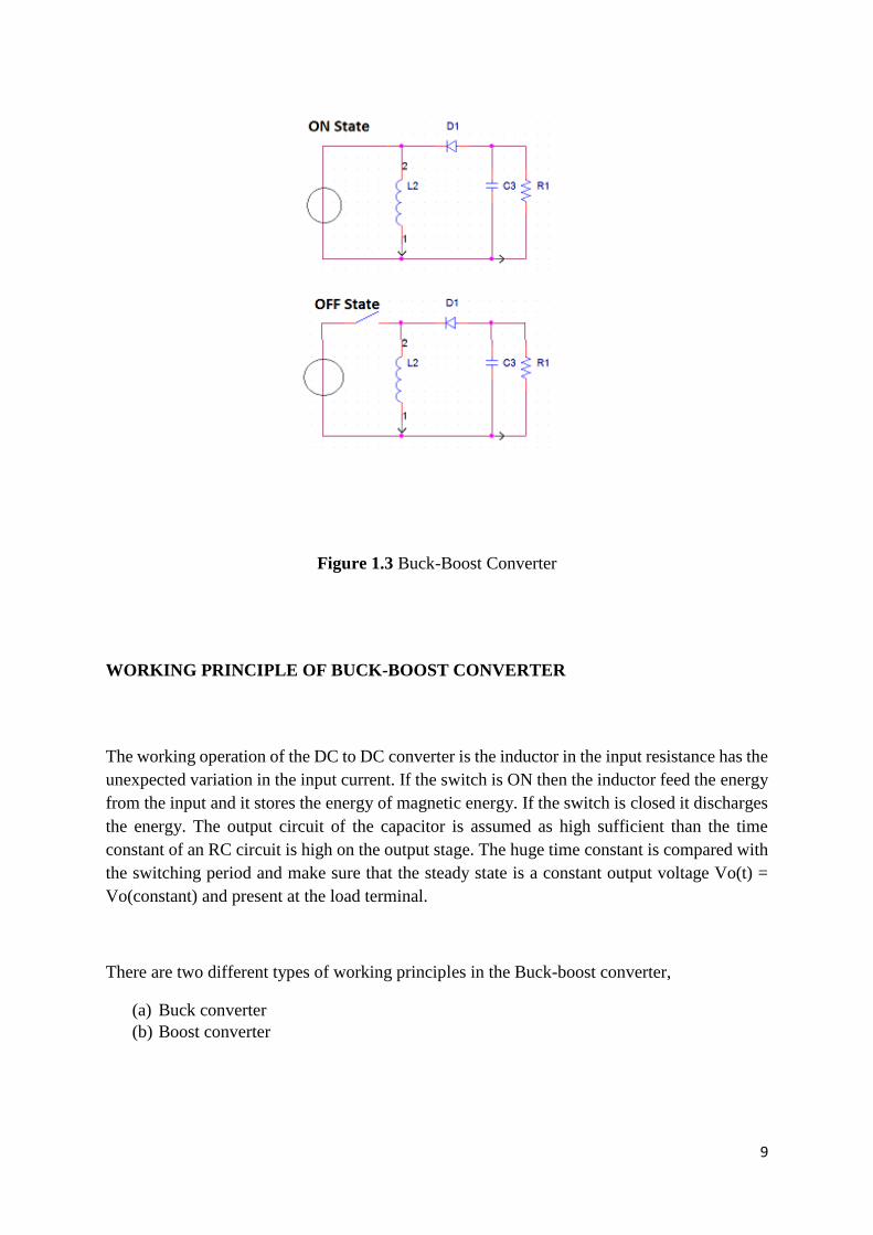
9
Figure 1.3 Buck-Boost Converter
WORKING PRINCIPLE OF BUCK-BOOST CONVERTER
The working operation of the DC to DC converter is the inductor in the input resistance has the
unexpected variation in the input current. If the switch is ON then the inductor feed the energy
from the input and it stores the energy of magnetic energy. If the switch is closed it discharges
the energy. The output circuit of the capacitor is assumed as high sufficient than the time
constant of an RC circuit is high on the output stage. The huge time constant is compared with
the switching period and make sure that the steady state is a constant output voltage Vo(t) =
Vo(constant) and present at the load terminal.
There are two different types of working principles in the Buck-boost converter,
(a) Buck converter
(b) Boost converter
10
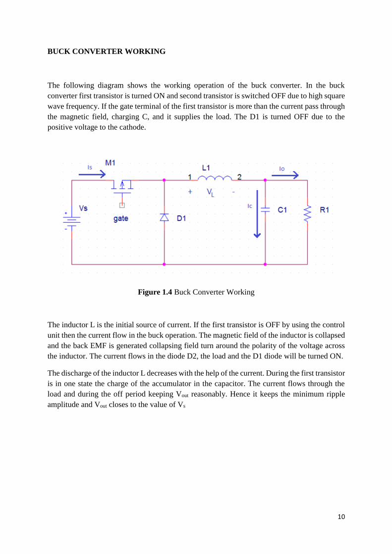
BUCK CONVERTER WORKING
The following diagram shows the working operation of the buck converter. In the buck
converter first transistor is turned ON and second transistor is switched OFF due to high square
wave frequency. If the gate terminal of the first transistor is more than the current pass through
the magnetic field, charging C, and it supplies the load. The D1 is turned OFF due to the
positive voltage to the cathode.
Figure 1.4 Buck Converter Working
The inductor L is the initial source of current. If the first transistor is OFF by using the control
unit then the current flow in the buck operation. The magnetic field of the inductor is collapsed
and the back EMF is generated collapsing field turn around the polarity of the voltage across
the inductor. The current flows in the diode D2, the load and the D1 diode will be turned ON.
The discharge of the inductor L decreases with the help of the current. During the first transistor
is in one state the charge of the accumulator in the capacitor. The current flows through the
load and during the off period keeping Vout reasonably. Hence it keeps the minimum ripple
amplitude and Vout closes to the value of Vs
11
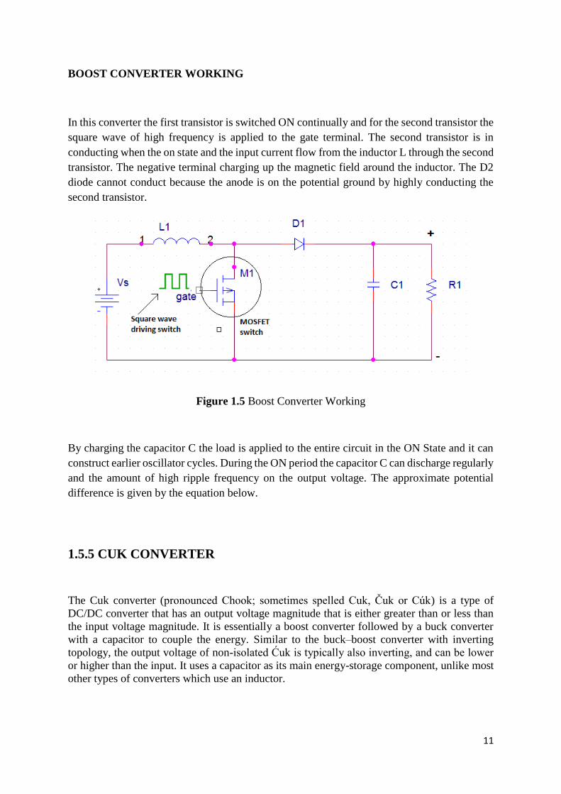
BOOST CONVERTER WORKING
In this converter the first transistor is switched ON continually and for the second transistor the
square wave of high frequency is applied to the gate terminal. The second transistor is in
conducting when the on state and the input current flow from the inductor L through the second
transistor. The negative terminal charging up the magnetic field around the inductor. The D2
diode cannot conduct because the anode is on the potential ground by highly conducting the
second transistor.
Figure 1.5 Boost Converter Working
By charging the capacitor C the load is applied to the entire circuit in the ON State and it can
construct earlier oscillator cycles. During the ON period the capacitor C can discharge regularly
and the amount of high ripple frequency on the output voltage. The approximate potential
difference is given by the equation below.
1.5.5 CUK CONVERTER
The Cuk converter (pronounced Chook; sometimes spelled Cuk, Čuk or Cúk) is a type of
DC/DC converter that has an output voltage magnitude that is either greater than or less than
the input voltage magnitude. It is essentially a boost converter followed by a buck converter
with a capacitor to couple the energy. Similar to the buck–boost converter with inverting
topology, the output voltage of non-isolated Ćuk is typically also inverting, and can be lower
or higher than the input. It uses a capacitor as its main energy-storage component, unlike most
other types of converters which use an inductor.
12
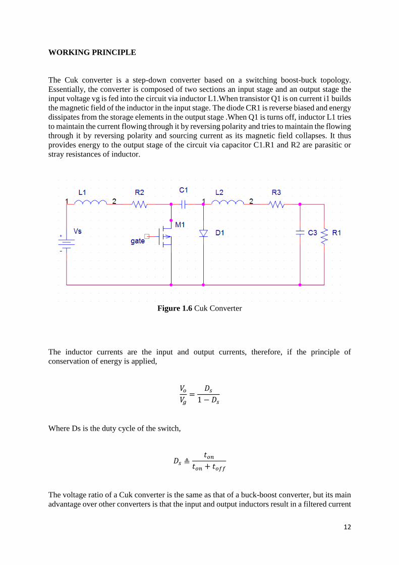
WORKING PRINCIPLE
The Cuk converter is a step-down converter based on a switching boost-buck topology.
Essentially, the converter is composed of two sections an input stage and an output stage the
input voltage vg is fed into the circuit via inductor L1.When transistor Q1 is on current i1 builds
the magnetic field of the inductor in the input stage. The diode CR1 is reverse biased and energy
dissipates from the storage elements in the output stage .When Q1 is turns off, inductor L1 tries
to maintain the current flowing through it by reversing polarity and tries to maintain the flowing
through it by reversing polarity and sourcing current as its magnetic field collapses. It thus
provides energy to the output stage of the circuit via capacitor C1.R1 and R2 are parasitic or
stray resistances of inductor.
Figure 1.6 Cuk Converter
The inductor currents are the input and output currents, therefore, if the principle of
conservation of energy is applied,
𝑉𝑜
𝑉𝑔=
𝐷𝑠
1 − 𝐷𝑠
Where Ds is the duty cycle of the switch,
𝐷𝑠 ≜𝑡𝑜𝑛
𝑡𝑜𝑛 + 𝑡𝑜𝑓𝑓
The voltage ratio of a Cuk converter is the same as that of a buck-boost converter, but its main
advantage over other converters is that the input and output inductors result in a filtered current
13
on both sides of the converter, while buck, boost, and buck-boost converters have a pulsating
current that occurs on at least one side of the circuit i.e either on input side or output side.
This pulsation will increase the ripple in the circuit and due to this ripple, the efficiency of
battery gets lowered. To ensure good efficiency ripple should be reduced.By controlling the
duty cycle of the switch, the output voltage VO can be controlled and can be higher or lower
than the input voltage vg. By using a controller to vary the duty cycle during operation, the
circuit can also be made to reject disturbances ,as second part of circuit consists of parallel
resonance circuit and it work as a tank circuit for specific frequency (resonant frequency), and
during resonance current will not be allowed to enter in the circuit.
1.5.6 SINGLE ENDED PRIMARY INDUCTOR CONVERTER (SEPIC)
The single ended primary inductor converter (SEPIC) is a DC-DC converter topology that
provides a positive regulated output voltage from an input voltage that varies from above to
below the output voltage.
Some applications of converters only need to buck or boost the voltage and can simply use the
corresponding converters. However, sometimes the desired output voltage will be in the range
of input voltage. When this is the case, it is usually best to use a converter that can decrease or
increase the voltage. Buck-boost converters can be cheaper because they only require a single
inductor and a capacitor. However, these converters suffer from a high amount of input current
ripple. This ripple can create harmonics; in many applications these harmonics necessitate
using a large capacitor or an LC filter. This often makes the buck-boost expensive or inefficient.
Another issue that can complicate the usage of buck-boost converters is the fact that they invert
the voltage. Cuk converters solve both of these problems by using an extra capacitor and
inductor. However, both Cuk and Buck-boost converter operation cause large amounts of
electrical stress on the components, this can result in device failure or overheating. SEPIC
solves both of these problems which is discussed in details in the next chapter.
Driving inductive loads with transistor switches, whether they be flyback transformers, relays
or motors, often result in the high voltage resonant spikes when the coils are interrupted from
their current source by the transistor .There are various ways of mitigating these undesirable
spikes which cause component failures and EMI issues. The most common approach is to use
snubber circuits across semiconductor devices to suppress voltage transients in electrical
system
14
1.6 OBJECTIVES OF THE RESEARCH
Efficiency, size, and cost are the primary advantages of switching power converters when
compared to linear converters. The switching power converter efficiencies can run between 70-
90%, whereas linear converters are usually 30% efficient.
The SEPIC is designed to provide an efficient method of taking a given DC voltage supply and
boosting it to a desired value. A SEPIC is also supposed to combine buck and boost functions
and allows a circuit to have flexible input voltages with a stable output voltage. The SEPIC
design also has minimal active components, a simple controller, and clamped switching
waveforms which provide low noise operation.
1.7 OUTLINE OF THE THESIS
This thesis consists of four chapters. Chapter-1 Deals with background study, application of
DC-DC converters, review of DC-DC converters with derivations and objective of the research.
Chapter-2 Includes the high gain SEPIC with snubber circuits. In this chapter, the hybrid boost
DC-DC converter, the SEPIC for one, two, three and four inductors and the proposed SEPIC
with snubber circuit for one, two, three and four inductors are studied by simulation. The
proposed circuit will provide higher voltage gain and efficiency at each duty cycle than the
conventional SEPIC.
Chapter-3 Deals with results and discussion.
Chapter-4 Concludes possible future works and conclusion.
15
Chapter-2
HIGH GAIN SEPIC WITH SNUBBER CIRCUIT
2.1 INTRODUCTION
Power Electronics is the basic concepts of switched-mode converter circuits for controlling and
converting electrical power with high efficiency. Principles of converter circuit analysis are
introduced, and are developed for finding the steady state voltages, current, and efficiency of
power converters. In modern system the conversion is performed with semiconductor devices
such as diodes, thyristor and transistor. In contrast to electronic systems concerned with
transmission and processing of signals and data, various types of converter can be used but
here in these analysis we are using a high gain hybrid converter “SEPIC”. In power electronics
SEPIC(Single ended Primary inductor converter) is a DC to DC converter and is capable of
operating in either step up or step down mode and widely used in battery operated equipments.
It is considered to be a fourth order DC to DC converter capable of delivering an output voltage
which can be greater than or less than the input voltage .Different portable electronic appliances
have been benefitted from a power converter which is able to achieve high efficiency with a
wide input and output ranges with a small size . But it is not easy for conventional power
converter design to maintain high efficiency especially in up and down voltage. Conversion
has to be achieved, all these characteristics are obtained in SEPIC DC to DC power conversion
system can be realized by different circuit topologies like for example (buck, boost, buck-
boost) are most widely used .For achieving the high voltage gain and efficiency these hybrid
SEPIC converter is proposed with “Snubber Circuit” which is being used in the switching
device and the performance is stimulate in Capture CIS software.
2.2 SINGLE ENDED PRIMARY INDUCTOR CONVERTER
Single-ended primary-inductor converter (SEPIC) is a type of DC-DC converter allowing
the electrical potential (voltage) at its output to be greater than, less than, or equal to that at its
input efficiently. The output of the SEPIC is controlled by the duty cycle of the control
transistor.
A SEPIC is essentially a boost converter followed by a buck-boost converter, therefore it is
similar to a traditional buck-boost converter but has advantages of having non-inverted output
(the output has the same voltage polarity as the input), using a series capacitor to couple energy
from the input to the output (and thus can respond more gracefully to a short-circuit output),

16
and being capable of true shutdown (when the switch is turned off, its output drops to 0 V
following a fairly hefty transient dump of charge).
SEPICs are useful in applications in which a battery voltage can be above and below that of
the regulator's intended output. For example, a single lithium ion battery typically discharges
from 4.2 volts to 3 volts .If other components require 3.3 volts, then the SEPIC would be
effective. SEPIC converters are especially useful for PV maximum power tracking purposes
where the objective is to draw maximum possible power from solar panels at all times,
regardless of the load.
ADVANTAGES
Single switch
Continuous input current
Ripple current can be steered away from the input ,reducing the need for input noise
filtering
Inrush/overload current limiting capability
Switch location is a simple low-side case hence easier gate drive circuits
Outer loop control capability
DISADVANTAGES
Higher switch/diode peak voltages compared to boost topology
Bulk capacitor size is needed and thus cost is greater compared to buck-boost
converters
Since the SEPIC transfers all its energy via the series capacitor, a capacitor with high
capacitance and current handling capability is required
SEPICs have a pulsating output current like buck-boost converters
2.3 WORKING PRINCIPLE
To derive the relationship between input and output voltages, these initial assumptions are
made:
1. Both inductors are very large and the currents in them are constant.
2. Both capacitors are very large and the voltages across them are constant.
3. The circuit is operating in the steady state, meaning that voltage and current waveforms are
periodic.
4. For a duty ratio of D, the switch is closed for time DT and open for (1 –D) T
5. The switch and the diode are ideal.
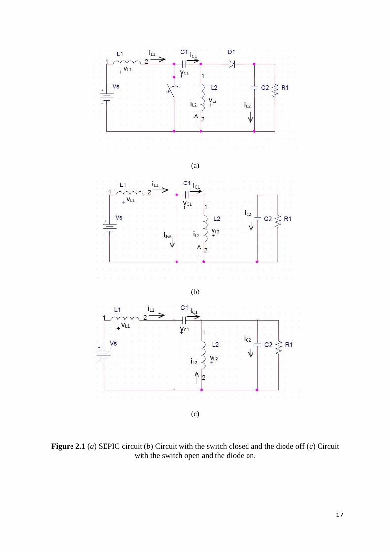
17
(a)
(b)
(c)
Figure 2.1 (a) SEPIC circuit (b) Circuit with the switch closed and the diode off (c) Circuit
with the switch open and the diode on.

18
The inductor current and capacitor voltage restrictions will be removed later to investigate the
fluctuations in currents and voltages. The inductor currents are assumed to be continuous in
this analysis. Other observations are that the average inductor voltages are zero and that the
average capacitor currents are zero for steady-state operation.
Kirchhoff’s voltage law around the path containing Vs, L1, C1, and L2 gives
−𝑉𝑆 + 𝑣𝐿1 + 𝑣𝐶1 − 𝑣𝐿2 = 0
Using the average of these voltages,
−𝑉𝑠 + 0 + 𝑉𝐶1 − 0 = 0
Showing that the average voltage across the capacitor C1 is,
𝑉𝐶1 = 𝑉𝑆 (1)
When the switch is closed, the diode is off, and the circuit is as shown in Figure 2.1(b)
The voltage across L1 for the interval DT is,
𝑣𝐿1 = 𝑉𝑠 (2)
When the switch is open, the diode is on, and the circuit is as shown in Figure 2.1(c)
Kirchhoff’s voltage law around the outermost path gives,
−𝑉𝑠 + 𝑣𝐿1 + 𝑣𝐶1 + 𝑉𝑜 = 0 (3)
Assuming that the voltage across C1 remains constant at its average value of Vs ,
−𝑉𝑠 + 𝑣𝐿1 + 𝑉𝑠 + 𝑉𝑜 = 0 (4)
Or
𝑣𝐿1 = −𝑉𝑜 (5)
For the interval (1 - D) T. Since the average voltage across an inductor is zero for periodic
operation. Equations (2) and (5) are combined to get
19
(𝑉𝐿1,𝑠𝑤 𝑐𝑙𝑜𝑠𝑒𝑑)(𝐷𝑇) + (𝑉𝐿1,𝑠𝑤 𝑜𝑝𝑒𝑛
) (1 − 𝐷)𝑇 = 0
𝑉𝑠(𝐷𝑇) − 𝑉𝑜(1 − 𝐷)𝑇 = 0
Where D is the duty ratio of the switch. The result is
𝑉𝑜 = 𝑉𝑠(𝐷
1−𝐷) (6)
Which can be expressed as
𝐷 =𝑉𝑜
𝑉𝑜+𝑉𝑠 (7)
This result is similar to that of the buck-boost and Cuk converter equations, with the important
distinction that there is no polarity reversal between input and output voltages. The ability to
have an output voltage greater or less than the input with no polarity reversal makes this
converter suitable for many applications.
Assuming no losses in the converter, the power supplied by the source is the same as the power
absorbed by the load.
𝑃𝑠 = 𝑃𝑜
Power supplied by the DC source is voltage times the average current, and the source current
is the same as the current in L1.
𝑃𝑠 = 𝑉𝑠𝐼𝑠 = 𝑉𝑠𝐼𝐿1
Output power can be expressed as,
𝑃𝑜 = 𝑉𝑜𝐼𝑜
Resulting in,
𝑉𝑠𝐼𝐿1= 𝑉𝑜𝐼𝑜
Solving for average inductor current, which is also the average source current,
𝐼𝐿1= 𝐼𝑠 =
𝑉𝑜𝐼𝑜
𝑉𝑠=
𝑉𝑜2
𝑉𝑠𝑅 (8)
20
The variation in 𝑖𝐿1 when the switch is closed is found from,
𝑉𝐿1= 𝑉𝑠 = 𝐿1 (
𝑑𝑖𝐿1
𝑑𝑡) = 𝐿1 (
∆𝑖𝐿1
∆𝑡) = 𝐿1 (
∆𝑖𝐿1
𝐷𝑇) (9)
Solving for ∆𝑖𝐿1,
∆𝑖𝐿1=
𝑉𝑠𝐷𝑇
𝐿1=
𝑉𝑠𝐷
𝐿1𝑓 (10)
For L2, the average current is determined from Kirchhoff’s current law at the node where C1,
L2, and the diode are connected.
𝑖𝐿2= 𝑖𝐷 − 𝑖𝐶1
Diode current is,
𝑖𝐷 = 𝑖𝐶2+ 𝐼𝑜
Which makes
𝑖𝐿2= 𝑖𝐶2
+ 𝐼𝑜 − 𝑖𝐶1
The average current in each capacitor is zero, so the average current in L2 is
I𝐿2= 𝐼𝑜
The variation in I𝐿2 is determined from the circuit when the switch is closed.Using Kirchhoff’s
voltage law around the path of the closed switch, C1, and L2 with the voltage across C1 assumed
to be a constant Vs, gives
𝑉𝐿2= 𝑉𝐶1
= 𝑉𝑠 = 𝐿2 (𝑑𝑖𝐿2
𝑑𝑡) = 𝐿2 (
∆𝑖𝐿2
∆𝑡) = 𝐿2 (
∆𝑖𝐿2
𝐷𝑇)
Solving for ∆𝑖𝐿2
∆𝑖𝐿2=
𝑉𝑠𝐷𝑇
𝐿2=
𝑉𝑠𝐷
𝐿2𝑓 (11)
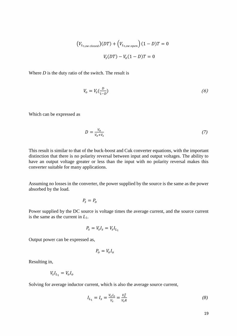
Applications of Kirchhoff’s current law show that the diode and switch currents are
21
(12)
Current waveforms are shown in Figure 2.2.
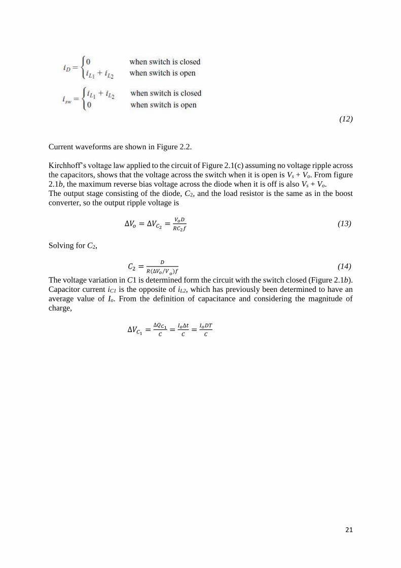
Kirchhoff’s voltage law applied to the circuit of Figure 2.1(c) assuming no voltage ripple across
the capacitors, shows that the voltage across the switch when it is open is Vs + Vo. From figure
2.1b, the maximum reverse bias voltage across the diode when it is off is also Vs + Vo.
The output stage consisting of the diode, C2, and the load resistor is the same as in the boost
converter, so the output ripple voltage is
∆𝑉𝑜 = ∆𝑉𝐶2=
𝑉𝑜𝐷
𝑅𝐶2𝑓 (13)
Solving for C2,
𝐶2 =𝐷
𝑅(∆𝑉𝑜 𝑉⁄𝑜)𝑓
(14)
The voltage variation in C1 is determined form the circuit with the switch closed (Figure 2.1b).
Capacitor current iC1 is the opposite of iL2, which has previously been determined to have an
average value of Io. From the definition of capacitance and considering the magnitude of
charge,
∆𝑉𝐶1=
∆𝑄𝐶1
𝐶=
𝐼𝑜∆𝑡
𝐶=
𝐼𝑜𝐷𝑇
𝐶
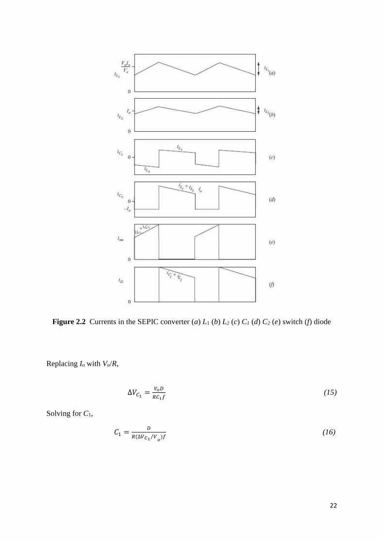
22
Figure 2.2 Currents in the SEPIC converter (a) L1 (b) L2 (c) C1 (d) C2 (e) switch (f) diode
Replacing Io with Vo/R,
∆𝑉𝐶1=
𝑉𝑜𝐷
𝑅𝐶1𝑓 (15)
Solving for C1,
𝐶1 =𝐷
𝑅(∆𝑉𝐶1 𝑉⁄𝑜
)𝑓 (16)
23
2.4 VOLTAGE GAIN
The equation of output voltage can be written as
𝑉𝑜 =𝐷
1 − 𝐷𝑉𝑠
If the input voltage is 𝑉𝑠, then the voltage gain would be,
𝑉𝑂
𝑉𝑆=
𝐷
1 − 𝐷
(17)
2.5 EFFICIENCY
Unlike linear voltage converters switched-mode voltage converters are capable of converting
a given input voltage to a higher output voltage. Such converters are commonly denoted as
step-up converters. A straightforward example of a charge pump step-up converter is the series-
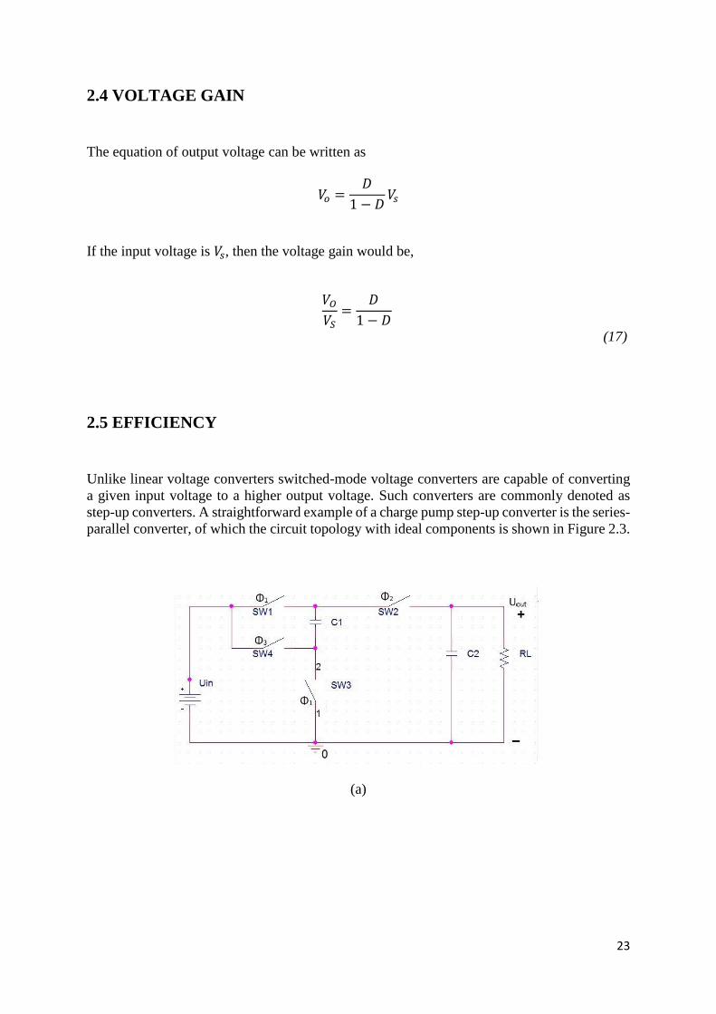
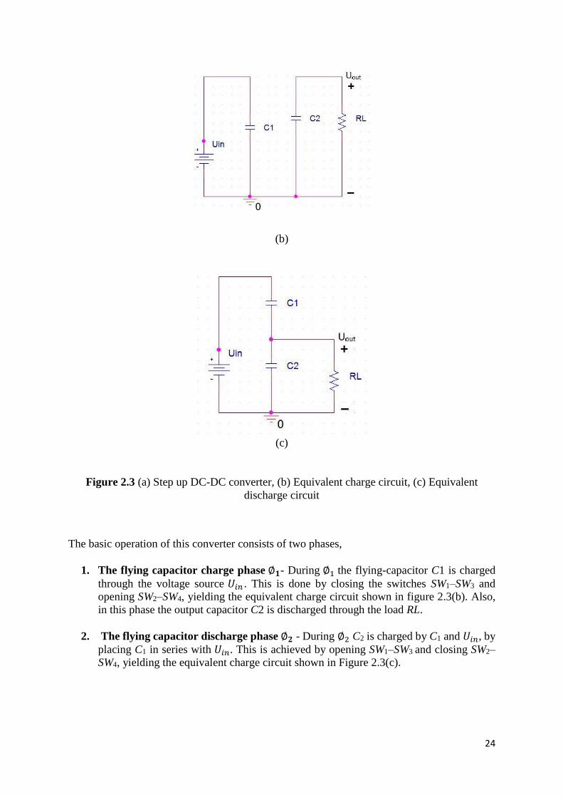
parallel converter, of which the circuit topology with ideal components is shown in Figure 2.3.
(a)
24
(b)
(c)
Figure 2.3 (a) Step up DC-DC converter, (b) Equivalent charge circuit, (c) Equivalent
discharge circuit
The basic operation of this converter consists of two phases,
1. The flying capacitor charge phase ∅𝟏- During ∅1 the flying-capacitor C1 is charged
through the voltage source 𝑈𝑖𝑛 . This is done by closing the switches SW1–SW3 and
opening SW2–SW4, yielding the equivalent charge circuit shown in figure 2.3(b). Also,
in this phase the output capacitor C2 is discharged through the load RL.
2. The flying capacitor discharge phase ∅𝟐 - During ∅2 C2 is charged by C1 and 𝑈𝑖𝑛, by
placing C1 in series with 𝑈𝑖𝑛. This is achieved by opening SW1–SW3 and closing SW2–
SW4, yielding the equivalent charge circuit shown in Figure 2.3(c).
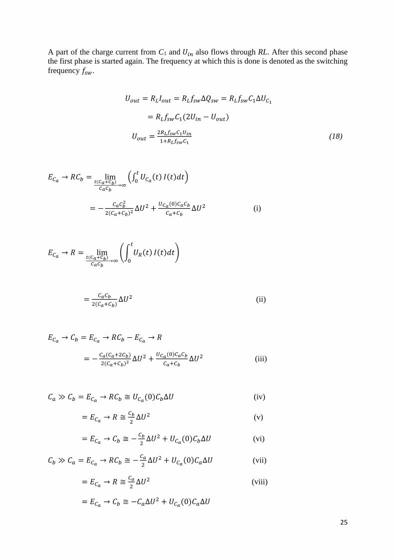
25
A part of the charge current from C1 and 𝑈𝑖𝑛 also flows through RL. After this second phase
the first phase is started again. The frequency at which this is done is denoted as the switching
frequency 𝑓𝑠𝑤.
𝑈𝑜𝑢𝑡 = 𝑅𝐿𝐼𝑜𝑢𝑡 = 𝑅𝐿𝑓𝑠𝑤∆𝑄𝑠𝑤 = 𝑅𝐿𝑓𝑠𝑤𝐶1∆𝑈𝐶1
= 𝑅𝐿𝑓𝑠𝑤𝐶1(2𝑈𝑖𝑛 − 𝑈𝑜𝑢𝑡)
𝑈𝑜𝑢𝑡 =2𝑅𝐿𝑓𝑠𝑤𝐶1𝑈𝑖𝑛
1+𝑅𝐿𝑓𝑠𝑤𝐶1 (18)
𝐸𝐶𝑎→ 𝑅𝐶𝑏 = lim
𝑡(𝐶𝑎+𝐶𝑏)
𝐶𝑎𝐶𝑏→∞
(∫ 𝑈𝐶𝑎(𝑡)
𝑡
0𝐼(𝑡)𝑑𝑡)
= −𝐶𝑎𝐶𝑏
2
2(𝐶𝑎+𝐶𝑏)2 ∆𝑈2 +𝑈𝐶𝑎(0)𝐶𝑎𝐶𝑏
𝐶𝑎+𝐶𝑏∆𝑈2 (i)
𝐸𝐶𝑎→ 𝑅 = lim
𝑡(𝐶𝑎+𝐶𝑏)
𝐶𝑎𝐶𝑏→∞
(∫ 𝑈𝑅(𝑡)𝑡
0
𝐼(𝑡)𝑑𝑡)
=𝐶𝑎𝐶𝑏
2(𝐶𝑎+𝐶𝑏)∆𝑈2 (ii)
𝐸𝐶𝑎→ 𝐶𝑏 = 𝐸𝐶𝑎
→ 𝑅𝐶𝑏 − 𝐸𝐶𝑎→ 𝑅
= −𝐶𝑎(𝐶𝑎+2𝐶𝑏)
2(𝐶𝑎+𝐶𝑏)2∆𝑈2 +
𝑈𝐶𝑎(0)𝐶𝑎𝐶𝑏
𝐶𝑎+𝐶𝑏∆𝑈2 (iii)
𝐶𝑎 ≫ 𝐶𝑏 = 𝐸𝐶𝑎→ 𝑅𝐶𝑏 ≅ 𝑈𝐶𝑎
(0)𝐶𝑏∆𝑈 (iv)
= 𝐸𝐶𝑎→ 𝑅 ≅
𝐶𝑏
2∆𝑈2 (v)
= 𝐸𝐶𝑎→ 𝐶𝑏 ≅ −
𝐶𝑏
2∆𝑈2 + 𝑈𝐶𝑎
(0)𝐶𝑏∆𝑈 (vi)
𝐶𝑏 ≫ 𝐶𝑎 = 𝐸𝐶𝑎→ 𝑅𝐶𝑏 ≅ −
𝐶𝑎
2∆𝑈2 + 𝑈𝐶𝑎
(0)𝐶𝑎∆𝑈 (vii)
= 𝐸𝐶𝑎→ 𝑅 ≅
𝐶𝑎
2∆𝑈2 (viii)
= 𝐸𝐶𝑎→ 𝐶𝑏 ≅ −𝐶𝑎∆𝑈2 + 𝑈𝐶𝑎
(0)𝐶𝑎∆𝑈
26
So,
𝐸𝐶𝑎→ 𝐶𝑏
𝐸𝐶𝑎→ 𝑅𝐶𝑏
=−
𝐶𝑎
2∆𝑈2 + 𝑈𝐶𝑎
(0)𝐶𝑎∆𝑈
𝑈𝐶𝑎(0)𝐶𝑏∆𝑈
Where,
∆𝑈 = 2𝑈𝑖𝑛 − 𝑈𝑜𝑢𝑡
𝐶𝑏 = 𝐶1
𝑈𝐶𝑎(0) = 𝑈𝑖𝑛
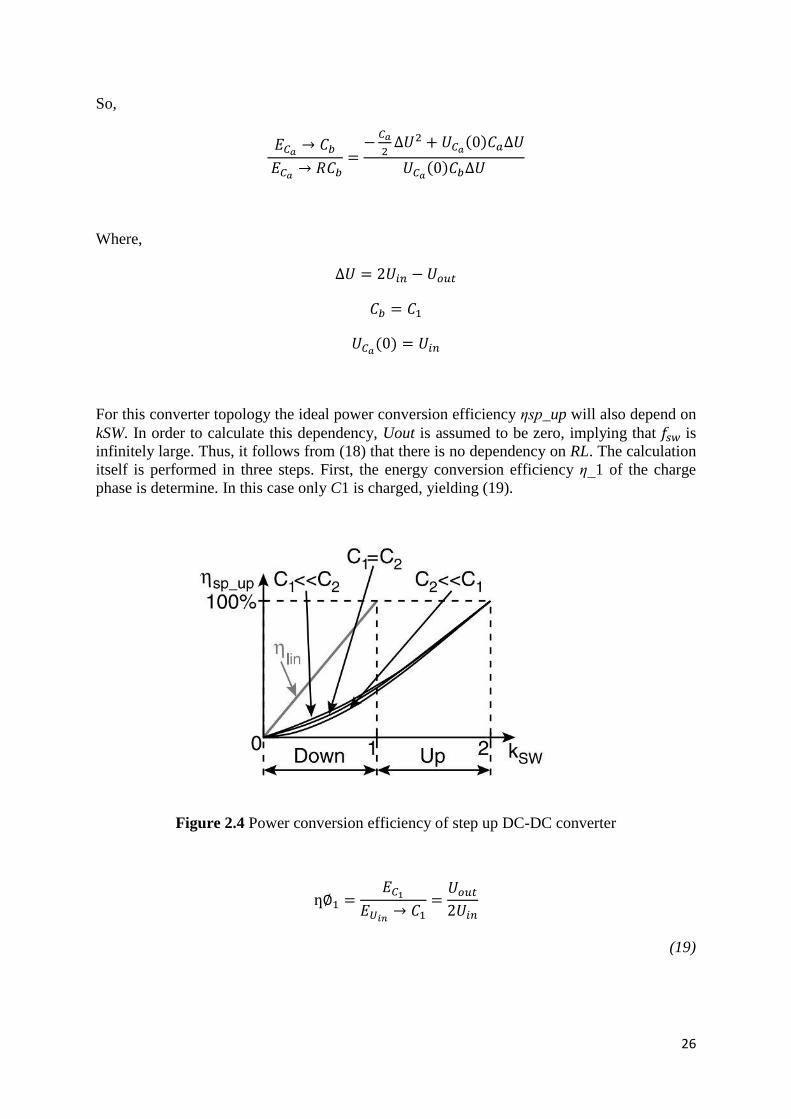
For this converter topology the ideal power conversion efficiency ηsp_up will also depend on
kSW. In order to calculate this dependency, Uout is assumed to be zero, implying that 𝑓𝑠𝑤 is
infinitely large. Thus, it follows from (18) that there is no dependency on RL. The calculation
itself is performed in three steps. First, the energy conversion efficiency η_1 of the charge
phase is determine. In this case only C1 is charged, yielding (19).
Figure 2.4 Power conversion efficiency of step up DC-DC converter
ƞ∅1 =𝐸𝐶1
𝐸𝑈𝑖𝑛→ 𝐶1
=𝑈𝑜𝑢𝑡
2𝑈𝑖𝑛
(19)
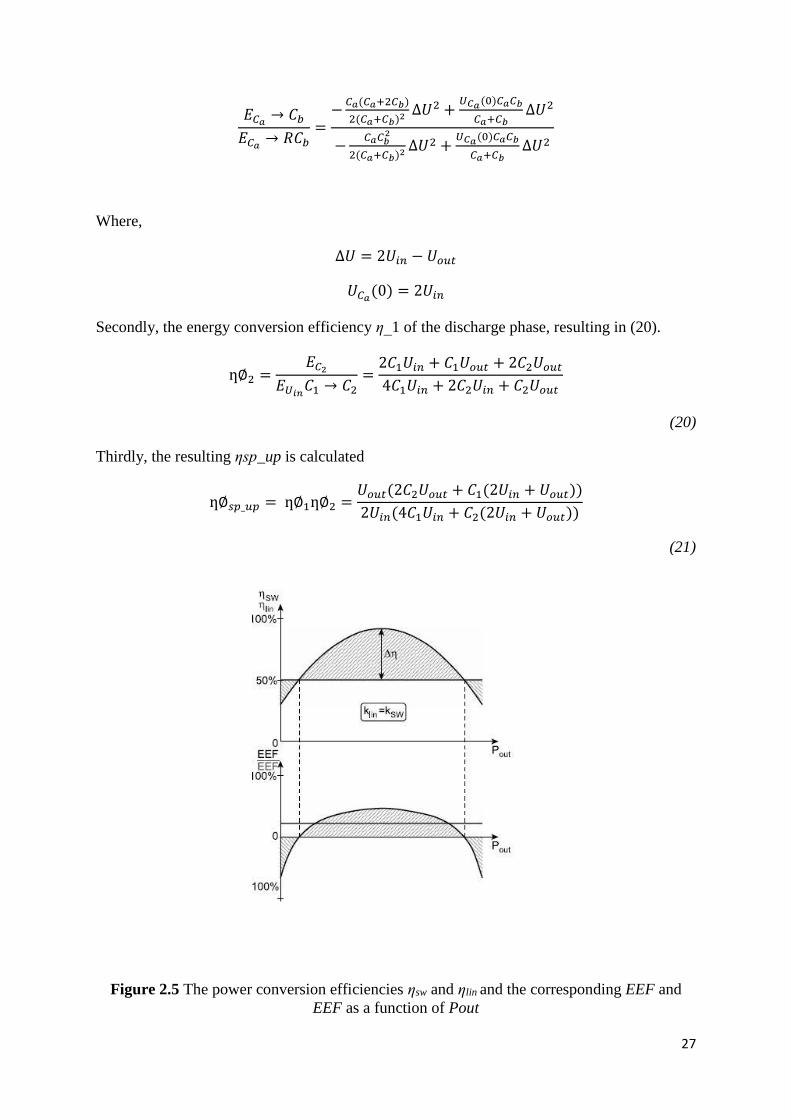
27
𝐸𝐶𝑎→ 𝐶𝑏
𝐸𝐶𝑎→ 𝑅𝐶𝑏
=−
𝐶𝑎(𝐶𝑎+2𝐶𝑏)
2(𝐶𝑎+𝐶𝑏)2 ∆𝑈2 +𝑈𝐶𝑎(0)𝐶𝑎𝐶𝑏
𝐶𝑎+𝐶𝑏∆𝑈2
−𝐶𝑎𝐶𝑏
2
2(𝐶𝑎+𝐶𝑏)2 ∆𝑈2 +𝑈𝐶𝑎(0)𝐶𝑎𝐶𝑏
𝐶𝑎+𝐶𝑏∆𝑈2
Where,
∆𝑈 = 2𝑈𝑖𝑛 − 𝑈𝑜𝑢𝑡
𝑈𝐶𝑎(0) = 2𝑈𝑖𝑛
Secondly, the energy conversion efficiency η_1 of the discharge phase, resulting in (20).
ƞ∅2 =𝐸𝐶2
𝐸𝑈𝑖𝑛𝐶1 → 𝐶2
=2𝐶1𝑈𝑖𝑛 + 𝐶1𝑈𝑜𝑢𝑡 + 2𝐶2𝑈𝑜𝑢𝑡
4𝐶1𝑈𝑖𝑛 + 2𝐶2𝑈𝑖𝑛 + 𝐶2𝑈𝑜𝑢𝑡
(20)
Thirdly, the resulting ηsp_up is calculated
ƞ∅𝑠𝑝_𝑢𝑝 = ƞ∅1ƞ∅2 =𝑈𝑜𝑢𝑡(2𝐶2𝑈𝑜𝑢𝑡 + 𝐶1(2𝑈𝑖𝑛 + 𝑈𝑜𝑢𝑡))
2𝑈𝑖𝑛(4𝐶1𝑈𝑖𝑛 + 𝐶2(2𝑈𝑖𝑛 + 𝑈𝑜𝑢𝑡))
(21)
Figure 2.5 The power conversion efficiencies ηsw and ηlin and the corresponding EEF and
EEF as a function of Pout
28
2.6 SNUBBER CIRCUIT
Semiconductor devices are very sensitive to over voltage & mostly this is the main reason
behind various failures .The maximum voltage supplied to an electronic device must be smaller
than its maximum rated voltage. In power electronic circuits, over voltage occurs due to
switching operation, lightning strokes, short circuiting etc. Due to junction capacitance, sudden
increment of voltage produces charging current in electronic devices as,
𝑖 = 𝐶 (𝑑𝑣
𝑑𝑡)
If the rate of application of the forward voltage is high, a large charging current flows, which
may damage the junction. For proper operation, dv/dt must be kept less than the specified value
.To protect electronic devices against damages created by dv/dt, suppression of voltage
transient is necessary and we can achieve it by adding a simple RC circuit which is called a
snubber circuit. Snubber circuits are placed across the semiconductor devices for protection as
well as to improve the performance.
Snubbers are frequently used in electrical systems with an inductive load where the sudden
interruption of current flow often leads to a sharp rise in voltage across the device creating the
interruption .This sharp rise in voltage is a transient and can damage and lead to failure of the
controlling device. A spark is likely to be generated (arcing), which can cause electromagnetic
interference (EMI) in the circuits .The snubber attempts to prevent this undesired voltage by
conducting transient current around device.
Snubbers enhance the performance of the switching circuits and result in higher reliability,
higher efficiency, higher switching frequency, smaller size, lower weight, and lower EMI. The
basic intent of a snubber is to absorb energy from the reactive elements in the circuit. The
benefits of this may include circuit damping, controlling the rate of change of voltage or
current, or clamping voltage overshoot. In performing these functions a snubber limits the
amount of stress which the switch must endure and this increases the reliability of the switch.
When a snubber is properly designed and implemented the switch will have lower average
power dissipation, much lower peak power dissipation, lower peak operating voltage and lower
peak operating current.
Snubbers are placed across the various switching devices like transistors, etc. Switching from
ON to OFF state results the impedance of the device suddenly changes to the high value. But
this allows a small current to flow through the switch. This induces a large voltage across the
device. If this current reduced at faster rate more is the induced voltage across the device and
also if the switch is not capable of withstanding this voltage the switch becomes burn out. So
auxiliary path is needed to prevent this high induced voltage

29
Similarly when the transition is from OFF to ON state, due to uneven distribution of the current
through the area of the switch overheating will takes place and eventually it will be burned.
Here also snubber is necessary to reduce the current at starting by making an alternate path.
Snubbers in switching mode provides one or more of the following functions,
Shape the load line of a bipolar switching transistor to keep it in its safe operating area.
Reducing the voltages and currents during turn ON and turn OFF transient conditions.
Removes energy from a switching transistor and dissipate the energy in a resistor to
reduce junction temperature.
Limiting the rate of change of voltage and currents during the transients.
Reducing EMI by damping voltage and current ringing
2.7 TYPES OF SNUBBERS
Rate of rise control snubbers and voltage clamp snubbers may be either dissipative or non-
dissipative. Non-dissipative snubbers reduce the power dissipation of the snubber and increase
the efficiency of the system.
Dissipative Snubbers
Simple RC Voltage Snubber
RCD Voltage Snubber
Simple RL Current Snubber
Non-dissipative Snubbers
Two Terminal 3D-2C-1L Voltage Snubber
Three Terminal 3D-2C-1L Voltage Snubber
Three Terminal Voltage Snubber with Intermediate Voltage
Flyback Reset Current Snubber
Resonant Recovery Current Snubber
In this thesis we have worked with RC snubber circuit.

30
2.8 RC SNUBBER
There are many kinds of snubbers like RC, diode and solid state snubbers but the most
commonly used one is RC snubber circuit. This is applicable for both the rate of rise control
and damping.
This circuit is a capacitor and series resistor connected across a switch. For designing the
Snubber circuits, the amount of energy is to dissipate in the snubber resistance is equal to the
amount of energy is stored in the capacitors. An RC Snubber placed across the switch can be
used to reduce the peak voltage at turn-off and to lamp the ring. An RC snubber circuit can be
polarized or non-polarized.
Polarized RC Snubbers
Used as turn-off snubbers to shape the turn on switching trajectory of controlled
switches.
Used as overvoltage snubbers to clamp voltages applied to controlled switches to safe
values.
Limit dv/dt during device turn off.
Non-Polarized RC Snubbers
Used to protect diodes and thyristors.
If we assume the source has negligible impedance, the worst case peak current in the snubber
circuit is
I =𝑉𝑂
𝑅𝑆
I = C𝑑𝑣
𝑑𝑡
31
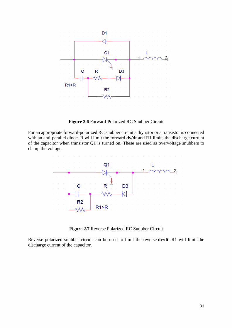
Figure 2.6 Forward-Polarized RC Snubber Circuit
For an appropriate forward-polarized RC snubber circuit a thyristor or a transistor is connected
with an anti-parallel diode. R will limit the forward dv/dt and R1 limits the discharge current
of the capacitor when transistor Q1 is turned on. These are used as overvoltage snubbers to
clamp the voltage.
Figure 2.7 Reverse Polarized RC Snubber Circuit
Reverse polarized snubber circuit can be used to limit the reverse dv/dt. R1 will limit the
discharge current of the capacitor.
32
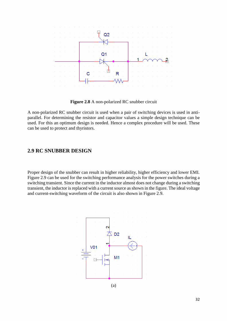
Figure 2.8 A non-polarized RC snubber circuit
A non-polarized RC snubber circuit is used when a pair of switching devices is used in anti-
parallel. For determining the resistor and capacitor values a simple design technique can be
used. For this an optimum design is needed. Hence a complex procedure will be used. These
can be used to protect and thyristors.
2.9 RC SNUBBER DESIGN
Proper design of the snubber can result in higher reliability, higher efficiency and lower EMI.
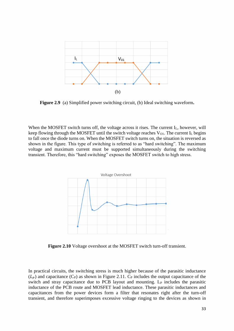
Figure 2.9 can be used for the switching performance analysis for the power switches during a
switching transient. Since the current in the inductor almost does not change during a switching
transient, the inductor is replaced with a current source as shown in the figure. The ideal voltage
and current-switching waveform of the circuit is also shown in Figure 2.9.
(a)
33
(b)
Figure 2.9 (a) Simplified power switching circuit, (b) Ideal switching waveform.
When the MOSFET switch turns off, the voltage across it rises. The current IL, however, will
keep flowing through the MOSFET until the switch voltage reaches VO1. The current IL begins
to fall once the diode turns on. When the MOSFET switch turns on, the situation is reversed as
shown in the figure. This type of switching is referred to as “hard switching”. The maximum
voltage and maximum current must be supported simultaneously during the switching
transient. Therefore, this “hard switching” exposes the MOSFET switch to high stress.
Figure 2.10 Voltage overshoot at the MOSFET switch turn-off transient.
In practical circuits, the switching stress is much higher because of the parasitic inductance
(𝐿𝑃) and capacitance (CP) as shown in Figure 2.11. CP includes the output capacitance of the
switch and stray capacitance due to PCB layout and mounting. LP includes the parasitic
inductance of the PCB route and MOSFET lead inductance. These parasitic inductances and
capacitances from the power devices form a filter that resonates right after the turn-off
transient, and therefore superimposes excessive voltage ringing to the devices as shown in
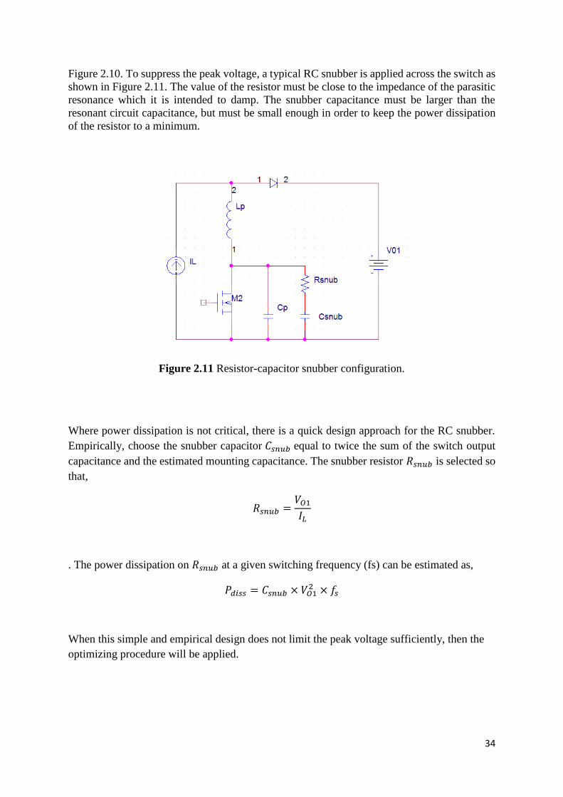
34
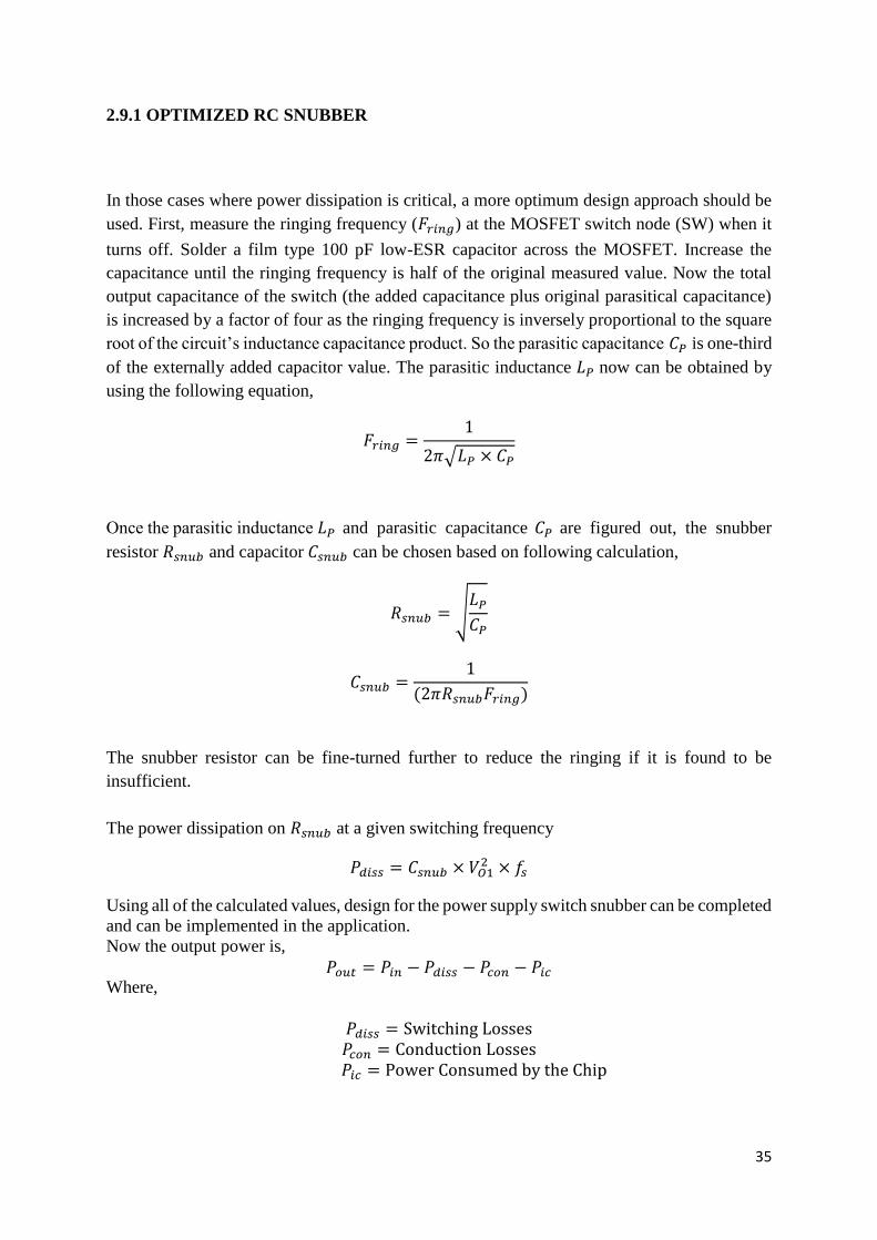
Figure 2.10. To suppress the peak voltage, a typical RC snubber is applied across the switch as
shown in Figure 2.11. The value of the resistor must be close to the impedance of the parasitic
resonance which it is intended to damp. The snubber capacitance must be larger than the
resonant circuit capacitance, but must be small enough in order to keep the power dissipation
of the resistor to a minimum.
Figure 2.11 Resistor-capacitor snubber configuration.
Where power dissipation is not critical, there is a quick design approach for the RC snubber.
Empirically, choose the snubber capacitor 𝐶𝑠𝑛𝑢𝑏 equal to twice the sum of the switch output
capacitance and the estimated mounting capacitance. The snubber resistor 𝑅𝑠𝑛𝑢𝑏 is selected so
that,
𝑅𝑠𝑛𝑢𝑏 =𝑉𝑂1
𝐼𝐿
. The power dissipation on 𝑅𝑠𝑛𝑢𝑏 at a given switching frequency (fs) can be estimated as,
𝑃𝑑𝑖𝑠𝑠 = 𝐶𝑠𝑛𝑢𝑏 × 𝑉𝑂12 × 𝑓𝑠
When this simple and empirical design does not limit the peak voltage sufficiently, then the
optimizing procedure will be applied.
35
2.9.1 OPTIMIZED RC SNUBBER
In those cases where power dissipation is critical, a more optimum design approach should be
used. First, measure the ringing frequency (𝐹𝑟𝑖𝑛𝑔) at the MOSFET switch node (SW) when it
turns off. Solder a film type 100 pF low-ESR capacitor across the MOSFET. Increase the
capacitance until the ringing frequency is half of the original measured value. Now the total
output capacitance of the switch (the added capacitance plus original parasitical capacitance)
is increased by a factor of four as the ringing frequency is inversely proportional to the square
root of the circuit’s inductance capacitance product. So the parasitic capacitance 𝐶𝑃 is one-third
of the externally added capacitor value. The parasitic inductance 𝐿𝑃 now can be obtained by
using the following equation,
𝐹𝑟𝑖𝑛𝑔 =1
2𝜋√𝐿𝑃 × 𝐶𝑃
Once the parasitic inductance 𝐿𝑃 and parasitic capacitance 𝐶𝑃 are figured out, the snubber
resistor 𝑅𝑠𝑛𝑢𝑏 and capacitor 𝐶𝑠𝑛𝑢𝑏 can be chosen based on following calculation,
𝑅𝑠𝑛𝑢𝑏 = √𝐿𝑃
𝐶𝑃
𝐶𝑠𝑛𝑢𝑏 =1
(2𝜋𝑅𝑠𝑛𝑢𝑏𝐹𝑟𝑖𝑛𝑔)
The snubber resistor can be fine-turned further to reduce the ringing if it is found to be
insufficient.
The power dissipation on 𝑅𝑠𝑛𝑢𝑏 at a given switching frequency
𝑃𝑑𝑖𝑠𝑠 = 𝐶𝑠𝑛𝑢𝑏 × 𝑉𝑂12 × 𝑓𝑠
Using all of the calculated values, design for the power supply switch snubber can be completed
and can be implemented in the application.
Now the output power is,
𝑃𝑜𝑢𝑡 = 𝑃𝑖𝑛 − 𝑃𝑑𝑖𝑠𝑠 − 𝑃𝑐𝑜𝑛 − 𝑃𝑖𝑐 Where,
𝑃𝑑𝑖𝑠𝑠 = Switching Losses
𝑃𝑐𝑜𝑛 = Conduction Losses
𝑃𝑖𝑐 = Power Consumed by the Chip
36
The switching loss can be decreased by using snubber circuit across the switch which results
in higher output voltage as well higher efficiency.
2.9.2 CAPACITOR SELECTION
Snubber capacitors are subjected to high peak and RMS currents and high dv/dt. An example
is turn-on and turn-off current spikes in a typical RCD snubber capacitor. The pulse will have
high peak and RMS amplitudes. The snubber capacitor has to meet two requirements. First, the
energy stored in the snubber capacitor must be greater than the energy in the circuit’s
inductance. Secondly, the time constant of snubber circuits should me small compared to
shortest on time expected, usually 10% of the on time. By allowing the resistor to be effective
in the ringing frequency this capacitor is used to minimize the dissipation at switching
frequency. The best design is selecting the impedance of the capacitor is same that of resistor
at the ringing frequency.
2.9.3 RESISTANCE SELECTION
It is important that R in the RC snubber, have low self-inductance. Inductance in R will increase
the peak voltage and it will tend to defeat the purpose of the snubber. Low inductance will also
be desirable for R in snubber but it is not critical since the effect of a small amount of inductance
is to slightly increase the reset time of C and it will reduce the peak current in switch at turn-
on. The normal choice of R is usually the carbon composition or metal film. The resistor power
dissipation must be independent of the resistance R because it dissipates the energy stored in
the snubber capacitor in each transition of voltage in the capacitor. If we select the resistor as
that the characteristic impedance, the ringing is well damped.
When comparing the Quick design to optimum design, the required snubber resistor’s power
capability will be reduced. Usually the “Quick” design is completely adequate for final design.
Going to the “Optimum” approach is only if power efficiency and size constraints dictate the
need for optimum design.
37
2.10 HIGH GAIN HYBRID BOOST DC-DC CONVERTER CIRCUIT
(REFERENCE CIRCUIT)
The high gain hybrid Boost DC-DC converter with two inductors is studied by simulation at
variable duty cycle in CAPTURE CIS. The inductor value in the circuit is kept at 0.5mH each
for the purpose of comparison on the same component value. The conventional high gain
hybrid Boost DC-DC converter circuit is shown in figure 2.12 and its typical output voltage
and current waveforms are shown in figure 2.13. The input voltage, output voltage, voltage
gain, input current, output current, input power, output power and efficiency are tabulated along
with duty cycle in Table 2.1 and depicted in graphs of figure 2.14-2.15. Figure 2.14 shows the
graphical representation of changing voltage gain with respect to duty cycle. Figure 2.15 shows
the graphical representation of changing efficiency with respect to duty cycle.
Figure 2.12 High gain hybrid Boost DC-DC converter
C310u
R2
0.001
V
0
V1
10V
R3
0.001
L3
.5m
1 2
V2
TD = 0
TF = 0.001mPW = 0.175mPER = 0.2m
V1 = 0
TR = 0.001m
V2 = 20
D5
D1N4001
L4
.5m
1 2
Z2
APT40GF100BN
L5
1m
1
2
R1
0.001
R5
1k
R4
200
C1
10u
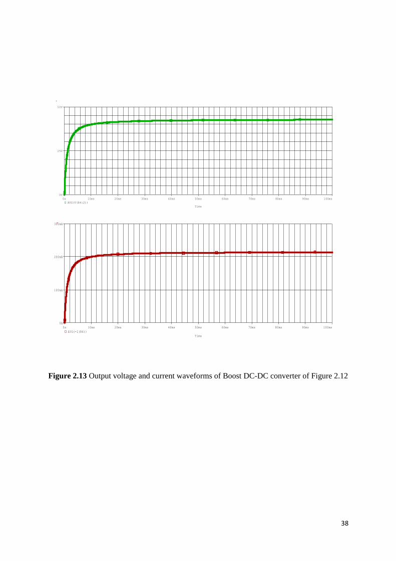
38
Figure 2.13 Output voltage and current waveforms of Boost DC-DC converter of Figure 2.12
Time
0s 10ms 20ms 30ms 40ms 50ms 60ms 70ms 80ms 90ms 100ms
AVG(V(R4:2))
0V
25V
50V
Time
0s 10ms 20ms 30ms 40ms 50ms 60ms 70ms 80ms 90ms 100ms
AVG(-I(R4))
0A
100mA
200mA
300mA
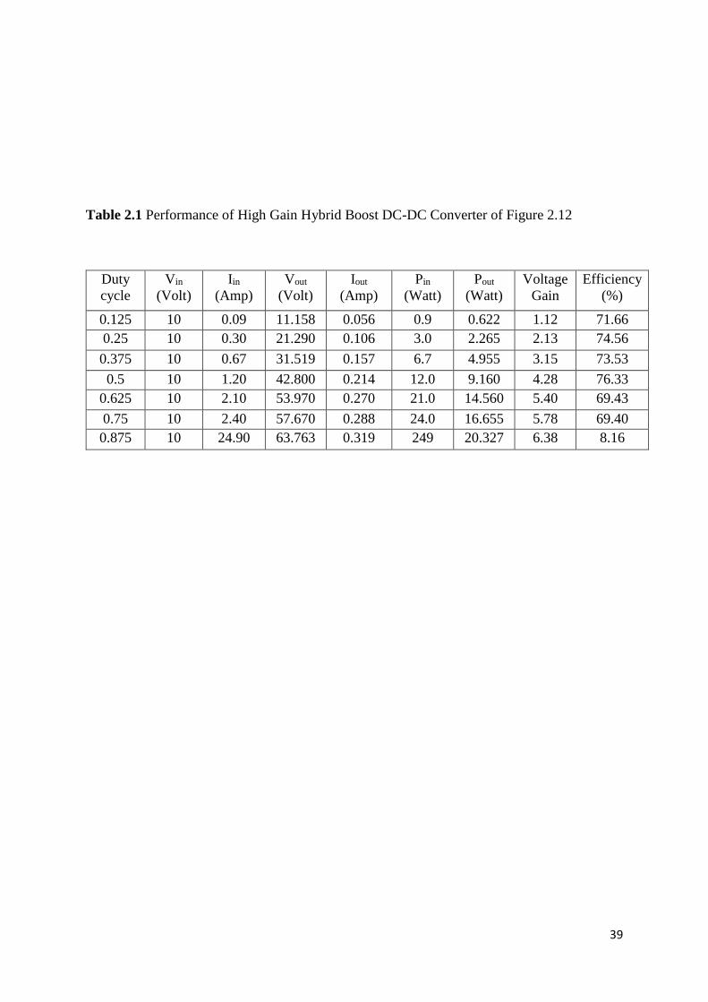
39
Table 2.1 Performance of High Gain Hybrid Boost DC-DC Converter of Figure 2.12
Duty
cycle
Vin
(Volt)
Iin
(Amp)
Vout
(Volt)
Iout
(Amp)
Pin
(Watt)
Pout
(Watt)
Voltage
Gain
Efficiency
(%)
0.125 10 0.09 11.158 0.056 0.9 0.622 1.12 71.66
0.25 10 0.30 21.290 0.106 3.0 2.265 2.13 74.56
0.375 10 0.67 31.519 0.157 6.7 4.955 3.15 73.53
0.5 10 1.20 42.800 0.214 12.0 9.160 4.28 76.33
0.625 10 2.10 53.970 0.270 21.0 14.560 5.40 69.43
0.75 10 2.40 57.670 0.288 24.0 16.655 5.78 69.40
0.875 10 24.90 63.763 0.319 249 20.327 6.38 8.16
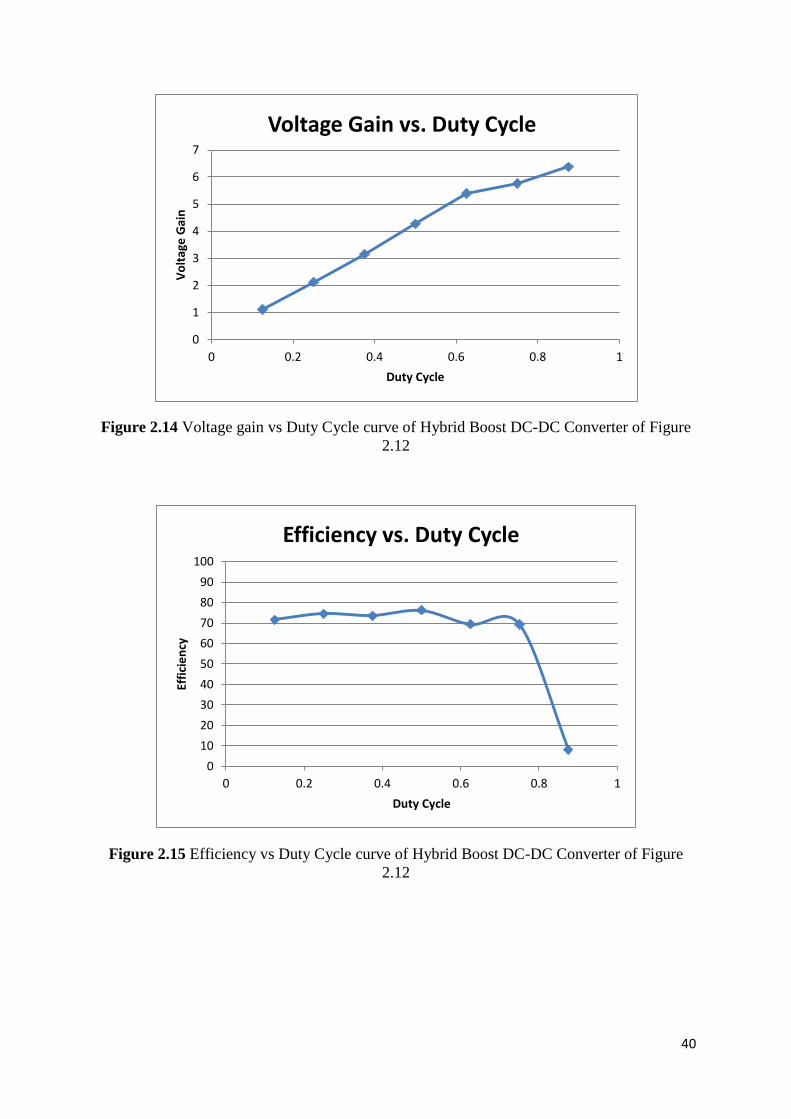
40
Figure 2.14 Voltage gain vs Duty Cycle curve of Hybrid Boost DC-DC Converter of Figure
2.12
Figure 2.15 Efficiency vs Duty Cycle curve of Hybrid Boost DC-DC Converter of Figure
2.12
0
1
2
3
4
5
6
7
0 0.2 0.4 0.6 0.8 1
Vo
ltag
e G
ain
Duty Cycle
Voltage Gain vs. Duty Cycle
0
10
20
30
40
50
60
70
80
90
100
0 0.2 0.4 0.6 0.8 1
Effi
cie
ncy
Duty Cycle
Efficiency vs. Duty Cycle
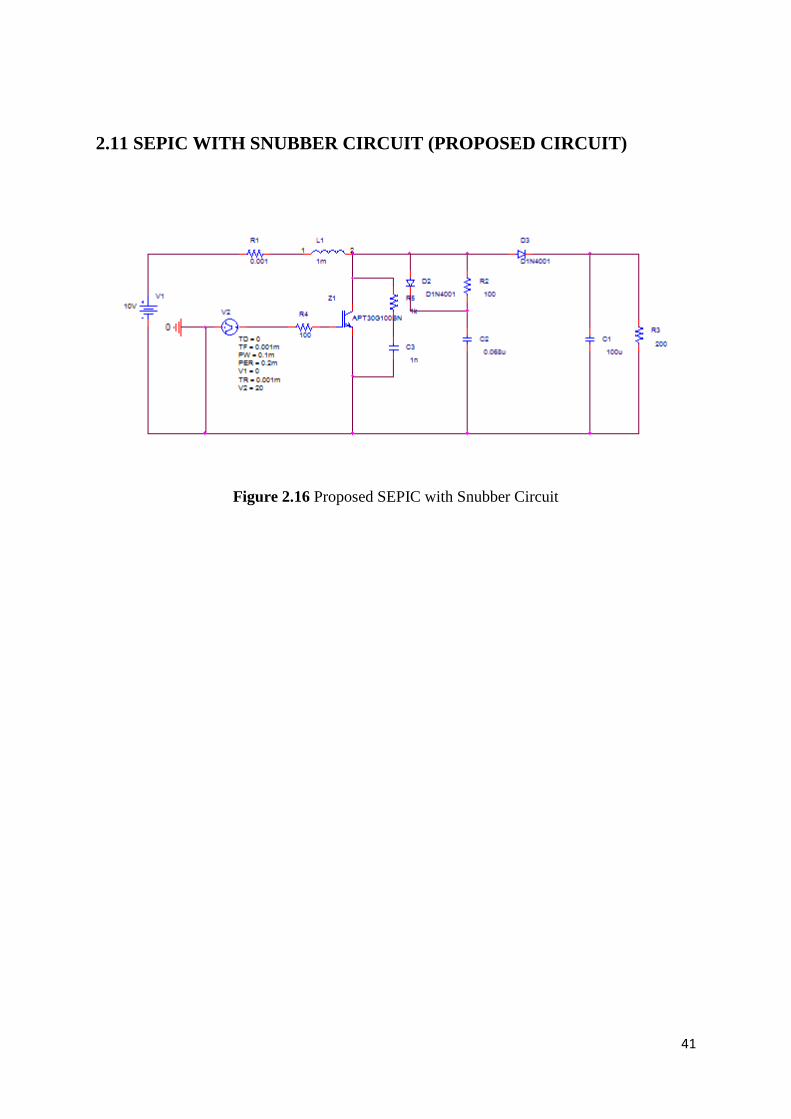
41
2.11 SEPIC WITH SNUBBER CIRCUIT (PROPOSED CIRCUIT)
Figure 2.16 Proposed SEPIC with Snubber Circuit
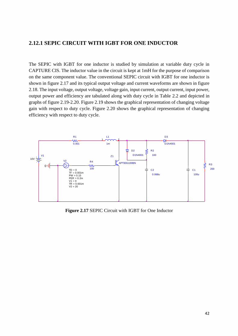
42
2.12.1 SEPIC CIRCUIT WITH IGBT FOR ONE INDUCTOR
The SEPIC with IGBT for one inductor is studied by simulation at variable duty cycle in
CAPTURE CIS. The inductor value in the circuit is kept at 1mH for the purpose of comparison
on the same component value. The conventional SEPIC circuit with IGBT for one inductor is
shown in figure 2.17 and its typical output voltage and current waveforms are shown in figure
2.18. The input voltage, output voltage, voltage gain, input current, output current, input power,
output power and efficiency are tabulated along with duty cycle in Table 2.2 and depicted in
graphs of figure 2.19-2.20. Figure 2.19 shows the graphical representation of changing voltage
gain with respect to duty cycle. Figure 2.20 shows the graphical representation of changing
efficiency with respect to duty cycle.
Figure 2.17 SEPIC Circuit with IGBT for One Inductor
C2
0.068u
Z1
APT30G100BN
0
D2
D1N4001
R1
0.001
V2
TD = 0TF = 0.001mPW = 0.15PER = 0.2mV1 = 0TR = 0.001mV2 = 20
R2
100
R4
100C1
100u
L1
1m
1 2
V1
10V
R3
200
D3
D1N4001
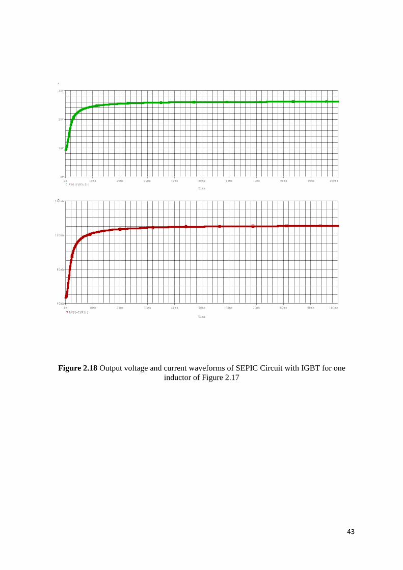
43
Figure 2.18 Output voltage and current waveforms of SEPIC Circuit with IGBT for one
inductor of Figure 2.17
Time
0s 10ms 20ms 30ms 40ms 50ms 60ms 70ms 80ms 90ms 100ms
AVG(V(R3:2))
0V
10V
20V
30V
Time
0s 10ms 20ms 30ms 40ms 50ms 60ms 70ms 80ms 90ms 100ms
AVG(-I(R3))
40mA
80mA
120mA
160mA
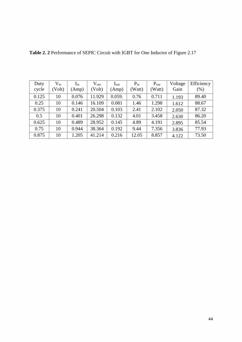
44
Table 2. 2 Performance of SEPIC Circuit with IGBT for One Inductor of Figure 2.17
Duty
cycle
Vin
(Volt)
Iin
(Amp)
Vout
(Volt)
Iout
(Amp)
Pin
(Watt)
Pout
(Watt)
Voltage
Gain
Efficiency
(%)
0.125 10 0.076 11.929 0.059. 0.76 0.711 1.193 89.40
0.25 10 0.146 16.109 0.081 1.46 1.298 1.612 88.67
0.375 10 0.241 20.504 0.103 2.41 2.102 2.050 87.32
0.5 10 0.401 26.298 0.132 4.01 3.458 2.630 86.20
0.625 10 0.489 28.952 0.145 4.89 4.191 2.895 85.54
0.75 10 0.944 38.364 0.192 9.44 7.356 3.836 77.93
0.875 10 1.205 41.214 0.216 12.05 8.857 4.122 73.50
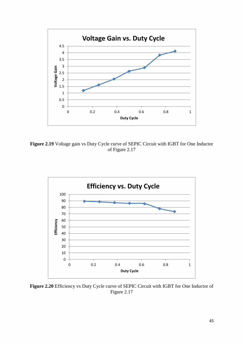
45
Figure 2.19 Voltage gain vs Duty Cycle curve of SEPIC Circuit with IGBT for One Inductor
of Figure 2.17
Figure 2.20 Efficiency vs Duty Cycle curve of SEPIC Circuit with IGBT for One Inductor of
Figure 2.17
0
0.5
1
1.5
2
2.5
3
3.5
4
4.5
0 0.2 0.4 0.6 0.8 1
Vo
ltag
e G
ain
Duty Cycle
Voltage Gain vs. Duty Cycle
0
10
20
30
40
50
60
70
80
90
100
0 0.2 0.4 0.6 0.8 1
Effi
cie
ncy
Duty Cycle
Efficiency vs. Duty Cycle
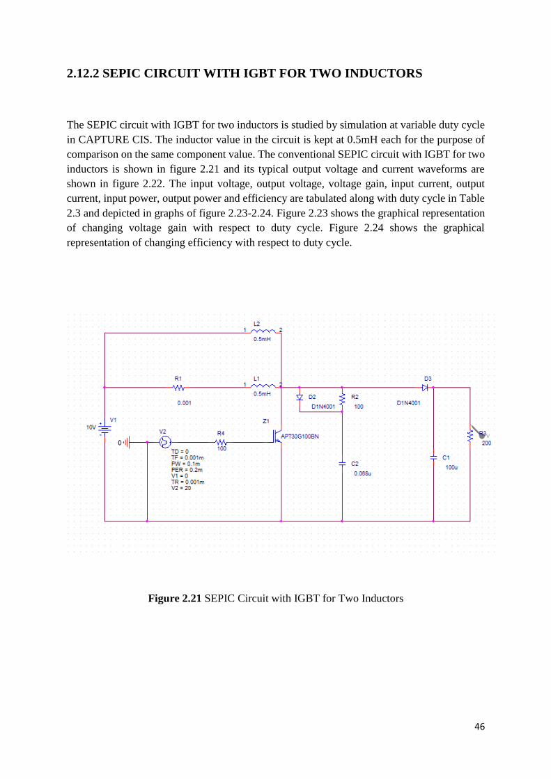
46
2.12.2 SEPIC CIRCUIT WITH IGBT FOR TWO INDUCTORS
The SEPIC circuit with IGBT for two inductors is studied by simulation at variable duty cycle
in CAPTURE CIS. The inductor value in the circuit is kept at 0.5mH each for the purpose of
comparison on the same component value. The conventional SEPIC circuit with IGBT for two
inductors is shown in figure 2.21 and its typical output voltage and current waveforms are
shown in figure 2.22. The input voltage, output voltage, voltage gain, input current, output
current, input power, output power and efficiency are tabulated along with duty cycle in Table
2.3 and depicted in graphs of figure 2.23-2.24. Figure 2.23 shows the graphical representation
of changing voltage gain with respect to duty cycle. Figure 2.24 shows the graphical
representation of changing efficiency with respect to duty cycle.
Figure 2.21 SEPIC Circuit with IGBT for Two Inductors
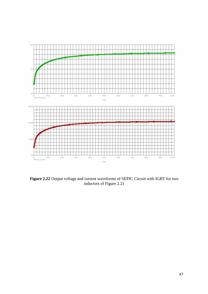
47
Figure 2.22 Output voltage and current waveforms of SEPIC Circuit with IGBT for two
inductors of Figure 2.21
Time
0s 10ms 20ms 30ms 40ms 50ms 60ms 70ms 80ms 90ms 100ms
AVG(V(R3:2))
0V
25V
50V
Time
0s 10ms 20ms 30ms 40ms 50ms 60ms 70ms 80ms 90ms 100ms
AVG(-I(R3))
0A
100mA
200mA
300mA
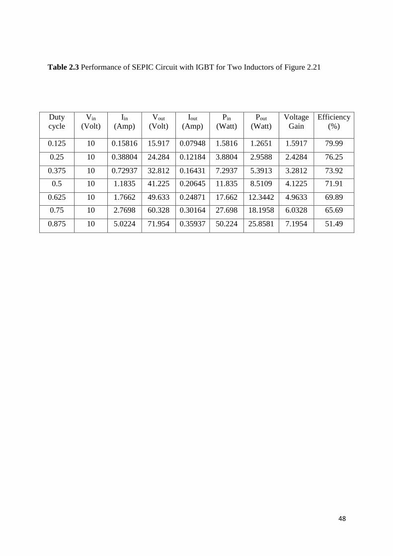
48
Table 2.3 Performance of SEPIC Circuit with IGBT for Two Inductors of Figure 2.21
Duty
cycle
Vin
(Volt)
Iin
(Amp)
Vout
(Volt)
Iout
(Amp)
Pin
(Watt)
Pout
(Watt)
Voltage
Gain
Efficiency
(%)
0.125 10 0.15816 15.917 0.07948 1.5816 1.2651 1.5917 79.99
0.25 10 0.38804 24.284 0.12184 3.8804 2.9588 2.4284 76.25
0.375 10 0.72937 32.812 0.16431 7.2937 5.3913 3.2812 73.92
0.5 10 1.1835 41.225 0.20645 11.835 8.5109 4.1225 71.91
0.625 10 1.7662 49.633 0.24871 17.662 12.3442 4.9633 69.89
0.75 10 2.7698 60.328 0.30164 27.698 18.1958 6.0328 65.69
0.875 10 5.0224 71.954 0.35937 50.224 25.8581 7.1954 51.49
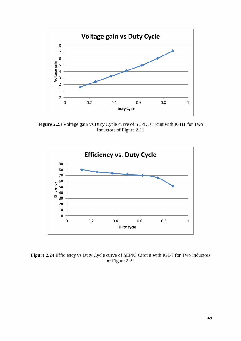
49
Figure 2.23 Voltage gain vs Duty Cycle curve of SEPIC Circuit with IGBT for Two
Inductors of Figure 2.21
Figure 2.24 Efficiency vs Duty Cycle curve of SEPIC Circuit with IGBT for Two Inductors
of Figure 2.21
0
1
2
3
4
5
6
7
8
0 0.2 0.4 0.6 0.8 1
Vo
ltag
e g
ain
Duty Cycle
Voltage gain vs Duty Cycle
0
10
20
30
40
50
60
70
80
90
0 0.2 0.4 0.6 0.8 1
Effi
cie
ncy
Duty cycle
Efficiency vs. Duty Cycle
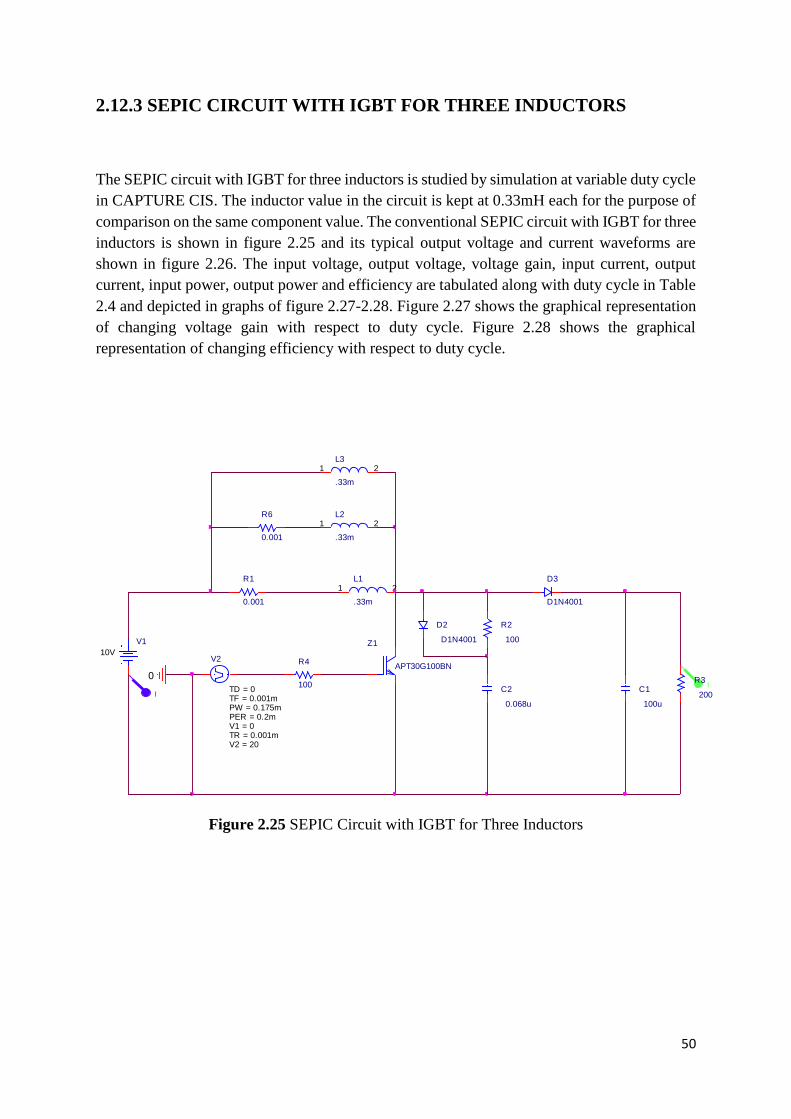
50
2.12.3 SEPIC CIRCUIT WITH IGBT FOR THREE INDUCTORS
The SEPIC circuit with IGBT for three inductors is studied by simulation at variable duty cycle
in CAPTURE CIS. The inductor value in the circuit is kept at 0.33mH each for the purpose of
comparison on the same component value. The conventional SEPIC circuit with IGBT for three
inductors is shown in figure 2.25 and its typical output voltage and current waveforms are
shown in figure 2.26. The input voltage, output voltage, voltage gain, input current, output
current, input power, output power and efficiency are tabulated along with duty cycle in Table
2.4 and depicted in graphs of figure 2.27-2.28. Figure 2.27 shows the graphical representation
of changing voltage gain with respect to duty cycle. Figure 2.28 shows the graphical
representation of changing efficiency with respect to duty cycle.
Figure 2.25 SEPIC Circuit with IGBT for Three Inductors
R1
0.001
V2
TD = 0TF = 0.001mPW = 0.175mPER = 0.2mV1 = 0TR = 0.001mV2 = 20
C1
100u
R4
100
R2
100
I
D3
D1N4001
0
Z1
APT30G100BN
C2
0.068u
I
L2
.33m
1 2
R3
200
V1
10V
L1
.33m
1 2
R6
0.001
L3
.33m
1 2
D2
D1N4001
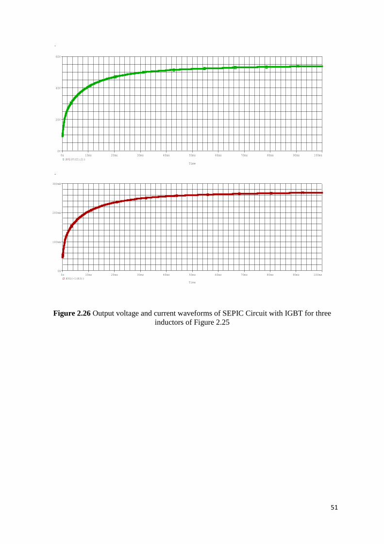
51
Figure 2.26 Output voltage and current waveforms of SEPIC Circuit with IGBT for three
inductors of Figure 2.25
Time
0s 10ms 20ms 30ms 40ms 50ms 60ms 70ms 80ms 90ms 100ms
AVG(V(C1:2))
0V
20V
40V
60V
Time
0s 10ms 20ms 30ms 40ms 50ms 60ms 70ms 80ms 90ms 100ms
AVG(-I(R3))
0A
100mA
200mA
300mA
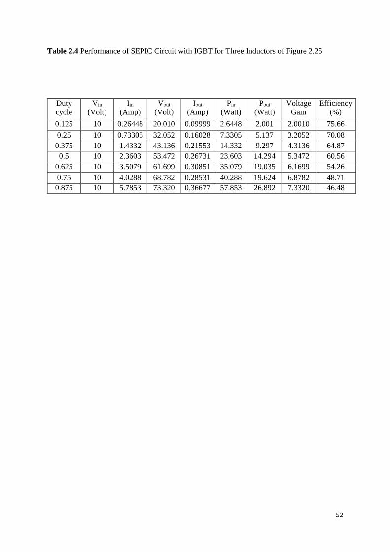
52
Table 2.4 Performance of SEPIC Circuit with IGBT for Three Inductors of Figure 2.25
Duty
cycle
Vin
(Volt)
Iin
(Amp)
Vout
(Volt)
Iout
(Amp)
Pin
(Watt)
Pout
(Watt)
Voltage
Gain
Efficiency
(%)
0.125 10 0.26448 20.010 0.09999 2.6448 2.001 2.0010 75.66
0.25 10 0.73305 32.052 0.16028 7.3305 5.137 3.2052 70.08
0.375 10 1.4332 43.136 0.21553 14.332 9.297 4.3136 64.87
0.5 10 2.3603 53.472 0.26731 23.603 14.294 5.3472 60.56
0.625 10 3.5079 61.699 0.30851 35.079 19.035 6.1699 54.26
0.75 10 4.0288 68.782 0.28531 40.288 19.624 6.8782 48.71
0.875 10 5.7853 73.320 0.36677 57.853 26.892 7.3320 46.48
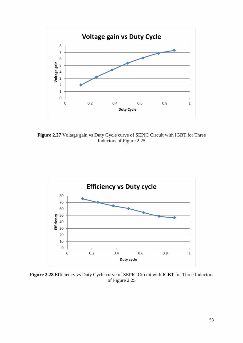
53
Figure 2.27 Voltage gain vs Duty Cycle curve of SEPIC Circuit with IGBT for Three
Inductors of Figure 2.25
Figure 2.28 Efficiency vs Duty Cycle curve of SEPIC Circuit with IGBT for Three Inductors
of Figure 2.25
0
1
2
3
4
5
6
7
8
0 0.2 0.4 0.6 0.8 1
Vo
ltag
e g
ain
Duty Cycle
Voltage gain vs Duty Cycle
0
10
20
30
40
50
60
70
80
0 0.2 0.4 0.6 0.8 1
Effi
cie
ncy
Duty cycle
Efficiency vs Duty cycle
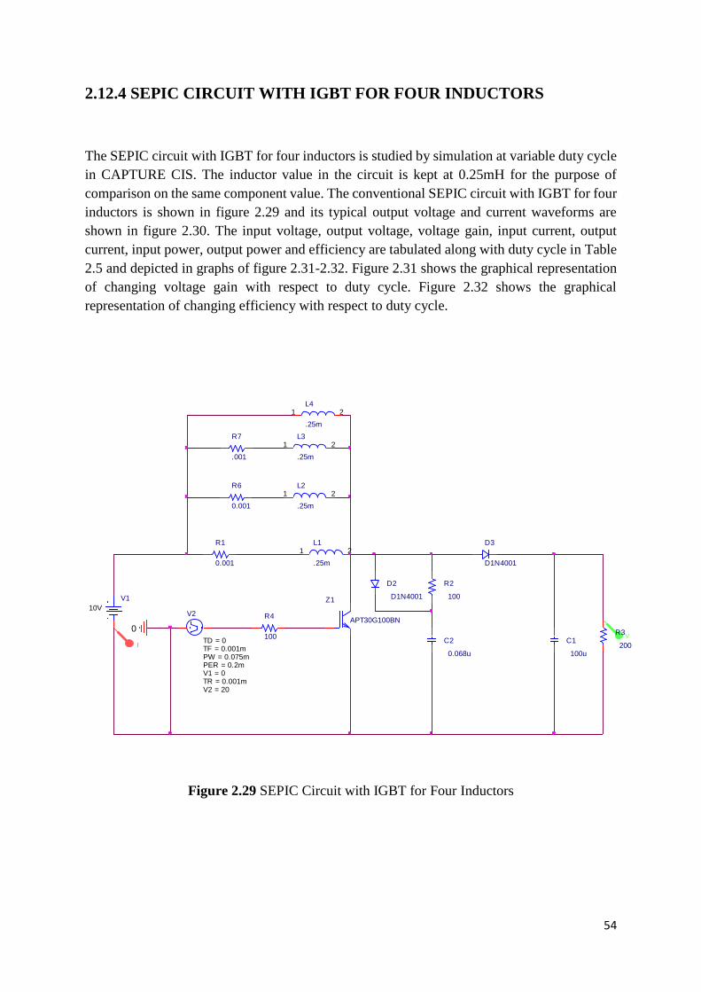
54
2.12.4 SEPIC CIRCUIT WITH IGBT FOR FOUR INDUCTORS
The SEPIC circuit with IGBT for four inductors is studied by simulation at variable duty cycle
in CAPTURE CIS. The inductor value in the circuit is kept at 0.25mH for the purpose of
comparison on the same component value. The conventional SEPIC circuit with IGBT for four
inductors is shown in figure 2.29 and its typical output voltage and current waveforms are
shown in figure 2.30. The input voltage, output voltage, voltage gain, input current, output
current, input power, output power and efficiency are tabulated along with duty cycle in Table
2.5 and depicted in graphs of figure 2.31-2.32. Figure 2.31 shows the graphical representation
of changing voltage gain with respect to duty cycle. Figure 2.32 shows the graphical
representation of changing efficiency with respect to duty cycle.
Figure 2.29 SEPIC Circuit with IGBT for Four Inductors
V
L4
.25m
1 2
R1
0.001
R2
100
R6
0.001
L1
.25m
1 2
C2
0.068u
D3
D1N4001
L3
.25m
1 2
V1
10V
I
D2
D1N4001
R7
.001
0
L2
.25m
1 2
R4
100C1
100u
V2
TD = 0TF = 0.001mPW = 0.075mPER = 0.2mV1 = 0TR = 0.001mV2 = 20
R3
200
Z1
APT30G100BN
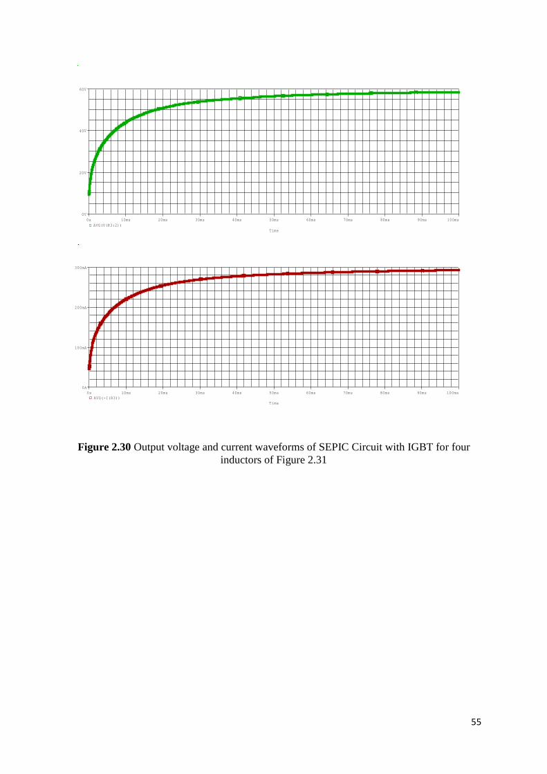
55
Figure 2.30 Output voltage and current waveforms of SEPIC Circuit with IGBT for four
inductors of Figure 2.31
Time
0s 10ms 20ms 30ms 40ms 50ms 60ms 70ms 80ms 90ms 100ms
AVG(V(R3:2))
0V
20V
40V
60V
Time
0s 10ms 20ms 30ms 40ms 50ms 60ms 70ms 80ms 90ms 100ms
AVG(-I(R3))
0A
100mA
200mA
300mA
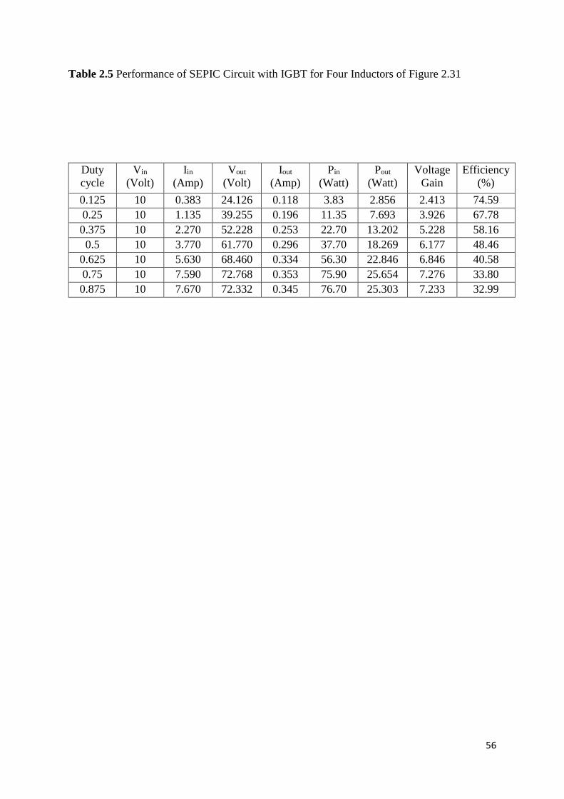
56
Table 2.5 Performance of SEPIC Circuit with IGBT for Four Inductors of Figure 2.31
Duty
cycle
Vin
(Volt)
Iin
(Amp)
Vout
(Volt)
Iout
(Amp)
Pin
(Watt)
Pout
(Watt)
Voltage
Gain
Efficiency
(%)
0.125 10 0.383 24.126 0.118 3.83 2.856 2.413 74.59
0.25 10 1.135 39.255 0.196 11.35 7.693 3.926 67.78
0.375 10 2.270 52.228 0.253 22.70 13.202 5.228 58.16
0.5 10 3.770 61.770 0.296 37.70 18.269 6.177 48.46
0.625 10 5.630 68.460 0.334 56.30 22.846 6.846 40.58
0.75 10 7.590 72.768 0.353 75.90 25.654 7.276 33.80
0.875 10 7.670 72.332 0.345 76.70 25.303 7.233 32.99
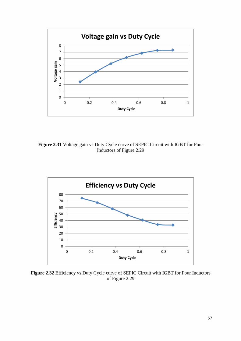
57
Figure 2.31 Voltage gain vs Duty Cycle curve of SEPIC Circuit with IGBT for Four
Inductors of Figure 2.29
Figure 2.32 Efficiency vs Duty Cycle curve of SEPIC Circuit with IGBT for Four Inductors
of Figure 2.29
0
1
2
3
4
5
6
7
8
0 0.2 0.4 0.6 0.8 1
Vo
ltag
e g
ain
Duty Cycle
Voltage gain vs Duty Cycle
0
10
20
30
40
50
60
70
80
0 0.2 0.4 0.6 0.8 1
Effi
cie
ncy
Duty Cycle
Efficiency vs Duty Cycle
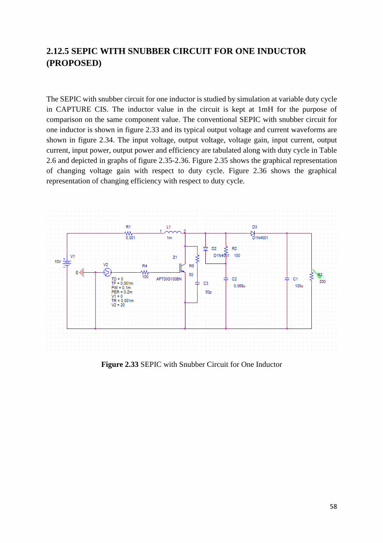
58
2.12.5 SEPIC WITH SNUBBER CIRCUIT FOR ONE INDUCTOR
(PROPOSED)
The SEPIC with snubber circuit for one inductor is studied by simulation at variable duty cycle
in CAPTURE CIS. The inductor value in the circuit is kept at 1mH for the purpose of
comparison on the same component value. The conventional SEPIC with snubber circuit for
one inductor is shown in figure 2.33 and its typical output voltage and current waveforms are
shown in figure 2.34. The input voltage, output voltage, voltage gain, input current, output
current, input power, output power and efficiency are tabulated along with duty cycle in Table
2.6 and depicted in graphs of figure 2.35-2.36. Figure 2.35 shows the graphical representation
of changing voltage gain with respect to duty cycle. Figure 2.36 shows the graphical
representation of changing efficiency with respect to duty cycle.
Figure 2.33 SEPIC with Snubber Circuit for One Inductor
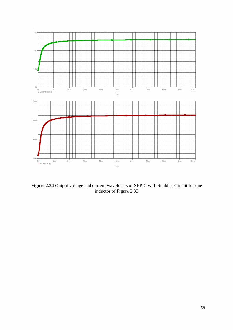
59
Figure 2.34 Output voltage and current waveforms of SEPIC with Snubber Circuit for one
inductor of Figure 2.33
Time
0s 10ms 20ms 30ms 40ms 50ms 60ms 70ms 80ms 90ms 100ms
AVG(V(R3:2))
0V
10V
20V
30V
Time
0s 10ms 20ms 30ms 40ms 50ms 60ms 70ms 80ms 90ms 100ms
AVG(-I(R3))
40mA
80mA
120mA
160mA
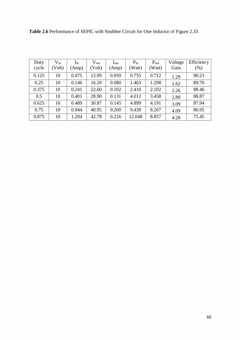
60
Table 2.6 Performance of SEPIC with Snubber Circuit for One Inductor of Figure 2.33
Duty
cycle
Vin
(Volt)
Iin
(Amp)
Vout
(Volt)
Iout
(Amp)
Pin
(Watt)
Pout
(Watt)
Voltage
Gain
Efficiency
(%)
0.125 10 0.075 12.99 0.059 0.755 0.712 1.29 90.23
0.25 10 0.146 16.20 0.080 1.463 1.298 1.62 89.70
0.375 10 0.241 22.60 0.102 2.410 2.102 2.26 88.46
0.5 10 0.401 28.90 0.131 4.012 3.458 2.89 88.87
0.625 10 0.489 30.87 0.145 4.899 4.191 3.09 87.94
0.75 10 0.944 40.95 0.200 9.439 8.207 4.09 86.95
0.875 10 1.204 42.78 0.216 12.048 8.857 4.28 75.45
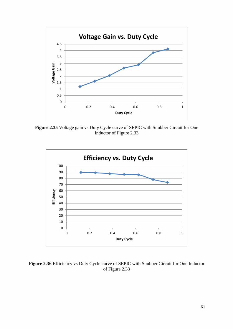
61
Figure 2.35 Voltage gain vs Duty Cycle curve of SEPIC with Snubber Circuit for One
Inductor of Figure 2.33
Figure 2.36 Efficiency vs Duty Cycle curve of SEPIC with Snubber Circuit for One Inductor
of Figure 2.33
0
0.5
1
1.5
2
2.5
3
3.5
4
4.5
0 0.2 0.4 0.6 0.8 1
Vo
ltag
e G
ain
Duty Cycle
Voltage Gain vs. Duty Cycle
0
10
20
30
40
50
60
70
80
90
100
0 0.2 0.4 0.6 0.8 1
Effi
cie
ncy
Duty Cycle
Efficiency vs. Duty Cycle
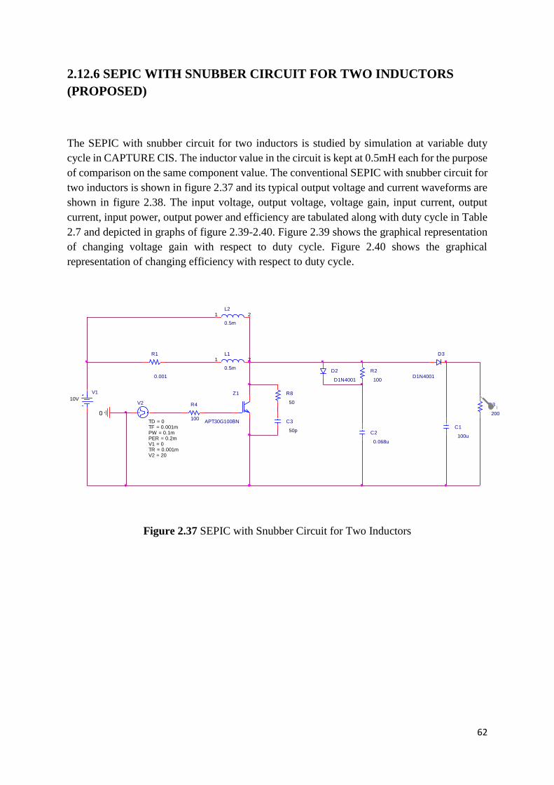
62
2.12.6 SEPIC WITH SNUBBER CIRCUIT FOR TWO INDUCTORS
(PROPOSED)
The SEPIC with snubber circuit for two inductors is studied by simulation at variable duty
cycle in CAPTURE CIS. The inductor value in the circuit is kept at 0.5mH each for the purpose
of comparison on the same component value. The conventional SEPIC with snubber circuit for
two inductors is shown in figure 2.37 and its typical output voltage and current waveforms are
shown in figure 2.38. The input voltage, output voltage, voltage gain, input current, output
current, input power, output power and efficiency are tabulated along with duty cycle in Table
2.7 and depicted in graphs of figure 2.39-2.40. Figure 2.39 shows the graphical representation
of changing voltage gain with respect to duty cycle. Figure 2.40 shows the graphical
representation of changing efficiency with respect to duty cycle.
Figure 2.37 SEPIC with Snubber Circuit for Two Inductors
V1
10V
D2
D1N4001
C2
0.068u
0
Z1
APT30G100BN
R2
100
R3
200
L1
0.5m
1 2
V2
TD = 0TF = 0.001mPW = 0.1mPER = 0.2mV1 = 0TR = 0.001mV2 = 20
I
R1
0.001
L2
0.5m
1 2
R8
50
C1
100u
D3
D1N4001
C3
50p
R4
100
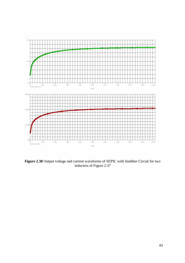
63
Figure 2.38 Output voltage and current waveforms of SEPIC with Snubber Circuit for two
inductors of Figure 2.37
Time
0s 10ms 20ms 30ms 40ms 50ms 60ms 70ms 80ms 90ms 100ms
AVG(V(R3:2))
0V
25V
50V
Time
0s 10ms 20ms 30ms 40ms 50ms 60ms 70ms 80ms 90ms 100ms
AVG(-I(R3))
0A
100mA
200mA
300mA
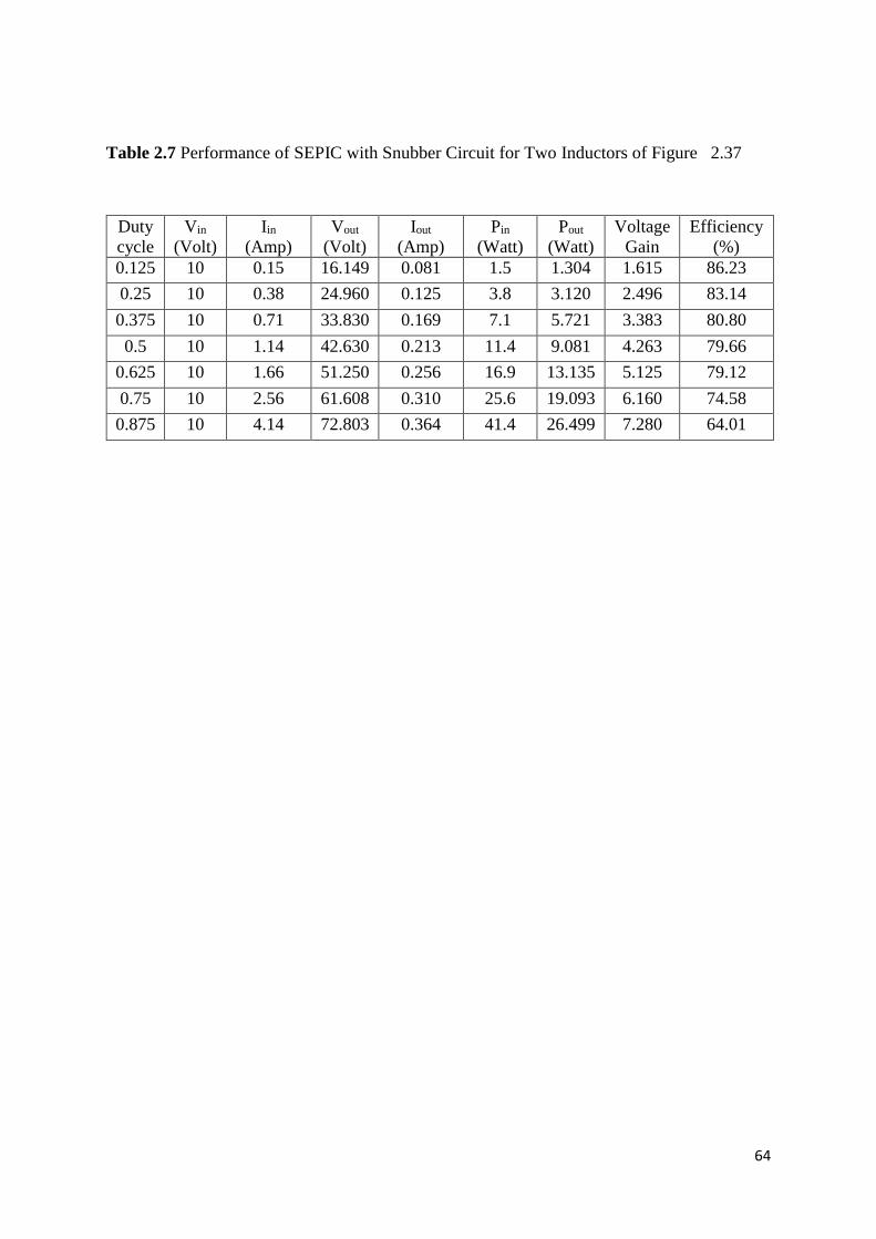
64
Table 2.7 Performance of SEPIC with Snubber Circuit for Two Inductors of Figure 2.37
Duty
cycle
Vin
(Volt)
Iin
(Amp)
Vout
(Volt)
Iout
(Amp)
Pin
(Watt)
Pout
(Watt)
Voltage
Gain
Efficiency
(%)
0.125 10 0.15 16.149 0.081 1.5 1.304 1.615 86.23
0.25 10 0.38 24.960 0.125 3.8 3.120 2.496 83.14
0.375 10 0.71 33.830 0.169 7.1 5.721 3.383 80.80
0.5 10 1.14 42.630 0.213 11.4 9.081 4.263 79.66
0.625 10 1.66 51.250 0.256 16.9 13.135 5.125 79.12
0.75 10 2.56 61.608 0.310 25.6 19.093 6.160 74.58
0.875 10 4.14 72.803 0.364 41.4 26.499 7.280 64.01
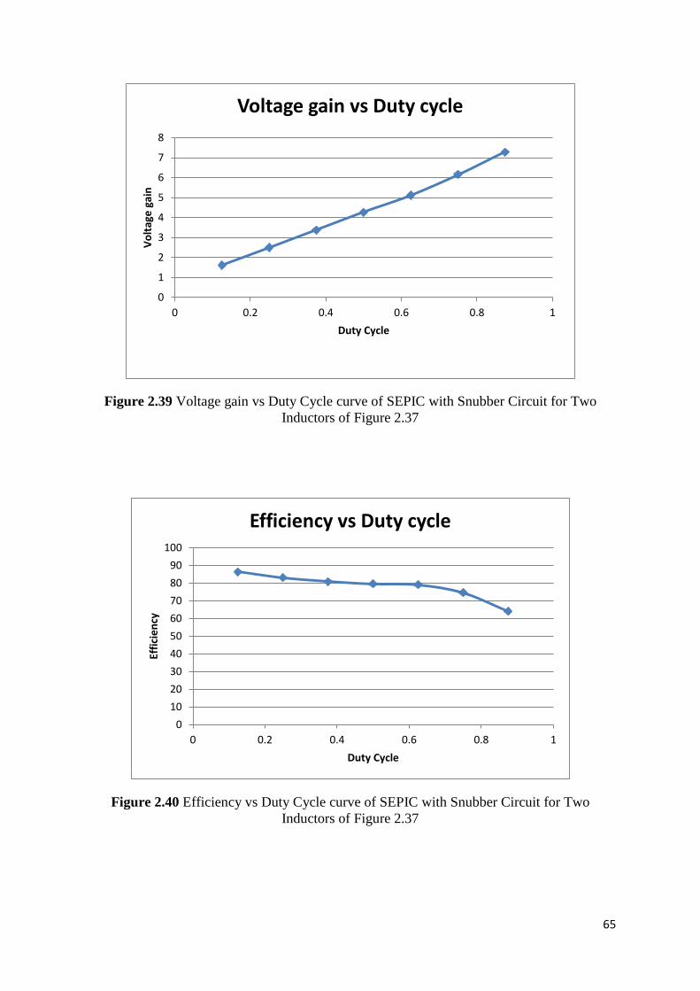
65
Figure 2.39 Voltage gain vs Duty Cycle curve of SEPIC with Snubber Circuit for Two
Inductors of Figure 2.37
Figure 2.40 Efficiency vs Duty Cycle curve of SEPIC with Snubber Circuit for Two
Inductors of Figure 2.37
0
1
2
3
4
5
6
7
8
0 0.2 0.4 0.6 0.8 1
Vo
ltag
e g
ain
Duty Cycle
Voltage gain vs Duty cycle
0
10
20
30
40
50
60
70
80
90
100
0 0.2 0.4 0.6 0.8 1
Effi
cie
ncy
Duty Cycle
Efficiency vs Duty cycle
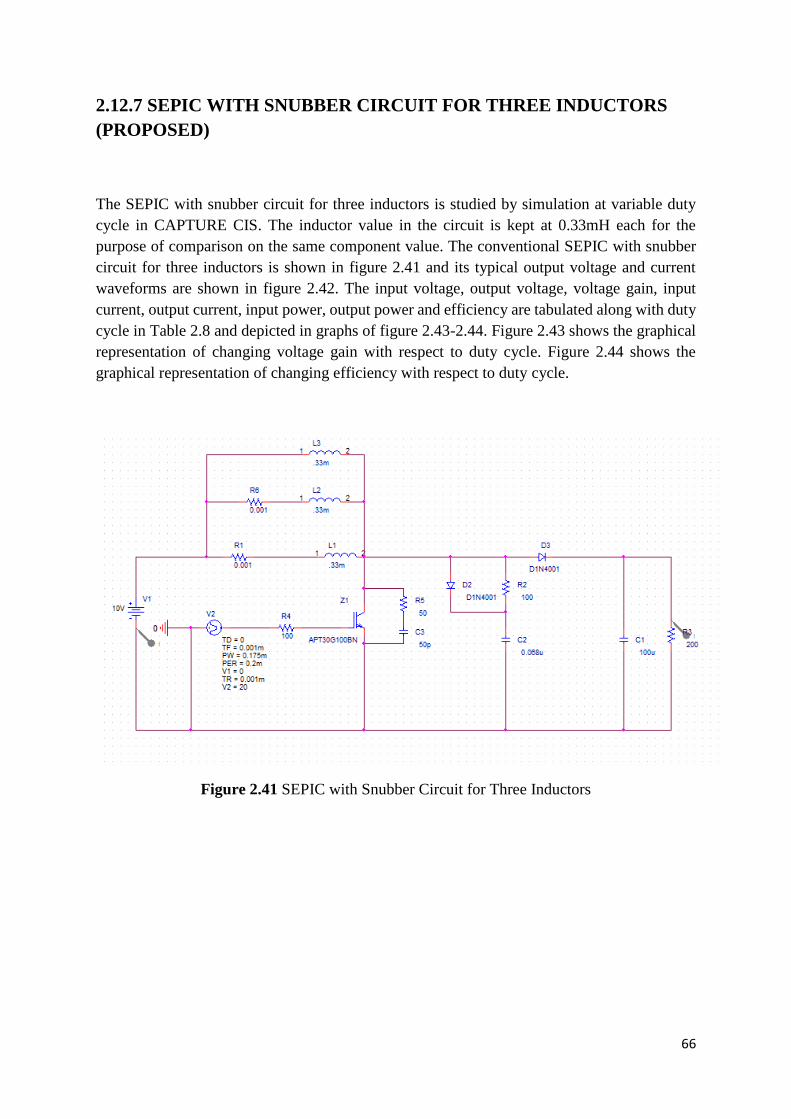
66
2.12.7 SEPIC WITH SNUBBER CIRCUIT FOR THREE INDUCTORS
(PROPOSED)
The SEPIC with snubber circuit for three inductors is studied by simulation at variable duty
cycle in CAPTURE CIS. The inductor value in the circuit is kept at 0.33mH each for the
purpose of comparison on the same component value. The conventional SEPIC with snubber
circuit for three inductors is shown in figure 2.41 and its typical output voltage and current
waveforms are shown in figure 2.42. The input voltage, output voltage, voltage gain, input
current, output current, input power, output power and efficiency are tabulated along with duty
cycle in Table 2.8 and depicted in graphs of figure 2.43-2.44. Figure 2.43 shows the graphical
representation of changing voltage gain with respect to duty cycle. Figure 2.44 shows the
graphical representation of changing efficiency with respect to duty cycle.
Figure 2.41 SEPIC with Snubber Circuit for Three Inductors
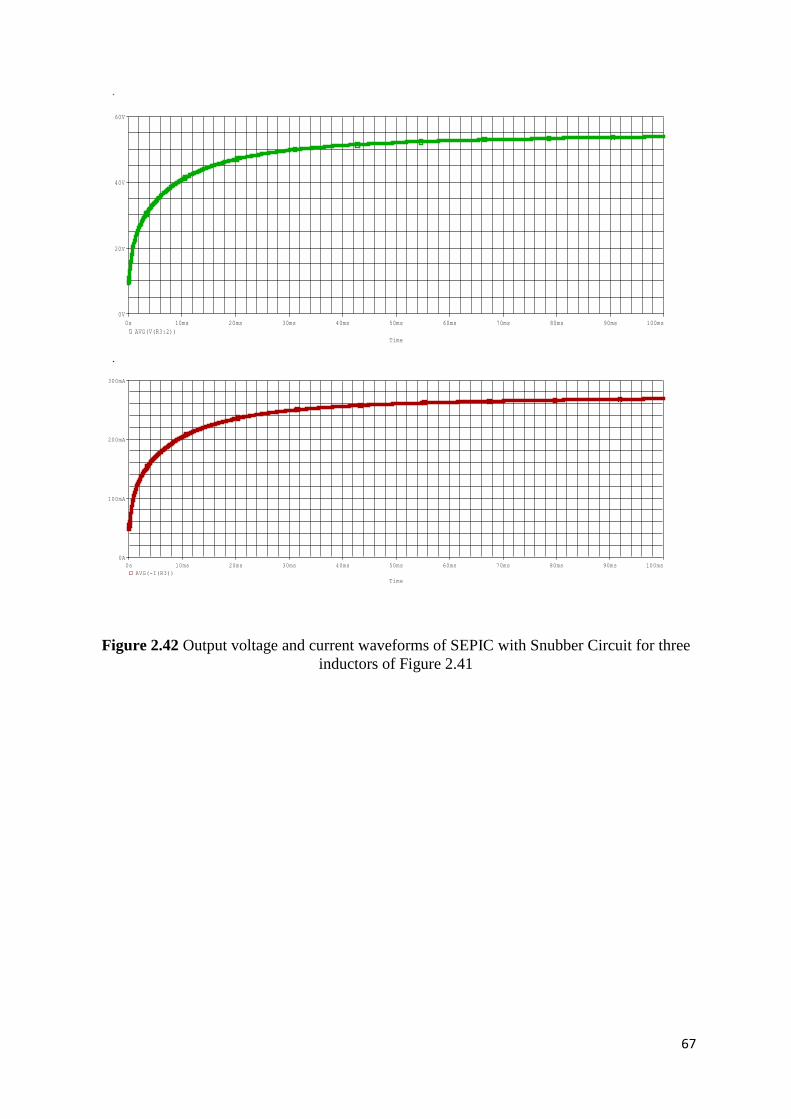
67
Figure 2.42 Output voltage and current waveforms of SEPIC with Snubber Circuit for three
inductors of Figure 2.41
Time
0s 10ms 20ms 30ms 40ms 50ms 60ms 70ms 80ms 90ms 100ms
AVG(V(R3:2))
0V
20V
40V
60V
Time
0s 10ms 20ms 30ms 40ms 50ms 60ms 70ms 80ms 90ms 100ms
AVG(-I(R3))
0A
100mA
200mA
300mA
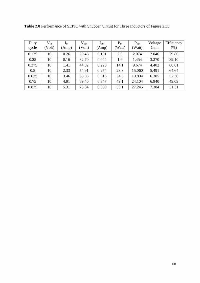
68
Table 2.8 Performance of SEPIC with Snubber Circuit for Three Inductors of Figure 2.33
Duty
cycle
Vin
(Volt)
Iin
(Amp)
Vout
(Volt)
Iout
(Amp)
Pin
(Watt)
Pout
(Watt)
Voltage
Gain
Efficiency
(%)
0.125 10 0.26 20.46 0.101 2.6 2.074 2.046 79.86
0.25 10 0.16 32.70 0.044 1.6 1.454 3.270 89.10
0.375 10 1.41 44.02 0.220 14.1 9.674 4.402 68.61
0.5 10 2.33 54.91 0.274 23.3 15.060 5.491 64.64
0.625 10 3.46 63.05 0.316 34.6 19.894 6.305 57.50
0.75 10 4.91 69.40 0.347 49.1 24.104 6.940 49.09
0.875 10 5.31 73.84 0.369 53.1 27.245 7.384 51.31
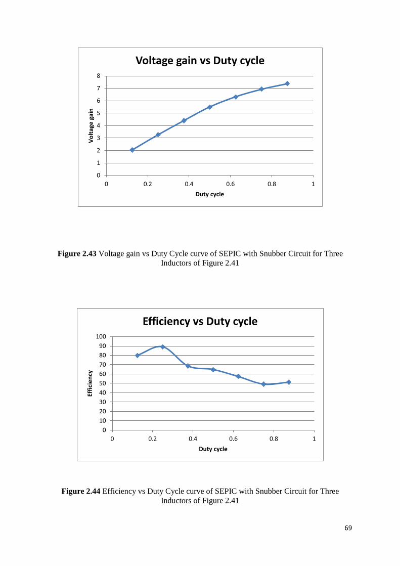
69
Figure 2.43 Voltage gain vs Duty Cycle curve of SEPIC with Snubber Circuit for Three
Inductors of Figure 2.41
Figure 2.44 Efficiency vs Duty Cycle curve of SEPIC with Snubber Circuit for Three
Inductors of Figure 2.41
0
1
2
3
4
5
6
7
8
0 0.2 0.4 0.6 0.8 1
Vo
ltag
e g
ain
Duty cycle
Voltage gain vs Duty cycle
0
10
20
30
40
50
60
70
80
90
100
0 0.2 0.4 0.6 0.8 1
Effi
cie
ncy
Duty cycle
Efficiency vs Duty cycle
70
2.12.8 SEPIC WITH SNUBBER CIRCUIT FOR FOUR INDUCTORS
(PROPOSED)
The SEPIC with snubber circuit for four inductors is studied by simulation at variable duty
cycle in CAPTURE CIS. The inductor value in the circuit is kept at 0.25mH each for the
purpose of comparison on the same component value. The conventional SEPIC with snubber
circuit for four inductors is shown in figure 2.45 and its typical output voltage and current
waveforms are shown in figure 2.46. The input voltage, output voltage, voltage gain, input
current, output current, input power, output power and efficiency are tabulated along with duty
cycle in Table 2.9 and depicted in graphs of figure 2.47-2.48. Figure 2.47 shows the graphical
representation of changing voltage gain with respect to duty cycle. Figure 2.48 shows the
graphical representation of changing efficiency with respect to duty cycle.
Figure 2.45 SEPIC with Snubber Circuit for Four Inductors
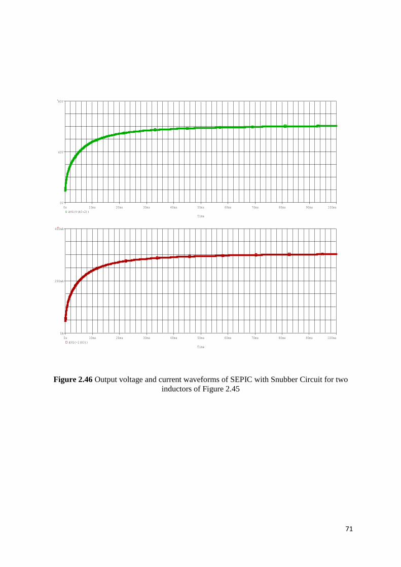
71
Figure 2.46 Output voltage and current waveforms of SEPIC with Snubber Circuit for two
inductors of Figure 2.45
Time
0s 10ms 20ms 30ms 40ms 50ms 60ms 70ms 80ms 90ms 100ms
AVG(V(R3:2))
0V
40V
80V
Time
0s 10ms 20ms 30ms 40ms 50ms 60ms 70ms 80ms 90ms 100ms
AVG(-I(R3))
0A
200mA
400mA
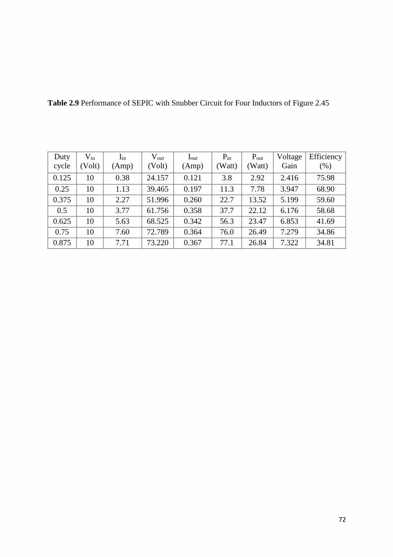
72
Table 2.9 Performance of SEPIC with Snubber Circuit for Four Inductors of Figure 2.45
Duty
cycle
Vin
(Volt)
Iin
(Amp)
Vout
(Volt)
Iout
(Amp)
Pin
(Watt)
Pout
(Watt)
Voltage
Gain
Efficiency
(%)
0.125 10 0.38 24.157 0.121 3.8 2.92 2.416 75.98
0.25 10 1.13 39.465 0.197 11.3 7.78 3.947 68.90
0.375 10 2.27 51.996 0.260 22.7 13.52 5.199 59.60
0.5 10 3.77 61.756 0.358 37.7 22.12 6.176 58.68
0.625 10 5.63 68.525 0.342 56.3 23.47 6.853 41.69
0.75 10 7.60 72.789 0.364 76.0 26.49 7.279 34.86
0.875 10 7.71 73.220 0.367 77.1 26.84 7.322 34.81
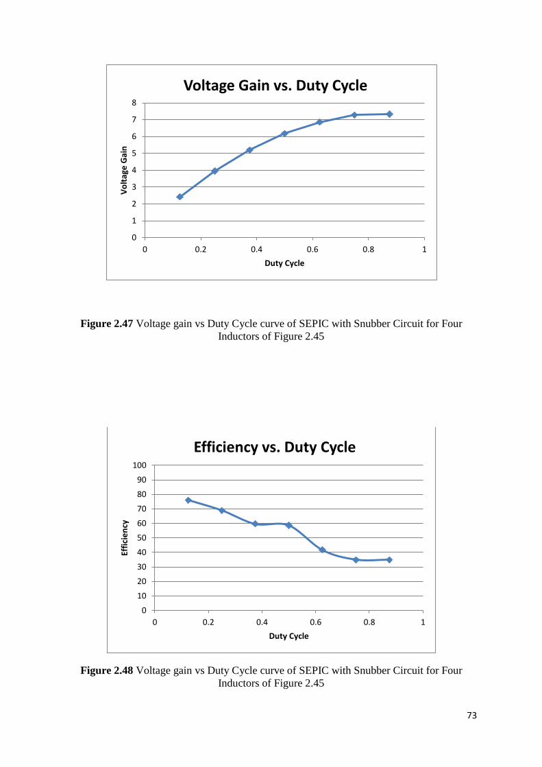
73
Figure 2.47 Voltage gain vs Duty Cycle curve of SEPIC with Snubber Circuit for Four
Inductors of Figure 2.45
Figure 2.48 Voltage gain vs Duty Cycle curve of SEPIC with Snubber Circuit for Four
Inductors of Figure 2.45
0
1
2
3
4
5
6
7
8
0 0.2 0.4 0.6 0.8 1
Vo
ltag
e G
ain
Duty Cycle
Voltage Gain vs. Duty Cycle
0
10
20
30
40
50
60
70
80
90
100
0 0.2 0.4 0.6 0.8 1
Effi
cie
ncy
Duty Cycle
Efficiency vs. Duty Cycle
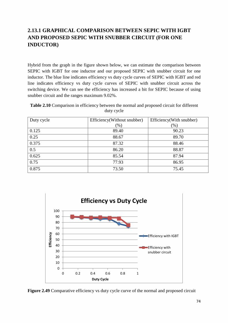
74
2.13.1 GRAPHICAL COMPARISON BETWEEN SEPIC WITH IGBT
AND PROPOSED SEPIC WITH SNUBBER CIRCUIT (FOR ONE
INDUCTOR)
Hybrid from the graph in the figure shown below, we can estimate the comparison between
SEPIC with IGBT for one inductor and our proposed SEPIC with snubber circuit for one
inductor. The blue line indicates efficiency vs duty cycle curves of SEPIC with IGBT and red
line indicates efficiency vs duty cycle curves of SEPIC with snubber circuit across the
switching device. We can see the efficiency has increased a bit for SEPIC because of using
snubber circuit and the ranges maximum 9.02%.
Table 2.10 Comparison in efficiency between the normal and proposed circuit for different
duty cycle
Duty cycle Efficiency(Without snubber)
(%)
Efficiency(With snubber)
(%)
0.125 89.40 90.23
0.25 88.67 89.70
0.375 87.32 88.46
0.5 86.20 88.87
0.625 85.54 87.94
0.75 77.93 86.95
0.875 73.50 75.45
Figure 2.49 Comparative efficiency vs duty cycle curve of the normal and proposed circuit
0
10
20
30
40
50
60
70
80
90
100
0 0.2 0.4 0.6 0.8 1
Effi
cie
ncy
Duty Cycle
Efficiency vs Duty Cycle
Efficiency with IGBT
Efficiency withsnubber circuit
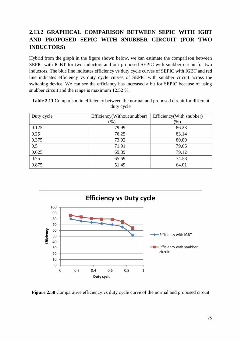
75
2.13.2 GRAPHICAL COMPARISON BETWEEN SEPIC WITH IGBT
AND PROPOSED SEPIC WITH SNUBBER CIRCUIT (FOR TWO
INDUCTORS)
Hybrid from the graph in the figure shown below, we can estimate the comparison between
SEPIC with IGBT for two inductors and our proposed SEPIC with snubber circuit for two
inductors. The blue line indicates efficiency vs duty cycle curves of SEPIC with IGBT and red
line indicates efficiency vs duty cycle curves of SEPIC with snubber circuit across the
switching device. We can see the efficiency has increased a bit for SEPIC because of using
snubber circuit and the range is maximum 12.52 %.
Table 2.11 Comparison in efficiency between the normal and proposed circuit for different
duty cycle
Duty cycle Efficiency(Without snubber)
(%)
Efficiency(With snubber)
(%)
0.125 79.99 86.23
0.25 76.25 83.14
0.375 73.92 80.80
0.5 71.91 79.66
0.625 69.89 79.12
0.75 65.69 74.58
0.875 51.49 64.01
Figure 2.50 Comparative efficiency vs duty cycle curve of the normal and proposed circuit
0
10
20
30
40
50
60
70
80
90
100
0 0.2 0.4 0.6 0.8 1
Effi
cie
ncy
Duty cycle
Efficiency vs Duty cycle
Efficiency with IGBT
Efficiency with snubbercircuit
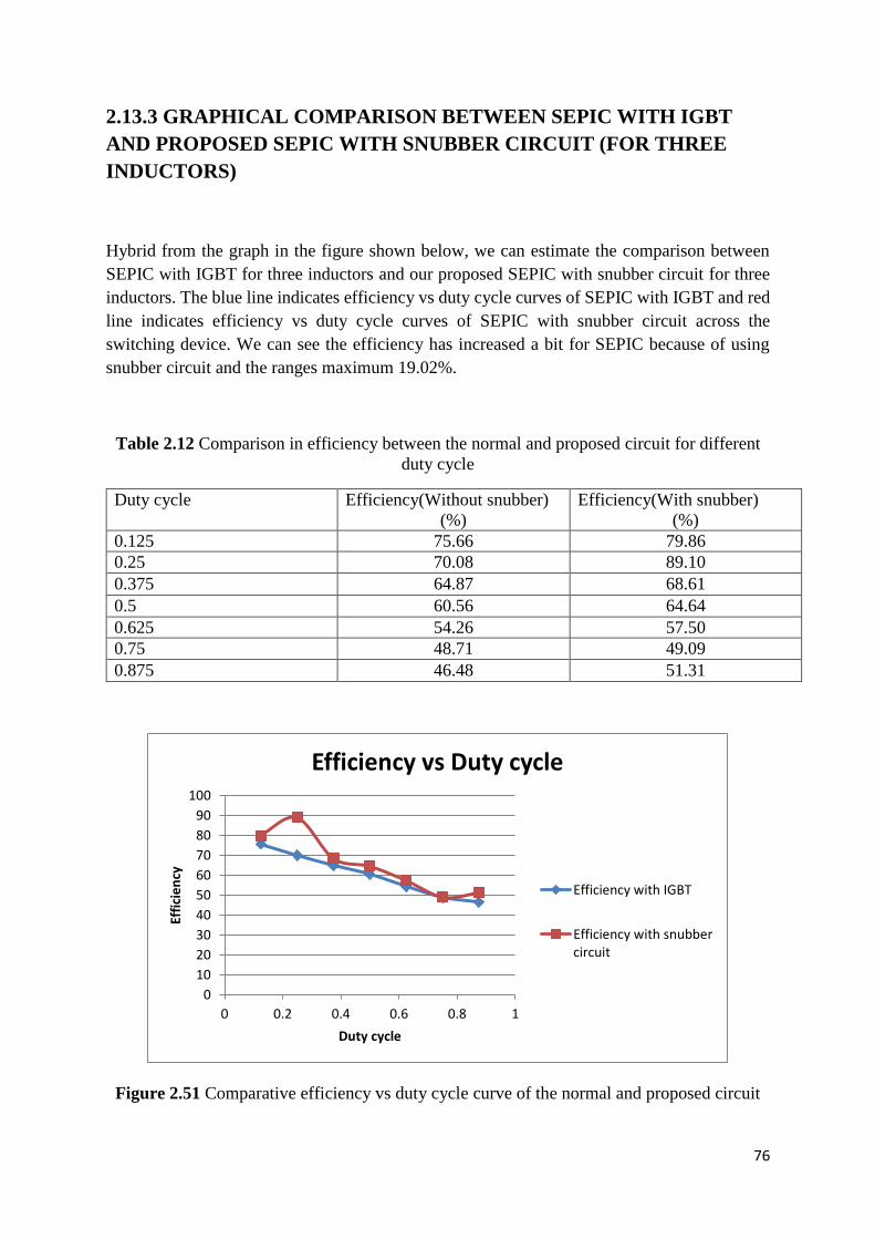
76
2.13.3 GRAPHICAL COMPARISON BETWEEN SEPIC WITH IGBT
AND PROPOSED SEPIC WITH SNUBBER CIRCUIT (FOR THREE
INDUCTORS)
Hybrid from the graph in the figure shown below, we can estimate the comparison between
SEPIC with IGBT for three inductors and our proposed SEPIC with snubber circuit for three
inductors. The blue line indicates efficiency vs duty cycle curves of SEPIC with IGBT and red
line indicates efficiency vs duty cycle curves of SEPIC with snubber circuit across the
switching device. We can see the efficiency has increased a bit for SEPIC because of using
snubber circuit and the ranges maximum 19.02%.
Table 2.12 Comparison in efficiency between the normal and proposed circuit for different
duty cycle
Duty cycle Efficiency(Without snubber)
(%)
Efficiency(With snubber)
(%)
0.125 75.66 79.86
0.25 70.08 89.10
0.375 64.87 68.61
0.5 60.56 64.64
0.625 54.26 57.50
0.75 48.71 49.09
0.875 46.48 51.31
Figure 2.51 Comparative efficiency vs duty cycle curve of the normal and proposed circuit
0
10
20
30
40
50
60
70
80
90
100
0 0.2 0.4 0.6 0.8 1
Effi
cie
ncy
Duty cycle
Efficiency vs Duty cycle
Efficiency with IGBT
Efficiency with snubbercircuit
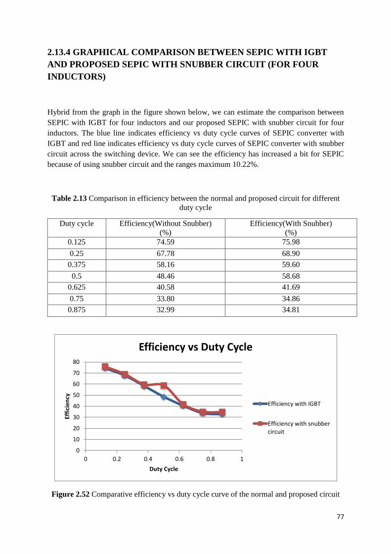
77
2.13.4 GRAPHICAL COMPARISON BETWEEN SEPIC WITH IGBT
AND PROPOSED SEPIC WITH SNUBBER CIRCUIT (FOR FOUR
INDUCTORS)
Hybrid from the graph in the figure shown below, we can estimate the comparison between
SEPIC with IGBT for four inductors and our proposed SEPIC with snubber circuit for four
inductors. The blue line indicates efficiency vs duty cycle curves of SEPIC converter with
IGBT and red line indicates efficiency vs duty cycle curves of SEPIC converter with snubber
circuit across the switching device. We can see the efficiency has increased a bit for SEPIC
because of using snubber circuit and the ranges maximum 10.22%.
Table 2.13 Comparison in efficiency between the normal and proposed circuit for different
duty cycle
Duty cycle Efficiency(Without Snubber)
(%)
Efficiency(With Snubber)
(%)
0.125 74.59 75.98
0.25 67.78 68.90
0.375 58.16 59.60
0.5 48.46 58.68
0.625 40.58 41.69
0.75 33.80 34.86
0.875 32.99 34.81
Figure 2.52 Comparative efficiency vs duty cycle curve of the normal and proposed circuit
0
10
20
30
40
50
60
70
80
0 0.2 0.4 0.6 0.8 1
Effi
cie
ncy
Duty Cycle
Efficiency vs Duty Cycle
Efficiency with IGBT
Efficiency with snubbercircuit

78
Chapter-3
RESULT AND DISCUSSION
In chapter 3, we have proposed a new high efficient SEPIC with Snubber circuit and simulated
in ORCAD. We have done the simulation for both SEPIC with IGBT and with snubber circuit
with one, two, three and four inductors separately for different duty cycles. We will discuss the
result for these converters in this chapter.
3.1.1 SIMULATION RESULT AND DISCUSSION OF PROPOSED
SEPIC WITH SNUBBER CIRCUIT FOR ONE INDUCTOR
The efficiency of the conventional SEPIC with IGBT for one inductor can be increased in many
ways. In our proposed SEPIC with snubber circuit for one inductor the overall efficiency
increases for each duty cycle and the maximum range of increment is 9.02%.
Table 3.1 Comparison in efficiency between normal and proposed circuit for different duty
cycle
Duty Cycle
(%)
Efficiency (SEPIC
Converter without
Snubber circuit)
(%)
Efficiency (Proposed
SEPIC Converter
with Snubber circuit)
(%)
Increment in
Efficiency
(%)
12.5 89.40 90.23 0.83
25.0 88.67 89.70 1.03
37.5 87.32 88.46 1.14
50.0 86.20 88.87 2.67
62.5 85.54 87.94 2.40
75.0 77.93 86.95 9.02
87.5 73.50 75.45 1.95
From Table 3.1 we can see that, for each duty cycle the efficiency of the proposed SEPIC with
snubber circuit for one inductor is a bit higher than the SEPIC with IGBT for one inductor
circuit. For 12.5% duty cycle, the efficiency has increased by 0.83%, for 25% it is 1.03%, for
37.5% it is 1.14%, for 50% it is 2.67%, for 62.5% it is 2.40%, for 75% it is 9.02% and for
87.5% it is 1.95%. The maximum increment in efficiency in this case is for 75% duty cycle
and the value is 9.02%.
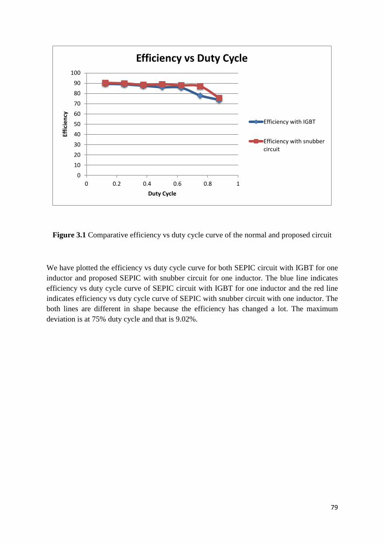
79
Figure 3.1 Comparative efficiency vs duty cycle curve of the normal and proposed circuit
We have plotted the efficiency vs duty cycle curve for both SEPIC circuit with IGBT for one
inductor and proposed SEPIC with snubber circuit for one inductor. The blue line indicates
efficiency vs duty cycle curve of SEPIC circuit with IGBT for one inductor and the red line
indicates efficiency vs duty cycle curve of SEPIC with snubber circuit with one inductor. The
both lines are different in shape because the efficiency has changed a lot. The maximum
deviation is at 75% duty cycle and that is 9.02%.
0
10
20
30
40
50
60
70
80
90
100
0 0.2 0.4 0.6 0.8 1
Effi
cie
ncy
Duty Cycle
Efficiency vs Duty Cycle
Efficiency with IGBT
Efficiency with snubbercircuit
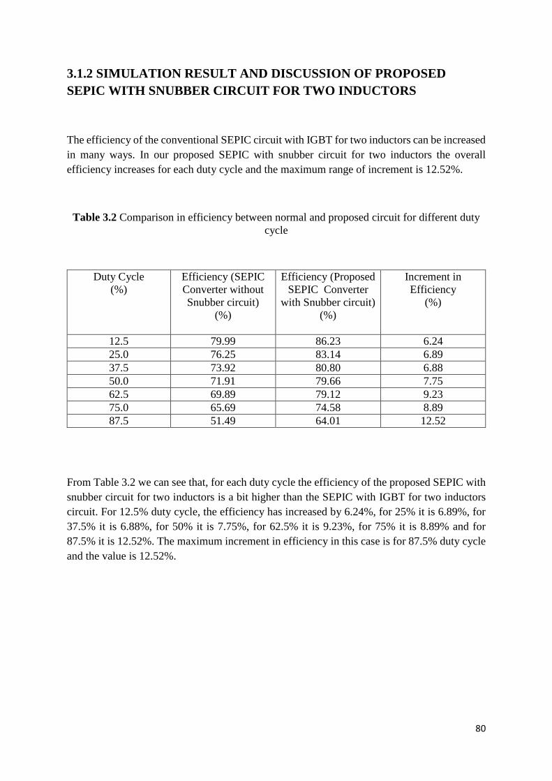
80
3.1.2 SIMULATION RESULT AND DISCUSSION OF PROPOSED
SEPIC WITH SNUBBER CIRCUIT FOR TWO INDUCTORS
The efficiency of the conventional SEPIC circuit with IGBT for two inductors can be increased
in many ways. In our proposed SEPIC with snubber circuit for two inductors the overall
efficiency increases for each duty cycle and the maximum range of increment is 12.52%.
Table 3.2 Comparison in efficiency between normal and proposed circuit for different duty
cycle
Duty Cycle
(%)
Efficiency (SEPIC
Converter without
Snubber circuit)
(%)
Efficiency (Proposed
SEPIC Converter
with Snubber circuit)
(%)
Increment in
Efficiency
(%)
12.5 79.99 86.23 6.24
25.0 76.25 83.14 6.89
37.5 73.92 80.80 6.88
50.0 71.91 79.66 7.75
62.5 69.89 79.12 9.23
75.0 65.69 74.58 8.89
87.5 51.49 64.01 12.52
From Table 3.2 we can see that, for each duty cycle the efficiency of the proposed SEPIC with
snubber circuit for two inductors is a bit higher than the SEPIC with IGBT for two inductors
circuit. For 12.5% duty cycle, the efficiency has increased by 6.24%, for 25% it is 6.89%, for
37.5% it is 6.88%, for 50% it is 7.75%, for 62.5% it is 9.23%, for 75% it is 8.89% and for
87.5% it is 12.52%. The maximum increment in efficiency in this case is for 87.5% duty cycle
and the value is 12.52%.
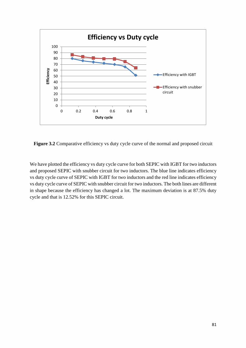
81
Figure 3.2 Comparative efficiency vs duty cycle curve of the normal and proposed circuit
We have plotted the efficiency vs duty cycle curve for both SEPIC with IGBT for two inductors
and proposed SEPIC with snubber circuit for two inductors. The blue line indicates efficiency
vs duty cycle curve of SEPIC with IGBT for two inductors and the red line indicates efficiency
vs duty cycle curve of SEPIC with snubber circuit for two inductors. The both lines are different
in shape because the efficiency has changed a lot. The maximum deviation is at 87.5% duty
cycle and that is 12.52% for this SEPIC circuit.
0
10
20
30
40
50
60
70
80
90
100
0 0.2 0.4 0.6 0.8 1
Effi
cie
ncy
Duty cycle
Efficiency vs Duty cycle
Efficiency with IGBT
Efficiency with snubbercircuit
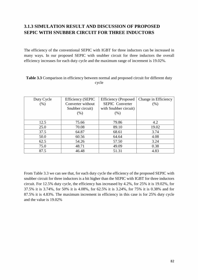
82
3.1.3 SIMULATION RESULT AND DISCUSSION OF PROPOSED
SEPIC WITH SNUBBER CIRCUIT FOR THREE INDUCTORS
The efficiency of the conventional SEPIC with IGBT for three inductors can be increased in
many ways. In our proposed SEPIC with snubber circuit for three inductors the overall
efficiency increases for each duty cycle and the maximum range of increment is 19.02%.
Table 3.3 Comparison in efficiency between normal and proposed circuit for different duty
cycle
Duty Cycle
(%)
Efficiency (SEPIC
Converter without
Snubber circuit)
(%)
Efficiency (Proposed
SEPIC Converter
with Snubber circuit)
(%)
Change in Efficiency
(%)
12.5 75.66 79.86 4.2
25.0 70.08 89.10 19.02
37.5 64.87 68.61 3.74
50.0 60.56 64.64 4.08
62.5 54.26 57.50 3.24
75.0 48.71 49.09 0.38
87.5 46.48 51.31 4.83
From Table 3.3 we can see that, for each duty cycle the efficiency of the proposed SEPIC with
snubber circuit for three inductors is a bit higher than the SEPIC with IGBT for three inductors
circuit. For 12.5% duty cycle, the efficiency has increased by 4.2%, for 25% it is 19.02%, for
37.5% it is 3.74%, for 50% it is 4.08%, for 62.5% it is 3.24%, for 75% it is 0.38% and for
87.5% it is 4.83%. The maximum increment in efficiency in this case is for 25% duty cycle
and the value is 19.02%
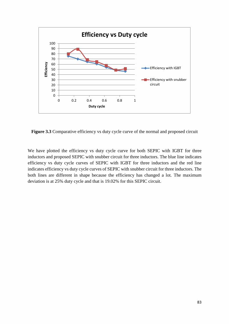
83
Figure 3.3 Comparative efficiency vs duty cycle curve of the normal and proposed circuit
We have plotted the efficiency vs duty cycle curve for both SEPIC with IGBT for three
inductors and proposed SEPIC with snubber circuit for three inductors. The blue line indicates
efficiency vs duty cycle curves of SEPIC with IGBT for three inductors and the red line
indicates efficiency vs duty cycle curves of SEPIC with snubber circuit for three inductors. The
both lines are different in shape because the efficiency has changed a lot. The maximum
deviation is at 25% duty cycle and that is 19.02% for this SEPIC circuit.
0
10
20
30
40
50
60
70
80
90
100
0 0.2 0.4 0.6 0.8 1
Effi
cie
ncy
Duty cycle
Efficiency vs Duty cycle
Efficiency with IGBT
Efficiency with snubbercircuit
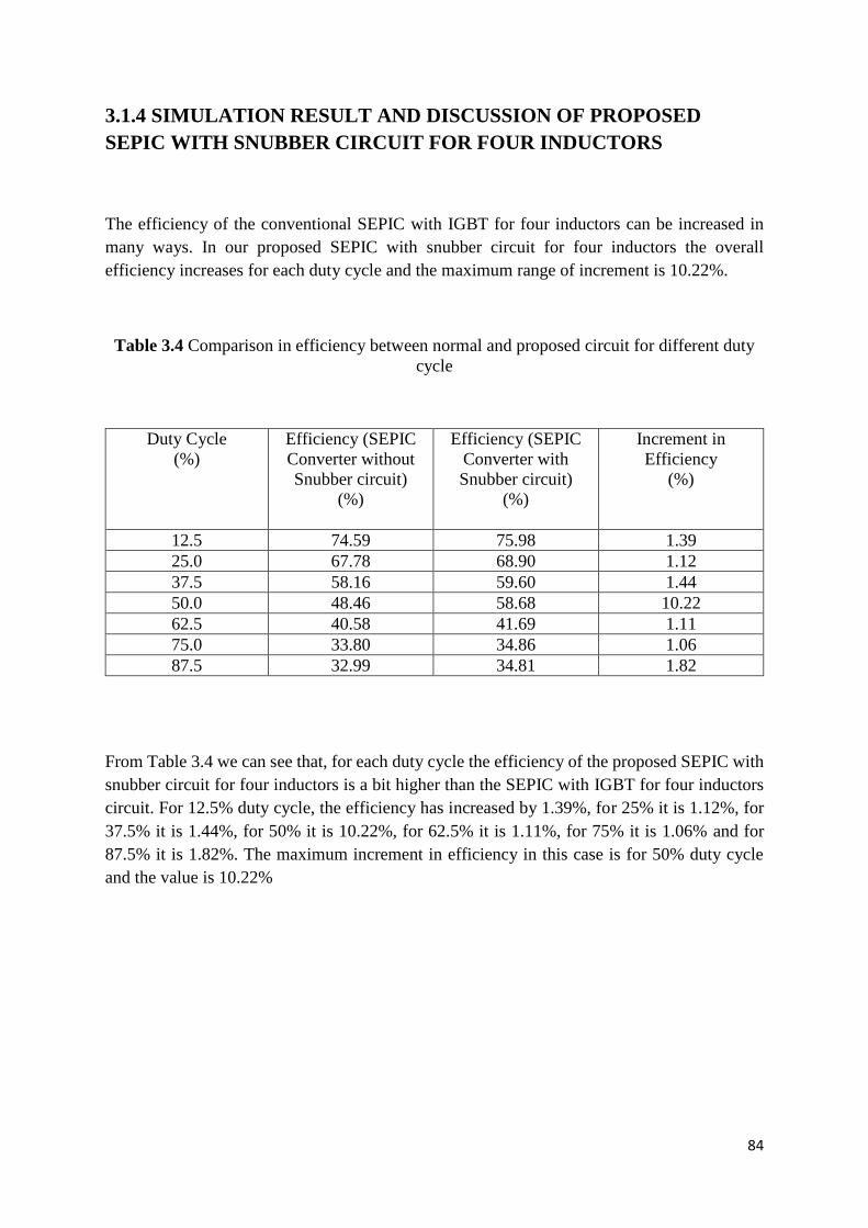
84
3.1.4 SIMULATION RESULT AND DISCUSSION OF PROPOSED
SEPIC WITH SNUBBER CIRCUIT FOR FOUR INDUCTORS
The efficiency of the conventional SEPIC with IGBT for four inductors can be increased in
many ways. In our proposed SEPIC with snubber circuit for four inductors the overall
efficiency increases for each duty cycle and the maximum range of increment is 10.22%.
Table 3.4 Comparison in efficiency between normal and proposed circuit for different duty
cycle
Duty Cycle
(%)
Efficiency (SEPIC
Converter without
Snubber circuit)
(%)
Efficiency (SEPIC
Converter with
Snubber circuit)
(%)
Increment in
Efficiency
(%)
12.5 74.59 75.98 1.39
25.0 67.78 68.90 1.12
37.5 58.16 59.60 1.44
50.0 48.46 58.68 10.22
62.5 40.58 41.69 1.11
75.0 33.80 34.86 1.06
87.5 32.99 34.81 1.82
From Table 3.4 we can see that, for each duty cycle the efficiency of the proposed SEPIC with
snubber circuit for four inductors is a bit higher than the SEPIC with IGBT for four inductors
circuit. For 12.5% duty cycle, the efficiency has increased by 1.39%, for 25% it is 1.12%, for
37.5% it is 1.44%, for 50% it is 10.22%, for 62.5% it is 1.11%, for 75% it is 1.06% and for
87.5% it is 1.82%. The maximum increment in efficiency in this case is for 50% duty cycle
and the value is 10.22%
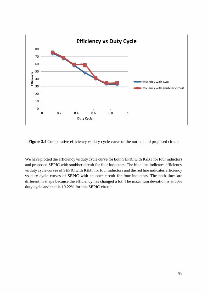
85
Figure 3.4 Comparative efficiency vs duty cycle curve of the normal and proposed circuit
We have plotted the efficiency vs duty cycle curve for both SEPIC with IGBT for four inductors
and proposed SEPIC with snubber circuit for four inductors. The blue line indicates efficiency
vs duty cycle curves of SEPIC with IGBT for four inductors and the red line indicates efficiency
vs duty cycle curves of SEPIC with snubber circuit for four inductors. The both lines are
different in shape because the efficiency has changed a lot. The maximum deviation is at 50%
duty cycle and that is 10.22% for this SEPIC circuit.
0
10
20
30
40
50
60
70
80
0 0.2 0.4 0.6 0.8 1
Effi
cie
ncy
Duty Cycle
Efficiency vs Duty Cycle
Efficiency with IGBT
Efficiency with snubber circuit
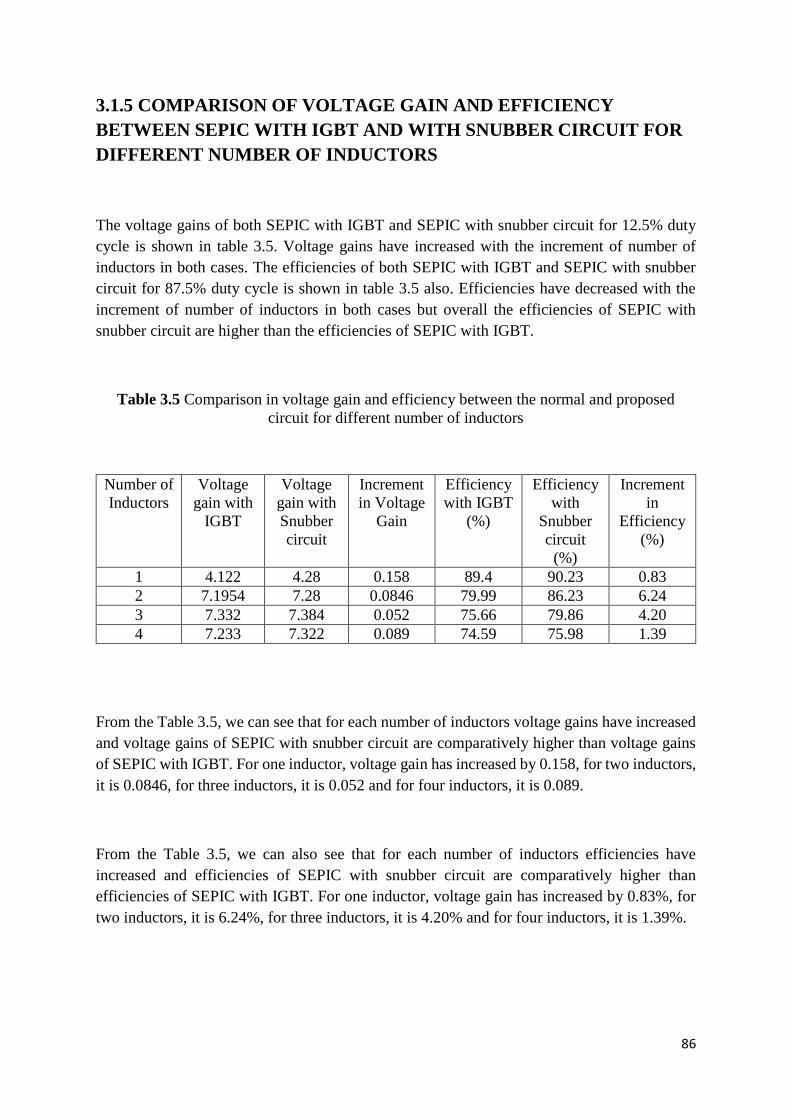
86
3.1.5 COMPARISON OF VOLTAGE GAIN AND EFFICIENCY
BETWEEN SEPIC WITH IGBT AND WITH SNUBBER CIRCUIT FOR
DIFFERENT NUMBER OF INDUCTORS
The voltage gains of both SEPIC with IGBT and SEPIC with snubber circuit for 12.5% duty
cycle is shown in table 3.5. Voltage gains have increased with the increment of number of
inductors in both cases. The efficiencies of both SEPIC with IGBT and SEPIC with snubber
circuit for 87.5% duty cycle is shown in table 3.5 also. Efficiencies have decreased with the
increment of number of inductors in both cases but overall the efficiencies of SEPIC with
snubber circuit are higher than the efficiencies of SEPIC with IGBT.
Table 3.5 Comparison in voltage gain and efficiency between the normal and proposed
circuit for different number of inductors
Number of
Inductors
Voltage
gain with
IGBT
Voltage
gain with
Snubber
circuit
Increment
in Voltage
Gain
Efficiency
with IGBT
(%)
Efficiency
with
Snubber
circuit
(%)
Increment
in
Efficiency
(%)
1 4.122 4.28 0.158 89.4 90.23 0.83
2 7.1954 7.28 0.0846 79.99 86.23 6.24
3 7.332 7.384 0.052 75.66 79.86 4.20
4 7.233 7.322 0.089 74.59 75.98 1.39
From the Table 3.5, we can see that for each number of inductors voltage gains have increased
and voltage gains of SEPIC with snubber circuit are comparatively higher than voltage gains
of SEPIC with IGBT. For one inductor, voltage gain has increased by 0.158, for two inductors,
it is 0.0846, for three inductors, it is 0.052 and for four inductors, it is 0.089.
From the Table 3.5, we can also see that for each number of inductors efficiencies have
increased and efficiencies of SEPIC with snubber circuit are comparatively higher than
efficiencies of SEPIC with IGBT. For one inductor, voltage gain has increased by 0.83%, for
two inductors, it is 6.24%, for three inductors, it is 4.20% and for four inductors, it is 1.39%.
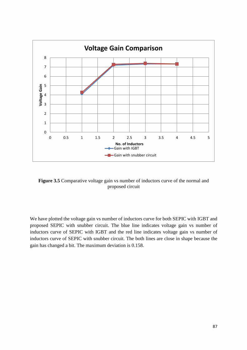
87
Figure 3.5 Comparative voltage gain vs number of inductors curve of the normal and
proposed circuit
We have plotted the voltage gain vs number of inductors curve for both SEPIC with IGBT and
proposed SEPIC with snubber circuit. The blue line indicates voltage gain vs number of
inductors curve of SEPIC with IGBT and the red line indicates voltage gain vs number of
inductors curve of SEPIC with snubber circuit. The both lines are close in shape because the
gain has changed a bit. The maximum deviation is 0.158.
0
1
2
3
4
5
6
7
8
0 0.5 1 1.5 2 2.5 3 3.5 4 4.5 5
Vo
ltag
e G
ain
No. of Inductors
Voltage Gain Comparison
Gain with IGBT
Gain with snubber circuit
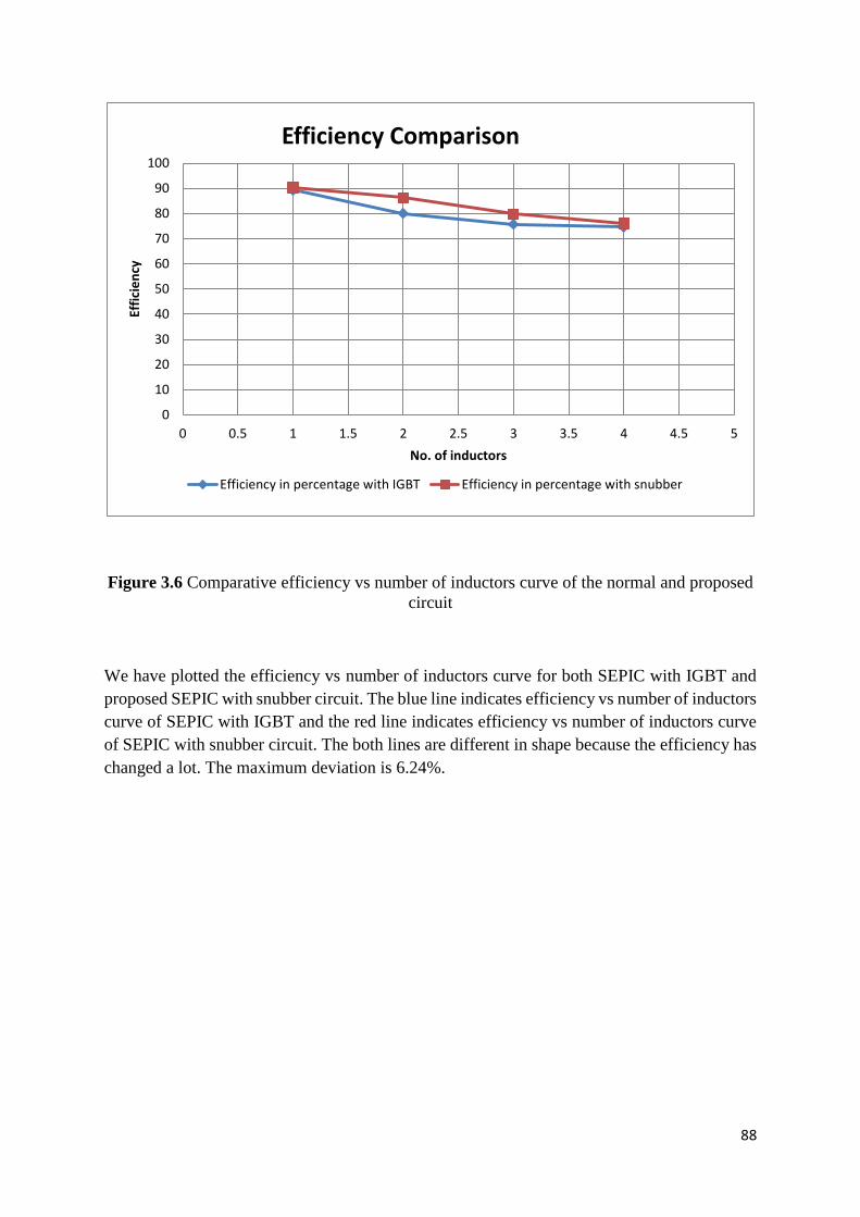
88
Figure 3.6 Comparative efficiency vs number of inductors curve of the normal and proposed
circuit
We have plotted the efficiency vs number of inductors curve for both SEPIC with IGBT and
proposed SEPIC with snubber circuit. The blue line indicates efficiency vs number of inductors
curve of SEPIC with IGBT and the red line indicates efficiency vs number of inductors curve
of SEPIC with snubber circuit. The both lines are different in shape because the efficiency has
changed a lot. The maximum deviation is 6.24%.
0
10
20
30
40
50
60
70
80
90
100
0 0.5 1 1.5 2 2.5 3 3.5 4 4.5 5
Effi
cie
ncy
No. of inductors
Efficiency Comparison
Efficiency in percentage with IGBT Efficiency in percentage with snubber
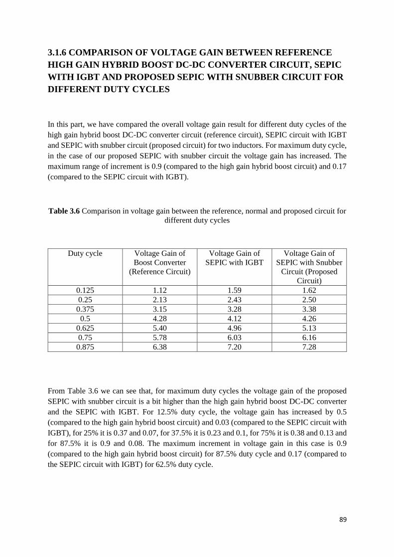
89
3.1.6 COMPARISON OF VOLTAGE GAIN BETWEEN REFERENCE
HIGH GAIN HYBRID BOOST DC-DC CONVERTER CIRCUIT, SEPIC
WITH IGBT AND PROPOSED SEPIC WITH SNUBBER CIRCUIT FOR
DIFFERENT DUTY CYCLES
In this part, we have compared the overall voltage gain result for different duty cycles of the
high gain hybrid boost DC-DC converter circuit (reference circuit), SEPIC circuit with IGBT
and SEPIC with snubber circuit (proposed circuit) for two inductors. For maximum duty cycle,
in the case of our proposed SEPIC with snubber circuit the voltage gain has increased. The
maximum range of increment is 0.9 (compared to the high gain hybrid boost circuit) and 0.17
(compared to the SEPIC circuit with IGBT).
Table 3.6 Comparison in voltage gain between the reference, normal and proposed circuit for
different duty cycles
Duty cycle Voltage Gain of
Boost Converter
(Reference Circuit)
Voltage Gain of
SEPIC with IGBT
Voltage Gain of
SEPIC with Snubber
Circuit (Proposed
Circuit)
0.125 1.12 1.59 1.62
0.25 2.13 2.43 2.50
0.375 3.15 3.28 3.38
0.5 4.28 4.12 4.26
0.625 5.40 4.96 5.13
0.75 5.78 6.03 6.16
0.875 6.38 7.20 7.28
From Table 3.6 we can see that, for maximum duty cycles the voltage gain of the proposed
SEPIC with snubber circuit is a bit higher than the high gain hybrid boost DC-DC converter
and the SEPIC with IGBT. For 12.5% duty cycle, the voltage gain has increased by 0.5
(compared to the high gain hybrid boost circuit) and 0.03 (compared to the SEPIC circuit with
IGBT), for 25% it is 0.37 and 0.07, for 37.5% it is 0.23 and 0.1, for 75% it is 0.38 and 0.13 and
for 87.5% it is 0.9 and 0.08. The maximum increment in voltage gain in this case is 0.9
(compared to the high gain hybrid boost circuit) for 87.5% duty cycle and 0.17 (compared to
the SEPIC circuit with IGBT) for 62.5% duty cycle.
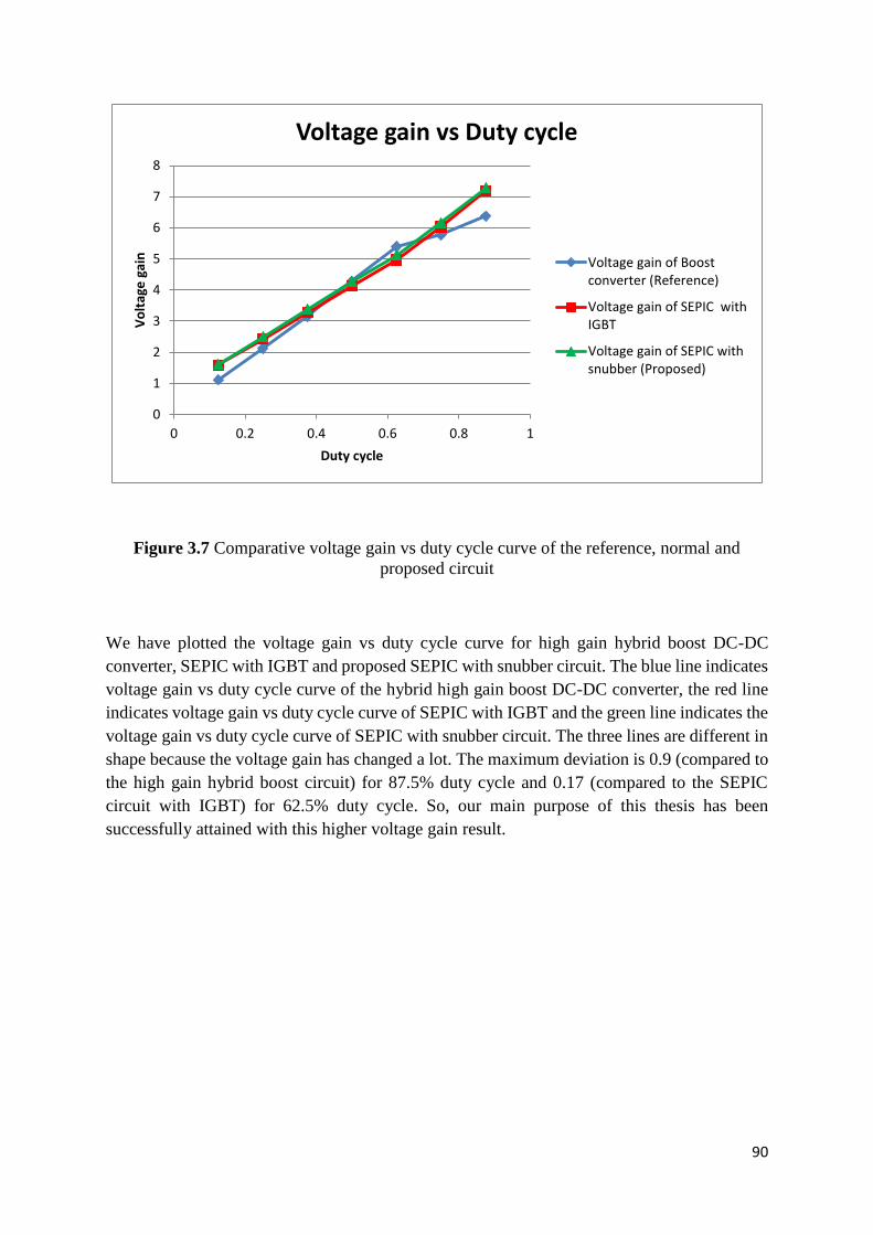
90
Figure 3.7 Comparative voltage gain vs duty cycle curve of the reference, normal and
proposed circuit
We have plotted the voltage gain vs duty cycle curve for high gain hybrid boost DC-DC
converter, SEPIC with IGBT and proposed SEPIC with snubber circuit. The blue line indicates
voltage gain vs duty cycle curve of the hybrid high gain boost DC-DC converter, the red line
indicates voltage gain vs duty cycle curve of SEPIC with IGBT and the green line indicates the
voltage gain vs duty cycle curve of SEPIC with snubber circuit. The three lines are different in
shape because the voltage gain has changed a lot. The maximum deviation is 0.9 (compared to
the high gain hybrid boost circuit) for 87.5% duty cycle and 0.17 (compared to the SEPIC
circuit with IGBT) for 62.5% duty cycle. So, our main purpose of this thesis has been
successfully attained with this higher voltage gain result.
0
1
2
3
4
5
6
7
8
0 0.2 0.4 0.6 0.8 1
Vo
ltag
e g
ain
Duty cycle
Voltage gain vs Duty cycle
Voltage gain of Boostconverter (Reference)
Voltage gain of SEPIC withIGBT
Voltage gain of SEPIC withsnubber (Proposed)
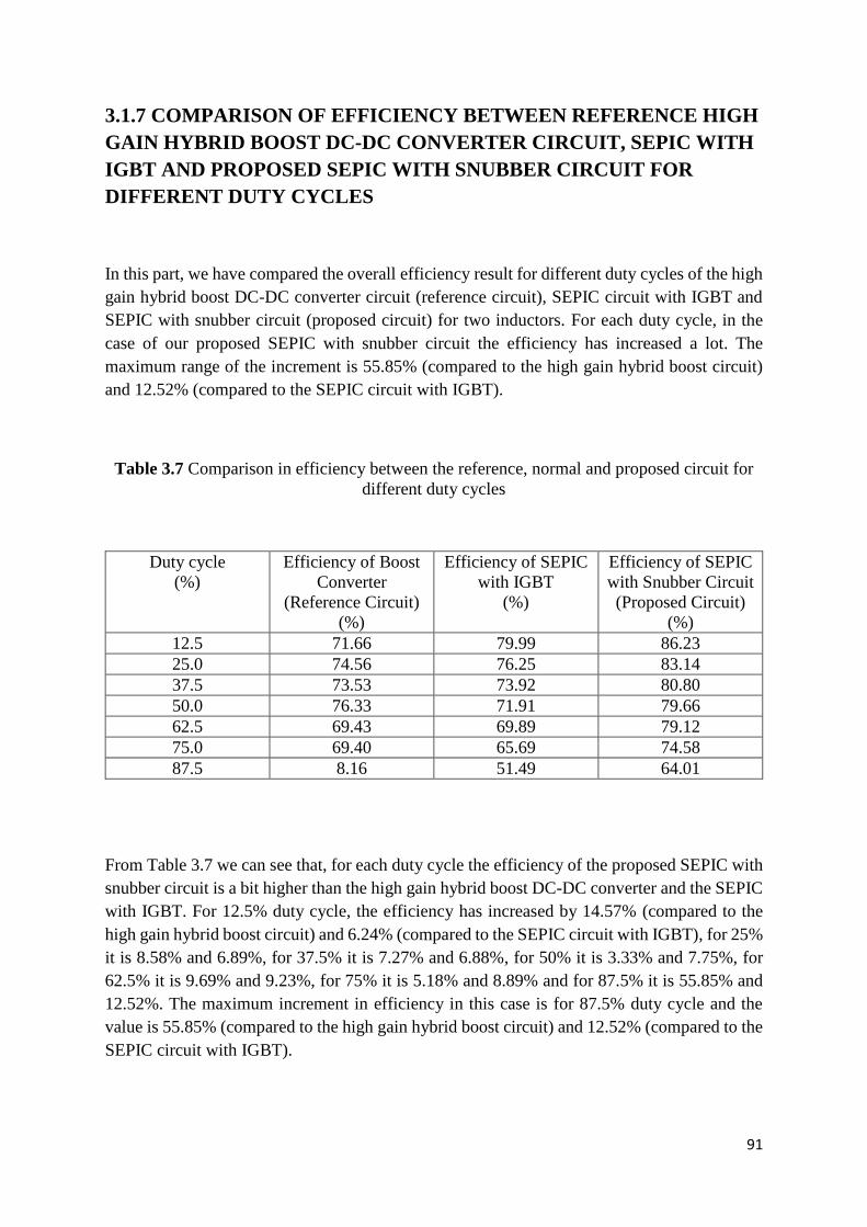
91
3.1.7 COMPARISON OF EFFICIENCY BETWEEN REFERENCE HIGH
GAIN HYBRID BOOST DC-DC CONVERTER CIRCUIT, SEPIC WITH
IGBT AND PROPOSED SEPIC WITH SNUBBER CIRCUIT FOR
DIFFERENT DUTY CYCLES
In this part, we have compared the overall efficiency result for different duty cycles of the high
gain hybrid boost DC-DC converter circuit (reference circuit), SEPIC circuit with IGBT and
SEPIC with snubber circuit (proposed circuit) for two inductors. For each duty cycle, in the
case of our proposed SEPIC with snubber circuit the efficiency has increased a lot. The
maximum range of the increment is 55.85% (compared to the high gain hybrid boost circuit)
and 12.52% (compared to the SEPIC circuit with IGBT).
Table 3.7 Comparison in efficiency between the reference, normal and proposed circuit for
different duty cycles
Duty cycle
(%)
Efficiency of Boost
Converter
(Reference Circuit)
(%)
Efficiency of SEPIC
with IGBT
(%)
Efficiency of SEPIC
with Snubber Circuit
(Proposed Circuit)
(%)
12.5 71.66 79.99 86.23
25.0 74.56 76.25 83.14
37.5 73.53 73.92 80.80
50.0 76.33 71.91 79.66
62.5 69.43 69.89 79.12
75.0 69.40 65.69 74.58
87.5 8.16 51.49 64.01
From Table 3.7 we can see that, for each duty cycle the efficiency of the proposed SEPIC with
snubber circuit is a bit higher than the high gain hybrid boost DC-DC converter and the SEPIC
with IGBT. For 12.5% duty cycle, the efficiency has increased by 14.57% (compared to the
high gain hybrid boost circuit) and 6.24% (compared to the SEPIC circuit with IGBT), for 25%
it is 8.58% and 6.89%, for 37.5% it is 7.27% and 6.88%, for 50% it is 3.33% and 7.75%, for
62.5% it is 9.69% and 9.23%, for 75% it is 5.18% and 8.89% and for 87.5% it is 55.85% and
12.52%. The maximum increment in efficiency in this case is for 87.5% duty cycle and the
value is 55.85% (compared to the high gain hybrid boost circuit) and 12.52% (compared to the
SEPIC circuit with IGBT).
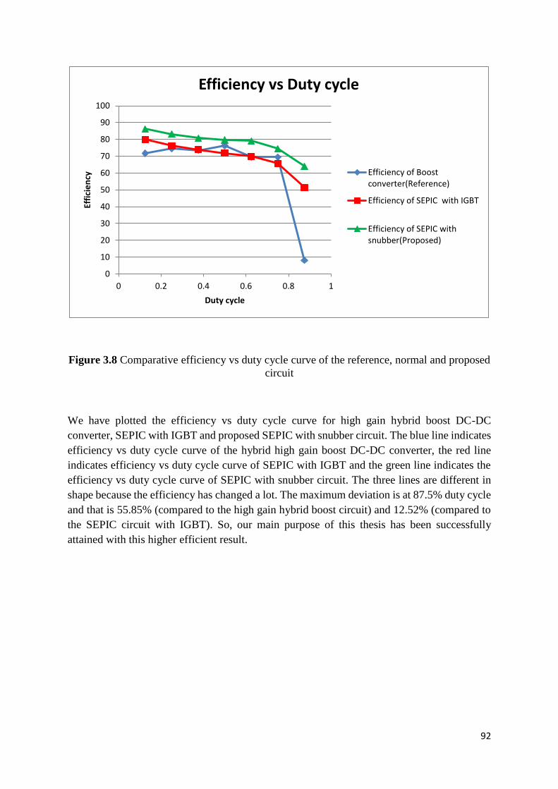
92
Figure 3.8 Comparative efficiency vs duty cycle curve of the reference, normal and proposed
circuit
We have plotted the efficiency vs duty cycle curve for high gain hybrid boost DC-DC
converter, SEPIC with IGBT and proposed SEPIC with snubber circuit. The blue line indicates
efficiency vs duty cycle curve of the hybrid high gain boost DC-DC converter, the red line
indicates efficiency vs duty cycle curve of SEPIC with IGBT and the green line indicates the
efficiency vs duty cycle curve of SEPIC with snubber circuit. The three lines are different in
shape because the efficiency has changed a lot. The maximum deviation is at 87.5% duty cycle
and that is 55.85% (compared to the high gain hybrid boost circuit) and 12.52% (compared to
the SEPIC circuit with IGBT). So, our main purpose of this thesis has been successfully
attained with this higher efficient result.
0
10
20
30
40
50
60
70
80
90
100
0 0.2 0.4 0.6 0.8 1
Effi
cie
ncy
Duty cycle
Efficiency vs Duty cycle
Efficiency of Boostconverter(Reference)
Efficiency of SEPIC with IGBT
Efficiency of SEPIC withsnubber(Proposed)
93
Chapter-4
POSSIBLE FUTURE WORKS AND CONCLUSION
4.1 IMPORTANCE OF HIGH EFFICIENT DC-DC CONVERTER
Efficiency is an important DC-DC converter characteristic, particularly for virtually every
battery-based or embedded system. It impacts the thermal and electrical losses in the system,
as well as the cooling required. It affects the physical package sizes of both the power supply
and the entire system. It also has a direct effect on the system’s operating temperatures and
reliability. These factors contribute to the total system cost, both in hardware and field support.
DC-DC converters are mainly used to step down/step up voltage, to match the loads to power
supply and to isolate the secondary circuits.
4.2 APPLICATIONS AND ACHIEVEMENTS
Switch Mode Power Supply topologies follow a set of rules. A very large number of converters
have been proposed, which however can be seen to be minor variations of a group of basic DC-
DC converters – built on a set of rules. Many consider the basic group to consist of the three:
Buck, Boost and Buck-boost converters. In power electronics ,converters has great impact on
increasing the voltage gain and efficiency in various applications on power semiconductor
devices such as heating, lighting, ventilating ,large rated DC drives, high voltage DC systems,
adjustable DC drive, battery energy storage systems, even in process technology such as
electroplating ,welding battery charging etc. So high frequency switching converters have
become part of electronic equipments to provide regulated of desired voltages at a low cost and
high frequency.
As we are doing analysis in SEPIC converter single ended primary inductor converter (SEPIC),
it can have its output voltage higher or lower than its input voltage unlike boost converter
(higher output voltage than input) or buck converter ( lower The output voltage than
input).Although buck- boost converter is also able to give higher as well as lower output voltage
than its input voltage, it's output voltage is negative with respect to ground unlike SEPIC
converter which provides positive output voltage ,whose efficiency has increased so it is a
94
good choice to use SEPIC converter in various applications such as same input and output
voltage polarity, low input current ripple, possibility of having multiple outputs, possibility of
having both step-up and step-down modes, electrical isolation between input and output.
Typical SEPIC applications include the following,
Battery-operated equipments and handheld devices
NiMH chargers
LED lighting applications
DC power supplies with a wide range of input voltages
So, converters have high efficiency because the regulating devices in them work as switches
ensuring low device loss. Their output voltage can be controlled for a wide range of input
voltage fluctuation by changing the duty cycle of the switching signals. Hybrid converters with
multiplier circuits have high efficiency then the conventional Buck, Boost or Buck-boost. As
our main purpose was to increase the Hybrid SEPIC converter and thus we used a RC snubber
circuit across the switching device .This helps to limit the ripples and spikes of the voltage as
well as higher efficiency. We examined this circuit in ORCAD and found out that the efficiency
of SEPIC converter increased maximum by 19.02% than the normal hybrid DC-DC Boost
converter. So, analytical part proposed higher gain voltage to the next stage at a lower duty
cycle than the conventional hybrid Buck-boost converter.
4.3 FUTURE RESEARCH SCOPE
For high quality, reliable and more efficient devices, DC-DC conversion techniques have been
developed very quickly. In this research work, IGBT and multiple inductors are used. In future,
there are various scopes to work on.
The switching device can be changed i.e. transistor, MOSFET can be used instead of
IGBT that is used in the analysis.
Instead of RC snubber, different types of snubber circuit can be used for analysis to
improve performance.
In the control of SEPIC converter, a current control method can be implemented. In this
work, the Continuous Conduction Mode of SEPIC is considered. Discontinuous
Conduction Mode of SEPIC can also be considered in future.
In future work, combination of SEPIC and other converters working in parallel can be
studied.

95
4.4 CONCLUSION
In industrial applications, DC converters are highly used for increasing system performance.
Various methodologies have been used for increasing efficiency of conventional Buck, Boost,
Buck-Boost, Cuk and SEPIC Converter. Some of the most used techniques are use of voltage
multiplier cell, use of switched capacitors and making use of coupled inductor technique. Our
main purpose of this thesis was to find a solution to increase the efficiency of SEPIC Converter.
Using multiple inductor multiplier cell has been proven to be very efficient in most cases. With
this technique it was possible to achieve a high voltage gain, which is a good solution to achieve
low voltage stress on the active switch. So with this it was possible to achieve high step-up.
But for further increase in efficiency we used RC snubber in this SEPIC Converter which has
given us an efficient output. Using snubber circuit has increased the efficiency of SEPIC
Converter by maximum of 19.02%. Almost in all cases, the proposed circuit provides higher
efficiency and voltage gain with compared to other conventional converter.
96
REFERENCES
[1] V. R. MOORTHI, “Power Electronics Devices, Circuits And Industrial Applications”,
Oxford University Press, 2010
[2] M. H. Rashid, “Power Electronics Circuits, Devices And Applications”, Academic
Press, 2001
[3] P. C. SEN, “Principles of Electric Machines And Power Electronics”, Lehigh
Press, 1997
[4] R. W. Erickson, “Fundamental of Power Electronics”, Chapman and Hall, USA, 1997
[5] Fang Lin Luo and Hong Ye, “Advanced Multi-Quadrant DC/DC Converters”, CRC
Press, 2006
[6] Dorin O. Neaesu, “Power Switching Converter”, CRC Press, 2006
[7] Daniel W. Hart, “Power Electronics”, McGraw Hill, 2010
[8] Robert W. Erickson, “Fundamentals of Power Electronics”, Kluwer Academic/Plenum
Press, 2001
[9] Vatché Vorpérian, “Fast Analytical Techniques for Electrical and Electronic Circuits”,
Cambridge University Press, 2002.
[10] Mousumi Biswal,Sidharth Sabyasachi, “A Study on Recent DC-DC Converters”,
International Journal of Engineering Research and Applications (IJERA), vol. 2, Issue
6, pp. 657-663, November- December 2012
[11] Md. Ali Azam Khan, Mohammad Ali Chowdhury, “Boost Hybrid Converter with
Multiple Inductor Multiplier Cell”, Electrical Engineering and Information
Communication Technology (ICEEICT), 2016
[12] Yu Du; Huang ,A.Q.; Mengqi Wang; Lukic ,S.M. ; “A novel high step-up ratio bi-
directional DC-DC converter," Applied Power Electronics Conference and Exposition
(APEC), 2012 Twenty-Seventh Annual IEEE, vol., no., pp. 524-531, 5-9 Feb 2012.
[13] Jingying Shi, Huailing Wang, Xiaoxiao Peng and Chunling Li, “A Research for
Improved BUCK-BOOST Circuit”, Tianjin University, Tianjin, China
[14] Shin, H.C., Lee, C.H., “Operation mode based high-level switching activity analysis
for power estimation of digital circuits”, IEICE Trans. Commum E90-B(7), 1826–1834
(2007)
[15] Duran ,E .; Sidrach-de-Cardona ,M .; Galán, J.; Andujar ,J. 2008b. , "Comparative
analysis of buck-boost converters used to obtain IV characteristic curves of
photovoltaic modules.", Power Electronics Specialists Conference, 2008. PESC2008,
IEEE:2036-2042
97
[16] Zhao and F. C. Lee , “High-efficiency, high step-up DC–DC converters,” IEEE
Transaction on Power Electronics, vol. 18, no. 1, pp. 65–73, Jan. 2003.
[17] Falin, Jeff., “Designing DC/DC converters based on SEPIC topology” 2008, Texas
Instruments, December 2013
[18] Dr. Ridly, Ray. “Analyzing the Sepic Converter” 2006, Ridley Engineering, March
2014
[19] Ray Ridley, “Analyzing the SEPIC Converter”, Power Systems Design Europe, Nov
2006
[20] John Betten and Robert Kollman , ”No need to fear: SEPIC outperforms the flyback.
Planet Analog”, 25 Jan 2006
[21] John Betten, “Benefits of a coupled-inductor SEPIC converter”Texas Instruments.
[22] Zhigang Liang; Huang, A.Q.; Rong Guo; “High efficiency switched capacitor buck-
boost converter for PV application," Applied Power Electronics Conference and
Exposition (APEC), 2012 Twenty-Seventh Annual IEEE , vol., no., pp. 1951-1958, 5-
9 Feb 2012
[23] U.Madhav Surendra Kumar Reddy, T.Sreenivasulu ,“A high voltage gain SEPIC
converter for grid connected PV application”, International Journal of Research, vol. 3,
Issue 10, p-ISSN: 2348-6848 e-ISSN: 2348-795X, June 2016
[24] Roger Gules, Walter Meneghette dos Santos, Flavio Aparecido dos Reis, Eduardo Felix
Ribeiro Romaneli and Alceu André Badin, “A modified SEPIC converter with high
static gain for renewable applications”, IEEE Transactions on Power Electronics,2013,
vol. 29, Issue: 11, pp. 5860 – 5871, 23 December 2013
[25] Reeto Jose K, Anisha Shivanandan, Vani Venugopal, Kshemada Devi V, “ DC-DC
SEPIC converter topologies”,International Journal of Research in Engineering and
Technology, vol. 4, Issue: 05, eISSN: 2319-1163 : pISSN: 2321-7308, May-2015
[26] Sweta Srivastav, Sanjay Kumar Singh,“An introduction to Resonant SEPIC converters
with variable Input and Output conditions” International Referred Research
Journal,vol-II, September 2011
[27] Jingying Hu, Student Member, IEEE, Anthony D. Sagneri, Student Member,IEEE,
Juan M. Rivas, Member, IEEE, Yehui Han, Member, IEEE, Seth M. Davis, and David
J. Perreault, Senior Member, IEEE, “High-Frequency Resonant SEPIC Converter With
Wide Input and Output Voltage Ranges”, IEEE Transaction on power electronics, vol.
27, no. 1, January 2012
[28] W. McMurray, “Optimum Snubbers for Power Semiconductors", IEEE Transactions
on Industry Applications, pp. 593-600, September/October 1972
[29] T. K. Phelps and W. S. Tate, “Optimizing Passive Input Filter Design”, Proceedings
of Powercon 6, paper G1, May 1979
98
[30] I. C. Fluke Sr., “The Flyback Characteristics of Ferrite Power Transformers In Forward
Converters”, Proceedings of the Power Electronics Show
and Conference, pp. 128-133, October 1986
[31] E. C. Whitcomb, “Designing Non-dissipative Current Snubbers for Switched Mode
Converters”, Proceedings of Powercon 6, paper B1, May 1979
[32] x. He, S. I. Finney, B. W. Williams and T. C. Green, “An Improved Passive Lossless
Tum-on and Turn-off Snubber”, IEEE Applied Power Electronics Conference
Proceedings, pp. 385-392, March 1993
[33] E. T. Calkin and B. H. Hamilton, “Circuit Techniques for Improving the Switching
Loci of Transistor Switches in Switching Regulators”, IEEE Transactions On Industry
Applications, pp. 364-369, Iuly/August 1976
[34] W. R. Skanadore, “Load Line Shaping Considerations for the High Speed Switching
Transistor In Switching Regulators and Other Highly Inductive Environments”,
Proceedings of Powercon 4, paper H-4, May 1977
[35] P. 0. Lauritzen and H. A. Smith, “A Nondissipative Snubber Effective Over a Wide
Range of Operating Conditions”, IEEE Power Electronics Specialist Conference
Proceedings, Iune 1983, pp. 345-354, May 1977
[36] Xu Zhang, Hao Ren, Soonjae Pyo, “A High-Efficiency DC–DC Boost Converter for
a Miniaturized Microbial Fuel Cell”, IEEE Transactions on Power Electronics, vol.
30, Issue: 4, pp. 2041 – 2049, 12 May 2014
[37] F.Krismer,J.Biela and J.W. Kolar, “A comparative evaluation of isolated bidirectional
DC/DC converters with wide input and output voltage ranges”,in Proc.IEEE
IAS,Atlanta,GA,vol. 1,2-6,pp. 599-606, October 2005
[38] B. M. Hasaneen, Adel A. Elbaset Mohammed, “Design and simulation of DC/DC boost
converter”, Power System Conference, 2008. MEPCON 2008. 12th International
Middle-East.
[39] Dileep G, S. N. Singh & G. K. Singh, “Modelling, design and stability analysis of an
improved SEPIC converter for renewable energy systems”, International Journal of
Electronics, vol. 104 ,Issue: 9, pp. 1527-1545, 22 May 2017
[40] T. F. Wu, Y. S. Lai, J. C. Hung, and Y. M. Chen, “Boost converter with coupled
inductors and buck-boost type of active clamp”, IEEE Trans. Ind. Electron., vol. 18, no.
1, pp. 154-162, Jan 2008
99
[41] H. L. Do, “A soft-swiching DC/DC converter with high voltage gain ”, IEEE
Trans.Power Electron., vol. 25, no. 5, pp. 1193-1200, May 2010
[42] J. Dawidziuk, “Review and comparison of high efficiency high power boost DC/DC
converters for photovoltaic applications”, Bulletin of the polish academy of sciences
technical sciences, vol. 59, no. 4, 2011
[43] Wai Rong-jong; Lin Chung-You; Chang Yung-Ruei; “High-efficiency DC-DC
converter with high voltage gain and reduced switch stress”,Industrial Electronics,IEEE
Transactions, vol. 54, no. 1, pp. 354-364, Feb 2007
[44] D. Maskimovic, S. CUK, “Switching converters with high step-up voltage gain”,
Industrial Electronics, IEEE Transactions, vol. 56, no. 1, pp. 151-157, 1991
[45] M. Zhu; F. L. Luo; “Series SEPIC implementing voltage-lift technique for DC/DC
power conversion”,Power Electronics, IET, vol. 1,no. 1,pp. 109-121, March 2008
[46] L. S. Yang and T. J. Liang, “Novel high efficiency step-up converter”IEE Proc inst.
Elect the Eng. Electr. Power Appl., 151(2), pp. 182-190, 2004
[47] Subramani Saravanan, Neelakandan Ramesh Babu, “A modified high step-up non-
isolated DC-DC converter for PV application,” Journal of Applied Research and
Technology, vol. 15, Issue: 3, pp. 242-249, June 2017
[48] [Online]. Available: http://www.rohm.com/web/global/electronics-basics/dc-dc-
converters/what-is-dc-dc-converter/
[49] [Online]. Available: https://www.eetimes.com/document.asp?doc_id=1273240
[50] [Online]. Available:
https://www.ijareeie.com/upload/2015/september/90_A_Closed.pdf
[51] [Online]. Available: http://esatjournals.net/ijret/2015v04/i05/IJRET20150405004.pdf
[52] [Online]. Available:
http://www.sciencedirect.com/science/article/pii/S166564231730041X
[53] [Online].Available: http://www.powersystemsdesign.com/design_
tips_nov06.pdf
[54] [Online].Available: http://www.switchingpowermagazine.com. Click on Articles and
SEPIC Analysis Notes.
[55] [Online].Available: http://www.ti.com/lit/an/snva168e/snva168e.pdf
[56] [Online].Available:
http://www.switchingpowermagazine.com/downloads/Sepic%20Analysis.pdf
Copyright © 2022 FDOKUMEN