
ADAPTING SEMICONDUCTOR MEMORY TO SMALL ... - CORE
181
ADAPTING SEMICONDUCTOR MEMORY TO SMALL MACHINE APPLICATIONS By ROBERT' P, BILLEG, JR. !I Bachelor of Science University of Oklahoma Norman, Oklahoma 1963 Submitted to the Facul ~y of the Graduate Co 11 ege of the Oklahoma State University in partial fulfillment of the requirements for the Degree of MASTER OF SCIENCE May, 1974
-
Upload
khangminh22 -
Category
Documents
-
view
2 -
download
0
Transcript of ADAPTING SEMICONDUCTOR MEMORY TO SMALL ... - CORE
ADAPTING SEMICONDUCTOR MEMORY TO
SMALL MACHINE APPLICATIONS
By
ROBERT' P, BILLEG, JR. !I
Bachelor of Science
University of Oklahoma
Norman, Oklahoma
1963
Submitted to the Facul ~y of the Graduate Co 11 ege of the Oklahoma State University
in partial fulfillment of the requirements for the Degree of MASTER OF SCIENCE
May, 1974
Jt~5;5 ,q1t,. <B 5q 1 it Cop- 2-
; '•
. I
ADAPTING SEMICONDUCTOR MEMORY TO
SMALL MACHINE APPLICATIONS
Thesis Approved:
~ Thesis ;dviser,
~IL!zn~/
n.nf4~ Dean o t e Gra uate College
891261 ii
OKf.AHOl<M
STATE U·NIYER~lY LIBRARY
SEP 3 1974
PREFACE
This study was undertaken·to present the techniques and design
principles required for a complete semiconductor memory system. There
are few, if any, documents that describe a semiconductor memory system
and the subsystems that it contains. During my tenure in industry, I
have been primarily concerned with the development of various semi
conductor memqry systems used in small peripheral and processor applica
tions, Each new assignment requires some different techniques, but most
applications. use repetition of the same basic equations, same basic
methods, and same basic needs. This thesis represents the documentation
of this experience adapted for the most recent Read/Write and Read Only
memories to be introduced within the industry. The techniques and
methods will .be applicable to many needs.
The author wishes to express appreciation to his major adviser,
Doctor Edward Shreve, for his assistance and.advice throughout the
preparation of this paper. Appreciation is also extended to the members
of the committee, for their assist;mce in the final preparation of the
manuscript.
I also want to thank the members of the engineering staff at
Honeywell Information Systems~ Inc., Oklahoma City, for their assistance
and in particular, Robert Bibles for his help in the preparation of the
illustrations and tables, A note of thanks is also expressed to the
Honeywell secretaries who typed the draft copies and to Dixie Jennings
for the final typed manuscript.
iii

A special gratitude to my wife, Sharon, and my four children for
the many sacrifices wqen education demanded time .that should have been
theirs.
iv
TABLE .OF CONTENTS
Chapter Page
I. INTRODUCTION TO A SEMICONDUCTOR MEMORY 1
Format,of a Memory Design •. History .•...•••.•• Present Day Usage • . . • . • .. A. Small Machines Archi tect1.1re
II, PROBLEM DEFINITION •....•.•
... 0 0 0 • e O , 0 0 0 0
1. 1 4 4
13
Defining the Small Machine Application. • . 13 · Introduction , . . , . • . • • • . . . • • 13
Defining the Processor.·. • . . . . . . . • 13 Defining the Memory to Processor Interface ..•.• 15 Defining Signal Level Interfaces • . •... 17
. Environmental Considerations . . 17 Defining the Memory Architecture. 17 Defining the Power Supply. . . . 20 Defining Memory Interface Timing. . . . . . . 20
Surveying the Semiconductor Read/Write Memory. 23 Introduction . . . · . • • . . 23 In4ustry Survey. . . . . . . . . • • . . 27
III. METHODS OF DEVELOPING. THE MEMORY INTERFACE LOGIC •
Introduction .• , , , , , Chapter Sununary. , , , Types of Interfaces. Timing Methods , ..
The Ring Counter. , . , , Choice of the Logic Clock Period. Implementing the Ring Counter Design. Decoding the Clock Pulses From the Register .. Ring Counter Design Analysis . . , , . • , • • ,
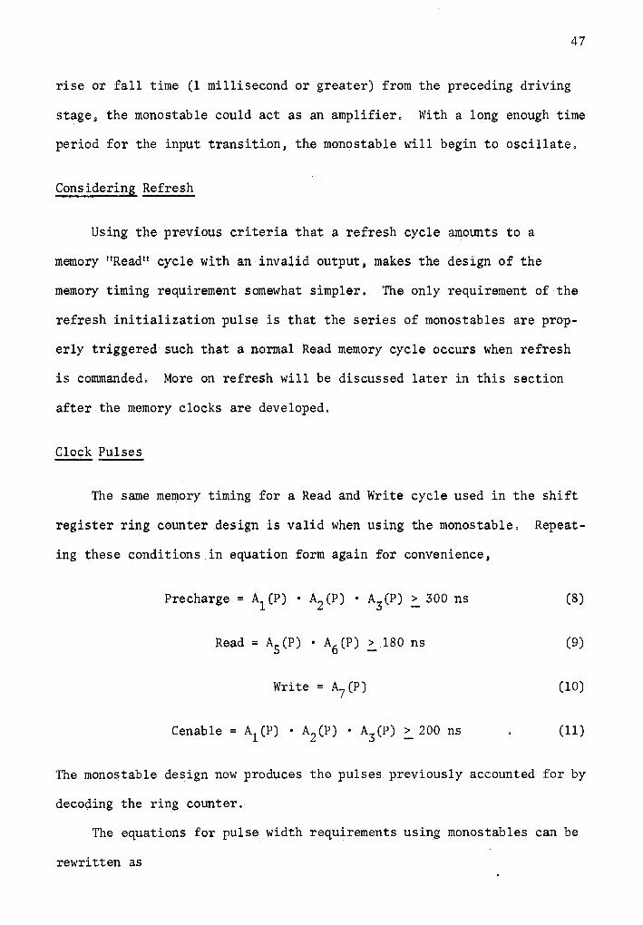
Timing Generation With Monostable Multivibrators. , Gene~al . o o • o o • • o o o o •
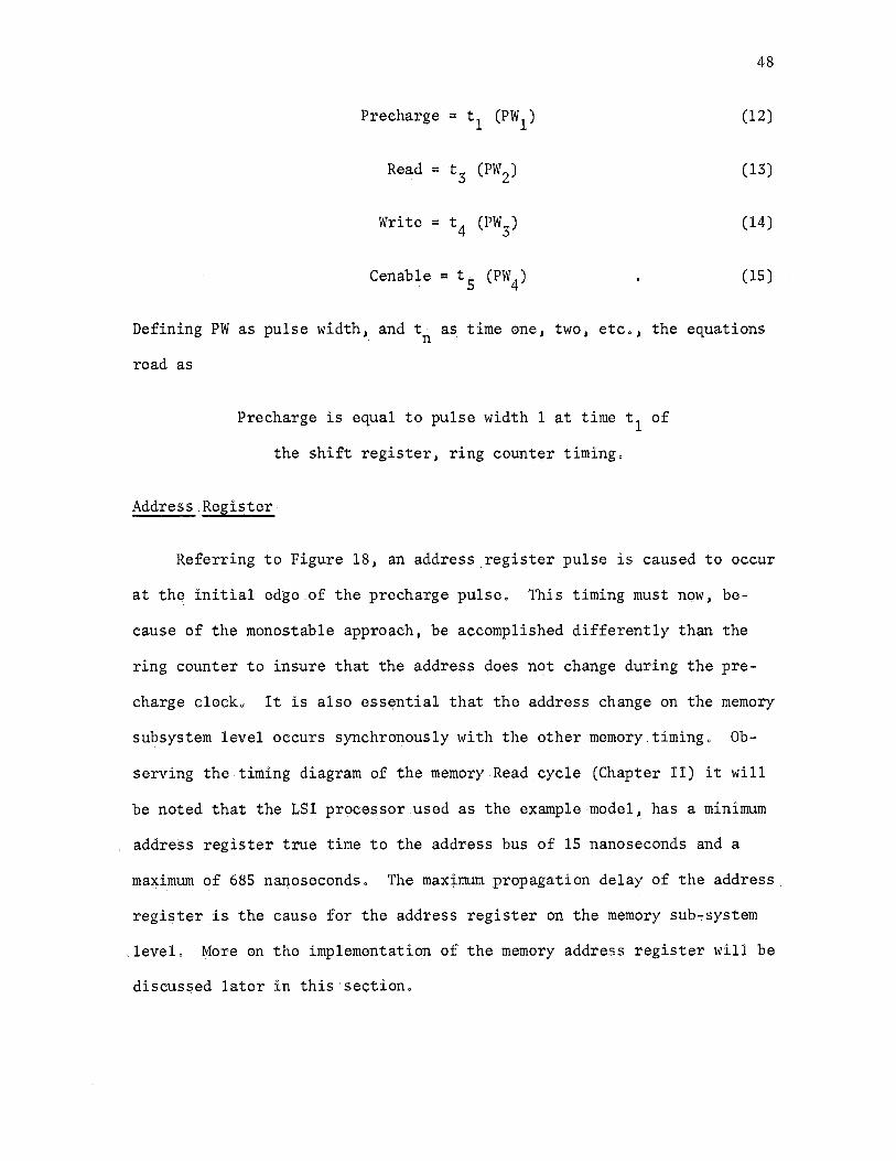
Considering Refresh. • • . . • • Clock Pulses •.. Address Register D~sired Timing. Implementing the Logic Equations .
The Memory Refresh Logic. , The Need for Refresh. Types of Refresh .•
·v
35
35 35 35 36 37 37 38. 41 42 46 46 47 47 48 50 50 57 57 60
Chapter
Operating Conditions •.•.•••...•. Processor Operation .•.•...•••.
Condition IA, Normal Operation •.•••. Condition IB, Normal Operation, Refresh
Requested o o o o o o " o o ., • o • o • o o o
Condition ,11 6 Repair Mode ... Condition III, Microprogramming Level Condition IV, Power~Off State, Memory.to
Retain Data ..•.....••. Memory Element Operation ..•...•••
Implementing the Processor Controlled Refresh. · Requirements Review ••.••..• , .•.
Realizing the Refresh Addressing . Implementing the Clock Detector.. • Detecting the Halt Mode ..
The Write Interface Logic .•.. Introduction ••. , ..•.. Defining the Write Cycle .. A Description of t4e Timing. , Implementing the Write Logic
Page
67 67 68
68 68 68
69 71 73 73 73 81, 87 90 90 90 92 94
IV. THE READ ONLY RANDOM ACCESS MEMORY. 97
Introduction. • • . • , . . , . , . • • • , 97 97 98
General Uses . . . , . . . • , . . . • . . . • • , The Read Only Memory .. Architecture . .
Problem Definition •• , .•. Bus Interconnections •...•
0 0 0 0 0 98 ' 0 ' • 98
Chip Select Decode Implementation .. 0 0 0 0 • 0 98 Output Data Bus Buffering. , Input Node Buffering • . . , . ,
Surveys of Semiconductor ROM. , , . General o o o o o • o o o o • o
Data Bus Switching Considerations . The Need for a Bus ,Driver, .
.. , . 100 0 0 0 0 • • 0 • • 101
0 0 0 0 0 • 0 0 0 103 , , , , , . 103
. 103 . , ... 103
Analysis o o o o o • o o o o ... , 106
V. SUPPORT LOGIC ..
Parity. , Intr<;>duction
.Basic Design ..•.• , Refresh Inhibit,
Test and Diagnostics. Introduction •. Implementation.
Memory Decode Logic. Introduction . • , . . • Implement~tion . , , , ,
Read/Write Memory Storage Register.
• 114
, 114 . , 114
0 0 0 0 0 0 0 11 115 0 0 0 0 G II 11 117
, , • 121 O Cl O O O O O 121
. • 122 0 0 0 0 0 Cl 124
. , , 124 , 126 , 128
Implementation, , , .. , , , •• 0 0 • 0 0 0 0 0 0 128.
vi
Chapt~r
VI. SUMMARY AND CONCLUSIONS.
Problem Summary • • • • Cqnclusions ••••••
Page·
. . 131
131. . 132
SELECTED BIBLIOGRAPHY •... 0 0 0 0 , 0 0 0 • 0 0 .. 134
APPENDIX A - A LIST OF·SEMICONDUCTOR MEMORY MANUFACTURERS.
APPENDIX B - TWO ALTERNATIVES FOR THE IMPLEMENTATION OF AN ASTABLE MULTIVIBRATOR .. , . , .•.•..••
APPENDIX C - A FINAL SCHEMATIC OF A READ/WRITE DESIGN USING MONOSTABLE. MULTIVIBRATOR FOR INTERFACE LOGIC ,
APPENDIX. D - A FINAL SCHEMATIC OF A DESIGN USING A RING COUNTER INTERFACE LOGIC. . • . • . • . • .
APPENDIX E - A FINAL SCHEMATIC OF THE READ ONLY RANDOM ACCESS MEMORY. . , . · . • . • . . • .
APPENDIX F - THE MICROSYSTEMS INTERNATIONAL, LTD. MF 7112, READ/WRITE IC DATA SHEET ...•. , , ••..
APPENDIX G - TijE FAIRCHILD SEMICONDUCTOR, INC. 3514 READ ONLY MEMORY DATA SHEET. , , , , . , , . , •
vii
... 135
138
142
147
0 , 0 It O o 152
154
162
LIST OF TABLES
Table
I. Processor to Memory Interface Signal Levels •
II. Summarizing the .MemoJ;y Environmental Factors.
III. Summarizing the System Power Supply Re~uirements ..
IV. Memory Selection Considerations ..•.... , ..
v. A Table of TTL Read/Write Semiconductqr Random Access Memories. . . . . . . . . . . . . . ' . . . . . . .
VI. A Table of ECL Read/Write Semiconduc~or Random Access Memories. . . . . . . . . . . . . . . . . . . . . .
VIL A Table of MOS Read/Write Semiconductor Random Access Memories. O I I a a I O O II O I • 0 I o I I I
. . .
. . .
. ·'
.
.
Page.
18
19
22
28
32
33 .
34
VII I. Sum,narizing the Cost of the .Ring Counter Method 45 ,
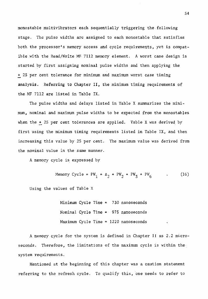
IX, Minimum Memory Pulse Widths of the Monostable .Multivibrator, 55
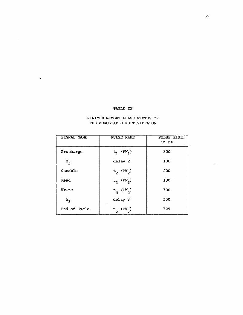
x. Monostable Pulse Variations 56
XI. Logic Truth Table of the Refresh Address Requirements . 72
XII. A Table of Bipolar Read Only Semiconductor Random · Access Memories . , . . . . . . , , . , , , ••• , 104
XIII. A. Table of MOS Read Only Semiconductor Random Access Memories. , ... . , 105
XIV. Summation of the Accumulative Bus and Nodal Capacitance • . •. 108
viii
LIST OF FIGURES
Figure Page
1. A Fl.ow Chart Representative of the Design Proce~s. 2
2. A Block Diagram of a Random Access Memory . . . . . . . 6
3. A Seven Transistor Minimum Size Dynamic Cell . . 9
4. A Three Transistor Storage Cell With Refresh . . . . . . 10
S. A Static Flip-Flop MOS Storage Cell .. 12
6. A Bl.ock Diagram of a Process.or . . . . 14
7. A Functional Block Diagram of the Processor to Memory Interface. 16
8. A Pictorial Representation of the Processor Showing Read/Write and Read Only Memory , . . . . . , . , , . . • . . 21
9. Timing Diagram of a Typical Processor Read Cycle Including Worst Case Design Parameters . . . . . . . . . . . 24
10 .. Timing Diagram of a Typical Processor Write Cycle Including Worst Case Design Parameters ... , . . . . 25
11. The MF 7112 Dynamic MOS Read/Write Memory Read and Write Cycle Timing Requirements. , ... , . . • . 26
12. The Choices of Semiconductor Read/Write Random Access Memories . 29
13. A Generalized Curve Showing the Trends of the Memory Technology. 30
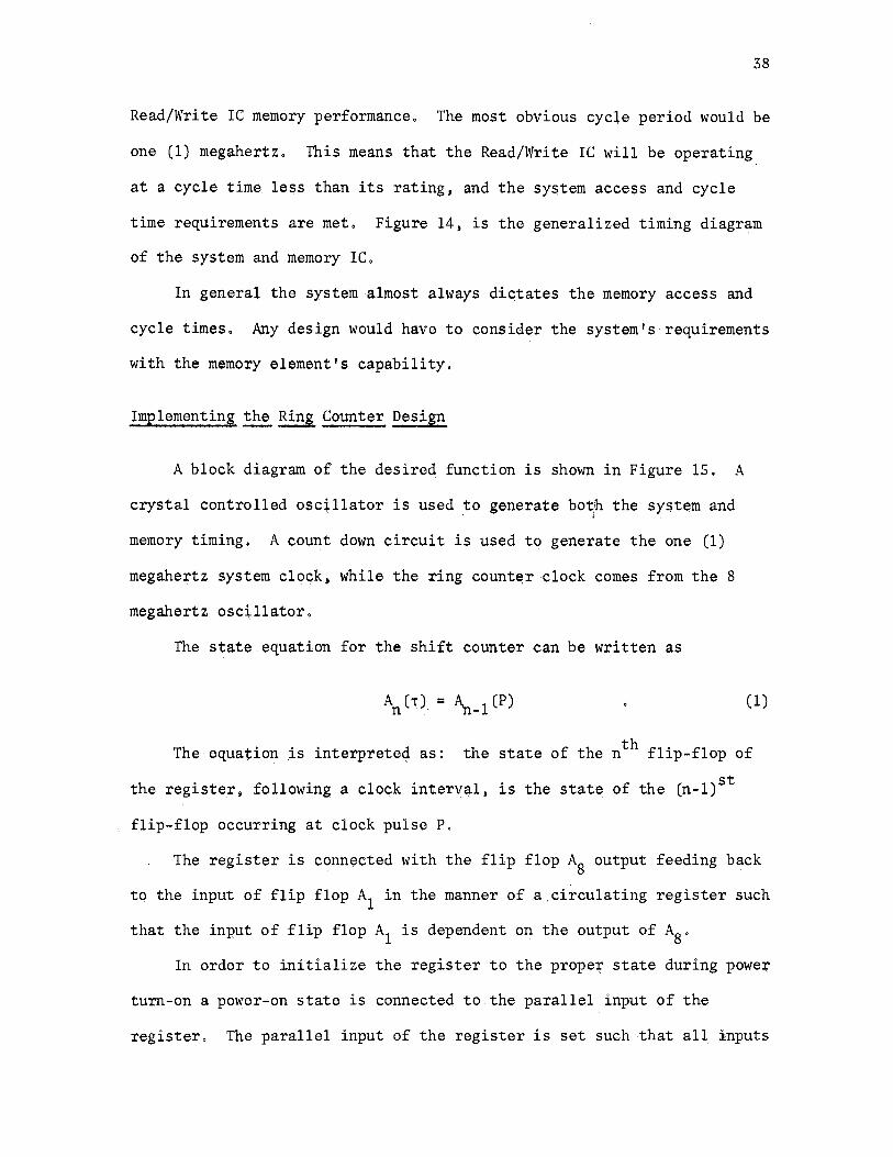
14. A Generalized Timing Diagram of the System and Memory IC 39
15. A Block Diagram of the Ring Counter Including Decoding . 40
16. Fi~al Implementation of the Ring Counter Method. . . . 43
17. Overall Timing Diagram of the System and the Ring Counter Method . o • o • • • • • • • • • • • • • • o • • • 44
18. Timing Diagram and Logic Diagram of the Address Register-Precharge Clock Relationship .. , , ... , . , . . . . 49
ix
Figure Page
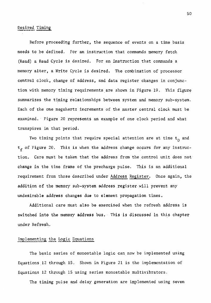
19. Processor Instruction Level Timing Diagram, . 51
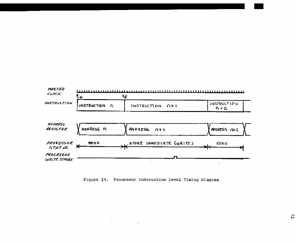
20. Timing Diagram of the Memory Level Signals • 52
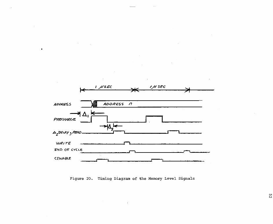
21. Schematic of the Basic Monostable Design. 53
22. Timing Diagram of the Monostable Memory Cycle. . 58
23. Final Schematic of the Monostable Multivibrator Design. 59
24. Schematic Representation of the Basic Ch~rge Pump Storage Cell . 62
25. A Block Dtagram of a 1024 Bit Semiconductor Memory IC Using Refresh by Addressing ..... , , .. , . , . , , . . . . 64
26. A Block Diagram of a 4096 Bit Semiconductor Memory IC Using Refresh by Addressing. . . . . . . · . . . . 65 ,
27. A Block Diagram of Planar Refresh ... 66
28. A Method to Gate or not to Gate the Master System Clock. • 70
29. A Block Diagram of the Processor Refresh Requirements. . . 74
30. A Completed Schematic of the Refresh Address Scheme. . 76
31. A Timing Diagram of the _Processor Controlled Refresh . 79 ·
32., A Worst Case Timing Diagram of the Refresh Pulse • 80
33, Implementation of the Logic to_Synchronize Refresh Signals , 82
34. A Logic. Diagram Representing a Detected Gated Clock. 84
35. A Schematic _Representing the Refresh Interface Logic Including Astable Synchronization. . . . . . , 86
36. Schematic of the Final Overall Refresh Interface Logic . 88
37. A Schematic of a Possible Clock Detector. , , . 89
38. A Block Diagram of the Timing, Refresh, and Write Interface Logic, o •••• o • • • • • • • • • • • • • • • • • 91
39. A Timing Diagram of a Processor Write Cycle .. 93
40. A Schema~ic of the Write Interface Logic. 95
41. A Block Diagram of the ROM Printed Circuit Card .. 99 ·
42. A Pictorial Representation of a.Typical Memory Bus Structure .. 107
x
Figure
43. A Typic~l MOS Output Driver for a ROM .• O e • 0 e
44. Waveform Diagram Representing the Access .Time of a ROM Including Accumulative Data Bus Switching Time
45. A Block Diagram of.a 16 Bit Memory.Parity Circuit ..
46. A Schematic of the Odd Parity Generation •• · ••
Page
• 109
111
• 0 116
. 118
47. A Schematic of Odd Paritr Gene:r;ation Including a Byte Inhibit .. 119
48. A Schematic of the Odd Parity Check Including the Parity Error Detect Logic •.•....•..•.• , •.•• . 0 120
49. A Flow Chart of the Initiali.zation Test and Diagnostic Routine . 123.
so. Implementation of the Test and Diagnostics Rout in~ Into Parity Generation. . . . . . . . . . . . . . . . . . 125
51. A Schematic .. for Memory Decode Logic Implementing 4096 Words. . . 127
52. A Schematic for Memory Decode Logic Implementing 8192 Words. 0 . 129
53. A Schematic.of the Output Data Register Including Open. Collecto~ Gates for Memory Bus Wire-OR Connection ••••.•. 130
54. A Schematic of.an Astable Using an.Integrated Monostable Multivibrator ••.••. , . . • • ..••• . .. , 140
55. A Schematic of a Discrete Astable .. , 141
56. A Final Schematic.of a Read/Write Memory Design Using Monost~ble Multi vibrator for Interface Logic., • , • . • . . . 143
57. A Final Schematic of a Read/Write Memory Design Using a Ring Counter ,Interface Logic , • . . • . • • . . . , , 148
58. A Final Schematic of the Read Only Random Access Memory .•... 153
xi
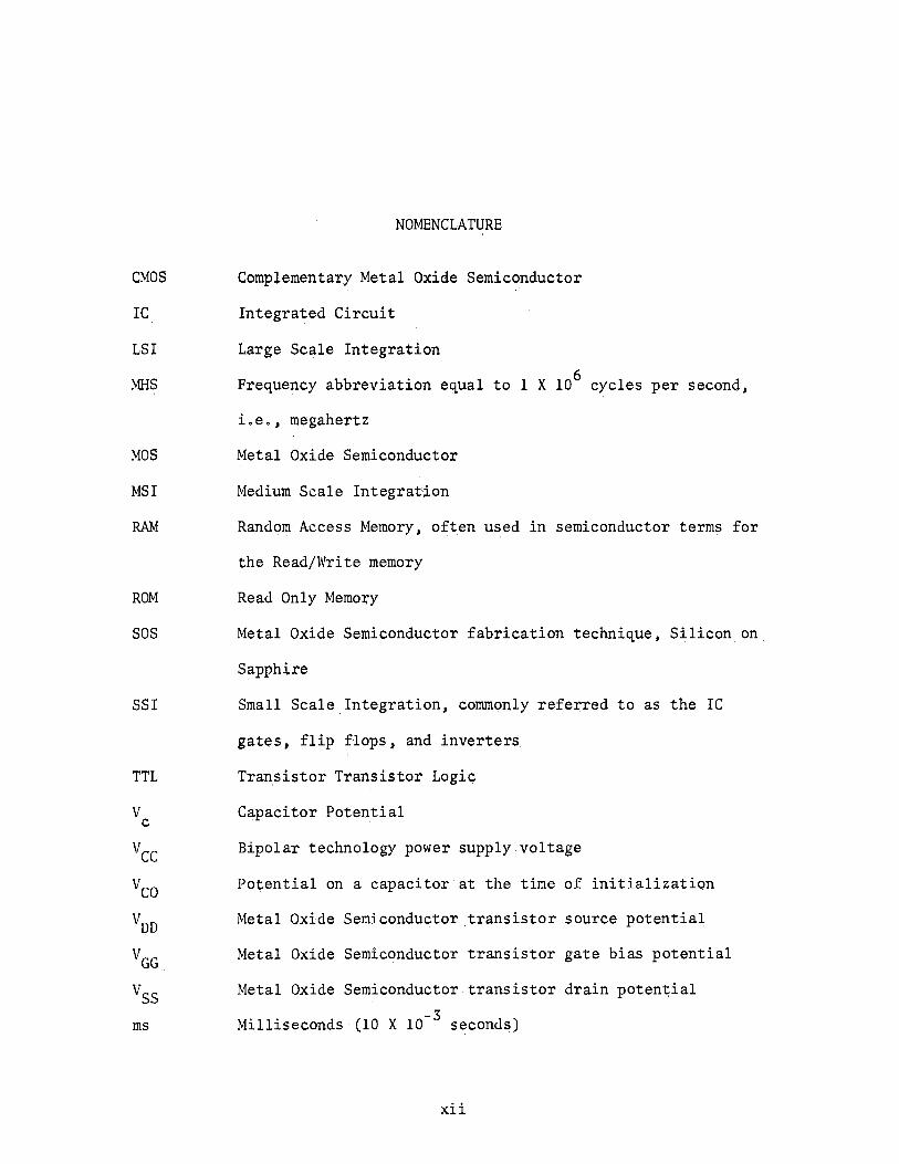
CMOS
IC
LSI
MHS
MOS
MSI
RAM
ROM
sos
SS!
TTL
v c
vcc
vco
VDD
VGG
vss ms
NOMENCLATURE
Complementary Metal Oxide Semiconductor
Integrated Circuit
Large Scale Integration
6 Frequency abbreviation equal to 1 X 10 cycles per second,
i.e., megahertz
Metal Oxide Semiconductor
Medium Scale Integradon
Random Access Memory,. oft.en used in semiconductor terms for
the Read/Write memory
Read Only Memory
Metal Oxide Semiconductor fabrication technique, Silicon on
Small Scale Integration, commonly refe~red to as the IC
gates, flip flops, and inverters
Transistor Transistor Logi~
Capacitor Potential
Bipolar technology power supply voltage
Potential on a capacitor at the time of ini tializ~tion
Metal Oxide Semiconductor .transistor source potential
Metal Oxide Semiconductor transistor gate bias potential
Metal Oxide Semiconductor transistor drain poten~ial
Milliseconds· (10 X 10-3 se~onds)
xii
n-channel Metal Oxide Semiconductor majority carrier designator,.
electrons
ns Nanoseconds ·(10 X 10-9 seconds)
p-channel Metal Oxide Semiconduct9r majority carrier designator,
holes
pf Picofarads (10; 10-12 farads)
µfd Microfarads (10 X 10-6 farads)
-6 µsec Microseconds (10 X 10 secqnds)
O Ohms
xiii
CHAPTER· I
INTRODUCTION TO A SEMICONDUCTOR MEMORY
Format of a.Memory Design
This paper represents the results of five years in designing ind.us
trial and commercial processor memory systems. The accumulation, the
techniques, and the criteria of this. exper.ience is offered in this thesis,
Chapter I presents the historical background and the architecture of a
semiconductor processor memory. The remaining chapters present the
design techniques that can be used for the design and manufacturing of a
memory. The memory is presented as a subsystem of a typical small
processor. Shown in Figure 1 in a flowchart format, are the design steps
that this· paper outlines,
History.
For many years the magnetic core memory has dominated both large and
medium computer memory applications, Only within the past two years has
it been seriously challenged. This challenge is the more economical,
faster access and cycle time and higher package density, monolithic
semiconductor memory.
Most non-magnetic memory used the Metal Oxide Semiconductor (MOS)
technology. The first applications of the MOS memories were not proc
essor oriented, The majority were used in computer peripheral equipment
where the memory was organized serially. This was because the shift
1
TKE DESIGN OF A SMALL MACHINE RANDOM ACCESS SEMICONDUCTOR ME.MORY
DEFINE l'!EMORY REOUIREMENTS
( CHAPTER II )
ESTABLISH SIZE, ORGANIZATION, ACCESS AND CYCLE TIME,AVAILABLE SYSTEM POWER, ENVIRONMENTAL LIMITATIONS
( CHAPTER II )
DEFINE AVAILABLE SEMICONDUCTOR MEMORIES BASED ON REQUIREMENTS
( CHAPTER II )
CHOOSE A COMPATIBLE RANDOM ACCESS ROM AND READ/WR! TE MODULE
·(CHAPTER II)
MONOSTABLE
MONOSTABLE DESIGN ( CHAPTER II I)
MEMORY REFRESH Df:SIGN (CHAPTER III)
MEMORY WRITE CYCLE INTERFACE OE.SIGN {CHAPTER III)
DEFINE THE READ ONLY MEMORY ARCHITECTURE (CHAPTER IV)
DATA BUS SWITCHING CONSIDERATION (CHAPTER IV)
FINAL ROM INTERFACE LOGIC DESIGN (CHAPTER IV)
RI NG COmfrER DESIGN ( CHAPTER I II )
SUPPORT LOGIC ( CHAPTER V)
PARITY
ERRO~ CORRECTION (NOT INCLUDED IN DISCUSSION)
TEST AND DIAGNOSTICS
MEMORY DECODE' LOGIC
STORAGE REGISTER
· SENSE AMPLIFIER OUTPUT LOGIC TRANSLATOR
Figure 1. A Flow Chart Representative of the Desigh Process
2
3
register, making use of the capacitance nodal storage property of·the MOS
device,. was. the first device that could be economically produced. Mell!ory,
sizes were restricted tq a few thousan.d bits, with a maximum clock fre
quency of l.MHZ. Individual package size was.confined to a maximum of
100 bits. This capacity was later expanded to one and two thousand bits
with a clock, frequency exceeding 5 MHZ •. However, the usefulnes~ of the
serial memory was limited due to the .introduction of the semiconductor
monolithic random access .memory.
In 1967, the first random access semiconductor .memory was made
available as.a connnercial product. It was in the form of the Read Only
and was.the first true processor oriented semiconducted memory. In 1969,
the semicondu~tor memory systems became practical with the introduction
of the semiconductor random access Read/Write memory. The performance
needs of processor applications could now·be cost effective using a semi
conductor memory, Once again the MOS technique was used first, because
of the increased package density an.d its ability to store data on a MOS
capacitance storage node. Individual monolithic IC sizes up to 1024 bits
were avail.able in early 1970. In the same pe:r:iod the bipolar Read/Write
memory became available for system use where fast cycle and access times
were required. Practical bipolar Read/Write memories do not now exceed
256 bits~ even though a few applications, particularly military, do use
the more.expensive bipolar ROM's.
The use of semiconductor memory .in small machine applications is .
becoming wide~y accepted because of the cost effectiveness of semi
conductor memory.opposed to the magnetic _core memory. A few exceptions
to this are the small applications found throughout the .computer industry
where a very large core memory (exceeding a few million words) has been
4
replaced by a semiconductor memory. However, the trend is definitely
away from magnetic core and to the semiconductor memory. This is
especially true as semiconductor mem_ory. becomes 1 ess expensive than . core.
Present Day Usage
The memories that are beirtg designed a.I).d used today are generally
classified into three areas: (1) Serial Memories; (2) Read/Write, random
access memory; and (3) Read Only, random access memory.
The serial memory.consists.of a serie~ of shift registers and is not
generally found in processor oriented machines. The serial memory is
more often found in computer peripheral equipment such as line printers
or Input/Output machines.
On the other hand, the Re~d/Write .and Read/Only random access memory
are found much more in. the processor oriented machine as memory, Stqrage
and retrieval are done on conunand.. Opposed to thi.s, the serial memory
requires multiple bit time delays to access the desired memory location ..
A Small Machines Architecture
A computer system, called a processor, is comprised of four inter
acting subsystems: (l} an arithmetic logic unit; (2) a control unit;
(3) .an input/output unit; and (4) a memory unit, Each unit is a separate
entity in itself, but-dependent on the other units to perform its
intended function.
The purpose of this paper.is to define, by example, the design
criteria to make. a sem_iconductor memory an. interacting subsystem within a
small computer system. Each chapter is divided into a portion of the
memory subsystem.·
As stated in the previous section, there are two basic memory
archit.ectures for processing machines, serial or random access. This
paper will pursue the random access memory as this is the ,largest per.,.
centage of ·the usage.
5
The memory function can be asynchronous or synchronous with respect
to processor operation. In synchronous operation the flow of address and
. storage information to and from memory is controlled .. by the arithmetic
and cont·J;'ol units .master clock. In asynchrono1,1s operation the memory
must communicate with the processor to determine a mutually ,agreeable
time for data transfer to take place. Because most memories operate
synchronously, thereby eliminating the need for external transfer
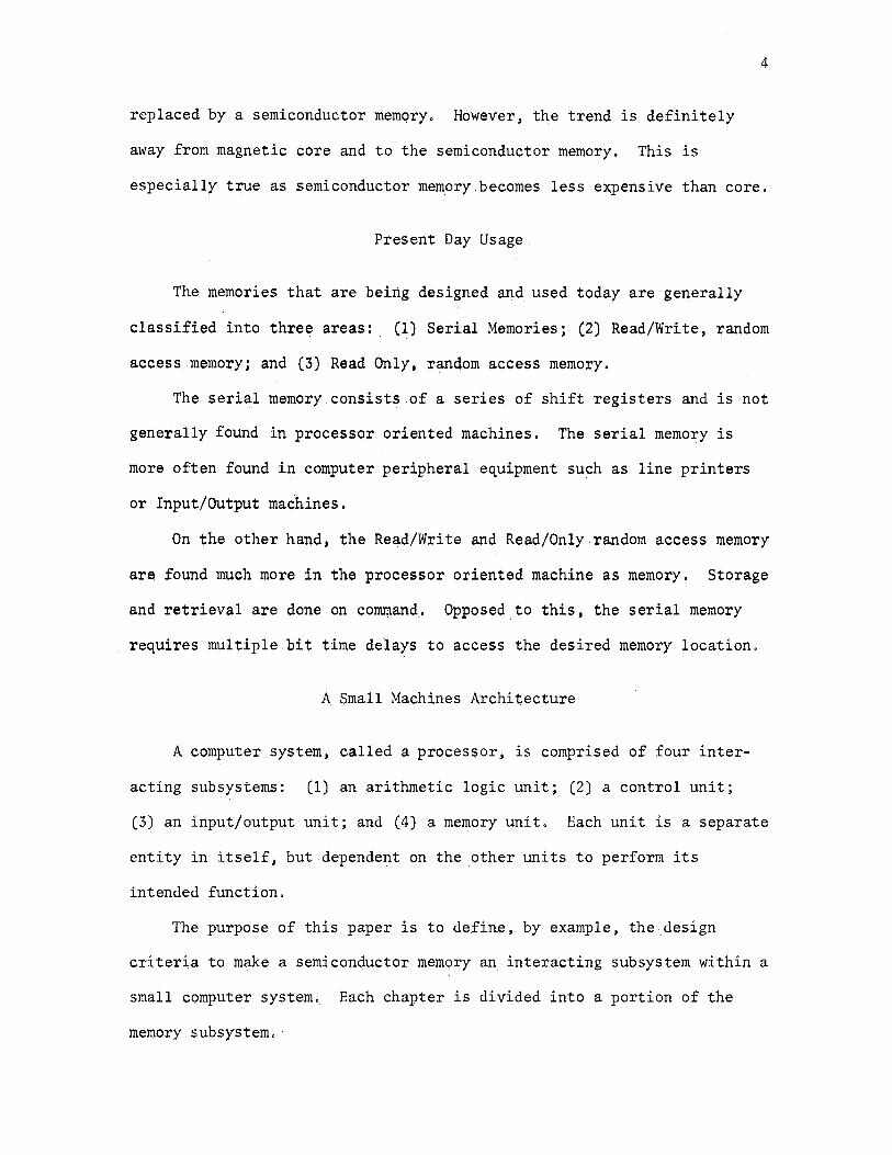
control, this paper will concentrate c;m synchronous operation. Figure 2
is a general block.diagram of a synchronous random access memory.
Often the performance and operation of a small processor requires
both an alterable Read/Write and a non-alterable Read Only random access
memory. This paper offers the engineer a worst case design outline for
designing a small processors semiconductor memory. Ma~y design tech
niques are applicable to large processor designs, but these.within this
text are directed primarily at memories whose capacities are less than
70,000 words.
The most common and.economical memory configuration used in a small
process qr is to bus both the Read . Only. and the Read/Write .memories on the
same data and address bus. This calls for common data and address
registers in the control and arithmetic unit:s thereby reducing costs by
eliminating duplication. Additional economy, and often physical
packaging size, can.be re~lized if the input and output data bus is
mut lip lex eel, · This in general, results in a need to reduce the memory
ADDRESS DECODE
ADDRESS ... ,
WORD SELECT
ADDRESS REGISTER
i '
.... ,
Figure 2.
STORAGE
i "
SYSTEM CLOCK
A Block Diagram
DATA,
CONTROL
I '
I/0 DATA REGISTER
'"
of a Random Access Memory
If\
I'
~ z H
I < 8
~
w
storage elements cycle and access. time, as time must be allotted for the
Input/Output (I/0) buffer to switch states.
7
The memory unit itself is composed of nine subsystems each perform
ing a separate task. A semiconductor memory.is composed of: (1) address
decode logic; (2) signal buffers; (3) control logic; (4) output buffers;
(5) output register; (6) storage element; (7) parity; (8) refresh if
required by the storage element; and (9) the timing interface logic. In
all ·recently developed semiconductor memory integrated circuits, the
address decode logic is built into the memory chip, thereby leaving the
· other 8 subsystems to be designed,
Chapter II details the design considerations and constraints when an
integrated circuit memory is chosen. These criteria are outlined in
Chapte.r II, but for now are listed to lend emphasis to the further dis
cussions of this chapter. The design criteria are: (1) cost; (2)
packaging; (3) performance; (4) storage capacity; (5) organization; (6)
environmental; and (7) pc;,wer supply available and required.
Th.e following chapters are developed based on a Read/Write integrated
circuit chosen for its recent announcement into the commercial field, and
because of its storage capacity. It was also chosen for the degree of
difficulty in implementing it into a processor's memory unit. The
storage element is an integrated circuit, Read/Write semiconductor memory
manufactured by Microsystems International Limited, of Ottawa, Canada,
The memory element is typical of the 4096 bit Read/Write semiconductor
memories .being introduced to industry during the latter part of 1973 and
the initial part of 1974. The int~grated ctrcuit is designated the
MF 7112, and is packaged in a 22 pi~ dual in-line (DIP). The manufac~
turer's data sheet is included in the appendix,
8
The MF 7112 was also chosen as the example memory storage element
because of its complexity in interfacing with the processor. The MF 7112
is complex because of the _design techniques .. used. to implement the
internal storage cell.
A semiconductor memory can always be categorized as either static or
dynamic, Static memory cells are cross-coupled bistable circuits wherein
information is stored by one of the two stable states. Most static .MOS
memory cells use six transistors for each cell, Dynamic circuits use the
absence or presence of charge on a.capacitor to store information,
typically with three or four transistors per cell. Almost all recently
introduced 4096 bit Read/Write memory elements use only one transistor
per storage cell, Since the capacitor that stores the charge has a
leakage current, the stored information degrades slowly and therefore
must be periodically refreshed. The MF 7112 is a dynamic memory
requiring periodic refreshing.
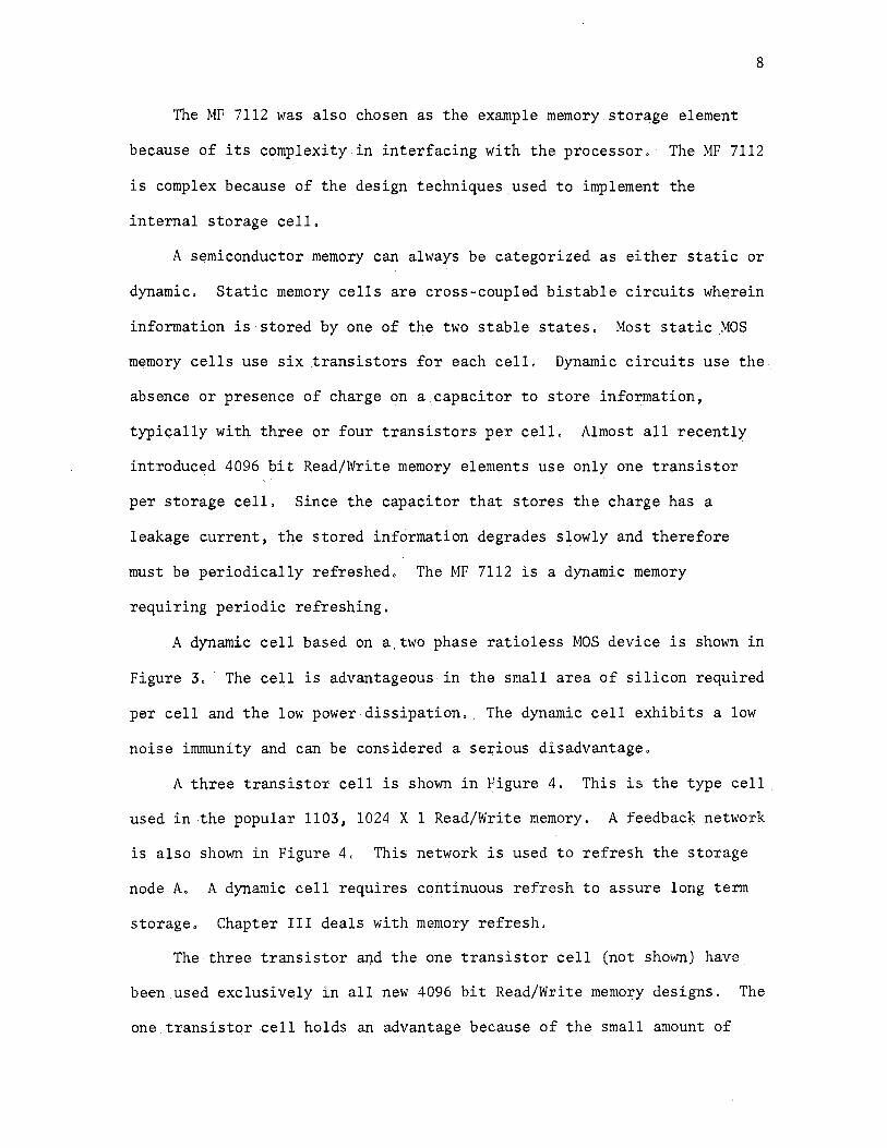
A dynamic cell based on a.two phase ratioless MOS device is shown in
Figure 3. The cell is advantageous'.in the small area of silicon required
per ceU and the low power dissipation .. The dynamic cell exhibits a low
noise immunity and can be considered a serious disadvantage.
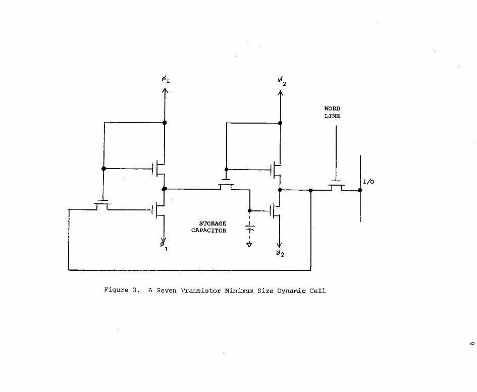
A three transistor cell is .shown in Figure 4. This is the type .cell .
used in the popular 1103, 1024 X 1 Read/Write memory. A feedback network.
is also shown in Figure 4. This network is used to refresh the storage
node A. A dynamic cell requires continuous refresh to assure long term
storage. Chapter HI deals with memory refresh.
The-three transistor ar:id the one transistor cell (not shown) have.
been.used exclusively in all new 4096 bit Read/Write memory designs. The
one. transistor .cell holds an advantage because of the small amount of
r&1
1 1
STORAGE CAPACITOR
' _,_ 1'
WORD LINE
Figure 3. A Seven Transistor Minimum Size Dynamic Cell
I/0
WR TE RE
I A
I
,_ - - - - - CELL ....J
DATA I/0
Figure 4. A Three Transistor Storage Cell With Refresh
fc
11
silicon cell area required compared with the three transistor cell ..
Cells larger than three transistors. require overall LC. di~ area larger
than present day processing techniques permit.
The static MOS and bipolar Read/Write memo~ies employ the common
flip-flop. Several types of static storage elements have been,proposed;
however, all of these elements work on the.flip-flop principle.
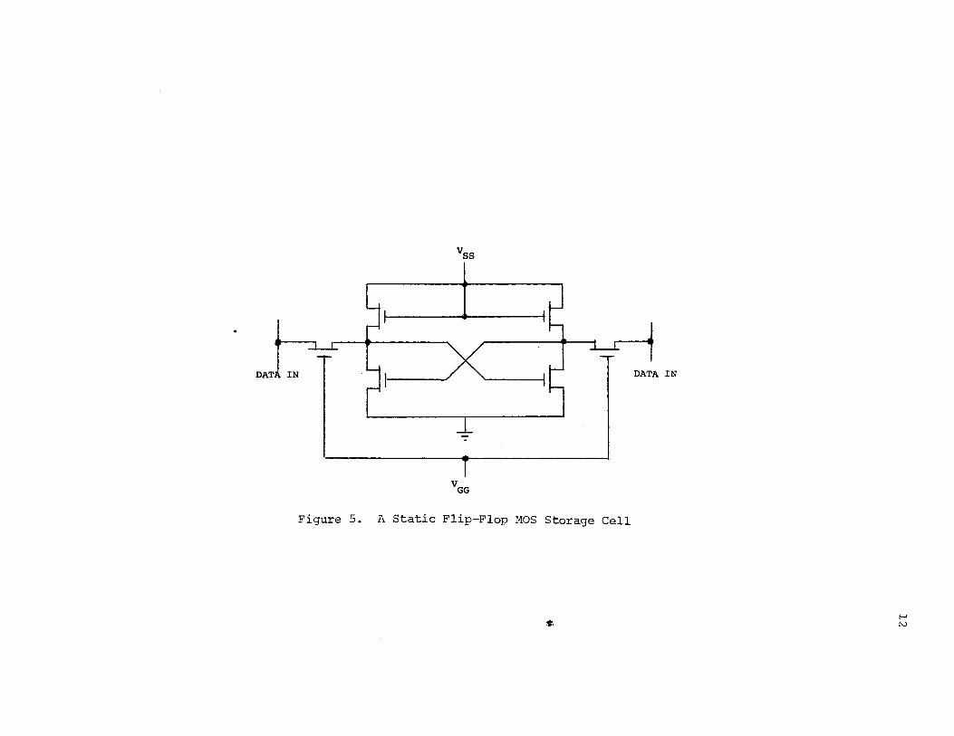
The simplest static cell is con_structed as shown in Figure 5, The
cell employs the basic flip-flop and requires a number of transistors.
The advantages of this cell are its noise immunity and wide electrical
operating range. The cell requires no refresh operation. The major
disadvantage of this cell is the large amount of silicon area and the
large amount of,power required. Power.dissipation of the _memory package
is the power of the _individual cell multiplied by the number of cells in
the memory array. This can be.an enormous amount of power when arrays
are interconnected to form a memory system.
The following chapters deal only with the dynamic Read/Write memory.
when implementing the alterable portion of the memory subsystem .. Static
memories are generally .not found in small machine applications because of
their.high cost and small storage capacity caused by the large cell size
and amount of power dissipation.
The design of the memory subsystem begins with the definition of the
problem, As in any design, the problem must first be defined before a
solution can be found. Chapter II defines an example processor require
ment •. Ch~pters III, IV, and V outline a solution for the example while
also detailing othe:i; possible approaches. In each case all steps are
~irycted towards a worst case prqduction design.
DAT IN DATA IN
Figure 5. A Static Flip-Flop MOS Storage Cell

CHAPTER II
PROBLEM DEFINITION
Defining the Small Machine Application
Introduction
The first step in designing a memory is to define the operating
conditions. The first half of Chapter II defines the .conditions of the
large scale integration (LSI) processor. The second half outlines.and
surveys the Read/Write memory !C's available in.industry.
Defining ~ .Processor
A small processor can be defined as being limited in word length, a
limited n.umber of transfer registers and instructions, and a memory
structure not exceeding 100,000 words. To insure that the descriptions
contained here are practical, a production design is used as a model.
The design centers_around a memory requirement .for a Honeywell Informa
tion Systems, LSI processor. Th.e processor is MOS p-channel, silicon
gate technology.
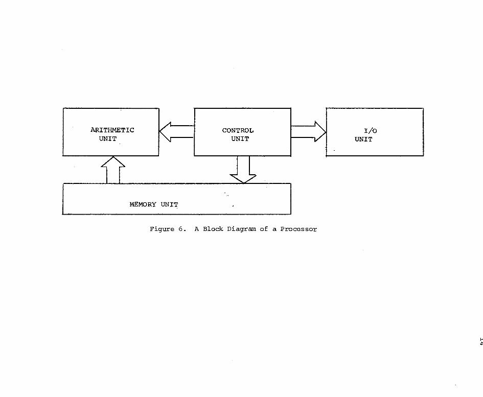
Any processor can be described in four basic blocks, arithmetic,
control, I/0, and memory. Such is the case of this examp,le processor.
Figure 6 represents -the gen.era! case for a. processor and will be used as
a basis for defining the memory design.
The guidelines contained in the .discussion of this paper are
13
ARITHMETIC UNIT
MEMORY UNIT
CONTROL UNIT
Figure 6. A Block Diagram of a Processor
I/0 UNIT

15
primarily directed towards the memory. Therefore, descriptions of the
arithmetic, control and I/0 units are omitted unless they directly affect
the memory.operation.
Defining the Memory ·!2. Processor Interface
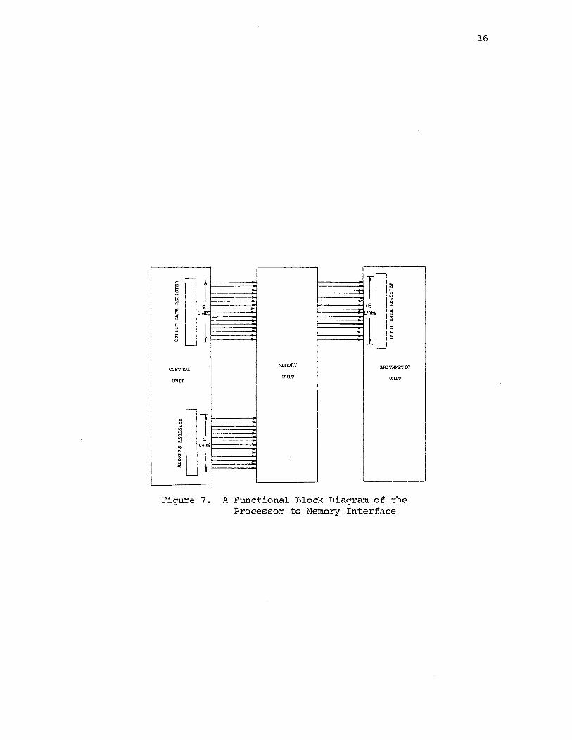
For the processor used in this discussion the data path for~..!!!.
and~ Out are separate. Some small machines are often designed with a
bidirectional data path. The bidirectional data path is convenient for
many applications and is generally used where memo~y interface registers
and wiring are to be minimized. A functional description of the inter
face is shown in Figure 7. The address register consists of a 14 bit
word. The Data register, both In and Out, are 16 bit words. Parity is
not included in the arithmetic or control units and therefore must be.
designed as part of the memory.
When the LSI processor design was conceived, the use of a dynamic
Read/Write memory.IC had been anticipated. Because of this, a memory
re£resh signal was incorporated into the Control Unit, The refresh sig-
nal consisted of a refresh conunand for each instruction.
tion simplified the refreshing requirement of the memory.
This incorpora
Any design of
a processqr, particularly LSI, must consider the dynamic Read/Write
memory and make the proper signals available before conunitting the
design. Reworking a system made.from small scale integrated circuits is
not too difficult. But, reworking a LSI design is often impractical both
from a cost and time to production basis.
--
l T 0: - - 0:
" " .. .. ~ ~ >----·-" " [:!
'' 16 [:! ,Cl
WIEl ,Cl
~ L1Ne5 ~
l !; 1 !; "' "' !; ~ 0 ~ -
MEMORY ARITHMETIC CONTROL
UNIT UNIT UNIT
-"' 1 " .. ~
" [:! 14
"' LINE&
"' [:! 1 0
~ ~
Figure 7. A Functional Block Diagram of the Processor to Memory Interface
16
17
Defining Signal Level Interfaces
One of t~e fi:i;-st steps ,in the design, is to insure processor tq
memory interface levels. Table I summarizes the proces~or signal levels.
After the memory IC selection it will be. necessary to check on proce~sor
to memory.interface compatibility.
Environmental Considerations
A small processor, especially those found in numeric control and
point-qf-sales applications, .are generally designed to an industrial
environmental stand~rd. A typical environmental specification is
summE!,rized in Tabl.e II.
An operating temperature of +65 degrees centigrade approaches the
design limits of .all industrial grade·IC's. It is advisable to always
insist on IC's,being tested on a component level to their maximum temper
ature specification. Many designers have discovered that what works in
the laboratory does not necessarily guarantee operation at all extremes
of temperature in the .field. Ca4tion must be particularly exercised in a
monostable timing development, such as is described later in Chapter III,
for temperature causes the greatest. percent~ge of change in timing pulse
widths.
Defining the Memory Architecture
The .architecture of the memory is generally described by the appli
cation of the processor. For this example, a Read/Write random access
memory of 6144 words is assumed to be a necessary application require
ment. This is consistent with the processor description ,given in the
beginning of this chapter. The processor has 14 address bits which
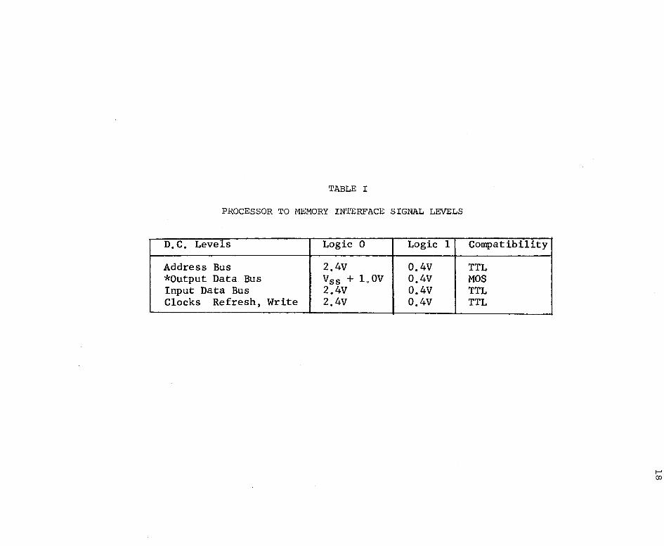
TABLE I
PROCESSOR TO MEMORY INTERFACE SIGNAL LEVELS
D.C. Levels Logic 0 Logic 1
Address Bus 2.4V 0.4V *Output Data. Bus Vss + LOV 0.4V Input Data Bus 2.4V 0.4V Clocks Refresh, Write 2.4V 0.4V
Compatibility
TTL MOS TTL TTL
1--' 00
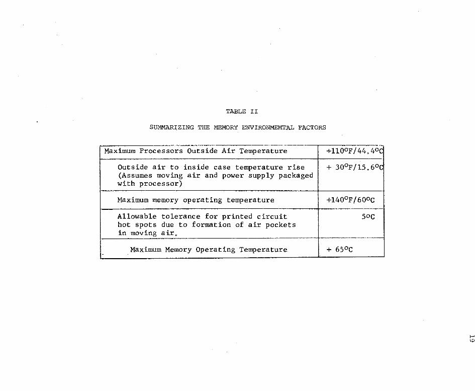
TABLE II
SUMMARIZING THE MEMORY ENVIRONMEMTAL FACTORS
-·---------·-··----··---- -----Maximum Processors Outside Air Temperature +1100F/44,4°C
Outside air to inside case temperature rise + 30°F/15.6°C (Assumes moving air and power supply packaged with processor)
Maximum memory operating temperature +140°F/600C
Allowable tolerance for printed circuit soc hot spots due to formation of air pockets in moving air,
·-
Maximum Memory Operating Temperature + 65°c ..
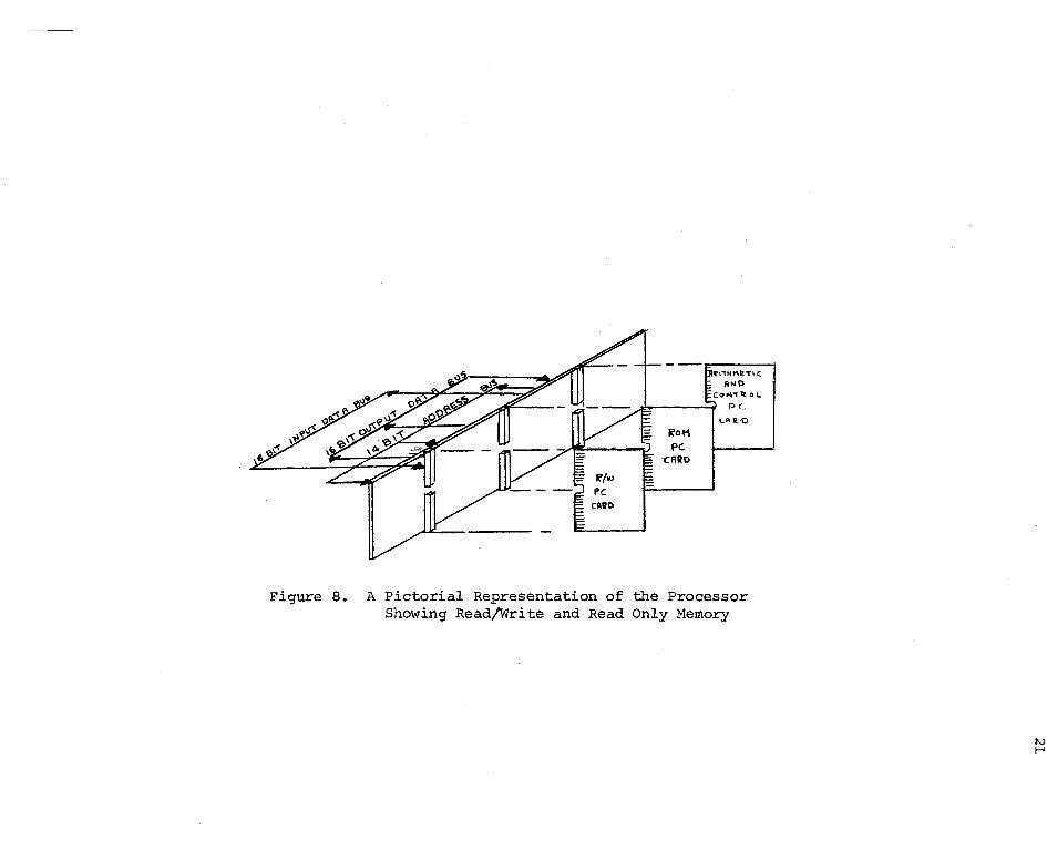
restrict memory to 16,384 words without resorting to memory expansion
techniques.
20
In order to be furthe~ consistent with the example processor, the
Read/Write and ROM both will share a conunon address and.data bus. Figure
8 is a pictorial structure of the memory/processor configuration.
Defining~ Power Supply
The ideal memory is always power supply compatible with the rest of
the machine. However, seldom is this luxury possible with a semiconduc-.
tor memory. Scanning the surveys.of ROM and Read/Write merpories will
show that few semiconductqr memories are power supply compatible. Table
III lists the processors and the MF 7112 power needs. Processors current
requirements are not il)clu.ded as they do not pertain to this discussion.
It is inunedi~tely obvious .that the Read/Write memory is not power supply
compatible. The ROM has not be~n chosen yet (see Chapter V) and the
power supply usage was therefore not included. The designer must insure
that the interface signals are truly compatible. In this case the power
supply sununary indicates that signal compatibility may be misleading as.
described by the manufacturer. Such is not the cas~ for the MF 7112, but
some manufacturers do resort.to misleading specifications that can lead
to many problems for the designer that; does not insure input and output
compatibility.
Defining Memory Interface Timing
The last definition is processor to memory timing. Often the timing
between processor and the memory elerpent~ are not compatible and.inter
face logic is required, Chapter III describes this interface timing,
~0-t'I
PC
PC..
c.AltO
Figure 8. A Pictorial Representation of the Processor Showing Read/Write and Read Only Memory
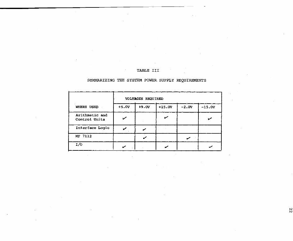
TABLE III
SUMMARIZING THE SYSTEM POWER SUPPLY REQUIREMENTS
VOLTAGES REQUIRED
WHERE USED +s.ov +9.0V +15.0V -2.0V -15.0V
Arithmetic and v' Control Units ,/ v'
Interface Logic ,,,. ,,,,,
MF 7112 ,,,. .,, I/0 ,,,,,. ,,,,,. .,,,
N N
23
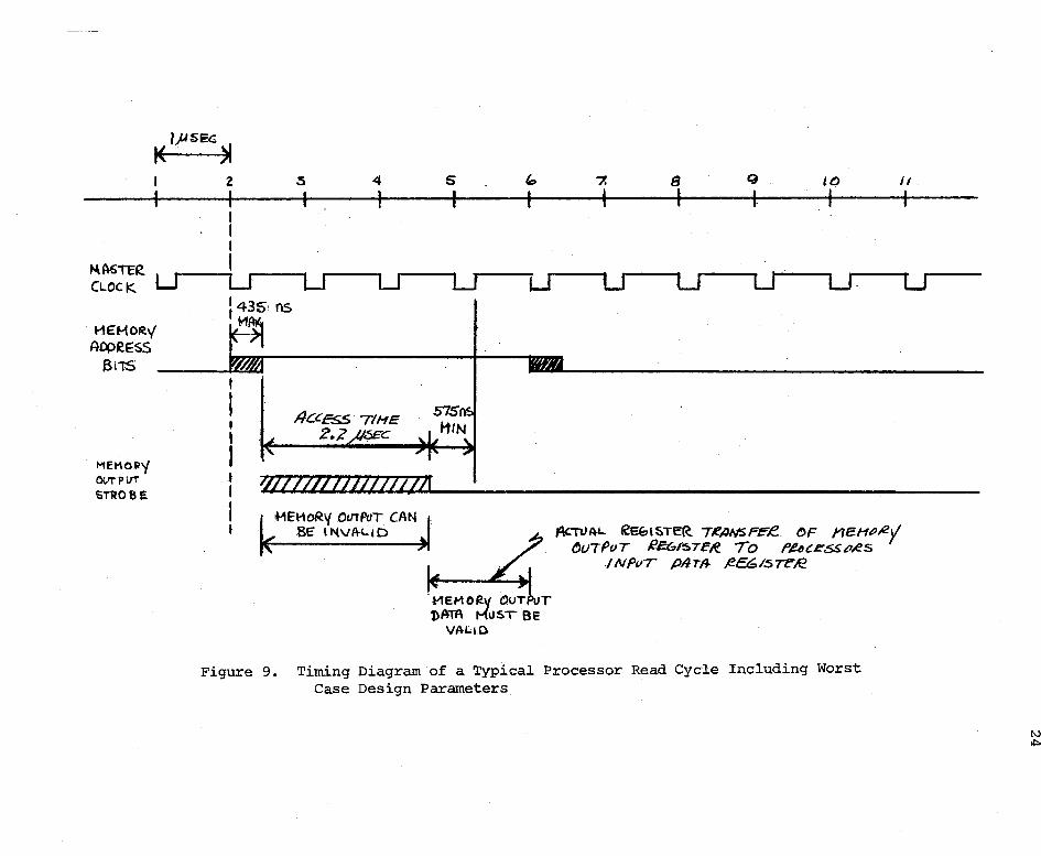
First the designer must define the processor's requirements and capabili
ties, and then define the memory element (in this case the MF 7112)
requirements and capabilities.. The best method for an overall view is by
timing diagrams, Figure 9 is the processor's Read Cycle; Figure 10 is
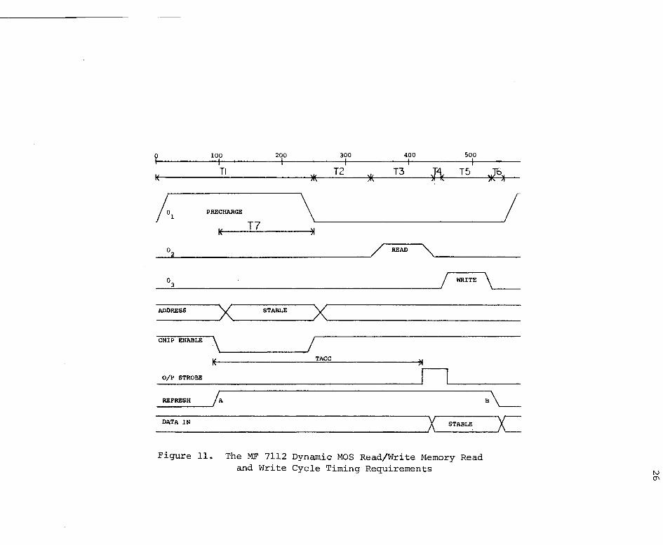
the ,processor's Write Cycle; Figure .11 is .the MF 7112 Read and Write
timing.
Surveying the Semiconductor Read/Write Memory.
Introdqction
The selection of a memory element.is usually a function of the sys
tems performance requirements and the memory cost goals. Many choices
are available to the designer. This section .surveys the present day
market of semiconductor Random Access Read/Write Memories, the technolo
gies, performance and cost are used as guidelines in graphing the avail
able market.
The designer is presented with a maze of choices.when he first
begins his memory selection., Armed with his cost goals or the perfor
mance goals as primary factors, he finds that these two parameters are
both directly related to the semiconductor technology. The axiom of
circuit design used from the beginning of electronics still holds true
for semiconductor memories, This axiom, the faster you must operate the·.
more. it is going to cost l often limi,ts the designers choice., In general~
the bipolar technology is chosen for applications with cycle times less
than 100 nanoseconds, whi.le the MOS technology is used for cycle times
greater than 100 nanoseconds,
Another rule of thumb for design cost considerations is, that bi
polar memories are two to four times the cost of MOS memories, On the
JµSEG 1< .· . )I
z ~ 4 5 " 7. 8 g to II
~A6TER. CLOCK LJ
l-1E:HORy ADPfESS
6i1S
MEMOR)' OVtl"IJT snose.
I I I I I I I I I LI u u Li u 1435, ns
f~
t I f I •
1lllllll721777Zlli ·I MEHoRV O<lTPoT CAN t· ·( SE l"lVA-LID )·
PIEM oR.v OUT T 1)ATF\ MOST BE
V.4L1.0
t ! l I
u u u u.
Acn)A-L. REGISTER. T~/)l./5Ff:f.e. OF neHP12f tJuTPvT ~l:6l'57e,(l 7o l'~c~SSPl€S
./Nf't1T pArA- ~£61571:',€
Figure 9. Timing Diagram of a Typical Processor Read Cycle Including Worst Case Design Parameters
I
u
HEMofl..'-{
AOl>tESS
~ I ..Jl5£c.)I
( l
Ll I
~ rt::, ---.IDli-
PATA '?EGl5TEf? tHTS ---ru.t!•
i
u
'1 l
u
s I
LJ
935" ns ~16" ns
·1:,
I
LJ
7 I
L1
$ I
u
9 I
u
/tJ I
LJ
'/i I
u
I< HIN ~ K y1M.)I
\NRtTE~-------__.r::::r-.....--:i---------------------------
Figure 10. Timing Diagram of a Typical Processor Write Cycle Including Worst Case Design Parameters
N lJ1
? 100 200 300 400 500 I I I I I
I< Tl
)I( T2
)I( T3 l\ T5 ,JG)t
/,, PRECHARGE \ I I( T7 )I
02 / READ "' 03 I WRITE \
ADDRESS x STABLE x CHIP ENABLE \ I
TACC
0/P STROBE n REFRESH /A a\_ DATA IN x STABLE 'C_
Figure 11. The MF 7112 Dynamic MOS Read/Write Memory Read and Write Cycle Timing Requirements
N O'I
other hand, bipolar memories are simpler to use and require less inter
face circuitry,
27
For small machine applications the designer m4st compare both
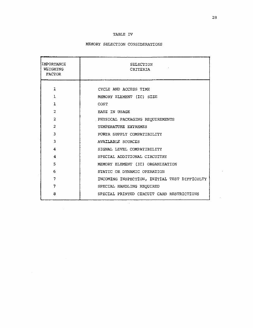
technologies for the best_system cost/performance trade off. Table IV
lists some of the more important items to be used in selecting a memory
for small machine applications. Their order 9f importance is also listed
even though these are variable depending on,the application. Notice that
some items must be treated with an equal importance factor.
Industry Survey
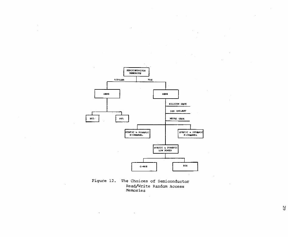
Both the MOS technology and the bipolar technology.can be divided
into various b~anc~es, .with each branch a cost/performance trade-off,
Out of necessity, the MOS technology must be sub-divided into t~e majori
ty carrier channei designation, Le., p-channel and n-channel, The
bipolar technology.can be divided into the type of transistor intercon
nections ,used within the memory element. Figure 12 represents the·.
structure of the bipola;' and MOS memories, and shows the choic~s avail
able to a designer, The bipolar branches are straight forward with two
choices _presently available 11 TTL and ECL, On the other hand, when the,
access and cyc~e time of a memory allow MOS to be the chosen technology,
there are many branches available, The MOS memories are broken down
into the three common technologies and then into the .majority carrier
cl).ann_el designator, Also, added are the complementary MOS (C-MOS) and
the silicon on sapphire (SOS) technologies,
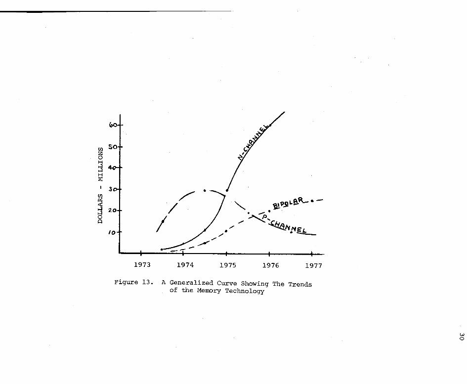
Shown in Figure 13 is a gene~alized c4rve representing the tech
nology trends.of the semiconquctor me~ory usage, It is important that
the de~igner consider the market trends for his product during the
IMPORTANCE WEIGHING
FACTOR
1
1
1
2
2
2
3
3
4
4
5
6
7
7
8
TABLE IV
MEMORY SELECTION CONSIDERATIONS
SELECTION CRITERIA
CYCLE AND ACCESS TIME
MEMORY ELEMENT (IC) SIZE
COST
EASE IN USAGE
PHYSICAL PACKAGING REQUIREMENTS
TEMPERATURE EXTREMES
POWER SUPPLY COMPATIBILITY
AVAILABLE SOURCES
SIGNAL LEVEL CO~ATIBILITY
SPECIAL ADDITIONAL CIRCUITRY
MEMORY ELEMENT (IC) ORGANIZATION
STATIC OR DYNAMIC OPERATION
INCOMING INSPECTION, INITIAL TEST DIFFICULTY
SPECIAL HANDLING REQUIRED
SPECIAL PRINTED CIRCUIT CARD RESTRICTIONS
28
SEMICCEDUCTOR MEK>RlsES
BIPOLllR Mos
ECL
Figure 12.
TTL
STATIC & DYNAMIC N-CHANNEL
c-ms
SILICON GATE
ION IMPIANT
METAL GATE
STATIC & DYNAMIC LOW POWER
STATIC & DYN»II P-CHANNEL
sos
The Choices of Semiconductor Read/Write Random Access Memories
Cl) z 0 H ..:I ..:I H ::E:
Cl) 0::: .:x: :j 0 A
20
IO I
1973
/ /
1974 1975 1976 1977
Figure 13. A Generalized Curve Showing The Trends of the Memory Technology
w 0
31
product's prime life period. For instance, the curves show that a
p-channel Read/Write memory would. be.the best choice for a product whose
life was to end in the 1974 to 1975 period. On the .other hand, for
products whose life expectancy.exceeded 1974 the choice of an n-channel
Read/Write memory would best suit the cost trade-off .of the product.
The trends shown in Figure 13 are based on personal research
gathered during interviews with various semicond4ctor memory manufac
turers.
The three tables,. Table V, Table VI, and Table VII represent semi
conductor memory technology divided into their two major components,
bipolar and MOS. Each chart includes the Random Access Read/Write
Memories presently available and forecasted for announcement prior to
June, 1974. The bipolar memories are further sub-divided into TTL (Table
VI) and ECL (Table VII).
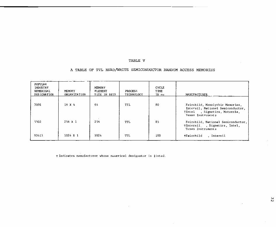
TABLE V
A TABLE OF TTL READ/WRITE SEMICONDUCTOR RANDOM ACCESS MEMORIES
POPUIAR INDUSTRY .MEMORY CYCLE NUMERICAL MEMORY ELEMENT PROCESS TIME DESIGNATION ORGANIZATION SIZE IN BITS TECHNOLOGY IN ns MANUFACTURER
3101 16 X 4 64 TTL 80 Fairchild, Monolythic Memories, Intersil, National Semiconductor,
tintel '
Signetics, Motorola, Texas Instruments
5503 256 X 1 256 TTL 85 Fairchild, National Semiconductor, tintersil
' Signetics, Intel,
Texas Instruments
93415 1024 X 1 1024 TTL 100 tFairchild '
Intersil
tindicates manufacturer whose numerical designator is listed.
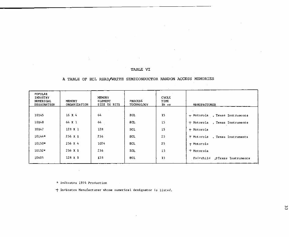
POPUIAR INDUSTRY NUMERICAL DESIGNATION
10145
10148
10147
10144*
10150*
10152*
10405
TABLE VI
A TABLE OF ECL READ/WRITE SEMICONDUCTOR RANDOM ACCESS MEMORIES
MEMORY CYCLE MEMORY ELEMENT PROCESS TIME ORGANIZATION SIZE IN BITS TECHNOLOGY IN ns MANUFACTURER
16 X 4 64 ECL 15 T Motorola , Texas Instruments
64 X 1 64 ECL 15 I Motorola , Texas Instruments
128 x 1 128 ECL 15 T Motorola
256 x 1 256 ECL 25 T Motorola , Texas Instruments
256 X 4 1024 ECL 25 t Motorola
256 x 1 256 ECL 15 T Motorola
128 x l 128 ECL 15 Fairchild ;tTexas Instruments
* Indicates 1974 Production
-t Indicates Manufacturer whose numerical designator is listed.
w w
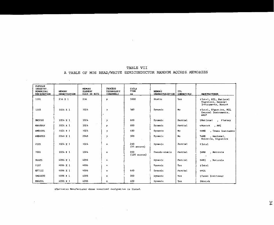
TABLE VII A TABLE OF MOS READ/WRITE SEMICONDUCTOR RANDOM ACCESS MEMORIES
POPULAR INDUSTRY MEMORY PROCESS CYCLE NUMERICAL MEMORY ELEMENT TECHNOLOGY TIME MEMORY TTL DESIGNATION ORGANIZATION SIGN IN BITS (CHANNEL) ns CHARACTERISTICS COMPATIBLE MANUFACTURER
1101 256 X l 256 p 1000 Static Yes tintel, MIL, National Signetics, General Instruments, Mostek
1103 1024 X l 1024 p 560 Dynamic No tintel, Signetics, MIL General Instruments, AMI*
Jotl5260 1024 X l 1024 p 680 Dynamic Partial tNational . Plursey
MK4006P 1024 X 1 1024 p 680 Dynamic Partial -tMostek , AMI
AMS6001 1024 X l 1024 p 480 Dynamic No '!"AMS , Texas Instrument
AMS6003 2048 X l 2048 p 500 Dynamic No TAMS , National, Motorola, Signetics
2105 1024 X 1 1024 n 200 Dynamic Partial tintel (95 access)
7001 1024 X l 1024 n 200 Pseudo-static Partial tAMS , Motorola (100 access) -
86605 4096 X l 4096 n Dynamic Partial tAMI , Motorola
2107 4096 x l 4096 n Dynamic Yes tintel
MF7112 4096 x 1 4096 n 680 Dynamic Partial tMIL
TMS4030 4096 x l 4096 n 500 Dynamic Yes tTexas Instrument
MK4096 4096 X l 4096 n 400 Dynamic Yes tMostek
tlndicates Manufacturer whose numerical designation is listed.
CHAPTER III
METHODS OF DEVELOPING THE MEMORY INTERFACE LOGIC
Introduction
Chapter Summarr·
The major portion Q:f the .text is developed in this chapter. Chapter
III considers the adaptation of the memory.tiwing requirements to those
of the processors. Discussed are two methods of interfacing the proces
sors master clock, address, and data registers to those of the memory.
Also developed, are the dynamic memory (MF 7112) refresh interface
requirements considering the four possible operating modes of a processor.
The final interface network considered is the gene~tion of the WRITE
strobe.in relation to the processors and memory timing.
Types of Interfaces
The timing between the control unit and the memory can be either
asynchronous . or synchronous. Th.e memory interface logic must be designed
dependent,on this timing. Most process~rs operate synchronously as a
mutually chosen time per~od does not have to be arrived at. For this
reason, this discussion will be directed towa,rds. the synchronous
operation •.
There are many.ways to develop the interface logic tiwing. Much
depends on the operation of the control unit and the .needs of the memory.
35
36
storage IC. The interface logic can be divided into three separate
sections, each related and dependent,on the other for operation. These
sections.are the: (1) timing, development of memory clock pulses; (2)
the dynamic memories refresh logic; and (3) the WRITE strobe synchrqniza-
tion logic.
Timing Methods
For a static .Read/Write memory.IC, interface logic is not required
unless it is operated asynchronously.
For a dynamic Read/Write memory IC, the adaptation to a processor is
much more complex, requiring the interface logic described in the pre,
ceding paragraph.
The most logical place.to begin the design of the memory interface
logic is ,in the timing area. There are two methods of deve~oping the
clock pulses that are practical and economical for industrial use. The
first method is the familiar ring counter and counter decode system. The·
seco~d me~hod is the more economical of the two but not as reliable or
accurate. This is the monostable multivibrator method. In this method
the monostable multivibra~ors are series one.,after the .other to generate
memory clock pulses using signals and master clock from the Control and
Arithmatic units.
The ring counter is used because of its accuracy. and low cost.
Pulse generation i~ done with a minimum of m~terial; however, in order to
have logical resolution, a master clock m~st be provided that, by rule.of
thumb, has a frequency that is eight (8) times.the memories cycle time.
This restriction makes the ring counter unsuitable for some applications.
such as battery operation after power is turned off,
37
On the ot~er hand, the series multivibrator is often used in appli
cations.where the ring counter m~thod is found to be undesirable. The
multivibrator can operate from a low frequency processor master clock and
still generate all of the necessary timing pulses and strobes. However,
the multivibrator method can not operate at frequencies above five (5)
megahertz in this type of application becau$e of the ·extre~ely large
minimum to maximum pulse width shifts caused by susceptibility to envi
ronmen.tal, and power supply changes. Also, the multi vibrator is
s4sceptible to large variations from one device to another. Th~ multi
vibrator also has the worst susceptibility .to noise transients of the two
methods~
Both methods are presented in the following sections and must be
chosen depending on the application and memory.storage IC. For these
examples, the MF 7112 Read/Write random access memory is used. The
timing is developed in accordance to the problem definition of Chapter
II.
The Ring Counter
Choice .of the Logic Clock Period
Examining the timing diagram of Chapter II shows that the system
requirements for both a Read Cycle and~ Write Cycle is approximately
2.2 microseconds. The Read/Write IC. itse.lf is capable ,of a 490 nano
second read cycle and a 680 nanosecond write cycle. Further, the basic
clock fl:'equ~ncy of.the system is one (1) megahertz. The first decision
to he made is deciding what frequency to operate the memory cycle.
The requirement is to make a compromise between memory performance
and system requirements, comparing the.system clock frequency with the
38
Read/Write IC memory performance. The most obvious cycle period would be
one (1) megahertz. This means that the Read/Write IC will be operating
at a cycle time less than its rating, and the system access and cycle
time requirements are met. Figure 14, is the generalized timing diagram
of the system and memory IC.
In general the system almost.always di~tates the memory access and
cycle times. A:ny design would have to consider the system's requirements
with the memory element's capability.
Implementing~ Ring Counter Design
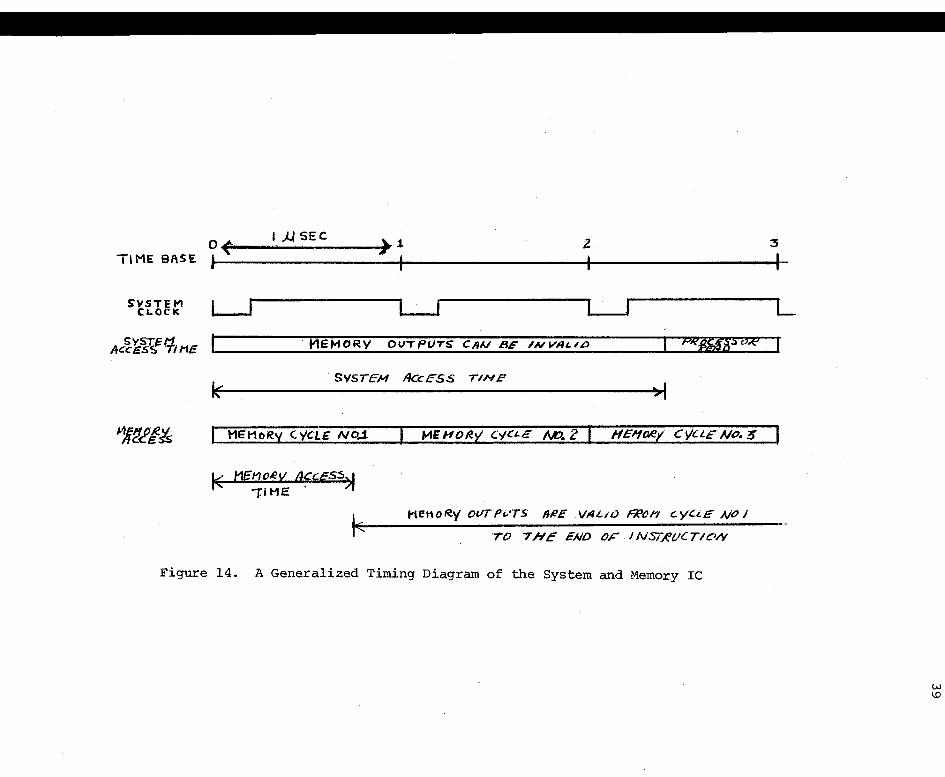
A block diagram of the desired function is shown in Figure 15. A
crystal controlled oscillator is used to generate bo\h the system and
memory timing. A count down circuit is used to generate the one (1)
megahertz system clo~k, while the ring c~unt~r clock comes from the 8
megahertz osctllator.
The state equation for the shift counter can be written as
An (T) = "1-l (P) (1)
The equation Js interprete4 as: the state of the nth flip-flop of
the register, following a clock interval, is the state, of the (n-l)st
flip-flop occurring at clock pulse P.
The register is connected with the flip flop A8 output feeding back
to the input of flip flop A1 in the manner of a, circulating register such
that the input of flip flop A1 is dependent on the output of A8.
In order to initialize the register to the prope~ state during powe:i;
turn-on a power-on state is connected to the parallel input of the
register. The parallel input of the register is set such that all inputs
0 -.<3--'-J.f_s_e_c __ ~) 1 TIME 81\SE
SYSTEM LJ t i CLOCK 1----J
2
SYSTEM fkceSS T/HJ:
'>I
l MEHoRy CYCLE NO~
t( 11{:"no.ev O~c:gss~ ""'fiHE
I< t1ft\oRy 01/TPt..'TS /1~£ .'VALii) FRon c.yC.Lc lt/0 I
·ro 7HE E/1/D OJ='. I NST~(JCTION
Figure 14. A Generalized Timing Diagram of the System and Memory IC
3
L
w \.D
p
8 MHZ PULSE DIVIDE . SYSTEM CLOCK 1 MU.,. osc .... SHAPER BY 8 . , > •
A ~=~ r,r ~-.,
SYST EM RESET - - -
I 1 l 1 ....
I I , > •
POWER ON - Al A2 A3 A4 A5 A6 A7 Aa RESET -
l l 1 J J l I
~ -
•• ,. ,. , ,. • • ,.,. , I,
DECODE LOGIC
WRITE= A7lp\ .... ,
C CARD CONNECTOR ~>- READ = Ai; o A,::;(P) .. ,
PRECHARGE. = Al• A2 o AJ {.P ,
CENABLE = A,• A2 • A3 (P) .. ,
Figure 15. A Block Diagram of the Ring Counter Including Decoding
~ 0
41
are at a ground potential except flip flop A1• When the power-on state
returns to the operating state, the inputs of flip flop A1 are such that
the start bit appears on the output of A1 and is shifted through the
register at a 8 megahertz rate until _the bit. appears on the output of
flip flop A8• The bit is then recirculat:ed back to flip flop A1 and the
cycle started over again. The eq~ation for the register is written as
A (t) = (A 1)P + C n · n- (2)
where C is the clearing pulse re~ulting from the power-on initialization •.
Decoding the Clock Pulses From the Register ·
The three clock pulses required by the MF 7112 are derived from the
register by deco4ing the output of the register. Examining the MF 7112
timing diagram from Chapter II, the equations . .for the' clock pulses are
written al?
Precharge = A1(P} • A2(P) • A3(P) (3)
(4)
Cenable = A1 (P) • A2 (P) • A3(P) (5)
A fourth pulse is also required. This pulse will be called, End of
Cycle, and will be defined later in this chapter under the sub-title of
Refresh. The pulse is defined. in equation form as
End of Cycle= A8 (P) (6)
The delay between the Precharge pulse and the Read pulse required by the
MF 7112, is guaranteed by the clock delay of A4.
42
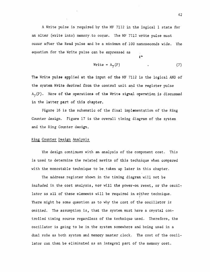
A Write pulse is required by the MF 7112 in the logical 1 state for
an alter (write into) memory,to oc~ur. The MF 7112 write pulse must
occur after the Read pulse and be a minimum of.100 nanoseconds wide, The
equation for the Write pulse can be expressed as
Write= A7(P) (7)
The Write pulse applied at the input of the MF 7112 is the logical AND of
t~e system Write derived from the control unit and the register pulse
A7(P). More of the ,operations of the Write sign9:l operation is discussed
in.the latte~ part of this chapter.
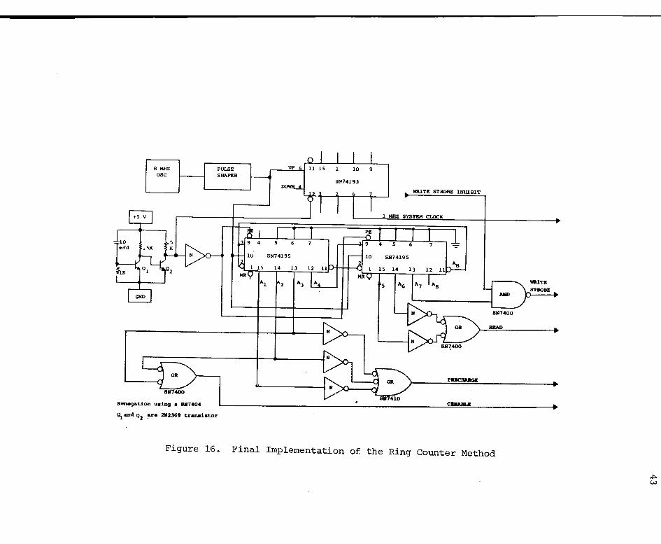
Figure 16 is the schematic .of tbe final implementation of tbe Ring
Counter design. Figure 17 is the overall timing diagram of the system
and the Ring Counter design.
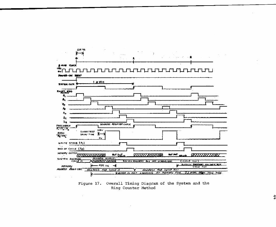
Ring Counter Design Analysis
The design continues with an analysis of the component cost, This
is used to determine the related merits of this technique,when compared
with the monostable technique to be,taken up later in this chapter.
The address register shown in the timing diagram will not be
included in the cost analysis, nor will the power-on rese~, or the oscil"'.'
lator as .all of these elements will be required in e~ther technique . . There might be some question as to why the cost of the oscillator is
omitted. The assumptio;n is; that the system must have a crystal con-
trolled timing source regardless of the technique used. Therefore, the
oscilfator i~ going to be in. the system somewhe:r;e and being used in a
dual role as both system and memory master clock. The cost of the oscil-
lator can then be eliminated as an integral part.of the memory cost,
8 MHZ osc
111..,egation uaing a 8117404
PULSE SHAPER
°i and o2 ar• 2112369 tranlliator
10 9
SN74193
WRITE STROBE INHIBIT
l MHZ SYSTEM CLOCK
5 6
SN74195
14 13 12 11
61117400
Figure 16. Final Implementation of the Ring Counter Method
WIUTE STROBE
1.
,.,..-CIN maT r1---------.-µ-st:.--c--------------u----------------------------------~ S)S'l'M OCCI( k 1'I
S~lllt ~:.:_____r--,~----------------~ .... i--.,__ ___________________ r--i~--~-11:i. r, r--, r....._ __ '"3 ri r, r. .... __ % Aa,
WRITE STR08 rA7)
-a,;c:. tJF CYCLE (Ag).
....._ __ , .--i~----~~--~----~--'r--I~------------------
r,: r---i~~~~~---V4ttllPfflllmf mur,-r KIWI v/llUWMW
Figure 17. Overall Timing Diagram of the System and the Ring Counter Method
45
TABLE VIII
SUMMARIZING THE COST OF THE RING COUNTER
COMPONENT FUNCTION QUANTITY COST
SN74193 COUNTER 1 $1.25 SN74195 SHIFT REGISTER 2 $1.50 SN7404 HEX INVERTER 1 $0.25 SN75361 AND GATE, HIGH 2 $4.00
VOLTAGE SN7400 2 INPUT AND GATE 1 $0.25 SN7410 3 INPUT AND GATE 1 $0.25 2N2369 TRANSISTOR 2 $0.50 RESISTOR 1/4 WATT 3 $0.15 CAPACITOR 10 MICROFARAD 1 $0.25
TOTAL $8.40
46
Timing Generation With Monostable Multivibrators
General
One of the simplest.and least expensive methods of developing
pulses, such a$ the MF 7112 memory IC requires, is to use monostable.
multivibrators (one-shots). However, the penality of simplicity is the
danger of false triggering and large tolerance variations. A large
amount of attention .must.be paid to the printed circuit, board layout
design and to power.supply filtering and individual IC decoupling to
avoid these undesirable effects. Monolithic monostables prove to be
attractive both from a.physical area and cost effectiveness. Such mono
stables as the single element 9601, or the dual element (two in a dual·
in-.line pac~age) 9602, are suitable for design. Both of these devices
are. similar in operation and performance. Pulse width tolerances for
wors~ case design analysis should be considered as:!:. 25 per cent~ This
accounts for individual device to.device substitution, 5 per cent power
supply variations, and temperature variations of O degree centigrade to
70 degree centigrade.
Both the 9601 and the 9602 multivibrators are edge triggering
devices. and are therefore particularly subject to false triggering from
such phen~me~a as inductive input signal ringing and power sµpply noise.
A great deal of care in printed circuit layout.and component placement
must be exercised to prevent undesirable input triggering. Rise and fall
times of input signals must be controlled to prevent the monostable from
assUll).ing the cq.aracteristics of a high gain amplifier with a 180 degree
phase shift. This can occur when a TTL device is transitioning in.the
active threshold region lying between a logical."!" and "0". With a slow
47
rise or fall time (1 millisecond or greater) from the preceding driving
stage~ the monostable could act as an amplifier. With a long enough time
period for the input transition, the monostable will begin to oscillate.
Considering Refresh
Using the previous criteria that a refresh cycle amounts to a
memory "Read" cycle with an invalid output, makes the design of the
memory timing requirement somewhat simpler. The only requirement of the
refresh initialization pulse is that the series of monostables are prop
erly triggered such that a normal Read memory cycle occurs when refresh
is commanded, More on refresh will be discussed later in this section
after the memory clocks are developed.
Clock Pulses
The same memory timing for a Read and Write cycle used in the shift
register ring counter design is valid when using the monostable, Repeat
ing these conditions in equation form again for convenience,
Precharge = A1(P) • A2(P) • A3(P) .::_ 300 ns
Read = As (P) • A6 (P) .::_ 180 ns
Write= A7(P)
Cenable = A1 (P) • A2 (P) • A3 (P) > 200 ns
(8)
(9)
(10)
(11)
The monostable design now produces the pulses previously accounted for by
decoding the ring counter.
The equations for pulse width requirements using monostables can be
rewritten as
48
Pre charge = t 1 (PW1) (12)
Read = t3 (PW2) (13)
Write= t 4 (PW3) (14)
Cenable = t. (PW ) 5 4 (15)
Defining PW as pulse width, and tn as time one, two, etc., the equations
read as
Precharge is equal to pulse width 1 at time t 1 of
the shift register, ring counter timing,
Address Regi~ter
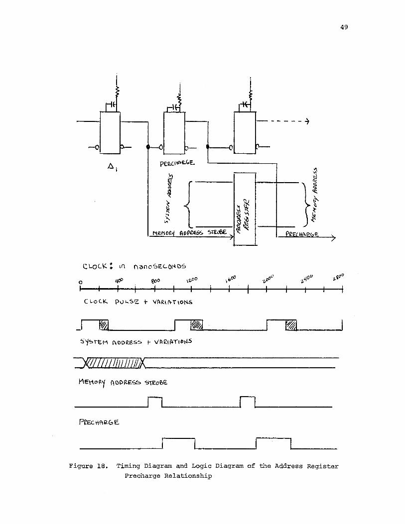
Referring to Figure 18, an address register pulse is caused to occur
at the initial edge of the precharge pulse, This timing must now, be-
cause of the monostable approach, be accomplished differently than the
ring counter to insure that the address does not change during the pre-
charge clock. It is also essential that the address.change on the memory
subsystem level occurs synchronously with the other memory.timing, Ob-
serving the timing diagram of the memory Read cycle (Chapter II) it will
be noted that the LSI processor.used as the example model, has a minimum
address.register true time .to the address bus of 15 nanoseconds and a
maximum of 685 n~oseconds, Th~ maxinuim propagation delay of the address.
register is the cause for the address register on the memory sub"'.'system
.level, More on the implementation of the memory address register .will be
discussed later in this section,
49
·------~
-o
>
<.: LOC. \( : \(\ ri anoSE.C.01"- cs
0 ~ ec,o rz-oo 1iPoO vi'(} ·1,
i400 if Po
I I I I I j
C 1.0 C.K Pvi...SE +- VI\~\ f>t. T lOl'lS
_I .wi
-::k/l701li11!///!JX __ -----------
___________ r-i ____________ nl--________ __
Figure 18. Timing Diagram and Logic Diagram of the Address Register Precharge Relationship
50
Desired Timing
Before proceeding further, the sequence of events on a time basis
needs to .be defined. For an instruction that connnands memory.fetch
(Read) a Read Cycle is desired. For an instruction that connnands a
memory alter, a Write Cycle is desired. The combination of processor
central clock, change of address, and data register changes in conjunc
tion with memory timing requirements.are shown in Figure 19, This figure
sunnnarizes the timing relat:ionships between system and memory sub-system,
Each of the one megahertz increments of the master central clock must be
examined. Figure 20 represents an example of one clock period and what
transpires in that period,
Two timing points that require special attention are at time t 0 and
tf of Figure 20, This is when the address change occurs for any instruc
tion. Care must be taken that the address from the control unit does not
ch~nge in the time. frame of the precharge pulse, This is an additional
requirement from those described under Address Register. Once again, the
addition of the memory sub-system address register will prevent any
undesirable address changes due to element propagation times.
Add,itional care must also be exercised when the refresh address is
switched into the memory address bus. This is discussed in this chapter
under Refresh.
Implementing the Logic Equations
The basic series of monostable logic can now be implemented using
Equations 12 through 15. Shown in Figure 21 is the implementation of
Equations 12 through 15 using series monostable multivibrators,
The timing pulse and delay generation are implemented using seven
MAS7£A! CLtX:.K
INS,Rucr,01,;
Jiii> OJe/!'55 R£GISTE~
llllllllllillltfflLIIIIJl\i\lt•l11llLJLlllllllllllliltttllllfllfllltlll to t...f I
INSTRUCTION n n+1 111-.l-Slli?UCf lO '-! I'\.+ 2.
X ... _A_oc_R_e_s_s_n ___ .... X __ Ao_· _"_~_e_ss __ n_+_, _______ _,x l!PoRESS nn. t ,"Ror:e.ssc;e READ ~w:STORE l11HEOlATE (wRliE) READ 5Tft7VS ~,(~~~~~~~7~~:--~~~~~~~~~~4,*''~,~~~~~~
F'ROCEsso.e W~i"Te 57/c!IJ!,£'
Figure 19. Processor Instruction Level Timing Diagram
-
J _ftSEC
~ ADDRess n
W~ltE
E'NO 01=" C•i( LE ---~~~~~~~~~,--,.__~~~
CfNABLE
Figure 20. Timing Diagram of the Memory Level Signals
R
one one Timing shot shot
Pulse In ut
Figure 21.
+SV
R cff c T c T c
one one one one shot shot shot shot
Schematic of the Basic Monostable Design
End-of-Cycle
Write Strobe
Read
Pre charge
lJ1 w
54
monostable multi vibrators. each sequentially triggering the following
stage. The pulse widths are assigned to each monostable that satisfies
both the processor's memory access and cycle requirements, yet is compat~
ible with the Read/Write MF 7112 memory element. A worst case design is
started by first assigning nominal pulse widths and then applying the
.!. 25 per cent tolerance for minimum and maximum worst case timing
analysis, Referring to Chapter II, the minimum timing requirements of
the MF 7112 are listed in Table IX.
The pulse widths and delays listed in Table X summarizes the mini
mum, nominal and maximum pulse widths to be expected from the monostables
when the .!. 25 per cent tolerances are applied. Table X was derived by
first using the minimum timing requirements listed in Table IX, and then
increasing this value by 25 per cent. The maximum value was derived from
the nominal value in the same manner.
A memory cycle is expressed by
Memory Cycle= PW1 + ~ 2 + PW2 + PW3 + PW6
Using the values of Table X
Minimum Cycle Time= 730 nanoseconds
Nominal Cycle Time= 975 nanoseconds
Maximum Cycle Time= 1220 nanoseconds
(16)
A memory cycle for the system is defined in Chapter II as 2.2 micro
seconds, Therefore, the limitations.of the maximum cycle is within the
system requirements.
Mentioned at the beginning of this chapter was a caution statement
referring to the refresh cycle, To qualify this, one needs to refer to
SIGNAL NAME
Pre charge
6.2
Cenable
Read
Write
6.3
TABLE IX
MINIMUM MEMORY PULSE WIDTHS OF THE MONOSTABLE MULTIVIBRATOR
PULSE NAME
t 1 (PW1 )
delay 2
t2 (PW2)
t3 (PW3)
t4 (PW4)
delay 3
End of Cycle t 5 (PW5 )
55
PULSE WIDTH inns
300
100
200
180
100
100
125
SIGNAL NAME
Pre charge
Delay Between Precharge and Read
Cenable Delay
Cenable Width
Read
Write
End of Cycle
TABLE X
MONOSTABLE PULSE VARIATIONS
MINIMUM PULSE NOMINAL PULSE PULSE WIDTH WIDTH IN ns WIDTH IN ns
PW! 300 400
6.2 100 134
6.3 100 134
PW2 210 280
PW3 180 240
PW4 100 134
PW5 50 67
MAXIMUM PULSE WIDTH IN ns
500
168
168
350
300
168
84
u, O'I
57
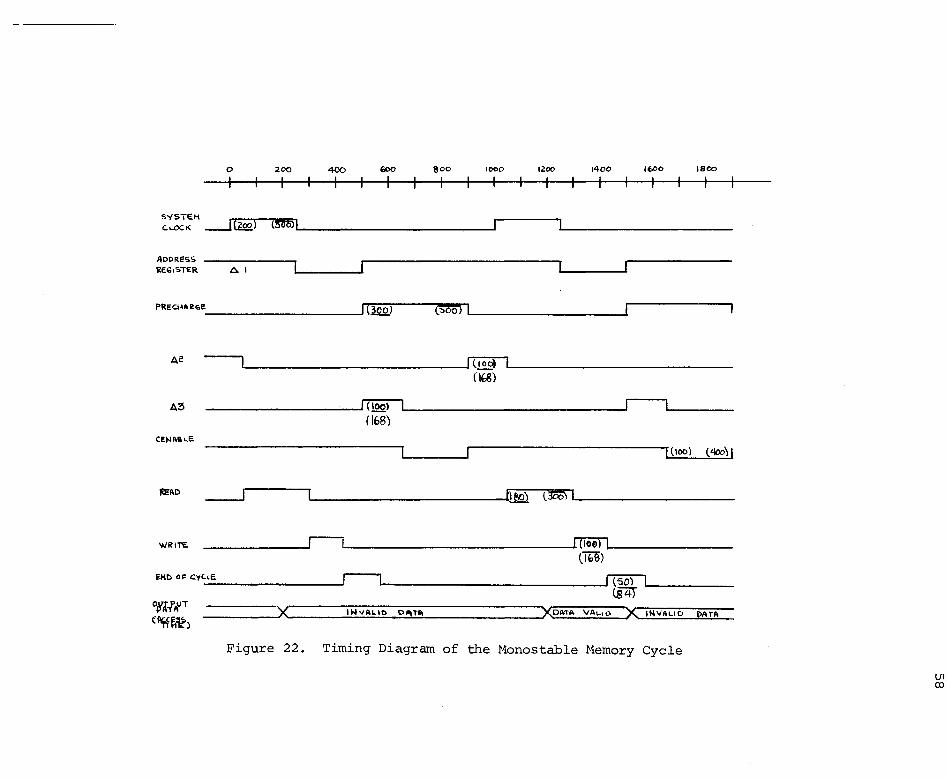
the latter part of this chapter; however, notice that in .the monostable
timing diagram of Figure 22, the End of Cycle pulse resets the refresh
line which in turn changes the address multiplexer from a refresh address
back to the system address, The prob.lem area to avoid is when a cycle
time is at a maximum and the End of Cycle leading edge.occurs after the
address register changes, With an End of Cycle pulse occurring after the
MF 7112 memory elements address ·for the next cycle, the change will occur.
during the Precharge pulse, One must insure tha~ this does not happen
for data can .. then be transferred internally from cell to cel.l within the
MF 7112,
Figure 23.is the final schematic .of the monostable multivibrator.
one-shot design.
The Memory Refresh Logic
The Need for Refresh. --- .
Many methods of.resupplying energy to a MOS dynamic Read/Write
m~mory have been suggested. In all cases the purpose of the resupplied
energy is to keep a capacitive node charged to.the logic state intended
when the memory was last altered, The name giyen to this resupply of
energy is "The Refresh Cycle". Chapter_! briefly discussed one.method of
internally refreshing the storage node for a two phase device. Other
methods are.used for single and three phase-devices. In any event, the.
internal mechanism that implements refresh is not usually of great con,
cern to the system memory designer. The concern lies in the method
external to the memory IC. Some of the questions that_arise are: Is
refresh executed synchronously II or asynch:r:on011sly? How· often must the.
memory element be refreshed? What corn~ti tut es a refr.esh cycle? The
0 200 400 EOO eoo 1000 1200 1400 lt,00 1800
I I I
SYSTEM C.l..()CI( __j~j <ffi>I
ADDRESS ~E6\<;,TER b. I
PRea-;~11.GE 1(1W (:,oo> I
Ae --, I (1ool I (lf,8)
A:3 (loo)
( 168) Cil-11\IILc
1(100) (400) I
!ilmO __J hlci lSI
WR \TI:. r, ((1001 I (iW)
i;MI) o F cyc,a II ITTon @IT
0~U,r x lloJV"'I.ID o,1n111 <Plij~)
xo,..,11 VAL1 I) x IJ.lVALIO PATA
Figure 22. Timing Diagram of the Monostable Memory Cycle
Ul OJ
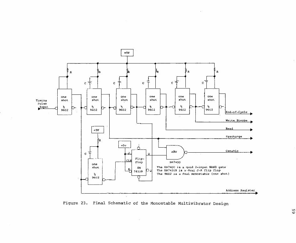
R
c
one Timing shot
Pulse In ut !:.;
9602
c
Figure 23.
J_ c
one shot
!:.; 9602
+SV
R
one shot
!:.; 9602
+sv
T one shot
!:.; 9602
+5v
c
FlipFlop
SN 74109
T one shot
!:.; 9602
Q
Q
c
one shot
!:.; 9602
SN7400
R
one shot
!:.; 9602
The SN7400 is a quad 2-input NAND gate The SN74109 is a·dual J-K flip flop
End-of-Cycle
Write Strobe
Read
Pre charge
Cenable
The 9602 is a dual monostable (one shot)
Address Register
Final Schematic of the Monostable Multivibrator Design
Ul \.0
60
answers to these questions and others are found in the .type of processor
and the choice of memory element. In the case of the example LSI
processor and the example Read/Write random access memory IC, the MF 7112,
the.refresh mechanism was designed into the processor anticipating a need
to use a dynamic memory element. Such niay not be the case for other
processor applications. Therefore, other means of mechanizing refresh
are available.
The design engineer wants to weigh careful!)' the choice between
advantages of a dynamic and a static Read/Write memory element.· One of
the biggest advantages of the static memory is its independence of a
refresh signal •. Because of the basic flip-flop design the static memory
does not require refreshing.
The remaining porti9n of this section is .devoted to guiding the.
engineer through a worst case design of a synchrqnous refresh cycle using
the exail).ple ,processor and the MF. 7112 memory IC. However, bec.ause this
design is indicative of only one type of ·refresh method other types of
refreshing will be explained also, but.will not be designed into the
example problem.
Types of Refresh
There are four methods of refr~shing the memory element that are in
use today: .
1) a charge pump refresh;
2) a continuous access refresh;
3) a planar refresh; and
4) a processor co~trolled refresh.
The example design to follow will be the Processor Controlled
61
Refresh. The Processor Controlled Refresh was chosen because it is the
more difficult of the four methods to implement. Each of the three other
methods is an adaptation of the Processor Controlled Refresh.
Before continuing with the design aspects, the four refresh methods
will be examined on a device level, ·
The theory of the Charge Pump was developed in the General Electric
research laboratories in the late l960 1 s. However, the technique was
never applied to production memories until the development by American
Memory System (AMS) in 1972. The first memory product is now entering
tl).e market place in the fall of 1973 and is designated the AM~ 7001.
The Charge Pump in the true sense does not require a refresh signal,
An asynchronous signal in the form of a sinusoidal, triangular, or square
wave is applied to the charge pump input of each memory IC. This is the
refresh mechanism and no other method of refreshing is required. Access
ing either in a Read or a Wr~te cycle is done completely independent of
the charge pump signal. Because of this, the charge pump method is the
easiest of the refreshing techniques to use. However, the disadvantages
of the charge pump refresh method lies in the physical size required to
make a storage celL Thus far, the processing techniques have restricted
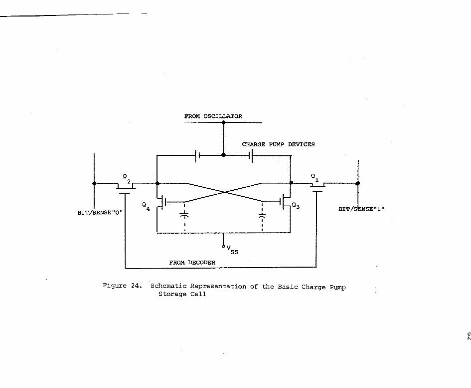
m~mory size to 1024 bits or less. Figure 24 is a schematic of the basic
charge pump and storage cell for one bit. Memory sizes of 4096 or larger
becomes prohibitive because of the large silicon area required.
It is doubtful that the charge pump method will be applied to memo
ries larger than 2048 bits because of the cell size limitations. How
ever, if a technological breakthrough does happen the charge pump method
is more attractive than other refreshing methods.
Each of the three remaining refresh methods occur during a pseudo
BIT/SENSE"O"
FROM OSCILLATOR
I CHARGE PUMP DEVICES
,------1 1----41-----tq,----..,.
FROM DECODER
v SS
Figure 24. Schematic Representation of the Basic Charge Pump Storage Cell
63
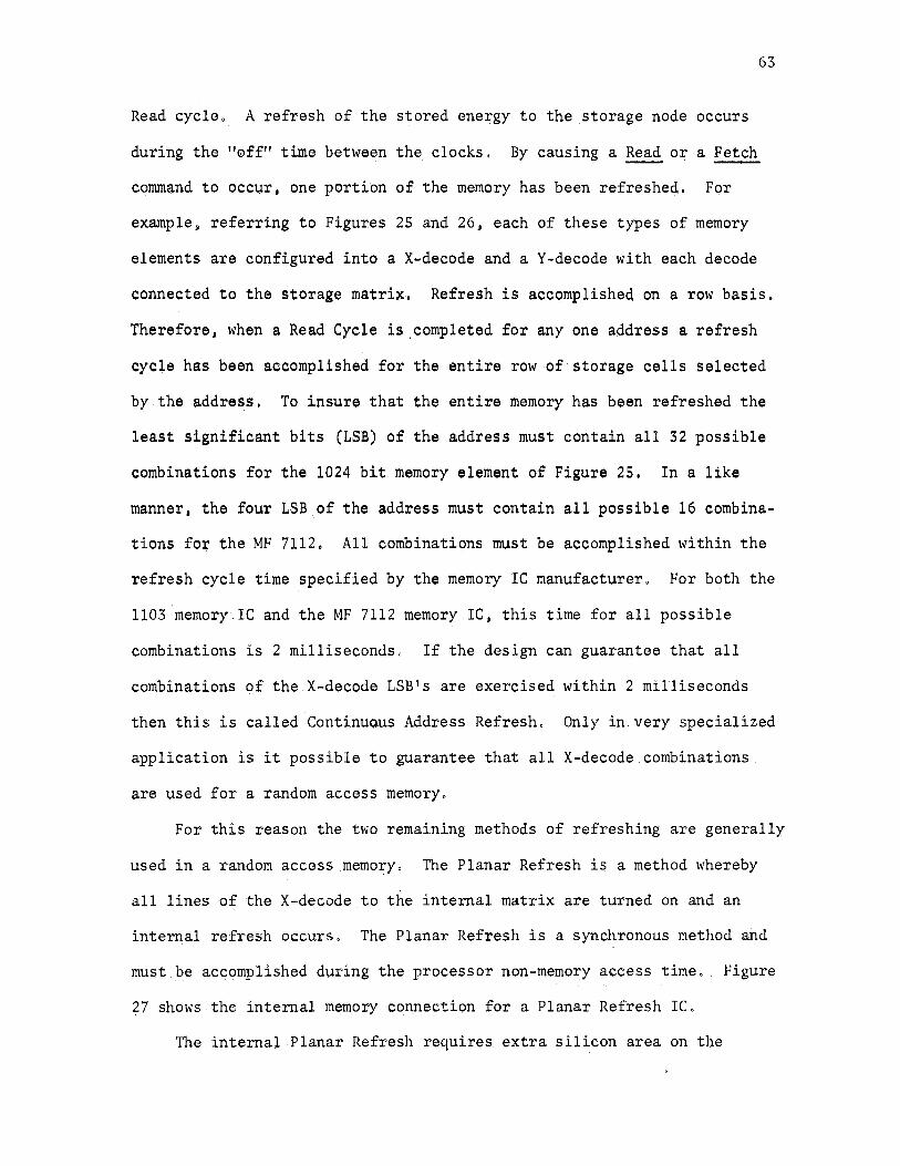
Read cycle. A refresh of the stored ene~gy to the .storage node occurs
during the 110ff11 time between the clocks •. By causing a Read or a Fetch
comm$nd to occ~r, one portibn of the memory has been refreshed. For
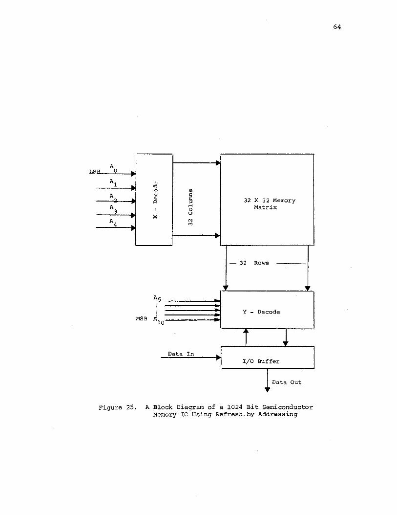
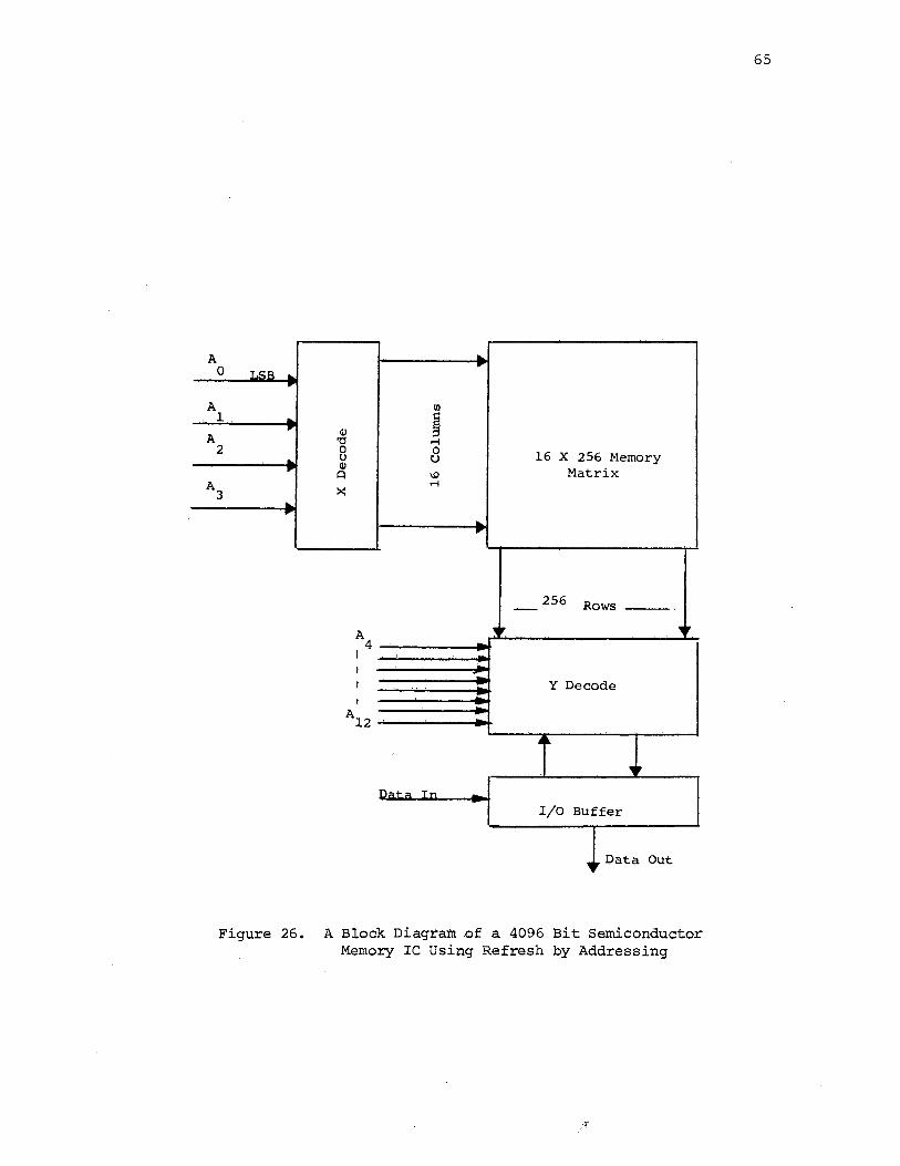
examplej referring to Figures 25 and 26, each of these types of memory
elements are configured into a X-decode and a Y-decode with each decode
connected to the storage matrix. Refresh is accomplished on a row basis.
Therefore, when a Read Cycle is .completed for any one address a refresh
cycle has been accomplished for the entire row -of storage cells selected
by.the addre~s. To insure that the entire memory has been refreshed the
least significant bits (LSB) of the address must contain all 32 possible
combinations for the 1024 bit memory element of Figure 25. In a like
manner, the four LSB_of the address must contain all possible 16 combina
tions fo~ the MF 7112. · All combinations must be accomplished within the
refresh cycle time specified by the memory IC manufacturer. For both the
1103 'me~ory.IC and the MF 7112 memory.IC, this time for all possible
combinations is 2 milliseconds, If the design can guarantee that all
combinations of the X-decode LSB's are exercised within 2 milliseconds
then this is called ContinuQus Address Refresh. Only in.very specialized
application is it possible to guarantee that all X-decode.combinations.
are used for a random access memory.
For this reason the two remaining methods of refreshing are generally
used in a random access memory. The Planar Refresh is a methods.whereby
all lines of the X-decode to the internal matrix are turned on and an
internal refresh occurs. The Planar Refresh is a synchronous method and
must be ac~omplished during the processor non-memory access time .. Figure
27 shows the internal memory connectipn for a Planar Refresh IC,
The internal Planar Refresh requires. extra sili.con area on the
.. A ...
:R LS 0 ... r
Al .. QI 'O
r 0 Ill
A t) m ~ ... QI 32 X 32 Memory r Q ::s A ...... Matrix
3 I 0 L u r ><
A4 N .. M ... .. ..
- 32 Rows
~. , . A5 -I -I Y - Decode
MSB d :: 10
' . l Data In .. .. I/0 Buffer
Data Out , I,
Figure 25. A Block Diagram of a 1024 Bit Semiconductor M~mory IC Using Refresh .. by Addressing
64
A ... 0
.. T.CIR .. ..
A Ill l .... i r- Q)
A 'ti ,-j
2 0 0 16 x 256 Memory ... u CJ Q) .. A IO Matrix
A3 >< ,-j
... ... .... ...
256 Rows -A P, 'II'
4 I I --i Y Decode I '' -
Al2 . '' -::-
0,
v n~._~ T,-, -
I/0 Buffer
'II' Data Out
Figure 26. A Block Diagram ~fa 4096 Bit Semiconductor Memory IC Using Refresh by Addressing
65
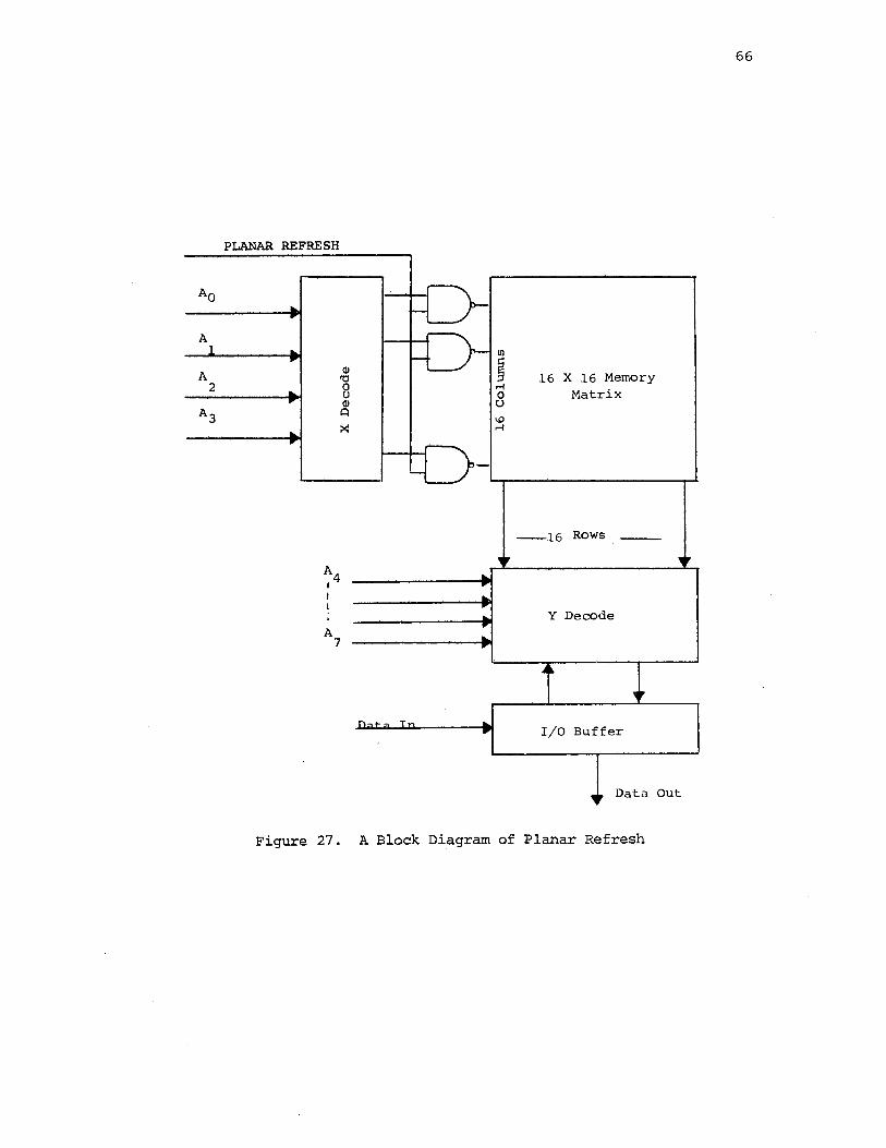
Ao
A
A 2
A3
PLANAR REFRESH
Q) 'O 0 0 Q) A
><
A4 I I I I I
A 7
Ill
~ ,-j
0 CJ
'° ,-j
16 X 16 Memory Matrix
--16 Rows __ _
Y Decode
I/0 Buffer
Data Out
Figure 27. A Block Diagram of Planar Refresh
66
67
memory die and is often left off the IC because of area restrictions.
However, this method is becoming quite pqpular and will probably replace
the refreshing through use of the .LSB address lines. Notice that for
applications that can.guarantee the Continuous Access Refresh method; the
Planar signal can be inhibited and the memory,refrt;)shed through the LSB,
X-decode address lines.
The final method of refresh utilizes a .. processor controlled refresh
signal that cauS(;)S a counter to update a refresh address each time the
control unit signifies that a refresh cycle is to take place. The pe~iod . . '
of refresh is generally .established based on the processor's instruction
time. Duration of the refresh is generally established as one period of
the processor central clock. This method is expanded in detail in the
following paragraphs.
OperatiI?,g Conditi.ons
Processor Operation
There are two operating conditions tha.t the designer must consider.
Th~ first of these is the condition the processor can assume during
normal operation. The second is the memory operating condition. These
conditions are reviewed below. Each of these conditions are. important
because they have a direct relation to the refresh interface c~rcuitry.
Any processor can have any, or all of these conditions. For the purpose
of this design exantple, it is assumed that.the LSI processor has all
possible operating conditions.· The four possible operating conditions
are:.
68
Condition IA, Nonnal Operationo This is the normal run condition of
the processor, The central clock is running uninhibited. Arithmetic and
control unit-indicate a non-halt conditiono
Condition_!!, Normal Operation, Refresh Requestedo This is the same
condition as IA except the control unit has determined that a refresh
condition exists during a particular instruction timeo
Condition.!..!.., Repair Mode, Condition II is a processor test mode_
primarily used for software debug or hardware repair, This condition is
a processor single instruction mode whereby the operator can step through
the instructions and execute one.instruction at a time.
The memory design must account for this mode, An ex~ernal signal
(Halt) originating from the control unit becomes active and the Refresh
signal becomes inactive by virtue of the processor being halted. These
are the operations that occur:
1) the central clock is running as if the processor is in the
normal operating mode (Condition I);
2) the Refresh signal becomes inactive, a low logical state;
3) a Halt signal is activated by the control unit, The purpose of
this signal line is to indicate that the processor has halted operation,
During the single instruction, the Halt signal indicates the processor
has returned to Condition I for the duration of the instructiono
Condition I II, Microprogramming LeveL Condition II I allows the
operator to select an even lower level of processor control by allowing
the central clock to be stopped and the processor to be controlled by a
single clock.mode on a micro-instruction level,
A single clock mode is difficult for a.semiconductor memory to
69
maintain the stored data because none of the essential interface signals
from the control unit are now operative. With the central clock stopped
n.either of the two timing methods described in th~ beginning of this
chapter will operate. Therefore,, a speciai set of logic must be include4
to meet the mel\lories timin~,and rE:lfresh needs and still operate·in a
single clock mode~ Activation of the clock is assumed to be arbitrary
depending on the desires of the.operator, The special method of working
with the, single clock for this design example ·will be to gate the clock.
and detect a clock activation when the processor is in Condition III .•
Figure 28 represents one method that can be used to gate the clock.for
single clock operation .. Also included in Figure 28 is .a brief timing
diagram of the operation.
The opera~ing conditions that can now be assumed are:
1) the ungated clo~k operating normally;
2) the gated clock is a single pulse as shown in Figure 28;
3) the Halt. signal in. relatio'.\1, to the gated clock is a pulse as
shown in Figure .28; and
4) the processor Refresh signal will remain inactive.
Cond.i tion _!!, Power-Off State, Memory ~ Retain ~· Condition IV
is the power-off/battery operation mode. The condition required for the
logic is to constantly refresh the memory within the maximum allowable
time as allowed.by the memory manufacturer. All processor signal leads
must be in a high impedance state. The central master clock.is not
available in this mode, Power.is supplied from batteries. Refresh is
initiated from a source powered separately from the,processor.
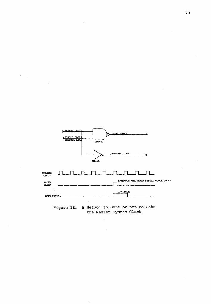
UNGATED CLOCK
GATED CLOCK
UNGATED CLOCK
SN7404
OPJmATOR ACTIVATED SINGLE CLOCK PULSE
ljJSECOND
Figure 28. A Method to Gate or not to Gate the Master System Clock
70
71
Memory Element Operation
The previous .discussion centered about the proces~or operating con- ..
ditions. This section describes what conditions a memory must assume
regardless of the processor's condition.
A dynamic IC Read/Write memory will require refreshing. The MF,7112
is a dynamic memory,element requiring regreshing with 2 milliseconds for
the entire me!OOry matrix. The MF 7112 can,be refreshed using either the
processor controlled or the con~inuous address refresh method .. The
o~ganization of the MF 7112 was reviewed previously and shown in Figure
26. The memory requires the least four significant bits of the address
register to completely refresh the memory matrix. One,of the simplest
methods,to address all posstbilitie~ is to sequentially progress through
.each binary possibility. Table XI represents the necessary address at
refresh time t.
As discussed in this chapte~ under Tn>es of Refresh, each refresh
cycle is a pseudo Read.cycle, but the address is pointed to one of the.
refresh addresses shown in Table.XI.
Regardless of processor operating conditions, or other factors, the
memory must.be refreshed in accordance with the inequality
t 0 + t 1 + t 2 + ••• + t 14 + t 15 < 2.0 milliseconds (17)
The refresh cycles are then repeated in accordance with the inequality or
s~ored memory data will be in error.
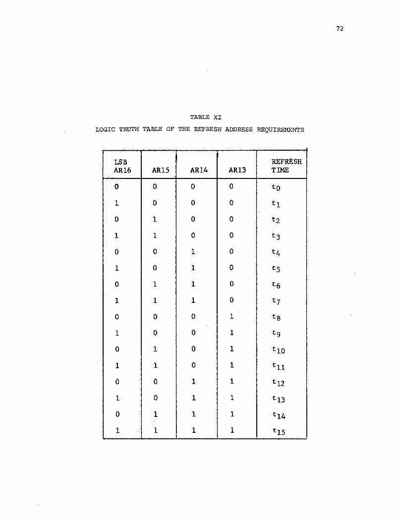
72
TABLE XI
LOGIC TRUTH TABLE OF THE REFRESH ADDRESS REQUIREMENTS
I.SB REFRESH AR16 AR15 AR14 AR13 TIME
0 0 0 0 to
1 0 0 0 t1
0 1 0 0 t2
1 1 0 0 t3
0 0 1 0 t4
1 0 1 0 t5
0 1 1 0 t6
1 1 1 0 t7
0 0 0 1 ts
1 0 0 1 t9
0 1 0 1 t10
1 1 0 1 :t:11
0 0 1 1 t12
1 0 1 1 t13
0 1 1 1 t14
1 1 1 1 t15
73
Implementing the Processor Controlled Refresh
Requirements Review
The requirements of the processor are: (1) provide a synchronous
refresh signal to the memory interface logi<:r for each instruction period;
(2) provide the memory interface logic a signal indicating a Halt condi
tion; (3) supply a gated and ungated clock to distinguish between a
single instruction .and a.single clock condition, In addition to the
three preceding requirements, which can be called the Processor Refresh
Requirements (PRR) the control unit must provide the normal address,
data, and Write control signals, Figure 29 represents a block diagram of
the PRR,
The interface logic insures that refresh occurs properly without
interfering with. the normal function of the memory. The interface logic ..
must also operate under any of the four processor operating conditions,
Realizing the Refresh Addressing
The first task is to design the logic that transmits the address
register contents to the.memory, but replaces the refresh address for the
instruction .address at Refresh.time as indicated by the control unit,
Two logical functions must be accounted for: (1) a means of substituting
the control units address register contents with a refresh address and,
(2) a means of generating the refresh address and updating this address
on command from the control unit,
Remembering that the refresh address operates on the 4 LSB of
address (the X-decbde.inputs of.the MF 7112) a modulo 16, 4 bit, up
counter wquld accomplish the desired refr~sh address generation, To
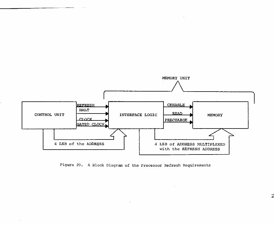
MEMORY UNIT
rr---___ /\ _____ l CENABLE
CONTROL UNIT
GATED CLOCK
4 LSB of the ADDRESS
INTERFACE LOGIC MEMORY
4 LSB of ADDRESS MULTIPLEXED with the REFRESH ADDRESS
Figure 29. A Block Diagram of the Processor Refresh Requirements
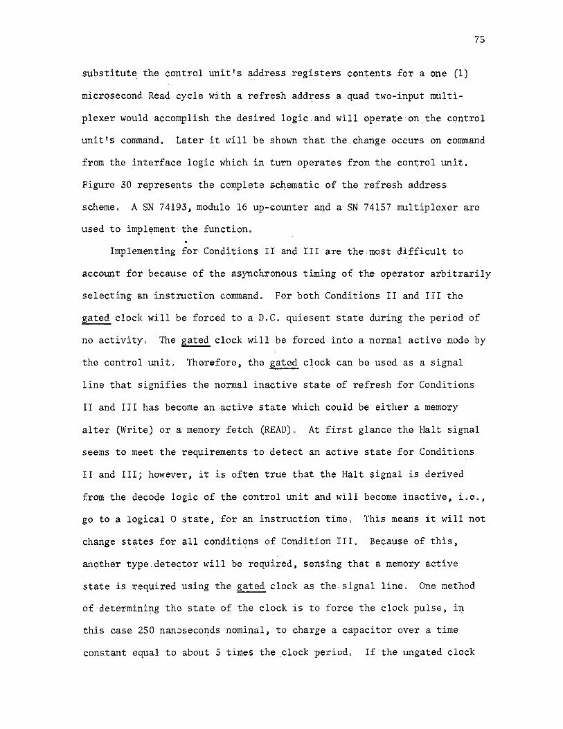
75
substitute, the control unit's address regi~ters contents for a one (1)
mi,cr9second Read cycle with a refresh address a quad two-input multi
plexer would accomplish the desired logic, and will operate on; the cc:mtrol
unit's command. Later it will be shown that the change occurs on cqmmand
from the interface logic which in turn operates from the control unit.
Figure 30 represents the complete scl).ematic of the refresh address
scheme. A SN 74193, modulo 16 up-counter a~d a SN 74157 multiplexer are
used to implement' the function.
Implementing for Conditions II and III are the most difficult to
account for because of the asynchronous timing of the operator arbitrarily
selecting an instructiQn comman4, For both Conditions II and III the
gated clock will be forced to a D.C. quiesent state during the period of
no activity, The gated clock will be forced into a_normal active _mode by
the control unit. Therefore, the gated clock can be used as a signal
line that signifies the normal inactive state of refresh for Conditions
II and III has become.an-active state which could be either a memory
alter (Write) or a memory fetch (READ). At first glance the Halt signal
seems to meet the requirements to detect an active state for Conditions
II and III; however, it is often true that the Halt signal is derived
from the decode logic of the control unit and will become inactive, i.e.,
go to a logical O state, for an instruction time. This means it will not
change states for all conditions of Condition III. Because of this,
another type detector will be required, sensing that a memory active
state is required using the gated clock as the signal line, One method
of determining the state of the clock is to force the clock pulse, in
this case 250 nanoseconds nominal, to charge a.capacitor over a time
constant equal to about 5 times the _clock period, If.the ungated clock
t.) H
§ r,::i
~ Iii
.... l'SB ., .... LSB + 1 .,.
LSB + 2 ,
-.... LSB + 3 ,
'""-
.A
R
MODULO 16 ('
~OUNTER D
.... l RESET .,
...... COUNTER UPDATE REFRESH CONTROL ,
I.SB OR .A > , LS.B + 1 OR B .... ,
MUX LSB + 2 .OR C,
r
LSB + 3 ORD, .,
r,::i The MUX is a quad 2-input SN74157 Multiplexer ~ The MODULO 16 COUNTER is a SN74193, 4 bit Counter
Figure 30. A Completed Schematic of the Refresh Address Scheme
76
77
stops running, as in Conditions II and III, the clock detector will
assume a logical state of "1", When the clock.is running, as in Condi
tion I, the detector assumes the complement state, This is also an
inactive state in that the detector. is in a static logical 11 111 or 11 011 as
long as the clock is running or.if the clock has been stopped, This
detector will be discussed in detail in the next section,
Before continuing with the design a review of the requirements and
logical states of the control signals from the control unit is in order,
Special needs of any processor can be added as required, These require
ments and logic states are:
1) when the processor is in a Halt (Conditions II and III) the.
refresh multiplex lead is to indicate a Refresh state;
2) a halt mode must be detected using both the Halt signal lead and
the ungated clock detector;
3) the refresh signal from the control unit is to be a one (1)
microsecond positive pulse, synchronous with the master clock when the
processor is in Condition I;
4) battery operation signal to be a.logical "1" (high) when inac
tive and must originate outside .of the control or arithmetic ,units;
5) the ungated clock to run continuously except for Condition IV;
6) all logic signals not involved with operation of the memory.
during Condition IV. are to assume a high impedance; this will prevent
them.from interfering with the logic needed to operate the refresh logic;
7) for Condition I, during an instruction time, the control unit
cannot require other operations ·concurrentl,y and simultaneously with the
refresh conunand, e,g,, a memory Read or Write conunand; and
8) sixteen complete memory refresh cycles must be completed within
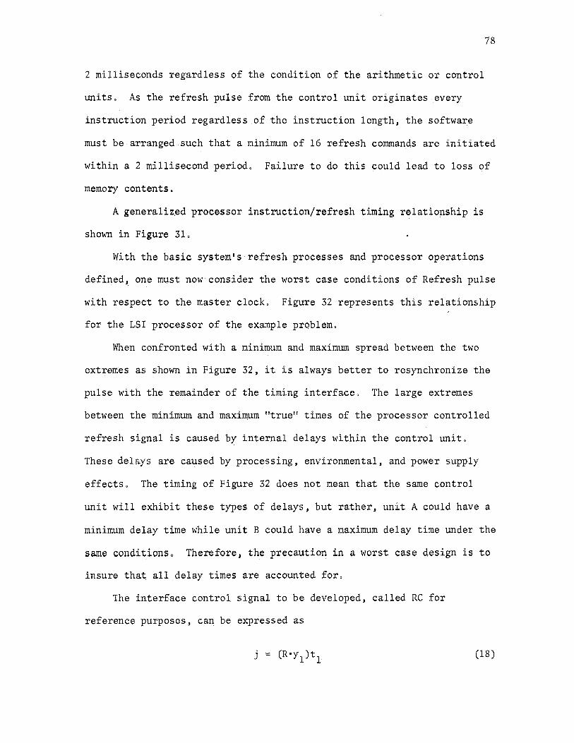
2 milliseconds regardless of the condition of the arithmetic or control.
unit.s, As the refresh puls.e from the control unit originates every
instruction period regardless of the instruction length, the software
78
must be arranged such that a minimum of 16 refresh commands are initiated
within a 2 millisecond period, Failure to do this could lead to loss of
memory contents.
A generaliz.ed processor instruction/refresh timing relatiopship is
shown in Figure 3L
With the basic system's refresh processes and processor operations.
defined~ one must now consider the worst case conditions of Refresh pulse
with respect to the master clock, Figure 32 represents this relationship
for the LSI processor of the example problem,
When confronted with a minimum and maximum spread between the two
extremes as shown in Figure 32, it is always better to resynchronize the
pulse with the remainder of the timing interface, The large extremes
between the minimum and maximum "true" times of the processor controlled
refresh signal is caused by internal delays within the control unit,
These delays are cau~ed by processing, environmental, and power supply
effects, The timing of Figure 32 does not mean that the same control
unit will exhibit these types of delays, but rather, unit A could have a
minimum delay time while unit B could have a maximum delay time under the
same conditions, Therefore,. the precaution in a worst case design is to
insure tha~ all delay times are accounted for,
The interface control. signal to be developed, called RC for
reference purposes, can be expressed as
J0 = (R•y )t 1 1 (18)
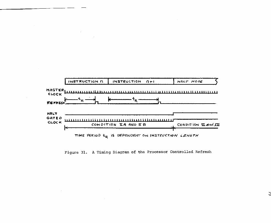
INSTRUCTION n INST~UC. TtON ('l i- I
MAST'ER t I t 11 I I 11. t 111 11 t t I 11 I I t J ! I I L \ I I. l t I l t 1 l 5 l 11 ll I I I l 5 l J. I l l I 11 I l l l t 111 l I I 11 Cl,.OCK
~ :tR~ ~ -{:R. ~ RE~~ESk~----------~~-------------------------1.----------------------HAL 'T
G-A1' E o CLOC i<
I l I I I I· I I I I I l 11 I I I l I I I 11 I I I l I- I I I 11 I I I I t \ I I I I 1-1 I l I I- I I CONC>ITIOIII ~A A-\JD :re
TlME PERtoD t~ IS 01:PENDENT ON INSTIWCTloN i..EN6TH
Figure 31. A Timing Diagram of the Processor Controlled Refresh
TIME 11-i Nf\t-10.SEC::.
0
I
~, zoo 400 eoo 1000 1200 \400
I ,.
rUOZZ0111u MAl(
RG~ESH Wit..L. Bl: C:i..OCKEO WITH ~ES/'£CT TO THE HRSTER C..Lo<:.A:;, TIHE: tte /5 ABSOL.()-71; GvMl:JNTEE ''Ttet1e" ltE.PlfC:Sff
Figure 32. A Worst Case Timing Diagram of the Refresh Pulse
(X) 0
81
which is the input expression for a triggered j-k flip flop. Time t 1 is
the leading edge of the master clock as shown in Figure 32, One must
check to insure that the movement in the time frames of the Refresh pulse
does not interfere with the performance or operation of the memory. For
instance, on short duration instructions, the next instruction address
change could occur inunediately after the Refresh pulse. Implementation
of the flip flop input equations are shown in Figure 33.
Implementing the Clock Detector
If the processor was never operated in the Single Instruction or
Single Clock Conditions, then the refresh logic design would be complete,
However, in order to account for Conditions II and III more logic is
required, The Clock Detector was first discussed on page 69, The logical
OR of the gated clock, detected by the Clock Detector, and the Halt
signal (H) will satisfy both processor conditions, Figure 34 is the
schematic for this connection, The output function of the gated clock
whose state is detected, and the OR of Hare expressed by
f=CD+H (20)
This function will be used to expand the refresh expression later in this
discussion.
In order to provide the clocking source for processor Conditions III
and IV, an astable will be required. The period of the astable is
selected to be 125 microseconds, With this period the total of 16
refresh address states initiated by the astable keeps the memory refresh
period less than 2 milliseconds, Possible astables suitable for use in
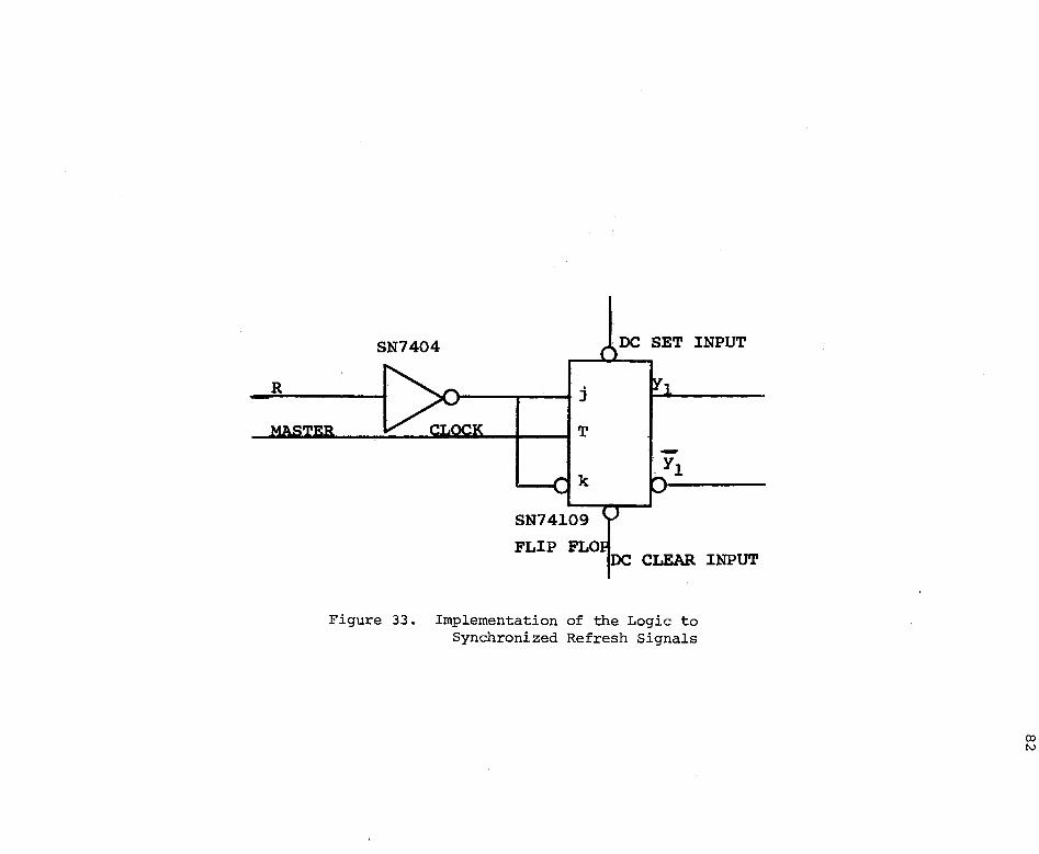
SN7404
">--~---1 j
k
SN74109
FLIP FLO
DC SET INPUT
DC CLEAR INPUT
Figure 33. Implementation of the Logic to Synchronized Refresh Signals
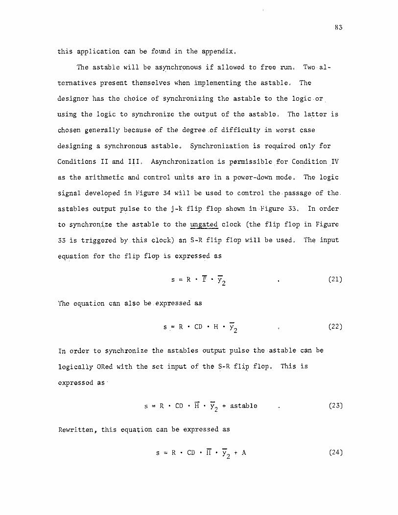
83
this application can be found in the appendix,
The astable will be as:ynchronous if allowed to free run, Two al
ternatives present themselves when implementing the astable, The
designer has the choice of synchronizing the astable to the logic or,
using the logic to synchronize the output of the astable, The latter is
chosen generally because of the degree .of difficulty in worst case
designing a synchronous .. as table. Synchronization is required only for
Conditions II and III. Asynchronization is permissible for Condition .IV
as the arithmetic and control unit~ are in a power-down mode. The logic
signal developed in Figure 34 will be used to control the.passage of the
astables output pulse to the j-k flip flop shown in Figure 33. In order
to synchronize the astable to the ungated clock (the flip flop in Fi,gure
33 is triggered by this clock) an S-R flip flop will be used, The input
eqU:ation for the flip flop is expressed as
s = R • I · y 2
The equation can also be expressed as
s = R ·CD· H • ~ 2
In order to synchronize the astables output pulse the .astable can be
logically ORed with the set input of the S-R flip flop. This is
expressed as
s = R • CD • H • y 2 + as tab 1 e
Rewritten, this equa1,:ion can be expressed as
s = R •CD· H · y2 + A
(21)
(22)
(23)
(24)
CLOCK
DETEC'l:PR ·
SN7404
NANO f=CD + H H
SN7400
Figure 34. A Logic Diagram Representing_ a Detec;ted Gated Clock
85
To. insure that the as1;:able inhibited for single instruction or single
clqck (Conditions II or III) the astable pulse is inhibited by a logical
AND of the Halt (H) and the Clock Dete~tors output. This can be
expressed and expanded as
(25)
To reset the S-R, flip flop the input r must be pulsed. with a signal that
will occur after each cycle yet.allow the refresh signal to propagate to
the j-k flip flop previously.used to insure.the inteface logic detects
the processor CQntrolled refresh signal. Th.e Cenable memory clo~k will
serve this purpose.
The final signal to the S-~ flip flop is the initialization power
turn-on signal. This insures the memory initializes in a non-refresh
condition for immediate memory use.
The r input can now be written as
r = Cenable • y2 + power~on • y2
The implementation is shown in Figure 35. Also included is the
j-k flip flop of Figure 33.
(26)
The final condition to ac9ount for is the power-off Condition IV.
To detect this condition the circuitry must first anticipate a power-down
situation and signal the logic to.stop memory and processor operation ..
This signal must also cause an unconditional refresh state to occur.
This special signal is the key to a power down mode. The unconditional
refresh is performed by.entering the j-k flip flop by means of the D,C,
st~tic inputs, This will force the interface_ logic to slave the as table
and ignore processor signals until the power down signal is removed,.
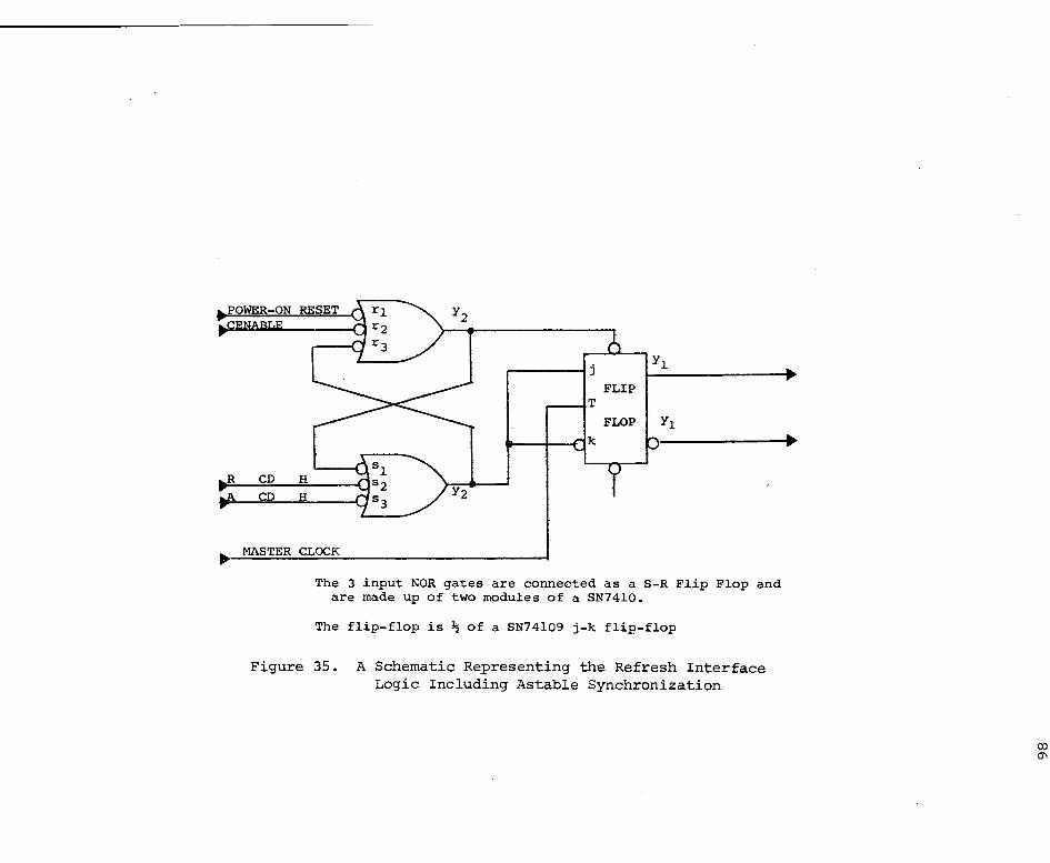
R CD CD
MASTER
r1 Y2
j Y1
FLI.P T
FLOP Y1 k
,_sl H s2 H 83
Y2
CLOCK
The 3 input NOR gates are connected as a S-R Flip Flop and are made up of two modules of a SN7410.
The flip-flop is\ of a SN74109 j-k flip-flop
Figure 35. A Schematic Representing th~ Refresh Interface Logic Including Astable Synchronization
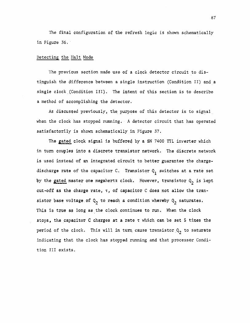
87
The final configuration of the refresh logic is shown schematically.
in Figure.36.
Detecting the Halt Mode
The previous section made use.of a clock.detector circuit .to dis
tinguish the difference between a single instruction (Condition II) and.a
single clock.(Condition III). The intent of this section is to describe
a method of ~ccomplishing the detector.
As discus~ed previously t the purpose .. of this detector is to signal.
when. the clock .. has stopped running. A detector circuit that has operated
satisfactorily is shown schematically in Figure 37.
The gated clock signal is buffereg by a SN 7400 TTL inverter which
in turn couples into a discrete transist.or network. The discrete ne't;work.
is used instead of an integrated circuit to better guarantee the charge
discharge rate of the capacitor C. Transist~r Q1 switches at a rate set
~y the gated maste.r one megahertz clock. However, transistor Q2 is kept
cut-off as the charge rate, T, of capacitor C does not allow the tran
sistor base voltage.of Q2 to reac~ a condition whereby Q2 saturates.
This is true as long as.the clock.cont~nues to run. When the clock
stops., the _capa~i tor C ch~rges at a rate 't' which can be set 5 ti11,1.es the
period of the clock. This will in turt\ cause transistor Q2 to saturate
indicating that the clock has stopped running and that processor Condi
tion III exists.
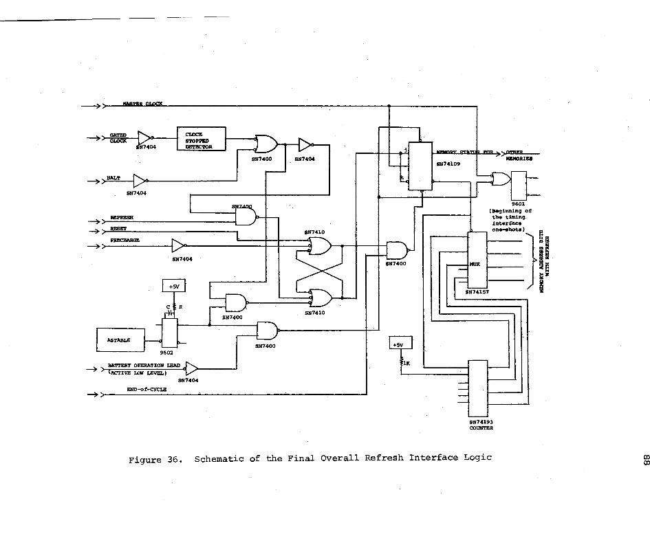
~
~
----,. ~
~
GATED CLOClt CLOCl( STOPPl!D
7404 DBTBCTOR
SALT
SN7404
Rl!:PRBSH
RESET
PIU!CBARGE
SN7404
AS TABLE
BATTERY OPERATION LEAD
ACTIVE LOW LEVEL)
SN7404
SN7400 SN7404
SN7410
SN7400
SN7410
SN7400
j,-1-1111:t...liiDIWJLilr:lll...:i, )OTBFB MEMORIES
9601 (Beginning of the timing interface
--,11! ·-Jr
SN74193 COUNTER
Figure 36. Schematic of the Final Overall Refresh Interface Logic OJ OJ
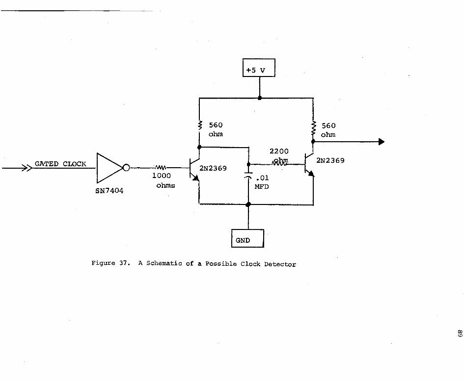
-->-) GATED CLOCK [:>,---~=s SN7404
j 560 olun
+5 V
GND
.01 MFD
2200
Figure 37. A Schematic of a Possible Clock Detector
560 ohm
2N2369
(X) I.D
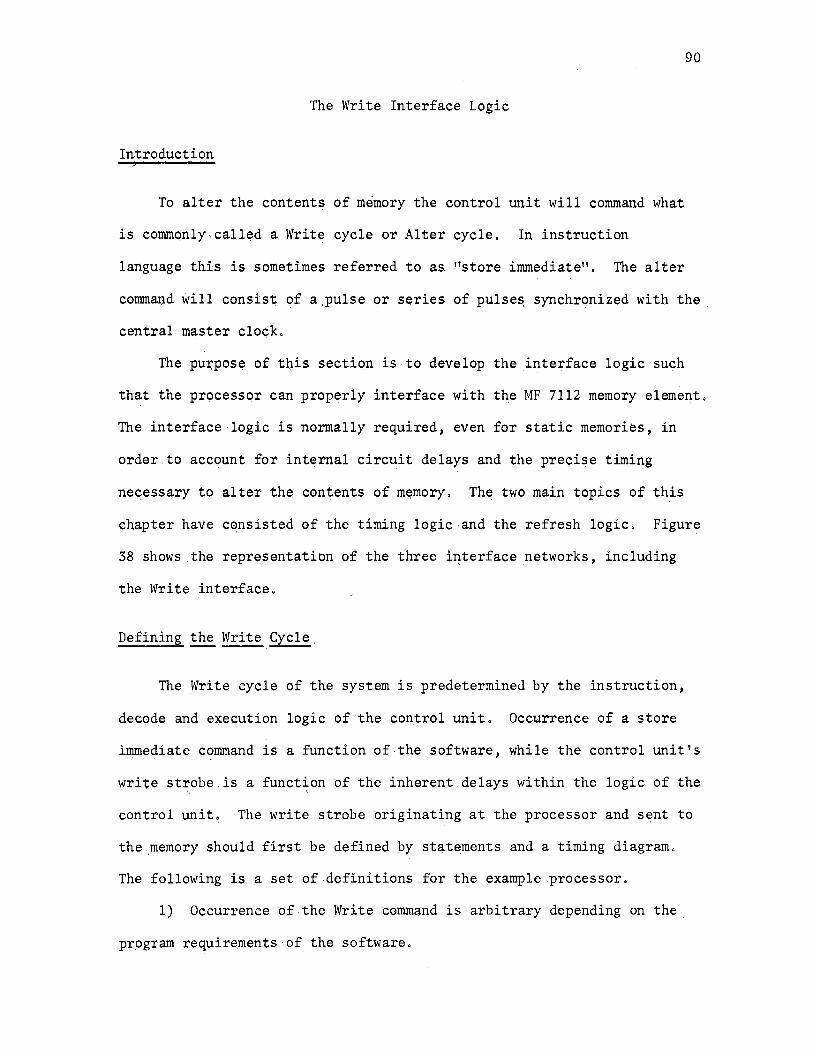
90
The Write Interface Logic
Introduction
To alter the cont.ents of memory the control unit will command what
is commonly.called a Write cycle or Alter cycle. In instruction
language·this is sometimes referred to as "store immediate". The alter
comma]J.d will consist of a ,pulse or s.eries of pulse~ synchronized with the
central master clock.
The pm;pose of this section is, to develop the interface logic such
that the processor can properly interface with th.e MF 7112 memory eleme11t.
The interface ·logic is normally required, even for static memories, in
order to account for internal circuit delays and the precise timing
nec;ess~ry to alter the contents of memory. The two main topics of .this
chapter have cansisted of the timing logic,and the refresh logic. Figure
38 shows the representation of the three interface networks, including
the Write interface.
Defining the Write Cycle
The Write cycle of the system is predetermined by the instruct.ion,
decode and execution logic . of ·the con.trol unit. Occurrence of a store
immediate cornnumd is a function of .the software, while the control unit's
write strobe,is a funct~on of the inherent_delays within the logic of the
control unit. The write strobe originating at the processor and sent to
the .memory should first be defined by statements and a timing diagram.
The following is a set of .definitions for the example processor.
1). Occurrence of the Write command is arbitrary depending on the
program requirements qf the software.
MASTER ..... , CLOCK .... REFRESH CONTROL ..... , TIMING LOGIC REFRESH LOGIC ,
~
'
I MEMORY CLOCKS ...... ,.
~ , WRITE STROBE ......
WRITE LOGIC ,
CONTROL UNIT WRITE CONTROL ..... , ........
Figure 38. A Block Diagram of the Timing, Refresh, and Write Interface Logic
92
2) Period of the Write strobe from the processor is dependent on
the instructi~n format which in turn itself is variable in length.
3) Duration of the write strobe from the processor is always one
microsecond independent of instruction length or any of the three condi
tions described in the refresh section. ' . . . '· .
4) Processor Refresh and Write never.occur simultaneously within
any given instruction •.
5). Time duration fr~m a.store inunediate to the next instruction
address change will be 2 microseconds-minimum.
6) A read after write from the arithmetic.and control unit is _not
required during an instruction.
7) A read before write is always required.
8) Output da~a from the memory is not valid during a Write cycle,
9) In the wo~st c~se analysis, if the rising edge of the Write
strobe (the leading edge) is at a maximum propagation time, then the
falling edge of the pulse will be at a.maximum.
10) A Write strobe will no.t ,occur in the processor Condition III.
11) The Write strobe to the.memory element is "true" in the logical
1 level and must be properly placed within the events of a.memory write
cycle.
A Description of the Timing
From the timing relat:ionship shown in Figure 39, it will be noted
that the Write strobe from the cqntrol unit has a minimum propagation
time from the leading edge of the clock of 15 nanoseconds to a maximum of.
665 nanoseconds.· Because of.this wide variation, a worst case design
cannot guarantee that the control unit's Write strobe can always occur in
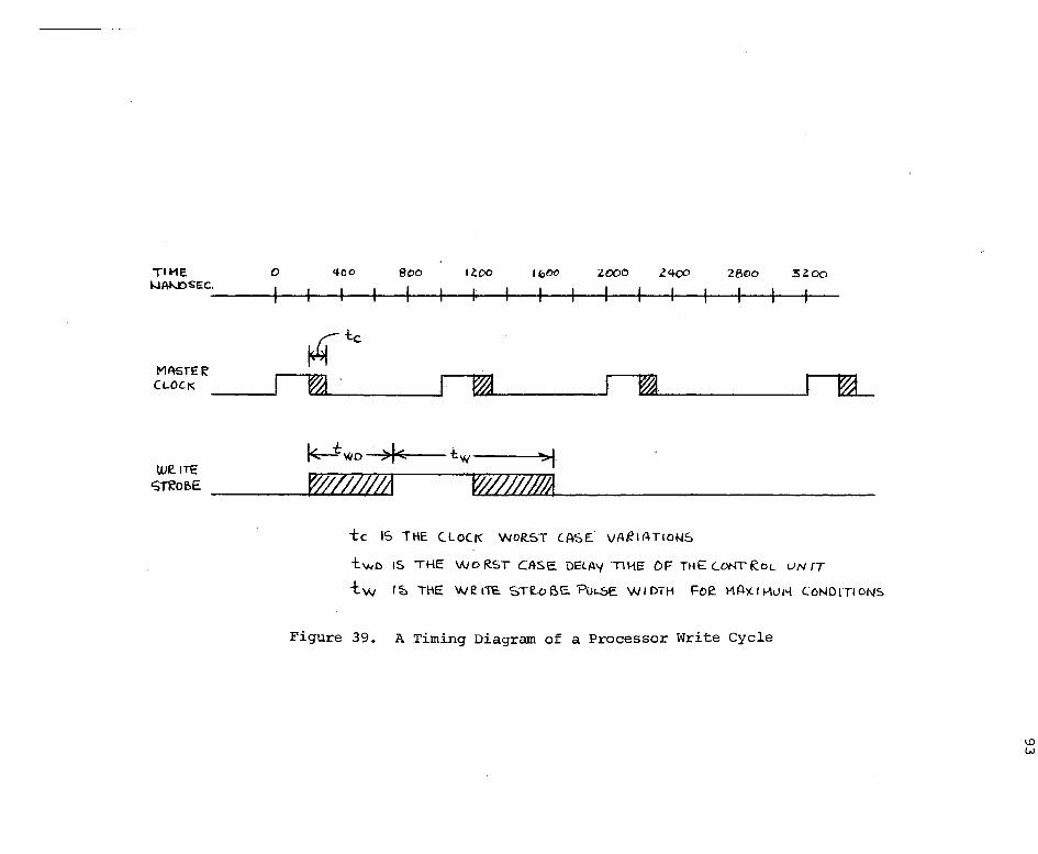
TIHE 0 l,.JA"-D~EC.
MAsTER CLO-CK
400 800 1200 I t,00 2000 2400 28DO 3200
~tc
~ j ~ .~. ra_
W//11///Jf
tc IS THE Clo(t( WOR.ST CASE vARIATIOt-.15
twn IS THE Wo RST C~SE. 'DEL~'( TIHE OF THE CONT RoL UN rT
tw ,~ iHE W£l1E s,e.oBE.'PiJL.SE. WIDTt1 Foe 1'1Ax11-1u1-1 CoNDiTION5
Figure 39. A Timing Diagram of a Processor Write Cycle
\.0 w
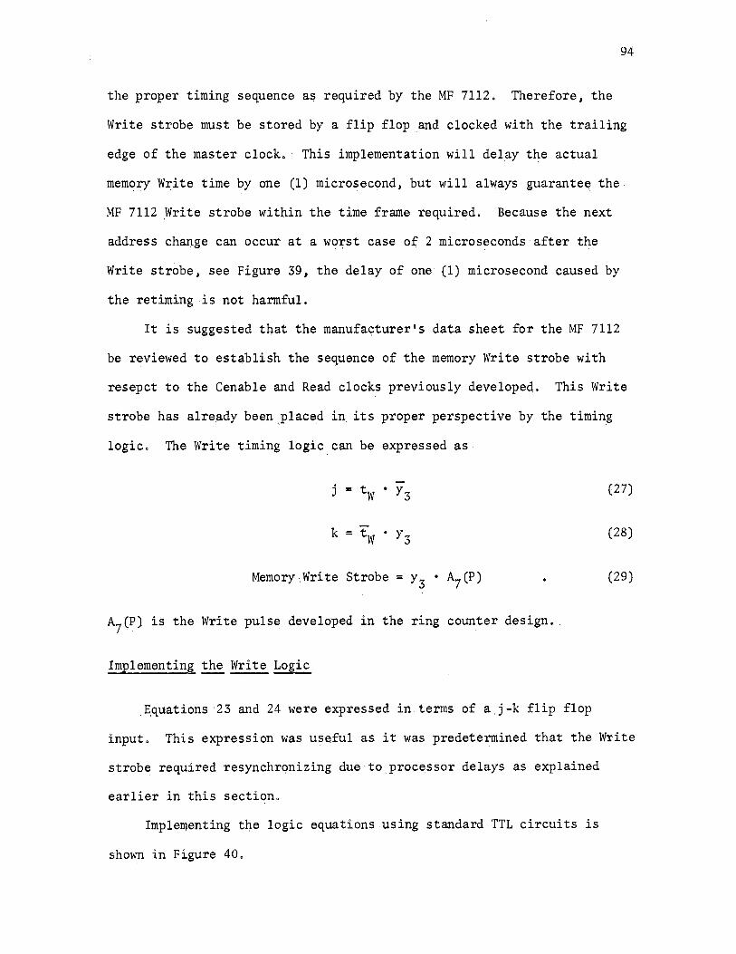
94
the proper timing sequence a~ required. by the MF 7112. Therefore, the
Write strobe must be stored by a flip flop and clocked with the trailing
edge of the master clock.· This implementation will delay the actual
memo:i;y Write time by one (1) microseco11d, but will always guarante~ the.
MF 7112 .Write strobe within the time frame required. Because the next
address change can occur at a wo:r;st case of 2 microseconds after the
Write strobe, see Figure 39, the delay of.one (1) microsecond caw~ed by
the retiming is not harmful.
It is suggested t~at the manufa9turer's data sheet for the MF 7112
be reviewed to establish the sequence of the memory Write strobe with
resepct to the Cenable and Read clock.s previously developed. This Write
strobe has already been. ,place.d in its proper perspective by the timin.g
logic. The Write timing logic.can be expressed as
j = tW • Y3 (27)
k = tW • Y3 (28)
Memory.Write Strobe= y3 • A7(P) (29)
A7(P) is the Write pulse developed in the ring counter design •.
Implementing the Write Logic,
. E,quations 23 and 24 were exptessed in terms of a j-k flip flop
input. This expression was useful as it was predetermined that the Write
strobe required resynchrqnizing due to.processor delays as explained
earlier in this section.
Implementing t4e logic equations using standard TTL circuits is
shown in Figure 4 0 • ·
POWER-ON RESET
PROCESSOR WRITE STROBE
CLOCK
j
SN 74109
y
-Y SN 7400 SN7404
Figure 40. A Schematic of the Write Interface Logic
MEMORY WRITE STRS.BE
A parity inhibit signal is also included. This will be shown as a
requirement in Chapter V. For now this signal will be express~d as.
96
Parity Inhibit (PI) = y 3 (30)
CHAPTER IV
THE READ ONLY RANDOM ACCESS MEMORY
Introduction
General Uses
Small machine uses in which processors are applied to applications
such as Point of Sale terminals, Interaction Cathode Ray Tube Displays,
Bank Deposit terminals, and numeric control, often require a Read Only
Random Access memory (ROM) to compliment the Random Access Read/Write
memory, The amount of ROM varies with the type of application. In the
case of the so-called "Smart Terminal", which is largely customer pro
grammable, the requirement for ROM is often small. On the .other hand, in
some applications in which the terminal is factory programmed, large
amounts of ROM are used which in turn requires only small amounts of
Read/Write memory, In either case, the design principles presented here
are suitable for a~l types of applications.
The discussions following in this section center .on the design
c:i;:iteria required to mix ROM and Read/Write memories on the same data and
address bus, · The discussions are divid.ed into three parts. a general ROM
architecture, followed by a survey of commonly available semiconductor
R,OM's, and concluding with data and address .bus precautions including a
switching speed design analysis. Memory printed circuit decoding logic
~s introduced in Chapter.V, The appendix will contain the final
97
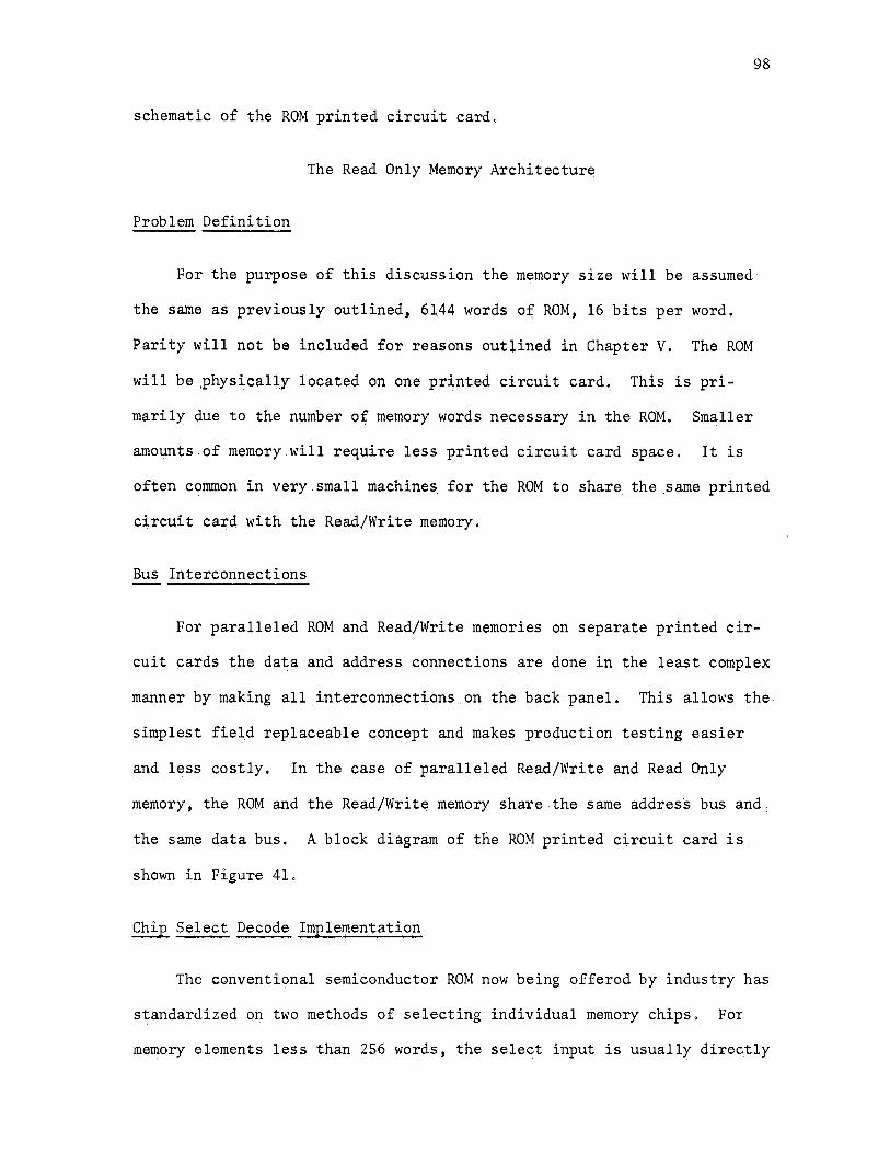
98
schematic of the ROM printed circuit card.
The Read Only Memory Architecture
Problem Definition
For the purpose of this discussion the memory size will be assumed
the same as previously outlined, 61.44 words of ROM, 16 bits per word.
Parity will not be included for reasons outlined in Chapter V. The ROM
will be ,physically located on one printed circuit card. This is pri
marily due to the number of memory words necessary in the ROM. Smaller
amounts of memory.will require less printed circuit card space. It is
often common in. very. small machines. for the ROM to share the same printed
circuit card with the Read/Write memory.
Bus Interconnections
For paralleled ROM and Read/Write memories on separate printed cir
cuit cards the data and address connections are done in the least complex
manner by making all interconnections on the back panel. This allows the
simplest fiel.d replaceable concept and makes prot;luction testing easier
and less costly. In the case of paralleled Read/Write and Read Only
memory, the ROM and the Read/Writ~ memory share the same address bus and
the same data bus. A block diagram of the ROM printed circuit card is
shown in Figure 41.
Chip Select Decode Implementation
The conventional semiconductor ROM now being offered by industry has
standardized on two methods of selecting individual memory chips. For
memory.elements.less than 256 words, the select input is usually directly
MSB . __.
MEMORY . DECODE
----' . __. .
-
,1, t ' I> .... .
- . ___. . -. . . . . . . _.. .
~
~ _.. ADDRESS . OUTPUT BUFFER READ ONLY MEMORY - BUS . - DR:[VER ~ . .
LSB . -- ;;;: -ADDRESS BUS
Figure 41. A Block Diagram of the ROM Printed Circuit Card
100
connected to the element~ output transistors. This method is used in
lieu of internal element decoding and permits the WIRED OR connec~ions
for memory expansion but requires additio.nal decode logic on the prin.t.ed
c:i,.rcuit card. Decode methods.are described in Chapter V. For memorr.
elements.larger than 512 words, the meiµorf.element,gene:r,-ally includes
internal decoding that cam~.es an individual memory package to dis.connect,
from the data bus;· This disconnect permits the WIRED OR condition allow
ing other memory elements to conmict to the. bus without interference,
The size of the internal decode is limited by package pin connections.
The Fairchild Semiconductor, Inc. MOS, 512 X 8, ROM chosen for the
example has internal decode permitti,Il.g memory expansion to 16,384 words
with four input pins .devo~ed to select decoding. The user we>uld spec:i,.fy
the desired select coding at the time the memory was coded by the semi~
conductor manufactµr~r.
Output ~ ~. Buffering
The two semiconductqr technologies that are most conunon to ROM,
bipolar and MOS, requi~e individual consideration when the connection to
the data bus is being implemeJ'lted. The reader's attention is directed to
the last topic of this chapter for output switching time considerations.
Both the bipolar and MOS technology ROM's are implemented with the
output buffering either tri-state or open node, i.e., open collector or
open drain. Tri-state is the fastest switching time configuration .but is
limited in the. number of output nodes that·can be connected together due
to leakage currents adding to a limit exceeding the receiving ele~ents
capacity. Also, tri-state logic adds current spikes to the data bus
which for some applications are intolerable. On the other hand, the open
101
node connection can be expanded to large memory capacities but is the
slowest method for switching time. The designer must .choose the output
buffering that best meets the application ..
In order to meet the access time requirements-of the processor, it
has been the autho.r' s experience that MOS outputs require buffering by a
device capable of large capacitance drive such as TTL devices.
Input Node Buffering
As .. in Output Data Buffering, the two semiconductor technologies must
be considered individually. However, for input nodes the reason for
individual consideration differs greatly.
The bipolar TTL technology is a current sinking family and when many
inputs are combined, s~ch as found in a memory address configuration,
this combined input curren.t becomes very _1 arge. For instance, assume a
memory whose.size is 6,144 words and is made up from 2S6 word ROM's. If
the memory is 16 bits wide then the number of input nodes is 96. Multi
plying 96 by the conventional 1.6 milliamperes per TTL input, and the
designer finds he,must supply a driving device capable of sinking 153,6
milliamperes and maintain a logic low level net exceeding the TTL low
voltage of 0.4 volts, The value of current changes fqr the bipolar ECL
family and the current must be sourced instead of sinking, but the same
rules apply.and input loading becomes an important consideration. One
method of providing the necessary drive without adding excessive delay is
to parallel TTL gates or buffers such as the SN 7400 gate or the.SN 7440
buffer. This arrangement provides minimum propagation delay and adequate
current drive. However, the memory cost is.increased by the additional
address drivers, and the printed circuit card area allowable for memory
102
is decreased.
The MOS technology has an input node·drive problem that differs
considerably from the bipolar technology. In the case of MOS Read Only
Memory, most applications are TTL logic driving MOS memo~ies. Even
though the manufacture.r's .data sheet claims TTL compatibility, a careful
review o~ the device input specifications generally reveals that.the MOS
memory,is close to being compatible but for worst case design cons~dera~
tions will not acc~pt TTL output levels and guarantee operation. There
fore; the de~igner must make provisions to guarantee operation. Specif
ically, the problem area is in the TTL output node being guaranteed to
be not less than 2,4 volts, while the MOS device is specified at a
guarantee level 9f, .Vss - 1 volt. The power supply, Vss~ is 5,0 volts
for TTL operation; therefore, the guaranteed high MOS input level that
can be tolerated is 4.0 volts which is 1.6 volts difference from the TTL
output guarant~e of 2.4 volts. One of the best methods of overcoming
this incompatibility is to add a pull-up register to the TTL output.node,
This addition will guarantee a high input level of 5,0 volts with a
penalty of added components'.and extra current used by the pull-up resis
tor. The resistance value is selected as a function of the memory speed
and the power supply current available,
For memory applications where the MOS inputs.are operated in fast
cycle times, fast being defined as crcle times-and address changes less
than 300 nanoseco~ds, the designer m~st contend with the average power
dissipation in the TTL driver. The MOS address inputs when connected
together to form a large memory block becomes a substantial capacitance
to drive and increases the power dissipation of the input driver, For
sucij applications, the SN 75361 is sugges~ed a~ a possible driver meeting
103
all necessary input drive requirements if an external pull-up resistor
is used.
Survey of Semiconductor ROM
General,
The majority of semiconductor ROM's available are divided into two
categories, bipolar and MOS. As a genera_! rule, the bi~olar ROM's are
small capacity but with very fast access times. The cost of bipolar
ROMts is generally 2.5 times that of a,MOS ROM. The bipolar ROM is often
found in small capacity, high speed applications such as microprogramming
or caclw memory. The MOS R.OM is mos4 often found in the program portion,
of memory where large capacity is. required but access time is :not criti~
cal, For these reasons this design will restrict itself to the MOS ROM's
which fi't;: the ._application better than a bipolar ROM. However, for refer
ence, the bipolar ROM's most commonly used are listed in Table XII. The
MOS ROM's offered as catalog devices.are listed in Table.XIII.
Oata Bus Switching Considerations
The Need for ~~Driver
Most manufacturer's data sheet for semiconductor ROM's specify the
ROM outputs as designed to be WIRED OR (or WIRED AND) with other memory
devices connected to a common data bus. Even though this type operation
is functionally satisfactory it is quite often impossible to drive a data
bus due to the associated node capacitance not normally accounted for on
a.manufacturer's data sheet. The problem can be defined as.a switching
time consideration in that the _standard ROM output transistor cannot
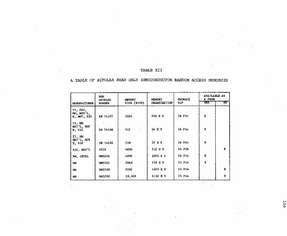
TABLE XII
A TABLE OF BIPOLAR READ ONLY SEMICONDUCTOR RANDOM ACCESS MEMORIES
ROM AVAIIABLE AS
CATALOG MEMORY MEMORY PACKAGE A PROM MANUFACTURER, NUMBER SIZE (BITS) ORGANIZATION DIP u;:, NO
TI, FSC, MM, NAT 'L, H, MOT, SIG SN 74187 1024 256 X 4 16 Pin x
TI, MM NAT'L, MOT H, SIG SN 74186 412 64 X 8 16 Pin x
TI, MM NAT'L, MOT H, SIG SN 74188 256 32 X 8 16 Pin x
SIG, NAT'L 8228 4096 512 X 8 24 PIN x
MM, INTEL MM5240 4096 1024 X 4 24 Pin x
MM MM52{)5 2048 256 X 8 24 Pin x
MM MM5280 8192 1024 X 8 24 Pin x
MM MM5290 10,368 1152 X 9 24 Pin x
,..... 0 ~
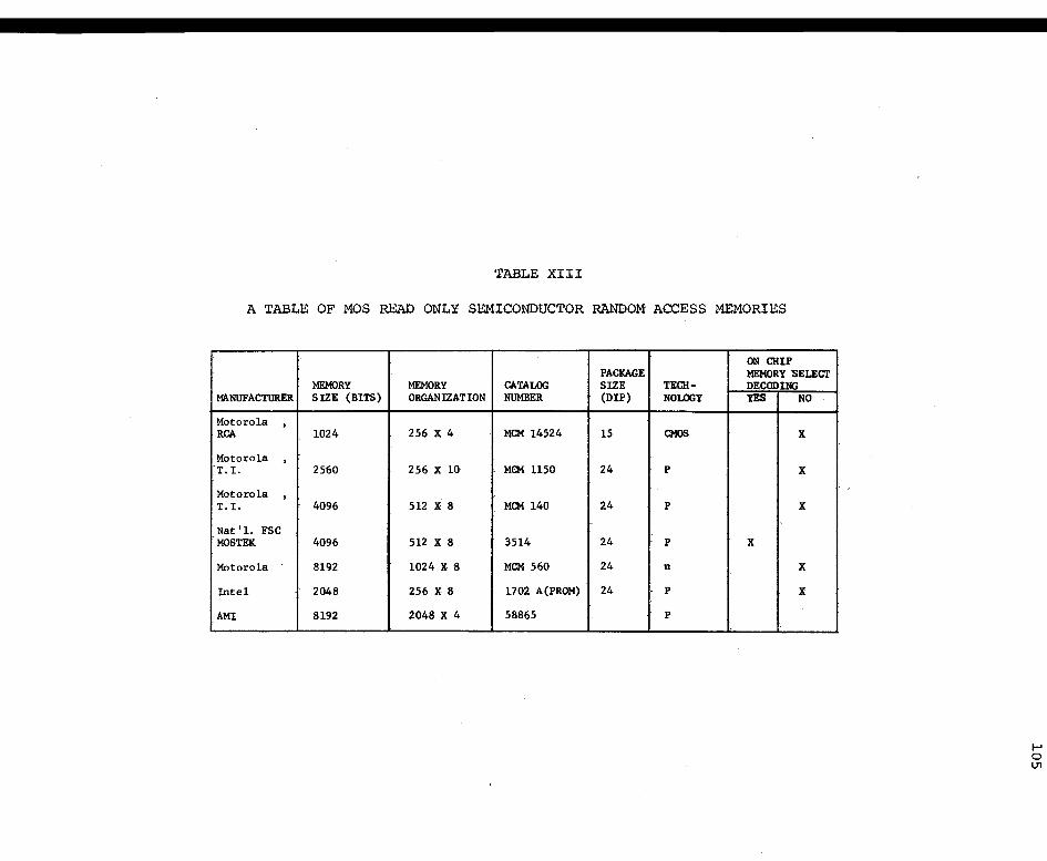
TABLE XIII
A TABLE OF MOS READ ONLY SEMICONDUCTOR RANDOM ACCESS MEMORIES
ON CHIP PACKAGE MEMORY -SELEcr
MEMORY MEMORY CATALOG SIZE TE.CH- DECODING MANUFACTURER SIZE (BITS) ORGANIZATION NUMBER (DIP) NO LOGY YES NO
Motorola . RCA 1024 256 X 4 MCM 14524 15 CMOS x
Motorola . T. I. 2500 256 X 10 MCM 1150 24 p x
Motorola . T. I. 4096 512 X 8 MCM 140 24 p x
Nat 'l. FSC MOSTEK 4096 512 X 8 3514 24 p x
Motorola 8192 1024 X 8 MCM 560 24 n x
Intel 2048 256 X 8 1702 A(PROM) 24 -- p x
AMI 8192 2048 X 4 58865 p
...... 0 lT1
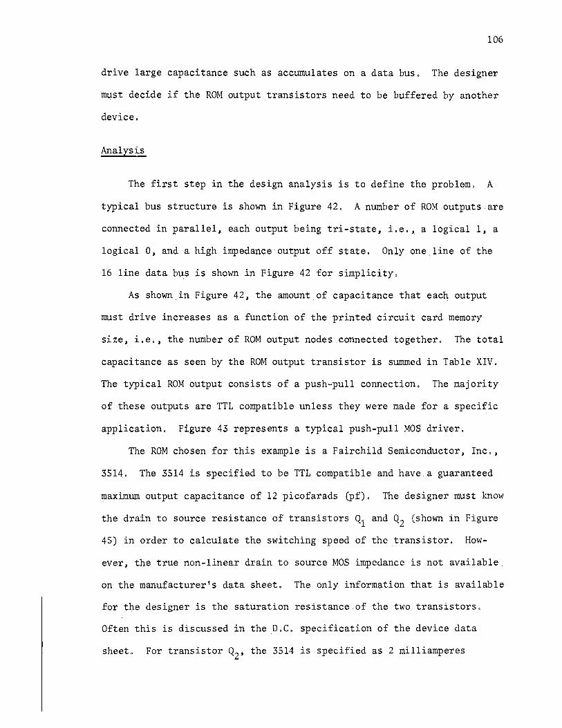
106
drive large capacitance such as accumulates on a data bus, The designer
m~st decide if the ROM output transistors need to be buffered by another
device,
Analysis
The first step in the design analysis is to define the problem. A
typical bus structure is shown in Figure 42. A number of ROM outputs are
connected in parallel, each output being tri-state, i.e., a logical 1, a
logical O, and a high impedance output off state. Only one.line of the
16 line data bus is shown in Figure 42 for simplicity.
As shown in Figure 42, the amount of capacitance that each output
must drive increases as a function of the printed circuit card memory
size, i. e, , th,.e number of ROM output nodes. connected together, The total
capacitance as seen by the ROM output transistor is sununed in Table XIV.
The typical ROM output consists of a.push-pull connection, The majority
of these ·outputs are TTL compatible unless they were made for a specific
application. Figure 43 represents a typical push-pull MOS driver.
The ROM chosen for this example is a Fairchild Semiconductor, Inc.,
3514, The 3514 is specified to be TTL compatible and have a guaranteed
maximum output capacitance of 12 picofarads (pf). The designer must know
the drain to source resistance of transistors Q1 and Q2 (shown in Figure
45) in order to calculate the switching speed of the transistor. How
ever, the true non-linear drain to source MOS impedance is not available.
on the manufacturer's data sheet. The only information that is available
for t4e designer is the saturation resistance of the two transistors.
Often this is discussed in the D.C. specification of the device data
sheet. For transistor Q2, the 3514 is specified as 2 milliamperes
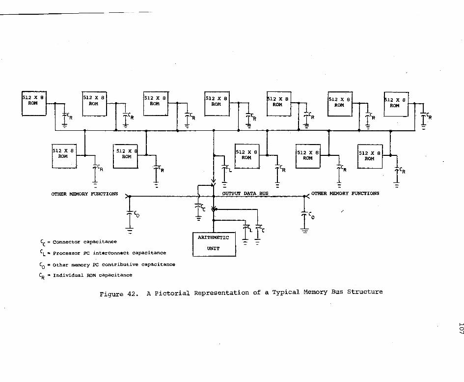
12 X 8 ROM
512 X 8
512 X 8 ROM
ROM .__ __ 512 X ROM
OTHER MEMORY FUNCTIONS
CC = Connector capacitance
512 X 8 ROM
CL= Processor PC interconnect capacitance
C0 = Other memory PC contributive capacitance
CR = Individual ROM capacitance
512 X 8 ROM .__ __ 12 X 8 ROM
512 X 8 ROM 1--+--
ARITHMET:lC
UNIT
512 X 8 ROM
512 X 8 ROM 1------. 512 X 8
ROM
Figure 42. A Pictorial Representation of a Typical Memory Bus Structure
12 X 8 ROM
I'R
..... 0 -..J
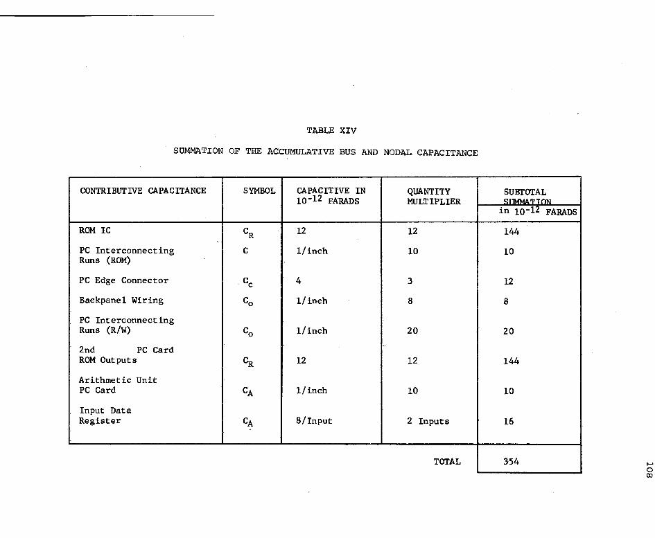
TABLE XIV
SUMMATION OF THE ACCUMULATIVE BUS AND NODAL CAPACITANCE
CONTRIBUTIVE CAPACITANCE SYMBOL CAPACITIVE IN QUANTITY 10-12 FARADS MULTIPLIER
ROM IC CR 12 12
PC Interconnecting c 1/inch 10 Runs (ROM)
PC Edge Connector . cc 4 3
Backpanel Wiring Co 1/inch 8
PC Interconnecting Runs (R/W} co 1/inch 20
2nd PC Card ROM Outputs ~ 12 12
Arithmetic Unit PC Card CA 1/inch 10
Input Data Register CA 8/Input 2 Inputs
TOTAL
SUBTOTAL C::TTMM.t\TTOl\l
in 10-12 FARADS
144
10
12
8
20
144
10
16
354 I-' 0 OJ
ROM DATA AND CHIP SELEC
0 2
OUTPUT NODE
Figure 43. A Typical MOS Output Driver for a ROM
I-' 0 I..O
110
current sink, i.e., current into the output device, guaranteed saturation
voltage not.to exceed 0.45 volts. Therefore, the saturation resistance
c~n be expressed as
_o_._4_5_ = 225 ohms 2 X 10⁻³
(31)
The pull-up transistor -Q1 is specified as supplying 100 microamperes,
i.e., current from the output node, at a satura,tion voltage no less than
2.4 volts when VSS equals 4.75 volts. Therefore, the saturatioll; resist
ance of Q1 can be expressed as
R (Q) = 4•75 - 2·4 = 2350 ohms SAT. 1 100 X 10-6
(32)
The MOS transistor.resistance not being linear can be approxi~ated
for switching time considerations by assuming linear operation of both·
the pull-up and the pull-down transistor. With a resistance value fo~
the ROM driver transistors.calculated, the switching time of the output
transistors can be found. The first step is to sum the accumulative node
capaci~ance shown in Figure 42. Table XIV is a summation of this
accumulated capacitance which includes all nodes that-the output tran-
sistors are required to drive.
Th.e initial memory design criteria specifies a memory logic O level
as being VSS minus 1.0 volt, an.cl a logic 1 level as v00 plus 0,4 volts.
An examination of the manufacturer's ROM data sheet indicates that the
output switching time is spectfied at v00 plus 1.5 volts, for both a
1o~ic.0 and a logic 1. It is immediately clear that the switching time
of the ROM will be increased for the logic O case. The method of testing
and the application differs greatly. Figure 44 represents a propagation
delay timing diagram of the Fairchild 3514 ROM.
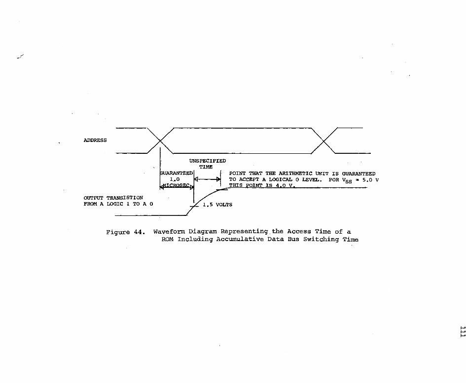
ADDRESS _:>i<,.____ __ x _____ UNSPECIFIED
TIME
OUTPUT TRANSISTION "~ ~
POINT THAT THE ARITHMETIC UNIT IS GUARANTEED TO ACCEPT A LOGICAL O LEVEL. FOR Vss = s.o V THIS POINT IS 4.0 v.
FROM A LOG_I_c_i_T_o_A_o _____ ,T 1. s- VOLTS
Figure 44. Waveform Diagram Representing the Access Time of a ROM Including Accumuiative Data Bus Switching Time
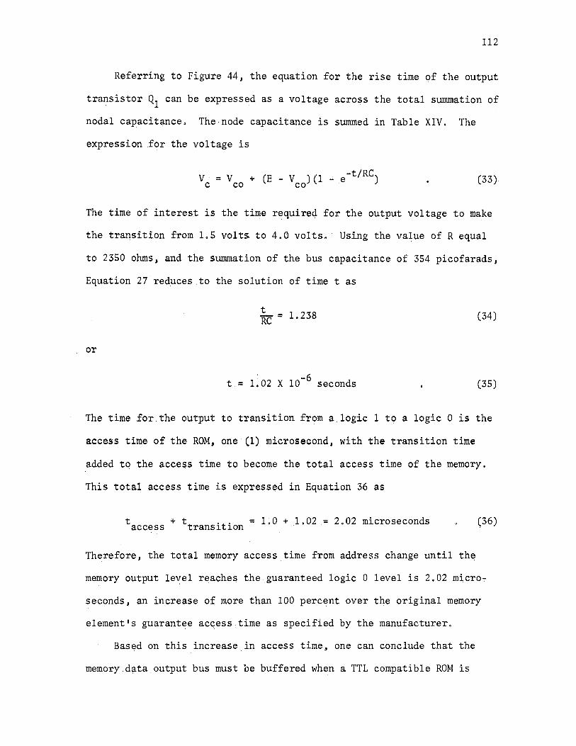
112
Referring to Figure 44, the equation for the rise time of the output
transistor Q1 can be express~~ as a voltage across the total summation of
nodal capacitance. The node capacitance is summed in Table XIV. The
expression for the voltage is
V = V + (E - V )(1 - e-t/RC) c co . co . (33)
The time of interest is the time r~quirecl for the output voltage to make
the transition from 1.5 volts to 4.0 volts.· Using the value of R equal
to 2350 qhms, and the summation of the bus capacitance of 354 picofarads,
Equation 27 reduces.to the solution of time t as
t RC= 1.238 (34)
. or
-6 t.= 1.02 X 10 seconds (35)
The time for the output to transition from a logic 1 t9 a logic O is the
access time of the ROM, one· (1) microsecond, with the transition time
adcl.ed tQ the access time to becoll).e the total access time of the memory.
This total access time is express~d in Equation 36 as
t + tt .t. = .1,0 + 1.02 = 2.02 microseconds access ransi. ion · · · · (36)
Therefore, the total memory ac~ess.time from address change until the
memory output le~el reaches the guaranteed logic O level is 2.02 micro-
seconds, an increase of more than 100 percent over the original memory
elemen.t 's guarantee acc;ess: time as specified by the manufacturer,
Based on this increase. in access . time,. one can conclude that the
memory.data.output bus must be buffered when a TTL compatible ROM is
113
driving a high capacitance MOS bus. This also holds true when the bus
node capacitance becomes large due to the summation of node capacitance
no matter what type technology is driving another technology, The
buffering can.be accomplished with either TTL tri-state or open collector
drivers. Either is suitable with the tri-state devices exhibiting the
fastest ,switching times. One can also conclude that the tri-state MOS
output arrangement is limited in use to very small memory applications
before switching time becomes prohibitive.
CHAPTER V
SUPPORT LOGIC
Parity
Introduction
Parity is often used as a simple way for detecting and checking
errors. By adding a check bit P to the memory matrix an error checking
circuit can be used to detect circuit malfunctions.
For the small machine applications odd or even is generally used,
opposed to more complicated methods. Odd parity is ordinarily used for
two reasons: (1) the zero digit is often rE;ipresented by loss of signal;
and (2) the odd parity used in an even number of bit words automatically
detects an error in the conunon all "l's" or all "O's" condition that most
often occur in circuit malfunctions,
Odd parity is normally more advantageous in a dynamic memory because
the memory will assume a logic level of zero (ne~ative logic) when most
circuit malfunctions ,.occur. This, in general, is a true stateme11t for
malfunc1;:ions such as loss of the refresh signal,. loss of .a clock, or
memory power. This is not to infer that all failures cause a zero level,
but only that a majority of failures will,
Parity is more often checked on the Read/Write portion of memory
only, rat:her than .expanding to the Read Only portion. This·is generally
an economic consideration, as the extra parity bit required to check the
114
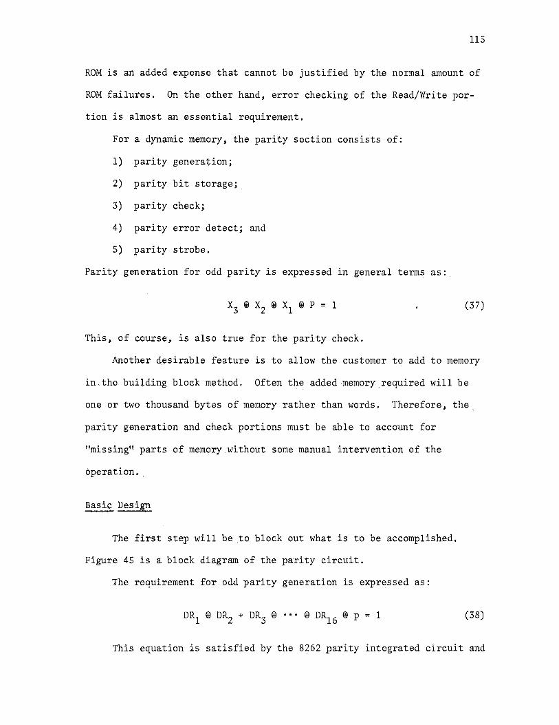
115
ROM is an added expense that cannot be justified by the normal amount of
ROM failures. On the .other hand, error checking of the Read/Write por
tion is almqst an essential requirement.
For a dynamic memory, the parity section consists of:
1) parity generation;
2) parity bit storage;
3) parity check;
4) parity error detect; and
5) parity strobe.
Parity generation for odd parity is expressed in general terms as:
(37)
This; of course, is also true for the parity check.
Another desirable feature is to a11ow the customer to add to memory
in the building block method. Often the added,memory required will be
one or two thousand bytes of memory rather than words. Therefore, the
parity generation and check portions must be able to account for
"missing" parts of memory.without some manual interventio11 of the
operation. ,
Basic Design
The first step will be to block out what is to be accomplished.
Figure 45 is a block diagram of the parity circuit.
The requirement for odd parity generation is expressed as:
(38)
This equation is satisfied by the 8262 parity integrated circuit and
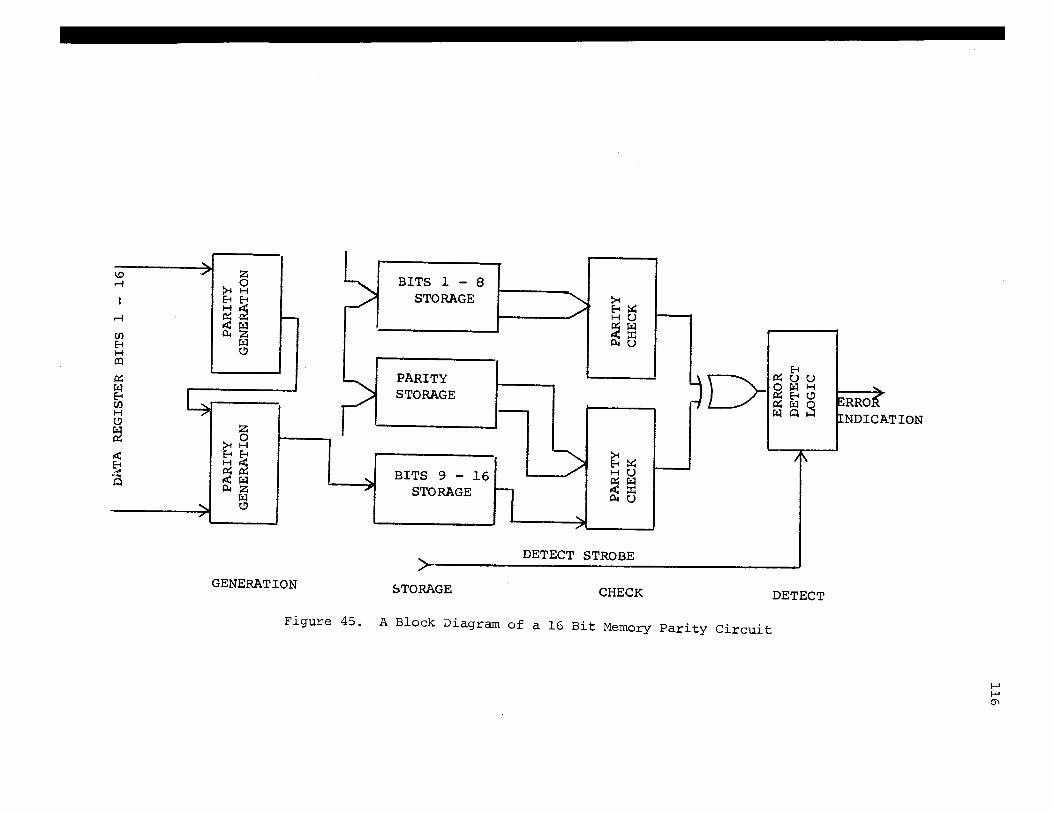
"° z BITS 1 - 8 r-1
>,! s STORAGE >,! E-t E-t
E-t ~ ~~ H CJ r-1
~~ f~ ti) i:i.. CJ E-t f:rl
H c, CCI
E-t r:i:: CJ CJ r:i:: PARITY Q f:rl H ti: E-t c, f:rl STORAGE r:i:: f:rl 3 E-t
f:rl Cl ti) H c, z f:rl
0 r:i:: >,! H
~~ < ~~ E-t BITS 9 - 16 H CJ ....
~~ A < f:rl i:i.. z STORAGE
i:i.. CJ f:rl c,
DETECT STROBE
GENERATION bTORAGE CHECK DETECT
Figure 45. A Block Diagram of a 16 Bit Memory Parity Circuit
..... ..... O'\
is shown schematically in Figure 46. For a byte to be implemented t11e
parity generation is expressed as:
117
(39)
Because of the relatively long propagation delay times of the 8262 and
the fact that the data is true for 500 ns, the two parity check 8262's
will be externally exclusive ORed together using another module of the SN
7486 gate originally used in the parity generation, One of the inputs to
the left half of memory will be grounded, The simplest method for
compensating for a byte of memory instead of a word is to not use any
complicated logic to disable the 8262 for the left side of memory, but
rat;her, make use of the fact that when memory is missing (physically re
moved) the data output bits are all logic l's by virtue of the pull down
resistors of the sense amplifier. However, one must use the~ output
node of the 8262 for the left half of memory, This byte inhibit is shown
in Figure 47.
Refresh Inhibit
One more·item must be accol.ll1ted for, When more than one RAM output
is connected in a wired OR condition, during refresh time the outputs of
the RAM's of each data bit, including parity, are invalid, This is be
cause the low logic O state is predominate and a logical O of one portion
of memory may be the correct bit; however, a logical 1 of another portion
may be correct, but the wired OR output will assume a logical O and cause
parity error to occur in the check, Therefore, a means to inhibit parity
during refresh is required, Figure 48 represents the final configuration
of the parity check circuit. Notice that the parity detect flip flop is
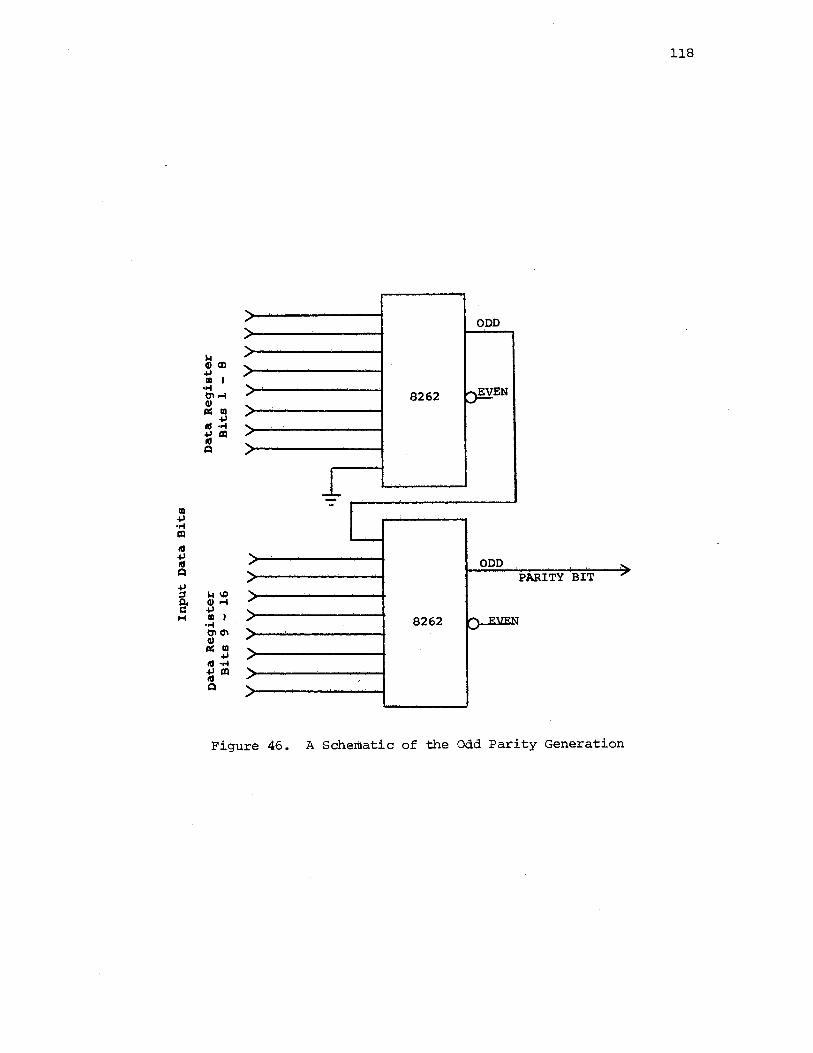
118
ODD
8262 EVEN
ODD .. PARITY BIT
8262
Figu~e 46. A Schematic of the Odd Parity Generation
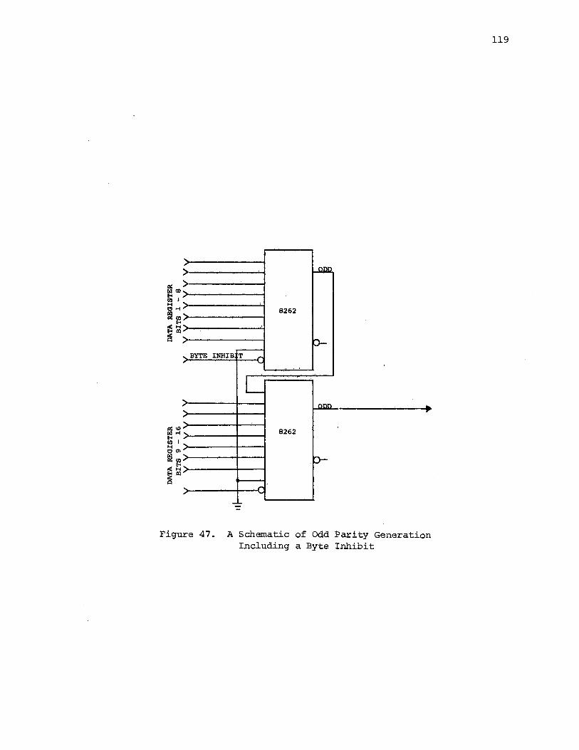
~ >·---------....... ~ !D f;j I >----------1 I: >----------1
E-< ~ :ii>-----------"'"! t§ >·------1
BYTE INHIB T
8262
8262
Figure 47. A Schematic of Odd Parity Generation Including a Byte !nhibit
119
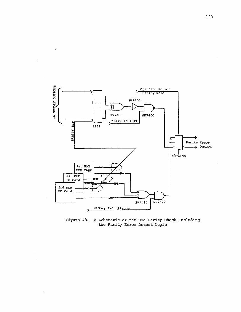
1st RPM MEM CARD
1st MEM PC card
2nd MEM PC Card
SN7486
) Oper~tor Action Parity Reset
SN7400
WRITE INHIBIT
8262
1--...-~....,,,.;...__.......;~--,
Memor Read .S.trobe
SN74109
120
Parity Error Detect
Figure 48. A Schematic of the Odd Parity Check Including the Parity Error Detect Logic
121
a D clocked flip flop (a SN 74109) with the set input connected to
ground. The·flip flop is strobed by the read strobe deve~oped in Figure
16.
The circuit is designed in this-manner to force some type of system
or operator action tQ reset a parity error indication,· With the set
side of the. D-type flip flop ·grounded an error will pennanently lock the
flip flop into a parity error indication until the pre-set input of the
flip flop is . grounded or power is turned off,
Test and Diagnostics
Introductton
L.ike their large machine counterparts, a machine normally will ha:ve
a power turn-on Test.and Diagnostic (T & D) routine written into the Read
Only Memory. This routine can be as complex or as simple as the applica
tion requires, One of the more popular simple and inexpensive routines
will. first. use a small portion of the Read Only Memory. to test the Read/
Write meory, transfer the routine from ROM to Read/Write and then test
the full ROM c~mplement, and finally .run a. test . of the communication
circuitry if an off line capability exists. The testing can be extended
to the other peripheral devices if used.
The discussion of the above areas will be restricted to the memory
as other testing is beyond the scqpe of this paper. Let us develop a
hypothetical routine to test the memories. The designer can expand or
delete tests depending on the application.
122
Implementation
The T & D starts with a routine written into ROM that is initiated
when power is turned on. This routine will generally consist of a Rel;!.d/
Write memory test exercising the memory Read/Write, addressing capabili-
ties, and parity circuit check out.· If the parity portion of memory.is
first checked, parity can then·.be·used to test the remainder.of the
Read/Write memory instead of requiring add.itional ROM. for a. "brute force"
compare. In order to check parity, the parity generation circuit
developed in the first part of this ch~pter requires modifying.
Wi~h the addition of the parity error lead a parity error can.be
forced and checked to insure an.error was.detected, and then fore~ a no
error condition and again insure that the no error was.detected. The·
flow chart of Figure 49 represents the sequence of events that are
required in the parity error test.
When the last portion of the test represented by the flow chart is
reached, the parity section of memory has been reasonably guaranteed to
be functional and reliable. ' ' '
Establishing that the parity portion of memory is reliable gives the
designer a powerful tool in checking the remainder of the Read/Write
memory. By using parity, the memory can be exercised to insure that all
functions are operational. As a minimum, the test should include:
1) memory address exercising;
2) all tes,t altereq (Write); and
3) all cells read.
When the Test and Diagnostic has established that the Read/Write
memory is operational the test routine can then be transferred from ROM
to the Read/Write memory and the same type of test performed to insure
POWER ON
WRITE PARITY ERROR
READ ERROR
WRITE INTO 1st MEMORY
LOCATION
ASSUME PARITY CIRCUI IS GOOD
CONTINUE MEMORY INITILI:lATION
YES
FLAG OPERATOR STOP PROCESSOR
Figure 49. A Flow Chart of the Initialization Test and Diagnostic Routine
123
124
that ROM is functiona~. This involves a check of the ROM's logicijl 1
Qutputs. These outputs are sunnned and compared with a pre-established
sum. A more elaborate Teas and Diagnostic routine would be required to
est;ablish where the error occurred.
Use of a 8.262 parity generator Integrated Circuit connected as shown
in Figure SO, allows.the implementation of the necessary inhibit by
adding one wire. Figure SO shows schematically this signal le~d desig
nated as Force Parity Error. The function of the Force Parity Error
signal is expressed as:
(40)
Element C is the parity error signal lead. The signal lead C when forced
to a logical 1 causes an error to be.detected by the parity check circuit
of Figure SO. With this modification to the parity generator circuit,
the parity check. circuit does not need to be changed.
An extra exc~usive-OR gate ext~rnal to the 8262 is also required to
add the Force Parity Error lead. This gate is an SN 7486 quad exclusive
OR, TTL integrated circuit •.
Memory Decode Logic
Int;.roduction
In the event memory is expanded beyond the limits imposed by the
memory element~ addressing capability, a method of selecting the specific
memory element requeste'd by the control unit; must be implemented. The
di~cus~ion in the following paragraph details one method of decoding the
address register i~formation into printed circuit card selection and.
memory element selection.
..... , > U2l21l
> > ..... ,
> 8262
..... ,
> b-..... BYTE INHIB T ~ ,
'-
L > ""'"' \ \
, I I PARITY BIT
..... ,
..... 8262 J , ..... SN7486 , .....
b--, ..... ,
..... -, "' ---=
FORCE PARITY ERROR ..... '
Figure 50. Implementation of the Test and Diagnostics Routine Into Parity Generation
125
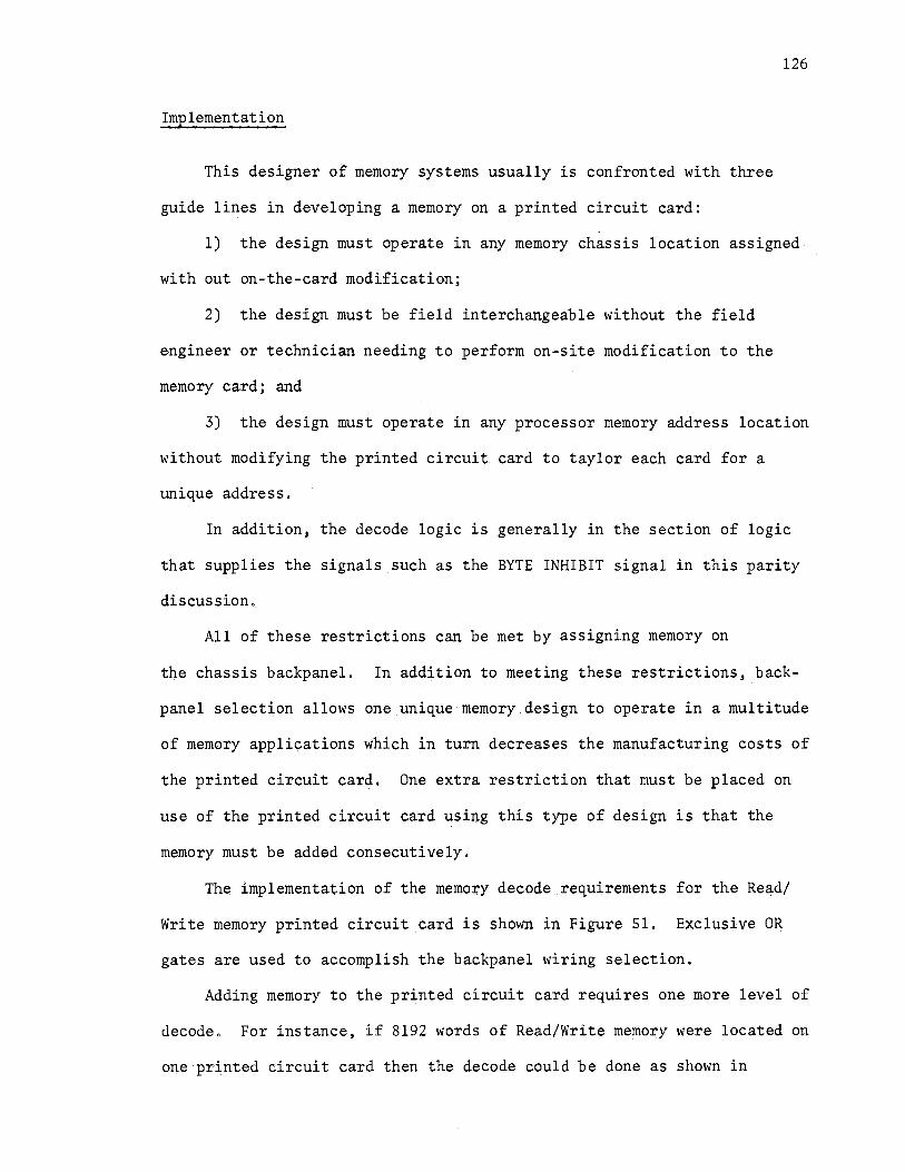
Implementation
This designer of memory systems usually is confronted with three
guide lines in developing a memory on a printed circuit card:
126
1) the design must operate in any memory chassis location assigned
with out on-the-card modification;
2) the design must be field interchangeable without the field
engineer or technician needing to perform on-site modification to the
memory card; and
3) the design must operate in any processor memory address location
without modifying the printed circuit card to taylor each card for a
unique address.
In addition, the decode logic is generally in the section of logic
that supplies the signals such as the BYTE INHIBIT signal in this parity
discussion.
All of these restrictions can be met by assigning memory on
the chassis backpanel. In addition to meeting these restrictions, back
panel selection allows one.unique·memory.design to operate in a multitude
of memory applications which in turn decreases the manufacturing costs of
the printed circuit card. On~ extra restriction that must be placed on
use of the printed circuit card using this type of design is that the
memory must be added consecutively.
Th~ implementation of the memory decode requirements for the Re~d/
Write memory printed circuit card is shown in Figure 51, Exclusive OR
gates are used to accomplish the backpanel wiring selection.
Adding memory to the printed circuit card requires one more level of
decode, For instance, if 8192 words of Read/Write memory were located on
one printed circuit card then the decode could be done as shown in
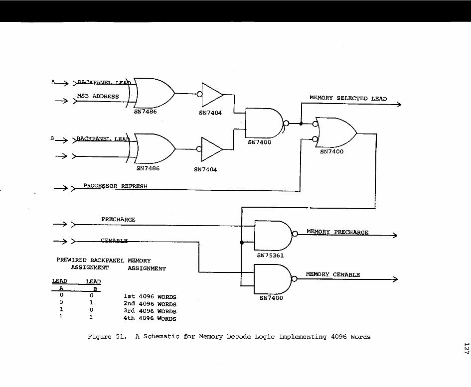
MSB ADDRESS MEMORY SELECTED LEAD
SN7486
SN7400
SN7400
SN7486 SN7404
PROCESSOR REFRESH
PRECHARGE
MEMORY PRECHARGE
SN75361 PREWIRED BACKPANEL MEMORY
ASSIGNMENT ASSIGNMENT MEMORY CENABLE
LEAD LEAD A a 0 0 1st 4096 WORDS 0 1 2nd 4096 WORDS
SN7400
1 0 3rd 4096 WORDS 1 1 4th 4096 WORDS
Figure 51. A Schematic for Memory Decode Logic Implementing 4096 Words ..... Iv -..J
128
Figure 52,
The decode circuit shown in Figure 52 will also perform for a.
16,384 word machine when a 1024 word memory element is used. One extra
lead must be brought into the SN 7442 decoder. The lead is MSB-3. This
breaks the 16,384 words into 1024 word increments. This decode circuit
also works well for ROM that does not have on chip decoding.
Read/Write Memory Storage Register
Implementation
For the small machine applications .where the processors data input
requires a static le~el, the dynamic RAM or ROM must have a data register.
A parallel in, parallel out register such as the SN 74195, MSI element
satisfies the requirement. To parallel memory printed circuit cards on
uncommitted TTL output open collector is required, The uncommitted out
put allows ROM and Read/Write memories to be wired OR on the backpanel.
Figure 53 is a schematic of the register and the inverters used to make
the data output lines uncommitted. The schematic is made to fit the 16
bit machine,
Also shown are pull up resistors normally required for sense ampli
fiers. In this example the SH 75108A was assumed to be used for the
sense amplifier. The SN 75108A is an uncommitted output high impedance
to TTL level device whose output is designed for memory wire - OR. The
resistors complete the output circuit~ The resistance value should be a
function of the designers speed, power requirements and the sense ampli
fiers low level current sink capabilities.
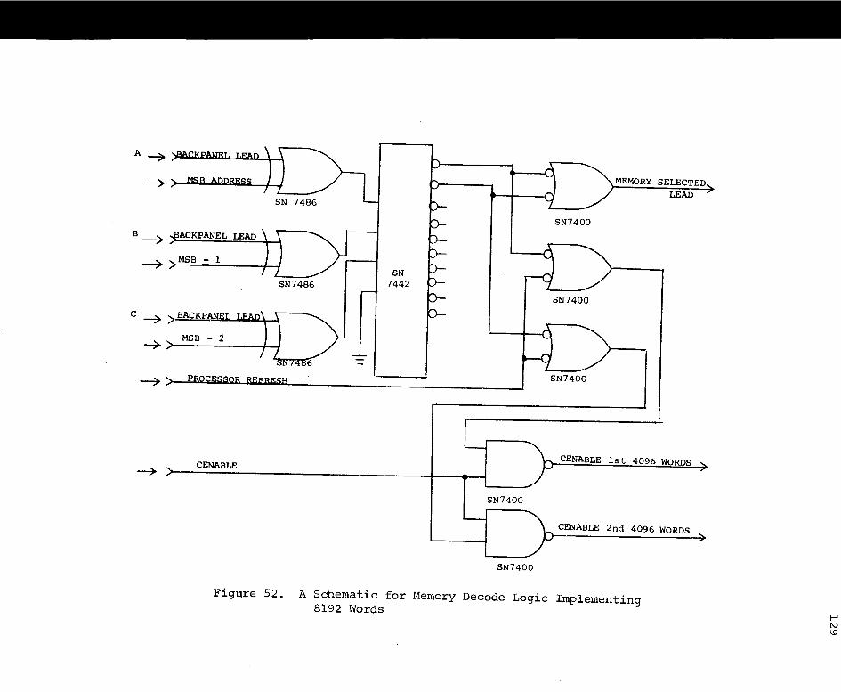
B~
SN7486
CENABLE
SN 7442
SN7400
SN7400
SN7400
SN7400
SN7400
MEMORY SELECTED LEAD
CENABLE 1st 4096 WORDS
CENABLE 2nd 4096 WORDS
Figure 52. A Schematic for Memory Decode Logic Implementing 8192 Words
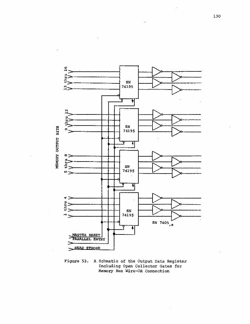
- ~-- / ~ >
" v SN
> 74195 /
-" 'I
- .. ..,. v f".. -- [> v SN f"... - 74195 -
y •1 -- v >·
f"... v - SN - 74195 v f'... ---
y •1 - ·- ... - v f"..._ -- f'-.. v -- SN v. [>--- 74195
- SN 7405 'I' ·1
,s
MASTER RESET - PARALLEL ENTRY ~ -- ~i;,11.n ~'T'RnRE -
Figure 53. A Schmatic of the Output Data Register Including Open Collector Gates for Memory Bus Wire-OR Connection
130
CHAPTER VI
SUMMARY AND CONCLUSIONS
Problem Summary
When adapting a semiconductor memory to a Small Machine application,
five basic problems must be considered. These problems can be summarized
as the following.
1) Choosing the type of memory.based on the requirements and cost
needs of the machine applications, Two technologies are available,
bipolar and MOS. Each technology can be divided into two distinct cate
gories. Bipolar is divided into TTL for medium speed applications, ECL
for very high speed application. MOS is divided into static memory for.
simple but small storage applications, dynamic for complex but dense
storage applications.
2) Interfacing between the three main block functions of the
processor and memory. Many techniques are available, but two are most
common because of their simplicity and cost effectiveness, These tech
niques are the ring counter and the monostable multivibrator.
3) Paralleling the Read/Write and Read Only memories on the
bus. Both the address and data bus require special attention to the
timing and loading interface.
4) Adding the memory peripheral logic. This logic requires
special attention both becatJse of its technical, Le, , timing, loading
and logic states, and the added cost and packaging needs. The general
131
132
peripheral logic can be summarized as parity, test and diagnostics, and
the data storage register.
5) Proper adaptation of the processor and memory refresh needs.
This is applicable to a MOS dynamic memory only. Particular attention
must be paid to the process~rs operating conditions and the_needs of the
memory.
Conclusions
The trend of the computer industry is away from magnetic core to
semiconductor memory. This trend is more dramatic, at present, in small
machines rather than the larger computers; however, the large processors
are beginning to appear with semiconductor main memory in greater num~
bers. Soon, all of the main computer memory will be semiconductor as the
memory cost is further reduced and the magnetic core can no lo~ger
compete. This trend is substantiated by the investments of core memory.
manufacturers into semiconductor subdivisions. With the advent of the
ma~etic bubble technique.and char~e coupled devices, the previous
dominated domain of the disk and tape handlers is being invaded with the
conclusion inevitable.
The first design step to be taken is to choose the memo4y that best
fits the application. This choice is often a compromise based on a broad
need and application requ~rement, In most cases an adaptat~on of the
memory will be _required. For static memories, this adaptation is minor.
For dynamic memories, the adaptation can,become complex. Howeve~, with
proper,techniques and precautions almost all applications can be
satisfied.
The MOS dynamic memory,is the most difficult type of memory to adapt
133
to a proces.sor. However, in a majority of cases, the dynamic MOS memory
is the most cost effective of the semiconductor memories, giving the.
largest storage capacity for the least power consumed, the lowest cost
per bit, and the smallest package size.
The proper interface logic is chosen as a function of many varia
bles. The principle variables are cost, performance, packaging require
ments. environment~l requirements, and power needs.
The final consideration of the designer is the method of refreshing
the memory. Many techniques are available, planar refreshing, charge
pump, and processor .controlled to name a few. All of these methods are
related and require a consideration of the processor's operating condi
tions. With these considerations held prominent, the most efficient
technique of refresh and interface logic can be decided.
SELECTED BIBLIOGRAPHY
Chu, Yaohan.
1962 Digital Computer Design Fundamentals. New York: McGrawHill.
Crawford, R.H.
1967 MOSFET in Circuit Design. New York: McGraw-Hill.
The Engineering Staff of American Micro-Systems, Inc.
1972 MOS Integrated Circuits. New York: Van Nostrand Rienhold.
The Intel Corporation.
1973 The Intel Memory Design Handbook. Santa Clara, California.
134
APPENDIX A
A LIST OF SEMICONDUCTOR MEMORY MANUFACTURERS
135
ADDRESS
American Micro-Systems, Incorporated 3800 Homestead Road Santa Clara~ California 95051
Advanced Memory Systems. 1276 Hammerwood Avenue Sunnyvale, California 94086
Fairchild Semiconductor Corporation 464 Ellis Street. Mountain View, California
General Instrument Corporation Microelectronics Division 600 West John Street Hicksville, New York· 11802
Harris Semiconductor P.O. Bo; 883 Melb9urne, Florida 32901
Intel Corporation 3065 Bowers .. Avenue Santa Clara, California 95051
Intersil Incorporated 10900 North Tantau Avenu~ Cupertino, California 95014
Monolithic Memoires, Incorporated 1165 East Arques Avenue · Sunnyvale, C~lifornia 94086
Mostek Corporation 1215 W. Corsby Road Carrollton, Texas 75006 . .
Motorola,Semiconducto~ Products Incorporated P. O. Box ,.20924 Phoenix, Arizona. 85036
National Semiconductor Corporation 2900 Semiconductor Drive Santa Clara, California 95951
Signetis Corporation 811 East Arques Avenue Sunnyvale, California 94086
136
ABBREVIATION
AMI
AMS
FSC
GI
H
I
INT
MM
MOS
MOT
NATL
SIG
ADDRESS
Texas Instruments, Incorporated P. ·O, Box 5012 Dallas, Texas 75222
137
ABBREVIATION
TI
APPENDIX B
TWO ALTERNATIVES FOR THE IMPLEMENTATION OF
AN ASTABLE MULTIVIBRATOR
138
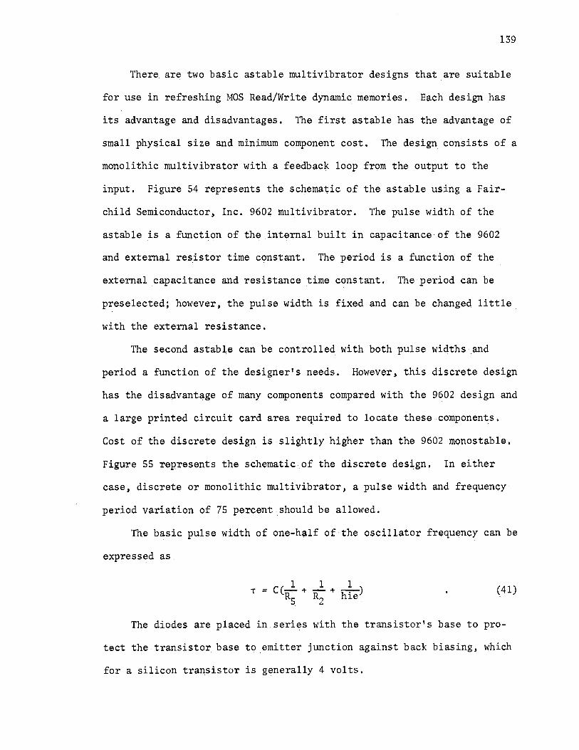
There. are two basic astable multivibrator designs that are suitable
for use in refreshing MOS Read/Write dynamic memories. Each design ~as
its advantage and disadvantages. The first astable has the advantage of
small physical size and minimum component cost. The design consists of a
monolithic multivibrator with a feedback loop fr9m the output to the
input, Figure 54 represents the schematic of the astable using a Fair-
child Semiconductor, Inc. 9602 multivibrator. The pulse width of the
astable is a function of the internal built in capacitance of the 9602
and external res,istor time constant, The period is a function of the·.
external capacitance and resistance _time constant. The _period can be
preselected; however, the pulse width is fixed and can be changed little ..
with the external resis~ance.
The second astable can be controlled_ with both pulse wiqths and
period a function of the designer's needs. However, this discrete design
has the disadvantage of many components compared with the 9602 design and
a.large printed circuit card area required to locate these ,components.
Cost of the discrete design is slightly higher than the 9602 monostable.
Figure 55 represents the schematic of the discrete design. In either
case, discrete or monolithic multivibrator, a pulse width and frequency
period variation of 75 percent ,should be allowed.
The basic pulse width of one-h~lf of the oscillator frequency can be
express~d as.
1 1 1 T .= C(- + - + -) R5 R2 hie (41)
The diodes are placed in seri~s with the transistor's base to pro-
tect the transistor base to _emitter junction against back biasing, which
for a silicon transistor is generally 4 volts.
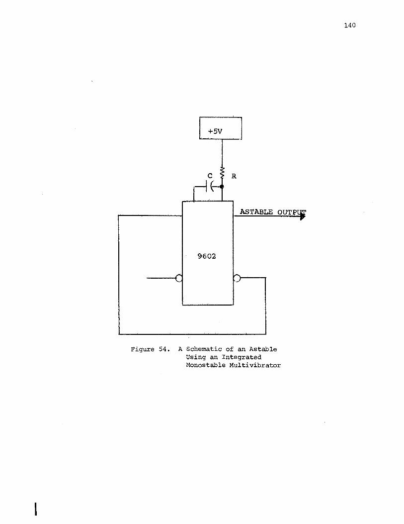
I
+sv
c .. ' . • R
,-1~1 ASTABLE OUTP!:J
9602
. ,,... ........ \.., ~_,
Figure 54. A Schematic of an Astable Using an Integrated Monostable Multivibrator
140
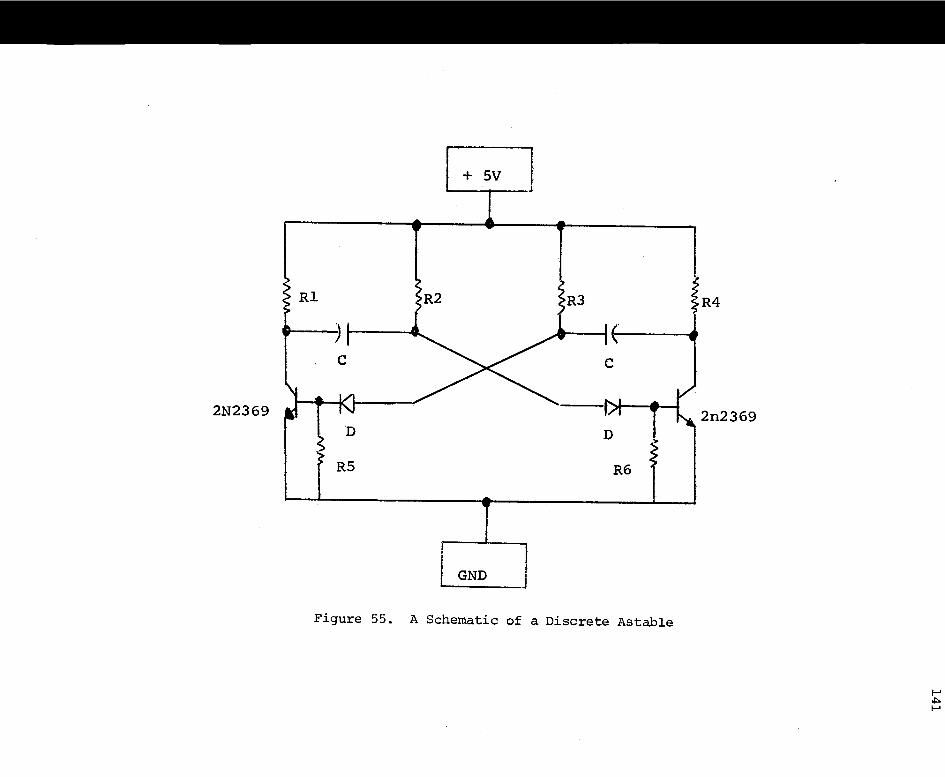
__ +_s_v_J
Rl R3 lR4
7 ~-
c c
2N2369 2n2369 D
RS R6
GND j
Figure 55. A Schematic of a Discrete Astable
APPENDIX C
A FINAL SCHEMATIC OF A READ/WRITE DESIGN USING
MONOSTABLE MULTIVIBRATOR FOR INTERFACE LOGIC
142
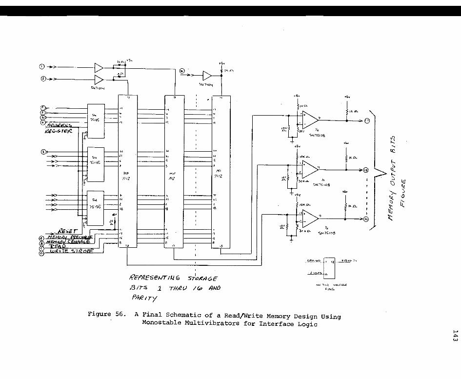
I ~> C> "" ©~> C>
I Sl-41,;o'-i
" ~
(E _,, ((' f-.- .. ,_. 5e
f--.-1 16 >< 751S6 -·· 'H 4.-, ... ,-.-~ -
fU,:.,,sre,e. ,-< I+~ ,---
I. - Zo
-> ·~ >---- ,, - ,s,gs >---- S" - >---- 3
,-,-MF
r< 711z !r , ..
--> _ .. -- I.I.I
_,, - .....__ z -> 7i>1% -- ~ 18
,,,. -r-
~t I-<
r~ - /1?1::;c, l " .- ,, i ""=· IS" •~-.... -A, C.i;;;;;.a.fAA. -~ 1,e "Pi='A O ,,
''"" l 11- "5.7fl "·~-
I
Figure 56.
1.3 trs. 1
P1+,e IT'/
I "
•i .. l ,q
>o
z,
s
' HI'"
71,2
" " z •8
" ,, ,s 8
" I
~>------{>- It<-"'-
SWNCo--f
. -~ " .
' •i . 1 ,q
' ' ' ' ' <o
<I
5 . ' H• ' '
7112
' ' ' ... ..
' ,; I
' I
' " ,, .. 8
I
"-f-' I
'
I 5Tto.e.4e:,E
TH~U /(p /.JNIJ
... s ... • •• ~,00- I 11i:. .n. .. .
i
100~ ~
9
.0.. J(c.' z
"' ..<>.
'},:
y .,,,n;;,oe,
'"" • s.
! 1<0-IOK..C\...
I ~~ ,,
3co..a.. Si'-41~ 108
••• -: ,r&y
0
I f 101<..0.. , . .(\_
~~ Y,
3co~ 'i,l,ll\,108
-(.~O\ltJ.D I 12~ .. T~
MF! 112. VOLTQ.(:,E
P1NS.
A Final Schematic of a Read/Write Memory Design Using Monostable Multivibrators for Interface Logic
@
fl ......
t:Q
h. ::.
' ,
~ Q... h. :::-i l!.J 'C:> l',t
'>- )
~ -!>
I
@
~ G: It ~
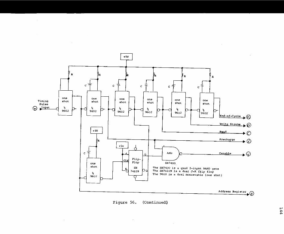
R
one Timing shot Pulse
© In ut !:; 9602
c
one shot
!:; 9602
+sv
one shot
!:; 9602
R
+SV
c T one shot
!:; 9602
+Sv
c
FlipFlop
SN 74109
Figure 56.
R
T c
one shot
one shot
one shot
!:; 9602
Q
Q
!:; 9602
!:; 9602'
End-of-Cycle ® Write Strobe ~ ~~~~~"""--~--'-'--~~
~~~~~~~~~~~~~~~---=R~e~a~d"--~~~-.{()
Precharge
AND
SN7400
The SN7400 is a quad 2-input NAND gate The SN74109 is a dual J-K flip flop The 9602 is a dual monostable (one shot)
0
Address Register ~
(Continued)
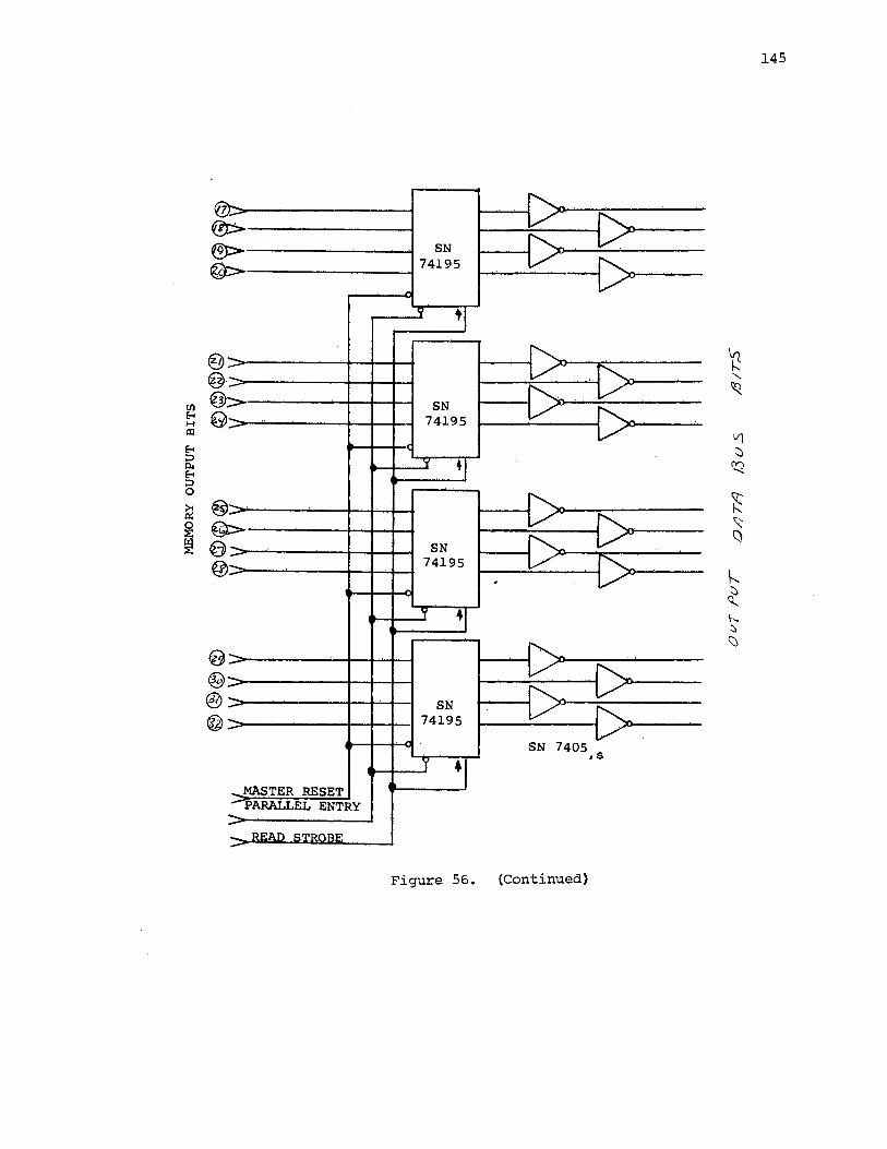
145
7 -
v "" g SN ~ v 74195 v
''
-I.I ti
-- v - .J -· [> v 3> ., SN . '
,_ " 74195 ~ -
'( ' +1
·~' - v f'... . - SN '-.....__ v -·- 74195 / . ""-, . .
" •1 - .. ,.
' - v ~ .. . ~- v -. SN v ~ - 74195 - - SN 7405
y 41 ,s
- MASTER RESET • _:"'"PARALLEL ENTRY -- t)i;'ZIT'\ ~'!'ROBE .
Figure 56. (Continued)
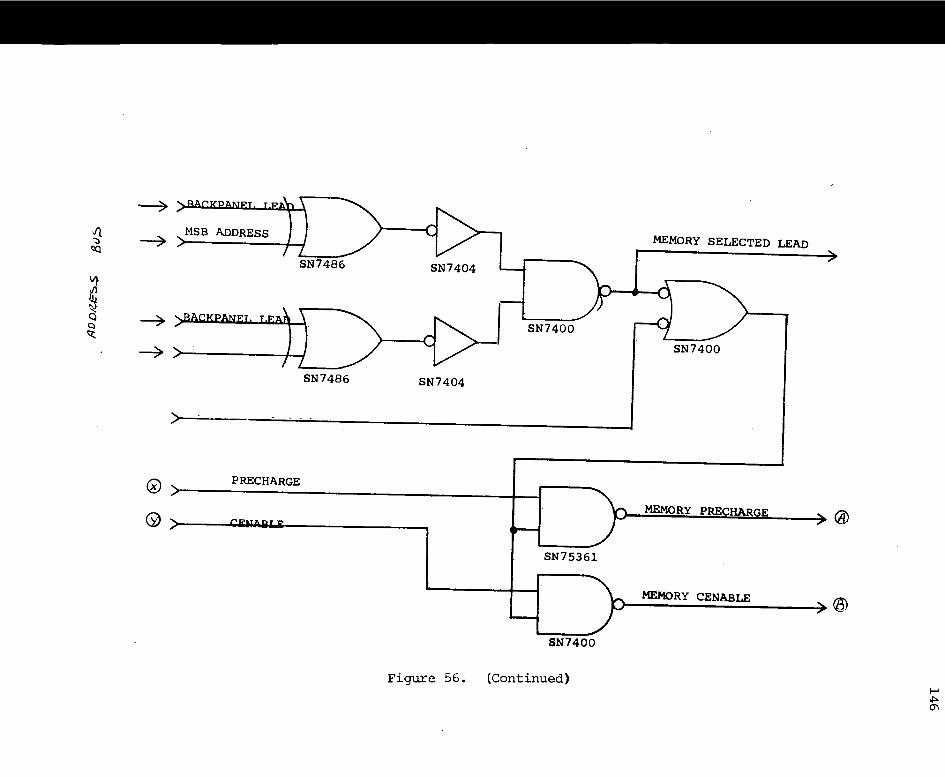
MSB ADDRESS MEMORY SELECTED LEAD
SN7486
SN7400
SN7400
SN7486 SN74.04
PRECHARGE
MEMORY PREC E
SN75361
MEMORY CENABLE
SN7400
Figure 56. (Continued)
APPENDIX D
A FINAL SCHEMATIC OF A DESIGN USING A RING
COUNTER INTERFACE LOGIC
147
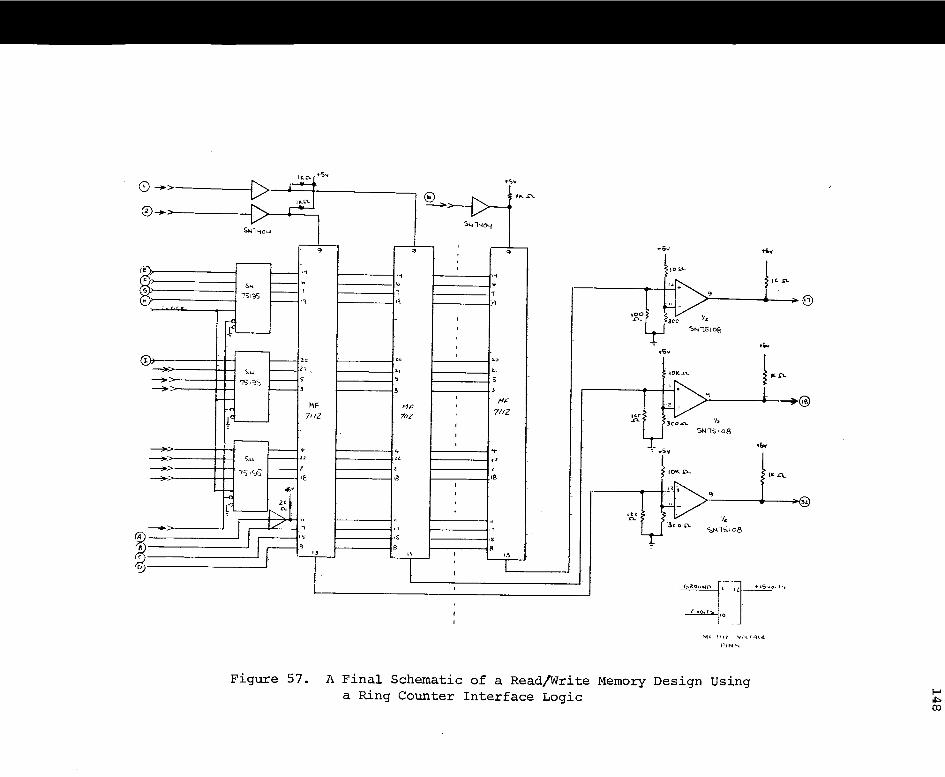
(i) -->
®->
~ (.".,
" -> -----+> --> --ti
~
(
~
I ~--{>-- ........
[> '~""
SM1'10"'1 I Sl.l1sCSj
I ... ; ... " " " ...
-' ~,00- I f-- ., ., ·,; t= s~ ,______" " . ...
751~ ,______ 1 1 1 v9 _,, ,q _.,
100 ,-< - I ...... Jee 'lz
It-- I 'SN1:SIOS
'
[>
' a ,...,
~ .s. i··~
' - le <o LO
.,,~ - 21 ' " ,, t IOK.n.
-s 5 s '7';1'.:J~ ' I >-3 ~ 3 PV~ ~~ I /'(IC
h: HF M/C 7112
If~ 7112 7/tl ' "' = )CO..d. '/z I
s~,~ 108 I - ' ,rw _,.
', ... -: ...-Sy su _,,
" u I ?~1s,c; -l
2 ' 1101".~ I• .n.. -'o •8 Je I R;>~ ->- "'' I I-<
---~t I r -'" ~ Y, "
,, "
.n. , , / le-on. _., ,, ,, "".::.N.lSwB
'" ,s ,s
' B = I -~
T ,, I ,.,
t ' -r I
-'
e,.2ovwo . ll~O,T',,
Figure 57.
- l" ..
1111 vn11,H,t
P1N'--,,
A Final Schematic of a Read/Write Memory Design Using a Ring Counter Interface Logic
11
;;@
"
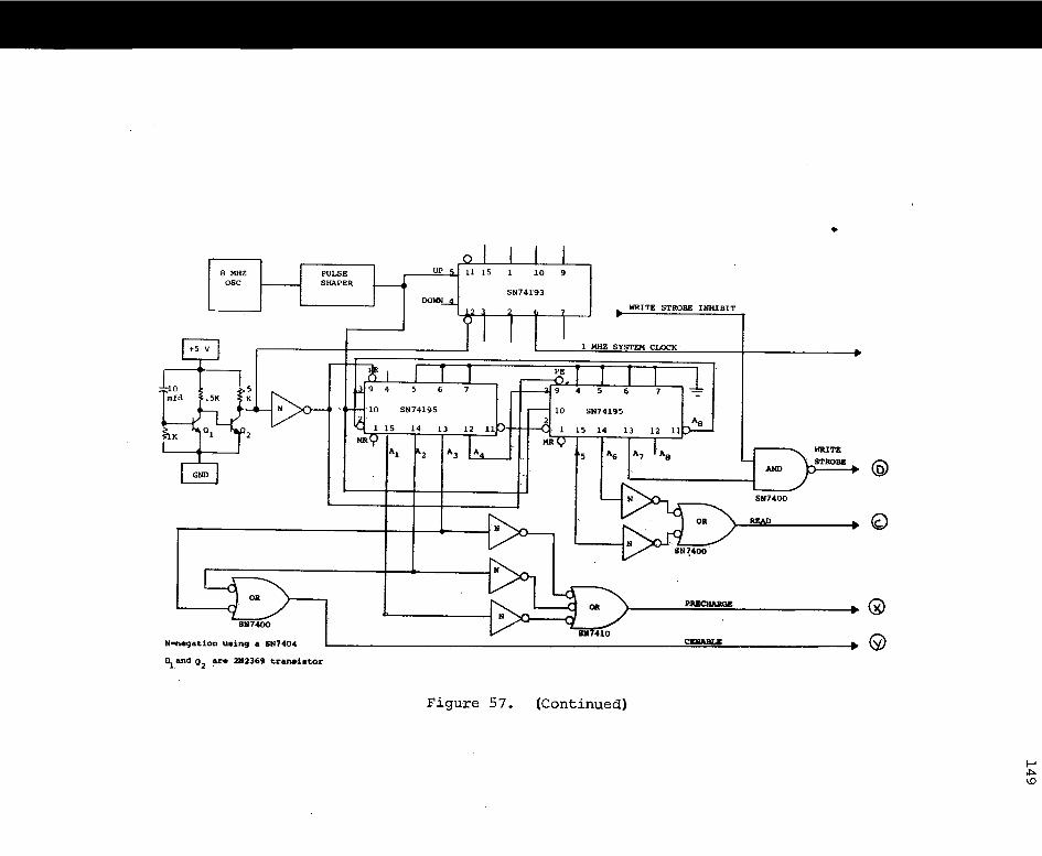
8 MHZ osc
PULSE SHAPER
N-negation u•ing a SN7404
°iand o2 are 2112369 tranehtor
-10 9
SN74193
WRITE STROBE INHIBIT
l MHZ SYSTEM CLOCK
6
SN74195
Figure 57. (Continued}
SN7400
•
tlRITE
STROBE
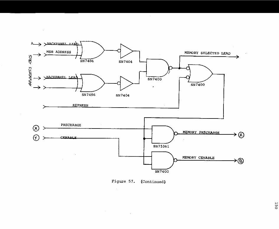
0 ©
MSB ADDRESS
SN7486
SN7486
REFRESH ,
PRECHARGE
SN7400
SN7404
SN75361
SN7400
Figure 57. (Continued)
MEMOR):' SELECTED LEAD
SN7400
u--,;ME=M;,;O~R;.;,Y~P:..:RE:.::·::.:C=HAR~· =G.:.i:E:1...._ __ , ®
MEMORY CENABLE ® >---------?'{_\
.... l1l 0
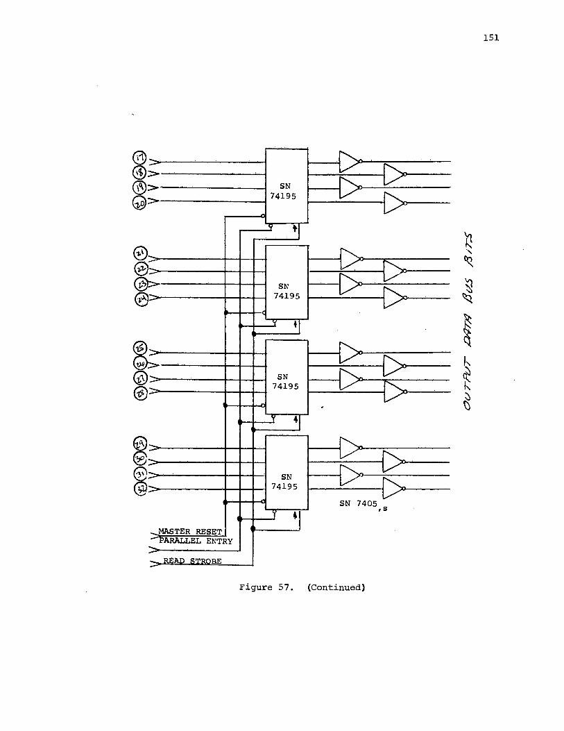
@ @ ® @
--> > >
--·--·-·-
-·-
----·--,_
- MASTER RESET - PARALLEL ENTRY -- 'Ql.'!l.n STROBE -
151
-
v ~ SN ~ v
74195 v -
v . 'I
v ~
C> ,V SN
74195
v 41
v "' SN ""'-- v 74195 v f'---.
- . v 41
-
v ""--f'.,__ v
SN v C>--74195
'( 41 SN 7405 ,s
Figure 57. (Continued)
APPENDIX E
A rINAL SCHEMATIC OF THE READ ONLY
RANDOM·ACCESS MEMORY
152
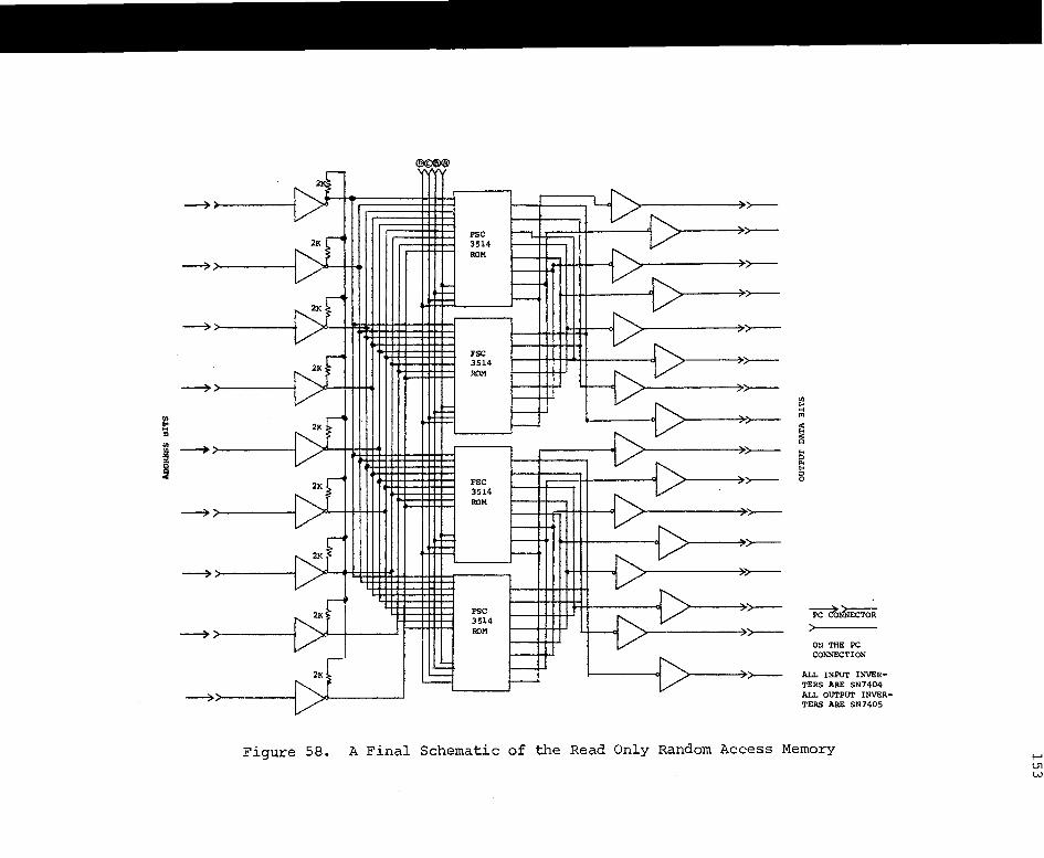
2r-.
. 2Kr
. 2Kr
2Kr
2Kr .
. ~ '
2Kf . '
> 2Kr
. 2Kr
Figure 58.
' -~ FSC
.._..... 3514 ROM
.___ -~ ~ - ,.._
FSC 3514 ROM
~ ...._ .._ -~ I::: -
FSC 3514 ROM
.... I- ,___ I-I- ,___
FSC 3514 ROM
-= ,-..___ '-- ,___
->-----
-
-->--
,
, >--
-{> ~
~ >---
>--
-, . , >--
, >--
, >--
>--
-{> -, >--
. >--
ON THE PC CONNECTION
ALL INPUT INVERTERS ARE SN7404 ALL OUTPUT INVERTERS ARE SN7405
A Final Schematic of the Read Only Random Access Memory I-' lJ1 w
APPENDIX F
THE MICROSYSTEMS INTERNATIONAL, LTD.
MF 7112, READ/WRITE IC DATA SHEET
154
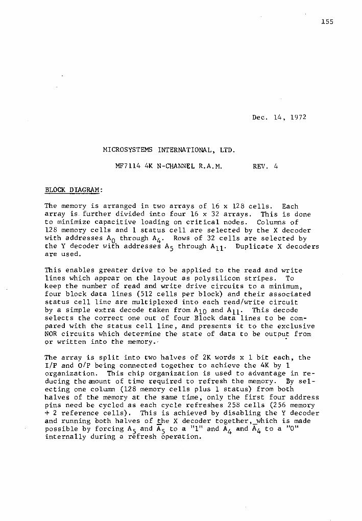
Dec. 14, 1972
MICROSYSTEMS INTERNATIONAL, LTD.
MF7114 4K N-CHANNEL R.A.M. REV. 4
BLO.CK DIA GRAM:
The memory is arranged in two arrays of 16 x 128 cells. Each array is further divided into four 16 x 32 arrays. This is done to minimize capacitive loading on critical nodes. Columri.s of 128 memory cells and l status cell are selected by the X decoder with addresses A0 through A4 . Rows of 32 cells are selected by the Y decoder with addresses A5 through An. Duplicate X decoders are used.
This enables greater drive to be applied to the read and write lines which appear on the layout as polysilicon stripes. To keep the number of read and write drive circuits to a minimum, four block data lines (512 cells per block) and their associated status cell line are multiplexed into each read/write circuit by a simple extra decode taken from A10 and A11· This decode selects the correct one out of four Block data lines to be compared with the status cell line, and presents it to the exclusive NOR circuits which determine the state of data to be output from or written into the memory.,
The array is split into two halves of 2K words x l bit each, the I/P and Q/p being connected together to achieve the 4K by l organization. This chip organization is used to advantage in reducing theanount of time required to refresh the memory. By selecting one column (128 memory cells plus l status) from both halves of the memory at the same time, only the first four address pins need be cycled as each cycle refreshes 258 cells (256 memory + 2 reference cells). This is achieved by disabling the Y decoder and running both halves of ~he X decoder together,_which is made possible by forcing A5 and As to a "l" and A4 and A4 to a "O" internally during a refresh operation.
155
156
DEVICE OPE.RATION:
Referring to the block diagram (Fig. 1) and the timing diagram (Fig. 2) it can be seen that the device cycle timing is established via the three clocks 01 02 03. The cycle is split into three separate portions by these clocks and this enables three types of cycle operation to be performed: (1) Read Only (2) Read/ Write (3) Read Modify Write. No read/write control line is used as 02 and 03 perform this function and tre chip enable pulse is used only to select the required memory chips in use at any particular time.
REFRESH CYCU:$:
Because of the dynamic storage nature of the 4K matrix the whole array must be periodically refreshed. The refresh cycle is a normal Read/Write cycle and to simplify the control of this cycle, and also speed up the total time taken to refresh the complete matrix, a refresh control is used. 'this control normally a "1" is taken to "O" for the complete 01 02 03 cycle and is arranged to have preference over chip enable so tfiat a refresh can be accomplished regardless of the state of chip enable. Simple gating on the X and Y decoders, also controlled from the refresh signal, enables a complete refresh to be performed in 16 memory cycles (i.e. the cycling of Ao through A3).
Data is automatically re-written every 01, 02 , 03 cycle, so no refresh amplifiers are needed as refresh is accomplished by the inverting cell itself. the refresh time is kept to a minimum, and in terms of lost memory cycles is only .43% of available read/write cycles and .37% of available read only cycles. Alternatively refresh can be accomplished during norm.al memory use. This is achieved by exercising each column of 128 memory cells plus 1 status cell at least once every 2mS. If refresh is done this way 32 cycles are needed for a complete refresh, but as these are normal Read/Write or Read-Modify-Write cycles, no memory time is lost.
INITIALIZATlON OF STATUS CELLS
During operation of the memory, the function of the status cells is to maintain a constant phase relationship with respect to the memory cells in the associated column. However, during the first few cycles it could be possible for the status cell to lose this relationship because of initial set up conditions in the memory. This could be overcome by cycling the memory a number of times before using it each time a power-on sequence occur~ed. This is time consuming, and a much simpler and quicker way is to perform
157
a refresh cycle with 02 inhibited. This way the precharge condition is written into each memory and status cell position a column at a time. This operation requires the usual 16 cycles required for a normal refresh. It is also possible to use this as a clear memory operation.
It would also be possible to achieve the same result by overlapping the clocks 0~ and 01 for a shor time. This would leave the write line at a "1 ' while charging all the data lines, thereby writing the charged data line onto each storage node. This is a one shot operation as ~1 also has the effect of setting all the X and Y decoders to a "1". Therefore instead of initializing cells a column at a time, all cells are initialized at one time.
\
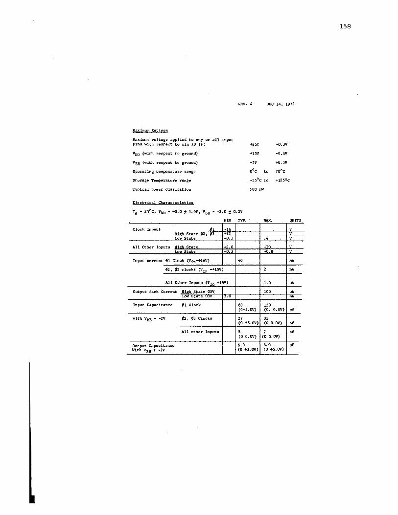
Maximum Ratings
Maximum voltage applied to any or all input pins with respect to pin 10 is:
VDD (with respect to ground)
VBB (with respect to ground)
Operating temperature range
Storage Temperature range
Typical power dissipation
Electrical Characteristics
REV. 4 DEC 14, 1972
+2SV -0.3V
+15V -0.3V
-5V +o.3V
o0 c to 10°c
-5S0 c to +12s0 c
500 rrM
TA• 25°C, VDD • +o.o ± 1.ov, VBB • -2.0 ± o.2v
MIN TYP UNITS
Clock Inputs lll1 +"· v Hillh State 112 1'13 +12 v Low State -0.3 .4 I v
All Other Inputs U4 .... Sh•a +2.0 +10 v Low State -0.3 +o.8 v
Input current Ill Clock (Vin-+16V) 40 mt.
112, 113 clocks (Vin -+15V) 2 mt.
All Other Inputs (V irt +15V) 1.0 uA
Output Sink Current Hiah State OSV 100 uA Low State 03V !3.0 mt.
Input Capacitance fll Clock 80 120 (o+S.OV) (0. O.OV) pf
with VBB • -2v 112, 113 Clocks 27 35 (0 +S.OV) (0 O.OV) pf
All other inputs 5 7 pf (0 O.OV) (0 o. OV)
Output· Capacitance 6.0 8.0 pf With VBB + -2V (0 +5.0V) (0 +5.0V)
158
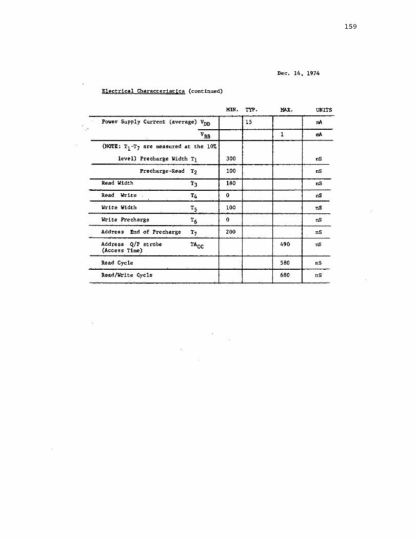
159
Dec. 14, 1974
Electrical Characteristics (continued)
MIN, TYP, MAX, UNITS
Power Supply Cun;'ent (average) VDD 15 mA '
VBB 1 mA
(NOTE: T1-T7 are measured at the 10%
level) Precharge Width T1 300 nS
Precharge-Read T2 100 nS
Read Width T3 180 nS
Read Write T4 0 nS '
Write Width T5 100 nS
Write Precharge T6 0 nS
Address End of Precharge T7 200 nS "'
Address Q/P strobe TA cc 490 nS (Access 'l'ime)
Read Cycle 580 nS
Read/Write Cycle 680 ns·
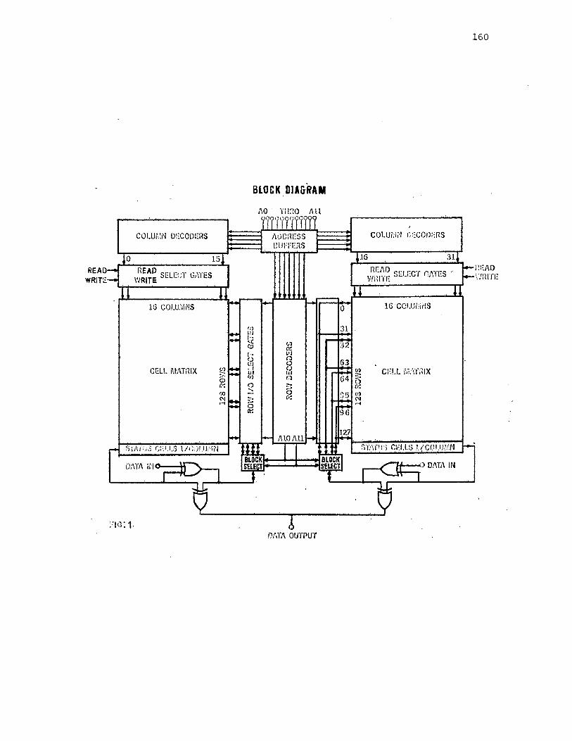
READ WRITE
COLUr.tN O::CODERS
READ S'"L•·, ··r l' ,. "ES WRITE c ,.:,, ,,.i
16 COLU,i'lt'IS
CELI. MATnlX
BLOCK DIAGRAM
nmo All
rrnFFrns
D!\TI\ OUTPUT
COLW.iN G;.:CODERS
REI\D sr:r .-c·r n,,,·r:s , wmr,~ ,_ .. r. . •• ,.
16 COJ.IJi'iii·JS
CELI. r,1.'WRIX
) DJ\li\ IN
160
!~::AD s:mrm
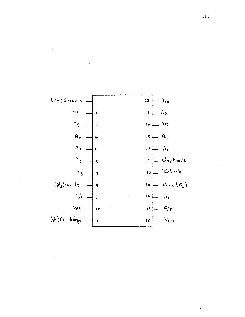
161
( Ov ) Gr o v" d ' , 2.2 A-10
A11 2 21 A<o
As :3 20 As
A9 + i9 A4
A'l 5 18 Ao
Ai E, 11 (h,r Enable
A3 '7 16 - 'Ke ·k-es. h
( r/3) i,U,-; t e. 8 15 - i?eaJ (oi!)
I/p 9 14 ft I
Vss 10 i.3 - o/p
(~i)Pre ch ar~e ii 12 Voo
APPENDIX G
THE FAIRCHILD SEMICONDUCTOR; INC. 3514
READ ONLY MEMORY DATA SHEET
162
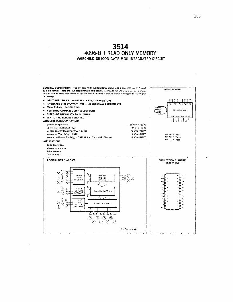
3514 4096-BIT READ ONLY MEMORY
FAIRCHILD SILICON GATE MOS INTEGRATED CIRCUIT
GENERAL OESCRIPTION -The 3514 is a 4096-Bit Read Only Memory. It is organized in a 512-word by 8-bit format. Ther~ are four programfflable chip selects to provide for OR wiring up to 16 chips. The 3514 is an MOS monolithic integrated circuit utilizing P-channel enhancement mode silicon gate technology,
• INPUT AMPLIFIER ELIMINATES ALL PULL UP RESISTORS
• INTERFACE DIRECTLY WITH TTL - NO EXTERNAL COMPONENTS
• 500 n1 TYPICAL ACCESS TIME
• 4-BIT PROGRAMMABLE CHIP SELECT COOE
• WIRED ... OR CAPABILITY ON OUTPUTS
• STATIC - NO CLOCKS REOUIREO ABSOLUTE MAXIMUM RATINGS
Storage Temperature Operating Temperature {TA) Volrage on Any lnpur Pin (V55 = GNOI Voltage on Voo (Vss = GNO) Voltage on Output Pin (V55 = GNO, Output Current@ ±10 mAI
APPLICATIONS
Code Conversion
Microprogramming
Table Lookup Control Logic
LOGIC BLOCK DIAGRAM
@@ Ao 0 A1
@@ A2 1 OF 64
AJ ROW
@ A4 DECODER
@ A5
e® l OF 8 COLUMN 14@ DECODER
@@cso 1 OF 16
0~~; CHIP SELECT 0 CS3 DECODER
oa 01 02 03 04 as as 01
© ® ®@) © 0 ®@
-65°C to +15!l°C o•c: to +10°c
-20 v 10 +0.3 v -7 V to +0.3 V .c..7 V 10 +0.3V
·vss@ voo @
"""'VGG0
0 = Pin Number
" 2J , 3
LOGIC SYMBOL
4 0 6 7 8 9 10 II
Pin 24 Vss Pir-12 V[)o Pin 1 VGG
CONNECTION DIAGRAM (TOPVIEWI
163
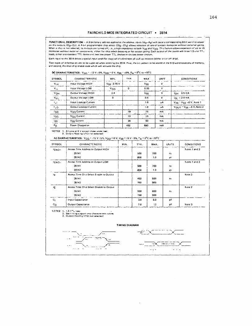
FAIRCHILD MOS INTEGRATED CIRCUIT • 3514
FUNCTIONAL DESCRIPTION - A 9-bit binary address applied to the address inputs (Ao-Aa) will cause a corresponding 8-bit word to appear on the outputs (Oo-07). A 4-bit programmable chip select (CS0-CS3) allows selection of one-of-sixteen memories without external gating. When a chip is not selected, its outputs are turned off, i.e., a high impedance to both V55 and Voo- This feature allows expansion of up to 16 memories without external components, either for chip select decoding or for output gating. Each output of the device will drive 1.5 unit TTL loads, either one standard TTL device and two low power TTL devices or she low power devices.
Each input to the 3514 drives a special input amplifier stage which eliminates all pull up resistors (either on or off chip).
Two types of information are to be supplied when ordering the 3514. First. the bit pattern to be stored in the 512-word locations of memory, and second, the 4-bit chip enable code which will activate the chip.
DC CHARACTERISTICS: VGG = -12 v ±5%, Voo" 0 V, Vss = ±5%, TA= 0°C to +70°C
SYMBOL CHARACTERISTIC MIN.
V1,1-t Input Voltage HIGH _vss-2.15 v
V1L Input Voltage LOW I
VoH Output Voltage HIGH ,, VoL Output Voltage LOW
iu Input Leakage Current
ILO Output Leakage Current
•oo Voo, Curr1en~
1GG v.GG Current
•ss V55 Cu_~rent
Po Power Dissipation
NOTES: 1. A11 pins at O v e,ccept those under test. 2. Output floating (chip not se1ected)
vGG
2.4
0
TYP. MAX,
Vss
0 0.55
Vss
0.4
1.0
1.0
19 25 "'
19 25 "
38 50
450 580
"
UNIT CONDITIONS
v
v I
v IOH =_0.5 ~A.
v IOL < 2.4 mA '
µA V1N a Vs,S -6 V, Note 1
µA VOU"f = Vss -6 _V.Note_2
mA ,,
mA "
mA
mW "
AC CHARACTERISTICS: VGG a -12 V ±5%, Voo = 0 V, Vss = ±5 V .±5%, TA= 0°C to +70°C ''
SYMBOL CHARACTERISTIC MIN. TYP. MAX. UNITS CONDITIONS . ' '" 1DAO+ Access Time Address to Outpwt HIGH Notes 1 and 2
35141 500 700 ns
35142 .600 1.0 ,,.. '' '.
1DAO- Access Time Address to Output LOW Notes 1 and 2
35141 500 700 ns
35142 .600 1.!) ,,.. IE Access Time Chip Select Enable to Output Note 2
35141 450 500 ns
35142 750 900 . ' , . 1g Access Time Chip Select Disable to Output Note2
35141 550 600 ns
35142 750 900
c, Input Capacitance 3.0 8.0 pF
Co Output Capacitance 7.0 12 pF Note3 "'
NOTES: 1. 1.5 TTL load 2. See timing diagram and characteristic curves. 3. Output floating (chip not selected)
TIMING DIAGRAM
~... / ... . , ... ~
~ - 1i -
164
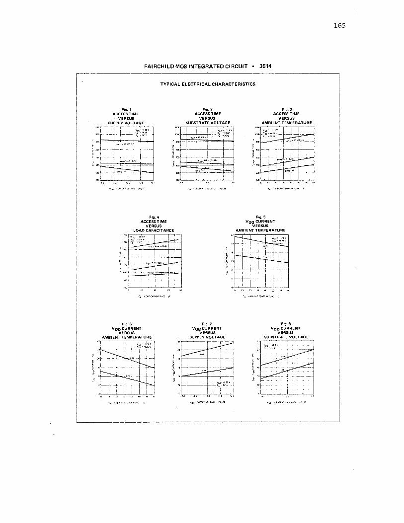
; 800
] 100
a ,, I
FAIRCHILD MOS INTE(;RATED CIRCUIT • 3514
TYPICAL ELECTRICAL CHARACTERISTICS
Fig. 1 ACCESS TIME
VERSUS SUPPLY VOLTAGE
..._ .. ··+ ll)AOIYP.
V55••4.1!,V Cl •10pF
-- T..,•2s•c
l-
v(;(j SUPPLYVOLTAG'I VOLTS
Fig. 4 ACCESS TIME
VERSUS LOAO CAPACITANCE
CL tOAOCAPACITANCE 11F
Fig.6 VooCURRENT
VERSUS AMBIENT TEMPERATURE
"'
Yao' 12,IIV Vss • •5.2SV
-l- ··-· --.---
TA At,!OlflVTTEMPERATIJRE C
Fig.2 ACCESS TIME
VERSUS SUBSTRATE VOLTAGE
VGG" -11,v
I-+-+-+-+-+--'- ~~ :;:.~
V55 SU8STAATf VOLTAGE VOLTS
Fig: 7 VGGCURRENT
VERSUS SUPPLY VOLTAGE
"'---'---'--~-'--'--'-~-' -10.8
Vea SUPPLVVOLTAGE
Fig.3 ACCESS TIME
VERSUS AMBIENT TEMPERATURE
T11,, AMBl(/IITTEfllPEAATURE 'C
Fig.5 .VGG CURRENT
VERSUS AMBIENT TEMPERATURE
TA AM81ENTTEMl'fAATURE C
Fig.8 VooCURRENT
VERSUS su_BSTRATE VOLTAGE
i .
SUIISTAATE VOLTAGf
165
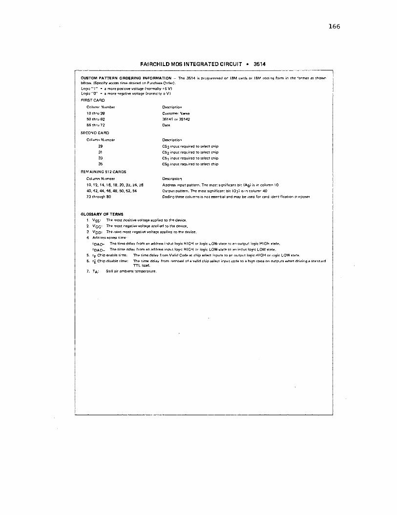
FAIRCHILD MOS INTEGRATED CIRCUIT • 3514
CUSTOM PATTERN ORDERING INFORMATION - The 3514 is programmed on IBM cards or IBM coding form in the format as shown b81ow. (Specify access time desired on Purchase Order).
Logic ••1•• = a more positive voltage (normally +5 V) Logic .,O" = a more negative voltage (normally o V)
FIRST CARD
Column Number
10 thru 29
50thru 62
65 thru 72
SECOND CARD
Column Number
29
31
33
35
REMAINING 512 CARDS
Column Number
10, 12, 14, 16, 18, 20, 22, ~4. 26
40, 42, 44, 46, 48, 50, 52, 54
73 through 80
GLOSSARY OF TERMS
Description
Customer Name
35141 or 35142
Date
Description
CS3 inpllt required to select chip
CS2 input required to select chip
CS1 input required to select chip
CSo input required to select chip
Description
Address input pattern. The most significant bit (Aal is in Column 10
Output pattern. The most significant bit (07) is in column 40
Coding these columns is not essential and may be used for card identification purposes.
1. V55: The most positive voltage applied to the device.
2. VGG: The most negative voltage applied to the device,
3. VDo: The next most negative voltage applied to the device.
4. Address access time:
'DAO+ "The time delay from an address input logic HIGH or logic LOW state to an output logic HIGH state.
'DAO- The tirne delay from an address input logic l-'IIGH or logic LOW state to an input logic LOW state.
5. te Chip enable time: The time delay from Valid Code at c:hip select inputs to an output logic HIGH or logic LOW state.
6. tE Chip disable time: The time delay from removal of a valid chip select input code to a high state on output~ when driving a standard TTL IClad.
7. TA: Still air ambient temperature.
166
VITA
Robert P. Billeg, Jr.
Candidate for the.Degree of
Master of Science
Thesis: ADAPTING SEMICONDUCTOR MEMORY TO SMALL MACHINE APPLICATIONS
Major Field: Electrical.Engiijeering
Biographical:.
Personal Data: Born,in. Bloomsburg, Pennsylvania, December 20, 1938, the son of Mr, and Mrs, R, P. Billeg, .
Education: Graduated from Central High School, Oklahoma City, Oklahoma, in May, 1956; received the Bachelor of Scienc~ degree in Electrical Engineering from the University of Oklahoma in 1963; enrolled in the master's program at the Oklahoma State University Extention Center in 1968; cQmpleted requireme~ts for the Master of Science degree at Oklahoma State University in May, 1974.
Professional Experience: Project and Evaluation Engineer, United States Air Force, 1963-1965; member of the General Electric, Incorporated, Oklahoma City, design engineering staff; 1965-. 1970; member of the .Honeywell Informations Systems, Incorporated, design engineering staff, 1970 to present.