Multiplayer game cheating prevention with pipelined lockstep protocol
Upload
independentCategory
view
3download
0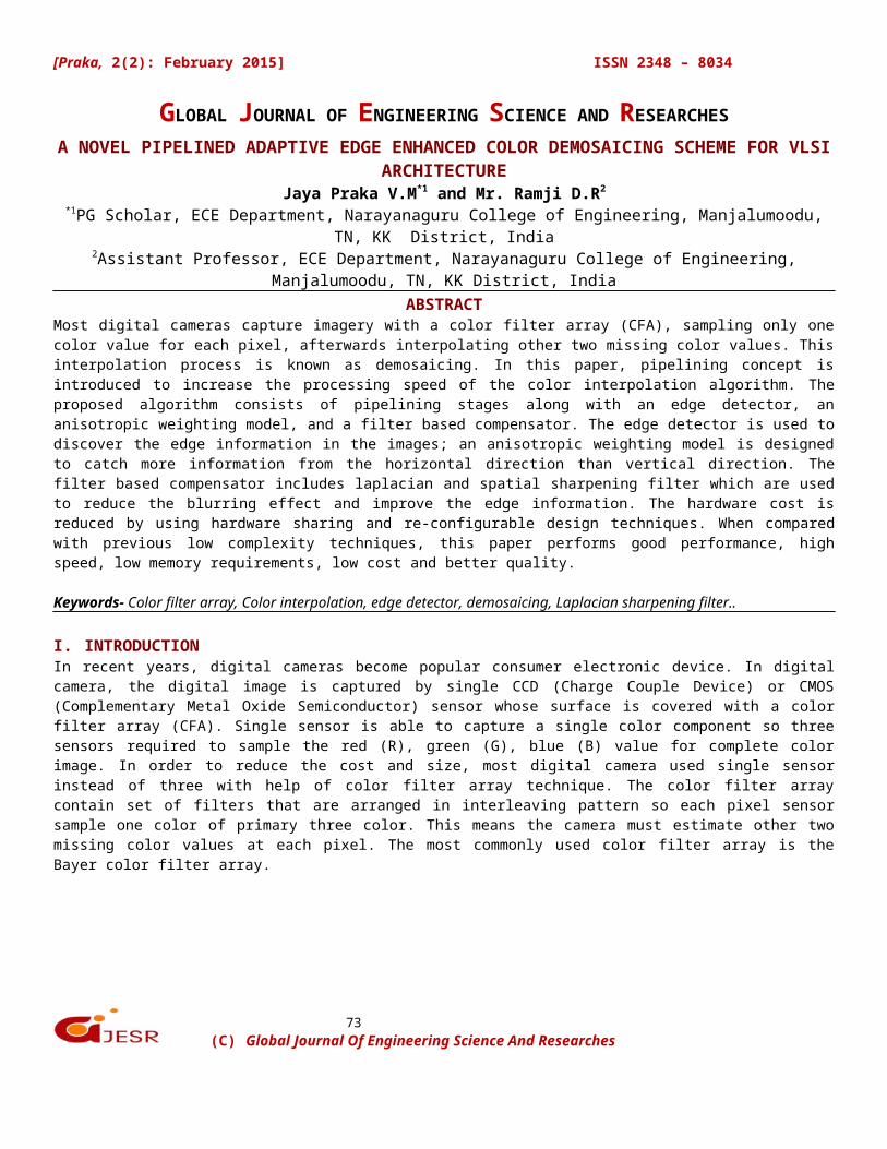
73
[Praka, 2(2): February 2015] ISSN 2348 – 8034
GLOBAL JOURNAL OF ENGINEERING SCIENCE AND RESEARCHESA NOVEL PIPELINED ADAPTIVE EDGE ENHANCED COLOR DEMOSAICING SCHEME FOR VLSI
ARCHITECTUREJaya Praka V.M*1 and Mr. Ramji D.R2
*1PG Scholar, ECE Department, Narayanaguru College of Engineering, Manjalumoodu,TN, KK District, India
2Assistant Professor, ECE Department, Narayanaguru College of Engineering,Manjalumoodu, TN, KK District, India
ABSTRACTMost digital cameras capture imagery with a color filter array (CFA), sampling only onecolor value for each pixel, afterwards interpolating other two missing color values. Thisinterpolation process is known as demosaicing. In this paper, pipelining concept isintroduced to increase the processing speed of the color interpolation algorithm. Theproposed algorithm consists of pipelining stages along with an edge detector, ananisotropic weighting model, and a filter based compensator. The edge detector is used todiscover the edge information in the images; an anisotropic weighting model is designedto catch more information from the horizontal direction than vertical direction. Thefilter based compensator includes laplacian and spatial sharpening filter which are usedto reduce the blurring effect and improve the edge information. The hardware cost isreduced by using hardware sharing and re-configurable design techniques. When comparedwith previous low complexity techniques, this paper performs good performance, highspeed, low memory requirements, low cost and better quality.
Keywords- Color filter array, Color interpolation, edge detector, demosaicing, Laplacian sharpening filter..
I. INTRODUCTIONIn recent years, digital cameras become popular consumer electronic device. In digitalcamera, the digital image is captured by single CCD (Charge Couple Device) or CMOS(Complementary Metal Oxide Semiconductor) sensor whose surface is covered with a colorfilter array (CFA). Single sensor is able to capture a single color component so threesensors required to sample the red (R), green (G), blue (B) value for complete colorimage. In order to reduce the cost and size, most digital camera used single sensorinstead of three with help of color filter array technique. The color filter arraycontain set of filters that are arranged in interleaving pattern so each pixel sensorsample one color of primary three color. This means the camera must estimate other twomissing color values at each pixel. The most commonly used color filter array is theBayer color filter array.
(C) Global Journal Of Engineering Science And Researches
74
[Praka, 2(2): February 2015] ISSN 2348 – 8034
Figure 1: Bayer CFA pattern
Figure 1 shows a color filter arrays called Bayer CFA, in which two colors havedisappeared in each pixel. In this figure, half of the pixels are allocated to greencolor because the peak sensitivity of the human visual system lies in the mediumwavelength, corresponding to the green portion of the spectrum; other half is shared byred and blue color.
In previous works, many efficient high quality algorithms [1]-[5] have been proposed forreconstructing the full color image. Gunturk [1] and Li [2] presented high performancealgorithms to reconstruct the missing colors by using the correlation between thefrequencies of the three colors components. Su et al. [3] presented a wavelet classifier.Also this method produced a high quality color interpolation. Chung et al. [4] presentedan edge estimation method. This method was using a variance of the different color. Changet al. [5] presented an adaptive color interpolation technique that used a 2-D locallystationary Gaussian process and an edge indicator. The high quality color interpolationalgorithms mentioned above, but these algorithms have high complexity and high memoryrequirements. Furthermore these algorithms are not realized using VLSI technique.
For this reason, low complexity color interpolation algorithms [6]-[8] are needed forVLSI implementation. VLSI implementation of low power high quality color interpolation[6] is proposed for CCD camera. This work is based on edge oriented weighting and localgain approach. The performance of this design was improved by a pipeline schedule andtime sharing techniques. For VLSI implementation, the chip area was increased byrealizing dividers and multipliers due to high complexity. Hsia et al. [7] presented ahigh performance and low complexity algorithms to develop a camera DSP system. It isnecessary to use the division and multiplication operation to detect the gain and edgeinformation. So the chip area was greatly increased. Hhiau et al. [8] presented a low-cost and high performance color demosaicing VLSI design. This design improves the qualityof the images by using edge information and inter-channel correlations. Also the
(C) Global Journal Of Engineering Science And Researches
75
[Praka, 2(2): February 2015] ISSN 2348 – 8034
performance of this design was improved by using pipeline architecture. With thisimplementation technique, the chip area was reduced because it is unnecessary to use anydivider to realize this design.
In this paper, a novel pipelined adaptive edge-enhanced color interpolation processor isproposed. In this technique we use a pipelining concept at edge detector to perform thespeed in a process and to reduce the critical path delay in the process. The proposedalgorithm consist of an pipelining stage along with an edge detector to enhance the edgeinformation in the images, an anisotropic weighting model to reduce the memoryrequirement, a filter-based compensator to improve the quality, and a register bank toprocess streaming data directly by using only a two line buffer memory. The rest of thepaper is organized as follows: Section II presents the proposed novel colorinterpolation. Section III describes the VLSI architecture of this work. Section IVdescribes the pipelined architecture of edge detector. Section V presents the simulationresults and Section VI concludes the paper.
II.PROPOSED COLOR INTERPOLATION ALGORITHMThe proposed novel algorithm is composed of edge detection, a green color interpolationand red-blue color interpolation techniques. Here, each color is interpolated bydifferent methodologies according to the relative locations and reference neighboringsamples.
1. Low-Complexity Edge Detection
To find the edge information, the difference in the vertical (DV) and horizontal (DH)directions are used. The DV neighboring around the pixel can be calculated by-
The DH neighboring around the pixel can be calculated by-
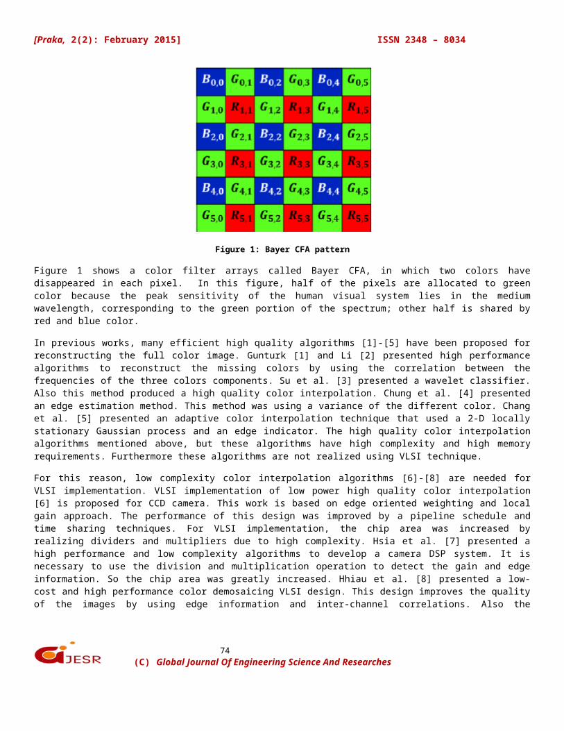
Figure 2: Relative locations and reference neighboring samples of in CFA format for green, blue orred color interpolation.
Figure 2 shows the relative locations and reference neighboring RGB pixels. After
(C) Global Journal Of Engineering Science And Researches

76
[Praka, 2(2): February 2015] ISSN 2348 – 8034
obtaining the both directions, the total difference (TD) is calculated by-
2. Green Color Interpolation
To improve the quality of images, an anisotropic weighting model is designed for thisdesign. The values of TD, DH, and DV can be used to select any one of the three greencolor interpolation models, without edge enhancement, edge enhancement in horizontaldirection, edge enhancement in vertical direction. If the value of TD is less than thethreshold value, the value of can be calculated by without edge enhancement model as
If the value of TD is larger than the threshold value and DH is less than DV, the valueof can be calculated by edge enhancement in horizontal direction model as
If the value of TD is larger than threshold value and the value of DH is larger than DV, the value of can be calculated by edge enhancement in vertical direction model as
The spatial sharpening filter can be used to reduce the blurring effect and the edge information can be efficiently enhanced by proposed adaptive edge enhancement technique.
3. Red and Blue Colors Interpolation
To reconstruct the red and blue color, it is necessary to use the information of the fourneighboring green colors. If the value of TD is less than a threshold value, the value ofRi,j
(B) can be calculated by without edge enhancement model. as
(C) Global Journal Of Engineering Science And Researches
77
[Praka, 2(2): February 2015] ISSN 2348 – 8034
If the value of TD is larger than the threshold value and DH is less than DV, the value of Ri,j
(B) or Bi,j(R) can be calculated by edge enhancement in horizontal direction model as
If the value of TD is larger than threshold value and DH is larger than DV, then the value of Ri,j
(B) or Bi,j(R)
can be calculated by edge enhancement in vertical direction model as
The red or blue color reconstructed pixel RBi.j where its upper and bottom pixels are RBi-
1.j and RBi+1.j at Gi.j can be calculated by-
The blue or red color reconstructed pixel BRi,j where its right and left pixels are BRi,j-1 and BRi,j+1 at Gi.j can be calculated by-
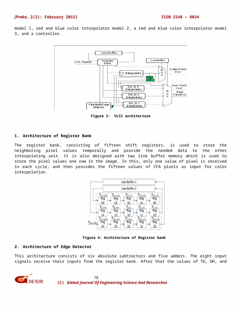
III. VLSI IMPLEMENTATIONFigure 3 shows the block diagram of the VLSI architecture for the proposed colorinterpolation processor. This architecture consist of seven main blocks: a register bank,pipelined edge detector, a green color interpolator, a red and blue color interpolator
(C) Global Journal Of Engineering Science And Researches
78
[Praka, 2(2): February 2015] ISSN 2348 – 8034
model 1, red and blue color interpolator model 2, a red and blue color interpolator model3, and a controller.
Figure 3: VLSI architecture
1. Architecture of Register Bank
The register bank, consisting of fifteen shift registers, is used to store theneighboring pixel values temporally and provide the needed data to the otherinterpolating unit. It is also designed with two line buffer memory which is used tostore the pixel values one row in the image. In this, only one value of pixel is receivedin each cycle, and then provides the fifteen values of CFA pixels as input for colorinterpolation.
Figure 4: Architecture of Register bank
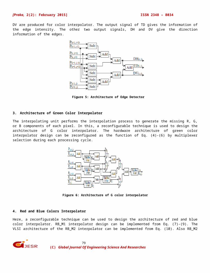
2. Architecture of Edge Detector
This architecture consists of six absolute subtractors and five adders. The eight inputsignals receive their inputs from the register bank. After that the values of TD, DH, and
(C) Global Journal Of Engineering Science And Researches
79
[Praka, 2(2): February 2015] ISSN 2348 – 8034
DV are produced for color interpolator. The output signal of TD gives the information ofthe edge intensity. The other two output signals, DH and DV give the directioninformation of the edges.
Figure 5: Architecture of Edge Detector
3. Architecture of Green Color Interpolator
The interpolating unit performs the interpolation process to generate the missing R, G,or B components of each pixel. In this, a reconfigurable technique is used to design thearchitecture of G color interpolator. The hardware architecture of green colorinterpolator design can be reconfigured as the function of Eq. (4)-(6) by multiplexerselection during each processing cycle.
Figure 6: Architecture of G color interpolator
4. Red and Blue Colors Interpolator
Here, a reconfigurable technique can be used to design the architecture of red and bluecolor interpolator. RB_M1 interpolator design can be implemented from Eq. (7)-(9). TheVLSI architecture of the RB_M2 interpolator can be implemented from Eq. (10). Also RB_M2
(C) Global Journal Of Engineering Science And Researches

80
[Praka, 2(2): February 2015] ISSN 2348 – 8034
interpolator design can be implemented from Eq. (11).
5. Controller
The control unit provides the control signals to other unit and handles the wholeinterpolation flow. It is implemented by a finite state machine sequential circuit. Thecontroller must monitor its input and output data access with memory to fit theperformance of pixel-in and pixel-out.
IV.PIPELINED EDGE DETECTORPipelining stage along with an edge detector is applied to increase the processing speedof the data. It also increases the CPU instruction throughput, the number of instructionscompleted per unit of time. Edge detection is identifying points in a digital image atwhich the image brightness changes sharply have discontinuities. In this paper, we aregoing to simulate the pipelined edge detector. The simulation procedure can be done bythe use of Xilinx ISE tool. Figure 7 shows the pipelined model edge detectorarchitecture.
Figure 7: Architecture of Pipelined model edge detector
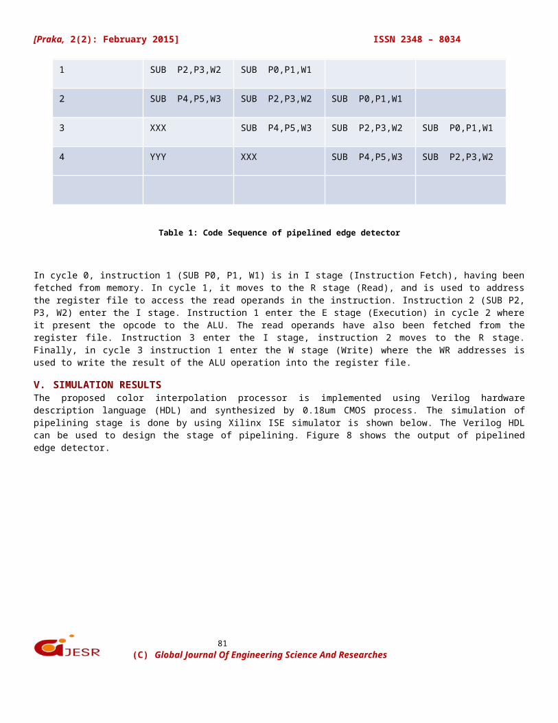
Cycle I stage R stage E stage W stage
0 SUB P0,P1,W1
(C) Global Journal Of Engineering Science And Researches
81
[Praka, 2(2): February 2015] ISSN 2348 – 8034
1 SUB P2,P3,W2 SUB P0,P1,W1
2 SUB P4,P5,W3 SUB P2,P3,W2 SUB P0,P1,W1
3 XXX SUB P4,P5,W3 SUB P2,P3,W2 SUB P0,P1,W1
4 YYY XXX SUB P4,P5,W3 SUB P2,P3,W2
Table 1: Code Sequence of pipelined edge detector
In cycle 0, instruction 1 (SUB P0, P1, W1) is in I stage (Instruction Fetch), having beenfetched from memory. In cycle 1, it moves to the R stage (Read), and is used to addressthe register file to access the read operands in the instruction. Instruction 2 (SUB P2,P3, W2) enter the I stage. Instruction 1 enter the E stage (Execution) in cycle 2 whereit present the opcode to the ALU. The read operands have also been fetched from theregister file. Instruction 3 enter the I stage, instruction 2 moves to the R stage.Finally, in cycle 3 instruction 1 enter the W stage (Write) where the WR addresses isused to write the result of the ALU operation into the register file.
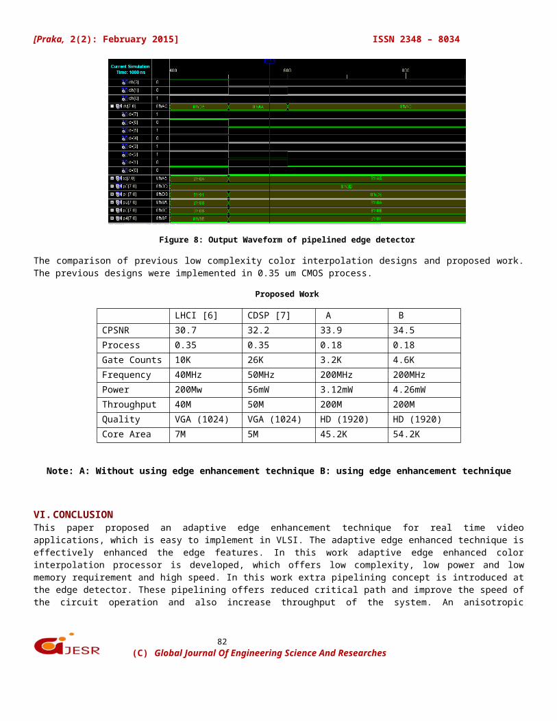
V. SIMULATION RESULTSThe proposed color interpolation processor is implemented using Verilog hardwaredescription language (HDL) and synthesized by 0.18um CMOS process. The simulation ofpipelining stage is done by using Xilinx ISE simulator is shown below. The Verilog HDLcan be used to design the stage of pipelining. Figure 8 shows the output of pipelinededge detector.
(C) Global Journal Of Engineering Science And Researches
82
[Praka, 2(2): February 2015] ISSN 2348 – 8034
Figure 8: Output Waveform of pipelined edge detector
The comparison of previous low complexity color interpolation designs and proposed work.The previous designs were implemented in 0.35 um CMOS process.
Proposed Work
LHCI [6] CDSP [7] A BCPSNR 30.7 32.2 33.9 34.5Process 0.35 0.35 0.18 0.18Gate Counts 10K 26K 3.2K 4.6KFrequency 40MHz 50MHz 200MHz 200MHzPower 200Mw 56mW 3.12mW 4.26mWThroughput 40M 50M 200M 200MQuality VGA (1024) VGA (1024) HD (1920) HD (1920)Core Area 7M 5M 45.2K 54.2K
Note: A: Without using edge enhancement technique B: using edge enhancement technique
VI.CONCLUSIONThis paper proposed an adaptive edge enhancement technique for real time videoapplications, which is easy to implement in VLSI. The adaptive edge enhanced technique iseffectively enhanced the edge features. In this work adaptive edge enhanced colorinterpolation processor is developed, which offers low complexity, low power and lowmemory requirement and high speed. In this work extra pipelining concept is introduced atthe edge detector. These pipelining offers reduced critical path and improve the speed ofthe circuit operation and also increase throughput of the system. An anisotropic
(C) Global Journal Of Engineering Science And Researches

83
[Praka, 2(2): February 2015] ISSN 2348 – 8034
weighting model, an pipelined edge detector and filter based compensator have been usedto reduce the memory requirement and improve the quality of images.
REFERENCES1. B. K. Gunturk, Y. Altunbasak, and R. M. Mersereau, “Color plane interpolation using alternating projection”, IEEE
Trans. Image Process., vol. 11, no. 9, pp. 997-1013, Sep.2002.2. X. Li, “Demosaicing by successive approximation,” IEEE Trans. Image Process., vol. 14, no. 3, pp. 370-379, Mar. 2005.3. C. Y. Su, and Y. S. Lin, “Color interpolation using wavelet based classifiers,” Electronics Letters, vol. 43, no. 43, no. 12
pp. 667-669, June 2007.4. K. H. Chung and Y. H. Chan, ”Color demosaicing using variance of color differences,” IEEE Trans. Image Process., vol.
15, no. 10. Pp. 2944-2955, Oct. 2007.5. H. A. Chang, and H. H. Chen, “Stochastic color interpolation for digital cameras”, IEEE Transaction on Circuits and
Systems for Video Technology, Vol. 17, no. 8, pp. 964-973, Aug. 2007.6. S. C. Hsia, M. H. Chen, and P. S. Tsai, “VLSI implementation of low-power high-quality color interpolation processor
for CCD camera,” IEEE Trans. Very Large Scale Integration (VLSI) Systems, vol. 14, no. 4, pp. 361-369, Apr. 2006.7. S. C. Hsia, and P. S. Tsai, ”VLSI implementation of camera digital signal processor for document projection,” in Proc.
IEEE Int. Conf. Signal Processing System (ICSPS), Jul. 2010, pp. 657-660. 8. Y. H. Shiau, P. Y. Chen, and C. W. Chang, “An area-efficient color demosaicing scheme for VLSI architecture,”
International Journal of Innovative Computing Information and Control, vol. 7, no. 4, pp. 1739-1752, Apr. 2011.9. Enhanced VLSI implementation of an adaptive edge-image scalar for real time multimedia applications by shih-Lun
Chen, Member, IEEE by Sep 2013. 10. Tannu Chhabra, Md Tauheed Khan “VLSI Design of a 16-bit Pipelined RISC Processor”, International Journal of
Electronics and Computer Science Engineering, ISSN 2277-1956/V1N3-1858-1861.
(C) Global Journal Of Engineering Science And Researches
Copyright © 2022 FDOKUMEN