A Low-Power 32Channel Digitally Programmable Neural Recording Integrated Circuit
11
592 IEEE TRANSACTIONS ON BIOMEDICAL CIRCUITS AND SYSTEMS, VOL. 5, NO. 6, DECEMBER 2011 A Low-Power 32-Channel Digitally Programmable Neural Recording Integrated Circuit Woradorn Wattanapanitch, Student Member, IEEE, and Rahul Sarpeshkar, Senior Member, IEEE Abstract—We report the design of an ultra-low-power 32-channel neural-recording integrated circuit (chip) in a 0.18 m CMOS technology. The chip consists of eight neural recording modules where each module contains four neural amplifiers, an analog multiplexer, an A/D converter, and a serial programming interface. Each amplifier can be programmed to record either spikes or LFPs with a programmable gain from 49–66 dB. To min- imize the total power consumption, an adaptive-biasing scheme is utilized to adjust each amplifier’s input-referred noise to suit the background noise at the recording site. The amplifier’s input-re- ferred noise can be adjusted from 11.2 (total power of 5.4 W) down to 5.4 (total power of 20 W) in the spike-recording setting. The ADC in each recording module digi- tizes the a.c. signal input to each amplifier at 8-bit precision with a sampling rate of 31.25 kS/s per channel, with an average power consumption of 483 nW per channel, and, because of a.c. coupling, allows d.c. operation over a wide dynamic range. It achieves an ENOB of 7.65, resulting in a net efficiency of 77 fJ/State, making it one of the most energy-efficient designs for neural recording applications. The presented chip was successfully tested in an in vivo wireless recording experiment from a behaving primate with an average power dissipation per channel of 10.1 W. The neural amplifier and the ADC occupy areas of 0.03 mm and 0.02 mm respectively, making our design simultaneously area efficient and power efficient, thus enabling scaling to high channel-count systems. Index Terms—Analog-to-digital converters, brain-machine interfaces, digitally programmable, energy efficient, low power, neural amplifiers, neural-recording systems. I. INTRODUCTION I N the past few decades, direct recordings from the cortical area of the brain have enabled scientists to gradually un- derstand and unlock the secrets of neural coding. With the aid of high-density microelectrode arrays, neural activities from a large population of neurons can be observed simultaneously with a spatial resolution down to that of a single cell [1], [2]. Many experiments in non-human primates [3]–[5] and a pilot Manuscript received March 06, 2011; revised May 21, 2011; accepted July 11, 2011. Date of publication September 08, 2011; date of current version De- cember 29, 2011. This work was supported by the National Institute of Health (NS056140 to R. Sarpeshkar). This paper was recommended by Associate Ed- itor Wentai Liu. W. Wattanapanitch was with the Department of Electrical Engineering and Computer Science, Massachusetts Institute of Technology, Cambridge, MA 02139 USA. He is now with the Department of Electrical Engineering, Kasetsart University, Bangkok 10900, Thailand (e-mail: [email protected]). R. Sarpeshkar is with the Research Laboratory of Electronics, Massachusetts Institute of Technology, Cambridge, MA 02139 USA (e-mail: [email protected]). Color versions of one or more of the figures in this paper are available online at http://ieeexplore.ieee.org. Digital Object Identifier 10.1109/TBCAS.2011.2163404 clinical trial in a human subject [6] illustrated that control sig- nals directly derived from spiking activities from a population of neurons in the cortical area of the brain can be used to success- fully control and manipulate computer devices or robotic limbs. The study in [7] shows that cortical activities from a population of neurons can be used to control even a sophisticated device such as a robotic limb with multiple degrees of freedom. These studies have shown great promise for successful development of practical brain-machine-interface (BMI) systems to restore lost body functions to patients with disorders in the central nervous system such as those suffered because of spinal cord injuries. Practical BMI systems of the future will be portable and may enable the users to control dexterous robotic limbs or their limbs naturally. Practical BMI systems require the use of neural-recording systems to amplify and digitize the neural signals. To avoid the risk of infection, the recording system should be entirely implanted under the skin while the recorded neural data and the power to operate the implant should be transferred through wireless means [8]. This implantability requirement poses major constraints on the size and total power consumption of the recording system [8]. To record from a large number of cortical neurons, high-channel-count recording systems are needed. Therefore, the area per recording channel must be small such that a high-channel-count recording system can be designed with a small form factor. Furthermore, the power consumption per channel must be minimal such that the total power dissipation of the recording system can be kept within feasible limits. To avoid excessive heat dissipation that may cause cell death in the surrounding tissues, the total power dissipation from the recording system should also be min- imal [8]. For battery-operated recording systems, low power consumption could prolong the time between recharges, thus expanding the battery’s life to avoid frequent surgeries for battery replacements. Advances in integrated-circuit (IC) fabrication technologies have enabled engineers to increase the number of recording channels that can be put on a single chip by decreasing the size and power consumption per recording channel, while still sig- nificantly improving the recording system’s performance. The first recording system reported in [9] contained 32 recording channels and data-reduction circuitry while consuming a total power of 5.4 mW (equivalent to 169 W per channel). Another system reported in [10] contained 100 channels and also in- cluded wireless data transmission and power-transfer features. By counting only the power consumption from the recording channels and the analog-to-digital converter, the average power consumption of this system is approximately 140 W/channel. 1932-4545/$26.00 © 2011 IEEE
-
Upload
independent -
Category
Documents
-
view
1 -
download
0
Transcript of A Low-Power 32Channel Digitally Programmable Neural Recording Integrated Circuit
592 IEEE TRANSACTIONS ON BIOMEDICAL CIRCUITS AND SYSTEMS, VOL. 5, NO. 6, DECEMBER 2011
A Low-Power 32-Channel Digitally ProgrammableNeural Recording Integrated Circuit
Woradorn Wattanapanitch, Student Member, IEEE, and Rahul Sarpeshkar, Senior Member, IEEE
Abstract—We report the design of an ultra-low-power32-channel neural-recording integrated circuit (chip) in a 0.18 mCMOS technology. The chip consists of eight neural recordingmodules where each module contains four neural amplifiers, ananalog multiplexer, an A/D converter, and a serial programminginterface. Each amplifier can be programmed to record eitherspikes or LFPs with a programmable gain from 49–66 dB. To min-imize the total power consumption, an adaptive-biasing scheme isutilized to adjust each amplifier’s input-referred noise to suit thebackground noise at the recording site. The amplifier’s input-re-ferred noise can be adjusted from 11.2 ���� (total power of5.4 W) down to 5.4 ���� (total power of 20 W) in thespike-recording setting. The ADC in each recording module digi-tizes the a.c. signal input to each amplifier at 8-bit precision witha sampling rate of 31.25 kS/s per channel, with an average powerconsumption of 483 nW per channel, and, because of a.c. coupling,allows d.c. operation over a wide dynamic range. It achieves anENOB of 7.65, resulting in a net efficiency of 77 fJ/State, makingit one of the most energy-efficient designs for neural recordingapplications. The presented chip was successfully tested in an invivo wireless recording experiment from a behaving primate withan average power dissipation per channel of 10.1 W. The neuralamplifier and the ADC occupy areas of 0.03 mm� and 0.02 mm�
respectively, making our design simultaneously area efficientand power efficient, thus enabling scaling to high channel-countsystems.
Index Terms—Analog-to-digital converters, brain-machineinterfaces, digitally programmable, energy efficient, low power,neural amplifiers, neural-recording systems.
I. INTRODUCTION
I N the past few decades, direct recordings from the corticalarea of the brain have enabled scientists to gradually un-
derstand and unlock the secrets of neural coding. With the aidof high-density microelectrode arrays, neural activities from alarge population of neurons can be observed simultaneouslywith a spatial resolution down to that of a single cell [1], [2].Many experiments in non-human primates [3]–[5] and a pilot
Manuscript received March 06, 2011; revised May 21, 2011; accepted July11, 2011. Date of publication September 08, 2011; date of current version De-cember 29, 2011. This work was supported by the National Institute of Health(NS056140 to R. Sarpeshkar). This paper was recommended by Associate Ed-itor Wentai Liu.
W. Wattanapanitch was with the Department of Electrical Engineeringand Computer Science, Massachusetts Institute of Technology, Cambridge,MA 02139 USA. He is now with the Department of Electrical Engineering,Kasetsart University, Bangkok 10900, Thailand (e-mail: [email protected]).
R. Sarpeshkar is with the Research Laboratory of Electronics, MassachusettsInstitute of Technology, Cambridge, MA 02139 USA (e-mail: [email protected]).
Color versions of one or more of the figures in this paper are available onlineat http://ieeexplore.ieee.org.
Digital Object Identifier 10.1109/TBCAS.2011.2163404
clinical trial in a human subject [6] illustrated that control sig-nals directly derived from spiking activities from a population ofneurons in the cortical area of the brain can be used to success-fully control and manipulate computer devices or robotic limbs.The study in [7] shows that cortical activities from a populationof neurons can be used to control even a sophisticated devicesuch as a robotic limb with multiple degrees of freedom. Thesestudies have shown great promise for successful development ofpractical brain-machine-interface (BMI) systems to restore lostbody functions to patients with disorders in the central nervoussystem such as those suffered because of spinal cord injuries.Practical BMI systems of the future will be portable and mayenable the users to control dexterous robotic limbs or their limbsnaturally.
Practical BMI systems require the use of neural-recordingsystems to amplify and digitize the neural signals. To avoidthe risk of infection, the recording system should be entirelyimplanted under the skin while the recorded neural data andthe power to operate the implant should be transferred throughwireless means [8]. This implantability requirement posesmajor constraints on the size and total power consumption ofthe recording system [8]. To record from a large number ofcortical neurons, high-channel-count recording systems areneeded. Therefore, the area per recording channel must besmall such that a high-channel-count recording system canbe designed with a small form factor. Furthermore, the powerconsumption per channel must be minimal such that the totalpower dissipation of the recording system can be kept withinfeasible limits. To avoid excessive heat dissipation that maycause cell death in the surrounding tissues, the total powerdissipation from the recording system should also be min-imal [8]. For battery-operated recording systems, low powerconsumption could prolong the time between recharges, thusexpanding the battery’s life to avoid frequent surgeries forbattery replacements.
Advances in integrated-circuit (IC) fabrication technologieshave enabled engineers to increase the number of recordingchannels that can be put on a single chip by decreasing the sizeand power consumption per recording channel, while still sig-nificantly improving the recording system’s performance. Thefirst recording system reported in [9] contained 32 recordingchannels and data-reduction circuitry while consuming a totalpower of 5.4 mW (equivalent to 169 W per channel). Anothersystem reported in [10] contained 100 channels and also in-cluded wireless data transmission and power-transfer features.By counting only the power consumption from the recordingchannels and the analog-to-digital converter, the average powerconsumption of this system is approximately 140 W/channel.
1932-4545/$26.00 © 2011 IEEE
WATTANAPANITCH AND SARPESHKAR: LOW-POWER 32-CHANNEL INTEGRATED CIRCUIT 593
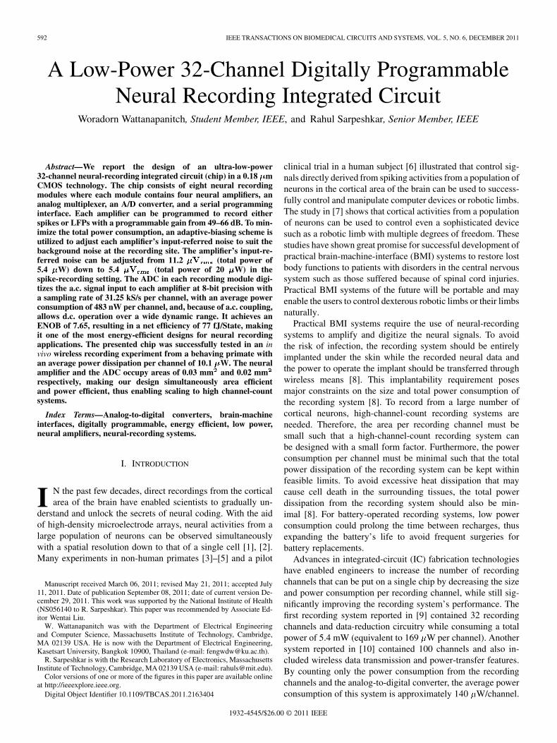
Fig. 1. Overall architecture of the 32-channel neural recording chip.
The systems reported in [11]–[14] represent examples of neural-recording systems with small area and power consumption perchannel and thus are feasible for the development of high-per-formance BMI systems. The system reported in [15] achieveda very low average power consumption of 3.77 W/channel.However, due to its very large area per channel, such a systemmay not be scalable to a high-channel-count system, and thus isnot yet suitable for high-performance BMI systems.
Our goal is to develop an ultra-low-power implantablewireless neural recording system for practical use in neuralprosthetic applications. For such applications, low powerconsumption and small area per recording channel are bothvery important. In this paper, we present the design andexperimental results of an ultra-low-power 32-channel dig-itally-programmable neural-recording chip for use in suchapplications. Even though our recording chip is not yet op-timized for total chip area, it achieves very small area andvery low average power consumption per recording channel.The chip is thus suitable for scaling to include a large numberof recording channels in subsequent generations. This paperis organized as follows: In Section II, we discuss the overallarchitecture of the 32-channel neural recording chip. In Sec-tion III, we present the design of the neural amplifier includingan adaptive-biasing technique to optimize the total powerconsumption of the recording chip. In Section IV, we presentthe design and power-saving techniques in our energy-efficientADCs, analog multiplexers, and control logic. In Section VIwe present both benchtop characterizations of the componentsof the neural-recording chip and in vivo experimental resultsobtained wirelessly from the brain of an awake non-humanprimate. In Section VII, we conclude the paper by summarizingour contributions.
II. OVERALL CHIP ARCHITECTURE
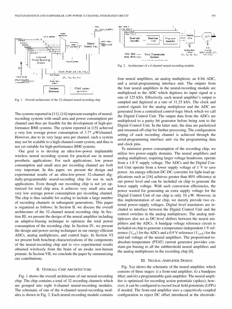
Fig. 1 shows the overall architecture of our neural-recordingchip. The chip contains a total of 32 recording channels whichare grouped into eight 4-channel neural-recording modules.The schematic of one of the 4-channel neural-recording mod-ules is shown in Fig. 2. Each neural-recording module contains
Fig. 2. Architecture of a 4-channel neural recording module.
four neural amplifiers, an analog multiplexer, an 8-bit ADC,and a serial-programming interface unit. The outputs fromthe four neural amplifiers in the neural-recording module aremultiplexed to the ADC which digitizes its input signal at arate of 125 kS/s. Effectively, each neural amplifier’s output issampled and digitized at a rate of 31.25 kS/s. The clock andcontrol signals for the analog multiplexer and the ADC aregenerated from a centralized control-logic block which we callthe Digital Control Unit. The output data from the ADCs aremultiplexed to a parity bit generator before being sent to theDigital Control Unit. In the latter unit, the data are packetizedand streamed off-chip for further processing. The configurationsetting of each recording channel is achieved through theserial-programming interface unit via the programming dataand clock pins.
To minimize power consumption of the recording chip, weutilize two power-supply domains. The neural amplifiers andanalog multiplexer, requiring larger voltage headroom, operatefrom a 1.8 V supply voltage. The ADCs and the Digital Con-trol Unit operate from a lower supply voltage of 1 V to savepower. An energy-efficient DC-DC converter for light-load ap-plications such as [16] achieves greater than 80% efficiency atour power level and can be included on chip to generate thelower supply voltage. With such conversion efficiencies, thepower wasted for generating an extra supply voltage for theDigital Control Unit of our chip is only 10 W. However, inthis implementation of our chip, we merely provide two ex-ternal power-supply voltages. Digital level translators are in-cluded to interface between the Digital Control Unit and thecontrol switches in the analog multiplexers. The analog mul-tiplexers also act as DC-level shifters between the neural am-plifiers and the ADCs. A bandgap voltage reference circuit isincluded on chip to generate a temperature-independent 1 V ref-erence for the ADCs and a 0.9 V reference for themid-rail voltage of the neural amplifiers. The proportional-to-absolute-temperature (PTAT) current generator provides con-stant-gm biasing to all the subthreshold neural amplifiers andthe analog multiplexers in the recording chip [8].
III. NEURAL-AMPLIFIER DESIGN
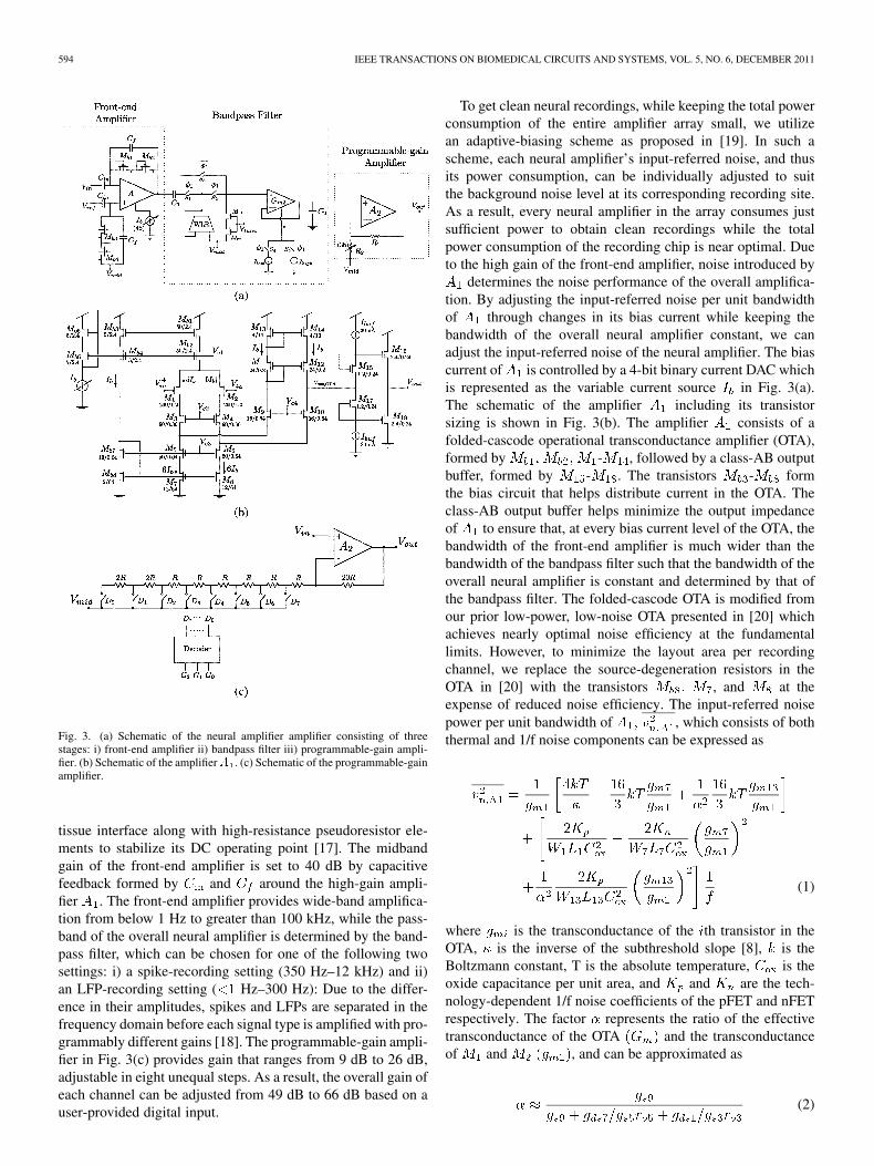
Fig. 3(a) shows the schematic of the neural amplifier, whichconsists of three stages: i) a front-end amplifier; ii) a bandpassfilter; and iii) a programmable-gain amplifier. The neural ampli-fier is optimized for recording action potentials (spikes); how-ever, it can be configured to record local field potentials (LFPs)if needed. The front-end amplifier uses a capacitively-coupledconfiguration to reject DC offset introduced at the electrode-
594 IEEE TRANSACTIONS ON BIOMEDICAL CIRCUITS AND SYSTEMS, VOL. 5, NO. 6, DECEMBER 2011
Fig. 3. (a) Schematic of the neural amplifier amplifier consisting of threestages: i) front-end amplifier ii) bandpass filter iii) programmable-gain ampli-fier. (b) Schematic of the amplifier� . (c) Schematic of the programmable-gainamplifier.
tissue interface along with high-resistance pseudoresistor ele-ments to stabilize its DC operating point [17]. The midbandgain of the front-end amplifier is set to 40 dB by capacitivefeedback formed by and around the high-gain ampli-fier . The front-end amplifier provides wide-band amplifica-tion from below 1 Hz to greater than 100 kHz, while the pass-band of the overall neural amplifier is determined by the band-pass filter, which can be chosen for one of the following twosettings: i) a spike-recording setting (350 Hz–12 kHz) and ii)an LFP-recording setting ( Hz–300 Hz): Due to the differ-ence in their amplitudes, spikes and LFPs are separated in thefrequency domain before each signal type is amplified with pro-grammably different gains [18]. The programmable-gain ampli-fier in Fig. 3(c) provides gain that ranges from 9 dB to 26 dB,adjustable in eight unequal steps. As a result, the overall gain ofeach channel can be adjusted from 49 dB to 66 dB based on auser-provided digital input.
To get clean neural recordings, while keeping the total powerconsumption of the entire amplifier array small, we utilizean adaptive-biasing scheme as proposed in [19]. In such ascheme, each neural amplifier’s input-referred noise, and thusits power consumption, can be individually adjusted to suitthe background noise level at its corresponding recording site.As a result, every neural amplifier in the array consumes justsufficient power to obtain clean recordings while the totalpower consumption of the recording chip is near optimal. Dueto the high gain of the front-end amplifier, noise introduced by
determines the noise performance of the overall amplifica-tion. By adjusting the input-referred noise per unit bandwidthof through changes in its bias current while keeping thebandwidth of the overall neural amplifier constant, we canadjust the input-referred noise of the neural amplifier. The biascurrent of is controlled by a 4-bit binary current DAC whichis represented as the variable current source in Fig. 3(a).The schematic of the amplifier including its transistorsizing is shown in Fig. 3(b). The amplifier consists of afolded-cascode operational transconductance amplifier (OTA),formed by - , followed by a class-AB outputbuffer, formed by - . The transistors - formthe bias circuit that helps distribute current in the OTA. Theclass-AB output buffer helps minimize the output impedanceof to ensure that, at every bias current level of the OTA, thebandwidth of the front-end amplifier is much wider than thebandwidth of the bandpass filter such that the bandwidth of theoverall neural amplifier is constant and determined by that ofthe bandpass filter. The folded-cascode OTA is modified fromour prior low-power, low-noise OTA presented in [20] whichachieves nearly optimal noise efficiency at the fundamentallimits. However, to minimize the layout area per recordingchannel, we replace the source-degeneration resistors in theOTA in [20] with the transistors , and at theexpense of reduced noise efficiency. The input-referred noisepower per unit bandwidth of , which consists of boththermal and 1/f noise components can be expressed as
(1)
where is the transconductance of the th transistor in theOTA, is the inverse of the subthreshold slope [8], is theBoltzmann constant, T is the absolute temperature, is theoxide capacitance per unit area, and and are the tech-nology-dependent 1/f noise coefficients of the pFET and nFETrespectively. The factor represents the ratio of the effectivetransconductance of the OTA and the transconductanceof and , and can be approximated as
(2)
WATTANAPANITCH AND SARPESHKAR: LOW-POWER 32-CHANNEL INTEGRATED CIRCUIT 595
where and represent the source admittance and the EarlyEffect drain-to-source resistance of the th transistor respec-tively . Due to the use of cascode transistors
and , the factor in (2) has a value close to 1. Thenoise optimization strategy for this OTA is similar to that de-scribed in [20].
The bandpass filter is designed using a Gm-C bandpass filtertopology with switches to configure the recording setting. Therecording setting is controlled by the signal ; when ,the filter is in a spike-recording setting, and when , thefilter is in an LFP-recording setting. The high-frequency cutoff
is set by -OTA connected in a unity-gain configurationand . In the spike-recording setting , the switchis closed and the -OTA is biased with a higher bias current,
, such that is approximately 12 kHz. Similarly, in theLFP-recording setting , the switch is closed and
-OTA is biased with a lower bias current, , such thatis approximately 350 Hz. To set the low-frequency cutoff
in the spike-recording setting, we use a combination of andthe unity-gain connected WLR-OTA [21]. In the LFP-recordingsetting, however, due to the difficulties of biasing a WLR-OTAat very low bias current to achieve Hz, we simply usea series combination of and to provide a large ef-fective resistance (denoted as ) to set below 1 Hz. Thegate voltage of and is set such that is muchlarger than , where is the transconductanceof the WLR-OTA. In the spike-recording setting , theswitches and are closed and the WLR-OTA appears inparallel with . Since , the effective resis-tance dominates, resulting in .The WLR-OTA’s bias current is set such that Hz. Inthe LFP-recording setting , the switches andare open while the switch is closed. The WLR-OTA is dis-connected from the signal path and appears in series with
through the switch . In this case, the combination ofand determines the cutoff frequency . By setting
, the effective resistance is very large such thatHz. To operate OTAs at low frequencies, we
utilize bump-linearization and source-degeneration techniquesdescribed in [21] or in [8] to reduce the of WLR-OTA toachieve a low-frequency cutoff of 300 Hz in the spike-recordingsetting. However, only the bump-linearization technique is usedin the -OTA to achieve a high-frequency cutoff of 350 Hzin the LFP-recording setting.
Fig. 3(c) shows the schematic of the programmable-gain am-plifier. The gain of the programmable-gain amplifier can be pro-grammed to any of the eight values and is given by
, where is the totalresistance seen between the negative input terminal of andthe node when the switch is closed. The digital decoderensures that only one of the switches ’s can be closed at agiven time depending on the decoder’s inputs , and .The values of the gain for every combination of ,and are tabulated in Table I. The amplifier is designedusing a standard two-stage amplifier topology with Miller com-pensation. The class-AB output buffer, similar to the one usedin Fig. 3(b), is included to drive resistive loads (the feedback re-sistors) at the output of .
TABLE IGAINS OF THE PROGRAMMABLE-GAIN AMPLIFIER
IV. NEURAL SIGNAL DIGITIZATION
In neural-recording applications, the sampling speed require-ment per recording channel is quite modest. Since the amplifiedneural signal is bandlimited to 12 kHz, we choose a samplingrate per channel in the spike-recording setting of 31.25 kHz,which is slightly higher than the Nyquist frequency. The samesampling rate per channel is also used in the LFP-recording set-ting to ease the design of our control logic for the ADC. TheADC in each recording module operates at 125 kS/s to digitizethe data from all the four amplifiers in the module. We chooseto implement an 8-bit successive approximation register (SAR)ADC with a 1-V full-scale voltage due to its good energy ef-ficiency and small area when implemented at 8-bit resolution.With 60 dB of gain from the neural amplifier, the ADC has suf-ficient resolution: The ADC’s quantization noise referred to theinput of the neural amplifier is only
, where is the voltagecorresponding to that between the adjacent digital codes of theADC. This quantization noise is much less than the input-re-ferred noise of the neural amplifier or noise from neural back-ground activity and from high-impedance electrodes.
A. Analog-to-Digital Converter Design
The schematic of the SAR ADC is shown in Fig. 4(a). Thehigh-level topology of the ADC is similar to the one presented in[22]. The ADC consists of a comparator, SAR logic, switchingnetwork, a capacitor DAC array, and a bootstrapped referenceswitch. To minimize dynamic power consumption of the ADC,the SAR logic is designed using dynamic logic techniques [23]to minimize internal capacitances. The capacitor DAC array isdesigned using a split-capacitor approach [24] to reduce thepower consumed by the capacitor DAC array. The unit capac-itance of the capacitor DAC array in Fig. 4(a) is fF.The clock and control signals of the ADC are derived from anexternal 10 MHz clock by the Digital Control Unit which arecommon among all eight ADCs on chip. The timing diagram ofthe clock and control signals of the ADC is shown in Fig. 4(b).The clock signal CK is used for controlling the timing operationof the SAR logic, while is used for registering the outputsof the comparator to ensure synchronous operation. The controlsignals SMP, STRT, EN are used by the SAR logic for samplingthe input voltage , initiating the conversion process, and dutycycling the comparator to reduce its static power consumptionrespectively.
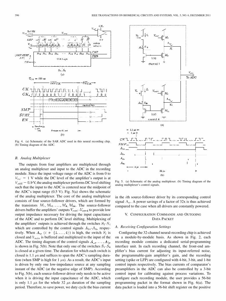
596 IEEE TRANSACTIONS ON BIOMEDICAL CIRCUITS AND SYSTEMS, VOL. 5, NO. 6, DECEMBER 2011
Fig. 4. (a) Schematic of the SAR ADC used in this neural recording chip.(b) Timing diagram of the ADC.
B. Analog Multiplexer
The outputs from four amplifiers are multiplexed throughan analog multiplexer and input to the ADC in the recordingmodule. Since the input voltage range of the ADC is from 0 to
V while the DC level of the amplifier’s output is atV, the analog multiplexer performs DC level shifting
such that the input to the ADC is centered near the midpoint ofthe ADC’s input range (0.5 V). Fig. 5(a) shows the schematicof the analog multiplexer. The core of the analog multiplexerconsists of four source-follower drivers, which are formed bythe transistors . The source-followerdrivers buffer the amplifiers’ outputs - to provide lowoutput impedance necessary for driving the input capacitanceof the ADC and to perform DC level shifting. Multiplexing ofthe amplifiers’ outputs is achieved through the switches -which are controlled by the control signals - respec-tively. When is high, the switch isclosed and is buffered and multiplexed to the input of theADC. The timing diagram of the control signalsis shown in Fig. 5(b). Note that only one of the switches -is closed at a given time. The duration for which each switch isclosed is 1.1 s and suffices to span the ADC’s sampling dura-tion (when SMP is high for 1 s). As a result, the ADC’s inputis driven by only one low-impedance source at any samplinginstant of the ADC (at the negative edge of SMP). Accordingto Fig. 5(b), each source-follower driver only needs to be activewhen it is driving the input capacitance of the ADC, whichis only 1.1 s for the whole 32 s duration of the samplingperiod. Therefore, to save power, we duty cycle the bias current
Fig. 5. (a) Schematic of the analog multiplexer. (b) Timing diagram of theanalog multiplexer’s control signals.
in the th source-follower driver by its corresponding controlsignal . A power savings of a factor of 32x is thus achievedcompared to the case when all drivers are constantly powered.
V. CONFIGURATION COMMANDS AND OUTGOING
DATA PACKET
A. Receiving Configuration Settings
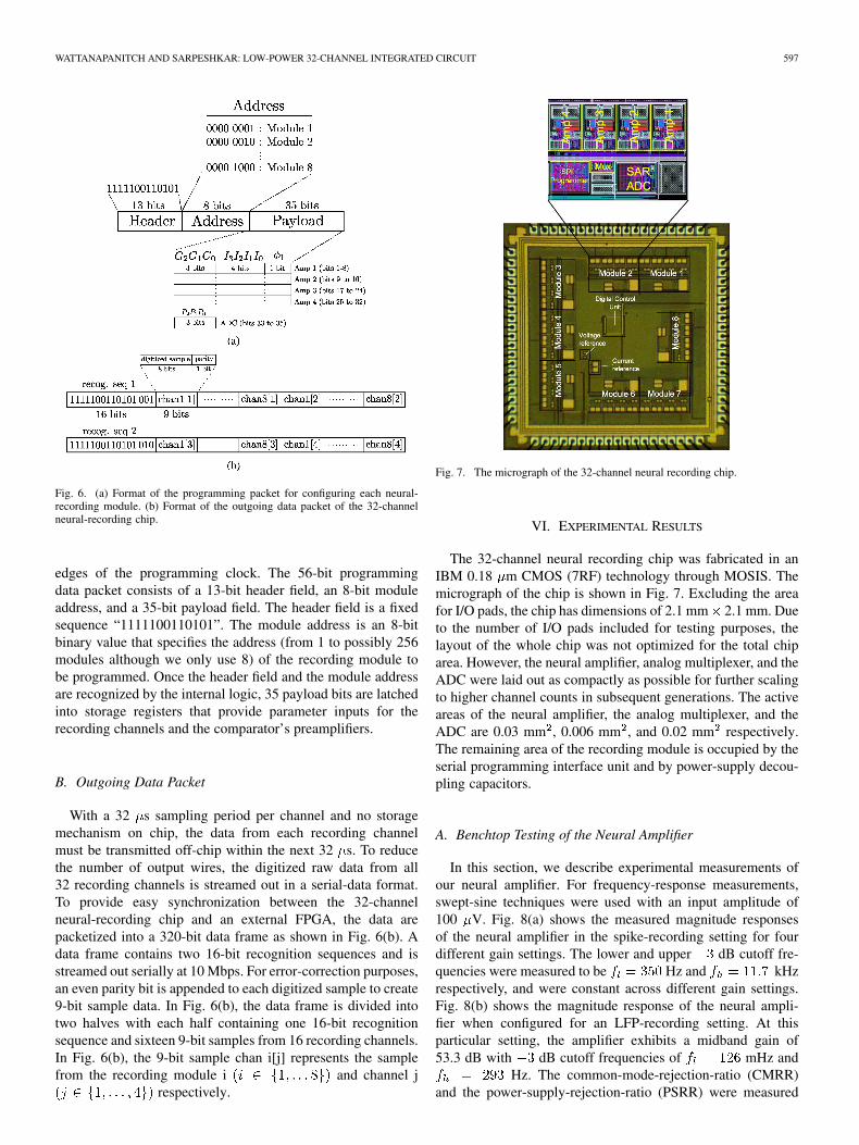
Configuring the 32-channel neural-recording chip is achievedon a module-by-module basis. As shown in Fig. 2, eachrecording module contains a dedicated serial-programminginterface unit. In each recording channel, the front-end am-plifier’s bias current for adjusting its input-referred noise,the programmable-gain amplifier’s gain, and the recordingsetting (spike or LFP) are configured with 4-bit, 3-bit, and 1-bitcontrol inputs respectively. The bias currents of comparator’spreamplifiers in the ADC can also be controlled by a 3-bitcontrol input for calibrating against process variations. Toconfigure each recording module, the user provides a 56-bitprogramming packet in the format shown in Fig. 6(a). Thedata packet is loaded into a 56-bit shift register on the positive
WATTANAPANITCH AND SARPESHKAR: LOW-POWER 32-CHANNEL INTEGRATED CIRCUIT 597
Fig. 6. (a) Format of the programming packet for configuring each neural-recording module. (b) Format of the outgoing data packet of the 32-channelneural-recording chip.
edges of the programming clock. The 56-bit programmingdata packet consists of a 13-bit header field, an 8-bit moduleaddress, and a 35-bit payload field. The header field is a fixedsequence “1111100110101”. The module address is an 8-bitbinary value that specifies the address (from 1 to possibly 256modules although we only use 8) of the recording module tobe programmed. Once the header field and the module addressare recognized by the internal logic, 35 payload bits are latchedinto storage registers that provide parameter inputs for therecording channels and the comparator’s preamplifiers.
B. Outgoing Data Packet
With a 32 s sampling period per channel and no storagemechanism on chip, the data from each recording channelmust be transmitted off-chip within the next 32 s. To reducethe number of output wires, the digitized raw data from all32 recording channels is streamed out in a serial-data format.To provide easy synchronization between the 32-channelneural-recording chip and an external FPGA, the data arepacketized into a 320-bit data frame as shown in Fig. 6(b). Adata frame contains two 16-bit recognition sequences and isstreamed out serially at 10 Mbps. For error-correction purposes,an even parity bit is appended to each digitized sample to create9-bit sample data. In Fig. 6(b), the data frame is divided intotwo halves with each half containing one 16-bit recognitionsequence and sixteen 9-bit samples from 16 recording channels.In Fig. 6(b), the 9-bit sample chan i[j] represents the samplefrom the recording module i and channel j
respectively.
Fig. 7. The micrograph of the 32-channel neural recording chip.
VI. EXPERIMENTAL RESULTS
The 32-channel neural recording chip was fabricated in anIBM 0.18 m CMOS (7RF) technology through MOSIS. Themicrograph of the chip is shown in Fig. 7. Excluding the areafor I/O pads, the chip has dimensions of 2.1 mm 2.1 mm. Dueto the number of I/O pads included for testing purposes, thelayout of the whole chip was not optimized for the total chiparea. However, the neural amplifier, analog multiplexer, and theADC were laid out as compactly as possible for further scalingto higher channel counts in subsequent generations. The activeareas of the neural amplifier, the analog multiplexer, and theADC are 0.03 mm , 0.006 mm , and 0.02 mm respectively.The remaining area of the recording module is occupied by theserial programming interface unit and by power-supply decou-pling capacitors.
A. Benchtop Testing of the Neural Amplifier
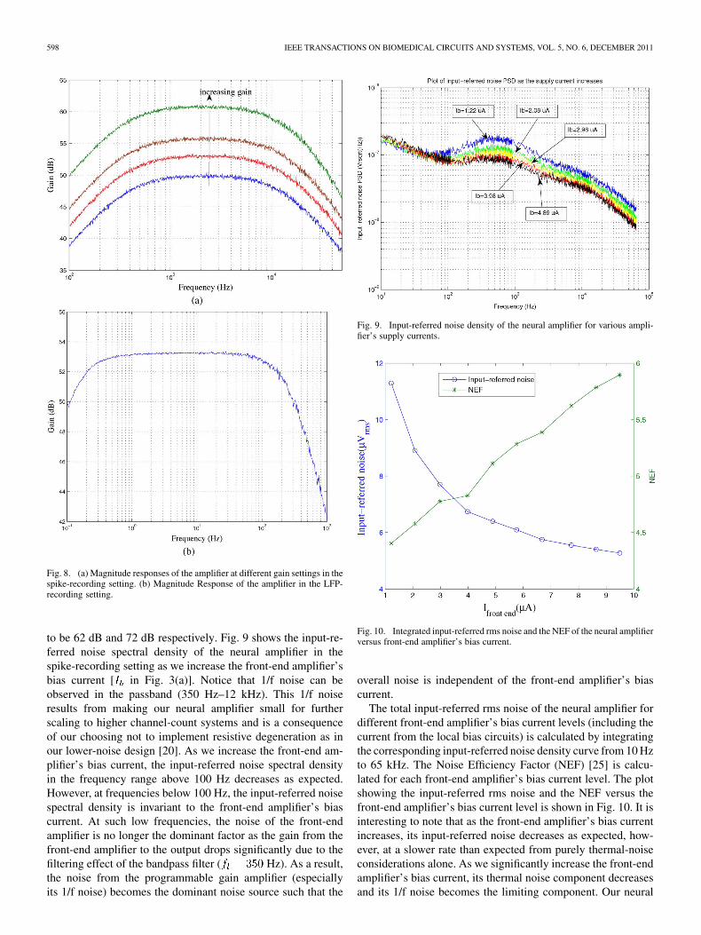
In this section, we describe experimental measurements ofour neural amplifier. For frequency-response measurements,swept-sine techniques were used with an input amplitude of100 V. Fig. 8(a) shows the measured magnitude responsesof the neural amplifier in the spike-recording setting for fourdifferent gain settings. The lower and upper dB cutoff fre-quencies were measured to be Hz and kHzrespectively, and were constant across different gain settings.Fig. 8(b) shows the magnitude response of the neural ampli-fier when configured for an LFP-recording setting. At thisparticular setting, the amplifier exhibits a midband gain of53.3 dB with dB cutoff frequencies of mHz and
Hz. The common-mode-rejection-ratio (CMRR)and the power-supply-rejection-ratio (PSRR) were measured
598 IEEE TRANSACTIONS ON BIOMEDICAL CIRCUITS AND SYSTEMS, VOL. 5, NO. 6, DECEMBER 2011
Fig. 8. (a) Magnitude responses of the amplifier at different gain settings in thespike-recording setting. (b) Magnitude Response of the amplifier in the LFP-recording setting.
to be 62 dB and 72 dB respectively. Fig. 9 shows the input-re-ferred noise spectral density of the neural amplifier in thespike-recording setting as we increase the front-end amplifier’sbias current [ in Fig. 3(a)]. Notice that 1/f noise can beobserved in the passband (350 Hz–12 kHz). This 1/f noiseresults from making our neural amplifier small for furtherscaling to higher channel-count systems and is a consequenceof our choosing not to implement resistive degeneration as inour lower-noise design [20]. As we increase the front-end am-plifier’s bias current, the input-referred noise spectral densityin the frequency range above 100 Hz decreases as expected.However, at frequencies below 100 Hz, the input-referred noisespectral density is invariant to the front-end amplifier’s biascurrent. At such low frequencies, the noise of the front-endamplifier is no longer the dominant factor as the gain from thefront-end amplifier to the output drops significantly due to thefiltering effect of the bandpass filter ( Hz). As a result,the noise from the programmable gain amplifier (especiallyits 1/f noise) becomes the dominant noise source such that the
Fig. 9. Input-referred noise density of the neural amplifier for various ampli-fier’s supply currents.
Fig. 10. Integrated input-referred rms noise and the NEF of the neural amplifierversus front-end amplifier’s bias current.
overall noise is independent of the front-end amplifier’s biascurrent.
The total input-referred rms noise of the neural amplifier fordifferent front-end amplifier’s bias current levels (including thecurrent from the local bias circuits) is calculated by integratingthe corresponding input-referred noise density curve from 10 Hzto 65 kHz. The Noise Efficiency Factor (NEF) [25] is calcu-lated for each front-end amplifier’s bias current level. The plotshowing the input-referred rms noise and the NEF versus thefront-end amplifier’s bias current level is shown in Fig. 10. It isinteresting to note that as the front-end amplifier’s bias currentincreases, its input-referred noise decreases as expected, how-ever, at a slower rate than expected from purely thermal-noiseconsiderations alone. As we significantly increase the front-endamplifier’s bias current, its thermal noise component decreasesand its 1/f noise becomes the limiting component. Our neural
WATTANAPANITCH AND SARPESHKAR: LOW-POWER 32-CHANNEL INTEGRATED CIRCUIT 599
Fig. 11. Input-referred noise density in the LFP-recording setting.
TABLE IIPERFORMANCE SUMMARY OF THE NEURAL AMPLIFIER
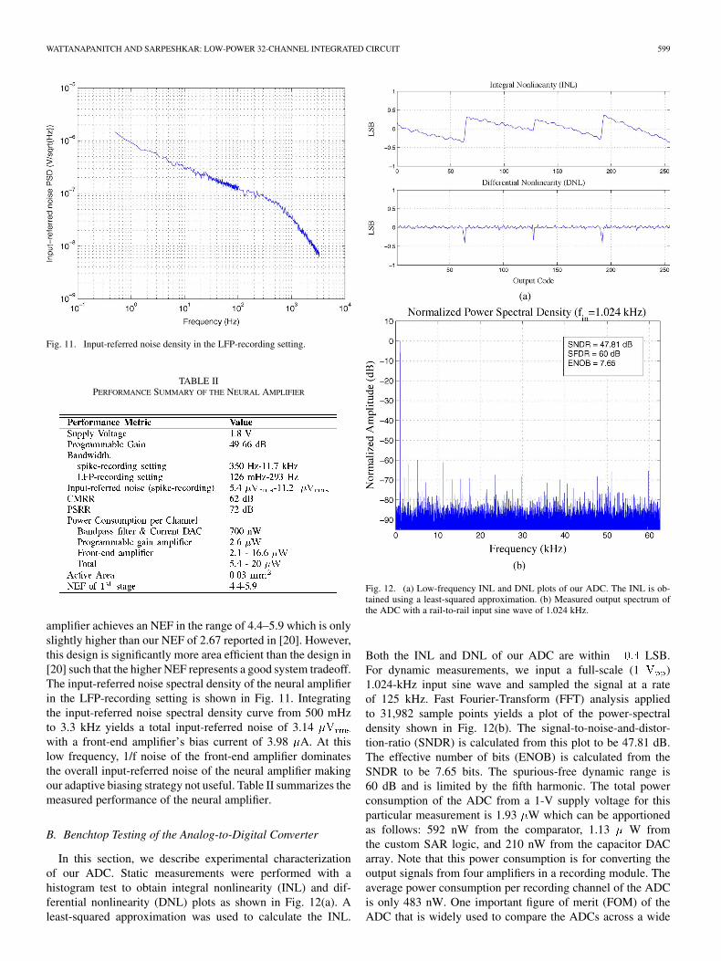
amplifier achieves an NEF in the range of 4.4–5.9 which is onlyslightly higher than our NEF of 2.67 reported in [20]. However,this design is significantly more area efficient than the design in[20] such that the higher NEF represents a good system tradeoff.The input-referred noise spectral density of the neural amplifierin the LFP-recording setting is shown in Fig. 11. Integratingthe input-referred noise spectral density curve from 500 mHzto 3.3 kHz yields a total input-referred noise of 3.14with a front-end amplifier’s bias current of 3.98 A. At thislow frequency, 1/f noise of the front-end amplifier dominatesthe overall input-referred noise of the neural amplifier makingour adaptive biasing strategy not useful. Table II summarizes themeasured performance of the neural amplifier.
B. Benchtop Testing of the Analog-to-Digital Converter
In this section, we describe experimental characterizationof our ADC. Static measurements were performed with ahistogram test to obtain integral nonlinearity (INL) and dif-ferential nonlinearity (DNL) plots as shown in Fig. 12(a). Aleast-squared approximation was used to calculate the INL.
Fig. 12. (a) Low-frequency INL and DNL plots of our ADC. The INL is ob-tained using a least-squared approximation. (b) Measured output spectrum ofthe ADC with a rail-to-rail input sine wave of 1.024 kHz.
Both the INL and DNL of our ADC are within LSB.For dynamic measurements, we input a full-scale (1 )1.024-kHz input sine wave and sampled the signal at a rateof 125 kHz. Fast Fourier-Transform (FFT) analysis appliedto 31,982 sample points yields a plot of the power-spectraldensity shown in Fig. 12(b). The signal-to-noise-and-distor-tion-ratio (SNDR) is calculated from this plot to be 47.81 dB.The effective number of bits (ENOB) is calculated from theSNDR to be 7.65 bits. The spurious-free dynamic range is60 dB and is limited by the fifth harmonic. The total powerconsumption of the ADC from a 1-V supply voltage for thisparticular measurement is 1.93 W which can be apportionedas follows: 592 nW from the comparator, 1.13 W fromthe custom SAR logic, and 210 nW from the capacitor DACarray. Note that this power consumption is for converting theoutput signals from four amplifiers in a recording module. Theaverage power consumption per recording channel of the ADCis only 483 nW. One important figure of merit (FOM) of theADC that is widely used to compare the ADCs across a wide
600 IEEE TRANSACTIONS ON BIOMEDICAL CIRCUITS AND SYSTEMS, VOL. 5, NO. 6, DECEMBER 2011
TABLE IIIPERFORMANCE SUMMARY OF THE ANALOG TO DIGITAL CONVERTER
range of bandwidths and precisions is the energy consumptionper quantization level [8]. The FOM can be calculated fromthe formula , whereand are the total power consumption and the samplingfrequency of the ADC respectively. The FOM of our ADC iscalculated to be 77 fJ per quantization level and is among themost energy-efficient ADCs reported to date especially for itscompact 0.02 mm area. The performance summary of ourADC is provided in Table III.
C. Wireless In Vivo Testing of the Neural-Recording Chip inan Awake Behaving Primate
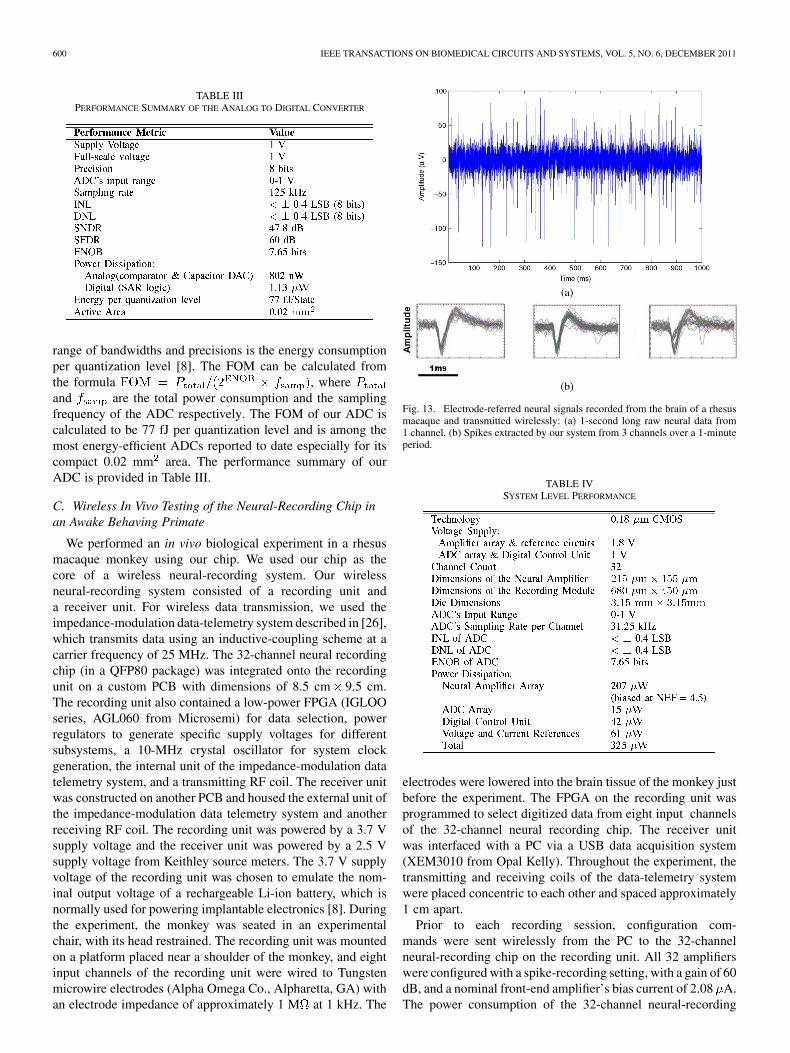
We performed an in vivo biological experiment in a rhesusmacaque monkey using our chip. We used our chip as thecore of a wireless neural-recording system. Our wirelessneural-recording system consisted of a recording unit anda receiver unit. For wireless data transmission, we used theimpedance-modulation data-telemetry system described in [26],which transmits data using an inductive-coupling scheme at acarrier frequency of 25 MHz. The 32-channel neural recordingchip (in a QFP80 package) was integrated onto the recordingunit on a custom PCB with dimensions of 8.5 cm 9.5 cm.The recording unit also contained a low-power FPGA (IGLOOseries, AGL060 from Microsemi) for data selection, powerregulators to generate specific supply voltages for differentsubsystems, a 10-MHz crystal oscillator for system clockgeneration, the internal unit of the impedance-modulation datatelemetry system, and a transmitting RF coil. The receiver unitwas constructed on another PCB and housed the external unit ofthe impedance-modulation data telemetry system and anotherreceiving RF coil. The recording unit was powered by a 3.7 Vsupply voltage and the receiver unit was powered by a 2.5 Vsupply voltage from Keithley source meters. The 3.7 V supplyvoltage of the recording unit was chosen to emulate the nom-inal output voltage of a rechargeable Li-ion battery, which isnormally used for powering implantable electronics [8]. Duringthe experiment, the monkey was seated in an experimentalchair, with its head restrained. The recording unit was mountedon a platform placed near a shoulder of the monkey, and eightinput channels of the recording unit were wired to Tungstenmicrowire electrodes (Alpha Omega Co., Alpharetta, GA) withan electrode impedance of approximately 1 M at 1 kHz. The
Fig. 13. Electrode-referred neural signals recorded from the brain of a rhesusmacaque and transmitted wirelessly: (a) 1-second long raw neural data from1 channel. (b) Spikes extracted by our system from 3 channels over a 1-minuteperiod.
TABLE IVSYSTEM LEVEL PERFORMANCE
electrodes were lowered into the brain tissue of the monkey justbefore the experiment. The FPGA on the recording unit wasprogrammed to select digitized data from eight input channelsof the 32-channel neural recording chip. The receiver unitwas interfaced with a PC via a USB data acquisition system(XEM3010 from Opal Kelly). Throughout the experiment, thetransmitting and receiving coils of the data-telemetry systemwere placed concentric to each other and spaced approximately1 cm apart.
Prior to each recording session, configuration com-mands were sent wirelessly from the PC to the 32-channelneural-recording chip on the recording unit. All 32 amplifierswere configured with a spike-recording setting, with a gain of 60dB, and a nominal front-end amplifier’s bias current of 2.08 A.The power consumption of the 32-channel neural-recording
WATTANAPANITCH AND SARPESHKAR: LOW-POWER 32-CHANNEL INTEGRATED CIRCUIT 601
TABLE VCOMPARISON TO OTHER STATE-OF-THE-ART NEURAL RECORDING SYSTEMS
chip for this experiment was 325 W. The power consumptionof the internal unit of the impedance-modulation wirelessdata telemetry system was approximately 100 W, while thereceiver unit’s power consumption was approximately 3.0 mWfor a 2.5 Mbps data rate [26]. Fig. 13(a) shows a 1-secondlong raw neural data from one of the input channels recordedwith our system. Fig. 13(b) shows superimposed neural spikesextracted by our chip from 3 channels over a 1-minute period.The performance summary of the neural-recording chip duringthe wireless recording experiment is shown in Table IV.
Table V compares the performance of our design with somedesigns in the literature that achieve low power consumption andsmall area per channel. The design in [14], [29] includes bothrecording and stimulation features while the design in [27] alsoincluded digital signal processing (DSP) and an ultra-wide-band(UWB) transmitter. In Table V, only the recording features thatinclude signal amplification and digitization are compared.
VII. CONCLUSION
We described the operation and measured performance of anultra-low-power 32-channel neural-recording chip. The chip canamplify and convert neural signals from 32 input channels into8-bit digital representations and transmit this data off chip in aserial format. An adaptive-biasing technique was utilized in thedesign of the neural amplifier to help minimize the total powerconsumption of the overall recording chip. Our neural amplifiersare highly programmable: their gain, recording mode (spike orLFP), and input-referred noise can be digitally programmed tosuit the recording environment. Our recording chip was success-fully tested in an in vivo wireless recording experiment from abehaving primate while dissipating only 10.1 W/channel. Dueto its very small area and power consumption per recordingchannel, our recording chip is suitable for high-channel-countrecording systems.
ACKNOWLEDGMENT
The authors would like to thank Prof. R. A. Andersen forproviding facilities for the animal experiments, B. I. Rappoport
and E. J. Hwang for tremendous help with the rhesus macaquerecording experiment, D. Kumar for help in designing theon-chip current reference and digital standard cells, L. Turicchiafor developing a software interface between the data-telemetrysystem and a computer, B. Do Valle for help in designing thewireless setup, and S. K. Arfin for valuable discussions andcomments during manuscript preparation.
REFERENCES
[1] D. R. Kipke, R. J. Vetter, J. C. Williams, and J. F. Hetke, “Silicon-substrate intracortical microelectrode arrays for long-term recordingof neuronal spike activity in cerebral cortex,” IEEE Trans. Neural Syst.Rehabil. Eng., vol. 11, no. 2, pp. 151–155, Jun. 2003.
[2] E. Maynard, C. Nordhausen, and R. Normann, “The utah intracorticalelectrode array: A recording structure for potential brain-computer in-terfaces,” Electroencephalogr. Clin. Neurophysiol., vol. 102, no. 3, pp.228–239, Mar. 1997.
[3] J. Wessberg, C. Stambaugh, J. Kralik, P. Beck, M. Laubach, J. Chapin,J. Kim, J. Biggs, M. Srinivasan, and M. Nicolelis, “Real-time predic-tion of hand trajectory by ensembles of cortical neurons in primates,”Nature, vol. 408, no. 6810, pp. 361–365, Nov. 16, 2000.
[4] D. Taylor, S. Tillery, and A. Schwartz, “Direct cortical control of 3Dneuroprosthetic devices,” Science, vol. 296, no. 5574, pp. 1829–1832,Jun. 7, 2002.
[5] M. Serruya, N. Hatsopoulos, L. Paninski, M. Fellows, and J. Donoghue,“Instant neural control of a movement signal,” Nature, vol. 416, no.6877, pp. 141–142, Mar. 14, 2002.
[6] L. R. Hochberg, M. D. Serruya, G. M. Friehs, J. A. Mukand, M. Saleh,A. H. Caplan, A. Branner, D. Chen, R. D. Penn, and J. P. Donoghue,“Neuronal ensemble control of prosthetic devices by a human withtetraplegia,” Nature, vol. 442, no. 7099, pp. 164–171, Jul. 13, 2006.
[7] M. Velliste, S. Perel, M. C. Spalding, A. S. Whitford, and A. B.Schwartz, “Cortical control of a prosthetic arm for self-feeding,”Nature, vol. 453, no. 7198, pp. 1098–1101, Jun. 19, 2008.
[8] R. Sarpeshkar, Ultra Low Power Bioelectronics: Fundamentals,Biomedical Applications, and Bio-Inspired Systems. Cambridge,U.K.: Cambridge Univ. Press, 2010.
[9] R. Olsson and K. Wise, “A three-dimensional neural recording mi-crosystem with implantable data compression circuitry,” IEEE J. Solid-State Circuits, vol. 40, no. 12, pp. 2796–2804, Dec. 2005.
[10] R. R. Harrison, P. T. Watkins, R. J. Kier, R. O. Lovejoy, D. J. Black,B. Greger, and F. Solzbacher, “A low-power integrated circuit for awireless 100-electrode neural recording system,” IEEE J. Solid-StateCircuits, vol. 42, no. 1, pp. 123–133, Jan. 2007.
[11] A. A. Sodagar, K. D. Wise, and K. Najafi, “A fully integratedmixed-signal neural processor for implantable multichannel corticalrecording,” IEEE Trans. Biomed. Eng., vol. 54, no. 6, pt. 1, pp.1075–1088, Jun. 2007.
602 IEEE TRANSACTIONS ON BIOMEDICAL CIRCUITS AND SYSTEMS, VOL. 5, NO. 6, DECEMBER 2011
[12] M. Chae, W. Liu, Z. Yang, T. Chen, J. Kim, M. Sivaprakasam, andM. Yuce, “A 128-channel 6 mw wireless neural recording ic withon-the-fly spike sorting and uwb tansmitter,” in Proc. Solid-StateCircuits Conf. Dig. Tech. Papers, Feb. 2008, pp. 146–603.
[13] M. Yin and M. Ghovanloo, “A flexible clockless 32-ch simultaneouswireless neural recording system with adjustable resolution,” in Proc.Solid-State Circuits Conf. Dig. Tech. Papers, 2009, pp. 432–433, 433a.
[14] F. Shahrokhi, K. Abdelhalim, D. Serletis, P. Carlen, and R. Genov,“The 128-channel fully differential digital integrated neural recordingand stimulation interface,” IEEE Trans. Biomed. Circuits Syst., vol. 4,no. 3, pp. 149–161, Jun. 2010.
[15] W.-S. Liew, X. Zou, L. Yao, and Y. Lian, “A 1-V 60-mu W 16-channelinterface chip for implantable neural recording,” in Proc. IEEE CustomIntegrated Circuits Conf., 2009, pp. 507–510.
[16] Y. Ramadass and A. Chandrakasan, “Voltage scalable switched capac-itor dc-dc converter for ultra-low-power on-chip applications,” in Proc.IEEE Power Electronics Specialists Conf., Jun. 2007, pp. 2353–2359.
[17] R. Harrison and C. Charles, “A low-power low-noise CMOS amplifierfor neural recording applications,” IEEE J. Solid-State Circuits, vol.38, no. 6, pp. 958–965, Jun. 2003.
[18] Y. Perelman and R. Ginosar, “An integrated system for multichannelneuronal recording with spike/LFP separation, integrated A/D conver-sion and threshold detection,” IEEE Trans. Biomed. Eng., vol. 54, no.1, pp. 130–137, Jan. 2007.
[19] R. Sarpeshkar, W. Wattanapanitch, S. K. Arfin, B. I. Rapoport, S.Mandal, M. W. Baker, M. S. Fee, S. Musallam, and R. A. Andersen,“Low-power circuits for brain-machine interfaces,” IEEE Trans.Biomed. Circuits Syst., vol. 2, no. 3, pp. 173–183, 2008.
[20] W. Wattanapanitch, M. Fee, and R. Sarpeshkar, “An energy-efficientmicropower neural recording amplifier,” IEEE Trans. Biomed. CircuitsSyst., vol. 1, no. 2, pp. 136–147, Jun. 2007.
[21] R. Sarpeshkar, R. Lyon, and C. Mead, “A low-power wide-linear-rangetransconductance amplifier,” Analog Int. Circuits Sig. Proc., vol. 13,no. 1–2, pp. 123–151, May–Jun. 1997.
[22] M. Scott, B. Boser, and K. Pister, “An ultralow-energy ADC for smartdust,” IEEE J. Solid-State Circuits, vol. 38, no. 7, pp. 1123–1129, Jul.2003.
[23] J. M. Rabaey, A. Chandrakasan, and B. Nikolic, Digital Integrated Cir-cuits: A Design Perspective, 2nd ed. Upper Saddle River, NJ: Pren-tice-Hall, 2003.
[24] B. Ginsburg and A. Chandrakasan, “An energy-efficient charge recy-cling approach for a SAR converter with capacitive DAC,” in Proc.IEEE Int. Symp. Circuits and Systems, 2005, pp. 184–187.
[25] M. Steyaert, W. Sansen, and Z. Chang, “A micropower low-noisemonolithic instrumentation amplifier for medical purposes,” IEEE J.Solid-State Circuits, vol. 22, no. 6, pp. 1163–1168, Dec. 1987.
[26] S. Mandal and R. Sarpeshkar, “Power-efficient impedance-modulationwireless data links for biomedical implants,” IEEE Trans. Biomed. Cir-cuits Syst., vol. 2, no. 4, pp. 301–315, Dec. 2008.
[27] M. S. Chae, Z. Yang, M. R. Yuce, L. Hoang, and W. Liu, “A 128-channel 6 mW wireless neural recording IC with spike feature extrac-tion and UWB transmitter,” IEEE Trans. Neural Syst. Rehabil. Eng.,vol. 17, no. 4, pp. 312–321, Aug. 2009.
[28] B. Gosselin, A. E. Ayoub, J.-F. Roy, M. Sawan, F. Lepore, A. Chaud-huri, and D. Guitton, “A mixed-signal multichip neural recording in-terface with bandwidth reduction,” IEEE Trans. Biomed. Circuits Syst.,vol. 3, no. 3, pp. 129–141, Jun. 2009.
[29] M. Azin, D. Guggenmos, S. Barbay, R. Nudo, and P. Mohseni, “A bat-tery-powered activity-dependent intracortical microstimulation ic forbrain-machine-brain interface,” IEEE J. Solid-State Circuits, vol. 46,no. 4, pp. 731–745, Apr. 2011.
Woradorn Wattanapanitch (S’07) received theB.S. degree (Summa Cum Laude) in electrical andcomputer engineering from Cornell University,Ithaca, NY, and the M.Sc. and Ph.D. degrees inelectrical engineering and computer science fromthe Massachusetts Institute of Technology (MIT),Cambridge, in 2005, 2007, and 2011, respectively,
At MIT, he worked on developing ultra-low-powerelectronics for biomedical applications. In 2011, hejoined the Department of Electrical Engineering,Kasetsart University, Bangkok, Thailand, as a faculty
member where he continues his research interests in the areas of low-poweranalog and mixed-signal VLSI for biomedical applications and control theory.
Rahul Sarpeshkar (SM’07) received the B.S.degrees in electrical engineering and physics fromthe Massachusetts Institute of Technology (MIT),Cambridge, and the Ph.D. degree in electrical engi-neering from the California Institute of Technology,Pasadena.
He then joined Bell Labs as a member of thetechnical staff in the Department of BiologicalComputation within its physics division. Since1999, he has been on the faculty of MITs ElectricalEngineering and Computer Science Department
where he heads a research group on analog very-large-scale and biologicalsystems. He holds more than 25 patents and has authored many publications,including one featured on the cover of Nature. He has authored Ultra LowPower Bioelectronics: Fundamentals, Biomedical Applications and Bio-in-spired Systems, which provides a broad and deep treatment of the fields oflow-power electronics and bioelectronics. He is an Associate Editor of theIEEE TRANSACTIONS ON BIOMEDICAL CIRCUITS AND SYSYTEMS.
Dr. Sarpeshkar has received several awards, including the National ScienceFoundation Career Award, the Office of Naval Research Young InvestigatorAward, the Packard Fellows Award, and the Indus Technovator Award for hisinterdisciplinary bioengineering research. He serves on the program committeesof several technical conferences.