A fast and low cost testing technique for core-based system-on-chip
15
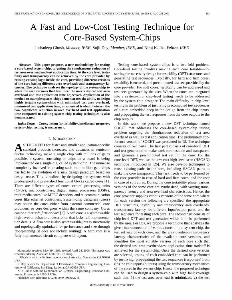
IEEE TRANSACTIONS ON COMPUTER-AIDED DESIGN OF INTEGRATED CIRCUITS AND SYSTEMS, VOL. 19, NO. 8, AUGUST2000 863 A Fast and Low-Cost Testing Technique for Core-Based System-Chips Indradeep Ghosh, Member, IEEE, Sujit Dey, Member, IEEE, and Niraj K. Jha, Fellow, IEEE Abstract—This paper proposes a new methodology for testing a core-based system-chip, targeting the simultaneous reduction of test area overhead and test application time. At the core level, testa- bility and transparency can be achieved by the core provider by reusing existing logic inside the core, providing different versions of the core having different area overheads and transparency la- tencies. The technique analyzes the topology of the system-chip to select the core versions that best meet the user’s desired test area overhead and test application time objectives. Application of the method to example system-chips demonstrates the ability to design highly testable system-chips with minimized test area overhead, minimized test application time, or a desired tradeoff between the two. Significant reduction in area overhead and test application time compared to existing system-chip testing techniques is also demonstrated. Index Terms—Cores, design for testability, intellectual property, system-chip, testing, transparency. I. INTRODUCTION A S THE NEED for faster and smaller application-specific standard products increases, and advances in semicon- ductor technology make a single chip with millions of gates possible, a system consisting of chips on a board is being implemented on a single die, called system-chip. The immense complexity involved in creating such multimillion gate chips has led to the evolution of a new design paradigm based on design reuse. This is realized by designing the systems with predesigned and preverified functional blocks called cores [1]. There are different types of cores: central processing units (CPUs), microcontrollers, digital signal processors (DSPs), multimedia cores like MPEG decoders, and telecommunication cores like ethernet controllers. System-chip designers (users) may obtain the cores either from external commercial core providers, or core designers within the same company. Cores can be either soft, firm or hard [2]. A soft core is a synthesizable high-level or behavioral description that lacks full implementa- tion details. A firm core is also synthesizable, but is structurally and topologically optimized for performance and size through floorplanning (it does not include routing). A hard core is a fully implemented circuit complete with layout. Manuscript received May 19, 1999; revised April 24, 2000. This paper was recommended by Associate Editor K.-T. Cheng. I. Ghosh is with the Fujitsu Laboratories of America, Sunnyvale, CA 94086 USA. S. Dey is with the Department of Electrical & Computer Engineering, Uni- versity of California, San Diego La Jolla, CA 92093 USA. N. K. Jha is with the Department of Electrical Engineering, Princeton Uni- versity, Princeton, NJ 08544 USA. Publisher Item Identifier S 0278-0070(00)06422-8. Testing core-based system-chips is a two-fold problem. Core-level testing involves making each core testable—in- serting the necessary design for testability (DFT) structures and generating test sequences. Typically, for hard and firm cores, testability is ensured, and precomputed test sets provided by the core provider. For soft cores, testability can be addressed and test sets generated by the user. When the cores are integrated into a system-chip, chip-level testing needs to be addressed by the system-chip designer. The main difficulty in chip-level testing is the problem of justifying precomputed test sequences of a core embedded deep in the design from the chip inputs, and propagating the test responses from the core outputs to the chip outputs. In this work, we propose a new DFT technique named SOCET that addresses the core-based system-chip testing problem targeting the simultaneous reduction of test area overhead as well as test application time. The preliminary con- ference version of SOCET was presented in [3]. The technique consists of two parts. The first part consists of core-level DFT and test generation to make each core testable and transparent and generate a precomputed test set for the core. For the core-level DFT, we use the low-cost high-level scan (HSCAN) technique introduced in [26]. We also develop techniques to reuse existing paths in the core, including HSCAN paths to make the core transparent. This task needs to be performed by the core provider in case of hard and firm cores, and the user in case of soft cores. During the core testability phase, various versions of the same core are synthesized, with varying trans- parency latency and area overhead characteristics. Hence, the core provider supplies various versions of the same core where for each version the following are specified: the appropriate DFT structures, testability and transparency area overheads, transparency latency for different input/output pairs, and the test sequence for testing each core. The second part consists of chip-level DFT and test generation which is to be performed by the user. For this, we propose a technique that analyzes the given interconnection of various cores in the system-chip, the test set size of each core, and the area overhead/transparency latency characteristics of the available core versions, and identifies the most suitable version of each core such that the desired test area overhead/test application time tradeoff is achieved for the system-chip. Once the desired core versions are selected, testing of each embedded core can be performed by justifying (propagating) the test sequences (responses) from (to) the chip inputs (outputs) using the transparency mechanism of the cores in the system-chip. Hence, the proposed technique can be used to design a system-chip with high fault coverage such that: 1) the test area overhead is minimized; 2) the test 0278–0070/00$10.00 © 2000 IEEE
Transcript of A fast and low cost testing technique for core-based system-on-chip
IEEE TRANSACTIONS ON COMPUTER-AIDED DESIGN OF INTEGRATED CIRCUITS AND SYSTEMS, VOL. 19, NO. 8, AUGUST 2000 863
A Fast and Low-Cost Testing Technique forCore-Based System-Chips
Indradeep Ghosh, Member, IEEE, Sujit Dey, Member, IEEE, and Niraj K. Jha, Fellow, IEEE
Abstract—This paper proposes a new methodology for testinga core-based system-chip, targeting the simultaneous reduction oftest area overhead and test application time. At the core level, testa-bility and transparency can be achieved by the core provider byreusing existing logic inside the core, providing different versionsof the core having different area overheads and transparency la-tencies. The technique analyzes the topology of the system-chip toselect the core versions that best meet the user’s desired test areaoverhead and test application time objectives. Application of themethod to example system-chips demonstrates the ability to designhighly testable system-chips with minimized test area overhead,minimized test application time, or a desired tradeoff between thetwo. Significant reduction in area overhead and test applicationtime compared to existing system-chip testing techniques is alsodemonstrated.
Index Terms—Cores, design for testability, intellectual property,system-chip, testing, transparency.
I. INTRODUCTION
A S THE NEED for faster and smaller application-specificstandard products increases, and advances in semicon-
ductor technology make a single chip with millions of gatespossible, a system consisting of chips on a board is beingimplemented on a single die, called system-chip. The immensecomplexity involved in creating such multimillion gate chipshas led to the evolution of a new design paradigm based ondesign reuse. This is realized by designing the systems withpredesigned and preverified functional blocks called cores [1].There are different types of cores: central processing units(CPUs), microcontrollers, digital signal processors (DSPs),multimedia cores like MPEG decoders, and telecommunicationcores like ethernet controllers. System-chip designers (users)may obtain the cores either from external commercial coreproviders, or core designers within the same company. Corescan be eithersoft, firm or hard [2]. A soft core is a synthesizablehigh-level or behavioral description that lacks full implementa-tion details. A firm core is also synthesizable, but is structurallyand topologically optimized for performance and size throughfloorplanning (it does not include routing). A hard core is afully implemented circuit complete with layout.
Manuscript received May 19, 1999; revised April 24, 2000. This paper wasrecommended by Associate Editor K.-T. Cheng.
I. Ghosh is with the Fujitsu Laboratories of America, Sunnyvale, CA 94086USA.
S. Dey is with the Department of Electrical & Computer Engineering, Uni-versity of California, San Diego La Jolla, CA 92093 USA.
N. K. Jha is with the Department of Electrical Engineering, Princeton Uni-versity, Princeton, NJ 08544 USA.
Publisher Item Identifier S 0278-0070(00)06422-8.
Testing core-based system-chips is a two-fold problem.Core-level testing involves making each core testable—in-serting the necessary design for testability (DFT) structures andgenerating test sequences. Typically, for hard and firm cores,testability is ensured, and precomputed test sets provided by thecore provider. For soft cores, testability can be addressed andtest sets generated by the user. When the cores are integratedinto a system-chip, chip-level testing needs to be addressedby the system-chip designer. The main difficulty in chip-leveltesting is the problem of justifying precomputed test sequencesof a core embedded deep in the design from the chip inputs,and propagating the test responses from the core outputs to thechip outputs.
In this work, we propose a new DFT technique namedSOCET that addresses the core-based system-chip testingproblem targeting the simultaneous reduction of test areaoverhead as well as test application time. The preliminary con-ference version of SOCET was presented in [3]. The techniqueconsists of two parts. The first part consists of core-level DFTand test generation to make each core testable and transparentand generate a precomputed test set for the core. For thecore-level DFT, we use the low-cost high-level scan (HSCAN)technique introduced in [26]. We also develop techniques toreuse existing paths in the core, including HSCAN paths tomake the core transparent. This task needs to be performed bythe core provider in case of hard and firm cores, and the userin case of soft cores. During the core testability phase, variousversions of the same core are synthesized, with varying trans-parency latency and area overhead characteristics. Hence, thecore provider supplies various versions of the same core wherefor each version the following are specified: the appropriateDFT structures, testability and transparency area overheads,transparency latency for different input/output pairs, and thetest sequence for testing each core. The second part consists ofchip-level DFT and test generation which is to be performedby the user. For this, we propose a technique that analyzes thegiven interconnection of various cores in the system-chip, thetest set size of each core, and the area overhead/transparencylatency characteristics of the available core versions, andidentifies the most suitable version of each core such thatthe desired test area overhead/test application time tradeoff isachieved for the system-chip. Once the desired core versionsare selected, testing of each embedded core can be performedby justifying (propagating) the test sequences (responses) from(to) the chip inputs (outputs) using the transparency mechanismof the cores in the system-chip. Hence, the proposed techniquecan be used to design a system-chip with high fault coveragesuch that: 1) the test area overhead is minimized; 2) the test
0278–0070/00$10.00 © 2000 IEEE
864 IEEE TRANSACTIONS ON COMPUTER-AIDED DESIGN OF INTEGRATED CIRCUITS AND SYSTEMS, VOL. 19, NO. 8, AUGUST 2000
application time for testing the system-chip is minimized; or3) a desired tradeoff is obtained between the test area overheadand test application time.
The paper is organized as follows. Some previous work onsystem-chip testing is discussed in Section II. In Section III,we briefly describe HSCAN which is our underlying method-ology for testing individual cores. In Section IV, the SOCETmethod is introduced with the help of an example core-basedsystem-chip. The method for obtaining transparency throughcores is described in greater detail in Section V. The core se-lection method for trading off test application time with over-heads is explained in detail in Section VI. Experimental resultsare presented in Section VII and conclusions in Section VIII.
II. PREVIOUS WORK
As mentioned before, the system-chip testing problem can bedivided into two parts: 1) core-level testing and 2) chip-leveltesting.
Core-level testing can be done through automatic test patterngeneration (ATPG) at the logic level [4] and by employing avariety of DFT techniques like full or partial scan [5]–[7], andbuilt-in self-test (BIST) [8]–[10]. Hierarchical testability tech-niques may also be used [11].
At the chip level, a number of DFT techniques have beenproposed [12], [13]. One existing DFT method, referred to asFScan-BScan, utilizes a combination of full scan and boundaryscan [14]. In this method, each core is made testable by fullscan while chip-level testability is obtained by isolating eachcore using boundary scan. However, the FScan-BScan schememay have large area and delay overheads. Moreover, each testvector of the test set of each embedded core needs to be shiftedfrom the chip inputs through the boundary scan chain and thenshifted serially through the full scan chain. Consequently, thetest application time for testing all the cores of a system-chipmay be prohibitively large. Recently, some work has been doneto address this problem [15].
Another existing DFT method, referred to as FScan-TBus,utilizes a combination of full scan and test bus [12], [23]. In thismethod, each core is made testable by using full scan. A test busis added to the system-chip, and runs from the primary inputs(PIs) of the chip to its primary outputs (POs). A series of multi-plexers is used to isolate each embedded core during testing toprovide chip-level testability. In this case as well, the area anddelay overheads can be quite large due to large multiplexer androuting requirements.
A silicon-based solution has been proposed for testingsystem-chips in [18]. In this approach, asoftnetlist level grid isused to provide direct access to storage elements, observationtest points and bi-directional test points via the chip pins. Var-ious other methods for providing test access to embedded coreshave also been provided [19]–[23]. A method for minimizingtest application time of system-chips using both BIST andexternal testing is given in [24].
In [16] and [17], a DFT method is described to test macroblocks inside a circuit with a combination of different test tech-niques. It relies heavily on full/partial scan and boundary scanwhose disadvantages have been stated above. Though functionalinformation of modules is sometimes used to reduce test over-head by utilizing the concept of module transparency, the tech-
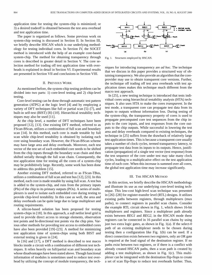
Fig. 1. Structures employed by HSCAN.
niques for introducing transparency aread hoc. The techniquethat we discuss in this paper provides a structured way of ob-taining transparency. We also provide an algorithm that the core-provider may use to obtain transparent core versions. Further,the technique off trading off test area overheads with test ap-plication times makes this technique much different from themacro test approach.
In [25], a new testing technique is introduced that tests indi-vidual cores using hierarchical testability analysis (HTA) tech-niques. It also uses HTA to make the corestransparent. In thetest mode, a transparent core can propagate test data from itsinputs to outputs without information loss. During testing ofthe system-chip, the transparency property of cores is used topropagate precomputed core test sequences from the chip in-puts to the core inputs, and test responses from the core out-puts to the chip outputs. While successful in lowering the testarea and delay overheads compared to existing techniques, thetechnique in [25] suffers from the drawback of relatively largetest application times. This is because a transparent core usuallytakes a number of clock cycles, termed transparency latency, topropagate test data from its inputs to its outputs. Hence, justifi-cation (propagation) of a single test vector (test response) fromthe test sequence of the core under test may take many clockcycles, leading to a multiplicative effect on the test applicationtime of each core. When this increase is summed over all cores,the global test application time may increase significantly.
III. T HE HSCAN METHOD
In this section, we briefly describe the HSCAN methodologyand illustrate its use as our underlying core-level testing tech-nique. This low-cost high-level scan technique was presentedin [26]–[28] for register-transfer level (RTL) designs. It utilizesexisting paths between registers, through multiplexers (muxpaths), to connect registers in parallel scan chains. Considerthe example RTL circuit shown in Fig. 1, which shows 16-bitmultiplexers and registers. Since a multiplexer path alreadyexists betweenREG1and REG2, in the HSCAN mode theseregisters can be connected in 16 parallel scan chains by usingjust two extra logic gates, as shown in Fig. 1(a). If the select-0path of an existing multiplexer needs to be chosen duringtesting then a configuration like Fig. 1(b) can be used. If adirect connection exists between two registers, only an OR gateis required at the load signal of the destination register. If nopaths exist between two registers, or if there is a conflict withalready created HSCAN paths, then a scan path is created byadding a test multiplexer, as shown in Fig. 1(c). This multi-plexer can be integrated with the destination flip-flops to createa set of scan flip-flops to reduce test overheads further. Thus,

GHOSHet al.: A FAST AND LOW-COST TESTING TECHNIQUE FOR CORE-BASED SYSTEM-CHIPS 865
Fig. 2. An example core-based system-chip.
the scheme ends up connecting each flip-flop in the circuit insome parallel scan chain, which runs from the circuit inputsto the circuit outputs. Inside the chains, existing connectivitybetween flip-flops is exploited as much as possible to reducetest overheads. HSCAN uses only one extra test pin. From theabove discussion, it is apparent that the HSCAN technique willhave the advantages of low test application time as achievedby parallel scan. It, typically, has lower area overhead than fullscan while retaining the usual advantages of full scan.
To achieve transparency in a core, the existing parallel pathsbetween registers as well as the ones introduced by HSCANcan be utilized to transfer data from the inputs of the core toits outputs making the HSCAN scheme suitable for obtaininglow-cost transparency for each core. In Section IV, we showhow transparency can be obtained by utilizing existing pathsin the cores. We will also show how transparency latency canbe reduced, and an area overhead/transparency latency tradeoffcan be obtained for each core. We must emphasize here that ourchip-level testing scheme is independent of the underlying coretesting and transparency method, and will work even if HSCANis not used to make each core testable and transparent.
IV. OUTLINE OF THE SYSTEM-CHIP TEST METHOD
In this section, we describe our core-based testing methodusing an example core-based system-chip that implements a
barcode scanning system. The example barcode system consistsof a CPU core, a PREPROCESSOR core, and a DISPLAY core,as shown in Fig. 2. There is also a RAM core and a ROM core.In our work, we used a CPU core modeled after a description in[29], with suitable modifications for the desired functionality.The PREPROCESSOR core is taken from [30]. It receives sig-nals from a video scanner (signalVideo), processes the barcodescanned, and if no errors are detected, writes the width of theblack and white bars in consecutive locations in the RAM core.Subsequently, the CPU uses an embedded program in the ROMcore to convert the barcode in the RAM to a cost. The DISPLAYcore then converts the binary coded decimal output of the CPUto seven-segment display codes for a series of six seven-seg-ment displays. The memory space is 4 KB long, organized as16 pages of 256 byte each and all ports are memory-mapped.
A brief description of the barcode system follows. When thesystem is powered on, the CPU takes control of the buses anddoes a memory check with a program in the ROM-BIOS. Itthen starts the PREPROCESSOR by outputting a particular ad-dress onto the address bus. It simultaneously relinquishes theDATA BUS and configures the multiplexer so that the PRE-PROCESSOR can supply desired addresses to the RAM core. Itthen goes into a wait state. At this point, the PREPROCESSORstarts processing the barcode. It gets its inputs from the chipinputsVideo, Scan, andNUM, and writes the widths of whiteand dark lines in consecutive locations in the fourteenth page of
866 IEEE TRANSACTIONS ON COMPUTER-AIDED DESIGN OF INTEGRATED CIRCUITS AND SYSTEMS, VOL. 19, NO. 8, AUGUST 2000
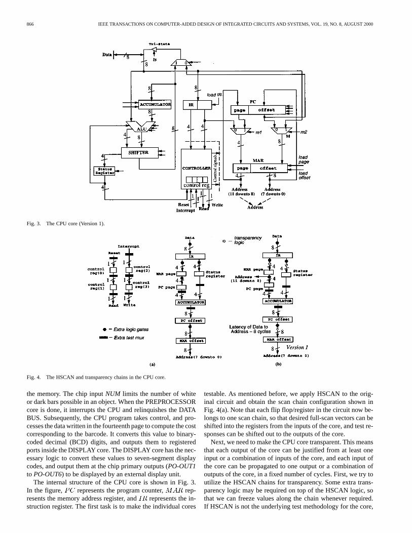
Fig. 3. The CPU core (Version 1).
Fig. 4. The HSCAN and transparency chains in the CPU core.
the memory. The chip inputNUM limits the number of whiteor dark bars possible in an object. When the PREPROCESSORcore is done, it interrupts the CPU and relinquishes the DATABUS. Subsequently, the CPU program takes control, and pro-cesses the data written in the fourteenth page to compute the costcorresponding to the barcode. It converts this value to binary-coded decimal (BCD) digits, and outputs them to registeredports inside the DISPLAY core. The DISPLAY core has the nec-essary logic to convert these values to seven-segment displaycodes, and output them at the chip primary outputs (PO-OUT1to PO-OUT6) to be displayed by an external display unit.
The internal structure of the CPU core is shown in Fig. 3.In the figure, represents the program counter, rep-resents the memory address register, andrepresents the in-struction register. The first task is to make the individual cores
testable. As mentioned before, we apply HSCAN to the orig-inal circuit and obtain the scan chain configuration shown inFig. 4(a). Note that each flip flop/register in the circuit now be-longs to one scan chain, so that desired full-scan vectors can beshifted into the registers from the inputs of the core, and test re-sponses can be shifted out to the outputs of the core.
Next, we need to make the CPU core transparent. This meansthat each output of the core can be justified from at least oneinput or a combination of inputs of the core, and each input ofthe core can be propagated to one output or a combination ofoutputs of the core, in a fixed number of cycles. First, we try toutilize the HSCAN chains for transparency. Some extra trans-parency logic may be required on top of the HSCAN logic, sothat we can freeze values along the chain whenever required.If HSCAN is not the underlying test methodology for the core,

GHOSHet al.: A FAST AND LOW-COST TESTING TECHNIQUE FOR CORE-BASED SYSTEM-CHIPS 867
Fig. 5. The DISPLAY core.
then we can use other techniques given in Section V to achievetransparency. The transparency mechanism for the CPU coreis shown in Fig. 4(b). Assume that the core outputAddress(7downto 0)needs a symbolic value. If a value is applied atthe core-inputData, then the core outputAddress(7 downto 0)will get the value after six clock cycles. While the valueis being shifted from the core input to output, the data in theStatus registerneeds to be frozen for a cycle so that the latencythrough the two parallel chains are balanced. This requires someextra transparency logic. Subsequently, the value required at theother core outputAddress(11 downto 8)can be applied at thecore inputData. The required value appears in the registerMARpage, which is connected toAddress(11 downto 8), after twoclock cycles. Thus, we can achieve a transparency latency of sixcycles for justifyingAddress(7 downto 0)throughData, two cy-cles for justifyingAddress(11 downto 8)throughData, and sixcycles for propagatingData to Address(7 downto 0). Also, theHSCAN chains can be used to transfer the value at inputResetto outputReadin two cycles, and inputInterruptto outputWritein two cycles. However, these single-bit chains are not explic-itly shown in Fig. 4(b). If all the bits of the core outputAddressneed to be justified simultaneously from inputData, then someextra logic is required to freeze the values at the output registersMAR pageandMAR offset.
Next, we briefly describe our chip-level testing methodologyof testing each embedded core, using transparency of the othercores in the system-chip. We demonstrate the importance of thetransparency latency of a core in determining the test applicationtime of a core under test, and the test application time of theentire system-chip. We show how the transparency latency ofcores can be reduced, at the expense of more area overhead, tosignificantly reduce the test application time.
Consider the DISPLAY core whose internal circuit is shownin Fig. 5(a). The HSCAN chains for the DISPLAY core areshown in Fig. 5(b). The longest HSCAN chain in the figure has
four registers/latches in it. This means four HSCAN vectors arerequired to fill up all the flip-flops in the parallel scan chain ofthe DISPLAY core. In addition, one more HSCAN vector is re-quired to control the values at the inputs during the applicationof the scan vector. Thus, each scan vector requires five HSCANvectors at the core inputs. After running a commercial, combi-national ATPG tool that assumes full scan, we found that theDISPLAY core takes 105 scan vectors for achieving 100% testefficiency. This means that 105 5 = 525 HSCAN vectors arerequired for testing the DISPLAY core.
Now, for testing the DISPLAY core in the system-chip ofFig. 2, its inputs and need to be controlled and its out-putsPO-PORT1 - PO-PORT6need be observed. For controllinginput from the chip inputs, the test vector needs to be propa-gated through the PREPROCESSOR core from its inputto its output and then through the CPU core from its inputData to its outputAddress. This path is shown with the help of adashed line in Fig. 2. The input of the DISPLAY core can becontrolled by propagating the desired vector through the PRE-PROCESSOR core from its input to its output . Theoutputs of the DISPLAY core can be observed directly as theyare the chip outputs.
Suppose the PREPROCESSOR can transfer data from inputto output in one cycle. The CPU takes a total
of eight cycles to transfer a test vector from its inputDatato outputAddress(six cycles to transfer a vector fromDatato Address(7 downto 0), and two cycles to transfer a vectorfrom Data to Address(11 downto 8)). Here, we have assumedthat test data cannot be pipelined through a core. Thus, iftwo transparency paths in a core share some logic betweenthem, then data through one path can be propagated onlyafter data has been completely propagated through the otherpath. Hence, a test vector can be propagated from the chipinput to the core-input in nine cycles where wehave assumed that test data can flow through different cores

868 IEEE TRANSACTIONS ON COMPUTER-AIDED DESIGN OF INTEGRATED CIRCUITS AND SYSTEMS, VOL. 19, NO. 8, AUGUST 2000
Fig. 6. Modifications for reducing transparency latency in CPU.
simultaneously. In between, the test vector at inputcan alsobe made ready. A subsequent test vector for the DISPLAYcore can be made ready at its inputs in another nine cycles.In the intermediate cycles, when the data at the inputs ofDISPLAY are not valid, the scan clock of DISPLAY needs tobe frozen. During this period, the test response can be scannedout through the primary outputs. Thus, the test application timerequired for testing DISPLAY alone iscycles. The last three cycles are required to scan out the lasttest response. Since, the display core has 66 flip flops and 20internal inputs, an FScan-BScan approach would have needed( cycles to do thesame. Note that this improvement is not due to the HSCAN
methodology. In fact, a scheme that uses HSCAN coupled withboundary scan would have required 10 083 cycles due to thebottleneck created by boundary scan.
Next, we show how the transparency latency through the CPUcan be reduced at the expense of area overhead, to significantlyreduce the test application time. This is done by exploiting alter-native connections that exist in the CPU and some extra trans-parency logic. In this case, outputAddress(7 downto 0)can bejustified from the inputData, with some extra logic at the selectline of multiplexer in Fig. 3, in one cycle. Also,Address(11downto 8)can be justified fromData in two cycles. This solu-tion is shown in Fig. 6(a) and (b). It employs a few extra logicgates only. This transparency logic is added in addition to the
GHOSHet al.: A FAST AND LOW-COST TESTING TECHNIQUE FOR CORE-BASED SYSTEM-CHIPS 869
HSCAN logic, but in the figure the HSCAN logic is not shownto keep the diagram simple. The transparency paths are high-lighted in the figure. Two extra lines and are required.These lines can be controlled internally by a test controller anddo not necessitate extra primary input pins for the chip. Supposethe PREPROCESSOR can transfer data from input tooutput in one cycle. Now, the CPU takes a total of three cy-cles to transfer a test vector from its inputDatato outputAddress(one cycle to transfer a vector fromData to Address(7 downto0), and two cycles to transfer a vector fromData to Address(11downto 8)). If this version of CPU is used in the chip, the test ap-plication time for testing DISPLAY is nowcycles only.
The latency of the CPU core can be further reduced by usingone extra transparency multiplexer, as shown in Fig. 6(c) and(d). The HSCAN logic is again not shown in this figure. Inthis configuration, both outputsAddress(7 downto 0)andAd-dress(11 downto 8)can be justified from inputDatain one cycle.The test application time for testing the DISPLAY core is nowreduced to cycles. Thus, further reduc-tion in test application time can be obtained at the expense ofsome extra logic. These results are summarized in the table inFig. 6(e). In the table, the area overheads are for the extra trans-parency logic only.
In practice, the transparency latency of critical cores (coreswhose latency affects the test application time of a lot of coresin the chip) can be reduced at the expense of some extra logic inthe cores to lower the global test application time of the chip sig-nificantly. In Section V, we propose a technique to make corestransparent and show how area overhead can be traded for re-ducing latency. In Section V, we also address the issue of ex-ploring the system design space to identify the most suitableversion of the cores in a system-chip to minimize the chip-levelarea overhead or test application time or trade off area overheadwith test application time.
V. MAKING CORESTRANSPARENT
In this section, we explain the method and algorithm whichwe have developed to make cores transparent with some giventransparency latency. The goal is that each output of the core canbe justified from at least one input or a combination of inputsof the core, and each input of the core can be propagated toone output or a combination of outputs of the core, in a fixednumber of cycles. At first, if HSCAN is the underlying DFTmethodology, we try to exploit the HSCAN chains to achievetransparency. If HSCAN is not the underlying test methodologyor if transparency is not possible through the HSCAN chainsor if any of the transparency latencies for an input or output isnot acceptable, we introduce extra logic into the circuit to createtransparency paths.
It is possible that the above requirements are an overkill fortesting certain configurations of cores in a system-chip. How-ever, it is impossible for the core provider to know beforehandhow the core will be connected in the chip. Thus, it is impossibleto predict which transparency paths will be used and which willbe unused (except for some common sense decisions). From thetest overheads point of view, this solution is still better than dedi-
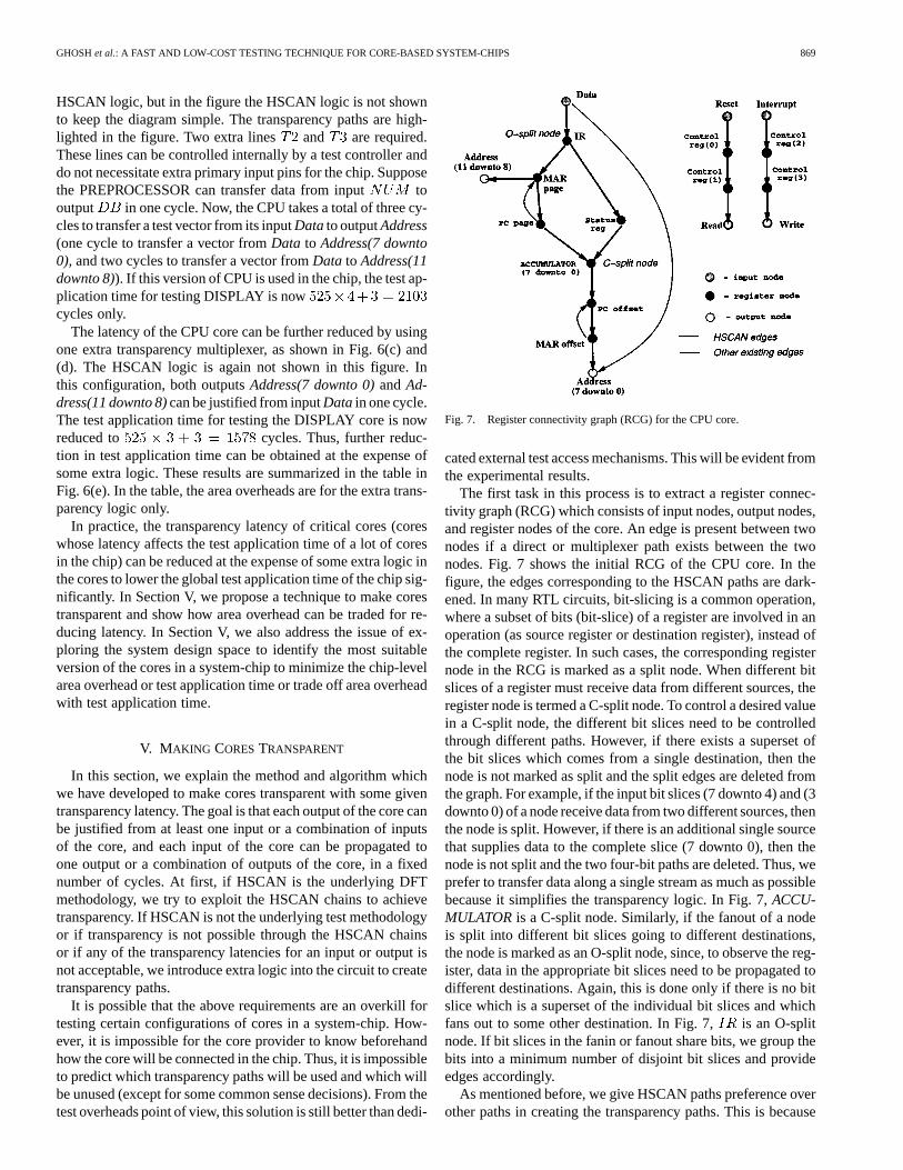
Fig. 7. Register connectivity graph (RCG) for the CPU core.
cated external test access mechanisms. This will be evident fromthe experimental results.
The first task in this process is to extract a register connec-tivity graph (RCG) which consists of input nodes, output nodes,and register nodes of the core. An edge is present between twonodes if a direct or multiplexer path exists between the twonodes. Fig. 7 shows the initial RCG of the CPU core. In thefigure, the edges corresponding to the HSCAN paths are dark-ened. In many RTL circuits, bit-slicing is a common operation,where a subset of bits (bit-slice) of a register are involved in anoperation (as source register or destination register), instead ofthe complete register. In such cases, the corresponding registernode in the RCG is marked as a split node. When different bitslices of a register must receive data from different sources, theregister node is termed a C-split node. To control a desired valuein a C-split node, the different bit slices need to be controlledthrough different paths. However, if there exists a superset ofthe bit slices which comes from a single destination, then thenode is not marked as split and the split edges are deleted fromthe graph. For example, if the input bit slices (7 downto 4) and (3downto 0) of a node receive data from two different sources, thenthe node is split. However, if there is an additional single sourcethat supplies data to the complete slice (7 downto 0), then thenode is not split and the two four-bit paths are deleted. Thus, weprefer to transfer data along a single stream as much as possiblebecause it simplifies the transparency logic. In Fig. 7,ACCU-MULATORis a C-split node. Similarly, if the fanout of a nodeis split into different bit slices going to different destinations,the node is marked as an O-split node, since, to observe the reg-ister, data in the appropriate bit slices need to be propagated todifferent destinations. Again, this is done only if there is no bitslice which is a superset of the individual bit slices and whichfans out to some other destination. In Fig. 7, is an O-splitnode. If bit slices in the fanin or fanout share bits, we group thebits into a minimum number of disjoint bit slices and provideedges accordingly.
As mentioned before, we give HSCAN paths preference overother paths in creating the transparency paths. This is because

870 IEEE TRANSACTIONS ON COMPUTER-AIDED DESIGN OF INTEGRATED CIRCUITS AND SYSTEMS, VOL. 19, NO. 8, AUGUST 2000
HSCAN paths are already able to transfer data from inputs tooutputs with a minimum amount of extra control logic. Anyother existing path needs some extra logic and control lines tobe used for transparency purposes. Also, while trying to createtransparency paths between different input-output pairs, we tryto make the paths parallel and disjoint as much as possible. Thisis because if edges are reused, then extra logic and control is re-quired in those paths as well as extra control lines to select thedifferent data flows through the same path at different times.
From the RCG, we try to find transparency paths from in-puts to outputs. To do this, we do a breadth-first search (BFS)from each input node until we reach an output node. During thissearch, any time we reach an O-split node, the BFS is done fromeach of the nodes at the fanout edges of the O-split node as allthe fanout edges need to be used for propagating the data at theO-split node. At first, we only use the HSCAN edges duringthis search. If we fail to get a transparency path, we try to useother existing edges in the RCG. For the CPU core, the BFSfrom inputDatareaches the node . From here, different BFSsstart along the two fanout edges. The search from the left edgeterminates at output nodeAddress(11 downto 8). We continuethe BFS from the right edge until we reach the output nodeAd-dress(7 downto 0). Thus, we have found a transparency path forpropagating the input to the output with a latency of six cycles.We delete this path and again do a BFS for any remaining in-puts whose transparency path has not yet been found. If no pathsare found, then the deleted paths are put back in the RCG andthe BFS is repeated with the aim of finding a transparency pathby reusing edges from prior transparency paths. If still no trans-parency paths are found, then a transparency path is created byadding extra logic. Any register reachable from the input in onecycle (found from the BFS) is connected to an output (or out-puts if bit-widths mismatch) with a test multiplexer. To keepthe transparency paths disjoint, preference is given to connectto output(s) which has not been used so far for providing trans-parency to other core inputs. If any edge is used in more thanone transparency path, then it may not be possible to propagatedata through the two paths in parallel and data have to be prop-agated sequentially. Finally, a solution is obtained where eachinput can be propagated to some output(s) in a fixed number ofcycles (transparency latency) in the test mode.
Next, we try to find transparency paths so that each outputof the core may be justified from some input of the core duringthe transparency mode. For this, we reverse all the edges in theRCG, and again do a BFS from each output node of the RCG.We select an output and continue the BFS until we reach an inputnode. For example, for the CPU core, we first selectAddress(7downto 0), and do a BFS using only the HSCAN edges. Whenwe reach a C-split node, the BFS is done from each of the nodesat the fanout edges (fanin in the original RCG) of the C-splitnode since all the fanout edges need to be used for justifyingthe data at the C-split node. When two BFSs originating at thefanout nodes of a C-split node converge at an O-split node, thenthey again constitute a single search. Thus, the search branchesinto two different searches at the C-split nodeACCUMULATORand reconverges to a single search at the O-split node, even-tually reaching the input nodeData. If the transparency paththus formed has split nodes, and if the parallel subpaths are not
balanced at each fanin of a C-split node in the original RCG, foreach fanin which does not fall on the longest subpath we addextra logic to freeze the data there. This balances the parallelsubpaths, so that the data, which have arrived early at the faninof a C-split node, wait until the data at all the fanin edges areready.
Next, we repeat the procedure for the other output nodes. Forthe CPU core, we delete the transparency path and do BFS forAddress(11 downto 8). Since we cannot find a path, we put backthe deleted path and try again. This time we succeed. Thus, thetransparency paths of the two outputs are not disjoint, but ratherreuse common edges , and , Data). When thesame edge(s) in the RCG have to be reused in multiple trans-parency paths, the data flow through the reused edges shouldbe controlled so as to avoid conflicts. In this work, we solvethis problem by transferring data through transparency pathsthat reuse common edges in a sequential manner. Hence, if twotransparency paths in a core share some edges between them,then data through one path can be propagated only after datahave been completely propagated through the other path.
If transparency paths are not found using HSCAN edges, thenother existing paths in the RCG are used to obtain transparency.In the case of the CPU core, transparency paths for all the inputsand outputs are achievable using HSCAN paths only. Here, wecan achieve a transparency latency of six cycles for justifyingAddress(7 downto 0)throughData, two cycles for justifyingAddress(11 downto 8)throughData, and six cycles for prop-agatingData to Address(7 downto 0). Hence, Version 1 of theCPU core is created whose characteristics are given in the tableof Fig. 6(e).
The transparency latency of a core can be reduced by addingextra logic either using existing non-HSCAN paths or by addingtransparency multiplexers. We next show how different versionsof the same core can be obtained by trading area overhead forreduced transparency latency. Consider again the RCG of theCPU core shown in Fig. 7. Let the non-HSCAN edges existingin the RCG be included in the BFS this time. Since an edge ex-ists fromData to Address(7 downto 0), a transparency path canbe found for outputAddress(7 downto 0)to inputData with alatency of just one cycle. A transparency path exists fromAd-dress(11 downto 8)to inputDatawith a latency of two cycles asbefore. Consequently, we have a new version of the CPU coreshown in Fig. 6(a). The transparency paths are shown in boldin the figure while the extra gates required to control them areshaded. As shown in Fig. 6(e), the transparency latency of Ver-sion 2 of the CPU core has reduced to three from eight, at alarger area overhead of 10 cells.
Further reduction in transparency latency can be obtainedby introducing transparency multiplexers. The transparency la-tency of an input can be reduced to one by adding a direct pathfrom the input to an output through a multiplexer such thatthe path can be activated in the transparency mode. Similarly,an extra multiplexer can achieve a transparency latency of onefor an output. This is done one at a time for each input/outputpair with a transparency latency greater than one, creating dif-ferent versions of the same core with different area overheadsand transparency latencies. Fig. 6(c) shows a transparency mul-tiplexer (shaded) added to reduce the latency of DataAd-

GHOSHet al.: A FAST AND LOW-COST TESTING TECHNIQUE FOR CORE-BASED SYSTEM-CHIPS 871
dress(11 downto 8)to one, leading to a new version (Version3) of the CPU core whose area overhead/transparency latencycharacteristics are shown in Fig. 6(e).
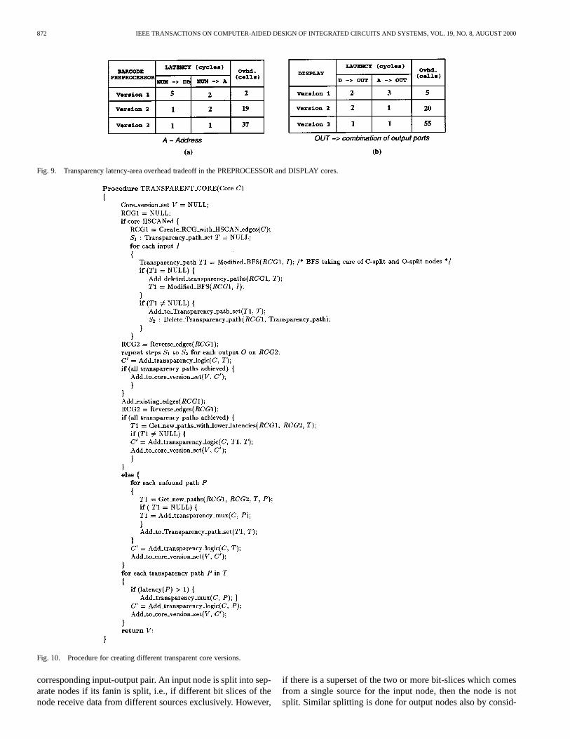
Similar procedures apply to the PREPROCESSOR coreshown in Fig. 8 and the DISPLAY core shown in Fig. 5(a).The tradeoffs for different core versions for these two cores areshown in Fig. 9(a) and (b), respectively. The pseudocode forthe procedure outlined in this section appears in Fig. 10.
For soft cores, the RTL modifications for the various versionsare already present in the core. The user needs to synthesize thecore based on the given area/performance requirements. Sincethe RTL code is visible, it can be tweaked to meet the desiredoptimization goals. The DFT modifications can be shown ex-plicitly through comments from the provider so that they can beremoved if SOCET is not the preferred testing methodology.
VI. A REA AND TEST APPLICATION TIME TRADEOFF AT THE
CHIP LEVEL
Given a system-chip with a particular interconnection ofembedded cores, like the barcode system shown in Fig. 2,the testing challenge is to make sure that each embeddedcore can be fully tested, by being able to justify at its inputsthe precomputed test set of the core from the chip PIs, andpropagate the test responses from the core outputs to the chipPOs. In the proposed system-chip testing method, for eachcore, the transparency mode of other cores is used to identifyjustification paths to control the core inputs from the chip PIsand propagation paths to observe the core outputs at the chipPOs.
In this section, we show that given a set of core versionshaving different transparency latency with different area over-heads, the combination of core versions selected will result intestable system-chips with significantly different area overheadsand chip test application times. For example, for the barcodesystem shown in Fig. 2, using Version 1 of CPU, Version 1 ofPREPROCESSOR, and Version 3 of the DISPLAY core, will re-sult in a testable system-chip with area overhead of 210 cells andchip test application time of 16 823 cycles. On the other hand, ifwe use Version 1 of CPU, Version 2 of PREPROCESSOR andVersion 1 of the DISPLAY core, the area overhead is reduced to180 cells, while the chip test application time is simultaneouslyreduced to 10 688 cycles. Hence, design tools are necessary toaid in exploring the design space so that the chip can be testedwith the desired area and test application time constraints.
We propose a system-chip testing method which selects thebest core versions available to produce a testable system-chipsuch that either of the following objectives are satisfied:
1) Given a test area overhead constraint ofcells, theglobal test application time of the system-chip is min-imized.
2) Given a test application time constraint ofcycles, theoverall test area overhead of the system-chip is mini-mized.
We propose an iterative improvement technique, which canobtain solutions for either of the design objectives by varyingthe parameters of a cost function described later. We first briefly
Fig. 8. The PREPROCESSOR core.
describe the overall approach, and then provide details subse-quently. Initially, the chip is assumed to consist of the minimumarea overhead versions of each core. For each core, the justifica-tion and propagation paths which result in the minimum test ap-plication time for the core is identified, leading to a knowledgeof the test application time and area overhead of the completechip. If the desired area/test application time constraints are notmet, the process is started to improve the existing solution, byiteratively replacing an existing version with the next (higherarea) version of a selected core. The selection of the core forreplacement is done based on the maximum improvement ob-tained by replacing the current version of the core with the nextversion, where improvement is a cost function, which is param-etrized such that either of the two objectives can be eventuallymet.
Next, we describe the method in detail. At first, we create acore connectivity graph (CCG) from the given system-chip. Inthis graph, there are system PI nodes, system PO nodes, coreinput nodes and core output nodes. Edges are added betweeninput-output pairs of a core according to the transparency pathsin the versions of the core currently in use. The cost associatedwith an edge represents the transparency latency between the
872 IEEE TRANSACTIONS ON COMPUTER-AIDED DESIGN OF INTEGRATED CIRCUITS AND SYSTEMS, VOL. 19, NO. 8, AUGUST 2000
Fig. 9. Transparency latency-area overhead tradeoff in the PREPROCESSOR and DISPLAY cores.
Fig. 10. Procedure for creating different transparent core versions.
corresponding input-output pair. An input node is split into sep-arate nodes if its fanin is split, i.e., if different bit slices of thenode receive data from different sources exclusively. However,
if there is a superset of the two or more bit-slices which comesfrom a single source for the input node, then the node is notsplit. Similar splitting is done for output nodes also by consid-

GHOSHet al.: A FAST AND LOW-COST TESTING TECHNIQUE FOR CORE-BASED SYSTEM-CHIPS 873
Fig. 11. Core connectivity graph (CCG) for the barcode system.
ering the fanout bits. The CCG for the barcode system in Fig. 2is shown in Fig. 11 where the minimum area version (Version 1)of each core is used. Note that we do not consider the memorycores in this discussion, as most memory cores use BIST [31].We assume that the memory cores are tested in parallel with therest of the system.
A. Identification of Test Paths for a Core
We next discuss how to identify the justification and prop-agation paths for each core such that the test application timeneeded for the core is minimized. Let us take the DISPLAY corefirst. We have to control its inputsA(7 downto 0),A(11 downto 8)and . First, we try to find the shortest path from any chip inputto A(7 downto 0). Any shortest path algorithm like Dijkstra’s al-gorithm can be used for this purpose. We find out all possibleshortest paths from the chip inputs toA(7 downto 0)and choosethe one with the lowest cost (which takes the least number ofclock cycles). Here, only one path is possible
Data Address(7 downto 0) A(7 downto 0)) which ishighlighted in Fig. 11. We mark this path and reserve the edgesfor the cycles in which they will be used. Hence, edge ,
in the PREPROCESSOR is reserved from cycle 0 to 5,edge (Data, Address(7 downto 0)) is reserved from cycle 5 to11, and so on. If there is no path possible, we add a system-leveltest multiplexer to connect the input of the core directly to a PI.Next, we try to find the shortest path from any chip PI toA(11downto 8). The shortest path algorithm is modified so that if anymarked edge is reused, then the cost is automatically modifiedso that the edge is not reused in the reserved cycles. Here, part ofthe previous path needs to be reused. Therefore, edge ,
can only be utilized from cycle 6 onwards, edge (Data,Address(7 downto 0)) can only be used from cycle 12 onwards,and so on. The minimum-cost path is again chosen among allpossible paths and test multiplexers are used if necessary. Sim-ilarly, the path for controlling input can be found.
Once the paths for controlling the inputs of a core are found,we try to find the paths for observing the core outputs at the POsof the chip. For this, we find all possible shortest paths from eachcore output to any PO of the chip and choose the one with min-imum cost. The path is marked and other paths are found as be-
Fig. 12. Chip-level testing procedure to trade off test application time witharea overhead.
Fig. 13. Plot of area overhead versus test application time for System 1.
fore. For the DISPLAY core, all paths are trivially found as theyconnect to POs of the chip. Again, test multiplexers are addedto increase observability if necessary. This process is repeatedfor every core in the system. In Fig. 11, the outputAddressofthe PREPROCESSOR is connected to a PO with a system-leveltest multiplexer, since there is no way of observing it by existingpaths through the cores.
874 IEEE TRANSACTIONS ON COMPUTER-AIDED DESIGN OF INTEGRATED CIRCUITS AND SYSTEMS, VOL. 19, NO. 8, AUGUST 2000
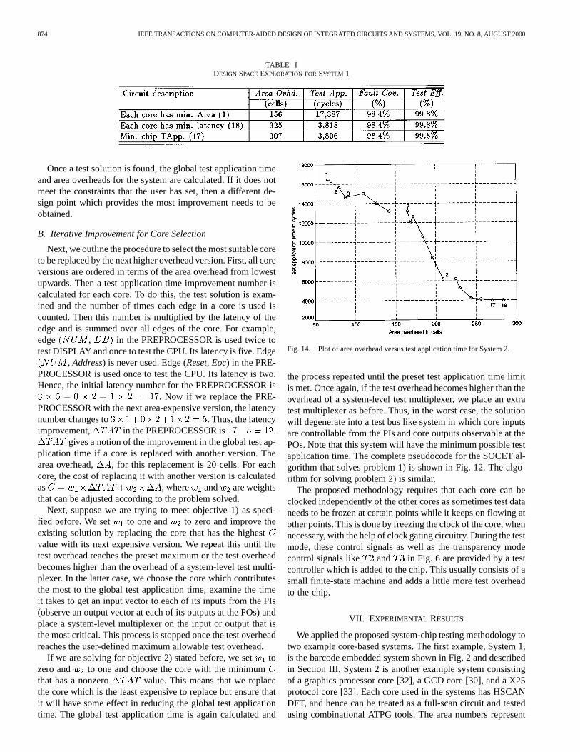
TABLE IDESIGN SPACE EXPLORATION FORSYSTEM 1
Once a test solution is found, the global test application timeand area overheads for the system are calculated. If it does notmeet the constraints that the user has set, then a different de-sign point which provides the most improvement needs to beobtained.
B. Iterative Improvement for Core Selection
Next, we outline the procedure to select the most suitable coreto be replaced by the next higher overhead version. First, all coreversions are ordered in terms of the area overhead from lowestupwards. Then a test application time improvement number iscalculated for each core. To do this, the test solution is exam-ined and the number of times each edge in a core is used iscounted. Then this number is multiplied by the latency of theedge and is summed over all edges of the core. For example,edge , in the PREPROCESSOR is used twice totest DISPLAY and once to test the CPU. Its latency is five. Edge
, Address) is never used. Edge (Reset, Eoc) in the PRE-PROCESSOR is used once to test the CPU. Its latency is two.Hence, the initial latency number for the PREPROCESSOR is
. Now if we replace the PRE-PROCESSOR with the next area-expensive version, the latencynumber changes to . Thus, the latencyimprovement, in the PREPROCESSOR is .
gives a notion of the improvement in the global test ap-plication time if a core is replaced with another version. Thearea overhead, , for this replacement is 20 cells. For eachcore, the cost of replacing it with another version is calculatedas , where and are weightsthat can be adjusted according to the problem solved.
Next, suppose we are trying to meet objective 1) as speci-fied before. We set to one and to zero and improve theexisting solution by replacing the core that has the highestvalue with its next expensive version. We repeat this until thetest overhead reaches the preset maximum or the test overheadbecomes higher than the overhead of a system-level test multi-plexer. In the latter case, we choose the core which contributesthe most to the global test application time, examine the timeit takes to get an input vector to each of its inputs from the PIs(observe an output vector at each of its outputs at the POs) andplace a system-level multiplexer on the input or output that isthe most critical. This process is stopped once the test overheadreaches the user-defined maximum allowable test overhead.
If we are solving for objective 2) stated before, we settozero and to one and choose the core with the minimumthat has a nonzero value. This means that we replacethe core which is the least expensive to replace but ensure thatit will have some effect in reducing the global test applicationtime. The global test application time is again calculated and
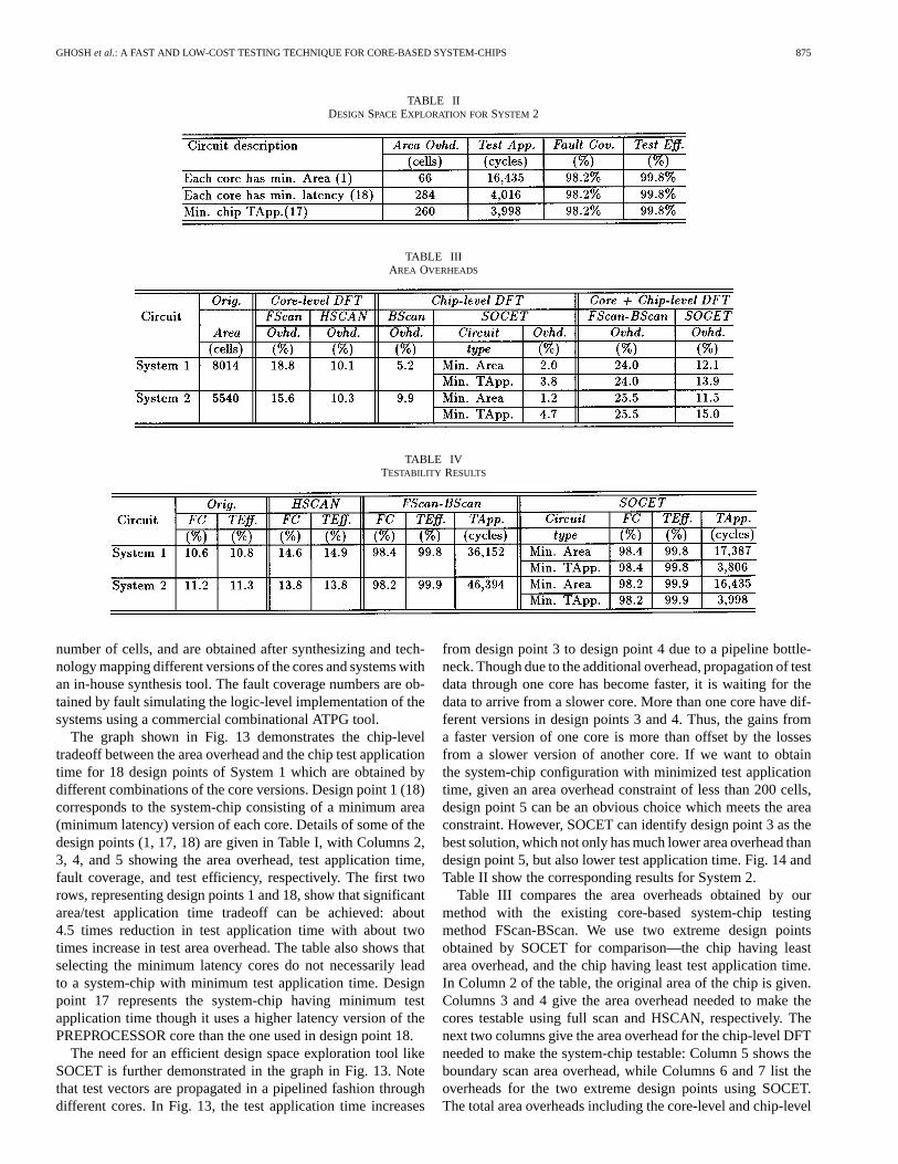
Fig. 14. Plot of area overhead versus test application time for System 2.
the process repeated until the preset test application time limitis met. Once again, if the test overhead becomes higher than theoverhead of a system-level test multiplexer, we place an extratest multiplexer as before. Thus, in the worst case, the solutionwill degenerate into a test bus like system in which core inputsare controllable from the PIs and core outputs observable at thePOs. Note that this system will have the minimum possible testapplication time. The complete pseudocode for the SOCET al-gorithm that solves problem 1) is shown in Fig. 12. The algo-rithm for solving problem 2) is similar.
The proposed methodology requires that each core can beclocked independently of the other cores as sometimes test dataneeds to be frozen at certain points while it keeps on flowing atother points. This is done by freezing the clock of the core, whennecessary, with the help of clock gating circuitry. During the testmode, these control signals as well as the transparency modecontrol signals like and in Fig. 6 are provided by a testcontroller which is added to the chip. This usually consists of asmall finite-state machine and adds a little more test overheadto the chip.
VII. EXPERIMENTAL RESULTS
We applied the proposed system-chip testing methodology totwo example core-based systems. The first example, System 1,is the barcode embedded system shown in Fig. 2 and describedin Section III. System 2 is another example system consistingof a graphics processor core [32], a GCD core [30], and a X25protocol core [33]. Each core used in the systems has HSCANDFT, and hence can be treated as a full-scan circuit and testedusing combinational ATPG tools. The area numbers represent
GHOSHet al.: A FAST AND LOW-COST TESTING TECHNIQUE FOR CORE-BASED SYSTEM-CHIPS 875
TABLE IIDESIGN SPACE EXPLORATION FORSYSTEM 2
TABLE IIIAREA OVERHEADS
TABLE IVTESTABILITY RESULTS
number of cells, and are obtained after synthesizing and tech-nology mapping different versions of the cores and systems withan in-house synthesis tool. The fault coverage numbers are ob-tained by fault simulating the logic-level implementation of thesystems using a commercial combinational ATPG tool.
The graph shown in Fig. 13 demonstrates the chip-leveltradeoff between the area overhead and the chip test applicationtime for 18 design points of System 1 which are obtained bydifferent combinations of the core versions. Design point 1 (18)corresponds to the system-chip consisting of a minimum area(minimum latency) version of each core. Details of some of thedesign points (1, 17, 18) are given in Table I, with Columns 2,3, 4, and 5 showing the area overhead, test application time,fault coverage, and test efficiency, respectively. The first tworows, representing design points 1 and 18, show that significantarea/test application time tradeoff can be achieved: about4.5 times reduction in test application time with about twotimes increase in test area overhead. The table also shows thatselecting the minimum latency cores do not necessarily leadto a system-chip with minimum test application time. Designpoint 17 represents the system-chip having minimum testapplication time though it uses a higher latency version of thePREPROCESSOR core than the one used in design point 18.
The need for an efficient design space exploration tool likeSOCET is further demonstrated in the graph in Fig. 13. Notethat test vectors are propagated in a pipelined fashion throughdifferent cores. In Fig. 13, the test application time increases
from design point 3 to design point 4 due to a pipeline bottle-neck. Though due to the additional overhead, propagation of testdata through one core has become faster, it is waiting for thedata to arrive from a slower core. More than one core have dif-ferent versions in design points 3 and 4. Thus, the gains froma faster version of one core is more than offset by the lossesfrom a slower version of another core. If we want to obtainthe system-chip configuration with minimized test applicationtime, given an area overhead constraint of less than 200 cells,design point 5 can be an obvious choice which meets the areaconstraint. However, SOCET can identify design point 3 as thebest solution, which not only has much lower area overhead thandesign point 5, but also lower test application time. Fig. 14 andTable II show the corresponding results for System 2.
Table III compares the area overheads obtained by ourmethod with the existing core-based system-chip testingmethod FScan-BScan. We use two extreme design pointsobtained by SOCET for comparison—the chip having leastarea overhead, and the chip having least test application time.In Column 2 of the table, the original area of the chip is given.Columns 3 and 4 give the area overhead needed to make thecores testable using full scan and HSCAN, respectively. Thenext two columns give the area overhead for the chip-level DFTneeded to make the system-chip testable: Column 5 shows theboundary scan area overhead, while Columns 6 and 7 list theoverheads for the two extreme design points using SOCET.The total area overheads including the core-level and chip-level
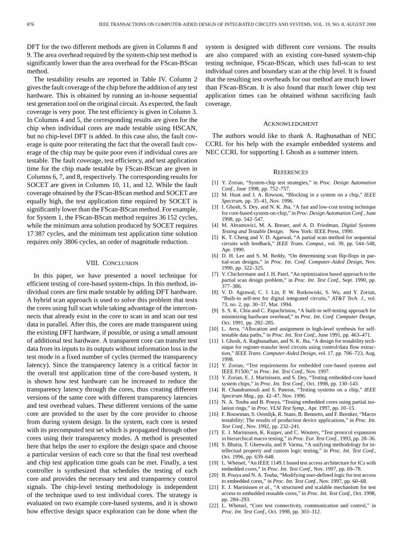
876 IEEE TRANSACTIONS ON COMPUTER-AIDED DESIGN OF INTEGRATED CIRCUITS AND SYSTEMS, VOL. 19, NO. 8, AUGUST 2000
DFT for the two different methods are given in Columns 8 and9. The area overhead required by the system-chip test method issignificantly lower than the area overhead for the FScan-BScanmethod.
The testability results are reported in Table IV. Column 2gives the fault coverage of the chip before the addition of any testhardware. This is obtained by running an in-house sequentialtest generation tool on the original circuit. As expected, the faultcoverage is very poor. The test efficiency is given in Column 3.In Columns 4 and 5, the corresponding results are given for thechip when individual cores are made testable using HSCAN,but no chip-level DFT is added. In this case also, the fault cov-erage is quite poor reiterating the fact that the overall fault cov-erage of the chip may be quite poor even if individual cores aretestable. The fault coverage, test efficiency, and test applicationtime for the chip made testable by FScan-BScan are given inColumns 6, 7, and 8, respectively. The corresponding results forSOCET are given in Columns 10, 11, and 12. While the faultcoverage obtained by the FScan-BScan method and SOCET areequally high, the test application time required by SOCET issignificantly lower than the FScan-BScan method. For example,for System 1, the FScan-BScan method requires 36 152 cycles,while the minimum area solution produced by SOCET requires17 387 cycles, and the minimum test application time solutionrequires only 3806 cycles, an order of magnitude reduction.
VIII. C ONCLUSION
In this paper, we have presented a novel technique forefficient testing of core-based system-chips. In this method, in-dividual cores are first made testable by adding DFT hardware.A hybrid scan approach is used to solve this problem that teststhe cores using full scan while taking advantage of the intercon-nects that already exist in the core to scan in and scan out testdata in parallel. After this, the cores are made transparent usingthe existing DFT hardware, if possible, or using a small amountof additional test hardware. A transparent core can transfer testdata from its inputs to its outputs without information loss in thetest mode in a fixed number of cycles (termed the transparencylatency). Since the transparency latency is a critical factor inthe overall test application time of the core-based system, itis shown how test hardware can be increased to reduce thetransparency latency through the cores, thus creating differentversions of the same core with different transparency latenciesand test overhead values. These different versions of the samecore are provided to the user by the core provider to choosefrom during system design. In the system, each core is testedwith its precomputed test set which is propagated through othercores using their transparency modes. A method is presentedhere that helps the user to explore the design space and choosea particular version of each core so that the final test overheadand chip test application time goals can be met. Finally, a testcontroller is synthesized that schedules the testing of eachcore and provides the necessary test and transparency controlsignals. The chip-level testing methodology is independentof the technique used to test individual cores. The strategy isevaluated on two example core-based systems, and it is shownhow effective design space exploration can be done when the
system is designed with different core versions. The resultsare also compared with an existing core-based system-chiptesting technique, FScan-BScan, which uses full-scan to testindividual cores and boundary scan at the chip level. It is foundthat the resulting test overheads for our method are much lowerthan FScan-BScan. It is also found that much lower chip testapplication times can be obtained without sacrificing faultcoverage.
ACKNOWLEDGMENT
The authors would like to thank A. Raghunathan of NECCCRL for his help with the example embedded systems andNEC CCRL for supporting I. Ghosh as a summer intern.
REFERENCES
[1] Y. Zorian, “System-chip test strategies,” inProc. Design AutomationConf., June 1998, pp. 752–757.
[2] M. Hunt and J. A. Rowson, “Blocking in a system on a chip,”IEEESpectrum, pp. 35–41, Nov. 1996.
[3] I. Ghosh, S. Dey, and N. K. Jha, “A fast and low-cost testing techniquefor core-based system-on-chip,” inProc. Design Automation Conf., June1998, pp. 542–547.
[4] M. Abramovici, M. A. Breuer, and A. D. Friedman,Digital SystemsTesting and Testable Design. New York: IEEE Press, 1990.
[5] K. T. Cheng and V. D. Agarwal, “A partial scan method for sequentialcircuits with feedback,”IEEE Trans. Comput., vol. 39, pp. 544–548,Apr. 1990.
[6] D. H. Lee and S. M. Reddy, “On determining scan flip-flops in par-tial-scan designs,” inProc. Int. Conf. Computer-Aided Design, Nov.1990, pp. 322–325.
[7] V. Chickermane and J. H. Patel, “An optimization based approach to thepartial scan design problem,” inProc. Int. Test Conf., Sept. 1990, pp.377–386.
[8] V. D. Agrawal, C. J. Lin, P. W. Rutkowiski, S. Wu, and Y. Zorian,“Built-in self-test for digital integrated circuits,”AT&T Tech. J., vol.73, no. 2, pp. 30–37, Mar. 1994.
[9] S. S. K. Chiu and C. Papachristou, “A built-in self-testing approach forminimizing hardware overhead,” inProc. Int. Conf. Computer Design,Oct. 1991, pp. 282–285.
[10] L. Avra, “Allocation and assignment in high-level synthesis for self-testable data paths,” inProc. Int. Test Conf., June 1991, pp. 463–471.
[11] I. Ghosh, A. Raghunathan, and N. K. Jha, “A design for testability tech-nique for register-transfer level circuits using control/data flow extrac-tion,” IEEE Trans. Computer-Aided Design, vol. 17, pp. 706–723, Aug.1998.
[12] Y. Zorian, “Test requirements for embedded core-based systems andIEEE P1500,” inProc. Int. Test Conf., Nov. 1997.
[13] Y. Zorian, E. J. Marinissen, and S. Dey, “Testing embedded-core basedsystem chips,” inProc. Int. Test Conf., Oct. 1998, pp. 130–143.
[14] R. Chandramouli and S. Pateras, “Testing systems on a chip,”IEEESpectrum Mag., pp. 42–47, Nov. 1996.
[15] N. A. Touba and B. Pouya, “Testing embedded cores using partial iso-lation rings,” inProc. VLSI Test Symp., Apr. 1997, pp. 10–15.
[16] F. Bouwman, S. Oostdijk, R. Stans, B. Bennetts, and F. Beenker, “Macrotestability; The results of production device applications,” inProc. Int.Test Conf., Nov. 1992, pp. 232–241.
[17] E. J. Marinissen, K. Kuiper, and C. Wouters, “Test protocol expansionin hierarchical macro testing,” inProc. Eur. Test Conf., 1993, pp. 28–36.
[18] S. Bhatia, T. Gheewala, and P. Varma, “A unifying methodology for in-tellectual property and custom logic testing,” inProc. Int. Test Conf.,Oct. 1996, pp. 639–648.
[19] L. Whetsel, “An IEEE 1149.1 based test access architecture for ICs withembedded cores,” inProc. Int. Test Conf., Nov. 1997, pp. 69–78.
[20] B. Pouya and N. A. Touba, “Modifying user-defined logic for test accessto embedded cores,” inProc. Int. Test Conf., Nov. 1997, pp. 60–68.
[21] E. J. Marinissenet al., “A structured and scalable mechanism for testaccess to embedded reusable cores,” inProc. Int. Test Conf., Oct. 1998,pp. 284–293.
[22] L. Whetsel, “Core test connectivity, communication and control,” inProc. Int. Test Conf., Oct. 1998, pp. 303–312.
GHOSHet al.: A FAST AND LOW-COST TESTING TECHNIQUE FOR CORE-BASED SYSTEM-CHIPS 877
[23] P. Varma and S. Bhatia, “A structured test re-use methodology for core-based system chips,” inProc. Int. Test Conf., Oct. 1998, pp. 294–302.
[24] M. Sugihara, H. Date, and H. Yasuura, “A novel test methodology forcore-based system LSIs and a testing time minimization problem,” inProc. Int. Test Conf., Oct. 1998, pp. 465–472.
[25] I. Ghosh, N. K. Jha, and S. Dey, “A low overhead design for testabilityand test generation technique for core-based systems,” inProc. Int. TestConf., Nov. 1997.
[26] S. Bhattacharya and S. Dey, “H-Scan: A high level alternative tofull-scan testing with reduced area and test application overheads,” inProc. VLSI Test Symp., Apr. 1996, pp. 74–80.
[27] S. Bhattacharya, S. Dey, and B. Sengupta, “An RTL methodology toenable low overhead combinational testing,” inProc. Eur. Design TestConf., Mar. 1997, pp. 146–152.
[28] T. Asaka, M. Yoshida, S. Bhattacharya, and S. Dey, “An efficient low-overhead approach using RTL design for testability technique with scanflip-flops,” in Proc. Int. Test Conf., Nov. 1997.
[29] Z. Navabi,VHDL Analysis and Modeling of Digital Systems. NewYork: McGraw Hill, 1993.
[30] P. R. Panda and N. D. Dutt, “1995 high-level synthesis design repos-itory,” in Proc. Int. Symp. System-Level Synthesis, Sept. 1995, pp.170–174.
[31] Y. Zorian, “A distributed BIST control scheme for complex VLSI de-vices,” inProc. VLSI Test Symp., Apr. 1993, pp. 6–11.
[32] A. Raghunathan, S. Dey, and N. K. Jha, “Power management techniquesfor control-flow intensive designs,” inProc. Design Automation Conf.,June 1997, pp. 429–434.
[33] S. Bhattacharya, S. Dey, and F. Brglez, “Performance analysis and opti-mization of schedules for conditional and loop-intensive specifications,”in Proc. Design Automation Conf., June 1994, pp. 491–496.
Indradeep Ghosh (S’95–M’98) received theB.Tech. degree in computer science and engineeringfrom the Indian Institute of Technology, Kharagpur,India, in 1993, and the M.A. and Ph.D. degrees inelectrical engineering from Princeton University,Princeton, NJ, in 1995 and 1998, respectively.
Currently he is a member of research staff in theAdvanced CAD Research group at Fujitsu Laborato-ries of America, Sunnyvale, CA. He has authored orco-authored more than 20 technical papers in interna-tional journals and conferences. His research inter-
ests include design for testability, high level test generation, BIST, high levelsynthesis and high-level design verification and diagnosis.
Dr. Ghosh has co-authored a paper which has won the Honorable MentionAward at the International Conference on VLSI Design (1998). He is currentlythe Audio-Visual Chair of the Tutorials Group of the IEEE Computer SocietyTest Technology Technical Committee.
Sujit Dey (S’90–M’91) received the Ph.D. degreein computer science from Duke University, Durham,NC, in 1991.
From 1991 to 1997, he was at the NEC C&CResearch Laboratories, Princeton, NJ, where hewas a Senior Research Staff Member. While atNEC, he developed methodologies and tools for thedesign and test of high-performance and low-powersystem-on-chips. In 1997, he joined the Universityof California, San Diego, (UCSD) where he is anAssociate Professor in the Electrical and Computer
Engineering Department. The goal of his research group at UCSD is enablingthe use of nanometer technologies and software systems. He has co-authoreda book, several book chapters, and over 80 journal and conference papers, andis a co-inventor of ten U.S. patents. He is affiliated with the DARPA/MARCOGigascale Systems Research Center, and the Center for Wireless Communica-tions at UCSD.
Dr. Dey received Best Paper awards at the Design Automation Conferencesin 1994, 1999, and 2000, and the 11th VLSI Design Conference in 1998, andseveral best paper nominations. He has presented numerous tutorials, and par-ticipated in panels, in the topics of hardware-software embedded systems, low-power design, and deep submicrometer system-on-chip design. He has been theGeneral Chair and Program Chair, and member of organizing and program com-mittees, of several IEEE conferences and workshops.
Niraj K. Jha (S’85–M’85–SM’93–F’98) receivedthe B.Tech. degree in electronics and electricalcommunication engineering from Indian Instituteof Technology, Kharagpur, India, in 1981, the M.S.degree in electrical engineering from the StateUniversity of New York, Stony Brook, in 1982,and the Ph.D. degree in electrical engineering fromUniversity of Illinois, Urbana, in 1985.
He is a Professor of Electrical Engineeringat Princeton University, Princeton, NJ. He hasco-authored two books titledTesting and Reliable
Design of CMOS Circuits(Norwell, MA: Kluwer, 1990) andHigh-LevelPower Analysis and Optimization(Norwell, MA: Kluwer, 1998). He hasauthored or co-authored more than 160 technical papers. His research interestsinclude digital system testing, computer-aided design of integrated circuits,fault-tolerant computing, and distributed computing.
Dr. Jha served as an Associate Editor of IEEE TRANSACTIONS ONCIRCUITS
AND SYSTEMS II: A NALOG AND DIGITAL SIGNAL PROCESSING, and is currentlyserving as an Associate Editor of IEEE TRANSACTIONS ONVERY LARGESCALE
INTEGRATION(VLSI) SYSTEMSand ofJournal of Electronic Testing: Theory andApplications(JETTA). He has served as the guest editor for the JETTA specialissue on high-level test synthesis. He has also served as the Program Chairmanof the 1992 Workshop on Fault-Tolerant Parallel and Distributed Systems. He isthe recipient of the AT&T Foundation Award and the NEC Preceptorship Awardfor research excellence.He has co-authored four papers which have won the BestPaper Award at ICCD’93, FTCS’97, ICVLSID’98, and DAC’99.