Fast neutron environments
72
SANDIA REPORT SAND2011-8527 Unlimited Release October 2011 Fast Neutron Environments Khalid Hattar, Luke N. Brewer, Brad L. Boyce, Thomas E. Buchheit, Stephen M. Foiles, Ping Lu, Blythe G. Clark, Paul G. Kotula, Steven Goods, Joseph Puskar, and Barney L. Doyle Prepared by Sandia National Laboratories Albuquerque, New Mexico 87185 and Livermore, California 94550 Sandia National Laboratories is a multi-program laboratory managed and operated by Sandia Corporation, a wholly owned subsidiary of Lockheed Martin Corporation, for the U.S. Department of Energy’s National Nuclear Security Administration under contract DE-AC04-94AL85000. Approved for public release; further dissemination unlimited.
Transcript of Fast neutron environments

SANDIA REPORT SAND2011-8527 Unlimited Release October 2011
Fast Neutron Environments
Khalid Hattar, Luke N. Brewer, Brad L. Boyce, Thomas E. Buchheit, Stephen M. Foiles, Ping Lu, Blythe G. Clark, Paul G. Kotula, Steven Goods, Joseph Puskar, and Barney L. Doyle
Prepared by Sandia National Laboratories Albuquerque, New Mexico 87185 and Livermore, California 94550
Sandia National Laboratories is a multi-program laboratory managed and operated by Sandia Corporation, a wholly owned subsidiary of Lockheed Martin Corporation, for the U.S. Department of Energy’s National Nuclear Security Administration under contract DE-AC04-94AL85000. Approved for public release; further dissemination unlimited.

2
Issued by Sandia National Laboratories, operated for the United States Department of Energy
by Sandia Corporation.
NOTICE: This report was prepared as an account of work sponsored by an agency of the
United States Government. Neither the United States Government, nor any agency thereof,
nor any of their employees, nor any of their contractors, subcontractors, or their employees,
make any warranty, express or implied, or assume any legal liability or responsibility for the
accuracy, completeness, or usefulness of any information, apparatus, product, or process dis-
closed, or represent that its use would not infringe privately owned rights. Reference herein to
any specific commercial product, process, or service by trade name, trademark, manufacturer,
or otherwise, does not necessarily constitute or imply its endorsement, recommendation, or fa-
voring by the United States Government, any agency thereof, or any of their contractors or
subcontractors. The views and opinions expressed herein do not necessarily state or reflect
those of the United States Government, any agency thereof, or any of their contractors.
Printed in the United States of America. This report has been reproduced directly from the best
available copy.
Available to DOE and DOE contractors from
U.S. Department of Energy
Office of Scientific and Technical Information
P.O. Box 62
Oak Ridge, TN 37831
Telephone: (865) 576-8401
Facsimile: (865) 576-5728
E-Mail: [email protected]
Online ordering: http://www.osti.gov/bridge
Available to the public from
U.S. Department of Commerce
National Technical Information Service
5285 Port Royal Rd.
Springfield, VA 22161
Telephone: (800) 553-6847
Facsimile: (703) 605-6900
E-Mail: [email protected]
Online order: http://www.ntis.gov/help/ordermethods.asp?loc=7-4-0#online

3
SAND2011-8527
Unlimited Release
October 2011
Fast Neutron Environments
Khalid Hattar, Blythe G. Clark, and Barney L. Doyle
01111
Thomas E. Buchheit, Stephen M. Foiles,
01814
Ping Lu, Paul G. Kotula. J.D. Puskar
01822
Brad L. Boyce
01831
Steven Goods
08252
Sandia National Laboratories
P.O. Box 5800
Albuquerque, New Mexico 87185-1056
Luke N. Brewer
Department of Mechanical and Aerospace Engineering
Graduate School of Engineering and Applied Sciences
Naval Postgraduate School
Monterey, CA 93943
Abstract
The goal of this LDRD project is to develop a rapid first-order experimental proce-
dure for the testing of advanced cladding materials that may be considered for genera-
tion IV nuclear reactors. In order to investigate this, a technique was developed to ex-
pose the coupons of potential materials to high displacement damage at elevated tem-
peratures to simulate the neutron environment expected in Generation IV reactors.
This was completed through a high temperature high-energy heavy-ion implantation.
The mechanical properties of the ion irradiated region were tested by either micropil-
lar compression or nanoindentation to determine the local properties, as a function of
the implantation dose and exposure temperature. In order to directly compare the mi-
crostructural evolution and property degradation from the accelerated testing and
classical neutron testing, 316L, 409, and 420 stainless steels were tested. In addition,
two sets of diffusion couples from 316L and HT9 stainless steels with various refrac-
tory metals. This study has shown that if the ion irradiation size scale is taken into
consideration when developing and analyzing the mechanical property data, signifi-
cant insight into the structural properties of the potential cladding materials can be
gained in about a week.

4
ACKNOWLEDGMENTS
The authors would like to thank Dan Buller and Stuart Van Deusen for their time and expertise
needed to complete the high temperature ion implantations. The authors would also like to thank
Stuart Maloy, Andrew T. Nelson, and Osman Anderoglu for the many useful discussions and for
supplying the HT9 steel used to produce the diffusion couples. The authors would also like to
thank Peter Hosemann from University of California, Berkeley, Mitra Taheri from Drexel Uni-
versity, Mark Kirk from Argonne National Laboratory, Emmanuelle Marques from University of
Michigan, and Yong Q. Wang from Los Alamos National Laboratory.

5
CONTENTS
1. ........................................................................................................................................... Introduction ................................................................................................................................................................... 11
1.1. Principles of Accelerated Testing of Cladding Materials .................................................. 11
2. Rapid Displacement Damage through High Temperautre Ion Irradiation ............ 13
3. Proof of Concept .......................................................................................................................... 17 3.1. High-Energy Heavy-Ion Irradiation Conditions.................................................................... 17 3.2. Micropillar Compression Production ...................................................................................... 19 3.3. Individual Micropillar Irradiation ............................................................................................ 26
4. Qualification of Technique in Stainless Steel ................................................................... 28 4.1. Finite Element Modeling of Nanoindentation into Irradiated Steels ............................ 28 4.2. Sample Preparation Ion Irradiation Conditions .................................................................. 29 4.3. Spherical Nanoindentation Results .......................................................................................... 29 4.4. Berkovich Nanoindentation Results ......................................................................................... 31 4.5. Microstructural Examination of Irradiated Region ............................................................ 35
5. Extension of Acelerated Testing to Diffusion Couples................................................... 42 5.1. Production of Diffusion Couples ................................................................................................ 42 5.2. Compositional Characterization of Diffusion Couples ....................................................... 43 5.3. Initial Nanoindentation Testing of Diffusion Couples ........................................................ 48 5.4. High-Energy Heavy-Ion Irradiation Conditions.................................................................... 51 5.5. Nanoindentation Testing of Irradiated Diffusion Couples ............................................... 51
6. Nearly In-situ Scanning Electron Microscopy / Electron Backscattered Diffraction Technique ........................................................................................................................ 55
6.1. Nearly In-situ SEM/EBSD System Configuration .................................................................. 55 6.2. Preliminary Results in an Iconel Alloy .................................................................................... 56
7. In-situ Ion Irradiation Transmission Electron Microscopy Technique................... 57 7.1. Need to Understand Structural Evolution at the Nanoscale............................................. 57 7.2. History of In-situ Ion Irradiation TEM ..................................................................................... 57 7.3. In-situ Ion Irradiation TEM System Configuration .............................................................. 58 7.4. Preliminary Results ........................................................................................................................ 63 7.5. Future Direction and Planned Collaborations ...................................................................... 64
8. Conclusions ................................................................................................................................... 67
9. References ..................................................................................................................................... 69
Distribution ........................................................................................................................................... 71

6
FIGURES Figure 1. Three potential Generation IV reactors: super critical water cooled reactor, sodium
cooled fast reactor, and the molten salt reactor............................................................................. 11 Figure 2. Ion damage simulation demonstrating the effect of the atomic number of the ion upon
the damage rate at nominally room temperature........................................................................... 13 Figure 3. A plot of the irradiation damage as a function of depth in stainless steel and a
schematic of the various defect structures that might result from ion implantation ..................... 14 Figure 4. Button heater with thermocouples used for in situ heating experiments...................... 15 Figure 5. Control of temperature for in situ heating during ion implantation ............................. 16 Figure 6. SRIM simulations of ion scattering of 20 MeV nickel into stainless steel. Note that the
mean ion range from this simulation is 3.6μm.............................................................................. 18
Figure 7. Compositional traces from STEM-EDX line profiles across copper implanted and
pristine steel surfaces. A.) compositional traces, B.) annular dark field image from e-brite steel.
....................................................................................................................................................... 19 Figure 8. SEM micrographs of pristine and irradiated ebrite steel (Fe-26Cr-1Mo) using a
30MeV copper ion beam at room temperature. (experiment performed at SNL) Note the
pronounced phase separation in these backscattered electron images. ......................................... 19
Figure 9. An array of micropillars created in single crystal Cu by FIB........................................ 20 Figure 10 Two micropillars both milled to have 2:1::Height:Diameter ratio. .............................. 21 Figure 11. Stress strain curves from the control and irradiated 10 µm tall pillars ........................ 22
Figure 12. Deformed pillars after compression of the irradiated and controlled 10 µm tall pillars
....................................................................................................................................................... 23
Figure 13. Stress strain curves from the control and irradiated 5 µm tall pillars.......................... 24 Figure 14. Deformed pillars after compression of the irradiated and controlled ? µm tall pillars.
....................................................................................................................................................... 24
Figure 15. Stress strain curves from the control and irradiated 4 µm tall pillars.......................... 25
Figure 16. Deformed pillars after compression of the irradiated and controlled 4 µm tall pillars.
....................................................................................................................................................... 26 Figure 17. SEM images of irradiation damage of select pillars in within an array ...................... 26
Figure 18. SEM images of irradiation damage of select pillars in within an array ...................... 27 Figure 19.Finite Element Model of conical indentation of a control and a irradiation hardened
microstructure ............................................................................................................................... 28 Figure 20. Simulated Hardness for both conical and spherical nanoindenters based on FEM
simulation ...................................................................................................................................... 29 Figure 21. Schematic indicating the advantages of spherical indentation to provide information
on the active creep mechanism ..................................................................................................... 30 Figure 22. Hardness as a function of depth for spherical indentations at 400 ºC, 500ºC, and
600ºC ............................................................................................................................................. 30 Figure 23. Optical Micrograph of an array of Berkovick indentations in steel ............................ 31
Figure 24. Nanoindentation results of controlled regions and irradiated regions to approximately
10 dpa at 400 ºC, 500ºC, and 600ºC ............................................................................................. 32 Figure 25. Nanoindentation results of controlled regions and irradiated regions to approximately
40 dpa at 400 ºC, 500ºC, and 600ºC ............................................................................................. 32 Figure 26. Nanoindentation results of controlled regions and irradiated regions to approximately
100 dpa at 400 ºC, 500ºC, and 600ºC ........................................................................................... 33

7
Figure 27. Nanoindentation results of controlled regions and irradiated regions to approximately
10 dpa, 40dpa, and 100 dpa at 400 ºC, 500ºC, and 600ºC ............................................................ 34 Figure 28. Nanoindentation results of controlled regions and irradiated regions. The samples
were irradiated at various ion fluxes. ............................................................................................ 35
Figure 29. EBSD orientation map of 316L control and 100 dpa irradiated regions. .................... 36 Figure 30. Pole figures of 316L control and 100 dpa irradiated regions. ..................................... 37 Figure 31. TEM micrograph of the 316L 100 dpa 600 ºC irradiated region as a function of depth.
....................................................................................................................................................... 38 Figure 32. TEM micrographs taken at 1.5 µm into the coupon illustrating the effects of ion
irradiation temperature and dose on microstructure. .................................................................... 39 Figure 33. STEM micrograph and EDS maps of the 316L 100 dpa 500 ºC and 600 ºC irradiated
region. ........................................................................................................................................... 40 Figure 34. STEM micrograph of the 316L 100 dpa 600 ºC irradiated region and accompaning
EDS spectra. .................................................................................................................................. 40 Figure 35. Photograph of the 316L diffusion couple set and a schematic of what the ................. 43
Figure 36. WDS scan and SEM image of the tungsten 316L stainless steel interface ................. 44 Figure 37. WDS scan and SEM image of the tantalum 316L stainless steel interface ................. 45
Figure 38. WDS scan and SEM image of the molybdenum 316L stainless steel interface .......... 46 Figure 39. WDS scan and SEM image of the niobium316L stainless steel interface .................. 47 Figure 40. Nanoindentation results across the tantalum 316L stainless steel diffusion couple
interface......................................................................................................................................... 48 Figure 41. Nanoindentation results across the niobium 316L stainless steel diffusion couple
interface......................................................................................................................................... 49 Figure 42 SEM image with the different phases formed in the niobium stainless steel diffusion
couple interface ............................................................................................................................. 50
Figure 43. Optical image of the nanoindentation impressions across the niobium 316L stainless
steel diffusion multiple interface .................................................................................................. 51 Figure 44. Nanoindentation results across a diffusion couple interface ....................................... 52 Figure 45. Nanoindentation results across a diffusion couple interface ....................................... 53
Figure 46. Nanoindentation results across a 10 dpa irradiated diffusion couple interface ........... 53 Figure 47. Nanoindentation results across a Ni ion irradiated diffusion couple interface ............ 54
Figure 48. Schematic of the nearly in-situ ion irradiation system on the micro-ONE beam line at
the Ion beam Lab .......................................................................................................................... 56
Figure 49. Picture of the micro-ONE beam line with the SEM, optical microscope and ion beam
line identified. ............................................................................................................................... 56 Figure 50. Electron backscattered diffraction pattern and orientation map of a Iconel standard
using the EBSD system installed on micro-ONE beam line......................................................... 57 Figure 51. A map of the location of in-situ ion irradiation TEM facilities around the world ...... 58
Figure 52. The floor plan for the ion beam lab with the location of the new in-situ ion irradiation
TEM indicated. ............................................................................................................................. 59
Figure 53. Development plans and current status of the In-situ Ion Irradiation TEM .................. 60 Figure 54. PBO simulation of a beam line configuration considered for the in-situ ion irradiation
TEM beam line. ............................................................................................................................ 61 Figure 55. Schematic of the proposed development of the In-situ Ion Irradiation TEM.............. 61 Figure 56. In-situ Ion Irradiation TEM from vision to completed first generation ...................... 62

8
Figure 57. Images of defect structure evolution in ion irradiated steels performed at IV-TEM and
Argonne National Laboratory ....................................................................................................... 64
TABLES
Table 1. A comparison of characteristics of various neutron generating test facilities ................ 11 Table 2. The Matrix of indentation performed on 316L stainless steel ........................................ 31 Table 3. A set of nanoindentation experiments run on the 420 stainless steel ............................. 34

9
NOMENCLATURE
DOE Department of Energy
dpa displacements per atom
EDM electrical discharge machining
FEM Finite Element Modeling
FIB Focused Ion Beam
GNEP Global Nuclear Energy Partnership
HIP hot isostatic pressing
IBL Ion Beam Laboratory
I3TEM In-situ Ion Irradiation Transmission Electron Microscopy
LBNL Lawrence Berkeley National Laboratory
LDRD Laboratory Directed Research and Development
MTS Materials Test Station
PBO Particle Beam Optics
SEM Scanning Electron Microscopy
SNL Sandia National Laboratories
SRIM Stopping and Range of Ions in Matter
STEM Scanning Transmission Electron Microscopy
TEM Transmission Electron Microscopy
WDS wavelength dispersive x-ray spectroscopy


11
1. INTRODUCTION
1.1. Principles of Accelerated Testing of Cladding Materials
Our country’s energy needs are driving a renewed interest in power generation and waste man-
agement by reviving fast neutron reactor technology. While promising, fast neutron reactors will
drive materials requirements in different directions from the more standard thermal neutron reac-
tors. In order to support programs such as the Global Nuclear Energy Partnership (GNEP), we
must find a way to measure, understand, and predict materials properties at high temperatures
and under high energy neutron irradiation. However, there are presently no operating fast neu-
tron reactors in the United States. Several types of generation IV reactors are being considered
these include, but are not limited to super critical water cooled reactors, sodium cooled fast reac-
tors, and the molten salt reactors. The general design of each can be seen in Figure 1. Each of
these reactor designs will require the operation of the reactor cladding materials in environments
of greater neutron flux and higher temperatures. Even when fast reactors in the U.S. become op-
erational again, available time for materials experiments on nuclear reactors is in general limited
and may not be sufficient for achieving the high levels of damage (100-200 dpa) that are neces-
sary for understanding materials life issues. A means for accelerated testing of irradiation dam-
age in a laboratory environment is clearly necessary in order to develop new cladding materials
that can withstand the expected extreme environments.
Figure 1. Three potential Generation IV reactors: super critical water cooled reactor, so-
dium cooled fast reactor, and the molten salt reactor
As is seen in Table 1, the next generation of fast neutron reactors will need materials which can
withstand neutron irradiation damage in excess of 100 displacements per atom (dpa). The cur-
rent irradiation testing capabilities are based primarily on thermal neutron reactors and cannot
create more than 20 dpa per year of exposure, leading to test requirements of several years. In
addition, the irradiation physics is quite different between thermal neutrons (meV) and fast neu-
trons (MeV). The proposed materials test station (MTS) at the LANSCE neutron facility at Los
Alamos National Laboratory, will produce neutrons in the fast spectrum, but will again only be
able to produce approximately 20dpa of damage per year. It should be noted that even fast neu-
tron reactors typically take several years of exposure to produce damage levels of 150-200dpa.
Table 1. A comparison of characteristics of various neutron generating test facilities

12

13
2. RAPID DISPLACEMENT DAMAGE THROUGH HIGH TEMPERAUTRE ION IRRADIATION
Ion irradiation has the ability and has been used to create much higher rates of irradiation dam-
age as a means for accelerated testing of materials. The rate of damage using ion irradiation is
controlled primarily by the atomic number of the ion used and the current of the ion beam. (Fig-
ure 2). Ion irradiation has been used to simulate irradiation damage in oxides and metals for use
in nuclear waste, thermal reactors[1, 2], fast reactor[3], and nuclear fusion applications[4-6].
Figure 2. Ion damage simulation demonstrating the effect of the atomic number of the ion
upon the damage rate at nominally room temperature.
Unfortunately, the damage profile resulting from ion implantation is limited in both spatial reso-
lutions by the beam optics and in depth by the beam energy and atomic mass of the ion species
and the specimen. This can be seen in the simulation of Frenkel pairs as a function of depth. This
plot was based on the theoretical implantation of 30 MeV Fe into stainless steel into 1 square
centimeter region for one hour at a current of one microampere. As can be seen, the majority of
the damage exists at the end of range of the ions. This is known to result in a wide distribution in
type and densities of defects found in the material as a function of depth. A schematic of the po-
tential defects and the associated distribution can be seen in Figure 3. The defects often include
small dense dislocation clusters, dislocation loops of various sizes, large disordered dislocation
structures, voids and bubbles of various sizes and even region denude of any defects. The result-
ing heterogeneous defect structure produced by ion irradiation makes the characterization of the
microstructure and mechanical properties of the radiation damage produced by ion irradiation
significantly more challenging than that produced by neutron or gamma radiation exposure.

14
30 MeV Fe on Stainless Steel
1 microAmp current into 1cm2
1 hour exposure - 2.25E16 ions/cm2
0.00E+00
5.00E+23
1.00E+24
1.50E+24
2.00E+24
2.50E+24
0 1 2 3 4 5
Depth (microns)
Fre
nke
l P
airs/c
m3
0
5
10
15
20
25
30d
pa
Figure 3. A plot of the irradiation damage as a function of depth in stainless steel and a
schematic of the various defect structures that might result from ion implantation
To obtain a fundamental understanding of irradiation effects in core reactor materials required
for modeling and advanced material development, we are developing an accelerated test bed
which combines high energy (MeV) ion irradiation with in situ microscopies and mechanical
testing capabilities to characterize the microstructural evolution and mechanical behavior of ma-
terials as a function of stress, temperature, and irradiation damage level. This report summarizes
our initial work to bring these heavy ion beam capabilities on line. Specifically, we will discuss
the instrument modifications made to allow control of the sample temperature and the measure-
ment of the ion current. We will also describe work to generate three different kinds of transition

15
metal ion beams and the initial use of these beams to perform implantation experiments on steels
specimens.
It is a great technical challenge to match the damage produced by years of fast neutron exposure
with that damage produced by hours of heavy ions. Two of the most important variables for try-
ing to match the damage are the sample temperature and the ion current of the beam. While the
Ion Beam Laboratory at Sandia National Laboratories has previously performed in situ heating
experiments and routinely measures ion beam currents, the simultaneous control of these two
parameters required some specific instrumentation. Based on literature experiments, we need to
be able to irradiate the samples at temperatures up to 600˚C.[3] We are using commercially
available button heaters to heat samples approximately 8mm on a side up to these temperatures
(Figures 4 and 5). As Figure 5, shows, there are some improvements that need to be made with
the temperature control. The ion beam itself actually heats the sample to at least 100˚C (at ion
beam current of 500nA) without any power applied to the heater. In addition, the 600˚C experi-
ment seemed to have excess thermal expansion of the steel sample that may have created contact
problems between the heater and the specimen.
Figure 4. Button heater with thermocouples used for in situ heating experiments.
16
Temperature Profiles for In Situ Heating
0
100
200
300
400
500
600
700
0 500 1000 1500 2000 2500 3000 3500 4000
Time (seconds)
Tem
pera
ture
(D
eg
rees C
en
tig
rad
e)
600C Experiment
500C Experiment
400C Experiment
Figure 5. Control of temperature for in situ heating during ion implantation
Typically, ion beam currents can be measured by electrically isolating the specimen from the rest
of the ion chamber and then measuring the ion beam current directly from the specimen. How-
ever, at the elevated temperatures required, there is a high enough leakage current develops
which will not allow this method to be used. Instead, we have employed the use of a beam
chopper up-stream of the sample to measure the ion beam current at these temperatures. The
beam chopper was calibrated to the direct sample current measurement at room temperature,
with a signal level ratio of approximately 1:5.

17
3. PROOF OF CONCEPT
To prove that this concept of using heavy ions combined with small scale mechanical testing ini-
tial test were done to determine the extent of damage structural materials using heavy ions.
3.1. High-Energy Heavy-Ion Irradiation Conditions
As noted above, the use of heavy ions (Z>20) is necessary to achieve the damage rates necessary
for reaching damage levels of 150-200dpa in a reasonable amount of experimental time (approx-
imately 1 day). In addition, it is also advisable to do self-ion implantation whenever possible.
When possible, an ion beam should be chosen which alters the composition of the material being
studied as little as possible. True fast neutron exposure can actually alter the composition of the
material somewhat by the process of transmutation (e.g. production of helium).
For cladding steels, the base element is iron (Z=26). The use of an iron ion beam would be ideal
to avoid altering the material composition. Unfortunately, it can be difficult to produce an iron
beam of sufficient intensity (at least 25 nA/mm2) to reach the required damage rate. Two at-
tempts were made to generate an iron beam. The first approach used a commercial, pure iron
cathode from NEC. However, this experiment only resulted in an ion beam current of 3nA/mm2.
The second approach uses hydrogen gas injected through a hole drilled through the metal cath-
ode to form a metal hydride which can be ionized and accelerated. This approach is not yet
working, but the ion source of the instrument was recently repaired which should improve the
ion beam yields for both iron ion beam approaches.
We were able to generate a copper ion beam with high intensity (several hundred nA/mm2) that
will allow damage levels up to 200dpa. However, use of the copper beam will somewhat alter
the composition of the steel in a way that does not well simulate the fast neutron experiment. An
copper ion beam with 1μA of current implanting into a 1cm2 area of pure iron with a 5μm end-
of-range with create an average mole fraction of 5*10-4
copper in the iron. While this is not a
large value compared to most alloy additions in the steel, it could change the microstructural re-
sponse and mechanical properties if the copper were to segregate to grain boundaries or form
precipitates.
In the ion beam implantation literature, a fair amount of work has been done with nickel ion
beams. [3, 7] Some steels of interest, e.g. 316 stainless, already have a large amount of nickel
added to the alloy (10-14wt%), so the additional nickel ions from the ion beam will not meaning-
fully alter the material composition. After repairing the ion source assembly, we were able to
generate nickel ion beams of up to 1μA/mm2 in current. This nickel ion beam was used to per-
form most of the implantation experiments described below.
The goals of the initial implantation experiments were to 1.) establish temperature and ion beam
current control and 2.) generate defects (e.g dislocation loops and nanovoids) that can be
matched to previous experiments in the literature. The ability to establish temperature and ion
beam current control has been discussed above. For the second goal, we chose three basic, struc-

18
tural steels which represent the three main classes of steels of interest in cladding and structural
applications in fast neutron reactors: austenitic, ferritic, and martensitic. The austenitic, stainless
steel 316L was chosen for the initial implantation experiments because previous experimental
data is available and can be used to judge our current experimental approach. The work of Sin-
delar et al. used 14MeV nickel ion beams to examine void formation in 316L steel.[8, 9] Based
in part on this work, we performed our implantations at 400, 500, and 600˚C using a 20MeV
nickel ion beam with a flux of (400-500nAcurrent/3mm2) The choice of the energy of the ion
beam affects the current available for the implantation and the depth of the implantation. An im-
plantation depth of 3-5μm is sufficient for our experiments. As can be seen from the SRIM sim-
ulation, the choice of 20MeV gives a sufficiently large ion current with a mean implantation
depth of 3.6μm. These samples will be prepared for defect analysis using the transmission elec-
tron microscope (TEM) in the next fiscal year.
Figure 6. SRIM simulations of ion scattering of 20 MeV nickel into stainless steel. Note
that the mean ion range from this simulation is 3.6μm.
We did perform initial TEM analysis of stainless steels implanted at nominally room temperature
with 30MeV copper ions. We used a beam current of 100nA/mm2 with a fluence sufficient for
producing 15-20dpa at end of ion range. The experiments examined some of the basic ion dam-
age characteristics and sample preparation issues for three stainless steels:
304 (austenitic, Fe, <0.08% C, 17.5-20% Cr, 8-11% Ni, <2% Mn, <1% Si, <0.045% P, <0.03%
S),
420 (martensitic, Fe, <0.15% C, 12.0-14.0% Cr, <1.0% Mn, <1.0% Si, <0.04% P, >0.03% S),
e-brite (ferritic, Fe, <0.2% C, 25-27.5% Cr, 0.75-1.5%Mo,<0.2% Cu, <0.4% Mn, <0.4% Si,
<0.02% P, <0.02% S)
The TEM samples were prepared by focused ion beam (FIB) cross-sectioning using a 30keV Ga
ion beam. The TEM imaging STEM microanalysis work was performed using the Tecnai TF-30
300keV TEM/STEM with an EDAX energy dispersive x-ray detector. These samples did not
show remarkable void or dislocation loop formation, probably because of the limited damage
level in the experiment and the relatively low temperature of the implantation. There was

19
marked compositional mixing at the surface of the e-brite specimens. The compositional mixing
was monitored by calculating the Cr/Fe ratio as a function of distance. This ratio should be con-
stant for an un-irradiated steel. The fact that the Cr/Fe trace for the pristine 304 stainless steel
specimen shows the same increase for the top 30nm as observed in the damaged areas for 304
and 420 stells, suggests that this is some sort of artifact and that there was little compositional
mixing for the 304 and 420 stainless steels. The compositional mixing in the e-brite steel was
also evident from backscattered electron SEM images (Figure 7). A clear phase separation was
observed with a length scale ranging from 200-500nm.
Figure 7. Compositional traces from STEM-EDX line profiles across copper implanted and pristine steel surfaces. A.) compositional traces, B.) annular dark field image from e-
brite steel.
A.) Surface of pristine steel B.) Surface of irradiated steel
Figure 8. SEM micrographs of pristine and irradiated ebrite steel (Fe-26Cr-1Mo) using a 30MeV copper ion beam at room temperature. (experiment performed at SNL) Note the
pronounced phase separation in these backscattered electron images.
3.2. Micropillar Compression Production
Cr/Fe Compositional Profiles for 30MeV Cu Ion Irradiated Steels
0
0.2
0.4
0.6
0.8
1
1.2
1.4
1.6
1.8
0.00E+00 2.00E+02 4.00E+02 6.00E+02 8.00E+02
Position from Surface (nm)
Cr/
Fe
In
ten
sit
y R
ati
o
ebrite
420SS
304SS
304SS-Pristine

20
Single crystal high purity copper samples of <001>, <011>, and <111> orientations were ob-
tained. 30 MeV Cu ions were used to irradiate a region of a millimeter squared in the center of
the sample. By during self-ion implantation, the composition of the sample remained unchanged,
while the microstructure of the sample was exposed to approximately 100 dpa. Focused ion
beam (FIB) milling was then used to produce an array of nine micropillars in the local region to
provide greater statistical certainty of the results. An example of an array milled into the single
crystal Cu can be seen in Figure 9. These were the first micropillars produced at Sandia adding a
new capability to do small scale mechanical testing not previously available. The pillars were
milled using the technique developed by Dr. M. Uchic or a modification there of. [10, 11] As
such, all of the pillars have a ratio of 2:1 between the height of the pillar and the diameter of the
pillar. These dimensions and milling parameters have been optimized to minimize bucking and
provide the most direct insight into the pillars mechanical properties when compressed using a
flat head punch on a nanoindentation tool.
Figure 9. An array of micropillars created in single crystal Cu by FIB

21
Figure 10 Two micropillars both milled to have 2:1::Height:Diameter ratio.
The first set of pillars produced at Sandia from each single crystal Cu orientation was made to
the standard dimensions of 10 µm tall and 5 µm in diameter can be seen in Figure 10. This was
done using the recently standardized dimensions in the micropillar field. As later results will
show, this standard proved inadequate for the evaluation of self-ion irradiation damage and as
such smaller micropillars were produced. This was done by scaling down the micropillar dimen-
sions in the milling using the Uchic protocol. This resulted in pillars as small as the second im-
age in Figure 10. This pillar has dimensions of approximately 4 µm tall and 2 µm in diameter. In
total an array of pillars were produced for both the irradiated region and a control region at three
different sizes resulting in a total of 81 miropillars produced in the single crystal Cu samples.

22
Figure 11. Stress strain curves from the control and irradiated 10 µm tall pillars
Figure 11 is a stress-strain curve resulting from the compression of the first 18 micropillars pro-
duced. In blue is the control pillars that had not been exposed to self-ion implantation and in red
is the samples that had been exposed to approximately 100 dpa worth of damage. Contrary to
what was expected, the difference in the data sets is within the scatter within each data set. This
without further explanation would suggest that minimal mechanical property damage in observed
in ion irradiated single crystal Cu even up to damage levels as high as 100 dpa.
23
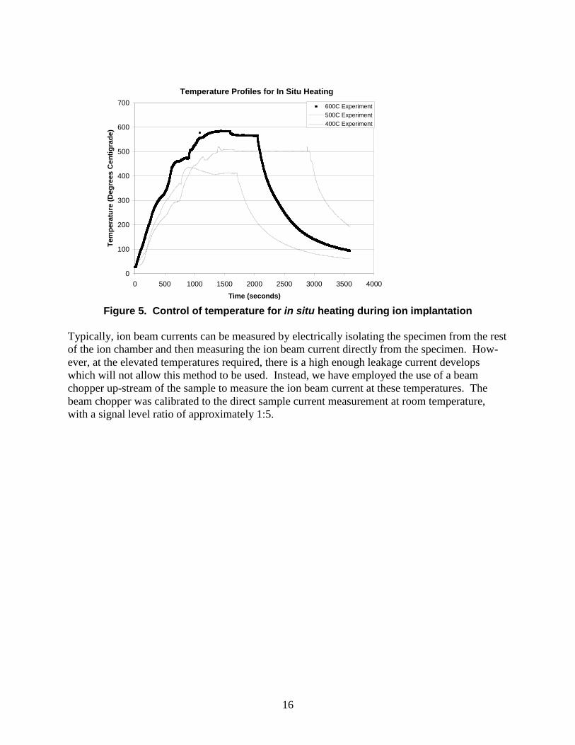
Figure 12. Deformed pillars after compression of the irradiated and controlled 10 µm tall
pillars
However the discrepancy between the prediction and the data presented in Figure 11 was quickly
solved when the micrographs of pillars were taken. As can be seen in Figure 12, the control pillar
on the left contains slip band running the entire length of the pillar. Whereas, the irradiated pillar
on the right has slip bands that only propagate on the bottom half of the pillar. These slip bands
are at height lower than the end of range of the copper ions and are this in virgin material that is
expected to react similar to that of the controlled sample. To avoid the effect of the ion implanta-
tion length scale on the recorded micropillar mechanical response, smaller pillars were produced
using modifications to the same milling protocol.

24
Figure 13. Stress strain curves from the control and irradiated 5 µm tall pillars
The pillars produced to be 5 µ tall and 2.5 µm diameters were produced and compressed using
identical FIB and nanoindentation facilities. In contrast to the taller pillars a distinct difference in
the strength of the pillar in compression can be seen with the irradiated pillars being approxi-
mately 100 MPa stronger. In addition, the irradiated micropillars appear to fail significantly less
total strain. These are the expected decease in ductility and increase in strength associated with
irradiation damage due to the accumulation of defect clusters, such as dislocation loops that pre-
vent the natural slip of glide dislocations.
Figure 14. Deformed pillars after compression of the irradiated and controlled ? µm tall
pillars.
The failure of these ion irradiated pillars was catastrophic in nature and resulted in significant
deformation of the pillar. This can be seen in the images on the right of Figure 14. In most of
these pillars the greatest slip occurred at the base (B2 and B3) or in a region approximately a mi-
crometer above the base (C1) of the pillar. The slip at the base might be explained as a small sec-

25
tion of the pillar is in the virgin copper crystal and can thus easily slip relative to the rest of the
pillar, although not through a complete slip plane as was seen in the taller pillars. The sample
that slip occurred about one micrometer above the base might be a result of the heterogeneous
nature of heavy ion irradiation. The end of range of the implants produces the greatest amount of
damage and would be hypothesized to be the strongest portion of the pillar. In order t investigate
the effect of end of range on the resulting stress-strain curves, even smaller pillars were pro-
duced.
Figure 15. Stress strain curves from the control and irradiated 4 µm tall pillars
Figure 15 is the stress-strain curve micropillars designed to be 4 µ tall and 2 µm diameters. It
should be noted that as the pillars get smaller the tolerance of the process remains the same,
which should increase the scatter in the data. Despite this effect, the greatest separation between
the control and ion irradiated data can be seen in this data set. The virgin copper pillars should
typical copper response with a maximum strength in compression around 200 MPa and an elon-
gation, which is similar to that seen in all of the controlled experiments independent of height. In
contrast, the irradiated pillars demonstrated compression strengths as high as 1500 MPa. This is
nearly an order of magnitude higher than the control samples and over three times that of the 5 µ
tall and 2.5 µm diameters pillars. This suggests that the inclusion of the end of range of the ions
in the pillars plays a significant role in the deformation and failure of the pillars.
26
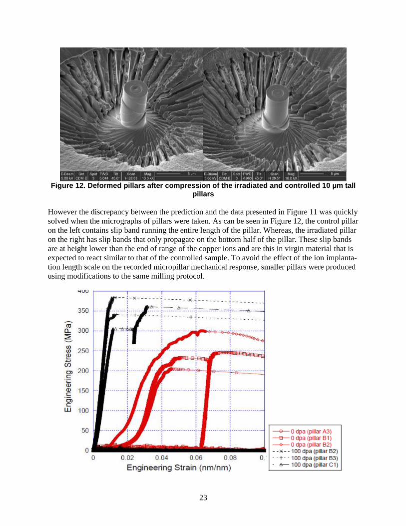
Figure 16. Deformed pillars after compression of the irradiated and controlled 4 µm tall
pillars.
SEM images of the controlled and irradiated be 4 µ tall and 2 µm diameters pillars after com-
pression can be seen in Figure 16. As expected, the controlled pillars exhibit slip bans throughout
the pillar height running along the 111 family of slip planes. In contrast, the irradiated pillar
shows no signs of slip in the pillar dimension, as is evident by the milling defect still present in
the pillar shown. This lack of deformation is in agreement with the increased hardness of the pil-
lar observed in the stress-strain curve.
The results of these sets of experiments show that micropillar compression provides significant
amount of information that can be used to characterize the effects of ion irradiation, but are lim-
ited in applicable conditions. The volume of the pillar must be larger enough to encompass any
inhomogeneity in the material investigated and small enough to contain only the relatively flat
part of the irradiation damage profile.
3.3. Individual Micropillar Irradiation
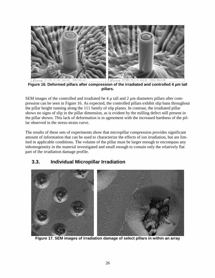
Figure 17. SEM images of irradiation damage of select pillars in within an array

27
Figure 18. SEM images of irradiation damage of select pillars in within an array
In addition to the effort detailed to produce pillars after ion irradiation of a sample, a project was
undertaken to irradiate the pillars after milling. The large control pillars produced in Figure 10
that were be 10 µ tall and 5 µm in diameters were irradiated using an in-situ optical microscope
to align the ion beam with the pillars during irradiation. The results of this effort can be seen in
Figure 17. The radiation damage could be observed using the nearly in-situ ion irradiation SEM
during the implantation. It was determined that the geometrical tilting and rotating requirements
required to provide uniform damage distribution in the pillar was extensive and thus not feasible.
Pior to recent upgrades in the system the resolution of the SEM only permitted a general charac-
terization of the radiation damage after extensive irradiation damage had been produced. This
can be seen in the blistered region of Figure 18.

28
4. QUALIFICATION OF TECHNIQUE IN STAINLESS STEEL
4.1. Finite Element Modeling of Nanoindentation into Irradiated Steels
To determine if the effects of irradiation damage would be detectable by nanoindentation, an ax-
isymmetric finite element model was created to simulate the nanoindention experiment using a
conical tip with an effective cone half-angle (19.7º) of a sharp 3-sided diamond Berkovich tip.
[12, 13] The finite element mesh of the model is shown in figure 1. The size of the substrate in
this simulation is a 60 µm by 40 µm and contains a sub-surface hardened region, highlighted in
red,. The bottom of the substrate is fixed in the simulation and the hardened region is 2.5 um
thick situated between 2.5 and 5 um beneath the substrate surface. It is included to capture the
effect of a radiation hardened layer beneath the surface of a 300 series stainless steel sample. In
the simulation, the diamond indenter has a Young’s modulus of 1141 GPa and a Poison’s ratio of
0.07. The substrate has a Young’s modulus of 200 GPa and a Poison’s ratio of 0.3. The coeffi-
cient of friction between the tip and the surface was set as 0.1. The yield strength of the sub-
strate, , was set to 350 MPa. To provide a first order approximation of a radiation hardened re-
gion produced by ion irradiation, the region outlined in red was set to yield strength of 700 MPa.
Figure 19.Finite Element Model of conical indentation of a control and a irradiation hard-
ened microstructure
A simulated result demonstrating the effect of the subsurface hardened layer is given in Figure
20. It is a plot of hardness, i.e. load divided by projected contact area, vs. indentation depth. For
comparison, the same result from simulation without a hardened region is also plotted in Figure
20. The comparison shows the increasing influence of the hardened region as the indentation
depth increases, even though the maximum depth in the simulation is significantly less than the
depth of the hardened region. This result suggests that the plastic zone ahead of the indentation
tip begins interacting with the hardened region, at an indentation depth of about 500 nm deep.
The hardness was found to increase as with increasing indentation depth suggesting that
nanoindentation should provide an adequate technique to sample the radiation damage in the lim-
ited volume that is produced by ion irradiation.

29
1.2
1.4
1.6
1.8
2
2.2
2.4
0 200 400 600 800 1000
Hardness vs. Depth
Simulated Indentation Experiments
304SS - Conical Tip Geometry
w/o hardened subsurface layer
with hardened subsurface layer
Tru
e H
ard
ness (
GP
a)
Indentation Depth (nm)
0
0.5
1
1.5
2
2.5
0 200 400 600 800 1000
Hardness vs. Depth
Simulated Indentation Experiments
304SS - 10 um spherical tip
w/o hardened subsurface layerwith hardened subsurface layer
Tru
e H
ard
ness (
GP
a)
Indentation Depth (nm) Figure 20. Simulated Hardness for both conical and spherical nanoindenters based on
FEM simulation
4.2. Sample Preparation Ion Irradiation Conditions
All of the studies discussed in this section are based on nine 8 mm x 8 mm sample coupons that
were cut and mechanically polished to a mirror finish from the same stock of steel. All of the
316L was cut from the same sheet of 316L AK Steel. The manufacture reports the tensile
strength as 631 MPa the 0.2% offset yield strength as 331 MPa, and the Rockwell hardness as
82. The coupons were grinded and polished culminating with a final polish of the coupons using
a vibratory polish and colloidal silica. Similarly, all of the 420F steel discussed in this section
were produced from the same 12.7 cm diameter rod manufactured by Bralco Metals. The rood
was cut into 8 mm x 8 mm sample coupons and polished to a mirror finish using a final vibratory
polishing step. This sample preparation provided the mirror finished needed for both nanoinden-
tation and various types of surface analysis in coupons suitable for the button heater seen in Fig-
ure 4.
4.3. Spherical Nanoindentation Results
Spherical indentations were investigated as a possible method to characterize the hardness of the
material. Although not as standard as Berkovich indentation for nanoindentation, spherical in-
dentation is in use and if done at elevated temperatures is able to provide some information on
the creep behavior of the sample as a function of stress and temperature. [14, 15] Due to the im-
portance of creep during the lifetime of the nuclear reactor under both high temperature and high
radiation flux, a technique like that outlined in Figure 21 was considered using spherical indenta-
tion.

30
Figure 21. Schematic indicating the advantages of spherical indentation to provide in-
formation on the active creep mechanism
Spherical indentations of 316 L stainless steel irradiated to approximately 100 dpa at 400 ºC,
500ºC, and 600ºC can be seen in Figure 22. The results show a similar trends and values to that
of the model created for the spherical indentation of 300 series stainless steel in the experiments
ran at 400 ºC and 500ºC. The major deviation between the models is that the implanted region
shows significant deviation from the perfectly elastic region of the hardness versus depth graph.
This deviation might be a result of increase surface roughness in the irradiated material. The poor
model fit for the 600ºC irradiated sample suggests that a microstructural evolution has occurred
in the materials softening the irradiated region to be similar to that of the control sample.
Figure 22. Hardness as a function of depth for spherical indentations at 400 ºC, 500ºC,
and 600ºC

31
4.4. Berkovich Nanoindentation Results
In addition to the spherical indentation, Berkovich indentation was done to provide mechanical
property information on the samples. This technique does not provide information related to the
creep properties of the sample, but does provide information regarding the hardness of the local
region and insight into the strength and ductility of the material. Because of the size of these in-
dents, an array of indents such as those seen in Figure 23 could be included within the irradiated
region providing some statistics over a heterogeneous microstructure.
Figure 23. Optical Micrograph of an array of Berkovick indentations in steel
Table 2. The Matrix of indentation performed on 316L stainless steel
Experiment Tests H (GPa) E (GPa)
400C baseline #1 16 2.46± 0.07 203 ± 10
400C baseline #2 16 2.40± 0.08 202 ± 7
400C implant region 16 3.07± 0.07 197± 7
500C baseline 14 2.30 ± 0.11 195 ± 6
500C implant region 15 3.05 ± 0.10 198 ± 11
600C baseline 16 2.33 ± 0.09 191 ± 8
600C implant region 16 2.36 ± 0.09 190 ± 9

32
As predicted by the finite element model, a distinction was observed in the majority of the ion
irradiated regions when compared to the set of baseline nanoindentation results, as can be seen in
Figures 24, 25, and 26. In the 316L coupon irradiated to approximately 10 dpa, the difference
between the ion irradiated regions and the baseline was slight, falling within the error bars for the
implants done at 500 ºC and 600 ºC. At approximately 40 dpa, a significant increase in hardness
is observed between the baseline nanoindentation results and those of the 400 ºC and 500 ºC ir-
radiation exposures. However, the hardness values for the material receiving a 40dpa exposure at
600 ºC remained similar to the baseline. This trend is enhanced in the 100 dpa set of implants
resulting in a 1 GPa difference between the hardness of material ion implanted at 400 ºC and 500
ºC compared with the baseline and the 600 ºC implanted region.
Figure 24. Nanoindentation results of controlled regions and irradiated regions to ap-
proximately 10 dpa at 400 ºC, 500ºC, and 600ºC
Figure 25. Nanoindentation results of controlled regions and irradiated regions to ap-
proximately 40 dpa at 400 ºC, 500ºC, and 600ºC

33
Initial analysis of the data raised a concern regarding the decreasing slope of the baseline hard-
ness versus depth curves shown in Figures 24, 25, and 26. To determine if this was a small scale
effect or if the surface had indeed been hardened during the metallographic sample preparation,
the samples were electropolished. The electropolished baseline sample did not exhibit the same
negative slope seen in the initial coupons suggesting that the negative slope seen was a result of
work hardening that occurred in the relatively malleable 316L stainless steel. This work harden-
ing appeared to be limited to the top 400 nm to 600 nm of the coupons and produced significant-
ly less damage than the radiation damage produced in the majority of the coupons.
Figure 26. Nanoindentation results of controlled regions and irradiated regions to ap-
proximately 100 dpa at 400 ºC, 500ºC, and 600ºC
To distinguish between the radiation hardening from ion implantation and the work hardening
from sample preparation, the data presented in Figure 1 is normalized to the baseline and is plot-
ted again in the left side of Figures 24, 25, and 26 . The effect of increasing dose on the hardness
ratio can be observed in both the 400 ºC and 500 ºC sets of coupons in the normalized data indi-
cating that the effect of dose was significantly larger than the surface work hardening resulting
from the vibratory polishing. Figure 4 also clearly demonstrates that there is minimal deviation
between the baseline samples and the set of samples irradiated at 600 ºC. Because differences
between surface and subsurface conditions can greatly affect nanoindentation results, it is strong-
ly recommended that a baseline normalization and similar hardness ratio should be implemented
in the rapid characterization of ion irradiation damage.
In addition to the experiments ran on the 316L stainless steels, a set of nanoindentations were
done on 420F stainless steel. The 420F was polished and irradiated to similar condition of ap-
proximately 10 dpa, 40 dpa, and 100 dpa at temperatures of 400 ºC, 500ºC, and 600ºC. Table 3
outlines the number of test done for each irradiation condition, the hardness and elastic moduli of
both the control and implanted samples. In comparing the data in the baseline column, a soften-
ing is evident as the temperature of the sample increases independent of the ion irradiation condi-
tion. In addition, a trend is observed as expected for increasing hardness with increasing radia-
tion damage for samples irradiated at the same temperature.

34
Table 3. A set of nanoindentation experiments run on the 420 stainless steel
Sample Temp. # of
Tests
Baseline
(1um depth)
H (GPa) E (GPa)
# of
Tests
Implant Region
(1um depth)
H (GPa) E (GPa)
10/high 400 16 3.27±0.09 228±8 16 3.93±0.11 213±8
10/high 500 16 3.15±0.09 200±6 17 3.58± 0.09 229± 7
10/high 600 15 2.92±0.07 190±5 16 2.96±0.13 232±6
40/1 400 16 3.44±0.09 230±7 14 4.35±0.16 226±6
40/high 500 15 3.20±0.07 236±6 14 3.71±0.08 233±8
40/high 600 16 2.90±0.05 222±6 11 2.90±0.08 229±12
100/high 500 16 3.05±0.08 227±7 9 3.58±0.09 230±9
Figure 27. Nanoindentation results of controlled regions and irradiated regions to ap-
proximately 10 dpa, 40dpa, and 100 dpa at 400 ºC, 500ºC, and 600ºC
A plot of this data, Figure 27, permits one to better visualize the change in hardness as a function
of depth into the materials. At the lowest damage level 10 dpa, there is no difference between the
600ºC and the control experiment and minimal difference between the 400 ºC and 500ºC sample
and the control region. This separation increases at the approximately 40 dpa damage level be-
tween the 400 ºC, and 500ºC and the control sample, but is note present in the 600ºC sample
and the control. This separation trend continues in the 100 dpa sample 500ºC sample. The
downward trend in the implanted hardness near the surface was attributed to increase surface
roughness due to the implantation, but might be an artifact of the denude zone present under the-
se implantation conditions.

35
Figure 28. Nanoindentation results of controlled regions and irradiated regions. The
samples were irradiated at various ion fluxes.
The 420F stainless steel was used for a experiment to investigate the effects of heavy ion irradia-
tion rate on the resulting mechanical properties. Figure 28 is a hardness plot of the samples im-
planted at various rate. Sample 1 was implanted at the slowest rate possible, which resulted in
extensive fluctuation of the ion beam. Sample 2 was implanted at half the implantation rate of
the maximum implantation rate. Sample 3 was implanted at a quarter and sample 4 was implant-
ed at an eighth of the maximum implantation rate. The results of this experiment is clear that the
ion irradiation rate does alter the microstructure and subsequently the mechanical properties of
the film and as such should be taken into consideration and at the minimum uniformed through-
out all the implantation experiments performed. This deviation was not determined to be be ei-
ther a direct result of the implantation rate or a secondary effect, as the sample was held at ele-
vated temperatures for longer periods of time during the slower implantation rate in an effort to
reach the same total dose.
4.5. Microstructural Examination of Irradiated Region
Due to the strong dependence between mechanical properties and microstructure in structural
materials, an effort was made to quickly characterize the microstructure of the ion irradiated
samples. The first effort that was made was the incorporation of an EBSD scan of this sample. If
this could be done successfully, then a rapid nearly in-situ capability could be used for the char-
acterization of the samples during ion irradiation. Figure 29 shows the EBSD maps obtained for
both the control steel sample and the ion irradiated region of a 316L sample after 100 dpa at
600ºC. The EBSD map of the control samples provides significant insight into the texture of the

36
film and the type of grain boundaries present. In contrast, the region ion irradiated to a dose of
100 dpa showed minimal set of spots with adequate confidence index. This initial result suggests
that EBSD maps will not be of great benefit for characterizing regions of heavy radiation dam-
age.
Figure 29. EBSD orientation map of 316L control and 100 dpa irradiated regions.
Despite the poor EBSD map, a pole figure can still be created with accurate data points for both
the control and radiation damaged samples. This set of pole figures can be seen in Figure 30 for
the same 316L stainless steel sample irradiated with 20 MeV Ni to approximately 100 dpa at
600ºC. It appears that at least under these conditions, the microstructure evolves from a 110
dominated texture to 111 texture. This effect provides some initial insight into the microstructur-
al evolution that occurs.

37
Figure 30. Pole figures of 316L control and 100 dpa irradiated regions.
In order to determine the effects of variation of defect structures as a function depth into the ion
irradiation damage, a cross-sectional TEM specimen was quickly prepared by FIB lift-out tech-
nique that has become fairly common of a technique. The sample was polished using a low ener-
gy cleanup of the film to minimize FIB damage. It was determined looking at Figure 31 and oth-
er FIB lift-out samples that the damage produced by the 1 to 2 keV gallium beam produces min-
imal damage in comparison to the 20 MeV Ni beam. An additional observation for Figure 31 is
that microstructural distribution is not uniform and appears to vary, at least in image condition,
from one grain to another. The microstructure of ion implantation damaged regions included dis-
location tangles, dislocation loops, small voids, and other small defect structures. The density
and location of these defects were found to be a function of depth into the sample and ion irradia-
tion conditions.

38
Figure 31. TEM micrograph of the 316L 100 dpa 600 ºC irradiated region as a function of
depth.

39
Figure 32. TEM micrographs taken at 1.5 µm into the coupon illustrating the effects of ion
irradiation temperature and dose on microstructure.
Beyond a comparison of the defect structure, as a function of depth into the sample a comparison
can be made between samples as a function of dose and temperature in the 316L stainless steel.
Figure 32 compares all three of the implantation dose and temperatures can be compared. To
compare the effects of various implantation dose and temperature, TEM bright-field micrographs
were taken at a depth of 1.5 µm below the surface of the original coupon. This region was cho-
sen as the damage profile predicted by SRIM to be relatively flat and it was significantly beyond
the denuded region at the surface of the coupon. In comparing the micrographs, the expected
trend of increased damage with increasing dose can be seen. The 10 dpa foils show isolated de-
fect clusters that image as black clusters, whereas it is difficult in the 400 ºC 100 dpa image to
clearly identify any isolated defect structures. The formation of larger dislocation loops and
voids in the high temperature implants provide an explanation for the observed nanoindentation
results. It is well known that as the size of the defects increases and the density decreases the
force need for a dislocations to pass through the defect field significantly decreases resulting in
the decreased hardness between the coupons irradiated at 600 ºC and those at 400 ºC. Despite
this effort microstructures are difficult to compare due to the various grain orientations.

40
Figure 33. STEM micrograph and EDS maps of the 316L 100 dpa 500 ºC and 600 ºC irradi-
ated region.
To further understand the effects of the ion irradiation on the 316L coupons, energy dispersive
X-ray spectroscopy and mapping were performed on the TEM samples. For the majority of the
samples, minimal heterogeneity was observed and in those cases was often associated with grain
boundaries, as might be expected and can be seen in the example in Figure 33. However in the
coupon irradiated to 100 dpa at 600 ºC a significant amount of both Ni and Si solute segregation
were observed to occur, as can be seen in Figures 33 and 34.
0 5 10 15 20 250
10
20
30
40
50
60
70
80
Mean Spectrum
Figure 34. STEM micrograph of the 316L 100 dpa 600 ºC irradiated region and accompan-
ing EDS spectra.

41
Although the post mortem TEM characterization provides insight into the microstructures that
form from radiation damage in these samples, it provides little insight into the mechanisms by
which this microstructure evolves under these conditions for such understanding in-situ observa-
tion of the microstructure is needed.

42
5. EXTENSION OF ACELERATED TESTING TO DIFFUSION COUPLES
Diffusion couples provide an excellent tool to investigate in a rapid combinatorial manner the
effects of various compositions on the properties of materials. In order for a combinatorial tech-
nique based on diffusion couples to be successful, the probe size to investigate the thermal, elec-
trical, or mechanical properties of the material must be smaller to the diffusion range of the ma-
terial. It was determined based on the length scale limitations already imposed on the rapid char-
acterization technique proposed in this work by the size scale of the ion irradiation that a diffu-
sion couple based production of various alloys would be a feasible way to investigate the effects
of various microstructural composition. The limitation of diffusion couples is that it does not
consider the microstructure formed by production process, as having a significant effect on the
properties and as such results in an uncontrolled key variable in the control of performance of a
material properties. [16-19] Despite this limitation, diffusion multiples combined with the pro-
posed characterization technique provides a rapid method to characterize the properties of a large
data set of compositions of irradiated materials.
5.1. Production of Diffusion Couples Diffusion couples for this study were produced by creating a plate of 316L or HT9 with a set of
both 6 mm and 18 mm holes produced by end milling the plate. Inserts of refractory metal (tung-
sten, molybdenum, tantalum, and niobium) plates of 1 mm thickness were placed into the proper-
ly labeled slots and covered by 316L plates of 4.5 mm thickness. To induce bonding between the
refractory plate and the 316L stainless steel on either side, hot isostatic pressing (HIP) was ap-
plied to both the 6 mm and 18 mm structures. The HIP process was followed by a high tempera-
ture long duration anneals to induce the diffusion between the refractory metal and the base steel
alloy. The resulting 316L plate after HIP and diffusion annealing can be seen in Figure 35 along
with a schematic of the sandwich structure created by the HIP procedure. Multiple diffusion
couples were then sectioned out of each plate using electrical discharge machining (EDM). The
diffusion couple coupons were then mechanical polished down using a final vibratory polish
producing a high quality mirror finish.

43
Figure 35. Photograph of the 316L diffusion couple set and a schematic of what the
5.2. Compositional Characterization of Diffusion Couples Once the 316L diffusion couples for this study were produced by the procedure outlined above,
the coupons were analyzed using both SEM and wavelength dispersive x-ray spectroscopy
(WDS) techniques. These techniques provided a rapid technique to characterize the interfaces
formed from the diffusion couple process. Figure 36 shows an example of the WDS line scan
and the SEM image of the tungsten 316L stainless steel couple. A few points to note in the com-
parison is that the diffusion length scale formed by the coupling is on the order of 10 µm. In both
the WDS and SEM images two distinct intermixing regions can be identified by either different
slopes in the WDS or different contrast in the SEM image. These are associated with different
phases formed. In addition to these regions, a long tail exists in the WDS for the tungsten com-
position. This portion is the area of greatest practical interest, as it is a stainless steel with vary-
ing alloy compositions of tungsten included. Despite this alloy being less than a few percent, it
could have an extreme effect on the high temperature and radiation tolerance of the steel.
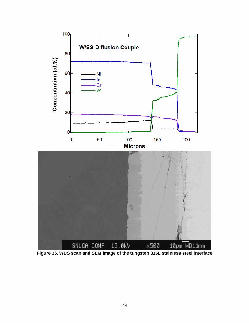
44
Figure 36. WDS scan and SEM image of the tungsten 316L stainless steel interface

45
Figure 37. WDS scan and SEM image of the tantalum 316L stainless steel interface
Similar to the tungsten alloy, the tantalum 316L stainless steel demonstrates the formation of dis-
tinct phases, in this case three, and a long diffusion tail of tantalum into the steel. In most of the-
se couples cracks can be seen between the various phases. The fact that the tantalum has diffused
significantly into the steel suggest that these formed during the long term anneal and not during
the HIP process and are thus a result of varying difference in the coefficient of thermal expan-
sion of the various new phases formed.

46
Figure 38. WDS scan and SEM image of the molybdenum 316L stainless steel interface
Figure 38 shows the SEM image and WDS scan for the molybdenum 316L stainless steel couple.
It also has a long diffusion tail and the formation of two distinct intermediate phases observed in
both the WDS and SEM image. The nature of the cracking in this diffusion couple is such that it
results in the blips in the all of the WDS composition profiles. Several of these coupons that were
produced required delicate polishing due to the pull out of the region near the crack, the separa-
tion failure of the interface, or both.
47
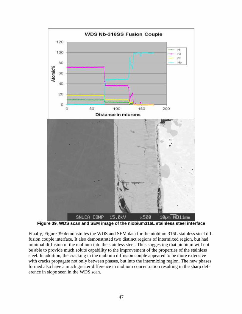
Figure 39. WDS scan and SEM image of the niobium316L stainless steel interface
Finally, Figure 39 demonstrates the WDS and SEM data for the niobium 316L stainless steel dif-
fusion couple interface. It also demonstrated two distinct regions of intermixed region, but had
minimal diffusion of the niobium into the stainless steel. Thus suggesting that niobium will not
be able to provide much solute capability to the improvement of the properties of the stainless
steel. In addition, the cracking in the niobium diffusion couple appeared to be more extensive
with cracks propagate not only between phases, but into the intermixing region. The new phases
formed also have a much greater difference in niobium concentration resulting in the sharp def-
erence in slope seen in the WDS scan.

48
5.3. Initial Nanoindentation Testing of Diffusion Couples
The difference in composition that was created by the diffusion couple and characterize in the
WDS scans and SEM images in the previous section were then tested using nanoindentation to
better understand the resulting change in the mechanical properties of the varying alloy composi-
tion.
Figure 40. Nanoindentation results across the tantalum 316L stainless steel diffusion
couple interface
Figure 40 is a plot of the hardness and elastic moduli from various indentations along the tanta-
lum 316L stainless steel diffusion couple characterized in Figure 37. Both the hardness and elas-
tic moduli show a general linear slop of the property values across the new phases and minimal if
any difference in the of properties in the 200 µm area extending into the stainless steel. This sug-
gest despite the diffusion of the tantalum into the stainless steel that can be observed in Figure
37, no observable change can be seen in the mechanical response of the pre-irradiated steel with
varying levels of tantalum composition.

49
Figure 41. Nanoindentation results across the niobium 316L stainless steel diffusion
couple interface
In Figure 41, the nanoindentation results for the niobium 316L diffusion couple vary from that of
the tantalum couple in that two distinct hardness plateau can be seen in the new phases that form
between the 316L and the niobium. Unfortunately, there does seem to be significant noise in be-
tween in the data that might be a result of the cracks that were seen in many of the optical micro-
graphs of the diffusion couples. In addition, there does not appear to be significantly relevant
change in the mechanical properties of the region in which the 316L might have absorbed a small
amount of the niobium. This suggests that the steel properties were not found to change much
even if the niobium was able to diffuse into the steel.

50
Figure 42 SEM image with the different phases formed in the niobium stainless steel dif-
fusion couple interface
Further characterization of the niobium 316L stainless steel interface was able to identify the re-
gion between the niobium and the steel as two distinct phases: FeNb and Fe2Nb. These two
phases were can be clearly identified in the SEM micrograph, seen in Figure 42, with distinct,
but not flat interfaces. In addition the grain structure of the different phases can also be observed
in the micrograph. The FeNb phase demonstrates a relatively uniform ultra-fine grain size with
minimal preference for the diffusion direction. In contrast, the Fe2Nb phase demonstrates colum-
nar grains running the length of the phase thickness and allying along the diffusion direction. The
difference in microstructure between phases and more importantly the changes in microstructure
of the stainless steel is an uncontrolled variable in the production of the stainless steel based dif-
fusion couple and something that would have to be studied using conventional samples if a alloy
composition of interest was identified.

51
Figure 43. Optical image of the nanoindentation impressions across the niobium 316L
stainless steel diffusion multiple interface
The nanoindentation marks remaining after indentation in the niobium stainless steel composi-
tion can be seen in Figure 43. Despite the difference in composition and properties of the three
phases seen in the optical micrograph there does not appear to be any signs of cracking or varied
indentation mark between the Nb, FeNb, and Fe2Nb phases at the indentation depths tested. This
suggests that all of the metal phases had relatively plastic response as expected.
5.4. High-Energy Heavy-Ion Irradiation Conditions
The final stage in the testing of the diffusion couples was the heavy ion irradiation of the diffu-
sion couples using the Tandem accelerator at nominally room temperature to varying dose level.
For comparison to previous work, the implantations were done with 20 MeV Ni ions at the max-
imum achievable dose rate possible by the accelerator on that given day. The spot size was a few
millimeters squared. This resulted in a damage rate of approximately 0.003 dpa/s and a end of
range of approximately 3.47 µm. In addition, a set of implants were done using a proton beam at
300 keV to t total damage level of 1 dpa and an estimated end of range of 1.32 µm. All of the
data presented in Section 5.5 will be on the molybdenum 316L stainless steel diffusion couple
for brevity.
5.5. Nanoindentation Testing of Irradiated Diffusion Couples
The results of the nanoindentation results across a diffusion couple that had been proton irradiat-
ed was successful completed and can be seen in Figure 44. The hardness values have been sepa-
rated out based on the depth of the indentation between surface-200 nm, 200-300 nm, 300-400
nm, and 400-500 nm. By doing this, a virtual three dimensional hardness plot is provided. This

52
was done in an effort to elucidate the effect of end of range on the mechanical property of the
film. Although there seems to be a significant amount of scatter in the data, several interesting
trends appear to emerge. The first is that the slope in the hardness seen in the non-irradiated cou-
pons as the sample transition between the refractory metal and the steel is maintained and shows
no distinct change from that of the pre-irradiated materials. The remainder of the steel with a de-
creasing molybdenum composition demonstrates a gradual decrease in hardness properties as a
function of depth into the diffusion couple with the exception of the data points taken at a depth
between 160 and 180 nm into the diffusion couple. This increase in hardness occurs in all of the
thickness and in three points suggestive that it is not the result of scatter in the data or faulty re-
sult from one indentation. It is possible that this result might be due to local heterogeneity in the
region tested and as such further examination is necessary before any conclusive insight can be
gained about the increased hardness associated with the composition created 180 nm into the mo-
lybdenum 316L stainless steel diffusion couple.
The fact that the hardness is greatest at the top of the 316L sample rather than closer to the end of
range suggests that the trend seen with decreased hardness with depth is a result of the work
hardening of the relatively soft 316L during the finally stages of vibratory polish used to produce
the sample. However, these convoluted effects could not be separated from the difference in the
mechanical properties observed between the 316L with molybdenum in it and the new phases
formed between the 316L and the molybdenum plate.
Figure 44. Nanoindentation results across a diffusion couple interface
Figure 45 is the optical image of the nanoindentations into the proton irradiated molybdenum
316L stainless steel diffusion couple. This image shows no significant variation in the indenta-
tion size or surrounding region as a function of distance from the molybdenum plate suggesting
that all of the material indented to a depth of 500 nm showed similar plastic response and none of
the regions appeared to have significant variations in local microstructure that can be observed
under the resolving capability of an optical microscope.

53
Figure 45. Nanoindentation results across a diffusion couple interface
In addition to the proton irradiation, a similar plot showing the three dimensional data can be
achieved for the 20 MeV Ni implantations to a damage level of approximately 10 dpa and is
plotted in Figure 46. In contrast to the proton irradiation plotted in Figure 44, little distinction in
the hardness can be seen between the different phases produced during the manufacturing of the
diffusion couple. This further lends weight to the argument that the distinct hardness difference
between the 316L and the new phases seen in Figure 44 may be a result of the difference in work
hardening response of the new phases and the 316L stainless steel. One of the limited general
trends that can be pulled from the scatter of data presented in Figure 46 is that the hardness in-
creases as a function of depth. This suggests that the 20 MeV ion implanted regions shows in-
creased radiation defect structure as a function of increasing depth that provides increased pin-
ning points for the dislocation formed and propagated during indentation. This series of micro-
structural effects would subsequently result in the increased hardness observed with increasing
depth.
Figure 46. Nanoindentation results across a 10 dpa irradiated diffusion couple interface

54
Figure 47. Nanoindentation results across a Ni ion irradiated diffusion couple interface
In addition, to plotting hardness in a three dimensional plot as a function of depth into the irradi-
ated zone and distance from the diffusion couple interface as was done in Figures 44 and 46, a
hardness plot can be created comparing the distance from the couple interface and the approxi-
mate damage level created in the diffusion couple. This was done in Figure 47 for regions im-
planted to 1 dpa, 10 dpa, and 100 dpa. When this is done a distinct difference in the hardness of
the new phases formed relative to the stainless steel can be observed. In addition, a slight de-
crease in the hardness of the stainless steel as a function of distance from the diffusion couple
interface can be seen in the range between 50 and 250 µm. Although there is significant scatter
in the data a region of increase hardness is again observed between 150 and 200 nm from the in-
terface. This region is only present in the regions implanted to approximately 100 dpa, red
squares. It is uncertain what factors resulted in this increased hardness in this local region and
further studies are planned at naval post graduate school to elucidate this data.
Based on the success of the 316L diffusion couple, diffusion couples of HT9 were produced us-
ing similar prepared, characterized, and irradiated using similar techniques. The coupons are cur-
rently at the naval post graduate school for nanoindentation and post-irradiation characterization.
These findings should provide greater insight into the effects of composition of refractory metals
in the mechanical properties and radiation tolerance of metal composition consider for nuclear
cladding materials.
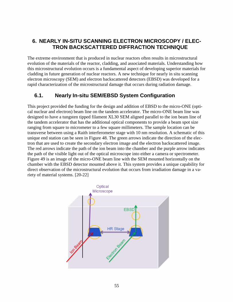
55
6. NEARLY IN-SITU SCANNING ELECTRON MICROSCOPY / ELEC-TRON BACKSCATTERED DIFFRACTION TECHNIQUE
The extreme environment that is produced in nuclear reactors often results in microstructural
evolution of the materials of the reactor, cladding, and associated materials. Understanding how
this microstructural evolution occurs is a fundamental aspect of developing superior materials for
cladding in future generation of nuclear reactors. A new technique for nearly in situ scanning
electron microscopy (SEM) and electron backscattered detectors (EBSD) was developed for a
rapid characterization of the microstructural damage that occurs during radiation damage.
6.1. Nearly In-situ SEM/EBSD System Configuration
This project provided the funding for the design and addition of EBSD to the micro-ONE (opti-
cal nuclear and electron) beam line on the tandem accelerator. The micro-ONE beam line was
designed to have a tungsten tipped filament XL30 SEM aligned parallel to the ion beam line of
the tandem accelerator that has the additional optical components to provide a beam spot size
ranging from square to micrometer to a few square millimeters. The sample location can be
transverse between using a Raith interferometer stage with 10 nm resolution. A schematic of this
unique end station can be seen in Figure 48. The green arrows indicate the direction of the elec-
tron that are used to create the secondary electron image and the electron backscattered image.
The red arrows indicate the path of the ion beam into the chamber and the purple arrow indicates
the path of the visible light out of the optical microscope into either a camera or spectrometer.
Figure 49 is an image of the micro-ONE beam line with the SEM mounted horizontally on the
chamber with the EBSD detector mounted above it. This system provides a unique capability for
direct observation of the microstructural evolution that occurs from irradiation damage in a va-
riety of material systems. [20-22]

56
Figure 48. Schematic of the nearly in-situ ion irradiation system on the micro-ONE beam line at the Ion beam Lab
Figure 49. Picture of the micro-ONE beam line with the SEM, optical microscope and ion
beam line identified.
6.2. Preliminary Results in an Iconel Alloy
The design required to obtain a proper electron backscattered detector provided a significant
challenge that required a coordinated effort between the EBSD producer TSL/EDAX and Sandia
National Labs. The instillation of the EBSD into the port of the micro-ONE beam line and the
design of an adequate tilting stage were developed, designed, and tested with an Inconel EBSD
standard sample. Figure 50 shows a <111> electron backscattered pattern generated from a spot
on the sample, as well as an orientation map produced from scanning over multiple grains of the
Iconel EBSD standard sample. This result demonstrates the capability to obtain EBSD pattern
and map from a horizontally mounted SEM attached to the end station of a tandem accelerator.
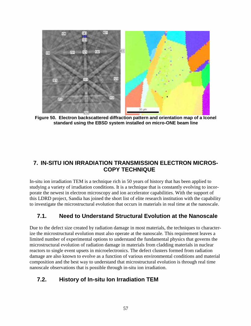
57
Figure 50. Electron backscattered diffraction pattern and orientation map of a Iconel
standard using the EBSD system installed on micro-ONE beam line
7. IN-SITU ION IRRADIATION TRANSMISSION ELECTRON MICROS-COPY TECHNIQUE
In-situ ion irradiation TEM is a technique rich in 50 years of history that has been applied to
studying a variety of irradiation conditions. It is a technique that is constantly evolving to incor-
porate the newest in electron microscopy and ion accelerator capabilities. With the support of
this LDRD project, Sandia has joined the short list of elite research institution with the capability
to investigate the microstructural evolution that occurs in materials in real time at the nanoscale.
7.1. Need to Understand Structural Evolution at the Nanoscale
Due to the defect size created by radiation damage in most materials, the techniques to character-
ize the microstructural evolution must also operate at the nanoscale. This requirement leaves a
limited number of experimental options to understand the fundamental physics that governs the
microstructural evolution of radiation damage in materials from cladding materials in nuclear
reactors to single event upsets in microelectronics. The defect clusters formed from radiation
damage are also known to evolve as a function of various environmental conditions and material
composition and the best way to understand that microstructural evolution is through real time
nanoscale observations that is possible through in-situ ion irradiation.
7.2. History of In-situ Ion Irradiation TEM

58
In situ ion irradiation TEM is a technique that originated 50 year ago in England with the co-
emission of electrons and oxygen ions from the tip of a tungsten TEM filament. [23] Since that
initial serendipitous observation effort has been made to attach a variety of linear accelerators to
a wide variety of TEM. This ranges from focused ion beams attached to intermediate voltage mi-
croscopes to tandem accelerators attached to 2 MeV TEMs. These various microscopes-
accelerators have been utilized to study the effects of radiation damage in everything from struc-
tural metals to microelectronic components. Currently, there exist 11 of these facilities world-
wide with the majority being in Japan. In addition to the multiple facilities in Japan, a facility for
in-situ ion irradiation TEM are located in China, France, and England each. With the additions of
the facility at Sandia partially supported by this project, two facilities now exist in the USA with
locations at Argonne National Lab and Sandia National Labs. [24] The locations of the various
in-situ ion irradiation TEM facilities can be seen in Figure 51.
Figure 51. A map of the location of in-situ ion irradiation TEM facilities around the world
7.3. In-situ Ion Irradiation TEM System Configuration
The last half of the LDRD project coincided with dedication of the new ion beam laboratory at
Sandia and the instillation of the four ion accelerators into the facility. Due to success of the con-
struction team, the building was completed several months ahead of schedule and under budget.
$1M of this cost savings was appropriated through a line item change to the purchase and instal-
lation of a new ion irradiation TEM. Several microscopes were considered, before a JEOL 2100
TEM was chosen to provide high contrast and tilting capabilities, while being within the budget
restraints. The location of the TEM was chosen to be off the 90º left beam line of the Tandem
accelerator in the northwest corner of the Tandem target hall. The location is circled in red in
Figure 64. It is the only TEM that JEOL USA is aware of that was aligned within a millimeter in
five axis. Due to budgetary restraints, a laser curtain was chosen to insulate the TEM from the
rest of the Tandem hall. The lighting and HVAC systems were made appropriate for a TEM lab.
The room modifications and the stand-alone TEM installation and operation at specifications
were completed on January 11, 2011.

59
Figure 52. The floor plan for the ion beam lab with the location of the new in-situ ion irra-
diation TEM indicated.
During the design of the microscope for in-situ ion irradiation studies, the design team consid-
ered many specifications, options, and additions to provide the TEM with various sets of capabil-
ities. The final TEM that resulting from the brainstorming sessions would have the following ca-
pabilities: 200 kV LaB6 TEM, ion beams from the tandem accelerator, two Colutron accelerators
(one concurrent with the Tandem and the other concurrent with the electron beam), all beams
will hit same location, electron tomography, scanning transmission electron microscopy
(STEM), nanosecond time resolution (DTEM), procession scanning (EBSD in TEM), in situ PL,
CL, and IL, in situ heating and cooling stage, in situ electrical measurement stage, in situ strain-
ing stage, in situ vapor phase stage, and in situ liquid mixing stage. By balance budgetary costs
associated with each option or addition with the added capability of the system, a plan was de-
velop for a four stage development of the facility as cost permitted. These four stages can be seen
in Figure 53. Each generation is associated with the introduction of a new ion beam into the
TEM. The instillation of the JEOL 2100 TEM with a maximum voltage of 200 kV LaB6 filament
with the addition of the single electron sensitive camera and active vibration feet was designated
as the 0th
generation. In this step, the purchase of three stages: in situ vapor phase stage, and in
situ liquid mixing stage, and the tomography stage, were completed. The 1st generation of the in-
situ ion irradiation TEM would include the insertion of a collimated ion beam from the 6MV

60
Tandem accelerator into the TEM through the 0º degree EDX port with all of the required elec-
trical, vibrational, and vacuum requirements required to operate the TEM with acceptable resolu-
tion. This was accomplished on April 19th
, 2011 with the first beam into the TEM. The 2nd
gen-
eration of the design will require the insertion of concurrent heavy and light ion beams into the
TEM through the 0º degree EDX port that will be produced by the tandem accelerator and a
Colutron, respectively. At the time of this report a final design of this system has been deter-
mined and construction of the support and vacuum systems has been initiated. During this stage
addition dosimetery will be added to provide optical observation of the TEM sample during ion
implantation, which may potentially provide the capability for cathodoluminescence and ion
beam induced luminescence. The final and fourth proposed generation of the I3TEM if complet-
ed will result in the inclusion of 4 ion beams into the TEM. The fourth addition ion beam will be
inserted through a high angle port of the TEM
Figure 53. Development plans and current status of the In-situ Ion Irradiation TEM
The first step of the development of an in-situ ion irradiation TEM facility is the installation of a new
JEOL 2100 TEM in the ion beam lab. This microscope was selected to have the highest contrast possible
through a combination of a wide pole-piece gap and a LaB6 filament. The TEM instillation was started on
October 29th by JEOL technicians assisted by Sandia scientists and Henderson construction crew. Accord-
ing to JEOL USA, this is the first TEM that location was specified to millimeter precision in x, y, and z.
Efforts were taken to mitigate local vibration by enhancing the local HVAC system and upgrading the
TEM to have both piezoelectric driven stages and active vibration isolation system installed. The TEM
was able to meet all of the specification including significantly surpassing the resolution limit by January
11, 2011.
To determine the optimal beam line configuration, Barney Doyle led a simulation effort to identify sever-
al proposed beam line configurations. This was done using particle beam optics (PBO) Lab a graphical
simulation designed for ion beam line configurations for the particle accelerator community. [25] An ex-
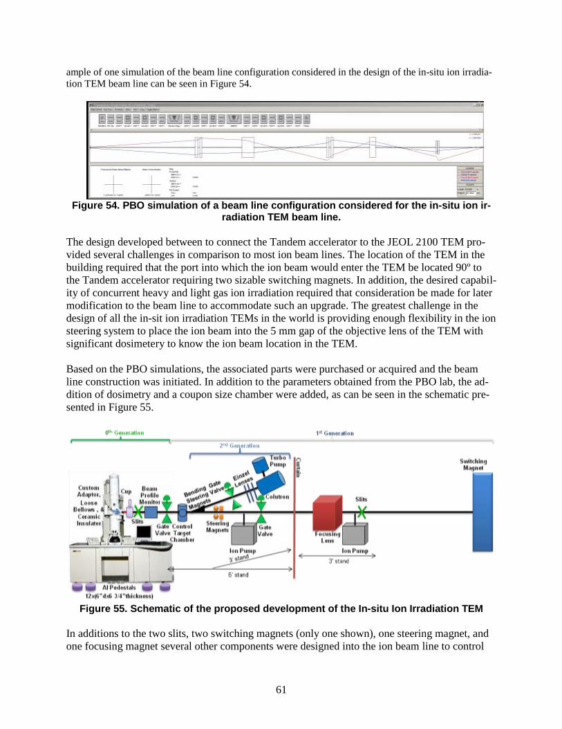
61
ample of one simulation of the beam line configuration considered in the design of the in-situ ion irradia-
tion TEM beam line can be seen in Figure 54.
Figure 54. PBO simulation of a beam line configuration considered for the in-situ ion ir-
radiation TEM beam line.
The design developed between to connect the Tandem accelerator to the JEOL 2100 TEM pro-
vided several challenges in comparison to most ion beam lines. The location of the TEM in the
building required that the port into which the ion beam would enter the TEM be located 90º to
the Tandem accelerator requiring two sizable switching magnets. In addition, the desired capabil-
ity of concurrent heavy and light gas ion irradiation required that consideration be made for later
modification to the beam line to accommodate such an upgrade. The greatest challenge in the
design of all the in-sit ion irradiation TEMs in the world is providing enough flexibility in the ion
steering system to place the ion beam into the 5 mm gap of the objective lens of the TEM with
significant dosimetery to know the ion beam location in the TEM.
Based on the PBO simulations, the associated parts were purchased or acquired and the beam
line construction was initiated. In addition to the parameters obtained from the PBO lab, the ad-
dition of dosimetry and a coupon size chamber were added, as can be seen in the schematic pre-
sented in Figure 55.
Figure 55. Schematic of the proposed development of the In-situ Ion Irradiation TEM
In additions to the two slits, two switching magnets (only one shown), one steering magnet, and
one focusing magnet several other components were designed into the ion beam line to control

62
vacuum, dosimetery, vibrational stability, and provide added capability. Two ion pumps were
included to provide sufficient vacuum capacity for the long beam line and several associated
chambers without relying on the TEM vacuum system. For dosimetery, a Faraday cup, and beam
profile monitor were included. The Faraday cup was located as close to the TEM as physically
possible. In order to minimize the potential vibration along the beam line from the various pumps
and mechanical systems associated with the Tandem accelerator and connected beam lines a soft
bellow was introduced between the custom TEM-beam line adaptor and the rest of beam line.
Once beams can be reliably introduced into the TEM, then initial experiments to provide a proof-
of-concept that heavy ion irradiation on the TEM samples produced without cutting, grinding, or
polishing could commence.
Figure 56. In-situ Ion Irradiation TEM from vision to completed first generation
The in-situ ion irradiation TEM beam line was constructed based on the description in the ap-
proach section and the schematic in Figures 54 and 55. The vacuum system was found to be bet-
ter than anticipated resulting in a significant improvement when the gate valve separating the
TEM and the beam line was open. With this beam line configuration, beam current was recorded
on a TEM Faraday stage on April 19, 2011. Despite this initial success the beam current was
found to be inadequate for the planned experiments.
As a result, several subsequent iterations were undertaken to optimize the beam line design. To
improve the vacuum system, two additional gate valves were added and an access port for leak
checking the system. One of the gate valves was directly vicinal to the last switching magnet to
protect the other beam lines and Tandem during maintenance of the beam line. The other was
placed between the Faraday cup and the bellow to minimize the volume the TEM pumps would
have to handle during non-irradiation experiments. The dosimetry was also found to be inade-
quate resulting in a requirement of up to eight hours for ion beam alignment. This is currently
being rectified by several measures. A beam profile monitor was added upstream of the first set
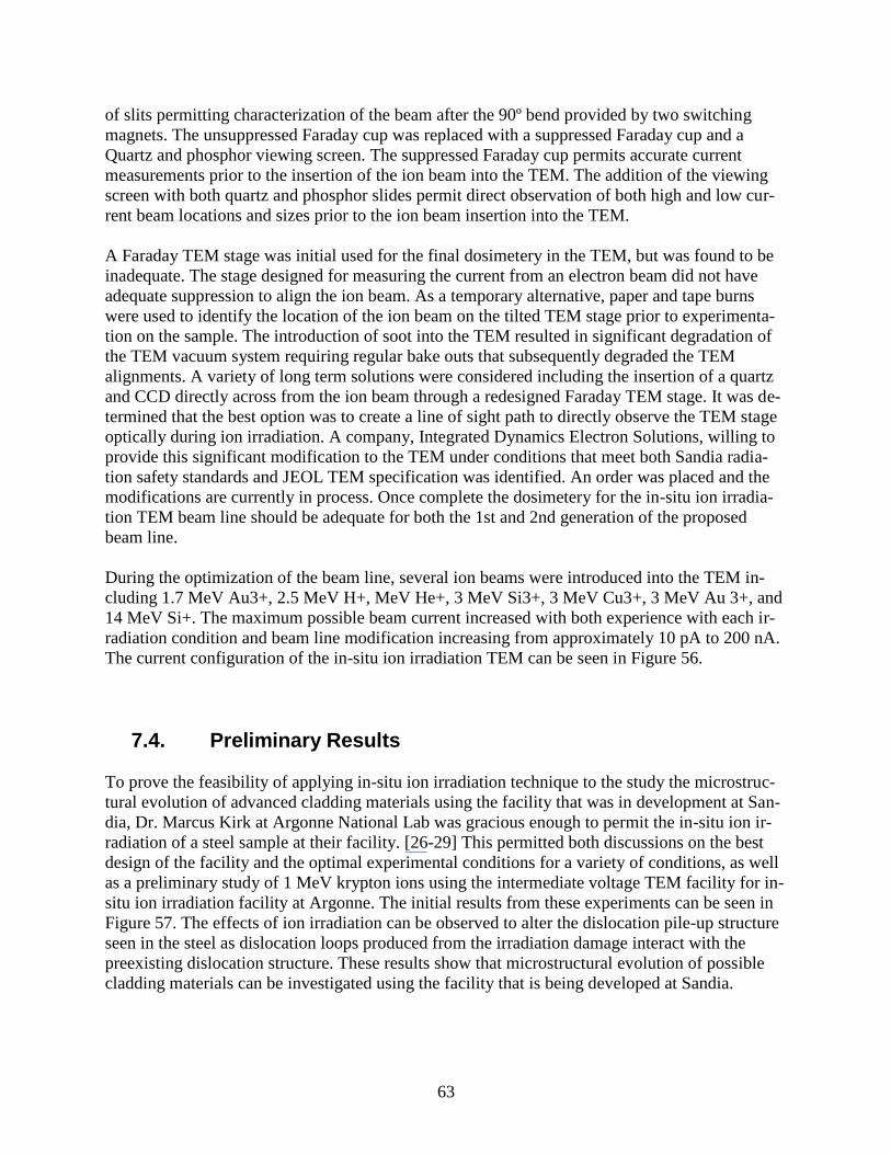
63
of slits permitting characterization of the beam after the 90º bend provided by two switching
magnets. The unsuppressed Faraday cup was replaced with a suppressed Faraday cup and a
Quartz and phosphor viewing screen. The suppressed Faraday cup permits accurate current
measurements prior to the insertion of the ion beam into the TEM. The addition of the viewing
screen with both quartz and phosphor slides permit direct observation of both high and low cur-
rent beam locations and sizes prior to the ion beam insertion into the TEM.
A Faraday TEM stage was initial used for the final dosimetery in the TEM, but was found to be
inadequate. The stage designed for measuring the current from an electron beam did not have
adequate suppression to align the ion beam. As a temporary alternative, paper and tape burns
were used to identify the location of the ion beam on the tilted TEM stage prior to experimenta-
tion on the sample. The introduction of soot into the TEM resulted in significant degradation of
the TEM vacuum system requiring regular bake outs that subsequently degraded the TEM
alignments. A variety of long term solutions were considered including the insertion of a quartz
and CCD directly across from the ion beam through a redesigned Faraday TEM stage. It was de-
termined that the best option was to create a line of sight path to directly observe the TEM stage
optically during ion irradiation. A company, Integrated Dynamics Electron Solutions, willing to
provide this significant modification to the TEM under conditions that meet both Sandia radia-
tion safety standards and JEOL TEM specification was identified. An order was placed and the
modifications are currently in process. Once complete the dosimetery for the in-situ ion irradia-
tion TEM beam line should be adequate for both the 1st and 2nd generation of the proposed
beam line.
During the optimization of the beam line, several ion beams were introduced into the TEM in-
cluding 1.7 MeV Au3+, 2.5 MeV H+, MeV He+, 3 MeV Si3+, 3 MeV Cu3+, 3 MeV Au 3+, and
14 MeV Si+. The maximum possible beam current increased with both experience with each ir-
radiation condition and beam line modification increasing from approximately 10 pA to 200 nA.
The current configuration of the in-situ ion irradiation TEM can be seen in Figure 56.
7.4. Preliminary Results
To prove the feasibility of applying in-situ ion irradiation technique to the study the microstruc-
tural evolution of advanced cladding materials using the facility that was in development at San-
dia, Dr. Marcus Kirk at Argonne National Lab was gracious enough to permit the in-situ ion ir-
radiation of a steel sample at their facility. [26-29] This permitted both discussions on the best
design of the facility and the optimal experimental conditions for a variety of conditions, as well
as a preliminary study of 1 MeV krypton ions using the intermediate voltage TEM facility for in-
situ ion irradiation facility at Argonne. The initial results from these experiments can be seen in
Figure 57. The effects of ion irradiation can be observed to alter the dislocation pile-up structure
seen in the steel as dislocation loops produced from the irradiation damage interact with the
preexisting dislocation structure. These results show that microstructural evolution of possible
cladding materials can be investigated using the facility that is being developed at Sandia.

64
Figure 57. Images of defect structure evolution in ion irradiated steels performed at IV-
TEM and Argonne National Laboratory
7.5. Future Direction and Planned Collaborations
Although this technique shows promise as a very rapid technique to screen for materials that are
resilient to extensive radiation damage, it raises many concerns that needed to be addressed if it

65
is ever applied to advanced materials. The first concern is the volume of the small scale testing
technique chosen. It must be significantly smaller than the irradiation volume, but significantly
large enough to average over the heterogeneous microstructures of the sample. Nanoindentaion
was found to provide this capability in a rapid fashion and as such was chosen over other tech-
niques like micropillar compression. The selection of the ion species and energy is important to
provide heavy displacement damage, minimal compositional variation, and a deep flat damage
profile. Although the choose of Ni did provide extensive displacement damage and minimal al-
teration in composition of the 316L steel, it did not provide an extremely deep and flat distribu-
tion of defects making too difficult associate the recorded hardness with an observed microstruc-
tural region. In addition, Ni ion beam has been indicated by others to have additional adverse ef-
fects when implanted into steels and thus provides a poor chose. Finally, the use of heavy ion
irradiation alone does not provide any insight into the bubble formation, swelling, blistering, and
hydrogen embrittlement that are observed in neutron exposure. A significant representation of
any of these effects alone can result in the exclusion of a material system from consideration.
Current work is underway to better understand the microstructural evolution and the resulting
effect on mechanical properties to further refine the proposed method to rapidly characterize to a
first-order the viability of new structural metals for extreme radiation environments. Work is also
underway to capitalize on the small scale nature of the irradiation and testing by reproducing this
works on various 316L and HT9 based diffusion multiples. Finally, work to incorporate a distri-
bution of hardness either from the distribution of various defect structures provided by TEM or
through SRIM calculations into the FEM has been initiated.
The success of this project has resulted in many scientists both internal and external to Sandia
being interested in continuing the research and utilizing the new capabilities developed by this
LDRD project. The capability to produce micropillars at Sandia that was initiated by this project
has already been utilized by Corbett Battalie, Brad Boyce, and others to investigate strength in
metal tribofilms and various other materials. [30] The nearly in-situ SEM/EBSD ion irradiation
capability is of interest to Prof. Mitra Taheri’s group at Drexel University, as they investigate
texture evolution in grain boundary engineered alloys for future cladding materials. In addition,
multiple groups from both other national laboratories and various universities have initiated dis-
cussion and in some cases research utilizing the in-situ ion irradiation TEM. For example, Amit
Misra at Los Alamos National Lab has initiated research into the radiation tolerance of the cop-
per-niobium interface using the I3TEM. Similarly, Prof. Julia Greer at Cal Tech’s group are in
the process of ex-situ TEM characterization of ion irradiated nanoscale tensile bars and are plan-
ning on following up to determine the active mechanisms using the I3TEM. Prof. Emmanuelle
Marquis’ group from University of Michigan has also initiated a collaboration to investigate the
effects ion irradiation on the segregation of tungsten-ruthenium alloys using atom probe tomog-
raphy and the I3TEM.
Effort to solicit follow on research has resulted in the successful development of a nano-to-micro
LDRD proposal on the degradation of nuclear waste fuels and cladding stored in dry storage.
Additional efforts have also resulted in meetings with both the DOE-BES and DOE-NE to sup-
port the development of the interesting and high potential collaborations, but with no addition
funding provided to date. Because of the large interest, efforts will continue to further develop
these capabilities and collaborations, as well as the proper funding to support them.


67
8. CONCLUSIONS
The conclusion of this LDRD project is that heavy-ion irradiation combined with small scale
mechanical testing and TEM characterization can be used to provide a rapid characterization of
the microstructure and mechanical properties of various metal compositions being considered for
extending the life-time of current reactors and those proposed for the next generation of reactors.
In order to successfully provide this first screening experimental technique, the effects of length
scale, ion irradiation rate, sample preparation, and microstructural heterogeneity must be taken
into consideration. To provide rapid subsurface microstructural characterization FIB-based TEM
lift-out was shown to elucidate radiation damage from the 20 MeV ion beams that is distinguish-
able from the few keV Ga beam used in the sample preparation. Despite these concerns, sample
preparation, irradiation, microstructural analysis, and mechanical property characterization can
currently be done in about a week time period.
In addition to proving the feasibility of this technique, this LDRD has left Sandia with three new
capabilities that can benefit a variety of projects. These include micropillar compression, nearly
in-situ ion irradiation SEM/EBSD, and in-situ ion irradiation TEM. These micropillar compres-
sion technique combined with nanoindentation provide a method for characterization of a variety
of microstructures within the limitation of the ion irradiated region. The nearly in-situ ion irradi-
ation SEM/EBSD provides information on the surface texture as a function of implantation dose,
which can be of great use in samples that exhibit grain boundary motion or large scale segrega-
tion as a result of the radiation damage. Finally, the in-situ ion irradiation TEM is a very unique
instrument that provides real time nanoscale observation of defect mobility during ion irradia-
tion. As a result of its capabilities, it has generated subsequent interest both internal and external
to Sandia. The addition of these three new techniques and the promising screening methods for
potential new materials for nuclear reactor claddings has made this LDRD a success.


69
9. REFERENCES
1. Jiao, Z., J.T. Busby, and G.S. Was, Deformation microstructure of proton-irradiated
stainless steels. Journal of Nuclear Materials, 2007. 361(2-3): p. 218-227.
2. Zu, X.T., et al., Effect of proton and Ne irradiation on the microstructure of Zircaloy 4.
Philosophical Magazine, 2005. 85(4-7): p. 649-659.
3. Kai, J.J. and G.L. Kulcinski, 14 MeV nickel-ion irradiated HT-9 ferritic steel with and
without helium pre-implantation. Journal of Nuclear Materials, 1990. 175(3): p. 227-236.
4. Plumton, D.L., G.L. Kulcinski, and R.A. Dodd, Phase transformations in ion irradiated
Ti-6242s alloys. Journal of Nuclear Materials, 1987. 144(3): p. 252-263.
5. Zee, R.H. and G.L. Kulcinski, Disordering of CuPd by 14 MeV copper ions. Journal of
Nuclear Materials, 1986. 141-143: p. 878-882.
6. Zinkle, S.J., R.A. Dodd, and G.L. Kulcinski, Ion irradiation of high strength, high
conductivity copper alloys at fusion-relevant temperatures. Journal of Nuclear Materials,
1985. 133-134: p. 680-684.
7. Ohta, J., et al., Hardness of 12Cr-8Mo ferritic steels irradiated by Ni ions. Journal of
Nuclear Materials, 1995. 225: p. 187-191.
8. Sindelar, R.L., G.L. Kulcinski, and R.A. Dodd, Depth dependent microstructure in ion-
irradiated 316 type steels. Journal of Nuclear Materials, 1984. 122(1-3): p. 246-251.
9. Sindelar, R.L., G.L. Kulcinski, and R.A. Dodd, Heterogeneous void formation in 14 MeV
nickel-ion irradiated 316 SS. Journal of Nuclear Materials, 1985. 133-134: p. 544-548.
10. Maass, R., et al., A strong micropillar containing a low angle grain boundary. Applied
Physics Letters, 2007. 91(13).
11. Uchic, M.D., P.A. Shade, and D.M. Dimiduk, Micro-compression testing of fcc metals: A
selected overview of experiments and simulations. JOM, 2009. 61(3): p. 36-41.
12. Fischei-Cripps, A.C., The sharpness of a Berkovich indenter. Journal of Materials
Research, 2010. 25(5): p. 927-934.
13. Fischer-Cripps, A.C., Review of analysis and interpretation of nanoindentation test data.
Surface & Coatings Technology, 2006. 200(14-15): p. 4153-4165.
14. Dean, J., J.M. Wheeler, and T.W. Clyne, Use of quasi-static nanoindentation data to
obtain stress strain characteristics for metallic materials. Acta Materialia, 2010. 58(10):
p. 3613-3623.
15. Yan-Ping, C., J. Xiang-Ying, and F. Xi-Qiao, Geometry independence of the normalized
relaxation functions of viscoelastic materials in indentation. Philosophical Magazine,
2010. 90(12).
16. Danielewski, M. and B. Wierzba, Intrinsic diffusivities and Modeling of the diffusion
multiples, in Diffusion in Solids and Liquids Iii, A.M.G.E. Ochsner, Editor. 2008. p. 105-
112.
17. Zhao, J.C., The diffusion-multiple approach to designing alloys, in Annual Review of
Materials Research. 2005. p. 51-73.
18. Zhao, J.C., M.R. Jackson, and L.A. Peluso, Mapping of the Nb-Ti-Si phase diagram using
diffusion multiples. Materials Science and Engineering a-Structural Materials Properties
Microstructure and Processing, 2004. 372(1-2): p. 21-27.
19. Zhao, J.C., Z. Xuan, and D.G. Cahill, High-throughput diffusion multiples intermetallic
interdiffusion. Materials Today, 2005. 8(10).

70
20. Branson, J.V., et al., Heavy Ion Radiation Effects Studies With Ion Photon Emission
Microscopy. AIP Conference Proceedings, 2011. 1336.
21. Pellish, J.A., et al., Heavy Ion Microbeam- and Broadbeam-Induced Transients in SiGe
HBTs. Ieee Transactions on Nuclear Science, 2009. 56(6): p. 3078-3084.
22. Vizkelethy, G., et al., Time Resolved Ion Beam Induced Current measurements on MOS
capacitors using a cyclotron microbeam. Nuclear Instruments & Methods in Physics
Research Section B-Beam Interactions with Materials and Atoms, 2009. 267(12-13): p.
2185-2188.
23. Hinks, J.A., A review of transmission electron microscopes with in situ ion irradiation.
Nuclear Instruments & Methods in Physics Research Section B-Beam Interactions with
Materials and Atoms, 2009. 267(23-24): p. 3652-3662.
24. Hinks, J.A., J.A. van den Berg, and S.E. Donnelly, MIAMI: Microscope and ion
accelerator for materials investigations. Journal of Vacuum Science & Technology A,
2011. 29(2).
25. Gillespie, G.H. and B.W. Hill, Open architecture software integration system (OASIS)
for the particle beam optics laboratory (PBO Lab). 2007 IEEE Particle Accelerator
Conference, 2007.
26. Kirk, M.A., M.L. Jenkins, and H. Fukushima. The search for interstitial dislocation loops
produced in displacement cascades at 20 K in copper. in International Workshop on
Basic Aspects of Differences in Irradiation Effects Between FCC, BCC and HCP Metals
and Alloys, 15-20 Oct. 1998
Journal of Nuclear Materials. 2000. Cangas de Onis, Asturias, Spain: Elsevier.
27. Bench, M.W., et al., Production of amorphous zones in GaAs by the direct impact of
energetic heavy ions. Journal of Applied Physics, 2000. 87(1): p. 49-56.
28. Jenkins, M.L., et al., Electron microscope weak-beam imaging of stacking fault
tetrahedra: observations and simulations. Journal of Materials Science, 2006. 41(14): p.
4445-53.
29. Lei, C.H., et al., Interface reactions and Kirkendall voids in metal organic vapor-phase
epitaxy grown Cu(In,Ga)Se<sub>2</sub> thin films on GaAs. Journal of Applied
Physics, 2006. 100(11): p. 114915.
30. Battaile, C.C., et al., The hardness and strength of metal tribofilms: an apparent
contradiction between nanoindentation and pillar compression. Acta Materialia, 2011.
submitted.

71
DISTRIBUTION
2 Professor Luke N. Brewer
Department of Mechanical and Aerospace Engineering
Watkins Hall
700 Dyer Road
Naval Postgraduate School
Monterey, CA 93943-5100
1 MS1056 Barney L. Doyle 01111
1 MS1423 Khalid M. Hattar 01111
1 MS0889 Brad L. Boyce 01831
1 MS0889 Thomas E. Buchheit 01814
1 MS1411 Stephen M. Foiles 01814
1 MS1411 Ping Lu 01822
1 MS1423 Blythe G. Clark 01111
1 MS0886 Paul G. Kotula 01822
1 MS0899 RIM-Reports Management 9532 (electronic copy)
1 MS0359 D. Chavez, LDRD Office 1911