A Course Material on Linear Integrated Circuits By Ms. N ...
202
A Course Material on Linear Integrated Circuits By Ms. N.Vijaya Bala ASSISTANT PROFESSOR DEPARTMENT OF ELECTRONICS & COMMUNICATION ENGINEERING SASURIE COLLEGE OF ENGINEERING VIJAYAMANGALAM – 638 056
-
Upload
khangminh22 -
Category
Documents
-
view
0 -
download
0
Transcript of A Course Material on Linear Integrated Circuits By Ms. N ...

A Course Material on
Linear Integrated Circuits
By
Ms. N.Vijaya Bala
ASSISTANT PROFESSOR
DEPARTMENT OF ELECTRONICS & COMMUNICATION ENGINEERING
SASURIE COLLEGE OF ENGINEERING VIJAYAMANGALAM – 638 056

QUALITY CERTIFICATE
This is to certify that the e-course material
Subject Code : EC6404
Subject : Linear Integrated Circuits
Class : II Year ECE
Being prepared by me and it meets the knowledge requirement of the university curriculum.
Signature of the Author
Name: N.Vijaya Bala
Designation: Assistant Professor/ECE
This is to certify that the course material being prepared by Ms. N.Vijaya Bala is of adequatequality. She has referred more than five books among them minimum one is from abroadauthor.
Signature of HD
Name: N.RAMKUMAR

6404 Linear Integrated Circuits
SCE DEPT. OF ECE
S.NO CONTENTS PAGE.NO
UNIT I BASICS OF OPERATIONAL AMPLIFIERS
1.1 Current mirror and current sources 1
1.2 Current sources as active loads 4
1.3 Voltage sources 4
1.4 Voltage References 8
1.5 BJT Differential amplifier with active loads 10
1.6 Basic information about op-amps 14
1.7 Ideal Operational Amplifier 14
1.8 General operational amplifier stages -and internal circuit diagrams of IC 741 14
1.9 DC & AC performance characteristics 18
1.10 Slew rate 24
1.11 Open and closed loop configurations. 25
UNIT II APPLICATIONS OF OPERATIONAL AMPLIFIERS
2.1 Sign Changer 32
2.2 Scale Changer 32
2.3 Phase Shift Circuits 32
2.4 Voltage Follower 34
2.5 V-to-I and I-to-V converters 34
2.6 Adder 39
2.7 Subtractor 39
2.8 Instrumentation amplifier 42
2.9 Integrator 44
2.10 Differentiator 47
2.11 Logarithmic amplifier 49
2.12 Antilogarithmic amplifier 51
2.13 Comparators 54
2.14 Schmitt trigger 57
2.15 Precision rectifier 59
2.16 Peak detector 61
2.17 Clipper and clamper 62

SCE Dept. of ECE
2.18 Low-pass, high-pass and band-pass Butterworth filters. 66
UNIT III ANALOG MULTIPLIER AND PLL
3.1 Analog Multiplier using Emitter Coupled Transistor Pair 77
3.2 Gilbert Multiplier cell 79
3.3 Variable transconductance technique 80
3.4 Analog multiplier ICs and their applications 81
3.5 Operation of the basic PLL 87
3.6 Closed loop analysis 90
3.7 Voltage controlled oscillator 91
3.8 Monolithic PLL IC 565 93
3.9 Application of PLL for AM detection, FM detection, FSK modulation and demodulation
and Frequency synthesizing. 94
UNIT IV ANALOG TO DIGITAL AND DIGITAL TO ANALOGCONVERTERS
4.1 Analog and Digital Data Conversions 102
4.2 D/A converter 104
4.3 Specifications 105
4.4 Weighted resistor type 106
4.5 R-2R Ladder type 108
4.6 Voltage Mode and Current-Mode R -2R Ladder types 109
4.7 Switches for D/A converters 111
4.8 High speed sample-and-hold circuits 113
4.9 A/D Converters – specifications 116
4.10 Flash type 118
4.11 Successive Approximation type 117
4.12 Single Slope type 120
4.13 Dual Slope type 120
4.14 A/D Converter using Voltage-to-Time Conversion 121
4.15 Over-sampling A/D Converters 121
UNIT V WAVEFORM GENERATORS AND SPECIAL FUNCTION ICS
5.1 Sine-wave generators 125

SCE Dept. of ECE
5.2 Multivibrators and Triangular wave generator 128
5.3 Saw-tooth wave generator 133
5.4 ICL8038 function generator 134
5.5 Timer IC 555 136
5.6 IC Voltage regulators -Three terminal fixed and adjustable voltage regulators 145
5.7 IC 723 general purpose regulator 147
5.8 Monolithic switching regulator 154
5.9 Switched capacitor filter IC MF10 159
5.10 Frequency to Voltage and Voltage to Frequency converters 162
5.11 Audio Power amplifier 165
5.12 Video Amplifier 170
5.13 Opto-couplers and fibre optic IC. 171

SCE Dept. of ECE
EC6404 LINEAR INTEGRATED CIRCUITS L T P C 3 0 0 3
OBJECTIVES: To introduce the basic building blocks of linear integrated circuits. To learn the linear and non-linear applications of operational amplifiers. To introduce the theory and applications of analog multipliers and PLL. To learn the theory of ADC and DAC. To introduce the concepts of waveform generation and introduce some special functionICs.
UNIT I BASICS OF OPERATIONAL AMPLIFIERS 9Current mirror and current sources, Current sources as active loads, Voltage sources,Voltage References, BJT Differential amplifier with active loads, Basic information about op-amps – Ideal Operational Amplifier - General operational amplifier stages -and internal circuitdiagrams of IC 741, DC and AC performance characteristics, slew rate, Open and closedloop configurations.
UNIT II APPLICATIONS OF OPERATIONAL AMPLIFIERS 9Sign Changer, Scale Changer, Phase Shift Circuits, Voltage Follower, V-to-I and I-to-Vconverters, adder, subtractor, Instrumentation amplifier, Integrator, Differentiator,Logarithmic amplifier, Antilogarithmic amplifier, Comparators, Schmitt trigger, Precisionrectifier, peak detector, clipper and clamper, Low-pass, high-pass and band-passButterworth filters.
UNIT III ANALOG MULTIPLIER AND PLL 9Analog Multiplier using Emitter Coupled Transistor Pair - Gilbert Multiplier cell – Variabletransconductance technique, analog multiplier ICs and their applications, Operation of thebasic PLL, Closed loop analysis, Voltage controlled oscillator, Monolithic PLL IC 565,application of PLL for AM detection, FM detection, FSK modulation and demodulation andFrequency synthesizing.
UNIT IV ANALOG TO DIGITAL AND DIGITAL TO ANALOG CONVERTERS 9 Analog andDigital Data Conversions, D/A converter – specifications - weighted resistor type, R-2RLadder type, Voltage Mode and Current-Mode R 2R Ladder types - switches for D/Aconverters, high speed sample-and-hold circuits, A/D Converters – specifications - Flashtype - Successive Approximation type - Single Slope type – Dual Slope type - A/D Converterusing Voltage-to-Time Conversion - Over-sampling A/D Converters.
UNIT V WAVEFORM GENERATORS AND SPECIAL FUNCTION ICS 9 Sine-wavegenerators, Multivibrators and Triangular wave generator, Saw-tooth wave generator,ICL8038 function generator, Timer IC 555, IC Voltage regulators – Three terminal fixed andadjustable voltage regulators - IC 723 general purpose regulator - Monolithic switchingregulator, Switched capacitor filter IC MF10, Frequency to Voltage and Voltage to Frequencyconverters, Audio Power amplifier, Video Amplifier, Isolation Amplifier, Opto-couplers andfibre optic IC.
TOTAL: 45 PERIODS
OUTCOMES: Upon Completion of the course, the students will be able to: Design linear and non linear applications of op – amps. Design applications using analog multiplier and PLL. Design ADC and DAC using op – amps. Generate waveforms using op – amp circuits. Analyze special function ICs.

SCE Dept. of ECE
TEXT BOOKS:1. D.Roy Choudhry, Shail Jain, “Linear Integrated Circuits”, New Age International Pvt. Ltd.,2000.2. Sergio Franco, “Design with Operational Amplifiers and Analog Integrated Circuits”, 3rd
Edition, Tata Mc Graw-Hill, 2007.
REFERENCES:1. Ramakant A. Gayakwad, “OP-AMP and Linear ICs”, 4th Edition, Prentice Hall / PearsonEducation, 2001.2. Robert F.Coughlin, Frederick F.Driscoll, “Operational Amplifiers and Linear IntegratedCircuits”, Sixth Edition, PHI, 2001.3. B.S.Sonde, “System design using Integrated Circuits” , 2nd Edition, New Age Pub, 20014. Gray and Meyer, “Analysis and Design of Analog Integrated Circuits”, Wiley International,2005.5. Michael Jacob, “Applications and Design with Analog Integrated Circuits”, Prentice Hall ofIndia, 1996.6. William D.Stanley, “Operational Amplifiers with Linear Integrated Circuits”, PearsonEducation, 2004.7. S.Salivahanan & V.S. Kanchana Bhaskaran, “Linear Integrated Circuits”, TMH, 2008.

6404 LINEAR INTEGRATED CIRCUITS
SCE 1 DEPT. OF ECE
UNIT-1BASICS OF OPERATIONAL AMPLIFERS
1.1 Constant current source (Current Mirror):A constant current source makes use of the fact that for a transistor in the active mode
of operation, the collector current is relatively independent of the collector voltage. In thebasic circuit shown in fig 1 and collector characteristics of a CE Transistor as in fig.2
Fig. 1.1 Current mirror circuit Fig 1.2 Current source output current characteristics
Transistors Q1&Q2 are matched as the circuit is fabricated using IC technology. Base andemitter of Q1& Q2 are tied together and thus have the same VBE. In addition, transistor Q1 isconnected as a diode by shorting its collector to base. The input current Iref flows through thediode connected transistor Q1 and thus establishes a voltage across Q1. This voltage in turn appearsbetween the base and emitter of Q2 .Since Q2 is identical to Q1, the emitter current of Q2 will beequal to emitter current of Q1 which is approximately equal to Iref. As long as Q2 is maintainedin the active region ,its collector current IC2=Io will be approximately equal to Iref . Since theoutput current Io is a reflection or mirror of the reference current Iref, the circuit is often referred toas a current mirror.Analysis:The collector current IC1 and IC2 for the transistor Q1 and Q2 can be approximatelyexpressed as ( ) / ----------------------------- (1)
( ) / ------------------------------ (2)
Where IES is reverse saturation current in emitter junction and VT is temperature equivalent of
voltage.
From equation (1) & (2)Since VBE1=VBE2 we obtain IC2=IC1=I\C=IO

6404 LINEAR INTEGRATED CIRCUITS
SCE 2 DEPT. OF ECE
Also since both the transistors are identical, IC1= IC 2KCL at the collector of Q1 gives
Iref = IC1+IB1+IB2= + + = + 2 When = = = --------------- (4)
Solving Eq (4) ( − ( ))/+ 2 = (1 + )= = = = ( − ( ))/ ----------------- (5)=From Eq.5 for β>>1, is almost unity and the output current I0 is equal to the reference current, refwhich for a given R1 is constant. Typically Io varies by about 3% for 50 ≤ β ≤200.The circuit however operates as a constant current source as long as Q2 remains in the activeregion.
Fig.1.3 Simple current source
1.1.1 Widlar current source:
Fig.1.4 Widlar current source

6404 LINEAR INTEGRATED CIRCUITS
SCE 3 DEPT. OF ECE
Widlar current source which is particularly suitable for low value of currents. The circuit differsfrom the basic current mirror only in the resistance RE that is included in the emitter lead ofQ2. It can be seen that due to RE the base-emitter voltage VBE2 is less than VBE1 and consequentlycurrent Io is smaller than IC1The ratio of collector currents IC1&IC2 using= e - (1)
Taking natural logarithm of both sides, we getV − V = V ln ----- (2)Writing KVL for the emitter base loop
VBE1=VBE2+(IB2+IC2)RE ----------------(3)Or VBE1-VBE2=(1/ β +1)IC2RE -----------(4)
From eqn. (2) & (4) we obtain V ln = (1/ β +1) IC2RE --------------------------------------(5)
A relation between IC1 and the reference current Iref is obtained by writing KCL atthe collector point of Q1
Iref= IC1+IB1+IB2Iref = IC1 + IC1/β + IC2/βNeglectingIC2/β, Iref = IC1(1 + )Iref =
When β>> 1, IC1 = Iref
1.1.2 Wilson current source:The Wilson current source shown in figure
Fig.1.5 Wilson current source

6404 LINEAR INTEGRATED CIRCUITS
SCE 4 DEPT. OF ECE
It provides an output current I0 which is very nearly equal to Vref and also exhibits a very highoutput resistance.Analysis:
Since V 1=V 2I 1=I 2 and I 1=I 2=I
At node ‘b’I 3=2I +IC2= ( + 1)I ------------------ (1)IE3 is equal toIE3=IC3+IB3=IC3 (1 + 1/β) ------------------ (2)From (1) and (2)
IC3 (1 + 1/β) =IC2 (1 + 2/β)From Eqn. (1) & (2) we obtain
IC3= Io= IC2 (β 2)/(β+1)= IC1(β 2)/(β+1) Since IC1=IC2
At node ‘a’ Iref = IC1 + IB3 = I o + =Iref = Io and Iref = ; I o − Iref = I ref is very small for modest β.But output resistance is greater than Widlar source.
1.2 Current sources as Active loads
The current source can be used as an active load in both analog and digital IC‘s. The active loadrealized using current source in place of the passive load (i.e. a resistor) in the collector arm ofdifferential amplifier makes it possible to achieve high voltage gain without requiring large powersupply voltage. The active load so achieved is basically R0 of a PNP transistor.
1.3 Voltage Sources
A voltage source is a circuit that produces an output voltage V0, which is independent ofthe load driven by the voltage source, or the output current supplied to the load. The voltage sourceis the circuit dual of the constant current source.
A number of IC applications require a voltage reference point with very low ac impedanceand a stable dc voltage that is not affected by power supply and temperature variations. There aretwo methods which can be used to produce a voltage source, namely,
1. Using the impedance transforming properties of the transistor, which in turndetermines the current gain of the transistor and2. Using an amplifier with negative feedback.
1.3.1 Voltage source circuit using Impedance transformation:The voltage source circuit using the impedance transforming property of the transistor is
shown in figure. The source voltage Vs drives the base of the transistor through a series resistanceRS and the output is taken across the emitter. From the circuit, the output ac resistance lookingInto emitter is given by

6404 LINEAR INTEGRATED CIRCUITS
SCE 5 DEPT. OF ECE
Fig.1.6 Voltage source circuit using Impedance transformation:
= = + ;
With β >> 100, =It is to be noted that, equation is applicable only for small changes in the output current.
The load regulation parameter indicates the changes in V0 resulting from large changes inoutput current I0 , Reduction in V0 occurs as I0 goes from no-load current to full-load currentand this factor determines the output impedance of the voltage sources.
1.3.2 Emitter– follower or Common Collector Type Voltage source:
The figure shows an emitter follower or common collector type voltage source.
Fig.1.7 Emitter– follower or Common Collector Type Voltage source
This voltage source is suitable for the differential gain stage used in op-amps. This circuit has theadvantages of
1. Producing low ac impedance and2. Resulting in effective decoupling of adjacent gain stages.

6404 LINEAR INTEGRATED CIRCUITS
SCE 6 DEPT. OF ECE
The low output impedance of the common-collector stage simulates a low impedance voltagesource with an output voltage level of V0 represented by= +The diode D1 is used for offsetting the effect of dc value VBE , across the E-B junction of thetransistor, and for compensating the temperature dependence of VBE drop of Q1. The load ZLshown in dotted line represents the circuit biased by the current through Q1.
The impedance R0 looking into the emitter of Q1 derived from the hybrid π model is given by= + ( )1.3.3 Voltage Source Using Temperature compensated Avalanche Diode
The voltage source using common collector stage has the limitations of its vulnerabilityfor changes in bias voltage VN and the output voltage V0 with respect to changes in supplyvoltage Vcc. This is overcome in the voltage source circuit using the breakdown voltage ofthe base- emitter junction shown below.The emitter – follower stage of common – collector is eliminated in this circuit, since theimpedance seen looking into the bias terminal N is very low. The current source I1 is normallysimulated by a resistor connected between Vcc and node n. Then, the output voltage level V0 atnode N is given by V0 = VB +VBE Where VB is the breakdown voltage of diode DB andVBE is the diode drop across D1.
The breakdown diode DB is normally realized using the base-emitter junction of thetransistor. The diode D1 provides partial compensation for the positive temperature coefficienteffect of VB. In a monolithic IC structure, DB and D1 can be conveniently realized as a singletransistor with two individual emitters as shown in figure.
Fig.1.8 Temperature Compensated avalanche diode

6404 LINEAR INTEGRATED CIRCUITS
SCE 7 DEPT. OF ECE
fR
1.3.4 Voltage source using breakdown voltage of the base- emitter junction
The structure consists of composite connection of two transistors which are diode-connected back-to back. Since the transistors have their base to collector terminals common, theycan be designed as a single transistor with two emitters.
The output resistance R0 looking into the output terminal in figure is given by Ro=RB+VT/I1
where RB and VT /I1 are the ac resistances of the base–emitter resistance of diode DB and D1
respectively. Typically RB is in the range of 40Ω to 100Ω, and V0 in the range of 6.5V to 9V.
1.3.5 Voltage Source using VBE as a reference:
The output stage of op-amp requires stabilized bias voltage source, which can be obtainedusing a forward-biased diode connected transistor. The forward voltage drop for such a connectionis approximately 0.7V, and it changes slightly with current.
When a voltage level greater than 0.7V, is needed, several diodes can be connected in series,which can offer integral multiples of 0.7V. Alternatively, the figure shows a multiplier circuit,which can offer voltage levels that need not be integral multiplied of 0.7V. The drop acrossR2 equals VBE drop of Q1. Considering negligible base current for Q1, current through R2 is thesame as that flowing through R1.Therefore, the output voltage V0 can be expressed as= ( + ) = ( + ) = ( + 1)
Fig.1.9 VBE multiplier Circuit
Hence, the voltage V0 can be any multiple of VBE by properly selecting the resistors R1 andR2. Due to the shunt feedback provided by R1, the transistor current I1 automatically adjusts itself,towards maintaining I2 and V0 relatively independent of the changes in supply voltage.The ac output resistance of the circuit R0 is given by,= = = ( ) When >>1= = as = ( )

6404 LINEAR INTEGRATED CIRCUITS
SCE 8 DEPT. OF ECE
1.4 Voltage References
The circuit that is primarily designed for providing a constant voltage independent ofchanges in temperature is called a voltage reference. The most important characteristic of a voltagereference is the temperature coefficient of the output reference voltage TCR , and it is expressed as=The desirable properties of a voltage reference are:
1. Reference voltage must be independent of any temperature change.2. Reference voltage must have good power supply rejection which is as independent of the
supply voltage as possible and3. Output voltage must be as independent of the loading of output current as possible, or
in other words, the circuit should have low output impedance.The voltage reference circuit is used to bias the voltage source circuit, and the combination can
be called as the voltage regulator. The basic design strategy is producing a zero TCR at a giventemperature, and thereby achieving good thermal ability. Temperature stability of the order of100ppm/0 C is typically expected.
1.4.1 Voltage Reference circuit using temperature compensation scheme
The voltage reference circuit using basic temperature compensation scheme is shownbelow. This design utilizes the close thermal coupling achievable among the monolithic componentsand this technique compensates the known thermal drifts by introducing an opposing andcompensating drift source of equal magnitude.
Fig.1.10 Voltage reference circuit using temperature compensation scheme
A constant current I is supplied to the avalanche diode DB and it provides a bias voltage ofVB to the base of Q1. The temperature dependence of the VBE drop across Q1 and those acrossD1 and D2 results in respective temperature coefficients. Hence, with the use of resistors R1and R2 with tapping across them at point N compensates for the temperature drifts in the base-emitter loop of Q1. This results in generating a voltage reference VR with normally zero

6404 LINEAR INTEGRATED CIRCUITS
SCE 9 DEPT. OF ECE
temperature coefficient.
1.4.2 Voltage Reference circuit using Avalanche Diode Reference:A voltage reference can be implemented using the breakdown phenomenon condition of a
heavily doped PN junction. The Zener breakdown is the main mechanism for junctions, whichbreakdown at a voltage of 5V or less. For integrated transistors, the base-emitter breakdown voltagefalls in the range of 6 to 8V. Therefore, the breakdown in the junctions of the integrated transistor isprimarily due to avalanche multiplication. The avalanche breakdown voltage VB of a transistorincurs a positive temperature coefficient, typically in the range of 2mV/0 C to 5mV/0 C.
Figure depicts a current reference circuit using avalanche diode reference. The base bias fortransistor Q1 is provided through register R1 and it also provides the dc current needed to bias DB,D1 and D2 .The voltage at the base of Q1 is equal to the Zener voltage VB added with two diodedrops due to D1 and D2. The voltage across R2 is equal to the voltage at the base of Q1 less thesum of the base – emitter voltages of Q1 and Q2.
Fig. 1.11 Voltage reference using avalanche diodes and temperature compensated
Hence, the voltage across R2 is approximately equal to that across DB = VB. Since Q2 andQ3 act as a current mirror circuit, current I0 equals the current through R2.=It shows that, the output current I0 has low temperature coefficient, if the temperaturecoefficient of R2 is low, such as that produced by a diffused resistor in IC fabrication.
The zero temperature coefficients for output current can be achieved, if diodes are added inseries with R2, so that they can compensate for the temperature variation of R2 and VB. Thetemperature compensated avalanche diode reference source circuit is shown in figure. Thetransistor Q4 and Q5 form an active load current mirror circuit. The base voltage of Q1 is thevoltage VB across Zener DB.

6404 LINEAR INTEGRATED CIRCUITS
SCE 10 DEPT. OF ECE
High gainDifferentialamplifier
V1
V2V0
Then, VB = (VBE * n) +VBE across Q1 + VBE across Q2 + drop across R2. Here, n is the numberof diodes.It can be expressed as VB = ( n+ 2) VBE + I 0 * R2Differentiating for VB, I0, R2 and VBE partially, with respect to temperature T, we get= + 2 + +
Dividing throughout by I0 R2, we get
= 0 = 1 [ − ( + 2) − 1Therefore, zero temperature coefficient of I0 can be obtained, if the above condition is satisfied.
1.5 Differential amplifier
The function of a differential amplifier is to amplify the difference between two signals.The need for differential amplifier arises in many physical measurements where response from DCto many MHz of frequency is required. This forms the basic input stage of an integrated amplifier.The basic differential amplifier has the following important properties of
Excellent stabilityHigh versatility andHigh immunity to interference signals
The differential amplifier as a building block of the op-amp has the advantagesof
Lower costEasier fabrication as IC component andclosely matched components.
Fig. 1.12 Block diagram of Differential amplifier
The above figure shows the basic block diagram of a differential amplifier, with two inputterminals and one output terminal. The output signal of the differential amplifier is proportional tothe difference between the two input signals.
V0 = Adm (V1 – V2 )If V1 = V2, then the output voltage is zero. A non-zero output voltage V0 is obtained when V1and V2 are not equal. The difference mode input voltage is defined as Vm = V1 – V2 and thecommon mode input voltage is defined as

6404 LINEAR INTEGRATED CIRCUITS
SCE 11 DEPT. OF ECE
These equation show that if V1 = V2, then the differential mode input signal is zero andcommon mode input signal is Vcm = V1 =V2.
1.5.1 Differential Amplifier with Active load:
Differential amplifier is designed with active loads to increase the differential mode voltagegain. The open circuit voltage gain of an op-amp is needed to be as large as possible. This is got bycascading the gain stages which increase the phase shift and the amplifier also becomes vulnerableto oscillations. The gain can be increased by using large values of collector resistance. For such acircuit, the voltage gain is given by
Adm = gm RCTo increase the gain the IC RC product must be made very large. However, there are limitationsin IC fabrication such as,
1. A large value of resistance needs a large chip area.2. For large RC, the quiescent drop across the resistor increase and a large power supply will
be required to maintain a given operating current.3. Large monolithic resistor introduces large parasitic capacitances which limits the frequency
response of the amplifier.4. for linear operation of the differential pair, the devices should not be allowed to enter into
saturation. This limits the max input voltage that can be applied to the bases of transistorsQ1 and Q2 the base-collector junction must be allowed to become forward-biased by morethan 0.5V. The large value of load resistance produces a large dc voltage drop (IEE / 2)RC, so that the collector voltage will be VC=Vcc - (IEE/2) RC and it will be substantiallyless than the supply voltage Vcc. This will reduce the input voltage range of thedifferential amplifier. Due to the reasons cited above, an active load is preferred in thedifferential amplifier configurations.
BJT Differential Amplifier using active loads:
A simple active load circuit for a differential amplifier is the current mirror active load as shown infigure. The active load comprises of transistors Q3 and Q4 with the transistor Q3 connected as aDiode with its base and collector shorted. The circuit is shown to drive a load RL. When an ac inputvoltage is applied to the differential amplifier, the various currents of the circuit are given byIC4 = IC3 = IC1 = gmVid/2 where IC4 = IC3 due to current mirror action.IC2 = - gmVid/2 .
We know that the load current IL entering the next stage isIL= IC2-IC4 = - gmVid/2 - gmVid/2 = - gmVid
Then, the output voltage from the differential amplifier is given by V0= - ILRL = gm RLVid.The ac voltage gain of the circuit is given by = = . The amplifier can amplify thedifferential input signals and it provides single-ended output with a ground reference since the loadRL is connected to only one output terminal. This is made possible by the use of the current mirroractive load. The output resistance R0 of the circuit is that offered by the parallel combination oftransistors Q2 (NPN) and Q4 (PNP). It is given by Rr = r02 || r04.

6404 LINEAR INTEGRATED CIRCUITS
SCE 12 DEPT. OF ECE
Fig. 1.13 BJT differential amplifier with current mirror active load
Analysis of BJT differential amplifier with active load:
The collector currents of all the transistors are equal.IC1 = IC2 = IC3 =IC4 = IEE/2 .
The Collector -emitter voltages of Q1 and Q2 are given byVCE1-VCE2 =VC-VE=V CC - VEB-(-VEB)= VCC
Eqn. shows that, the offset is higher than that of a resistive loaded differential amplifier A. This canbe reduced by the use of emitter resistors for Q 3 and Q 4 , and a transistor Q5 in the current mirrorload.
CMRR of the differential amplifier using active load:
The differential amplifier using active load provides high voltage gain to the differentialinput signal and a single – ended output that is referenced to the ground is obtained. Thedifferential amplifier which provides conversion for a differential signal to a single ended signal isnecessary in differential input signal ended output amplifiers. The op-amp is one such circuit. Thechanges in the common-mode signal of the bias current source. This induces a change in IC2 andan identical change in IC1. The change in IC1 will then produce a change in the PNP load devices,and thereby a change in IC4, which is the collector current Q4, The current IC4 is in such adirection as to cancel the change in IC2. As a result of this, any common mode input does notcause a change in output.
The voltage gain of the differential amplifier is independent of the quiescent current IEE.This makes it possible to use very small value of IEE as low as 20μA, while still maintaining alarge voltage gain. Small value of IEE is preferred, since it results in a small value of bias currentand a large value for the input resistance. A limitation in choosing a small IEE is, however, the factthat, it will result in a poor frequency response of the amplifier.

6404 LINEAR INTEGRATED CIRCUITS
SCE 13 DEPT. OF ECE
Fig.1.14. Improved differential circuit using active load
When a small value of bias current is required, the best approach is to use a JFET orMOSFET differential amplifier that is operated at comparatively higher values of IEE.
Fig.1.15. Differential to single ended conversion and output stage
Differential Mode signal analysis:The ac analysis of the differential amplifier can be made using the circuit model as shown
below. The differential input transistor pair produces equal and opposite currents whose amplitudeus given by gm2 Vid /2 at the collector of Q1 and Q2. The collector current Ic1 is fed by the transistorQ3 and it is mirrored at the output of Q4. Therefore, the total current i0 flowing through the loadresistor RL is given by i = = g V .

6404 LINEAR INTEGRATED CIRCUITS
SCE 14 DEPT. OF ECE
Then the output voltage is = = and the differential mode gain Ad of thedifferential amplifier is = =
This current mirror provides a single ended output which has a voltage equal to themaximum gain of the common emitter amplifier.
The power of the current mirror can be increased by including additional common collectorstages at the o/p of the differential input stage. A bipolar differential amplifier structure withadditional stages is shown in figure. The resistance at the output of the differential stage is nowgiven by the parallel combination of transistors Q2 and Q4 and the input resistance is offered byQ5. Then, the equivalent resistance is expressed by Req = ro2 || r04 || ri5 = ri5.
The gain of the differential stage then becomes Adm = gm 2 Req = gm2 ri5=βIC2/IC5 .
Fig. 1.16 Differentail amplifier with differential mode input and common mode input
1.6 Basic information about operational amplifiers
An operational amplifier is a direct coupled high gain amplifier consisting of one or moredifferential amplifiers, followed by a level translator and an output stage.
It is a versatile device that can be used to amplify ac as well as dc input signals & designedfor computing mathematical functions such as addition, subtraction ,multiplication, integration &differentiation
1.7 Ideal operational Amplifiers

6404 LINEAR INTEGRATED CIRCUITS
SCE 15 DEPT. OF ECE
Ideal op-amp characteristics: Infinite voltage gain A. Infinite input resistance Ri, so that almost any signal source can drive it and there is no
loading of the proceeding stage. Zero output resistance Ro, so that the output can drive an infinite number of other devices. Zero output voltage, when input voltage is zero. Infinite bandwidth, so that any frequency signals from o to ∞ HZ can be amplified with out
attenuation. Infinite common mode rejection ratio, so that the output common mode noise voltage is
zero. Infinite slew rate, so that output voltage changes occur simultaneously with input voltagechanges.
1.8 General Operational Amplifier stages and internal circuit diagrams of IC 741
An operational amplifier generally consists of three stages, namely1. A differential amplifier2. Additional amplifier stages to provide the required voltage gain and dc level shifting.3. An emitter-follower or source follower output stage to provide current gain and lowoutput resistance.
A low-frequency or dc gain of approximately 104 is desired for a general purpose op-ampand hence, the use of active load is preferred in the internal circuitry of op-amp.
The output voltage is required to be at ground, when the differential input voltages arezero, and this necessitates the use of dual polarity supply voltage. Since the output resistance ofop-amp is required to be low, a complementary push-pull emitter – follower or source followeroutput stage is employed. Moreover, as the input bias currents are to be very small of the order ofpico amperes, an FET input stage is normally preferred.
Input stage:
The input differential amplifier stage uses p-channel JFETs M1 and M2. It employs a three-transistor active load formed by Q3, Q4, and Q5. The bias current for the stage is provided by atwo-transistor current source using PNP transistors Q6 and Q7. Resistor R1 increases the o utputresistance seen looking into the collector of Q4 as indicated by R04. This is necessary to providebias current stability against the transistor parameter variations. Resistor R2 establishes a definitebias current through Q5. A single ended output is taken out at the collector of Q4.MOSFET‘s are used in place of JFETs with additional devices in the circuit to prevent any damagefor the gate oxide due to electrostatic discharges.
Gain stage:
The second stage or the gain stage uses Darlington transistor pair formed by Q8 and Q9 as shownin figure. The transistor Q8 is connected as an emitter follower, providing large inputresistance.Therefore, it minimizes the loading effect on the input differential amplifier stage. The transistorQ9 provides an additional gain and Q10 acts as an active load for this stage. The current mirror

6404 LINEAR INTEGRATED CIRCUITS
SCE 16 DEPT. OF ECE
formed by Q7 and Q10 establishes the bias current for Q9. The VBE drop across Q9 and dropacross R5 constitute the voltage drop across R4, and this voltage sets the current through Q8. It canbe set to a small value, such that the base current of Q8 also is very less.
Fig. 1.17 Internal stages of Op-amp
Output stage:The final stage of the op-amp is a class AB complementary push-pull output stage. Q11 is anemitter follower, providing a large input resistance for minimizing the loading effects on the gainstage. Bias current for Q11 is provided by the current mirror formed by Q7 and Q12, through Q13and Q14 for minimizing the cross over distortion. Transistors can also be used in place of thetwo diodes.The overall voltage gain AV of the op-amp is the product of voltage gain of each stage as given byAV=|Ad| |A2||A3|Where Ad is the gain of the differential amplifier stage, A2 is the gain of the second gain stage andA3 is the gain of the output stage.
IC 741 Bipolar operational amplifier:
The IC 741 produced since 1966 by several manufactures is a widely used general purposeoperational amplifier. Figure shows that equivalent circuit of the 741 op-amp, divided into variousindividual stages. The op-amp circuit consists of three stages.1. The input differential amplifier2. The gain stage3. the output stage.A bias circuit is used to establish the bias current for whole of the circuit in the IC. The op-amp issupplied with positive and negative supply voltages of value ± 15V and the supply voltages as low

6404 LINEAR INTEGRATED CIRCUITS
SCE 17 DEPT. OF ECE
as ±5V can also be used.
Bias Circuit:
The reference bias current IREF for the 741 circuit is established by the bias circuit consistingof two diodes-connected transistors Q11 and Q12 and resistor R5. The Widlar current sourceformed by Q11, Q10 and R4 provide bias current for the differential amplifier stage at thecollector of Q10. Transistors Q8 and Q9 form another current mirror providing bias currentfor the differential amplifier. The reference bias current IREF also provides mirrored andproportional current at the collector of the double –collector lateral PNP transistor Q13. Thetransistor Q13 and Q12 thus form a two-output current mirror with Q13A providing bias current foroutput stage and Q13B providing bias current for Q17. The transistor Q18 and Q19 provide dcbias for the output stage. Formed by Q14 and Q20 and they establish two VBE drops of potentialdifference between the bases of Q14 and Q18.
Input stage:
The input differential amplifier stage consists of transistors Q1 through Q7 with biasing provided byQ8 through Q12. The transistor Q1 and Q2 form emitter – followers contributing to highdifferential input resistance, and whose output currents are inputs to the common base amplifierusing Q3 and Q4 which offers a large voltage gain. The transistors Q5, Q6 and Q7 along withresistors R1, R2 and R3 from the active load for input stage. The single-ended output is availableat the collector of Q6. The two null terminals in the input stage facilitate the null adjustment. Thelateral PNP transistors Q3 and Q4 provide additional protection against voltage breakdownconditions. The emitter-base junction Q3 and Q4 have higher emitter-base breakdown voltages ofabout 50V. Therefore, placing PNP transistors in series with NPN transistors provide protectionagainst accidental shorting of supply to the input terminals.
Gain Stage:
The Second or the gain stage consists of transistors Q16 and Q17, with Q16 acting as an emitter –follower for achieving high input resistance. The transistor Q17 operates in common emitterconfiguration with its collector voltage applied as input to the output stage. Level shifting is donefor this signal at this stage.Internal compensation through Miller compensation technique is achieved using the feedbackcapacitor C1 connected between the output and input terminals of the gain stage.
Output stage:
The output stage is a class AB circuit consisting of complementary emitter follower transistor pairQ14 and Q20. Hence, they provide an effective loss output resistance and current gain. The outputof the gain stage is connected at the base of Q22, which is connected as an emitter followerproviding a very high input resistance, and it offers no appreciable loading effect on the gainstage. It is biased by transistor Q13A which also drives Q18 and Q19, that are used forestablishing a quiescent bias current in the output transistors Q14 and Q20.

6404 LINEAR INTEGRATED CIRCUITS
SCE 18 DEPT. OF ECE
1.9 AC Characteristics:
For small signal sinusoidal (AC) application one has to know the ac characteristics such asfrequency response and slew-rate.
1.9.1 Frequency Response:
The variation in operating frequency will cause variations in gain magnitude and its phase angle.The manner in which the gain of the op-amp responds to different frequencies is called thefrequency response. Op-amp should have an infinite bandwidth BW =∞ (i.e.) if its open loop gainin 90dB with dc signal its gain should remain the same 90 dB through audio and onto high radiofrequency. The op-amp gain decreases (roll-off) at higher frequency what reasons to decrease gainafter a certain frequency reached. There must be a capacitive component in the equivalent circuit ofthe op-amp. For an op-amp with only one break (corner) frequency all the capacitors effects can berepresented by a single capacitor C. Below fig is a modified variation of the low frequency modelwith capacitor C at the output.
Fig 1.18 Equivalent circuit of practical circuit
There is one pole due to R0 C and one -20dB/decade. The open loop voltage gain of an op-ampwith only one corner frequency is obtained from above fig.f1 is the corner frequency or the upper 3 dB frequency of the op-amp. The magnitude and phaseangle of the open loop volt gain are f1 of frequency can be written as,The magnitude and phase angle characteristics:
1. For frequency f<< f1 the magnitude of the gain is 20 log AOL in db.2. At frequency f = f1 the gain in 3 dB down from the dc value of AOL in db. This frequency
f1 is called corner frequency.3. For f>> f1 the fain roll-off at the rate off -20dB/decade or -6dB/decade.
Fig 1.19 Frequency response of op amp

6404 LINEAR INTEGRATED CIRCUITS
SCE 19 DEPT. OF ECE
From the phase characteristics that the phase angle is zero at frequency f = 0. At the corner
frequency f1 the phase angle is -45 (lagging and an infinite frequency the phase angle is -90 . It
shows that a maximum of 90 phase change can occur in an op-amp with a single capacitor C. Zerofrequency is taken as the decade below the corner frequency and infinite frequency is onedecade above the corner frequency.
Fig. 1.20 Roll off rate of op amp gain
1.9.2 Circuit Stability:
A circuit or a group of circuit connected together as a system is said to be stable, if itso/p reaches a fixed value in a finite time. A system is said to be unstable, if its o/p increases withtime instead of achieving a fixed value. In fact the o/p of an unstable sys keeps on increasing untilthe system break down. The unstable system is impractical and need be made stable. Thecriterion gn for stability is used when the system is to be tested practically. In theoretically,always used to test system for stability, ex: Bode plots.Bode plots are compared of magnitude Vs Frequency and phase angle Vs frequency. Any systemwhose stability is to be determined can represented by the block diagram.
Fig. 1.21 Feedback loop system
The block between the output and input is referred to as forward block and the block between theoutput signal and f/b signal is referred to as feedback block. The content of each block is referredas transfer frequency. From fig. we represented it by AOL (f) which is given by

6404 LINEAR INTEGRATED CIRCUITS
SCE 20 DEPT. OF ECE
AOL (f) = V0 /Vin if Vf = 0 ----- (1)where AOL (f) = open loop volt gain.
The closed loop gain Af is given by AF = V0 /Vin= AOL / (1+(AOL ) (B) ----(2)
B = gain of feedback circuit.B is a constant if the feedback circuit uses only resistive components.
Once the magnitude Vs frequency and phase angle Vs frequency plots are drawn, system stabilitymay be determined as follows1. Method 1:Determine the phase angle when the magnitude of (AOL) (B) is 0dB (or) 1.
If phase angle is >-180 , the system is stable. However, the some systems the magnitude may neverbe 0, in that cases method 2, must be used.
2. Method 2:Determine the phase angle when the magnitude of (AOL) (B) is 0dB (or) 1.
If phase angle is > - 180 , If the magnitude is –ve decibels then the system is stable. However, thesome systems the phase angle of a system may reach -1800, under such conditions method 1 mustbe used to determine the system stability.
1.9.3 DC Characteristics of op-amp:
Current is taken from the source into the op-amp inputs respond differently to current andvoltage due to mismatch in transistor.DC output voltages are, Input bias current Input offset current Input offset voltage Thermal drift
Input bias current:
The op-amp‘s input is differential amplifier, which may be made of BJT or FET.In an ideal op-amp, we assumed that no current is drawn from the input terminals the base currentsentering into the inverting and non-inverting terminals (IB- & IB+ respectively).Even though both the transistors are identical, IB- and IB+ are not exactly equal due to internalimbalance between the two inputs. Manufacturers specify the input bias current IB

6404 LINEAR INTEGRATED CIRCUITS
SCE 21 DEPT. OF ECE
= +2If input voltage Vi = 0V. The output Voltage Vo should also be (Vo = 0) but for IB = 500nAWe find that the output voltage is offset by Op-amp with a 1M feedback resistorVo = 500nA X 1M = 500mVThe output is driven to 500mV with zero input, because of the bias currents.In application where the signal levels are measured in mV, this is totally unacceptable. This can becompensated by a compensation resistor Rcomp has been added between the non-inverting inputterminal and ground as shown in the figure below.
Fig. 1.22 Bias compensated circuit
Current IB+ flowing through the compensating resistor Rcomp, then by KVL we get,-V1+0+V2-Vo = 0 (or)Vo = V2 – V1 --- - - - - - - (1)
By selecting proper value of Rcomp, V2 can be cancelled with V1 and the Vo = 0. The value ofRcomp is derived as
V1 = IB+Rcomp (or)
IB+ = V1/Rcomp ------------------------ (2)The node ‘a’ is at voltage (-V1). Because the voltage at the non-inverting input terminal is (-V1). So with Vi = 0 we get,
I1 = V1/R1 ------------------------ (3)I2 = V2/Rf ------------------------ (4)

6404 LINEAR INTEGRATED CIRCUITS
SCE 22 DEPT. OF ECE
For compensation, Vo should equal to zero (Vo = 0, Vi = 0). i.e. from equation (3) V2 = V1. Sothat, I2 = V1/Rf ——> (5)
KCL at node ‘a’ gives,IB- = I2 + I1 =( V1/Rf ) +(V1/R1) = V1(R1+Rf)/R1Rf ------------------------ (5)
Assume IB- = IB+ and using equation (2) & (5) we getV1 (R1+Rf)/R1Rf = V1/RcompRcomp = R1 || Rf ------------------------ (6)
i.e. to compensate for bias current, the compensating resistor, Rcomp should be equal to theparallel combination of resistor R1 and Rf.
Input offset current: Bias current compensation will work if both bias currents IB+ and IB- are equal. Since the input transistor cannot be made identical. There will always be some smalldifference between IB+ and IB-. This difference is called the offset current
|Ios| = IB+-IB------------------------- (7)Offset current Ios for BJT op-amp is 200nA and for FET op-amp is 10pA. Even with biascurrent compensation, offset current will produce an output voltage when Vi = 0.
V1 = IB+ Rcomp ------------------------ (11)And I1 = V1/R1------------------------ (12)
KCL at node a gives,= ( − ) = − ( )Again V0 = I2 Rf – V1
Vo = I2 Rf - IB+ RcompVo = 1M Ω X 200nAVo = 200mV with Vi = 0
Equation (16) the offset current can be minimized by keeping feedback resistance small. Unfortunately to obtain high input impedance, R1 must be kept large. R1 large, the feedback resistor Rf must also be high. So as to obtain reasonable gain.
The T-feedback network is a good solution. This will allow large feedbackresistance, while keeping the resistance to ground low (in dotted line).
The T-network provides a feedback signal as if the network were a single feedback resistor.By T to Π conversion, = + 2To design T- network first pick Rt<<Rf/2 and calculate= − 2Input offset voltage:
In spite of the use of the above compensating techniques, it is found that the output voltage

6404 LINEAR INTEGRATED CIRCUITS
SCE 23 DEPT. OF ECE
may still not be zero with zero input voltage [Vo ≠ 0 with Vi= 0]. This is due to unavoidableimbalances inside the op-amp and one may have to apply a small voltage at the input terminal tomake output (Vo) = 0.
This voltage is called input offset voltage Vos. This is the voltage required to be applied atthe input for making output voltage to zero (Vo = 0).
Let us determine the Vos on the output of inverting and non-inverting amplifier. If Vi = 0 (Fig (b)and (c)) become the same as in figure (d).
Total output offset voltage:
The total output offset voltage VOT could be either more or less than the offset voltageproduced at the output due to input bias current (IB) or input offset voltage alone(Vos). This isbecause IB and Vos could be either positive or negative with respect to ground. Thereforethe maximum offset voltage at the output of an inverting and non-inverting amplifier (figure b, c)without any compensation technique used is given by many op amps provide offset compensationpins to nullify the offset voltage. A 10K potentiometer is placed across offset null pins 1&5. Thewipes connected to the negative supply at pin 4. The position of the wipes is adjusted to nullify theoffset voltage.

6404 LINEAR INTEGRATED CIRCUITS
SCE 24 DEPT. OF ECE
Fig.1.23 Compensation circuit for offset voltage
When the given (below) op-amps does not have these offset null pins, external balancingtechniques are used. = 1 + +With Rcomp, the total output offset voltage = 1 + +
Balancing circuit: Inverting amplifier: Non-inverting amplifier:
Thermal drift:
Bias current, offset current, and offset voltage change with temperature. A circuit carefully nulled at25ºC may not remain. So when the temperature rises to 35ºC. This is called drift. Offset currentdrift is expressed in nA/ºC. These indicate the change in offset for each degree Celsius change intemperature.
1.10 Slew Rate
Slew rate is the maximum rate of change of output voltage with respect to time. Specified in V/μs.Reason for Slew rate:
There is usually a capacitor within 0, outside an op-amp oscillation. It is this capacitorwhich prevents the o/p voltage from fast changing input. The rate at which the volt across thecapacitor increases is given by
dVc/dt = I/C --------(1)I -> Maximum amount furnished by the op-amp to capacitor C.
Op-amp should have the either a higher current or small compensating capacitors.For 741 IC, the maximum internal capacitor charging current is limited to about 15μA. So the

6404 LINEAR INTEGRATED CIRCUITS
SCE 25 DEPT. OF ECE
slewrate of 741 IC is
SR = dVc/dt |max = Imax/CFor a sine wave input, the effect of slew rate can be calculated as consider volt follower. The inputis large amp, high frequency sine wave.If Vs =Vm Sinwt then output V0 = Vm sinwt .The rate of change of output is given by dV0/dt=Vm w coswt.
Fig. 1.22 Voltage Follower Circuit
Fig. 1.23 Input and output waveforms of a voltage follower
The max rate of change of output across when coswt =1(i.e) SR =dV0/dt |max = wVm.
SR = 2 fVm V/s = 2 fVm v/ms.
Thus the maximum frequency fmax at which undistorted output volt of peak value Vm is givenby fmax (Hz) = Slew rate/6.28 * Vm called the full power response. It is maximum frequency of alarge amplitude sine wave with which op-amp can have without distortion.
1.11. Open – loop op-amp Configuration:
The term open-loop indicates that no feedback in any form is fed to the input from the output.When connected in open – loop the op-amp functions as a very high gain amplifier. There arethree open – loop configurations of op-amp namely,
1. Differential amplifier2. Inverting amplifier3. Non-inverting amplifierThe above classification is made based on the number of inputs used and the terminal to which
the input is applied. The op-amp amplifies both ac and dc input signals. Thus, the input signals canbe either ac or dc voltage.

6404 LINEAR INTEGRATED CIRCUITS
SCE 26 DEPT. OF ECE
1.11.1 Loop Differential Amplifier:
In this configuration, the inputs are applied to both the inverting and the non-inverting input terminals of the op-amp and it amplifies the difference between the two inputvoltages. Figure shows the open-loop differential amplifier configuration.
The input voltages are represented by Vi1 and Vi2. The source resistance Ri1 and Ri2 arenegligibly small in comparison with the very high input resistance offered by the op-amp, and thusthe voltage drop across these source resistances is assumed to be zero. The output voltage V0 isgiven by
V0 = A (Vi1 – Vi2)where A is the large signal voltage gain. Thus the output voltage is equal to the voltage gainA times the difference between the two input voltages. This is the reason why this configurationis called a differential amplifier. In open – loop configurations, the large signal voltage gain A isalso called open-loop gain A.
Inverting amplifier:
In this configuration the input signal is applied to the inverting input terminal of the op- ampand the non-inverting input terminal is connected to the ground. Figure shows the circuit of an open
– loop inverting amplifier. The output voltage is 180 out of phase with respect to the input andhence, the output voltage V0 is given by, V0 = -AVi. Thus, in an inverting amplifier, the input signal
is amplified by the open-loop gain A and in phase shifted by 180

6404 LINEAR INTEGRATED CIRCUITS
SCE 27 DEPT. OF ECE
Non-inverting Amplifier:
Figure shows the open – loop non- inverting amplifier. The input signal is applied to thenon-inverting input terminal of the op-amp and the inverting input terminal is connected to theground. The input signal is amplified by the open – loop gain A and the output is in-phasewith input signal. V0 = AVi
In all the above open-loop configurations, only very small values of input voltages can be applied.Even for voltages levels slightly greater than zero, the output is driven into saturation, which isobserved from the ideal transfer characteristics of op-amp shown in figure. Thus, when operated inthe open-loop configuration, the output of the op-amp is either in negative or positive saturation, orswitches between positive and negative saturation levels. This prevents the use of open – loopconfiguration of op-amps in linear applications.
Limitations of Open – loop Op – amp configuration:
Firstly, in the open – loop configurations, clipping of the output waveform can occur when theoutput voltage exceeds the saturation level of op-amp. This is due to the very high open – loopgain of the op-amp. This feature actually makes it possible to amplify very low frequency signal ofthe order of microvolt or even less, and the amplification can be achieved accurately without any

6404 LINEAR INTEGRATED CIRCUITS
SCE 28 DEPT. OF ECE
distortion. However, signals of such magnitudes are susceptible to noise and the amplification forthat application is almost impossible to obtain in the laboratory.
Secondly, the open – loop gain of the op – amp is not a constant and it varies with changingtemperature and variations in power supply. Also, the bandwidth of most of the open- loop opamps is negligibly small. This makes the open – loop configuration of op-amp unsuitable for acapplications. The open – loop bandwidth of the widely used 741 IC is approximately 5Hz. But inalmost all ac applications, the bandwidth requirement is much larger than this.For the reason stated, the open – loop op-amp is generally not used in linear applications.However, the open – loop op amp configurations find use in certain non – linear applications suchas comparators, square wave generators and astable multivibrators.
1.11.2 Closed – loop op-amp configuration:
The op-amp can be effectively utilized in linear applications by providing a feedback from theoutput to the input, either directly or through another network. If the signal feedback is out- of-phase by 1800 with respect to the input, then the feedback is referred to as negative feedback ordegenerative feedback. Conversely, if the feedback signal is in phase with that at the input, thenthe feedback is referred to as positive feedback or regenerative feedback.
An op – amp that uses feedback is called a closed – loop amplifier. The mostcommonly used closed – loop amplifier configurations are 1. Inverting amplifier (Voltage shuntamplifier) 2. Non- Inverting amplifier (Voltage – series Amplifier)
InvertingAmplifier:The inverting amplifier is shown in figure and its alternate circuit arrangement is shown in figure,with the circuit redrawn in a different way to illustrate how the voltage shunt feedback is achieved.The input signal drives the inverting input of the op – amp through resistor R1.The op – amp has an open – loop gain of A, so that the output signal is much larger than the errorvoltage. Because of the phase inversion, the output signal is 1800 out – of – phase with the inputsignal. This means that the feedback signal opposes the input signal and the feedback is negative ordegenerative.
Practical Inverting amplifier:
The practical inverting amplifier has finite value of input resistance and input current, itsopen voltage gain A0 is less than infinity and its output resistance R0 is not zero, as againstthe ideal inverting amplifier with finite input resistance, infinite open – loop voltage gain and zerooutput resistance respectively.Figure shows the low frequency equivalent circuit model of a practical inverting amplifier. Thiscircuit can be simplified using the Thevenin‘s equivalent circuit shown in figure. The signal sourceVi and the resistors R1 and Ri are replaced by their Thevenin‘s equivalent values. The closed –loop gain AV and the input impedance Rif are calculated as follows.The input impedance of the op- amp is normally much larger than the input resistanceR1.Therefore, we can assume Veq ≈ Vi and Req ≈ R1 . From the figure= = and = =

6404 LINEAR INTEGRATED CIRCUITS
SCE 29 DEPT. OF ECE
0 f
V 0 =IR0 = AV idSubstituting the value of I derived from above eqn. and obtaining the closed loop gain. It can be
observed from above eqn. that when A>> 1, R0 is negligibly small and the product AR1 >> R0 +Rf, the closed loop gain is given by Av = − RRWhich as the same form as given in above eqn for an ideal inverter.
`
Input Resistance:
Rif = Vid/ I1 =(Rf+R0)/(1+A)
Output Resistance:

6404 LINEAR INTEGRATED CIRCUITS
SCE 30 DEPT. OF ECE
Figure shows the equivalent circuit to determine Rof. The output impedance Rof without the loadresistance factor RL is calculated from the open circuit output voltage Voc and the shortcircuit output current ISC.
= ( + )+ +1 + + +Non –Inverting Amplifier:
The non – inverting Amplifier with negative feedback is shown in figure. The input signal drivesthe non – inverting input of op-amp. The op-amp provides an internal gain A. The externalresistors R1 and Rf form the feedback voltage divider circuit with an attenuation factor of β.Since the feedback voltage is at the inverting input, it opposes the input voltage at the non –inverting input terminals, and hence the feedback is negative or degenerative.The differential voltage Vid at the input of the op-amp is zero, because node A is at thesame voltage as that of the non- inverting input terminal. As shown in figure, Rf and R1 form apotential divider. Therefore,
Fig. 1.24 Non –Inverting Amplifier:
Closed Loop Non – Inverting Amplifier
The input resistance of the op – amp is extremely large (approximately infinity,) since the op –amp draws negligible current from the input signal.
Practical Non –inverting amplifier:
The equivalent circuit of a non- inverting amplifier using the low frequency model is shownbelow in figure. Using Kirchhoff’s current law at node a,

6404 LINEAR INTEGRATED CIRCUITS
SCE 31 DEPT. OF ECE
Av = 1 + RRThe difference volt is equal to the input volt minus the f/b volt. (or) The feedback volt alwaysopposes the input volt (or out of phase by 1800 with respect to the input voltage) hence thefeedback is said to be negative.It will be performed bycomputing
1. Closed loop volt gain2. Input and output resistance3. Bandwidth
1. Closed loop volt gain:
The closed loop volt gain is AF = V0 /VinV0 = Avid =A(V1 –V2 )
Fig.1.25 equivalent circuit of practical op amp
A = large signal voltage gain.From the above eqn. V0 = A(V1 – V2 )

6404 LINEAR INTEGRATED CIRCUITS
SCE 32 DEPT. OF ECE
Refer fig, we see that, V1 = VinV2 = Vf = Since Ri >> R1
V0 = AVin - R1 V0------
R1 +RfV0 + = AVin
UNIT – IIAPPLICATIONS OF OPERATIONAL AMPLIFIER
2.1 Sign Changer (Phase Inverter)
Fig 2.1 Basic inverting configuration
The basic inverting amplifier configuration using an op-amp with input impedance Z1 andfeedback impedance Zf . If the impedance Z1 and Z f are equal in magnitude and phase, then theclosed loop voltage gain is -1, and the input signal will undergo a 180° phase shift at the output.Hence, such circuit is also called phase inverter. If two such amplifiers are connected in cascade,then the output from the second stage is the same as the input signal without any change of sign.Hence, the outputs from the two stages are equal in magnitude but opposite in phase and such asystem is an excellent paraphase amplifier.

6404 LINEAR INTEGRATED CIRCUITS
SCE 33 DEPT. OF ECE
2.2 Scale Changer:Referring the above diagram, if the ratio Zf / Z1 = k, a real constant, then the closed loop gain is –k, and the input voltage is multiplied by a factor –k and the scaled output is available at theoutput. Usually, in such applications, Zf and Z1 are selected as precision resistors for obtainingprecise and scaled value of input voltage.
2.3 Phase Shift Circuits
The phase shift circuits produce phase shifts that depend on the frequency and maintain aconstant gain. These circuits are also called constant-delay filters or all-pass filters. That constantdelay refers to the fact the time difference between input and output remains constant whenfrequency is changed over a range of operating frequencies.
This is called all-pass because normally a constant gain is maintained for all thefrequencies within the operating range. The two types of circuits, for lagging phase angles andleading phase angles.
Phase-lag circuit:
Phase log circuit is constructed using an op-amp, connected in both inverting and noninverting modes. To analyze the circuit operation, it is assumed that the input voltage v1 drives asimple inverting amplifier with inverting input applied at(-)terminal of op-amp and a non invertingamplifier with a low-pass filter.
It is also assumed that inverting gain is -1 and non-inverting gain after the low-pass circuit

6404 LINEAR INTEGRATED CIRCUITS
SCE 34 DEPT. OF ECE
is 1 + = 1 + 1 = 2 Since R f =R1.
Fig. 2.2 Phase lag circuit
Fig 2.3 Bode plot of phase lag circuit
For the circuit fig 2.2, it can be written as( ) = − ( ) −1 + 21 +and the relationship between output and input can be expressed by( )( ) = (1 − )(1 + )
The relationship is complex as defined above equation and it shows that it has both magnitude andphase. Since the numerator and denominator are complex conjugates, their magnitudes are identicaland the overall phase angle equals the angle of numerator less the angle of the denominator.= −2 tanPhases-lead circuit: ( )( ) = − (1 − )(1 + )= 180° − 2 tan

6404 LINEAR INTEGRATED CIRCUITS
SCE 35 DEPT. OF ECE
v
Figs 2.4 Phase lead circuit Fig 2.5 Bode plot of Phase lead circuit
2.4 Voltage follower:
Fig 2.6 Voltage follower
If R1=∞ and Rf =0 in the non inverting amplifier configuration. The amplifier act as a unity-gainamplifier or voltage follower.The circuit consists of an op-amp and a wire connecting the output voltage to the input, i.e. theoutput voltage is equal to the input voltage, both in magnitude and phase. V0=Vi.Since the outputvoltage of the circuit follows the input voltage, the circuit is called voltage follower. It offers veryhigh input impedance of the order of MΩ and very low output impedance.
Therefore, this circuit draws negligible current from the source. Thus, the voltage followercan be used as a buffer between a high impedance source and a low impedance load for impedancematching applications.
2.5 Voltage to Current Converter with floating loads (V/I):
Voltage to current converter in which load resistor RL is floating (not connected to ground).Vin is applied to the non- inverting input terminal, and the feedback voltage across R1 devicesthe inverting input terminal. This circuit is also called as a current – series negative feedbackamplifier. Because the feedback voltage across R1 (applied Non-inverting terminal) depends onthe output current i0 and is in series with the input difference voltage Vid.

6404 LINEAR INTEGRATED CIRCUITS
SCE 36 DEPT. OF ECE
Fig. 2.7 Voltage to Current Converter with floating loads (V/I):
Writing KVL for the input loop,Voltage = and IB = 0 , = where =
From the fig input voltage Vin is converted into output current of Vin/RL [Vin -> i0].In other words, input volt appears across R1. If RL is a precision resistor, the output current
(i0 = Vin/R1) will be precisely fixed.
Applications:1. Low voltage ac and dc voltmeters2. Diode match finders3. LED and Zener diode testers.
Voltage – to current converter with Grounded load:
This is the other type V – I converter, in which one terminal of the load is connectedto ground.
Fig 2.8 V – I converter with grounded load

6404 LINEAR INTEGRATED CIRCUITS
SCE 37 DEPT. OF ECE
Analysis of the circuit:The analysis of the circuit can be done by following 2 steps.
1. To determine the voltage V1 at the non-inverting (+) terminals and2. To establish relationship between V1 and the load current IL. Applying KCL at node a,
R= RfI1 +I2=IL
(Vi+Va)/R + (Vo –Va )/R= ILVo = (Vi +Vo - IL R)/2 and gain =1+ R/R= 2.∴ = ; = /
Current to Voltage Converter (I –V):
`Fig. 2.9 Non inverting current to voltage convertor
Open – loop gain A of the op-amp is very large. Input impedance of the op amp is very high.
Sensitivity of the I – V converter:
1. The output voltage V0 = -RF Iin.2. Hence the gain of this converter is equal to -RF. The magnitude of the gain (i.e.) is
called as sensitivity of I to V converter.3. The amount of change in output volt ∆V0 for a given change in the input current ∆Iin is
decide by the sensitivity of I-V converter.4. By keeping RF variable, it is possible to vary the sensitivity as per the requirements.
Applications of V-I converter with Floating Load:1. Diode Match finder:
In some applications, it is necessary to have matched diodes with equal voltage dropsat a particular value of diode current. The circuit can be used in finding matched diodes and isobtained from fig (V-I converter with floating load) by replacing RL with a diode.
When the switch is in position 1: (Diode Match Finder) Rectifier diode (IN 4001) isplaced in the f/b loop, the current through this loop is set by input voltage Vin and Resistor R1. ForVin = 1V and R1 = 100Ω, the current through this I0 = Vin/R1 = 1/100 = 10mA. As long as V0and R1 constant, I0 will be constant. The Voltage drop across the diode can be found either bymeasuring the volt across it or o/p voltage.
The output voltage is equal to (Vin +VD) V0= Vin + VD.

6404 LINEAR INTEGRATED CIRCUITS
SCE 38 DEPT. OF ECE
Fig. 2.10 Diode Match finder:
To avoid an error in output voltage the op-amp should be initially nulled. Thus thematched diodes can be found by connecting diodes one after another in the feedback path andmeasuring voltage across them.
2. Zener diode Tester:
(When the switch position 2) when the switch is in position 2, the circuit becomes a Zenerdiode tester. The circuit can be used to find the breakdown voltage of Zener diodes. The Zenercurrent is set at a constant value by Vin and R1. If this current is larger than the knee current (IZK ) ofthe Zener, the Zener blocks (Vz ) volts. For Ex: IZK = 1mA , VZ = 6.2V, Vin = 1V, R1 = 100Ω Sincethe current through the Zener is , I0 = Vin/R1 = 1/100 =10mA > IZK the voltage across the Zener willbe approximately equal to 6.2V.
3. When the switch is in position 3: (LED)
The circuit becomes a LED when the switch is in position 3. LED current is set at aconstant value by Vin and R1. LEDs can be tested for brightness one after another at this current.Matched LEDs with equal brightness at a specific value of current are useful as indicates anddisplay devices in digital applications.
Applications of I – V Converter:
One of the most common uses of the current to voltage converter is1. Digital to analog Converter (DAC)2. Sensing current through Photo detector. Such as photo cell, photo diodes and
photovoltaic cells.Photoconductive devices produce a current that is proportional to an incident energy or light (i.e).It can be used to detect the light.

6404 LINEAR INTEGRATED CIRCUITS
SCE 39 DEPT. OF ECE
Fig. 2.11 I – V Converter DAC
Fig. 2.12 Photo cell detector
Photocells, photodiodes, photovoltaic cells give an output current that depends on theintensity of light and independent of the load. The current through these devices can be convertedto voltage by I – V converter and it can be used as a measure of the amount of light. In this figphotocell is connected to the I – V Converter. Photocell is a passive transducer it requires anexternal dc voltage (Vdc). The dc voltage can be eliminated if a photovoltaic cell is used insteadof a photocell. The Photovoltaic Cell is a semiconductor device that converts the radiant energy toelectrical power. It is a self-generating circuit because it does not require dc voltage externally.Ex of Photovoltaic Cell: used in space applications and watches.
2.6 Adder:
Op-amp may be used to design a circuit whose output is the sum of several input signals.Such a circuit is called a summing amplifier or a summer or adder.
An inverting summer or a non-inverting summer may be discussed now.

6404 LINEAR INTEGRATED CIRCUITS
SCE 40 DEPT. OF ECE
Inverting Summing Amplifier:
Fig. 2.13 inverting summer
A typical summing amplifier with three input voltages V1, V2 and V3 three input resistorsR1, R2, R3 and a feedback resistor Rf is shown in figure 2.The following analysis is carried out assuming that the op-amp is an ideal one, AOL= ∞.Since the input bias current is assumed to be zero, there is no voltage drop across the resistorRcomp and hence the non-inverting input terminal is at ground potential.
I= V1/R1+V2/R2…..+Vn/Rn;Vo= - Rf I=Rf/R(V1+V2+….Vn).
To find Rcomp, make all inputs V1 = V2 = V3 = 0.So the effective input resistance Ri = R1 || R2 || R3.Therefore, Rcomp = Ri || Rf = R1 || R2 || R3 || R,f.
Non-Inverting Summing Amplifier:
Fig.2.14 Non inverting summer
A summer that gives a non-inverted sum is the non-inverting summing amplifier of figureLet the voltage at the (-) input terminal be Va. which is a non-inverting weighted sum of inputs.
Let R1 = R2 = R3 = R = Rf/2, then Vo = V1+V2+V3
2.7 Subtractor:
Fig. 2.15 Subtractor

6404 LINEAR INTEGRATED CIRCUITS
SCE 41 DEPT. OF ECE
A basic differential amplifier can be used as a subtractor as shown in the above figure. If allresistors are equal in value, then the output voltage can be derived by using superpositionprinciple.
To find the output V01 due to V1 alone, make V2 = 0.Then the circuit of figure as shown in the above becomes a non-inverting amplifier having
input voltage V1/2 at the non-inverting input terminal and the output becomesV01 = V1/2(1+R/R) = V1 when all resistances are R in the circuit.Similarly the output V02 due to V2 alone (with V1 grounded) can be written simply for
an inverting amplifier asV02 = -V2
Thus the output voltage Vo due to both the inputs can be written asV0 =V01 -V02 =V1 - V2
Adder/Subtractor:
Fig. 2.16 Adder-Subtractor
Fig. 2.17 (b) equivalent circuit for V2=V3=V4=0 and (c) for V1=V2=V4=0
It is possible to perform addition and subtraction simultaneously with a single op-ampusing the circuit shown in figure 2.16.

6404 LINEAR INTEGRATED CIRCUITS
SCE 42 DEPT. OF ECE
The output voltage Vo can be obtained by using superposition theorem. To find output voltageV01 due to V1 alone, make all other input voltages V2, V3 and V4 equal to zero.The simplified circuit is shown in figure 2.17. This is the circuit of an inverting amplifierand its output voltage is, V01= -R/(R/2) * V 1/2= - V1 by Thevenin‘s equivalent circuit at invertinginput terminal).
Similarly, the output voltage V02 due to V2 alone is,V02= - V2
Now, the output voltage V03 due to the input voltage signal V3 alone applied at the (+) inputterminal can be found by setting V1, V2 and V4 equal to zero.V03=V3
The circuit now becomes a non-inverting amplifier as shown in fig.(c).So, the output voltage V03 due to V3 alone is
V03 = V3Similarly, it can be shown that the output voltage V04 due to V4 alone is
V04 = V4Thus, the output voltage Vo due to all four input voltages is given by
Vo =V01 = V02 = V03 = V04Vo = -V1 -V2 +V3+ V4V o = (V 3 +V 4) – (V1 +V 2)
So, the circuit is an adder-subtractor.
2.8 Instrumentation Amplifier:
Fig. 2.18 Basic Differential Amplifier
Fig. 2.19 Instrumentation Amplifier
Current flowing in resistor R is I= (V1-V2)/R and it flow through R’ in the direction shown, Voltage

6404 LINEAR INTEGRATED CIRCUITS
SCE 43 DEPT. OF ECE
at non-inverting terminal op-amp A3 is R2V1’/(R1+R2). By superposition theorem,Vo= (R2/R1)V1+(1+R2/R1)(R2V2/(R1+R2)=R2/R1(V1’-V2’);
V1’= R’I+V1=R’/R(V1-V2)+V1
V2’= R’I+V1=R’/R(V1-V2)+V2;
V0= (R2/R1)[(2R’/R(V2-V1)+ (V2-V1)]= (R2/R1)[(1+2R’/R)(V2-V1)
In a number of industrial and consumer applications, one is required to measure and controlphysical quantities.
Some typical examples are measurement and control of temperature, humidity, light intensity,water flow etc. these physical quantities are usually measured with help of transducers.
The output of transducer has to be amplified so that it can drive the indicator or display system.This function is performed by an instrumentation amplifier. The important features of aninstrumentation amplifier are
1. High gain accuracy2. High CMRR3. High gain stability with low temperature coefficient4. Low output impedanceThere are specially designed op-amps such as µA725 to meet the above stated requirements of
a good instrumentation amplifier. Monolithic (single chip) instrumentation amplifier are alsoavailable commercially such as AD521, AD524, AD620, AD624 by Analog Devices, LM363.XX(XX -->10,100,500) by National Semiconductor and INA101, 104, 3626, 3629 by Burr Brown.
In the circuit of figure 6(a), source V1 sees an input impedance = R3+R4 (=101K) and theimpedance seen by source V2 is only R1 (1K). This low impedance may load the signal sourceheavily.
Therefore, high resistance buffer is used preceding each input to avoid this loading effect asshown in figure
The op-amp A1 and A2 have differential input voltage as zero. For V1=V2, that is, undercommon mode condition, the voltage across R will be zero. As no current flows through R and R‘the non-inverting amplifier.
A1 acts as voltage follower, so its output V2‘=V2. Similarly op-amp A2 acts as voltagefollower having output V1‘=V1. However, if V1≠V2, current flows in R and R‘, and (V2‘-V1‘)>(V2- V1). Therefore, this circuit has differential gain and CMRR more compared to the single op-amp circuit of figure 2.10.
The difference gain of this instrumentation amplifier R, however should never be madezero, as this will make the gain infinity. To avoid such a situation, in a practical circuit, a fixedresistance in series with a potentiometer is used in place of R.
Figure (c) shows a differential instrumentation amplifier using Transducer Bridge. Thecircuit uses a resistive transducer whose resistance changes as a function of the physical quantity tobe measured.
The bridge is initially balanced by a dc supply voltage Vdc so that V1=V2. As thephysical quantity changes, the resistance RT of the transducer also changes, causing anunbalance in the bridge (V1≠V2). This differential voltage now gets amplified by the three op-amp differential instrumentation amplifier.

6404 LINEAR INTEGRATED CIRCUITS
SCE 44 DEPT. OF ECE
Fig.2.20 Instrumentation bridge using transducer Bridge
RB(Vdc)/(RB+RA)= RCVdc/(RC+RT)Applications of instrumentation amplifier with the transducer bridge,o temperature indicator,o temperature controller ando light intensity meter .o
2.9 Integrator:
A circuit in which the output voltage waveform is the integral of the input voltage waveform isthe integrator or Integration Amplifier. Such a circuit is obtained by using a basic invertingamplifier configuration if the feedback resistor RF is replaced by a capacitor CF.The expression for the output voltage V0 can be obtained by KVL eqn. at node V2.
Fig 2.21Integrator Circuit
i1 = I B + ifSince I B is negligible small, i1 =iFRelation between current through and voltage across the capacitor is

6404 LINEAR INTEGRATED CIRCUITS
SCE 45 DEPT. OF ECE
iC (t) = Cdvc(t)/dtV 1=0 because A is very large,
The output voltage can be obtained by integrating both sides with respect to timeV (jw) = V (jw)
Indicates that the output is directly proportional to the negative integral of the input volts andinversely proportional to the time constant R1 CF.Ex: If the input is sine wave -> output is cosine wave.If the input is square wave -> output is triangular wave.

6404 LINEAR INTEGRATED CIRCUITS
SCE 46 DEPT. OF ECE
Fig.2.22 Waveforms from Integrator
These waveform with assumption of R1 Cf = 1, Vout =0V (i.e) C =0.When Vin = 0 the integrator works as an open loop amplifier because the capacitor CF acts an opencircuit to the input offset voltage Vio.The Input offset voltage Vio and the part of the input is charging capacitor CF produce the errorvoltage at the output of the integrator.
Practical Integrator:
Practical Integrator to reduce the error voltage at the output, a resistor RF is connected acrossthe feedback capacitor CF.Thus RF limits the low frequency gain and hence minimizes the variations in the outputvoltages. The frequency response of the basic integrator, shown from this fb is the frequency atwhich the gain is dB and is given by = 12

6404 LINEAR INTEGRATED CIRCUITS
SCE 47 DEPT. OF ECE
Fig. 2.23 Practical Integrator Circuit
Both the stability and low frequency roll-off problems can be corrected by the addition of aresistor RF in the practical integrator.
Stability refers to a constant gain as frequency of an input signal is varied over a certainrange.
Low frequency -> refers to the rate of decrease in gain roll off at lower frequencies. From the fig of practical Integrators, f is some relative operating frequency and for
frequencies f to fa to gain RF / R1 is constant. After fa the gain decreases at a rate of20dB/decade or between fa and fb the circuit act as an integrator.
The gain limiting frequency fa is given by = 12 The value of fa and R1 CF and RF CF values should be selected such that fa<fb. The input signal will be integrated properly if the time period T of the signal is larger than
or equal to RF CF, = 12Uses:
Most commonly used in analog computers ADC Signal wave shaping circuits.
2.10 Differentiator:
The circuit performs the mathematical operation of differentiation (i.e.) the output waveform is the

6404 LINEAR INTEGRATED CIRCUITS
SCE 48 DEPT. OF ECE
derivative of the input waveform. The differentiator may be constructed from a basic invertingamplifier if an input resistor R1is replaced by a capacitor C1. Since the differentiator performsthe reverse of the integrator function. Thus the output V0 is equal to RF C1 times the negative rate
of change of the input voltage Vin with time. The –sign indicates a 180 phase shift of the outputwaveform V0 with respect to the input signal. The below circuit will not do this because it has somepractical problems.The gain of the circuit (RF /XC1) R with R in frequency at a rate of 20dB/decade. This makes thecircuit unstable. Also input impedance XC1s with R in frequency which makes the circuit verysusceptible to high frequency noise.
Fig 2.24 Basic Differentiator
Fig. 2.25 Frequency response of differentiator
From the above fig. fa = frequency at which the gain is 0dB and is given by
= 12Both stability and high frequency noise problems can be corrected by the addition of two
components. R1 and CF. This circuit is a practical differentiator.From Frequency fa to feedback the gain Rs at 20dB/decade after feedback the gain S at 20dB/

6404 LINEAR INTEGRATED CIRCUITS
SCE 49 DEPT. OF ECE
decade. This 40dB/ decade change in gain is caused by the R1 C1 and RF CF combinations.The gain limiting frequency fb is given by, = 12Where R1 C1 = RF CFR1 C1 and RF CF help to reduce the effect of high frequency input, amplifier noise and offsets.All R1 C1 and RF CF make the circuit more stable by preventing the R in gain with frequency.The input signal will be differentiated properly, if the time period T of the input signal is larger thanor equal to RF C1 (i.e) T > RF C1 generally, the value of Feedback and in turn R1 C1 and RFCF values should be selected such that
RF C1>> R1 C1
Fig 2.26 Practical Differentiator
A workable differentiator can be designed by implementing the following steps.1. Select fa equal to the highest frequency of the input signal to be differentiated then assuming
a value of C1 < 1μf. Calculate the value of RF.2. Choose fb = 20fa and calculate the values of R1 and CF so that R1 C1 = RF CF.Uses:It is used in wave shaping circuits to detect high frequency components in an input signal and alsoas a rate of change and detector in FM modulators.

6404 LINEAR INTEGRATED CIRCUITS
SCE 50 DEPT. OF ECE
Fig.2.27 Output for practical differentiator.
2.11 Log and Antilog Amplifier:
Log Amplifier:
Fig 2.28 Fundamental log-amp Circuit and its characteristics
There are several applications of log and antilog amplifiers.Antilog computation may require functions such as ln x, log x or sin hx.

6404 LINEAR INTEGRATED CIRCUITS
SCE 51 DEPT. OF ECE
Uses:Direct dB display on a digital Voltmeter and Spectrum analyzer.Log-amp can also be used to compress the dynamic range of a signal.
A grounded base transistor is placed in the feedback path. Since the collector is placedin the feedback path. Since the collector is held at virtual ground and the base is also grounded,the transistor‘s voltage-current relationship becomes that of a diode and is given by,= [ − 1] and since Ic =IE for a grounded base transistor IC = Is e kT
Is-emitter saturation current ≈10-13Ak=Boltzmann‘s constantT=absolute temperature (in o K)
where Vref =R1IsThe output voltage is thus proportional to the logarithm of input voltage.Although the circuit gives natural log (ln), one can find log10, by proper scaling
Log10X=0.4343 ln X
The circuit has one problem.The emitter saturation current Is varies from transistor to transistor and with temperature. Thus astable reference voltage V ref cannot be obtained. This is eliminated by the circuit given below
Fig. 2.29 Logarithmic amplifier with compensation of emitter saturation current
The input is applied to one log-amp, while a reference voltage is applied to one log-amp, while areference voltage is applied to another log-amp. The two transistors are integrated close together inthe same silicon wafer. This provides a close match of saturation currents and ensures good thermaltracking.Assume IS1=IS2=ISThus the reference level is now set with a single external voltage source. Its dependence on device

6404 LINEAR INTEGRATED CIRCUITS
SCE 52 DEPT. OF ECE
and temperature has been removed. The voltage Vo is still dependent upon temperature and isdirectly proportional to T. This is compensated by the last op-amp stage A4 which provides anon-inverting gain of (1+R2/RTC). Temperature compensated output voltage VL
Fig.2.30 Logarithmic amplifier using two op amps
Where RTC is a temperature-sensitive resistance with a positive coefficient of temperature (sensor)so that the slope of the equation becomes constant as the temperature changes.
2.12 Antilog AmplifierA circuit to convert logarithmically encoded signal to real signals. Transistor in inverting inputconverts input voltage into logarithmically varying currents
Fig. 2.31 Antilog amplifier
Ii=Ic= Is( ) and V0=Rf Is( )
The circuit is shown in figure below. The input Vi for the antilog-amp is fed into the temperaturecompensating voltage divider R2 and RTC and then to the base of Q2. The output of A2 is fed backto R1 at the inverting input of op amp A1. The non-inverting inputs are grounded

6404 LINEAR INTEGRATED CIRCUITS
SCE 53 DEPT. OF ECE
Fig 2.32 Antilog amplifier= ln[ ] and = ln[ ] and VA = - V1BE and VB= RTC/(R2+RTC) Vi
VQ2E= VB+V2BE= RTC/(R2+RTC) Vi - ln[ ]VQ2E= VA

6404 LINEAR INTEGRATED CIRCUITS
SCE 54 DEPT. OF ECE
The output Vo of the antilog- amp is fed back to the inverting input of A1 through the resistor R1.Hence an increase of input by one volt causes the output to decrease by a decade.
2.13 Comparator
A comparator compares a signal voltage on one input of an op-amp with a known voltagecalled a reference voltage on the other input. Comparators are used in circuits such as, Digital Interfacing Schmitt Trigger Discriminator Voltage level detector and oscillators
2.13.1 Non-inverting Comparator:
Fig. 2.33 non-inverting comparator circuit
A fixed reference voltage Vref of 1 V is applied to the negative terminal and time varyingsignal voltage Vin is applied to the positive terminal.
When Vin is less than Vref the output becomes V0 at –Vsat[Vin < Vref => V0 (-Vsat)].
When Vin is greater than Vref, the (+) input becomes positive, the V0 goes to +Vsat.[Vin > Vref => V0 (+Vsat)].Thus the V0 changes from one saturation level to another.
The diodes D1 and D2 protect the op-amp from damage due to the excessive input voltageVin. Because of these diodes, the difference input voltage Vid of the op-amp diodes are called clampdiodes.The resistance R in series with Vin is used to limit the current through D1 and D2. To reduceoffset problems, a resistance Rcomp = R is connected between the (-ve) input and Vref.

6404 LINEAR INTEGRATED CIRCUITS
SCE 55 DEPT. OF ECE
Fig. 2.34 Input and Output Waveforms of non-inverting comparator
2.13.2 Inverting Comparator:
This fig shows an inverting comparator in which the reference voltage Vref is applied to the (+)input terminal and Vin is applied to the (-) input terminal.
Fig. 2.35 Inverting comparator circuit
In this circuit Vref is obtained by using a 10K potentiometer that forms a voltage divider withDC supply volt +Vcc and -1 and the wiper connected to the input. As the wiper is moved towards+Vcc, Vref becomes more positive. Thus a Vref of a desired amplitude and polarity can be got bysimply adjusting the 10k potentiometer.

6404 LINEAR INTEGRATED CIRCUITS
SCE 56 DEPT. OF ECE
Fig. 2.36 Input and Output Waveforms of non-inverting comparator
Applications: Zero Crossing Detector: [ Sine wave to Square wave converter]
Fig. 2.37 Zero crossing detector circuit and input-output waveforms
One of the applications of comparator is the zero crossing detector or ―sine wave to Squarewave Converter. The basic comparator can be used as a zero crossing detector by setting Vref isset to Zero.This Fig shows when in what direction an input signal Vin crosses zero volts. (i.e.) the o/p V0 isdriven into negative saturation when the input the signal Vin passes through zero in positivedirection. Similarly, when Vin passes through Zero in negative direction the output V0 switchesand saturates positively.
Drawbacks of Zero- crossing detector:In some applications, the input Vin may be a slowly changing waveform, (i.e) a low frequency

6404 LINEAR INTEGRATED CIRCUITS
SCE 57 DEPT. OF ECE
signal. It will take Vin more time to cross 0V, therefore V0 may not switch quickly from onesaturation voltage to the other.Because of the noise at the op-amp‘s input terminals the output V0 may fluctuate between 2saturations voltages +Vsat and –Vsat. Both of these problems can be cured with the use ofregenerative or positive feedback that cause the output V0 to change faster and eliminate anyfalse output transitions due to noise signals at the input Inverting comparator with positive feedbackThis is known as Schmitt Trigger.
2.14 Schmitt Trigger: [Square Circuit]
This circuit converts an irregular shaped waveform to a square wave or pulse. Thecircuit is known as Schmitt Trigger or squaring circuit. The input voltage Vin triggers (changes thestate of) the o/p V0 every time it exceeds certain voltage levels called the upper threshold Vut andlower threshold voltage.
Fig.2.38 Schmitt Trigger circuit and hysteresis phenomenon
These threshold voltages are obtained by using the voltage divider R1– R2, where thevoltage across R1 is feedback to the (+) input. The voltage across R1is variable referencethreshold voltage that depends on the value of the output voltage. When V0 = +Vsat, the voltageacross R1 is called upper threshold voltage Vut.
The input voltage Vin must be more positive than Vut in order to cause the output V0 toswitch from +Vsat to -Vsat using voltage divider rule,
Voltage at (+) input terminal is VUT=Vref+ R2 (Vsat-Vref)/(R1+R2) when V0= +vsat.When v0= -vsat. Hysteris width VH= VUT - VLT = 2 R2 (Vsat)/ (R1+R2)
When V0 = -Vsat, the voltage across R1 is called lower threshold voltage Vlt .the Vin mustbe more negative than Vlt in order to cause V0 to switch from –Vsat to +Vsat.for Vin > Vlt , V0 is at –Vsat.Voltage at (+) terminal is VLT=Vref - R2 (Vsat+Vref)/(R1+R2).
If the threshold voltages Vut and Vlt are made larger than the input noise voltages, thepositive feedback will eliminate the false o/p transitions.
Also the positive feedback, because of its regenerative action, will make V0 switch faster

6404 LINEAR INTEGRATED CIRCUITS
SCE 58 DEPT. OF ECE
between +Vsat and –Vsat. Resistance Rcomp=R1 || R2 is used to minimize the offset problems. The comparator with positive feedback is said to exhibit hysteresis, a dead band condition.
(i.e) when the input of the comparator exceeds Vut its output switches from +Vsat to –Vsatand reverts to its original state, +Vsat when the input goes below VLT. The hysteresisvoltage is equal to the difference between Vut and Vlt. Therefore
VH= Vut – Vlt. If Vref=0, Vut= -VLT =2 R2(Vsat)/(R1+R2)
Fig. 2.39 Schmitt Trigger as squarer
2.15 Precision Rectifier:
The ordinary diodes cannot rectify voltages below the cut-in-voltage of the diode. A circuitwhich can act as an ideal diode or precision signal – processing rectifier circuit for rectifyingvoltages which are below the level of cut-in voltage of the diode can be designed by placing thediode in the feedback loop of an op-amp.
Fig.2.40 Precision diode and its waveform
Precision diodes:

6404 LINEAR INTEGRATED CIRCUITS
SCE 59 DEPT. OF ECE
Figure shows the arrangement of a precision diode. It is a single diode arrangement andfunctions as a non-inverting precision half– wave rectifier circuit. If V1 in the circuit of figure ispositive, the op-amp output VOA also becomes positive. Then the closed loop condition is achievedfor the op-amp and the output voltage V0 = Vi . When Vi < 0, the voltage V0A becomes negativeand the diode is reverse biased. The loop is then broken and the output V0 = 0.
Consider the open loop gain AOL of the op-amp is approximately 104 and the cut-in voltageVγ for silicon diode is ≈ 0.7V. When the input voltage Vi > Vγ / AOL, the output of the op-ampVOA exceeds Vγ and the diode D conducts.
Then the circuit acts like a voltage follower for input voltage level Vi > Vγ / AOL ,(i.e.
when Vi > 0.7/104 = 70μV), and the output voltage V0 follows the input voltage during thepositive half cycle for input voltages higher than 70μV as shown in figure.
When Vi is negative or less than Vγ / AOL, the output of op-amp VOA becomesnegative, and the diode becomes reverse biased. The loop is then broken, and the op-amp swingsdown to negative saturation. However, the output terminal is now isolated from both the inputsignal and the output of the op-amp terminal thus V0 =0.
No current is then delivered to the load RL except for the small bias current of the op-ampand the reverse saturation current of the diode.
This circuit is an example of a non-linear circuit, in which linear operation is achievedover the remaining region (Vi < 0). Since the output swings to negative saturation level when Vi <0, the circuit is basically of saturating form. Thus the frequency response is also limited.
Applications: The precision diodes are used in half wave rectifier, Full-wave rectifier, peak value detector, Clipper and clamper circuits.
Disadvantage:It can be observed that the precision diode as shown in figure operated in the first quadrant with Vi> 0 and V0 > 0. The operation in third quadrant can be achieved by connecting the diode in reversedirection.
2.15.1 Half – wave Rectifier:
A non-saturating half wave precision rectifier circuit is shown in figure. When Vi >0V, the voltage at the inverting input becomes positive, forcing the output VOA to go negative.This results in forward biasing the diode D1 and the op-amp output drops only by ≈ 0.7V below theinverting input voltage. Diode D2 becomes reverse biased. The output voltage V0 is zero when theinput is positive.
When Vi > 0, the op-amp output VOA becomes positive, forward biasing the diode D2 andreverse biasing the diode D1. The circuit then acts like an inverting amplifier circuit with a non-linear diode in the forward path. The gain of the circuit is unity when Rf = Ri.

6404 LINEAR INTEGRATED CIRCUITS
SCE 60 DEPT. OF ECE
Fig. 2.41 Half wave rectifier and its operation
The circuit operation can mathematically be expressed asV 0 = 0 when V i > 0 and
V 0 = Rf/RiV1 forV i <0The voltage VoA at the op amp output is VOA= - 0.7V for V i>0
VOA= Rf/RiV1 + 0.7V forV i<0Advantages: it is a precision half wave rectifier and it is a non saturating one.
The inverting characteristics of the output V0 can be circumvented by the use of an additionalinversion for achieving a positive output.
2.15.2 Full wave Rectifier:
The first part of the Full wave circuit is a half wave rectifier circuit. The second part of thecircuit is an inverting amplifier.
Fig. 2.42 Full wave rectifier and its operation

6404 LINEAR INTEGRATED CIRCUITS
SCE 61 DEPT. OF ECE
For positive input voltage Vi > 0V and assuming that RF =Ri = R, the output voltage VOA= Vi. The voltage V0 appears as (-) input to the summing op-amp circuit formed by A2, Thegain for the input V‘0 is R/(R/2), as shown in figure.
The input Vi also appears as an input to the summing amplifier. Then, the net output is V0=-Vi -2V0= -Vi -2(-Vi) = Vi. Since Vi > 0V, V0 will be positive, with its input outputcharacteristics in first quadrant. For negative input Vi < 0V, the output V‘0 of the first part ofrectifier circuit is zero. Thus, one input of the summing circuit has a value of zero. However, Vi isalso applied as an input to the summer circuit formed by the op-amp A2.
The gain for this input id (-R/R) = -1, and hence the output is V0 = -Vi. Since Vi isnegative, V0 will be inverted and will thus be positive. This corresponds to the second quadrant ofthe circuit.
To summarize the operation of the circuit,V0 = Vi when Vi < 0V andV0 = Vi for Vi > 0V, and henceV0 = |Vi |
2.16 Peak Detector
Square, Triangular, Saw tooth and pulse waves are typical examples of non-sinusoidalwaveforms. A conventional AC voltmeter cannot be used to measure these sinusoidal waveformsbecause it is designed to measure the RMS value of the pure sine wave. One possible solution tothis problem is to measure the peak values of the non-sinusoidal waveforms. Peak detectormeasures the +ve peak value of the square wave input.
Fig. 2.43 Peak detector circuit and input and output waveforms
i) During the positive half cycle of Vin:the o/p of the op-amp drives D1 on. (Forward biased)Charging capacitor C to the positive peak value Vp of the input volt Vin.
ii) During the negative half cycle of Vin:D1 is reverse biased and voltage across C is retained.The only discharge path for C is through RL since the input bias IB is negligible.

6404 LINEAR INTEGRATED CIRCUITS
SCE 62 DEPT. OF ECE
For proper operation of the circuit, the charging time constant (CRd ) and discharging time constant(CRL) must satisfy the following condition.
CRd <= T/10Where Rd = Resistance of the forward-biased diode.
T = time period of the input waveform.CRL >= 10T (2)
Where RL = load resistor.If RL is very small so that eqn. (2) cannot be satisfied. Use a (buffer) voltage follower circuit between capacitor C and RL load resistor. R is used to protect the op-amp against the excessive discharge currents. Rcomp = minimizes the offset problems caused by input current D2 conducts during the –ve half cycle of Vin and prevents the op-amp from going into
negative saturation.Note: -ve peak of the input signal can be detected simply by reversing diode D1 and D2
2.17 Clipper and clipper
Applications:
Wave shaping circuits are commonly used in digital computers and communication such as TV andFM receiver.Wave shaping technique include clipping and clamping.
In op-amp clipper circuits a rectifier diode may be used to clip off a certain portion ofthe input signal to obtain a desired o/p waveform.The diode works as an ideal diode (switch) because when on, the voltage drop across the diode is
divided by the open loop gain of the op-amp. When off (reverse biased) the diode is an open circuit.In an op-amp clamper circuits, however a predetermined dc level is deliberately inserted in the o/pvolt. For this reason, the clamper is sometimes called a dc inverter.
2.17.1 Positive and Negative
Clipper: Positive Clipper:A circuit that removes positive parts of the input signal can be formed by using an op-amp with arectifier diode. T he clipping level is determined by the reference voltage Vref, which shouldless than the i/p range of the op-amp (Vref < Vin). The Output voltage has the portions of the positivehalf cycles above Vref clipped off.The circuit works as follows:
During the positive half cycle of the input, the diode D1 conducts only until Vin = Vref.This happens because when Vin <Vref, the output volts V0 of the op-amp becomes negative todevice D1 into conduction when D1 conducts it closes feedback loop and op-amp operates as avoltage follower. (i.e.) Output V0 follows input until Vin = Vref.
When Vin > Vref => the V0 becomes +ve to derive D1 into off. It opens the feedback loopand op- amp operates open loop. When Vin drops below Vref (Vin<Vref) the o/p of the op-amp V0again becomes –ve to device D1 into conduction. It closes the feedback path. (o/p follows the i/p).Thus diode D1 is on for vin<Vref (o/p follows the i/p) and D1 is off for Vin>Vref.

6404 LINEAR INTEGRATED CIRCUITS
SCE 63 DEPT. OF ECE
The op-amp alternates between open loop (off) and closed loop operation as the D1 isturned off and on respectively. For this reason the op-amp used must be high speed and preferablycompensated for unity gain.
Fig. 2.44 Positive Clipper
Fig 2.45 Positive clipper input output waveforms
Ex: for high speed op-amp HA 2500, LM310, μA 318. In addition the difference input voltage(Vid=high) is high during the time when the feedback loop is open (D1 is off) hence an op-ampwith a high difference input voltage is necessary to prevent input breakdown. If Rp (pot) isconnected to –VEE instead of +Vcc, the ref voltage Vref will be negative (Vref = -ve). This willcause the entire o/p waveform above –Vref to be clipped off.
2.17.2 Negative Clipper:

6404 LINEAR INTEGRATED CIRCUITS
SCE 64 DEPT. OF ECE
Fig.2.46 Negative clipper
Fig. 2.47 Input output waveforms
The positive clipper is converted into a –ve clipper by simply reversing diode D1 and changing thepolarity of Vref voltage. The negative clipper clips off the –ve parts of the input signal below thereference voltage. Diode D1 conducts -> when Vin > -Vref and therefore during this period o/p voltV0 follows the i/p volt Vin. The –Ve portion of the output volt below –Vref is clipped off because(D1 is off) Vin<-Vref. If –Vref is changed to –Vref by connecting the potentiometer Rp to the+Vcc, the V0 below +Vref will be clipped off. The diode D1 must be on for Vin > Vref and off forVin.
2.17.3 Positive and Negative Clampers:
In clamper circuits a predetermined dc level is added to the output voltage. (or) The output isclamped to a desired dc level.1. If the clamped dc level is +ve, the clamper is positive clamper2. If the clamped dc level is –ve, the clamper is negative clamper.Other equivalent terms used for clamper are dc inserter or restorer. Inverting and Non-Invertingthat uses this technique.

6404 LINEAR INTEGRATED CIRCUITS
SCE 65 DEPT. OF ECE
Fig.2.48 Positive –Negative campers
Fig.2.49 Input and output waveform with +Vref
Capacitor:
The Value of the capacitors in these circuits depends on different input rates and pulse widths.1. In both circuits the dc level added to the o/p voltage is approximately equal to Vcc/2.2. This +ve fixed dc level is needed to obtain a maximum undistorted symmetrical sine wave.
Peak clamper circuit:

6404 LINEAR INTEGRATED CIRCUITS
SCE 66 DEPT. OF ECE
Fig.2.50 Peak clamper circuit
In this circuit, the input waveform peak is clamped at Vref. For this reason, the circuit iscalled the peak clamper.First consider the input voltage Vref at the (+) input: since this volt is +ve, V‘0 is also +ve whichforward biases D1. This closed the feedback loop.Voltage Vin at the (-) input: During its –ve half cycle, diode D1 conducts, charging c; to the –vepeak value of Vp. During the +ve half cycle, diode D1 in reverse biased. Since this voltage Vp is inseries with the +ve peak volt Vp the o/p volt V0 = 2 Vp. Thus the nett o/p is Vref plus 2 Vp. Sothe – ve peak of 2 Vp is at Vref. For precision clamping, CiRd << T/2
Fig. 2.51 Input and Output Waveform with –Vref
Where Rd = resistance of diode D1 when it is forward biased.T = time period of the input waveform.Resistor R is used to protect the op-amp against excessive discharge currents from capacitor Ciespecially when the dc supply voltages are switched off. A +ve peak clamping is accomplished byreversing D1 and using –ve reference voltage (-Vref).Note:Inv and Non-Inv clamper – Fixed dc levelPeak clamper – Variable dc level
2.18 Active filters:

6404 LINEAR INTEGRATED CIRCUITS
SCE 67 DEPT. OF ECE
An electric filter is often a frequency selective circuit that passes a specified band of frequenciesand blocks or alternates signal and frequencies outside this band.Filters may be classified as
1. Analog or digital.2. Active or passive
3. Audio (AF) or Radio Frequency (RF)
1. Analog or digital filters:Analog filters are designed to process analog signals, while digital filters process analog signalsusing digital technique.
2. Active or Passive:Depending on the type of elements used in their construction, filter may be classified as passive orActive elements used in passive filters are Resistors, capacitors, inductors. Elements used in activefilters are transistor, or op-amp.
Active filters offer the following advantages over passive filters:1. Gain and Frequency adjustment flexibility:
Since the op-amp is capable of providing gain, the i/p signal is not attenuated as it is in apassive filter. [Active filter is easier to tune or adjust].
2. No loading problem:Because of the high input resistance and low o/p resistance of the op-amp, the active filterdoes not cause loading of the source or load.
3. Cost:Active filters are more economical than passive filter. This is because of the variety ofcheaper op-amps and the absence of inductors.
The most commonly used filters are these:1. Low pass Filters2. High pass Filters3. Band pass filters4. Band –reject filters5. All pass filters.
Frequency response of the active filters:

6404 LINEAR INTEGRATED CIRCUITS
SCE 68 DEPT. OF ECE
Fig 2.52 Frequency response of Low Pass filter and High pass Filter
Fig 2.53 Frequency response of Band Pass filter and Band reject Filter
Low pass filters:1. It has a constant gain from 0 Hz to a high cutoff frequency f1.2. At fH the gain in down by 3db.3. The frequency between 0 Hz and fH are known as the pass band frequencies where as therange of frequencies those beyond fH, that are attenuated includes the stop band frequencies.4. Butterworth, Chebyshev and Cauer filter are some of the most commonly used practicalfilters.5. The key characteristics of the butter worth filter are that it has a flat pass band as well as stopband. For this reason, it is sometimes called flat- flat filters.6. Chebyshev filter -> has a ripple pass band & flat stop band.7. Causer Filter -> has a ripple pass band & ripple stop band. It gives best stop band responseamong the three.
High pass filter:High pass filter with a stop band 0 <f< f L and a pass band f> f LfL -> low cut off frequencyf -> operating frequency.
Band pass filter:
It has a pass band between 2 cut off frequencies fH and fL where fH > fL and two, stop bands: 0<f<fL and f > fH between the band pass filter (equal to fH - fL.Band –reject filter: (Band stop or Band elimination)It performs exactly opposite to the band pass.It has a band stop between 2 cut-off frequency fL and fH and 2 pass bands: 0<f< fL and f> fHfC -> center frequency.Note:The actual response curves of the filters in the stop band either Ror S or both with Rin

6404 LINEAR INTEGRATED CIRCUITS
SCE 69 DEPT. OF ECE
frequencies.The rate at which the gain of the filter changes in the stop band is determined by the order of thefilter.Ex: 1st order low pass filter the gain rolls off at the rate of 20dB/decade in the stop band.(i.e) for f > fH.2nd order LPF -> the gain roll off rate is 40dB/decade.1st order HPF -> the gain rolls off at the rate of 20dB (i.e.) until f:fL2nd order HPF -> the gain rolls off at the rate of 40dB/decade
First order LPF Butterworth filter:First order LPF that uses an RC for filtering op-amp is used in the non inverting configuration.Resistor R1 & Rf determine the gain of the filter. According to the voltage –divider rule, the voltageat the non-inverting terminal (across capacitor) C is,
Fig. 2.54 First order LPF Butterworth filter
Gain A= (1+Rf/R1)Voltage across capacitor V1= Vi / (1+j2πfRC)Output voltage V0 for non inverting amplifier =AV1
= (1+Rf/R1) Vi/(1+j2πfRC)Overall gain V0/Vi = (1+Rf/R1) Vi/(1+j2πfRC
Transfer function H(s) =A/(jf/fh+1) if fh =1/2πRCH (jω) = A/( j RC+1) = A/( j RC+1).
The gain magnitude and phase angle of the equation of the LPF can be obtained byconverting eqn. (1) b into its equivalent polar form as follows.
1. At very low frequency, f < fH|H (jω)| =A

6404 LINEAR INTEGRATED CIRCUITS
SCE 70 DEPT. OF ECE
2. At f =fH|H (jω)| =A/√2=0.707A
3. At f> fH|H (jω)| <<A ≅ 0
When the frequency increases by tenfold (one decade), the volt gain is divided by 10. The gain fallsby 20 dB (=20log10) each time the frequency is reduces by 10. Hence the rate at which the gainrolls off fH = 20 dB or 6dB/octave (twofold Rin frequency). The frequency f = fH is called thecut off frequency because the gain of the filter at this frequency is down by 3 dB (=20 log 0.707).
Filter design:
A LPF can be designed by implementing the following steps.1. Choose a value of high cut off frequency fH.2. Select a value of C less than or equal to 1μf.3. Choose the value of R using fh=1/2πRC
4. Finally select values of R1 and RF dependent on the desired pass band gain AF
Using A= (1+Rf/R1)
Second order LP Butterworth filter:
A second order LPF having a gain 40dB/decade in stop band. A First order LPF can be convertedinto a II order type simply by using an additional RC network.The gain of the II order filter is set by R1 and RF, while the high cut off frequency fH is determinedby R2, C2, R3 and C3.
Fig. 2.55 second order LP Butterworth filter

6404 LINEAR INTEGRATED CIRCUITS
SCE 71 DEPT. OF ECE

6404 LINEAR INTEGRATED CIRCUITS
SCE 72 DEPT. OF ECE
Fig. 2.56 Second order Low pass Butterworth and filter with unity gain and its transferfunction
Filter Design:
1. Choose a value for a high cut off freq. (fH ).2. To simplify the design calculations, set R2 = R3 = R and C2 = C3 = C then choose a value of
C<=1μf.3. Calculate the value of R R =1/2πfhC

6404 LINEAR INTEGRATED CIRCUITS
SCE 73 DEPT. OF ECE
4. Finally, because of the equal resistor (R2 = R3) and capacitor (C2 = C3 ) values, thepass band volt gain AF = 1 + RF / R1 of the second order had to be = to 1.586. RF = 0.586R1. Hence choose a value of R1 <=100kΩ.
5. Calculate the value of RF.
First order HP Butterworth filter:
High pass filters are often formed simply by interchanging frequency-determiningresistors and capacitors in low-pass filters.(i.e) I order HPF is formed from a I order LPF by interchanging components R & C. Similarly IIorder HPF is formed from a II order LPF by interchanging R & C.
Fig. 2.57 I order HPF and its frequency response
Here I order HPF with a low cut off frequency of fL. This is the frequency at which themagnitude of the gain is 0.707 times its passband value.Here all the frequencies higher than fL are passband frequencies.The output voltage V0 of the first order active high pass filter is
The gain of the filter:
Frequency response of the filter is
At high frequencies f>fL gain = A. At f= fL gain = 0.707 A. At f < fL the gain decreases at a rate of -20 db /decade. The frequency below cutoff
frequency is stop band.
Second – order High Pass Butterworth Filter:I order Filter, II order HPF can be formed from a II order LPF by interchanging the frequency

6404 LINEAR INTEGRATED CIRCUITS
SCE 74 DEPT. OF ECE
Fig. 2.58 II order HPF and its frequency response
2.20 Band pass filters Filters that pass band of frequencies and attenuates others. Its high cutoff frequency and low
cutoff frequency are related as fH >fL and maximum gain at resonant frequency fr= fH fL
Figure of merit Q= fr/ (fH- fL) = fr/B where B= bandwidth. 2 types of filters are Narrow band pass and wide band pass filters
Wide band pass filter:It is connection of a low pass filter and a high pass filter in cascade.The fH of low pass filter and fL of high pass filter are related as fH > fL
Fig. 2.59 (a) Wide band pass filter and (b) its frequency response
UNIT III
ANALOG MULTIPLIER AND PLL
Analog Multipliers:
A multiple produces an output V0 which is proportional to the product of two inputs Vx
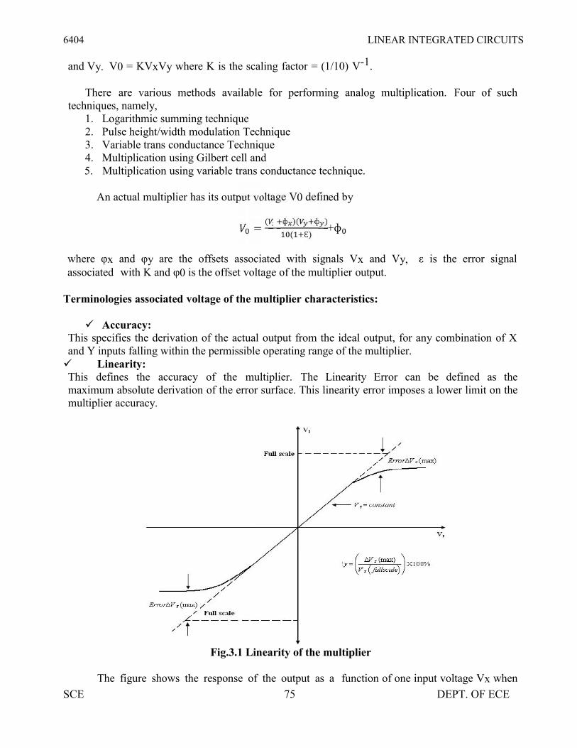
6404 LINEAR INTEGRATED CIRCUITS
SCE 75 DEPT. OF ECE
and Vy. V0 = KVxVy where K is the scaling factor = (1/10) V-1.
There are various methods available for performing analog multiplication. Four of suchtechniques, namely,
1. Logarithmic summing technique2. Pulse height/width modulation Technique3. Variable trans conductance Technique4. Multiplication using Gilbert cell and5. Multiplication using variable trans conductance technique.
An actual multiplier has its output voltage V0 defined by= ( ф )( ф )( Ɛ) +фwhere φx and φy are the offsets associated with signals Vx and Vy, ε is the error signalassociated with K and φ0 is the offset voltage of the multiplier output.
Terminologies associated voltage of the multiplier characteristics:
Accuracy:This specifies the derivation of the actual output from the ideal output, for any combination of Xand Y inputs falling within the permissible operating range of the multiplier. Linearity:This defines the accuracy of the multiplier. The Linearity Error can be defined as themaximum absolute derivation of the error surface. This linearity error imposes a lower limit on themultiplier accuracy.
Fig.3.1 Linearity of the multiplier
The figure shows the response of the output as a function of one input voltage Vx when

6404 LINEAR INTEGRATED CIRCUITS
SCE 76 DEPT. OF ECE
the other Vy is assumed constant. It represents the maximum percentage derivation from the idealstraight line output. An error surface is formed by plotting the output for different combinationsof X and Y inputs.
Square law accuracy:The Square – law curve is obtained with the X and Y inputs connected together and applied withthe same input signal. The maximum derivation of the output voltage from an ideal square –law
curve expresses the squaring mode accuracy.
Fig. 3.2 squaring mode accuracy
Bandwidth:The Bandwidth indicates the operating capability of an analog multiplier at higher frequencyvalues. Small signal 3 dB bandwidth defines the frequency f0 at which the output reduces by 3dBfrom its low frequency value for a constant input voltage. This is identified individually for the Xand Y input channels normally.
The transconductance bandwidth represents the frequency at which the transconductanceof the multiplier drops by 3dB of its low frequency value. This characteristic defines theapplication frequency ranges when used for phase detection or AM detection.
Quadrant:
The quadrant defines the applicability of the circuit for bipolar signals at its inputs. First – quadrantdevice accepts only positive input signals, the two quadrant device accepts one bipolar signal andone unipolar signal and the four quadrant device accepts two bipolar signals.
Logarithmic summing Technique:
This technique uses the relationship lnVx + lnVy =ln(VxVy)As shown in figure the input voltages Vx and Vy are converted to their logarithmicequivalent, which are then added together by a summer. An antilogarithmic converterproduces the output voltage of the summer. The output is given by,
Vz = ln-1 (ln(Vx Vy )) = Vx Vy .

6404 LINEAR INTEGRATED CIRCUITS
SCE 77 DEPT. OF ECE
Fig. 3.3 logarithmic summing method
The relationship between I0 and VBE of the transistor is given by IC = I0e(VBE /VT ) .Itis found that the transistor follows the relationship very accurately in the range of 10nA to100mA. Logarithmic multiplier has low accuracy and high temperature instability. This methodis applicable only to positive values of Vx and Vy.
Limitation: this type of multiplier is restricted to one quadrant operation only.
Pulse Height/ Width Modulation Technique:
Fig.3.4 Pulse Height/ Width Modulation Technique
In this method, the pulse width of a pulse train is made proportional to one input voltageand the pulse amplitude is made proportional to the second input voltage. Therefore, Vx =Kx A,Vy =Ky t, and Vz =Kz T where Kx, Ky, Kz are scaling factors. In figure A is the amplitude of thepulse, t is the pulse width and T is the area of the pulse. Therefore,= =The modulated pulse train is passed through an integrated circuit. Therefore, the input of theintegrator is proportional to the area of pulse, which in turn is proportional to the product of twoinput voltages.
3.1 Analog multiplier using an Emitter coupled Transistor pair:
The output currents IC1 a n d IC2 are related to the differential input voltage V1 by= / and = /

6404 LINEAR INTEGRATED CIRCUITS
SCE 78 DEPT. OF ECE
Fig.3.5 multiplier circuit using an emitter coupled pair
where V i s thermal voltage and the base currents have been neglected. Combining above eqn.,difference between the two output currents as
IC =IC1 – IC = / − / =I EE tanh (V1/2VT)The dc transfer characteristics of the emitter – coupled pair is shown in figure. It shows that theemitter coupled pair can be used as a simple multiplier using this configuration. When thedifferential input voltage V1 << VT, we can appropriate as given by
IC =I EE (V1/2VT)The current IEE is the bias current for the emitter – coupled pair. If the current IEE is madeproportional to a second input signal V2, thenIEE =K0 (V 2 - V BE)/2VT
Substituting above eqn. , we get IC = K 0 V1 (V2 - V BE)/2VT
Fig. 3.6 DC Transfer characteristics of emitter coupled pair
This arrangement is shown in figure. It is a simple modulator circuit constructed using adifferential amplifier. It can be used as a multiplier, provided V1 is small and much less than50mV and V2 is greater than VBE (on). But, the multiplier circuit shown in figure has severallimitations. The first limitation is that V2 is offset by VBE (on).

6404 LINEAR INTEGRATED CIRCUITS
SCE 79 DEPT. OF ECE
Fig. 3.7 A simple modulator using a differential amplifier
The second is that V2 must always be positive which results in only a two-quadrant multiplieroperation. The third limitation is that, the tanh (X) is approximately as X, where X = V1 /2VT.The first two limitations are overcome in the Gilbert cell.
3.2 Gilbert Multiplier cell:
The Gilbert multiplier cell is a modification of the emitter coupled cell and this allows four –quadrant multiplication. Therefore, it forms the basis of most of the integrated circuit balancedMultipliers. Two cross- coupled emitter- coupled pairs in series connection with an emitter coupledpair form the structure of the Gilbert multiplier cell.
Fig. 3.8 Gilbert multiplier cell
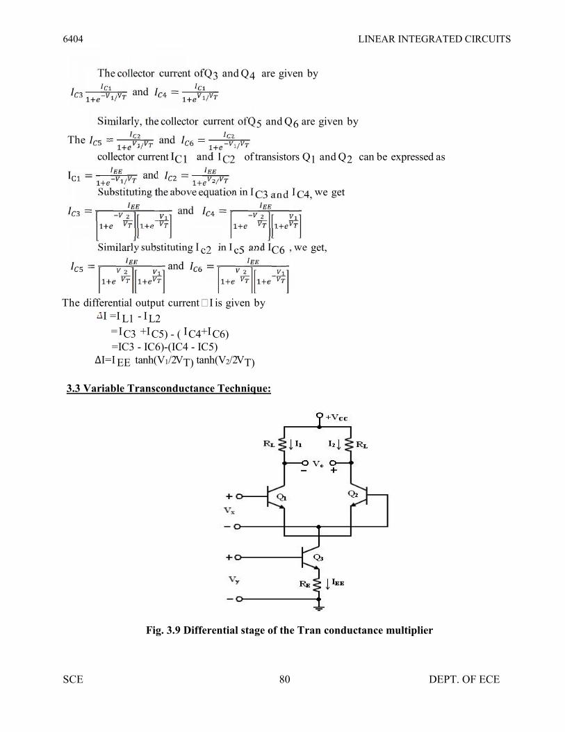
6404 LINEAR INTEGRATED CIRCUITS
SCE 80 DEPT. OF ECE
The collector current ofQ3 and Q4 are given by
/ and = /Similarly, the collector current ofQ5 and Q6 are given by
The = / and = /collector current IC1 and IC2 of transistors Q1 and Q2 can be expressed asI = / and = /Substituting the above equation in IC3 and IC4, we get= and =Similarly substituting I c2 in I c5 and IC6 , we get,= and =
The differential output current I is given byI =I L1 - IL2
=IC3 +IC5) - ( IC4+IC6)=IC3 - IC6)-(IC4 - IC5)∆I=I EE tanh(V1/2VT) tanh(V2/2VT)
3.3 Variable Transconductance Technique:
Fig. 3.9 Differential stage of the Tran conductance multiplier

6404 LINEAR INTEGRATED CIRCUITS
SCE 81 DEPT. OF ECE
o The variable transconductance technique makes use of the dependence characteristic of thetransistor transconductance parameter on the emitter current bias applied. A simple
differential circuit arrangement depicting the principle is shown in figure. The relationship between V0 and Vx . is given by V0 = gm RL VX where gm = IEE /VT is the
transconductance of the stage. Application of a second input Vy to the reference current source of the differential amplifier
can vary gm. Thus, if RE IEE >>VBE, the bias voltage Vy is related to IEE by the relation Vy = IEE RE.
Then, the overall voltage transfer expression is given byo V0 = gm RLVx = (Vy/VTRE)VxRL
= VxVy RL/ VTRE
3.4 Analog Multiplier ICs
Analog multiplier is a circuit whose output voltage at any instant is proportional to theproduct of instantaneous value of two individual input voltages.
Important applications of these multipliers are multiplication, division, squaring andsquare – rooting of signals, modulation and demodulation.
These analog multipliers are available as integrated circuits consisting of op-amps andother circuit elements. The Schematic of a typical analog multiplier, namely, AD633 is shown infigure.
Fig. 3.10 Multiplier IC and its symbol
The AD633 multiplier is a four – quadrant analog multiplier. It possesses high input impedance; this characteristic makes the loading effect on the signal
source negligible. It can operate with supply voltages ranging from ±18V. The

6404 LINEAR INTEGRATED CIRCUITS
SCE 82 DEPT. OF ECE
IC does not require external components. The typical range of the two input signals is ±10V.
Schematic representation of a multiplier:The schematic representation of an analog multiplier is shown in figure. The output V0 isthe product of the two inputs Vx and Vy is divided by a reference voltage Vref. Normally, thereference voltage Vref is internally set to 10V. Therefore, V0 =VxVy/10. In other words, thebasic input – output relationship can be defined by KVx Vy when K = 1/10, a constant. Thus forpeak input voltages of 10V, the peak magnitude of output voltage is 1/10 *10 *10 =10V. Thus, itcan be noted that, as long as Vx < 10V and Vy < 10V, the multiplier output will not saturate.Multiplier quadrants:The transfer characteristics of a typical four-quadrant multiplier are shown in figure. Both theinputs can be positive or negative to obtain the corresponding output as shown in the transfercharacteristics.Applications of Multiplier ICs:The multiplier ICs are used for the following purposes:
1. Voltage Squarer2. Frequency doublers3. Voltage divider4. Square rooter5. Phase angle detector6. Rectifier
Fig.3.11 Transfer characteristics of a typical four-quadrant multiplier
Voltage Squarer:
Fig. 3.12 voltage squarer circuit

6404 LINEAR INTEGRATED CIRCUITS
SCE 83 DEPT. OF ECE
Figure shows the multiplier IC connected as a squaring circuit. The inputs can be positive ornegative, represented by any corresponding voltage level between 0 and 10V. The input voltage Vito be squared is simply connected to both the input terminals, and hence we have, Vx = Vy = Viand the output is V0 = KVi2. The circuit thus performs the squaring operation. This applicationcan be extended for frequency doubling applications.
Frequency doublers:
Figure shows the squaring circuit connected for frequency doubling operation. A sine-wave signalVi has a peak amplitude of Av and frequency of f Hz. Then, the output voltage of the doublerscircuit is given by= ∗ = sin 2 = (1 − cos4 )
Assuming a peak amplitude Av of 5V and frequency f of 10KHz, V0 =1.25–1.25 cos2 20000) t.The first term represents the dc term of 1.25V peak amplitude. The input and output waveforms areshown in figure. The output waveforms ripple with twice the input frequency in the rectified outputof the input signal. This forms the principle of application of analog multiplier as rectifier of acsignals.
(a)
(b)Fig. 3.13 (a) circuit diagram and (b) input –output waveform of frequency doubler

6404 LINEAR INTEGRATED CIRCUITS
SCE 84 DEPT. OF ECE
The dc component of output V0 can be removed by connecting a 1µF coupling capacitorbetween the output terminal and a load resistor, across which the output can be observed.
Voltage Divider:
In voltage divider circuit the division is achieved by connecting the multiplier in the feedback loopof an op-amp.The voltages Vden and Vnum represent the two input voltages, Vdm forms one input of themultiplier, and output of op-amp VoA forms the second input.The output VOA forms the second input. The output VOM of the multiplier is connected back ofop- amp in the feedback loop. Then the characteristic operation of the multiplier givesVom = KVOA Vdm (1)
Fig 3.14 divider circuit
As shown in figure, no input signal current can flow into the inverting input terminal of op-amp,which is at virtual ground. Therefore, at the junction a, i1 +i2 =0, the current i1 = Vnum / R,where R is the input resistance and the current i2 = Vom /R. With virtual ground existing at a,
i1+i2 = Vnum / R + Vom /R = 0KV OA V den = - V num orvoA=- vnum/Kvden
where Vnum and Vden are the numerator and denominator voltages respectively. Therefore,the voltage division operation is achieved. Vnum can be a positive or negative voltage and Vdencan have only positive values to ensure negative feedback. When Vdm is changed, the gain10/Vdm changes, and this feature is used in automatic gain control (AGC) circuits.
Square Rooter:
The divider voltage can be used to find the square root of a signal by connecting both inputs ofthe multiplier to the output of the op-amp. Substituting equal in magnitude but opposite inpolarity (with respect to ground) to Vi. But we know that Vom is one- term (Scale factor) of V0 *V0 or -Vi = Vom = V2/1 0
Solving for V0 and eliminating √-1 yields. V0 = √10|Vi |Eqn. states that V0 equals the square root of 10 times the absolute magnitude of Vi.

6404 LINEAR INTEGRATED CIRCUITS
SCE 85 DEPT. OF ECE
1
The input voltage Vi must be negative, or else, the op-amp saturates.The range of Vi is between -1 and -10V. Voltages less than -1V will cause inaccuracies in theresult.The diode prevents negative saturation for positive polarity Vi signals. For positive values of Vi
the diode connections are reversed.
Phase Angle detector:
The multiplier configured for phase angle detection measurement is shown in figure. When twosine-waves of the same frequency are applied to the inputs of the multiplier, the output V0 has adc component and an AC component.
The trigonometric identity shows that Sin A sin B =1/2 (cos (A-B) – cos (A+B)).When the two frequencies are equal, but with different phase angles, e.g. A=2πft +θ for signal Vxand B= 2πft for signal Vy, then using the identity
[sin (2 ft+ )][sin2 ft)]=1/2[cos -cos(4 ft + )]=1/2(dc- the double frequency term)Therefore, when the two input signals Vx and Vy are applied to the multiplier, V0 (dc) is given by( ) = coswhere Vxp and Vyp are the peak voltage amplitudes of the signals Vx and Vy. Thus, the outputV0(dc) depends on the factor cos θ. A dc voltmeter can be calibrated as a phase angle meterwhen the product of Vxp and Vyp is made equal to 20. Then, a (0-1) V range dc voltmeter candirectly read cos θ, with the meter calibrated directly in degrees from a cosine table. The inputand output waveforms are shown in figure.Then the above eqn becomes V0 (dc) = cos θ, if we make the product Vxp Vyp = 20 or in otherwords, Vxp – Vyp = 4.47V.
Fig 3.15 Phase angle measurement circuit diagram

6404 LINEAR INTEGRATED CIRCUITS
SCE 86 DEPT. OF ECE
Fig. 3.16 input- output waveforms of phase angle detector

6404 LINEAR INTEGRATED CIRCUITS
SCE 87 DEPT. OF ECE
fOUT
3.5 Operation of Basic Phase Locked Loop
Input frequency
Fig 3.17 Block diagram of PLL
The PLL consists of i) Phase detector ii) LPF iii) VCO. The phase detector or comparatorcompares the input frequency fIN with feedback frequency fOUT. The output of the phase detector is proportional to the phase difference between fIN & fOUT.
The output of the phase detector is a dc voltage & therefore is often referred to as the errorvoltage.
The output of the phase detector is then applied to the LPF, which removes the highfrequency noise and produces a dc level. This dc level in turn, is input to the VCO.
The output frequency of VCO is directly proportional to the dc level. The VCO frequencyis compared with input frequency and adjusted until it is equal to the input frequencies.
PLL goes through 3 states, i) free running ii) Capture iii) Phase lock.Before the input is applied, the PLL is in free running state. Once the input frequency is
applied the VCO frequency starts to change and PLL is said to be in the capture mode.The VCO frequency continuous to change until it equals the input frequency and the PLL isin phase lock mode. When Phase locked, the loop tracks any change in the input frequencythrough its repetitive action.
If an input signal vs of frequency fs is applied to the PLL, the phase detector compares thephase and frequency of the incoming signal to that of the output vo of the VCO. If the twosignals differ in frequency of the incoming signal to that of the output vo of the VCO.
The phase detector is basically a multiplier and produces the sum (fs + fo) and difference(fs - fo) components at its output.
The high frequency component (fs + fo) is removed by the low pass filter and the differencefrequency component is amplified then applied as control voltage vc to VCO.
The signal vc shifts the VCO frequency in a direction to reduce the frequency differencebetween fs and fo. Once this action starts, we say that the signal is in the capture range. TheVCO continues to change frequency till its output frequency is exactly the same as the inputsignal frequency. The circuit is then said to be locked. Once locked, the output frequency foof VCO is identical to fs except for a finite phase difference φ. This phase difference φgenerates a corrective control voltage vc to shift the VCO frequency from f0 to fs andthereby maintain the lock. Once locked, PLL tracks the frequency changes of the input signal.Thus, a PLL goes through three stages (i) free running, (ii) capture and (iii) locked or tracking.Capture range: the range of frequencies over which the PLL can acquire lock with an inputsignal is called the capture range. This parameter is also expressed as percentage of fo.
Voltagecontrolledoscillator
Phasedetector
Lowpassfilter
6404 LINEAR INTEGRATED CIRCUITS
SCE 88 DEPT. OF ECE
Pull-in time: the total time taken by the PLL to establish lock is called pull-in time. Thisdepends on the initial phase and frequency difference between the two signals as well as on theoverall loop gain and loop filter characteristics.
3.5.1 Phase Detector
Phase detector compares the input frequency and VCO frequency and generates DCvoltage i.e., proportional to the phase difference between the two frequencies. Depending onwhether the analog/digital phase detector is used, the PLL is called either an analog/digitaltype respectively. Even though most monolithic PLL integrated circuits use analog phasedetectors.Ex for Analog: Double-balanced mixerEx for Digital: Ex-OR, Edge trigger, monolithic Phase detector. Ex-OR Phase Detector:
This uses an exclusive OR gate. The output of the Ex-OR gate is high only when fIN or fOUT ishigh.The DC output voltage of the Ex-OR phase detector is a function of the phase differencebetween its two outputs. The maximum dc output voltage occurs when the phase difference is Πradians or180 degrees. The slope of the curve between 0 or Π radians is the conversion gain kp of thephase detector for eg; if the Ex-OR gate uses a supply voltage Vcc = 5V, the conversion gain Kp is
.Advantages of Edge Triggered Phase Detector over Ex-OR arei) The dc output voltage is linear over 2Π radians or 360 degrees, but in Ex-OR it is Π radiansor 180 degrees.ii) Better Capture, tracking & locking characteristics.Edge triggered type of phase detector using RS Flip – Flop. It is formed from a pair of crosscoupled NOR gates.RS FF is triggered, i.e., the output of the detector changes its logic state on the positive edge of theinputs fIN & fOUT Monolithic Phase detector:
It consists of 2 digital phase detector, a charge pump and an amplifier. Phase detector 1 is used in applications that require zero frequency and phase difference
at lock. Phase detector 2, if quadrature lock is desired, when detector 1 is used in the main
loop, detector can also be used to indicate whether the main loop is in lock or out of lock.
3.5.2 Low – Pass filter
The function of the LPF is to remove the high frequency components in the output ofthe phase detector and to remove the high frequency noise. LPF controls the characteristicsof the phase locked loop. i.e., capture range, lock ranges, bandwidth Lock range(Tracking range):

6404 LINEAR INTEGRATED CIRCUITS
SCE 89 DEPT. OF ECE
The lock range is defined as the range of frequencies over which the PLL systemfollows the changes in the input frequency fIN.
Capture range:Capture range is the frequency range in which the PLL acquires phase lock. Capturerange is always smaller than the lock range.
Filter Bandwidth:Filter Bandwidth is reduced, its response time increases. However reducedBandwidth reduces the capture range of the PLL. Reduced Bandwidth helps to keep theloop in lock through momentary losses of signal and also minimizes noise.
3.5.4 Voltage Controlled Oscillator (VCO):
The third section of PLL is the VCO; it generates an output frequency that isdirectly proportional to its input voltage. The maximum output frequency of NE/SE 566 is 500Khz.
3.5.5 Feedback path and optional divider:
Most PLLs also include a divider between the oscillator and the feedback input to the phasedetector to produce a frequency synthesizer. A programmable divider is particularly useful in radioTransmitter applications, since a large number of transmit frequencies can be produced froma single stable, accurate, but expensive, quartz crystal–controlled reference oscillator.Some PLLs also include a divider between the reference clock and the reference input to thephase detector. If this divider divides by M, it allows the VCO to multiply the referencefrequency by N / M. It might seem simpler to just feed the PLL a lower frequency, but insome cases the reference frequency may be constrained by other issues, and then the referencedivider is useful.Frequency multiplication in a sense can also be attained by locking the PLL to the 'N'thharmonic of the signal.
The equations governing a phase-locked loop with an analog multiplier as the phasedetector may be derived as follows. Let the input to the phase detector be xc(t) and the outputof the voltage- controlled oscillator (VCO) is xr(t) with frequency ωr(t), then the output ofthe phase detector xm(t) is given by
the VCO frequency may be written as a function of the VCO input y(t) as
where gv is the sensitivity of the VCO and is expressed in Hz / V.Hence the VCO output takes the form
where
The loop filter receives this signal as input and produces an outputxf(t) = Ffilter(xm(t))
where Filter is the operator representing the loop filter transformation.
When the loop is closed, the output from the loop filter becomes the input to the VCO thusy(t) = xf(t) = Ffilter(xm(t))

6404 LINEAR INTEGRATED CIRCUITS
SCE 90 DEPT. OF ECE
We can deduce how the PLL reacts to a sinusoidal input signal:xc(t) = Acsin(ωct).
The output of the phase detector then is:
This can be rewritten into sum and difference components using trigonometric identities:
As an approximation to the behaviour of the loop filter we may consider only the differencefrequency being passed with no phase change, which enables us to derive a small-signal model
Of the phase-locked loop. If we can make ≈ then the sin (.)can be approximated by its
argument resulting in: . The phase-locked loop is said to be locked ifthis is the case.
3.6 Control System Analysis/ Closed Loop Analysis Of PLL
Phase locked loops can also be analyzed as control systems by applying the Laplace transform.The loop response can be written as:
Where
θo is the output phase in radians θi is the input phase in radians Kp is the phase detector gain in volts per radian Kv is the VCO gain in radians per volt-second F(s) is the loop filter transfer function (dimensionless)
The loop characteristics can be controlled by inserting different types of loop filters. The simplestfilter is a one-pole RC circuit. The loop transfer function in this case is:
The loop response becomes:
This is the form of a classic harmonic oscillator. The denominator can be related to that of asecond order system:
Where
ζ is the damping factor ωn is the natural frequency of the loop.
For the one-pole RC filter,

6404 LINEAR INTEGRATED CIRCUITS
SCE 91 DEPT. OF ECE
The loop natural frequency is a measure of the response time of the loop, and the damping factor isa measure of the overshoot and ringing. Ideally, the natural frequency should be high and thedamping factor should be near 0.707 (critical damping). With a single pole filter, it is not possibleto control the loop frequency and damping factor independently. For the case of critical damping,
A slightly more effective filter, the lag-lead filter includes one pole and one zero. This can berealized with two resistors and one capacitor. The transfer function for this filter is
This filter has two time constants
τ1 = C(R1 + R2) τ2= CR2
Substituting above yields the following natural frequency and damping factor
The loop filter components can be calculated independently for a given natural frequency anddamping factor
Real world loop filter design can be much more complex eg using higher order filters to reducevarious types or source of phase noise.
Applications of PLL:The PLL principle has been used in applications such as FM stereo decoders

6404 LINEAR INTEGRATED CIRCUITS
SCE 92 DEPT. OF ECE
motor speed control tracking filters FM modulation and demodulation FSK modulation Frequency multiplier Frequency synthesis etc.,
Example PLL ICs:560 series (560, 561, 562, 564, 565 & 567)
3.7 Voltage Controlled Oscillator:
Fig. 3.18 Pin diagram and block diagram of VCO
Referring to the circuit in the above figure, the capacitor c1 is linearly charged or discharged by aconstant current source/sink. The amount of current can be controlled by changing the voltage vcapplied at the modulating input (pin 5) or by changing the timing resistor R1 external to the ICchip. The voltage at pin 6 is held at the same voltage as pin 5.
Thus, if the modulating voltage at pin 5 is increased, the voltage at pin 6 alsoincreases, resulting in less voltage across R1 and thereby decreasing the charging current.
The voltage across the capacitor C1 is applied to the inverting input terminal of Schmitttrigger via buffer amplifier. The output voltage swing of the Schmitt trigger is designed to Vcc and1.5 Vcc. If Ra = Rb in the positive feedback loop, the voltage at the non-inverting input terminalof Schmitt trigger swings from 0.5 Vcc to 0.25 Vcc.
When the voltage on the capacitor c1 exceeds 0.5 Vcc during charging, the output of theSchmitt trigger goes LOW (0.5 Vcc). The capacitor now discharges and when it is at 0.25Vcc, the output of Schmitt trigger goes HIGH (Vcc). Since the source and sink currents areequal, capacitor charges and discharges for the same amount of time. This gives a triangularvoltage waveform across c1 which is also available at pin 4.
The square wave output of the Schmitt trigger is inverted by buffer amplifier at pin 3. Theoutput waveforms are shown near the pins 4 and 3.
The output frequency of the VCO can be given as follows:
where V+ is Vcc.The output frequency of the VCO can be changed either by (i) R1, (ii) c1 or (iii) the
voltage vc at the modulating input terminal pin 5. The voltage vc can be varied by connecting a

6404 LINEAR INTEGRATED CIRCUITS
SCE 93 DEPT. OF ECE
R1R2 circuit as shown in the figure below. The components R1and c1 are first selected sothat VCO output frequency lies in the centre of the operating frequency range.
Now the modulating input voltage is usually varied from 0.75 Vcc to Vcc which canproduce a frequency variation of about 10 to 1.
The signetics NE/SE 560 series is monolithic phase locked loops. The SE/NE 560, 561,562, 564, 565 & 567 differ mainly in operating frequency range, poser supply requirements &frequency & bandwidth adjustment ranges.
3.8 Monolithic Phase Locked Loops (PLL IC 565):
Pin Configuration of PLL IC 565
Basic Block Diagram Representation of IC 565
The important electrical characteristics of the 565 PLL are, Operating frequency range: 0.001Hz to 500 Khz. Operating voltage range: ±6 to ±12v Input level required for tracking: 10mv rms min to 3 Vpp max Input impedance: 10 K ohms typically. Output sink current: 1mA Output source current: 10 mA
Fig. 3.19 External connections of VCO

6404 LINEAR INTEGRATED CIRCUITS
SCE 94 DEPT. OF ECE
The center frequency of the PLL is determined by the free running frequency of the VCO, which isgiven by
fOUT = 1.2/ 4R1C1where R1&C1 are an external resistor & a capacitor connected to pins 8 & 9.
The VCO free-running frequency fOUT is adjusted externally with R1 & C1 to be at the center ofthe input frequency range.
C1 can be any value; R1 must have a value between 2 k ohms and 20 K ohms. Capacitor C2 connected between 7 & +V. The filter capacitor C2 should be large enough to eliminate variations in the demodulated
output voltage in order to stabilize the VCO frequency.The lock range fL & capture range fc of PLL is given by,
fL= ±7.8 fout/ V Hz
Where fOUT = free running frequency of VCO (Hz)V = (+Vcc)-(-Vcc) voltsfC=±[ fL/(2Π)(3.6)(103)C2 ]½
5.9 Monolithic PLL IC 565 applications:
The output from a PLL system can be obtained either as the voltage signal vc(t)corresponding to the error voltage in the feedback loop, or as a frequency signal at VCOoutput terminal. The voltage output is used in frequency discriminator applications whereas thefrequency output is used in signal conditioning, frequency synthesis or clock recovery applications.

6404 LINEAR INTEGRATED CIRCUITS
SCE 95 DEPT. OF ECE
The circuit diagram of LM565 PLL
When PLL is locked to an input frequency, the error voltage vc(t) is proportional to (fs-fo). If theinput frequency is varied as in the case of FM signal vc will also vary in order to maintain thelock. Thus the voltage output serves as a frequency discriminator which converts the inputfrequency changes to voltage changes.
In the case of frequency output, if the input signal is comprised of many frequencycomponents corrupted with noise and other disturbances, the PLL can be made to lock,selectively on one particular frequency component at the input. The output of VCO wouldthen regenerate that particular frequency (because of LPF which gives output for beat frequency)and attenuate heavily other frequencies. VCO output thus can be used for regenerating orreconditioning a desired frequency signal (which is weak and buried in noise) out of manyundesirable frequency signals.Some of the typical applications of PLL are discussed below.
Frequency Multiplier:
Frequency divider is inserted between the VCO & phase comparator. Since the output of thedivider is locked to the fIN, VCO is actually running at a multiple of the input frequency.The desired amount of multiplication can be obtained by selecting a proper divide-by-Nnetwork, where N is an integer.

6404 LINEAR INTEGRATED CIRCUITS
SCE 96 DEPT. OF ECE
Fig. 3.20 Frequency multiplier using PLL
Frequency Shift Keying (FSK) demodulator:
In computer peripheral & radio (wireless) communication the binary data or code istransmitted by means of a carrier frequency that is shifted between two preset frequencies. Since acarrier frequency is shifted between two preset frequencies, the data transmission is said to use aFSK. The frequency corresponding to logic 1 & logic 0 states are commonly called the mark &space frequency.For example, When transmitting teletype writer information using a modulator-demodulator(modem) a 1070-1270 (mark-space) pair represents the originate signal, while a 2025-2225 Hz(mark-space) pair represents the answer signal.

6404 LINEAR INTEGRATED CIRCUITS
SCE 97 DEPT. OF ECE
FSK Generator:
The FSK generator is formed by using a 555 as an astable multivibrator, whose frequency iscontrolled by the state of transistor Q1.
In other words, the output frequency of the FSK generator depends on the logic state of thedigital data input.
150 Hz is one the standards frequencies at which the data are commonly transmitted. When the input is logic 1, the transistor Q1 is off. Under the condition, 555 timer works in its
normal mode as an astable multivibrator i.e., capacitor C charges through RA & RB to 2/3Vcc & discharges through RB to 1/3 Vcc. Thus capacitor C charges & discharges between 2/3Vcc & 1/3 Vcc as long as the input is logic 1.
The frequency of the output waveform is given by,1.45
fo=-------------- = 1070 Hz (mark frequency)(RA +2RB)C
When the input is logic 0, (Q1 is ON saturated) which in turn connects the resistance Rc acrossRA. This action reduces the charging time of capacitor C1 increases the output frequency,which is given by,
1.45fo= ------------------ = 1270 Hz (space frequency)
(RA || RC+2 RB)C By proper selection of resistance Rc, this frequency is adjusted to equal the space frequency of
1270 Hz. The difference between the FSK signals of 1070 Hz & 1270 Hz is 200 Hz, thisdifference is called “frequency shift”.
The output 150 Hz can be made by connecting a voltage comparator between the output of theladder filter and pin 6 of PLL.
The VCO frequency is adjusted with R1 so that at fIN = 1070 Hz.

6404 LINEAR INTEGRATED CIRCUITS
SCE 98 DEPT. OF ECE
FSK Demodulator: The output of 555 FSK generators is applied to the 565 FSK demodulator. Capacitive coupling is used at the input to remove dc line. At the input of 565, the loop locks to the input frequency & tracks it between the 2 frequencies. R1 & C1 determine the free running frequency of the VCO, 3 stages RC ladder filter is used
to remove the carrier component from the output.
Applications:
In digital data communication and computer peripheral, binary data is transmitted by means of acarrier frequency which is shifted between two preset frequencies. This type of data transmission iscalled frequency shift keying (FSK) technique. The binary data can be retrieved using FSKdemodulator. The figure below shows FSK demodulator using PLL for tele-typewriter signals of1070 Hz and 1270 Hz. As the signal appears at the input, the loop locks to the input frequency andtracks it between the two frequencies with a corresponding dc shift at the output. A three stagefilter removes the carrier component and the output signal is made logic compatible by a voltagecomparator.
Fig. 3.21 FSK demodulator circuit
AM Demodulation:
A PLL may be used to demodulate AM signals as shown in the figure below. The PLL islocked to the carrier frequency of the incoming AM signal. The output of VCO which hasthe same frequency as the carrier, but unmodulated is fed to the multiplier. Since VCOoutput is always 900 before being fed to the multiplier. This makes both the signalsapplied to the multiplier and the difference signals, the demodulated output is obtainedafter filtering high frequency components by the LPF. Since the PLL responds only tothe carrier frequencies which are very close to the VCO output, a PLL AM detectorexhibits high degree of selectivity and noise immunity which is not possible withconventional peak detector type AM modulators.

6404 LINEAR INTEGRATED CIRCUITS
SCE 99 DEPT. OF ECE
Fig.3.22 AM demodulator FM Demodulation:
If PLL is locked to a FM signal, the VCO tracks the instantaneous frequency of the inputsignal. The filtered error voltage which controls the VCO and maintains lock with the inputsignal is the demodulated FM output.
The VCO transfer characteristics determine the linearity of the demodulated output.Since, VCO used in IC PLL is highly linear, it is possible to realize highly linear FMdemodulators.
Frequency multiplication/division:
The block diagram shown below shows a frequency multiplier/divider using PLL. A divide by Nnetwork is inserter between the VCO output and the phase comparator input. In the locked state,the VCO output frequency fo is given by fo = Nfs. The multiplication factor can be obtained byselecting a proper scaling factor N of the counter.
Frequency multiplication can also be obtained by using PLL in its harmonic locking mode.If the input signal is rich in harmonics e.g. square wave, pulse train etc., then the VCO can bedirectly locked to the n-th harmonic of the input signal without connecting any frequencydivider in between. However, as the amplitude of the higher order harmonics becomes less,effective locking may not take place for high values of n. Typically n is kept less than 10.

6404 LINEAR INTEGRATED CIRCUITS
SCE 100 DEPT. OF ECE
Fig. 3.23 Frequency Divider
The circuit of the figure above can also be used for frequency division. Since the VCOoutput (a square wave) is rich in harmonics, it is possible to lock the m-th harmonic of the VCOoutput with the input signal fs. The output fo of VCO is now given by fo=fs/m PLL Frequency Synthesis:
In digital wireless communication systems (GSM, CDMA etc), PLL's are used to provide theLocal Oscillator (LO) for up-conversion during transmission, and down-conversion duringreception. In most cellular handsets this function has been largely integrated into a singleintegrated circuit to reduce the cost and size of the handset.
However due to the high performance required of base station terminals, the transmissionand reception circuits are built with discrete components to achieve the levels of performancerequired. GSM LO modules are typically built with a Frequency Synthesizer integrated circuit,and discrete resonator VCO's.
Principle of PLL synthesizers
A phase locked loop does for frequency what the Automatic Gain Control does forvoltage. It compares the frequencies of two signals and produces an error signal which isproportional to the difference between the input frequencies.
The error signal is then low pass filtered and used to drive a voltage-controlled oscillator(VCO) which creates an output frequency. The output frequency is fed through a frequencydivider back to the input of the system, producing a negative feedback loop.
If the output frequency drifts, the error signal will increase, driving the frequency in theopposite direction so as to reduce the error. Thus the output is locked to the frequency at theother input. This input is called the reference and is derived from a crystal oscillator, which is verystable in frequency.
The block diagram below shows the basic elements and arrangement of a PLL basedfrequency synthesizer.
Fig. 2.24 PLL based frequency synthesizer
The key to the ability of a frequency synthesizer to generate multiple frequencies is thedivider placed between the output and the feedback input. This is usually in the form of a digitalcounter, with the output signal acting as a clock signal.

6404 LINEAR INTEGRATED CIRCUITS
SCE 101 DEPT. OF ECE
The counter is preset to some initial count value, and counts down at each cycle of theclock signal. When it reaches zero, the counter output changes state and the count value isreloaded.
This circuit is straightforward to implement using flip-flops, and because it is digital innature, is very easy to interface to other digital components or a microprocessor. This allows thefrequency output by the synthesizer to be easily controlled by a digital system.Example:Suppose the reference signal is 100 kHz, and the divider can be preset to any value between 1 and100. The error signal produced by the comparator will only be zero when the output of the divideris also 100 kHz. For this to be the case, the VCO must run at a frequency which is 100 kHz x thedivider count value.
Thus it will produce an output of 100 kHz for a count of 1, 200 kHz for a count of 2, 1MHz for a count of 10 and so on. Note that only whole multiples of the reference frequencycan be obtained with the simplest integer N dividers. Fractional N dividers are readily availablePractical considerations:In practice this type of frequency synthesizer cannot operate over a very wide range of frequencies,because the comparator will have a limited bandwidth and may suffer from aliasing problems. Thiswould lead to false locking situations, or an inability to lock at all. In addition, it is hard to make ahigh frequency VCO that operates over a very wide range.
This is due to several factors, but the primary restriction is the limited capacitance rangeof varactor diodes. However, in most systems where a synthesizer is used, we are not after ahuge range, but rather a finite number over some defined range, such as a number of radiochannels in a specific band.
Many radio applications require frequencies that are higher than can be directly input to thedigital counter. To overcome this, the entire counter could be constructed using high-speed logicsuch as ECL, or more commonly, using a fast initial division stage called a prescaler whichreduces the frequency to a manageable level.
Since the prescaler is part of the overall division ratio, a fixed prescaler can causeproblems designing a system with narrow channel spacing’s - typically encountered in radioapplications. This can be overcome using a dual-modulus prescaler.
Further practical aspects concern the amount of time the system can switch fromchannel to channel, time to lock when first switched on, and how much noise there is in theoutput. All of these are a function of the loop filter of the system, which is a low-pass filterplaced between the output of the frequency comparator and the input of the VCO.
Usually the output of a frequency comparator is in the form of short error pulses, but theinput of the VCO must be a smooth noise- free DC voltage. (Any noise on this signal naturallycauses frequency modulation of the VCO.).
Heavy filtering will make the VCO slow to respond to changes, causing drift and slowresponse time, but light filtering will produce noise and other problems with harmonics. Thus thedesign of the filter is critical to the performance of the system and in fact the main area that adesigner will concentrate on when building a synthesizer system.

6404 LINEAR INTEGRATED CIRCUITS
SCE 102 DEPT. OF ECE
UNIT IVANALOG TO DIGITAL & DIGITAL TO ANALOG CONVERTERS
4. 1 1Analog To Digital Conversion
The natural state of audio and video signals is analog. When digital technology was not yetaround, they are recorded or played back in analog devices like vinyl discs and cassette tapes. Thestorage capacity of these devices is limited and doing multiple runs of re-recording and editingproduced poor signal quality. Developments in digital technology like the CD, DVD, Blu-ray,flash devices and other memory devices addressed these problems.
For these devices to be used, the analog signals are first converted to digital signalsusing analog to digital conversion (ADC). For the recorded audio and video signals to beheard and viewed again, the reverse process of digital to analog conversion (DAC) is used.
ADC and DAC are also used in interfacing digital circuits to analog systems. Typicalapplications are control and monitoring of temperature, water level, pressure and other real-worlddata.
An ADC inputs an analog signal such as voltage or current and outputs a digital signal inthe form of a binary number. A DAC, on the other hand, inputs the binary number and outputsthe corresponding analog voltage or current signal.
Fig 4.1 ADC and DAC circuits Sampling rate
The analog signal is continuous in time and it is necessary to convert this to a flow ofdigital values. It is therefore required to define the rate at which new digital values are sampledfrom the analog signal. The rate of new values is called the sampling rate or samplingfrequency of the converter.A continuously varying band limited signal can be sampled (that is, the signal values at intervals oftime T, the sampling time, are measured and stored) and then the original signal can be exactlyreproduced from the discrete-time values by an interpolation formula. The accuracy is limited byquantization error. However, this faithful reproduction is only possible if the sampling rate ishigher than twice the highest frequency of the signal. This is essentially what is embodied inthe Shannon-Nyquist sampling theorem.Since a practical ADC cannot make an instantaneous conversion, the input value must necessarilybe held constant during the time that the converter performs a conversion (called the conversion

6404 LINEAR INTEGRATED CIRCUITS
SCE 103 DEPT. OF ECE
time). An input circuit called a sample and hold performs this task—in most cases by usinga capacitor to store the analog voltage at the input, and using an electronic switch or gate todisconnect the capacitor from the input. Many ADC integrated circuits include the sample and holdsubsystem internally.
Accuracy
An ADC has several sources of errors. Quantization error and (assuming the ADC is intended to belinear) non-linearity is intrinsic to any analog-to-digital conversion. There is also a so-called aperture error which is due to a clock jitter and is revealed when digitizing a time-variantsignal (not a constant value).These errors are measured in a unit called the LSB, which is an abbreviation for least significantbit. In the above example of an eight-bit ADC, an error of one LSB is 1/256 of the full signalrange, or about 0.4%.
Quantization error
Quantization error is due to the finite resolution of the ADC, and is an unavoidable imperfection inall types of ADC. The magnitude of the quantization error at the sampling instant is between zeroand half of one LSB.
In the general case, the original signal is much larger than one LSB. When thishappens, the quantization error is not correlated with the signal, and has a uniformdistribution.
Its RMS value is the standard deviation of this distribution, given by .In the eight-bit ADC example, this represents 0.113% of the full signal range.
At lower levels the quantizing error becomes dependent of the input signal, resulting indistortion. This distortion is created after the anti-aliasing filter, and if these distortions areabove 1/2 the sample rate they will alias back into the audio band. In order to make theQuantizing error independent of the input signal, noise with amplitude of 1 quantization step isadded to the signal. This slightly reduces signal to noise ratio, but completely eliminates thedistortion. It is known as dither.
Non-linearity
All ADCs suffer from non-linearity errors caused by their physical imperfections, resulting in theiroutput to deviate from a linear function (or some other function, in the case of a deliberately non-linear ADC) of their input. These errors can sometimes be mitigated by calibration, or preventedby testing.
Important parameters for linearity are integral non-linearity (INL) and differential non- linearity(DNL). These non-linear ties reduce the dynamic range of the signals that can be digitized by theADC, also reducing the effective resolution of the ADC.
D To A Converter- Specifications
D/A converters are available with wide range of specifications specified by manufacturer. Some ofthe important specifications are Resolution, Accuracy, linearity, monotonicity, conversion time,settling time and stability.

6404 LINEAR INTEGRATED CIRCUITS
SCE 104 DEPT. OF ECE
Resolution:Resolution is defined as the number of different analog output voltage levels that can be providedby a DAC. Or alternatively resolution is defined as the ratio of a change in output voltage resultingfor a change of 1 LSB at the digital input. Simply, resolution is the value of LSB.
Resolution (Volts) = VoFS / (2 n - 1) = 1 LSBincrement Where ‘n’ is the number of input bits
‘VoFS’ is the full scale output voltage.Example:Resolution for an 8 – bit DAC for example is said to have
: 8 – bit resolution: A resolution of 0.392 of full-Scale (1/255): A resolution of 1 part in 255.
Thus resolution can be defined in many different ways.
he following table shows the resolution for 6 to 16 bit DACs
Table 4.1 Resolution for DAC
S.No. Bits Intervals LSB size (% offull-scale)
LSB size (For a 10 V full-scale)
1. 6 63 1.588 158.8 mV2. 8 255 0.392 39.2 mV3. 10 1023 0.0978 9.78 mV4. 12 4095 0.0244 2.44 mV5. 14 16383 0.0061 0.61 mV6. 16 65535 0.0015 0.15 mV
Accuracy:
Absolute accuracy is the maximum deviation between the actual converter output and theideal converter output. The ideal converter is the one which does not suffer from any problem.Whereas, the actual converter output deviates due to the drift in component values, mismatches,aging, noise and other sources of errors.The relative accuracy is the maximum deviation after the gain and offset errors have beenremoved. Accuracy is also given in terms of LSB increments or percentage of full-scale voltage.Normally, the data sheet of a D/A converter specifies the relative accuracy rather than absoluteaccuracy.
Linearity:
Linearity error is the maximum deviation in step size from the ideal step size. Some D/Aconverters are having a linearity error as low as 0.001% of full scale. The linearity of a D/Aconverter is defined as the precision or exactness with which the digital input is converted intoanalog output. An ideal D/A converter produces equal increments or step sizes at output for everychange in equal increments of binary input.

6404 LINEAR INTEGRATED CIRCUITS
SCE 105 DEPT. OF ECE
Monotonicity:
A Digital to Analog converter is said to be monotonic if the analog output increases for an increasein the digital input. A monotonic characteristic is essential in control applications. Otherwise itwould lead to oscillations. If a DAC has to be monotonic, the error should be less than ± (1/2) LSBat each output level. Hence all the D/A converters are designed such that the linearity errorsatisfies the above condition.When a D/A Converter doesn’t satisfy the condition described above, then, the output voltage maydecrease for an increase in the binary input. Conversion Time:
It is the time taken for the D/A converter to produce the analog output for the given binary inputsignal. It depends on the response time of switches and the output of the Amplifier. D/A convertersspeed can be defined by this parameter. It is also called as setting time.
Settling time:
It is one of the important dynamic parameter. It represents the time it takes for the output to settlewithin a specified band ± (1/2) LSB of its final value following a code change at the input (Usuallya full-scale change). It depends on the switching time of the logic circuitry due to internal parasiticcapacitances and inductances. A typical settling time ranges from 100 ns to 10 µs depending on theword length and type of circuit used.
Stability:
The ability of a DAC to produce a stable output all the time is called as Stability. The performanceof a converter changes with drift in temperature, aging and power supply variations. So all theparameters such as offset, gain, linearity error & monotonicity may change from the valuesspecified in the datasheet. Temperature sensitivity defines the stability of a D/A converter.
4.2 Digital To Analog Conversion
A DAC converts an abstract finite-precision number (usually a fixed-point binarynumber) into a concrete physical quantity (e.g., a voltage or a pressure). In particular, DACs areoften used to convert finite-precision time series data to a continually-varying physical signal.
A typical DAC converts the abstract numbers into a concrete sequence of impulses thatare then processed by a reconstruction filter using some form of interpolation to fill in databetween the impulses.
Other DAC methods (e.g., methods based on Delta-sigma modulation) produce a pulse-density modulated signal that can then be filtered in a similar way to produce a smoothly-varyingsignal.By the Nyquist–Shannon sampling theorem, sampled data can be reconstructed perfectlyprovided that its bandwidth meets certain requirements (e.g., a baseband signal with bandwidthless than the Nyquist frequency). However, even with an ideal reconstruction filter, digitalsampling introduces quantization that makes perfect reconstruction practically impossible.Increasing the digital resolution (i.e., increasing the number of bits used in each sample) orintroducing sampling dither can reduce this error.
DACs are at the beginning of the analog signal chain, which makes them very important to

6404 LINEAR INTEGRATED CIRCUITS
SCE 106 DEPT. OF ECE
system performance. The most important characteristics of these devices are:
4.3 Specifications:
Resolution: This is the number of possible output levels the DAC is designed to reproduce.This is usually stated as the number of bits it uses, which is the base two logarithm of thenumber of levels. For instance a 1 bit DAC is designed to reproduce 2 (21) levels while an 8bit DAC is designed for 256 (28) levels. Resolution is related to the Effective number of bits (ENOB) which is a measurement of the actual resolution attainedby the DAC. Maximum sampling frequency: This is a measurement of the maximum speed at
which the DACs circuitry can operate and still produce the correct output. As stated in theNyquist–Shannon sampling theorem, a signal must be sampled at over twice the frequency of thedesired signal. For instance, to reproduce signals in all the audible spectrum, which includesfrequencies of up to 20 kHz, it is necessary to use DACs that operate at over 40 kHz. The CDstandard samples audio at kHz, thus DACs of this frequency are often used. A commonfrequency in cheap computer sound cards is 48 kHz—many work at only this frequency,offering the use of other sample rates only through (often poor) internal resampling. Monotonicity: This refers to the ability of a DAC's analog output to move only in the
direction that the digital input moves (i.e., if the input increases, the output doesn't dip beforeasserting the correct output.) This characteristic is very important for DACs used as a lowfrequency signal source or as a digitally programmable trim element.
THD+N: This is a measurement of the distortion and noise introduced to the signal by theDAC. It is expressed as a percentage of the total power of unwanted harmonic distortion and noisethat accompany the desired signal. This is a very important DAC characteristic for dynamic andsmall signal DAC applications. Dynamic range: This is a measurement of the difference between the largest and smallest
signals the DAC can reproduce expressed in decibels. This is usually related to DAC resolutionand noise floor.Other measurements, such as phase distortion and sampling period instability, can also be veryimportant for some applications.
4.4 Binary-Weighted Resistor DAC
The binary-weighted-resistor DAC employs the characteristics of the inverting summer Op Ampcircuit. In this type of DAC, the output voltage is the inverted sum of all the input voltages. If theinput resistor values are set to multiples of two: 1R, 2R and 4R, the output voltage would be equalto the sum of V1, V2/2 and V3/4. V1 corresponds to the most significant bit (MSB) while V3corresponds to the least significant bit (LSB).

6404 LINEAR INTEGRATED CIRCUITS
SCE 107 DEPT. OF ECE
Fig. 4.2 Binary weighted DAC
The circuit for a 4-bit DAC using binary weighted resistor network is shown below:
Fig. 4.3 weighted resistor DAC using Op-amp
The binary inputs, ai (where i = 1, 2, 3 and 4) have values of either 0 or 1. The value, 0, representsan open switch while 1 represents a closed switch.
The operational amplifier is used as a summing amplifier, which gives a weighted sumof the binary input based on the voltage, Vref.
For a 4-bit DAC, the relationship between Vout and the binary input is as follows:

6404 LINEAR INTEGRATED CIRCUITS
SCE 108 DEPT. OF ECE
The negative sign associated with the analog output is due to the connection to asumming amplifier, which is a polarity-inverting amplifier. When a signal is applied to thelatter type of amplifier, the polarity of the signal is reversed (i.e. a + input becomes -, or viceversa).
For a n-bit DAC, the relationship between Vout and the binary input is as follows:
The LSB, which is also the incremental step, has a value of - 0.625 V while the MSB or the fullscale has a value of - 9.375 V.
Practical Limitations:
o The most significant problem is the large difference in resistor values required betweenthe LSB and MSB, especially in the case of high resolution DACs (i.e. those that has largenumber of bits). For example, in the case of a 12-bit DAC, if the MSB is 1 k Ω, thenthe LSB is a staggering 2 MΩ.
o The maintenance of accurate resistances over a large range of values is problematic. Withthe current IC fabrication technology, it is difficult to manufacture resistors over a wideresistance range that maintains an accurate ratio especially with variations in temperature.
4.5 R-2R Ladder DAC
An enhancement of the binary-weighted resistor DAC is the R-2R ladder network. This typeof DAC utilizes Thevenin’s theorem in arriving at the desired output voltages.
A disadvantage of the former DAC design was its requirement of several differentprecise input resistor values: one unique value per binary input bit.
The R-2R network consists of resistors with only two values - R and 2xR. If each input issupplied either 0 volts or reference voltage, the output voltage will be an analog equivalent of thebinary value of the three bits. VS2 corresponds to the most significant bit (MSB) while VS0corresponds to the least significant bit (LSB).
Fig.4.4 Ladder type DAC circuit
Vout = - (VMSB + Vn + VLSB) = - (VRef + VRef/2 + VRef/ 4)

6404 LINEAR INTEGRATED CIRCUITS
SCE 109 DEPT. OF ECE
Table 4.2 operation of a R-2R ladder DAC
---------------------------------| Binary | Output voltage |---------------------------------| 000 | 0.00 V |---------------------------------| 001 | -1.25 V |---------------------------------| 010 | -2.50 V |---------------------------------| 011 | -3.75 V |---------------------------------| 100 | -5.00 V |---------------------------------| 101 | -6.25 V |---------------------------------| 110 | -7.50 V |---------------------------------| 111 | -8.75 V |---------------------------------
4.6 Inverted Or Current Mode DAC
Current mode DACs operates based on the ladder currents. The ladder is formed byresistance R in the series path and resistance 2R in the shunt path. Thus the current is dividedinto i1 , i2, i3 …………in. in each arm. The currents are either diverted to the ground bus (io) orto the Virtual-ground bus ( io ).
Fig.4.5 Current mode DAC
The currents are given asi1 = VREF/2R = (VREF/R) 2-1, i2 = (VREF)/2)/2R = (VREF/R) 2-2………in = (VREF/R) 2-n.And the relationship between the currents are given as
i2 = i1/2i3 = i1/4

6404 LINEAR INTEGRATED CIRCUITS
SCE 110 DEPT. OF ECE
i4 = i1/8in = i1/ 2n-1
Using the bits to identify the status of the switches, and letting V0 = -Rf io givesV0 = - (Rf/R) VREF (b12-1 + b22-2+ ……….. + bn2-n)
The two currents io and io are complementary to each other and the potential of io bus mustbe sufficiently close to that of the io bus. Otherwise, linearity errors will occur. The final op-amp is usedas current to voltage converter.
Advantages
1. The major advantage of current mode D/A converter is that the voltage change across eachswitch is minimal. So the charge injection is virtually eliminated and the switch driver design ismade simpler.2. In Current mode or inverted ladder type DACs, the stray capacitance do not affect theSpeed of response of the circuit due to constant ladder node voltages. So improved speedperformance.
Voltage Mode DAC
This is the alternative mode of DAC and is called so because the 2R resistance in the shunt path isswitched between two voltages named as VL and VH. The output of this DAC is obtained from theleftmost ladder node. As the input is sequenced through all the possible binary state starting fromAll 0s (0…..0) to all 1s (1…..1). The voltage of this node changes in steps of 2-n (VH - VL) fromthe minimum voltage of Vo = VL to the maximum of Vo = VH - 2-n (VH - VL).
Fig. 4.6 Voltage mode DAC

6404 LINEAR INTEGRATED CIRCUITS
SCE 111 DEPT. OF ECE
The diagram also shows a non-inverting amplifier from which the final output is taken. Due to thisbuffering with a non- inverting amplifier, a scaling factor defined by K = 1 + (R2/R1) results.
Advantages
1. The major advantage of this technique is that it allows us to interpolate between any twovoltages, neither of which need not be a zero.2. More accurate selection and design of resistors R and 2R are possible and simple construction.3. The binary word length can be easily increased by adding the required number orR-2R sections.
4.7 Switches For DAC
The Switches which connects the digital binary input to the nodes of a D/A converter isan electronic switch. Although switches can be made of using diodes, bipolar junctionTransistors, Field Effect transistors or MOSFETs, there are four main configurations used asswitches for DACs. They are
i) Switches using overdriven Emitter Followers.ii) Switches using MOS Transistor- Totem pole MOSFET Switch and CMOS Inverter Switch.iii) CMOS switch for Multiplying type DACs.iv) CMOS Transmission gate switches.
These configurations are used to ensure the high speed switching operations for different types ofDACs.
Switches using overdriven Emitter Followers:
The bipolar transistors have a negligible resistance when they are operated in saturation. Thebipolar transistor operating in saturation region indicates a minimum resistance and thus representsON condition. When they are operating in cut-off region indicates a maximum resistance and thusrepresents OFF condition.The circuit shown here is the arrangement of two transistors connected as emitter followers. Asilicon transistor operating in saturation will have an offset voltage of 0.2V dropped across them.To have a zero offset voltage condition, the transistors must be overdriven because thesaturation factor becomes negative. The two transistors Q1 (NPN) and Q2 (PNP) acts as adouble pole switch. The bases of the transistors are driven by +5.75V and -5.75V.Case 1:When VB1 = VB2 = +5.75V, Q1 is in saturation and Q2 is OFF. And VE ≈ 5Vwith VBE1 = VBE2 = 0.75VCase 2:When VB1 = VB2 = -5.75V, Q2 is in saturation and Q1 is OFF. And VE ≈ - 5Vwith VBE1 = VBE2 = 0.75VThus the terminal B of the resistor Re is connected to either -5V or +5V depending on the input bit. Switches using MOS transistor:
i) Totem pole MOSFET Switch:

6404 LINEAR INTEGRATED CIRCUITS
SCE 112 DEPT. OF ECE
As shown in the figure, the totem pole MOSFET Switch is connected in series with resistors of R-2R network. The MOSFET driver is connected to the inverting terminal of the summing op-amp.The complementary outputs Q and Q drive the gates of the MOSFET M1 and M2respectively. The SR flip flop holds one bit of digital information of the binary word underconversion. Assuming the negative logic (-5V for logic 1 and +5V for logic 0) the operation isgiven as two cases.Case 1:When the bit line is 1 with S=1 and R=0 makes Q=1 and Q =0. This makes the transistor M1ON, thereby connecting the resistor R to reference voltage -VR. The transistor M2 remainsin OFF condition.Case 2:When the bit line is 0 with S=0 and R=1 makes Q=0 and Q =1. This makes the transistor M2ON, thereby connecting the resistor R toGround. The transistor M1 remains inOFF condition.ii) CMOS Inverter Switch:The figure of CMOS inverter is shown here. It consists of a CMOS inverter connected with an op-amp acting as a buffer. The buffer drives the resistor R with very low output impedance.Assuming positive logic (+5V for logic 1 and 0V for logic 0), the operation can be explained intwo cases.Case1:When the complement of the bit line Q is low, M1 becomes ON connecting VR to thenon- inverting input of the op-amp. This drives the resistor R HIGH.Case2:When the complement of the bit line Q is high, M2 becomes ON connecting Ground to thenon- inverting input of the op-amp. This pulls the resistor R LOW (to ground).
CMOS switch for Multiplying type DACs:
The circuit diagram of CMOS Switch is shown here. The heart of the switching element is formedby transistors M1 and M2. The remaining transistors accept TTL or CMOS compatible logicinputs and provides the anti-phase gate drives for the transistors M1 and M2. The operation forthe two cases is as follows.Case 1:When the logic input is 1, M1 is ON and M2 is OFF. Thus current IK is diverted to Io bus.Case 2:When the logic input is 0, M2 is ON and M1 is OFF. Thus current IK is diverted to Io bus.
CMOS Transmission gate switches:
The disadvantage of using individual NMOS and PMOS transistors are threshold voltage drop(NMOS transistor passing only minimum voltage of VR- VTH and PMOS transistor passingminimum voltage of VTH). This is eliminated by using transmission gates which uses a parallelconnection of both NMOS and PMOS. The arrangement shown here can pass voltages from VR to0V acting as a ideal switch. The following cases explain the operation.Case 1:When the bit-line bk is HIGH, both transistors Mn and Mp are ON, offering low resistance overthe entire range of bit voltages.

6404 LINEAR INTEGRATED CIRCUITS
SCE 113 DEPT. OF ECE
Case 2:When the bit-line bk is LOW, both the transistors are OFF, and the signal transmission is inhibited(Withdrawn).Thus the NMOS offers low resistance in the lower portion of the signal and PMOS offers lowresistance in the upper portion of the signal. As a combination, they offer a low parallel resistancethroughout the operating range of voltage. Wide varieties of these kinds of switches wereavailable. Example: CD4066 and CD4051.
4.8 High Speed Sample and Hold Circuits
Introduction:Sample-and-hold (S/H) is an important analog building block with many applications,
including analog-to-digital converters (ADCs) and switched-capacitor filters. The function of theS/H circuit is to sample an analog input signal and hold this value over a certain length of time forsubsequent processing.
Taking advantages of the excellent properties of MOS capacitors and switches,traditional switched capacitor techniques can be used to realize different S/H circuits [1]. Thesimplest S/H circuit in MOS technology is shown in Figure 1, where Vin is the input signal, M1 is anMOS transistor operating as the sampling switch, Ch is the hold capacitor, ck is the clock signal, andVout is the resulting sample-and-hold output signal.
As depicted by Figure 4. , in the simplest sense, a S/H circuit can be achieved usingonly one MOS transistor and one capacitor. The operation of this circuit is verystraightforward.
Figure 4.7 Simplest sample-and-hold circuits in MOS technology.
Figure 4, in the simplest sense, a S/H circuit can be achieved using only one MOS transistor andone capacitor. The operation of this circuit is very straightforward. Whenever ck is high, the MOSswitch is on, which in turn allows Vout to track Vin. On the other hand, when ck is low, the MOSswitch is off. During this time, Ch will keep Vout equal to the value of Vin at the instance when ckgoes low.Unfortunately, in reality, the performance of this S/H circuit is not as ideal as described above. Thetwo major types of errors occur. They are charge injection and clock feed through, that areassociated with this S/H implementation. Three new S/H techniques, all of which try tominimize the errors caused by charge injection and/or clock feed through.
Alternative CMOS Sample-and-Hold CircuitsThree alternative CMOS S/H circuits that are developed with the intention to minimize chargeinjection and/or clock feed through are

6404 LINEAR INTEGRATED CIRCUITS
SCE 114 DEPT. OF ECE
Series Sampling:The S/H circuit of Figure 4. is classified as parallel sampling because the hold capacitor is inparallel with the signal. In parallel sampling, the input and the output are dc-coupled. On the otherhand, the S/H circuit shown in Figure 2 is referred to as series sampling because the hold capacitor isin series with the signal.
Figure 4.8 Series sampling.
When the circuit is in sample mode, both switches S2 and S3 are on, while S1 is off.Then,S2 is turned off first, which means Vout is equal to VCC (or VDD for most circuits) and thevoltage drop across Ch will be VCC – Vin. Subsequently, S3 is turned off and S1 is turned onsimultaneously. By grounding node X, Vout is now equal to VCC –Vin, and the drop from VCCto VCC – Vin is equal to the instantaneous value of the input.
As a result, this is actually an inverted S/H circuit, which requires inversion of the signal ata later stage. Since the hold capacitor is in series with the signal, series sampling can isolate thecommon- mode levels of the input and the output.
This is one advantage of series sampling over parallel sampling. In addition, unlikeparallel sampling, which suffers from signal-dependent charge injection, series sampling does notexhibit such behavior because S2 is turned off before S3. Thus, the fact that the gate-to-sourcevoltage, VGS, of S2 is constant means that charge injection coming from S2 is also constant (asopposed to being signal-dependent), which means this error can be easily eliminated throughdifferential operation.Limitations:On the other hand, series sampling suffers from the nonlinearity of the parasitic capacitance at nodeY. This parasitic capacitance introduces distortion to the sample-and hold value, thusmandating that Ch be much larger than the parasitic capacitance. On top of this disadvantage,the settling time of the S/H circuit during hold mode is longer for series sampling than for parallelsampling. The reason for this is because the value of Vout in series sampling is being reset to VCC(or VDD) for every sample, but this is not the case for parallel sampling.
Switched Op-Amp Based Sample-and-Hold Circuit:
This S/H technique takes advantage of the fact that when a MOS transistor is in the saturationregion, the channel is pinched off and disconnected from the drain. Therefore, if the hold capacitor isconnected to the drain of the MOS transistor, charge injection will only go to the source junction,leaving the drain unaffected. Based on this concept, a switched op- amp (SOP) based S/H circuit, asshown in Figure 4.9

6404 LINEAR INTEGRATED CIRCUITS
SCE 115 DEPT. OF ECE
Fig. 4.9 Switched op-amp based sample and hold circuit.
During sample mode, the SOP behaves just like a regular op-amp, in which the value of theoutput follows the value of the input. During hold mode, the MOS transistors at the output node ofthe SOP are turned off while they are still operating in saturation, thus preventing any channelcharge from flowing into the output of the SOP. In addition, the SOP is shut off and its output isheld at high impedance, allowing the charge on Ch to be preserved throughout the hold mode. Onthe other hand, the output buffer of this S/H circuit is always operational during sample and holdmode and is always providing the voltage on Ch to the output of the S/H circuit.
S/H circuits that operate in closed loop configuration can achieve high resolution, but theirrequirements for high gain circuit block, such as an op-amp, limits the speed of the circuits. As aresult, better and faster S/H circuits must be developed.
Fig.4.10 High speed Sample and Hold circuit with MOSFET
The above figure shows a sample and holds circuit with MOSFET as Switch acting as asampling device and also consists of a holding capacitor Cs to store the sample values until thenext sample comes in. This is a high speed circuit as it is apparent that CMOS switch has avery negligible propagation delay.
Three S/H circuits to reduce error:o series sampling,o SOP based S/H circuit,o bottom plate S/H circuit with bootstrapped switch

6404 LINEAR INTEGRATED CIRCUITS
SCE 116 DEPT. OF ECE
Fig.4.11 LF 398 IC- Functional Diagram
Fig.4.12 Connections of S&H IC
4.9 A to D Converter- Specifications
Like DAC, ADCs are also having many important specifications. Some of them areResolution, Quantization error, Conversion time, Analog error, Linearity error, DNL error, INLerror & Input voltage range.
Resolution:
The resolution refers to the finest minimum change in the signal which is accepted for conversion,and it is decided with respect to number of bits. It is given as 1/2n, where ‘n’ is the number of bitsin the digital output word. As it is clear, that the resolution can be improved by increasing thenumber of bits or the number of bits representing the given analog input voltage.
Resolution can also be defined as the ratio of change in the value of input voltage Vi,needed to change the digital output by 1 LSB. It is given as
Resolution = ViFS / (2n – 1)Where ‘ViFS’ is the full-scale input voltage.
‘n’ is the number of output bits. Quantization error:
If the binary output bit combination is such that for all the values of input voltage Vi between any

6404 LINEAR INTEGRATED CIRCUITS
SCE 117 DEPT. OF ECE
two voltage levels, there is a unavoidable uncertainty about the exact value of Vi when the outputis a particular binary combination. This uncertainty is termed as quantization error. Its value is ±(1/2) LSB. And it is given as,
QE = ViFS / 2(2n – 1)Where ‘ViFS’ is the full-scale input voltage
‘n’ is the number of output bits.Maximum the number of bits selected, finer the resolution and smaller the quantization error.
Conversion Time:
It is defined as the total time required for an A/D converter to convert an analog signal todigital output. It depends on the conversion technique and propagation delay of the circuitcomponents.
Analog error:
An error occurring due to the variations in DC switching point of the comparator, resistors,reference voltage source, ripples and noises introduced by the circuit components is termed asAnalog error.
Linearity Error:
It is defined as the measure of variation in voltage step size. It indicates the difference between thetransitions for a minimum step of input voltage change. This is normally specified as fraction ofLSB. Differential Non-Linearity(DNL) Error:
The analog input levels that trigger any two successive output codes should differ by 1 LSB. Anydeviation from this 1 LSB value is called as DNL error.
Integral Non-Linearity (INL) Error:
The deviation of characteristics of an ADC due to missing codes causes INL error. Themaximum deviation of the code from its ideal value after nulling the offset and gain errorsis called as Integral Non-Linearity Error.
Input Voltage Range:
It is the range of voltage that an A/D converter can accept as its input without causing anyoverflow in its digital output.
Analog Switches
There were two types of analog switches. Series and Shunt switch. The Switch operation is shownfor both the cases VGS=0 VGS= VGs (off)

6404 LINEAR INTEGRATED CIRCUITS
SCE 118 DEPT. OF ECE
Fig 4.13 Series and shunt Analog switches
4.10 Direct-conversion ADC/Flash type ADC:
Fig.4.14 Flash ADC

6404 LINEAR INTEGRATED CIRCUITS
SCE 119 DEPT. OF ECE
This process is extremely fast with a sampling rate of up to 1 GHz. The resolution is however,limited because of the large number of comparators and reference voltages required. The inputsignal is fed simultaneously to all comparators. A priority encoder then generates a digital outputthat corresponds with the highest activated comparator.
4.12 Successive-approximation ADCs
Successive-approximation ADC is a conversion technique based on a successive-approximation register (SAR). This is also called bit-weighing conversion that employs acomparator to weigh the applied input voltage against the output of an N-bit digital-to-analogconverter (DAC).
The final result is obtained as a sum of N weighting steps, in which each step is a single-bitconversion using the DAC output as a reference. SAR converters sample at rates up to 1Mbps,requires a low supply current, and the cheapest in terms of production cost.A successive-approximation ADC uses a comparator to reject ranges of voltages, eventuallysettling on a final voltage range. Successive approximation works by constantly comparing theinput voltage to the output of an internal digital to analog converter (DAC, fed by the current valueof the approximation) until the best approximation is achieved.
At each step in this process, a binary value of the approximation is stored in asuccessive approximation register (SAR). The SAR uses a reference voltage (which is thelargest signal the ADC is to convert) for comparisons.
For example if the input voltage is 60 V and the reference voltage is 100 V, in the 1st clockcycle, 60 V is compared to 50 V (the reference, divided by two. This is the voltage at the outputof the internal DAC when the input is a '1' followed by zeros), and the voltage from thecomparator is positive (or '1') (because 60 V is greater than 50 V). At this point the first binarydigit (MSB) is set to a '1'. In the 2nd clock cycle the input voltage is compared to 75 V (beinghalfway between 100 and 50 V: This is the output of the internal DAC when its input is '11'followed by zeros) because 60 V is less than 75 V, the comparator output is now negative (or'0'). The second binary digit is therefore set to a '0'. In the 3rd clock cycle, the input voltage iscompared with 62.5 V (halfway between 50 V and 75 V: This is the output of the internal DACwhen its input is '101' followed by zeros). The output of the comparator is negative or '0'(because 60 V is less than 62.5 V) so the third binary digit is set to a 0. The fourth clock cyclesimilarly results in the fourth digit being a '1' (60 V is greater than 56.25 V, the DAC output for'1001' followed by zeros). The result of this would be in the binary form 1001. This is alsocalled bit-weighting conversion, and is similar to a binary.
The analogue value is rounded to the nearest binary value below, meaning this convertertype is mid-rise (see above). Because the approximations are successive (not simultaneous), theconversion takes one clock-cycle for each bit of resolution desired.
The clock frequency must be equal to the sampling frequency multiplied by the numberof bits of resolution desired. For example, to sample audio at 44.1 kHz with 32 bit resolution,a clock frequency of over 1.4 MHz would be required.
ADCs of this type have good resolutions and quite wide ranges. They are more complexthan some other designs.

6404 LINEAR INTEGRATED CIRCUITS
SCE 120 DEPT. OF ECE
Fig.4.15 Successive approximation ADC
4.13 Dual slope ADC (Integrating ADCs)
In an integrating ADC, a current, proportional to the input voltage, charges a capacitor for afixed time interval T charge. At the end of this interval, the device resets its counter andapplies an opposite-polarity negative reference voltage to the integrator input. Because of this,the capacitor is discharged by a constant current until the integrator output voltage zero again.
The T discharge interval is proportional to the input voltage level and the resultant finalcount provides the digital output, corresponding to the input signal. This type of ADCs isextremely slow devices with low input bandwidths. Their advantage, however, is their ability toreject high-frequency noise and AC line noise such as 50Hz or 60Hz. This makes them useful innoisy industrial environments and typical application is in multi-meters.
An integrating ADC (also dual-slope or multi-slope ADC) applies the unknown inputvoltage to the input of an integrator and allows the voltage to ramp for a fixed time period(the run-up period). Then a known reference voltage of opposite polarity is applied to theintegrator and is allowed to ramp until the integrator output returns to zero (the run-down period).The input voltage is computed as a function of the reference voltage, the constant run-uptime period, and the measured run-down time period.
The run-down time measurement is usually made in units of the converter's clock, solonger integration times allow for higher resolutions. Likewise, the speed of the converter canbe improved by sacrificing resolution.
Use: Converters of this type (or variations on the concept) are used in most digitalvoltmeters for their linearity and flexibility.
4.14 A/D Using Voltage To Time Conversion:
The Block diagram shows the basic voltage to time conversion type of A to D converter.Here the cycles of variable frequency source are counted for a fixed period. It is possible tomake an A/D converter by counting the cycles of a fixed-frequency source for a variableperiod. For this, the analog voltage required to be converted to a proportional time period.
As shown in the diagram a negative reference voltage -VR is applied to an integrator,whose output is connected to the inverting input of the comparator. The output of the comparator isat 1 as long as the output of the integrator Vo is less than Va.

6404 LINEAR INTEGRATED CIRCUITS
SCE 121 DEPT. OF ECE
At t = T, Vc goes low and switch S remains open. When VEN goes high, the switch S is closed,thereby discharging the capacitor. Also the NAND gate is disabled. The waveforms are shownhere.
Fig. 4.16 A/D Using Voltage To Time Conversion:
Fig.4.17 Conversion process
4.15 Sigma-delta ADCs/ Over sampling Converters:
It consists of 2 main parts - modulator and digital filter. The modulator includes anintegrator and a comparator with a feedback loop that contains a 1-bit DAC. The modulatoroversamples the input signal, converting it to a serial bit stream with a frequency much higher thanthe required sampling rate. This is then transformed by the output filter to a sequence of paralleldigital words at the sampling rate. The characteristics of sigma-delta converters are highresolution, high accuracy,
Low noise and low cost.Typical applications are for speech and audio.A Sigma-Delta ADC (also known as a Delta-Sigma ADC) oversamples the desired
signal by a large factor and filters the desired signal band. Generally a smaller number of bits than

6404 LINEAR INTEGRATED CIRCUITS
SCE 122 DEPT. OF ECE
required are converted using a Flash ADC after the Filter. The resulting signal, along with theerror generated by the discrete levels of the Flash, is fed back and subtracted from the inputto the filter. This negative feedback has the effect of noise shaping the error due to the Flashso that it does not appear in the desired signal frequencies.
A digital filter (decimation filter) follows the ADC which reduces the sampling rate,filters off unwanted noise signal and increases the resolution of the output. (sigma-deltamodulation, also called delta-sigma modulation)
Fig 4.18 Sigma-delta ADCs/ Over sampling Converters:
UNIT V
WAVEFORM GENERATORS AND SPECIAL FUNCTION ICs
Basics Of Oscillators: Criteria for oscillation:
The canonical form of a feedback system is shown in Figure 5 . 1, and Equation 1 describesthe performance of any feedback system (an amplifier with passive feedbackComponents constitute a feedback system).
Fig. 5.1 Canonical form of feedback circuit
Oscillation results from an unstable state; i.e., the feedback system can’t find a stable state because

6404 LINEAR INTEGRATED CIRCUITS
SCE 123 DEPT. OF ECE
its transfer function can’t be satisfied. Equation 1 becomes unstable when (1+Aβ) = 0 because A/0is an undefined state. Thus, the key to designing an oscillator is to insure that Aβ = –1 (called theBarkhausen criterion), or using complex math the equivalent expression is Aβ = 1 –180°. The180° phase shift criterion applies to negative feedback systems, and 0° phase shift applies topositive feedback systems.
The output voltage of a feedback system heads for infinite voltage when Aβ = –1. When theoutput voltage approaches either power rail, the active devices in the amplifiers change gain,causing the value of A to change so the value of Aβ ≠1; thus, the charge to infinite voltageslows down and eventually halts. At this point one of three things can occur.
First, nonlinearity in saturation or cutoff can cause the system to become stable and lockup.
Second, the initial charge can cause the system to saturate (or cut off) and stay that way fora long time before it becomes linear and heads for the opposite power rail.
Third, the system stays linear and reverses direction, heading for the opposite power rail.Alternative two produces highly distorted oscillations (usually quasi square waves), and theresulting oscillators are called relaxation oscillators. Alternative three produces sine waveoscillators.
Phase Shift in Oscillators:
The 180° phase shift in the equation Aβ = 1 –180° is introduced by active and passivecomponents. The phase shift contributed by active components is minimized because it varieswith temperature, has a wide initial tolerance, and is device dependent.
Amplifiers are selected such that they contribute little or no phase shift at the oscillationfrequency. A single pole RL or RC circuit contributes up to 90° phase shift per pole, and because180° is required for oscillation, at least two poles must be used in oscillator design.
An LC circuit has two poles; thus, it contributes up to 180° phase shift per pole pair, butLC and LR oscillators are not considered here because low frequency inductors areexpensive, heavy, bulky, and non-ideal. LC oscillators are designed in high frequencyapplications beyond the frequency range of voltage feedback op amps, where the inductor size,weight, and cost are less significant.
Multiple RC sections are used in low-frequency oscillator design in lieu of inductors.Phase shift determines the oscillation frequency because the circuit oscillates at the frequency thataccumulates –180° phase shift. The rate of change of phase with frequency, dS/dt, determinesfrequencystability.
When buffered RC sections (an op amp buffer provides high input and low outputimpedance) are cascaded, the phase shift multiplies by the number of sections, n (see Figure 2).
Although two cascaded RC sections provide 180° phase shift, dS/dt at the oscillatorfrequency is low, thus oscillators made with two cascaded RC sections have poor frequencystability. Three equal cascaded RC filter sections have a higher dS/dt, and the resultingoscillator has improved frequency stability.
Adding a fourth RC section produces an oscillator with an excellent dS/dt, thus this is themost stable oscillator configuration. Four sections are the maximum number used

6404 LINEAR INTEGRATED CIRCUITS
SCE 124 DEPT. OF ECE
Figure 5.2 Phase plot of RC sections
because op amps come in quad packages, and the four-section oscillator yields four sine waves thatare 45° phase shifted relative to each other, so this oscillator can be used to obtain sine/cosine orquadrature sine waves.
ApplicationsCrystal or ceramic resonators make the most stable oscillators because resonators have an
extremely high dS/dt resulting from their non-linear properties.Resonators are used for high- frequency oscillators, but low-frequency oscillators do not
use resonators because of size, weight,and cost restrictions.
Op amps are not used with crystal or ceramic resonator oscillators because op amps havelow bandwidth. It is more cost-effective to build a high- frequency crystal oscillator and countdown the output to obtain a low frequency than it is to use a low-frequency resonator.
Gain in Oscillators:
The oscillator gain must equal one (Aβ = 1–180°) at the oscillation frequency. The circuitbecomes stable when the gain exceeds one and oscillations cease. When the gain exceeds one witha phase shift of –180°, the active device non-linearity reduces the gain to one.
The non-linearity happens when the amplifier swings close to either power rail becausecutoff or saturation reduces the active device (transistor) gain. The paradox is that worst-casedesign practice requires nominal gains exceeding one for manufacturability, but excess gaincauses more distortion of the output sine wave.
When the gain is too low, oscillations cease under worst-case conditions, and when the gainis too high, the output wave form looks more like a square wave than a sine wave.Distortion is a direct result of excess gain overdriving the amplifier; thus, gain must becarefully controlled in low distortion oscillators.
Phase-shift oscillators have distortion, but they achieve low-distortion output voltagesbecause cascaded RC sections act as distortion filters. Also, buffered phase-shift oscillatorshave low distortion because the gain is controlled and distributed among the buffers.
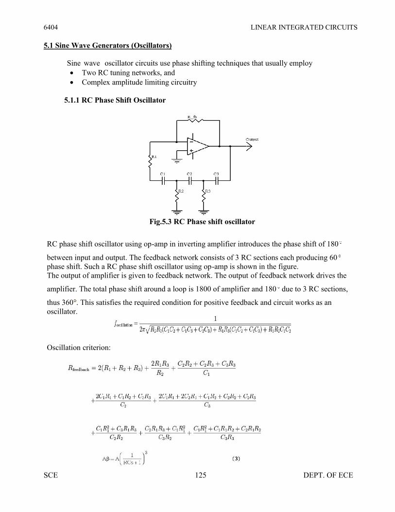
6404 LINEAR INTEGRATED CIRCUITS
SCE 125 DEPT. OF ECE
5.1 Sine Wave Generators (Oscillators)
Sine wave oscillator circuits use phase shifting techniques that usually employ Two RC tuning networks, and Complex amplitude limiting circuitry
5.1.1 RC Phase Shift Oscillator
Fig.5.3 RC Phase shift oscillator
RC phase shift oscillator using op-amp in inverting amplifier introduces the phase shift of 180
between input and output. The feedback network consists of 3 RC sections each producing 60phase shift. Such a RC phase shift oscillator using op-amp is shown in the figure.The output of amplifier is given to feedback network. The output of feedback network drives the
amplifier. The total phase shift around a loop is 1800 of amplifier and 180 due to 3 RC sections,
thus 360 . This satisfies the required condition for positive feedback and circuit works as anoscillator.
Oscillation criterion:

6404 LINEAR INTEGRATED CIRCUITS
SCE 126 DEPT. OF ECE
The loop phase shift is –180° when the phase shift of each section is –60°, and this occurs when ω= 2πf = 1.732/RC because the tangent 60° = 1.73. The magnitude of β at this point is (1/2)3, sothe gain, A, must be equal to 8 for the system gain to be equal to 1.
5.1.2 Wien Bridge Oscillator:
Figure 5. 3 give the Wien-bridge circuit configuration. The loop is broken at the positive input,and the return signal is calculated in Equation 2 below.
Fig.5.4 Wien Bridge Oscillator
When ω = 2πf = 1/RC, the feedback is in phase (this is positive feedback), and the gain is 1/3, sooscillation requires an amplifier with a gain of 3. When RF = 2RG, the amplifier gain is 3and oscillation occurs at f = 1/2πRC. The circuit oscillated at 1.65 kHz rather than 1.59 kHzwith the component values shown in Figure 3, but the distortion is noticeable.

6404 LINEAR INTEGRATED CIRCUITS
SCE 127 DEPT. OF ECE
Fig.5.5 Wien Bridge Circuit Schematic with non-linear feedback
Figure 4 shows a Wien-bridge circuit with non-linear feedback. The lamp resistance, RL, isnominally selected as half the feedback resistance, RF, at the lamp current established by RFand RL. The non-linear relationship between the lamp current and resistance keeps outputvoltage changes small.If a voltage source is applied directly to the input of an ideal amplifier with feedback, the inputcurrent will be:
Where vin is the input voltage, vout is the output voltage, and Zf is the feedback impedance. Ifthe voltage gain of the amplifier is defined as:
And the input admittance is defined as:
Input admittance can be rewritten as:
For the Wien Bridge, Zf is given by:
If Av is greater than 1, the input admittance is a negative resistance in parallel with an inductance.The inductance is:
If a capacitor with the same value of C is placed in parallel with the input, the circuit has anatural resonance at:
Substituting and solving for inductance yields:
If Av is chosen to be 3: Lin = R2C
Substituting this value yields:Or
Similarly, the input resistance at the frequency above is:For Av = 3: Rin = − R
If a resistor is placed in parallel with the amplifier input, it will cancel some of the

6404 LINEAR INTEGRATED CIRCUITS
SCE 128 DEPT. OF ECE
negative resistance. If the net resistance is negative, amplitude will grow until clipping occurs.Similarly, if the net resistance is positive, oscillation amplitude will decay. If a resistance
is added in parallel with exactly the value of R, the net resistance will be infinite and thecircuit can sustain stable oscillation at any amplitude allowed by the amplifier.
Increasing the gain makes the net resistance more negative, which increases amplitude. Ifgain is reduced to exactly 3 when suitable amplitude is reached, stable, low distortion oscillationswill result.
Amplitude stabilization circuits typically increase gain until suitable output amplitudeis reached. As long as R, C, and the amplifier are linear, distortion will be minimal.
5.2 Multivibrators
5.2.1 Astable Multivibrator
The two states of circuit are only stable for a limited time and the circuit switchesbetween them with the output alternating between positive and negative saturation values.
Fig. 5.6 Astable multivibrator circuit
Analysis of this circuit starts with the assumption that at time t=0 the output has justswitched to state 1, and the transition would have occurred.
An op-amp Astable multivibrator is also called as free running oscillator. The basicprinciple of generation of square wave is to force an op-amp to operate in the saturationregion (±Vsat).
A fraction β =R2/(R1+R2) of the output is feedback to the positive input terminal ofop-amp. The charge in the capacitor increases & decreases upto a threshold value called ±βVsat.The charge in the capacitor triggers the op-amp to stay either at +Vsat or –Vsat.
Asymmetrical square wave can also be generated with the help of Zener diodes. Astablemulti vibrator do not require a external trigger pulse for its operation & output toggles fromone state to another and does not contain a stable state.
Astable multi vibrator is mainly used in timing applications & waveforms generators.Design1. The expression of fo is obtained from the charging period t1 & t2 of capacitor as
T=2RCln (R1+2R2)/R12. To simplify the above expression, the value of R1 & R2 should be taken as R2 = 1.16R
Such that fo simplifies to fo =1/2RC.3. Assume the value of R1 and find R2.

6404 LINEAR INTEGRATED CIRCUITS
SCE 129 DEPT. OF ECE
4. Assume the value of C & Determine R from fo =1/2R C5. Calculate the threshold point from βVSATl = R1lVTl/ R1-R2
l/βVSATl w h e r e β is the feedback ratio.
5.2.2 Monostable Multivibrator using Op-amp: circuit diagram:
Fig.5.7 Mono stable Multi vibrator using Op-amp
Fig.5.8 Input Output Waveform:

6404 LINEAR INTEGRATED CIRCUITS
SCE 130 DEPT. OF ECE
A multivibrator which has only one stable and the other is quasi stable state iscalled as Monostable multivibrator or one-short multivibrator. This circuit is useful forgenerating signal output pulse of adjustable time duration in response to a triggering signal.The width of the output pulse depends only on the external components connected to the op-amp. Usually a negative trigger pulse is given to make the output switch to other state. But, itthen return to its stable state after a time interval determining by circuit components. The pulsewidth T can be given as T = 0.69RC. For Monostable operation the triggering pulse width Tpshould be less then T, the pulse width of Monostable multivibrator. This circuit is also called astime delay circuit or gating circuit.
5.2.3 Triangular Wave Generator Circuit:
Fig. 5.9 Circuit diagram of Triangular waveform generator

6404 LINEAR INTEGRATED CIRCUITS
SCE 131 DEPT. OF ECE
This signal generator gives two waveforms: a triangle-wave and a square- wave. Thecentral component of this circuit is the integrator capacitor CI. Basically we are interested inperforming two functions on CI: charge it, discharge it - repeat indefinitely. The outputwaveforms are shown here and it is apparent that a square wave generator followed by anintegrator acts as a triangular wave generator.
Fig.5.10 Output waveforms from generator
Fig. 5.11 Basic triangular waveform generator
The triangle peaks and period may not accurately meet +/-10V swing at 100 us. The mainreason is that current source and thresholds are derived from Zener diodes - not exactly the mostaccurate reference.
5.2.4 Linear Ramp GeneratorA triangle wave implies that the circuit generates a linear voltage ramp. One way to
achieve this goal is by charging discharging CI with a constant current. The Op AmpIntegrator provides f o r this.

6404 LINEAR INTEGRATED CIRCUITS
SCE 132 DEPT. OF ECE
Fig. 5.12 Linear Ramp Generator
Ramp UpConnect RI to VN and With V- held at the virtual ground (0V), a constant current flows from V- toVN.
Iin = VN / RI.CI integrates Iin creating a positive linear ramp at Vo. The ramp is linear because Vo changesproportionally to the time elapsed ΔT.
ΔVo = - VN / (CI ∙ RI) ∙ ΔTRamp Down Connect RI to VP and constant current flows from VP to V-,
Iin = - VP / RI.Now Vo ramps down linearly ΔVo = - VP / (CI ∙ RI) ∙ ΔT
Ramp Up:ΔVo/ΔT= -VN/(CIRI)Ramp Down:ΔVo /ΔT = - VP / ( CI ∙ RI )
These equations show the parameters available to control the ramp up / down speeds.Asymmetrical voltage swings are got by including a reference voltage VREF to the comparator'snegative input.
Vth+ =VREF∙(R1+R2)/R2-VN∙R1/R2Vth- = VREF ∙ (R1+R2)/R2 -VP ∙ R1 / R2
Upper and Lower Bounds
When do we switch from charging to discharging CI? Basically, there is a need to pick two levels -an upper and a lower threshold - to define the bounds of the triangle wave. The circuit ramps up ordown, reversing at the upper and lower thresholds.
With one leg of RI at VN, the output ramps up until the Upper Threshold (Vth+ ) isreached. Then RI is switched from VN to VP.
With one leg of RI at VP, the output ramps down until the Lower Threshold (Vth- ) isreached. Then RI is switched from VP to VN.
Comparator:
An Op Amp Comparator with two thresholds. Produce circuit changes in output state fromVN to VP (or vice-versa) depending on the upper Vth+ and lower Vth- thresholds.
Vth+=-VN∙R1/R2Vth- = -VP ∙ R1 / R2

6404 LINEAR INTEGRATED CIRCUITS
SCE 133 DEPT. OF ECE
Comparator Working:
o When Vin > Vth+, the output switches to VP, the POSITIVE output state.o When Vin < Vth-, the output switches to VN, the NEGATIVE output state.
Zener diodes D1 and D2 set the positive and negative output levels:
VP=VfD1+VZD2 VN =VfD2 + VZD1.
These output levels do double duty - they set the comparator thresholds, and set the voltage levelsfor the next stage - the integrator.
5.3 Saw-Tooth Wave Generator
Fig. 5.13 Saw-Tooth Wave Generator Circuit Diagram and output waveform
The saw tooth wave oscillator which used the operational amplifier. The composition of thiscircuit is the same as the triangular wave oscillator basically and is using two operationalamplifiers.
At the circuit diagram above, IC(1/2) is the Schmitt circuit and IC(2/2) is the Integration

6404 LINEAR INTEGRATED CIRCUITS
SCE 134 DEPT. OF ECE
circuit. The difference with the triangular wave oscillator is to be changing the time of thecharging and the discharging of the capacitor. When the output of IC (1/2) is positive voltage, itcharges rapidly by the small resistance (R1) value.
(When the integration output voltage falls) When the output of IC(1/2) is negative voltage,it is made to charge gradually at the big resistance(R2) value. The output waveform of theintegration circuit becomes a form like the tooth of the saw. Such voltage is used for thecontrol of the electron beam (the scanning line) of the television,
When picturing a picture at the cathode-ray tube, an electron beam is moved comparativeslow. (When the electron beam moves from the left to the right on the screen). When turningback, it is rapidly moved.(When moving from the right to the left).
Like the triangular wave oscillator, the line voltage needs both of the positive power supplyand the negative power supply. Also, to work in the oscillation, the condition of R3>R4 isnecessary. However, when making the value of R4 small compared with R3, the outputvoltage becomes small. The near value is good for R3 and R4
The oscillation frequency can be calculated by the following formula.
With the circuit diagram,the oscillation frequency is as follows.f = (1/2C (R1+R2))*(R3/R4)
= (1/(2x0.1x10-6x(5.6x103+100x103))x(120x103/100x103)= (1/(21.12x10-3))x1.2= 56.8 Hz
5.4 Function Generator IC 8038:
Fig.5.14 Functional block diagram of Function generator

6404 LINEAR INTEGRATED CIRCUITS
SCE 135 DEPT. OF ECE
Fig. 5.15 Output Waveforms from Function Generator IC 8038
It consists of two current sources, two comparators, two buffers, one FF and a sine wave converter.Pin description: Pin 1 & Pin 12: Sine wave adjusts:
The distortion in the sine wave output can be reduced by adjusting the 100KΩ potsconnected between pin12 & pin11 and between pin 1 & 6. Pin 2 Sine Wave Output:
Sine wave output is available at this pin. The amplitude of this sine wave is 0.22 Vcc.Where ± 5V ≤ Vcc ≤ ± 15 V.
Pin 3 Triangular Wave output:Triangular wave is available at this pin. The amplitude of the triangular wave is 0.33Vcc.
Where ± 5V ≤ Vcc ≤ ± 15 V.
Pin 4 & Pin 5 Duty cycle / Frequency adjust:The symmetry of all the output wave forms & 50% duty cycle for the square wave output
is adjusted by the external resistors connected from Vcc to pin 4. These external resistors &capacitors at pin 10 will decide the frequency of the output wave forms. Pin 6 + Vcc:
Positive supply voltage the value of which is between 10 & 30V is applied to this pin. Pin 7 : FM Bias:
This pin along with pin no8 is used to TEST the IC 8038. Pin9 : Square Wave Output:
A square wave output is available at this pin. It is an open collector output so that this pincan be connected through the load to different power supply voltages. This arrangement is veryuseful in making the square wave output. Pin 10 : Timing Capacitors:
The external capacitor C connected to this pin will decide the output frequency along withthe resistors connected to pin 4 & 5. Pin 11 : -VEE or Ground:
If a single polarity supply is to be used then this pin is connected to supply ground & if (±)supply voltages are to be used then (-) supply is connected to this pin. Pin 13 & Pin 14: NC (No Connection)

6404 LINEAR INTEGRATED CIRCUITS
SCE 136 DEPT. OF ECE
Important features of IC 8038:1. All the outputs are simultaneously available.2. Frequency range : 0.001Hz to 500kHz3. Low distortion in the output wave forms.4. Low frequency drifts due to change in temperature.5. Easy to use.
Parameters:(i) Frequency of the output wave form:
The output frequency dependent on the values of resistors R1 & R2 along with theexternal capacitor C connected at pin 10.If RA= RB = R & if RC is adjusted for 50% duty cycle then f0= 0.3/RC; RA = R1, RB =
R3, RC= R2.(ii) Duty cycle / Frequency Adjust : (Pin 4 & 5):
Duty cycle as well as the frequency of the output wave form can be adjusted by externalresistors at pin 4 & 5.The values of resistors RA & RB connected between Vcc pin 4 & 5 respectively alongwith the capacitor connected at pin 10 decide the frequency of the wave form. The values ofRA & RB should be in the range of 1kΩ to 1MΩ.
(iii)FM Bias: The FM Bias input (pin7) corresponds to the junction of resistors R1 & R2. The voltage Vin is the voltage between Vcc & pin8 and it decides the output frequency. The output frequency is proportional to Vin as given by the following expression.
For RA = RB (50% duty cycle). f0= 5 Vin/CRAVcc ; where C is the timing capacitor. With pin 7 & 8 connected to each other the output frequency is given by f0= 0.3/RC where
R = RA = RB for 50% duty cycle. This is because M Sweep input (pin 8): Vin=R1Vcc/R1+R2 This input should be connected to pin 7, if we want a constant output frequency. But if the output frequency is supposed to vary, then a variable dc voltage should be
applied to this pin. The voltage between Vcc & pin 8 is called Vin and it decides the output frequency as,
f0=1.5 Vin/CRAVCCA potentiometer can be connected to this pin to obtain the required variable voltage
required to change the output frequency.
5.5 The 555 Timer ICThe 555 is a monolithic timing circuit that can produce accurate & highly stable timedelays or oscillation. The timer basically operates in one of two modes: either(i) Monostable (one - shot) multivibrator or(ii) Astable (free running) multivibrator
The important features of the 555 timer are these:(i) It operates on +5v to +18 v supply voltages(ii) It has an adjustable duty cycle(iii) Timing is from microseconds to hours(iv) It has a current o/p

6404 LINEAR INTEGRATED CIRCUITS
SCE 137 DEPT. OF ECE
Fig. 5.16 Pin configuration of 555 timerPin description:
Pin 1: Ground:All voltages are measured with respect to this terminal.
Pin 2: Trigger:The o/p of the timer depends on the amplitude of the external trigger pulseapplied to this pin.
Pin 3: Output:There are 2 ways a load can be connected to the o/p terminal either between pin3& ground or between pin 3 & supply voltage
(Between Pin 3 & Ground ON load) (BetweenPin 3 &+ Vcc OFF load)(i) When the input is low:
The load current flows through the load connected between Pin 3 &+Vcc in to the output terminal & is called the sink current.
(ii) When the output is high:The current through the load connected between Pin 3 & +Vcc(i.e. ON load) is zero. However the output terminal supplies currentto the normally OFF load. This current is called the source current.
Pin 4: Reset:The 555 timer can be reset (disabled) by applying a negative pulse to this pin.When the reset function is not in use, the reset terminal should be connectedto +Vcc to avoid any false triggering.
Pin 5: Control voltage:An external voltage applied to this terminal changes the threshold as well astrigger voltage. In other words by connecting a potentiometer between this pin& GND, the pulse width of the output waveform can be varied. When not used,the control pin should be bypassed to ground with 0.01 capacitor to prevent anynoise problems.
Pin 6: Threshold:

6404 LINEAR INTEGRATED CIRCUITS
SCE 138 DEPT. OF ECE
This is the non inverting input terminal of upper comparator which monitorsthe voltage across the external capacitor.
Pin 7: Discharge:This pin is connected internally to the collector of transistor Q1.When the output is high Q1 is OFF.When the output is low Q is (saturated) ON.
Pin 8: +Vcc:The supply voltage of +5V to +18V is applied to this pin with respect to ground.
Fig.5.17 Block Diagram of 555 Timer IC
From the above figure, three 5k internal resistors act as voltage divider providing biasvoltage of 2/3 Vcc to the upper comparator & 1/3 Vcc to the lower comparator. It ispossible to vary time electronically by applying a modulation voltage to the control voltageinput terminal (5).(i) In the Stable state:
The output of the control FF is high. This means that the output is low because ofpower amplifier which is basically an inverter. Q = 1; Output = 0(ii) At the Negative going trigger pulse:
The trigger passes through (Vcc/3) the output of the lower comparator goes high & setsthe FF. Q = 1; Q = 0(iii) At the Positive going trigger pulse: It passes through 2/3Vcc, the output of the uppercomparator goes high and resets the FF. Q = 0; Q = 1The reset input (pin 4) provides a mechanism to reset the FF in a manner which overrides

6404 LINEAR INTEGRATED CIRCUITS
SCE 139 DEPT. OF ECE
the effect of any instruction coming to FF from lower comparator. Monostable Operation:
Fig. 5.18 555 connected as a Monostable Multivibrator
Fig. 5.19 Waveforms of monostable multivibrators
Initially when the output is low, i.e. the circuit is in a stable state, transistor Q1 is ON &capacitor C is shorted to ground. The output remains low. During negative going trigger pulse,transistor Q1 is OFF, which releases the short circuit across the external capacitor C &drives the output high. Now the capacitor C starts charging toward Vcc through RA. When thevoltage across the capacitor equals 2/3 Vcc, upper comparator switches from low to high. i.e.Q = 0, the transistor Q1 = OFF ; the output is high.Since C is unclamped, voltage across it rises exponentially through R towards Vcc with atime constant RC (fig b) as shown in below. After the time period, the upper comparator resetsthe FF,i.e. Q = 1, Q1 = ON; the output is low.[i.e discharging the capacitor C to ground potential (figc)]. The voltage across the capacitor as in fig (b) is given by

6404 LINEAR INTEGRATED CIRCUITS
SCE 140 DEPT. OF ECE
Vc = Vcc (1-e-t/RC)……. (1)Therefore At t = T, Vc = 2/3 Vcc
2/3 Vcc = Vcc(1-e-T/RC)orT = RC ln (1/3)OrT = 1.1RC seconds ……………. (2)
If the reset is applied Q2 = OFF, Q1 = ON, timing capacitor C immediately discharged. Theoutput now will be as in figure (d & e). If the reset is released output will still remain lowuntil a negative going trigger pulse is again applied at pin 2.
Applications of Monostable Mode of Operation:
(a) Frequency Divider:
The 555 timer as a monostable mode. It can be used as a frequency divider by adjustingthe length of the timing cycle tp with respect to the time period T of the trigger input. Touse the monostable multivibrator as a divide by 2 circuit, the timing interval tp must be alarger than the time period of the trigger input. [Divide by 2, tp > T of the trigger]
By the same concept, to use the monostable multivibrator as a divide by 3 circuit, tpmust be slightly larger than twice the period of the input trigger signal & so on, [ divide by 3tp > 2T oftrigger](b) Pulse width modulation:
Fig.5.20 Pulse Width Modulation

6404 LINEAR INTEGRATED CIRCUITS
SCE 141 DEPT. OF ECE
Fig. 5.21 Output Waveform
Pulse width of a carrier wave changes in accordance with the value of aincoming (modulating signal) is known as PWM. It is basically monostable multivibrator.A modulating signal is fed in to the control voltage (pin 5). Internally, the control voltage isadjusted to 2/3 Vcc externally applied modulating signal changes the control voltage level ofupper comparator. As a result, the required to change the capacitor up to threshold voltagelevel changes, giving PWM output.
(c) Pulse Stretcher:
This application makes use of the fact that the output pulse width (timing interval) ofthe monostable multivibrator is of longer duration than the negative pulse width of the inputtrigger. As such, the output pulse width of the monostable multivibrator can be viewed asa stretched version of the narrow input pulse, hence the name “Pulse stretcher”.
Often, narrow –pulse width signals are not suitable for driving an LED display,mainly because of their very narrow pulse widths. In other words, the LED may be flashingbut not be visible to the eye because its on time is infinitesimally small compared to its offtime. The 55 pulse stretcher can be used to remedy this problem. The LED will be ONduring the timing interval tp = 1.1RAC which can be varied by changing the value of RA& C.
Fig.5.23 Pulse Stretcher

6404 LINEAR INTEGRATED CIRCUITS
SCE 142 DEPT. OF ECE
The 555 timer as an Astable Multivibrator:An Astable multivibrator, often called a free running multivibrator, is a
rectangular wave generating circuit. Unlike the monostable multivibrator, this circuit doesnot require an external trigger to change the state of the output, hence the name free running.However, the time during which the output is either high or low is determined by 2 resistorsand capacitors, which are externally connected to the 55 timer.
Fig.5.24 Astable Multivibrator
Fig. 5.25 Waveforms of Astable multivibrator
The above figures show the 555 timer connected as an astable multivibrator and its model graph

6404 LINEAR INTEGRATED CIRCUITS
SCE 143 DEPT. OF ECE
Initially, when the output is high :Capacitor C starts charging toward Vcc through RA & RB. However, as soon as
voltage across the capacitor equals 2/3 Vcc. Upper comparator triggers the FF & outputswitches low.When the output becomes Low:
Capacitor C starts discharging through RB and transistor Q1, when the voltage across Cequals 1/3 Vcc, lower comparator output triggers the FF & the output goes high. Thencycle repeats. The capacitor is periodically charged & discharged between 2/3 Vcc & 1/3Vcc respectively. The time during which the capacitor charges from 1/3 Vcc to 2/3 Vcc equalto the time the output is high & is given by
tc = (RA+RB)C ln 2……………(1) Where [ln 2 = 0.69]= 0.69 (RA+RB) C
Where RA & RB are in ohms. And C is in farads.Similarly, the time during which the capacitors discharges from 2/3 Vcc to 1/3 Vcc is
equal to the time, the output is low and is given by,tc = RB C ln 2td = 0.69 RB C …………………..(2) where RB is in ohms and C is in
farads.Thus the total period of the output waveform is
T = tc + td = 0.69 (RA+2RB) C …………….(3)This, in turn, gives the frequency of oscillation as,f 0 = 1/T = 1.45/(RA+2RB)C ………(4)
Equation 4 indicates that the frequency f 0 is independent of the supply voltage Vcc.Often the term duty cycle is used in conjunction with the astable multivibrator. The dutycycle is the ratio of the time tc during which the output is high to the total time period T.It is generally expressed as a percentage.
% duty cycle = (tc / T )* 100% DC = [(RA+RB)/ /(RA+2RB)] * 100
Astable Multivibrator Applications:
(a) Square wave oscillator:
Fig.5.26 Square Wave Oscillator

6404 LINEAR INTEGRATED CIRCUITS
SCE 144 DEPT. OF ECE
Without reducing RA = 0 ohm, the astable multivibrator can be used to producesquare wave output. Simply by connecting diode D across Resistor RB. The capacitor Ccharges through RA & diode D to approximately2/3Vcc & discharges through RB & Q1 until the capacitor voltage equals approximately1/3Vcc, then the cycle repeats.To obtain a square wave output, RA must be a combination of a fixed resistor & potentiometerso that the potentiometer can be adjusted for the exact square wave.
(b) Free – running Ramp generator:
The astable multivibrator can be used as a free – running ramp generator when resistorRA& RB is replaced by a current mirror.
The current mirror starts charging capacitor C toward Vcc at a constant rate. When voltage across C equals to 2/3 Vcc, upper comparator turns transistor Q1 ON
& C rapidly discharges through transistor Q1. When voltage across C equals to 1/3 Vcc, lower comparator switches transistor
OFF & then capacitor C starts charging up again. Thus the charge – discharge cycle keeps repeating. The discharging time of the capacitor is relatively negligible compared to its charging
time. The time period of the ramp waveform is equal to the charging time & is
approximately is given by,T = VccC/3IC(1) IC = (Vcc - VBE)/R = constantcurrent
Therefore the free – running frequency of ramp generator isf0 = 3IC/ Vcc C

6404 LINEAR INTEGRATED CIRCUITS
SCE 145 DEPT. OF ECE
5.6 Linear Regulators
All electronic circuits need a dc power supply for their operation. To obtain this dcvoltage from 230 V ac mains supply, we need to use rectifier.
Therefore the filters are used to obtain a “steady” dc voltage from the pulsating one. The filtered dc voltage is then applied to a regulator which will try to keep the dc
output voltage constant in the event of voltage fluctuations or load variation.The combination of rectifier & filter can produce a dc voltage. But the problem with thistype of dc power supply is that its output voltage will not remain constant in the event offluctuations in an AC input or changes in the load current(IL).
The output of unregulated power supply is connected at the input of voltage regulator circuit. The voltage regulator is a specially designed circuit to keep the output voltage constant. It
does not remain exactly constant. It changes slightly due to changes in certain parameters.
Factors affecting the output voltage:i) IL (Load Current)ii) VIN (Input Voltage)iii) T (Temperature)
IC Voltage Regulators:They are basically series regulators.
Important features of IC Regulators:1. Programmable output2. Facility to boost the voltage/current3. Internally provided short circuit current limiting4. Thermal shutdown5. Floating operation to facilitate higher voltage output
Classifications of IC voltage regulators:
IC Voltage Regulator
Fixed Volt Reg. Adjustable O/P Volt Reg Switching RegPositive/negative
Fixed & Adjustable output Voltage Regulators are known as Linear Regulator. A series pass transistor is used and it operates always in its active region.
Switching Regulator:
1. Series Pass Transistor acts as a switch.2. The amount of power dissipation in it decreases considerably.3. Power saving result is higher efficiency compared to that of linear.

6404 LINEAR INTEGRATED CIRCUITS
SCE 146 DEPT. OF ECE
Adjustable Voltage Regulator:
Advantages of Adjustable Voltage Regulator over fixed voltage regulator are,1. Adjustable output voltage from 1.2v to 57 v2. Output current 0.10 to 1.5 A3. Better load & line regulation4. Improved overload protection5. Improved reliability under the 100% thermal overloading
Adjustable Positive Voltage Regulator (LM317):
Fig. 5.27 Circuit diagram of LM317 regulator
LM317 series adjustable 3 terminal positive voltage regulator, the three terminals areVin, Vout & adjustment (ADJ).
LM317 requires only 2 external resistors to set the output voltage. LM317 produces a voltage of 1.25v between its output & adjustment terminals. This
voltage is called as Vref. Vref (Reference Voltage) is a constant, hence current I1 flows through R1 will also
be constant. Because resistor R1 sets current I1. It is called “current set” or “programresistor”.
Resistor R2 is called as “Output set” resistors, hence current through this resistor is thesum of I1 & Iadj
LM317 is designed in such as that Iadj is very small & constant with changes in linevoltage & load current.
The output voltage Vo is, Vo=R1I1+(I1+Iadj)R2 ------------- (1)Where I1= Vref/R1
Vo = (Vref/R1) R1 + Vref/R1 + Iadj R2= Vref + (Vref/R1) R2 + Iadj R2
Vo = Vref [1 + R2/R1] + Iadj R2 ------------- (2)
R1 = Current (I1) set resistorR2 = output (Vo) set resistor.
Vref = 1.25v which is a constant voltage between output andADJ terminals.
Current Iadj is very small. Therefore the second term in (2) can be neglected. Thus the final expression for the output voltage is given by
Vo= 1.25v[1 + R2/R1] -------------- (3)Eqn (3) indicates that we can vary the output voltage by varying the resistance R2. Thevalue of R1 is normally kept constant at 240 ohms for all practical applications.

6404 LINEAR INTEGRATED CIRCUITS
SCE 147 DEPT. OF ECE
Practical Regulator using LM317:
Fig. 5.28 Practical regulator
If LM317 is far away from the input power supply, then 0.1μf disc type or 1μftantalum capacitor should be used at the input of LM317.
The output capacitor Co is optional. Co should be in the range of 1 to 1000μf. The adjustment terminal is bypassed with a capacitor C2 this will improve the ripple
rejection ratio as high as 80 dB is obtainable at any output level. When the filter capacitor is used, it is necessary to use the protective diodes. These diodes do not allow the capacitor C2 to discharge through the low current point of
the regulator. These diodes are required only for high output voltages (above 25v) & for higher
values of output capacitance 25μf and above.
5.7 IC 723 – General Purpose Regulator
Disadvantages of fixed voltage regulator:1. Do not have the shot circuit2. Output voltage is not adjustable
These limitations can be overcomes in IC723.
Features of IC723:1. Unregulated dc supply voltage at the input between 9.5V & 40V2. Adjustable regulated output voltage between 2 to 3V.3. Maximum load current of 150 mA (ILmax = 150mA).4. With the additional transistor used, ILmax upto 10A is obtainable.5. Positive or Negative supply operation6. Internal Power dissipation of 800mW.7. Built in short circuit protection.8. Very low temperature drift.9. High ripple rejection.

6404 LINEAR INTEGRATED CIRCUITS
SCE 148 DEPT. OF ECE
The simplified functional block diagram can be divided in to 4 blocks.
1. Reference Generating block:The temperature compensated Zener diode, constant current source & voltage
reference amplifier together from the reference generating block. The Zener diode is usedto generate a fixed reference voltage internally. Constant current source will make theZener diode to operate at affixed point & it is applied to the Non – inverting terminal oferror amplifier. The Unregulated input voltage ±Vcc is applied to the voltage referenceamplifier as well as error amplifier.
2. Error Amplifier:Error amplifier is a high gain differential amplifier with 2 input (inverting & Non-
inverting). The Non-inverting terminal is connected to the internally generated referencevoltage. The Inverting terminal is connected to the full regulated output voltage.
Fig. 5.29 Functional block diagram of IC723

6404 LINEAR INTEGRATED CIRCUITS
SCE 149 DEPT. OF ECE
Fig.5.30 Pin diagram of IC723
3. Series Pass Transistor:Q1 is the internal series pass transistor which is driven by the error amplifier. This transistoractually acts as a variable resistor & regulates the output voltage. The collector of transistorQ1 is connected to the Un-regulated power supply. The maximum collector voltage of Q1is limited to 36Volts. The maximum current which can be supplied by Q1 is 150mA.
4. Circuitry to limit the current:The internal transistor Q2 is used for current sensing & limiting. Q2 is
normally OFF transistor. It turns ON when the IL exceeds a predetermined limit.Low voltage, Low current is capable of supplying load voltage which is equal to orbetween 2 to 7Volts.
Vload = 2 to 7V and Iload= 50mA
5.7.1 IC723 as a LOW voltage LOW current:
Fig.5.31 Typical circuit connection diagram

6404 LINEAR INTEGRATED CIRCUITS
SCE 150 DEPT. OF ECE
R1 & R2 from a potential divider between Vref & Gnd. The Voltage across R2 is connected to the Non – inverting terminal of the regulator IC
Vnon-inv = R2/(R1+R2) Vref
Gain of the internal error amplifier is largeVnon-inv = Vin
Therefore the Vo is connected to the Inverting terminal through R3 & RSC must alsobe equal to Vnon-inv
Vo = Vnon-inv =R2/(R1+R2) VrefR1 & R2 can be in the range of 1 KΩ to 10KΩ & value of R3 is given by
R3 = R1ll R2 =R1R2/(R1+R2)Rsc (current sensing resistor) is connected between Cs & CL. The voltagedrop across Rsc is proportional to the IL.
This resistor supplies the output voltage in the range of 2 to 7 volts, but the load currentcan be higher than 150mA.
The current sourcing capacity is increased by including a transistor Q in the circuit. The output voltage , Vo =R2/(R1+R2) Vref
5.7.2 IC723 as a HIGH voltage LOW Current: This circuit is capable of supplying a regulated output voltage between the ranges of 7
to 37 volts with a maximum load current of 150 mA. The Non – inverting terminal is now connected to Vref through resistance R3. The value of R1 & R2 is adjusted in order to get a voltage of Vref at the inverting
terminal at the desired output.Vin = Vref =R2 /(R1+R2) V0Vo = [1+R1/R2] Vin
Rsc is connected between CL & Cs terminals as before & it provides the shortCircuit current limiting Rsc =0.6/Ilimit
The value of resistors R3 is given by ,R3= R1ll R2 =R1R2/(R1+R2)
5.7.3 IC723 as a HIGH voltage HIGH Current: An external transistor Q is added in the circuit for high voltage low current regulator to
improve its current sourcing capacity.

6404 LINEAR INTEGRATED CIRCUITS
SCE 151 DEPT. OF ECE
Fig.5.32 Typical circuit connection diagram For this circuit the output voltage varies between 7 & 37V. Transistor Q increase the current sourcing capacity thus IL (MAX) is greater than 150mA. The output voltage Vo is given by ,
V0= Vo = [1+R1/R2] VinRsc =0.6/Ilimit
5.8 Switching Regulators
IntroductionThe switching regulator offers the advantages higher power conversion efficiency Increased design flexibility (multiple output voltages of different polarities can be
generated from a single input voltage). a lot less heat and Smaller size.
The primary filter capacitor is placed on the input to the regulator to help filter out the60 cycle ripple. If the output voltage is 12 volts and the input voltage is 24 volts then wemust drop 12 volts across the regulator. At output currents of 10 amps this translates into120 watts (12 volts times 10 amps) of heat energy that the regulator must dissipate intoheat.
Fig.5.33 switching regulator principle

6404 LINEAR INTEGRATED CIRCUITS
SCE 152 DEPT. OF ECE
The switching regulator is much more efficient than the linear regulator achieving efficiencies ashigh as 80% to 95% in some circuits. The obvious result is smaller heat sinks, less heat andsmaller overall size of the power supply.
The switching regulator is really nothing more than just a simple switch. This switch goeson and off at a fixed rate usually between 50 Khz to 100Khz as set by the circuit.Operation:Diode D1 has to be a Schottky or other very fast switching diode. Inductor L1must be a typeof core that does not saturate under high currents. Capacitor C1 is normally a low ESR(Equivalent Series Resistance) type.To understand the action of D1 and L1, let’s look at what happens when S1 is closed asindicated below:
Fig.5.34 switching operation of regulator
L1, which tends to oppose the rising current, begins to generate an electromagnetic field inits core. Diode D1 is reversed biased and is essentially an open circuit at this point.
When S1 opens, the electromagnetic field that was built up in L1 is now discharging andgenerating a current in the reverse polarity. As a result, D1 is now conducting and will continueuntil the field in L1 is diminished. This action is similar to the charging and discharging ofcapacitor C1. The use of this inductor/diode combination gives us even more efficiency andaugments the filtering of C1.
Because the switching system operates in the 50 to 100 kHz region and has an almostsquare waveform, it is rich in harmonics way up into the HF and even the VHF/UHF regionFour most commonly used switching converter types:Buck: used the reduce a DC voltage to a lower DC voltage.Boost: provides an output voltage that is higher than the input.Buck-Boost (invert): an output voltage is generated opposite in polarity to the input.Fly back: an output voltage that is less than or greater than the input can be generated, as well asmultiple outputs.Converters:Push-Pull: A two-transistor converter that is especially efficient at low input voltages.Half-Bridge: A two-transistor converter used in many off-line applications.Full-Bridge: A four-transistor converter (usually used in off-line designs) that can generate thehighest output power of all the types listed.
Switching Regulator:
An example of general purpose regulator is Motorola’s MC1723. It can be used inmany different ways, for example, as a fixed positive or negative output voltage regulator,

6404 LINEAR INTEGRATED CIRCUITS
SCE 153 DEPT. OF ECE
variable regulator or switching regulator because of its flexibility.To minimize the power dissipation during switching, the external transistor used must be a
switching power transistor.To improve the efficiency of a regulator, the series pass transistor is used as a switch
rather than as a variable resistor as in the linear mode. A regulator constructed to operate in this manner is called a series switching regulator. In
such regulators the series pass transistor is switched between cut off & saturation at a highfrequency which produces a pulse width modulated (PWM) square wave output.
This output is filtered through a low pass LC filter to produce an average dc outputvoltage.
Thus the output voltage is proportional to the pulse width and frequency. The efficiency of a series switching regulator is independent of the input & output
differential & can approach 95%
Fig.5.35 Basic Switching regulator
A basic switching regulator consists of 4 major components,1. Voltage source Vin2. Switch S13. Pulse generator Vpulse4. Filter F1
1. Voltage Source Vin:It may be any dc supply – a battery or an unregulated or a regulated voltage. The voltagesource must satisfy the following requirements. It must supply the required output power & the losses associated with the switching
regulator. It must be large enough to supply sufficient dynamic range for line & load
regulations. It must be sufficiently high to meet the minimum requirement of the regulator system
to be designed. It may be required to store energy for a specified amount of time during power
failures.
2. Switch S1:It is typically a transistor or thyristor connected as a power switch & is operated in thesaturated mode. The pulse generator output alternately turns the switch ON & OFF
3. Pulse generator Vpulse:

6404 LINEAR INTEGRATED CIRCUITS
SCE 154 DEPT. OF ECE
It provides an asymmetrical square wave varying in either frequency or pulse width calledfrequency modulation or pulse width modulation respectively. The most effective frequencyrange for the pulse generator for optimum efficiency 20 KHz. This frequency is inaudible tothe human ear & also well within the switching speeds of most inexpensive transistors &diodes.
The duty cycle of the pulse wave form determines the relationship between theinput & output voltages. The duty cycle is the ratio of the on time ton, to the periodT of the pulse waveform.
Duty cycle = ton/(ton+toff) = ton/T =ton.f
Where ton = On-time of the pulse waveform toff=off-time of the pulse waveformT = time period = ton + toff
= 1/frequency or T = 1/f
Typical operating frequencies of switching regulator range from 10 to 50 kHz. Lower operating frequency improve efficiency & reduce electrical noise, but
require large filter components (inductors & capacitors).
4. Filter F1:It converts the pulse waveform from the output of the switch into a dc voltage.
Since this switching mechanism allows a conversion similar to transformers, the switchingregulator is often referred to as a dc transformer.
The output voltage Vo of the switching regulator is a function of duty cycle & theinput voltage Vin.
Vo is expressed as follows,Vo= ton Vin/T
This equation indicates that, if time period T is constant, Vo is directly proportional tothe ON-time, ton for a given value of Vin. This method of changing the outputvoltage by varying ton is referred to as a pulse width modulation.
Similarly, if ton is held constant, the output voltage Vo is inversely proportional tothe period T or directly proportional to the frequency of the pulse waveform. Thismethod of varying the output voltage is referred to as frequency modulation (FM).
Switching regulator can operate in any of 3 modesi) Step – Downii) Step – Upiii) Polarity inverting
5.8 Monolithic Switching Regulator [µa78s40]:
The µA78S40 consists of a temperature compensated voltage reference, duty cyclecontrollable oscillator with an active current limit circuit, a high gain comparator, a high- current,high voltage output switch, a power switching diode & an uncommitted op-amp.Important features of the µA78S40 switching regulators are: Step up, down & Inverting operation

6404 LINEAR INTEGRATED CIRCUITS
SCE 155 DEPT. OF ECE
Operation from 2.5 to 40V input 80dB line & load regulations Output adjustable from 1.3 to 40V Peak current to 1.5A without external resistors Variable frequency, variable duty cycle device
The internal switching frequency is set by the timing capacitor CT, connected between pin12 &ground pin 11. The initial duty cycle is 6:1. The switching frequency & duty cycle can bemodified by the current limit circuitry, IPK sense, pin14, 7 the comparator, pin9 & 10.
Comparator:
The comparator modifies the OFF time of the output switch transistor Q1 & Q2. In the step– up & step down modes, the non-inverting input(pin9) of the comparator is connected to thevoltage reference of 1.3V (pin8) & the inverting input (pin10) is connected to the output terminalvia the voltage divider network.
Fig.5.36 Functional block diagram of µA78S40
Fig.5.37 Pin diagram of Monolithic Switching Regulator [µa78s40]:
In the Inverting mode the non – inverting input is connected to both the voltagereference & the output terminal through 2 resistors & the inverting terminal isconnected to ground.
When the output voltage is correct, the comparator output is in high state & has no effect onthe circuit operation.

6404 LINEAR INTEGRATED CIRCUITS
SCE 156 DEPT. OF ECE
However, if the output is too high & the voltage at the inverting terminal is higher thanthat at the non-inverting terminal, then the comparator output goes low.
In the LOW state the comparator inhibits the turn on of the output switching transistors.This means that, as long as the comparator output is low, the system is in off time.
As the output current rises or the output voltage falls, the off time of the system decreases. Consequently, as the output current nears its maximum IoMAX, the off time approaches its
minimum value.In all 3 modes (Step down, step up, Inverting), the current limit circuit is completed by connectinga sense resistor Rsc, between IPK sense & Vcc. The current limit circuit is activated when a 330mV potential appears across Rsc. Rsc is selected such that 330mV appears across it when the desired peak current IPK,
flows through it. When the peak current is reached, the current limit circuit is turned on.The forward voltage drop, VD, across the internal power diode is used to determine the value ofinductor L off time & efficiency of the switching regulator.Another important quantity used in the design of a switching regulator is the saturation voltage Vs:
In the step down mode an “output saturation volt” is 1.1V typical, 1.3VMAX.In the step up mode an “Output saturation volt” is 0.45V typical, 0.7 maximum.The desired peak current value is reached; the current limiting circuit turns ON &immediately terminates the ON time & starts OFF time.
As we increase IL (load current), Vout will decrease, to compensate for this, the ON timeof the output is increased automatically.
If the IL decreased then Vout increased, to compensate for this, the OFF time of the output isincreased automatically.
(i) Step – Down Switching Regulator: CT is the timing capacitor which decides the switching frequency. Rsc is the current sensing resistance. Its value is given by The Non-inverting terminal of the internal op-amp (pin9) is connected to the 1.3V
reference (pin8). Resistances R1 & R2 from a potential divider, across the output voltage Vo. Their
value should be such that the potential at the inverting input of the op-amp shouldbe equal to 1.3V ref when Vo is at its desired level.
The output capacitance Co is used for reducing the ripple contents in the output voltage. It acts as afilter along with the inductor L.
The inductor L is a part of filter connected on the output side, to reduce the ripplepercentage.
The 0.1μF capacitor connected between pin8 & ground bypasses any noise voltagecoupled to the reference (pin8).

6404 LINEAR INTEGRATED CIRCUITS
SCE 157 DEPT. OF ECE
Fig. 5.38 Step down convertor

6404 LINEAR INTEGRATED CIRCUITS
SCE 158 DEPT. OF ECE
(ii) Step – Up Switching Regulator: Inductor is connected between the collectors of Q1 & Q2. When Q1 is ON, the output is shorted & the collector current of Q1 flows through L. The diode D1 is reverse biased & Co supplies the load current. The inductor stores the energy. When the Q1 is turned OFF, there is a self induced emf that
appears across the inductor with polarities. The output voltage is given by,
Vo = Vin + VL Hence it will be always higher than Vin & step up operation is achieved.
Fig.5.39 Step up convertor
With Q1 ON with Q1 oFF

6404 LINEAR INTEGRATED CIRCUITS
SCE 159 DEPT. OF ECE
(iii) Inverting Switching Regulator:
Inverting switching regulator converts a positive input voltage into a negativeoutput voltage which is higher in magnitude.
Fig.5.40 Circuit diagram of inverting switching regulator
5.9 The Switched Capacitor Filter
Basic Representation:
Fig 5.41 Switched-capacitor resistor
The simplest switched capacitor (SC) circuit is the switched capacitor resistor, made of onecapacitor C and two switches S1 and S2 which connect the capacitor with a givenfrequency alternately to the input and output of the SC. Each switching cycle transfers a charge qfrom the input to the output at the switching frequency f. Recall that the charge q on a capacitorC with a voltage V between the plates is given by:
where V is the voltage across the capacitor. Therefore, when S1 is closed while S2 is open, thecharge transferred from the source to CS is:

6404 LINEAR INTEGRATED CIRCUITS
SCE 160 DEPT. OF ECE
And when S2 is closed while S1 is open, the charge transferred from CS to the load is:
Thus, the charge transferred in each cycle is:
Since a charge q is transferred at a rate f, the rate of transfer of charge per unit time is:
Note that we use I, the symbol for electric current, for this quantity. This is to demonstrate that acontinuous transfer of charge from one node to another is equivalent to a current. Substituting forq in the above, we have:
Let us define V, the voltage across the SC from input to output, thus:
We now have a relationship between I and V, which we can rearrange to give an equivalentresistance R:
Thus, the SC behaves like a resistor whose value depends on CS and f.The SC resistor is used as a replacement for simple resistors in integrated circuits
because it is easier to fabricate reliably with a wide range of values. It also has the benefit thatits value can be adjusted by changing the switching frequency. See also: operational amplifierapplications.
This same circuit can be used in discrete time systems (such as analog to digitalconverters) as a track and hold circuit. During the appropriate clock phase, the capacitorsamples the analog voltage through switch one and in the second phase presents this heldsampled value to an electronic circuit for processing.
Switched Capacitor Circuits:
The switched capacitor filter allows for very sophisticated, accurate, and tuneableanalog circuits to be manufactured without using resistors.
Advantages: resistors are hard to build on integrated circuits (they take up a lot ofroom), and the circuits can be made to depend on ratios of capacitor values (which can be setaccurately), and not absolute values (which vary between manufacturing runs).
The Switched Capacitor Resistor:
Consider the circuit shown with a capacitor connected to two switches and two differentvoltages.
Fig.5.42 Example circuit
If S2 closes with S1 open, then S1 closes with switch S2 open, a charge (q is transferred from v2 tov1 with

6404 LINEAR INTEGRATED CIRCUITS
SCE 161 DEPT. OF ECE
If this switching process is repeated N times in a time (t, the amount of charge transferred per unittime is given by
the number of cycles per unit time is the switching frequency (or clock frequency, fCLK)
Rearranging we get
Which states that the switched capacitor is equivalent to a resistor? The value of this resistordecreases with increasing switching frequency or increasing capacitance, as either will increase theamount of charge transferred from v2 to v1 in a given time.
The Switched Capacitor Integrator:
Now consider the integrator circuit. You have shown (in a previous lab) that the input-outputrelationship for this circuit is given by (neglecting initial conditions):
We can also write this with the "s" notation (assuming a sinusoidal input, Aest, s=jω)
If you replaced the input resistor with a switched capacitor resistor, you would get
Thus, you can change the equivalent ω' of the circuit by changing the clock frequency. The valueof ω' can be set very precisely because it depends only on the ratio of C1 and C2, and nottheir absolute value. Switched Capacitor Filter ICs:
Some of the Switched capacitor filter ICs is MF 5, MF10 and MF100 MF10:
The MF10 contains two of the second-order universal filter sections found in the MF5. Thereforewith MF10, two second order filters or one fourth-order filter can be built. As the MF5 and MF10have similar filter sections, the design procedure for them is same.
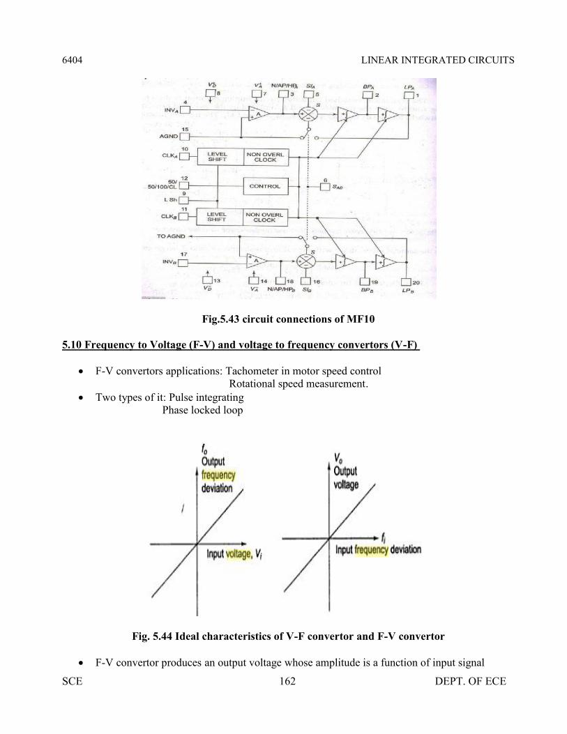
6404 LINEAR INTEGRATED CIRCUITS
SCE 162 DEPT. OF ECE
Fig.5.43 circuit connections of MF10
5.10 Frequency to Voltage (F-V) and voltage to frequency convertors (V-F)
F-V convertors applications: Tachometer in motor speed controlRotational speed measurement.
Two types of it: Pulse integratingPhase locked loop
Fig. 5.44 Ideal characteristics of V-F convertor and F-V convertor
F-V convertor produces an output voltage whose amplitude is a function of input signal

6404 LINEAR INTEGRATED CIRCUITS
SCE 163 DEPT. OF ECE
frequency. V0=kf fi kf is sensitivity of F-V convertor It is basically a FM discriminator.
Fig.5.45 Frequency To Voltage Convertor using VFC32 (V-F)
Fig.5.46 F-V Convertor using VF32 and input and output characteristics

6404 LINEAR INTEGRATED CIRCUITS
SCE 164 DEPT. OF ECE
Input frequency is applied to comparator A.Resistor R acts as feedback element.Capacitor Ci enables charge-balancing,High pass network conditions input signalFor negative spike of V01, comparator COMP triggers one shot multivibrator with threshold 7.5V Theoutput of multivibrator closes the switch SW, for a time TH, this causes voltage Vo to build up andinject thru R and this continues until current out of summing input of opamp is equal to that injectedby Vo through R continuously.Vo=10-3 *TH *R*fi as TH =7.5 C /1X10-3
Ripple Voltage, Vr(max) =7.5 C /Ci
5.10.2 Voltage to frequency convertor
Principle: Charge balancing technique-the process of charging and discharging results in frequencyproportional to input signal F0= k Vi
Operation: Op-amp A converts input Vi to current Ii = Vi/R into summing junction.When switch SW is open the current flows into capacitor Ci and charges it, and node voltage Vo1produce ramp down.When V01 =0 CMP triggers and sends a triggering signal to one shot multivibrator that closes theswitch SW and turns transistor Q ON for time TH.The threshold of mono shot = 7.5 V and TH= 7.5 C/10-3
During TH , V01 ramps upward by amount ∆ 01=(1mA-Ii) TH /CiTime duration TL for vo1 to return to 0 is TL = C∆ 01/Ii
TL+TH = 1mA TH /Ii = TF0=Vi/7.5 RC
Fig.5.47 Voltage-Frequency convertor using VF32 and its input output characteristics

6404 LINEAR INTEGRATED CIRCUITS
SCE 165 DEPT. OF ECE
5.11 Power Audio Amplifier IC LM 380:
Introduction:Small signal amplifiers are essentially voltage amplifier that supplies their loads with
larger amplifier signal voltage.On the other hand, large signal or power amplifier supply a large signal current to current
operated loads such as speakers & motors.In audio applications, however, the amplifier called upon to deliver much higher current
than that supplied by general purpose op-amps. This means that loads such as speakers & motorsrequiring substantial currents cannot be driven directly by the output of general purpose op-amps.To handle it following is done
To use discrete or monolithic power transistors called power boosters at the output of theop-amp
To use specialized ICs designed as power amplifiers like LM 380.
Features of LM380:1. Internally fixed gain of 50 (34dB)2. Output is automatically self centering to one half of the supply voltage.3. Output is short circuit proof with internal thermal limiting.4. Input stage allows the input to be ground referenced or ac
coupled.5. Wide supply voltage range (5 to 22V).6. High peak current capability.7. High impedance.
Fig.5.48 Functional block diagram of Audio Power Amplifier

6404 LINEAR INTEGRATED CIRCUITS
SCE 166 DEPT. OF ECE
Fig.5.49 Pin diagram Of Power amplifier LM380
Fig.5.50 Block diagram of LM380
LM380 circuit description:It is connected of 4 stages,
(i) PNP emitter follower(ii) Different amplifier(iii) Common emitter(iv) Emitter follower
(i) PNP Emitter follower: The input stage is emitter follower composed of PNP transistors Q1 & Q2 which drives the
PNP Q3-Q4 differential pair. The choice of PNP input transistors Q1 & Q2 allows the input to be referenced to ground
i.e., the input can be direct coupled to either the inverting & non-inverting terminals of the

6404 LINEAR INTEGRATED CIRCUITS
SCE 167 DEPT. OF ECE
amplifier.(ii) Differential Amplifier: The current in the PNP differential pair Q3-Q4 is established by Q7, R3 & +V. The current mirror formed by transistor Q7, Q8 & associated resistors then establishes the
collector current of Q9. Transistor Q5 & Q6 constitute of collector loads for the PNP differential pair. The output of the differential amplifier is taken at the junction of Q4 & Q6 transistors & is
applied as an input to the common emitter voltage gain.
(iii) Common Emitter amplifier stage: Common Emitter amplifier stage is formed by transistor Q9 with D1, D2 & Q8 as a current
source load. The capacitor C between the base & collector of Q9 provides internal compensation &
helps to establish the upper cutoff frequency of 100 KHz. Since Q7 & Q8 form a current mirror, the current through D1 & D2 is approximately the
same as the current through R3. D1 & D2 are temperature compensating diodes for transistors Q10 & Q11 in that D1 & D2
have the same characteristics as the base-emitter junctions of Q11. Therefore the currentthrough Q10 & (Q11-Q12) is approximately equal to the current through diodes D1 & D2.
(iv) (Output stage) - Emitter follower:
Emitter follower formed by NPN transistor Q10 & Q11. The combination of PNP transistorQ11 & NPN transistor Q12 has the power capability of NPN transistors but thecharacteristics of a PNP transistor.
The negative dc feedback applied through R5 balances the differential amplifier so that thedc output voltage is stabilized at +V/2;
To decouple the input stage from the supply voltage +V, by pass capacitor in order ofmicro farad should be connected between the bypass terminal (pin 1) & ground (pin 7).
The overall internal gain of the amplifier is fixed at 50. However gain can be increased byusing positive feedback.
Applications:(i) Audio Power Amplifier:
Fig. 5.51 Connections of audio power amplifier

6404 LINEAR INTEGRATED CIRCUITS
SCE 168 DEPT. OF ECE
Amplifier requires very few external components because of the internal biasing, compensation& fixed gain.
When the power amplifier is used in the non inverting configuration, the inverting terminalmay be either shorted to ground, connected to ground through resistors & capacitors.
Similarly when the power amplifier is used in the inverting mode, the non inverting terminalmay be either shorted to ground or returned to ground through resistor or capacitor.
Usually a capacitor is connected between the inverting terminal & ground if the input has ahigh internal impedance.
As a precautionary measure, an RC combination should be used at the output terminal (pin 8)to eliminate 5-to-10 MHz oscillation.
C1 is coupling capacitor which couples the output of the amplifier to the 8 ohms loud speakerwhich acts as a load. The amplifier will amplify the Vin applied at the non-inverting terminal.
(ii) LM 380 as a High gain amplifier:
Fig.5.52 Circuit connections
The gain of LM380 is internally fixed at 50. But it can be increased by using the externalcomponents.
The increase in gain is possible due to the use of positive feedback, this setup to obtain a gain200.
(iii) LM 380 as a variable Gain: Instead of getting a fixed gain of 50, it is possible to obtain a variable gain up to 50 by
connecting a potentiometer between the input terminals.

6404 LINEAR INTEGRATED CIRCUITS
SCE 169 DEPT. OF ECE
Fig. 5.53 Circuit connections
(iv) LM 380 as a Bridge Audio Power Amplifier:
Fig. 5.54 Circuit connections
If a certain application requires more power than what is provided by a single LM380amplifier, then 2 LM380 chips can be used in the bridge configuration.
With this arrangement we get an output voltage swing which is twice that of a single LM380amplifier.
As the voltage is doubled, power output will increase by four times that of a single LM380amplifier. The pot R4 is used to balance the output offset voltages of the two chips.
(v) Intercom system using LM 380:
When the switch is in Talk mode position, the master speaker acts as a microphone. When the switch is in Listen position, the remote speaker acts as a microphone. In either phone the overall gain of the circuit is the same depends on the turns of transformer T.

6404 LINEAR INTEGRATED CIRCUITS
SCE 170 DEPT. OF ECE
Fig. 5.55 Talk mode
Fig.5.56 Listen mode
5.12 Monolithic video amplifier
Fig.5.57 Monolithic video amplifier

6404 LINEAR INTEGRATED CIRCUITS
SCE 171 DEPT. OF ECE
5.13 Opto couplers/Opto Isolators and fibre optic IC
Opto couplers or Opt isolators is a combination of light source & light detector in the samepackage.
They are used to couple signal from one point to other optically, by providing a completeelectric isolation between them. This kind of isolation is provided between a low power controlcircuit & high power output circuit, to protect the control circuit.
Characteristics of opto coupler:(i) Current Transfer Ratio:
It is defined as the ratio of output collector current (Ic) to the input forward current(If)CTR = Ic/If * 100%. Its value depends on the devices used as source &
detector.(ii) Isolation voltage between input & output:
It is the maximum voltage which can exist differentially between the input & outputwithout affecting the electrical isolation voltage is specified in K Vrms with arelative humidity of 40 to 60%.
(iii) Response Time:Response time indicates how fast an opto coupler can change its output state.Response time largely depends on the detector transistor, input current & loadresistance.
(iv) Common mode Rejection:Even though the opto couplers are electrically isolated for dc & low
frequency signals, an impulsive input signal (the signal which changes suddenly)can give rise to a displacement current Ic= Cf*dv/dt. This current can flowbetween input & output due to the capacitance Cf existing between input &output. This allows the noise to appear in the output. Depending on the type of lightsource & detector used we can get a variety of opto couplers.
They are as follows,(i) LED – Photodiode opto coupler:
Fig.5.58 Schematic symbol and waveforms

6404 LINEAR INTEGRATED CIRCUITS
SCE 172 DEPT. OF ECE
LED photodiode shown in figure, here the infrared LED acts as a light source & photodiode isused as a detector.
The advantage of using the photodiode is its high linearity. When the pulse at the input goeshigh, the LED turns ON. It emits light. This light is focused on the photodiode.
In response to this light the photocurrent will start flowing though the photodiode. As soon asthe input pulse reduces to zero, the LED turns OFF & the photocurrent through the photodiodereduces to zero. Thus the pulse at the input is coupled to the output side.
(ii) LED – Phototransistor Opto coupler:
Fig.5.59 Schematic symbol and waveforms
The LED phototransistor opto coupler shown in figure. An infrared LED acts as a light sourceand the phototransistor acts as a photo detector.
This is the most popularly used opto coupler, because it does not need any additionalamplification.
When the pulse at the input goes high, the LED turns ON. The light emitted by the LED isfocused on the CB junction of the phototransistor.
In response to this light photocurrent starts flowing which acts as a base current for thephototransistor.
The collector current of phototransistor starts flowing. As soon as the input pulse reduces tozero, the LED turns OFF & the collector current of phototransistor reduces to zero. Thus thepulse at the input is optically coupled to the output side.
The input & output waveforms are 180º out of phase as the output is taken at the collectorof the phototransistor
Advantages of Opto coupler:
Control circuits are well protected due to electrical isolation. Wideband signal transmission is possible. Due to unidirectional signal transfer, noise from the output side does not get coupled to
the input side.

6404 LINEAR INTEGRATED CIRCUITS
SCE 173 DEPT. OF ECE
Interfacing with logic circuits is easily possible. It is small size & light weight
device.Disadvantages: Slow speed. Possibility of signal coupling for high power signals.
Applications:Opto couplers are used basically to isolate low power circuits from high power circuits.
At the same time the control signals are coupled from the control circuits to the high powercircuits.
Some of such applications are,(i) AC to DC converters used for DC motor speed control(ii) High power choppers(iii) High power inverters
One of the most important applications of an opto coupler is to couple the base driving signalsto a power transistor connected in a DC-DC chopper.
Opto coupler IC:
Fig. 5.60 The block diagram of opto-electronic-integrated circuit (OEIC)The optocouplers are available in the IC form MCT2E is the standard optocoupler IC
which is used popularly in many electronic application. This input is applied between pin 1& pin 2. An infrared light emitting diode is connected
between these pins. The infrared radiation from the LED gets focused on the internal phototransistor. The base of the phototransistor is generally left open. But sometimes a high value pull down
resistance is connected from the Base to ground to improve the sensitivity. The block diagram shows the opto-electronic-integrated circuit (OEIC) and the
major components of a fiber-optic communication facility. The block diagram shows the opto-electronic-integrated circuit (OEIC) and the
major components of a fiber-optic communication facility.

6404 LINEAR INTEGRATED CIRCUITS
SCE 174 DEPT. OF ECE
Question Bank
UNIT-I BASICS OF OPERATIONAL AMPLIFIERS
2 marks questions
1. What do you mean by a band-gap referenced biasing circuit?The biasing sources referenced to VBE has a negative temperature coefficient and VT has a positivetemperature co-efficient. Band gap reference circuit is one in which the output current is referencedto a composite voltage that is a weighted sum of VBE and VT so that by proper weighting, zerotemperature coefficient can be achieved.
2. Define thermal drift.The bias current, offset current & offset voltage change with temperature. A circuit carefully nulledat 25oC may not remain so when the temperature raises to 35oC.This is called thermal drift. Often,offset current drift is expressed in nA/ oC and offset voltage drift in mV/ 0C.
3. Define supply voltage rejection ratio (SVRR)The change in OPAMP’s input offset voltage due to variations in supply voltage is called the supplyvoltage rejection ratio. It is also called Power Supply Rejection Ratio (PSRR) or Power SupplySensitivity (PSS).4. Define an operational amplifier.An operational amplifier is a direct-coupled, high gain amplifier consisting of one or moredifferential amplifier. By properly selecting the external components, it can be used to perform avariety of mathematical operations.
5. Mention the characteristics of an ideal op-amp.Open loop voltage gain is infinity.Input impedance is infinity.Output impedance is zero.Bandwidth is infinity.Zero offset.
6. Define input offset voltage.A small voltage applied to the input terminals to make the output voltage as zero when the two inputterminals are grounded is called input offset voltage.
7. Define CMRR of an op-amp.The relative sensitivity of an op-amp to a difference signal as compared to a common –mode signalis called the common –mode rejection ratio. It is expressed in decibels. CMRR= Ad/Ac
8. What is frequency response of Op-amp?The plot showing the variations in magnitude and phase angle of the gain due to change in frequencyis called frequency response of Op-amp. The plot is used to find the bandwidth and cut-off

6404 LINEAR INTEGRATED CIRCUITS
SCE 175 DEPT. OF ECE
frequencies of Op-amp.
9. Define Unity Gain Bandwidth of Op-amp.For a certain frequency of the input signal, the gain of the Op-amp reduces to 0 dB. This means 20log |AOL (f) | is 0dB i.e. |AOL (f) | = 1. Such a frequency is called gain cross over frequency or unitygain bandwidth (UGB).
10. Define slew rate.The slew rate is defined as the maximum rate of change of output voltage caused by a step inputvoltage. An ideal slew rate is infinite which means that opamp’s output voltage should changeinstantaneously in response to input step voltage.
16 marks questions1. Wilson current source circuit and widlar current source circuit.2. Explain Block diagram of op-amp (8) Internal Stages of Op-amp.3. Explain the operation of differential amplifier, DC analysis of differential amplifier,
Differential amplifier with constant current source, Differential amplifier active load.4. Elaborate on AC & DC characteristics of Op-amp.5. Analyse the open loop and closed loop characteristics of Op amp
UNIT II - APPLICATION OF OP – AMPS
1. Mention some of the linear applications of op – amps.Adder, subtractor, voltage –to- current converter, current –to- voltage converters, instrumentationamplifier, analog computation ,power amplifier, etc are some of the linear op-amp circuits.
2. Mention some of the non – linear applications of op-amps.Rectifier, peak detector, clipper, clamper, sample and hold circuit, log amplifier, anti –log amplifier,multiplier are some of the non – linear op-amp circuits.
3. Define virtual ground property of Op-amp.Concept of virtual ground says that the two input terminals of the Op-amp are always at the samepotential. Thus if one terminal is grounded the other can be assumed to be at ground potential, whichis called virtual ground.
4. What is Voltage follower? voltage is called voltage follower
Circuit. -amp if the inverting input and the output terminals are shorted and if any signal is
Applied at the non-inverting terminal, it appears at the output without any change. follower, unity gain amplifier, buffer amplifier or isolation
amplifier.
1. Calculate the output voltage V0 of the circuit shown in fig. 1

6404 LINEAR INTEGRATED CIRCUITS
SCE 176 DEPT. OF ECE
6. Draw the circuit diagram of voltage follower using IC 741.7. For the op-amp shown, determine the voltage gain.
8. List the features of instrumentation amplifier.High gain accuracyHigh CMRRHigh gain stability with low temperature co-efficientLow dc offsetLow output impedance
9. What are the applications of V-I converter?Low voltage dc and ac voltmeterLEDZener diode tester
10. What do you mean by a precision diode?The major limitation of ordinary diode is that it cannot rectify voltages below the cut – in voltage ofthe diode. A circuit designed by placing a diode in the feedback loop of an op – amp is called theprecision diode and it is capable of rectifying input signals of the order of milli volt.
11.What are the limitations of the basic differentiator circuit?At high frequency, a differentiator may become unstable and break into oscillations. The input
impedance decreases with increase in frequency , thereby making the circuit sensitive to highfrequency noise.

6404 LINEAR INTEGRATED CIRCUITS
SCE 177 DEPT. OF ECE
12. Write down the condition for good differentiation.For good differentiation, the time period of the input signal must be greater than or equal to Rf C1T > R f C1 Where, Rf is the feedback resistance Cf is the input capacitance
13. What are the applications of comparator?Zero crossing detectorWindow detectorTime marker generatorPhase detector
14. What is a Schmitt trigger?Schmitt trigger is a regenerative comparator. It converts sinusoidal input into a square wave output.The output of Schmitt trigger swings between upper and lower threshold voltages, which are thereference voltages of the input waveform.
16. Define logarithmic and antilogarithmic amplifier.-amp circuit in which the output is proportional to the logarithmic of the input is called
logarithmic amplifier. It employs a diode or a transistor in the negative feedback path.-amp circuit in which the output is proportional to the antilogarithmic of the input is called
logarithmic amplifier. It employs a diode or a transistor in the input stage.
17. List the applications of Log amplifiers.Analog computation may require functions such as ln x, log x, sin h x etc.
These functions can be performed by log amplifiersLog amplifier can perform direct dB display on digital voltmeter and spectrum analyzerLog amplifier can be used to compress the dynamic range of a signal
18. What is a filter?Filter is a frequency selective circuit that passes signal of specified band of frequencies andattenuates the signals of frequencies outside the band.
19. What are the advantages of active filters?Active filters used op- amp as the active element and resistors and capacitors as passive elements.By enclosing a capacitor in the feedback loop , inductor less active filters can be obtainedOp-amp used in non – inverting configuration offers high input impedance and low output
impedance, thus improving the load drive capacity.

6404 LINEAR INTEGRATED CIRCUITS
SCE 178 DEPT. OF ECE
20.What are the requirements for producing sustained oscillations in feedback circuits?For sustained oscillations,
The total phase shift around the loop must be zero at the desired frequency of oscillation, fo. ie,AB =0 (or) 360°
At fo, the magnitude of the loop gain | A β | should be equal to unity
16 marks questions
1. What is meant by voltage follower?2. Determine the output voltage vo for the following circuit.
3. Explain the operation of the Schmitt trigger.4. Describe Logarithmic and anti-logarithmic amplifier5. Explain Precision rectifier and its applications -Clipper and clamper circuits6. Analyse of low pass Butterworth filters.7. Elaborate on I to V and V to I converters and applications8. Explain application of op-amp as integrator and differentiator9. Discuss the need for an instrumentation amplifier? Explain three op-amp instrumentation
amplifier with diagram (16)
UNIT –III ANALOG MULTIPLIER AND PLL
2 marks questions1. What is a four quadrant multiplier?In a multiplier circuit, if both the inputs are allowed to swing in both positive and negative directionsthe multiplier is called as a four quadrant multiplier.
2. Mention some areas where PLL is widely used.Radar synchronizationSatellite communication systemsAir borne navigational systemsFM communication systems
3v2k
U2
Vo+
-
OUT2v
2k
10k
5v2k

6404 LINEAR INTEGRATED CIRCUITS
SCE 179 DEPT. OF ECE
Computers.
3. List the basic building blocks of PLLPhase detector/comparatorLow pass filterError amplifierVoltage controlled oscillator
4. What are the three stages through which PLL operates?Free runningCaptureLocked/ tracking
5. Define lock-in range of a PLL.The range of frequencies over which the PLL can maintain lock with the incoming signal is calledthe lock-in range or tracking range. It is expressed as a percentage of the VCO free runningfrequency.
6. Define capture range of PLL.The range of frequencies over which the PLL can acquire lock with an input signal is called thecapture range. It is expressed as a percentage of the VCO free running frequency.
7. Define Pull-in time.The total time taken by the PLL to establish lock is called pull-in time. It depends on the initial phaseand frequency difference between the two signals as well as on the overall loop gain and loop filtercharacteristics.
8. Mention some typical applications of PLL:Frequency multiplication/divisionFrequency translationAM detectionFM demodulationFSK demodulation.
9. What is a voltage controlled oscillator?Voltage controlled oscillator is a free running multivibrator operating at a set frequency called thefree running frequency. This frequency can be shifted to either side by applying a dc control voltageand the frequency deviation is proportional to the dc control voltage.
10. Define VCO.A voltage controlled oscillator is an oscillator circuit in which the frequency of oscillations can becontrolled by an externally applied voltage.
11. On what parameters does the free running frequency of VCO depend on?External timing resistor, RTExternal timing capacitor, CT

6404 LINEAR INTEGRATED CIRCUITS
SCE 180 DEPT. OF ECE
The dc control voltage Vc.
12. Give the expression for the VCO free running frequency.fo = 0.25 / RT CT
13. Define Voltage to Frequency conversion factor.Voltage to Frequency conversion factor is defined as,Ky = fo / Vc= 8fo /Vccwhere, Vc is the modulation voltage required to produce the frequency shift fo
14. Define FSK modulation.In digital data communication, binary data is transmitted by means of a carrier frequency. FSKemploys two different carrier frequencies one for logic 1 and other for logic 0 states ofbinary datasignal. This process is called FSK modulation.
14. Define free running mode.In a PLL if the error control voltage is zero then the PLL is said to be operated in free running modeand its output frequency is called its center frequency f0.
16 marks1. Elaborate on Gilbert multiplier cell/ Four quadrant multiplier.2. Explain Analog multiplier using emitter coupled transistor.3.Analyze the analog multiplier IC with a neat circuit diagram. Discuss its applications.4.Discuss the Operation of PLL & applications of PLL.5.With a neat functional diagram, explain the operation of VCO. Also derive an expression for fo.
UNIT IV - ANALOG TO DIGITAL AND DIGITAL TO ANALOG CONVERTERS
1. Explain in brief the principle of operation of successive Approximation ADC.The circuit of successive approximation ADC consists of a successive approximation register (SAR),to find the required value of each bit by trial & error. With the arrival of START command, SAR setsthe MSB bit to 1. The O/P is converted into an analog signal & it is compared with I/P signal. ThisO/P is low or High. This process continues until all bits are checked.
2. Where are the successive approximation type ADC’s used?The Successive approximation ADCs are used in applications such as data loggers & instrumentationwhere conversion speed is important.
3. What is the main drawback of a dual-slop ADC?The dual slope ADC has long conversion time. This is the main drawback of dual slope ADC.
4. State the advantages of dual slope ADC:It provides excellent noise rejection of ac signals whose periods are integral multiples of the

6404 LINEAR INTEGRATED CIRCUITS
SCE 181 DEPT. OF ECE
integration time T.
5. Define conversion time.It is defined as the total time required to convert an analog signal into its digital output. It depends onthe conversion technique used & the propagation delay of circuit components. The conversion timeof a successive approximation type ADC is given byT(n+1) where T---clock periodTc---conversion time n----no. of bits
6.. Define resolution of a data converter.The resolution of a converter is the smallest change in voltage which may be produced at the outputor input of the converter.Resolution (in volts)= VFS/2n-1=1 LSB increment. The resolution of an ADC is defined as thesmallest change in analog input for a one bit change at the output.
7. Define accuracy of converter.Absolute accuracy:It is the maximum deviation between the actual converter output & the ideal converter output.Relative accuracy:It is the maximum deviation after gain & offset errors have been removed. The accuracy of aconverter is also specified in form of LSB increments or % of full scale voltage.
8. What is settling time?It represents the time it takes for the output to settle within a specified band .LSB of its final valuefollowing a code change at the input (usually a full scale change). It depends upon the switching timeof the logic circuitry due to internal parasitic capacitance & inductances. Settling time ranges from100ns. 10μ s depending on word length & type circuit used.
9. Explain in brief stability of a converter:The performance of converter changes with temperature age & power supply variation . So all therelevant parameters such as offset, gain, linearity error & monotonicity must be specified over thefull temperature & power supply ranges to have better stability performances.
10. What is meant by linearity?The linearity of an ADC/DAC is an important measure of its accuracy & tells us how close theconverter output is to its ideal transfer characteristics. The linearity error is usually expressed as afraction of LSB increment or percentage of full-scale voltage. A good converter exhibits a linearityerror of less than .LSB.
11. What is monotonic DAC?A monotonic DAC is one whose analog output increases for an increase in digital input.
12. Find the resolution of an 8-bit DAC.Resolution =1/( 28 -1) =1/ 255

6404 LINEAR INTEGRATED CIRCUITS
SCE 182 DEPT. OF ECE
13. Which is the fastest A/D converter and why?`Flash type A/D converter is the fastest ADC, because the fast conversion speed is accomplished byproviding 2n-1 comparators and simultaneously comparing the input signal with unique referencelevels spaced 1 LSB apart.
14. What are limitations of Flash type ADC?Flash type ADC employs 2n-1 comparators for conversion which makes it costlier which tradeoffs inthe speed of conversion.
15. Name the essentials parts of a DAC.Analog input signal, D/A converter circuit, Switches for DAC.
16. What are advantages and disadvantages of R-2R ladder DAC?Adv:-
istors are requiredcan be expanded by adding more sections of same R/2R values.
This avoids any slowdown effects by stray capacitances.Disadv:-
17. What is a sample and hold circuit? Where it is used?A sample and hold circuit is one which samples an input signal and holds on to its last sampled valueuntil the input is sampled again. This circuit is mainly used in digital interfacing, analog to digitalsystems, and pulse code modulation systems.
18.Define sample period and hold period.The time during which the voltage across the capacitor in sample and hold circuit is equal to theinput voltage is called sample period. The time period during which the voltage across the capacitoris held constant is called hold period.
19.What are the specifications of data convertors?conversion time, settling time, accuracy, linearity, monotonic etc.
16 marks questions
1. Explain the operation of sample and hold circuit .2. Explain the operation of FLASH type ADC.3. Weighted resistor type D/A converter, R-2R ladder type D/A converter – Voltage mode and
current mode4. Dual Slope type A/D converter , Single slope type A/D converter5. Sample and Hold circuits for A/D converter6. Explain A/D convertors using any two methods - successive Approximation ADC.

6404 LINEAR INTEGRATED CIRCUITS
SCE 183 DEPT. OF ECE
UNIT V – SPECIAL FUNCTION ICs2 mark questions
1. Define 555 IC?The 555 timer is an integrated circuit specifically designed to perform signal generation and timingfunctions.
2. Draw the Pin diagram of IC 555.
3. List the basic blocks of IC 555 timer?
4. Give the classification of voltage regulators:
5.Mention some applications of 555 timer:Oscillatorpulse generatorramp and square wave generator

6404 LINEAR INTEGRATED CIRCUITS
SCE 184 DEPT. OF ECE
mono-shot multivibratorburglar alarmTraffic light control.
6.List the applications of 555 timer in monostable mode of operation:Missing pulse detectorLinear ramp generatorFrequency dividerPulse width modulation.
7.List the applications of 555 timer in Astable mode of operation:FSK generatorPulse-position modulator
8. What is a multivibrator?Multivibrators are a group of regenerative circuits that are used extensively in timing applications. Itis a wave shaping circuit which gives symmetric or asymmetric square output. It has two states eitherstable or quasi- stable depending on the type of multivibrator.
9 .What do you mean by monostable multivibrator?Monostable multivibrator is one which generates a single pulse of specified duration in response toeach external trigger signal. It has only one stable state. Application of a trigger causes a change tothe quasi-stable state. An external trigger signal generated due to charging and discharging of thecapacitor produces the transition to the original stable state.
10.What is an astable multivibrator?Astable multivibrator is a free running oscillator having two quasi-stable states. Thus, there isoscillations between these two states and no external signal are required to produce the change instate.
11. Give the classification of voltage regulators: What is a voltage regulator?A voltage regulator is an electronic circuit that provides a stable dc voltage independent of the loadcurrent, temperature, and ac line voltage variations.
12. What is a linear voltage regulator?Series or linear regulator uses a power transistor connected in series between the unregulated dcinput and the load and it conducts in the linear region .The output voltage is controlled by thecontinuous voltage drop taking place across the series pass transistor.
13. What is a switching regulator?Switching regulators are those which operate the power transistor as a high frequency on/off switch,so that the power transistor does not conduct current continuously. This gives improved efficiencyover series regulators.
14. Give some examples of monolithic IC voltage regulators:78XX series fixed output, positive voltage regulators

6404 LINEAR INTEGRATED CIRCUITS
SCE 185 DEPT. OF ECE
79XX series fixed output, negative voltage regulators723 general purpose regulator.
15. What is the purpose of having input and output capacitors in three terminal ICregulators?A capacitor connected between the input terminal and ground cancels the inductive effects due tolong distribution leads. The output capacitor improves the transient response.
16. Define line regulation.Line regulation is defined as the percentage change in the output voltage for a change in the inputvoltage. It is expressed in milli volts or as a percentage of the output voltage.
17. Define load regulation.Load regulation is defined as the change in output voltage for a change in load current. It isexpressed in millivolts or as a percentage of the output voltage.
18. What is meant by current limiting?Current limiting refers to the ability of a regulator to prevent the load current from increasing above apreset value.
19. Give the drawbacks of linear regulators:
The input step down transformer is bulky and expensive because of low line frequency.Because of low line frequency, large values of filter capacitors are required to decrease the ripple.Efficiency is reduced due to the continuous power dissipation by the transistor as it operates in the
linear region.
20. What is the advantage of switching regulators?Greater efficiency is achieved as the power transistor is made to operate as low impedance switch.
Power transmitted across the transistor is in discrete pulses rather than as a steady current flow.By using suitable switching loss reduction technique, the switching frequency can be increased so
as to reduce the size and weight of the inductors and capacitors.
21. Define drop-out voltage of a fixed voltage regulator.It is the minimum voltage that must exist between input and output terminals. It is defined as theratio of the r.m.s input ripple voltage to the r.m.s output ripple voltage. It is expressed in decibels(dB).
22. What are the advantages of switched capacitor filters?high value of resistors can be easily simulated using small value capacitors, of the order of
10pF.
capacitors.a monolithic IC chip.

6404 LINEAR INTEGRATED CIRCUITS
SCE 186 DEPT. OF ECE
23. Define video amplifier.A video amplifier has to amplify signals over a wideband of frequencies, say upto 20MHz. It is a RCcoupled amplifier with bandwidth from d.c. to high frequency upto few megahertz.
24. What is opto coupler?An opto-isolator, also called an optocoupler, photocoupler, or optical isolator, is "an electronicdevice designed to transfer electrical signals by utilizing light waves to provide coupling withelectrical isolation between its input and output". The main purpose of an opto-isolator is "to preventhigh voltages or rapidly changing voltages on one side of the circuit from damaging components ordistorting transmissions on the other side
25. What is LM380?It is a power amplifier produced by national semiconductor. It is capable of delivering 2.5 W min, to8 ohm load.
26. Mention the advantages of opto-couplers:Better isolation between the two stages.Impedance problem between the stages is eliminated.Wide frequency response.Easily interfaced with digital circuit.Compact and light weight.Problems such as noise, transients, contact bounce, are eliminated.
27. What is an isolation amplifier?An isolation amplifier is an amplifier that offers electrical isolation between its input and outputterminals
28. What are the types of optocouplers?
LED and photo transistor,
29. Give two examples of IC optocouplers?-coupler IC
.30. List the applications of Isolation amplifier. -noise environments. -end processing.
16 marks1. Wien Bridge and RC phase oscillator using IC7412. Triangular and saw tooth wave generator

6404 LINEAR INTEGRATED CIRCUITS
SCE 187 DEPT. OF ECE
3. Working of ICL 8038 function generator4. Discuss in detail the operation of Astable multivibrator, Monostable multivibrator.5. Explain functional block diagram of IC 555 timer.(8)6. In detail discuss the 723 IC general purpose voltage regulators.7. Explain the operation of switching regulators. Give its advantages.8. Explain the functional diagram of LM 380 power amplifier.9. Explain the operation of ICL 8038 function generator. Give its advantages.10. Explain the operation of(1) opto electronic ICs, (2) audio amplifier (3) video amplifier (4)Opto-couplers and fiber optic ICs

6404 LINEAR INTEGRATED CIRCUITS
SCE 188 DEPT. OF ECE
UNIVERSITY QUESTIONS
Department of Electronics and Communication Engineering
EC2254-Linear Integrated Circuits
April/May 2014
Question Paper
PART A (10*2=20)
1. List any two advantages of ICS over discrete components.
2. Define slew state.
3. What is a voltage follower?
4. Draw the circuit diagram of peak detector.
5. State the operation of a basic PLL.
6. What is the need for frequency synthesizer?
7. What is a sample/hold circuit?
8. Give the two advantages of SA type ADC.
9. List the two type of multi vibrators.
10. What is an opto-coupler?
PART-B (5*16=80)
11. a) Explain the construction of monolithic bipolar transistor, monolithic diode andIntegrated resistors. (16)
Orb) Explain the Integral circuit diagram of IC741.Discuss its AC and DC performance
Characteristics. (16)
12 .a) With neat diagram explain logarithmic amplifier and anti logarithmic amplifier.(16)
Or

6404 LINEAR INTEGRATED CIRCUITS
SCE 189 DEPT. OF ECE
b) With neat diagram explain the application of op-amp as precision rectifier, clipper andClamper. (16)
13. a) Explain the working of Analog multiplier using emitter coupled transistor pair.. Discuss the applications of analog multiplier IC. (16)
b) Explain the application of PLL as AM detection, FM detection and FSK demodulation.(16)
14. a) Explain weighted resistor type and R-2R Ladder type DAC. (16)
Orb) Explain Flash type, Single type and Dual slope type ADC. (16)
15. a) With neat diagram explain IC723 General Purpose regulator. (16)
Or
b) Explain in detail voltage to frequency and frequency to voltage converters. (16)