
EC8453 LINEAR INTEGRATED CIRCUITS 3 0 0 3 OBJECTIVES
66
REGULATION: 2017 ACADEMIC YEAR: 2020 - 2021 JIT-JEPPIAAR/ECE/Dr.S.Kamatchi/II Yr/SEM 04 /EC8453/Linear Integrated Circuits/UNIT 1 5/QB+Keys/Ver2.0 EC8453 LINEAR INTEGRATED CIRCUITS 3 0 0 3 OBJECTIVES: • To introduce the basic building blocks of linear integrated circuits • To learn the linear and non-linear applications of operational amplifiers • To introduce the theory and applications of analog multipliers and PLL • To learn the theory of ADC and DAC • To introduce the concepts of waveform generation and introduce some special function ICs UNIT I BASICS OF OPERATIONAL AMPLIFIERS 9 Current mirror and current sources, Current sources as active loads, Voltage sources, Voltage References, BJT Differential amplifier with active loads, Basic information about op-amps – Ideal Operational Amplifier - General operational amplifier stages -and internal circuit diagrams of IC 741, DC and AC performance characteristics, slew rate, Open and closed loop configurations – JFET Operational Amplifiers – LF155 and TL082. UNIT II APPLICATIONS OF OPERATIONAL AMPLIFIERS 9 Sign Changer, Scale Changer, Phase Shift Circuits, Voltage Follower, V-to-I and I-to-V converters, adder, subtractor, Instrumentation amplifier, Integrator, Differentiator, Logarithmic amplifier,Antilogarithmic amplifier, Comparators, Schmitt trigger, Precision rectifier, peak detector, clipper and clamper, Low-pass, high-pass and band-pass Butterworth filters. UNIT III ANALOG MULTIPLIER AND PLL 9 Analog Multiplier using Emitter Coupled Transistor Pair - Gilbert Multiplier cell – Variable transconductance technique, analog multiplier ICs and their applications, Operation of the basic PLL, Closed loop analysis, Voltage controlled oscillator, Monolithic PLL IC 565, application of PLLfor AM detection, FM detection, FSK modulation and demodulation and Frequency synthesizing and clock synchronisation. UNIT IV ANALOG TO DIGITAL AND DIGITAL TO ANALOG CONVERTERS 9 Analog and Digital Data Conversions, D/A converter – specifications - weighted resistor type, R-2R Ladder type, Voltage Mode and Current-Mode R - 2R Ladder types - switches for D/A converters, high speed sample-and-hold circuits, A/D Converters – specifications - Flash type - Successive Approximation type - Single Slope type – Dual Slope type - A/D Converter using Voltage-to-Time Conversion - Over-sampling A/D Converters, Sigma – Delta converters. UNIT V WAVEFORM GENERATORS AND SPECIAL FUNCTION ICS 9 Sine-wave generators, Multivibrators and Triangular wave generator, Saw-tooth wave generator, ICL8038 function generator, Timer IC 555, IC Voltage regulators – Three terminal fixed and adjustable voltage regulators - IC 723 general purpose regulator - Monolithic switching regulator, Low Drop – Out(LDO) Regulators - Switched capacitor filter IC MF10, Frequency to Voltage and Voltage to Frequency converters, Audio Power amplifier, Video Amplifier, Isolation Amplifier, Opto- couplers and fibre optic IC. TOTAL:45 PERIODS
-
Upload
khangminh22 -
Category
Documents
-
view
3 -
download
0
Transcript of EC8453 LINEAR INTEGRATED CIRCUITS 3 0 0 3 OBJECTIVES

REGULATION: 2017 ACADEMIC YEAR: 2020 - 2021
JIT-JEPPIAAR/ECE/Dr.S.Kamatchi/II Yr/SEM 04 /EC8453/Linear Integrated Circuits/UNIT 1
5/QB+Keys/Ver2.0
EC8453 LINEAR INTEGRATED CIRCUITS 3 0 0 3
OBJECTIVES:
• To introduce the basic building blocks of linear integrated circuits
• To learn the linear and non-linear applications of operational amplifiers
• To introduce the theory and applications of analog multipliers and PLL
• To learn the theory of ADC and DAC
• To introduce the concepts of waveform generation and introduce some special function ICs
UNIT I BASICS OF OPERATIONAL AMPLIFIERS 9
Current mirror and current sources, Current sources as active loads, Voltage sources, Voltage
References, BJT Differential amplifier with active loads, Basic information about op-amps – Ideal
Operational Amplifier - General operational amplifier stages -and internal circuit diagrams of IC
741, DC and AC performance characteristics, slew rate, Open and closed loop configurations – JFET
Operational Amplifiers – LF155 and TL082.
UNIT II APPLICATIONS OF OPERATIONAL AMPLIFIERS 9
Sign Changer, Scale Changer, Phase Shift Circuits, Voltage Follower, V-to-I and I-to-V converters,
adder, subtractor, Instrumentation amplifier, Integrator, Differentiator, Logarithmic
amplifier,Antilogarithmic amplifier, Comparators, Schmitt trigger, Precision rectifier, peak
detector, clipper and clamper, Low-pass, high-pass and band-pass Butterworth filters.
UNIT III ANALOG MULTIPLIER AND PLL 9
Analog Multiplier using Emitter Coupled Transistor Pair - Gilbert Multiplier cell – Variable
transconductance technique, analog multiplier ICs and their applications, Operation of the basic
PLL, Closed loop analysis, Voltage controlled oscillator, Monolithic PLL IC 565, application of
PLLfor AM detection, FM detection, FSK modulation and demodulation and Frequency
synthesizing and clock synchronisation.
UNIT IV ANALOG TO DIGITAL AND DIGITAL TO ANALOG
CONVERTERS
9
Analog and Digital Data Conversions, D/A converter – specifications - weighted resistor type, R-2R
Ladder type, Voltage Mode and Current-Mode R - 2R Ladder types - switches for D/A converters,
high speed sample-and-hold circuits, A/D Converters – specifications - Flash type - Successive
Approximation type - Single Slope type – Dual Slope type - A/D Converter using Voltage-to-Time
Conversion - Over-sampling A/D Converters, Sigma – Delta converters.
UNIT V WAVEFORM GENERATORS AND SPECIAL FUNCTION ICS 9
Sine-wave generators, Multivibrators and Triangular wave generator, Saw-tooth wave generator,
ICL8038 function generator, Timer IC 555, IC Voltage regulators – Three terminal fixed and
adjustable voltage regulators - IC 723 general purpose regulator - Monolithic switching regulator,
Low Drop – Out(LDO) Regulators - Switched capacitor filter IC MF10, Frequency to Voltage and
Voltage to Frequency converters, Audio Power amplifier, Video Amplifier, Isolation Amplifier,
Opto- couplers and fibre optic IC.
TOTAL:45 PERIODS

REGULATION: 2017 ACADEMIC YEAR: 2020 - 2021
JIT-JEPPIAAR/ECE/Dr.S.Kamatchi/II Yr/SEM 04 /EC8453/Linear Integrated Circuits/UNIT 1
5/QB+Keys/Ver2.0
OUTCOMES:
Upon completion of the course, the student should be able to:
• Design linear and non linear applications of OP – AMPS
• Design applications using analog multiplier and PLL
• Design ADC and DAC using OP – AMPS
• Generate waveforms using OP – AMP Circuits
• Analyze special function ICs.
TEXT BOOKS:
1. D.Roy Choudhry, Shail Jain, ―Linear Integrated Circuits‖, New Age International Pvt.
Ltd., 2018, Fifth Edition. (Unit I – V)
2. Sergio Franco, ―Design with Operational Amplifiers and Analog Integrated
Circuits‖, 4th Edition, Tata Mc Graw-Hill, 2016 (Unit I – V)
REFERENCES:
1. 1. Ramakant A. Gayakwad, ―OP-AMP and Linear ICs‖, 4th Edition, Prentice Hall / Pearson
Education, 2015.
2. 2. Robert F.Coughlin, Frederick F.Driscoll, ―Operational Amplifiers and Linear Integrated
Circuits‖, Sixth Edition, PHI, 2001.
3. 3. B.S.Sonde, ―System design using Integrated Circuits‖ , 2nd Edition, New Age Pub, 2001.
Gray and Meyer, ―Analysis and Design of Analog Integrate Circuits ‖, Wiley
International,5th Edition, 2009.
4. 4. William D.Stanley, ―Operational Amplifiers with Linear Integrated Circuits‖, Pearson
Education,4th Edition,2001.
5. 5. S.Salivahanan & V.S. Kanchana Bhaskaran, ―Linear Integrated Circuits‖, TMH,2nd Edition,
4th Reprint, 2016.

REGULATION: 2017 ACADEMIC YEAR: 2020 - 2021
JIT-JEPPIAAR/ECE/Dr.S.Kamatchi/II Yr/SEM 04 /EC8453/Linear Integrated Circuits/UNIT 1
5/QB+Keys/Ver2.0
Subject Code:EC8453 Year/Semester: II /04
Subject Name: LINEAR INTEGRATED CIRCUITS Subject Handler: Dr. S. KAMATCHI
UNIT I - BASICS OF OPERATIONAL AMPLIFIERS
Current mirror and current sources, Current sources as active loads, Voltage sources, Voltage References,
BJT Differential amplifier with active loads, Basic information about op-amps – Ideal Operational
Amplifier - General operational amplifier stages -and internal circuit diagrams of IC 741, DC and AC
performance characteristics, slew rate, Open and closed loop configurations – JFET Operational
Amplifiers – LF155 and TL082.
PART * A
Q.No. Questions
1.
Define an Integrated circuit. BTL1
An integrated circuit (IC) is a miniature, low- cost electronic circuit consisting of active and passive
components fabricated together on a single crystal of silicon. The active components are transistors
and diodes, and passive components are resistors and capacitors.
2
What are the basic processes involved in fabricating ICs using planar technology? BTL1
• Silicon wafer (substrate) preparation
• Epitaxial growth
• Oxidation
• Photolithography
• Diffusion
• Ion Implantation
• Isolation technique
Metallization
• Assembly processing & packaging
3
List out the steps used in the preparation of Si – wafers. BTL1
• Crystal growth &doping
• Ingot trimming grinding
• Ingot slicing
• Wafer policing etching
• Wafer cleaning
4
Define virtual ground of OP-Amp. BTL1
A virtual ground is a ground which acts like a ground. It is a point that is at the fixed ground
potential (0v), though it is not practically connected to the actual ground or common terminal of
the circuit.
5 What are the advantages and limitations of ion implantation? BTL1

REGULATION: 2017 ACADEMIC YEAR: 2020 - 2021
JIT-JEPPIAAR/ECE/Dr.S.Kamatchi/II Yr/SEM 04 /EC8453/Linear Integrated Circuits/UNIT 1
5/QB+Keys/Ver2.0
Advantages:
• Accurate control over doping
• Very good reproducibility
• Precise resistance value
• A room temperature process
Limitations:
• Annealing at higher temperature is required for avoiding the crystal damage
• The possibility of doping implanting through various layers of wafer.
6
Why IC 741 is not used for high frequency applications? BTL2
IC741 has a low slew rate because of the predominance of capacitance present in the circuit at
higher frequencies. As frequency increases the output gets distorted due to limited slew rate.
7
In practical op-amps, what is the effect of high frequency on its performance? BTL2
The open-loop gain of op-amp decreases at higher frequencies due to the presence of parasitic capacitance. The closed-loop gain increases at higher frequencies and leads to instability.
8
Define input offset voltage. BTL1
A small voltage applied to the input terminals to make the output voltage as zero when the two
input terminals are grounded is called input offset voltage.
9
Define input offset current. State the reasons for the offset currents at the input of the op-
amp. BTL1
The difference between the bias currents at the input terminals of the op-amp is called as input
offset current. The input terminals conduct a small value of dc current to bias the input transistors.
Since the input transistors cannot be made identical, there exists a difference in bias currents.
10
Define sensitivity. BTL1
Sensitivity is defined as the percentage or fractional change in output current per percentage or
fractional change in power-supply voltage.
11
What are the limitations in a temperature compensated zener-reference source? BTL2
A power supply voltage of at least 7 to 10 V is required to place the diode in the breakdown region
and that substantial noise is introduced in the circuit by the avalanching diode.
12
Define CMRR of an op-amp. (DEC 09) BTL1
The relative sensitivity of an op-amp to a difference signal as compared to a common –mode signal is called the common –mode rejection ratio. It is expressed in decibels.
CMRR= Ad/Ac
13
What are the applications of current sources? BTL1
Transistor current sources are widely used in analog ICs both as biasing elements and as load devices for amplifier stages.
14
Justify the reasons for using current sources in integrated circuits. BTL4
• Superior insensitivity of circuit performance to power supply variations and temperature.
• More economical than resistors in terms of die area required providing bias currents of
small value.
• When used as load element, the high incremental resistances of current source results in
high voltage gain at low supply voltages.
15 What is the advantage of widlar current source over constant current source? BTL1

REGULATION: 2017 ACADEMIC YEAR: 2020 - 2021
JIT-JEPPIAAR/ECE/Dr.S.Kamatchi/II Yr/SEM 04 /EC8453/Linear Integrated Circuits/UNIT 1
5/QB+Keys/Ver2.0
Using constant current source output current of small magnitude (micro amp range) is not attain
able due to the limitations in chip area. Widlar current source is useful for obtaining small output
currents. Sensitivity of widlar current source is less compared to constant current source.
16
Mention the advantages of Wilson current source. BTL1
• Provides high output resistance.
• Offers low sensitivity to transistor base currents.
17
Mention the advantages of integrated circuits over discrete components. (May2010) BTL1
• Miniaturization and hence increased equipment density.
• Cost reduction due to batch processing.
• Increased system reliability due to the elimination of soldered joints.
• Improved functional performance.
• Matched devices.
• Increased operating speeds.
• Reduction in power consumption.
18 Define sheet resistance. (May 2010) BTL1
Sheet resistance is defined as the resistance in ohms /square offered by the diffused area.
19
What is the use of buried n+ layer in monolithic IC transistor? (MAY 2010) BTL1
The buried n+ layer provides a low resistance path in the active collector region for the flow of
current.
20
What is active load? Where it is used and why? (MAY/JUNE 2010) BTL1
The active load realized using current source in place of the passive load in the collector arm of
differential amplifier makes it possible to achieve high voltage gain without requiring large power
supply voltage.
21
Why open loop OP-AMP configurations are not used in linear applications? (May/June
2010) BTL2
The open loop gain of the op-amp is not a constant and it varies with changing the temperature and
variations in power supply. Also the bandwidth of the open loop op-amp is negligibly small. For
this reasons open loop OP-AMP configurations are not used in linear applications.
22
What are the two common methods for obtaining integrated capacitors? (May 2010) BTL2
• Monolithic junction capacitor
• Thin-film capacitor
23
Define slew rate. (MAY 2010) BTL1
The slew rate is defined as the maximum rate of change of output Voltage caused by a step input
voltage. An ideal slew rate is infinite which means that op- amp’s output voltage should change
instantaneously in response to input step voltage.
24
What causes slew rate? (DEC 09) BTL1
There is a capacitor with-in or outside of an op-amp to prevent oscillation. The capacitor which
prevents the output voltage from responding immediately to a fast changing input.
25
What happens when the common terminal of V+ and V- sources is not grounded? (DEC 09)
BTL1
If the common point of the two supplies is not grounded, twice the supply voltage will get applied
and it may damage the op-amp.
PART * B
1 Describe the AC performance characteristics of an operational amplifier. (8M) BTL2

REGULATION: 2017 ACADEMIC YEAR: 2020 - 2021
JIT-JEPPIAAR/ECE/Dr.S.Kamatchi/II Yr/SEM 04 /EC8453/Linear Integrated Circuits/UNIT 1
5/QB+Keys/Ver2.0
Answer: page 112 – 115 LIC D. Roy Choudhury
Frequency Response (2M)
Infinite Bandwidth at ideal condition.
At higher frequencies practical op-amp gain rolls off.
High frequency op-amp circuit figure 1.18 (2M)
Magnitude characteristics (2M)
Phase Characteristics (2M)
2
What is slew rate? Discuss the methods of improving slew rate. (10M) (Nov/Dec 2008),
(May/June 2009), (Nov/Dec 2009) BTL2
Answer: page 123 – 125 LIC D. Roy Choudhury
• Slew rate limits Op-amp speed
• Capacitor prevents output voltage from responding immediately. (2M) 𝑑𝑉𝑐𝑑𝑡
= 𝐼
𝐶 (3M)
• Maximum rate of change of output voltage
• Slew rate = 0.5 𝑣 10−6𝑠⁄ (2M)
• SR = 2fVm 𝑣 10−6𝑠⁄ (3M)
𝑓𝑚𝑎𝑥 (𝐻𝑧) = 𝑠𝑙𝑒𝑤 𝑟𝑎𝑡𝑒
6.28𝑋𝑉𝑚 𝑋 106
3 a) What is an active load? Explain differential amplifier with active load. (6M)
(May/June 2009)

REGULATION: 2017 ACADEMIC YEAR: 2020 - 2021
JIT-JEPPIAAR/ECE/Dr.S.Kamatchi/II Yr/SEM 04 /EC8453/Linear Integrated Circuits/UNIT 1
5/QB+Keys/Ver2.0
b) Explain pole-zero compensation (7M) (Nov/Dec 2008) (BTL2)
Answer: page 77 – 78, 120 – 122 LIC D. Roy Choudhury
• Differential amplifier with active load (4M)
• Circuit behaves as a transconductance amplifier.
• Gain proportional to load resistor Rc.
• Two limitations to increase Rc.
• Requires large chip area
• Quiescent drop across it increases.
• 𝐼𝐿=𝐼1 − 𝐼2 = 𝑔𝑚(𝑉1 − 𝑉2) = 𝑔𝑚𝑉𝑑 (2M)
Pole zero compensation (4M)
• Transfer function A alters
• Add both pole and a zero
• Zero at higher frequency than pole
• 𝑍1 = 𝑅1 𝑎𝑛𝑑 𝑍2 = 𝑅2 + 1/(jωC2 ) (2M)
• A’ = 𝑉0
𝑉𝐼 = 𝑉0
𝑉2 .𝑉2
𝑉𝑖 (1M)
4
Describe the DC performance characteristics of operational amplifier. (13M) (Nov/Dec
2014) BTL 2
Answer: page 104 – 111 LIC D. Roy Choudhury
• Input Bias current (3M)
𝐼𝐵 = 𝐼𝐵
++𝐼𝐵−
2
Input Offset Voltage (3M)
𝑉𝑂 = (1 +𝑅𝑓
𝑅1)𝑉𝑖𝑜𝑠
Input Offset current (3M)
𝐼𝑜𝑠 = 𝐼𝐵+ − 𝐼𝐵
−
𝑉𝑜 = 𝑅𝑓𝐼𝑜𝑠
Thermal drift (4M)
Bias current, offset current, offset voltage change with temperature.
Current drift expressed 𝑛𝐴 °𝐶⁄
Voltage drift expressed 𝑚𝑉 °𝐶⁄
Careful PCB, forced air cooling – reduce thermal drift
5
Explain the working of Widlar current source.(8M)(Nov/Dec 2008)(Nov/Dec 2009) BTL2
Answer: page 68 – 69 LIC D. Roy Choudhury
• limitation of basic current mirror – not suitable for low value current source (2M)
• R1 required high – impossible to fabricate in IC
• Widlar current source suitable for low value of currents (2M)
• Circuit differs only in resistance Re in Q2
• Current Io smaller than Ic1
• Due to Re base emitter voltage Vbe2 <<< Vbe1 (2M)
• Basic current mirror circuit, 𝐼0 = 𝐼𝑟𝑒𝑓 𝐼𝑟𝑒𝑓 = 𝑉𝑐𝑐
𝑅1 (2M)
6
Discuss the frequency compensation in operational amplifier. (13M) (May/June 2009) BTL2
Answer: page 119 – 122 LIC D. Roy Choudhury
• Dominant pole compensation
REGULATION: 2017 ACADEMIC YEAR: 2020 - 2021
JIT-JEPPIAAR/ECE/Dr.S.Kamatchi/II Yr/SEM 04 /EC8453/Linear Integrated Circuits/UNIT 1
5/QB+Keys/Ver2.0
• External frequency compensation method (1M)
𝐴′ = 𝑉𝑜𝑉𝑖
(2M)
𝑓𝑑 = 1
2𝜋𝑅𝐶 (2M)
• 𝑓𝑑 < 𝑓1 < 𝑓2 < 𝑓3 (2M)
• Pole zero compensation
• External frequency compensation method (1M)
• Transfer function A alters
• Add both pole and a zero (1M)
• Zero at higher frequency than pole (1M)
• 𝑍1 = 𝑅1 𝑎𝑛𝑑 𝑍2 = 𝑅2 + 1/𝑗𝑤𝑐2 (2M)
• A’ = 𝑉0
𝑉𝐼 = 𝑉0
𝑉2 .𝑉2
𝑉𝑖 (1M)
7
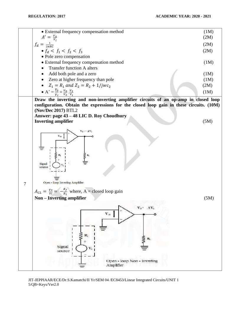
Draw the inverting and non-inverting amplifier circuits of an op-amp in closed loop
configuration. Obtain the expressions for the closed loop gain in these circuits. (10M)
(Nov/Dec 2017) BTL2
Answer: page 43 – 48 LIC D. Roy Choudhury
Inverting amplifier (5M)
𝐴𝐶𝐿 = 𝑉𝑜
𝑉𝑖= −
𝑅𝑓
𝑅1 where, A = closed loop gain
Non – Inverting amplifier (5M)

REGULATION: 2017 ACADEMIC YEAR: 2020 - 2021
JIT-JEPPIAAR/ECE/Dr.S.Kamatchi/II Yr/SEM 04 /EC8453/Linear Integrated Circuits/UNIT 1
5/QB+Keys/Ver2.0
𝐴𝐶𝐿 = 𝑉𝑜
𝑉𝑖= 1 +
𝑅𝑓
𝑅1 where A = closed loop gain
8
What is a current mirror? Give the current mirror circuit analysis. (8M) (Nov/Dec 2009)
BTL2
Answer: page 65 – 67 LIC D. Roy Choudhury
Basic current mirror circuit figure 1.1
Output current characteristics figure 1.2 (6M)
Collector current independent of collector voltage
Bases and emitter of Q1,Q2 tied together.
𝐼0 = 𝐼𝑟𝑒𝑓 (2M)
PART *C
1
Discuss about the principle of operation differential amplifier using BJT.(15M) (Apr/May
2018) (BTL 2)
Answer: page 53 – 61 LIC D. Roy Choudhury
Basic differential amplifier using BJT figure 1.12 (6M)
Types of operation
Common mode and Differential mode operation (9M)
Current mirror with active load figure 1.13

REGULATION: 2017 ACADEMIC YEAR: 2020 - 2021
JIT-JEPPIAAR/ECE/Dr.S.Kamatchi/II Yr/SEM 04 /EC8453/Linear Integrated Circuits/UNIT 1
5/QB+Keys/Ver2.0
2
Explain about Ideal Op-amp in detail with suitable diagrams.(15M) (Apr/May 2018) BTL 2
Answer: page 41 – 48 LIC D. Roy Choudhury
Ideal op-amp (6M)
Ideal characteristics (1M)
Open loop voltage gain A=∞ (2M)
Input impedance Ri = ∞ (2M)
Output impedance Ro = 0 (2M)
Bandwidth BW = (1M)
Zero offset V0 = 0, when V1=0, V2=0
Vd = V1 – V2 (1M)
3
With a help of a diagram, explain the various stages present in an operational amplifier.
(15M) (Nov/Dec 2017) (BTL 2)
Answer: page 41 – 48 LIC D. Roy Choudhury
• Differential amplifier (1M)
• Level translator (1M)
• Gain Stage (3M)
• Output stage, input stage (2M)
• Bias Circuit (3M)
• Diagram figure 1.17 (5M)

REGULATION: 2017 ACADEMIC YEAR: 2020 - 2021
JIT-JEPPIAAR/ECE/Dr.S.Kamatchi/II Yr/SEM 04 /EC8453/Linear Integrated Circuits/UNIT 1
5/QB+Keys/Ver2.0

REGULATION: 2017 ACADEMIC YEAR: 2020 - 2021
JIT-JEPPIAAR/ECE/Dr.S.Kamatchi/II Yr/SEM 04 /EC8453/Linear Integrated Circuits/UNIT 1
5/QB+Keys/Ver2.0
Subject Code:EC8453 Year/Semester: II /04
Subject Name: LINEAR INTEGRATED CIRCUITS Subject Handler: Dr. S. KAMATCHI
UNIT II - APPLICATIONS OF OPERATIONAL AMPLIFIERS
Sign Changer, Scale Changer, Phase Shift Circuits, Voltage Follower, V-to-I and I-to-V converters,
adder, subtractor, Instrumentation amplifier, Integrator, Differentiator, Logarithmic
amplifier,Antilogarithmic amplifier, Comparators, Schmitt trigger, Precision rectifier, peak
detector, clipper and clamper, Low-pass, high-pass and band-pass Butterworth filters.
PART * A
Q.No. Questions
1.
Mention some of the linear applications of op – amps. (DEC 09) BTL 2
• Adder, sub tractor,
• Voltage –to current converter,
• current –to- voltage converters,
• Instrumentation amplifier,
• Analog computation
• power amplifier
2
Mention some of the non – linear applications of op-amps. BTL 2
• Rectifier, peak detector,
• clipper, clamper,
• sample and hold circuit,
• log amplifier, anti –log amplifier
3
What are the areas of application of non-linear op- amp circuits? BTL 1
• Industrial instrumentation
• Communication
• Signal processing
4 What is voltage follower?(MAY 2010) BTL 1
A circuit in which output follows the input is called voltage follower.
5
What is the need for an instrumentation amplifier? BTL 1
In a number of industrial and consumer applications, the measurement of physical quantities is
usually done with the help of transducers. The output of transducer has to be amplified So
that it can drive the indicator or display system. This function is performed by an instrumentation
amplifier.
6
List the features of instrumentation amplifier. BTL 1
• High gain accuracy
• High CMRR
• High gain stability with low temperature co-efficient 4 low DC offset
• Low output impedance
7
What are the applications of V-I converter? BTL 1
• Low voltage dc and ac voltmeter
• LED
• Zener diode tester
8 Define Band pass filter. (MAY 2010) BTL 1

REGULATION: 2017 ACADEMIC YEAR: 2020 - 2021
JIT-JEPPIAAR/ECE/Dr.S.Kamatchi/II Yr/SEM 04 /EC8453/Linear Integrated Circuits/UNIT 1
5/QB+Keys/Ver2.0
The band pass filter is the combination of high and low pass filters, and this allows a specified
range of frequencies to pass through.
9
Write transfer function of op amp as an integer. (MAY 2010) BTL 1
The transfer function of the integer is
A=1/ωR1cf
10
What do you mean by a precision diode? BTL 1
The major limitation of ordinary diode is that it cannot rectify voltages below the cut – in voltage
of the diode. A circuit designed by placing a diode in the feedback loop of an op – amp is called
the precision diode and it is capable of rectifying input signals of the order of milli volt.
11
Write down the applications of precision diode. BTL 1
• Half - wave rectifier
• Full - Wave rectifier
• Peak – value detector
• Clipper
• Clamper
12
Define Logarithmic and antilogarithmic amplifier. (MAY 2010) BTL 1
When a logarithmic PN junction is used in the feedback network of op-amp, the circuit exhibits
log or antilog response. The logarithmic amplifier is a current to voltage converter with the transfer
characteristics v0=vi In(If/Ii).
Antilog amplifier is a decoding circuit which converts the logarithmically encoded signal back to
the original signal levels as given by v1=vR10-kvi.
13
Differentiate Schmitt trigger and comparator. BTL 4
• It compares the input signal with references voltage then yields the output voltage
• It need not consist of feedback
• comparator output need not to be square wave
14
List the applications of Log amplifiers. BTL 1
• Analog computation may require functions such as lnx, log x, sin hx etc. These functions
can be performed by log amplifiers
• Log amplifier can perform direct dB display on digital voltmeter and spectrum analyzer
• Log amplifier can be used to compress the dynamic range of a signal
15
What are the limitations of the basic differentiator circuit? BTL 1
• At high frequency, a differentiator may become unstable and break into oscillations
• The input impedance decreases with increase in frequency , thereby 0making the circuit
sensitive to high frequency noise.
16
Write down the condition for good differentiation. BTL 1
• For good differentiation, the time period of the input signal must be greater than or equal
to Rf C1
• T > R f C1 Where, Rf is the feedback resistance
• Cf is the input capacitance
17
What is a comparator? (MAY 2010) BTL 1
A comparator is a circuit which compares a signal voltage applied at one input of an op amp with
a known reference voltage at the other input. It is an open loop op - amp with output + Vsat.
18 What are the applications of comparator? BTL 1
• Zero crossing detectors

REGULATION: 2017 ACADEMIC YEAR: 2020 - 2021
JIT-JEPPIAAR/ECE/Dr.S.Kamatchi/II Yr/SEM 04 /EC8453/Linear Integrated Circuits/UNIT 1
5/QB+Keys/Ver2.0
• Window detector
• Time marker generator
• Phase detector
19
What is a Schmitt trigger? (DEC 09,MAY 10) BTL 1
Schmitt trigger is a regenerative comparator. It converts sinusoidal input into a square wave
output. The output of Schmitt trigger swings between upper and lower threshold voltages, which
are the reference voltages of the input waveform.
20
What is a multivibrator? BTL 1
Multi vibrators are a group of regenerative circuits that are used extensively in timing applications.
It is a wave shaping circuit which gives symmetric or asymmetric square output. It has two states
stable or quasi- stable depending on the type of multivibrator.
21
What do you mean by monostable multivibrator? BTL 1
• Monostable multivibrator is one which generates a single pulse of specified duration in
response to each external trigger signal. It has only one stable state.
• Application of a trigger causes a change to the quasi-stable state.
• An external trigger signal generated due to charging and discharging of the
capacitor produces the transition to the original stable state.
22
What is an astable multivibrator? BTL 1
Astable multivibrator is a free running oscillator having two quasi-stable states. Thus, there are
oscillations between these two states and no external signal are required to produce the change in
state.
23
What are the characteristics of a comparator? BTL 1
• Speed of operation
• Accuracy
• Compatibility of the output
24
What is a filter? BTL 1
Filter is a frequency selective circuit that passes signal of specified band of frequencies and
attenuates the signals of frequencies outside the band.
25
What are the demerits of passive filters? BTL 1
Passive filters works well for high frequencies. But at audio frequencies, the inductors become
problematic, as they become large, heavy and expensive. For low frequency applications, more
number of turns of wire must be used which in turn adds to the series resistance degrading
inductor’s performance ie, low Q, resulting in high power dissipation.
PART * B
1
With neat sketch explain the operation of a 3 op-amp instrumentation amplifier.
(13M) (Nov/Dec 2014) BTL 1
Answer: page 141 – 144 LIC D.Roy Choudhury
• High gain accuracy (1M)
• High CMRR (1M)
• High gain stability with low temperature coefficient (1M)
• Low dc offset (1M)
• Low output impedance (1M)
• 𝑉0 = 𝑅2𝑅1
(𝑉1 − 𝑉2) (2M)

REGULATION: 2017 ACADEMIC YEAR: 2020 - 2021
JIT-JEPPIAAR/ECE/Dr.S.Kamatchi/II Yr/SEM 04 /EC8453/Linear Integrated Circuits/UNIT 1
5/QB+Keys/Ver2.0
Instrumentation Amplifier figure 2.18, 2.19 (6M)
2
With neat diagram explain logarithmic amplifier and antilogarithmic amplifier. (13M) (May/
June 2014) BTL1
Answer: page 155 – 159 LIC D.Roy Choudhury
Direct DB display on digital voltmeter, spectrum analyzer. (2M)
Compress dynamic range of signal. (1M)
Diagram: (5M)
Anti – log Amplifier: (5M)

REGULATION: 2017 ACADEMIC YEAR: 2020 - 2021
JIT-JEPPIAAR/ECE/Dr.S.Kamatchi/II Yr/SEM 04 /EC8453/Linear Integrated Circuits/UNIT 1
5/QB+Keys/Ver2.0
3
With neat diagram explain the application of op-amp as precision rectifier, clipper and
clamper. (13M) (May/ June 2014) BTL2
Answer: page 148 – 153 LIC D.Roy Choudhury
Typical applications of precision diode
Half wave rectifier and waveform figure 2.41 (3M)
Full wave rectifier (3M)

REGULATION: 2017 ACADEMIC YEAR: 2020 - 2021
JIT-JEPPIAAR/ECE/Dr.S.Kamatchi/II Yr/SEM 04 /EC8453/Linear Integrated Circuits/UNIT 1
5/QB+Keys/Ver2.0
Clipper and waveform figure 2.44,2.45 (7M)
Clamper and waveform figure 2.48,2.49
4 What is an active integrator? Explain the working of an active integrator. (8M) (Nov/Dec

REGULATION: 2017 ACADEMIC YEAR: 2020 - 2021
JIT-JEPPIAAR/ECE/Dr.S.Kamatchi/II Yr/SEM 04 /EC8453/Linear Integrated Circuits/UNIT 1
5/QB+Keys/Ver2.0
2009) BTL2
Answer: page 168 – 171 LIC D.Roy Choudhury
Integrator – simple low pass RC circuit (1M)
Inverting integrator (1M)
𝐴 = 1
𝑤𝑅1𝐶𝑓 (1M)
Integrator circuit figure 2.21 (5M)
5
With a neat circuit diagram explain the working of op-amp based Schmitt trigger. (8M)
(Nov/Dec 2009) BTL2
Answer: page 212 – 214 LIC D.Roy Choudhury
𝑉𝑈𝑇 = 𝑉𝑟𝑒𝑓𝑅1
𝑅1+𝑅2+ 𝑅2𝑉𝑠𝑎𝑡
𝑅1𝑅2 (1M)
𝑉𝑈𝑇 = 𝑉𝑟𝑒𝑓𝑅1
𝑅1+𝑅2− 𝑅2𝑉𝑠𝑎𝑡
𝑅1𝑅2 (1M)
𝑉𝐻 = 𝑉𝑈𝑇 − 𝑉𝐿𝑇 (2M)
𝑉𝐻 = 2𝑅2𝑉𝑠𝑎𝑡𝑅1+𝑅2
Schmitt trigger figure 2.38 (4M)

REGULATION: 2017 ACADEMIC YEAR: 2020 - 2021
JIT-JEPPIAAR/ECE/Dr.S.Kamatchi/II Yr/SEM 04 /EC8453/Linear Integrated Circuits/UNIT 1
5/QB+Keys/Ver2.0
6
Design an op-amp based second order active low pass filter with cut off frequency 2KHz.
(8M) (Nov/Dec 2011) BTL3
Answer: page 265 – 268 LIC D.Roy Choudhury
𝑉𝑜 = 𝐴𝑜𝑉𝐵 (1M)
𝑉𝐵 voltage at node B
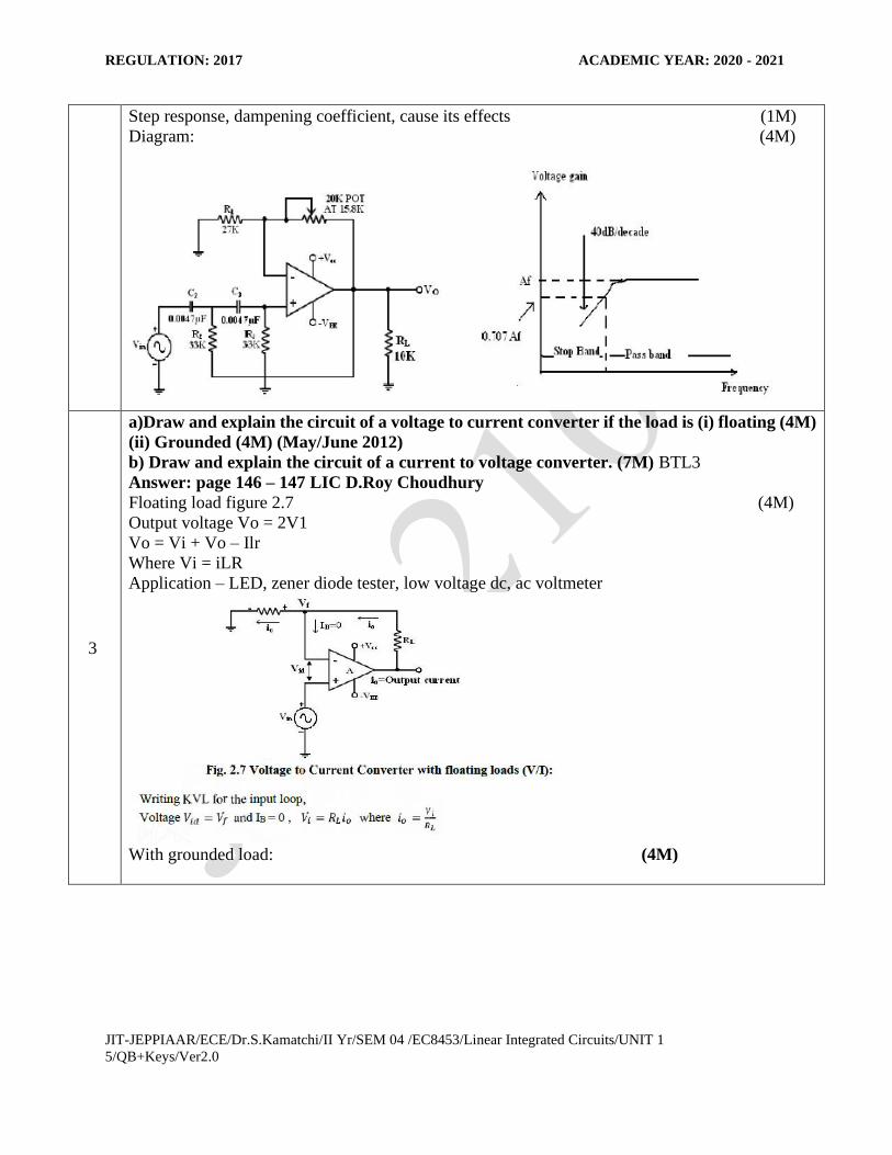
Step response, dampening coefficient, cause its effects
Low pass filter figure 2.55 (3M)
Design: (4M)
• Choose a value for a high cut off freq. (fHz ).
• To simplify the design calculations, set R2 = R3 = R and C2 = C3 = C then choose a value
of C<=1μf.
• Calculate the value of R R =1/2πfhC
• Finally, because of the equal resistor (R2 = R3) and capacitor (C2 = C3 ) values, the pass
band volt gain AF = 1 + RF / R1 of the second order had to be = to 1.586. RF = 0.586 R1.
• Hence choose a value of R1 <=100kΩ.
• Calculate the value of RF.
7
Write in detail about summing amplifier. (8M) BTL2
Answer: page 135 – 137 LIC D.Roy Choudhury
Inverting summing amplifier figure 2.13 (4M)

REGULATION: 2017 ACADEMIC YEAR: 2020 - 2021
JIT-JEPPIAAR/ECE/Dr.S.Kamatchi/II Yr/SEM 04 /EC8453/Linear Integrated Circuits/UNIT 1
5/QB+Keys/Ver2.0
𝑉𝑜 = - (𝑉1+𝑉2+𝑉3
3)
Non inverting summing amplifier figure 2.14 (4M)
𝑉𝑜 = (1 + 𝑅𝑓
𝑅)𝑉𝑎
8
Explain voltage follower with neat sketch. (8M) BTL2
Answer: page 49 – 50 LIC D.Roy Choudhury
Rf = 0, R1 = ∞ (1M)
Non inverting amplifier (1M)
Output voltage follows input voltage (1M)
Buffer for impedance matching (1M)
Connect a high impedance source to a low impedance load (1M)
Diagram : (3M)
PART *C
1
Sketch the basic circuit using op-amp to perform the mathematical operation of
differentiation and explain. What are the limitations of an ordinary op-amp differentiator?
Draw and explain the circuit of a practical differentiator that will eliminate these limitations.

REGULATION: 2017 ACADEMIC YEAR: 2020 - 2021
JIT-JEPPIAAR/ECE/Dr.S.Kamatchi/II Yr/SEM 04 /EC8453/Linear Integrated Circuits/UNIT 1
5/QB+Keys/Ver2.0
(15M) (May/June 2012) BTL3.
Answer: page 164 – 170 LIC D.Roy Choudhury
Differentiator circuit and waveform figure 2.24,2.25 (7M)
Contains capacitor at input
𝑉𝑜 = −𝑅𝑓𝐶1𝑑𝑣𝑖
𝑑𝑡
Integrator circuit figure 2.21 (8M)
Integrator – simple low pass RC circuit
Inverting integrator
𝐴 = 1
𝑤𝑅1𝐶𝑓

REGULATION: 2017 ACADEMIC YEAR: 2020 - 2021
JIT-JEPPIAAR/ECE/Dr.S.Kamatchi/II Yr/SEM 04 /EC8453/Linear Integrated Circuits/UNIT 1
5/QB+Keys/Ver2.0
2
a) Explain the working of an op-amp based regenerative comparator circuit? (8M)
(May/June 2012), (Nov/Dec 2011).
b) Design an op-amp based second order active low pass filter with cut off frequency 2KHz.
(7M) BTL3
Answer: page 212 – 215,265 - 267 LIC D.Roy Choudhury
𝑉𝑈𝑇 = 𝑉𝑟𝑒𝑓𝑅1
𝑅1+𝑅2+ 𝑅2𝑉𝑠𝑎𝑡
𝑅1𝑅2 (1M)
𝑉𝐿𝑇 = 𝑉𝑟𝑒𝑓𝑅1
𝑅1+𝑅2− 𝑅2𝑉𝑠𝑎𝑡
𝑅1𝑅2 (1M)
𝑉𝐻 = 𝑉𝑈𝑇 − 𝑉𝐿𝑇 (1M)
𝑉𝐻 = 2𝑅2𝑉𝑠𝑎𝑡𝑅1+𝑅2
(1M)
Schmitt trigger figure 2.38 (4M)
II ORDER HPF:
𝑉𝑜 = 𝐴𝑜𝑉𝐵 (1M)
𝑉𝐵 voltage at node B (1M)
REGULATION: 2017 ACADEMIC YEAR: 2020 - 2021
JIT-JEPPIAAR/ECE/Dr.S.Kamatchi/II Yr/SEM 04 /EC8453/Linear Integrated Circuits/UNIT 1
5/QB+Keys/Ver2.0
Step response, dampening coefficient, cause its effects (1M)
Diagram: (4M)
3
a)Draw and explain the circuit of a voltage to current converter if the load is (i) floating (4M)
(ii) Grounded (4M) (May/June 2012)
b) Draw and explain the circuit of a current to voltage converter. (7M) BTL3
Answer: page 146 – 147 LIC D.Roy Choudhury
Floating load figure 2.7 (4M)
Output voltage Vo = 2V1
Vo = Vi + Vo – Ilr
Where Vi = iLR
Application – LED, zener diode tester, low voltage dc, ac voltmeter
With grounded load: (4M)

REGULATION: 2017 ACADEMIC YEAR: 2020 - 2021
JIT-JEPPIAAR/ECE/Dr.S.Kamatchi/II Yr/SEM 04 /EC8453/Linear Integrated Circuits/UNIT 1
5/QB+Keys/Ver2.0
Current to voltage converter figure 2.9 (7M)

REGULATION: 2017 ACADEMIC YEAR: 2020 - 2021
JIT-JEPPIAAR/ECE/Dr.S.Kamatchi/II Yr/SEM 04 /EC8453/Linear Integrated Circuits/UNIT 1
5/QB+Keys/Ver2.0
Subject Code: EC8453 Year/Semester: II /04
Subject Name: LINEAR INTEGRATED CIRCUITS Subject Handler: Dr. S. KAMATCHI
UNIT III - ANALOG MULTIPLIER AND PLL
Analog Multiplier using Emitter Coupled Transistor Pair - Gilbert Multiplier cell – Variable trans
conductance technique, analog multiplier ICs and their applications, Operation of the basic PLL, Closed
loop analysis, Voltage controlled oscillator, Monolithic PLL IC 565, application of PLL for AM
detection, FM detection, FSK modulation and demodulation and Frequency synthesizing and clock
synchronisation.
PART * A
Q.No. Questions
1.
List the basic building blocks of PLL. BTL1
• Phase detector/comparator
• Low pass filter
• Error amplifier
• Voltage controlled oscillator
2
Define FSK modulation.(MAY 2010) BTL1
FSK is a type of frequency modulation in which the binary data or code is transmitted by means
of a carrier frequency that is shifted between two fixed frequency namely mark(logic1) and space
frequency(logic 0).
3
What is analog multiplier?(MAY 2010) BTL1
A multiplier produces an output 𝑽𝟎, which is proportional to the product of two inputs 𝑽𝒙 and
𝑽𝒚. 𝑽𝟎 =K 𝑽𝒙 𝑽𝒚
4
List out the various methods available for performing for analog multiplier. BTL1
• Logarithmic summing technique
• Pulse height /width modulation technique
• Variable trans conductance technique
• Multiplication using gilbert cell
• Multiplication technique using trans conductance technique
5
Mention some areas where PLL is widely used. (DEC 2009) BTL1
• Radar synchronizations
• Satellite communication systems
• Air borne navigational systems
• FM communication systems
• Computers.
6
What are the three stages through which PLL operates? BTL1
• Free running
• Capture
• Locked/ tracking
7
Define lock-in range of a PLL. (MAY 2010) BTL1
The range of frequencies over which the PLL can maintain lock with the incoming signal is called
the lock-in range or tracking range. It is expressed as a percentage of the VCO free running
frequency.

REGULATION: 2017 ACADEMIC YEAR: 2020 - 2021
JIT-JEPPIAAR/ECE/Dr.S.Kamatchi/II Yr/SEM 04 /EC8453/Linear Integrated Circuits/UNIT 1
5/QB+Keys/Ver2.0
8
Define capture range of PLL. (MAY 2010) BTL1
The range of frequencies over which the PLL can acquire lock with an input signal is called the
capture range. It is expressed as a percentage of the VCO free running frequency.
9
Write the expression for FSK modulation.(MAY 2010) BTL1
The expression for FSK modulation is,
Δvf=f2-f1/k0
10
Define free running mode .(MAY 2010) BTL1
An interactive computer mode that allows more than one user to have simultaneous use of a
program.
11
For perfect lock, what should be the phase relation between the incoming signal and VCO
output signal? BTL2
The VCO output should be 90 degrees out of phase with respect to the input signal.
12
Give the classification of phase detector. BTL1
• Analog phase detector .
• Digital phase detector
13
What is a switch type phase detector? BTL1
An electronic switch is opened and closed by signal coming from VCO and the input signal is
chopped at a repetition rate determined by the VCO frequency. This type of phase detector is
called a half wave detector since the phase information for only one half of the input signal is
detected and averaged.
14
What are the problems associated with switch type phase detector? BTL1
• The output voltage Ve is proportional to the input signal amplitude. This is undesirable
because it makes phase detector gain and loop gain dependent on the input signal
amplitude.
• The output is proportional to cosφ making it non linear.
15
What is a voltage controlled oscillator? BTL1
Voltage controlled oscillator is a free running multi vibrator operating at a set frequency called
the free running frequency. This frequency can be shifted to either side by applying a dc control
voltage and the frequency deviation is proportional to the dc control voltage
16
Define Voltage to Frequency conversion factor. BTL1
Voltage to Frequency conversion factor is defined as,
Kv = fo / Vc= 8fo /Vcc
Where, Vc is the modulation voltage fo frequency shift.
17
What is the purpose of having a low pass filter in PLL? BTL1
• It removes the high frequency components and noise.
• Controls the dynamic characteristics of the PLL such as capture range, lock-in range,
band-width and transient response.
• The charge on the filter capacitor gives a short- time memory to the PLL
18
Discuss the effect of having large capture range. BTL2
The PLL cannot acquire a signal outside the capture range, but once captured, it will hold on till
the frequency goes beyond the lock-in range. Thus, to increase the ability of lock range, large
capture range is required. But, a large capture range will make the PLL more susceptible to noise
and undesirable signal.
19 Mention some typical applications of PLL. BTL1

REGULATION: 2017 ACADEMIC YEAR: 2020 - 2021
JIT-JEPPIAAR/ECE/Dr.S.Kamatchi/II Yr/SEM 04 /EC8453/Linear Integrated Circuits/UNIT 1
5/QB+Keys/Ver2.0
• Frequency multiplication/division
• Frequency translation
• AM detection
• FM demodulation
• FSK demodulation.
20
What is a compander IC? Give some examples.(DEC 2009) BTL1
The term commanding means compressing and expanding. In a communication system, the audio
signal is compressed in the transmitter and expanded in the receiver.
Examples: LM 2704- LM 2707; NE 570/571.
21
What are the merits of companding? BTL1
• The compression process reduces the dynamic range of the signal before it is transmitted.
• Companding preserves the signal to noise ratio of the original signal and avoids non linear
distortion of the signal when the input amplitude is large.
• It also reduces buzz,bias and low level audio tones caused by mild interference.
22
List the applications of analog multipliers.(May/June 2013) BTL1
• Analog computer
• Analog signal processing
• Automatic gain control
• True RMS converter
• Analog filter (especially voltage-controlled filters)
• PAM-pulse amplitude modulation
23
In what way VCO is different from other oscillator. (May/June 2012) BTL2
• To adjust the output frequency to match (or perhaps be some exact multiple of)
an accurate external reference.
• Where the oscillator drives equipment that may generate radio-frequency
interference, adding a varying voltage to its control input can disperse the
interference spectrum to make it less objectionable. See spread spectrum clock.
24
List the applications of NE565. (Nov/Dec2010) BTL1
• Frequency multiplier
• FM Demodulator is the applications of NE565.
25
Why the VCO is called voltage to frequency converter? (Nov/Dec 2012) BTL1
The VCO provides the linear relationship between the applied voltage and the oscillation frequency.
Applied voltage is called control voltage. The control of frequency with the help of control voltage
is also called voltage to frequency conversion. Hence VCO is also called voltage to frequency
converter.
PART * B
1
Explain the working of voltage controlled oscillator.(8M) (Nov/Dec 2009), (April/May 2010)
BTL2
Answer: page 334 – 336 LIC D. Roy Choudhury
IC signetics NE/SE566 (4M)

REGULATION: 2017 ACADEMIC YEAR: 2020 - 2021
JIT-JEPPIAAR/ECE/Dr.S.Kamatchi/II Yr/SEM 04 /EC8453/Linear Integrated Circuits/UNIT 1
5/QB+Keys/Ver2.0
Application – converts EEGs, EKGs to AF range. (4M)
Fo changes with change in Rt, Ct, voltage at pin 5.
Voltage to frequency conversion factor
𝐾𝑣 = ∆𝑓𝑜
∆𝑉𝑐
𝐾𝑣 = 8𝑓𝑜
𝑉𝑐
2
Draw the pin configuration of PLL IC 565. (8M) BTL1
Answer: page 337 – 342 LIC D. Roy Choudhury
Pin configuration: (4M)
• The important electrical characteristics of 565 PLL,
• Operating frequency range: 0.001Hz to 500 Khz.
• Operating voltage range: ±6 to ±12v (4M)
• Input level required for tracking: 10mv rms min to 3 Vpp max
• Input impedance: 10 K ohms typically.
• Output sink current: 1mA
• Output source current: 10 Ma
3
Brief about PLL application Frequency multiplication / Division. (8M) BTL2
Answer: page 342 – 343 LIC D. Roy Choudhury
• Divide by N network
• Frequency divider insert between the VCO & phase comparator. (2M)

REGULATION: 2017 ACADEMIC YEAR: 2020 - 2021
JIT-JEPPIAAR/ECE/Dr.S.Kamatchi/II Yr/SEM 04 /EC8453/Linear Integrated Circuits/UNIT 1
5/QB+Keys/Ver2.0
• Output of the divider locks to f IN.
• VCO runs at multiple of input frequency. (2M)
• Desired amount of multiplication obtains by selecting a proper divide-by-N network,
• where N is an integer.
Diagram: (4M)
4
Elaborate FSK demodulator with neat diagram. (8M) BTL2
Answer: page 344 – 345 LIC D. Roy Choudhury.
• Capacitive coupling - at input to remove dc line. (1M)
• At input of 565, loop locks to input frequency & tracks it between 2 frequencies.
• R1 & C1 determine the free running frequency of VCO,
• 3 stages RC ladder filter - to remove carrier component from output. (2M)
Diagram: (4M)
Applications: (1M)
• Digital data communication, computer peripheral
• Binary data transmits by means of carrier frequency - shifts between two preset
frequencies.
• This type of data transmission called frequency shift keying (FSK) technique.
• The binary data retrieved by FSK demodulator.
5
Describe the working principle of a analog multiplier using emitter coupled transistor pair.
(13M) (Nov/Dec 2014) BTL2
Answer: page 338 – 339 LIC D. Roy Choudhury

REGULATION: 2017 ACADEMIC YEAR: 2020 - 2021
JIT-JEPPIAAR/ECE/Dr.S.Kamatchi/II Yr/SEM 04 /EC8453/Linear Integrated Circuits/UNIT 1
5/QB+Keys/Ver2.0
• Gilbert multiplier cell - modification of the emitter coupled cell (2M)
• Allows four – quadrant multiplication.
• It forms the basis of the integrated circuit balanced Multipliers. (2M)
• Two cross- coupled emitter- coupled pairs in series connection with an emitter coupled pair
form the structure of the Gilbert multiplier cell. (3M)
Circuit Diagram: (6M)
6
Explain in detail the block diagram PLL. (13M) BTL2
Answer: page 338 – 339 LIC D. Roy Choudhury
Circuit Diagram: (7M)
• Center frequency of the PLL - free running frequency of the VCO, given by

REGULATION: 2017 ACADEMIC YEAR: 2020 - 2021
JIT-JEPPIAAR/ECE/Dr.S.Kamatchi/II Yr/SEM 04 /EC8453/Linear Integrated Circuits/UNIT 1
5/QB+Keys/Ver2.0
• fOUT = 1.2/ 4R1C1 (2M)
• where R1&C1 - an external resistor & a capacitor connected to pins 8 & 9.
• VCO free-running frequency fOUT adjusts externally with R1 & C1 to be at center of input
frequency range. (2M)
• C1 can be any value; R1 must have a value between 2 k ohms and 20 K ohms.
• Capacitor C2 connected between 7 & +V.
• Filter capacitor C2 should be large enough to eliminate variations in the demodulated output
voltage in order to stabilize VCO frequency. (2M)
7
Explain the working principle of operational Transconductance Amplifier. (8M) BTL2
Answer: page 342 – 344 LIC D. Roy Choudhury
• Makes use of dependence characteristic of transistor transconductance parameter on emitter
current bias applied. (1M)
• Simple differential circuit arrangement depicting the principle is shown in figure.
• Relationship between V0, Vx given by V0 = gm RL VX (2M)
• where gm = IEE /VT transconductance of stage. (1M)
• Application of second input Vy to reference current source of differential amplifier varies
gm.
• Thus, if RE IEE >>VBE, bias voltage Vy relates to IEE by relation Vy = IEE RE.
• Then, overall voltage transfer expression,
• V0 = gm RLVx = (Vy/VTRE)VxRL
= VxVy RL/ VTRE
Diagram: (4M)
8
Define capture range and lock range . (3M)
Explain the process of capturing the lock and also derive for capture range and lock
range.(10M) BTL2
Answer: page 339 – 342 LIC D. Roy Choudhury
• Lock range(Tracking range): (2M)
The lock range - range of frequencies over which PLL system follows changes in input
frequency fIN.
• Capture range: (1M)

REGULATION: 2017 ACADEMIC YEAR: 2020 - 2021
JIT-JEPPIAAR/ECE/Dr.S.Kamatchi/II Yr/SEM 04 /EC8453/Linear Integrated Circuits/UNIT 1
5/QB+Keys/Ver2.0
Capture range - frequency range in which PLL acquires phase lock.
• Always smaller than lock range. (1M)
• If divider divides by M, it allows the VCO to multiply the reference frequency by N / M.
• In some cases reference frequency constrains by other issues, - then reference divider -
useful. (2M)
• Frequency multiplication - attains by locking PLL to 'N'th harmonic of signal. (2M)
• Let input to phase detector be xc(t) (2M)
• Output of voltage- controlled oscillator (VCO) - xr(t) with frequency ωr(t). (3M)
PART *C
1
Explain with neat block diagrams, how PLL is used as (i) AM Detector (5M) (ii) FM Detector
(5M) (iii) Frequency synthesizer (5M) (May/June 2012) BTL2
Answer: page 342 – 344 LIC D. Roy Choudhury
AM Detector: (5M)
FM Detector: (5M)
• If PLL locks to a FM signal, VCO tracks instantaneous frequency of input signal.
• Filtered error voltage which controls the VCO, maintains lock with input signal to get
demodulated FM output.
• VCO transfer characteristics determine linearity of demodulated output.
• Since, VCO in IC PLL - highly linear, possible to realize highly linear FM
demodulators.
Frequency synthesizer: (5M)

REGULATION: 2017 ACADEMIC YEAR: 2020 - 2021
JIT-JEPPIAAR/ECE/Dr.S.Kamatchi/II Yr/SEM 04 /EC8453/Linear Integrated Circuits/UNIT 1
5/QB+Keys/Ver2.0
• Ability of a frequency synthesizer to generate multiple frequencies is the divider between
the output and feedback input.
• This usually in form of a digital counter, with output signal acts as a clock signal.
• The counter preset to some initial count value,
• counts down at each cycle of clock signal.
• When it reaches zero, the counter output changes state and count value reloads.
2
a) List and define the various performance parameters of a multiplier IC. (5M) (May/June
2012).b) How the multiplier is used as voltage divider? (5M) (May/June 2012). c) How the
multiplier is used as frequency doubler? (5M) (May/June 2012) BTL2
Answer: page 159 – 164 LIC D. Roy Choudhury
Multiplier IC figure 3.10 (5M)
• Circuit whose output voltage at any instant proportional to product of instantaneous value
of two individual input voltages.
• Important applications of these multipliers - multiplication, division, squaring,
• square – rooting of signals, modulation, demodulation.

REGULATION: 2017 ACADEMIC YEAR: 2020 - 2021
JIT-JEPPIAAR/ECE/Dr.S.Kamatchi/II Yr/SEM 04 /EC8453/Linear Integrated Circuits/UNIT 1
5/QB+Keys/Ver2.0
• Available as integrated circuits consists of op-amps and other circuit elements.
• The Schematic of a typical analog multiplier, namely, AD633 is shown in figure.
Voltage divider figure 3.14 (5M)
• No input signal current flow into nverting input terminal of op-amp, - virtual ground.
• Therefore, at the junction a, i1 +i2 =0,
• current i1 = Vnum / R, where R = input resistance.
• current i2 = Vom /R. With virtual ground existing at a,
• i1+i2 = Vnum / R + Vom /R = 0
• KV OA V den = - V num or
• voA=- vnum/Kvden
• where Vnum and Vden numerator, denominator voltages respectively.
Frequency Doubler figure 3.13 (5M)
• Squaring circuit connects for frequency doubling operation.
• Sine-wave signal Vi has a peak amplitude of Av, frequency of f Hz.
• Output waveforms ripple with twice input frequency in rectified output of input signal.
• This forms principle of application of analog multiplier as rectifier of ac signals.
3 i)Discuss the principle of operation of NE 565 PLL circuit. (10M)

REGULATION: 2017 ACADEMIC YEAR: 2020 - 2021
JIT-JEPPIAAR/ECE/Dr.S.Kamatchi/II Yr/SEM 04 /EC8453/Linear Integrated Circuits/UNIT 1
5/QB+Keys/Ver2.0
ii)How can PLL be modeled as a frequency multiplier.(5M) BTL4
Answer: page 337 – 338,342 - 343 LIC D. Roy Choudhury
• Center frequency of PLL - free running frequency of VCO, given by
• fOUT = 1.2/ 4R1C1 (2M)
• where R1&C1 - an external resistor & capacitor connected to pins 8 & 9.
• VCO free-running frequency fOUT adjusts externally with R1 & C1 (2M)
C1 can be any value; R1 must have a value between 2 k ohms and 20 K ohms.
• Capacitor C2 connected between 7 & +V.
Diagram: (6M)
ii) Frequency multiplier (5M)
• Divide by N network
• Frequency divider insert between the VCO & phase comparator.
• Output of the divider locks to f IN.
• VCO runs at multiple of input frequency.
• Desired amount of multiplication obtains by selecting a proper divide-by-N network,
• where N is an integer.

REGULATION: 2017 ACADEMIC YEAR: 2020 - 2021
JIT-JEPPIAAR/ECE/Dr.S.Kamatchi/II Yr/SEM 04 /EC8453/Linear Integrated Circuits/UNIT 1
5/QB+Keys/Ver2.0

REGULATION: 2017 ACADEMIC YEAR: 2020 - 2021
JIT-JEPPIAAR/ECE/Dr.S.Kamatchi/II Yr/SEM 04 /EC8453/Linear Integrated Circuits/UNIT 1
5/QB+Keys/Ver2.0
Subject Code:EC8453 Year/Semester: II /04
Subject Name: LINEAR INTEGRATED CIRCUITS Subject Handler: Dr.S. KAMATCHI
UNIT IV - ANALOG TO DIGITAL AND DIGITAL TO ANALOG
CONVERTERS
Analog and Digital Data Conversions, D/A converter – specifications - weighted resistor type, R-2R
Ladder type, Voltage Mode and Current-Mode R - 2R Ladder types - switches for D/A converters, high
speed sample-and-hold circuits, A/D Converters – specifications - Flash type - Successive
Approximation type - Single Slope type – Dual Slope type - A/D Converter using Voltage-to-Time
Conversion - Over-sampling A/D Converters, Sigma – Delta converters.
PART * A
Q.No. Questions
1.
Give the operation of basic sample and hold circuit. BTL1
A typical sample and hold circuit stores electric charge in a capacitor and contains at least one fast
FET switch and at least one operational amplifier. To sample the input signal the switch connects
the capacitor to the output of a buffer amplifier. The buffer amplifier charges or discharges the
capacitor so that the voltage across the capacitor is practically equal, or proportional to, input
voltage. In hold mode the switch disconnects the capacitor from the buffer. The capacitor is
invariably discharged by its own leakage currents and useful load currents, which makes the circuit
inherently volatile, but the loss of voltage (voltage drop) within a specified hold time remains within
an acceptable error margin.
2
State the advantages and applications of sample and hold circuits. BTL1
A sample and hold circuit is one which samples an input signal and holds on to its last sampled
value until the input is sampled again. This circuit is mainly used in digital interfacing, analog to
digital systems, and pulse code modulation systems.
3
List the drawbacks of binary weighted resistor technique of D/A conversion.BTL1
• Wide range of resistor values needed.
• Difficulty in achieving and maintaining accurate ratios over a wide range of variations
4
What is the advantage and disadvantages of flash type ADC? BTL1
• Flash type ADC is the fastest as well as the most expensive.
• The disadvantage is the number of comparators needed almost doubles for each added bit (For a n-
bit convertor 2(n-1) comparators, 2n resistors are required).
5
The basic step of a 9 bit DAC is 10.3 mV. If 000000000 represents 0Volts, what is the output
for an input of 101101111? BTL2
The output voltage for input of 101101111 is
= 10.3 mV (1*28+0*27+1*26+1*25+0*24+1*23+1*22+1*21+1*20)
= 10.3 * 10-3 * 367 = 3.78 V
6 Find the resolution of a 12 bit DAC converter. BTL1
Resolution (volts) = VFS/(212-1) = I LSB increment VFS – Full scale voltage
7 What are the advantages and disadvantages of R-2R ladder DAC? BTL1 Advantages:
• Easier to build accurately as only two precision metal films are required.

REGULATION: 2017 ACADEMIC YEAR: 2020 - 2021
JIT-JEPPIAAR/ECE/Dr.S.Kamatchi/II Yr/SEM 04 /EC8453/Linear Integrated Circuits/UNIT 1
5/QB+Keys/Ver2.0
• Number of bits can be expanded by adding more sections of same R/2R values.
8
What are the disadvantages of R-2R ladder DAC? BTL1
In this type of DAC, when there is a change in the input, changes the current flow in the resistor
which causes more power dissipation which creates non-linearity in DAC.
9 Define Start of Conversion. BTL1
This is the control signal for start of conversion which initiates A/D conversion process.
10 Define End of Conversion. BTL1
This is the control signal which is activated when the conversion is completed.
11
What are the types of ADC? BTL1
• Flash (comparator) type converter
• Counter type converter
• Tracking or servo converter
• Successive approximation type converter
12
What are the types of DAC? BTL1
• Weighted resistor DAC
• R-2R Ladder
• Inverted R-2R Ladder
13
What is the difference between direct ADC and integrating type ADC? BTL1
The integrating type of ADC’s do not need a sample/Hold circuit at the input.
• It is possible to transmit frequency even in noisy environment or in an isolated form.
14
Define Resolution. BTL1
The resolution of a converter is the smallest change in voltage which may be produced at the output
or input of the converter. Resolution (in volts)= VFS/2n-1=1 LSB increment. The resolution of an
ADC is defined as the smallest change in analog input for a one bit change at the output.
15 What is meant by Accuracy? BTL1
It is the maximum deviation between the actual converter output & the ideal converter output.
16 What is the purpose of DAC Monotonicity? BTL1
A monotonic DAC is one whose analog output increases for an increase in digital input.
17
Define Conversion time. BTL1
It is defined as the total time required to convert an analog signal into its digital output. It depends
on the conversion technique used & the propagation delay of circuit components.
The conversion time of a successive approximation type ADC is given by
T(n+1)
where T---clock period
Tc---conversion time no of bits.
18 Define Relative accuracy. BTL1
Relative Accuracy is the maximum deviation after gain & offset errors have been removed. The
accuracy of a converter is also specified in form of LSB increments or % of full scale voltage.
19 Define dither. BTL1
REGULATION: 2017 ACADEMIC YEAR: 2020 - 2021
JIT-JEPPIAAR/ECE/Dr.S.Kamatchi/II Yr/SEM 04 /EC8453/Linear Integrated Circuits/UNIT 1
5/QB+Keys/Ver2.0
Dither is very small amount of noise to add a before the A/D conversion.
20
Define sampling period and hold period. BTL1
Time duration of capacitor to sample and hold the equal value of voltage input period is called as
sampling period and the time duration of voltage across the capacitor at constant time duration is
called as hold period.
21
Define the term settling time. BTL1
It represents the time it takes for the output to settle within a specified band+-(1/2) LSB of its final
value. It depends upon the switching time of the logic circuitry due to internal parasitic capacitances
and inductances. Settling time ranges from 100ns to 10μs depending on word length and type of
circuit used.
22
Define conversion time. BTL1
It is the time taken for the D/A converter to produce the analog output for the given binary input
signal. It depends on the response time of switches and the output of the Amplifier. D/A converters
speed can be defined by this parameter. It is also called as setting time.
23
Define slew rate and state its significance. (Apr/May 2010) BTL1
The circuit of successive approximation ADC consists of a successive approximation register
(SAR), to find the required value of each bit by trial & error. With the arrival of START command,
SAR sets the MSB bit to 1. The O/P is converted into an analog signal & it is compared with I/P
signal. This O/P is low or high. This process continues until all bits are checked.
24
What is the fastest ADC and why? (Nov/Dec 2010) BTL1
The circuit of successive approximation ADC consists of a successive approximation register
(SAR), to find the required value of each bit by trial & error. With the arrival of START command,
SAR sets the MSB bit to 1. The O/P is converted into an analog signal & it is compared with I/P
signal. This O/P is low or high. This process continues until all bits are checked.
25
An 8 bit DAC has a resolution of 20mV/bit. What is the analog output voltage for the digital
input code 00010110(the MSB is the left most bit)?(Apr/May 2010) BTL2
The output voltage for input 00010110 is
=20 *0* 28
* 0* 27
* 0* 26
*1* 25
* 0* 24
*1* 23
*1* 22
* 0* 21
=20 * 44
=880 Mv
PART * B
1
With neat internal diagram, explain the following (i) Dual slope ADC (7M)
ii) Successive Approximation ADC. (6M) BTL1
Answer: page 361 – 365 LIC D.Roy Choudhury
Dual slope : (7M)
• In Integrating ADC, current, proportional to input voltage, charges a capacitor for a fixed time
interval T charge. (2M)
• At the end of this interval, the device resets its counter and applies an opposite-polarity negative
reference voltage to the integrator input. (2M)
• Because of this, the capacitor is discharged by a constant current until the integrator output voltage
zero again. (1M)
• The T discharge interval is proportional to the input voltage level and the resultant final count

REGULATION: 2017 ACADEMIC YEAR: 2020 - 2021
JIT-JEPPIAAR/ECE/Dr.S.Kamatchi/II Yr/SEM 04 /EC8453/Linear Integrated Circuits/UNIT 1
5/QB+Keys/Ver2.0
provides the digital output, corresponding to the input signal. (2M)
Successive Approximation ADC: (6M)
2
i)Estimate the working of R‐2R ladder type DAC. (10M)
ii)Compare binary weighted DAC with R‐2R ladder network DAC. (3M) BTL1
Answer: page 352 – 353,349 - 351 LIC D.Roy Choudhury
Tabulation : (3M)
Vout = - (VMSB + Vn + VLSB) = - (VRef + VRef/2 + VRef/ 4) (2M)
Diagram: (5M)

REGULATION: 2017 ACADEMIC YEAR: 2020 - 2021
JIT-JEPPIAAR/ECE/Dr.S.Kamatchi/II Yr/SEM 04 /EC8453/Linear Integrated Circuits/UNIT 1
5/QB+Keys/Ver2.0
• Enhancement of binary-weighted resistor DAC - R-2R ladder network. (1M)
• DAC utilizes Thevenin’s theorem in arriving at desired output voltages.
• Disadvantage of the former DAC design - its requirement of several different precise input resistor
values. (1M)
• one unique value per binary input bit.
• R-2R network consists of resistors with only two values - R and 2xR. (1M)
• If each input supplied either 0 volts or reference voltage, the output voltage will be an analog
equivalent of the binary value of the three bits.
• VS2 corresponds to the most significant bit (MSB) while VS0 corresponds to the least significant
bit (LSB).
3
With circuit schematic explain analog switches using FET. (13M) BTL1
Answer: page 361 – 365 LIC D.Roy Choudhury
• Two types of analog switches. (1M)
• Series and Shunt switch. (2M)
• Switch operation is shown for both the cases VGS=0 VGS= VGs (off) (2M)
Diagram: (8M)

REGULATION: 2017 ACADEMIC YEAR: 2020 - 2021
JIT-JEPPIAAR/ECE/Dr.S.Kamatchi/II Yr/SEM 04 /EC8453/Linear Integrated Circuits/UNIT 1
5/QB+Keys/Ver2.0
4
i)Categorize the different sources of error in DAC. (7M)
ii)Analyze the types of errors in DAC. (6M) BTL4
Answer: page 349 – 355 LIC D.Roy Choudhury
Sampling rate (3M)
• The analog signal is continuous in time and it is necessary to convert this to a flow of
• digital values.
• It is therefore required to define the rate at which new digital values are sampled from the analog
signal.
• The rate of new values is called the sampling rate or sampling frequency of the converter.
• The accuracy is limited by quantization error.
Accuracy (4M)
• An ADC has several sources of errors.
• Quantization error and (assuming the ADC is intended to be linear) non-linearity is intrinsic to
any analog-to-digital conversion.

REGULATION: 2017 ACADEMIC YEAR: 2020 - 2021
JIT-JEPPIAAR/ECE/Dr.S.Kamatchi/II Yr/SEM 04 /EC8453/Linear Integrated Circuits/UNIT 1
5/QB+Keys/Ver2.0
• There is also a so called aperture error which is due to a clock jitter and is revealed when
digitizing a time-variant signal (not a constant value).
• These errors are measured in a unit called the LSB, which is an abbreviation for least significant
bit.
Quantization error (3M)
• Quantization error is due to the finite resolution of the ADC, and is an unavoidable imperfection
in all types of ADC.
• The magnitude of the quantization error at the sampling instant is between zero and half of one
LSB.
• In the general case, the original signal is much larger than one LSB.
• When this happens, the quantization error is not correlated with the signal, and has a uniform
distribution.
Non-linearity (3M)
• These errors can sometimes be mitigated by calibration, or prevented by testing.
• Important parameters for linearity are integral non-linearity (INL) and differential non- linearity
(DNL).
• These non-linear ties reduce the dynamic range of the signals that can be digitized by the ADC,
also reducing the effective resolution of the ADC.
5
Show the operation of any two direct type of ADC. (13M) BTL2
Answer: page 361 – 365 LIC D.Roy Choudhury
• Process extremely fast with a sampling rate of up to 1 GHz. (1M)
• Resolution however, limited because of large number of comparators, reference voltages required.
(1M)
• Input signal fed simultaneously to all comparators. (1M)
• Priority encoder then generates a digital output that corresponds with the highest activated
comparator. (1M)
Diagram: (3M)

REGULATION: 2017 ACADEMIC YEAR: 2020 - 2021
JIT-JEPPIAAR/ECE/Dr.S.Kamatchi/II Yr/SEM 04 /EC8453/Linear Integrated Circuits/UNIT 1
5/QB+Keys/Ver2.0
Successive Approximation method:
• Bit-weighting conversion, similar to a binary. (1M)
• Analogue value rounded to the nearest binary value below,
Because the approximations are successive (not simultaneous), conversion takes one clock-cycle
for each bit of resolution desired. (1M)
Circuit Diagram: (4M)
6 Discuss in detail about the following Digital to Analog & Analog to Digital conversion
techniques.

REGULATION: 2017 ACADEMIC YEAR: 2020 - 2021
JIT-JEPPIAAR/ECE/Dr.S.Kamatchi/II Yr/SEM 04 /EC8453/Linear Integrated Circuits/UNIT 1
5/QB+Keys/Ver2.0
i)Flash type ADC (6M)
ii)Weighted Resistor DAC. (7M) BTL1
Answer: page 358 – 360,349 - 351 LIC D.Roy Choudhury
• Process extremely fast with a sampling rate of up to 1 GHz. (1M)
• Resolution however, limited because of large number of comparators, reference voltages required.
(1M)
• Input signal fed simultaneously to all comparators. (1M)
• Priority encoder then generates a digital output that corresponds with the highest activated
comparator. (1M)
Diagram: (2M)
Weighted Resistor DAC:
For a n-bit DAC, the relationship between Vout and the binary input is as follows: (2M)
The LSB, which is also the incremental step, has a value of - 0.625 V while the MSB or the full
scale has a value of - 9.375 V. (1M)
Diagram: (4M)

REGULATION: 2017 ACADEMIC YEAR: 2020 - 2021
JIT-JEPPIAAR/ECE/Dr.S.Kamatchi/II Yr/SEM 04 /EC8453/Linear Integrated Circuits/UNIT 1
5/QB+Keys/Ver2.0
7
i)Draw the diagram of sample and hold circuit. (7M)
ii)State how you will reduce its hold mode drop. (6M) BTL2
Answer: page 153 - 154 LIC D.Roy Choudhury
Circuit Diagram: (4M)
• During sample mode, the SOP behaves just like a regular op-amp, in which the value of the output
follows the value of the input. (1M)
• During hold mode, the MOS transistors at the output node of the SOP are turned off while they are
still operating in saturation, thus preventing any channel charge from flowing into the output of the
SOP. (2M)
• In addition, the SOP is shut off and its output is held at high impedance, allowing the charge on Ch
to be preserved throughout the hold mode. (2M)
• On the other hand, the output buffer of this S/H circuit is always operational during sample and
hold mode and is always providing the voltage on Ch to the output of the S/H circuit. (1M)
Circuit Diagram : (3M)

REGULATION: 2017 ACADEMIC YEAR: 2020 - 2021
JIT-JEPPIAAR/ECE/Dr.S.Kamatchi/II Yr/SEM 04 /EC8453/Linear Integrated Circuits/UNIT 1
5/QB+Keys/Ver2.0
8
Explain the working of a voltage to time converter and voltage to frequency converter.(7M)
Construct the working of dual slope ADC and explain. (6M) BTL2
Answer: page 363 - 365 LIC D.Roy Choudhury
• Analog voltage required to be converted to a proportional time period. (1M)
• As shown in diagram a negative reference voltage -VR is applied to an integrator,
• whose output is connected to the inverting input of the comparator.
• output of the comparator is at 1 as long as the output of the integrator Vo is less than Va.
Voltage to time converter: (3M)
Voltage to time conversion process: (3M)
Dual slope :
• In Integrating ADC, current, proportional to input voltage, charges a capacitor for a fixed time
interval T charge. (2M)
• At the end of this interval, the device resets its counter and applies an opposite-polarity negative
reference voltage to the integrator input. (2M)
• Because of this, the capacitor is discharged by a constant current until the integrator output voltage
zero again. (1M)
• The T discharge interval is proportional to the input voltage level and the resultant final count

REGULATION: 2017 ACADEMIC YEAR: 2020 - 2021
JIT-JEPPIAAR/ECE/Dr.S.Kamatchi/II Yr/SEM 04 /EC8453/Linear Integrated Circuits/UNIT 1
5/QB+Keys/Ver2.0
provides the digital output, corresponding to the input signal. (1M)
PART *C
1
With example explain the successive Approximation ADC Technique. (11M)
Discuss the important specification of Data Converters. (4M)
Answer: Page 361 - 363 LIC D.Roy Choudhury
Successive Approximation: (6M)
• bit-weighting conversion, similar to a binary. (1M)
• Analogue value rounded to the nearest binary value below, (1M)
• Because the approximations are successive (not simultaneous), (2M)
• conversion takes one clock-cycle for each bit of resolution desired. (1M)
ii)Data converters:
• input n bit binary word D (1M)
• reference voltage Vr (1M)
• analog output signal (1M)
• output of DAC – voltage or current (1M)
2
Derive the Inverted or Current mode R-2R Ladder Digital to analog converter and explain.
Examine the inverted R-2R ladder (refer above question) has R=Rf=10kΩ and VR=10V.
Calculate the total current delivered to the op-amp and the output voltage when the binary
input is 1110. (15M) BTL3
• Currents given as (4M)
• i1 = VREF/2R = (VREF/R) 2-1,
• i2 = (VREF)/2)/2R = (VREF/R) 2-2………
• in = (VREF/R) 2-n.
• Relationship between the currents given as (4M)

REGULATION: 2017 ACADEMIC YEAR: 2020 - 2021
JIT-JEPPIAAR/ECE/Dr.S.Kamatchi/II Yr/SEM 04 /EC8453/Linear Integrated Circuits/UNIT 1
5/QB+Keys/Ver2.0
• i2 = i1/2
• i3 = i1/4
• i4 = i1/8
• in = i1/ 2n-1
• Using bits to identify status of switches,
• letting V0 = -Rf io gives
• V0 = - (Rf/R) VREF (b12-1 + b22-2+ ……….. + bn2-n) (7M)
3
(i)Compare single slope ADC and dual slope ADC.(3M) BTL4
(ii)Explain the working of dual slope A/D converter.(7M) BTL2
(iii)For a particular dual slope ADC, t1 is 83.33ms and the reference voltage is 100mv.
Calculate t2 if V1 is 100 mv and 2. 200 mv. (5M) BTL3
Answer: page 363 - 366 LIC D.Roy Choudhury
• In Integrating ADC, current, proportional to input voltage, charges a capacitor for a fixed time
interval T charge. (2M)
• At the end of this interval, the device resets its counter and applies an opposite-polarity negative
reference voltage to the integrator input. (2M)
• Because of this, the capacitor is discharged by a constant current until the integrator output voltage
zero again. (2M)
The T discharge interval is proportional to the input voltage level and the resultant final count
provides the digital output, corresponding to the input signal. (3M)
𝑻𝟏 = 𝒕𝟐 − 𝒕𝟏 = 𝟐𝒏 𝒄𝒐𝒖𝒏𝒕𝒔
𝒄𝒍𝒐𝒄𝒌 𝒓𝒂𝒕𝒆 (3M)
𝒕𝟑 − 𝒕𝟐 = 𝒅𝒊𝒈𝒊𝒕𝒂𝒍 𝒄𝒐𝒖𝒏𝒕 𝑵
𝒄𝒍𝒐𝒄𝒌 𝒓𝒂𝒕𝒆 (3M)
REGULATION: 2017 ACADEMIC YEAR: 2020 - 2021
JIT-JEPPIAAR/ECE/Dr.S.Kamatchi/II Yr/SEM 04 /EC8453/Linear Integrated Circuits/UNIT 1
5/QB+Keys/Ver2.0
Subject Code:EC8453 Year/Semester: II /04
Subject Name: LINEAR INTEGRATED CIRCUITS Subject Handler: Dr.S. KAMATCHI
UNIT V - WAVEFORM GENERATORS AND SPECIAL FUNCTION ICs
Sine-wave generators, Multivibrators and Triangular wave generator, Saw-tooth wave generator,
ICL8038 function generator, Timer IC 555, IC Voltage regulators – Three terminal fixed and adjustable
voltage regulators - IC 723 general purpose regulator - Monolithic switching regulator, Low Drop –
Out(LDO) Regulators - Switched capacitor filter IC MF10, Frequency to Voltage and Voltage to
Frequency converters, Audio Power amplifier, Video Amplifier, Isolation Amplifier, Opto- couplers and
fibre optic IC.
PART * A
Q.No. Questions
1.
What are the operating modes of a 555 timer? BTL1
• Monostable mode
• Astable mode
2
List out the applications of 555 timer. BTL1
• Oscillator
• pulse generator
• ramp and square wave generator d. mono-shot multivibrator
• burglar alarm
• traffic light control.
3 Define sink current. BTL1
When the output is low, the load current that flows through cted between Vcc and o/p terminal is
called sink current.
4
Define source current. BTL1
When the output is high, the load current that flows through the load connected between ground
and o/p terminal is called source current.
5 What is the use of reset pin of 555 timer? BTL1
This is an interrupt for the timing device when pin 4 is grounded, it stops the working of device
and makes it off.
6
What is the purpose of control voltage pin (5) of 555 timer? BTL1
This pin is the inverting input terminal of comparator. This is reference level for comparator
with which threshold is compared. If reference level is other than 2/3 VCC, then external input is to be given to pin 5. Pulse width modulation is possible due to pin 5.
7
List out the major blocks in functional diagram of 555 timer. BTL1
The IC 555 timer combines the following elements.
• A relaxation oscillator
• RS flip-flop
• Two comparators
• Discharge transistor
8 List the types of regulators? BTL1

REGULATION: 2017 ACADEMIC YEAR: 2020 - 2021
JIT-JEPPIAAR/ECE/Dr.S.Kamatchi/II Yr/SEM 04 /EC8453/Linear Integrated Circuits/UNIT 1
5/QB+Keys/Ver2.0
• Linear regulator
• Switched regulator
9
Write the expression for pulse width of 555 timer in monostable mode. BTL1
Pulse width W = 1.1 RC seconds
R – resistor in ohms,
C – capacitor in farads
10
Write the expression for total time period of 555 timer in astable mode. BTL1
T = 0.693 (RA + 2 RB) C seconds
Where RA,RB are resistors
C is capacitor
11
What is the frequency of oscillation of free running mode of 555 timer? BTL1
F = 1.44/ (RA + 2 RB) C Hz
Where RA,RB are resistors
C is capacitor
12
List out the applications of 555 timer in astable mode. BTL1
• missing pulse detector
• Linear ramp generator
• Frequency divider
• Pulse width modulation.
13
List out the applications of 555 timer in monostable mode. BTL1
• FSK generator
• Pulse-position modulator
14
Define voltage regulators and give the types. BTL1
• A voltage regulator is an electronic circuit that provides a stable dc voltage independent
of the load current, temperature, and ac line voltage variations.
• The classification of voltage regulators:
Series / Linear regulators
Switching regulators.
15
What do you mean by linear voltage regulators? BTL1
Series or linear regulator uses a power transistor connected in series between the unregulated dc
input and the load and it conducts in the linear region .The output voltage is controlled by the
continuous voltage drop taking place across the series pass transistor.
16
Define switched voltage regulators. BTL1
Switching regulators are those which operate the power transistor as a high frequency on/off
switch, so that the power transistor does not conduct current continuously. This gives improved
efficiency over series regulators.
17
What are the advantages of adjustable voltage regulators over the fixed voltage regulators?
BTL1
• Improved line and load regulation by a factor of 10 or more.
• Because of the improved overload protection, greater load current can be drawn.

REGULATION: 2017 ACADEMIC YEAR: 2020 - 2021
JIT-JEPPIAAR/ECE/Dr.S.Kamatchi/II Yr/SEM 04 /EC8453/Linear Integrated Circuits/UNIT 1
5/QB+Keys/Ver2.0
• Improved reliability.
18
List out the parameters related to the fixed voltage regulators. BTL1
• Line regulation
• Load regulation
• Ripple rejection
• Output impedance
• Maximum power dissipation
• Rated output current
19 Define dropout voltage of a fixed voltage regulator. BTL1
It is the minimum voltage that must exist between input and output terminals. For most of
regulators, it is 2 to 3 volts.
20
What is an opto-coupler IC? Give examples. BTL1
• Opto-coupler IC is a combined package of a photo-emitting device and a photosensing
device.
• Examples for opto-coupler circuit : LED and a photo diode, LED and
photo transistor, LED and Darlington.
• Examples for opto-coupler IC : MCT 2F , MCT 2E
21
Mention the advantages of opto-couplers. BTL1
• Better isolation between the two stages.
• Impedance problem between the stages is eliminated.
• Wide frequency response.
22
Why do switching regulators have better efficiency then series regulators? (May/June 2012)
BTL1
In switching regulators, the transistor is operated in cut off region or saturation region. In cut off
region, there is no current and hence power dissipation is almost zero. In the saturation region
there is negligible voltage drop across it hence the power dissipation is almost zero.
23
List the important parts of regulated power supply. (April/May2010) BTL1
• Reference voltage circuit
• Error amplifier
• Series pass transistor
• Feedback network
24
What are the advantages of a switch mode power supplies? (April/May2010) BTL1
• Smaller size
• Lighter weight (from the elimination of low frequency transformers which have a
high weight)
• Lower heat generation due to higher efficiency.
25
What are the disadvantages of linear voltage regulators? (Nov/Dec2011) BTL1
The input step down transformer is bulky and expensive because of low line frequency. Because of low line frequency, large values of filter capacitors are required to decrease the ripple. Efficiency is reduced due to the continuous power dissipation by the transistor as it operates in the linear region.
PART * B

REGULATION: 2017 ACADEMIC YEAR: 2020 - 2021
JIT-JEPPIAAR/ECE/Dr.S.Kamatchi/II Yr/SEM 04 /EC8453/Linear Integrated Circuits/UNIT 1
5/QB+Keys/Ver2.0
1
Write a short notes on
Opto couplers (4M) Switched capacitor filter (4M)
Audio power amplifier (5M) BTL2
Answer: page 288 – 293,193 LIC D.Roy Choudhury
Opto couplers:
Opto couplers or Opto isolators is a combination of light source & light detector in the same
package. (2M)
They are used to couple signal from one point to other optically, by providing a complete electric
isolation between them. This kind of isolation is provided between a low power control circuit &
high power output circuit, to protect the control circuit.
Characteristics of opto coupler:
(i) Current Transfer Ratio: (1M)
It is defined as the ratio of output collector current (Ic) to the input forward current (If)
CTR = Ic/If * 100%. Its value depends on the devices used as source & detector.
(ii) Isolation voltage between input & output:
It is the maximum voltage which can exist differentially between the input & output without
affecting the electrical isolation voltage is specified in K Vrms with a relative humidity of 40 to
60%.
(iii) Response Time:
Response time indicates how fast an opto coupler can change its output state. Response time largely
depends on the detector transistor, input current & load
resistance.
(iv) Common mode Rejection:
Even though the opto couplers are electrically isolated for dc & low frequency signals, an impulsive
input signal (the signal which changes suddenly) can give rise to a displacement current Ic=
Cf*dv/dt.
Diagram: (2M)
Switched capacitor filter: (4M)

REGULATION: 2017 ACADEMIC YEAR: 2020 - 2021
JIT-JEPPIAAR/ECE/Dr.S.Kamatchi/II Yr/SEM 04 /EC8453/Linear Integrated Circuits/UNIT 1
5/QB+Keys/Ver2.0
Audio Power amplifier: (5M)
LM380 circuit description:
It is connected of 4 stages,
• PNP emitter follower
• Different amplifier
• Common emitter
• Emitter follower
2
Demonstrate the functional diagram of LM 380 power amplifier. (13M) BTL4
llustrate the essential characteristics of power amplifier.
Answer: page 188 - 193 LIC D.Roy Choudhury
Diagram : (6M)

REGULATION: 2017 ACADEMIC YEAR: 2020 - 2021
JIT-JEPPIAAR/ECE/Dr.S.Kamatchi/II Yr/SEM 04 /EC8453/Linear Integrated Circuits/UNIT 1
5/QB+Keys/Ver2.0
Circuit Diagram: (7M)
Features of LM380:
• Internally fixed gain of 50 (34dB)
• Output is automatically self centering to one half of the supply voltage.
• Output is short circuit proof with internal thermal limiting.
• Input stage allows the input to be ground referenced or ac
• Wide supply voltage range (5 to 22V).

REGULATION: 2017 ACADEMIC YEAR: 2020 - 2021
JIT-JEPPIAAR/ECE/Dr.S.Kamatchi/II Yr/SEM 04 /EC8453/Linear Integrated Circuits/UNIT 1
5/QB+Keys/Ver2.0
• High peak current capability.
• High impedance.
3
What are 555 timers? Explain the working of 555 timer as Monostable Multivibrator.
Derive an expression for the frequency of oscillation with relevant waveforms. (10M) BTL1
Answer: page 312 - 317 LIC D.Roy Choudhury
Initially when the output is low, i.e. the circuit is in a stable state, transistor Q1 is ON & capacitor
C is shorted to ground. (2M)
The output remains low. During negative going trigger pulse, transistor Q1 is OFF, which
releases the short circuit across the external capacitor C & drives the output high. (2M)
Now the capacitor C starts charging toward Vcc through RA. (2M)
When the voltage across the capacitor equals 2/3 Vcc, upper comparator switches from low to
high. i.e. Q = 0, the transistor Q1 = OFF ; the output is high.
Diagram & waveform: (4M)
4 Analyze and explain the operation of switching regulator with neat diagram. (8M)

REGULATION: 2017 ACADEMIC YEAR: 2020 - 2021
JIT-JEPPIAAR/ECE/Dr.S.Kamatchi/II Yr/SEM 04 /EC8453/Linear Integrated Circuits/UNIT 1
5/QB+Keys/Ver2.0
Examine the operation of frequency to voltage converters. (5M) BTL4
Answer: page 255 – 257 LIC D.Roy Choudhury
Switching regulator: (3M)
• Unregulated dc supply voltage at the input between 9.5V & 40V
• Adjustable regulated output voltage between 2 to 3V.
• Maximum load current of 150 mA (ILmax = 150mA).
• With the additional transistor used, ILmax upto 10A is obtainable.
• Positive or Negative supply operation
• Internal Power dissipation of 800mW.
• Built in short circuit protection.
• Very low temperature drift.
• High ripple rejection.
Diagram: (5M)
Frequency to voltage converters: (5M)
F-V convertor produces an output voltage whose amplitude is a function of input signal
frequency.
V0=kf fi kf is sensitivity of F-V convertor
It is basically a FM discriminator.

REGULATION: 2017 ACADEMIC YEAR: 2020 - 2021
JIT-JEPPIAAR/ECE/Dr.S.Kamatchi/II Yr/SEM 04 /EC8453/Linear Integrated Circuits/UNIT 1
5/QB+Keys/Ver2.0
5
Show the working of Astable Multivibrator using op-amp. (8M)
Recall any one application of Astable Multivibrator. (5M) BTL2
Answer: page 318 – 323,312 - 317 LIC D.Roy Choudhury
Astable multivibrator:
The two states of circuit are only stable for a limited time and the circuit switches between them
with the output alternating between positive and negative saturation values. (2M)
Diagram: (6M)
Square wave oscillator: (5M)
Without reducing RA = 0 ohm, the astable multivibrator can be used to produce square wave output.
Simply by connecting diode D across Resistor RB.

REGULATION: 2017 ACADEMIC YEAR: 2020 - 2021
JIT-JEPPIAAR/ECE/Dr.S.Kamatchi/II Yr/SEM 04 /EC8453/Linear Integrated Circuits/UNIT 1
5/QB+Keys/Ver2.0
The capacitor C charges through RA & diode D to approximately 2/3Vcc & discharges through RB
& Q1 until the capacitor voltage equals approximately 1/3Vcc, then the cycle repeats.
To obtain a square wave output, RA must be a combination of a fixed resistor & potentiometer so
that the potentiometer can be adjusted for the exact square wave.
6
(i)Define voltage regulator and explain the working of Linear Voltage regulator with neat
circuit diagram using op-amps. (8M)
(ii)List any two important features of linear voltage regulator IC723. (5M) BTL1
Answer: page 241-248 LIC D.Roy Choudhury
Factors affecting the output voltage: (3M)
• IL (Load Current)
• VIN (Input Voltage)
• T (Temperature)
IC Voltage Regulators: (5M)
They are basically series regulators.
Important features of IC Regulators:
• Programmable output
• Facility to boost the voltage/current
• Internally provided short circuit current limiting
• Thermal shutdown
• Floating operation to facilitate higher voltage output

REGULATION: 2017 ACADEMIC YEAR: 2020 - 2021
JIT-JEPPIAAR/ECE/Dr.S.Kamatchi/II Yr/SEM 04 /EC8453/Linear Integrated Circuits/UNIT 1
5/QB+Keys/Ver2.0
Diagram: (5M)
7
Illustrate the function of 555 timer in Astable mode. (13M) BTL4
Derive the expression for the pulse width.
Diagram: (7M)

REGULATION: 2017 ACADEMIC YEAR: 2020 - 2021
JIT-JEPPIAAR/ECE/Dr.S.Kamatchi/II Yr/SEM 04 /EC8453/Linear Integrated Circuits/UNIT 1
5/QB+Keys/Ver2.0
Astable multivibrator, often called a free running multivibrator, is a rectangular wave generating
circuit. (2M)
Unlike the monostable multivibrator, this circuit does not require an external trigger to change the
state of the output, hence the name free running. (2M)
However, the time during which the output is either high or low is determined by 2 resistors and
capacitors, which are externally connected to the 555 timer. (2M)
8
Explain IC 555 timer. (8M) BTL2
Diagram: (5M)

REGULATION: 2017 ACADEMIC YEAR: 2020 - 2021
JIT-JEPPIAAR/ECE/Dr.S.Kamatchi/II Yr/SEM 04 /EC8453/Linear Integrated Circuits/UNIT 1
5/QB+Keys/Ver2.0
In the Stable state: (3M)
• The output of the control FF is high. This means that the output is low because of
power amplifier which is basically an inverter. Q = 1; Output = 0
• At the Negative going trigger pulse:
• The trigger passes through (Vcc/3) the output of the lower comparator goes high & sets
the FF. Q = 1; Q = 0
• At the Positive going trigger pulse: It passes through 2/3Vcc, the output of the upper
comparator goes high and resets the FF. Q = 0; Q = 1
• The reset input (pin 4) provides a mechanism to reset the FF in a manner which overrides
the effect of any instruction coming to FF from lower comparator.
PART *C
1
With a neat diagram explain blocks and function of IC723. (15M) BTL4
Features of IC723: (9M)
Unregulated dc supply voltage at the input between 9.5V & 40V
Adjustable regulated output voltage between 2 to 3V.
Maximum load current of 150 mA (ILmax = 150mA).
With the additional transistor used, ILmax upto 10A is obtainable.
Positive or Negative supply operation
Internal Power dissipation of 800mW.
Built in short circuit protection.
Very low temperature drift.
High ripple rejection. (6M)
Diagram:

REGULATION: 2017 ACADEMIC YEAR: 2020 - 2021
JIT-JEPPIAAR/ECE/Dr.S.Kamatchi/II Yr/SEM 04 /EC8453/Linear Integrated Circuits/UNIT 1
5/QB+Keys/Ver2.0
2
Develop the basic principle of function generator? Draw the schematic of ICL 8038
function generator and discuss its features. (7M)
(ii)Solve the expression for the frequency of a triangular waveform
generator and explain the circuit. (8M) BTL4
Diagram: (7M)
Important features of IC 8038:
• All the outputs are simultaneously available.
• Frequency range : 0.001Hz to 500kHz
• Low distortion in the output wave forms.

REGULATION: 2017 ACADEMIC YEAR: 2020 - 2021
JIT-JEPPIAAR/ECE/Dr.S.Kamatchi/II Yr/SEM 04 /EC8453/Linear Integrated Circuits/UNIT 1
5/QB+Keys/Ver2.0
• Low frequency drifts due to change in temperature.
• Easy to use.
Diagram: (8M)
3
Write some applications of IC 555 Timer Monostable Mode of Operation. BTL4
(a) Frequency Divider: (5M)
• The 555 timer as a monostable mode.
• It can be used as a frequency divider by adjusting the length of the timing cycle tp with
respect to the time period T of the trigger input.
• To use the monostable multivibrator as a divide by 2 circuit, the timing interval tp must be
a larger than the time period of the trigger input.

REGULATION: 2017 ACADEMIC YEAR: 2020 - 2021
JIT-JEPPIAAR/ECE/Dr.S.Kamatchi/II Yr/SEM 04 /EC8453/Linear Integrated Circuits/UNIT 1
5/QB+Keys/Ver2.0
• [Divide by 2, tp > T of the trigger] By the same concept, to use the monostable
multivibrator as a divide by 3 circuit, tp must be slightly larger than twice the period of
the input trigger signal & so on, [ divide by 3tp > 2T of trigger]
(b) Pulse width modulation: (5M)
Fig.5.20 Pulse Width Modulation
• Pulse width of a carrier wave changes in accordance with the value of a
• incoming (modulating signal) is known as PWM.
• It is basically monostable multivibrator. A modulating signal is fed in to the control voltage
(pin 5).
• Internally, the control voltage is adjusted to 2/3 Vcc externally applied modulating signal
changes the control voltage level of upper comparator.
• As a result, the required to change the capacitor up to threshold voltage level changes,
giving PWM output.
(c) Pulse Stretcher: (5M)
• This application makes use of the fact that the output pulse width (timing interval) of the
monostable multivibrator is of longer duration than the negative pulse width of the input
trigger. As such, the output pulse width of the monostable multivibrator can be viewed as a
stretched version of the narrow input pulse, hence the name “Pulse stretcher”.
• Often, narrow –pulse width signals are not suitable for driving an LED display, mainly
because of their very narrow pulse widths. In other words, the LED may be flashing but not
be visible to the eye because its on time is infinitesimally small compared to its off time.
• The 55 pulse stretcher can be used to remedy this problem. The LED will be ON during the
timing interval tp = 1.1RAC which can be varied by changing the value of RA & C.

REGULATION: 2017 ACADEMIC YEAR: 2020 - 2021
JIT-JEPPIAAR/ECE/Dr.S.Kamatchi/II Yr/SEM 04 /EC8453/Linear Integrated Circuits/UNIT 1
5/QB+Keys/Ver2.0
Fig.5.23 Pulse Stretcher


![&8562'( /,1*8$*(0 3+3 $XWRU0DXUtFLR9LYDVGH6RX]D%DUUHWR](https://static.fdokumen.com/doc/165x107/6312f5163ed465f0570a754c/8562-180-33-xwru0dxutflr9lydvgh6rxdduuhwr.jpg)