A computationally efficient algorithm for the 2D covariance method
Upload
khangminh22Category
view
1download
0
University of Calgary
PRISM: University of Calgary's Digital Repository
Graduate Studies Legacy Theses
2001
A computationally efficient small-signal modeling
technique for switch mode power converters
Lee, Jung W.
Lee, J. W. (2001). A computationally efficient small-signal modeling technique for switch mode
power converters (Unpublished doctoral thesis). University of Calgary, Calgary, AB.
doi:10.11575/PRISM/22668
http://hdl.handle.net/1880/42587
doctoral thesis
University of Calgary graduate students retain copyright ownership and moral rights for their
thesis. You may use this material in any way that is permitted by the Copyright Act or through
licensing that has been assigned to the document. For uses that are not allowable under
copyright legislation or licensing, you are required to seek permission.
Downloaded from PRISM: https://prism.ucalgary.ca

The author of this thesis has granted the University of Calgary a non-exclusive license to reproduce and distribute copies of this thesis to users of the University of Calgary Archives. Copyright remains with the author. Theses and dissertations available in the University of Calgary Institutional Repository are solely for the purpose of private study and research. They may not be copied or reproduced, except as permitted by copyright laws, without written authority of the copyright owner. Any commercial use or publication is strictly prohibited. The original Partial Copyright License attesting to these terms and signed by the author of this thesis may be found in the original print version of the thesis, held by the University of Calgary Archives. The thesis approval page signed by the examining committee may also be found in the original print version of the thesis held in the University of Calgary Archives. Please contact the University of Calgary Archives for further information, E-mail: [email protected]: (403) 220-7271 Website: http://www.ucalgary.ca/archives/
I
T H E U N I V E R S I T Y OF C A L G A R Y
A COMPUTATIONALLY EFFICIENT
SMALL-SIGNAL MODELING TECHNIQUE FOR
SWITCH MODE POWER CONVERTERS
by
Jung W . Lee
A DISSERTATION
S U B M I T T E D T O T H E F A C U L T Y OF G R A D U A T E STUDIES
IN P A R T I A L F U L F I L L M E N T OF T H E R E Q U I R E M E N T S F O R
T H E D E G R E E OF D O C T O R OF P H I L O S P H Y
D E P A R T M E N T OF E L E C T R I C A L A N D C O M P U T E R
E N G I N E E R I N G
C A L G A R Y , A L B E R T A
M A R C H , 2001
© Jung W . Lee 2001

ABSTRACT
Techniques used to model the nonlinear characteristics of a switch mode power
converter can generally be categorized as either a state averaging approach or as
a discrete modeling approach. The averaging technique uses numerous matrix
manipulations or equivalent circuit manipulations to obtain the final small-signal
model, but this model becomes inaccurate as the modulation frequency approaches
one-half the switching frequency. On the other hand, the discrete modeling tech
nique provides accurate information even at high frequencies, but the modeling
process is very complicated. A computationally efficient method for obtaining the
small-signal model of a switch mode power converter operating in the continu
ous conduction mode is presented. To apply this proposed technique, the only
analytical work involved is the derivation of the two switched circuits of a given
switch mode power converter in state-space representation form, and the devel
oped computer simulation program provides a good approximated small-signal
model in the form of open-loop Bode plots. Programming algorithms of finding
the steady-state operating point are discussed. An important difference between
this method and existing techniques is that a small-signal perturbation is applied
to the control signal not to the duty-ratio signal. Therefore, the derived model
reflects better to the actual hardware behavior. The proposed modeling technique
is applied to the boost-derived power factor correction circuit as well as buck con
verter. The derived models are compared with the small-signal model obtained
using the the state-space averaging technique. To further verify the validity of
the proposed modeling technique, a 24W buck converter is experimentally im
plemented. To measure the open-loop characteristics of the buck converter, a
computer-based gain and phase meter is also developed using a PC , plug-in data
acquisition board, and instrumentation software.
i i i

The interface circuits are designed and programed to measure the ac amplitudes
and ac component time delay of the control signal (perturbed control signal)
and controlled signal (output voltage). The experimental results indicate that
the proposed modeling technique is a valid technique for describing the dynamic
behavior of a switch mode power converter operating in the continuous conduction
mode at a given operating point.
iv

ACKNOWLEDGEMENTS
I first like to express my deep and sincere gratitude to my supervisor, Dr. E.P.
Nowicki for his guidance, support and advice during my doctoral studies and
research. He has shown me how to investigate technical problems academically,
and many aspects of writing. I just cannot express my sincere appreciation to
him in a few words. I shall remember him forever. I would also like to thank
my committee members, Dr. D.N. Rao, Dr. B .J . Maundy, Dr. C.L. Hyndman,
and Dr. J. C. Salmon for spending their valuable time in making suggestions and
comments on my dissertation.
Special thanks to Chairman of DongAh Elecomm Corp., K . S. Lee for the
financial support.
I am indebted to my friend, Alfred Chu and technical support staff, Mr. Ed
Evanik for sharing knowledge and encouragement time to time.
Finally, I would like to thank my loving wife, SoYeong Bae for her care, support
and understanding. This work would have been incomplete without her.
v

To my loving wife, SoYeong
and my beloved kids, Eunice and Stephen

CONTENTS
A P P R O V A L P A G E ii
A B S T R A C T iii
A C K N O W L E D G E M E N T S v
D E D I C A T I O N vi
T A B L E OF C O N T E N T S vii
LIST OF T A B L E S ix
LIST OF F I G U R E S x
LIST OF S Y M B O L S A N D N O M E N C L A T U R E xiv
C H A P T E R S
1. I N T R O D U C T I O N 1 1.1 Background 1 1.2 General Description of a Switch Mode Power Converter 4 1.3 Motivation of the Research 11 1.4 The Objective of the Research 12 1.5 Outline of the Dissertation 13
2. S W I T C H M O D E P O W E R C O N V E R T E R M O D E L I N G T E C H NIQUES 15
2.1 Introduction 15 2.2 The Basic Small-Signal Modeling Principle 17 2.3 State-Space Averaging Method 19 2.4 Circuit Averaging Technique 23 2.5 Discrete Modeling Technique 25 2.6 Summary 26
3. E F F E C T OF PARASITIC C O M P O N E N T S 27 3.1 Introduction 27 3.2 Effect of Winding Resistance 27 3.3 The Effect of Semiconductor Switch Nonidealities 31 3.4 The Effect of Effective Series Resistance (ESR) of the Output Ca
pacitor 34 3.5 Summary 36
4. C O M P U T A T I O N A L S M A L L - S I G N A L M O D E L I N G A P P R O A C H F O R S W I T C H M O D E P O W E R C O N V E R T E R S 37
4.1 Introduction 37 4.2 Basic Principles of the Proposed Computational Modeling Technique 38 4.3 Software Development for Computing Frequency Response Prediction 43
vii

4.4 Modeling the Pulse Width Modulator 46 4.5 Application to a Boost-Derived P F C circuit 47
4.5.1 State-Space Representation 52 4.5.2 Actuator Signal Perturbation from Steady-State 53 4.5.3 Computational modeling versus state-space averaging . . . 59
4.6 Summary 62
5. I M P R O V E D C O M P U T A T I O N A L S M A L L - S I G N A L M O D E L I N G A P P R O A C H F O R S W I T C H M O D E P O W E R C O N V E R T E R S . 65
5.1 Introduction 65 5.2 Improved computational modeling technique 66 5.3 Improved Program 72 5.4 Buck Converter Example 76 5.5 Computational Modeling Versus State-Space Averaging 90 5.6 Experimental Verification 94
5.6.1 Experimental Circuit 94 5.6.2 Experimental Setup 99 5.6.3 Development of Gain and Phase Meter 99 5.6.4 Experimental Results 104
5.7 Summary 112
6. R E V I E W A N D CONCLUSIONS A N D F U T U R E W O R K . . . . 114 6.1 Review and Conclusions 114 6.2 Future work 115
R E F E R E N C E S 118
A P P E N D I X
A . D E R I V A T I O N OF S T A T E - S P A C E E Q U A T I O N S F O R T H E B U C K C O N V E R T E R 122
B. D E R I V A T I O N OF A S M A L L - S I G N A L M O D E L F O R B U C K C O N V E R T E R USING S T A T E - S P A C E A V E R A G I N G A P P R O A C H 126
C. D I S C R E T I Z A T I O N OF C O N T I N U O U S - T I M E S T A T E - S P A C E E Q U A T I O N S 131
D. C - C O D E F O R C A L C U L A T I N G F R E Q U E N C Y R E S P O N S E D A T A 133
vm

LIST OF TABLES
4.1 Component values of boost-derived P F C circuit 48
5.1 Component values of buck converter 77
5.2 Component values of boost-derived P F C circuit 98
5.3 List of test equipment 99
5.4 Selection of data points 102
5.5 Actual range and Measurement precision [27] 103
5.6 Measured loop gain data 109
ix

LIST OF FIGURES
1.1 A basic linear power converter 1
1.2 A basic switch mode power converter 2
1.3 The basic block diagram of the switch mode power converter power circuit 4
1.4 Three common switch mode power converters: (a) buck converter (b)
boost converter (c) buck-boost converter 6
1.5 Pulse-width modulator circuit 7
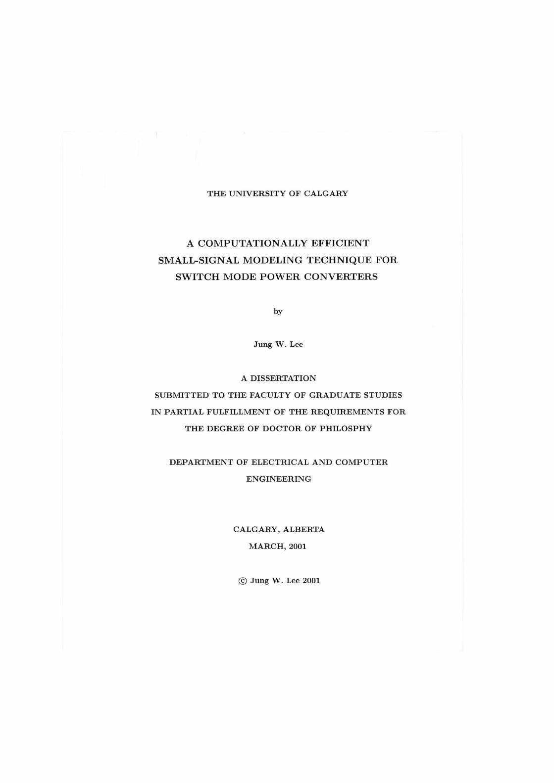
1.6 Buck converter inductor current waveform for converter power-up with zero initial energy within inductor and capacitor components. . . 8
1.7 Buck converter steady state waveforms in continuous conduction mode: (a)
inductor voltage waveform (b) inductor current waveform . . . . 9
1.8 Output voltage waveform of a buck converter 10
2.1 Block diagram of voltage mode switch mode power converter . . . . 16
2.2 A C perturbed waveforms: (a) duty ratio (b) output waveform . . . . 18
2.3 A switch mode power converter with separated switching devices. . . 24
2.4 The two-port building block 24
2.5 Switch mode power converter waveforms are averaged over one switch
ing period 25
3.1 Buck converter with winding resistance 28
3.2 Equivalent circuit of the boost converter with winding resistance: (a) interval DTSW (b) interval DTSW 29
3.3 Equivalent circuit of the buck-boost converter with winding resistance: (a) interval DTSW (b) interval DTSW 31
3.4 Equivalent circuit of the Buck converter: (a) interval DTSW (b) interval DTSW 32
3.5 Equivalent circuit model of the boost converter: (a) interval DTSW (b) interval DTSW 32
x

3.6 Equivalent circuit model of the buck-boost converter: (a) interval DTSW
(b) interval DTSW 33
3.7 Equivalent circuit including ESR: (a) interval DTSW (b) interval DTSW 34
3.8 Boost converter equivalent circuit including ESR: (a) interval DTSW
(b) interval DTSW 35
3.9 Buck-boost converter equivalent circuit including ESR: (a) interval
DTSW (b) interval DTSW 36
4.1 Linear time invariant system in steady state 38
4.2 Block diagram of a switch mode power converter with feedback circuit 39 4.3 A C variation of the switching device gating waveform: (a) for a con
stant duty ratio of D=0.5, (b) for a sinusoidal perturbed duty ratio with D=0.5, / t e s t =10kHz 41
4.4 I/O diagram of frequency response prediction algorithm 44
4.5 Structure of frequency response prediction algorithm 45
4.6 Waveforms of the pulse-width modulator 47
4.7 Boost-derived P F C circuit with average current control 49
4.8 Open-loop boost converter circuit 50
4.9 Block diagram of the current control loop for the P F C circuit loop . . 51
4.10 Block diagram of an open loop current control of d to ii loop . . . . 51
4.11 Two switched circuit models of boost-derived switch mode power converter: (a) On-time interval, (b) Off-time interval 52
4.12 Time response of the P F C example circuit: (a) Duty ratio, (b) Inductor current, (c) Capacitor voltage 54
4.13 Duty ratio perturbed at Ad = 0 .5*d n o m ; n a j : (a) Duty ratio and Inductor current waveforms, (b) Harmonic contents of inductor current. 56
4.14 Duty ratio perturbed at Ad = 0.1*dnorninai: (a) Duty ratio and Inductor current waveforms, (b) Harmonic contents of inductor current. 57
4.15 Predicted frequency response of the example boost-derived switch mode power converter using the proposed modeling technique 58
xi

4.16 Predicted frequency response of the example boost-derived switch mode power converter using the proposed modeling technique without parasitic components and compared to the state-space averaging technique [7] 59
4.17 Predicted frequency response of the example boost-derived switch mode power converter using the proposed modeling technique with parasitic components and compared to the state-space averaging technique [7] 60
4.18 Duty ratio modulation and inductor current waveforms of modulation
frequency at 40kHz 61
4.19 Frequency response predictions at various operating points 62
5.1 Block diagram of the impulse sampled voltage mode switch mode power
converter 67
5.2 Discretely operated P W M 69
5.3 Operation of open loop switch mode power converter 71
5.4 Flowchart of switch mode power converter small-signal modeling. . . 73
5.5 Single output P W M IC output pulse 74
5.6 Dual output P W M IC output pulses 75
5.7 Steady-state operating establishment by peak detection method . . . 76
5.8 Buck type switch mode power converter power stage with parasitics included 78
5.9 Open-loop voltage conversion ratio versus duty cycle 80
5.10 Open-loop time response of example buck converter 81
5.11 Inductor current waveform of example buck converter: (a) Inductor current, (b) Enlarged section shown in (a) 82
5.12 Responses of an example buck converter: (a) Sinusoidal steady-state time response at test frequency of 5kHz, (b) Computed frequency response 84
5.13 (a) Frequency response plots of example buck converter with various values of perturbed control signal amplitude, (b) Bode plots of various test frequency steps 87
xii

5.14 Bode plots of an example buck converter: (a) Bode plot from the simulation data, (b) Bode plot with second-order fit 88
5.15 (a) Pole-zero configuration of proper transfer function, (b) Bode plot
of strictly proper transfer function 89
5.16 Open-loop block diagram of buck converter 92
5.17 Bode plot of the duty-ratio, d to output voltage, v0 transfer functions. 93
5.18 Buck converter schematic diagram 95
5.19 Drive scheme for the buck converter 96
5.20 Measurement setup (CH2/CH1) 100
5.21 Computer-based gain and phase meter 101
5.22 Experimental waveforms: C H . l sawtooth signal, CH.2 modulated con
trol signal 105
5.23 Measured waveforms: (a) the duty ratio, (b) the output voltage. . . 106
5.24 The output voltage at startup 107
5.25 Control and output signals measured with an oscilloscope: (a) at test frequency of 70Hz, (b) at test frequency of 10kHz 108
5.26 Control and output signal measured with network analyzer: (a) unfil-
tered waveforms, (b) filtered waveforms 110
5.27 Experimental and predicted frequency response I l l
A . l Buck type switch mode power converter 122
A.2 On-time switched circuit of buck type switch mode power converter. 123
A. 3 Off-time switched circuit of buck type switch mode power converter. 124
B. l Switched circuit for the buck converter: (a) interval DTs, (b) interval DTs 126
xin

LIST OF SYMBOLS AND NOMENCLATURE
A averaged n x n state matrix
Aon n x n on-time state matrix
A0ff n x n off-time state matrix
Aon n x n on-time discretized state matrix
A0ff n x n off-time discretized state matrix
A D C analog-to-digital converter
ac alternating current
act* actuating signal that controls the duty-ratio
B averaged n x m input matrix with m inputs.
Bon n x m on-time input matrix with m inputs.
Baff n x m off-time input matrix with m inputs.
Bon n x m on-time discretized input matrix with m inputs.
B0ff n x m off-time discretized input matrix with m inputs.
C averaged p x n output matrix with p outputs
Con p x n on-time output matrix with p outputs
C0ff p x n off-time output matrix with p outputs
Con p x n on-time discretized output matrix with p outputs
C0ff p x n off-time discretized output matrix with p outputs
C C M continuous conduction mode
D on duty ratio.
D off duty ratio (1-D)
D C M discontinuous conduction mode
'nominal normal operating duty-ratio.
d sinusoidally modulated duty-ratio
xiv

Ad amplitude of modulated duty-ratio
d(kTsw) discretely sampled duty ratio
ESR equivalent series resistance
fsw switching frequency
ftest modulation frequency
IC integrated circuit
iLrms rms value of current
I\Lrms rms value of the fundamental current component
it inductor current
ic capacitor current
ix represents ac component current
Gid.sim calculated duty-ratio to inductor current transfer function using computational method
Gid.ave calculated duty-ratio to inductor current transfer function using state-space averaging method
Gid.sim calculated duty-ratio to inductor current transfer function that represents approximately all operating points
L inductor
LTI linear time invariant
mramp sawtooth signal ramp slope
P C personal computer
P F C power factor correction
P W M pulse width modulation
RL load resistance
RSEN current sensing resistor of the power factor correction circuit
RE inductor winding resistance (parasitic resistance)
RD diode resistance (parasitic resistance)
X V

RESR equivalent series resistance of capacitor
S M P C switch mode power converter
T H D total harmonic distorsion
Tsw switching period
Ton on-time interval
T0ff off-time interval
Ttest modulated signal period
t time
A t amount of time change
tdeiay time difference between the two sinusoids
Vvaiiey offset voltage of the sawtooth signal
vg input voltage
v0 output voltage
Vi inductor voltage
vc capacitor voltage
VR voltage across the inductor winding resistance
VDS conduction voltage of M O S F E T
VDO forward voltage drop of diode
VD voltage across the diode resistance
vesr voltage across ESR
control signal from the output of error amplifier
vx ac component of x voltage
impulse sampled control signal
v*saw impulse sampled sawtooth signal
< vx(t) >T sw averaged value of x voltage over one switching period
wm modulation angular frequency
xvi

waw angular switching frequency
x state variable
xon derivative of on-time equivalent circuit state varible
x0ff derivative of off-time equivalent circuit state varible
8 phase shift between two sinusoids in degrees
P parasitic component (RL/(RL + Resr)
r] efficiency
xvii

CHAPTER 1 l
INTRODUCTION
1.1 Background The design process for electrical power converters has evolved considerably over
the past three decades. Several reasons can be attributed to the advances that
have taken place in this industry, where the underlying drive for progress has
in no small part been motivated by the requirements of the communication and
information industries. In the 60's and 70's many artificial satellites, were placed
into earth orbit. The cost of weight and space within these satellites was very
high. This motivated engineers and researchers to develop low weight low volume
power converters. The use of switch mode power converters as opposed to linear
power converters quickly became common practice in satellite design.
In a linear power converter, the power transistor operated in the linear (active)
region, and a line-frequency transformer is used to provide electrical isolation.
The major parts of a linear power converter are shown in Fig. 1.1.
Line-frequency Diode transformer rectifier
Utility supply
Figure 1.1. A basic linear power converter.

2
The control signal applied to the transistor is a continuous time signal that
controls the equivalent on-resistance of the transistor, thereby controlling power
flow through the transistor. This power transistor can be seen as an adjustable
resistor, resulting in a low power conversion efficiency. The voltage drop across
the transistor is significant enough that a linear power converter typically has an
efficiency of 50 percent for power conversion in the 100W to l k W range. The
line-frequency transformer is relatively large and heavy.
By contrast, in a switch mode power converter (SMPC), as illustrated in Fig. 1.2,
the transistor(s) is operated in two modes, simply referred to as on and off.
Diode rectifier
High-frequency transformer
0
Utility supply c ^ A
J [ c < c ^ A
J [ c <
Error amplifier
Ref.
AAA
Figure 1.2. A basic switch mode power converter.
The required control signal is a sequence of square pulses. Ideally, in the on
mode, a transistor has zero voltage drop across the device and in the off mode the
transistor has zero current flow through the device. So ideally there is no power
dissipated in a switch mode power transistor. In practice, the on or conduction
losses of transistor and diode components can be significant and so called switching
losses (power spikes occurring during switching) can also be significant. A typical
switch mode power converter has 80 to 90 percent efficiency in the 100W to l k W

3
range (output voltages of 12V and up). This efficiency improvement with respect
to a linear power converter is at the acceptable cost of slightly more complicated
converter and control topologies as well as an increase in the output voltage ripple.
In the early 70's an analysis technique referred to as state-space averaging was
applied to the design of switch mode power converters. The technique permits
a frequency domain analysis of a power converter that is claimed to be valid up
to a frequency of one-half of the switching frequency; a significant improvement
over more conservative frequency domain methods that are considered valid up
to about one-tenth of the switching frequency. These concepts are explored in
greater detail later the dissertation.
In the late 70's personal computers were among the consumer electronic prod
ucts that took advantage of the weight and space savings afforded by switch mode
power converters. Since then switch mode power converters have been exploited
in consumer and commercial electronic equipment in a dramatic way. The per
ceived need for cost effective, reliable power converters has led to tremendous
engineering innovation in the construction of switch mode power converters. To
meet this need, researchers developed a variety of power transistors, each having a
niche power range for cost effective use of the device. Power converter engineering
and transistor improvements have led to modern switch mode power converters
having a mean time between failure (MTBF) approaching or exceeding 1,000,000
hours compared to 10,000 hours achievable in the 70's. Also, power densities of
100W/in3 are possible for today's switch mode power converters verses 20W/in3
achievable in the 70's.
Despite the dramatic improvements in switch mode converter designers still
employ relatively unsophisticated converter analysis methods. This issue is ad
dressed in this dissertation.

4
1.2 General Description of a Switch Mode Power Converter
Almost all switch mode power converters are based on three basic switch mode
power converters that are introduced and briefly described here. The explanation
of their operation is based on idealized circuit elements, such as lossless inductors
and capacitors and ideal switches with zero on-resistance, infinite off-resistance,
and zero switching time.
Almost invariably the switch mode power converter is a closed loop regulatory
system in which the power handling devices are operated as switches in on or off
states. In general, a power circuit of a switch mode power converter has three
ports: power input and power output ports as well as a control port as illustrated
in Fig. 1.3.
Input port Switch Mode Power Converter output port
A
Control port
Figure 1.3. The basic block diagram of the switch mode power converter power circuit.
Most often the switch mode power converter processes ac or dc input voltage
to produce a higher or smaller magnitude of dc output voltage. The control
port controls provides access to control variable (power transistor on-time duty
ratio) to maintain the output voltage at a specified constant magnitude in the

5
presence of variations in the input voltage and load current. Thus, the switch
mode power converter must usually have a feedback circuit. The three basic types
of dc to dc switch mode power converter power circuits are the buck converter
(often called the step-down converter because its output voltage is always lower
than or equal to its input voltage), the boost converter (sometimes called the step-
up converter because its output voltage is always greater than or equal to its input
voltage), and the buck-boost or inverting converter (often called step-up-down or
inverting converter since its output voltage is either greater or smaller than its
input voltage). These are shown in Fig. 1.4.
For the 10W to 5kW range of switch mode power converter applications, the
commonly used semiconductor transistor device is the M O S F E T (Metal Oxide
Semiconductor Field Effect Transistor), as is illustrated in Fig. 1.4. M O S F E T
and diode devices operate in a switch mode power converter as a switch: either
fully turned on or fully turned off. The control signal to turn the devices on and
off is obtained from the pulse-width modulator shown in Fig. 1.5.
Its inputs are the feedback signal produced by the error amplifier and a con
stant amplitude fixed frequency sawtooth signal. The output of the pulse-width
modulator is a periodic sequence of on/off levels which, after amplification or con
ditioning, drives the gate of the M O S F E T shown in Fig. 1.4. This on/off signal
has the switching frequency,
and the ratio of the M O S F E T on time, Ton to the complete switching period Ts
is defined as the steady-state switch duty ratio,
A basic switch mode power converter the steady-state analysis is now presented,
where two states of operation are defined corresponding to transistor on and off
aw (1.1)
(1.2)

6
Figure 1.4. Three common switch mode power converters: (a) buck converter (b) boost converter (c) buck-boost converter

7
sawtooth oscil lator
Figure 1.5. Pulse-width modulator circuit
intervals respectively. The inductor in switch mode power converters acts as an
energy storing and releasing device, accumulating the energy in the form of a
magnetic field during the transistor on-time interval and then releasing it to the
RLC components during the transistor off-time interval.
The power-up (initial converter turn on) inductor current waveform of a buck
converter (L and C components having zero initial energy) is shown in Fig. 3.1
During subinterval DTSW, the transistor is on, and the inductor current in
creases with a slope of (Vg — v0)/L with va initially zero. Next, during off-time
interval DTSW, where £>=(1 — D), the transistor is off, the diode is on, and the in
ductor current changes with a slope of —v0/L. Since the output voltage is initially
zero, this off-time slope is nearly zero. It can be seen that there is a net increase
in inductor current over the first switching period. Also, since the inductor cur-
8
on-time slope of •
Figure 1.6. Buck converter inductor current waveform for converter power-up with zero initial energy within inductor and capacitor components.
rent flows to the output, the output filter capacitor charges up slightly, and the
output voltage increases slightly as well. This process repeats until there is no
net change in inductor current over a complete switching period, and the switch
mode power converter operates in steady state. Once the inductor current reaches
steady state, the inductor voltage and current waveforms appear as in Fig. 1.7.
This steady-state operation is called continuous conduction mode (CCM), since
inductor current remains continuously at a non-zero value. It is possible and some
times desirable that the inductor current decreases to zero before the next turn-on
interval (transistor and diode are both off), however such converters operating in
the discontinuous conduction mode (DCM) are not considered explicitly in this
dissertation. There are therefore two states of operation considered here, namely:
the transistor on state, and the diode on state.
For a given switch mode power converter to produce the desired dc output

9
v L(t) V g • v 0(t) iL(t)
0 DT C
v 0 ( t )
(a)
on-time slope of i
V g • v „<t)
1
off-time slope of
(b)
v 0 ( t )
Figure 1.7. Buck converter steady state waveforms in continuous conduction mode: (a) inductor voltage waveform (b) inductor current waveform
voltage, it is a typical requirement that the ripple voltage on the output must be
small compared to its dc component. The output voltage appears as illustrated
in Fig. 1.8 and can be expressed as,
v0 = V0 + v0 (1.3)
where V0 is the dc component of the output voltage, and v0 is the ac component,
i.e., the switching frequency component and all harmonics.
From the small ripple requirement,
v0 « V0 (1.4)
This approximation greatly simplifies the basic analysis of converter operation.
According to Faraday's law the inductor voltage can be expressed as,
M*) = i f (1-5)
This may be expressed in integral form as in equation (1.6) over one switching
period from 0 to TSW,
1 rTsw
IL{TW) - h{0) = j Jo vLdt (1.6)

10
vD(t) DC + AC component: V +v (t)
DC component: V
Figure 1.8. Output voltage waveform of a buck converter
In steady state the initial and final values of the inductor current must be equal,
therefore,
0 = / vL(t)dt (1.7) J o
Equation (1.7) illustrates the principle of inductor volt-second balance: any pos
itive I>LA£ area is balanced by a negative ULAT , area. This can be seen in Fig.
1.7 (a). Volt-second balance is useful in the derivation of an expression for the dc
component of the converter output voltage and is used extensively in chapter 3.
As a simple example, referring to Fig. 1.7 (a), an application of the volt-second
balance principle yields,
(Vg - V0)DTsw = K ( l - D)T„ (1.8)
or
^ = D (1.9)
which is the ideal steady-state input voltage to output voltage transfer function
for the buck converter. Notice that D is between zero and unity, hence the output
voltage is less than the input voltage.
As mentioned earlier, it is desirable that the switch mode power converter

11
output voltage be kept at a predetermined value despite disturbances in the input
voltage and wide range requirements of load current. These requirements can be
fulfilled by the application of negative feedback in a closed loop control scheme.
To design such a feedback circuit requires a dynamic model of the given switch
mode power converter. The existing modeling techniques that can be used to
model dynamics of switch mode power converters operating in the continuous
conduction mode are discussed in chapter 2.
1.3 Motivation of the Research
Typically, the primary requirement of a switch mode power converter is to
maintain the output voltage at a desired constant level despite load current and
input voltage changes. In designing the feedback loop, the often used trial and
error process is inefficient. This process is inherently slow as it requires design-
build-redesign iterations. It uses more resources, has longer development time and
requires a large budget compared to a non-iterative approach. For these reasons,
researchers have been continuously working to improve the design process. A good
feedback loop design requires an accurate model that provides a good prediction
of dynamic characteristics of a given switch mode power converter. The derived
model using available modeling techniques allows one to predict the following:
• Margin of stability of the switch mode power converter.
• The transient response due to a step change in the input supply voltage.
• The transient response due to a step change of load resistance or current.
In obtaining a small signal model, researchers naturally have tried to make a
compromise between the simplicity of the model and accuracy of the results of
the analysis. If an extreme accuracy is not needed, it is preferable to obtain
only a reasonably simplified small signal model that can be used in designing

12
the feedback loop for meeting the required specifications. This has been the
motivation for many researchers, engineers and students who have used the small
signal model of the switch mode power converter power stage in designing the
feedback loop.
The motivation of this dissertation is to investigate the minimization of the trial
and error process in the feedback loop design of switch mode power converters.
A new modeling technique is proposed. The agreement between the obtained
results of the proposed modeling technique and state-space averaging technique
is investigated. If a good agreement is obtained, this research would indicate that
by minimizing both the trial and error process in the feedback loop design and
excessive resource requirements, the proposed modeling technique may reduce the
requirement for highly-experienced designers and speed up the design process of
the switch mode power converters.
1.4 The Objective of the Research
The objectives of the research work underlying this thesis may be summarized
as follows:
• To review three existing modeling techniques: the state-space averaging, cir
cuit averaging (in fact a sub-class of state-space averaging) and the discrete
modeling techniques.
• To investigate the accuracy of the model, and to study the influences of the
main parasitic components of a switch mode power converter.
• To develop a computer algorithm based on the proposed modeling technique
that can extract the dynamic characteristics of a given switch mode power
converter.
• To verify the proposed modeling technique, by comparing results with those

13
for a model obtained using the state-space averaging technique.
• To further verify the proposed modeling approach by implementing and
testing a buck converter.
1.5 Outline of the Dissertation This dissertation is divided into 6 chapters. The first chapter provides a general
description of the switch mode power converter. The remainder of this dissertation
is organized as follows:
Chapter 2 - A n introduction to the small-signal modeling of switch mode power
converters is presented, including a discussion of the fundamental re
quirements in the small-signal modeling process. The most commonly
used small-signal modeling techniques, the state-space averaging, circuit
averaging, and discrete modeling methods are briefly described.
Chapter 3 - The effect of parasitic components on the voltage input to output trans
fer function of a switch mode power converter is investigated.
Chapter 4 — The principle of the proposed computational small-signal modeling tech
nique is described. The algorithm for computing frequency response is
developed and demonstrated with the boost-derived power factor cor
rection circuit.
Chapter 5 - A n improved computational small-signal modeling technique is also pre
sented. For a buck converter, the obtained model is compared with the
model derived using the state-space averaging technique and is also
compared with the experimental data. Design considerations regarding
practical implementation of the buck converter are also discussed.

14
Chapter 6 - A summary, the conclusions, and comments on further research topics
in related areas are presented.

15
CHAPTER 2
SWITCH MODE POWER CONVERTER MODELING TECHNIQUES
2.1 Introduction In this chapter the existing small-signal modeling principles of switch mode
power converters are introduced. Two of these are analytical modeling techniques
and one is a numerical modeling technique.
Switch mode power converters are nonlinear systems to which straightforward
linear analysis tools cannot be directly applied. Therefore several modeling tech
niques have been developed specifically for switch mode power converters. Two of
the most widely used analytical techniques are the state-space averaging technique
of Cuk [1] and circuit averaging technique of Middlebrook [2]. Both techniques
provide small-signal linear models and both make it possible to analyze and design
switch mode power converters. The discrete modeling technique of Packard [3]
is a numerical modeling technique that describes the small-signal behavior of the
switch mode power converter at only one instant of time during each switching
cycle.
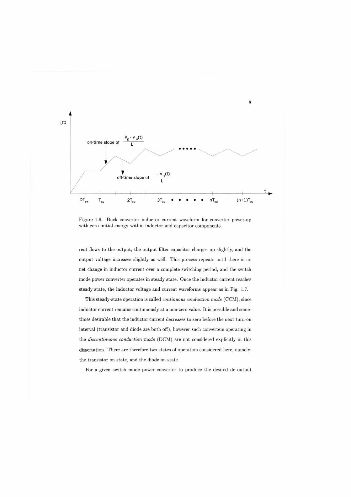
A typical voltage mode switch mode power converter with a feedback loop is
illustrated in Fig. 2.1.
The design objective of the feedback circuit is such that the control signal duty
ratio d(t) is controlled to maintain the output voltage at a constant value given
disturbances in the input voltage vg(t) and the load current. In addition, the
switch mode power converter with feedback should be stable, and properties such
as step-load overshoot, settling time and steady-state regulation should meet the
required specifications. The feedback circuit design requires a small-signal model
that represents the effect of duty ratio on the output voltage at a particular
16
Input v„(t)
Power Stage of Switch Mode Power Converter
G(s)
Drive Circuitry
P W M
d(t)
Output vQ(t)
Error amplifier Divider network
-div
Reference voltage
Figure 2.1. Block diagram of voltage mode switch mode power converter
operating point. This small-signal linear model is defined as a set of equations
(mathematical model) that represents the dynamic and steady-state operation of
the switch mode power converter. Such a model is not unique and cannot reflect
the physical switch mode power converter exactly, but can only approximate the
actual dynamic and steady state operation. A switch mode power converter,
consisting of a power stage and a controller, may be represented in many different
ways and may have many mathematical models depending on one's perspective.
The contents of this chapter are organized as follows: In Section 2.2 the basic idea
behind the modeling of a switch mode power converter is described. In Section 2.3
the state-space averaging technique is reviewed. The circuit averaging technique
is described in Section 2.4. In section 2.5 the discrete modeling technique is
reviewed. In Section 2.6 a chapter summary is presented.

17
2.2 The Basic Small-Signal Modeling Principle Modeling is the representation of physical phenomena by mathematical means.
The objective of modeling is to obtain a mathematical description that is ad
equate for the problem under consideration. Once the basic insight is gained,
the obtained model can be tuned by including some of the neglected components
for improving the accuracy of the model. Thus the modeling process involves
use of approximation techniques while neglecting insignificant effects. In model
ing switch mode power converters, it is a good idea to start with nondissipative
switches, inductors and capacitors. Once a good physical understanding is gained,
the parasitic components discussed in chapter 3 can be incorporated into the ba
sic model to obtain the refined model. To design the feedback loop of the switch
mode power converter, the information regarding the effect of duty ratio variation
on the output voltage is needed. Referring to Fig. 2.1, if some ac variation is
introduced into the switch mode power converter duty ratio d{t) such that,
d(t) = D + Dm sin wmt (2.1)
where D and Dm are constants, \Dm\ <C D and the modulation angular frequency
wm is much smaller than the switching angular frequency wsw. The use of the
linear ripple approximation discussed in section 1.2 leads to the resulting switching
pulse and the output voltage waveforms as shown in Fig. 2.2.
The averaged1 output voltage waveform shown in Fig. 2.2 (b) has no switching
ripple component. The switching ripple component is removed by averaging the
capacitor voltage waveform over each switching period, and modeled by equation
of the form,
Cd < ^ r " =< ic(t) >Tsw (2.2) xThe term average is often used in the literature where it is in fact a local average or moving
average

18
switching pulse
Ts (a)
actual output waveform of vjt) including ripple components averaged output waveform of v0(t) at
every switching period
DC output voltage, Vo at constant D
t _
(b)
Figure 2.2. A C perturbed waveforms: (a) duty ratio (b) output waveform
The averaged capacitor voltage is allowed to vary from one switching period to
the next, such that the modulated components (ac variation) are modeled. This
can be shown from the basic capacitor equation,
(2.3)
which may be expressed in integral from as,
1 rt+T.
vc(t + Ts) - vc(t) = - J ic(r)dr
The average capacitor current over one switching period is obtained from. 1 rt+Ts
< ic{t) >TSW= Tf \ ic{r)dT *• sw J *
Multiplying both sides of equation (2.5) by Tsw gives, rt+Ts
Tsw < ic(t) >Tsw= J ic(r)dr
(2.4)
(2.5)
(2.6)

19
Substituting equation (2.6) into (2.4) leads to,
ve(t + Ts) - vc(t) = ^Tsw < ic(t) >T,W (2.7)
Comparing equation (2.7) to (2.2), equation (2.7) states that the net change in
the capacitor voltage over one switching period is equal to the switching period,
Tsw, multiplied by the average slope, < ic(t) >T3W /C.
The modulated output voltage (v0 — vc) components can be predicted by repeat
ing this process over a number of switching periods. This output voltage represents
the moving average values. The objective of ac small-signal modeling efforts is
to predict these low-frequency components. For a switch mode power converter
operating in the continuous conduction mode, two different linear models corre
spond to the two states in a complete switching period. These linear models can
be represented in differential equation or in state-space form. The goal of small-
signal modeling is to combine these two derived models according to the duty
ratio variations and obtain one single small-signal linear model that suffices to de
scribe the switch mode power converter at a given operating point. Thus the basic
ideas behind the modeling of a switch mode power converter are "averaging" and
"small-signal linearization". In the next three sections, three small-signal model
ing methods are discussed: state-space averaging, circuit averaging, and discrete
modeling.
2.3 State-Space Averaging Method The state-space description of dynamic systems is the mainstay of modern
control theory. The state-space averaging method [1] makes use of this description
as a basic tool to further develop a technique which results in a switch mode power
converter description as an approximated continuous linear system.

20
The switch mode power converter operating in the continuous conduction mode
can be characterized by two state equations and two output equations during a
switching period:
1. On-time interval: dT«,
•ton ~~ -^-onS. + BonVg (2-8)
Von = ConX (2.9)
2. Off-time interval: dTs,,
±oU - Aoffx + BoffVg (2.10)
v0ff = Coffx (2.11)
where Aon and A0ff are square matrices which describe the two linear circuits
and Bon and B0jf are the input matrices that determine the effects of the input
vg and Con and C 0 / / are the output matrices. For notational clarity, underlined
letters denote vectors and upper case letters represent matrices.
The switch mode power converter circuit contains independent states that form
the state vector x and is driven by independent source vg.
The state equations (2.8) and (2.10) are multiplied by the duty ratio as a weighing
factor and combined to yield an averaged single state equation,
x = Ax + Bvg (2.12)
where
A = dAon + dAoff (2.13)
B = dBon + dBQf f (2.14)
A similar process is applied to the output equations (2.9) and (2.11) to yield an
averaged single output equation,
v0 = Cx (2.15)

21
where
C = dCon + dCoff (2.16)
The next step is to linearize equations (2.12) and (2.15) using perturbation tech
niques. Introducing ac variations in the input voltage and duty ratio as,
V9 = V9 + Vg
d = D + d
d = D-d
will cause corresponding perturbations in the state vector and output,
X = 2L + ZL
v0 = V0 + i)0
This results in the following averaged model,
| - AX + BVg+Ax + Bvg+[{Am-Aoff)X + {Bm-Boff)Vg]d v ' v ' > v '
dc term line variation duty ratio variation + [(Aon - Aoff)x + {Bon - Boff)vg}d (2.17)
" v ' nonlinear second—order term
and,
V0 + v0= CX + Cs. +{Con - Coff)Xd+{Cm - CofJ)xd (2.18) dc term ac term ac term nonlinear term
With the assumptions that the perturbed values are much smaller in magnitude
compared to the steady-state values,
Vg » Vg
X » i

22
it is possible to neglect the second-order term in equations(2.17) and (2.18) to
yield the state-space averaged model in its final form,
1. The steady-state (dc) model:
0 = AX + BVg (2.19)
V„ = CX (2.20)
2. The small-signal (ac) model:
x = Ax + Bvg + \{Aon - Aoff)X + {Bon - Boff)Vg}d (2.21)
v0 = Cx + (Con - Coff)Xd (2.22)
From the dc and ac models, the transfer function can be determined. The steps
in obtaining the small-signal model using the state-space averaging technique are
summarized below:
(1) Derive two linear circuit models for on-time and off-time intervals.
(2) Write state and output equations for each linear circuit state using natural
laws (Kirchhoff's voltage and current laws).
(3) Perform state-space averaging over one period using the duty ratio as a
weighting factor.
(4) Combine state equations into a single averaged state equation.
(5) Perturb the averaged state equation and output equation to yield steady-
state and dynamic terms and eliminate the nonlinear terms.

23
2.4 Circuit Averaging Technique The circuit averaging technique [2] is based on equivalent circuit manipulations.
After considerable circuit manipulations, it gives a single equivalent linear circuit
model of a switch mode power converter. A l l manipulations are performed on the
circuit diagram of the switch mode power converter instead of on its equations.
Thus the circuit averaging technique gives a more physical interpretation to the
model. It also involves averaging and small-signal linearization equivalent to the
state-space averaging technique.
The key step in circuit averaging is to replace the switch mode power converter
switches with voltage and current sources to obtain a time-invariant circuit. The
procedure for obtaining the small-signal model using the circuit averaging tech
nique is summarized below:
(1) Separate the switching devices from the power stage of the switch mode
power converter as shown in Fig. 2.3.
(2) Treat two of the terminal variables shown in Fig. 2.4 as independent sources
and the remaining two terminal variables as dependent sources.
(3) Remove the switching harmonics by averaging all signals in Fig. 2.3 over one
switching period to yield the averaged switch mode power converter shown
in Fig. 2.5.
(4) Perturb and linearize the switch mode converter variables about an operat
ing,
<Vg{t) >T„=V, + Vg
d{t) = D + d(t)
d(t) = D — d(t)

24
v B(t)
Time-Invariant network containing switch mode power converter reactive elements
+ L iL(t)
vc(t)
v ii(t) i2(t) 4
v/t) port 1 Switch elements port 2 vt(t)
Control Input d(t)
VLoadCt)
Figure 2.3. A switch mode power converter with separated switching devices.
•l '2 +
Input port v r W
w w
circuit +
V2^) Output port
Figure 2.4. The two-port building block.
< >raw=h +ii(t)
< k(t) > T s w = h + h(t)
< v(t)Load >Ts= Vhoad + VLoad(t)
<Vl(t) >T„=Vi+Vi(t)
< V2{t) >TSW= Vhoad + VLoad{t)
where, <> denotes averaging over one switching period.

25
<vg(t)>Ts
Averaged Time-Invariant network containing switch mode power converter reactive elements
+ L
r J- <iL(t)>TS <VLoad(t)>Ts
Control Input d(t)
Figure 2.5. Switch mode power converter waveforms are averaged over one switching period.
(5) Remove the nonlinear terms and reconstruct the linearized circuit averaged
switch mode power converter model. Replace the dependent linear sources
with an equivalent ideal transformer.
2.5 Discrete Modeling Technique The derivation of a switch mode power converter small-signal model using
the discrete modeling technique [3] begins with characterizing the switch mode
power converter by a set of linear difference equations rather than by a set of
linear differential equations. The steps deriving a small-signal model using discrete
modeling technique are summarized below:
(1) Write the large-signal equations of the switch mode power converter.
(2) Choose a steady state operating point.
(3) Find the nonlinear differential equations for perturbations about the oper
ating point.

26
(4) Use the small-signal approximation to integrate the perturbation equations
across one complete cycle including modulation to find the small-signal dif
ference equations.
The discrete modeling technique is accurate even at high modulation frequencies,
but it is very complex and cumbersome. It is difficult to apply in the practical
circuit design and physical insight into the circuit operation is not easily gained.
2.6 Summary Modern modeling techniques for switch mode power converter are discussed in
this chapter. The key step in modeling a switch mode power converter operating
in the continuous conduction mode is to average the states or the signals for two
separate states over one complete switching period. The state-space averaging
technique offers a very convenient continuous time invariant form, but it requires
significant matrix manipulations in the modeling process. The circuit averaging
technique also yields equivalent results as the state-space averaging method, but
the derivation involves the manipulation of circuits rather than equations. The
down side of these two techniques is that both techniques lack accuracy as the
modulation frequency approaches half of the switching frequency and the fre
quency at which the model starts to give untrustworthy information cannot be
easily determined.
The discrete modeling technique has been developed to overcome model inaccu
racy when the modulation frequency approaches half of the switching frequency.
Therefore it does not have the more stringent frequency limitations of the state-
space averaging and circuit averaging techniques. However, the modeling process
is very complicated and cumbersome to use.

CHAPTER 3 27
EFFECT OF PARASITIC COMPONENTS
3.1 Introduction The technique of approximating a physical device with a relatively simple model
is an important part of modeling a switch mode power converter. The model that
represents a particular device is not unique, but should be simple and reflect
the actual device as closely as possible. The main parasitic components of a
switch mode power converter that effect the output voltage are inductor winding
resistance, capacitor effective series resistance (ESR), and the turn-on voltage of
switching devices.
This chapter is divided into five sections and is concerned with output voltage
degradation due to the presence of main the parasitic components. The three
basic types of dc-to-dc switch mode power converters described in section 1.2 are
used to demonstrate the effects of component imperfections.
The outline of the chapter is as follows: In Section 3.2 the effect of inductor
winding resistance on the output voltage is investigated. Section 3.3 deals with
semiconductor switch losses. In Section 3.4 the output capacitor is modeled to
include a resistor connected in series with ideal capacitor in order to study the
effect on output voltage. Finally, in section 3.5 a chapter summary is presented.
3.2 Effect of Winding Resistance The inductor is composed of wire wound around a core to provide the necessary
inductance for the switch mode power converter. Practical inductors contribute
two types of power loss in switch mode power converters:
1. Copper loss due to the resistance of the wire.

28
2. Core loss due to hysteresis and eddy current losses in the magnetic core.
The inductor should be designed to have small resistance. An approximate induc
tor model that incorporates copper losses can be simply represented as a resistor
connected in series with the inductor.
An analysis is performed to determine the effect of inductor series resistance for
the Buck, Boost, and Buck-Boost converters.
Buck Converter
Fig. 3.1 shows the buck converter with a nonideal inductor.
Figure 3.1. Buck converter with winding resistance
Referring to Fig. 3.1, applying the principle of inductor volt-second balance
and the small ripple approximation in steady-state,
(VG - V R - V0)DTSW = {VR + V0)DTSW (3.1)
The inductor current is equal to the output current for the buck converter. There
fore,
VR = IRE and / = £
where, I is the average inductor current.

29
From equation (3.1) the output voltage of a buck converter may be expressed
as,
Vo = D V g { — ( 3 . 2 )
It can be seen that equation (3.2) contains two terms, the ideal output voltage
term, DVg with RE — 0 and the winding resistance impact factor term, ( V_) .
If RE << RL, then the output voltage is approximately equal to the ideal value
DVg, but as RE is increased, the output voltage is reduced according to the winding
resistance term.
Boost Converter
Equivalent circuit models of on and off states of the boost converter are shown in
Fig. 3.2.
A V J Y V Y L
+ V, •
v. v n
L
+ v,
R,
(a) (b)
Figure 3.2. Equivalent circuit of the boost converter with winding resistance: (a) interval DTSW (b) interval DTSW
Applying the volt-second balance to the inductor over one switching period
gives,
{VG - VR)DTSW = (VG + V R - V0)DTSW (3.3)
which yields the expression for the output voltage,
v ; = ( ^ M (3.4)

30
The output current is equal to the inductor current when the switch is off. There
fore, the average output current becomes,
Io = ILD (3.5)
From equation (3.5), II in terms of Va yields,
h = ^ (3.6)
Substituting for 1L in equation (3.4) gives,
V° = ^(1 + ^ ) ( 3 ' 7 )
Equation (3.7) shows that if the winding resistance is not zero, the output voltage
of the boost converter is lower than the ideal case,
V0 = ^ (3.8)
Buck-Boost Converter
The equivalent circuit models of the buck-boost converter including winding re
sistance are shown in Fig. 3.3.
Following the similar analysis steps used for the boost converter, the output
voltage of the buck-boost converter becomes,
It can be seen from equation (3.9) that, as the winding resistance becomes zero,
the output equation for the buck-boost converter yields the ideal output equation,
Vo = Vg^ (3.10)

31
+
+ _
u VR
[+ c V.
(a) (b)
Figure 3.3. Equivalent circuit of the buck-boost converter with winding resistance: (a) interval DTSW (b) interval DTSW
3.3 The Effect of Semiconductor Switch Nonidealities The conduction voltage of the switching devices have a significant effect on
the performance of a switch mode power converter, especially when the input
and output voltages are low. Metal Oxide Semiconductor Field-Effect Transistors
(MOSFETs) and diodes are common switching devices that are used in switch
mode power converters. These devices are either on or off in each switching
cycle, thus the M O S F E T is operated in the triode region. When the M O S F E T
is operated in the triode region, it can be modeled as an on-resistance RDSOU- A
constant voltage, Vp, plus resistance, RD, model is used to describe the diode.
An analysis is carried out to establish the effect of semiconductor conduction losses
for the Buck, Boost, and Buck-Boost converters.
Buck Converter
The equivalent circuit models of the buck converter incorporating switch losses
are shown in Fig. 3.4.
Analyzing the circuit of Fig. 3.4 using the principle of inductor volt-second

32
R D S
+ V D S •
L + v,
R L> y
(a)
Figure 3.4. Equivalent circuit of the Buck converter: (a) interval DTSW (b) interval DT
balance, and the small-ripple approximation yields,
(VG - VDS - V0)DTSW = (VDO + V D - V0)DTS, (3.11)
Solving for the output voltage of the buck converter gives,
DV,-DVD
yo V-, . Rnsp . RdD> 1 ^ RL ^ RL
(3.12)
Equation 3.12 shows that as the parasitic components VD, RDS, and Rd decrease
the output voltage.
Boost converter
L
+ v, -
R D S V D S
(a)
_L
L j'~W~Y~"N\_
+ v, •
R d v D 0
—vw—11— + v n - + -
(b)
R,
Figure 3.5. Equivalent circuit model of the boost converter: (a) interval DTSW (b) interval D T , „ ,
Referring to the equivalent circuit models that include switching device non-

33
idealities in Fig. 3.5, and following similar steps as applied in case of the buck
converter analysis, the effect of the switching device parasitics on the output of
the boost converter is derived as,
V0 = VG - VDOD D RdD
RL RnsD RLD
(3.13)
It can be seen from equation (3.13) that when the parasitic components Rd, RDS,
and VDO a r e zero, the output equation of the boost converter becomes same as
that of an ideal boost converter.
Buck-Boost Converter
An equivalent switched circuit model of the buck-boost converter that includes
switching device conduction losses is shown in Fig. 3.6.
R D S
+ v, DS
I
J
(a)
L +
v,
I m 1 - vD + - +
L
j
(b)
Figure 3.6. Equivalent circuit model of the buck-boost converter: (a) interval DTSW (b) interval DTSW
The effect of switching device conduction losses on the output voltage of the
buck-boost converter is obtained by following the preceding steps,
V,D-VDOD n | R*D | Rn*D2 V ;
U T RL t RLD
Again, equation (3.14) becomes the ideal output equation for the buck-boost con
verter when the conduction loss factors are eliminated.

34
3.4 The Effect of Effective Series Resistance (ESR) of the Output Capacitor
To provide a steady dc output voltage, and to reduce ripple and noise, an L C
low pass filter is normally employed in the output section of a buck converter.
Other converters will at least employ an output capacitor. The electrolytic capac
itors which are usually used in the output filter section, have significant ESR that
degrades the desired output characteristic and causes high ripple at the switching
frequency. A real capacitor can be modeled as an ideal capacitor with an ESR.
An analysis is performed to determine the effect ESR for the Buck, Boost, and
Buck-Boost converters.
Buck Converter
The equivalent buck converter circuit models including ESR are shown in Fig.
3.7.
+ v + v,
T
(a) (b)
Figure 3.7. Equivalent circuit including ESR: (a) interval DTSW (b) interval DTS.
Once again, applying the volt-second balance principle on the inductor yields,
(vg - vesr - vc)DTsw = (vesr - vc)DTsw (3.15)
in which,
Vesr = iLResrP ~ (3.16)

35
where,
P = i r f f c ; a n d iL = io = %-L
Use of the small-ripple approximation leads to the output voltage,
V0 = DVg (3.17)
This analysis shows that the ESR of the output capacitor does not affect the
output voltage for the buck converter.
Boost Converter
The boost converter switched circuit model with a capacitor model that includes
ESR is shown in Fig. 3.8.
+ v, • rr T Resr Vesr
(a)
L
+ v, •
Resr V e s r
+ v.
(b)
Figure 3.8. Boost converter equivalent circuit including ESR: (a) interval DTS, (b) interval DTSW
Following the preceding analysis steps leads to the output equation of the boost
converter,
Vo = ^-,R * (3.18)
where,

36
It can be seen from equation (3.18) that the output voltage is reduced by the
parasitic term,
(3.19)
Buck-Boost Converter
( Resrff D I 1 \ ^ RL D >
Referring to Fig. 3.9, the output voltage due to ESR for a buck-boost converter
+
) < . Resr : Vesr L
+
V.
(a)
+
Resr vesr
(b)
Figure 3.9. Buck-boost converter equivalent circuit including ESR: (a) interval DTSW (b) interval DTSW
is,
V 0 = V g D
t R B \ (3.20) D ( ^ § + 1)
lower than V0 = for the ideal case.
3.5 Summary
The effect of parasitic components on converter output voltage is discussed in
this chapter. The analysis clearly demonstrates that the presence of parasitic com
ponents can significantly alter the performance of switch mode power converters,
thus the ideal model should be refined to account for component imperfections
such as inductor winding resistance, switching device conduction-resistances, and
forward voltage drops, and ESR.

CHAPTER 4
:57
COMPUTATIONAL SMALL-SIGNAL MODELING APPROACH FOR SWITCH MODE POWER
CONVERTERS
4.1 Introduction In recent years, several switch mode power converter modeling techniques have
been developed to better approximate switch mode power converter dynamic char
acteristics. The evolution of computers and the increasing demand for reduced
design lead time, stimulates the technical innovations in the numerical modeling
of switch mode power converters.
The objective of the research underlying this chapter is the development of a novel
computational modeling technique that overcomes the drawbacks of the known
modeling techniques discussed in chapter 2.
In this chapter, a computational modeling technique which imitates the "gain
and phase meter" is presented to calculate the dynamic characteristics of a switch
mode power converter. This chapter is organized as follows: In Section 4.2 the
basic principles of the proposed computational modeling technique are discussed.
In Section 4.3 the implemented software for computing frequency response pre
dictions is presented. In Section 4.4 the modeling of the pulse width modulator
is discussed. In Section 4.5 the computational modeling technique applied to the
boost-derived power factor correction circuit is discussed. Also, the derived model
is compared with the state-space averaged model for verification of the proposed
technique. In Section 4.6 a chapter summary is presented.
.'58
4.2 Basic Principles of the Proposed Computational Modeling Technique
The derived small-signal model using the techniques proposed in this chapter,
like other small-signal models using available techniques as discussed in chapter 2,
is useful in describing the local behavior about a given operating point of a switch
mode power converter. However, the proposed modeling technique is a much
simpler process and shortens modeling time. With the inclusion of the parasitic
components discussed in chapter 3, for a sufficiently small disturbance relative
to an operating point, the model obtained using the proposed computational ap
proach gives a high fidelity model that describes the physical switch mode power
converter characteristics.
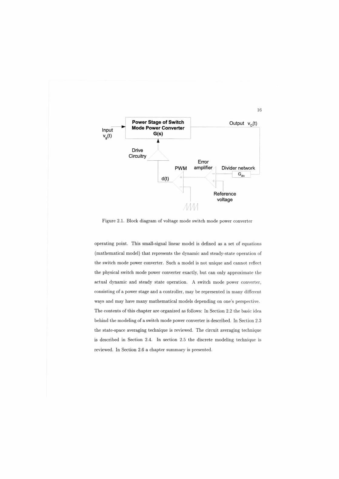
The basic principle of the computational modeling approach is best explained
by first discussing the characteristics of a linear time invariant system as shown
in Fig. 4.1.
x(t) A f\
V \J \J \J t
Linear y(t) Time
Invariant System
Figure 4.1. Linear time invariant system in steady state
Referring to Fig. 4.1, the input and output of a linear time-invariant system are
represented by x(t) and y{t), respectively. In the proposed computational small-
signal modeling approach, an "approximation approach of the sinusoidal response"
is used to calculate the dynamic characteristics of a linear time-invariant system.
If the input x(t) is a sinusoidal signal, the steady-state output will also be a
39
sinusoidal signal with the same frequency as the input signal, but possibly with a
different magnitude and phase angle. Therefore the dynamic characteristics of a
linear time-invariant system can be computed by varying the input frequency until
the entire frequency range of interest is covered and by calculating the amplitude
ratio of the output and the input sinusoids and the phase shift between the input
sinusoid and the output sinusoid at each frequency. Normally the objective of
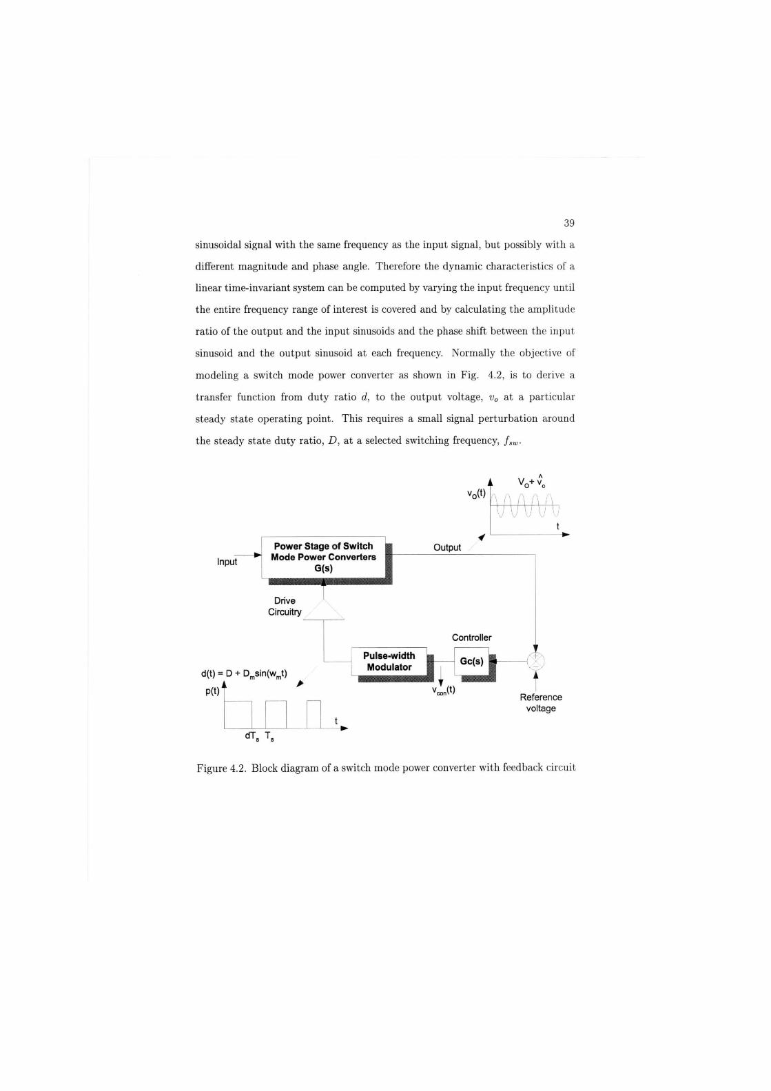
modeling a switch mode power converter as shown in Fig. 4.2, is to derive a
transfer function from duty ratio d, to the output voltage, vQ at a particular
steady state operating point. This requires a small signal perturbation around
the steady state duty ratio, D, at a selected switching frequency, fsw.
v0(t)
Input
Power Stage of Switch Mode Power Converters
G(s)
Drive Circuitry
Output
Controller
d(t) = D + Dmsin(wmt)
P(t)
Pulse-width Modulator
d T T s s
A V + V v O v o
Reference voltage
Figure 4.2. Block diagram of a switch mode power converter with feedback circuit
10
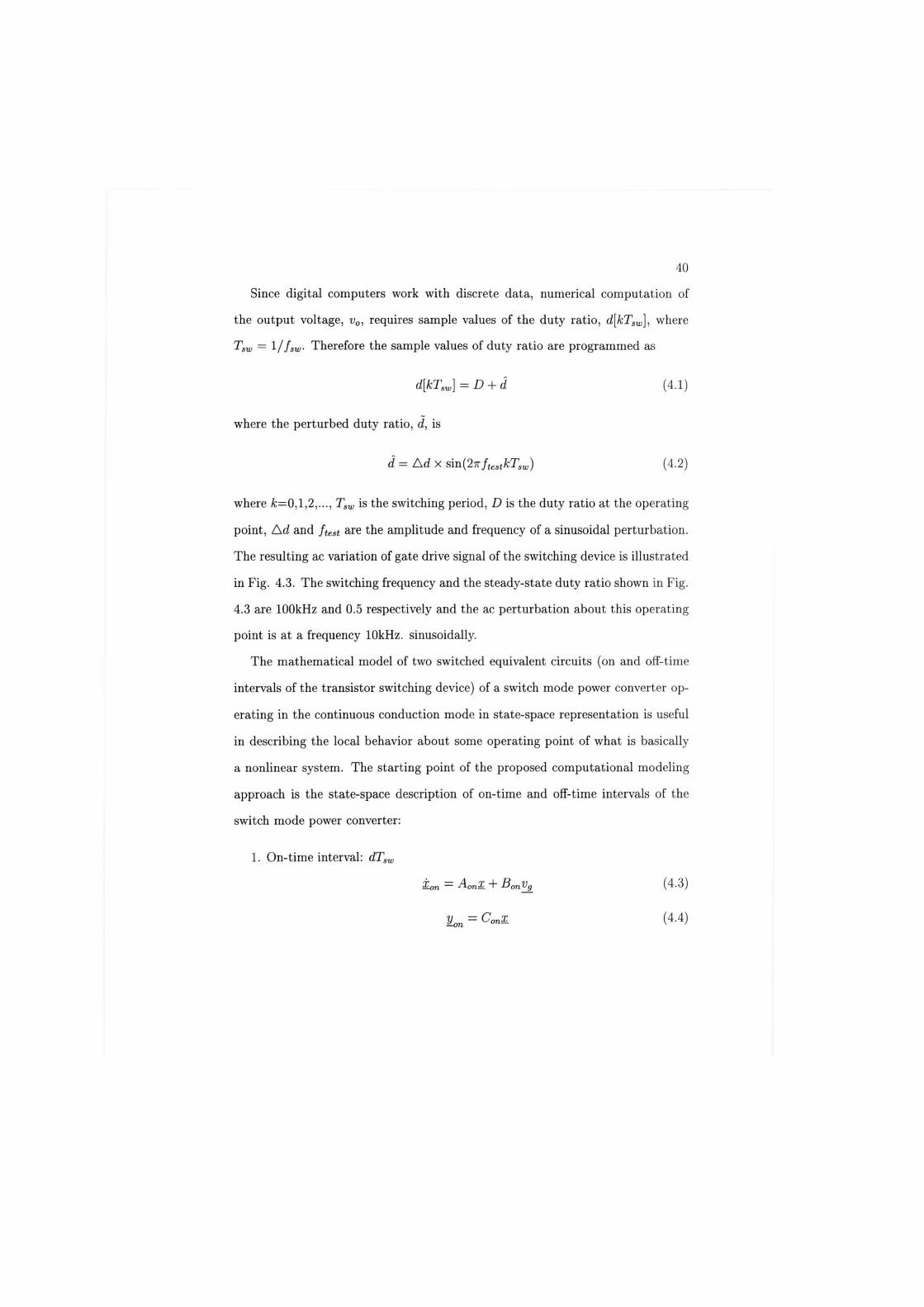
Since digital computers work with discrete data, numerical computation of
the output voltage, v0, requires sample values of the duty ratio, d[kTsw], where
Tsw — Therefore the sample values of duty ratio are programmed as
where k—0,1,2,..., Tsw is the switching period, D is the duty ratio at the operating
point, Ad and ftest are the amplitude and frequency of a sinusoidal perturbation.
The resulting ac variation of gate drive signal of the switching device is illustrated
in Fig. 4.3. The switching frequency and the steady-state duty ratio shown in Fig.
4.3 are 100kHz and 0.5 respectively and the ac perturbation about this operating
point is at a frequency 10kHz. sinusoidally.
The mathematical model of two switched equivalent circuits (on and off-time
intervals of the transistor switching device) of a switch mode power converter op
erating in the continuous conduction mode in state-space representation is useful
in describing the local behavior about some operating point of what is basically
a nonlinear system. The starting point of the proposed computational modeling
approach is the state-space description of on-time and off-time intervals of the
switch mode power converter:
1. On-time interval: dTsw
d[kTsw] = D + d (4.1)
where the perturbed duty ratio, d, is
d = Ad x sm(2irftestkTsw) (4.2)
(4.3)
(4.4)
41
15
§ 10 h i—i-
CQ (D
< 5 h o_ ft-(a
0 0.5 1
time (Second) 1.5
x 10
(a)
time (Second) -4 x 10
(b)
Figure 4.3. A C variation of the switching device gating waveform: (a) for a constant duty ratio of D=0.5, (b) for a sinusoidal perturbed duty ratio with D=0.5, / t e a t =10kHz.

42
2. Off-time interval: dTsw
£off = A<>ff£ + BoffVg^ (4.5)
For notational clarity, underlined letters denote vectors and upper case letters
denote matrices.
Equations (4.3) and (4.5) are the state equations. Equations (4.4) and (4.6) are
the output equations. For computation of the dynamic characteristics of a switch
mode power converter under investigation, a discrete-time representation of two
switched equivalent circuits which fulfill the same functionality of a state-space
representation is required. For the present, note that the discrete-time descriptions
of two switched equivalent circuits are recursive descriptions in which the state
vectors at any given sampling instant depend only on the state vectors at the
previous instant. Since the input vector is kept constant, each sample calculation
of the state vector does not depend on the input vector. The general forms of two
switched equivalent circuits are:
1. On-time sampled instant: d[(k + l ) T s a m ]
xm\k + 1] = Aonx[k] + BonVg_ (4.7)
Von[k] = Conx[k + 1] (4.8)
2. Off-time interval: d[(k + l ) T s a m ]
xofflk + 1] = Aoffx[k] + Bofjvg (4.9)
yoff[k} = Coffx[k + l} (4.10)
where Tsam is the sampling period.

43
The initial value of xon at k=0 is set at 0 and then repeatedly applied to
generate the state and output responses as time passes, one sampling instant
after another for a defined duration of time. The frequency response prediction
begins by collecting the amplitude and phase shift information of the perturbed
duty ratio and the output for each frequency step after the switch mode power
converter reaches steady-state operation. The frequency response about a given
operating point is calculated by,
\M\ = ^ p ^ (4.11)
e = tj^v x 36o (4.12) Tfest
where Moutput and M j n p u 4 are the amplitude of output voltage and modulated
duty ratio sinusoids respectively, while t^eiay is the phase shift between the two
sinusoids, and Ttest is the period of modulated signal.
System level software was developed to calculate the frequency response auto
matically for each frequency step, over a specified frequency range.
4.3 Software Development for Computing Frequency Response Prediction
1. Problem Statement
Compute the frequency response prediction of the switch mode power con
verter.
2. Input/Output Description
In Fig. 4.4, the I/O diagram shows the user input that represents state and
output matrices for two switched equivalent circuits, and circuit definition,
components information, a frequency array for frequencies of interest, and
the length of time for the simulation.

44
Aon Bon Con Don
Aoff Boff Coff Doff
Circuit parameters^ Component values Interested f requenc ies-Frequency step function Simulation t ime
Table of amplitude and phase vs. frequency
Figure 4.4. I /O diagram of frequency response prediction algorithm
3. Algorithm Development
To break up the solution into a series of sequential steps, the following
decomposition outline was developed.
• Obtain the user specified information
• Generate the time response data and store it at the end of each switching
period when the Frequency Response computation function is called.
• Generate the time response data when the switch mode power con
verter operates in steady-state and find the maximum amplitudes of
the perturbed duty ratio and the output, and the phase shifts for each
frequency step.
• Compute the frequency response at each frequency step.
The core structure of the implemented algorithm is shown in Fig. 4.5. In Fig.
4.5, AON BON
CON DON and AOFF BOFF
CQFF DOFF are the state space representations for
the on-time and off-time interval equivalent circuits of a switch mode power con
verter. At the start of each switching period, d is updated according to the type
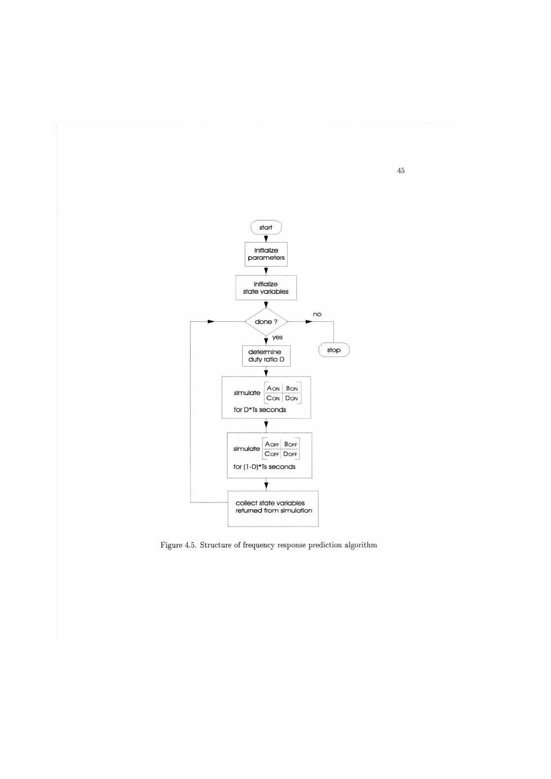
45
initialize parameters
t initialize
state variables
no
determine duty ratio D
simulate A O N B O N simulate C O N D O N
for D*Ts seconds
simulate A OFF BOFF simulate C O F F D O F F
for (1 -D)*Ts seconds
co l l ec t state variables returned from simulation
stop
Figure 4. 5. Structure of frequency response prediction algorithm

46
of switch mode power converter under investigation. When the two switched in
terval circuits are being simulated, the state variables at the end of on (or off)
time simulations are used as the initial conditions for off (or on) time simulations.
The program result represents a small-signal model for the transfer function from
the duty ratio, d(t) to the output voltage, v0(t) as is normally done [l]-[3]. How
ever, it is suggested here that it is more appropriate to obtain a small-signal model
from the control signal, vcon(t), to the output voltage, va(t) (c.f. Fig. 4.2).
Therefore a small-signal model for the pulse width modulator (PWM) is needed.
4.4 Modeling the Pulse Width Modulator
The function of the pulse with modulator (PWM) shown in Fig. 1.5 is to
produce a duty ratio d(t) that is proportional to the analog control signal vcon(t).
The P W M input and output waveforms are illustrated in Fig. 4.6.
The peak amplitude of the sawtooth waveform is Vspk- The P W M is an analog
comparator that compares the analog control signal to a sawtooth signal in order
to generate on/off pulses that switch the M O S F E T in the switch mode power
converter on and off. If over a switching period, vsaw(t) varies linearly with time,
then for 0 < vcon(t) < Vspk the duty ratio will be a linear function of Vcon(t).
Hence similar triangles can be used to write,
d(t) = ^ (4.13) Vspk
This relationship is only valid if the switching frequency is much higher than
the modulation frequency of the control signal. To support this requirement,
the P W M can be thought of as a sampler. Within a switching period there can
only be a one discrete value of the duty ratio. Therefore the P W M samples the
control signal vcon(t) with sampling frequency of fsw. The maximum modulation
frequency of the control signal is less than half of the switching frequency.
In the next section the proposed modeling technique is applied to model the

47
*«Jt)
d(t)
l
t
•
Figure 4.6. Waveforms of the pulse-width modulator
current loop of a boost derived power factor correction circuit.
4.5 Application to a Boost-Derived PFC circuit The developed modeling technique in the preceding section is illustrated here
by application to a simple boost-derived power factor correction (PFC) circuit.
The most popular approach to achieve high power factor and low line harmonics
is to add a boost derived active power factor correction circuit in front of the
dc-dc converter portion of a switch mode power converter. The objective of a
boost-derived P F C circuit is to track a current command whose shape is a scaled
replica of the input voltage Vi, where, typically V{ is a full-bridge rectified sinusoidal
voltage with a fundamental frequency of 120Hz. Fig. 4.7 shows a boost derived

48
average current control P F C circuit scheme.
To derive the small-signal model for this example of a boost-derived PFC cir
cuit, the averaged value of the rectified input voltage (dc voltage) is considered as
a constant voltage. Therefore the power stage is equivalent to a dc/dc boost con
verter. In reality, the input voltage is a full-wave rectified voltage with a frequency
two times the line frequency, which is much slower than the switching frequency.
Thus the dynamics of Uj are relatively slow and the uncompensated current loop
can be viewed as a plant with a slowly time varied input system.
Based on the computational modeling approach discussed in the previous sec
tions, a simple boost-derived P F C circuit shown in Fig. 4.8 was designed with the
following specification and component values listed in Table 4.1.
Speci f ica t ion:
Input voltage: DC 312V
Output voltage: DC 400V
Output current: 1A
Switching frequency: lOOKHz
Table 4.1. Component values of boost-derived P F C circuit
Nomenclature Component Values Components Description L 550/itf main inductor
RE m Winding resistance Co 1000//F Output capacitor
RESR lmQ. Equivalent Series Resistance (output cap.) Rsen Sensing resistor

49
D Vo
Q Gate Drive
Current tracking controller
IYY\
LOAD
• Multiplier
Current command
Vlr. *
Ref. Voltage
Figure 4.7. Boost-derived P F C circuit with average current control

Gate Drive
t
• Figure 4.8. Open-loop boost converter circuit
There are two main tasks in the current loop design:
(1) A voltage feed forward disturbance compensation scheme is needed for ac
commodating large variations about the operating point. This feed for
ward compensation scheme is an open-loop correction method which helps
to maintain consistent dynamic response over the wide range of ac input line
voltages. There are numerous integrated P F C control circuits available on
the market to alleviate the circuit complexity required by the P F C circuit
[4]-[6].
(2) When a reliable input current signal is available, a properly compensated
feedback loop can be used to force the input current to follow the current

51
command. In general, the closed loop current controller is designed as a
linear controller for the set of all nominal small signal models. The current
control loop is illustrated in Fig. 4.9.
Figure 4.9. Block diagram of the current control loop for the P F C circuit loop
The proposed computational small-signal approach is used to demonstrate the
second task. For the verification of the derived model, the frequency response
prediction is made from d to %L as shown in Fig. 4.10, i.e. the open-loop response
is being investigated. This result is compared with a mathematically derived
small-signal model presented in [7].
Figure 4.10. Block diagram of an open loop current control of d to IL loop

52
4.5.1 State-Space Representation
Assuming that the boost-derived P F C circuit operates in the continuous con
duction mode in which the instantaneous inductor current does not decrease to
zero at anytime in the switching period, then there are only on and off-time
switched circuit models to be considered as shown in Fig. 4.11.
^SEN m 1 1
(b)
Figure 4.11. Two switched circuit models of boost-derived switch mode power converter: (a) On-time interval, (b) Off-time interval.
First the linear time invariant (LTI) continuous-time state-space equations that
describe the switched circuit are determined. For a state vector x — [iivC]T, and
output y=iL, the state equations and the output equations are:

53
1. On-time interval:
(RE+RSEN) L
0 C0X(RESR+RLOAD) J .
VC -1 L 0
(4.14)
'<L0 "l1 °] VC
(4.15)
2. Off-time interval:
Xoff ~ {RE+RSEN+RESR\\RLOAD)
L RLOAD
C 0 x (RLOAD +RESR)
RLOAD LX(RLOAD-TRESR) 1
C0X(RESR+RLOAD) vc
+ L
0 (4.16)
(4.17)
Using state and output matrices from equations (4.14) to (4.17) in the developed
program leads to sampled-data that describes the evolution of the state from the
beginning of the on-time to the end of the on-time interval and the beginning of
the off-time to the end of the off-time interval until a given computation time has
elapsed. The state x(t) is continuous across each change in switch configuration,
i.e., the final state in one configuration is the initial state in the next.
4.5.2 Actuator Signal Perturbation from Steady-State
The output voltage expression for the ideal case of the boost converter (not
including any parasitic components) is given by
D = YTB <4-18)
To obtain the 400V output voltage specified, the steady-state duty ratio is set at
D = 0.22. The resulting time responses of the boost-derived P F C converter using
equations (4.14) to (4.17) in the implemented software are shown in Fig. 4.12.

54
Figure 4.12. Time response of the P F C example circuit: (a) Duty ratio, (b) Inductor current, (c) Capacitor voltage.

55
The steady-state values given in Fig. 4.12 are used as the initial conditions
of the second simulation for steady-state analysis, because these values represent
the estimated steady-state values so that the steady-state analysis simulation time
can be reduced.
With the duty ratio perturbation given in equations (4.1) and (4.2), the al
lowable amplitude Ad at a given operating point is determined by quantizing
the amount of distortion of the current waveform iL. An index called the total
harmonic distortion (THD) is used to determine the amount of distortion in the
current waveform.
The T H D in terms of the rms amplitudes of the inductor current components is
written as:
THD = P - T2
Lrms ILrms (4.19) ILrms
which means that
1Lrms — \/1 ILrms + ^2Lrms + ' ' ' + InLrms (4.20)
where h T m s is rms value of the fundamental current component and hrms • • • Inrms
are the harmonic rms values.
The inductor waveforms of sinusoidally perturbed duty ratio at Ad = 0.5*dnommaJ
and Ad = 0.1 * dnominoX are shown in Figs. 4.13 and 4.14 respectively.
In Fig. 4.13 (a), it can be seen that when A d is an unreasonably large value,
the shape of %L deviates significantly from that of a sinusoid and contains large
components at unwanted harmonics (multiples) of the fundamental frequency. In
addition, ii is negative in various portions of its trajectory. To obtain a good
agreement with a small-signal model predicted using other modeling techniques,
the perturbed duty ratio amplitude is set at a value which gives the calculated
T H D of 10 to 15 percent. Fig. 4.14 (a) shows that when Ad is properly con-

56
—
E o U
100
90
80
70
60
50
40
| 30
20
10
Perturbed Duty ratio A d = 0.5*dnominal
0.02 0.03
Inductor Current
0.04 0.05
0.01 0.02 0.03 time (seconds)
0.04 0.05
(a)
Harmonic Components of Inductor Current
THD = 2 2 %
10 20 30 40 Order of Fundamental C urrent
50
(b)
Figure 4.13. Duty ratio perturbed at A d = 0.5 * dnominal: (a) Duty ratio and Inductor current waveforms, (b) Harmonic contents of inductor current.
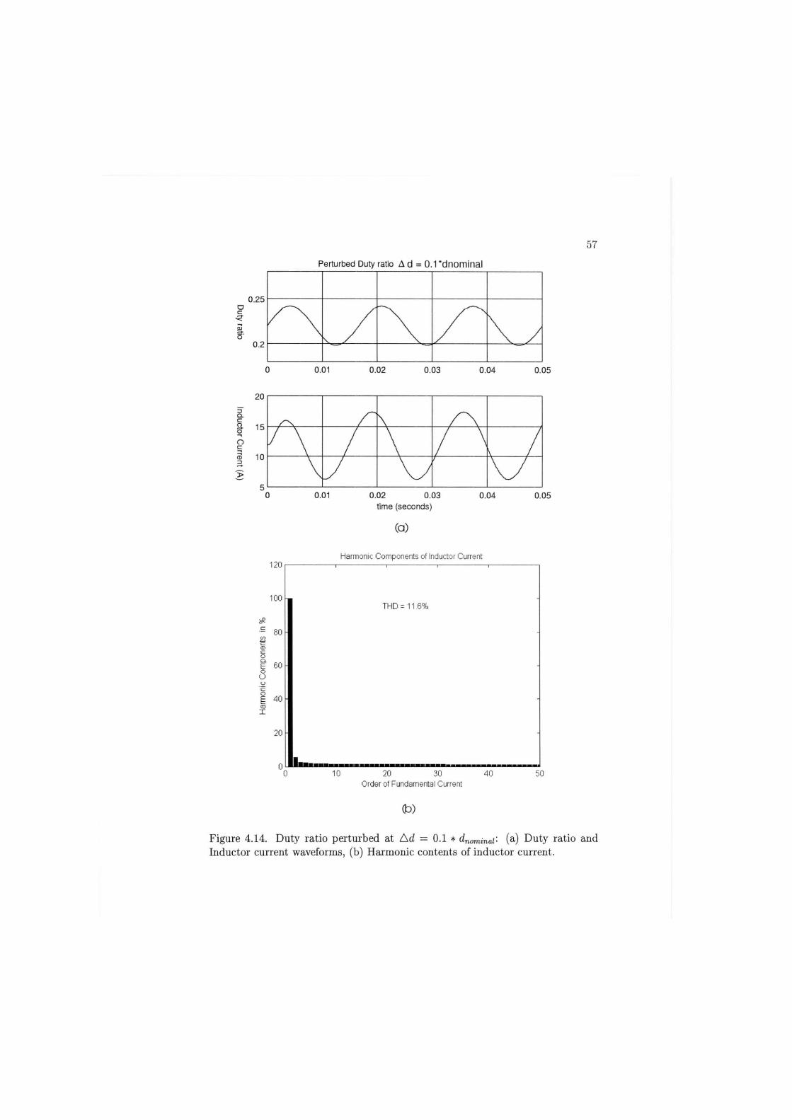
Perturbed Duty ratio A d = 0.1 *dnominal
57
0.25
0 0.01 0.02 0.03 0.04 0.05
20
Harmonic Components of Inductor Current
THD = 11.6%
"0 10 20 30 40 50 Order of Fundamental Current
( b )
Figure 4.14. Duty ratio perturbed at A d = 0.1 * dnomina\\ (a) Duty ratio and Inductor current waveforms, (b) Harmonic contents of inductor current.
100
•30
o
CI E o U 0 1 CD I
60
40

58
strainted (Ad = 0.1 * d n o m i n a l ) , iL assumes positive values only and has a siusoidal
shape. Similarly the allowable A d at other operating points can be verified.
At this point, prediction of the frequency response can be made by specifying the
interested frequency range. Fig. 4.15 shows a Bode plot of the control (duty-ratio
modulation d) to inductor current modulation (iL) transfer function, Gid.sim of
the boost-derived switch mode power converter for 1Hz to 40kHz.
Predicted Frequency Response of Boost-derived Switch Mode Power Converter
100 r" 1 1—1—1—1 1 1 11 1 1—i—i—i—i i i | r
Frequency (Hz)
Figure 4.15. Predicted frequency response of the example boost-derived switch mode power converter using the proposed modeling technique

59
4.5.3 Computational modeling versus state-space averaging
In this section, the computationally predicted frequency response is compared
with predicted frequency response using the state-space averaging method [7].
The comparison is shown in Fig. 4.16 and Fig. 4.17.
100
80
I 60
I 4 0
20
Ill I I o simulation result
state-space averac ed model
l 6 ^
10 10 frequency (Hz)
Figure 4.16. Predicted frequency response of the example boost-derived switch mode power converter using the proposed modeling technique without parasitic components and compared to the state-space averaging technique[7]
In Fig. 4.16, the transfer function of duty-ratio, d to inductor current ii using
proposed method without parasitic components, Gid.sim is marked by circles, the

60
150 legend:
— : state space averaged model • • i : approx. model to cover all op. pts. O : simulation results, parasitics included.
100
0
•100 10 10 10 10
frequency (Hz) 10'
Figure 4.17. Predicted frequency response of the example boost-derived switch mode power converter using the proposed modeling technique with parasitic components and compared to the state-space averaging technique [7]
same transfer function obtained using the state-space averaging method, G i d M v e
is shown as solid line. The transfer function that represents approximately all
operating points, Gid is shown in Fig. 4.17 as dotted line. In the power factor
correction circuit, the power stage dc gain, poles, and zero are dependent on the
input line voltage as shown in Fig. 4.19. It can be seen that the high frequency
portion of the frequency responses to the various inputs are identical. Therefore,

61
as indicated in [7], the dynamic characteristics from d to IL can be well represented
by the approximated transfer function, Gid-
Several remarkable features are observed from these plots:
1- Gid.sim has a much smaller resonance peak than Gid.ave- This is caused by
the inclusion of parasitic device elements in the device model.
2. Except in the neighborhood of the resonant frequency, the frequency re
sponses of Gid.sim and Gid.ave have a good agreement. A time trajectory of
d and IL obtained by simulation at a duty ratio modulation frequency of
40kHz is shown in Fig. 4.18. Neither waveforms are of sinusoidal shape.
Therefore the magnitude response at high frequencies shown in Fig. 4.17
and Fig. 4.17 should be treated as a crude approximation.
11.71 • ' ' 1
0.015 0.0151 0.0152 0.0153 0.0154 time (second)
Figure 4.18. Duty ratio modulation and inductor current waveforms of modulation frequency at 40kHz.

62
3. The uncertainties in the frequency response at high frequencies suggest that
a controller design according to C7;d shown in Fig. 4.17 may not cover the
worst possible case. Moreover, Gid is overly conservative at low frequencies.
The upper bound of all operating points at low frequency is approximately
50dB.
150
100
CD CD i_ CO CD T3
-100 10 10 frequency (Hz)
10
Figure 4.19. Frequency response predictions at various operating points.
4.6 Summary In this chapter, an effective approach for obtaining a suitable small-signal model
by the proposed computational technique is discussed. The fundamental principle
of this technique is explained and then demonstrated on the boost-derived power
factor correction circuit. An approximation approach of the sinusoidal response is

63
the general principle applied for the developed small-signal modeling technique.
The superimposed sinusoidal signal on the nominal duty ratio is controlled so that
the T H D content of the time response for the output is under 15 percent for the
minimum modeling error. The following benefits are claimed for the developed
small-signal modeling technique:
1. Mathematics used in the construction of the simulator involve only ordi
nary differential equations and perhaps rudimentary state-space theory. The
modeling process is therefore readily tractable.
2. Parasitic and non-linear effects can be incorporated easily in the developed
modeling process for better representation of the plant which leads to im
proved controller design.
3. Other switch mode power converter topologies can be modeled with a similar
process by replacing the state-space matrix coefficients.
The limitation of the proposed small-signal modeling technique is the computa
tional power. A pentium II desktop 333MHz P C is used to obtain the results
shown in this chapter. A frequency sweep from 1Hz to 40kHz in half decade
increments took longer than 9 hours. However, if frequency response below 10Hz
are neglected, approximately 4 hours and 45 minutes is required to perform the
frequency response prediction.
To obtain a small-signal model from the act* signal to the output iL shown
in Fig. 4.9, a small-signal model for the P W M must be included. Hence, by
combining the P W M small-signal model and results from the demonstrated small-
signal model represents the small-signal transfer properties of act* signal to the

63
the general principle applied for the developed small-signal modeling technique.
The superimposed sinusoidal signal on the nominal duty ratio is controlled so that
the T H D content of the time response for the output is under 15 percent for the
minimum modeling error. The following benefits are claimed for the developed
small-signal modeling technique:
1. Mathematics used in the construction of the simulator involve only ordi
nary differential equations and perhaps rudimentary state-space theory. The
modeling process is therefore readily tractable.
2. Parasitic and non-linear effects can be incorporated easily in the developed
modeling process for better representation of the plant which leads to im
proved controller design.
3. Other switch mode power converter topologies can be modeled with a similar
process by replacing the state-space matrix coefficients.
The limitation of the proposed small-signal modeling technique is the computa
tional power. A pentium II desktop 333MHz P C is used to obtain the results
shown in this chapter. A frequency sweep from 1Hz to 40kHz in half decade
increments took longer than 9 hours. However, if frequency response below 10Hz
are neglected, approximately 4 hours and 45 minutes is required to perform the
frequency response prediction.
To obtain a small-signal model from the act* signal to the output ii shown
in Fig. 4.9, a small-signal model for the P W M must be included. Hence, by
combining the P W M small-signal model and results from the demonstrated small-
signal model represents the small-signal transfer properties of act* signal to the
output %L-

64
However, this technique has some drawbacks:
• The execution time of the simulator written in MatLab code takes a long
time.
• The obtained model of the P W M is based upon a linearity assumption.
In the next chapter, a discussion is presented on how these drawbacks may be
overcome by using an improved computational small-signal modeling technique
for the switch mode power converter. This is done by perturbing the act* sig
nal instead of the duty ratio signal and implementing the simulator using the C
language.

CHAPTER 5 G5
IMPROVED COMPUTATIONAL SMALL-SIGNAL MODELING APPROACH FOR SWITCH MODE
POWER CONVERTERS
5.1 Introduction
The content of this chapter is an extension of the principal work of the pre
vious chapter. In that chapter basic principles of the computational modeling
technique are introduced and demonstrated with the example of the boost-derived
power factor correction circuit. Based on a physical understanding of switch mode
power converter circuit operation, an improved computational small-signal mod
eling technique is discussed in this chapter.
Referring to chapter 4, the pulse-width-modulator and power stage are modeled
separately and combined together to determine the overall loop-gain characteris
tics. In contrast to the complicated mathematical and circuit manipulation efforts
involved in the existing methods, this chapter shows that the improved compu
tational modeling approach models the dynamic characteristics of a switch mode
power converter with remarkably little effort.
For a real switch mode power converter, the duty ratio does not change within a
switching period, but the control signal VCON commands the duty cycle to change
once per switching period as shown in Fig. 4.2. Therefore neither the model
obtained by the modeling techniques introduced in chapter 2, nor the computa
tional modeling technique, obtained by introducing ac variation in the duty ratio
as discussed in the previous chapter, reflects hardware behavior. Thus, a small-
signal perturbation should be employed on the nominal control signal, VCON- The
improved computational modeling technique introduces an ac perturbation to the
nominal control signal VCON and uses the sampling effect to predict the dynamic

66
characteristics. The objective of this chapter is to develop an improved com
putational modeling technique that reflects hardware behavior and reduces the
modeling computation time.
The chapter is organized as follows: In section 5.2, an improved computational
modeling technique is introduced. In section 5.3 the enhanced frequency response
computation program is presented. In section 5.4 the proposed modeling technique
is applied to the buck converter. In section 5.5 an obtained small-signal model
using the proposed method is compared with a small-signal model using the state-
space averaging approach. Hardware verification is discussed in section 5.6 and
the chapter is summarized in section 5.7.
5.2 Improved computational modeling technique The improved method also begins with the state-space representations of each
on/off circuit state which characterize the behavior of the switch mode power
converter. Since modern digital computers work with discrete-time data, the
derived continuous-time state-space representations of the on/off linear switched
circuits must be converted into the discrete-time state-space form as given in
equations (4.7) to (4.10), and as illustrated in Fig. 5.1.
The role of the pulse width modulator (PWM) is to produce the drive pulses
for the switching device, such as a M O S F E T . It compares the error signal from the
error amplifier with a sawtooth signal. Typically, when the error signal intersects
with the sawtooth signal, the P W M turns off the switching device. This switching
transition is needed to establish the on-time for the switching device. To estimate
the turn-off switching edge of the drive signal, an impulse sampler is introduced at
each input of the P W M . The impulse sampled control signal is a train of impulses
with the strength of each impulse equal to the sampled value of the continuous-
time control signal at the corresponding sampling instant. Thus, the sampled

67
Vcon(t) vcon(kTsam) v0(kTsam)
i l l r kTsam
Comparator d(kTsam)
Pulse-Width Power Stage of Switch Mode Power Converters
6(8)
f v 0(kTsam)
sampler Modulator
Power Stage of Switch Mode Power Converters
6(8) H ^
• ' ' ~
kTsam — •
V s a w (kTsam) A
/ / kTsam
V*saW(t) sampler
Figure 5.1. Block diagram of the impulse sampled voltage mode switch mode power converter
control signal, v*on(t) may be represented with the following expression,
vcon(t) — vcon{kTsam)8(t — kTsam) k=0
(5.1)
or
vcon(*) = vcm{Q)6{t) + Vcon{Tsam)6(t ~ Tsam) + ' ' ' + Vcon{kTsarn)5{t - kTsam) + • • •
(5.2)
Similarly, the expression for the impulse sampled sawtooth signal is,

68
<aw(t) = £ vtaw(kTiam)6(t - kTsam) (5.3)
or
vsaw (v = sou; (0)<J(t) ~t~ ^sau)(TSQm)r5(£ — Tsam) + • • • + Vsaw(kTsam)5(t — kTsam) + • • •
(5.4)
At every sampling instant, the sampled values from each output of the impulse
sampler are compared to determine if the switch is to be on or off. A pictorial
diagram of the discrete-time operation of the P W M is illustrated in Fig. 5.2.
For digital computer implementation, it is desirable to reduce the errors that are
produced in the course of turn-off switching edge determination by the impulse
sampling and comparison process. To this end, the impulse sampling duration
must be very short in comparison with the natural sampling duration of the P W M .
Therefore,
where Tsam is the impulse sampling period, and Tsaw is the period of the sawtooth
signal. A good choice for the impulse sampler sampling frequency is approxi
mately,
fsam = 500 X fsaw (5.6)
During the "switch on" command for the switching device, the on-time state
equation (4.7) and the output equation (4.8) are solved. Since the input is given
for t > t0 and the initial state at t = to is specified, the future state of the switch
mode power converter under investigation is completely determined by a recursive
procedure.
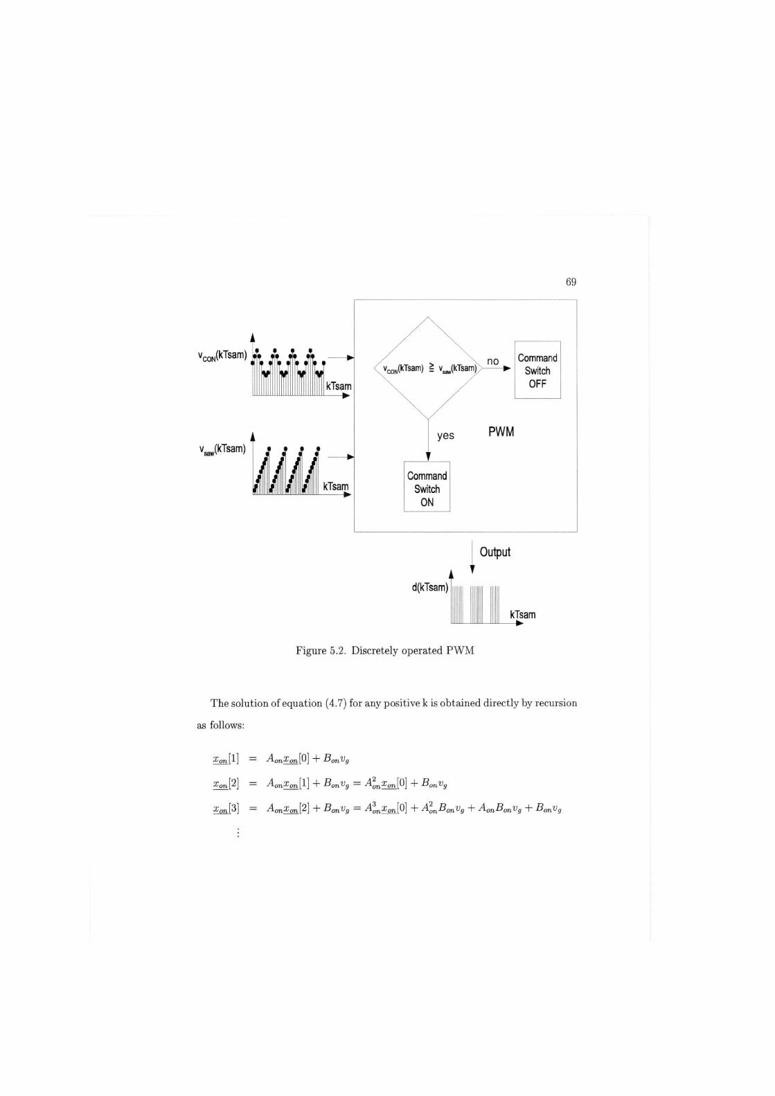
69
vC0N(kTsam)
v TkTsam)
kTsam
n o Command Switch OFF
yes P W M
Command Switch
ON
d(kTsam)
Output
kTsam
Figure 5.2. Discretely operated P W M
The solution of equation (4.7) for any positive k is obtained directly by recursion
as follows:
•Eonjl] = AonXon [0| -\- BonVg
Xon[2] = ^-on^onll] B<mvg = •^•on.Xon[^\ ~l~ Bonvg
%on\3] — Aonxon \2] + Bonvg — Anri xon\0] + AonBonVg + AonBonVg + BgnVg

70
Continuing with recursion procedure yields,
fc-i Xon{k] = A^xJtO] + £ Ak
on->-lBonvg (5.7) 3=0
and the output voltage yon[k] is given by,
Uon[k] = CAk
onXon[0] + C £ Ak
0-j-lBonv9 (5.8)
j=Q
In the recursion process, the input vg is assumed constant over the interval between
any two consecutive sampling instant. Therefore,
u(t) = u[kTsam], k = 1,2,3, (5.9)
and
u(t) = u[kTsam], for kTsam < t < kTsam + Tsam (5.10)
similarly, at the moment the P W M commands turn-off of the switching device, the
initial conditions for the off-time state equation becomes the last computed state
values and equation (4.9) and (4.10) are then solved recursively. The resulting
solution of the off-time state equation and output equation are,
fc-i Xoffjk] = Ak
offxoff[0] + £ AkJj-lBoffv9 (5.11) 3=0
and
VofjW\ = CAk
offXoff[0) + C Y Ak
0Jj~lB0ffVg (5.12)
The operation of solving equations (5.7), (5.8) and (5.11), (5.12) to obtain a time
domain response is illustrated in Fig. 5.3. This process is repeated until the
output voltage which is sampled every switching period settles in steady-state.
Then the gain and phase at the test frequency is calculated using equations
(4.11) and (4.12). For the frequency response prediction, this process is repeated
until the interested frequency range is covered.

71
x„ = A x + R v o n on o rr g
* o f f K f f + fYg
•
Figure 5.3. Operation of open loop switch mode power converter
The computational method described here is based upon the following assump-
• The switching frequency is constant.
• The switch mode power converter operates in continuous conduction mode.
• The samplers are synchronized and have the same sampling period; that is
The remaining step for obtaining the dynamic characteristics of the switch
mode power converter computationally is to implement a simulator that calculates
frequency response at each swept test frequency of the control signal by solving
the discussed discrete-time state equations recursively. This is discussed in the
next section.
tions:
tk+i — h — T, sam for all k, where k is an integer.

72
5.3 Improved Program A computer algorithm has been developed to implement the extended compu
tational method and implemented using the C language. The main objective of
the developed program is to compute the gain and phase transfer functions of a
switch mode power converter. Since the small-signal model formulation is based
on the steady-state information of the switch mode power converter, the key task
of the program is to find the steady-state operating point. The Peak Detection
algorithm discussed below is employed to find the steady-state point. The overall
description of the program is shown in the form of a flowchart in Fig. 5.4.
The operating point parameters and steady-state condition are established in
the following manner.
Find the nominal values of the control signal, VCON o,nd the ramp slope, mTamp of
the sawtooth signal.
Once the switching topology is selected, the Standard Calculations step in the
flowchart of Fig. 5.4 determines the nominal values of VCON and, mramp. There
are two types of voltage mode pulse width modulation integrated circuit ( P W M
IC): single output and dual output.
1. Single output P W M IC.
The single output P W M IC has one output for turning on and off the main
switching device of the switch mode power converter. It features a wide
range of the duty ratio control, i.e., from 0 to 1. A typical drive pulse
produced by a voltage mode P W M IC is shown in Fig. 5.5.
The nominal value of the control signal is calculated using the relationship,
t, on VCON ~ Vyalley (5.13) T sw spk 'valley
and, ton = dTt sw

73
User Input
buck boost etc. Choose
Topology
Specifications
plant order plant degree
Standard Calculations,
Rules...
Standard Calculations,
Rules... 1
f
|
Virtual Input-Output Experiment
«••••••
|
Virtual Input-Output Experiment 1
^ r
Plant Identification
Nomina! Values for Parts
Frequency Response
Data
Plant Transfer 1 Function /
r
Bode plot
End
Figure 5.4. Flowchart of switch mode power converter small-signal modeling.

74
/ Vspk
w VCON
k
v valley
*0N
J drive pulse drive pulse
-« y
Figure 5.5. Single output P W M IC output pulse
By rearranging the equation (5.13), the nominal control signal, VQON is
expressed as,
VCON = (Vspk - Vvaiiey) * d + VvaUey (5-14)
and the ramp slope is determined using,
(VSpk - Vvauey) * fsw (5.15)
2. Dual output P W M IC
The dual output P W M IC is usually used when two switching devices are
needed to be turned on and off alternately. Therefore the two outputs are
180° out-of-phase pulses of the same width. The output pulses produced by
dual output P W M IC are shown in Fig. 5.6.
If one of the dual outputs is used to switch a single switching device,
the switch frequency becomes one-half of the sawtooth oscillator frequency.

75
CON
valley
drive pulse 1
*0 N
drive pulse 2
Figure 5.6. Dual output P W M IC output pulses
Thus, the nominal value of the control signal and ramp slope become,
VcON — (VSpk - Vvaiiey) * 2d + Vvauey (5.16)
and
^ramp = (VSpk ~ Vvauey) * 2fsw (5-17)
Steady-state operating point establishment
The high and low peak search technique is used to establish that steady-state
operation has been achieved. This technique searches for the highest and lowest
peak values of the sampled output voltage every perturbed control signal period
(imposed sinusoidal test signal) at the sampling rate equal to the switching fre
quency. The detected peak values give amplitude information about the discretely
sampled sinusoidal output voltage at each frequency step as shown in Fig. 5.7.
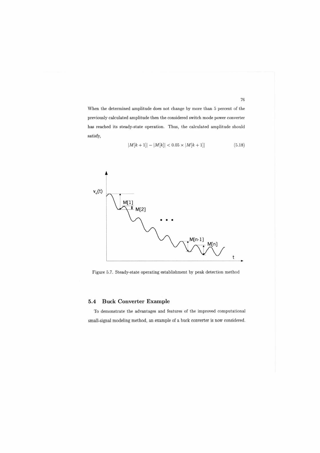
76
When the determined amplitude does not change by more than 5 percent of the
previously calculated amplitude then the considered switch mode power converter
has reached its steady-state operation. Thus, the calculated amplitude should
satisfy,
\M[k + 1]| - \M[k]\ < 0.05 x \M[k + 1]| (5.18)
5.4 Buck Converter Example To demonstrate the advantages and features of the improved computational
small-signal modeling method, an example of a buck converter is now considered.

77
The converter was designed and built with the following specifications:
Specification:
Input voltage: DC 48V
Output voltage: DC 12V
Output current: 2A
Switching frequency: lOOKHz
Table 5.1. Component values of buck converter
Components Components Description Component values Inductor L 450>H
Winding resistance RL 0.5Q Capacitor C 1000/^F
Eq. Series Resistance (ESR) Rc 450mfi M O S F E T conduction voltage VQ OAV
Diode forward voltage drop VD 0.6V
Resistive load Rload on
Converter component values and parasitic values are given in Table 5.1. The
power stage of the buck converter with specified parameters is shown in Fig. 5.8.
The nonidealities of components are included in Fig. 5.8 to increase the accuracy
of the derived mathematical model.
The semiconductor switches are modeled as an ideal switch with a battery:
the M O S F E T is modeled by the conduction voltage drop, VQ, and the diode is
modeled by the forward voltage drop, vp. The inductor and capacitor are modeled
with the winding resistance, R L , and equivalent series resistance, RC, respectively.
The first step is the derivation of the buck converter mathematical model for
each state in state-space form. The characterization of each state of operation in

78
rLoad
Figure 5.8. Buck type switch mode power converter power stage with parasitics included.
state-space form is generally easy if one is familiar with the state variable formu
lation, but practicing engineers may not be so familiar with this characterization,
hence the derivation of buck converter state and output equations are given in
Appendix A .
By choosing the state-space vector x = [i^d, the state and output equations
become
1. On-time interval:
Xnn RL
L rLoadRc
L(rLoad+Rc
rLoad C(rLoad+Rc)
rLoad L{rLoad-\-Rc)
C{rLoad+Rc) .
iL + 1 L 0 0
- i o V9
vD
(5.19)
and
Vnn. = rLoadRc
rLoad+Rc 'Load
rLoad+Rc H VC
+ 0 0 0 V9
VQ VD
(5.20)
79
2. Off-time interval:
Xoff =
and
Ri, rLoadRc. L L (rLoad+Rc)
rLoad
rLoad
C(rLoad+Rc)
L(rLoad+Rc) 1 C(rLoad+Rc)
iL + "0 0 - I " + 0 0 0
V9
(5.21)
rLoad rLoadRc rLoad+Rc rLoad+Rc
IL + 0 0 0 ' vc
W9 (5.22)
The next step is to set the amplitude of the sinusoidal signal superimposed on
the dc control signal, VCON- For the boost-derived power factor correction circuit
in chapter 4, the amplitude of the injected sinusoidal signal was set such that the
resulting output waveform has an ac component with a T H D under 15 percent,
but the voltage conversion characteristics of a buck converter versus duty ratio
operating in the continuous conduction mode is linear as shown in Fig. 5.9.
Therefore the amplitude of the perturbed control signal superimposed on the
dc control signal does not produce a distorted sinusoidal component in the time
response. Thus, the frequency response plot is independent of the amplitude value
of the perturbed control signal for the buck converter. The frequency response
plots of the buck converter for various values of the perturbed control signal
amplitude will be shown later. For this example buck converter, the amplitude of
perturbed control signal, VAMP is set as,
VAMP = 0.1 x VCON (5.23)
The time response of the buck converter with the control signal perturbed at 5kHz
is shown in Fig. 5.10.
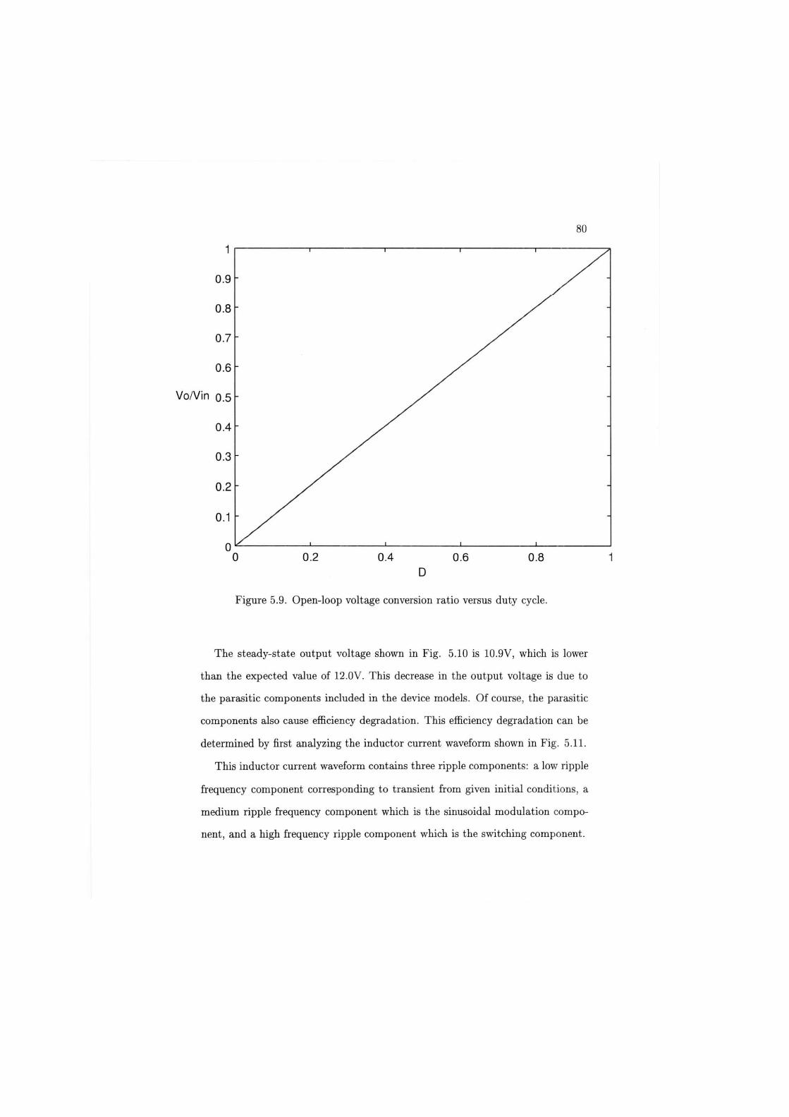
80
0 0.2 0.4 0.6 0.8 1 D
Figure 5.9. Open-loop voltage conversion ratio versus duty cycle.
The steady-state output voltage shown in Fig. 5.10 is 10.9V, which is lower
than the expected value of 12.0V. This decrease in the output voltage is due to
the parasitic components included in the device models. Of course, the parasitic
components also cause efficiency degradation. This efficiency degradation can be
determined by first analyzing the inductor current waveform shown in Fig. 5.11.
This inductor current waveform contains three ripple components: a low ripple
frequency component corresponding to transient from given initial conditions, a
medium ripple frequency component which is the sinusoidal modulation compo
nent, and a high frequency ripple component which is the switching component.

81
12.4 Time response of Buck converter with duty ratio perturbed at 5KHz
time (s) x 10"
Figure 5.10. Open-loop time response of example buck converter.
Recognizing that the dc component of inductor current and output current are
equal for the buck converter, the average inductor current, < %L > is calculated
from the inductor waveform shown in Fig. 5.11(b),
AiL
< iL >= IL = I0 = iLjPk - (5.24)
where is the ripple inductor current,
&%XJ — iL,highpk ^L,lowpk (5.25)

82
Inductor current waveform
0 2 4 6 8 10 12 14 Sampling index (K)
(a)
Inductor current waveform
1.335 1.34 1.345 1.35 1.355 1.36 Sampling index (K) x 1 Q 5
(b)
Figure 5.11. Inductor current waveform of example buck converter: (a) Inductor current, (b) Enlarged section shown in (a).

83
The calculated average inductor current using equations (5.24) and (5.25) is
2.005A and during the same time interval, the average input current, < iin >,
for the buck converter is found from the on-time interval of the inductor current
waveform:
< iin >= 0.49A
Then, the efficiency, 77, of the example buck converter is estimated using,
rj = x 100 (5.26)
gives, r) = 92.7 percent.
To find the frequency response characteristics, the implemented program is exe
cuted with simulation parameters, the start frequency, fstart, and stop frequency,
fstop- In the program, frequency step size is set at 1.2 * ftest. The program yields
the magnitude and the phase shift information over the specified frequency range
and then stores this information in arrays for further analysis. Consider an ex
ample of a buck converter with the control signal perturbed at 5kHz. The time
response of the output voltage after the buck converter is in the steady-state oper
ation is shown in Fig. 5.12 (a). The ratio of the magnitude of the output voltage,
V0, to the control signal, Vam, is the gain at that particular frequency, thus it is
denoted as a function of frequency M(f). Similarly, the phase shift is the phase
difference between the output voltage, v0, and the control signal, vcon, at the given
test frequency, and designated also as a function of frequency, <f>(f).
For the above example, the gain M(f5kHZ) and phase shift <j>(fekHz) calculated
from Fig. 5.12 (a) using equations 4.11 and 4.12 are 0.215 and -89.9 degrees
respectively. This process is repeated at each test frequency to construct the gain
and phase plots shown in Fig. 5.12 (b).

2
Figure 5.12. Responses of an example buck converter: (a) Sinusoidal steady-state time response at test frequency of 5kHz, (b) Computed frequency response

85
The important observation in Fig. 5.12 (b) is the erratic behaviour of the
phase response in the vicinity of 10kHz. The accuracy of an open-loop small-
signal model as applied to a switch mode power converter obtained using the
state-space averaging method by Cuk [1], and also discussed in [10] claim that the
model is theoretically accurate up to half of the switching frequency. However, as
discussed in chapter 2, the pulse width modulator produces a train of on/off gate
pulses for the switching device (MOSFET), once per switching cycle by compari
son of a sawtooth waveform with the control signal vcon as long as the modulator
(comparator) is not saturated. This means that the control signal is sampled
once per switching period. In other words, the pulse-width modulator behaves
as a sampler. Therefore, as the test frequency approaches 10kHz, the phase plot
starts to become erratic. This may indicate that the obtained model starts to
give erroneous information about the dynamic characteristics of the switch mode
power converter as the test frequency approaches one-tenth of the switching fre
quency. As shown in Fig. 5.9, the transfer characteristics of the buck converter is
linear. The frequency response should therefore be independent of the amplitude
of the perturbed control signal. This is illustrated in Fig. 5.13 (a), the frequency
response plots of the various amplitudes of the perturbed control signal.
The bode plots of the various test frequency steps are shown in Fig. 5.13 (b).
There is an uncertainty in the phase plots at high frequencies. The phase plot
deviates as much as ±15 degrees, which indicates the dynamic characteristics at
high frequencies are not predictable.
The established analytical modeling techniques, such as the state-space aver
aging method of Cuk [1], or discrete modeling technique of Packard [3], result in a
mathematical small-signal linear model (transfer function) after numerous analyt
ical steps. On the other hand, the proposed small-signal modeling technique can
be utilized to obtain a transfer function from the control signal, vcon, to the output

86
voltage, v0, in a single step rather than in several steps. For the established mod
eling techniques, the small-signal model for the power stage and P W M is derived
separately and then combined together for the overall open-loop transfer function
for the duty ratio, d, to the output voltage, va. In order to extract the transfer
function of the control signal, vcon, to the output voltage, v0, the simulation data
is transferred to Matlab and using the System Identification toolbox, a Bode plot
is constructed and this original Bode plot was fitted with a second-order system
shown in Fig. 5.14.
When a second-order curve fit is performed to the original Bode plot, Matlab
places an extra zero near s = oo and returns a transfer function which is always
proper, v0 0.0095615s2 + 1272.9456s + 3199695.0603
* * ~ v^„. ~ s2 + 2131.8697s + 1993384.9337
This transfer function can be made to be strictly proper by eliminating a zero.
The following criterion is applied to discard a zero:
Discard criterion If the magnitude of the real part of a zero is greater than 10 times the magnitude of the real part of the second zero, then the effect of this zero on the system response is negligible and it can be discarded.
As shown the pole and zero map in the complex frequency plane of Fig. 5.15
(a), the real part of Z2 is located much farther than Z l , thus Z2 is discarded to
yield a strictly proper transfer function,
Vo 1272.9456s + 3199695.0603 ' ' ~ vZn' ~ s2 + 2131.8697s + 1993384.9337 * ' '
and the resulting Bode plot of strictly proper transfer function is illustrated in
Fig. 5.15 (b), which fits the simulation Bode plot shown in Fig. 5.14 (a) well.
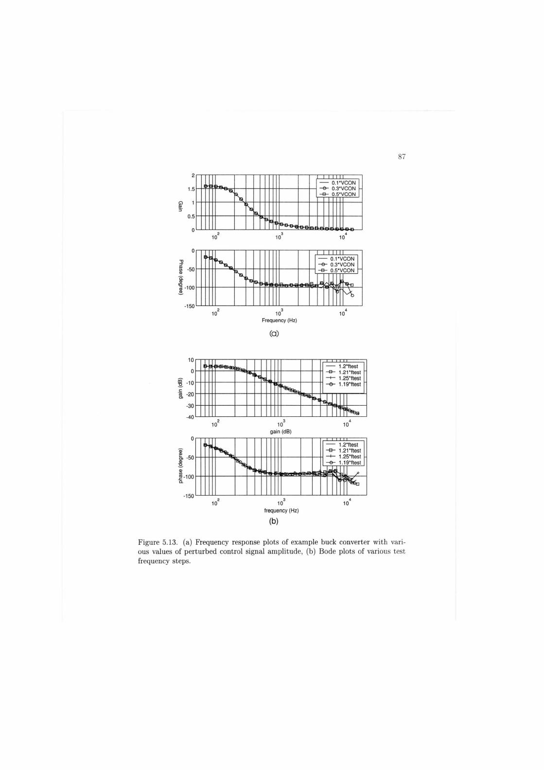
87
Figure 5.13. (a) Frequency response plots of example buck converter with various values of perturbed control signal amplitude, (b) Bode plots of various test frequency steps.

88
Figure 5.14. Bode plots of an example buck converter: (a) Bode plot from the simulation data, (b) Bode plot with second-order fit.

89
Pole-zero map
3 i
1000
BOO
600
400
2C0
0
-200
400
•600
-800
•1000 -1
Z2
-12
abs[real(Z2)] » abs[real(Zl)] Z 1
-10 -6
Real Axis
0 2
x 10J
(a)
Figure 5.15. (a) Pole-zero configuration of proper transfer function, (b) Bode plot of strictly proper transfer function.

90
5.5 Computational Modeling Versus State-Space Averaging
Cross checking of the agreement between the small-signal model derived us
ing the proposed improved computational method and the state-space averaging
method, the example buck converter discussed in the previous section is modeled
using the state-space averaging approach and a comparison is made. The following
state-space averaging procedures for obtaining a small-signal model of the buck
converter power stage shown in Fig. 5.8 operating in continuous conduction mode
is used:
Step 1. Draw a linear switched circuit model for each state of the switch mode power
converter.
Step 2. Identify the state variables and write state and output equations for each
switched circuit model using Kirchhoff's voltage and current laws.
Step 3. Perform state-space averaging over one switching period by multiplying the
on and off equations by the duty ratio as a weighing factor.
Step 4. Combine state and output equations into a single averaged state and output
equation.
Step 5. Perturb the averaged state and output equations to yield steady-state and
dynamic terms and eliminate the nonlinear terms
The M O S F E T and diode are modeled as resistors so that the state-space rep
resentation of each on/off switched model represents a single-input-single-output
system. Appendix B illustrates the derivation of a small-signal model of the ex
ample buck converter by making use of the above procedure. Introducing the
duty ratio perturbation to the averaged model derived in Step 4 and removing the

nonlinear terms based on the small-signal approximation,
91
Vg « Vg, d « D, X « X (5.29)
and separating ac and dc parts, yields the final state-space averaged small-signal
model transfer function, d to v0,
d
where,
= (si - Aa^-^Aon - Aoff)X + (Bon - Boff)Vg] + (Con - C0ff)X (5.30)
Anjjfi — dfip.s i dRi
L "*" L _ Rp RL.
L L rLoad
C{rLoad+Rc)
rLoadRc. L(rLoad+Rc)
rLoad L(rLoad+Rc)
1 C(rLoad+Rc)
A •*» on —
L EL. L
rLoadRc L(rLoad+Rc)
•Load C(rLoad+Rc)
rLoad L(rLoad+Rc)
1 C(rLoad+Rc) .
Aoff =
_ Rp L
BL. I.
rLoadRc. L(r Load-\-Rc)
rLoad C(rLoad+Rc)
rLoad L(rLoad+Rc) 1 C(rLoad+Rc)
Brtn — L 0
B0ff = 0
0
fi /•> f rl ^on — ^off — [ r L
LoadRc rLoad id+Rc rLoad+Rc
and X is obtained from the dc part,
X = -A~lBVg (5.31)

92
Referring to the open-loop block diagram of the example buck converter shown in
Fig. 5.16, the open loop transfer function v^m to va becomes the product of the
transfer functions of the individual elements, where G d i v is the gain of the divider
network, 1/VS is the sawtooth ramp amplitude, and Gss is the derived small-signal
model transfer function of d to va. The resulting overall open loop characteristics
in Bode plots are shown in Fig. 5.17.
con
Figure 5.16. Open-loop block diagram of buck converter.
Shown as o's in Fig. 5.17 is the Bode plots generated using the proposed
improved computational small-signal modeling method and the solid line Bode
plots are produced by the state-space averaging method. It is seen that there is
good agreement between these two different modeling methods.
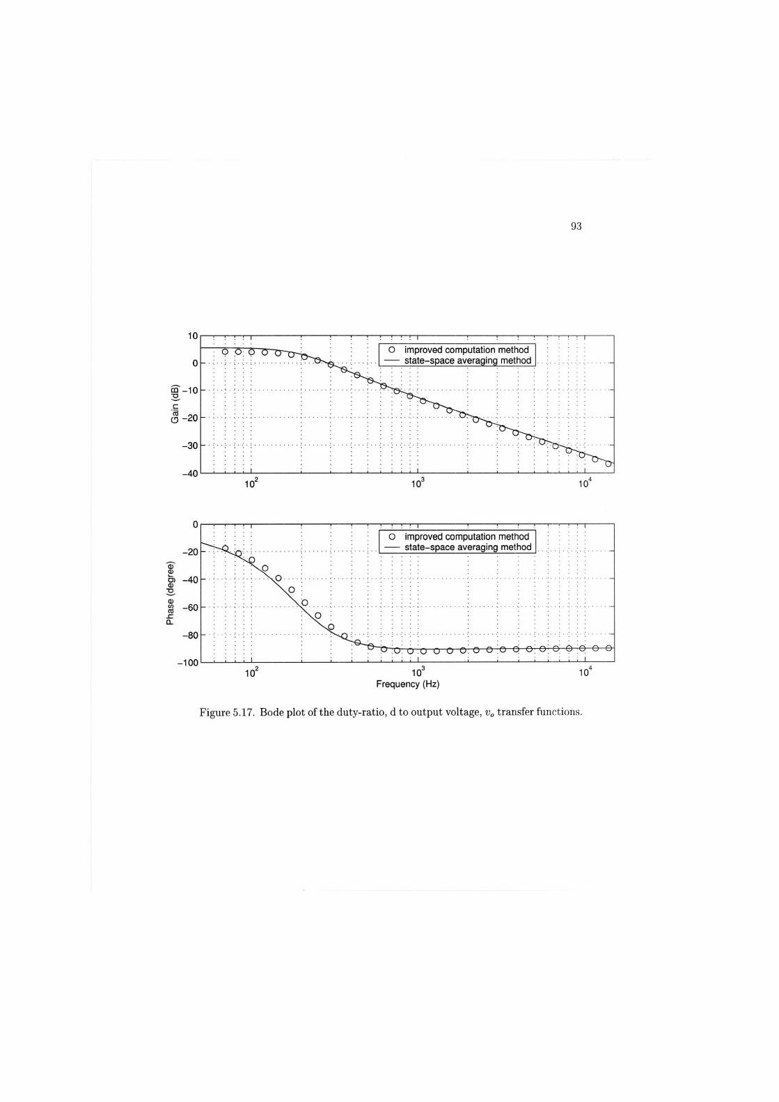
93
Figure 5.17. Bode plot of the duty-ratio, d to output voltage, vQ transfer functions.

94
5.6 Experimental Verification 5.6.1 Experimental Circuit
The buck converter was built as shown in the schematic diagram Fig. 5.18 to
demonstrate the effectiveness of the improved computational modeling technique.
The key elements of the buck converter are designed as follows:
Specifications
The design process starts with the specifications for the buck converter perfor
mance. For the example converter the specifications are:
Input voltage: 48V
Output voltage: 12V
Maximum power output: 24W
Switching frequency
The choice of switching frequency is generally somewhat arbitrary. The switching
frequency must be high enough to make the components small and must be low
enough to keep the switching loss small. The switching frequency for the example
buck converter is selected to be 100kHz as a compromise between size and effi
ciency.
Inductor design
The inductor value is calculated to give some predetermined ripple current. The
inductor calculation begins with the equation,
VL = (5.32)
therefore, the inductance L becomes,
A T L={VIN~V0)— (5.33)
Allowing 10 percent ripple current and 10 percent margin, the inductance value
is then defined as L = 500/iif.

0
—< 5
>
0 E 2 v—
id $ 6 a UC2524
as i £ g rJ CO
5
0
lvw—II—|
Figure 5.18. Buck converter schematic diagram

96
Output capacitor selection
Typical values for the output capacitor is 500/iF per amp. Thus, for a 2A output
current, 3 * 330>F capacitors are selected.
Drive circuitry
Since the source of the n-channel M O S F E T is not connected to the return line of
the buck converter, the drive scheme shown in Fig. 5.19 is used.
Vin (+)
From PWM I.C. output H I — | >. <\-
-WV-To switch in
device
Vin (-)
Figure 5.19. Drive scheme for the buck converter.
M O S F E T selection
For the buck converter, the maximum voltage on the power switch does not exceed
the input voltage plus a diode turn on voltage (not including noise spikes), the
200V IRF 250 power M O S F E T which has a fairly low on resistance of 0.7 ohm,
in a TO-3P package was selected.

97
Free wheeling diode
This diode catches the stored energy in the inductor when the M O S F E T turns
off. The S60SC4M Schottky barrier diode is used to perform the task.
The band gap reference voltage from the voltage mode P W M controller, SG3524
is used to set the nominal control voltage. The error amplifier is used as a buffer.
The table 5.2 summarizes the components used in the buck converter design.

Table 5.2. Component values of boost-derived P F C circuit
Component List Component Values Component Description C I , C2, C3 330/UF/63V Electrolytic Capacitor C4, C5, C6 330//F/63V Electrolytic Capacitor
c7, C l l 2A/471 Film capacitor C8 1 0 / / F / W Electrolytic Capacitor C9 471/2K Ceramic Capacitor
CIO, C12 220/zF/25V Electrolytic Capacitor C13 102 Film Capacitor C14 100/JF/50V Electrolytic Capacitor C15 2A/104 Film Capacitor C16 102/1K Ceramic Capacitor C17 101 Film Capacitor R l 0.5/1W Power Resistor R2 1K/3W Power Resistor R3 25K 1/4W Resistor R4 200/1W Power Resistor
R5, R7 1.5K 1/4W Resistor R6, R13 5.6K 1/4W Resistor R8, R9 2K/3W Power Resistor
RIO, R l l , R12 2K 1/4W Resistor R14 10K 1/4W Resistor R15 22/1W Power Resistor R16 I K 1/4W Resistor R17 100/2W Power Resistor R18 1/2W Power Resistor
POT1 10K Potentiometer POT2, POT3 IK Potentiometer
D2, D4, D5 ERC81-004 General purpose diode D3 S60SC4M Schottky Barrier diode D7 ERA84-009 General purpose diode
4420 M O S F E T driver SG2524 P W M IC TL431 Programmable Precision Reference
optr, optd P521-1GB Opto-coupler Q l IRF250 M O S F E T Q2 IRF640 M O S F E T Q3 2SA1356 P N P transistor LI 450/iif Inductor L2 Inductor T l Aux. transformer T2 Driver transformer

99
5.6.2 Experimental Setup
The test setup for measuring the frequency response of the implemented buck
converter is illustrated in Fig. 5.20 and the test equipment used for measurement
is listed in Table 5.3.
Table 5.3. List of test equipment
Equipment Maker Model Computer ABS computers Pentium II
Signal injection transformer Hewlett Packard HP35282A Oscilloscope Tektronix TDS754D
Rheostat James G. Biddle CO. 19 Ohms D V M Data Precision Corp. Driver 2480R
D C Power source Lambda LK345 Waveform Generator Hewlett Packard 33120A
DAQ Board National Instruments Corp. PCI-MIO-16E-1 DAQ Interface Board University of Calgary 130956
Switch mode power converters generate a large amount of switching noise rela
tive to the sinusoidal injection signal, therefore it is almost impossible to estimate
the gain and phase of switch mode power converters with an oscilloscope. There
fore, the narrow band tracking voltmeter function is an essential requirement for
switch mode power converter loop measurements.
5.6.3 Development of Gain and Phase Meter
In order to make a proper loop gain measurement, it is necessary to build the
gain and phase meter with a narrow band tracking function. The computer-based
narrow band tracking feature of the gain and phase meter is developed using
the Labwindows/CVI programming environment and a plug-in data acquisition
board.
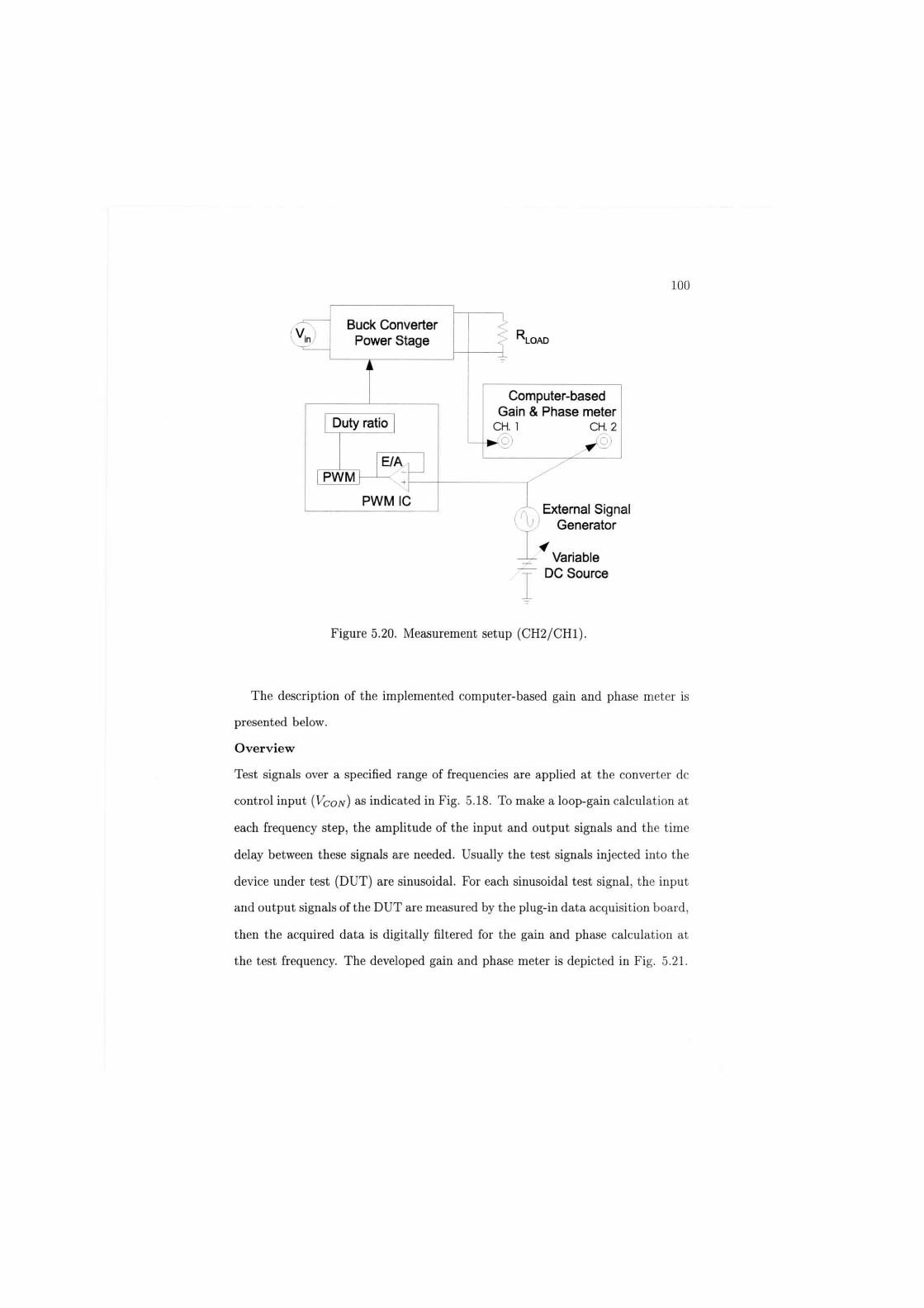
100
v i n
Buck Converter Power Stage
Duty ratio
PWM E/A
PWM IC
LOAD
Computer-based Gain & Phase meter
CH. ] CH. 2
External Signal Generator
Variable DC Source
Figure 5.20. Measurement setup (CH2/CH1).
The description of the implemented computer-based gain and phase meter is
presented below.
Overview
Test signals over a specified range of frequencies are applied at the converter dc
control input (VCON) a s indicated in Fig. 5.18. To make a loop-gain calculation at
each frequency step, the amplitude of the input and output signals and the time
delay between these signals are needed. Usually the test signals injected into the
device under test (DUT) are sinusoidal. For each sinusoidal test signal, the input
and output signals of the D U T are measured by the plug-in data acquisition board,
then the acquired data is digitally filtered for the gain and phase calculation at
the test frequency. The developed gain and phase meter is depicted in Fig. 5.21.

101
+12 V
Protection box
Figure 5.21. Computer-based gain and phase meter.
Plug-in data acquisition board (DAQ)
The plug-in data acquisition board, PCI-MIO-16E from National Instrument
Corp. is used to acquire the input and output signal information. Two inputs
out of 8 differential input channels are used sampling at 1.25MS/s (multiplexed)
The differential input helps to cancel out the common-mode noise picked up by
the leads.
Software
The instrumentation software, Labwindows/CVI programming environment is
used to develop a software driver which bridges the gap between the P C and
DAQ board. The included functions of the driver software are:
1. Data acquisition
For display and analysis purposes, the digital version of the ac coupled
waveform is stored in memory in a near optimal manner. The selected

102
number of data points at different test frequencies are given in Table 5.4.
These data points are sampled at the frequency of
fSam(Hz) = ftest x No.of points (5.34)
used by the analog-to-digital (ADC) converter to represent the analog signal.
For this apparatus, the sampling frequency is selected at least 20 times the
test signal frequency for the proper data acquisition.
Table 5.4. Selection of data points
Test freq. No. of Pts. Test freq. No. of Pts. Test freq. No. of Pts. ftest > 150 2500 ftest > 150 2500 ftest > 500 500
ftest > 2500 100 ftest > 200 2000 ftest > 1000 400 ftest > 5000 50 ftest > 250 1500 ftest > 1250 300 ftest > 10000 40 ftest > 300 1000 ftest > 1500 200 ftest > 12000 30 ftest > 500 500 ftest > 2500 100 ftest > 16000 20
2. Scaling the acquired waveforms
The range, resolution, and gain available on a DAQ board determine the
smallest detectable change in voltage. The PCI-MIO-16E DAQ board is a
12-bit DAQ board with a selectable voltage range of 0 to 10V or -10 to 10V
and selectable gain given in Table 5.5. Therefore, the output voltage of the
buck converter is attenuated using 1:1 voltage divider and quantized at the
resolution of
Res = M a ™ d y e (5.35) gam x 2U
which gives the theoretical resolution of one bit in the digitized value of
2.24mV.

103
Table 5.5. Actual range and Measurement precision [27]
Range configuration Gain Actual Input range precision 0 to +10V 1.0 0 to +10V 2.44mV
2.0 0 to +5V 1.22mV 5.0 0 to +2V 488.28/xV 10.0 0 to +1V 244.14/iV 20.0 0 to +500mV 122.07/zV 50.0 0 to +200mV 48.83//V 100.0 0 to +100mV 24.4/iV
-5V to +5V 0.5 -10 to +10V 4.88mV 1.0 -5 to +5V 2.44mV 2.0 -2.50 to +2.5V 1.22mV 5.0 -1 to +1V 488.28yuV 10.0 -500 to +500mV 244.14/iV 20.0 -250 to +250mV 122.07/zV 50.0 -100 to +100mV 48.83//V 100.0 -50 to +50mV 24.4/^V
3. A C coupled waveform
Once the two channel input signals are acquired, the max, min, and mean
values are calculated, then the calculated mean value is subtracted from
each acquired data value. The resulting values represent the ac coupled
data points.
4. Software filter
The ac coupled input data stored in the input array is filtered using a digital
bandpass Chebyshev filter. The bandpass digital filter that is fiat in its pass
band and has a smooth transition from the pass band to the stop band is
implemented to remove unwanted signals from the acquired signals.
5. Graph the results
The filtered waveforms of C H . l (va) and CH.2 (vcon) are displayed and the
gain and phase value of each test frequency are calculated.

104
5.6.4 Experimental Results
The buck converter shown in Fig. 5.18 is used to provide some experimental
waveforms and frequency response data. The buck converter was operated at a
constant input voltage of 48V and in a nominal predetermined duty ratio of 0.25.
The rheostat was set for a full load current of 2A.
To start an open-loop gain and phase measurement, an adjustable dc voltage
source (dc control signal) and output from the signal generator (sinusoidal per
turbation) are added together to provide the control signal input for the pulse
width modulator. As discussed in Chapter 1, the behavior of this pulse width
modulator in its simplest form is a voltage comparator that switches when the
control signal, t>con intersects with the sawtooth signal. Without a small sinusoidal
perturbation signal vcon added to the dc control signal VCON, the resulting duty
ratio represents a nominal duty ratio at that particular operating point. The error
amplifier in the P W M control IC is set to unity gain by connecting pin 1 and pin
9 together. To operate the buck converter at nominal conditions, the adjustable
dc voltage source was slowly increased from zero until the output voltage had
reached the nominal value of 12V. Then the signal generator was turned on to
modulate the control signal which gives the perturbation of the duty ratio. The
amplitude of the modulation signal was carefully adjusted so that it does not over
drive the buck converter. The modulated control signal and sawtooth waveforms
are shown in Fig. 5.22, for illustration purposes only (normally frequency of the
modulated control signal is much less than the sawtooth signal frequency).
Once the test set-up is correctly tuned, the open-loop characteristic of the buck
converter is measured at each swept test frequency. The test frequency step size
was selected such that:
ftest(n+l) = 1-2 x f t e s t ( n ) (5.36)
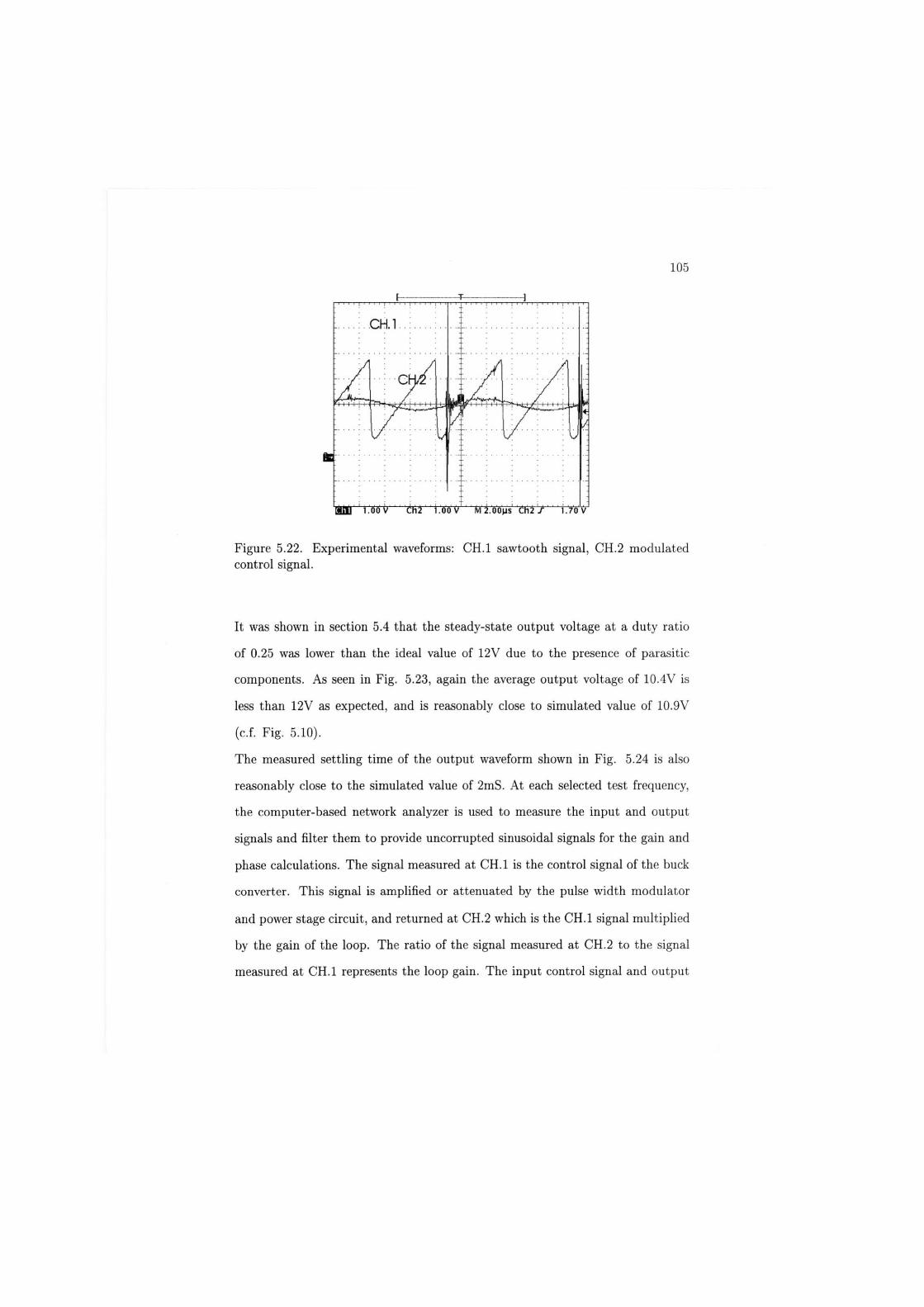
105
[ : ~~ :- 7-^ - •• - i
c K i
Ijjftl 1.00 V Ch2 1.00 V M 2.00ms C h 2 y 1.70 V
Figure 5.22. Experimental waveforms: C H . l sawtooth signal, CH.2 modulated control signal.
It was shown in section 5.4 that the steady-state output voltage at a duty ratio
of 0.25 was lower than the ideal value of 12V due to the presence of parasitic
components. As seen in Fig. 5.23, again the average output voltage of 10.4V is
less than 12V as expected, and is reasonably close to simulated value of 10.9V
(c.f. Fig. 5.10).
The measured settling time of the output waveform shown in Fig. 5.24 is also
reasonably close to the simulated value of 2mS. At each selected test frequency,
the computer-based network analyzer is used to measure the input and output
signals and filter them to provide uncorrupted sinusoidal signals for the gain and
phase calculations. The signal measured at C H . l is the control signal of the buck
converter. This signal is amplified or attenuated by the pulse width modulator
and power stage circuit, and returned at CH.2 which is the C H . l signal multiplied
by the gain of the loop. The ratio of the signal measured at CH.2 to the signal
measured at C H . l represents the loop gain. The input control signal and output

106
a -
On time = 2 5 LIS
S.oo v MS.oolis CHI / BTTv"
(a)
Output voltage = 10.4 V
am g.oov M S.OOjas Ch1 / 672V
(b)
Figure 5.23. Measured waveforms: (a) the duty ratio, (b) the output voltage.

107
waveforms are measured with an oscilloscope and two cases are presented in Fig.
5.25. At a test frequency of 70Hz, the output waveform shown in Fig. 5.25(a)
is a sinusoidal shape but the waveforms at the test frequency of 10kHz shown
in Fig. 5.25 (b) indicates that the loop-gain measurement becomes increasingly
inaccurate at higher test frequencies. Also, the switching ripple and noise corrupts
the desired output signal which make gain and phase measurements impossible
with an oscilloscope. The same waveforms measured with the developed computer-
based gain and phase meter are illustrated in Fig. 5.26. The gain and phase
calculation at each test frequency is performed on the filtered waveforms shown
in 5.26 (b). The amplitude and phase of sinusoidal waveforms are determined
either automatically, or manually by selecting the peak values of the waveforms
with cursors. This measurement is repeated at enough points across the frequency
range of interest to create a relatively smooth frequency response plot.
yjU 5.00 v M sooiis chi j 6.4 v
Figure 5.24. The output voltage at startup.
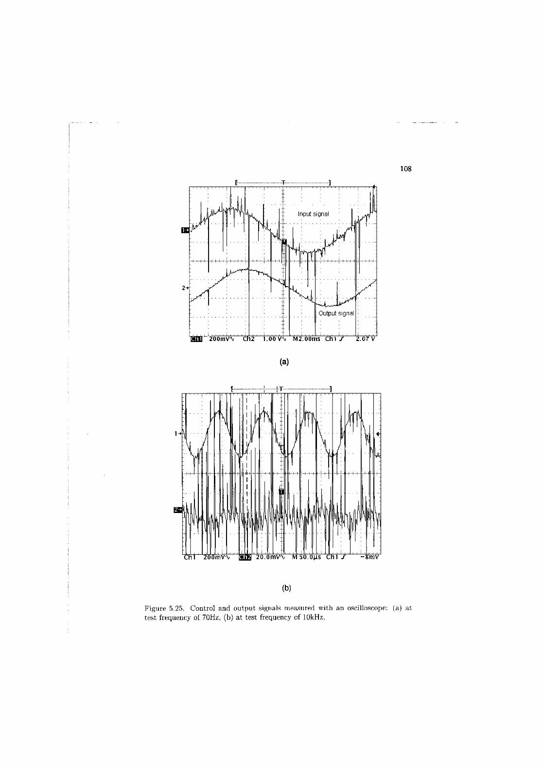
Figure 5.25. Control and output signals measured with an oscilloscope: (a) at test frequency of 70Hz, (b) at test frequency of 10kHz.

109
The loop gain characteristic measured data at various test frequencies is given
in Table 5.6 and a Bode plot comparison between the predicted and measured
result are presented in Fig. 5.27.
Table 5.6. Measured loop gain data
Test freq. Gain (dB) Phase (degree) Test freq. Gain (dB) Phase (degree) 50 7.56 -18 900 -11.7 -99.5 60 7.33 -24.0 1080 -13.3 -98.6 70 7.12 -26.0 1300 -16.5 -102.4 80 6.85 -28.0 1600 -18.2 -105.8 90 6.54 -30.0 2000 -19.6 109.1 100 6.26 -33.0 2400 -22.7 -106.2 120 5.80 -36.0 3000 -24.6 -112.5 150 4.52 -40.0 3600 -24.2 -117.3 180 3.56 -48.0 4500 -27.6 -109.2 220 2.85 -53.0 5400 -29.2 -121.4 270 0.18 -62.0 6500 -30.8 -96.8 350 -2.21 -82.0 7800 -32.4 -126.8 420 -3.74 -87.0 8500 -34.8 -130.9 500 -6.00 -94.0 12000 -36.2 -125.5 600 -7.40 -97.0 15000 -40.1 -120.6 750 -9.7 -99.0
Shown as a solid curve in Fig. 5.27 is the predicted loop-gain using the proposed
improved computational small signal modeling approach and marked as +'s curve
represents the measured result. It is seen that there is a good agreement between
the measured and predicted curves at low frequencies. The noticeable phase curve
disagreement at the test frequency of 6kHz is not surprising because, as discussed
in chapter 4, the pulse width modulator can be thought as a simple sampler
with a sampling frequency equal to the switching frequency. Since the switching
frequency is fixed at 100kHz, more data points are acquired in a given time at
lower test frequencies, therefore a better representation of the resulting signal is

110
1 y (join Phase Meier Fie Ed* Graph Cursors Grid
Phase 0 0
Gain (dbm) 13 5
Xcu1 0 0OE.O. Ycurl 0 5??S , Yow3 0 1337
Xcur2 00(36*0 II Yeur2 -0 5348 I Ycur4 0 1016 <~~StoreDala Save Plot to File
:V Vref Vref (Tittered) |
• Vout
I [vout (Tittered}!
Frequency
Upper cutoff 33000 I Lower cutoff
Phase 301 g Gain[dbm)
13.0 J ( Sujj ) Frequency -G1_0~H Fier Order
Bode Plots
(a)
•a*) Gain Phase Meier Fie Edit Graph Cursors Grid
1.0-;
as-
0.4-
0.2-
I -00-
- \ \ v
•o.2-r
-0.4-
Oli—
-0.8---
-1.0-, 0.06»0 1.4E-3 Z8E-3 4.26-3 5.66-3 6.9E-3 8.36-3 376-3 11.1E-3 1256-3 1196-3 1536-3 167E-3
Time
Phase -281
Gain (dbmt 12 0
Xcurl 2916 3
XCU2 4 21E-3
Ycurl 0 8 396
Yo«2 -08717
YcurS C 1925
Ycur4 0.6203 <"-StoteD«ta Save Plot to Fte
[Vref iiv-rvVcf (filtrieili 9 Vout
*> Voirt (filtered;:
Frequency
Z 600 Upper cutoff } 1 oo o Lower cutoff
BBS) Phase-
Gain (dbm) 12.8
J u n J
Frequency
66.0 WW Filer Order
Bode Plots
(b)
Figure 5.26. Control and output signal measured with network analyzer: (a) unfiltered waveforms, (b) filtered waveforms .
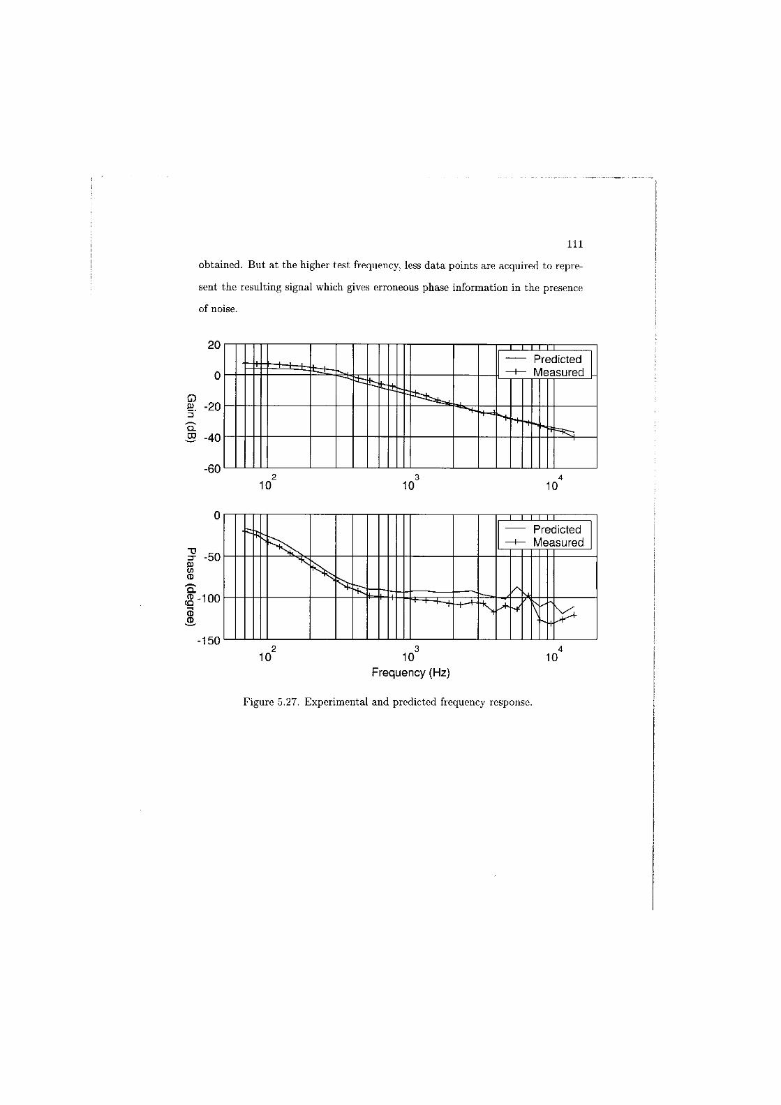
I l l
obtained. But at the higher test frequency, less data points are acquired to repre
sent the resulting signal which gives erroneous phase information in the presence
of noise.
•150 10 10
Frequency (Hz) 10
Figure 5.27. Experimental and predicted frequency response.

112
5.7 Summary In this chapter, an improved computational small-signal modeling and anal
ysis technique has been presented which is applicable to all types of switching
regulators using P W M control and operating in the continuous conduction mode.
This modeling technique is used to analyze performance in the time domain and
frequency domain. The results of this chapter are briefly summarized as follows.
1. The developed small-signal modeling technique offers a considerable sim
plification over the existing modeling approaches in [l]-[3] by allowing the
computer to solve any complex numerical calculations.
2. The small-signal model that combines the pulse width modulator and power
stage of a switch mode power converter is obtained in a single step.
3. The accuracy of a small-signal model obtained computational approach at
low-frequency agrees with the state-space averaged model.
4. The transfer function of the switch mode power converter was found by
performing a curve fit on the collected raw data. This curve fitting gives
a transfer function that is made to be strictly proper by neglecting a high
frequency zero.
5. At a frequency near l/10th of the switching frequency, the phase curve starts
to become erratic. This is due to the natural behavior of the pulse width
modulator.
6. The accuracy of the small-signal model using state-space averaging and cir
cuit averaging approaches has been studied. The phase curve erratic be
haviour at higher test frequencies shown in Fig. 5.27 reveals that the fre
quency limitation of reliable dynamic characteristic information is approxi
mately up to l/10th of the switching frequency.

113
7. Measured Bode plots confirms the predicted result. This indicates that the
small-signal model obtained using existing modeling methods provides fairly
accurate dynamic information up to approximately l/10th of the switching
frequency but beyond this frequency, dynamic information is an estimation
based on the low frequency information.
8. The calculated efficiency of the example buck converter is 92.7 percent (ex
perimental value is lower but was not determined). This efficiency degra
dation is due to the losses in the parasitic components. Efficiency can be
improved by using high quality semiconductor switches such as a low on-
resistance M O S F E T or low forward drop diode.

CHAPTER 6 114
REVIEW AND CONCLUSIONS AND FUTURE WORK
6.1 Review and Conclusions The main effort of this dissertation is the development of a simple small-signal
modeling technique that can be used in the design process of a switch mode
power converter feedback loop. In this dissertation, a computational small-signal
modeling technique is presented, that is applicable to practically any dc-to-dc
voltage mode converter topology operating in the continuous conduction mode.
The derivation of the switch mode power converter in state-space form is the first
step of the computational modeling process. This step must be performed only
once. The parasitic components discussed in chapter 3 are included in the state-
space representation of the converter for increasing accuracy of the model. The
proposed computational small-signal modeling technique is applied to the boost-
derived power factor correction circuit in chapter 4 to demonstrate the validity of
the developed modeling technique. As with other state-space based techniques,
the amplitude of the perturbation signal must be kept small such that operation
remains in the linear region. The key result of this chapter is that the small-
signal model obtained using the computational approach agrees with state-space
averaged model at low-frequency. However, the most noticeable disagreement be
tween these models occurs if the perturbation signal frequency is above l/10th of
the switching frequency. The frequency response computation program written in
MatLab code requires a long execution time (approximately 12 hours). Discussed
in Chapter 5 is an improved computational modeling method and a better fre
quency response calculation algorithm. This improved algorithm implemented in
C-language takes approximately 15 minutes to calculate the frequency response

115
characteristics for a test frequency range of 60Hz to 15kHz. A buck converter
is designed and implemented to show the effectiveness of the proposed improved
modeling method. A computer-based gain and phase meter is developed to verify
the predicted model. Through development of the gain and phase meter, the basic
measurement capabilites that are used in the stand-alone network analyzer avail
able in the market are achieved. The commercially available network analyzer
measures the loop-gain information similarly to that discussed in chapter 5 and
performs a curve fit function based on the measured data in order to generate a
smooth plot. This curve fit function is not included in the developed gain and
phase meter since the primary purpose is to compare the obtained raw data with
actual measured data at each test frequency. A comparison given in Bode plots
showed a good agreement.
The results of this dissertation indicate that the proposed improved computational
small-signal modeling approach may be used in the initial phase of switch mode
power converter feedback loop design. Also, it is shown that the time domain
characteristics of a switch mode power converter can be predicted.
Finally, it should be clear from this dissertation that use of the improved computa
tional small-signal modeling method offers the designer a better understanding of
the switch mode power converter being designed and is a useful tool for feedback
circuit design.
6.2 Future work Based on the work of this dissertation, further study is recommended in the
following areas:
1. It would be worthwhile, and not difficult, to apply the proposed computa
tional small-signal modeling technique to other switch mode power converter
topologies (flyback, forward, etc.)

116
2. It is logical to extend the research of this dissertation to include the switch
mode power converters operating in the discontinuous conduction mode.
3. Since a significant computational effort is required to reach steady-state at
each frequency step, it may be worthwhile to determine if initial conditions
on inductor current and capacitor voltage could improve convergence toward
steady-state operation.
4. To enhance the practical utility of the proposed modeling technique, the
proposed modeling method should be applied to current mode control P W M .
5. Based on the obtained small-signal model, development of a software assisted
feedback circuit design tool would be a substantial achievement in reducing
the feedback circuit design effort.
6. The laboratory implementation of the developed computer-based gain and
phase meter offers greater flexibility over the commercially available product
since the required functions can be defined in the software and tailored to
the design of switch mode power converters. To improve the measurement
process, an automatic measurement subroutine program can be implemented
into the existing program.
7. An ac coupling capacitor can be used to acquire the ac component of a signal
for high resolution A / D conversion. This would remove the dc offset on the
acquired signal.
8. This dissertation research work has shown that the dynamic characteristics
of a switch mode power converter can be easily obtained using the proposed
approach. To further improve the utility of this approach, it would be
worthwhile to develop a graphical user interface environment so that the

117
user can easily enter data and quickly configure and analyze the underlying
switch mode power converter.

118
REFERENCES
[1] Slobodan Cuk, "Modelling, Analysis, and Design of Switching Regulators,"
PhD thesis, California Institute of Technology, Nov. 1976.
[2] G. W. Wester and R. D. Middlebrook, "Low-Frequency Characterization of
Switched DC-DC Converters," IEEE Transactions an Aerospace and Elec
tronic Systems, Vol. AES-9, pp. 376-385, May 1973.
[3] Dennis J. Packard, "Discrete Modeling and Analysis of Switching Regula
tors," PhD thesis, California Institute of Technology, May 1976.
[4] M . K . Nalbant, A . Koblinski, "Active Power Factor Correction Technique,"
Application Note 9, Micro Linear Data., 1996.
[5] M . K . Nalbant, "Power Factor Calculations and Measurements," Applied
Power Electronics Conference Proceeding.,pp. 543-552, 1990.
[6] L. Dixon, "High Power Factor Preregulators for Off-line Power Supplies,"
Unitrode Switching Regulated Power Supply Design Seminar Manual, S E M -
700, 1990.
[7] F. Lee, "Analysis and design of power factor correction circuits," Lecture
Notes, VPEC power electronics professional seminar, Virginia Power Elec
tronics Center, 1990.
[8] C. Silva, "Power factor correction with the UC3854," Application Note, Uni
trode Integrated Circuits
[9] A . Capel and J .G. Ferrante and R. Prajoux, "Dynamic Behaviour and
Z-Transform Stability Analysis of D C / D C Regulators with A Non Linear
P .W.M. Control Loop," IEEE Power Electronics Specialists Conference, pp.
149-157, 1973.

119
[10] A .R . Brown and R.D. Middlebrook, "Sampled-Data Modeling of Switching
Regulators," PESC 81, pp. 349-369, Jan. 1981.
[11] Rainer von Lutz and Manfred Grtozbach, "Straightforward discrete Mod
elling for Power Converter Systems," IEEE Power Electronics Specialists
Conference, pp. 761-770, 1985.
[12] C. George and E. Malik and G. John Kassakian, "General Approach to
Sampled-Data Modeling for Power Electronic Circuits," IEEE Trans, on
Power Electronics., vol. PE-1, NO. 2, pp. 76-89, Apr. 1986.
[13] P. Maranesi and V . Varoli, " P W M Regulators Transfer-Functions by Exact
Time-Variant Network Analysis," IEEE Power Electronics Specialists Con
ference, pp. 295-298, May 1987.
[14] Richard Tymerski, "A Fast Time domain Simulation for Power Electronic
Systems," APEC'93, pp. 477-483.
[15] Ray Ridley, "New Simulation Techniques for P W M Converters," APEC'93,
pp. 517-523.
[16] Wei Tang, "Modelling, Average Current-Mode Control and Charge Control
for P W M , " PhD thesis, Virginia Power Electronics Center, Oct. 1994.
[17] R. D. Middlebrook, "Topic in Multiple-Loop Regulators and Current-Mode
Programming," IEEE Trans. Power Electronics, Volume PE-2, pp. 109-124,
Apr. 1987.
[18] Ronald C. Wong and Harry A . Owen, JR. and Thomas G. Wilson, "An
Efficient Algorithm for the Time-Domain Simulation of Regulated Energy-
Storage DC-DC Converters," IEEE Trans. Power Electronics, Volume PE-2,
pp. 154-168, Apr. 1987.

120
[19] Jung W. Lee, "A Study of an Effect of Main Components in Active P F C
Circuit A C - D C High frequency Power Supply," M.Eng. thesis, ChungAny
University, Dec. 1995.
[20] Jung W. Lee, "Computer aided Modeling of Current Loop for a Boost Derived
P F C circuit," Intelec'98, pp. 283-286.
[21] Jung W. Lee, "Time-Domain Derivation of Frequency-Domain Characteris
tics of Switch Mode Coverters," Intelec'99, pp. 345-351.
[22] Jung W. Lee, E.P. Nowicki, A . Chu "A Computational Small-Signal Modeling
Technique for Switch Mode Converters," CCECE, May 2000.
[23] National Instrument, "Data Acquisition (DAQ) Fundamentals," National In
struments Application Note 007, 1996.
[24] Scott Kasin, "Is your Data Inaccurate Because of Instrumentation Amplifier
Settling Time?," National Instruments Application Note 045, 1993.
[25] Rahman Jamal, Mike Cerna, John Hanks, "Designing Filters Using the Digital
Filter Design Tools in the Signal Processing Toolset," National Instruments
Application Note 097, 1998.
[26] Syed jaffar Shah, "Field Wiring and Noise Considerations for Analog signals,"
National Instruments Application Note 025, 2000.
[27] National Instrument, "Multifunction I/O Boards for PCI Bus Computers,"
Data Acquisition (DAQ) PCI E series User Manual, 1997.
[28] Hewlett Packard Co., "Control Systems Development Using Dynamic Signal
Analyzers," Application Note 243-2, 1984.

121
[29] H. Dean Venable, "Testing Power Factor Correction Circuits For Stability,"
Venable Industries, Inc. Tech Paper 16
[30] H. Dean Venable, "Oh, By The Way-We Need Power Supply," Venable In
dustries, Inc. Tech Paper 11
[31] H. Dean Venable, "Testing Power Sources For Stability," Venable Industries,
Inc. Tech Paper 12
[32] H. Dean Venable, "Practical testing Techniques for Modern Control Loops,"
Venable Industries, Inc. Tech Paper 16
[33] John G. Kassakian, Martin F. Schlecht, George C. Verghese Principles of
Power Electronics, Addison Welsley, 1991.
[34] Benjamin C. Kuo, Automatic Control Systems, 5th Ed., Prentice Hall(New
Jersey), 1987.
[35] B.P. Lathi, Linear Systems and Signals, Berkeley-Cambridge(Carmichael,
California), 1992.
[36] K . Ogata, Discrete-Time Control Systems, 2nd Ed., Prentice Hall(New Jer
sey), 1995.
[37] K . Ogata, Modern Control Engineering, 3rd Ed., Prentice Hall(New Jersey),
1997.
[38] W. Erickson Robert, Fundamentals of Power Electronics, Chapman-Hall(New
York), 1997.
[39] Power Electronics Group of the California Institute of Technology, "User's
Manual for the Switching Converter Analysis and Measurement Program,"
Caltech, May, 1991

APPENDIX A 122
DERIVATION OF STATE-SPACE EQUATIONS FOR THE BUCK CONVERTER
In this appendix, finding the state-space equations for the buck converter shown
in Fig. A . l operating in continuous conduction mode is presented.
RL L
rLoad
Figure A . l . Buck type switch mode power converter.
The first step is to identify state variables and find linear switched circuit model
for on-time (dTs). On-time linear switched circuit model is shown in Fig. A.2.
Apply Kirchhoff's voltage law to the circuit and assigning a positive sign to a
voltage drop leads to the expression
L ^ - = vg - vQ - i L R L - vQ (A. l)
where vQ is dv
v0 = Rc- C - f + vc (A.2) at
and applying Kirchhoff's current law yields
ic = h - i0 (A.3)

123
R l
~fn~ • • 'L
• > Rc
rLoad
Figure A.2. On-time switched circuit of buck type switch mode power converter.
since the output current can be expressed as
rLoad (A.4)
then equation A.2 becomes
Vn = rLoadRc
rLoad + Rc
rLoad rLoad + Rr
Substituting equation A.5 into equation A . l results
rLoadRr „ rLoad ^ L _ t ^ _ U Q + i , R L dt ~ L L L L(rLoad) + RC rLoad+ RC
(A.5)
(A.6)
since
dt
Substituting equation A.5 into equation A.4, then equation A.3 gives
(A.7)
dvc . rLoad . 1 ~dt^lL' ^C(rLoad + Rcy ~ C(rLoad + Rc)
(A.8)

124
Equations A.5, A.6, and A.8 are written in matrix form as
rLoadRc rLoad dij, dt
dvc
. dt .
EL L L(rLoad+Rc)
rLoad C(rLoad+Rc)
L(rLoad+Rc) 1
C(rLoad+Rc) J .
iL + iL + I - I o L L 0 0 0
V Q
vD
(A.9)
»o rLoadRc rLoad
rLoad+Rc rLoad+Rc
IL + ' 0 0 o 1 J
V9 VQ (A.10)
Off-time switched linear circuit state-space equations are derived similarly. Fig.
A.2 shows off-time switched circuit.
RL L A/w-nnnp— f
• i,
Rc
rLoad
Figure A.3. Off-time switched circuit of buck type switch mode power converter.
Once again, applying Kirchhoff's voltage law gives
rflr L — - v D - i L R L - v 0 (A.11)
at
Substituting equation A.5 into equation A. 11 and simplifying gives
<HL VD R L rLoadRc rLoad
~dt=~T + %L^~~L ~ LirLoad) + RJ ~ rLoad + R c ' V c ^ ' ' and applying Kirchhoff's current law and proceed similar manner as before results
dVc_. rLoad 1 fA 13) dt ~ l L ' [C(rLoad + Rc)) C(rLoad + Rc) ' V c 1 j

The output equation is same as equation A.5. Express equations A . l l ,
A.5 in matrix form becomes
dir, dt dvc
. dt .
EL L
rLoadRc L(rLoad+Rc)
rLoad
rLoad
C(rLoad+Rc)
L(rLoad-\-Rc) 1
' C(rLoad+Rc)
h + 0 0 ~i o o o
and once again
V0
rLoadRc rLoad rLoad+Rc rLoad+Rc
IL
+ [ o o o ] VQ VD
125
A.13 and
U9 V Q
VD
(A.14)
(A.15)

APPENDIX B 126
DERIVATION OF A SMALL-SIGNAL MODEL FOR BUCK CONVERTER USING STATE-SPACE
AVERAGING APPROACH
In this appendix, the state-space averaging technique is used to derive the
small-signal model for buck converter shown as two switched circuits in Fig. B . l .
To make analysis simple, all ideal components are used.
(a)
rLoad
L
rLoad
(b)
Figure B . l . Switched circuit for the buck converter: (a) interval DTs, (b) interval DTs.
With the state vector chosen as,
x = (B.l)
The state and output equation for interval dTs are derived in the form,
and
Von — ConX^

yields,
0 i f 1 - 1
C CrLoad J . ' L '"c +
1 L 0
[ o i ] II
VC
127
(B-2)
(B.3)
and the state and output equations for interval dTs of the form,
Xpff = Aoffx + BoffVg
and
voff = C0ffX
becomes,
Xoff 0 L 1 - i C CrLoad
lL + ' 0 " lL + 0 0
0 1 VC
(B.4)
(B.5)
Taking the average of both state and output equations for two switched circuit
equations, (B.2)-(B.5) by summing the equations for interval dTS multiplied by
d, and the equations for interval dTs by d gives state-space averaged state and
output equations,
(dAon + dAoff)x + (dBon + dBoff)vg
Vave — {dCon + dC0ff)x
(B.6)
(B.7)
are in the form,
•Egve — AaveX_ -\- Bai)eVg
then,

and
Vane. — 0 1 vc
128
(B.9)
Introducing ac variations in the input voltage and duty ratio to equations (B.6)
and (B.8) as,
Vg = Vg + Vg
d = D + d
d = D-d
will cause corresponding perturbations in the state vector and output,
x = X_ + x
v0 = V0 + v0
The resulting equations become,
x - AaveX + BaveVg + Aavex + Bavevg + [(Aon - Aoff)X + (Bon - Boff)Vg]d dc term line variation
+ [(Aon - Aoff)x + (Bon - B0ff)vg}d „ ' nonlinear second—order term
duty ratio variation
(B.10)
and,
Vo + Vo = CgVeK+CgVe3l+(Con ~ Coff)Xd+(Con - Coff)xd ( B . l l ) dc term ac term ac term nonlinear term
Now, the steady-state terms from equations (B.10) and ( B . l l ) gives the steady-
state dc transfer function of,
77 — Cave^ave^ave (B-12)
Therefore, the steady-state dc transfer function of the buck converter becomes,
" 0 -i - 1 " d ' " 0 L L 1
. c - 1
CrLoad . 0 (B.13)

129
To obtain the small-signal transfer functions, the line and duty ratio variation
terms from equation (B.10) gives,
x = Aavex + Bavevg + [(Aon - Aoff)X + (Bon - Boff)Vg]d
and equation ( B . l l ) gives,
vo — Cavex + (Con — C0ff)Xd
(B.14)
(B.15)
For the line to output small-signal transfer function, let d=0 in equations (B.14)
and (B.15),
x = Aavex + Bavevg (B.16)
and
v0 = Cavex (B.17)
Taking the Laplace transform of equations (B.16) and (B.17) and setting all initial
conditions to zero, gives the small-signal line to output transfer function of,
v0 — ~Cave(sI — A) lBa (B.18)
Thus, the small-signal line to output transfer function of the buck converter be
come,
C S + CrLoad
• - 1 " d ' L 0
(B.19)
To calculate the duty ratio to output transfer function, let vg=0 in equations
(B.14) and (B.15) give,
x = Aavex + [{Aon - Aoff)X + (Bon - Boff)Vg]d (B.20)
and
Vo = Cavex + {Con ~ Coff)Xd (B.21)
and following the preceding steps result the duty ratio to output transfer function,
d °j = Cave(sl - A)-l[{Aon - Aoff)X + (Bon - Boff)Vg] + (Con - Coff)X (B.22)

130
Therefore, the buck converter transfer function becomes,
71_ L 1 C
s + 1 CrLoad
1 - 1 " 1 "
L 0 (B.23)

APPENDIX C 131
DISCRETIZATION OF CONTINUOUS-TIME STATE-SPACE EQUATIONS
In digital computation, the continuous-time state-space equation is needed
to be converted into the discrete-time state-space equation. To do this, the
continuous-time system is sampled at much higher frequency than the continuous-
time system signal. In this section, the discretization steps of a continuous-time
system represented in state-space form is discussed. First, the derivation of a
continuous-time state equation solution is reviewed.
Consider a continuous-time state equation,
where A is an n x n constant nonsingular system matrix, B is the n x m input
matrix for an nth-order system with m inputs, x is the n x 1 state vector for an
nth-order system, u is the m x 1 input vector nth-order system.
By rewrting equation (C.l) as,
x(t) = Ax(t) + Bu(t) (C.l)
x(t) - Ax(t) = Bu(t) (C.2)
If premultiply both sides of equation (C.2) by e , then it becomes,
e-Atx(t) - e-AtAx(t) = e-AtBu(t) (C.3)
Using matrix differentiation of,
= -e-AtAx + e-At3L{t) (C.4)
then, equation (C.3) becomes,
y[e-Atx] = e-AtBu(t) (C.5)

132
Integrating both sides of equation (C.5) from 0 to t gives,
x(t) = eAtx(0) + f eA^Bu{r)dr (C.6) Jo
The discrete-time representation of equation (C.l) is the form,
x[(k + 1)T] = G[x(kT)} + H[u(kT)} (C.7)
Equation (C.6) is used to determine the system matrix A and input matrix B.
Throughout the discretization process, the input vector u(t) is assumed constant
over the interval between any two consecutive sampling instant.
Since,
x[(k + 1)T] = e A ( f c + 1 ) r x(0 ) + eA^k+l)T e-ATBu{r)dr (C.8) J 0
and,
x[kT] = eAkTx{0) + eAkT f e~ArBu(r)dT (C.9)
multiplying equation (C.9) by eAT and subtracting it from equation (C.8) gives,
x[(k + l)T] = eATx{kT) + eA{k+1)T / e-ATBu{r)dr (CIO) JkT
Note that u(t) may jump at t = [(K + 1)T] and thus u[(K + 1)T] may be different
from u[kT]. Such a jump in u(r) at r = [(k + 1)T], the upper limit of integration,
does not affect the value of the integral in equation (C.10).
Therefore,
x[(k + 1)T] = eATx(kT) + eA{k+1)T CeAXBu(kT)dX ( C . l l )
Jo
where X — T — t.
by comparing equation (C.10) with (C.7), the system matrix A and input matrix
B is defined as,
G = eAT (C.12)
H=([TeAxd\)B (C.13) Jo

APPENDIX D 133
C-CODE FOR CALCULATING FREQUENCY RESPONSE DATA
Main Engine
/*
Auto Design for buck converter - Prototype.
- At present, it is only semi-automatic
- !!! Requires first buckabcd.m in MatLab !!! to obtain nominal
ABCD for ON and OFF time operation.
- Requires visual frequency domain design in MatLab
Possible Improvements
- Re-group elements to improve modularity.
- Integration of C and MatLab codes, perhaps by using dLL.
- Modification auto buck design as a special case of forward
converter design having a txRatio = 1.
- Extend autodesign for boost and flyback.
*/
#include <stdio.h>
#include <math.h>
#include <ctype.h>
#include"ctrl.h" #include "freq.h"
#include "load.h"
#include<stdlib.h>

134
/*
Nominal primary parameters
- g_vln : nominal input voltage
- g_vOut nominal output voltage
- g_iOut : nominal output current
- g_vS : peak magnitude of sawtooth on PWM chip
- g_vValley : offset of min value of sawtooth from zero
- g_vG : redundant, equals g_vln.
- g_vQ : drop across switch during ON time
- g_vD diode forward drop
Derived parameters
- g_dNom: nominal duty ratio. For buck, i t is fixed as
g_v0ut/g_vln.
- g_vRef: nominal control voltage. Must have a value to
effect g_dNom.
- g_rampSlope: slope of sawtooth.
- g_Ts: sampling interval in simulation. Defined in
buckabcd.m because must be compatible with
discretization of ABCD.
- g_numPart: number of partitions within a switching interval.
Note that for a switching frequency of 100 KHz,
numPart should be about 500 for proper simulations
at frequencies not lower than 50 Hz.
*/
double g_vln=48.0,g_v0ut=12.0, g_i0ut=2.0;

135
double g_vS=3.5,g_vValley=1.0; double g_vG=48.0,g_vQ=0.4,g_vD=0.7;
double g_dNom,g_vRef,g_Ts,g_numPart,g_rampSlope; int g_type;
void PwmlcDef(void);
void PwmlcDef(void) {
double fSw;
FILE* ifpSimPara;
ifpSimPara = fopen("simpara.txt","r");
fscanf (ifpSimPara.'7.1f7.rf",&fSw,&g_numPart);
if (ifpSimPara)
fclose(ifpSimPara);
g_Ts = 1.0/(fSw*g_numPart);
g_dNom = g_v0ut/g_vln;
g_vRef = (g_vS-g_vValley)*g_dNom+g_vValley;
g_rampSlope = (g_vS-g_vValley)*fSw;
puts("Enter PWM IC output Type.");
puts ("Totem pole 1") ;
putsC'Single output 2");
printf("» ");
scanf (7.d",&g_type); puts(" ");
if (g_type == 1) {
g_vRef = (g_vS-g_vValley)*2.0*g_dNom+g_vValley;

136
g.rampSlope = (g_vS-g_vValley)*2.0*fSw;
}
else {
g_vRef = (g_vS-g_vValley)*g_dNom+g_vValley;
g.rampSlope = (g_vS-g_vValley)*fSw;
}
printfC'Vref = '/.f \n" ,g_vRef);
int main(void) {
PwmlcDef();
FreqSweepO ;
CtrlDesignO ;
LoadTestO ;
return 0;
>

137
Frequency Response Calculation Function
-PERFORMS FREQUENCY SWEEP FROM VC TO VO
#include <stdio.h> #include <stdlib.h> #include <math.h> #include
<ctype.h> #include "freq.h"
extern double g_vRef, g_vG, g_vQ, g_vD, g_vOut, g_iOut; extern
double g_Ts; extern int g_type; extern double g_rampSlope; extern
double g_vValley; extern double g_numPart;
/* PRIVATE FUNCTION PROTOTYPES */ void
ReadABCD(intchoiceOfConverter);
double CalVc(double fTest,doublek);
double CalVramp(int k);
double StateSim(double vC_vRamp);
void GainPhase(double k,double vOut.double fTest.int init ) ;
double Aonll, Aonl2, Aon21, Aon22, Bonll, Bonl2, Bonl3, Bon21,
Bon22, Bon23; double Conll, Conl2; double Aoffll, Aoffl2, Aoff21,

138
Aoff22, Boffll, Boffl2, Boffl3; double Boff21, Boff22, Boff23;
double Coffll, Coffl2;
double xl_k, x2_k, xl_kpl, x2_kpl; double vlnit, i l n i t , araplnput,
gain, phase;
/*
HOLY MACARONI GAIN PHASE METER
- When successive peak (upper or lower) of output
- voltage does not change by more than 5 percent
- of its amplitude, calculate gain and phase.
*/
void GainPhase(double k,double vOut,double fTest.int init) {
static double maxLoc, minLoc, maxMag, minMag;
static double lastLoc, lastMag;
static double ampOld, ampNew;
static int reset, rising, dropping;
double tPassed, dPassed, inputSigPeriod;
reset = init;
i f (reset) {
lastMag = minMag = maxMag = vlnit;
lastLoc = maxLoc = minLoc = k;
rising = dropping = 0;
/* vOut is neither rising nor dropping */
ampOld = ampNew = 0.0;

139
}
else {
if (vOut > lastMag) {
if (dropping) { /* Then we have detected a low point */
minLoc = lastLoc;
minMag = lastMag;
ampOld = ampNew;
ampNew = maxMag-minMag;
}
dropping = 0;
rising = 1;
}
else {
if (rising) { /* Then we have detected a high point */
maxLoc = lastLoc;
maxMag = lastMag;
ampOld = ampNew;
ampNew = maxMag-minMag;
}
dropping = 1;
rising = 0;
}
i f (fabs(ampNew-ampOld) < ampNew*0.005) {
gain = ampNew/(2.0*ampInput); /* p2p0utput/p2pInput */
tPassed = maxLoc*g_Ts;
inputSigPeriod = 1.0/fTest;
dPassed = 360.0*fmod(tPassed,inputSigPeriod)/inputSigPeriod;

140
phase = -1.0*(dPassed-90.0);
/* Because input start from degree zero */
>
lastMag = vOut;
lastLoc = k;
}
}
double StateSim(double vC_vRamp) {
double vOut;
if (vC.vRamp > 0.00001) {
xl_kpl = Aonll*xl_k+Aonl2*x2_k+Bonll*g_vG+Bonl2*g_vQ+Bonl3*g_vD;
x2_kpl = Aon21*xl_k+Aon22*x2_k+Bon21*g_vG+Bon22*g_vQ+Bon23*g_vD;
vOut = Conll*xl_k+Conl2*x2_k;
}
else {
xl.kpl = Aoffll*xl_k+Aoff12*x2_k+Boffll*g_vG+Boff12*g_vQ+Boff13*g_vD;
x2_kpl = Aoff21*xl_k+Aoff22*x2_k+Boff21*g_vG+Boff22*g_vQ+Boff23*g_vD;
vOut = Coffll*xl_k+Coff12*x2_k;
}
xl_k = xl_kpl;
x2_k = x2_kpl;
return vOut;
>
double CalVrampCint k) {

double vRamp;
vRamp = ((double)k)*g_Ts*g_rampSlope+g_vValley;
return vRamp;
}
double CalVc(double fTest, double k) {
double vC;
vC = g_vRef+ampInput*sin(6.2831853*fTest*k*g_Ts);
return vC;
}
void ReadABCD(int command) {
FILE* ifp; /* INPUT FILE POINTER CONTAINING APPROPRIATE ABCD
switch (command) {
case 1: ifp = fopen("buckpara.txt","r");
break;
case 2: puts("No such animal");
break;
case 3: puts("No such animal");
break;
default: putsC'No such animal");
break;
}
/* SCANNING DISCRETE TIME ABCD MATRICES */
f scanf (ifp, '7.1f'/.lf '/.If °/.lf " ,&Aonll ,&Aon21 ,&Aonl2 ,&Aon22) ;
f scanf (if p, "'/.If'/.If 7,lf'/.If '/.If'/.If •', feBonl 1, &Bon21, &Bonl2, &Bon22,

142
&Bonl3,&Bon23);
fscanf (ifp,"7.1f,
/.lf'1
,&Conll,&Conl2);
f scanf (if p, '"/.If'/.If'/.If'/.If " ,&Aof f 11, fcAof f 21,&Aoff12,&Aof f 22);
fscanf (if p, "'/.If'/.If */.lf'/.If 7.1f */.lf " , &Bof f 11, ftBof f 21, fcBof f 12, &Bof f 22,
&Boffl3,&Boff23);
f scanf (ifp, '"/.If'/.If " .fcCof f 11 ,&Coff 12);
if (ifp)
fclose(ifp);
}
void FreqSweep(void) {
FILE* ofpSin;
FILE* ofpGainPhase;
FILE* output;
int command,factCount.rampCount;
double lowF = 50.0, highF, fTest, vC, vRamp, vOut;
double k, maxK;
/* use float for index to avoid extra large integer ? */
puts("Enter type of converter:");
puts ("Buck 1");
putsC'Boost 2");
puts("Flyback 3");
printf("» ");

scanf ("7.d" .fecommand);
ReadABCD(command);
printf("\nLowest frequency to be swept \? (Hz) » ")
scanf ('"/.If", felowF);
printf("\nHighest frequency to be swept \? (Hz) » "
scanf ('"/.If \&highF) ;
fTest = lowF;
factCount = 0;
vlnit = g_vOut;
i l n i t = g_iOut;
amplnput = .15*g_vRef;
ofpSin = fopen("sinewave.txt","w");
ofpGainPhase = fopen("fgtheta.txt","w");
output = fopen("output.txt","w");
while (fTest < highF+1.0) {
printf ("Input Frequency = */.lf \n" ,fTest);
k = 0.0;
rampCount = 0;
gain = phase = 0.0;
GainPhase(k,g.vOut,fTest,1);
/* Send integer 1 to init gain phase analyzer */
xl_k = i l n i t ;
/* Init state variables to reduce sim time */
x2_k - v l n i t ;
xl.kpl = x2_kpl =0.0;
maxK = floor(2.0/(10.0*g_Ts));
/* At most do 10 Hz sweep for 2 cycles */

144
while (1) {
vC = CalVc(fTest,k);
vRamp = CalVramp(rampCount);
vOut = StateSim(vC-vRamp);
/*N0TE: COLLECTING INTERSWITCHING POINTS LEADS TO VERY */
/* VERY HUGE FILE BECAUSE PROPER SIM REQUIRES */
/* CHOPPING SWITCHING PERIOD AT LEAST INTO 500 */
/* PARTS. */
/* INTERSWITCHING POINTS SHOULD BE COLLECTED WITH */
/* CAUTION FOR INSPECTION PURPOSE ONLY. */
i f (k>maxK)
break;
rampCount++;
if (rampCount == g_numPart) {
rampCount = 0;
fprintf (output,,|,
/.lf\t,
/,lf\n" ,k,vOut);
GainPhase(k,vOut,fTest,0);
/* Send 0, indicating not for init */
/*
Sinewave input and sinewave output for verifications
of gain and phase at a single frequency

145
*/
fprintf (of pSin, "•/.. lOlf \t'/.. lOlf \t*/.. lOlf \n" ,
((double)k)*g_Ts,vC,vOut);
}
/*
Collects frequency, gain, and phase
*/
i f (gain > 0.0)
f printf (of pGainPhase, '7,lf \t'/,lf \f/,lf \n" ,
fTest,gain*g_vRef/g_vOut.phase);
if (gain > 0.0)
break;
k=k+1.0;
}
fTest = fTest*1.2;
factCount++;
if (factCount == 4)
factCount = 0;
}
printf ("gain = */,lf \n" .gain);
printf ("phase = 7,lf\n" .phase);
if (ofpSin)
fclose(ofpSin);
i f (ofpGainPhase)
fclose(ofpGainPhase);
>
Copyright © 2022 FDOKUMEN