A 4.4 pJ/Access 80 MHz, 128 kbit Variability Resilient SRAM With Multi-Sized Sense Amplifier...
15
2416 IEEE JOURNAL OF SOLID-STATE CIRCUITS, VOL. 46, NO. 10, OCTOBER 2011 A 4.4 pJ/Access 80 MHz, 128 kbit Variability Resilient SRAM With Multi-Sized Sense Amplifier Redundancy Vibhu Sharma, Stefan Cosemans, Member, IEEE, Maryam Ashouei, Member, IEEE, Jos Huisken, Member, IEEE, Francky Catthoor, Fellow, IEEE, and Wim Dehaene, Senior Member, IEEE Abstract—An ultra low energy, 128 kbit 6T SRAM in 90 nm LP CMOS with energy consumption of 4.4 pJ/access, operating at 80 MHz for the wireless sensor applications is developed. The variability resilient and low power techniques developed include innovation in the local architecture with the use of local read/write assist circuitry. The energy-efficient hierarchical bit-lines struc- ture includes low swing global bit-lines and VDD/2 pre-charged short local bit-lines. The innovative Multi-Sized SA redundancy (MS-SA-R) calibration technique for the global read sense ampli- fiers of the SRAM not only adds to the variability resilience but also yields maximum energy reduction compared with existing calibra- tion techniques. Index Terms—Charge recycling, gated read buffer, Multi-Sized SA, SRAM, ultra low energy, WRITE masking. I. INTRODUCTION E NERGY-EFFICIENT sensor networks design involves an holistic approach, covering all aspects of the senor net- work viz. network protocols, software and hardware platforms. There is a limit on an average energy consumption of wireless sensor nodes, even with the most advanced methods of energy scavenging. The target energy consumption has to be below 100 W/cm [1]. Event monitoring is a core application fea- ture of these sensor nodes, whether it is for a security surveil- lance, environment monitoring or for the biomedical purposes. The operational clock frequency of the sensor nodes is depen- dent on the application scenario ranging from a few hundreds of KHz [2] to the tens of MHz range [3]. The bio-DSP [4] chip designed for monitoring brain signals and heart beat signals re- duces the power consumption associated with the transmission of a raw data by providing a computational intelligence at the sensor node. Several millions of operations per second are re- quired for the processing of this raw data, thereby reducing the Manuscript received December 28, 2010; revised April 18, 2011; accepted April 21, 2011. Date of publication July 12, 2011; date of current version September 30, 2011. This paper was approved by Associate Editor Peter Gillingham. V. Sharma is with the ESAT-MICAS Laboratory, Katholieke Universiteit Leuven, B-3001 Leuven, Belgium, and with IMEC-NL (Holst Centre), 5656 AE Eindhoven, The Netherlands (e-mail: [email protected]). S. Cosemans and W. Dehaene are with the ESAT-MICAS Laboratory, Katholieke Universiteit Leuven, B-3001 Leuven, Belgium, and also with IMEC, B-3001 Leuven, Belgium. F. Catthoor is with IMEC, B-3001 Leuven, Belgium, and also with the Katholieke Universiteit Leuven, B-3001 Leuven, Belgium. M. Ashouei and J. Huisken are with the IMEC-NL (Holst Centre), 5656 AE Eindhoven, The Netherlands. Digital Object Identifier 10.1109/JSSC.2011.2159056 amount of raw data transmission. Embedded memories con- sume a major proportion of the power budget ranging from a very data intensive multimedia applications [5] to the low power sensor nodes applications [4], [6]. Our embedded memory de- sign targets bio-DSP chip, operating below 100 MHz of fre- quency range. Software code optimization techniques [7] tend to improve locality of data/instruction fetches. In memory hierarchy system the largest memories have the least number of accesses per word whereas the largest number of accesses per word is of L1 memory. Therefore, ultra low energy SRAMs for L1 data/in- struction memory is a fundamental component of the wireless sensor node architecture, to meet the energy limitations of en- ergy scavenging. Hence, energy-efficient implementations for these small memories are a key requirement to enable further extensions of the capabilities of the energy scavenged wireless sensor nodes. Classic technology scaling reduced the energy consumption of both memories and processor on a regular basis. Energy re- duced in proportion to , with the smallest feature size that can be realized in the technology. This ended with the intro- duction of the 90 nm technology node [1], [8]. The threshold voltage reduction is limited, as the leakage currents started to dominate the energy budget. The variations between the ad- jacent transistors, also known as mismatch, increased quickly with the smaller dimensions. This mismatch has a detrimental impact on the available noise margins for the memory cells [9], which further impedes the reduction of the power supply. Although, high performance systems still benefit from further miniaturization but the energy per operation now reduces pro- portional to , rather . This work addresses all the design challenges associated with the energy limitations of wireless sensor nodes and the increased variability in 90 nm LP technology node. Table I shows the SRAM 6T bit cell details and memory dimensions. The designed 2 K 64 bits L1 SRAM consumes 4.4 pJ/access at 80 MHz and the leakage power is 0.6 W at the retention mode. The VDD of the SRAM matrix is at 0.4 V. SRAM cell array leakage is mitigated by utilizing only HVT transistors in the memory cell. SRAM 6T cell design is based on the logic DRC. A low power design feature of SRAM based on the divided word line decoder architecture with the low swing hierarchical bit-lines includes: 1) Innovative local assist circuitry used during READ and WRITE operation lowers the energy consumption and also 0018-9200/$26.00 © 2011 IEEE
Transcript of A 4.4 pJ/Access 80 MHz, 128 kbit Variability Resilient SRAM With Multi-Sized Sense Amplifier...
2416 IEEE JOURNAL OF SOLID-STATE CIRCUITS, VOL. 46, NO. 10, OCTOBER 2011
A 4.4 pJ/Access 80 MHz, 128 kbitVariability Resilient SRAM With Multi-Sized
Sense Amplifier RedundancyVibhu Sharma, Stefan Cosemans, Member, IEEE, Maryam Ashouei, Member, IEEE, Jos Huisken, Member, IEEE,
Francky Catthoor, Fellow, IEEE, and Wim Dehaene, Senior Member, IEEE
Abstract—An ultra low energy, 128 kbit 6T SRAM in 90 nmLP CMOS with energy consumption of 4.4 pJ/access, operatingat 80 MHz for the wireless sensor applications is developed. Thevariability resilient and low power techniques developed includeinnovation in the local architecture with the use of local read/writeassist circuitry. The energy-efficient hierarchical bit-lines struc-ture includes low swing global bit-lines and VDD/2 pre-chargedshort local bit-lines. The innovative Multi-Sized SA redundancy(MS-SA-R) calibration technique for the global read sense ampli-fiers of the SRAMnot only adds to the variability resilience but alsoyields maximum energy reduction compared with existing calibra-tion techniques.
Index Terms—Charge recycling, gated read buffer, Multi-SizedSA, SRAM, ultra low energy, WRITE masking.
I. INTRODUCTION
E NERGY-EFFICIENT sensor networks design involves anholistic approach, covering all aspects of the senor net-
work viz. network protocols, software and hardware platforms.There is a limit on an average energy consumption of wirelesssensor nodes, even with the most advanced methods of energyscavenging. The target energy consumption has to be below100 W/cm [1]. Event monitoring is a core application fea-ture of these sensor nodes, whether it is for a security surveil-lance, environment monitoring or for the biomedical purposes.The operational clock frequency of the sensor nodes is depen-dent on the application scenario ranging from a few hundredsof KHz [2] to the tens of MHz range [3]. The bio-DSP [4] chipdesigned for monitoring brain signals and heart beat signals re-duces the power consumption associated with the transmissionof a raw data by providing a computational intelligence at thesensor node. Several millions of operations per second are re-quired for the processing of this raw data, thereby reducing the
Manuscript received December 28, 2010; revised April 18, 2011; acceptedApril 21, 2011. Date of publication July 12, 2011; date of current versionSeptember 30, 2011. This paper was approved by Associate Editor PeterGillingham.V. Sharma is with the ESAT-MICAS Laboratory, Katholieke Universiteit
Leuven, B-3001 Leuven, Belgium, and with IMEC-NL (Holst Centre), 5656AE Eindhoven, The Netherlands (e-mail: [email protected]).S. Cosemans and W. Dehaene are with the ESAT-MICAS Laboratory,
Katholieke Universiteit Leuven, B-3001 Leuven, Belgium, and also withIMEC, B-3001 Leuven, Belgium.F. Catthoor is with IMEC, B-3001 Leuven, Belgium, and also with the
Katholieke Universiteit Leuven, B-3001 Leuven, Belgium.M. Ashouei and J. Huisken are with the IMEC-NL (Holst Centre), 5656 AE
Eindhoven, The Netherlands.Digital Object Identifier 10.1109/JSSC.2011.2159056
amount of raw data transmission. Embedded memories con-sume a major proportion of the power budget ranging from avery data intensivemultimedia applications [5] to the low powersensor nodes applications [4], [6]. Our embedded memory de-sign targets bio-DSP chip, operating below 100 MHz of fre-quency range.Software code optimization techniques [7] tend to improve
locality of data/instruction fetches. In memory hierarchy systemthe largest memories have the least number of accesses perword whereas the largest number of accesses per word is of L1memory. Therefore, ultra low energy SRAMs for L1 data/in-struction memory is a fundamental component of the wirelesssensor node architecture, to meet the energy limitations of en-ergy scavenging. Hence, energy-efficient implementations forthese small memories are a key requirement to enable furtherextensions of the capabilities of the energy scavenged wirelesssensor nodes.Classic technology scaling reduced the energy consumption
of both memories and processor on a regular basis. Energy re-duced in proportion to , with the smallest feature size thatcan be realized in the technology. This ended with the intro-duction of the 90 nm technology node [1], [8]. The thresholdvoltage reduction is limited, as the leakage currents started todominate the energy budget. The variations between the ad-jacent transistors, also known as mismatch, increased quicklywith the smaller dimensions. This mismatch has a detrimentalimpact on the available noise margins for the memory cells[9], which further impedes the reduction of the power supply.Although, high performance systems still benefit from furtherminiaturization but the energy per operation now reduces pro-portional to , rather .This work addresses all the design challenges associated
with the energy limitations of wireless sensor nodes and theincreased variability in 90 nm LP technology node. Table Ishows the SRAM 6T bit cell details and memory dimensions.The designed 2 K 64 bits L1 SRAM consumes 4.4 pJ/accessat 80 MHz and the leakage power is 0.6 W at the retentionmode. The VDD of the SRAM matrix is at 0.4 V. SRAM cellarray leakage is mitigated by utilizing only HVT transistorsin the memory cell. SRAM 6T cell design is based on thelogic DRC. A low power design feature of SRAM based onthe divided word line decoder architecture with the low swinghierarchical bit-lines includes:1) Innovative local assist circuitry used during READ andWRITE operation lowers the energy consumption and also
0018-9200/$26.00 © 2011 IEEE
SHARMA et al.: A 4.4 pJ/ACCESS 80 MHz, 128 kbit VARIABILITY RESILIENT SRAMWITH MULTI-SIZED SENSE AMPLIFIER REDUNDANCY 2417
TABLE IMEMORY DIMENSIONS AND SRAM 6T CELL DETAILS
adds more variability resilience compared to the conven-tional local assist techniques.
2) The WRITE masking feature further decreases the writeenergy by facilitating the partial WRITE operations.
3) The novel Multi-Sized SA redundancy proposed for theglobal read sense amplifiers accommodates process vari-ation and achieves an ultra low energy access for the giventarget yield.
This paper is organized as follows. The memory architecture,operation and detailed overview of the local bit slice architec-ture, including design constraints associated with the conven-tional 6T SRAM cell and usage of local assist circuitry for therealization of energy-efficient READ and WRITE operationsare described in Section II. Section III provides information onREAD/WRITE operation at the local hierarchy, it also coversrelevance and implementation of the WRITE masking feature.Section IV includes detailed discussion on the design of vari-ability resilient low power sense amplifiers. Section V containsmeasurement results and comparisons with state-of-the-art ultralow energy memories.
II. MEMORY ARCHITECTURE AND OPERATION
This section discusses the memory organization, floor plan-ning and operation. First, an overview of memory floorplanis provided along with details of the decoding structure. En-ergy-efficient hierarchical bit-lines and READ/WRITE opera-tion at the global level are discussed in Section II-B. The archi-tecture of the local bit slice and its advantage over conventionallocal bit-line architectures is covered in Section II-C.
A. Memory Floorplan
The memory matrix consists of 512 cells by 256 cells. Fig. 1shows top level memory organization. The memory matrix isdivided into 4 columns. Each row of the memory matrix has itsown global word line activation signal (GWL). Each columnconsists of 64 word blocks and 64 pairs of vertical globalbit-lines (VGBL). The VGBL pairs of all the columns share acommon horizontal global bit-lines (HGBL) bus. The columnsare activated by the column select (CS) activation signals ofa decoder. The CS activation signal also enables the interfaceMUX of VGBL pairs of the activated column with the HGBLbus. The word block consists of word decode logic performingthe local decoding function and the mask decode logic blocks
for decoding the masking information at the local level duringthe WRITE operation. Each mask decode logic block, controls16 local bit- slices. A detailed architecture overview of thelocal bit-slice is given in Section II-C.The 11 address bits are decoded with static AND-AND de-
coding logic. The decoding structure is shown in Fig. 2. The firststage of decoding logic generates 64 block row select (BRS) sig-nals, 4 column select (CS) signals and 8 within block row select(WBRS) signals. The second stage of the decoding logic com-bines, BRS and WBRS signals to generate 512 GWL activationsignals. The Word Block activation signal (Block En) is gener-ated from CS and the BRS signals. The Word Blocks are acti-vated by Block En. The word decode logic generates the localword line (LWL) by combining GWL and Block En signals. Italso generates activation signal for the local assist circuitry usedin the local bit slices during a READ/WRITE operation. Thedivided word line architecture [10] activates only the requiredcells and the bit lines. This not only result in low energy opera-tion but also eliminates the issues related with the half—selectcondition for cells. The word mask decodes logic blocks are thelast stage of the decoding structure. It selectively activates onlythe required quarters of the local bit-slices. During WRITE op-eration the LWL and other the control signals for the local assistcircuitry are decoded to obtain a masked LWL and a masked ac-tivation signal. This further decreases the WRITE energy con-sumption, discussed in Section III-C.
B. Hierarchical Bit-Lines and READ/WRITE Timing
This design features hierarchical bit-lines with reducedvoltage swing. This reduces the energy consumption asso-ciated with the charging and discharging of huge capacitiveglobal bit-lines during the READ/WRITE operation. Fig. 3shows reduced swing bit-line hierarchy for energy-efficientREAD/WRITE operation along with timing waveforms at theglobal level. During a READ operation the HGBL pre-chargecircuitry is activated, thereby pre-charging the HGBL bus.Then the decoder activates the VGBL-HGBL interface MUXand disables the VGBL pre-charge circuitry. The word blockdecoder generates the required control signals for the localbit-slices. After the local block processing, the READ infor-mation is transferred back onto the VGBL/HGBL bus. READoperation concludes with the disabling of the interface MUXand enabling the VGBL pre-charge circuitry. The local blockprocessing for the READ operation and the global read senseamplifiers will be discussed in the next sections. Similaryduring the WRITE operation the write drivers enable (WD En)signal transfers the data input information onto the HGBLbus. This low swing data information is then made availableto the VGBLs, disabling the VGBL precharge circuitry of theselected column. The write data transfer (WDT) activationsignal transfer this low swing signal to the local bit slicesof the selected word block. Then the local block processingis done for the WRITE operation. The WRITE operation atthe local bit slices will be discussed in Section III-B. TheHGBL precharge circuitry and global sense amplifiers are notused during WRITE operation. Similarly write drivers are notactivated during READ operation. Timing signals viz. HGBL

2418 IEEE JOURNAL OF SOLID-STATE CIRCUITS, VOL. 46, NO. 10, OCTOBER 2011
Fig. 1. Memory organization.
Fig. 2. Decoder structure.
pre-charge activation, WD En & WDT are generated from thememory clock input and the write flag input.
C. Local Bit Slice: Architecture
SRAM cell design is a critical feature in achieving technologyscaling benefits for SOC designs. The reduced voltage level and
Fig. 3. Energy-efficient bit-line hierarchy for reduced swing READ/WRITEoperation.
the utilization of low-power (LP) CMOS technologies are re-quired for the low leakage SRAM cell design. The reductionin VDD and the increased threshold voltage aggravates vari-ability for the SRAM cell design. This result in degradation of

SHARMA et al.: A 4.4 pJ/ACCESS 80 MHz, 128 kbit VARIABILITY RESILIENT SRAMWITH MULTI-SIZED SENSE AMPLIFIER REDUNDANCY 2419
Fig. 4. Novel local bit-slice architecture: Improves Read SNM and achieves an ultra low energy READ/WRITE operation compared to the conventional localbit-line architectures.
, read static noise margin (SNM) and write-ability ofSRAM cell. The design optimizations done in improving oneparameter often ends up in worsening the other [9]. Read SNM(functionality) is of utmost concern and SRAM design trends toimprove the read SNM [14] comes at the expense of detrimentalimpact on . Therefore, conventional SRAM 6T cell de-sign is a highly constrained area–stability–power–performancetrade-off design effort.Local assist circuit techniques with hierarchical bit-lines
[11]–[13] are becoming increasingly necessary to maintain theSRAM cell functionality and to achieve performance targetat the minimal cost of an area increase. The use of localassist circuits alleviates the complex design trade-off effortof SRAM cell design. The hierarchical bit-lines reduce theeffective bit-line capacitance and the upsized low Vt readbuffer employed [11]–[13] delivers more read current. Therelieved small sized SRAM cell can then be optimized forimproving a read SNM. However, there is a major drawbackin achieving ultra low energy read access with this approach.First, the low Vt read buffers used increase the leakage power.Second, the read buffers used are operating with the full swingpre-charged local bit-lines (LBLs), resulting in an increaseddynamic energy consumption. The conventional local bit-linearchitecture techniques benefit from the dynamic read stability[21], due to the reduced effective bit-line capacitance withthe hierarchical bit-lines. The stress on the accessed SRAMcell is reduced because of the reduction in the noise source
. In the beginning of the READ operationthe word line activation signal is significantly below its finalvalue of VDD. By the time this final value is reached, thebit-line has been discharged significantly. The use of VDD/2pre-charged LBLs as proposed in our design further reducesthe noise source to , during the READ
operation. This result in an increased read SNM compared tothe conventional local bit-line architectures.The new local hierarchy designed addresses all the previous
mentioned design challenges. The local bit slice architecture isshown in Fig. 4 features:1) a local sense amplifier which also acts as a write receiverduring a WRITE operation;
2) the VDD/2 pre-charged local bit-lines resulting in an in-creased read SNM and reduction in the dynamic energy;
3) the gated read buffer which delivers the required read cur-rent and also mitigates the local bit-line leakage.
The HVT transistors based SRAM cell reduces leakage and readupset failures. The VDD/2 pre-charge value for the short localbit-lines further improves cell stability (Fig. 5). The cell side thatstores “1” gets discharged for the pre-charge voltages less than
, resulting in the read upset failures. But for theHVT transistors based SRAM cell, VDD/2 pre-charge value forthe bit-lines is greater than . Therefore, the cellstability degradation for the reduced bit-line pre-charge voltage[15] is valid for the bit-line voltages less than VDD/2 for ourSRAM cells.There are 8 SRAM cells in the local hierarchy. The toggling
of the VDD/2 pre-charged local bit-lines by the activation ofthe local sense amplifier in order to sense the small local bit-line voltage swing created by an accessed SRAM cell results incharge recycling. This decreases the energy consumption. Thelocal sense amplifier relieves the accessed SRAM cell from cre-ating enough voltage swing required to trigger the read buffer.The VDD/2 pre-charged local bit-lines not only aid in reducingthe dynamic energy with charge recycling but also improve theread SNMcompared to the VDD pre-charged conventional localbit-line architecture (Fig. 6).

2420 IEEE JOURNAL OF SOLID-STATE CIRCUITS, VOL. 46, NO. 10, OCTOBER 2011
Fig. 5. Read SNM (cell stability) versus bit-line pre-charge voltage for theHVT minimum sized transistors based SRAM cell (DC simulations).
Fig. 6. Distribution of Read SNM for VDD (conventional local bit-line archi-tecture) versus VDD/2 (this work) pre-charge voltage for the local bit-lines ob-tained by performing 10K Monte Carlo runs for V.
The required is delivered by an upsized gated readbuffer. This buffer is enabled, only for a limited period duringthe READ operation thereby reducing the local bit-line leakage.The leakage current of the VDD/2 pre-charged local bit-linesis not that high because of the gated read buffer and the use ofHVT transistors for SRAM cells. The leakage current of VDD/2pre-charged local bit-lines constitutes 9% of the total measuredleakage current.The local sense amplifier design is optimized for VDD/2 pre-
charged local bit-lines. PMOS input transistors of the local senseamplifier are made stronger than the NMOS input transistors(Fig. 7). The delay contribution of the local assist circuitry (in-cluding SRAM cell and local sense amplifier) is only 20% of thetotal SRAMmacro access time and also the target application islow performance DSP. Therefore, the minor performance loss
Fig. 7. Local sense amplifier sizing and the impact of local bit-line pre-chargevoltage. Delay of local sense amplifier is based on, 1 K Monte Carlo runs.
TABLE IIIMPACT OF VDD/2 PRE-CHARGE VALUE FOR THE SHORT LOCAL BIT-LINES
due to the VDD/2 pre-charged local bit-lines is not a major con-cern, especially considering the benefits achieved (Table II).The write multiplexer is enabled during the WRITE opera-
tion, transferring low swing data signals from the highly ca-pacitive global-bit-lines onto the short local bit-lines. The localsense amplifier used during READ operation is also employedas a write receiver during the WRITE operation. The local writereceiver (local sense amplifier) amplifies a low voltage swing tofull swing on the short local bit-lines, reducing dynamic energyconsumption during the WRITE operation.
III. LOCAL BIT SLICES: READ/WRITE OPERATION
This section describes the READ/WRITE operation of thelocal bit slices. READ operation of the SRAM cell from thelocal bit slice perspective is described in Section III-A. Then lowpower write operation is covered in Section III-B. The sectionconcludes with an overview of write masking, requirements andimplementation.
A. Local Bit Slice: READ Operation
Fig. 8 shows READ operation at the local bit slice level. Theminimum sized accessed SRAM cell creates a small voltage dif-ference of the order of only 150 mV on the short local bit lines.This voltage difference is resolved by the local sense ampli-fier. The local sense amplifier pulls the local bit-line for the “0”stored side of the SRAM cell to VSS and the local bit line forthe other side to VDD. The gated read buffer is enabled after the

SHARMA et al.: A 4.4 pJ/ACCESS 80 MHz, 128 kbit VARIABILITY RESILIENT SRAMWITH MULTI-SIZED SENSE AMPLIFIER REDUNDANCY 2421
Fig. 8. READ Operation: local sense amplifier assist accessed SRAM cell.Gated read buffer transfers the READ information onto VDD/4 pre-chargedglobal bit-lines. Use of VDD/4 pre-charged global bit-lines reduces energy con-sumption and improves variability resilience [16]. It is particularly suited forlow performance SRAMs.
local sense amplifier has resolved, the small voltage swing cre-ated by an accessed SRAM cell to full voltage swing signal. Thegated read buffer transfers the local bit line information onto theglobal bit-lines. The VDD/2 pre-charged local bit-lines resultsin charge recycling with the activation of local sense amplifier.This further decrease the dynamic energy consumption associ-ated with the toggling of the local bit-lines during READ oper-ation. Approximately there is a 40% reduction in the active en-ergy consumption, with charge recycling including the energycost associated with the activation of the assist circuitry (LSA)compared to a VDD pre-charged local bit-lines used in the con-ventional local bit-line architectures. Fig. 9 shows charge recy-cling at the local bit lines.The design optimization problem of 6T SRAM cell, im-
provement in read SNM without the degradation of access timeis solved with our architecture. Fig. 10 shows an accessed 6TSRAM cell and the gated read buffer used in the local bit-linearchitecture. The accessed SRAM cell creates a small voltageswing on the VDD/2 pre-charged short local bit-lines. Thevoltage swing is amplified to full swing voltage level bythe local sense amplifier. The read buffer is activated onlyduring the READ operation. The VDD side of the local bit-linetrips the NMOS access transistor of the activated read buffer.The is delivered by the read buffer. The voltage swing,( mV) on the high capacitive globalbit-lines created by of the activated read buffer pre-dominantly determines the memory access time. This is howthe access time dependence on is relaxed, SRAM cellis then sized in favor of improving the read SNM. The readbuffer enabled for a short duration during READ operationresults in a pseudo 8T SRAM cell type READ operation. Thegated read buffer provides differential read sensing thereby
Fig. 9. The VDD/2 pre-charged bit-lines and the local sense amplifier activa-tion in response to accessed SRAM cell results in charge recycling.
eliminating the issues associated with the single ended sensingof a conventional read buffered 8T SRAM cell.For the unselected local bit slices , the gate ter-
minal of NMOS access transistors are biased at the pre-chargedvoltage of the short local bit-lines (VDD/2). The source ter-minal of NMOS access transistors of the pulled down globalbit-line is at . Therefore, the gate to sourcevoltage of the unselected local bit slices NMOS access transis-tors is smaller thanVtn (HVT transistors). In other words there are no current pathsfor the unselected local bit slices as the NMOS access transistorsremain in the cut off region. The gated read buffer is shared withall the 6T SRAM cells in the local hierarchy. With the result, thearea penalty normally associated with the use of a conventionalread buffered 8T SRAM cell and with improved 8T SRAM cellsenabling differential read sensing [17], [18] is minimized in theproposed design.
B. Local Bit Slice: WRITE Operation
During READ operation, the voltage swing of the bit-linesis limited to a smaller value (depending on the resolution of theSA employed) whereas aWRITE operation requires full voltageswing on the bit-lines. The charging and discharging of the highcapacitive bit-lines account for the major proportion of the dy-namic energy consumption. This result in energy consumptionof the WRITE operation to be much higher compared to theREAD operation. The WRITE operation dynamic energy con-sumption is a critical parameter in the design of the ultra lowenergy SRAMs.

2422 IEEE JOURNAL OF SOLID-STATE CIRCUITS, VOL. 46, NO. 10, OCTOBER 2011
Fig. 10. Gated read buffer mitigates bit-line leakage and enables pseudo 8T SRAM cell type READ operation with 6T SRAM cell.
Reduced voltage swing on the data-lines is an efficientmethod to reduce the dynamic energy consumption duringWRITE operation. Many solutions have been proposed for alow power WRITE operation by using low swing data-lines[15], [19]–[22]. SAC-SRAM [19] uses a low power senseamplifying cell. In addition to the increased area overheadwith the use of SAC-SRAM [19], the static noise margins arereduced because of the ground voltage connection of a SRAMcell via nMOS transistor. The increased probability of writefailures for the advance sub-nanometric nodes under processvariations limits the reduction of voltage swing. The voltageswing cannot be reduced below 0.45 V in order to ensurewrite-ability under the impact of intra and inter die variationsfor 90 nm LP technology node. Therefore, selectively loweringthe bit-line voltage swing based schemes during write-cycles asreported in [15], [19] are becoming less effective for realizingan ultra low energy WRITE operation.Low power SRAM using charge recycling (CR-SRAM) [20],
reduces the voltage swing on the bit-lines during write-cycles.Low voltage swing for each bit-line is obtained by the recycledcharge from the neighboring bit-line capacitance. The degrada-tion in write-ability due to the charge loss because of the bit-lineleakage is a limiting factor. CR-SRAM [20] proposes to reducethe bit-line leakage by increasing the source line voltage. It re-quires all the bit-lines to be pre-charged back to VDD duringREAD operation. This results in power and delay overheads forthe write-start up. In addition increased leakage, reducing im-pact of body bias in the advance technology nodes makes it aless optimum choice.Low power WRITE operation proposed in [21] and [22] uses
hierarchical bit-lines and a local write receiver. The WRITEoperation is executed with low swing data transfers from highcapacitive global bit-lines onto much less capacitive local bit-
lines where the full swing conversion is done by the local writereceiver (WR). In [21] a single write receiver is shared betweentwo local blocks, in order to reduce the number of local writereceivers. This necessitates the use of a dedicated write bit-line.The addition of a dedicated write bit-line complicates the designeffort.The WRITE operation approach used in this design features
low swing data transfer on the high capacitive global bit-lineswith the local amplification on the short local bit-lines, withoutthe use of a dedicated local write receiver. The reduced swingused on the global bit-lines during WRITE opera-tion is larger than the voltage swing created by an accessedSRAM cell on the local bit-lines during READ operation. Thedesigned local sense amplifier used during READ operation forresolving is easily utilized duringWRITE operation. There-fore, the local sense amplifier acts as a local write receiver am-plifying to the full swing voltage level on the shortlocal bit-lines and consumes on 4.7 fJ/decision during WRITEoperation.The local WRITE operation at the local bit slice level and the
associated timing waveforms are shown in Fig. 11. The writedata transfer (WDT) signal transfers the data from the globalbit-lines onto the short local bit-lines. After the data transferfrom the global bit-lines, the local write receiver is activated(LWR en). The enabled local write receiver resolves the lowswing data information to the full swing voltage levelon much less capacitive short local bit-lines. There is no write-ability degradation with the use of low swing data informationon the global bit-lines, since the local bit-lines of the accessedSRAM cell are full swing. The energy consumption incrementdue to full swing voltage is much less because of the reduction ofeffective bit-line capacitance with the hierarchical bit-line struc-ture. The reuse of local sense amplifier designed for READ op-

SHARMA et al.: A 4.4 pJ/ACCESS 80 MHz, 128 kbit VARIABILITY RESILIENT SRAMWITH MULTI-SIZED SENSE AMPLIFIER REDUNDANCY 2423
Fig. 11. WRITE operation and timing waveform: local sense amplifier usedduring READ operation acts as a local write receiver for WRITE operation.
eration as a local write receiver during WRITE operation rulesout an extra dedicated write receiver in each local bit slice.In order to ensure the write-ability of the SRAM cell under
the impact of intra and inter die variations at the reduced voltagelevel. The write margin is compensated by switching down theVDD cell for the local bit-slice that contains the SRAM cell tobe written to VDD/2.
C. Local Bit Slice: WRITE Masking
This design also implements the masking feature to mask cer-tain bits of words during the WRITE operation. The WRITEmasking acts as an energy control knob feature for the wirelesssensor node system. This control feature of selectively maskingthe WRITE operation for certain bits of the data word lengthhas a direct energy reduction implication. This feature enablesthe operating system to pro-actively reduce the WRITE energyconsumption. The data correlation is exploited and the write op-eration for the certain set of bits of the data word is prevented.In this implementation WRITE masking is done for a quarter
of a word by the mask decode logic used in each word blockas shown in Fig. 1. The masking bits are decoded at the de-coder stage and masks out the events for the WRITE opera-tion. Fig. 12 shows the WRITE masking implementation. Forthe quarter of masked word the global bit lines are not
loaded with the data input information. The write multiplexersat the local bit-line architecture are not activated and the localbit-lines remain pre-charged at VDD/2. The word line for themasked quarter of cells and the corresponding write receiversof the masked local bit-slices are not activated. The VDD of 16local bit slices in a word block is shared. The VDD of the SRAMcells for the masked local bit slices are not switched to VDD/2.The dynamic energy consumption of WRITE operation is re-
duced with the selective activation of circuits for the unmaskedquarters of the word. The WRITE energy is reduced by 44%when writing a 3/4 masked word compared to the full word.The option of masking feature results in an overall decrease inenergy consumption for the applications in which the number ofpartial writes (Nw) are relatively high compared to the numberof reads (Nr). For example, let us take an application in whichthe (Nr/Nw) is 1 .• —Read, write energy consumption withoutmasking.
• —Read, write energy consumption withmasking.
• —Write energy consumption for writing partialword for e.g., writing 1/4 of word.
• Na—Total number of memory accesses .••
.The additional decode circuitry required for the selective acti-vation of the assist circuitry for the low energy implementationof the masking feature increases the read energy consumptionby 16%. However, the masking feature is a part of design specsrequired by the bio DSP chip for which this memory is used. Inapplications where the partial write accesses are in good pro-portion to the read accesses it reduces the overall access en-ergy consumption. Fig. 13 shows the measured total energy con-sumption for 30 memory accesses for different proportions ofREAD/WRITE accesses.
IV. VARIATION TOLERANT LOW POWER SENSE AMPLIFIER
This section describes the READ sense amplifier of thememory. Section IV-A discusses the fundamental limita-tion on the SA performance, especially for the memories indeep-submicron technologies. Section IV-B describes previ-ously proposed solutions. Then Multi-Sized SA redundancy,a novel solution used in our design, is discussed along withthe practical implementation details. Finally, a comparisonof Multi-Sized SA redundancy with existing state-of-the-arttechniques is provided.
A. Energy–Offset Tradeoff Problem in SA
A sense amplifier is a circuit that resolves a small inputvoltage difference applied to its input terminals to a full swingvoltage level output. The READ sense amplifier is designedto sense the low voltage swing created by the small sizedSRAM cell on the bit-lines. The reduction in low voltageswing created by an accessed SRAM cell reduces the energyconsumption associated with charging and discharging of highcapacitive bit-lines. This also relieves the SRAM cell design asthe accessed cell has to develop less swing thereby decreasing

2424 IEEE JOURNAL OF SOLID-STATE CIRCUITS, VOL. 46, NO. 10, OCTOBER 2011
Fig. 12. Write masking implementation.
Fig. 13. Total energy consumption based on the measurement results of testchip pJ, pJ for , and .
the memory access time. But the minimal bit-line swing thatcan be resolved reliably is limited by the offset of the senseamplifier. The input offsets of sense amplifier sets the higherlevels for the required bit-line discharge, thereby increasingthe energy consumption. The sense amplifiers are becomingcritical feature in SRAM design for achieving ultra low energyoperation for the advance subnanometric technology nodes.The minimal target value of the required bit-line discharge
depends on the technology, sense amplifier design,sizing and the target yield level. For instance, the sense am-plifier failure accounts for only one die malfunctioning out of10,000. If a die contains 1000 sense amplifiers, then the relia-bility requirement translates into one failure out of 10 millionsense amplifiers. Both sides of offset distribution together de-fine the failure rate , so each side accounts for . If
follows a Gaussian distribution with 0 mean and a stan-dard deviation , then the required minimum bit-line dis-charge computed from the inverse of the normal cumulative dis-tribution function is
(1)
The desired yield target is expressed in the number of standarddeviations, . For the above example .According to the Pelgrom law [23], the minimum bit-line dis-
charge for a given reliability requirement which can be resolvedby the input transistors of a sense amplifier is
(2)
where is the desired yield (reliability requirement) expressedin the number of standard deviations, is the standard de-viation of the difference in the threshold voltage betweenthe two input transistors, is the Pelgrom constant, isthe width of the sense amplifier input transistor, and is thelength of the sense amplifier input transistor.The standard deviation of the difference in the threshold
voltage between the two minimal transistors is
(3)
The upscale factor for the input transistor pair is defined as
(4)
Reformulating (2) based on (3) and (4):
(5)
The size of the strobed SA which is proportional to energy con-sumption is quadratically proportional with the reliability re-quirements for a fixed input swing. In other words, the reliability
SHARMA et al.: A 4.4 pJ/ACCESS 80 MHz, 128 kbit VARIABILITY RESILIENT SRAMWITH MULTI-SIZED SENSE AMPLIFIER REDUNDANCY 2425
Fig. 14. Symmetric SA redundancy [24].
margins directly impacts the energy consumption of a sense am-plifier. E.g., designing for will increasethe sense amplifier energy by 155% compared to one designedfor .In traditional SA design this offset is reduced by increasing
the size of the critical transistors [23], which directly maps intoan increased dynamic energy consumption. This is becomingproblematic, especially for memories with large word length de-signed in deep submicron technologies. The expected contribu-tion of SA energy to the total READ energy of the memory isexpected to increase to 29% in 32 nm [13] for resolving 100 mVcompared to 90 nm technology node.
B. State-of-the-Art Calibration Techniques
Sense Amplifier Redundancy: In traditional memory designthere is a single SA per bit-line designed for a certain failurerate . In [24] this single SA is replaced by set of N equal-sizedsmaller sense amplifiers. Fig. 14 shows sense amplifier redun-dancy. There is a separate calibration phase to find a workingSA from the set. Then only this selected SA is activated duringthe READ operation. Under the assumption that SA failures areindependent, the resulting failure rate after calibration is
(6)
The failure rate of an individual sense amplifier with sense am-plifier redundancy is
(7)
Without calibration, the SA size must be .With N-fold redundancy, the SA size can be relaxed to
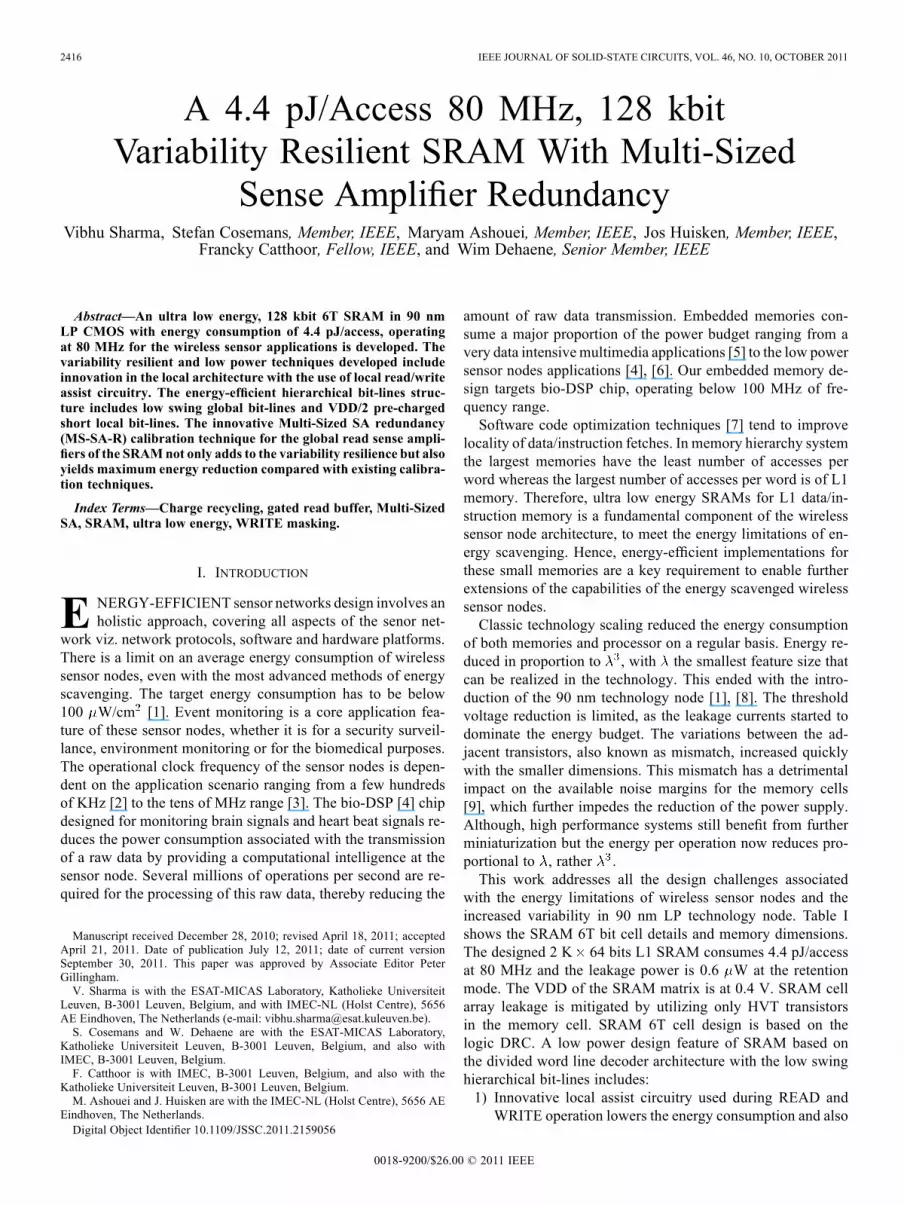
. The reduced SA size maps into reducedenergy consumption.Sense Amplifier Tuning: In [13] voltage tuning is used for
the offset cancellation. Each SA receives the most appropriate
Fig. 15. Sense amplifier tuning [13].
reference voltage based on the offset. Fig. 15 shows sense am-plifier tuning. For a given SA design, the minimal required inputsignal is N times smaller compared to the one with no tuning. Nrefers to number of reference voltage levels available.
(8)
The SA sizes for the given reliability requirement required tosense bit-line discharge signal with traditional SA designand with SA tuning [13] respectively are
(9)
(10)
The ratio of traditional SA size and the SA sizewith tuning provides a good indication of the reductionin active energy that can be obtained with SA tuning comparedto a traditional SA design.
(11)
SA tuning does not require any selection in the critical logicpath, so it scales gracefully to large values of N compared to SAredundancy. N refers to the number of reference voltages for thetuning and number of redundant sense amplifiers for SA redun-dancy. SA tuning definitely reduces the active energy consump-tion, but it does not take into account the energy consumptionrequired to generate multiple reference voltages and also the in-crease in area with this approach. Alternatively, [25] limits thereference voltage choice to only two values.C. Multi-Sized SA Redundancy: Concept and Implementation
Multi-Sized SA redundancy (MS-SA-R) [26], [27] replacesa single sense amplifier with the set of different sized SAs, col-lectively having the same or even less . In other words, N re-dundant differently-sized sense amplifiers are used, with failurerates . The indices are sorted on sense amplifiersizes so that the smallest sense amplifier size with maximum

2426 IEEE JOURNAL OF SOLID-STATE CIRCUITS, VOL. 46, NO. 10, OCTOBER 2011
Fig. 16. Multi-Sized Sense Amplifier [26], [27]: Concept.
failure rate has index1. Fig. 16 shows the concept ofMulti-SizedSA redundancy.The collective failure rate of this SA system, assuming that
SA failures are independent applies are as follows:
(12)
The probability of the usage of the smallest sense amplifierwith the lowest power consumption and the maximum
failure rate:
(13)
The probability of the usage of the immediate next senseamplifier with the next higher power consumption and the nextlower failure rate:
(14)
Similarly, the probability of the usage of the th sense am-plifier with the th higher power consumption and the th lowerfailure rate:
(15)
The probability of the usage of the largest sized senseamplifier of the N redundant multi-sized sense amplifiers withthe highest power consumption and the lowest failure rate:
(16)
For example, a traditional sense amplifier designed for yieldis replaced by two sense amplifiers. The smaller one is designedfor yield, with its energy consumption 9 times smaller thanthat of the traditional single SA designed for yield.The bigger SA in a set is designed for yield. Then the averageenergy consumption of MS-SA-R, is approxi-mately 6 times smaller compared to that of the traditional SA.
Fig. 17. Multi-Sized Sense Amplifier [26], [27].
% %
(17)
The sizes of redundant multi-sized sense amplifiers are basedon the metric of minimizing the total energy consumption ofthe sense amplifier system for a target yield requirement. Whenthe optimal sizes of the critical transistors of the smallest SAapproach closer to the minimum transistor sizes of a technology,it determines an upper limit on the value of N for Multi-SizedSA redundancy. Also the area overhead of selection logic withthe larger values of N cannot be ignored.Multi-Sized SA redundancy in this design is implemented
with . The doublet of SA used consists of a smaller senseamplifier designed for yield and the other sense amplifier isdesigned for yield. There is a separate calibration phase tofind a working SA from the set. Then, only this selected SA isactivated during the READ operation. Fig. 17 shows SA dou-blet with calibration bits, used in this design.
D. Calibration Algorithm Used With Multi-Sized SARedundancy
Calibration algorithm selects a sense amplifier out of the re-dundant set of differently sized sense amplifiers. Fig. 18, showscalibration algorithm used in this design. More particularly, it isdesired to use each time the smallest available SA which doesnot fail. The calibration is done as follows.Step 1) Initially only the 2-sigma sized SA are selected
{Act 2-sigma high} and the pre-defined data storedis successfully read.
Step 2) A READ operation with 2-sigma SA is performed.Failing bit locations are identified. For example,when reading a 64 bit word with bit locations 2, 5,31, and 64 are erroneous (by comparing with the predefined data stored), then for the doublet numbers 2,5, 31 and 64 the 6-sigma SA is selected.
Step 3) The calibration register is updated and READ opera-tion is performed with 2-sigma SA activated except
SHARMA et al.: A 4.4 pJ/ACCESS 80 MHz, 128 kbit VARIABILITY RESILIENT SRAMWITH MULTI-SIZED SENSE AMPLIFIER REDUNDANCY 2427
Fig. 18. Calibration algorithm.
for the number 2, 5, 31 and 64 doublets for whichAct 6-sigma is activated.
Step 4) If Step 3 confirms Step 2 (successful READ oper-ation), then the selection bits will be locked in thecalibration, until the next calibration phase. In theexample with the 2-sigma SAs of doublet numbers2, 5, 31 and 64 failing, this means that the followingselection is stored:
wherein 0 represents Act 6-sigma high and 1 repre-sents Act 2-sigma high. These values will be usedfor the memory accesses, until the next calibrationphase. The next calibration phase is decided basedon the user application.
E. Comparison With Other Calibration Techniques
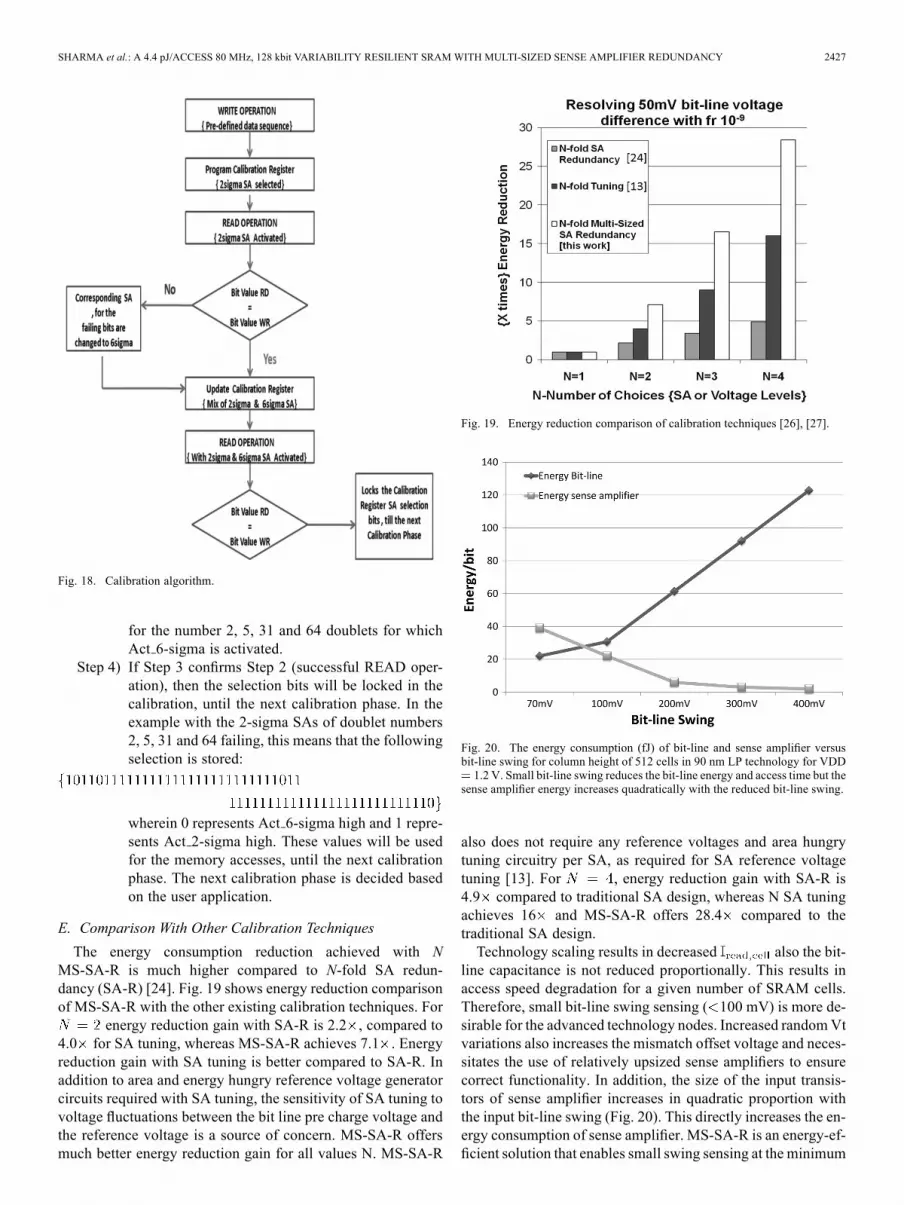
The energy consumption reduction achieved with NMS-SA-R is much higher compared to N-fold SA redun-dancy (SA-R) [24]. Fig. 19 shows energy reduction comparisonof MS-SA-R with the other existing calibration techniques. For
energy reduction gain with SA-R is 2.2 , compared to4.0 for SA tuning, whereas MS-SA-R achieves 7.1 . Energyreduction gain with SA tuning is better compared to SA-R. Inaddition to area and energy hungry reference voltage generatorcircuits required with SA tuning, the sensitivity of SA tuning tovoltage fluctuations between the bit line pre charge voltage andthe reference voltage is a source of concern. MS-SA-R offersmuch better energy reduction gain for all values N. MS-SA-R
Fig. 19. Energy reduction comparison of calibration techniques [26], [27].
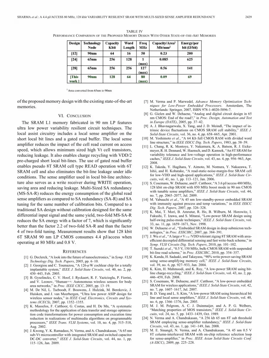
Fig. 20. The energy consumption (fJ) of bit-line and sense amplifier versusbit-line swing for column height of 512 cells in 90 nm LP technology for VDD1.2 V. Small bit-line swing reduces the bit-line energy and access time but the
sense amplifier energy increases quadratically with the reduced bit-line swing.
also does not require any reference voltages and area hungrytuning circuitry per SA, as required for SA reference voltagetuning [13]. For , energy reduction gain with SA-R is4.9 compared to traditional SA design, whereas N SA tuningachieves 16 and MS-SA-R offers 28.4 compared to thetraditional SA design.Technology scaling results in decreased also the bit-
line capacitance is not reduced proportionally. This results inaccess speed degradation for a given number of SRAM cells.Therefore, small bit-line swing sensing ( 100 mV) is more de-sirable for the advanced technology nodes. Increased randomVtvariations also increases the mismatch offset voltage and neces-sitates the use of relatively upsized sense amplifiers to ensurecorrect functionality. In addition, the size of the input transis-tors of sense amplifier increases in quadratic proportion withthe input bit-line swing (Fig. 20). This directly increases the en-ergy consumption of sense amplifier. MS-SA-R is an energy-ef-ficient solution that enables small swing sensing at the minimum

2428 IEEE JOURNAL OF SOLID-STATE CIRCUITS, VOL. 46, NO. 10, OCTOBER 2011
TABLE IIICOMPARISON OF RELATIVE SIZING OF CRITICAL TRANSISTORS
FOR SA-R [24] AND MS-SA-R FOR
cost of energy consumption compared to the traditional senseamplifier and will play a vital role in realizing energy-efficientSRAMs for the advance technology nodes.The relative sizing of the critical transistors with respect to
the critical transistors of a traditional sense amplifier for a givenyield requirement is used as a measure for area comparison(Table III). The slight increase in area overhead with MS-SA-Rcan be ignored considering the enormous energy reduction gainachieved compared with SA-R. SA tuning is not considered inthis comparison because the reference voltage generator circuitaccounts for the main area overhead instead of the sense ampli-fier circuit itself.Thus, Multi-Sized SA redundancy offers highest energy re-
duction gain for the same number of calibration bits comparedto the existing calibration techniques. The area overhead ofMS-SA-R, compared to traditional SA is 30%, ignoringthe area overhead of selection logic. As this design uses ex-tended GBLs [21], only one set of global SAs (64) is requiredand the area of MS-SA-R is only 1% of the total memory area.Therefore, area overhead posed by MS-SA-R is not a majorconcern in this design.
V. PROTOTYPE AND COMPARISON WITHOTHER STATE OF THE ART
A. Measurement Results.
The proposed memory is fabricated in a 90 nm LP CMOSprocess. Fig. 21 shows a die photograph of the proposedmemory. The prototype consists of an SRAM macro and testcircuitry. The test circuitry consists of an input shift register,an output shift register and delay measurement circuitry. Thewrite data, write flag information, masking bits and address bitsare shifted serially into an input shift register. The output ofSRAM macro is loaded into the output shift register and thenshifted serially out. The delay measurement circuitry consistsof latch lines to monitor internal signals of SRAM macro.Fig. 22 shows measurement results at 25 C and at VDD0.8 V. The target application is a 50–80 MHz DSP processorfor wireless sensor nodes. The memory operates at 80 MHzconsuming 4.42 pJ/access for READ, operation, 5.02 pJ/ac-cess for WRITE operation and 2.79 pJ/access for 3/4 maskedWRITE operations. The active leakage power is 5.26 W and
Fig. 21. Die photograph with superimposed layout.
Fig. 22. Measurement results at 25 C and VDD 0.8 V [26].
Fig. 23. Energy breakdown of READ operation VDD 0.8 V and 25 C withSA (traditional # of SA 64) versus MS-SA-R
.
the static leakage power at retention mode is 0.6 W when thedata is held at 0.4 V. Fig. 23 compares the energy breakdownof READ operation of SRAM macro with SA and withMS-SA-R, .
B. Comparison
The energy consumption per access per bit [E/WL] is used asa figure of merit. This enables the comparison between differentsized memories of different word length. This figure of meritwill favor the memories with long word length, as the decoderand timing circuitry overhead does not alter significantly withlong word length. Table IV shows the performance comparison
SHARMA et al.: A 4.4 pJ/ACCESS 80 MHz, 128 kbit VARIABILITY RESILIENT SRAMWITH MULTI-SIZED SENSE AMPLIFIER REDUNDANCY 2429
TABLE IVPERFORMANCE COMPARISON OF THE PROPOSED MEMORY DESIGN WITH OTHER STATE-OF-THE-ART MEMORIES
of the proposedmemory design with the existing state-of-the-artmemories.
VI. CONCLUSION
The SRAM L1 memory fabricated in 90 nm LP featuresultra low power variability resilient circuit techniques. Thelocal assist circuitry includes a local sense amplifier on theshort local bit lines and a gated read buffer. The local senseamplifier reduces the impact of the cell read current on accessspeed, which allows minimum sized high Vt cell transistors,reducing leakage. It also enables charge recycling with VDD/2pre-charged short local bit-lines. The use of gated read bufferenables pseudo 8T SRAM cell type READ operation with 6TSRAM cell and also eliminates the bit-line leakage under idleconditions. The sense amplifier used in local bit-line architec-ture also serves as a write receiver during WRITE operation,saving area and reducing leakage. Multi-Sized SA redundancy(MS-SA-R) reduces the energy consumption of the global readsense amplifiers as compared to SA redundancy (SA-R) and SAtuning for the same number of calibration bits. Compared to atraditional SA design without calibration designed for the samedifferential input signal and the same yield, two-fold MS-SA-Rreduces the SA energy with a factor of 7, which is significantlybetter than the factor 2.2 of two-fold SA-R and than the factor4 of two-fold tuning. Measurement results show that 128 kbit6T SRAM 90 nm LP CMOS consumes 4.4 pJ/access whenoperating at 80 MHz and 0.8 V.
REFERENCES[1] G. Declerck, “A look into the future of nanoelectronics,” in Symp. VLSI
Technology Dig. Tech. Papers, 2005, pp. 6–10.[2] J. Georgiou and C. Toumazou, “A 126- W cochlear chip for a totally
implantable system,” IEEE J. Solid-State Circuits, vol. 40, no. 2, pp.430–443, Feb. 2005.
[3] B. Gyselinckx, C. V. Hoof, J. Ryckaert, R. F. Yazicioglu, P. Fiorini,and V. Leonov, “Human++: Autonomous wireless sensors for bodyarea networks,” in Proc. IEEE CICC, 2005, pp. 13–19.
[4] M. De Nil, L. Tseboodt, F. Bouwens, J. Hulzink, M. Berekovic, J.Huisken, and J. van Meerbergen, “Ultra low power ASIP design forwireless sensor nodes,” in IEEE Conf. Electronics, Circuits and Sys-tems (ICECS), 2007, pp. 1352–1355.
[5] K. Masselos, F. Catthoor, G. Costas, and H. De Mn, “A systematicmethodology for the application of data transfer and storage optimiza-tion code transformations for power consumption and execution timereduction in realizations of multimedia algorithms on programmableprocessors,” IEEE Trans. VLSI Systems, vol. 10, no. 4, pp. 515–518,Aug. 2002.
[6] J. Kwong, Y. K. Ramadass, N. Verma, and A. Chandrakasan, “A 65 nmsub-Vt microcontroller with integrated SRAM and switched capacitorDC-DC converter,” IEEE J. Solid-State Circuits, vol. 44, no. 1, pp.115–126, Jan. 2009.
[7] M. Verma and P. Marwedel, Advance Memory Optimization Tech-niques for Low-Power Embedded Processors. Amsterdam, TheNetherlands: Springer, 2007, ISBN 978-1-4020-5896-7.
[8] G. Gielen and W. Dehaene, “Analog and digital circuit design in 65nm CMOS: End of the road?,” in Proc. Design, Automation and Testin Europe (DATE), 2005, pp. 37–42.
[9] A. J. Bhavnagarwala, X. Tang, and J. D. Meindl, “The impact of in-trinsic device fluctuations on CMOS SRAM cell stability,” IEEE J.Solid-State Circuits, vol. 36, no. 4, pp. 658–665, Apr. 2001.
[10] M. Yoshimoto et al., “A 64 Kb full CMOS RAM with divided wordline structure,” in IEEE ISSCC Dig. Tech. Papers, 1983, pp. 58–59.
[11] L. Chang, R. K. Montoye, Y. Nakamura, K. A. Batson, R. J. Eicke-meyer, R. H. Dennard,W.Haensch, and D. Kamsek, “An 8T SRAM forvariability tolerance and low-voltage operation in high-performancecaches,” IEEE J. Solid-State Circuits, vol. 43, no. 4, pp. 956–963, Apr.2008.
[12] K. Takeda, Y. Hagihara, Y. Aimoto, M. Nomura, Y. Nakazawa, T.Ishii, and H. Kobatake, “A read-static-noise-margin-free SRAM cellfor low-VDD and high-speed applications,” IEEE J. Solid-State Cir-cuits, vol. 41, no. 1, pp. 113–121, Jan. 2006.
[13] S. Cosemans,W. Dehaene, and F. Catthoor, “A 3.6 pJ/access 480MHz,128 kbit on-chip SRAM with 850 MHz boost mode in 90 nm CMOSwith tunable sense amplifiers,” IEEE J. Solid-State Circuits, vol. 44,no. 7, pp. 2065–2077, Jul. 2009.
[14] M. Yabuuchi et al., “A 45 nm low-standby-power embedded SRAMwith immunity against process and temp variations,” in IEEE ISSCCDig. Tech. Papers, 2007, pp. 326–328.
[15] K. Mai, T. Mori, B. Amrutur, R. Ho, B. Wilburn, M. Horowitz, I.Fukushi, T. Izawa, and S. Mitarai, “Low-power SRAM design usinghalf-swing pulse-mode techniques,” IEEE J. Solid-State Circuits, vol.33, no. 11, pp. 1659–1671, Nov. 1998.
[16] W. Dehaene et al., “Embedded SRAM design in deep submicron tech-nologies,” in Proc. ESSCIRC, 2007, pp. 384–391.
[17] J. Wu et al., “A large V /VDD tolerant zigzag 8T SRAMwith area-efficient decoupled differential sensing and fast write-back scheme,” inSymp. VLSI Circuits Dig. Tech. Papers, 2010, pp. 101–102.
[18] T. Suzuki et al., “0.5 V, 150 MHz, bulk-CMOS SRAMwith suspendedbit-line read scheme,” in Proc. ESSCIRC, 2010, pp. 354–357.
[19] K. Kanda, H. Sadaaki, and Takayasu, “90%write power-saving SRAMusing sense-amplifying memory cell,” IEEE J. Solid-State Circuits,vol. 39, no. 6, pp. 927–933, Jun. 2004.
[20] K. Kim, H. Mahmoodi, and K. Roy, “A low-power SRAM using bit-line charge-recycling,” IEEE J. Solid-State Circuits, vol. 43, no. 2, pp.446–459, Feb. 2008.
[21] S. Cosemans, W. Dehaene, and F. Catthoor, “A low-power embeddedSRAM for wireless applications,” IEEE J. Solid-State Circuits, vol. 42,no. 7, pp. 1607–1617, Jul. 2007.
[22] B. D. Yang and L. S. Kim, “A low-power SRAM using hierarchical bitline and local sense amplifiers,” IEEE J. Solid-State Circuits, vol. 40,no. 6, pp. 1366–1376, Jun. 2005.
[23] M. J. M. Pelgrom, A. C. J. Duinmaijer, and A. P. G. Welbers,“Matching properties of MOS transistors,” IEEE J. Solid-State Cir-cuits, vol. 24, no. 5, pp. 1433–1439, Oct. 1989.
[24] N. Verma and A. Chandrakasan, “A 256 kb 65 nm 8T sub thresholdSRAM employing sense-amplifier redundancy,” IEEE J. Solid-StateCircuits, vol. 43, no. 1, pp. 141–149, Jan. 2008.
[25] M. E. Sinangil, N. Verma, and A. Chandrakasan, “A 45 nm 0.5 V8T column-interleaved SRAM with on-chip reference selection loopfor sense-amplifier,” in Proc. IEEE Asian Solid-State Circuits Conf.(A-SSCC), 2009, pp. 225–228.

2430 IEEE JOURNAL OF SOLID-STATE CIRCUITS, VOL. 46, NO. 10, OCTOBER 2011
[26] V. Sharma, S. Cosemans, M. Ashouei, J. Huisken, F. Catthoor, andW. Dehaene, “A 4.4 pJ/access 80 MHz, 2 K word X 64 b memorywith write masking feature and variability resilient multi-sized senseamplifier redundancy for W. S. nodes,” in Proc. ESSCIRC, 2010, pp.358–361.
[27] V. Sharma, S. Cosemans, and W. Dehaene, “Memory circuit withmulti-sized sense amplifier redundancy,” U.S. patent 12/879,972, Sep.10, 2010.
[28] K. Kushida, A. Suzuki, G. Fukano, A. Kawasumi, O. Hirabayashi, Y.Takeyama, T. Sasaki, A. Katayama, Y. Fujimura, and T. Yabe, “A 0.7V single-supply SRAM with 0.495 m cell in 65 nm technology uti-lizing self-write-back sense amplifier and cascaded bit line scheme,”IEEE J. Solid-State Circuits, vol. 44, no. 4, pp. 1192–1198, Apr. 2009.
Vibhu Sharma is a doctoral candidate at K.U.Leuven, working with Prof. Wim Dehaene andIMEC (Holst Center, Eindhoven) in the area of ultralow energy embedded SRAM design. Prior to this,he worked as a Design Engineer with the ImagingRD&I group of ST Microelectronics India from2006 to 2008, designing imaging coprocessors formobile phone applications. He worked on low powermethodology definition at RTL2GDS level for ad-vance subnanometric technology nodes, architectureaware and activity driven physical implementation
of timing critical designs. He received the M.S. degree in electrical engineeringfrom SUNY Stony Brook in December 2005. He was awarded the New YorkState Research Foundation assistantship for his graduate studies at SUNYStony Brook.
Stefan Cosemans (S’04–M’09) was born in Mol,Belgium, in 1981. He received the M.Sc. degree inelectrical engineering from the Katholieke Univer-siteit Leuven (K.U. Leuven), Heverlee, Belgium,in 2004. In May 2009 he received the Ph.D. degreefrom the Katholieke Universiteit Leuven for his workon the variability-aware design of low-power SRAMmemories. Currently, he is a research assistant atthe ESAT-MICAS Laboratory of the KatholiekeUniversiteit Leuven, working in close collaborationwith IMEC, Leuven, Belgium.
Maryam Ashouei (S’04–M’07) received the B.Sc.degree in computer engineering from Sharif Uni-versity of Technology, Tehran, Iran, the M.S. degreefrom Northeastern University, Boston, MA, andthe Ph.D. degree from the Georgia Institute ofTechnology, Atlanta, in 2002 and 2007, respectively.Currently, she is a Researcher at the IMEC (HolstCenter, Eindhoven), working on low-power tech-niques for biomedical signal processing.
Jos Huisken (A’98–M’08) received the Master’sdegree in 1984 from University of Twente, TheNetherlands, after which he joined Philips ResearchIC-design center to work on IC’s, architectures anddesign methodologies for digital signal processingapplications. This lead to first prototypes of archi-tectural synthesis tools which found their way toseveral companies. He used these tools, and lead theprojects, to create the first VLSI design for DigitalAudio Broadcasting ICs, which were applied in thefirst commercial DAB receivers. Also he has been
active in the field of 3G mobile, from which results ended up in commercialproducts as well. In 2002 he was part of the startup team of Silicon Hive,a company using the basic technology he developed before. In 2008 he leftSilicon Hive to join IMEC (Holst Center, Eindhoven) as a principal researcherleading the ULP-DSP group.
Francky Catthoor (S’86–M’87–SM’98–F’05)received the Ph.D. in electrical engineering from theKatholieke Universiteit Leuven, Belgium, in 1987.Between 1987 and 2000, he headed several researchdomains in the area of high-level and system syn-thesis techniques and architectural methodologies,including related application and deep submicrontechnology aspects, all at IMEC, Leuven, Belgium.Currently he is an IMEC Fellow. He is also part-timefull Professor in the Electrical Engineering Depart-ment of the K.U. Leuven.
He has been an associate editor for several IEEE and ACM journals,including TRANSACTIONS ON VLSI SIGNAL PROCESSING, TRANSACTIONSON MULTIMEDIA, and ACM TODAES. He was the program chair of severalconferences including ISSS’97 and SIPS’01.
Wim Dehaene (S’89–M’97–SM’04) was born inNijmegen, The Netherlands, in 1967. He receivedthe M.Sc. degree in electrical and mechanical en-gineering in 1991 from the Katholieke UniversiteitLeuven. In November 1996 he received the Ph.D.degree at the Katholieke Universiteit Leuven. Histhesis was entitled “CMOS integrated circuits foranalog signal processing in hard disk systems.”After receiving the M.Sc. degree he was a researchassistant at the ESAT-MICAS Laboratory of theKatholieke Universiteit Leuven. His research in-
volved the design of novel CMOS building blocks for hard disk systems. Theresearch was first sponsored by the IWONL (Belgian Institute for Scienceand Research in Industry and Agriculture) and later by the IWT (the Flemishinstitute for Scientific Research in the Industry). In November 1996 he joinedAlcatel Microelectronics, Belgium. There he was a senior project leader forthe feasibility, design and development of mixed mode Systems on Chip. Theapplication domains were telephony, xDSL and high speed wireless LAN. InJuly 2002 he joined the staff of the ESAT-MICAS Laboratory of the KatholiekeUniversiteit Leuven where he is now a full Professor. His research domain iscircuit level design of digital circuits, with current focus is on ultra low powersignal processing and memories in advanced CMOS technologies. Part of thisresearch is performed in cooperation with IMEC, Belgium, where he is also apart time principal scientist. Prof. Dehaene teaches several classes on electricalengineering and digital circuit and system design.