

9780521862905htl 1..2
423
-
Upload
khangminh22 -
Category
Documents
-
view
0 -
download
0
Transcript of 9780521862905htl 1..2

This page intentionally left blank

Competing for the future
Everybody knows that digital technology has revolutionized our eco-
nomy and our lifestyles. But how many of us really understand the
drivers behind the technology – the significance of going digital; the
miniaturization of electronic devices; the role of venture capital in
financing the revolution; the importance of research and development?
How many of us understand what it takes to make money from
innovative technologies? Should we worry about manufacturing
going offshore? What is the role of India and China in the digital
economy? Drawing on a lifetime’s experience in the industry, as an
engineer, a senior manager, and as a partner in a global venture capital
firm, Henry Kressel offers an expert personalized answer to all these
questions. He explains how the technology works, why it matters, how
it is financed, and what the key lessons are for public policy.
H E N R Y K R E S S E L is a Managing Director of Warburg Pincus, LLC. He
began his career at RCA Laboratories where he pioneered the first
practical semiconductor lasers. He was the founding president of the
IEEE Laser and Electro-Optics Society (LEOS) and co-founded the IEEE/
OSA Journal of Lightwave Technology. He is the recipient of many
awards and honors, a fellow of the American Physical Society and of
the IEEE, and the holder of thirty-one issued US patents for electronic
and optoelectronics devices.
T H O M A S V. L E N T O is founder and President of Intercomm, Inc., a
corporate communications consultancy.


Competing for
the future
How digital innovationsare changing the world
H E N R Y K R E S S E L
W I T H
T H O M A S V . L E N T O

CAMBRIDGE UNIVERSITY PRESS
Cambridge, New York, Melbourne, Madrid, Cape Town, Singapore, São Paulo
Cambridge University Press
The Edinburgh Building, Cambridge CB2 8RU, UK
First published in print format
ISBN-13 978-0-521-86290-5
ISBN-13 978-0-511-28499-1
© Henry Kressel 2007
2007
Information on this title: www.cambridge.org/9780521862905
This publication is in copyright. Subject to statutory exception and to the provision of
relevant collective licensing agreements, no reproduction of any part may take place
without the written permission of Cambridge University Press.
ISBN-10 0-511-28499-3
ISBN-10 0-521-86290-6
Cambridge University Press has no responsibility for the persistence or accuracy of urls
for external or third-party internet websites referred to in this publication, and does not
guarantee that any content on such websites is, or will remain, accurate or appropriate.
Published in the United States of America by Cambridge University Press, New York
www.cambridge.org
hardback
eBook (EBL)
eBook (EBL)
hardback

For Bertha


Contents
List of figures page ix
List of tables xix
Acknowledgements xx
Introduction 1
Part I The technology – how electronic devices
work – digital systems and software 7
1 Genesis: Inventing electronics for the digital world 9
2 Building digital systems 56
Part II Innovators, entrepreneurs, and venture capitalists 99
3 Edison’s legacy: Industrial R&D 101
4 R&D goes global 122
5 Financing innovation: Venture capital 175
Part III Global reach, global repercussions 215
6 Manufacturing: Globalizing faster than ever 217
7 Your government is here to help 258
8 The digital world: Industries transformed 290
9 The digital world: A global village 332
Appendix 1.1: Smaller, faster, more efficient MOSFETs 347
Appendix 1.2: Building multi-transistor logic gates 355
Appendix 1.3: MOSFETs in memory devices 357
Appendix 1.4: CMOS reduces logic gate power dissipation 359
vii

Appendix 1.5: Laser diode basics 362
Appendix 1.6: Light-emitting diodes (LEDs) 367
Appendix 1.7: Photodetectors 370
Appendix 1.8: Making fiber optic cables 372
Appendix 1.9: Principles of LCD displays 374
Appendix 2.1: The demise of analog computers 377
Appendix 2.2: IP, TCP, and the Internet 381
Appendix 2.3: Building an object-oriented program 383
Index 386
viii Contents
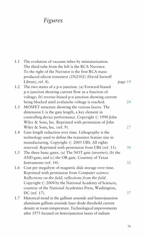
Figures
1.1 The evolution of vacuum tubes by miniaturization.
The third tube from the left is the RCA Nuvistor.
To the right of the Nuvistor is the first RCA mass-
produced silicon transistor (2N2102) (David Sarnoff
Library, ref. 4). page 19
1.2 The two states of a p-n junction. (a) Forward-biased
p-n junction showing current flow as a function of
voltage; (b) reverse-biased p-n junction showing current
being blocked until avalanche voltage is reached. 24
1.3 MOSFET structure showing the various layers. The
dimension L is the gate length, a key element in
controlling device performance. Copyright # 1990 John
Wiley & Sons, Inc. Reprinted with permission of John
Wiley & Sons, Inc. (ref. 9). 27
1.4 Gate length reduction over time. Lithography is the
technology used to define the transistor feature size in
manufacturing. Copyright # 2005 UBS. All rights
reserved. Reprinted with permission from UBS (ref. 11). 30
1.5 The three basic gates. (a) The NOT gate (inverter); (b) the
AND gate; and (c) the OR gate. Courtesy of Texas
Instruments (ref. 14). 32
1.6 Cost per megabyte of magnetic disk storage over time.
Reprinted with permission from Computer science:
Reflections on the field, reflections from the field.
Copyright# 2004 by the National Academy of Sciences,
courtesy of the National Academies Press, Washington,
DC (ref. 17). 37
1.7 Historical trend in the gallium arsenide and heterojunction
aluminum gallium arsenide laser diode threshold current
density at room temperature. Technological improvements
after 1975 focused on heterojunction lasers of indium
ix

gallium arsenide phosphide emitting at 1.55 microns for
fiber optic systems. Reprinted from Semiconductor lasers
and heterojunction LEDs. Copyright # 1977, with
permission from Elsevier (ref. 23). 41
1.8 Schematic of a simple double heterojunction laser diode
structure showing light beam emitted under stripe contact
10 microns wide. The front and back of the structure
constitute the two surfaces of the Fabry-Perot cavity.
Reprinted with permission from Physics Today. Copyright
# 1976, American Institute of Physics (ref. 25). 42
1.9 A laser diode packaged in a metal case with a glass face
for the emitted radiation. 43
1.10 Spectral loss data for silica optical fibers over time. The
heterojunction lasers used in communications systems
emit in the 1.55 microns region. Reprinted with
permission from Lasers: Invention to applications.
Copyright# 1987 by the National Academy of Sciences,
courtesy of the National Academies Press, Washington,
DC (ref. 31). 46
1.11 Historical reduction in the cost of a fiber-meter of
single-mode optical fiber. Figure courtesy of KMI
Research, www.kmiresearch.com (ref. 32). 47
1.12 (a) Two types of imagers. Left, CCD and right,
CMOS-based with MOSFETs incorporated into pixels.
Reprinted with permission from D. Litwiller, DALSA
(ref. 35). 49
1.12 (b) Architecture of simple imaging system using a CCD
imager. Reprinted with permission from D. Litwiller,
DALSA (ref. 36). 50
1.13 Flat-panel display sales surpassed cathode-ray tube (CRT)
sales in 2002. Reprinted with permission from
DisplaySearch, an NPD Group company (ref. 40). 53
1.14 Price of 45-inch LCD TV display over time. Reprinted
with permission from IBS (ref. 41). 53
2.1 Integrated circuit market segments between 1999 and
2005, and projected to 2010. Microprocessors are
included in the ‘‘MOS Micro’’ segment (from IBS, ref. 3). 59
2.2 Extrapolation (dashed lines) of processor switching power
dissipation and leakage current-related power
x List of figures

dissipation. Fit line replotted (solid line) and
extrapolated (dashed line) with G. Moore’s presentation
in 2003 (see ref. 3). The crossing of the extrapolated lines
indicates that the leakage current power dissipation is
progressively dominant from around 2002–2003.
Copyright # 2005 IEEE (from Gea-Banacloche and
Kish, ‘‘Future directions in electronic computing,’’
ref. 6). 62
2.3 Historical relative cost of three elements of computing
systems: magnetic disk storage, DRAM, and
microprocessor performance. Reprinted with permission
from Mashey, TechViser (ref. 12). 64
2.4 US national communications channel capacity
improvement as a function of time. Note the
discontinuous change in the average slope with the
introduction of optical fiber systems. Reprinted with
permission from Lasers: Invention to applications.
Copyright# 2004 by the National Academy of Sciences,
courtesy of the National Academies Press, Washington,
DC (ref. 14). 67
2.5 AT&T telephone switchboard operators (property of
AT&T Archives. Reprinted with permission of AT&T). 68
2.6 Recent and anticipated growth of VoIP customers in the
US. These numbers are most likely understated given the
VoIP service of Skype and of companies such as Google
and Yahoo! Reprinted with permission from Bear
Stearns (ref. 21). 77
2.7 Historical software investments in the US since 1993
(from SG Cowen, Perspectives, ref. 31). 86
3.1 Dr. S. Cherukuri’s curve of product maturity over time
showing the process from concept to obsolescence.
Reprinted with permission from S. Cherukuri, Sarnoff
(ref. 3). 104
3.2 Trade balance in R&D-intensive electronics sectors,
1970–1989. This group of sectors includes data
processing equipment, electronic components, and
telecommunications equipment. Standardized trade
balances are expressed as a percentage of total world
trade in R&D-intensive electronics sectors. For methods
List of figures xi

and sources, see ref. 8. Reprinted with permission from
Linking trade and technology policies. Copyright #
1992 by the National Academy of Sciences, courtesy of
the National Academies Press, Washington, DC (ref. 8). 116
4.1 The self-reinforcing advantage of high-tech
industries. Reprinted with permission from Linking
trade and technology policies: An international
comparison of the policies of industrialized nations.
Copyright# 1992 by the National Academy of Sciences,
courtesy of the National Academies Press, Washington,
DC (ref. 7). 126
4.2 Degrees awarded in science and engineering (S&E) as a
percentage of new degrees in 2001 (from OECD,
Science, technology and industry outlook, ref. 10). 131
4.3 Percentage of foreign students in tertiary education by
country of study in 2002. Copyright # 2005 The
Economist Newspaper Ltd. All rights reserved.
Reprinted with permission. Further reproduction
prohibited; www.economist.com (ref. 15). 135
4.4 Computer science (CS) listed as probable major among
incoming freshmen since 1971 in the US. Reprinted from
‘‘President’s letter,’’ Communications of the ACM, 48:9,
September 2005. Figure reprinted with permission
from the Higher Education Research Institute (HERI)
(ref. 18). 136
4.5 Annual information technology employment in the US
from 1999 based on US Bureau of Labor Statistics.
Reprinted from ‘‘President’s letter,’’ Communications of
the ACM, 48:9, September 2005 (ref. 19). 137
4.6 Division of programs at Taiwan’s Industrial Technology
Research Institute (ITRI) in 2003. Reprinted with
permission from ITRI (ref. 28). 145
4.7 Educational background of the staff of Taiwan’s Industrial
Technology Research Institute (ITRI) in 2003. Reprinted
with permission from ITRI (ref. 28). 146
4.8 Funds provided by US federal agencies to universities and
colleges for conduct of R&D in fiscal year 2002.
Copyright # 2004 by Rand Corporation. Reproduced
xii List of figures

with permission of Rand Corporation via Copyright
Clearance Center (ref. 40). 154
4.9 Net license income of US research universities. Reprinted
with permission from AUTM US licensing survey
summary: FY 2004 (Northbrook, IL: Association of
University Technology Managers, 2005) (ref. 44). 157
4.10 (a) The changing sources of publications in the physical
sciences and engineering in two publications, Applied
Physics Letters and Electronics Letters, between 1988
and 2004 by country or region of origin. 165
4.10 (b) The changing sources of publications in the physical
sciences and engineering in two publications, Applied
Physics Letters and Electronics Letters, between 1988
and 2004 by the nature of the authors’ institution. 165
4.11 (a) The changing sources of publications on software in
the IEEE Transactions on Software Engineering and
Communications of the ACM between 1988 and 2004
by country or region of origin. 166
4.11 (b) The changing sources of publications on software in
the IEEE Transactions on Software Engineering and
Communications of the ACM between 1988 and 2004
by the nature of the authors’ institution. 166
5.1 (a) Capital commitments to US venture funds ($ billions) –
1979–2005. Reprinted with permission from NVCA (ref. 5). 180
5.1 (b) Investments to portfolio companies ($ billions) –
1979–2005. Reprinted with permission from NVCA
(ref. 5). 181
5.2 Venture capital investments in 2005 – by industry sector.
Reprinted with permission from NVCA (ref. 10). 190
5.3 Venture capital investments – first versus follow-on
1979–2005 – software. Reprinted with permission from
NVCA (ref. 11). 191
5.4 Venture capital investments – first versus follow-on
1979–2005 – semiconductors and electronics. Reprinted
with permission from NVCA (ref. 12). 192
5.5 The ‘‘Bubble’’ in the US Telecom Networking Index
October 1998 to October 2001. From BigCharts.com
quoted by Dr. A. Bergh; reprinted with permission from
OIDA (ref. 15). 195
List of figures xiii

5.6 Venture-backed IPOs showing number of IPOs and total
amount raised. Reprinted with permission from NVCA
(ref. 19). 204
5.7 Worldwide laser diode sustainable revenues. Removal of
bubble (1999–2002) in worldwide laser diode market
history to show sustainable revenue levels. Reprinted
with permission from OIDA (ref. 21). 209
5.8 Venture capital raised by high-tech companies in various
countries (2002–2004). Reprinted with permission from
Israel Venture Capital (ref. 22). 212
6.1 Early growth apparatus for liquid phase epitaxy of
semiconductor lasers developed at RCA Laboratories in
the early 1960s. From Nelson, ‘‘Epitaxial growth.’’ Photo
courtesy A. Magoun, David Sarnoff Library (ref. 6). 229
6.2 Automated fabrication equipment used to manufacture
semiconductor lasers. Photo courtesy Sarnoff
Corporation (ref. 7). 230
6.3 Low absorption optical fiber demand by region
(1998–2009). Values beyond 2004 are estimated.
Figure courtesy KMI Research, www.kmiresearch.com
(ref. 11). 239
6.4 Product cost distribution in China – 2005 compared to
the US in 1999. Example of product manufacturing cost
of identical electro-mechanical components in China
(from private communications/survey, ref. 13). 242
6.5 Estimated manufacturing cost of 300 mm CMOS wafer
in various geographies in 2005 (from Jones, IBS, ref. 14). 243
6.6 Large-panel liquid crystal display (LCD) production by
country and by year. Reprinted with permission from
Displaybank (ref. 20). 249
6.7 The production value of Taiwan’s photonics from 2003
(ref. 21). 250
7.1 Software patents granted in the US by grant date
(1976–2002). The data comes from the USPTO as
computed by Hunt and Bessen, ‘‘Software patent
experiment.’’ Reprinted with permission from the
Federal Reserve Bank of Philadelphia (ref. 8). 269
7.2 The percentage of patents granted in a year that are
software patents (1976–2002). The data comes from the
xiv List of figures

USPTO as computed by Hunt and Bessen, ‘‘Software
patent experiment.’’ Reprinted with permission from the
Federal Reserve Bank of Philadelphia (ref. 9). 269
7.3 Federal district court patent lawsuits terminated by
fiscal year. ‘‘Terminated’’ includes judgments,
dismissals, settlements, transfers, and remands. From
Merrill, Levin, and Myers (eds.), A patent system
(ref. 14). 276
7.4 American Bar Association membership: Intellectual
Property Law Section and total. Copyright # 2006 by
the American Bar Association. Reprinted with
permission (ref. 15). 277
8.1 Penetration rate of some major consumer products in the
US since 1947. Reprinted with permission from the IDC
and the Consumer Electronics Association (CEA)
(ref. 18). 302
8.2 Entertainment content that can be stored on a
160 gigabyte (GB) hard drive. Reprinted with permission
from Parks Associates (ref. 27). 307
8.3 Global online commerce since 2000 showing the dollars of
sales and the per cent of online users that shop on the
Internet. Reprinted with permission from Bear Stearns
(ref. 33). 311
8.4 The number of transistors per person on the planet. Data
from US Census Bureau and Semiconductor Industry
Association (SIA) (ref. 47). 324
8.5 The worldwide (WW) sales of semiconductor devices and
the fraction that they represent of electronic systems
sales. The dotted line shows the average trend. Copyright
# 2006 UBS. All rights reserved. Reprinted with
permission from UBS (ref. 48). 324
8.6 Estimated percentage of semiconductor devices used in
major electronic product sectors (2004). Copyright #
2006 UBS. All rights reserved. Reprinted with
permission from UBS (ref. 49). 325
8.7 Electronic products represent an increasing share
of the world’s GDP. Copyright # 2006 UBS. All
rights reserved. Reprinted with permission from UBS
(ref. 53). 328
List of figures xv

9.1 Fraction of world trade in high-tech products in 1980
and 2003 by region of origin (from
www.futureofinnovation.org, ‘‘The knowledge
economy,’’ ref.1.Updatesof the2001data to2003have
been provided by the American Physical Society (APS)). 334
9.2 Semiconductor device sales by region as a percentage
of total worldwide semiconductor sales since 2001.
Copyright # 2006 UBS. All rights reserved.
Reprinted with permission from UBS (ref. 2). 335
9.3 Trade balance in high-tech products of the US
1990–2005 (from www.futureofinnovation.org,
‘‘The knowledge economy,’’ ref. 6.Updatesof the2001
data to 2005 have been provided by the American
Physical Society (APS)). 337
A-1.1.1 Operation of n-p-n bipolar transistor. (a) Current
flow as emitter-to-base p-n junction is forward-
biased. The base to collector p-n junction is reverse-
biased. (b) Opening and closing switch turns
transistor on and off. 348
A-1.1.2 Schematic of elementary n-channel MOSFET (metal
oxide semiconductor field-effect transistor). (a) Gate
voltage is 0 and device is off; (b) 10 volts applied to
gate turns the device on. Courtesy of Texas
Instruments (ref. 2). 350
A-1.1.3 Principles of MOSFET scaling where the gate length L
is reduced to L/k. H. Dennard, F. H. Gaensslen,
H. N. Yu, V. L. Rideout, E. Bassous, and A. R. LeBlanc,
‘‘Design of ion-implanted MOSFETs with very small
physical dimensions,’’ IEEE J. Solid-State Circuits,
SC-9, p. 256. Copyright # 1974 IEEE (ref. 3). 351
A-1.2.1 NAND gate input using n-channel MOSFETs.
Courtesy of Texas Instruments (ref. 1). 356
A-1.3.1 Schematic of basic MOSFET structure for non-volatile
memory devices. Reprinted with permission from
R. Zaks (ref. 2). 358
A-1.4.1 Inverter using n-channel MOSFETs. Courtesy of Texas
Instruments (ref. 1). 360
A-1.4.2 Inverter using CMOS structure. 361
xvi List of figures

A-1.5.1 (a) Homojunction and (b) double-heterojunction laser
diode structures showing the recombination region
layer of thickness d. 364
A-1.5.2 Schematic cross-section of a double-heterojunction
laser showing the refractive index distribution
perpendicular to the junction plane and intensity
distribution of the fundamental transverse mode
with a fraction K of the radiant energy within the
recombination region of width d. 365
A-1.6.1 Improvement in visible LED efficiency since the
1960s. LEDs have averaged efficiency improvements
of �10x/decade over this time frame. Today’s
devices are significantly more efficient than
unfiltered incandescents with the best devices
approaching fluorescent lamp efficiencies. Reprinted
with permission from physica status solidi (a) and
F. Steranka. Copyright # 2002 Wiley-VCH Verlag
GmbH & Co. KG (ref. 1). 368
A-1.7.1 P-n junction used as light detector. (a) In the dark
(no current); (b) with incident light which results in
current flow proportional to light intensity. 371
A-1.8.1 Three types of optical fibers. (a) Multimode fiber;
(b) single-mode fiber; and (c) multimode graded-
index fiber. Reprinted with permission from Physics
Today. Copyright # 1976 American Institute of
Physics (ref. 1). 373
A-2.1.1 (a) A sine wave; (b) sampling the sine wave;
(c) quantizing the samples to 3 bits which produces
eight distinct values for each sample. Copyright #
1996 Pearson Education, Inc. Reprinted by
permission of Pearson Education, Inc., Upper Saddle
River, NJ (ref. 2). 380
A-2.3.1 Organization of program using ‘‘conventional’’
algorithmic architecture, to be compared to Figure
A-2.3.2. Booch, Object solutions, p. 15 figure
1–2, Copyright # 1991 Pearson Education, Inc.
Reproduced by permission of Pearson Education,
Inc. All rights reserved (ref. 1). 384
List of figures xvii

A-2.3.2 Organizing the same program as shown in
Figure A-2.3.1 using object-oriented architecture.
Booch, Object solutions, p. 16 figure 1–3, Copyright
# 1991 Pearson Education, Inc. Reproduced by
permission of Pearson Education, Inc. All rights
reserved (ref. 2). 384
xviii List of figures

Tables
1.1 Key device innovations page 16
1.2 Intel microprocessor timeline 29
1.3 Price per gigabyte of storage 38
4.1 Annual engineering costs 134
4.2 National R&D expenditures for 1981 and 2002 140
4.3 Government budget appropriations 142
4.4 The world’s top universities and annual R&D
funding from US government 155
4.5 Patents simultaneously filed in Europe, US, and Japan 168
4.6 Number of patents applied for in Japan in 2004 169
5.1 Internet-related investments 193
5.2 Five-year rolling averages: Rates of return 194
5.3a Selected industry pioneers 202
5.3b Selected industry innovators 203
5.4 Venture-backed IPOs vs. all IPOs 205
6.1 Fully-burdened hourly labor costs (2005) 241
7.1 Software-protection techniques in the US 270
xix

Acknowledgements
The idea for this book has its origins in a visit to the University of
Cambridge in 2005, hosted by Professor Ian Leslie, Pro-Vice-Chancellor
(Research). I am very grateful for the insights I gained from him regarding
the technology programs at the university. I met some of the faculty and
students of the Cavendish Laboratory, a place where so much of the
world’s basic scientific work was accomplished. I also visited a number
of entrepreneurial companies founded to commercialize the innovations
that grew out of university research. I am indebted to Lord Broers, former
vice-chancellor of the university, and to my partner Dr. William H.
Janeway, Chairman of Cambridge in America for making the appropriate
introductions to facilitate my visit and the many valuable discussions.
These visits called to mind the long chain, bridging the centuries, that
links fundamental scientific discovery to technological advances. This
process has accelerated dramatically in the twentieth century, allowing
digital technologies to transform the modern world in a remarkably short
time. Why and how this has happened, and the consequences of the
transformation, are among the topics that I have explored in this book.
In deciding to write this book, I have been fortunate in working with
Thomas V. Lento, without whom it would not have been completed.
His collaboration was critical in shaping its contents.
This book also reflects my experience over the years from collabora-
tions in venture investments with my partners at Warburg Pincus:
Lionel I. Pincus, John L. Vogelstein, Dr. William H. Janeway, Joseph
P. Landy, Charles R. Kaye, Jeffrey A. Harris, Dr. Harold Brown, Bilge
Ogut, Beau Vrolyk, Cary J. Davis, James Neary, Patrick T. Hackett,
Henry B. Schacht, Steven G. Schneider, Stewart Gross, Robert Hillas,
Dr. Nancy Martin, Julie Johnson Staples, Andrew Gaspar, Christopher
W. Brody, and Frank M. Brochin.
My knowledge of China was built up over the years in collaboration
with the Warburg Pincus team in Hong Kong – Chang Q. Sun, Jeff Leng
and Julian Cheng.
xx

Dr. Peter D. Scovell and Dr. Stanley Raatz greatly enhanced the
accuracy of the material through their perceptive reading of the manu-
script, and Chris Harrison, my editor at Cambridge University Press,
provided essential guidance for refining its presentation.
In my early technical career I had the good fortune to work with many
talented collaborators at RCA. These included Dr. Adolph Blicher,
Herbert Nelson, Benjamin Jacoby, Dr. Jim J. Tietjen, Dr. Harry
F. Lockwood, Dr. Michael Ettenberg, Frank Hawrylo, and Ivan
Ladany. More recently, I have greatly benefited from my work with SRI
International headed by Dr. Curt Carlson and Sarnoff Corporation staff, in
particular Dr. Satyam Cherukuri.
Finally, I am very grateful to Tina Nuss for her extraordinary work
in preparing and proofreading the manuscript.
Acknowledgements xxi


Introduction – Competing for thefuture: How digital innovationsare changing the world
DA V I D Sarnoff, long the chairman of RCA and a pioneer in
the electronics industry, summarized his career in these words: ‘‘I
hitched my wagon to the electron rather than theproverbial star.’’1
The world has followed suit. The past sixty years have witnessed the
most rapid transformation of human activity in history, with digital
electronic technology as the driving force.
Nothing has been left untouched. The way people communicate,
live, work, travel, and consume products and services have all changed
forever. The digital revolution has spurred the rapid expansion of
economic activity across the face of the planet.
In this book I will explore the unprecedented outburst of electronic
innovation that created the digital revolution. Based on this example,
I will examine how innovation works, what it has achieved, and what
forms we can expect it to assume in the near future.
Since innovation does not happen in a vacuum, I will also explore
the political and economic factors that can accelerate or impede
changes in the industrial landscape. One of these is globalization,
which creates neither a level playing field nor a truly ‘‘flat world.’’
Governments everywhere are focused on industrializing as quickly as
possible in the face of growing competition. As a result, attempts to
gain national competitive advantage by building artificial walls are not
going away.
Defining innovation
Before outlining the issues to be covered, we must clarify what consti-
tutes an ‘‘innovation’’ in the first place. The blue laser diode that
1 The New York Times, April 4, 1958.
1

enables the next generation of optical storage is obviously an innova-
tion. But many would say an improved connector for circuit boards
qualifies too. To avoid confusion, we need a definition that focuses the
term on the kind of transformational technology that we’re exploring.
Here is a good starting point.
Innovation is an historic and irreversible change in the way of doing things . . .
This covers not only techniques, but also the introduction of new commodi-
ties, new forms of organization, and the opening of new markets.2
In this book, then, innovation refers to a technical development or
invention that contributes toward creating new industries, new pro-
ducts and processes, and new approaches to solving complex industrial
problems. Innovation includes commercializing the technology to
move it into the market and disseminate it throughout the world.
Needless to say, some technical developments or inventions are more
fundamental and far-reaching than others. The most potent force for
change is a revolutionary innovation. This is a basic invention that
ultimately replaces a technology once central to industry.
A revolutionary innovation is the tsunami of the industrial world. Its
power spreads out from a central technology base, overcoming all
resistance in its path through successive industrial innovations, until
its effects are felt in the farthest reaches of the world economy.
Revolutionary innovations are followed and supported by innova-
tions that are valuable in and of themselves, but are more evolutionary
in nature. Evolutionary innovations help implement the fundamental
discoveries and extend their reach.
Building the digital world
To understand how digital electronics conform to this pattern, we must
first look at how the technology was developed. Then we will examine
how it has affected industrial development around the world.
It promises to be a fascinating journey. The following overview can
serve as a map of the terrain, to guide us through the issues we will
encounter. To get started, let’s orient ourselves by looking at where
electronic technology came from in the first place.
2 J. A. Schumpeter, Readings in business cycle theory (Philadelphia: The BlackistonCompany, 1944), p. 7.
2 Competing for the future

Modern electronics began with the invention of the vacuum tube
(called a ‘‘valve’’ in the UK) in the early twentieth century. This device
initiated the ‘‘analog’’ electronic age, from radio through telephony,
television, radar, and the very beginnings of computing.
Today vacuum tubes have all but disappeared. They were replaced
by two of the most revolutionary device innovations in history, the
transistor and the semiconductor laser diode. These landmark inven-
tions proved to be the key components in the digital technologies
that have transformed the world. Chapter 1 talks about them in more
depth.
Significantly, both the transistor and the laser diode were largely
conceived and commercialized in the United States. Following World
War II, the US had become the epicenter for technological break-
throughs, the result of enormous R&D investments by major corpora-
tions over a span of many years. These companies also carried out the
commercial implementation of their discoveries.
US technical leadership persisted through the end of the twentieth
century. As we shall see, however, in the later years this was due more
to financial and social structures than industrial and governmental
support. In fact, it was the availability of private venture capital in
the United States during the 1980s and 1990s that drove many revolu-
tionary innovations to their present dominance.
Venture funding made possible the formation of hundreds of highly
innovative companies that created new digital electronic products to
pioneer new markets. They produced innovations in communications
and computing, particularly microprocessors and software, that gen-
erated whole new spheres of activity.
Now, at the start of the twenty-first century, the world order has
changed. Innovation and the capital to finance new technology busi-
nesses are more globally distributed. This has profound consequences
for regional economic development.
Innovation on a global scale
Today the talk is all about globalization, as if it were a new phenom-
enon. But globalization has been going on for thousands of years, with
people migrating across lands and seas, carrying ideas and products
with them. The real difference in the modern world is how much faster
the process has become.
Introduction 3

The invention of printing in the fifteenth century led to an enormous
increase in the spread of ideas, but it took about 100 years to make
meaningful changes to Western society. The introduction of the steam
engine in the eighteenth century triggered its own chain of industrial
transformations, but it wasn’t until the middle of the nineteenth cen-
tury that its full impact began to register on societies around the world.
By contrast, digital electronics have profoundly altered societies
around the globe in little more than twenty years. This has happened
despite the fact that the electronics revolution has involved countries
that were not full participants in the earlier industrial upheavals.
Part of the reason is political. After the two world wars of the
twentieth century, Europe and Asia underwent nearly twenty years of
reconstruction. Meanwhile, US businesses were becoming the undis-
puted leaders in technological industries. As we will see, the largest
corporations established central research laboratories in the expectation
that fostering industrial innovations would help assure their futures.
By the 1970s, however, we see the beginning of a new wave of
very rapid globalization. The industrialized countries most devastated
by the war in Western Europe had recovered, as had Japan, and they
began to build their industries using technologies that had been largely
innovated in the United States. They represented new, well-capitalized
international competitors in the world market.
That was a rude awakening for the United States. Suddenly, industry
leaders found themselves faced by formidable challengers. Complacency
quickly gave way to panic. Most noticeable was the challenge mounted
by Japanese companies, which were competing not only on price but
also on quality. Forecasts of the inevitable takeover of US industry by
large Japanese companies produced widespread public fear.
The feared collapse of the US economy under the onslaught of
European and Japanese competition did not happen. What did occur
was the rise of a whole new class of formidable Asian competitors to
further threaten the dominance of incumbents. Starting in the late
1970s, South Korea, Taiwan, Malaysia, and the Philippines became
centers of low-cost manufacturing outsourced from the US.
No one dreamed at the time that China would emerge as an indus-
trial colossus any time soon. Its economy was too restrictive and too
badly managed. But emerge it did, starting in the 1980s, when its
government decided to open the country to market forces, entre-
preneurial capitalism, and, increasingly, foreign investment.
4 Competing for the future

Nor did anyone predict that India would become a major source for
the international production of software. But today Bangalore is boom-
ing with software firms.
The acceleration of industrial development in the leading Asian
economies has been astonishing. They have accomplished in just a few
years what once took many decades. How were they able to manage it?
I will propose that this shock wave of rapid development resulted
from a crucial combination of factors not present in previous phases of
industrialization. First and most important was the readily transferable
nature of the technology being commercialized. Although the revolu-
tionary innovations in digital electronics originated primarily in the US
between the 1940s and 1980s, they allowed an extraordinary degree of
global industrial mobility.
Other factors included new government policies in the industrializ-
ing nations, and the availability of risk capital to fund new business
ventures. We will consider the effectiveness of both approaches in
fostering industrial development.
The new world order
Earlier waves of globalization saw industries move to new parts of the
world. New centers of innovation arose. The movement of risk capital
seeking the highest return financed industrial development in those
new regions. We have witnessed the same train of events in our own
time, but in a highly compressed time frame.
We have also seen the inevitable consequences of this process.
Excessive investment overbuilds capacity, and a return to reality is
accompanied by a destructive collapse. The boom and bust in telecom-
munications in the late 1990s, where trillions of dollars of value were
wiped out in a few short years, is a classic example.
As the aftereffects of the tidal wave of digital electronics ripple in
new directions, it is time to take stock of what has happened, why, and
how. I trust that this book will provide a useful analysis.
More than that, I hope it will stimulate discussions not just about the
future of technology, innovation, and industrialization, but about their
global impact. One thing is certain: the future will be quite different
from the linear extrapolations of the present.
In talking about the future, I am mindful of the spotty history of
technological and market predictions. One of my favorite examples
Introduction 5

involves conflicting views on television. In 1939 David Sarnoff, the
chairman of RCA, presided over the televised opening of the RCA
Pavilion at the World’s Fair. He said: ‘‘Now we add sight to sound. It
is with a feeling of humbleness that I come to this moment of announ-
cing the birth, in this country, of a new art so important in its implica-
tions that it is bound to affect all society. It is an art which shines like a
torch in a troubled world.’’
Contrast his prophetic statement with the opinion expressed in a
New York Times editorial at about the same time: ‘‘The problem with
television is that people must sit and keep their eyes glued to the screen;
the average American family hasn’t time for it. Therefore the showmen
are convinced that, for this reason, if no other, television will never be a
serious competitor of [radio] broadcasting.’’ Who would have guessed
that the average household now spends over six hours a day watching
television?3
3 Quoted in the New York Times, August 28, 2005, Opinion, 12.
6 Competing for the future

P A R T I
The technology – how electronic devices work – digitalsystems and software
P A R T I
The technology – how electronic devices work – digitalsystems and software


1 Genesis: Inventing electronicsfor the digital world
TH I S book is about the creation and con sequenc es of digital
ele ctronics .
Over the last ha lf-century no oth er area of techni cal inno vation has
so drastically altered the way we live, work, and interact. Digital
electronics give us instant access to a whole universe of information,
and powerful tools to process it. They also equip us with an unpre-
cedented ability to communicate instantly with people anywhere in
the world.
I was privileged to contribute to these developments, first as a scientist
engaged in creating new electronic devices and systems, and then as a
venture capitalist involved in creating successful new businesses.
From these vantage points, I watched digital electronics grow from a
technical specialization into a revolutionary force that generates new
industries and transforms developing economies into global competi-
tors, and does both seemingly overnight.
To sense the full extent of its impact, first visualize a contemporary
scenario. A programming group in India is working on a project from
the US. They are using computers built in China, with LCD displays
made in Korea, driven by software from Silicon Valley and Germany.
They communicate with colleagues in the US and other countries over
the Internet, by e-mail and voice. It all seems quite normal today.
Now try to picture the same situation twenty-five years ago. You
can’t. There was little global sourcing of technical expertise then. High-
tech manufacturing in developing Asian economies was just getting
started. The major sources of equipment were Japan, the US, and
Europe. Collaboration over the Internet was a science-fiction fantasy.
Digital electronics had yet to transform our lives.
That’s how fast and how thoroughly things have changed. If we’re to
track these developments and their implications, there is obviously a lot
of ground to cover.
9

Where should we begin our journey? My choice is to start where I
began my career, with solid-state devices, which were the genesis of the
whole field of digital electronics.
Why start with these early innovations? Because so much of the
progress in digital systems grew out of the advances in structures and
materials embodied in these basic devices. An understanding of how they
work gives you a better grasp of the evolution of digital technology. By
knowing their physical characteristics you can also better appreciate the
limitations that will sooner or later put the brakes on further progress.
The crucial factor of device miniaturization is a prime example.
When I was working on electronic devices, miniaturization was a
dream endeavor for materials scientists. But its significance extends
far beyond the solution of a technical challenge.
The drive to miniaturize led to the concept of reducing the size and
cost of digital systems. Miniaturization has been driving performance
increases in semiconductor devices and magnetic disk storage for the
past forty years. Marvelous advances in software, after all, need an
ever-increasing number of transistors running at ever higher speeds to
process their commands.
By constantly reducing device sizes, scientists have kept systems
small and inexpensive while their power and complexity have
increased. The fact that people can carry and afford to own sophisti-
cated cell phones that fit in their pockets is a direct outcome of the
effort to miniaturize devices.
Today, unfortunately, even technologists ignore the roots of digital
technology. I have interviewed job applicants with backgrounds in
computer science and digital systems for many years. More often
than not, I ask them to explain to me how a transistor works.
What I usually get in response is a sage discourse on Moore’s Law
and how this inexorable law of nature will continue to drive up the
value of digital systems for the foreseeable future. When I remark that
Moore’s Law is neither a law of nature nor inexorable, and press them
again as to just how a transistor really works, I’m often answered by an
embarrassed silence.
The fact is that everyone, engineers included, takes the basic devices
for granted. They’re looked at as immutable, like the rising and setting
of the sun. Yet when it comes to continuing the progress of digital
electronics, this is where the real energy lies. It’s the power dissipation
of devices that sets serious limits on future performance gains in digital
10 Competing for the future

systems. I take pains in this chapter and the next to explain why and
how these limitations will be circumvented.
So we open our study with some material to help you understand the
physical basis of digital electronics. At the end of the first two chapters
you can take some satisfaction in knowing that you’re better versed on
the subject than some engineers I’ve met, and it’s only taken you an
hour to get there.
In this first chapter I have also included an introduction to the next
wave of device technology, based not on semiconductors but on poly-
mers, which are organic materials. No one dreamed that this would
happen forty years ago when technologists worked only on crystalline
semiconductors.
An insider’s perspective
I confess to some bias toward technical information. I started my career
at RCA as a physicist fascinated by solid-state devices. This passion
remained with me throughout the many projects I worked on, includ-
ing these developments:* the company’s first production silicon transistor (1960);* integrated circuits (1961);* microwave devices for the Apollo mission radios (1961);* practical semiconductor lasers (1967);* solar cell energy converters (1974);* fiber optic systems for military applications (1975);* high-efficiency light sensors for fiber optic systems (1979).
It was my good fortune to be in the right place to make these
contributions. I was at RCA at a time when that company prided itself
on fostering electronic innovations and was willing to invest the money
necessary to take them to market.
At RCA Laboratories, I was surrounded by remarkable researchers. In
the 1960s and 1970s, my friends down the hall there developed the
modern MOSFET (metal oxide semiconductor field-effect transistor),
CMOS (complementary metal oxide semiconductor) integrated circuits,
the solid-state imager, and the first liquid crystal displays. These inven-
tions are at the heart of the digital devices and systems we use every day.
We knew that those were remarkable times. But none of us could have
predicted where our work and that of others in our nascent fields would
lead. Our industry conferences focused on technical developments, not
Inventing electronics for the digital world 11

on multi-billion dollar industries that would change the world’s eco-
nomic order. The business impact came much more slowly than the
technical breakthroughs.
Looking back, I wonder at the miraculous way that so many revolu-
tionary innovations, originally intended for applications that appeared
obvious at the time, ended up coming together in totally unexpected
ways to create the digital systems described in Chapter 2.
If there is an equivalent to Adam Smith’s ‘‘invisible hand’’ of the
market that somehow guides the integration of all these technologies, it
keeps its own counsel. The development of these technologies was by
no means a coordinated effort. The innovations originated in various
organizations, each of which made its own investment decisions.
Many of those decisions were proved wrong, and the companies
failed to reap any commercial rewards for their inventions. Of course
they didn’t have our historical perspective on technology markets to
help in their decision making. They were sizing up immediate oppor-
tunities and taking action on the basis of incomplete information.
The case for vision
It is fashionable to believe that revolutionary innovations inevitably
lead to world-changing events, and that visionaries can see beyond
present conditions to predict which inventions will be successful. We
will have occasion in Chapter 3 to discuss industry leaders who suc-
cessfully staked large bets on the potential of revolutionary innovations
to open new markets. But such visionary leaders are rare.
All too often linear thinking, the projection of current knowledge
into the future, is confused with genuine vision. I remember looking at
a book from the 1920s on how commercial aviation would look in fifty
years. The author foresaw giant planes with indoor lounges and swim-
ming pools. They would have dozens of engines that would be serviced
by technicians walking on the wings (in flight) to keep the oil level up.
In effect he was describing a big passenger ship with wings. The author
had no other point of reference for his predictions except ocean liners
and planes with unreliable small engines. This is classic linear thinking.
We all have stories to tell on this score. In my case, in the early 1970s,
I showed our RCA Laboratory fiber optic communications link to an
expert on communications. He commented that there was going to be a
very small market for such systems.
12 Competing for the future

He was sure that one or two optical links at 1 Gb/s between San
Francisco or Los Angeles and New York would be enough to serve all
the communications needs of the US. Such systems would need just one
laser at each end. Thus semiconductor lasers had no commercial future
except as aiming devices for military systems.
Fortunately, this individual was not in a position to influence the
direction of RCA’s research and I continued on my way. However, all
too often there are instances where such thinking at high management
levels in big companies kills programs.
For example, AT&T’s management decided against managing the
predecessor to the Internet (the ARPANET) in the 1970s, believing that
switched-packet networks could never compete with their existing
telephony switched network.1
The reason for what now seems like misguided thinking is not hard
to find. While the Department of Defense had a vital interest in building
a data network capable of withstanding hostile attacks, AT&T’s tele-
phony network had no such requirement and was in fact very reliable.
Hence, why bother with a risky new technology that would disturb
things?
Of course, it helps to be a monopoly, and the incipient Internet posed
no threat to the company’s existing business. As a result, AT&T’s Bell
Labs was late to begin research on Internet Protocol systems, leaving
others to take market leadership. (Bell Labs did, however, contribute
enormously to device technology and computer technology with the
invention of the UNIX operating system for high-performance
computing.)
The real visionaries in the early days were to be found in US defense
organizations. They were funding truly innovative electronics research
for practical applications in national defense.
In fact, military requirements drove the origin and implementations
of many of the innovations that I talk about in this book. The
Department of Defense (DoD) funded work on semiconductor lasers,
integrated circuits, liquid crystal displays, imaging devices, fiber optic
communications, advanced software, and computer systems, to name
just some of the important projects.
1 J. Naughton, A brief history of the future: The origins of the Internet (London:Weidenfeld and Nicolson, 1999), pp. 114–117.
Inventing electronics for the digital world 13

This research was funded at corporate laboratories (at RCA Labs we
were major recipients), at universities and their affiliated labs (such as
the MIT Lincoln Laboratories), and at start-up companies with inno-
vative ideas.
Were the funders at the DoD visionaries? Yes, in the sense that they
recognized that only revolutionary innovations could address pressing
problems not amenable to the solutions of linear thinking. They also
had the good sense to risk funding a wide variety of research projects.
Many failed to come up with anything useful. But the spectacular
successes more than made up for the failures.
Innovation as a social force
The rest of this chapter will describe the basic concepts and significance
of transistors, integrated circuits, memories, semiconductor lasers,
fiber optics, and imagers and displays.
These devices did not leap into the world fully formed, and some
took decades to find their true role in fomenting the digital revolution.
Going from concept to practical products is a long stretch.
Their migration through intervening applications is not important in
the context of this book. My major purpose is to communicate the
impact that these innovations have had on broader economic and social
developments. Also, since the book is not intended as a history of
science and technology, I have done my best to keep its focus on the
practical realizations of innovations.
We now turn our attention to the origins of our age.
Where it all started
Fifty years ago the most complex electronic product in the average
American home was a black-and-white television. It usually received
only three or four channels. Coverage of breaking news was limited to a
studio announcer reading reports to viewers at 6:00 p.m. If the story
was big enough, the announcer would patch in a telephone conversa-
tion with a reporter at the scene.
Compare that with the media-rich, information-intensive environ-
ment of the twenty-first century. Is there a war, an earthquake, an
Olympic triumph, an astronaut arriving at the space station? Hundreds
of sources can put us in the middle of the action with live audio and
14 Competing for the future

video, in full color and high definition. We can watch the story break on
24-hour cable and satellite news channels, or on Web sites we access
through our personal computers.
Miracles like this are now so commonplace that we take them for
granted. In the 1950s, calling someone in the next state was ‘‘long
distance.’’ In 2006, it’s easier and cheaper to phone Paris, Tokyo, or
Islamabad. We can do it while walking down the street. As recently as
the mid-1980s, computers were too arcane and expensive for ordinary
mortals. Today we carry around laptop PCs with millions more circuit
devices and vastly greater power than the behemoth corporate number
crunchers of 1980.
It’s a story of power made small, solid-state, and digital. By packing
millions of circuits onto a sliver of silicon, innovators have made it
possible for miniaturized devices to handle the high-speed information
processing that drives today’s digital functions.
The digital revolution has altered more than the size and power of
our electronic tools. It has changed our way of life. New industries have
emerged to exploit its power. Thanks to electronic communications,
countries once considered backward or isolated have been able to
become significant players in global commerce. A world community
has emerged based on the Internet.
Social structures, government policies, business efficiency – all have
been transformed by the computing and communications capabilities
made possible by innovations in electronics.
Building blocks of modern electronics
This transformation is all the more astonishing in that it sprang from a
handful of electronic devices invented between 1947 and 1968. They
include:* The transistor, a semiconductor device to switch and amplify
currents.* Devices that store and retrieve large amounts of digital data, using
either magnetic or solid-state technology.* Laser light sources, light sensors, and glass fibers for optical signal
transmission, which together enable digital fiber optic communications.* Semiconductor devices to capture images in electronic form.* Solid-state displays for images and data. The newest displays show
the growing importance of polymer materials in electronic devices.
Inventing electronics for the digital world 15

These revolutionary innovations quickly swept away existing
approaches, replacing them with technology that offered vast potential
for further development.
Table 1.1 shows where the most important devices were developed
in their ultimate practical form and taken to market. You will note that
most grew out of efforts at large American corporations, whose staff
conceived the technologies and developed manufacturing processes to
bring them to market.
Table 1.1 does not attempt to list all of the individual inventors for
these devices because our focus is on the socioeconomic impact of
innovation, not the history of science. We will recognize those individual
achievements in the text as appropriate, and when attribution is clear.
A word is needed about the difficulty of assigning individual credit
for innovations. Students of the history of science and technology are
well aware that practically no significant invention springs in isolation
Table 1.1 Key device innovations and their commercial introduction
Innovation Year Company Notes
Transistor Early 1950s AT&T (Western Electric) a
Magnetic Disk Storage 1960 IBM
Integrated Circuits (ICs) 1960 Fairchild Semiconductor b
CMOS ICs 1969 RCA
Heterojunction Laser Diode 1969 RCA c, d
Fiber Optics Early 1970s Corning e
Liquid Crystal Displays 1968 RCA f
CCD Imager 1974 Fairchild Semiconductor g
a – AT&T produced transistors for its own equipment. RCA, Sylvania, Philco, Texas
Instruments (and others) introduced commercial germanium transistors in the 1950s.
b – Independent development at Texas Instruments.
c – Early laser diode research at General Electric, Lincoln Labs, and IBM Labs.
d – Heterojunction laser research independently conducted at RCA Labs, Bell Labs,
and A. F. Ioffe Institute.
e – Fiber optic research also conducted at Bell Labs and Standard Telecommunications
Laboratory, UK.
f – RCA introduced a commercial small alpha-numeric display for watches and
instruments.
g – Basic CCD imager concept originated at Bell Labs. W. Boyle and G. Smith, US
Patent 3,792,322, ‘‘Buried channel charge coupled devices,’’ (February 12, 1974).
Seminal research was also conducted at Philips.
16 Competing for the future

from the mind of a single inventor. Important innovations arise when
creative and prepared minds understand and synthesize early results
and meld them with their own inspirations into a radical new result.
For this reason more than one person can come up with some form of
the same invention at the same time. Alexander Graham Bell and Elisha
Gray both invented the telephone, but Bell got to the patent office first.
Likewise, some of the inventions listed in Table 1.1 have been attrib-
uted to more than one person. In these cases, history will sort out the
claims at some future time.
From tubes to transistors
The true start of the electronic age can be dated from the invention of
the electron vacuum tube (also called a valve) in the early years of the
twentieth century. Tube-based technologies dealt with information
almost exclusively in continuous (analog) form, mirroring how physi-
cal phenomena such as light and sound occur in nature.
This is very different from the solid-state electronic technologies
which have transformed the world over the past fifty years. These
rely primarily on the processing of information in binary (digital)
form. This means they perform all of their computations using a
numbering system with only two values, either a zero or a one.2
Since there were no alternatives to vacuum tubes until the 1940s,
tubes and analog information processing provided the only practical
approach to electronics for nearly a half-century. During that time,
innovations in tube technology produced increasingly sophisticated
devices to amplify and switch electronic signals, display images, pro-
cess voice, and emit and receive radio signals. These devices were the
2 A comparison of the analog method of sound recording, invented by Edison, withthe digital approach will make the difference clear. In analog recording, audiowaveforms are physically engraved on a phonograph disc as an undulating spiralgroove. On a digital compact disk (CD) recording, however, the sound is repre-sented by a ‘‘sample’’ of the signal, a series of ones and zeros which the CD playerprocesses to reconstruct the original waveforms for playback. It might seempreferable (more ‘‘faithful’’) to use the simple, direct approach of keeping wave-forms in the analog domain from recording through playback. But this exposesthe signal to noise, interference, and gradual degradation. Converting it to digitalbits preserves its integrity, with the added benefit of making it easy to enhancethrough computer processing.
Inventing electronics for the digital world 17

enablers of all electronic systems: radio, television, telephones, tele-
graph, wireless communications, and radar.
Tubes were even used as digital switching devices on a large scale in
the early digital computers of the 1940s and 1950s. There were as
many as 60,000 tubes in one computer. But although digital processing
was technically possible with tubes, it was highly impractical. Early
tube-based computers were nightmares of size and heat generation, and
had very poor reliability.
By the 1950s, vacuum tube technology had reached its practical
limits. Tubes suffered from a fundamental handicap: they were single-
function devices incapable of efficient integration. Electronic products
such as radios required a large number of discrete tubes, wired with
resistors, inductors, and capacitors, to perform all of their functions,
making them bulky and power-hungry.
Tubes had other handicaps. They could not be miniaturized past a
certain point because of their principle of operation, which required an
electron ‘‘cloud’’ surrounding a cathode, anode, and other structures in
a vacuum. In addition, the inevitable deterioration of the internal
materials used to generate electrons in vacuum tubes limited their
reliability.
As a result, tube-based systems were fated to be supplanted by newer
technologies in the second half of the twentieth century. Electron tubes
have not completely disappeared. They have retained niche applica-
tions in microwave systems and in very expensive home audio systems
because of their unique properties, and the cathode-ray tubes (CRTs),
long used as display devices for TVs and computers, are vacuum tubes.
However, tubes are becoming much less important even in those areas.
The first solid-state devices
The technology that was to re-energize electronic development
appeared in a primitive form: the transistor, invented by AT&T’s Bell
Laboratories scientists in 1947.3
Their invention consisted of a tiny slab of germanium with two metal
point contacts making up the emitter and collector parts of the device.
The contacts corresponded to the cathode and anode of the vacuum
3 J. Bardeen and W. H. Brattain, ‘‘The transistor, a semiconductor triode,’’ PhysicalReview 74 (1948), 230–231.
18 Competing for the future

tube. But it was not just its small size that made the transistor so
groundbreaking.
The transistor was the first device to replicate a vacuum tube’s
current amplification and switching functions using only solid-state
(semiconductor) elements. It made the vacuum tube and its electron
cloud unnecessary. From a technical standpoint the transistor was
revolutionary because it showed that it was possible to manage elec-
tron flow within tiny bits of solid material. The achievement earned its
inventors a Nobel Prize.
The electron tube industry, including RCA, General Electric, and
Sylvania immediately recognized that a formidable new competitor
was on the scene. It appeared just as the miniaturization of vacuum
tubes had reached its peak.
For example, a new tube introduced by RCA, the Nuvistor, was
remarkable for its small size and ruggedness, as Figure 1.1 shows.4
Note that the transistor, packaged in its metal can, is almost as large as
the Nuvistor, although the actual solid-state device inside the can is tiny.
1.1. The evolution of vacuum tubes by miniaturization. The third tube from
the left is the RCA Nuvistor. To the right of the Nuvistor is the first RCA mass-
produced silicon transistor (2N2102) (David Sarnoff Library, ref. 4).
4 Photo courtesy David Sarnoff Library.
Inventing electronics for the digital world 19

This transistor, the 2N2102, was RCA’s first mass-produced silicon
transistor (1961). Its development was my first project when I joined
RCA.5 It is still available from ST Microelectronics.
Even though the future of transistors was unknown, their potential as
tube replacements was clear. As a result, all the major electron tube
manufacturers started semiconductor business units in the 1950s. RCA,
the leader in tubes, demonstrated experimental high-frequency transis-
tors for use in radios and other products as early as 1952, and introduced
its first commercial germanium transistor in 1957.
Material for growth
Access to the new technology was easy and cheap. AT&T, which was
not in the component business (except for its own use), licensed its
transistor technology to anyone for only $25,000 as prepayment against
modest royalties.
By 1958, the germanium transistor was widely available. Small por-
table radios based on the transistor were selling well. Computers were
being designed with germanium transistors. The solid-state industry was
born, though the full commercial impact of the device took years to
be felt.
In the meantime Bell Laboratories had started work on silicon, the
semiconductor material that was to prove dominant in the long run.
This element was harder to master as part of the transistor production
process, but it had the known advantage of withstanding higher oper-
ating temperatures than germanium.
The first generally useful silicon transistors appeared commercially
in the late 1950s. Though it took time for them to displace germanium
due to their initially high cost, falling prices and operational superiority
eventually made them the devices of choice.
The development of silicon proved fortunate for the future of digital
electronics. Although it received little attention in the 1950s, there was
a crucial area in which silicon had a huge advantage over germanium:
the fact that one could oxidize its surface (in a hot oxygen atmosphere)
5 The 2N2102 evolved from the device described in H. Kressel, H. S. Veloric, andA. Blicher, ‘‘Design considerations for double diffused silicon switching transis-tors,’’ RCA Review 4 (1962), 587–616.
20 Competing for the future

to produce a thin insulating film of silicon dioxide (glass) with remark-
able interfacial properties.
A whole new device technology enabled by this property eventually
culminated in integrated circuits. Modern microelectronics are built
around the unique properties of this oxide/silicon interface. This led
directly to the incredible feats of miniaturization that made the digiti-
zation of electronics practical.
The oxides of germanium, on the other hand, were not useful, another
reason the element faded as an important semiconductor material.
When I arrived at the RCA Solid State Division in late 1959 as a
transistor designer, the heroes of the organization were the people
working on germanium transistors. I joined the organization with no
transistor or device experience, having answered an ad for junior
engineers to work on new silicon transistor products being planned in
a department headed by Dr. Adolph Blicher, a talented Polish scientist.
My job was to get a silicon transistor into production within one year.
Although the Fairchild Semiconductor Corporation had just introduced
some very expensive silicon transistors, the opinion of the local experts
was that silicon was just too difficult to manufacture, and that germa-
nium transistors would dominate the industry forever. The general view
was that the new guy was wasting his time. They were right about the
difficulty of mastering the technology, as I discovered in the course of
my efforts to build the first production line, described in Chapter 6.
However, they were wrong about the future of silicon technology.
They were not alone in their error. Germanium looked like the future
to many transistor industry experts in the late 1950s.
Papers published around the tenth anniversary of the transistor, in a
special issue of the Proceedings of the IRE, discussed the application of
the device to computers and communications. Yet none of them so
much as hinted at the revolution that silicon-based microelectronics
would unleash in the 1960s. In fact, silicon transistors were not espe-
cially featured. William Shockley, who shared the Nobel Prize for the
transistor, wrote:
It may be appropriate to speculate at this point about the future of transistor
electronics. Those who have worked intensively in the field share the author’s
feeling of great optimism regarding the ultimate potentialities. It appears to
most of the workers that an area has been opened up comparable to the entire
area of vacuum and gas-discharge electronics . . . It seems likely that many
Inventing electronics for the digital world 21

inventions unforeseen at present will be made based on the principles of
carrier injection, the field effect, the Suhl effect, and the properties of rectify-
ing junctions.6
The importance of the transistor would far outshine anything the
experts of the early solid-state era could have imagined. None of
them focused on the fundamental future importance of p-n junction
devices in other applications.
The big bang: The p-n junction
Smaller size, higher reliability, and much lower power requirements:
these advantages would have made the transistor a logical successor to
the vacuum tube even if it offered no other benefits. But the transistor
used the concept of the p-n junction, which opened up endless
possibilities.
The p-n junction is the basic building block of the transistor and most
other semiconductor devices. It is the source of their functionality and
flexibility. This remarkable device, which owes its theoretical founda-
tions to the work of William Shockley,7 ranks as one of the major
scientific discoveries of the twentieth century.
It is well worth the effort to understand how it works, since everything
that happens in digital electronics grows from its elementary functions.
P-n materials in brief
The first step toward understanding solid-state electronics in general
(and the p-n junction in particular) is to look at the properties of
semiconductor materials, and explore how they can be altered to create
certain electrical properties.
Semiconductors are either elemental – germanium and silicon, for
example – or compounds, such as gallium arsenide and gallium nitride.
In the pure state, as the name semiconductor implies, they exhibit
electrical conductivity somewhere between that of insulators and
metals, depending on the material.
6 W. Shockley, ‘‘An invited essay on transistor business,’’ Proceedings of the IRE 28(1958), 954.
7 W. Shockley, ‘‘The theory of p-n junctions in semiconductors and the p-n junctiontransistor,’’ Bell System. Technical Journal 28 (1949), 435–489.
22 Competing for the future

Add controlled amounts of certain other elements (‘‘dopants’’), how-
ever, and semiconductors gain very interesting and useful electrical
properties. Depending on which element you add, a semiconductor
will become either a ‘‘p-type’’ or ‘‘n-type’’ material.
Adding phosphorus atoms to silicon (or germanium), for example,
produces an n-type material, possessing free electrons that can wander
in the silicon’s lattice structure, conducting electricity.
The addition of boron has the opposite effect and results in a p-type
material. In this case there are too few electrons, creating ‘‘holes’’ (spaces
for missing electrons) that similarly move freely through the crystal as
conductors of electricity. We call freely moving electrons and holes
carriers. Electrons, the carriers in n-type materials, carry a negative electric
charge, while the holes found in p-type materials carry a positive charge.
Building and using p-n junctions
The basic process of creating semiconductor devices consists of the con-
trolled formation of n-type and p-type regions in close proximity. When
we have adjoining p-type and n-type regions, we have a p-n junction.
What is special about p-n junctions? They are so versatile that just
about every semiconductor electronic device which we will discuss,
including transistors, light sensors and imagers, and light emitters such
as semiconductor lasers, has one or more p-n junctions as core elements.
Figure 1.2 illustrates the electrical properties of the p-n junction.
Wired one way (a), with positive voltage applied to the p-side and
negative voltage to the n-side, the p-n junction is called ‘‘forward-
biased,’’ and acts as an electron injector from the n-side into the p-side,
and a hole injector from the p-side into the n-side. In other words, it
conducts electricity. The free electrons on the n-side are pushed by the
negative voltage across the junction’s barrier region into the p-side, while
the positive holes are pulled into the n-side.
Forward-biased junctions are used as the carrier injectors in electro-
nic devices, for example, as the ‘‘emitter’’ part of the transistor. In
semiconductor laser diodes, a forward-biased junction provides the
carriers that generate the light emitted by the laser.
Wire the p-n junction in reverse (b), however, with positive voltage
applied to the n-side and negative voltage to the p-side, and it acts very
differently. The positive voltage prevents the flow of current through
the junction, making it ‘‘reverse-biased.’’
Inventing electronics for the digital world 23

In this condition both electrons and holes are drawn away from the
junction, creating a carrier-free region called the depletion zone on either
side of it. By blocking the injection of carriers, the depletion zone prevents
the flow of electricity through the device. The higher the reverse voltage,
the bigger the depletion zone. Essentially the device is turned ‘‘off.’’
Increase the voltage beyond a certain value, however, and you get the
whimsically-named avalanche breakdown, in which a sudden large
current flows. At this point the high internal voltage near the junction
in the depletion zone releases a stream of electrons from their tight
atomic orbits, setting them free to move within the semiconductor.
This effect does not damage the device.
This property is used in devices designed for controlling voltage
levels in electrical circuits. Current flow is blocked until a critical
voltage is reached, at which point the circuit begins to conduct elec-
tricity just as if someone had flipped an ‘‘on’’ switch.
Reverse-biased junctions are used primarily as collectors of carriers
that can come from various sources. In the transistor, the reverse-biased
np
Electrons
+ –
Holes
Cur
rent
np
+–
Voltage
+ Volts
Cur
rent
– Volts
Cur
rent
0 0
Depletion Zone
(a) (b)
AvalancheVoltage
1.2. The two states of a p-n junction. (a) Forward-biased p-n junction showing
current flow as a function of voltage; (b) reverse-biased p-n junction showing
current being blocked until avalanche voltage is reached.
24 Competing for the future

p-n junction collects the carriers that originate in the emitter. In other
applications (light sensors for example) a reverse-biased junction
collects the carriers released from their atomic orbits by the incident
light of the appropriate wavelength and this carrier flow produces a
current flow in the junction. Devices based on p-n junctions are used to
build imagers and light sensors of all kinds, including those used in
fiber optic communications systems.
From rectifiers to digital circuits
An important application of p-n junctions as they switch from the
forward- to the reverse-biased state is as rectifiers of alternating vol-
tage. When forward-biased, the device passes current; when reverse-
biased it blocks it.
In effect, this is the first step in converting alternating to direct
current in power sources. This is the basis of the power supplies that
all electronic systems use to give their devices the direct voltage or
current they need for their operation.
As will be obvious by now, the p-n junction is the enabling factor not
just for rectifiers and transistorized amplifiers and switches, important
as those are, but for many other essential devices.
Even more importantly, the p-n junction opened the way to creating
extremely fast and efficient on/off current sources that can represent
the ones and zeros of binary processing. It laid the foundation for
creating miniaturized digital circuits.
Applying the p-n effect: Bipolar transistors and MOSFETs
To see how p-n junctions enable transistors, let us look briefly at the
two basic types of transistor, bipolar and MOSFET (metal oxide semi-
conductor field-effect transistor).
Bipolar beginnings
The bipolar transistor was the first important commercial device of the
1950s. It consists of two p-n junctions back to back. The two n-type
regions, called the collector and the emitter, are separated by a single
thin p-type semiconductor layer, referred to as the base.
This structure, described in Appendix 1.1, is the successor to the
original point-contact transistor invented at Bell Labs. The p-n junc-
tions make it far more robust and practical than that first pioneering
Inventing electronics for the digital world 25

device. Instead of metal contacts forming the emitter and collectors,
p-n junctions in the device perform this function. By removing metal
contact points, we now have a completely solid-state device. So was
born the modern bipolar transistor.
The bipolar transistor operates as a switch or an amplifier, but since
the 1980s it has been gradually replaced by MOSFET structures.
Advancing to MOSFETs
Although the first integrated circuits were built using bipolar transis-
tors, since the 1980s they have been largely superseded by integrated
circuits built around MOSFETs.8 This device is the foundation of most
of today’s integrated circuits, memories, commercial transistors, and
imaging devices.
Hundreds of millions of MOSFETs, miniaturized to the point that
their size approach atomic dimensions, can be built and interconnected
to fit on an integrated circuit chip the size of a fingernail. These micro-
processors are at the heart of today’s computers.
Like the bipolar transistor, the MOSFET also performs switching
and amplifying functions. However, it is easier to manufacture on chips
in high densities than the bipolar transistor. Even more important, a
MOSFET dissipates far less power when it acts as a switch. However,
its operation, also described in Appendix 1.1, is more complex.
Figure 1.3 shows, in schematic form, what a MOSFET structure
looks like when built as part of an integrated circuit.9 The important
dimension to focus on is the distance L, which represents the length of
the channel traversed by electrons when the transistor switches. The
smaller L is, the faster the transistor switches, because the electrons
have a shorter distance to travel.
This dimension is one of the key elements in determining the switching
speed of the transistor, a parameter of vital importance in building com-
puters. The smaller the MOSFET, the shorter L will be. Miniaturization of
the transistor is therefore crucial in boosting speed. We will have a lot to
say about miniaturization below.
8 S. R. Hofstein and F. P. Heiman, ‘‘The silicon insulated-gate field effect transis-tor,’’ Proceedings of the IEEE 51 (1963), 1190–1202. Also see D. Kahng,‘‘A historical perspective on the development of MOS transistors and relateddevices,’’ IEEE Transactions on Electron Devices ED-23 (1976), 655–657.
9 J. R. Brews, ‘‘The submicron MOSFET,’’ in High-speed semiconductor devices,S. M. Sze (ed.) (New York: A. Wiley-Interscience Publications, 1990), p. 144.
26 Competing for the future

Switching transistors on and off does not come without limitations.
This function dissipates power, meaning the transistor heats up. The
faster we switch, the more heat is generated and the hotter the chip gets.
Heat must be removed from the chip in order to keep its temperature
under control.
By way of compensation, however, the smaller we make the transis-
tor, the less power it dissipates individually at a given switching fre-
quency. Since the object of microelectronics is to make the transistor as
small as possible, switch it as rapidly as possible, and dissipate minimal
total chip power, this is a real benefit. It opens the way to putting more
and more fast transistors on every chip.
MOSFETs keep shrinking: Moore’s ‘‘law’’
In sum, there are many advantages to be gained by making MOSFETs
smaller. We can put more transistors, and thus more processing cap-
ability, on a single chip. Their switching speed improves at smaller
DepletionLayerBoundary
ChannelStop Implant
Field Oxide
ConductingPolycrystalSilicon
GateContact Drain
ContactSourceContact
FieldOxide
Channel Implant
n+
n+
Al
AlAl
p+ Conductive Substrate
p-type
L
Shallow Junction
Extension
1.3. MOSFET structure showing the various layers. The dimension L is the
gate length, a key element in controlling device performance. Copyright #
1990 John Wiley & Sons, Inc. Reprinted with permission of John Wiley &
Sons, Inc. (ref. 9).
Inventing electronics for the digital world 27

sizes. Appendix 1.1 discusses the relationship between the size of the
MOSFET and its operating characteristics. As we have already noted,
their individual switching power dissipation drops.
Gordon Moore, Intel’s co-founder, observed in 1965 that the ability
to shrink transistor dimensions was such that the processing capability
of a single chip doubled approximately every two years. In effect, this
doubled the performance of the chip even if chip costs remained con-
stant (which they have not – costs keep dropping).
Table 1.2 shows how Intel was able to translate smaller transistors
into ever higher performance for its microprocessors. As transistor
dimensions continued to shrink, Intel put more devices on each new
microprocessor, starting with 6,000 in 1974 and growing to 230
million in 2005.10 The result was more processing power per chip.
Progress is still being made: billion-transistor chips exist.
While transistor sizes were decreasing, as you would expect, speed
was rising. Table 1.2 also shows the switching speed of the chips
increasing from 4.77 MHz to 3.2 GHz during the same thirty-one-
year period. Each generation of microprocessors has offered more
processing power at higher speeds, achieved at ever-decreasing unit
transistor costs.
Nature has been very cooperative in giving us the ability to shrink
MOSFETs – but only up to a point.
Limits to progress: Leakage current and thin connections on chip
That point appears when we reach near-atomic spacing. As Figure 1.4
shows, the steady reduction in gate length L is putting us close to this
mark.11 It was 0.5 micron (500 nm) in 1993, and is projected to be only
0.032 micron (32 nm) in 2009. We are now facing the limits of our
ability to shrink MOSFETs as currently understood.
There are two reasons why this has happened: excessive currents in
the device as the source/drain p-n junction spacing approaches near-
atomic dimensions; and the shrinking of the on-chip equivalent of
interconnect wires. The metal interconnects between transistors cannot
10 Data from H. Jones, IBS (2005), private communications.11 T. Thornhill III, CFA, ‘‘Global semiconductor primer,’’ UBS Investment
Research (UBS Securities LLC, an affiliate of UBS AG (UBS) – March 30,2005), p. 82.
28 Competing for the future
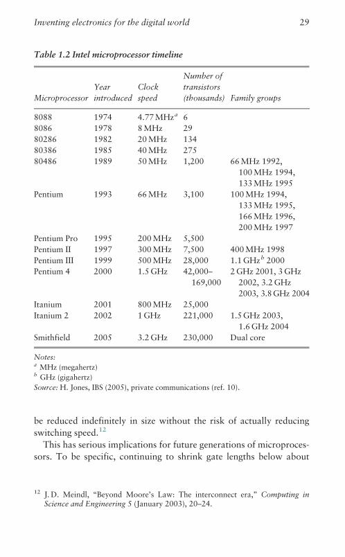
be reduced indefinitely in size without the risk of actually reducing
switching speed.12
This has serious implications for future generations of microproces-
sors. To be specific, continuing to shrink gate lengths below about
Table 1.2 Intel microprocessor timeline
Microprocessor
Year
introduced
Clock
speed
Number of
transistors
(thousands) Family groups
8088 1974 4.77 MHza 6
8086 1978 8 MHz 29
80286 1982 20 MHz 134
80386 1985 40 MHz 275
80486 1989 50 MHz 1,200 66 MHz 1992,
100 MHz 1994,
133 MHz 1995
Pentium 1993 66 MHz 3,100 100 MHz 1994,
133 MHz 1995,
166 MHz 1996,
200 MHz 1997
Pentium Pro 1995 200 MHz 5,500
Pentium II 1997 300 MHz 7,500 400 MHz 1998
Pentium III 1999 500 MHz 28,000 1.1 GHzb 2000
Pentium 4 2000 1.5 GHz 42,000–
169,000
2 GHz 2001, 3 GHz
2002, 3.2 GHz
2003, 3.8 GHz 2004
Itanium 2001 800 MHz 25,000
Itanium 2 2002 1 GHz 221,000 1.5 GHz 2003,
1.6 GHz 2004
Smithfield 2005 3.2 GHz 230,000 Dual core
Notes:a MHz (megahertz)b GHz (gigahertz)
Source: H. Jones, IBS (2005), private communications (ref. 10).
12 J. D. Meindl, ‘‘Beyond Moore’s Law: The interconnect era,’’ Computing inScience and Engineering 5 (January 2003), 20–24.
Inventing electronics for the digital world 29

0.065 micron (65 nm) is going to bring the interconnect problem to the
forefront.
The most practical approach to solving the dilemma to this point has
been the implementation of single-chip multiprocessor architectures. In
effect, we build two or more interconnected computing devices on a
single chip instead of one. This technique, discussed in more detail in
Chapter 2, promises to let designers continue delivering advances in
processing technology and architecture.
Logic gates: Using transistors in digital processing
Up to now we have been considering the physical properties of semi-
conductor structures and their impact on microprocessors. We’ve also
seen how their structures allow them to perform basic electrical func-
tions such as voltage control, amplification, and switching.
We’re now ready to outline the basic principles of digital processing,
and to show how they are embodied by the MOSFETs used to build
computing chips. This is the turning point in modern electronics, when
the electrical characteristics of miniature devices formed an exact
match with the binary mathematics of digital calculation.
Digital computing uses Boolean algebra, which was developed in the
nineteenth century as a tool for logical analysis. The Boolean system is
1
0.1
0.01
Gat
e Le
ngth
(M
icro
ns)
Year1993 1995 1997 1999 2001 2003 2005 2007E 2009E
0.50.35
0.250.18
0.130.09
0.0650.045
0.032
Lithography Advances
Lithography andMaterial Advances
Source: Courtesy of Intel Corporationand UBS estimates
1.4. Gate length reduction over time. Lithography is the technology used to
define the transistor feature size in manufacturing. Copyright # 2005 UBS. All
rights reserved. Reprinted with permission from UBS (ref. 11).
30 Competing for the future

the ultimate in logical simplicity. There are just two states: true or false.
It is a binary system.
In the electronic universe, these two states are represented by the
‘‘bits’’ zero and one. They are produced by two different voltage levels,
for example, zero volts and ten volts.
An electronic system can perform any binary arithmetic operation
(or logic function) by using combinations of only three basic functional
blocks, which are called logic gates. Logic gates control the path of the
signals that execute the desired logical operations.13
The power of the binary system is that we can build up the most
complex computers by simply replicating and interconnecting logic
gates of only three basic types: NOT, AND, OR. To give a sense of
the massive numbers of devices this can involve, the most complex
CMOS microprocessor chips contain more than 100 million intercon-
nected gates, each of which contains an average of four MOSFETs.
The ability to assemble the most complex computers by repeating
such simple structures millions of times is truly remarkable and worthy
of further discussion. Let’s take a closer look at three basic logic gates,
illustrated in Figure 1.5.14 For clarity, we will treat the gates as switches
that turn a light bulb on and off.* An Inverter, or NOT gate (a), changes an input one into an output
zero, and an input zero into an output one. If input signal to the
switch is 1 (positive), as it is in the diagram on the left, the light is off
(zero) because the signal is holding the switch open. When the input
is zero, as is shown on the right, the switch is held closed by an
internal spring and the light bulb is on (1).* The AND gate (b) takes two or more inputs and produces a single
output. This simplistic model shows two switches, A and B, in series.
The output is zero and the light is off, as is shown on the left, if either
or both switches are open; it is 1 and the light is on only if both of the
inputs are 1, as it is on the right.* TheOR gate (c) produces a 1 when any of the inputs are 1, and a zero
when all of the inputs are zero. Only when both switches A and B are
off, as on the left, is the bulb off (zero). When either switch is open, as
13 Z. Kohavi, Switching and finite automata theory (New York: McGraw-Hill, 1978).14 D. Cannon and G. Luecke, Understanding microprocessors (a Texas Instruments
Learning Center Publication, 1979), pp. 3–13.
Inventing electronics for the digital world 31

in the middle and on the right, current flows to the light bulb, turning
it on.
Digital logic also uses combinations of gates for its processing, such
as the NAND gate. This is an inverter connected to an AND gate.
Appendix 1.2 explains how such gates are produced with multiple
transistors.
Switch Pulled Open(“1”)
PowerSource
LightOFF(“0”)
Switch Closed(“0”)
PowerSource
LightON(“1”)
PowerFlows
Switch AOpen (“0”)
PowerSource
LightOFF(“0”)
Switch AClosed (“1”)
PowerSource
LightON(“1”)
PowerFlows
Switch BOpen (“0”)
Switch BClosed (“1”)
Switch A(“0”)
PowerSource
LightOFF(“0”)Switch B
(“0”)
Switch A(“1”)
PowerSource
LightON(“1”)Switch B
(“0”)
Switch A(“0”)
PowerSource
LightON(“1”)Switch B
(“1”)
(a) Simple NOT Gate (Inverter)
(b) Simple AND Gate
(c) Simple OR Gate
1.5. The three basic gates. (a) The NOT gate (inverter); (b) the AND gate; and
(c) the OR gate. Courtesy of Texas Instruments (ref. 14).
32 Competing for the future

Power dissipation: The crucial role of CMOS
We’ve noted that power dissipation issues are impeding progress toward
further size reductions in transistors, a topic we will explore in more
depth in Chapter 2. But this is actually the second time the semiconduc-
tor industry has found a power dissipation problem standing in the way
of increased transistor density on chips – and solved it brilliantly.
The first time was in the early days of integrated circuit development.
MOSFETs were already the obvious choice as building blocks for logic
gates, but their architecture suffered from a serious flaw. Many of the
transistors were always conducting electricity, even when they were
not switching.
As shown in the example of a two-transistor inverter gate in
Appendix 1.2, one of the MOSFET’s devices was conducting current
even when the other one was completely off and no output was
required. The result was excessive power dissipation.
So while miniaturization of MOSFET transistors made it possible to
put many logic gates on a microprocessor chip, too many of the
transistors would dissipate power even at idle, creating serious over-
heating. This severely limited the number of transistors that could be
used on a single chip.
The problem was solved with the invention of the complementary
metal oxide semiconductor (CMOS) architecture, which reduced
power dissipation enormously.15 With overall power dissipation
much lower, the door was open to massive increases in chip transistor
density, from tens of thousands to many millions.
RCA introduced the first commercial CMOS integrated circuits in
1969. Practically all integrated circuits using MOSFETs are built with
the CMOS architecture.
Giving computers a memory
There would be no computers without the ability to store and rapidly
retrieve massive amounts of digital information. The stored informa-
tion can take the form of software programs or data.
15 For a view of the early work on CMOS, see J. R. Burns, ‘‘Switching response ofcomplementary-symmetry MOS transistor logic circuits,’’ RCA Review 25(1964), 627–661. Wanlass, US Patent 3,356,858, ‘‘Low power stand-by powercomplementary field effect circuitry’’ (December, 1967).
Inventing electronics for the digital world 33

Software programs are stored instructions that tell a computer how
to perform a task: word processors, financial spreadsheets, video edi-
tors, or wireless communications protocols. Data is the information
that is created and manipulated during processing, such as documents,
database tables, image files, and more.
Software and data must be stored within easy reach of the processor.
There are three major media for storing information, each with its own
advantages and drawbacks.
Semiconductor memory offers the fastest access because it is totally
electronic. This benefit has a downside: all solid-state memories
(except FLASH ones) will lose all the information they contain if
cut off from electric power.
Magnetic disks store information on a physical medium where it is
unaffected by power losses. They offer reasonably fast access,
huge capacities, and very low cost per unit of storage. So-called
hard disks are the primary magnetic storage devices, used in
everything from desktop PCs to mainframes. Floppy disks have
been supplanted by optical and solid-state storage. Magnetic tape
is the medium for another class of magnetic storage systems. Tape
is primarily used for storing backup information, an application
where its much slower access time is less of a disadvantage.
Optical disks store data in a form that can be read by laser-based
mechanisms. Originally read-only, they now include write-once
and rewritable CDs and DVDs. They compete with magnetic
media in that they provide permanent storage, but capacities
are lower and optical access times are much slower. Their chief
advantage is that the physical disks are removable, allowing for
exchange of physical media and for inexpensive off-site storage of
valuable data.
MOSFET memory structures
Transistors are remarkably versatile. Nothing better illustrates this
than the fact that, besides being used in logic gates for processing
information, MOSFETs are the building blocks for data storage
devices. These semiconductor devices are more commonly known as
memory, computer memory, or simply RAM (for random access
memory).
34 Competing for the future

Three memory types
The most important class of semiconductor memory is dynamic ran-
dom access memory (DRAM). In a DRAM a charge representing a bit
of data is stored in a single transistor incorporating a special built-in
capacitor. The charge on the capacitor needs to be constantly refreshed
by special circuits. DRAMs offer the largest storage capacity for a given
chip size precisely because they require only a single transistor per cell.
Static random access memories (SRAMs) constitute the second most
important class of charge-storage memory. Instead of a single transis-
tor with an attached capacitor to hold a charge, SRAMs use six tran-
sistors to create the unit cell for storage of a single bit. The basic
concept is that this cell changes its state by having different transistors
turned on or off depending on whether or not a bit is stored there. The
master circuit on the SRAM chip can interrogate each cell and deter-
mine or change its status as required.
SRAMs do not need to have their stored charges refreshed. And
while DRAMs have a storage density four times that of SRAMs for a
given chip area, SRAMs offer important benefits, such as faster access
time, that justify their higher cost in some systems.
DRAMs and SRAMs share one drawback: stored information is
retained only as long as the devices are connected to a power source.
This is not true of the third most important class of semiconductor
memories, which is emerging into greater and greater importance.
Non-volatile memory (the term FLASH memory is more often used)
will store cell charges in practical systems indefinitely, even without being
connected to a power source. (Indefinitely does not mean forever – storage
is reliable within a time period on the order of a few years.) This makes
FLASH memory the first choice for such applications as retaining inform-
ation in a cell phone, for example, which is frequently turned off.
Appendix 1.3 describes the basic principles behind the special
MOSFET structure that makes up the unit cell of such memories.
Since MOSFETs have undergone a radical reduction in size over the
past two decades, chip makers have been able to produce RAM chips
with steadily increasing storage capacities at progressively lower cost.
For example, four memory modules totaling 128 MB of RAM might
have cost over $1,000 in 1990. In 2006 a single module that holds
1 GB, eight times as much memory, sold for under $100.
All memory devices in a digital system work on the same basic
principle. They contain storage sites called cells, each of which can
Inventing electronics for the digital world 35

hold a ‘‘bit’’ of information. All that is needed from a memory cell is the
ability to store (or not store) an electronic charge, which is equivalent
to the presence or absence of a 1 or 0. It’s binary logic at its simplest.
Each cell in a device, or in an array of such devices, has a unique
address, called a memory location. A processor or other circuit can use
that address to access the cell. It then performs either of two operations:* interrogate the cell to obtain the value it is storing, for use in
performing an operation;* change the value as the result of a process or operation.
Magnetic disk storage
The principle of magnetic disk storage dates to the mid-1950s, when
IBM originated the concept of using tiny magnetic regions on the sur-
face of a rotating disk as bit storage locations. The first useful product
appeared in 1960.16
The surface of the disk is coated with a metal oxide, and the read/
write/erase function is performed by an electro-magnetic head. A bit
(one or zero) is written (stored) by a change in the magnetization of a
tiny spot on the disk. Alternatively, the head leaves the bit in place but
simply detects its presence.
The disk rotates at a speed in excess of 4,000 revolutions/minute.
High-performance drives spin at more than twice that speed. The head
never actually touches the magnetic material; instead, it floats very
close to the disk surface.
The storage capacity of disk drives has doubled about every eighteen
months since the late 1950s. This has been accomplished by finding
ways to store a bit on a disk in less and less space, which translates into
lower and lower cost per unit of storage.
Figure 1.6 shows the amazing decline in the cost of a megabyte of
storage between 1958 and 2005.17 The cost per megabyte has dropped
by a factor of ten million!
16 A. S. Hoagland, ‘‘History of magnetic disk storage based on perpendicularmagnetic recording,’’ IEEE Transactions on Magnetics 39 (2003), 1871–1875.
17 Committee on the Fundamentals of Computer Science: Challenges andOpportunities, Computer Science and Telecommunications Board, andNational Research Council of the National Academies, Computer science:Reflections on the field, reflections from the field (Washington, DC: NationalAcademies Press, 2004), p. 90.
36 Competing for the future

This did not happen without overcoming serious technical chal-
lenges. As the heads put bits in smaller magnetic spaces on the disk,
the magnitude of the signal in those spaces, which indicate the presence
or absence of the bits, has gotten smaller as well.
Engineers have managed to design specialized integrated circuits to
read these weak signals with improved reliability at ever-lower costs.
Also, as the heads seek locations on the surface and perform their read/
write/erase functions, sophisticated transistor-based electronic systems
control their movement and manage the data flow.
Other key parameters of disks that have evolved over the years include
faster access time, higher storage densities, and higher data transfer rates.
At one time, magnetic disks were literally the only practical perma-
nent storage medium. Magnetic floppy disks dominated the removable
storage market the way that hard disks controlled the fixed storage
space. This is changing.
FLASH memories are competing with hard drives and floppy drives in
lower-density portable device storage applications. The FLASH structure
has an advantage, in that it is an all-solid-state device with no moving
parts. In addition, the bit density on the chips continues to increase.
1950 1960 1970 1980 1990 2000 2010
Year
Dol
lars
per
Meg
abyt
e (M
B)
1000
10000
100
10
1
0.1
0.01
0.001
0.0001
1.6. Cost per megabyte of magnetic disk storage over time. Reprinted with
permission from Computer science: Reflections on the field, reflections from
the field. Copyright # 2004 by the National Academy of Sciences, courtesy of
the National Academies Press, Washington, DC (ref. 17).
Inventing electronics for the digital world 37

This is another effect of the shrinking of transistor dimensions,
discussed earlier in this chapter. Chips with four gigabits of storage
capacity became commercially available in the year 2006. Such chips
contain about four billion transistors.
However, as of this writing (in 2006), FLASH memory is still over
ten times as costly per unit of storage as magnetic disks. Table 1.3
tracks the price ratio per gigabyte between FLASH memories and
hard disks. Although hard disks are still far less expensive, the differ-
ence is expected to narrow. It is felt that eventually the density of data
on a disk will reach its limit, while FLASH densities will continue
to rise.
Whether or not this happens, it is certainly true that FLASH memory,
in the form of the plug-in USB ‘‘drive,’’ has already replaced the
floppy disk as the medium of choice in the personal removable storage
market. Optical disks are making headway too, and are the only
removable-media option for storing data in multi-GB quantities.
However, their larger form factor puts them at a disadvantage in
portable devices.
Semiconductor laser diodes
Heterojunction semiconductor laser diodes are the devices that enable
optical communications and many other systems. They power laser
printers, read from and write to CDs and DVDs, enable certain medical
procedures, and even provide the light source for the humble laser
pointer so useful in public presentations.
We’ve grown so used to them that we no longer think about what the
word ‘‘laser’’ really means. We just know what lasers do. (For the
Table 1.3 Price per gigabyte (GB) of storage (dollars)
Year Disk drive Flash memory Price ratio
2003 1.50 25.20 16.8
2004 0.81 12.15 15.0
2005 0.42 5.60 13.3
Source: Data collected by H. Jones, IBS (2005), private communications.
38 Competing for the future
record, ‘‘laser’’ is an acronym for ‘‘light amplification by stimulated
emission of radiation.’’)
Appendix 1.5 presents an introduction to the basic concepts behind
laser diodes. For our purposes here we will focus on the fundamentals
behind the enormous progress in semiconductor lasers since the late
1960s.
Semiconductor laser diodes, like MOSFETs, are everywhere, though
there are far fewer of them. Like MOSFETs, semiconductor laser
diodes have undergone a rapid reduction in price as their applications
have proliferated.
Several factors combine to make heterojunction semiconductor
lasers so useful compared to other light sources.* Tiny size, reliability, and very low operating currents.* Emission of monochromatic light energy. The emitted wavelength is
determined by the choice of semiconductor and ranges from the blue
into the far infrared.* Ability to generate a single highly directional beam.* Extraordinary internal efficiency (nearly 100%) in converting elec-
tricity into light.* Ability to tailor properties and control costs accordingly from less
than a dollar a unit to thousands of dollars for the most demanding
requirements.
The heterojunction laser, which replaced earlier devices that per-
formed poorly, was developed independently at RCA Labs,18 the A. F.
Ioffe Physicotechnical Institute in St. Petersburg, Russia,19 and Bell
Labs.20,21
18 H. Kressel and H. Nelson, ‘‘Close-confinement gallium arsenide p-n junctionlasers with reduced optical loss at room temperature,’’ RCA Review 30 (1969),106–114. The first commercial heterojunction lasers were commercially intro-duced by RCA in 1969.
19 Zh. I. Alferov, V. M. Andreev, E. L. Portrisi, and M. K. Trukan, ‘‘AlAs-GaAsheterojunction injection lasers with a low room temperature threshold,’’ SovietPhysical Semiconductor 3 (1970), 1107–1109.
20 I. Hayashi, M. B. Panish, P. W. Foy, and S. Sumski, ‘‘Junction lasers whichoperate continuously at room temperature,’’ Applied Physical Letters 17(1970), 109–111.
21 For a history of laser diode development, see H. Kressel and J. K. Butler,Semiconductor lasers and heterojunction LEDs (New York: Academic Press,1977).
Inventing electronics for the digital world 39

A heterojunction is the interface between two dissimilar semicon-
ductors, whether they are p-type or n-type. In other words, it is a special
case of the p-n junction that has figured so prominently in electronics
since the 1950s.22
By using heterojunctions, it is possible to reduce the active lasing
volume and hence the current needed to operate these devices. Using
entirely different concepts from those applied to shrinking MOSFETs,
this new architecture has made possible benefits similar to those of
miniaturization.
Operating current levels are important in creating practical lasers.
Figure 1.7 shows the historical reduction in the current density needed
to sustain lasing in these devices.23 Operating current density require-
ments have now dropped so low that a penlight battery is quite ade-
quate to power a small laser diode emitting a few milliwatts of
continuous red light.
Because of their low power dissipation and superior emission character-
istics, it is possible to modulate specially constructed heterojunction-
based laser diodes at gigabit/second rates at room temperature. This
makes it possible to create optical communications links operating at
those rates. However, the highest data rate systems (up to 40 Gb/s)
use an electro-optic modulator between the laser diode and the fiber to
produce the optical bit stream.
Nor is their power dissipation a significant problem in fiber optic
systems, although temperature control is provided to keep the lasers
operating within their optimum temperature range. Other major
improvements have been also made in the operating characteristics of
laser diodes to adapt them to many applications.24
Figure 1.8 shows in schematic form what these devices look like.25
Note the light beam emitted from a small region which, in this simple
22 H. Kromer, ‘‘A proposed class of hetero-junction injection lasers,’’ Proceedingsof the IEEE 51 (1963), 1782–1783.
23 Adapted from Kressel and Butler, Semiconductor lasers, p. 4.24 Two publications offer interesting accounts of these advances: M. Dutta and
M. S. Stroscio (eds.), Advances in semiconductor lasers and applications tooptoelectronics (Singapore: World Scientific, 2000) and ‘‘Special issue on semi-conductor lasers,’’ IEEE Journal of Selected Topics in Quantum Electronics 9(September/October, 2003).
25 H. Kressel, I. Ladany, M. Ettenberg, and H. Lockwood, ‘‘Light sources,’’ PhysicsToday 29 (May 1976), 45.
40 Competing for the future

structure, is only 10 microns wide. Figure 1.9 shows how tiny laser
diodes are when fully packaged as a general purpose laser emitting a
beam through the front glass platelet. A device this size can emit
hundreds of watts of pulsed power!
105
104
103
102
Thr
esho
ld C
urre
nt D
ensi
ty (
A/c
m2 )
Year
1965 1967 1969 1971 1973 1975
Homojunction Lasers
Heterojunction Lasers
1.7. Historical trend in the gallium arsenide and heterojunction aluminum
gallium arsenide laser diode threshold current density at room temperature.
Technological improvements after 1975 focused on heterojunction lasers of
indium gallium arsenide phosphide emitting at 1.55 microns for fiber optic
systems. Reprinted from Semiconductor lasers and heterojunction LEDs.
Copyright # 1977, with permission from Elsevier (ref. 23).
Inventing electronics for the digital world 41

A key requirement for systems: Device reliability
We should not leave the subject of the rapid progress made in developing
practical electronic devices without reflecting on what it tells us about
the gap between new device concepts and their practical utility. Perhaps
the most important lesson we can learn has to do with device reliability.
Practical consumer electronic systems can tolerate device operating
lifetimes of tens of thousands of hours. This is not the case for com-
munications systems. In these applications predicted device lifetimes
must be well in excess of ten years. For undersea communications links,
lifetimes have to be a lot longer.
The early history of all electronic devices, and particularly of laser
diodes, was plagued by erratic lifetimes. A thousand hours of life was
noted as a great achievement. This problem was rarely discussed in the
published papers that described the wonderful properties of a new
structure.
In fact, it was not unusual for researchers to report test data on a new
device without mentioning that the device lasted just long enough to
1.8. Schematic of a simple double heterojunction laser diode structure showing
light beam emitted under stripe contact 10 microns wide. The front and back of
the structure constitute the two surfaces of the Fabry-Perot cavity. Reprinted
with permission from Physics Today. Copyright # 1976, American Institute of
Physics (ref. 25).
42 Competing for the future
Metallic Stripe Contact
n
p
10 Microns
Ground
Cleaved Facet
Current Distribution
Lasing Region Thickness d
SiO2 Insulator
Substrate
d

make the measurements. For example, early MOSFETs degraded
rapidly because of impurities, such as sodium, in the oxide layers.
Laser diode degradation was a complex phenomenon which turned
out to be largely due to crystalline defects that increased in density as
the device operated, eventually leading to its destruction.26
Driven by the importance of commercial value, the work at RCA Labs
and other commercial laboratories was heavily focused on improving
device reliability. It took years of patient work by a number of labora-
tories to create devices that offered the many years of reliable operation
needed in practical systems. This work involved painstaking research on
atomic-level effects of temperature, stress, and operating currents.
We take it for granted that ‘‘solid-state’’ means ‘‘forever’’ when
compared to vacuum tubes. This only proved to be the case after
many years of first-class research and development.
1.9. A laser diode packaged in a metal case with a glass face for the emitted
radiation.
26 Kressel and Butler, Semiconductor lasers.
Inventing electronics for the digital world 43

Optical fibers and modern digital communications
An optical communications system uses lasers, photodetectors, and
glass fibers to transport digital data in the form of short light pulses
over very long distances. Of the three components in this basic system,
the only one not built around solid-state electronics and p-n junctions
or heterojunctions is the transport medium, the optical fiber.
We have already explored the transformational technology of laser
diodes, and Appendix 1.7 offers a brief primer on photodetectors. But
no consideration of the innovations that formed the digital computing
and communications landscape would be complete without including
the development of optical fibers.27
Simply put, the infrastructure that enables wideband digital commu-
nications exists only because of glass fibers. Their extraordinary ability
to carry data at high speeds over long distances is the reason we have
the Internet. It is also why such high-capacity data transmission ser-
vices as video are possible over the Internet.
The glass backbone of digital communications
Up to now we’ve been focused on digital data primarily in the form of
electrical signals, routed through electronic devices such as transistors
and integrated circuits. Optical fibers, however, are pipes that carry
data not as electricity, but as bursts of laser light.
The data originates as rapidly alternating voltages representing
streams of digital bits. The voltages turn a laser diode on and off very
quickly, producing laser pulses that faithfully replicate the ones and
zeros of the data. The optical pulses enter the fiber optic cables. At the
receiving end, p-n junction light sensors regenerate the original elec-
trical pulses, which provide input to signal processing systems.
The concept and early demonstration of using fiber optics for
communications over long distances was explored in the mid-1960s
in the UK at the Standard Telecommunications Laboratory of ITT,
27 For a good succinct historical overview, see T. E. Bell, ‘‘Fiber optics,’’ IEEESpectrum (November 1988), 97–102. For a longer history, see J. Hecht, Cityof light: The story of fiber optics (New York: Oxford University Press, April1999).
44 Competing for the future

as reported in a publication by Dr. Charles Kao and Dr. George
Hockam.28
Commercial optical fibers trace their origins to the late 1960s, when
Corning scientists invented thin glass fibers of extraordinary purity
that could faithfully and reliably transmit short optical pulses over
long distances.29 This achievement required many innovations on the
part of the scientists, plus some fortunate but unplanned coincidences.
In one such coincidence, nature helped solve a crucial difficulty. The
scientists discovered glass compositions that happened to absorb very
little light at precisely the near-infrared wavelength (1.55 microns)
where InGaAsP heterojunction laser diodes were designed to operate.30
Figure 1.10 shows how optical fiber transmission loss was reduced
over a ten-year period.31 Between 1973 and 1983 signal loss due to
light absorption was reduced from 100 dB (decibels) per kilometer to
under 0.2 dB per kilometer (at about 1.55 microns), approaching the
theoretical limits set by the properties of glass.
This low value, combined with the development of excellent
InGaAsP heterojunction laser diodes emitting in the appropriate spec-
tral region, enabled fiber links many kilometers long that could carry
high data rates with acceptable transmission loss.
Another problem involved sending short pulses over long distances
with minimal distortion. In a plain glass fiber, an input pulse (repre-
senting a bit of information) will spread out as the light propagates
through the fiber. Eventually the shape of the pulse flattens out. This
makes it impossible to determine that a bit of information has been
transmitted.
The answer was to design the refractive index profile of the glass
fiber to produce an internal ‘‘lensing’’ effect that keeps the pulses
coherent. Of course, this property had to be consistent with low-cost
28 C. K. Kao and G. Hockham, ‘‘Dielectric fiber surface waveguides for opticalfrequencies,’’ Proceedings of the IEEE 113 (1966), 1151–1158.
29 For a review of this development see R. D. Maurer, ‘‘Glass fibers for opticalcommunications,’’ Proceedings of the IEEE 61 (1973), 452–462. A survey ofrecent progress can be found in a special issue of the Journal of LightwaveTechnology 23 (2005), 3423–3956.
30 B. E. A. Saleh and M. C. Teich, Fundamentals of photonics (New York: JohnWiley & Sons, Inc., 1991), pp. 592–643.
31 C. Kumar and N. Patel, ‘‘Lasers in communications and information proces-sing,’’ in Lasers: Invention to applications, J. H. Ausubel and D. Langford (eds.)(Washington, DC: National Academies Press, 1987), p. 48.
Inventing electronics for the digital world 45

mass production techniques. Appendix 1.8 discusses this aspect of the
technology.
It was also necessary to develop cladding techniques that protect the
delicate fibers as they are deployed over land or undersea. All these
objectives were met, and the fiber optic industry was born.
The cost of fiber optic cables has dropped radically over the last
two decades. This is the result of high-volume fiber production in
huge plants. Figure 1.11 tracks the price per meter of single-mode
fiber since 1983.32
During this period the cost of the semiconductor components used
in optical communications was drastically declining as well. The
100
10
1
0.1
1973
Opt
ical
Los
s dB
/km
Wavelength (micron)
0.8 1.0 1.2 1.4 1.6
1976
1983
Theory
1.10. Spectral loss data for silica optical fibers over time. The heterojunction
lasers used in communications systems emit in the 1.55 microns region.
Reprinted with permission from Lasers: Invention to applications. Copyright
# 1987 by the National Academy of Sciences, courtesy of the National
Academies Press, Washington, DC (ref. 31).
32 Figure courtesy KMI Research, www.kmiresearch.com.
46 Competing for the future

combination of plummeting system costs combined with increasing
demand drove the global deployment of fiber optic communications.
Now, just a quarter-century after low-loss fiber was first demonstrated,
universal availability of high-speed communications for voice, data, and
video is practically taken for granted. The world will never be the same.33
Semiconductor imagers and displays: Visualizing information
We began this chapter by recounting the transition from vacuum tubes
to solid-state devices. Our focus since then has been on digital innova-
tions for processing, storing, and communicating information: transis-
tors, integrated circuits, lasers, and more.
But humans are analog. We can’t handle digital data in electronic
form the way a computer chip can. We actually need to see the input
and output of the process.
0.70
0.60
0.50
0.40
0.30
0.20
0.10
0.00
Year
Cabled Fiber
Fiber
Dol
lars
Per
Fib
er-M
eter
Source: KMI Research
1983
2006
2005
2004
2003
2002
2001
2000
1999
1998
1997
1996
1995
1994
1993
1992
1991
1990
1989
1988
1987
1986
198419
85
1.11. Historical reduction in the cost of a fiber-meter of single-mode optical
fiber. Figure courtesy of KMI Research, www.kmiresearch.com (ref. 32).
33 ‘‘Technologies for next-generation optical systems,’’ special issue of theProceedings of the IEEE 94 (2006), 869–1035.
Inventing electronics for the digital world 47

Here, too, electronic innovation has created more efficient solutions.
The cameras we use to capture the physical world are now completely
solid-state. Vacuum tube-based video camera imagers have been
replaced by semiconductor imagers.
On the display side, the bulbous CRT picture tube, derived from a
device invented by Karl Ferdinand Braun in 1897 and used in televisions
for over half a century, is quickly giving ground to flat-panel alternatives.
To close out our survey of the devices that underlie the digital world,
then, we will briefly survey the technology behind solid-state imagers
and displays.
Digital image capture: CMOS camera sensors
The original semiconductor imagers used charge-coupled device (CCD)
technology, which requires unique manufacturing processes. CCDs are
still used in many high-end digital cameras and camcorders, but they are
now facing a serious challenge from imagers built with CMOS-based
technology.
CMOS imagers were once confined to applications where quality was
less important than price. For the past few years, however, they have
offered image quality every bit as good as all but the best CCDs. They
still maintain their cost advantage, too, because they can be manufac-
tured on standard IC production lines (with some modifications).
This repeats the pattern followed by all other digital semiconductor
devices: steadily increasing performance at a rapidly decreasing price.
The technology that enables this progress is the by-now familiar
MOSFET structure.
Basically, an imager consists of an array of photodiodes that gener-
ates an electric signal proportional to the intensity of the light that
strikes it.34 Each photodiode represents one pixel (picture element), the
dots that make up the final image. Figure 1.12a compares the CMOS
approach to that of the CCD.35
In Figure 1.12a, the CCD architecture appears on the left. The
photodiodes sense light, generate electrical signals in response, and
34 Information on CMOS imagers is adapted from A. El Gamal and H. Eltoukhy,‘‘CMOS image sensors,’’ IEEE Circuits and Devices 21 (2005), 6–12.
35 D. Litwiller, ‘‘CMOS vs. CCD: Maturing technologies, maturing markets,’’Photonics Spectra (August 2005), 55.
48 Competing for the future

transmit the signals (electronic charge) via a ‘‘bucket brigade’’ pixel-to-
pixel transfer process. This is an analog method of transmitting the
signal level (i.e., the number of electrons generated in a pixel) to the
periphery of the chip, where the signals are processed.
On the right we see a CMOS-based imager. Each pixel has its own
processing circuitry, consisting of MOSFETs, the output of which is sent
directly to the periphery of the chip, and from there to the camera system.
Figure 1.12b is a diagram of the elements that constitute a digital
camera.36 As indicated, the CMOS imager chip actually incorporates
many of the functions of a camera system. With a CCD, all of these
functions have to be implemented separately. CMOS obviously repre-
sents a potentially large cost advantage to the camera manufacturer.
The block labeled ‘‘color filters’’ merits some attention. Regardless of
the type of imager, the photodiodes (or pixel sites) that convert the
detected light into an electric charge are monochrome. In order to
image color pictures, the chip has to use three adjacent light sensors,
one each for red, green, or blue light, for every imaging unit. For this
reason the chip is covered with a regular pattern of red, green, and blue
filters, so that each element of the triad can respond to just one color.
Light to ElectronConversion
Charge toVoltage
Conversion
CCD CMOS
Source: DALSA
1.12a. Two types of imagers. Left, CCD and right, CMOS-based with MOSFETs
incorporated into pixels. Reprinted with permission from D. Litwiller, DALSA
(ref. 35).
36 Litwiller, ‘‘CMOS vs. CCD,’’ 56.
Inventing electronics for the digital world 49
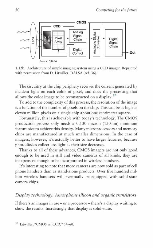
The circuitry at the chip periphery receives the current generated by
incident light on each color of pixel, and does the processing that
allows the color image to be reconstructed on a display.37
To add to the complexity of this process, the resolution of the image
is a function of the number of pixels on the chip. This can be as high as
eleven million pixels on a single chip about one centimeter square.
Fortunately, this is achievable with today’s technology. The CMOS
production process only needs a 0.130 micron (130 nm) minimum
feature size to achieve this density. Many microprocessors and memory
chips are manufactured at much smaller dimensions. In the case of
imagers, however, it’s actually better to have larger features, because
photodiodes collect less light as their size decreases.
Thanks to all of these advances, CMOS imagers are not only good
enough to be used in still and video cameras of all kinds, they are
inexpensive enough to be incorporated in wireless handsets.
It’s interesting to note that more cameras are now sold as part of cell
phone handsets than as stand-alone products. Over five hundred mil-
lion wireless handsets will eventually be equipped with solid-state
camera chips.
Display technology: Amorphous silicon and organic transistors
If there’s an imager in use – or a processor – there’s a display waiting to
show the results. Increasingly that display is solid-state.
DigitalSignalChain
CMOSCCD
OutAna
log
to D
igita
lC
onve
rter
AnalogSignalChain
Lens
DigitalControl
Source: DALSA
PixelArray
1.12b. Architecture of simple imaging system using a CCD imager. Reprinted
with permission from D. Litwiller, DALSA (ref. 36).
37 Litwiller, ‘‘CMOS vs. CCD,’’ 54–60.
50 Competing for the future

A technical discussion of liquid crystal displays (LCDs) appears in
Appendix 1.9. For our purposes in this chapter, however, the most
interesting aspect of displays is the materials from which they are made.
So far our discussion on semiconductors has dealt with crystalline
forms. These followed an historical evolution from germanium, to
silicon, to compound semiconductors whose special properties gave
them particular value in electro-optic devices.
But two other classes of materials have found their way into large-
scale device applications: amorphous silicon and polymers.38 These
materials, produced as thin films, find their most important applica-
tions in solid-state flat-panel displays. We will consider amorphous
silicon first.
Amorphous silicon and LCDs
In contrast to crystalline materials, which have well-ordered atomic
arrangements, amorphous materials can be thought of as similar to
glass, where atomic arrangements are only of short order. The resulting
lack of a regular form (such as the lattice structure of a crystal) is the
source of the designation amorphous.
The crystalline silicon wafers on which integrated circuits are built
do not lend themselves to integration with materials such as the liquid
crystals used for displays, or for use as a means of producing inexpen-
sive electronic devices. It would obviously be desirable just to deposit a
thin film of silicon on glass (at a temperature that did not melt the glass)
and then build display circuits from that.
When research was begun to develop such a process in the early
1980s, it was found that the silicon deposited at low temperatures is
actually an amorphous film. It had interesting applications, although it
could not serve as replacement for the ‘‘classic’’ silicon crystals used to
build integrated circuits.
The first application of amorphous silicon was in solar cells (for solar
power generation). These devices could be built cheaply, helping to
make up for their much lower efficiency compared to standard silicon
crystals.
It was also discovered that one could fabricate large arrays of ‘‘infer-
ior’’ transistors with this material. These transistors exhibited very
38 P. Yam, ‘‘Plastics get wired,’’ in a special issue of Scientific American: The solid-state century (1997), 91–96.
Inventing electronics for the digital world 51

slow switching speeds, yet were still useful in limited applications far
removed from microprocessors. Techniques to improve the electrical
quality of the thin silicon films include heating them to improve their
structures.
Thin-film silicon electronics were the key to the commercial manu-
facturing of large flat-panel liquid crystal displays.39 The thin-film sili-
con devices incorporated in the display provided just the right level of
pixel switching capability to make practical displays at acceptable cost.
The LCD flat-screen display opened up brand new applications, such
as laptop computers, that were totally impractical with CRTs (picture
tubes). Once again solid-state devices provided a more practical alter-
native to vacuum tube technology.
Figure 1.13 shows that the turning point in the market transition
from tube-based to flat displays occurred in 2002.40 The figures cited
include all display-based devices, including PDAs, cell phones, compu-
ters, and TVs.
Even in television receivers, formerly a bastion of CRTs because of
their lower price point, the dominance of the tubes is rapidly fading as
LCDs and other semiconductor displays take hold. Figure 1.14 shows
the dramatic price reductions for large LCD TV receiver displays that
began in 2003, turning them from a luxury item into a common con-
sumer product.41
Polymers and OLEDs
Polymers are emerging as important devices for special applications in
displays, light emitters, and even solar power generation (solar cells).42
39 For a review of amorphous silicon properties and applications, see M. S. Shur,H. C. Slade, T. Ytterdal, L. Wang, Z. Xu, K. Aflatooni, Y. Byun, Y. Chen,M. Froggatt, A. Krishnan, P. Mei, H. Meiling, B.-H. Min, A. Nathan, S. Sherman,M. Stewart, and S. Theiss, ‘‘Modeling and scaling of Si:H and poly-Si thin filmtransistors,’’ Materials Research Society Symposium Proceedings 467 (1997),831–842.
40 Special technology area review on displays, a report of Department of Defense,Advisory Group on Electron Devices, Working Group C (Electro-Optics) (Officeof the Under Secretary of Defense, Acquisition, Technology and Logistics,Washington, DC, March 2004), p. 16.
41 H. Jones, IBS (2005), private communications.42 For display applications see H. Hoppe and N. S. Sariciftci, ‘‘Organic solar cells:
An overview,’’ Journal of Material Research 19 (2004), 19–24. Applications tosolar cells are reviewed by S. R. Forrest, ‘‘The path to ubiquitous and low-costorganic electronic appliances on plastic,’’ Nature 428 (2004), 911–920.
52 Competing for the future
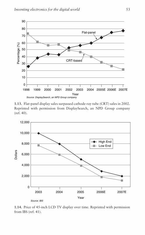
90
80
70
60
50
40
30
20
10
0
Per
cent
age
(%)
Flat-panel
CRT-based
Year
1998 1999 2000 2001 2002 2003 2004 2005E 2006E 2007E
Source: DisplaySearch, an NPD Group company
1.13. Flat-panel display sales surpassed cathode-ray tube (CRT) sales in 2002.
Reprinted with permission from DisplaySearch, an NPD Group company
(ref. 40).
12,000
10,000
8,000
6,000
4,000
2,000
0
Dol
lars
Year
2003 2004 2005 2006E 2007E
High EndLow End
Source: IBS
1.14. Price of 45-inch LCD TV display over time. Reprinted with permission
from IBS (ref. 41).
Inventing electronics for the digital world 53

In the course of investigating other kinds of semiconducting materials,
researchers discovered that certain polymers could be used to construct
thin-film transistors with limited properties.43
It was also discovered that polymers could be used to create thin-film
light-emitting devices with emission in the blue, green, and red, suitable
for manufacturing flat-panel displays. These are generally called
OLEDs (organic light emitting diodes), though they are known as
organic EL (electroluminescent) displays in Japan.44
The ability to use polymer-based electronics is expected to have a far-
reaching impact on applications such as large-area displays. With
flexible substrates replacing glass as the base material, large displays
will become more portable, less fragile, and less expensive.
Other advantages of OLEDs include lower power consumption and
potentially lower production costs. Several companies are racing to
develop a method for printing the transistors and diodes on a contin-
uous roll of thin plastic, which could enable ‘‘video wallpaper’’ at
extremely low prices.
Foundations for digital systems
The proliferation of new electronic devices that started in the late
1940s was the first wave of technology in the flood tide of digital
products that still engulfs us. These fundamental components washed
away previous assumptions about how people could create and use
technology to interact with information.
The major impact of these devices wasn’t their ability to miniaturize
products that had previously been unwieldy, power-hungry, and lim-
ited in functionality. It wasn’t the potential to achieve higher perfor-
mance at drastically lower prices either, though that was certainly
important.
It was the promise of huge, powerful systems built on tiny elements,
rather like living organisms composed of invisible atoms. Each of these
devices plays a role in creating the immense power of the computing
43 H. Sirringhaus, N. Tessler, and R. H. Friend, ‘‘Integrated optoelectronic devicesbased on conjugated polymers.’’ Science 280 (1998), 1741–1744.
44 J. H. Burroughes, D. D. C. Bradley, A. R. Brown, R. N. Marks, K. Mackay,R. H. Friend, P. L. Burns, and A. G. Holmes, ‘‘Light-emitting diodes based onconjugated polymers,’’ Nature 347 (1990), 539–541.
54 Competing for the future

and communications systems that affect human life in every corner of
the world.
In Chapter 2, we will see how innovation at the system level changed
the world to a digital environment and helped to create the global
village. It all started, however, with a handful of tiny devices, devel-
oped in corporate labs long ago.
Inventing electronics for the digital world 55

2 Building digital systems
BY the early 1970s, most of the basic electronic development
that made digital technology feasible was in place. One great
burst of innovation over two decades had produced the
transistor, the p-n junction, the CMOS process for integrated circuits,
magnetic disk storage, heterojunction semiconductor lasers, fiber optic
communications, and semiconductor imagers and displays.
The speed with which researchers put the new devices to practical
use was almost as remarkable. They quickly developed an array of
systems that gather, process, and transmit information.
The most visible example was the computer. In 1982, Time magazine
focused popular attention on the computer’s importance by naming it
‘‘Machine of the Year,’’ a widely discussed departure from the ‘‘Man of
the Year’’ honor the magazine had bestowed for over sixty years.
Since then computers have become a part of our lives. Smaller, more
powerful microprocessors and supporting devices, combined with
plummeting costs, have sparked an endless stream of new computer-
ized consumer and industrial products.
However, while the computer has been central to the Information
Age, the most revolutionary transformation has taken place in commu-
nications. Data transmission, once limited to 300 bits per second on
analog phone lines, now uses digital links to carry multi-megabit per
second data streams. Voice has gone digital and wireless. The Internet
has metamorphosed in just ten years from an ‘‘insider’’ network for
scientists to an indispensable, ubiquitous communications backbone
linking billions of people around the globe.
And both computing and communications have been enabled by
advances in software architecture.
This chapter summarizes the development of computing systems;
examines wired and wireless communication for voice, data, and
video; and explores the software innovations that endow hardware
with intelligence and purpose.
56
It also looks at how the explosive growth of digital systems is chan-
ging the business and economic landscape, especially in communica-
tions and software. Customers are no longer locked into telephone
companies for voice service, and companies now have alternatives to
proprietary software.
Cheap computing and universal high-speed communications have an
impact on society which is far beyond the spheres of technology and
industry. This chapter lays the groundwork for our later exploration of
the socioeconomic implications of the digital revolution.
Computing systems: Data processing made affordable
Personal computers are now so commonplace that it’s easy to forget
how exotic – and forbiddingly expensive – they once were. In 1990, a
desktop PC with an 8 MHz processor, 128 Kbytes of memory, and an
arcane command-line operating system cost $4,000. Fifteen years later
a pocket-sized personal digital assistant with a user-friendly touch-
screen interface offers more memory and a speedier, more powerful
processor for $99.
This astonishing progress is typical of the digital revolution: as
products become smaller, faster, more powerful, and easier to use,
they also get cheaper – much cheaper. It’s no accident that during the
past decade computing has become a normal activity, even in under-
developed parts of the world.
None of this would have happened if electronics had not made the
leap from analog to digital. Analog electronics were not a practical
platform for large-scale computing and communications systems.
Readers interested in a technical explanation for this will find it in
Appendix 2.1, ‘‘The demise of analog computers,’’ which also describes
how digital systems interact with the analog world.
For our purposes, the important thing to keep in mind is the scal-
ability of digital technology. Scalability allows designers to put high
functionality into tiny devices, then assemble them into powerful,
relatively inexpensive computing systems.
Since the microprocessor is at the center of all modern digital sys-
tems, we will start by focusing on its technology and applications. Later
in the chapter, when we look at the communications and software
industries that the microprocessor made possible, the true extent of
its economic impact will become apparent.
Building digital systems 57

Microprocessors: Affordable processing power
It’s worth repeating that digital computation is conceptually simple. In
Chapter 1 we saw that combinations of only three basic logic gates
(NOT, AND, and OR) are needed to perform any logic or arithmetic
function. All you need is a processing unit with enough gates and
adequate access to memory. The more gates you have, the faster and
more powerful the processor becomes. This scalability is the biggest
advantage of digital technology.
Until the 1970s, getting enough gates was a costly proposition. The
central processing units (CPUs) in computers were built around silicon
integrated circuits containing custom-designed logic gate arrays. This
made them very expensive. The situation changed dramatically with
Intel’s introduction of the microprocessor in 1971.
Gordon Moore, co-founder of Intel, saw the microprocessor as an
alternative to building logic for each individual application. He
described the device as ‘‘a broadly applicable, complex integrated
logic circuit that can be produced in huge volume, and hence [at] low
cost, and that utilizes the technology advantageously.’’1
Experts of that time expected that microprocessors would be used to
control traffic lights, manage automobile functions, and perform other
mundane applications.2 These predictions have proven accurate.
However, nobody envisioned the major role of microprocessors:
enabling ever more powerful, ever cheaper PCs. And no one foresaw that
the mainframes of the 1970s would be largely replaced by microprocessor-
powered computers.
Moore’s forecast of huge production volumes has been fulfilled
beyond anything he could have predicted. Today microprocessors are
everywhere, at all levels of performance. There are hundreds at work
for each human being in the world.
They coexist with many other types of digital and analog/digital chips
to make up complete systems. Figure 2.1 shows sales of semiconductors
worldwide since 1999, broken out by type of chip and total revenues.3
1 G. E. Moore, ‘‘Microprocessors and integrated electronics technology,’’ Proceedingsof the IEEE 64 (1976), 837–841.
2 A. J. Nichols, ‘‘An overview of microprocessor applications,’’ Proceedings of theIEEE 64 (1976), 951–953.
3 Data from H. Jones, IBS (2005), private communications.
58 Competing for the future

Microprocessors command an important share, yet other types of ICs
exhibit strong sales as well.
The great majority of these ICs use MOSFETs, described in Chapter 1,
to enable digital and analog functions. Because of this they benefit from
the same progress in manufacturing technology that has steadily
increased the power and reduced the size and cost of microprocessors.
Flexible, scalable processing
While the other IC types are vitally important, it’s still the micropro-
cessor that established the dominance of digital electronics. In one form
or another it is at the heart of every digital product sold today.
The scalability of its architecture in terms of instruction size makes it
the ideal device for digital computation. Designers can choose a micro-
processor with the level of power and sophistication they need, at a
price point that makes sense for the final product.
Depending on its power, a microprocessor can vary in cost from
under a dollar for an 8-bit unit to hundreds of dollars for the high-end
300
250
200
150
100
50
0
Year
Bill
ions
of D
olla
rs
MOS Memory
Analog
MOS Logic
MOS Micro
1999 2000 2001 2002 2003 2004 2005 2006E 2007E 2008E 2009E 2010E
Source: IBS
2.1. Integrated circuit market segments between 1999 and 2005, and projected
to 2010. Microprocessors are included in the ‘‘MOS Micro’’ segment (from
IBS, ref. 3).
Building digital systems 59
64-bit unit used in the most complex systems. Each of these devices
contains the major elements of a computer, small or large.
As the speed and performance of microprocessors have improved,
and their cost has dropped, they have found their way into everything
from toys to washing machines to large computers. For example, over
fifty microprocessors are found in every automobile,4 and that number
is rising (see Chapter 8).
Not all of these devices are full-function, stand-alone products such
as those sold by Intel and AMD. Many are ‘‘cores,’’ smaller processors
with limited functionality embedded on a larger chip.
A core provides the computing engine for ICs containing a system on
a chip (SoC). Designers use SoCs to carry out tightly defined applica-
tions, such as managing the data flow in cell phones.
A stand-alone 64-bit microprocessor with fifty million gates is
clearly overkill for such a simple application, and it draws too much
power. A 32-bit core embedded in an onboard SoC chip, on the other
hand, may have only 100,000 gates. That’s enough power to do the job,
with little additional battery drain, and it costs much less than the
stand-alone IC.
When smaller is not better
Every new generation of microprocessors has offered higher perfor-
mance at a lower price, often in a smaller package. That progression
has driven the decline in system costs from $4,000 PCs to $99 PDAs
(personal digital assistants). But how long can these dramatic advances
continue?
Moore’s Law, described in Chapter 1, predicted that the processing
power of ICs would double every two years with no increase in price.
This was based on the rate at which MOSFETs were being shrunk in
size (Appendix 1.1), permitting more logic gates on each chip. As
Table 1.2 showed us, market leader Intel has achieved dramatic
increases in chip densities over the years.
Today, however, MOSFETs are approaching the practical limits of
miniaturization. Making them smaller once meant getting more speed
4 R. Kline, ‘‘An overview of twenty-five years of electrical and electronics engineer-ing in the Proceedings of the IEEE, 1963–1987,’’ Proceedings of the IEEE 93(2005), 2170–2187.
60 Competing for the future

for less money. But as MOSFET gate dimensions shrink well below the
micron (100 nm) level, and the density of transistors on the chip con-
tinues to increase, we begin to bump up against physical constraints on
performance.
In addition, as we observed in Chapter 1, the connections among IC
components have become so thin that they are slowing on-chip com-
munications. More ominously, the combination of increased density of
transistors on the chip and higher clock rates (speeds) is generating
severe power dissipation problems. This has the potential to raise the
operating temperatures of chips above a safe level.5
Figure 2.2 shows how both static and switching sources of power
dissipation have evolved in advanced processors.6 Since 2002, when
0.09 micron (90 nm) gate spacing became practical, static current leak-
age from the rising number of transistors on a chip became more
significant as a source of power dissipation than switching frequency.
(This assumes that the transistors are switched at their theoretical
limits.)
With clock rates exceeding 3 GHz,7 a single high-end microproces-
sor can easily surpass 100 watts of power dissipation. For most appli-
cations, a value of thirty watts or less is needed, and portable devices
require considerably lower values to prevent excess battery drain. At
100 watts it’s also hard to keep the device from overheating without
water-cooling.
Microprocessor architects are learning to control power dissipation
by designing the chip so that only part of the device is functioning at
any one time. Other sectors stay in stand-by mode, waiting for activa-
tion as needed. Designers also minimize power dissipation by mixing
different size transistors on a chip, using the smallest and fastest devices
only in critical areas. New materials can also help. But these
approaches are only partial solutions.
5 A comprehensive review of this situation can be found in J. P. Uyemura,Introduction to VLSI circuits and systems (New York: John Wiley & Sons,2002), pp. 257–259; and R. Goering, ‘‘Leakage takes priority at 65 nm,’’ EETimes (January 16, 2006), 47–48.
6 J. Gea-Banacloche and L. B. Kish, ‘‘Future directions in electronic computing andinformation processing,’’Proceedings of the IEEE 93 (2005), 1858–1863.
7 From Gea-Banacloche and Kish, ‘‘Future directions in electronic computing,’’1858–1863.
Building digital systems 61

Breathing room: Parallel processors
It appears, then, that the strategy of squeezing more performance and
lower cost out of a microprocessor by continuously shrinking the size
of transistors in order to increase their speed and density is reaching its
physical limits. However, there is another answer: parallel processors.
Parallel processing has long been done by building a single system
around multiple discrete processors.8 Now, however, Intel, AMD, and
others are using well-known parallel processing concepts in single-
chip, multi-core implementations.
In these configurations each core has its own processing resources, but
shares access to centralized control functions, including instructions
102
101
100
10–1
10–2
10–3
Year
Pow
er (
W)
1980 1985 1990 1995 2000 2005 2010
Processor SwitchingPower Dissipation
Power Dissipation Dueto Leakage Current
2.2. Extrapolation (dashed lines) of processor switching power dissipation and
leakage current-related power dissipation. Fit line replotted (solid line) and
extrapolated (dashed line) with G. Moore’s presentation in 2003 (see ref. 3).
The crossing of the extrapolated lines indicates that the leakage current power
dissipation is progressively dominant from around 2002–2003. Copyright #
2005 IEEE (from Gea-Banacloche and Kish, ‘‘Future directions in electronic
computing,’’ ref. 6).
8 See J. L. Hennessy and D. A. Patterson, Computer architecture – a quantitativeapproach, 3rd edition (Amsterdam: Morgan Kaufman Publishers, 2003),pp. 636–659.
62 Competing for the future

and data storage. Since the individual processors have significant
autonomy in the execution of instructions, this arrangement reduces
the requirement for high-speed on-chip communications. The problem
of processing speed being slowed down by the thin metal lines between
transistors is alleviated as well.
For operations where parallel processing is easily implemented, a
dual-processor chip can deliver about 70 percent more throughput than
a single-processor chip running at the same clock rate (speed). The
price disparity between the two chips is very small. By anyone’s stan-
dards, that’s an impressive boost in price/performance ratio.
The problems with parallel processing
Parallel processing is neither simple nor a panacea. To achieve its full
benefit, the software has to be designed to take advantage of the
subdivision of computing tasks into parallel tracks. This works well
for such applications as the analysis of data packets in networks and
images. Other computing tasks are more difficult to divide, and the
benefits of using parallel processing for these applications are less clear.
In addition, it can be difficult to convert software programs designed
for single microprocessors to a multi-core environment.9 It is estimated
that 100 billion lines of code exist for the X86 Intel microprocessor
family. Conversion of all this software may never happen, but propo-
nents of parallel processors argue that new software designs are inevi-
table anyway if computing costs are to continue to decline at historical
rates.10
There is little doubt, on the hardware side at least, that parallel
processing is the wave of the future. Published reports suggest that
Intel expects that 40 percent of all desktop computers, 70 percent of all
mobile devices, and 85 percent of all servers produced after 2006 will
use multi-core processor chips.11
So at least for the foreseeable future each new generation of comput-
ing systems will continue to be smaller, more powerful, and cheaper,
thanks to a combination of reduced feature size and parallel processing.
9 K. Krewell, ‘‘Software grapples with multicore,’’ Microprocessor Design 19(December 2005), 1–4.
10 P. Hester, CTO of AMD, quoted by D. Lammers, ‘‘New microarchitectures,from the ground up,’’ EE Times (January 16, 2006), 20.
11 R. Kay and P. Thibodeau, ‘‘Counting cores: the newest processors cram two ormore CPUs onto a single chip,’’ Computerworld (June 20, 2005), 48–54.
Building digital systems 63
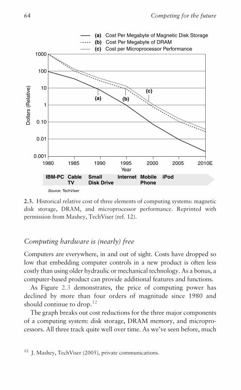
Computing hardware is (nearly) free
Computers are everywhere, in and out of sight. Costs have dropped so
low that embedding computer controls in a new product is often less
costly than using older hydraulic or mechanical technology. As a bonus, a
computer-based product can provide additional features and functions.
As Figure 2.3 demonstrates, the price of computing power has
declined by more than four orders of magnitude since 1980 and
should continue to drop.12
The graph breaks out cost reductions for the three major components
of a computing system: disk storage, DRAM memory, and micropro-
cessors. All three track quite well over time. As we’ve seen before, much
1000
100
10
1
0.10
0.01
0.001
Year
Dol
lars
(R
elat
ive)
1980 1985 1990 1995 2000 2005 2010E
Source: TechViser
(a) Cost Per Megabyte of Magnetic Disk Storage(b) Cost Per Megabyte of DRAM(c) Cost per Microprocessor Performance
(a) (b)
(c)
IBM-PC CableTV
SmallDisk Drive
Internet MobilePhone
iPod
2.3. Historical relative cost of three elements of computing systems: magnetic
disk storage, DRAM, and microprocessor performance. Reprinted with
permission from Mashey, TechViser (ref. 12).
12 J. Mashey, TechViser (2005), private communications.
64 Competing for the future

of the historical drop in microprocessor costs to date can be traced to
progressive reductions in transistor feature sizes. The same is true for
DRAMs and the chips attached to magnetic disk storage devices.
Going forward, multiprocessor chips promise to help microproces-
sor performance to increase at declining prices. Cost reductions in
other devices, such as DRAMs, will also come from new architectures
and further shrinkage of MOSFET dimensions.
In the case of magnetic disk storage, future cost reductions will come
from perpendicular recording, a new magnetic technology that yields a
45 percent increase in storage density on the disk surface compared to
the current method. Perpendicular recording differs from the tradi-
tional longitudinal method in that it aligns data bits vertically rather
than horizontally on a disk platter.
Seagate Technologies, the leading provider of hard disks, started
marketing 2.5 inch perpendicular storage disks with 160 GB capacities
for portable use in early 2006. A few months later it announced its first
desktop models, boasting 750 GB capacities for $560 at introduction.
As other disk makers follow, further progress in increasing densities
is sure to come. Eventually it may be practical to use optical holograms
to increase storage densities.
Figure 2.3 also suggests something interesting about the way com-
puter technology responds to the pressures of supply and demand. The
dates when important computer-related products were released, listed
along the bottom axis, point to a correlation between lower prices and
increased demand. Evidently, when demand goes up, supply goes up
even more.
Communications systems: Wideband information access
Computers made digital communications possible. But digital commu-
nications has turned out to be the more disruptive technology. The
social and economic effects of its widespread deployment are just
beginning to be felt. A look at its advantages over earlier models will
prepare us to understand why it is having such a major impact.
Advantage digital: Speed, distance, flexibility
Like computers, modern communications must be digital. Had com-
munications remained in the analog domain, the Internet would not
Building digital systems 65

exist, and neither would computer networks, cell phones, or even the
modern telephone system.
The reason, as we indicated in Chapter 1, is that high-speed trans-
mission of large amounts of analog information over long distances is
simply impractical. Different parts of an analog signal will travel at
different speeds over copper lines or cables. As the distance increases,
the signal shape grows increasingly distorted, and signal strength
drops. Eventually information gets lost.
In principle, the problem can be solved if we first digitize the infor-
mation and transmit it as pulses. In optical communications systems,
we use light pulses to transmit information. A pulse would correspond
to a one, and the absence of a pulse in a time slot to a zero. We can then
detect the presence or absence of pulses at the receiving end of the
transmission link.
While the pulses can distort or be reduced in intensity as they travel,
no information is lost as long as we can differentiate one pulse from
another at the end of the path. It is also easy to maintain the signal
strength of digital communications by reformatting and amplifying the
bit stream at intervals along the way. This makes long, high-speed fiber
optic links practical. For example, fiber links 10,500 km long can
theoretically transmit reliably at 40 Gb/s.13
Of course this is an oversimplification based on fiber optic networks,
but it helps in understanding the principles of digital communications.
In actual practice, the use of pulse trains applies only to fiber optics.
When digital data is transmitted over coaxial cables, through copper
lines, or wirelessly, the bits are encoded on parallel electrical sine waves
by highly complex methods based on sophisticated computations.
Thanks to increasingly powerful microprocessor chips, however, this
technology is also extremely reliable.
Digital communication offers overwhelming advantages over
analog:* A single network can be used for all services. Because binary digital
transport is content-neutral, it carries data, voice, or video equally
well.
13 M. Lefrancois, G. Charlet, and S. Big, ‘‘Impact of very large cumulated disper-sion on performance of 40Gbit/s submarine systems over nonzero dispersionfibres,’’ Electronics Letters 42 (2006), 174–176.
66 Competing for the future

* Speed and capacity are far higher. Advances in signal processing,
spurred by declines in computing costs, continue to produce dra-
matic increases in bit rates.* Compressed data streams, possible only with digital technology,
yield substantial increases in capacity.* Fiber optic transmission, practical only with digital data, has pro-
duced phenomenal increases in the information-carrying capacity of
networks, as shown in Figure 2.4.14
* International standards defined by organizations such as the
Institute of Electrical and Electronic Engineers (IEEE) and the
International Telecommunications Union (ITU) have made world-
wide digital system interconnection practical.
108
107
106
105
104
1000
100
10
1
Year
Rel
ativ
e In
form
atio
n C
apac
ity
Optical Fiber
1890 1910 1930 1950 1970 1990 2010E 2030E
CommunicationSatellites
Coaxial Cable and Microwave HighwaysCarrying 32,000 Voice Channels
Coaxial Cable Links Carrying600 Voice Channels
Carrier Telephony First Used:12 Voice Channels On One Wire Pair
Telephone Lines First Constructed
L5 CarrierCoaxial System
2.4. US national communications channel capacity improvement as a function
of time. Note the discontinuous change in the average slope with the
introduction of optical fiber systems. Reprinted with permission from Lasers:
Invention to applications. Copyright # 2004 by the National Academy of
Sciences, courtesy of the National Academies Press, Washington, DC (ref. 14).
14 C. Kumar and N. Patel, ‘‘Lasers in communications and information proces-sing,’’ in Lasers: Invention to applications, J. H. Ausubel and H. D. Langford(eds.), (Washington, DC: National Academies Press, 1987), p. 47.
Building digital systems 67

Switched connection, data overload
To understand how disruptive the digital communications revolution
actually is, let’s compare the original public switched telephone net-
work (PSTN), which prevailed for a century, with its successor, packet-
switched digital systems.
The original analog telephone system completed a call by establish-
ing temporary connections between subscribers. In the earliest days,
when Mabel wanted to call Joe, she would alert the operator. If the line
was free, the operator would connect Mabel’s line with Joe’s on an
early manual switchboard, and get out of the way. When the call was
completed and both parties hung up, the operator was signaled that
both lines were free for another call.
This manual process, with an operator directly involved in every
connection, is shown in Figure 2.5. As the number of lines and calls
grew beyond the capacity of operators to handle them, the process was
automated in three successive phases.
2.5. AT&T telephone switchboard operators (property of AT&T Archives.
Reprinted with permission of AT&T).
68 Competing for the future
* Electro-mechanical switches set up the call, interconnected the sub-
scribers, and then disconnected the callers. They also managed all
dial and ring tones needed during the process.* Automated electronic switches ultimately displaced the electro-
mechanical ones in the PSTN. The first electronic switches were
analog, but digital models began appearing in the 1980s. Traffic
was still analog.* Eventually digital transmission, using the concept of time-division
multiplexing (TDM), replaced analog in the network backbone.
TDM carried high-bit-rate data streams among its many commu-
nications channels through dedicated time slots.
TDM-based digital transmission seemed so advanced. No one
expected that in a few years data would far surpass voice as a percen-
tage of network traffic, but that’s just what happened. Voice networks
were never built to address that eventuality. Soon the PSTN was facing
a crisis.
To grasp the dimensions of the crisis, consider what happens if we
want to carry data over a TDM switched network. While a (voice)
telephone call lasts only a few minutes, a data call can keep lines
connected for hours. This places a huge burden on the switches that
have to maintain those connections.
The phone companies responded by setting up dedicated data lines.
These are always-on connections which bypass the voice switches and
link selected destinations on a permanent basis. It was a reasonable
solution for large companies with heavy data traffic needs. To this day
businesses use leased lines to connect geographically dispersed facilities
where alternatives do not exist.
For smaller companies and individuals, however, this was not a
workable alternative. These users, whose data communications
volume did not justify the expense of a leased line, continued to burden
the PSTN with data traffic. They needed a more flexible network
architecture to handle their data requirements.
The connectionless IP network
In a stroke of irony, the solution was developed in answer to an entirely
different set of needs: those of the US Department of Defense (DoD),
a large user of data communications services. The DoD understood
how vulnerable a switched network was to wartime devastation. Its
Building digital systems 69

strategists started looking for redundant networks that would bypass
destroyed nodes and allow military traffic to survive in the event of an
attack.
Researchers hit upon the idea of a connectionless packet-switched
network. Connectionless packet networks are built on the radical con-
cept that you don’t need a dedicated traffic path to distribute digital data.
Instead of formatting a continuous stream of information that must
be kept intact from origin to end-point, it’s possible to divide the
information into individually addressed digital ‘‘packets’’ of data.
These packets can find the way to their destination independent of
each other. Even if they’re broken up en route, they can be reassembled
into a complete transmission when they arrive.
Though complex in its execution, the process is easy to understand.* The packets traverse a network consisting of data transport links
such as fiber optic lines.* Routers (specialized computers) are placed at nodes in the network
to read the packets and direct them to the next node until they reach
their destination.* Optical signals are converted into electrical ones at each node, to
allow the routers to do their work.* The routers read the address headers on the packets, compare them
to lookup tables stored at the node, determine the best available path
to the destination, and send the packets on their way.* The packets are held at their final destination until the whole trans-
mission arrives, after which the complete data transmission is put
back together for the recipient.
This basic concept is attributed to Paul Baran, who was at the Rand
Corporation when he published the architecture in a study for the US
Air Force in 1964. Later it became the basis of ARPANET, developed
under sponsorship of the Defense Advanced Research Projects Agency
(DARPA). ARPANET eventually evolved into the Internet.15
By 1977, ARPANET was a network of 111 computer switching
nodes providing data services primarily to research centers and
15 A useful history can be found in Kline, ‘‘An overview of twenty-five years,’’2170–2187; and J. Naughton, A brief history of the future: The origins of theInternet (London: Weidenfeld & Nicolson, 1999), pp. 93–97. A technicaldescription will be found in P. Baran, ‘‘On distributed communications net-works,’’ IEEE Transactions on Communications Systems CS-12 (1964) 4, 1–9.
70 Competing for the future
government facilities. The first commercial packet-switched network,
TELENET, formed by contractors who operated ARPANET, began
service in 1975.
While PSTN networks for voice traffic will be around for a long time,
packet-switched networks are now universally accepted as the path to
the future. A huge amount of work has been done to standardize their
operations.
How packets work
A packet consists of two parts:* the payload, a group of bits that contains the data content to be
delivered;* the header, containing the packet’s origin and destination addresses,
plus instructions for its handling.
The header does the real work. The payload is along for the ride.
Header information uses rigidly prescribed protocol standards,
established by the networking industry, which allow packets to be
universally recognized. To get to their destinations, for example,
packet headers use the Internet Protocol (IP) addressing system,
described in more detail in Appendix 2.2, ‘‘IP, TCP, and the
Internet.’’ IP is the lingua franca of the networking business.
But the header contains more than simple routing information –
much more. In fact, header instructions that ensure packets are prop-
erly treated as they travel to their destination can account for as much
as half of a packet’s total bits.
This is necessary because of the random nature of a digital packet
network. The packets in a single transmission from one point of origin
can be routed through different nodes, and may arrive at their destina-
tion out of sequence.
Some data, such as live video or voice, do not lend themselves to
being delivered out of sequence. That’s where the headers come into
play. The headers of packets that need to travel together can be tagged
with a special code telling a router to keep them together en route.
Packet networks use standard protocols to tag packets that require
such special treatment. The universally accepted tags make it possible
to deliver time-sensitive data packets to their destination in the same
sequence and with the same time allotments they had at their origin.
Appendix 2.2 also contains a more detailed explanation of how this
is accomplished.
Building digital systems 71
Packet-switched networks enable new services
Packet-switched networks, especially the Internet, are changing the
way we communicate, and shaking up the established order of the
world’s communications industry in the process. To summarize:* The networks are flexible. Different services can be provided by
managing packet headers and provisioning lookup tables on the
routers. This allows services to be handled the right way during
transport. When people speak of ‘‘intelligence at the edge of the
network,’’ this is what they mean: computers at the edge of the
network tag packets and provision routers with updated tables to
enable a variety of defined services to be implemented by packet
management.* If the network is provisioned by appropriate protocols to handle
time-sensitive classes of packets in their proper sequences, it does not
matter whether we transmit data, voice or video. Voice and video
become just two more data types.* The reliability of these new networks is very high. Instead of using a
dedicated voice network based on a switched architecture, the traffic
travels over a widely dispersed network consisting of interconnected
routers. Because the routers are independent engines, the network
has built-in redundancy. If one segment goes down, packets can be
rerouted to their destination through alternate paths.
The speed, flexibility, and reliability of digital communications,
from the simplest text e-mail to video on the Web, are a direct outcome
of the packetized network structure.
The World Wide Web (WWW)
The unique accomplishment of the Internet is its ability to seamlessly
interconnect hundreds of millions of computers on the basis of a
standard addressing scheme. Its extraordinary value arises from two
attributes:* nearly universal transport properties;* protocols enabling efficient sharing and distribution of documents,
plus the ability to extract data from within documents.
In other words, almost any type of information can be carried by the
Internet; and it can all be shared by anyone with a computer and access
to the network.
72 Competing for the future

The second of these attributes became far more practical in 1989,
when Tim Berners-Lee and Robert Cailliau at the Centre Europeen
pour la Recherche Nucleaire (CERN) in Geneva designed the hyper-
text system for encapsulating data. Hypertext refers to the way
information can be shared. It allows each page stored on an acces-
sible site to link to another page. Using hypertext, information
retrieval or search is a process of finding connected links in response
to a query.
Hypertext addressed the need for convenient data and document
sharing among scientists using the Internet. As the first protocol for
Web markup, Hypertext Markup Language (HTML) formed the basis
of the World Wide Web’s document sharing capabilities.
But being able to share documents isn’t enough. You must first find
them. Since HTML is relatively primitive, with limited search capabil-
ities, the Web needed a mechanism to enable intelligent data search.
This was done by adding more information to the hypertext ‘‘tags’’ in
Web documents.
The protocols for handling documents have since evolved into the
now-dominant eXtensible Markup Language (XML), which defines
the digital notation for content ‘‘tagging’’ and presentation of data.16
XML formats include standard definitions that allow a wide range of
industries to define their products. For example, the computer industry
has standard XML descriptions so that when someone who wants to
buy a PC conducts an Internet search, it will quickly find comparative
data on computers offered for sale.17
Further enhancements continue to extend XML’s capabilities in
managing document searches on the Web. The Semantic Web project,
under way as of this writing, promises to generate improved standards
for adding information to the document tags. The overall aim is to
improve the ability to extract data from within documents.18
16 XML was adapted from the Standard Generalized Markup Language (SGML),long used in industries such as aerospace and pharmaceuticals to catalog com-plex documents with extensive specifications. SGML defines formats fordocuments.
17 R. Vidgen and S. Goodwin, ‘‘XML: What is it good for?’’ Computing andControl Engineering (June 2000), 119–121.
18 R. Kay, ‘‘Semantic Web,’’ Computerworld (February 27, 2006), 32.
Building digital systems 73

Managing the wealth
By one estimate, as of February 2005 there were 11.5 billion indexed
pages on the World Wide Web.19 Searching all these documents is
obviously impossible without innovative concepts in data management
and the document search process, and several prominent search engines
have filled this gap. We will cover this subject in detail in Chapter 8.
A more fundamental issue is how to direct traffic among the Web
sites that house all this information. Since 1998, the Internet
Corporation for Assigned Names and Numbers (ICANN), under con-
trol of the US Department of Commerce, has been responsible for the
Internet. There is a central hardware architecture, consisting of thirteen
powerful backbone computers that route traffic worldwide. Four of
these computers are in California; six are near Washington, DC; and
there is one each in Stockholm, London, and Tokyo.
ICANN also supervises a system of domain names that provides the
organizing principle for this traffic. An Internet subscriber’s computer
is assigned an IP address, which consists of a unique number. When it
accesses the Internet, the traffic is routed through computers in the
Domain Name System (DNS) that translate the number into a name
address (such as XYZ.com). Subscribers, of course, see only the name
address.
ICANN appoints the managers of the DNS. For example, addresses
ending in .com are managed in the computers of the Verisign
Corporation, while .biz addresses are managed by the Neustar
Corporation. Everything else is handled behind the scenes by the com-
puters in the backbone.
The Internet, including the World Wide Web, now has over one
billion users worldwide. Some authorities project that Web traffic
will grow at 100 percent per year through 2015.20 Built in just a
decade, the Internet ranks as one of the greatest and most profoundly
transforming feats of technology in history. Chapter 8 will discuss its
commercial and social impact.
19 A. Gulli and A. Signorini, ‘‘The indexable Web is more than 11.5 billion pages,’’a research paper posted at www.cs.uiowa.edu/�asignori/web-size/ (accessed onMarch 27, 2006).
20 Briefing to Warburg Pincus by Morgan Stanley Research, April 16, 2006.Original source: Cisco Systems.
74 Competing for the future

Enabling IP phone calls
We’ve seen how packet networks took the bulk of data traffic away
from the PSTN. Now IP-based systems are threatening to do the same
with voice traffic.
One of the new services enabled by IP-based packet networks is
IP telephony, or voice over IP (VoIP). VoIP became a factor in the
market in 2004, when it reached the million customer mark. Although
digitized voice and video signals are transmitted just like any other
data, and problems relating to time-sensitive information flow had
largely been solved years before, other issues had to be addressed before
VoIP networks could match the PSTN in voice quality.
For one thing, there was the difficulty of reproducing the sound of
the human voice. At first glance this might not seem like much of a
problem. While human hearing is sensitive to a much wider frequency
spectrum, the bandwidth of human speech is mostly between 600 and
6000 Hz. The bit rates required to encode this sonic range are well
within the capacity of the network.
But encoding is complicated by other properties of individual expres-
sion, including variations in pitch, frequency, and intensity.
Furthermore, the ear is very sensitive to sound variations. It can pick
up delays lasting just a few milliseconds. The digitizing process had to
be designed very carefully to prevent voice users from having unplea-
sant hearing experiences.
To allow digital processing of voice information, sound waves of
varying frequency and intensity are converted to digital signals (see
Appendix 2.1 for a description of the digital sampling process), and
then packeted. The voice packets use header protocols that request
special treatment to prevent delays and other audible artifacts.
At this point the packets are ready to be carried as VoIP calls. This
involves converting the digitized signal to a TCP/IP bit stream, then
setting it up through a special computer in the network, which usually
uses the Session Initiation Protocol (SIP) to handle signaling, caller
identification, connection, routing, and disconnection.
This sounds complex, but it actually streamlines the handling of
calls. Because they use the Internet, VoIP calls do not require a hier-
archical set of expensive switches. This gives VoIP a cost advantage
over conventional PSTN voice transmission.
Building digital systems 75
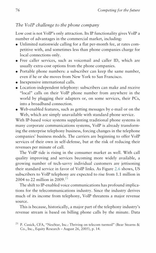
The VoIP challenge to the phone company
Low cost is not VoIP’s only attraction. Its IP functionality gives VoIP a
number of advantages in the commercial market, including:* Unlimited nationwide calling for a flat per-month fee, at rates com-
petitive with, and sometimes less than phone companies charge for
local connections only.* Free caller services, such as voicemail and caller ID, which are
usually extra-cost options from the phone companies.* Portable phone numbers: a subscriber can keep the same number,
even if he or she moves from New York to San Francisco.* Inexpensive international calls.* Location-independent telephony: subscribers can make and receive
‘‘local’’ calls on their VoIP phone number from anywhere in the
world by plugging their adapters or, on some services, their PCs,
into a broadband connection.* Web-enabled features, such as getting messages by e-mail or on the
Web, which are simply unavailable with standard phone service.
With IP-based voice systems supplanting traditional phone systems in
many corporate communications systems, VoIP is already transform-
ing the enterprise telephony business, forcing changes in the telephone
companies’ business models. The carriers are beginning to offer VoIP
services of their own in self-defense, but at the risk of reducing their
revenues per minute of call.
The VoIP tide is rising in the consumer market as well. With call
quality improving and services becoming more widely available, a
growing number of tech-savvy individual customers are jettisoning
their standard service in favor of VoIP links. As Figure 2.6 shows, US
subscribers to VoIP telephony are expected to rise from 1.1 million in
2004 to 22 million in 2009.21
The shift to IP-enabled voice communications has profound implica-
tions for the telecommunications industry. Since the industry derives
much of its income from telephony, VoIP threatens a major revenue
source.
This is because, historically, a major part of the telephony industry’s
revenue stream is based on billing phone calls by the minute. Data
21 P. Cusick, CFA, ‘‘NeuStar, Inc.: Thriving on telecom turmoil’’ (Bear Stearns &Co., Inc., Equity Research – August 26, 2005), p. 14.
76 Competing for the future

connections, on the other hand, are assumed to be always on, and are
generally billed at a flat fee based on data rate.
For example, a one-minute digital (not IP-based) phone call requires
480,000 bits, for which a phone company will charge $0.02. This
doesn’t seem like much, but it is actually an artificially high price. The
call represents a relatively small data stream which, in principle, should
cost no more than the transport of any other data stream of that size.
By comparison, a 2 Mb/s Digital Subscriber Loop (DSL) connection
to the Internet from the same phone company may cost a flat $20 a
month. A short mathematical exercise shows that if a one-minute call
were made over an IP service bundled with that DSL service, the cost
per minute of access works out to only $0.0005 – almost nothing.
What’s more, since this call uses only a fraction of the data capacity
of the DSL line, subscribers can continue to use the line for e-mail, Web
browsing, or other activities without affecting the call.
A VoIP call is not totally immune to network tolls. Calls can incur
costs from conventional telephony access providers, who charge an
25
20
15
10
5
0
YearSource: Bear, Stearns & Co. Inc. estimatesFor illustrative purposes only
Num
ber
of S
ubsc
riber
s (M
illio
ns)
Per
Cen
t Pen
etra
tion
(%)
20
18
16
14
12
10
8
6
4
2
02004 2005E 2006E 2007E 2008E 2009E
Cable VoIP Subscribers
Wireline VoIP Subscribers
Independent VoIP Subscribers
Total VoIP Penetration (Household)
2.6. Recent and anticipated growth of VoIP customers in the US. These
numbers are most likely understated given the VoIP service of Skype and of
companies such as Google and Yahoo! Reprinted with permission from Bear
Stearns (ref. 21).
Building digital systems 77

access fee when a call jumps onto the PSTN to reach the called party’s
location. However, VoIP carriers usually offer ‘‘free’’ VoIP-to-VoIP
calls among their subscribers. Since these never touch the conventional
network, their cost is covered by the monthly subscription charge.
Skype moves VoIP off the phone
To see how digital technologies can transform whole industries, con-
sider the impact of a venture capital-financed start-up company which
emerged in 2003.
Skype offers voice service based on a proprietary protocol capable of
excellent call quality. It differs from standard VoIP services like Vonage
in several respects.* Unlike existing VoIP services, it requires no central servers. Instead,
it uses subscribers’ computers/telephony gateways to provide
connectivity.* While services such as Vonage use stand-alone adapters to connect
phones to IP-based networks, Skype is fundamentally a PC-to-PC
service (although a new option called SkypeOut can provide PC-to-
phone connections).* Vonage and similar services assign standard phone numbers to sub-
scribers. Skype subscribers do not receive a phone number unless
they subscribe to the SkypeIn option.
In many ways Skype works like a peer-based music-sharing service.
There’s a good reason for this. Its founders, Niklas Zennstrom and
Janus Friis, were the founders of KaZaA, a leading music site.
There were PC-to-PC phone schemes before Skype, but they were
unreliable, and offered erratic (and frequently very poor) voice quality.
Skype achieves good call quality through a relay technique, routing
calls through other subscribers’ equipment to bypass network bottle-
necks. Strong encryption, integrated Instant Messaging, and secure file
transfer complete the offering.
Just as they did for music sharing, Zennstrom and Friis have taken
PC-to-PC voice communication out of the hobbyist realm and made it
commercially acceptable.
Skype’s revenue model is based on charges recovered when a call is
made to a conventional PSTN number using SkypeOut. Skype-
to-Skype calls are free, and there is no subscription or setup fee.
The technology attracted a lot of attention when it was announced,
which helped Skype sign up an estimated 100 million subscribers
78 Competing for the future
around the globe in just over two years.22 Between three and five
million subscribers are on line at any one time.
The company also attracted a huge sales price from online auction
giant eBay, which acquired Skype in September 2005 forE2.5 billion in
cash and stock.
In a development entirely characteristic of new digital technologies,
formidable competition quickly entered the market. Google, Earthlink,
Lycos, and Yahoo! have all announced similar services.
The economic effects of change
VoIP technology can interface with any transmission medium. As
shown in Figure 2.6, its adoption rates are increasing among all types
of voice telephony customers, including those using wireline tele-
phones, cable connections, or independent (Internet access) services.
Phone service has long been the beneficiary of government regulation
and artificial price controls. But when voice calls are just another data
service, these barriers crumble. The impact of VoIP on the revenues of
established public carriers promises to be significant, and the ready
availability of a cheap communications service will change social
structures too, particularly in developing nations.
In Chapter 8 we will consider how all digital technologies, including
VoIP communications, transform existing industries.
Digital video over IP networks
Video is one of the fastest-growing applications in the information
society. Here, too, packet-based networks are a natural medium.
For example, as broadband connections become more common, video
is popping up all over the Web. In fact, according to CacheLogic, a
provider of traffic monitoring and management technology to Internet
service providers, in 2004 peer-to-peer file-sharing traffic already
accounted for 60 percent of Internet traffic, with video making up
62 percent of that amount.23 This is in addition to the growing use of
streaming video on commercial Web sites.
22 Briefing to Warburg Pincus by Morgan Stanley Research, April 16, 2006.23 ‘‘CacheLogic technology installed in tier-one ISPs worldwide monitors actual
network traffic, reveals surprising facts in audio/video trends and format usage’’(August 9, 2005), Press Release accessed on May 23, 2006 at www.cachelogic.com/news/pr090805.php.
Building digital systems 79

But transmitting digital video over an IP network poses an even
greater challenge than voice. It requires handling data from sequential
frames made up of anywhere from 300,000 to two million pixels, for
standard and high definition resolutions respectively. The signal con-
tains an enormous amount of information – color, sound, and
intensity.
In fact, the data stream of a standard US broadcast television pro-
gram at 30 frames/second, using 8 bits/pixel to describe its parameters,
is approximately 140 Mb/s.
To reduce the demands that video places on the network, providers
normally compress this signal. Data compression relies on sophisti-
cated mathematical algorithms for encoding the image at the source
and decompressing it for the destination display.24
The algorithms compress the image by encoding information that
describes the full content of the image every few frames, but describes
only the changes in the image for the intervening frames. The decoder
at the receiving end reconstructs the partial frames in such a way that
the viewer sees little or no deterioration in the image.
Industry standards are essential if video systems from various man-
ufacturers are to work together. The Joint Photographic Experts Group
(JPEG) has developed standards for still images that can produce a
compression ratio as high as 20:1.
For motion video the most widely accepted standards come from the
Motion Picture Experts Group (MPEG). MPEG-2, for example, is the
standard used to compress data for DVDs, the US broadcast digital TV
system, and most digital satellite television. The newer MPEG-4 Part
10 standard, more commonly called H.264, offers higher compression
ratios and more features. Satellite services are adopting it for high-
definition video content. It is the choice for next-generation video
applications, including video on cell phones.
These standards, combined with reduced frame rates and lower
resolution, have compressed video to data streams as low as 64 Kb/s.
While this is adequate for some applications, it is not a TV-quality
viewing experience.
24 For a review of theory and methods, see R. Steinmetz and K. Nahrstedt,Multimedia: Computing, communications and applications (Englewood Cliffs,NJ: Prentice Hall, 1995).
80 Competing for the future
Under MPEG-2 a data stream of about 1 Mb/s (compressed) is
required to transmit VCR-quality video. An MPEG-2 encoder will
compress the 140 Mb/s stream of a standard-definition signal to
between 1 Mb/s and 5 Mb/s. It will encode a 1 Gb/s HDTV signal at
10 Mb/s to 18 Mb/s.
As compression algorithms continue to improve, we may see video at
much higher resolutions become readily available in multiple streams
on the Internet.
The wireless world
Guglielmo Marconi first demonstrated long-distance radio transmission
in 1897. A century later consumer and industrial wireless applications
had exploded, thanks to dramatic improvements in semiconductor-
based digital signal detection and processing capabilities.25
The biggest beneficiary of these developments in the commercial
sphere was two-way wireless service. This was made possible by the
cellular network concept, invented at Bell Laboratories in the 1960s
and 1970s.26
Wireless voice goes digital
Cellular networks are a brilliant solution to a fundamental problem
that had prevented wide deployment of wireless service. The previous
two-way wireless architecture used scarce radio spectrum to cover
wide geographic areas. This severely limited the number of users that
could access the system at the same time.
The idea behind the cellular network is that spectrum can be reused
by building adjacent regions, or cells, with their own transmitting and
receiving towers, and limiting their range to that region, usually a few
square kilometers. This allows adjacent cells to use the same frequency
spectrum without interfering with each other.
As a wireless user moves from one cell to another, technology built
into the system hands off connected calls to the appropriate
25 These advances are fully described in T. S. Rappaport, Wireless communica-tions: Principles and practice, 2nd edition (Upper Saddle River, NJ: Prentice HallPTR, 2002).
26 V. H. McDonald, ‘‘The cellular concept,’’ Bell System Technical Journal 58(1979), 15–43.
Building digital systems 81
transmitter/receiver. The whole wireless network is connected to the
wireline infrastructure so calls can be made to or from anywhere.
AT&T rolled out the first generation of cell phones, an analog
system called Advanced Mobile Phone Service (AMPS), in Chicago
in 1983. Once cellular systems entered the digital age with second-
generation (2G) technology in the 1990s, progress was faster.* The Global Service for Mobile (GSM) became the most widely used
cellular technology in the world after its introduction in Europe in
1991.* In North America and some parts of Asia another 2G technology,
developed by Qualcomm and based on CDMA (Code Division
Multiple Access), was introduced in the early 1990s.* So-called 2.5G systems, launched in the late 1990s, marked the first
packet-based cellular systems. They included GPRS (General Packet
Radio Service), derived from GSM; and 1x EV-DO, derived from
Qualcomm’s CDMA technology.* Now a 3G system, a packet-based technology introduced after 2000,
offers much higher capacity, allowing data, voice, and video to be
offered on handsets.
In the 1980s and early 1990s cellular phone service was still restricted
to business use. It was too expensive for most individual consumers,
even in developed countries.
Today basic service is affordable practically anywhere. For example,
millions of low-income people in India and China have access to voice
service because fees are only $8 to $10 a month, and handsets cost
under $100.
By the start of 2006, only fifteen years after the introduction of the
first digital system, there were more than two billion wireless users
worldwide, including nearly 400 million in China alone.27
Cellular’s amazing adoption rates were spurred by two factors. First,
digital technology has created systems that make more efficient use of
the available radio spectrum. Essentially this allows service providers
to put more people on line. Second, there have been huge price cuts for
both network equipment and user handsets, making the service far less
expensive to offer and use.
Wireless communications was transformed into a global mass mar-
ket by the cellular revolution of the mid-1990s. We are already seeing
27 Morgan Stanley Research, April 16, 2006.
82 Competing for the future

the emergence of the next stage: more advanced services, including data
and video distribution to wireless handsets.
Packets enable data transmission
Since digital wireless networks are packet-based just like the Internet,
their messages can theoretically contain any kind of information. As a
result, data transmission is increasingly moving to handheld wireless
devices.
The first wireless data networks created dedicated connections that
lasted the length of the data message, emulating the method used by
PSTN data links. The newer approach uses encoded, switched data
packets. These are transmitted on a channel shared with other mes-
sages, but the data packets are addressed to reach only a specific
subscriber.
Switched-packet technology makes the most efficient use of avail-
able spectrum. It is the foundation of the new third-generation (3G)
cellular systems. The most advanced wireless technology, under devel-
opment for large-scale mobile markets, aims at data rates as high as
2 Mb/s, although in practice the rates are likely to be lower.
Wireless has also been used to connect fixed subscribers, but this
approach has found a very limited market. The largest such networks
(e.g., in Mexico) have reached only 500,000 subscribers. New stan-
dards such as WiMax promise lower costs and broadband capability to
rival DSL. These might meet with greater success.
Potential capacity limitations
The growth of IP-based networks has produced a classic case of
demand rising in tandem with capacity. However, traditional telecom-
munications networks continue to be used, so big networks use mixed
technologies. Voice, video, and data traffic are all increasing as com-
panies and consumers alike call up, log in, and download. Even the
phone companies are promoting TV and movie services over consumer
digital subscriber lines. Is there enough capacity to accommodate this
growth?
The answer depends on what kind of capacity we’re talking about.
It’s unlikely we’ll run out of data transport capacity in the backbone of
the Internet, for example, because fiber optic links can be scaled to any
capacity the routers can handle. Although the theoretical limit is much
Building digital systems 83

higher, in practice single fiber links will transmit 43 Gb/s over a dis-
tance of 4,800 kilometers without repeaters.28
Furthermore, a fiber can carry more than one channel of data
streams by using different laser sources emitting at different closely
spaced wavelengths (colors). Wave Division Multiplexed (WDM) sys-
tems use this technique to put as many as 160 different channels on a
single fiber.
Finally, there is the matter of so-called ‘‘dark fiber.’’ During the
1990s there was an extensive build-out of optical fiber cables to meet
an anticipated surge in demand. The estimates turned out to be wildly
optimistic. Anecdotal information suggests that only a few percent of
the fiber links now available actually carry traffic, although the rapid
rise in video transmission is likely to change this number.
In short, supply is still way ahead of demand. This has produced the
expected result. As fiber capacity has increased, transport costs have
dropped dramatically. An informal survey of large national companies
that lease data transport to interconnect their facilities suggests that the
monthly cost of a 100 Mb/s connection declined by 95 percent between
1995 and 2005.29
At the local level it’s a different story. In this market segment data
capacity is an issue, at least in the US, due to a combination of technical
limitations and economic reality. Accordingly the cost of local data
access at 1.54 Mb/s to a small business or residence has declined by
only one-third, and even less in some regions.
Cost reductions in the local market haven’t matched national figures
for fiber mostly because the market is uncompetitive. Fiber has not
been economical to deploy in local markets, so copper wirelines pre-
dominate. Wired ‘‘last mile’’ lines to consumers or small businesses are
generally controlled by the incumbent phone or cable company, which
is in a better position to control prices.
All this is beginning to change. As equipment costs decline, local
fiber optic terminations will expand. Verizon Communications, one of
the largest US telecommunications providers, has promised nearly
28 Data quoted in Lefrancois, Charlet, and Big, ‘‘Impact of cumulated dispersion onperformance,’’ 174–176.
29 Author’s informal survey of major financial institutions in New York City area(2005).
84 Competing for the future

universal broadband access in its regional market, and AT&T has a
similar program under way.
For the foreseeable future, most small businesses and consumers will
be stuck with copper lines or cable access with limited data carrying
capacity. At the beginning of 2006, only about 32 percent of all US
residences had what is called ‘‘broadband.’’
Since broadband in the US is presently limited to under 10 Mb/s, this
is actually low-data-rate service by the highest world standards.30 In
countries such as South Korea, many people have much higher data-
rate connections.
On the mobile side, wireless access rates are generally below 2 Mb/s,
though fixed wireless access can reach much higher values.
Software innovations
Computing hardware may be getting cheaper and more powerful every
year, but without clever software it is useless. Software is the chief
enabler of new technology-based products and services, including ser-
vices based on IP networks. In addition, software development can
represent as much as 70 percent of the development cost of new
electronic equipment systems.
Figure 2.7 tracks US industry’s investment in software over the ten
years between 1993 and 2002. The increase from well under $100
billion to nearly $200 billion during that period underlines the impor-
tance of the field.31 Given how much software is generated every year,
it would be surprising if there had been no effort to systematize the
writing of code.
And in fact, over the past fifty years the writing of software has gone
from an arcane art to something more akin to a production process,
employing millions of people.32 This ‘‘mechanization’’ has been made
possible by new methodologies, languages, and tools that automate
much of the routine work originally needed to write and test software.
Although program definition and architecture remain highly specia-
lized skills, the software development and maintenance process has
30 Data from Cusick, ‘‘Thriving on telecom turmoil.’’31 SG Cowen Tech Research Team, Perspectives, ‘‘Tech road map 2002: Our out-
look for the New Year’’ (New York: SG Cowen, January 2002), p. 105.32 D. M. Hoffman and D. M. Weiss (eds.), Software fundamentals (New York:
Addison-Wesley, 2001).
Building digital systems 85
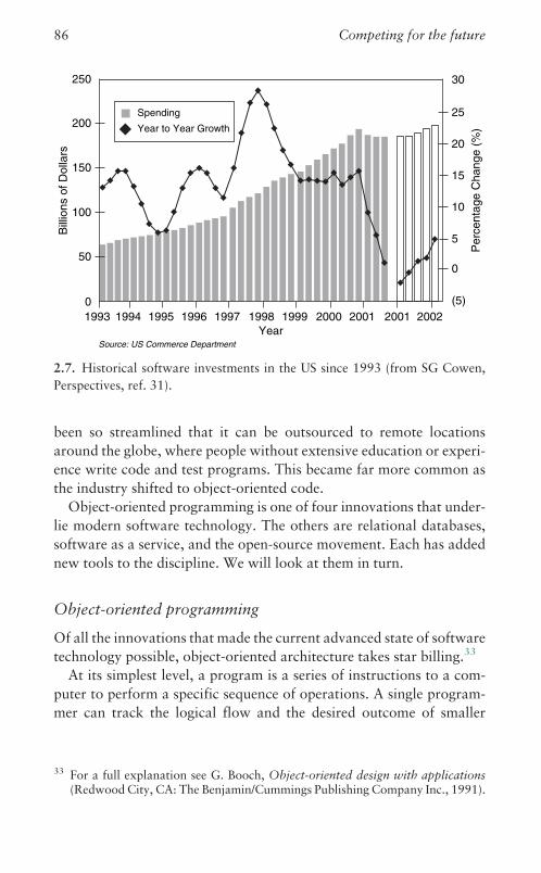
been so streamlined that it can be outsourced to remote locations
around the globe, where people without extensive education or experi-
ence write code and test programs. This became far more common as
the industry shifted to object-oriented code.
Object-oriented programming is one of four innovations that under-
lie modern software technology. The others are relational databases,
software as a service, and the open-source movement. Each has added
new tools to the discipline. We will look at them in turn.
Object-oriented programming
Of all the innovations that made the current advanced state of software
technology possible, object-oriented architecture takes star billing.33
At its simplest level, a program is a series of instructions to a com-
puter to perform a specific sequence of operations. A single program-
mer can track the logical flow and the desired outcome of smaller
1993 1994 1995 1996 1997 1998 1999 2000 2001 2001 2002
250
200
150
100
50
0
Bill
ions
of D
olla
rs
30
25
20
15
10
5
0
(5)
Spending
Year to Year Growth
Year
Per
cent
age
Cha
nge
(%)
Source: US Commerce Department
2.7. Historical software investments in the US since 1993 (from SG Cowen,
Perspectives, ref. 31).
33 For a full explanation see G. Booch, Object-oriented design with applications(Redwood City, CA: The Benjamin/Cummings Publishing Company Inc., 1991).
86 Competing for the future

programs. However, large programs involving complex interacting
operations require a division of labor through which sequences of
operations (called subroutines) can be defined and assigned to several
different programmers. The subroutines are then assembled into the
final program.
This seems simple, but in practice it has proven very difficult to
manage. Programs evolve over time, with programmers working to
improve performance or add features and functions. Even with the best
of intentions, requirements defined at the start are guaranteed to
change. If the program’s architecture proves inflexible, changes
become difficult, and the quality of the finished product suffers.
Furthermore, because code from one program cannot be reused in
another, each new program must be written from scratch.
Or at least that was the situation in the early days of software
development. Object-oriented technology, a revolutionary idea con-
ceived in the late 1960s and widely adopted in the late 1980s, provides
a modular architecture that solves many of these problems.
Objects and software structure
Let’s start with some definitions, and then look at what it all means. An
object is a ‘‘bundle’’ of software that contains related data and the
procedures, or methods, for using the data to perform specified opera-
tions. The methods are fixed, but the data can change as required.
Objects interact with each other by sending messages (via a bus) that
request the execution of their individual procedures. A message con-
sists of the name of the receiving object and the name of a procedure
that the receiving object knows how to execute. The message may also
include additional information (called parameters) required for a par-
ticular object to perform its procedures.
An object forms part of a class in which all the objects are identical in
form and behavior but contain different data. Any object in a class is an
instance of the class. The extraordinary value of the object concept is
that it allows the formation of class hierarchies. This lets the software
architect structure complex programs, from the most general down to
the most specific elements, as a series of modules. Each module per-
forms certain well-defined processing functions in the sequence desig-
nated by its place in the hierarchy.
Suppose, for example, that at some point the program needs digital
signal processing functions for creating music, or a series of algorithms
Building digital systems 87

to solve problems in physics. The architect simply chooses classes of
objects that carry out those procedures and plugs them into the pro-
gram’s bus. This is a much simpler and more logical way of represent-
ing complicated operations.
In the hands of skilled architects, any program can be structured as
objects interconnected by a bus. The objects can then be coded indivi-
dually in the expectation that the whole edifice will be brought together
at the end as a functioning program.
Object-oriented technology has dramatically changed the way soft-
ware is written.* Once the architecture of a program is defined, development tasks can
be divided into objects and each part independently tested.* Once written, the objects are building blocks that can be reused in
other projects.* Changes in a completed program can be made by changing objects.* Object-oriented technology produces more robust programs as:
– each object hides the complexity of its function;
– messages between objects convey the relevant variables needed for
the object to do its job, but only the object’s own methods interact
with its data;
– this prevents corruption of the object and, by extension, the
program.
To see how object-oriented programs are actually built, turn to the
example in Appendix 2.3.
Relational database architecture
Managing the massive amounts of information used in a modern busi-
ness requires a database, a highly efficient architecture for storing and
retrieving content. The single most important innovation in that field is
the relational database model
The concept is simple. The data is arranged in tables. New tables are
created from older ones as data is presented or rearranged to meet new
needs.34 The term ‘‘relational’’ is a way of stating that tables are the
basis of the system.
34 For a complete description see C. J. Date, An introduction to database systems,6th edition (New York: Addison-Wesley, 1995).
88 Competing for the future

Introduced in the 1970s, relational database architecture has largely
replaced the less flexible hierarchical model used in early mainframe
computing. It dominates the field because its tabular formats store not
only the information but the relationships within the information.
Relational searches can be logically conducted with great efficiency,
generating new tables to provide the requested information in a useful
format.
The Oracle Corporation is now the world’s leading supplier of
proprietary software products for managing relational databases, and
of tools for integrating them with other data processing applications.
A new software model: Software as a Service (SaaS)
A convergence of innovations often produces unexpected outcomes.
Software modules, now linked by the Internet, are again transforming
the software industry by enabling what are generally called Web ser-
vices or ‘‘software as a service’’ (SaaS).
In Web services, software residing on separate computers is
assembled on demand for specific applications, then delivered to a
user through the Internet. In effect, rather than having a software
application residing on an individual computer, the user taps the
Internet to get a software-based service.35
The delivery of software-enabled services to a user’s terminal is not a
new idea. In the 1960s the mainframe computer was connected to a
‘‘dumb’’ client terminal. In the client/server architecture of the 1980s,
the server computer contained the business logic and data storage,
while the client computer had the resources needed to run applications.
In both cases the user could only call up applications that were avail-
able within the local area network.
In the new Web services model, however, the components needed to
provide a given service are not resident on a single mainframe or server.
They are distributed among multiple Internet-connected computers.
This structure can deliver functionalities within and outside of an
enterprise.
35 For a full presentation see G. Glass, Web services: Building blocks for distributedsystems (Upper Saddle River, NJ: Prentice Hall PTR, 2002); and A. T. Manes,Web services, a manager’s guide (Boston: Addison-Wesley, 2003).
Building digital systems 89

The SaaS Web services architecture represents a major step toward
distributed computer networks. Linked by the Internet, these networks
promise increased flexibility in the development and maintenance of
applications software. They are capable of delivering services to or
from any kind of device, from a mainframe computer to a small con-
sumer gadget or a processor embedded in an instrument.
And since users can tap into applications through the Internet
regardless of their location or computer platform, enterprises do
not need multiple sites hosting the same software to achieve these
benefits.
In addition, upgrades are no longer an issue. Everyone always uses
the latest version of the software, since that’s what’s on the Internet.
While the potential benefits are easy to see, the implementation and
maintenance of the architecture is not simple. In addition to developing
frameworks for creating the services, providers must find reliable,
automated methods for several important functions:* registry (to capture the details of the services being made available);* approval of work flow;* policy management (to ensure that the services meet enterprise com-
pliance standards);* management of program component changes.
Because the architecture is so open, another key requirement is ensur-
ing secure communications over the public Internet. Commercial SaaS
products are designed to provide this capability by default.
There are many successful examples of SaaS implementations on a
large scale, including the package-tracking system for Federal Express,
which uses a BEA Systems platform. A simple example of a successful
SaaS implementation is at Accredited Home Lenders, Inc., which is in
the mortgage lending business. Accredited Home Lenders has reduced
the procedures involved in completing a mortgage application to a set
of interconnected software components. This has streamlined the pro-
cess of managing applications by turning it into a simple, integrated,
self-service procedure. Brokers go on line to submit applications,
get pricing, and receive approval. In addition to saving time and
money, the process ensures uniform procedures and consistent risk
management.
The SaaS approach to deploying software applications is attracting a
great deal of interest. However, it is not a trivial matter to master the
library of functions and train developers to use the ones appropriate to
90 Competing for the future

a given task. Integrating activities in companies with multiple develop-
ment sites significantly raises the stakes.36
In spite of the learning curve, though, the benefits of the new archi-
tecture are truly compelling. In mid-2005 about 70 percent of the
largest companies were already using SaaS architectures for some
applications. Most of the rest were in the process of developing appli-
cations of their own.
For these companies, the biggest hurdles in implementation are
creating interfaces to existing legacy code, mastering security hurdles,
and establishing standards.37 Other issues include the challenges of
routing packets that carry an enormous amount of information, some
of it relating to security, and of maintaining routing service levels.
Bandwidth limitations and slow response can pose problems in some
applications. Fortunately, as the processing power of chips increases,
the speed with which packet analysis can be conducted improves as
well. This will assure continuing progress in overcoming these
limitations.
Selling service. Not software licenses
You might wonder why all providers don’t offer on-demand software
functions instead of sticking to the model of loading large, full-featured
stand-alone programs onto PCs.
Imagine not owning a word processor, office suite, or financial
package. In their place you would have twenty-four-hour access to
those programs and any others you might occasionally need. You
would simply access the server or servers that house the required soft-
ware and use it for the task at hand, sharing the application with others
who are using it at the same time.
This sounds promising. But it does present several problems. The
biggest of these is lack of control. Rather than having full possession
of the application, the user is totally dependent on a lifeline to the
Internet.
There are benefits to balance this disadvantage. The first, presum-
ably, is lower costs. Companies would not have to license software
36 See D. Karolak, Global software development: Managing virtual teams andenvironments (New York: Wiley-IEEE Computer Society Press, 1998) for areview of the challenges.
37 Forrester Research Inc. (Cambridge, MA: April 2005); Evans Data Corp. (SantaCruz, CA: June 2005) in Computerworld (August 15, 2005), 42.
Building digital systems 91
packages in multiple copies, one for every user, knowing that they
would sit idle most of the time.
They would not have to worry about their users working with
outdated programs either. Instead of wasting users’ time in occasion-
ally updating PC-resident packages (assuming users bother to update
them), they would be giving all users automatic access to the latest
version of any program they need.
Solutions that use SaaS architecture are already available at the
enterprise level. They are generally provided and maintained by corpo-
rate information technology organizations. But independent vendors
are obviously anxious to offer them on their own.
The reason for their enthusiasm is easy to understand. The usual
software business model, which involves selling software through
licensing agreements and then negotiating maintenance contracts, pro-
vides a ‘‘lumpy’’ revenue flow. Software vendors prefer to provide
software on a recurring ‘‘rental’’ basis, with customers paying a sub-
scription. This generates a smoother, more predictable revenue stream.
The SaaS model has met with success, but problems have surfaced.
One survey showed that 69 percent of the enterprises polled were
satisfied with the architecture they had installed.38 Of those that
found the results disappointing, 50 percent found that legacy applica-
tions could not be integrated, 25 percent found that the cost was higher
than in the previous architecture, and 25 percent found that the com-
plexity and difficulty of maintaining the service was higher than
expected.39
Problems have been most common in situations where the solution
had to incorporate legacy applications. In brand new IT structures,
on the other hand, the degree of success is limited only by the selection
of software functions deployed and quality of the communications
network.
Selling software as a service is a trend in tune with the times. Services
have represented more than half of US economic output since 1987,
reaching 82.5 percent of the total in 2005. According to a study by Peer
38 C. Babcock, ‘‘Work in progress – service-oriented architectures are a blueprintfor software development, but they’re hard to perfect,’’ www.informationweek.com(October 31, 2005) (accessed on April 20, 2006).
39 www.itarchitect.com (November, 2005) (accessed on May 2, 2006).
92 Competing for the future
Insight LLC,40 service innovations are likely to be more successful if
their development is centralized, which is certainly true of SaaS.
However, they also require more attention to the customer experience
than product innovations, as well as more prototyping. This may help
explain the early problems in SaaS implementation.
Computer operating systems and open-source software
Sparked by the open communications available through the Internet,
the open-source software movement, which began as a student project,
has revolutionized the software industry.
The name of the movement encapsulates its software development
philosophy. Software developers make the underlying program code of
open-source software freely available to everyone, to use and modify as
they wish. Variations occur where such ‘‘free’’ software morphs into a
licensable product as the result of specific modifications made by
commercial companies.
The Linux operating system is the first and most important example
of open-source software. Before we take a closer look at Linux, how-
ever, we should first clarify what an operating system is and why it is
significant.
An operating system is a group of software routines that access the
hardware of a computer and enable it to perform the functions
requested by application software. Different computers have different
operating systems, and application software must be tailored for the
specific operating system of the computer on which it will run.
In the early years of the industry, a proliferation of computer man-
ufacturers (most now defunct) generated an equal number of operating
systems. After years of consolidation, however, Microsoft Windows
and various versions of UNIX (an operating system that originated in
Bell Laboratories), along with MVS, developed by IBM, emerged in the
late 1990s as the dominant ‘‘proprietary’’ operating systems.
Obviously the ability to lock in applications programs that run on
specific types of machines is a valuable asset for owners of operating
40 J. M. Rae, ‘‘Using innovation to drive growth in service markets,’’ presented atthe Business Marketing Association annual conference, May 12, 2006. Thanksalso to Ms. Rae, President and S. J. Ezell, Vice President, Peer Insight,Alexandria, VA, for providing a preliminary executive summary of their forth-coming study: The discipline of service innovation.
Building digital systems 93

systems, and a good source of licensing revenues. This situation even
offers users a benefit. Tight control over the core code of the operating
system insures a desirable level of uniformity and interoperability.
However, no one willingly pays licensing fees if there is a viable free
alternative. That is what Linux represents.
The Linux operating system was developed by Linus Torvalds while
a student at the University of Helsinki in 1994. Intended as a simplified
replacement for UNIX, it has had a dramatic impact worldwide on the
cost of computers, and has acted as a stimulant to software innovation.
The success of Linux is the result of a number of factors. Over the years,
various computer manufacturers licensed UNIX but built in proprie-
tary modifications in order to lock customers into their products.
Hence computer buyers found themselves restricted in their ability to
buy equipment from different vendors and felt that they were being
overcharged. The advent of Linux opened their equipment options.
Once IBM endorsed Linux, this operating system gained enormous
commercial credibility.
Free and valuable
The success of open-source software caught everybody by surprise. Just
imagine complex programs, even an operating system, for the most
demanding equipment in the world, with no single point of ownership.
Contrary to many prophecies, these products have achieved enterprise-
level quality comparable to, or actually better than, long-established
proprietary products.
Linux code is available free on the Internet, although few organiza-
tions can do without the support provided on a commercial basis by
several companies. Linux has increasingly proven to be as robust as
the UNIX operating system that it replaces. It has even been adopted
by IBM.
No one owns Linux or any other open-source software. But open-
source software does have control points. These are established by ad
hoc communities of developers devoted to specific software sectors and
working in concert.
The software is supported by organizations of volunteers who
collaborate over the Web. They congregate at sites such as
SourceForge.net, which calls itself ‘‘the world’s largest Open Source
software development web site, hosting more than 100,000 projects
and over 1,000,000 registered users with a centralized resource for
94 Competing for the future
managing projects, issues, communications, and code.’’41 Naturally,
the number of projects that yield valuable software is but a small
fraction of these endeavors.
There are thousands of groups that establish standards and decide
which modifications will be accepted. For example, Linus Torvalds is
the current authority for open-source Linux. Improvements that pass
muster with Torvalds and the Linux standards committee are periodi-
cally wrapped into new Linux distributions that can be downloaded at
no cost from the Internet. Companies such as Red Hat and Novell sell
packaged versions with user support.
In contrast to proprietary software, which is relatively static and
‘‘closed,’’ open-source software evolves constantly. Useful changes and
corrections are made available very quickly and posted on the Web for
all to see and use.
Open-source software engages the coordinated interest of many
developers with no axes to grind except the satisfaction of seeing
their work accepted by others. Their efforts drive the fast turnaround
of new features, functions, and fixes.
But that does not mean that the software is slapdash. Release cycles
are managed by the volunteer organizations to ensure quality and
provide rapid fixes for any deficiencies. The end product is often touted
as being comparable to proprietary software programs.
Quality, performance, competition
Questions regarding open-source, mission-critical software usually
revolve around issues of quality control, network operability, and
security features. Over time these concerns have abated, thanks to the
speed with which patches and vulnerabilities are identified by the open
community and posted on the Internet for all to see and react.
One big business that will be increasingly impacted by the availabil-
ity of dependable open-source software is the database sector. The field
has long been dominated by Oracle. Now, however, there’s an open-
source competitor, MySQL, which claims to offer an alternative free of
licensing fees. It comes with impressive credentials. The Los Alamos
National Laboratory has used it for several years with good success.42
41 http://sourceforge.net/docs/about (accessed May 23, 2006).42 M. DiGiacomo, ‘‘MySQL: Lessons learned on a digital library,’’ IEEE Software
22 (2005), 10–14.
Building digital systems 95
MySQL is not alone in claiming parity with commercial products. A
number of studies43 have been made regarding the quality standards of
open-source software for mission-critical applications, and the results
have been quite satisfactory.
The fact that open-source software is license-free has not escaped the
attention of governments. Government agencies looking for a no-cost
alternative to Windows and UNIX helped foster the international
acceptance of Linux. Authorities in China, Taiwan, Hong Kong, and
South Korea, as well as countries in Europe and Latin America, have
made it a priority to adopt open-source software whenever possible.
Taiwan is particularly important, since so many of the world’s com-
puter boards are produced there.44
Open-source has defied the doubters who considered it a hobbyist
enterprise. It is estimated, for example, that some form of Linux was
used by 80 percent of major companies in 2005.45 Thanks to the
success of Linux, the open-source idea has gone from an experiment
to a very practical way to save money while encouraging innovation.46
With all that is at stake for commercial companies, it is no surprise
that litigation plagues the open-source industry. Claims have been
made that parts of the Linux operating system are elements of the
copyrighted UNIX code base. Even users are at risk. Because licensed
and unlicensed software is commonly used in the same environment,
they must make sure that the licensable software is accounted for and
licensing fees paid.
An experiment in success
The idea that a self-generated community of developers using the Web
can develop complex commercial-grade software is truly revolution-
ary. While the number of successful projects is small relative to the
number started, open-source activity will no doubt be the impetus for
43 See, for example, J. S. Norris, ‘‘Mission-critical development with open-sourcesoftware: Lessons learned,’’ IEEE Software 21 (2004), 42–49; T. Dinh-Trongand J. M. Bieman, ‘‘The free BSD project, a replication case study of opensource development,’’ IEEE Transactions on Software Engineering 31 (2005),481–494.
44 Opinion by M. Betts, ‘‘Linux goes global,’’ Computerworld (July 18, 2005),31–40.
45 D. Schweitzer, ‘‘Linux muscles into Microsoft space,’’ Computerworld (May 30,2005), 33.
46 F. Hayes, ‘‘Our Linux values,’’ Computerworld (July 18, 2005), 46.
96 Competing for the future

even more important innovations. In effect, developers are free to
invent software, share it freely with all comers, and, once a community
of users is established, have an informal arrangement for its further
evolution.
I have seen the advantages of open-source development first hand.
One of my portfolio companies used the approach for one application
in a communications system.
The whole solution, including protocols, was assembled in about one
man-month of development time. No licensing costs were incurred. In
the past such an application might have required ten times the pro-
grammer effort and thousands of dollars of specialized software licen-
sing fees.
An interesting side benefit of the open-source movement is the speed
with which the market delivers its verdict on the quality of specific
applications. As an ever-growing number of potential users gets used to
looking for useful free software, all open-source programs are sub-
jected to a very public popularity test.
Recently there have been some interesting open-source-related devel-
opments on the commercial front as well. One trend has a few estab-
lished companies weighing the idea of opening up their proprietary
products to public scrutiny.
One of the biggest is SAP, the world leader in enterprise resource
software. In 2003, the company decided to make its software more
flexible. It plans to accomplish this by reengineering its products to
take full advantage of object-oriented technology linked with Internet
connectivity. The task is massive, and will cost billions.
At its conclusion, SAP will offer customers a new architecture in
which software systems consist of connected applications running on
different computers linked through the Internet. This will replace its
currently closed architecture.
This ambitious, far-reaching initiative will take years to have a
significant impact on the ability of customers to allow more efficient
sharing of data and resources.47
The second development moves in the opposite direction, from open
to closed. New companies are being launched to exploit free open-source
47 A. Reinhardt, ‘‘Germany: SAP: A sea change in software: The German legend’smove into Lego-like modules could revolutionize the way companies do busi-ness,’’ BusinessWeek (July 11, 2005), 46–47.
Building digital systems 97

software as a starting point for their own commercial products. These
products are designed to compete with offerings from established
proprietary software vendors. However, their economic success is
unproven because innovation inevitably produces a proprietary
element in software that the market needs to validate.
For example, a new company called JBoss, Inc. is competing with IBM’s
WebSphere on the basis of open-source software. While these products
address a market estimated to be in excess of one billion dollars, their
success in garnering a meaningful percentage is unclear because estab-
lished large software vendors are not sitting idle in the face of new
competitors and continue to build increased value in their proprietary
products.
Like other innovations in information technology, open-source soft-
ware has created opportunities for new service businesses. A number of
companies such as Red Hat have been established to provide support
services for open-source code. By helping users implement, run, and
customize the software, they offer the kind of comfort level that would
have been provided by vendors of proprietary software.
While open-source software is free of license fees, many users wind
up paying for this third-party support. Even taking the fees for such
services into account, however, the overall cost of open-source solu-
tions is still substantially lower than that of proprietary software.
The digital future is now
Clearly, object-oriented technology, software as a service, and open-
source software have changed our assumptions about the way software
is developed and sold. At the same time, they are heavily dependent on the
availability of networking and communications, especially the Internet.
Communications, in turn, relies on the speed and power of computers.
In the rest of this book we shall see what impact all this technological
innovation has produced on financial investment, corporate strategy,
manufacturing, global employment patterns, and other non-technical
matters. Every advance we have covered up to this point, from devices
to systems to software, has resonance beyond electronics, and is forcing
change around the world in the broader spheres of social and economic
development and government policy.
98 Competing for the future

P A R T I I
Innovators, entrepreneurs, and venture capitalists


3 Edison’s legacy: IndustrialR&D
What makes the capitalist system work,
what keeps economies dynamic, is precisely
nonconformity, the new, the unusual, the
eccentric, the egregious, the innovative,
springing from the inexhaustible inventive-
ness of human nature.1
Most of the revolutionary innovations in semiconductors and software
explored in the preceding two chapters came out of the corporate R&D
organizations of AT&T, General Electric, IBM, Corning, RCA, and
other large companies.
That doesn’t mean these breakthroughs reflect a corporate mindset.
Nothing could be further from the truth. The scientists who created
them were following their own paths, not some managerial directive or
mandated marketing strategy. As someone who began his career in this
environment, I can attest to its creative ferment.
Truly creative people tend to be free spirits. They are the essential
spark plugs of innovation. At the same time, their drive for discovery is
often in conflict with practical considerations such as company direc-
tion or fiscal constraints. This trait presents corporate R&D managers
with endless challenges.
Perhaps that is why the talk today is all about ‘‘small, innovative
companies,’’ not big, powerful corporate laboratories (labs). But the
fact is that for much of the twentieth century those big labs were the
primary generators of new technology, because they had the resources
and the funding necessary for research. They were the vehicles innova-
tors needed to carry their work forward.
1 P. Johnson, ‘‘What Europe really needs,’’ The New York Times (June 17, 2005),A14.
101

We’ve begun our study of digital electronics by looking at how the
technology works, and how it affects people and businesses. This chapter
traces the history of the central corporate laboratory as a model for
innovation, starting with its great progenitor Thomas Alva Edison.
It also looks at how market pressures and new technology eventually
relegated advanced corporate R&D to a secondary role in exploiting
the massive new business opportunities created by digital technologies.
This marked a transition to widespread entrepreneurship backed by
venture funding, the subject of a future chapter.
Learning the ABCs
Before we discuss research and development centers, it’s important to
understand the three distinct kinds of R&D that were done at the
corporate labs. Here are some generally accepted definitions.
Basic research aims at the discovery of laws governing natural phe-
nomena. The best basic research is conducted in an open environment
where creative minds can follow their instincts.
Major discoveries are frequently made in the course of looking for
something else, so it’s important that a researcher is free to work on
hunches. From my experience, management-directed basic research is
rarely productive, because basic research scientists are motivated by the
excitement of exploring the unknown and earning the respect of their
peers.2
Investing in basic research is a high-risk endeavor. It has the potential
to generate enormous economic gains, but it is impossible to predict
whether a specific discovery will have commercial value.
Adding to the risk is the need to invest in follow-up development
before a raw technology can be commercialized. This investment is
costly, since development work is best done with the collaboration of
scientists who are expert in the subject. Expertise of this kind does not
come cheap. Even rarer is the expertise to exploit the new market
opportunities created by major innovations.
The fundamental work that uncovered the properties of semi-
conductors in the 1930s and 1940s is an excellent example of the
process. As basic research, its discoveries produced extraordinary
2 An interesting perspective on this subject is found in B. Bunch, The history ofscience and technology (New York: Houghton Mifflin Company, 2004).
102 Competing for the future
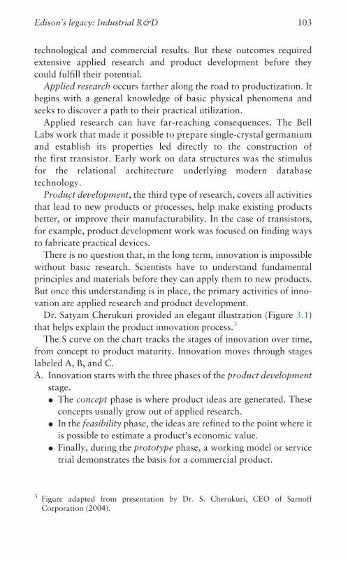
technological and commercial results. But these outcomes required
extensive applied research and product development before they
could fulfill their potential.
Applied research occurs farther along the road to productization. It
begins with a general knowledge of basic physical phenomena and
seeks to discover a path to their practical utilization.
Applied research can have far-reaching consequences. The Bell
Labs work that made it possible to prepare single-crystal germanium
and establish its properties led directly to the construction of
the first transistor. Early work on data structures was the stimulus
for the relational architecture underlying modern database
technology.
Product development, the third type of research, covers all activities
that lead to new products or processes, help make existing products
better, or improve their manufacturability. In the case of transistors,
for example, product development work was focused on finding ways
to fabricate practical devices.
There is no question that, in the long term, innovation is impossible
without basic research. Scientists have to understand fundamental
principles and materials before they can apply them to new products.
But once this understanding is in place, the primary activities of inno-
vation are applied research and product development.
Dr. Satyam Cherukuri provided an elegant illustration (Figure 3.1)
that helps explain the product innovation process.3
The S curve on the chart tracks the stages of innovation over time,
from concept to product maturity. Innovation moves through stages
labeled A, B, and C.
A. Innovation starts with the three phases of the product development
stage.* The concept phase is where product ideas are generated. These
concepts usually grow out of applied research.* In the feasibility phase, the ideas are refined to the point where it
is possible to estimate a product’s economic value.* Finally, during the prototype phase, a working model or service
trial demonstrates the basis for a commercial product.
3 Figure adapted from presentation by Dr. S. Cherukuri, CEO of SarnoffCorporation (2004).
Edison’s legacy: Industrial R&D 103

B. The process now proceeds to the critical (and costlier) product
launch stage. If the launch is successful, this stage delivers the high
profit margins and return on investment necessary to encourage
continued innovation.
C. Eventually the product enters the commoditization stage. Competition
for the product emerges, driving profit margins down. When obsoles-
cence sets in, the product loses all commercial value.
The path from A to C can span decades. In the case of the transistor,
five years elapsed between the first demonstration in 1947 and the first
commercial product. On the other hand, in some consumer electronics
sectors, the time from idea to product launch can be as short as two
years.
By clarifying the process of product innovation, Dr. Cherukuri’s
chart also shows where the hazards lie. Right at the start, for example,
a misreading of the market or of the competition can produce a
fatally flawed product concept. This misstep only becomes apparent
during the launch, when the finished product fails to meet sales
Sta
ges
of M
atur
ity
Time
Innovation
CriticalTransition
ProductCommoditization/Maturity
A
B+
$$
$
B
C
Launch
Product
Prototype
Feasibility
Concept Concept
Obsolescence
A+
inve
stm
ent
revenue/profit
3.1. Dr. S. Cherukuri’s curve of product maturity over time showing the process
from concept to obsolescence. Reprinted with permission from S. Cherukuri,
Sarnoff (ref. 3).
104 Competing for the future

expectations. By that time the producer has already invested heavily
in its development.
Failures at other points in the process also cause products to under-
perform. A product may prove too difficult or expensive to manu-
facture. If development takes longer than projected, competitors can
stake out the market with innovative products of their own.
So much depends on the innovation process that it’s not surprising
that companies try to manage it. In this field, as in so many others, the
person who created the pattern for the modern era was its greatest
innovator, Thomas Edison.
Edison invents the industrial laboratory
The twentieth century has often been called the Age of Edison, because
he played a role in creating many of the technologies that shaped the
modern industrial world. With 1,093 patents to his name, Edison has
been held up as the archetype of the lone inventor, producing inno-
vations by sheer force of personal genius.
This is a myth. Thomas Edison did not work alone. He may have
been the driving force behind his many inventions, but he was sup-
ported by a hand-picked research team assembled for that purpose.
The composition of his team marked a change in attitude toward
scientific endeavor. Since the beginning of the Industrial Revolution
there had been a sharp cultural distinction between ‘‘pure’’ scientists
who advanced the state of knowledge, and practical inventors of com-
mercial products. Scientists enjoyed high status as noble searchers after
Truth, while inventors were considered a lower order of commercially-
minded technicians. The scientists did basic research, while the tech-
nologists did applied research and product development.
Recognizing that this cultural gap must be bridged within a single
organization is one of Edison’s key contributions. In 1876 he created
the world’s first industrial laboratory in Menlo Park, New Jersey. This
organization, which he dubbed the Invention Factory, successfully
integrated scientists with technologists. His move to the Edison
Laboratory in West Orange, New Jersey in 1887 solidified his organi-
zation and created what has been called the world’s first R&D center.
The spectacular results from his labs made history, producing the
phonograph, motion pictures, incandescent lighting, and electric
power generation (among many other breakthroughs). His discovery
Edison’s legacy: Industrial R&D 105

of the ‘‘Edison effect’’ in 1883 anticipates modern electronics, even
though he himself did not pursue it.
The phenomenon he described, of electrons flowing to a metal plate
placed in one of his light bulbs, inspired John Ambrose Fleming to
create the world’s first diode in vacuum tube form. This led, in turn, to
the creation of the triode, a tube capable of amplification and counting,
by Lee deForest, an early radio pioneer.
Edison’s labs generated a steady flow of products. What’s even more
impressive is how many of them were commercially successful. This
was not an accident. Edison designed his approach for that outcome,
based on hard experience.
In 1868 he had patented his first invention, an electric voting
machine. The idea was to speed up the legislative process by eliminat-
ing time-consuming roll calls through instant tallying of yea and nay
votes in the Massachusetts house (he was living in Boston) and in the
US Congress.
The machine worked perfectly, but found no buyers. Legislators
liked roll calls because they represented an opportunity for oratory.
The lawmakers also used the delays during roll calls to cut deals with
other lawmakers for the passage or defeat of the bills being debated.
After this disappointment, Edison decided he would never again
work on a technology that didn’t have a good chance of commercial
success. Research for its own sake played no role in his investigations.
All R&D was focused on the development of product innovations – the
A and B stages of Figure 3.1 above.
If the research lab is Edison’s greatest invention, as some have
claimed, his focus on teamwork and creating products makes his lab
the forerunner of all commercial research strategies. One perceptive
writer has summarized his significance.
A just view of Edison’s historic role, suggested recently by Norbert Wiener,
would be that he was a transitional figure in late nineteenth century science,
arriving on the scene at the period when the crude mechanical inventors had
done their part, and systematic experiment and research was henceforth to be
undertaken by skilled and specialized men, on a much larger scale than
before . . . Today [1959], giant research laboratories, owned by private cor-
porations or by government, stand everywhere as monuments to Edison’s
innovative spirit. The technicians working in those institutions have been
telling us for some time now that the day of the lone inventor, in an attic or
small laboratory, has passed forever. Inventions, we have been assured, are
106 Competing for the future

henceforth to be produced by scientific teams using more complex instru-
ments than Edison ever knew and ‘‘made to order.’’ But can we ever dispense
with the individual inventor, who is both dreamer and man of action? Good
inventions are still not ‘‘predictable.’’ Of late, serious doubts have been
expressed that the mile-long laboratories and the teams of experts are any
guarantee of original achievement. Technical men themselves voice fears that
the new conditions of mass research may be less helpful in independent or
nonconformist thought; and that the bureaucratic inventors of today may be
losing something of the intuitive skills and the sense of simple things that an
Edison possessed.4
As countless companies have since learned, managing creative indus-
trial laboratories is difficult. Unfortunately, Edison did not leave
behind a foolproof recipe. Here is a description of a visit to the
Edison Laboratory in 1900, when its staff had reached 90 people:
A sociologist wandered into the Edison Laboratory one day to inquire of the
great inventor what methods of organization he used in conducting his
research work. ‘‘I’m the organization,’’ Edison said roundly. The professor
could discover that for himself by looking around for a few minutes, and
could save himself much time thereby. In truth the sociologist soon learned
that, though the inventor had numerous assistants and business managers, he
kept control of everything in his own hands, and himself supervised all the
different experiments and tests going on. Yet somehow the ‘‘system’’
worked.5
The big central research laboratories emerge
Edison’s example led to the formation of several large corporate
laboratories in the twentieth century. The intent was to provide an
environment for far-reaching innovation which would be commercial-
ized by product divisions. In order to eliminate short-term product
pressures on the labs, funding for their activities came from the corpo-
rate budget rather than budgets tied to specific product units.
In terms of Figure 3.1, the labs were expected to participate in the
A to Aþ stages, leaving B to the product divisions. Of course, implicit in
this arrangement is the corporate willingness to maintain predictable
4 M. Josephson, Edison, a biography (New York: History Book Club, 1959), p. xiv.5 Josephson, Edison, p. 411.
Edison’s legacy: Industrial R&D 107

and constant annual funding, regardless of the vagaries of business
cycles.
The strategy also assumed that the product divisions would have the
ability to exploit the innovations developed in these laboratories for
commercial gain. Obviously, it was not expected that these labora-
tories would be free from the necessity of integrating their results with
corporate strategic needs.
The most important electronics research laboratories were part of
vertically integrated corporations such as American Telephone and
Telegraph (AT&T), International Business Machines (IBM), the Radio
Corporation of America (RCA), Westinghouse, and General Electric,
covering broad industrial sectors.
The biggest of them all was AT&T’s Bell Laboratories, founded in
1924. The work at Bell Labs ran the gamut from basic research through
product development. By the early 1980s, when AT&T was broken up
by agreement between AT&T and the US Department of Justice, Bell
Labs employed about 20,000 scientists, engineers, and support staff
distributed in various facilities around the country. A total of 2,000
were in the research department, while about 8,000 people worked on
the software that operated the telephone network and enabled its
services. The remaining 10,000 were tasked with product development
on behalf of AT&T’s business units.
Long-term research and product development spanning many years
were possible at the Laboratories because they benefited from a unique
industrial advantage: being part of a government-created telephony
monopoly.
AT&T controlled the telecommunications network, its technology,
the production of all telephone equipment, and (through the regional
Bell operating companies) most service deployment. AT&T’s profits
were predictable, because they were guaranteed by cost plus pricing
(based on assets deployed) negotiated with government regulators. As a
result, the rate at which new services and technologies were introduced
was controlled by the company – and because it had no competition, it
could take its time.
This happy situation made it possible for AT&T to support a very large
R&D staff covering all aspects of science and technology with a bearing
on communications, and to provide a well-planned path from research
results into products. Competitive technologies could not threaten the
business, because they were not allowed. This was one reason why
108 Competing for the future

packet-switched networks did not get serious attention from AT&T
when Internet Protocol-based technologies emerged in the 1970s.
Society benefited from this structure, too, at least through the 1970s.
Bell Labs work that spanned decades made possible the modern wire-
line and wireless telephony systems, and built the scientific and tech-
nological foundation for the semiconductor industry. The Laboratories
also made noteworthy contributions to computer science, including
the invention of UNIX, the most important operating system for
large-scale and high-performance computing.
There is a common misconception that the big laboratories were
unproductive ivory towers, where engineers and scientists worked in
isolation. The example of Bell Labs proves that this is not true. While
some of the basic research conducted by these organizations was
esoteric, the vast majority of the research programs were in areas
with commercial potential.
Many of these programs did not pan out, but that is the nature of the
innovation process. In fact, only a fraction of the staff at these labs
(typically about 10 percent) worked on research projects that were not
tied into ongoing product development.
Because of the variety of skills among the researchers, the availability
of first-rate facilities, and the ability to pursue programs that took years
to complete, many of the great innovations that have shaped the
modern world originated as a result of the work of a relatively small
number of very creative people in Bell Labs and other laboratories.
These are just a few prominent examples:* IBM’s research laboratories were early pioneers in electro-optic
devices as well as mass storage technologies.* Westinghouse Research Laboratories contributed active matrix
liquid crystal displays as well as early research on integrated circuits.* Hughes Research Laboratories developed the first practical gas laser.* The Xerox Palo Alto Research Center developed the visual computer
interface, the Ethernet protocol and the laser printer.
Another major contributor, RCA Laboratories, where I did my
scientific work, will be discussed below.
Yet no matter how creative these organizations were, their value to their
parent companies was usually beyond the control of their management or
staff. They were sometimes the objects of criticism, mostly because of
their companies’ inability to commercialize their major innovations.
Here is where corporate leadership must play a key role.
Edison’s legacy: Industrial R&D 109
Great innovations need visionary leaders
‘‘I’m the organization,’’ Edison said. Not every big corporate lab had an
Edison to run it. This is the story of one that did.
While relatively small compared to the other major corporate labs,
RCA Laboratories in Princeton, New Jersey, was unique in its corpo-
rate leadership and the level of support it received from RCA. This
made it possible for the Labs to generate a stream of outstanding
commercial contributions far out of proportion to its size, including
color television, reliable semiconductor laser diodes for telecommuni-
cations and other applications, the LCD, amorphous silicon solar cells,
and many more.
The technical staff at RCA Labs was relatively constant for many
years. It consisted of about 1,200 scientists, engineers, and technicians,
including about 300 PhDs in disciplines ranging from basic physics and
chemistry to electronic systems.
It was fortunate in its parentage. RCA was one of the pioneering
companies in electronics. It was founded in 1919, initially to commer-
cialize radio technology, and by World War II had become a leader in
consumer electronics.
During much of its history RCA was under the leadership of David
Sarnoff, a visionary who focused on ensuring the company’s future
through heavy investments in innovative technologies. Unlike Edison,
Sarnoff was a businessman, not a technologist, but he had faith in the
potential of electronic technology to transform society and create
whole new industries. This was matched by a sure instinct for the
market potential of individual innovations.
To ensure a steady flow of marketable innovations, Sarnoff decided
to amalgamate earlier RCA development laboratories into a central
corporate research facility. This led to the founding of RCA
Laboratories in 1941. During World War II, the Labs focused on mili-
tary communications, but after the war, commercial communications,
consumer electronics, and particularly television became its prime areas
of activity.
The development of color television, the achievement that made the Labs
famous, is a great example of how Sarnoff’s visionary leadership created
an industry by linking brilliant research to a sound commercial strategy.
After the success of commercial radio in the 1920s, Sarnoff saw huge
opportunities in television. RCA had demonstrated commercial black
110 Competing for the future
and white television at the 1939 New York World’s Fair, but the war
put a halt to further development. After the war, Sarnoff resumed his
focus on television, with color television as the ultimate objective.
Color TV presented enormous technical problems for the technology
of the day. Sarnoff turned to the Labs to solve them. He provided
unstinting support in the effort, including spending the (then) enor-
mous sum of $40 million on this program. He was roundly criticized by
his many public detractors for squandering the company’s resources on
an innovation they thought the public wouldn’t buy, and one they were
sure couldn’t be done.
None of this mattered. David Sarnoff could safely ignore his critics,
because he had absolute control of RCA. And since RCA also owned the
National Broadcasting Company (NBC), he was in a position not only to
pioneer color television technology, but to ensure its commercial launch.
Urged on by Sarnoff, RCA Laboratories researchers invented and
patented every one of the core technologies (including manufacturing
methods) for color television by 1950. NBC launched the new service
in 1951.
Its ultimate success was due to a sound technical strategy. It was
designed to be compatible with existing television receivers. Color
broadcasts could be viewed on black and white sets, while new RCA
color-enabled receivers displayed both black and white and color
broadcasts. This meant that color TV broadcasts could be initiated
without losing viewers.
To create the equipment industry (and incidentally gain an audience
for NBC), RCA also adopted an aggressive (and lucrative) technology
licensing strategy that made it possible for other manufacturers and
broadcasters to enter the color television market.
The development and successful commercialization of color tele-
vision by RCA is an excellent example of the value of truly innovative
research in a vertically integrated company driven by a visionary
leader. No independent organization could have succeeded without
RCA’s access to capital, its broad technical and scientific skills, and
its control of a television broadcast network. The strategy of strong
intellectual property protection resulted in an impregnable patent
portfolio that allowed RCA to dominate the television industry and
extract license revenues from all parts of the world.
This is not to imply that the profits came quickly or easily. In fact, it
took ten years for RCA to begin earning a profit on its color TV
Edison’s legacy: Industrial R&D 111

receivers. But the wait was worth it. Because of the profitability of its
television products, RCA was able to expand into many other com-
mercial and government product sectors.
Since it was a leader in vacuum tube electronics, semiconductor
devices were a natural and important investment area for the company.
The first germanium transistor designed for consumer electronics was
developed at the Laboratories in 1952, and manufactured by the newly
established Solid State Division in 1953. This was the start of a new era
for the company, and for the electronics industry as a whole.
Not many companies get the opportunity to create a new industry.
Even fewer meet the challenge. RCA did so, and changed the world
forever. Most aspects of life today are in some way touched by televi-
sion. The technology provides news and entertainment that would have
been unobtainable just 60 years ago. It spawned a major consumer
electronics industry, which has made it possible to provide a television
set for one out of every four people in the world – a total of nearly two
billion TVs in operation today.
Part of the credit for this immense achievement must go to David
Sarnoff and the management of RCA. But an equal share should be
assigned to the scientists and managers of RCA Labs. Like Edison, they
proved that an R&D center can successfully generate revolutionary
innovations as part of a corporate strategy.6
The role of innovation management
An important element in the success of RCA Laboratories was a
management style and culture that merged individual initiative and
corporate product requirements. As a researcher and manager at the
Labs for nearly twenty years, I had the opportunity to observe and
work within this unique culture myself.
My experience convinced me that technology transfer into products
is best done when innovators can participate in the process as much
as possible. A ‘‘hands-off’’ approach is not as efficient, because an
innovator who knows the product from the ground up can solve
6 For a pictorial history of the Labs, see A. Magoun, David Sarnoff Research Center –RCA Labs to Sarnoff Corporation (Charleston, SC: Arcadia, 2003). A goodbiography of RCA’s legendary leader can be found in E. Lyons, David Sarnoff(New York: Harper & Row, 1966).
112 Competing for the future
performance and production problems far more rapidly than someone
uninvolved with its creation.
That’s why the Laboratories encouraged researchers to participate in
moving their innovations into products. As part of this culture, PhDs
willingly worked with engineers in the product division to launch
products. Researchers commonly took up residence in RCA factories
in the course of new product introductions. When the product launch
was completed, they went back to the Laboratories and started other
projects, applying the valuable practical experience they had gained,
plus an appreciation of what it takes to deliver a product.
Personal exposure
To promote creativity among new researchers, PhDs entering the Labs
were encouraged to define their own areas of interest. I decided to study
gallium arsenide (GaAs), then a little-understood semiconductor which
had been successfully used to produce light emitting devices.
As a result, I met Dr. George Dousmanis, one of the scientists study-
ing semiconductor lasers made of GaAs. He demonstrated the opera-
tion of these devices to me. At that time they were practically useless,
because they operated for only a few minutes before burning out for
reasons unknown.
Dr. Dousmanis, working with Herbert Nelson, enjoyed studying the
physics of these new devices, but shared the general opinion that they
were fated to remain laboratory curiosities. In fact, the funding for the
laser program at the Labs came from the US Army, which was interested
in developing a solid-state infrared searchlight for battlefield illumination.
To everyone’s shock, Dr. Dousmanis died suddenly a few days after
our meeting, leaving no one to complete his contract. I volunteered to
take on the project, and was fortunate enough to discover the factors
affecting the performance of these lasers. In addition, I conceived a new
heterojunction architecture for the devices and developed the manu-
facturing technology, which was transferred to the Solid State Division.
In just two years this revolutionary device went from laboratory
curiosity to the first commercial semiconductor laser. It was made
commercially available by RCA in 1969 and found immediate appli-
cations in military systems.
This rapid effort was possible because the Labs’ organization was so
flexible that talent needed for specific programs could be assembled very
quickly. The same story was repeated many times in the history of RCA Labs.
Edison’s legacy: Industrial R&D 113

Innovations for the core business
Television products remained huge profit generators for RCA, but
thanks largely to the work done at the Labs, the company successfully
entered into other major consumer, military, and industrial markets
starting in the early 1950s. During the 1960s and 1970s RCA Labs
(renamed the David Sarnoff Research Center in 1951) pioneered such
important innovations as:* novel high-power silicon transistors;* thyristors and rectifiers;* the first metal oxide semiconductor field-effect transistors (MOSFETs);* the first complementary metal oxide semiconductor (CMOS) devices;* the first practical liquid crystal displays;* the first practical solar cells;* the first practical semiconductor laser diodes using heterojunction
structures;* the first rewritable optical storage disk;* the first magnetic core memory;* a host of new microwave devices.
Not all of the work was R&D. When other organizations within
RCA did not have the talent they needed, the Laboratories stepped in
to complete practical systems and products. Two examples warrant
special mention.
First, the Laboratories assumed responsibility for providing the
communications equipment that connected the Lunar Orbiter with
the Lunar Explorer Module on the moon during the 1969 Apollo
mission. I developed a core semiconductor device for this system.
Also, the Labs developed the first commercial-quality portable color
TV camera to be built with CCD solid-state imagers (see Chapter 1). It
was initially used by NBC – another example of the value of being part
of a vertically integrated company. The achievement won the Labs an
Emmy Award in 1984.
RCA Laboratories was a challenging place to work. But it was also
the best place to be if you wanted to pursue interesting innovations, and
then see them launched in product form.
The 1970s: Corporate labs in a changing environment
After World War II, with the industrial base of both Europe and Japan
largely devastated, the US came to dominate the technology-based
114 Competing for the future

industries of the world. New technologies in electronics and other
fields, coupled with a manufacturing capacity untouched by war,
gave US companies a huge advantage over their foreign rivals.
This situation would not last. In Europe the Marshall Plan jump-
started post-war recovery. On the other side of the world, the enormous
effort to rebuild the industrial base of Japan, starting in the 1950s, soon
produced a formidable competitor. Japan’s approach involved close
collaboration between government and industry, as has been well
documented.7 It also involved licensing foreign technologies for domes-
tic manufacturing.
The full force of competition started to hit American corporations in
the 1970s, led by Japanese companies that had organized themselves to
achieve leadership in selected industries with the collaboration of their
government.
Figure 3.2 shows the US trade balance in electronics sectors from
1970 to 1989. This includes data processing equipment, electronic
components, and telecommunications equipment. Note the decline in
the US trade balance and the corresponding rise in that of Japan and
other Asian countries.8
Growing international competition impacted various US companies
differently in the 1970s, but in every case it had a negative effect on
product profitability. This forced companies to revise their business
strategies to counter the onslaught. The companies had to mobilize all
of their resources to meet the challenge.
Their reorganization spelled trouble for many R&D labs.
Companies came to the conclusion that they could no longer afford
to finance the long-range research programs that their labs had carried
out. They needed new products, and they needed them fast.
To force the central labs to focus on shorter-term projects, they were
increasingly made responsible to corporate business units. The labs
served these units as internal contractors, with their funding tied to
specific projects.
7 See C. Johnson, MITI and the Japanese miracle (Stanford, CA: StanfordUniversity Press; 1982); and P. Choate, Hot property, the stealing of ideas in anage of globalization (New York: Alfred A. Knopf, 2005).
8 P. Guerrieri, ‘‘Technological and trade competition: The changing positions of theUnited States, Japan and Germany,’’ in Linking trade and technology policies,M. Harris and G. Moore, (eds.) (Washington, DC: National Academies Press,1992), p. 44.
Edison’s legacy: Industrial R&D 115

This represented a fundamental shift from the days when R&D
efforts were totally funded by the corporation. Now, instead of annual
funding from the corporate budget, R&D labs typically received only
10 percent of their operating expenses from headquarters. The rest was
to be funded by government contracts or by direct allocations from
business units in support of dedicated projects. These contracts were
negotiated each year, and it is not hard to imagine why business units
with low profits or outright losses were not very generous.
In effect the corporate labs gradually lost the status of ‘‘independent’’
research organizations. As budgets shrank, staff members faced the
choice of selling their services to business units, competing for govern-
ment contracts, transferring to the engineering departments of the
business units, or leaving the company.
Many researchers, unwilling to surrender more of their freedom in
selecting projects, left the companies to join the faculties of universities
or work in government laboratories. This migration generated major
new centers of innovation, as we discuss below.
25
70
Year
United States
GermanyAsian NICsa
Japan
Per
cent
of G
loba
l Tra
de (
%)
71 72 73 74 75 76 77 78 79 80 81 82 83 84 85 86 87 8988
20
15
10
5
0
a = Newly Industrialized Countries
3.2. Trade balance in R&D-intensive electronics sectors, 1970–1989. This
group of sectors includes data processing equipment, electronic components,
and telecommunications equipment. Standardized trade balances are expressed
as a percentage of total world trade in R&D-intensive electronics sectors. For
methods and sources, see ref. 8. Reprinted with permission from Linking trade
and technology policies. Copyright # 1992 by the National Academy of
Sciences, courtesy of the National Academies Press, Washington, DC (ref. 8).
116 Competing for the future

At RCA Labs, too, an era was ending. Corporate funding was becoming
an annual problem. Government work (mostly through the Department
of Defense) was supporting a significant portion of the work on lasers,
integrated circuits, microwave devices, and such other electronic inno-
vations as liquid crystals and solar energy converters. Many of these
eventually found their way into the commercial world, either under the
RCA name or as products made by others under license from RCA.
Licensing, at least at RCA, was proving to be a lucrative business.
Ironically, while RCA and many other companies were reducing their
commitment to R&D, RCA’s own experience was showing that
research could add significant profits to the bottom line. When
General Electric acquired the company in 1986, its annual license
revenues of $160 million from over 28,000 patents greatly exceeded
the $80 million operating budget of the Laboratories.
The decline of the central laboratory
Even at the height of their reputations the central laboratories did not
lack for critics. But once the business units took over their funding they
were increasingly regarded as expensive luxuries with only tenuous
connections to the businesses they served. The complaints against
them included irrelevance, poor response time, and waste.
The problem stemmed from a mismatch between the way the labora-
tories operated and the new corporate imperatives. For example, the
labs encouraged broad creative thinking as a way to stimulate research-
ers to do their best work. But too often this produced innovative
product ideas that did not fit within the defined parameters of the
company’s business units.
It was easy to forget that the charter of such laboratories was in fact to
open new market opportunities. Generating promising product ideas
was a good beginning, but ultimately entering a whole new business
involves investment decisions that only CEOs can make. More often
than not, the ‘‘prudent’’ decision is to forego such new ventures and focus
on the current business as part of the drive to maximize profit and
minimize risk.
Faced with corporate indifference to the market potential of their
work, more of the creative people left, taking their ideas with them.
Many of their ideas later reappeared in the guise of new businesses
funded by venture capital.
Edison’s legacy: Industrial R&D 117

Another charge against the corporate labs involved their perfor-
mance in product development. Critics complained that even when
they came up with really promising products that everyone agreed
were worthy of bringing to market, corporate laboratories were far
slower in handing them off to production than the new nimble compe-
tition, foreign or domestic.
Paradoxically, one of the strengths of the central laboratories was
also becoming a liability for their corporate parents. The expertise they
had built up over many years in selected areas of technology was not
necessarily what the corporation needed to satisfy new market demands.
Too often the laboratories were unable to respond to challenges from
new competitors who were using other, more efficient approaches. In
short, their capabilities were out of date, and the experts they had
nurtured for years could not easily shift into new fields.
Something had to change. As the pace of globalization accelerated
and new companies challenged incumbent leaders, the business units
that were now funding R&D refocused the shrinking central labora-
tories on meeting near-term threats. This only reinforced the narrowing
of their vision and mission, with effects that are still being felt today.
The end result was that large companies gradually lost the ability to
enter new markets with innovative products they had developed inter-
nally. Increasingly, corporations came to view acquisition as the pre-
ferred path to new businesses. To a large degree, this shift in strategy
paralleled the replacement of visionary leaders with more financially-
focused executives.
Assessing potential risk and reward from technology investments is a
difficult and intuitive process. A David Sarnoff might relish the chal-
lenge and understand the odds when deciding to bless an investment of
the magnitude needed to develop color television. But a less intuitive
and more financially-focused management is likely to reach a different
conclusion.
Of course, RCA was not alone in having a visionary leader. At IBM,
for example, Tom Watson’s decision in 1964 to launch the enormously
risky and costly IBM System/360 project gave the company the tool it
needed to dominate computing for years to come. The System/360
went on to become the foundation for the company’s success.
In our own time we have seen Bill Gates drive Microsoft from a small
start-up with modest funding to a dominant force in many aspects of
computing, based on new product launches. His counterpart at Apple,
118 Competing for the future

founder Steve Jobs, has returned from exile to revitalize the company’s
computer business with a risky decision to jettison its legacy operating
system and substitute one based on UNIX. Jobs also revolutionized the
music business with his iPod player and iTunes music download
service.
On the debit side of the ledger, however, there were too many
laboratories that failed to produce highly visible and profitable con-
tributions to their parent corporations. The immensely innovative
Xerox Palo Alto Research Center (PARC) is often singled out (perhaps
unfairly) as an example of this phenomenon.9 Whatever the cause, it
was apparent by the 1970s that corporations were moving away from
involvement in long-term industrial research projects.
Federal funds helped to fill the gap by supporting research which
opened a number of important new fields and ultimately created whole
new markets. Satellite-based services are just one example.
The Department of Defense funded the development of new tech-
nologies for military applications, producing many different kinds of
semiconductor devices now used in computers, communications, or
microwave systems (radar). The Defense Advanced Research Projects
Agency (DARPA) and the National Space and Aeronautics Agency
(NASA) backed R&D on electronic devices of all types, including
integrated circuits and lasers, which eventually found their way into
commercial products.
But the era of large-scale corporate innovation was drawing to a
close. The Westinghouse Research Laboratory disappeared by the end
of the 1970s as the company transformed itself. The biggest event,
however, was the 1984 breakup of AT&T and the consequent splitting
up of Bell Laboratories, the world’s largest central laboratory.
The Bell Labs breakup was a watershed event in the decline of
corporate research, even though its immediate cause was a government
action against its parent company rather than a shift in business strat-
egy. A summary will show how it fits in with the larger trend.
Under the agreement with the government, AT&T initially removed
itself from local telephone service. This meant spinning out the
Regional Bell Operating Companies (RBOC) as separate entities. To
meet the technology needs of the RBOCs, AT&T moved a section of
9 M. A. Hiltzik, Dealers of lightning: Xerox PARC and the dawn of the computerage (New York: HarperCollins Books, 2000).
Edison’s legacy: Industrial R&D 119

the Bell Labs staff into a new research entity called Bellcore, which built
and maintained operating support software for the local carriers.
The next split-up of Bell Labs staff came after AT&T spun out
Lucent Technologies, Agere Systems, and Avaya Communications.
Lucent was formed as a network equipment company, Avaya was an
enterprise equipment and networking provider, and Agere became a
semiconductor components company. Whole sections of the Labs were
assigned to the newly-created businesses, and their individual missions
were adapted to their owners’ needs. For example, about seventy Bell
Labs researchers ended up as Avaya’s research department. The days of
self-selected research projects were at an end.
RCA Laboratories underwent its own radical transition. When
General Electric acquired RCA in 1986, the Labs (later renamed
Sarnoff Corporation) became a subsidiary of SRI International, a
major not-for-profit research institute. It now had to find all its funding
from outside sources.
Research in the post-Edison era
There are still some large technology companies in the United States,
Europe, and Japan that fund central industrial laboratories. The pro-
grams of these labs, though strongly guided by the needs of the parent
company, are more exploratory in nature than those of the product
development organizations attached to business units. Their basic
principle is to avoid investing in projects that their parents are unlikely
to commercialize. For example, the head of the Sun Microsystems
Laboratory defines his organization’s mission this way: ‘‘To solve
hard technical problems brought to us by our customers.’’10
The most prominent of today’s corporate labs include those at GE,
IBM, Microsoft, Qualcomm, and Corning’s Discovery Center, to name
a few funded by US corporations, but they are no longer located
exclusively in the US. There are now branch laboratories in China
and India. Central laboratories exist in Japan and Europe as well.
The resources they earmark for exploratory work is generally less
than 10 percent of their total R&D budget.
However, these labs are the exception. The Edisonian concept of a
central research laboratory still has value, but for the most part
10 G. H. Hughes, ‘‘Sun’s R&D spectrum,’’ Computerworld (June 5, 2005), 29.
120 Competing for the future

corporations are unwilling to support its activities. The focus of senior
management within many large companies faced with pressing invest-
ment needs from all sides is likely to be financial rather than technical.
They only want innovations that address immediate business needs.
This has led them to move research organizations out of the corporate
sphere and into the business units, where their proximity to the market
will presumably give their activities a sharper commercial focus.
Business units are not congenial places for long-term research. They
won’t tolerate slow delivery of even the most promising innovations.
They are also more interested in extensions to their current product
lines than in developing new businesses, and so are more likely to fund
safe projects that address current markets than risky innovations, no
matter how promising. In times of poor financial performance they will
more than likely back off on funding advanced R&D regardless of its
relevance to their business.
The 1970s and the breakup of Bell Labs marked the end of an era.
For over 50 years central corporate laboratories had been primary
sources of revolutionary and evolutionary innovations. Their achieve-
ments helped create the digital revolution, just as Edison’s inventions
built the foundation for the Industrial Age.
But the time of these great centers of commercial innovation seems to
be over. Today, when large companies decide to enter a new business,
they commonly go outside to buy the necessary technology. Their
internal research organizations focus on current business needs.
In the next few chapters we will explore how new technology, new
organizational structures, and new funding methods have sprung up to
provide viable alternatives to the role of the corporate laboratory in the
electronics industry. It will come as no surprise that the basic processes
of R&D have not varied much since Edison’s time. What has changed is
not so much what researchers do or how they do it, but where they do
it, the organizations behind them, and the way they realize the eco-
nomic value of their creations. We will see small entrepreneurial groups
under visionary leadership developing the products and services of the
future.
At the end of the day, innovation comes down to the creativity of
individual human beings with good ideas and a path to the market.
That much, at least, will not change.
Edison’s legacy: Industrial R&D 121

4 R&D goes global
Innovation is an historic and irreversible
change in the way of doing things . . . This
covers not only techniques, but also the
introduction of new commodities, new
forms of organization, and the opening of
new markets . . .Major innovations entail the
construction of a new plant and equipment,
but not every new plant embodies an
innovation.1
We must distinguish, says Schumpeter,
between innovation possibilities and the
practical realization of these possibilities.
Prosperity does not arise merely as a result of
inventions or discoveries. It waits upon the
actual development of innovations which is
the driving power of the period of
prosperity.2
Technology, like life, evolves in stages. The genesis of digital electronics
was a handful of simple yet profound innovations, the silicon counter-
parts of single-celled organisms in primordial seas. Soon successive gen-
erations of the technology, each more complex than the last, appeared at
unheard-of speed and spread across the face of the earth.
Unlike the progenitor of life, the creative spirit behind the digital
electronics revolution is easy to identify. It is the genius of innovation,
embodied in the visionary researchers who developed solid-state electro-
nics, ICs, sensors, and software.
1 J. A. Schumpeter, Readings in business cycle theory (Philadelphia: The BlackistonCompany, 1944), p. 7.
2 A. H. Hansen, ‘‘What is industrial innovation?’’ Business cycles and nationalincome (New York: W.W. Norton and Company, 1951), p. 301.
122

Fifty years ago these innovators were concentrated within the pio-
neering R&D organizations of a few American corporations.
They invented the transistor, fiber optics, the microprocessor, and the
semiconductor laser. They created new software structures and
languages.
In Schumpeter’s sense of the term, these were revolutionary innova-
tions, with far-reaching (and largely unforeseen) consequences. By
their transformation of electronic technology, they gave rise to entirely
new industries.
They were followed by a cascade of evolutionary innovations which
translated the radical concepts of digital technology into marketable
products and services. Researchers developed methods and tools to
manufacture the basic components. They designed computers and
other products and systems to use them, created networks and infra-
structure to extend their functionality, and made the technology
affordable to the masses.
The success of all these innovations is self-evident. From calculators
to PCs, from CDs to iPods, from cell phones to vast computing and
communications networks, digital electronics are now as central to our
life as electricity.
Their economic impact has been just as pervasive. In 2004, according
to the Consumer Electronics Association, consumer expenditures on
digital devices and services in the US alone totaled nearly a quarter
of a trillion dollars.3
While electronic technology was becoming a crucial component of
the world economy, a less visible but equally revolutionary change was
under way. Many of the evolutionary innovations that helped spur the
growth and acceptance of digital electronics have come from countries
other than the US.
Innovation, like electronics, is spreading to the ends of the earth.
First its products, and now its production are taking on an interna-
tional character.
In part this is due to the explosive growth of overseas manufacturing.
When factories started to appear in countries with lower costs, local
3 From ‘‘A truly digital America,’’ www.ce.org/Press/CEA_Pubs/827.asp (accessedon February 2, 2006).
R&D goes global 123

engineers learned more than manufacturing skills. They developed
knowledge of the new technologies and began to produce evolutionary
innovations of their own.4
Overseas outsourcing and industrial enterprise were not the only fac-
tors helping emerging economies develop innovation capabilities. As we
shall see, governments have also been actively promoting industrial
development, and establishing R&D centers to support this strategy.
This is a logical development. Innovation has always been the most
effective way to create new prosperity, new companies, and new high-
wage jobs. The electronics industry is just the latest and most spectacular
example. Any country that’s serious about growing its economy will try to
foster local innovation so it, too, can reap the social and economic benefits.
Wen Jiabao, premier of China, made the case for domestic innova-
tion very succinctly. He said it was ‘‘impossible to buy core technology;
the national strategy is independent innovation.’’5
To achieve this goal, governments are directly or indirectly funding
innovation activities in cooperation with industry and, increasingly,
with universities.
In the following pages we will look at how government and univer-
sity support for R&D is being implemented in countries around the
world, including the US. We will also appraise the effectiveness of these
strategies, and speculate on their ultimate significance for the future of
industrial progress.
To support this discussion we will summarize the most significant
developments in the globalization of R&D, including:* the global fostering of technical education;* the worldwide dissemination of technical talent and its relative quality;* R&D investments around the world and how they are being allocated
among various disciplines;* government support for industry, especially through national and
regional laboratories;* migration of R&D from developed to developing countries, primar-
ily China and India;* increases in research outcomes from universities around the world;
4 See the account in C. Perez, Technological revolutions and financial capital(Cheltenham, UK: Edward Elgar, 2005).
5 Quoted in D. Normile, ‘‘Is China the next R&D superpower?’’ ElectronicBusiness (July, 2005), 37–41.
124 Competing for the future

* examples of university-industry collaboration in developing new
products for the market;* internationalization of patent filings – an indication of the growing
innovative capabilities of developing economies.
Surveying trends in global R&D is a daunting task, involving a blizzard
of facts and statistics from dozens of sources. But it will provide a
context for discussing some important topics. We will consider how the
ultimate commercial value of R&D investments can be assessed, and
whether the R&D activity in developing economies is a threat to the
leadership of the developed countries in industrial innovation.
High-tech industries as a national priority
History teaches us that industrial innovation is hardly a new pheno-
menon. In fact, the development of a high-tech industry follows a basic,
replicable pattern, refined over hundreds of years.
All technology industries create products based on the discovery of
specific materials, processes, or procedures. They export their products
at high profit margins to countries that lack the knowledge, materials,
or tools to make them.
A technology industry delivers rising real wages and an improved
standard of living for the people in its home country as long as it
remains competitive. That’s why workers, owners, and government
officials alike all find new industries so attractive. But when other
countries establish competitive industries, the monopoly profits
erode, and the industry is no longer a dynamic creator of prosperity.
For example, the textile industry of medieval Flanders, the fine glass
industry of thirteenth-century Venice, and the Chinese porcelain indus-
try prior to the eighteenth century were the high-profit envies of their
age. Each dominated its market for a century or more. All three
eventually declined as others copied their products.
It may seem odd to talk about centuries-old industries as high-tech.
However, Paul A. Krugman has defined a technology industry as ‘‘one
in which knowledge is a prime source of competitive advantage for
firms, and in which firms invest large resources in knowledge crea-
tion.’’6 Seen this way, every new industry is high-tech for its time.
6 P. R. Krugman, ‘‘Technology and international competition: A historial perspec-tive,’’ Linking trade and technology policies: An international comparison of the
R&D goes global 125

Krugman’s expanding knowledge base is the most important prere-
quisite for building a successful domestic high-tech industry. The other
necessary elements, as summarized in Figure 4.1,7 include capital
investment, a base of suppliers, and a skilled labor pool to make the
products.
Knowledge is a competitive advantage, which is why industries keep
the processes behind their innovations as secret as they can. Sooner or
later, however, by fair means or foul, competitors learn the secrets of
each industry’s technology and duplicate its products. At this point the
industry’s monopoly profits melt away.
The modern term for this phenomenon is ‘‘technology migration.’’ It
used to take centuries, as in the case of the Venetian glass industry. Secrets
could be kept for a long time in a world where travel and communication
were far more difficult than they are now.8 Things went faster during the
nineteenth century, when Germany became an industrial power.
But in today’s wired world, technology migration happens at extra-
ordinary speed. Japan provides the most prominent example in our
Strength ofDomestic Industry
Skilled Labor PoolSupplier Base
Knowledge Base
Spillovers
Interaction
Market Size Effects
4.1. The self-reinforcing advantage of high-tech industries. Reprinted with
permission from Linking trade and technology policies: An international
comparison of the policies of industrialized nations. Copyright # 1992 by
the National Academy of Sciences, courtesy of the National Academies Press,
Washington, DC (ref. 7).
policies of industrialized nations (Washington, DC: National Academies Press,1992), p. 13.
7 Krugman, Linking trade and technology, p. 15.8 For an interesting review of early technology migration, see A. C. Crombie, The
history of science from Augustine to Galileo (New York: Dover Publications,1995).
126 Competing for the future

time. In less than four decades it rose from the wartime devastation of
the early 1950s to become the world’s second-largest economy.
Japan started its resurgence as a low-cost manufacturing site for labor-
intensive industries, including electronics. Japanese companies then
licensed American innovations, manufactured them, and marketed
them domestically and abroad. They added evolutionary innovations
of their own to make the products more attractive, and the Japanese
economic miracle was under way.
Perhaps the most noteworthy factor behind that success is the
Japanese focus on innovative manufacturing management and related
technologies, which allowed them to cut costs while increasing
quality.
Smaller investment, easier migration
Several of today’s fast-growing economies in other parts of Asia also
started as low-cost manufacturers in the 1970s, and are striving to
emulate Japan’s example. South Korea, Taiwan, Singapore, India,
and China have made their impact even faster than Japan was able to
manage, for reasons that have a lot to do with the current state of
digital technology.
For one thing, the price of entry into the electronics industry is lower
today than it was fifty years ago. R&D programs in the early days of
solid-state electronics had to focus on finding new electronic materials
with properties that could be exploited to create new devices.
This approach was prohibitively expensive. It takes sophisticated
facilities and on-site collaboration among many specialists to produce
commercially viable results from materials-based research. The few
large corporate laboratories that dominated early electronic innova-
tion had an advantage: their companies could afford it.
Materials-based research is still expensive. As the materials and
processes under investigation grow increasingly exotic, the equipment
to carry out the research also becomes more and more costly.
Fortunately, an enormous amount of basic research in materials has
already been done. Newcomers to the electronics industry have ave-
nues to innovation that do not require a large capital investment. The
most important of these new points of entry is software-based research.
All you need to get started are computers and expertise. Both are
cheaper than growth chambers for crystal structures.
R&D goes global 127

There are functional advantages to this approach as well. First,
bringing expertise together is no longer a problem, because software
code doesn’t require a lab. The ready availability of high-speed com-
munication links lets collaborators participate in ‘‘hands-on’’ work
from remote locations. Project leaders can choose the best people for
the job no matter where they’re located.
Software-based research also helps level the playing field in favor
of companies or countries with limited resources. In software develop-
ment a small team of outstanding individual contributors will often
out-produce a large, cumbersome corporate staff. Access to unlimited
resources does not confer an automatic competitive advantage. In this
field, quality trumps size.
Software as equalizer
The rise of software innovation affects all electronics, because software
now drives hardware. Integrated circuit design, for example, is a soft-
ware process. It can be carried out by a team of design experts working
at inexpensive computers. Manufacturing the physical ICs, on the
other hand, requires costly production plants, of which there are only
a few dozen in the world. Thousands of small organizations can design
chips, but only a few manufacture them.
This situation has enormous implications for the future of inno-
vation. With software as a central factor in developing new products
and services, in a very real sense we have returned to the early years
of the Industrial Revolution, when extraordinary creative individuals
could seed new industries. It’s the Edison model in its purest form.
The ascendancy of software-based research is a boon to developing
countries as they try to start industries of their own. They have easier
entry to the electronics industry, and their low labor costs give them
an advantage. All they need is creative individuals to produce new
innovations.
And that’s where their advantage stops. The US has maintained a
consistent lead in software-based research because of its vast depth
of experience, and because it provides a rewarding environment for
small teams of truly creative software developers. There are creative
individuals in the developed world, too, and they have the benefit of
more support, equal or superior expertise, and a lot of hard-won
experience.
128 Competing for the future

As we review the strategies that developing countries use to encou-
rage innovation, it is crucial to keep this simple fact in mind: innovative
research occurs most often in an unregimented environment, where
open inquiry is encouraged and collaboration across functional bound-
aries is a priority. These have always been the essential cultural ele-
ments of the good research laboratories.
If I keep insisting on the importance of individual initiative in pro-
ductive research, it is because I have seen what happens in regimented
organizations. When managers introduce bureaucratic control proce-
dures and arbitrary timelines in an attempt to improve productivity,
innovative thinking is stifled and projects fail.
Innovation can succeed only when researchers are allowed to play
out their insights to the end. Some of these ideas succeed, others fail,
but that is how great results are eventually achieved.
In effect, I believe that the great laboratories of the past were built on
a very special culture which cannot be replicated by government fiat.
Hence, attempts to build massive research organizations rapidly are
not a recommended path to building a productive R&D effort.
Where government support helps
The rapid development of countries such as Germany in the nineteenth
century, and Japan in the twentieth, taught economic planners a useful
lesson: governments must finance the framework for industrialization.
This is one area where government involvement in R&D produces
positive results.
The US explored this approach in the mid-1920s. At the time the
country had limited experience with ambitious government programs,
and the Republican Party was even more suspicious of government
‘‘meddling’’ in the economy than it is now. Yet Secretary of Commerce
Herbert Hoover, a Republican, called for government support for basic
research. He was concerned that applied science, and hence industrial
innovation, would prove unable to sustain itself solely on the basis of
business investment.9
Many governments have followed suit, anxious to see their electro-
nics industries move upstream in product value. To help the transition
9 D. O. Belanger, Enabling American innovation (West Lafayette, Indiana: PurdueUniversity Press, 1998), p. 17.
R&D goes global 129

from manufacturing resource to technology originator, they have
focused on four basic objectives.
1. Increase the population of highly technically trained people.
2. Fund local R&D to reduce the reliance on imported technology.
3. Attract high-tech industries with subsidies and trade benefits.
4. Encourage access to the local market through joint manufacturing
ventures with technology-rich foreign companies.
The methods for achieving these ends differ from country to country.
This chapter looks at how governments around the world approach the
first two objectives, starting with the education of technical talent.
We’ll leave the last two for our survey of manufacturing in Chapter 6.
Expanding the global talent base
Since every industry needs a skilled labor pool to draw on, countries
seeking to industrialize always try to build an educated workforce.
Getting students to take up courses of study in technology has never
been a problem for these countries. Many university students willingly
choose to pursue a technical education in a growing economy.
One attraction is the ready availability of jobs in technical fields.
Technology industries also hold out the promise of a career path based
purely on talent, which is available in few other occupations.
In spite of the lure of technical careers, however, the number of
students studying science and engineering varies greatly from country
to country.
Figure 4.2 ranks member countries of the Organization for
Economic Cooperation and Development (OECD) by the percentage
of college degrees awarded in science and engineering.10 The figures
range (for 2001) from about 10 to nearly 40 percent. Overall, science-
related degrees in OECD countries average 23 percent of the total
degrees granted.
South Korea, where nearly 40 percent of all degrees are in science
and engineering, is clearly the champion. It is no accident that Korea is
one of the countries that has industrialized the fastest over the past
thirty years. The US is sixth from last at 16 percent.
10 OECD, Science, technology and industry outlook (Paris: OECD Publications,2004), p. 150.
130 Competing for the future

We must be careful about drawing conclusions from these figures,
however. The fact that a country produces large numbers of technical
graduates does not mean that its economy can absorb them all.
Depending on the degree of industrial development in each country,
there can be either a surplus or shortage of technical talent.
Korea
Science Engineering
GermanyLuxembourg3
SwedenFrance
SwitzerlandUnited Kingdom
FinlandAustriaIreland
Slovak RepublicJapan
Czech RepublicSpain
ItalyMexico
BelgiumEU1
OECD2
TurkeyCanada3
New ZealandAustralia
IcelandUnited States
NetherlandsDenmark
NorwayPoland
Hungary
29.525.7
33.736.4
18.035.0
26.124.3
41.832.4
12.826.535.6
36.632.628.533.430.7
34.936.1
41.033.2
38.534.917.530.2
24.735.5
28.7
1. 15 European countries before May 2004 with the exception of Luxembourg, Greece, and Portugal, and four new members (Czech Republic, Hungary, Poland, and Slovak Republic).2. Average of the available countries.3. 2000 instead of 2001.
Percentage of S&Edegrees awarded towomen
0 5 10 15 20 25 30 35 40 45
Per cent (%)
Source: OECD, Education database, July 2004.
Reproduced in OECD, Science, technology and industry outlook 2004, © OECD 2004.
4.2. Degrees awarded in science and engineering (S&E) as a percentage
of new degrees in 2001 (from OECD, Science, technology and industry
outlook, ref. 10).
R&D goes global 131
For example, in 2001 China produced 600,000 technical graduates,
while India accounted for 350,000. In the same year the comparable
figures for the US and Japan were about 118,000 and 134,000, respec-
tively.11 China and India are clearly producing surplus engineers, while
the US must import talent.12
Quality and quantity: China and India
Nor do these figures tell the whole story regarding the actual level of
technical talent available in a given country. India and China are
excellent cases in point.
India’s top technical schools include the seven Indian Institutes of
Technology (IIT), which accept less than 1 percent of applicants.
Together these institutions produce a few thousand of the world’s
best-trained engineering and science graduates every year.
However, this accounts for only about 1 percent of the country’s
total. Furthermore, many of the elite graduates emigrate to other
countries. (We examine this phenomenon in more detail later in this
chapter.)
At the other end of the quality scale are some of India’s new private
schools, opened to fill the booming demand for software engineers. In
2005, nearly 100 such institutions were reported closed by the Indian
Supreme Court because of unacceptable quality standards.13
The wide disparity between IIT and other Indian colleges is a symp-
tom of high demand overwhelming limited supply. While training
qualified software engineers requires little capital investment, it does
presuppose qualified teachers. These are a scarce commodity, because
in emerging economies, industrial jobs often pay much better than
teaching, particularly at less prestigious institutions. The resulting
shortage of teaching talent is a huge barrier to the expansion of tech-
nical education.
China’s educational system presents, if anything, an even more con-
tradictory picture. On the negative side, a 2005 McKinsey report finds
11 OECD, Science, technology and industry, p. 218.12 Many experts worry that we are overreliant on foreign sources of talent. See
G. Colvin, ‘‘America isn’t ready [Here’s what to do about it] in the relentless, global,tech-driven, cost-cutting struggle for business,’’ Fortune (July 25, 2005), 70–77.
13 ‘‘The brains business: A survey of higher education,’’ The Economist (September10, 2005), 15.
132 Competing for the future

that only a fraction of the country’s graduates are believed to be
sufficiently trained to work in the high-tech export sector. The reasons
for this situation are narrow training and inadequate English language
skills.14
Yet there is no question that China is rapidly expanding its pool of high-
quality talent. The ranks of elite Chinese universities aspiring to world-
class status have grown significantly. They include Tsinghua University
(Beijing), Zhjiang University (Hangzhou), Shanghai Jiaotong University,
Hua Zhong University of Science and Technology (Wuhan), University of
Science and Technology of China (Hefai, Anhui Province), and Hunan
University of Technology (Guangzhou).
These institutions combine high-quality teaching with research
activities along the lines of the best American universities. As another
sign of progress, the number of doctoral degrees awarded by Chinese
universities has increased rapidly, from about 2,500 annually in 1990
to about 18,000 in 2003.
In spite of this impressive progress, Indian university graduates still
enjoy one major advantage over their Chinese counterparts in the
world market for technology – their training is in English. The success
that India has had in building a software service industry to meet the
needs of US customers can be attributed largely to the language skills of
the engineers.
The net result of the growing pool of engineers around the world is a
huge disparity in their cost, including corporate salaries and overheads.
Table 4.1 (based on my personal communications with companies with
facilities in various geographies) shows estimates in 2006 of the fully
burdened cost of employing engineers in different countries.
Brain drain, brain gain
From the point of view of emerging economies, education is a domestic
necessity and a foreign threat.
Countries must build a solid educational system if they are to keep
their brightest students at home to help build high-tech industries. If
they do not, top-flight universities in other countries will attract their
most ambitious and talented prospects. The danger is that if these
14 G. Dyer and K. Merchant, ‘‘Graduates may fail Chinese economy,’’ FinancialTimes (October 7, 2005), 8.
R&D goes global 133

technical elite find greater rewards in the host country’s industries, they
may well decide not to return.
The brain drain, is, of course, a reality. Countries with outstanding
universities benefit greatly from the enrollment of foreign students,
particularly for higher education. These total 1.9 million in the coun-
tries listed in Figure 4.3.
As shown, 28 percent of the student expatriates were in the US in
2002. By one reliable estimate, they make up an amazing 60 percent of
graduate students in the sciences and engineering. The UK accounted
for 12 percent of the expatriate total, followed by Germany with 11
percent, France with 10 percent, and Australia with 9 percent.15
The brain drain from the students’ countries of origin creates a brain
gain for their host countries. In its survey of global higher education,16
The Economist provided an estimate of the number of highly-skilled
immigrants who are pursuing careers in developed countries. The US,
with 8.2 million, has the largest number of any country by far. You
would have to combine the figures from the next four countries on the
list (Canada, Australia, Britain, and Germany) to get a comparable
total.
Table 4.1 Annual engineering costsa
Country Entry level ($) 5-year experience ($)
China 5,000 9,000
Ukraine 6,000 8,000
India 20,000 25,000
Malaysia 21,000 27,000
Mexico 21,000 27,000
Korea 22,000 32,000
Finland 40,000 60,000
Israel 60,000 80,000
Canada 60,000 80,000
United States 100,000 150,000
Note:a Fully burdened costs
15 The Economist, ‘‘The brains business,’’ 16.16 Ibid., 18.
134 Competing for the future

A disparity this large calls for some explanation. We noted above
that the US is not producing enough engineers to fill its needs, especially
in disciplines where there is high demand for skilled practitioners. The
figures from The Economist reinforce what other studies have shown:
to a significant extent the US is filling the gap with talented foreign
students who remain in the country after their graduation. Among
foreign PhDs who completed their studies in the US between 1998
and 2001, about 70 percent are believed to have remained in the
country with permanent jobs.17
The US need for foreign talent is especially great in information
technology. A study quoted by David A. Patterson18 (see Figure 4.4)
shows that the interest in computer science on the part of American
college students is cyclical, and it is currently on the downswing.
In 1982 some 5 percent of incoming freshman listed computer
United StatesBritain
GermanyAustralia
FranceJapan
BelgiumItaly
SpainSwitzerland
Other OECDNon-OECD
Total:1.9 m
0 5 10 15 20 25 30
Source: OECD
Per Cent (%)
4.3. Percentage of foreign students in tertiary education by country of study
in 2002. Copyright # 2005 The Economist Newspaper Ltd. All rights
reserved. Reprinted with permission. Further reproduction prohibited; www.
economist.com (ref. 15).
17 Ibid., 21.18 D. A. Patterson, ‘‘President’s letter – Restoring the popularity of computer
science,’’ Communications of the ACM 48 (September 2005), 25; derived fromdata from the CIRP Freshman Survey on entering students’ interest in computercareers from the Higher Education Research Institute (HERI) at UCLA.
R&D goes global 135

science as a potential major. This number was down to 1.5 percent in
2004.
One explanation, offered by Patterson, is that students are avoiding
the IT profession because news about jobs being sent to India has
convinced them there is no future in the field. This is probably an
over-reaction to bad news.19 As shown in Figure 4.5, US Department
of Labor statistics indicate that domestic IT employment has
grown by 17 percent since 1999. It rose to over three million workers
in 2004 despite the shift of IT engineering jobs to India during this
period.
Per
cent
age
of F
resh
men
Inte
ndin
g to
Maj
or in
CS
Fall of Year
1971
7
6
5
4
3
2
1
6.5
5.5
4.5
3.5
2.5
1.5
0.5
1974
1978
1982
1986
1990
1994
1998
2002
Women
Total
Men
Source: HERI at UCLA
4.4. Computer science (CS) listed as probable major among incoming
freshmen since 1971 in the US. Reprinted from ‘‘President’s letter,’’
Communications of the ACM, 48:9, September 2005. Figure reprinted with
permission from the Higher Education Research Institute (HERI) (ref. 18).
19 Patterson, ‘‘President’s letter,’’ 26.
136 Competing for the future

Reciprocal benefits
If Americans are unwilling to bet their futures on careers in information
technology, foreign professionals are more than willing to take their
place. About 400,000 science graduates from the EU were residing in
the US in 2005, and only about 14 percent are prepared to return home,
according to a survey quoted in the Wall Street Journal.20
Since their presence helps sustain the US industrial base, the govern-
ment has established a procedure to accommodate them. Special H-1B
visas allow an annual immigration of engineers to fill jobs for which
local talent is not available. There were about 65,000 in 2006. There
has been no problem filling these quotas.
Some immigrants are attracted by the technical environment. The
Wall Street Journal article cited above quotes a Russian software
engineer as saying: ‘‘This is the original country for computer science.
This is the ultimate place.’’
Another draw is the belief that a successful US residency is a valida-
tion of the immigrant’s professional standing. An Indian consultant
Computer Software Engineers(Systems Software, Applications and Programmers)
Analysts (Computer Systems, Network Systems,and Data Communications)
Computer Specialists
Computer Hardware Engineers IT Researchers
Managers
Systems Administrators (Computer, Network, Databases)
3.5
3.0
2.5
2.0
1.5
1.0
0.5
01999 2000 2001 2002 2003 May 2004
Year
Mill
ions
of P
eopl
e
Source: National Bureau of Labor Statistics
4.5. Annual information technology employment in the US from 1999 based
on US Bureau of Labor Statistics. Reprinted from ‘‘President’s letter,’’
Communications of the ACM, 48:9, September 2005 (ref. 19).
20 J. Kotkin, ‘‘Our immigrants, their immigrants,’’ Wall Street Journal (November 8,2005), A16.
R&D goes global 137

remarked, ‘‘There is no dearth of jobs for the qualified in India, but
a US job is quite another thing. It’s seen as a career landmark, like a
prestigious MBA, that guarantees strong career growth.’’21
Such immigrants contribute enormously to their adopted countries
through their entrepreneurship, their technical achievements, or their
work as university faculty. But their biggest impact occurs in the
economic realm.
Over the years, technically trained immigrants have created
enormous wealth for themselves and their host country as well. IT
graduates in the US are reported to have a total net worth of $30 billion
dollars. It is safe to assume that the value of enterprises which they
helped create is many times that number.22
R&D investments around the world: An overview
There’s little benefit in creating a pool of highly trained people if they
have nothing to do. In addition to educating technical talent, govern-
ments around the world are also engaged in ambitious efforts to fund
and encourage R&D on a national level.
The more developed economies see ongoing research as vital to
supporting and advancing their industrial base. For countries with
emerging economies, local research not only helps create new products
and services, it reduces dependence on imported technology.
Table 4.2 shows the total national R&D expenditures (normalized
to 1995 dollars) of various countries in 1981 and 2002, according to
the OECD.23 Total global R&D spending reached about $657 billion
in 2002.
Because this figure included corporate and government-funded
expenditures, which support defense, academic, and industrial pro-
grams, inter-country comparisons are hard to calibrate in terms of
economic value. The notoriously elastic definition of R&D makes the
problem worse. Still, these data show a significant increase in national
expenditures to support technology development over the twenty-
one-year period.
21 P. Thibodeau, ‘‘IT groups push congress to raise H-1B visa limits,’’Computerworld (October 3, 2005), 12.
22 The Economist, ‘‘The brains business,’’ 18.23 OECD, Science, technology and industry, pp. 190–191.
138 Competing for the future

In 2002 the US spent $245 billion, followed by Japan with $94
billion, then China with $65 billion. The number for China includes
expenditures by foreign corporations. We can expect this to grow as
more foreign companies move engineering facilities into China.
Absolute dollar numbers don’t allow us to compare manpower
figures, as salaries are so different from one country to another. R&D
expenditures as a fraction of the gross national product (GDP) are
perhaps more meaningful. As Table 4.2 also shows, China’s outlays
increased from 0.74 percent of GDP in 1981 to 1.23 percent in 2002.
By comparison, R&D in the UK declined from 2.38 percent of GDP
in 1981 to 1.88 percent in 2002. Japan, which trailed the US in 1981,
moved to the top of the rankings among major economies by spending
at least 3.12 percent of GDP, while the US reached a level of 2.67
percent.
The growth in China’s spending level has not escaped the attention
of European Union officials, who are charged with maintaining
employment. To quote Janez Potocnik, the EU Commissioner for
Research: ‘‘The Chinese trend is extremely clear. If the trend continues,
[China] will catch up with us in 2009 or 2010. It is obvious that
[European companies] are transferring some of their investments
there.’’24 However, the Commission appears to have little ability to
get the EU to adopt a more aggressive inward investment strategy.
So far we have discussed total R&D spending in each country,
including government and private sectors. Let’s now consider govern-
ment R&D spending on its own, to get a better picture of each coun-
try’s innovation priorities.
Government budget appropriations for various broadly defined
objectives (on a percentage basis) for the years 1991 and either 2001
or 2003 are shown in Table 4.3.25 Note that in the latter years the US,
UK, and Russian Federation devoted the largest shares of their budgets
to defense, whereas Korea and Japan spent the highest percentages on
economic development.
The US government spent about $100 billion on R&D in 2003,26
but the bulk of these funds went to defense initiatives (54%) and
24 R. Minder, ‘‘Chinese poised to outstrip Europe’s spending on R&D,’’ FinancialTimes (October 10, 2005), 4.
25 OECD, Science, technology and industry, p. 213.26 Statistics from www.nsf.gov/statistics/infbrief/nsf03321/ (accessed on February
2, 2006); also www.aaas.org/spp/rd/fy06.htm (accessed on February 2, 2006).
R&D goes global 139

Table 4.2 National R&D expenditures for 1981 and 2002
Country
1981 2002
1981 gross R&D
expenditures (M)
constant US dollars
(1995 value)
1981 – as a
percentage of GDP
2002 gross R&D
expenditures (M)
constant US dollars
(1995 value)
2002 – as a
percentage of GDP
United States 114,530 l 2.34 l 245,430 l,o 2.67 l,o
Japan 38,752 i,m 2.12 94,172 3.12
China 13,824c,n 0.74c,n 65,485 1.23
Germany 27,895 2.43 48,934 i 2.52 i
France 17,870h 1.93h 31,923o 2.2o
United Kingdom 19,201h 2.38h 26,207 1.88
Korea 7,563c,k 1.92c,k 20,858k 2.91k
Canada 5,843 1.24 16,072p 1.91p
Italy 7,914q 0.88q 14,830e 1.11e
Russian Federation 23,032c 1.43c 13,651 1.24
Sweden 3,234h,n 2.22h,n 9,503e,n 4.27e,n
Spain 1,754 0.41 8,090 1.03
Netherlands 4,304 1.79 7,670e 1.89e
Israel 1,937c, j 2.5c, j 5,516 j,o 4.72 j,o
Switzerland 3,233 i 2.12 i 5,255d 2.57d
Finland 904h 1.18h 4,374 3.46
Austria 1,457 1.13 4,098 i,o 1.93 i,o
Rest of World
(ROW)
17,656a,b, f, i, j,p – 35,164g, i, j,o –
T O T A L W H O L E
W O R L D
310,903 i – 657,232 i,o –

Note
s:
Yea
ravail
abil
ity
aSom
eR
OW
countr
ies
1982
inst
ead
of
1981
bSom
eR
OW
countr
ies
1983
inst
ead
of
1981
c1991
inst
ead
of
1981
d2000
inst
ead
of
2002
e2001
inst
ead
of
2002
fSom
eR
OW
countr
ies
1991
and
1995
inst
ead
of
1981
gSom
eR
OW
countr
ies
2000
and
2001
inst
ead
of
2002
Sta
ndard
stati
stic
alnote
suse
dfo
rsc
ience
and
tech
nolo
gy
indic
ato
rsh
Bre
ak
inse
ries
wit
hpre
vio
us
yea
ri
Est
imate
jD
efen
seex
cluded
(all
or
most
ly)
kE
xcl
udin
gR
&D
inth
eso
cialsc
ience
sand
hum
anit
ies
lE
xcl
udes
most
or
all
capit
alex
pen
dit
ure
mO
ver
esti
mate
dor
base
don
over
esti
mate
ddata
nU
nder
esti
mate
dor
base
don
under
esti
mate
ddata
oPro
vis
ional
pD
oes
not
corr
espond
exact
lyto
the
OE
CD
reco
mm
endati
ons
qIn
cludin
gex
tram
ura
lR
&D
expen
dit
ure
s
Sourc
e:O
EC
D,M
ST
Idata
base
,M
ay
2004,re
pro
duce
din
OE
CD
,Sc
ience
,te
chnolo
gyan
din
dust
ryoutl
ook
2004,#
OE
CD
2004.
Table
4.2
(cont.)

Table 4.3 Government budget appropriations and outlays for R&D by socioeconomic objectives, 1991 and 2003
as a percentage of total R&D budget (percentages do not always add up to 100% because of use of dissimilar years in
some cases)
Country
Defense Civil
1991 2003
Economic
development Health Space
Non-oriented
programs
General university
funds
1991 2003 1991 2003 1991 2003 1991 2003 1991 2003
Australia 10.3h 5.7h,m 25.8h 34h,m 14.5h 19.9h,m 0 0h,m 15.0h 3.7h,m 34.4h 36.4h,m
Austria 0h 0h,m 14.6h 12.7h,m 8.6h 8.5h,m 0.4h 0.1h,m 12.4h 13.1h,m 64.0h 65.5h,m
Belgium 0.2 0.4m 25.6 36.9m 10.1 9.6m 12.4 8.9m 22.7 22.9m 23.9 18.2m
Canada 5.1h 4.3a,h 33.8h 32.0a,h 13.8h 23.5a,h 7.2h 6.2a,h 12.5h 7.2a,h 27.6 f,h 25.7a, f,h
Denmark 0.6 1.1 26.3 16.5 14.1 16.7 2.7 2.2 23.3 20.6 33.0 42.1
Finland 1.4e 2.9m 40.4e 39.1m 16.3e 15.2m 3.1e 1.9m 10.5e 13.7m 28.3e 27.2m
France 36.1 24.3b,m 21 12.3b,m 6.3 10.2b,m 8.6 8.9b,m 15.3 19.7b,m 12.4 23.0b,m
Germany 11.0e 6.7m 22.7e 19.1m, i 11.6e 13.7m, i 5.4e 4.9m, i 15.2e 16.6m, i 33.2e 39.3m, i
Italy 7.9 4.0a,m 21.8 16.1a,m 18.2 15.5a,m 7.0 7.3a,m 10.6 13.3a,m 31.3 43.7a,m
Japan 5.7g,h,k 4.5 31.6g,h 31.9h,m 5.1g,h 7.3h,m 6.8g,h 6.7 8.0g,h 15.3h,m 42.5g,h 34.4h,m
Korea 0 14.2 0 44.7 0 16.7 0 2.8 0 21.6 0 0
Netherlands 3.0 1.9a 28.1 25.3a 8.7 8.7a 2.6 2.6a 10.6 10.7a 43.0 46.3a
Russian Federation 0 43.5a 0 24.4a 0 7.0a 0 10.1a 0 14.0a 0 0a
Spain 16.8 37.3a, f 27.5 22.7a, f 15.1 9.7a, f 7.0 2.4a, f 10.8 2.1a, f 20.0 25.8a, f
Sweden 27.3 22.2 17.8 13.6 8.3 8.9 1.7 0.6 14.6 16.7 30.4 38.0
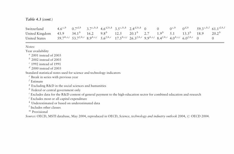
Table 4.3 (cont.)
Switzerland 4.6c,h 0.7d,h 3.7c,h,k 4.6d,h,k 3.5c,h,k 2.4d,h,k 0 0 0c,h 0d,h 59.3c,h, l 61.1d,h, l
United Kingdom 43.9 34.1b 16.2 9.8b 12.5 20.1b 2.7 1.9b 5.1 13.3b 18.9 20.2b
United States 59.7h, i, j 53.7 f,h, i 8.9h, i, j 5.6 f,h, i 17.5h, i, j 26.3 f,h, i 9.9h, i, j 8.4 f,h, i 4.0h, i, j 6.0 f,h, i 0 0
Notes:
Year availabilitya 2001 instead of 2003b 2002 instead of 2003c 1992 instead of 1991d 2000 instead of 2003
Standard statistical notes used for science and technology indicatorse Break in series with previous yearf Estimateg Excluding R&D in the social sciences and humanitiesh Federal or central government onlyi Excludes data for the R&D content of general payment to the high-education sector for combined education and researchj Excludes most or all capital expenditurek Underestimated or based on underestimated datal Includes other classesm Provisional
Source: OECD, MSTI database, May 2004, reproduced in OECD, Science, technology and industry outlook 2004, # OECD 2004.

health-related research (26%). Only the UK spends comparable per-
centages on these two activities.
This means that the US government spends only about $30 billion a
year on programs unrelated to defense or health technology programs.
In constant dollars this amount has not changed much over the past
decade.
The $3.2 billion budget of the National Science Foundation, which
supports basic physical and computer science research in universities, is
part of the non-defense category. It’s usually assumed that the spillover
from defense programs into commercial applications is modest, but
there have been some noteworthy contributions, such as supercompu-
ters, the Internet, and satellite technology.
One agency stands out in this regard: the Defense Advanced Research
Projects Agency (DARPA), with about $3 billion in funding. DARPA
underwrites the development of multipurpose technologies, and it has a
long history of supporting projects that have had a major impact on the
industrial sector. DARPA and the National Science Foundation (NSF)
have been responsible for funding some farsighted technology develop-
ments, including the early innovations that enabled the Internet.
National research initiatives
Most countries use both indirect and direct research subsidies to encour-
age their high-tech industries. The primary objective is to develop
innovations that will generate thriving local industries.
Indirect subsidies include tax rebates to encourage business spending
on R&D. Direct government subsidies include funding for research
centers, training facilities, centers promoting the inflow of technology
through international relationships, and venture funding of new
companies.
A few examples of national research initiatives will illustrate the
variety of approaches used by different countries.
United States: Albany Nanotech Facility
The Albany Nanotech Facility is a regional (rather than national)
initiative in support of a highly specialized industry. The facility is
funded in part by the State of New York to develop semiconductor
manufacturing processes. It is expected to cost about $600 million over
seven years, and will serve the advanced technology needs of US-based
semiconductor manufacturers such as IBM, Micron Technologies, and
144 Competing for the future

Texas Instruments, as well as those of Applied Materials and other
suppliers of production equipment for this industry.27
Taiwan: Industrial Technology Research Institute (ITRI)
Established in 1973, ITRI is a government-managed laboratory which
serves its country’s industries by centralizing certain R&D functions.
Its long, successful history merits special attention.28
ITRI provides over 600 local companies in Taiwan with many of the
services that the big corporate laboratories used to furnish to their
parent companies. Offerings range from training programs to the
management of technology transfers from foreign sources.
The distribution of ITRI’s programs, shown in Figure 4.6, covers
both established and developing fields of industrial activity in Taiwan.
Communicationand OptoelectronicTechnology45%
Advanced Materials andChemical Technology
11%
Precision Machineryand MEMSTechnology
25%
Sustainable DevelopmentTechnology5%
Others2%
Biomedical Technology
12%
Revenue: US$506 Million (2003)
Government Research Project 54%, Industrial Contract Service 46%
Source: ITRI
4.6. Division of programs at Taiwan’s Industrial Technology Research
Institute (ITRI) in 2003. Reprinted with permission from ITRI (ref. 28).
27 D. Lammers, ‘‘Albany lands lead on litho R&D stage,’’ EE Times (July 25,2005), 1.
28 Presentation by Dr. P. Lin, Vice President of ITRI (August 26, 2004).
R&D goes global 145

For example, 47 percent of ITRI’s revenues from optoelectronic and
communications technology go to support research on displays and
light emitting diodes, areas where Taiwan has built a world-leading
manufacturing position.
Its precision machinery and micro-electro-mechanical systems
(MEMS) technology activities, on the other hand, address an emerging
industrial area of great importance: new sensor technology that marries
mechanical and electronic concepts to create new products.
In 2003 ITRI had a staff of about 6,200 people (including 813
PhDs), and a budget of about $500 million as shown in Figure 4.7.
The government provided 54 percent of its funding. The remaining
46 percent came from industrial contracts, under which the organ-
ization produces intellectual property for the exclusive use of the
funders.
The institute also functions as an incubator for new businesses, and
as a training facility for management and technical personnel for local
industries.
Others 3005%
Bachelors 1,22120%
Master 3,07049%
Associates 79013%
Doctorates 81213%
Total Manpower as of December 31, 2003: 6,193
Source: ITRI
4.7. Educational background of the staff of Taiwan’s Industrial Technology
Research Institute (ITRI) in 2003. Reprinted with permission from ITRI
(ref. 28).
146 Competing for the future
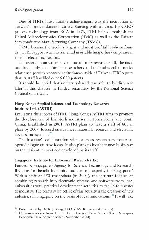
One of ITRI’s most notable achievements was the incubation of
Taiwan’s semiconductor industry. Starting with a license for CMOS
process technology from RCA in 1976, ITRI helped establish the
United Microelectronics Corporation (UMC) as well as the Taiwan
Semiconductor Manufacturing Company (TSMC).
TSMC became the world’s largest and most profitable silicon foun-
dry. ITRI support was instrumental in establishing other companies in
various electronics sectors.
To foster an innovative environment for its research staff, the insti-
tute frequently hosts foreign researchers and maintains collaborative
relationships with research institutions outside of Taiwan. ITRI reports
that its staff has filed over 6,000 patents.
It should be noted that university-based research, to be discussed
later in this chapter, is funded separately by the National Science
Council of Taiwan.
Hong Kong: Applied Science and Technology Research
Institute Ltd. (ASTRI)
Emulating the success of ITRI, Hong Kong’s ASTRI aims to promote
the development of high-tech industries in Hong Kong and South
China. Established in 2001, ASTRI plans to have a staff of 800 in
place by 2009, focused on advanced materials research and electronic
devices and systems.29
The institute’s collaboration with overseas researchers fosters an
open dialogue on new ideas. It also plans to incubate new businesses
on the basis of innovations developed by its staff.
Singapore: Institute for Infocomm Research (IIR)
Funded by Singapore’s Agency for Science, Technology and Research,
IIR aims ‘‘to benefit humanity and create prosperity for Singapore.’’
With a staff of 350 researchers (in 2004), the institute focuses on
combining research into electronic systems and software from local
universities with practical development activities to facilitate transfer
to industry. The primary objective of this activity is the creation of new
industries in Singapore on the basis of local innovations.30 It will take
29 Presentation by Dr. R. J. Yang, CEO of ASTRI (September 2005).30 Communications from Dr. K. Lai, Director, New York Office, Singapore
Economic Development Board (November 2004).
R&D goes global 147
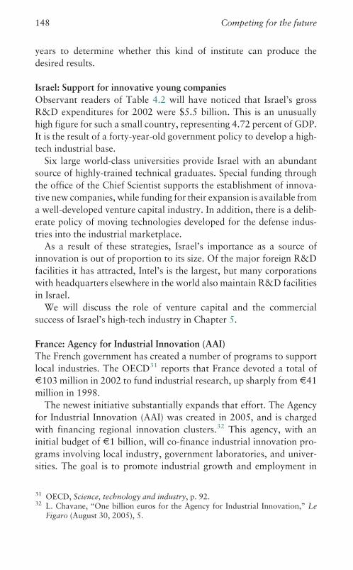
years to determine whether this kind of institute can produce the
desired results.
Israel: Support for innovative young companies
Observant readers of Table 4.2 will have noticed that Israel’s gross
R&D expenditures for 2002 were $5.5 billion. This is an unusually
high figure for such a small country, representing 4.72 percent of GDP.
It is the result of a forty-year-old government policy to develop a high-
tech industrial base.
Six large world-class universities provide Israel with an abundant
source of highly-trained technical graduates. Special funding through
the office of the Chief Scientist supports the establishment of innova-
tive new companies, while funding for their expansion is available from
a well-developed venture capital industry. In addition, there is a delib-
erate policy of moving technologies developed for the defense indus-
tries into the industrial marketplace.
As a result of these strategies, Israel’s importance as a source of
innovation is out of proportion to its size. Of the major foreign R&D
facilities it has attracted, Intel’s is the largest, but many corporations
with headquarters elsewhere in the world also maintain R&D facilities
in Israel.
We will discuss the role of venture capital and the commercial
success of Israel’s high-tech industry in Chapter 5.
France: Agency for Industrial Innovation (AAI)
The French government has created a number of programs to support
local industries. The OECD31 reports that France devoted a total of
E103 million in 2002 to fund industrial research, up sharply from E41
million in 1998.
The newest initiative substantially expands that effort. The Agency
for Industrial Innovation (AAI) was created in 2005, and is charged
with financing regional innovation clusters.32 This agency, with an
initial budget of E1 billion, will co-finance industrial innovation pro-
grams involving local industry, government laboratories, and univer-
sities. The goal is to promote industrial growth and employment in
31 OECD, Science, technology and industry, p. 92.32 L. Chavane, ‘‘One billion euros for the Agency for Industrial Innovation,’’ Le
Figaro (August 30, 2005), 5.
148 Competing for the future

various parts of France. Out of the 105 fields of activity proposed for
funding by the regions, the agency selected sixty-seven, a clear indica-
tion of the scope of its ambitions.
Belgium: Interuniversity Microelectronics Center (IMEC)
Although Belgium does not have a significant semiconductor manu-
facturing industry, it does have a leading microelectronics research
laboratory. IMEC,33 founded in 1984, is an independent institution
affiliated with local universities and supported by government grants
and industrial research contracts. The range of its activities, and its
unique mission, require some explanation.
IMEC’s facilities are staffed and equipped to develop commercial
grade manufacturing technologies. Its permanent staff of about 900
scientists, engineers, and technicians, plus an additional 400 temporary
guest researchers, can prove out new processes on a fully-equipped
prototype production line.
In sharp contrast to the programs we have been considering so far,
IMEC’s objectives include the globalization of sophisticated technol-
ogy developed at the center. Guest researchers are expected to transfer
the technologies developed at the center to their employers when they
return home. For example, IMEC-trained staff have facilitated the
start-up of new chip production facilities in China.
IMEC’s 2004 operating budget of E159 million was partly funded
by the Belgian government, which contributed 24 per cent of the total.
Contracts from sponsors that gain access to its technology provide
the remainder. These sponsors include corporations in Europe, the US,
and Asia.
In return for their funding, sponsors also benefit from an activity that
is just as important as personnel training. The center performs the kind
of materials science research that was one of the trademark contribu-
tions of the big central laboratories at IBM, AT&T, and RCA. As we
have already noted, materials research is a costly undertaking. It is
obviously more economical to share its cost among several funding
sources than to pursue it on an individual basis.
33 From IMEC history, www.imec.be/wwwinter/about/en/IMEChistory.shtml(accessed on April 30, 2006).
R&D goes global 149

IMEC’s productivity, and its standing in the technical community is
indicated by the number of papers its researchers publish on their
results – 1,400 in 2004 alone. It is a highly respected institution.
Commercial contract research: Sarnoff Corporation
There are a number of independent organizations in the US that con-
duct research on behalf of government agencies and industrial clients.
They include Battelle, SRI International, Midwest Research Institute,
Southwest Research Institute, and Sarnoff Corporation.
Sarnoff, a subsidiary of SRI, is the successor to RCA Labs, where
I worked as a researcher and manager. I have served on its board for a
number of years, and am chairman at the time of writing. The com-
pany’s unusual charter suggests an alternative approach to fostering
innovation and creating new high-tech companies.
Unlike other independent research organizations, including its parent
SRI, Sarnoff is a for-profit enterprise. It is also set apart by its client base
and commercial focus. While government research accounts for up to 60
percent of contracts, Sarnoff has historically maintained a good balance
between government and commercial clients. It has shown uncommon
skill in developing marketable technologies and products, a legacy of its
decades of experience in creating technologies for RCA to commercialize.
During the nearly twenty years since its separation from RCA, Sarnoff
has developed some of the most successful commercial products and tech-
nologies in history on behalf of its clients. It was instrumental in creating
direct digital satellite TV, the US standard for digital HDTV, radio fre-
quency ID chips, computer vision technology, advanced LCD displays,
in silico drug discovery algorithms and processors, disposable hearing
aids, MEMS sensors, and self-configuring communication networks.
Sarnoff also participated in the founding of more than twenty new
companies to commercialize its innovations. In recent years it has
established subsidiaries in Asia and Europe to build a global innovation
network for its clients. It is still too early to assess the impact of these
initiatives, but the company offers an intriguing alternative to govern-
ment, university, and industrial research.
The migration of engineering: India, China, and beyond
Countries with emerging economies are not relying solely on govern-
ment funding to set up R&D centers. As developing countries have
150 Competing for the future

built up their innovation infrastructures, they have been able to attract
an impressive array of leading international companies to invest in
local facilities and engage local technical talent.
A major driver for this migration of engineering work has been the
much lower costs in developing countries as compared to those in
Western Europe, Japan, and the US.
A few years ago these investments might have been confined to low-
cost, labor-intensive manufacturing plants in China, or business service
centers in India. More recently, corporations have been building soft-
ware development centers in India, and product development and
engineering facilities in both China and India. There is similar activity
in other parts of Asia, though on a smaller scale.
This phenomenon is no longer confined to European and US com-
panies. Engineering is migrating from Japan, South Korea, and Taiwan
as well. Here are just a few examples of the trend.* Intel, which already has 2,000 engineers in India, expects to have
about 1,000 in China by the end of 2006.* Microsoft has about 200 people in its central research laboratory in
China. This organization is charged with exploratory research and is
not directly affiliated with specific product groups.* Cypress Semiconductor, a billion-dollar company, will expand its
engineering organization in India from 200 engineers to about 700 in
2007. Cypress says that the chip design effort conducted there has
produced forty US patents in ten years.34 Cypress also owns an
engineering center in China.* MediaTek (Taiwan), a leading consumer electronics chip company,
has set up an R&D center in Singapore which will have about 300
chip design engineers.* Motorola had 2,500 software engineers in India in 2005 and plans to
add another 1,000.* General Electric’s largest R&D center is in India, with 2,300 engi-
neers involved in product development for areas including power
trains and medical instruments.35
34 ‘‘Cypress plans $10 million Indian R&D center,’’ Electronic News (September19, 2005).
35 S. J. Binggaman, ‘‘Maintaining America’s competitive edge,’’ APS News (June2005), 8.
R&D goes global 151

* IBM has thousands of engineers in China and India. The company
also works with new businesses around the world in product areas of
interest to IBM. In this way, and through a network of venture
capital funding sources, it can keep track of new companies with
products that it needs and acquire them if they fit the corporate
strategy.36
* Alcatel of France manufactures telecommunications equipment in
China through Alcatel Shanghai Bell (ASB), which is a joint venture
with the Chinese government. ASB employs 2,000 engineers. It
enjoys the status of a domestic business entitled to government
subsidies and such financial benefits as partial support for R&D
and preferred access to bank capital. ASB develops many of the
products sold by Alcatel worldwide, and manufactures them in
China under very favorable cost conditions.37
* Siemens has thousands of engineers in China and India involved in
both software and equipment development.* Infosys Technologies, an Indian information technology services
company, in 2005 reported plans to hire 6,000 software engineers
in China, which would allow it to participate in the IT service
business in China as well as do contract work for overseas
businesses.38
Few issues are as emotionally charged today as the ‘‘outsourcing’’ of
jobs. The temperature of the debates over this practice will no doubt
rise as engineering is shifted overseas to join the business process
functions already being relocated to India.
The availability of trained engineers in emerging economies does
allow more value-added engineering to be done at a lower cost than
previously possible. This is good news in an age of reduced R&D
budgets. In the long run, China and India will also benefit because
their engineers are learning state of the art technologies, thus expand-
ing native innovative capabilities.
But this does not mean these countries have caught up with the
advanced economies. Developed countries still produce a greater
36 A. Clark, ‘‘Innovation sourcing: Leveraging the global ecosystem,’’ VentureCapital Review (Summer 2005), 7.
37 Presentation to industry analysts by Alcatel spokesperson, Olivia Qiu (2005).38 K. Merchant, ‘‘Infosys plans to hire 6,000 staff in China,’’ Financial Times
(October 1–2, 2005), 8.
152 Competing for the future
number of contributors to the more innovative areas of product
research and development. These countries have resources that their
newly industrializing partners cannot match: the generally higher qual-
ity of their universities, the influx of talented foreigners, and the
maturity of their research institutions.
The growing importance of university research
The university has often been portrayed as an ivory tower, insulated
from the hubbub of the commercial world, where theoretical studies
increase the store of general human knowledge. Tangible innovations
that emerge from this bastion of intellectual inquiry are byproducts of
its central mission.
This view of university research is no longer tenable. Universities in
general, and technical institutes in particular, are increasingly involved
in the development of innovative technology, which they license to
outside companies or commercialize through venture capital-funded
start-ups.
Exactly how critical universities are in building high-tech industrial
prowess is difficult to pin down. The facts and figures on funding and
productivity are uncertain. But there is enough to suggest the impor-
tance of their role.
Funding the research
University operations in most countries are fully supported by their
national governments.39 Table 4.3 (shown earlier) shows that in many
countries expenditures in support of universities exceed 30 percent of
government R&D budgets. Between 1991 and 2003 the trend was for
this percentage to increase. There is no equivalent national number for
the US because most universities are either private or funded by one of
the fifty states.
39 One major developed country recently moved away from this model. Japan’sprestigious national universities have been spun out of the government as inde-pendent educational corporations. They must apply for government fundingbased on merit. They are also being encouraged to become more open tocollaboration with business and industry through joint projects and the licensingof intellectual property.
R&D goes global 153
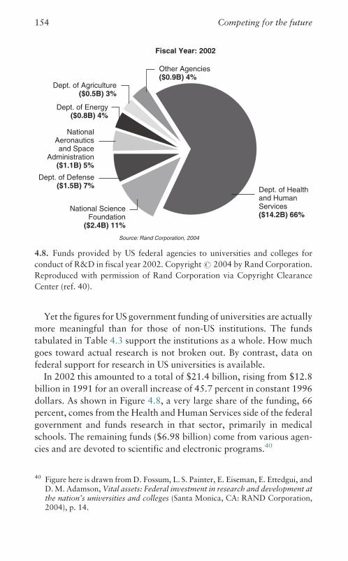
Yet the figures for US government funding of universities are actually
more meaningful than for those of non-US institutions. The funds
tabulated in Table 4.3 support the institutions as a whole. How much
goes toward actual research is not broken out. By contrast, data on
federal support for research in US universities is available.
In 2002 this amounted to a total of $21.4 billion, rising from $12.8
billion in 1991 for an overall increase of 45.7 percent in constant 1996
dollars. As shown in Figure 4.8, a very large share of the funding, 66
percent, comes from the Health and Human Services side of the federal
government and funds research in that sector, primarily in medical
schools. The remaining funds ($6.98 billion) come from various agen-
cies and are devoted to scientific and electronic programs.40
Other Agencies($0.9B) 4%
Dept. of Healthand HumanServices($14.2B) 66%
National Aeronautics
and SpaceAdministration
($1.1B) 5%
Dept. of Energy($0.8B) 4%
Dept. of Agriculture($0.5B) 3%
Dept. of Defense($1.5B) 7%
National ScienceFoundation
($2.4B) 11%
Source: Rand Corporation, 2004
Fiscal Year: 2002
4.8. Funds provided by US federal agencies to universities and colleges for
conduct of R&D in fiscal year 2002. Copyright # 2004 by Rand Corporation.
Reproduced with permission of Rand Corporation via Copyright Clearance
Center (ref. 40).
40 Figure here is drawn from D. Fossum, L. S. Painter, E. Eiseman, E. Ettedgui, andD. M. Adamson, Vital assets: Federal investment in research and development atthe nation’s universities and colleges (Santa Monica, CA: RAND Corporation,2004), p. 14.
154 Competing for the future

A survey published by The Economist lists what are believed to be
the top twenty research universities in the world in 2005. Of these, as
shown in Table 4.4,41,42 seventeen are in the US. The table also shows
Table 4.4 The world’s top universitiesa and annual R&D funding from
US government for US institutionsb
World’s top
university
rankings World’s top universities
US federal funds
received in 2002 –
excluding medical
school ($m)
1 Harvard University 193
2 Stanford University 178
3 University of Cambridge NA
4 University of California, Berkeley 224
5 Massachusetts Institute of Technology 381
6 California Institute of Technology 64
7 Princeton University 80
8 University of Oxford NA
9 Columbia University 129
10 University of Chicago 48
11 Yale University 67
12 Cornell University 149
13 University of California, San Diego 223
14 Tokyo University NA
15 University of Pennsylvania 118
16 University of California, Los Angeles 193
17 University of California, San Francisco 71
18 University of Wisconsin, Madison 253
19 University of Michigan, Ann Arbor 216
20 University of Washington, Seattle 267
Notes:a Ranked by a mixture of indicators of academic and research performance, including
Nobel Prizes and articles in respected publications, reported in The Economist, ‘‘The
brains business’’ (September 10, 2005), 4 (ref. 41).b D. Fossum, L. S. Painter, E. Eiseman, E. Ettedgui, and D. M. Adamson, Vital assets:
Federal investment in research and development at the nation’s universities and
colleges (Santa Monica, CA: RAND Corporation, 2004), pp. C-13–C-14 (ref. 42).
41 The Economist ‘‘The brains business,’’ 4.42 Fossum, Painter, Eiseman, Ettedgui, and Adamson, Vital assets, pp. C-13 and C-14.
R&D goes global 155

government funds for R&D received by these institutions in fiscal year
2002, excluding support of medical school research.
When medical school funding is included the level of federal funding is
much larger. For example, the University of Michigan (Ann Arbor) received
$429 million in 2002 which increased to $517 million in 2003.43
Although there are 3,200 colleges and universities in the US, only a
few can support large, federally funded research programs. The reci-
pients of such programs are concentrated in a group of 100 universities,
which together receive more than 80 percent of the funds.
There is also great disparity within this elite group of 100. The top
twenty schools get the lion’s share of 45 percent. The 100th recipient,
for example, the University of South Carolina, received $32 million
compared to MIT’s total of $381 million.
It should be easy to quantify the industrial impact of this level of
R&D spending, but in fact trying to correlate university research
funding with its ultimate commercial value is a futile endeavor. This
is partly due to the nature of the research.
Universities increasingly perform applied research in physical
sciences, electronic devices, and software – the kind of research that
used to be done in the big corporate research laboratories. It is notor-
iously difficult to transfer the results of such work into practical appli-
cations, because the process is so random and inefficient.
How, then, does government-funded work become available to ben-
efit the industrial world? There are a number of mechanisms, including:* Open publication of research results, a valuable source of informa-
tion and ideas for commercial companies.* Placing graduate students in research projects in disciplines of poten-
tial commercial interest to give them job training. These people can
become productive very quickly in an industrial R&D environment,
which clearly benefits local industry.* Patenting innovations conceived by the faculty at major research
universities, and licensing these patents to industry. As shown in
Figure 4.9,44 revenues to US universities from the licensing of patents
43 J. V. Lombardi, E. D. Capaldi, K. R. Reeves, and D. S. Mirka, The top Americanresearch universities, 2005, an annual report from the Lombardi Program onmeasuring university performance (The Center, University of Florida, 2005), p. 20.
44 S. A. Merrill, R. C. Levin, and M. B. Myers (eds.), A patent system for the 21stcentury (Washington, DC: National Academies Press, 2004), p. 34; derived from
156 Competing for the future

and technology rose from under $200 million in 1991 to about $1.38
billion in 2004.* Allowing part-time consulting by faculty, usually up to a day a week.
This is an efficient way to transfer knowledge to industry while
providing financial rewards to the faculty.* Transfer of new ideas and concepts as seeds for new products, or
even for new businesses started with venture capital funding. Some
universities allow faculty to take a leave of absence for starting
businesses or other commercial pursuits.* Leveraging of university-developed technologies into new products
by existing businesses. We will discuss the cases of Sensors Unlimited
and Analog Devices later.
Can one measure the economic value of university research?
Unfortunately, no. There is no question that universities such as
MIT, the California Institute of Technology, University of Michigan,
Stanford University, the University of California (Berkeley),
Source: AUTM (2005)
1200
Mill
ions
of D
olla
rs
1000
0
1400
1600
800
600
400
200
1992
1993
1994
1995
1996
1997
1998
1999
2000
2001
2002
2003
2004
Year
4.9. Net license income of US research universities. Reprinted with permission
from AUTM US licensing survey summary: FY 2004 (Northbrook, IL:
Association of University Technology Managers, 2005) (ref. 44).
AUTM US licensing survey summary: FY 2004 (Northbrook, IL: Association ofUniversity Technology Managers, 2005).
R&D goes global 157

Cambridge University, and Carnegie Mellon University have been the
source of many important industrial innovations. However, these only
gained commercial importance when the concepts were turned into
products outside of the university environment.
Creating clusters of innovation
There is one clear indication of how important a university can be in the
development of a technology. It is the increasing influence of clusters of
high-tech industries that have grown up around large research universities.
The most successful examples, the ones that everyone else strives to
replicate, were built in the San Francisco Bay area around Stanford
University and the University of California–Berkeley. Large high-tech
industry clusters were also built around MIT and Harvard University in
the Boston area, and around Carnegie Mellon University in Pittsburgh.
Cambridge University in the UK has attracted corporate research
centers because of the local availability of outstanding talent. It has also
generated companies from research in biotechnology, silicon chips,
displays, and software. For example, Sir Richard Friend, Cavendish
Professor of Physics at Cambridge, is the co-founder of two companies
based on his research. Professor Andy Hopper is the co-founder of
twelve companies.
The conditions required to create such innovation clusters are not
easy to duplicate. They include universities with outstanding faculties,
students, and researchers from around the world; funding for research
programs from industry and other sources; and the availability of local
entrepreneurs and venture capital. The faculty must also be tempted to
get involved in new ventures, which usually means offering financial
incentives.
The hardest requirement to meet may be the availability of entrepre-
neurs. This subject is discussed in Chapter 5. Entrepreneurship is not a
universal urge among technologists. It is fairly common in the US,
Canada, and Israel (and increasingly the UK). But for cultural and
regulatory reasons it is much rarer in other countries.
Cultures in which failure condemns the individual to a life of shame
are not conducive to entrepreneurism. Unwillingness to assume career
risks on a personal level is a major deterrent to starting a new business.
To avoid failure, the inclination of technically trained people in those
cultures is toward employment in big companies or the government.
158 Competing for the future

Restrictive government regulations designed to protect employment
also discourage entrepreneurship in many countries. While it is easy to
hire people, the regulations make job elimination very difficult. Since a
start-up must be able to trim expenses (including employees) very
quickly if it is to survive unexpected financial setbacks, these con-
straints threaten its existence.
This is a particular problem in some European countries. Jacques
Delpla, economic advisor to the interior minister of France, has
remarked that ‘‘a Google or a Microsoft could not happen in France.’’45
Another problem in moving university innovations into the market is
the scarcity of venture capital needed for seed financing of risky busi-
ness ideas. Funds dedicated to this kind of investing are rare inter-
nationally because professional investors favor lower-risk situations
where technology issues are well under control. Lam Kong-Peng,
director of Singapore’s Biomedical Research Council, has commented
on the need ‘‘to educate Asian investors, who tend to be more cautious
than western investors.’’46
University/industry collaboration: Effective innovationpartnerships
The most effective way to exploit university research in building a high-
tech industry is to make the two sides partners. For a long time that
wasn’t even possible, since research in the physical sciences at US
universities was a rather primitive affair.
Professors focused on theoretical research because they didn’t have
adequate labs for more practical investigations. Scientists interested in
more practical research in fields like atomic energy or advanced com-
puting gravitated to the National Laboratories, attracted by their
excellent facilities and freedom from day-to-day funding pressures.
All that changed in the 1960s with a massive increase in funding for
university research from the US Department of Defense. This was a
reaction to the surprise launch of two Sputnik satellites by the Soviet
Union in 1957. In an effort to close a perceived technology gap with the
45 Quoted in J. Gapper, ‘‘Better to be a foreigner than an entrepreneur,’’ FinancialTimes (October 6, 2005), 15.
46 Quoted in C. Cookson, ‘‘Innovative Asia: How spending on research and devel-opment is opening the way to a new sphere of influence,’’ Financial Times (June9, 2005), 15.
R&D goes global 159

Soviets, government made funding available to major universities to
support research on materials, electronic devices, and computer science.
This was the first time government funding had been provided to
facilitate ‘‘practical’’ experimental work. It helped turn the US research
university into a quasi-industrial business, ready to take on develop-
ment programs formerly restricted to corporate laboratories.
Coincidentally, this seismic shift happened just as large US corpora-
tions were beginning to de-emphasize basic research in their own labs.
As a result of the combination of circumstances, PhD level engineers
and scientists were increasingly drawn to academic careers.
Eventually a new generation of researchers, composed of top scien-
tists drawn from the big corporate laboratories, joined university
faculties and obtained research grants. They were willing and able to
tackle problems addressing industrial and defense needs. This effec-
tively changed the academic attitude toward ‘‘practical’’ research.
For example, Stanford University became a leading semiconductor
device research center in the 1960s when a highly-respected scientist,
Dr. Gerald Pearson, joined the faculty after a long career at Bell
Laboratories. Students trained at Stanford University during that time
later staffed many of the Silicon Valley semiconductor companies.
Having started university centers of expertise with government
grants, professors soon added consulting to their portfolios of activ-
ities. In this way they obtained corporate sponsorship for their
research.
The passage of the Bayh-Dole Act in 1980 further encouraged, and in
many cases enabled, technology transfers between university labs and
commercial companies. The Act allows American universities to retain
rights to technology they develop under federal funding. It also permits
small or emerging companies to build their business plans on technol-
ogy developed at research universities.
The Bayh-Dole Act set the stage for risk-taking by entrepreneurs in
high-tech collaborations between university labs and venture start-ups.
The following two case histories show how different these collabora-
tions could be from one another.
Princeton and Sensors Unlimited: New company launch
One successful technology transfer involved a novel imaging device
operating with non-visible infrared (IR) light. The technology behind
160 Competing for the future

the device was developed at Princeton University, and then transferred
to Sensors Unlimited, also in Princeton, NJ.
The imaging device has become a key element in night vision systems
and various industrial applications. Its basic technology was developed
by Prof. Stephen Forrest, a distinguished scientist who had left Bell
Laboratories in 1985 to join the University of Southern California, and
later relocated to Princeton.47
In 1990, Dr. Marshall Cohen and Dr. Greg Olsen, the latter a former
RCA Laboratories scientist and founder of Sensors Unlimited,
approached Prof. Forrest with a proposal. They wanted to collaborate
on the development of commercial imaging systems based on Forrest’s
invention.
This was not a simple undertaking. The fabrication of such devices is
an extremely capital-intensive process. It requires several million dol-
lars worth of equipment and clean room facilities to create even the
most rudimentary capabilities for device manufacture.
Fortunately, the university had just won a large grant from the State
of New Jersey for the express purpose of moving photonic technologies
(including IR detector arrays) from academic laboratories into the
marketplace. This was part of a plan to transform the basis of the
state’s economy from manufacturing to high-tech.
In fact, Prof. Forrest had been recruited to Princeton to manage that
state grant through the university’s newly-founded Center for
Photonics and Optoelectronic Materials (POEM). So a deal was made.
Both Prof. Forrest and Dr. Olsen were sensitive to the different and
sometimes conflicting objectives of the university and the new com-
pany. The company’s goal was to build a profitable business manufac-
turing new products based on proprietary technology. The university,
on the other hand, had as its mission the generation of new knowledge
and the education of the next generation of scientists and engineers.
To meet the needs of both parties, all of the initial work, done jointly
by Prof. Forrest’s students and employees of Sensors Unlimited, was
devoted to engineering research: investigating new ideas for making the
devices more efficient, reliable, or versatile. This allowed the students
to publish papers on new results – a necessary step in meeting require-
ments for their advanced degrees in electrical engineering.
47 H. Kressel conversation with Professor S. Forrest, July 2005.
R&D goes global 161

At first glance this would not appear to move the company toward its
goal of profitability. In fact, the mechanism for financing this initial
work did advance this goal.
The joint university/industry team was funded through the Small
Business Innovation Research (SBIR) program sponsored by several
US government agencies. To get an SBIR grant, a company must win
competitive awards for developing new product technologies. A team
that took innovative ideas developed at a university, turned them into
products, and had an eventual commercial outlet through an aggressive
small business was precisely the type of organization the SBIR program
was established to support.
After three years of collaborative research, Sensors Unlimited was
able to market a unique product that outperformed its competitors.
With this product it established customer relationships that gave it
strong prospects for future success. At this juncture the company
could afford to build its own fabrication facility and begin large-scale
commercial production.
Although the initial phase of the relationship had served its purpose,
Sensors Unlimited and Princeton University continued to collaborate
closely on many projects over the ensuing seven years. The early
experiences of working together, of having students collaborate closely
with company technical staff on numerous innovative projects, created
a culture at both Princeton and Sensors Unlimited that encouraged
innovation and teamwork.
This culture served both entities extremely well. A number of
Princeton graduates assumed jobs and even significant leadership
roles within the company. Sensors Unlimited became one of the world’s
leading manufacturers of IR detectors.
In 2000 this self-financed company, built on the concept of partner-
ing in innovation with a university, was sold to Finisar, Inc. for $600
million. Two years later the company was reacquired in a management
buyback. It is now part of the Optical and Space Systems Division of
the Goodrich Corporation.
Berkeley, MIT, and Analog Devices: New product launch
Sensors Unlimited was a start-up. The industrial partner in this second
case history is a large, established company collaborating with not one,
but two universities.
162 Competing for the future
The University of California–Berkeley and the Massachusetts
Institute of Technology had received complementary Department of
Defense funding in sensor technology. Ray Stata, co-founder of Analog
Devices, a leading semiconductor company, remembers that faculty
enthusiasm for corporate sponsorship of university research dramati-
cally increased as government grants become more difficult to obtain in
the 1980s.
Analog Devices was enthusiastic too. It is a billion-dollar manufac-
turing company that supports product development, but it does not
have a central research laboratory of its own. Academic research
offered a way to fill that void at modest cost. For that reason the
company funded several small research programs at top universities
in the 1980s to build on the results of Department of Defense-funded
programs in sensors.
The Berkeley/MIT program involved the development of inertial,
pressure, and acoustic sensors, all based on a novel semiconductor
technology that integrated mechanical and electronic functions into a
single device. These devices are used in automobile applications to
provide the trigger mechanism for air bags.
This program represents a perfect application of the ABC model of
innovation shown in Figure 3.1, with the universities contributing to
the concept and early development (the ‘‘A’’ phase of the program), and
Analog Devices engineers taking the product from Aþ to B.48
The result was a huge commercial success. More than 200 million of
these devices have been shipped since their introduction in the 1990s.
Mr. Stata attributes his company’s current (2005) dominant position in
this class of sensors to the collaborative programs conducted with
Berkeley and MIT.
Publications and patents: A shift to Asia, universities
Earlier in this chapter we saw how innovation activity is increasing in
China, India, South Korea, and other Asian countries. As we have just
seen, universities are also attaining new stature as centers of applied
R&D.
48 H. Kressel conversation with R. Stata, June 10, 2005.
R&D goes global 163

One would expect that these major changes would be reflected in
two leading indicators of increased scientific activity, publications and
patents. This is indeed the case.
To get a sense of which countries of origin appeared more often, I
surveyed journals from scientific or engineering societies. In the realm
of scientific publications, however, all technical journals are not cre-
ated equal. For a truer picture of the value of the work being published,
I focused on a few highly-respected journals.
These are refereed or peer-reviewed publications, meaning that the
articles they contain have been reviewed by anonymous experts who
recommend their inclusion based on the importance and validity of the
results they describe. I looked at four English-language publications
covering materials science, electronic devices, and software that
attract submissions from around the world: Applied Physics Letters
(published by the American Physical Society), IEEE Transactions on
Software Engineering (published by the IEEE), Communications of the
ACM (published by the Association for Computing Machinery), and
Electronics Letters (published by the UK’s Institution of Engineering
and Technology).
A survey of the geographical origin of papers dealing with the
physical sciences in two publications, Applied Physics Letters and
Electronics Letters, is shown in Figure 4.10a. It demonstrates that
US contributions have dropped from about 60 per cent in 1988 to
30 per cent in 2004. In that time, contributions from Asia (excluding
Japan) have increased from 5 per cent or less to between 25 and 36 per
cent.
Figure 4.11a shows that articles in the software-oriented journals
(IEEE Transactions on Software Engineering and the Communications
of the ACM) exhibit a similar trend. In 1988 US contributions were in
the 75 per cent range for both publications, whereas in 2004 they
constituted only 35 per cent of the former. (Figures for the latter
remained fairly stable.)
Figure 4.10b also shows that fewer and fewer of the authors are
affiliated with corporations. In the physical sciences, contributions
from corporate research centers declined from 40 per cent in 1988 to
20 per cent or less in 2004. During the same period, contributions from
universities rose from 45 to nearly 70 per cent.
In the software field, Figure 4.11b, university contributions have
stayed in the 60–70 per cent range, while corporate contributions have
164 Competing for the future

1988 Comparison ofDistribution by Country or Region
70
60
50
40
30
20
10
0
US Europe Japan Asia Other
Per
cent
(%
)
2004 Comparison ofDistribution by Country or Region
0
70
60
50
40
30
20
10
US Europe Japan Asia Other
Per
cent
(%
)
Applied Physics Letters Electronics Letters
4.10(a). The changing sources of publications in the physical sciences and
engineering in two publications, Applied Physics Letters and Electronics
Letters, between 1988 and 2004 by country or region of origin.
1988 Comparison ofDistribution by Source
2004 Comparison ofDistribution by Source
80
70
60
50
40
30
20
10
0CorporateResearch
Center
CorporateResearch
Center
IndependentResearchInstitute
IndependentResearchInstitute
GovernmentResearchInstitute
GovernmentResearchInstitute
University University
80
70
60
50
40
30
20
10
0
Per
cent
(%
)
Per
cent
(%
)
Applied Physics Letters Electronics Letters
4.10(b). The changing sources of publications in the physical sciences and
engineering in two publications, Applied Physics Letters and Electronics
Letters, between 1988 and 2004 by the nature of the authors’ institution.
R&D goes global 165

IEEE Transactions on Software Engineering Communications of the ACM
1988 Comparisons of Software JournalsDistribution by Country or Region
2004 Comparisons of Software JournalsDistribution by Country or Region
80
70
60
50
40
30
20
10
0US Europe Japan Asia Other
80
70
60
50
40
30
20
10
0US Europe Japan Asia Other
Per
cent
(%
)
Per
cent
(%
)
4.11(a). The changing sources of publications on software in the IEEE
Transactions on Software Engineering and Communications of the ACM
between 1988 and 2004 by country or region of origin.
1988 Comparison of Software JournalsDistribution by Source
2004 Comparison of Software JournalsDistribution by Source
80
70
60
50
40
30
20
10
0
80
70
60
50
40
30
20
10
0
IEEE Transactions on Software Engineering
Per
cent
(%
)
Per
cent
(%
)
CorporateResearch
Center
IndependentResearchInstitute
GovernmentResearchInstitute
University CorporateResearch
Center
IndependentResearchInstitute
GovernmentResearchInstitute
University
Communications of the ACM
4.11(b). The changing sources of publications on software in the IEEE
Transactions on Software Engineering and Communications of the ACM
between 1988 and 2004 by the nature of the authors’ institution.
166 Competing for the future

declined from the 25–30 percent range to under 20 percent. On the other
hand, government research institutes increased their contributions to the
20 percent range in 2004 from a negligible amount in 1988.
Although there are signs of a shift to Asia, the changes seen in the
origins of patent filings are not as dramatic. The OECD tracks patents
which their owners deem sufficiently important to file in the European
Union, the US, and Japan simultaneously.49 In the year 2000 that
number was about 42,000, up from about 29,000 in 1991 (see
Table 4.5).
About 34 percent of these patents originated in the US, the same
percentage as in 1991. Japan’s percentage also hardly changed. About
61 percent of the patents filed came from those two countries, a clear
indication of their continuing importance in industrial innovation. China
appears as a participant in 2000 after negligible contributions in 1991.
Figures are also available for the number of patents filed in major
countries during 2004. The se are summari zed by Table 4.7. 50
Japan is in the lead in 2004, followed by the US. Note also the greatly
improved ranking of Korea (third) and China (fifth). The table also
shows that the Japanese filings were heavily weighted toward the
industrial sectors of telecommunications, information technology,
and electronics.
It’s important to note that the number of patents filed in various
countries is not by itself a reliable indicator of their innovative or
commercial value. The overwhelming majority of patents represent
evolutionary innovations of uncertain potential.
But this activity confirms our observation that Asian countries con-
stitute a growing presence in high-tech innovation. Even if most patents
have little individual value, when combined into a portfolio of inter-
connecting intellectual property they may stake a claim on a larger
technical field that is of considerable worth.
Patents are also an indication of long-term strategy. They show that
Asian countries embraced innovation as the path to prosperity, and
that they have created an environment where research and develop-
ment are encouraged and supported.
R&D has truly gone global.
49 OECD, Science, technology and industry, p. 219.50 Table from Thomson Scientific, printed in Financial Times (October 12,
2005), 5.
R&D goes global 167

Table 4.5 Patents simultaneously filed in Europe, the US, and Japan in 1991
and 2000
1991 2000
Country
Number of
triadica patent
families
% of total
world triadica
patent families
Number of
triadica patent
families
% of total
world triadica
patent families
United States 10,217 34.1 14,985 34.3c,e
Japan 8,895 29.7 11,757c,e 26.9c,e
Germany 3,676 12.3 5,777c,e 13.2c,e
France 1,783 6 2,127c,e 4.9c,e
United Kingdom 1,250 4.2 1,794c,e 4.1c,e
Switzerland 723 2.4 753c,e 1.7c,e
Italy 659 2.2 767c,e 1.8c,e
Netherlands 568 1.9 857c,e 2c,e
Sweden 391 1.3 811c,e 1.9c,e
Canada 275 0.9 519c,e 1.2c,e
Finland 161 0.5 489c,e 1.1c,e
Korea 93 0.3 478c,e 1.1c,e
Israel 104 0.3 342c,e 0.8c,e
China 12 0 93c,e 0.2c,e
Rest of World 1,116b 3.9 2,115c,e 4.8c,e
T O T A L W H O L E
W O R L D 28,807c – 41,549c,d,e –
Notes:a Patent filed at the European Patent Office (EPO), the US Patent & Trademark Office
(USPTO), and the Japanese Patent Office (JPO)
Year availabilityb Some 1992 instead of 1991
Standard statistical notes used for science and technology indicatorsc Estimated Underestimated or based on underestimated datae Provisional
Source: OECD, MSTI database, May 2004, reproduced in OECD, Science, technology and
industry outlook 2004, # OECD 2004.
168 Competing for the future
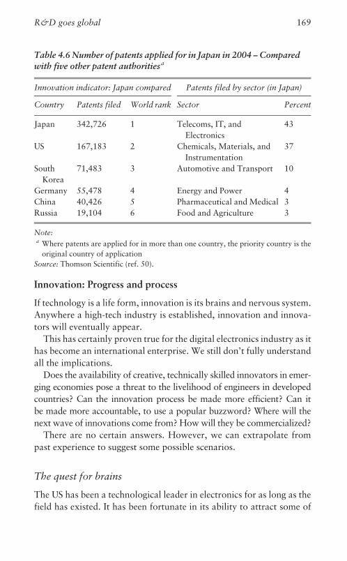
Innovation: Progress and process
If technology is a life form, innovation is its brains and nervous system.
Anywhere a high-tech industry is established, innovation and innova-
tors will eventually appear.
This has certainly proven true for the digital electronics industry as it
has become an international enterprise. We still don’t fully understand
all the implications.
Does the availability of creative, technically skilled innovators in emer-
ging economies pose a threat to the livelihood of engineers in developed
countries? Can the innovation process be made more efficient? Can it
be made more accountable, to use a popular buzzword? Where will the
next wave of innovations come from? How will they be commercialized?
There are no certain answers. However, we can extrapolate from
past experience to suggest some possible scenarios.
The quest for brains
The US has been a technological leader in electronics for as long as the
field has existed. It has been fortunate in its ability to attract some of
Table 4.6 Number of patents applied for in Japan in 2004 – Compared
with five other patent authoritiesa
Innovation indicator: Japan compared Patents filed by sector (in Japan)
Country Patents filed World rank Sector Percent
Japan 342,726 1 Telecoms, IT, and
Electronics
43
US 167,183 2 Chemicals, Materials, and
Instrumentation
37
South
Korea
71,483 3 Automotive and Transport 10
Germany 55,478 4 Energy and Power 4
China 40,426 5 Pharmaceutical and Medical 3
Russia 19,104 6 Food and Agriculture 3
Note:a Where patents are applied for in more than one country, the priority country is the
original country of application
Source: Thomson Scientific (ref. 50).
R&D goes global 169

the finest technical minds in the world, domestic and foreign, and offer
them an environment for success.
This dominance is now being challenged by the creation of huge
pools of technically trained talent in other parts of the world, especially
the emerging countries of Asia. The threat is compounded by economic
factors, especially cost of labor and shrinking profit margins. First
manufacturing moved to areas of the world that offered low-cost
production. Now it seems that engineering will join it.
Does this mean that US leadership in electronic technology is certain
to vanish as popular fears suggest?51
I don’t think so, provided that the US recognizes that the competitive
arena has changed and develops business strategies that take advantage
of the new realities.
The most immediate challenge is outsourcing. The push to reduce
costs by accessing resources globally is an unstoppable force. Product
development accounts for a large share of the costs in high-tech indus-
tries, and there are hundreds of thousands of trained engineers in India
and China available to work on product development at lower salaries
than their counterparts in more developed countries. The migration of
some engineering functions to those resources has already begun, and is
certain to continue.
Yet I don’t think we are dealing with a zero-sum game where out-
sourcing will drain developed countries of all their engineering jobs.
Mindful of the need to protect their intellectual property, international
companies are keeping the more strategic aspects of product develop-
ment closer to home, or at least in locations where piracy is less of a
danger.
There is also the question of quality versus quantity. Large numbers
of less-skilled engineers can’t equal the value of a few creative minds
left free to innovate. At least for now, the true innovators seem to
congregate in countries where strategic R&D is being done.
Measuring the value of R&D
It is an article of popular faith that a higher level of R&D spending
translates into greater economic value. Unfortunately, both experience
51 See, for example, R. Florida, The flight of the creative class (New York, NY:HarperBusiness, 2004).
170 Competing for the future

and recently published studies support a contrary conclusion: the
correlation between research spending and value produced is poor.
This is certainly true on a national level, where R&D projects are
frequently selected to accommodate political constituencies or because
they are the pet projects of planners. In the case of corporations, where
financial accountability is a watchword, you would expect the correla-
tion to be better. You would be wrong, as some recent research on the
subject indicates.
Booz Allen Hamilton surveyed 1,000 publicly-traded companies,
looking for the connection between R&D spending and corporate
financial performance.52 The total R&D spending for these companies
in 2004 was $384 billion, which on average, represented 4.2 percent of
their sales.
R&D expenditures were especially heavy in technology-intensive
industries such as software, health products, computing, and electronics.
The highest spending rates relative to sales, averaging 12.7 percent, was
in the software and Internet sector, while the lowest, 1.5 percent on
average, was in chemicals and energy.
The study found that there was no direct correlation between R&D
as a function of revenues and either growth rate or overall profitability.
However, there was a significant correlation with profitability mar-
gins. Companies that spent large sums on R&D were in a better
position to get into markets early, and hence enjoy better gross profits.
(This did not necessarily translate to better net margins once all com-
pany expenses were included.)
There are two explanations for the results reported in the Booz Allen
Hamilton study. First, translating R&D expenditures into profitable
new products is becoming increasingly difficult; second, in a globally
distributed industry, comparative spending levels are not meaningful.
The first problem is especially difficult to solve, since companies
often have little control over the factors involved. In today’s rapidly
changing technological landscape, short-term product development
projects can miss their market windows, reducing sales and margins.
Long-term projects can be made obsolete before they’re finished, as
52 B. Jaruzelski, K. Dehoff, and R. Bordia, ‘‘The Booz Allen Hamilton globalinnovation 1000 – Money isn’t everything,’’ Strategy and Business 41 (Winter2005), 55–67.
R&D goes global 171

new global competitors emerge from the shadows with cheaper, better
products.
The second point goes to the heart of the R&D quandary. It’s
obvious that in a globally-distributed enterprise the same expenditure
level can buy vastly different amounts of manpower. It all depends on
how much work is assigned to lower-cost engineering staff in, for
example, India.
You could make the case that the international dispersal of R&D
leads to a higher level of real investment, resulting in better returns on
the research dollar. More people can now be employed for the same
budget by shifting significant elements of engineering to locations
where manpower costs are lower.
A new global semiconductor company
New high-tech companies cannot ignore the need to use global
resources in order to speed time to market, control costs, and gain
access to the best possible talent. The Warburg Pincus investing experi-
ence in the past few years has been heavily influenced by these needs,
and our portfolio companies are global in their thinking.
As an example, let’s look at Raza Microelectronics Inc. (RMI), a
company founded by Atiq Raza, which is in the business of designing
and marketing very high-performance multi-core microprocessors for
use in managing IP networks. Its customers include the world’s largest
network equipment companies in the US, EU, and Asia.
The company’s operations are sited in various international loca-
tions. The sites are chosen to fulfill two objectives: finding the best
talent in each region, and placing resources as close as possible to the
company’s customers.
Here is how RMI’s talent is distributed regionally:* San Francisco Bay headquarters: Architecture design team, com-
prised of veterans of high-performance microprocessor design with
experience working at major companies in the field.* India: Software engineering, working in close collaboration with the
US design team.* China: Software engineering, required for support of specific custo-
mer requirements.* Taiwan: Chip manufacturing in the facilities of TSMC, providing
world-class, state-of-the-art processes. The US design teams work
very closely with the TSMC process engineers to ensure that the
172 Competing for the future
company’s products are manufactured for the best possible
performance.* US: Prototype, low-volume system design and manufacturing. These
are used to allow customers to design RMI’s chips into their systems
where quick time to market is essential.* Marketing and sales: Worldwide deployment in regions where cus-
tomers are located.
This business organization has been in place since the company was
founded in the early 2000s. It has produced outstanding results in terms
of development costs and total time required to produce microprocessors,
even though the devices are among the most complex ever manufactured.
Global innovation and industry
You will note that RMI’s microprocessor design team is located in the
US – and for good reason. The combination of talent and the many
years of experience needed to execute such devices cannot be found
elsewhere.
I can repeat this observation about many other fields of activity,
including highly-complex software products that some of my portfolio
companies have developed and successfully marketed. In hardware and
software, there is no substitute for an experienced team, and US tech-
nologists have simply been at it longer than anyone else.
So it is not surprising that there is little evidence that revolutionary
innovations are as yet originating from the emerging economies.
Instead, the newly-established industries are using their low-cost engi-
neering talent to steadily improve productivity and competitiveness.
I expect that companies in these new geographies will eventually gain
industry leadership in some sectors. But although this has happened
with products like flat panels that are heavily driven by manufacturing
technology, it is not as rapid a process as some assume.
We saw how this could be done in the case of ITRI and its role in
Taiwan’s industrial development. ITRI spurred Taiwan’s successful
effort to build the leading contract chip production facilities in the
world. Taiwanese companies are also leaders in subsystems for com-
puters, including displays. They have become fearsome competitors
through relentless attention to reducing costs and improving processes.
South Korea has also been successful in establishing technological
industries by blending the best foreign ideas with their own contributions.
R&D goes global 173

Like Taiwan, it developed strong local technical talent while leveraging
the availability of large amounts of investment capital from state and
foreign corporate sources. Businesses in the two countries used these
resources to generate enormous value for their economies.
It was not revolutionary innovation that generated this growth, but
evolutionary innovation focused on manufacturing disciplines. There’s
nothing wrong with that. In any economy, both revolutionary and
evolutionary innovation must be supported – and not confused.
The US, by contrast, put revolutionary innovation at the forefront of
industrial development. The high-tech industry has thrived in large part
because there were entrepreneurs with an appetite for risk, and venture
capital organizations willing to help them start new enterprises based
on their maverick ideas. New enterprises were born with revolutionary
innovations as their business focus.
Many of the best innovators in the US do start-ups. In most coun-
tries, the best engineers tend to stay with big employers.53
Where does that leave developed economies in face of the new
competition? In a world where intellectual property is the core corporate
asset but is difficult to protect (see Chapter 7), innovations are of little
value unless they can be rapidly exploited.
Globally deployed companies, many of which are headquartered in
the developed countries, are best positioned to turn new ideas into
valuable revenue generators. The example of RMI is but one among
many such new companies that have learned to be global.
I consider the Apple iPod as an example of this process for an
established company. Conceived in the US (with locally-developed
software) but manufactured in Asia, in a supply chain controlled by
Apple, this product is marketed worldwide with huge success. The
profits flow largely to Apple and media suppliers in the US.
Innovation is global, but it is not everywhere the same. The trick is to
exploit it globally, capitalizing on the differences. In this realm, the
developed economies still have the advantage.
53 Cookson, ‘‘Innovative Asia,’’ 11.
174 Competing for the future

5 Financing innovation: Venturecapital
In the morning sow your seed and in the
evening do not be idle, for you cannot know
which will succeed.
(Ecclesiastes 9.6)
Just when global competition forced the big vertically-integrated US
corporations to focus their R&D on near-term products, a new support
system for innovation emerged: venture capital.
In the early 1980s, the venture capital industry became a major catalyst
in bringing to market digital technologies that had been incubated
in the corporate laboratories. In the mid-1990s came the rush of venture
investments in start-up Internet companies.
Much as we might deplore the excesses of the Internet bubble, the
many billions of dollars invested there left a permanent legacy of
achievement. It is doubtful that the Internet would have developed as
rapidly as it did, bringing with it the benefits that we enjoy today,
without venture capital. About $200 billion of funding was provided
between 1984 and 2005 to build thousands of new companies.
Having entered the venture capital business in 1983, I had a ringside
seat as these events unfolded. I participated in the successes as well as
the heartbreaks that come with revolutionary periods in history.
In hindsight it looks obvious that the new digital technologies would
find willing investors. That was not the case. In fact, many promising
companies struggled in their early years because the markets were so
ill-defined.
But trailblazers in every era have a hard time finding investors to
fund their exploits. The difficulties Columbus faced in financing his
journeys are well known.
Exploration, after all, is too high-risk for all but the boldest backers.
For that reason, my favorite ‘‘angel investors’’ of the past are two vision-
ary women: Queen Isabella of Spain and Queen Elizabeth I of England.
175

By supporting Columbus in 1492, Isabella helped open up new
horizons for European growth and expansion. Then Elizabeth financed
the Sir Francis Drake expedition of 1577 to pillage the very American
possessions that Isabella had acquired for Spain. It was an object lesson
on how one successful investment enables another: Elizabeth’s profit
was nearly thirty times her investment!
Inventors and entrepreneurs are explorers, too. They discover new
technologies for new markets. Like the explorers of old, they must line
up investors to back their enterprises. But finance and marketing do not
come naturally to them.
The business talent for promoting an invention and bringing it to the market . . .
seems to occur in men in inverse proportion to the talent for creating
inventions.1
It’s no wonder, then, that the relationship between inventors and
investors is not always harmonious, even though many of their interests
are aligned. The alliance between Edison and the investors who funded
the great inventor’s electric lighting company in the 1880s is a case in
point.
The relationship between the inventor and his bankers, who were to provide
the sinews of war for the Edison system, were at best those of an uneasy
coalition between opposing interests and temperaments. To the men of
capital Edison might be a ‘‘genius’’ and a great ‘‘creative force’’ in himself,
but he was still an eccentric, an impetuous character, whose ways of doing
business were fantastic.2
Managing the relationship between investors and the entrepreneurial
inventor is an art form, learned only through experience. Smart investors
know that they are not kings and queens who can dictate terms and
command obedience in return for patronage. On the other hand,
entrepreneurs cannot sail out of sight of their benefactors and follow
their own whims.
Investors and entrepreneurs obviously need each other, and unless
they work well together there is no way a venture can be successful.
Moving innovations into the marketplace requires a flexible, pragmatic
1 Jeremy Bentham quoted in M. Josephson, Edison, a biography (New York:History Book Club, 1959), p. 64.
2 Josephson, Edison, p. 247.
176 Competing for the future

approach that addresses the needs and aspirations of investors and
entrepreneurs alike.
It also requires patience on both sides. Building a successful business
takes years and, as I learned as both inventor and investor, there are no
simple formulas for success. Every day brings new challenges and
opportunities that must be addressed, and there is never as much time
as you would like to make decisions, or enough information on which
to base them.
Yet the decisions must be made. To avoid them is to let random
events control the future of the business. In the course of this chapter
we will see how a number of representative companies responded to
this challenge over the years, and either triumphed over changing
market conditions or were overtaken by them.
In the digital age the major practitioners of this art have been professional
venture capital firms. Since the late 1970s, the availability of multiple
billions of dollars of venture capital has revolutionized the way high-tech
businesses are created, with the US as a primary beneficiary.
It is no exaggeration to say that venture capital firms have helped create
many of the most innovative businesses in the world today. Knowing how
this came about, and how venture capital helps entrepreneurs build
businesses, is crucial to understanding the technological and economic
revolution now in progress around the world.
It is also important to see the larger context within which the venture
capital industry operates. We will look at the nature of the entre-
preneurs who actually run companies which receive venture funds. In
some cases these are the original innovators, but more often they are
business executives chosen for their ability to guide start-up companies
through the process of growth and success. We will also address the
role of angel investors and other funding mechanisms.
Venture capital: A growth industry
First an innovator comes up with a new product or technology with
great commercial potential. The next question is, how do we start a
company to bring it to market?
Entrepreneurs of the past typically financed their new businesses
with their own money, plus investments from individuals (called
‘‘angel investors’’), family and friends, and customers. In the US,
banks have not been a viable source of capital for start-ups, because
Financing innovation: Venture capital 177

federal laws from the 1930s have restricted the ability of US banks to
invest in certain classes of assets. Because of this, banks in the US
usually back their loans with real assets, not equity. This is not the
case in many other countries, where banks are actively involved in
financing new businesses.
Although bootstrapping a business without institutional support
was the entrepreneur’s traditional course of action, it is a very difficult
process. Because an undercapitalized company is unlikely to realize its
potential, and runs a much higher risk of failure, the entrepreneur must
spend a huge amount of time raising funds. Attracting private investors
to a company that is not a big, visible financial success is a major
challenge, to say the least, and a distraction from running the business.
This is not to say that it is impossible to build a big business without a
large influx of outside capital. Microsoft and a few others have shown
that it can be done. But this avenue is closed to many entrepreneurs.
Most require substantial up-front capital to develop a product, build
facilities and gain market attention.
I should point out that there is a middle ground between personal
and institutional financing. Entrepreneurs can invest some of their
savings, or those of friends and family, to demonstrate that their new
product has market potential. Then they can solicit professional inves-
tors for serious amounts of capital to grow the business.
Whether entrepreneurs go for institutional backing right off the bat,
or wait until they’ve proven their concept, they will eventually need
funds to grow the business. At that point it makes sense to turn to a
specialized funding organization that manages a pool of money to
finance promising businesses. This structure gives those who invest
through the fund the opportunity to get in on the ground floor of a
new industry, while providing the entrepreneurs with the means to
grow their companies.
From the entrepreneur’s point of view, the ideal funding organization
would have the resources to cover the company’s initial needs. It would
also provide the basis for a stable, long-term relationship between inves-
tor and entrepreneur. This is particularly important to new companies in
rapidly growing markets, where follow-on investments are usually
needed to expand a business beyond the start-up stage.
Until relatively recently, however, this approach to funding a new
enterprise did not exist in any organized form. Venture capital filled
that void.
178 Competing for the future

Venture capital emerged as a modern industry fifty years ago, when
professionally-managed limited partnerships were formed in the US in
response to the lack of other institutional funding. Their purpose was
to finance new businesses that balanced high risk with great potential
for growth and profitability.
It is no coincidence that the expansion of venture capital coincided
with the emergence of the revolutionary electronic innovations we
examined earlier in this book. Large holders of capital, such as
pension funds, recognized that they could reap attractive financial
returns if they invested in businesses focused on commercializing
new technologies and services. These institutions also realized that
they needed specialists to manage this investment process, since it
was likely to be as complex and fast-moving as the underlying
technologies.
As we shall see, over the years the venture capital industry as a whole
has delivered superior financial returns to its limited partners (the
investors). As always, however, we must keep in mind that industry
averages tend to mask substantial differences in how well the indivi-
dual funds have done.
Venture capital investing is a high-risk, high-reward business where
luck, timing, and talent play big roles. Some funds are better managed
than others, but many of the companies financed by venture firms turn
into financial disappointments or outright failures. The firms with poor
returns close their doors when their funds reach maturity, only to be
replaced by new firms able to attract a new group of investors willing to
bet on yet another new investment team.
A growth industry
The earliest notable venture capital (VC) company was American
Research and Development Corporation, active from 1946 to 1973.3
Another prominent firm, Greylock Partners, was founded in 1965. It is
still active in the industry, having raised $500 million in 2005 for its
twelfth fund. Warburg Pincus, where I am a partner, opened its first
3 To avoid redundancy and confusion, for the rest of this chapter we will use‘‘venture capital’’ to refer to this type of funding. The abbreviation ‘‘VC’’ will beapplied to the firms that provide the funding.
Financing innovation: Venture capital 179

venture fund in 1971with $41 million of committed capital. In 2005 it
raised its ninth fund, for $8 billion.
Recently the industry has expanded at a tremendous rate. The num-
ber of venture capital management firms in the US has grown almost
tenfold in the last twenty-five years – from 89 in 1980 to 866 in 2005.
Their professional staff has mushroomed, too, especially in the last
fifteen years, from 1,335 in 1980 to 9,266 in 2005.4
Figure 5.1a tracks investments made by VC firms between 1979
and 2005 against the money committed to their venture funds.5
This demonstrates just how efficient an investment vehicle the
venture capital model really is. The annual investments made by
venture funds are about equal to the capital committed, as seen in
Figure 5.1b.
120
100
80
60
40
20
0
197919
8019
8119
8219
8319
8419
8519
8619
8719
8819
8919
9019
9119
9219
9319
9419
9519
9619
9719
9819
9920
0020
0120
0220
0320
0420
05
Bill
ions
of D
olla
rs
YearSource: NVCA
0.6 2.1 1.5 1.7 4.0 3.2 4.0 3.8 4.5 4.5 5.1 3.4 2.05.3 4.0
8.910.211.5
19.7
30.1
57.4
107.1
38.0
9.311.7
18.325.2
5.1(a). Capital commitments to US venture funds ($ billions) – 1979–2005.
Reprinted with permission from NVCA (ref. 5).
4 National Venture Capital Association (NVCA) Yearbook 2006 (New York:Thomson Financial, 2006), p. 9.
5 NVCA Yearbook 2006, p. 11.
180 Competing for the future

Structure and operation
There is a tendency among the general public to lump all forms of
corporate financing together under the general heading of Wall Street.
The financial media assume their readers know better, and rarely take
the trouble to explain the differences. As a result, readers hear the
names Kohlberg Kravis Roberts (KKR), Kleiner Perkins, Loews
Corporation, or JP Morgan, and ask, ‘‘What’s the difference?’’
To prevent confusion, we need to highlight some key distinctions
that separate one type of investment firm from another. I must caution
the reader that the definitions given here are rather arbitrary, as the
investment model of a given firm may span a number of strategies.
Nevertheless, the distinctions are worth knowing to illustrate the
‘‘classic’’ venture capital investment process.
In general, there are three basic approaches to corporate funding:
industrial holdings, private equity, and venture capital. Each is built on
a different model, and each is more likely to invest in a company in a
particular kind of business at a specific point in its life cycle.
120
100
80
60
40
20
0
Bill
ions
of D
olla
rs
YearSource: NVCA
0.4 0.6 1.2 1.6 3.0 3.0 2.8 3.1 3.3 3.4 3.3 2.8 2.2 3.6 3.7 4.28.2
11.514.9
21.3
54.5
105.8
40.9
21.618.9
21.021.0
197919
8019
8119
8219
8319
8419
8519
8619
8719
8819
8919
9019
9119
9219
9319
9419
9519
9619
9719
9819
9920
0020
0120
0220
0320
0420
05
5.1(b). Investments to portfolio companies ($ billions) – 1979–2005.
Reprinted with permission from NVCA (ref. 5).
Financing innovation: Venture capital 181
Industrial holding companies
An industrial holding company owns a substantial percentage of the
voting stock in one or (usually) more firms. It uses this ownership to
exercise control over management and operations, which it can do by
influencing or electing a company’s board of directors. The holding
company is also called a parent company.
There are many well-known holding companies. Berkshire
Hathaway, the company headed by Warren Buffet, owns GEICO,
Executive Jet, Dairy Queen, and many others. Loews Corporation,
mentioned above, is the parent company of Loews Hotels, Lorillard,
CNA Financial, Diamond Offshore Drilling, and more.
While industrial holding companies and VC firms both own equity in
businesses, there are crucial differences between them.
1. Holding companies generally invest in established businesses, while
‘‘classic’’ VC firms mostly focus on start-ups and early-stage companies.
2. Holding companies can own assets for indefinite periods of time,
while venture capital funds have a finite life. They must eventually
be returned to the original investors in the funds.
Private equity firms
Although some large firms have investment strategies that include both
approaches, there is a distinct difference between ‘‘classic’’ VC firms
and private equity investors. VCs frequently invest in companies that
are in the early stages of development. These companies are a risky
investment, because neither their technology nor their business plans
have been market-tested.
By contrast, private equity firms (also called buy-out firms) like to
invest in mature businesses that are already profitable. Increasingly,
firms such as Warburg Pincus will invest in a broad range of com-
panies with different models, straddling the ‘‘VC’’ and ‘‘private
equity’’ model.
Private equity firms use a combination of equity and debt to acquire
ownership in their target companies. Big lenders, such as banks, help
finance these acquisitions on the basis of the cash flow generated by the
acquired businesses.
A typical private equity transaction would be the purchase of a
business with a history of steady, multi-million dollar revenues and
sustained profitability. The idea, akin to professional real estate invest-
ing, is to repay the loans over time with the cash flow of the business,
182 Competing for the future
and then sell the business. The strategy of the investors is to focus on
improving the profitability of the business while expanding sales,
usually with new management.
The realized profit to the investors when they sell the business is the
difference between the sale price and the remaining debt. When it
works, the rate of return can be very attractive, assuming the interest
rates on the loans are relatively low.
Because of favorable market conditions in recent years, this process
has been used to acquire larger and larger companies, with the pur-
chase price financed largely by low-interest debt. Acquired companies
have included manufacturing businesses, retail store chains, and even
software companies. Started in the US, this kind of investing has also
become prominent in the EU.
It is estimated that in the years 2005 and 2006, well over $200 billion
of private equity capital was available worldwide for equity invest-
ment. To date, relatively few private equity buy-outs have involved
high-tech companies due to the greater revenue and profitability risks
involved, although more of these are being done.
Venture capital investing
We have already described how VC firms raise funds from limited
partners for investment in new or developing companies, and how
these investments balance high potential returns against a greater
degree of risk.
As VC firms have proliferated, they have increasingly specialized in
specific industry sectors, such as communications, software, or bio-
technology. They also tend to specialize according to the maturity of
the companies they fund, preferring to handle either early-stage com-
panies or ones that have already demonstrated a degree of financial and
operational stability.
The specialization reflects their staffing and structure. VC firms are
staffed by partners with extensive industrial and financial experience.
The general partners who manage the funds have broad discretion in
investment decisions.
The amount of funds available varies widely from one firm to
another. Some VCs manage as little as $20 million and limit their
investments to seeding start-ups. Others, with hundreds of millions of
dollars under management, concentrate on investments in more mature
companies that need expansion capital.
Financing innovation: Venture capital 183

The compensation structure is reasonably uniform across the
industry. VCs receive an annual management fee tied to the size of
the funds they invest, as well as a share of the profits realized by the
investments.
Because the investments are in privately-held companies, they are
illiquid. It normally requires several years of development before a
private company’s value can be realized through a sale or a public
offering of its shares. As a result, the typical life of a VC fund is expected
to be at least ten years, at which point the fund is liquidated and its assets
are returned to the limited partners.
In general, the median age of a venture capital investment at liquida-
tion is between five and six years.
How VCs invest
Venture capitalists view their mission as the creation of valuable busi-
nesses through active participation in all phases of the development of
their portfolio companies. In this discussion, remember that venture
investing is a Darwinian process.
That clearly calls for involvement far beyond simply putting invest-
ment money into a company. The money is crucial, of course, but VCs
must also protect their investments. They have to engage in activities
that help give each company its best chance to succeed.
The first step is to select a business for investment. This is not as easy
as it sounds, as I discovered when I started my venture capital investing
career in 1983. I was deluged with ideas from entrepreneurs, and
sorting through them proved very difficult. It’s easy to be attracted by
exceptionally promising ideas, but many of them never get translated
into successful businesses. On the other hand, even average business
concepts brilliantly executed often lead to spectacular successes. That’s
a lesson I learned only over time.
Execution really is crucial. The success or failure of a company can
usually be traced to how well its management (and investors) deal with
rapidly changing markets and technology. For this reason, VCs also
pay close attention to the strategic aspects of the business, and to the
people who execute it.
In fact, staying current in a broad range of industries and techno-
logies is an essential requirement for choosing and managing invest-
ments. New issues come up almost daily that require managers to make
184 Competing for the future

decisions without delay. When they do not have sufficient information,
they must rely on their knowledge of the industry.
The best analogy for the process is navigating a small sailboat
through perpetually stormy waters, with sharks added for good mea-
sure. These circumstances make jumping ship a highly undesirable exit
strategy. This is not a business for the faint of heart.
Needless to say, the hazards of the business don’t stop VCs from
fulfilling their ultimate obligation: developing what is commonly
called the ‘‘exit strategy.’’ This means finding ways to liquidate their
investment and return the proceeds to the firm and its original
investors.
I am often asked what VCs actually do in the course of their work.
Here are some of the activities that my VC colleagues and I engage in
during the life cycle of an investment.* Identify technologies and/or companies with the promise of creating
markets with unusual growth potential.* Find a management team to build a business around the technology.
This is particularly important with firms who collaborate with uni-
versities to generate investment ideas.* Work with entrepreneurs to formulate a business plan based on a
perceived market opportunity.* Negotiate the terms for a new investment.* Track whether the portfolio company is progressing along the
desired lines. If not, make sure that steps are taken to fix the prob-
lems, including changes in management.* Seek opportunities for mergers or acquisitions that can increase the
value of a portfolio company.* Help find sources of capital to supplement the original investment.6
* Position the company for an initial public offering or sale.
Obviously, VCs are not and cannot be passive investors. Given the
constant challenges of managing a high-tech company in unpredictable
and competitive markets, overseeing investments requires constant
attention and involvement.
6 It is not unusual to see companies with investments from more than ten differentVC firms by the time they go public or are sold. By co-investing with other firms,the original VC can spread the risk while bringing new sources of investmentexpertise into the venture. The additional funding is usually sought in stages,allowing companies to meet their cash needs throughout their development.
Financing innovation: Venture capital 185
In addition, VCs must have the legal power to make strategic and
managerial changes in their portfolio companies in order to carry out
their fiduciary responsibilities. The vehicle by which they exercise their
prerogatives is the company’s board of directors.
The board usually includes representatives from the VC firm, the
chief executive officer of the company, and experts selected for their
industry knowledge. Outside members play an extremely important
role, as they bring a broad range of pertinent experience onto the
board.
Typically such boards do not exceed six to eight people, who nor-
mally meet monthly for a detailed review of all activities of the busi-
ness. This structure provides the oversight and control VC firms need to
respond quickly to anything that might impact the company’s chances
of success.
All the attention in the world, however, cannot compensate for an
inadequate management team. It takes the very best executives and
managers to succeed. While there might be many people hoping to be
successful entrepreneurs, only a few prove to be capable of building
valuable businesses. So what makes people want to try?
Incentives for entrepreneurs
Entrepreneurs are notoriously independent-minded. It’s reasonable,
then, to wonder what attracts outstanding entrepreneurs and manage-
ment teams to start or join venture capital-backed firms, when they
know they will be under constant scrutiny from their investors and
their boards.
The answer is twofold: the opportunity to build a new business in a
dynamic industry, and the potential to make a meaningful amount of
money.
The earnings potential is a powerful incentive. Much of it comes
from the fact that a start-up’s employees, particularly the professionals,
can acquire significant equity in the firm.
The distribution of ownership varies widely from one start-up to
another, depending on each company’s history and the total amount of
money invested from the outside. It is not unusual, however, for employ-
ees to own 15 to 25 percent of the economic value of a venture company.
If the company is successful, those employees can share many mil-
lions of dollars when the company is sold or has a public offering of its
186 Competing for the future

stock. Many of the early employees of Intel became instant millionaires
during their company’s IPO. This happy example has not been lost on
others in the San Francisco Bay area and elsewhere. Many have since
attempted to replicate this outcome in their own start-up companies,
with varying degrees of success. The more recent IPO of Google, which
created a business with a multi-billion dollar valuation, keeps encourag-
ing others.
To make the prospect of entrepreneurship more enticing, a company
can command an enormous price in a sale even before it shows any
revenues. All it needs is technology valuable enough to attract buyers.
Witness Chromatis, an Israel-based start-up in the network equip-
ment business. Chromatis was acquired by Lucent Technologies in
2001 for stock valued at $4.5 billion at the time. The total venture
capital investment in the company was about $50 million. That leaves a
lot of room for profit when cashing out.
Such blockbuster returns on investment are relatively rare, of course.
Yet despite the odds, many people are willing to take the risk, encour-
aged by the number of other venture capital-backed start-ups that have
created wealth for investors and employees on a smaller but no less
welcome scale.
Options, incentives, and taxes
Employees usually acquire ownership in start-up companies through
grants of stock options. While only 3 percent of all US companies offer
stock options, they have been part of the employee incentive program
in virtually every venture capital-backed company.7
Stock options give employees a chance to share in the capital apprecia-
tion of a business without incurring any direct cash cost to the company
or the employees themselves. In this way they help a company reward
talented people while conserving its cash for growth and development.
The practice of issuing stock options has been so successful that many
high-tech companies continue it even after they go public. However,
in the interest of total disclosure to investors of anything that might
affect present or future corporate earnings, the US Department of the
Treasury and the Internal Revenue Service have drafted new regulations
that force companies to place a value on these options.
7 B. McConnell, ‘‘Venture firms fret that a job creation bill could curb the use ofstock options,’’ The Deal (September 25, 2005), 20.
Financing innovation: Venture capital 187

Valuation of options using these legally required but problematic
methodologies has financial reporting implications for both public and
private companies. A company offering options to its employees has to
record them as an expense. This affects its reported profits for the
current year, thereby reducing its perceived value, even though there
is no cash transfer to the employee.
The entrepreneurial society
As venture capital firms proliferate around the globe, it is worth reflect-
ing on the factors that influence people’s interest in entrepreneurship.
We should first note that the US has no monopoly on entrepreneurs.
People with the talent and drive to create new technology, new busi-
nesses, or new industries can be found everywhere.
Still, a large number of foreign entrepreneurs do set up shop in the
US. In fact, recent immigrants made up a surprising percentage of the
founders of US-based technology companies. One study shows that
close to 30 percent of the Silicon Valley companies started between
1984 and 2000 were founded by immigrants.8
Immigrants also constitute a large fraction of the engineering staffs at
some US technology companies, as we mentioned in Chapter 4. Some
will eventually leave to start ventures of their own.
The fact that there are so many foreign-born and, in some cases,
foreign-educated entrepreneurs and innovators proves that the entre-
preneurial spirit operates across cultures. So-called ‘‘national character’’
is not the decisive factor in promoting or discouraging risk-taking. It is
more accurate to speak of ‘‘national culture.’’
Why do these immigrants choose the US as the place to pursue their
dreams? The answer seems to be that it offers them a unique set of
cultural and business conditions.
First, there is the US attitude toward failure. We noted in Chapter 4
that in Europe and other parts of the world, where examples of success-
ful start-ups are relatively scarce, failure in business carries very
unpleasant social consequences. It can brand an individual for life.
8 R. Florida, The flight of the creative class (New York: HarperBusiness, 2004),p. 107; derived from A. Saxenian, Silicon Valley’s new immigrant entrepreneurs(San Francisco: Public Policy Institute of California, 1999).
188 Competing for the future

The fear of failure is a huge deterrent to entrepreneurship in these
countries.
In the US, on the other hand, business failure doesn’t carry the same
social stigma, and it certainly does not end a career. Instead of being
shunned by their peers, entrepreneurs with a failure in their past are
often given credit for surviving a learning experience. The assumption
is that this will help them be more successful in their next venture.
To give one example of this mindset, sociological studies suggest that
when people in the UK with the skills to build businesses are presented
with entrepreneurial opportunities, they are much less likely to take the
leap than their US counterparts.9
Entrepreneurship in the US has had another, albeit negative, stimu-
lus: the 1990s breakup of large companies such as AT&T (for the
second time), ITT, W. R. Grace, GM/EDS, and Host Marriott.
The turmoil of that era produced a generation of employees who no
longer believed that they could gain job security simply by working for a
Fortune 500 company. They had seen too many people, including them-
selves, lose their jobs for reasons unrelated to their skills or performance.
Once these talented employees had decided that lifetime jobs with a
single company were a thing of the past, it was much easier to attract
them to new, smaller companies that offered exciting work. In essence,
they were willing to take larger risks for bigger rewards, because work-
ing at established companies was not all that safe anyway.
Europe and Japan have yet to experience a massive restructuring of
their own major companies, and that may be one reason why the urge
to strike out in a new venture is less common. However, given the
entrenched nature of the local culture in most countries, it is unclear
whether even the disillusionment that follows such a huge layoff would
stimulate entrepreneurship as it did here.
In fact, entrepreneurship is not universal even in the US, in spite of
the favorable conditions we have been discussing. Instead, it is a
regional phenomenon. For example, entrepreneurs enjoy great local
prestige in California, Boston, and other areas where there have been a
significant number of successful start-ups. They are looked on as role
models for others.
9 See R. Harding, Global entrepreneurship monitor (London: London BusinessSchool, 2004); and J. Moules, ‘‘The start-ups that finish badly,’’ Financial Times(November 16, 2005), 9.
Financing innovation: Venture capital 189

In other parts of the country, where big companies have historically
dominated local industry, the situation is quite different. People may
talk about entrepreneurship, but they still see it as a less attractive
option than joining an existing company for better job security.
Where venture capital gets invested
Venture capital firms seek out businesses within their investing horizon
that have the potential for unusual value creation. These tend to be in
dynamic new markets driven by rapid technology changes. Not surpris-
ingly, many venture investments continue to be in the areas of digital
electronics, computers, and communications, the original fields
that helped establish the VC industry and have delivered sustained
returns.
In 2005 a total of $21.9 billion was invested in 2,527 companies.
Figure 5.2 shows the distribution of investments by industry sector.10
Computer Hardwareand Services6%
Computer Software22%
Semiconductorsand Electronics10%
Biotechnology18%
Healthcare Related12%
Industrial/Energy3%
Retailing and Media7%
Business/Financial5%
Communications17%
Source: NVCA
5.2. Venture capital investments in 2005 – by industry sector. Reprinted with
permission from NVCA (ref. 10).
10 NVCA Yearbook 2006, p. 12.
190 Competing for the future

Semiconductors, electronics, and software together received 32 percent
of the money, while 18 percent went into biotechnology and 17 percent
into communications.
These investments have fluctuated over the years. As Figure 5.3
shows, software investments grew rapidly between 1995 and 2000.
They hit a peak of $23 billion in 2000, then dropped to $4.7 billion in
2005.11 (The 1999–2001 figures are an anomaly caused by the Internet
frenzy.) The money was invested in 729 different companies.
Although the dollar amounts are much lower, investment in semi-
conductors and electronics follows the same pattern, having peaked in
2000, as shown in Figure 5.4.12 A total of $2.2 billion was invested in
these technologies in 2005.
An amazing example of how quickly venture capital flows into really
promising new markets is the investment boom in Internet companies
which cut across several of the industrial sectors listed in Figure 5.2.
25,000
20,000
15,000
10,000
5,000
0
Mill
ions
of D
olla
rs
YearSource: NVCA
Follow-on
First
197919
8019
8119
8219
8319
8419
8519
8619
8719
8819
8919
9019
9119
9219
9319
9419
9519
9619
9719
9819
9920
0020
0120
0220
0320
0420
05
5.3. Venture capital investments – first versus follow-on 1979–2005 – software.
Reprinted with permission from NVCA (ref. 11).
11 Ibid., p. 48. 12 Ibid., p. 51.
Financing innovation: Venture capital 191

Table 5.1 shows the spectacular increase in Internet-related business
investments between 1994 and 2005.13 In the peak year of 2000, VCs
invested $78 billion in 4,444 companies.
This represents a staggering 73 per cent of all the venture capital
invested that year (a total of $107 billion). In a memorable phrase, Alan
Greenspan, then chairman of the Federal Reserve Bank, dubbed such
behavior ‘‘irrational exuberance.’’ Few of these hastily financed start-ups
survived into adulthood. Those that did were pioneers, blazing a trail
followed by many others and thereby creating immense value. Some were
acquired by the survivors for their technology. Many just disappeared.
Venture capital growth and profitability
Given the experience of the late 1990s, it is fair to conclude that too
many companies are created and financed in hot new product areas.
5,000
4,500
4,000
3,500
3,000
2,500
2,000
1,500
1,000
500
0
Mill
ions
of D
olla
rs
YearSource: NVCA
Follow-on
First
197919
8019
8119
8219
8319
8419
8519
8619
8719
8819
8919
9019
9119
9219
9319
9419
9519
9619
9719
9819
9920
0020
0120
0220
0320
0420
05
5.4. Venture capital investments – first versus follow-on 1979–2005 –
semiconductors and electronics. Reprinted with permission from NVCA (ref. 12).
13 NVCA Yearbook 2006 , p. 33.
192 Competing for the future
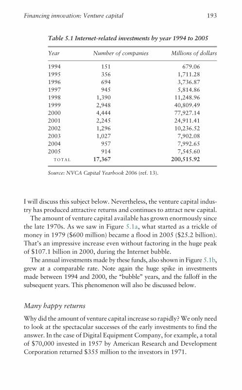
I will discuss this subject below. Nevertheless, the venture capital indus-
try has produced attractive returns and continues to attract new capital.
The amount of venture capital available has grown enormously since
the late 1970s. As we saw in Figure 5.1a, what started as a trickle of
money in 1979 ($600 million) became a flood in 2005 ($25.2 billion).
That’s an impressive increase even without factoring in the huge peak
of $107.1 billion in 2000, during the Internet bubble.
The annual investments made by these funds, also shown in Figure 5.1b,
grew at a comparable rate. Note again the huge spike in investments
made between 1994 and 2000, the ‘‘bubble’’ years, and the falloff in the
subsequent years. This phenomenon will also be discussed below.
Many happy returns
Why did the amount of venture capital increase so rapidly? We only need
to look at the spectacular successes of the early investments to find the
answer. In the case of Digital Equipment Company, for example, a total
of $70,000 invested in 1957 by American Research and Development
Corporation returned $355 million to the investors in 1971.
Table 5.1 Internet-related investments by year 1994 to 2005
Year Number of companies Millions of dollars
1994 151 679.06
1995 356 1,711.28
1996 694 3,736.87
1997 945 5,814.86
1998 1,390 11,248.96
1999 2,948 40,809.49
2000 4,444 77,927.14
2001 2,245 24,911.41
2002 1,296 10,236.52
2003 1,027 7,902.08
2004 957 7,992.65
2005 914 7,545.60
T O T A L 17,367 200,515.92
Source: NVCA Capital Yearbook 2006 (ref. 13).
Financing innovation: Venture capital 193

Returns like this, far surpassing those available from assets such as
real estate, bonds, or publicly-traded equities, were sure to make
investors more willing to commit capital to the brand-new electronics
market.
Investors in venture capital funds have indeed done well over the
years. Of course, the industry’s average rates of return depend on what
period you are considering. But even taking periodic fluctuations into
account, the results since 1990 are mostly positive, especially when
compared to the public equities markets.
This can be seen in Table 5.2, where a rolling average of five-year
increments is used for the calculation.14 The only period where the US
venture capital industry as a whole lost money was during the five years
Table 5.2 Five-year rolling averages of rate of return in
capital funds: Venture capital vs. public markets
Five-year period ending Venture capital S&P 500 NASDAQ
1990 6.5 9.4 2.8
1991 8.6 11.5 10.9
1992 8.7 12.0 15.4
1993 11.7 10.9 15.3
1994 13.2 5.4 10.6
1995 20.1 13.3 23.0
1996 22.5 12.2 17.1
1997 26.0 17.4 18.3
1998 26.7 21.4 23.1
1999 46.5 26.2 40.2
2000 48.4 16.5 18.6
2001 36.9 9.2 8.6
2002 27.3 �1.9 �3.2
2003 25.4 �2.0 �1.8
2004 �2.3 �3.8 �11.8
2005 �6.8a �1.1 �2.2
Note:a Average of 600 funds. The top performing 150 funds generated a rate of
return of 24.4%.
Source: NVCA Capital Yearbook 2006 (ref. 14).
14 NVCA Yearbook 2006, p. 81.
194 Competing for the future

ending in 2004 and 2005 – a reflection of the excesses in investment of
the bubble years. However, it is important to note that the fund
performance varies greatly. Of the 600 firms that were surveyed for
the results shown in the table for the 2005 period, the top 150 firms
averaged returns of 24.4 percent for the five-year period ending in
2005. Obviously, the average result for the whole group was weighted
down by the very poorly performing funds with bad investments.
Those five years encompassed the ‘‘Internet bubble’’ period, when
valuations of publicly held technology companies rose sharply, then
suddenly dropped. This is reflected in Figure 5.5, which charts the
rise and fall of the public market index for the telecommunications
networking sector between 1999 and 2001.15 This curve is a good
proxy for what happened to other high-tech companies in the public
market.
You may wonder why we are looking at the valuations of public
companies, when VC firms invest in private companies. There is a good
reason for this: public company valuations strongly impact the valua-
tion of investments in private firms in similar markets.
Inde
x (D
olla
rs)
1600
1400
1200
1000
800
600
400
200Jan ’99 Jan ’00 Jan ’01
Source: BigCharts.com
Year
5.5. The ‘‘Bubble’’ in the US Telecom Networking Index October 1998 to
October 2001. From BigCharts.com quoted by Dr. A. Bergh; reprinted with
permission from OIDA (ref. 15).
15 Optoelectronics Industry Development Association (OIDA), courtesy ofDr. A. Bergh, 2005; figure from BigCharts.com.
Financing innovation: Venture capital 195

Public/private correlations
This requires a bit of explanation. Since VC firms must eventually
liquidate their investments, they fund a promising business in the
expectation of one of two possible outcomes:* an initial public offering, which offers liquidity to investors and
employees by converting their equity into publicly traded shares; or* the sale of the business for a value in excess of the investment.
If either of these events coincides with a period of huge interest in the
company’s industry (as was the case in telecommunications and the
Internet during the period from 1995 to 2000), a company with inter-
esting technology can receive enormous valuations, regardless of its
profitability or even revenues.
For example, during the Internet bubble years, many start-ups in the
network equipment business, even those with negligible revenues, were
acquired by dominant industry players such as Lucent Technologies
and Nortel for prices in excess of $1 billion. The payment usually came
in the form of company stock.
The giants paid these amounts because they badly needed certain
technologies to compete, and because they could afford the price. At
that time Lucent was valued at about $200 billion. In the absence of
internally generated products it viewed the acquisition of a start-up
with stock (not cash) as the cheapest and quickest way to grow its
business.
We have already mentioned Chromatis, acquired by Lucent, as a
prime example of the unbelievable run-ups in value that can occur
during a bubble period. Chromatis was by no means the only such
case. Lucent alone made thirty-eight acquisitions between 1996 and
September 2000. Many of the companies it acquired were venture
capital financed, and all were acquired at valuations far in excess of
their original investments. Most of them were also overpriced. They
were benefiting from the bubble mentality of the time, and from the
public market valuations in that sector.
Such profitable transactions obviously produced outstanding returns
to the investing VC firms. When the public valuation bubble collapsed
in 2000, so did the opportunity to sell private companies at outland-
ishly inflated prices. The effect was predictable: a steep falloff in
the profits generated by the VCs and in the rates of return from their
funds.
196 Competing for the future

This is not to say that windfall deals are dead. In the preceding
chapter we looked at Skype Technologies SA, an Internet voice-over-
IP software company. Skype, funded with total VC investments of
about $25 million, was sold to eBay in 2005 for more than $4 billion.
According to Thomas Venture Economics and the National Venture
Capital Association, of the 107 sales of venture capital-backed compa-
nies in 2005, fully 10 percent were sold at prices which represented ten
times their total investment. Another 60 percent fetched prices between
one and four times their investments, while about 30 percent were sold
at prices below the investments.16
The flawed art of picking winners
As we look at these numbers, it is a good time to reflect on the vagaries
and risks of venture capital investing. First and foremost, it is a people-
driven process. The fund managers must have the savvy to constantly
shift and adjust the management of their portfolio businesses when the
assumptions they made at the time of investing bump up against new
realities.
For example, a common investment thesis is that a new product
requirement will emerge some time in the future because of recent
government regulations, or new industry standards, or new ways of
doing business (like buying products on the Internet). When a VC firm
and an entrepreneur base a business on one of these assumptions, they
are betting on uncontrollable events. They are investing in new product
development to meet a future need that is by no means certain.
If their timing is right, the product emerges just as the need for
it is growing. If the start-up hits a big market at the right time, the
results can be spectacular. Cisco Systems grew to dominate its market
by betting on the emergence of enterprise data networks. Similarly, one
of my investments (in collaboration with Joseph Landy), Level
One Communications, bet on the emergence of Ethernet networks
built with copper wire rather than coaxial cable. The company
gained a leading world share of Ethernet connectivity chips in excess
of 40 percent before being acquired by Intel in 1999 for $2.2 billion.
16 Reported by C. Murphy and G. White, ‘‘Start-up investors stung by weak M&Aexits,’’ The Daily Deal (October 21, 2005), 2.
Financing innovation: Venture capital 197

Those are happy results. Now suppose that the anticipated market
never appears, or competitors get there first with better products, or the
market’s emergence is delayed by years. In any of these situations the
investors have some unattractive options.
They can fund the company to develop a new product for another
market, fix the current product to meet competition or, if they believe
that the market is delayed, just buckle down, invest more money and
keep going. If the investors have lost faith in the management team,
which happens when products never work right, they will first try to
find a buyer for the business and, if unsuccessful, shut it down.
Closing a laggard
Faced with a choice between investing more money in a company that’s
not meeting expectations or walking away, which option does one
choose? How do the investors weigh the options and either decide to
put up more capital or call it a day? As you can imagine, board meet-
ings where such life and death options are being discussed are very
painful, and counsel is likely to be divided.
This extreme situation underlines the importance of a VC firm
having awareness of the market and technology, and access to the best
talent, in each business sector that it selects for its investments. There
are examples of successful companies emerging from early failures. But
there are no formulas for success, because no two situations are the
same.
It all boils down to the judgment of the decision makers that control
the money. At the end, the decision to continue investing or call it a day
rests with the venture capital partner responsible for the investment. It
can be a very lonely job.
My first experience with such a situation occurred in the mid-1980s.
A start-up company called Licom was financed to commercialize the
first equipment leveraging then-emerging synchronous network tech-
nology. This equipment was built around a new telecommunications
industry standard called SYNTRAN, and Licom was first to market.
The product was tested by all of the Regional Bell Operating
Companies of the time and worked as expected. The only problem
was that production orders never came. Why? Because after
SYNTRAN was in place, the industry decided to establish a new
standard called SONET, and the big telecommunications equipment
198 Competing for the future
companies publicly committed to building products meeting that
standard.
There was no way that Licom could develop a SONET product with-
out massive new funding, and the timing for product acceptance was
uncertain. I decided to exit the investment. Licom was sold for a very
modest sum, which ended up being used to pay off the building lease.
There was a buyer for the company because its engineers were out-
standing, so at least some jobs were saved. The net result was a loss of
$4 million for my firm, but I never regretted the decision. As it turned
out, SONET/SDH products took many years to become accepted, and
the market ended up being dominated by the giant vendors.
The lesson is just what you would expect. Technology investing is a
very risky business. There is high potential for profitability, but only if
you learn when to cut your losses and how to ride your winners.
The role of the angel investor
VC firms do not have the field of early-stage funding to themselves.
Investments in start-ups and early-stage companies by wealthy indivi-
duals have continued in parallel with the growth of professionally-
managed venture capital funds.
These ‘‘angel investors’’ are frequently organized in informal invest-
ment groups that pool capital for specific deals. Angel investors are
often the only source of money available to fund new companies at
sums under a million dollars. The majority of VCs simply aren’t inter-
ested in such low funding levels. As VC firms have grown in size, the
management of small investments has become impractical.
Yet these small investments add up to a surprisingly large total.
A study by the University of New Hampshire’s Center for Venture
Research indicates that individuals invested $22.5 billion in start-ups
in 2004. This exceeds the total amount of venture capital investment
for that year.17
Given the typically small size of angel investments, this means that
tens of thousands of new companies are financed in this way, many of
which do not survive for more than a year or two. For those new
17 R. Sechler, ‘‘Angel investors cut start-up funding,’’ The Wall Street Journal(November 2, 2005), B2G.
Financing innovation: Venture capital 199

businesses that show promise, however, larger follow-on funding
comes in the form of venture capital.
Angel investors provide a valuable service. As seed investors, they
help get the highest-risk companies off the ground. These are compa-
nies which otherwise would not be funded.
Obviously, angel investors’ appetite for risk is affected by the pro-
spect of public market exits, the amount of follow-on capital needed,
and their belief in ‘‘hot markets’’ where big profits can be anticipated.
Internet start-ups, which usually need only small sums to get off the
ground, continue to be favorite investment targets.
Not surprisingly, angel investors became harder to find in times of
depressed public market valuations for technology companies.
Venture capital winners and losers
Right from the earliest days of American Research and Development,
the ability to generate handsome returns on capital has been a primary
reason for the existence of VC firms. Good returns are possible only if
valuable companies are created. In this regard VCs have a large number
of remarkable successes to their credit.
They have also had their share of failures, as evidenced by the fact
that few start-ups become truly successful businesses. Many of these
failures are the result of ‘‘herd’’ investing, which pours too much money
into hot new markets. The predictable result is a surfeit of companies
chasing the same opportunities.
Let me explain how this happens. In large part it is due to the nature
of the business. The way venture capital gets invested is not accidental –
money follows emerging technologies that promise to open large new
markets.
The innovations trigger a flood of investments into new companies,
as entrepreneurs and investors flock to capitalize on their potential.
Important regulatory changes that reduce the power of dominant
companies can have a similar effect.
We see historical precedents for this behavior in the development of
industries before the age of the VC. These include railroad building in
the nineteenth century and the emergence of commercial radio and
mass-produced automobiles in the 1920s.
The most dramatic example in our time has been the unprecedented
flow of capital into Internet-related companies between 1994 and
200 Competing for the future

2000, just as the Internet’s potential was becoming widely recognized.
Another enormous but short-lived wave of investments was triggered
by a landmark regulatory change, the Telecommunications Act of
1996. An extensive discussion of this phenomenon appears later in
this chapter.
After a number of start-ups join the race to address new markets, a
Darwinian process divides the entrants into three broad categories:* Early failures that chew up capital, then vanish without a trace.* Companies that develop valuable products, stay private, and cannot
reach the scale needed for long-term viability. These end up being
acquired.* The finalists, a group of companies that rank among the market leaders.
Some of the finalists become consolidators of new markets through
successive mergers with their competitors. These companies can reach
annual revenues in the multi-billion dollar range.
About 21,000 companies covering a number of industry sectors
received initial venture capital between 1980 and 2004. We don’t know
what happened to them all. However, the record shows that 4,000 of
them went public during that time, and 2,783 were sold or merged.18
Table 5.3a is a list of venture-backed (and two angel investor-
backed) start-up companies that I believe were pioneers in validating
major new electronic industry markets. This list and the list in
Table 5.3b do not claim to be exhaustive, but they are illustrative of
the effect new companies can have.
While these companies did not necessarily invent their core techno-
logies, they were the agents for taking them into the market. Some are
still independent and consolidators of their market space; others have
been acquired or merged out of existence. All left their mark. We
discuss the contributions of some of these examples below.
Companies that went public
We can certainly count some of the 4,000 companies that had success-
ful initial public offerings (IPOs) of their securities between 1980 and
2004 as being among the biggest winners. Figure 5.6 shows the number
of venture-backed companies with IPOs for each year between 1970
and 2005.19
18 NVCA Yearbook 2006, p. 76. 19 Ibid., p. 73.
Financing innovation: Venture capital 201

Table 5.3a Selected industry pioneers (venture or angel capital-backed) that became industry leaders (2004)
Company Year founded IPO year 2004 revenues (millions $) Product
Intel 1968 1971 34,209 Microprocessors
Checkpoint Systems 1969 1977 779 Security network software
Microsofta 1975 1986 38,474 PC software
Apple Computer 1976 1980 9,763 User friendly personal computers
Oraclea 1977 1986 10,557 Relational databases
3-Com 1979 1984 669 Ethernet networks
Seagate 1979 2002 6,129 Disk drives for the masses
Sun Microsystems 1982 1986 11,230 UNIX workstations
Electronic Arts 1982 1989 2,957 Electronic computer games
Autodesk 1982 1985 1,234 Design automation software
Cisco Systems 1984 1990 23,579 Computer networks
Xilinx 1984 1990 1,586 Programmable logic chips
Comverse Technologies 1984 1986 959 Voice mail systems for telecommunication
Amazon.com 1994 1997 6,921 Internet store
BEA Systems 1995 1997 1,012 Internet transaction software
eBay 1995 1998 3,271 Internet auction service
Covad Communications 1996 1999 429 Digital Subscriber Loop (DSL) service
Google 1998 2004 3,189 Internet search engine
NeuStar 1999 2005 165 Telecom inter-carrier services
Note:a Initial capital from angel investors

Table 5.3b Selected venture capital-backed industry innovators (acquired)
Company Year founded Product IPO year Year acquired
Digital Equipment Corporation 1957 Minicomputers 1981 1998
WordStar 1978 Pioneered word processing software for PCs – 1994
Ortel 1980 Semiconductor lasers for cable systems 1994 2000
Lotus 1982 Spreadsheets for PC 1983 1995
Compaq 1982 First portable PC 1983 2002
Epitaxx 1983 Fiber optic light detectors – 1999a
Level One Communications 1985 Ethernet connectivity chips 1993 1999
Maxis 1987 Games for PCs 1995 1997
Netscape 1994 Internet software 1995 1998
NexGen 1988 Intel compatible microprocessors 1995 1996
Note:a Acquired by JDS Uniphase

Cyclical peaks occur in years when public markets are unusually
receptive to new technology companies. 1996 in particular was a
banner year, with 279 companies filing for IPOs. The lean years after
2000 followed the bursting of the Internet bubble in 2000.
Table 5.4 gives us a good overview of the impact of venture-backed
start-ups on the public markets.20 It shows that between 1998 and
2005 these companies represented between 25 percent and 69 percent
of all companies filing for IPOs. It is not possible to really do justice to
such a large number of businesses. It is interesting, however, to con-
sider some illustrative examples of two classes of outcomes.
If you go back to Tables 5.3a and b, you can see that the venture-
backed companies that went public are divided into two groups.
Table 5.3a is a selection of companies that pioneered new industrial
sectors and, as of 2005, remained leaders in their defined markets.
Included are two very prominent companies, Oracle and Microsoft,
that were started with angel investment rather than professional ven-
ture capital. Note that many are multi-billion revenue businesses.
Table 5.3b lists a sample group of pioneers that have been acquired
by other companies. Included are two companies, WordStar and
500
400
300
200
100
0
Num
ber
of IP
Os
Year
25,000
20,000
15,000
10,000
5,000
0
Mill
ions
of D
olla
rs
Source: NVCA
No. of IPOs
Offer ($ Mill)
1979
1978
1977
1976
1975
1974
1973
1972
1971
1970
198019
8119
8219
8319
8419
8519
8619
8719
8819
8919
9019
9119
9219
9319
9419
9519
9619
9719
9819
9920
0020
0120
0220
0320
0420
05
5.6. Venture-backed IPOs showing number of IPOs and total amount raised.
Reprinted with permission from NVCA (ref. 19).
20 Ibid., p. 73.
204 Competing for the future

Epitaxx, that deserve mention for their contributions, although they
were private when acquired.
One characteristic of market leaders is their ability to assimilate tech-
nologies from other sources. While the companies selected in Tables 5.3a
and b are notable for their own technical contributions, they were also
adept at commercializing innovations developed at universities or in big
laboratories. For example, the core idea for Cisco’s first product origi-
nated at Stanford University. Google’s Internet search engine idea also
grew out of academic research at Stanford (see Chapter 8).
Another common trait of market leaders is the ability to ensure their
futures by acquiring other companies with innovative products, rather
than relying totally on internal development. For example, some
companies in Table 5.3b ended up being acquired by companies in
Table 5.3a.
The fact that companies merge is a reflection of the natural tendency
of markets to consolidate around a few strong leaders. As a result, the
life span of many new innovative companies as separate entities tends
to be only a few years.
Companies that joined others
The ultimate winners are companies that have had an IPO and success-
fully maintained their identities and market leadership. But that’s not
the only way to succeed as a new, innovative organization.
Table 5.4 Number of venture-backed IPOs vs. all IPOs
Year All IPOs Venture-backed IPOs Percentage
1998 312 79 25%
1999 477 263 55%
2000 353 242 69%
2001 83 37 45%
2002 77 21 27%
2003 68 27 40%
2004 190 83 44%
2005 183 45 25%
Source: NVCA Capital Yearbook 2006 (ref. 20).
Financing innovation: Venture capital 205

We will now turn our attention to the companies listed as acquired or
merged in Table 5.3b, to see how they fit into the innovation pattern. They
are representative examples of many other companies that fit this category.* Digital Equipment Corporation (DEC) pioneered minicomputers. It
was acquired by Hewlett-Packard, which also acquired Compaq, the
pioneer in small portable personal computers.* Netscape eventually disappeared into America Online, but not
before demonstrating the commercial value of Internet functionality.* Maxis pioneered the personal computer game market for adults with
its SimCity product, one of the best-selling such games in history. It
was acquired by Electronic Arts.* Level One Communications, under the leadership of Dr. Robert
Pepper, pioneered Ethernet connectivity chips. It was acquired by
Intel in 1999.* NexGen was the first chip company to demonstrate the ability to
generate microprocessors compatible with the Intel operating sys-
tems. Headed by Atiq Raza, it was acquired by AMD, which has
continued to be a serious competitor to Intel, in part thanks to
NexGen’s technology.* Lotus, a leader in desktop personal computer software, was acquired
by IBM. It is no longer a significant player in its original market.* Ortel commercialized semiconductor laser technology developed at
the California Institute of Technology and was acquired by Lucent
Technologies in 2000.* Epitaxx, founded by Drs. Greg Olsen and Vladimir Ban, established
the commercial market for high-speed detectors for fiber optic com-
munications. It was acquired by JDS Uniphase in 1999.* WordStar developed early word processing software for PCs,
demonstrating the value of such software. It eventually disappeared
in a series of mergers.
Winners and losers: Telecommunications
Among the thousands of venture-backed companies that have disap-
peared are many firms whose demise was the result of poor timing or
plain bad luck, not faulty technology. These unfortunate companies
often bet on market opportunities created by government regulations,
only to see those opportunities evaporate. While government regula-
tions can create winners, they also create lots of losers.
206 Competing for the future

For example, the Telecommunications Act of 1996 was a landmark
event, triggering one of the largest speculative investment bubbles in
history. As you would expect, quite a few companies built to exploit
this opportunity wound up as victims of its collapse.
The Act effectively opened access to local phone lines owned by the
Regional Bell Operating Companies (RBOCs, separated from AT&T
under the Consent Decree of 1984). For the first time, non-Bell System
companies could offer services directly to consumers and businesses.
These new companies were called Competitive Local Exchange
Carriers (CLECs).
At the time of the Act, the RBOCs controlled about $100 billion in
annual revenues. CLECs were funded by an enormous wave of private
and public capital from people seduced by the hope of gaining a piece of
that market. The emergence of the Internet only added fuel to the specu-
lative fever. Investors had visions of unlimited demand for communica-
tions capacity, and hence unparalleled growth in data traffic revenues.
Many equipment and software vendors soon emerged, offering new
products to equip this growing industry. This period coincided with the
emergence of new broadband communications technologies such as
Digital Subscriber Loop (DSL), which were just reaching the commer-
cial stage.
Covad Communications, to name one participant in the frenzy, was
founded in 1996 with Warburg Pincus capital as the first company to
capitalize on the emerging opportunity. Unlike most others of its kind,
it has successfully remained an independent provider of data services,
though not without financial turmoil after the collapse of the Internet
bubble in 2000.
Neustar is another successful company spurred into existence by the
Telecommunications Act. Neustar, led by Chief Executive Officer
Jeffrey Ganek and Chief Technical Officer Mark Foster, is a Warburg
Pincus venture capital-backed spin-out from Lockheed Martin
Corporation. The company provides the interconnection service that
enables local number portability in the telecommunications industry.
The industry needed this functionality, since the Act mandated
that carriers find a way for telephone subscribers to change service
providers without losing their phone number. Neustar went public
in 2005.
Unfortunately, the Act spawned far more losers than winners. With
so many new companies offering equipment, software, and services to
Financing innovation: Venture capital 207
the telecommunications industry to entice investors, there was a herd-
like rush of private and public capital into the market, launching a
classic speculative boom/bust cycle.
Inevitably, massive business failures followed. It is estimated that
more than $2 trillion of public value in publicly traded securities was
lost between 2000 and 2003. As mentioned earlier, a good proxy for
this cycle is Figure 5.5, which shows the public-market Telecom
Networking Index rising to 1,400 in October 1998 and dropping to
200 in October 2001.
To understand what helped fuel the overinvestment spree of the late
1990s, let us scroll back and see how matters looked to investors at that
time. Consider two examples: the semiconductor laser industry, selling
key components in the deployment of fiber optic communications
systems; and new software products that addressed the emerging
needs of the carriers.
Disaster in the electro-optic component business
The opening of the communications market to newcomers in 1996
started a race to build new fiber-optic communications systems
in the US and elsewhere. Companies that supplied semiconductor
lasers for these systems finally began to look like an attractive
investment.
As Figure 5.7 shows, sales of lasers began rising sharply in 1998.21
Looking at the laser business in 1997, a shrewd investor would have
projected rising demand and a resulting industry order backlog. The
investor would have valued a laser business opportunity on the basis of
a $6 billion market, which it actually reached in 2000.
As evidence for this valuation the investor only had to look at such
public companies in the laser business such as JDS Uniphase, with a
stock price that reached $145 in 2000. The investor could even have
been led to extrapolate industry growth past the $6 billion total, and
factor this into the estimate of company value.
As it happened, this demand was not sustainable. It represented the
peak of a rapid buildup in capacity. Demand was sure to level off or
even decline as fiber-optic systems deployment slowed. At that point
there would be a huge amount of overcapacity in the laser industry.
21 OIDA, courtesy of Dr. A. Bergh, 2005.
208 Competing for the future

Unfortunately, investors assumed that the market saturation point
was still a long way off. They believed that the build-out of new systems
would be driven indefinitely by the insatiable demand for Internet
traffic bandwidth, which was believed to double every month or so.
The market ran out of steam much sooner than they anticipated. As
the downturn came, component suppliers saw their revenues drop
sharply and their losses rise. That $145 share of JDS Uniphase fell to
$3 later in 2000. Built by acquisitions of multiple electro-optic compo-
nent start-up companies, it was no longer in a position to buy anything.
Private companies supplying lasers were hit hard, echoing what was
happening in the public markets. Their values declined sharply as it
became clear to investors that only massive infusions of new capital
could cover their losses and ensure their survival.
A new software market emerges
In 1996 it became evident that the advent of the CLECs, which used the
existing infrastructure of the RBOCs to reach their customers, was
creating a new market for interconnections.
Source: OIDA
7
6
5
4
3
2
1
01996 1997 1998
Bubble
1999 2000 2001 2002 2003 2004 2005
Rev
enue
(B
illio
ns o
f Dol
lars
)
Year
SustainableTotal
Raw Total
Sustainable Revenue Levels
5.7. Worldwide laser diode sustainable revenues. Removal of bubble
(1999–2002) in worldwide laser diode market history to show sustainable
revenue levels. Reprinted with permission from OIDA (ref. 21).
Financing innovation: Venture capital 209

With the dawning of the multi-vendor era, voice and data traffic
would have to traverse several carriers to reach its destination. The
only way to ensure end-to-end delivery was to create a platform for
inter-company communications, so that a CLEC could automatically
request service from another CLEC or a big carrier.
For a company like Covad to provide data service over lines owned by
the local phone company, for example, it has to send a request to the
local company to connect a new customer. Though it may seem un-
believable today, just a few years ago this service request was submitted
by fax, and it took a great deal of manual work to implement the service.
An electronic interface between Covad and its line providers to
process and implement such requests would obviously be far more
efficient. However, this meant developing sophisticated software plat-
forms to interface the internal systems of Covad with those of the
phone company.
Here we have a good new product idea. It was clearly a much better
solution than the existing methods. No invention was needed – just
software development. The target customers were well defined.
Unfortunately, the same idea occurred to several entrepreneurs
almost simultaneously. They all began to solicit venture capital. Some
won financial backing, because investors believed that interconnection
software was part of an emerging $4 billion market serving the liber-
ated telecommunications industry.
It was evident, however, that this market would support only one
ultimate winner, because the interconnection platform had to be stan-
dardized to broadly serve the industry. The company that acquired the
largest customer base in the shortest time would ultimately dominate.
Four new companies, backed with a total of $200 million of venture
capital among them, entered the market between 1996 and 2000. Their
software was not interoperable. Fierce price competition ensued as
each company tried to gain market share and reach profitability.
Every sales opportunity became a battlefield, resulting in ever-declining
prices for both software and support. By 2002, none had reached critical
mass, all had high fixed costs, and all were losing money.
To make the situation worse, CLECs began to go out of business
after 2000 and software sales dropped. Management and investors
recognized that a merger was needed to build one viable business, but
nothing happened. Each competitor expected the others to fail, clearing
the field for its product.
210 Competing for the future
At the end, three of the companies were out of business, and the
fourth was acquired in 2003 for a modest valuation. There was no last
man standing.
The globalization of venture capital
VC firms typically focus on local companies. An old truism heard in
long-established California firms is that they only invest in companies
within a one-hour riding distance from their offices.
This has changed. Attractive deal opportunities are now found glob-
ally, leading many of the larger US and European firms to start invest-
ing internationally.
Warburg Pincus, headquartered in New York City, began develop-
ing a global strategy in the 1980s. Today we have offices and partners
in Asia and Europe. Smaller VC firms have branched out as well,
usually partnering with local firms for their overseas investments. It is
now taken for granted that technology firms must have a global out-
look, and investors are acting accordingly.
Figure 5.8 shows the venture capital raised by high-tech companies
in countries in Asia and Europe from 2002 to 2004. Israel, with a
population of about six million, invests more venture capital than
China. In 2004 about 55 per cent of the money came from foreign
sources.22 In China approximately 90 per cent of the capital invested in
2004 came from outside the country.23
The case of Israel is especially interesting, because it bears upon
many of the points we have been considering.24 We noted in the
preceding chapter how actively Israel’s government encourages the
formation of innovative companies. Venture capital has a huge impact
on the Israeli economy as well.
There are many opportunities for venture investments in the economy.
One of the reasons for this is Israel’s unusually large proportion of highly-
trained engineers relative to its total working population. The country has a
large percentage of the kind of people who produce innovations. There are
135 engineers per 10,000 employees in Israel, compared to seventy in the US,
22 Israel Venture Capital Research Center Yearbook (Tel Aviv 2005), p. 29.23 M. Maschek, ‘‘China is ripe for VCs with the right approach,’’ Venture Capital
Journal (November, 2005), 41.24 ‘‘Punching above its weight: The secret of Israel’s success,’’ The Economist
(November 12, 2005), 64.
Financing innovation: Venture capital 211
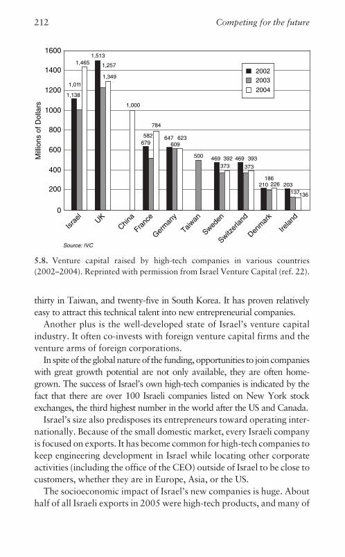
thirty in Taiwan, and twenty-five in South Korea. It has proven relatively
easy to attract this technical talent into new entrepreneurial companies.
Another plus is the well-developed state of Israel’s venture capital
industry. It often co-invests with foreign venture capital firms and the
venture arms of foreign corporations.
In spite of theglobalnatureof the funding,opportunities to join companies
with great growth potential are not only available, they are often home-
grown. The success of Israel’s own high-tech companies is indicated by the
fact that there are over 100 Israeli companies listed on New York stock
exchanges, the third highest number in the world after the US and Canada.
Israel’s size also predisposes its entrepreneurs toward operating inter-
nationally. Because of the small domestic market, every Israeli company
is focused on exports. It has become common for high-tech companies to
keep engineering development in Israel while locating other corporate
activities (including the office of the CEO) outside of Israel to be close to
customers, whether they are in Europe, Asia, or the US.
The socioeconomic impact of Israel’s new companies is huge. About
half of all Israeli exports in 2005 were high-tech products, and many of
1600
1400
1200
1000
800
600
400
200
0
Israe
lUK
China
Franc
e
Germ
any
Taiwan
Sweden
Switzer
land
Irelan
d
Denm
ark
Mill
ions
of D
olla
rs
20022003
20041,138
1,011
1,4651,513
1,257
1,349
1,000
679582
784
647609
623
500 469373392 469
373
393
210186
226 203137136
Source: IVC
5.8. Venture capital raised by high-tech companies in various countries
(2002–2004). Reprinted with permission from Israel Venture Capital (ref. 22).
212 Competing for the future

the participating companies had venture capital funding at some point
in their development.
If you want to see how the development and commercialization of
innovation can build a country’s economy and shape its relationships
with the rest of the world, you could do worse than to look at Israel.
The continuing role of venture capital
There can be no question that companies financed by venture capital
have played a central role in transforming the digital innovations of the
past thirty years into new products and new markets.
As is always the case in the open competition of a capitalist system,
there were winners and losers among the companies created to sell
these products. Some went on to market dominance; some validated
the new markets but were eventually absorbed by emerging market
leaders; and many simply disappeared.
We should not belittle the achievements of the second group, the
thousands of firms that were eventually bought out by better-positioned
competitors. While their contributions may have been modest and impos-
sible to measure in the aggregate, they were no less real than those of the
survivors. It is fair to say that these companies brought new products and
technologies with them that enhanced the value of their acquirers.
They also provided R&D that could not have been performed inside
the acquiring companies. In their case we can think of the role of
venture capital as financing the creation of new products rather than
building stand-alone companies. Many venture-backed Israeli compa-
nies fit into this category.
Does this investment strategy make economic sense for investors? The
answer depends on market demand and the rapidity with which new technol-
ogies reach the commercial stage. In fast-moving industry sectors, established
companies are frequently handicapped in their internal product development
by a lack of specialized talent. Acquiring the talent along with a start-up
is cheaper and faster than trying to build a product team from scratch.
The prices paid for start-ups often reflect the value of the talent
needed to develop their products as well as the market potential of
the products. On this basis, building a company with the intent of
selling it rather than establishing a stand-alone entity continues to be
a successful model for everyone involved: the VCs and entrepreneurs
behind the start-ups as well as the purchasers of the firms.
Financing innovation: Venture capital 213

By funding innovators and creative entrepreneurs, venture capital not only
seeds new markets, it also influences or transforms existing markets and the
companies that dominate them. We have seen how any new development of
major magnitude sets off a wave of investments in direct proportion to the
perceived opportunity. This can shake up even industry giants to the point
of redirecting their strategies. To take the most salient example in recent
history, the success of Netscape forced Microsoft to focus on the Internet.
More recently, Google has revolutionized the Internet business model.
A similar transformation is now under way in the software industry.
We discussed in Chapter 2 the impact that the Internet is having on the
software industry, especially in relation to software as a service (SaaS),
a model under which customers access and use software on line as they
need it, and pay for only what they use.
This development, now being aggressively marketed by start-ups,
threatens to upset the whole commercial structure of the software
business. Up to now software vendors have derived the bulk of their
revenues from licensed software that sits on the user’s computer. There
is ample evidence that in 2005 the management of Microsoft began to
take this new threat seriously, and that the company will respond.
Without the emergence of VC-funded start-ups, ready to challenge
incumbents with new ideas and products, technology markets would
be much less exciting places – and the US would lose a great deal of the
innovative energy that has been its strength in the past. Creative force,
builder of value, or commercial gadfly, venture capital continues to add
its own value to the world of innovation.
Before leaving the topic, we need to remember that venture capital
financing alone is not the answer to reversing the decline of US manufactur-
ing. The capital committed does not address the massive sums needed for
such businesses. Therefore, industrial capital needs to partner with venture
capital to build the capabilities that allow major markets to be addressed.
New markets that will be created by process-intensive innovations
require long-term capital outlays and making such commitments is
outside the usual pattern of venture capital investing. By and large,
VC-funded businesses are more likely to be based on services, software,
semiconductors, and the design of equipment whose production will be
outsourced. However, in partnership with industry, it is possible to
envision a successful path to commercialization as long as the manu-
facturing technologies are sufficiently innovative to overcome the
higher labor costs in the US.
214 Competing for the future

P A R T I I I
Global reach, global repercussions

6 Manufacturing: Globalizingfaster than ever
MA D E in China. Or in Malaysia, Sri Lanka, Singapore – the list
goes on.
Discovering that your clothing was sewn in a newly industrializing
Asian country no longer raises eyebrows. But now it seems that even
the most advanced electronic products are produced in a developing
country, and that the manufacturing job is an endangered species in the
US and Europe.
This is an exaggeration, of course. Yet the kernel of truth within it is
undeniable: there has been an extraordinary migration of manufactur-
ing, most notably of electronics, out of developed countries since the
1980s. What’s more alarming is that the trend shows no signs of
slackening.
To a large extent the rapid globalization of manufacturing is a
consequence of digital technologies reaching maturity. Technological
changes have altered the nature of the competitive advantage derived
from manufacturing.
To take just one prominent example, contract manufacturing as a
stand-alone business has become a major global activity. Developed in
Asia, it represents a total reversal of the historical business structure,
under which integrated manufacturing was considered a competitive
advantage for practically all product suppliers.
Furthermore, as we discuss later, even software writing has become
part of the outsourced ‘‘manufacturing’’ sector, a development made
possible by the remarkable advances made in the technology of soft-
ware development.
This chapter will trace the trajectory of outsourcing through product
sectors and whole countries, revealing the pattern of exporting low-
skill assembly jobs to foreign shores in search of cost reductions.
As manufacturing plants close in developed countries it has become
fashionable to dismiss the importance of manufacturing ‘‘hard goods.’’
217

There are supposedly more advantages to be derived from creating
industries based on software and services.
That’s not how I see it. I am convinced that, especially in large
economies like the US, a selective but competitive manufacturing sector
is a prerequisite for sustaining the innovation that ensures economic
prosperity in the first place.
My experience in setting up a new factory, recounted later in this
chapter, taught me that the process of innovation extends right onto the
production line, particularly in industries where process technologies
are important value-creating elements. If you are not well versed in
manufacturing, your ability to innovate in these industries will atro-
phy. Naturally, this presupposes that such industries will be highly
innovative to compensate for their greater labor costs.
Whether to manufacture, then, is the wrong question. What to man-
ufacture and what to outsource is a more fruitful line of inquiry for
product companies. The answer to this question will vary by industry,
and will change with the rapid transitions in global markets, but it must
be asked. History shows that it is far from being a new dilemma.
Early outsourcing
The Industrial Revolution started in England in the mid-eighteenth
century. Fifty years later its triumph was assured. The old agricultural
and commercial society had given way to the new industrial economy.
Machinery had replaced tools in most industries. Factories were super-
seding craft producers. In the pantheon of economic heroes, commer-
cial entrepreneurs had displaced merchant adventurers.
But clouds were on the horizon. In the 1800s, though Britain was the
dominant manufacturing nation, its reign was already being chal-
lenged. In the second half of the century major competitors, primarily
the US and Germany, emerged with more efficient manufacturing
processes that allowed them to commercialize innovations faster. By
1900, it was evident that the industrial landscape had changed. British
industry, made complacent by its long supremacy, was finding it diffi-
cult to respond to the competitive threat.
The national response set the tone for a debate that has echoed down
to our own day. There was a bitter debate between advocates of free
trade and those who supported protection to shield local manufac-
turers from ‘‘unfair’’ foreign competition.
218 Competing for the future

Free traders argued that industry needed to migrate to higher value
products. In their view, the new competitors were welcome to the
‘‘commodities.’’ Protectionists, fearing the collapse of important indus-
tries, strongly disagreed. A tirade by Joseph Chamberlain, who cam-
paigned for Prime Minister in 1905 on a platform of trade protection,
will sound all too familiar to observers of more recent trade wars.
Your once great trade in sugar refining is gone; alright, try jam. Your iron
trade is going; never mind, you can make mousetraps. The cotton trade is
threatened; well what does that matter to you? Suppose you try doll’s eyes.
But for how long is this to go on? Why on earth are you to suppose that the
same process which ruined the sugar refinery will not in the course of time be
applied to jam? And when jam is gone? Then you have to find something else.
And believe me, that although the industries of this country are very various,
you cannot go on watching with indifference the disappearance of your
principal industries.1
The issues of this debate are as pertinent today as they were 100 years
ago. Many developed economies must now make painful adjustments
as the manufacturing of more and more products shifts to lower-cost
developing countries.
Manufacturing is the vehicle that moves innovations into the market.
Its offshoring (to use a newly fashionable word) carries implications
that resonate far beyond the simple calculus of comparative labor costs.
It raises such questions as, to what extent is the discipline of produc-
tion a necessary component of innovation? Does losing dominance in
production spell trouble for a country’s ability to compete in a field?
Does manufacturing still have a place in developed economies? If so,
what is it?
Recent trends are beginning to provide the answers to these questions.
The China factor
If Joseph Chamberlain were speaking today, he would probably single
out China as the most prominent usurper of manufacturing jobs.
Virtually every international company from Panasonic to Wal-Mart
has production facilities or manufacturing partners on the Chinese
1 Quoted in R. Skielelsky, ‘‘The Chinese shadow: II,’’ The New York Review ofBooks (December 1, 2005), 32.
Manufacturing: Globalizing faster than ever 219

mainland, rolling out everything from clothing and Barbie dolls to
televisions and notebook computers.
China is not alone, of course. Eastern Europe is increasingly viewed
as an attractive location for labor-intensive manufacturing.2 However,
China is the most important and fastest-growing new site for manu-
facturing electronics, the product area of interest to us. Therefore much
of our discussion of the globalization of production will focus there.
The current wave of manufacturing displacement from developed to
emerging economies grew out of cost-cutting efforts by large, estab-
lished companies. This is reflected in the fact that 87 percent of China’s
exports in 2004 came from plants owned wholly or in part by foreign
companies. Chinese customs data puts the share of exports controlled
by foreign companies at 60 percent.3
These companies believe that they have no choice but to leverage
lower labor costs to remain competitive.4 They can do so because of
five major factors that help drive the process. You will note that
automation and communications, made possible by rapidly improving
computerized and networked digital systems, have played a key role.
1. The growing intelligence and efficiency of computer-enabled man-
ufacturing equipment. Digital controls make it easy to relocate
machinery, because the need for expert human operators is reduced.
2. Massive improvements in air, ground, and sea transportation.
Sending materials and supplies to offshore factories and returning
finished goods to consuming countries is now a matter of days
rather than months. That’s fast enough to respond to the most
volatile markets.
3. High-speed digital communications, which make managing off-
shore facilities and transmitting design information as efficient as
walking next door for a meeting.
4. The liberalization of economic policies, especially in China and
India, to encourage foreign investments.
5. Various forms of government subsidies for high-tech industries.
2 This trend has attracted much attention recently. See both ‘‘The rise of nearshoring,’’The Economist (December 3, 2005), 65–67; and J. Ewing and G. Edmondson, ‘‘Therise of central Europe,’’ BusinessWeek (December 12, 2005), 50–56.
3 Quoted in D. Barboza, ‘‘Some assembly needed: China as Asia’s factory,’’ TheNew York Times (February 9, 2006), C6.
4 M. Dickie, ‘‘China’s challenge changes the rules of the game,’’ Financial TimesSpecial Report (October 19, 2005), 1.
220 Competing for the future

Once these enabling mechanisms were in place, the outsourcing
of manufacturing happened with remarkable speed. In 1972, when
Richard Nixon became the first US president to visit what was
then called ‘‘Communist China,’’ no one could have imagined that
China (and other developing countries) would become major players
in electronic manufacturing so quickly. It’s as if the Industrial
Revolution happened overnight, not just in China, but throughout
Asia.
Electronics and automation
To better understand the pace of global electronics manufacturing, it is
worthwhile to define the three major segments of the industry and
discuss how value is created in each. We will start with the transforma-
tion of materials and end with final product assembly.* Process. The process sector creates value by producing, transforming
or combining materials. Some of its products can be used on their
own, but most are components designed to be integrated into more
complex electronic or optical devices. Because this kind of manufac-
turing involves the mastery of complex processes, it is built around a
great deal of proprietary intellectual property. The manufacture of
semiconductor devices falls into the process category.* Intermediate assembly. In this sector, value is created by assembling
components into functional assemblies or subsystems. The assem-
blies are used in turn to build more complex machines. Examples of
intermediate assembly include packaging semiconductor devices,
assembling electro-mechanical components, and attaching compo-
nents to printed circuit boards.* Final product assembly and test. At this stage all of the components
and subsystems from the process and intermediate assembly sectors
are integrated into complete products such as computers, television
receivers, or cellular handsets.
Each of these three sectors involves different disciplines. Each also
requires different levels of labor input, capital investment, and intellec-
tual property.
The first sector, process-intensive production, creates the most value
because it is based on proprietary knowledge. Since the process sector
demands a high level of skill and knowledge from its workers, the
quality of the labor force is more important than its quantity. This
Manufacturing: Globalizing faster than ever 221

sector also demands substantial capital investment. In all of these
respects processing closely parallels materials-based R&D.
Assembly operations, on the other hand, are more labor-intensive
than capital-intensive and only semi-skilled workers are required. For
this reason the assembly sectors are the first to migrate to countries
with low labor costs. Later, when a country has developed a skilled and
knowledgeable workforce, it can begin building a process sector.
This pattern has been repeated in country after country across Asia.
It started when Japan ramped up its electronic assembly sector in the
1950s. By the 1970s it was building up its process industry, in the form of
state-of-the-art semiconductor fabrication plants (fabs), just at the time
that the intermediate assembly of electronic components started migrat-
ing to Korea, Taiwan, Malaysia, and the Philippines. Korea and Taiwan
started building semiconductor fabrication plants of their own in the
1980s.
Now China is creating its own process sector, having gained experi-
ence in electronic assembly over the past two decades. Modern semi-
conductor production began there in the late 1990s.
From craft to automation: Technology enables migration
Long after Joseph Chamberlain railed against the loss of England’s
manufacturing dominance, the West is once again watching a manu-
facturing sector shift overseas, to Asia. This time it’s happening faster,
powered by computerized production equipment that automates com-
plex production processes.
The principles of automation have been common knowledge since
the dawn of the Industrial Revolution. Adam Smith, in his famous 1776
book, An inquiry into the nature and causes of the wealth of nations,
observed that the essential element in raising manufacturing volume
and reducing costs is the division of labor into ever finer specializa-
tions. Machines play a central role in this transformation.
For the sake of simplicity Smith chose the example of a pin factory
where production was divided into eighteen separate operations. But
he stressed that his observations applied to the most complicated
production processes.
In every other art and manufacture, the effects of the division of labour are
similar to what they are in this trifling one. The division of labour, so far as it
222 Competing for the future

can be introduced, occasions, in every art, a proportionable increase in the
productive powers of labour. . . .
Everybody must be sensible how much labour is facilitated and abridged by
the application of proper machinery.5
Smith’s most important point was that the division of labor and use
of machines not only increased productivity, it reduced or eliminated
the need for skilled craftspeople in production operations.
Modern digital data processing accelerates this changeover. It
embeds the highly specialized skills originally required to make elec-
tronic products into microchips and the machine tools they control.
With computer-controlled machines carrying out precision opera-
tions at high speed, there is no need for large numbers of skilled
production workers. A manufacturing plant requires only a few people
with the knowledge to program and maintain the sophisticated
machinery. All other positions are semi-skilled, and a new workforce
can be rapidly trained to fill them. This has made the migration of
manufacturing easier than ever.
Automating transistor production
Automation does not happen overnight. It may come as a surprise to
learn that even semiconductor manufacturing was once a hands-on
craft. It took forty years, but we have progressed from an industry of
skilled craftspeople working within vertically integrated companies to
a standardized, highly automated production environment where a
turnkey plant can be placed practically anywhere in the world with
the appropriate level of support engineering.
I had the good fortune to learn semiconductor manufacturing from
the ground up. In 1961 I was put in charge of building a production line
for the first RCA transistor factory to make silicon transistors.
Silicon devices were new at the time, and relatively little was known
about silicon as a material for the mass production of transistors. The
first transistors had been made of germanium, as were all commercial
transistors up to that point.
Having designed a new silicon-based transistor (which became the
type 2N2102), and having made a few hundred in the laboratory with
5 A. Smith, An inquiry into the nature and causes of the wealth of nations(New York: The Modern Library, 1937), pp. 4 and 9.
Manufacturing: Globalizing faster than ever 223

the help of one technician, I took on the assignment of setting up a
production line in Somerville, New Jersey. The plant was already
manufacturing germanium transistors with unionized production
workers. Part of my task was training the hourly production workers
to use the process recipes that I had developed in the laboratory.
Union rules required that operators be specialized, so each was
trained in only one part of the process. Cross-training was not per-
mitted. We did this over two shifts, which meant that I sometimes spent
as much as fourteen hours a day watching each part of the process as
the devices made their way through the evolving production line.
There was little automation, as we used mostly home-built equip-
ment. To make matters more difficult, there was not much overlap with
the processes used to make germanium transistors. Finally, the actual
assembly of the devices was a laborious job where leads were attached
in a machine produced by a local mechanic.
The first batch emerged after a few days. It was a reasonable success.
Device yields were about 40 percent comparable to what had been
achieved in the laboratory. This was high enough for a commercial
product, given that those devices were expected to sell for five dollars
each. My management was delighted and a commercial launch was
planned.
During the next few days, as subsequent lots of transistors emerged,
the yields got progressively worse, until the fifth batch yielded not one
good device!
This is when I learned some hard lessons about what pioneering
manufacturing really entails. It is a difficult profession, and requires
the same level (though not the same kind) of creativity as device design.
Manufacturing is all about discipline: you must understand and
control every variable that could impact product quality and cost. To
do so requires obsessive attention to detail, since a random event that
affects quality or performance in the laboratory inevitably turns into a
source of major disaster as volume ramps up.
That’s exactly what had happened in my process. As I looked at how
the various transistor lots were manufactured, I discovered that my
original recipe had been augmented (without documentation) by the
specialized operators on the line, who were trying to fill in process steps
that had been left undefined.
The reverse also happened. For example, in the laboratory we had
performed some operations (such as rinses after chemical etching)
224 Competing for the future

under conditions that were, quite by accident, reasonably ‘‘clean.’’
The operators on the production floor did not take this precaution.
Our recipe did not mention it, so they were not aware of its
importance.
It took two months, and many experiments, to identify all process
details and find remedies for the problems. Our method was to
introduce controlled process changes in selected transistor lots, moni-
tor the impact on device yields, and put in place the procedures that
gave us reasonably consistent results. Finally our product was
launched.
In the course of this painstaking process I learned to appreciate the
value of a motivated labor force. The enthusiasm and intelligence of the
production workers proved instrumental in the success of our experi-
ments. They helped us identify the elements that affected transistor
yield, and of course they were vital to the implementation of each
process change.
On the negative side, I also stumbled into some of the pitfalls of
employing unionized factory workers in a dynamic industry. The
biggest problems were changing work assignments, and the fact that
non-union personnel (including myself) were not allowed to touch
production equipment.
Of course, there was no way I could keep my hands off the equip-
ment (including making needed repairs in the middle of the night). As a
result, my days in the plant usually concluded with a written grievance
from the union formally charging me with a serious breach of contract.
This went on for months, and was considered a joke by most of the
people involved.
Over time, as production parameters were better understood,
mechanization was introduced and some of the human factor removed.
However, some of the best ideas for automation in the early days
came from factory personnel, and all of the early machines were built
at RCA.
The first commercial equipment was designed for automating tran-
sistor assembly on metal headers. A company called Kulick and Sofa
introduced such a machine, and I believe I was their first customer.
They were among the earliest of the many specialized equipment
vendors that have supplied production equipment to the electronics
industry over the years. Many of these vendors helped define new
processes through their innovations.
Manufacturing: Globalizing faster than ever 225

The automation of integrated circuit (IC) production
The discrete transistor in a metal can, made on a primitive production
line has evolved into the integrated circuit with many millions of
transistors on a single chip, produced in a sophisticated IC fab.
If the semiconductor industry had remained in the manufacturing
mode of the 1960s, electronics could not have transformed
the world. Digital technology could only make its full impact
on institutions, businesses, and ordinary consumers when the
power of millions of logic gates was condensed into small, manage-
able circuits.
Manufacturing rose to the challenge. Technical innovations led to
the fabrication of devices in smaller and smaller geometries. At the
same time, the equipment to produce them steadily increased in speed.
With more chips on a wafer and higher-speed production the cost per
device dropped dramatically.
In circular fashion the product improved its own manufacturing
process. The digital processing revolution launched by these devices
(discussed in Chapter 2) gave engineers the tools to design even faster
mass production equipment, ensuring ever-decreasing unit costs.
The 2N2102 single transistor is still commercially available. The
way it is made bears little resemblance to my production recipes. It is
still only one transistor on a chip, but with the transistor count on
modern chips reaching one billion, production processes have evolved
in a form that was undreamed of in a simpler age.
Highly-automated processing equipment, driven by digital compu-
ters running process-defining software, takes the human element out of
manufacturing. Humans are not really involved except to maintain,
load, and program machines. Devices are automatically tested by
digital computers, not by hand as my trained operators and I used to
do. The result is that device yields for many semiconductor devices in
an automated plant are well over 90 percent.
Given the huge volumes, high yields, and extensive automation in
modern fabrication plants, there is very little direct labor cost. The
single 2N2102 transistor now sells for pennies.
Of course, the production equipment costs far more than it did forty
years ago. My original production line was equipped with machines
built for a few thousand dollars; a modern, high-volume, state-of-
the-art factory costs billions. But volume justifies the cost, and as the
226 Competing for the future

role of automation continues to grow, equipment vendors increasingly
add value by making advances of their own in process technology.
Globalizing IC production
To gain an appreciation for how automation makes it easy to move
production lines around the globe, let us look at a single step in the
production process: controlling transistor feature dimensions, and thus
the physical size of the transistor, on a wafer.
As we have seen, shrinking the transistor is the key to progress in
digital electronics. Reducing this process to a repeatable formula at the
wafer level took years. Engineers had to define the complex relation-
ships among materials, processes, and device parameters in IC
manufacturing.
Only after this was done could computers be programmed to control
the hundreds of process steps needed to make a transistor at the desired
feature size. Totally new process technologies, capable of controlling
materials at the atomic level, were invented to take advantage of this
capability.
Much of the early work on manufacturing innovations was driven by
the requirements of the US Department of Defense (DoD), which
needed advanced devices for space and military systems. For example,
Very High Speed Integrated Circuits (VHSICs), a DoD-funded pro-
gram in the early 1980s, focused on the then-challenging reduction of
feature sizes to 1.25 micron (1,250 nm).
One process innovation that produced much smaller feature sizes
over the years involved delineating some of the thin film materials that
are coated on the wafers. The dimensions of the lines thus formed have
to be very accurately controlled. This innovation eventually displaced
processes that called for the use of a chemical etch.
Chemical etch processes were always troublesome. Controlling them
required tight control of the chemical bath, its temperature, and the
characteristics of the material being etched. Production workers
learned to adjust their parameters to achieve the desired dimensions
only after years of experience. As feature sizes continued to shrink,
chemical etching became more and more impractical.
The innovation that eventually replaced chemical etching involves
using heavy atoms to blast atoms of the thin film right off its surface.
This approach uses the atomic-level computer controls mentioned
Manufacturing: Globalizing faster than ever 227

above to consistently produce devices at the proper feature size. Two
versions of the technology exist: reactive ion etching (RIE), also called
plasma etching, and sputtering, which is RIE without the ions.
The processes are conducted inside a vacuum chamber. Computer-
controlled sensors inside the machine monitor the thickness and com-
position of the films being etched and stop the process at the appro-
priate time. The machine can be adjusted to perform this operation on
different films with process recipes provided by the equipment manu-
facturer. In principle, the equipment is no more difficult to use than a
washing machine. But it does cost a lot more. Prices start at about
$1 million per unit.
Over the years plasma etching and sputtering systems have produced
a drastic decline in direct labor costs for electronic device manufactur-
ing. For example, when Zilog replaced its mid-1980s 6-inch wafer
factory with an 8-inch wafer facility in the early 1990s, the direct
labor force was reduced by a factor of three, while device output
doubled.
A similar transformation has occurred in the production of opto-
electronic devices. The early semiconductor lasers of the 1960s were
produced at RCA Laboratories in the simple handmade apparatus
shown in Figure 6.1.6 The temperature in the furnace where the che-
mical processes occurred was adjusted manually, using the temperature
indicator on the left.
Automation has replaced this relatively crude device with the equip-
ment shown in Figure 6.2, which costs about $4 million.7 Its chemical
technology is more advanced than that used in the 1960s process, and
the chamber carries out all process sequences on its own, using soft-
ware-driven recipes.
At this level of automation, the production of even complex compo-
nents can quickly proliferate around the world. It is estimated that
there are dozens of machines in Taiwan used to make semiconductor
lasers for videodisc players. The final products are assembled using
low-cost labor in China. The light-emitting components are produced
for just a few cents each.
6 H. Nelson, ‘‘Epitaxial growth from the liquid state and its application to thefabrication of tunnel and laser diodes,’’ RCA Review 24 (1963), 603–615. Photocourtesy A. Magoun, David Sarnoff Library.
7 Photo courtesy Sarnoff Corporation.
228 Competing for the future

Automation as an industry
What happened in semiconductor production has occurred in other
fields as well. The enormous advances in computer-aided automation
have transformed process industries such as plastics, steel, and chemi-
cals. But the most profound impact has been felt in the electronics
industry, where automation affects every sector from process to final
assembly.
For Japanese companies, automation quickly came to represent not
just a tool, but a business opportunity. Taiwan, Korea, and other Asian
countries were already emulating Japan’s electronics industry, using
efficient, large-volume manufacturing of electronic products as an
entry point into high-tech mass markets. But Japan went beyond manu-
facturing and assembly to establish a position in the tools that made
automation possible: the equipment used in electronics manufacturing.
From the viewpoint of Japanese industry, this was a logical next step.
Japan had long dedicated itself to achieving superior manufacturing
efficiency as a key competitive advantage over Western suppliers.
Because of this commitment, Japanese companies have been leaders
in manufacturing innovation for decades. By investing in the produc-
tion equipment business they helped preserve their lead in manufactur-
ing technology while opening up new markets for their products.
6.1. Early growth apparatus for liquid phase epitaxy of semiconductor lasers
developed at RCA Laboratories in the early 1960s. From Nelson, ‘‘Epitaxial
growth.’’ Photo courtesy A. Magoun, David Sarnoff Library (ref. 6).
Manufacturing: Globalizing faster than ever 229

Circuit boards to wristwatches
The initiative started with specialized tool vendors serving local indus-
try. Soon these companies were competing against established vendors
in the world market.
6.2. Automated fabrication equipment used to manufacture semiconductor
lasers. Photo courtesy Sarnoff Corporation (ref. 7).
230 Competing for the future

For example, the first commercial machines for automatic assembly
of components on printed circuit boards (including pick-and-place and
wave solder equipment) were produced by US companies. Today,
however, Fuji, a Japanese company, is a leading vendor of equipment
used to assemble the printed circuit boards for computers and similar
products.
Other major Japanese suppliers of automated equipment for electro-
nic manufacturing include Canon, Hitachi, Nikon, Olympus, and
Shinkawa. The roster of names represents leading companies in the
fields of optical technology, instrumentation, electrical machinery,
robotics, and computers. This reflects the diverse expertise these com-
panies bring to the field of electronic manufacturing.
Japanese companies have been highly successful in establishing a
dominant position in electronics production equipment. To cite just
one example, they have essentially taken over the market for supplying
equipment to makers of wristwatches.
They were up against formidable competition from Switzerland, a
country whose famous watchmakers had dominated wristwatch man-
ufacturing virtually from its inception. The Swiss watch industry had
spawned Swiss machine tool manufacturers who offered highly specia-
lized wristwatch assembly equipment.
However, as the mass market electro-mechanical watch industry
moved to Japan, the automation equipment business went with it. In
2004, four Japanese companies accounted for 85 percent of the
approximately $1 billion annual market for assembly machines.
In fact, Citizen, one of the largest watchmakers in the world, began
focusing on automation to reduce the cost of watches early in the
transition from mechanical to electronic timepieces. Today a few
Citizen workers can produce the same number of watches as hundreds
did only a few years ago.8
Redefining the sources of competitive advantage
In the bygone age of vertical integration, US companies took pride in
operating their own manufacturing facilities. Having your own
8 P. Marsh, ‘‘Watch and learn to outperform the Swiss,’’ Financial Times (May 1,2005), 11.
Manufacturing: Globalizing faster than ever 231

production plant was seen as a competitive differentiator. Once man-
ufacturing techniques were standardized, however, this viewpoint
changed.
By standardized I mean that the industry adopted a set of common
physical forms for component parts such as semiconductor devices,
resistors, capacitors, and connectors, so that they could be mounted
onto the circuit boards (also standardized) that all electronic equip-
ment uses. Standardization made manufacturing easier and less labor-
intensive, since it was feasible to design assembly machinery to handle
the bulk of the work.
As the complexity of these boards escalated, however, the machines
became proportionately more expensive, making assembly an increas-
ingly capital-intensive process. The only way to drive down assembly
costs was by increasing the scale of production.
It became evident that companies selling computers, for example,
could reduce costs by shifting the production of their boards to specia-
list companies. Since they served the needs of multiple clients, their
volume was high enough to fully utilize the assembly equipment. The
combination of high-volume production and full utilization meant
lower cost was virtually guaranteed.
Subcontracting process and assembly
Over time the manufacturing process evolved to the point where con-
tract manufacturers took responsibility for every aspect of production.
They started with their customers’ designs and ended with the delivery
of a fully-tested end product.
This trend has permeated the industry. In the process sector, while
very large semiconductor companies such as Intel can justify their own
chip fabrication plants, smaller ones are choosing to use contract fabs.
We will look more closely at these ‘‘fabless semiconductor companies’’
in more detail below.
In the assembly sector, even equipment companies are increasingly
outsourcing the manufacture of final products. For example, Avaya
Communications, a global leader in the enterprise telephone equip-
ment business, sees its competitive advantage residing in its innovative
product design, proprietary software, targeted marketing, and custo-
mer service. Not only is its equipment production outsourced, but
232 Competing for the future

much of its standards-based software products work with products
from other vendors, not just Avaya.
If the belief that vertical integration gives a company competitive
advantage has not completely vanished, it is no longer a central article
of faith, even for large companies.
Outsourced assembly: Subsidiaries and contractors
The same drama has played out on the global stage. As Western
companies began to seek access to low-cost foreign labor, they had
two choices: build their own facilities, or contract out activities (pri-
marily component assembly) that required only semi-skilled labor to
local companies in the various countries.
The largest companies usually chose to build their own plants.
Visitors to Padang in Malaysia, an early low-cost production destina-
tion, cannot miss the vast expanse of manufacturing plants carrying the
logos of the best-known companies in the world, such as Texas
Instruments.
Smaller companies that could not justify the cost of building stand-
alone facilities chose to use specialized contract manufacturers. The
implications of this decision deserve a closer look.
The advantages of contract manufacturing
The economic advantage of using contract manufacturing specialists is
clear: large-scale production, the model for the contract industry,
drives costs down. But there is another reason to take this approach
to the final product: the chance to tap the expertise of manufacturing
experts.
As I learned from starting production of the 2N2102 transistor,
manufacturing is a difficult discipline to master. It is not a robot-driven
process, even with the most sophisticated equipment. While industry
standards increasingly shape product specifications, and automation
handles many of the routine aspects of manufacturing, there are still
many areas where manufacturing specialists can be the source of
further cost reduction by improving equipment utilization and modify-
ing a process for higher efficiency.
Many of the cost reductions grow out of the ‘‘design for manufactur-
ing’’ discipline. For this to happen, product designers must have a full
Manufacturing: Globalizing faster than ever 233

appreciation of all cost and quality elements at the earliest stages of
product development. This may sound obvious, but in fact it is extre-
mely difficult to achieve. There are now specialist manufacturing com-
panies that make ‘‘design for manufacturing’’ their value contribution.
Types of contract manufacturers
Contract suppliers come in all sizes, capabilities, specialties, and ranges
of service offerings. Most fit into one or another of the following three
categories.
Contract assembly
Among the earliest specialists in the electronics manufacturing business
were companies that assembled components on printed circuit boards.
Flextronics, a company which operates globally and had about $16
billion in 2004 revenues, is a prime example of this approach. Many of
its factories were purchased from equipment manufacturers who
decided to outsource their production to Flextronics.
Original Design Manufacturers (ODMs) – Turnkey manufacturers
Over the past decade a new breed of contract manufacturers has
emerged in Taiwan. Called Original Design Manufacturers (ODMs),
these companies provide more than a single manufacturing function.
Although they do not own the branded electronics products they
manufacture, they participate in the design of the products and take
responsibility for their production.
In effect, they perform all product development and production
functions except the creation of the original concept and the marketing
and sales of the finished item. For example, ODMs are completely
responsible for manufacturing cellular phone handsets for some
major international brands. This is a large business: the top ten
ODMs in Taiwan had combined revenues of $49 billion in 2004.
Among the leaders in the turnkey manufacturing arena is Hon Hai
Precision Industry Ltd. (trading as FoxConn Corporation). FoxConn
was founded in Taiwan in 1974 by Terry Gou to make plastic switches
for television sets. Today it is one of the world’s largest contract
manufacturers of computers, consumer electronics and other electronic
products for Apple, Cisco, Dell, Nokia, and other well-known brand-
name companies.
234 Competing for the future

FoxConn is widely known for its expertise in low-cost, high-speed
production of all kinds of high-quality mechanical/electronic products.
It starts with a client’s concept for a product, then takes responsibility
for sourcing parts, molding plastic elements, assembling the product,
and testing it.
FoxConn’s contribution is a turnkey system that completely removes
the burden of manufacturing from the product owners. At the end of
the process FoxConn delivers a complete product, ready to ship. The
market and product risk remains with the customer.
The secret of FoxConn’s success is fanatical attention to detail and
continuous improvement in cost and quality, plus an extraordinary
ability to manage a complex supply chain where some components are
produced internally and others, like chips, are purchased.
The company makes maximum use of capital equipment by conti-
nually improving its utilization. Factory workers are trained in this
discipline, and are at the forefront of the effort. In one case, after many
months of tweaking, the company was able to reduce molding time on
a part from two hours to thirty minutes. It sounds trivial, but an
organization that knows how to focus on details every day emerges as
the low-cost, highest quality vendor in the long term.
FoxConn’s success has been dramatic, as indicated by its size. Of its
total of 160,000 employees, about 100,000 are in China. The company
has a large technical staff, including 15,000 mechanical engineers and
15,000 electronic engineers who work with customers and on the
manufacturing floor. The central R&D organization in Taiwan num-
bers 5,000 people. The company’s revenues were about $16 billion in
2004. Generous stock option plans motivate management and
professionals.
This is a new breed of company, born of the specialized modern
discipline of electronic products manufacturing.
Independent semiconductor fabrication plants (fabs)
Contract manufacturing, as we saw above, has extended its reach
beyond assembly to semiconductor processing as well. Large, sophis-
ticated fabrication plants now produce ICs for many clients who don’t
have their own fabs – and even for some who do.
Independent contract fabs owe their existence to the standardization
of most production processes. This allows a single facility to implement
many chip designs from almost anyone, anywhere.
Manufacturing: Globalizing faster than ever 235

The economics of IC production are also a significant factor in
driving business to the contract fabs, especially from smaller clients.
As production plant costs have escalated beyond the reach of any
company with less than $5 billion in annual revenues, contract fabs
have become the only viable route to a product for all but the largest
firms.
If the semiconductor industry helped the contract fabs get under
way through standardization, the fabs have returned the favor by
stimulating industry growth. Starting in the late 1980s, access to fab-
rication plants offering state-of-the-art processing prompted the
founding of many new venture capital-backed ‘‘fabless’’ semiconductor
companies.
There are thirty-six publicly-traded fabless companies in the US, and
forty in Taiwan. Many others are privately held.
Fabless companies consider the designing and marketing of specia-
lized products as their competitive advantage, and leave manufacturing
to the experts. For example, Xilinx, the pioneer in the programmable
logic business, relies solely on outside contract manufacturing.
The world’s largest and most successful independent semiconductor
contract manufacturer is Taiwan Semiconductor Manufacturing
Company (TSMC). Founded in 1987, it has an annual production
capacity of 4.3 million wafers. Its revenues ($8 billion in 2004) repre-
sent some 50 percent of the global foundry market.
TSMC is large and profitable enough to maintain a technical devel-
opment capability, which allows the company to introduce state-
of-the-art processes in a timely fashion. Furthermore, because of
the excellence of its management, it offers such outstanding service
that companies with their own fabs use it as a supplementary source
of supply. This company has proven that manufacturing as a business
can be highly profitable, even in the most difficult technology on the
planet.
Manufacturing success: The China challenge
We noted earlier the unprecedented rate at which manufacturing has
migrated to Asian countries. There are many elements to the story, but
none of this would have happened without the decisions made by the
Chinese and Indian governments to open their countries to foreign
investment in plants and facilities, and to build modern infrastructures
236 Competing for the future

to support these plants.9 To clarify how these incentives worked, we
will focus on China, which has had the greatest success in attracting
manufacturing.
The emergence of China would not have been possible without
massive foreign investment and local subsidies. Between 1983 and
2004 this infusion of money rose from about $500 million to nearly
$60 billion per year.
The Chinese government did its share to encourage the foreigners. It
offered subsidies they could use to leverage their investments. The
government also supported the movement of labor from the country
into industrial regions, and the free movement of materials and pro-
ducts in and out of the country. In addition, it lured plants through the
rapid development of infrastructure in the coastal regions. Without
massive investments in ground, air, and data communications, the
commercialization program would not have succeeded.
To ensure that China was acquiring advanced technology, the govern-
ment mandated joint ventures between foreign corporations and either
local companies or Chinese government entities. These joint ventures
enjoy a special status, entitling them to financial incentives that further
reduce the cost of products manufactured in China.
The joint venture between Alcatel and the Chinese government that
led to the formation of Alcatel Shanghai Bell, now a leading producer
and exporter of communications equipment, was covered in Chapter 4.
The political and financial aspects of China’s modernization have been
well documented elsewhere.10
But a country’s great leap forward into modern electronic manufac-
turing hinges on more than foreign investment and industrial policy. It
also requires fundamental changes in the manufacturing sector, sup-
ported by upgrades in infrastructure.
To address this need, the Chinese government made massive
improvements in infrastructure and business conditions in selected
9 See A. Waldman, ‘‘India accelerating: Mile by mile, India paves a smoother roadto its future,’’ The New York Times (December 4, 2005), 1, 32–33; andM. J. Enright, E. E. Scott, and K. Chang, The greater Pearl River delta and therise of China (Hoboken, NJ: John Wiley & Sons, 2005).
10 A comprehensive analysis can be found in T. C. Fishman, China Inc.: How therise of the next superpower challenges America and the world (New York:Scribner, 2005).
Manufacturing: Globalizing faster than ever 237
parts of the country, making it possible for modern plants to operate
efficiently and tap into global markets. Their goals included:* Physical improvements, including the rapid buildup of a sophisti-
cated digital communications network, plus the creation of better
roads, ports, airports, and industrial parks.* The availability of a large number of trained engineers.* A huge, disciplined labor force, willing and able to staff modern
factories at wages far below those in developed economies.
This is not to imply that the government tried to modernize the
whole country at once. Like all developing countries seeking to grow
their manufacturing sectors, China deployed most of its new infra-
structure around industrial parks or ‘‘zones’’ to attract industry. A
nationwide build-out would have been impractical, though in fact
there has been progress on a countrywide level.
In the manufacturing sector, however, China’s rapid advance is
testimony to its success in meeting the three goals listed above. A
brief examination of its progress will show the extent of its
achievement.
Communications infrastructure
Manufacturing for the world market requires close management of
supply chains that may stretch around the globe. Modern information
technology, based on reliable, high-speed digital voice and data com-
munications, is vital to this endeavor. It is the nervous system of
industry, and a necessary precondition for companies (and countries)
that plan to compete in the global economy.
There is ample proof that Asia in general, and China in particular,
place high priority on creating a modern communications infrastruc-
ture. The speed and extent of the region’s buildup of digital commu-
nications is clear from its deployment of fiber-optic cable.
Figure 6.3 shows how much high-quality, low-loss fiber-optic cable,
used in long distance communications, has been installed in various
geographies since 1998.11 Note the sharp rise in fiber optic deployment
in only two geographies: North America (US and Canada) and the
Asia-Pacific region. The latter includes China and other rapidly
11 Worldwide optical fiber and cable markets: Market developments and forecast(Nashua, NH: KMI Research, Pennwell Corporation, March 2005), p. 143.
238 Competing for the future

industrializing Asian countries. The chart predicts that Asia-Pacific will
outpace all other regions in fiber installations by 2009.
Another indicator of the rapid spread of digital communications is
the penetration of cell phone service. China now has the largest cellular
subscriber base in the world, exceeding 400 million in 2006 and still
growing.
Trained engineering workforce
As we observed in Chapter 4, both India and China annually graduate
legions of university-trained engineers. At 600,000 per year, however,
China produces nearly twice as many as India, and over five times what
the US can claim.
While the standards of training in developing countries are variable,
there can be no doubt that China has an abundant pool of technically
trained people who can support modern manufacturing at a much
lower cost than in the developed economies (see Table 4.1).
30,000
25,000
20,000
15,000
10,000
5,000
0
North AmericaWestern Europe
Eastern EuropeAsia-Pacific
Emerging Markets
Tho
usan
ds o
f Kilo
met
ers
| | | | | | | | | | | |1998 1999 2000 2001 2002 2003 2004 2005E 2006E 2007E 2008E 2009E
YearSource: KMI Research
6.3. Low absorption optical fiber demand by region (1998–2009). Values
beyond 2004 are estimated. Figure courtesy KMI Research, www.kmiresearch.
com (ref. 11).
Manufacturing: Globalizing faster than ever 239

Diligent, motivated production workers
The manpower for the industrial transformation of Europe, Japan,
Taiwan, and Korea came from the migration of agricultural workers
into factories, in an effort to improve their standard of living. As that
flow of labor diminished, and industries had to compete for workers,
the cost of production labor increased. The growth of social benefits
helped move production workers into the middle class.
In addition, the workers were frequently represented by labor unions
with the clout to demand better wages and benefits. The result has been
a steady rise in the cost of labor over the past forty years. This was
balanced in large part by continuous improvements in manufacturing
productivity, the result of successful automation.
This equilibrium has been shattered by the massive entry of new
industrial workers in China and other Asian countries into the labor
market. It is estimated that about 100 million workers are engaged in
manufacturing in mainland China, and that another 200 million could
move into the industrial workforce from the countryside if jobs were
available.
As one would expect, the wages for Asia’s newly-minted manufac-
turing employees are much lower than for comparable workers else-
where. While wages for semi-skilled labor are likely to rise over time,
employees whose skills are in demand will continue to command
higher compensation.
Table 6.1 shows representative hourly labor costs (including plant
overhead costs and personal benefits) for semi-skilled workers in typi-
cal industrial manufacturing plants in various countries.12 Estimates of
fully-burdened hourly labor rates for China vary widely, but they all
peg the pay rates very low, ranging from $1 to $4 depending on skill
levels and location.
Obviously, rates this low have unpleasant implications for the man-
ufacturing sector in countries with high labor costs. It calls into ques-
tion the very ability of these countries to maintain labor-intensive
manufacturing as a viable industry without drastic wage reductions.
12 Table created from private communications from various multinational compa-nies. For data on China labor, see www.iht.com/articles/2005/10/20/business/dvd.php (October 20, 2005) (accessed on May 8, 2006).
240 Competing for the future

Labor vs. IP: Manufacturing in developed economies
Conventional wisdom says that companies – or countries – with higher
labor costs will soon find their manufactured goods priced out of the
market. This is not always true. Let us look at two examples to test the
truth of this assumption.
High direct labor content
First we will consider a company that produces electro-mechanical
components (such as switches) and larger sub-assemblies for consumer
products, such as washing machines. The company makes these pro-
ducts in thousands of different form factors, which are assembled in
small lots to meet rapidly changing customer needs. The basic products
themselves have changed very little over the past few years.
While the metal, electronic, and plastic components of the products
are made on highly-automated equipment, their assembly into the
customized configurations is a mostly manual process. It is simply
impractical to design automated assembly equipment flexible enough
to handle such small production lots. As a result, the products have a
high percentage of direct labor content.
In 2002 production moved from a factory in the eastern US to China.
The Chinese plant employs about 3,000 people, and has equipment
Table 6.1 Fully-burdened hourly labor costs (2005).
Country Rate/Hour ($)
Chinaa 1–4
Mexico 10
Malaysia 11
Hungary 24
Korea 33
United States 51
Japan 75
Holland 80
Note:a The wide range is dependent on labor skills and locations in
China.
Source: Data from private communications (ref. 12).
Manufacturing: Globalizing faster than ever 241

comparable to that used in the US. The assembly of the many variants
of the basic products continues to be done by hand.
Figure 6.4 shows the cost breakdown of the product as produced in
China in 2005.13 The average part costs $0.90 to manufacture. Of this
total, 56 percent is for raw materials, while only 15 percent is direct
labor. Production engineering and other overhead costs make up the
remaining 29 percent.
By comparison, in 1999 the part cost $1.70 to make in the US, even
though material costs were the same. The difference in production cost
can be attributed largely to higher direct and indirect labor costs. As a
result of the cost reduction, the selling price of the product is now
$1.20, or about 45 percent lower than the 1999 price of $2.20.
Once a major player in an industry cuts costs like this, the competi-
tion has no choice but to follow suit, invent a revolutionary new way to
produce the product cheaper, or leave the market. This experience is
being repeated in many other industries with products that have simi-
larly high labor content.
Raw Materials56%
Direct Labor15%
Logistics,Administration,
Engineering29%
Total Cost of Product1999: $1.70 (US)2005: $0.90 (China)
Sale Price1999: $2.202005: $1.20
6.4. Product cost distribution in China – 2005 compared to the US in 1999.
Example of product manufacturing cost of identical electro-mechanical
components in China (from private communications/survey, ref. 13).
13 Chart created from private communications/survey by author.
242 Competing for the future

High IP content
Now let’s look at a highly automated industry with low direct labor
content: state-of-the-art semiconductor production. Our test case will
be a 300 mm silicon CMOS wafer with state-of-the-art geometries. We
will compare the cost of producing it at plants in three different parts of
the world: California, Taiwan, and China.
These plants have similar capacities, cost about the same to equip
($2 billion), and use identical commercial equipment. Their processes
are highly automated. There is very little direct labor, but a lot of
highly-skilled production support engineering. As a result of differ-
ences in levels of experience, the productivity of the plants may vary.
However, the processes and materials they use are industry-standard.
As Figure 6.5 shows, the cost to produce a wafer in California is
$3,600.14 The comparative cost in Taiwan is $3,300, while in China it
is $3,100. Because of the huge investment required for automated
production equipment, the dominant costs in all three locations are
depreciation-related.
Sale Value of Product: $6,000 – $15,000
California($3,600)
OperatingCosts43%
Depreciation57%
Depreciation61%
Depreciation67%
OperatingCosts39%
OperatingCosts33%
Taiwan($3,300)
China($3,100)
Source: IBS
6.5. Estimated manufacturing cost of 300mm CMOS wafer in various geographies
in 2005 (from Jones, IBS, ref. 14).
14 Chart created from data provided by H. Jones, IBS (July 2005), privatecommunications.
Manufacturing: Globalizing faster than ever 243

Here is where the cost of capital comes into the equation. If money to
build these plants is available through state subsidy or at very low
interest rates in one particular country, it becomes a key element in
site selection, but not necessarily the deciding factor.
Labor cost alone is also not the deciding factor. There is no denying
that the lower cost of labor in Asia has an impact on the total cost of
production. But as we shall see, there are other important considerations
in determining whether manufacturing in California is a viable option.
It is apparent that China offers a substantially lower cost structure
than the US in semiconductor production, but there is a big difference
between the IC industry and the assembly of components for consumer
appliances. For one thing, because there is a high degree of automation
in semiconductor production, direct labor costs have much less impact
on the final price.
The real differentiators are the value of the intellectual property (IP)
embedded in the individual semiconductor devices on each wafer, and
the necessity of protecting it.
To put it another way, the production cost of the wafer is less
important than the market price of the chips and the ability to rapidly
implement new proprietary process technologies to maintain a compe-
titive advantage. Once a wafer has been processed, the devices it con-
tains are cut apart into chips, packaged, and tested. The individual sale
prices of these chips vary widely depending on what they are, which is
largely a function of how much IP they represent.
Commodity memory chips, for example, are cheapest in terms of
value per unit area of silicon wafer, whereas proprietary programmable
logic and high-end microprocessors are the most expensive. The com-
mercial value of a given wafer can range from a low of $8,000 for
commodity ICs to a high of $15,000 for a batch of microprocessors
with high IP content.
In other words, as long as a product is proprietary and its IP trans-
lates into high sales prices, modest differences in wafer costs are not a
major contributor to the profitability of the company marketing the
end products. The ability to come out first with new products and the
resulting high value-added content in the products readily outweighs
any modest disadvantage in raw manufacturing costs. Under these
conditions it is perfectly economical for companies to continue manu-
facturing products in developed countries, where the most productive
technical talent is currently found.
244 Competing for the future

There are also strategic reasons to do so. First, keeping manufactur-
ing on shore maintains close proximity to the best engineering talent,
which the manufacturer can tap to rapidly introduce process improve-
ments. Process improvements still drive value if they are quickly trans-
lated into better products.
Second, and most compelling, is the fact that it is much easier to
protect intellectual property in one’s home country than it is offshore.
Contracting the manufacture of an IC to an overseas supplier is as
much about security as it is about economics.
Reversing the tide of migration
If proof was needed that IP content trumps labor costs in deciding
where to put an automated manufacturing operation, the past few
years have provided it. Several new high-tech facilities, including four
new semiconductor fabs, are under construction or in operation in the
US and Japan, two countries with high labor costs.
In 2002, Toshiba Corporation announced that it had ‘‘decided in
principle to construct advanced semiconductor production facilities
employing 300-millimeter diameter wafers’’ at two of its major facil-
ities in Oita and Mie prefectures, Japan. The production lines were for
system chips for broadband networking and for FLASH memories,
respectively.15 The Oita line, now in operation, is expected to move
to the more advanced 45 nm process technology in the future.
According to its press release, Toshiba’s rationale for locating these
facilities in Japan, rather than in a country with lower labor costs, was
to ‘‘remain a driving force in technological innovation.’’ In other
words, they decided to produce high-IP-content ICs at home, where
they could safeguard the IP and further develop the process while
reaping good profits – an exact parallel to the strategic position we
have been discussing.
Other Japanese companies were announcing new domestic plants at
around the same time. Canon, to name just one, started construction on
a 29,000 square meter digital camera plant, also in Oita. According to
15 From a corporate press release, ‘‘Toshiba to build 300-millimeter wafer semiconduc-tor plants,’’ www.toshiba.co.jp/about/press/2002_12/pr1301.htm (December 13,2002) (accessed on February 10, 2006).
Manufacturing: Globalizing faster than ever 245

analysts, the focus on domestic capacity reflected new attitudes toward
offshore sourcing of manufacturing, as well as economic reality.
Why the shift? On one level it’s because Japanese companies have already
reaped most of the potential gains from moving production overseas . . .Most
of the plants being built in Japan are capital-intensive operations where labor
represents a small fraction of the total cost of the finished products . . .
Japanese companies are also finding that it pays to have researchers work
closely with – and in tight proximity to – production teams. Canon . . . has
slashed the time it takes to develop and produce new digital cameras by a
third . . .Then there’s the question of security. Canon reports that its Japanese
employees [are] less likely to walk off with knowledge of the latest techno-
logical developments.16
More recently, the Japanese newspaper Yomiuri reported that
Toshiba, Hitachi, Matsushita, NEC, and Renesas Technology, five
large Japanese semiconductor companies, had reached an agreement
to build a $1.6 billion joint fab for next-generation microprocessors.
The deal was aimed at recapturing market share from US and Korean
competition.17
In the US, Texas Instruments (TI), also a major semiconductor
producer, announced in 2003 that it would build its next fab in
Richardson, Texas. The company broke ground on the $3 billion
facility in November, 2005 to produce digital signal processing (DSP)
and analog-based system-on-chip (SoC) devices for wireless, broad-
band, and digital consumer applications in 65 nm process technologies
on 300 millimeter wafers.
Rich Templeton, TI’s president and CEO, explained the decision by
saying, ‘‘Texas Instruments is one of the few semiconductor companies
able to leverage the significant advantages that come with closely
linking our chip design activity with manufacturing and process tech-
nology development.’’18
16 I. Rowley with H. Tashiro, ‘‘So much for hollowing out: Japan’s giants areinvesting in plants at home again. Why the switch?’’ BusinessWeek online(October 11, 2004), www.businessweek.com (accessed on February 10, 2006).
17 Reported in C. Preimesberger, ‘‘Top Japanese chip makers reportedly ally tobuild plant,’’ eWeek (November 18, 2005), www.eweek.com (accessed onFebruary 10, 2006).
18 From a corporate press release, ‘‘Texas Instruments prepares for future growth,sets November groundbreaking date for new facility; new fab to compete
246 Competing for the future

Another indication of a commitment to chip manufacturing in the US
is the plan of AMD to build a $3.5 billion plant in upstate New York.
State incentives helped in financing.19
Clearly there is a future for electronic manufacturing in developed
nations, provided it’s the right kind of manufacturing.
Innovation in manufacturing: A long-term project
We know that automation reduces the production costs for established
product categories. The mathematical modeling is easy. But investing
in automation is a more difficult decision in new markets. The payback
is not as clear with manufacturing technologies that enable new pro-
ducts for emerging industries. This is where visionary corporate man-
agement comes in. Companies that invest in these processes must be
prepared to wait a long time for any returns, in some cases more than a
decade.
In most cases they are alone in pursuing the new technologies. Once
the technologies mature and automated production equipment
becomes commercially available, however, the pioneers can expect to
see competitors emerge very quickly.
LCDs: Pioneers and profiteers
Perhaps the best historical example of this situation is the flat-panel
liquid-crystal display (LCD) industry. It took over twenty years for the
technology behind this revolutionary innovation to mature, and a total
of forty years for it to end up in mass-produced television sets.
When the early technology was developed at RCA Laboratories in
the 1960s, it was only suited to small numeric displays, such as electronic
watches. In fact, RCA set up a factory for the commercial production of
small LCD displays for just this purpose. Everyone dreamed about the
LCD’s potential to replace picture tubes in television sets, but there
were enormous technological hurdles to clear before this could be
achieved.
Inventing solutions to these problems ultimately required the
investment of many billions of dollars. None of the dominant
globally with 300-mm wafers, advanced processes,’’ www.ti.com/corp/docs/press/company/2004/c04050.shtml (accessed February 17, 2006).
19 Computer Wire Computergram, June 26, 2006.
Manufacturing: Globalizing faster than ever 247

manufacturers of television tube displays in the US (including RCA)
were willing to commit themselves to such a program.
But one pioneering company, the Sharp Corporation of Japan,
finally took the lead. Sharp made the investment in automated plants
and engineering necessary to master large-scale LCD production tech-
nology. Much of this equipment had to be developed because no one
had ever made such products before.
Their gamble paid off. In the 1980s new products appeared, unfore-
seen in the 1960s, that used LCDs to display information and graphics.
The portable personal computer, the cellular handset, digital cameras,
and a host of other applications requiring readouts turned LCDs into a
major market. Sharp emerged as the world’s leading supplier of LCD
displays.
But it was not alone, and here we have the classic problem for
pioneers. Other companies recognized the emerging market opportu-
nity in LCDs. Production equipment became commercially available to
enable building plants with lower costs. Sharp found itself in competi-
tion with new entrants into the market.
By the 1990s, when demand for PCs and cellular handsets was
exploding, the technology risks had been largely removed, so the
supplier with the lowest LCD production costs was likely to win the
highest market share.
Companies in Taiwan and Korea began making massive investments
in automated LCD manufacturing plants. With their focus on cost
reduction, they soon overtook the Japanese vendors, and emerged as
the leaders in the LCD market.
This was no small achievement: the display industry reached $60
billion in sales in 2004.20 Figure 6.6 shows the shift in large-panel LCD
market share from Japan to Korea and Taiwan between 2000 and
2005, with projections to 2008.
We should stress that the migration of this technology from Japan
was only possible because of the strong engineering skills that had
been developed in Korea and Taiwan. The availability of automated
production equipment leveraging ever more sophisticated digital
technologies makes it possible to manufacture LCD displays more
20 Market statistics in presentation by Dr. A. Bergh, Optoelectronics IndustryDevelopment Association (OIDA), Washington, DC (2005). Figure courtesy ofDisplaybank.
248 Competing for the future
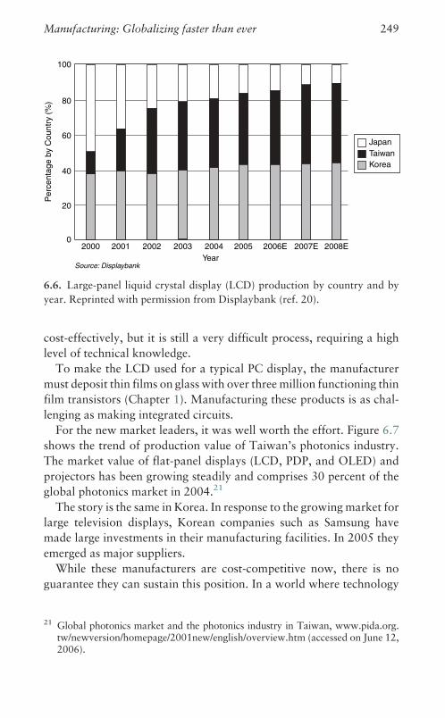
cost-effectively, but it is still a very difficult process, requiring a high
level of technical knowledge.
To make the LCD used for a typical PC display, the manufacturer
must deposit thin films on glass with over three million functioning thin
film transistors (Chapter 1). Manufacturing these products is as chal-
lenging as making integrated circuits.
For the new market leaders, it was well worth the effort. Figure 6.7
shows the trend of production value of Taiwan’s photonics industry.
The market value of flat-panel displays (LCD, PDP, and OLED) and
projectors has been growing steadily and comprises 30 percent of the
global photonics market in 2004.21
The story is the same in Korea. In response to the growing market for
large television displays, Korean companies such as Samsung have
made large investments in their manufacturing facilities. In 2005 they
emerged as major suppliers.
While these manufacturers are cost-competitive now, there is no
guarantee they can sustain this position. In a world where technology
100
80
60
40
20
0
Year2000 2001 2002 2003 2004 2005 2006E 2007E 2008E
JapanTaiwanKorea
Source: Displaybank
Per
cent
age
by C
ount
ry (
%)
6.6. Large-panel liquid crystal display (LCD) production by country and by
year. Reprinted with permission from Displaybank (ref. 20).
21 Global photonics market and the photonics industry in Taiwan, www.pida.org.tw/newversion/homepage/2001new/english/overview.htm (accessed on June 12,2006).
Manufacturing: Globalizing faster than ever 249

diffuses rapidly and foreign competitors can offer lower labor costs and
superior technology, keeping pace with automation is obviously
important, but it is not enough to maintain a competitive advantage.
Other factors come into play.
Domestic specialties, offshore commodities
One of these is focusing on specialized products. Japanese companies
have adopted this approach, translating proprietary skills into robust
competitive positions while making optimum use of less expensive
offshore production. Consider, for example, how automotive compo-
nent suppliers balance the twin demands for technological sophistica-
tion and low-cost production.
Of course, the Japanese are famous for turning excellence in manu-
facturing into a major competitive advantage, but recent cost pressure
from China has forced changes in this strategy, even for domestic
production.
Toyota is supplied within Japan by a network of companies with
interlocking ownerships. These suppliers manage to maintain domestic
plants with highly-skilled workforces, even though their labor costs are
about ten times those in China.
Their secret: unique products that can command premium prices. In
Nagoya, where Toyota and its suppliers have major manufacturing
Source: Photonics Industry and Technology Development Association (PIDA)
0
5,000
10,000
15,000
20,000
25,000
30,000
Mill
ions
of D
olla
rs
Other = Opto-electronic (OE) components, optical input/output devices, optical storage,optical fiber communication (OFC), optical components, and laser applications
2003 2004 2005 2006E 2007EYear
Flat-panel displays
Other
6.7. The production value of Taiwan’s photonics from 2003 (ref. 21).
250 Competing for the future
facilities, the local plants continue to concentrate on high-end,
difficult-to-make products. But the suppliers are shifting production
of simpler components to China to give their big customer higher tech
or lower labor costs, depending on which is more appropriate.
The Japanese machine tool industry follows a similar strategy. Easy-
to-manufacture parts for the machines are made in low-cost countries.
High-end parts continue to be made in Japan, with a constant focus on
enhancements to maintain a performance advantage over overseas
competitors. As much as 85 percent of a given product may use com-
ponents from low-cost countries, but the proprietary 15 percent of the
machine that creates the major part of its value is jealously guarded and
produced domestically.22
As another example of how companies in capital-intensive industries
site their manufacturing facilities according to the skill levels needed,
consider a German company, Continental AG, a global supplier of tires
and automotive components to Daimler-Chrysler and other automakers.
The company has moved labor-intensive operations offshore.
However, it keeps its most automated operations in Germany and
other countries with high labor costs, where it depends on small but
specialized teams of skilled employees.
In Continental’s German-based operations labor amounts to less
than 4 percent of production costs. These plants work at full capacity
and use extensive automation to produce high value-added products.
Continental sees no advantage in moving such plants to low-wage
countries unless logistical reasons require them to be closer to
customers.23
Proprietary processes
Corning, the world’s leading supplier of specialty glass products, is a
prime example of a company that has built its success on highly-
specialized process automation. When large market applications for
glass emerge, the company quickly invests in new production equip-
ment and pioneers a dominant position in the new products.
22 J. Sapsford, ‘‘Japan’s economy gains steam from manufacturing heartland,’’ TheWall Street Journal (October 11, 2005), 1.
23 M. Landler, ‘‘A German auto supplier Delphi might envy,’’ The New York Times(November 24, 2005), C1.
Manufacturing: Globalizing faster than ever 251
Corning spends 10 percent of its revenues on research and develop-
ment, and relies on proprietary processes and a well-trained workforce
to produce unique products. In the 1950s, Corning pioneered the
production of TV picture tubes. In the late 1960s and 1970s, it led in
the development of glass fibers for communications. In 2000, it intro-
duced special glass plates for liquid crystal displays.
It has plants in Japan and Taiwan that produce the glass plates used
to manufacture LCDs. Although these are both now relatively high-
cost countries, the plants make good economic sense, because they are
close to Corning’s flat-panel display customers. Shipping large glass
plates over longer distances would be far too costly.
In keeping with Corning’s philosophy, each plant is automated. Both
can produce $1 billion dollars’ worth of product annually with only
about 250 employees.24
Offshoring and outsourcing software development
Chapter 2 introduced the innovations in software engineering that
transformed programming from a craft to something more like a
production process. These technological innovations turned software
development into a global industry, though it remains a very labor-
intensive process.
As with any product, the overall design of a software program is the
key to its success and value. In standard practice a small number of
skilled software architects designs the ‘‘solution,’’ but a much larger
number of engineers codes and tests the finished software. About
40 percent of the development cost of most programs is in the testing.
The common practice is for companies to retain the core design
teams in their home countries but outsource the coding and testing
chores to lower-cost engineering groups in other countries. The idea is
to keep the teams that do the fundamental innovation close to the
center of the business. This is also a good way to protect intellectual
property. For example, core software development for Apple products
is done in the US.
Designing a new software or software-based product is one thing.
Development and support is another. Although improvements in
24 P. Marsh, ‘‘A careful giant behind the glass,’’ Financial Times (September 30,2005), 10.
252 Competing for the future

training and tools continue to increase the productivity of software
engineers, development activity is still a major cost center for many
companies, and occupies an ever-growing portion of the technical staff.
To reduce its cost, companies in all types of businesses have opened
software engineering facilities in India or outsourced the work to
contract software companies there and elsewhere. Many of these com-
panies are service businesses, such as banks, insurance companies, and
investment firms that maintain large proprietary software programs
and databases.
But it is not just software-dependent businesses that need to cut back
on software development costs. Equipment companies incur substan-
tial programming costs as well. During product development they
spend more on software engineers than they do on engineers in other
disciplines. In fact, an estimated 70 percent of the engineering cost
needed to bring a new electronic equipment product to market is
spent on software development.
Large companies such as General Electric opened software develop-
ment facilities in India in the 1980s. They were followed by many
others. Today practically all major US companies that rely on software
have offshore facilities employing many thousands of engineers.
However, wages are rising in India at about 10 percent a year. The
escalation is prompting companies to look at sites such as China and
Eastern Europe for less expensive programming services. So far, the
fact that English is the language of instruction in Indian colleges has
helped facilities there retain this business.
Other companies were also interested in having access to India’s low-
cost software resources, but either could not open their own facilities
there, or chose to outsource such a small fraction of their software
development projects that creating an Indian operation did not make
economic sense. In response to this market opportunity, many contract
software companies were established in India.
The founders were frequently engineers who had returned from the
US. Some of these companies, such as Infosys, are now publicly traded
and are highly profitable.25 In 2004, the total revenues of the software
contract companies in India are estimated to be in excess of $17 billion,
having grown at a 30 percent annual rate.
25 For a lengthy discussion of the outsourcing industry see R. Hira and A. Hira,Outsourcing America (New York: AMACOM, 2005).
Manufacturing: Globalizing faster than ever 253

It is estimated that they employ about one million engineers,
although this number is hard to verify. These companies take full
responsibility for delivering software in accordance with the specifica-
tions of their customers. Their clients own the code they produce.
Contract software businesses have been established in other coun-
tries as well, notably in Eastern Europe. One country where contract
software companies have been emerging is Ukraine, where engineering
labor rates are below those in India (see Table 4.1).
Then there are international contract software companies such as
Ness Technologies, which provides services from locations in India and
Slovakia. Eastern Europe is attractive because of its proximity to major
Western European companies, and because many Eastern Europeans
know German or French. This makes communications easier than
dealing with the English-speaking Indian facilities.
We can expect that other countries will enter the contract software
market as they expand their engineering populations. However, India
is currently unique in the size of its software engineering force.
Looking at the frenetic activity in the contract software universe, it is
fair to ask how much of the cost of product development outsourcing
actually saves. From personal experience and from conversations with
outsourcing companies, I estimate at this writing that software can be
produced in India and other low-engineering-cost countries for about
half the cost of doing it in the US or Western Europe.
This figure takes into account the increased cost of management and
communications required for such offshore organizations. However,
the savings are neither instant nor automatic. It takes time to reach full
efficiency because of training requirements, and actually realizing the
savings presupposes close management of all projects.
What happens to outsourced workers?
It is not the purpose of this book to address social issues or stump for
changes in government labor policies. However, no discussion of out-
sourcing can ignore the fact that moving software development (or any
other kind of production) offshore does more than cut costs. As recent
headlines show, it obviously affects domestic workers.26
26 R. Hira, ‘‘Impacts and trends of offshoring engineering tasks and jobs,’’ TheBridge (Fall 2005).
254 Competing for the future

US Department of Labor Statistics show that 35 percent of the soft-
ware workers displaced between 2001 and 2003 were still unemployed
in January 2004. Of the 65 percent who had found employment,
only 43 percent earned as much as they had before being laid
off. The unemployment rate of electrical engineers and computer
scientists has increased from between 2 to 4 percent in the years from
1982 to 2000, to between 4 and 5 percent in the 2001–2004 time
periods.27
What is happening is that an increasing level of skill in emerging
technological areas is required to maintain high wage levels in a devel-
oped economy. It is well known that there are very large differences in
the productivity of software engineers. For example, while average
coders find it hard to get jobs that pay well, highly-skilled engineers
in Internet-related software development are in high demand in the
US.28 Furthermore, as long as corporations continue to keep the high-
est software development skills in their home countries, the demand
will be high for very talented engineers to fill these roles, and their
compensation will reflect their value.
We would do well to remember that our prosperity, and the domestic
employment it brings, has been the outgrowth of innovations and the
new industries they create. Creating a climate for innovation in all
phases of industrial development, including manufacturing invest-
ment, may be the best prescription of all for the conditions that indus-
tries in the developed economies face today.
The future of manufacturing
With the contemporary focus on software and the Internet as sources of
value creation, it’s easy to forget that the manufacturing of hard
goods continues to be an important creator of value and source of
employment.
Unfortunately, at least in the West, the future of manufacturing in
general does not look bright. If current trends continue, all but the most
highly-specialized manufacturing will soon leave high-cost countries.
27 Displaced Workers Survey (2004), US Bureau of Labor Statistics, Washington,DC.
28 B. Prabhakar, C. R. Litecky, and K. Arnett, ‘‘IT skills in a tough job market,’’Communications of the ACH (October 2005), 91–94.
Manufacturing: Globalizing faster than ever 255

And even in this case the availability of low-cost capital and govern-
ment subsidies will affect the location of new plant construction.
The extent of the migration is already staggering. Mass-market
consumer products invented in the US, such as personal computers,
color televisions, flat-panel displays, cellular handsets, and even the
iPod, are manufactured in Asia.
Some of the components used in these products, such as the semi-
conductor devices, are made in the US. To underscore the extent of
Asia’s rise in manufacturing, it is estimated that about 45 percent of the
semiconductor devices shipped in the world in 2005 ended up in Asian
countries, where they are assembled into products. Chapter 8 addresses
this situation in more depth.
The semiconductor industry in developed countries is threatened
too. As fabs come on stream in China and elsewhere, local vendors
will increasingly fill the demand for chips in the newly constructed
assembly plants. This is the manufacturing ‘‘network effect,’’ where
component production tends to move to the final assembly region
when conditions are ripe.
To summarize, other Asian nations are now following the path
blazed by Japan, using their cost advantage in labor and engineering
to gain entrance to electronics manufacturing. Then, aided by the
skilled use of automation, they move up the value chain to manufacture
products of increasing complexity. But they are doing it much faster,
thanks to the very electronic technologies they are making.
A total loss of manufacturing industries to lower-cost countries is not
a foregone conclusion, as our examples have shown. Moreover, even in
industries outside of high-tech, production workers in the developed
economies will agree to lower wages when faced with unemployment.
We see this trend in the US, where union wages in some contracts are
going to a two-tiered model. As reported in The New York Times,29
Caterpillar, a major maker of heavy construction equipment company,
will be paying new workers $12–13 per hour, whereas previously
employed workers earned about $20 per hour more. This is a wage
rate that the company believes allows it to compete while keeping
production in the US.
29 L. Uchitelle, ‘‘Two tiers slipping into one,’’ The New York Times (February 26,2006), 1.
256 Competing for the future

But this is a coping mechanism, not a solution. A better answer to the
migration of jobs lies in how industry approaches manufacturing.
Developed nations that do not invest in sophisticated manufacturing
are missing major opportunities for value creation, over and above
what they can get through product or technology innovation. Both
US and Asian enterprises have demonstrated that relentless attention
to developing specialized manufacturing technologies is an effective
strategy for staying competitive in the field. More companies should
emulate these efforts.
If LCD makers in Taiwan, or Corning in the US, can capture and
keep a leadership position in manufacturing high-value products,
others can as well. But this cannot be done by clinging to the past and
subsidizing uncompetitive industries.
Manufacturing: Globalizing faster than ever 257

7 Your government is here to help
ST E E L , textiles, clothing, and consumer electronics: one after
another, manufacturing industries in the US and other developed
countries have buckled under the pressure of low-cost foreign
competition. It’s happened so often over the last half-century that it
no longer generates much political heat.
That doesn’t mean governments won’t enact protectionist measures
to shield their basic industries. In 2002, for example, the US imposed
tariffs on imported steel. But tariffs are often little more than rearguard
holding actions. The basic industries (always excepting agriculture and
big employers like automobile manufacturing) no longer seem to be
regarded as central to the economic future of their countries.
Let foreign competition threaten the growth engines of a developed
nation’s economy, however, and this attitude suddenly changes. The
government will muster an arsenal of legal and economic counter-
measures to thwart the challenge.
Most of these measures target the protection of intellectual property
(IP), the foundation of electronics-related industries. They include
tactics such as embargoes and policing. Unfortunately, these tactics
are not much more effective than import tariffs.
Other approaches, such as patents, trade secrets, and copyrights,
may have more staying power. We will consider each of them.
From embargoes to patent protection
The promotion of industrial development has never been a gentleman’s
game.1 Countries building their industrial bases always seek to acquire
valuable technologies by fair means or foul, and attract investment
capital with government subsidies. Once they achieve their aims, they
1 For a perceptive overview, see P. Choate, Hot property: The stealing of ideas in anage of globalization (New York: Alfred A. Knopf, 2005).
258

turn their energies toward the task of keeping foreign competitors from
doing the same thing to them.
This is the cycle we’ve seen in the rapid industrialization of Germany
in the second half of the nineteenth century, that of Japan in the 1960s
and 1970s, and the emergence of China in the 1990s. German industry
took business away from the British, the Japanese from Western com-
panies, and the Chinese from Western and other Asian competitors. In
each case the incumbent leaders called for government protection from
the foreign challengers.
While the debate over protectionist policies is centuries old, over the
last half-century it has changed in one significant aspect: the current
international focus on protecting IP. This relatively new strategy shows
how important high-tech industries have become in developed econo-
mies. One source estimates that 42 percent of the $5 trillion GDP
generated in the US each year takes the form of intellectual property. IP
in this sense includes software, music recordings, and video products.2
All of these products are easy prey for software pirates, especially in
the consumer market. The stakes are huge. Although precise figures are
difficult to come by, electronics-based industries are clearly at risk of
losing IP that costs them billions of dollars to develop.
Governments use one or more of the following techniques to try to
stem the theft of IP and control where the technology goes:* export embargoes and similar constraints: blocking certain countries
or individuals from buying or accessing technology, usually for
security reasons;* legal protections for IP, including patents and copyrights;* tariffs and other trade restrictions to protect local industry while it
struggles to establish itself or become competitive again;* prohibitions on importing products that are deemed (usually by
court action) to violate patents or copyrights.
The first tactic, embargoes and access restrictions, applies mainly to
technology that has implications for national defense. This relates only
tangentially to our focus on innovation and economic growth, but it’s
worth a brief look to see how government action works.
In an embargo, the US government (for example) might restrict the
sale of a technology to certain countries (such as Iran) because
2 V. Shannon, ‘‘Value of US ideas is huge, but protection is lax, study finds,’’International Herald Tribune (October 14, 2005), 17.
Your government is here to help 259

permitting those countries to acquire the technology would create a
security risk. The embargoed technology usually has important mili-
tary or intelligence applications. The country imposing the embargo
fears that the technology will find its way to adversaries, who could use
it to compromise the defenses of the originating country and its allies.
Using this same rationale the US sometimes restricts foreign students
and visitors from having access to such advanced technologies while
they are working here.
Unfortunately, the effectiveness of such restrictions is questionable at
best. For one thing, few technologies are totally domestic. Most advanced
technologies have spread around the globe, making even embargoed
products readily available outside the US. The only predictable effect of
embargoes, therefore, is to steer potential buyers of embargoed technol-
ogy away from US firms and toward their foreign competitors.3
In addition, restricting the technical activities of foreign students
simply drives those applicants to other countries, which are just as
anxious to attract overseas talent. This is not a desirable situation for
the US. As pointed out in Chapter 4, immigrants are very important to
US high-tech industries.
In short, government action to embargo IP often fails to achieve its
goal, and can handicap the country’s own industries.
Hiding behind trade barriers
Governments will also try to protect their industrial base by creating
trade barriers. They often do so at the request of an affected company
or industry.
Trade barriers give companies or industries a temporary reprieve
from economic pressures, but that often amounts to little more than
postponing an inevitable collapse. Protection in and of itself cannot
make a company more competitive.
RCA and Zenith vs. Japan Inc.
That certainly proved true in the case of a famous American TV set
manufacturer when Japanese competition invaded its home market.
3 A. Segal, ‘‘Blocking the flow of ideas will not bring security,’’ Financial Times(September 1, 2005), 11.
260 Competing for the future

The drama played out during the 1970s, when Japanese companies
entered the US market in force. They included such competitors as
Sharp, Sony, and Matsushita (maker of Panasonic products, and in
1974 the buyer of Motorola’s American-made Quasar TV business),
and they arrived with a formidable array of low-priced, high-quality
products.
RCA and Zenith, the two leading domestic makers, reacted very
differently to the challenge. RCA, an industry pioneer, had a formid-
able patent portfolio going back to the 1920s in commercial radio and
television technology. Continuing investments in research and devel-
opment had kept the company at the forefront of both technologies.
Zenith, on the other hand, got its start in 1927 with a license to
RCA’s radio technology. Over the years it had invested very little in
innovation. When consumer television emerged in the 1950s as a major
new market, Zenith continued to rely on acquired technology. During
the succeeding two decades, the company’s patent wars with RCA and
other competitors, combined with its failure to invest much in its own
R&D, had left Zenith in a very weak technology position.
At the time of the Japanese onslaught, RCA’s strategy was to license
its technology globally. The resulting large annual licensing revenues
helped finance more research and development, which then allowed
RCA to continue developing highly competitive products.
Lacking a technology edge, Zenith took the path of seeking legal
protection against the imports. In 1974 the company filed a federal suit
charging Japanese television manufacturers with dumping and illegal
collusion. Specifically, Zenith claimed that a Japanese television set
selling for $500 in Japan, where the market was closed to imports, was
being dumped for $300 in the US.
This highly visible and politically charged case wandered through the
legal system for over a decade, at great cost to Zenith. Eventually, in
1985, the Supreme Court ruled in favor of the Japanese.
Zenith’s effort to protect itself through trade sanctions had been in
vain. Lacking competitive products, the company never managed to
make a profit. It was eventually acquired by its Asian manufacturing
partner, LG Electronics of South Korea, and disappeared as a separate
entity.
In one final irony, Zenith did finally create its own technological
legacy – just about the time it was being acquired. The company’s
engineers developed the 8VSB modulation scheme for terrestrial
Your government is here to help 261

broadcasting of digital TV signals. This innovation has been adopted
by the US and other countries that use the ATSC system for digital and
high definition television.
Protectionism Asian style
Charges of dumping and similar unfair trade practices are also preva-
lent in other segments of the electronics industry. Semiconductors are a
case in point.
In the 1980s the Japanese chip industry entered on a period of
aggressive expansion, evidenced by its growing exports to the US.
This produced an outcry from American makers about Japan’s dump-
ing of dynamic random access memory (DRAM) chips in the US
market.
Perhaps predictably, the plaintiffs got the same satisfaction from the
government as Zenith did: the flood of low-priced, high-quality
imported devices did not abate. Production of DRAM chips wound
up being concentrated in Japan. Today Micron Technologies is the only
US-based manufacturer still in the DRAM business.
But the story does not end there. Competitive battles between
national champions are still going on. In the 1990s, Samsung of
South Korea emerged as a worldwide leader in memory chips and
selected areas of consumer electronics. Its ascendancy, and that of
other Korean manufacturers, came primarily at the expense of the
established Japanese companies.
A similar scenario is now playing out between China and Taiwan.
Taiwanese semiconductor companies are producing non-memory
chips in increasing volumes, and they are asking for government help
to keep from losing domestic business to cutthroat competition from
the mainland.
In August 2005, J. S. Huang, the director general of the Taiwanese
Semiconductor Industry Association (TSIA), noted that Taiwanese
equipment manufacturers imported 16.8 per cent of their chips from
the mainland during the first half of that year. In terms of volume,
China had also become the second-largest source of chips to Japan.
Even more worrisome to the TSIA, these were high-performance chips,
marking a break from the pattern of previous years when mainland
imports were mostly low-end products.
262 Competing for the future
Huang, obviously asking for government help, said that ‘‘Taiwan
should prevent mainland Chinese dumping of chips on the island.’’4
Given other political considerations between Taiwan and China, and
the fact that lower-cost chips help Taiwanese equipment manufac-
turers stay competitive, it is unlikely that anything will be done in
response to this plea.
Nowhere to hide, somewhere to go
It has always been difficult to shield high-tech industries (or indeed any
industry) from foreign competitors. Asking the government for import
protection on the basis of unfair pricing tactics rarely accomplishes
much in the US. It certainly does not provide a bulwark against a
determined, well-capitalized competitor, especially when the challen-
ger combines efficient manufacturing with state-of-the-art technology.
Trade barriers may delay the entry of foreigners, but in the final
analysis, the only approach that creates sustainable businesses is to
combine technological innovation with market savvy and creative
ways to cut costs. That’s the lesson we learned in Chapter 6 from the
examples of the Taiwanese LCD makers, the IP-based US semiconduc-
tor companies, and the Japanese machine tool industry.
Another way to stay in the game is to form a joint venture with your
potential competition. As Chapter 4 briefly mentioned, Alcatel, a
French telecommunications company, has done just that. It has entered
into a partnership agreement with a Chinese government-owned entity.
Let us take a closer look at Alcatel’s calculated move.
China is industrializing faster than any other country in history.
Although hardly a paragon of laissez-faire capitalism, it attracts enor-
mous amounts of outside investment capital. The Chinese govern-
ment’s industrial policy targets the development of specific industries,
with information and electronic technologies getting high priority.
All of this spells trouble for companies in those industries in other
parts of the world. As Chinese manufacturers get better at making
world-class products and begin to export, established companies like
Alcatel are faced with an age-old dilemma: how do you survive when
4 ‘‘Organization warns of likely mainland Chinese chip dumping in Taiwan,’’ TheTaiwan Economic News–China Economic News Service (August 29, 2005).
Your government is here to help 263
your overseas competition can undercut your prices even in your home
market?
For most companies, regardless of their nationality, their short-term
answer has been to join the party. Don’t rely on import barriers.
Instead, move your most labor-intensive manufacturing operations to
lower-cost countries. Keep the others close to home where the intellec-
tual property can be better protected.
In many cases, companies abandon local manufacturing altogether.
In the long term, as we discussed in Chapter 6, intellectual property
generated by manufacturing excellence creates value in many indus-
tries, but companies under financial pressure to reduce costs fast may
not be able to justify investing toward that objective when the option of
moving offshore is open.
That’s the reason behind the rapidly growing influx of foreign-
financed production plants into China. They are capitalizing on the
labor cost savings available in emerging economies, the better to com-
pete on international markets.
There is an alternative to building those plants, however, and the
Chinese government is heavily promoting it – a joint venture. This
arrangement allows international equipment companies to leverage
advanced technology with low-cost manufacturing, so they can pro-
duce exported products at costs far lower than otherwise possible. This
is the route chosen by Alcatel.
Alcatel Shanghai Bell (ASB), a joint venture formed in 2001, is 49
percent owned by Alcatel. A Chinese government-owned entity con-
trols the rest. ASB produces telecommunications network equipment in
China using Alcatel technology.
The arrangement gives ASB access to China’s low-cost resources
(labor and infrastructure). It also qualifies ASB for subsidies in the
form of R&D incentives and low-interest loans to finance exports.
Essentially the joint venture gets the same preferential treatment as
other similar domestic companies, including access to assistance from
municipalities in industrializing regions to encourage local
employment.5
With these advantages ASB is well positioned to sell into the fast-
growing local market for communications equipment, and move into
international markets as well. ASB gives Alcatel the ability to compete
5 This information is from a speech by Olivia Qiu, Vice President ASB, July 2005.
264 Competing for the future

on price and product quality anywhere in the world, with Alcatel
providing the international marketing reach.
But Alcatel and other vendors face a difficult choice – either take
advantage of the Chinese partnership opportunity and compete world-
wide, or fight a losing battle for market share with emerging Chinese
companies such as Huawei, which offer state-of-the-art products built
with the same low labor costs and access to financial resources that
benefit ASB.
While this form of government intervention has its advocates and its
advantages, it hasn’t been around long enough to build a track record.
Only one type of government program has established a positive record
for developing sustainable industry: the patent system. It also has the
advantage of being built around the concept of encouraging the devel-
opment of innovation, in the form of IP.
Protecting IP: The new international battlefield
The patent system in the US was created over 200 years ago. Its intent
was to promote industrial innovation by giving a limited monopoly to
inventors. Few people debate the historical value of the system in
fostering R&D investments, but recent changes in the patent granting
process have prompted a great deal of criticism. Many experts charge
that the patent system does as much to hinder as to promote
innovation.
By law, a patent is only granted for inventions that are useful, new,
and not obvious. The definition of ‘‘obvious,’’ however, is a major
bone of contention in most patent suits. The intent of the law in
excluding ‘‘obvious’’ innovations is to avoid patenting trivial exten-
sions of the existing art. This, of course, begs the question of what is
trivial, and opens the door to more challenges over the legitimacy of
patents.
The courts have been heavily involved in settling such disputes
almost from the beginning of the system. Resolving this issue is a
process that enriches lawyers while it clogs the courts. The demand
for adjudication was so great that in 1982 a special court was created to
handle certain types of patent case appeals.
According to many experts, however, the biggest problem with the
current patent system is not the number of disputes, lawsuits, and
appeals it generates. The real difficulty is that patents have become
Your government is here to help 265

too easy to obtain, especially since the 1980s, when the criteria for
awarding them were greatly expanded.
It’s hard to determine the exact dimensions of this problem. Ideally
we would like to compare how patent approval rates have changed
over the years. But it’s difficult to calculate an accurate figure for even
one year, in large part because inventors can file multiple patent
applications for the same work.
However, we can compare approval rates in the US to those of other
countries. Between 1994 and 1998, according to the US Patent and
Trademark Office (USPTO), about 75 percent of original patent appli-
cations in the US were eventually granted. The rate of acceptance in
Japan and by the European Patent Office is substantially lower – in the
50 to 60 percent range.6 The high acceptance rate in the US has serious
implications for the future of innovation.
Moving software into the patent system
The largest single change in the US patent system in the 1980s, and the
one with the biggest impact, was allowing patents for software. Up to
this point software IP had been protected by copyrights on a program,
or by keeping the code a trade secret.
The landmark case that opened the way to patenting processes
implemented in software was Diamond v. Diehr and Lutton. This
dispute (450 US 175, 209 USPQ 1) went all the way to the US
Supreme Court in 1981.7
Diehr and Lutton worked for a company that made products molded
from rubber compounds. The standard method for molding these
products was to place the compound on a heated press, set a timer to
sound an alarm at the end of the correct curing period, and have an
operator remove the finished product from the press.
6 Information on the US patent system was drawn from S. S. Merrill, R. C. Levin,and M. B. Myers (eds.), A patent system for the 21st century (Washington, DC:The National Academies Press, 2004), p. 53; and from A. B. Jaffe, ‘‘The US patentsystem in transition: Policy innovation and the innovation process,’’ ResearchPolicy 29 (2000), 531–537.
7 J. Tripoli, ‘‘Legal protection of computer programs,’’ RCA Engineer 29 (January/February 1984), 40–46; and R. Hunt and J. Bessen, ‘‘The software patent experi-ment,’’ Business Review Q3 (Philadelphia, PA: Federal Reserve Bank ofPhiladelphia, 2004), 22–32.
266 Competing for the future
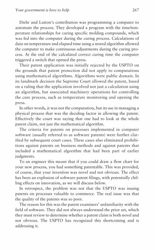
Diehr and Lutton’s contribution was programming a computer to
automate the process. They developed a program with the time/tem-
perature relationships for curing specific molding compounds, which
was fed into the computer during the curing process. Calculations of
data on temperature and elapsed time using a stored algorithm allowed
the computer to make continuous adjustments during the curing pro-
cess. At the end of the calculated correct curing time the computer
triggered a switch that opened the press.
Their patent application was initially rejected by the USPTO on
the grounds that patent protection did not apply to computations
using mathematical algorithms. Algorithms were public domain. In
its landmark decision the Supreme Court allowed the patent, based
on a ruling that the application involved not just a calculation using
an algorithm, but associated machinery operations for controlling
the cure process, such as temperature monitoring and opening the
press.
In other words, it was not the computation, but its use in managing a
physical process that was the deciding factor in allowing the patent.
Effectively the court was saying that one had to look at the whole
patent claim, not just the mathematical algorithm.
The criteria for patents on processes implemented in computer
software (usually referred to as software patents) were further clar-
ified by subsequent court cases. These cases also eliminated prohibi-
tions against patents on business methods and against patents that
included a mathematical algorithm that had been part of earlier
judgments.
To an engineer this meant that if you could draw a flow chart for
your new process, you had something patentable. This was provided,
of course, that your invention was novel and not obvious. The effect
has been an explosion of software patent filings, with potentially chil-
ling effects on innovation, as we will discuss below.
In retrospect, the problem was not that the USPTO was issuing
patents on processes valuable to commerce. The real issue was that
the quality of the patents was so poor.
The reason for this was the patent examiners’ unfamiliarity with the
field of software. They did not always understand the prior art, which
they must review to determine whether a patent claim is both novel and
not obvious. The USPTO has recognized this shortcoming and is
addressing it.
Your government is here to help 267

Patents, copyrights, and trade secrets
After 1990 the floodgates opened wide. As shown in Figure 7.1, the
number of issued software patents, which had been increasing slowly
up to that point, jumped from 5,000 in that year to 25,000 in 2002.8
Software patents accounted for 15 percent of all patents issued in 2002,
up from less than 6 per cent in 1990 (see Figure 7.2).9
Patents provide new and potent protection for software IP. Under the
law, courts can issue injunctions against any company found guilty of
patent infringement. In effect, the infringing business can be shut down
if the patent holder refuses to license the use of the contested patent or
make some other arrangement with the infringer.
Even large companies with battalions of lawyers are vulnerable to
such penalties. At the end of a celebrated dispute, Kodak was forced
to shut down its instant photography business when it was found to
infringe a number of Polaroid patents.
To make matters worse, such cases may take years to decide, depres-
sing an ongoing business under a cloud of uncertainty. A recent US
Supreme Court ruling that judges have flexibility in deciding whether
to issue court orders barring continued use of a technology after juries
find a patent violation may result in much fewer injunctions – a welcome
development for industrial activity.10
Patents are one of three mechanisms available to protect software.
The others are copyrights and trade secrets. Table 7.1 compares how
each works to protect IP.11
We think of copyrights as applying mostly to books, images, movies,
and similar works. Prior to the Diehr and Lutton case, however, copy-
right was the most common method of protecting software, as covered
under US federal law (Title 17 of the US code).
The ability to copyright computer code was established by Congress
in the Computer Software Copyright Act of 1980. This law states that
‘‘a set of statements or instructions to be used directly or indirectly in
8 Hunt and Bessen, ‘‘Software potent experiment,’’ 24. 9 Ibid., 25.10 J. Bravia, M. Mangalindan, and D. Clark, ‘‘eBay ruling changes dynamic in
patent-infringement cases,’’ The Wall Street Journal (May 16, 2006), B1.11 J. Tripoli, ‘‘Legal protection of computer programs,’’ RCA Engineer 29 (January/
February 1984), 45.
268 Competing for the future
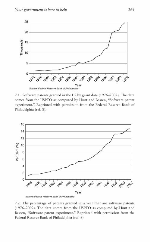
0
2
4
6
8
10
12
14
16
Year
Per
Cen
t (%
)
Source: Federal Reserve Bank of Philadelphia
1976
1978
1980
1982
1984
1986
1988
1990
1992
1994
1996
1998
2000
2002
7.2. The percentage of patents granted in a year that are software patents
(1976–2002). The data comes from the USPTO as computed by Hunt and
Bessen, ‘‘Software patent experiment.’’ Reprinted with permission from the
Federal Reserve Bank of Philadelphia (ref. 9).
0
5
10
15
20
25
1976
1978
1980
1982
1984
1986
1988
1990
1992
1994
1996
1998
2000
2002
Year
Tho
usan
ds
Source: Federal Reserve Bank of Philadelphia
7.1. Software patents granted in the US by grant date (1976–2002). The data
comes from the USPTO as computed by Hunt and Bessen, ‘‘Software patent
experiment.’’ Reprinted with permission from the Federal Reserve Bank of
Philadelphia (ref. 8).
Your government is here to help 269

Table 7.1 Brief comparison of software-protection techniques in the US
Parameter Patents Copyrights Trade secrets
What is protected? Underlying ideas,
concepts, or methods
used in the system.
Original works of
ownership fixed in any
tangible medium of
expression.
Formulas, ideas, devices,
compilations,
programs, techniques.
How is protection
obtained?
File an application in US
Patent Trademark
Office.
For published work: Place
copyright notice on work.
For unpublished work:
Automatic upon
completion.
Maintain secrecy.
When does
protection
start?
Issuance of patent. Upon completion of the
work.
At creation of secret
information.
How long does
protection last?
20 years from date of
patent filing.
Life of author plus 50 years.
Work for hire: 75 years
from publication, or, 100
years from creation,
whichever comes first.
As long as information is
kept secret.
Criteria for
providing
protection.
Must fall within
statutory subject
matter and must be
new, useful, and
unobvious.
Any original work of
authorship.
Must have value and not
be generally known to
others.

Table7.1
(cont.
)
Who
infr
inges
?A
nyone
who,w
ithout
auth
ori
zati
on,m
akes
,
use
s,or
sell
scl
aim
ed
inven
tion.
Anyone
who,w
ithout
auth
ori
zati
on,co
pie
s,
makes
der
ivati
ve
work
s,
publi
cly
per
form
s,or
dis
trib
ute
sco
pyri
ghte
d
work
by
sale
,le
ase
,re
nta
l
(subje
ctto
statu
tory
exce
pti
ons)
.
Anyone
who
vio
late
sa
confi
den
tial
rela
tionsh
ipor
use
s
unla
wfu
lm
eans
to
gain
acc
ess
totr
ade
secr
etin
form
ati
on.
Avail
able
rem
edie
sfo
r
infr
ingem
ent.
Inju
nct
ion,re
aso
nable
royalt
ies.
Inju
nct
ion,st
atu
tory
dam
ages
,ro
yalt
ies.
Inju
nct
ion,dam
ages
,
crim
inalsa
nct
ions
for
thef
t.
Appli
cable
law
.Fed
eralPate
nt
Act
.Fed
eralC
opyri
ght
Act
.Sta
tetr
ade
secr
et
statu
tes.
Sourc
e:Fro
mT
ripoli
,‘‘L
egalpro
tect
ion
of
com
pute
rpro
gra
ms,
’’re
f.11.

a computer in order to bring about a certain result’’ can be copyrighted.
Hence, the program developed by Diehr and Lutton could have been
protected by copyright.
As Table 7.1 shows, establishing a copyright on one’s work is simple.
The work is copyrighted as soon as it is ‘‘fixed in any tangible medium.’’
At that point the familiar # symbol gives the public clear notice of
one’s claim to copyright.
This informal copyright does not entitle the holder to legal redress
against IP theft. In order to initiate action against an infringer, the
copyright holder must officially register the work with the Registrar
of Copyright.
Copyrights also provide more limited protection than patents. A
copyright protects the code that makes up a program, but not the
idea behind the software. If someone else achieves the same results
using different code, this is not considered a copyright infringement.
A patent, on the other hand, protects the concept of the software.
Any other program that achieves the same results as a patented pro-
gram would be regarded as an infringement on the patent.
A third way of protecting work is through trade secrets. The Uniform
Trade Secrets Act, a statute used by some states, defines a trade secret as
information, including a formula, pattern, compilation, program,
device, method, technique, or process that:
1. derives independent economic value, actual or potential, from not
being generally known, and not being readily ascertainable by
proper means to other persons who can obtain economic value
from its disclosure or use; and
2. is the subject of efforts that are reasonable under the circumstances
to maintain its secrecy.
In order to treat information as a trade secret, companies must take steps
to restrict access to the information and tightly control its dissemination. In
the case of computer software, this is typically implemented in a license
accompanying the product, whether a written agreement signed by the
licensee, a printed license on the packaging, or a click-to-accept license.
Patent protection is obviously the strongest of the three protection
techniques, but filing for a patent has its downside. The patent must
disclose valuable information about the invention.
This can allow competitors to achieve the same results by designing
their way around the patent. For that reason manufacturing industries
prefer trade secret protection, which allows them to avoid disclosing
272 Competing for the future

process information. Other industries, including software, increasingly
file patents as a defensive measure.
Broader patents, more litigation
Patent litigation is a costly proposition. Since millions of patents con-
tinue to be filed around the world, just about every technology-based
business will face it sooner or later.
Usually it’s sooner. Depending on a number of factors, the life of a US
patent is currently limited to between seventeen and twenty years (twenty
years being most common), and patent holders want to derive maximum
value from their IP before their exclusivity expires. For that reason most
will quickly take action against any suspected infringements.
There’s a broader basis for suits, too. It is commonly argued that
easing the patent award process in the US has resulted in filings that are
indefensible on the basis of novelty or other meaningful criteria.
Software patents in particular, if written broadly enough, can cover
almost anything under the sun.
Patents that cover services rendered through the use of software,
such as the delivery of a service with a special billing method, are
particularly onerous, because they can be extremely broad and difficult
to litigate. There are companies whose only business is enforcing their
claims to just these kinds of patents. Their stock in trade is lengthy,
costly litigation. This tactic can hinder the development of a new
service sector for years.
Two basic issues come up in patent litigation: first, whether the
claims of the patent are valid; and second, whether a valid claim has
been infringed. During the hearing, expert witnesses are called upon to
testify about the infringement.
Regarding the primary question, that of validity, there are many
issues that can arise, particularly whether there is prior art which
could invalidate the patent in question. Those challenging the patent
can request reexamination of the patent by the USPTO, which may
reopen the question of patentability. This results in one of three out-
comes: the patent can be upheld, its claims may be modified, or it may
be found invalid.
There have been cases in which the Commissioner of Patents has
ordered the reexamination of certain software patents which simply
used a computer to implement a preexisting process.
Your government is here to help 273

The law states that ‘‘patent[s] shall be presumed valid.’’ This is a
significant advantage for incumbents, because the tendency is for
courts to rule in favor of patent holders. Still, because so much depends
on the testimony of expert witnesses, and on the ability of lawyers to
explain highly-complex technical matters to non-technical judges and
jurors, patent litigation is always risky and its outcome highly uncer-
tain. More often than not the two sides reach a settlement just to avoid
the hazards of jury trial.
Under this system new enterprises are obviously at risk from incum-
bents determined to ‘‘expense’’ them out of business through patent
litigation, frivolous or not. So the question is: does the current process,
which makes patents on new technologies easier to get, promote or
hinder innovation and industrial growth?
There is no simple answer, and scholarly work on the subject is
inconclusive.12 One thing is certain: IP litigation is a growth business
all on its own.
How litigation can stifle innovation
It is understandable that companies that invest in research and devel-
opment are anxious to protect their innovations by aggressive legal
means. In a world where ideas move so quickly, this is a fair way to gain
an advantage.
However, allowing trivial patents in a legal system that encourages
litigation will have a chilling effect on innovation. The current system
allows almost any innovation to be challenged if the challenger is
willing to spend money on costly litigation.
Patent suits thus become a restraint of trade, delaying the introduc-
tion of new products or services while cases drag through the courts.
This makes intellectual property litigation one of the major risks facing
entrepreneurs (and investors).
The system also favors companies with the resources to aggressively
fight patent cases. High-priced law firms often offer executive seminars
12 Pertinent documents on the subject include J. Bessen and R. M. Hunt, ‘‘Anempirical look at software patents,’’ Working Paper No. 03-17/R, FederalReserve Bank of Philadelphia meeting, March 2004; and R. J. Mann, ‘‘Themyth of the software thicket: An empirical investigation of the relationshipbetween intellectual property and innovation in software firms,’’ AmericanLaw and Economics Association Annual Meeting, May 7–8, 2004, Paper 44.
274 Competing for the future

on litigation as a ‘‘business strategy,’’ where they tell big, entrenched
companies that suits filed against potential competitors are a relatively
inexpensive way to hold onto their markets.
It’s not just big companies defending large market shares that bene-
fit. As noted above, the system also encourages the formation of
companies set up solely to buy broadly-based patents, which they use
in litigation and nuisance suits in the hope of being paid to go away.
A well-publicized case, settled in 2006, involved Research in Motion
(RIM), the company that provides wireless e-mail service to about
three million BlackBerry handset subscribers worldwide. RIM was
sued for patent infringement by NTP Inc., a company that owns certain
software patents and whose sole business is deriving licensing income
from them.
When the US Court of Appeals in Washington DC rejected the
appeal of RIM on October 7, 2005, the company faced an injunction
shutting down its operations unless it reached an agreement with NTP.
At this stage of a case, with all appeals exhausted, the patent holder has
all the cards.
Although RIM said it had developed an operating system that
avoided the NTP patents, the OS was not ready for rollout, and RIM
could not afford to risk its business or its customers. It had no choice
but to settle – for $612 million. Technology columnist Michael Miller
reacted to the settlement this way:
And the US Patent system continues to look pretty silly, as the Patent Office
has overturned a couple of NTP’s patents, but not until after the court case
(and others are still being appealed). I’ve yet to be convinced that software
patents make sense, given the vagueness of the difference between an idea and
execution of that idea in the software world; and the lack of a good database
[of] prior art.13
Unfortunately, the RIM/NTP case is just one of many such actions
flooding the courts. And this is a long-term problem, not a temporary
aberration. Two statistics prove it.
Figure 7.3 shows that the number of district court patent cases has
more than doubled between 1988 and 2002.14 As software cases
13 ‘‘Patently crazy – The BlackBerry settlement,’’ http://blog.pcmag.com/blogs/miller/archive/2006/03/06/682.aspx (accessed March 8, 2006).
14 Merrill, Levin, and Myers (eds.), A patent system, p. 32.
Your government is here to help 275

proliferate, this curve is only going up. The increased legal activity has
produced great employment opportunities for lawyers specializing in
IP matters. Between 1984 and 2001, as Figure 7.4 indicates, member-
ship of the American Bar Association grew by 29 percent while the
membership devoted to Intellectual Property matters grew by 79
percent.15
Faced with these facts, what choice does an innovative business have
but to play the game and file for as many patents as possible? At best, it
is a means of keeping competitors at bay, and creating opportunities to
cross-license patents. At worst, it can be a defensive tactic, establishing
a claim that the company can offer to trade when attacked by others.
After years of ignoring the problem, even very big software compa-
nies are adopting this strategy. The biggest of them, Microsoft
Corporation, until very recently relied mostly on market muscle and
3000
2500
2000
1500
1000
500
0
Year
Cas
es T
erm
inat
ed
Source: Federal Judicial Center Research Division, Integrated Data Base
1988
1989
1990
1991
1992
1993
1994
1995
1996
1997
1998
1999
2000
2001
2002
7.3. Federal district court patent lawsuits terminated by fiscal year.
‘‘Terminated’’ includes judgments, dismissals, settlements, transfers, and
remands. From Merrill, Levin, and Myers (eds.), A patent system (ref. 14).
15 Ibid., p. 33.
276 Competing for the future

copyrights for its competitive advantage. It has now decided to seek
patents aggressively, with a target of 3,000 a year.16
Since Microsoft is the most dominant company in the software
industry by far, this could spell big trouble for smaller innovators. If
an industry includes a small number of large companies of equal
weight, there is little incentive for extensive patent fights. The big
adversaries can reach a mutually satisfactory agreement because both
sides have something to trade and something to gain.
Things are different when a single company’s IP controls a new
industry, the way RCA’s patents did in the early years of color televi-
sion, or Qualcomm’s CDMA technology does in the wireless world
today. In this case a patent portfolio becomes the weapon of choice for
freezing out competitors or extracting hefty license fees. Newcomers
450000
400000
350000
300000
250000
200000
150000
100000
50000
0
25000
20000
15000
10000
5000
0
Year
AB
A T
otal
AB
A-I
PL
Sec
tion
Source: American Bar Association (ABA)
1984
1985
1986
1987
1988
1989
1990
1991
1992
1993
1994
1995
1996
1997
199819
9920
0020
01
7.4. American Bar Association membership: Intellectual Property Law Section
and total. Copyright # 2006 by the American Bar Association. Reprinted with
permission (ref. 15).
16 R. Stross, ‘‘Why Bill Gates wants 3,000 new patents,’’ The New York Times (July31, 2005), BU3.
Your government is here to help 277
must invent their way around the established patents and be willing
and able to defend themselves in multi-million dollar litigations.
Reforming the system
There is no shortage of people willing to complain about the US patent
system. Pundits in every industry loudly proclaim that the system is
‘‘broken,’’ and that patents are impeding innovation rather than pro-
moting beneficial research and development.17 But changing the sys-
tem is a lengthy process. It is also likely to be very contentious. This is
not surprising, since any reform will create winners and losers.
Nevertheless, there are signs of movement. In 2005 a bill was pro-
posed in Congress to change the process of issuing patents in a way that
would substantially reduce the differences between US and foreign
practice. It would also subject patent applications to more careful
scrutiny.
The hope is that the proposed reforms will halt the growth of patent
litigation. If the bill is passed, its most far-reaching provisions would:
1. Start the time clock for establishing priority of invention from first
to file rather than first to invent.
2. Eliminate the requirement that the patent disclose the best mode of
practicing the invention.
3. Provide for publishing all applications.
4. Provide for post-issuance opposition procedures.
Not everyone agrees that the system needs reform. A minority view,
represented by Bruce A. Lehman, former US Commissioner of Patents
and Trademarks, holds that the current software patent policy in the
US actually encourages innovation.18 The more common view, how-
ever, and one with which I strongly agree, is that present practice
encourages litigation, restrains competition by penalizing new compa-
nies, and diverts money to legal maneuvering that would be better
spent on product development.
17 See the summary in P. Samuelson, ‘‘Why reform the US patent system?’’Communications of the ACM (June 2004), 19–23. Also informative is thework of A. B. Jaffe and J. Lerner, Innovation and its discontents: How ourbroken patent system is endangering innovation and progress and what to doabout it (Princeton: Princeton University Press, 2003).
18 B. A. Lehman, ‘‘Don’t fear software patents,’’ The Wall Street Journal (August 30,2005), B2.
278 Competing for the future

There is no question that the best and simplest way of dealing with
frivolous patents is to ensure more careful screening by patent exam-
iners. The examiners must do a more thorough job of checking prior art
and testing the relative merits of the applications. Unfortunately, this
entails more expense at the USPTO.
Would a stricter process for issuing patents, incorporating the
changes discussed above, cut down on the amount or cost of patent
litigation? Probably. It would certainly reduce the number of trivial
patents granted, and also remove some of the more subjective issues in
patent litigation.
To keep things in their proper perspective, let us recognize that the
great majority of patents are never contested because they are essen-
tially useless. Litigation actually involves a very small number of issued
patents. This makes me wonder whether a tighter screen at the original
issuing process would produce a meaningful reduction in the legal
fights that surround the few important cases. But at least it would
take some of the more frivolous ‘‘nuisance’’ lawsuits off the docket.
An issue that has no borders
We’ve been focusing on patent issues as they relate to the US, but other
countries are facing problems of their own. Patent standards differ from
country to country, creating fertile ground for continuing legal conflicts. In
those countries, as in the US, the growing economic importance of software
guarantees that software patents will be at the heart of many disputes.
These countries are not much farther along than the US in addressing
patent issues. An attempt to produce a uniform European Union soft-
ware patent policy, one that would override national differences, was
recently the subject of a three-year legislative battle within the
European Parliament.
The proposed law would have granted patent protection to new,
non-obvious, and technically meritorious software inventions. The
arguments pitted open-source software advocates, who denied the
need for software patents, against companies with large portfolios
who were fearful of losing their future income from software IP.
The law was defeated in the Parliament in 2005. Hence there are
no uniform standards within EU countries, and certainly no match
between the patent criteria of the individual countries and those of
the US.
Your government is here to help 279

Software will continue to be patented in the US and in EU countries,
but standards of acceptance will vary. This will undoubtedly leave lots
of room for litigation and uncertainty regarding what is protected, as
one case after another makes its dreary way through the courts.19
Patents and industry standards: A difficult marriage
One way that companies share IP is through industry standards. These
are essentially technology platforms that ensure that products and
services that comply with the standards fit their purpose and perform
as intended. Examples include the various Motion Picture Experts
Group (MPEG) software standards for encoding and decoding digital
video, and the WiFi standards for wireless communications.
A standard normally includes IP from a number of companies. Each
contributor is paid a royalty when other companies build products
around the standard. The IP makes it easier to commercialize a tech-
nology by assuring interoperability and enabling faster design.
Standards users don’t have to re-invent the core technology, because
it’s already in the standards.
Since standards can involve hundreds of industry participants, a
crucial question is how to deal with the patented IP incorporated into
each standard. Standards-setting bodies address this issue head-on,
requiring a participant to disclose whether a proposed contribution is
covered by patents. This eliminates surprise claims for royalties from
an individual company after the standard has been set. To be included
in an IEEE standard, the contributing company makes a statement that
the IP should be licensed under reasonable terms.20
Although industry standards incorporate agreements on their con-
tent from all participants, there are still squabbles among the compet-
ing companies. An industry thought leader with a strong patent portfolio
that commands hefty license fees under the standard is a tempting
target for complaints of unfair use of patent protection.
Take the case of Qualcomm, a company with a large number of core
patents covering WCDMA technology for wireless communications. In
a 2005 complaint before the European Commission, six major players
19 ‘‘A sorry software saga,’’ Financial Times (July 7, 2005), 12.20 C. K. Lindell, ‘‘Standard issue,’’ TechConfidential (May/June 2005), 41.
280 Competing for the future
in wireless (Broadcom Corporation, LM Ericsson Telefon AB, NEC
Corporation, Nokia Corporation, Panasonic Mobile Communications
Co. Ltd., and Texas Instruments) jointly alleged that Qualcomm had
not lived up to the commitment it had made during standards devel-
opment. The companies said Qualcomm had failed to license its tech-
nology on ‘‘fair, reasonable and non-discriminatory terms’’ to anyone
that wanted to make equipment that complied with that standard.
The prospect of royalties from IP in an industry standard can touch
off litigation well before the process of defining the standard even
starts. This is particularly true if the standard is going to be essential
to the new technology finding its market. A good example of this
syndrome is radio frequency identification (RFID) technology.
RFID uses tags on products which, when interrogated by radio
frequency signals, send back information. Consumers are familiar
with highway toll passes which use this principle, but the technology
is also an attractive replacement for the familiar bar codes widely used
to track products through the supply chain.
The major benefit is that light sensing, necessary for using bar codes,
can be replaced by signals which will be detected even in products that
are enclosed and inaccessible to light. In 2004, Wal-Mart Corporation
indicated its intent to mandate that RFID tags be part of its supply
chain management process, and announced that its suppliers would be
expected to adopt it.
The idea behind this technology is over thirty years old, but imple-
mentations have been hindered by the cost of the tags and reliability
issues in reading them. Given Wal-Mart’s immense size and buying
clout, however, the chain’s announcement was expected to spur rapid
improvements in the technology and its widespread adoption. The
announcement set off a scramble for ownership of relevant intellectual
property.
It is estimated that as of 2005, over 1,400 patents have been issued in
the field of RFID. Since 1976, by comparison, only 3,300 applications
have been filed. Industry standards are essential for the adoption of a
technology like this, and those who hold patents that are incorporated
into the standards can realize valuable revenues when the licenses are
negotiated.
But because of RFID’s long history and the many patents filed,
sorting out IP ownership is no trivial matter. Companies are now
using legal action to establish their claims in preparation for licensing
Your government is here to help 281
IP for use in forthcoming standards. The first litigation over this
technology involved UNOVA, Intermec, and Symbol Technologies.
They initiated suits and countersuits in 2004 and 2005 in the US
District Court of Delaware.
Producers and pirates: The world of digital media
When voice and video were analog, and the equipment and media for
recording them were bulky, expensive, and localized, the theft of
music, movies, and TV shows was not a major concern. Software
piracy wasn’t an issue either, because there wasn’t any software.
How things have changed, thanks to digital technology. Piracy of
recorded entertainment, video games, and computer programs is per-
vasive. Inexpensive technology allows criminals and consumers alike to
capture, store, and transmit voice and video anywhere in the world.
For the media industries that produce this content, the digital age is both
positive and negative. The positive: digital technology promises to trans-
form the industry by creating new distribution channels for their product.
The negative: the industry is losing control of the product and its price.
Legal inroads: Digital distribution models
Take a look at how revolutionary new forms of distribution are under-
mining the status quo in recorded music. The advent of inexpensive
portable devices for storage and playback of digital music (such as the
Apple iPod1, which had 80 percent of the market in 2005) has made it
possible to circumvent the conventional routes of disk sales and radio
play and instead transmit tunes directly into the hands of the public.
The enormous popularity of these devices concentrates a big portion
of the music distribution function in a few new hands. The digital
moguls who control this new distribution channel can set the price
for downloading songs, and force copyright holders to agree to their
terms.
It can be argued that new channels for the music industry generate
new revenue opportunities, and expand the customer base.21 The good
21 J. Leeds, ‘‘Apple, digital music’s angel, earns record industry’s scorn,’’ The NewYork Times (August 27, 2005), 1.
282 Competing for the future

news for the music industry is the fact that the sales of musical down-
loads totaled $790 million in the first half of 2005, up from $200
million for the same period in 2004. This amounts to 6 percent of
industry sales, according to the Federation of the Phonographic
Industry.
During that same period in 2005, recorded music sales (CDs and
tapes) fell 1.9 per cent, or about $200 million, according to The Wall
Street Journal. So the net effect is that digital downloads have actually
increased consumer access to music – a great example of how new
technologies can expand entertainment markets.22
The bad news is that the industry has to share its profits with new-
comers, and that its album-oriented marketing strategy has been sub-
verted. The music industry had effectively killed the sales of individual
songs (the ‘‘singles’’ of years past) and forced the public to buy multi-
song albums at a huge price premium. With online music the industry
must once again accept sales of singles, at one-twentieth the cost of an
album.
Illegal distribution: From DVDs to downloads
Even worse news comes from rampant piracy, which is stealing poten-
tial revenues in ever-increasing amounts. Piracy has always been a
problem, particularly in emerging economies, but never to the extent
it is now. It is estimated that in Russia alone the piracy of motion
pictures, music, software, and books cost US companies about $1.7
billion in lost revenues in 2004.23
Over the next few years the situation will get rapidly worse for the
music, video game, and movie industries, as pirates use increasingly
sophisticated Internet-based electronic distribution techniques. Consider,
for example, the comparative inefficiency of today’s business model for
illegally copying and distributing movies, and then look at the potential
of the Internet to improve the picture – for the pirates.
22 ‘‘Digital music’s surging growth offsets CD slump,’’ The Wall Street Journal(October 4, 2005), A19. However, worldwide music industry sales havedeclined. See J. Leeds, ‘‘Music industry’s sales post their sixth year of decline,’’The New York Times (April 1, 2006), C2.
23 G. Chazan, ‘‘In Russia, politicians protect movie and music pirates,’’ The WallStreet Journal (May 12, 2005), B1.
Your government is here to help 283

In either case the process starts with a recording. Pirates first capture
movies off the screens in theaters using video camcorders. Under
today’s model they then transfer the movies to DVDs with replication
technology that is readily available (just look at the ads for disk copiers
in any hobbyist magazine). The resulting disks are then sold at a
fraction of the price of the authorized version.
It’s not easy to interdict this form of piracy, but it is possible. DVDs
are physical products. Their sale requires shipping to the target market.
If you find the bootleg copies, you can destroy them. Even if the pirates
slip them past authorities, they can’t afford to ship them very far, so
damages are somewhat contained by geography.
Electronic distribution via the Internet changes the game completely.
Since there is no need to mechanically reproduce a physical copy of the
movie, distribution can be both unlimited and invisible. When a boot-
leg movie is just one more bitstream within international network
traffic, it is extremely difficult to track and control.
It’s happening now, and the economic effects are already being felt.
The US movie industry reported global revenues of $84 billion in 2004.
In that same year, when Internet distribution was still in its infancy, the
industry’s loss due to online bootlegging was estimated at about $3
billion.24
Movies in theatrical release are not the only targets of piracy. The
cable TV industry is under attack as well. Programs recorded right off
cable feeds are being distributed over the Internet by international
pirates using peer-to-peer software. There is no technological solution
to prevent this kind of piracy, since it simply relays programs that are
readily available on cable systems.25
Given that the number of Internet nodes in the world is approaching
the billion level, and that growing broadband penetration is making it
possible for larger numbers of people to download huge, movie-size
files to their computers, the field is wide open for pirates to push
contraband to the public. Clever distribution technologies like
BitTorrent only make it easier.
24 T. L. O’Brien, ‘‘King Kong vs. the pirates of the multiplex,’’ The New York Times(August 28, 2005), Section 3, 1.
25 G. A. Fowler and S. McBride, ‘‘Newest export from China: Pirated pay TV,’’ TheWall Street Journal (September 2, 2005), B1.
284 Competing for the future

There are huge economic and cultural consequences to the growth of
content piracy. Unlimited free distribution of content could destroy the
industry. The average production cost of a feature length movie is in
excess of $50 million. If pirates make it impossible to recoup that
investment by siphoning off legitimate revenues, investors would
quickly conclude that it makes little economic sense to put money
into making movies.
The creative side of the business would likewise find it hard to justify
investing time and talent into projects that brought them little or no
financial return.
Government and industry battle the IP pirates
Faced with the economic equivalent of a life-threatening situation, the
media industries are fighting piracy on two fronts:* with legal action to enforce intellectual property protection in coun-
tries where there are known patterns of copyright infringement; and* through digital rights management (DRM) technology, which embeds
code in the music or movie to impede copying, or to trace illegal
copies back to their source.
On the legal front, governments are increasingly active in attacking
piracy and pirates. A Hong Kong judge condemned a man to three
months in jail for using an Internet file sharing program to make three
Hollywood movies available for free downloads.26
The government of China announced in March 2006 that its
supreme court had named a special Judicial Court of Intellectual
Property to handle cases of illegal copying of copyrighted products.27
Amid such promising signs it is important to remember that the strict
enforcement of intellectual property laws is still relatively rare in many
of the world’s countries. Without such enforcement and the prosecu-
tion of offenders, it is impossible to deter piracy.
Rather than wait for the legal climate to improve, some media
companies are turning to more pragmatic ways of pre-empting piracy.
Movie studios are making DVDs of their films available for sale much
26 K. Bradsher, ‘‘In Hong Kong, a jail sentence for online file-sharing,’’ The NewYork Times (November 8, 2005), Section C, 4.
27 D. Visser, ‘‘China creates court for piracy cases,’’ www.washingtonpost.com/wp-dyn/content/article/2006/03/10/AR2006031000275.html (accessed March 10,2006).
Your government is here to help 285

earlier than before. In the case of video games, Electronic Arts is no
longer offering games from its Chinese studios on disks, but only as
Internet downloads. Games in this format are harder to copy than a
disk.28
On the technical side, DRM remedies come in two forms:
1. Encryption or similar schemes to deter illicit copies of files.
2. Watermarking through which illicit copies can be traced back to
their source.
Encryption
Encryption is only marginally effective, because it can be broken by
clever hackers, just the sort of people who might engage in piracy.
What’s more, it risks alienating the industry’s honest customers. People
who have paid good money for a CD, for example, are unhappy when
copy protection prevents it from working in high-end CD players or
PCs.
In their anti-piracy zeal, some media companies have gone beyond
copy protection to use DRM schemes that could be considered an
invasion of their customers’ privacy. For some time, Sony BMG, one
of the world’s largest recorded music companies, was putting copy
protection programs on their music CDs that installed hidden software
on the hard disk of any PC used to play it.
The software (either XTC from First 4 Internet or MediaMax from
SunComm Technologies, Inc.) then sent information from the PC to
Sony without the customer’s knowledge. Inadvertently it also made the
PC vulnerable to attacks or takeovers by hackers. When the ploy was
revealed to the public, customers were predictably outraged and Sony
BMG found itself facing a public relations disaster and a spate of class-
action lawsuits.29
Watermarking
Watermarking, which incorporates invisible digital identifying marks
in the video, is difficult if not impossible to break. However, it is a
forensic tool, not a piracy preventive. It is useful in prosecuting
28 G. A. Fowler and J. Dean, ‘‘Media counter piracy in China in new ways,’’ TheWall Street Journal (September 28, 2005), B1.
29 The Electronic Frontier Foundation, a group of consumer advocates opposed tomany forms of DRM, maintains a website (www.eff.org) documenting suchcases and their involvement.
286 Competing for the future

offenders because it can identify the last legal owner of a bootleg movie.
That person is likely to have been the pirates’ source.
Another technological curse hanging over the movie and music
industries is cheap software (i.e., peer-to-peer) for file serving over
the Internet. This software allows the distribution of video and music
files without the need to go back to a source, and thus without paying
fees to the copyright owners.
The case of MGM v. Grokster shows how seriously content provi-
ders are taking this threat. The Grokster case reached the US Supreme
Court in 2005. The issue to be decided was whether the provider of the
free file exchange software, Grokster, was an accessory to the illegal
distribution of music, and as such could be put out of business.
The court ruled that Grokster was protected by a prior legal decision
(Sony vs. Universal, 1984). In this case the court ruled that technology
developers who know their products are capable of infringement are
not liable for illegal use as long as lawful uses for the technology also
exist.
However, the Court left the decision open to review by a lower court
if Grokster was found to have actively promoted the use of its software
for copyright infringement purposes. In 2005, another file sharing
company, KaZaA was ordered by a judge in Australia to change its
software to prevent its use in copyright violations.
Print in the digital age
Up to now we have been talking about the illegal distribution of copy-
righted songs, games, and movies. But what about books still under
copyright?
So far book publishers have been insulated from digital piracy, real
or perceived, because electronic scanning of books was costly and the
demand for any one title hardly justified the investment for pirates.
This is changing, however. High-speed scanning has made it possible to
turn books into electronic objects even if there are no original computer
typesetting files available.
All that was missing was an organization willing to bear the cost and
effort involved in the scanning process. In 2005 Google stepped for-
ward, announcing that it plans to digitally scan entire libraries at
selected major universities and make their contents available on line,
in fully searchable form. The plan even made business sense. After all,
Your government is here to help 287

Google has become an economic powerhouse by supplying visitors
with free information.
Google’s initial proposal was to scan the books regardless of copy-
right status. Protests by the American Association of Publishers are
forcing a change in those plans. Under copyright law, Google (and
others doing similar scanning) could be fined $150,000 per violation,
and the prospect of paying huge fines is not appealing. As a result,
publishers will have the opportunity to opt out of the scanning program
if they so choose.30
Other programs for digitizing books, such as that proposed by Yahoo!,
will include works not covered by copyright, either because they are in the
public domain or because their owners have given permission.
This is just the beginning. The process of digitizing printed media
will make the protection of copyrighted books ever more difficult.
Governments vs. IP holders
Obviously, companies that own valuable IP have good reason to be
concerned. Technology is outstripping their ability to control the dis-
tribution of content. If the flood of piracy is not stemmed, they could
face steep revenue declines as cheap pirated music, movies, and soft-
ware kill the sales of legally-produced material.
As if the industry did not have enough to worry about, some govern-
ments are now on the offensive against accepted industry practices.
Microsoft, for example, has been fined by South Korea in an antitrust
case for bundling Media Player, a program to play audio and video
material, and Microsoft Messenger, an instant messaging program,
into the Windows operating system.
The Korean government says that local vendors with similar solu-
tions cannot sell against such a dominant supplier, especially when that
supplier is providing its software free. The chairman of the Korean Fair
Trade Commission, Kang Chul-kyu, said that the bundling of software
is an abuse of the market, and is ‘‘blocking competition and leading to a
monopoly in the market . . . as well as raising the entry barrier to PC
makers . . . and hurting the interests of consumers.’’31
30 T. G. Donlan, ‘‘Go-go Google,’’ Barron’s (August 22, 2005), 39.31 A. Fifield, ‘‘Software group fined $31 m by Korean watchdog,’’ Financial Times,
London Edition (December 8, 2005), 32.
288 Competing for the future

The European Commission also fined Microsoft $594 million
(E497 million) in 2004 on similar grounds. In March 2007, Microsoft
accused the commission of colluding with its rivals in pursuing a settle-
ment of the case, a charge the commission denied.32
Global questions
What are IP owners to do? Trade barriers are rarely effective in pro-
tecting them against foreign competition. Outsourcing and joint ven-
tures keep them competitive for the time being, but the exporting of
jobs has political implications, and locating key facilities in foreign
countries can diminish their control of their own technology.
Even legal remedies such as patents and copyright don’t ward off
pirates, who have sophisticated technology of their own. And foreign
governments will act to protect their own industries from domination,
as South Korea and the EU are doing.
Globalization produces winners and losers, and in many cases tech-
nology is not the deciding factor. Managing contradictory trends is the
key. As companies move from one strategy to another to protect and
expand their positions, and as governments try to establish conditions
for sustained growth for their most promising industries, only the
flexible enterprise will survive.
This is what it means to live in interesting times. The global economy
is being transformed by digital technology. The same technology that
has enabled new models of communication, entertainment, and com-
merce is threatening the very existence of some of the leading compa-
nies in the field.
In the midst of these contradictions, government and industry are
matched in an uneasy alliance, trying to control the forces that have
been unleashed. We cannot know the end of the process – perhaps there
is no end – but one thing is certain. They must work together, not just to
hold chaos at bay, but to build sustainable, prosperous economies.
32 For a summary see S. Taylor, ‘‘EU hits back at Microsoft complaints,’’www.computerworld.com (March 10, 2006) (accessed on March 12, 2006).
Your government is here to help 289

8 The digital world: Industriestransformed
IN just fifty years digital electronics have transfigured every aspect of
human life and redrawn the economic map of the world. Their effect
has been revolutionary.
But revolutions produce displacements as well. We must now assess
the impact of digital technology on some key industries and the con-
sumers they serve. We will discuss the implications for national eco-
nomies in Chapter 9, keeping in mind that changes are so rapid that
conclusions are risky.
We began our exploration of digital electronics by defining the
breakthroughs of the 1950s and 1960s: the devices, systems, and soft-
ware that launched the digital revolution. We also looked at how
scientists and entrepreneurs created and commercialized the resulting
products and services that grew out of these innovations.
Their efforts changed the world at incredible speed, often in unanti-
cipated ways, and with far greater effect than even the most optimistic
visionaries could have foreseen. Since the 1970s powerful digital sys-
tems have transformed the way people work, talk on the phone, send
messages, acquire knowledge, play games, access entertainment, and
even cure diseases. This is especially true of the Internet, the ultimate
embodiment of the digital technology’s power and reach.
Nor have the benefits accrued only to wealthy nations. Electronic
devices are now so inexpensive that hundreds of millions of consumers
in developing countries use cell phones, PCs, and MP3 players. Just two
or three decades ago many of these people would have considered a
standard telephone to be an unattainable luxury.
Vast demand from consumers and businesses creates huge opportu-
nities on the supply side. As we have seen, corporate boardrooms and
government offices alike have moved to exploit the potential of digital
innovation for creating wealth and jump-starting economic growth.
We have seen how its emergence has raised serious issues for business
and government leaders in four areas:
290

* The transfer of technical knowledge to developing economies.* Venture capital stepping in to replace corporate support of innova-
tion activities.* The threat that offshore manufacturing poses to developed econo-
mies, even while it helps developing countries move toward
prosperity.* Attempts by governments to protect high-tech industries from for-
eign competition.
We will now consider the broader implications of these developments.
Anatomy of change: Looking at fundamentaltechnology markets
Much of the digital remaking of our social and economic life has come
from four crucial areas of innovation. They are the Internet; the com-
munications industry; the electronics industry (especially its impact on
manufacturing); and the software industry.
We will not revisit the software industry, which was covered at some
length in Chapter 2, because much of its transformational value is
embedded in electronic systems. Besides, the breakthroughs driving
the field’s economic growth, such as open source software and software
as a service (SaaS), could not exist without the Internet, which we
consider in depth below.
For that reason we will focus on the Internet and its impact, the big
changes in communications, and the global expansion of the electro-
nics industry. In these three areas we will clearly see the balance of
economic power shifting within industries and among nations.
This is no longer a world in which a few dominant providers in a
handful of countries can monopolize production and the creation of
wealth. The rules are changing and everyone, from individuals to gov-
ernments, must deal with them. We will explore the new realities of the
digital world as they affect the economic, social, and political spheres.
Our itinerary begins with the Internet, an innovation that musters all
of the attributes of digital technology to bring people and organizations
together as a global community. Then we will survey the turmoil in the
communications industry, which not incidentally provides the under-
lying technology for the Internet.
Finally, we will scrutinize the electronics industry, which develops
and builds digital systems. Readers who believe the whole world is
Industries transformed 291

evolving toward a service economy may be surprised at how important
manufacturing still is.
The Internet: Crosslinking the digital universe
The Internet is one of the most revolutionary innovations in human
history. It is the convergence of remarkable new electronic systems
with extraordinary advances in communications, and as such, embo-
dies their transformational power.
Indeed, if the p-n junction was the electronic equivalent of the ‘‘big
bang,’’ the cosmic event that created the materials of the universe, the
Internet is the digital ecosystem that grew out of that explosion.
Like any ecosystem, the Internet provides an environment in which
single organisms and whole species can develop, interact, proliferate –
and become extinct. The life forms of the Internet are individuals,
companies, and large social structures, including governments. Their
success or failure depends on how well they adapt to the environment.
Information is the digital ecosystem’s life force. To move from
metaphor to a functional description, we can think of the Internet,
including the World Wide Web, as the pivotal contribution of electro-
nic technology to the dissemination of information.
Surpassing print
To a significant degree the Internet is an outgrowth of the printed
word. Print and the Internet have a commonality of purpose: acceler-
ating and broadening the spread of information. But a comparison of
the two media also shows how different they are, both in what they do,
and in the extent of their influence.
Gutenberg’s brainchild revolutionized the world’s social and eco-
nomic structures, just as the Internet is doing in our own day. Before
printing, recorded knowledge and learning were the private preserve of
the privileged and educated classes. Printing broke new ground by
making knowledge accessible to the general public.
For the first time in history people could easily read the Bible, for
example, instead of having its messages filtered through the sermons of
the ecclesiastical hierarchy. Through mass-produced books, broad-
sides, and periodicals the ordinary person could encounter information
292 Competing for the future

directly, instead of being dependent on hearsay, oral tradition, and the
limited number of intermediaries who could read manuscripts.
In short, by democratizing knowledge and information, printing
empowered its audience. Abraham Lincoln memorably characterized
its unchaining of human potential. ‘‘ ‘When printing was first invented,’
Lincoln [wrote], ‘the great mass of men . . . were utterly unconscious
that their conditions, or their minds, were capable of improvement.’ To
liberate ‘the mind from this false and under estimate [sic] of itself, is the
great task which printing came into the world to perform.’ ’’1
But printing has its limitations. It is not instantaneous, so the infor-
mation it provides may not be current. It provides little opportunity for
readers to interact with other readers. Each document is a separate
physical product, which readers must obtain from specialist suppliers.
Most significantly, the production of printed materials requires
expensive resources – presses, ink, paper, skilled labor. This limits the
process to publishers who can afford them, and makes printing vulner-
able to control by totalitarian governments. In A. J. Liebling’s famous
observation, ‘‘freedom of the press is guaranteed only to those who
own one.’’
With the advent of the Internet, those constraints have almost van-
ished. Information gets posted to the Web as soon as it’s available, so
it’s always up to date. E-mails, chat rooms, comment pages, personal
and corporate Web sites, and blogs provide unprecedented opportunity
for interaction among users. The whole experience is virtual: there are
no books to buy, CDs to play, newspapers to recycle.
Last but not least, the users have ultimate control. While govern-
ments can limit access to the Web, it’s much harder to do than it is to
regulate printers or shut down a newspaper.
Both printing and the Internet opened new vistas in information
access. But by providing services that were not practical before it
came on the scene, it is the Internet that has fostered the creation of
new communities, and new possibilities for collaboration. The Internet
is changing our personal lives, and creating new business models while
tearing down old ones.
The new applications constantly emerging for the Internet are bring-
ing about fundamental changes in a wide range of economic and social
1 D. K. Goodwin, Team of rivals: The political genius of Abraham Lincoln (NewYork: Simon and Shuster, 2005), p. 51.
Industries transformed 293

activities. Our discussion will frequently refer to articles on these
applications published in the general press. I have chosen them because
they provide concrete examples that are indicative of broader trends.
Internet search: Empowering the Web
One of the new business models generated by the Internet is the func-
tion commonly known as ‘‘search.’’ Search is the service that makes the
World Wide Web (and therefore the Internet) readily navigable by
every user. Without it the Web would be a huge jumble of undiffer-
entiated documents, difficult to navigate and impossible to use.
Search uses specialized, astonishingly sophisticated software to cat-
alog hundreds of millions of Web sites. When a user asks for informa-
tion on virtually any topic of interest, the search engine presents a list of
links to sites with related content.
In effect we are talking about tapping vast reservoirs of intelligence
distributed around the globe, and harnessing it for the purposes speci-
fied by individual users. This is unprecedented in the history of the
world, and the results of its success are just beginning to emerge.2
Because of the importance of search, it is the logical starting point for
a survey of the implications of the Internet and the Web. It also offers a
case study in how an innovative approach to information technology
can have effects that resonate far beyond its source.
From research desks to electronic queries
Search did not spring full-blown from the minds of electronic engin-
eers. It is analogous to earlier document-based research methods. That
stands to reason, since the World Wide Web is at heart a vast collection
of electronic documents.
In the days before the Internet, when a trip to the local library was the
best way to pursue a subject, information retrieval was the specialty of
expert research librarians. Instead of browsing the stacks, a library user
could submit a query to a librarian.
2 M. Meeker, B. Pitz, B. Fitzgerald, and R. Ji of Morgan Stanley Research, ‘‘Internettrends,’’ a talk presented at Web 2.0 (October 6, 2005). Accessed at www.morganstanley.com/institutional/techresearch/internet_trends_web20.html?page=research (accessed on May 9, 2006).
294 Competing for the future

The librarian would use reference books, indices, and catalogs to
find out what information on the subject was available on and off site
in perhaps millions of books, journals, or other documents. Then the
librarian would collect relevant documents for the user.
The Web, like the library, is designed for document sharing, but it
goes about the task differently. Users could simply browse through
Web sites they know about, as if they were browsing through the books
on library shelves. But that approach would be time-consuming and
inefficient, and they would certainly miss valuable information on sites
they did not access.
To make search faster and more comprehensive, the developers of
the Web looked beyond browsing. They created new procedures and
protocols for searching across all sites, and for returning results with
hyperlinks. The hyperlinks let users go to the documents without
knowing where they are.
Beyond cataloging
The Web’s beginnings were humble. There were only 100,000 acces-
sible text pages in 1994, and users seeking information submitted only
a few thousand queries a day.3
Nobody could have known that a little over a decade later there
would be over eleven billion pages of information available on the
Web.4 And they certainly never dreamed it would be possible to ‘‘cat-
alog’’ and search all of these documents and answer specific informa-
tion queries in seconds.5 But that is exactly what search does.
Obviously the number of documents available on the Web today
dwarfs what the research librarian could access in print. We are dealing
with billions of indexed digital documents stored on magnetic disks
controlled by hundreds of thousands of servers (computers); this takes
powerful and highly sophisticated search engines.
3 O. A. McBryan, ‘‘GENVL and WWWW: Tools for taming the Web,’’ presented atFirst International Conference on the World Wide Web (Geneva: CERN, May22–27, 1994).
4 A. Gulli and A. Signorini, ‘‘The indexable Web is more than 11.5 billion pages,’’a research paper posted at www.cs.uiowa.edu/~asignori/web-size/ (accessed onMarch 27, 2006).
5 F. Cowan, M. L. Nelson, and X. Liu, ‘‘Search engine coverage of the OIA-PMHcorpus,’’ IEEE Internet Computing (March/April 2006), 66–73.
Industries transformed 295

Every day search engines respond to hundreds of millions of keyword-
based queries. They answer each query in a matter of seconds. The
secret is in the complex mathematical algorithms that rank documents
by their anticipated value in answering a specific query. These algo-
rithms are continuously updated to keep pace with the growing volume
of documents and queries.6
A search engine also handles a pervasive problem that a librarian
would rarely, if ever, face with printed materials. Documents on the
Web come from uncontrolled sources, and since they are in electronic
form they are easy to edit. As a result, they are in a constant state of flux.
When librarians catalog and shelve books they don’t have to be
concerned that the content between the covers is going to change the
minute their back is turned, but that is essentially what happens on
the Web. A search engine can’t take a single electronic glance at the
title and contents of the document (site name) and index it forever. The
engine must revisit the site periodically and look not just at its title
page, but also at the present content of its documents as revealed by
standardized labeling techniques.
Web gateways: Google and search technology
About 38 per cent of the Americans who go on line do so for search.7 This
is a testimonial to the importance of search for the Internet. Because
search is so central, the companies in control of the best search engines
have become the gatekeepers of the World Wide Web. In the process they
have turned information retrieval into a valuable industry in its own right.
Their success is built around a new class of software architecture that
lets them transform the huge amount of data on the Web into useful
information. Efficient implementation of this software requires power-
ful and highly creative information management techniques.
There are many commercial search engines, but the clear leader is
Google.8 Its superior search results have made it far and away the most
popular site of its kind, handling half of all queries on the Web. Its
6 For a glimpse into the world of Internet search technology, see ‘‘Needles andhaystacks,’’ IEEE Internet Computing (May–June, 2005), 16–88.
7 Pew Internet and American Live Project, cited in ‘‘The digit,’’ Newsweek(February 27, 2006), 14.
8 According to Google’s Web site, the name comes from a deliberate misspelling of‘‘googol,’’ which is the fanciful name for a value of 10 to the power of 100. Somesuspect it is also a pun on ‘‘googly,’’ an old slang adjective for protruding eyes
296 Competing for the future

success is a validation of its stated mission: ‘‘to organize the world’s
information and make it universally accessible and useful.’’9
On a technical level, Google’s success derives from two advantages.
First, its engine has enormous scaling capabilities. More crucially, it
has developed very efficient methods for ranking documents in order of
their predicted relevance to users’ needs.
Google’s ranking algorithm, called PageRank�, is the foundation of
its superior performance. PageRank, developed by Google founders
Sergey Brin and Larry Page10 while students at Stanford University,
works by looking at how many documents on other Web sites link to
the page being ranked, and by determining the legitimacy of those links.
A simple way to characterize this process is to refer once again to
the print world and think of a comparable situation in doing research
with paper documents. If you run across a source that seems relevant,
how do you determine its importance to your study? One way is to
note how many other publications refer to the source as you continue
to gather information. The more frequently others refer to it, the more
important it is.
This is overly simplistic – PageRank factors in many site attributes
beyond the raw numbers of crosslinks. Among other things, it looks at
the quality and standing of the linking sites. But crosslinks are still at
the heart of its rankings.
Google: Search as a business plan
Entrepreneurs realized early on that document sharing was a key
Internet capability. Many start-ups launched their businesses to exploit
this capability by catering to interest groups that they wanted to attract
to their Web sites.
They discovered that having an efficient search engine is not enough to
build a viable Internet business. Monetizing the search service proved
(bugged-out, searching eyes have occasionally appeared in the two letter Os ofthe company’s logo).
9 Quoted from Google’s corporate information page at www.google.com(accessed April 24, 2006).
10 Their research was funded by the National Science Foundation, the DefenseAdvanced Research Agency, and the National Aeronautics and SpaceAdministration. For an early description of their methods see S. Brin andL. Page, ‘‘The anatomy of a large-scale hypertextual Web search engine,’’Proceedings of the Seventh International World Wide Web Conference(Brisbane, Australia: April 14–18, 1998), 107–117.
Industries transformed 297

very difficult. There was no problem in getting visitors onto the sites.
What was missing was a model for generating revenues to pay for site
development and support.
Sites tried to finance their operations by selling ‘‘banner ads’’ on their
Web pages to generate revenues. This approach mimics the same
ad-supported model used by specialty magazines. For example, a com-
pany called EarthWeb that catered to software developers had Web
sites featuring ads for software products.
Unfortunately, ad revenues proved disappointing as a source of
income. The problem was that advertisers could not determine the
impact of their ads. They were understandably reluctant to continue
paying for uncertain results.
The metric most commonly used to measure advertising results was a
count of the number of visitors who clicked onto the site where an ad
was posted. Since visitors could not click through to the advertisers’
Web sites, advertisers could not judge the effectiveness of their ads in
generating leads or sales.
A click metric is still used today but in a manner that is meaningful to
advertisers. Google has to be credited for developing the approach that
changed the rules of the game, and became the most successful business
model for search.11
Google recognized that advertisers will pay more for search engine
advertising if they can measure the impact of their ads. Accordingly,
Google links ads on its site to specific keyword search results.
It works like this. In answer to a user’s query for information on, say,
‘‘dc motors,’’ the Web site will bring up pages of results listing free
documents available on the Web. The documents are ranked in order of
predicted relevance down the left-hand side.
At the top of the list on each page are ads, called ‘‘sponsored links,’’
that look like search results. These appear because of their relevance to
the keywords used in the search. Advertisers ‘‘buy’’ keywords, meaning
they pay to have their ads served to a page in response to a query on
those words. They compete on price for the placement of their ad on the
page. Advertisers are billed at that price for the number of times (clicks)
their sites are accessed.
11 For an excellent introduction to the business behind Internet search seeJ. Battelle, The search: How Google and its rivals rewrote the rules of businessand transformed our culture (New York: Penguin Group, 2005).
298 Competing for the future

On the same Web page, on the right-hand side, the searcher finds
other advertisements for companies selling dc motors. These, too, are
called sponsored links. Typically, the higher the page position, the
higher the price per click paid by the advertiser.
This approach, and variants from Google competitors, has been
highly successful for search companies and advertisers alike. Online
advertising revenues in the US in 2005 totaled $12.9 billion, and search
engine companies had a 41 percent share.12
Advertisers have flocked to the search sites because they deliver
much higher click-through rates. This is only logical, because the
search engines are serving ads to people who requested the information
they contain.
Google also encourages other companies to populate their Web sites
with relevant ads served from Google. Its AdSense program pays
participants every time a visitor clicks on one of these ads. In some
cases it pays based on the number of people who see the ad when they
log onto the Web site. About half of the revenues that Google derives
from its advertisers are passed along to ‘‘partners’’ that provide links on
their Web sites.
Letting advertisers track and pay for the number of viewer clicks on
their ads accordingly seems like a bulletproof business model.
However, some scattered but troubling reports of ‘‘click fraud’’ have
recently appeared.
The fraud is based on the fact that advertisers generally limit their
ads to a certain number of clicks per day, for example, to hold down
expenses. Once an ad reaches that number of clicks, it gets pulled from
the rotation.
Advertisers have detected an increasing amount of phony automated
clicking on their ads. This is carried out by fraud specialists on behalf of
competing merchants, who are trying to get competitive ads pulled
early in the day. If they succeed, their ads get more exposure to
potential buyers throughout the day. Meanwhile the advertiser being
victimized pays for wasted clicks and loses sales opportunities.
If merchants don’t get the value they pay for, the whole online
advertising industry could be the loser. It remains to be seen how big
12 Cited by eMarketer in an April 25, 2006 Web site article accessed at www.emarketer.com; figures are based on analyses by the Internet Advertising Bureauand PricewaterhouseCoopers.
Industries transformed 299

the problem really is, but its increasing incidence has been flagged in the
press.13 The online advertising industry is taking the threat seriously
and looking for remedies.
Web 2.0 expands search horizons
The Internet emerged during the late 1990s, but the true measure of its
impact has only been felt since the early 2000s. This period has been
called the Web 2.0 Era, to indicate that the Internet is in its second
generation.14
As part of this new direction, what started as a search capability is
rapidly expanding into other services. The dominant search companies
are offering telephone service, online data storage, and e-mail service.
They are even hosting software as a service (SaaS), in competition with
established software vendors.
They are riding a larger trend. After all, Web 2.0 already hosts such
amenities as social networking sites, podcasts, blogs, VoIP, music,
games, software services, and video. But search companies haven’t
forgotten their roots. They have also conceived new search ideas,
such as ‘‘intelligent search agents,’’ to find information specifically
tailored to an individual. These agents can ‘‘learn’’ from past searches,
as well as from user profiles, to continuously improve the quality of
search results in a given area of information.15
Given the colossal clutter of the Web, search is indispensable.
Without it users simply could not find their way among the geometric-
ally expanding store of information making its way on line. Search lets
them identify, locate, and research information, products, or services
they need.
The search companies with the largest ‘‘libraries’’ of Web links are
the guardians of, and guides to, the Internet. As long as they expand
their libraries and build partnerships to disseminate information,
13 T. G. Donlan, ‘‘Truth in advertising,’’ Barron’s (January 30, 2006), 51.M. Veverka, ‘‘How click fraud just got scammier,’’ Barron’s (June 19, 2006), 44.
14 R. O’Reilly, ‘‘What is Web 2.0: Design patterns and business models for thegeneration of software,’’ (accessed on www.oreilly.com on October 30, 2005).
15 Surveys of this technology can be found in A. Levy and D. Weld, ‘‘IntelligentInternet systems,’’ Artificial Intelligence 11 (2000), 1–14; and in A. Ferreiraand J. Atkinson, ‘‘Intelligent search agents using Web-driven natural-languageexplanatory dialogs,’’ Computer (October 2005), 44–52.
300 Competing for the future

they will continue to be the first place users go to find it. That has
enormous significance for them, their advertisers, and the whole online
universe.
The Internet generation (and others) do everything on line
In a single decade, an amazingly large segment of the public has
embraced the Internet. They have done so with a zeal that is redefining
practically every aspect of commercial and social activity. They exploit
what search makes possible, with effects we discuss below.
This rapid adoption of the Internet for personal and business activ-
ities can be explained by several factors.* The increase in information-related jobs means a large and growing
majority of the workforce in the US and other developed countries
are now computer-literate. The percentage of workers employed in
the information sector, who are presumably comfortable with com-
puters, increased from 36.8 per cent in 1950 to 58.9 per cent in 2000
and is still rising.16
* Personal computers are affordable. As a result, market penetration
in the US passed the 60 per cent mark in 2003.17 Figure 8.1 shows
that this is still an upward trend, no doubt spurred by the fact that
major makers began selling entry-level PCs at prices in the $400
range in 2005.18
* Access to the Internet is readily available in most parts of the world.
An estimated billion people can go on line with dial-up connections
through their phone lines. China alone had over 94 million Internet
users in mid-2005. Broadband subscribers, those who get service at
over 1 MB/s, topped 180 million in 2005.19 With access now possi-
ble via wireless as well as wireline connections, the Internet could
soon be available anywhere.
16 E. Wolf, ‘‘The growth of information workers in the US economy,’’Communications of the ACH (October, 2005), 37–42.
17 Data from the Consumer Electronics Association, reported on www.ebrain.org.18 From a presentation by D. Levitas, ‘‘The next frontier: Conquering the digital
home,’’ IDC (March 2005). Data collected from US Census Bureau, StatisticalAbstracts of the United States, IDC, and vendor reports. This chart includes datafrom Consumer Electronics Association (CEA) Market Research.
19 Meeker, Pitz, Fitzgerald, and Ji, ‘‘Internet trends,’’ a talk.
Industries transformed 301
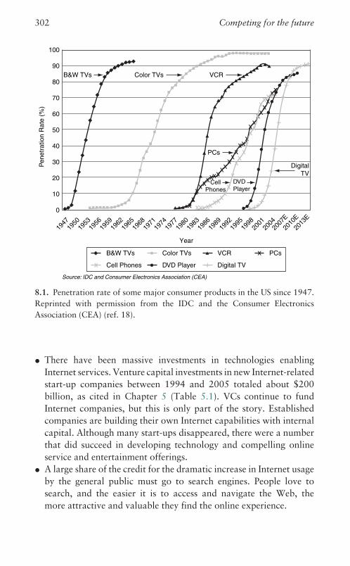
* There have been massive investments in technologies enabling
Internet services. Venture capital investments in new Internet-related
start-up companies between 1994 and 2005 totaled about $200
billion, as cited in Chapter 5 (Table 5.1). VCs continue to fund
Internet companies, but this is only part of the story. Established
companies are building their own Internet capabilities with internal
capital. Although many start-ups disappeared, there were a number
that did succeed in developing technology and compelling online
service and entertainment offerings.* A large share of the credit for the dramatic increase in Internet usage
by the general public must go to search engines. People love to
search, and the easier it is to access and navigate the Web, the
more attractive and valuable they find the online experience.
100
90
80
70
60
50
40
30
20
10
0
Pen
etra
tion
Rat
e (%
)
Year
1947
1950
1953
1956
1959
1962
1965
1968
1971
1974
1977
1980
1983
1989
1992
1995
1998
2001
2004
2007
E
2010
E
2013
E
1986
B&W TVs Color TVs VCR
PCs
CellPhones
DVDPlayer
DigitalTV
Source: IDC and Consumer Electronics Association (CEA)
B&W TVs Color TVs VCR PCs
Cell Phones DVD Player Digital TV
8.1. Penetration rate of some major consumer products in the US since 1947.
Reprinted with permission from the IDC and the Consumer Electronics
Association (CEA) (ref. 18).
302 Competing for the future

The eclipse of print media
With search thriving and the world moving on line, print is becoming
less relevant. Print industries are watching their influence wane and
their revenues fall in an increasingly digital world.
Not surprisingly, a report by the Forrester Group indicates that the
more people become accustomed to accessing the Web, the less interest
they have in reading printed material.20
Proof can be found at that bastion of print, The New York Times.
While the Times produces one million newspapers a day, its Internet
news source, www.NYTimes.com, has over eighteen million distinct
users monthly.21
Not surprisingly, the Times is committed to expanding its online
presence. It bought the online portal About.com in 2005 to shore up its
electronic offerings. In early 2006, Leonard Apcar, editor-in-chief of
www.NYTimes.com, told an industry audience that although the print
side of the business was downsizing, his division was 200 strong and
growing fast.22
Apcar also pointed out a more interesting development. The Times is
integrating its Web and print organizations, previously distinct opera-
tions, to leverage the content generation strengths of the old newsroom
for the online product.
The reason: people who do not subscribe to a print edition seem to be
willing to pay for online access to its contents. The company’s newest
online offering, a fee-based news and archive service called
TimesSelect�, quickly enrolled 200,000 subscribers at $50 per year,
in spite of the fact that users can get it free if they also sign up for the
printed newspaper.
Editorial content is not the only kind of traditional newpaper content
moving on line, of course. As eyeballs leave print media, so does
advertising.
20 C. M. Kelley and G. DeMoulin., ‘‘The Web cannibalizes media.’’ Technicalreport by the Forrester Group, May 2002.
21 D. Radev, J. Otterbacher, A. Winkel, and S. Blair-Goldensohn, ‘‘NewsInEssence:Summarizing online news topics,’’ Communications of the ACH (October,2005), 95–98.
22 Remarks made at the BusinessWire briefing in New York on ‘‘New mediatechnologies: Why it is vital for PR and IR pros to tune in before being tunedout,’’ (March 21, 2006).
Industries transformed 303

The increasing loss of local classified advertisements, which accounted
for $15 billion in US news media revenues in 2005, is especially worri-
some for newspapers. For example, craigslist.com offers free Internet
classified listings in fifteen markets. Offerings like this cost papers in the
San Francisco Bay area $60 million in lost job ads in 2005.
It is estimated that about 5 percent of US advertising revenues in
2005 were channeled through the Internet. As noted earlier, that
amounts to $12 billion worth of online advertising, 41 percent of
which went to Google.23
This phenomenon, which comes at the expense of broadcast and
print advertising, is not exclusive to the US. Online advertisement
revenues in the UK increased by 62 percent in the first half of 2005.24
Success on this scale attracts more investment, and more innovation.
Online ads are expected to grow 15 percent a year for the next few
years. Meanwhile, ad agencies and Web sites are seeking more effective
ways to present advertiser messages.25
GlobalSpec: Replacing catalogs with clicks
There are precedents for established print publications simply disap-
pearing under an Internet-based onslaught. One of the most suggestive
examples is found in the business-to-business process of sourcing
industrial products and services.
For over 100 years, generations of US engineers relied on the Thomas
Register of American Manufacturers, an annual Yellow Pages-like set of
very thick books that provided information on tens of thousands of types
of industrial components. A full shelf was needed to store them. Finding
the manufacturer of a component such as a resistor, for example, meant
searching the pages of the Register for ads and listings, and then
contacting the vendors for specifications and prices.
The Register was so important to suppliers that it was not unusual
for companies to allot their entire advertising budget to placements in
every product category where they had an offering. This was before
GlobalSpec, a start-up founded in 1996 (with Warburg Pincus funding)
23 S. Lohr, ‘‘Just Googling it is striking fear into companies,’’ The New York Times(November 6, 2005), 1.
24 ‘‘Online advertising: Classified calamity,’’ The Economist (November 19, 2005), 67.25 T. Ray, ‘‘Google faces stiffer competition as online advertising goes glitzy,’’
Barron’s (November 21, 2005), 32.
304 Competing for the future

by former General Electric employees John Schneiter and Thomas
Brownell, built a novel Internet product search capability.
Schneiter and Brownell had the idea of hosting product catalogs on
line. They designed a search engine that could quickly find a desired
product on the basis of its specifications, not just its name, and then
provide links to the Web sites of the participating vendors.
For example, if an engineer enters the keyword ‘‘carbon resistor’’ on
the GlobalSpec site, a Web page appears with links to information
about resistors from publications and standards organizations. There
are tabbed sections for searching according to products, part numbers,
properties, and other criteria. And of course there are the links to
vendors’ Web sites. The vendors pay GlobalSpec to list their catalogs.
To attract engineers to its site, the company has over 250 million
technical documents accessible to registered users as a free service. The
more than two million registered GlobalSpec users can also elect to
receive periodic e-mails about new products in their selected categories.
The company does not ignore the big search engines. Google, Yahoo!
and MSN act as gateways to the site, popping up links to GlobalSpec
when users search on any of 600,000 keywords. Catalog owners who
pay for listings on GlobalSpec benefit from the extra traffic this brings.
By any measure, GlobalSpec is a success. At the start of 2006 it could
search over 17,000 vendor catalogs, and give its two million users access
to 76,000 suppliers. That’s a huge advance over printed directories.
From the user’s perspective, however, it is the intrinsic efficiency of
GlobalSpec’s online sourcing process that makes it a successful endea-
vor. Because of the quality of the site’s search results and its compre-
hensive catalog list, engineers can source a new product in minutes.
With print catalogs this would take days or even weeks.
What happened to the Thomas Register? It went on line in the late
1990s with a search function to access the products in its lists.
Meanwhile the print edition shrank from thirty-three volumes in
1997 to twenty in 2005, its last year. The Register books are no longer
printed and will not come back.
Universal online access to broadband content: Voice, data, video
The Internet, as we learned in Chapter 2, does not discriminate among
different types of content, provided they are digital and packetized.
Some packets need special handling, but in general all content is
transmitted the same way.
Industries transformed 305

As a result, the Internet is as adept with voice and video as with
documents and data. All that’s required is enough bandwidth to handle
the huge numbers of packets that make up, say, a one-hour video
presentation.
That requirement is being met. Broadband availability is expanding
rapidly, giving consumers around the world convenient online access to
voice, music, movies, and games. The Morgan Stanley report cited
above, which put the total number of broadband subscribers world-
wide at over 180 million, shows that the trend has gone global.26
For example, the report points out, the percentage of homes in the
Netherlands with broadband access reached 55 percent in 2005. The
US currently trails, with only 32 percent, but that number is expected to
nearly double by 2011. South Korea has probably the highest broad-
band penetration in the world, exceeding 70 percent.
Consumers consider broadband access to be only half the value
equation. They’re not interested in sitting down at a PC and logging
into the Internet every time they want to hear a tune or see a video.
They want to capture the content and use it on their own terms.
And in fact, the availability of low-cost hard disks (magnetic storage,
discussed in Chapter 1) makes capturing this content practical. As
Figure 8.2 shows, a 160 GB disk (about $100 in 2006) can hold
90 hours of video and 2,700 hours of music.27 Consumers can keep
the content on the disk, transfer it to other media for portability, or
stream it to a playback device in another part of the house.
Consumer capture and storage represent a seismic shift for the media
business.
The Internet and cheap digital storage: Challenges
for the media industries
From the days of Edison, the media industries have made their money
by selling entertainment through controlled channels to mass
audiences.
The media maximize their profits from music, movies, and television
programming by segmenting distribution geographically and by mar-
ket channel. To take a contemporary example, when a movie has
finished its theatrical run in the US, it goes into distribution overseas,
26 Meeker, Pitz, Fitzgerald, and Ji, ‘‘Internet trends,’’ a talk.27 Data from Parks Associates (2005).
306 Competing for the future

while the studio issues a DVD of the movie for domestic purchase or
rental.
The disk is regionally coded so that it will not play on DVD machines
outside the US. This is done to keep unauthorized disk sales into foreign
countries from cannibalizing overseas theater revenues. When a movie
finishes its run in an overseas region, the studio issues disks coded for
that market.
Studios also sell the movie to premium cable TV channels after its
theatrical run. Eventually it is sold to network TV. Reuse of content is
obviously the cornerstone of this business model.
But the model is breaking down. Two major developments are
reducing the demand for video DVDs and prerecorded music, and
changing the value proposition for broadcast TV as well. Both grow
out of the power of the Internet.
First, as we have just seen, the spread of broadband makes it possible
to distribute video and music directly to consumers over the Internet.
Second, Internet availability of TV shows enables a highly sophisti-
cated form of on-demand viewing (i.e., time-shifting).
We’ll start with the sale of content over the Internet. This was
pioneered by Apple and its iTunes music download site. Geared to
Thousands of Digital Pictures
Hundreds of Hours of Digital Music
Hours of Digital Video (DVD Quality)
Number of Games Like Everquest
Hours of DivX HD Video
Hours of HD Video
40
Source: Parks Associates, 2005
0 10 20 30 40 50 60 70 80 90 100
90
35
13
80
27
8.2. Entertainment content that can be stored on a 160 gigabyte (GB) hard
drive. Reprinted with permission from Parks Associates (ref. 27).
Industries transformed 307

owners of the iPod (Apple’s portable playback device), iTunes has been
extremely successful. At this writing it accounts for 80 percent of all
digital music sales over the Internet.28
Video distribution is ramping up as well. Over twenty-five million
US Internet users visited sites offering downloadable videos in January
2006.29 Big search engines such as Google and Yahoo! are major entry
points for consumers seeking portals where video, music, and related
content is stored.
The growth and popularity of such portals happened spontaneously
rather than by plan. Once established, however, they demonstrated
significant value as a means of accessing special groups of customers.
For example, when NBC Universal acquired iVillage (which bills itself
as ‘‘The Internet For Women�’’) for $600 million in 2006, the portal
already had 14.5 million unique users.30
So the audience is there, it can be segmented by special interests, and
the facilities are in place. Web sites such as www.CinemaNow.com are
offering legal downloads of Hollywood films on a rental or purchase
basis, and promise that customers will eventually be able to transfer
them to DVDs or portable video players, once the studios agree on
security to protect the content from piracy.
While this looks like another potential market where studios can
resell content, there is a sticking point: content protection, also called
digital rights management (DRM). DRM is supposed to prevent savvy
hackers from purchasing one legal copy of a movie, then duplicating it
on inexpensive DVD disks to share with friends or sell for profit.
Unfortunately for the industry, no DRM scheme is completely
hacker-proof. Even the best content protection is no guarantee that
the movie will not be pirated.
Is developing an Internet distribution channel worth that risk? The
music industry, which was the first to embrace digital distribution, has
now had plenty of time to evaluate the security of the new medium, and
so far the news is not good.
28 B. Stone, ‘‘Can Amazon catch Apple,’’ Newsweek (February 13, 2006), 46.29 Reported in S. McBride and M. Mangalindan, ‘‘Coming attractions:
Downloadable movies from Amazon,’’ The Wall Street Journal (March 10,2006), B1.
30 R. Morgan and C. Murphy, ‘‘NBC Universal takes iVillage for $600 million,’’The Daily Deal (March 2, 2006), 1.
308 Competing for the future

In the several years since the digital music distribution channels
launched, total worldwide music industry revenues (about $22 billion
at wholesale prices in 2005) have steadily declined. This is because sales
of recorded music fell faster than Internet sales grew.31 The industry
has been quite vocal in its claims that unauthorized downloading and
pirated CDs are the cause of the problem.
TV faces a similar dilemma. Broadcasters are concerned about the
availability of video on demand, just as their counterparts in the movie
and music industries are about post-sale duplication.
People are using their PCs to download television shows from the
Internet, capture them off the air, or record them from a cable feed, and
store them for later viewing. This undermines the basic premise of
commercial TV. Advertisers rely on dedicated broadcast time slots to
target audiences, and pay broadcasters accordingly.
Now viewers can shift the shows out of those slots. Worse, they can
delete advertisements automatically, reducing the willingness of adver-
tisers to finance programs.
As we discussed in Chapter 7, new technologies for controlling
content are being developed, but it’s clear that the industry will also
seek regulatory protection to safeguard its revenues.32 Whether these
efforts will bear fruit is uncertain. What is certain is that the historical
pattern of mass distribution of movies and TV programming is no
longer the solid, secure business model it once was.
Shopping is an Internet experience
No account of the impact of the Internet would be complete without
mentioning consumer purchases. This is the engine that drives the
economy, and it is the killer application for the Internet as well.
An incredible range of products is sold on line. Do you need a part for
an old barbecue? A coffee cake, diamond ring, light bulb, computer,
toy, house, classic car? Whatever you want, it’s available. What’s more,
thanks to the quality of the search engines, you can find it in seconds
from multiple vendors who are clamoring for your business.
31 J. Leeds, ‘‘Music industry’s sales post their sixth year of decline,’’ The New YorkTimes (April 1, 2006), C2.
32 A. Schatz and B. Barnes, ‘‘To blunt the Web’s impact, TV tries building onlinefences: Stations are using technology to restrict who watches; seeking aid fromCongress,’’ The New York Times (March 16, 2006), 1.
Industries transformed 309

In a total shift in the balance of power between buyers and sellers, the
buyers are in control. Using comprehensive information available free
on line, they can rank one product against others and from multiple
sellers and do a price comparison while they are at it. Companies and
retailers who once relied on consumer ignorance to help them sell
inferior products at premium prices are finding it much harder to
play that game.
That does not mean that online merchants have no cards to play.
Brick-and-mortar merchandisers use nice stores, pleasant salespeople,
and extensive advertising to gain the advantage over their rivals.
Online vendors get their competitive edge from superior Web sites to
ease the shopping experience, the right search keywords to bring buyers
to their sites, and high rankings for their ads on a Google Web page.
Here are some of the distinctive advantages that make Web-based
stores a threat to conventional retailers, especially those who ignore the
Internet as an adjunct to store sales.* Buying online is a global experience. As Figure 8.3 shows, 40 percent
of all Internet users around the world purchased merchandise online in
2004.33 Studies show that over 90 percent of buyers were satisfied with
their shopping experience.34
* Online retailing can be more flexible. Direct contact between ven-
dors and consumers on the Internet makes it possible to sell customized
products at standard-product prices and still be profitable. Dell built a
very healthycomputerbusiness thisway.The flexible, interactivenature
of the medium promotes the creation of unique business models,
too. The auction model invented by eBay is a prominent example.* Size and cost are no obstacles. Although Internet retailing started
with inexpensive items such as books, today even Amazon.com, the
pioneer in this sector, is selling large, costly items over the Web. The
buying public now has a high degree of confidence in the credibility
of the vendors and the security of payment methods.35
33 R. Peck, CFA, ‘‘Vistaprint Ltd: A paradigm shift in printing,’’ Bear Stearns EquityResearch (November 16, 2005), p. 26.
34 Summarized by M. Meeker and R. Ji, ‘‘Thoughts on the Internet and China,’’Hua Yuan 2005 Annual Conference (June 7, 2005).
35 M. Mangalindan, ‘‘Size doesn’t matter anymore in online purchases: Web shop-pers get comfortable buying big-ticket items; 3,600 pounds of copper gutter,’’The Wall Street Journal (March 22, 2006), D1.
310 Competing for the future

* Voice, data, and video are making Internet marketing more attrac-
tive. To cite just one example, the real estate industry is using online
animated maps and detailed, up-to-date local information to make
the search for property faster and simpler. Using VoIP, customers
can talk to an agent through a direct, free Internet phone call placed
through their computer, while watching a video of the house or
office under consideration.* Mom-and-pop retailers can compete with giant chains. The big
chains are getting a challenge from an unlikely source: the Web
version of ‘‘neighborhood’’ stores. While the brand recognition and
marketing muscle of a Wal-Mart or Best Buy still give them an
advantage, it’s not a decisive one in cyberspace. When people search
for products, the results show the smaller retailers right alongside the
larger ones.* The Internet can lower order fulfillment costs for retailers. For
example, Avon Products, the world’s largest direct sales cosmetic
company, replaced paper forms from its reps with Internet-based
order fulfillment. This reduced processing costs from over a dollar
19,000
17,000
15,000
13,000
11,000
9,000
7,000
5,000
3,000
1,000
Mill
ions
of D
olla
rs
72
64
56
48
40
32
24
16
8
0
Source: IDC; Bear, Stearns & Co. Inc. estimates
2000 2001 2002 2003 2004 2005E 2006E 2007E 2008E 2009E 2010E
Dollars
Online Buyers asa % of Total Users
Year
Per
cent
age
(%)
For illustrative purposes only.
8.3. Global online commerce since 2000 showing the dollars of sales and the
per cent of online users that shop on the Internet. Reprinted with permission
from Bear Stearns (ref. 33).
Industries transformed 311

per order to a few cents each.36 Another valuable role of the Internet
in fostering commerce is in managing the flow of information that
encompasses the product supply chain. This is a benefit exploited by
the carriers such as Federal Express to great advantage.
Avon’s strategy shows that old and new retailing models can mix.
Several other US retailers have instituted hybrid approaches of their
own, usually dubbed ‘‘clicks and mortar.’’ One popular model is using
physical stores as drop-off points for Internet orders and returns.
But there can be no doubt that, on balance, the virtual mall of the
Internet is pulling shoppers away from actual stores, especially during
the holidays, when customers want to avoid the crowds.
Online social networks
Commerce is not the only arena where the Internet has changed the
rules of the game. It also has a unique ability to foster social networks
and host opinion exchange forums. Because it can accommodate and
serve interest groups of any size, it can scale from providing a platform
for personal expression to creating forums for the exchange of views
and information at any level of organization.
There seems to be a Web site for every interest group, and it’s not
always about mass market appeal. Niches are everywhere on the Web.
Their individual audiences may be small, but in the aggregate the
numbers are huge. One example of a niche audience attraction is
Sail.tv, a sailing ‘‘channel’’ created in the UK that covers sailboat
races and offers videos on sailing techniques.37
Other sites cater to much larger groups. Teenagers, the group-
oriented pioneers of all things on line, have endorsed the social aspect
of the Internet almost unanimously. Surveys show that 87 per cent of
teens use the Internet as a preferred place for socializing and purchasing
products that cater to social fads.38 The Web site mySpace.com, which
serves as a social forum for more than 50 million young people, built
its business model around their longing for a place of their own on
the Web.
36 Andrea Jung, Avon CEO, quoted in ‘‘Ideas outside shot: A conversation withAndrea Jung,’’ BusinessWeek (February 6, 2006), 104.
37 S. Hansell, ‘‘Much for the few: As Internet TV aims at niche audiences, theslivercast is born,’’ The New York Times (March 12, 2006), BU1.
38 J. Hempel, ‘‘The MySpace generation,’’ BusinessWeek (December 12, 2005),88–94.
312 Competing for the future

Teens are hardly the only people forming Web-based bonds with
like-minded spirits. Earlier we mentioned iVillage, the forum for
women’s issues accessed by more than 14.5 million unique users
annually. However, mySpace.com hosts over three times that many
young people. Media giant News Corporation acquired mySpace.com
in July 2005 as the major property in a $580 million purchase of its
parent company.
Power to the wired people
Web site involvement in the political arena is also growing. It ranges
from one-person initiatives to campaigns organized at the local,
national, or even international levels. The most interesting of the
individual efforts is the ‘‘blog.’’
Blogs (the name comes from ‘‘weB LOG,’’ a diary of online activity)
are easy-to-build Web sites that individuals use as platforms for their
views. Blogs have become quite influential in shaping public opinion on
a variety of subjects, from product quality to political issues.
There are tens of thousands of blogs, accessible to anyone with an
Internet connection. The sites can be accessed through search engines,
and there is software available to broadcast the latest updates to inter-
ested Internet users.
They have a surprisingly large audience. Morgan Stanley Research
data suggest that 27 percent of US Internet users read blogs.39 They are
quoted in TV newscasts, and some bloggers have become minor
celebrities.
At their most powerful, blogs harness ‘‘grass-roots’’ political opi-
nions and bring pressure on politicians to take positions on issues of the
day.40 But they also have unexpected applications in the commercial
world. Blogs written by company executives attract attention the com-
pany would not otherwise get. Blogs also provide a forum where
consumers can air opinions on products and services. This creates a
powerful new tool for gathering market information.
Politicians were slow to tap into the power of the Internet, but in
the last few years it has been used for issues and election campaigns at
every level of government. Political strategists have teamed with
39 Meeker, Pitz, Fitzgerald, and Ji, ‘‘Internet trends,’’ a talk.40 A. Cohen, ‘‘Bloggers at the gates: What was good for eBay should be good for
politics,’’ The New York Times (March 12, 2005), WK 11.
Industries transformed 313

technologists to develop methods for reaching target audiences
directly, including the latest fad, daily podcasts to send to the faithful.
We are talking about a platform for voter outreach that is replacing
older communications methods such as television broadcasts to mass
audiences. The rapid rise of Howard Dean in the 2004 US Democratic
presidential primaries was attributed in large part to his canny use of
the Internet to rally his supporters. To quote Ken Mehlman, the
Republican national chairman, ‘‘The effect of the Internet on politics
will be every bit as transformational as television was.’’41
It should not come as a surprise that some governments are unhappy
with the freedom of expression possible on the Internet, and deliber-
ately try to keep their citizens from accessing content they consider
objectionable or inflammatory. While it is difficult to censor what
people see on the Internet, it can be done. Governments can set up
gateway servers to scan the packet traffic and filter out documents that
contain certain words. In effect, search engines become tools for block-
ing access to certain hyperlinks and the Web sites they represent.
Fundamentally, however, this is a rearguard action. Some contra-
band content is sure to slip past the monitors. And even on ‘‘permitted’’
Web sites people are likely to encounter perspectives that make them
reconsider what they hear from their government.
Turbulent era in communications
Digital communication has been a profoundly revolutionary force for
progress over the past two decades. It literally enabled global indus-
trialization and the Internet. Without high-speed digital links the
instant exchange of information, which is at the heart of international
business today, would be impossible.
As we discussed in the first two chapters of this book, digital com-
munication got its real commercial start in the 1970s with the maturity
and convergence of five revolutionary innovations: computers, fiber
optics, switched packet networks, semiconductor laser diodes, and
integrated circuits. Mix these innovations in a potent technological
brew financed by huge amounts of capital and extensive government
41 A. Nagourney, ‘‘Internet injects sweeping change into US politics: Terrain shiftssince 2004 as time-honored tools move onto the Web,’’ The New York Times(April 2, 2006), 1, 23.
314 Competing for the future
support, and then add the wireless technology of the 1990s, and you
have our current state of ubiquitous communications.
This is the nervous system of the industrialized world, within which the
Internet is taking an increasingly central position. And let us not forget
that digital communications provides the infrastructure for the Internet.
You would think that the communications industry, having invested
hundreds of billions of dollars to make this all possible, would now
be reaping huge financial rewards. But that is not how things have
worked out.
The first big wave of communications growth and investment, which
took place during the 1990s, ended with the financial collapse of 2000.
It is estimated that investors lost over $2 trillion (US) dollars in the
crash of public markets and the ensuing bankruptcies.
The collapse of the bubble took down many new companies, includ-
ing over 250 newly created public carriers in the US. But they left
behind an enormous global communications infrastructure which is
just now exerting the full force of its influence.
Today the industry is dealing with the heritage of the freewheeling
1990s, facing challenges from new competitors on the one hand, and
confronting vast opportunities on the other. We are now riding the
second big wave in communications, which is once again affecting
nearly all commercial activities around the world.
Sources of unrest
Telecommunications used to be a quiet, predictable business. Its trans-
formation, at least in the US, began with the 1984 breakup of AT&T,
the regulated monopoly telephone company, into eight separate busi-
nesses: seven Regional Bell Operating Companies (RBOCs) plus
AT&T as a long-distance firm and equipment provider. Bell Labs
went along with AT&T.
That was the beginning of twenty years of corporate turmoil. In 1996
AT&T spun out its equipment business, along with two-thirds of Bell
Labs, as Lucent Technologies. The smaller RBOCs were eventually
bought up by the stronger ones, essentially reconstituting much of the
old AT&T monopoly, but without any involvement from AT&T.
The latest chapter of the saga has now been written. Four former
RBOCs have been reunited with AT&T under the original corporate
name. This leaves two dominant wireline carriers in the US.
Industries transformed 315

Before all this happened, the communications industry was made up
of three distinct businesses: wireline data and telephony, cable TV, and
wireless voice services. The same structure pertained, with regional
variations, in countries outside the US. Governments provided benign
supervision to ensure orderly markets where everybody could make an
attractive return on investments.
That is no longer the case. With the breakup of AT&T in the US and
deregulation in other countries, many new carriers have been able to
enter the long distance and data transport markets since the 1980s. The
result has been sharply declining long distance telephony and data
transport prices.
At the local level the marketplace in the US became even more
chaotic. The Telecommunications Act of 1996 opened local loop access
to newcomers on a low-cost lease basis, ending the local service mono-
poly of the RBOCs. This event sparked the introduction of nationwide
DSL broadband service over copper lines to consumers by independent
companies such as Covad Communications, founded in 1997 with
funding from Warburg Pincus. These DSL providers operated in com-
petition with the telephone companies.
It was a watershed moment in communications history: the avail-
ability of broadband Internet access to telephone service subscribers.
Competition among carriers
Deregulation exposed telecommunications carriers to competition, but
it is technology that drove the process. The massive rollout of packet-
switched digital communications using the Internet Protocol (IP) made
it possible for aggressive companies to challenge market incumbents
with attractive new services at affordable prices, while rapid advances
in cellular wireless technology made cell phones a viable communica-
tions option.42
Cable TV operators are also competing against telephone companies
for their voice business. By upgrading their networks to carry digital
traffic in parallel with analog video, cable companies can offer subscri-
bers voice service and broadband data along with television. Subscribers
42 Note that this situation is not limited to the US. The communications industryfinds itself dealing with similar issues all over the world. Big waves in technologydo not respect national boundaries.
316 Competing for the future

who sign up for this ‘‘triple play’’ package can get lower rates for
telephone service than those available from the phone company.
To make matters worse for the phone companies, the pricing struc-
ture of voice over IP (VoIP) telephony also threatens to undermine their
voice business. VoIP providers can afford to offer a flat per-month fee
for all calls, because the cost to carry voice, video, or data is exactly the
same. But switched-network telephone companies earn a lot of their
revenues, and thus their profit, on voice calls metered by the minute.
This puts them at a distinct disadvantage against VoIP telephony
offered by competitors.
VoIP service is slowly eating into the revenues of telephone com-
panies not just in the US, but around the world. In Germany, for
example, subscribers to United Internet AG’s broadband DSL service
are offered a choice of VoIP plans: either a flat rate of E 10 a month for
unlimited national calls, or metered calls at only E 0.01 per minute.
The free Skype computer-to-computer telephony service, with over
100 million customers around the world, offers a different but no less
serious challenge. Other Internet companies are also offering VoIP
service.
Competition is not limited to the wired networks. In one decade the
cell phone has gone from luxury to necessity, with market penetration
in some countries exceeding 100 percent.
One effect of this growth is that wireless phone ‘‘lines’’ are displacing
wired lines, both switched and IP-based, all over the world. Every year
the number of wired phone lines drops a few per cent as subscribers
decide they don’t need both forms of service and rely exclusively on
cellular.
Cable companies are not immune to threats to their operating rev-
enues. Their monopolies in local markets offer little protection from
three new sources of competition.* Telephone companies are responding to the cable encroachment into
voice service with video service offerings on their own lines. By
extending fiber optic networks to homes they can provide cable-
like video content, including video-on-demand, via IPTV.* Movie studios can sell viewers direct access to video content over the
Internet, diverting entertainment revenues from the cable operators.
Customers purchase a video and download it for storage on a PC
or recordable DVD, or order it for limited viewing as a video on
demand.
Industries transformed 317

* Internet portals (Yahoo!, Google, etc.) now provide streaming video
directly to subscribers, bypassing the traditional providers of enter-
tainment content.
The battle for revenues
The growth in Internet traffic, primarily due to the popularity of video
and search, has increased the demand for backbone capacity on the
networks.
Unfortunately, although the wireline and wireless carriers own the
network’s distribution ‘‘pipes,’’ they do not get incremental revenues
from the sale of what they deliver. The content owners and Internet
companies that collect advertising revenues reap most of the profits.
To increase the pressure, ubiquitous access through the Internet and
wireless devices is making subscribers less willing to pay for transport.
The value proposition has shifted toward content owners. The carriers
are in danger of becoming commodity ‘‘bit-providers’’ and losing their
lucrative margins.
Cellular carriers, in particular, could use the revenue to support their
tremendous expansion. In a matter of a decade they have blanketed the
world with cellular wireless networks, and have launched at least three
generations of service.
The new, packet-based third generation (3G) networks let mobile
subscribers access the Internet for data, video, e-mail, and voice con-
nections. This makes the cell phone the most versatile consumer access
device available, replicating the functions of the PC, PDA, portable
television, and telephone. A whole generation uses the cellular handset
as its primary electronic device.
Having invested in their costly 3G network infrastructure, carriers
need to increase their monthly subscription fee revenues to cover the
cost. They are looking for new services that consumers are willing to
pay for.
So far this has been a slow process. Voice calls still generate the bulk
of the revenues. In fact, voice call revenues constitute, on average,
between 80 and 90 percent of the total wireless revenues of carriers in
the US and the EU. The other 10 to 20 percent comes from auxiliary
services such as short digital messages (SMS) and ring tones.
Both wireless and wireline operators dread the prospect of remaining
poorly compensated carriers of valuable content over their expensive
318 Competing for the future

broadband networks, especially as voice traffic revenues grow slowly
in the developed economies. But how can they participate in the rev-
enue stream? Once an Internet connection is opened on their network,
a direct path between buyer and seller is also open. Creative billing is
the only way that carriers can share in the profits generated by the
bandwidth-hogging traffic they provide.43
Content providers are pressing their advantage by directly accessing
consumers through their own branded cellular services. For example,
Disney’s service uses the facilities of Sprint Corporation.
Carrier competition: Strategies and outcomes
In spite of work-arounds by content companies, the network operators –
the carriers who own the pipes – still control customer access. They are
working to solidify that position against the competition, and to find
ways to make their businesses more profitable.
The carriers’ struggle to increase market share will not be decided
easily or quickly. The new broadband technologies can reach consum-
ers in too many ways. But smart carriers know they have to start by
choosing markets where their technology gives them the best chance
for success. They must have the technology that gives them maximum
flexibility and operational efficiency within their market segments, and
provides high-quality services at low delivered cost.
Wireline carriers, to start with the largest group of providers, are
focused on high-bandwidth data transport for enterprises. This is
where their ownership of high-capacity, globally accessible networks
gives them a distinct advantage. Cable operators and wireless carriers
simply cannot compete in this market space right now.
That doesn’t mean wireline carriers can sit pat with what they have.
To sustain their lead they have to give their customers better broadband
access by bringing fiber optic connections closer to customer premises.
This requires massive infrastructure investments, which carriers all
over the world are making.
The wireless industry will attempt to capture greater market share by
offering new services. Their strategy is to make the cellular handset
43 R. Siklos, ‘‘How much profit is lurking in that cellphone?’’ The New York Times(March 5, 2006), BU3.
Industries transformed 319
indispensable as a personal and business tool. One of these services is
television.
We are already seeing the start of limited digital TV broadcasts to
wireless handsets.44 Full rollout is being delayed by the usual battles
over industry standards, as companies jockey for competitive posi-
tion.45 Furthermore, new direct–to-handset TV broadcast technology,
which completely bypasses the cellular networks, may limit TV’s value
to the cellular industry.
Although wireline and wireless are the whole game right now, other
ways of reaching consumers are emerging. The Edison-era electrical
distribution system could pose a competitive threat to phone com-
panies. The technology for providing broadband Internet access over
power lines is improving slowly, offering one more choice among high-
capacity ‘‘pipes.’’
New wireless technologies are coming, too. The impending shut-
down of analog TV and consequent parceling out of its broadcast
spectrum will free up the airwaves for alternatives to cellular.
WiMax, a fixed wireless broadband service, is being touted as compe-
tition for both cellular and wireline carriers in providing voice and
data.
You can be sure that the industry will continue to invest in technol-
ogy to provide new services. It’s just as certain that it will continue to
consolidate. Developing technology and building infrastructure is
expensive, and bigger providers have more resources to use for these
processes.
Paying for the network: Tiered service, higher prices
Whether they operate over wires or through the air, carriers have to
streamline and automate their network operations to reduce operating
costs. They must also make their networks more flexible to speed up
the implementation of promising new services.
This means that migrating to unified IP networks is a priority,
although legacy network units will continue to exist alongside them
44 M. Odell, ‘‘Mobile television may be the answer,’’ Financial Times (February 13,2006), FTDB1. This service was first introduced in South Korea, an indication ofwhere consumer service innovations are hitting the market first.
45 J. Yoshida, ‘‘Mobile TV may not yet be ready for prime time,’’ EETimes(February 13, 2006), 1,13.
320 Competing for the future

for a long time. An IP structure not only delivers flexibility at lower
cost, it allows the same network to handle voice and data. New soft-
ware architectures are now being implemented to achieve these goals.
An IP network offers a strategic advantage to go along with its
operational superiority. Executives with the vision to position their
companies for the future are already driving in this direction.
Cutting costs and rolling out attractive offerings brings tangible
benefits to the top line of the corporate balance sheet. Carriers will
also see improved profits if they implement a controversial change in
their billing practices: tiered billing, that is, charging different rates for
different types of data or different levels of service quality.
In one model, carriers would change their billing to differentiate
among classes of data carried on their networks. Voice, for example,
might be charged at a higher rate than data.
Another approach under discussion is to build a new, higher-speed
network infrastructure, but bill differently for it. ‘‘One version would
be free, as everything is now. The other would be the digital equivalent
of HOV lanes on highways . . . to qualify for the speed slot, sites and
services would have to pony up huge tolls.’’46
It’s only a matter of time before the carriers rationalize their billing to
reflect new traffic levels and their associated costs. The demand for
bandwidth on public networks is steadily increasing, the carriers are
spending huge sums to increase capacity, and tariffs must eventually
reflect market realities.
Needless to say, proposals to change the billing model raise violent
opposition. The public takes cheap Internet traffic costs for granted,
forgetting that the networks are not publicly supported highways.
A free consumer VoIP call is not free for the carriers that transport it.
In an unregulated, competitive communications marketplace, how-
ever, the tendency will inevitably be for prices to approach marginal
costs, generating losses for the least efficient network operators and
satisfactory profits for the best ones. The economic challenge is that the
marginal cost of transporting an incremental bit is as close to zero as
one can get. That’s a poor basis for funding the massive investments the
carriers need to make to build and maintain their networks.
46 S. Levy, ‘‘The technologist: When the Net goes from free to fee,’’ Newsweek(February 27, 2006), 14.
Industries transformed 321

Prices for transport must at least cover network operating and capi-
tal costs. As long as carriers are privately owned and rely on commer-
cial financial sources, they will have to justify investments on the basis
of return on capital. Right now they’re justifying their investments on
the basis of the returns they expect when the competitive situation
reaches equilibrium.
In terms of profitability, content owners still have an early advantage
over carriers. The ready availability of broadcast, broadband cable and
wireline, and low-cost home digital storage makes access easy to find at
very low prices. Valuable content, on the other hand, remains a scarce
commodity, and people are willing to pay for it.
Where all this will end up remains an open question. History has
shown that sooner or later companies in capital-intensive industries
stabilize prices by consolidating facilities and attempting to reduce
competition.
But history has also shown that in dynamic industries with extra-
ordinary technological innovations, slowing competition is not an easy
option. The communications industry certainly fits that description.
Digital electronics: Markets, manufacturing,and global strategy
Crankshafts and pistons don’t transport us from place to place; roads
and cars do. Microchips and lasers don’t link people to the online
bounty of information and social interaction, or directly to each
other. Those are the functions of the Internet, the global communica-
tions network, and the electronic devices that connect to them.
The car and the Internet are systems that empower. Efficient trans-
portation and easy access to information and communications have
had a profoundly transformative effect on human social and economic
life. In the end what matters is how we use our innovations.
Yet without engines and axles there would be no cars. In the same
way, without powerful computers in the network, innovative software
to manage them, PCs, and fiber optics, there would be no Internet. The
manufacturing of electronic products is the foundation of the digital
world.
To gain perspective on the scope and significance of the world’s elec-
tronics industry, we will begin with the smallest components, consider
product direction, then look at the changing structure of the industry.
322 Competing for the future
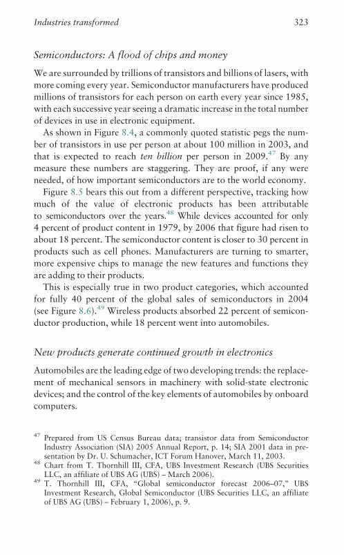
Semiconductors: A flood of chips and money
We are surrounded by trillions of transistors and billions of lasers, with
more coming every year. Semiconductor manufacturers have produced
millions of transistors for each person on earth every year since 1985,
with each successive year seeing a dramatic increase in the total number
of devices in use in electronic equipment.
As shown in Figure 8.4, a commonly quoted statistic pegs the num-
ber of transistors in use per person at about 100 million in 2003, and
that is expected to reach ten billion per person in 2009.47 By any
measure these numbers are staggering. They are proof, if any were
needed, of how important semiconductors are to the world economy.
Figure 8.5 bears this out from a different perspective, tracking how
much of the value of electronic products has been attributable
to semiconductors over the years.48 While devices accounted for only
4 percent of product content in 1979, by 2006 that figure had risen to
about 18 percent. The semiconductor content is closer to 30 percent in
products such as cell phones. Manufacturers are turning to smarter,
more expensive chips to manage the new features and functions they
are adding to their products.
This is especially true in two product categories, which accounted
for fully 40 percent of the global sales of semiconductors in 2004
(see Figure 8.6).49 Wireless products absorbed 22 percent of semicon-
ductor production, while 18 percent went into automobiles.
New products generate continued growth in electronics
Automobiles are the leading edge of two developing trends: the replace-
ment of mechanical sensors in machinery with solid-state electronic
devices; and the control of the key elements of automobiles by onboard
computers.
47 Prepared from US Census Bureau data; transistor data from SemiconductorIndustry Association (SIA) 2005 Annual Report, p. 14; SIA 2001 data in pre-sentation by Dr. U. Schumacher, ICT Forum Hanover, March 11, 2003.
48 Chart from T. Thornhill III, CFA, UBS Investment Research (UBS SecuritiesLLC, an affiliate of UBS AG (UBS) – March 2006).
49 T. Thornhill III, CFA, ‘‘Global semiconductor forecast 2006–07,’’ UBSInvestment Research, Global Semiconductor (UBS Securities LLC, an affiliateof UBS AG (UBS) – February 1, 2006), p. 9.
Industries transformed 323

1012
1010
108
106
104
102
0
Tran
sist
ors
Per
Per
son
Year
1967 1973 1979 1985 1991 1997 2003 2009E
8.4. The number of transistors per person on the planet. Data from US Census
Bureau and Semiconductor Industry Association (SIA) (ref. 47).
— 20
— 18
— 16
— 14
— 12
— 10
— 8
— 6
— 4
— 2
— 0
300
250
200
150
100
50
0
Bill
ions
of D
olla
rs
Year
Sem
icon
duct
or D
iffus
ion
Per
cent
age
(%)
1979 1982 1985 1988 1991 1994 1997 2000 2003 2006E
WW Semiconductor Rev ($B)
Semiconductor Diffusion (%)
Linear (Semiconductor Diffusion (%))
Source: SIA and UBS estimates. VLSI Research and UBS estimates.
8.5. The worldwide (WW) sales of semiconductor devices and the fraction that
they represent of electronic systems sales. The dotted line shows the average
trend. Copyright # 2006 UBS. All rights reserved. Reprinted with permission
from UBS (ref. 48).
324 Competing for the future

It is estimated that electronic systems account for around $2,500 of
the cost of the average automobile, in the range of 10 to 15 per cent of
its sale price.50 These systems range from high-end audio and video
entertainment systems to air bag, engine, and antilock brake controls.
More sophisticated control, safety, and entertainment systems are
being introduced every year, virtually guaranteeing that the percentage
of a car’s cost that is attributed to electronics will continue to increase.
The other big user of semiconductors, the wireless industry, churns
out new cell phone models on what seems like a weekly basis. Since
the mid-1990s, the simple wireless handset has evolved into an all-
encompassing appliance combining the functions of telephone and
television receiver, Internet and e-mail tool, financial services terminal,
still camera, videocam, and fashion statement. And it fits in a shirt
pocket.
Military/Aero2%
PC/Storage22%
WirelessHandset22%
Communications12%
Consumer13%
AutomotiveElectronics18%
Industrial11%
Source: Gartner and UBS estimates
8.6. Estimated percentage of semiconductor devices used in major electronic
product sectors (2004). Copyright # 2006 UBS. All rights reserved. Reprinted
with permission from UBS (ref. 49).
50 R. DeMeis, ‘‘Cars sag under weighty wiring,’’ EETimes (October 24, 2005),47–49.
Industries transformed 325

Informal surveys suggest that most owners see their handset as their
primary personal electronic product. The average consumer keeps a
handset for about two years. At that point the added features of new
models entice the owner into replacing it. As a result, industry sources
forecast continued global sales of over 600 million handsets per year,
with annual sales figures of a billion units in sight.
Demand for other electronic products also continues to rise, driven
by the introduction of new digital functionality and the emergence of
completely new technologies. We have digital cameras, personal com-
puters, digital wireless devices, digital television receivers, and digital
video and audio recorders.
Analog product categories, even long-established ones, simply dis-
appear when faced with competition from digital devices. Videotape
has gone the way of the vinyl LP record. They were both killed by
optical disk player/recorders. Digital cameras are rapidly turning the
film camera into a museum piece. Film utilization is estimated to be
dropping at the rate of 20–30 percent a year.51
Even digital devices can be victims of quick obsolescence. Low-price
digital cameras, for example, are competing against a formidable foe:
the picture phone. Digital cameras built into cell phones now out-
number stand-alone devices.
Prospects for continued growth
Commercial radio and TV broadcasting are the last major analog
holdouts in the consumer market. Digital satellite TV has made sig-
nificant inroads, and satellite radio has emerged. However, most tele-
vision shows, even on digital satellite or cable feeds, originate in analog
form. On the receiving end only a small percentage of TVs are truly
digital. Few households are equipped to receive digital radio by
satellite.
That is about to change, with television leading the way.
Governments in many countries have mandated a switch from analog
to digital television (DTV) broadcasting by 2010.52 It is virtually
certain that TV manufacturers will rack up huge sales of new DTV
sets and analog-to-DTV converters for existing sets once the switch-
over occurs.
51 ‘‘Film fades fast,’’ Photonics Spectra (March 2006), 32.52 R. M. Rast, ‘‘The dawn of digital TV,’’ IEEE Spectrum (October 2005), 27–31.
326 Competing for the future

Sales could happen fast, since today’s consumers are eager to adopt
new technology. Figure 8.1 shows the penetration rates of consumer
electronic products in the US since 1947. Color television and PCs both
needed about twenty years to achieve a 60 percent penetration rate. It
took cell phones about fifteen years to reach the same level of
penetration.
DVD players, in the most successful product launch in consumer
electronics history, reached the 60 percent mark in only six years. The
current pace of penetration suggests that digital television (DTV) will
achieve a 60 percent penetration level in under six years.
Terrestrial radio has lagged behind, but digital technology has now
been developed for the oldest broadcast service. Digital Audio
Broadcasting (DAB), available primarily in Europe, Canada, and
Australia, and HD Radio, launched in the US and being tested in
Canada and parts of South America and Asia, both promise
‘‘CD-quality’’ sound with less interference. Both require consumers to
buy new receivers to get the service.
Given relentless consumer and industry demand for newer, more
sophisticated digital technology, it is no surprise that electronic pro-
ducts make up an increasing part of the world’s gross national product.
As shown in Figure 8.7, this share increased from 0.5% in 1958 to just
about 2.3 percent in 2006.53
Readers might be surprised at how small this percentage is for an
industry that garners so much attention. However, this number covers
only the value of the electronic products themselves. If you take into
account the huge value produced by business categories that leverage
electronic products, such as software, services, and non-electronic equip-
ment, you get a more accurate picture of the industry’s importance.
Countries cannot afford to ignore the industry’s potential if they
wish to sustain or grow their economies. But they must decide how to
handle the many challenges the electronics industry presents.
Deflation in action
Throughout its history, the electronics industry has displayed some
consistent if contradictory traits:
53 Data from T. Thornhill III, CFA, UBS Investment. Research (UBS SecuritiesLLC, an affiliate of UBS AG (UBS) – March 2006).
Industries transformed 327

* steadily increasing product volumes;* constant advances in product functionality;* steep declines in selling prices;* ever-shorter product cycles.
To make matters worse, every emerging technology brings new
companies into the industry, heating up an already intense competitive
situation. In this environment, sustained profits are elusive for all but
the best-managed, most dominant companies in their market sectors.
The standing joke is that the consumer electronics industry loses
money on every unit of product it sells, but makes it up on volume.
Everyone recognizes the problem, but companies that compete in the
global consumer electronics market usually have no choice but to
compete on price, or at least meet the lowest price offered.
However, profitability in a new product is generated by being first to
market. This puts a big premium on effectively managing innovation to
establish market leadership with new products.
3.0
2.5
2.0
1.5
1.0
0.5
0.0
Year
1958
1961
1964
1967
1970
1973
1976
1979
1982
1985
1988
1991
1994
1997
2000
2003
2006
E
Ele
ctro
nics
Diff
usio
n P
erce
ntag
e (%
)
Source: VLSI Research and UBS estimates. IMF, 9/05.
8.7. Electronic products represent an increasing share of the world’s GDP.
Copyright # 2006 UBS. All rights reserved. Reprinted with permission from
UBS (ref. 53).
328 Competing for the future

Yet even with new products, companies must reduce costs to stay
competitive. With Asian companies leading the low-cost parade, com-
petitors in other geographies either follow or drop out. As we have
seen, this explains the massive migration of engineering resources and
manufacturing from developed economies with a free trade policy to
the lowest-cost countries.
If the world appears ‘‘flat’’ to some observers, it is not because the
international commercial playing field is level or the game is fair.
Governments support their national champions to the detriment of
foreign competitors. How can a company already running on thin
margins counter that kind of pressure?
One answer: electronic product companies with global ambitions
must be large enough to support product diversity, scaled R&D facil-
ities, and the lowest-cost manufacturing in their sectors. That’s why
markets such as TV receivers, memory products, and network equip-
ment, where industry standards determine many product features, have
seen especially rapid consolidation through mergers or the disappear-
ance of participating companies.
In the network equipment space, for example, Cisco Systems has
become the dominating force in the world market as competitors have
dropped out or been relegated to niches. Samsung is now the leading
manufacturer of FLASH memories, as Seagate is of magnetic disks, and
Intel is of high-end microprocessors.
All of these companies can use their size and economic strength to
create the high-quality, low-cost products that boost sales volumes.
With the demand for consumer electronics opening new markets
around the world, it would seem that their opportunities for interna-
tional sales are enormous.
And so they are, if the companies meet a fundamental challenge.
Rising incomes in the developing economies mean that billions of
people are entering the market for electronic products – if they are
cheap enough.
While we are used to $200 cellular handsets, a $40 handset is what a
Chinese worker can afford, and a PC for $100 would be a wonderful
buy. These end-user prices can be met profitably only by product
vendors who understand how to design with minimal features and
low cost in mind right from the start.
It’s not just consumer products that present a challenge. In emerging
markets even infrastructure products are under heavy cost pressure.
Industries transformed 329

Consider the economics of selling telecommunications equipment in
India, for example. Basic cellular phone service in India is offered very
profitably at only about $10 a month, compared to about $40 in the
US. Such low-cost service is possible for two reasons.* Employees of the carriers in India get about one-fifth the wages of
their US-based counterparts.* Indian carriers buy their equipment and associated software from
international vendors under very favorable terms. The vendors have
to meet very low price points to win the business.
The chief financial officer of Siemens Communications, an equip-
ment vendor to the wireless industry, gave the best summary of the
situation: ‘‘There is no such thing as easy mobile money anymore.’’54
Just as in the wireline and cable industries, any investment in new
equipment to increase the capacity of a wireless network must be
justified by new revenues. As these are hard to predict, the pressure is
on equipment vendors to provide products at the lowest possible cost.
Equipment manufacturers thus have a choice – forego big sales
opportunities in the fastest growing markets, or stay in the game by
reducing all enterprise costs to preserve profits while accelerating the
speed with which new products are brought to market.
Executing this strategy is not simple. To summarize its elements, as
covered in Chapters 4 through 6, companies need:* A global presence to help find the best ideas, technical talent, and
manufacturing facilities.* Fast product cycles, critical to sustaining sales momentum in a
dynamic market.* High-quality engineering for efficient R&D.* Lowest labor costs consistent with tasks to be performed.
As we concluded in Chapter 6, there is no single right approach to
locating engineering resources or setting manufacturing strategies.
However, protection of intellectual property and the shortening of
supply chains to speed up product cycles can easily outweigh other
factors in selecting locations.
One thing is certain: there are more potential manufacturing loca-
tions for technology companies than there were twenty years ago.
54 Quoted in J. Yoshida, ‘‘Mobile operators hammer on costs,’’ EETimes (February20, 2006), 1.
330 Competing for the future

Where they choose to locate will shape the course of the world eco-
nomy for years to come.
In the next (and final) chapter we will offer some thoughts on how
those choices are being or should be made, and discuss their implica-
tions for developed and developing economies alike.
Evolving into the future
If the electronics industry (including software and hardware), commu-
nications, and the Internet seem to be generating turmoil and progress
in almost equal measure, that’s not surprising. They are progenitors of
and participants in a revolution. Turmoil goes with the revolutionary
territory, and progress is the outcome of a good revolution.
It’s fascinating to see how interdependent these three areas are.
Advances in the electronics industry enable new products and services.
These are adopted by the communications industry, which makes the
new services available to subscribers. The Internet helps inform the
public about the products and services, creating demand and hence
huge markets.
They participate in an accelerating yet circular process. Electronic
innovation continues to drive down the cost of products and services.
The public becomes comfortable with these more quickly with every
new round of introductions, thanks to their price and their improved
ease of use. As a result, users are more willing to buy the next round of
changes or improvements, further shortening the time to mass market
adoption. New services, in turn, drive up demand for communications
and storage capacities, which increases the impetus for more electronic
innovation.
Dizzying as it has been, the recent history of electronics, commun-
ications, and software has taught us one thing: with obsolescence a way
of life, only the most innovative companies can thrive. There is no room
for the slow or the risk-averse.
That applies to nations as well, as we will see in the following pages.
Industries transformed 331

9 The digital world: A globalvillage
MY career as a researcher gave me a front-row seat during the
period when electronics quickly advanced from primitive
prototype transistors and lasers to incredibly tiny devices,
sophisticated software-driven systems, and vast computing and com-
munication networks. It was an exciting time to be a scientist, and to
make my own contributions to the progress of the field.
As a venture capital manager, I’ve had an equally fortunate vantage
point. I saw digital technology become a global force, delivering new
services and creating opportunities where none had existed before.
I also had the opportunity to arrange funding for innovative companies
that helped move the technology forward.
No one in the 1950s and 1960s, when the fundamental discoveries
were rolling out of US corporate laboratories, could have imagined that
digital electronic technology would help to lift whole countries from
isolation and poverty into participation in the global economy. But I’ve
seen first hand how these revolutionary innovations have improved the
human condition and even realigned the economic order among
nations.
Today we live in a global village sustained by digital computing and
communication technologies. It is a much more complex world, tech-
nologically, socially, and politically. To conclude this study of the
nature and influence of digital technology, we will look at what the
globalization of technology means for developed and developing
nations alike, and how innovation and manufacturing can build pros-
perity at both stages of economic progress.
We’ll begin with an assessment of the current situation.
Trade realities
Free trade has served the world well. Under its aegis, digital technology
has spread around the world. It has not only benefited hundreds of
332

millions of users, but it has also created jobs and industries for workers
and engineers in newly emergent economies. These workers, in turn,
produce the low-cost electronics that are used by people across the
globe.
For many, however, free trade and the globalization of electronics
has brought new problems. Workers in developed countries who lose
well-paid production jobs to low-cost foreign labor may face a future
that is far from rosy. There is growing concern in the developed world
that the exporting of jobs is hurting national prosperity.
Reality, as usual, is more complicated than the perceptions.
Figure 9.1 gives protectionists and free trade proponents alike some-
thing to think about. It shows the changes in relative market shares
among major economic powers for high-tech products between 1980
and 2003.1 It also lists total trade figures for each of those years.
No one who has seen the statistics in this book and elsewhere will be
shocked to see that the emerging Asian economies (China, South
Korea, and others in the region) have substantially boosted their
share of the world’s technology product exports, from 7 per cent in
1980 to 28 per cent in 2003. Those gains had to come from somewhere.
During the same period, the US share declined from 30 to 16 per cent,
and that of the EU from 41 to 32 per cent.
In terms of relative market share, then, the developed world has lost
significant ground to the emerging nations. But market share is not the
whole story. Total dollar figures give us an altered perspective.
World trade in high-tech products totaled $190 billion in 1980. The
figure for 2003 was ten times higher, at $1,902 billion. (All figures are
in 1997 dollars.) While the US share got smaller in percentage terms,
the monetary value of its share has risen from $60 billion to $200
billion.
In other words, so long as the total market is expanding, this does not
have to be a zero-sum game. You can do quite well with a smaller slice
of a much bigger pie. But you don’t want your share to decline indefi-
nitely. It is important to spot trends that could pose a threat to future
prosperity.
1 From ‘‘The knowledge economy: Is the United States losing its competitiveedge?’’ Benchmarks of our innovation future; the report of the task force on thefuture of American innovation (February 16, 2005), p. 11 (accessed atwww.futureofinnovation.org/PDF/Benchmarks.pdf on May 9, 2006).
A global village 333

Asian tigers: How much of a threat?
One of those trends, of course, is the migration of manufacturing to
Asia. This has dramatically changed world trade.
Manufacturing is fueling the rapid industrialization of the leading
Asian economies, as we discussed in Chapter 6. Their success is no
accident. Asia has driven the process of growing high-tech industries
through national programs to expand education, fund national R&D
programs, build national laboratories, and subsidize industrial
projects.
Of course, programs like these can be found in developed countries
as well. In all cases the results are largely dependent on the quality of
their management in producing economic value, and the competitive
advantages of the affected industries.
Other9%
European Union41%
United States30%
EmergingAsian
Economies7%
Japan13%
Other15%
European Union32%
United States16%
Emerging Asian Economies
28%
Japan9%
Source: National Science Foundation, Science and Engineering Indicators 2006, Appendix Table 6-4. Compiled by the Association of American Universities and APS Physics (Washington Office).
* 1997 US dollars. Emerging Asian Economies: China, South Korea, Taiwan, Singapore, Hong Kong, India. High-tech includes Aircraft, Pharmaceuticals, Office and computing machinery, Communication equipment, Medical, precision, and optical instruments.
1980Value = $190 B*
2003Value = $1,902 B*
9.1. Fraction of world trade in high-tech products in 1980 and 2003 by region
of origin (from www.futureofinnovation.org, ‘‘The knowledge economy,’’
ref. 1. Updates of the 2001 data to 2003 have been provided by the American
Physical Society (APS)).
334 Competing for the future

Another trend that indicates the success of Asian countries in creat-
ing an electronics manufacturing industry is their rising consumption
of semiconductor products. Figure 9.2 shows that about 45 percent of
the devices produced in the world ended up in the Asia Pacific region in
2005, almost double the 24 percent of production that shipped there in
2001.2 This shows that the developing economies of Asia are producing
more of the world’s electronic products, of which semiconductors are
primary components.
Reverse growth
The shift of domestic manufacturing to offshore locations is not a new
trend. The assembly of electronic products like TV receivers first
2007E
2006E
2005
2004
2003
2002
2001
Yea
r
Percentage (%)
Asia PacificJapanEuropeAmericas
Source: SIA and UBS estimates
0 10 20 30 40 50 60
9.2. Semiconductor device sales by region as a percentage of total worldwide
semiconductor sales since 2001. Copyright # 2006 UBS. All rights reserved.
Reprinted with permission from UBS (ref. 2).
2 T. Thornhill III, CFA, ‘‘Global semiconductor forecast 2006–07,’’ UBSInvestment Research, Global Semiconductor (UBS Securities LLC, an affiliate ofUBS AG (UBS) – February 1, 2006), p. 10.
A global village 335
migrated out of the US in the 1970s – to Mexico. But the floodgates
really opened in the 1990s, when China became a source of low-cost
manufacturing.
The decline in US manufacturing activities has now become painfully
obvious. Since 2000, more factories have closed in the US than have
opened. Investment figures show a declining amount going into new
plant construction. Only $18.7 billion was invested in plant construc-
tion in 2005, compared to $43.7 billion in 1998.3
Just as troubling, the decline in manufacturing investment has spread
to other industry sectors. Process industries are following high-tech
ones overseas. The US chemical industry, with annual revenues of $500
billion, is one example. Only one new billion-dollar chemical plant was
under construction in 2005, compared to fifty such plants in China.4
But it’s not just the US and other established, developed economies
that are affected by the wholesale migration of manufacturing to
China. Even Brazil is feeling the effects, as Chinese goods pour into
their market.5
Difficult balance
The growing power of Asia relative to the developed world is also
reflected in the shifts in the balance of trade among the countries of
the world. As Figure 9.3 makes clear, the US trade balance for high-tech
products turned negative in 2001.6 It has been in decline ever since. The
deficit with China alone reached $200 billion for 2005–2006 (includ-
ing all products).
While Japan and Germany with strong manufacturing sectors con-
tinue to have trade surpluses, other major countries such as the UK,
France, and Spain also have significant trade deficits with Asia.7
3 T. Aeppel, ‘‘US ‘birthrate’ for new factories is steadily falling: Decline promptsconcern about long-term health of nation’s manufacturing,’’ The Wall StreetJournal (March 13, 2006), A4.
4 ‘‘No longer the lab of the world: US chemical plants are closing in droves asproduction heads abroad,’’ BusinessWeek (May 2, 2005), 80.
5 D. J. Lynch, ‘‘China’s growing pull puts Brazil in a bind: South American nationswamped by imports,’’ USA Today (March 21, 2006), 1B, 2B.
6 From www.futureofinnovation.org, ‘‘The knowledge economy,’’ p. 11.7 F. Norris, ‘‘Setting a dubious record, but still out of line,’’ The New York Times
(March 18, 2006), C3.
336 Competing for the future

In one sense the US is fortunate, because at least its huge trade deficits
are financed by the importation of capital. There are even those who
argue that the deficits are irrelevant to the future of the US economy.
More sober analysts point out that no trade deficit of this size is
sustainable indefinitely, especially when it goes largely to support
consumption rather than capital investment. It is widely expected
that the value of the dollar relative to other major currencies will
depreciate if this deficit continues unchecked.
Experts also predict that, as the results of the deficits become appa-
rent to the public, there will be mounting political pressure to ‘‘do
something.’’ The public in the US and other affected countries already
fear that their economies are at risk of reverting to the Stone Age as
their advanced industries desert them for low-cost Asian sites.
50
25
0
–25
–50
Bill
ions
of D
olla
rs
Year
1990
1991
1992
1993
1994
1995
1996
1997
1998
1999
2000
2001
2002
2003
2004
2005
9.3. Trade balance in high-tech products of the US 1990–2005 (from
www.futureofinnovation.org, ‘‘The knowledge economy,’’ ref. 6. Updates of
the 2001 data to 2005 have been provided by the American Physical Society
(APS)).
A global village 337

Given those depressing statistics and dire forecasts, their anxiety is
understandable. Whether it is justified is another matter. The problem
is that we don’t have adequate information on the true deficit, or the
ability to interpret it.
We’ve already seen that while part of the migration of manufacturing
to Asia goes to the region’s native industries, a substantial percentage of
the facilities there are owned by international technology companies.
These companies have moved operations overseas to get access to the
low costs and available talent that keep them competitive in the world
market. The trade deficit figures do not account for their production.
For example, US corporations with production sites in Asia will
import many of their own-branded products back into the US. The
more finished products the company re-imports and sells domestically,
the higher the trade deficit.
To further complicate the situation, US-branded products that are
both manufactured and sold overseas never show up as a US export,
even though they obviously benefit the companies that make them.
Analyst Marc Chandler, a currency strategist at Brown Harriman in
New York, believes that half of the trade deficit reflects overseas transac-
tions among subsidiaries of US-based companies.8 Hence the trade deficit
number, while real, is misleading. It masks the movement of products
within US-headquartered companies. We must take care in judging the
country’s economic condition based on the official deficit figures.
Global situation, global solutions
We come back finally to Joseph Chamberlain’s lament of 1905, quoted
in connection with manufacturing – how does an advanced economy
with relatively high labor costs generate new industries fast enough to
replace those that migrate into lower-cost countries?
Not to worry, responds US Commerce Secretary Carlos Gutierrez.
He argues that the US, for one, has nothing to fear from the rise of
China as a low-cost manufacturing power. Instead, the country should
concentrate on further growth in high-tech, high-value industries.9
8 Quoted in C. Karmin, ‘‘Theories on what bedevils beleaguered dollar,’’ The NewYork Times (April 3, 2006), C7.
9 Quoted in ‘‘China output not a threat, official says: US urged to focus on itsstrengths,’’ The New York Times (April 1, 2006), C4.
338 Competing for the future

Secretary Gutierrez is stating a belief commonly held in advanced
economies: new high-tech, high-wage industries will spring up to
replace older ones being cannibalized by offshore competition.
They don’t spring up on their own, of course. They need encourage-
ment and resources. While some look to the government for subsidies
and technology development programs, many others, presumably
including Gutierrez, believe ‘‘lower taxes and more business investment
can do a better job delivering the competitiveness America needs.’’10
Economic analyst R. J. Samuelson, a contributing editor to
Newsweek and regular columnist for The Washington Post, takes a
more philosophical approach. Samuelson maintains that America’s
ability to compete is based on cultural advantages.
America’s economic strengths lie in qualities that are hard to distill into
simple statistics or trends. We’ve maintained beliefs and practices that com-
pensate for our weaknesses, including ambitiousness; openness to change
(even unpleasant change); competition; hard work; and a willingness to take
and reward risks. If we lose this magic combination, it won’t be China’s
fault.11
Gutierrez and Samuelson both have a point. Innovation, as we’ve
seen throughout this book, is a proven path to economic prosperity.
The innovative strength of the US has served the country well in the
past, and should continue to do so. As the country that invests the most
money in R&D by far, and essentially created the venture capital
industry that funded many of the innovative new companies of the
digital revolution, we have a tradition of developing the next big,
commercially successful technology.
The question is whether the past can still be an adequate predictor of
how fast major new industry formation will occur in developed coun-
tries like the US. These nations need sources of high-value exportable
products to replace departing industries that once employed hundreds
of thousands of workers.
Innovations are counted on as the engines for growth. But, even if
innovations appear, there’s no guarantee they will originate in the US
or anywhere else in the developed world. We now face competition
10 T. G. Donlan, ‘‘Technological hubris,’’ Barron’s (June 19, 2006), 51.11 R. J. Samuelson, ‘‘Sputnik scare, updated,’’ The Washington Post (May 26,
2005), A27.
A global village 339

from countries that have worked hard to develop their own innovative
capabilities. We are no longer alone in the sphere of innovation.
Assessing the environment
To plan for the future, we in the developed world must make a proper
assessment of where we are now, and how we got here. We can start
by accepting the fact that the worldwide diffusion of R&D and high-tech
manufacturing has created a new set of competitive realities. These
can be summarized in seven points, all covered at length earlier in this
book.* History has shown that countries that begin with low-cost manufac-
turing strive to move up the value chain over time.* Competition for the creation of high-value-added industries is now
global.* Government subsidies (hidden or open) are prevalent everywhere to
encourage high-tech industrial development. Their effectiveness,
however, varies greatly.* At the corporate and national level, the challenge is to exploit
innovations rapidly to create maximum value. Time to market is a
key competitive differentiator.* Fierce international competition in commercializing innovations
will be a way of life.* Developing valuable intellectual property is crucial. It, too, is now a
global process. It is no longer the exclusive birthright of the devel-
oped economies. This makes its protection far more difficult. Hence
the necessity of rapidly commercializing innovations, to keep in
front of the pack.* Manufacturing must be considered as important a source of value
creation as the development of intellectual property. Industries are
most valuable, and sustainable, when they implement a large part of
the value creation process, from innovation to product delivery.
Without participation in those important aspects of manufacturing
that leverage sophisticated intellectual property, the value extracted
from certain innovations is limited and may be short-lived.
The alert reader will notice that the last two points on innovation
and manufacturing are the most detailed, and the last point the most
prescriptive. In my opinion those two activities, and the tension
between them, supply the strategic basis for continuing prosperity.
340 Competing for the future

Before we discuss these final points at length, however, let us go
through the earlier ones in order. We can dispatch the first three
quickly enough.
By now we know that Korea, Taiwan, India, and China are either
making the move, or have moved up the value scale from low-cost
manufacturing to high-tech electronics. Korea is even challenging
Japan, which years earlier had displaced the US as the major manufac-
turer of consumer electronics.
China’s current dominance at the bottom of the value chain makes it
difficult for other countries to make inroads there, but this will change
as China leaves low-skill assembly behind in favor of higher-value
industries.
A more crucial question is how to extract maximum value from
industrial innovations. For developed economies, competitive advan-
tage comes from technological superiority, competitive cost, and the
development of unique products serving large international markets,
plus the ability to quickly exploit innovations in the marketplace.
As the products mature and competition emerges, developed countries
decrease costs by automating manufacturing processes. Eventually,
when skilled labor is no longer required for production, the products
migrate to low-cost manufacturing nations.
This seems like a reasonable approach, especially since, sooner or
later, high-tech industries in most Western countries have to fend for
themselves. In theory, they will have embarked on the commercializa-
tion of new, higher-value innovations by the time older products
migrate to low-cost manufacturing sites.
Policy and politics
We now turn to the issue of productivity. How do companies in the
developed economies achieve their objectives in the face of efficient
new competitors? This is a much-debated question. The standard
answer in the US and other developed economies is to:* increase the technical capabilities of the workforce through training
and education;* build new industries on the basis of advanced R&D, which is heavily
supported by taxpayers.
People who support these recommendations reflect the mindset that
R&D will generate new industries, that these industries will not be
A global village 341

subject to limitations on labor costs, and that the workforce will be
better educated in math and the sciences than the current norm. They
also assume that advanced intellectual property can be protected from
piracy as it generates valuable new large industries.12
This way of thinking commonly ignores the need for domestic man-
ufacturing in critical areas of innovation. Thus it implies the abandon-
ment of all but the most esoteric manufacturing activities. Non-esoteric
manufacturing would be outsourced. Most industries would be built
around exportable services and marketable intellectual property.
There are unfortunate social ramifications in such a system, espe-
cially for employment patterns. No one denies that highly-skilled
employees are essential to advanced product and service industries
and would be well paid by international standards. But what would
happen to the rest of the workforce?
Moderately skilled workers might get jobs in service industries at
much lower salary levels. Faring worst in this scenario are low and
semi-skilled workers, who will wind up competing for work with
people in low-wage countries.
Another problem is the emphasis on R&D funding. Proposals for
improving the competitive position of the US in high-tech industries
commonly include recommendations for increased R&D spending in
the physical sciences.13
But as we have documented, current federal R&D spending is heav-
ily weighted toward supporting the life sciences and military projects.
As there is no guarantee that this mix will change, new initiatives will
require large increases in funding.
Finally, these proposals also neglect what I consider to be the most
crucial part of the innovation process. In order to meet international
12 A good example can be found in the proposal from the Committee on Prosperingin the Global Economy of the 21st Century, Rising above the gathering storm:Energizing and employing America for brighter economic future (Washington,DC: National Academy of Sciences, National Academy of Engineering, andInstitute of Medicine, 2005).
13 Examples include the report prepared by Committee to Assess the Capacity ofthe US Engineering Research Enterprise, Engineering research and America’sfuture: Meeting the challenges of a global economy (Washington: NationalAcademies Press, 2005); and the report of the Task Force on the future ofAmerican innovation, ‘‘The knowledge economy: Is the United States losing itscompetitive edge?’’ (accessed at www.futureofinnovation.org, February 16,2006).
342 Competing for the future

competition in exploiting the commercial value of many innovations,
developed economies like the US must know how to make what they
invent.
Markets are created by selling innovative products and adding value
at various stages of the delivery chain. Manufacturing creates a lot of
the value in such product categories as advanced semiconductor pro-
duction. In these fields the companies that command the most
advanced processes are in the best position to quickly enter the market
with the highest value products.
In short, the innovation process is crippled without at least some
critical manufacturing activity. Innovative physical products (as
opposed to software or media content) only generate profitable mass-
market launches if part of the product value is contributed by innova-
tive manufacturing.
Strategies for sustaining progress
All of these considerations focus us at last on the most important of
the competitive realities listed above. They address the two areas
where economic prosperity is created: developing valuable IP, and
manufacturing products to exploit it. Countries that encourage these
activities stand the best chance of maintaining or increasing their
industrial strength even in the face of challenges from emerging
nations.
Many of my remarks here will refer to the US and other developed
countries. However, they could just as easily apply to any country
seeking sustained economic growth and prosperity. I do not pretend
to have all the answers, but all of the facts marshaled for this book
support these conclusions.
Innovation: R&D teams with manufacturing
The US economy is huge, so it needs hugely successful products to
compete in global high-tech markets. R&D is a critical step in deve-
loping such high-value products, but it must be directed at areas of
great economic promise.
There is no lack of candidates. This book has focused on electronics
because they have long proven their importance in global commerce.
Software will continue to be an important value generator, but other
A global village 343
technologies with vast potential future value are now being developed,
all based on the physical sciences.
For example, as scientists uncover new information on near-atomic
level phenomena, a field broadly called ‘‘nanotechnology’’ has
emerged. It holds the promise of developing several new industries,
including new kinds of electronic devices, advanced structural materi-
als, special-purpose coatings, and biomedical molecules.
Genomics is another burgeoning field of exploration. The field is
narrower, but its implications are profound. It seems certain to create
whole new modalities for disease control and human development.
Perhaps the most urgent and exciting area of exploration is renew-
able energy. One of the most promising sources of energy is the solar
cell, an energy converter that produces electricity from sunlight. This
device is fertile ground for a national R&D effort capable of generating
new domestic industries, and it exemplifies the need for manufacturing
as a national priority.
Solar cells are very large semiconductor p-n junctions, a technology
we understand well. It so happens that this technology is highly mate-
rial science-intensive, requiring massive investments in production
plants resembling larger versions of those used for chip production.
Research to improve cell efficiency is already being done in the US
using federal funding. However, it will lead to measurable market
value only if production plants are also built domestically. Otherwise
these innovations will be marketed by those that have made manufac-
turing investments in Asia or elsewhere. The US R&D investment will
have a negligible effect on exports or balance of trade.
That is the crux of the matter. Building large industries based on the
physical sciences requires manufacturing commercial products at high
volumes and acceptable costs. These industries develop by the trial and
error process that only comes from a close link between manufacturing
and R&D. The countries that benefit the most from materials and
process-intensive innovations are those that turn manufacturing into
a competitive advantage.
As discussed in Chapter 6, the semiconductor industry is a good
model for how this works. Its process-intensive nature has kept it in
close touch with the factory floor. Over the years the expertise gained
through this tight integration of R&D with production has allowed the
rapid introduction of evolutionary innovations into commercial
products.
344 Competing for the future

If more proof were needed, the Asian countries now expanding their
economies provide it. They have focused on manufacturing as a dis-
cipline. This didn’t just make them better manufacturers; it’s making
them innovators, and reducing their dependence on the foreign IP they
have been using to build their industries. The IP they have developed on
their own is manufacturing-focused, as it was in the US at the beginning
of the semiconductor era.
Another excellent example is the flat-panel display industry. While the
technology was originally pioneered in the US and benefited from large
government-supported programs before 2000, the industry is no longer
in its place of origin. Asian countries have poured many years of produc-
tion innovations into flat-panel devices, ensuring that not a single flat-
panel TV or computer display will come from any place but Asia. No one
else has the process technology to achieve the necessary yields.
The US, and indeed all developed economies, must maintain an edge
in the cycle of product innovation. Small programs to promote manu-
facturing innovation in the US have been funded through the National
Institute of Standards and Technology over the years. But these pro-
grams are too small to have a significant impact on US industry.
I am not proposing that we subsidize obsolete plants or inefficient
manufacturing. This is bound to fail. Low-wage countries can risk a little
inefficiency in their manufacturing process. Developed economies can’t.
We have to rethink every aspect of the production process to achieve
efficient manufacturing through flexibility, improved quality control, and
the elimination of routine hand assembly. Those industries that fall behind
in manufacturing innovation become easy targets for new entrants.
Workforce considerations
Sophisticated manufacturing requires an equally sophisticated work-
force. To create such a labor force we must have better training. This
does not mean drilling line workers in physics and trigonometry. It
means developing highly-skilled workers who are comfortable in the
most modern production environments.
Inadequate worker skills are not just a production problem. They are
an economic issue as well. If the US does make a serious effort to
rebuild its manufacturing base – and I believe it must, if it is to save
its innovative capabilities – it must face the question of labor costs.
There are no easy answers. If labor costs make up a substantial portion
A global village 345

of the cost of a particular class of product, then this country cannot
compete in that market, because our labor is simply too expensive.
That essentially eliminates opportunities for semi-skilled workers in
manufacturing, at least in developed countries like the US. These work-
ers will be displaced by more efficient automation to keep labor content
down. The tin-banger in an auto plant is out of a job. The robot
operator may not be. Automated plants in developed countries can
compete; semi-skilled factories cannot.
Some concluding thoughts
New nations are emerging as global economic powers, while estab-
lished economies search for ways to sustain their standard of living.
Digital technology is helping to level the playing field. Governments
espouse free trade, but try to protect their domestic industries, with
varying degrees of success.
Globalization cannot be stopped. The best way to maintain prosper-
ity and growth is to sustain the capability to innovate in all areas,
including software as well as advanced manufacturing.
Promising new technologies loom on the horizon. They offer the
hope of great new industrial growth, continued improvement in the
human condition, and the freeing of still more nations from the cycle of
isolation, poverty, and ignorance. We cannot know which, if any of
them, will replicate the impact of digital electronics.
We need to give researchers the freedom to pursue innovation oppor-
tunities in these fields, rather than being shackled to making incremen-
tal improvements for current products. Freeing the creative innovator
to explore ideas is a prerequisite for success. When a researcher does
come up with a promising commercial innovation, we must make sure
that its development is tightly integrated with manufacturing.
The US launched the digital age through a potent combination of
innovation, risk capital, and advanced manufacturing. Creating an
industry with global ambitions, one that breaks technological barriers
and expands economic opportunity, requires all three of these ele-
ments. That’s the ultimate lesson of the digital revolution.
We have come a long way from that magic moment when the first
transistor actually worked. Today’s digital technology is influential
and successful because it is both powerful and flexible. We should
strive for the same qualities in industrial policies.
346 Competing for the future

Appendix 1.1: Smaller, faster,more efficient MOSFETs
Bipolar beginnings
The bipolar transistor was the first important commercial device of
the 1950s. Figure A-1.1.1 is a schematic of an n-p-n bipolar transistor.
It consists of two p-n junctions back to back. The two n-type regions,
called the collector and the emitter, are separated by a very thin p-type
semiconductor layer, referred to as the base.
This structure is the successor to the original point-contact transistor
invented at Bell Labs. The p-n junctions make it far more robust and
practical than that first pioneering device.
We can get an appreciation of the bipolar transistor’s principles of
operation by applying a negative voltage to the n-type top side (emit-
ter region) and a positive voltage to the n-type bottom side of the
structure (collector region), where we see a resistor in series with the
battery.
Because of the negative (forward) bias on the emitter-to-base p-n
junction, electrons are injected into the base region. Since the base is
very thin (a fraction of a micron), the injected electrons traverse it with
little loss. They are collected by the reverse-biased base-to-collector p-n
junction.
The result is that a large current flows through the collector circuit
with the large resistor. On the other hand, the current through the other
circuit (the emitter-to-base circuit) is very small, because few electrons
flow through that circuit. In effect we have built an amplifier, in which
a small current in the emitter-to-base circuit is translated into a large
current in the collector-to-base circuit.
The transistor can also function as a switch – we can turn the current
flow in the output of the device on and off by turning the emitter
voltage on and off.
347

Advancing to MOSFETs
The second major type of transistor is the MOSFET (metal oxide
semiconductor field-effect transistor).1 This device is the foundation
of most of today’s integrated circuits, memories, commercial transis-
tors, and imaging devices.
The MOSFET performs switching and amplifying functions similar
to those of the bipolar transistor. It is easier to manufacture, and
dissipates far less power when it acts as a switch.
In the interest of easy understanding we will focus on the switching
function of the MOSFET. That also happens to be the feature of most
importance in digital systems.
Hundreds of millions of MOSFETs, miniaturized to the point that
their sizes approach atomic dimensions, can be built and intercon-
nected to fit on an integrated circuit chip the size of a fingernail. Such
microprocessors are at the heart of today’s computers.
(a) (b)
Emitter
Input “0”
Base
Collector
Resistor
n
n
p
Icb = 0
Emitter
Base
Collector
Resistor
n
n
p
Ieb
Icb
A-1.1.1. Operation of n-p-n bipolar transistor. (a) Current flow as emitter-to-
base p-n junction is forward-biased. The base to collector p-n junction is
reverse-biased. (b) Opening and closing switch turns transistor on and off.
1 S. R. Hofstein and F. P. Heiman, ‘‘The silicon insulated-gate field effect transistor,’’Proceedings of the IEEE 51 (1963), 1190–1202. Also see D. Kahng, ‘‘A historicalperspective on the development of MOS transistors and related devices,’’ IEEETransactions on Electron Devices ED-23 (1976), 655–657.
348 Competing for the future
Figure A-1.1.2 shows a highly simplified schematic useful for under-
standing the basic operations of MOSFETs.2 The body of the device
shown in the illustration (called an n-channel transistor) consists of a
p-type semiconductor in which two p-n junctions have been formed by
the addition of n-type regions. These are separated by the gate width
(distance L). Note that the gate is covered with an insulating silicon
dioxide (glass) layer overlaid with a conducting contact region.
When the gate voltage is zero (a), the source and drain are isolated
and the transistor is switched off. To turn the device on, we apply a
positive voltage (10 volts in the examples we use) to the gate (b). This
produces a temporary conducting channel between source and drain,
because free electrons are attracted into the gate region that separates
them.
Hence we have a switching device where the current between the
source and drain is controlled by the value of the applied gate voltage.
This functionality comes at a price: switching the device on and off
dissipates power, which translates into more heat as we increase the
switching frequency. Heat must somehow be removed from the chip in
order to keep its temperature under control.
By way of compensation, however, the smaller we make the transis-
tor, the less power it dissipates individually for a given switching
frequency. Since the object of microelectronics is to make the transistor
as small as possible, switch it as rapidly as possible, and dissipate
minimal total chip power, this is a real benefit. It opens the way to
putting more and more fast transistors on every chip.
Shrinking MOSFETs
As noted in Chapter 1, shrinking MOSFETs not only makes it possible
to put more of them on a chip, but also greatly improves their perfor-
mance. To understand the basis of scaling, we use Figure A-1.1.3.3
This figure shows two versions of the same transistor, the original
device on the left and a scaled-down version on the right.
2 G. McWhorter, ‘‘How digital circuits make decisions,’’ Understanding digitalelectronics (a Texas Instruments Learning Center Publication, 1978), pp. 2-12–2-13.
3 Y. Taur and T. H. Ning, Fundamentals of modern VLSI devices (Cambridge UK:Cambridge University Press, 1998), p. 165.
More efficient MOSFETs 349
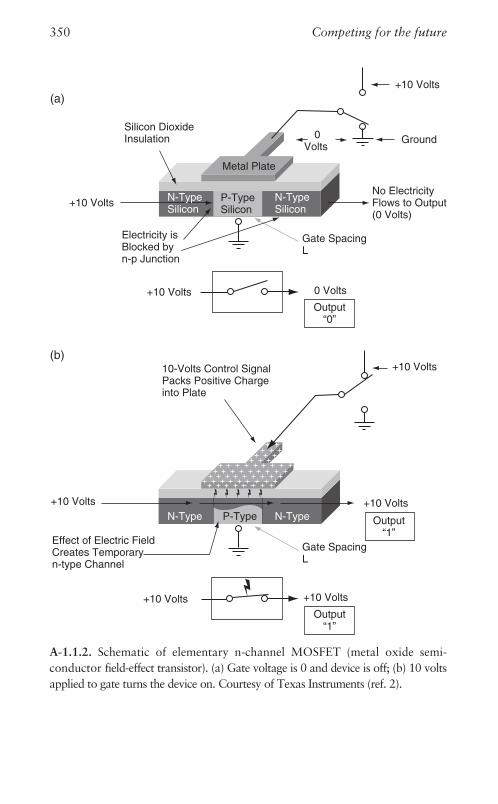
No ElectricityFlows to Output(0 Volts)
0Volts
Electricity isBlocked byn-p Junction
(b)
(a)
Silicon DioxideInsulation
N-TypeSilicon
P-TypeSilicon
Metal Plate
N-TypeSilicon
10-Volts Control SignalPacks Positive Chargeinto Plate
+10 Volts
Effect of Electric FieldCreates Temporaryn-type Channel
+10 Volts
+10 Volts
+10 Volts
+10 Volts +10 Volts
+10 Volts
+10 Volts
Ground
N-Type P-Type N-Type Output“1”
Output“1”
0 Volts
Output“0”
Gate SpacingL
Gate SpacingL
A-1.1.2. Schematic of elementary n-channel MOSFET (metal oxide semi-
conductor field-effect transistor). (a) Gate voltage is 0 and device is off; (b) 10 volts
applied to gate turns the device on. Courtesy of Texas Instruments (ref. 2).
350 Competing for the future

In the scaled-down version, the linear dimension L, separating source
and drain is reduced by a factor of k. The principle of scaling MOSFETs
consists of reducing the device operating voltage V and the device
horizontal dimensions by the same factor k, as well as the thickness
tox of the glass insulator sitting on top of the gate.4 In addition, the
silicon dopant concentration Na is increased by k.
Three benefits derive from scaling down.* Faster switching speed, allowing higher operating frequencies by a
factor of approximately k.* Reduced transistor area by a factor of k2.* For a single on-off cycle, reduced switching power dissipation per
transistor by a factor of k2.
How does scaling reduce the power dissipated in switching? The
total power dissipated in operation is given by the product of the
switching frequency, applied voltage, and the current flowing between
the source and drain when the transistor is in the conducting (on)
condition. Since the voltage is reduced by k, as is the current flowing
between source and drain (because of the smaller device area), the
power dissipated is reduced by a factor of k2 for a single switching
cycle.
Gate
Original Device Scaled Device
Oxide
nSource
nDrain
L
p Substrate, Doping Na
tox
WD
n n
tox /k
V/kV
L/k
Doping kNa
A-1.1.3. Principles of MOSFET scaling where the gate length L is reduced to
L/k. H. Dennard, F. H. Gaensslen, H. N. Yu, V. L. Rideout, E. Bassous, and
A. R. LeBlanc, ‘‘Design of ion-implanted MOSFETs with very small physical
dimensions,’’ IEEE J. Solid-State Circuits, SC-9, p. 256. Copyright # 1974
IEEE (ref. 3).
4 Taur and Ning, VLSI devices, pp. 164–173.
More efficient MOSFETs 351

An example will show how scaling works. Assume that k is 2. The
area of the transistor is reduced by a factor of 4; hence the transistor
density on the chip can be increased by approximately that amount. At
the same time, the switching speed is approximately doubled while the
total power dissipated by the chip remains constant. This is basically
Moore’s Law in practice. It is obvious why shrinking transistors have
been the productivity driver of the chip industry.
However, as noted in Chapters 1 and 2, there are limits to the ability
to reduce the gate spacing L, set by the fact the two p-n junctions do not
stay electrically isolated as the gate length shrinks substantially below
0.1 micron (100 nm). As a result, a leakage current between source and
drain exists even when the transistor is supposed to be in the off state,
causing power dissipation problems.
A further factor to keep in mind in limiting the ultimate practical
switching frequency achievable with a MOSFET chip architecture is
that increasing the switching frequency increases the total chip power
dissipation, and can lead to unacceptable chip heating. Currently,
limitations for the smallest, fastest devices are in the 3 to 4 GHz range.
Over time, the complexity of the devices has kept increasing, with
more than twenty separate layers of material that have to be deposited
and patterned in order to produce a state-of-the-art MOSFET structure
and provide the massive on-chip interconnections.
Figure 1.3 shows the cross-section of such a transistor. To get an idea
of the scale, note the gate dimension L, which is now below 0.09
microns (90 nm). Extraordinary precision in manufacturing is needed
as patterns are repeated millions of times on a chip.5
Limits to progress: Leakage current
Chapter 1 points out that when we reach near-atomic spacing, we
approach the limits of our ability to shrink MOSFETs as currently
understood. As Figure 1.4 shows, the steady reduction in gate length
is putting us close to the mark.6 It was 0.5 micron (500 nm) in 1993,
and is projected to be only 0.032 micron (32 nm) in 2009.
5 J. R. Brews, ‘‘The submicron MOSFET,’’ in S. M. Sze (ed.), High-speed semi-conductor devices (New York: A. Wiley-Interscience Publications, 1990), p. 144.
6 T. Thornhill III, CFA, ‘‘Global semiconductor primer,’’ UBS InvestmentResearch, Global Semiconductor (UBS Securities LLC, an affiliate of UBS AG(UBS) – March 30, 2006), p. 82.
352 Competing for the future
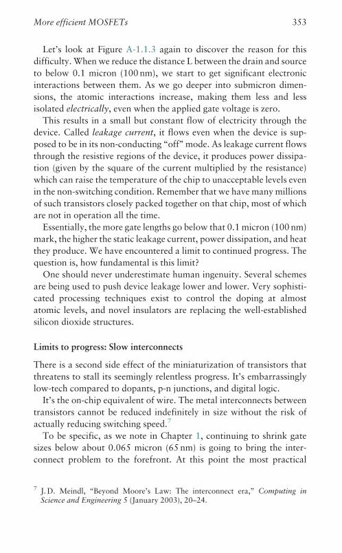
Let’s look at Figure A-1.1.3 again to discover the reason for this
difficulty. When we reduce the distance L between the drain and source
to below 0.1 micron (100 nm), we start to get significant electronic
interactions between them. As we go deeper into submicron dimen-
sions, the atomic interactions increase, making them less and less
isolated electrically, even when the applied gate voltage is zero.
This results in a small but constant flow of electricity through the
device. Called leakage current, it flows even when the device is sup-
posed to be in its non-conducting ‘‘off’’ mode. As leakage current flows
through the resistive regions of the device, it produces power dissipa-
tion (given by the square of the current multiplied by the resistance)
which can raise the temperature of the chip to unacceptable levels even
in the non-switching condition. Remember that we have many millions
of such transistors closely packed together on that chip, most of which
are not in operation all the time.
Essentially, the more gate lengths go below that 0.1 micron (100 nm)
mark, the higher the static leakage current, power dissipation, and heat
they produce. We have encountered a limit to continued progress. The
question is, how fundamental is this limit?
One should never underestimate human ingenuity. Several schemes
are being used to push device leakage lower and lower. Very sophisti-
cated processing techniques exist to control the doping at almost
atomic levels, and novel insulators are replacing the well-established
silicon dioxide structures.
Limits to progress: Slow interconnects
There is a second side effect of the miniaturization of transistors that
threatens to stall its seemingly relentless progress. It’s embarrassingly
low-tech compared to dopants, p-n junctions, and digital logic.
It’s the on-chip equivalent of wire. The metal interconnects between
transistors cannot be reduced indefinitely in size without the risk of
actually reducing switching speed.7
To be specific, as we note in Chapter 1, continuing to shrink gate
sizes below about 0.065 micron (65 nm) is going to bring the inter-
connect problem to the forefront. At this point the most practical
7 J. D. Meindl, ‘‘Beyond Moore’s Law: The interconnect era,’’ Computing inScience and Engineering 5 (January 2003), 20–24.
More efficient MOSFETs 353

approach to further performance improvements has proven to be
implementing single-chip multiprocessor architectures, discussed in
depth in Chapter 2. This technique promises to let designers continue
delivering advances in processing technology and architecture.
MOSFET shrinks still pay
There are also architectural tricks that can be used in designing chips.
Transistors of different dimensions can be used on the same chip, with
only the fastest ones having the troublesome deep sub-micron dimen-
sions. Having said all that, however, there are practical limits, primar-
ily set by power dissipation, which have profound implications for
future chip transistor densities and further increases in switching
speeds.
However, these remarks should not be interpreted to mean that the
historical trends are already at their end. More performance will be
obtained by reducing MOSFET dimensions, not necessarily because
the transistors are switching faster, but because their density increase
provides more functions on a chip. The wireless handset industry will
benefit from those trends as functions that previously requried several
individual devices are consolidated into a single chip. The MOSFETs
on these chips will be switching well below their GHz theoretical limits;
hence power dissipation will be manageable.
354 Competing for the future

Appendix 1.2: Buildingmulti-transistor logic gates
IN Chapter 1, we described the three basic logic gates used to build
computers. Here we will illustrate a combination gate – a NAND
built with MOSFETs. As shown in Figure A-1.2.1, it takes three
transistors of the same n-channel type in this configuration.1 A CMOS
configuration for the same gate function requires four transistors.
The NAND is a combination of an AND gate and an inverter. The
top MOSFET is connected to a voltage source of 10 volts which biases
it in the on (conducting) state.
The truth table gives the logical combinations of this gate.
If both voltage A and voltage B are positive (1), then the bottom two
transistors are turned on and hence conducting. This effectively con-
nects the current flow from the voltage source through the top transis-
tor to ground, and the output voltage V is 0. Hence it takes two positive
(1) inputs to produce a (0) output.
On the other hand, if either of the two voltages at A or B is 0, then the
current path is connected to the output, resulting in 10 volts at the
terminal, which is defined as a ‘‘1.’’
1 G. McWhorter, Understanding digital electronics (a Texas Instruments LearningCenter Publication, 1978), pp. 2–17.
355
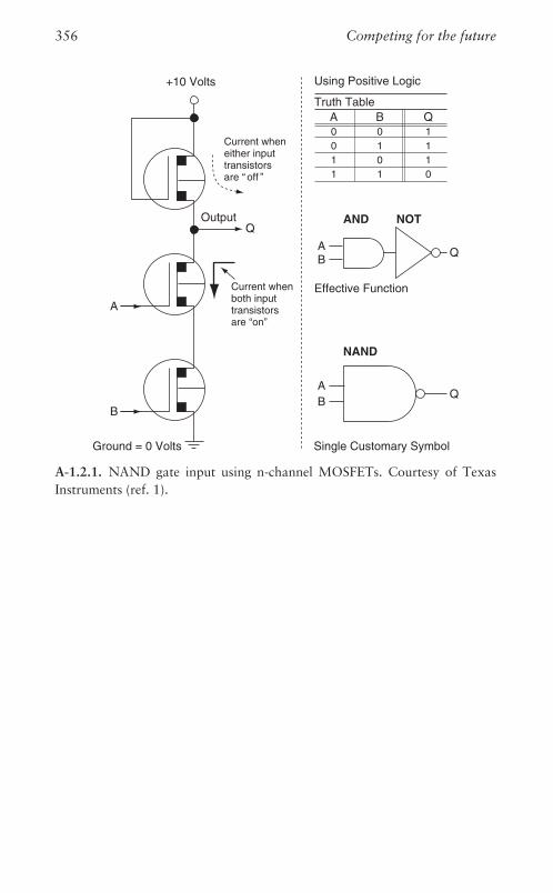
+10 Volts
Ground = 0 Volts
Q
A
Current whenboth inputtransistorsare “on”
B
Output
Current wheneither inputtransistorsare “ off ”
AB
Q
Single Customary Symbol
Effective Function
NAND
AND NOT
AB
Q
Using Positive Logic
Truth TableA B Q0 0 10 1 11 0 11 1 0
A-1.2.1. NAND gate input using n-channel MOSFETs. Courtesy of Texas
Instruments (ref. 1).
356 Competing for the future

Appendix 1.3: MOSFETsin memory devices
AN important application of multi-transistor gates is the creation
of building blocks that retain information, enabling data
storage devices.1
The static random access memory (SRAM) requires six transistors
per storage cell. The electrical configuration of the ‘‘unit’’ determines
whether a bit is stored there or not. The MOSFET structures used in
SRAMs are fairly standard and comparable to those used in building
logic elements.
However, special structures are used to build the dynamic random
access memory (DRAM), which stores a charge on individual transis-
tors that incorporate a capacitor. This charge must be constantly
refreshed in millisecond cycles as it leaks away.
At the other end of charge storage technology is FLASH (non-volatile)
memory, which will maintain charge in the complete absence of a
power supply. It requires special MOSFET structures very different
from the standard devices.
These MOSFETs hold an electrical charge for a very long period of
time in a special isolated capacitor.
Figure A-1.3.1 shows a highly simplified schematic of a special
MOSFET p-channel transistor.2 In contrast to a standard MOSFET,
it has a silicon film imbedded within an insulating silicon dioxide film
sitting on top of where the gate would normally be. This constitutes the
‘‘floating’’ gate of the p-channel MOSFET.
The basic operation by which the cell stores one bit is as follows.* The device is programmed by injecting an electronic charge into the
floating silicon gate (by applying a very short high-voltage pulse).
1 B. Prince, Semiconductor memories, 2nd edition (New York: John Wiley & Sons,1991).
2 R. Zaks, ‘‘System components,’’ From chips to systems: An introduction tomicroprocessors (Berkeley, CA: SYBEX, Inc., 1981), p. 139.
357

* This negative charge in the silicon film – the ‘‘floating gate’’ – induces
a conducting p-type channel between the two p-type regions, turning
it on.* Hence, when this transistor is interrogated to determine whether a
bit is stored there or not, its conducting state signals that a charge, a
(1), is stored in that location.* In the absence of a charge on the floating gate, the transistor is off, a
(0), because no conducting channel is present between the two p-n
junctions, and this is the result that is returned when the transistor is
interrogated.
Practical non-volatile memories are considerably more complex.
They require sophisticated circuits on the chip for programming, eras-
ing the charge, and addressing.
A final note: Whatever the specific transistor architecture used to
store bits, all memory devices rely on combinations of basic gates for
their addressing, sensing, and communications tasks.
Floating Si Gate
P+ P+
n-Type Si Substrate
Aluminum Contact
Si02 Glass
L
A-1.3.1. Schematic of basic MOSFET structure for non-volatile memory
devices. Reprinted with permission from R. Zaks (ref. 2).
358 Competing for the future

Appendix 1.4: CMOS reduceslogic gate power dissipation
DI G I T A L processing needs lots of logic gates. MOSFET
transistors, as noted in the main text, are the preferred way
to create them. However, owing to excessive current leakage,
early gates built with MOSFETs suffered from high power dissipation.
Put millions of these devices on a chip and the constant current drain
could cause overheating.
The CMOS architecture provided the solution to this problem, at the
expense of more complex chip manufacturing, by dramatically redu-
cing the gate power dissipation, enabling very large scale integrated
circuits.
To demonstrate the principle behind CMOS, let’s examine the dif-
ferences between a simple inverter gate built without this architecture
and one built with it.
We start with the non-CMOS inverter built with just one kind of
MOSFET.1 As Figure A-1.4.1 shows, two n-channel transistors are
interconnected with the source of the bottom transistor connected to
the drain of the top transistor. The top transistor is always on since its
gate is always connected to the battery.
Look at the left side of the figure. When a value of 10 volts (the input
voltage) is applied to the bottom transistor gate, a (1), it turns on,
forming a conducting path from battery to ground. Therefore, the
output voltage is zero, indicating a (0) state.
Now look at the right side of the figure. The input gate voltage
is zero, the bottom transistor is off, and the output is connected to
the battery through the top transistor. Hence the output voltage is 10
volts, a (1).
1 G. McWhorter, Understanding digital electronics (a Texas Instruments LearningCenter Publication, 1978), pp. 2–15.
359

This is simple enough, but it creates a huge problem when we want to
put many of these gates on one chip in close proximity: constant power
consumption. A small current is always flowing through the top tran-
sistor between the battery and the output, whether the lower transistor
is on or off.
Since the top transistor never turns completely off, its wasted current
leads to constant power dissipation. Put millions of these devices on a
chip and the power dissipation can cause overheating. That limits the
number of transistors on a chip.
Figure A-1.4.2 shows how the CMOS inverter works. We combine
two different (complementary) MOSFETs, one n-channel (bottom)
and the other p-channel (top). The gates of both transistors are con-
nected to the input voltage.
Observe what happens in (a) when the positive input gate voltage is
10 volts applied to both transistors. The top p-channel transistor is off
while the bottom n-channel transistor is on. As a result, the output
voltage is zero because the conducting path is to ground through the
turned-on bottom transistor.
Top “Load” Transistoris Always “On”
10 Volts 10 Volts
Output“0”
Output“1”
0 Volts
10 Volts
0 Volts 0 Volts
10 Volts
Input“1”
“ON” “OFF”
(a) (b)
Input“0”
0 Volts
n-ChannelMOSFET
A-1.4.1. Inverter using n-channel MOSFETs. Courtesy of Texas Instruments
(ref. 1).
360 Competing for the future

Compare that to the right side of the figure. Now the input voltage is
zero. The top transistor is on, while the bottom transistor is off. As a
result, a conduction path is formed between the battery and the output
where now 10 volts appear defined as a (1).
The only time a conduction path through the gate is formed is when a
logic path has to be generated. Since the top transistor turns off when
not needed, there is no significant leakage of current. In reality there is
always some very small leakage current through transistors that are
turned off, but it is orders of magnitude lower than in the non-CMOS
inverter shown above.
In summary, the CMOS architecture greatly decreases the constant
leakage current of transistors forming parts of gates on a chip as
compared to earlier approaches. Less leakage translates into much
lower power dissipation, and hence less heating of the chip.
The example above was chosen for simplicity. The same concept of
using complementary transistors applies to all gate structures, but it
does require that one or more transistors be added to form certain
gates. CMOS made it possible to produce the microprocessors of
today, densely populated with hundreds of millions of transistors.
As a result, CMOS structures are dominant in practically all inte-
grated circuits, including processors, memory chips, and imagers.
10 Volts
Output“0”
0 Volts
Input“1”
10 Volts
(a) (b)
10 Volts
Output“1”
10 Volts
Input“0”
0 Volts
0 Volts 0 Volts
p-ChannelMOSFET
n-ChannelMOSFET
A-1.4.2. Inverter using CMOS structure.
CMOS 361

Appendix 1.5: Laser diode basics
TH E fundamental physics of laser operation are similar for all
media capable of laser operation, whether gases, insulators, or
semiconductors. However, the operating details are vastly
different in the various materials.1
The early lasers were made using special solid-state materials or gases
confined within glass envelopes.2 For example, important gas lasers
use helium-neon or argon gas mixtures enclosed in a large glass tube
10 centimeters or more long. These are obviously bulky but useful as
light sources when certain emission colors or high power are required –
but not for the major applications that awaited semiconductor lasers.
The basic attraction of semiconductor lasers is their high atomic
density, which makes possible laser operation in a volume which is
ten million times smaller than in a gas. The idea of using semiconduc-
tors was discussed theoretically in the 1950s, but it took until 1962 for
a laser diode device to be demonstrated.3
In semiconductors, lasing is possible only in certain classes of mate-
rials endowed with special natural properties – direct bandgap semi-
conductors. Lasing occurs as a result of a highly complex interactive
process between very high densities of electrons and holes confined
1 A comprehensive review is provided by G. P. Agrawal and N. K. Dutta,Semiconductor lasers, 2nd edition (New York: Van Nostrand Reinhold, 1993).B. E. A. Saleh and M. C, Teich (eds.), Fundamental of Photonics (New York: JohnWiley & Sons, Inc., 1991).
2 A history of early laser development can be found in J. L. Bromberg, The laser inAmerica: 1960–1970 (Cambridge, MA: The MIT Press, 1991).
3 R. N. Hall, G. E. Fenner, J. D. Kingsley, T. J. Soltys, and R. O. Carlson, ‘‘Coherentlight emission from GaAs junctions,’’ Physical Review Letters 9 (1962), 366–368;M. I. Nathan, W. P. Dumke, G. Burns, F. H. Dill, Jr., and G. Lasher, ‘‘Stimulatedemission of radiation from GaAs p- junction,’’ Applied Physics Letters 1 (1962),62–63; T. M. Quist, R. H. Rediker, RlJ. Keyes, W. E. Krag, B. Lax, A. L.McWhorter, and H. J. Ziegler, ‘‘Semiconductor master of GaAs,’’ AppliedPhysics Letters 1 (1962), 91–92.
362

within a region where the intense radiation released by their recombi-
nation is also confined.
Laser emission has been obtained in semiconductor laser diodes in a
spectral region ranging from the blue to the far-infrared. This makes
semiconductors the materials of choice for most laser applications
requiring intense light beams that can be modulated at high frequencies
with high reliability and small size.
To produce a simple working device, the confined volume where
lasing occurs needs to be bound in two sides by partially reflecting
mirrors (a Fabry-Perot cavity) through which the laser emission is
released to the outside. This is the structure shown in Figure 1.8. For
applications requiring very stable control of the emitted spectrum, laser
structures use internal gratings to form what are called ‘‘distributed
feedback’’ lasers. We need not dwell on these architectural details. Our
purpose is to understand the advances made possible by the introduc-
tion of heterojunction lasers which can meet the technological require-
ments for many applications. The most important fact is that many
material combinations have been developed to produce heterojunction
lasers covering a wide spectral emission range from the blue into the
far-infrared.
The first semiconductor laser diode consisted of a special p-n junc-
tion structure in crystals of gallium arsenide (GaAs). Both sides of the
junction used the same GaAs material. Called homojunction lasers,
these devices operated best when refrigerated to low temperatures, but
were impractical for room temperature operation owing to their exces-
sive current requirements and poor reliability.
The introduction of heterojunction laser structures in the late 1960s
enabled all of the current applications of these devices with a wide
range of materials. However, the fundamental principles of operation
can be understood from a very simple double-heterojunction structure
based on GaAs and higher bandgap energy aluminium gallium arsenide
(AlGaAs).
Figure A-1.5.1 shows two highly-simplified laser diode structures to
illustrate the difference between the original homojunction and a het-
erojunction structure. Part (a) shows a simple p-n junction laser, where
the laser action occurs in a volume that is of relatively uncontrolled
thickness d. This is approximately 2 microns in the example shown.
Part (b) shows, for illustration purposes, a simple double-heterojuncton
laser. The p-n junction has been replaced by a p-n heterojunction of
Laser diode basics 363
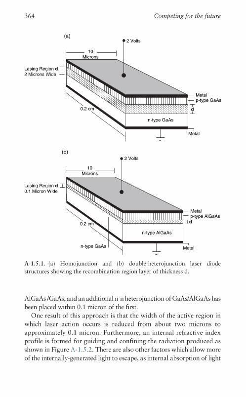
AlGaAs /GaAs, and an additional n-n heterojunction of GaAs/AlGaAs has
been placed within 0.1 micron of the first.
One result of this approach is that the width of the active region in
which laser action occurs is reduced from about two microns to
approximately 0.1 micron. Furthermore, an internal refractive index
profile is formed for guiding and confining the radiation produced as
shown in Figure A-1.5.2. There are also other factors which allow more
of the internally-generated light to escape, as internal absorption of light
0.2 cm
10Microns
d
Metal
Metal
p-type GaAs
Lasing Region d2 Microns Wide
n-type GaAs
2 Volts(a)
0.2 cm
10Microns
d
Metal
Metal
p-type AlGaAs
Lasing Region d0.1 Micron Wide
n-type AlGaAs
2 Volts(b)
n-type GaAs
A-1.5.1. (a) Homojunction and (b) double-heterojunction laser diode
structures showing the recombination region layer of thickness d.
364 Competing for the future

is reduced by confinement of the radiation as it propagates toward the
edge of the device. As an approximation, because of the much improved
carrier and radiation confinement resulting from the thin lasing region,
as much as a twenty-fold reduction in the laser volume is obtained. This
translates into a corresponding reduction in the diode current flow
needed to sustain lasing.
To better understand the impact of the heterojunctions we need to
look at the internal distribution of the radiation as it travels in the
device. Figure A-1.5.2 shows the refractive index profile inside the
homojunction and double heterojunction laser to illustrate the impor-
tant difference between them.
In (a) we see the internal refractive index profile of the homojunction
lasers where the electron-hole recombination occurs in the region d,
but the radiation produced is poorly confined.
In (b) we see the effect of confining the lasing region between the two
heterojunctions. Not only is the recombination region very thin
because the electron-hole recombination is confined by two hetero-
junctions, but in addition the sharply greater difference in refractive
index at the boundaries focuses the radiation and produces much lower
losses as the radiation propagates toward the edge of the laser where it
is emitted. The radiation spreads outside that region to some extent,
but in a very controlled way.
The end result is that the current density that this structure requires
for sustained laser emission is drastically reduced, by a factor that is
nearly (but not quite) proportional to the reduced laser volume.
Indexn
d
Electron-HoleRecombination Region
Light
Indexn
d
Light
(a) Homojunction Laser (b) Double-Heterojunction Laser
K
K
A-1.5.2. Schematic cross-section of a double-heterojunction laser showing the
refractive index distribution perpendicular to the junction plane and intensity
distribution of the fundamental transverse mode with a fraction K of the
radiant energy within the recombination region of width d.
Laser diode basics 365

Figure 1.7 shows the historical reductions in the threshold current
density as the technology continued to be refined, reaching operating
currents so low that they proved to be no hindrance to the most
important commercial or consumer laser applications.
For modern optical communications, heterojunction lasers require
emission in the 1.55 micron range and are constructed from combina-
tions of indium, gallium, arsenic, and phosphorous compounds.
As new materials get developed, such as lasers using gallium nitride
compounds operating in the blue spectral region, new materials chal-
lenges have to be overcome to reach acceptable operating current
levels. It usually takes many years to master the manufacturing tech-
nologies for new laser materials.
366 Competing for the future
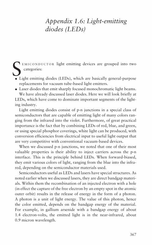
Appendix 1.6: Light-emittingdiodes (LEDs)
SE M I C O N D U C T O R light emitting devices are grouped into two
categories:
* Light emitting diodes (LEDs), which are basically general-purpose
replacements for vacuum tube-based light emitters.* Laser diodes that emit sharply focused monochromatic light beams.
We have already discussed laser diodes. Here we will look briefly at
LEDs, which have come to dominate important segments of the light-
ing industry.
Light emitting diodes consist of p-n junctions in a special class of
semiconductors that are capable of emitting light of many colors ran-
ging from the infrared into the violet. Furthermore, of great practical
importance is the fact that by combining LEDs of red, blue, and green,
or using special phosphor coverings, white light can be produced, with
conversion efficiencies from electrical input to useful light output that
are very competitive with conventional vacuum-based devices.
When we discussed p-n junctions, we noted that one of their most
valuable properties is their ability to inject carriers across the p-n
interface. This is the principle behind LEDs. When forward-biased,
they emit various colors of light, ranging from the blue into the infra-
red, depending on the semiconductor materials used.
Semiconductors useful as LEDs and lasers have special structures. As
noted earlier when we discussed lasers, they are direct bandgap materi-
als. Within them the recombination of an injected electron with a hole
(in effect the capture of the free electron by an empty spot in the atomic
outer orbit) results in the release of energy in the form of a photon.
A photon is a unit of light energy. The value of this photon, hence
the color emitted, depends on the bandgap energy of the material.
For example, in gallium arsenide with a bandgap energy of about
1.4 electron-volts, the emitted light is in the near-infrared, about
0.9 micron wavelength.
367
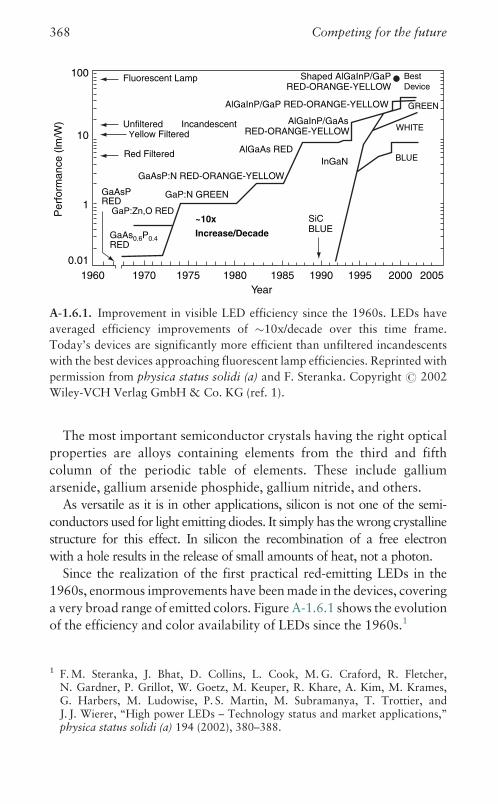
The most important semiconductor crystals having the right optical
properties are alloys containing elements from the third and fifth
column of the periodic table of elements. These include gallium
arsenide, gallium arsenide phosphide, gallium nitride, and others.
As versatile as it is in other applications, silicon is not one of the semi-
conductors used for light emitting diodes. It simply has the wrong crystalline
structure for this effect. In silicon the recombination of a free electron
with a hole results in the release of small amounts of heat, not a photon.
Since the realization of the first practical red-emitting LEDs in the
1960s, enormous improvements have been made in the devices, covering
a very broad range of emitted colors. Figure A-1.6.1 shows the evolution
of the efficiency and color availability of LEDs since the 1960s.1
1960 1970 1975 1980 1985 1990 1995 2000 2005
100
10
1
0.01
GaAsPRED
SiCBLUE
InGaNAlGaAs RED
AlGaInP/GaAsRED-ORANGE-YELLOW
AlGaInP/GaP RED-ORANGE-YELLOW GREEN
WHITE
BLUE
Shaped AlGaInP/GaPRED-ORANGE-YELLOW
GaP:N GREEN
GaAs0.6P0.4RED
GaP:Zn,O RED
GaAsP:N RED-ORANGE-YELLOW
Fluorescent Lamp BestDevice
UnfilteredYellow Filtered
Red Filtered
Incandescent
~10x
Increase/Decade
Year
Per
form
ance
(lm
/W)
A-1.6.1. Improvement in visible LED efficiency since the 1960s. LEDs have
averaged efficiency improvements of �10x/decade over this time frame.
Today’s devices are significantly more efficient than unfiltered incandescents
with the best devices approaching fluorescent lamp efficiencies. Reprinted with
permission from physica status solidi (a) and F. Steranka. Copyright # 2002
Wiley-VCH Verlag GmbH & Co. KG (ref. 1).
1 F. M. Steranka, J. Bhat, D. Collins, L. Cook, M. G. Craford, R. Fletcher,N. Gardner, P. Grillot, W. Goetz, M. Keuper, R. Khare, A. Kim, M. Krames,G. Harbers, M. Ludowise, P. S. Martin, M. Subramanya, T. Trottier, andJ. J. Wierer, ‘‘High power LEDs – Technology status and market applications,’’physica status solidi (a) 194 (2002), 380–388.
368 Competing for the future

Some devices are exceeding the luminous efficiency of vacuum-based
light emitters such as incandescent or even fluorescent bulbs. In fact,
the quality and cost of LEDs have reached the point where they can
selectively replace some vacuum tube-based light sources in applica-
tions such as automobile headlights and traffic signals.
Recently several TV makers have announced rear-projection sets
that replace the conventional projector bulb with an LED array for
longer life, better power, and quiet operation without a cooling fan.
Light-emitting diodes 369

Appendix 1.7: Photodetectors
SE M I C O N D U C T O R devices for sensing light levels are in wide use,
and their properties are tailored to specific applications. They
range in complexity from the simplest light sensors, used in door
openers, to sophisticated devices that detect ultra-short, very low-level
communications signals that have traveled hundreds of miles over an
optical fiber.
As mentioned in the main text, light sensors are also the core sensing
element in imaging devices, where millions of sensors are built into a
single chip. Finally, solar energy converters (solar cells) are in the same
class of device.
We learned in Chapter 2 that a photodetector is usually a reverse-
biased p-n junction. The type of semiconductor material used for the
junction is determined by its intended application, particularly with
regard to the wavelength of the light to be detected and the response
speed desired.
The operational principle is that a photon of incident light absorbed
in the vicinity of the p-n junction, and within the depletion zone,
generates free carriers that give rise to a current proportional to the
intensity of the incident light. Figure A-1.7.1 shows the p-n junction
detector in the dark and with incident light. The current through the
device increases with light intensity.
Silicon photodetectors are widely used to capture visible light,
whereas III-V compound devices are used to detect signals in the infra-
red portion of the spectrum. Most detectors used in fiber optic com-
munications systems, where the laser emission is in the 1.5 micron
(near-infrared) spectral region of low fiber absorption, are made of
indium gallium arsenide.
370
Cur
rent
(a) (b)
p-Typen-Type+V
p-n Junction
Depletion Zone
p-Typen-Type
p-n Junction Interface
Depletion Zone
CurrentFlows
– –
++
––+ +
V+ Volts
Cur
rent
NoCurrent
Incident Light
VVolts
+V
A-1.7.1. P-n junction used as light detector. (a) In the dark (no current); (b) with
incident light which results in current flow proportional to light intensity.
Photodetectors 371

Appendix 1.8: Making fiberoptic cables
TO gain an appreciation of how one builds optical fibers for
different communications applications, look at Figure A-1.8.1,
which illustrates three different types of fibers.1
Each of these types is distinguished by its refractive index profile.
The refractive index profile is a key part of fiber design because it
determines the product’s ability to propagate short pulses and maintain
their shapes over long distances.
The topmost illustration shows the simplest stepped-index profile
fiber (also called multimode). This is the least costly type to manufac-
ture, but it has the poorest pulse propagation characteristics. It is used
for transmission over short distances.
Single mode fiber with a tailored stepped refractive index profile,
shown in the second illustration, is much better at keeping the pulse
shape intact, but it is costlier. This type of fiber is used for high-data-
rate communications over long distances.
Finally, in the illustration at the bottom of the figure, we have a
multimode, graded-index fiber that falls between the two profiles above
it. This fiber has applications in intermediate distance transmission.
In all three examples the glass fibers are encased in claddings. Large
numbers of individual cladded fibers are enclosed in cables that protect
them from external forces and the elements. Special techniques exist for
creating cables that can survive undersea deployment and other
demanding environments.
1 A. G. Chynoweth, ‘‘The fiber lightguide,’’ Physics Today (May 1976), 28–37.
372

MultimodeFiberStepped-Index Profile
Cross- Section
IndexProfiles
InputPulse
LightPaths
OutputPulse
Cladding
Core
r
n
SingleMode FiberStepped-Index Profile
MultimodeFiberGraded-Index Profile
r
n
r
n
A-1.8.1. Three types of optical fibers. (a) Multimode fiber; (b) single-mode
fiber; and (c) multimode graded-index fiber. Reprinted with permission from
Physics Today. Copyright # 1976 American Institute of Physics (ref. 1).
Making fiber optic cables 373
Appendix 1.9: Principlesof LCD displays
FL A T - S C R E E N displays based on organic materials dominate the
display device field. Chief among them for its commercial
importance is the liquid crystal display, or LCD.
Liquid crystals are a class of organic materials with very interesting
properties. Their molecular alignment (and hence their optical proper-
ties) change reversibly with temperature, as well as under the effect of
moderate electric or magnetic fields.1
At high temperatures these materials exhibit the properties of
liquids, while below a critical temperature they assume more of the
properties of solids. For example, as a result of this transformation, a
liquid crystal film can change reversibly from a milky fluid, opaque to
light, to one which is transparent to visible light.
The discovery of liquid crystals dates to the nineteenth century.
However, the materials languished without serious applications until
the late 1960s, when research at RCA Laboratories found an applica-
tion for them in flat-screen displays. The researchers achieved this by
applying electric fields to thin liquid crystal films to change the optical
properties of the materials.2
This discovery made two types of display applications possible as
materials were developed. First, applying an electrical field to certain
classes of liquid crystals changes them from light absorbers to good
reflectors. Second, in other materials, the applied field can make the
film either opaque or transparent to visible light; hence the film can
become a ‘‘light valve.’’
1 For a complete description see G. W. Gray, Molecular structure and properties ofliquid crystals (London: Academic Press, 1962).
2 G. H. Heilmeier, L. A. Zanoni, and L. A. Barton, ‘‘Dynamic scattering: A newelectro-optic effect in certain classes of nematic liquid crystals,’’ Proceedings ofthe IEEE 56 (1968), 1162–1170.
374

Flat-screen display technology has proven to be crucial to the mass
acceptance of sophisticated electronic systems. There would be no
personal computers, digital cameras, cellular handsets, or dozens of
other portable products without the ability to display high-resolution
images on inexpensive, lightweight displays. Of course, transistors play
a key role in enabling LCD displays as part of their data stream and
addressing management.
The simplest structure for making liquid crystal displays consists of
sandwiching a thin film of the crystal material between two glass
plates, each side of which is covered with a transparent conductor.
To form an imager, we divide the ‘‘sandwich’’ into a grid of individual
pixels, each of which can be a recipient of the voltage necessary to
change the properties of the material within its borders.
For example, we can choose to make an array of two hundred by
three hundred pixels. Each pixel can be accessed by a transistor circuit
that applies a temporary voltage to that pixel. Assuming that there is
uniform light incident on the device, images will be created by the
pattern of pixels that do or do not reflect the light to our eyes, based
on whether they have been subjected to the applied electric field. Color
filters can be incorporated to turn the image from monochrome into
full color.
If we are interested in creating images without uniform incident
light, we can use liquid crystals that shift from transparent to opaque
with the application of an electric field. This type of display requires
that a light source, such as LEDs for small displays or fluorescent
devices for larger ones, be placed behind the screen, so it can shine
through the transparent pixels to create the image.
What we have described is really primitive. Today’s versions are far
more sophisticated. Modern ‘‘active matrix’’ displays are built with
thin films of silicon deposited on glass and containing transistors
arrayed in complex integrated circuits. In effect the thin film electronic
circuitry is built as part of LCD display.3
Manufacturing such displays is very demanding and involves tech-
nologies as complex as those needed to produce silicon integrated
circuits. Production plants cost billions of dollars.
3 A useful text on modern LCDs is W. den Boer, Active matrix liquid crystaldisplays (Amsterdam: Elsevier, 2005).
Principles of LCD displays 375

LCDs face competition from new flat-panel technologies. These
include displays using organic light emitting diodes (OLEDs) and, for
large TV displays, vacuum plasma devices built using huge arrays of
tiny electrodes that are image-energized to produce small streams of
electrons that energize phosphors in order to produce the color effect.
Such devices fall outside of our consideration of solid-state imagers and
do not impact the mass market for LCD flat-panel displays.
376 Competing for the future

Appendix 2.1: The demiseof analog computers
IN Chapter 1 we pointed out the difficulty of using vacuum tubes for
large-scale digital data processing.
This observation, while perfectly true, begs the question, why shift to
digital in the first place? We live in the natural world, which is defiantly
analog. It seems logical that analog systems would process information
from the analog world more efficiently than their digital counterparts.
On the surface they do seem more efficient. In analog electronic
systems a smoothly variable electrical quantity (such as voltage, capa-
citance, or current) is used to represent information. The value of the
electrical property is directly proportional to the magnitude of the
physical signal being processed or transmitted.
Suppose, for example, you want to measure the intensity of light in a
room. You place a photodetector (an analog light sensor) there. When
light hits the device, it responds either by generating an electrical
current or by permitting such a current to flow. As the light gets
stronger, the current flowing in the system becomes greater as well.
The current increases in a linear fashion, allowing you to track and
record the level of light falling on the photodetector. The term ‘‘linear’’
is used to describe analog systems because, under ideal conditions, their
electrical information varies in line with the received signal.
Human beings are analog systems, too. We respond in a linear
fashion to external analog signals such as temperature, sound, light,
and images. Our brains are analog computers that interpret and ana-
lyze these signals, then generate output signals, which are delivered
through our nervous systems.
Since our brains are analog, the question of why go digital applies
equally well to computing systems. Why not simply replicate the
human brain in an analog computer system?
In fact, the first practical computers were analog. Well before digital
computers were widely available, there were special-purpose analog
units that computed artillery trajectories and solved complex scientific
377

equations in heat flow and aerodynamics. These computers operated by
manipulating voltage levels in circuits that combined, at various times,
vacuum tubes, transistors, diodes, amplifiers, resistors, and capacitors.
By today’s standards analog computers were quite limited. When
more flexible and powerful digital processors became available, stand-
alone analog machines simply disappeared.1 A comparison between
digital and analog will make clear the reasons for this sudden shift.
The digital advantage
We now take the superiority of digital computers for granted, but we
rarely consider why they vanquished analog processors. Here are some
of the reasons.
Scalability
As we saw in Chapter 1, only three basic logic gates are needed to
perform any logic or arithmetic function using Boolean algebra. Each
CMOS gate requires, on average, four transistors, as shown in
Appendix 1.4.
As a result, large computations are conceptually simple. They can be
carried out through multiple arrays of interconnected gates. To
increase the processing power of a digital computer, you just increase
the number of available gates.
In practice, of course, matters get more complicated, and the archi-
tecture of the device becomes all-important. But in theory, as long as
you can manage the interconnections that carry data traffic, you can
continue to increase processing power. There are no theoretical limits
to the size or power of a digital computer.
Analog computers, on the other hand, must deal with complex
interrelated changes in signal levels. As the computer gets larger, it
becomes less reliable, since its greater complexity increases the chances
that the analog signals will interfere with each other. This makes
scaling enormously complicated and very costly.
1 While stand-alone analog computers may be history, analog computation is verymuch alive as part of some digital integrated circuits. Among other functions it isused for power management and for analyzing wireless signals. If done in thedigital domain, these processes would require large, complex digital signal pro-cessing circuitry on the ICs. Keeping the signals in analog yields superior resultsand smaller chips.
378 Competing for the future

Flexibility
The function of an analog computer is usually determined by its hard-
ware. By contrast, a digital computer can be adapted to different
functions through the use of programs stored in software or firmware.
You don’t have to change hardware when you change tasks.
Data integrity and processing precision
Internal and external noise and interference can disrupt the linear
nature of analog information, especially when the signals carrying
that information are weak. Digital processors, on the other hand, are
isolated from analog variations by their very nature, and therefore not
subject to interference.
An analog processor also has difficulty maintaining precision when the
values are very small. The mathematical basis of digital processors allows
them to handle very small and very large values with equal accuracy.
Data storage
Digital data (input and output) can be stored indefinitely in various
types of memory devices. Analog computers store information only for
relatively short periods of time.
Communications reliability
Digital communications have overwhelming advantages over analog
signal transport. A digital signal can be transmitted over any distance,
provided its bits can be individually identified at the receiving end.
In an analog communications system, by contrast, irreversible
changes in the waveform cause the signal to deteriorate over distance.
The signal is also more likely to encounter interference from the analog
world around it. In either case information is lost.
The modern communications infrastructure could never have been
built with analog systems.
Achieving digital accuracy
Digital signal and data processing is done in binary format. Therefore
digital systems must convert analog signals into ones and zeros so they
can be processed in the digital domain.
The demise of analog computers 379

While this seems like an extra step, it permits easier, more accurate
processing, provided the conversion is done with high enough preci-
sion. When an analog signal is digitized, the precision of the digital
signal increases with its sampling rate and the number of bits used to
describe the values it represents.
Take the simple example of digitizing a sine wave (Figure A-2.1.1).
The wave is shown in (a) and the digitizing process in (b). If we digitize
the signal using 3-bit numbers, we can only obtain eight values, from
�1.00 to þ1.00, in steps of 0.25 (c).
We can get much higher precision by adding bits. For example, with
8 bits we can get 256 values for each sample. With 16 bits we get
65,536 values for each sample.2 It would be difficult to achieve this
level of precision in an analog system.
Precision is not the only advantage digital systems have over their
analog equivalents. Digitized data can also be processed repeatedly
without having values shift or deteriorate. After all processing is
done, digital signals can be converted back to analog if the results
require human interface.
In short, digital systems offer the best of both worlds: the precision,
flexibility, and reliability of a system based on mathematics, and the
ability to interact with our analog world.
1.00
0.75
0.50
0.25
0
–0.25
–0.50
–0.75
–1.00(a) (b) (c)
T T TT
1_2
1T_
2
A-2.1.1. (a) A sine wave; (b) sampling the sine wave; (c) quantizing the samples
to 3 bits which produces eight distinct values for each sample. Copyright
# 1996 Pearson Education, Inc. Reprinted by permission of Pearson
Education, Inc., Upper Saddle River, NJ (ref. 2).
2 Figure and calculations from A. S. Tanenbaum, Computer networks, 3rd edition(Upper Saddle River, NJ: Prentice Hall PTR, 1996), p. 725.
380 Competing for the future

Appendix 2.2: IP, TCP, and theInternet
WE already know that special computers called routers direct
data traffic on a packet-switched network, and that
computers communicate through special, industry-defined
machine languages (protocols). Here we examine the protocols that
underlie packet networks in general and the Internet in particular.
The protocol that has reached star status for communications sys-
tems is the Internet Protocol (IP), which grew out of the early
ARPANET work. Networks designed to operate with the IP protocol
use a 32-bit address embedded in each packet header to move it from
source to destination.
Every computer on the Internet has an IP address. That includes each
router. Since routers transmit digital streams of bits in the form of
packets, the physical implementation of the IP protocol involves coding
headers attached to the packets. These headers provide the address of
the sending and receiving computers.
The packets travel a path from one router to another on the way to
their destination. The routers direct this trip, using stored lookup
tables to find paths to the destination IP address in the packet
headers.
But even IP doesn’t work alone. To provide reliable internetworking
on the Internet, it is closely linked with TCP (Transmission Control
Protocol). Let us look at how IP and TCP work together.
While the router lookup tables are continuously updated, that
doesn’t prevent packets from getting lost or delayed. If a target router
is temporarily overloaded or down, the packets sent through it could
lose their way, and the network would be unreliable.
To prevent this from happening, TCP provides the equivalent of
certified mail. The instructions imbedded in the TCP part of the head-
ers ensure that packets are handled appropriately. In effect, it estab-
lishes a ‘‘virtual’’ connection between the source of the data and its
destination.
381
TCP also supplies an acknowledgement that the packet has arrived
at the destination, and that it has not been corrupted during its passage.
If a packet is lost or damaged, a makeup packet or replacement will
be sent.
The maximum content of each packet, including its header, is limited
to 65,535 bytes (8 bits in each byte). The TCP portion of the header
contains much more information about source, destination, and cor-
rect packet sequence than the IP portion. It is the main reason that the
packets can be reassembled at the destination in the proper order.
Another aspect of the TCP protocol is the ability it provides to
encode headers with information specifying levels of security, and to
manage the parallel flow of related packet streams.
IP may get star billing, but TCP does a lot of the behind-the-scenes work.
Protocols designed to label packets for special treatment continue to
be developed to further provide a quality of service beyond that of TCP/
IP. For example, a standard has been established called multi-protocol
label switching (MPLS).
MPLS ensures that routers provide appropriate treatment to related
packets. It adds a 32-bit header to the packet that contains prioritizing
information and the type of content being transported. In effect, pack-
ets having the appropriate label headers get priority routing as they
navigate through the networks.
As a result, therefore, IP-enabled networks are fully capable of
reliably transporting any kind of data. This is a transformational
achievement, allowing the connectionless network model to provide
the same functionality as the PSTN, but with far more flexibility. This
changes the game for the communications industry.
382 Competing for the future

Appendix 2.3: Buildingan object-oriented program
TO get a feel for object-oriented architectures, consider a very
simple program designed to update the contents of a particular
master file. Figure A-2.3.1 shows the ‘‘old’’ way of architecting
such a program, by logical decomposition of the process into steps that
are sequentially linked to produce the program.1 To produce this
program, each element of the process must be coded in tightly-linked
sequences.
By contrast, in the object-oriented architecture shown in Figure
A-2.3.2, the program is divided into abstractions of the key elements.2
Instead of steps, the problem is now defined in terms of autonomous
interconnected objects. Each object has its real-world mission defined,
and is given its operational orders and required variables through
the bus.
Program development using object-oriented technology can be
divided into four interdependent elements.* The first critical task is the definition of program requirements. This
requires close communication with the intended users and an under-
standing of their applications.* Program architecture is developed on the basis of these require-
ments. The skill of the architect determines the ultimate quality of
the program and the time required to complete it.* The production of the program proceeds, with coding by program-
mers who write within tight guidelines provided by the program
architects.* Finally, the completed program must be tested. Note that testing can
account for between 40 and 50 percent of the cost of developing a
large program.
1 G. Booch, Object-oriented design with applications (Redwood City, CA: TheBenjamin/Cummings Publishing Company, Inc., 1991), p. 15.
2 Booch, Object-oriented design, p. 16.
383

UpdateFile
PutUnmatchedMaster
Put NewMasterArea
FormatOutput
MatchGetFormattedUpdate
GetMasterArea
Get OkMaster
Expand ReformatGet ValidCard
ValidateCheck Sum
Get OldMasterRecord
GetSequencedCard
Edit
SeqCheck
GetUpdateCard
AddCheckSum
Put NewMasterRecord
PutFormattedMaster
Update
A-2.3.1. Organization of program using ‘‘conventional’’ algorithmic architecture,
to be compared to Figure A-2.3.2. Booch, Object solutions, p. 15 figure 1–2,
Copyright# 1991 Pearson Education, Inc. Reproduced by permission of Pearson
Education, Inc. All rights reserved (ref. 1).
MasterFile
MasterRecord
File ofUpdates
Updatesto Card
Update
Match
GetPutCreate
Is ValidAdd
Get FormattedUpdate
GetReformat
Check Sum
A-2.3.2. Organizing the same program as shown in Figure A-2.3.1 using
object-oriented architecture. Booch, Object solutions, p. 16 figure 1–3,
Copyright # 1991 Pearson Education, Inc. Reproduced by permission of
Pearson Education, Inc. All rights reserved (ref. 2).
384 Competing for the future

Program definition and architecture require the most skilled and
experienced people. These two steps produce virtually all of the pro-
gram’s intellectual property value. Hence, these functions are very
rarely outsourced.
Code writing and program testing require the most manpower, but a
lower level of detailed expertise. This division of labor has made
possible the partial outsourcing of software development to lower-
cost geographies like India, where software ‘‘factories’’ employing
thousands of people have been set up in the past few years to write
and test software code.
In effect, software production is becoming analogous to the equip-
ment business. The concept, product design, and architecture are done
within an enterprise, while the more mechanical processes of assembly
and final product test are frequently in the hands of outside
contractors.
Building an object-oriented program 385

Index
access restrictions 259, 260Accredited Home Lenders,
Inc. 90AdSense 299advertising on the Internet 298–300,
303–304Agency for Industrial Innovation (AAI;
France) 148Agere Systems 120Albany Nanotech Facility
(USA) 144–145Alcatel 152, 237, 263, 264Amazon.com 310AMD 60, 206, 247America Online 206American Research and Development
Corporation 179, 193,196–197, 200
amorphous silicon liquid crystaldisplays (LCDs) 51–52
Analog Devices 162–163analog systems 17, 57
computers 377–380data transmission 66vacuum tubes (valves) 3, 17–18,
19, 106angel investors 177, 199–200antitrust cases 288–289Apcar, Leonard 303Apple 119, 174, 252, 282, 307applied research 103Applied Science and Technology
Research Institute (ASTRI;Hong Kong) 147
ARPANET 13, 70assembly of products 221, 222
contract assembly 234subcontracting 232–233
AT&T 13, 20, 82, 85, 189, 207,315–316
Bell Laboratories 18, 39, 81,108–109, 119, 121
Australiamigration of technical graduates and
134automation 220, 221–231
as industry 229–231integrated circuit (IC)
production 226–227transistor production 223–225
automobile industry 323–325Avaya Communications 120, 232aviation 12Avon Products 311, 312
balance of trade 336–338banks 177Baran, Paul 70basic research 102–103, 127Belgium
Interuniversity MicroelectronicsCenter (IMEC) 149–150
Bell, Alexander Graham 17Bell Laboratories 18, 39, 81, 103,
108–109, 119, 121Berkshire Hathaway 182Berners-Lee, Tim 73binary system 31bipolar transistors 25, 347Blicher, Adolph 21blogs 313blue laser diode 1books 287–288Boolean algebra 30boom/bust cycles 5Braun, Karl Ferdinand 48Brin, Sergey 297broadband 85, 301, 305–306Brownell, Thomas 305buy-out firms 182
386

CacheLogic 79Cailliau, Robert 73Cambridge University (UK) 158cameras 48, 326
CMOS camera sensors 48–50Canon 231, 245car industry 323–325Carnegie Mellon University (USA) 158cathode-ray tubes (CRTs) 18, 48cellular networks 81–83, 239, 318–319,
325, 330censorship 314Chamberlain, Joseph 219, 338Chandler, Marc 338changes caused by digital electronics
290–292charge-coupled devices (CCDs) 48chemical industry 336Cherukuri, Satyam 103–105China 4, 82, 120, 124, 263, 341
communications infrastructure238–239
international trade 333Internet and 301joint ventures in 264–265manufacturing sector 222, 236–238
outsourcing to 150–153,219–221, 336
wages 240workforce 239, 240
patents 167protectionism and 262–263research and development (R&D)
in 139response to IP piracy 285technology education in 132–133venture capital in 211
Chromatis 187, 196CinemaNow.com 308Cisco 205, 329‘‘click fraud’’ 299client/server architecture 89clusters of innovation 158–159Code Division Multiple Access
(CDMA) 82Cohen, Marshall 161collaboration
antitrust cases 288–289joint ventures 159–163, 263,
264–265
Colombus, Christopher 175commoditization 104communications see
telecommunicationscompact discs (CDs) 17, 34, 283
encryption 286Compaq 206competition 329, 340
competitive advantage 231–236telecommunications 316–318
strategies and outcomes 319–320complementary metal oxide
semiconductor (CMOS) 33,359–361
camera sensors 48–50compression of data 80
JPEG standard 80MPEG standard 80, 81, 280
computers 15, 18, 56, 57, 301analog 377–380costs of hardware 64–65magnetic disk storage 34, 36–38, 65
floppy disks 34, 37hard disks 34, 37, 38, 65, 306
memory 33–38dynamic random access memory
(DRAM) 35, 65, 357FLASH memory 35, 37, 38, 357MOSFET memory structures
34–36, 357–358optical disks 34, 38semiconductor memory 34static random access memory
(SRAM) 35, 357microprocessors 58–63
flexibility and scalability 59–60multiprocessors (parallel
processors) 30, 62–63, 65when smaller is not better 60–61
software see softwareconnectionless packet networks 69–71
digital video transmission 79–81enabling new services 72how it works 71IP phone calls 75potential capacity limitations 83–85wireless 83
content protection see digital rightsmanagement (DRM)
Continental AG 250, 251
Index 387

contract manufacturing 233types 234–236
contract assembly 234independent semiconductor
fabrication plants(fabs) 235–236
Original Design Manufacturers(ODMs) 234–235
copyright 259piracy see piracysoftware 268–272
cores 60Corning 251–252Covad Communications 207, 210culture, entrepreneurship and 158,
188, 339Cypress Semiconductor 151
data transmission 56, 69analog systems 66connectionless packet
networks 69–71digital video transmission 79–81enabling new services 72how it works 71IP phone calls 75potential capacity
limitations 83–85wireless 83
optical fibers 11, 12, 44–47, 66,83–84
wireless 83databases, relational 88–89Dean, Howard 314Defense Advanced Research Projects
Agency (DARPA; USA) 119, 144deflation 327–331deForest, Lee 106Dell 310Delpla, Jacques 159design for manufacturing 233digital electronics 1, 2–3, 4, 9–11,
54–55, 98, 123, 346building digital systems 56–57future 331growth in 323–327insider’s perspective 11–12origins 14–15vision and 12–14see also individual topics
Digital Equipment Corporation (DEC)193, 195, 206
digital rights management (DRM)285, 308
encryption 286watermarking 286–287
digital versatile discs (DVDs) 34,284, 307
diodeslaser diodes
basics 362–366blue laser diode 1semiconductor lasers 3, 11, 13,
38–43, 113, 208–209, 362–366light emitting diodes
(LEDs) 367–369organic (OLEDs) 52–54
displayscathode-ray tubes (CRTs) 18, 48liquid crystal displays (LCDs) 11, 51,
247–250, 345, 374–376amorphous silicon and 51–52
division of labor 222Domain Names System (DNS) 74Dousmanis, George 113Drake, Francis 176dynamic random access memory
(DRAM) 35, 65, 357
Earthlink 79EarthWeb 298eBay 79, 310economic environment
assessment of 340–341economic growth strategies 343
R&D teaming withmanufacturing 343–345
workforce considerations 345–346economic liberalization 220Edison, Thomas Alva 102, 105–107,
110, 121, 176education
migration of graduates 132,133–136, 137–138
technological 130–138China 132–133India 132, 133
Electronic Arts 206, 286Elizabeth I of England, Queen 175embargoes 259, 259, 260
388 Index

employmenteconomic growth strategies
and 345–346information sector 301manufacturing sector 241–247
China 239, 240high direct labor content 241–242high intellectual property
content 243–245encryption 286entrepreneurship 158–159, 177, 178,
188–190culture and 158, 188, 339incentives for entrepreneurs 186–188
Epitaxx 204, 206Ethernet networks 197European Union (EU)
antitrust cases 289patents 279
EV-DO 82evolutionary innovation 123eXtensible Markup Language (XML) 73
Fairchild SemiconductorCorporation 21
Federal Express 312fiber optic systems 11, 12, 44–47, 66,
83–84, 238, 372FLASH memory 35, 37, 38, 357Fleming, John Ambrose 106floppy disks 34, 37Forrest, Stephen 161FoxConn 234–235France
balance of trade 336migration of technical graduates
and 134research and development (R&D) in
Agency for Industrial Innovation(AAI) 148
fraud, ‘‘click fraud’’ 299free trade 219, 332Friend, Richard 158Friis, Janus 78Fuji 231
gallium arsenide 113Gates, Bill 118General Electric 19, 117, 120, 253
outsourcing by 151
General Motors (GM) 189General Packet Radio Service
(GPRS) 82genomics 344germanium transistors 18, 20, 21, 112Germany 126, 218, 259
balance of trade 336government support in 129manufacturing sector 250, 251migration of technical graduates
and 134telecommunications in 317
Global Service for Mobile (GSM) 82globalization 1, 118, 332, 346
innovation and 3–5, 173–174intellectual property (IP) and 289manufacturing sector 217–218
integrated circuit (IC)production 227–228
outsourcing 150–153, 218–219,233, 252–255
reversing tide ofmigration 245–247
new world order and 5–6R&D and 122–125solutions to problems 338–340
assessment of economicenvironment 340–341
policy and politics 341–343venture capital 211–213
GlobalSpec 304–305Google 79, 187, 205, 214, 287, 308
business plan 297–300Internet searches 296–300
government and the state 5policy and political solutions to
problems 341–343protection of industry see
protectionismpublic sector R&D 139–144regulation by 159response to IP piracy 285subsidies 220, 339, 340support for R&D/innovation 128,
129–130, 160expanding global talent
base 130–138Grace, W. R. 189Gray, Elisha 17Greenspan, Alan 192
Index 389

Greylock Partners 179Grokster 287growth strategies see economic growth
strategiesGutierrez, Carlos 338
hard disks 34, 37, 38, 65, 306Harvard University (USA) 158heterojunction lasers 38–43, 363, 365Hewlett-Packard 206Hitachi 231, 246Hockam, George 45holding companies 182Hon Hai Precision Industry
Ltd. 234–235Hong Kong
Applied Science and TechnologyResearch Institute (ASTRI) 147
response to IP piracy 285Hoover, Herbert 129Hopper, Andy 158Host Marriott 189Huang, J. S. 262Hughes Research Laboratories 109hypertext 73Hypertext Markup Language
(HTML) 73
IBM 94, 109, 118, 120, 206outsourcing by 152
import prohibitions 259incentives for entrepreneurs 186–188independent semiconductor fabrication
plants (fabs) 235–236India 5, 82, 120, 341
outsourcing to 150–153software development 253
technology education in 132, 133telecommunications 330
industrial holding companies 182Industrial Technology Research
Institute (ITRI; Taiwan)145–147, 173
industry standards see standardsInfosys 152, 253infrared imaging 160innovation 1, 169
creating clusters ofinnovation 158–159
definition 1–2
evolutionary 123globalization and 3–5, 173–174high-tech industries as national
priority 125–127management 112–114
innovations for the corebusiness 114
personal exposure 113manufacturing sector 247–252
domestic specialties and offshorecommodities 250–251
liquid crystal displays(LCDs) 247–250
proprietary processes 251–252revolutionary 123as social force 14software as equalizer in 128–129strategy for 343–345vision and 12–14, 110–112see also research and development
(R&D)Institute of Electrical and Electronic
Engineers (IEEE) 67, 280Institute for Infocomm Research (IIR;
Singapore) 147integrated circuits (ICs) 11, 26, 58, 128,
129–130, 323automation of production 226–227globalization of production 227–228independent semiconductor
fabrication plants(fabs) 235–236
Intel 28, 58, 60, 63, 187, 206, 232microprocessor timeline 29outsourcing by 151
intellectual property (IP) 243–245,259–260, 264, 340
globalization and 289piracy 282, 283–285
government and industry response285–287
see also copyright; patents; tradesecrets
International TelecommunicationsUnion (ITU) 67
international trade 332–333balance of trade 336–338free trade 219, 332protectionism 219, 258–259,
260–265
390 Index

access restrictions 259, 260embargoes 259, 260import prohibitions 259problems of 263–265RCA/Zenith vs. Japan 260–262tariffs 258, 259
solutions to problems 338–340assessment of economic
environment 340–341policy and politics 341–343
threat from Asian tigers 334–335Internet 13, 15, 56, 72–73, 291, 292, 322
advertising 298–300, 303–304ARPANET 13, 70broadband 85, 301, 305–306comparison with printed
media 292–294eclipse of print media 303–304management of information 74media and 306–309online catalogues 304–305phone calls (VoIP) 75, 76–79,
311, 317piracy and 283, 284politics and 313–314rapid growth in 301–302searches 294–301, 302
development 295–296Google 296–300Web 2.0 and 300–301
shopping 309–312social networks and 312–313software as a service (SaaS)
89–93, 214venture capital and 175, 192, 193,
195, 196Internet Corporation for Assigned
Names and Numbers(ICANN) 74
Internet Protocol (IP) 71, 381connectionless packet
networks 69–71digital video transmission 79–81enabling new services 72how it works 71phone calls (VoIP) 75, 76–79,
311, 317potential capacity limitations
83–85wireless 83
Interuniversity Microelectronics Center(IMEC; Belgium) 149–150
investment see venture capitalinvisible hand metaphor 12Ioffe Physicotechnical Institute 39Isabella of Spain, Queen 175Israel
research and development (R&D)in 148
venture capital in 211–213ITT 45, 189iVillage 308, 313
Japan 4, 115, 120, 126, 259automation in 229–231balance of trade 336government support in 129manufacturing sector 222, 250–251patents 167, 169protectionism and 260–262research and development (R&D)
in 139government sector 139
technology education in 132JBoss 98JDS Uniphase 206, 208, 209Jobs, Steve 119Joint Photographic Experts Group
(JPEG)compression standards 80
joint ventures 159–163, 263, 264–265journal publications 164–167
Kang Chul-kyu 288Kao, Charles 45KaZaA 78, 287knowledge 126Kodak 268Kong-Peng, Lam 159Korea (South) 4, 85, 173, 341
antitrust cases 288broadband in 306international trade 333manufacturing sector 249patents 167protectionism and 262public sector R&D 139technology education in 130
Krugman, Paul A. 125Kulick and Sofa 225
Index 391

laboratories 11, 12, 21, 39, 43,120–121
corporate laboratories in changingenvironment 114–117
decline of central laboratory 117–120Edison and invention of industrial
laboratory 105–107emergence of big research
laboratories 107–109role of innovation
management 112–114innovations for the core
business 114personal exposure 113
lasers 38basics 362–366blue laser diode 1heterojunction lasers 38–43,
363, 365semiconductor lasers 3, 11, 13,
38–43, 113, 208–209, 362–366Lehman, Bruce A. 278Level One Communications 197, 206LG Electronics 261liberalization 220libraries 294, 296licensing
software 92Licom 198Liebling, A. J. 293light sensors (photodetectors) 11,
367, 370light emitting diodes (LEDs) 367–369
organic (OLEDs) 52–54Lincoln, Abraham 293linear thinking 12–13Linux 93, 94–95, 96liquid crystal displays (LCDs) 11, 51,
247–250, 345, 374–376amorphous silicon and 51–52
litigationpatents and 273–274
stifling innovation 274–278Lockheed Martin Corporation 207Loews Corporation 182logic gates 30–32, 58, 355Lotus 206Lucent Technologies 120, 152,
196, 206Lycos 79
magnetic disk storage 34, 36–38, 65floppy disks 34, 37hard disks 34, 37, 38, 65, 306
Malaysia 4outsourcing to 233
managementinnovation management 112–114
innovations for the corebusiness 114
personal exposure 113management of Internet
information 74manufacturing sector 334–335,
340, 343automation 220, 221–231
as industry 229–231integrated circuit (IC)
production 226–227transistor production 223–225
China 222, 236–238outsourcing to 150–153,
219–221, 336wages 240workforce 239, 240
contract manufacturing 233contract assembly 234independent semiconductor
fabrication plants(fabs) 235–236
Original Design Manufacturers(ODMs) 234–235
types 234–236future of 255–257globalization 217–218
integrated circuit (IC)production 227–228
reversing tide ofmigration 245–247
innovation in 247–252domestic specialties and offshore
commodities 250–251liquid crystal displays
(LCDs) 247–250proprietary processes 251–252
labor costs 241–247high direct labor content 241–242high intellectual property
content 243–245outsourcing 150–153, 218–219, 233,
335–336
392 Index

China 150–153, 219–221, 336software development 252–255what happens to outsourced
workers 254–255R&D teaming with 343–345specialized production 250–251subcontracting 232–233
Marconi, Guglielmo 81Massachusetts Institute of Technology
(MIT) 156, 158, 162–163Matsushita 246Maxis 206Media Tek 151Mehlman, Ken 314memory 33–38
magnetic disk storage 34, 36–38, 65floppy disks 34, 37hard disks 34, 37, 38, 65, 306
MOSFET memory structures 34–36,357–358
optical disks 34, 38semiconductor memory 34
dynamic random access memory(DRAM) 35, 65, 357
FLASH memory 35, 37, 38, 357static random access memory
(SRAM) 35, 357mergers 205–206metal oxide semiconductor field-effect
transistors (MOSFETs) 11,26–30, 33, 59, 60, 348–352
leakage current 352–353MOSFET memory structures 34–36,
357–358shrinking 349–352, 354slow interconnects 353–354
Mexico 83microprocessors 58–63
flexibility and scalability 59–60multiprocessors (parallel processors)
30, 62–63, 65problems with 63
when smaller is not better60–61
Microsoft 118, 120, 178, 204,214, 276
antitrust cases 288–289outsourcing by 151Windows 93
microwave devices 11
migrationentrepreneurship and 188graduates 132, 133–136, 137–138reversing tide of migration 245–247
military technology 13–14, 69, 119, 227R&D 144
Miller, Michael 275miniaturization 10, 19, 21mobile telephony (cellular networks)
81–83, 239, 318–319, 325, 330monitors see displaysMoore, Gordon 28, 58Moore’s Law 10, 27–28, 60Motion Picture Experts Group (MPEG)
compression standards 80, 81, 280Motorola 151multiprocessors (parallel processors)
30, 62–63, 65problems with 63
multi-protocol label switching (MPLS) 382music
digital distribution 282–283Internet and 306–309piracy 282, 283–285
government and industryresponse 285–287
mySpace.com 312, 313MySQL 95
nanotechnology 344National Science Foundation (US) 144National Space and Aeronautics Agency
(NASA; USA) 119NBC Universal 308NEC 246Nelson, Herbert 113Ness Technologies 254Netherlands, broadband in 306Netscape 206, 214Neustar 207new world order 5–6New York Times 303news reporting 14NexGen 206Nikon 231Nixon, Richard 221Nortel 196Novell 95NTP 275Nuvistor 19
Index 393
object-oriented programming 86–88,383–385
Olsen, Greg 161Olympus 231open-source software 93–98operating systems 93
Linux 93, 94–95, 96Microsoft Windows 93UNIX 13, 93, 96
optical disks 34, 38optical fibers 11, 12, 44–47, 66,
83–84, 238, 372options, stock 187–188Oracle 95, 204organic light emitting diodes
(OLEDs) 52–54Original Design Manufacturers
(ODMs) 234–235Ortel 206outsourcing 124, 170
manufacturing sector 150–153,218–219, 233, 335–336
China 150–153, 219–221, 336software development
252–255what happens to outsourced
workers 254–255
packet networks see connectionlesspacket networks
Page, Larry 297PageRank 297parallel processors see multiprocessors
(parallel processors)patents 167, 168, 259, 265–266, 272
industry standards and280–282
litigation and 273–274stifling innovation 274–278
reform proposals 278–279software 266–267, 268, 272
Patterson, David A. 135Pearson, Gerald 160peer-to-peer file sharing 287Philippines 4photodetectors (light sensors) 11,
367, 370piracy 282, 283–285, 288
government and industryresponse 285–287
encryption 286watermarking 286–287
printed materials 287–288p-n junction 22–27, 292, 344, 367, 370
applications 25–30building and using 23–25overview 22–23
Polaroid 268politics
Internet and 313–314political solutions to
problems 341–343polymers 11
OLEDs and 52–54Potocnik, Janez 139power dissipation issues 28, 33, 61,
352–353Princeton University 160–162printing 4
comparison of Internet with printedmedia 292–294
eclipse of print media 303–304piracy of printed materials 287–288
private equity firms 182–183process sector 221
subcontracting 232–233products
assembly 221, 222contract assembly 234subcontracting 232–233
development 103launch 104
profitability 328venture capital and 192–199
closing laggards 198–199problems picking winners 197–198public/private correlations 193,
196–197returns 193–195
proprietary processes 251–252protectionism 219, 258–259, 260–265
access restrictions 259, 260embargoes 259, 259, 260import prohibitions 259problems of 263–265RCA/Zenith vs. Japan 260–262tariffs 258, 259
publications 164–167
Qualcomm 82, 120, 277, 280
394 Index
radio 18digital 326, 327
radio frequency identification(RFID) 281–282
Raza, Atiq 172–173, 206Raza Microelectronics Inc. (RMI)
172–173, 174RCA 14, 19, 247, 277
color television 110–112Laboratories 11, 12, 21, 39, 43, 109,
110–114, 117, 120protectionism and 261role of innovation
management 112–114innovations for the core
business 114personal exposure 113
visionary leadership 110–112Red Hat 95, 98regulation 159relational databases 88–89reliability issues 42–43, 379Renesas Technology 246research and development (R&D)
101–102, 120–121, 341, 342applied research 103basic research 102–103, 127collaboration 159–163corporate laboratories in changing
environment 114–117decline of central laboratory 117–120Edison and invention of industrial
laboratory 105–107emergence of big research
laboratories 107–109failures 104globalization and 122–125government support for 128,
129–130, 160expanding global talent base
130–138measurement of value of
170–172model of process 103–105overview of R&D investment
138–150Agency for Industrial Innovation
(AAI; France) 148Albany Nanotech Facility (USA)
144–145
Applied Science and TechnologyResearch Institute (ASTRI;Hong Kong) 147
Industrial Technology ResearchInstitute (ITRI; Taiwan)145–147, 173
Institute for Infocomm Research(IIR; Singapore) 147
Israel 148Sarnoff Corporation (USA) 150
patents 167, 168product development 103
Interuniversity MicroelectronicsCenter (IMEC;Belgium) 149–150
public sector 139–144role of innovation
management 112–114innovations for the core
business 114personal exposure 113
smaller investment and easiermigration 127–130
expanding global talentbase 130–138
government support 128, 129–130software as equalizer 128–129
teaming with manufacturingsector 343–345
university research 153–159collaboration with
industry 159–163creating clusters of
innovation 158–159funding 153–158
vision and 110–112Research in Motion (RIM) 275revolutionary innovation 123Russia
piracy in 283public sector R&D 139
Sail.tv 312Samsung 249, 262, 329Samuelson, R. J. 339SAP 97Sarnoff, David 1, 6, 110, 111, 112Sarnoff Corporation 150scalability 57, 58, 59–60, 378Schneiter, John 305
Index 395

Schumpeter, J. A. 122Seagate Technologies 65, 329searches on Internet 294–301, 302
development 295–296Google 296–300Web 2.0 and 300–301
Semantic Web project 73semiconductor imagers and
displays 47–54semiconductor laser diodes 3, 11, 13,
38–43, 113, 208–209, 362–366semiconductor materials 22, 102semiconductor memory 34
dynamic random access memory(DRAM) 35, 65, 357
FLASH memory 35, 37, 38, 357static random access memory
(SRAM) 35, 357semiconductor photodetectors (light
sensors) 11, 367, 370Sensors Unlimited 160–162Sharp 248Shinkawa 231Shockley, William 21, 22shopping, Internet 309–312Siemens 152, 330silicon
amorphous 51–52transistors 20–21
SingaporeInstitute for Infocomm Research
(IIR) 147skills issues 345–346Skype 78–79, 197, 317Smith, Adam 222social networks
Internet and 312–313software 85–98, 291
copyright 268–272as equalizer in R&D 128–129licensing 92object-oriented programming 86–88,
383–385open-source 93–98operating systems 93
Linux 93, 94–95, 96Microsoft Windows 93UNIX 13, 93, 96
outsourcing of software development252–255
patents 266–267, 268, 272piracy 282, 283–285
government and industryresponse 285–287
relational databasearchitecture 88–89
software as a service (SaaS)89–93, 214
telecommunications 209–211trade secrets 272
solar energy 11, 344solid-state imagers 11SONET 198Sony 286SourceForge.net 94Spain
balance of trade 336specialized production 250–251ST Microelectronics 20standards
compression of data 80, 81, 280patents and 280–282wireless communications 280, 320
Stanford University (USA) 158,160, 205
static random access memory (SRAM)35, 357
steam engines 4stock options 187–188subcontracting,
manufacturing 232–233subsidies 220, 339, 340Sun Microsystems 120Switzerland, watch industry in 231Sylvania 19SYNTRAN 198system on a chip (SoC) 60
Taiwan 4, 341manufacturing sector 249open-source software in 96Original Design Manufacturers
(ODMs) 234protectionism and 262–263research and development (R&D) in
Industrial Technology ResearchInstitute (ITRI) 145–147, 173
Taiwan Semiconductor ManufacturingCompany 236
tape storage 34
396 Index

tariffs 258, 259technology
high-tech industries as nationalpriority 125–127
transfer/migration 5, 126smaller investment and easier
migration 127–130see also digital electronics
telecommunications 65–67, 220battle for revenues 318–319China 238–239competition among carriers 316–318
strategies and outcomes 319–320data transmission 56, 69
analog systems 66optical fibers 11, 12, 44–47, 66,
83–84see also connectionless packet
networksdigital video over IP networks 79–81IP phone calls (VoIP) 75, 76–79,
311, 317network costs 320–322public switched telephone
network 68–69turbulence in 314–315
sources of unrest 315–316venture capital loser
companies 206–211wireless 81–83
cellular networks 81–83, 239,318–319, 325, 330
data transmission 83standards 280, 320
see also Intern etTELENET 71telephones 15
mobile telephony (cellular networks)81–83, 239, 318–319, 325, 330
public switched telephonenetwork 68–69
voice over IP (VoIP) 75, 76–79,311, 317
television 5–6, 52, 112color 110–112digital 326–327Internet and 306–309US protectionism 260–262to wireless handsets 320
Templeton, Rich 246
Texas Instruments 233, 246Thomas Register of American
Manufacturers 304time-division multiplexing (TDM) 69Torvalds, Linus 94, 95Toshiba 245, 246Toyota 250, 251trade, international see international
tradetrade secrets in software 272training 224transistors 3, 10, 11, 18–22, 104, 323
automation of production 223–225bipolar 25, 347complementary metal oxide
semiconductor (CMOS) 33,359–361
germanium 18, 20, 21, 112metal oxide semiconductor field
effect transistors (MOSFETs)11, 26–30, 33, 59, 60,348–352
leakage current 352–353MOSFET memory structures
34–36, 357–358shrinking 349–352, 354
p-n junction 22–27, 292, 344,367, 370
applications 25–30building and using 23–25overview 22–23
silicon 20–21use in digital processing 30–32
Transmission Control Protocol(TCP) 381–382
transport 220triodes 106turnkey manufacturers 234–235
Ukraine, outsourcing to 254United Kingdom
balance of trade 336entrepreneurship in 189migration of technical graduates
and 134outsourcing by 218–219research and development (R&D)
in 139clusters of innovation 158government sector 139, 144
Index 397

United States of America 169, 173, 218banks 177broadband in 85, 306computer ownership in 301copyright
software 268–272entrepreneurship 188–190expenditure on digital electronics 123international trade 333
balance of trade 336–338protectionism 258, 259, 260–262
journal publications 164migration to 134–136, 137–138,
188, 227military 13–14, 119, 144patents 167, 265, 266
litigation 273–278reform proposals 278–279software 266–267, 268
protectionism in 258access restrictions 260embargoes 259television industry 260–262
research and development (R&D)in 139
Albany Nanotech Facility 144–145clusters of innovation 158government sector 139, 144, 160government support 129Sarnoff Corporation 150software-based 128university research 154–156,
157, 158university/industry
collaboration 159–163research laboratories 105–109,
110–121service sector 92stock options in 187–188technological leadership 3, 4technology education in 130, 132telecommunications
industry 315–316trade secrets 272venture capital in 179, 180,
183, 214returns 193–195where venture capital gets
invested 190–192winners and losers 200–211
wages in 256what happens to outsourced
workers 254–255universities
industry collaboration 159–163research and development (R&D)
and 153–159creating clusters of
innovation 158–159funding 153–158
University of California Berkeley 158,162–163
University of Michigan 156University of South Carolina 156UNIX 13, 93, 96
vacuum tubes (valves) 3, 17–18, 19, 106venture capital 159, 175–177, 302
angel investors 177, 199–200continuing role 213–214globalization 211–213as growth industry 177–180how VCs invest 184–186incentives for entrepreneurs 186–188profitability and 192–199
closing laggards 198–199problems picking winners
197–198public/private correlations 193,
196–197returns 193–195
structure and operation 181–184industrial holding companies 182private equity firms 182–183venture capital investing
183–184where venture capital gets
invested 190–192winners and losers 200–211
companies that joinedothers 205–206
companies that wentpublic 201–205
telecommunications 206–211Verizon Communications 84video
Internet and 306–309piracy 282, 283–285
government and industryresponse 285–287
398 Index

watermarking as means ofprevention 286–287
transmission over IP networks 79–81videotape 326vision
innovation and 12–14, 110–112voice over IP (VoIP) 75, 76–79,
311, 317Vonage 78voting machines 106
wagesChina 240USA 256
Wal-Mart 281Warburg Pincus 179, 182, 207, 211watch industry 231watermarking 286–287Watson, Tom 118Wave Division Multiplexed (WDM)
systems 84WebSphere 98
Wen Jiabao 124Westinghouse Research Laboratories
109, 119Wiener, Norbert 106WiMax 83, 320Windows 93wireless communications 81–83
cellular networks 81–83, 239,318–319, 325, 330
data transmission 83standards 280, 320
WordStar 204, 206World Wide Web see Internet
Xerox Palo Alto Research Center109, 119
Yahoo! 79, 288, 308
Zenith 261–262Zennstrom, Niklas 78Zilog 228
Index 399