
2013 Volume 45 / Special Issue B - Bulgarian Chemical ...
238
BULGARIAN CHEMICAL COMMUNICATIONS Journal of the Chemical Institutes of the Bulgarian Academy of Sciences and of the Union of Chemists in Bulgaria 2013 Volume 45 / Special Issue B Proceedings of the Jubilee Scientific Session on “Interdisciplinary Chemistry”, October 17-18, 2013, Bankya, Bulgaria
-
Upload
khangminh22 -
Category
Documents
-
view
0 -
download
0
Transcript of 2013 Volume 45 / Special Issue B - Bulgarian Chemical ...

BULGARIAN CHEMICAL
COMMUNICATIONS
Journal of the Chemical Institutes
of the Bulgarian Academy of Sciences
and of the Union of Chemists in Bulgaria
2013 Volume 45 / Special Issue B
Proceedings of the Jubilee Scientific Session on “Interdisciplinary
Chemistry”, October 17-18, 2013, Bankya, Bulgaria


5
Preface
Dear reader, This special issue of the “Bulgarian Chemical
Communications” puts together most of the studies, presented during the Jubilee Scientific Session on “Interdisciplinary Chemistry”, which took place on October 17-18, 2013 in the town of Bankya. The session was dedicated to the 90th birth anniversary of the notable Bulgarian scientist Academician Jordan Malinowski – undoubtedly one of the most prominent representatives of the Bulgarian Physical Chemistry domain in 20th century. A brief essay featuring the life and the achievements of this world- renowned man of science is set at the beginning of this special issue of the journal.
The Jubilee Scientific Session was organized by the Institute of Optical Materials and Technologies at the Bulgarian Academy of Sciences, whose patron is the very Acad. Jordan Malinowski. The testimony for the vivid interest to this event was the really high response rate resulting into more than 70 attendees. Along with the invited distinguished lecturers in key fields of the contemporary chemistry, the reputation of the forum was boosted by the participation of Bulgarian scientists, working together with colleagues from leading international institutes.
Against this background, the overwhelming presence of young scientists and PhD students put the final touch to the attractiveness of this high-profile scientific forum. The presentations demonstrated the interdisciplinarity of the modern chemistry and its application in the various fields ranging from photonics, sensor technique and catalysis to organic electronics, holography, medicine, etc. Moreover, the continuous face-to-face communication during the session days provided the opportunities to the attendees to share knowledge and exchange experience, to network actively and discuss the latest developments in the fields of research and technologies in the corresponding areas of interest.
Now, the organizers of the Jubilee Scientific
Session thankfully grab the chance to reach out the audience through the pages of this journal. In that way the participants would be given the possibility to recollect the ideas, presented or generated at the event and get acquainted with all details that couldn’t be covered during the live presentations. For those who didn’t have the chance to be there – we hope that this reading will serve as a teaser to attend the next session.
Wishing you an exciting and valuable experience,
Guest editors of the special issue:
S. Kitova J. Dikova T. Babeva
E. Stoykova

7
Life devoted to science
The great Bulgarian scientist Jordan Malinowski
was born on June 3, 1923 in Sliven, Bulgaria. He studied in the American college in Sofia and after graduation in 1943, took part in the World War II and was awarded a medal. In 1948 he graduated the Faculty of mathematics and physics with specialty “Chemistry” in Sofia State University “Kliment Ohridski” and worked as a research associate in the field of physical chemistry. From 1948 up to 1958 he was a research associate in the Institute of Physics to the Bulgarian Academy of Sciences (BAS). He got his PhD degree in chemistry in 1958 and his Doctor of Science degree in 1969. In 1959 he was elected associated professor, and in 1964 – professor in the Institute of Physical Chemistry to BAS. In 1989 he was elected academician of BAS. He was a founder of the Central Laboratory of Photoprocesses to BAS (1967) being its Director up to 1992, when he was elected President of BAS. He remained on this high position till the end of his life in 1996.
Academician Malinowski started his research activities in 1950 as an assistant in the Physical - Chemical department at the Physical Institute of Bulgarian Academy of Sciences. He soon obtained essential results on the physical ripening of the photographic emulsions. Besides, he worked out a
method for differential development, which allowed the obtaining of photosensitive materials with improved characteristics and better performance. Subsequently, this method has been widely used by the many specialized laboratories for a long time.
Further, Malinowski’s interest was directed towards studying the elementary processes in silver halides leading to the formation of a “latent image “, i.e. the invisible Ag clusters, formed initially on illumination of the photosensitive material, which is consecutively visualized by chemical or physical development. Until then, the theory of the photographic process was based solely on the electron-ionic stage of light quanta. The role of the “defect” electrons, the so-called “photoholes”, formed simultaneously with the photoelectrons, remained entirely obscure. To clarify this problem Academician Malinowski developed a unique experimental method allowing studying quantitatively the physical characteristics of the photoholes: mobility, free drift, mean lifetime, etc. The results obtained led to the conclusion that the role of the photoholes in the photographic process could not be neglected. The investigations allowed further development of the theory of the photographic process, which became well-known in the international scientific literature as a “symmetric scheme of Malinowski”. This remarkable study is now world widely accepted as the most essential scientific achievement of Jordan Malinowski. Moreover, using these theoretical concepts, Acad. Malinowski developed a new photoprocess based exceptionally on the formation of photoholes by illumination of the photosensitive material and further interaction with metal atoms coated on the light-sensitive surface by vacuum evaporation. The research performed in his Laboratory revealed that such a process can be carried out in a number of photosensitive materials, including non-silver ones.
Furthermore, new profound knowledge on the essence of the photoprocesses was obtained by Acad. Malinowski and his co-workers by applying vacuum-evaporated layers of silver halides as an adequate model of the complex photographic emulsions. This gave access to numerous aspects of the widely used, but still not completely clear,

8
conventional photographic process. Thus, the action of sensitizers (substances increasing the sensitivity of the photographic material) was elucidated by representing them as traps for photoelectrons and photoholes. The process of development of illuminated emulsions was modeled and it was shown that its mechanism can be regarded as a special case of the theory of crystal growth. Moreover, the longstanding systematic research made possible clarification of the photographic process also in others photo-sensitive materials, including non-silver compounds.
With a view to the above, it is noteworthy that there were papers which brought to two of the Malinowski’s PhD students the prestigious Egert award - the highest award of the Swiss Polytechnic for young scientists working in the field of photography. In these works experimental studies are combined with the use of modern for its time computing and simulation methods. The results obtained allowed to conclude that most probably the centers of the latent image in the silver halides consist of about 10 atoms of silver. This statement was subsequently confirmed by data from Monte Carlo simulation of the mechanism of the photographic process. Today, these results and experiments still arouse admiration taking into account the boldness of Acad. Malinowski and his students to investigate nanosized objects by available at about 40 years ago apparatus and chemical methods. Remarkable! The original methods applied for experimental studies of the photographic process, the precisely built experimental equipment, and the knowledge attained on the formation, growth, and properties of the vacuum deposited layers allowed the development of novel photographic materials with extreme resolution by evaporation of various photosensitive substances on flexible and glass substrates.
For the practical realization of these projects, pilot lines were designed and built in the Central laboratory of Photographic Processes and a small scale production of various photographic materials was organized. During the years more than several thousand different encoders, tachometric sensors and raster discs were manufactured and sold in industry. Practical implementation of the pioneer achievements of Academician Jordan Malinowski made possible organization of a totally new for Bulgaria high-tech field, namely production of photo-raster transducers. This made possible the creation of a new industry in the country – the
production of photo optical transitional transducers including as a basic element the high precision gratings manufactured in the Malinowski’s Laboratory. The transducers are built in most products of machine building, electronics and robotics applying digital program control.
Academician Jordan Malinovski was widely recognized all over the world. He was an honorable member of the Royal society of the United Kingdom, of American and Japanese societies for photographic science and technique, of European Academy of Sciences, art and literature, of Academy of Valonia in Belgium etc. He was awarded numerious national and international awards as the medal of the German Academy for Natural Sciences, Lieven-Gevaert Medal – the most prestigious award of American society for photographic science and technique, award for the best paper of the year of the American journal for photographic science and technique (2 times); Dimitrov award; decorations “Republic Bulgaria” – ІІІ degree, “Cyrill and Methodius” – ІІ degree, medal “1300 anniversary of Bulgaria”, medal “100 years BAS” etc. Many years he was a member of the International committee for photographic science and editor in prestigious international journals. As an outstanding scientist he was invited to deliver keynote lectures at all international congresses and symposia in the field of photographic processes.
As a president of BAS Academician Jordan Malinowski has worked fruitfully to reform the Academy. He has made a lot of efforts to keep and strengthen the leading position of BAS in the scientific community of Bulgaria and Bulgarian society. Today we, as his heirs and disciples, united in the newly created Institute of Optical Materials and Technologies, are striving to follow and elaborate the ideas of our Patron. Refer to his vision about the organization of the scientific work: “There is no Bulgarian science, science is global, with global criteria and requirements. Science is not divided into fundamental and applied –there is science and application of science”. How relevant are these words of AcademicianMalinowski today, when in European and globalscience the tendency to combine scientific and application activities is steadily on top of the agenda. This is also the flagship line of Scientists in Bulgaria in their efforts to help building a society and economy in our country, based on knowledge!

9
The brief memory of the life and scientific work of our patron Academician Jordan Malinowski today makes us feel lucky to have the opportunity to be his disciples, collaborators and followers, and to be proud of his scientific achievements, won the
undisputed international prestige of Bulgarian science. Celebrating the 90th anniversary of his birth we would like to extend with love and deep respect:
Thank you, Teacher!
Assoc. Prof. Julita Dikova, PhD
Scientific Secretary of the Institute for Optical Materials and Technologies

11
Bulgarian Chemical Communications, Volume 45, Special Issue B (pp. 11-17) 2013
Effect of the sublayer thickness and furnace annealing on the crystallographic structure and grain size of nanocrystalline ZnxCd1-xSe thin films
D.D. Nesheva1*, I.E. Bineva1, M. Danila2, A. Dinescu2, Z.M. Levi1, Z.I. Aneva1, R. Muller2
1Institute of Solid State Physics, Bulgarian Academy of Sciences, 72 Tzarigradsko chaussee blvd., 1784 Sofia, Bulgaria 2National Institute for R&D in Microtechnologies – IMT Bucharest 126А, Erou Iancu Nicolae Street, 077190
Bucharest, Romania
Received October 17, 2013; Revised November 25, 2013
X-ray diffraction (XRD) and high resolution scanning electron microscopy (HRSEM) were used to study the influence of the sublayer thickness and furnace annealing on the crystallographic structure and microstructure of 400 nm thick films from ZnxCd1-xSe with x = 0.4, 0.6 and 0.8. The films were prepared by consecutive deposition of ultrathin, island type sublayers of ZnSe and CdSe with various nominal thicknesses (0.08, 0.12 and 0.23 nm). Based on the X-ray diffraction results it has been concluded that independently of the sublayer thickness all films have predominantly cubic structure. Existence of a small amount of wurtzite phase has also been ascertained and the wurtzite phase decreases with increasing Zn content. The SEM images have revealed that in as-deposited films of each composition the thinner the sublayer thickness, the smaller the grain size. It has been also found that the internal strain in the annealed films with x=0.6 and 0.8 is higher than that in the as-deposited ones.
Keywords: thermal evaporation, ZnxCd1-xSe, annealing, X-ray diffraction, scanning electron microscopy, film structure
INTRODUCTION
Group II-VI compound semiconductors are important in a wide spectrum of applications. In particular, ternary compounds including zinc cadmium selenide (ZnxCd1-xSe) have attracted significant attention in the field of solar cells due to their band gap [1, 2] and lattice constant modulation by composition. Ternary II-VI semiconductors alloys (ZnCdSe, ZnSSe) included in ZnSe based quantum structures have also demonstrated considerable promise as short-wavelength light sources, fast switching devices, etc. [3-5].
Different methods have been used for deposition of ZnxCd1-xSe films including vacuum techniques [6, 7], chemical vapour [8] and chemical bath [9] deposition, electrodeposition [1, 2]. The crystalllographic structure of ZnxCd1-xSe films is rather sensitive to the preparation conditions. Both cubic [9, 10] or wurtzite [1] structure for all compositions in the range 0≤ x ≤1, as well as transition from wurtzite in Cd-rich, to cubic in Zn-rich films, with a mixture of the two phases in between have been reported [11, 12]. Therefore for each preparation method the effect of the
preparation conditions on the crystallographic structure of ZnxCd1-xSe films has to be studied carefully.
Recently we have reported on preparation of nanocrystalline ZnxCd1-xSe thin films by thermal evaporation in vacuum [13-15]. The film were produced by thermal evaporation of ZnSe and CdSe in vacuum and alloying of a large number of consecutively deposited island type sublayers of ZnSe and CdSe whose nominal thickness (i.e. the thickness of a film if continuous) is 0.12, 0.25 and 0.37 nm. The nominal thickness and film composition were defined by the deposition rates of both materials. Thus ZnxCd1-xSe films with five different, well reproducible compositions were produced. Atomic force microscopy (AFM) phase images revealed a nanosized second phase on the surface of as-deposited films. The largest amount of the second phase was observed in the films with greatest nominal thickness of both sublayers and it disappeared after annealing at 673 K [15] while in the films with lowest nominal sublayer thickness no second phase was observed after furnace annealing at 473 K. The second phase on the film surface was related [14] to existence of nanosized Cd-enriched regions which may appear in the alloying process.
In this article we report production of ZnxCd1-xSe films with three different compositions * To whom all correspondence should be sent:
E-mail: [email protected] © 2013 Bulgarian Academy of Sciences, Union of Chemists in Bulgaria

12
by applying the above described preparation technique but reducing considerably the nominal sublayer thickness. The effect of the sublayer thickness reduction on the film crystal structure and microstructure is explored by comparing the X-ray diffraction data of films prepared at different deposition rates. The influence of the film furnace annealing at 673 K on the crystal structure is also investigated.
EXPERIMENTAL
Thin films of ZnxCd1-xSe with x = 0.4, 0.6 and 0.8 (x represents the Zn content, x = Zn/(Zn+Cd)) and thickness of 400 nm were prepared by simultaneous thermal evaporation of ZnSe and CdSe powders (Merck, Suprapure) from two independent tantalum crucibles. The films were deposited on Corning 7059 glass substrates (for the XRD measurements) and crystalline silicon (c-Si) substrates (for HRSEM investigations) kept at room temperature and rotated at a rate of 20 turn/min. During each turn pass the substrates spent over each crucible 0.25 sec; the time between the consecutive deposition of CdSe and ZnSe is 1.25 sec. Thus, small portions of ZnSe/CdSe were consecutively deposited at rates Vdep = 0.3 nm/sec (nominal thickness 0.075 nm), 0.5 nm/sec (nominal thickness 0.12 nm) and 0.9 nm/sec (nominal thickness 0.23 nm). The nominal thickness was determined by multiplying the deposition rate by the time substrates spent over the crucible. Both materials alloyed and form ternary ZnxCd1-xSe films (Group I samples). The film composition was set by using appropriate deposition rate (Vdep
ZnSe/VdepCdSe:
0.3/0.9, 0.5/0.5, 0.9/0.3 nm/sec for films with x = 0.4, 0.6 and 0.8, respectively). For comparison Group II films of ZnxCd1-xSe with the same thickness and composition were prepared at deposition rates of 0.5, 1.0 or 1.5 nm/sec [13, 14], as well as single layers of ZnSe and CdSe deposited on rotated substrates at the same substrate temperature. The deposition rates were controlled by two previously calibrated quartz microbalance systems MIKI FFV. A part of the Group I films were furnace annealed at Ta = 673 K for 60 min in an argon atmosphere.
Gracing Incidence XRD (GIXRD) experiments were performed on a X-ray Diffraction System (triple axis rotating anode) - SmartLab - 9kW rotating anode, in-plane arm (Rigaku Corporation,
Japan) with Cu Kα radiation, = 0.154 nm. The GIXRD patterns realized at an angle of incidence α = 0.5o were registered via the continuous method applying 0.01o steps (2θ, θ is the Bragg angle) and a counting speed of 12.000 deg/min. The scattered X-ray radiation was detected with SC-70 detector. All XRD patterns were taken within an angular interval 2θ from 20o to 60o in which the main diffraction peaks of ZnSe and CdSe are located. High Resolution SEM images of the sample surfaces were obtained using a Nova NanoSEM 630 (FEI Company, USA) scanning electron microscope operating at an accelerating voltage of 10 kV. The grain size was estimated with SPIPtm image processing software version 6.0.9 (Image metrology A/S).
RESULTS AND DISCUSSION
XRD spectra of ZnSe and CdSe single layers and three ZnxCd1-xSe layers from Group I with x = 0.4, 0.6 and 0.8 are shown in Fig.1 (a). Similar series of spectra has been taken for the ZnxCd1-xSe layers from Group II. A very intense diffraction peak is seen in all spectra which is centred in the range 2 = 25 - 27o. Its angular position is dependent on the film composition (x value). As expected, the decrease of the Zn content causes a shift of this peak to the higher angles in respect to its position in the spectrum of pure CdSe (for which x = 0). The reason for this is the larger atomic radius of Cd in comparison with the Zn atomic radius. The substitution of Cd with Zn atoms leads to decrease of the lattice parameter (i.e. to decrease of the interplanar spacing) and causes the observed shift of the diffraction peaks towards higher 2 angles.
X-ray diffraction bands of much lower intensity were also detected. In order to analyze their behaviour the low-intense parts of the patterns are presented in an enlarged scale (Fig.1 (b)). Two additional peaks at 2 = 45.2 o and 53.5o are revealed in the ZnSe spectrum while in the CdSe spectrum four additional peaks are observed at 2 35o, 42o, 46 o and 50o and also two low-intense bands at 2 24 o and 27o can be noticed. It is known, that both CdSe and ZnSe, can form cubic and hexagonal (wurtzite) polymorphous modifications. The three bands in the ZnSe
Necheva et al.: Effect of the sublayer thickness and furnace annealing on the crystallographic structure…

13
Fig. 1. (a) X-ray diffraction patterns of binary CdSe and ZnSe single layers and three ZnxCd1-xSe layers from Group I; (b) a part of the patterns at an expanded y-scale. The dashed lines indicate the band shift to the higher angles when Zn
content increases.
spectrum are typical for cubic ZnSe – the peaks at 27.225o, 45.196o and 53.569o are due to X-ray diffraction from the 111, 220 and 311 families of crystallographic planes (JCPDS 05-0522). No bands appear that are characteristic for the wurtzite structure (JCPDS 15-0105), which indicates that at the preparation conditions applied the ZnSe films are entirely cubic. On the other hand the bands at 2 24o, 27o, 35o and 46o are typical for wurtzite CdSe (diffraction from the 100 family of crystallographic planes at 23.97o, 101 at 27.1o, 102 at 35.1o and 103 at 45.8o (JCPDS 08-0459)). Since the intensity of these bands is rather low one can infer that here investigated CdSe single layer has predominantly cubic structure (JCPDS 19-0191) but small amount of wurtzite phase is also present. These results are in good agreement with the conclusions made in our previous studies on ZnSe [14] and CdSe [16] single layers which indicates a good reproducibility of the structure of the binary ZnSe and CdSe films. Similarly to the peak at 2 ~ 27o, the two weak bands in the spectra of ZnxCd1-xSe layers at ~ 43 - 44o and 51 - 52o are shifted towards higher angles as the Zn content increases (Fig.1 (b), dashed lines) but it is difficult to make a reliable conclusion for the shift of the middle band (at 2 ~ 47o) since its intensity is rather low in the spectra of the films with greater Zn content. The intensity decrease of this band indicates that the wurtzite fraction in the
ternary ZnxCd1-xSe layers decreases with increasing Zn content though it is still noticeable in the x = 0.8 films.
Table 1. Angular position, full width at half maximum and integrated intensity of the strongest peak in the XRD spectra of as-deposited ZnxCd1-xSe thin films from Groups I and II.
In order to determine the position and FWHM of
the strongest peak in the XRD spectra of Group I
Necheva et al.: Effect of the sublayer thickness and furnace annealing on the crystallographic structure…
ZnxCd1-xSe XRD band center (deg)
FWHM (deg)
IiiiIntegrated
Iintensity
x = 0.8, Group I as-deposited
annealed
x = 0.8, Group II as deposited
26.85
0.41
21834
(1)26.79 (2)26.53
26.88
0.34 0.46
0.42
10985 18369
24308
x = 0.6, Group I
as-deposited annealed
x = 0.6, Group II
as deposited
26.49 26.46
0.49 0.45
14204 36198
26.52
0.46
14080
x = 0.4, Group I as-deposited
annealed
x = 0.4, Group II as deposited
26.18 0.52 21100 26.15
26.02
0.41
0.34
22552
29200

14
and Group II as-deposited ZnxCd1-xSe samples it was fitted with a single Lorentzian (only for the spectrum of Group I, annealed x = 0.8 film the fitting with two Lorentzians gave better result). The results obtained are summarized in Table 1. For the films with x = 0.6 and 0.8 both the positions and the FWHM are practically the same. For the films with x = 0.4 a small difference is observed in the peak positions and the FWHM of the film from the Group I is significantly larger than that of the Group II sample. These results indicate a good reproducibility of the film composition independently of the thickness of the ZnSe and CdSe sublayers.
For ZnxCd1-xSe films prepared using the same way as that applied for the Group II film
preparation we observed [14] some deviation of the lattice constant (calculated using the angular position of the 111 peak and assuming pure cubing structure) from the Vegard’s rule for the films with x ≤ 0.6. It has been assumed that this deviation is due to lattice distortion, which could be significant at the relatively high amount of Cd atoms. Based on the results of this study one can suggest that the observed deviation from the Vegard’s rule is due to the appreciable amount of wurtzite phase in the films with relative high Cd content which may cause lattice distortion in the cubic phase.
Fig. 2. X-ray diffraction patterns of as-deposited and annealed ZnxCd1-xSe thin films from Group I with two compositions (x = 0.6 and x = 0.8) denoted in the figure.
X-ray diffraction patterns of as-deposited and annealed ZnxCd1-xSe thin films from Group I with two compositions (x = 0.6 and 0.8) are depicted in Fig. 2. A comparison of the spectra shows that the film annealing at 673 K results in an intensity increase of the band at 2 47o that is an indication that the amount of the wurtzite phase increases. Moreover, as seen from Table 1, the integrated intensity of the strongest band in the spectra of x = 0.4 and 0.6 annealed films increases but the peak position remains nearly the same as for the as-deposited films; in addition the FWHM is reduced. Only for the x = 0.8 sample an asymmetry is observed after annealing which has been discussed in more details in ref. 17. Annealing induced intensity increase has been also observed [15] for films deposited using the preparation conditions applied for the Group II samples. It is most likely related to an improvement of the film crystallinity
and grain size increase. A small annealing induced shift of 0.07 - 0.1o to higher Bragg angles was observed for the Group II type samples [15], which corresponds to a lattice constant decrease of ~ 0.02 nm. Therefore it has been ascribed to some annealing induced film densification. Should this be the case, the same position of the most intense band of the as-deposited and annealed films from Group I indicates that no annealing induced densification occurs and one can assume that these films are slightly denser than the films with thicker sublayers.
Let us now consider in more details the observed changes in the FWHM. As mentioned above the FWHM of the most intense band (at 2 ~ 27o) in the spectra of Group I as-deposited films is almost equal (x = 0.6 and 0.8) or higher (x = 0.4) than that of the Group II samples (Table 1). Moreover the annealing at 673 K causes FWHM
Necheva et al.: Effect of the sublayer thickness and furnace annealing on the crystallographic structure…

15
(a) (b)
(c)
Fig. 3. High resolution SEM surface images of: (a) as-deposited, (b) annealed Zn0.4Cd0.6Se films from Group I, (c) an as-deposited Zn0.4Cd0.6Se film from Group II. A part of the crystal grains are marked by white curves to
make the size and shape clearer. The grain size values given in the figure were obtained by the SPIPtm image processing software.
decrease in the x = 0.4 films while for the other two compositions no appreciable decrease has been registered. It is known that both grain size and internal strain affect FWHM of the bands in XRD spectra of polycrystalline samples. The grain size decrease and the internal strain increase cause a FWHM increase. Hence the lower FWHM in the spectra of Group II as-deposited x = 0.4 film and the Group I annealed x = 0.4 film (Table 1) implies that the grain size in these films should be larger than that in the as-deposited Group I sample.
Information about the grain size has been obtained from the HRSEM investigation. HRSEM surface images of as-deposited and annealed x = 0.4 samples from Group I are shown in Fig.3 (a) and (b), respectively; HRSEM image of an as-deposited x = 0.4 sample from Group II is depicted in Fig. 3 (c). It is seen that most grains have close to spherical shape. For the Group I samples the grain size of the annealed film is larger than that of the as-deposited one. Moreover for the same composition of as-deposited films the grain size is larger in the Group II sample. The SPIPtm image
processing has given an average size of 4.6 nm in the Group I as-deposited film, while the size in the annealed film is approximately four times greater (17.4 nm); the size in the Group II as-deposited sample is about twice greater than that of the Group I sample (8.3 nm). These observations confirm the conclusion based on the XRD data. The HRSEM results for the other two compositions are similar to those obtained for x = 0.4 i.e. the grain size in as-deposited films of Group I is smaller than the size in the other two kinds of films. It is known [18] that in the films deposited by thermal evaporation in vacuum the grain size decreases with decreasing both film thickness and deposition rate (not too strongly in the latter case). Hence, the smallest grain size in the Group I as-deposited films can be related to both the lower sublayer thickness and the lower deposition rate used for the sample preparation.
No appreciable reduction of the FWHM values has been observed upon annealing of the x = 0.6 and 0.8 samples. Taking into account the strong annealing induced size increase which should cause
Necheva et al.: Effect of the sublayer thickness and furnace annealing on the crystallographic structure…

16
significant FWHM reduction, as well as the “27o” band intensity increase related to improved crystallinity, one can infer that in the annealed films with these compositions the internal strain is significantly higher than in the as-deposited ones. This strain increase could be related to some cracking observed in the SEM images of annealed samples [17].
CONCLUSIONS
Thin films of ZnxCd1-xSe with x = 0.4, 0.6 and 0.8 were produced by alloying of consecutively deposited ultrathin, island type ZnSe and CdSe sublayers with various thicknesses. The influence of the sublayer thickness and furnace annealing on the crystallographic structure and microstructure of the films has been investigated. It has been shown that all ZnxCd1-xSe films prepared have predominantly cubic structure independently of the sublayer thickness. A small amount of wurtzite phase has also been detected and it decreases with increasing Zn content. It has been suggested that the wurtzite phase in the Cd-enriched films causes some lattice distortion in the cubic phase which is the reason for the small lattice constant deviation from the Vegard’s rule reported earlier.
It has been found that in as-deposited films of each composition the grain size is influenced by the sublayer thickness; it is smaller in the films built of thinner sublayers. This observation has been related to the combined effect of the reduction of both sublayer thickness and deposition rate. It has also been concluded that the internal strain in the x = 0.6 and 0.8 annealed films is higher than in the as-deposited films.
Acknowledgements: This work was supported by the Bulgarian Ministry of Education, Youth and Science under grant DMU 03-91.
REFERENCES
1 R. Chandramohan, T. Mahalingam, J. P. Chu, P. J. Sebastian, Sol. Energy Mater. Solar Cells, 81, 371 (2004).
2 S. Ham, S. Jeon, U. Lee, K.-J. Paeng, N. Myung, Bull. Korean Chem. Soc., 29, 939 (2008).
3 I. Suemune, T. Tawara, T. Saitoh, K. Uesugi, Appl. Phys. Lett., 71, 3886 (1997).
4 M. C. H. Liao, Y. H. Chang, Y. F. Chen, J. W. Hsu, J. M. Lin, W. C. Chou, Appl. Phys. Lett., 10, 2256 (1997).
5 M. A. Hines, P. Guyot-Sionnest, J. Phys. Chem. B, 102, 3655 (1998).
6 F. C. Peiris, S. Lee, U. Bindley, J. K. Furdina, J. Appl. Phys., 86, 918 (1999).
7 O. Maksimov, W. H. Wang, N. Samarth, M. Munoz, M. C. Tamargo, Solid State Commun., 128, 461 (2003).
8 L. Gupta, S. Rath, S. C. Abbi, F. C. Jain, Pramana - journal of physics, 61, 729 (2003).
9 P. P. Hankare, P. A. Chate, M. R. Asabe, S. D. Delekar, I. S. Mulla, K. M. Garadkar, J. Mater Sci: Mater Electronics, 17, 1055 (2006).
10 X. T. Zhang, Z. Liu, Li Quan, S. K. Hark, J. Phys. Chem. B, 109, 17913 (2005).
11 D. S. Sutrave, G. S. Shahane, V. B. Patil, L. P. Deshmikh, Turk J. Phys., 24, 63 (2000).
12 A. H. Ammar, Vacuum, 20, 355 (2001). 13 D. Nesheva, Z. Aneva, M. J. Scepanovic, I.
Bineva, Z. Levi, Z. V. Popovic, B. Pejova, J. Phys.: Conf. Series, 253, 012035 (2010).
14 D. Nesheva, Z. Aneva, M. J. Scepanovic, Z. Levi, I. Iordanova, Z. V. Popovic, J. Phys. D: Appl. Phys., 44, 415305 (2011).
15 I. Bineva, D. Nesheva, B. Pejova, M. Mineva, Z. Levi, Z. Aneva, J. Phys.: Conf. Series, 398, 012015 (2012).
16 D. Nesheva, D. Arsova, R. Ionov, J. Mater. Sci., 28, 2183 (1993).
17 I. Bineva, A. Dinescu, D. Nesheva, M. Danila, Z. Aneva, Z. Levi, R. Muller, in IEEE Proc. Int. Semicond. Conf., CAS 2013, Bucharest, 2013, vol. 1, p.127.
18 K. L. Chopra, in Electrical phenomena in thin films, T. D. Shermergor (ed.), Mir, Moskva, 1972.
Necheva et al.: Effect of the sublayer thickness and furnace annealing on the crystallographic structure…

17
ВЛИЯНИЕ НА ДЕБЕЛИНАТА НА ПОДСЛОЕВЕТЕ И ОТГРЯВАНЕТО ВЪРХУ КРИСТАЛНАТА
СТРУКТУРА И РАЗМЕРА НА ЗЪРНАТА НА НАНОКРИСТАЛНИ СЛОЕВЕ ОТ ZnXCd1-XSe
Д. Д. Нешева1*, И. E. Бинева1, M. Данила2, A. Динеску2, З. M. Леви1, З. И. Aнева1, Р. Мюлер2
1Институт по физика на твърдото тяло, Българска академия на науките, бул. Цариградско шосе 72, 1784 София, България
2Национален институт за изследване и разработки в микротехнологиите - ИМТ Букурещ 126А, ул. Ероу Янку Николае, 077190 Букурещ, Румъния
Постъпила на 17 октомври 2013 г.; коригирана на 25 ноември, 2013 г.
(Резюме)
С рентгенова дифракция и високо-разделителна сканираща електронна микроскопия (ВРСЕМ) е изследвано влиянието на дебелината на подслоевете и термично отгряване върху кристалографската структура и микроструктурата на 400 нм дебели слоеве от ZnxCd1-xSe с x = 0.4, 0.6 и 0.8. Слоевете са изготвени с последователно отлагане на ултратънки слоеве от ZnSe и CdSe от островен тип с различна номинална дебелина (0.08, 0.12 и 0.23 нм). Направено е заключение, че всички слоеве са с доминиращо кубична структура, независимо от дебелината на подслоевете. Установено е и наличие на малко количество вюрцитна фаза, което намалява с увеличаване на съдържанието на Zn. От ВРСЕМ резултатите е направен извод, че за всеки състав на неотгретите слоеве размерът на кристалните зърна е по-малък в слоевете, изградени от по-тънки подслоеве. Вътрешните напрежения в отгретите слоеве с x=0.6 и 0.8 са по-големи от тези в неотгретите образци.
Necheva et al.: Effect of the sublayer thickness and furnace annealing on the crystallographic structure…

18
Bulgarian Chemical Communications, Volume 45, Special Issue B (pp. 18-22) 2013
Pure silica MFI zeolite films as antireflection coatings
T. Babeva1*, H. Awala2, M. Vasileva1, J. El Fallah2, K. Lazarova1, S. Mintova2*
1Institute of Optical Materials and Technologies ‘‘Acad. J. Malinowski’’, Bulgarian Academy of Sciences, Acad. G. Bonchev str., bl. 109, 1113 Sofia, Bulgaria.
2Laboratoire Catalyse &Spectrochimie, University of Caen, 6, Boulevard du Maréchal Juin, 14050 Caen Cedex, France
Received October 17, 2013; Revised November 25, 2013
Densely packed thin films of pure silica MFI (Mordenite Framework Inverted) type zeolites nanocrystals (35 nm) are deposited by spin coating method. The influence of coating suspension suspensions and spin-on rotation conditions on films thickness is investigated. The optical constant and thickness of the films are defined from the reflection spectra using nonlinear curve fitting method. It is demonstrated that the MFI thin films with appropriate thickness deposited on both sides of glass substrate operate as an antireflection coating in the visible spectral range. An increase of transmission with 6% and decrease of reflection with 7.5 % are observed.
Keywords: zeolite nanocrystals, films, optical properties, antireflection coatings.
INTRODUCTION
Zeolites (molecular sieves) are crystalline materials with framework-type structure built of regular and uniform pores of molecular dimensions [1]. The zeolites are classified according to their framework type, pore dimension and the Si/Al ratio of the frameworks.
The high crystalline zeolites have found wide application in catalysis, separation, and ion exchange processes [2,3]. In addition to the traditional uses, advanced applications of these materials have also been explored [4] including low dielectric constant (low-k) zeolite film used as insulator for future generation computer chips [5,6], single zeolite layer antireflective coatings [7], various sensor devices [8,9], etc. Besides, the unique combination of chemical and optical properties of zeolites opened up the possibility of using them as a part of tunable Bragg stacks [10,11]. A number of novel applications of zeolites depend on the ability to create thin, adhesive films on various substrates [4]. Among various techniques for fabrication of zeolite-based films, the spin coating method is widely used because it is simple, fast and offers operating precision, flexibility and high uniformity over the surface [9,12,13].
Reliable and non-destructive measurements of zeolite film characteristics such as the film
thickness and refractive index (or dielectric constant) are beneficial for estimating the performance of zeolite films in the above-mentioned applications. If the optical properties of zeolite films can be controlled and optimized then the opportunity for variety of practical applications is opened up.
In this paper we study the optical properties of zeolite films obtained by spin coating of aqueous zeolite dispersion consisting of pure silica crystals with MFI type structure (Si-MFI) and small sizes (35 nm). Besides, the possibility of controlling the optical thickness of the zeolite films through variation of concentration or spin-on deposition rate is investigated. The preparation of single layer antireflection coating consisting of Si-MFI nanocrystals is demonstrated.
EXPERIMENTAL DETAILS
Pure silica MFI-type zeolite (Si-MFI) was synthesized according to the procedure described in [14]. After completing the synthesis, the crystalline suspension was purified by high-speed centrifugation in three subsequent cycles and redispersed in water. The size of the nanoparticles was measured by Dynamic Light Scattering (DLS) using a Malvern Zetasizer Nano. Additionally, the size and crystalinity of nanosized particles were confirmed by Transmission Electron Microscopy
* To whom all correspondence should be sent: E-mail: [email protected], [email protected] © 2013 Bulgarian Academy of Sciences, Union of Chemists in Bulgaria

Babeva et al.: Pure silica MFI zeolite films as antireflection coatings
19
(TEM) using a JEOL 2010 FEG operating at 200 kV.
The zeolite thin films were prepared by spin coating approach: 0.25 ml of aqueous colloidal suspension with a constant concentration (1-7 wt. %) was mixed with 0.05 ml of methylcellulose and the mixture was dropped onto preliminarily cleaned Si-substrate according to the procedure described in [15]. The speed and duration of rotation were 1000 - 2500 min-1 and 30 s, respectively. The layers were annealed from room temperature to 320 °C with temperature accelerating speed of 10 °C / min and then held at this temperature for 30 minutes. The zeolite layers with a thickness in the range 40-200 nm were subjected to further characterization.
The surface roughness and thickness of zeolite films were studied by Scanning Electron Microscopy (SEM) using JEOL JSM6700F SEM at an accelerating voltage 30.0 kV. Reflection spectra
(R) of zeolite films were measured in the spectral range 400 – 900 nm using UV-VIS-NIR spectrophotometer (Cary 5E, Varian) with an accuracy of 0.3 %. The refractive index (n), extinction coefficient (k), and thickness (d), of the films were determined simultaneously from the reflection measurements using non-linear curve fitting method described in details elsewhere [16]. The experimental errors for n, k and d are 0.005, 0.003 and 2 nm, respectively.
RESULTS AND DISCUSSION
The DLS and TEM results for zeolite suspensions with Si-MFI nanocrystals are presented in Fig. 1. As can be seen, the mean hydrodynamic diameter of the zeolites is 35 nm and the crystals exhibit almost plate-like morphology.
Fig. 1. (a) DLS curves for colloidal suspensions containing Si-MFI type zeolites; (b) TEM images of Si-MFI zeolites.
Fig. 2. SEM images of Si-MFI film: (a) surface and (b) cross-sectional view.
The zeolite nanocrystals are deposited in the films (thickness of 40-200 nm) by spin coating with different deposition conditions (concentrations from 1 to 7 wt.%; deposition rates from 1000 to 2500 min-1). The surface and cross sectional views
of the films with thickness of 150 nm are presented in Fig. 2. As shown, the zeolite nanocrystals are closely packed and form continuous cracks free films along the silicon substrate. The quality of the
Babeva et al.: Pure silica MFI zeolite films as antireflection coatings
20
zeolite films (surface roughness and homogeneity) is preserved under annealing at 320 °C.
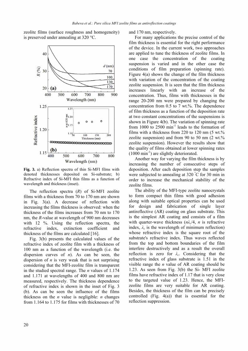
Fig. 3. a) Reflection spectra of thin Si-MFI films with denoted thicknesses deposited on Si-substrate; b) Refractive index of Si-MFI thin films as a function of wavelength and thickness (inset).
The reflection spectra (R) of Si-MFI zeolite films with a thickness from 70 to 170 nm are shown in Fig. 3(a). A decrease of reflection with increasing the films thickness is observed: when the thickness of the films increases from 70 nm to 170 nm, the R-value at wavelength of 900 nm decreases with 12 %. Using the reflection spectra, the refractive index, extinction coefficient and thickness of the films are calculated [16].
Fig. 3(b) presents the calculated values of the refractive index of zeolite film with a thickness of 100 nm as a function of the wavelength (i.e. the dispersion curves of n). As can be seen, the dispersion of n is very weak that is not surprising considering that the MFI-zeolite film is transparent in the studied spectral range. The n values of 1.174 and 1.171 at wavelengths of 400 and 800 nm are measured, respectively. The thickness dependence of refractive index is shown in the inset of Fig. 3 (b). As can be seen the influence of the films thickness on the n value is negligible: n changes from 1.164 to 1.175 for films with thicknesses of 70
and 170 nm, respectively. For many applications the precise control of the
film thickness is essential for the right performance of the device. In the current work, two approaches are applied to tune the thickness of zeolite films. In one case the concentration of the coating suspension is varied and in the other case the conditions of film preparation (spinning rate). Figure 4(a) shows the change of the film thickness with variation of the concentration of the coating zeolite suspension. It is seen that the film thickness increases linearly with an increase of the concentration. Thus, films with thicknesses in the range 20-200 nm were prepared by changing the concentration from 0.5 to 7 wt.%. The dependence of film thickness as a function of the deposition rate at two constant concentrations of the suspensions is shown in Figure 4(b). The variation of spinning rate from 1000 to 2500 min-1 leads to the formation of films with a thickness from 220 to 120 nm (5 wt.% zeolite suspension) and from 90 to 50 nm (2 wt.% zeolite suspension). However the results show that the quality of films obtained at lower spinning rates (1000 min-1) are slightly deteriorated.
Another way for varying the film thickness is by increasing the number of consecutive steps of deposition. After each deposition step the samples were subjected to annealing at 320 ºC for 30 min in order to increase the mechanical stability of the zeolite films.
The ability of the MFI-type zeolite nanocrystals to form compact thin films with good adhesion along with suitable optical properties can be used for design and fabrication of single layer antireflective (AR) coating on glass substrate. This is the simplest AR coating and consists of a film with quarter-wave thickness (nλc/4, n is refractive index, λc is the wavelength of minimum reflection) whose refractive index is the square root of the substrate's refractive index. Thus waves reflected from the top and bottom boundaries of the film interfere destructively and as a result the overall reflection is zero for λc. Considering that the refractive index of glass substrate is 1.51 in the visible range the n value of AR coating should be 1.23. As seen from Fig. 3(b) the Si- MFI zeolite films have refractive index of 1.17 that is very close to the targeted value of 1.23. Hence, the MFI-zeolite films are very suitable for AR coating. Besides, the thickness of the film can be precisely controlled (Fig. 4(a)) that is essential for the reflection suppression.

Babeva et al.: Pure silica MFI zeolite films as antireflection coatings
21
Fig. 4. Dependence of thickness of Si-MFI films on the concentration of the colloidal solution (a) and on deposition rate (b).
Fig. 5. Transmittance and reflection spectra of single layer antireflection coatings with thicknesses of 85 nm (AR1-dotted curve) and 170 nm (AR2-dashed curve) deposited on both sides of glass substrate (solid curve).
Figure 5 presents two AR coatings for the visible and near infrared spectral range. For quarter wave optical thickness of 400 nm, (i.e 4nd = 400 nm) the thickness of AR coating should be 85.5 nm, while for 800 nm, the d value should be 171 nm. For the deposition of films with the desired thicknesses, colloidal solutions of Si-MFI nanocrystals with concentrations of 2.7 and 5.8 wt.% respectively are prepared. The films are deposited on both sides of
the glass substrate. The films transmission and reflection spectra are presented in Fig.5 along with the spectra of the bare glass substrate. It is seen that both films (AR1 and AR2) operate as antireflection coatings: a decrease of R and increase of T are observed in the whole studied spectral range. Besides minimum reflection of 0.36 % has been reached (see AR2 curve). The mean value of R in broad spectral range (600-1200 nm) is below 1%. Simultaneously an increase in transmission with 6 % is observed.
CONCLUSIONS
The optical properties of zeolite films obtained by spin coating of aqueous suspension of Si-MFI nanocrystals are investigated. It is demonstrated that zeolite nanocrystals are closely packed and form continuous films that cover the entire surface of the substrate. The optical characterization revealed that the Si-MFI film exhibits refractive index from 1.164 to 1.175 depending on the film thickness. Besides, two ways for controlling the films thickness are presented: variation of the concentration of coating suspension and spinning rate during deposition process. The potential of Si-MFI zeolite films for broadband antireflection (AR) application is demonstrated by fabrication of AR coating on both side of glass substrate.
Acknowledgements: The financial support from MEET, Materials for Energy Efficiency in Transport, INTERREG EC and Bilateral BAS-CNRS projects is acknowledged.
REFERENCES
1. R. M. Barrer, Hydrothermal Chemistry of Zeolites, Academic Press, London, 1982
2. J. Čejka, A. Corma and S. Zones, Zeolites and Catalysis: Synthesis, Reactions and Applications, New York, Wiley-VCH, 1st ed., 2010.
3. E.M. Flanigen, R.W. Broach, S.T. Wilson, in: Zeolites in Industrial Separation and Catalysis, ed. S. Kulprathipanja, Wiley VCH, Weinheim, 2010, pp. 1–26. (3)
4. T. Bein, S. Mintova, Stud. Surf. Sci. Catal., 157, 263, 2005.
5. Z. B. Wang, H. T. Wang, A. Mitra, L.M. Huang, Y.S. Yan, Adv. Mater., 13, 746, 2001.
6. S. Mintova, M. Reinelt, T. H. Metzger, J. Senker and T. Bein, Chem. Commun., 3, 326, 2003.
7. C.H. Chen, S-Yi Li, A.S.T. Chiang, A.T. Wu, Y.S. Sun, Sol. Energ. Mat. Sol. Cells, 95, 1694, 2011.
8. X. Xu, J. Wang, Y. Long, Sensors, 6, 1751, 2006.

Babeva et al.: Pure silica MFI zeolite films as antireflection coatings
22
9. Y. Zheng, X. Li, P.K. Dutta, Sensors, 12, 5170, 2012.
10. F.M. Hinterholzinger, A. Ranft, J.M. Feckl, B. Ruhle, T. Bein, B. V. Lotsch, J. Mater. Chem., 22, 10356, 2012.
11. T. Babeva, R. Todorov, B. Gospodinov, N. Malinowski, J. El Fallah, S. Mintova, J. Mater. Chem., 22, 18136, 2012.
12. Z.B. Wang, A.P. Mitra, H.T. Wang, L.M. Huang, Y.S. Yan, Adv. Mater., 13, 1463, 2001.
13. S. Mintova, T. Bein, Adv. Mater., 13, 1880, 2001.
14. S. Mintova, N.H. Olson, J. Senker, T. Bein, Angew. Chem., 41, 2558, 2002.
15. L. Lakiss, I. Yordanov, G. Majano, T. Metzger and S. Mintova, Thin Solid Films, 518, 2241, 2010.
16. B. Gospodinov, J. Dikova, S. Mintova, T. Babeva, J. Phys. Conf. Ser., 398, 1742, 2012.
SI-MFI ЗЕОЛИТНИ ФИЛМИ КАТО АНТИОТРАЖАТЕЛНИ ПОКРИТИЯ
Ц. Бабева1*, Х. Авала2, М. Василева1, Дж. Ел Фаллах2, К. Лазарова1, С. Минтова2*
1Институт по оптически материали и технологии "Акад. Й. Малиновски", Българска aкадемия на науките, ул. "Акад. Г. Бончев", бл. 109, София 1113, България
2Лаборатория по катализ и спектроскопия, Университет на Каен, бул. Маршал Жуин, 6, Каен 14050, Франция
Постъпила на 17 октомври 2013 г.; коригирана на 25 ноември, 2013 г.
(Резюме)
Si-MFI зеолитни нанокристали (35 nm) са отложени като тънки слоеве посредством метода на центрофужното нанасяне. Показателите на пречупване и поглъщане, както и дебелината са определени от измерените спектри на отражение чрез нелинейно фитване. Дебелината на отложените слоеве е калибрирана като функция на концентрацията на суспензията и скоростта на отлагане. Показано е, че Si-MFI слоеве с подходяща дебелина, отложени върху двете повърхности на стъклена подложка могат да се използват като антиотражателни покрития. Наблюдавано е намаляване на отражението във видимата област на спектъра с 7.5 %, като едновременно с това пропускането нараства с 6%.

23
Bulgarian Chemical Communications, Volume 45, Special Issue B (pp. 23-27) 2013
Sol-gel derived Nb2O5 thin films for photonic applications
K. Lazarova*, M. Vasileva, G. Marinov, T. Babeva
Institute of Optical Materials and Technologies "Acad. J. Malinowski", Bulgarian Academy of Sciences, Acad. G. Bonchev Str. Bl. 109, 1113 Sofia, Bulgaria
Received October 17, 2013; Revised November 25, 2013
The fabrication and optical characterization of thin Nb2O5 films, obtained by spin coating of Nb sol on silicon substrate are presented. The Nb sol is prepared by sonocatalytic method using niobium chloride as a source for Nb and ethanol for solvent. The structure and morphology of the films are inspected through XRD and SEM measurements. Refractive index, extinction coefficient and thickness of the films are determined from measured reflectance spectra using non-linear curve fitting method. The impacts of ageing of the Nb sol, the duration of sonocatalytic treatment and post deposition annealing on the optical properties and thickness of the films are investigated. The possibility for fabrication of one dimensional photonic crystals using Nb2O5 and SiO2 as high and low refractive index materials is discussed.
Keywords: sol-gel materials; Nb2O5 films; optical properties; optical characterization; spin-coating
INTRODUCTION
In recent years there is an increased scientific interest in Niobium pentoxide (Nb2O5) material because it is thermodynamically most stable as compared to other stoichiometries of niobium oxide and shows excellent chemical stability and corrosion resistance in both acidic and alkaline media [1]. Most often Nb2O5 was studied from the application in smart windows point of view and hereof the investigations of its properties are mainly devoted to optimization of its electrochromic behavior [2,3]. However, due to its interesting photoelectric and photocatalytic properties [4,5] Nb2O5 films may find application in different devices such as batteries and nanocrystalline solar cells [6,7], sensors [8], or transparent conductive electrodes [9]. A number of novel applications of Nb2O5 films rely on the ability to deposit high quality films with relatively simple and inexpensive techniques. Among various deposition techniques used for production of thin films from Nb oxides, the sol-gel method emerges as an attractive deposition method because of its versatility, low cost and low temperature processing [6]. Two types of precursors are currently used for formation of sol-gel Nb2O5 films: metal alkoxides (Nb ethoxide) [1] or metal salt-NbCl5 [10]. The last one is preferred because of the lower price and weaker sensitivity to moisture as compared to the organic one.
For development of film application areas and implementation of Nb2O5 sol gel films in optical devices it is essential to characterize and optimize film properties (refractive index and extinction coefficient) and to be able precisely to control the film thickness. However, according to our knowledge there are only few studies on optical properties of sol-gel Nb2O5 films mainly concerning the determination of optical band gap and optical absorption [1,10,11]. The present paper studies the optical properties of thin sol-gel Nb2O5 films obtained by spin coating and their dependences on the duration of sonocatalytic treatment, time of sol ageing and post deposition annealing. The possibility of fabrication of one-dimensional photonic crystals is discussed.
EXPERIMENTAL DETAILS
The Nb sol was prepared by sonocatalytic method using NbCl5 (99%, Aldrich) as a precursor according to the recipe in [12]. Briefly, 0.400g NbCl5 was mixed with 8.3 ml ethanol (98%, Sigma-Aldrich) and 0.17 ml distilled water. The solution was subjected to sonification for 30 min and aged for 24 h at ambient conditions prior to spin coating. Transparent and stable sol was obtained easily and without additives.
Thin Nb2O5 films were deposited by dropping of 0.3 ml of the coating solution on pre-cleaned Si substrates and spin-on at a rate of 2500 rpm for 30 s. After the deposition, the films were annealed in
* To whom all correspondence should be sent: E-mail: [email protected]
© 2013 Bulgarian Academy of Sciences, Union of Chemists in Bulgaria

24
air at different temperatures in the range 60-650 oC for 30 min and have thicknesses of 35-40 nm. In order to obtain thicker films the coating procedure is repeated several times. Prior to the next deposition, the films are dried at 60 oC with hot air to prevent the wash out of the underneath layer. The surface morphology of the films and their structures were inspected by Philips 515 electron microscope and Philips 1710 X-ray difractometer, respectively. The optical properties were investigated through measurements of reflectance spectra of the films with CARY 05E UV-VIS-NIR spectrophotometer with accuracy of 0.3 %. The refractive index n, extinction coefficient k, and thickness d, of the films were determined using non-linear curve fitting method described in details elsewhere [13].
RESULTS AND DISCUSSION
The structure and surface morphology of Nb2O5 film annealed at 320 and 450 oC are shown in Fig. 1. It is seen that films have similar surface morphology at different temperatures while their structures change from amorphous at 320oC to polycrystalline at 450 oC.
Fig. 1. XRD spectra of Nb2O5 films on Si-substrates
annealed at 320 and 450 oC; Insets: SEM images of the films surface; the scale bar is 1μm.
In order to study the effect of the sol ageing on the optical properties and thickness of the films we prepared films at the same conditions but at different sol ageing time.
Fig. 2 presents reflectance spectra, refractive index and thickness of the prepared films. It is seen that during the first 10 days the films have very similar thicknesses (about 25-27 nm) while the refractive index decreases after period of 3 days. The most probable reason for the thickness increase of the films prepared from sol aged more than 10
days is the evaporation of the solvent and consequent increase of the sol concentration. Besides, we can speculate that the higher concentration of the sol prevents to some extent the reaction of polycondensation to take place, thus decreasing the refractive index. Another possible reason is particle aggregation that increases interparticles gaps thus decreasing the density and n values.
Our investigations on the influence of sonocatalytic treatment of the Nb sol prior the spin coating shows that higher refractive index are obtained for duration of 20 min. For shorter and longer time of sonification the values of n decrease. There is no influence on the thickness of the films.
In order to enable controllable tuning of the refractive index and thickness of the films we have studied the temperature dependence of optical properties of thin Nb2O5 films. Fig. 3 (a) presents the dispersion curves of n at different temperatures in the range 60 - 650 oC and the changes of d and n at wavelength of 600 nm with annealing (Fig 3(b)). Two different regimes of annealing are presented: i) consecutive annealing at 60, 120, 180, 320, 450 and
300 400 500 600 700 800 9000
5
10
15
20
25
30
0 5 10 15 20
2.0
2.2
2.4
2.6
0
10
20
3020
17
61
3
Ref
lect
ane
(%)
Wavelength (nm)
9
n
Duration (days) d
(nm
)
Fig. 2. Reflectance spectra of Nb2O5 films obtained from Nb sol aged for the denoted time; Inset: refractive index
(circles) and thickness (squares) of Nb2O5 films as a function of the ageing time
650 oC and ii) separate annealing at the specific temperature, i.e no cumulative annealing history. It is seen that the two regimes yield almost the same values of n and d. Besides, Nb2O5 films have similar values of n in the temperature range 120 - 650 oC (2.11-2.17). The most pronounced changes of n are for temperatures from 60 to 120 oC where n changes from 1.82 to 2.11, respectively. Similarly, a fast decrease of d is observed for temperatures in the range 60 - 180 oC followed by weak variation for T up to 650 oC.
Lazarova et al.: Sol-gel derived Nb2O5 thin films for photonic applications

25
Fig. 3(a) Dispersion curves for refractive index of Nb2O5
annealed at different temperatures; (b) temperature dependence of refractive index (squares) and thickness
(circles) of the films; the symbol interior shows different sequence of annealing - see the text.
The increase of n and decrease of d with annealing is due to removing of residual solvent and organic additives along with polymerization into a metal oxide network that takes place at high temperatures. The first also leads to densification of layers manifesting itself in the initial sharp decrease of thickness. It should be noted here that even at temperatures below 120 oC Nb2O5 films with high refractive index could be deposit. This can be regarded as an advantage because allows deposition of high refractive index materials onto heat-sensitive substrates.
For many applications the precise control of the film thickness is essential for right performance of the device. For example the implementation of Nb2O5 as a high refractive index building block of interference filters requires films with specific thickness to be deposited [14]. One way of tuning the film thickness is using sol with different concentrations. Our experiments show that very good linear dependence of film thickness as a function of sol concentration was obtained. Thus, by changing the concentration from 2.35 to 4.7 wt.% and repeating the coating procedure twice,
15 30 45 60 75
1.8
2.0
2.2
2.4
2.6
400
600
800
Ref
ract
ive
inde
x
Thickness (nm)
[nm]
Fig. 4. Thickness dependence of refractive index of Nb2O5 films at three different wavelengths.
400 500 600 700 800 9000
20
40
60
80
100
Wavelength (nm)
unpol 0o
p-pol 70o
s-pol 70o
Ref
lect
ance
(%
)
q-ODRband
Fig. 5. Calculated reflectance spectra for 11 layered quarter-wavelength stack of Nb2O5 and SiO2 films.
films with thicknesses from 19 to 75 nm are obtained. The ratio of film thicknesses from the first and second coating steps is equal to 2 and remains constant over the whole studied concentration range. Another possible way for obtaining thicker films is decreasing of deposition rate. However, our experiments show deterioration of the quality of the films at low rotation speeds.
For application of sol-gel derived Nb2O5 films in photonics it is very important the thickness dependence of refractive index to be studied. Fig. 4 presents the refractive index of Nb2O5 films as a function of thickness for 3 different wavelengths.
It is well seen from Fig. 4 that refractive index has similar values for film thicknesses in the range 20-60 nm while a decrease for thinner films and an increase for thicker is observed. Because refractive index can be directly connected to density of the films the obtained results indicate that the packing density increases with thickness manifesting itself in an increase of refractive index.
Lazarova et al.: Sol-gel derived Nb2O5 thin films for photonic applications

26
The final step of our investigation concerns the application of Nb2O5 films as high refractive index material in omnidirectional reflectors consisting SiO2 as low refractive index material. Fig. 5 presents calculated reflectance spectra of 11 layered stack from alternating Nb2O5 and SiO2 films with quarter-wave thicknesses.
It is seen that with increasing of angle of incidence from 0 to 70 degrees the reflectance band shifts towards shorter wavelengths, widening for s-polarization and narrowing for p-polarization. Quazi omnidirectional band opens up centered at 530 nm with width of 35 nm and maximum reflectance values of 71%. This means that the quarter-wave reflector of alternating Nb2O5 and SiO2 layers exhibits R > 71 % for incident angle range 0 - 70o and all types of polarizations.
CONCLUSIONS
Thin films from Nb2O5 were fabricated by sonocatalytic sol-gel method using inorganic precursor (NbCl5) dissolved in ethanol. The investigations of the sol ageing processes have shown that during the first week the films have identical thicknesses and similar values of refractive indices varying in the range 2.14-2.20 with the highest value reached after 3 days of ageing. A decrease in n and increase of d were observed afterwards. Two possible reasons were discussed: particles aggregation and increase of sol concentration. Further it was demonstrated that a precise control of film thickness could be achieved simply by controlling the sol concentration. The tuning of n in the range 1.82 to 2.20 could be achieved by post deposition annealing in the temperature range 60-650oC. Possible application of Nb2O5 films in quazi-omnidirectional reflectors was demonstrated.
Acknowledgement: The authors are grateful to J. Pirov and G. Maleshkova for XRD and SEM analysis.
REFERENCES
1. G. Agarwal, G. B. Reddy, J. Mater. Sci. - Mater. Electron., 16, 21 (2005).
2. A. Pawlicka, M. Atik, M. A. Aegerter, J. Mater. Sci. Lett., 14, 1568 (1995).
3. J. Livage, D. Ganguli, Sol. Energy Mater. Sol. Cells, 68, 365 (2001).
4. J. Gandhi, R. Dangi, S. Bhardwaj, Rasayan J. Chem., 1, 567 (2008).
5. P. Guo, M.A. Aegerter, Thin Solid Films, 351, 290 (1999).
6. M. A. Aegerter, Sol. Energy Mater. Sol. Cells, 68, 401 (2001).
7. R. Jose, V. Thavasi, S. Ramakrishna, J. Am. Ceram. Soc., 92, 289, (2009).
8. Y. Wang, L. Yang, Z. Zhou, Y. Li, X. Wu, Mater. Lett., 49, 277 (2001).
9. A. Dhar, T. L. Alford, J. Appl. Phys., 112, 103113 (2012).
10. D. Filho, P. Filho, U. Werner, M. Aegerter, J. Sol-Gel Sci. Technol., 8, 735 (1997).
11. B. Kościelska, M. Łapiński, W. Sadowski, M. Dęby, Photonics Letters of Poland, 3, 61 (2011).
12. N. J. Arfsten, J. F. Gavlas, US patent 6811901 B1, 2004
13. B. Gospodinov, J. Dikova, S. Mintova, T. Babeva, J. Phys.: Conf. series, 398, 012026 (2012).
14. F. Richter, H. Kupfer, P. Schlott, T. Gessner, C. Kaufmann, Thin Solid Films, 389, 278 (2001).
Lazarova et al.: Sol-gel derived Nb2O5 thin films for photonic applications

27
ТЪНКИ СЛОЕВЕ ОТ NB2O5, ПОЛУЧЕНИ ЧРЕЗ ЗОЛ-ГЕЛ МЕТОД С ПРИЛОЖЕНИЕ ВЪВ
ФОТОНИКАТА
К. Лазарова*, M. Василева, Г. Маринов, Ц. Бабева
Институт по оптически материали и технологии "Акад. Й. Малиновски", Българска Академия на науките, ул. "Акад. Г. Бончев", бл. 109, София 1113, България
Постъпила на 17 октомври 2013 г.; коригирана на 25 ноември, 2013 г.
(Резюме)
Настоящото изследване е фокусирано върху получаването и оптичното характеризиране на тънки слоеве от Nb2O5, получени чрез нанасяне от разтвор на Nb зол върху силициева подложка. Nb зол се получава чрез ултразвуково третиране на NbCl5 и етанол. Структурата и морфологията на слоевете е изследвана чрез XRD и SEM. Показателите на пречупване и поглъщане, както и дебелината се определят от измерените спектри на отражение чрез нелинейно фитване. Изследвано е влиянието на стареенето на зола, времетраенето на ултразвуковото третиране и температурата на нагряване върху оптичните параметри и дебелината на слоевете. Дискутирана е възможността за изработване на едноразмерен фотонен кристал от Nb2O5 и SiO2 като материали с висок и нисък показател на пречупване, съответно.
Lazarova et al.: Sol-gel derived Nb2O5 thin films for photonic applications

28
Bulgarian Chemical Communications, Volume 45, Special Issue B (pp. 28-32) 2013
Fabrication and characterization of high refractive index optical coatings by sol-gel method for photonic applications
T. Babeva*, K. Lazarova, M. Vasileva, B. Gospodinov and J. Dikova
Institute of Optical Materials and Technologies "Acad. J. Malinowski", Bulgarian Academy of Sciences, Acad. G.Bonchev Str. Bl. 109, 1113 Sofia, Bulgaria
Received October 17, 2013; Revised November 25, 2013
The deposition and characterization of thin Ta2O5, TiO2 and Nb2O5 film, obtained by the sol-gel methods using tantalum ethoxide, titanium isopropoxide and niobium chloride as precursors and specially developed water free sol-gel procedure are presented. Structure and morphology of the obtained layers are inspected through XRD and SEM measurements. Refractive index, extinction coefficient and thickness of the films are determined from reflectance spectra using non-linear curve fitting method. Refractive index values as high as 1.9, 2.28 and 2.39 are obtained for Ta2O5, TiO2 and Nb2O5 film, respectively at wavelength of 500 nm. The possibility of controlled tuning of optical properties by appropriate annealing is demonstrated. The application of coatings as high refractive index building blocks of one dimensional photonic crystals is discussed.
Keywords: sol-gel materials; Ta2O5; TiO2; Nb2O5; optical properties; spin-coating.
.
INTRODUCTION
In recent years there is an increased scientific interest in high refractive index thin film materials due to their applications for improving optical performance of different devices such as Bragg gratings, optical filters, waveguide-based optical circuits, photonic crystals, sensors etc [1-3]. Because of its high dielectric constant Ta2O5 is a promising dielectric material for high-density dynamic random access memory applications [4]. It was shown that thin sol-gel TiOx film could dramatically increase the efficiency and lifetime of organic solar cells by using it as an optical spacer, hole-blocking layer, and oxygen-protecting layer [5,6]. Emerging applications of Nb2O5 films in the areas of electrochromic coatings, batteries, and nanocrystalline solar cells were also discussed [7]. Among various deposition techniques used for production of thin films from metal oxides, the sol-gel method attracts considerable scientific interest because of its versatility, low cost ant low temperature processing [8,9]. Besides, it allows control of the microstructure of the coating and produces durable and chemically stable films [9].
Reliable and non-destructive measurements of thin film characteristics such as the film thickness and refractive index (or dielectric constant) are
beneficial for estimating the performance of films in the above mentioned applications. It is shown that the post-deposition annealing of sol-gel films had a pronounced impact on their structure, thickness and optical properties [5,10]. If the optical properties of sol-gel films can be controlled and optimized than the opportunity for variety of practical applications is opened up.
In this paper we study the optical properties of thin Ta2O5, TiO2 and Nb2O5 films obtained by the sol-gel method and subjected to annealing in the temperature range 60 - 650 oC. The possibility of controlled tuning of refractive index and thickness of the films is demonstrated. The potential of using the films as high refractive index counterparts of one dimensional photonic crystals was discussed.
EXPERIMENTAL DETAILS
Thin films from TiO2, Ta2O5 and Nb2O5 with thicknesses in the range 50-150 nm were prepared by using a sol–gel method. The Ti sol was prepared by method similar to that of Chrysicopoulou et. al.[11]. It is based on the hydrolysis of metal alkoxide in alcoholic solution in the presence of acid stabilizer. The main difference in our procedure is the complete absence of water in the prepared sol. Besides, due to the greater stability toward the humidity titanium tetra-isopropoxide
*To whom all correspondence should be sent: E-mail: [email protected]
© 2013 Bulgarian Academy of Sciences, Union of Chemists in Bulgaria

Babeva et al.:Fabrication and characterization of high refractive index optical coatings…
29
Ti(OC3H7)4 (97% Merck) was chosen as precursor instead of titanium tetra-ethoxide, used in the original recipe. The preparation procedure involved the dissolution of 6 ml of Ti(OC3H7)4 in 94 ml of isopropyl alcohol (C3H7OH, 97% Merck), followed by the addition of 0.05 ml of nitric acid (65 vol.%, Merck). Thus, the molar ratio between the constituents of solution was 1:63:0.01. The mixture was stirred at room temperature for 90 min to form slightly yellow transparent sol.
The tantalum sol was prepared according to the previously developed water free procedure [12]. Briefly, 35 ml of isopropyl alcohol were mixed with 1 ml of glacial acetic acid (CH3COOH, Sigma-Aldrich) and then 1.5 ml Ta(OC2H5)5 (99.98 %, Sigma-Aldrich) was slowly added. Second solution was prepared by mixing 2 ml glacial acetic acid with 15 ml isopropyl alcohol. After 30 min stirring both solutions were mixed and then 1 ml diethanolamine (HN(CH2CH2OH)2, 98%, Sigma-Aldrich) was added. The final mixture was transparent and colorless with pH of about 5. The obtained solution was subjected to slow stirring for 18 h. The solution was very stable and can be kept at ambient temperature for extended time.
The Nb sol was prepared by sonocatalytic method using NbCl5 (99%, Aldrich) as a precursor according to the recipe in [13]: 0.400g NbCl5 was mixed with 8.3 ml ethanol (98%, Sigma-Aldrich) and 0.17 ml distilled water. The solution was subjected to sonification for 30 min and aged for 24 h at ambient conditions prior to spin coating.
Thin TiO2, Ta2O5 and Nb2O5 films were deposited by dropping of 0.3 ml of the coating solution on pre-cleaned Si substrates and spin-on at a rate of 2500 rpm for 30 s. After deposition, the films were annealed in air at different temperatures in the range 60-650 oC for 30 min. The surface morphology of the films and their structures were inspected by Philips 515 electron microscope and Philips 1710 X-ray difractometer, respectively. The optical properties were investigated through measurements of reflectance spectra of the films with CARY 05E UV-VIS-NIR spectrophotometer with accuracy of 0.3 %.
RESULTS AND DISCUSSION
The surface morphology and the cross-section view of Ta2O5 film with thickness of 80 nm are presented in Fig. 1 (a) and 1 (b), respectively. It is seen that the film exhibits a uniform surface without any granular structure. The film is dense and smooth and covers the entire surface of the substrate. The top and side views of TiO2 and
Nb2O5 films are very similar to these of Ta2O5 shown in Fig. 1 and for sake of briefness are omitted from the results. The polycrystalline structure of the films annealed at 450 oC is confirmed by XRD measurements presented in Fig. 1 (c). The XRD spectra of films annealed at 320 oC (not shown here) indicate amorphous structure for Ta2O5 and weak initial crystallization for Nb2O5 films.
Fig. 1. Plane-view (a) and cross-section (b) SEM images
of Ta2O5 film; XRD spectra of Ta2O5 and Nb2O5 annealed at 40 oC for 30 min (c).
Fig. 2 presents refractive index and thickness of sol-gel derived Nb2O5, TiO2 and Ta2O5 films as a function of the annealing temperature. The values are averaged over 3 samples and the error bars present the deviations from the average value. The refractive index, n, extinction coefficient, k and thickness, d of the films were determined simultaneously from measured reflectance spectra using non-linear curve fittin g method described in details elsewhere [12]. The increase of n and decrease of d with annealing are clearly seen. The reasons are removing of residual solvent and organic additives along with polymerization into a metal oxide network that take place at high temperatures. The first also leads to densification of layers manifesting itself in decrease of thickness and increase of refractive index. The fastest decrease of d of Ta2O5 is due to the presence of bigger amount of organic additives in Ta sol (as acetic acid and diethanolamine) that are not used for preparation of Nb and Ti sols. From Fig. 2 it is seen that in the temperature range from 60oC to 650oC the refractive index of the films at wavelength of 600 nm varies in the range n = 1.818

Babeva et al.:Fabrication and characterization of high refractive index optical coatings…
30
- 2.169 for Nb2O5, n = 1.576 - 1.848 for Ta2O5 and n = 1.880 - 2.07 for TiO2 films. Simultaneously the thickness changes from 117 nm to 63 nm for Nb2O5, from 257 nm to 76 nm for Ta2O5 and from 66 nm to 44 nm TiO2 films. Annealing at temperature around 320 oC is sufficient to produce stable films. Further annealing does not lead to significant changes in both n and d. It should be noted here that the values of n for Ta2O5 and TiO2 films obtained in this study are lower as compared to those obtained in literature [10,14]. Different thicknesses and increased porosity in our case could be the possible reasons. The values of Nb2O5 films are in very good agreement with those obtained in [15].
Fig. 2. Refractive index at wavelength of 600 nm (a) and thickness (b) of Nb2O5 (square), TiO2 (circle) and Ta2O5 (triangle) films as a function of annealing temperature
One possible application of the studied oxides is in omnidirectional reflectors (ODR) that comprise alternating materials with high and low refractive index. Because ODR have high reflectance for all angles of incidence and types of light polarization they also are referred to as one-dimensional photonic crystals. Additional experiments on sol- gel derived SiO2 films show that they are suitable low-n materials for ODR (n = 1.435 – 1.391 for λ =
Fig. 3. Maximum reflectance calculated as a function of
number of the layers in the stacks consisting of alternating SiO2 and Nb2O5 (squares), SiO2 and TiO2
(triangles) and SiO2 and Ta2O5 (circles). The horizontal line indicates level of R = 98%
Fig 4. Calculated reflectance spectra for quarter-
wavelength stacks consisting of (a) 11 layers of Nb2O5 and SiO2; (b) 13 layers of TiO2 and SiO2 and (c) 19
layers of Ta2O5 and SiO2 films

Babeva et al.:Fabrication and characterization of high refractive index optical coatings…
31
400 – 800 nm). Fig. 3 presents the calculated values of maximum reflectance (Rmax) for stacks consisting of different number of layers of Nb2O5, Ta2O5 and TiO2 as high-n and SiO2 as low-n materials.
It is well seen that Rmax increases with the number of the layers in the stacks mostly pronounced for the stacks with the highest refractive index contrast. Thus to obtain R = 98% a different number of layers in the stack are needed: 11 layers of Nb2O5 and SiO2, 13 layers of TiO2 and SiO2 and 19 layers of Ta2O5 and SiO2. Fig. 4 presents the calculated reflectance spectra for angles of incidence of 0 and 60o for 11, 13 and 19 layered stacks of Nb2O5, TiO2 and Ta2O5, respectively combined with SiO2. With increasing of angle of incidence the reflectance band shifts towards shorter wavelengths, widening for s-polarization and narrowing for p-polarization. The overlap of reflectance bands is referred to as quazi-omnidirectional band (q-ODR). It consists of spectral range with high reflectance for all polarization types of light incident at angles from 0 to 60o. It is seen that for all three types of stacks a q-ODR band opens. However the reflectance value, the central wavelength and the width depends on the optical contrast. The widest band is for Nb2O5 / SiO2 stack (90 nm) that have the highest optical contrast. It is centered at wavelength of 550 nm and has reflectance value of 80 %. In order to obtain ODR band higher contrast is needed.
CONCLUSIONS
A specially developed water free sol-gel procedure was applied for deposition of thin Ta2O5, TiO2 and Nb2O5 films. Reflectance spectra of the films deposited on Si-substrates by spin coating were used for calculations of refractive index (n) and thickness (d) of the films by means of non-linear curve fitting method. The smallest values of n were obtained for Ta2O5 (1.848 at 600 nm) films and the highest - for Nb2O5 (2.169). The values of n for TiO2 are in the middle (2.072). An increase in n and decrease in d were observed with annealing. Two possible reasons are discussed: i) removing of
residual solvent and organic additives and ii) polymerization into a metal oxide network. The potential of using the films as building blocks of quazi-omnidirectional reflectors was demonstrated theoretically. Acknowledgements: The authors are thankful to Prof. S. Mintova, Dr. J. El Fallah and H. Awala from LCS-ENSICAEN, France for XRD and SEM measurements of Ta2O5 films and to J. Pirov form IOMT-BAS, Bulgaria for XRD measurements of Nb2O5.
REFERENCES
1. A. Cusano, A. Iadicicco, D. Paladino, S. Campopiano, A. Cutolo, M. Giordano, Opt. Fiber Techn. 13, 291 (2007).
2. W. F. Ho, M.A. Uddin, H. P. Chan, Polym. Degrad. Stab., 94 158 (2009).
3. T. Kohoutek, J. Orava, T. Sawada, H. Fudouzi, J. Colloid Interface Sci., 353 454 (2011).
4. S. Ezhilvalavan, T. Y. Tseng, J. Mater. Sci. - Mater. Electron., 10, 9 (1999).
5. J. Li, A. M. Deberardinis, L. Pu, M. C. Gupta, Appl. Opt. 51, 1131 (2012).
6. S. Cho, K. Lee, J. Heeger, Adv. Mater., 21, 1941 (2009).
7. M. A. Aegerter, Sol. Energy Mater. Sol. Cells, 68, 422 (2001).
8. A. Vioux, Chem. Mater., 9, 2292 (1997). 9. M. A. Aegerter, R. Almeida, A. Soutar, K.
Tadanaga, H. Yang, T. Watanabe, J. Sol-Gel Sci. Technol. 47, 203 (2008).
10. F. E. Ghodsi, F. Z. Tepehan, Sol. Energy Mater. Sol. Cells, 59, 367 (1999).
11. P. Chrysicopoulou, D. Davazoglou, C. Trapalis, G. Kordas, Thin Solid Films, 323, 188 (1998).
12. B. Gospodinov, J. Dikova, S. Mintova, T. Babeva, J.Phys.: Conf. series, 398, 012026 (2012).
13. N. J. Arfsten and J. F. Gavlas, US patent 6811901 B1, 2004.
14. R. Himmelhuber, P. Gangopadhyay, R. Norwood, D. Loy, N. Peyghambarian, Opt.Mater.Express, 1, 252 (2011).
15. M. A. Aegerter, Sol. Energy Mater. Sol. Cells, 68, 401 (2001).

Babeva et al.:Fabrication and characterization of high refractive index optical coatings…
32
ОТЛАГАНЕ И ХАРАКТЕРИЗИРАНЕ НА ЗОЛ-ГЕЛ ОПТИЧНИ ПОКРИТИЯ С ВИСОК ПОКАЗАТЕЛ НА ПРЕЧУПВАНЕ ЗА ПРИЛОЖЕНИЕ ВЪВ ФОТОНИКАТА
Ц. Бабева, K. Лазарова, M. Василева, Б. Господинов и Ю. Дикова
Институт по оптически материали и технологии "Акад. Й. Малиновски", Българска Академия на науките, ул. "Акад. Г. Бончев", бл. 109, София 1113, България
Постъпила на 17 октомври 2013 г.; коригирана на 25 ноември, 2013 г.
(Резюме)
Тънките слоеве от Ta2O5, TiO2 и Nb2O5 са получени по метода зол-гел посредством разработена процедура без използване на вода. Структурата и морфологията на слоевете е изследвана чрез рентгенова дифракция и електронна микроскопия, а оптичните им свойства - чрез нелинейно минимизиране на разликата между измерените и изчислените спектри на отражение. Демонстрирана е възможността за контролирано вариране на оптичните параметри и дебелината на слоевете чрез подходящо загряване. Дискутиран е потенциала на изучаваните филми за приложение като градивни блокове на едномерни фотонни кристали.

33
Bulgarian Chemical Communications, Volume 45, Special Issue B (pp. 33-37) 2013
Linear and non-linear optical properties of GeS2 doped with the elements from III and V group of the periodic table
J. Tasseva, V. Lozanova, R. Todorov*
Institute of Optical Materials and Technologies “Acad. J. Malinowski”, Bulgarian Academy of Sciences, Acad. G. Bonchev Str., bl. 109, 1113 Sofia, Bulgaria.
Received October 17, 2013; Revised November 25, 2013
The present paper summarizes the results from a study on the linear and nonlinear optical properties of GeS2 when adding elements from III and V group of the periodic table (Ga, In, Tl, As and Bi). The refractive index n and the optical band gap Eg
opt were calculated from the transmittance and reflectance spectra. The results showed that the doping of GeS2 with Tl or Bi leads to increase in the refractive index by about 0.2–0.3. The non-linear refractive index, γ, and the two-photon absorption coefficient, β, were evaluated by applying a formula developed by Sheik-Bahae. Each of the films studied exhibits a high non-linear refractive index at the telecommunication wavelength, 40–250 times higher than that measured for fused silica.
Keywords: chalcogenide glasses, non-linear refractive index, Sheik-Bahae formula
.
INTRODUCTION
The physical properties of chalcogenide glasses and their changes under exposure to light depend considerably on the composition and the conditions of deposition and illumination of the layers [1]. This is the reason for the intensive studies of the influence of the above parameters on the optical properties of thin films from the systems GexS(Se)1-
x [2, 3]. It is shown that the effect of photo-bleaching in thin Ge–S films is due to transformation of the homeopolar bonds in heteropolar ones and to a process of irreversible photo-oxidation [4, 5].
When a third element is incorporated in GeS2 it leads to considerable changes in its structure and properties. The addition of gallium and indium in the chalcogenide glasses is intensively investigated since the both elements makes the glassy network an appropriate host for rare-earth elements [6]. The glasses from Ge - S(Se) - In systems are attractive as materials for ultra-fast all optical switching, fiber amplifiers and glass ceramics [6].Ternary Ge-S-Bi glasses were studied during the last decade because the addition of 6–8 at.% of Bi to GeS2 changes the material type conductivity from p– to n–type. Small quantities of Bi or Tl cause some transformations in the glassy network of GeS2 forming different structural units which leads to changes in the band
gap as well as in the electrical [7] and optical [8-10] properties. However, the glasses from the Ge-S-Tl systems were not investigated systematically. Data for the structure and optical properties of Ge - S- Tl glasses and thin films can be found in [9, 10].
The aim of the present paper is to summarize the results of a study on the linear and nonlinear optical properties of GeS2 when adding elements of group III and V of the periodic table (Ga, In, Tl, As and Bi).
EXPERIMENTAL DETAILS
The synthesis of glasses from GexS100-x and (GeS2)100-xMex systems, where Me = Ga, In, Tl, As, Bi or Tl (for x = 4, 6 and 10 at.%) was accomplished in a silica ampoule at 970 °C for 14 h [10]. Cooling was carried out in ice water. Thin films were deposited on graphite and optical glass substrates BK-7, with a rate of evaporation of about 0.5 nm/s in high vacuum better than 10-3 Pa by thermal evaporation and stopping the process when the necessary film thickness was achieved. The composition of the thin films obtained was determined in a scanning electron microscope with an X-ray microanalyser Joel Superprobe 733 (Japan). The experiments were performed at an electron accelerating voltage of 25 kV and current of 1.4 nA and a scanning time of 200 s for each spectrum. Exposure was made by a halogen lamp
* To whom all correspondence should be sent: E-mail: [email protected] © 2013 Bulgarian Academy of Sciences, Union of Chemists in Bulgaria

Todorov et al.: Linear and non-linear optical properties of GeS2 doped with the elements…
34
(20 mWcm-2) in air. The transmittance (T) and reflectance (R) were measured by a Cary 5E spectrophotometer (USA) in the range 350–2000 nm to an accuracy of ΔT =±0,1% and ΔR = ±0,5%.
RESULTS AND DISCUSSION
The thin films from (GeS2)100-xMex systems where deposited by conventional thermal evaporation from previously prepared bulk glasses.
Table 1. Optical parameters (thickness, d, refractive index, n, Sellmeier coefficients A1 and A2, optical band gap, Eg
opt and slope parameter, B) of untreated thin GeS2 - Me films.
Composition d
[nm] n
(λ = 1550 nm) A1 A2
[nm] Eg
opt
[eV] B
[cm-1/2eV-1/2] GeS2 987 2.11 3.395 231.48 2.56 593
Ge20S80 744 2.04 3.086 230.13 2.77 706 Ge40S60 1137 2.55 5.376 257.77 1.85 645
Ge31S63Ga6 1078 2.13 3.435 249.74 2.35 529 Ge34.6S63.2In2.2 766 2.12 3.407 245.81 2.34 530
As5Ge35S60 878 2.43 4.736 267.55 2.07 588 Ge32S63Bi4 1122 2.06 3.181 240.98 2.47 576 Ge31S63Bi6 764 2.41 4.706 252.28 1.89 459 Ge32S64Tl4 990 2.22 3.822 236.75 2.39 576 Ge31S63Tl6 1263 2.26 3.955 238.136 2.26 535
The results from X-ray microanalysis for their composition are given in Table 1. The refractive index, n and thickness, d of thin Ge - S - Me films were calculated from the interference extrema in the transmission spectra using Swanepoel’s method [11, 12]. The program used to calculate n will determine it to an accuracy of 0.5 % for an error in the transmittance of 0.1 % [12]. The calculated values for n were extrapolated by Sellmeier’s equation:
22
2
212 1)(
A
An
(1)
where A1 and A2 are Sellmeier’s coefficients. The Sellmeier’s coefficients obtained for (1) with λ written in nm are presented in Table 1. At high values of the linear absorption coefficient α, where the condition αd ≥ 1 is fulfilled, α can be calculated from the equation:
)exp()1( 2 dRT (2)
Analysis of the strong absorption region
(54 1010 ) has been carried out using the
following well-known quadratic equation, often referred to as Tauc’s law [13]:
2)()( optgEhBh
(3)
where B is a substance parameter, which is in an inverse proportion to the width of the localized states in the density of states diagram, hν is the
photon energy and Egopt is the so called Tauc’s gap.
The results for the optical parameters of thin Ge-S-Me films are summarized in Table 1. It is seen that the inclusion of 2-6 at % of In, Tl, Bi, As in GeS2
leads to increasing of the refractive index and to decreasing of the width of the optical band gap, respectively. The influence of the gallium is not too notable due to the similar polarizability of its atoms to those of germanium.
Further we will consider the non-linear response of the chalcogenide medium to intense light with photon energies ħω<Eg
opt. We know that two-photon absorption would be involved in the interband transitions in that case [14]. One of the associated effects is the inducing of non-linear refractive index, n2[esu] or [m2/W]. It is known [15] that the intensity-dependent refractive index n’ can be expressed as:
22
2' E
nnInn (4)
where n is the linear, weak-field refractive index, I denotes the intensity and E - the strength of the applied optical field, and n2 gives the rate at which the refractive index increases with increasing the optical intensity. For prediction of the non-linear refractive index we have applied a formula, developed by Sheik-Bahae et al. [19] for crystalline semiconductors and successfully applied for the glasses and thin films from Ag-As-S-Se systems [16-17]. In the simple model n2 and can be expressed as:

Todorov et al.: Linear and non-linear optical properties of GeS2 doped with the elements…
35
SIcn
esun 402 and
optg
optg
p
EG
En
EcK
2422
(5)
where Ep = 21 eV, K is found to be 3.1 x 10⁻⁸ in units such that Ep and Eg
opt are measured in eV, and
is measured in m2/W, ħ is the reduced Plank’s constant, c – the speed of light in vacuum and G2 is a universal function:
6
2
35432
2 64
)21()21(24
3
4
3362
)(x
xxxxxxxxG
(6)
where is the Heaviside step function. In the same approximation, the two-photon absorption, βNL, originally defined by NLI ' (α' being the
intensity-dependant absorption coefficient), can be expressed:
)/2(232
optgopt
g
p
NL EFEn
EK
(7)
where
5
2/3
2 2
)12()2(
x
xxF
for 2х > 1 and F2(2x) = 0,
otherwise. That means that two-photon absorption occurs only for photon energies higher than at least half of the optical band-gap. It is shown [18] that the two-photon absorption possibly accompanying the high non-linear refractive index, γ, could prevent the optical switching effect, thus seriously limiting the applicability of any high third order
nonlinear material in all-optical switches. In Figs. 1-3 the dispersion of γ and β for chalcogenide layers from binary Ge-S and ternary Ge-S-Me systems are shown. For the films from binary Ge-S system it was obtained that the increase of Ge- content leads to approximately 5 times increased value of γ from 1.3310-18m2/W for the thin Ge20S80 film to 6.63 10-18m2/W for thin layer with composition Ge40S60 at wavelength λ = 1550 nm. The non-linear refractive index, γ of the glasses from Ge-S system depending on the germanium content is from ~ 4.8 to 250 times higher than that of fused SiO2. The influence of inclusions of 1-2 at % of gallium and indium in thin GeS2 films can be seen in Fig. 2. Due to similar polarizability of the gallium and germanium atoms, the inclusion of 4 at % of gallium affects poorly the non-linear parameters.
0.2 0.4 0.6 0.8 1.0 1.2 1.4 1.6
-4x10-18
0
4x10-18
8x10-18
1x10-17 a)
[m
2 /W]
h/Eg
opt
Ge20
S80
Ge33
S67
Ge40
S60
0.2 0.4 0.6 0.8 1.0 1.2 1.4 1.6
0
4x10-11
8x10-11
1x10⁻¹⁰
2x10⁻¹⁰ b)Ge
20S
80
Ge33
S67
Ge40
S60
[m
/W]
h/Eg
opt
Fig. 1. Dispersion of the non-linear refractive index, γ (a) and non-linear absorption coefficient,β (b) for thin chalcogenide layers from the binary GexS100-x (for x= 28, 33 and 40) system.

Todorov et al.: Linear and non-linear optical properties of GeS2 doped with the elements…
36
0.2 0.4 0.6 0.8 1.0 1.2 1.4 1.6
-2x10-18
0
2x10-18
4x10-18
6x10-18
8x10-18
a) Ge33
S67
Ge32
S64
Ga4
Ge31
S63
Ga6
Ge34
S63
In2
[m
2 /W]
h/Eg
opt 0.2 0.4 0.6 0.8 1.0 1.2 1.4
0
5x10-11
1x10⁻¹⁰
b) Ge33
S67
Ge32
S64
Ga4
Ge31
S63
Ga6
Ge34
S63
In2
[m
/W]
h/Eg
opt
Fig. 2. Dispersion of the non-linear refractive index, γ (a) and non-linear absorption coefficient, β (b) for thin chalcogenide layers from the ternary Ge-S-Ga(In) systems.
0.2 0.4 0.6 0.8 1.0 1.2 1.4 1.6
-4x10-18
0
4x10-18
8x10-18
1x10-17a) Ge
32S
64Bi
4
Ge32
S64
Tl4
Ge35
S60
As5
Ge31
S63
Bi6
Ge31
S63
Tl6
[m
2 /W]
h/Eg
opt0.2 0.4 0.6 0.8 1.0 1.2 1.4 1.6
0
5x10-11
1x10⁻¹⁰
2x10⁻¹⁰
2x10⁻¹⁰ b) Ge32
S64
Bi4
Ge32
S64
Tl4
Ge35
S60
As5
Ge31
S63
Bi6
Ge31
S63
Tl6
[m
/W]
h/Eg
opt
Fig. 3. Dispersion of the non-linear refractive index, γ (a) and non-linear absorption coefficient,β (b) for thin chalcogenide layers from the ternary Ge-S-As(Bi, Tl) systems.
Further increase of Ga or In content in the
films to~ 6 at % leads to increasing of the values of γ to ~2.7 10-18m2/W. For comparison, γ for GeS2 is ~1.6 10-18m2/W.
The influence of inclusion from Tl and Bi on the non-linear optical properties of Ge-S-Me films is demonstrated in Fig.3. The increase of thallium content from 4 to 6 at % in thin (GeS2)100-xTlx films increase the non-linear refractive index, γ from 2.3310-18m2/W to 3.7110-18m2/W at λ = 1550 nm.
The highest value for the non-linear refractive index, γ = 6.3810-18m2/W we obtained for the thin film with composition Ge31S63Bi6, which was approximately 4 times higher than those for the thin GeS2 coating index of fused SiO2. To understand the role of the different metals, which are subject of the investigation of the present work we used the proposed in [19] formula for the non-linear refractive index n2 and non-linear optical susceptibility, χ(3):
0
)3(
212
nn
, where
4
222)3(
)(4
o
do
E
EEA (10)
where A = 1.7.10-10 (for χ(3) in esu). E0 and Ed are dispersion parameters in the Wemple Di Domenico model [20]. n0 being the limit of the refractive index dispersion as ħω approaches 0. It is seen from equations (10) that the non-linear refractive index is in direct proportion to the fourth power of the dispersion energy, Ed. According to [20] the dispersion energy, Ed is related with the coordination number, Nc of the cations by the following equation - Ed= βNcZaNe, where Za is the formal chemical valence of the anion, Ne is the effective number of valence electrons per anion, and β is a two-valued constant with either an ionic or covalent value (β = 0.26 ± 0.03 eV and β = 0.37 ± 0.04 eV, respectively). According to [6] the

Todorov et al.: Linear and non-linear optical properties of GeS2 doped with the elements…
37
gallium and indium are four-fold coordinated in the glasses from Ge-S-Ga (In) systems forming tetrahedral units (GaS4, InS4) while the thallium atoms are univalent forming bonds with non-bridging sulfur in terminal bonds Ge+-S- from the type GeS4Tl [13]. The atoms of As and Bi are three-fold coordinated in the glasses from Ge-S-As(Bi) systems creating pyramidal structural units (AsS3, BiS3) [5, 8].
CONCLUSION
In the present work it is demonstrated the influence of elements of III and V group of the periodic table (Ga, In, Tl, As and Bi) on the linear and non-linear optical properties of thin Ge-S-Me films. The results showed that the doping of GeS2 with Tl or Bi leads to increase in the refractive index by about 0.2-0.3.Applying the formula proposed by Sheik-Bahae et al. [15], it was found that the non-linear refractive index can be in the range of 4-250 times higher than that of fused SiO2. The increase in the linear and non-linear refractive indices was explained on the basis of the model, proposed by Wemple and DiDomenico [20].
REFERENCES
1. P.J.S. Ewen and A. E. Owen, in: M. Cabal and J. M. Parker (Eds.), High Performance Glasses, Blackie, London, 1992, p. 287.
2. L. Tichy, H. Ticha, J. Blecha and M. Vlcek, Mater. Lett., 17, 268 (1993).
3. E. Marquez, P. Nagels, J. M. Gonzalez-Leal, A. M. Bernal-Oliva, E. Sleeckx, R. Callaerts, Vacuum, 52, 55(1999).
4. L. Tichy, H. Ticha, K. Handlir, K. Jurec, Phil. Mag. Lett., 58, 233 (1988).
5. L. Tichy, H. Ticha, K. Handlir, K. Jurec, J. Non-Cryst. Solids, 101, 223 (1988).
6. M. Guignard, V. Nazabal, A. Moreac, S. Cherukuluappurath, G. Boudebs, H .Zeghlache, G. Martinelli, Y. Quiquempois, F. Smektala, J-L.Adam, J. Non-Cryst. Solids, 354, 1322 (2008).
7. M. Afifi, M.M. Abdel-Aziz, H.H. Lahib, M. Fadel, E.G. El-Metwally, Vacuum, 61, 53 (2001).
8. M. Polcik, J. Drahokoupil, I. Drbohlav, L.Tichy, J. Non-Cryst.Solids, 192&193, 380 (1995).
9. M. Bokova, I. Alekseev, E. Bychkov, Physics Procedia, 44, 35 (2013).
10. R. Todorov, Tz. Iliev, K Petkov, J. Non-Cryst. Solids, 326/327, 263 (2003).
11. R. Swanepoel, J. Phys. E: Sci. Instrum. 16, 1214 (1983).
12. R. Todorov, J. Tasseva, Tz. Babeva, K. Petkov, J. Phys. D: Appl. Phys., 43, 505103 (2010).
13. J. Tauc, Amorphious and liquid semiconductors, Plenum Press, New York, 1974.
14. R. W. Boyd, Nonlinear Optics, Academic Press, Elsevier Science, USA, 2003.
15. M. Sheik-Bahae, A. A. Said, W. Tai-Huei, D.J. Hagan, E.W. Van Stryland, IEEE J. Quantum Electron., 26, 760 (1990).
16. T.I. Kosa, R. Rangel-Rojo, E. Hajto, P.J.S. Ewen, A. E. Owen, A.K. Kar, B.S. Wherrett, J. Non-Cryst. Solids, 164/166, 1219 (1993).
17. J. Tasseva, R. Todorov, K. Petkov, J. Optoelectron. Adv. Mater., 11, 1257 (2009).
18. V. Mizhari, K.W. De Long, G.I. Stegeman, Opt. Lett. 14, 1140 (1989).
19. H. Ticha, L. Tichy, J. Optoelectron. Adv. Mater., 4, 381 (2002).
20. S.H. Wemple and M. DiDomenico, Phys. Rev. B, 3, 1338 (1971).
ЛИНЕЙНИ И НЕЛИНЕЙНИ ОПТИЧНИ СВОЙСТВА НА GES2 ДОТИРАН С ЕЛЕМЕНТИ ОТ III И V ГРУПА НА ПЕРИОДИЧНАТА ТАБЛИЦА
Й. Тасева, В. Лозанова, Р. Тодоров
Институт по оптични материали и технологии "Акад. Й. Малиновски", Българска Академия на науките, ул. Акад. Г. Бончев, бл., Бл. 109, 1113 София, България.
Постъпила на 17 октомври 2013 г.; коригирана на 25 ноември, 2013 г.
(Резюме)
Настоящото изследване е обобщение на резултатите от проучване на линейни и нелинейни оптични свойства на GeS2 при добавяне на елементи от III и V група на периодичната таблица (Ga, In, Tl, и Bi). Резултатите показват, че внасянето на Tl или Bi води до увеличаване на линейния и нелинейния показатели на пречупванe.

38
Bulgarian Chemical Communications, Volume 45, Special Issue B (pp. 38-42) 2013
Thickness dependence of the optical properties of amorphous As-Ge-S thin films
R. Todorov*, A. Lalova and J. Tasseva
[email protected] Institute of Optical Materials and Technologies “Acad. J. Malinowski”, Bulgarian Academy of Sciences, Acad. G.
Bonchev Str., bl. 109, 1113 Sofia, Bulgaria.
Received October 17, 2013; Revised November 25, 2013
In this paper we present some results from the study of the optical properties of thin As - S - Ge films and their dependence on the composition and film thickness. The optical constants (refractive index, n and extinction coefficient, k) were calculated using both measured transmittance, T and reflectance, R spectra. The thickness dependence of the optical properties of thin As - S - Ge layers was investigated. The results for the refractive index showed that the optical constants of As - S - Ge films thicker than 80 nm are independent on the film’s thickness. For the films thinner than 80 nm the refractive index is strongly influenced by the substrate and depends on the process of the thin films growth. We used the Bruggeman model for determination of the porosity of the thin films. It was established that the porosity of the films increases with 25 % when the film’s thickness decreases from 80 to 30 nm.
Keywords: optical properties, thin films, chalcogenide glass, refractive index.
INTRODUCTION
Chalcogenide glasses are characterized with high refractive index and wide region of transparency in the infrared. It is well known that the exposure to light of thin chacogenide films initiates changes in their refractive index and thickness [1]. Most applications of chalcogenide glasses and thin films are based on the photoinduced phenomena in these materials and on the respective changes in their optical properties [2 - 4].
Chalcogenide glasses and thin films from As - Ge - S system are of a great interest because of their large glass-formation region and high optical non-linearity [5-6]. The possibility of varying their refractive index in a wide range by changing their composition make them perspective candidates for fabrication of chalcogenide photonic crystals and Bragg gratings. Until now, most of the experiments on studying their optical properties were carried out on bulk samples and thin films with a thickness between 1 and 5 m [7-8]. Furthermore, these materials can be deposited in very thin films (with a thickness smaller than 1 m) in order to build photonic integrated circuits. The better knowledge
of the optical constants (n, k) and thickness of thin chalcogenide films is of great importance for understanding the mechanism of the optical processes and will benefit their practical applications. For the design of multilayered systems it is very important to know the thickness dependence of the optical constants as well as to be able to accurately monitor the deposition process. It would open up the possibility of controllable tuning of the optical properties of thin chalcogenide films.
The main goal of the work is to study the optical properties of thin amorphous As - S - Ge films depending on their thickness and composition. We have also shown how the optical constants are influenced by the rate of thermal evaporation.
EXPERIMENTAL DETAILS
The synthesis of glasses from As40-xGexS60 was accomplished in a silica ampoule at 970°C for 14 h [9]. Cooling was carried out in ice water. Thin films were deposited by thermal evaporation on graphite and optical glass substrates BK-7, with evaporation rate of about 0.5 nm/s in high vacuum better than 10-3Pa. The process was interrupted when the target film thickness was achieved. The composition of the thin films obtained was determined in a scanning electron microscope with X-ray microanalyser Joel Superprobe 733 (Japan). * To whom all correspondence should be sent:
E-mail: [email protected]
© 2013 Bulgarian Academy of Sciences, Union of Chemists in Bulgaria

Todorov et al.: Thickness dependence of the optical properties of amorphous As-Ge-S thin films
39
Exposure to halogen lamp (20 mWcm-2) was performed in air. The transmittance (T) and reflectance (R) were measured by a Cary 5E UV–VIS–NIR spectrophotometer (USA) in the range 350–2000 nm to an accuracy of ΔT = ±0,1% and ΔR = ±0,5%.
RESULTS AND DISCUSSION
The optical constants (refractive index, n and extinction coefficient, k) and thickness, d, of the thin As40-xGexS60 films (for x = 10, 20, 30) were calculated using transmittance and reflectance measurements and applying the double methods developed by Theye and Abeles [10-12] for the films in the thickness range from 20-130 nm and through the conventional Swanepoel’s method for thicker films [13].
The method of calculation of the optical constants of thin films in the thickness range of 20-130 nm is based on minimization of the discrepancy between theoretically calculated (T(n(), k(), d) and R(n(), k(), d)) and experimentally measured values Texp. and Rexp. of the transmittance and reflectance at normal incidence, until the difference becomes lower than the accuracy of the measurements, T and R [10, 11].
T(n(), k(), d) – T exp. =T
R(n(), k(), d) – R exp. = R (1)
Discontinuities appear in the solution for n and k due to the necessity of knowing the correct film thickness and loss of solutions in the interference extrema. The thickness d is not computed from the system (1), but is introduced as a parameter. For an initial approximation for the thickness we used the value, measured by a profilometer with an accuracy of ± 5 nm. Hence, varying the thickness slightly around the approximate one, we chose the value, yielding the smallest discontinuities in the solution for n and k. The accuracy in the determination of the refractive index, n, was better than ±0.005 and for the absorption coefficient, k, around the absorption edge it was about ±0.01 [14]. The accuracy of the methods in determining d is better than ±1 nm [14].
The results for films in thickness range of 20-130 nm were compared with the optical constants of thin films with thickness ~ 1.0 μm calculated by the Swanepeol’s method [13] and the procedure presented in [14]. The dispersion of the refractive index for thin As40-xGexS60 films for x= 10, 20, 30 is presented in Figs. 1 and 2.The dispersion curves of
unexposed and exposed one-micron thick films with the same compositions are given with continuous or broken lines, respectively. It is seen that the refractive index of the unexposed film with composition As20Ge20S60 and thickness 80 nm is the same as the one of the one-micron thick layer. In the case of As10Ge30S60 it is observed reduction of the values of n of the unexposed film with thickness 52 nm in respect to the dispersion for the 1 µm one. Smaller photo-induced changes of the refractive index are observed for the 1 µm thick films from both compositions.
400 600 800 1000 1200 1400 16001.8
2.0
2.2
2.4
2.6
2.8
b)
As10
Ge30
S60
unexposed d=52 nm exposed d=57 nm
n
[nm]
Fig. 1. Comparison of the dispersion of the refractive indices of thin As-Ge-S films for d< 0.1μm (symbols)
and d~ 1.0 μm (lines).
The photo-induced changes for thin As30Ge10S60 are negligible and are not presented in Fig. 1. Obtained changes for the refractive index after illumination was Δn = 0.01.
One possible reason for negligible changes in As30Ge30S60 film is that in some ternary Ge-As-S(Se) materials, photo-darkening and photo-bleaching might be compensated by an appropriate choice of composition leading to photo-stability effect [15]. Such hypothesis could be interesting for the concept of intrinsically photo-stable amorphous chalcogenides. Therefore attention of this work is thus focused on As30Ge10S60 thin films optical
400 600 800 1000 1200 1400 16001.8
2.0
2.2
2.4
2.6
2.8
a)
As20
Ge20
S60
unexposed d = 80 nm exposed d = 85 nm
n
[nm]
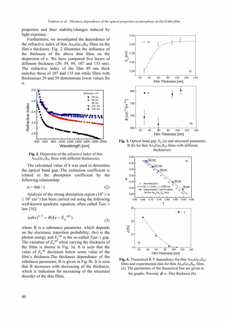
Todorov et al.: Thickness dependence of the optical properties of amorphous As-Ge-S thin films
40
properties and their stability/changes induced by light exposure.
Furthermore, we investigated the dependence of the refractive index of thin As30Ge10S60 films on the film’s thickness. Fig. 2 illustrates the influence of the thickness of the above thin films on the dispersion of n. We have compared five layers of different thickness (29, 59, 89, 107 and 135 nm). The refractive index of the film 89 nm thick matches those of 107 and 135 nm while films with thicknesses 29 and 59 demonstrate lower values for n.
400 600 800 1000 1200 1400 1600 1800 2000
2.0
2.2
2.4
2.6
2.8thickness, nm
Re
fra
ctiv
e in
dex
Wavelength [nm]
29 nm 59 nm 89 nm 107 nm 135 nm
Fig. 2. Dispersion of the refractive index of thin
As30Ge10S60 films with different thicknesses.
The calculated value of k was used to determine the optical band gap. The extinction coefficient is related to the absorption coefficient by the following relationship:
α = 4πk / λ (2)
Analysis of the strong absorption region (104 ≤ α ≤ 105 cm-1) has been carried out using the following well-known quadratic equation, often called Tauc’s law [16]:
)()( 2/1 optgEhBh
(3)
where B is a substance parameter, which depends on the electronic transition probability, (hν) is the photon energy and Eg
opt is the so-called Tauc’s gap. The variation of Eg
opt when varying the thickness of the films is shown in Fig. 3a. It is seen that the value of Eg
opt decreases below some value of the film’s thickness.The thickness dependence of the substance parameter, B is given in Fig 3b. It is seen that B decreases with decreasing of the thickness, which is indication for increasing of the structural disorder of the thin films.
20 40 60 80 100 120 140
2,28
2,32
2,36
2,40
2,44
a)
Eg [e
V]
Film Thickness [nm]
Eg
20 40 60 80 100 120 140650
700
750
800
b)
B [c
m-1
/2eV
-1/2]
Film Thickness [nm]
B
Fig. 3. Optical band gap, Eg (a) and structural parameter,
B (b) for thin As30Ge10S60 films with different thicknesses.
0.60 0.65 0.70 0.75 0.80 0.85 0.90 0.95
0.05
0.10
0.15
0.20
0.25
0.30
0.35
1020
3040
50
60
70
80
90
100110
120130
140150 a)
29 nm
59 nm
89 nm
107 nm
135 nm
R
T
theoretical for n = 2.32, k = 0.001, = 1550 nm
experimental T and R values for thin As
30Ge
10S
60 films
20 40 60 80 100 120 1400
10
20
30
b)
[%
]
Film Thickness [nm]
Fig. 4. Theoretical R-T dependence for thin As30Ge10S60 films and experimental data for thin As30Ge10S60 films (a). The parameters of the theoretical line are given in
the graphs. Porosity vs. film thickness (b).

Todorov et al.: Thickness dependence of the optical properties of amorphous As-Ge-S thin films
41
Theoretical T-R dependence for thin films with refractive index n = 2.32, k = 0.001 and d = 20 - 160 nm at λ = 1550 nm and experimental results for thin As30Ge10S60 films are shown in Fig. 4. It is seen that thin films with thickness larger than 90 nm follow the theoretical line while at smaller thicknesses a deviation of the experimental results is observed. The above results are in agreement with previous reports, which claim the existence of a critical value for d, above which optical constants are thickness independent [12, 17].
We used the effective medium theory for determination of the porosity of the thin films. According to the Bruggeman model, a porous semiconductor material can be considered as a mixture of two phases and its effective refractive index neff in the non-absorbing region follows the equation:
2
23/1
2
2
2
2
2
2
1
1
c
d
c
eff
c
d
c
eff
n
n
n
n
n
n
n
n
(4)
where nc and nd are the refractive indices of the continuous media and pores, respectively, while is the porosity. We have considered as continuous media the thin films deposited at normal incidence and duly used the data obtained for their refractive index. We found that the values for varied in the range of 0.2 % to 23 % for thin films with thicknesses 88 and 29 nm. The increasing in the porosity of the thin layers with d <80 nm is a probable cause for the increasing of the photo-induced changes in the refractive index. The increase of the porosity probably results in increased flexibility of the glass network, and also enables oxygen from the air to penetrate into the volume of the thin layer. According to [18], the oxidation process leads to a substantial increase of the effect of photobleaching (increase in the width of the band gap) and therefore a reduction in the refractive index.
CONCLUSIONS
In the present work the influence of the thickness on the optical constants of thin As-Ge-S films and their photo-induced changes were investigated. It was established that the refractive index and optical band gap decrease for the film
thickness smaller than 80 nm. The photo-induced changes of the refractive index and optical band gap increase when film’s thickness decrease. Through applying the model for the effective media proposed by Bruggeman we found that the values for porosity varied in the range of 0.2 % to 23 % for the thin films in the thicknesses range 88 -29 nm. The increase of porosity probably results in enhanced flexibility of the glass network and oxidation processes into the volume of the thin layer.
REFERENCES
1. A. Zakery, S.R. Elliott, J. Non-Cryst. Solids, 330, 1 (2003).
2. P.J.S. Ewen and A.E. Owen, in: High Performance Glasses, M. Cabal, J.M. Parker (Eds.), Blackie, London, 1992, p. 287.
3. S. Elliot, Clacogenide glasses (Chapter 7) in: Materials Science and Technology, J. Zarzycki (Ed.), vol. 9, VCH, Weinheim, 1991 p.376.
4. K. Shimakawa, A. Kolobov, S.R. Elliott, Adv. Phys., 44, 475 (1995).
5. Z. Borisova, Glassy Semiconductors, Plenum Press, New York, 1981.
6. K. Petkov, P.J.S. Ewen, J. Non-Cryst. Solids, 249, 150 (1999).
7. D.A. Minkov, J. Phys. D: Appl. Phys., 22, 1157 (1989).
8. K. Petkov, B. Dinev, J. Mater. Sci., 29, 468 (1994).
9. R. Todorov, K. Petkov, J. Optoelectron. Adv. Mat., 3, 311 (2001).
10. F. Abeles, M.L. Theye, Surf. Sci., 5, 325 (1966). 11. Y. Laaziz, A. Bennouna, N. Chahboun, A.
Outzourhit, E.L. Ameziane, Thin Solid Films, 372, 149 (2000).
12. R. Todorov, A. Lalova, K. Petkov and J. Tasseva, Semicond. Sci. Tech., 27, 115014 (2012).
13. R. Swanepoel, J. Phys. E: Sci. Instrum. 16, 1214 (1983).
14. R. Todorov, J. Tasseva, Tz. Babeva, K. Petkov, J. Phys. D: Appl. Phys., 43, 505103 (2010).
15. P. Němec, S. Zhang, V. Nazabal, K. Fedus, G. Boudebs, A. Moreac, M. Cathelinaud, and X.-H. Zhang, Opt. Express, 18, 22944 (2010).
16. J. Tauc, Amorphious and liquid semiconductors, Plenum Press, New York, 1974.
17. R Todorov, J Tasseva, V. Lozanova, A. Lalova, Tz Iliev, A Paneva, Adv. Condens. Matter Phys., 2013, 308258, (2013).
18. L. Tichy, H. Ticha, P. Nagels and E. Sleeckx, Opt. Mater., 4, 771 (1995).
Todorov et al.: Thickness dependence of the optical properties of amorphous As-Ge-S thin films
42
ЗАВИСИМОСТ НА ОПТИЧНИТЕ СВОЙСТВА НА АМОРФНИ As-Ge-S ТЪНКИ ФИЛМИ ОТ ДЕБЕЛИНАТА
Р. Тодоров, А. Лалова, Й. Тасева
Институт по оптични материали и технологии "Акад. Й. Малиновски", Българска Академия на науките, ул. Акад. Г. Бончев, бл. 109, 1113 София, България.
Постъпила на 17 октомври 2013 г.; коригирана на 25 ноември, 2013 г.
(Резюме)
В тази статия са представени резултати от изследване на оптичните свойства на тънки As - S - Ge филми и зависимостта им от състава и дебелината на филмите. Оптичните константи (показател на пречупване, n и показател на поглъщане, k) са определени от спектрите на пропускане, Т и отражение, R. Резултатите за показателя на пречупване показаха, че оптичните константи на As - S - Ge филми за стойности на d> 80 nm не зависят от дебелината на филма. За тънки филми с d< 80 nm стойността на показателя на пречупване е силно повлияна от подложката и зависи от условията на отлагане на тънкия слой. Моделът на Bruggeman е използван за определяне на порьозността на тънки слоеве. Установено е, че порьозността на филмите нараства с 25%, когато дебелината на слоевете намалява.

43
Bulgarian Chemical Communications, Volume 45, Special Issue B (pp. 43-46) 2013
Grain size effect on the optical properties of thin silver films
Vesela Lozanova, Jordanka Tasseva, Rosen Todorov*
Institute of Optical Materials and Technologies “Acad. J. Malinowski”, Bulgarian Academy of Sciences, Acad. G. Bonchev Str., bl. 109, 1113 Sofia, Bulgaria.
Received October 17, 2013; Revised November 25, 2013
The characterization of the optical constants of metals is an extensive task and dates back to many decades ago. In present work, particular emphasis has been placed on calculations of the dielectric function of thin silver films performed using both photometric (reflection and transmission) measurements. Silver thin films were deposited on glass substrates via radio-frequency sputtering. The thickness of the thin films is in the range of 10 to 100 nm. The optical constants (refractive index and extinction coefficient) and the parameters for the Drude optical model (damping constant, Γ and plasma frequency, ωp) of the films were calculated. It was established that the value of Γ strongly depends on the thickness due to a size effect in the metal films. When the thickness of the silver films decreases, the magnitude of the imaginary part of the dielectric function becomes smaller than its bulk value. This feature should be taken into account in the design and simulation of the most optical metamaterials with metal-dielectric meta-atoms.
Keywords: silver films, modified Drude model, complex permittivity, grain-size effect
INTRODUCTION
Thin silver films have attracted much attention owing to their peculiar optical properties [1-2]. They have found many applications in different optical devices such as solar cells, light emitting diodes, to improve the properties of organic semiconductor materials and to launch new metamaterials [3].
Widely used techniques for fabrication of metal films on a dielectric substrate are vacuum evaporation, cathode sputtering and electron beam physical vapor deposition. It is well-known the fact that the deposition conditions (deposition rate, vacuum pressure and kind and temperature of substrate) control the aggregation of grains during the deposition of thin metal films [4, 5]. On its part, the size of the crystalline grains building the metal coatings affect the electrical and optical properties of the metals layers [6].
The object of investigation of the present work is the influence of the deposition rate and film’s thickness on the optical properties of thin silver coatings obtained by RF (radio-frequency) sputtering method.
EXPERIMENTAL DETAILS
The silver coatings were deposited by RF
cathode sputtering (13 MHz) in argon atmosphere. The partial pressure of Ar was p ~ 5.10-2and 10-1 Pa. The deposition rate was controlled by variation of the applied cathode voltage. The thickness of thin films was controlled after film deposition by profilemeter “Talystep”.The data for the thickness showed that the increase of the argon leads to an increase of the deposition rate from 1 to 3 nm/s.
The transmittance (T) and reflectance (R) were measured by a UV–VIS–NIR spectrophotometer Cary 5E (Australia) in the range 350–2000 nm to an accuracy of ΔT = ±0,1% and ΔR = ±0,5%.
RESULTS AND DISCUSSION
Theory
The Drude model is suited for description of the optical function of metals. In the present work we used the modified Drude model, which takes into account the constant offset for interband transitions [7]. According to this model, the complex permittivity, (ω), as a function of the angular frequency is given by the following equation:
(1)
where is the relative dielectric constant (for the
silver 9[7]). ω / is the metal plasma frequency, where ne is the number of free * To whom all correspondence should be sent:
E-mail: [email protected] © 2013 Bulgarian Academy of Sciences, Union of Chemists in Bulgaria

Lozanova et al.: Grain size effect on the optical properties of thin silver films
44
electrons, e and m are the electron’s charge and mass, respectively. Γ is a damping parameter and it is related with the electron mean free path, l and the Fermi velocity vF by:
(2)
For the bulk silver, the parameters in (2) have the following values: l = 4.37510-8 m and vF = 1.4106 m/s [7]. The refractive index, n, extinction coefficient, k and film thickness, d were calculated from the transmittance or reflectance spectra [8]. The real and imaginary parts of the complex permittivity, = ’+i” can be calculated from the refractive index and extinction coefficient by the following equations:
’ = n2 – k2 and ” = 2nk (3)
The Drude parameters were determined by fitting the obtained data for the refractive index. Furthermore, the results for the optical parameters were used for calculation of the theoretical reflectance spectra. In Fig. 1 it is given the fit of the reflection spectra of thin silver films with thickness 16 nm obtained by rf sputtering with deposition rate 1 and 3 nm/s. The results for the fitting parameters, ωp and Γ are given in Table 1. It is seen that the plasma frequency is close to that for bulk metal [7], while Γ depends on the deposition rate and thickness of the film.
Fig. 1. Measured and theoretically calculated reflectance
spectrum of silver coatings with thickness 16 nm and deposition rate 1 and 3 nm/s.
In Fig. 2 data are presented for the real and imaginary part of the permittivity, refractive index, n and extinction coefficient, k for thin films with thicknesses 16 and 41 nm and deposition rate 3 nm/s.
Fig. 2. Comparison of the dispersions of the real and imaginary part of the complex permittivity, refractive index and extinction coefficient of the thin silver films in the present study and bulk metal published in [9].
500 1000 15000
20
40
60
80
100
1 nm/s
3 nm/s
v ~3 nm/s v ~1 nm/s
theoretical reflectance for:
= 0.040x10¹⁵s-1
= 0.052x10¹⁵s-1
Ref
lect
ance
[%]
Wavelength [nm]
500 1000 1500-100
-80
-60
-40
-20
0
bulk
d = 16 nm
d = 40 nm '
Wavelength [nm]
bulk d = 16 nm d = 40 nm
500 1000 15000
2
4
6
8
10
bulk
d = 16 nmd
= 40
nm
"
Wavelength [nm]
bulk d = 16 nm d = 40 nm
400 600 800 1000 1200 14000.0
0.2
0.4
0.6
0.8
1.0
n
Wavelength [nm]
bulk Ag d = 16 nm d = 40 nm
400 600 800 1000 1200 14000
2
4
6
8
10
k
Wavelength [nm]
bulk Ag d = 16 nm d = 40 nm

Lozanova et al.: Grain size effect on the optical properties of thin silver films
45
Table 1. Drude parameters - metal plasma frequency, ωp, damping parameter, Γ, size-limited mean free path, l1 and size of the film’s grains, Rm
Film thickness, d [nm]
Deposition rate [nm/s]
ωp [s-1]
Γ [s-1]
l1 [m]
Rm [nm]
16 1 13.61015 5.21013 3.510-8 17.1 16 3 14.61015 4.011013 2.810-8 19.4 41 3 13.41015 1.071014 1.310-8 10.1
Influence of thin oxide overlayer
The existence of a thin oxide layer on the metal surface is a well-known fact. Usually it leads to reduction of the reflectance. According to [10] the thickness of the silver oxide varies in the range of 1-10 nm and the refractive index - between 2.3 - 2.75 in the spectral range 400-1200 nm [11]. The authors of the latter work report a value of n = 2.51. Further, we use the optical parameters plotted in Fig. 2 and the calculated thickness to theoretically compute the reflectance spectrum of a double layered Ag2O/silver structure. The calculation procedure is described in [8]. The comparison between the reflectance spectrum of a silver layer and the theoretical one for a double layered structure from Ag2O and Ag is shown in Fig. 4. This result shows that the consideration of a very thin Ag2O layer with thickness 1-2 nm significantly reduces the discrepancy between the theoretical and experimental reflectance spectrum.
Fig. 3. Comparison of the measured reflectance
spectrum of silver film (d = 16 nm) to the theoretical reflectance spectra calculated considering a silver oxide
overlayer with different thicknesses.
Grain size effect
Usually Γ in the Drude model (formula (1)) is considered to be a constant at a given temperature. Due to shortening of the mean free path of electrons, the fixed value for Γ, however is no longer valid, when thickness of the film become tens of nanometers. The effective mean free path, l is reduced in the following manner [7]:
(4)
where Rm represents the size of the metal particle and l1 is the size-limited mean free path of electrons. Using equation (2) and the data for Γ from Table 1 we can find the values for l1. Inputting the obtained data for the size-limited mean free path in formula (4) the size of the silver grains is determined. The results show that increasing of the deposition rate from 1 to 3 nm/s would change the average size of the layer’s grains from 17.1 to 19.4 nm. These values are in agreement with the published data for the average crystallite size of thermally evaporated silver films [5].
CONCLUSION
In the present work it is analyzed the influence of the deposition rate and thickness on the optical properties of thin silver layers. It was established that the introducing of a thin oxide overlayer with thickness 2-4 nm and refractive index 2.51 reduces the discrepancy between the theoretical and measured reflectance spectra. The metal plasma frequency ωp and damping constant, Γ are determined applying the Drude model. On the base of the dependence of Γ on the thin film’s thickness it was calculated that the average size of the metal crystallites is 17.1 and 19.1 nm.
REFERENCES
1. Y-J. Jen, A. Lakhtakia, C-W. Yu, Ch-T. Lin, Opt. Express, 17, 7784, (2009).
2. C.Y. Chen, M.W. Tsai, T.H. Chuang, Y.T. Chang, S.C. Lee, Appl. Phys. Lett., 91, 063108 (2007).
3. B.T. Schwartz, R. Piestun, J. Opt. Soc. Am. B, 20, 2248, 2003.
4. T. Kawagoe, T. Mizoguchi, Jpn. J. Appl. Phys., 32, 935 (1993).
5. J. Lv, Appl. Surf. Sci., 273, 215 (2013). 6. D.P. Singh, P. Goel, J. P. Singh, J. Appl. Phys.
112, 104324 (2012). 7. W. Cai and V. Shalaev, Optical Metamaterials,
Fundamentals and Applications, Chapters 1 and
1000 1100 1200 1300 1400 150070
75
80
85
90
experimental spectrumoxyde layer
0 nm 1 nm 2 nm 4 nm
Ref
lect
ance
[%]
Wavelength [nm]

Lozanova et al.: Grain size effect on the optical properties of thin silver films
46
2, Springer New York, Dordrecht Heidelberg, London, 2010, pp. 1-36.
8. R. Todorov, A. Lalova, K. Petkov, J. Tasseva, Semicond. Sci. Tech., 27, 115014 (2012).
9. E.D. Palik (Ed.), Handbook of Optical Constants of Solids, Academic Press, USA, 1985.
10. W.M. Moor,P. Codella, J. Phys. Chem., 92, 4421 (1988).
11. X-Y. Gao, H-L. Feng, J-M. Ma, Z-Y. Zhang, J-X. Lu, Y-S. Chen, Sh-E. Yang, J-H. Gu, Phys. B, 405, 1922 (2010).
ВЛИЯНИЕ НА РАЗМЕРА НА КРИСТАЛИТИТЕ ИЗГРАЖДАЩИ ТЪНКИ СЛОЕВЕ ОТ СРЕБРО ВЪРХУ ОПТИЧНИТЕ ИМ СВОЙСТВА
Весела Лозанова, Йорданка Тасева, Росен Тодоров
Институт по оптични материали и технологии "Акад.. Й. Малиновски ", Българска академия на науките, ул. акад. Г. Бончев, бл. 109, 1113 София, България
Постъпила на 17 октомври 2013 г.; коригирана на 25 ноември, 2013 г.
(Резюме)
Определянето на оптичните константи на тънки метални покрития е сложна задача и по нея се работи от много десетилетия. В настоящата работа, особен акцент е поставен върху изчисленията на диелектричната функция на тънки слоеве от сребро чрез използване спектрофотометрични измервания на коефициентите на пропускане и отражение. Тънките слоеве бяха отложени върху стъклени подложки чрез радиочестотно катодно разпрашване. Дебелината на тънки слоеве беше в интервала от 10 до 40 нанометра. Оптичните константи (показател на пречупване и показател на поглъщане) и параметрите на дисперсионния модел на Drude (коефициент на затихване, Γ и плазмена честота, ωp) бяха определени от спектрите на отражение и пречупване. Резултатите показаха, че Γ силно зависи от дебелината на слоевете.

47
Bulgarian Chemical Communications, Volume 45, Special Issue B (pp. 47-50) 2013
Optical properties of thin nanoporous aluminium oxide films formed by anodization
Lyubomir Soserov, Rosen Todorov*
Institute of Optical Materials and Technologies “Acad. J. Malinowski”, Bulgarian Academy of Sciences, Acad. G. Bonchev Str., bl. 109, 1113 Sofia, Bulgaria.
Received October 17, 2013; Revised November 25, 2013
The anodic porous alumina templates are used for fabrication of nanomaterials such as nanowires, nanorods and nanotubes. In the present work the aluminum oxide thin films were fabricated by anodization of Al layer obtained by dc magnetron sputtering. The anodic alumina layer was formed in a two-step procedure under a constant cell voltage of 20 or 30V in a 2 or 4 wt % H2SO4 at temperature of 25°C. It is found that the reflectance of the film decreases and the transmittance increases with the increasing of the time of anodization. The optical constants and thickness of the aluminum oxide thin films after anodization were determined from normal incidence reflectance data.
Keywords: thin aluminum films, anodization, porous films, refractive index
INTRODUCTION
The surface of metals such as Al, Ta, Nb and Ti is instantaneously covered with a native oxide film when exposed to oxygen containing environment and can be used for fabrication of ordered pore arrays. Fabrication of nanoporous metal oxide templates has been attracting considerable interest because of their application in many areas such as fabrication of porous electrodes in gas sensors, nanoporous membranes for separation, template membranes used for skin tissue engineering, nanostructured materials with a periodicity lower than 100 nm and templates for growing of metal nanowires for metamaterials [1, 2].
The conditions of anodization influence strongly the processes occurring on the surface of the aluminum. Depending on the applied electrical voltage and the density of the current, processes of oxidation, self-organization and formation of periodic structures, electro-polishing and surface etching can be observed [3].
The anodic porous alumina templates used for fabrication of nanomaterials can be commercially purchased or laboratory made. Crucial faults of the commercially available templates are the lack of order in the nanopore arrangement and higher than the declared pore diameter. That’s why the searching of conditions for fabrication of alumina templates with periodic structures is an appealing research task [4].
Porous anodic aluminum oxide templates are generally fabricated by anodization of aluminum foils. The anodized aluminum foils are not suitable for many applications in micro- and nano-devices. In these cases it is necessary to perform the anodization process on thin metal films [5].
The aim of the present work is to present our initial results for the anodization of thin aluminum films deposited on glass substrate by dc magnetron sputtering. The thickness and the refractive index of the created Al2O3 overlayer are determined applying the double layered model.
EXPERIMENTAL DETAILS
Thin aluminum films were deposited by dc magnetron sputtering technique in argon atmosphere with pressure 2.5.10-1 Pa in thin film deposition system Leybold Heraeus Z700 P2. The thickness of the thin films measured by profilometer was determined to be d = 107 nm. Anodization process was performed in the following steps:
1. The aluminum films were annealed at 380C for 30 min to remove mechanical stresses and enablingre-crystallization.
2. Anodization was conducted under constant cell potential in 2wt % and 4 wt% water solutions of H2SO4 (sulfuric acid). The temperature in both cases was kept constantat25C. The DC voltages were 20 and 30V. The current density was 1 and 5 A/cm2.
* To whom all correspondence should be sent: E-mail: [email protected] © 2013 Bulgarian Academy of Sciences, Union of Chemists in Bulgaria

Todorov et al.: Optical properties of thin nanoporous aluminium oxide films formed by anodization
48
The surface of the thin films was observed by a scanning electron microscope Joel Superprobe 733 (Japan). The transmittance (T) and reflectance (R) were measured by a UV–VIS–NIR spectrophotometer Cary 5E (Australia) in the range 350–2000 nm to an accuracy of ΔT = ±0,1% and ΔR = ±0,5%.
RESULTS
SEM images of thin aluminum films treated in 2 or 4 wt % water solutions of H2SO4 are presented in figure 1. Lines and indications for crystallization were observed on the surface of the films.
Fig. 1. SEM image of thin aluminum film after
anodization in 2wt. % water solutions of H2SO4 for 60 min (a) and 90 min (b).
We suggest that the lines observed in the SEM images are due of the mechanical tensions in the films. In [6] it was observed that mechanical tensions lead to similar lines on the surface of the aluminum foil after anodization.
In Figure 2a the reflectance spectra of thin aluminum films before and after anodization process in 2 or 4 wt % water solutions H2SO4 at 25°C are presented. It is seen that the reflectance of treated in H2SO4 samples decreases and it depends on the time of the treatment. To understand the origin of these changes in the spectra we calculated the theoretical reflectance of a double-layered system consisting from Al2O3/Al on a glass substrate. It is seen on the Fig. 2b that the oxide
overlayer affects the reflectance spectra in the visible spectral range.
400 600 800 1000 1200 1400 1600 1800 200060
80
100
a)
Ref
lect
ance
[%]
Wavelength [nm]
Al filmAnodizated in 2 wt% H
2SO
4:
U = 20 V, I = 1 A, t2 = 30 min
U = 20 V, I = 5 A, t2 = 60 min
U = 30 V, I = 5 A, t2 = 60 min
Anodizated in 4 wt% H2SO
4:
U = 30 V, I = 5 A, t2 = 60 min
400 600 800 1000 1200 1400 1600 1800 200060
80
100
b)
Ref
lect
ance
[%]
Wavelength [nm]
Al filmwith
15 nm Al2O
3, n = 1.75
25 nm Al2O
3, n = 1.75
25 nm porous Al2O
3, n = 1.5
Fig. 2. Reflectance spectra of Al thin films before and
after anodization at different times (a); theoretical simulation of the spectrum of Al film with thin Al2O3
overlayer with different thicknesses and refractive index (b).
In next step we have calculated the optical constants of non-treated Al film. The procedure of the calculation of the refractive index, n and extinction coefficient, k from transmittance and reflectance spectra is described in [7, 8].
400 600 800 1000 12000
4
8
12
Ref
ract
ive
inde
x
Wavelength [nm]
bulk calculated
0
4
8
12 Extinction co
efficient
k bulk
k calculated
Fig. 3. Dispersion of the refractive index, n and extinction coefficient, k for thin films.For comparison the data for bulk aluminum taken from [9] are given.
The results for the dispersion of n and k of the thin films are presented in Figure 3. The data for

Todorov et al.: Optical properties of thin nanoporous aluminium oxide films formed by anodization
49
the dispersion of the optical constants of the bulk aluminum taken from [9] are given in the same figure. It is seen that the thin aluminum film possesses lower values of the extinction coefficient k at all wavelengths in the spectral range of 400-1300 nm. Deviation of the refractive index, n of the thin films from that of the bulk metal is observed in range of 700-900 nm where the resonant peak of Al centered at 800 nm is situated.
Once the refractive index and extinction coefficient of the aluminum thin films are determined, they can be used in the further calculations of the refractive index and thickness of aluminum oxide layer created during the process of anodization. In these calculations we applied the double layered model, described in [8]. For description of the dispersion of the refractive index of thin Al2O3 films we used the Sellmeier’s equation:
22
2
212 1)(
A
An
(1)
where A1 and A2 are Sellmeier’s coefficients. We varied the thickness, d of Al2O3 layer and parameters A1 and A2 until the discrepancy between the experimental and calculated reflectance spectra
becomes lower than the accuracy of the measurements.
The results for the refractive index and thickness of the Al2O3 overlayer created after anodization in 2 % water solutions of H2SO4 for 60 min at 20 and 30 V are shown in Fig. 4. The calculated refractive index dispersion of the overlayer obtained at electrical potential U = 20 V and determined to be with thickness d = 4 nm, is presented in Fig. 4a. In this case the Sellmeier’s coefficients were determined as follows - A1 = 1.24 and A2 = 123.51 nm. The refractive index for this layer varies between 1.51-1.55 in the spectral range 400-1300 nm. The obtained values of n are lower than the ones reported for Al2O3 [9] and show that the oxide over layer is still a discontinuous film. The thickness of Al2O3 film was found to be 26 nm, when the applied potential was increased up to 30 V (Fig. 4b). The calculated Sellmeier’s coefficients are A1 = 2.04 and A2 = 114.31 nm. In this case the values of the refractive index are close to hose of the bulk materials [9].
CONCLUSION
In the present work results are reported from the experiments on anodization of thin aluminum films deposited by dc magnetron sputtering. We made an experimental characterization of the impact of the applied potential and the time of treatment on the anodization of thin films from aluminum. Double layered model was used for the description of the optical properties of the anodized aluminum films. It was established that the thickness of the alumina layer depends on the applied electrical potential. The thickness of the Al2O3 overlayer was found to be in the range of 4-26 nm.
REFERENCES
1. G. E.J.Poinern, N. Ali and D. Fawcett, Materials, 4, 487 (2011).
2. D.J. Yang,H.G. Kim, W. Y. Choi, Key Engineering Materials, 326-328, 437 (2006).
3. G.E.Thompson, Surface Characteristics of Aluminum and Aluminum Alloys in TALAT Lecture 5101, Training in Aluminum Application Technologies, 1994, http://core.materials.ac.uk/repository/eaa/talat/5101.pdf
4. G.D. Sulka, W.J. Stepniowski, Electrochim. Acta, 54, 3683 (2009).
5. H. Zhuo, F.Peng, L. Lin, Y.Qu, F. Lai, Thin Solid Films, 519, 2308, (2011).
6. T.P. Hoar, J. Yahaloom, J. Electrochem. Soc., 110, 614 (1963).
400 600 800 1000 12000.0
0.2
0.4
0.6
0.8
1.0
a)
Al2O
3 overlayer
d = 4 nm
Re
flect
ance
Wavelength [nm]
Measured spectrum of anodized Al film(U = 20 V, I = 5 A, t
2 = 60 min)
Theoretical spectrum of double layered system Al/Al
2O
3
400 600 800 1000 1200 1400 1600
1.50
1.55
1.60
1.65
1.70
1.75
1.80
Wavelength [nm]
Ref
ract
ive
inde
x
400 600 800 1000 12000.0
0.2
0.4
0.6
0.8
1.0
b)
Al2O
3 overlayer
d = 26 nm
Ref
lect
ance
Wavelength [nm]
Measured spectrum of anodized Al film(U = 30 V, I = 5 A, t
2 = 60 min)
Theoretical spectrum of double layered system Al/Al
2O
3
400 600 800 1000 1200 1400 16001.60
1.65
1.70
1.75
1.80
Wavelength [nm]
Re
frac
tive
ind
ex
Fig. 4. Measured and theoretically calculated reflectance spectrum of a double layered Al/Al2O3
coating after anodization at U = 20 V (a) and U = 30 V (b). The dispersion of the refractive index of Al2O3
overlayers is given in the inset.

Todorov et al.: Optical properties of thin nanoporous aluminium oxide films formed by anodization
50
7. Y. Laaziz, A. Bennouna, N. Chahboun, A. Outzourhit, E.L. Ameziane, Thin Solid Films, 372, 149 (2000).
8. R. Todorov, A. Lalova, K. Petkov and J. Tasseva, Semicond. Sci. Tech., 27, 115014 (2012).
9. E.D.Palik (Ed.), Handbook of Optical Constants of Solids, Academic Press, USA, 1985.
ОПТИЧНИ СВОЙСТВА НА ТЪНКИ НАНОПОРОЗНИ ФИЛМИ ОТ АЛУМИНИЕВ ОКСИД, ПОЛУЧЕНИ ПОСРЕДСТВОМ АНОДИЗАЦИЯ
Любомир Сосеров, Росен Тодоров*
Институт по оптични материали и технологии "Акад.. Й. Малиновски ", Българска академия на науките, акад. Г. Бончев, Бл. 109, 1113 София, България.
Постъпила на 17 октомври 2013 г.; коригирана на 25 ноември, 2013 г.
(Резюме)
Порестите алуминиеви темплейти получени чрез анодизиране на алуминиево фолио намират приложение за производство на различни наноматериали, като наножици, нанопръчици и нанотръбчки. В настоящата работа тънки филми от алуминиев оксид са получени чрез анодизация на Al слоеве. Металните покрития са отложени чрез постояннотоково магнетронно разпрашване. Алуминиевият оксид се получава чрез двуетапна анодизация при постоянно напрежение от 30V и в 2 или 4 тегловни % водни разтвори на H2SO4 при температура от 25°С. Установено е, че коефициента на отражение на слоевете намалява и пропускането нараства с увеличаването на времето за анодизация. Оптичните константи и дебелината на тънкия слой от алуминиев оксид образувал се след анодизация беше определен от спектрите отражение измерен при нормално падане на светлината.

51
Bulgarian Chemical Communications, Volume 45, Special Issue B (pp. 51-54) 2013
UV and NIR optical functions of very thin (< λ / 50) Hf, Al or Ti doped tantalum pentoxide films, deposited on Si [100] substrate
P. S. Sharlandjiev* and D. I. Nazarova
Institute for Optical Materials and Technologies, Bulgarian Academy of Sciences,
Str. „Akad. G. Bonchev“, block 109, Sofia PS-1113, Bulgaria
Received October 17, 2013; Revised November 25, 2013
We study the optical characteristics of tantalum pentoxide films, deposited on Si [100] substrate by reactive sputtering. These films are investigated as high-kappa materials for the needs of nano-electronics, i.e. design of DRAM. Metal oxides are thermodynamically unstable with Si and an interfacial layer is formed between the oxide film and the silicon substrate during the deposition process. The physical situation gets more complicated when the Ta2O5 layer is doped – the overall structure becomes non-homogeneous. Herein, we study the optical properties of Ta2O5 layer deposited on Si substrate and doped with Hf, Al or Ti. The evaluation of the optical parameters of the structure is fulfilled with the genetic algorithm approach from spectral photometric measurements. The overall physical thickness of the structure, assumed to be equivalent to 3 homogeneous layers and the equivalent refractive indices of each layer are estimated from 240 to 750 nm.
Keywords: High-kappa materials, Non-homogeneous thin films, Optical functions
INTRODUCTION
Modern electronics till recently was based on SiO2 devices which have reached the limits of miniaturization due to quantum mechanical effects at 1 – 2 nm thickness. New advancing replacements of SiO2 are the so-called high-permittivity (high-kappa) materials, which already have found applications in next-generation dynamic random access memories [1]. Metal oxides (Ta2O5, HfO2, ZrO2, etc.) are investigated intensively because their high-kappa is leading to higher physical thickness. Thus, the effective thickness of the oxide is less than 1 nm. Pure and doped Ta2O5 thin films are promising candidates for next generation nano-electronics devices [3].
Unfortunately, there are two facts that make the optical characterization of metal oxide films on Si very difficult. First, their optical properties are tightly correlated with the layer synthesis conditions, i.e. layers show different exponential absorption in the sub-gap spectral region. Second, metal oxides are thermodynamically unstable with Si [2]. An interfacial layer (IL) is formed between the oxide film and the silicon substrate during the deposition process. That affects directly the performance of the active nano-electronic devices.
Herein, studies are presented on the characteristics of very thin (1 to 10 nm) Ta2O5 layers doped with Hf, Al or Ti. The physical situation gets more complicated, because the doped Ta2O5 layer becomes non-homogeneous.
The optical functions of Ta2O5 have been studied systematically for the last 10 years [3]. Different models of the oxide permittivity have been tried, i.e. Sellmeier, Lorentz, Forouhi – Bloomer, etc. [See Ref. 6 and references therein]. One of the latest (and very successful) is the extended Tauc – Lorentz model (suggested by Jellison and Modine) with Urbach tail absorption law for the sub-gap region (T-L-U). As a rule, thick samples (70 – 200 nm) are investigated and spectral ellipsometric data is used for the fitting procedure, based on Levenberg – Marcquardt (L-M) derivative method [3, 4]. The interfacial layer usually is described in the effective medium approximation, although a direct approach based on ideas for solving ill-posed inverse problems is also proposed [3]. Recently we have determined the optical functions of non-doped Ta2O5 on Si [100] and the parameters of the IL layer [5, 6].
The aim of this work is to extract from spectral photometric data the optical characteristics of Si/IL/doped-Ta2O5 structure, which is assumed as a stack of 3 homogeneous layers on a Si [100]
* To whom all correspondence should be sent: E-mail: [email protected] © 2013 Bulgarian Academy of Sciences, Union of Chemists in Bulgaria

Sharlandjiev et al.: UV and NIR optical functions of very thin (< λ / 50) Hf, Al or Ti….
52
substrate. Reflectance at nearly normal incidence is measured between 240 and 750 nm. Model parameters are estimated by the help of stochastic genetic algorithm [6]. The Si, SiO2, and the metal oxides HfO2, Ti2O3 и Ta2O3 optical functions are taken from literature [4].
EXPERIMENTAL
Tantalum pentoxide thin films (provided by ISSP - BAS [1] see Acknowledgments) were deposited on chemically cleaned p-type 15 Ω.cm Si [100] wafers (after HF last pre-clean to remove the native oxide layer). No deionized water rinse was used in an effort to minimize the formation of a new oxide film. Films with thicknesses of 5 to 16 nm were deposited by reactive sputtering of Ta target (purity of 99.99%) in Ar and 10% O2 atmosphere. The working gas pressure was 0.33 Pa, rf power density - 3.6 W/cm2, and the substrate temperature during deposition was 200 oC. Previously, it was found [1] that high quality layers can be obtained by rf sputtering. These optimized conditions were applied for deposition of the Ta2O5 films studied here with respect of their optical parameters. The doping was done by deposition of a thin metal film on the top of the Ta2O5 layer. Post deposition annealing was performed in N2 at 400 oC for 30 min. Reflectance spectra were measured with high precision Cary 5E spectrophotometer at nearly normal incidence (light incidence at ~8 degrees, TM polarization) in the range 240 - 750 nm with experimental uncertainty of 1% to 0.5%.
RESULTS AND DISCUSSION
We consider a simple model of 3 layers on Si [100] substrate. The layers are assumed as homogeneous with no roughness. The first layer next to the substrate is IL with unknown physical thickness. For the doped Ta2O5 films we assume an equivalent 2 homogeneous layers structure. That assumption is based on Herpin theorem for non-homogeneous films. The refractive index and thickness of every layer are unknown. Generally, the optical characterization of thin films is based on least square fits to experimental data. These fits are mathematical procedures in order to solve a set of non-linear equations in the presence of inevitable experimental uncertainties (errors). The search for a solution (numeric fitting) is obtained by different minimization techniques. In the present study, we used several derivative approaches (L-M included), but the results were unstable with strong
dependence on the initial guess. It is not obvious that fitting procedures that are successfully applied to films with physical thickness D > 50 nm, are effective for very thin layers, when D < λ/60, (λ is the wavelength). Besides, the derivative methods use one point in the parametric space for determination of step magnitude and direction to the global minimum, while stochastic algorithms start with a set of possible solutions and new set is generated at each new iteration. That is why we preferred for evaluation of unknown parameters the so-called genetic algorithm (GA), which has a stochastic nature.
There are three substantial steps in GA: initiation, evolution, and termination [5]. First stage is a choice of ‘initial population’: points in the parameter space of the fitting model. This population has ‘aim and aspiration’: to find a global minimum of the objective function in the parameter space within the termination limits. The aim is reached after several ‘generations’ of the initial population by evolution and reproduction. The algorithm makes ‘evolution’ by selection rules (roulette, tournament, etc.). ‘Reproduction’ is done by crossover and mutation. It is obvious that the mathematics behind these intuitive descriptions is very complicated. From User point of view, the problem is that there are over 30 parameters of the algorithm to be tuned before the start of the procedure in order to obtain a robust estimation of the unknown parameters. Here we give some specific features of the GA procedure. We chose 100 ‘generations’ to reach the global minimum, each one with a ‘population’ of 120 ‘individuals’, members of 3 ‘tribes’. Migration between the tribes was allowed in both directions. The crossover fraction was 0.6 and the selection rule was set to the type ‘roulette’. The minimization procedure is terminated if the maximum number of generations (100, in this search) is exceeded.
The implementation of the GA method for fitting procedures to IL/Ta2O5 reflectance data (R) had two supplementary features. First, we found that there is a strong statistical correlation between the model parameters. That is why the oxide film physical thickness D is uncoupled from GA fitting. An internal loop (step 0.1 nm) for D is organized. New GA procedure is launched at each thickness iteration. Second, in order to eliminate a lot of ‘white or coloured’ noise in the fitting procedure, minimization is done in a certain spectral sub-region. In the limit D/λ →0 (for λ in VIS and NIR in this study), the film optical response becomes

Sharlandjiev et al.: UV and NIR optical functions of very thin (< λ / 50) Hf, Al or Ti….
53
less sensitive to variations of the unknowns. The choice of this spectral sub-region is rather arbitrary and based on “trial and error” approach. The results presented below are obtained with GA fitting for wavelengths between 236 and 380 nm. The estimated model parameters from the spectral sub-region are used to calculate the optical response in the whole experimental spectral region (extrapolation in UV and NIR), which are then compared to the experimental data from 240 to 750 nm.
We found that GA approach, being intrinsically non-derivative method, has certain advantages compared to L-M in this case. The key issue is to have over-determined set of non-linear equations as possible. The last is true if, and only if, variations of a model parameter lead to a perceivable change in the optical response [5-6]. That is why, in what follows below, we restricted the spectral range of the fitting between 236 and 380 nm.
In Fig.1, the reflectance of the tantalum pentoxide samples on Si substrate is presented, together with the optical response of Al, Hf and Ti doped layers.
200 300 400 500 600 700 800
0
10
20
30
40
50
Ref
lect
ivity
(%
)
Wavelength (nm)
Al Hf Ti Ta2O5
Fig. 1. Reflectivity of pure and doped Ta2O5 thin
films.
For evaluation of the fitting, we use the root mean square uncertainty (RMSU), normalized by the number of degree of freedom so that it gives the uncertainty (error) per one point of observations. It is a statistical measure of the goodness-of-fit and is compared to the experimental uncertainty. RMSU is calculated by the residuals, defined as difference between the measured data (R) and predicted response by the help of the estimated model parameters.
In Figure 2, 3 and 4 we present the residual of the fits for the Al, Hf and Ti doped Ta2O5 thin films. Compared to the uncertainty of the experiment, we can accept the fits as very good.
200 300 400 500 600 700 800
-1,0
-0,5
0,0
0,5
1,0
1,5
Al
Fit
Res
idua
l Al (
%)
Wavlength (nm)
Fig. 2. Residuals of the fit of Ta2O5 thin film doped with Al.
200 300 400 500 600 700 800-1,0
-0,8
-0,6
-0,4
-0,2
0,0
0,2
0,4
0,6
0,8
1,0
Hf
Fit
Re
sidu
al H
f (%
)
Wavelength (nm)
Fig. 3. Residuals of the fit of Ta2O5 thin film doped with Hf.
200 300 400 500 600 700 800
-0,6
-0,4
-0,2
0,0
0,2
0,4
0,6
0,8
Ti
Fit
Res
idua
l Ti (
%)
Wavelength (nm)
Fig. 4. Residuals of the fit of Ta2O5 thin film doped with Ti.
Although the goodness-of-fit criteria is quite convincing, we have to discuss the uncertainties of the estimated parameters. We have calculated the Jacobian at the point in parameter space, corresponding to the global minimum found by GA. Also, we have used a Student’s coefficient of 0.10 and calculated confidence intervals of the estimated parameters. The physical thickness of the Interfacial Layer is in the [1, 1.5] nm interval. The uncertainties of the equivalent homogeneous films

Sharlandjiev et al.: UV and NIR optical functions of very thin (< λ / 50) Hf, Al or Ti….
54
are in the range [2, 2.5] nm and the equivalent thicknesses are between 7 and 10.5 nm.
CONCLUSION
Within the simple model of three homogeneous films on Si (100) substrate, we have determined the optical characteristics of doped Ta2O5 thin films. In the regression procedure we used three layers model. The layers are assumed as homogeneous with no roughness. We have applied the genetic algorithm in the evaluation of the unknown parameters. This approach is found to be very robust and effective.
Acknowledgments:The work was financially supported by the BNS Fund (project DTK02/50).
REFERENCES
1. E. Atanassova, M. Kalitzova, G. Zollo, A. Paskaleva, A. Peeva M. Georgieva and G. Vitali, Thin Solid Films, 426, 191-99 (2003).
2. G. Jellison and F. Modine, Appl. Phys. Lett., 69, 371–73(1996).
3. Karmakov, A. Konova, E. Atanassova and A. Paskaleva A, Appl. Surf. Sci., 225 9211-16 (2009).
4. E. D. Palik, Handbook of Optical Constants of Solids, Academic Press, (1998).
5. P. Sharlandjiev and D. Nazarova, J. Opt. Quant. Electron., 44, 673-81 (2012).
6. P. Sharlandjiev, D. Nazarova, accepted for publication in Phys. Scr., (2013).
Оптически функции в UV и NIR на много тънки (< λ / 50) слоеве танталов петоос, дотирани с Hf, Al или Ti, и отложени върху подложки Si [100]
П. Шарланджиев и Д. Назърова
Институт по оптически материали и технологии, БАН ул. „Aкад. Г. Бончев”, блок 109, София 1113, България
Постъпила на 17 октомври 2013 г.; коригирана на 25 ноември, 2013 г.
(Резюме)
Изследвали сме оптическите характеристики на слоеве от танталов пентоокис, отложени върху Si (100) подложки. Ta2O5 е представител на хай-капа (high-kappa) материалите, които са най-переспективни за развитието на нано-електрониката. Съществен проблем при дизайна и производството им е, че металните оксиси са термодинамично нестабилни към Si. Това води до получаване по време на техния синтез на нежелан слой 1 – 2 нм на границата между подложката и хай-капа филма. Ако Ta2O5 слоевете се дотират, структурата като цяло става нехомогенна, но електическото ѝ поведение се подобрява. Тук разглеждаме оптическите свойства на Ta2O5 слоеве, отложени върху Si подложки и дотирани с Hf, Al и Ti. Слоевете са изследвани спектрофотометрично в областа 240 – 750 нм, а измерванията са интерпретирани чрез решаване на обратната оптическа задача с помоща на Генетичния Алгоритъм.
55
Bulgarian Chemical Communications, Volume 45, Special Issue B (pp. 55-58) 2013
Very thin germanium films: optical and structural properties
P. S. Gushterova*, P. S. Sharlandjiev, B. Schmidta, A. Mücklicha
Institute of Optical Materials and Technologies, Bulgarian Academy of Sciences, “Acad. G. Bontchev” Str., Bl. 101, 1113 Sofia, Bulgaria.
aInstitute of Ion Beam Physics and Materials Research, Helmholtz-Zentrum Dresden-Rossendorf, POB 51 01 19, 01314 Dresden, Germany.
Received October 17, 2013; Revised November 25, 2013
Very thin and ultrathin optically isotropic layers are key components for many applications in X-ray optics, microelectronics and optical storage of the information. Here we present an application of a recently developed spectrophotometric method for determination of optical constants (refractive index, n, extinction coefficient, k, and physical thickness, d) of very thin films to thermally deposited germanium (Ge) films with d between 10 and 25 nm. The method is based on limited development of the Abelès characteristic matrix elements. (n, k, d) are obtained by analytical solution of the system (1+Rf)/Tf, (1-Rf)/Tf and (1-Rf)/Tf , where (Tf) is the film transmittance, (Rf) is the front side and (Rf) backside reflectance. For comparison to the so-obtained (n, k, d), Veritable Angle Spectroscopic Ellipsometry is used as an independent technique. The ellipsometric angles are fitted, using a generalized oscillation layer. An acceptable relative difference between (n, k, d), obtained by both methods, is achieved.
Keywords: Ge thin films, Optical constants
INTRODUCTION
The rapid expansion of contemporary nanotechnology stimulates the development of methods for the synthesis, preparation and characterization of very thin films. Optical methods for thin film characterization have the advantage that they are nondestructive, fast and effective. Several recently developed spectrophotometric [1, 2] and ellipsometric [3] methods for the estimation of the optical constants (refractive index n and extinction coefficient k) and the thickness d of nanolayers can be found in the literature. However, they have their own limitations.
Here, we report the application of a recently developed method for the determination of the complex refractive index ñ = n - ik and the thickness to thermal deposited Ge films with d between 10 and 30 nm. In this method, the evaluation of n, k, and d is made by the use of spectrophotometric data of the thin film transmittance Tf, front side reflectance Rf and backside reflectance Rf. Due to the nanothickness of the films we derived analytical expressions for Rf, Rf and Tf by expansion of the Abelès characteristic matrix elements [4] to the 4-th order
in terms of ñd/. The exact analytical approach is used to estimate n, k and d. Thus, the problems related to multiple solutions or the lack of any solutions is overcome.
EXPERIMENTAL
The Ge films were deposited by thermal evaporation with a deposition rate of 0.3-0.4 nm/s at a base pressure of 10-4 Pa in the vacuum chamber of a LAB 500 evaporator (Leybold Optics GmbH). The intended thickness of the films was in the range from 10 nm to 25 nm. The deposition rate and the thickness of the film were controlled by a standard oscillating quartz sensor. 2 mm thick selected white float glass substrates (Präzisions Glas & Optic GmbH) were used. Prior to thin film deposition the substrates were cleaned in a H2SO4:H2O2 = 1:1 solution at 120oC for 10 min, subsequently rinsed in de-ionized water and spin-dried.
The optical transmission and reflection of the films were measured with a Cary 5E (Varian Co.) spectrophotometer at normal incidence in the range from 450 to 700 nm with an accuracy of 0.2% and 0.5%, respectively.
A spectroscopic ellipsometer M44 (J. A. Woollam Co. Inc.) was employed for the measurement of the ellipsometric angles ( and ) * To whom all correspondence should be sent:
E-mail: [email protected] © 2013 Bulgarian Academy of Sciences, Union of Chemists in Bulgaria
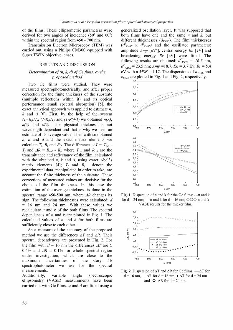
Gushterova et al.: Very thin germanium films: optical and structural properties
56
of the films. These ellipsometric parameters were derived for two angles of incidence (50o and 60o) within the spectral region from 450 - 700 nm.
Transmission Electron Microscopy (TEM) was carried out, using a Philips CM300 equipped with Super TWIN objective lenses.
RESULTS AND DISCUSSION
Determination of (n, k, d) of Ge films, by the proposed method
Two Ge films were studied. They were measured spectrophotometrically, and after proper correction for the finite thickness of the substrate (multiple reflections within it) and its optical performance (small spectral absorption) [5], the exact analytical approach was applied to estimate n, k and d [6]. First, by the help of the system (1+Rf)/Tf, (1-Rf)/Tf and (1-Rf)/Tf we obtained n(), k() and d(). The physical thickness is not wavelength dependant and that is why we need an estimate of its average value. Then with so obtained n, k and d and the exact matrix elements we calculate Tf, Rf and Rf. The differences T = Tcal - Tf and R = Rcal - Rf, where Tcal and Rcal are the transmittance and reflectance of the film, calculated with the obtained n, k and d, using exact Abelès matrix elements [4]; Tf and Rf denote the experimental data, manipulated in order to take into account the finite thickness of the substrate. These corrections of measured values are decisive for the choice of the film thickness. In this case the estimation of the average thickness is done in the spectral range 450-500 nm, where R changes its sign. The following thicknesses were calculated: d = 16 nm and 24 nm. With these values we recalculate n and k of the both films. The spectral dependences of n and k are plotted in Fig. 1. The calculated values of n and k for both films are sufficiently close to each other.
As a measure of the accuracy of the proposed method we use the differences T and R. Their spectral dependences are presented in Fig. 2. For the film with d = 16 nm the differences T are 0.4% and R 0.1% for whole spectral region under investigation, which are close to the maximum uncertainties of the Cary 5E spectrophotometer we use for the spectral measurements. Additionally, variable angle spectroscopic ellipsometry (VASE) measurements have been carried out with Ge films. and are fitted using a
generalized oscillation layer. It was supposed that both films have one and the same n and k, but different thicknesses (dVASE). The film thicknesses (d1
VASE и d2VASE) and the oscillator parameters:
amplitude Amp еV2, central energy Еn еV and broadening energy Вr еV were fitted. The following results are obtained: d1
VASE = 16.7 nm, d2
VASE = 23.5 nm; Amp =18.7, En = 3.7 Ev; Br = 5.4 eV with a MSE = 1.17. The dispersions of nVASE and kVASE are plotted in Fig. 1 and Fig. 2, respectively.
450 500 550 600 650 7003,8
4,0
4,2
4,4
4,6
4,8
5,0
5,2
n nm
d = 16 nm d = 24 nmWVASE
450 500 550 600 650 7000,8
1,0
1,2
1,4
1,6
1,8
2,0
2,2
2,4
2,6
2,8
3,0
k
nm
d = 16 nm d = 24 nm WVASE
Fig. 1. Dispersion of n and k for the Ge films: ---n and k for d = 24 nm; n and k for d = 16 nm; n and k
VASE results for the thicker film.
450 500 550 600 650 700
-1,6
-1,2
-0,8
-0,4
0,0
0,4
0,8
1,2
T, R
(%
)
(nm)
T d=16 nm R d=16 nm T d=24 nm R d=24 nm
Fig. 2. Dispersion of T and R for Ge films: T for d = 16 nm, --- R for d = 16 nm, T for d = 24 nm
and -- R for d = 24 nm.

Gushterova et al.: Very thin germanium films: optical and structural properties
57
450 500 550 600 650 700
-30
-25
-20
-15
-10
-5
0
5
10
15n
/n, k
/k (
%)
(nm)
n/n d=16.7 nm k/k d= 13.7nm n/n d=23.5 nm k/k d= 23.5nm
Fig. 3. Dispersion of n/n and k/k for the Ge films: -- n/n (d = 23.5 nm), -- n/n (d = 16.7 nm), -- k/k (d = 16.7 nm) and -- k/k (d = 23.5 nm).
a)
b)
Fig. 4. TEM micrograph of Ge film with d = 16 nm (a) and d = 24 nm (b).
We define the relative difference between n and k on the one hand and nVASE and kVASE on the other hand as: n/n = (nvase – n)/nvase and k/k = (kvase – k)/kvase.
In Fig. 3 the spectral dependences of n/n and k/k for the both film are shown. Acceptable values for n/n and k/k are obtained. For instance, the maximum value of n/n for the thinner is 1.7% and 3.7% for the thicker film at = 550 nm. The values of k/k curve of the thinner film reach 25 % at 700
nm. We must have in mind that the generalized oscillator model, which is used in the VASE evaluations, is not at all proven to be close to the physical reality of evaporated very thin Ge films. Our approach is more realistic, flexible and free from pre-assumed models.
TEM characterisation
TEM was applied to investigate the morphology of the both thin films. The micrographs of the thinner and thicker film are shown in Fig.4a and Fig. 4b, respectively.
It can be seen that the films have fine granular structure and the grain dimensions of the both films are quite similar. Thus, TEM results are in a good agreement with the results from the optical characterization, which show independence of n and k from d in the thickness range 15 25 nm.
CONCLUSION
We have applied a simple and effective method for the determination of n, k and d of Ge thin films in VIS. The thin film optical parameters are evaluated in three steps. First, n, k and d are estimated for each wavelength of the spectral measurements. Then, from the obtained data, a single value of the physical thickness is evaluated within a specific spectral region. Finally, n and k are re-calculated in order to minimize the thin film optical response, this time with the estimated “scalar” value of the physical thickness. This approach is very functional and practical, because there is no need for n and k dispersion models (Cauchy, Drude, Selmeier, etc.). It does not use numeric minimization techniques, i.e. derivative methods, which must be used in the case of very thin films optics with extreme precaution. a
REFERENCES
1. I. Chambouleyron, S. Ventura, E. Birgin, J. Martinez, J. Appl. Phys., 92, 3093 (2002).
2. Tz. Babeva, S. Kitova, I. Konstantinov, Appl. Opt., 40, 2682 (2001).
3. J. Kattner, H. Hoffmann, J. Phys. Chem. B, 106, 9723 (2002).
4. M. Born, E. Wolf, Principles of Optics (Pergamon, Oxford, 1983).
5. P. Gushterova, P. Sharlandjiev, J. Opt. Adv. Mat., 7(3), 1305 (2005).
6. B. Hristov, P. Gushterova and P. Sharlandjiev, J. Opt. Adv. Mat., 9(1), 217 (2007).
Gushterova et al.: Very thin germanium films: optical and structural properties
58
МНОГО ТЪНКИ ГЕРМАНИЕВО СЛОЕВЕ: ОПТИЧЕСКИ И СТРУКТУРНИ СВОЙСТВА
П. Гущерова *, П. Шарланджиев, Б. Шмитa, A. Мюклихa
Институт по оптически материали и технологии, БАН
ул. „Aкад. Г. Бончев”, блок 109, София ПС-1113, България аИнститут по физика на йонните лъчения и изследване на материяли
Център Хелмхолц, Дрезден – Росендорф, ПК 51 01 19, 01314 Дрезден, Германия
Постъпила на 17 октомври 2013 г.; коригирана на 25 ноември, 2013 г.
(Резюме)
Тьнките и сврьх тьнките слоеве са основни градивни елементи на много приложения в рентгеновата оптика, микроелектрониката и оптичния запис на информация. В настоящата работа представяме приложението на развит от нас спектрофотометричен метод за определяне на оптичните константи (показател на пречупване, n, коефициент на поглъщане, k, и физична дебелина, d на много тьнки слоеве към термично отложени германиеви слоеве с d между 10 и 25 nm. Методът се основава на ограничено развитие на елементите на характеристичната матрица на слоевете. (n, k, d) се пресмятат чрез аналитично решаване на системата уравнения (1+Rf)/Tf, (1-Rf)/Tf и (1-Rf)/Tf , където (Tf) е пропускането на слоя, (Rf) е отражението от страната на слоя и (Rf) е отражението от страната на подложката. Като допънителна методика, за сравнение на така пресметнатите (n, k, d), е използвана спектрална елипсометрия с променлив ъгъл като елипсометричните ъгли на измерените слоевете са фитнати чрез обобщен осцилаторен модел. Получена е приемлива разлика между (n, k, d), прсметнати по двата метода.

59
Bulgarian Chemical Communications, Volume 45, Special Issue B (pp. 59-62) 2013
Sensor properties of asymmetric Bragg stack from chalcogenide glass and PMMA
A. Lalova*, R. Todorov
Institute of Optical Materials and Technologies “Acad. J. Malinowski”, Bulgarian Academy of Sciences, Acad. G. BonchevStr., bl. 109, 1113 Sofia, Bulgaria.
Received October 17, 2013; Revised November 25, 2013
Asymmetric Bragg stack with one defect layer was designed and prepared through layer-by-layer deposition of spin coated Poly (methyl methacrylate) (PMMA) and vacuum deposited chalcogenide film. In this work, first the thickness changes, Δd of the thin films from poly (methyl methacrylate) following exposure to chloroform vapors in the concentration range 1000 - 9000 ppm were determined. Two layered structure from PMMA and vacuum deposited chalcogenide film was consecutively prepared. The ability of the thin chalcogenide films to let the chloroform vapors passing through was investigated. The asymmetric photonic structure consists of 11 alternating layers from As30Ge10S60 chalcogenide glass and PMMA. The defect layer from PMMA is situated before the last high refractive index film from chalcogenide glass. The thickness of the defect layer from poly (methyl methacrylate) was determined so that the pass band to be centered at wavelength of 520 nm. It was observed an offset of the position of the pass band to larger wavelengths after exposure to chloroform vapors. The proposed multilayered structure exhibits potential for applications as optical sensor.
Keywords: Bragg stack, chalcogenide glass, PMMA, thin films, sensor properties
INTRODUCTION
Photonic crystals can be defined as structures in which the dielectric constant (refractive index) shows a periodic variation in one, two or in all three orthogonal directions [1]. 1D photonic crystals, or the so-called multilayer structures consist of alternating layers of two materials with different refractive indices resulting in a periodically varying refractive index in one direction but homogeneous in the other two directions. The thickness of the layers in the Bragg stack is determined by the following equation:
nd = λ0/4 (1)
where n is the refractive index of the layer, d is the thickness and λ0 is the wavelength of the center of the fundamental reflection band of the Bragg stack. It is known that gases possess a refractive index close to that of air, differing of the order of 10-4 [2]. It is easily estimated then from formula (1) that different gases permeating into the structure cannot cause a significant change in the position, λ0 of the fundamental reflection band. Therefore, the manufacture of a gas sensor based on the changes of the refractive index is not possible and materials must be sought that change their volume under the
influence of the gas that would be the object of detection. From the literature it is known that upon contact with chloroform thin PMMA (poly methyl methacrylate) films increase their thickness by Δd = 13.6-19.7% [3]. In previous works [4, 5] the possibility was shown for preparation of a Bragg stack from As30Ge10S60/PMMA for the infrared spectral range and the potential for gas sensing application. In the present paper we demonstrate modeling and deposition of multilayered coating from chalcogenide glass and polymer working as Bragg stack in the visible spectral range. The potential for gas sensor application is demonstrated. The chalcogenide glass composition was chosen such that the material would be transparent in the larger part of the visible region and at the same time would possess sufficiently high refractive index. Our previous studies [6] have shown that thin films of this composition have a band gap of 2.45eV (506 nm).
EXPERIMENTAL DETAILS
Thin films from As30Ge10S60 were deposited in high vacuum of 10-3 Pa by thermal evaporation of previously weighted quantities of the bulk material. Bulk glasses from As30Ge10S60 were synthesized in a quartz ampoule from elements of purity 99,999 % by the method of melt quenching [7, 8]. The deposition rate was 0.4 nm/s, and it was monitored
* To whom all correspondence should be sent: E-mail: [email protected] © 2013 Bulgarian Academy of Sciences, Union of Chemists in Bulgaria
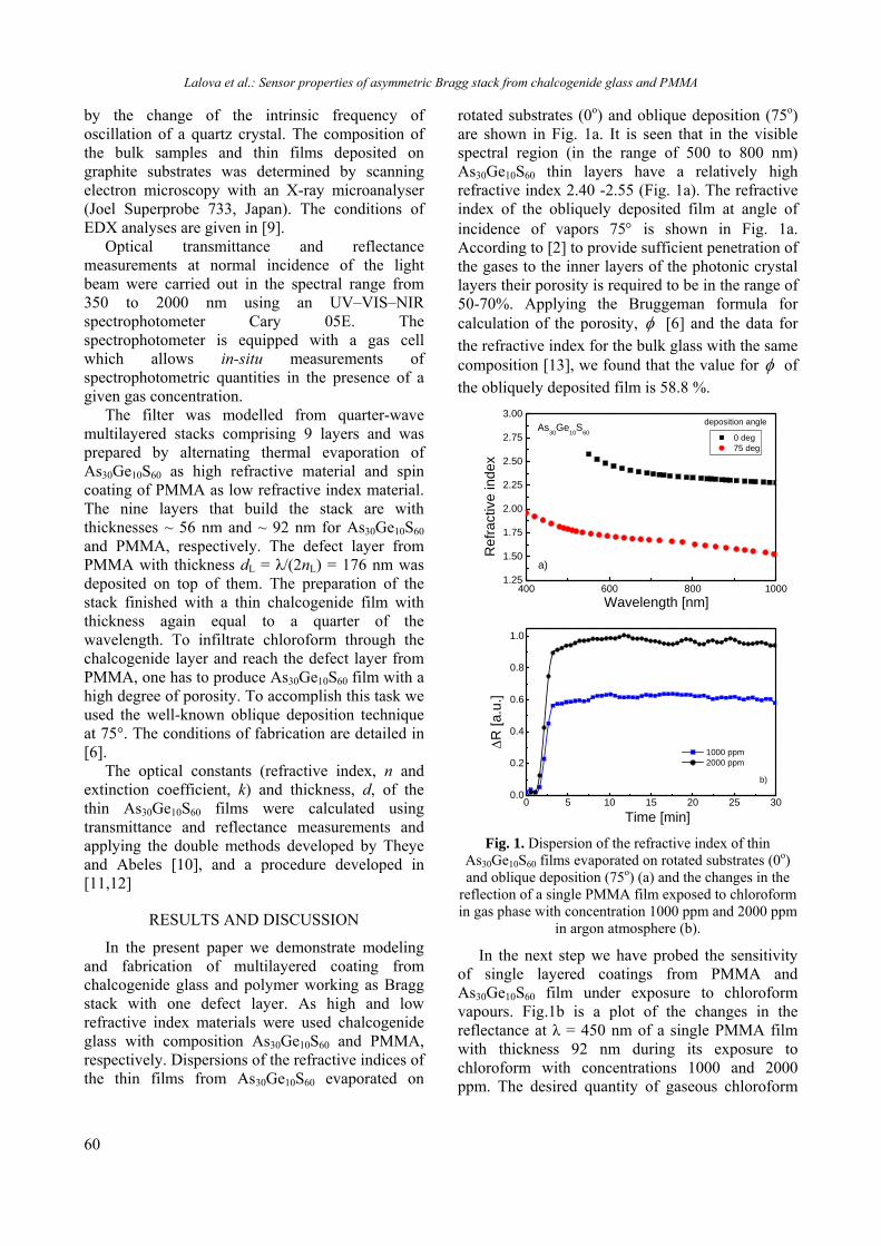
Lalova et al.: Sensor properties of asymmetric Bragg stack from chalcogenide glass and PMMA
60
by the change of the intrinsic frequency of oscillation of a quartz crystal. The composition of the bulk samples and thin films deposited on graphite substrates was determined by scanning electron microscopy with an X-ray microanalyser (Joеl Superprobe 733, Japan). The conditions of EDX analyses are given in [9].
Optical transmittance and reflectance measurements at normal incidence of the light beam were carried out in the spectral range from 350 to 2000 nm using an UV–VIS–NIR spectrophotometer Cary 05E. The spectrophotometer is equipped with a gas cell which allows in-situ measurements of spectrophotometric quantities in the presence of a given gas concentration.
The filter was modelled from quarter-wave multilayered stacks comprising 9 layers and was prepared by alternating thermal evaporation of As30Ge10S60 as high refractive material and spin coating of PMMA as low refractive index material. The nine layers that build the stack are with thicknesses ~ 56 nm and ~ 92 nm for As30Ge10S60 and PMMA, respectively. The defect layer from PMMA with thickness dL = λ/(2nL) = 176 nm was deposited on top of them. The preparation of the stack finished with а thin chalcogenide film with thickness again equal to a quarter of the wavelength. To infiltrate chloroform through the chalcogenide layer and reach the defect layer from PMMA, one has to produce As30Ge10S60 film with a high degree of porosity. To accomplish this task we used the well-known oblique deposition technique at 75°. The conditions of fabrication are detailed in [6].
The optical constants (refractive index, n and extinction coefficient, k) and thickness, d, of the thin As30Ge10S60 films were calculated using transmittance and reflectance measurements and applying the double methods developed by Theye and Abeles [10], and a procedure developed in [11,12]
RESULTS AND DISCUSSION
In the present paper we demonstrate modeling and fabrication of multilayered coating from chalcogenide glass and polymer working as Bragg stack with one defect layer. As high and low refractive index materials were used chalcogenide glass with composition As30Ge10S60 and PMMA, respectively. Dispersions of the refractive indices of the thin films from As30Ge10S60 evaporated on
rotated substrates (0o) and oblique deposition (75o) are shown in Fig. 1a. It is seen that in the visible spectral region (in the range of 500 to 800 nm) As30Ge10S60 thin layers have a relatively high refractive index 2.40 -2.55 (Fig. 1a). The refractive index of the obliquely deposited film at angle of incidence of vapors 75 is shown in Fig. 1a. According to [2] to provide sufficient penetration of the gases to the inner layers of the photonic crystal layers their porosity is required to be in the range of 50-70%. Applying the Bruggeman formula for calculation of the porosity, [6] and the data for the refractive index for the bulk glass with the same composition [13], we found that the value for of the obliquely deposited film is 58.8 %.
400 600 800 10001.25
1.50
1.75
2.00
2.25
2.50
2.75
3.00
a)
0 deg 75 deg
Ref
ract
ive
inde
x
Wavelength [nm]
As30
Ge10
S60
deposition angle
0 5 10 15 20 25 300.0
0.2
0.4
0.6
0.8
1.0
b)
R [
a.u.
]
Time [min]
1000 ppm 2000 ppm
Fig. 1. Dispersion of the refractive index of thin
As30Ge10S60 films evaporated on rotated substrates (0o) and oblique deposition (75o) (a) and the changes in the
reflection of a single PMMA film exposed to chloroform in gas phase with concentration 1000 ppm and 2000 ppm
in argon atmosphere (b).
In the next step we have probed the sensitivity of single layered coatings from PMMA and As30Ge10S60 film under exposure to chloroform vapours. Fig.1b is a plot of the changes in the reflectance at λ = 450 nm of a single PMMA film with thickness 92 nm during its exposure to chloroform with concentrations 1000 and 2000 ppm. The desired quantity of gaseous chloroform

Lalova et al.: Sensor properties of asymmetric Bragg stack from chalcogenide glass and PMMA
61
was pushed in the camera. It is seen that the notable changes in the reflectance due to of thickness changes of PMMA are started after ~ 30 s exposure to chloroform and achieved saturation after 2.5-3 minutes.
In our previous work [6] we showed that chloroform vapors induced negligible changes in thin As30Ge10S60 films. To determine the time for penetration of chloroform through the chalcogenide layer and its interaction with PMMA film we used three-layer coating consisting of one polymer film sandwiched between two chalcogenide films. The changes in the transmittance spectra due to the changes in film’s thickness during exposure to chloroform are shown in Fig.2.
400 500 600 700 800 900 1000
-0,6
-0,4
-0,2
0,0
0,2
0,4 a)
T
Wavelength [nm]
5 min 10 min 15 min 20 min
Treated with 1000ppm CHCl
3 vapours
400 500 600 700 800 900 1000
-0,3
-0,2
-0,1
0,0
0,1
0,2
2 min 4 min 6 min 10 min 20 min
b)
T
Wavelength [nm]
Treated with 9000ppm CHCl
3 vapours
Fig. 2. Changes in the transmittance, ΔT of three-layered
structure exposed of chloroform in gas form at concentrations 1000 ppm (a) and 9000 ppm (b).
The quarter-wavelength stack, i.e., nHdH = nLdL = 1/4λ0 with a target wavelength of λ0 = 550nm was prepared from PMMA and chalcogenide thin films with composition As30Ge10S60. In Fig. 3a the reflectance spectra of a multilayer coating is shown. The changes of the position of the pass band centered at ~ 520 nm are shown in Figs.3b-c. Due to the increase of the thickness of the defect layer a shift was observed to the longer wavelengths. It is seen that even concentration of the gaseous
400 500 600 700 800 9000
20
40
60
80
100a)
530 nm
Re
flect
anc
e [%
]
Wavelength [nm]
3 layers 5 layers 7 layers 9 layers 11 layers
500 520 540 560 580 6000
2
4
6
b)
570 nm
524 nm520 nm
Tra
nsm
ittan
ce [%
]
Wavelength [nm]
Untreated sample exposed to CHCl
3 vapours
anealed after CHCl3
490 500 510 520 530 540 550 560 570 5800
1
2
3
4
5
before after
c)
530 nm
532 nm
Treated with 1000ppm CHCl
3 vapours
Tra
nsm
ittan
ce [%
]
Wavelength [nm]
75,6
75,8
76,0
76,2
76,4
76,6
76,8 d) 20 min atCHCl
3 vapours
20 min atCHCl
3 vapours
heated
30 min at 60oC
heated
30 min at 60oC
T56
4 nm
%
heated
30 min at 60oC
10 min atCHCl
3 vapours
Treatment
Fig. 3. Evolution of the reflectance band with the number of the layers in the filter structure (a); changes of
the pass band in the spectral range 500-570 nm under exposure to vapors of chloroform (b) in gas form at
concentration 1000 ppm (c); and cyclic changes of the value of T at wavelength λ = 564 nm for 11 layered filter
consecutively exposed to chloroform and thermal treatment (d).
chloroform of 1000 pm induces 2 nm shift of the pass band. The obtained changes probably are due to the volume changes of defect PMMA film. It is

Lalova et al.: Sensor properties of asymmetric Bragg stack from chalcogenide glass and PMMA
62
known that chloroform in gas phase possess refractive index (n = 1.001) close to those of air [2]. In the case of vapors significant shift from 520 nm to 570 nm was observed (fig. 3 b). The significant changes of vapor probably are due not only of the increase of the thickness of the defect layer but higher refractive index of vapors (n = 1.36) [2]. After annealing at 60C the band nearly restores its original position. The cyclic changes of transmittance of pass band are shown in fig. 3d.
CONCLUSION
The subject of the present work is modeling and preparation of an asymmetric Bragg stack with one defect layer from chalcogenide glass and organic polymer – PMMA. Taking advantage of the low absorption of the glass with composition As30Ge10S60, a Bragg stack with a stop band in the range 400-700 nm was prepared. The deposition of a defect layer was used to realize of pass band in fundamental reflection band. In the next step the sensitivity of single layers and multilayered coatings was probed. It was established that the pass band is sensitive to concentration of chloroform 1000 ppm.
REFERENCES
1. M. Centini, C. Sibilia, M. Scalora, G. D’ Aguanno, M. Bertolotti, M.J. Blomer, C.M.
Bowden, I. Nefedov, Phys. Rev. E, 60, 4891 (1999).
2. R.V. Nair, R. Vijaya, Prog. Quant. Electronics, 34, 89 (2010).
3. I. Capan, C. Tarimci, A.K. Hassan, T. Tanrisever, Mater. Sci. Eng. C, 29, 140 (2009).
4. R. Todorov, J. Tasseva, Tz. Babeva, Thin Chalcogenide Films For Photonic Applications, chapter 9 in: Photonic Crystals- Innovative Systems, LasersandWaveguides, pp.143-168, Editor: Dr. Eng. Alessandro Massaro, INTECH, Rijeka, Croatia, 2012.
5. T. Babeva, G. Marinov, J. Tasseva, A. Lalova and R. Todorov, J. Phys.: Conf. Series, 398, 012025, (2012).
6. A. Lalova, R Todorov, J. Phys.: Conf. Series, 398, 012023, (2012).
7. K. Petkov, B. Dinev, J. Mater. Sci., 29, 468 (1994).
8. R. Todorov and K. Petkov, J. Optoelectron. Adv. Mat., 3, 311 (2001).
9. K. Petkov, Tz. Iliev, R. Todorov and D. Tzvetkov, Vacuum, 58, 321 (2000).
10. F. Abeles, M.L. Theye, Surf. Sci., 5, 325 (1966). 11. Y. Laaziz, A. Bennouna, N. Chahboun, A.
Outzourhit, E.L. Ameziane, Thin Solid Films, 372, 149 (2000).
12. R. Todorov, A. Lalova, K. Petkov and J. Tasseva, Semicond. Sci. Tech., 27, 115014 (2012).
13. Z. Borisova, Glassy Semiconductors, Plenum Press, New York, 1981.
СЕНЗОРНИ СВОЙСТВА НА АСИМЕТРИЧЕН БРАГОВ СТЕК ОТ ХАЛКОГЕНИДНО СТЪКЛО И PMMA
А. Лалова, Р. Тодоров
Институт по оптични материали и технологии "Акад. Й. Малиновски ", Българска Академия на науките, ул. акад. Г. Бончев, бл. 109, 1113 София, България
Постъпила на 17 октомври 2013 г.; коригирана на 25 ноември, 2013 г.
(Резюме)
Асиметричен Брягов отражател с един дефектен слой е моделиран и получен чрез послойно нанасяне на центрофужно нанесени покрития от поли (метил метакрилат) (ПММА) и вакуумно изпарени халкогенидни филми със състав As30Ge10S60. Изследвана е промяната на дебелината на тънки слоеве от ПММА при излагането им на пари на хлороформ в аргонова атмосфера с концентрация 1000-9000 ppm. Двуслойни покрития от тънки слоеве от ПММА и халкогенидно стъкло са използвани за определяне способността на халкогенидния филм да пропуска пари на хлороформ. Асиметричият фотонен кристал е изгареден от 11 редуващи се слоеве от халкогенидно стъкло със състав As30Ge10S60 и ПММА. Дефектният слой от ПММА е разположен преди последния филм от халкогенидно стъкло. Неговата дебелината беше определена така, че ивицата на пропускане да бъде разположена при дължина на вълната 520 нм. В резултат на излагането на пари на хлороформ беше наблюдавано отместване на ивицата на пропускане към по-големи дължини на вълната. Предложената многослойна структура показва потенциални възможости за приложения като оптичен сензор.

63
Bulgarian Chemical Communications, Volume 45, Special Issue B (pp. 63-67) 2013
Investigation of humidity sensors based on Sn-O-Te films by impedance spectroscopy
B. C. Georgieva*1, Z. P.Nenova2, I. L. Podolesheva1, J. T. Pirov1, T. G.Nenov2 1Institute of Optical Materials and Technologies “Acad. J. Malinovski”, Bulgarian Academy of Sciences, Acad.
G.Bonchev Str., bl.109, 1113 Sofia, Bulgaria 2Technical University of Gabrovo, 4 H. Dimitar Str., 5300 Gabrovo, Bulgaria
Received October 17, 2013; Revised November 25, 2013
Thin Sn-O-Te films with a thickness of 60 nm have been deposited by co-evaporation of Sn and TeO2 on alumina substrates with interdigitated silver-palladium electrodes. During the co-evaporation a chemical reaction between the two substances takes place, resulting in the formation of a Sn-oxide matrix and finely dispersed phases of Te, Sn, TeO2 or SnTe, depending on the atomic ratio of Sn to Te (RSn/Te). To study the morphology and structure as well as to determine the atomic ratio RSn/Te of the films, electron microscopy techniques (TEM, SAED) and analytical methods (EDS in SEM) have been applied. The electrical properties of the sensors studied have been investigated in the frequency range of 20 Hz – 5 MHz using a Precision Impedance Analyzer. The measurements have been taken on samples placed in a controlled humidity and temperature chamber. The characteristics of the resistance R, capacitance C, impedance z and phase θ as functions of relative humidity RH%, the frequency dependences of R, C, z and , the Nyquist plots and equivalent electrical circuits of the sensors have been obtained. As a result, the relation between the type of water adsorption, impedance spectra and the properties of the films as humidity sensors are presented in this paper.
Keywords: humidity sensors, impedance spectra, tin dioxide
INTRODUCTION
Humidity measurement and control are an important task in industry, agriculture, medicine, for storage and transportation of various products and raw materials, pieces of art, etc. Various types of humidity sensors are employed in all these fields [1].
Thin vacuum deposited films, obtained by co-evaporation of Sn and TeO2, are an object of intensive study in the Institute of Optical Materials and Technologies [2] since they are a base for development of gas sensors, conductive films etc. This paper presents a detailed investigation on the electrical properties, impedance spectra and equivalent electrical circuits of as-deposited Sn-O-Te films, intended for humidity sensors.
EXPERIMENTAL
Sample preparation
The films were obtained by thermal co-deposition of Sn and TeO2 from independently
heated Knudsen type cells, under vacuum better than 10-4 Pa [3]. Alumina plates of 18x10x0.5 mm with interdigitated silver-palladium electrodes, held at ambient temperature, were used as substrates. The condensation rates of both substances were controlled separately during the whole evaporation process using quartz crystal monitors. Samples with two different values of RSn/Te < 1 were prepared, which have been previously shown [4] to be sensitive to ambient humidity. The samples with RSn/Te ≈ 0.86 were marked as S1, and with RSn/Te ≈ 0.6 - as S2.
Measurements
Structure and composition - The amount of both substances (RSn/Te) and the thickness of the films were calculated on the base of the measured evaporation rates using computer programs as described in [5]. The data obtained for RSn/Te were controlled by Energy Dispersive Spectrometry (EDS) in SEM (Philips 525/EDAX 9900), and for the film thickness – by a profilometer Talystep (Rank Taylor Hobson). Transmission electron microscopy (TEM) and selected area electron diffraction (SAED) (HRTEM JEOL JEM 2100) were used for studying the morphology and * To whom all correspondence should be sent:
E-mail: [email protected] © 2013 Bulgarian Academy of Sciences, Union of Chemists in Bulgaria

Georgieva et al.: Investigation of humidity sensors based on Sn-O-Te films by impedance spectroscopy
64
structural characterization of the films. The samples intended for TEM were evaporated on glass plates with a water soluble PVA sub-layer. Their thickness (60 nm) was suitable for the direct imaging in TEM.
Electrical characteristics and parameters - The measurement of the impedance characteristics of the samples was taken by Precision Impedance Analyzer 6505P product of Wayne Kerr Electronics Ltd, in the frequency range of 20 Hz to 5 MHz and 500 mVrms of the excitation signal. The samples were placed into a chamber of the Humidity Generator VAPORTRON H-100BL, manufactured by BUCK RESEARCH INSTRUMENTS L.L.C., which provides conditioning of accurately controlled humidity ranging from 15 to 95% with maximal deviation of up to ±1.5% of relative humidity.
RESULTS AND DISCUSSIONS
Structure and composition
As seen in Fig. 1, the films with RSn/Te ≈ 0.8 have a fine-grained structure and the selected area electron diffraction does not indicate the presence of a crystalline phase. This is in accordance with previous results of ours which have shown that the as-deposited films with RSn/Te varying over a wide range (0.3÷2.3) are amorphous and exhibit a nanosized grain and columnar structure [3, 4].
Fig. 1. TEM image and SAED pattern of 60 nm thick
layer with RSn/Te ≈ 0.8.
The sensing properties of the films are strongly dependent on their composition. That is why it was important to check the reliability of the computer calculations described above and the preparation reproducibility. The calculated RSn/Te values were compared to the respective data obtained by EDS-analyses in SEM and a very good coincidence was found (deviation ~ 2%) [2].
Electrical measurements
Measurements have been taken with alternating current to avoid the effect of sample polarization. Figure 2 and Fig. 3 present the characteristics
RHfR , RHfC , RHfz ,
RHf of samples S1 and S2, respectively, at a temperature of 25°С, where R, C, z and θ are their electric resistance, capacitance, impedance and phase, and RH is the relative humidity. For all parameters investigated, the ranges of their changes are largest at 20 Hz and decrease with a rise in frequency. These changes are insignificant above 10 kHz. From a comparison of the characteristics RHfR , RHfC ,
RHfz at 20 Hz, it can be concluded that electrical resistance R has the greatest relative change Rmax/Rmin in the range from 15 to 95%RH for both samples compared to the relative changes Cmax /Cmin and zmax/zmin. A large change in phase is observed from around 86 down to around 10 at a frequency of 20 Hz, but within the narrower range of 65 to 93% RH. Therefore the parameter R is the most informative and for that reason it is used to compare the sensitivity SR of the different elements. The sensitivity SR has been determined for different segments of the sensor characteristics and is given by the slope of the characteristic,
i.e. RHRSR , where RH is the relative
humidity change and R - the respective resistance change for a specific segment. The sensitivity to humidity is the lowest at low values of humidity for both samples. It is observed for sample S1 that sensitivity is greatly enhanced at humidity values of over 45%RH and at a frequency of 20 Hz the maximum value of SR within the range of 45-73%RH reaches 106.7 MΩ/%RH, and after that it gradually decreases. For sample S2 at a frequency of 20 Hz the maximum sensitivity is observed within the range of 65-73%RH and it reaches 46.6 MΩ/%RH, and after that it gradually decreases. Consequently the maximum sensitivity of sample S1 is about twice as high as the sensitivity of sample S2. Besides, the humidity range with high sensitivity is wider for sample S1. The range of resistance change at a frequency of 20 Hz for sample S1 is of about 3 orders, and for sample S2 it is of about 2 orders. The resistance of sample S1 at 93%RH decreases up to about 1.7 MΩ, and for sample S2 – up to 6.5 MΩ.

Georgieva et al.: Investigation of humidity sensors based on Sn-O-Te films by impedance spectroscopy
65
Fig. 2. Characteristics: RHfR , RHfC ,
RHfz and (d) RHf of samples S1 at a
temperature of 25°C and for various frequencies.
Fig. 3. Characteristics RHfR , RHfC ,
RHfz and RHf of samples S2 at a
temperature of 25°C and for various frequencies.

Georgieva et al.: Investigation of humidity sensors based on Sn-O-Te films by impedance spectroscopy
66
The results obtained show that better properties as humidity sensors are observed for the layers with the higher RSn/Te value. They are in a very good agreement with earlier published data about the influence of RSn/Te on the humidity sensing behaviour and the very high sensitivity measured at a frequency of 0.2 Hz [2].
Since with rising frequency the resistance of the layers decreases at low values of humidity, which is favourable for practical applications, it is possible to use them in measuring circuits at higher frequencies as well (up to 1 kHz). Then their maximum sensitivity decreases but it is sufficiently high (5.1 MΩ/%RH for layers S1 and 2.2 MΩ/%RH for layers S2) for such applications.
Impedance spectra
Humidity sensing elements of metal oxide materials are characterized by water adsorption and condensation [6]. The resistance of the investigated sensor elements of metal oxide type decreases with an increase in the relative humidity due to the chemical adsorption and physical adsorption and condensation of water molecules. In the initial stage of adsorption, a chemical adsorption of water molecules on the surface of the respective sensors takes place [7, 8]. The active role in this process is played by metallic atoms, M. They interact with the water molecules to form hydroxyl groups M-OH. In this way the surface of crystals is covered by a monolayer of water molecules. After the formation of the first chemically adsorbed film a physical adsorption of water molecules on it occurs [9, 10]. The mechanism of water adsorption described is closely related to its effect on the impedance characteristics of the samples and on the impedance spectra, respectively. To clarify this relation based on the frequency characteristics z(f) and θ(f), the Nyquist plots of reactive resistances on active resistances for samples S1 and S2 at various RH and a temperature of 25°C have been obtained. Within the frequency range of 20 Hz to 5 MHz the impedance spectra and equivalent electrical circuits for the sensor elements are shown in Fig. 4.
At low humidity values (up to about 45% RH for the investigated samples), these plots are close to a straight line which corresponds to Nyquist plots of the base sensing material [9]. When humidity rises above these values (in this case above 45%RH) the Nyquist plots are arcs from semicircles of very large radii, and their equivalent circuit consists of resistance R1 and capacitance C1 connected in parallel, shown by circuit (I) in Fig. 4.
Fig. 4. Nyquist plots and equivalent electrical circuits for: (a) sample S1 and (b) sample S2 at a temperature of
25°C and at various RH.
Тhis type of impedance spectra can be explained by the prevailing type of electron conduction through the base sensing material and the adsorbed water on the sensor surface in the stage of chemical adsorption [9, 10]. With increasing RH (above 65%RH) the chemisorption enhancement and leakage current increment lead to growing the curvature of the arc and it gradually approximates a complete semicircle (73%RH for sample S1 and 93% for sample S2). Simultaneously, a decrement in the sample impedance is observed which is related to the enhancement of this conduction. When humidity increases further, ionic conduction also appears as a consequence of the presence of physical adsorption as well. It is exhibited by the initiation of a second semicircle with a very large radius in the Nyquist plots within the range of lower frequencies [10]. This additional part of arc is observed in the Nyquist plots of sample S1 at 93%RH. In this case in the equivalent electrical circuit a second group of R2C2 is added which is explained by the appearance of conduction of ionic type. It is represented by circuit (II) in Fig. 4. Therefore, the entire conduction mechanism is a combined action of both electron and ionic

Georgieva et al.: Investigation of humidity sensors based on Sn-O-Te films by impedance spectroscopy
67
conduction [9, 10]. The electron conduction enhancement and the ionic conduction appearance lead to a serious reduction in the impedance of samples when humidity rises. For sample S1 this reduction is more significant. The obtained relation confirms the better humidity sensing properties of sample S1, compared to sample S2.
CONCLUSION
Thin Sn-O-Te films obtained by vacuum co-deposition of Sn and TeO2 could be successfully used as humidity sensors operating at room temperature. Films with RSn/Te ≈ 0.86 possess better humidity sensing properties than films with RSn/Te ≈ 0.65. The appearance of electron and ionic conduction is related to chemical and physical adsorption of water on the sensor surface.
Aknowledgement: This work was supported by the National Scientific Research Fund of Bulgaria under Contract DO 02-148/2008.
REFERENCES
1. Zhi Chen and Chi Lu, Sens. Lett., 3, 274–295, (2005)
2. B. Georgieva1, I. Podolesheva and G. Spasov, J. Phys.: Conf. Ser., 356 012033 (2012)
3. I. Podolesheva, V. Dimov, M. Tarassov, V. Platikanova, and I. Konstantinov, J. Vac. Sci. Technol. A, 16(4), 2608 (1998)
4. B. Georgieva, I. Podolesheva, J. Pirov, V. Platikanova, J. Optoelectr. Adv. Mater., 7, 2595 (2005).
5. I. Podolesheva, P. Gushterova, V. Platikanova and I. Konstantinov, J. Vac. Sci. Technol. A, 16(2), 674 (1998).
6. T. Seiyama, N. Yamazoe, H. Arai, Sens. Actuators, 4, 85 (1983).
7. N. Yamazoe, T. Seiyama, Sens. Actuators, 10, 379 (1986).
8. T. Nenov, S. Yordanov, Technomic Publ. Co. Inc., Lancaster-Basel, (1996).
9. Y. Zhang, Y. Chen, Y. Zhang, X. Cheng, C. Feng, L. Chen, J. Zhou, S. Ruan, Sens. Actuators B, 174, 485 (2012).
10. E. C. Dickey, O. K. Varghese, K. G. Ong, D. W. Gong, M. Paulose C. A. Grimes, Sensors, 2, 91 (2002).
ИЗСЛЕДВАНЕ НА СЕНЗОРИ ЗА ВЛАЖНОСТ НА БАЗАТА НА Sn-O-Te СЛОЕВЕ ЧРЕЗ ИМПЕДАНСНА СПЕКРОСКОПИЯ
Б. Ч. Георгиева1, З. П.Ненова2, И. Л. Подолешева1, Й. Т. Пиров1, Т. Г.Ненов2 1Институт по оптически материали и технологии „Акад. Йордан Малиновски“, Българска академия на
науките, ул. Акад. Георги Бончев, бл. 109, София 1113 2Технически Университет Габрово, ул. Хаджи Димитър 4, Габрово 5300
Постъпила на 17 октомври 2013 г.; коригирана на 25 ноември, 2013 г.
(Резюме)
Получени са тънки Sn-O-Te слоеве с дебелина 60 nm чрез термично вакуумно отлагане на Sn и TeO2 върху керамични подложки от Al2O3 със сребърно-паладиеви гребеновидни електроди. По време на съвместното изпарение протича химическа реакция между двете вещества, която води до образуването на матрица от Sn оксиди и финодиспергирана фаза от Te, Sn, TeO2 или SnTe, в зависимост от атомното съотношение между Sn и Te (RSn/Te). За изследване на морфологията и структурата, както и за определяне на атомното съотношение RSn/Te в слоевете са използвани методи на електронна микроскопия (TEM, SAED) и аналитични методи (EDS в SEM). Електрическите свойства на изследваните сензори са проследени в честотния диапазон 20 Hz – 5 MHz с помощта на прецизен импедансен анализатор. Измерванията са проведени върху образци, поставени в камера с контролирана влажност и температура. Получени са характеристиките на активното съпротивление R, капацитета C, импеданса z и фазата θ като функция на относителната влажност, честотните зависимости на R, C, z and , комплексните импеданси (Nyquist plots) и еквивалентните електрически схеми на сензорите. Като резултат е показана връзката между типа на адсорбцията, импедансните спектри и свойствата на изследваните образци като сензори за влажност.

68
Bulgarian Chemical Communications, Volume 45, Special Issue B (pp. 68-72) 2013
Investigation of apples’ aging by electric impedance spectroscopy
T. Yovcheva1, E. Vozáry2, I. Bodurov3*, A. Viraneva1, M. Marudova1, G. Exner1
1Plovdiv University “Paisii Hilendarski”, 24 “Tsar Asen” str., 4000 Plovdiv, Bulgaria 2Corvinus University of Budapest, 14-16 “Somlói” str., H-1118 Budapest, Hungary
3Institute of Optical Materials and Technologies “Acad. J. Malinowski”, Bulgarian Academy of Sciences, “Acad. G. Bonchev” str., block 109, 1113 Sofia, Bulgaria
Received October 17, 2013; Revised November 25, 2013
Electric impedance spectroscopy, as a fast and non-invasive method, was used to monitor apples’ properties during aging. This method provides information about the physical properties of apples which are closely related to the chemical ones. Two different analytical techniques for assessment of the changes of apples’ properties during aging time were proposed. The first one is based on a single measurement in the low frequency range (around 100 Hz) and the other one - on Argand plot. According to our results, the observed changes in the electric impedance spectroscopy spectra can be attributed to the changes in the relative moisture content of the apples. The apoplastic and simplistic resistances and relaxation times were derived by modeling the apples’ behaviour with equivalent circuit scheme.
Keywords: Apples aging, Dielectric properties, Impedance spectroscopy
INTRODUCTION
One of today’s challenges in food physics field is to establish an exact relationship between the engineering properties of food and the food product quality. The best solution would be to find some fast and non-destructive methods, which can undoubtedly show the food quality.
The electrical properties of food are believed to be sensitive to the food quality and could be used to follow the structural properties changes. Some recent attempts have been made to prove the applicability of such approach [1-6].
We focus our attention on Electrical impedance spectroscopy (EIS), as one of the methods for rapid determination of the electric properties of food. In EIS, alternating voltage is applied to the sample, causing polarization and relaxation in it. This leads to changes in the amplitude and the phase of the alternating current signal and hence the changes in the sample’ impedance (Z) can be determined. The impedance is a complex quantity, consisting of real (R) and imaginary (X) parts. At a priori known frequency, one defines single values of Z. If one varies the frequency in a certain interval, spectral dependence of Z could be obtained.
The aim of the present work is to find out whether appropriate EIS parameters sensitive to the
changes in the apples’ properties during 21 days aging, at room temperature, exist and to propose some applicable techniques for their monitoring.
MATERIALS AND METHODS
Idared apples were supplied from a local Hungarian market. They were stored at room temperature for period of 3 weeks. The mass of the apples was measured immediately after the apples were bought and each time just before the measurement (1st, 7th, 14th, and 21st day). The microbalance used, allowed accuracy 0,001 g of the measured values. Assuming initial moisture content of w0 = 89 % - wet basis [7] - and supposing that the soluble solid content (11%) remained unchanged during the entire storage period, the relative moisture content of the apples (dry basis) was calculated according to the equation:
00 11.0/11.0 mmmw (1)
where m0 is the initial apple mass, expressed in kg; m is the apple mass at the time of the experiment (1st, 3th, 7th, 14th, and 21st day, respectively), expressed in kg.
For the sake of improving results reliability, each time the mass of 10 different apples (without any treatment) was measured and the standard deviation was calculated.
* To whom all correspondence should be sent: E-mail: [email protected]
© 2013 Bulgarian Academy of Sciences, Union of Chemists in Bulgaria
Bodurov et al.:Investigation of apples’ aging by electric impedance spectroscopy
69
EIS measurements were performed on HP 4284A Precision LCR meter and HP 4285A Precision LCR meter, covering the frequency range from 30 Hz to 30 MHz. The voltage had a magnitude of 1 V for all measurements. The experimental values for impedance were corrected for stray admittance and residual impedance (open-short correction) [8]. Plate Ag/AgCl ECG electrodes (Fiab Spa) with a diameter of 10 mm were used, avoiding apples’ injury.
For all measurements, cylindrical samples having initial length up to 46 mm and a diameter of 20 mm were cut from the equatorial part of the apples. Impedance magnitude (Z) and phase angle () were measured at different frequencies. Consecutive shortening of the samples allowed us to gain Z and dependences on the sample length (d).
It is supposed [9] that the open-short corrected impedance (Zm) values depend on electrode impedance (Ze), tissue impedance (Zt), and electrode distance (which equals the sample length - d) and the electrode impedance is independent of the place of the measurement. In such case:
tem ZdZZ . (2)
where Zt is expressed in [ / mm] and Zm is a complex number ( mmm jXRZ ). Rm is the real
and Xm is the imaginary parts of Zm:
tem RdRR . and tem XdXX . (3)
In the present work, the open-short corrected experimental values (Zm and m) were averaged over three consecutive measurements for one and the same d. Rm and Xm values for each d were calculated from those averaged values as follows:
mmm ZR cos. and
mmm ZX sin. (4)
The obtained values were drawn as Rm (or Xm) versus d dependences. With the help of linear regression, the values of Re or Xe (as the intercept with R or X axis, at d = 0) and Rt or Xt (the linear slope) were derived for each sample and each frequency. The coefficient of determination was not lower than 0.98 for all plots. The final values for Re, Xe, Rt, and Xt were obtain after a calculation of the average value of all measurements at identical conditions. Then after, Zt and t values were constructed from the averaged Rt and Xt, according to the equations:
22ttt XRZ and
t
tt R
Xarctan (5)
Further, the experimental results were modeled by the help of equivalent circuits’ method, where the fruit tissue features could be described by means of electrical circuit scheme. The exact elements and connections of the scheme depend on the experimental findings. In this concern, one first constructs Argand plot, representing Rt versus Xt dependences. In the present investigations, the corresponding plots (Fig.1) consist of two arcs, which centers lie under the Rt-axis. Hence, as it was
Fig. 1. Argand plot at different storage time.
pointed out in the literature [10], there is a distribution of the relaxation times rather than a single relaxation time. Following some previous works [10, 11], a model comprising of serial connection of two constant distributed circuit elements (CDCE) and one Ohmic resistance was built so that:
1
22
1
1121 11
jRjRRZt
(6)
where R – is an ohmic resistance, accounting for the resistance of the tissue at infinite high frequency; 1R , 2R - are the resistances of the first and second CDCE elements, respectively;
1 , 2 - are the relaxation times, connected with
each of the CDCE elements; 1 , 2 - are parameters, which account for the relaxation time dispersion; 2 f , where f is the frequency. One gets R as the distance between the origin of the Argand plot and the intercept point of the Rt-axis with the high frequency arc, 1R and 2R correspond to the lengths of the chords appearing as cross-sectional points of the Rt-axis with the arcs at higher and lower frequencies, respectively. The
0 200 400 600 8000
-80
-160
-240
-320 1st day
7th day
14th day
21st day
Xt
[ /
mm]
Rt [ / mm]

Bodurov et al.:Investigation of apples’ aging by electric impedance spectroscopy
70
relaxation times 1 and 2 are derived from the apex of the high and low frequencies arcs ( 1. ii ), respectively.
1 and 2 parameters (which vary from 0 to 1)
describe the distributions of 1 and 2 relaxation
times. When 1 a single relaxation time is
observed, whereas at decreasing values of , a broadening of the relaxation time distribution appears. The coefficients 1 and 2 were
calculated ( 90/1 ii , where i is the angle
between the Rt-axis and the radius of the circle in the intercept point of the circle with the Rt-axis).
The derived values of R, 1R and 2R were then used to calculate the simplastic (intracellular), Rs, and apoplastic (extracellular), Ra, resistances [11]:
21 RRRRa and
21/1 RRRRRs (7)
The last two equations were built on the supposition that at low frequencies the current may not pass the cell membranes but flows into apoplastic space and at high frequencies the current may pass the cell membranes and so the flow passed through both apoplastic and simplistic space [12].
RESULTS AND DISCUSSION
The moisture content values for different storage times, calculated from Eqn. 1, are shown in Fig.2. During the entire experimental time period, the moisture content decreases with storage time. In Fig. 3, the frequency dependencies of Zt magnitude and t (values obtained after Eqns.7-8) are presented. Since the uncertainty did not exceed 4 %, the confidence intervals are not presented in the figure.
As it is seen in Fig. 3A, the impedance magnitude values, Zt, show considerable differences in the low frequency interval and the curves merge in the high frequency interval. The frequency dependencies of phase angles, t, are very similar for all days of measurements (Fig. 3B). According to these results, Zt magnitude values and Zt frequency dependence are the EIS parameters, sensitive to the apples’ quality changes. Since the main differences were observed in the low frequency interval (up to 400 Hz) one may choose
0 5 10 15 20 25
7.6
7.8
8.0
w [
wat
er c
onte
nt /S
SC
]
t [days]
Fig. 2. Relative moisture content storage time dependence. The line is drawn only for eye guide.
1 0 1 0 0 0 0 1 E 7
1 5 0
3 0 0
4 5 0
6 0 0
7 5 0 A
|Zt|
[ ]
f [ H z ]
1 s t d a y
7 th d a y
1 4 th d a y
2 1 s t d a y
10 10000 1E7
-60
-50
-40
-30
-20
-10
0 B
1st day
7th day
14th day
21st day
t d
eg
f [ Hz ]
Fig. 3. Impedance magnitude, Zt, (A) and phase angle, t, (B) frequency dependencies for different storage
times.
to monitor the time changes of Ztat a single fixed frequency in this range. Comparing the results from Figs. 2-3, one might suppose that the changes in both dependencies could be connected and Ztincrease could be attributed mainly to the moisture content decrease.
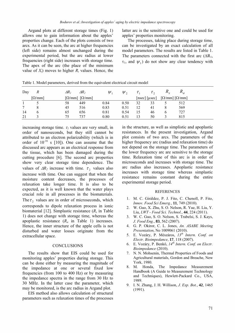
Bodurov et al.:Investigation of apples’ aging by electric impedance spectroscopy
71
Argand plots at different storage times (Fig. 1) allows one to gain information about the apples’ properties change. Each of the plots consists of two arcs. As it can be seen, the arc at higher frequencies (left side) remains almost unchanged during the experimental period, but the arc radius at lower frequencies (right side) increases with storage time. The apex of the arc (the place of the minimum value of Xt) moves to higher Rt values. Hence, the
latter arc is the sensitive one and could be used for apples’ properties monitoring.
The processes, taking place during storage time, can be investigated by an exact calculation of all model parameters. The results are listed in Table 1. The parameters connected with the first arc (R1, 1, and 1 ) do not show any clear tendency with
Table 1. Model parameters, derived from the equivalent electrical circuit model
Day R R1 R2 1 2 1 2 sR aR
[/mm] [/mm] [/mm] [nsec] [sec] [/mm] [/mm] 1 5 58 449 0.84 0.50 32 33 5 512 7 8 45 516 0.83 0.51 12 41 8 569 14 6 65 656 0.81 0.54 15 46 6 727 21 3 75 737 0.80 0.51 13 50 3 815
increasing storage time. 1 values are very small, in order of nanoseconds, but they still cannot be attributed to an electron polarizability (which is in order of 10-16 s [10]). One can assume that the discussed arc appears as an electrical response from the tissue, which has been damaged during the cutting procedure [6]. The second arc properties show very clear storage time dependence. The values of R2 increase with time. 2 values also increase with time. One can suggest that when the moisture content decreases, the processes of relaxation take longer time. It is also to be expected, as it is well known that the water plays crucial role in all processes in the biomaterials. The 2 values are in order of microseconds, which corresponds to dipole relaxation process in ionic biomaterial [12]. Simplastic resistance (Rs in Table 1) does not change with storage time, whereas the apoplastic resistance (Ra in Table 1) increases. Hence, the inner structure of the apple cells is not disturbed and water losses originate from the extracellular space.
CONCLUSIONS
The results show that EIS could be used for monitoring apples’ properties during storage. This can be done either by measuring the magnitude of the impedance at one or several fixed low frequencies (from 100 to 400 Hz) or by measuring the impedance spectra in the range from 30 Hz to 30 MHz. In the latter case the parameter, which may be monitored, is the arc radius in Argand plot.
EIS method also allows calculation of structural parameters such as relaxation times of the processes
in the structure, as well as simplistic and apoplastic resistances. In the present investigation, Argand plot consists of two arcs. The parameters of the higher frequency arc (radius and relaxation time) do not depend on the storage time. The parameters of the lower frequency arc are sensitive to the storage time. Relaxation time of this arc is in order of microseconds and increases with storage time. The arc radius also increases. Apoplastic resistance increases with storage time whereas simplastic resistance remains constant during the entire experimental storage period.
REFERENCES
1. M. C. Giráldez, P. J. Fito, C. Chenoll, P. Fito, Innov. Food Sci Emerg., 11, 749 (2010).
2. W. Guo, X. Zhu, S. O. Nelson, R. Yue, H. Liu, Y. Liu, LWT - Food Sci. Technol., 44, 224 (2011).
3. W. C. Guo, S. O. Nelson, S. Trabelsi, S. J. Kays, J. Food Eng., 83, 562 (2007).
4. G. P. Okiror, C. L. Jones, An. ASABE Meeting Presentation, No 1009061 (2010).
5. E. Vozáry, P. Mészáros, 13th Intern. Conf. on Electr. Bioimpedance, 17, 118 (2007).
6. E. Vozáry, P. Benkő, 14th Intern. Conf. on Electr. Bioimpedance (2010).
7. N. N. Mohsenin, Thermal Properties of Foods and Agricultural materials, Gordon and Breache, New York, 1980.
8. M. Honda, The Impedance Measurement Handbook (A Guide to Measurement Technology and Techniques), Hewlett-Packard Co., USA, 1989.
9. I. N. Zhang, J. H. Willison, J. Exp. Bot., 42, 1465 (1991).

Bodurov et al.:Investigation of apples’ aging by electric impedance spectroscopy
72
10. J. R. Macdonald, Impedance Spectroscopy – Emphasing Solid Materials and Systems, John Wiley and Sons, USA, 1987.
11. T. Repo, G. Zhang, A. Ryyppö, R. Rikkala, J. Exp. Bot., 51(353), 2095 (2000).
12. S. Grimnes, O. G. Martinsen, Bioimpedance and Bioelectricity Basics, Academic Press, London, 2000.
ИЗСЛЕДВАНЕ СТАРЕЕНЕТО НА ЯБЪЛКИ С ЕЛЕКТРИЧНА ИМПЕДАНСНА СПЕКТРОСКОПИЯ
Т. Йовчева1, Е. Возари2, И. Бодуров3, А. Виранева1, М. Марудова1, Г. Екснер1 1Пловдивски университет „П. Хилендарски”, ул. Цар Асен 24, 4000 Пловдив, България
2Корвинус Университет Будапеща, ул. Сомлои 14-16, H-1118 Будапеща, Унгария 3Институт по оптически материали и технологии, БАН, ул. „Акад. Георги Бончев“, блок 109, 1113 София,
България
Постъпила на 17 октомври 2013 г.; коригирана на 25 ноември, 2013 г.
(Резюме)
Елекричната импедансна спектроскопия, като бърз и недестуктивен метод, е използвана за проследяване на свойствата на ябълките при стареене. Този метод дава инфорация за физичните свойства на ябълките, които са тясно свързани с химичните. Две различни аналитични техники за проследяване на промените в свойствата на ябълките са предложени. Едната се базира на единично измерване в нискочестотния диапазон (около 100 Hz), а вторaта е основанa на Argand диаграмата. Получените резултати показаха, че наблюдаваните промени в импедансните спектри се дължат на промяна във влажността на ябълките. Апопластичното и симпластичното съпротивления, както и времената на релаксация бяха получени чрез моделиране с еквивалентна електрична верига.

73
Bulgarian Chemical Communications, Volume 45, Special Issue B (pp. 73-76) 2013
Effect of TiO2 particle incorporation on the electret properties of corona charged polypropylene composite films
A. Viraneva1*, T. Yovcheva1, I. Bodurov2, M. Galikhanov3 1Plovdiv University “Paisii Hilendarski”, 24 “Tsar Asen” str., 4000 Plovdiv, Bulgaria
2Institute of Optical Materials and Technologies “Acad. J. Malinowski”, Bulgarian Academy of Sciences, “Acad. Georgi Bonchev” str., block 109, 1113 Sofia, Bulgaria
3Kazan National Research Technological University, 68 “Karl Marx” str., 420015 Kazan, Republic of Tatarstan, Russian Federation
Received October 17, 2013; Revised November 25, 2013
In the present paper the influence of the concentration of TiO2 particles of average size 500 nm on the electret properties of the polypropylene (PP) composite films were studied. We investigated the PP composite films with different weight concentrations of the TiO2 particles (0 wt., 2 wt.% and 4 wt.%) and thickness of 200 μm. The samples were charged 1 minute under room temperature by the method of the corona discharge using a point-to-plate three electrode system in a positive or in a negative corona.
The voltage of the corona electrode was ± 5 kV and the one of the grid was ±1 kV with the same polarity. The surface potential of the electrets was measured by the method of the vibrating electrode with compensation. We studied the surface potential decay with reference to both time and storage temperature aiming at determination of the particle influence on the stability of the electret composite films.
The results obtained showed a significant change in the electret behaviour of the composite films after the introduction of particles with different concentration into the PP matrix. It was established that the surface potential decay depended on the corona polarity and the concentration of the particles.
Keywords: electrets, composite films, corona discharge
INTRODUCTION
Electrets have been a field of investigations for many years [1-3]. They have been used in different areas of science, technology and medicine. The surface potential values and the lifetime of electrets are the most important parameters giving rise to the possibility of their practical usage. Hence over the years, considerable interest has been shown in the surface potential decay of corona-charged polyolefin polymers among which polypropylene is the most widely used [4-5]. This is due to their low cost, low density, high thermal stability, resistance to corrosion, low relative weight. Over the last few years, however, together with these materials another relatively new direction has been developed. It is the investigation of different composite electret films with specific features. New structural elements that influence the electrets’ properties occur when filling the polymers with dispersive-distributed fillers such as metallic oxide (ZnO, CuO, TiO2) [6-7]. In such a way polymer
composite films have attracted wide interest because of changing polymer electrets’ properties and extending their applications.
The aim of the present paper is to investigate the influence of the concentration of TiO2 particles (0 wt., 2 wt.% and 4 wt.%) on the electret properties of the PP composite films.
EXPERIMENTAL
Fabrication of the PP composite films
Compositions of PP and 500 nm TiO2 particles were prepared on Brabender® measuring mixer with controlled electrical heating. Mixing occurred for 5 minutes at 190 °C. Polymer composite samples were prepared as 200 μm films on hydraulic press. Molding temperature was 190 ± 5°С. Compositions were heated for 10 minutes, molded for 5 minutes at 140 kg/cm2 clamping force and then cooled for 5 minutes as long as samples obtained structural stiffness temperature.
* To whom all correspondence should be sent: E-mail: [email protected] © 2013 Bulgarian Academy of Sciences, Union of Chemists in Bulgaria

Varineva et al.: Effect of TiO2 particle incorporation on the electret properties of corona…
74
Corona charging and surface potential measurement
The charging of composite electrets in the corona discharge was carried out by means of a conventional three-electrode system (Fig. 1), consisting of grounded plate electrode, corona electrode and a grid placed between them.
Fig. 1. Arrangement of the corona charging set-up. 1 – sample on a metal pad; 2 – corona electrode; 3 – grid; 4
– grounded plate electrode; Ug – grid voltage power supply; Uc –corona voltage power supply.
The distance between the corona electrode and the grid was 10 mm and the distance between the grid and the grounded plate electrode was 3 mm. The samples were charged for 1 minute under room conditions. Positive or negative 5 kV voltage was applied to the corona electrode. Voltage of the same polarity as that of the corona electrode was applied to the grid and its value was 1 kV. Electrets surface potential was measured by the method of the vibrating electrode with compensation by which the estimated error was better than 5%.
RESULTS AND DISCUSSION
Influence of time storage on electrets surface potential decay
The dependences of normalized surface potential on the time of storage under room conditions for positively and negatively charged PP composite films with different weight concentrations of the TiO2 particles (0 wt.%, 2 wt.% and 4 wt.%) have been studied for 70 days. The surface potential was measured once a week except for the first 15 days when it was measured more often because the charge was rapidly decaying. After this period, steady state values of the surface potential were established for all of the samples.
Time dependences of the normalized surface potential for positively and negatively charged PP composite films are presented in Figs. 2 and 3 respectively.
0 10 20 30 40 50 60 700,0
0,2
0,4
0,6
0,8
1,0
V /
V0
t, days
0 % 2 % 4 %
Fig. 2. Time dependences of the normalized surface potential for positively charged PP composite films.
0 10 20 30 40 50 60 700,0
0,2
0,4
0,6
0,8
1,0
V /
V0
t, days
0 % 2 % 4 %
Fig. 3. Time dependences of the normalized surface potential for negatively charged PP composite films.
The results illustrated in Figs. 2 and 3 demonstrate the following:
The final values of the normalized surface potential for the samples charged in a positive corona are higher than those for the samples charged in a negative corona for all concentration of the TiO2 particles as has been observed earlier [8];
For all samples investigated the normalized surface potential are initially decaying exponentially for the first 15 days and then are decreasing slowly and are practically stabilized to 70th day;
The normalized surface potential of PP composite films with concentrations of the TiO2 particles (2 wt.% and 4 wt.%) decays faster than the one of the pure PP films independently of the corona polarity. This might be due to conductivity enhancement with incorporation of the TiO2 particles into the PP matrix, resulting in easier and faster charge transport in the bulk.

Varineva et al.: Effect of TiO2 particle incorporation on the electret properties of corona…
75
The decay of the normalized surface potential becomes faster with increasing the concentration of the TiO2 particles. When the concentration of the TiO2 particles is higher (4 wt. %), the normalized surface potential of the composite film decays very fast and reaches a stable state value depending on the polarity of the corona as shown in Figs. 2 and 3. This behavior may be attributed to the fact that the partial injection of the deposited charges depends on the level of concentration of the TiO2 particles.
Therefore, the incorporation of TiO2 particles with a greater concentration in a matrix of PP leads to a decrease of the electrets surface potential value.
Influence of different concentration of the filler on electrets surface potential decay
The dependences of the steady state value of the normalized surface potential on the different concentration of the TiO2 particles for positively and negatively charged PP composite films were presented in Fig. 4.
0 2 40,0
0,2
0,4
0,6
0,8
V /
V0
C, %
positive negative
Fig. 4. The dependences of the steady state value of the
normalized surface potential on the different concentration of the TiO2 particles for positively and
negatively charged PP composite films.
The results illustrated in Fig. 4 show that: The stable state values of the surface
potential decrease with increasing concentration independently of the corona polarity;
The stable state values of the surface potential for positively charged PP composites are higher than those for negatively charged irrespectively of the concentration of TiO2 particles.
Influence of the temperature on electrets surface potential decay
The dependence of the normalized surface potential on the temperature for positively and negatively charged PP composite films with different weight concentrations of the TiO2 particles (0 wt.%, 2 wt.% and 4 wt.%) was investigated. The surface potential measurements were performed by
means of the surface potential measurement set-up at elevated temperatures. The surface potential was measured every two minutes for 1 hour at a constant temperature increase.
The dependences of normalized surface potential on the temperature for positively and negatively charged PP composite films are presented in Figs. 5 and 6 respectively.
20 40 60 80 100 120 1400,0
0,2
0,4
0,6
0,8
1,0
V /
V0
T, oC
0 % 2 % 4 %
Fig. 5. Temperature surface potential decay curves for PP composite films after positive corona charge.
20 40 60 80 100 120 1400,0
0,2
0,4
0,6
0,8
1,0
V /
V0
T, oC
0 % 2 % 4 %
Fig. 6. Temperature surface potential decay curves for PP composite films after negative corona charge.
The experimental results (Fig. 6) show that the curves of the PP composites are shifted slightly to higher temperatures with the increase of the particle concentrations. Probably the introduction of TiO2 particles with different concentration leads to the creation of new charge traps that require higher energies for charges release and leads to the curves shift toward higher temperatures. When the temperature increases, the transport processes through the bulk will play a determinant role because of the increase of both the injection of the carriers from the surface into the bulk and the generating of the carriers in the bulk as well as the increase of their mobility.

Varineva et al.: Effect of TiO2 particle incorporation on the electret properties of corona…
76
CONCLUSION
The surface potential decays of polypropylene composite films with different concentration of the TiO2 particles (0 wt., 2 wt.% and 4 wt.%) were investigated. It was established that there was a significant change in the electret behavior of the composite films after the incorporation of particles with different concentration into the PP matrix. The normalized surface potential of PP composite films with concentrations of the TiO2 particles decayed faster than that of pure PP films and the stable state values of the surface potential decreased with the increasing concentration independently of the corona polarity. Therefore, the incorporation of TiO2 particles with a greater concentration in a matrix of PP leaded to a decrease of the electrets surface potential value. This might be due to conductivity enhancement with incorporation of the TiO2 particles into the PP matrix, resulting in an easier and faster charge transport in the bulk.
REFERENCES
1. G. Sessler, R. Gerhard-Multhaupt, Electrets 3rd Ed., Laplacian: Press Morgan Hill, California, 1999.
2. H. S. Nalwa, Ferroelectric polymers, Marcel Dekker Inc., New York, 1995.
3. B. Hilczer, J. Malecki, Electrets, Elsevier, Amsterdam, 1986.
4. J. Hillenbrand, N. Behrendt, V. Altstädt, H-W. Schmidt, G. M. Sessler, J. Phys. D: Appl. Phys., 39, 535 (2006).
5. G. F. Leal Ferreira, M. T. Figueiredo, IEEE Trans. Electr. Ins., 27, 719 (1992).
6. Sh. Chen, R. Huang, Z. Peng, X. Wang, X. Cheng. (Proc. of Int. Conf. on Solid Dielectrics, Potsdam, Germany, 2010).
7. M. Galikhanov, A. Borisova, R. Deberdeev, Russ. J. Appl. Chem., 78, 820 (2005).
8. T. Yovcheva, M. Marudova, A. Viraneva, E. Gencheva, N. Balabanov, G.Mekishev, J. Appl. Polymer Scie., DOI: 10.1002/APP.38140, 1 (2012).
ВЛИЯНИЕ НА КОНЦЕНТРАЦИЯТА НА TiO2 ЧАСТИЦИ ВЪРХУ ЕЛЕКТРЕТНИТЕ СВОЙСТВА
НА КОРОНО ЗАРЕДЕНИ ПOЛИПРОПИЛЕНОВИ КОМПОЗИТНИ ФИЛМИ
Ася Виранева1, Теменужка Йовчева1, Иван Бодуров2, Мансур Галиханов3 1Пловдивски университет “Паисий Хилендарски”, ул. “Цар Асен” 24, 4000 Пловдив, България
2Институт по оптически материали и технологии „Акад. Йордан Малиновски”, БАН, ул. „Акад. Георги Бончев” блок 109, 1113 София, България
3Казански технологичен университет, ул. “Карл Маркс” 68, 420015 Казан, Република Татарстан, Руска Федерация
Постъпила на 17 октомври 2013 г.; коригирана на 25 ноември, 2013 г.
(Резюме)
В настоящата работа беше изследвано влиянието на концентрацията на частици от TiO2 със среден размер 500 nm върху електретните свойства на полипропиленови (ПП) композитни филми. Бяха изследвани ПП композитни филми с различно тегловно съдържание на частици от TiO2 (0 wt., 2 wt.% and 4 wt.%) и дебелина 200 μm. Образците бяха зареждани по метода на коронния разряд с помощта на триелектродна система в положителна и отрицателна корона за една минута при стайна температура. На корониращия електрод беше подавано напрежение ± 5 kV, а на решетката ±1 kV със същата полярност. Повърхностният потенциал на получените електрети беше измерен по метода на вибриращия електрод с компенсация. За определяне на влиянието на частиците върху стабилността на електретните композитни филми беше изследвано спадането на повърхностния потенциал с времето и температурата на съхранение. Получените резултати показват значително изменение в електретното поведение на композитите след вкарването на частици с различна концентрация в матрица от ПП. Беше установено, че спадането на повърхностния потенциал зависи от полярността на короната и концентрацията на частиците.

77
Bulgarian Chemical Communications, Volume 45, Special Issue B (77-80) 2013
Surface properties of PMMA films with different molecular weights
I. Bodurov1*, I. Vlaeva2, T. Yovcheva3, V. Dragostinova1, S. Sainov1 1Institute of Optical Materials and Technologies “Acad. Jordan Malinowski”, Bulgarian Academy of Sciences, “Acad.
Georgi Bonchev” str., block 109, 1113 Sofia, Bulgaria 2University of Food Technologies, 26 “Maritsa” bvld, 4002 Plovdiv, Bulgaria
3Plovdiv University “Paisii Hilendarski”, 24 “Tsar Asen” str., 4000 Plovdiv, Bulgaria
Received October 17, 2013; Revised November 25, 2013
The paper presents the results of the investigation of the surface refractive index and the contact angle analysis of poly(methyl methacrylate) (PMMA) films. The following two PMMA trademarks, Vedril (Italy) and Plexigum (Germany) with different molecular weights were used. Films of PMMA were prepared by the drop casting technique using 10 wt.% solution of PMMA in 1,2-dichlorethane. The surface refractive index was measured by the method of the disappearing diffraction pattern using a laser microrefractometer at wavelengths of 405 nm, 532 nm and 656 nm. The experimental uncertainty was 1.5×10⁻⁴. The obtained experimental data were used for dispersion analysis following the Sellmeier and the Wemple DiDomenico one term models. The differences between the surface refractive index values of the upper and lower side of the samples (the sample-air interface and the sample-substrate one) were observed. The influence of the polymer molecular weight on the surface properties of the lower and upper film’s side was estimated based on the free surface energy values, calculated with the help of the contact angle technique and the Bickermann’s method. The refractive index differences observed are analyzed on the basis of the molecular refraction and the free surface energy components changes.
Keywords: Refractive index, Poly(methyl methacrylate), Contact angle, Molecular weight
INTRODUCTION
Polymethylmethacrylate (PMMA) is an amorphous thermoplastic which is derived by addition polymerization of methylmethacrylate. The polymer has very good optical properties but has poor scratch resistance. It has the best transparency of commercially available plastics. PMMA is versatile material and has been used in wide range of fields and applications. It can be purchased in one of several molecular weights. The refractive index is a basic optical property of materials and its accurate value is often needed in many branches of physics and chemistry. The optical parameters of PMMA depend on its molecular structure and they can be modified in different ways [1].
Previously, the refractive index and the birefringence dependence on molecular weight are reported for polymer blend films coated on glass substrates via spin coating [2].
The aim of the present paper is to determine the influence of the polymer molecular weight on the refractive index and the surface properties of
PMMA films measured on the two sides of the films – upper and lower.
EXPERIMENTAL PROCEDURES
Sample preparation
PMMA with trademarks Vedril (Italy) and Plexigum (Germany) with molecular weights Mw = 115 000, and Mw = 495 000 respectively were used. 10 wt.% solutions of PMMA, weighted with 0.0001 g accuracy in 1,2-dichloroethane were used to obtain films, coated by casting technique on suitably cut and cleaned rectangular glass substrates. The thickness of the films was 160 μm, measured by Mitutoyo digimatic micrometer with ± 1 μm uncertainty. The samples were dried at room conditions for 24 hours. After drying, the films were separated from the substrates. All the measurements were carried out on the upper and lower side of the samples (on the sample-air interface and the sample-substrate one).
Refractive index measurement
The surface refractive index of the samples was measured by the method of the disappearing diffraction pattern using a laser microrefractometer. * To whom all correspondence should be sent:
E-mail: [email protected] © 2013 Bulgarian Academy of Sciences, Union of Chemists in Bulgaria

Bodurov et al.: Surface properties of PMMA films with different molecular weights
78
Three diode lasers generating at 405 nm, 532 nm and 656 nm wavelengths were used as light sources.
The samples were placed between a glass prism and a metal diffraction grating. To reduce the Fresnel losses the immersion oil was used as a contact liquid. At angles smaller than the critical angle the laser beam passed through a glass prism and diffracted from the metal grating. The critical angle value (φcr) was measured in the air at a chosen wavelength, and the refractive index of the sample (n) was calculated by the formula:
sinsin arcsin crn N A
N
(1)
where A = 65° is the refraction angle of the prism and N is the refractive index of the prism for the used wavelengths 1.7347 (656 nm), 1.7480 (532 nm) and 1.7880 (405 nm). In the present experiments, a rotary stage with 1 arc min resolution was used. The experimental uncertainty of the refractive index, based on φcr and Δφcr, was estimated to be less than 1.5×10⁻⁴.
RESULTS AND DISCUSSION
For all the samples prepared by their separation from the substrate the refractive indexes of the top (na) and bottom (ns) films side were measured. Table 1 presents the measured values.
The obtained refractive index values were used to obtain the oscillator (E0) and dispersion (Ed) energies, as well as the Sellmeier dispersion coefficients (s) and (λs) using the following relations [3, 4]:
2 022
0
1 dE En
E
(Wemple DiDomenico)(2)
22
2 21
s
sn
(Sellmeier) (3)
where is the Planck constant, ω is the angular frequency and λ is the wavelength.
The obtained values of the dispersion coefficients are given in Table 2.
Table 1. The refractive indexes of the air-film and the film-substrate interfaces.
Sample λ = 405 nm λ = 532 nm λ = 635 nm
na ns na ns na ns Vedril 1.5035 1.5045 1.4934 1.4944 1.4889 1.
Plexigim 1.4958 1.4973 1.4854 1.4869 1.4806 1.48219
Table 2. Dispersion coefficients.
Sample Interface Sellmeier Wemple and DiDomenico
s λs , nm E0 , eV Ed , eV
Vedril upper 1.191 94.68 13.10 15.60 lower 1.194 94.60 13.11 15.65
Plexigum upper 1.166 97.41 12.73 14.84 lower 1.170 97.28 12.75 14.91
The dispersion dependences for the samples
constructed by Sellmeier one-term equation are presented in Fig. 1.
Using the group contributions we can obtain the refractive index of PMMA structural unit with the following relation [5]:
\ /2 / \1 2 1 1.475n CH COO C (4)
which is in fair agreement with the experimental value (nD = 1.490).
According to the Lorentz-Lorenz relation after differentiation we can obtain the relation between the refractive index and the changes of the polarisability, the polymer density and the molecular weight:
2 2
2
1 2
6
n nn M
n n M
(5)
The obtained relation confirms the obtained experimental results. Optical properties of polymers are preliminary related to the polymer chain orientation which significantly depends on the molecular weight. If we suppose that the polarizability and the density of the films, remains unchanged it becomes clear from eqn. (5) that the refractive index decreases with increase of the molecular weight.
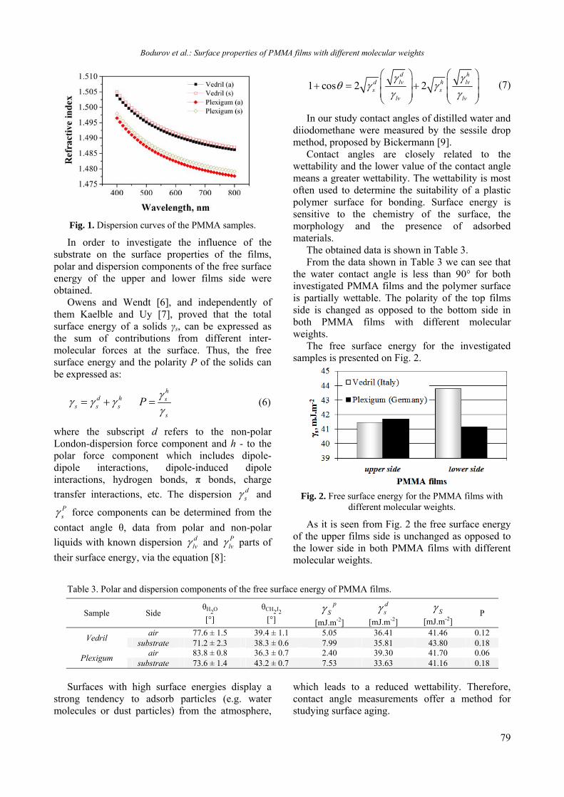
Bodurov et al.: Surface properties of PMMA films with different molecular weights
79
Fig. 1. Dispersion curves of the PMMA samples.
In order to investigate the influence of the substrate on the surface properties of the films, polar and dispersion components of the free surface energy of the upper and lower films side were obtained.
Owens and Wendt [6], and independently of them Kaelble and Uy [7], proved that the total surface energy of a solids γs, can be expressed as the sum of contributions from different inter-molecular forces at the surface. Thus, the free surface energy and the polarity P of the solids can be expressed as:
d hs s s
hs
s
P
(6)
where the subscript d refers to the non-polar London-dispersion force component and h - to the polar force component which includes dipole-dipole interactions, dipole-induced dipole interactions, hydrogen bonds, π bonds, charge
transfer interactions, etc. The dispersion ds and
Ps force components can be determined from the
contact angle θ, data from polar and non-polar
liquids with known dispersion dlv and P
lv parts of
their surface energy, via the equation [8]:
1 cos 2 2d hlv lvd h
s slv lv
(7)
In our study contact angles of distilled water and diiodomethane were measured by the sessile drop method, proposed by Bickermann [9].
Contact angles are closely related to the wettability and the lower value of the contact angle means a greater wettability. The wettability is most often used to determine the suitability of a plastic polymer surface for bonding. Surface energy is sensitive to the chemistry of the surface, the morphology and the presence of adsorbed materials.
The obtained data is shown in Table 3. From the data shown in Table 3 we can see that
the water contact angle is less than 90° for both investigated PMMA films and the polymer surface is partially wettable. The polarity of the top films side is changed as opposed to the bottom side in both PMMA films with different molecular weights.
The free surface energy for the investigated samples is presented on Fig. 2.
Fig. 2. Free surface energy for the PMMA films with
different molecular weights.
As it is seen from Fig. 2 the free surface energy of the upper films side is unchanged as opposed to the lower side in both PMMA films with different molecular weights.
Table 3. Polar and dispersion components of the free surface energy of PMMA films.
Sample Side θH2O
[°]
θCH2J2
[°]
pS
[mJ.m-2]
ds
[mJ.m-2] S
[mJ.m-2] P
Vedril air 77.6 ± 1.5 39.4 ± 1.1 5.05 36.41 41.46 0.12
substrate 71.2 ± 2.3 38.3 ± 0.6 7.99 35.81 43.80 0.18
Plexigum air 83.8 ± 0.8 36.3 ± 0.7 2.40 39.30 41.70 0.06
substrate 73.6 ± 1.4 43.2 ± 0.7 7.53 33.63 41.16 0.18
Surfaces with high surface energies display a
strong tendency to adsorb particles (e.g. water molecules or dust particles) from the atmosphere,
which leads to a reduced wettability. Therefore, contact angle measurements offer a method for studying surface aging.

Bodurov et al.: Surface properties of PMMA films with different molecular weights
80
CONCLUSION
The obtained results show that the refractive index of PMMA films decreases with the polymer molecular weight increasing. The refractive index of films differs depending on the film side (upper or lower). The refractive index at the substrate side is higher than the one at the free surface side which can be attributed to the different density along the thickness of the films. These results should be taken into account in the optical elements construction.
REFERENCES
1. V. Švorčík, O. Lyutakov, I. Huttel, J. Mater. Sci.: Mater. Electron., 19, 363 (2008).
2. K. Koynov, A. Bahtiar, T. Ahn, C. Bubeck, Appl. Phys. Lett., 84, 3792 (2004).
3. G. H. Meteen, Optical properties of polymers, Elsevier, London 1986.
4. S. Wemple, M. DiDomenico, Phys. Rev. Lett., 3, 1333 (1971).
5. D. W. Van Krevelen, Properties of polymers correlations with chemical structure, Elsevier Pub., London-New York, 1972.
6. D. Owens, R. Wendt, J. Appl. Polym. Sci., 13, 1741 (1969).
7. D. Kaelble, K. Uy, J. Adhes., 2, 50, (1970). 8. S. Kitova, M. Minchev, G. Danev, J.
Optoelectron. Adv. Mater., 7, 2607 (2005). 9. R. Johnson, R. Dettre, Surface and colloid
science, vol. 2, ed. E. Matijevic, Wiley-Interscience, 1969.
ПОВЪРХНОСТНИ СВОЙСТВА НА ФИЛМИ ОТ ПММА С РАЗЛИЧНА МОЛЕКУЛНА МАСА
И. Бодуров1, И. Влаева2, Т. Йовчева3, В. Драгостинова1, С. Съйнов1
1Институт по оптически материали и технологии „Акад. Йордан Малиновски“, БАН, ул. “Акад. Георги
Бончев”, блок 109, 1113 София, България 2Университет по хранителни технологии, бул. “Марица” 26, 4002 Пловдив, България
3Пловдивски университет “Паисий Хилендарски”, ул. “Цар Асен” 24, 4000 Пловдив, България
Постъпила на 17 октомври 2013 г.; коригирана на 25 ноември, 2013 г.
(Резюме)
Статията представя резултатите от изследванията на повърхностните свойства, показателя на пречупване и контактния ъгъл на филми от ПММА. Използвани са две търговски марки ПММА, Ведрил (Италия) и Плексигум (Германия), с различна молекулна маса. Филмите са получени по метода на изливане от разтвор чрез използването на 10 wt.% разтвор на ПММА в дихлороетан. Повърхностният показател на пречупване е измерен по метода на изчезващата дифракционна картина чрез лазерен микрорефрактометър при дължини на вълната 405 nm, 532 nm и 656 nm. Експерименталната неопределеност на измерванията е 1.5×10⁻⁴. Получените експериментални резултати са анализирани чрез дисперсионните модели на Зелмаер и Уемпъл и ДиДоменико. Констатирани са разлики в показателя на пречупване между двете страни на филма – горна и долна (контактуваща с въздуха и подложката, съответно). Влиянието на молекулната маса върху повърхностните свойства на двете страни на филма са оценени от гледна точка на стойностите на свободната енергия, изследвана по метода на контактния ъгъл, предложен от Бикерман. Разликите в показателите на пречупване са анализирани от гледна точка на приносите на молекулярната рефракция и измененията на компонентите на свободната повърхностна енергия.

81
Bulgarian Chemical Communications, Volume 45, Special Issue B (pp. 81-85) 2013
Detection of adulteration in olive oils using optical and thermal methods
I. Bodurov1*, I. Vlaeva2, M. Marudova3, T. Yovcheva3, K. Nikolova2, T. Eftimov3, V. Plachkova3
1Institute of Optical Materials and Technologies “Acad. J. Malinowski”, Bulgarian Academy of Sciences, “Acad. Georgi Bonchev” str., block 109, 1113 Sofia, Bulgaria,
2University of Food Technologies, 26 “Maritsa” blvd., 4002 Plovdiv, Bulgaria 3Plovdiv University “Paisii Hilendarski”, 24 “Tsar Asen” str., 4000 Plovdiv, Bulgaria
Received October 17, 2013; Revised November 25, 2013
Quantification of olive oils is an important issue because of frequent adulteration with cheaper oils such as soybean, sunflower or canola. The standard chemical methods used to determine the chemical content of the oils are usually time-consuming, laboratory intensive and expensive. Therefore, we have tested three physical methods measuring refractive indices and their dispersion curves, fluorescence spectra and DSC spectra that are related to the chemical structure and content of the olive oils. These methods are fast, easy to perform and do not require any additional chemical agents. Two groups of olive oils – pure and adulterated, were investigated.
Keywords: refractive index, fluorescence, DSC, olive oils, adulteration
INTRODUCTION
Olive oil is one of the best vegetable oil used in nutrition, medical treatment and cosmetics. The accumulated clinical data prove the beneficial effect of olive oil as a nutrient reducing the risk of heart diseases, skin diseases, breast, prostate and gastrointestinal cancer formation, etc. and is included as an ingredient in a number of pharmaceutical and cosmetic mixtures. Due to its higher price virgin olive oil is often adulterated with cheaper vegetable oils. Olive oil contains a lower level of saturated and higher level of non-saturated fatty acids [1], basically oleic acid (64%), while vegetable oils have a higher level of linoleic acid [2]. Additions of vegetable oils in extra virgin olive oil are usually detected using gas or liquid chromatographic methods [3-4]. The latter methods are expensive, using numerous chemical agents, demanding lengthy analysis and qualified personnel which poses the need for other fast, cheaper and real time methods. An alternative to chromatographic methods are spectroscopic methods which are fast, cheap but with lower sensitivity [5]. Infrared spectroscopy also needs preliminary preparation of sample [6-7]. On the other hand, refractive index and the FTIR spectra of virgin coconut and virgin olive oil were
successfully used to determine purity of olive oils [8] and adulteration with sunflower or corn oils [9]. The analysis performed in [10] showed that the refractive index of the olive oils treated by the different enzymes slightly changes.
In recent years fluorescence spectroscopy has been intensively used to study the origin and contents of olive and vegetable oils [11-12] as well as the detection of soy and sunflower oils in olive oil [13].
The objectives of the present work are: to study the capabilities of a group of physical methods such as fluorescence spectroscopy in the visible spectral range, differential scanning calorimetry (DSC) and laser refractometry to discern extra virgin from adulterated olive oil without the use of chemical agents; to propose improved non-traditional fluorescence and refractometric methods for olive oil analysis using low-cost light emitting (LED) and laser diodes (LD).
MATERIALS AND METHODS
Three types of commercially available extra virgin olive oils (EVOO) from Italy, Spain and Greece were chosen for analysis and their characteristics were compared with three different salad mixtures of olive oil (SMOO) with sunflower and soy bean oils. The samples were measured immediately after opening the bottle to avoid accelerated oxidation processes. * To whom all correspondence should be sent:
E-mail: [email protected] © 2013 Bulgarian Academy of Sciences, Union of Chemists in Bulgaria

Bodurov et al.: Detection of adulteration in olive oils using optical and thermal methods
82
Three methods were used: DSC, refractometry, and fluorescence.
A differential scanning calorimeter SETARAM 141 (France) was used for thermal analysis of the olive oils. The samples were cooled at a rate of 5°C.min-1, from room temperature to -40°C and were kept for 3 minutes to crystallize the sample. After this procedure, melting curves were recorded to 75°C at a heating rate of 5°Cmin-1. The resulting DSC thermograms were analyzed by SETARAM software, melting temperature and enthalpy were determined. Melting temperature was considered as the temperature of the extreme.
The refractive index (RI) values of the samples were measured with a total experimental
uncertainty of less than 42 10 by the method of the disappearing diffraction pattern [14] for three laser wavelengths – 405 nm, 532 nm and 635 nm at a temperature of t = 20C. The data obtained from the three wavelengths RI measurements were used for the construction of dispersion curves using the one-term Sellmeier equation far from the fundamental absorption band [15]. By the one-oscillator Sellmeier’s model used for 3 combinations of RI pairs measured at three wavelengths we can determine the Sellmeier’s coefficients from the systems:
3 ,2i ;3 ,1i ;2 ,1i ,.
12s
2i
2i2
is
sn (1)
Then we can calculate the average Sellmeier’s coefficients s and s for all the samples in order to
obtain more accurate dispersion dependences for the studied liquids.
Fluorescence spectra were measured using a fiber optic spectrometer (AvaSpec-2038, Avantes) and the samples were excited by LEDs at 370 nm, 395 nm, 425 nm and 450 nm using the set-up, shown in Fig. 1. The spectrometer’s sensitivity is in the 200 – 1100 nm range with a resolution of about 5 nm. The oil samples were placed in a 10mm x 10mm cuvette and irradiated by LDs or LEDs. Fluorescence spectra were taken from a direction orthogonal to the line of transmission (Fig. 1).
The pigments have been determined without diluting the sample with a cuvette of 1 cm thickness by using the Lovibond PFX 880 instrument (Tintometer Limited, UK). Special software of the equipment has been used to process the data from the red-yellow-blue (RYB) color scale and to
calculate the contents of β-carotene and clorophyll in the samples.
Fig. 1. Experimental set-up for the observation of
fluorescence spectra.
All analysis were carried out in triplicate and the average data are presented in tables. Differences between means at the 95% (p < 0.05) confidence level were considered statistically significant.
RESULTS AND DISCUSSIONS
Fluorescence peaks for olive oils are the highest in the spectral range 671 nm - 675 nm and are associated with the presence of chlorophyll [15]. For all salad mixes this peak is weaker due to the higher contents of vegetable oils which have less chlorophyll. It is known that if chlorophyll is less than 1 ppm, olive oils contain a large quantity of sunflower or soy bean oils. Their presence causes a stronger peak at around 500 - 550 nm, related to the increase of oxidation products caused by the increased content of linoleic acid. The fatty acid content was independently measured by traditional chemical methods and the results were compared. The comparison shows that the adulterated samples contain a lower level of oleic and a higher level of linoleic acid.
The content of β-carotene is rather high, while for salad mixtures it decreases. It is comparable to that of olive oils for only one sample possibly due to artificial vitamin E enrichment (Table 1).
Since fluorescence spectra are similar, to better discern extra virgin olive oils from salad mixtures we calculate the first derivatives of the averaged fluorescence intensities (dI/dλ) results for the three natural olive oils and the three salad mixtures. The dependences of the first derivatives of fluorescence intensity on the wavelength for two types of olive oils are presented in Fig. 2.While the fluorescence peak in the first derivative caused by chlorophyll is clearly observable for the EVOO, for SMOO we observe mostly noise with weak peaks in the range from 430 nm to 550 nm due to oxidation products in the vegetable oils.

Bodurov et al.: Detection of adulteration in olive oils using optical and thermal methods
83
Table 1. Data on the pigments and Sellmeier’s coefficients in olive oils. Type Β-carotene, ppm Chlorophyll,ppm s λs
EVOO 1 48,74 4,656 1,111 112 EVOO 2 52,64 3,744 1,114 113 EVOO 3 51,21 7,152 1,111 111 SMOO 1 3,18 0,07 1,134 106 SMOO 2 47,45 0,175 1,132 107 SMOO 3 35,67 0,155 1,133 108
Table 2. Data from DSC analysis of the olive oils samples.
Type T1, C T2, C T3, C T4, C T5, C H, J/g
EVOO 1 -4.57 5.31 66.79
EVOO 2 -4.99 5.80 80.92
EVOO 3 -4.12 4.67 82.56
SMOO 1 -29.72 -22.41 -9.22 59.41
SMOO 2 -28.97 -22.67 59.20
SMOO 3 -24.16 -10.47 89.30
a)
Fig. 2. First derivatives of the fluorescence spectra of
salad and natural olive oil for an excitation wavelength of 425 nm.
Using the Sellmeier’s coefficients - s and s
(Table 1) obtained from the RI data we calculated the dispersion curves of RI for all samples in the spectral range (400-800) nm and plotted them in Fig.3. The refractive indices of the virgin olive oils measured at room temperature are in very good
Fig. 3. RI dispersion curves of the olive oil samples.
agreement with the results announced in [8]. It was found for extra virgin olive oils that the refractive index and the Sellmeier’s coefficient s are obviously lower and the Sellmeier’s coefficient s
are obviously higher than ones for salad olive oils as shown in Fig.3 and Table 1. These changes could be associated with the presence of adulterants in salad olive oils. Similar increase of the extra virgin olive oil refractive index with addition of an adulterant as refined olive oil, refined olive pomace oil, sunflower oil and corn oil was estimated in [9].
Melting range and DSC curve shape result from combined effects between fatty acid composition, polymorphism and thermal history (Fig. 4). The extra virgin olive oil has characteristics melting range from -20°С to 10°С with 2 melting temperatures of the order of T4=-5°С and T5=5°С. In contrast the salad oil melts in the range of -35°С to 5 °С and there are three endotherm extreme of the order of T1=-29°С, T2=-22 °С and T3=-10°С

Bodurov et al.: Detection of adulteration in olive oils using optical and thermal methods
84
respectively. All the values for melting temperatures and enthalpies of the samples examined are presented in Table 2.
Fig. 4. DSC thermograms of the olive oil samples.
The results obtained for the melting temperatures of extra virgin olive oils are in good agreement with previous researches [16-17]. The low temperature melting is due to presence of adulterants – most probably sunflower oil, which has melting temperatures at -29°С and -22°С. The absence of the highest melting temperature could be explained by the decrease of the lipid fraction with higher saturation degree (disaturated triacylglycerides, monosaturated triacylglycerides, palmitic and stearic acid) that is expected to melt in the temperature range of the minor shoulder peak [18]. The shift of the major peak to lower temperature could be associated with the presence of adulterants. It may be hypothesised that the change of the chemical composition of the salad olive oils induced by increasing percentages of sunflower oil may have influenced the formation of different and less stable polymorphic crystals than those of pure oil, which also may melt at lower temperature [18].
CONCLUSIONS
Comparative analysis shows that all pure olive oils exhibit a higher fluorescence peak at 670 nm while the adulterated have a higher peak in the 490 nm – 540 nm range. Correspondingly the refractive indices of pure olive oils are lower compared to the adulterated. The melting temperatures of the pure samples were of the order of -5°C and +5°C while those of the adulterated ranged in the -10°C to -29°C temperature interval.
These preliminary results suggest that all the presented physical methods are correlated and
could be useful for a fast detection of adulteration and discriminating among olive oils of different commercial categories.
Acknowledgement: The authors thanks the University Scientific Project NI13FF003 for the financial support
REFERENCES
1. K. Poulli, G. Mousdis, G. Constantinos, Anal. Bioanl.Chem., 386, 1571 (2006).
2. J. C. Allen, R. J. Hamilton, Rancidity in foods, Blackie Academic, New York, 1983.
3. N. K. Andrikopoulos, I. G. Giannakis, V. Tzamtzis,J. Chromatogr. Sci 39, 137 (2001).
4. M. Tsimidou, R. Macrae, Food Chem., 25, 251, (1987).
5. R. Aparicio, R. J. Aparicio-RuÕz, A. Chromatogr., 881, 93 (2000).
6. E. Bertran, M. Blanco, J. Coello, H. Iturriaga, S. Maspoch, I.R. Montoliu, J. Am. Oil Chem. Soc., 76, 611 (1999).
7. G. Downey, R. Briandet, R. Wilson, E.Kemsley, J.Agric. Food Chem., 45, 4357 (1997).
8. W. M. M. Yunus, Y. W. Fen, L. M. Yee, Am. J. Appl. Sci. 6 (2), 328 (2009).
9. J. S. Torrecilla, J. García, S. García, F. Rodríguez, J. Food Eng., 103, 211 (2011).
10. N. Hadj-Taieb, N. Grati, M. Ayadi, I. Attia, H. Bensalem, A. Gargouri, Biochem. Eng. J., 62, 79 (2012).
11. P. Giungato, L. Notarnicola, L. Colucci, In R. Zielinski (Ed.), Current trends in commodity science, Poznan University of Economics Press, Poznan, 2002, p. 513.
12. N. B. Kyriakidis, P. Skarkalis, J. AOAC Int., 83, 1435 (2000).
13. E. Sikorska, A. Romaniuk, I. Khmelinskii, R. Herance, J. Bourdelande, M. Sikorski, J. Kozioł, J. Fluoresc., 14, 25, (2003).
14. S Sainov, Rev. Sci. Instrum., 62, 3106 (1991). 15. J. Singh, Optical Properties of Condensed Matter
and Applications, Wiley-VCH Berlin, 2006. 16. C. Man, CP. Tan, Phytochem. Anal., 13, 142
(2002). 17. C. Ferrari, M. Angiuli, E. Tombari, M. C.
Righetti, E. Matteoli, G. Salvetti, Thermochim. Acta, 459, 58 (2007).
18. E. Chiavaro, M. T. Rodriguez-Estrad, C. Barnaba, E. Vittadini, L. Cerretani, A. Bendini, Anal. Chim. Acta, 625, 215 (2008).
19. E. Chiavaroa, E. Vittadinia, M. T. Rodriguez-Estradab, L. Cerretanic, A. Bendinic, Food Chem., 110, 248 (2008).

Bodurov et al.: Detection of adulteration in olive oils using optical and thermal methods
85
ОТКРИВАНЕ НА ПРИМЕСИ В ЗЕХТИН ЧРЕЗ ОПТИЧНИ И ТЕРМИЧНИ МЕТОДИ
И. Бодуров1, И. Влаева2, М. Марудова3, Т. Йовчева3, К. Николова2, Т. Ефтимов3, В. Плачкова3 1Институт по оптични материали и технологии, Българска академия на науките, ул. Акад. Г. Бончев, бл.109,
1113 София, България 2Университет по хранителни технологии, бул. Марица 26, 4002 Пловдив, България
3Пловдивски Университет „П. Хилендарски”, ул. Цар Асен 24, 4000 Пловдив, България
Постъпила на 17 октомври 2013 г.; коригирана на 25 ноември, 2013 г.
(Резюме)
Качеството на маслиновото масло е важен проблем, защото много често то се примесва с някои евтини растителни мазнини като соево, слънчогледово или рапично олио. Стандартните химически методи, използвани за определяне на химичния състав на маслата са бавни, скъпи и изискват специално оборудване. Затова ние предлагаме три физични метода, измерващи показателя на пречупване и дисперсионните криви, флуоресцентните спектри и DSC спектрите, които са свързани с химичната структура и съдържание на маслиновото масло. Тези методи са бързи, лесни за употреба и не изискват химически реагенти.

86
Bulgarian Chemical Communications, Volume 45, Special Issue B (pp. 86-89) 2013
On silver electromigration in nano-sized As2S3 films
I. Bodurov1*, R. Todorov1, T. Yovcheva2, G. Spassov1 and S. Sainov1 1Institute of Optical Materials and Technologies “Acad. J. Malinowski”, Bulgarian Academy of Sciences, “Acad.
Georgi Bonchev” str., block 109, 1113 Sofia, Bulgaria 2Plovdiv University “Paisii Hilendarski”, 24 “Tsar Asen” str., 4000 Plovdiv, Bulgaria
Received October 17, 2013; Revised November 25, 2013
In this paper the silver mobility in thin chalcogenide films is investigated. The diffraction gratings in 96 nm thick As2S3 films are holographically recorded using evanescent wave, created by total internal reflection and normally incident plane one. The grating step Λ is 447 nm and corresponding spatial frequency is 2237 mm-1. 5 kV corona discharge is applied during the holographic recording. The maximum measured value of the diffraction efficiency is greater than 8%. The mobility of silver, μ, at temperature 17°C is calculated by the Nernst-Einstein equation. The diffusion coefficient D is obtained using the method of holographic grating spectroscopy (Forced Rayleigh Scattering). The dependence of the diffusion coefficient and the mobility of silver on corona charge polarity are investigated.
Keywords: Chalcogenide glasses, Forced Rayleigh Scattering, Silver electromigration, Diffusion coefficient, Silver ion mobility
INTRODUCTION
Seven years after the pioneer work of Kostyshin and co-workers [1], the conductivity increase of the As2S3 bulk samples was observed in an electric field [2]. As a result of this investigation, one quite natural question is raised: How the external electric field will influence the silver transportation into the chalcogenide glasses? As far as we know, the answer was given for the first time by Lebedev and co-workers [3, 4] in 1975. For As2S3 samples it was found that the migration of the noble atom in singly charged ionic form was accelerated by the application of the external electric field.
The main futures of these investigations are: 1. The ionic mobility was obtained in high
temperature region 120 °C – 180 °C. 2. The time-consuming radioactive tracer is
applied for the diffusion coefficient determination. 3. The investigations was carried out in bulk
As2Se3 samples. In the present work the electromigration of
silver is studied in following different conditions: 1. The nanometer thick samples are used. 2. The electromigration is studied by corona
discharged electric field. 3. The diffusion is studied by holographic
method of Forced Rayleigh Scattering. 4. The experiments are carried out at
temperature, 17 °C.
EXPERIMENTAL
Sample preparation
We performed holographic recording in an As2S3/Ag/Cr multilayer system. Firstly, a thin transparent chromium electrode with 10 nm thickness was deposited on a glass substrate by radio-frequency sputtering in argon plasma. A thin silver layer (dAg ~20 nm) was sputtered over the chromium film in the same vacuum cycle. Thin As2S3 films with thicknesses 96 nm were deposited on the silver coating by high vacuum thermal evaporation in a Leybold Heraeus A 702 Q depositing system. The chalcogenide films were prepared in a vacuum of 10-3 Pa, at a deposition rate of 0.1 nm.s-1. The constant thickness of the obtained layers was guaranteed by the planetary rotation of the substrate holders.
Optical arrangement
The general optical arrangement for holographic recording is given in Fig. 1.
In the optical system a crown K-8 glass 45-90-45 prism for the holographic recording was used. The refractive index of the prism at wavelength λ = 442 nm was n = 1.526 and the calculated critical * To whom all correspondence should be sent:
E-mail: [email protected] © 2013 Bulgarian Academy of Sciences, Union of Chemists in Bulgaria

Bodurov et al.: On silver electromigration in nano-sized As2S3 films
87
angle was φcr = 40.9°. Therefore the incidence angle φ = 41.5° was selected for the experiments.
Fig. 1. Optical set-up for evanescent-wave holographic
recording.
The total light intensity of the recording He-Cd laser was 10 μW.cm-2. For real-time diffraction efficiency monitoring a He-Ne laser with 23 μW.cm-2 intensity was used. The reconstructed red light beam was measured with “Thorlabs” PM 130 powermeter. Signal to noise ratio was higher than 100:1. Microscope oil with refractive index 1.53 was used as a matching liquid between the substrate and the prism’s reflecting wall. When the exposure was switched off at the maximum point of the diffraction efficiency (DE), high voltage with different polarity (± 5 kV) was applied to the corona electrode (needle), situated at a distance of 10 mm from the As2S3 film. The Cr sub-layer was used with a spring –contact as a second electrode and to improve the adhesion of the silver to the glass substrate. The corona discharge occurred between the needle and the grounded electrode (Cr sub-layer).
Auger characterization
Тhe AES analysis is performed with a microprobe (including a cylindrical mirror analyzer with a coaxial electron gun), mounted in a stainless-steel bell year at a working pressure 1.3×10⁻⁸ Pa. The analyzer’s energy resolution is about 0.3%. It uses 0.08 μA current and 3 keV electron beam with a diameter 10μm, directed normally to the surface. The spectra are differential; the modulation voltage is 4 Vp.t.p. The profiling is performed with a 3 keV Ar+-ion sputtering at an angle of 79° to the surface normal. The following Auger peaks were monitored S (152 еV), C (272 еV), Ag (356 eV), O (510 еV), Cr (529 eV) and As (1228 eV). Their intensity was measured peak-to-peak.
Previous results of As-S-Se/Ag [5] showed that the electron beam induced additional silver diffusion into the chalcogenide glasses composition. In order to avoid the phenomenon the time of electron-beam interaction with matter
should be as short as possible. Therefore instead of the conventional, the crater-edge profiling was utilized. The latter approach consists in etching a crater in the studied specimen and successively scanning the fabricated edge by the electron beam. Thus, the duration of irradiation at each scanned spot is reduced to less than 1.5 min and the accumulation of silver is prevented.
RESULTS AND DISCUSSION
Fig. 2 presents Auger profiles of As40S60 layers after holographic recording in the presence of the negative and positive corona electric field. The AES profiles reveal uniform distribution of all the elements in the depth (Figs. 2, 3). The AES analysis
Fig. 2. Auger profiles of silver doped As40S60 films obtained by negative corona discharge treatment.
Fig. 3. Auger profiles of silver doped As40S60 films obtained by positive corona discharge treatment.
showed presence significant amount of embedded carbon (it is not shown in figures), due to the immersion fluid used in the process of holographic record. The ratio of S/As for negative electric field treated sample is 2:1, while this ratio varied from 1 (to the surface) tо 1.7 in the case of positive electric field treated samples. The results showed that the silver is approximately homogenous distributed in

Bodurov et al.: On silver electromigration in nano-sized As2S3 films
88
the samples, independently from the electric field’s polarity. The composition analysis showed that the ratios (S+As)/Ag are 4.3 and 2.8 for positively and negatively charged samples, respectively.
The time dependencies of the diffraction efficiency during the holographic recording in the presence of negative or positive corona discharge are shown in Fig. 4.
Fig. 4. Normalized diffraction efficiency of holographic
recording in the presence of a corona discharge.
The experimental results show that the diffraction efficiency changes more drastically in the first (50-60) s of the holographic recording. The time-dependent decay of the diffraction efficiency is proportional to the interference term and its time constant τ can be obtained by fitting of the experimental data with time dependent expression described in [6].
The diffusion coefficients D are calculated with the help of the method of the holographic grating relaxation spectroscopy (forced Rayleigh scattering) [7] by the following relation using already obtained values of the time constant τ:
114.8410D
cm2.s-1 for λ = 442 nm (1)
and they are found to be D = 5.1×10⁻¹³ cm2s-1 and 1.7×10⁻¹³ cm2s-1 for negatively and positively charged samples, respectively.
With the obtained values of the diffusion coefficient, the mobility of silver ions is calculated using the modified Nernst-Einstein relation:
1q e
D DkT kT
(2)
where e is the elementary charge of the electron; q is the silver ions charge; k is the Boltzmann constant; T is the absolute temperature; ∆ is the
correction coefficient [8] and in our case it is defined as:
0
0
1
2 2 1
(3)
For As2S3 the constant ε0 is 7.8 [9, 10] and the correction coefficient was calculated from eqn. (3) to be ∆ = 0.205. This result is in very good agreement with the experimentally obtained value
of the silver ions charge 1.2 0.2q e reported
in [3]. The values of the silver ions mobility are
calculated from eqn. (2) to be 2.4×10⁻¹¹ cm2V-1s-1 and 0.8 ×10⁻¹¹ cm2V-1s-1 for negatively and positively charged samples, respectively.
In our room temperature experiment the mobility of silver’s ion is about three orders of magnitude smaller, compared with the high temperatures value of the silver’s ion mobility in bulk chalcogenide glass samples. The temperature dependence of the mobility of silver’s ion is presented by Lebedev [3] by the following relation:
9expU
kT
(4)
where U is the activation energy of the electromigration.
It should be noted that in [3] Lebedev and co-authors have accepted that U = 0.80 eV. Most common ionization state of silver is +1. The activation energy in our case is
0.80
0.671 1.2
LebedevUU
eV. So, for T = 290 K
from eqn. (4) we have μ = 2.1×10⁻¹¹ cm2/Vs, that is in good agreement with the experimentally obtained value for 100 nm thick film.
CONCLUSION
The combination between the holographic grating spectroscopy (Forced Rayleigh Scattering) and corona charging seems to be a useful experimental method for electromigration study of nanometer-thick materials. It should be noted the main advantaged as:
1. Negligible Joule heating. 2. The measurements are express. 3. One contact plate electrode is needed. 4. The sub-layer (Cr) electrode could be used
for the sample heating for high temperature

Bodurov et al.: On silver electromigration in nano-sized As2S3 films
89
electromigration investigations.
REFERENCES
1. M. Kostyshin, E. Mikhaylovskaya, P. Romanenko, Sov. Phys.Sol. State, 8, 451 (1966).
2. J. Shimizu, H. Kokaido, E. Inoue, Bull. Chem. Soc. Jpn., 46, 3662 (1973).
3. E. Lebedev, P. Suptitz, I. Willert, Phys. Stat. Sol. (a), 28, 461 (1975).
4. P. Suptitz, J. Teltow, E. Lebedev, I. Willert, Phys. Status Solidi, (A) 31, 31 (1975).
5. R. Todorov, J. Tasseva, G. Spassov, K. Petkov, J. Phys.: Conf. Ser., 223, 012040 (2010).
6. S. Sainov, J. Chem. Phys., 104, 6901 (1996). 7. S. Sainov, R. Todorov, I. Bodurov, T. Yovcheva,
J. Opt., 15 105705 (2013) 8. E. Katz, Phys. Rev., 99, 1334 (1955). 9. N. Goyal, A. Zolanvari, S. K. Tripathi, J.
Optoelectron. Adv. Mater., 3, 741 (2001). 10. Z. Borisova, Semiconductrors, Plenum Press,
New York, 1981.
ОТНОСНО ЕЛЕКТРОМИГРАЦИЯТА НА СРЕБРО В НАНОРАЗМЕРНИ ФИЛМИ ОТ AS2S3
И. Бодуров1, Р. Тодоров1, Т. Йовчева2, Г. Спасов1 и С. Съйнов1 1Институт по оптически материали и технологии „Акад. Йордан Малиновски“, БАН, ул. “Акад. Георги
Бончев”, блок 109, 1113 София, България 2Пловдивски университет “Паисий Хилендарски”, ул. “Цар Асен” 24, 4000 Пловдив, България
Постъпила на 17 октомври 2013 г.; коригирана на 25 ноември, 2013 г.
(Резюме)
В настоящата работа е изследвана подвижността на среброто в тънки халкогенидни филми. Във филми As2S3 с дебелина 96 nm бяха записани холографски дифракционни решетки чрез използването на нормално падаща вълна и на затихваща вълна, създадена при пълно вътрешно отражение. Стъпката на решетката Λ беше 447 nm със съответстваща пространствена честота 2237 mm-1. Записът беше осъществен едновременно с прилагане на електрично поле на 5 kV коронен разряд. Максималната измерена дифракционна ефективност беше по-голяма от 8%. Подвижността на среброто, μ, при температура 17°C, беше изчислена с уравнението на Нернст-Айнщайн. Коефициентът на дифузия D беше получен по метода на холографската релаксационна спектроскопия (Форсирано разсейване на Релей). Изследвана е зависимостта на коефициента на дифузия и на подвижността на среброто от полярността на коронния разряд.

90
Bulgarian Chemical Communications, Volume 45, Special Issue B (pp. 90-93) 2013
Laser modification and chemical metalization of sol-gel zirconia thin films as potential material for catalytic applications
E. Krumov1, J. Dikova*1, N. Starbov2 and K. Starbova2
1 Institute for optical materials and technologies “Acad. Jordan Malinowski”, Bulgarian Academy of Sciences
Acad. G. Bonchev Str., block 109, 1113 Sofia, Bulgaria 2 Research center “Physical properties of materials, surfaces and structures” at Institute of solid state physics,
Bulgarian Academy of Sciences 72, Tzarigradsko Chausee Blvd, 1784 Sofia, Bulgaria
Received October 17, 2013; Revised November 25, 2013
The possibilities for modification of sol-gel ZrO2 thin films by excimer laser radiation with respect to their potential application in heterogeneous catalysis are studied. It is established that as a result of laser irradiation, the film microstructure is strongly modified and a higher specific surface area is obtained. It is observed also that amorphous to crystalline phase transition occurs in the exposed film areas. The excimer laser modified surface is found to be active in promoting of electroless metallization with Ni and Cu. The results obtained are very encouraging for further catalytic applications of the thin sol-gel zirconia films.
Keywords: ZrO2 thin films, sol-gel, excimer laser processing, electroless plating
INTRODUCTION
Thin films of ZrO2 (zirconia) have beneficial ceramic properties [1] which offer various possibilities for technological applications as, for example, optical coatings, thermal barrier as well as catalysts or catalytic supports [2]. As known, the active part of the contemporary catalysts represents highly dispersed nanostructured metal clusters on proper catalyst supports. Therefore, the metallization process is of great importance for development of advanced materials on the base of ceramics. However, reliable and reproducible deposition of metals on thin ceramic films still remains a key problem that needs to be optimized since the experience on the metallization of bulk ceramics can not be directly applied to thin film materials.
Variety of methods and techniques for modification of ceramic thin films and their properties are described in the literature [3-5]. In that respect, the excimer lasers are among the most powerful and efficient tools. Recent investigations show that laser irradiation of sintered alumina induces extremely fast melting/quenching processes resulting in the evolution of γ-Al2O3 [6]. On the other hand, microstructure modification and
separation of metal phase in ceramic thin films under excimer laser exposure is also found to take place [7, 8]. Both types of phase transitions are known to be responsible for the catalytic activity of some oxide ceramics towards electroless metal plating. That approach could be applied for functionalization of zirconia films with respect to their application in heterogeneous catalysis.
Since the construction of three way catalysts for exhaust gases conversion, attempts for substituting ceramic supported noble metal catalysts by inexpensive transient ones or theirs oxides have been made. In this respect copper (Cu) and nickel (Ni) as well as their oxides are among the most intensively studied systems. The other way to produce a cheaper catalyst is to decrease the price of the catalyst support. A promising low cost technique for preparation of thin zirconia films is the sol-gel method, which has the advantage of being able to form homogeneous thin ceramic films at low temperatures onto complex shapes [9].
In the present paper the possibilities for surface modification of sol-gel ZrO2 thin films by excimer laser processing are studied. Besides, the catalytic activity of exposed samples toward Ni and Cu electroless plating is investigated. The results obtained are discussed in the view point of potential application of the sol-gel ZrO2 films in heterogeneous catalysis. * To whom all correspondence should be sent:
E-mail: [email protected]
© 2013 Bulgarian Academy of Sciences, Union of Chemists in Bulgaria

Krumov et al.: Laser modification and chemical metalization of sol-gel zirconia thin films…
91
EXPERIMENTAL
The experiments were carried out on sol-gel ZrO2 thin films with thicknesses between 400 and 1000 nm. The samples were prepared via multiple spin coating from zirconium propoxide solution, stabilized by acetyl-acetone, at room temperature. The substrates used were preliminary cleaned Ca-Na silicate glass plates or sheets of chemically roughened stainless steel. The preparation procedure consisted in consecutive spin coating of a single layer followed by thermal treatment at 350 oC. Thus, multilayered ZrO2 films with different thickness were obtained. These samples were exposed to excimer laser radiation and after that chemically treated in electroless baths for metal deposition. The irradiation was carried out by a KrF+ (λ=248 nm) or ArF+ (λ =193 nm) excimer lasers applying single shots or multiple pulses in repetitive rate of 1 Hz. During the exposures the pulse energy density was in the range between 0.4 and 1.7 J/cm2 and was always kept below the ablation threshold of the material. For metallization of the exposed layers two commercial baths were chosen – one for Ni- and the other for Cu-plating. The surface morphology of the samples was imaged under Philips 515 scanning electron microscope after each stage of experimental process. Тhe phase composition of irradiated and non-irradiated ZrO2 films were followed under SEM and by means of XRD analysis.
RESULTS AND DISCUSSION
Fig. 1 presents SEM micrographs of the surface of non-irradiated (a) and irradiated by ArF+ laser with 10 pulses at pulse energy density of 0.88 J/cm2 (b) 400 nm thick ZrO2 sol-gel film as well as the corresponding Zr X-ray mapping (Fig. 1c, d). As seen, due to the laser absorption, the microstructure of the films is strongly modified and is distinctly different from that of the non-illuminated sample. Besides, an appearance of fine morphological details like bubbles and pores in the exposed ceramic films is detected. Obviously, these changes are due to the occurrence of fast melting/re-solidification processes in the samples thus increasing their specific surface area. Moreover, the Zr X-ray maps evident that the ceramic film is uniformly distributed on the substrate and after laser irradiation remain unchanged. Therefore, the laser energy density is below the ablation threshold of the material and the radiation used do not causes films damages.
Fig. 1. Scanning electron micrographs (a, b) and
corresponding Zr (K) (c, d ) elemental X-ray maps of non-irradiated (a, c) and irradiated (b, d) 400 nm thick
ZrO2 sol-gel films deposited on stainless steel substrates.
20 30 40 50 60
c-ZrO2
c-ZrO2
b
a
X-r
ay in
tens
ity
2
c-ZrO2
Fig. 2. X-ray diffraction spectra of 400 nm sol-gel ZrO2
film deposited on glass substrate, before (a) and after irradiation (b).
Fig. 2 presents XRD spectra of 400 nm sol-gel ZrO2 film, deposited on glass substrates, before (a) and after irradiation (b). Evidently, as a result of laser irradiation a phase transition from amorphous to crystalline state takes place. The crystalline phase was identified as high temperature cubic modification of zirconia, c-ZrO2, known as a promising catalyst [2]. Unlike those deposited on

Krumov et al.: Laser modification and chemical metalization of sol-gel zirconia thin films…
92
glass substrates, the sol-gel films coated on stainless steel plates comprise both amorphous and orthorhombic zirconia phase. Under conditions of single shot irradiation of 800 nm thick films, a complete amorphous to orthorombic zirconia phase transition takes place.
Fig. 3. SEM micrographs (a, b) and corresponding Ni
(K) (c, d ) elemental X-ray maps of non-irradiated (a, c) and irradiated (b, d) 400 nm thick ZrO2 sol-gel films
deposited on stainless steel substrates after electroless plating.
Further, the excimer laser modified surface was found to promote both the electroless plating of nickel and copper. Fig. 3 presents scanning electron micrographs of the surface of as deposited (a) and laser irradiated (b), processed in Ni-electroless bath as well as the corresponding nickel X-ray maps (c, d). As can be seen from the SEM micrograph in Fig. 3a, regularly distributed aggregates are formed on the surface of the laser-irradiated and chemically treated sample. In this case the X-ray map (Fig. 3d) evidences a high density of Ni (Kα) X-ray counts, which follow the distribution of the electroless deposited aggregates. It is thus clear that the laser-modified zirconia surface activates the process of the Ni-electroless plating. The micrograph in Fig. 3c displays Ni background signal that is consistent with the absence of metal aggregates on the surface
of non-irradiated and chemically treated sample (Fig. 3a). It should be noted here that the EDS analysis performed reveals a uniform Zr distribution in both as-deposited and laser irradiated sol-gel films after the chemical treatment. This is an evidence for the relatively good chemical stability of laser-modified samples in the Ni bath used.
Fig. 4. SEM micrographs of irradiated by KrF* excimer laser 800 nm stainless supported ZrO2 sol-gel film after
Cu-electroless plating.
Similar experiments were performed in order to study the possibilities for electroless deposition of Cu on the surface of laser irradiated sol-gel ZrO2 films. An example for the coatings obtained is demonstrated in Fig. 4, where a SEM micrograph of the surface of 800 nm stainless supported ZrO2 film, irradiated by KrF+ laser at pulse energy density 1.7 J/cm2 is presented. It was also established that both irradiation and plating conditions can be efficiently optimized with respect to the size of deposited Cu clusters, which is an important prerequisite for practical application of the results obtained.
CONCLUSIONS
The results of the present study show that the excimer laser processing modifies significantly the structure of ZrO2 thin films, obtained by the sol sol-gel method. The evolution of the specific surface area as a result of laser absorption combined with opportunity for electroless plating of catalytic active metals reveals possibilities for the development of both catalytic supports and catalysts, based on thin sol-gel zirconia films.
Acknowledgements: The authors are grateful to prof. L. D. Laude and prof. J. Solis for the opportunity for excimer laser irradiation as well as to Dr. J. Pirov for the EDS analysis performed.

Krumov et al.: Laser modification and chemical metalization of sol-gel zirconia thin films…
93
REFERENCES
1. D.H.Aguilar, L.C.Torres-Gonzalez, L.M.Torres-Martinez, T.Lopez and P. Quintana, J. Solid State Chem., 158, 349 (2000).
2. R. Rujkorakarn, J. R. Sites, J. Vac. Sci. Technol., A, 4, 568 (1986).
3. J. Liu, C. J. Barbero, J. W. Corbett, K. Rajan, H. Leary, Mat. Res. Soc. Symp., 311, 239 (1993).
4. W. K. Choi, S. C. Choi, H. J. Jung, S. K.Koh, D. J. Byun, D. W. Kum, J. Vac. Sci. Technol. A, 16, 3311 (1998).
5. B. Stolz, G. Backes, A. Gilner, E. W. Kreutz, Appl. Surf. Sci., 109-110, 242 (1997).
6. L. D. Laude, K. Kolev, M. Brunel, P. Deleter, Appl. Surf. Sci., 86, 368 (1995).
7. K. Starbova, V. Mankov, N. Starbov, D. Popov, D. Nihtianova, K. Kolev, L. D. Laude, Appl. Surf. Sci., 173, 177 (2001).
8. A. J. Pedraza, M. J. Godbole, M. J. DeSilva, D. H. Lowndes, MRS-Proc., 285, 203 (1994).
9. Kljachko-Gurvich, “Izv. ANSSSR Otd. Chim. Nauk”, 10, 1884 (1961) (Russ).
ЛАЗЕРНА МОДИФИКАЦИЯ И ХИМИЧЕСКА МЕТАЛИЗАЦИЯ НА ЗОЛ-ГЕЛ ТЪНКИ ФИЛМИ ОТ ZRO2 КАТО ПОТЕНЦИАЛЕН МАТЕРИАЛ ЗА КАТАЛИТИЧНИ ПРИЛОЖЕНИЯ
E. Крумов1, Ю.Дикова1 , Н. Щърбов2 и К. Щърбова2 1IИнститут по оптически материали и технологии “Акад. Йордан Малиновски”, Българска
Академия на науките ул. „Акад. Г. Бончев“, блок 109, 1113 София, България 2 Изследователски център “Физични свойства на материали, повърхности и структури” към
Институт по физика на твърдото тяло, Българска Академия на науките
бул. „Цариградско шосе“72, 1784 София, България
Постъпила на 17 октомври 2013 г.; коригирана на 25 ноември, 2013 г.
(Резюме)
Изследвани са възможностите за модификация на зол-гел ZrO2 тънки слоеве чрез ексимерно лазерно облъчване по отношение на потенциалните им приложения в хетерогенния катализ. Установено е, че в резултат на лазерното облъчване микроструктурата на слоевете се променя значително, което води до увеличаване на специфичната им повърхност. Също така е установено, че в експонираните области настъпва фазов преход от аморфно към кристално състояние. Намерено е, че лазерно модифицираните повърхности проявяват активност по отношение на отлагане на Ni и Cu при обработка в съответните химически бани. Получените резултати са многообещаващи с оглед на по-нататъшни каталитични приложения на тънки слоеве от циркониев оксид, получени по зол-гел метод.

94
Bulgarian Chemical Communications, Volume 45, Special Issue B (pp. 94-98) 2013
Simplified procedure for Al2O3 microfibers preparation by the method of electrospinning
M.M. Dimitrovaa,b, E.D. Krumovb, D.B. Karashanovab*
aFaculty of Chemistry and Pharmacy, Sofia University “St. Kliment Ohridski”, 1 James Bourchier Blvd., 1164 Sofia, Bulgaria
bInstitute of Optical Materials and Technologies “Acad. Jordan Malinovski”, Bulgarian Academy of Sciences, Acad G. Bonchev St., bl. 109, 1113 Sofia, Bulgaria
Received October 17, 2013; Revised November 25, 2013
Inorganic micro-fibers of alumina are successfully produced by the method of electrospinning. A simplified procedure of the solution preparation is applied. It is based on single organic precursor dissolved alcohol and excludes the use of assisted polymer usually added to facilitate further fiber formation. Thermal treatment of the as-spun fibers is applied to remove the rests of organic components and for final inorganic mat synthesis.
The morphology of the as-spun and thermally treated fibers is imaged by scanning electron microscopy. Their phase composition is studied by XRD and SAED. The potential for ecology applications of the mat prepared is discussed.
Keywords: alumina fibers, electrospinning, catalytic materials
INTRODUCTION
Al2O3 is known as a functional material in many applications, due to its exceptional physical and chemical properties like high electronic conductivity of some alumina phases, chemical inertness and mechanical stability. Thin films, nanoparticles, micro- and nanofibers of Al2O3, together with the bulk material, are applied in electrical and electronics industries, catalysis, medicine, ecology etc. [1-4].
The method of electrospinning is discovered at the beginning of the 20 century by Zeleny [5,6]. Now, it is one of the main bottom – up approaches, used for the nanomaterials preparation. The electrospinning is the most versatile and simplest one between all methods for preparing micro- and nanofibers, as drawing with a micro-pipette, template synthesis, phase separation, chemical vapor deposition, and melt blowing [7-9]. It is also potentially scalable and requires little equipment.
In the method, a precursor solution of the fiber material is enclosed in a syringe, putted in a mechanical pump, ensuring a uniform supply of the solution. A high voltage is applied between the needle of the syringe and a metal plate, serving as a fibers collector. The electric field charges the solution. At certain value of the electric force, the
surface tension of the precursor solution is overcome, the drop elongates and a jet is formed. The jet dries during the flight to the opposite electrode and solid fibers are collected on it. The process of fiber formation could be controlled by several essential parameters – solution concentration and viscosity, strength of the applied voltage, distance between the drop and the collector, ambient temperature and humidity.
In the years, the method of electrospinning has been applied for preparation of fibers of polymers, hybrid materials and inorganic substances. In the last decade many experiments have been carried out for the production of ceramic fibers by this method: Al2O3 [10], ZrO2 [11], TiO2 [12], SiC [13], ZnO [14], CaP [15]. The classical receipt for inorganic fibers preparation by the method of electrospinning includes from one side a precursor solution of the Al and from the other - a polymer component, aiming to facilitate the fiber formation process. For preparation of Al2O3 fibers, Azad et al. use Al 2,4-pentanedionate and polyvinylpyrrolidone in ethanol as a polymer component of the electrospinning solution [16]. In other research, Panda and Ramakrishna apply two different precursors — aluminium acetate and aluminium nitrate, as well as two types of polymers — polyvinyl alcohol and polyethylene oxide in the process of the Al2O3 fibers formation [17].
* To whom all correspondence should be sent: E-mail: [email protected] © 2013 Bulgarian Academy of Sciences, Union of Chemists in Bulgaria

Dimitrova et al.: Simplified procedure for Al2O3 microfibers preparation…
95
The aim of the present work is to synthesize successfully Al2O3 fibers, using only an organic precursor for Al. Thus, we eliminate the additional polymer component, used by other authors and simplify the procedure for Al2O3 fibers formation.
EXPERIMENTAL
High purity (99.995%) aluminum sec-butoxide (Al(OCH[CH3]C2H5)3) from Sigma-Aldrich Co,
USA was used as a precursor for the synthesis of Al2O3 fibers. As the viscosity of the pure butoxide was very high, thus obstructing the electrospinning process, a butanol (CH3(CH2)3OH, Sigma-Aldrich, 99.9%) was added as a solvent. Experiments were carried out with 3 different solvent to precursor mixing ratios: 3:1, 5:1 and 7:1. In all 3 cases, a stirring for few minutes with a magnetic stirrer was applied and homogeneous solutions were prepared. After that the solutions were drawn into 5 ml syringes, supplied with stainless steel needles. The syringes with the different butoxide contents were mounted successively on the mechanical pump of the electrospinning installation and different mats were collected.
The electrospinning apparatus is home made vertical realization of the set-up. It consists of three main parts – a DC power supply with maximal voltage 30 kV, mechanical mechanism for pumping the solution with constant rate and grounded collector electrode from aluminum foil. At the beginning of the electrospinning process, the pump is started. The piston moves and presses uniformly the solution in the syringe. When the high voltage is not applied yet, the liquid from the syringe drops on the collector. After connecting the needle to one terminal of the power supply and the collecting electrode to the other, under the voltage of about 15 kV, the drops from the electrospinning solution transform into a long jet. When the distance between the tip of the needle and the collecting plate is big enough, the jet accomplishes a movement by spiral trajectory and dries. At the end of its path on the collector, it was completely transformed in a solid fiber. The totality of fibers form so-called non-woven mat. One part of the as-spun fibers is separated for different analysis – Scanning Electron Microscopy (SEM), Transmission Electron Microscopy (TEM), X-ray difractometry (XRD). The remaining fibers are thermally treated in a programmable oven Dentamatic 6000, Tokmet -TK Ltd. and also analyzed after calcination.
The calcination procedure of the fibers, produced from aluminum sec-butoxide aims to eliminate definitively the rest of the organic precursor and solvent, to stabilize the fibers, to increase their crystallinity and to create predominantly one or another of the crystalline phases of the alumina, depending on the temperature. The as-spun fibers are thermally treated up to 800°C, starting from room temperature and following a special three-step procedure. At the first stage the samples are heated at 120°C in order to eliminate the volatile organic compounds. Fibers calcination is accomplished during the second stage when they are held at 360°C. The third step leads to complete crystallization of the fibers applying thermal treatment at 800°C. Duration of each stage is one hour and the heating rate from one to other stage is 1.6°C/min. The fibers annealing is carried out in a quartz tube with pure dry air flow for better elimination of the volatile components and for complete oxidation of the aluminum to alumina.
The study of the fibers morphology is performed by digitalized scanning electron microscope Philips 515 at accelerating voltage 25 kV. The microstructure of the fibers is carried out by transmission electron microscope JEOL JEM 2100 at accelerating voltage 200 kV. The phase composition of the mat is determined by X-ray powder diffractometer Philips PW 1710/00 and by selected area electron diffraction (SAED) mode of the transmission electron microscope.
RESULTS AND DISCUSSION
Three types of electrospinning solutions, with butoxide to butanol ratios: 3:1, 5:1 and 7:1 were examined. Visually, the best quality fibers and the best electrospinning process were produced at the ratio 5:1. All further results presented in this paper - morphology, microstructure and phase composition, will be referred to this ratio.
Except the properties of the solution, the process of the electrospinning and the quality of the fibers produced depend on the electric field parameters. The SEM micrographs of the as-spun fibers, prepared at three different strengths of the electric field: E<1 kV/cm, E=1 kV/cm and E>1 kV/cm are presented in Fig. 1 a), b) and c), respectively. It is seen that when the strength is E<1 kV/cm or E=1 kV/cm, the fibers growth defectless, while at E>1 kV/cm, the defects like beads appear in the structure of the fibers. More over, in the last case, the fibers are fragile and crushed. In all these experiments, the applied voltage is kept at 15 kV,

Dimitrova et al.: Simplified procedure for Al2O3 microfibers preparation…
96
but the distance between the needle tip and the fibers collector is varied. At the beginning it is equal to 20 cm, thus ensuring a strength of the electric field E<1 kV/cm. After that, the distance is diminished consecutively to 15 cm and 10 cm for E=1 kV/cm and E>1 kV/cm, respectively. The distance of 10 cm is insufficient for the solvent to leave completely the jet of the solution. Its evaporation continues and after that the jet reaches the collector, thus causing the formation of crushed web.
Fig. 1. SEM micrographs of as-spun fibers, prepared at
strengths of the electric field: a) E<1 kV/cm, b) E=1 kV/cm
and c) E>1 kV/cm.
Fig. 2. Diameter distribution of as-spun
fibers, prepared at electric field: a) E<1 kV/cm, b) E=1 kV/cm
and c) E>1 kV/cm.
The morphology of the fibres after additional thermal treatment at 800°C during 1 hour is imaged in Fig. 3. The micrographs for the different strengths of the electric field are presented, as follows: a) E<1 kV/cm, b) E=1 kV/cm and c) E>1 kV/cm. The fibrillose morphology is stable and remains unchanged after the thermal treatment
which indicates that the applied scheme of annealing is suitable for the samples studied.
Fig. 3. SEM micrographs of annealed at 800°C fibers,
prepared at strengths of the electric field: a) E<1 kV/cm,
b) E=1 kV/cm and c) E>1 kV/cm.
Fig. 4. Diameter distribution of
annealed at 800°C fibers, prepared at
electric field: a) E<1 kV/cm, b) E=1 kV/cm
and c) E>1 kV/cm.
The micrographs in Figs. 1 and 3 are processed with the computer program ImageJ [18] and the distribution of the fibers diameters is presented as histograms in Figs. 2 and 4, respectively. The diameters of the as-spun fibers lie in the interval from 1.5 to 7 µm. Their mean values dav, differ for the different strenght of the applied electric field. When E<1 kV/cm, dav = 3.5 µm, at E=1 kV/cm, dav = 4.5 µm and at E>1 kV/cm, dav = 4.0 µm. The diameters of the fibers annealed at 800°C are situated in the interval from 1 to 5.5 µm. For the annealed fibers, the values of the mean diameter at the three strengths of the electric field are equal to 3 µm. It is seen that, as a result of the thermal treatment, the fibers fold and the values of their diameters diminish with 15% - 25%.

Dimitrova et al.: Simplified procedure for Al2O3 microfibers preparation…
97
The XRD pattern of the annealed at 800°C Al2O3 fibers, prepared at electric field E>1 kV/cm is presented in Fig. 5. The peaks are identified and a presence of the θ-Al2O3 with crystalline structure, characterized by monoclinic lattice and lattice parameters а=11,79Å, b=2,91 Å, c=5,62 Å, ß=103,79° [19] is established. These results coincide with the data of other authors [20]. The fibers, studied by XRD are subjected to TEM
Fig. 5. XRD spectra of annealed at 800°C Al2O3 fibers,
prepared at electric field E>1 kV/cm.
Fig. 6. TEM and corresponding SAED patterns of
annealed at 800°C Al2O3 fibers, prepared at electric field E>1 kV/cm.
analysis. The TEM micrograph and the corresponding SAED patterns are presented in Fig. 6. The indexation of the polycrystalline diffraction patterns confirms the formation of θ-phase Al2O3. This phase of Al2O3 is suitable for catalytic application as catalyst support, due to its low surface energy. Combined with suitable metal or ceramic nanoparticles, Al2O3 fibers could be used as catalyst in ecological monitoring.
CONCLUSION
Al2O3 fibres were successfully produced by the method of electrospinning. A simplified procedure for preparation of the initial solution was proposed. The surface morphology, microstructure and phase composition of the fibers were examined by scanning and transmission electron microscopy and
X-ray difractometry. The diameter distribution of the fibers was presented. It was demonstrated that the applied procedure leads to the formation of stable, free of structural defects and well defined Al2O3 fibers with diameters below 10 µm. After a precise thermal annealing, catalytically active Θ – phase was identified, that is a prerequisite for potential ecological applications of the fibers.
REFERENCES
1. N. Alagappan, N.T. Kumar, in: Engineering Materials, Tata McGraw-Hill Publishing Com. Ltd., New Delhi 1988, 21-st Reprint 2007.
2. C. Kemball, D. A. Dowden, G. J. K. Acres, A. J. Bird, J. W. Jenkins and F. King, in: Catalysis, C. Kemball, D.A. Dowden (eds.), vol.4, RSC Publishing, London, 1981, p.1.
3. T.V. Thamaraiselvi, S. Rajeswari, Trends Biomater. Artif. Organs, 18, 9 (2004).
4. Y.C. Sharma, V. Srivastava, A.K. Mukherjee, J. Chem. Eng. Data, 55, 2390 (2010).
5. J. Zeleny, Phys. Rev., 3, 69 (1914). 6. J. Zeleny, Phys. Rev., 10, 1 (1917). 7. K. Nakata, K. Fujii, Y. Ohkoshi, Y. Gotoh, M.
Nagura, M. Numata, M. Kamiyama, Macromol. Rapid Commun. 28, 792 (2007).
8. V. Bansal, R.L. Shambaugh, Ind. Eng. Chem. Res., 37, 1799 (1998).
9. J.M. Deitzel, J. Kleinmeyer, D. Harris, N.C.B. Tan, Polymer, 42, 8163 (2001).
10. R.W. Tuttle, A. Chowdury, E.T. Bender, R.D. Ramsier, J.L. Rapp, M.P. Espe, Appl. Surf. Sci., 254, 4925 (2008).
11. B. Ksapabutr, M. Panapoy, in: Fabrication of Ceramic Nanofibers Using Atrane Precursor, Nanofibers, Ashok Kumar (ed.), InTech, 2010, p. 367.
12. D.Y. Lee, B.Y. Kim, S.J. Lee, M.H. Lee, Y.S. Song, J.Y. Lee, J. Korean Phys. Soc., 48, 1686 (2006).
13. D.G. Shin, D.H. Riu, H.E. Kim, J. Ceram. Process. Res., 9, 202 (2008).
14. N.E. Zander, Polymers, 5, 19 (2013). 15. K. Starbova, E. Krumov, D. Karashanova, N.
Starbov, J. Opt. Adv. Mater., 11, 1319 (2009). 16. A.M. Azad, M. Noibi, M. Ramachandran,
Bulletin of the Polish Academy of Sciences: Technical Sciences, 55, 195 (2007).
17. P.K. Panda, S. Ramakrishna, J. Mater. Sci., 42, 2189 (2007).
18. W.S. Rasband, ImageJ, U.S. National Institutes of Health, Bethesda, Maryland,USA, http://imagej.nih.gov/ij/, 1997-2012.
19. JCPDS International Center for Diffraction Data, PDF 86-1410, 2001.
20. S. Cava, S.M. Tebcherani, I.A. Souza, S.A. Pianaro, C.A. Paskocimas, E. Longo, J.A. Varela, Mater. Chem. Phys., 103, 394 (2007).

Dimitrova et al.: Simplified procedure for Al2O3 microfibers preparation…
98
ОПРОСТЕНА ПРОЦЕДУРА ЗА ПОЛУЧАВАНЕ НА МИКРОВЛАКНА ОТ АЛУМИНИЕВ ОКСИД ПО МЕТОДА НА ЕЛЕКТРООВЛАКНЯВАНЕ
М.М. Димитроваa,б, Е.Д. Крумовб, Д.Б. Карашановаб
aФакултет по химия и фармация, Софийски университет “Св. Климент Охридски”, бул. “Джеймс Баучер” 1, 1164 София, България
бИнститут по оптически материали и технологии “Акад. Йордан Малиновски”, Българска академия на науките, ул. “Акад. Георги Бончев”, бл. 109, 1113 София, България
Постъпила на 17 октомври 2013 г.; коригирана на 25 ноември, 2013 г.
(Резюме)
Успешно са получени неорганични влакна от алуминиев оксид по метода на електроовлакняване. За целта е приложена опростена процедура за приготвяне на предилния разтвор. Тя се основава на разтварянето в алкохол на органичен прекурсор, без да се добавя асистиращ полимер, служещ за улесняване образуването на влакната. За отстраняване на остатъци от органичната компонента в получените влакна и за превръщането им в неорганичен мат е приложено термично третиране.
Морфологията на получените влакна, както и на термично третираните е визуализирана със сканираща електронна микроскопия. Фазовият състав на влакната е изследван с помощта на прахова рентгенова дифракция и електронна дифракция. Дискутирана е възможността за приложение на така получените матове от алуминиев оксид за екологични цели.

99
Bulgarian Chemical Communications, Volume 45, Special Issue B (pp. 99-104) 2013
Zinc oxide nanostructures prepared on glass substrates by thermal evaporation of zinc at atmospheric pressure
S. Kitova*, I. Kalaglarski, R. Stoimenov, R. Kazakov and V. Mankov
Institute of Optical Materials and Technologies “Acad. J .Malinowski”, Bulgarian Academy of Sciences, Acad. G. Bonchev Str., Bl.109, 1113 Sofia, Bulgaria
Received October 17, 2013; Revised November 25, 2013
In this work ZnO nanostructures were prepared on glass substrates without any ZnO seeds by a simple thermal evaporation of high purity metallic Zn powder. ZnO nanostructures with different morphologies and sizes were synthesized at atmospheric pressure at low temperature of glass substrates (390oC) by the oxidation of Zn vapour in a flow of Ar and O2 gas mixture. The morphology, phase composition and crystallinity of the nanostructures were investigated by scanning electron microscopy and X-ray diffraction analysis. The electrical properties of ZnO/glass system were investigated via current-voltage (I-V) characteristics. XRD demonstrates that the wurtzite phase of ZnO with preferred c-axis orientation is formed predominantly. The results obtained reveal that the gas flow rate and oxygen content during the layer deposition influence strongly the morphology and electrical resistance of the produced ZnO nanostructures. The layers grown at low gas flow rates were built by ZnO nanotapes, while the other layers consisted of ZnO nanorods with tripod morphology. The increase in the resistivity of the nanostructures was observed with increasing amount of oxidizing agent in the currier gas. All structures exhibit a strong near-band-edge emission at 380 nm.
Keywords: ZnO nanostructures, thermal evaporation, SEM, XRD, electrical properties, photoluminescence
INTRODUCTION
In recent years, ZnO has gained much more interest because of its potential use in many applications, ranging from transparent conductive contacts, solar cells, sensors, laser diodes, ultraviolet lasers, thin film transistors, optoelectronic and piezoelectric applications to surface acoustic wave devices [1-5].The tendency of ZnO to grow in a variety of exotic morphologies such as nanowires, nanorods, nanostars, nanotubes, nanobelts, nanosprings, nanopropellers, etc has induced great interest to explore simple methodologies to grow such nanoarchitectures. Many methods have been developed to produce ZnO nanostructures such as vacuum thermal evaporation and condensation, metalorganic chemical vapor deposition, solution phase method, electrochemical deposition, etc. [1, 6-9]. Different types of ZnO nano- and microstructures were reported in the literature, synthesized by the thermal evaporation processes using metallic zinc powder as source materials for zinc. ZnO micro and nanorods were synthesized on silicon substrates in a
horizontal quartz furnace by the thermal evaporation of metal zinc powder under oxygen ambient [10-13].
In the present paper, we report the synthesis of different kinds of ZnO nanostructures on glass substrates at relatively low temperature (390 oC) without use of any seeds, via a simple thermal evaporation of zinc powder at atmospheric pressure. The influence of the Ar flow rate and oxygen content in deposition atmosphere on the phase composition, morphology, electrical resistance and photoluminescence of the nanostructured layers obtained has been studied.
EXPERIMENTAL
ZnO nanostructures were grown on glass substrates using a metal vapour deposition method. The schematic diagram of the experimental setup for the fabrication of ZnO nanostructures is shown in Fig. 1. Zinc powder (99.9999 %) was placed in a quartz boat as the Zn source in the center of a quartz tube in a furnace. The quartz tube was kept at atmospheric pressure by flowing high purity Ar (99.99%) with a flow rate of 300 sccm and heated up to 710 oC. Ar carrier gas mixed with different O2
* To whom all correspondence should be sent: E-mail: [email protected] © 2013 Bulgarian Academy of Sciences, Union of Chemists in Bulgaria

Kitova et al.: Zinc oxide nanostructures prepared on glass substrates by thermal evaporation…
100
Fig. 1. Schematic diagram of the experimental setup for fabricating ZnO nanostructures by thermal evaporation
of Zn.
content from 0.5 to 20 vol.% flew through the quartz tube at reaching the synthesis temperature. The flow rate, R, of gas mixture varied from 200 to 700 sccm. All gas flows were controlled by mass flow meters controllers. The substrates were placed horizontally at the downstream side of the Zn source at a distance of about 25 cm. The temperature of the substrate, controlled by a thermocouple, was 390 oC. The growth time was set to 30 min before terminating oxygen flow and cooling down to room temperature. The thicknesses of the layers were measured by a profilometer type Talystep. The thickness varied within the range 500 – 2500 nm in dependence of deposition conditions.
The layers were deposited on carefully cleaned glass substrates. The cleaning procedure first involved washing with a 1% detergent solution and then with deionized water in an ultrasonic cleaner.
The crystal structure of the layers was characterized by XRD diffraction (XRD), using a Philips (PW 1710) apparatus with Cu-Kα radiation, separated by a graphite focusing monochromator. The 2θ range used in XRD measurements was from 20º to 80º in step of 0.05º s-1 and fixed counting time of 5 s per step. The surface morphology of the layers was examined by a scanning electron microscope (SEM Philips 515).
The measurement of resistivity was provided with 2 mm planar narrow strip Al electrodes, 200 nm thick, with a distance of 2.9 mm between each other. Al was vacuum deposited through a precise stainless steel mask on the ZnO surface. Current – voltage (I-V) measurements were performed in dark at 25 oC with Keithley 230 voltage source and Keithley 617 electrometer.
The optical properties of these layers were studied by means of room-temperature photoluminescence (PL) spectroscopy using pulsed Nd:YAG laser (third harmonic at 355 nm ) as the excitation source and Ocean Optics HR2000+ spectrophotometer as a detection system.
RESULTS AND DISCUSSION
All deposited layers were white in color. The phase of the layers and their crystallographic orientation were determined by XRD spectra. Fig. 2 shows XRD patterns of the layers deposited on glass plates at different flow rates of Ar gas mixed with 1 vol. % O2 during their deposition. The XRD results show that the ZnO layers consist of ZnO crystalline phase. Five peaks observed at 31.55, 34.2, 36.0, 47.30, 56.4, 62.69 and 72.5° match the values given in powder diffraction file 80-0074 [14] while the relative intensities of these peaks are
20 30 40 50 60 70 80
20 30 40 50 60 70 80
20 30 40 50 60 70 80
200sccm
Int
ensi
ty (
a.u.
)
300sccm
500 sccm
2(degree)
(110) (103)(004)
(102)
(101)
(002)
700sccm
(100)
Fig. 2. XRD spectra of ZnO layers deposited at indicated
flow rate of Ar gas mixed with 1vol. % O2 gas.

Kitova et al.: Zinc oxide nanostructures prepared on glass substrates by thermal evaporation…
101
distinct from those of ZnO powder. These peaks can be indexed to (100), (002), (101), (102), (110), (103) and (004) planes of the hexagonal wurtzite structure of ZnO crystal. The analysis of spectra indicate that the increasing of gas flow rated leads to deposition of ZnO layers with predominant c-axis phase, while the layers grown at low flow rate
of 200 sccm exhibit more random orientation with formation of a-axis phase. No peaks of metallic Zn is observed which means that 1% O2 in gas mixture is sufficient for complete oxidation of Zn independently of gas flow rate and no additional thermal annealing in oxidation atmosphere is needed.
Fig. 3. Top-view SEM images of ZnO layers deposited at Ar/O2 (1 %)gas flow rates of: a) 200 sccm; b) 300 sccm; c) 500 sccm; d) 700 sccm.
Fig. 3 shows top-view SEM images of the same
layers. It is seen that the layers have different morphology which depend strongly on gas flow rate. The layers grown at low flow rate of 200 sccm are built by ZnO nanotapes, while the other layers consist of ZnO nanorods. At middle flow rate of 300 and 500 sccm all the observed nanorods are produced regularly on a whole substrate (30 mm x 20 mm) and they exhibit hexagonal surfaces throughout their length with hexagonal facets. Further increasing of gas flow rate however leads to destroying the uniformity of the layer and the substrate is covered with small drops consisting of randomly distributed ZnO nanorods.
SEM images presented in Fig. 4 illustrates the influence of the oxygen content in deposition atmosphere on the morphology of the obtained ZnO layers. It is seen that the layers deposited at O2 content up to 10 % in the gas mixture consist of ZnO nanorods grown perpendicular to the substrate surface. It is seen that layers exhibit tripod
morphology with feet in different lengths and diameters depending on O2 content. A further increase in the amount of oxidizing agent up to 20 % in the carrier gas destroys the uniformity of the layer. The substrate is covered with small drops consisting of randomly distributed ZnO nanowires shown in the Fig. 4f.
The XRD and SEM analysis shed some light on the growth mechanism. The formation of ZnO nanostructures with different morphologies is obviously due to the different Zn and O vapour pressure since the morphologies of ZnO layers are influenced by the gas flow rate and concentration of oxygen gas. Most probably on pure glass plates the growth of ZnO nanorods followed a self-seeding vapor–solid (VS) growth mechanism [15]. In the initial growth stage, the self-seeding occurred on the glass substrate and then the ZnO nanorods grew on the seeds by feeding with the evaporated zinc and oxygen elements. ZnO will grow preferentially on the ZnO nuclei that have been formed during the

Kitova et al.: Zinc oxide nanostructures prepared on glass substrates by thermal evaporation…
102
Fig. 4. Top-view SEM images of the layers grown at constant gas flow rate of 500
sccm and different O2 content in gas mixture: a) 0.5 %; b) 1%; c) 2.5%; d) 5%; e) 10%; f) 20%.
Fig. 5. Resistivity (ρ) of the ZnO layers grown at constant gas flow rate of 500 sccm in function of
O2 content in the gas mixture.
beginning of the layer growth. Growth of tripod structures on pure plates can be explained by the formation of a zinc blende nucleus, out of which wurtzite legs grow [16]. The formation of such
highly anisotropic shapes as tripods requires a kinetic growth regime, where the rate of the monomer arrival is greater than its diffusion on the surface [16].
Fig. 5 depicts the resistivity of layers in dependence of the O2 content in the gas mixture. It is seen that the resistivity of ZnO nanostructures increases from 4.2x10⁵ Ω cm to 1.2x10⁹ Ω cm as the oxygen content in carrier gas increases from 0.5 to 20 %. This result is in correspondence with the data of other authors published in the literature [17]. As it was well known undoped ZnO thin films have n-type conduction which is caused by a deviation from stoichiometry due to native defects. Various kind of native point defects are present in ZnO layers [18]. They include oxygen vacancies (VO), zinc vacancies (VZn), Zn interstitials (Zni), oxygen interstitials (Oi), Zn atoms at oxygen anti-sites (ZnO), and oxygen atoms at Zn anti-sites (OZn). Previously, (VO) and Zni have been assumed
0 5 10 15 20
106
107
108
109
1010(b)
(
cm
)
O2 content (%)

Kitova et al.: Zinc oxide nanostructures prepared on glass substrates by thermal evaporation…
103
to be the main sites of donors in ZnO crystals. However, recent first principles calculations verified that VO is a deep donor and it cannot be the origin of n-type conduction [18]. In contrast, Zni
can act as a shallow donor. The high value of ρ obtained for ZnO layers deposited at high O2 content in gas mixture indicates that the number of defects in ZnO layers have diminished. More probably in our case with the increase in oxygen content in the gas mixture during the deposition some oxygen vacancies and especially interstitial Zn disappear thus causing the increase in film resistivity.
282 376 470 564 658 752 846 940
Int
ensi
ty
(nm)
Fig. 6. PL spectrum of ZnO layer grown at 500 sccm flow rate of gas mixture of Ar with 2.5% O2.
The optical properties of ZnO layers were studied by means of room-temperature photoluminescence (PL) spectroscopy. The spectra of all samples showed a single strong, dominated and high intensity peak in the UV region at 382–388 nm as illustrated in Fig. 6. In addition of these peaks, no emission in the visible range was observed. The peak at 355 nm is due to emission of the excitation source. The UV emission is also referred to as the ‘‘near band edge’’ emission, generated by the recombination of the free excitons between the conduction and valence bands through an exciton–exciton collision process, while the visible light emission is ascribed to the structural defects such as zinc vacancy, oxygen vacancy, interstitials of zinc and oxygen and antisite oxygen [2]. Disappearance of visible emission implies that the as prepared ZnO nanostructures have very low defects density and good optical quality.
CONCLUSION
The polycrystalline nanostructured ZnO layers with different morphology were obtained at low temperature of glass substrates without the use of any seeds at atmospheric pressure. The XRD data indicated that all layers exhibit the hexagonal wurtzite structure. It was found that c-axis phase
was most predominant in layers deposited at higher flow rates.
Scanning electron microscopic observations revealed that the morphology of layers strongly depended of gas flow rate and O2 content in gas mixture. The layers grown at low flow rate were built by ZnO nanotapes, while the other layers consisted of ZnO nanorods. The layers exhibit tripod morphology with feet in different lengths and diameters depending on O2 content. The further increase in amount of oxidizing agent up to 20 % in the carrier gas destroyed the uniformity of layer.
The results by I-V measurements showed that the resistivity of the nanostructures increased with increasing O2 content in the gas. The room-temperature photoluminescence spectra of all the deposited structures displayed a strong near-band-edge emission without visible light emission implying the formation of ZnO nanostructures with very low defects density and good optical quality.
It can be expected that due to their characteristics these nanostructured layers may be used as building blocks for preparing chemical and biosensors as well as photocatalysts where inherently large surface to volume ratio of structured materials are important prerequisite for enhanced sensitivity.
REFERENCES
1. A. Djurisic, A.Ng. X. Chen, Prog. Quantum Electrоnics, 34, 191(2010).
2. U. Ozgur, Y. Alivov, C. Liu, A. Teke, M. Reshchikov, S. Dogan, V. Avrutin,. S. Cho, and. H. Morkoc, J. Appl. Phys., 98, 041301 (2005).
3. X. Duan, Y. Huang, R. Agarwal and C. Lieber, Nature, 421, 241(2003).
4. Y. Xia, P. Yang, Y. Sun, Y. Wu, B. Mayers, B. Gates, Y. Yin, F. Kim and Y. Yan, Adv. Mater., 15, 353 (2003).
5. Z. Wang, J. Phys.: Condens. Matter, 16, R829 (2004).
6. M. Huang, S. Mao, H. Feick, H. Yan, Y. Wu, H. Kind, E. Weber, R. Russo and P. Yang, Science, 292, 1897.
7. Z. Wang, Mater. Sci.& Eng. R, 64, 33 (2009). 8. Y. Heo, D. Norton, L. Tien, Y. Kwon, B. Kang,
F. Ren, S. Pearton, J. LaRoche, Mater. Sci.& Eng. R, 47, 1 (2004).
9. D. Dimova-Malinovska, K. Lovchinov, M. Ganchev, O. Angelov, J. Graff and Al. Ulyashin, Phys. Status Solidi (A) Applications and Mater. Sci., 210, 737(2012).
10. D. Zhao, Y. Liu, D. Shen, Y. Lu, L. Zhang, and X. Fan, J. Appl. Phys., 94, 5605 (2003).
11. A. Umar, Y. Im and Y. Hahn, J. Electron. Mater. 35, 758 (2006).

Kitova et al.: Zinc oxide nanostructures prepared on glass substrates by thermal evaporation…
104
12. Y. Zhang, H. Jia, R. Wang, C. Chen, X. Luo, D. Yu, and C. Lee, Appl. Phys. Lett. 83, 4631 (2003).
13. Y. Yan, X. Wang, H. Chen, L. Zhou, X. Cao, and J. Zhang, J. Phys. D: Appl. Phys., 46, 155304 (2013).
14. Powder Diffraction File 80-0074 for hexagonal Zinc oxide (1998 JCPDS-International center for Diffraction data).
15. Z. Wang, Mater. Sci. Eng. R, 64, 33 (2009). 16. . Y. Ding, Zh. Wang, T. Sun and J, Qui, Appl.
Phys. Lett., 90, 153510 (2007). 17. Y. Ma, G. Du, T. Yanga, D. Qiu, X. Zhang,
H.Yang, Y. Zhang, B. Zhao, X. Yang and D. Liu, J. Cryst. Growth, 255, 303 (2003).
18. A. Janotti and C. Van de Walle, Phys. Rev. B., 76, 165202 (2007).
ZnO НАНОСТРУКТУРИ ПОЛУЧЕНИ ВЪРХУ СТЪКЛЕНИ ПОДЛОЖКИ ЧРЕЗ ТЕРМИЧНО ИЗПАРЕНИЕ НА ЦИНК ПРИ АТМОСФЕРНО НАЛЯГАНЕ
Сн. Китова, И. Калагларски, Р. Стоименов, Р. Казаков и В. Манков
Институт по оптически материали и технологии "Акад. Й . Малиновски", Българската академия на науките, ул. „Акад. Г. Бончев“, бл.109, 1113 София, България
Постъпила на 17 октомври 2013 г.; коригирана на 25 ноември, 2013 г.
(Резюме)
В тази работа e изследвано отлагането на наноструктурирани ZnO слоеве върху стъклени подложки, без предварително нанасяне на зародиши върху тях, чрез обикновено термично изпарение на цинков прах. ZnO наноструктури с различни морфология и размери са израснати при атмосферно налягане при ниска температура на стъклени подложки (390 oC ) чрез окисление на Zn пари в газов поток от аргон и кислород. Морфологията, фазовия състав и кристалността на получените наноструктури са изследвани чрез сканираща електронна микроскопия и рентгенов дифракционен анализ. Електрическите свойства на системата ZnO/стъкло са изследвани чрез снемане на ток - напрежение характеристики. Получените резулатати показват, че се формира предимно вюрцитната фаза на ZnO с предпочитана ориентация по с-оста. Установено е, че скоростта на газовия поток и съдържание на кислород по време на отлагането влият силно на морфологията и електрическо съпротивление на получените ZnO наноструктури. Слоевете, израснати при ниски скорости на газовия поток са изградени от наноленти, докато останалите са изградени от ZnO нанопръчки с три рамена. Показано е, че съпротивлението на получените наноструктури нараства с увеличаване количеството на окисляващия агент в газовия поток. Всички наноструктури имат силна фотолуминесцентна емисия при 380 нм.

105
Bulgarian Chemical Communications, Volume 45, Special Issue B (pp. 105-109) 2013
XPS investigation on the surface of ZnO photocatalytic films obtained by polymer modified spray pyrolysis
M. G. Shipochka*, I. D. Stambolova, V. N. Blaskov, P. K. Stefanov
Institute of General and Inorganic Chemistry, Bulgarian Academy of Sciences, Acad. G. Bonchev St., bl.11, 1113 Sofia, Bulgaria.
Received October 17, 2013; Revised November 25, 2013
Photocatalytically active ZnO nanosized films were deposited by polymer modified spray pyrolysis method. The influence of the polymers and the type of zinc precursor on the chemical composition, surface morphologies and the photocatalytic properties towards Malachite Green dye degradation were investigated. The amount of oxygen in the lattice (OL) and oxygen total (OT) as well as the atomic ratio of Zn/OT were evaluated by means of X-ray Photoelectron Spectroscopy (XPS). The ZnO films are non-stoichiometric. The addition of polymers to both zinc salt solutions does not change significantly the oxygen concentration in the films. After photocatalytic test the ratio OL/OT decreases, showing that the amount of adsorbed hydroxyl groups is increased.
The films obtained from zinc acetate possess higher photocatalytic activity than those, obtained from zinc nitrate. The highest efficiency is achieved with the films obtained from zinc acetate with ethylcellulose addition.
Keywords: ZnO, thin films, XPS surface analysis, spray pyrolysis, photocatalytic properties
INTRODUCTION
The growth of the world’s industry and population has increased the demand for water supply. The textile industries are among the industries that consume largest volumes of water in the processing operations including pre-treatment, dyeing, pattern printing and finishing. It has been reported that some of the dyes used in this industry are toxic, mutagenic and carcinogenic [1]. In general, photocatalysis is used as a pre-treating step to degrade non-biodegradable organic pollutants to biodegradable compounds. As a well-known photocatalyst, ZnO has received much attention in the degradation and complete mineralization of environmental pollutants [2].
The spray pyrolysis process, as a simple and easy thin films deposition method is one of the versatile methods to prepare thin nanosize films. The studies on the ZnO sprayed films surface by XPS analysis before and after pfotocatalysis are quite scarce in the available literature. This information is important because it elucidates the changes on the surface of the photocatalysts. Data about the effects of the polymeric modifier, added to the spray solution composition, and the nature of the zinc precursor in regard to the effectiveness of
tuning of some physicochemical characteristics of the ZnO films and their correlations with the catalysts efficiency are quite a few.
In this paper we aimed at obtaining correlations between the type of polymer additive in the zinc precursor spray solution, some physicochemical characteristics and the photocatalytic properties of the ZnO films.
EXPERIMENTS
Two types of zinc precursor solutions have been prepared for the purpose of spray pyrolysis deposition. Zinc acetate (Zn(CH3COO)2) and zinc nitrate (Zn(NO3)2) were diluted in an ethanol–water mixture to obtain 0.4 M/L solutions of Zn and these were denoted as “sol A” and “sol B”, respectively. The ethanol-water volume ratio in the solutions was 3:1. Polyvinyl alcohol (PVA) was prepared in ethanol-water mixture under stirring (sol C). A defined quantity of “sol C” was added to sols A or B in order to prepare the final spray solutions with 30 wt% PVA. The obtained solutions were denoted as “sol AC” and “sol BC”, respectively. In parallel to this the solution of ethyl cellulose [C6H7O2(OC2H5)3]n in ethanol was prepared under stirring for 2h (sol D) (40wt%) and then added to “sol A” and “sol B” in order to obtain the final solutions “sol AD” and “sol BD”. The aerosol was transported to the aluminum foil plates heated at
© 2013 Bulgarian Academy of Sciences, Union of Chemists in Bulgaria
* To whom all correspondence should be sent: E-mail: [email protected]

Shipochka et al.: XPS investigation on the surface of ZnO photocatalytic films…
106
300–400oC. Finally the films were treated at 400oC for 1h. The evaluated amount of deposited ZnO was 17 mg/cm2.
The surface composition, type of crystalline phase and morphology have been analyzed by X-ray Photoelectron Spectroscopy (XPS), X-ray diffraction (XRD) and Scanning Electron Microscopy (SEM). The photocatalytic experiments have been carried out using an ultraviolet light source UV-A mercury lamp. Malachite Green (MG) oxalate dye has been used as the model organic pollutant. The photocatalytic degree of degradation of 5ppm MG oxalate was measured using spectrophotometer type Jenway 6400 at regular time intervals.
RESULTS AND DISCUSSION
The XRD spectra show that all films possess a wurtzite structure and the diffraction peaks (100), (002), (101) can be indexed to hexagonal ZnO. The average crystallite sizes of the thin films are determined using the Scherrer’s equation. The nitrate films possess smaller crystallite sizes (8-10 nm) in comparison to the acetate films (15-20 nm). It can be seen that in the case of nitrate the chemical nature of the zinc precursor does not influence the crystallites size. It was observed with the films, prepared from acetate solutions, that the polymer modifier PVA decreases slightly the crystallites size (10-11nm).
SEM micrographs of the zinc oxide films, prepared either from zinc acetate or from zinc nitrate solutions, exhibit different morphologies. The film, obtained by spray pyrolysis from zinc acetate, shows compact granular morphology without any visible pores and cracks, and it follows the substrates surface. It is observed that the films obtained from acetate - PVA solutions possess more developed surface with ganglia-like morphology [3] (Fig. 1b). The ethylcellulose modifier leads to highly porous morphology (Fig. 1c). The nitrate films possess fine grains with spherical shapes. In the case of nitrate solution modified with PVA or with ethylcellulose, the morphology preserves its granular character, but then it becomes more porous (Fig. 1e, f).
The surface composition and chemical state of the ZnO films have been investigated by XPS. The Zn2p spectra obtained from sol A and sol B are sharp and symmetric and have a maximum at
Fig. 1. SEM images on the surface of the ZnO films
deposited from sol AC (b), sol AD (c), sol BC (e) and sol BD (f).
1021.7 eV, typical for ZnO. When polymers are added to the sols, the shape of the Zn2p peaks does not change. The binding energies of the peaks are almost the same: 1021.6 eV when PVA is used and 1021.8 eV with ethylcellulose and they are ascribed to zinc atoms in ZnO lattice. After the photocatalytic reaction, the Zn2p photoelectron peaks become wider compared to these of fresh sample (Table 1). Probably the reason for this is the formation of several phases during the photoemission. Certain quantity of ZnO formed to Zn(OH)2. The deconvolution of the O1s

Shipochka et al.: XPS investigation on the surface of ZnO photocatalytic films…
107
Table 1. XPS data of O and Zn elements on the surface of ZnO films
ZnO samples Binding energy of two kinds of
O1s [eV]
Atomic ratio of OL/OT
FWHM of Zn2p3/2
Atomic ratio of Zn/OL
Atomic ratio of Zn/OT
a) sol A 530.1, 531.8 0.60 2.3 0.85 0.51 b) sol AC 530.3, 531.8 0.62 2.4 0.81 0.50 c) sol AD 530.1, 531.6 0.64 2.4 0.82 0.53 d) sol B 530.2, 531.5 0.60 2.4 0.95 0.57 e) sol BC 530.5, 532.0 0.52 2.3 1.19 0.62 f) sol BD 530.1, 531.9 0.32 2.4 1.44 0.47 b') after test 529.7, 532.0 0.21 2.9 2.05 0.43 c') after test 529.4, 531.8 0.16 3.6 1.99 0.32 ZnO powder 530.3, 531.8 0.70 2.3 1.05 0.74
OL – crystal lattice oxygen; OT – total oxygen
Fig. 2. O1s core level spectra of the ZnO films obtained from: sol AC (b), sol AD (c) and after photocatalysis b',
c'.
photoelectron spectra of the ZnO films shows that the O1s peaks are wide and asymmetric and different oxygen states are to be distinguished. They are deconvoluted by Lorentzian–Gaussian curve fitting to two components, having the binding energy values shown in Table 1. These values are in accordance with those registered by Ayochi et al.
for ZnO sprayed films [4]. The first component with the lower binding energy is attributed to O2− ions in the ZnO lattice and the second one with the higher binding energy is ascribed to oxygen atoms in hydroxyl groups. The shape of O1s peaks for the films, prepared from unmodified and modified zinc acetate or zinc nitrate solutions, is similar. After the photocatalytic tests, the O1s photoelectron peaks showing that the amount of adsorbed OH- groups is increased (Fig. 2). The XPS analysis indicated that the ZnO films are non-stoichiometric, which was proved by the deconvolution of the O1s peaks and the calculated Zn/OT atomic ratio. The oxygen concentration was influenced slightly by the addition of polymers in both solutions.
Table 1 shows the XPS data of O and Zn elements on the surface of the ZnO films. It has been found out that the atomic ratios of Zn to total oxygen (OT) for the films, obtained from different sols, are almost one and the same. This indicates that the OT amount does not change, comparing with that of Zn. The atomic ratio of Zn to crystal lattice oxygen (OL) for the samples, obtained from zinc nitrate, increases when polymers are added. Respectively, the amount of OL decreases, while the amount of adsorbed OH- species increases. In the case of pure or modified zinc acetate solutions, the atomic ratios of Zn/OL almost do not change. The ratio Zn/OL is higher than 1 for the polymer modified nitrate films, which could be attributed to the presence of oxygen vacancies on the surface and the formation of some more surface hydroxyl species. After photocatalytic test the ratio OL/OT decreases, attributed to the increased amount of hydroxyl groups at the outermost surface and adsorbed water from air moisture.
Figure 3 represents the course of dye discoloration with the time of illumination of ZnO films, using A, AC and AD solutions. The

Shipochka et al.: XPS investigation on the surface of ZnO photocatalytic films…
108
discoloration of Malachite Green dye is 73% after 3h of UV irradiation. The films prepared from unmodified solutions manifest lower activities than those of the modified films. It is probably due both to more compact structure and to slightly larger crystallites. The addition of ethyl cellulose or PVA in the solution enhances strongly the discoloration rate of Malachite Green dye. The highest photocatalytic activity is achieved with the films obtained from zinc acetate with ethylcellulose addition. The experiments showed also that the type of the zinc precursor is an important parameter for the effective discoloration of the MG. The films, obtained from zinc acetate, are more active photocatalysts than those, obtained from zinc nitrate. There are two possible explanations for this behavior: (i) the size and distribution of particle aggregates can influence both the light absorption and the light scattering mechanisms that determine the degree of photon interaction with photocatalyst surface. The scattered light intensity is probably stronger on the surface of nitrate films in comparison to the acetate films. (ii) the existence of a certain optimal value of the crystallites size; as a result below this optimal size the possibility for the electron-hole recombination increases, which is detrimental to the photocatalytic activity [5].
Fig. 3. Discoloration of MG with the time by ZnO films, deposited from: sol A (a'), sol AC (b') and sol AD (c').
The polymer addition to the spray solutions improve significantly the photocatalytic behavior of the films, which could be explained by changes in the morphology: from compact it becomes porous with increased surface area. The films obtained from modified zinc nitrate solutions reveal lower activity than that of the modified acetate films. The Zn/OL ratios of nitrate films are different from those of the acetate films. The Zn/OL аtomic ratios
for modified nitrate films are slightly higher than in the case of unmodified films, respectively the amount of OL is decreased (probably due to the formation of oxygen vacancies) (Table 1). It is known that the oxygen vacancies can trap electrons, leaving holes in the lattice. The decrease in electron density leads to an increase in the amount of the hydroxyl groups, which improve the photocatalytic activity. Salvador et al. [6] have also found out that the oxygen vacancies acts as effective electron scavengers for the oxidation of H2O on the TiO2 surface. According to the results it is obvious that in our case the films morphology affects more significantly the photocatalytic activity than the Zn/OL ratio.
CONCLUSIONS
Thin nanosize ZnO films have been prepared by polymer modified spray pyrolysis. The films morphology and the crystallites size are influenced by the nature of the zinc precursor and the presence of polymer modifier in the spray solution. The addition of polymers into spray solution leads to a more developed surface morphology and enhance significantly the photocatalytic properties of the ZnO films. According to the XPS analysis the ZnO films are non-stoichiometric, which is evidenced by the Zn/OT atomic ratio. The addition of polymers to both zinc salt solutions does not change significantly the oxygen concentration in the films. After photocatalytic test the ratio OL/OT decreases, showing that the amount of adsorbed hydroxyl groups is increased.
The films obtained from ethylcellulose modified acetate solution showed the highest discoloration degree of the dye and could be promising photocatalysts for degradation of organic dyes in waste waters.
Acknowledgement: The authors gratefully acknowledge the sponsorship by the ESF (Grant BG051PO001-3.3.06-0050) and are thankful to the National Science Fund of Bulgaria by project DVU 02-36/10 for the financial support.
REFERENCES
1. A. Aguedach, S. Brosillon, J. Morvan, El K. Lhadi, Appl. Catal., B: Environmental, 57, 55 (2005).
2. I. Stambolova, V. Blaskov, M. Shipochka, S. Vassilev, C. Dushkin,Y. Dimitriev, Mat. Chem. Phys., 121, 447 (2010).

Shipochka et al.: XPS investigation on the surface of ZnO photocatalytic films…
109
3. Y.-F. Gao, M. Nagai, Y. Masuda, F. Sato, K. Koumoto, J. Cryst. Growth, 286, 445 (2006).
4. R Ayochi, D. Leinen, F. Martin, M. Cabas, E. Dalchiele, J. R. Ramos-Barrado, Thin Solid Films, 426, 68 (2003).
5. M. Fallet, S. Permpoon, J. L. Deshanvres, M. Langlet, J. Mater. Sci., 41, 2915 (2006).
6. P. Salvador, M. L. Garcia Gonzalez, F. Munoz, J. Phys. Chem., 96, 10349 (1992).
РЕНТГЕНОВО ФОТОЕЛЕКТРОННО СПЕКТРОСКОПСКО ИЗСЛЕДВАНЕ НА ПОВЪРХНОСТТА НА ZnO ФОТОКАТАЛИТИЧНИ ФИЛМИ, ПОЛУЧЕНИ ЧРЕЗ ПОЛИМЕРНО МОДИФИЦИРАНА
СПРЕЙ ПИРОЛИЗА
M. Г. Шипочка, И. Д. Стамболова, В. Н. Блъсков, П. К. Стефанов
Институт по обща и неорганична. химия, БАН, ул. "Акад. Г. Бончев", бл.11, 1113 София, България
Постъпила на 17 октомври 2013 г.; коригирана на 25 ноември, 2013 г.
(Резюме)
Фотокаталитично активни наноразмерни ZnO филми бяха отложени чрез полимерно модифицирана спрей пиролиза. Изследвани са влиянието на полимера и вида на цинковия прекурсор върху химическия състав, повърхностната морфология и фотокаталитични свойства по отношение на разграждането на малахитово зелено багрило. С рентгенова фотоелектронна спектроскопия (РФС) са изчислени количествата на кислорода в решетката (OL) и общия кислород (OT), както и отношението Zn/OT. Цинково оксидните филми са нестехиометрични. Не се наблюдава значителна промяна на концентрацията на кислорода във филмите при добавянето на полимери към двата цинкови разтвора. Стойността на отношението OL/OT намалява след фотокаталитичния тест, което показва, че се увеличава количеството на адсорбираните на повърхността хидроксилни групи. Филмите, получени от цинков ацетат притежават по-висока фотокаталитична активност в сравнение с тези получени от цинков нитрат. Най-висока ефективност се постига с филмите, получени от цинков ацетат с етилцелулоза.
110
Bulgarian Chemical Communications, Volume 45, Special Issue B (pp. 110-114) 2013
Photocatalytic Oxidation of Paracetamol and Chloramphenicol by ZnO Nanowires
N. V. Kaneva*, L. K. Krasteva, A.S. Bojinova, K. I. Papazova, D. Tz. Dimitrov
Laboratory of Nanoparticle Science and Technology, Department of General and Inorganic Chemistry, Faculty of Chemistry and Pharmacy, University of Sofia, Sofia 1164, Bulgaria
Received October 17, 2013; Revised November 25, 2013
This study is focused on ZnO nanowires, synthesized by chemical bath deposition method and spin-coating technique. The dimensions of nanowires growth (diameter and height) are controlled by adjusting of zinc nitrate and methenamine concentrations in the precursor.
The crystallite size, surface morphology and photocatalytic efficiency are determined by X-ray diffraction, scanning electron microscopy and UV-vis spectroscopy. The ZnO nanowires, grown on glass substrate have average diameter of 100–150 nm and height of approximately 3–3.5 μm. The nanocrystallites size is of 70 nm. The photocatalytic action of ZnO nanowires is checked in photodegradation of two pharmaceutical drugs, Paracetamol (PCA) and Chloramphenicol (CA), in aqueous solutions under UV-light irradiation. The experimental results show that the films exhibit better photocatalytic activity in the degradation of CA, compared to that of PCA.
Keywords: Photocatalysis, ZnO nanowires, UV, Paracetamol, Chloramphenicol
INTRODUCTION
One-dimensional (1D) semiconductor nanostructures such as nanowires, nanorods, nanofibres, nanobelts and nanotubes are of a great interest in both academic research and industrial applications because of their potential as building blocks for other structures [1]. 1D nanostructures are useful materials for investigating the dependence of electrical and thermal transport or mechanical properties on dimensionality and size reduction (or quantum confinement) [2]. They also play an important role as both interconnects and functional units in the fabrication of electronic, optoelectronic, electrochemical and electromechanical nanodevices [3]. Among the one-dimensional (1D) nanostructures, zinc oxide (ZnO) nanowire is one of the most attractive nanomaterials for nanotechnology in modern research [4]. ZnO is a semiconductor material with direct wide band gap energy (3.37 eV) and a large exciton binding energy (60 meV) at room temperature [5]. ZnO is also biocompatible and biodegradable for medical and environmental applications [6].
ZnO nanowires are attractive candidates for many applications such as UV lasers [7], light-
emitting diodes [8], solar cells [9], nanogenerators [10], gas sensors [11], photodetectors [12] and photocatalysts [13]. Among these applications, ZnO nanowires are being increasingly used as photocatalysts to inactivate bacteria and viruses for the degradation of environmental pollutants such as dyes, pesticides, pharmaceutical products and volatile organic compounds under appropriate light irradiation [14, 15].
There are many fabrication methods for 1D ZnO nanostructures, such as the vapor phase transport deposition, pulsed laser ablation, chemical vapor deposition, electro deposition and thermal evaporation [16-20]. Most of these methods are not suitable for controllable synthesis. Moreover, the complex processes, sophisticated equipment and economically prohibitive high temperatures are also required. Compared with those methods, chemical bath deposition method (CBD) can be controlled easily, and no sophisticated equipments are required. The most important advantage is that the experiment can be carried out under low temperature. Temperature is an important thermodynamic factor that plays a key role in controlling the growth rate and aspect ratio of ZnO 1D nanostructure [21]. It is well known that the properties of ZnO are dependent on preparation parameters such as growth temperature, precursor concentration and time.
* To whom all correspondence should be sent: E-mail: [email protected] © 2013 Bulgarian Academy of Sciences, Union of Chemists in Bulgaria

Kaneva et al.: Photocatalytic Oxidation of Paracetamol and Chloramphenicol…
111
In this paper we investigate the photocatalytic efficiency of low-temperature grown well-aligned ZnO nanowires. The films are deposited on glass substrates by spin coating technique and chemical deposition growth. Then their structure and morphology are investigated. The decolorization kinetics of two pharmaceutical drugs – Paracetamol (PCA) and Chloramphenicol (CA) are studied in aqueous solutions.
EXPERIMENTAL
Materials
Zinc acetate dihydrate, 2 methoxyethanol, zinc nitrate hexahydrate (>99.9%) and commercial ZnO powder were from Fluka. Methenamine (>99.9%) were from Reidel de Haen. The pharmaceutical drugs – Paracetamol (C8H9NO2, Actavis) and Chloramphenicol (C11H12Cl2N2O5, Actavis) were used as model contaminants in the photocatalytic experiments. All chemicals were of analytical reagent grade and without further purification. The glass plates (50x50x20 mm) used as substrates were subsequently cleaned with acetone, ethanol and distilled water for 20 min, respectively. Then, the substrates were dried in an oven for several minutes. Finally the thin films were thoroughly cooled to room temperature, washed with water and dried in air.
Preparation and characterization of ZnO nanowires
Zn(CH3COO)2.H2O + C2H5OH
Spin coating, 2200 rpm for 20 sec
Rinsing, drying
Annealing at 320oC for 20 min
Seeded substrate
X 2
Heating at 87oC for 3 h,in 25 mM solution (Zn(NO3)2 + C6H12N4)
X 8
Rinsing with distilled water and placing in fresh batch of precursor
ZnO nanowires
Zn(CH3COO)2.H2O + C2H5OH
Spin coating, 2200 rpm for 20 sec
Rinsing, drying
Annealing at 320oC for 20 min
Seeded substrate
X 2
Heating at 87oC for 3 h,in 25 mM solution (Zn(NO3)2 + C6H12N4)
X 8
Rinsing with distilled water and placing in fresh batch of precursor
ZnO nanowires
Fig. 1. Synthesis procedure of ZnO nanowires, coated onto glass substrates by wet chemical method.
ZnO nanowires used in the experiment were grown on the glass slides by wet chemical method (Fig. 1). The procedure consists of two steps [22]:
(1) modification of the substrates with a thin layer of densely and uniformly dispersed ZnO by spin coating, and (2) hydrothermal growth of ZnO nanowires in aqueous solution. Zinc acetate dihydrate was dissolved in pure ethanol with concentration of 5 mM. Commercial ZnO powder was suspended in pure ethanol to form 25 wt% suspension. The resulting solution of zinc acetate was coated on glass by spin coating with rate 900 rpm for 10 sec and then at 2200 rpm for 20 sec (one cycle). The substrates were coated by four cycles and rinsed with water. The substrates were dried at room temperature and annealed at 320 °C for 20 min. The above procedure was repeated twice. The seeded substrates were placed in 25 mM aqueous solution of zinc nitrate hexahydrate and methenamine and heated up in a closed vial at 87 °C for 3 h. Then the samples were removed from the solution, rinsed with distilled water and placed in a new batch of precursor solution. The growth process was repeated eight times and finally the samples were dried in air. Figure 2 shows schematic illustration of preparation scheme for ZnO nanowires on glass substrate.
ZnO seed crystal
Glass substrate ZnO nanowires
ZnO seed crystal
Glass substrate ZnO nanowires
ZnO seeded crystal
ZnO seed crystal
Glass substrate ZnO nanowires
ZnO seed crystal
Glass substrate ZnO nanowires
ZnO seeded crystal
Fig. 2. Schematic illustration of the growth process of
the ZnO nanowires on glass substrate.
The morphology and crystallite size of ZnO nanowire films were characterized using Scanning Electron Microscopy (SEM) and X-ray diffraction (XRD).
The SEM images were obtained by scanning electron microscope (JSM-5510 JEOL) operated at 10 kV of acceleration voltage. The investigated samples were coated with thin film of gold by fine coater (JFC-1200 JEOL) before observation.
The XRD spectra were recorded at room temperature by powder diffractometer (Siemens D500 with CuKα radiation within 2θ range 25-75 deg at a step of 0.05 deg 2θ and counting time 2 s/step).
Photocatalytic measurements
The photocatalytic efficiency of ZnO nanowires was investigated and compared in photo oxidation of Paracetamol and Chloramphenicol from aqueous solutions. The measurements were

Kaneva et al.: Photocatalytic Oxidation of Paracetamol and Chloramphenicol…
112
conducted in glass reactor, equipped with magnetic stirrer and UV lamp (Sylvania BLB, 315-400 nm of emission range, 18 W). The distance between the sample and the lamp was 15 cm. The light power density of the sample position was 0,66 mW/cm2 as measured with research radiometer (Ealing Electro-optics, Inc.).
The volume of PCA and CA solutions was 150 ml with initial concentration of 15 and 8 ppm respectively. The decolorization processes of the pharmaceutical drugs was measured by UV-vis absorbance spectroscopy (spectrophotometer Evolution 300 Thermo Scientific, wavelength range from 200 to 400 nm) after aliquot sampling at regular time intervals. Each aliquot sample was returned back to the reaction reactor immediately after the spectrophotometrical measurement. All photocatalytic tests were performed at a constant stirring rate of 500 rpm and at room temperature (23±2°C).
Fig. 3. Absorbance spectrum of PCA (a) and (b) CA in water solutions. The initial concentrations are 15 and 8
ppm.
Fig. 4. Change in the absorbance maxima of PCA and CA at wavelength 243 and 278 nm versus the drugs
concentration.
Paracetamol and Chloramphenicol exhibit one maximum of absorbance at 243 and 278 nm, respectively. The absorption spectra are measured at various concentrations of the pollutants (Fig. 3 and 4).
The photocatalytic efficiency of decomposition D (%) of PCA and CA were calculated using the equation:
D%=(C0-Ct)/C0.100 (1)
where C0 represents the initial concentration, Ct represents the drugs concentration after t min of photocatalysis.
RESULTS AND DISCUSSION
Structure characterization
The morphology of ZnO nanowires with hexagonal crystal structure and density, alignment and size is shown in Fig. 5. The films obtained by wet chemical method (shown on Fig. 1) are with density about 3 μm. The diameter of nanowires is 100-150 nm and length 3-3.5 μm. The nanowires grow perpendicular to the glass substrate. This is due to the two stage preparation method (seeding and growing process separately).
Fig. 5. SEM images of ZnO nanowires grown on
glass substrate (a) plain view and (b) cross-section.
XRD patterns are taken to examine the crystal structure of ZnO nanowires. Figure 6 shows the typical XRD patterns of the well-ordered ZnO nanowires grown on glass substrate. The sample gives XRD spectra indicating the nanowires are of high crystallinity. The three characteristic peaks clearly proof the existence of ZnO, which correspond to different crystallographic orientations of the crystal lattice of wurtzite (from left to right) (100) - at (2θ = 31.76); (002) - at (2θ = 34.39)

Kaneva et al.: Photocatalytic Oxidation of Paracetamol and Chloramphenicol…
113
and (101) - at 2θ = 36.24. The most intense peak is in charge of the crystallographic orientation (002).
002
101100
002
101100
Fig. 6. XRD spectra of ZnO nanowires.
This means that the crystal growth of the resulting nanowires of zinc oxide is z-axis, i.e. nanowires, and the other axis is negligible. The average size of crystallites is 70 nm as calculated by the Scherrer equation.
Photocatalytic activity
The decomposition of model pharmaceutical products, Paracetamol (analgesic) and Chloramphenicol (antibiotic), in aqueous solutions are investigated using ZnO nanowires under UV-light illumination. The initial concentrations of PCA and CA are 15 and 8 ppm.
(a) (b)(a) (b) Fig. 7. Photodegradation kinetic of PCA and CA in the
presence of ZnO nanowires (a) and (b) schematic illustration of photocatalytic action ZnO nanowires
under UV-light illumination.
The reaction kinetics is revealed by plotting the natural logarithm of concentration ratio, ln(C/Co), versus the irradiation time, t. Straight lines are obtained, indicating that the reaction is of pseudo first-order expressed by ktCoC )/ln( . The slope of logarithmic scale linear fits represents the rate constant of photocatalysis k. As seen from Fig. 7, the ZnO nanowires exhibit higher photocatalytic
efficiency (k = 0.1327 min−1) in the degradation of CA compared to of PCA (k = 0.0084 min−1). The degradation of drugs is calculated using equation 1 and the results are presented in Figure 8.
Fig. 8. Photocatalytic activity regarding the degradation
of PCA and CA by ZnO nanowires for 4 hours UV illumination.
Figure 8 compares the photocatalytic activity of ZnO nanowires with respect to the degradation of pharmaceutical products under UV-light illumination. Nanostructure films have the higher decolorization percentage of Chloramphenicol (36.08% for four hours) compared to Paracetamol (3% for four hours).
CONCLUSIONS
ZnO nanowires with hexagonal structure are successfully prepared on glass substrates by chemical bath deposition technique. The optimal method for synthesis of ZnO nanowires with high density and uniformity and aligned along the z-axis is a seed deposition by spin coating on glass substrates. This synthesis route has a good reproducibility. The as-obtained ZnO nanowires are used for photocatalytic degradation of the pharmaceutical drugs – Paracetamol and Chloramphenicol. The experimental results show that the films have higher activity and faster decolorization Chloramphenicol in comparison with Paracetamol. This is confirmed by the values of the rate constants and degree of degradation.
Acknowledgements: This research is financially supported by project BG051PO001-3.3.06-0050, FP7 project Beyond Everest and Russian Presidential Program of engineer advanced trading.
Kaneva et al.: Photocatalytic Oxidation of Paracetamol and Chloramphenicol…
114
REFERENCES
1. B. Weintraub, Z. Zhou, Y. Li, Y. Deng, Nanoscale, 2, 1573 (2010).
2. Y. Xia, P. Yang, Y. Sun, Adv. Mater., 15, 353 (2003).
3. G. Yi, C. Wang, W. Park, Semicond. Sci. Technol., 202, S22 (2005).
4. Z. Wang, Chin. Sci. Bul., 54, 4021 (2009). 5. F. Lu, W. Cai, Y. Zhang, Adv. Func. Mater.s, 18,
1047 (2008). 6. J. Zhou, N. Xu, Z. Wang, Adv. Mater., 18, 2432
(2006). 7. S. Chu, G. Wang, W. Zhou, Nature Nanotechnol.,
6, 506 (2011). 8. K. Kim, T. Moon, M. Lee, J. Kang, Y. Jeon, S.
Kim, Solid State Sci., 13, 1735 (2011). 9. P. Sudhagar, R. Kumar, J. Jung, Mater. Res. Bul.,
46, 1473 (2011). 10. Z. Wang, R. Yang, J. Zhou, Mater. Sci. Eng., R,
70, 320 (2010). 11. J. Xu, J. Han, Y. Zhang, Y. Sun, B. Xie, Sens.
Actuators B, 132, 334 (2008).
12. C. Lu, S. Chang, S. Chang, Appl. Phys. Lett., 89, 153101 (2006).
13. S. Cho, S. Kim, J. Jang, J. Phys. Chem., C, 113, 10452, (2009).
14. A. Sapkota, A. Anceno, S. Baruah, O. Shipin, J. Dutta, Nanotechnology, 22, 215703 (2011).
15. X. Wang, W. Wang, P. Liu, P. Wang, L. Zhang, J. Wuhan University of Technology, 26, 222 (2011).
16. Y. Wu, P. Yang, Chem. Mater., 12, 605 (2000). 17. M. Huang, Y. Wu, H. Feick, E. Weber, P. Yang,
Adv. Mater., 13, 113 (2001). 18. Y. Wu, R. Fan, P. Yang, Nano Lett., 2, 83 (2002). 19. P. Izaki, T. Omi, J. Electrochem. Soc., 144, 1949
(1997). 20. Z. Pan, Z. Dai, Z. Wang, Science, 291, 1947
(2001). 21. M. Guo, P. Diao, S. Cai, J. Solid State Chem.,
178, 1864 (2005). 22. L. Krasteva, K. Papazova, A. Bojinova, N.
Kaneva, A. Apostolov, Bulg. Chem. Comm., 45, 625 (2013).
ФОТОКАТАЛИТИЧНО ОКИСЛЕНИЕ НА ПАРАЦЕТАМОЛ И ХЛОРАМФЕНИКОЛ ЧРЕЗ ZnO НАНОЖИЧКИ
Н. В. Кънева, Л. К. Кръстева, А. С. Божинова, К. И. Папазова, Д. Ц. Димитров
Лаборатория по наука и технологии на наночастици, катедра "Обща и неорганична химия,
Факултет по Химия и Фармация, Софийски университет, София 1164, България
Постъпила на 17 октомври 2013 г.; коригирана на 25 ноември, 2013 г.
(Резюме)
Това изследване е фокусирано върху наножички от ZnO, синтезирани чрез метода за химично отлагане и техника за нанасяне. Размерът за растежа на наножичките (диаметър и височина) се контролира посредством концентрациите на цинков нитрат и метенамин в прекурсорът.
Размерът на кристалитите, повърхностната морфология и фотокаталитичната ефективност са установени чрез Рентгенова дифракция, сканираща електронна микроскопия и УВ-вис спектроскопия. Наножичките от ZnO, израснали върху стъклена подложка имат среден диаметър 100 – 150 nm и височина около 3 – 3.5 μm. Размерът на нанокристалитите е 70 nm. Фотокаталитичната активност на ZnO наножички е установена чрез фотокаталитичното разграждане на две фармацевтични лекарства, Парацетамол (PCA) и Хлорамфеникол (CA), във водни разтвори при облъчване с УВ светлина. Експерименталните резултати показват, че филмите проявяват по-добра фотокаталитична активност при разграждане на CA, в сравнение с РCA

115
Bulgarian Chemical Communications, Volume 45, Special Issue B (pp. 115-118) 2013
Surface plasmon-polariton resonances in metal-coated holographic azopolymer gratings
Dimana Nazarova*, Lian Nedelchev, Peter Sharlandjiev
Institute of Optical Materials and Technologies, Bulgarian Academy of Sciences Acad.G.Bonchev Str., bl.109, 1113 Sofia, Bulgaria
Received October 17, 2013; Revised November 25, 2013
Surface plasmon polariton (SPP) is an electromagnetic excitation that propagates along the interface between a metal and a dielectric medium and is generated by resonant interaction between the surface charge oscillation and the electromagnetic field of light. This excitation decays exponentially with increasing distance from the surface and for this reason cannot be observed in far-field experiments unless the SPP is transformed into light. Three methods are mainly applied to couple light on a metal-dielectric interface and observe SPP – using a prism, a non-periodic or periodic structure (e.g. diffraction grating) on the surface. In this article a study of surface plasmon resonance is presented using a diffraction grating to couple light on the dielectric–metal interface. Surface relief gratings holographically recorded in azopolymer film are used as a substrate and are subsequently coated with thin film of aluminum (Al). The presence of SPR is experimentally verified by the observed resonance peaks in transmission of TM polarized light.
Keywords: Surface plasmon polaritons, Holographic gratings, Azopolymers
INTRODUCTION
The proximity of the SPP to the interface leads to an extraordinary sensitivity of SPP to surface conditions [1], which is extensively used for sensing applications. That is why SPP are of interest to a wide spectrum of scientists from physicists, chemists and materials scientists to biologists. Surface plasmon polariton-based devices exploiting this sensitivity become increasingly popular as a label-free method for measurement. Previously we have studied resonant optical transmission and surface plasmon polariton resonances with 1D periodic metal-coated relief structures [2-4]. The main goal of these investigations was to demonstrate how the position of the resonance peak in transmission can serve as a very sensitive probe of the optical properties of symmetric structures consisting of an upper layer and a continuous metal film on top of a relief grating acting as a substrate. As a model system for substrate, we used polycarbonate relief diffraction gratings. On the relief structure, an Al film was deposited in a vacuum installation, by dc magnetron sputtering. For an upper layer we used different contact liquids (all grade pro analysis,
transparent in the wavelength region of the resonance peak) and a cover glass. With the increase of the refractive index of the contact fluids, the resonance peak was red shifted. Thus, a calibration curve was plotted and it allows to determine an unknown refractive index of a given compound. Development of new kind of devices was proposed and the potential of the SPP techniques in holographic sensing was demonstrated [4-8].
The aim of this paper is to show that surface relief structures, or surface photopatterning, in azopolymers can be applied for design and fabrication of sensing devices based on surface plasmon polariton resonance phenomenon.
Holographically recorded relief gratings are suitable for investigations of resonances because of their high sensitivity, high diffraction efficiency, and low cost. The main advantage of holographic recording of gratings is the possibility to obtain relief gratings with different characteristics. In such way, the conditions to observe a resonance can be controlled and optimized. For this study relief diffractive structures have been prepared by holographic recording in azopolymer synthesized in Institute of Optical Materials and Technologies (IOMT). The material used for holographic recording is capable to form relief in specific
* To whom all correspondence should be sent: E-mail: [email protected] © 2013 Bulgarian Academy of Sciences, Union of Chemists in Bulgaria

Nazarova et al.: Surface plasmon-polariton resonances in metal-coated holographic azopolymer…
116
conditions, depending on the polarization of the recording laser beams.
EXPERIMENTAL
Azopolymer
The azopolymer used in our experiments is a side-chain azobenzene-containing polymer and its chemical structure is shown in Fig. 1.
Fig. 1. Structure of the azopolymer used in the present study.
It was synthesized by process consisting of three stages: preparation of the azo dyes; preparation of the chromophore monomers and radical-type polymerization of the chromophore monomers. Two types of azo dye were synthesized: (A) 4-(4-hydroxy-phenylazo) benzonitrile and (B) 4-[4-(6-hydroxyhexyloxy) phenylazo] benzonitrile. Dye A was synthesized by dissociation of 4-aminobenzonitrile and coupling with phenol using standard technology. Dye B was synthesized from dye A by etherification with 6-bromo-1-hexanol. By etherification with acryloyl chloride azo dye B was transformed in monomer [9]. Polymer, used in our experiment and shown on Fig. 1 is a homopolymer obtained from monomer of the dye 4-[4-(6-hydroxy-hexyloxy) phenylazo] benzonitrile. The differential scanning calorimetry (DSC) data indicate glass transition temperature Tg = 35 °C. The polymer is liquid-crystalline and its average molecular weight is Mw = 2.05×10³ g/mol, as measured by gel-permeation chromatography (GPC).
Holographic recording
In Fig. 2 the holographic set up for recording of relief azobenzene gratings is shown. Argon laser with wavelength 488 nm was used. In order to obtain two laser beams with orthogonal linear polarizations, a Wolaston prism was placed splitting the beam into two linear polarizations – horizontal and vertical.
Fig. 2. Set-up for holographic recording.
Fig. 3. AFM image of relief holographic azobenzene
grating with 50 nm surface relief amplitude and spatial frequency of 150 l/mm.
AFM imaging of the holographic azopolymer gratings
Atomic force microscope (AFM) surface scan of the relief holographic grating recorded in the azopolymer film was made. It is shown in Fig. 3. As it can be seen from this plot, the spatial frequency of the grating is 150 l/mm, and the surface relief amplitude is 50 nm.
Metal thin films coating
For metal-coating of the azopolymer gratings only aluminum was used, because of their specific features. Azopolymers are reversible materials for holographic recording and the relief structures formed in them can be erased thermally at temperatures above 100 °C. Therefore, the metal-coating with silver and gold by a thermal evaporation method is not suitable for these materials. Thin aluminum film was deposited by dc magnetron sputtering technique in argon atmosphere with pressure 0.25 Pa in thin film deposition system Leybold Heraeus Z700 P2. The low energy of the Al ions ensures that there is no interaction between them and the gratings.

Nazarova et al.: Surface plasmon-polariton resonances in metal-coated holographic azopolymer…
117
RESULTS AND DISCUSSION
Azo dyes are compounds that are characterized by the presence of one or more azo groups -N = N-, linking the aromatic radicals. The azoaromatic group exists in two configurations – trans and cis. Irradiation of a polymer system containing azochromophores with a wavelength within the absorption band, leads to a trans-cis isomerization of the dye molecules. Reverse cis-trans isomerisation can be induced thermally or optically, and after it the molecule can be randomly oriented. The trans molecules oriented in direction parallel to the polarization of the light beam are subjected again to the trans-cis isomerization. The process continues until the azomolecules are oriented in such way, that light has minimal influence on them i.e. in direction perpendicular to light polarization. As a result of the reorientation of the azochromophores, anisotropy is induced in the medium as well as surface relief.
The formation of surface relief in amorphous side-chain azobenzene copolymer was reported for the first time by Rochon et al. [10] and Tripathy and coworkers [11]. In both cases, the surface relief was obtained by scalar holographic recording (when only the intensity of the light field is modulated) and sinusoidal form of relief was observed with AFM. Several types of polymers have been studied [12], and it was shown that cross-linking of the polymer is not required for the formation of a surface relief. Later it was found that the higher intensity of the recording beams leads to more effective formation of the relief [13]. Surface relief was observed also in the case of polarization holographic recording (when the intensity of the light field is constant, but the polarization is spatially modulated) in azopolymer recording medium[14]. The dependence of the spatial frequency of the relief grating on the geometry of the polarization recording is described in Ref. 15. When the recording beams are with s and p polarizations, relief grating with doubled frequency compared to the frequency of the anisotropic lattice is observed. This method is also used in our experiments in order to achieve higher amplitude of the surface relief and in the same time higher spatial frequency. Many materials have been studied for use in recording holographic gratings [16-19]. In some of them like acrylamide -based photopolymers it is shown formation of photoinduced surface relief and the use of this feature for sensors application [20,21].
Fig. 4 depicts the transmission ratio TM/TE for the azopolymer gratings coated with Al. TM
corresponds to light polarization perpendicular to the grating vector and TE to light polarization parallel to the grating vector. The spectra are measured with Varian CARY 5E precision spectrophotometer. A high-quality Glan-Taylor prism providing extremely pure linear polarization with a ratio 100 000:1 in the optical range of 250-3000 nm is used as a polarizer. The experimental data show no difference in transmission spectra for the two polarization states before metal-coating.
400 450 500 550 600 650 700 7501,0
1,1
1,2
1,3
1,4
1,5
1,6
Tra
nsm
issi
on r
atio
TM
/TE
Wavelength [nm]
Fig. 4. Transmission ratio TM/TE for the azopolymer gratings coated with Al.
In contrast, the transmittance of the metal-coated gratings for TM and TE polarizations is different. This is clearly seen when we determine the ratio between them – TM/TE, as shown in Fig. 4. The observed values of the TM/TE ratio are in good agreement with the surface plasmon polariton theory. According to this theory, when such resonance is observed there is a significant difference in the optical transmission for the two linear polarizations TM and TE.
CONCLUSION
Our experiments indicate that we can use holographically recorded relief gratings for surface plasmon polariton sensor applications. These applications however require high surface relief and high spatial frequency. Finding the right conditions and materials for recording with high relief and spatial frequency is our goal for future development of the subject.
Acknowledgments: The financial support of COST Action MP1205 is highly appreciated. The authors wish to thank also to B. Mednikarov for metalization of the samples and to team of Tz. Petrova for providing the polymers.
REFERENCES
1. H. Raether, Surface Plasmons, Springer-Verlag,

Nazarova et al.: Surface plasmon-polariton resonances in metal-coated holographic azopolymer…
118
Berlin, 1988. 2. P. Sharlandjiev, D. Nazarova, B. Mednikarov, M.
Pham, J. Optoel. Adv. Mat., 7, 309 (2005). 3. D. Nazarova, P. Sharlandjiev, B. Mednikarov,
Proc. SPIE, 6252, 2A1 (2005). 4. D. Nazarova, B. Mednikarov, P. Sharlandjiev,
Appl. Opt., 46, 8250 (2007). 5. K. S. Bipin, A. C. Hillier, Anal. Chem., 80, 3803
(2008). 6. W. H. Yeh, J. Kleingartner, A. C. Hillier, Anal.
Chem., 82, 4988 (2010). 7. W. H. Yeh, J. W. Petefish, A. C. Hillier, Anal.
Chem, 83, 6047 (2011). 8. W. H. Yeh, A. C. Hillier, Anal. Chem., 85, 4080
(2013). 9. G. Martinez-Ponce, Ts. Petrova, N. Tomova, V.
Dragostinova, T. Todorov, L. Nikolova, J. Opt. A: Pure Appl. Opt., 6, 324 (2004).
10. P. Rochon, E. Batalla, A. Natansohn, Appl. Phys. Lett., 66, 136 (1995).
11. D. Y. Kim, S. K. Tripathy, L. Lian, J. Kumar, Appl. Phys. Lett., 66, 1166 (1995).
12. D. Y. Kim, J. Kumar, S. K. Tripathy, PMSE Proceedings, 73, 761 (1995).
13. X. L. Jiang, L. Li, J. Kumar, D. Y. Kim, V. Shivshankar, S. K. Tripathy, Appl. Phys. Lett., 68, 2618 (1996).
14. N. C. R. Holme, L. Nikolova, P. S. Ramanujam, Appl. Phys. Lett., 74, 519 (1999).
15. I. Naydenova, Tz. Petrova, N. Tomova, V. Dragostinova, L. Nikolova, T. Todorov, Pure Appl. Opt., 7, 723 (1998).
16. B. Ivanov, M. Shopova, E. Stoykova, V. Sainov, Opt. Appl. 42 (3), 643, (2012).
17. B. Ivanov, E. Stoykova, Ts. Petrova, V. Sainov, Proc. Bulg. Acad. Sci. , 64 (3), 345, (2012).
18. B. Ivanov, M. Shopova, A. Baldjiev, E. Stoykova, V. Sainov, Proc. SPIE, 7747, 77470K-1-8, (2011).
19. I. Naydenova, S. Martin, V. Toal, J. Eu. Opt. Soc. Rapid, 4, 09042, (2009).
20. K. Pavani, I. Naydenova, S. Martin, R. G. Howard, V. Toal, J. Mater. Sci., 20, 198, (2009).
21. K. Pavani, I. Naydenova, S. Martin and V. Toal, J. Opt. A: Pure Appl. Opt., 9, 43, (2007).
ПОВЪРХНОСТНИ ПЛАЗМОН-ПОЛАРИТОННИ РЕЗОНАНСИ В МЕТАЛИЗИРАНИ ХОЛОГРАФСКИ АЗОПОЛИМЕРНИ РЕШЕТКИ
Д. И. Назърова, Л. Л. Неделчев, П. С. Шарланджиев
Институт по Оптически Материали и Технологии, Българска Академия на Науките, ул. Акад. Г. Бончев, бл. 109, 1113 София, България
Постъпила на 17 октомври 2013 г.; коригирана на 25 ноември, 2013 г.
(Резюме)
Повърхностните плазмон-поларитони (ППП) са електромагнитни вълни, които се разпространяват на
границата между метална и диелектрична среда и се генерират от резонансното взаимодействие между осцилациите на повърхностните заряди и електромагнитното светлинно поле. За наблюдаването на ППП се използват основно три метода: чрез призма, непериодични или периодични структури на повърхността.
В тази статия ние представяме изследване на ППП, използвайки метализирана релефна дифракционна решетка. Използваната релефна решетка е записана по холографски метод, след което е метализирана с тънък слой алуминий (Al). Наличието на ППП резонанс е експериментално установено в режим на пропускане на TM поляризираната светлина.

119
Bulgarian Chemical Communications, Volume 45, Special Issue B (pp. 119-123) 2013
Surface plasmon polariton characteristics and resonant coupling on thin Al, Ag and Au layers
D. I. Nazarova*, L. L. Nedelchev, P. S. Sharlandjiev
Institute of Optical Materials and Technologies, Bulgarian Academy of Sciences
Acad.G.Bonchev Str., bl.109, 1113 Sofia, Bulgaria
Received October 17, 2013; Revised November 25, 2013
Herein we present surface plasmon polariton (SPP) main characteristics of Al, Au and Ag layers. SPP wavelength, propagation length, and penetration depths (into the dielectric and into the metal) are evaluated. The resonant coupling of two excited SPP on both metal/dielectric boundaries of a very thin metal layer is of great importance in the synthesis of new generation sensors and optoelectronic devices.
Keywords: Surface plasmon polariton, Thin metal layer, Al layer, Ag layer, Au layer
INTRODUCTION
Surface plasmon polariton (SPP) is an electromagnetic excitation that propagates along the interface between a metal and a dielectric medium and whose amplitude decays exponentially with increasing distance into each medium from the interface [1]. Surface plasmon polaritons are generated by resonant interaction between the surface charge oscillation and the electromagnetic field of light.
As early as 1950s Ritchie introduced the concept of SPP [1]. Recently the interest in them was renewed for various reasons [2]. The use of lasers in optical experiments also opens up new opportunities for researchers. Development of techniques for structuring surfaces with submicron resolution, allows production of high-quality devices, working in the visible spectrum. Various sensors based on SPP resonance were developed [3–6]. They are one of the possible ways for the development of nano-optics [7, 8]. The length of propagation of SPP in certain metals is sufficient to connect two optical devices in a chip. It is possible to make optical elements with very small losses, and hence to permit the propagation of SPP over several centimeters [9, 10].
The aim of this paper is to present an evaluation of SPP main characterictcs of SPP with an emphasis on those aspects that underlie the recent research interest. Attention will be focused on the
different length scales that are of practical interest: the SPP wavelength – λSPP, the SPP propagation length – δSPP, the penetration depth of the electromagnetic field associated with the SPP mode into the dielectric medium – δd, and the penetration depth of the field into the metal – δm. Although the approach we use here is based on some simplifying assumptions, the presented results clearly indicate the potential that SPPs offer for subwavelength optics.
THEORY
Optical excitation of SPP at a metal-dielectric interface requires matching of the momentum of the incident light and the SPP. The SPP is characterized by a complex wavevector kSPP. Let us first consider a very thick metal layer and p-polarized (transverse magnetic or TM) wave, incident at the metal / dielectric interface.
For such wave the magnetic vector is perpendicular to the plane of incidence – the plane defined by the direction of propagation and the normal to the surface. Solving Maxwell’s equations under the appropriate boundary conditions yields the SPP dispersion relation [7, 11]:
dm
dmSPP c
k
(1)
where εm and εd are the dielectric constants of the metal and dielectric layers.
When we consider an s-polarized (transverse electric or TE) wave, it is the electric vector that is * To whom all correspondence should be sent:
E-mail: [email protected] © 2013 Bulgarian Academy of Sciences, Union of Chemists in Bulgaria

Nazarova et al.: Surface plasmon polariton characteristics and resonant coupling…
120
perpendicular to the plane of incidence. Solving Maxwell’s equations in this case, it becomes clear that surface plasmon polariton cannot exist for this light polarization [11]. Since the momentum of incident light in air is lower than that given by Eq. (1), a coupling device is needed. There are three main techniques by which the missing momentum can be provided. The first makes use of prism coupling to enhance the momentum of the incident light [12, 13]. The second involves scattering from a topological defect on the surface, such as a subwavelength protrusion or hole, which provides a convenient way to generate SPPs locally [14]. The third makes use of a periodic corrugation on the metal’s surface [15].
Plasmon on the surface of a thin metal layer has properties that are not observed in SPP propagating on the interface of a semi-infinite dielectric media. If the metal is thin enough, then the surface plasmons of the two surfaces of the metal can interact and form a connected SPP mode. As we will show, the thickness of the metal layer must be of the order of 20 nm or less, in order to observe a significant binding.
The dispersion relation of SPP for the system: vacuum ( 1 =1)/metal layer ( m )/dielectric ( d ) in
direction parallel to the interface is given by Zayats et al. [11]:
dk
mz
dz
d
mmz
zm
mz
dz
d
mmz
zm
mze
k
k
k
k
k
k
k
k
21
1
1
1
11
11
(2)
Dispersion relations in the cases metal/vacuum and metal/dielectric are obtained as special cases of the equation for a thin layer, when the dielectric layer thickness d .
There are two main approaches to find the dispersion equation of the SPP. One of them is to use Maxwell equations and boundary conditions, as described above. However, in case of complex systems, consisting of more than one thin layer, it is better to use a second method based on the Fresnel's formulas for reflection/transmission. This results in complex transcendental equations which can be solved only numerically.
Below we present a numerical analysis of the following key characteristics:
the SPP wavelength – λSPP, the SPP propagation length – δSPP,
the penetration depth of the SPP mode into the dielectric medium – δd, and
the penetration depth of the field into the metal – δm.
Wavelength of SPP depends on the period of oscillation of the surface charges. The SPP wavelength and the SPP propagation length, may be found from the dispersion equation for two semi-infinite media, by using the real and
imaginary part of the wave vector 'SPPk and
''SPPk
[16]. When dm ' , the real part of the wave
vector of the SPP is:
'
'
0'
md
mdSPP kk
(3)
Hence
'
'
0md
mdSPP
. (4)
The ratio between the wavelength of the plasmon and the wavelength in vacuum is:
'
'
0 md
mdSPP
. (5)
The SPP propagation length is another characteristic and it is calculated from the imaginary part of the wave vector of the plasmon. It is the distance in which the power or intensity of the mode is reduced to 1/e of its initial value.
Taking into account that '''mm , from the
dispersion equation Eq. (1) follows that:
2
3
'
'
2'
''
0''
2
dm
dm
m
mSPP kk
(6)
The SPP propagation length SPP is given
by ''21 SPPSPP k , and is:
2
3
'
'
''
2'
0 2
dm
dm
m
mSPP
. (7)
The penetration depths of the SPP mode into the dielectric medium δd, and into the metal δm are found similarly and they are:

Nazarova et al.: Surface plasmon polariton characteristics and resonant coupling…
121
2
1
2
'
0
1
d
dmd k
and
2
1
2'
'
0
1
m
dmm k
(8)
RESULTS AND DISCUSION
The first basic characteristic of SPP is the ratio between the wavelength of the plasmon λSPP and the wavelength in vacuum λ0. We can calculate it from Eq. (5) for metal layer (in this case silver) bordering either with air or with polycarbonate as used in [16-18]. Results in the range 400–1200 nm (VIS and NIR) are shown in Fig. 1.
400 600 800 1000 12000,4
0,5
0,6
0,7
0,8
0,9
1,0
polycarbonate (d=1.57)
SP
P/
[nm]
air (d=1) Ag layer
Fig.1. Dependence of the SPP wavelength on the
wavelength in vacuum. The dielectric is air (solid line) or polycarbonate (dashed line).
In the case when the dielectric media is air with εd = 1 (solid line in Fig. 1), the wavelength of the plasmon is very close, but always smaller than the wavelength in vacuum. When εd ≠ 1 (Fig. 1, dashed line), the wavelength of the plasmon is always less, but approaches the wavelength in the corresponding dielectric. The important conclusion from these data is that if we want to control the SPP by a periodic structure, then its characteristic length should be of the order of the SPP wavelength.
The next characteristic important for the practical applications of the surface plasmons is the SPP propagation length SPP . As mentioned in the
theoretical section, this characteristic can be determined by Eq. (7).
In Fig. 2 the dependences of the SPP propagation length on the wavelength in vacuum
400 600 800 1000 12000
20000
40000
60000
80000
100000
120000
140000
SP
P [
nm]
0[nm]
Al layer
400 600 800 1000 12000
20000
40000
60000
80000
100000
120000
140000
160000
SP
P [
nm]
0[nm]
Au layer
400 450 500 550 600 650 700 7500
50000
100000
150000
200000
250000
300000
SP
P [
nm]
[nm]
Ag layer
Fig. 2. Dependence of the SPP propagation length on the wavelength for Al, Au and Ag. The dielectric is air
(solid line) or polycarbonate (dashed line).
for three metals: aluminum, gold and silver (Al, Au and Ag) are shown.
The SPP propagation length sets an upper limit on the size of the structures that can be used. One way to increase SPP is by using coupled modes
that are present in the thin metal layers. The SPP propagation length is significantly greater (about 102 ÷ 103 times) than the wavelength of the plasmon. Hence, diffraction gratings with period on the order of the SPP wavelength can be used to control the plasmon propagation, provided that interaction with the SPP over several periods of the structure is ensured.
Other basic characteristics are the penetration depths of the plasmon in the metal and in the dielectric. Their dependences on the wavelength are shown in Fig. 3 and Fig. 4. They are very important, in order to determine whether coupling

Nazarova et al.: Surface plasmon polariton characteristics and resonant coupling…
122
of plasmons from both sides of the metal layer is possible. They are calculated using Eq. (8).
The SPP penetration depth into the dielectric is a measure of the distance at which the SPP mode is sensitive to changes in the refractive index of the dielectric layer.
As seen in Fig. 4, penetration of the SPP into the aluminum layer on the two boundaries is approximately 16 nm (the value obtained for the longer wavelengths is used), i.e. coupling between the plasmons on both sides of the thin layer may be expected for thickness less than 32 nm. In the case of gold and for wavelengths above 600 nm coupling of the plasmons can be expected in films with thickness below 48 nm.
Note that for the combination gold/polycarbonate, there is a sharp dip in the penetration depth around 500 nm, i.e. the SPPs remain localized. At this wavelength the numerator in Eq. (8) becomes close to zero, due to the value of the dielectric constant of polycarbonate. Penetration on the two boundaries for silver is approximately 22 nm and coupling of the plasmons is possible for thickness less than 44 nm.
CONCLUSION
We have numerically solved equations that give some SPP main characteristics. We have shown that for large wavelengths, i.e. in the NIR region of the spectrum, m asymptotically approaches a
400 600 800 1000 12000
500
1000
1500
2000
2500
d [
nm
]
0 [nm]
Al layer
400 600 800 1000 12000
400
800
1200
1600
d [
nm
]
0 [nm]
Ag layer
400 600 800 1000 12000
400
800
1200
1600
d [
nm
]
0 [nm]
Ag layer
Fig. 3. Dependence of the SPP penetration depth in the dielectric on the wavelength for Al, Au and Ag layer.
The dielectric is air (solid line) or polycarbonate (dashed line).
400 600 800 1000 120012
13
14
15
16
17
18
m [
nm]
0 [nm]
Al layer
400 600 800 1000 12000
5
10
15
20
25
30
35
40
m [
nm
]
0[nm]
Au layer
400 600 800 1000 1200
20
21
22
23
24
25
26
27
m [
nm
]
0 [nm]
Ag layer
Fig. 4. Dependence of the SPP penetration depth in the metal on the wavelength for Al, Au and Ag layer. The dielectric is air (solid line) or polycarbonate (dashed
line).

Nazarova et al.: Surface plasmon polariton characteristics and resonant coupling…
123
different limit for each metal. In our case, the penetration depth is smallest for aluminum and highest for the noble metals especially for gold, which is also confirmed in the literature. Knowledge of the basic characteristics of the SPP is important and necessary for a deeper understanding of resonance processes in the studied structures. In this manner, one can optimize the individual elements in the realization of the various sensing devices.
REFERENCES
1. R. H. Ritchie, Phys. Rev., 106, 874 (1957). 2. J. Homola, Anal. Bioanal. Chem., 377, 528
(2003). 3. B. N. Feltis, B. A. Sexton, F. L. Glenn, M. J.
Best, M. Wilkins, T. J. Davis, Biosensors and Bioelectronics, 23, 1131 (2008).
4. D. Nazarova, B. Mednikarov, P. Sharlandjiev, Appl. Opt., 46, 8250 (2007).
5. B. K. Singh, A. C. Hillier, Anal. Chem., 80, 3803 (2008).
6. K. Welford, Opt. Quantum Electron., 23, 1 (1991).
7. W. L. Barnes, A. Dereux, T. W. Ebbesen, Nature, 424, 824 (2003).
8. W. L. Barnes, Nature, 3, 588 (2004). 9. P. Berini, R. Charbonneau, N. Lahoud, G.
Mattiussi, J. Appl. Phys, 98, 043109 (2005). 10. P. Berini, Phys. Rev. B, 61, 10484 (2000). 11. A. V. Zayats , I. I. Smolyaninov, A. A.
Maradudin, Phys. Rep., 408, 131 (2005). 12. E. Kretschmann, H. Raether, Z. Naturforsch. A,
23, 2135 (1968). 13. A. Otto, Z. Phys., 216, 398 (1968). 14. H. Ditlbacher, J. R. Krenn, N. Felidj, B.
Lamprecht, G. Schider, M. Salerno, A. Leitner, F. R. Aussenegg, Appl. Phys. Lett., 80, 404 (2002).
15. R. H. Ritchie, E. T. Arakawa, J. J. Cowan, R. N. Hamm, Phys. Rev. Lett., 21, 1530 (1968).
16. W. L. Barnes, J. Opt. A: Pure Appl. Opt., 8, S87 (2006).
17. B. K. Singh, A. C. Hillier, Anal. Chem., 80, 3803 (2008).
18. W. H. Yeh, J. W. Petefish, A. C. Hillier, Anal. Chem., 83, 6047 (2011).
ПОВЪРХНОСТНИ ПЛАЗМОН-ПОЛАРИТОННИ РЕЗОНАНСИ ПРИ ТЪНКИ Al, Ag И Au СЛОЕВЕ
Д. И. Назърова, Л. Л. Неделчев, П. С. Шарланджиев
Институт по Оптически Материали и Технологии, Българска Академия на Науките, ул. Акад. Г. Бончев, бл. 109, 1113 София, България
Постъпила на 17 октомври 2013 г.; коригирана на 25 ноември, 2013 г.
(Резюме)
В тази статия разглеждаме основните характеристики на повърхностните плазмон-поларитони (ППП) за слоеве от Al, Au и Ag. Дължината на вълната на ППП, дължината на разпространение и дълбочините на проникване в метала и в диелектрика. Взаимодействието на два ППП от двете граници на много тънък слой е от голямо значение за синтезирането на ново поколение сензори и оптоелектронни устройства.

124
Bulgarian Chemical Communications, Volume 45, Special Issue B (pp. 124-128) 2013
Surface plasmon-polariton resonances in metal-coated polycarbonate gratings
D. I. Nazarova*, L. L. Nedelchev, R. N. Todorov and P. S. Sharlandjiev
Institute of Optical Materials and Technologies, Bulgarian Academy of Sciences
Acad.G.Bonchev Str., bl.109, 1113 Sofia, Bulgaria
Received October 17, 2013; Revised November 25, 2013
In this article a study of surface plasmon resonance (SPR) is presented using a diffraction grating to couple light on the dielectric–metal interface. A polycarbonate surface relief gratings obtained from commercially available DVD-R stampers are used as substrates and are subsequently coated with silver and gold thin films (with physical thickness d = 15-25 nm) . The presence of SPR is experimentally verified by the observed resonance peaks in spectral transmittance of TM polarized light. Furthermore, the spectral positions of these peaks are determined for the given film thickness – 510 nm for the Ag layer and 760 nm for the Au layer. The results are compared with previous study of SPR peaks in aluminum thin films.
Keywords: Surface plasmon polariton, Gratings, Resonances
INTRODUCTION
Surface plasmon polariton (SPP) is an electromagnetic excitation that propagates along the planar interface between a metal and a dielectric medium and whose amplitude decays exponentially with increasing distance into each medium from the interface [1]. In such way SPP is a surface electromagnetic wave, whose electromagnetic field is confined to the near vicinity of the dielectric–metal interface. This confinement leads to an extraordinary sensitivity of SPP to surface conditions which is extensively used for studying adsorbates on a surface, surface roughness, and related phenomena. That is why SPP are of interest to a wide spectrum of scientists ranging from physicists, chemists and materials scientists to biologists. SPP-based devices exploiting this sensitivity become increasingly popular as a label-free method for measurement and are widely used in chemo- and bio-sensors based on surface plasmon resonance (SPR). The large field enhancement associated with SPR is also the basis for many surface analytical techniques such as surface-enhanced Raman scattering [2], surface-enhanced fluorescence [3, 4] and infrared absorption spectroscopy [5]. SPR sensing has been exploited in the development of immunosensors
[6], accelerating drug discovery [7, 8], and detecting protein-DNA interactions [9, 10].
Three methods are mainly used to couple light on a metal-dielectric interface and observe SPP – using a prism, a non-periodic or periodic structure on the surface. Diffraction gratings are a typical example of the last method.
In our previous work we studied polycarbonate gratings metal-coated with Al [11] and extraordinary transmission was observed i.e. a peak in transmission of linearly polarized light parallel to the grating vector (denoted as TM). It was shown that such structures are suitable for sensor applications. When applying various homogeneous and inhomogeneous upper layers (over the metal coating), nature of the resonant curve of transmission does not change, but a shift of the peaks towards higher wavelengths is observed with an increase of the refractive index. This makes it possible to determine the unknown refractive index of transparent liquids in a given operating range. For upper layers consisting of suspensions of dispersed nanoparticles a shift of the resonance peak towards larger wavelengths is found with an increase of the concentration of the nanoparticles. This allows determining the concentration of the nanoparticles in the suspension by the spectral position of the resonance peak. Hillier and coworkers have also demonstrated that a diffraction grating consisting of a commercial DVD coated with a thin metal film supports surface plasmon * To whom all correspondence should be sent:
E-mail: [email protected] © 2013 Bulgarian Academy of Sciences, Union of Chemists in Bulgaria

Nazarova et al.: Surface plasmon-polariton resonances in metal-coated polycarbonate gratings
125
enhanced light transmission [12-15]. They demonstrate the ability to determine film’s thickness tracking the position of the plasmon peak and for ex situ sensing by analyzing thin films of various thicknesses and detecting a model immunoreaction between bovine serum albumin and anti-bovine serum albumin. This transmission SPP device based on metal-covered grating is a simple and sensitive platform, which can be used for biomolecular interactions analysis or in the study of a variety of surface adsorption processes.
Herein we present a study of one-dimensional metalized diffraction gratings, in which at specific wavelength resonant optical transmission is observed. For this purpose, commercially available polycarbonate DVD stampers used are coated with a thin layer of various metals (Al, Au, Ag). The influence of these metals on the behavior of the resonance peak in transmittance is studied.
EXPERIMENTAL
Polycarbonate substrate preparation.
In the present work we use polycarbonate DVD stamped gratings. They are factory made relief gratings with a storage capacity of 4.7 GB. These structures are high quality plastic diffraction gratings and are useful as a model for testing, because they are cheap, readily available and highly standardized within a certain series. The DVD-Rs consist of two 0.6 mm thick circular polycarbonate pieces that sandwich a metal and a dye layer between them. One of the polycarbonate pieces possesses a continuous spiral groove that assists in laser tracking during reading/writing of data. This is, in fact, the grating used in our experiments. The other piece is a cover with protective function preventing physical damage to the metal and dye layers. For preparation of the gratings, the two polycarbonate pieces of the DVD-R were manually separated. The grooved polycarbonate piece useful for us is easily distinguishable from the smooth one as it diffracts light. The dye is easily removed from the surface by washing in ethanol followed by drying. Details about the grating characteristics are given in section 3.2.
Metal Thin Films Coating
For metal coating of polycarbonate substrate various metals were used (aluminum, gold and silver). Thin aluminum film was deposited by dc magnetron sputtering technique in argon atmosphere with pressure 2.5.10-1 Pa in thin film deposition system Leybold Heraeus Z700 P2. The
low energy of the Al ions ensures that there is no interaction between them and the polycarbonate gratings. Thin gold and silver films were deposited by thermal evaporation in high vacuum 5.10-3 Pa in deposition system Leybold Haraeus A 702 Q. The thickness of the layers was controlled by quartz monitoring technique. The deposition rate was 0.02 nm/s [16]. As a result the substrate was coated with 15-25 nm thin metal layers from the above mentioned metals.
ATOMIC FORCE MICROSCOPE (AFM) IMAGING.
AFM images of the used sample surfaces were acquired before and after metal-coating with AFM DS 40-45 (Danish Micro Engineering).
RESULTS AND DISCUSSION
To understand the nature and origins of the SPP phenomena in the transmittance spectra, we investigated the role of surface plasmons. Optical excitation of SPP at a metal-dielectric interface requires matching of the momentum of the incident light and the SPP. The SPP have a complex wave vector kSPP, the real part of which is described by the dispersion relationship shown below [17,18]. Let us first consider a p-polarized (transverse magnetic or TM) wave. In a wave with such polarization the magnetic vector is perpendicular to the plane of incidence – the plane defined by the direction of propagation and the normal to the surface. Solving Maxwell’s equations under the appropriate boundary conditions yields the SPP dispersion relation that is the frequency-dependent SPP wave-vector, kSPP:
dm
dmSPP c
k
(1)
where εm and εd are the dielectric constants of the metal and dielectric layers and ω is the angular frequency.
When we consider s-polarized (transverse electric or TE) wave, its electric vector is perpendicular to the plane of incidence. Solving Maxwell’s equations for s-polarized light, shows clearly that surface plasmon polariton cannot exist in this light polarization [17]. Since the momentum of incident light in air is lower than the one given by Eq. (1), a coupling device is needed. There are three main techniques to provide the missing momentum. The first makes use of prism coupling to enhance the momentum of the incident light

Nazarova et al.: Surface plasmon-polariton resonances in metal-coated polycarbonate gratings
126
[19,20]. The second involves scattering from a topological defect on the surface, such as a subwavelength protrusion or hole, which provides a convenient way to generate SPPs locally [21].
The third makes use of a periodic corrugation in the metal’s surface [22]. For a periodically modulated interface such as a grating between a metal and a dielectric with a period a, the surface component of the wave vector of incident light can be increased or decreased. If the light with a wave vector k is incident on the grating at an angle 0 ,
the components on the surface will have a wave vector gc 0sin , were is an integer
(0, ±1, ±2,...) indicating the diffracted order and ag 2 . If 1d , then the dispersion
equation for surface plasmon polariton is given by
SPPm
mx k
cg
ck
1sin 0
(2),
or
SPPxx kkc
k 0sin (3)
where xk comes out from any perturbation on the
surface [1]. In the above equations the projections of the wave vectors on the х direction were used (on the surface of the boundary between a metal and dielectric). If xk = 0 the dispersion relation
has no solution. The wave vector of the surface plasmon polariton is a component of the wave vector of the incident light in the plane of propagation. The charges on the surface of the metal have to maintain the electric field perpendicular to the surface i.e. must change the sign of the dielectric permittivity of the border. The frequency-dependent real parts of the metal and the dielectric material permittivity must have opposite signs in order for SPP to exist at such an interface. This condition is satisfied for metals because m is
both negative and complex (the latter corresponding to absorption in the metal). Since in the visible range dielectrics have positive permittivity, the permittivity of the metal must be negative. This condition is fulfilled for metals in the visible and near infrared regions of the spectrum (such as aluminum, gold, silver and copper), which have a large negative real part (small positive imaginary part is related to the loss due to
absorption and scattering in the metal). Permittivity of metals can be found in [23].
The metal-coated substrates used in this study were obtained by depositing semi-transparent metal films with 15÷25 nm thickness onto gratings derived from commercial DVDs. In Fig. 1(a) AFM image of the clean polycarbonate grating before deposition of thin metal film is presented. Fig. 1(b) shows the AFM image of the same grating after coating with gold. As seen, there are no significant differences in the basic characteristics of the diffractive grating before and after coating.
a)
b) Fig. 1. AFM image of the grating before coating
(a), and of the grating coated with 20 nm gold layer (b).
The grating period is determined to be 750 nm. The groove profile is neither sinusoidal, nor rectangular. That means that there are higher harmonics in the Fourier transform of the grating modulation. The groove depth is estimated to be 170 nm. Refractive index of the polycarbonate substrate is 1.57.
The diffraction from clean gratings (not coated with metal film) was measured in transmission with He-Ne laser (633 nm) at normal incidence. The diffraction efficiencies of the ±1 orders are 16 and 21 % respectively, and lay in one plane with the zero order. Thus, the intrinsic conical form of the grooves can be ignored.
In Fig. 2 the transmittance spectra of the polycarbonate substrate before metal-coating for TM and TE polarized light are given. TM corresponds to light polarization perpendicular to the grating vector and TE to light polarization parallel to the grating vector. The spectra are measured with CARY 5E high-precision

Nazarova et al.: Surface plasmon-polariton resonances in metal-coated polycarbonate gratings
127
spectrophotometer. A high quality Glan-Taylor prism which provides extremely pure linear polarization with a ratio 100 000:1 in the range 250-3000 nm is used as a polarizer. The experimental data show no difference in transmission spectra for the two polarization states before metal-coating.
In contrast, the transmittance of the metal-coated gratings for TM and TE polarizations is different. This is clearly seen when we determine the ratio between them – TM/TE. This ratio is measured for gratings coated with three different metals (Al, Au and Ag) and the results are shown in Fig. 3. As we can expect from the theory, there is a significant
500 1000 1500 20000,0
0,2
0,4
0,6
0,8
1,0
Tra
nsm
ittan
ce
Wavelength (nm)
TM
TE
Fig. 2. Transmission of non-coated polycarbonate
substrate.
400 600 800 1000 1200 14001,0
1,2
1,4
1,6
1,8
2,0
2,2
2,4
2,6
Rat
io T
M/T
E
a)
400 500 600 700 8001,0
1,2
1,4
1,6
1,8
b)
Wavelength (nm)
400 600 800 1000 1200 14001,0
1,2
1,4
1,6
1,8
2,0
2,2
2,4
c)
Fig.3. Transmission ratio TM/TE for the gratings coated with Al (a), Ag (b) and Au (c).
difference in the transmission for the two linear polarizations TM and TE.
The well-developed resonance peak in the case of Al is situated at 1090 nm, for the grating coated with Ag layer it is located at 510 nm and for the Au at 760 nm.
CONCLUSION
According to the theoretical considerations, for all three metals resonant structures are observed. The increased light transmission for these films at TM polarization represents a considerable enhancement over the similar spectrum for TE polarization. Resonances in aluminum and gold are very well pronounced, the silver film also shows a 75% enhancement over the TE spectra.
The locations of these spectral peaks in transmittance, as well as their magnitude are found to vary with the thickness of the metal films for the same grating parameters. The study of the behavior of the resonance peaks in the transmission of
gratings coated with silver and gold but with different upper layers is a subject of future research.
REFERENCES
1. H. Raether, Surface Plasmons, Springer-Verlag, Berlin, 1988.
2. S. M. Nie, S. R. Emery, Science, 275, 1102 (1997).
3. F. Yu, S. J. Tian, D. F. Yao, W. Knoll, Anal. Chem., 76, 3530 (2004).
4. A. W. Wark, H. J. Lee, A. J. Qavi, R. M. Corn, Anal. Chem., 79, 6697 (2007).
5. C. L. Leverette, S. A. Jacobs, S. Shanmukh, S. B. Chaney, R. A. Dluhy, Y. P. Zhao, Appl. Spectrosc., 60, 906 (2006).
6. W. M. Mullett, E. P. C. Lai, J. M. Yeung, Methods, 22, 77 (2000).
7. R. Rich, Y. Day, T. Morton, D. Myszka, Anal. Biochem., 296, 197 (2001).
8. C. L. Baird, E. S. Courtenay, D. G. Myszka, Anal. Biochem., 310, 93 (2002).

Nazarova et al.: Surface plasmon-polariton resonances in metal-coated polycarbonate gratings
128
9. M. Gotoh, M. Hasebe, T. Ohira, Y. Hasegawa, Y. Shinohara, H. Sota, J. Nakao, M. Tosu, Genet. Anal.-Biomol. Eng., 14, 47 (1997).
10. V. Silin, A. Plant, Trends Biotechnol., 15, 353 (1997).
11. D. Nazarova, B. Mednikarov, P. Sharlandjiev, Appl. Opt., 46, 8250 (2007).
12. K. S. Bipin, A. C. Hillier, Anal. Chem., 80 , 3803 (2008).
13. W. H. Yeh, J. Kleingartner, A. C. Hillier, Anal. chem., 82, 4988 (2010).
14. W. Yeh, J. Petefish, A. Hillier, Anal. chem., 83(15), 6047, (2011).
15. W. H. Yeh, A. C. Hillier, Anal. chem., 85, 4080 (2013).
16. J. Eneva, A. Gushterov, B. Tomerova, B. Mednikarov, J. Mat.Sci., 10, 529 (1999).
17. A. V. Zayats , I. I. Smolyaninov, A. A. Maradudin, Phys. Rev., 408, 131 (2005).
18. W. L. Barnes, A. Dereux, T. W. Ebbesen, Nature, 424, 824 (2003).
19. E. Kretschmann, H. Raether, Z.Naturforsch. A, 23, 2135 (1968).
20. A. Otto, Z. Phys., 216, 398 (1968). 21. H. Ditlbacher, J. R. Krenn, N. Felidj, B.
Lamprecht, G. Schider, M. Salerno, A. Leitner, F. R. Aussenegg, Appl. Phys. Lett., 80, 404 (2002).
22. R. Ritchie, E. Arakawa, J. Cowan, R. Hamm, Phys. Rev. Lett., 21,1530 (1968).
23. P. B. Jonson, R. W. Christy, Phys. Rev. B, 6, 4370 (1979).
ПОВЪРХНОСТНИ ПЛАЗМОН-ПОЛАРИТОННИ РЕЗОНАНСИ ОТ МЕТАЛИЗИРАНИ ПОЛИКАРБОНАТНИ ДИФРАКЦИОННИ РЕШЕТКИ
Д. И. Назърова, Л. Л. Неделчев, Р. Н. Тодоров, П. С. Шарланджиев
Институт по Оптически Материали и Технологии, Българска Академия на Науките, ул. Акад. Г. Бончев, бл. 109, 1113 София, България
Постъпила на 17 октомври 2013 г.; коригирана на 25 ноември, 2013 г.
(Резюме)
В тази статия представяме изследване на повърхностни плазмон-поларитонни (ППП) резонанси на базата на дифракционни решетки. Използвали сме поликарбонатни релефни решетки от DVD-R стемпери, метализирани с тънки слоеве от Au и Ag. Присъствието на резонанси е експериментално доказано за TM поляризираната светлина. Резултатите са сравнени с докладваните по-рано за тънки слоеве от Al.

129
Bulgarian Chemical Communications, Volume 45, Special Issue B (pp. 129-132) 2013
Scattering response of Au and Ag nanoparticles with different sizes embedded in azopolymer matrix
D. I. Nazarova*, L. L. Nedelchev, P. S. Sharlandjiev
Institute of Optical Materials and Technologies, Bulgarian Academy of Sciences
Acad.G.Bonchev Str., bl.109, 1113 Sofia, Bulgaria
Received October 17, 2013; Revised November 25, 2013
In this article we analyze the scattering response of a realistic model of thin azopolymer film (synthesized in Institute of Optical Materials and Technologies) with embedded Au and Ag spheres with mean radius 45 nm and 20 nm. The refractive index of the polymer matrix at 473 nm is 1.628, as determined by spectrophotometric measurement. This wavelength is commonly used for recording holographic gratings in such materials. Single particle optical behavior is analyzed using the exact vector equations of the scattering theory. Computer program was developed for estimation of scattered fields in terms of expansion coefficients. The particles are considered as ensemble of non-aggregated spheres with normal distribution of sizes, characterized by the mean radius <r> and its standard deviation which is taken as σr = <r>/4. We ignore multiple scattering by individual particles. Based on these approximations, the angular dependences of all the matrix elements describing the optical response of the investigated nanocomposite film are calculated.
Keywords: light scattering, metal nanoparticles, nanocomposite films, azopolymer
INTRODUCTION
The problem of light scattering by particles has attracted the attention of many researchers. In optical particle characterization, mainly scattering by some basic particle shapes such as spheres, spheroids, ellipsoids, cubes and cylinders have been investigated. In some early works special cases for certain types of particles have been resolved using various approximations [1-3]. Pioneering work of Gustav Mie and Lorenz provides more comprehensive view of the problem of scattering of particles [4].
Perhaps the most important, analytically solved problem in the theory of scattering by small particles is that of a sphere of arbitrary radius and refractive index [4, 5]. The Mie solution was obtained applying Maxwell's electromagnetic theory to the problem of light scattering from a homogeneous spherical particle with separation of variables.
Herein we present a numerical analysis of the scattering response of thin azopolymer film (synthesized in Institute of Optical Materials and Technologies) with embedded Au and Ag spheres with mean radius 45 nm or 20 nm by calculations
of the scattering matrix. This study is related with recently reported
results for the enhanced photoinduced birefringence in composite materials [6, 7]. One of the suggested mechanisms that assist the reorientation of the azomolecules in presence of nanoparticles is connected with the light scattered from the nanoparticles at the recording wavelength, namely 473 nm.
THEORY
The scattering of electromagnetic radiation by any material is related to its heterogeneity. Each material is in some sense heterogeneous, and for this reason all materials scatter electromagnetic radiation.
When a particle is illuminated by light, the nature of the particle – its shape, size and material – determine how much light will be scattered, what is its angular dependence, as well as how much light will be absorbed by the particle [8]. The process of scattering from a particle can be described as follows: A particle with a certain shape, size and optical properties is illuminated by monochromatic plane wave with arbitrary polarization. In order to determine the electromagnetic field inside and outside the particle, vector Maxwell’s equations are solved by separation of variables, within and
© 2013 Bulgarian Academy of Sciences, Union of Chemists in Bulgaria
* To whom all correspondence should be sent: E-mail: [email protected]

Nazarova et al.: Scattering response of Au and Ag nanoparticles with different sizes…
130
outside the particle, so that they fulfil the boundary conditions between the particle and the surrounding environment. Naturally, these equations are solved for the various separate areas, namely inside the particle, near and far from the particle.
The connection between the incident (i) and scattered (s) electric field is presented in a matrix form as follows:
i
izrik
s
s
E
E
PP
PP
ikr
eE
E ||
14
32||
(1)
where the elements 4,3,2,1jPj of the
amplitude scattering matrix are complex variables and depend in general on the angle of scattering θ and the azimuth angle φ and k is the wave vector. Eq. (1) is valid for polar coordinate system ,,r and the z-axis is defined as the direction of propagation of light ahead (forward direction). The scattering angle θ is counted from the centre of the particle and is equal to zero for backscattering (i.e. in direction opposite to the incident light) and 180° for forward direction.
The intensity and polarization of light are usually characterized in terms of the Stokes vector VUQIS ,,, . The Stokes parameters of light scattered by a single particle are found from the electromagnetic field inside and outside the particle. A scattering matrix with 16 elements converts the Stokes parameters of the incident light iiii VUQI ,,, into the Stokes parameters of
scattered light SSSS VUQI ,,, , as seen below [8]:
i
i
i
i
S
S
S
S
V
U
Q
I
PPPP
PPPP
PPPP
PPPP
rk
V
U
Q
I
44434241
34333231
24232221
14131211
22
1
(2)
This matrix is also sometimes referred to as phase matrix. The phase matrix in the case of spherical isotropic particles has much simpler form, and it is described by only four parameters – P11, P12, P33 and P34:
3334
3433
1112
1211
00
00
00
00
PP
PP
PP
PP
(3)
Hence, if we find these four parameters (P11, P12, P33 and P34) of the scattering matrix, we will know the scattering response of the system.
So far we considered a single particle. Recently, materials composed of several nanosized components, known as nanocomposite materials, have attracted considerable attention. They consist of a matrix in which nanoparticles are embedded. When we have an ensemble of particles, each particle in addition to the external field is excited by the resultant field of the scattered waves from all other particles. This complex case is usually simplified by two main approximations. The first is that the density of particles is small enough and they are at sufficiently large distance from each other, so that in the vicinity of each particle the total scattered field from all the other particles is less than the external field. Then each particle is affected only by the external field. The second approximation assumes an incoherent scattering by particles in the ensemble.
RESULTS AND DISCUSSION
Our model considers a homogeneous spherical metal (Au or Ag) particle embedded in azopolymer matrix. The complex refractive indices of gold and silver are taken from Ref. 9. The calculations are made for mean radius of the metal spheres 45 nm and 20 nm, respectively, the ensemble of particles having a normal distribution of sizes. The azopolymer used for the matrix of the nanocomposite material is synthesized in the Institute of Optical Materials and Technologies. The refractive index of the polymer matrix is estimated to be 1.628 at 473 nm based on spectrophotometric experimental data. This wavelength corresponds to the one commonly used for recording holographic gratings in such materials. Single particle optical behavior is analyzed using the exact vector equations of the scattering theory. Far-field scattered and near-field electromagnetic fields are calculated by the method of separation of variables.
Computer algorithm was developed for calculation of the scattered fields in terms of expansion coefficients. The particles are considered as ensemble of non-aggregated spheres. Further, we have ignored multiple scattering by individual particles. We also assume that the spheres, incorporated in the azopolymer samples, have normal distribution of sizes, characterized by the mean radius <r> and its standard deviation σr.

Nazarova et al.: Scattering response of Au and Ag nanoparticles with different sizes…
131
0 20 40 60 80 100 120 140 160 180
0,5
1,0
1,5
2,0
2,5
3,0
P1
1
Angle (deg)
P11Au45 P11Ag45 P11Au20 P11Ag20
0 20 40 60 80 100 120 140 160 1800,0
0,2
0,4
0,6
0,8
1,0
P12
Angle (deg)
P12Au45 P12Ag45 P12Au20 P12Ag20
0 20 40 60 80 100 120 140 160 180
-1,0
-0,5
0,0
0,5
1,0
P3
3
Angle (deg)
P33Au45 P33Ag45 P33Au20 P33Ag20
0 20 40 60 80 100 120 140 160 1800,0
0,1
0,2
0,3
0,4
0,5
0,6
P34
Angle (degree)
P34Au45 P34Ag45 P34Au20 P34Ag20
Fig. 1. Angular dependence of the scattering matrix elements P11, P12, P33 and P34.
Calculations were done for Au and Ag nanoparticles with <r> = 45 nm and <r> = 20 nm. In both cases the value of the standard deviation is taken to be σr = <r>/4.
The angular dependences of all the matrix elements P11, P12, P33 and P34 describing the scattering response of the investigated nanocomposite film are calculated and graphically presented in Fig. 1.
As seen in Fig. 1, the behavior of all four scattering matrix elements for both the gold and silver particles with radius 20 nm is similar. This is because they are within the approximation for small particles. On the other hand, the angular scattering dependences of the 45 nm sized gold and silver particles are different.
CONCLUSION
The scattering matrix elements are calculated and compared for nanocomposite layers consisting of Au or Ag nanoparticles with two different sizes (20 and 45 nm) embedded in dielectric azopolymer matrix. In such a way, the scattering response of the system can be defined. The angular dependences of the four scattering matrix elements in the case of spherical isotropic particles are presented. It is seen,
that the obtained values for gold and silver particles with size 20 nm are very close, which is explained by the approximation for small particles. Hence, for particles with radius 20 nm or below, the scattering response does not depend on the composition of the particle.
For particles with radius 45 nm however, the scattering of the system is different for gold and silver, and depending on the desired optical properties, one of these materials can be selected.
REFERENCES
1. T. W. Strutt, Philos. Mag., 41, 107 (1871). 2. H. C. van de Hulst, Light Scattering by Small
Particles, Y. Wiley: NewYork (1957). 3. J. Bricard, Handb. Phys., 48, 329 (1957). 4. G. Mie, Ann. Phys., 25, 377 (1908). 5. P. Debye, Ann. Phys., 30, 57 (1909). 6. L. Nedelchev, D. Nazarova, V. Dragostinova, D.
Karashanova, Opt.Lett., 37, 2676 (2012). 7. L. Nedelchev, D. Nazarova, V. Dragostinova, J.
Photoch. and Photob. A: Chem., 261, 26 (2013). 8. C. F. Bohren, D. R. Huffman, Absorption and
Scattering of Light by Small Particles, John Wiley & Sons: New York (1983).
9. P. B. Jonson, R. W. Christy, Phys. Rev. B, 6, 4370 (1972).

Nazarova et al.: Scattering response of Au and Ag nanoparticles with different sizes…
132
РАЗСЕЙВАНЕ ОТ АЗОПОЛИМЕРЕН СЛОЙ С ВГРАДЕНИ Au И Ag ЧАСТИЦИ С РАЗЛИЧНИ РАЗМЕРИ
Д. И. Назърова, Л. Л. Неделчев и П. С. Шарланджиев
Институт по Оптически Материали и Технологии, Българска Академия на Науките, ул. Акад. Г. Бончев, бл. 109, 1113 София, България
Постъпила на 17 октомври 2013 г.; коригирана на 25 ноември, 2013 г.
(Резюме)
Анализирано е разсейването на реалистичен модел на тънък азополимерен слой (синтезиран в ИОМТ) с вградени Au и Ag сферични наночастици с радиуси 45 нм и 20 нм. Показателят на пречупване на полимерната матрица за 473 нм е 1,628 и е определен от спектрофотометрични експериментални данни. Тази дължина на вълната е подходяща за холографски запис в изследваните материали. Поведението на единична частица е анализирано посредством точните векторни уравнения на Максуел.
Разработени са компютърни програми за пресмятане на ъгловата зависимост на разсеяната светлина. Частиците се разглеждат като ансамбъл от неагрегирали сфери като се пренебрегват многократните отражения между частиците. Приемаме също, че частиците имат нормално разпределение по размери и се характеризират със средния си радиус <r> и стандартно отклонение σr= <r>/4. Направените изчисления са за Au и Ag наночастици с <r> = 45 нм и <r> = 20 нм. Представени са ъгловите зависимости за 473 нм на четирите матрични елемента, определящи разсейването на изследвания нанокомпозитен слой.

133
Bulgarian Chemical Communications, Volume 45, Special Issue B (pp. 133-136) 2013
Large photoinduced birefringence observed over a wide spectral range in an amorphous azopolymer
L. L. Nedelchev*, D. I. Nazarova, P. Petrova
Institute of Optical Materials and Technologies, Bulgarian Academy of Sciences Acad.G.Bonchev Str., bl.109, 1113 Sofia, Bulgaria
Received October 17, 2013; Revised November 25, 2013
The birefringence spectrum Δn(λ) for an amorphous azopolymer synthesized in the Institute of Optical Materials and Technologies is measured in a wide wavelength region – from 390 to 700 nm. High values of Δn are established – from 0.02 at the longer wavelengths up to 0.05 close to 400 nm. Hence, the polymer could be used in applications such as polarization holographic gratings and diffractive optical elements with unique polarization properties usable in the entire visible range.
Keywords: spectral birefringence, high photoinduced birefringence, azopolymer
INTRODUCTION
Optical anisotropy is a property of the medium which varies depending on the direction of propagation of the optical wave. In contrast, isotropy implies identical properties in all directions. Anisotropy of absorbance is referred as “dichroism” (ΔD) and anisotropy of the refractive index – as “birefringence” (Δn). Anisotropy can also be linear or circular, inherent or photoinduced. Most interesting for practical applications is the photoinduced linear birefringence. Based on it, efficient polarization phase gratings can be recorded (up to 100 % diffraction efficiency), whereas for absorption gratings (when dichroism is used), the maximal theoretical efficiency is limited to 6.25 % [1].
Photoinduced birefringence has been found in various inorganic and organic materials, but one of the most efficient are the azobenzene polymers and therefore they have numerous applications, especially in the field of polarization holography [1–6]. The photoinduced effects in them arise from two main processes: selective trans–cis isomerization followed by reorientation of the trans-azobenzenes.
Usually the value of birefringence is measured at fixed laser wavelengths – either of reading or recording laser. However there are some cases, where it is critical to know the birefringence over a broad spectral range. An example is polarization
diffraction grating used in a device (spectral Stokesmeter) measuring the polarization state of light, i.e. the four Stokes parameters, simultaneously for a number of wavelengths [7, 8]. Its diffraction efficiency at a given wavelength is closely related with the birefringence value for the same wavelength.
Although reports can be found of recording in azopolymers at wavelengths outside the typical 440–500 nm range – either in the UV [9], or in the yellow and red [10], very few researchers present data about the spectral birefringence [11]. Therefore, we believe our study will be of interest to the scientific community and will clarify the dependence of Δn on the wavelength.
EXPERIMENTAL
Azopolymer synthesis and sample preparation
The polymer we use is a side-chain azopolymer denoted as P1. Its chemical structure is shown in Fig. 1. The synthetic procedure is briefly described below.
Fig. 1. Structure of the azopolymer P1 used in the present study.
Initially azo chromophore 4-(4-hydroxy-phenylazo)benzonitrile was prepared by
* To whom all correspondence should be sent: E-mail: [email protected] © 2013 Bulgarian Academy of Sciences, Union of Chemists in Bulgaria
n
NO
O
N N

Nedelchev et al.: Large photoinduced birefringence observed over a wide spectral range…
134
dissociation of 4-aminobenzonitrile and coupling with phenol using standard technology. Then by etherification with acryloyl chloride the azo dye monomer was obtained. Finally, the polymer was synthesized by radical-type polymerization [12]. The differential scanning calorimetry (DSC) data indicate glass transition temperature Tg = 106 °C. The polymer is amorphous and its weight average molecular weight is Mw = 1.46×10⁴ g/mol, as measured by gel-permeation chromatography (GPC).
In order to prepare thin films for optical testing, 20 mg of the polymer were dissolved in 200 μl of 1,2-dichloroethane, i.e. at concentration of 100 g/L. Then the solutions were spin coated at 1500 rpm on glass substrates to produce films with uniform thickness.
Thickness measurement and spectrophotometric characterization
As it will be seen in the next section, the thickness is an important characteristic of the photosensitive films, as it is directly used in the calculation of the birefringence. Hence, its value has to be determined precisely. For this purpose we employed a high-precision Talystep profilometer with 1 nm vertical and 0.1 µm horizontal
(a)
300 350 400 450 500 550 600 6500
1
2
3
4
5
6
7
Ab
sorp
tion
co
effi
cien
t (
m-1
)
Wavelength (nm)
P1
(b)
Fig. 2. (a) Thickness profile of a thin film prepared from the azopolymer P1; (b) Spectrum of
absorption of the same thin film.
resolution, additionally upgraded with a digital recording device. A typical scan over the film
surface is presented in Fig. 2a. The “valley” corresponds to a region where the polymer layer has been removed. Thus the thickness of the film is d = 730 nm, assuming uncertainty of the measurement of ±1 %.
The spectral measurements required to determine the absorbance and also the spectral variation of the birefringence are performed on a Varian Cary 5E spectrophotometer. The device has a spectral range from 200 to 3300 nm, i.e. in the UV/VIS/NIR parts of the spectrum. Figure 2b shows the absorption spectrum of a thin film from P1 before irradiation.
Birefringence recording setup
To induce birefringence in the sample, an expanded vertically polarized beam from a Diode-Pumped Solid State (DPSS) laser at 473 nm was used. The beam diameter after the collimator is 8 mm and the intensity is approximately 25 mW/cm2. The azopolymer film is placed behind an aperture with 5 mm diameter in order to ensure a more uniform light distribution over the irradiated area of the film. To control in situ the birefringence value Δn, the sample is placed between two crossed polarizers with axes oriented at ±45° with respect to the vertical and a probe He-Ne laser beam (λ = 633 nm) is passed through this system. The intensity of the transmitted beam is given by [2]:
NeHe
20
.sin
nd
II (1)
where I0 is the intensity of the probe beam before the exposure and at parallel polarizers, d is the thickness of the film and λHe-Ne is the wavelength of the probe He-Ne beam. From Eq. (1) the value of birefringence can be easily determined as
0NeHe arcsin II
dn
(2)
The intensity is measured in real time during the experiment and the irradiation continues until saturation of I and respectively Δn is reached. In our case this time is about 30 min. Shortly after the exposure has been stopped, the value of the birefringence at 633 nm is calculated using Eq. (2): Δn (633 nm) = 0.0235.
RESULTS AND DISCUSSION
In order to determine the spectrum of birefringence, three spectra have to be measured, corresponding to transmission of the sample placed between:

Nedelchev et al.: Large photoinduced birefringence observed over a wide spectral range…
135
1. crossed polarizers after the exposure –
)(exp T ; 2. crossed polarizers before the exposure –
)(expnon T ;
3. parallel polarizers before the exposure –
)(expnon|| T .
For an isotropic sample we would expect
)(expnon T = 0. However, although the sample is
isotropic before the exposure, this spectrum has very small, but non-zero values. They are probably due to stray light in the spectrophotometer compartment or scattering from the sample. Thus, in order to take these effects into account, we have to subtract this spectrum from the first one (after the exposure). So finally we can express the spectral birefringence in terms of the three spectra, using Eq. (2) as:
exp||
expexp1sin)(
non
non
T
TT
dn
(3)
Note, that in this expression, the wavelength is not a constant, as it is in Eq. (2).
The birefringence spectrum calculated using the last equation is shown in Fig. 3. The value of Δn for 633 nm is indicated by an arrow and is equal to 0.0233. This value coincides very well with the
400 500 600 7000,00
0,01
0,02
0,03
0,04
0,05
n(633)=0.0233
Bire
frin
genc
e n
Wavelength (nm)
Fig. 3. Spectral birefringence obtained after irradiation of 730 nm thick film from azopolymer P1 with linearly
polarized light (λ = 473 nm, I = 25 mW/cm2) for 30 min.
value obtained at the end of recording (0.0235), which means the two methods of measuring Δn – as time series at fixed wavelength, and in the spectral domain – give compatible results.
In this case the data for Δn(λ) are given for visible light (390–700 nm), but the range of measurement can be easily expanded. To cover the
UV, it is essential to replace the glass substrates with quartz. Both for UV and NIR, polarizer and analyzer with broad spectral operating range have to be used.
We would like to point out that the shape of the curve for Δn(λ) obtained by us is similar to the one reported by Lachut et al. [11] in bis-azo polymer, in spite of the different wavelength region. The trend in both cases is that the birefringence is higher at shorter wavelengths and approaches a constant value at longer wavelengths.
In our further studies, we intend to expand the range of measurement both in the UV and NIR, in order to confirm this trend and to address the telecommunication band (1300–1500 nm), which is important for many applications as planar waveguides, optoelectronic devices, etc.
CONCLUSIONS
In summary, we present data for the spectral dependence of the photoinduced birefringence Δn for an azopolymer over a wide wavelength band, covering the entire visible part of the spectrum (390–700 nm). As the birefringence at a given wavelength is closely related to the diffraction efficiency on holographic recording, this method gives a fast estimate whether an azopolymer can be used as a media for polarization diffraction grating suitable for certain wavelength range.
Acknowledgements: The financial support of COST Action MP1205 is highly appreciated. The authors would like to thank Prof. P. S. Ramanujam for the valuable ideas and comments.
REFERENCES
1. L. Nikolova, P. S. Ramanujam, Polarization Holography, Cambridge Univ. Press, Cambridge, 2009.
2. T. Todorov, L. Nikolova, N. Tomova, Appl. Opt., 23, 4309 (1984).
3. M. Eich, J. H. Wendorff, Makromol. Chem.–Rapid Comm., 8, 467 (1987).
4. A. Natansohn, P. Rochon, Chem. Rev., 102, 4139 (2002).
5. L. Nedelchev, T. Todorov, L. Nikolova, Tz. Petrova, N. Tomova, V. Dragostinova, Proc. SPIE, 4397, 338 (2001).
6. D. Ilieva, L. Nedelchev, Ts. Petrova, N. Tomova, V. Dragostinova, L. Nikolova, J. Opt A: Pure Appl. Opt., 7, 35 (2005).
7. T. Todorov, L. Nikolova, Opt. Lett., 17, 358 (1992).
8. T. Todorov, L. Nikolova, G. Stoilov, B. Hristov, Appl Opt., 46, 6662 (2007).

Nedelchev et al.: Large photoinduced birefringence observed over a wide spectral range…
136
9. P. S. Ramanujam, L. Nedelchev, A. Matharu, Opt. Lett. 28, 1072 (2003).
10. P. S. Ramanujam, O. B. Jensen, P. Tidemand-Lichtenberg, Opt. Express, 21, 1812 (2013).
11. B. L. Lachut, S. A. Maier, H. A. Atwater, M. J. A. de Dood, A. Polman, R. Hagen, S. Kostromine, Adv. Mater., 16, 1746 (2004).
12. G. Martinez-Ponce, Ts. Petrova, N. Tomova, V. Dragostinova, T. Todorov, L. Nikolova, J. Opt. A: Pure Appl. Opt., 6, 324 (2004).
ГОЛЯМО ФОТОИНДУЦИРАНО ДВУЛЪЧЕПРЕЧУПВАНЕ НАБЛЮДАВАНО В ШИРОК СПЕКТРАЛЕН ДИАПАЗОН В АМОРФЕН АЗОПОЛИМЕР
Л. Л. Неделчев, Д. И. Назърова, П. Петрова
Институт по Оптически Материали и Технологии, Българска Академия на Науките, ул. Акад. Г. Бончев, бл. 109, 1113 София, България
Постъпила на 17 октомври 2013 г.; коригирана на 25 ноември, 2013 г.
(Резюме)
В статията са представени експериментални данни за спектъра на двулъчепречупване Δn(λ) за аморфен полимер, синтезиран в Института по Оптически Материали и Технологии към БАН. Измерването е в широк спектрален диапазон – от 390 до 700 nm. Установени са високи стойност на Δn: от 0,02 за дълговълновата част на спектъра, до 0,05 в близост до 400 nm. От това следва, че полимерът е подходящ за приложения от типа на поляризационни холографски решетки и дифракционни оптични елементи с работна област, обхващаща целия видим спектър.
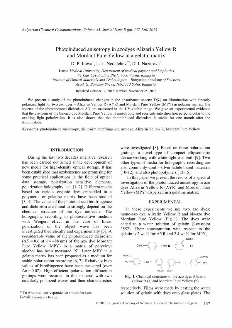
137
Bulgarian Chemical Communications, Volume 45, Special Issue B (pp. 137-140) 2013
Photoinduced anisotropy in azodyes Alizarin Yellow R and Mordant Pure Yellow in a gelatin matrix
D. P. Ilieva1, L. L. Nedelchev2*, D. I. Nazarova2
1Varna Medical University, Department of medical physics and biophysics, 84 Tzar Osvoboditel Blvd., 9000 Varna, Bulgaria
2Institute of Optical Materials and Technologies – Bulgarian Academy of Sciences, Acad. G. Bonchev Str, bl. 109,1113 Sofia, Bulgaria.
Received October 17, 2013; Revised November 25, 2013
We present a study of the photoinduced changes in the absorbance spectra D(λ) on illumination with linearly polarized light for two azo dyes – Alizarin Yellow R (AYR) and Mordant Pure Yellow (MPY) in gelatine matrix. The spectra of the photoinduced dichroism ΔD are measured in the UV-visible range. We give an experimental evidence that the cis-form of the bis-azo dye Mordant Pure Yellow is anisotropic and reorients into direction perpendicular to the exciting light polarization. It is also shown that the photoinduced dichroism is stable for one month after the illumination.
Keywords: photoinduced anisotropy, dichroism, birefringence, azo dye, Alizarin Yellow R, Mordant Pure Yellow
INTRODUCTION
During the last two decades intensive research has been carried out aimed at the development of new media for high-density optical storage. It has been established that azobenzenes are promising for some practical applications in the field of optical data storage, polarization sensitive elements, polarization holography, etc. [1, 2]. Different media based on various organic dyes embedded in a polymeric or gelatine matrix have been studied [3, 4]. The values of the photoinduced birefringence and dichroism are found to strongly depend on the chemical structure of the dye molecule. The holographic recording in photosensitive medium with Weigert effect in the case of linear polarization of the object wave has been investigated theoretically and experimentally [3]. A considerable value of the photoinduced dichroism (ΔD = 0.6 at λ = 488 nm) of the azo dye Mordant Pure Yellow (MPY) in a matrix of polyvinyl alcohol has been measured [5]. Later MPY in a gelatin matrix has been proposed as a medium for stable polarization recording [6, 7]. Relatively high values of birefringence have been measured (over Δn = 0.02). High-efficient polarization diffraction gratings were recorded in this material with two circularly polarized waves and their characteristics
were investigated [8]. Based on these polarization gratings, a novel type of compact ellipsometric device working with white light was built [9]. Two other types of media for holographic recording are also commonly used – silver halide based materials [10-12], and also photopolymers [13-15].
In this paper we present the results of a spectral investigation of the photoinduced anisotropy in azo dyes Alizarin Yellow R (AYR) and Mordant Pure Yellow (MPY) dispersed in a gelatine matrix.
EXPERIMENTAL
In these experiments we use two azo dyes: mono-azo dye Alizarin Yellow R and bis-azo dye Mordant Pure Yellow (Fig. 1). The dyes were added to a water solution of gelatin (Rousselot 3552). Their concentration with respect to the gelatin is 2 wt % for AYR and 2.4 wt % for MPY,
COOH
O2N OH
COOH
O2N OH
OH
NaOOC COONa
NaO3S SO3H
HO OH
NaOOC COONa
NaO3S SO3H
HO
Fig. 1. Chemical structures of the azo dyes Alizarin Yellow R (a) and Mordant Pure Yellow (b).
respectively. Films were made by casting the water solution of gelatin with dyes onto glass plates. The * To whom all correspondence should be sent:
E-mail: [email protected] © 2013 Bulgarian Academy of Sciences, Union of Chemists in Bulgaria

Nedelchev et al.: Photoinduced anisotropy in azodyes Alizarin Yellow R…
138
films thickness is between 3 and 5 μm. The samples were dried for 24 h at 20 °C and then for another 2 h at 80 °C to remove the residual moisture.
Linearly polarized light from a 200 W mercury lamp was used to induce isomerization of the azo-dyes. The illumination was done directly with the lamp or through filters transmitting 310–460 nm or 370–530 nm respectively. In the case of direct illumination the light intensity was 0.05 mW/cm2. When using the filters, it was 0.03 mW/cm2. The spectral measurements were carried out with a Cary 5E UV–VIS–NIR spectrophotometer (Varian Inc.) in the range 300–550 nm where is the absorbance band of the dyes. From the measured values of transmittance T, the absorbance D was easily determined using the Beer-Lambert law: D = – log(T).
RESULTS AND DISCUSSION
Curves 1 and 2 on Fig. 2 show the absorbance spectra of the two types of films before the illumination. The absorbance maximum of the Mordant Pure Yellow in gelatin is about 375 nm and for Alizarin Yellow R in gelatin is at 389 nm. After the exposure we measured the absorbance spectra of the samples through a polarizer oriented parallel and perpendicular to the exciting light polarization direction. The corresponding absorbances are denoted as Dpar and Dort and the dichroism is defined as ΔD = Dort – Dpar.
300 350 400 450 500 5500,0
0,5
1,0
1,5
2,0
Abs
orba
nce
Wavelength (nm)
12
Fig. 2. Absorbance spectra of the MPY/gelatin (1) and
AYR/gelatin films (2) before illumination.
In Fig. 3 the absorbance spectrum of the Alizarin Yellow R/gelatin film before and after illumination through the filter transmitting light in the range 370–530 nm is shown. Do is the absorbance before illumination and Dort and Dpar are the absorbances after 3 h exposure with linearly polarized light with intensity I = 0.03 mW/cm2.
Similar spectra were measured after exposure directly with mercury lamp and through filter transmitting from 310 nm to 460 nm.
300 400 5000,0
0,5
1,0
1,5
D
Dpar
DortDo
Abs
orba
nce
Wavelength (nm)
Fig. 3. Photoinduced changes in the absorbance of the AYR/gelatin film. Do –absorbance before the
illumination, Dort and Dpar – polarized absorbance spectra, ΔD = Dort – Dpar – dichroism.
In Fig. 4a the absorbance spectra of the bis-azo dye Mordant Pure Yellow in a gelatine matrix before and after 2 hours illumination with linearly
300 400 5000,0
0,5
1,0
1,5
D
Dpar
Dort
Do
Abs
orba
nce
Wavelength (nm)
(a)
300 400 5000,0
0,5
1,0
1,5
D
Abs
orba
nce
Wavelength (nm)
Do
Dort
Dpar
(b)
Fig. 4. Photoinduced changes in the absorbance of the MPY/gelatin film before and after 2 h exposure,
I = 0.05 mW/cm2 (a) and measured again after 1 month (b).
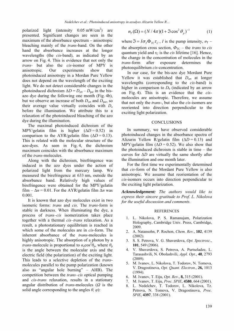
Nedelchev et al.: Photoinduced anisotropy in azodyes Alizarin Yellow R…
139
polarized light (intensity 0.05 mW/cm2) are presented. Significant changes are seen in the maximum of the absorbance spectrum – anisotropic bleaching mainly of the trans-band. On the other hand the absorbance increases at the longer wavelengths (the cis-band), as indicated by an arrow on Fig. 4. This is evidence that not only the trans- but also the cis-isomer of MPY is anisotropic. Our experiments show that photoinduced anisotropy in a Mordan Pure Yellow does not depend on the wavelength of the exciting light. We do not detect considerable changes in the photoinduced dichroism ΔD = Dort – Dpar in the bis-azo dye during the following one month (Fig. 4b), but we observe an increase of both Dort and Dpar, so their average value virtually coincides with Do before the illumination. We attribute this to a relaxation of the photoinduced bleaching of the azo dye during the illumination.
The maximal photoinduced dichroism of the MPY/gelatin film is higher (ΔD = 0.52) in comparison to the AYR/gelatin film (ΔD = 0.13). This is related with the molecular structure of the azo-dyes. As seen in Fig. 4, the dichroism maximum coincides with the absorbance maximum of the trans-molecules.
Along with the dichroism, birefringence was induced in the azo dyes under the action of polarized light from the mercury lamp. We measured the birefringence at 633 nm, outside the absorbance band. Relatively high values of birefringence were obtained for the MPY/gelatin film – Δn = 0.01. For the AYR/gelatin film Δn was 0.001.
It is known that azo dye molecules exist in two isomeric forms: trans and cis. The trans-form is stable in darkness. When illuminating the dye, a process of trans–cis isomerization takes place together with a thermal cis–trans relaxation. As a result, a photostationary equilibrium is reached in which some of the molecules are in cis-form. The inherent absorbance of the trans-molecules is highly anisotropic. The absorption of a photon by a trans-molecule is proportional to αzcos2θp, where θp is the angle between the molecular axis and the electric field (the polarization) of the exciting light. This leads to a selective depletion of the trans-molecules parallel to the pump polarization (known also as “angular hole burning” – AHB). The competition between the trans–cis optical pumping and cis-trans relaxation, results in a stationary angular distribution of trans-molecules (Ω is the solid angle corresponding to the angles θ, φ):
2 1( ) ( / 4 )(1 cos )T pn N (1)
where T TC CI , I is the pump intensity, σT –
the absorption cross section, ФTC – the trans to cis quantum yield and τC is the cis lifetime [16]. Hence, the change in the concentration of molecules in the trans-form after exposure determines the photoequilibrium cis-concentration.
In our case, for the bis-azo dye Mordant Pure Yellow it was established that Dort at longer wavelengths (corresponding to the cis-band) is higher in comparison to D0 (indicated by an arrow on Fig. 4). This is an evidence that the cis-molecules are anisotropic. Therefore, we assume that not only the trans-, but also the cis-isomers are reoriented into direction perpendicular to the exciting light polarization.
CONCLUSIONS
In summary, we have observed considerable photoinduced changes in the absorbance spectra of Alizarin Yellow R/gelatin film (ΔD = 0.13) and MPY/gelatin film (ΔD = 0.52). We also show that the photoinduced dichroism is stable in time – the curves for ΔD are virtually the same shortly after the illumination and one month later.
For the first time we experimentally determined that cis-form of the Mordant Pure Yellow is also anisotropic. We assume that reorientation of the cis-isomers occurs into direction perpendicular to the exciting light polarization.
Acknowledgement: The authors would like to express their sincere gratitude to Prof. L. Nikolova for the useful discussion and comments.
REFERENCES
1. L. Nikolova, P. S. Ramanujam, Polarization Holography, Cambridge Univ. Press, Cambridge, 2009.
2. A. Natansohn, P. Rochon, Chem. Rev., 102, 4139 (2002).
3. S. S. Petrova, V. G. Shaverdova, Opt. Spectrosc., 101, 549 (2006).
4. V. Shaverdova, S. Petrova, A. Purtseladze, L. Tarasashvili, N. Obolashvili, Appl. Opt., 48, 2793 (2009).
5. M. Ivanov, L. Nikolova, T. Todorov, N. Tomova, V. Dragostinova, Opt. Quant. Electron., 26, 1013 (1994).
6. M. Ivanov, T. Eiju, Opt. Rev., 8, 315 (2001). 7. M. Ivanov, T. Eiju, Proc. SPIE, 4580, 664 (2001). 8. L. Nedelchev, T. Todorov, L. Nikolova, Tz.
Petrova, N. Tomova, V. Dragostinova, Proc. SPIE, 4397, 338 (2001).
Nedelchev et al.: Photoinduced anisotropy in azodyes Alizarin Yellow R…
140
9. T. Todorov, L. Nikolova, G. Stoilov, B. Hristov, Appl Opt., 46, 6662 (2007).
10. B. Ivanov, M. Shopova, E. Stoykova, V. Sainov, Opt. Appl. 42, 643 (2012).
11. B. Ivanov, E. Stoykova, Ts. Petrova, V. Sainov, Proc. Bulg. Acad. Sci., 64, 345 (2011).
12. B. Ivanov, M. Shopova, A. Baldjiev, E. Stoykova, V. Sainov, Proc. SPIE, 7747, 77470K (2011).
13. I. Naydenova, S. Martin, V. Toal, J. Eur. Opt. Soc. Rapid, 4, 09042, (2009).
14. K. Pavani, I. Naydenova, S. Martin, R. Howard, V. Toal, J. Mater. Sci., 20, 198 (2009).
15. K. Pavani, I. Naydenova, S. Martin, V. Toal, J. Opt. A: Pure Appl. Opt., 9, 43, (2007).
16. M. Dumont, Z. Sekkat, Proc. SPIE, 1774, 188 (1992).
ФОТОИНДУЦИРАНА АНИЗОТРОПИЯ В АЗОБАГРИЛАТА АЛИЗАРИН ЖЪЛТО Р И ПРОТРАВНО ЧИСТО ЖЪЛТО В МАТРИЦА ОТ ЖЕЛАТИН
Д. П. Илиева1, Л. Л. Неделчев2, Д. И. Назърова2
1 Медицински университет “Проф. д-р П. Стоянов”, Катедра по медицинска физика и биофизика, бул. “Цар Освободител” 84, 9000 Варна, България
2 Институт по Оптически Материали и Технологии, Българска Академия на Науките, ул. Акад. Г. Бончев, бл. 109, 1113 София, България
Постъпила на 17 октомври 2013 г.; коригирана на 25 ноември, 2013 г.
(Резюме)
В настоящата работа са представени резултатите от изследване на фотоиндуцираните промени в спектрите на поглъщане D(λ) при облъчване с линейно поляризирана светлина за две азобагрила – Ализарин Жълто Р (АЖР) и Протравно Чисто Жълто (ПЧЖ) в матрица от желатин. Спектрите на фотодихроизъм ΔD = Dort – Dpar са измерени в УВ и видимата област. Представено е експериментално доказателство, че цис изомерът на бис-азобагрилото Протравно Чисто Жълто е анизотропен и се преориентира перпендикулярно на посоката на поляризация на въздействащата светлина. Показано е също, че фотоиндуцирания дихроизъм е стабилен един месец след облъчването.

141
Bulgarian Chemical Communications, Volume 45, Special Issue B (pp. 141-144) 2013
Time stability of photoinduced birefringence in amorphous and liquid-crystalline azopolymers
L. L. Nedelchev*, D. I. Nazarova
Institute of Optical Materials and Technologies, Bulgarian Academy of Sciences Acad.G.Bonchev Str., bl.109, 1113 Sofia, Bulgaria
Received October 17, 2013; Revised November 25, 2013
One of the most important parameters for every optical data storage media is the stability of the recorded information in time. When polarization holography is used for data recording, the information is encoded via the photoinduced anisotropy (most often birefringence) in the media.
In this article we present a study on the stability of the photoinduced birefringence (Δn) in amorphous (P1) and liquid-crystalline (LC) azobenzene polymer (P2) with similar structures of the backbone and the chromophore unit, but different spacers between them. As our experiments indicate, 72 % of the photoinduced birefringence is retained in the polymer P1, and 104 % in the polymer P2 one hour after the end of the recording process i.e. the stability of the birefringence in the LC polymer is considerably higher than in the amorphous.
Keywords: birefringence, time stability, optical data storage, azopolymer
INTRODUCTION
Azobenzene materials have attracted considerable attention since 1984 when Todorov et al. established the possibility to record high-efficient polarization diffraction gratings in layers of azo dye methyl-orange in polyvinyl alcohol (PVA) matrix [1]. The observed high values of reversible photoinduced anisotropy (birefringence and dichroism) on irradiation with linearly polarized light are obtained by two main processes:
selective trans-cis isomerization followed by reorientation of the trans-azobenzenes. The trans-cis-trans process for reorientation of the molecules is illustrated in Fig. 1. As the trans isomer is the stable form of the azo molecule, the trans-cis isomerization is always photoinduced (hν), but the cis-trans isomerization can be either photoinduced (hν'), or can result from spontaneous thermal relaxation (kT).
N
N N N
h
h ', kT
trans cis Fig. 1. Trans–cis–trans isomerization of azobenzenes.
The process continues until most of the azo
molecules lie in direction perpendicular to the polarization of the writing beam. In such position they cease to absorb light [1, 2].
Azopolymers have found numerous applications related with polarization recording and
in particular polarization holography [2] – optical elements with unique polarization properties can be inscribed in them [3, 4], as well as surface relief gratings [5, 6] and chiral structures [7, 8]. They are also good candidates for reversible holographic storage [9–13] allowing also polarization holographic multiplexing [14].
Recording in azopolymers is highly reversible, as it has been shown by Ramanujam and co-* To whom all correspondence should be sent:
E-mail: [email protected] © 2013 Bulgarian Academy of Sciences, Union of Chemists in Bulgaria

Nedelchev et al.: Time stability of photoinduced birefringence in amorphous…
142
workers: more than 10 000 cycles of optical recording and erasure have been realized without apparent fatigue of the media [15]. This is a certain advantage, but on the other hand raises the question about the stability of the recorded information in time.
In order to optimize the performance, many different types of azobenzene materials have been studied – azo dye solutions, azo dyes in polymer or gelatin matrix [1, 16], azo dyes chemically attached to the polymer backbone (called azopolymers) [6–15], even hybrid materials based on azopolymers doped with inorganic nanoparticles [17–19].
Here we present a study on the stability of the photoinduced birefringence (Δn) in two azopolymers with similar structure of the backbone and the chromophore unit, but different spacers between them. As a result, one of them is amorphous (P1) and the other is liquid-crystalline (P2).
EXPERIMENTAL
Azopolymer samples preparation and characterization
The polymers used in our experiments are side-chain cyanoazobenzene polymers. Their chemical structures are shown in Fig. 2. They were synthesized by radical-type polymerization, as described elsewhere [20]. The azopolymer denoted as P1 is amorphous and the polymer P2 is liquid-crystalline (LC). As seen in Fig. 2, the structures of
Fig. 2. Structures of the azopolymers P1 and P2 used in the present study.
their backbone and chromophore units are the same, but they differ in the spacer between the backbone and the azochromophore. The amorphous
character of P1 is determined by the short and rigid spacer, and the LC properties of P2 – by the flexible methylene chain, that allows the chromophore units to form LC domains.
The glass transition temperatures Tg and molecular weights Mw of the two polymers were measured by differential scanning calorimetry (DSC) and gel-permeation chromatography (GPC), respectively and the following data were obtained – P1 (Mw = 1.46×10⁴ g/mol, Tg = 106 °C) and P2 (Mw = 2.05×10³ g/mol, Tg = 35 °C).
Thin films from the two polymers dissolved in 1,2-dichloroethane were prepared by spin coating onto glass substrates. The samples based on the LC polymer P2 were heated above 80 °C and then rapidly cooled to room temperature; the other samples were not thermally processed. The thickness of the films was measured by high-precision Talystep profilometer and is 0.73 μm for the P1 film and 0.80 μm for the P2 film.
Polarimetric setup for photoinduced birefringence measurement
The kinetics of the photoinduced birefringence Δn is measured by a classical polarimetric scheme [1, 9–11]. Vertically polarized recording beam at 473 nm with intensity 400 mW/cm2 is used to induce birefringence. The sample is placed between crossed polarizers oriented at ±45° with respect to the vertical. The intensity I of a probe beam from He-Ne laser (λprobe = 633 nm) passing through the system is measured by a digital optical power meter (Thorlabs PM100). From this intensity, the value of the photoinduced birefringence can be easily determined using the following equation [1]:
0
)(arcsin)(
I
tI
dtn probe
(1)
where d is the thickness of the film, I0 is the intensity of the probe beam before the start of the recording and at parallel polarizers.
RESULTS AND DISCUSSION
Data for the time stability of the photoinduced birefringence can be found already in the first articles on azobenzenes. For instance, this issue is addressed by Todorov et al. and there is a comment that the decay of the birefringence may be slowed down substantially by preliminary thermal treatment of the samples [1]. Indeed, after such treatment more than 50 % of the photoinduced birefringence (and about 30 % of the diffraction

Nedelchev et al.: Time stability of photoinduced birefringence in amorphous…
143
efficiency) is retained for a long time after the acting light is stopped.
Later, Natansohn and co-workers [11] proposed a model for the birefringence relaxation. They obtained a good fit of the experimental data with a biexponential function of the type
EtkDtkCy DC )exp()exp( , where one
of the exponential terms corresponds to a “fast” decay process, the other – to a “slow” decay process and the constant value E, normalized to En = E/(C + D + E) represents the fraction of the induced birefringence retained permanently in the polymer film. For the investigated azopolymers the value of En was 84 %, calculated however on the base of relatively short (25 seconds) measurement of the birefringence decay.
A close correlation has been established between a short-term (30 min) and long-term (1 week) stability of the photoinduced birefringence in a family of amorphous azobenzene polyesters [12]. The polyester with highest short-term stability of 89 % demonstrated also highest long-term stability of 83 % one week after the recording.
The amorphous polymers are usually preferred for storage applications because of the lower scattering in them compared to the LC ones. On the other hand, as our experiments indicate, the stability of the birefringence in the LC polymer is considerably higher than in the amorphous. The results are shown in Table 1 and Fig. 3. The coefficients rt are defined as rt = Δn(t)/Δnmax, where in this case t is the time expired after the end of the recording process and Δnmax is the maximal value of the birefringence reached during the recording.
Table 1. Summary of the time stability data for azopolymers P1 and P2.
Azopolymer Δnmax r10min r30min r1hour
P1 0,030 85 % 75 % 72 % P2 0,066 102 % 102 % 104 %
As seen, after 1 hour 72 % of the photoinduced birefringence is retained in the polymer P1, and 104 % in the LC polymer P2. The fact that the value of Δn is even slightly increasing in the LC polymer after the end of the recording is attributed to the relaxation from cis to trans state of some of the chromophores, which tend to orient in direction parallel to the already optically oriented majority of the azomolecules. The data for Δnmax and r10min are in good agreement with our earlier measurements on the 10 min birefringence stability in polymers P1 and P2 [19]. The extended one hour measurement of
0 1000 2000 3000 40000,0
0,2
0,4
0,6
0,8
1,0
1,2
Nor
m. b
irefr
inge
nce n
/n
ma
x
Time [sec]
P1 - amorphous
a)
end of recording
72%
0 1000 2000 3000 40000,0
0,2
0,4
0,6
0,8
1,0
1,2
104%
P2 - liquid-crystalline
b)
Nor
m. b
irefr
inge
nce n
/n m
ax
Time [sec]
end of recording
Fig. 3. Time dependence of the normalized birefringence during the recording and in the
following 1 hour for the amorphous azopolymer P1 (a), and for the LC polymer P2 (b).
the time stability in the present experiment is sufficient for the “fast” decay process to complete. Therefore we can use the linear relation between the short-term (30 min) and long-term stability established in [12] for amorphous azopolymers and estimate the long-term stability of the recording in the polymer P1 to about 65 %.
CONCLUSIONS
Based on the experimental measurement of the photoinduced birefringence for one hour after the end of the recording, we have found the value of the anisotropy retained – 72 % in the amorphous azopolymer P1 and 104 % in the LC polymer P2. The long-term stability in P1 was estimated as 65 % using data from the literature.
This results also suggest that a co-polymer of the amorphous P1 and the LC polymer P2 may possess an optimal combination of properties – amorphous state and in the same time relatively high time-stability of the photoinduced anisotropy.
REFERENCES
1. T. Todorov, L. Nikolova, N. Tomova, Appl. Opt., 23, 4309 (1984).

Nedelchev et al.: Time stability of photoinduced birefringence in amorphous…
144
2. L. Nikolova, P. S. Ramanujam, Polarization Holography, Cambridge Univ. Press, Cambridge, 2009.
3. T. Todorov, L. Nikolova, Opt. Lett., 17, 358 (1992).
4. G. Martinez-Ponce, T. Petrova, N. Tomova, V. Dragostinova, T. Todorov, L. Nikolova, Opt. Lett., 29, 1001 (2004).
5. D. Y. Kim, L. Li, X. L. Jiang, V. Shivshankar, J. Kumar, S. K. Tripathy, Macromolecules, 28, 8835 (1995).
6. I. Naydenova, L. Nikolova, T. Todorov, N. C. R. Holme, P. S. Ramanujam, S. Hvilsted, J. Opt. Soc. Am. B, 15, 1257 (1998).
7. L. Nedelchev, L. Nikolova, T. Todorov, T. Petrova, N. Tomova, V. Dragostinova, P. S. Ramanujam, S. Hvilsted, J. Opt. A: Pure Appl. Opt., 3, 304 (2001).
8. J. del Barrio, R. M. Tejedor, L. Oriol, Eur. Polym. J., 48, 384 (2012).
9. A. Natansohn, P. Rochon, J. Gosselin, S. Xie, Macromolecules, 25, 2268 (1992).
10. S. Hvilsted, F. Andruzzi, C. Kulinna, H. W. Siesler, P. S. Ramanujam, Macromolecules, 28, 2172 (1995).
11. M. S. Ho, A. Natansohn, P. Rochon, Macromolecules, 28, 6124 (1995).
12. L. Nedelchev, A. S. Matharu, S. Hvilsted, P. S. Ramanujam, Appl. Opt., 42, 5918 (2003).
13. A. S. Matharu, S. Jeeva, P. S. Ramanujam, Chem. Soc. Rev., 36, 1868 (2007).
14. D. Ilieva, L. Nedelchev, T. Petrova, N. Tomova, V. Dragostinova, L. Nikolova, J. Opt. A: Pure Appl. Opt., 7, 35 (2005).
15. N. C. R. Holme, P. S. Ramanujam, S. Hvilsted, Opt. Lett., 21, 902 (1996).
16. T. D. Ebralidze, A. N. Mumaladze, Appl. Opt., 29, 446 (1990).
17. J. Zhou, J. Yang, Y. Sun, D. Zhang, J. Shen, Q. Zhang, K. Wang, Thin Solid Films, 515, 7242 (2007).
18. L. Nedelchev, D. Nazarova, V. Dragostinova, D. Karashanova, Opt. Lett., 37, 2676 (2012).
19. L. Nedelchev, D. Nazarova, V. Dragostinova, J. Photoch. Photobio. A, 261, 26 (2013).
20. G. Martinez-Ponce, Ts. Petrova, N. Tomova, V. Dragostinova, T. Todorov, L. Nikolova, J. Opt. A: Pure Appl. Opt., 6, 324 (2004).
ВРЕМЕВА СТАБИЛНОСТНА ФОТОИНДУЦИРАНОТО ДВУЛЪЧЕПРЕЧУПВАНЕ В АМОРФЕН И ТЕЧНОКРИСТАЛЕН АЗОПОЛИМЕР
Л. Л. Неделчев, Д. И. Назърова
Институт по Оптически Материали и Технологии, Българска Академия на Науките, ул. Акад. Г. Бончев, бл. 109, 1113 София, България
Постъпила на 17 октомври 2013 г.; коригирана на 25 ноември, 2013 г.
(Резюме)
Един от най-важните параметри на всяка среда за оптичен запис на информация е стабилността на записаната информация във времето. Когато записа се извършва чрез поляризационна холография, информацията се кодира чрез фотоиндуцираната в средата анизотропия (най-често двулъчепречупване).
В настоящата статия е представено изследване на фотоиндуцираното двулъчепречупване (Δn) в два азополимера – аморфен P1 и течнокристален P2 с еднакви структури на главната верига и хромофора, но различни дължини на страничните вериги. Както показват експерименталните данни, един час след прекратяването на записа в полимер P1 се запазват 72 % от фотоиндуцираното двулъчепречупване, а в полимер P2 – 104 % т.е. стабилността на двулъчепречупването в течнокристалния полимер е значително по-висока отколкото в аморфния.

145
Bulgarian Chemical Communications, Volume 45, Special Issue B (pp. 145-148) 2013
Photoinduced anisotropy in a series of azobenzene copolymers
L. L. Nedelchev1*, D. I. Nazarova1, V. D. Dragostinova1, P. K. Petkov2, A. A. Stoilova2
1Institute of Optical Materials and Technologies, Bulgarian Academy of Sciences Acad.G.Bonchev Str., bl.109, 1113 Sofia, Bulgaria
2University of Chemical Technology and Metallurgy,8 Kl.Ohridski Blvd,
Received October 17, 2013; Revised November 25, 2013
In order to optimize the parameters of the photoinduced birefringence in azopolymers, we have synthesized and studied copolymers with different weight ratios of two monomers which differ in the length of spacer between the azochromophore and the polymer backbone. The polymer P1 based only on the first monomer is amorphous, and the polymer P2 which contains only the second monomer is liquid-crystalline (LC). In addition to the homopolymers P1 and P2, five copolymers were synthesized, described by the general formula P1(100 – x)P2(x), where x gives the percent weight ratio of the second monomer in the final copolymer. As a result the following seven polymers were obtained – P1, P1(75)P2(25), P1(60)P2(40), P1(50)P2(50), P1(40)P2(60), P1(25)P2(75), P2.
The main parameters of the photoinduced birefringence in these polymers, such as maximal value, response time and time stability, have been measured and compared.
Keywords: azopolymer, copolymer, photoinduced birefringence, optimization
INTRODUCTION
The first report on high-efficient polarization recording in azobenzene material appeared in 1984 by Todorov et al. [1]. The material was solid solution of methyl orange in poly(vinyl alcohol). The large photoinduced birefringence and dichroism are caused by the reorientation of the azomolecules via trans-cis-trans photo-isomerization.
The potential of the azobenzenes for reversible digital and holographic storage including also commercial applications was realized by Eich and Wendorff [2, 3]. They used a material, where the azochromophore was chemically attached to a polymer chain i.e. the first liquid crystalline (LC) azopolymer. Later, huge number of azopolymers have been studied for holographic data storage [4] – liquid crystalline [5–8] and amorphous [9–11]. As both states (LC and amorphous) have certain advantages, some researchers tried to combine them, synthesizing copolymers containing mesogenic and non-mesogenic monomers [12].
Our approach in this study is similar. Earlier, we have synthesized and investigated three side-chain
azopolymers (two homopolymers and a copolymer) with similar structures of the main chain and the chromophore, but different spacer between them [13]. These azopolymers have also been used as organic matrix for recently developed photosensitive hybrid organic/inorganic materials [14–17].
Two of these polymers are amorphous and one is LC. In order to optimize the parameters of the photoinduced anisotropy in azopolymers, we have synthesized four additional copolymers with different weight ratios of two monomers and determined the main characteristics of the birefringence in the entire azopolymer family.
EXPERIMENTAL
Synthesis of the azo homopolymers and copolymers
All seven polymers (both homopolymers and copolymers) studied in this article are side-chain cyan azo polymers containing different ratios of the monomers shown in Fig. 1. They were synthesized by a three-step process: (a) synthesis of the azo dyes; (b) preparation of the chromophore monomers, and (c) radical-type polymerization of the monomers. Initially the azo dye (I) 4-(4-hydroxy-phenylazo)benzonitrile was synthesized by dissociation of 4-aminobenzonitrile and coupling * To whom all correspondence should be sent:
E-mail: [email protected] © 2013 Bulgarian Academy of Sciences, Union of Chemists in Bulgaria

Nedelchev et al.: Photoinduced anisotropy in a series of azobenzene copolymers
146
with phenol using standard technology. Dye (II) 4-[4-(6-hydroxy-hexyloxy)phenylazo]benzonitrile was obtained from dye (I) by etherification with 6-bromo-1-hexanol. At the second step, the two azo dyes were transformed in the monomers M1 and M2 (see Fig. 1) by etherification with acryloyl chloride. Finally, different weight ratios of the two monomers have been combined and polymerized via radical-type polymerization.
M1
M2
Fig. 1. Structure of the monomers used to prepare the homopolymers and copolymers.
In addition to the homopolymers P1 (obtained from monomer M1 only) and P2 (containing only M2), five copolymers were synthesized, described by the general formula P1(100 – x)P2(x). Here x gives the percent weight ratio of the second monomer (M2) in the final copolymer and has values x = 0, 25, 40, 50, 60, 75, 100. As a result the following seven polymers were obtained – P1, P1(75)P2(25), P1(60)P2(40), P1(50)P2(50), P1(40)P2(60), P1(25)P2(75), P2.
The polymers P1, P1(50)P2(50) and P2 have been studied earlier and it has been established that P1 and P1(50)P2(50) are amorphous, P2 is liquid crystalline [13, 16]. Their molecular weights and glass transition temperatures are also known: P1 – Mw = 1.46×10⁴ g/mol, Tg = 106 °C, P1(50)P2(50) – Mw = 3.60×10³ g/mol, Tg = 102 °C and P2 – Mw = 2.05×10³ g/mol, Tg = 35 °C. The other four copolymers are newly synthesized.
Thin films preparation and FTIR characterization
In order to prepare thin films for optical testing, 20 mg of the polymer were dissolved in 200 μl of 1,2-dichloroethane, i.e. at concentration of 100 g/L. Then the solutions were spin coated at 1500 rpm on glass substrates to produce films with uniform
thickness. The thicknesses of the films were measured by high-precision Talystep profilometer. Fourier transform infrared spectra (FT-IR) were measured by Bruker IR spectrometer for the homopolymers P1 and P2, and also for their “closest” copolymers: P1(75)P2(25) and P1(25)P2(75), respectively. They are given in Fig. 2. As seen, the characteristic peaks of absorption of the corresponding polymers are similar that indicates the correct composition of the copolymers.
0 1000 2000 3000 40000,0
0,1
0,2
0,3
0,4
0,5
P1
P1(75)P2(25)
Abs
orb
an
ceWavenumber, cm-1
a)
0 1000 2000 3000 40000,0
0,1
0,2
0,3
0,4
0,5
0,6
b)
P2
P1(25)P2(75)
Abs
orb
ance
Wavenumber, cm-1
Fig. 2. FT-IR spectra of: a) P1 and P1(75)P2(25); b) P2 and P1(25)P2(75).
Photoinduced birefringence measurement
Birefringence is induced in the samples by a vertically polarized beam from a DPSS laser at 473 nm (I = 400 mW/cm2), inside the absorption band of the azochromophores. The sample is placed between crossed polarizers oriented at ±45° with respect to the vertical. The intensity I of a probe beam (λprobe = 633 nm) passing through the system is measured and the value of the photoinduced birefringence Δn is determined by the equation
0)(arcsin)()( ItIdtn probe , where d is
the film thickness, I0 is the intensity of the probe beam before the start of the recording and at parallel polarizers.

Nedelchev et al.: Photoinduced anisotropy in a series of azobenzene copolymers
147
RESULTS AND DISCUSSION
Using the optical scheme described in Section 2.3, for each sample we have made a 15 min measurement, consisting of three stages: (i) 1 min to estimate the background optical noise; (ii) 5 min of recording by which we find the response time τ and the maximal birefringence Δnmax, and (iii) 9 min of relaxation after the end of the recording to determine the stability r. A typical measurement is presented in Fig. 3a for the copolymer P1(75)P2(25). The data for all the polymers from the series are given in Table 1. The correlation between Δnmax and the polymers composition is shown in Fig. 3b. From the tabulated data is seen that the LC polymer P2 has highest value of the photoinduced birefringence and it is also most stable, even some increase is observed after the end of the recording. This is most likely due to a relaxation from cis to trans state of some of the chromophores, which tend to orient in line with the already optically oriented majority of the azomolecules. On the other hand, the copolymer P1(75)P2(25) has fastest response. The choice of particular polymer from these series can be done depending on the application.
0 200 400 600 800 10000,00
0,01
0,02
0,03
0,04
iiiii
P1(75)P2(25)
Bire
frin
genc
e n
Time [sec]
a)
i
0 20 40 60 80 1000,00
0,02
0,04
0,06
0,08
0,10
b)
P1(25)P2(75)P2
Bire
frin
genc
e n
Ratio of M2, %
P1
Fig. 3. a) kinetics of Δn for P1(75)P2(25); b) Δnmax vs. ratio of the monomer M2.
Table 1. Summary of data for the series of azobenzene copolymers P1–P2.
CONCLUSIONS
We have synthesized a series of seven azopolymers described by the general formula P1(100 – x)P2(x), namely P1, P1(75)P2(25), P1(60)P2(40), P1(50)P2(50), P1(40)P2(60), P1(25)P2(75), P2. The main parameters of the photoinduced birefringence in these polymers, such as maximal value, response time and time stability, have been measured and compared. The highest birefringence is obtained in the homopolymer P2 (Δnmax = 0,102) and the copolymer P1(75)P2(25) has shortest response time – 6 s.
REFERENCES
1. T. Todorov, L. Nikolova, N. Tomova, Appl. Opt., 23, 4309 (1984).
2. M. Eich, J. Wendorff, B. Reck, H. Ringsdorf, Makromol. Chem. Rapid Commun., 8, 59 (1987).
3. M. Eich, J. Wendorff, B. Reck, US Patent No. 4 837 745 (1989).
4. A. Natansohn, P. Rochon, Chem. Rev., 102, 4139 (2002).
5. S. Hvilsted, F. Andruzzi, C. Kulinna, H. W. Siesler, P. S. Ramanujam, Macromolecules, 28, 2172 (1995).
6. K. Ichimura, Chem. Rev. 100, 1847 (2000). 7. A. S. Matharu, S. Jeeva, P. S. Ramanujam, Chem.
Soc. Rev., 36, 1868 (2007). 8. N. C. R. Holme, S. Hvilsted, E. Lorincz, A.
Matharu, L. Nedelchev, L. Nikolova, P. S. Ramanujam, in: Handbook of organic electronics and photonics, H. S. Nalwa (ed), vol. 2, American Scientific Publishers, Valencia, CA, 2007, p. 184.
9. A. Natansohn, P. Rochon, J. Gosselin, S. Xie, Macromolecules, 25, 2268 (1992).
10. S. J. Zilker, T. Bieringer, D. Haarer, R. S. Stein, J. W. van Egmond, S.G. Kostromine, Adv. Mater., 10, 855 (1998).
11. L. Nedelchev, A.Matharu, S.Hvilsted, P.S. Ramanujam, Appl. Opt., 42, 5918 (2003).
Azopolymer Maximal
Birefringence Δnmax
Stabilitya r, %
Response time τ, sec
P1 0,025 84 25 P1(75)P2(25) 0,038 82 6b
P1(60)P2(40) 0,041 85 11,5 P1(50)P2(50) 0,058 89 12 P1(40)P2(60) 0,052 88 10 P1(25)P2(75) 0,069 86 19
P2 0,102b 110b 25,5 a Stability is evaluated as ratio of birefringence 9 min after the end of recording to Δnmax. b The highest values of the maximal birefringence and stability as well as the shortest response time are outlined in bold.

Nedelchev et al.: Photoinduced anisotropy in a series of azobenzene copolymers
148
12. L. Nedelchev, L. Nikolova, A. Matharu, P. S. Ramanujam, Appl. Phys. B, 75, 671 (2002).
13. G. Martinez-Ponce, Ts. Petrova, N. Tomova, V. Dragostinova, T. Todorov, L. Nikolova, J. Opt. A: Pure Appl. Opt., 6, 324 (2004).
14. L. Nedelchev, D. Nazarova, V. Dragostinova, D. Karashanova, Opt. Lett., 37, 2676 (2012).
15. D. Nazarova, L. Nedelchev, P. Sharlandjiev, V. Dragostinova, Appl. Opt., 52, E28 (2013).
16. L. Nedelchev, D. Nazarova, V. Dragostinova, J. Photochem. Photobiol. A: Chem., 261, 26 (2013).
17. D. Nazarova, L. Nedelchev, V. Dragostinova, N. Berberova, Proc. SPIE, 8770, 877009 (2013).
ФОТОИНДУЦИРАНА АНИЗОТРОПИЯ В СЕРИЯ АЗОБЕНЗЕН-СЪДЪРЖАЩИ СЪПОЛИМЕРИ
Л. Л. Неделчев1, Д. И. Назърова1, В. Д. Драгостинова1, П. К. Петков2, А. А. Стоилова2
1 Институт по Оптически Материали и Технологии, Българска Академия на Науките, ул. Акад. Г. Бончев, бл. 109, 1113 София, България
2Химикотехнологичен и Металургичен Университет, бул. “Кл. Охридски” 8, София 1756, България
Постъпила на 17 октомври 2013 г.; коригирана на 25 ноември, 2013 г.
(Резюме)
С цел оптимизиране параметрите на фотоиндуцираното двулъчепречупване в азополимери, бяха синтезирани и изследвани съполимери с различни тегловни отношения на два мономера, които се различават по дължината на страничната верига, свързваща азохромофора с главната полимерна верига. Полимерът P1 изграден само от единия мономер е аморфен, докато полимерът P2, който е съставен само от втория мономер е течнокристален. Освен това са синтезирани още пет съполимера, описани от общата формула P1(100–x)P2(x), където x задава тегловното съдържание в проценти на втория мономер в крайния съполимер. В резултат на това са получени следните седем полимера – P1, P1(75)P2(25), P1(60)P2(40), P1(50)P2(50), P1(40)P2(60), P1(25)P2(75), P2.
Измерени са основните параметри на фотоиндуцираното двулъчепречупване в тези полимери – максималната му стойност, времето на отклик и стабилността във времето – и е направено сравнение между тях.

149
Bulgarian Chemical Communications, Volume 45, Special Issue B (pp. 149-153) 2013
Dynamic speckle technique as a leaf contamination sensor
B. Ivanov, E. Stoykova*, N. Berberova, T. Nikova, E. Krumov, N. Malinowski
Instute of Optical Materials and Technologies, Bulgarian Academy of Sciences, Acad. G. Bonchev Str., Bl. 101, 1113 Sofia, Bulgaria
Received October 17, 2013; Revised November 25, 2013
The phenomenon of laser speckle yields information about physical, chemical or biological activity in time for various objects (e.g. fruits, seeds, coatings) through statistical description of speckle dynamics. The paper introduces analysis of dynamic speckle patterns as an effective leaf contamination sensor by non-destructive whole-field characterization of the tested samples with high spatial and temporal resolution. More specifically, the paper presents the results of two test experiments in order to detect any variation of activity related to increase of humidity or treatment by chemical agents. In total, time sequences of 256 images of speckle patterns were recorded and processed by pointwise implementation of correlation-based algorithms. The experiments proved the ability of this approach to differentiate between differently treated leaves.
Keywords: dynamic speckle, leaf contamination, correlation analysis
INTRODUCTION
Coherent illumination of a diffuse object yields a randomly varying speckle pattern[1] in case of physical, chemical or biological activity within the object. This phenomenon can be used for non-invasive whole-field detection and visualization of processes in biological samples through statistical description of laser speckle dynamics [2]. The main advantage of this approach is ability to perform distant measurements with high spatial and temporal resolution without requirement for sophisticated equipment. Speckle fluctuations can be easily seen with a bare eye but a comprehensive statistical analysis is required to retrieve relevant information [3]. Usage of modern 2D optical sensors to register time sequences of speckle patterns provides large amount of data for accurate estimation of both first and second statistical moments of the recorded intensity data [1, 3] that can be used to characterize activity of samples. Dynamic laser speckle has been applied to study perfusion of blood flow in human tissues in medicine [4-5], bacterial response in biology [6], plant development processes [7], seeds viability [8], as well as for quality assessment of fruits and control of pasty products [11-13].
Here we reported the results of test experiments conducted to prove the efficiency of dynamic
speckle technique for detection of changes on a leaf surface after applying a chemical agent. For the purpose, randomly varying speckle patterns of laser light, reflected from the leaf surface, were recorded as time sequences. They were used to calculate spatial distributions of temporal correlation and structure functions across the leaf surface and to evaluate the undergoing activity in time. The results proved the ability of this approach to differentiate between differently treated leaves.
EXPERIMENTAL AND DATA PROCESSING
In the set-up for acquisition and storage of dynamic speckle patterns (Fig. 1) an expanded beam from a He-Ne laser (632.8 nm and 3.2 mW) illuminated the leaf sample placed on a horizontal stage through a ground glass diffuser. The set-up was positioned on a vibration insulated table. An optical axis of a CCD camera, adjusted to focus the sample, was normal to its surface. The camera recorded regularly a sequence of 8-bit encoded images at sampling frequency chosen to provide at least 10-20 points within the width of the temporal auto-correlation function which characterized intensity fluctuations due to sample activity.
We made two test experiments. In the first one, a pea leaf was placed on a sheet of paper. Two separate acquisitions of speckle patterns were carried on under different humidity conditions. In the second experiment three leaves (Tradescantia
* To whom all correspondence should be sent: E-mail: [email protected] © 2013 Bulgarian Academy of Sciences, Union of Chemists in Bulgaria

Ivanov et al.: Dynamic speckle technique as a leaf contamination sensor
150
Fig. 1. Set-up for acquisition and storage of dynamic
speckle patterns: 1 – He-Ne laser, 2 – beam expander, 3 – ground glass diffuser, 4 – sample, 5 – vibration
insulated table, 6 – CCD camera, 7 – PC.
albiflora) were placed next to each other in a petri dish. Two drops of acid (HNO3, 0.01%) and two drops of alkali (NaOH, 0.01%) water solutions were squeezed at the cut endings of the stems and at the middle parts of two of the leaves respectively; no chemical agent was applied to the third leaf. The leaves were fixed by sticking their tips with a plastic tape to the petri dish. The stem ending and the tip of the leaf without treatment were also fixed to the dish by a plastic tape to prevent penetration of the chemical agents from the other leaves.
Specifics of the observed object required to estimate activity at each point of the leaf surface. If N patterns of size yx NN are acquired for time T at
a sampling rate TNt /1 and a pixel period ,
yx NN time sequences of 8-bit encoded intensities
tnlkII nkl ,,, , yx NlNk ...2,1,...2,1 ,
Nn ...2,1 are formed. They allow for building a point wise estimate of a given statistical measure by averaging over T. We processed the data by correlation based algorithms which yield a set of 2D activity maps at increasing time lags and spatial resolution limited by the pixel period. We assume that the short-time activity within the sample is described by the 2D spatial distribution of the normalized temporal correlation function (NTCF), which is a function of the time lag, tm at a point with spatial coordinates yx, and has a
radius of correlation lkcc , which may
vary from point to point. The estimate normR of normR
is calculated from the series nklI , as
mN
nklmnklklnkl
mnorm IIII
lkmlkR
0,,,
,,ˆ
(1)
with 1
1
mNm and
N
nklnkl II
Nlk
1
2
,
1,
,
N
nnklkl I
NI
1,
1, where lk,
and klI are the estimates
of the variance and the mean of the intensity fluctuations in time at the point lk , .
Theoretically normR gives degree of correlation
and decreases with the time lag tm . Fully correlated state with zero activity corresponds to 1. The point wise processing yields a set of 2D spatial maps of activity at increasing time lags starting from t1 and going up to tMM with
NM . Although these maps are obtained for the averaging time interval T, they provide information about temporal scales of activity within this interval and in the different spatial regions of the sample. Using normalized correlation-based algorithms ensures spatial characterization of activity that is independent of illumination and reflectivity variation across the object surface.
RESULTS AND DISCUSSION
The results from the first test experiment are shown in Fig. 2 and Fig. 3, which give 2D gray-scale maps of the NTCF at four different lags for a pea leaf at normal (Fig. 2) and increased (Fig. 3) humidity. All maps were obtained after averaging over a sequence of N = 170 images with yx NN =
600500; the gray scale varies from -0.25 to 1.0. The intensity for the leaf region in the speckle patterns is considerably lower than for the surrounding sheet of paper, but the latter exhibits practically zero fluctuations with exception of the shadow zone. The shadow in Fig. 2 is cast by the stem of the leaf whereas in Fig. 3 it is caused by one of the leaf petals. Observation of activity in this zone is an indicator of microscopic changes of the leaf surface. As a whole, more or less uniform activity across the leaf surface is observed. As it should be expected, the processes within the leaf sample are going much faster and the correlation time is much shorter at increased humidity.

Fig. 2
normalizfluctu
between
Fig.
normalizfluctu
betw
In the intensity wepetri dish awetting by and alkali sleaves. Thein comparisthat the spreof the leaf iof the petriusing of a nwith the sipattern. To of interest introduced calculated
2. Gray scalezed temporal cuations of a pe
the processed
3. Gray scale zed temporal cuations of a peween the proce
h
second exere observedaround the lgradual spre
solutions aroe reflectivityson to the suead of speckis also loweri dish. As hnormalized eignal-dependfocus on the– the sura threshold
a binary m
Ivanov et al.:
maps from -0correlation funa leaf at differ
d patterns at n
maps from -0correlation funea leaf at diffeessed patterns humidity.
xperiment, d also on theleaves due teading of th
ound and beny of leaves wurrounding akle fluctuatior than in thehas been meestimator solvdent variance changes onrface of thed value of
mask which
Dynamic speck
0.25 to 1 of a nction of speckrent time lags ormal humidi
0.25 to 1 of a nction of specrent time lagsat increased
fluctuations e surface of to its inevita
he drops of aneath the treawas much lorea. This me
ons in the rege remaining entioned aboves the prob
ce in a specnly in the rege leaves –f intensity
kept only
kle technique as
kle s ity.
ckle s
in f the able acid ated
ower eans gion part ove,
blem ckle gion
we and the
inteseqtwochacouwitdistaveof rmastrosamfor alkleav
theacidwitAftacidwitfixeon of aNTflucstru
acqFigmamarowrecAccstem
s a leaf contam
ensities beloquences of 25o days at ange in meauld not be exthin the lastributions oferaging over recording thps differ wiongly varyimples, the in
the three lekali solutionsves are clear
Fig. 4. Grayintensity dencoded s
(right) aftertreatment, water solu
treatment isd solution –th alkali solter 20 hours d treatment sth exception ed tip, and ththe leaf withactivity in th
TCF. To vctuations in ducture functi
mlkS ,,ˆ
The results quired sequeng. 5 where thps whereas tps at 3 s and
w corresponorded immecording to tms and insid
ination sensor
ow the thres56 images tht =1.5 s. W
an intensity xplained onlyser spot. Ff the mean v256 speckle
e time sequeith 20 hoursing reflectitensity range
eaves and ths at the midrly seen. In
-scale maps frdistribution calpeckle pattern
r picking the lemiddle leaf –tion, bottom l
alkali wate
s at the top, – in the middution – at tthe reflectiv
strongly incrof the area
he contours oh alkali treathis experimevisualize bdifferent regon estimated
N
nnklm I
0,
for N = 25nces of speckhe first two cthe other twod 6 s time lagnds to the ediately aftethe NTCF thde the drops
shold. We hat were reco
We noticed aon the seco
y by increaseFigure 4 prvalue estimae patterns. Tences for bos. The first ivity acrosse is practica
he drops of tddle part ofFig. 4 the l
from 0 to 100 oalculated from ns at 0 h (left)eaves; top lea
– with two droleaf – with twoer solution.
the leaf treadle, and the the bottom vity of the lreases all ovea in the proxof the drop r
atment. Chaent was madebetter the gions we usedd as
mnklI 2,
56 and for kle patterns acolumns givo – the structgs respective
sequence ter picking he activity with chemic
151
processed 7orded withina substantialond day thate of intensityresents twoate klI after
The momentsoth presented
map showss the leaflly the samethe acid andf the treatedeaf without
of the mean 256 8-bit and 20 h f – without
ops of acid o drops of
ated with anleaf treated
of the map.leaf with theer its surfaceximity of itsremains onlyracterizatione by using a
spread ofd a temporal
(2)
four of theare shown in
ve the NTCFture functionely. The first
of imagesthe leaves.
close to thecal agents is
7 n l t y o r s d s f e d d
n d . e e s y n a f l
e n F n t s . e s

152
higher. Onemaps corres
Fig. 5. Gtime lag
scale mtime lag
maps are encoded
h (2nd
most considlarger area iand the fouron the next has more uacid treatmmuch higheThe drop wzone of incr
e hour later sponding to t
Gray-scale ma3 s (1st colum
maps from 0 tog 3 s (3rd colum calculated fro
d speckle patted row), 20 h (3
picki
derable chanin which reflrth row in Fday. The act
uniform distrment shows er reflectivity
with alkali soreased activit
Ivanov et al.:
(second rowthe acid treat
aps from -0.25mn) and 6 s (2n
o 60 of a strucmn) and 6 s (4om time sequeerns acquired a3rd row), 21 h ng the leaves.
nge: the dropflectivity incrig. 5 presenttivity stronglribution. Thless variatioy than the otolution is stilty for the thi
Dynamic speck
w in Fig. 5) tment show t
5 to 1 of NTCFnd column); grcture function 4th column). Tences of 256 8at 0 h (1st row(4th row) after.
p is spread treases. The tht the same mly decreases
he leaf with on in time ther two leavll traceable aird leaf.
kle technique as
the the
F at ray-at
The 8-bit
w), 1 r
to a third maps
and the and
aves. as a
spesurappencexpalgtemtheinddiff
1
2
3
4
5
6
7
8
9
1
s a leaf contam
In summaryeckle techniqrface as a plication of couraging rperiments worithms. The
mporal correlactivity acr
dicate clearlyferent treatm
1. H. Rabal,and AppGroup, 20
2. Y. Aizu, optics, Ac
3. R. Braga, N. Cap, Horgan, O
4. V.Rajan, Steenberg
5. A. Serov, (2005).
6. S. MurialdGonzalez,14, 06401
7. R. Braga,Eur. J. Bio
8. R. BragaMachado,Biosystem
9. E.Silva, SProc., 992
10. E. StoykLiubenova7747, 774
ination sensor
CONCLU
y, we checkeque to detec
result of a chemica
results fromwith point e calculated ation or struross the sury the region
ment.
REFEREN
and R. Braglications, Cr
008 T. Asakura,
cademic, LondB. Silva, G. RH. Rabal, R
Opt. Las. Eng.B.Varghe
gen, Opt. Lett.,T. Lasser, Op
do, G. Sendra, H. Rabal, M5 (2009).
, , L. Dupuy,ophys. 38, 679,G. Rabelo, L R. Arizaga
ms EngineeringS. Lannes, M2, 309 (2008).kova, B. Iva, I. Panchev
470L-1-11 (20
USION
ed the abilityct changes humidity v
al agent. Wm the perf
wise corre2D gray-sc
ucture functiorface of the ns that have
NCES
ga, Dynamic Lrc Press, Ta
In: Biospecdon, 1996, 27-Rabelo, R. Co
R. Arizaga, M., 45, 390 (200ese, T.Lee, 31, 468 (200
Opt. Express, 1
a, L. Passoni, M. Trivi, J. B
, M. Pasqual,9 (2009). L. Granato, a, H. Rabag, 91, 465 (20
M. Muramatsu. vanov, M. v, V. Sainov011).
y of dynamicon the leaf
variation orWe obtainedformed testelation-basedcale maps ofons visualizesample and
e undergone
Laser Speckleaylor&Francis
kle trends in-49 osta, A. Enes,M. Trivi, G.07). uwen, W.
06). 13, (17), 6416
R. Arizaga, J.Biomed. Opt.,
, R. Cardoso,
E. Santos, J.l, M. Trivi,
005). u, AIP Conf.
Shopova, T., Proc. SPIE
c f r d t d f e d e
e s
n
, .
.
6
. ,
,
. ,
f.
. E

Ivanov et al.: Dynamic speckle technique as a leaf contamination sensor
153
АНАЛИЗ НА ИЗМЕНЯЩИ СЕ СПЕКЪЛ КАРТИНИ КАТО НЕРАЗРУШАВАЩА СЕНЗОРНА ТЕХНИКА ЗА ЗАМЪРСЯВАНЕ НА ЛИСТА НА РАСТЕНИЯ
Бр. Иванов, Е. Стойкова, Н. Берберова, Т. Никова, Е. Крумов, Н. Малиновски
Институт по оптически материали и технологии- БАН ул. "Акад. Г.Бончев", бл.109, ПК 1113,София, България
Постъпила на 17 октомври 2013 г.; коригирана на 25 ноември, 2013 г.
(Резюме)
Явлението лазерен спекъл позволява проследяване на скоростта на протичане на физични, химични или биологични процеси в различни обекти като например плодове, семена, покрития и други чрез статистическо описание на динамиката на спекъл картината върху повърхността на тези обекти. Настоящата работа въвежда анализа на изменящи се във времето спекъл картини като неразрушаваща сензорна техника за замърсявания на листа на растения. Характерзирането на образците се извършва паралелно по цялата им повърхност с висока пространствена и времева разделителна способност. По-конкретно работата представя резултатите от два тестови експеримента за установяване на промяна в скоростта на процесите вследсвие на изменение на влажността и на химично въздействие. Като цяло, серии от 256 изображения на спекъл картини се записват последователно във времето и се обработват чрез корелационно-базирани алгоритми, прилагани за всяка точка от образеца. Експериментите потвърждават потенциала на този подход за различаване на листа, подложени на различно въздействие.

154
Bulgarian Chemical Communications, Volume 45, Special Issue B (pp. 154-158) 2013
Filled out Correcting in Auger Electron Spectroscopy
G. S. Spasov*
Institute of Optical Materials and Technologies “Academician Jordan Malinovski”, Bulgarian Academy of Sciences, Acad. G. Bonchev St., Block 109, 1113 Sofia, Bulgaria;
Received October 17, 2013; Revised November 25, 2013
The concept "correcting" in Auger quantification is filled out by the idea "total correction". 2 new groups of corrections – for the analysis regime (presented in this work by the factors "primarily beam energy” and "modulation voltage") and for the apparatus (presented by the quantity "spectrometer’ energy resolution") are included more except the matrix. The analyses accuracy' increase (with the increase of the correction steps) is monitored on the base of AlN standard quantification.
The filled out correction provides to compare the accuracy of Auger quantitative methods. The introduced term "autocorrecting" indicates the inner insurance for a condition (a priori worsening the accuracy) from the method itself. One method is more accurate at more complete "autocorrecting". The experiment compares six Auger quantitative methods.
Keywords: Auger electron spectroscopy, AES, quantification, correcting, correction
INTRODUCTION
Usually the AES applications require quantitative results. Unfortunately an accuracy of less than 10% remains а difficult task for AES. During the first significant attempt for quantitative Auger analysis, Palmberg et al. [1] define the content of an element A from the sample сA as proportional to its spectral intensity IA:
i
0iAi0AA )/I(I)//I(Ic (1)
where the sum is over all elements of the sample and the relative Auger elemental sensitivity factor (RAESF) I0 is the spectral intensity from the pure (100%) element. The atomic density N, electron back-scattering factor R and attenuation depth λ of the emitting surface act as multipliers in the emission intensity. If the analyzed element is built into the matrix in small amounts, these quantities would be those of the matrix. For a true comparison of the intensity of the sample with that of the standard, the Auger emission from both have to run in the same way, i.e. the composing multipliers N, R and λ have to be equalized. For example for R (RM and R0 respective to the sample and the standard), the sample’s intensity is multiplied with R0/RM. The N, R and λ differences’ equalizing for
the sample and the standards is known as matrix correction. It notes the second stage in AES quantification (binary alloys’ theory). But it proves that the matrix corrected result is still not right. That is because the quantification errors are not only due to the Auger process, but also to other factors, being different for the sample and the standard.
We consider that the quantitative Auger analysis will be accurate, if all of its aspects (Auger process, data processing, quantification procedure etc.) are equal (or corrected appropriately) for the sample and the standard. The aim of this work is an experimental verification of the above statement. A layer of aluminium nitride АlNx is chosen as an object of the analysis. An attempt is done to systemize the main factors, differing for sample/standards. The error is traced after subsequently introduced correcting steps.
Above, can be provides to the methods themself. We affirm that one quantification method is more accurate, if it equalizes better the analysis’ aspects for the sample and the standards. The statement is studied by comparing the results obtained by 6 methods.
EXPERIMENTAL
General Setting. The aluminum content from an АlNx standard is evaluated by an quantification procedure, containing the sequentially introduced * To whom all correspondence should be sent:
E-mail: [email protected] © 2013 Bulgarian Academy of Sciences, Union of Chemists in Bulgaria

Spasov: Filled out Correcting in Auger Electron Spectroscopy
155
-1.5
-1.0
-0.5
0.0
0.5
1.0
1.5
-1.5
-1.0
-0.5
0.0
0.5
1.0
1.5ON AlC
525475290240
1410136040035075
Aug
er I
nten
sity
, arb
. un.
Energy, eV25
Al
IN
IAL
0 20 40 60 800
20
40
60
80
100
120
140
160
Si
N/A
l In
ten
siti
es R
atio
Au
ger
Sig
nal
, arb
.un
.
Etching Time, min
0.0
0.5
1.0
1.5
N
Al
O
correcting steps. The error in a certain stage is the difference between the calculated content and the real one.
Standard creation and Auger experiment. For clear setting of the experiment a binary standard is chosen with high sensitive ingredients having one order concentrations. A layer of АlNx is deposed on Si polished wafer at the temperature of 200ºC by DC magnetron sputtering of Al target in the presence of N2, diluted 6:5 with Ar2. Layer depth of 150 nm is suitable for both Auger profiling and Electron Probe Microanalysis (EPMA). ЕPMA is used for the layer’ composition calibration and is performed on ESEM XL30 FEI Co. It gives for the specimen 57.9 at.% Al, 40.6 at.% N and 1.5 at.% oxygen. It is supposed that the oxygen binds part of aluminium (1 at.%) as Al2O3. If the oxygen and Al, bonded to it, are not accounted in the composition, its reduced (binary) content is: 58.4 at.% Al and
Fig. 1. Auger spectrum of the AlNx surface
Fig. 2. Auger profile of the АlNx specimen
41.6 at.% N. EMPA’ result gives the integral composition of the layer. The Auger analyses are performed by microprobe with a beam energy Ep up
to 10 keV and an energy resolution E/E ~ 0.3 %. Our regime is Ер = 3 keV and Vmod = 4 Vptp. The differential mode peaks for N, O and Al 1398 eV are monitored. The intensity is measured by the peak’ negative wing (”ptb”), as shown in Fig. 1. Auger profiling of the layer (performed by 3 keV Ar+ ion sputtering) shows the rather good homogeneity in the depth, Fig. 2. That allows Auger data to be averaged for the layer. As above, Al-peak is reduced for the available oxygen (by Al2O3 spectrum) and the relative “binary” intensity IN/Al of the laboratory standard is determined.
Quantification. The experimental input quantity is one for binary case. It is the relative intensity of the components IN/Al, IN/Al = IN/IAl. Now Eq. 1 becomes:
ХAl = (1 + F.SAl/NIN/Al) – 1 (2)
where the aluminium content ХAl is in atomic parts, F is the correction factor and SAl/N = SAl/SN. If the intensity does not contain the corrected quantity Y as a multiplayer, but it is a function of it, f(Y), the correction is introduced by the factor F(Y) = f(Y0)/f(YM).
Comparison of Auger quantification methods. Four methods are considered in the work, as one of them has 3 varieties. The main difference is the way of determining SN/Al. Here is a brief characterization of the methods: Ia) RAESF’ method is standardless and uses a data bank for RAESFs and Eq. 2 (with F = 1).; Ib) It can be applied also with own (local) standards, calibrating laboratory’ RAESFs. In our Auger experiment the nitrogen sensitivity was determined at taking as a standard silicon nitride for electronic uses (Si55N45).; Ic) The RAESF’ determination from another data is made by using the the work [2].; II) At “one binary standard calibration” method SAl/N is calculated from the standard content XAl
St and the measured relative Auger intensity IAl/N
St by Eq. 2. Knowing SAl/N, the Al content of the specimen is calculated by its relative Auger intensity (Eq. 2).; III) The “near standard” method [3] uses layer standards of Si3N4, SiO2 (compounds of Si which is near in Auger behavior to Al) and Al2O3. SAl/N is calculated by directly measured intensitis of the compounds indicated in the brackets:
SAl/N = ISi/N(Si3N4).IAl/O(Al2O3).IO/Si(SiO2) (3)
IV) “One peak’s” method uses only the standard’ content XAl
ST and intensity IAlST:
XAl = (IAl/IAlS). XAl
ST) (4)

Spasov: Filled out Correcting in Auger Electron Spectroscopy
156
RESULTS AND DISCUSSION
Types of corrections. We determined as important for our analysis not only the classic matrix correction Fm but 3 more groups of factors: the analytic regime FR, the instrument FA and the peak shape FPS. With corrected there factors in the brackets and since the correcting of independent factors is multiplicative, the total correction Ftot is:
Ftot = FR(Ep, Vmod, …)FA(ΔE/E, …)Fm(N, R, λ)FPS (5)
Corrections introduction. The regime’ Ер-correction can be done: I. experimentally; II. according to a data bank (the available spectra’ atlases should be assigned here); III. theoretically – by the curves of Sato et al. [4]. As a RAESF’ data bank we use the atlases of PEI [1] (3 keV, 2 Vpp; 0.6%; TaN), McGuire [5] (5 keV, 4 Vpp; 0.6%; Si3N4) and Jeol [6] (10 keV, 5 Vpp; 0.5%; Si3N4); the analytical regime, ΔЕ/Е and the standard for nitrogen are shown in brakets. Chew and Huang’s SAl/N = 0.98 at Ер = 10 keV and Vmod = 10 Vpp [2]. The correcting for Vmod at the same ΔЕ/Е also can be done experimentally or by McGuire [5]. But a common correction for ΔE/E and Vmod is going on when there is a difference in ΔE/E. The universal dependency f of the signal intensity on Vmod includes the parametric peak half-width W [7]. For the peak of ith element:
Ii = f(Vmod/Wi)/Wi (6)
Wi includes the intrinsic half-width W0i due to ΔE/E enlargement. At energy Еi:
Wi2 = W0i
2 + [(ΔЕ/Е)Еi]2 (7)
W0i is determined from a spectral window almost filled up by the peak. We set a time-constant 3s, a record rate of 0.017 V/s and Vmod = 1 Vpp and received W0Аl and W0N. The correction at the transition from one to the other parameters (ΔЕ/Е, Vmod) is:
1
1
11
11
2
2
22
2221:);/(
W(N)
W(Al)
/W(Al)Vf
/W(N)Vf
W(Al)
W(N)
/W(N)Vf
/W(Al)VfF(AlN)
VEE
(8)
We applied the classic matrix correction in the binary alloys theory version with Seah and Dench [8] relationship for the inelastic mean free path of the electroSn and Shimizu relationship [9] for the back-scattering calculation. For our standards (Al
and Si3N4 for N), given in the brackets the material for which the quantity is relevant to:
AlR
NSiR
AlNR
AlNR
AlN
NSiNF
Al
43N
N
Al
1/2
43m
(9)
Comparison of correction results. The rows of Tables 1 and 2 present the separate correcting steps. Each following correction is done on the base of the results of the previous one. Table 1 shows Al content. Table 2 gives the average quantification error. The first row of data in the tables show the uncorrected results. The correction for the regime starts from Ер and is shown in the next table row. ΔЕ/Е is different for the sample (our analysis) and the 4 sources for RAESF (used as standards for Al and N); and that enforces a common correction with Vmod. Thus, correcting for regime and apparatus completes in the third row. The next row shows the triple classic (N, R, λ) matrix correction. In our case the influence of the peak form is in the error’ limits. Correcting comments. With regard to the accuracy of the quantification, the performance of an additional correction gives a next (better) approximation and should improve the result. That is observed in the Tables 1 and 2 and appears as a confirmation for both the right choice and the exact modeling of the corrected effects. The exception for the Jeoul’ data at the first correction have an explanation too: The effects from Ep and ΔE/E are with an opposite sign and not corrected compensate each other partially. The total correction introduced by us has turned out sufficient, i.e. the quantification error is of the same order as that of the intensities’ measuring (3.6% for the profile and 1% for our standards). From the above it follows that: I. The basic factors requiring а correcting are determined truthfully; II. It confirms the basic conception that at total correcting (e.g. elimination of all main sources of uncertainties) the result is exact; III. The last is valid for the 4 data banks. The results from the 3rd row of 2nd table confirm the published error up to 30% in RAESD’ method with data bank by Chang [10]. The published 30-50% [11] are probably relative to different apparatuses and the comparison must be with the upper row (46.4, 44.6, 42.9) with a good confirmation. According to this work the quantification improvement is 31% after a regime’s plus instrumental correction and another 12% after a matrix one. The matrix effects' correction conforms by literature data 13% at 50% оf the binary couples

Spasov: Filled out Correcting in Auger Electron Spectroscopy
157
(or 30% at 85% ) [12, 13]). For the analyzed АlN, some factors (as chemical changes, changes in the surface composition due to preferential ion sputtering, roughnes etc.) are not essential. There are quite a few factors, influencing the Auger
analysis [14] and a negligible to an analyzed object factor might turn out crucial to another. An algorithm is given for data transfer from one regime and an apparatus to others.
Table 1. Comparison for the correction’ steps results (instead of 58.4 at.%)
Table 2. Mean error of the quantification: (ΔcAl/cAl + ΔcN/cN)/2.
Correction
By Shew/ Huang Data
RAESF’ with a Data Base PEI
(3keV, 2eV)
McGuire (5keV, 4eV)
Jeol (10keV,
5eV) None 80.9 71.3 60.8 Regime’s, Ep 88.9 (80.9) 80.1 79.2 Mod. & Instr. 61.3 66.5 64.5 68.0 Matrix 56.7 56.5 60.2 64.6 Peak’ Shape ? ? ? ?
Correction
By Shew/Huang Data
RAESF’ with a Data Base PEI
(3keV, 2eV)
McGuire (5keV, 4eV)
Jeol (10keV,
5eV) None 46.4 28.6 4.9 Regime’s, Ep 62.8 (46.4) 44.6 42.9 Mod. & Instr. 6.0 16.7 12.2 19.8 Matrix 3.5 3.9 3.7 12.3 Peak’ Shape ? ? ? ?
Table 3. Quantification methods compared after their autocorrecting and the mean relative error from the quantification (%): (ΔcAl/cAl + ΔcN/cN)/2
Correction
Methods and their errors Standardless … with Standards
RAESF’ with a
Data Base
RAESF’ from Another one’s
data
RAESF’ with Own Standards
1Calibration Point’
Near Standard’
One Peak’
None 46.3 a 26.5 b 4.9 c
+ Regime’s 62.8 d + Instrumental 4.3 27.8 + Matrix = Total 4.3 2.9
Quantification methods discussion. Every
introduced correcting step removed (or at least decreased) the influence of certain factors worsening the analysis. The set of potential worsening factors is divided for any method in two: active (which elimination requires correction) and such, which are removed by the nature of the method. I.e. the provision of certain condition can be intrinsic (attribute) for certain method. If one method provides a condition, we will say that the condition is “autocorrected” (or that the method is “autocorrected” in respect to this condition). Our base conception is that one quantitative AES method is more accurate when it is more complete autocorrected (placed down in the correction scheme). This really turns into tendency in Table 3.
The latter explains the accuracy of the separate methods, as well as of already expressed expert opinions. For example the methods with standards are more accurate than with RAESF from data banks [11] and the RAESF method is more accurate
by own standards used [15, 16] – it comes to two auto-correcting degrees more.
At a complete autocorrecting, the inaccuracy is of the order as the intensities’ error.
The conclusion that one calibrating point method is the most accurate would be wrong. It ignores the matrix effects and its result is true if the analyzed composition is near to the standard (in our case the difference in N concentration for both binary material is ~1%). The “near standard” method is applicable with an element available, near in Auger behaviour to the metal component, which compensates the matrix effects. The “one peak method” Eq. 4 is readily obtained from Eq. 1, if the correcting is ignored and the denominator is 1. But without a normalization the quantification result can turn out to be distorted. Therefore the method is not advisable in the AES practice.
CONCLUSIONS
The concept of “correcting” is filled out and the

Spasov: Filled out Correcting in Auger Electron Spectroscopy
158
term “total correction” is introduced (The total correction equalizes all the analytical parameters for the sample and the standards).
Two new groups of correction parameters are introduced – for the analysis regime (primary beam energy and modulation voltage) and for the apparatus (spectrometer’ energy resolution). The total correction is modeled by them and the classic matrix (N, R, λ) correction for AES quantitative analysis of AlN. In this case it turns out to be enough.
The influence of the different corrections over the analysis accuracy is followed.
The term “autocorrecting” is introduced, which denotes the provision of one condition (by default worsening the accuracy) from the analysis itself. “Autocorrecting” is intrinsic characteristic of every AES quantification method. The last is more accurate at more complete “autocorrecting”. That is verified by 6 quantification methods.
REFERENCES
1. L. Davis, N. MacDonald, P. Palmberg, G. Riach, R. Weber, Handbook of Auger Electron Spectroscopy, 2nd edition, Physical Electronics Industries Inc., Minnesota, 1976.
2. B. -Y. Chew, J. -L. Huang, Surf. Coat. Technol., 73, 66 (1995).
3. G. Spasov, Annu. J. Electronics, 6, 84 (2012). 4. T. Sato, Y. Nagasawa, T. Sekine, Y. Sakai, A.
Buonaquisti, Surf. Interface Anal., 14, 787 (1989).
5. G. McGuire, Auger Electron Spectroscopy Reference Manual, Plenum Press, New York, 1979.
6. T. Sekine, Y. Nagasawa, M. Kudoh, Y. Sakai, A. Parkes, J. Geller, A. Mogami, K. Hirata, Handbook of Auger Electron Spectroscopy, JEOL, Tokyo, 1982
7. M. Аnthony, M. Seah, J. Electron. Spectrosc. Relat. Phenom., 32, 73 (1983).
8. M. Seah, W. Dench, Surf. Interface Anal., 1, 2 (1979).
9. R. Shimizu, Jap. J. Appl. Phys., 22, 1631 (1983)12.
10. C. Chang, Surf. Sci., 48, 9 (1975). 11. A. Joshi, L. Davis, P. Palmberg, In: Methods
of Surface Analysis, Elsevier, 1975. 12. P. Hall, J. Morabito, Surf. Sci., 83, 391 (1979). 13. A. Zagorenko, V. Zaporozchenko, Surf.
Interface Anal., 14, 438 (1989). 14. C. Walker, D. Peacock, M. Prutton, M. El
Gomati, Surf. Interface Anal., 11, 266 (1988). 15. E. Minni, Appl. Surf. Sci., 15, 270 (1983). 16. R. Vanden Berghe, R. Vlaeminck, Surf.
Interface Anal., 10, 316 (1987).
РАЗШИРЕНО КОРИГИРАНЕ В ЕЛЕКТРОННАТА ОЖЕ СПЕКТРОСКОПИЯ
Г. С. Спасов
Институт по оптични материали и технплогии, Българска академия на науките, ул. Акад. Г. Бончев, блок 109, София 1113;
Постъпила на 17 октомври 2013 г.; коригирана на 25 ноември, 2013 г.
(Резюме) Понятието “коригиране” в количествената Оже спектроскопия е разширено чрез идеята за “пълна
корекция”. Две нови групи корекции – за аналитичния режим и за апаратурата са добавени към матричната (N, R, λ) корекция. Нарастването на точността на анализа при последователно въвеждани коригиращи стъпки е проследено чрез количествен анализ на AlN стандарт.
Разширеното коригиране дава възможност да се сравни точността при различни методи за количествен Оже анализ. С въведения термин “автокоригиране” се обозначава осигуряването на едно условие (априорно влошаващо точността) от самия метод. Един метод е по-точен при по-пълно “автокоригиране”. Експерименталнaта проверка е за 6 метода за количествен Оже анализ.

159
Bulgarian Chemical Communications, Volume 45, Special Issue B (pp. 159-164) 2013
Estimation of energy levels of new Iridium cyclometalated complexes via cyclic voltammetry
P. Petrova1*, P. Ivanov1, Y. Marcheva2, R. Tomova1 1 Institute of Optical Materials and Technolologies “Acad. J. Malinowski”,
Bulgarian Academy of Sciences, Acad. G. Bonchev str. bl. 109, 1113 Sofia,Bulgaria 2 Technical University of Sofia, 8 Kl. Ohrydski bld., 1756 Sofia, Bulgaria
Received October 17, 2013; Revised November 25, 2013
Cyclic voltammetry (CV) is one of the standard and useful methods for characterization of energy levels of organic compounds. In this article we present the CV investigation of newly synthesized Iridium cyclometalated complexes used for the first time as phosphorescent dopants in Organic Light Emitting Diodes (OLEDs). The energy of the highest occupied molecular orbital (HOMO) and the lowest unoccupied molecular orbital (LUMO) of complexes dissolved in acetomitrile were estimated on the basis of theirs reduction half-wave potentials, taken from cyclic voltamograms and band gaps, obtained from UV (Ultraviolet–visible) absorption measurements. In this paper the obtained HOMO/LUMO values of complexes are discussed in connection with electroluminescent characteristics of OLEDs with hole transporting layer doped with the same complexes.
Keywords: HOMO, LUMO, cyclic voltametry, bang gap, organic compounds
INTRODUCTION
Phosphorescent organo-transition metal complexes are often applied as emitters in organic light emitting diodes (OLEDs) due to their high electroluminescence efficiencies. Among them, cyclometalated iridium(III) complexes are the most promising because of their quasi-octahedral geometry permitted introducing of specific ligands in a controlled manner, good stability, high photoluminescence (PL) quantum yields and short triplet state lifetimes. The yellow-emitting Ir(III) complexes are of great interest in view of the fact that in combination with blue emitters, they can be used for fabrication of WOLEDs [1, 2]. Knowledge of charge carrier energy levels in organic thin films is essential for the understanding and design of organic devices. For example, OLED usually consists of several layers of various stacked organic thin films [3] and differences between energies of separate layers act as potential energy barriers to the flow of charge and molecular excited states (or excitons). That’s why the fine adjusting of HOMO and LUMO energy levels of different OLED’s layers or between host and guest in doped devices is very important.
Two conventional methods to ascertain HOMO
energies (EHOMO) are cyclic voltammetry (CV) [4] and ultraviolet photoemission spectroscopy (UPS) [5]. Solution-based CV experiment is employed for determination of ionization potential (IP) and electron affinity (EA) of dissolved organic compound. IP and EA may be regarded as the HOMO and the LUMO levels of molecule, underwent electrochemical oxidation or reduction on the electrode (Fig. 1a) and can be estimated from the extrapolation onsets of its oxidation and reduction potentials. UPS refers to the measurement of kinetic energy spectra of photoelectrons emitted by molecules which have absorbed ultraviolet photons, in order to determine molecular energy levels in the valence region. UPS experiments determine the ionization energy (Ei) of a molecule on the surface of a thin film, where Ei = -EHOMO [6]. D’Andrade at all [7] have found, that the two spectroscopic techniques are quantitatively related by:
EHOMO = -(1.4 ± 0.1) qVCV - (4.6 ± 0.08) eV (1)
for a wide range of organic materials, where EHOMO is directly measured from the UPS spectrum and VCV is molecular oxidation potentials, measured from CV and q is the charge of an electron. On account of high cost and complexity of UPS systems, CV is the preferable method used in many laboratories. * To whom all correspondence should be sent:
E-mail: [email protected] © 2013 Bulgarian Academy of Sciences, Union of Chemists in Bulgaria

Petrova et al.: Estimation of energy levels of new Iridium cyclometalated complexes via cyclic voltammetry
160
The aim of this study was to estimate the HOMO and LUMO energy levels of four new synthesized Iridium cyclometalated complexes via cyclic voltammetry and discussed them in connection with electroluminescent characteristics of OLEDs, where these complexes were used as dopants.
EXPERIMENTAL
Instruments and measurements 1H-NMR (600 MHz) spectra were referenced to
internal tetramethylsilane (TMS) and recorded on a Bruker Avance ІІ+ 600 at room temperature. The elemental analyses were made on Elementar Vario EL ІІІ. The UV and fluorescence spectra of the complexes in solutions were recorded on a Thermo Spectronic Unicam 500 spectrophotometer and a Varian Cary Eclipse fluorescence spectrophotometer. The electroluminescent spectra (EL) and Commission Internationale de L’Eclairage (CIE) coordinates were obtained by Ocean Optics HR2000+ spectrometer. The luminescence (L) was measured in continuous DC mode and the light output was detected using a calibrated Hamamatsu silicon photodiode S2281-01.
Cyclic voltammetry (CV) measurements
CV is potentiodynamic electrochemical measurement. It is accomplished with a three electrode arrangement (with three-electrode electrochemical cell) whereby the potential relative to some reference electrode is scanned at a working electrode while the resulting current flowing through a counter (or auxiliary) electrode is monitored in a quiescent solution. A typical cyclic voltammogram where i½
ox and i½red show the peaks
of cathodic and anodic current respectively for a reversible reaction along with corresponding oxidation and redaction reactions are shown in Fig. 1. CV were done in acetonitryle solutions containing 0.001 M Ir(III)-complex and 0.1 M LiClO4 as supporting electrolyte, at scan rate of 100 mV/s via Potentiostat Gamry PC 3 voltammetric analyzer. Platinum plates were used as working and counter electrodes and Ag/AgCl - as reference electrode. For ease of comparison, all electrode potentials were converted using the ferrocene/ferrocenium redox couple as a reference point (EFeC = 0 mV) [8]. An empirical relationship between E1/2
ox and E1/2red and Ip and Ea were
proposed by Pommerehne et al. [9].
Fig. 1. a) The oxidation and reduction of an organic
molecule involve electron transfers; b) - A typical cyclic voltammogram.
Synthesis and characterization of iridium diketonato complexes
Four new cyclometalated iridium diketonato complexes based on benztiasole ligands were synthesized according to Scheme 1.
Iridium(ІІІ)bis[2-phenylbenzothiazolato-N,C2’]-(1,3-diphenylpropane-1,3-dionate), (bt)2Ir(dbm) Yeld: 70%. 1H NMR (600 MHz, CDCl3 ), [ppm]: 6.49 (s, 1H), 6.55 (d, 2H, J=7.2Hz), 6.71 (td, 2H, J1=1.2Hz, J2=7.2Hz), 6.93 (td, 2H, J1=1.2Hz, J2=7.8Hz), 7.18-7.21(m, 2H), 7.30-7.36 (m, 6H), 7.40-7.42 (m, 2H), 7.74-7.77 (m, 6H), 7.86 (dd, 2H, J1=8.4Hz, J2=0.6Hz), 8.09 (d, 2H, J=8.4Hz); C41H27N2S2O2Ir. Elemental analysis: Calc. C 58.90%, H 3.26%, N 3.35%. Found: C 58.85%, H 3.30%, N 3.30%.
Iridium(ІІІ)bis[2-phenylbenzothiazolato-N,C2’]-[4,4,4-trifluoro-1-(thiophen-2-yl) butane-1,3-dionate], (bt)2Ir(tta) Yeld: 70%. 1H NMR (600
Ene
rgy
Oxidation Reduction
A ? A++ e- A++ e- ? A-
HOMO
LUMO
a
-0,5 0,0 0,5
-0,001
0,000
0,001
i1/2
red
i1/2
ox
E1/2
ox
E1/2
red
Eo
Potential (vs Ag/AgCl), V
Cu
rren
t, m
A
forward
reverse
b

Petrova et al.: Estimation of energy levels of new Iridium cyclometalated complexes via cyclic voltammetry
161
S N2-ethoxyethanol:H2O=3:1
110oC, 20h, Ar
IrCl3.3H2O
2 2
N SS N
IrIrCl
Cl 2-ethoxyethanol, Na2CO3
110oC, 20h, Ar
O O
2
S N
IrO
O
R1
R1
R
R
R R1 complex C6H5- C6H5- (bt)2Ir(dbm) CF3- C4H3S- (bt)2Ir(tta) p-F-C6H4- p-CH3O-C6H4- (bt)2Ir(fmtdbm) C6H5- C17H35- (bt)2Ir(bsm) CH3 CH3 (bt)2Ir(acac)
Scheme 1. Synthesis of Ir complexes.
MHz, CDCl3 ), [ppm]: 5.98 (s, 1H), 6.36 (t, 2H,
J=8.4Hz), 6.58-6.62 (m, 2H), 6.80-6.86 (m, 2H), 6.91-6.92 (m, 1H), 7.12-7.15 (m, 1H), 7.29-7.48 (m, 5H), 7.60-7.62 (m, 2H), 7.78-7.84 (m, 3H), 8.00-8.03 (m, 1H); C34H20N2O2S3F3Ir. Elemental analysis: Calc. C 48.97%, H 2.42%, N 3.36%. Found: C 48.90%, H 2.38%, N 3.31%.
Iridium(ІІІ)bis[2-phenylbenzothiazolato-N,C2’]-[1-(4-fluorophenyl)-3-(4-methoxyphe-nyl)propane-1,3-dionate], (bt)2Ir(fmtdbm) Yeld: 75%. 1H NMR (600 MHz, CDCl3 ), [ppm]: 3.72 (s, 3H), 6.29 (s, 1H), 6.44 (dd, 2H, J1=2.4Hz, J2=7.2Hz), 6.59-6.62 (m, 2H), 6.71-6.72 (m, 2H), 6.82-6.88 (m, 4H), 7.07-7.10 (m, 2H), 7.23-7.26 (m, 2H), 7.64-7.67 (m, 6H), 7.76 (dd, 2H, J1=3.0Hz, J2=7.2Hz) 7.97 (dd, 2H, J1=5.4Hz, J2=8.4Hz); C42H28N2S2O3FIr. Elemental analysis: Calc. C 57.06%, H 3.19%, N 3.17%.
Iridium(ІІІ)bis[2-phenylbenzothiazolato-N,C2’]-(1-phenylicosane-1,3-dionate), (bt)2Ir(bsm) Yeld: 80%. 1H NMR (600 MHz, CDCl3 ), [ppm]: 1.06-1.09 (m, 3H), 1.19 (bs, 32H), 5.70 (s, 1H), 6.39-6.41 (m, 1H), 6.45 (d, 1H, J=7.2Hz), 6.57-6.60 (m, 2H), 6.79-6.83 (m, 2H), 7.09-7.12 (m, 1H), 7.17 (s, 1H), 7.26-7.33 (m, 5H), 7.58-7.63 (m, 4H), 7.77-7.79 (m, 2H), 7.96 (d, 1H, J=8.4Hz), 8.01-8.03 (m, 1H); C52H57N2O2S2Ir. Elemental analysis: Calc. C 62.56%, H 5.75%, N 2.81%.
OLED fabrication
Devices with area of 1cm2 were prepared on commercial polyethylene terephtalate (PET) substrate, precoated with anode of ITO (90% In2O3, 10% SnO2) (40Ω/sq). The (30nm) composite films of PVK:CBP(or TPD)10 wt%:(Ir complex)X W%
(relatively to PVK) were formed by spin-coating from 0.75% solution in CH2Cl2 at 2000 rpm. The films of Bis(8-hydroxy-2-methylquinoline)-(4-phenylpheno-xy) aluminum (BAlq) (40nm), as electroluminescent layer (EL), Bis[2-(2-benzothiazoly) phenolato]zinc(ІІ) (Zn(btz)2) (35nm) ETL as electron-transporting layer and Al cathode (120nm), were thermal evaporated in vacuum better than 10-4 Pa at rates of 2-5 Ǻ/s, controlled with a quartz crystal microbalance.
RESULTS AND DISCUSSION
Cyclic voltammetric measurements
Cyclic voltammetry (CV) was employed to investigate the electrochemical behavior of the Ir complexes and was applied for the estimation of the ionization potential (Ip) and electron affinity (Ea). Ip and Ea of the complexes were estimated from the extrapolated onsets of their oxidation and reduction potentials, respectively. The empirical relationships were proposed by Pommerehne et al. [9].
Ip = E1/2ox + 4.8 (3)
Ea = E1/2red + 4.8 (4)
Eg = Ip – Ea, (5)
where E1/2ox and E1/2
red are electrochemical potentials over ferrocenium/ferrocene (Fc+/Fc) reference (vs. Ag/AgCl), and 4.8 eV is the value of Fc with respect to zero vacuum level. Ip and Ea may be regarded as the HOMO and the LUMO and the electrochemical gap between them as the band gap (Eg) of the complex. On the other hand according to the theory reported by Burrows et al.

Petrova et al.: Estimation of energy levels of new Iridium cyclometalated complexes via cyclic voltammetry
162
[10] Eg may be evaluated from the long-wavelength absorption edge using the equation (6)
Eg = h.f = h.c / λ = 1241 / λ, (6)
where: h is Planck’s constant; c is the speed of light and λ is the wavelength in nm.
Absorption spectra and reduction CV scans of new Ir complexes and (bt)2Ir(acac) as reference are shown in Figs. 2 and 3. The oxidation CV scans are not presented, because the measurements were not provided in inert atmosphere.
Fig. 2. Absorption spectra of Ir complexes, dissolved
in C2H2Cl2.
Fig. 3. Reduction CV waves of 0.001 M of Ir
complexes and Ferrocene in acetonitryle and 0.1 M LiClO4, at scan rate 100 mV/min.
The all complexes exhibited two reversible reduction waves with very close potentials. The first of them was taken for estimation of Ea and LUMO level of the complexes. The data of absorption-edges and electrochemical potentials E1/2
red (determined from Figs. 2 and 3) and Eg, Ea and Ip, calculated according to Eqs. (6), (4) and (3), are summarized in Table 1.
The value of E1/2red (0.98 V vs Ag/AgCl)
obtained for (bt)2Ir(acac) are nearly the same (0.96 V vs Ag/AgCl) to this, presented by Xu at all.[11], that confirms the reliability of all our CV results.
Table 1. Electrochemical reduction potentials, optical energy gaps, HOMO and LUMO energy levels of iridium complexes
complex E1/2red vs
Ag/AgCl [V]
E1/2red vs
Fc/Fc+
[V]
Absorption edge [nm]
Eg
[eV]
Ip (- HOMO)
[eV]
Ea (- LUMO)
[eV] (bt)2Ir(tta) 1.17 1.64 550 2.25 5.41 3.16 (bt)2Ir(dbm) 1.13 1.60 580 2.14 5.34 3.20 (bt)2Ir(fmtdbm) 1.11 1.58 590 2.10 5.33 3.22 (bt)2Ir(bsm) 1.02 1.50 590 2.10 5.40 3.30 (bt)2Ir(acac) 0.98 1.46 585 2.12 5.46 3.34
Electroluminescence
The El of OLED structure PVK:CBP: (bt)2Ir(dbm)xw%/BAlq/Zn(btz)2 at different doping concentration are shown in Fig.4. It is seen that increasing of the dopants concentration caused increasing of the intensity of irradiated from the dopant light (peaked at 554 nm) and shifted the CIE coordinates of OLEDs from greenish blue (0.22, 0.37) at 0 wt % to orange (0.34, 0.44) at 10 wt %.
In Fig. 5 are presented the El spectra (at 16 V DC) of OLEDs doped with different complexes at
concentration 8 w%, where the intensity of the peaks of BAlq at 503 nm and (bt)2Ir(dbm) at 554 nm were roughly the same and the CIE coordinates of devices (0.33;0.44) were the most close to white (0.33;0.33). All devices emitted in light orange region (CIE (x,y) from (0.33;0.44) to (0.38;0.48)) and only device doped with (bt)2Ir(tta) emitted in green-yellow region (0.26;0.43). This blue shift was in accordance with the wider with nearly 0.10 eV energy gap Eg (2.25 eV) of (bt)2Ir(tta) in comparison to that of the other complexes (Table 1).
300 400 500 6000,00
0,25
0,50
0,75
Inte
nsi
ty (
a.u
.)
(bt)2Ir(tta)
(bt)2Ir(dbm)
(bt)2Ir(fmtdbm)
(bt)2Ir(bsm)
(bt)2Ir(acac)
Wave length, nm
-4 -3 -2 -1 0 1
-0,004
-0,002
0,000
(bt)2Ir(tta)
(bt)2Ir(dbm)
(bt)2Ir(fmtdbm)
(bt)2Ir(bsm)
(bt)2Ir(acac)
Ferocene
Voltage (vs Ag/AgCl), V
Cu
rren
t, m
A

Petrova et al.: Estimation of energy levels of new Iridium cyclometalated complexes via cyclic voltammetry
163
Fig. 4. El spectra and CIE of devices doped with
(bt)2Ir(dbm) at different doping and DC 16 V.
Fig. 5. El spectra and CIE of devices doped with
different complexes at 8 wt% doping concentration and DC 16 V.
CONCLUSION
In summary we have successfully designed, synthesized and characterized four new cyclometalated iridium diketonato complexes, based on benztiasole ligands. We estimated their HOMO, LUMO and band gap by means of
combination of cyclic voltammetry and UV absorption measurements. The complexes were applied as dopants in OLEDs and it was established that depending on the dopant concentration they were very useful for fine tuning of emitted colour.
Acknowledgements: The authors are grateful to Gamry Instruments for the technical support.
REFERENCES
1. S. Reineke, F. Lindner, G. Schwartz, N. Seidler, K. Walzer, B. Lüssem and K. Leo, Nature 459, 234 (2009).
2. H. Sasabe, J.-I. Takamatsu, T. Motoyama, S. Watanabe, G. Wagenblast, N. Langer, O. Molt, E. Fuchs, C. Lennartz and J. Kido, Adv. Mater., 22, 5003 (2010).
3. R. Holmes, B. D’Andrade, S. Forrest, X. Ren, J. Li and M. Thompson, Appl. Phys. Lett., 83, 3818 (2003).
4. D.T. Sawyer, A. Sobkowiak, J. Julian and L. Roberts, Electrochemistry for Chemists, first ed., John Wiley &Sons, New York, 1995.
5. Rajagopal, C.I. Wu and A. Kahn, J. Appl. Phys. 83, 2649 (1998).
6. E.V. Tsiper, Z.G. Soos, W. Gao and A. Kahn, Chem. Phys.Lett., 360, 47 (2002).
7. D’Andrade, Sh. Datta, S. Forrest, P. Djurovich, E. Polikarpov and M. Thompson, Org. Electron., 6, 11 (2005).
8. G. Gritzner and J. Kuta, Pure Appl. Chem., 56, 461 (1984).
9. J. Pommerehne, H. Vestweber, W. Guss, R. Mahrt, H. Bässler, M. Porsch and J. Daub, Adv. Mater., 7, 551 (1995).
10. P. Burrows, Z. Chen, V. Bulovic, D. McCarty and S. Forrest, J. Appl. Phys., 79, 7991 (1996).
11. M. Xu, R. Zhou, G. Wang and J. Yu, Inorg. Chim. Acta, 362, 515 (2009).
400 600 800 10000
5000
10000
Wave length, nm
Inte
nsi
ty (
a.u
.)
CIE(x;y) 10% 0.34;0.44 8% 0.33;0.44 6% 0,34;0.42 4% 0,28;0,42 2% 0.28;0.47 1% 0.27;0.47 0% 0.22;0.37
(PVK+CBP+(bt)2Ir(dbm)
X%)/BAlq/Zn(btz)
2
400 600 800 1000
103
104
Wave length, nm
Inte
nsit
y (a
.u.)
CIE (x;y)0.26;0.43 (bt)
2Ir(tta)
0.33;0.44 (bt)2Ir(dbm)
0.36;0.42 (bt)2Ir(fmtdbm)
0.37;0.43 (bt)2Ir(bsm)
0.38;0.48 (bt)2Ir(acac))

Petrova et al.: Estimation of energy levels of new Iridium cyclometalated complexes via cyclic voltammetry
164
ОПРЕДЕЛЯНЕ НА ЕНЕРГЕТИЧНИТЕ НИВА НА НОВОСИНТЕЗИРАНИ ИРИДИЕВИ
ЦИКЛОМЕТАЛНИ КОМПЛЕКСИ ПОСРЕДСТВОМ ЦИКЛИЧНА ВОЛТ-АМПЕРОМЕТРИЯ
П. Петрова1, П. Иванов1, Й. Марчева2, Р. Томова1 1Институт по оптически материали и технологии „Акад. Й. Малиновски”, Българска академия на науките, ул.
„Акад. Г. Бончев”, бл. 109, 1113 София, България 2Технически университет-София, бул. „Климент Охридски”8, 1756 София, България
Постъпила на 17 октомври 2013 г.; коригирана на 25 ноември, 2013 г.
(Резюме)
Цикличната волт амперометрия (CV) е един от стандартните и широко използвани методи за определяне на енергетичните нива на органичните съединения. В тази статия ние представяме едно CV изследване на новосинтезирани иридиеви циклометални комплекси, намиращи приложение като фосфоресцентни допанти в Органични Светоизлъчващи Диоди (OLEDs). Енергиите на най-високата заета (HOMO) и най-ниската незаета (LUMO) молекулни орбитали на разтворени в ацетонитрил комплекси бяха пресметнати въз основа на измерените волтаметрично редукционни потенциали и стойностите на ширините на забранените зони, определени от UV абсорбционните им спектри.
165
Bulgarian Chemical Communications, Volume 45, Special Issue B (pp. 165-169) 2013
Bis(2-phenylbenzothiazolato) (acetylacetonate) iridium complex as phosphorescent doppant for White Organic Light Emitting Diodes
P. I. Ivanov*, P. K. Petrova, R. L. Tomova
Institute of optical materials and technologies „Acad. J. Malinowski", Bulgarian Academy of Sciences, Acad. G. Bonchev str. bl. 109, 1113 Sofia, Bulgaria
Received October 17, 2013; Revised November 25, 2013
In this article we demonstrate White Organic Light Emitting Diodes (WOLEDs) using yellow-emitting iridium complex bis(2-phenylbenzothiazolato) (acetyl-acetonate)iridium(III) (Ir(bt)2acac), as a dopant in the hole-transporting layer (composed of N,N’-bis(3-methylphenyl)-N,N’-diphenylbenzidine (TPD) dispersed in poly(N-vinylcarbazole) (PVK) matrix. Bis(8-hydroxy-2-methylquinoline)-(4-phenylphenoxy)aluminum (BAlq) and bis(2-(2-hydroxyphenyl) benzothiazolate)zinc (Zn(btz)2) were used as electroluminescent and electron-transporting materials. It was found that OLED with 2.5 wt % Ir(bt)2acac irradiated a white light which CIE coordinates changed from bluish-white (0.28, 0.30) at 8 V, to yellowish-white (0.35, 0.40) at 20 V.
Keywords: WOLEDs, Ir(bt)2acac, BAlq, Zn(btz)2
INTRODUCTION
WOLEDs have attracted great attention due to their potential applications such as full color displays, backlight units for LCD displays and solid-state light sources for interior and exterior general illumination. WOLEDs can be classified into three types according to the emitters used: fluorescent devices (F-WOLEDs), phosphorescent devices (P-WOLEDs) and hybrid devices employing both fluorescent and phosphorescent emitters (F/P-WOLED) [1, 2]. It have been shown that P-WOLEDs based on heavy metal complexes (Ru, Os, Eu, Pt, particularly Ir [3-6] can achieve an internal quantum efficiency of 100%, as compare to the theoretical value of 25% in F-WOLEDs, because they harvest both singlet and triplet emissions. Among these phosphorescent complexes, cyclometalated iridium(III) complexes are the most promising because of their good stability, high photoluminescence (PL) quantum yields, ease of spectral tuning and short triplet state lifetimes. The yellow-emitting Ir(III) complexes are of great interest in view of the fact that in combination with blue emitters, they can be used for fabrication of white WOLEDs [7, 8].
The typical orange phosphorescent emitter Bis(2-phenylbenzothiozolato-
N,C2’)iridium(acetylacetonate) [(bt)2Ir(acac)] [9] and its derivatives have been widely investigated mainly as a dopants in different electroluminescent hosts materials for: “small molecule“ OLED (SMOLED), obtained by vacuum evoparation and “polymer” OLED (POLED), obtained by spin coating [10-12]. The frequently used host for SMOLED is CBP (4,4’-N,N’-dicarbazole-biphenyl) independently [3, 13] or mixed with NPB (N,N’-Di(naphthalen-1-yl)-N,N’-diphenyl-benzidine) [14] or UGH3 (m-bis-(triphenylsilyl)benzene [5] and for POLED - PVK (poly(N-vinylcarbazole). The electroluminescent properties of developed devices are still very unsatisfactory that motivated us to investigate the possibility of application of (bt)2Ir(acac) as a dopant in the hall transporting layer (HTL) of OLED.
EXPERIMENTAL DETAILS
We investigated the device structure: PET/ITO/dopped-HTL/EL/ETL/M, where ITO was a transparent anode of In2O3:SnO2, dopped-HTL was dopped with Ir(bt)2acac HTL of incorporated in PVK matrix N, N’-bis(3-methylphenyl)-N, N’- diphenylbenzidine (TPD), EL - electroluminescent layer of Bis(8-hydroxy-2-methylquinoline)-(4- phenylphenoxy) aluminum (BAlq), ETL - electron-transporting layer of Bis[2-(2-benzothiazoly) phenolato]zinc(ІІ) (Zn(btz)2) and M - a metallic Al cathode. * To whom all correspondence should be sent:
E-mail: [email protected] © 2013 Bulgarian Academy of Sciences, Union of Chemists in Bulgaria

Ivanov et al.: Bis(2-phenylbenzothiazolato) (acetylacetonate) iridium complex
166
Devices with area 1cm2 were prepared on polyethylene terеphthalate (PET) substrates coated with ITO (40 Ω/sq). The doped HTL of PVK:TPD10wt%:Ir(bt)2acacx wt% (wt% relative to PVK) composite film was formed by spin-coating from 0.75 % solutions in dichloroethane at 2000 rpm. The layers of BAlq (40 nm), Zn(btz)2 (35 nm) and Al cathode (80 nm) were thermal evaporated in vacuum better than 10-4 Pa at rates 0.2 - 0.5 nm/s. The quartz crystal microbalance thickness sensor was positioned near the PET/ITO substrate for better accuracy. For each run, four samples were fabricated simultaneously without breaking the vacuum, to ensure similar deposition conditions. All materials were purchased from Aldrich, except Zn(btz)2 and Ir(bt)2acac which were synthesized in the Laboratory of Organic Photochemistry Faculty of Chemistry and Pharmacy, University of Sofia “St. Kl. Ohridski”.
All measurements were performed at room temperature and under ambient atmosphere, without any encapsulation. The photoluminescence (PL) and the electroluminescence (EL) spectra were taken out on Ocean Optics HR2000+ spectrometer. The current-voltage (I-V) curves were recorded by programmable with Labview power supply. The electroluminescence was measured in continuous DC mode and the light output was detected using a calibrated Hamamatsu silicon photodiode S2281-01. The current and external quantum efficiency (ηL, ηEQE) were calculated by equations (1) and (2) and used for quantifying the properties of the OLEDs.
ηL = L/I, cd/A (1)
ηEQE = IΦ100/I, %, (2)
where L is the luminescence (in cd/m2), I and IΦ are the densities of current and photocurrent (in A/m2), respectively.
Chemical structures of used organic materials, device structure, and schematic energy level diagram of OLEDs discussed in this study, are briefly sumarized in Fig. 1.
RESULTS AND DISCUSSION
Figure 2 shows the optical absorption spectrum of Ir(bt)2acac and PL spectra of Ir(bt)2acac, PVK and TPD in CH2Cl2 solution at photoexcitation with PX-2 Pulsed Xenon Lamp UV (220-750 nm). The Ir(bt)2acac emitted a greenish yellow light with a peak at 557 nm and shoulder at 597 nm. The PVK
Fig. 1. Chemical structure of the organic materials,
device structure, and schematic energy level diagram of WOLED.
Fig. 2. UV–visible absorption spectrum of Ir(bt)2acac
and PL emission spectra of Ir(bt)2acac, PVK and TPD in CH2Cl2.
and TPD emitted a blue light with peaks at 367 and 414 nm. It can be expected that the efficient either Förster or Dexter energy transfer would be possible from PVK and TPD host to Ir(bt)2acac guest, since 1MLCT and 3MLCT absorption spectra of Ir(bt)2acac has broader spectral overlap with fluorescence spectra of PVK in the range from 330 to 450 nm and of TPD from 390 to 450 nm. The PL spectra of pure and doped with Ir(bt)2acac PVK:TPD spin coated films are shown in Fig. 3. It is seen that the blue emission at ~ 414 nm, attributed to PVK:TPD composite film, reduces
200 400 600 8000,0
0,2
0,4
0,6
0,8
1,0
absorption emission Ir(bt)
2acac
PVK TPD
Wavelength(nm)
400 nm
Inte
nsi
ty(a
.u.)
272 nm
329 nm
557 nm
597 nm
493 nm
367 nm
BAlq
ITO
/ PE
T
BA
lq(40n
m)
(PV
K:T
PD
)+Ir(b
t)2 acac(30nm
)
Zn
(btz)2 (30n
m)
Al(80n
m)
Ir(bt)2acac
O
N
O
Al
N
O
CH3
CH3
S N+
CH3
CH3
O+
O
Ir-
2
S
NO
N
S
OZn
Zn(btz)2
CH3CH3
N
n
PVK
- - - - -2.3 ‐ 2.5
ITO
4.84.1
Al(+)(-)
h+
e-
ETL
BAlq
2.9
5.9Zn
(btz)
2.73
5.05
5.85.65.4
HTL
EL
3.4
Ir(bt)2acac
PVK+TP
D

Ivanov et al.: Bis(2-phenylbenzothiazolato) (acetylacetonate) iridium complex
167
significantly with increasing of the dopant concentration from 0 to 5 wt %, indicating that an energy transfer from PVK and TPD to Ir(bt)2acac not only takes place, but also increases with doping
concentration and was completely brought to an end at 2.5 wt %. In the same figure the PL spectra of thermally evaporated on a quartz glass neat films of BAlq and Zn(btz)2 as well as consequently evaporated over BAlq Zn(btz)2 film are presented. It was found that neat films had similar spectra with PL maximums at 496 nm and there are not essential differences between them and consequently evaporated BAlq/Zn(btz)2.
In contrast to the PL spectra of the doped with iridium complex PVK films (Fig. 3.), in the EL spectra of OLED devices (Fig. 4.), any PVK-induced emission about 400 nm was not observed, irrespective of the Ir(bt)2acac concentration. The absence of major PVK related emission features has implied a charge trapping rather than an exciton transfer mechanism. The EL spectra of doped devices did not include any Zn(btz)2 emission at 529 nm too and were basically the sum of the emissions of Ir(bt)2acac (at 560 nm) and BAlq (at 496 nm). With increasing Ir(bt)2acac concentration, the relative intensity of the greenish-blue emission (496 nm) decreased, while the yellow (560 nm) - increased and CIE coordinates of OLEDs shifted from blue (0.19, 0.30) at 0 wt % to yellow (0.42, 0.45) at 5 wt % of the dopant. It was established that the OLED with 2.5 wt % Ir(bt)2acac irradiated a white light which intensity increased with increasing of applied voltages and CIE coordinates changed from bluish-white (0.28, 0.30) at 8 V, to yellowish-white (0.35, 0.40) at 20 V (Fig. 5).
The L-I-V characteristics of the devices with different dopant concentration and their current and external quantum efficiencies (ηL, ηEQE) are presented in Fig. 6a and Fig. 6b. It can be seen that increasing Ir(bt)2acac concentration from 0.5 to 5 wt% decreases the driving voltage from 10.5 to 8 V and enhances electroluminescence and current density at 13 V from 100 to 400 Cd/m2 and from 20 to 110 A/m2, respectively. A further increase in the dopant concentration to 10 wt% results in a weak rising of the driving voltage to 8.5 V and in materially reducing of the luminescence to 350 Cd/m2 and the current density to 95 A/m2. Besides, the electroluminescent and external quantum efficiencies decrease from 6 Cd/A and 1.5% EQE for non doped device to 4 Cd/A and 1.05 % EQE for doped with 10 w% Ir(bt)2acac device. At the same time the range of current densities with maximum efficiencies at the fixed dopant concentration expands and reaches its optimal value at 5wt% Ir(bt)2acac.
The obtained results can be explained with energy level diagram of studied device, shown in
Fig. 3. PL spectra of: pure and doped with Ir(bt)2acac PVK:TPD spin coated films; neat BAlq, Zn(btz)2 and consequent BAlq/Zn(btz)2 thermal evaporated films.
Fig. 4. Taken at 16 V DC normalized EL spectra and
CIE coordinates of OLEDs with different concentrations of the dopant.
400 600 800
0,0
0,2
0,4
0,6
0,8
1,0
1,2 film of:
PVK PVK:TPD PVK:TPD+1,25% Ir(bt)
2acac
PVK:TPD+5,00% Ir(bt)2acac
BAlq Zn(btz)
2
BAlq/Zn(btz)2
Inte
nsit
y(a.
u.)
Wavelength(nm)
496 nm 556 nm414 nm
390 nm
400 500 600 7000,0
0,2
0,4
0,6
0,8
1,00,6 0
(PVK:TPD + Ir(bt)2acac
(x%))/BAlq/Zn(btz)
2
0 0.6 1.25 2.50 5.00 (PVK:TPD/BAlq (PVK:TPD)/Zn(btz)
2
Wavelength(nm)
Inte
nsit
y(a
.u.) 1.25
2.5
5.0
524 nm496 nm 560 nm
0%
1.25%
2,5%
5,0%
10,0%
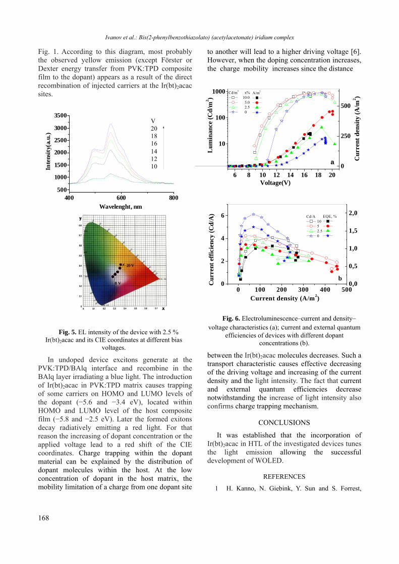
Ivanov et al.: Bis(2-phenylbenzothiazolato) (acetylacetonate) iridium complex
168
Fig. 1. According to this diagram, most probably the observed yellow emission (except Förster or Dexter energy transfer from PVK:TPD composite film to the dopant) appears as a result of the direct recombination of injected carriers at the Ir(bt)2acac sites.
Fig. 5. EL intensity of the device with 2.5 %
Ir(bt)2acac and its CIE coordinates at different bias voltages.
In undoped device excitons generate at the PVK:TPD/BAlq interface and recombine in the BAlq layer irradiating a blue light. The introduction of Ir(bt)2acac in PVK:TPD matrix causes trapping of some carriers on HOMO and LUMO levels of the dopant (−5.6 and −3.4 eV), located within HOMO and LUMO level of the host composite film (−5.8 and −2.5 eV). Later the formed exitons decay radiatively emitting a red light. For that reason the increasing of dopant concentration or the applied voltage lead to a red shift of the CIE coordinates. Charge trapping within the dopant material can be explained by the distribution of dopant molecules within the host. At the low concentration of dopant in the host matrix, the mobility limitation of a charge from one dopant site
to another will lead to a higher driving voltage [6]. However, when the doping concentration increases, the charge mobility increases since the distance
Fig. 6. Electroluminescence–current and density–
voltage characteristics (a); current and external quantum efficiencies of devices with different dopant
concentrations (b).
between the Ir(bt)2acac molecules decreases. Such a transport characteristic causes effective decreasing of the driving voltage and increasing of the current density and the light intensity. The fact that current and external quantum efficiencies decrease notwithstanding the increase of light intensity also confirms charge trapping mechanism.
CONCLUSIONS
It was established that the incorporation of Ir(bt)2acac in HTL of the investigated devices tunes the light emission allowing the successful development of WOLED.
REFERENCES
1 H. Kanno, N. Giebink, Y. Sun and S. Forrest,
400 600 800500
1000
1500
2000
2500
3000
3500
In
tens
ity(
a.u.
)
Wavelenght, nm
V201816141210
8 V
20 V
6 8 10 12 14 16 18 20
10
100
1000
0
250
500
Cur
rent
den
sity
(A
/m2 )
Cd/m2 x% 10.0 5.0 2.5 0
Voltage(V)
Lu
min
ance
(C
d/m
2 )
a
A/m2
0 100 200 300 400 5000
2
4
6
0,0
0,5
1,0
1,5
2,0
b
Cd/A 10 5 2.5 0
Current density (A/m2)
Cur
rent
eff
icie
ncy
(Cd
/A) EQE, %

Ivanov et al.: Bis(2-phenylbenzothiazolato) (acetylacetonate) iridium complex
169
Appl. Phys. Lett., 89, 023503 (2006). 2 Y. Sun, N. Giebink, H. Kanno, B. Ma, M.
Thompson and S. Forrest, Nature, 440, 908 (2006).
3 J. Wang, J. Yu, H. Lin, X. Wei and Y. Jiang, J. Lumin., 128, 1379 (2008).
4 Z. Su, W. Li and B. Chu, Thin Solid Films, 519, 5634 (2011).
5 J. Lee, Jeong-Ik Lee and H. Chu, ETRI Journa,l 31, 842 (2009).
6 C. Ko and Y. Tao, Appl. Phys. Lett., 79, 4234 (2001).
7 S. Reineke, F. Lindner, G. Schwartz, N. Seidler, K. Walzer, B. Lüssem and K. Leo, Nature, 459, 234 (2009).
8 H. Sasabe, J. Takamatsu, T. Motoyama, S. Watanabe, G. Wagenblast, N. Langer, O. Molt, E. Fuchs, C. Lennartz and J. Kido, Adv. Mater., 22, 5003 (2010).
9 S. Lamansky, P. Djurovich, D. Murphy, F. Abdel-Razzaq, H. Lee, C. Adachi, P. Burrows, S. Forrest and M. Thompson, J. Am. Chem. Soc., 123, 4304 (2001).
10 J. Choi, C. Jung, J. Kwon, H. Cho, J. Lee, J. Lee, H. Chu and D. Hwang, Synth. Met., 159, 1517 (2009).
11 R. Wang, D. Liu, H. Ren, T. Zhang, H. Yin, G. Liu and J. Li, Adv. Mater., 23 2823 (2011).
12 R. Wang, L. Deng, T. Zhang and J. Li, Dalton Trans., 41, 6833 (2012).
13 J. Li, P. Chen, Y. Duan, F. Zhao, Ch. Li,W. Xie, Sh. Liu, L. Zhang and B. Li, Semicond. Sci. Technol., 22, 798 (2007).
14 G. Xiao, X. Li, H. Chi, Y. Lu, Y. Dong, Zh. Hu, J. Yu and M. Kimura, Synth. Met., 162 497 (2012).
BIS(2-PHENYLBENZOTHIAZOLATO) (ACETYLACETONATE) ИРИДИЕВ КОМПЛЕКС КАТО ФОСФОРЕСЦЕНТЕН ДОПАНТ ЗА БЕЛИ ОРГАНИЧНИ СВЕТОИЗЛЪЧВАЩИ ДИОДИ
П. И. Иванов, П. K. Петрова, Р. Л. Томова
Институт по оптически материали и технологии (ИОМТ) “Акад. Й. Малиновски”, Българска Академия на Науките, ул. „Акад. Г. Бончев” бл.109, София 1113
Постъпила на 17 октомври 2013 г.; коригирана на 25 ноември, 2013 г.
(Резюме)
В тази статия са представени резултатите от разработването на бели органични светоизлъчващи диоди (WOLEDs), в които като допант в транспортиращия дупки композитен слой от диспергиран в матрица от poly(N-vinylcarbazole) (PVK) - N,N’-bis(3-methylphenyl)-N,N’-diphenylbenzidine (TPD) е използван излъчващия жълта светлина иридиев комплекс bis(2-phenylbenzothiazolato) (acetyl-acetonate)iridium(III) (Ir(bt)2acac) Като електролуминесцентен и електрон транспортен слой в WOLED са използвани Bis(8-hydroxy-2-methylquinoline)-(4-phenylphenoxy)aluminum (BAlq) и bis(2-(2-hydroxyphenyl) benzothiazolate)zinc (Zn(btz)2). Установено е, че устройствата с 2.5 тегловни % Ir(bt)2acac излъчват бяла светлина със CIE координати, променящи се от студено бяло (0.28, 0.30) при напрежение 8 V до топло бяло (0.35, 0.40) при напрежение 20 V.

170
Bulgarian Chemical Communications, Volume 45, Special Issue B (pp. 170-174) 2013
Comparative study of electroluminescent Zn metal–chelate complexes with mixed ligands
P. K. Petrova*, R. L. Tomova
Institute of Optical Materials and Technologies, Bulgarian Academy of Sciences “Acad. G. Bonchev” str., bl. 109, 1113 Sofia, Bulgaria
Received October 17, 2013; Revised November 25, 2013
In this work the results from a comparative study of electroluminescent and photophysical properties of four Zn chelate complexes based on benzothiazoles and quinolines ligands (zinc bis-[8-hydroxyquinoline], zinc [8-hydroxyquinoline] acetylacetonate, zinc bis[2-(2-hydroxyphenyl) benzothiazole], zinc 2-(2-hydroxyphenyl) benzothiazole acetylacetonate), and their application in Organic Lght-emitting Diodes (OLED) are presented. The absorption, photoluminescence spectra and morphology of thin films of Zn complexes were investigated. The luminance-voltage (L-V) characteristics, efficiencies and electroluminescences of the diodes based on bilayer structure ITO/HTL/Zn complex/Al were determined.
Keywords: OLED, Zn complex, Znq2, Znq acac, Zn(BTz)2, ZnBTz acac
INTRODUCTION
Organic light-emitting diodes (OLEDs) have attracted great interest in the last years due to their potential applications as the future generation flat panel displays and solid-state light sources. Blue, green, and red light-emitting materials with standard color and high efficiency are necessary for full color displays. Since the first Tang’s report [1] of the light-emitting diode based on Aluminum tris-(8-hydroxyquinoline), a variety of organic materials have been synthesized and studied, and extended efforts have been made to obtain high performance electroluminescent devices. Among these materials, Zn complexes have been especially important because of the simplicity in synthesis procedures and wide spectral response. Extensive research work is going on in various laboratories to synthesize new Zn complexes containing new ligands to produce a number of novel luminescent Zn complexes as emitters and electron transporters [2-8]. Zinc bis-(8-hydroxyquinoline) (Znq2) has been investigated as an electroluminescent [3] and electron transporting material [4] in vapor deposited [3, 9] or Langmuir-Blodgett films [10]. Zinc bis[2-(2-hydroxyphenyl) benzothiazole] (Zn(BTz)2) has been studied as an effective white light emissive and electron transporting material in OLED. Hamada et al. reported that Zn(BTz)2 was a
new white-light emitting material, but the device with single-emitting layer of Zn(BTz)2 showed a greenish white emission [4]. Recently Zhu et al. fabricated white OLED with Zn(BTz)2 only as emitter [11]. White emission is composed of two parts: one is at 470 nm, which originates from exciton emission in Zn(BTz)2, the other is at 580 nm, which originates from exciplexes formation at the interface of TPD/Zn(BTz)2.
The aim of this paper is to make a comparative study of the performance of OLEDs based on Zinc bis-[8-hydroxyquinoline] (Znq2), Zinc [8-hydroxyquinoline] acetylacetonate (Znq acac), Zinc bis[2-(2-hydroxyphenyl) benzothiazole] (Zn(BTz)2), and Zinc 2-(2-hydroxyphenyl) benzothiazole acetylacetonate (ZnBTz acac).
EXPERIMENTAL
We investigated the electroluminescent devices with conventional structure: ITO/HTL/EL/M, where ITO is a transparent anode of In2O3:SnO2, HTL – а hole-transporting layer, EL is electroluminescent layer (75 nm) of Zn complex and M - a metallic Al cathode (120 nm). Devices with area 1 cm2 were prepared on commercial polyethylene terеphtalate (PET) substrates coated with ITO (40 Ω/sq). The HTL (31 nm) of PVK : TPDx (x = 10 w% relative to PVK) composite films
were prepared by spin-coating from 0.75% solution in dichloroethane at 2000 rpm. The layers of Zn * To whom all correspondence should be sent:
E-mail: [email protected] © 2013 Bulgarian Academy of Sciences, Union of Chemists in Bulgaria

Petrova et al.: Comparative study of electroluminescent Zn metal–chelate complexes…
171
complexes and metal cathode were deposited by thermal evaporation in vacuum better than 10-4 Pa at rates 2-5 A/s. ITO covered PET substrate, PVK and TPD were purchased from Aldrich. The four investigated Zn complexes (Fig. 1) were
synthesized in the Laboratory of Dyes Synthesis at the Department of Applied Organic Chemistry, Faculty of Chemistry, Sofia University ”St. Kl. Ohridski”.
Fig. 1. Chemical structures of the investigated Zn complexes.
All measurements were performed with
unpackaged devices at room temperature and under ambient atmosphere. The absorption and fluorescent (PlS) spectra of the complexes were taken using the Spectrofluorimeter Perkin Elmer MPF 44 and the electroluminescent spectra (ElS) by Ocean Optics HR2000+ spectrometer. The current-voltage (I-V) and luminance–voltage (L–V) characteristics were measured by programmable with Labview power supply. The luminescence (L) was measured in DC (direct current) mode and the light output was detected using a calibrated Hamamatsu silicon photodiode S2281-01. The electroluminescent efficiency (ηL) was calculated by equation (1) and used for quantifying the properties of the OLEDs.
ηL = L/I (1)
where L is the luminescence (in cd/m2) and I is the current density (in A/m2))
The surface morphology of the electroluminescent layers was studied with a AFM “EasyScan 2” produced by “Nanosurf” (Switzerland) on area of 12.5 x 12.5 μm, at measurement mode “scan forward” and Scan mode from down to up.
RESULTS AND DISCUSSION
Morphology
The results of AFM investigations are presented in Fig. 2. The AFM images show that the evaporated Znq2, Znq acac and Zn(BTz)2 compounds on the PET/ITO/PVK:TPD structure, formed amorphous, homogeneous and very smooth
surfaces with root mean square (RMS) roughness 6.88 nm, 7.52 nm and 4.64 nm, respectively. The ZnBTz acac layer made soft outline ridge surface with RMS roughness 20.06 nm. The formed from all of complexes flat film surfaces are a prerequisite for a good performance of devices on their base.
Electrical measurements
Fig. 3. presents the luminance/voltage and efficiency characteristics of four identical devices with different EL. The highest luminescence showed the device with ZnBTz acac as EL followed by that with Zn(BTz)2, Znq acac and Znq2 (Fig. 3a). The luminescence of the device with Znq acac at 15 V DC is nearly 1.5, 2.4 and 3 times higher than those by Zn(BTz)2, Znq acac and Znq2, respectively.
At the same time the electroluminescent efficiencies of the devices with ZnBTz acac and Zn(BTz)2 are nearly the same (around 3 cd/A) and 1. 5 times higher than that of devices with Znq2 and Znq acac (Fig. 3b) which are 2 and 1.8 cd/A, respectively. The higher luminance and efficiency of the devices based on Zn hydroxyphenyl benzothiazole complexes indicate better electron transport properties of these complexes than Znq2 and Znq acac.
For OLEDs with similar structures Sano et al. reported in [5] efficiency of 1.39 cd/A at luminance 100 cd/m2 for ITO/TPD/Zn(BTz)2/Mg:In device, Zheng et al. - 4.05 cd/A for doped with rubrene Zn(BTz)2 white device at maximum luminescence
N
OZnN
O
N
O ZnO
O
CH3
CH3
S
NO
N
S
OZn
O
OZn
O
NS
H3C
H3C
Znq2 Znq acac Zn(BTz)2 ZnBTz acac
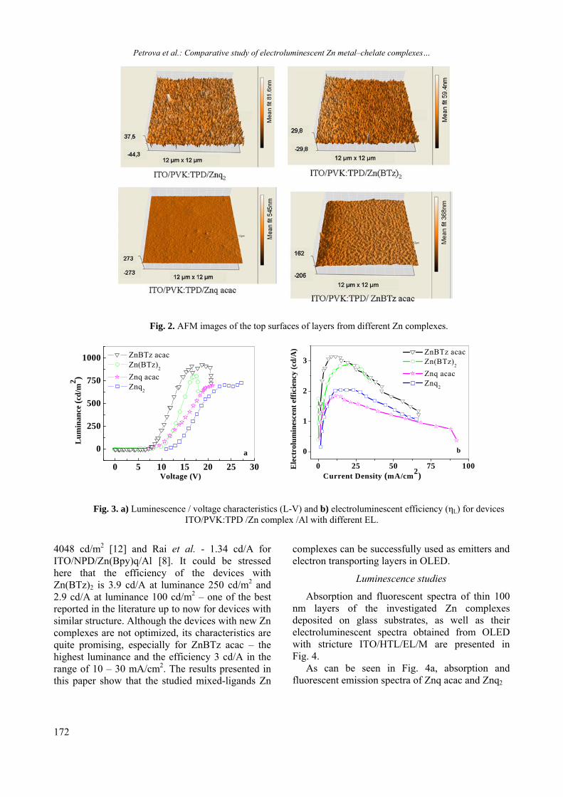
Petrova et al.: Comparative study of electroluminescent Zn metal–chelate complexes…
172
Fig. 2. AFM images of the top surfaces of layers from different Zn complexes.
Fig. 3. a) Luminescence / voltage characteristics (L-V) and b) electroluminescent efficiency (ηL) for devices
ITO/PVK:TPD /Zn complex /Al with different EL.
4048 cd/m2 [12] and Rai et al. - 1.34 cd/A for ITO/NPD/Zn(Bpy)q/Al [8]. It could be stressed here that the efficiency of the devices with Zn(BTz)2 is 3.9 cd/A at luminance 250 cd/m2 and 2.9 cd/A at luminance 100 cd/m2 – one of the best reported in the literature up to now for devices with similar structure. Although the devices with new Zn complexes are not optimized, its characteristics are quite promising, especially for ZnBTz acac – the highest luminance and the efficiency 3 cd/A in the range of 10 – 30 mA/cm2. The results presented in this paper show that the studied mixed-ligands Zn
complexes can be successfully used as emitters and electron transporting layers in OLED.
Luminescence studies
Absorption and fluorescent spectra of thin 100 nm layers of the investigated Zn complexes deposited on glass substrates, as well as their electroluminescent spectra obtained from OLED with stricture ITO/HTL/EL/M are presented in Fig. 4.
As can be seen in Fig. 4a, absorption and fluorescent emission spectra of Znq acac and Znq2
0 5 10 15 20 25 30
0
250
500
750
1000 ZnBTz acac Zn(BTz)
2
Znq acac Znq
2
Voltage (V)
Lu
min
ance
(cd
/m2 )
a
0 25 50 75 100
0
1
2
3
b
ZnBTz acac Zn(BTz)
2
Znq acac Znq
2
Current Density (mA/cm2)
Ele
ctro
lum
ines
cent
eff
icie
ncy
(cd/
A)
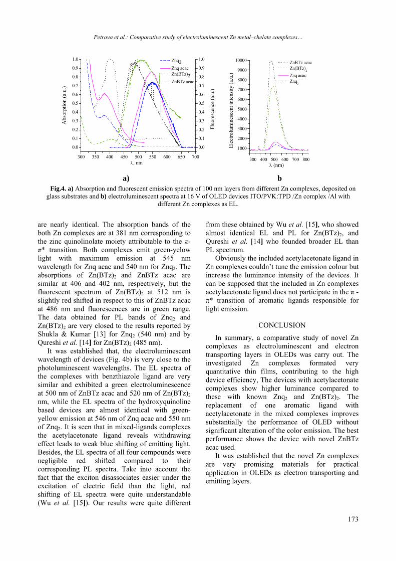
Petrova et al.: Comparative study of electroluminescent Zn metal–chelate complexes…
173
a) b Fig.4. a) Absorption and fluorescent emission spectra of 100 nm layers from different Zn complexes, deposited on
glass substrates and b) electroluminescent spectra at 16 V of OLED devices ITO/PVK:TPD /Zn complex /Al with different Zn complexes as EL.
are nearly identical. The absorption bands of the both Zn complexes are at 381 nm corresponding to the zinc quinolinolate moiety attributable to the π-π* transition. Both complexes emit green-yelow light with maximum emission at 545 nm wavelength for Znq acac and 540 nm for Znq2. The absorptions of Zn(BTz)2 and ZnBTz acac are similar at 406 and 402 nm, respectively, but the fluorescent spectrum of Zn(BTz)2 at 512 nm is slightly red shifted in respect to this of ZnBTz acac at 486 nm and fluorescences are in green range. The data obtained for PL bands of Znq2 and Zn(BTz)2 are very closed to the results reported by Shukla & Kumar [13] for Znq2 (540 nm) and by Qureshi et al. [14] for Zn(BTz)2 (485 nm).
It was established that, the electroluminescent wavelength of devices (Fig. 4b) is very close to the photoluminescent wavelengths. The EL spectra of the complexes with benzthiazole ligand are very similar and exhibited a green electroluminescence at 500 nm of ZnBTz acac and 520 nm of Zn(BTz)2 nm, while the EL spectra of the hydroxyquinoline based devices are almost identical with green-yellow emission at 546 nm of Znq acac and 550 nm of Znq2. It is seen that in mixed-ligands complexes the acetylacetonate ligand reveals withdrawing effect leads to weak blue shifting of emitting light. Besides, the EL spectra of all four compounds were negligible red shifted compared to their corresponding PL spectra. Take into account the fact that the exciton disassociates easier under the excitation of electric field than the light, red shifting of EL spectra were quite understandable (Wu et al. [15]). Our results were quite different
from these obtained by Wu et al. [15], who showed almost identical EL and PL for Zn(BTz)2, and Qureshi et al. [14] who founded broader EL than PL spectrum.
Obviously the included acetylacetonate ligand in Zn complexes couldn’t tune the emission colour but increase the luminance intensity of the devices. It can be supposed that the included in Zn complexes acetylacetonate ligand does not participate in the π - π* transition of aromatic ligands responsible for light emission.
CONCLUSION
In summary, a comparative study of novel Zn complexes as electroluminescent and electron transporting layers in OLEDs was carry out. The investigated Zn complexes formated very quantitative thin films, contributing to the high device efficiency, The devices with acetylacetonate complexes show higher luminance compared to these with known Znq2 and Zn(BTz)2. The replacement of one aromatic ligand with acetylacetonate in the mixed complexes improves substantially the performance of OLED without significant alteration of the color emission. The best performance shows the device with novel ZnBTz acac used.
It was established that the novel Zn complexes are very promising materials for practical application in OLEDs as electron transporting and emitting layers.
300 350 400 450 500 550 600 650 700
0.0
0.1
0.2
0.3
0.4
0.5
0.6
0.7
0.8
0.9
1.0
0.0
0.1
0.2
0.3
0.4
0.5
0.6
0.7
0.8
0.9
1.0A
bsor
ptio
n (a
.u.)
, nm
Flu
ores
cenc
e (a
.u.)
Znq2 Znq acac Zn(BTz)2 ZnBTz acac
300 400 500 600 700 800
1000
2000
3000
4000
5000
6000
7000
8000
9000
10000
Ele
ctro
lum
ines
cent
inte
nsit
y (a
.u.)
(nm)
ZnBTz acac Zn(BTz)
2
Znq acac Znq
2

Petrova et al.: Comparative study of electroluminescent Zn metal–chelate complexes…
174
REFERENCES
1. C. Tang, S. VanSlyke, Appl. Phys. Lett., 51, 913 (1987).
2. L. Sapochak, A. Padmaperuma, N. Washton, F. Endrino, G. Schmett, J. Marshall, D. Fogarty, P. Burrows, S. Forrest, J. Am. Chem. Soc., 123, 6300 (2001).
3. L. Sapochak, F. Benincasa, R. Schofield, J. Baker, K. Riccio, D. Fogarty, H. Kohlmann, K. Ferris, P. Burrows, J. Am. Chem. Soc., 124, 6119 (2002).
4. Y. Hamada, T. Sano, H. Fujii, Y. Nishio, H. Takahashi, K. Shibata, Jpn. J. Appl. Phys., 35, L1339 (1996).
5. T. Sano,Y. Nishio, Y. Hamada, H. Takahashi, T. Usuki, K. Shibata, J. Mater. Chem., 10, 157 (2000).
6. Y. Jang, D. Kim, Oh. Kwon, Y. Kwon, J. Korean Phys. Soc., 49, 1057 (2006).
7. D. Kim, W. Kim, B. Lee, Y. Kwon, Jpn. J. Appl. Phys., 46, 2749 (2007).
8. V. Rai, R. Srivastava, G. Chauhan, K. Saxena, R. Bhardwaj, S. Chuand, M. Kamalasan, Mater. Lett., 62, 2562 (2008).
9. N. Donze, P. Pechy, M. Gratzel, M. Schaer, L. Zuppiroli, Chem. Phys. Lett., 315, 405 (1999).
10. G. Wang, Z. Lu, Ch. Yuan, Yu. Wei, Thin Solid Films, 288, 334 (1996).
11. F. Zhu, Y. Hua, S.Yin, J. Deng, K. Wu, X. Niu, X. Wu, M. Petty, J. Lumin., 122-123, 717, (2007).
12. J. Zheng, Y. Hua, S. Yin, X. Feng, X. Wu, Y. Sun, Y. Li, Ch. Yang, Z. Shuai, Chin. Sci. Bull., 50, 509 (2005).
13. V. Shukla, S. Kumar, Synth. Met., 160, 450, (2010).
14. M. Qureshi, S. Manohara, S. Singh, Y. Mahapatra, Solid State Commun., 133, 305 (2005).
15. X. Wu, Y. Hua, Z. Wang, J. Zheng, X. Feng, Y. Sun, Chin. Phys. Lett., 22, 1797 (2005).
СРАВНИТЕЛНО ИЗСЛЕДВАНЕ НА ЕЛЕКТРОЛУМИНЕСЦЕНТНИ Zn МЕТАЛ-ХЕЛАТНИ КОМПЛЕКСИ СЪС СМЕСЕНИ ЛИГАНДИ
П. К. Петрова, Р. Л. Томова
Институт по оптически материали и технологии „Акад. Йордан Малиновски”, Българска академия на науките, ул “ Акад. Г. Бончев” блок 109, 1113 София, България
Постъпила на 17 октомври 2013 г.; коригирана на 25 ноември, 2013 г.
(Резюме)
В работата са представени резултатите от едно сравнително изследване на електролуминесцентните и фотофизичните свойства на четири цинкови хелатни комплекса, базирани на бензотиазолни и хинолонови лиганди (цинков бис(8-хидроксихинолин), ацетилацетонатен цинков 8-хидроксихинолин, цинков бис[2-(2-хидроксифенил) бензотиазол], ацетилацетонатен цинков 2-(2-хидроксифенил) бензотиазол) и тяхното приложение в OLED. Изследвани са абсорбцията, фотолуминесцентните спектри и морфологията на тънки филми от цинковите комплекси. Определени са характеристиките луминесценция / напрежение, ефективностите и електролуминесценциите на ITO/HTL/Zn complexes/Al диодите.

175
Bulgarian Chemical Communications, Volume 45, Special Issue B (pp. 175-180) 2013
New “push-pull” type merocyanine dye for application in bulk-heterojunction organic solar cells
J. Dikova*, S. Kitova, D. Stoyanova, A.Vasilev1, T. Deligeorgiev1 and S. Angelova2
Institute for Optical Materials and Technologies “Acad. J. Malinowski”, Bulgarian Academy of Sciences, “Acad. G. Bonchev” str. Bl. 109, 1113 Sofia, Bulgaria
1Sofia University.”St. Kliment Ohridski, Faculty of Chemistry and Farmacy, 1 James Bourchier Blvd., 1164 Sofia, Bulgaria
2Institute of Organic Chemistry with Centre of Phytochemistry, Bulgarian Academy of Sciences, “Acad. G. Bonchev” str. Bl. 9, 1113 Sofia, Bulgaria
Received October 17, 2013; Revised November 25, 2013
The potentiality of our newly synthesized push-pull type merocyanine dye, labeled BMBII, for using as electron donating component in solution processed bulk heterojunction (BHJ) organic solar cells has been studied. For the purpose, soluble n-type fullerene, (6,6)-phenyl C61 butyric acid methyl ester (PCBM), which is without alternative in the near future, is chosen as acceptor. The optical constants (n and k) of thin films obtained by spin coating from solutions in chlorbenzene of BMBII as well as of BMBII/PCBM blend are determined by spectrophotometric measurements. Further, an optical simulation of a standard BHJ cell with active layer from BMBIIdye/PCMB blend has been performed using transfer-matrix formalism. Thus, the optimum thickness of the active layer is calculated to be about 80 nm, which provides an overlapping of the total absorption with solar spectrum in a broad range between 400 and 800 nm. Finally, the maximum current density Jsc of 13 mA.cm-2 is determined, assuming the internal quantum efficiency, IQE, equals one. By comparing the calculated Jsc with data for some advanced small molecular BHJ devices the perspectives for practical applications of the new merocyanine dye are discussed.
Keywords: Bulk heterojunction solar cells, small molecule, push-pull chromophores, merocyanine dyes
INTRODUCTION
During the past years the organic photovoltaics (PV) are subject of continuously growing interest as promising alternative for high cost crystalline silicon cells (c-Si), which still dominate the market. In the most successful devices, a soluble n-type fullerene, (6,6)-phenyl C61 butyric acid methyl ester (PCBM) as acceptor, is blended with the donor from conjugated p-type polymers to form bulk-heterojunction (BHJ) cells [1]. An attraction of these devices, which are processed from solution, is the ability to deposit active layer precursors over large areas in a single step, using techniques ranging from inkjet printing to spin-coating. Small molecule donors offer the same facile processing however are easier to synthesize in many variants and purify, are intrinsically monodisperse, and are often photo- and chemically more stable [2]. The disadvantage of lower solubility of this class of organic semiconductors can be overcome by functionalizing of their molecular structure. This
approach has been successfully applied to different dyes and very encouraging results about the performance of devices developed on this base have been achieved [3]. However, the power conversion efficiency remains considerably lower than that of the polymeric solar cells [4]. This explains the increased scientific efforts recently for developing new small molecular electron donors for solution processed BHJ solar cells. In this respect the so-called “push-pull” chromophores look very promising [5]. The molecular structure of this unique class of dyes comprises electron-donating, π-conjugated bridging and electron withdrawing moieties. In the exited state a strong intramolecular charge transfer occurs which provides an enlargement of the absorption area of the donor, increasing of the charge mobility and therefore rising of the conversion efficiency [6].
The present work represents a first step in characterization of our newly synthesized push-pull type merocyanine dye (E)-3-((1-benzylquinolin-4(1H)-ylidene)methyl)-7H-benzo[de]benzo[4,5] imidazo-[2,1-a]isoquinolin-7-one, which we labelled as BMBII. The structure and electronic
© 2013 Bulgarian Academy of Sciences, Union of Chemists in Bulgaria
* To whom all correspondence should be sent: E-mail: [email protected]

Dikova et al.: New “push-pull” type merocyanine dye for application in bulk-heterojunction…
176
properties of the dye were studied by means of density functional theory (DFT) calculations. We determined also the optical constants (refractive index n and extinctions coefficient k) of spin coated thin BMBII dye and BMBII/PCMB films using previously developed methods, based on spectrophotometric measurements. Based on that, optical simulation was carried out in order to predict and understand photovoltaic performance of a bulk heterojunction cell with active layer from a
solid-state blend of BMBII and the fullerene C61 derivative PCBM.
EXPERIMENTAL
The new push-pull dye BMBII was synthesized via the reaction between 3-nitro-7H-benzo[de]benzo[4,5]imidazo[2,1-a]isoquinolin-7-one (1) and 1-benzyl-4-methyl-quinolinium bromide (2) in metoxyethanol, in the presence of diizopropyl-ethylamine (DIPEA) and pyridine (Scheme 1).
Scheme 1. Synthesis of new type merocyanine dye (E)-3-((1-benzylquinolin-4(1H)-ylidene) methyl)-7H-benzo[de]benzo[4,5]imidazo-[2,1-a]isoquinolin-7-one (BMBII).
The target merocyanine compound (E)-3-((1-
benzylquinolin-4(1H)-ylidene)methyl)-7H-benzo[de]benzo[4,5] imidazo-[2,1-a]isoquino-lin-7-one (BMBII) was obtained with excellent yield. Detailed description of the reaction procedure and full characterization data of dye BMBII will be published in a separate paper [7].
The molecular ground-state geometry of BMBII compound was optimized - using Perdew-Burke-Ernzerhof (PBE0) hybrid functional [8] with triple-ζ polarized basis set, 6-311G(d,p). Local minima were verified by establishing that all vibrational frequencies are real. All calculations were performed using Gaussian 09 [9]. Thus, the values of HOMO (the highest occupied molecular orbital), LUMO (the lowest unoccupied molecular orbital) and their energy difference HLG (HOMO-LUMO gap), which are very important for photovoltaic application of the dye, were calculated.
Further, thin dye films were prepared from solution of the compound BMBII in chlorobenzene by spin coating. In the preliminary experiments the concentration of the solution, the spin rate and duration were varied in order to obtain films with
thickness, suitable for optical measurements. Thus, 25 nm films were deposited from solution containing 4mg/ml BMBII, coated at 1500 rpm for 120 s. Blended films were prepared also by spin coating from chlorobenzene solutions of 1:1 (by weight) mixture of BMBII and PCBM (PCBM was commercially available). In both cases preliminary carefully cleaned BK7 optical glass plates and Si wafers were used as substrates.
Optical constants of the BMBII dye and blended BMBII/PCMB layers were determined on the basis of three spectrophotometric measurements at normal incidence of light - transmittance T and reflectances Rf and Rm of the both kinds of films, deposited on transparent (BK7) and opaque (Si wafers) substrates, respectively. Spectro-photometric measurements were performed with a spectrophotometer Cary 5E in the spectral region 350 – 800 nm. A value of the dye film thickness derived from the (TRfRm) method [10] was used for determining n and k by (TRm) or (TRf ) methods, using Newton Raphson iterative techniques [11]. The combination of the two methods makes possible the determination of the optical constants
N NO
NO2
+
1
N+H3C Br-
2
MeOEtOH
Pyridine, DIPEA
70oC, overnight
N NO
NBMBII

of the dye a[11].
Optical carried out based on tinterfaces obeen explai13]. In ourBurkhard anincidence odistribution thickness hrange 350 –the AM 1.5film thicknphotons, absummation number ofmaximum assuming thcollected efficiency, I
For optcommon BITO(120nmnm)/LiF(1010 nm LiF fand the ITOform the ocollection. Tchanged for320 nm.
The optisimulation woptical conby us usingand blendeMoO3 films(10-4 Pa).
Fig. 1 sh(a) and caexperimentadata analysion the elLUMO is mregion. TheBMBII is cHOMO leveV) and ver5.2 and -5.the LUMO
Dikova et
and blended
simulation ot using the the Fresnel
occurring in ined in greatr work a Mnd Hoke, whf light, was a for each
has been cal– 800 nm. M5 sun spectruness results bsorbed for
over all waf absorbedcurrent de
hat each abselectron i.eIQE, equals tical simulaBHJ device
m)/MoO3(5nm0nm)/Al(100nfilms were in
O surface andohmic contaThe thicknesr numerical
ical constantswere taken fstants of M
g the same pd films. Fors were therm
RE
hows molecualculated enal energy valis showed thlectron-donatmore spread e frontier orcalculated tovel of the dyry close to th8 eV). Besid energy leve
t al.: New “push
d films with
of a BHJ detransfer maformulas f
the cell. Tht detail in th
Matlab scripthich treats theapplied [14].wavelength lculated in
Multiplying wum and integ
in the toeach wavele
avelength resd photons. ensity Jsc wsorbed photoe. the intone [14]. ation we he structure m)/blendBMBnm). 5 nm tnserted betwd Al surfaceacts for holss of the blesimulation i
s of ITO, Al from the liteoO3 films w
procedure as r the purpos
mally evapor
ESULTS
ular structurenergy levelslues [16] for
hat HOMO isting moietyover the ele
rbital energy be 2.78 eVye is reasonhe desired rades, the diffel of PCBM
h-pull” type me
a high accur
evice stack atrix formalifor the sev
his approach he literature t developede case of nor. The absorp
over the fthe wavelen
with the lighgration over
otal number ength. Lastlysults in the t
The posswas calculaons results iernal quan
have chosenconsisting
BII/PCBMthick MoO3
ween active larespectively
le and electended layer in the range
and LiF userature [15].
were determifor BMBII
se 50 nm thrated in vacu
e of dye BMs for dye PCBM (b).
s mainly locay whereas ectron-accepy difference
V. The estimaably low (-5ange (betweeference betw
M and the dy
erocyanine dye
racy
was ism,
veral has
[12, d by rmal ption film ngth ht of r the r of y, a total sible ated in a
ntum
n a of (x
and ayer y, to tron was 40-
ed in The ined dye
hick uum
MBII and The ated the
pting for
ated 5.17 en -
ween ye’s
HOhig
B[16
As opecharesufabmadatchrThesenapporgconcoeandabsat λalth
for application
OMO energygher than the
Fig. 1. PBE0BMBII (a) and 6] and PBE0/6
known, thisen circuit voaracteristics oult, we can r
bricated usiny be about 0
ta for soromophores, erefore, it c
nsitized meroplication as eganic solar cnfirmed by thefficient α ded presented isorption peakλ = 598 andhough the ab
n in bulk-heteroj
y level is 0.required min
(a)
(b)/6-311G(d,p) experimental
6-311G(d,p) cdye BM
s difference oltage Voc thof the cell’s roughly guesng BMBII/PC0.7 V [17], wome promi
based oncan be conocyanine dyelectron donacells. This she spectral determined fon Fig. 2. As
ks of 7.3 x10d 402 nm, cosorption of t
ojunction…
.87 eV, whinimum of 0.2
)
) optimized ge
l energy levelscalculated ener
MBII.
determines that is one o
performancss that the VCBM BHJ
which is comising new n squarine ncluded thatye has also pating compo
statement is dependence oor 25 nm this it is seen, th04 cm-1 and 5orrespondingthe film is m
177
ich is much2-0.3 eV.
ometry of s for PCBM rgy levels for
the value ofof the basice. From thisoc of devicesactive layerparable with
push-pulldyes [6].
t the newlypotential for
onent in BHJadditionally
of absorptionick dye filmhere are two
5.5 x104 cm-1
gly. Besides,moderate the
7
h
f c s s r h l . y r J y n
m o 1 ,

Dikova et al.: New “push-pull” type merocyanine dye for application in bulk-heterojunction…
178
400 500 600 700 800 900 1000 1100
0.0
2.0x10⁴
4.0x10⁴
6.0x10⁴
8.0x10⁴
1.0x10⁵
1.2x10⁵
1.4x10⁵
1.6x10⁵
2.6 2.8 3.0 3.20.0
0.5
1.0
1.5
2.0
2.5
3.0
(
cm-1)
(nm)
(h)
2 1
0-10(e
V c
m-1)
h(eV)
Eg=2.73 eV
Fig. 2. Absorption coefficient profile (α=4πk/λ) of 25
nm thick BMBII dye film.
absorption area is broad and covers the 400 - 750 nm spectral region, where the solar photon flux is maximum. This as well as the low intrinsic fluorescence of the new push-pull merocyanine dye [7] are an important prerequisite for its photovoltaic application. Simultaneously, it is worth to pointing out the good coincidence between the values of optical energy gap Eg, determined according to the so-called Tauc’s law [18] as 2.73 eV (see the inset in Fig. 2), and calculated HLG energy of 2.8 eV. This fact can be regarded as an experimental confirmation of the results obtained from the theoretical analysis performed in the study.
For modeling of light propagation within a solar cell device, the optical constants of all involved layers needed to be known. The refractive index (n) and the extinction coefficient (k) of each layer used in optical simulation are plotted as a function of wavelength in Fig. 3. Optical constants of the blended film were determined for an about 45 nm thick film. As it was mentioned, the optical simulation was performed for a standard BHJ cell structure, where the light enters through the glass substrate, sequentially passing the layers of ITO, MoO3, BMBII/PCBM blend layer and LiF. Then the light is reflected back from the Al electrode and finally leaves the solar cell partly at the front again.
Figure 4 presents the spectral dependence of total absorption within the BMBII/PCBM active layer for a set of different layer thicknesses. For comparison, the photon flux of a standard AM1.5 solar spectrum is shown as a gray solid line. It is clear that the blue light is mainly absorbed by PCBM and red and near infrared by BMBII dye. Besides, it is seen that the absorption of blended film overlaps the solar spectrum from 400 to 800 nm as required for high efficiency solar energy conversion.
300 400 500 600 700 8000.0
0.5
1.0
1.5
2.0
2.5
3.0
blend MoO
3
LiF ITO BMBII
n
nm
a
300 400 500 600 700 800
0.0
0.1
0.2
0.3
0.4
k
nm
b
0
2
4
6
8
10
k (A
l)
Fig. 3. Optical constants of layers used in simulation: refractive indices n (а) and extinction coefficients k (b).
Fig. 4. Fraction of incident light absorbed within the dye-PCBM layer of the solar cell for several layer
thickness. For comparison, the photon flux of a standard AM 1.5G solar spectrum is shown as a gray solid line
(right axis).
Assuming an IQE=1, the maximum short circuit current density Jsc under AM 1.5 illumination for different BMBII/PCBM layer thickness is depicted
400 500 600 700 8000.0
0.2
0.4
0.6
0.8
1.0
ligh
t ab
sorb
ed f
ract
ion
nm
20 nm 40 nm 80 nm 120 nm 160 nm 200 nm 240 nm 280 nm
0
1x10¹⁸
2x10¹⁸
3x10¹⁸
4x10¹⁸
5x10¹⁸
num
ber
ofph
oto
ns
(#*m
-2*s
-1*n
m-1)
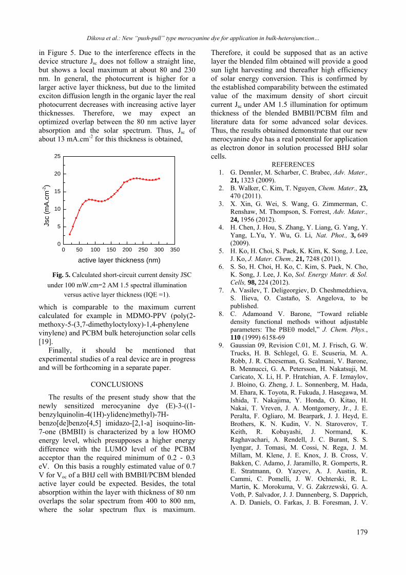
Dikova et al.: New “push-pull” type merocyanine dye for application in bulk-heterojunction…
179
in Figure 5. Due to the interference effects in the device structure Jsc does not follow a straight line, but shows a local maximum at about 80 and 230 nm. In general, the photocurrent is higher for a larger active layer thickness, but due to the limited exciton diffusion length in the organic layer the real photocurrent decreases with increasing active layer thicknesses. Therefore, we may expect an optimized overlap between the 80 nm active layer absorption and the solar spectrum. Thus, Jsc of about 13 mA.cm-2 for this thickness is obtained,
Fig. 5. Calculated short-circuit current density JSC
under 100 mW.cm−2 AM 1.5 spectral illumination versus active layer thickness (IQE =1).
which is comparable to the maximum current calculated for example in MDMO-PPV (poly(2-methoxy-5-(3,7-dimethyloctyloxy)-1,4-phenylene vinylene) and PCBM bulk heterojunction solar cells [19].
Finally, it should be mentioned that experimental studies of a real device are in progress and will be forthcoming in a separate paper.
CONCLUSIONS
The results of the present study show that the newly sensitized merocyanine dye (E)-3-((1-benzylquinolin-4(1H)-ylidene)methyl)-7H-benzo[de]benzo[4,5] imidazo-[2,1-a] isoquino-lin-7-one (BMBII) is characterized by a low HOMO energy level, which presupposes a higher energy difference with the LUMO level of the PCBM acceptor than the required minimum of 0.2 - 0.3 eV. On this basis a roughly estimated value of 0.7 V for Voc of a BHJ cell with BMBII/PCBM blended active layer could be expected. Besides, the total absorption within the layer with thickness of 80 nm overlaps the solar spectrum from 400 to 800 nm, where the solar spectrum flux is maximum.
Therefore, it could be supposed that as an active layer the blended film obtained will provide a good sun light harvesting and thereafter high efficiency of solar energy conversion. This is confirmed by the established comparability between the estimated value of the maximum density of short circuit current Jsc under AM 1.5 illumination for optimum thickness of the blended BMBII/PCBM film and literature data for some advanced solar devices. Thus, the results obtained demonstrate that our new merocyanine dye has a real potential for application as electron donor in solution processed BHJ solar cells.
REFERENCES 1. G. Dennler, M. Scharber, C. Brabec, Adv. Mater.,
21, 1323 (2009). 2. B. Walker, C. Kim, T. Nguyen, Chem. Mater., 23,
470 (2011). 3. X. Xin, G. Wei, S. Wang, G. Zimmerman, C.
Renshaw, M. Thompson, S. Forrest, Adv. Mater., 24, 1956 (2012).
4. H. Chen, J. Hou, S. Zhang, Y. Liang, G. Yang, Y. Yang, L.Yu, Y. Wu, G. Li, Nat. Phot., 3, 649 (2009).
5. H. Ko, H. Choi, S. Paek, K. Kim, K. Song, J. Lee, J. Ko, J. Mater. Chem., 21, 7248 (2011).
6. S. So, H. Choi, H. Ko, C. Kim, S. Paek, N. Cho, K. Song, J. Lee, J. Ko, Sol. Energy Mater. & Sol. Cells, 98, 224 (2012).
7. A. Vasilev, T. Deligeorgiev, D. Cheshmedzhieva, S. Ilieva, O. Castaño, S. Angelova, to be published.
8. C. Adamoand V. Barone, “Toward reliable density functional methods without adjustable parameters: The PBE0 model,” J. Chem. Phys., 110 (1999) 6158-69
9. Gaussian 09, Revision C.01, M. J. Frisch, G. W. Trucks, H. B. Schlegel, G. E. Scuseria, M. A. Robb, J. R. Cheeseman, G. Scalmani, V. Barone, B. Mennucci, G. A. Petersson, H. Nakatsuji, M. Caricato, X. Li, H. P. Hratchian, A. F. Izmaylov, J. Bloino, G. Zheng, J. L. Sonnenberg, M. Hada, M. Ehara, K. Toyota, R. Fukuda, J. Hasegawa, M. Ishida, T. Nakajima, Y. Honda, O. Kitao, H. Nakai, T. Vreven, J. A. Montgomery, Jr., J. E. Peralta, F. Ogliaro, M. Bearpark, J. J. Heyd, E. Brothers, K. N. Kudin, V. N. Staroverov, T. Keith, R. Kobayashi, J. Normand, K. Raghavachari, A. Rendell, J. C. Burant, S. S. Iyengar, J. Tomasi, M. Cossi, N. Rega, J. M. Millam, M. Klene, J. E. Knox, J. B. Cross, V. Bakken, C. Adamo, J. Jaramillo, R. Gomperts, R. E. Stratmann, O. Yazyev, A. J. Austin, R. Cammi, C. Pomelli, J. W. Ochterski, R. L. Martin, K. Morokuma, V. G. Zakrzewski, G. A. Voth, P. Salvador, J. J. Dannenberg, S. Dapprich, A. D. Daniels, O. Farkas, J. B. Foresman, J. V.
0 50 100 150 200 250 300 3500
5
10
15
20
25
Jsc
(mA
.cm
-2)
active layer thickness (nm)
Dikova et al.: New “push-pull” type merocyanine dye for application in bulk-heterojunction…
180
Ortiz, J. Cioslowski, and D. J. Fox, Gaussian, Inc., Wallingford CT, 2010.
10. V. Panayotov, I. Konstantinov, SPIE Proc., 2253, 1070 (1994).
11. I. Konstantinov, Tz. Babeva, S. Kitova. Appl. Opt., 37, 4260 (1998).
12. L. Pettersson, L. Roman, O. Inganä, J. Appl. Phys., 86, 487 (1999).
13. P. Peumans, A. Yakimov, R. Forrest, J. Appl. Phys., 93, 3693 (2003).
14. G. Burkhard, E. Hoke, M. McGehee, Adv. Mater., 22, 3293 (2010).
15. D. Smith, E. Shiles, M. Inokuti, in: Handbook of Optical constants of Solids, E.Palik (ed.), New
York: Academic, 1985 pp 377-405. 16. N. Blouin, A. Michaud, D. Gendron, S. Wakim,
E. Blair, R. Neagu-Plesu, M. Belletête, G. Durocher, Y. Tao, and M. Leclerc, J. Am. Chem. Soc., 130 732 (2008).
17. M. C. Scharber, D. Muhlbacher, M. Koppe, P. Denk, C. Waldauf, A. J. Heeger, C. J. Brabec, Adv. Mater., 18, 789 (2006).
18. J. Tauc, in: The Optical Properties of Solids, F. Abeles (ed.), North Holland, Amsterdam, 1970, pp 277–415.
19. H. Hoppe, N. Arnold, N. Sariciftci, D. Meissner, Sol. Energy Mater. & Sol. Cells, 80, 105 (2003).
НОВО „PUSH-PULL“ ТИП МЕРОЦИАНИНОВО БАГРИЛО ЗА ПРИЛОЖЕНИЕ В ОРГАНИЧНИ СЛЪНЧЕВИ КЛЕТКИ С ОБЕМЕН ХЕТЕРОПРЕХОД
Ю. Дикова, С. Китова, Д. Стоянова, А. Василев1, Т. Делигеоргиев1 и С. Ангелова2
Институт по оптически материали и технологии "Акад. Й. Малиновски", Българска Академия на науките, ул. "Акад. Г. Бончев", бл. 109, 1113 София, България
1Софийски Университет ”Св. Климент Охридски“, Факултет по Химия и фармация, ул. Джеймс Баучер, 1164 София, България
2Институт по органична химия с Център по фитохимия, Българска Академия на науките, ул. "Акад. Г. Бончев", бл. 9, 1113 София, България
Постъпила на 17 октомври 2013 г.; коригирана на 25 ноември, 2013 г.
(Резюме)
Изследвани са възможностите за приложение на синтезирано от нас ново мероцианиново багрило от „push-pull“ тип, означено с BMBII, като електронен донор в органични слънчеви клетки с обемен хетеропреход. За целта като акцептор е избран разтворим дериват на фулеренa от n-тип (6,6)-phenyl C61 butyric acid methyl ester (PCBM), чието приложение е без алтернатива в близко бъдеще. На базата на резултатите от спектрофотометрични измервания са определени оптичните константи (n и k) на тънки филми, получени чрез нанасяне на центрофуга от разтвор на BMBII, както и на смес BMBII/PCBM в хлорбензол. Проведена оптична симулация на стандартна клетка с обемен хетеропреход и активен слой от BMBII/PCBM, прилагайки формализма на трансферна матрица. По този начин е определена оптимална дебелина на активния слой от 80 нм, която осигурява припокриване на областта на абсорбция със слънчевия спектър в широк интервал - от 400 до 800 нм. Определена е възможната максимална плътност на тока Jsc от около 13 mAcm-2, приемайки че вътрешната квантова ефективност е равна на 1. Чрез сравняване на тази стойност с литературни данни за някои перспективни аналогични устройства са дискутирани перспективите за практическо приложение на новосинтезираното мероцианиново багрило.

181
Bulgarian Chemical Communications, Volume 45, Special Issue B (pp. 181-184) 2013
Optical measurements of electrophoretic suspension kinetics
V. Siderov1, R. Yordanov2, I. Yordanova2, S. Boyadjiev3, M. Vala1, V. Milenkov1, P. Heinrichova1, M. Weiter1, and I. Zhivkov1, 4*
1Brno University of Technology, Faculty of Chemistry, Centre for Materials Research, Purkynova 118, 612 00 Brno, Czech Republic
2 Technical University - Sofia, Faculty of Electronic Engineering and Technologies, Department of Electronics, 8 Kliment Ohridski blvd., 1000 Sofia, Bulgaria
3Budapest University of Technology and Economics, Department of Inorganic and Analytical Chemistry, Technical Analytical Chemistry Research Group of the Hungarian Academy of
Sciences, H-1111 Budapest, Muegyetem rakpart 4., Hungary 4Institute of Optical Materials and Technologies “Acad. J. Malinowski”, Bulgarian Academy of
Sciences, Acad. G. Bonchev Str. bl. 101/109, 1113 Sofia, Bulgaria
Received October 17, 2013; Revised November 25, 2013
Electrophoretic deposition (EPD) was originally used for formation of coatings, e. g. in the automotive industry. Recently EPD is successfully utilized for thin film preparation with an application in the optics and electronics. This paper investigates the process of the suspension formation and aggregation by ultraviolet and visible spectroscopy (UV-VIS) spectroscopy and Dynamic Light Scattering (DLS) methods. The suspensions were formed by a precipitation of solution of poly[2-methoxy-5-(3′,7′-dimethyloctyloxy)-1,4-phenylenevinylene] in toluene using acetonitrile as a precipitator. It could be concluded that the progressive suspension particle growth observed by DLS affects regularly the first derivative of the UV-VIS spectra. By a comparison of the results obtained by both methods it could be seen that UV-VIS spectroscopy combined with the spline method could be successfully used for an estimation of electrophoretic suspensions.
Keywords: Electrophoretic suspension characterization, UV-VIS spectroscopy, Dynamic light scattering, Kinetics of suspension particle growth.
INTRODUCTION
In the recent years the electrophoretic deposition (EPD) is successfully used for a thin organic film preparation for the purpose of the organic electronics. The method allows casting films of several hundred nanometers from low suspension concentration. The particle size in the EPD suspension could be controlled by changing the ratio of solvent and non-solvent [1] without using surfactant additives [2]. EPD potentially enables quick patterned deposition, because the deposition area can be specified by the electrification of selected electrodes [3].
Ultraviolet and visible spectroscopy (UV-VIS) measurements are often used for electrophoretic suspension characterization. The material efficiency of electrophoretic deposition of a fluorene-based conjugated polymer, from suspensions with a
mixture of acetonitrile and toluene as dispersant was studied by taking a snapshot of the material concentration by measuring absorption spectra [4]. The extraction coefficient called “recovery rate” (η), which is defined as ratio between the suspension absorbance before and after the EPD process and represents the efficiency of the material usage was calculated.
The suspension depletion during the EPD process was investigated by the same authors. The temporal dependence of the peak absorbance during electrophoretic deposition in a suspension containing 90% of acetonitrile at various applied voltages was studied. It was found that the values in the early stages of deposition can be fitted by single exponential functions. The dependence of η on the acetonitrile content during EPD from toluene/acetonitrile suspensions was also studied [4]. It has been found that η decreases with decreasing acetonitrile content.
* To whom all correspondence should be sent: E-mail: [email protected] © 2013 Bulgarian Academy of Sciences, Union of Chemists in Bulgaria

Siderov et al.: Optical measurements of electrophoretic suspension kinetics
182
According to the author’s knowledge a little could be found in the literature, about the kinetics of the suspension particle formation and growth. This article presents a comparative study of the kinetics investigated by two methods UV-VIS and Dynamic light scattering (DLS).
EXPERIMENTAL
Stock solution (concentration of 0.0495 g/l) was prepared by dissolving 1 mg poly[2-methoxy-5-(3′,7′-dimethyloctyloxy)-1,4- phenylenevinylene] (MDMO-PPV) in 20 ml toluene. 1.5 ml toluene/acetonitrile electrophoretic suspension with MDMO-PPV concentration of 0.0033 g/l containing 45% toluene by volume was prepared diluting of 0.1 ml stock solution (concentration of 0.0495 g/l) with 0.725 ml of pure toluene, followed by addition of 0.675 ml acetonitrile. The mixture was shaken 10 s for a homogenization.
For a comparison 1.5 ml solution with the same MDMO-PPV concentration of 0.0033 g/l was prepared adding 1.4 ml of pure toluene to 0.1 ml stock solution with a concentration of 0.0495 g/l.
Optical absorption spectra of the solution and suspension prepared were measured by a Varian Cary 50 UV-VIS dual beam spectrophotometer. The measurements were carried out in a quartz cuvette with an optical path of 10 mm. The baseline for the UV-VIS measurements was taken from a cuvette, filled with pure toluene or toluene/acetonitrile mixture containing 45% toluene by volume. The spectra in the range of 600-310 nm were measured.
A correct calculation of the derivative from experimental data requires smoothing the noise. The cubic spline procedure [5] has the advantages of derivative calculation and smoothing of almost an arbitrary dataset controlling the spline depth. As a criterion for a correct choice of the spline depth in a way to distinguish the meaningful data from the noise a subsequent recovering of the spectrum was applied.
In Fig. 1 a typical spectrum measured (Fig. 1a), the first derivative (Fig. 1b), determined by a cubic spline procedure and the recovered from the first derivative spectrum (Fig. 2c) are presented. The good coincidence between the experimental data (Fig. 1a) and the recovered by digital integration curve (Fig. 1c) confirms the correct choice of the spline depth parameters, i. e. the first derivative curve calculated (Fig. 1b) represents correctly the experimental data.
Fig. 1. Derivative calculation: a) – typical characteristic
peak of MDMO-PPV (splined data), b) – the first derivative of the data, c) – the spectrum recovered from
the first derivative curve.
DLS measurements of suspension with the same parameters as used in UV-VIS experiments were carried out in the same quartz cuvette at 25 ºC. The averaged data were reprocessed taking into account the correct parameters of a toluene/acetonitrile mixture with a content of 45% toluene by volume. The parameters used, i. e. the viscosity of 0.3492 cP, dielectric constant of 30.32 [6] and refraction index of 1.3996 [7] were determined by an approximation from literature data.
RESULTS AND DISCUSSION
UV-VIS absorption spectra of solution and suspension were measured as a function of the time. The first derivatives, calculated according to the aforementioned procedure are presented in Fig. 2. For a sake of clarification the curves obtained from measurement at 100, 215, 440, 2150 and 4635 s are omitted. Comparing the spectrum taken from solution a slight broadening of the low energy (“red”) shoulder of the characteristic peak in the suspension spectra was observed.
The first derivatives in the vicinity of the “red” side inflection point are plotted with more details on the inset in Fig 2. It is seen that the shape of the peak around the inflection point is changed progressively with increasing the time.
The absorbance at the inflection point (the values of the minimum from the first derivative curves, see the inset in Fig. 2) is plotted as a function of the time in Fig. 3 (left Y axes). It is seen that a monotonic and almost linear increase of the absorbance with the time is taking place.

Siderov et al.: Optical measurements of electrophoretic suspension kinetics
183
Fig. 2. The first derivatives of the absorbance spectra,
measured at different times after the suspension preparation. Inset: part of the absorption spectra of
suspensions indicating the changes in the vicinity of the inflection point: (ellipse) – curve 2) measured at 33 s, (triangle) – curve 3), measured at 1000 s, (rectangle) –
curve 4) measured at 3500 s, (diamond) – curve 5 measured at 10000 s.
Fig. 3. Kinetics of the absorbance, measured at the
inflection point on the “red” side of the maximum of the MDMO-PPV characteristic peak (left Y axes); kinetics
of the particle growth in MDMO-PPV suspension, measured by DLS (right Y axes).
The suspension particle size was determined by DLS experiment. In Fig. 3 (right Y axes) the kinetics of the suspension particle growth is presented. It is clearly seen that a progressive suspension particle growth with increasing the time is taking place.
Comparing the kinetics of the UV-VIS absorbance and the kinetics of the suspension particle growth, obtained by DLS experiment a similar dependence could be observed.
These similarities could represent the same or similar processes. It is known that the broadening and the shift of the characteristic peak in UV-VIS spectra of polymers are usually connected with the
presence of a solid phase [8]. Therefore, the changes in the vicinity of the inflection point on the “red” side of the characteristic peak maximum, observed in Fig. 2 should be related to the formation of suspension. On the other hand the DLS experiment directly determines the suspension particle size, which increases with increasing the time. Therefore it could be concluded that the similarities in the curves (Fig. 3), measured by both methods should be related to a formation of the particles in the suspension and the increase of their size as a function of the time. The nonlinear dependence of both curves, presented in Fig. 3 shows that more complicated processes of the particle formation and growth are taking place. This slight nonlinearity could be connected with a possible precipitation of the solid phase which increases progressively with increasing the particle size. The origin of this nonlinearity could be a subject of further investigation.
It could be concluded that the progressive suspension particle growth observed by DLS correlates with the changes in the first derivatives of the UV-VIS spectra. On the basis of this correlation it could be suggested that the UV-VIS measurement, combined with spline and the first derivative calculation could be successfully used for a characterization of the electrophoretic suspensions, namely, for a simple and satisfactory determination of the suspension particle size.
CONCLUSION
The shape of the low energy part of the characteristic absorption peak observed in the first derivative of the spectrum changes in the vicinity of the inflection point regularly with the time. It could be connected with the change of the amount of the solid phase in the toluene/acetonitrile suspension.
Dynamic light scattering measurements confirm the increase of the amount of the solid phase in toluene/acetonitrile suspension with the time, observed as an increase of the particle size. The comparison of both methods shows that UV-VIS spectroscopy could be used as a fast and simple method for a characterization of electrophoretic suspensions indicating indirectly the particle size.
Acknowledgements: This work was supported by Ministry of Industry and Trade of the Czech Republic project No FR-TI1/144, Grant Agency of the Czech Republic projects No. P205/10/2280 and 13-29358S and by project "Centre for Materials Research at FCH BUT" No. CZ.1.05/2.1.00/ 01.0012 supported by ERDF. S. Boyadjiev thanks a

Siderov et al.: Optical measurements of electrophoretic suspension kinetics
184
Postdoctoral Fellowship of the Hungarian Academy of Sciences (2013-2015).
REFERENCES
1. K. Tada, M. Onoda, Thin Solid Films, 518, 711 (2009).
2. K. Tada, M. Onoda, Jpn. J. Appl. Phys., 42, L1279 (2003).
3. K. Tada, M. Onoda, Synth. Met., 152, 341 (2005).
4. K. Tada, M. Onoda, J. Phys. D: Appl. Phys., 42, 172001, (2009).
5. В. А. Василенко, Сплаин-функции: Теория, альгоритми, программи, Наука, Новосибирск, 1983.
6. G. Ritroulls, N. Papadopoulos, and D. Jannakoudakls, J. Chem. Eng. Data, 37, 146 (1986).
7. A. K. Shams, J. Al-Nahrain Univ., 14, 75 (2011). 8. O. Mirzov and I. G. Scheblykin, Phys. Chem.
Chem. Phys., 8, 5569 (2006).
ОПТИЧНИ ИЗМЕРВАНИЯ НА КИНЕТИКА НА ЕЛЕКТРОФОРЕЗНИ СУСПЕНЗИИ
В. Сидеров1, Р. Йорданов2, И. Йорданова2, С. Бояджиев3, М. Вала1, В. Миленков1, П. Хайнрихова1, М. Вайтер1, И. Живков1, 4
1Технологичен университет – Бърно, Химически факултет, Център по материалознание, ул. Пуркиньова 118, 612 00 Бърно, Чешка република
2Технически университет – София, Факултет по електронна техника и технологии, Катедра Микроелектроника, бул. Климент Охридски 8, 1000 София, България
3Университет по технологии и икономика – Будапеща, Катедра по неорганична и аналитична химия, Изследователска група по техническа аналитична химия на Унгарската академия на науките, Мюуедйетем
пристан 4, 1111 Будапеща, Унгария 4Институт по оптически материали и технологии “акад. Й. Малиновски”, Българска академия на науките, ул.
акад. Г. Бончев, бл. 109, 1113 София, България
Постъпила на 17 октомври 2013 г.; коригирана на 25 ноември, 2013 г.
(Резюме)
Електрофорезното отлагане (EPD) е метод за получаване на покрития, например в автомобилната индустрия. Понастоящем EPD се използва успешно за отлагане на тънки слоеве с приложения в оптиката и електрониката. В тази статия се изследва процесa на формиране и нарастване на частиците чрез спектроскопия в ултравиолетовата и видимата и област (UV-VIS) и чрез динамично разсейване на светлина (DLS). Суспензиите са формирани чрез утаяване на разтвор на poly[2-methoxy-5-(3′,7′-dimethyloctyloxy)-1,4-phenylenevinylene] в тулол чрез добавяне на утаител – ацетонитрил. Въз основа на получените резултати може да се направи заключение, че прогресивното нарастване на частиците, наблюдавано с DLS може да бъде установено и чрез първата производна на UV-VIS спектри, след изглаждането чрез сплайн процедура, тоест, UV-VIS спектроскопията може успешно да се използва за оценка на свойствата на електрофорезни суспензии.
Ключови думи: Характеризиране на електрофорезни суспензии, спектроскопия в ултравиолетовата и видимата област, динамично разсейване на светлина, кинетика на растежа на частиците в суспензията.

185
Bulgarian Chemical Communications, Volume 45, Special Issue B (pp. 185-188) 2013
Influence of the residual gas atmosphere in the vacuum chamber on the properties of thin polyimide layers.
V. Y. Strijkova*, G. V. Danev
Institute of Optical Materials and Technology “Acad. J. Malinowski”, Bulgarian Academy of Sciences “Acad. G. Bonchev” Str., bl. 109, 1113 Sofia, Bulgaria
E-mail: [email protected]
Received October 17, 2013; Revised November 25, 2013
Thin polyimide (PI) layers prepared by simultaneous vacuum evaporation of the polyimide precursors in presence of gas were investigated. After deposition, the layers were transformed into PI by thermal treatment. This study discusses the influence of the gas atmosphere of Ar, N2, He or air in the vacuum chamber on the imidization process, electrical properties and microhardness of the layers. Infrared spectra of these samples were recorded and studied. Our investigation has shown that the gas type has a significant influence on the electrical and micromechanical properties of the layers. Тhe most significant changes in the electrical and micromechanical properties were found for polyimide layers obtained in the presence of nitrogen gas in vacuum chamber. These layers display the highest values of the microhardness, the highest degree of imidization and the lowest value of the capacitance.
Keywords: polyimide layers; vacuum deposition, electrical properties and microhardmess
INTRODUCTION
Aromatic polyimides (PIs) demonstrate good material characteristics such as high thermal stability, good mechanical strength, low dielectric constant, high chemical resistance, high optical transmittance [1]. Polyimides are widely used in the microelectronic industry as insulators, barrier layers or capsulation layers [2, 3]. One of the methods used for PI layer preparation is physical vapor deposition (PVD) of precursors, like diamines and dianhydriedes [4] followed by a thermal treatment.
The thin vacuum deposited polyimide layers show an uniform and easy to control thickness, a lower dielectric constant as compared to layers prepared by spin coating and do not contain a solvent [1, 5]. Their structure, electrical and optical properties and microhardness strongly depend on the preparation conditions [1].
The gas introduction into the evaporation chamber reduces the total pressure and the inert gas is inevitably buried into the growing film, which may change some of the film properties.
The aim of this investigation is to study the influence of the residual gas atmosphere of Ar, N2, He or Air in the vacuum chamber on the degree of
imidization, electrical properties and microhardness of thin polyimide layers deposited by vacuum evaporation in the presence of gas. The influence of the type of gas in the vacuum chamber on these properties is also studied.
EXPERIMENTAL
The layers were obtained by vacuum deposition of the precursors – oxydianiline (ODA) and pyromellitic dianhydride (PMDA). They were evaporated from two independent thermally heated Knudsen type evaporation sources. The evaporation temperatures were 120-145oC for PMDA and 100-110 oC for ODA used in order to achieve deposition rates from 0.2 to 2 A/sec, the latter being carefully controlled by quartz oscillators. Thus, the optimal ratio in the flux of 1:1 for the ODA:PMDA vapours was ensured [6]. The Polyimide (PI) layers were prepared by using of planetary movement of the substrates of soda-lime-glass plates or p-type (100) Si wafers, in vacuum system UVN. The process of maintenance of a definite permanent residual pressure of the gas in the vacuum chamber was performed by the introduction of the corresponding gas by a mass flow controller which is computer-controlled via information obtained from the vacuummeter. The precursors condensed on the substrates in the presence of residual gas * To whom all correspondence should be sent:
E-mail: [email protected] © 2013 Bulgarian Academy of Sciences, Union of Chemists in Bulgaria

Strijkova et al.: Influence of the residual gas atmosphere in the vacuum chamber…
186
atmosphere at vacuum of 10-2 Pa. The co-deposited precursors layers were transformed into PI layer by two steps thermal treatment for 1 hour at 170oC and for 1 hour at 250oC. The goal of the thermal treatment is to accelerate the polycondensation solid state reaction between the monomers, leading to the PI formation [1]. In addition to the imide formation, polyamic acid (PAA) as an intermediate product, may also undergo either ciclization to form iso-imide or, by reversible dissociation, to regenerate the anhydride ahd the amino groups [1]. The possible types of chemical defects include also trapped monomers, trapped polyiamic acid, amide or imine bond formation [1].
After the thermal treatment, layers with thickness of 300 nm and 1000 nm were produced. Thickness of the PI layers was measured using profilometer Talystep. FTIR- spectra of PI layers deposited on KBr substrate were recorded by a Perkin Elmer 1600 spectrometer in the 2000-650 cm-1 range with resolution of 4 cm-1 and interval of 0,2. The peak at 1501 cm-1 characterizes р-substituted benzene rings. It is used as an internal standard and does not change at the imidization time. That is why the degree of imidization () can be indirectly defined by the ratio of the absorptions (the corrected areas of the bands) 1380 cm-1 to 1501 cm-1 [7]. The degree of imidization is of essential importance for most of the film properties. For electrical measurements, the PI layers were deposited on Si wafers. The Al top electrode was the vacuum evaporated thought mask. The capacitance was measured at frequency f=1MHz, room temperature t = 20 oC and 40% relative humidity by Resonance method. The capacitance on the Si/PI/Al sandwich structures was measured by RLC meter ASSIKO - 02 with automatic calibration of zero. Error range of 2 nF capacitance measurement 0.1% of the measured value. The layer microhardness (Mhd) was determined by the Knoop prism method known to be sensitive for measurements of thin layers [8]. The load value was 1.25 mPa for all samples studied.
RESULTS AND DISCUSSION
FTIR spectra of the thermally treated PI layers deposited in presence at different gas –air, Ar, N2 or He atmosphere are presented in Fig.1. As it is seen the reduced intensity of the absorption bands near 1550 cm-1 (amide II) and 1665 cm-1 (amide I)
1800 1700 1600 1500 1400 1300 12000,0
0,2
0,4
0,6
0,8
1450 1400 1350 13000,0
0,1
0,2
0,3
0,4
1640 1620 1600 1580 1560 15400,00
0,02
0,04
Inte
nsty
, arb
. un
its
Wave numbercm-1
PI - air PI - Ar PI - N PI - He
Fig. 1. FTIR spectra of 1000 nm thick polyimide layers obtained at residual gas atmosphere of air, Ar, N2, and
He.
indicates that polyamic acid has been converted into PI. Simultaneously, this is confirmed by the occurrence of the C=O stretch (imide I) peaks at 1770–1780 cm-1 (symmetric), 1720–1740 cm-1 (asymmetric) and the typical C–N stretch (imide II) peak around 1380 cm-1. The intensity of the anhydride peak around 1300 cm-1 and the intensity of the imine (NH2) peak around 1600 cm-1 and 1550 cm-1 increase for layer produced in air residual atmosphere. The peaks at 1290 cm-1 and 1304 cm-1 are due to friable matrix in this case and due to ODA conformations – more degrees of freedom in achieving the required orientation (the two benzene rings are twisted one with respect to the other). Layers produced in nitrogen residual atmosphere are with lower amount of by-products. Fig. 2 shows
Air He N Ar9
10
11
Deg
ree
of im
idiz
atio
n, a
. u.
residual gas2
Fig. 2. Degree of imidization of the polyimide layers
with thickness 1000 nm obtained at residual gas atmosphere of air, Ar, N2, and He.

Strijkova et al.: Influence of the residual gas atmosphere in the vacuum chamber…
187
the degree of imidization in dependence of the type of the residual gas. The peak around 1380 cm-1 indicative of imide formation was used for assessing the degree of imidization. The layer produced in nitrogen atmosphere is with the highest degree of imidization. The degree of imidization decreases with about 10% for layers deposited in presence of air compared with the layers produced in presence of nitrogen (Fig.2). The results obtained indicated that layers obtained in the presence of an inert gas – Ar, He or N2 have higher degree of imidization. The rate of imidization depends on the availability of favorable conformation for cyclodehydration of amic acid to imide. PVD involves a solid-state polymerization that, in the absence of solvent, is kinetically hindered due to low monomer and oligomer mobility [9]. The presence of the nitrogen most probably leads to favorable conformations affording the highest degree of imidization.
Air He N Ar0
10
20
30
40
50
60
70
80
Mhd
, kP
/mm
2
residual gas2
Fig. 3. Microhardness of the 1000 nm thick polyimide layers deposited at different residual gas atmosphere.
Fig. 3 summarizes results from the microhardness measurements of the 1000 nm thick polyimide layers deposited at different residual gas. The layers obtained in the presence of nitrogen have the highest value of microhardness. Most probably this is due to their increased degree of imidization. As known the high degree of imidization leads to the formation of longer polymer chains and appearing of inter-chain forces resulting in increased film density.
The influence of the presence of residual gases in vacuum chamber during the deposition of the layers on their dielectric properties was investigated by measurement capacitance of the structures Si/ PI /Al. Thickness of the PI layers was 300 nm. Fig.4
Air He N Ar0
50
100
150
200
250
C, p
F
residual gas2
Fig. 4. Capacitance of the 300 nm thick polyimide layers deposited at different residual gas atmosphere.
shows the capacitance of the PI layers deposited at indicated residual gas. It is seen that the lowest value of the capacitance have layers obtained in a nitrogen atmosphere in the vacuum chamber. As it is known the high degree of imidization leads to low values of the dielectric constant and therefore to low values of their capacitance. From this point of view the result obtained is consistent with the highest degree of imidization derived by FTIR spectra of the same layers.
CONCLUSION
The results show that the controlled introduction of different gas into the vacuum chamber causes a change in the electrical and micromechanical properties of the PI layers. Тhe most significant changes in these properties were found for polyimide layers obtained in the presence of nitrogen atmosphere. These layers display the highest values of the microhardness, the highest degree of imidization and the lowest value of the capacitance and hence dielectric constant.
REFERENCES
1. Y. Strunskus, M. Grunze, in: Polyimides: Fundamentals and applications, M. Crosh and K. Mittal (eds), New York: Marcel Dekker, Inc., 1994, 187.
2. D. S. Soane, Z. Martynenko, Polymers in Microelectronic: Fundamentals and applications, Elsevier, Amsterdam, 1989.
3. M. Crosh, K. Mittal (eds), Polyimides-fundamentals and applications, Marcel Dekker, New York, 1994.
4. E. Spassova, Vacuum, 70, 551-561 (2003).

Strijkova et al.: Influence of the residual gas atmosphere in the vacuum chamber…
188
5. G. Danev, E. Spassova, J. Assa, I. Karamancheva, A. Paskaleva, K. Popova, J. Ihlemann, Vacuum, 70, 37 (2003).
6. G. Danev, E. Spassova, J. Assa, J. Optoelectron. Adv. Mater., 7, 1179 (2005).
7. I. Karamancheva, V. Stefov, B. Soptrajanov, G. Danev, E. Spassova, J. Assa, Vibr. Spectrosc., 19, 369 (1999).
8. A. Gardner, G. Sward, in: Physical and chemical examinatoins of paints, varnishes, lacquers and colors,12th ed., Gardner Laboratory, Inc. Bethseda 14, MD, U.S.A. 1962, p. 129.
9. M. Anthamatten, S. Letts, K. Day, R. Cook, A. Gies, T. Hamilton, W. Nonidez, J. Polym. Sci. A: Polym. Chem., 42, (23), 5999 (2004).
ВЛИЯНИЕ НА ОСТАТЪЧНАТА ГАЗОВАТА АТМОСФЕРА ВЪВ ВАКУУМНАТА КАМЕРА
ВЪРХУ СВОЙСТВАТА НА ТЪНКИ ПОЛИИМИДНИ СЛОЕВЕ
В. Й. Стрижкова, Г. В. Данев
Институт по Оптически Материали и Технологии "Акад. Й. Малиновски", Българска Академия на Науките "Акад. Г. Бончев”, Бл. 109, 1113 София, България
Постъпила на 17 октомври 2013 г.; коригирана на 25 ноември, 2013 г.
(Резюме)
Изследвани са тънъки полиамидни (PI) слоеве, получени чрез съвместно вакуумно съизпарение на изходните прекурсори в присъствие на газ. След отлагане, слоевете бяха подложени на термично третиране. Това изследване разглежда влиянието на остатъчната атмосфера от различен газ, Аr , N2 , Не или въздух, във вакуумна камера, върху степента на имидизация, електричните свойства и микротвърдоста на слоевете. Получените резултати показват, че вида на газа има значително влияние върху електрическите и микромеханичните свойствата на слоевете. Най-съществени промени в тези свойства са установени за полиамидни слоеве, получени в присъствието на азотна атмосфера. Тези слоеве показват най-висока стойност на микротвърдостта, най-висока степен на имидизация, най-ниска стойност на капацитета, т.е. на диелектричната константа.

189
Bulgarian Chemical Communications, Volume 45, Special Issue B (pp. 189-193) 2013
Deposition of polyimide layers by applying argon plasma
D.Dimov*
Institute of Optical Materials and Technologies, BAS, G. Bonchev Str., Bl.109, 1113 Sofia, Bulgaria
Received October 17, 2013; Revised November 25, 2013
A new method for physical deposition of thin polyimide layers was developed by applying argon plasma assisting process. The study included both the impact on the individual precursors (oxydianiline (ODA) and pyromellitic dianhydride (PMDA)) and that on the combined molecular flux of both precursors. SEM study showed considerable changes in the structures of the condensed precursors. It was established that the plasma assisted deposition leaded to an increase in the layer thickening with remarkable changes in their surface morphology. As a consequence the measured microhardness of the polyimide layers increased more than two times. The results from FTIR analyses confirmed the formation of closed anhydride rings of PMDA, which is an indication that in this way the “soft” plasma treating contributes to the proceeding of the imidization process. The observed effects were explained by the increased energy of the precursor molecules as a results of the interaction with the plasma.
Keywords: Ar plasma, polyimide, evaporation
INTRODUCTION
Polyimides have evolved in the past decades to emerge as attractive materials in a wide variety of industrial and research applications. Due to the considerable range of characteristics displayed by polyimide (PI) materials, their potential applications appear unlimited [1]. Different methods such as spin-coating, dipping, roll to roll, vapor deposition polymerization, ionized cluster beam deposition and the recently developed method - glow discharge have been used for obtain PI coating [2]. Danev and Spasova have prepared thin PI layers by physical vapor deposition of precursors [3] and studied their properties [4] in view of their applicability in optics and electronics. It was found that the prepared films exhibited specific surface defects due to the low thermal energy of the deposited precursor molecules [4]. By adding extra energy during their deposition it can be expected the improving the film quality.
In this paper we investigate the effect of plasma assisted deposition of the precursor molecule flux on the properties of obtained PI layers. Our assumption was that the influence of the plasma flux would result an increase of the precursor molecule mobility. This would lead to a considerable reduction of the number of surface defects in the layers and probably to a greater film
density.
EXPERIMENTAL
Sample preparation
The 500 nm thick PI layers were formed on static soda - lime glass substrates by vacuum co-deposition of the precursors (oxydianiline – ODA and pyromellitic dianhydride – PMDA), from two independent thermally heated Knudsen-type vessels sources (Fig.1). The pressure was 5x10⁻⁴ Pa. The evaporation temperatures were 120 - 145C for PMDA and 100 - 110C for ODA, and they were strictly controlled at all steps of vacuum deposition. The deposition rates were 0.2 – 0.38 nm.sec-1, controlled by quartz oscillators. The layers were grown by argon plasma assisted processes. The ion beam was irradiated perpendicular to the vapor flux as it can be seen in Fig. 1. The plasma conditions were: cathode current – 22 A; anode current – 0,6 A; anode DC voltage – 120 V at constant Ar flux.
Fig. 1. Detailed scheme of the experimental set up. * To whom all correspondence should be sent:
E-mail: [email protected] © 2013 Bulgarian Academy of Sciences, Union of Chemists in Bulgaria
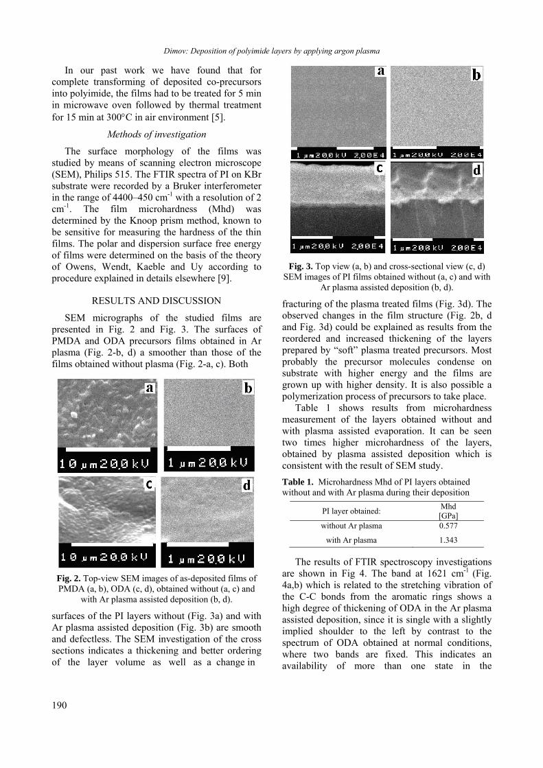
Dimov: Deposition of polyimide layers by applying argon plasma
190
In our past work we have found that for complete transforming of deposited co-precursors into polyimide, the films had to be treated for 5 min in microwave oven followed by thermal treatment for 15 min at 300C in air environment [5].
Methods of investigation
The surface morphology of the films was studied by means of scanning electron microscope (SEM), Philips 515. The FTIR spectra of PI on KBr substrate were recorded by a Bruker interferometer in the range of 4400–450 cm-1 with a resolution of 2 cm-1. The film microhardness (Mhd) was determined by the Knoop prism method, known to be sensitive for measuring the hardness of the thin films. The polar and dispersion surface free energy of films were determined on the basis of the theory of Owens, Wendt, Kaeble and Uy according to procedure explained in details elsewhere [9].
RESULTS AND DISCUSSION
SEM micrographs of the studied films are presented in Fig. 2 and Fig. 3. The surfaces of PMDA and ODA precursors films obtained in Ar plasma (Fig. 2-b, d) a smoother than those of the films obtained without plasma (Fig. 2-a, c). Both
Fig. 2. Top-view SEM images of as-deposited films of PMDA (a, b), ODA (c, d), obtained without (a, c) and
with Ar plasma assisted deposition (b, d).
surfaces of the PI layers without (Fig. 3a) and with Ar plasma assisted deposition (Fig. 3b) are smooth and defectless. The SEM investigation of the cross sections indicates a thickening and better ordering of the layer volume as well as a change in
Fig. 3. Top view (a, b) and cross-sectional view (c, d)
SEM images of PI films obtained without (a, c) and with Ar plasma assisted deposition (b, d).
fracturing of the plasma treated films (Fig. 3d). The observed changes in the film structure (Fig. 2b, d and Fig. 3d) could be explained as results from the reordered and increased thickening of the layers prepared by “soft” plasma treated precursors. Most probably the precursor molecules condense on substrate with higher energy and the films are grown up with higher density. It is also possible a polymerization process of precursors to take place.
Table 1 shows results from microhardness measurement of the layers obtained without and with plasma assisted evaporation. It can be seen two times higher microhardness of the layers, obtained by plasma assisted deposition which is consistent with the result of SEM study.
Table 1. Microhardness Mhd of PI layers obtained without and with Ar plasma during their deposition
PI layer obtained: Mhd [GРa]
without Ar plasma 0.577
with Ar plasma 1.343
The results of FTIR spectroscopy investigations are shown in Fig 4. The band at 1621 cm-1 (Fig. 4a,b) which is related to the stretching vibration of the C-C bonds from the aromatic rings shows a high degree of thickening of ODA in the Ar plasma assisted deposition, since it is single with a slightly implied shoulder to the left by contrast to the spectrum of ODA obtained at normal conditions, where two bands are fixed. This indicates an availability of more than one state in the
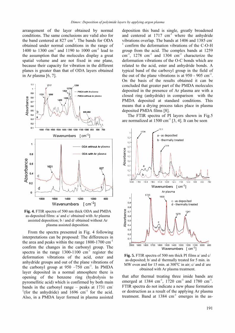
Dimov: Deposition of polyimide layers by applying argon plasma
191
arrangement of the layer obtained by normal conditions. The same conclusions are valid also for the band centered at 827 cm-1. The bands for ODA obtained under normal conditions in the range of 1400 to 1300 cm-1 and 1190 to 1000 cm-1 lead to the assumption that the molecules display a great spatial volume and are not fixed in one plane, because their capacity for vibration in the different planes is greater than that of ODA layers obtained in Ar plasma [6, 7].
Fig. 4. FTIR spectra of 500 nm thick ODA and PMDA as-deposited films: a/ and c/ obtained with Ar plasma
assisted deposition; b / and d/ obtained without Ar plasma assisted deposition.
From the spectra presented in Fig. 4 following interpretations can be proposed: The differences in the area and peaks within the range 1800-1700 cm-1 confirm the changes in the carbonyl group. The spectra in the range 1300-1100 cm-1 register the deformation vibrations of the acid, ester and anhydride groups and out of the plane vibrations of the carbonyl group at 950 –750 cm-1. In PMDA layer deposited in a normal atmosphere there is opening of the benzene ring (hydrolysis to pyromellitic acid) which is confirmed by both main bands in the carbonyl range – peaks at 1731 cm-
1(for the anhydride) and 1696 cm-1 for the acid. Also, in a PMDA layer formed in plasma assisted
deposition this band is single, greatly broadened and centered at 1717 cm-1 where the anhydride vibrations overlap. The bands at 1406 and 1385 cm-
1 confirm the deformation vibrations of the C-O-H group from the acid. The complex bands at 1259 cm-1, 1278 cm-1 and 1304 cm-1 characterize the deformation vibrations of the O-C bonds which are related to the acid, ester and anhydride bonds. A typical band of the carboxyl group in the field of the out of the plane vibrations is at 950 - 905 cm-1. On the basis of the results obtained it can be concluded that greater part of the PMDA molecules deposited in the presence of Ar plasma are with a closed ring (anhydride) in comparison with the PMDA deposited at standard conditions. This means that a drying process takes place in plasma deposited PMDA films [8].
The FTIR spectra of PI layers shown in Fig.5 are normalized at 1500 cm-1 [3, 4]. It can be seen
Fig. 5. FTIR spectra of 500 nm thick PI films a/ and c/ as-deposited; b/ and d/ thermally treated for 5 min. in
MW oven and for 15 min. at 300oC in air; c/ and d/ are obtained with Ar plasma treatment.
that after thermal treating three imide bands are emerged at 1384 cm-1, 1720 cm-1 and 1780 cm-1. FTIR spectra do not indicate a new phase formation or destruction as a result of the applying Ar plasma treatment. Band at 1384 cm-1 emerges in the as-

Dimov: Deposition of polyimide layers by applying argon plasma
192
deposited layer obtained in the presence of Ar plasma, while under normal conditions such band is absent, which is indication that the process of imidization takes place. In the as-deposited layer obtained at standard conditions without plasma the quantity of the polyamide acid is high [3, 4]. On the contrary our results show (Fig.5-c, d) that PI is formed more easily in the presence of Ar plasma
because the precursor molecules react more actively and at a greater rate. FTIR spectra presented in Fig.5-c, d categorically corroborate the fact that imidization process takes place in the PI layers obtained by Ar plasma assisted process. The reason for the appearance of polyimide peaks in as deposited plasma treated films is not investigated in
Table 2. Contact angle, polar and dispersion component and overall free surface energy of PI layers deposited without and with Ar plasma.
PI layer obtained:
Contact angle Polar component γsp
[mJ.m-2] Dispersion
component γsd
[mJ.m-2]
Surface energy
[mJ.m-2] H2O CH2J2
without Ar plasma 93 31 0.26 43.8 44.1
with Ar plasma 73.6 16.0 4.55 45.36 49.91
details. Most probably the collisions between precursors, electrons and ions or the ultraviolet irradiation from the plasma influence strongly the imidization process.The influence of Ar plasma on the film surface energy is shown in Table 2. It is seen that the plasma treatment causes a small increase in the polar component of free energy. It can be expected that these changes in polar surface energy will be stable in time, because the layers are modified in the whole volume, not just at the surface. Obviously more detailed investigation is needed to confirm the assumption.
CONCLUSION
A new method of physical deposition of polyimide thin films employing plasma assisted deposition is developed. The impact of Ar plasma on the precursor molecular flux provokes an increasing in the kinetic energy of the molecules. In this way the plasma treating leads to an activation of the precursor molecules or some change of molecular structure of the precursors which results in an enhancement of the imidization process, in the thickening of the layers as well as in the increasing of microhardness. The results obtained show that the proposed method offers the possibility for changing the parameters of the vacuum deposited polyimide films in the direction desired by us.
Acknowledgement: The financial support of the National Fund of the Ministry of Education and Science, Bulgaria – contract DO 02-254 is gratefully acknowledged.
REFERENCES
1. N. Capps, D. Carter, G. Roche, Advanced Energy Industries Inc., Fort Collins, Colo. Semiconductor International, 7, 1 (2000).
2. G. Maggioni, S. Carturan, V. Rigato, G. D. Mea, Surf. Coat. Technol., 142-144, 156 (2001).
3. E. Spassova, Vacuum, 70, 551 (2003). 4. G. Danev, E. Spassova, J. Assa, I. Karamancheva,
A. Paskaleva, K. Popova, J. Ihlemann, Vacuum, 70, 37 (2003).
5. D. Dimov, A. Georgiev, E. Spassova, I. Karamancheva, Y. Shopov, G. Danev, J. Optoelectr. Adv. Mater., 9, 494 (2007).
6. B. Stuart, Infrared Spectroscopy: Fundamentals and Application, Wiley, Chapter 3 and Ch, 6, 2004.
7. S. Wartewig, IR and Raman Spectroscopy Fundamental Processing, Wiley – VCH GmbH & Co. KGaA, Ch. 10, 2003.
8. D. Dimov, E. Spassova, I. Karamancheva, I. Zhivkov, G. Danev, Vacuum ,76, 223 (2004).
9. S. Kitova, M. Minchev, G. Danev, J. Optoelectron. Adv. Mater., 7, 249 (2005).

Dimov: Deposition of polyimide layers by applying argon plasma
193
ОТЛАГАНЕ НА ПОЛИИМИДНИ СЛОЕВЕ ЧРЕЗ ПРИЛАГАНЕ НА АРГОНОВА ПЛАЗМА
Д. Димов
Институт по оптически материали и технологии „Акад. Й. Малиновски“, БАН, Ул.“Акад. Г. Бончев“, бл.109, 1113 София, България
Постъпила на 17 октомври 2013 г.; коригирана на 25 ноември, 2013 г.
(Резюме)
Разработен е нов метод за физическо парно отлагане на тънки слоеве, чрез прилагане на плазмено асистиращи процеси. Изследването включва както въздействие върху индивидуалните прекурсори (оксидианилин (ОДА ) и пиромелитов дианхидрид ( PMDA ) ) така и върху двата мономера едновременно. Изследвано е влияние върху структурата на получените слоеве и промяна на свойствата им. Чрез SEM анализ, са показани значителни промени в структурата на кондензираните прекурсори. Установено е, че плазменото асистирано отлагане води до уплътняване на слоя, със забележителни промени в повърхностната им морфология. Наблюдавано е увеличаване на измерената микротвърдост с повече от 50 процента. Получените резултати от FTIR анализа потвърждават формирането на затворени анхидридни пръстени като по този начин плазмено асистиращо отлагане допринася за протичане на имидизационния процес. Наблюдаваните ефекти са обяснени с повишената енергия на прекурсорите, получена от взаимодействието с плазмата.

194
Bulgarian Chemical Communications, Volume 45, Special Issue B (pp.194-197) 2013
Film thickness measurement by optical profilometer MicroProf® FRT
V. Siderov1, D. Mladenova1,2, R. Yordanov3, V. Milenkov1, M. Ohlidal4, O. Salyk1, I. Zhivkov1,3*, and M. Weiter1
1Centre for Materials Research, Faculty of Chemistry, Brno University of Technology, Purkynova 118, 612 00 Brno, Czech Republic
2Institute of Optical Materials and Technologies “Acad. J. Malinowski”, Bulgarian Academy of Sciences, Acad. G. Bonchev Str. bl. 101/109, 1113 Sofia, Bulgaria
3Department of Electronics, Faculty of Electronic Engineering and Technologies, Technical University - Sofia, 8 Kliment Ohridski blvd., 1000 Sofia, Bulgaria
4Department of Optics and Precise Mechanics, Institute of Physical Engineering, Brno University of Technology, Technicka 2, 616 96 Brno, Czech Republic
Received October 17, 2013; Revised November 25, 2013
This paper compares Chromatic white light (CWL) and stylus profilometer measurements. Standard samples with vacuum deposited aluminum films of different thicknesses in the range of 50-300 nm were prepared and measured by both methods. It was found that the CWL technique is proper for a measurement of thin organic films with higher than 40-50 nm film thicknesses.
Keywords: thickness measurements, chromatic white light, stylus profilometer
INTRODUCTION
Thickness measurement is of a main importance in both the first stage of the thin film deposition and the final steps of testing and failure analysis in the microelectronics and MEMS [1]. Usage of the organic semiconductors in the microelectronics causes specific new problems, concerning the film deposition and measurement.
Organic semiconductors are more recently investigated due to their low price and easy processing at room temperatures and atmospheric pressure [2], with low cost “wet” techniques – spin and dip coating [3], electrophoretic deposition [4] and ink-jet printing [5]. They are promising materials for a thin film application as electrode, insulator or semiconductor films in the future microelectronic devices [6] – OLEDs, solar cells, OFETs and gas sensors. But some problems as film softness, bad adhesion and the presence of impurities result in low reproducible parameters and impede the organic microelectronics development. In general the film softness could considerable affect the organic film thickness determination.
The film thickness could be measured by
forming a step between the film and the uncovered substrate. In a case of “wet” film deposition techniques used, the step is usually formed by a scratching [7]. The film delamination and removal depends on the stylus material and shape, the force applied, the film and substrate properties [8].
The most used tool for a thin film thickness measurement is the stylus profilometer. It is capable to scan area of tens of millimeters with a vertical range starting from several nanometers up to hundreds of microns. Its main disadvantage is the contact with the surface, which can cause a destruction of the organic film surface and a misrepresentation of the data measured. Due to this, the stylus profilometer is not always the best tool for a thickness measurement of thin soft organic films.
Chromatic white light (CWL) method is a non-contact technique for 3D profiling of the surface roughness [9]. It allows scanning of a wide area surfaces with a lateral and vertical resolution of 1 µm and 10 nm, respectively. It is successfully utilized for a surface topography evaluation in mechanical engineering, electro-technical industry and bioengineering [10]. CWL method was originally developed mainly for surface scanning. The software for data processing in fact has all capabilities, (e. g. digital processing and Fourier filtering) available in AFM measurement. The main * To whom all correspondence should be sent:
E-mail: [email protected] © 2013 Bulgarian Academy of Sciences, Union of Chemists in Bulgaria

Siderov et al.: Film thickness measurement by optical profilometer MicroProf® FRT
195
disadvantage of the method is the influence of the optical inhomogeneity of the film on the accuracy of the measurement.
This paper compares two different measurement techniques – CWL and stylus profilometer to determine the capabilities of the non-contact CWL method for thickness measurements of thin organic films.
EXPERIMENTAL
Standard samples with vacuum deposited aluminum films of different thicknesses in the range of 50-300 nm were prepared. The different thicknesses were obtained by placing the substrates at different distances from the evaporation source. Al was used because of both good mechanical and excellent light reflectance properties fulfilling the requirements for both contact and non-contact thickness measurement.
Thicknesses of the standard samples with Al films were measured by CWL and stylus profilometer methods. The reliability of both methods was estimated.
The CWL measurement with CWL MicroProf® FRT (Fig. 1) is based on the chromatic aberration of the optical sensor CHR 150 N. A white light from a polychromatic source is passed through a semitransparent mirror and splits spectrally in the chromatic aberration lens. The optical aberration effect causes each wavelength to be focused at a different Z height. As a result of the chromatic “splitting” the film thickness is measured [11].
Fig. 1. Principle of Chromatic White Light (CWL)
measurement.
The thickness of the films was measured using a contact profilometer, Talystep. (Taylor Hobson Talystep, Model 223-7.)
RESULTS AND DISCUSSION
CWL thickness measurements
In Fig. 2 a typical step profile, formed between two thin Al films on a standard sample is measured by the CWL method in 1D mode. The measurement was performed after leveling of the sample. A distinguishable step between the Al films is formed allowing determining the film thickness. It could be seen that the noise is 2-3 times the device resolution. The minimum value successfully measured with the CWL technique under the aforementioned conditions was 49 nm, which is about 5 times the device resolution.
Fig. 2. Step profile formed between two Al layers,
measured by CWL method in 1D mode.
This measurement shows the limits of the method for thin film thickness measurements. When the measured value is close to the device resolution, the measurement needs a statistical processing. Hereafter all data from at least 10 CWL measurements are presented after statistical processing in the form of mean value and standard relative error. The standard relative error was chosen to make possible the comparison of errors obtained from different film thicknesses.
Stylus profilometer thickness measurements
In Fig. 3 typical contact profilometer measurement of the step between two Al layers on a standard sample is presented. The measurement was carried out at the maximum possible magnification after a precise sample leveling in a way to extend the step over the full scale of the range. In this case it was assumed that the resolution of the measurement is equal to or less than the resolution of the scale on the paper of 1 mm (1.6% from the full scale). The picture presents a smooth curve resulted from the low speed of scanning. Moreover the relatively heavier tip

Siderov et al.: Film thickness measurement by optical profilometer MicroProf® FRT
196
facilitates the integration of the noise during the scanning.
Fig. 3. Measurement of a step between two Al layers of a standard sample with stylus profilometer.
It could be seen from the figure that a clear distinguishable step is measured. Obviously the stylus profilomenter has the advantage of smooth measurement with higher resolution. It has the disadvantage of a mechanical contact between the stylus and the measured surface. In case of soft thin films it could vitiate the measurement.
Comparison of the methods
Summarized results of the CWL and stylus profilometer are presented in Table 1.
Table 1. Comparative thin film thickness measurements with CWL and stylus profilometer methods.
Sample No
CWL thickness [nm] (Relative error
[ %])
Stylus thickness [nm] (Relative error
[ %]) s1 s2 s3
49 (8) 109 (7.5) 275 (4)
50 (7) 98 (3)
275 (3)
Comparing the CWL measurements on samples with different thicknesses, standard relative error less than 8% was obtained. The variation of the standard relative error from one to the other sample could be related to the sample properties - presence of dust or film inhomogeneity. Measurement of samples with thicknesses bellow 50 nm is not proper; the values measured are close to the device ADC resolution.
Stylus profilometer produces smoother and distinguishable step. It has the capability of measurement in the range less than 50 nm. But the standard relative error of the measurement for ranges higher than 50 nm is similar to that obtained by the CWL method.
Comparing measurements with both methods on the same sample, it could be seen that the differences are close or within the relative standard error, i. e. no apparent constant error related to the measured device was observed.
CONCLUSION
The CWL method is proper for a measurement of thin soft organic films with higher than 40-50 nm film thicknesses. Measurement of lower thicknesses could be affected by the limit of the device resolution. In a case of optical inhomogeneity the method requires covering the film with a uniform high reflective coating (for example Al).
For films thicker than 50 nm both CWL and stylus profilometer methods give comparable results with comparable standard relative error.
Acknowledgements: This work was supported by Ministry of Industry and Trade of the Czech Republic project No FR-TI1/144, Grant Agency of the Czech Republic projects No. P205/10/2280 and 13-29358S and by project "Centre for Materials Research at FCH BUT" No. CZ.1.05/2.1.00/ 01.0012 supported by ERDF.
REFERENCES
1. J. M. Bennett, V. Eling, K. Kjoller, Appl. Opt., 32, 3442 (1993).
2. K. Tada, M. Onoda, Mol. Cryst. Liq. Cryst., 505, 124 (2009).
3. K. Norrman, A. Ghanbari-Siahkali, N. B. Larsen, Annu. Rep. Prog. Chem., Sect. C: Phys. Chem., 101, 174 (2005).
4. K. Tada, M. Onoda, Thin Solid Films, 518, 711 (2009).
5. P. Yin, YA. Huang, NB. Bu, XM. Wang, YL. Xiong, Chinese Science Bulletin, 55, 3383 (2010).
6. A. Tsumura, H. Koezuka, T. Ando, Appl. Phys. Lett., 49, 1210 (1986).
7. F. Wredenberg, P.-L. Larsson, JoMMS, 4, 6, 1041 (2009).
8. D. W. Butler, C. T. H. Stoddart, P. R. Stuart, J. Phys. D: Appl. Phys., 3, 877 (1970).
9. http://www.frt-gmbh.com/frt/upload/pdf_en/ FRT_Sensor_CWL_EN.pdf (2013).
10. K. Palenikova, M. Ohlidal, Proc. SPIE, 5945 (2005).
11. http://www.solarius-inc.com/html/ whitelightprobe.html.

Siderov et al.: Film thickness measurement by optical profilometer MicroProf® FRT
197
ИЗМЕРВАНЕ НА ДЕБЕЛИНИ С ОПТИЧЕН ПРОФИЛОМЕТЕР MICROPROF® FRT
В. Сидеров1, Д. Младенова1,2, Р. Йорданов3, В. Миленков1, М. Охлидал4, И. Живков1, 4, М. Вайтер1,
1Технологичен университет – Бърно, Химически факултет, Център по материалознание, ул. Пуркиньова 118, 612 00 Бърно, Чешка република
2Институт по оптически материали и технологии “акад. Й. Малиновски”, Българска академия на науките, ул. акад. Г. Бончев, бл. 109, 1113 София, България
3Катедра Микроелектроника, Факултет по електронна техника и технологии, Технически университет - София, бул. Климент Охридски 8, 1000 София, България
4Отдел по оптика и финна механика, Институт по инженерна физика, Технологичен университет – Бърно, Технична 2, 616 96 Бърно, Чешка република
Постъпила на 17 октомври 2013 г.; коригирана на 25 ноември, 2013 г.
(Резюме)
Тази статия сравнява измервания с методите хроматична бяла светлина (CWL) и контактен профилометър. Приготвени са еталонни образци с отложени тънки слоеве алуминий с дебелини в интервала 50-300 нм и с гореспоменатите методи са измерени техните дебелини. Установено е, че CWL техниката е подходяща за измерване на тънки слоеве с дебелини, по-големи от 40-50 нм.

198
Bulgarian Chemical Communications, Volume 45, Special Issue B (pp. 198-202) 2013
Rare earth metal modified alumina-supported copper cobaltite catalysts in reduction of NO with CO
B. K. Ivanov*, M. S. Khristova, I. P. Spassova
Institute of General and Inorganic Chemistry, Bulgarian Academy of Sciences, 1113 Sofia, Bulgaria
Received October 17, 2013; Revised November 25, 2013
The effect of low loading rare earth metal addition (RE= La, Ce, Nd and Gd) to alumina supported copper-cobalt spinel oxide on the catalysts efficiency in NO reduction with CO was investigated. Samples RE/CuCo/Al (RE= La, Ce, Nd and Gd) were prepared by vacuum- evaporation. The rare earth modified as well as their “parent” catalysts were characterized by XRD, XPS, AAS, SEM-EDS, BET analysis. The catalytic experiments were carried out in catalytic flow apparatus in an isothermal flow reactor in the temperature range 20–500оС. It was found that the modification of alumina supported copper- cobalt spinel with rare earths (RE= La, Ce, Nd and Gd) influenced in different ways on the catalytic activity in NO reduction with CO depending on the temperature. For temperatures up to 100oC La has the most positive effect while at temperatures above 250oC Gd is the most proper modifier. Nd is not convenient for catalyst improvement in this reaction.
Keywords: rare earth, catalyst, modification, NO reduction with CO.
.
INTRODUCTION
Exhaust gases containing nitrogen oxides from stationary and mobile combustion sources cause a variety of environmentally harmful effects. NOx removal from these gases still remains one of major challenges in the area of environmental catalysis [1-3]. The most common approach is the reaction with residual reductors (unburned or partially burned hydrocarbons and CO) in the exhaust. Various catalysts have been extensively studied. It was found out that Cu-Co oxide spinels such as CuxCo(3-
x)O4 [4] and CuCo2O4/γ-Al2O3 [5] are catalysts demonstrating high activity in the reduction of NO with CO.
The mixing of two different oxides offers an opportunity not only to improve the performance of the involved metal oxide but also to form new stable compounds that may lead to totally different physicochemical properties and catalytic behavior from the individual components. In order to improve the activity of copper-based catalysts for the SCR, some additives, such as Fe, Co, Ni, V, Mn, W, Mo, and Cr, were doped for the promotion of the copper species dispersion. The addition of certain promoters could enhance the catalytic performance of supported catalysts for the SCR of NOx with hydrocarbons [6]. Cerium oxide is a
commonly used promoter in automotive three-way catalysts [7]. The rare earth oxides, although constituting a closely related group of compounds, exhibit a rich variety of characteristic behaviors and solid-state properties, including features that make them interesting subjects for catalytic studies [8].
In the present work we investigate the effect of low loading rare earth metal addition (RE= La, Ce, Nd and Gd) to alumina supported copper-cobalt spinel oxide on the catalysts efficiency in NO reduction with CO.
EXPERIMENTAL
Alumina supported copper cobaltite catalyst (CuCo/Al) was prepared preliminary according to [9] procedure. It has been established that after modification of the support with Cu2+ ions, the stoichiometric CuCo2O4 phase is formed, thus avoiding the “chromatographic effect”. This catalyst was impregnated with 1wt. % La, Nd, Ce and Gd by nitrate solutions. The catalysts for the targeted research were obtained in a vacuum-evaporator and thermally treated at 500оС for 2 h. The samples RE/CuCo/Al (RE= La, Ce, Nd and Gd) were prepared.
The rare earth modified as well as their “parent” catalysts were characterized by XRD, XPS, SEM-EDS, AAS and BET analysis. The catalytic experiments were carried out in catalytic flow apparatus in an isothermal flow reactor in the
© 2013 Bulgarian Academy of Sciences, Union of Chemists in Bulgaria
* To whom all correspondence should be sent: E-mail: [email protected]
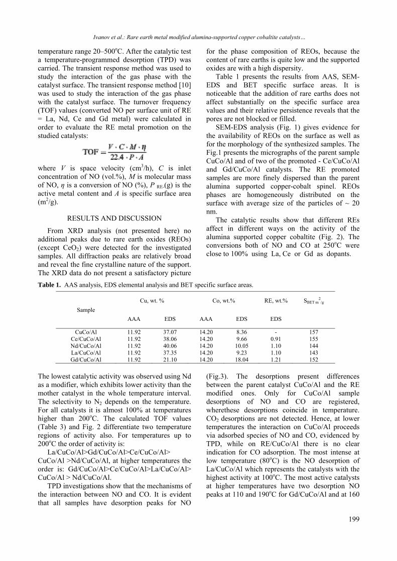
Ivanov et al.: Rare earth metal modified alumina-supported copper cobaltite catalysts…
199
temperature range 20–500оС. After the catalytic test a temperature-programmed desorption (TPD) was carried. The transient response method was used to study the interaction of the gas phase with the catalyst surface. The transient response method [10] was used to study the interaction of the gas phase with the catalyst surface. The turnover frequency (TOF) values (converted NO per surface unit of RE = La, Nd, Ce and Gd metal) were calculated in order to evaluate the RE metal promotion on the studied catalysts:
where V is space velocity (cm3/h), C is inlet concentration of NO (vol.%), M is molecular mass of NO, η is a conversion of NO (%), P RE (g) is the active metal content and A is specific surface area (m2/g).
RESULTS AND DISCUSSION
From XRD analysis (not presented here) no additional peaks due to rare earth oxides (REOs) (except CeO2) were detected for the investigated samples. All diffraction peaks are relatively broad and reveal the fine crystalline nature of the support. The XRD data do not present a satisfactory picture
for the phase composition of REOs, because the content of rare earths is quite low and the supported oxides are with a high dispersity.
Table 1 presents the results from AAS, SEM-EDS and BET specific surface areas. It is noticeable that the addition of rare earths does not affect substantially on the specific surface area values and their relative persistence reveals that the pores are not blocked or filled.
SEM-EDS analysis (Fig. 1) gives evidence for the availability of REOs on the surface as well as for the morphology of the synthesized samples. The Fig.1 presents the micrographs of the parent sample CuCo/Al and of two of the promoted - Ce/CuCo/Al and Gd/CuCo/Al catalysts. The RE promoted samples are more finely dispersed than the parent alumina supported copper-cobalt spinel. REOs phases are homogeneously distributed on the surface with average size of the particles of ~ 20 nm.
The catalytic results show that different REs affect in different ways on the activity of the alumina supported copper cobaltite (Fig. 2). The conversions both of NO and CO at 250oC were close to 100% using La, Ce or Gd as dopants.
Table 1. AAS analysis, EDS elemental analysis and BET specific surface areas.
Sample
Cu, wt. % Co, wt.% RE, wt.% SBET m2/g
AAА EDS AAА EDS EDS
CuCo/Al 11.92 37.07 14.20 8.36 - 157 Ce/CuCo/Al 11.92 38.06 14.20 9.66 0.91 155 Nd/CuCo/Al 11.92 40.06 14.20 10.05 1.10 144 La/CuCo/Al 11.92 37.35 14.20 9.23 1.10 143 Gd/CuCo/Al 11.92 21.10 14.20 18.04 1.21 152
The lowest catalytic activity was observed using Nd as a modifier, which exhibits lower activity than the mother catalyst in the whole temperature interval. The selectivity to N2 depends on the temperature. For all catalysts it is almost 100% at temperatures higher than 200oC. The calculated TOF values (Table 3) and Fig. 2 differentiate two temperature regions of activity also. For temperatures up to 200oC the order of activity is:
La/CuCo/Al>Gd/CuCo/Al>Ce/CuCo/Al> CuCo/Al >Nd/CuCo/Al, at higher temperatures the order is: Gd/CuCo/Al>Ce/CuCo/Al>La/CuCo/Al> CuCo/Al > Nd/CuCo/Al.
TPD investigations show that the mechanisms of the interaction between NO and CO. It is evident that all samples have desorption peaks for NO
(Fig.3). The desorptions present differences between the parent catalyst CuCo/Al and the RE modified ones. Only for CuCo/Al sample desorptions of NO and CO are registered, wherethese desorptions coincide in temperature. CO2 desorptions are not detected. Hence, at lower temperatures the interaction on CuCo/Al proceeds via adsorbed species of NO and CO, evidenced by TPD, while on RE/CuCo/Al there is no clear indication for CO adsorption. The most intense at low temperature (80oC) is the NO desorption of La/CuCo/Al which represents the catalysts with the highest activity at 100oC. The most active catalysts at higher temperatures have two desorption NO peaks at 110 and 190oC for Gd/CuCo/Al and at 160

Ivanov et al.: Rare earth metal modified alumina-supported copper cobaltite catalysts…
200
and 330oC for Ce/CuCo/Al. These peaks represent probably two forms of NO adsorption.
A transient response method was applied to obtain information about the processes that occur on the surface of the studied catalysts and about the mechanism of the reduction of NO with CO. The differences in the curves reveal the different rate-controlling steps of the reaction over the catalysts.
0 100 200 300 400 5000
20
40
60
80
100Gd/CuCo/AL
Temperature, oC
NO
con
vers
ion,
%
Nd/CuCo/AL
Ce/CuCo/AL
La/CuCo/ALCuCo/AL
0 100 200 300 400 50000
2020
4040
6060
8080
100100
CO
oxi
datio
n, %
Gd/CuCo/AL
La/CuCo/AL
CuCo/AL
Nd/CuCo/AL
Ce/CuCo/AL
Temperature, oC
Fig. 2. Temperature dependence of the conversion degree of NO and CO on samples Gd/CuCo/Al,
Ce/CuCo/Al, La/CuCo/Al, Nd/CuCo/Al and CuCo/Al.
0 100 200 300 400 500
NO
80oC
Gd/CuCo/AL
Ce/CuCo/AL
La/CuCo/AL
Nd/CuCo/AL
CuCo/AL
110oC190oC
NO
160oC
120oC
330oC
NO
NO
NO
COCuCo/AL
Inte
nsit
y (a
.u.)
Temperature, oC Fig. 3. TPD spectra of NO and CO for the investigated
samples.
a
b
c Fig. 1. SEM micrographs of a) CuCo/Al, b)
Ce/CuCo/Al and c) Gd/CuCo/Al.

Ivanov et al.: Rare earth metal modified alumina-supported copper cobaltite catalysts…
201
2 40
200
400
600
800
1000
1200
Gd/CuCo/AL
La/CuCo/AL
NO+CO+Ar
CuCo/AL
Nd/CuCo/AL
Ce/CuCo/AL
Time, min
Con
cent
ratio
n o
f N
O, p
pm
100oC
2 40
200
400
600
800
1000
1200
Time, min
La/CuCo/AL
CuCo/AL
Gd/CuCo/AL
Nd/CuCo/AL
Ce/CuCo/AL
NO+CO+Ar
Con
cent
ratio
n o
f N
O, p
pm
250oC
Fig. 4. Transient response curves of NO on Gd/CuCo/Al, Ce/CuCo/Al, La/CuCo/Al, Nd/CuCo/Al and CuCo/Al at
100 and 250oC.
The change in the rate-controlling step is associated with a change in the reaction mechanism. In Fig. 4 the transient response curves of reactant NO are presented at 100oC and 250oC. At 100oC the response curves for NO are of a monotonically growing type for Gd/CuCo/Al and of an instantaneous type at for Ce/CuCo/Al, La/CuCo/Al, Nd/CuCo/Al and CuCo/Al. The monotonically type response, according to Kobayashi’s classification, indicates that the rate-limiting step in the reaction mechanism could be the surface reaction or desorption of the products. As desorption of the products is absent in the stop stage the surface reaction seems to be the rate-determining step. The instantaneous response deduces that the rate-limiting step could be the surface reaction or the adsorption of the reagents.
The transient curves for NO at 250oC for Gd/CuCo/Al and Ce/CuCo/Al are of the overshot type response, indicating that the rate-limiting step
in the reaction mechanism could be creation or regeneration of the new catalytically active sites responsible for both reduction and decomposition of NO. The results coincide with the TPD spectra these samples that represent two desorption (low and high) peaks for both samples. This implies the change in the reaction mechanism for these catalysts that are the most active at temperatures above 250oC. The response curves show that depending on the temperature the catalytic reaction proceeds on various types of active centers.
CONCLUSION
The modification of alumina supported copper- cobalt spinel with rare earths (RE= La, Ce, Nd and Gd) influenced in different ways on the catalytic activity in NO reduction with CO depending on the temperature. For temperatures up to 100oC La has the most positive effect while at temperatures above 250oC Gd is the most proper modifier. Nd is not convenient for catalyst improvement in this reaction.
Acknowledgements: The work was financed by the European Social Fund BG051PO001-3.3.06-0050 and National Science Fund of Bulgaria DTK 02/64/2009.
REFERENCES
1. M. Shelef, Chem. Rev.,95 (1995) 209. 2. R. Burch, Catal. Rev., 46 (2004) 271. 3. R. Hernández-Huesca, J. Santamaría-González, P.
Braos-García, P. Maireles-Torres, E. Rodríguez-Castellón, A. Jiménez-López, Appl. Catal., B 29 (2001) 1.
4. D. Panayotov, M. Khristova, D. Mehandjiev, J. Catal., 156 (1995) 219.
5. D. Panayotov, M. Khristova, M. Velikova, Appl. Catal., B 9 (1996) 107.
6. Y. Yokomichi, T. Yamabe, T. Kakumoto, O. Okada, H. Ishikawa, Y. Nakamura, H. Kimura, I. Yasuda, Appl. Catal., B 28 (2000) 1.
7. W.D. Wang, P. Lin, Y.L. Fu, G.Y. Cao, Catal. Lett., 82 (2002) 19.
8. M. Rosynek, Catal. Rev.-Sci. Eng., 16(1) (1977) 111.
9. D. Mehandjiev, P.Dimitrova, React. Kinet.Catal. Lett., 56 (2) (1995) 341.
10. M. Kobayashi, Chem. Eng. Sci., 37 (1982) 393.

Ivanov et al.: Rare earth metal modified alumina-supported copper cobaltite catalysts…
202
НАНЕСЕНИ НА АЛУМИНИЕВ ОКСИД МОДИФИЦИРАНИ С РЕДКОЗЕМНИ МЕТАЛИ КАТАЛИЗАТОРИ ОТ МЕДЕН КОБАЛТИТ В РЕАКЦИЯТА НА РЕДУКЦИЯ НА NO С СО
Б. K. Иванов, М. Ст. Христова, И. П. Спасова Институт по обща и неорганична химия, Българска академия на науките, 1113 София, България
Постъпила на 17 октомври 2013 г.; коригирана на 25 ноември, 2013 г.
(Резюме)
Ефектът от малки добавки от редкоземни елементи (RE= La, Ce, Nd и Gd) върху нанесен на алуминиев оксид медно-кобалтов шпинелен оксид по отношение ефективността в редукцията на NO с CO беше изследван. Образците RE/CuCo/Al (RE= La, Ce, Nd и Gd) бяха приготвени чрез вакуум-изпарение. Модифицираните с редкоземни елементи катализатори, както и медно-кобалтовият катализатор бяха охарактеризирани с XRD, XPS, SEM-EDS, AAS и BET анализи. Каталитичните експерименти бяха проведени в поточна каталитична апаратура с изотермичен реактор в температурен интервал 20–500оС. Намерено е, че модифицирането на нанесения на алуминиев оксид медно-кобалтов шпинел с редкоземни елементи (RE= La, Ce, Nd и Gd) влияе по различен начин върху каталитичната активност при редукцията на NO с CO в зависимост от температурата. За температури до 100oC La притежава най-положителен ефект, докато при температури над 250oC Gd е най-подходящият модификатор. Nd не е подходящ за подобряване на каталитичната активност при тази реакция.

203
Bulgarian Chemical Communications, Volume 45, Special Issue B (pp. 203-207) 2013
Study on the stoichiometry and reaction products of extra virgin olive oil ozonation
V.Georgiev*, M. Anachkov, T. Batakliev, S. Rakovsky
Institute of Catalysis, Bulgarian Academy of Sciences 1113, Sofia, Bulgaria
Received October 17, 2013; Revised November 25, 2013
The amount of consumed ozone during ozonation of olive oil has been determined on the basis of continuous measurement of ozone concentrations at the bubbling reactor outlet, under conditions of constant values of ozone concentrations at the reactor inlet. This amount has been used for evaluation of reaction stoichiometry, according to which one conditional average molecule olive oil reacts with about three molecules of ozone.
The IR-spectroscopy and 1H-NMR spectroscopy have been applied for identification and quantitatively characterization of basic ozonolysis products: ozonides and aldehydes. It has also been found out that cis and trans ozonides are formed and their ratio has been determined.
Keywords: ozone, ozonolysis, olive oil, cis/trans ozonides, olive oil unsaturation, 1H-NMR spectroscopy
.
INTRODUCTION
Recently, there has been increasing interest of cosmetic and pharmaceutical industries in the application of ozonized unsaturated triglycerides of vegetable oils [1-3] .It has been found out that the products of vegetable oils ozonolysis have antibacterial, fungicidal and antiviral properties; results of their successful utilization in dermatology for the treatment of acute cutaneous wound were reported [4-6]. At the same time their wider application is facing resistance from the orthodox medicine [7, 8]. One of the reasons for such kind of attitude is the insufficiently complete characterization of the nature and properties of the ozonolysis products. The ozonated vegetable oils have been used as modifiers in biodiesel fuel [9-11] and as additives to cutting fluid emulsions [12].
In interpreting the results of ozonolysis, the authors usually refer to the classical Criegee’s scheme, according to which, when the reaction is carried out in neat substrate or in nonparticipating solvents, ozonides (1,2,4 trioxolanes) are obtained as the main product. There are few studies, in which attempts have been made to characterize all the obtained functional groups [13]. The results on the ratio between ozonides and aldehydes are contradictory [13, 14]. Although, the formation of two isomeric forms of 1,2,4 trioxolanes (cis and
trans), is well known, the structural and isomeric composition of the ozonides, obtained during ozonolysis of vegetable oils has practically not been studied yet [13, 15]. As an example of the complexity of this problem the study on methyl oleate ozonolysis can be distinguished where six isomeric ozonides (cis and trans forms of the normal type and two other types of cross-ozonides) have been identified [15.].
In the present paper we monitor the ozone absorption during reaction of olive oil in neat form or in nonparticipating solutions. The ozonolysis products were identified and quantitatively determined by FT-IR and 1H-NMR spectroscopy.
EXPERIMENTAL
Ozone was prepared by passing oxygen through a 4-9 kV discharge.
The experiments have been performed in a bubbling reactor, containing 5-10 mL of olive oil or olive oil solutions in CCl4, equipped with a thermostating water jacket. An ozone–oxygen mixture with ozone concentration in the range of 1000–25000 ppm (4.5.10-5-1.2.10-3 mol L-1) was passed through the reactor at a flow rate of (1.67± 0.15).10-3 L s-1. The ozone concentrations in the gas phase at the reactor inlet ([O3]o) and outlet ([O3]u) have been measured by OZONE ANALYZER BMT 964 device.
© 2013 Bulgarian Academy of Sciences, Union of Chemists in Bulgaria
* To whom all correspondence should be sent: E-mail: [email protected]

Georgiev et al.:Study on the stoichiometry and reaction products of extra virgin olive…
204
Infrared spectra were recorded on thin films coated onto KBr plates using Nicolet 6700 FTIR spectrometer: The spectra comprise the result of 100 scans with a resolution of 4 cm-1.
1H-NMR spectra were recorded on a Bruker Avance 600 MHz instrument under the following conditions: 20 oC; digital resolution 0.3 Hz; number of scans 30. Samples were dissolved in CDCl3 containing TMS as internal standard.
RESULTS AND DISCUSSION
Monitoring of the ozone absorption
The kinetics of the ozone absorption has been studied by continuous monitoring of ozone concentrations at the reactor outlet ([O3]u),under condition of constant values of initial ozone concentration at the reactor inlet ([O3]o
The kinetics of ozonolysis of different double bonds in solution is considerably less investigated than the corresponding mechanism [16]. Because of the high rates of ozonolysis of alkenes, whose double bonds are structurally similar to the RHCH=CHR1H bonds of 3-glycerides in olive oil, the rate constant values, published in the literature, are determined mainly by three methods:1)- measuring the relative rate of consumption of the investigated olefin, comparing with a control compound; 2) – determining of the [O3]u values and 3)- stop-flow method [17-19]. Although there are some differences, the values of the rate constants of alkenes, discussed above, are in the range of 5.104-5.105
L mol-1 s-1 Based on the features of olefins ozonolysis, a spectrophotometric method has been developed for quantitative determination of the double bonds by means of measuring the amount of absorbed ozone [17, 20]. This method could be competitive to the iodine value method determination and it has a very high sensitivity due to the great values of the extinction coefficient of ozone absorption [21]. The essence of the method is illustrated in Fig. 1, where the dependence of [O3]u on the time of ozonation of olive oil solution in CCl4 is shown under conditions of normal bubbling regime and [O3]o=const. The respective curve is characterized by two practically perpendicular sections at the beginning and at the end of the reaction, and region where [O3]u≈0. The absence of outlet ozone is due to the high values of the rate constant of ozone reaction with double C = C bonds [18]. The surface of the area integrated between the curves [O3]u=f(τ) and the line y=[O3]o (where [O3]o= O3]u at τ = 0) is proportional to the amount
Fig. 1. Dependence of the ozone concentration at the
reactor outlet ([O3]u) on the reaction time for solution of olive oil in carbon tetrachloride (0.1 mL in 10 mL CCl4)
ozonolysis.
of consumed ozone. This amount has been calculated by using the coefficient of ozone absorbance at UV-C wavelength 254 nm [21] and the respective flow rate of the ozone–oxygen mixture. At appropriately selected concentrations of double bonds in the solution, the surface area of the solvent saturation with ozone becomes negligible compared to the curve area of the olive oil solution and it may be neglected. The degree of unsaturation of olive oils is usually measured by the so called “iodine value”. Its determination is based on the reaction of double bonds with halogens (iodine), resulting in the formation diiodine alkans. The iodine value is the mass (in grams) of halogens, expressed as iodine, which is absorbed by 100 grams of olive oil. The amount of measured ozone, shown in Fig. 1, is 3.02.10-4 mol. Assuming that it is equal to that of the double bonds, normalizing it to 100 g of olive oil and recalculating into grams of iodine, according to the methodology for determining of the iodine value [22, 23] we obtained 83.4 g of iodine, absorbed by 100 grams of olive oil. Hence the iodine number of olive oil, determined on the basis of its ozonolysis in solution was 83.4. This value is within the range, known from the literature to be specific for the iodine number of olive oils [24].
Functional group analysis
A broad and strong band at 1109 cm-1 is seen in the IR spectra of ozonated olive oil (Fig. 2), assigned to the C-O stretching vibration of ozonide [17, 25] and the band at 1727 cm -1 is typical for ν C=O of aldehydes [26]. In addition to these two signals, an intensive peak at 1379 cm-1 and a shoulder at 975 cm-1 were also identified. It is mentioned in the literature that the trans isomer of

Georgiev et al.:Study on the stoichiometry and reaction products of extra virgin olive…
205
Fig. 2. Infra-red spectra of: non-ozonized (1) and ozonated (2) olive oil in: 800-2000 cm-1 region (a);
1700-1800 cm-1 region (b).
Fig. 3a. 1H NMR spectra of neat olive oil in the region
of 5.0-5.5 ppm.
Fig. 3b. 1H NMR spectra of ozonated olive oil in the
region of 5.0-5.5 ppm (a) and 9.70-9.80 ppm (a').
the 1,2,4-trioxolane absorbs at about 1300 cm-1, while the cis isomer absorbs at about 800 cm-1 [25]. According to another work, upon ozonolysis of sunflower oil methyl esters, a broad peak at 1365 cm-1 appears and on this basis it is concluded that the corresponding trans ozonides are dominating
products [13]. According to the experimental reference data from applied IR-spectroscopy, the peak at 1379 cm-1 is most likely associated with ν C-O-C [26]. The band at 975 cm-1 is characteristic for the stretching vibration of ν O-O [26].
The 1H-NMR spectroscopy provides much more opportunities for identification and quantitative determination of functional groups formed during ozonolysis of olive oil. Assignment of the signals of non-ozonized olive oil (Fig. 3a) is discussed in detail by Vlahov [27]. There exist two isomeric forms of 1,2,4-trioxolanes: cis and trans [25]. Their ratio is a function of the double bond stereochemistry, the steric effect of the substituent, and the conditions of ozonolysis, and it has been studied only in cases of low-molecular-weight alkenes [25, 28, 29]. The signal of the cis form appears at lower field intensity, compared with the trans one [25, 28]. The cis/trans ratio of the olive oil ozonides, determined from integrated intensity of signals at 5.18 and 5.13 ppm was 46:54 (Fig. 3b).
The formation of the basic ozonolysis product- the ozonide is represented in Fig. 4. The modern concepts about the mechanism of the reaction of ozone with С=С double bonds in nonparticipating solvents, in contrast to the classical Criegee’s mechanism, take into account the stereochemical features of the reaction, which ultimately leads to formation of cis and trans 1,2,4 – trioxolanes [16, 25, 29].
Fig. 4. Ozonation and formation of ozonides
The initial reaction is 1,3 coordinated addition of ozone to cis(trans) С=C double bond with formation of cis- or trans-molozonide (MO) respectively. The cis- or trans-molozonide are unstable species, and at temperatures higher than -150oC for the cis-isomer and -90oC for the trans-isomer it is decomposing via the so-called "cycloreversion" (reaction 2) [29]. It is assumed that as a result of the passing of the reaction through the envelope transition state, predominantly anti carbonyl oxides are obtained from cis isomers of MO. The degree of the isomer preference and the extent of stereoselectivity

Georgiev et al.:Study on the stoichiometry and reaction products of extra virgin olive…
206
depend on substituent steric effects, secondary orbital interactions and anomeric interactions [29]. Ozonides are formed as a result of the interaction of the corresponding carbonyl oxides with aldehydes (reaction 3). It is supposed that this interaction is of the cycloaddition type via envelope transition state according to orbital overlap arguments [29]. Thus a syn (or anty) carbonyl oxide (Fig. 5) will react with aldehyde in either endo or exo transition state to give cis or trans ozonide. This step, like the
Fig. 5. Stereochemistry of carbonyl oxides
intermediates.
previous one, can occur with varying degrees of stereoselectivity depending on substituent interactions, electronic effects, temperature etc [16, 25, 29]. It has been found out that the dominant part of ozonides is formed through interaction between carbonyl oxide and the corresponding carbonyl group, which both originate from the decomposition of one and the same MO, i.e., a solvent "cage effect" is occurring (Fig. 4, reaction 3) [16, 17, 25]. The yield of the so-called normal ozonides from the simple olefins is usually of the order of 70 % of the total ozonide yield [25]. Cross ozonides are products of the interaction between carbonyl oxide and aldehyde, originating from different double bonds (Fig. 4, reaction 4). It is assumed that the greater volume of the substituents hampers their formation [25, 30]. The second main type of product of the olive oil ozonolysis are the aldehydes. According to the mechanism of the ozone reaction with double bonds in solution, the aldehyde groups are being formed when the conversion of carbonyl oxide intermediates is proceeding through such routes, which are an alternative to the carbonyl oxide–aldehyde interaction [25, 30]. The nonozonide routes are discussed in detail by Anachkov [30]. The ozonide/aldehyde ratio, defined as ratio between half of integrated intensity of signals of methine protons of the cis- and trans- ozonides and
aldehyde signal at 9.75 ppm was 93.4:6.6 (mol. %). On the basis of the material balance of ozone, the stoichiometry of ozonolysis of olive oil was estimated. It was found that one molecule olive oil reacts with about three molecules of ozone.
CONCLUSIONS
The kinetics of ozone absorption during olive oil ozonolysis has been studied by continuous monitoring of ozone concentrations at the bubbling reactor outlet, under conditions of constant values of ozone concentrations at the reactor inlet. The determined amount of ozone, consumed during the ozonolysis of the double bonds, was used as an alternative method for the quantitative determination of the degree of oil unsaturation. The basic compounds, products of the reaction: ozonides and aldehydes have been identified and quantitatively characterized by means of IR-spectroscopy and 1H-NMR spectroscopy; their ratio was found out to be 93.4:6.6 (mol. %) respectively. The ratio between the cis and trans ozonides was also determined to be 46:54.
REFERENCES
1. J. Sadowska, B. Johansson, E. Johannessen, R. Friman, L. Broniarz-Press, J. B. Rosenholm, Chem. Phys. Lipids, 151, 85 (2008).
2. J. Dıaz, M. Gavın, V. Gomez, J. Brazilian Chem. Soc., 17, 2, 403 (2006)
3. A. Cirlini, G. Caligiani, A. Palla, De Ascentiis, P. Tortini, Ozone Sci. Eng., 34, 293 (2012).
4. I. Lezcano, N. Núñez, M. Espino, M. Gómez, Ozone Sci. Eng., 22, 2, 207 (2000).
5. Sechi, I. Lezcano, N. Nuñez, M. Espino J. Appl. Microbiol., 90, 2, 279 (2001).
6. http://www.nedo.go.jp/content/100084712.pdf. 7. V. Bocci, Oxygen-Ozone Therapy. Kluwer
Academia Publishers, Dordrecht, (2002). 8. V. Bocci, Arch. Medical Res., 37 4 425 (2006). 9. N.U. Soriano Jr., V. Migo, M. Matsumura,J.
Am.Oil Chem. Soc., 80 ,10, 997 (2003). 10. N. U. Soriano Jr., V. Migo, Eur. J. Lipid Sci.
Technol., 107, 689 (2005). 11. N. U. Soriano Jr., V. Migo, Fuel, 85, 25 (2006). 12. J. John, M. Bhattacharya, P. Raynor, Colloids
Surf. A, 237, 141 (2004). 13. N.U.Soriano Jr., V. Migo, and M. Matsumura,
Chem. Phys. Lipids, 126, 133 (2003). 14. http://www.ebookbrowse.com/structure-
elucidation-of-ozonated-olive-oil-doc-d138. 15. M. Wu, D.F. Church, T.J. Mahier, S.A. Barker,
W.A. Pryor, Lipids, 27, 2, 129 (1992).

Georgiev et al.:Study on the stoichiometry and reaction products of extra virgin olive…
207
16. G.E. Zaikov, S.K. Rakovsky, Ozonation of Organic & Polymer Compounds, Smithers, Shrewsbury, (2009).
17. S. D. Razumovskii, G. E. Zaikov, Russ. Chem. Rev., 49, 12, 1163 (1980).
18. S. D. Razumovskii, Khimicheskaja Physika, 19, 7, 58 (2000).
19. W.A. Pryor, D. H. Giamalva, D. F. Church. J. Amer. Chem. Soc., 107, 2793 (1985).
20. S.D. Razumovskii, Vysokomolekulyarnye soedineniya, 50, 12, 2069 (2008).
21. IOA Standardisation Committee-Europe, Brussels. Ozone Concentration Measurement in a Process Gas by UV Absorption, 002/87 (F) (1987).
22. British Pharmacopoeia, Appendix XE, IA, IB. Iodine value (2000).
23. D. Firestone J. AOAC Intern., 77, 3, 674 (1994). 24. Pocklington, W.D. Pure Appl. Chem., 62, 12,
2339 (1990). 25. P. S. Bailey Ozonation in organic chemistry,
Academic Press. New York, (1978). 26. A. L. Smith, Applied Infrared Spectroscopy, Mir,
Moskow, (1982). 27. G. Vlahov, Prog. Nucl. Magn. Reson. Spectrosc.,
35, 341 (1999). 28. R.W. Murray, R. D. Youssefyeh, P. R Story, J.
Amer. Chem. Soc., 89, 2429 (1967). 29. R.L. Kuczkowski, Chem. Soc. Rev., 21, 1, 79
(1992). 30. M. P. Anachkov, S. K. Rakovsky, G. E. Zaikov,
J. Appl. Polym. Sci., 104, 1, 427 (2007).
ИЗСЛЕДВАНЕ НА СТЕХИОМЕТРИЯТА И РЕАКЦИОННИТЕ ПРОДУКТИ ОТ ОЗОНИРАНЕТО НА
ЧИСТ ЗЕХТИН
В. Георгиев, М. Аначков, Т. Батаклиев, С. Раковски
Институт по катализ – БАН, София 1113, ул. „Акад. Г. Бончев“, бл 11
Постъпила на 17 октомври 2013 г.; коригирана на 25 ноември, 2013 г.
(Резюме)
Определено е количеството на погълнатия озон по време на озониране на маслиново масло на базата на непрекъснато измерване на концентрациите на озона на изхода от барботиращ реактор, при условия на постоянни стойности на концентрацията на озона на вход на реактора. Това количество се използва за определяне на стехиометрията на реакцията, съгласно с което една условна молекула от маслиновото масло реагира с около три молекули озон. За идентифициране и количествено характеризиране на основните продукти от озонолизата: озониди и алдехиди, са приложени ИЧ и 1H-NMR спектроскопии. Установено е, че в хода на реакцията се образуват цис и транс озониди, като е определено и тяхното съотношение.
.

208
Bulgarian Chemical Communications, Volume 45, Special Issue B (pp. 208-212) 2013
Comparative study on the formation of lithium and sodium manganese phospho-olivines
T. Boyadzhieva, V. Koleva*, R. Stoyanova
Institute of General and Inorganic Chemistry, Bulgarian Academy of Sciences,
Acad. G. Bonchev Str., Bldg. 11, Sofia 1113, Bulgaria
Received October 17, 2013; Revised November 25, 2013
The phase formation in the systems NH4MnPO4.H2O-LiCl-LiNO3 and NH4MnPO4.H2O-NaCH3COO.3H2O is systematically investigated in order to obtain at low-temperature olivine-type LiMnPO4 and NaMnPO4 which are of great interest as cathode materials for lithium and sodium ion batteries. The experimental conditions such as molar ratio between reagents, temperature and reaction time are varied to find the more suitable procedure for the low temperature formation of pure phospho-olivines. It is established that the transformation of the dittmarite precursor into sodium manganese phospho-olivine proceeds between 200-250 oC with participation of large excess of the Na-salt more slowly in comparison with the fast ion exchange of NH4
+ for Li+ leading to the formation of LiMnPO4 for 1.5 h only. Both prepared olivines are well-crystallized and exhibit nano-sized crystallites (50 - 60 nm).
Keywords: LiMnPO4, NaMnPO4, phospho-olivines, Li-ion batteries
.
INTRODUCTION
Lithium metal phosphates, LiMPO4 (M = Mn, Fe, Co, Ni) with olivine-type structure known as phospho-olivines are amongst the most promising cathode materials for Li-ion batteries due to the high capacity, cyclic stability, tolerance to overcharge, excellent safety and low cost [1-2]. More recently, in response to the current requirements for the development of cheaper "green" batteries the replacement of lithium with sodium becomes very attractive and research on sodium intercalation materials gains an increasing importance [3-4].
While olivine LiMPO4 family, and especially LiFePO4 and LiMnPO4, is widely studied from different aspects of material science [1,2,5,6], very little work is done on the corresponding sodium analogues [3,7,8]. Owing to the larger ionic size of Na+ than Li+ the thermodynamically stable NaMPO4 compounds do not crystallize in the desired olivine structure: they crystallize in a maricite structure that is electrochemically inactive [3,7,8]. Because of that the synthesis of olivine-type NaMPO4 is a great challenge and requires original synthesis approaches.
Regarding NaMnPO4 only one report in the literature deals with the preparation of olivine-type
phase [8]. Most recently we have demonstrated that dittmarite-type KMnPO4.H2O precursor acts as structure and morphology template for low-temperature preparation of nano-sized LiMnPO4 and NaMnPO4 olivines [9,10].
The present paper is focused on the preparation of olivine-type lithium and sodium manganese phosphates by cation exchange reactions using NH4MnPO4.H2O as a host matrix. The phase composition in the reaction systems NH4MnPO4.H2OLiClLiNO3 and NH4MnPO4.H2ONaCH3COO.3H2O is studied by X-ray powder diffraction (XRD). Various experimental conditions have been considered, such as molar ratio between the reagents, temperature and reaction time. The specific features of the preparation of LiMnPO4 and NaMnPO4 from NH4MnPO4.H2O are discussed.
EXPERIMENTAL
The host matrix NH4MnPO4.H2O is prepared as described elsewhere [11]. The cation exchange of NH4
+ for Li+ and Na+ is carried out using eutectic composition LiCl–LiNO3 (0.12:0.88 mole ratio) and NaCH3COO.3H2O, respectively, as lithium and sodium reagents are taken in excess. The synthetic procedure is same for both systems and it is analogical to that applied in the case of KMnPO4.
* To whom all correspondence should be sent: E-mail: [email protected] © 2013 Bulgarian Academy of Sciences, Union of Chemists in Bulgaria

Boyadzhieva et al.: Comparative study on the formation of lithium and sodium manganese phospho-olivines…
209
H2O [9,10]. For the lithium system the experiments are carried out at 200 and 270 ºC, whereas for the sodium system a broader temperature interval from 75 to 250 ºC is explored. The molar ratio between NH4MnPO4.H2O and Li-salt (accordingly Na-salt) is varied between 1:2 and 1:12. The reaction time is also varied from 1.5 to 24 h.
The XRD patterns are recorded on a Bruker Advance 8 diffractometer using CuK radiation. The lattice parameters are determined by WinPlotr programme. The crystallite sizes are calculated by the Scherrer equation as the instrumental broadening is taken into account. The line width is determined by profile analysis (WinPlotr programme). The TG-DTA analysis of NH4MnPO4.H2O is performed using LABSYSТМ Evo apparatus (SETARAM) in an argon flow at a heating rate of 10 ºC/min.
RESULTS AND DISSCUSION
NH4MnPO4.H2O belongs to the dittmarite family which is characterized by a layer structure consisting of M2+-PO4 sheets separated by M+ ions [12]. Due to the remarkable structural similarity in the topology of the M2+-PO4 layers between dittmarite and olivine structures, the dittmarites are particularly suitable as precursors in cation exchange reaction [8-10,13].
Since the dehydration process is very essential for the transformation of the dittmarite into olivine structure [9,10] we have analyzed the thermal behaviour of the NH4MnPO4.H2O precursor (Fig. 1). It is stable up to 135 ºC when a complex decomposition with simultaneous release of H2O and NH3 takes place resulting in the formation of MnHPO4 around 300 ºC (18.72 % mass loss vs calculated 18.92 %). Above 350 oC MnHPO4
75
80
85
90
95
100
0 100 200 300 400 500 600
Mas
s (%
)
Temperature (oC)
TG
DTA
235
458
Exo
End
o
T
-8
-6
-4
-2
0
2
4
6
Hea
t Flo
w (V
)
Fig. 1. TG- and DTA curves for NH4MnPO4.H2O.
undergoes an inter-molecular dehydration to Mn2P2O7 (5.56 % mass loss vs calculated 5.96 %)
in accordance with the XRD data of Wenwei at al. [14]. The two endothermic effects at 235 and 458 ºC correspond to the above processes.
The major advantageous of the reactions in molten salts is the ability to run the process at low-temperature which is favorable for the formation of small particles as well as the synthesis process is less expensive. Eutectic LiCl-LiNO3 with a low melting point of 270 oC is very suitable for cation exchange reactions for Li+. To facilitate the ion-exchange reaction, the molten salts are usually taken in large (e.g. tenfold) excess. Our first experiment performed with tenfold excess of Li-eutectic (1:10 mole ratio) at 270 ºC for 6h (Fig. 2) shows that the reaction product comprises approximately 90 % olivine phase, 10 % Li3PO4 (PDF 71-1528) and small amount of an unidentified phase. Evidently, the high concentration of lithium
NH4MnPO4.H2O
Inte
nsit
y
2(o)
*
10 20 30 40 50
Li3PO4
LiMnPO4
*
270oC; 1:10;6h
??
270oC; 1:2; 1.5h
**
200oC; 1:5; 3h
200oC; 1:2; 3h
Fig. 2. XRD patterns of the reaction product in
NH4MnPO4.H2OLiClLiNO3 system at different experimental conditions (* denotes Li3PO4; ? denotes an
unidentified impurity).
ions promotes competitive reaction of decomposition of the dittmarite precursor.
The drastic reduction of the amount of the Li-eutectic and reaction time (1:2, 90 min) results in a fast formation of LiMnPO4 free of impurities (Fig. 2). Successful experiments are also performed at

Boyadzhieva et al.: Comparative study on the formation of lithium and sodium manganese phospho-olivines…
210
200 ºC i.e. at a temperature below the melting point of the Li-eutectic (Fig.2). Pure LiMnPO4 is obtained at a mole ratio 1:2 for 3h, while very small amount of Li3PO4 (below 1 %) is detected with the larger excess (1:5) of the Li-eutectic (Fig. 2).
It is clear that formation of the olivine phase takes place at temperatures where the parent NH4-precursor should decompose to MnHPO4 (Fig. 1). The absence of any pyrophosphate phases is a further support that the ion exchange of NH4
+ for Li+ occurs very fast in the framework of the dittmarite structure, and thus the decomposition of the precursor is prevented. The ion exchange is immediately followed by the H2O release and the transformation of the dittmarite structure into olivine structure is accomplished.
The prepared LiMnPO4 (Fig. 2) display a good crystallinity irrespective of the low synthesis temperatures and short reaction time. The lattice parameters do not depend on the temperature of formation (a = 10.4429(4) Å, b = 6.0879(2) Å, c= 4.7480(2) Å) and coincide well with the reported in the literature [9,13,15].
Ion-exchange of NH4+ for Na+ is performed with
NaCH3COO.3H2O having very low melting point of 58 ºC. At dynamic conditions (heating with 10 ºC/min) Liptay reported [16] that at about 65-70 ºC the salt undergoes an incongruent melting, followed by a complete dehydration at 200-220 ºC. The anhydrous sodium acetate melts at 324 ºC [16]. Considering these data the first experiment is performed at 75 ºC using 1:10 mole ratio and a reasonable reaction time of 6h. At these conditions (Fig. 3) the reaction product comprises a mixture of a main component (about 60 %) Mn3(PO4)2.7H2O (PDF 84-1160), unreacted precursor (about 20 %) and small amount (about 15-20 %) of target olivine NaMnPO4 (PDF 74-386). Taking into account that the parent NH4-precursor is thermally stable at 75 ºC (Fig. 1) the presence of Mn3(PO4)2.7H2O can be explained by the precursor decomposition under the influence of the high concentration of Na+. Evidently, the ion exchange reaction and the decomposition reaction are competitive reactions and at the above synthesis conditions the latter predominates over the former. To enhance the rate of the ion-exchange reaction the next experiments are performed at higher temperatures (between 100 and 250 ºC), longer reaction times and varying the excess of NaCH3COO.3H2O (Figs. 3 and 4).
Unreacted precursor is not observed at 100 ºC and between 100 and 150 ºC the reaction product is biphasic consisting of Mn3(PO4)2.7H2O (still main
component) and NaMnPO4 (Fig. 3). At 150 ºC the amount of the olivine phase reaches to 40 %. It is worth noting that our results on the phase composition between 75 and 100 ºC differ considerably from these of Nazar et al. [8], who reported for the preparation of pure olivine NaMnPO4 between 65 and 100 ºC using the same reaction reagents (no experimental details were supplied).
NaMnPO4-olivine
NH4MnPO4.H2O
Mn3(PO4)2
.7H2O
100oC; 1:10; 24h
100oC; 1:5; 24h
150oC; 1:10; 24h
150oC; 1:5; 24h
Inte
nsit
y
2(o)10 20 30 40 50
75oC; 1:10; 6h
Fig. 3. XRD patterns of the reaction product in
NH4MnPO4.H2O NaCH3COO.3H2O system at temperatures between 75 and 150 ºC .
At 200 ºC the target olivine phase becomes the main component in the system (Fig. 4). Mn3(PO4)2.7H2O is now absent, but minor quantity of another impurity (most probably NaMn3(PO4)(HPO4)2 (PDF 83-329)) is also observed.
The inset on Fig. 4 compares the intensity of the peak due to the impurity with the intensity of the nearest olivine peak at different experimental conditions. The comparison clearly shows that the quantity of the impurity decreases with the increase in the excess of NaCH3COO.3H2O and the reaction time. Best results regarding the purity of olivine NaMnPO4 are achieved at 1:10 mole ratio for 15 h as well as at 1:12 mole ratio for 6h (same for 15 h).

Boyadzhieva et al.: Comparative study on the formation of lithium and sodium manganese phospho-olivines…
211
The level of the impurity in these cases is around 5 %.
31 32 33 34
10 20 30 40 50
NaMnPO4- olivine
.
200oC; 1:10; 15h*
200oC; 1:10; 6h
*
.
.
.
. 200
oC; 1:5; 6 - 15h
*
**.
250oC; 1:5; 6h
*
.
200oC; 1:3; 6h
*
Inte
nsit
y
*
200oC; 1:12; 6-15h*
2(o)
*
31 32 33 34
.*
31 32 33 34
.
31 32 33 34
.*
Fig. 4. XRD patterns of the products in NH4MnPO4.H2O NaCH3COO.3H2O system at temperatures of 200-250 ºC (* denotes the impurity; denotes the nearest olivine
peak).
The prepared olivine NaMnPO4 at 200 ºC is well-crystallized (Fig. 4) and the unit cell parameters (a = 10.5275(5) Å, b = 6.3232(3) Å, c= 4.9843(3) Å) coincides well with the reported for NaFe0.07Mn0.93PO4 (mineral natrophilite having olivine structure) [17] as well as with these for NaMnPO4 prepared by us from KMnPO4.H2O [10].
Regarding the preparation of LiMnPO4 and NaMnPO4 olivines from NH4MnPO4.H2O, it appears that the synthesis of LiMnPO4 proceeds by using a small excess of the Li-reagent (not more than twofold excess) and short reaction time (up to 3h), while a large excess of the Na-reagent (tenfold and more) and longer reaction time (15 h) are needed for the synthesis of olivine NaMnPO4: The difference in the formation of lithium and sodium analogues can be related with the hindered diffusion of the larger Na+ ions in comparison with the fast mobility of the smaller Li+ ions at same temperature (e.g. 200 ºC). However, because of the low synthesis temperature (200 ºC) the crystallite sizes of both sodium and lithium phospho-olivines are in the nano-scale region: The average crystallite
size calculated from the line broadening of six diffraction peaks from the 1635 º (2) range is 47 nm for LiMnPO4 and 61 nm for NaMnPO4. The larger crystallite size for sodium phopsho-olivine could be explained by the prolonged heating at 200 ºC that favors the crystallite growth.
CONCLUSION
Nano-crystalline olivine-type LiMnPO4 and NaMnPO4 are prepared at low temperatures (i.e. around 200 oC). It has been demonstrated that dittmarite-type compound NH4MnPO4.H2O is a suitable structure template for the synthesis of lithium and sodium phospho-olivines, which are promising cathode materials in lithium and sodium ion batteries.
Acknowledgments: This work was supported by European Social Fund (Grant BG051PO001-3.3.06-0050) and National Centre for New Materials UNION (Contract No DCVP-02/2/2009).
REFERENCES
1. B.L. Ellis, K.T. Lee, L.F. Nazar, Chem. Mater., 22, 691 (2010).
2. M.S. Whittingham, Chem. Rev., 104, 4271 (2004). 3. B.L. Ellis, L.F. Nazar, Curr. Opin. Solid State
Mater. Sci., 16, 168 (2012). 4. N. Yabuuchi, M. Kajiyama, J. Iwatate, H.
Nishikawa, S. Hitomi, R. Okuyama, R. Usui, Y. Yamada, S. Komaba, Nat. Mater., 11, 512 (2012).
5. M.S. Whittingham, Y. Song, S. Lutta, P.Y. Zavalij, N. Chernova, J. Mat. Chem., 15, 3362 (2005).
6. K. Zaghib, A. Mauger, C.M. Julien, J. Solid State Electrochem., 16, 835 (2012).
7. K. Zaghib, J. Trottier, P. Hovington, F. Brochu, A. Guerfi, A. Mauger, C.M. Julien, J. Power Sources, 196, 9612 (2011).
8. K.T. Lee, T.N. Ramesh, F. Nan, G. Botton, L.F. Nazar, Chem. Mater., 23, 3593 (2011).
9. V. Koleva, E. Zhecheva, R. Stoyanova, Dalton Trans., 40, 7385 (2011).
10. V. Koleva, T. Boyadzhieva, E. Zhecheva, D. Nihtianova, S. Simova, G. Tyuliev, R. Stoyanova, Cryst. Eng. Comm., 15, 9080 (2013).
11. V.G. Koleva, Spectrochim. Acta, 66A, 413 (2007). 12. G. Carling, P. Day, D. Visser, Inorg. Chem., 34,
3917 (1995). 13. N. Bramnik, H. Ehrenberg, J. Alloys Compd., 464,
259 (2008). 14. W. Wenwei, F. Yanjin, W. Xuehang, L. Sen, L.
Shushu, J. Phys. Chem. Solids, 70, 584 (2009). 15. V.A. Strel'tsov, E.L. Belokoneva, V.G. Tsirelson,
N.K. Hansen, Acta Cryst., 49B, 147 (1993). 16. Liptay, Atlas of Thermoanalytical curves, Vol. 1,
Akademiai Kiado, Budapest, 1971 17. P.B. Moore, Am. Mineral., 57, 1333 (1972).


Boyadzhieva et al.: Comparative study on the formation of lithium and sodium manganese phospho-olivines…
212
СРАВНИТЕЛНО ИЗСЛЕДВАНЕ НА ОБРАЗУВАНЕТО НА ЛИТИЕВО-МАНГАНОВ И НАТРИЕВО-МАНГАНОВ ФОСФО-ОЛИВИНИ
Т. Бояджиева, В. Колева, Р. Стоянова
Институт по обща и неорганична химия, Българска академия на науките,
1113 София, България
Постъпила на 17 октомври 2013 г.; коригирана на 25 ноември, 2013 г.
(Резюме)
Фазообразуването в системите NH4MnPO4.H2O-LiCl-LiNO3 и NH4MnPO4.H2O-NaCH3COO.3H2O е систематично изучено с цел да се получат при ниска температура оливинов-тип LiMnPO4 и NaMnPO4, които представляват интерес като катодни материали за литиево- и натриево-йонни батерии. Варирани са редица експериментални параметри като молно отношение между реагентите, температура и реакционно време, за да се намерят най-подходящите условия за ниско температурно образуване на чисти фосфо-оливини. Установено е, че трансформирането на дитмаритния прекурсор в натриево-манганов фосфо-оливин протича между 200 и 250 ºС в присъствие на голям излишък от натриева сол много по-бавно в сравнение с бързия йонен обмен на NH4
+ с Li+ йони, водещ до образуване на LiMnPO4 само за 90 мин. Получените фосфо-оливини се характеризират с добра кристалност и нано-размерни кристалити (50-60 nm).
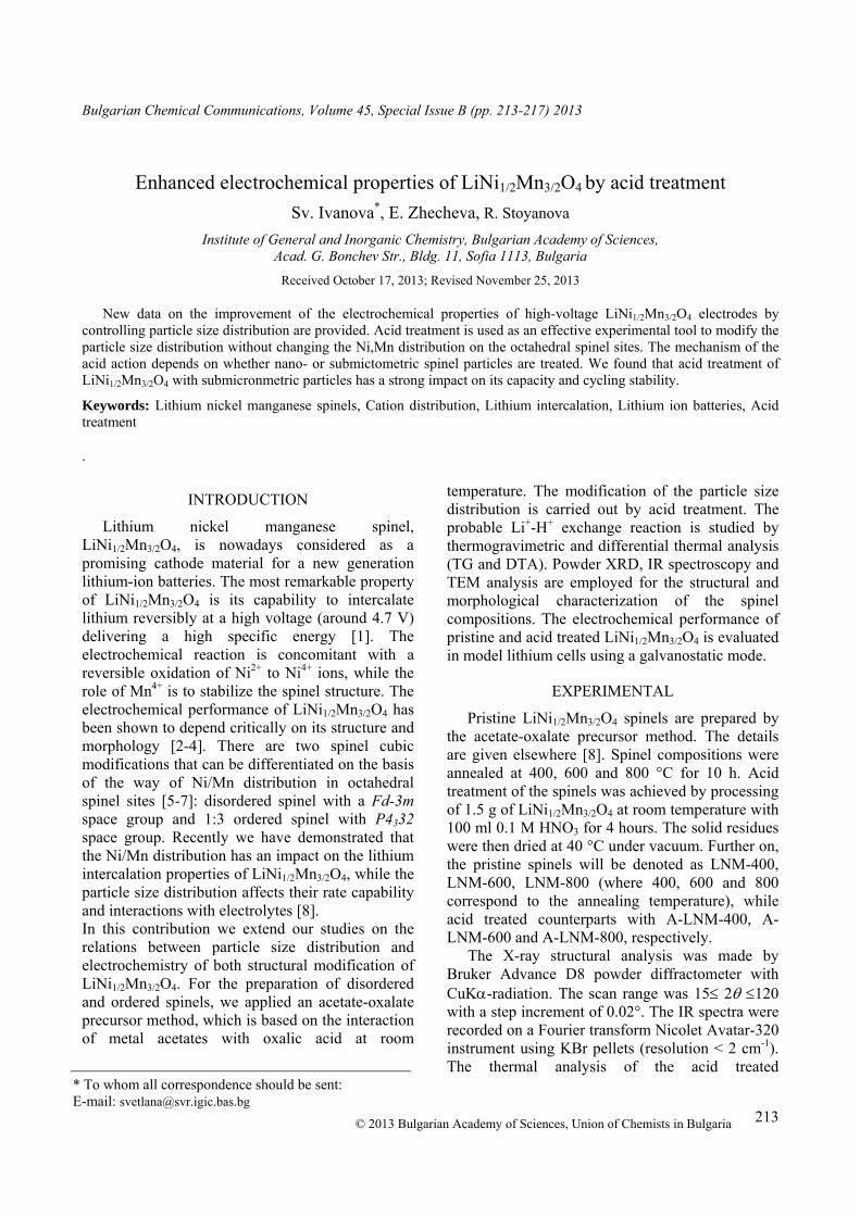
213
Bulgarian Chemical Communications, Volume 45, Special Issue B (pp. 213-217) 2013
Enhanced electrochemical properties of LiNi1/2Mn3/2О4 by acid treatment
Sv. Ivanova*, E. Zhecheva, R. Stoyanova
Institute of General and Inorganic Chemistry, Bulgarian Academy of Sciences, Acad. G. Bonchev Str., Bldg. 11, Sofia 1113, Bulgaria
Received October 17, 2013; Revised November 25, 2013
New data on the improvement of the electrochemical properties of high-voltage LiNi1/2Mn3/2O4 electrodes by controlling particle size distribution are provided. Acid treatment is used as an effective experimental tool to modify the particle size distribution without changing the Ni,Mn distribution on the octahedral spinel sites. The mechanism of the acid action depends on whether nano- or submictometric spinel particles are treated. We found that acid treatment of LiNi1/2Mn3/2O4 with submicronmetric particles has a strong impact on its capacity and cycling stability.
Keywords: Lithium nickel manganese spinels, Cation distribution, Lithium intercalation, Lithium ion batteries, Acid treatment
.
INTRODUCTION
Lithium nickel manganese spinel, LiNi1/2Mn3/2O4, is nowadays considered as a promising cathode material for a new generation lithium-ion batteries. The most remarkable property of LiNi1/2Mn3/2O4 is its capability to intercalate lithium reversibly at a high voltage (around 4.7 V) delivering a high specific energy [1]. The electrochemical reaction is concomitant with a reversible oxidation of Ni2+ to Ni4+ ions, while the role of Mn4+ is to stabilize the spinel structure. The electrochemical performance of LiNi1/2Mn3/2O4 has been shown to depend critically on its structure and morphology [2-4]. There are two spinel cubic modifications that can be differentiated on the basis of the way of Ni/Mn distribution in octahedral spinel sites [5-7]: disordered spinel with a Fd-3m space group and 1:3 ordered spinel with P4332 space group. Recently we have demonstrated that the Ni/Mn distribution has an impact on the lithium intercalation properties of LiNi1/2Mn3/2O4, while the particle size distribution affects their rate capability and interactions with electrolytes [8]. In this contribution we extend our studies on the relations between particle size distribution and electrochemistry of both structural modification of LiNi1/2Mn3/2O4. For the preparation of disordered and ordered spinels, we applied an acetate-oxalate precursor method, which is based on the interaction of metal acetates with oxalic acid at room
temperature. The modification of the particle size distribution is carried out by acid treatment. The probable Li+-H+ exchange reaction is studied by thermogravimetric and differential thermal analysis (TG and DTA). Powder XRD, IR spectroscopy and TEM analysis are employed for the structural and morphological characterization of the spinel compositions. The electrochemical performance of pristine and acid treated LiNi1/2Mn3/2O4 is evaluated in model lithium cells using a galvanostatic mode.
EXPERIMENTAL
Pristine LiNi1/2Mn3/2O4 spinels are prepared by the acetate-oxalate precursor method. The details are given elsewhere [8]. Spinel compositions were annealed at 400, 600 and 800 °C for 10 h. Acid treatment of the spinels was achieved by processing of 1.5 g of LiNi1/2Mn3/2O4 at room temperature with 100 ml 0.1 M HNO3 for 4 hours. The solid residues were then dried at 40 °C under vacuum. Further on, the pristine spinels will be denoted as LNM-400, LNM-600, LNM-800 (where 400, 600 and 800 correspond to the annealing temperature), while acid treated counterparts with A-LNM-400, A-LNM-600 and A-LNM-800, respectively.
The X-ray structural analysis was made by Bruker Advance D8 powder diffractometer with CuK-radiation. The scan range was 15 2 120 with a step increment of 0.02°. The IR spectra were recorded on a Fourier transform Nicolet Avatar-320 instrument using KBr pellets (resolution < 2 cm-1). The thermal analysis of the acid treated
* To whom all correspondence should be sent: E-mail: [email protected] © 2013 Bulgarian Academy of Sciences, Union of Chemists in Bulgaria

Ivanova et al.:Enhanced electrochemical properties of LiNi1/2Mn3/2О4
214
compositions is carried out by a combined LABSYSТМ Evo DTA/TG system of the SETARAM Company, France. The samples are investigated at a heating rate of 10 °С/min in O2 flow (20 ml/min). The TEM investigations were performed on a TEM JEOL 2100 instrument at an accelerating voltage of 200 kV. The electrochemical charge-discharge of LiNi1/2Mn3/2O4 was carried out by using a two-electrode cells of the type Li|LiPF6 (EC:DMC)|LiNi1/2Mn3/2O4. The positive electrode, supported onto an aluminium foil, was a mixture containing 80% of the active composition LiNi1/2Mn3/2O4, 7.5% KS 6L graphite (TIMCAL), 7.5% Super C65 (TIMCAL) and 5% polyvinylidene fluoride (PVDF). The electrolyte was an 1M LiPF6 solution in ethylene carbonate and dimethyl carbonate (1:1 by volume) with less than 20 ppm of water. The electrochemical reactions were carried out using an eight-channel Arbin BT 2000 system in galvanostatic mode. The cell is cycled between 4.95 and 3.5 V at C/20, C/10, C/5 and C/1 rates.
RESULTS AND DISCUSSION
In accordance with our previous studies [8], the acetate-oxalate precursor method yields at 400 °C the disordered modification of LiNi1/2Mn3/2O4, while between 600 and 800 °C an ordered modification is stabilized.
Acid treatment of spinels takes place with preservation of the spinel structure. For LiNi1/2Mn3/2O4 obtained at 800 °C the lattice parameters remain the same, while for the low-temperature spinels they are slightly lower: 8.1851, 8.1700 and 8.1580 Ǻ for LNM-400, LNM-600, LNM-800 respectively and 8.1665, 8.1587 and 8.1562 Ǻ for the acid treated LNM-400, A-LNM-600 and A-LNM-800.
In order to distinguish clearly between the two cubic modifications of LiNi1/2Mn3/2O4 with Fd-3m and P4332 space groups, the IR spectroscopy is applied (Fig. 1). The IR spectrum of the low-temperature modification consists of two typical spinel modes at 500 and 610 cm-1, while the high-temperature modification display a splitting of the IR spectra into several components, indicating the reduction of the symmetry due to the Ni2+/Mn4+ ordering. It is noticeable that the IR spectra display the same features for the pristine and acid treated spinels. The changes in the IR profile demonstrate clearly that LNM-400 and A-LNM-400 adopt a disordered spinel structure, while the 1:3 ordered
spinel structure is stabilized for LNM- 600 and LNM-800 and acid treated A-LNM-600 A-LNM-800. Thus, IR spectroscopy reveals that the Ni2+/Mn4+ cationic distribution is preserved after acid treatment.
Fig. 1. XRD patterns of pristine LiNi1/2Mn3/2O4 annealed at 400 °C and 800 °C: LNM-400 (a), LNM-800 (b) and acid treated spinel oxides A-LNM-400 (a') and A-LNM-
800 (b'). The asterisks denote the most intensive diffraction peaks due to the impurities of NiO phase.
The next question is related with a possible exchange of Li+ with protons from the acidic solution. This reaction usually proceeds during acid treatment of lithium transition metal oxides [9]. To check for possible H+/Li+ exchange reactions, TG experiments were undertaken. TG analysis shows that the acid treated spinels release H2O after heating up to 250 °C, the H2O amount being 1.50, 0.47 and 0.12 wt.% for A-LNM 400, A-LNM-600 and A-LNM-800, respectively. Comparison shows that the H+/Li+ exchange reaction proceeds easily for the disordered spinels. It is noticeable that LNM-800 is most stable against acid treatment.

Ivanova et al.:Enhanced electrochemical properties of LiNi1/2Mn3/2О4
215
An important parameter that changes after acid treatment is the particle size distribution (Fig. 2).
Fig. 2. Particle size distribution of acid treated
LiNi1/2Mn3/2O4 A-LNM-400 (a), A-LNM-600 (b), A-LNM-800 (c).
The low-temperature disordered modification consists of well-crystallized particles with nanometric dimensions and a close particle size distribution: more than 50% of the particles are between 10 and 20 nm for LNM-400 (Fig. 2). Acid treatment of LNM-400 leads to a broadening of the particle size distribution due to preferential dissolution of the smallest particles (Figs. 2). For the pristine spinels obtained at 600 and 800 °C, the ordered modification is obtained in the form of nanometric and submicronmetric particles: at 600 °C, the particles are distributed predominantly between 15 and 30 nm, while at 800 °C there is a particle growth, resulting in formation of thick particles with dimensions of 150 - 300 nm. The acid treatment of nano- and submicronmetric ordered spinels proceeds in a different way: the
particle size distribution becomes broader for A-LNM-600, while a three-modal particle size distribution curve with maxima at 18, 88 and 275 nm is obtained for A-LNM-600 (Fig. 2).
Fig. 3. First derivative of the capacity –voltage curves (right) of LNM-400, LNM-600, LNM-800 (red lines)
and the acid treated counterparts A-LNM-400, A-LNM-600 and A-LNM-800 (black lines). Figures a, b, c are related to the annealing temperature: 400, 600, 800 °C
respectively.
Figure 3 compares the first charge-discharge curves for pristine and acid treated spinels. The figure gives the capacity-voltage curves as first derivatives. All curves show intensive peaks of oxidation and reduction in the high voltage region of 4.7 V due to Ni2+/Ni4+ couples. In addition, low-intensive peaks in the 4.0 -V region, which originate from the Mn3+/Mn4+ couple, are also distinguished. Both oxidation and reduction peaks are split, this splitting being dependent on the Ni,Mn cationic distribution. In the 4.7 V-region, the
Ivanova et al.:Enhanced electrochemical properties of LiNi1/2Mn3/2О4
216
peak splitting decreases when going from disordered to ordered composition: 80 mV versus 40 mV, respectively. In the 4.0 V region, the peak splitting seems to increase for the spinels having an ordered Ni/Mn distribution: from 140 mV to 210 mV, respectively. It is of importance that both reactions at 4.0 and 4.7 V are reversible. The insensitivity of the peak positions on the particle size distribution indicates that Ni,Mn cation distribution is the main factor controlling the electrochemical reaction. This result is in a good agreement with the data established by several research groups [2]. The new finding is the preservation of the charge-discharge profile of the spinels after acid treatment (Fig. 3). This is an another proof that acid treatment does not attack the Ni,Mn distribution on the spinel sites. The acid treatment of the spinels has a significant impact on the capacity and its stability during cycling (Fig. 4).
Fig. 4. Cycling stability curves at different rates for
LNM-400, LNM-600, LNM-800 and the acid treated spinels A-LNM-400, A-LNM-600 and A-LNM-800.
The first charge capacity increases for both disordered and ordered spinels, while the first discharge capacity displays a complex dependence: there is a decrease in the discharge capacity for nanometric A-LNM-400 and A-LNM-600 spinels, while A-LNM-800 spinel that encompass both nano- and submicronmetric particles is characterized with an increased discharge capacity (Fig. 4). As a result, the first irreversible capacity is significant for A-LNM-400 and A-LNM-600, while the irreversibility is limited for A-LNM-800.
The next cycles reduce the irreversibility and the columbic efficiency reaches of 98-99%. A characteristic feature of all acid treated spinels is their good cycling stability during cycling (Fig. 4). The best electrochemical performance is observed for the acid treated spinel having ordered type
structure and three modal particle distributions. This spinel provides also good rate capability: by increasing the rate from C/20 to C/1, discharge capacity decreases only from 120 mAh g-1 to 95 mAh g-1.
CONCLUSION
Acid treatment is an effective way to modify the particle size distribution of LiNi0.5Mn1.5O4 spinels without changing the Ni,Mn distribution over the octahedral spinel sites. When nanometric LiNi0.5Mn1.5O4 spinels with ordered and disordered structure are treated with acid, the particle size distributions are broadened. The submicronmetric particles are broken during acid treatment, as a result of which the particle size distribution becomes complex comprising both nano- and submicronmetric particles. The mechanism of acid treatment is associated with partial spinel dissolution. The side reaction of exchange of Li+ with H+ proceeds more easily for the disordered spinel modification, while the ordered modification is most stable.
After acid treatment, both disordered and ordered spinels display good cycling stability. The best electrochemical performance in terms of capacity, cycling stability and rate capability is achieved for the ordered spinel LiNi0.5Mn1.5O4 having a combination of nano- and submicronmetric particles.
In general, an enhancement of the electrochemical performance of high-voltage LiNi0.5Mn1.5O4 can be achieved by acid treatment of the spinel with submicronmetric particles. This approach can be applied to other Mn4+-containing lithium transition metal oxides in order to improve their electrochemical performance.
Acknowledgements: This work was supported by European Social Fund (Grant BG051PO001-3.3.06-0050).
REFERENCES
1. R. Santhanam, B. Rambabu, J. Power Sources, 195, 5442 (2010).
2. J. H. Kim, S. T. Myung, C. S. Yoon, S. G. Kang, Y. K. Sun, Chem. Mater., 16, 906 (2004).
3. R. Alcántara, M. Jaraba, P. Lavela, J. L. Tirado, Chem. Mater., 15, 2376 (2003).
4. K. Shaju and P. Bruce, Dalton Trans, 5471 (2008).
5. D. Gryffroy, R. E. Vandenberghe, J. Phys. Chem. Solids, 53, 777 (1992).

Ivanova et al.:Enhanced electrochemical properties of LiNi1/2Mn3/2О4
217
6. W. Branford, M. A. Green, D. A. Neumann, Chem. Mater., 14, 1649 (2002).
7. R. Alcántara, M. Jaraba, P. Lavela, J. L. Tirado, E. Zhecheva, R. Stoyanova, Chem. Mater., 16, 1573 (2004).
8. Sv. Ivanova, E. Zhecheva, R. Stoyanova, D. Nihtianova, S. Wegner, P. Tzvetkova, S. Simova, J. Phys. Chem. C, 115, 25170 (2011).
9. R. Stoyanova, E. Zhecheva, J. Solid State Chem., 108, 211 (1994).
ПОДОБРЯВАНЕ НА ЕЛЕКТРОХИМИЧНИТЕ ХАРАКТЕРИСТИКИ НА LINI1/2MN3/2О4 ЧРЕЗ
ТРЕТИРАНЕ С КИСЕЛИНА
Св. Иванова, Е. Жечева, Р. Стоянова
Институт по обща и неорганична химия, Българска академия на науките, бул. Акад. Г. Бончев, блок 11, София 1113
Постъпила на 17 октомври 2013 г.; коригирана на 25 ноември, 2013 г.
(Резюме)
Все по-широката употреба на литиево-йонни батерии налага разработването на батерии с по-висока плътност на енергията и на мощността, които да са безопасни за околната среда, с висока плътност на енергията и ниска цена. LiNi1/2Mn3/2O4 шпинелен оксид е от технологичен и изследователски интерес като електроден материал за литиево-йонни батерии, тъй като литий се интеркалира обратимо при висок потенциал (4.7 V), което способства за висока плътност на енергията (658 Wh/kg), стабилен е и има добри електрохимични характеристики. Разпределението на никеловите и мангановите йони в октаедричните позиции оказва влияние върху свойствата на литиево-никелово-мангановия шпинел. В тази статия са показани ефектите от третиране на LiNi1/2Mn3/2O4 с киселина чрез прилагането на дифракционни и спектроскопски методи. Третирането на подреден субмикроразмерен шпинелен оксид с киселина модифицира разпределението на частиците по размер без да настъпва промяна в разпределението на катионите в октаедричните шпинелни позиции. Синергичният ефект между нано- и микроразмерни частици оказва влияние върху стабилността на капацитета на LiNi1/2Mn3/2O4 шпинел при многократно циклиране.
.

218
Bulgarian Chemical Communications, Volume 45, Special Issue B (pp. 218-221) 2013
Relaxation of light-induced absorption in Cr-doped Bi12TiO20 crystals
Vera Marinova1*, Etienne Goovaerts2 1Institute of Optical Materials and Technologies, Acad. G. Bonchev Str. 109, Sofia, Bulgaria
2 Experimental Condensed Matter Physics, Department of Physics, University of Antwerp, Universiteitsplein 1, B-2610 Antwerpen, Belgium
Received October 17, 2013; Revised November 25, 2013
The lifetime of the excited charge carriers in Cr-doped Bi12TiO20 (BTO) crystals is characterized by measuring the optical density changes after nanosecond pulse excitation. It is found that the Cr-addition in the BTO crystal structure significantly increases the relaxation decay time, which is attributed to the increased densities of trapping centers. The observed relaxation dynamics follows a double-exponential behavior, assigned to the two long-lived intermediate levels in BTO:Cr crystal structure.
Keywords: doped BTO crystal, light-induced absorption, charge carriers, trapping centers
INTRODUCTION
Sillenite crystals Bi12M(M=Si,Ge,Ti)O20 are well known as excellent photoconductors and due to their remarkable high photosensitivity and charge carrier mobility these belong among the fastest photorefractive materials for real-time image processing and related dynamic purposes [1-3]. Sillenite crystals found applications in real-time holography, coherent light amplification, optical phase conjugation, optical information processing, optical metrology, etc. Doping with transition metal ions is well known approach to enhance the response time and photosensitivity of sillenites, especially at near infrared spectral range [4-6]. For example, Ru addition in BSO structure leads to significant improvement of the response time at 1064nm and the beam-coupling enhancement, which opens further opportunities for the development of near infrared sensitive devices for bio-medical diagnostic and real-time image processing [7]. Furthermore, by using green light pre-exposure significant improvement of the operation speed has been achieved [7].
Recently, sillenites become very attractive media for combination with liquid crystals or functional molecules into so called hybrid organic/inorganic cells (light valves) for non-linear optic and photonic applications, especially at near infrared [8-10]. In such kind of devices (optically addressed spatial light modulators) the detail
characterizations of the photogenerated charge carriers dynamic processes in photoconductive substrate (as doped BTO, BSO) are essentially important. In that aspect, the light-induced absorption spectroscopy is a valuable technique to study defect levels and to characterize the transport properties of the excited charge carriers.
In the present work, we report relaxation dynamics in Cr-doped BTO induced by nanosecond pulse excitation by measuring the time evolution of the photoinduced absorption.
EXPERIMENTAL DETAILS
Cr-doped BTO crystals were grown by Top Seeded Solution Growth Method [11]. Chromium was introduced into the melt solution as Cr2O3 and it's concentration of 6 x1018 cm–3 in the grown crystals was determined by Atomic Absorption Spectroscopy.
An optically polished plate (thickness of 0.5 mm) was prepared for the absorption measurements. The absorption spectra were measured in the visible range using a Varian Cary 5 UV spectrophotometer after thermal annealing at 350C for 2 hours.
For the relaxation dynamics study we used pump-probe technique (Flash Photolysis instrument LP 920). The time scale length covered from the first fraction of ns (after photoexcitation) to the several hundred seconds. The sample was irradiated with single shot pulses from a frequency doubled Q-switched Nd:YAG laser (=532 nm, pulse duration 6 ns). A weak monochromatic probe beam * To whom all correspondence should be sent:
E-mail: [email protected] © 2013 Bulgarian Academy of Sciences, Union of Chemists in Bulgaria

Marinova et al.: Relaxation of light-induced absorption in Cr-doped Bi12TiO20 crystals
219
(600 nm) transmitted through the sample was used to measure the absorption changes, detected by a photomultiplier and recorded by a high bandwidth digital storage oscilloscope. For the long-time scanning (up to several hundred seconds) a halogen lamp was used as a probe light. Alternatively, a xenon lamp operating in a pulsed mode was used for a short time scanning (ranges below 1 ms). The sample was placed in a holder allowing near anti-collinear geometry with an angle of 5 between the pump and probe beam. At least 10 shots measurements are always averaged in order to improve the signal to noise ratio. Also, we wait few minutes interval between each two shots, which is considering enough for complete the relaxation process.
For the temperature dependent measurements, the sample was fixed in a helium flow cryostat with a temperature-controlled holder. The temperature was measured with a Pt-100 thermocouple, mounted just above the sample with an accuracy of 1K.
The monitored light-induced absorption data are presented as change in the optical density OD
)(loglog 01010 IITOD (1)
which is related to the change in transmittance T, or alternatively in the relative transmitted light intensity through the sample I to incident light intensity I0 .
RESULTS AND DISCUSSIONS
Figure 1 shows the absorption spectrum of Cr-doped BTO compared with the non-doped BTO. At it seen, the main absorption edge is shifted from ~400 nm to the 500 nm range. The long wavelength tail together with the three characteristic peaks
400 500 600 700 8000
1
2
3
optic
al a
bsor
ptio
n
wavelength (nm)
BTO
BTO:Cr
Fig.1. Optical absorption spectrum of Cr-doped BTO
compared to the non-doped BTO crystal.
around 700-800 nm are typical for Cr addition into BTO structure and assigned to the strong absorption by Cr-related defects [4].
The temporal evolution of the dark decay of the light-induced absorption at different time scales (from sub-microseconds to several hundred sec range) after pulse intensity of 8 MW/cm2 hits the sample is presented at Fig. 2 (a,b). At the beginning of the process (after the laser shot hits the sample) the signal is constant (Fig. 2a) following with long lasting component of the decay process (Fig.2b). As it seen, the relaxation process of Cr-doped BTO crystal takes very long time and 500 s time scale interval is not enough to detect the full relaxation process at room temperature. The complete relaxation of the excited charge is achieved when the sample was heated at 160C. Further, we will focus on the tail of the decay process (at longer time range) and its temperature dependence which are supposed to reveal relevant information about the charge carrier’s dynamics.
10-8 10-7 10-6 10-5 10-4 10-3 10-2 10-11E-4
1E-3
0.01
0.1
100 101 1021E-4
1E-3
0.01
0.1
1E-4
1E-3
0.01
0.1
OD
cha
nge
BTO:Cr
OD
cha
nge
time (s)
(a)
BTO:Cr
time (s)
(b)
Fig. 2. Time evolution of the light-induced OD change of Cr-doped BTO after laser pulse of 532 nm hits the sample: from the beginning of the process until 500 s
time scale.

Marinova et al.: Relaxation of light-induced absorption in Cr-doped Bi12TiO20 crystals
220
It was found that in a longer time scale (Fig.2b) the OD decay is well fitted by a sum of two exponential functions:
ss
ff
tOD
tODtOD
expexp)( (2)
where “f” and “s” correspond to a faster and a slower component of the decay, ODf and ODs denote their amplitudes, f and s are their time constants, respectively. We calculate a relatively fast component with a time constant within 10s (at room temperature) and a slower one with a long lived level ~103 s. After heating the sample in the cryostat (Fig.3), the complete relaxation happens with slow decay of s = 253 s at 160 C.
0 100 200 300 400 5000.0
0.2
0.4
0.6
0.8
1.0
2s
1s
2s
BTO:Cr
OD
cha
nge,
a.u
.
time (s)
RT
160 C
1s
Fig. 3. Normalized OD change measured at room temperature and at 160C. The symbols refer to the
measured results, the straight lines results from the curve fitting.
The detected two time constants of Cr-doped BTO can be attributed to the existence of two different types of traps centers. The photoconductivity in sillenites is assumed as n-type, therefore the light-induced absorption is associated with the filling of initially empty shallow traps with the electrons released by the action of light. The measured significant slow decay gives evidence for exceptionally high concentration of Cr- related defects acting as acceptor centers with high trapping efficiency for the photoexcited electrons. Ru-addition in BSO structure also caused longer relaxation time (f =3.2s and s =20s) in comparison with non-doped BSO (where the decay occurs within few ms), however the relaxation process in BSO:Ru happens in much shorter time interval than in BTO:Cr [12]. The long relaxation indicates that Cr-related traps are located rather deeper in the energy gap of BTO:Cr crystal in comparison with Ru-related trap levels in BSO structure.
Light-induced absorption with a double-exponential decay on time scales ranging from seconds to even days was already observed in various sillenite crystals [5]. For example, the above presented results are in good agreement with the recently published photo-induced absorption data in BTO crystals, irradiated with a high intensity pulse laser of 532 nm [13]. The observed relaxation dynamics follows a double-exponential behavior, which the authors explained with two very long-lived (about 104 s to 105 s) intermediate levels located in the forbidden band of BTO.
Earlier, the photocurrent decay in non-doped sillenites after short pulse illumination has been studied at RT and decay curves with multiple time constants were reported. For example, the authors in [14] announced about the dark decay processes which consists of a rapid initial decay (ascribed to the filling of shallow traps below the CB) followed by a slower “coasting” decay (associated with the recombination of charges to the deep traps). Also, Okamoto et al. [15] reported the existence of several kinds of shallow acceptor levels during thermally stimulated current measurements and proposed two shallow acceptor levels to explain the transient response up to a few ms.
We suppose that in Cr-doped BTO the excited charge carriers are not directly trapped by deep centers, but they are captured and re-excited numerous times by shallow levels before they finally recombine with the deep centers.
CONCLUSION
A photo-induced absorption study of the dynamics of charge carriers generated by nanosecond pulse laser excitation in Cr-doped BTO is reported. Cr-addition significantly slows down recombination kinetics, which is attributed to the increased densities of the relevant trapping centers.
Acknowledgments: This work has been done through bilateral collaboration project supported by FWO (Fund for Scientific Research Flanders, Belgium) and Bulgarian Academy of Science. Samples were grown by the Crystal Growth Laboratory of the Institute of Solid State Physics, Sofia.
REFERENCES
1. J. Frejlich, Photorefractive materials , Wiley Interscience (2007).

Marinova et al.: Relaxation of light-induced absorption in Cr-doped Bi12TiO20 crystals
221
2. E. A. Barbosa, A. O. Preto, D. M. Silva, J. F. Carvalho, and N. I. Morimoto, Opt. Commun., 281, 408-414 (2008).
3. G. Caroena, M. Mori, M. R. R. Gesualdi, E. A. Liberti, E. Ferrara, and M. Muramatsu, J. Biomech., 43, 680-686 (2010).
4. A. A. Nechitailov, M. V. Krasin'kova, E. V. Mokrushina, Inorg. Mater., 36, 820-825 (2000).
5. F. Ramaz, L. Rakitina, M. Gospodinov, B. Briat, Opt. Mater., 27, 1547 (2005).
6. V. Marinova, M.-L. Hsieh, S.-H. Lin, and K.- Y. Hsu, Opt. Commun., 203, 377 (2002).
7. V. Marinova, R.- C. Liu, S.- H. Lin and K.- Y. Hsu, Opt. Lett., 36, 1981 (2011).
8. U. Bortolozzo, S. Residori and J. P. Huignard, J. Phys. D, 41, 224007 (2008).
9. U. Bortolozzo, S. Residori and J. P. Huignard, J. Nonlinear Opt. Phys. Mater., 16, 231-236 (2007).
10. V. Marinova, R.- C. Liu, S.- H. Lin, M.-S. Chen, Y.- H. Lin and K.- Y. Hsu, Opt. Lett., 38, 495-497 (2013).
11. P. Sveshtarov and M. Gospodinov, J. Cryst. Growth, 113, 186-208 (1991).
12. V. Marinova, I. Ahmad, and E. Goovaerts , J. Appl. Phys., 107, 113106 (2010).
13. A. Matusevich, A. Tolstik, M. Kisteneva, S. Shandarov, V. Matusevich, A. Kiessling, and R. Kowarschik, Appl. Phys. B, 92, 219 (2008).
14. D. C. Jones and L. Solymar, Opt. Commun., 85, 372 (1991).
15. K. Okamoto, T. Sawada, and K. Ujihara, Opt. Commun., 99, 82 (1993).
РЕЛАКСАЦИЯ НА СВЕТЛИННО- ИНДУЦИРАНАТА АБСОРБЦИЯ В КРИСТАЛИ ОТ BI12TIO20
ДОТИРАНИ С Cr
Вера Маринова1, Етиен Гуваертц2 1Институт за оптични материали и технологии, Ул. Акад. Г. Бончев 109, София, България
2Експериментална физика на кондензираната материя, Катедра Физика, Университет на Антверпен, Университетплеин 1, B-2610, Антверпен, Белгия
Постъпила на 17 октомври 2013 г.; коригирана на 25 ноември, 2013 г.
(Резюме)
Определено е времето на живот на възбудените зарядоносители в кристали от Bi12TiO20 (BTO) дотирани с Cr чрез проследяване на промените в светлинната абсорбция при облъчване с наносекундни лазерни импулси. Установено е че вследствие включването на Cr в кристалната структура на BTO времето на затихване на релаксацията нараства значително, което показва увеличена плътност на уловките. Наблюдаваната динамика на релаксацията следва двойно експоненциален характер, което се свързва с наличието на две междинни енергитични нива с продължително време на живот в кристалната структура на BTO: Cr.
222
Bulgarian Chemical Communications, Volume 45, Special Issue B (pp. 222-225) 2013
-ray induced effects in Sm-doped strontium borate glasses
V. Marinova1,2* V. Tomov3, C. I. Chuang2, Y. C. Lin4, S. H. Lin4, Y. F. Chao2, W. C. Chou4, M. Gospodinov3 and K. Y. Hsu2
1Institute of Optical Materials and Technologies, Sofia 1784, Bulgaria 2Department of Photonics, National Chiao Tung University, Hsinchu, 30010, Taiwan
3 Institute of Solid State Physics, Tzarigradsko Chaussee 72, Sofia 1784, Bulgaria 4Department of Electrophysics, National Chiao Tung University, Hsinchu 30010, Taiwan
Received October 17, 2013; Revised November 25, 2013
Strontium borate glasses SrB4O7 doped with Sm ions are prepared by conventional melting-quenching method. The effect of –ray irradiation on the glass samples is studied by measuring the absorption spectra and the photoluminescence. It is found that the -ray irradiation caused partial reduction of Sm3+ to Sm2+
at room temperature. Borate framework is supposed to be responsible for the Sm3+ to Sm2+ transition.
Keywords: Sm3+ doped SrB4O7 glass, -ray radiation, photoluminescence, room temperature dosimeters
INTRODUCTION
Strontium borate glasses SrB4O7 due to their simple preparation, low cost, high transparency, easy shaping and long term stability found applications in many optoelectronic devices, as solid state laser materials (owing to their persistent spectral hole burning), non-linear parametric converters and broadband optical fiber amplifiers [1-3]. Furthermore, the absorbance of borate glasses is very close to that of human tissue, thus makes them very attractive for radiation dosimetry applications, based on their luminescent properties [4]. In that aspect, the search for new dosimieric materials is still constant to meet up the medical and environmental needs.
Strontium borate SrB4O7 glass is well known as a suitable host material to accommodate divalent lanthanide ions (Eu2+, Sm2+, Yb2+) on the Sr2+ site. Therefore, when doped with rare earth (RE) ions strontium borate matrix become very attractive for radiation dosimetry due to the RE3+ to RE2+ transition [1]. When doped with Samarium, which is generally stable at its trivalent state, Sm3+ must be reduced to Sm2+ and keep it stabilized. The well known and effective method to transfer Sm3+ to Sm2+ is by heating the sample under reduction atmosphere in H2 stream [5]. Although this method is very effective, it requires a rather complicated
gas flow system that is difficult to perform practically. Another reduction method is to irradiate the glass sample with femto-second laser pulses [6] or with high energy radiation (-irradiation [7], - irradiation [8] or x-ray irradiation [9]). For a first time Pei at al [1] reported that three valent RE3+ ions were successfully reduced to RE2+ ions in SrB4O7 host without reduction atmosphere. Since then an intense attention has been paid on the incorporation of RE3+ ions in strontium borate matrices towards different practical applications.
In the present work synthesis of Sm3+ doped SrB4O7 glasses with two different concentrations is reported. The absorption and photoluminescence spectra before and after -irradiation are recorded and analyzed. In addition, the refractive index values are measured at the visible spectral range.
EXPERIMENTAL DETAILS
Two glasses compositions were prepared by mixture of SrO, B2O3 and Sm2O3, by varying the ratio of the starting materials. A conventional melting- quenching method was used to prepare the samples. For the first composition we added 7 % Sm2O3 in a mixture of SrO and B2O3. For the second one the Sm2O3 content was increased to 10%, varying the SrO to B2O3 ratio in the mixture.
* To whom all correspondence should be sent: E-mail: [email protected] ; [email protected] © 2013 Bulgarian Academy of Sciences, Union of Chemists in Bulgaria

Marinova et al.: -ray induced effects in Sm-doped Strontium Borate glasses
223
Table 1. Chemical composition (in weight %) and sample code.
Chemical composition (in weight %) Sample code 1. 28% SrO + 65% B2O3 + 7% Sm2O3 0.28SrO-0.65BO-0.07Sm 2. 40% SrO + 50% B2O3 + 10% Sm2O3 0.4SrO-0.5BO-0.1Sm
The nominal glasses compositions by weight % are given in Table 1.
Further, the obtained glasses were annealed at 400ºC for 48h for thermal and structural stability enhancement. Samples of 1mm thickness were cut and polished to optical quality. To study the effect of -irradiation, the samples were irradiated with 60Co isotope with the dose rate of 0.1mGy.s-1. The optical absorption spectra of the initial state (denoted hereinafter as non-irradiated) and the state after -ray irradiation (denoted as -ray irradiated) were measured at room temperature in the spectral range 200-1800nm using Shimadzu spectrophotometer. Photoluminescence spectra were measured with a monochromator equipped with PMT (Hamamatsu) detector at room
temperature. The laser excitation at 405 nm was used. In addition, the refractive indices of synthesized glass compositions were measured by polarizer-sample-analyzer ellipsometry at the visible spectral range [10].
RESULTS AND DISCUSSIONS
Figure 1(a,b) shows the absorbance spectra of both glass compositions at wavelengths from 300nm to 1700nm. As it seen, γ-ray irradiation induced significant absorbance in 0.28SrO-0.65BO-0.07Sm sample, with several intensive characteristic peaks at the ultraviolet and infrared spectral range.
1000 1200 1400 16000
1
2
3
4
300 400 500 600 700 8000
1
2
3
4
0.28SrO-0.65BO-0.07Sm
abso
rban
ce
wavelength (nm)
no irradiation
ray irradiation
(a)
300 400 500 600 700 8000
1
2
3
4
1000 1200 1400 16000
1
2
3
4
04SrO-0.5BO-0.1Sm
abs
orb
an
ce
wavelength (nm)
(b)
no irradiation
-ray irradiation
Fig. 1. Absorbance spectra of (a) 0.28SrO-0.65BO-0.07Sm and (b) 0.4SrO-0.5BO-0.1Sm glass.
550 575 600 625 650 675 700 725 750
0.28SrO-0.65BO-0.07Sm
Sm3+
Sm3+
Sm2+
PL
inte
snity
(a
.u)
wavelength (nm)
before irradiation after irradiation
(a)
550 575 600 625 650 675 700 725 750
Sm3+
0.4SrO-0.5BO-0.1Sm before irradiation after irradiation
Sm2+
Sm3+
PL
Inte
snity
(a
.u)
wavelength (nm)
(b)
Fig. 2. PL (a.u) spectra of Sm-doped glass compositions before and after γ-ray irradiation at room temperature.
Furthermore, two very intensive absorption peaks around 400 nm and 1200nm are detected, which
could be considered for further application of the above glass composition as narrow band cut off

Marinova et al.: -ray induced effects in Sm-doped Strontium Borate glasses
224
filters. At the same time, there is almost no obvious absorbance change in 0.4SrO-0.5BO-0.1Sm composition.
Photoluminescent (PL) spectra at room temperature of both compositions before and after γ-ray irradiation are presented at Fig.2 (a,b). The emission lines in the range from 680nm to 720nm correspond to the 5Do-
7FJ (J=0,1,2,3,) transitions of the Sm2+ ions [11,12]. Evidently, the -ray irradiation caused Sm3+ reduction to Sm2+ in the host glass matrix. The effect is stronger in the case of 0.28SrO-0.65BO-0.07Sm composition, leading to more intensive peak of Sm2+ around 700 nm and diminishing the intensity of Sm3+ luminescence
between 550-600 nm. Generally, the excitation and emission of rare-
earth doped glasses are due to the transitions from the 4fn electronic states of RE3+ ions (RE3+ electronic configuration of 4fn5s25p6), which are highly sensitive to the symmetry, structure and phonon energy of the host matrix. During the irradiation, free electrons and holes are created and some electrons can be trapped by Sm3+ ions, leading to the formation of Sm2+ ions, while holes can be trapped by other defects. In SrB4O7 glass
matrix, all of the boron atoms are tetrahedrally coordinated with oxygen atoms and form a three-dimensional borate network [13]. Therefore, the basic structure of SrB4O7 can be expressed as SrO.nB2O3 (with different n values, different anion units are linked together, forming different networks –thus the number of triangularly coordinated boron atoms (BO3) per tetrahedral coordinated boron atoms (BO4) is equal to n-1 [3,13]). As a result the divalent ions in SrB4O7 are completely surrounded by the tetraherdral BiO4 and therefore are hardly expected to be attacked by oxygen. From another side, since the ionic radii of Sm2+ (1.32Å) is very similar to those of Sr2+
(1.31Å), with the same valence state, some Sr2+ can be replaced by Sm2+ without expecting serious distortion in the structure. Therefore, the two main anion units: BO3 and BO4 are expected to play significant role for the Sm3+ reduction. These two units are supposed as the basis of the infrared spectra as well [14]. The above statement is well confirmed by the photoluminescence results presented at Fig.2 (a). The increasing the B2O3 ratio in a glass composition, the Sm3+ to Sm2+reduction is more efficient.
In addition, the refractive index measurements using polarizer-sample-analyzer ellipsometry were performed at 632.8nm, 594.1nm, 543.5nm and
473nm. The refractive indices for different compositions shown in Fig. 3 were calculated by using the formula [10]:
2 1/ 20 2
4 tan [1- sin ]
(1 )i i in n
(1)
where ni is the refractive index of the ambient air, and θi is the incident angle for measurements and ρ is an ellipsometric parameter, defined by the ratio of rp to rs (denoted as reflection coefficients in the parallel (p) and perpendicular (s) planes to the incident plane, respectively. As it seen, there is a difference in refractive index values for both compositions.
480 510 540 570 600 630
1.5
1.6
1.7
1.8
refr
act
ive
ind
ex
wavelength (nm)
0.28SrO-0.65BO-0.07Sm
0.4SrO-0.5BO-0.1Sm
Fig. 3. Refractive index values measurements using
polarizer-sample-analyzer ellipsometry. The standard deviation is ± 0.001.
Although at the first trial there is a partial reduction of Sm3+ to Sm2+ transitions, further adjustment of Sm concentration and B2O3 ratio are necessary for dozimetry requirement applications at room temperatures.
CONCLUSIONS
Sm doped SrB4O7 glasses have been synthesized by conventional melt quenching method. The performed luminescence measurements verified that Sm3+ ions can be partially reduced to Sm2+ by γ-ray irradiation at room temperature. The γ -irradiation doze can be estimated from the luminescence peaks intensity change. The effect is stronger in 0.28SrO-0.65BO-0.07Sm composition with less Sm concentration, but with larger B2O3
content. In addition, the above composition displays shows potential ability for narrow band filter application both at ultraviolet and infrared spectral range.
Marinova et al.: -ray induced effects in Sm-doped Strontium Borate glasses
225
Acknowledgments: This work has been done through bilateral collaboration project supported by National Science Council (NSC), Taiwan and Bulgarian Academy of Science under the contract #NSC99-2911-1-009-008. Glass compositions were obtained at the Crystal Growth Laboratory, Institute of Solid State Physics, Sofia.
REFERENCES
1. Z. Pei, Q. Su and J. Zhang, J Alloys Compd., 198, 51-53 (1993).
2. P. Mikhail & J. Hulliger, Inorg. Chem., 21, 263-283, (1999).
3. S. Park, K. Jang, I. Kim, Y. I. Lee and H. J. Seo, J. Phys. Soc. Japan, 75, 054709 (2006).
4. S. S. Rojas, K. Yukimitu, A. S. S. de Camargo, L. A. O. Nunes, A. C. Hernandes, J . Non-Cryst. Solids, 352, 3608-3612 (2006).
5. Z. Chao and C. Shi, Sci. China (Ser. B) 9, 904 (1992).
6. J. Qui, K. Miura, T. Suzuki, T. Mitsuyu and K. Hirao, Appl. Phys. Lett., 74, 10 (1999).
7. E. Malchukova, B. Boizot, D. Ghaleb and G. Petite, Nucl. Instrum. Methods Phys. Res. A, 537, 411 (2005).
8. E. Malchukova, B. Boizot, G. Petite and D. Ghaleb, J. Non-Cryst. Solids, 353, 2397 (2007).
9. M. Nogami and K. Suzuki, Adv. Mater., 14, 923 (2002).
10. Y. F. Chao, W.C. Lee, C. S. Hung and J. J. Lin, J. Phys. D, 31 , 1968 (1998).
11. M. Santiago,C. Grasseli, E. Caselli, M. Lester, A. Lavat, F. Spano, Phys Status Solidi (a), 285 (2001).
12. E. M. Yoshimura, C. N. Santos, A. Ibanez and A. C. Hernandes, Opt. Mater., 31, 795-799 (2009).
13. S. Park, K. Jang, S. Kim, I. Kim and H. J. Seo, J. Phys. Cond. Matter., 18, 1267 (2006).
14. Q. Zeng, Z. Pei, S. Wang and Q. Su, J. Mat . Sci Technol., 15, 449-452 (1999).
ЕФЕКТИ ОТ ГАММА-ОБЛЪЧВАНЕ В Sm -ЛЕГИРАНИ СТРОНЦИЕВО БОРАТНИ СТЪКЛА
В. Маринова1,2, В. Томов3, C. И. Чуанг2, У. C. Лин4, С. Х. Лин4, У. Ф. Чао2,
В. C. Чоу4, М. Господинов3 and К. У. Хсу2
1Институт за оптични материали и технологии, Ул. Акад. Г. Бончев 109, София, България 2Департмент по фотоника, Национален Чао Тунг Университет, Тайван
3Институт по физика на твърдото тяло, Бул. Цариградско шосе 72, София, България 4Департмент по електрофизика, Национален Чао Тунг Университет, Тайван
Постъпила на 17 октомври 2013 г.; коригирана на 25 ноември, 2013 г.
(Резюме)
Стъкла от стронциев борат SrB4O7 легирани със Sm са получени по конвенционалният метод на топене-закаляване. Ефекта на облъчване с –лъчи е изследван чрез измерване на абсорбционните спектри и спектрите на фотолуминесценция. Установено е, че облъчването с –лъчи води до валентен преход на Sm3+ към Sm2+ йони при стайна температура. Предполага се, че боратните връзки са отговорни за този вид преходи.

226
Bulgarian Chemical Communications, Volume 45, Special Issue B (pp. 226-228) 2013
Crystals growth of topological insulators in Bi2(SexTe1-x)3 system
D. Dimitrov a,*, V. Marinova a,, V. Tomov b, P. Rafailov b, M. Gospodinov b a Institute of Optical Materials and Technologies, Sofia 1113, Bulgaria
b Institute of Solid State Physics, Sofia 1723, Bulgaria
Received October 17, 2013; Revised November 25, 2013
Topological insulator single crystals of Bi2(SexTe1-x)3 and doped Bi2Se3 are prepared by modified Bridgman technique. The crystals are with high quality as confirmed by XRD and Raman spectroscopy measurements. These new materials are of great importance for the research on devices and technologies based on topological insulator properties.
Keywords: topological insulators, Bi2Se3, single crystals
INTRODUCTION
Topological insulators (TIs) have generated a great interest in the fields of condensed matter physics, chemistry and materials science. The topological insulator is an insulator in the bulk, while it conducts on the surface like a metal. Topological insulators occur as two-dimensional (2D) – also called quantum spin Hall state – and three-dimensional (3D) versions. They have a full energy gap in the bulk, but host topologically protected gapless edge (2D) or surface (3D) states.
The first TIs was predicted in 2006 and experimentally realized in 2007 in HgTe quantum wells. Shortly later, three well-known binary chalcogenides, Bi2Se3, Bi2Te3 and Sb2Te3, were predicted and observed to be TIs with a large bulk gap and a metallic surface state consisting of a single Dirac cone. The discovery of these topological materials opened up the exciting field of topological insulators. Extensive experimental and theoretical efforts are devoted to synthesizing and optimizing samples, characterizing the topological states, transport measurements, device fabrications, and searching for new material candidates [1].
The most promising 3D system is currently Bi2Se3, which is known to have a large bandgap and a single surface Dirac cone [2]. Bi2Se3, Bi2Te3 and Sb2Te3 have rhombohedral crystal structures [3] and the surface Brillouin zone of the (001) surface is hexagonal. The combination of spin polarization and extreme robustness of the surface states on the TIs makes these materials promising for practical
device applications. However, in order to achieve conduction from the surface states alone the chemical potential needs to be placed inside the bulk band gap, something which requires careful control of the amount of bulk defects in these materials. In reality, this has proven difficult in the stoichiometric Bi2Se3 due to a large number of Se vacancies which render the materials n-doped, placing the Fermi-level in the conduction band [4]. The surface state transport accessing in as-grown Bi2Se3 remains challenging. There are several possible strategies [5] to reduce the bulk conduction: reducing the thickness of the crystal; adding more Se during growth to reduce Se vacancies; growing mixed crystals with large bulk resistivity (low bulk carrier density) ; growing crystals with compensating dopants (e.g., Sb or Ca) to reduce bulk doping. Employing one or more of such strategies is considering important to prepare TI materials for transport studies and device applications of TI surface states.
In this paper growth and characterization of Bi2(SexTe1-x)3 mixed crystals and Bi2Se3 crystals doped with Ca, Cu and Mn are reported.
EXPERIMENTAL DETAILS
Single crystals of 3D topological insulators in the system Bi2(SexTe1-x)3, where x= (0.5; 0.75; 1) as well as crystals in the Bi2Se3-based system doped with Ca, Cu, Co and Mn are grown by a modified Bridgman technique.The starting materials with high purity as follows Bi -99.999%, Se - 99.999%, Te 99.9999%, Cu (99.99 %),Ca (99.99 %), Co(99.99 %) and Mn (99.99%) are mixed according to the desired compositions of Bi2(SexTe1-x)3 or doped Bi2Se3 and placed in * To whom all correspondence should be sent:
E-mail: [email protected] © 2013 Bulgarian Academy of Sciences, Union of Chemists in Bulgaria

Dimitrov et al.: Crystals growth of topological insulators in Bi2(SexTe1-x)3 system
227
encapsulated quartz ampoules with diameter 10 mm-50 mm.. The possible reaction between Ca and quartz during the crystal growth of doped Bi2Se3 is prevented by covering the inside surface of the quartz ampoule with pyrolytic graphite. The Bi2(SexTe1-x)3 crystals are grown with a speed of withdrawing of quartz ampoule of 0.2mm/h, after being heated to 800 C and kept at a constant temperature. The ampoule rotation speed was 25 rot/min. Doped Bi2Se3 crystals were grown by melting the stoichiometric mixtures at 850oC overnight in sealed evacuated quartz tubes. The crystal growth took place via slow cooling from 850 oC to 620oC and then quenching in cold water.
The polarized Raman spectra were measured from (100) cubic surfaces with a triple T64000 spectrometer equipped with microscope. The crystal structure characterization of as-grown topological insulators was performed by X-ray single crystal analyses. The data are collected at room temperature on SuperNova (Oxford Diffraction) diffractometer with Mo radiation (λ = 0.071073 nm).
RESULTS AND DISCUSSION
High-quality Bi2(SexTe1-x)3, and Bi2Se3 doped with Co, Mn, Ca (shown in Fig.1a) and Cu (shown in Fig.1b) single crystals were synthesized by modified Bridgman technique. Bi2Se3 is a direct band gap semiconductor. Compared to other topological insulator compounds it has a relatively large (300 meV) bulk band gap and the Dirac point lies well above the valence band maximum. The crystal structure is solved by direct methods using
Fig. 1. Bi2Se3 doped with Ca (a) and Cu (b) crystals.
SHELXS-97 and refined by the full matrix least-squares procedure on F2 with SHELXL-97. The crystal is rhombohedral and can be presented as stacks of quintuple Se-Bi-Se-Bi-Se layers where the Bi and Se order hexagonally. The quintuple layers are bonded together with weak van der Waals force. Due to the weak Van der Waals bonds the crystal
cleaves easily. Figure 2 shows an example of cleaved Bi2Se3 crystals. The prepared crystals are in single phase as confirmed by XRD patterns shown in Figure 3 for some representative crystal samples. The lattice constant as determined from the powder X-ray diffraction measurements ( not shown) are as follows: Bi2Se3 (a = 4.137 Å and c = 28.679 Å); Bi2Se2.25Te0.75 (a = b=4.211Å and c = 29.331 Å); Cu-doped Bi2Se3 (a = 4.136 Å and c = 28.626 Å); Mn-doped Bi2Se3 (a = 4.106 Å and c = 28.563 Å).
Fig. 2. Cleaved Bi2Se3 single crystal.
Fig. 3. X-ray diffraction (XRD) pattern of Bi2Te3,
BiSeTe and Cu- doped Bi2Se3 crystals.
Fig. 4. Raman spectroscopy spectra.
The lattice structure of the prepared single crystals was further investigated by Raman spectroscopy. Some representative Raman spectra are shown in Fig.4. The spectra obtained with 633 nm, 515 nm, 488 nm, or 458 nm excitation were observed to be practically the same. Raman peaks for the characteristic lattice vibration modes A1g
2
and Eg2 are detected.

Dimitrov et al.: Crystals growth of topological insulators in Bi2(SexTe1-x)3 system
228
It is known that Bi2Se2Te is stable, bulk topological insulator suitable for studying massive Dirac Fermions, with a (111) cleavage-surface derived Dirac point isolated in the bulk band gap at the Fermi energy, with a spin texture alterable by layer chemistry [6]. The potential use of these new materials as a 3D – topological insulator device requires control over the bulk resistivity, therefore the development of high-quality materials is of utmost importance.
CONCLUSIONS
Crystals of 3D topological insulators: - Bi2(SexTe1-x)3 and Cu, Ca, Co and Mn –doped Bi2Se3 were grown by modified Bridgman method. They were characterized by X-ray diffraction and Raman spectroscopy. The frequencies of the vibrational modes in the different samples were compared and their shifts depending on the changes in stoichiometry and composition as well as the lattice parameter analyzed. Both single-mode and two-mode behavior are observed in the mixed crystals. In view of the recently discovered
topological-insulator states in these compounds, studies of the variation of their mechanical and electronic properties with composition and the doping concentration are highly important for their future applications.
REFERENCES
1. L. Fu, C. L. Kane, and E. J. Mele, Phys. Rev. Lett., 98, 106803 (2007).
2. Y. Xia, L. Wray, D. Qian, D. Hsieh, A. Pal, H. Lin, A. Bansil, D. Grauer, Y.S. Hor, R.J. Cava, and M.Z. Hasan, Nature Phys., 5, 398 (2009).
3. H. Zhang, C. X. Liu, X. L. Qi, X. Dai, Z. Fang, and S. C. Zhang, Nature Phys. 5, 438–442 (2009).
4. F. T. Huang, M. W. Chu, H. Kung, W. Lee, R. Sankar, S.-C. Liou, K. Wu,Y. Kuo, and F. Chou, Phys. Rev. B, 86 (2012), 081104(R).
5. H. Cao, S. Xu, I. Miotkowski, J. Tian, D. Pandey, M. Zahid Hasan and Y.P. Chen, Phys. Status Solidi RRL, 7 (1-2), 133 (2013).
6. L. L. Wang, D. D. Johnson, Phys. Rev., B 83(24), 24139 (2011).
ИЗРАСТВАНЕ НА КРИСТАЛИ ОТ ТОПОЛОГИЧНИ ИЗОЛАТОРИ В СИСТЕМАТА BI2(SEXTE1-X)3
Д. Димитров a, В. Маринова a,, В. Томов b, П. Рафаилов b, М. Господинов b a Институт за оптични материали и технологии, София 1113, България
b Институт по физика на твърдото тяло, София 1723, България
Постъпила на 17 октомври 2013 г.; коригирана на 25 ноември, 2013 г.
(Резюме)
Монокристални топологични изолатори от Bi2(SexTe1-x)3 и дотиран Bi2Se3 са получени с модифициран метод на Бриджмен. Получените кристали са с високо качество което е потвърдено с изследвания по методите на рентгеновата дифракция и Раманова спектроскопия. Тези нови монокристални материали са от съществено значение за изследването и разработването на нови технологии и устройства основаващи се на топологичните свойства.

229
Bulgarian Chemical Communications, Volume 45, Special Issue B (pp. 229-234) 2013
Silver nanoparticles assisted etching of silicon
Dimitre Z. Dimitrov*
Institute of Optical Materials and Technologies, Sofia 1113, Bulgaria
Received October 17, 2013; Revised November 25, 2013
Silicon nanostructures are attractive for optics and optoelectronics application to provide more efficient light absorption. Most common processes for formation of silicon surface nanostructures are rather expensive and require high temperatures, high vacuum and hazardous precursors. The silver nanoparticles assisted electroless etching process is a simple and cheap method for preparation of nanostructured silicon surfaces. The silver nanoparticles are deposited in-situ by electroless deposition from non- HF (Hydrofluoric acid) containing solution of activated persulfate. Silicon is selectively etched in HF based solutions with the help of silver nanoparticles. Both the etch process and the deposition of silver particles are studied. The experimental observations are used to get more insight into the etching mechanism.
Keywords: silver nanoparticles, activated persulfate, silicon, wet-chemical etching
INTRODUCTION
Recently, [1-7] new methods for a nano-scale isotropic texturing of silicon surface based on metal particles (Au, Ag, Pt) catalyzed wet chemical etching have been developed. These methods are using an electroless process for texturing and therefore, are suitable for mass fabrication of nano structures on the silicon surface. A metal-assisted electroless etching using Na2S2O8 as an oxidizing agent in a HF containing aqueous solution was proposed [8, 9] to form a porous silicon surface layer on a highly resistive p-type single crystalline silicon. A thin layer of Ag or Pd was deposited onto the Si surface before the immersion in the HF/Na2S2O8 solution. This technique was further modified [10] to fabricate silicon nanowires on silicon in aqueous HF/(AgNO3+ Na2S2O8) solution. The targeted application of these techniques was the photoluminescence enhancement [11].
In this paper, the development of rapid surface nanotexturing technique consisting on two-stage wet chemical process, which is suitable for all types of crystalline silicon substrates and surface morphologies, is presented. The nanotexturing technique includes an electroless treatment in aqueous solution of silver ions activated sodium (potassium) persulfate for local oxidation/ reaction on the silicon wafer surface following by oxidation/reaction products etching in an aqueous solution of HF and H2O2.
Persulfates (especially Na2S2O8 and K2S2O8) are strong oxidants that have been widely used in many industries. The standard oxidation – reduction potential for the reaction:
S2O8-2 + 2H+ + 2e- 2HSO4
- (1)
is 2.12 V, as compared to 1.8 V for hydrogen peroxide (H2O2), which is widely used in the electroless etching of silicon. In addition to direct oxidation, sodium persulfate can be induced to form sulfate radicals. The sulfate radical is one of the strongest aqueous oxidizing species with a redox potential estimated to be 2.6 V, similar to that of the hydroxyl radical, 2.7 V. In addition to its oxidizing strength, persulfate and sulfate radical oxidation have several advantages over the other oxidant systems. First, they are kinetically fast (when appropriately activated). Second, the sulfate radical is more stable than the hydroxyl radical.
Reactions involving persulfates (persulfate ions) usually are slow at ordinary temperatures. There are, however, several well-developed methods [12] to activate/ catalyze the persulfates such as transition metal ions presence, heat, or hydrogen peroxide addition, for instance. In the transition metal (metal ion) activation, the following reaction is performed through the metal salt initiation (for example, readily water-soluble silver salt – AgNO
3)
and persulfate [13]:
Ag+ + S2O
8-2 → Ag2+ + SO
4•- + SO
4-2 (2)
Ag2+ is a highly reactive transition ion while
SO42- and SO
4
•- - sulfate radical are known as * To whom all correspondence should be sent:
E-mail: [email protected] © 2013 Bulgarian Academy of Sciences, Union of Chemists in Bulgaria

Dimitrov: Silver nanoparticles assisted etching of silicon
230
powerful oxidants. All these species are capable to interact with the silicon surfaces causing local oxidation/ surface reactions, the exact mechanisms and the reaction products being still not clear [14].
EXPERIMENTAL DETAILS
Multi-crystalline as well as single crystalline (100) p –type silicon wafers with resistivity of 0.5-2 Ω.cm and 0.5-3 Ω.cm respectively were used as substrates. All samples were first cleaned using the standard procedures. The saw damage (SD) of multi-crystalline (mc-Si) wafers was removed by treatment in an isotropic etching/texturing solution (HCl: HF: HNO
3 = 11:2:7 at 10 °C) or by polishing
etching in NaOH (50%): H2O = 1:1, for 3 min at 80 C. Single-crystal silicon (c-Si) wafers were textured with random pyramids using the standard KOH/IPA etching method. For a nanotexture preparation on the wafer surfaces the samples, after SD removal, were first immersed in mixed Na
2S
2O
8 (K
2S
2O
8)
/ AgNO
3 aqueous solution for electroless
selective oxidation/reaction. The electroless solution was prepared as follows: an aqueous solution of silver nitrate in dilute nitric acid was first prepared then solid sodium/ potassium persulfate powder was added to the liquid. When this is done, the liquid becomes lightly brown. The brown color is presumably due to silver (III) ions. In acidic media, persulfate is capable of oxidizing silver (I) ions to silver (III) ions according to the following reaction [15].
Ag+ + S2O82- Ag3+ + 2SO4
2- (3)
Ag3+ + Ag+ 2Ag2+ (4)
Silver (III) ions are not very stable. This liquid slowly loses its color and releases oxygen. A black precipitate of silver (I) silver (III) oxide was formed. The solution was finally filtered and then ready for use.
After the electroless treatment, an etching in H
2O, H
2O
2 (35%) and HF (40%) solution was
performed. Different concentration ratios of the electroless and the etching solutions as well as different immersion/ etching times (ranging usually from 5 to 20 min for electroless treatment and from 1 to 10 min for etching) were used. The nanotexturization was performed at room temperature (RT) and under ambient light. The porous silicon layer formed especially after longer etching was removed of some wafers in diluted KOH solution. Finally, both wafer cleaning and
metal ions/particles removals were done consequently, in concentrated HNO
3 (at RT) and
standard HPM (HCl: H2O2: H2O = 1:1:5; at 80C for 20 min) solutions.
The total reflectance of the texturized wafers was measured with a Hitachi U-3010 spectrophotometer equipped with an integrating sphere, in the wavelength range 300-900 nm. The wafers surface morphology was studied by using Scanning Electron Microscopy (SEM) and Scanning Force Microscopy (SPM) techniques. For SEM (JEOL JSM-6500F) and SPM measurements
square pieces of 20 x 20 mm2
size were prepared using laser cutting.
RESULTS AND DISCUSSION
The surface of silicon after an electroless treatment in Na
2S
2O
8 (SPS)/ AgNO
3 (AN) solution
was loaded with particles as shown in Fig. 1. The size and the shape of the particles depend on the immersion time. On the silicon surfaces treated for 20 min (Fig.1a) in above mentioned solution randomly distributed isolated nearly spherical particles are obtained. Most of the particles were of several tens of nanometers although the observed size distribution was broad probably due to particles aggregation up to m dimensions. Silver and in some larger particles oxygen were detected by EDX (Energy Dispersive X-ray spectrometry) analyses (Fig.1b). The same analyses of the surfaces not covered with particles show mainly silicon and small quantity of oxygen. It could be supposed that the particles are probably silver metal nanoparticles or/and silver oxide particles. The surface of the silicon is also covered (at least partially in selected areas) with an oxide layer. The surface changed from hydrophobic initially (after a HF dip) to hydrophilic after the above electroless treatment.
Since no porous layer was formed neither hydrogen evolution was observed during the electroless immersion treatment we suppose that the reactions between Si and the strong oxidant containing SPS/AN solution, (whose most reactive species are sulfate radicals and Ag2+ ions, see eq. 2) lead to oxidation of silicon and silver nanoparticles/silver oxide particles deposition.
The SO4.- radical anion is an extremely strong
electron acceptor. It extracts an electron from the VB (valence band) of silicon, this is equivalent to a hole injection into the VB

Dimitrov: Silver nanoparticles assisted etching of silicon
231
Fig. 1. Silver nanoparticles deposited onto silicon
surface plan-view SEM image, scale bar – 1μm (a). EDX analyses (b) of a silver nanoparticle.
SO4.- SO4
2- + h+(VB) (5)
Therefore, after the electroless treatment of the silicon surfaces in SPS/AN solution the surfaces became oxidized with randomly distributed silver oxide particles and metal Ag nanoparticles.
Silicon wafer surfaces etching for nanotexturization was performed in a HF/H2O2/H2O solution. After an initial short period (approximately 60- 90sec) in the etching solution gas (H2) release was observed and the silicon surface became visible darker. The initial period is most probably necessary for the silicon oxide/reaction products dissolution.
Ag+ reduces onto the Si wafer surface by injecting holes into the Si valence band and oxidizing the surrounding lattice. The Ag nuclei adhered to the silicon surface possess higher electronegativity than Si and, therefore, strongly attract electrons from Si to become negatively charged. These Ag nuclei have strong catalytic activity and could provide an appropriate surface for the reduction of Ag ions. The Ag2+ and Ag+ ions on the silicon surface get electrons from Ag nuclei to be deposited around them, rather than on bare silicon. In this way, the Ag nuclei grow into larger particle (see Fig.1 b) as more Ag ions are deposited [15].
Ag2+ + e- Ag+ (6)
Ag+ + e- Ag (7)
Then the reaction proceeds as a localized microscopic electrochemical process consisting of
H2O2 reduction at the silver particles sites and dissolution of silicon into H2SiF6 at the wafer surface described by the following overall chemical process [15]:
Si + 6HF + n/2H2O2 H2SiF6 + nH2O + [(4-n)/2]H2 (8)
Fig. 2. Plan-view SEM images (tilted 45º). Morphologies of the silicon surfaces: multicrystalline
silicon after SDR (a); multicrystalline silicon after silver nanoparticles-assisted etching (b) and cross-sectional
SEM of silver nanoparticles-assisted etched multicrystalline silicon surface (c), Scale bars – 1μm.
Fig. 2 (a,b) shows SEM surface morphology images of a mc-Si wafer after acidic SDR and after nanotexturization with SPS/ AN electroless

Dimitrov: Silver nanoparticles assisted etching of silicon
232
treatment and etching in H2O: H
2O
2: HF = 10:5:1
solution. In comparison to the SDR surface rather uniform texture with smooth surface features possessing lateral size less than 500 nm was observed in the nanotextured wafers. The reflection suppression obtained after the nanotexture formation on silicon wafers according to the present method can be understood further from the morphology of the etched surface as revealed by SPM measurements (SII/SPI 3 800N, Seiko Instrument). The micrograph on Fig.3 shows densely packed hillocks with relatively rounded shape. The etching time in H2O: H2O2: HF = 10:5:1 solution was 6 min. Usually the reflectivity decreases with the RMS (root mean square) surface roughness and the aspect ratio (depth to the lateral size ratio) values. P-V (peak-to- valley, maximum height difference) represents the difference between the highest point and the lowest point of a designated surface. In all samples, these dimensions are of several hundreds of nanometer scale – i.e. the surface is nanotextured. Some of the parameters relevant for the texture estimation of mc-Si samples prepared by electroless immersion in SPS 0.1M: AN 0.1M solution with volume ratio 10:1 and 20:1 respectively are listed as follows: RMS 47nm -57 nm; P-V 321nm -383 nm; aspect ratio 1.86-2.07. It is obvious that all the measured parameters (RMS, P-V and the aspect ratio) increased for the silicon surfaces treated with higher SPS content electroless solution. The estimated etching rate increases from approximately 53nm/min to 64 nm/min as the sodium persulfate concentration in the electroless solution increases.
A porous layer on the surface of the mc-Si wafer, pre-textured with an alkaline solution for SDR, was formed after nanotexturization using 10 min SPS/AN electroless immersion and 2 min etching in H2O: H2O2: HF = 10:5:2 solutions as seen in Fig.4a. The surface morphology represents crystalline facets of approximately 1 m size. The porous layer was completely etched back after a treatment in diluted KOH solution (Fig.4 b).
Fig. 5 shows the total reflectance spectra of c-Si (pyramids pre-textured) surface as well as the c-Si surface after nanotexturization using an electroless selective oxidation treatment in K
2S
2O
8
(PPS)/AgNO3
(AN) solution in a volume ratio of
20:1 for 6 minutes and etching in H2O: H
2O
2: HF =
10:5:1 solution for 6 minutes. After the
Fig. 3. SPM profile of nanotextured silicon surface.
Fig. 4. SEM plan view images of alkaline pre-etched Si surface after nanotexturization (a) and after the surface
porous layer removal (b), Scale bars – 1μm.

Dimitrov: Silver nanoparticles assisted etching of silicon
233
Fig. 5. Reflectance spectra of c-Si wafers after
standard pyramids etching and after an additional nanotexturization.
Fig. 6. SEM plan-view image of silicon micro/nano surface structure, scale bar – 10 μm (a) and cross-
sectional image (b), scale bar-1 μm.
nanotexturization the reflectance decreased to less than 5% in the whole measured wavelengths interval from 300 nm to 900 nm. It is obvious that the nanotexturization method according to the present research is equally effective on both mc-Si and c-Si substrates as well as on macrotextured (rough) and polished surfaces (not shown). Especially interesting from the practical
applications point of view is the possibility to prepare two scales texture [16], i.e. nanotexture on top of a macrotexture as in the case of pyramids pre-textured sc-Si as shown in Fig. 6 (a, b). In these hierarchically textured surfaces additional functionality as superhydrophobicity could be achieved.
CONCLUSIONS
A simple wet chemical method for nano-scale texturization of silicon surface is proposed. The method applied on mc-Si as well as c-Si resulted in significant reflectance suppression in a broad spectral range. The method is applicable for various of silicon surface morphologies and combined micro/nano hierarchical structured surfaces are easily prepared allowing additional surface functionality. The method is further potentially applicable for surface structuring of other semiconductor materials.
REFERENCES
1. X. Li and P.W. Bohn, Appl. Phys. Lett., 77, 2572 (2000).
2. S. Koynov, M. S. Brandt, and M. Stutzmann, Phys. Status Solidi RRL, 1, R53 (2007).
3. S. Yae, Y.Morii, N. Fukunuru, H. Matsuda, Nanoscale Res. Lett., 7, 352 (2012).
4. S. Bastide, N. Lê Quang, R. Monna and C. Levy-Clement, Phys. Status Solidi C, 6, 1536 (2009).
5. Z.Huang, N.Geyer, P.Werner, J.de Boor, U.Gösele, Adv. Mater., 23, 285 (2011).
6. H. M. Branz, V. E. Yost, S. Ward, K. M. Jones, B. To, P. Stradins, Appl. Phys. Lett., 94, 231121 (2009).
7. X. Li, Curr. Opin. Solid State Mater. Sci., 16, 71 92012).
8. T. Hadjersi, N. Gabouze, E. S. Kooij, A. Zinine, A. Ababou, W. Chergui, H. Cheraga, S. Belhousse and A. Djeghri, Thin Solid Films, 459, 271 (2004).
9. T. Hadjersi, Appl. Surf. Sci., 253, 4156 (2007). 10. A. Douani, T. Hadjersi, R. Boukherroub, L.
Adour and A. Manseri, Appl. Surf. Sci., 254, 7219 (2008).
11. T. Hadjersi, N. Gabouze, N. Yamamoto, K. Sakamaki, H. Takai, A. Ababou and E.S. Kooij, Phys. Status Solidi C, 2, 3384 (2005).
12. D. A. House, Chem. Rev., 62, 185 (1962). 13. C. Walling and D. M. Camaioni, J. Org. Chem.,
43, 3266 (1978). 14. E. S. Kooij, S. M. Noordhoek, J. J. Kelly, J. Phys.
Chem., 100, 10754 (1996). 15. C. Chartier, S. Bastide and C. Lévy-Clément,
Electrochim. Acta, 53, 5509 (2008). 16. D. Z. Dimitrov, C.-H. Du, Appl. Surf. Sci., 266, 1
(2013).
Dimitrov: Silver nanoparticles assisted etching of silicon
234
ЕЦВАНЕ НА СИЛИЦИЕВИ ПОВЪРХНОСТИ С ПОМОЩТА НА СРЕБЪРНИ НАНОЧАСТИЦИ
Димитър З. Димитров
Институт за Оптични Материали и Технологии, София 1113, България
Постъпила на 17 октомври 2013 г.; коригирана на 25 ноември, 2013 г.
(Резюме)
Наноструктурирането на силициеви повърхности е от съществено значение за приложения в оптиката и оптоелектрониката с цел осигуряване на по ефективна абсорбция на светлината. Повечето от известните досега методи за получаване на наноструктури върху повърхността на силиций са сравнително скъпи и изискват високи температури, вакуум и опасни за здравето химикали. Методът за безтоково ецване с помощта на сребърни наночастици е доказано по-лесен за практическо изпълнение и с по ниски финансови разходи. Сребърните наночастици са отложени непосредсвено върху повърхността на силиция чрез третиране в разтвор на активиран персулфат, който не съдържа флуороводородна киселина. Силиция е ецван селективно след това в разтвор на флуороводородна киселина и водороден прекис с помощта на отложените сребърни наночастици. Механизъма на отлагане на сребърните наночастици както и на ецването на силиция са изследвани.

Bulgarian Chemical Communications, Volume 45, Special Issue B, 2013
235
BULGARIAN CHEMICAL COMMUNICATIONS
Instructions about Preparation of Manuscripts
General remarks: Manuscripts are submitted in English by e-mail or by mail (in duplicate). The text must be typed double-spaced, on A4 format paper using Times New Roman font size 12, normal character spacing. The manuscript should not exceed 15 pages (about 3500 words), including photographs, tables, drawings, formulae, etc. Authors are requested to use margins of 3 cm on all sides. For mail submission hard copies, made by a clearly legible duplication process, are requested. Manuscripts should be subdivided into labelled sections, e.g. Introduction, Experimental, Results and Discussion, etc.
The title page comprises headline, author’s names and affiliations, abstract and key words.
Attention is drawn to the following: a) The title of the manuscript should reflect
concisely the purpose and findings of the work. Abbreviations, symbols, chemical formulas, refer-ences and footnotes should be avoided. If indis-pensable, abbreviations and formulas should be given in parentheses immediately after the respective full form.
b) The author’s first and middle name initials, and family name in full should be given, followed by the address (or addresses) of the contributing laboratory (laboratories). The affiliation of the author(s) should be listed in detail (no abbreviations!). The author to whom correspondence and/or inquiries should be sent should be indicated by asterisk (*).
The abstract should be self-explanatory and intelligible without any references to the text and containing not more than 250 words. It should be followed by key words (not more than six).
References should be numbered sequentially in the order, in which they are cited in the text. The numbers in the text should be enclosed in brackets [2], [5, 6], [9−12], etc., set on the text line. Refer-ences, typed with double spacing, are to be listed in numerical order on a separate sheet. All references are to be given in Latin letters. The names of the authors are given without inversion. Titles of journals must be abbreviated according to Chemical Abstracts and given in italics, the volume is typed in bold, the initial page is given and the year in parentheses. Attention is drawn to the following conventions:
a) The names of all authors of a certain
publications should be given. The use of “et al.” in the list of references is not acceptable.
b) Only the initials of the first and middle names should be given.
In the manuscripts, the reference to author(s) of cited works should be made without giving initials, e.g. “Bush and Smith [7] pioneered...”. If the refer-ence carries the names of three or more authors it should be quoted as “Bush et al. [7]”, if Bush is the first author, or as “Bush and co-workers [7]”, if Bush is the senior author.
Footnotes should be reduced to a minimum. Each footnote should be typed double-spaced at the bottom of the page, on which its subject is first mentioned.
Tables are numbered with Arabic numerals on the left-hand top. Each table should be referred to in the text. Column headings should be as short as possible but they must define units unambiguously. The units are to be separated from the preceding symbols by a comma or brackets.
Note: The following format should be used when figures, equations, etc. are referred to the text (followed by the respective numbers): Fig., Eqns., Table, Scheme.
Schemes and figures. Each manuscript (hard copy) should contain or be accompanied by the respective illustrative material as well as by the respective figure captions in a separate file (sheet). As far as presentation of units is concerned, SI units are to be used. However, some non-SI units are also acceptable, such as °C, ml, l, etc.
The author(s) name(s), the title of the manuscript, the number of drawings, photographs, diagrams, etc., should be written in black pencil on the back of the illustrative material (hard copies) in accordance with the list enclosed. Avoid using more than 6 (12 for reviews, respectively) figures in the manuscript. Since most of the illustrative materials are to be presented as 8-cm wide pictures, attention should be paid that all axis titles, numerals, legend(s) and texts are legible.
The authors are asked to submit the final text (after the manuscript has been accepted for publication) in electronic form either by e-mail or mail on a 3.5’’ diskette (CD) using a PC Word-processor. The main text, list of references, tables and figure captions should be saved in separate files (as *.rtf or *.doc) with clearly identifiable file names. It is essential that the name and version of
Bulgarian Chemical Communications, Volume 45, Special Issue B, 2013
236
the word-processing program and the format of the text files is clearly indicated. It is recommended that the pictures are presented in *.tif, *.jpg, *.cdr or *.bmp format, the equations are written using “Equation Editor” and chemical reaction schemes are written using ISIS Draw or ChemDraw programme.
The authors are required to submit the final text with a list of three individuals and their e-mail addresses that can be considered by the Editors as potential reviewers. Please, note that the reviewers should be outside the authors’ own institution or organization. The Editorial Board of the journal is not obliged to accept these proposals.
EXAMPLES FOR PRESENTATION OF REFERENCES
REFERENCES
1. D. S. Newsome, Catal. Rev.–Sci. Eng., 21, 275 (1980). 2. C.-H. Lin, C.-Y. Hsu, J. Chem. Soc. Chem. Commun., 1479 (1992). 3. R. G. Parr, W. Yang, Density Functional Theory of Atoms and Molecules, Oxford Univ. Press, New York, 1989. 4. V. Ponec, G. C. Bond, Catalysis by Metals and Alloys (Stud. Surf. Sci. Catal., vol. 95), Elsevier, Amsterdam, 1995. 5. G. Kadinov, S. Todorova, A. Palazov, in: New Frontiers in Catalysis (Proc. 10th Int. Congr. Catal., Budapest,
1992), L. Guczi, F. Solymosi, P. Tetenyi (eds.), Akademiai Kiado, Budapest, 1993, Part C, p. 2817. 6. G. L. C. Maire, F. Garin, in: Catalysis. Science and Technology, J. R. Anderson, M. Boudart (eds), vol. 6,
Springer-Verlag, Berlin, 1984, p. 161. 7. D. Pocknell, GB Patent 2 207 355 (1949). 8. G. Angelov, PhD Thesis, UCTM, Sofia, 2001. 9. JCPDS International Center for Diffraction Data, Power Diffraction File, Swarthmore, PA, 1991.
10. CA 127, 184 762q (1998). 11. P. Hou, H. Wise, J. Catal., in press. 12. M. Sinev, private communication. 13. http://www.chemweb.com/alchem/articles/1051611477211.html.

Bulgarian Chemical Communications, Volume 45, Special Issue B, 2013
237
CONTENTS
Preface ...................................................................................................................................................... 5 Life devoted to science .............................................................................................................................. 7 D.D. Nesheva1, I.E. Bineva1, M. Danila, A. Dinescu, Z.M. Levi1, Z.I. Aneva1, R. Muller, Effect of the
sublayer thickness and furnace annealing on the crystallographic structure and grain size of nanocrystalline ZnxCd1-xSe thin films ………………………………………………..……….
11 T. Babeva, H. Awala, M. Vasileva, J. El Fallah, K. Lazarova, S. Mintova, Pure silica MFI zeolite films
as antireflection coatings,………………………………………………..……………….……..
18 K. Lazarova, M. Vasileva, G. Marinov, T. Babeva, Sol-gel derived Nb2O5 thin films for photonic
applications …………………......................................................………………………….…...
23 T. Babeva, K. Lazarova, M. Vasileva, B. Gospodinov and J. Dikova, Fabrication and characterization
of high refractive index optical coatings by sol-gel method for photonic applications ………..
28 J. Tasseva, V. Lozanova, R. Todorov, Linear and non-linear optical properties of GeS2 doped with the
elements from III and V group of the periodic table ……………………………………………
33 R. Todorov, A. Lalova and J. Tasseva, Thickness dependence of the optical properties of amorphous
As-Ge-S thin films .......................................................................................................................
38 Vesela Lozanova, Jordanka Tasseva, Rosen Todorov, Grain size effect on the optical properties of thin
silver films ………………………………….…………….……………………………….……
43 Lyubomir Soserov, Rosen Todorov, Optical properties of thin nanoporous aluminium oxide films
formed by anodization .................................................................................................................
47 P. S. Sharlandjiev and D. I. Nazarova, UV and NIR optical functions of very thin (< λ / 50) Hf, Al or
Ti doped tantalum pentoxide films, deposited on Si [100] substrate …………………..……...
51 P. S. Gushterova, P. S. Sharlandjiev, B. Schmidta, A. Mücklicha, Very thin germanium films: optical
and structural properties ……………………………………………………………………….
55 A. Lalova, R. Todorov, Sensor properties of asymmetric Bragg stack from chalcogenide glass and
PMMA ………………………………………………………………………………………….
59 B. C. Georgieva, Z. P.Nenova, I. L. Podolesheva, J. T. Pirov, T. G.Nenov, Investigation of humidity
sensors based on Sn-O-Te films by impedance spectroscopy …………………………….…….
63 T. Yovcheva, E. Vozáry, I. Bodurov, A. Viraneva, M. Marudova, G. Exner, Investigation of apples’
aging by electric impedance spectroscopy ……………………………………………………..
68 A. Viraneva, T. Yovcheva, I. Bodurov, M. Galikhanov, Effect of TiO2 particle incorporation on the
electret properties of corona charged polypropylene composite films …..…………….……
73 I. Bodurov, I. Vlaeva, T. Yovcheva, V. Dragostinova, S. Sainov, Surface properties of PMMA films
with different molecular weights ……………………………………………………………….
77 Bodurov, I. Vlaeva, M. Marudova, T. Yovcheva, K. Nikolova, T. Eftimov, V. Plachkova, Detection of
adulteration in olive oils using optical and thermal methods I. ………………………………...
81 I. Bodurov, R. Todorov, T. Yovcheva, G. Spassov and S. Sainov, On silver electromigration in nano-
sized As2S3 films …………………………………………………………………………...….
86 E. Krumov, J. Dikova, N. Starbov and K. Starbova, Laser modification and chemical metalization of
sol-gel zirconia thin films as potential material for catalytic applications…………….…….….
90 M.M. Dimitrovaa, E.D. Krumov, D.B. Karashanova, Simplified procedure for Al2O3 microfibers
preparation by the method of electrospinning…………………………………………………..
94 S. Kitova, I. Kalaglarski, R. Stoimenov, R. Kazakov and V. Mankov, Zinc oxide nanostructures
prepared on glass substrates by thermal evaporation of zinc at atmospheric pressure …………
99 M. G. Shipochka, I. D. Stambolova, V. N. Blaskov, P. K. Stefanov, XPS investigation on the surface of
ZnO photocatalytic films obtained by polymer modified spray pyrolysis ……………………..
105 N. V. Kaneva, L. K. Krasteva, A.S. Bojinova, K. I. Papazova, D. Tz. Dimitrov, Photocatalytic
Oxidation of Paracetamol and Chloramphenicol by ZnO Nanowires ………………………….
110 Dimana Nazarova, Lian Nedelchev, Peter Sharlandjiev, Surface plasmon-polariton resonances in
metal-coated holographic azopolymer gratings ………………………………………….…….
115 D. I. Nazarova, L. L. Nedelchev, P. S. Sharlandjiev, Surface plasmon polariton characteristics and
resonant coupling on thin Al, Ag and Au layers ………………………………………….……
119

Bulgarian Chemical Communications, Volume 45, Special Issue B, 2013
238
D. I. Nazarova, L. L. Nedelchev, R. N. Todorov and P. S. Sharlandjiev, Surface plasmon-polariton resonances in metal-coated polycarbonate gratings …………………………………………….
124
D. I. Nazarova, L. L. Nedelchev, P. S. Sharlandjiev, Scattering response of Au and Ag nanoparticles with different sizes embedded in azopolymer matrix …………………………………………..
129
L. L. Nedelchev, D. I. Nazarova, P. Petrova, Large photoinduced birefringence observed over a wide spectral range in an amorphous azopolymer ……………………………………………………
133
D. P. Ilieva, L. L. Nedelchev, D. I. Nazarova, Photoinduced anisotropy in azodyes Alizarin Yellow R and Mordant Pure Yellow in a gelatin matrix …………………………………………………..
137
L. L. Nedelchev, D. I. Nazarova, Time stability of photoinduced birefringence in amorphous and liquid-crystalline azopolymers ………………………………………………………………….
141
L. L. Nedelchev, D. I. Nazarova, V. D. Dragostinova, P. K. Petkov, A. A. Stoilova, Photoinduced anisotropy in a series of azobenzene copolymers ………………………………………………
145
B. Ivanov, E. Stoykova, N. Berberova, T. Nikova, E. Krumov, N. Malinowski, Dynamic speckle technique as a leaf contamination sensor ……………………………………………..………..
149
G. S. Spasov, Filled out Correcting in Auger Electron Spectroscopy ………………………………….. 154 P. Petrova, P. Ivanov, Y. Marcheva, R. Tomova, Estimation of energy levels of new Iridium
cyclometalated complexes via cyclicvoltammetry …………………………………….……….
159 P. I. Ivanov, P. K. Petrova, R. L. Tomova, Bis(2-phenylbenzothiazolato) (acetylacetonate) iridium
complex as phosphorescent doppant for White Organic Light Emitting Diodes ……………….
165 P. K. Petrova, R. L. Tomova, Comparative study of electroluminescent Zn metal–chelate complexes
with mixed ligands ……………………………………………………………………..……….
170 Dikova, S. Kitova, D. Stoyanova, A.Vasilev, T. Deligeorgiev and S. Angelova, New “push-pull” type
merocyanine dye for application in bulk-heterojunction organic solar cells J. ……..………….
175 V. Siderov, R. Yordanov, I. Yordanova, S. Boyadjiev, M. Vala, V. Milenkov, P. Heinrichova, M.
Weiter, and I. Zhivkov, Optical measurements of electrophoretic suspension kinetics ……..….
181 V. Y. Strijkova, G. V. Danev, Influence of the residual gas atmosphere in the vacuum chamber on the
properties of thin polyimide layers ……………………………………………………………..
185 D. Dimov, Deposition of polyimide layers by applying argon plasma ……………………..………….. 189 V. Siderov, D. Mladenova, R. Yordanov, V. Milenkov, M. Ohlidal, O. Salyk, I. Zhivkov, and M. Weiter,
Film thickness measurement by optical profilometer MicroProf® FRT ……………………....
194 B. K. Ivanov, M. S. Khristova, I. P. Spassova, Rare earth metal modified alumina-supported copper
cobaltite catalysts in reduction of NO with CO ………………………………………………...
198 V.Georgiev, M. Anachkov, T. Batakliev, S. Rakovsky, Study on the stoichiometry and reaction
products of extra virgin olive oil ozonation ………………………………………………..…..
203 T. Boyadzhieva, V. Koleva, R. Stoyanova, Comparative study on the formation of lithium and sodium
manganese phospho-olivines ………………………………………………………..………….
208 Sv. Ivanova, E. Zhecheva, R. Stoyanova, Enhanced electrochemical properties of LiNi1/2Mn3/2О4 by
acid treatment ………………………………………………………………………….………..
213 Vera Marinova, Etienne Goovaerts, Relaxation of light-induced absorption in Cr-doped Bi12TiO20
crystals ………………………………………………………………………………………….
218 V. Marinova1, V. Tomov, C. I. Chuang, Y. C. Lin, S. H. Lin, Y. F. Chao, W. C. Chou, M. Gospodinov
and K. Y. Hsu, γ -ray induced effects in Sm-doped strontium borate glasses ………………….
222 D. Dimitrov, V. Marinova, V. Tomov, P. Rafailov, M. Gospodinov, Crystals growth of topological
insulators in Bi2(SexTe1-x)3 system ……………………………………………………….…..
226 Dimitre Z. Dimitrov, Silver nanoparticles assisted etching of silicon …………………………….……. 229 INSTRUCTIONS TO THE AUTHORS………………………………………………………..………………. 235

Bulgarian Chemical Communications, Volume 45, Special Issue B, 2013
239
СЪДЪРЖАНИЕ
Предговор ................................................................................................................................................ 5 Живот, посветен на науката ................................................................................................................ 7 Д. Д. Нешева, И. E. Бинева, M. Данила, A. Динеску, З. M. Леви, З. И. Aнева, Р. Мюлер,
ВЛИЯНИЕ НА ДЕБЕЛИНАТА НА ПОДСЛОЕВЕТЕ И ОТГРЯВАНЕТО ВЪРХУ КРИСТАЛНАТА СТРУКТУРА И РАЗМЕРА НА ЗЪРНАТА НА НАНОКРИСТАЛНИ СЛОЕВЕ ОТ ZnXCd1-XSe ………………………….………………………….………..…...
17 Ц. Бабева, Х. Авала, М. Василева, Дж. Ел Фаллах, К. Лазарова, С. Минтова, SI-MFI
ЗЕОЛИТНИ ФИЛМИ КАТО АНТИОТРАЖАТЕЛНИ ПОКРИТИЯ ………………..…….
22 К. Лазарова, M. Василева, Г. Маринов, Ц. Бабева, ТЪНКИ СЛОЕВЕ ОТ NB2O5, ПОЛУЧЕНИ
ЧРЕЗ ЗОЛ-ГЕЛ МЕТОД С ПРИЛОЖЕНИЕ ВЪВ ФОТОНИКАТА ….................………….
27 Ц. Бабева, K. Лазарова, M. Василева, Б. Господинов и Ю. Дикова, ОТЛАГАНЕ И
ХАРАКТЕРИЗИРАНЕ НА ЗОЛ-ГЕЛ ОПТИЧНИ ПОКРИТИЯ С ВИСОК ПОКАЗАТЕЛ НА ПРЕЧУПВАНЕ ЗА ПРИЛОЖЕНИЕ ВЪВ ФОТОНИКАТА .…………………………..
32 Й. Тасева, В. Лозанова, Р. Тодоров, ЛИНЕЙНИ И НЕЛИНЕЙНИ ОПТИЧНИ СВОЙСТВА НА
GES2 ДОТИРАН С ЕЛЕМЕНТИ ОТ III И V ГРУПА НА ПЕРИОДИЧНАТА ТАБЛИЦА
37 Р. Тодоров, А. Лалова, Й. Тасева, ЗАВИСИМОСТ НА ОПТИЧНИТЕ СВОЙСТВА НА
АМОРФНИ As-Ge-S ТЪНКИ ФИЛМИ ОТ ДЕБЕЛИНАТА ……...……………………….
42 Весела Лозанова, Йорданка Тасева, Росен Тодоров ВЛИЯНИЕ НА РАЗМЕРА НА
КРИСТАЛИТИТЕ ИЗГРАЖДАЩИ ТЪНКИ СЛОЕВЕ ОТ СРЕБРО ВЪРХУ ОПТИЧНИТЕ ИМ СВОЙСТВА ………………………………..……………………………
46 Любомир Сосеров, Росен Тодоров, ОПТИЧНИ СВОЙСТВА НА ТЪНКИ НАНОПОРОЗНИ
ФИЛМИ ОТ АЛУМИНИЕВ ОКСИД, ПОЛУЧЕНИ ПОСРЕДСТВОМ АНОДИЗАЦИЯ ..
50 П. Шарланджиев и Д. Назърова, Оптически функции в UV и NIR на много тънки (< λ / 50)
слоеве танталов петоос, дотирани с Hf, Al или Ti, и отложени върху подложки Si [100] ..
55 П. Гущерова, П. Шарланджиев, Б. Шмит, A. Мюклих, МНОГО ТЪНКИ ГЕРМАНИЕВО
СЛОЕВЕ: ОПТИЧЕСКИ И СТРУКТУРНИ СВОЙСТВА ………………………………….
58 А. Лалова, Р. Тодоров, СЕНЗОРНИ СВОЙСТВА НА АСИМЕТРИЧЕН БРАГОВ СТЕК ОТ
ХАЛКОГЕНИДНО СТЪКЛО И PMMA …………………………………………………..…
62 Б. Ч. Георгиева, З. П.Ненова, И. Л. Подолешева, Й. Т. Пиров, Т. Г.Ненов, ИЗСЛЕДВАНЕ НА
СЕНЗОРИ ЗА ВЛАЖНОСТ НА БАЗАТА НА Sn-O-Te СЛОЕВЕ ЧРЕЗ ИМПЕДАНСНА СПЕКРОСКОПИЯ ……….……………………………………………………………………
67 Т. Йовчева, Е. Возари, И. Бодуров, А. Виранева, М. Марудова, Г. Екснер, ИЗСЛЕДВАНЕ
СТАРЕЕНЕТО НА ЯБЪЛКИ С ЕЛЕКТРИЧНА ИМПЕДАНСНА СПЕКТРОСКОПИЯ …
72 Ася Виранева, Теменужка Йовчева, Иван Бодуров, Мансур Галиханов, ВЛИЯНИЕ НА
КОНЦЕНТРАЦИЯТА НА TIO2 ЧАСТИЦИ ВЪРХУ ЕЛЕКТРЕТНИТЕ СВОЙСТВА НА КОРОНО ЗАРЕДЕНИ ПOЛИПРОПИЛЕНОВИ КОМПОЗИТНИ ФИЛМИ ………………
76 И. Бодуров, И. Влаева, Т. Йовчева, В. Драгостинова, С. Съйнов, ПОВЪРХНОСТНИ
СВОЙСТВА НА ФИЛМИ ОТ ПММА С РАЗЛИЧНА МОЛЕКУЛНА МАСА …………..
80 И. Бодуров, И. Влаева, М. Марудова, Т. Йовчева, К. Николова, Т. Ефтимов, В. Плачкова,
ОТКРИВАНЕ НА ПРИМЕСИ В ЗЕХТИН ЧРЕЗ ОПТИЧНИ И ТЕРМИЧНИ МЕТОДИ ..
85 И. Бодуров, Р. Тодоров, Т. Йовчева, Г. Спасов и С. Съйнов, ОТНОСНО
ЕЛЕКТРОМИГРАЦИЯТА НА СРЕБРО В НАНОРАЗМЕРНИ ФИЛМИ ОТ AS2S3 ….....
89 E. Крумов, Ю.Дикова, Н. Щърбов и К. Щърбова, ЛАЗЕРНА МОДИФИКАЦИЯ И
ХИМИЧЕСКА МЕТАЛИЗАЦИЯ НА ЗОЛ-ГЕЛ ТЪНКИ ФИЛМИ ОТ ZRO2 КАТО ПОТЕНЦИАЛЕН МАТЕРИАЛ ЗА КАТАЛИТИЧНИ ПРИЛОЖЕНИЯ …………………..
93 М.М. Димитрова, Е.Д. Крумов, Д.Б. Карашанова, ОПРОСТЕНА ПРОЦЕДУРА ЗА
ПОЛУЧАВАНЕ НА МИКРОВЛАКНА ОТ АЛУМИНИЕВ ОКСИД ПО МЕТОДА НА ЕЛЕКТРООВЛАКНЯВАНЕ ……………………………….…………………………………
98 Сн. Китова, И. Калагларски, Р. Стоименов, Р. Казаков и В. Манков, ZnO НАНОСТРУКТУРИ
ПОЛУЧЕНИ ВЪРХУ СТЪКЛЕНИ ПОДЛОЖКИ ЧРЕЗ ТЕРМИЧНО ИЗПАРЕНИЕ НА ЦИНК ПРИ АТМОСФЕРНО НАЛЯГАНЕ …………………………………………………..
104

Bulgarian Chemical Communications, Volume 45, Special Issue B, 2013
240
M. Г. Шипочка, И. Д. Стамболова, В. Н. Блъсков, П. К. Стефанов, РЕНТГЕНОВО ФОТОЕЛЕКТРОННО СПЕКТРОСКОПСКО ИЗСЛЕДВАНЕ НА ПОВЪРХНОСТТА НА ZnO ФОТОКАТАЛИТИЧНИ ФИЛМИ, ПОЛУЧЕНИ ЧРЕЗ ПОЛИМЕРНО МОДИФИЦИРАНА СПРЕЙ ПИРОЛИЗА ………………………………..…………………
109 Н. В. Кънева, Л. К. Кръстева, А. С. Божинова, К. И. Папазова, Д. Ц. Димитров,
ФОТОКАТАЛИТИЧНО ОКИСЛЕНИЕ НА ПАРАЦЕТАМОЛ И ХЛОРАМФЕНИКОЛ ЧРЕЗ ZnO НАНОЖИЧКИ ………………………………………………………..…………..
114 Д. И. Назърова, Л. Л. Неделчев, П. С. Шарланджиев, ПОВЪРХНОСТНИ ПЛАЗМОН-
ПОЛАРИТОННИ РЕЗОНАНСИ В МЕТАЛИЗИРАНИ ХОЛОГРАФСКИ АЗОПОЛИМЕРНИ РЕШЕТКИ ……………………………………..………………………
118 Д. И. Назърова, Л. Л. Неделчев, П. С. Шарланджиев, ПОВЪРХНОСТНИ ПЛАЗМОН-
ПОЛАРИТОННИ РЕЗОНАНСИ ПРИ ТЪНКИ Al, Ag И Au СЛОЕВЕ ……………………
123 Д. И. Назърова, Л. Л. Неделчев, Р. Н. Тодоров, П. С. Шарланджиев, ПОВЪРХНОСТНИ
ПЛАЗМОН-ПОЛАРИТОННИ РЕЗОНАНСИ ОТ МЕТАЛИЗИРАНИ ПОЛИКАРБОНАТНИ ДИФРАКЦИОННИ РЕШЕТКИ ………………..…………………
128 Д. И. Назърова, Л. Л. Неделчев и П. С. Шарланджиев, РАЗСЕЙВАНЕ ОТ АЗОПОЛИМЕРЕН
СЛОЙ С ВГРАДЕНИ Au И Ag ЧАСТИЦИ С РАЗЛИЧНИ РАЗМЕРИ ……………………
132 Л. Л. Неделчев, Д. И. Назърова, П. Петрова, ГОЛЯМО ФОТОИНДУЦИРАНО
ДВУЛЪЧЕПРЕЧУПВАНЕ НАБЛЮДАВАНО В ШИРОК СПЕКТРАЛЕН ДИАПАЗОН В АМОРФЕН АЗОПОЛИМЕР ……………………………………..………………………..
136 Д. П. Илиева, Л. Л. Неделчев, Д. И. Назърова, ФОТОИНДУЦИРАНА АНИЗОТРОПИЯ В
АЗОБАГРИЛАТА АЛИЗАРИН ЖЪЛТО Р И ПРОТРАВНО ЧИСТО ЖЪЛТО В МАТРИЦА ОТ ЖЕЛАТИН ……..…………………………………………………………..
140 Л. Л. Неделчев, Д. И. Назърова, ВРЕМЕВА СТАБИЛНОСТНА ФОТОИНДУЦИРАНОТО
ДВУЛЪЧЕПРЕЧУПВАНЕ В АМОРФЕН И ТЕЧНОКРИСТАЛЕН АЗОПОЛИМЕР …….
144 Л. Л. Неделчев, Д. И. Назърова, В. Д. Драгостинова, П. К. Петков, А. А. Стоилова,
ФОТОИНДУЦИРАНА АНИЗОТРОПИЯ В СЕРИЯ АЗОБЕНЗЕН-СЪДЪРЖАЩИ СЪПОЛИМЕРИ ……………………….………………………………………………………
148 Бр. Иванов, Е. Стойкова, Н. Берберова, Т. Никова, Е. Крумов, Н. Малиновски, АНАЛИЗ НА
ИЗМЕНЯЩИ СЕ СПЕКЪЛ КАРТИНИ КАТО НЕРАЗРУШАВАЩА СЕНЗОРНА ТЕХНИКА ЗА ЗАМЪРСЯВАНЕ НА ЛИСТА НА РАСТЕНИЯ ….………………………..
153 Г. С. Спасов, РАЗШИРЕНО КОРИГИРАНЕ В ЕЛЕКТРОННАТА ОЖЕ СПЕКТРОСКОПИЯ …. 158 П. Петрова, П. Иванов, Й. Марчева, Р. Томова, ОПРЕДЕЛЯНЕ НА ЕНЕРГЕТИЧНИТЕ НИВА
НА НОВОСИНТЕЗИРАНИ ИРИДИЕВИ ЦИКЛОМЕТАЛНИ КОМПЛЕКСИ ПОСРЕДСТВОМ ЦИКЛИЧНА ВОЛТ-АМПЕРОМЕТРИЯ ……………………………….
164 П. И. Иванов, П. K. Петрова, Р. Л. Томова, BIS(2-PHENYLBENZOTHIAZOLATO)
(ACETYLACETONATE) ИРИДИЕВ КОМПЛЕКС КАТО ФОСФОРЕСЦЕНТЕН ДОПАНТ ЗА БЕЛИ ОРГАНИЧНИ СВЕТОИЗЛЪЧВАЩИ ДИОДИ ………..……………
169 П. К. Петрова, Р. Л. Томова, СРАВНИТЕЛНО ИЗСЛЕДВАНЕ НА
ЕЛЕКТРОЛУМИНЕСЦЕНТНИ Zn МЕТАЛ-ХЕЛАТНИ КОМПЛЕКСИ СЪС СМЕСЕНИ ЛИГАНДИ ………………………………………………………………………….…………
174 Ю. Дикова, С. Китова, Д. Стоянова, А. Василе, Т. Делигеоргиев и С. Ангелова НОВО „PUSH-
PULL“ ТИП МЕРОЦИАНИНОВО БАГРИЛО ЗА ПРИЛОЖЕНИЕ В ОРГАНИЧНИ СЛЪНЧЕВИ КЛЕТКИ С ОБЕМЕН ХЕТЕРОПРЕХОД …………………………………….
180 В. Сидеров, Р. Йорданов, И. Йорданова, С. Бояджиев, М. Вала, В. Миленков, П. Хайнрихова, М.
Вайтер, И. Живков, ОПТИЧНИ ИЗМЕРВАНИЯ НА КИНЕТИКА НА ЕЛЕКТРОФОРЕЗНИ СУСПЕНЗИИ ……………………………………………..………….
184 В. Й. Стрижкова, Г. В. Данев, ВЛИЯНИЕ НА ОСТАТЪЧНАТА ГАЗОВАТА АТМОСФЕРА
ВЪВ ВАКУУМНАТА КАМЕРА ВЪРХУ СВОЙСТВАТА НА ТЪНКИ ПОЛИИМИДНИ СЛОЕВЕ .……………………………………………………………………………………….
188 Д. Димов, ОТЛАГАНЕ НА ПОЛИИМИДНИ СЛОЕВЕ ЧРЕЗ ПРИЛАГАНЕ НА АРГОНОВА
ПЛАЗМА ……………………………………………………………………………………….
193 В. Сидеров, Д. Младенова, Р. Йорданов, В. Миленко, М. Охлидал, И. Живков, М. Вайтер,
ИЗМЕРВАНЕ НА ДЕБЕЛИНИ С ОПТИЧЕН ПРОФИЛОМЕТЕР MICROPROF® FRT ....
197

Bulgarian Chemical Communications, Volume 45, Special Issue B, 2013
241
Б. K. Иванов, М. Ст. Христова, И. П. Спасова, НАНЕСЕНИ НА АЛУМИНИЕВ ОКСИД МОДИФИЦИРАНИ С РЕДКОЗЕМНИ МЕТАЛИ КАТАЛИЗАТОРИ ОТ МЕДЕН КОБАЛТИТ В РЕАКЦИЯТА НА РЕДУКЦИЯ НА NO С СО ………………………..……
202 В. Георгиев, М. Аначков, Т. Батаклиев, С. Раковски ИЗСЛЕДВАНЕ НА СТЕХИОМЕТРИЯТА
И РЕАКЦИОННИТЕ ПРОДУКТИ ОТ ОЗОНИРАНЕТО НА ЧИСТ ЗЕХТИН ……….…..
207 Т. Бояджиева, В. Колева, Р. Стоянова, СРАВНИТЕЛНО ИЗСЛЕДВАНЕ НА ОБРАЗУВАНЕТО
НА ЛИТИЕВО-МАНГАНОВ И НАТРИЕВО-МАНГАНОВ ФОСФО-ОЛИВИНИ ..……
212 Св. Иванова, Е. Жечева, Р. Стоянова, ПОДОБРЯВАНЕ НА ЕЛЕКТРОХИМИЧНИТЕ
ХАРАКТЕРИСТИКИ НА LINI1/2MN3/2О4 ЧРЕЗ ТРЕТИРАНЕ С КИСЕЛИНА …..……
217 Вера Маринова, Етиен Гуваертц, РЕЛАКСАЦИЯ НА СВЕТЛИННО- ИНДУЦИРАНАТА
АБСОРБЦИЯ В КРИСТАЛИ ОТ BI12TIO20 ДОТИРАНИ С Cr …………………………..
221 В. Маринова, В. Томов, C. И. Чуанг, У. C. Лин, С. Х. Лин, У. Ф. Чао, В. C. Чоу, М. Господинов
and К. У. Хсу, ЕФЕКТИ ОТ ГАММА-ОБЛЪЧВАНЕ В Sm -ЛЕГИРАНИ СТРОНЦИЕВО БОРАТНИ СТЪКЛА ………………………………………………………….………………
225 Д. Димитров, В. Маринова, В. Томов, П. Рафаилов, М. Господинов, ИЗРАСТВАНЕ НА
КРИСТАЛИ ОТ ТОПОЛОГИЧНИ ИЗОЛАТОРИ В СИСТЕМАТА BI2(SEXTE1-X3) ...........
228 Димитър З. Димитров, ЕЦВАНЕ НА СИЛИЦИЕВИ ПОВЪРХНОСТИ С ПОМОЩТА НА
СРЕБЪРНИ НАНОЧАСТИЦИ ………………………..…………………………………….
234 ИНСТРУКЦИЯ ЗА АВТОРИТЕ ............................................................................................................. 235