
160-Gb/s Bidirectional Parallel Optical Transceiver Module for Board-Level Interconnects Using a...
6
Optomodule Lens Array OE’s Optomodule Lens Array Optocard Lens Array Lens Array OE’s SLC OE’s CMOS IC OE’s OE’s 160-Gb/s Bidirectional Parallel Optical Transceiver Module for Board-Level Interconnects Using a Single-Chip CMOS IC Fuad E. Doany, Clint L. Schow, Christian Baks, Russell Budd, Yin-Jung Chang 1 , Petar Pepeljugoski, Laurent Schares, Daniel Kuchta, Richard John, Jeffrey A. Kash, Frank Libsch IBM T. J. Watson Research Center 1101 Kitchawan Road, Yorktown Heights, New York 10598 Email: [email protected], Tel: 914-945-2831, Fax: 914-945-4219 1 Present Address: Dept. of Elec. Eng., Georgia Institute of Technology, Atlanta, GA Roger Dangel, Folkert Horst, and Bert J. Offrein IBM Research GmbH, Säumerstrasse 4, 8803 Rüschlikon, Switzerland Abstract We report here on the design, fabrication and high-speed performance of a novel parallel optical module with sixteen 10-Gb/s transmitter and receiver channels for a 160-Gb/s bidirectional aggregate data rate. The module utilizes a single-chip CMOS optical transceiver containing both transmitter and receiver circuits. 16-channel high-speed photodiode (PD) and VCSEL arrays are flip-chip attached to the low-power CMOS IC. The substrate emitting/illuminated VCSEL and PD arrays operate at 985 nm and include collimating lenses integrated into the backside of the substrate. The IC-OE assembly is then flip-chip attached to a high density organic package forming the transceiver optical module. The exclusive use of flip-chip packaging for both the IC-to-optoelectronic (OE) devices and for the IC-to- organic package minimizes the module footprint and associated packaging parasitics. The OE-on-IC assembly achieves a high area efficiency of 9.4 Gb/s/mm 2 [1]. The complete organic carrier transceiver package provides a low- cost, low-profile module similar to a conventional chip-carrier that can be directly surface mounted to a circuit board using a conventional BGA solder process. SLC transceiver modules with transmitter and receiver OE-IC arrays were assembled and characterized. Operation of all 16 transmitters in the transceiver module was demonstrated at data rates >10 Gb/s. Similarly, all 16 receiver channels operated error-free at >10 Gb/s. The receiver eye-diagrams were generated using a second transceiver source and therefore constitute a full transceiver optical link. Introduction Advances in high performance computing and switch/router applications continue to drive the requirements for wider and higher-speed data buses. High performance chips and multi-chip modules are increasingly limited by off- chip or off-module bandwidth. Parallel optical interconnects offer the potential to meet the increasing interconnect bandwidth requirements of systems with higher speeds and multiple processors. Key challenges, such as power consumption, density, throughput and cost must first be met for the adoption of optical interconnects between processor modules on a single circuit board or boards interconnected through a backplane. Optical interconnects provide the additional benefit of supporting longer link lengths than electrical links. In the Terabus program, we are developing technologies for chip-to-chip (module-to-module) board-level interconnects that fulfill the speed, density, and power requirements that are capable of providing terabit/sec-class data transfer. Earlier, we reported the development of a chip- like optoelectronic packaging structure based on a silicon carrier that is assembled directly onto an organic circuit board with integrated waveguides (Optocard) [2]. The Si carrier provides a platform for heterogeneous integration of 48- channel CMOS chips and 48-channel optoelectronic (OE) devices using flip-chip bonding, and provides electrical through vias, high speed wiring and a cavity for the OE devices [3]. The Optocard incorporates 48-channel polymer waveguides on a 62.5-μm pitch with core dimensions 35 μm x 35 μm. In this paper, we describe the design and fabrication of a novel optical transceiver module that explores application of the Terabus OE-on-IC and on-card waveguiding technology to more conventional chip attachment processes. A single CMOS IC with flip-chip attached optoelectronic devices is mounted directly onto an organic chip carrier forming the transceiver optical module (Optomodule). The transceiver Optomodule provides a low-cost, low-profile module that utilizes key aspects of the Terabus technology: 1) high-speed, low-power CMOS analog amplifier circuits, 2) efficient, high- speed substrate illuminated/emitting photodiode (PD) and VCSEL arrays that operate at 985 nm, 3) exclusive use of flip-chip packaging to minimize both the module footprint and associated packaging parasitics. Transceiver: Design and Fabrication Figure 1. Transceiver Optomodule concept. The concept of the Terabus transceiver Optomodule is depicted in Fig. 1. OE arrays are flip-chip attached to the CMOS IC, which is then flip-chip attached to the organic 1-4244-0985-3/07/$25.00 ©2007 IEEE 1256 2007 Electronic Components and Technology Conference
Transcript of 160-Gb/s Bidirectional Parallel Optical Transceiver Module for Board-Level Interconnects Using a...
Optomodule
Optocard
Lens Array
SLC
CMOS IC
OE’s
Optomodule
Optocard
Lens Array
Optocard
Lens ArrayLens Array
SLC
CMOS IC
OE’sSLC
CMOS IC
OE’s
CMOS IC
OE’sOE’s
160-Gb/s Bidirectional Parallel Optical Transceiver Module for Board-Level Interconnects Using a Single-Chip CMOS IC
Fuad E. Doany, Clint L. Schow, Christian Baks, Russell Budd, Yin-Jung Chang1, Petar Pepeljugoski,
Laurent Schares, Daniel Kuchta, Richard John, Jeffrey A. Kash, Frank Libsch IBM T. J. Watson Research Center
1101 Kitchawan Road, Yorktown Heights, New York 10598 Email: [email protected], Tel: 914-945-2831, Fax: 914-945-4219
1 Present Address: Dept. of Elec. Eng., Georgia Institute of Technology, Atlanta, GA
Roger Dangel, Folkert Horst, and Bert J. Offrein IBM Research GmbH, Säumerstrasse 4, 8803 Rüschlikon, Switzerland
Abstract
We report here on the design, fabrication and high-speed performance of a novel parallel optical module with sixteen 10-Gb/s transmitter and receiver channels for a 160-Gb/s bidirectional aggregate data rate. The module utilizes a single-chip CMOS optical transceiver containing both transmitter and receiver circuits. 16-channel high-speed photodiode (PD) and VCSEL arrays are flip-chip attached to the low-power CMOS IC. The substrate emitting/illuminated VCSEL and PD arrays operate at 985 nm and include collimating lenses integrated into the backside of the substrate. The IC-OE assembly is then flip-chip attached to a high density organic package forming the transceiver optical module. The exclusive use of flip-chip packaging for both the IC-to-optoelectronic (OE) devices and for the IC-to-organic package minimizes the module footprint and associated packaging parasitics. The OE-on-IC assembly achieves a high area efficiency of 9.4 Gb/s/mm2 [1]. The complete organic carrier transceiver package provides a low-cost, low-profile module similar to a conventional chip-carrier that can be directly surface mounted to a circuit board using a conventional BGA solder process. SLC transceiver modules with transmitter and receiver OE-IC arrays were assembled and characterized. Operation of all 16 transmitters in the transceiver module was demonstrated at data rates >10 Gb/s. Similarly, all 16 receiver channels operated error-free at >10 Gb/s. The receiver eye-diagrams were generated using a second transceiver source and therefore constitute a full transceiver optical link.
Introduction Advances in high performance computing and
switch/router applications continue to drive the requirements for wider and higher-speed data buses. High performance chips and multi-chip modules are increasingly limited by off-chip or off-module bandwidth. Parallel optical interconnects offer the potential to meet the increasing interconnect bandwidth requirements of systems with higher speeds and multiple processors. Key challenges, such as power consumption, density, throughput and cost must first be met for the adoption of optical interconnects between processor modules on a single circuit board or boards interconnected through a backplane. Optical interconnects provide the additional benefit of supporting longer link lengths than electrical links.
In the Terabus program, we are developing technologies for chip-to-chip (module-to-module) board-level interconnects that fulfill the speed, density, and power requirements that are capable of providing terabit/sec-class data transfer. Earlier, we reported the development of a chip-like optoelectronic packaging structure based on a silicon carrier that is assembled directly onto an organic circuit board with integrated waveguides (Optocard) [2]. The Si carrier provides a platform for heterogeneous integration of 48-channel CMOS chips and 48-channel optoelectronic (OE) devices using flip-chip bonding, and provides electrical through vias, high speed wiring and a cavity for the OE devices [3]. The Optocard incorporates 48-channel polymer waveguides on a 62.5-µm pitch with core dimensions 35 µm x 35 µm.
In this paper, we describe the design and fabrication of a novel optical transceiver module that explores application of the Terabus OE-on-IC and on-card waveguiding technology to more conventional chip attachment processes. A single CMOS IC with flip-chip attached optoelectronic devices is mounted directly onto an organic chip carrier forming the transceiver optical module (Optomodule). The transceiver Optomodule provides a low-cost, low-profile module that utilizes key aspects of the Terabus technology: 1) high-speed, low-power CMOS analog amplifier circuits, 2) efficient, high-speed substrate illuminated/emitting photodiode (PD) and VCSEL arrays that operate at 985 nm, 3) exclusive use of flip-chip packaging to minimize both the module footprint and associated packaging parasitics.
Transceiver: Design and Fabrication
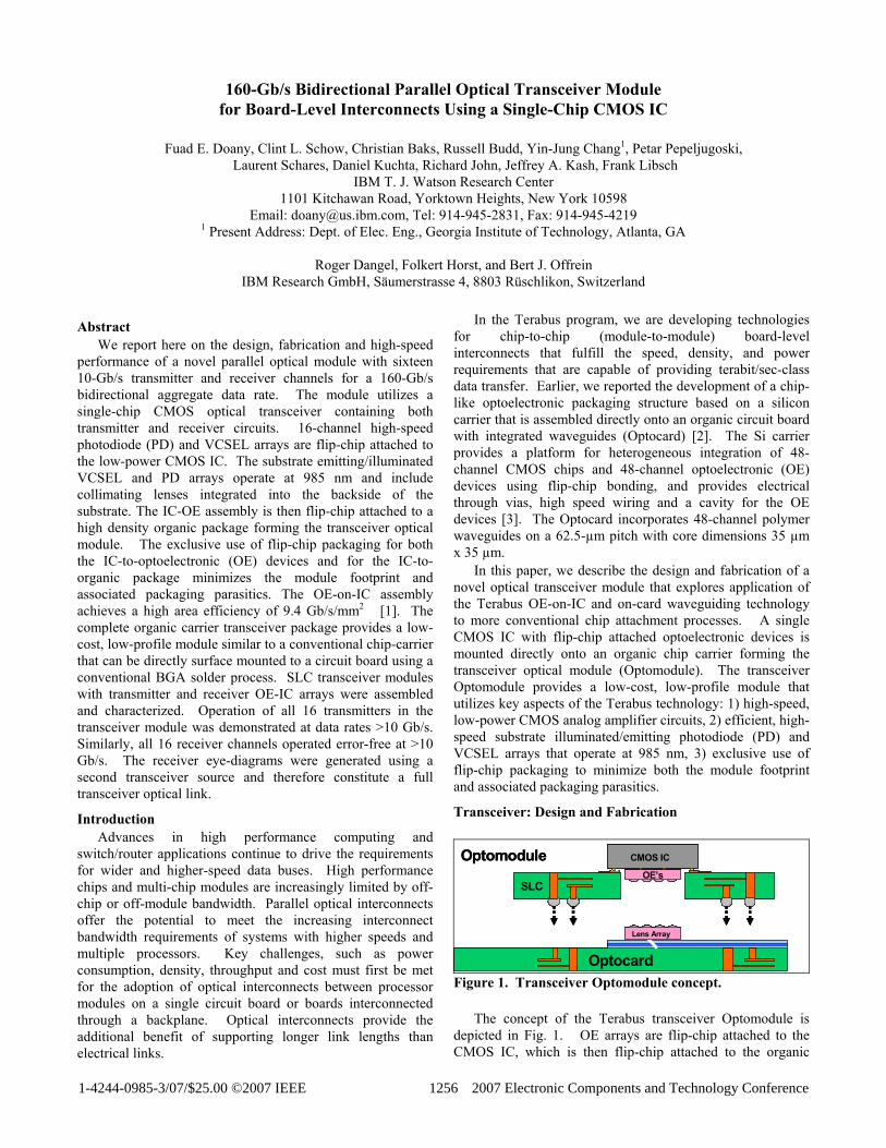
Figure 1. Transceiver Optomodule concept. The concept of the Terabus transceiver Optomodule is
depicted in Fig. 1. OE arrays are flip-chip attached to the CMOS IC, which is then flip-chip attached to the organic
1-4244-0985-3/07/$25.00 ©2007 IEEE 1256 2007 Electronic Components and Technology Conference
SLCTM [4] laminated high density circuit card. The Optomodule can be directly surface mounted to an FR4 circuit board with integrated waveguides to simultaneously provide the electrical and optical interconnection. A ball grid array (BGA) solder process similar to that used for conventional chip-carriers provides the electrical contacts while a lens array incorporated onto the waveguides provides the optical connectivity.
The transceiver IC was fabricated in the IBM 0.13-µm CMOS technology, and consists of sixteen independent laser-diode driver (LDD) circuits and sixteen receiver amplifier (RX) circuits arrayed in two separate 4x4 blocks with a 250-µm x 350-µm pitch. Differential 100-Ω microstrip transmission lines connect the inputs (outputs) of the LDD (RX) circuits to bond pads arranged on the long sides of the transceiver chip in a GSSG configuration. The 100-µm diameter pads on a 200-µm pitch are compatible with current high-volume industrial flip-chip attachment such as the IBM C-4 process. This pad configuration also allows all channels to be characterized using standard co-planar microwave probes at the IC level. Power and control signals for the transmitter and receiver sections of the chip are connected to bond pads at the short edges of the chip. The transceiver chip measures 5.25 mm by 3.25 mm.
The transceiver is designed to be used in conjunction with the 985-nm OE elements developed for 48-channel Terabus transmitter and receiver modules. Because the TX or RX portion of the transceivers utilize only 16 channels, the 4x12 OEs are diced into 4x4 arrays. A 500-µm separation between the TX and RX portions of the transceiver was chosen to minimize TX-RX crosstalk and allow for dicing tolerance, while retaining compatibility with the Optocard waveguide layout.
The following solder hierarchy enabled the multi-step assembly process of the Optomodule: Au pads on the OEs were bonded to the IC pads using Eutectic AuSn (80%Au, 20%Sn) solder deposited on the IC pads. The melting temperature of eutectic AuSn is 278 °C during reflow and >400 °C after reflow. This enabled the sequential flip-chip attachment of the OEs to the IC. The IC was subsequently flip–chip attached to the SLC carrier using eutectic SnPb (63%Sn, 37%Pb) solder with a melting temperature of 183 °C. Underfill can be applied to the IC-SLC solder interface to enable future BGA attachment of the Optomodule to the Optocard using eutectic SnPb solder.
4x4 VCSEL Array 4x4 PD Array4x4 VCSEL Array 4x4 PD Array
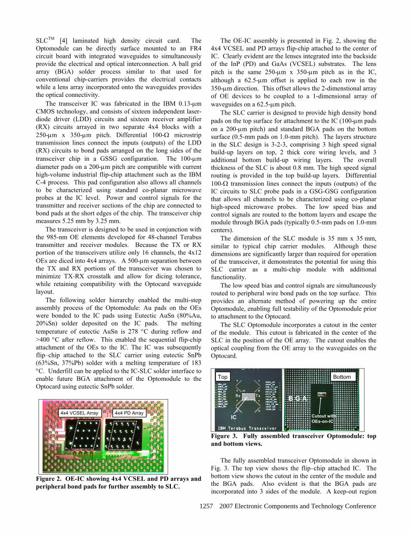
Figure 2. OE-IC showing 4x4 VCSEL and PD arrays and peripheral bond pads for further assembly to SLC.
The OE-IC assembly is presented in Fig. 2, showing the 4x4 VCSEL and PD arrays flip-chip attached to the center of IC. Clearly evident are the lenses integrated into the backside of the InP (PD) and GaAs (VCSEL) substrates. The lens pitch is the same 250-µm x 350-µm pitch as in the IC, although a 62.5-µm offset is applied to each row in the 350-µm direction. This offset allows the 2-dimenstional array of OE devices to be coupled to a 1-dimensional array of waveguides on a 62.5-µm pitch.
The SLC carrier is designed to provide high density bond pads on the top surface for attachment to the IC (100-µm pads on a 200-µm pitch) and standard BGA pads on the bottom surface (0.5-mm pads on 1.0-mm pitch). The layers structure in the SLC design is 3-2-3, comprising 3 high speed signal build-up layers on top, 2 thick core wiring levels, and 3 additional bottom build-up wiring layers. The overall thickness of the SLC is about 0.8 mm. The high speed signal routing is provided in the top build-up layers. Differential 100-Ω transmission lines connect the inputs (outputs) of the IC circuits to SLC probe pads in a GSG-GSG configuration that allows all channels to be characterized using co-planar high-speed microwave probes. The low speed bias and control signals are routed to the bottom layers and escape the module through BGA pads (typically 0.5-mm pads on 1.0-mm centers).
The dimension of the SLC module is 35 mm x 35 mm, similar to typical chip carrier modules. Although these dimensions are significantly larger than required for operation of the transceiver, it demonstrates the potential for using this SLC carrier as a multi-chip module with additional functionality.
The low speed bias and control signals are simultaneously routed to peripheral wire bond pads on the top surface. This provides an alternate method of powering up the entire Optomodule, enabling full testability of the Optomodule prior to attachment to the Optocard.
The SLC Optomodule incorporates a cutout in the center of the module. This cutout is fabricated in the center of the SLC in the position of the OE array. The cutout enables the optical coupling from the OE array to the waveguides on the Optocard.
Figure 3. Fully assembled transceiver Optomodule: top and bottom views.
The fully assembled transceiver Optomodule in shown in Fig. 3. The top view shows the flip–chip attached IC. The bottom view shows the cutout in the center of the module and the BGA pads. Also evident is that the BGA pads are incorporated into 3 sides of the module. A keep-out region
Top Bottom
Cutout withOEs-on-IC
IC
B G A
Top Bottom
Cutout withOEs-on-IC
IC
B G A
1257 2007 Electronic Components and Technology Conference
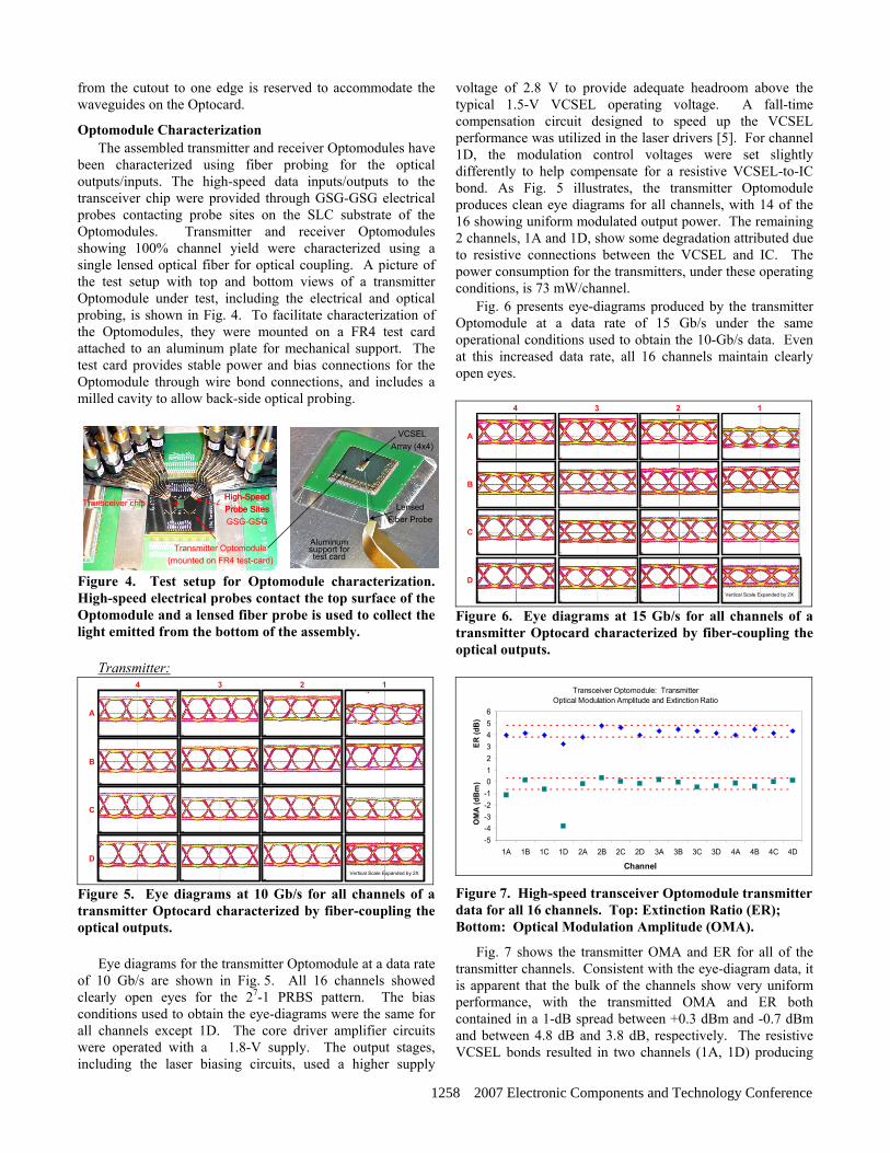
from the cutout to one edge is reserved to accommodate the waveguides on the Optocard.
Optomodule Characterization The assembled transmitter and receiver Optomodules have
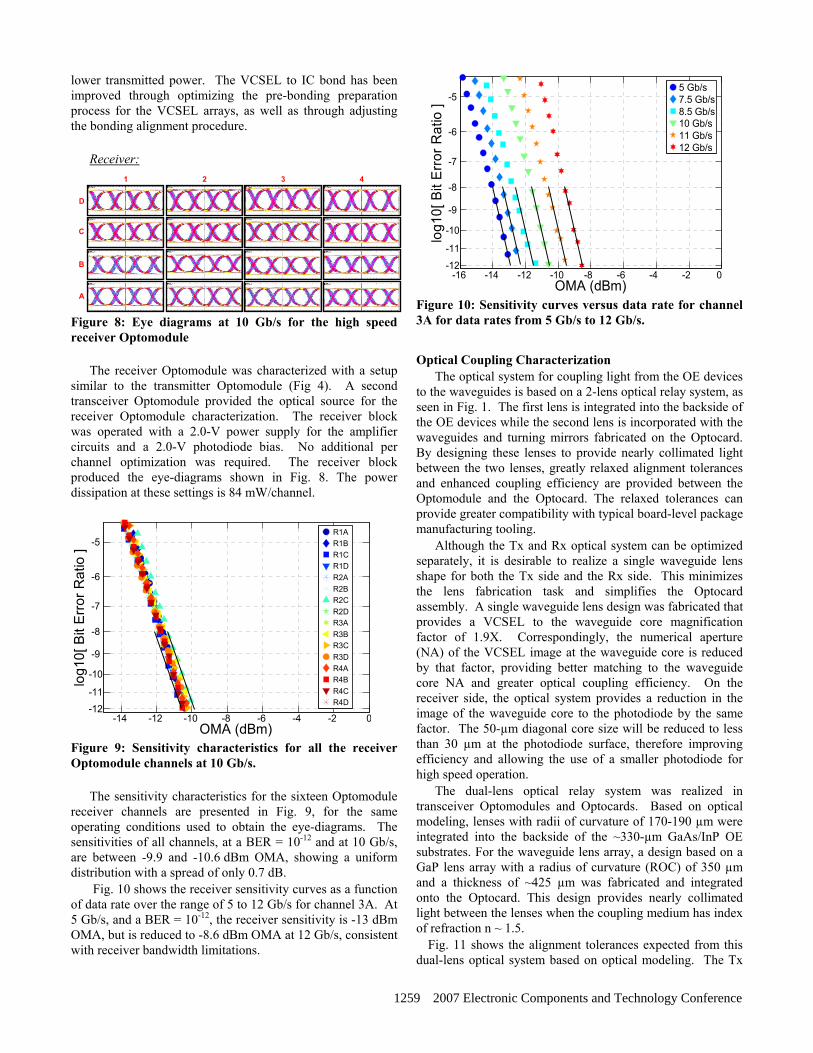
been characterized using fiber probing for the optical outputs/inputs. The high-speed data inputs/outputs to the transceiver chip were provided through GSG-GSG electrical probes contacting probe sites on the SLC substrate of the Optomodules. Transmitter and receiver Optomodules showing 100% channel yield were characterized using a single lensed optical fiber for optical coupling. A picture of the test setup with top and bottom views of a transmitter Optomodule under test, including the electrical and optical probing, is shown in Fig. 4. To facilitate characterization of the Optomodules, they were mounted on a FR4 test card attached to an aluminum plate for mechanical support. The test card provides stable power and bias connections for the Optomodule through wire bond connections, and includes a milled cavity to allow back-side optical probing.
Transmitter Optomodule(mounted on FR4 test-card)
High-SpeedProbe SitesGSG-GSG
Transceiver chipHigh-SpeedProbe Sites
Aluminum support fortest card
LensedFiber Probe
VCSELArray (4x4)
Figure 4. Test setup for Optomodule characterization. High-speed electrical probes contact the top surface of the Optomodule and a lensed fiber probe is used to collect the light emitted from the bottom of the assembly.
Transmitter:
A
B
C
D
1234
Vertical Scale Expanded by 2X Figure 5. Eye diagrams at 10 Gb/s for all channels of a transmitter Optocard characterized by fiber-coupling the optical outputs.
Eye diagrams for the transmitter Optomodule at a data rate
of 10 Gb/s are shown in Fig. 5. All 16 channels showed clearly open eyes for the 27-1 PRBS pattern. The bias conditions used to obtain the eye-diagrams were the same for all channels except 1D. The core driver amplifier circuits were operated with a 1.8-V supply. The output stages, including the laser biasing circuits, used a higher supply
voltage of 2.8 V to provide adequate headroom above the typical 1.5-V VCSEL operating voltage. A fall-time compensation circuit designed to speed up the VCSEL performance was utilized in the laser drivers [5]. For channel 1D, the modulation control voltages were set slightly differently to help compensate for a resistive VCSEL-to-IC bond. As Fig. 5 illustrates, the transmitter Optomodule produces clean eye diagrams for all channels, with 14 of the 16 showing uniform modulated output power. The remaining 2 channels, 1A and 1D, show some degradation attributed due to resistive connections between the VCSEL and IC. The power consumption for the transmitters, under these operating conditions, is 73 mW/channel.
Fig. 6 presents eye-diagrams produced by the transmitter Optomodule at a data rate of 15 Gb/s under the same operational conditions used to obtain the 10-Gb/s data. Even at this increased data rate, all 16 channels maintain clearly open eyes.
A
B
C
D
1234
Vertical Scale Expanded by 2X
Figure 6. Eye diagrams at 15 Gb/s for all channels of a transmitter Optocard characterized by fiber-coupling the optical outputs.
Figure 7. High-speed transceiver Optomodule transmitter data for all 16 channels. Top: Extinction Ratio (ER); Bottom: Optical Modulation Amplitude (OMA).
Fig. 7 shows the transmitter OMA and ER for all of the transmitter channels. Consistent with the eye-diagram data, it is apparent that the bulk of the channels show very uniform performance, with the transmitted OMA and ER both contained in a 1-dB spread between +0.3 dBm and -0.7 dBm and between 4.8 dB and 3.8 dB, respectively. The resistive VCSEL bonds resulted in two channels (1A, 1D) producing
Transceiver Optomodule: TransmitterOptical Modulation Amplitude and Extinction Ratio
-5-4-3-2-10123456
1A 1B 1C 1D 2A 2B 2C 2D 3A 3B 3C 3D 4A 4B 4C 4D
Channel
O
MA
(dB
m)
ER
(dB
)
1258 2007 Electronic Components and Technology Conference
lower transmitted power. The VCSEL to IC bond has been improved through optimizing the pre-bonding preparation process for the VCSEL arrays, as well as through adjusting the bonding alignment procedure.
Receiver:
Figure 8: Eye diagrams at 10 Gb/s for the high speed receiver Optomodule
The receiver Optomodule was characterized with a setup
similar to the transmitter Optomodule (Fig 4). A second transceiver Optomodule provided the optical source for the receiver Optomodule characterization. The receiver block was operated with a 2.0-V power supply for the amplifier circuits and a 2.0-V photodiode bias. No additional per channel optimization was required. The receiver block produced the eye-diagrams shown in Fig. 8. The power dissipation at these settings is 84 mW/channel.
-14 -12 -10 -8 -6 -4 -2 0
-5
-6
-7
-8
-9
-10
-11
-12
OMA (dBm)
log1
0[ B
it Er
ror R
atio
]
R1AR1BR1CR1DR2AR2BR2CR2DR3AR3BR3CR3DR4AR4BR4CR4D
Figure 9: Sensitivity characteristics for all the receiver Optomodule channels at 10 Gb/s.
The sensitivity characteristics for the sixteen Optomodule receiver channels are presented in Fig. 9, for the same operating conditions used to obtain the eye-diagrams. The sensitivities of all channels, at a BER = 10-12 and at 10 Gb/s, are between -9.9 and -10.6 dBm OMA, showing a uniform distribution with a spread of only 0.7 dB.
Fig. 10 shows the receiver sensitivity curves as a function of data rate over the range of 5 to 12 Gb/s for channel 3A. At 5 Gb/s, and a BER = 10-12, the receiver sensitivity is -13 dBm OMA, but is reduced to -8.6 dBm OMA at 12 Gb/s, consistent with receiver bandwidth limitations.
-16 -14 -12 -10 -8 -6 -4 -2 0
-5
-6
-7
-8
-9
-10
-11
-12
OMA (dBm)
log1
0[ B
it Er
ror R
atio
]
5 Gb/s7.5 Gb/s8.5 Gb/s10 Gb/s11 Gb/s12 Gb/s
Figure 10: Sensitivity curves versus data rate for channel 3A for data rates from 5 Gb/s to 12 Gb/s.
Optical Coupling Characterization The optical system for coupling light from the OE devices
to the waveguides is based on a 2-lens optical relay system, as seen in Fig. 1. The first lens is integrated into the backside of the OE devices while the second lens is incorporated with the waveguides and turning mirrors fabricated on the Optocard. By designing these lenses to provide nearly collimated light between the two lenses, greatly relaxed alignment tolerances and enhanced coupling efficiency are provided between the Optomodule and the Optocard. The relaxed tolerances can provide greater compatibility with typical board-level package manufacturing tooling.
Although the Tx and Rx optical system can be optimized separately, it is desirable to realize a single waveguide lens shape for both the Tx side and the Rx side. This minimizes the lens fabrication task and simplifies the Optocard assembly. A single waveguide lens design was fabricated that provides a VCSEL to the waveguide core magnification factor of 1.9X. Correspondingly, the numerical aperture (NA) of the VCSEL image at the waveguide core is reduced by that factor, providing better matching to the waveguide core NA and greater optical coupling efficiency. On the receiver side, the optical system provides a reduction in the image of the waveguide core to the photodiode by the same factor. The 50-µm diagonal core size will be reduced to less than 30 µm at the photodiode surface, therefore improving efficiency and allowing the use of a smaller photodiode for high speed operation.
The dual-lens optical relay system was realized in transceiver Optomodules and Optocards. Based on optical modeling, lenses with radii of curvature of 170-190 µm were integrated into the backside of the ~330-µm GaAs/InP OE substrates. For the waveguide lens array, a design based on a GaP lens array with a radius of curvature (ROC) of 350 µm and a thickness of ~425 µm was fabricated and integrated onto the Optocard. This design provides nearly collimated light between the lenses when the coupling medium has index of refraction n ~ 1.5.
Fig. 11 shows the alignment tolerances expected from this dual-lens optical system based on optical modeling. The Tx
D
C
B
A
4321
1259 2007 Electronic Components and Technology Conference
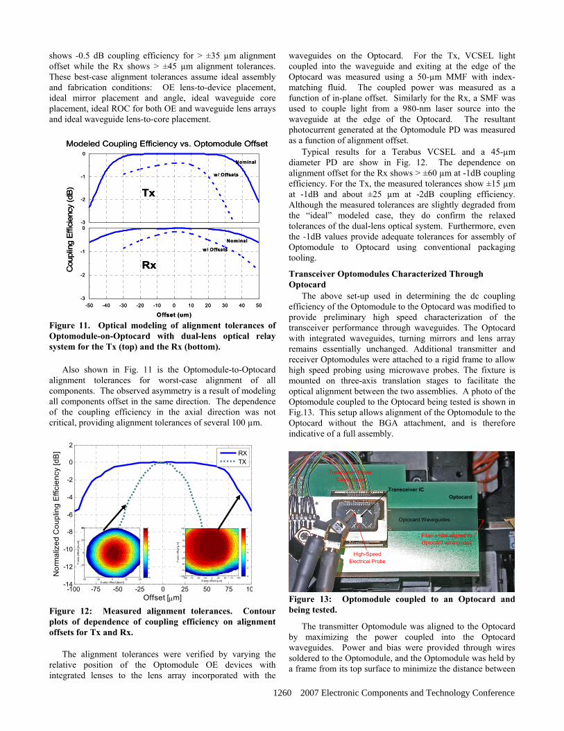
shows -0.5 dB coupling efficiency for > ±35 µm alignment offset while the Rx shows > ±45 µm alignment tolerances. These best-case alignment tolerances assume ideal assembly and fabrication conditions: OE lens-to-device placement, ideal mirror placement and angle, ideal waveguide core placement, ideal ROC for both OE and waveguide lens arrays and ideal waveguide lens-to-core placement.
Figure 11. Optical modeling of alignment tolerances of Optomodule-on-Optocard with dual-lens optical relay system for the Tx (top) and the Rx (bottom).
Also shown in Fig. 11 is the Optomodule-to-Optocard
alignment tolerances for worst-case alignment of all components. The observed asymmetry is a result of modeling all components offset in the same direction. The dependence of the coupling efficiency in the axial direction was not critical, providing alignment tolerances of several 100 µm.
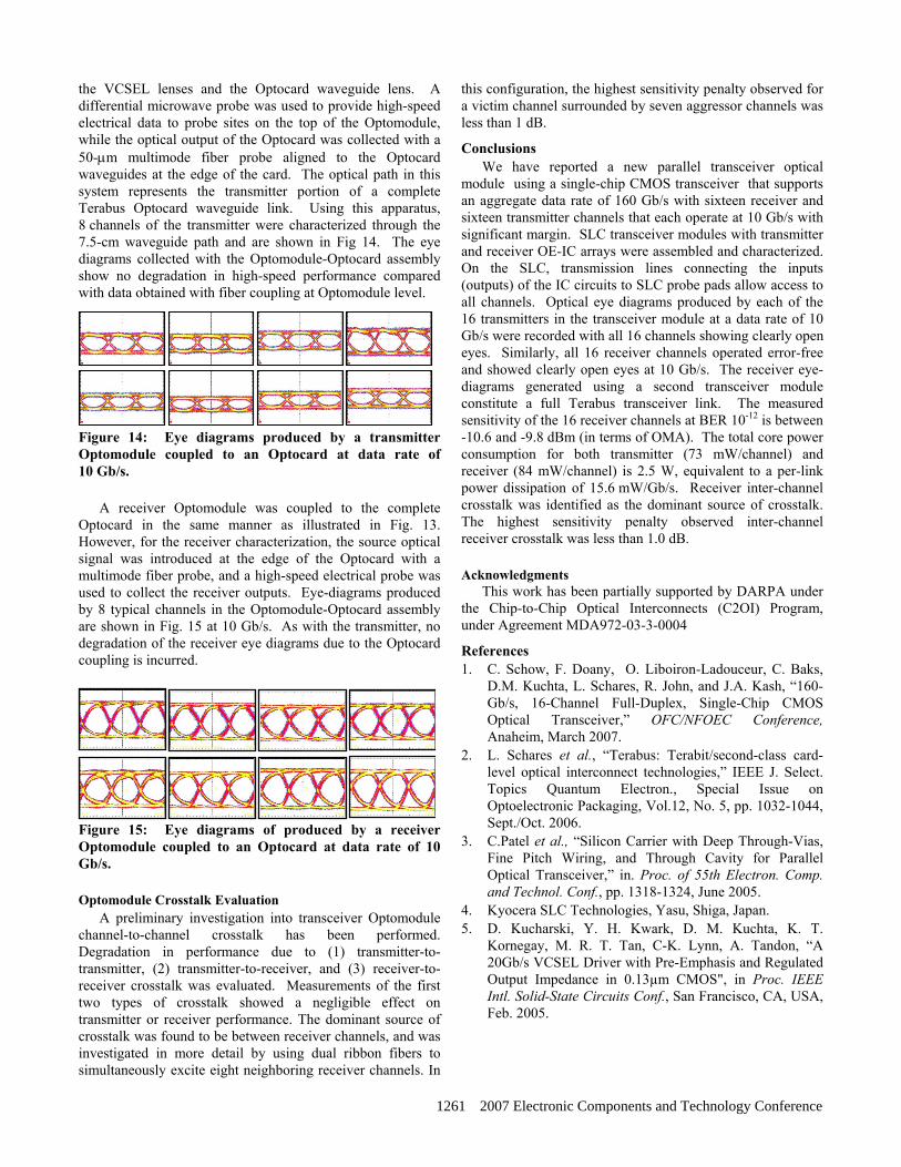
Figure 12: Measured alignment tolerances. Contour plots of dependence of coupling efficiency on alignment offsets for Tx and Rx.
The alignment tolerances were verified by varying the relative position of the Optomodule OE devices with integrated lenses to the lens array incorporated with the
waveguides on the Optocard. For the Tx, VCSEL light coupled into the waveguide and exiting at the edge of the Optocard was measured using a 50-µm MMF with index-matching fluid. The coupled power was measured as a function of in-plane offset. Similarly for the Rx, a SMF was used to couple light from a 980-nm laser source into the waveguide at the edge of the Optocard. The resultant photocurrent generated at the Optomodule PD was measured as a function of alignment offset.
Typical results for a Terabus VCSEL and a 45-µm diameter PD are show in Fig. 12. The dependence on alignment offset for the Rx shows > ±60 µm at -1dB coupling efficiency. For the Tx, the measured tolerances show ±15 µm at -1dB and about ±25 µm at -2dB coupling efficiency. Although the measured tolerances are slightly degraded from the “ideal” modeled case, they do confirm the relaxed tolerances of the dual-lens optical system. Furthermore, even the -1dB values provide adequate tolerances for assembly of Optomodule to Optocard using conventional packaging tooling.
Transceiver Optomodules Characterized Through Optocard
The above set-up used in determining the dc coupling efficiency of the Optomodule to the Optocard was modified to provide preliminary high speed characterization of the transceiver performance through waveguides. The Optocard with integrated waveguides, turning mirrors and lens array remains essentially unchanged. Additional transmitter and receiver Optomodules were attached to a rigid frame to allow high speed probing using microwave probes. The fixture is mounted on three-axis translation stages to facilitate the optical alignment between the two assemblies. A photo of the Optomodule coupled to the Optocard being tested is shown in Fig.13. This setup allows alignment of the Optomodule to the Optocard without the BGA attachment, and is therefore indicative of a full assembly.
Figure 13: Optomodule coupled to an Optocard and being tested.
The transmitter Optomodule was aligned to the Optocard by maximizing the power coupled into the Optocard waveguides. Power and bias were provided through wires soldered to the Optomodule, and the Optomodule was held by a frame from its top surface to minimize the distance between
Transceiver IC
High-SpeedElectrical Probe
Transceiver PowerConnections
Optocard Waveguides
Fiber probe aligned toOptocard waveguides
Optocard
-100 -75 -50 -25 0 25 50 75 10-14
-12
-10
-8
-6
-4
-2
0
2
Offset [µm]
Nor
mal
ized
Cou
plin
g E
ffici
ency
[dB
]
RXTX
X-axis offset [mum]
Y-a
xis
offs
et [m
um]
-50 -25 0 25 50
-25
0
25
5050
-10
-9
-8
-7
-6
-5
-4
-3
-2
-1
0
1
X-axis offset [µm]
Y-a
xis
offs
et [ µ
m]
-100 -75 -50 -25 0 25 50 75 100-100
-75
-50
-25
0
25
50
75
100
-16
-14
-12
-10
-8
-6
-4
-3
-2
-1
0
Nominal
w/ Offsets
-3
-2
-1
0
-50 -40 -30 -20 -10 0 10 20 30 40 50
Offset (um)
Nominal
w/ Offsets
Cou
plin
g Ef
ficie
ncy
(dB
)
Modeled Coupling Efficiency vs. Optomodule Offset
Tx
Rx
-3
-2
-1
0
Nominal
w/ Offsets
-3
-2
-1
0
-50 -40 -30 -20 -10 0 10 20 30 40 50
Offset (um)
Nominal
w/ Offsets
Cou
plin
g Ef
ficie
ncy
(dB
)
Modeled Coupling Efficiency vs. Optomodule Offset
Tx
Rx
1260 2007 Electronic Components and Technology Conference
the VCSEL lenses and the Optocard waveguide lens. A differential microwave probe was used to provide high-speed electrical data to probe sites on the top of the Optomodule, while the optical output of the Optocard was collected with a 50-µm multimode fiber probe aligned to the Optocard waveguides at the edge of the card. The optical path in this system represents the transmitter portion of a complete Terabus Optocard waveguide link. Using this apparatus, 8 channels of the transmitter were characterized through the 7.5-cm waveguide path and are shown in Fig 14. The eye diagrams collected with the Optomodule-Optocard assembly show no degradation in high-speed performance compared with data obtained with fiber coupling at Optomodule level.
Figure 14: Eye diagrams produced by a transmitter Optomodule coupled to an Optocard at data rate of 10 Gb/s.
A receiver Optomodule was coupled to the complete Optocard in the same manner as illustrated in Fig. 13. However, for the receiver characterization, the source optical signal was introduced at the edge of the Optocard with a multimode fiber probe, and a high-speed electrical probe was used to collect the receiver outputs. Eye-diagrams produced by 8 typical channels in the Optomodule-Optocard assembly are shown in Fig. 15 at 10 Gb/s. As with the transmitter, no degradation of the receiver eye diagrams due to the Optocard coupling is incurred.
Figure 15: Eye diagrams of produced by a receiver Optomodule coupled to an Optocard at data rate of 10 Gb/s. Optomodule Crosstalk Evaluation
A preliminary investigation into transceiver Optomodule channel-to-channel crosstalk has been performed. Degradation in performance due to (1) transmitter-to-transmitter, (2) transmitter-to-receiver, and (3) receiver-to-receiver crosstalk was evaluated. Measurements of the first two types of crosstalk showed a negligible effect on transmitter or receiver performance. The dominant source of crosstalk was found to be between receiver channels, and was investigated in more detail by using dual ribbon fibers to simultaneously excite eight neighboring receiver channels. In
this configuration, the highest sensitivity penalty observed for a victim channel surrounded by seven aggressor channels was less than 1 dB.
Conclusions We have reported a new parallel transceiver optical
module using a single-chip CMOS transceiver that supports an aggregate data rate of 160 Gb/s with sixteen receiver and sixteen transmitter channels that each operate at 10 Gb/s with significant margin. SLC transceiver modules with transmitter and receiver OE-IC arrays were assembled and characterized. On the SLC, transmission lines connecting the inputs (outputs) of the IC circuits to SLC probe pads allow access to all channels. Optical eye diagrams produced by each of the 16 transmitters in the transceiver module at a data rate of 10 Gb/s were recorded with all 16 channels showing clearly open eyes. Similarly, all 16 receiver channels operated error-free and showed clearly open eyes at 10 Gb/s. The receiver eye-diagrams generated using a second transceiver module constitute a full Terabus transceiver link. The measured sensitivity of the 16 receiver channels at BER 10-12 is between -10.6 and -9.8 dBm (in terms of OMA). The total core power consumption for both transmitter (73 mW/channel) and receiver (84 mW/channel) is 2.5 W, equivalent to a per-link power dissipation of 15.6 mW/Gb/s. Receiver inter-channel crosstalk was identified as the dominant source of crosstalk. The highest sensitivity penalty observed inter-channel receiver crosstalk was less than 1.0 dB.
Acknowledgments
This work has been partially supported by DARPA under the Chip-to-Chip Optical Interconnects (C2OI) Program, under Agreement MDA972-03-3-0004
References 1. C. Schow, F. Doany, O. Liboiron-Ladouceur, C. Baks,
D.M. Kuchta, L. Schares, R. John, and J.A. Kash, “160-Gb/s, 16-Channel Full-Duplex, Single-Chip CMOS Optical Transceiver,” OFC/NFOEC Conference, Anaheim, March 2007.
2. L. Schares et al., “Terabus: Terabit/second-class card-level optical interconnect technologies,” IEEE J. Select. Topics Quantum Electron., Special Issue on Optoelectronic Packaging, Vol.12, No. 5, pp. 1032-1044, Sept./Oct. 2006.
3. C.Patel et al., “Silicon Carrier with Deep Through-Vias, Fine Pitch Wiring, and Through Cavity for Parallel Optical Transceiver,” in. Proc. of 55th Electron. Comp. and Technol. Conf., pp. 1318-1324, June 2005.
4. Kyocera SLC Technologies, Yasu, Shiga, Japan. 5. D. Kucharski, Y. H. Kwark, D. M. Kuchta, K. T.
Kornegay, M. R. T. Tan, C-K. Lynn, A. Tandon, “A 20Gb/s VCSEL Driver with Pre-Emphasis and Regulated Output Impedance in 0.13µm CMOS", in Proc. IEEE Intl. Solid-State Circuits Conf., San Francisco, CA, USA, Feb. 2005.
1261 2007 Electronic Components and Technology Conference