05256974
10
2834 IEEE JOURNAL OF SOLID-STATE CIRCUITS, VOL. 44, NO. 10, OCTOBER 2009 An Activity-Triggered 95.3 dB DR 75.6 dB THD CMOS Imaging Sensor With Digital Calibration Jie Yuan, Member, IEEE, Ho Yeung Chan, Sheung Wai Fung, and Bing Liu, Student Member, IEEE Abstract—Imaging sensors are being used as data acquisi- tion systems in new biomedical applications. These applications require wide dynamic range (WDR), high linearity and high signal-to-noise ratio (SNR), which cannot be met simultaneously by existing CMOS imaging sensors. This paper introduces a new activity-triggered WDR CMOS imaging sensor with very low distortion. The new WDR pixel includes self-resetting circuits to partially quantize the photocurrent in the pixel. The pixel residual analog voltage is further quantized by a low-resolution column-wise ADC. The ADC code and the partially quantized pixel codes are processed by column-wise digital circuits to form WDR images. Calibration circuits are included in the pixel to improve the pixel linearity by a digital calibration method, which requires low calibration overhead. Current-mode difference cir- cuits are included in the pixel to detect activities within the scene so that the imaging sensor captures high quality images only for scenes with intense activity. A proof-of-concept 32 32 imaging sensor is fabricated in a 0.35 m CMOS process. The fill factor of the new pixel is 27%. Silicon measurements show that the new imaging sensor can achieve 95.3 dB dynamic range with low distortion of after calibration. The maximum SNR of the sensor is 74.5 dB. The imaging sensor runs at frame rate up to 15 Hz. Index Terms—Activity-triggered detection, CMOS imaging sensor, difference image, digital calibration, high linearity, wide dynamic range. I. INTRODUCTION T HE continuous improvement of CMOS imaging sensors in recent years has opened up new application areas in sci- entific research ([1], [2]) and biomedical diagnostics ([3]–[7]), such as space telescope, DNA microarray, bioluminescence de- tection, and computed tomography. An imaging sensor serves as a data acquisition system in these applications, which require wide dynamic range (WDR) and high linearity over the full range. Charge-coupled devices (CCD) have been mainly used for these applications. However, powerful on-chip processing capabilities make CMOS imaging sensors more attractive than CCD sensors besides its cost advantage [8]. CMOS imaging sensors have already been developed for several biomedical ap- plications ([6]–[10]). However, a lot of these new applications ([1]–[5], [9], [10]) require WDR CMOS imaging sensors with Manuscript received November 15, 2009; revised May 31, 2009. Current ver- sion published September 28, 2009. This paper was approved by Associate Ed- itor Kenneth Shepard. This work was supported by a grant from the Research Grant Council of the Hong Kong Special Administrative Region Government (Reference No. RGC DAG06/07.EG04). The authors are with the Electronic and Computer Engineering Department, the Hong Kong University of Science and Technology, Clear Water Bay, Kowloon, Hong Kong (e-mail: [email protected]; [email protected]). Digital Object Identifier 10.1109/JSSC.2009.2027929 dynamic range (DR) around five decades ( ) and lin- earity better than 12 bits ( ). WDR imaging sensors usually generate high output data rate which demands high pro- cessing power. Hence, activity-triggered image acquisition is desirable. WDR CMOS imaging sensors have been designed with non- linear techniques and linear techniques [11]. Logarithmic pixels have wider DR than linear pixels [12]. However, the noise level of a logarithmic pixel is high. The DR of a linear pixel is nor- mally limited by its potential well size. The well size can be adjusted nonlinearly to accommodate the wide DR [13]. The DR can be also extended by scaling the integration time ac- cording to the photo current level [14]. Equivalently, a WDR image can be synthesized from images captured from multiple exposures ([15], [16]). More recently, a lateral overflow integra- tion capacitor scheme was developed to greatly expand the DR [17]. These WDR imaging sensors expand the DR nonlinearly by spilling extra photo charges, or changing the pixel conver- sion gain, so that the pixel linearity is not preserved over the wide DR. In-pixel - A/D conversion can linearly expand the imaging sensor DR [18]. However, the oversampled output data rate can be high. This paper introduces the design of a new WDR CMOS imaging sensor with high linearity and lower output data rate. The new pixel design enables both the activity detection and the WDR image acquisition. A partial quantization scheme is implemented in the new pixel, which linearly expands the imaging sensor DR to be 95.3 dB. The linearity of the partial quantization scheme over the wide DR is improved using a dig- ital calibration method with a back-end digital signal processor (DSP). The pixel distortion after calibration reaches . The partial quantization pixel also achieves high signal-to-noise ratio (SNR). The fill factor of the new pixel is 27%. Part of the concepts in this paper has been presented in [19]. The paper is organized in six sections. The existing WDR CMOS imaging sensor techniques are summarized in Section II. Circuits of the new imaging sensor are detailed in Section III. The digital calibration method is introduced in Section IV. Measurement results are given in Section V. Section VI draws conclusions. II. WDR PIXEL DESIGN The accumulated photo voltage ( ) of a conventional 3 T active pixel is (1) where is the integration duration. is the integration capacitor, which is the diode capacitance for the 3 T active pixel. 0018-9200/$26.00 © 2009 IEEE
Transcript of 05256974
2834 IEEE JOURNAL OF SOLID-STATE CIRCUITS, VOL. 44, NO. 10, OCTOBER 2009
An Activity-Triggered 95.3 dB DR 75.6 dB THDCMOS Imaging Sensor With Digital Calibration
Jie Yuan, Member, IEEE, Ho Yeung Chan, Sheung Wai Fung, and Bing Liu, Student Member, IEEE
Abstract—Imaging sensors are being used as data acquisi-tion systems in new biomedical applications. These applicationsrequire wide dynamic range (WDR), high linearity and highsignal-to-noise ratio (SNR), which cannot be met simultaneouslyby existing CMOS imaging sensors. This paper introduces a newactivity-triggered WDR CMOS imaging sensor with very lowdistortion. The new WDR pixel includes self-resetting circuitsto partially quantize the photocurrent in the pixel. The pixelresidual analog voltage is further quantized by a low-resolutioncolumn-wise ADC. The ADC code and the partially quantizedpixel codes are processed by column-wise digital circuits to formWDR images. Calibration circuits are included in the pixel toimprove the pixel linearity by a digital calibration method, whichrequires low calibration overhead. Current-mode difference cir-cuits are included in the pixel to detect activities within the sceneso that the imaging sensor captures high quality images only forscenes with intense activity. A proof-of-concept 32 32 imagingsensor is fabricated in a 0.35 m CMOS process. The fill factorof the new pixel is 27%. Silicon measurements show that thenew imaging sensor can achieve 95.3 dB dynamic range with lowdistortion of �� � �� after calibration. The maximum SNR ofthe sensor is 74.5 dB. The imaging sensor runs at frame rate upto 15 Hz.
Index Terms—Activity-triggered detection, CMOS imagingsensor, difference image, digital calibration, high linearity, widedynamic range.
I. INTRODUCTION
T HE continuous improvement of CMOS imaging sensorsin recent years has opened up new application areas in sci-
entific research ([1], [2]) and biomedical diagnostics ([3]–[7]),such as space telescope, DNA microarray, bioluminescence de-tection, and computed tomography. An imaging sensor servesas a data acquisition system in these applications, which requirewide dynamic range (WDR) and high linearity over the fullrange. Charge-coupled devices (CCD) have been mainly usedfor these applications. However, powerful on-chip processingcapabilities make CMOS imaging sensors more attractive thanCCD sensors besides its cost advantage [8]. CMOS imagingsensors have already been developed for several biomedical ap-plications ([6]–[10]). However, a lot of these new applications([1]–[5], [9], [10]) require WDR CMOS imaging sensors with
Manuscript received November 15, 2009; revised May 31, 2009. Current ver-sion published September 28, 2009. This paper was approved by Associate Ed-itor Kenneth Shepard. This work was supported by a grant from the ResearchGrant Council of the Hong Kong Special Administrative Region Government(Reference No. RGC DAG06/07.EG04).
The authors are with the Electronic and Computer Engineering Department,the Hong Kong University of Science and Technology, Clear Water Bay,Kowloon, Hong Kong (e-mail: [email protected]; [email protected]).
Digital Object Identifier 10.1109/JSSC.2009.2027929
dynamic range (DR) around five decades ( ) and lin-earity better than 12 bits ( ). WDR imaging sensorsusually generate high output data rate which demands high pro-cessing power. Hence, activity-triggered image acquisition isdesirable.
WDR CMOS imaging sensors have been designed with non-linear techniques and linear techniques [11]. Logarithmic pixelshave wider DR than linear pixels [12]. However, the noise levelof a logarithmic pixel is high. The DR of a linear pixel is nor-mally limited by its potential well size. The well size can beadjusted nonlinearly to accommodate the wide DR [13]. TheDR can be also extended by scaling the integration time ac-cording to the photo current level [14]. Equivalently, a WDRimage can be synthesized from images captured from multipleexposures ([15], [16]). More recently, a lateral overflow integra-tion capacitor scheme was developed to greatly expand the DR[17]. These WDR imaging sensors expand the DR nonlinearlyby spilling extra photo charges, or changing the pixel conver-sion gain, so that the pixel linearity is not preserved over thewide DR. In-pixel - A/D conversion can linearly expand theimaging sensor DR [18]. However, the oversampled output datarate can be high.
This paper introduces the design of a new WDR CMOSimaging sensor with high linearity and lower output data rate.The new pixel design enables both the activity detection andthe WDR image acquisition. A partial quantization schemeis implemented in the new pixel, which linearly expands theimaging sensor DR to be 95.3 dB. The linearity of the partialquantization scheme over the wide DR is improved using a dig-ital calibration method with a back-end digital signal processor(DSP). The pixel distortion after calibration reaches .The partial quantization pixel also achieves high signal-to-noiseratio (SNR). The fill factor of the new pixel is 27%. Part of theconcepts in this paper has been presented in [19].
The paper is organized in six sections. The existing WDRCMOS imaging sensor techniques are summarized in Section II.Circuits of the new imaging sensor are detailed in Section III.The digital calibration method is introduced in Section IV.Measurement results are given in Section V. Section VI drawsconclusions.
II. WDR PIXEL DESIGN
The accumulated photo voltage ( ) of a conventional 3 Tactive pixel is
(1)
where is the integration duration. is the integrationcapacitor, which is the diode capacitance for the 3 T active pixel.
0018-9200/$26.00 © 2009 IEEE
YUAN et al.: ACTIVITY-TRIGGERED 95.3 dB DR 75.6 dB THD CMOS IMAGING SENSOR WITH DIGITAL CALIBRATION 2835
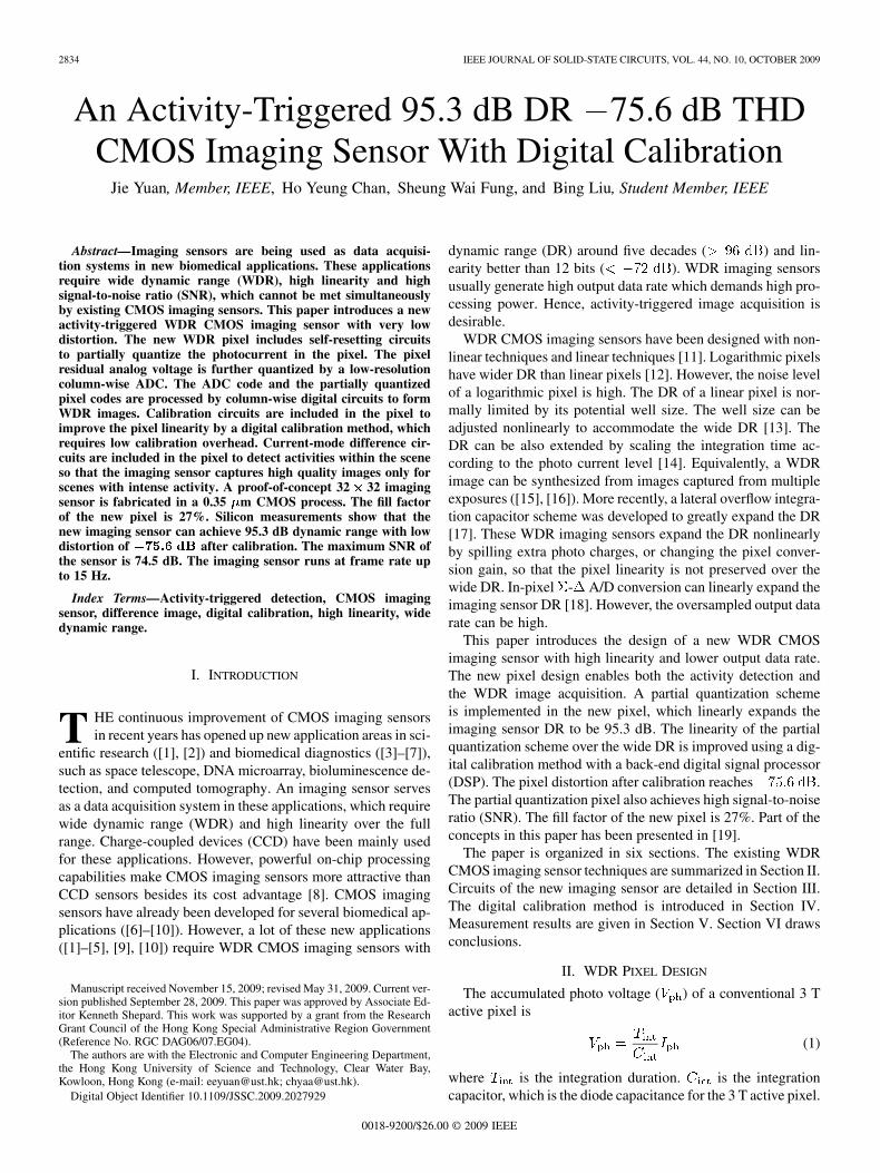
Fig. 1. The linearly expanded WDR pixel. (a) The pixel block diagram. (b) The pixel dynamics.
is the photo current. is limited by the maximum allowedvoltage at the integration node, which is generally known as thewell capacity ( ). Conventional CMOS imaging sensors keep
and constant for the pixel array. The DR of one pixelis limited by the well capacity as
(2)
where is the minimum photo current that the sensor candetect. This is determined by the least significant bit (LSB) sizeof the quantizer or the pixel read-out noise level, whichever islarger [20]. The maximum SNR of this pixel is [11]
(3)
where is the input-referred read-out voltage noise power.In order to expand the imaging sensor’s DR beyond the lim-
itation of (2), two types of WDR methods have been developedbased on (1). The accumulation time can be scaled non-linearly for different photo currents [14]. Small photo currentcan be detected with long integration, while large photo cur-rent can be accommodated within with short integration. Asthe integration duration is nonlinear, the linearity of this type ofWDR imaging sensor is low. The maximum SNR is still lim-ited by as stated in (3). Another method is to scale the accu-mulation capacitor for different photo currents [10], [17].A small photo current can be sensed by a small , while alarge photo current can be accommodated within by a large
. As the capacitance cannot be scaled as easily as the inte-gration time, existing designs use only one extra capacitor forscaling. With a proper capacitor, the DR can improve by 32times. The maximum SNR improves as the accumulated chargecan increase beyond the potential well limitation. However, thepixel linearity over the wide DR is still low because the conver-sion gain changes for different photo currents.
In order to design a highly linear WDR imaging sensor withhigh SNR, the DR should be expanded linearly. Ideally, the DRcan be linearly expanded by adding a comparator and a counterin the pixel as shown in Fig. 1(a). The photo diode gets resetwhenever falls below the threshold voltage, as shown inFig. 1(b). The number of pixel overflow events ( ) is recordedby a counter. The equivalent well size in this pixel is - .
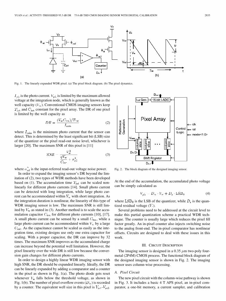
Fig. 2. The block diagram of the designed imaging sensor.
At the end of the accumulation, the accumulated photo voltagecan be simply calculated as
(4)
where is the LSB of the quantizer, while is the quan-tized residual voltage ( ).
Several problems need to be addressed at the circuit level tomake this partial quantization scheme a practical WDR tech-nique. The counter is usually large which reduces the pixel fillfactor greatly. An in-pixel counter also injects switching noiseto the analog front-end. The in-pixel comparator has nonlinearoffsets. Circuits are designed to deal with these issues in thiswork.
III. CIRCUIT DESCRIPTION
The imaging sensor is designed in a 0.35 m two-poly four-metal (2P4M) CMOS process. The functional block diagram ofthe designed imaging sensor is shown in Fig. 2. The imagingsensor uses column-wise processing.
A. Pixel Circuit
The new pixel circuit with the column-wise pathway is shownin Fig. 3. It includes a basic 4 T APS pixel, an in-pixel com-parator, a one-bit memory, a current sampler, and calibration

2836 IEEE JOURNAL OF SOLID-STATE CIRCUITS, VOL. 44, NO. 10, OCTOBER 2009
Fig. 3. The pixel circuit and the column-wise pathway of the new imaging sensor.
circuits. The pixel operates in three modes: the difference mode,the WDR mode, and the calibration mode.
1) Difference Mode: The sensor normally runs in the differ-ence mode to reduce the output data rate, which saves data trans-mission power and the digital power of following processingcircuits. In the difference mode, the current sampler is active.
of the comparator is set to a low value, which keeps thecomparator output low. The difference mode runs through twoframes.
At the beginning of the sampling frame, both samplingswitches stay on. turns off early, which injects chargeonly onto the MOS capacitor M6. At the end of the frame,
turns off, and injects most charge onto M8 which isabout 5 times larger than M6 [21]. The designed sampler cansample the photo current with offset less than 0.1%, which isenough for activity detection in most applications.
In an accumulation frame, the difference current between thenew photo current and the sampled current accumulates on thefloating drain (FD) after the difference shutter ( ) turnsoff. The reset level is in the middle of the voltage rangeso that both positive and negative difference currents can be ac-cumulated. At the end of the frame, the accumulated voltage isquantized by the column-wise ADC.
An off-chip DSP checks the difference image, which indi-cates the activity in the scene. If the activity is beyond a certainlevel, the imaging sensor switches to the WDR mode to capturea high-quality image. The current sampler is switched off during
the WDR mode. The supply voltage of the sampler ( ) is0.4 V lower than to suppress the leakage current from thesampler [22].
2) WDR Mode: To avoid image lag in the 4 T APS pixel, thetransfer gate M1a never resets during the accumulation. Instead,
stays fixed so that the potential well of the diode is alwaysfull in the steady state, as shown in Fig. 4. The photo chargespills over to the FD during the accumulation.
The WDR mode starts as a rolling shutter ( ) resets thepixel. When the accumulated voltage on the FD ( ) reachesthe threshold voltage of the comparator, the output of thecomparator ( ) resets the FD, as shown in Fig. 4(b). Then,the photo current accumulates on the FD again. The FD voltage
changes as shown in Fig. 1(b). An overflow event is recordedby a MOS capacitor M3. M3 is regularly read and reset by thecolumn slice to count the overflow number. At the end of theaccumulation, the residual voltage of the pixel is read out andquantized by the column-wise ADC.
Correlated double sampling (CDS) is performed on theresidual voltage. The ADC first samples ( ) the residualvoltage on . The pixel is reset before the analog read-outcontrol ( ) switches to the next row. The pixel reset voltageis sampled on . This CDS is performed over two frames. Itcan effectively remove reset noise [23]. The quantizationtakes place after the CDS phase ( ) turns off .
With a constant well size , the accumulated photo voltageof this partial quantization scheme can be calculated by (4).
YUAN et al.: ACTIVITY-TRIGGERED 95.3 dB DR 75.6 dB THD CMOS IMAGING SENSOR WITH DIGITAL CALIBRATION 2837
Fig. 4. The potential diagram of the pixel during the WDR mode.
Fig. 5. Simulated � at different photo currents of the partial quantizationpixel.
Fig. 6. The 16-bit dual-slope current ADC.
Nonetheless, is nonlinear because the asynchronous resetby the weak-current comparator (1 nA) depends heavily on thephoto current. Fig. 5 shows the simulated with differentphoto currents using HSPICE. A digital calibration scheme isdeveloped to compensate for this nonlinearity. At first, this non-linear function is sampled in the calibration mode. In theWDR mode, the accurate well size is interpolated from thesampled nonlinear function, and is applied in (4) to calculate theaccurate photo voltage.
3) Calibration Mode: In the calibration mode, the PD isswitched off. Instead, the pixel accumulates an on-chip calibra-tion current ( ). Identical cascade transistors M1a and M1bkeep the same FD capacitance in the calibration mode and theWDR mode. The exact value can be measured from anon-chip 16-bit current ADC, as shown in Fig. 6. With (4), thewell capacity for current can be calculated, which formsone sample on the nonlinear function in Fig. 5. Twelve on-chipcurrent sources are designed for each column.
Fig. 7. The pixel layout 25 �m� 25 �m.
The current ADC is a dual-slope ADC. In the pre-chargephase , charges . In the quantization phase , thereference current discharges . is compared with
continuously in phases. CDS is performed inphases. The zero crossing moment will be latched by
the output of , which is proportional to . The systemclock is 20 MHz. Each quantization takes about 3.2 ms.Measurements of the calibration currents in one column lastabout 38.4 ms.
The layout of the pixel is shown in Fig. 7. The pixel area is25 m 25 m. The photodiode size is 17 m 10 m, whichgives a fill factor of 27%. The current sampler accounts for about19% of the pixel. Without the current sampler, the fill factor is33%.)
4) Temporal Noise Analysis: With a small photo currentwhich does not trigger an overflow, the pixel temporal noisemainly comes from the photo current shot noise and theread-out circuit noise. The noise power is
(5)
At the low current end, the circuit noise dominates. Therefore,the SNR increases 6 dB per photo current doubling. At the largecurrent end, the photo current shot noise dominates. The SNRincreases 3 dB per photo current doubling.
When the photo current is large enough to trigger overflows,the pixel temporal noise mainly comes from the reset noise andthe photo current shot noise. The overall noise power is
(6)

2838 IEEE JOURNAL OF SOLID-STATE CIRCUITS, VOL. 44, NO. 10, OCTOBER 2009
Fig. 8. The pixel SNR for photo currents which trigger overflows:� � ����,� � �� ��, � � � .
where is the overflow number. The reset noise is muchsmaller than the shot noise. Therefore, the SNR improves by3 dB per photo current doubling. The pixel SNR can be simu-lated and plotted in Fig. 8. In the simulation, the well capacity
is 1.5 V. The DR is extended by 256 times. The integrationcapacitance is 12 fF. The read out circuit noise is 30 . As thepartial quantization scheme extends the DR greatly, the pixelSNR can be better than the previous designs [20], [23].
B. Column-Wise Counter
To expand the pixel DR by 256 times, an 8-bit counter isneeded by the pixel. A normal 8-bit counter needs 8 D-flip-flops(DFFs), which requires about 300 transistors. If this counter isincluded in the pixel, the fill factor will be low. The digital spikeswill contaminate the analog sensor as well. A new counter isdesigned at the column level, as shown in Fig. 9.
The column-wise counter includes an SRAM bank for dif-ferent pixels in the column. The logics add the overflow bitfrom the pixel to the content of the SRAM periodically. Thecounter runs on the counter clock . The clock rate is256 , where is the row number. At the begin-ning of each frame of every row, SRAM of this row is reset by
. The digital read-out control signal selects both theSRAM and the 1-bit memory of the th row to perform the ad-dition. After the addition, the falling edge of latchesthe new overflow number. Then, the column digital write signal
controls the new overflow number to be written into thesame SRAM. After that, the next row is turned on for refreshing.Within a frame, the SRAM of one pixel will be refreshed by256 times. The adder and the register should operate at thisfrequency.
After the addition, the clock resets the 1-bit memoryin the pixel of -th row. To prevent a write and reset conflic-tion, a weak reset is designed by applying a low gate voltage onthe NMOS switch S3. If the comparator generates a high pulseduring the reset phase , the NMOS diode is still able topull up the voltage on M3.
Because the adder is shared by different pixels in the column,the transistor count per pixel can be greatly reduced. On average,48 transistors are needed for each pixel, which could be furtherreduced by using dynamic RAM (DRAM). DRAM can be easilyimplemented in this architecture because the refreshing circuitsare already in place.
C. Column-Wise ADC
As shown in Fig. 3, a single-slope ADC is designed to quan-tize the pixel residual voltages in one column. The ADC designis similar to the one introduced in [24]. A high quality rampsignal is generated by a similar ramp signal generator in [25]with on-chip calibration. The column-wise ADC is designed for9 bit resolution. The frequency of the column-wise ADC clock( ) is 512 .
IV. DIGITAL CALIBRATION
In the calibration mode, the pixel is configured tosample the nonlinear well capacity with samples
. In the WDR mode, the imaging sensorgenerates raw image data ( , ). A DSP estimates theaccurate well capacity through linear interpolation from the
samples in real time, and recovers the accurate image fromthe raw image data.
A. Recovery Procedure
For a photo current , the pixel quantizes it into andso that
(7)
where .With an approximate applied, a crude can be calcu-
lated. Based on , the interpolation segment region can beidentified as shown in Fig. 10. With interpolation, the accurate
can be calculated.
(8)
where is the slope in this region. With (7) and (8), the accu-rate photo current can be found.
(9)
The interpolation region should be verified with this photocurrent value. If it is in the wrong region, the new region wouldbe used for another iteration. Theoretically, it might take severaliterations before the final is found. However, experimentsshow that no iteration is needed because the pixel nonlinearitygenerally is small, and the nonlinear function is well formed.
During the experiment, a digital version of this algorithm iscoded in a DSP. The mathematical derivation of this digital al-gorithm can be found in ([19], [26]).
B. Decoder
The calibration and recovery procedures are implemented bytwo decoders in the off-chip DSP. Fig. 11 shows structures of the
YUAN et al.: ACTIVITY-TRIGGERED 95.3 dB DR 75.6 dB THD CMOS IMAGING SENSOR WITH DIGITAL CALIBRATION 2839
Fig. 9. The column-wise counter.
Fig. 10. Estimate the accurate well capacity � through linear interpolation.
decoders. The rectangular boxes are memory elements. Signalsoutside boxes are inputs or outputs to the DSP.
The decoder in Fig. 11(a) calculates the interpolation pa-rameters in the calibration mode. is the digitized value of
. The speed of this decoder is not critical. The decoder inFig. 11(b) recovers the photo current during the WDR mode. Itsupports the real-time calculation. As the current ADC quan-tizes currents into 16 bits, bytes memory is required foreach pixel on average. For a 1 K-pixel image sensor,KB memory is needed in the DSP. If all pixels are processed inserial, the decoder needs to run at the rate Hz,where is the column number. Although 16-bit multipliersare needed in the decoder, only one such decoder is needed inthe DSP. If the image size is not large, multiplications can bedone in serial as well. Hence, the hardware overhead for digitalcalibration is low.
Fig. 11. Decoder structures in the DSP back-end. (a) Parameter decoder in thecalibration mode. (b) � decoder for real-time recovery during the WDR mode.
V. EXPERIMENTAL RESULTS
A proof-of-concept 32 32 imaging sensor is fabricated in a0.35 m 2P4M CMOS process. The micrograph of the die is inFig. 12. The die area is 2.7 mm 3.5 mm . The main measure-ment setup is shown in Fig. 13. The imaging chip is illuminatedby an integrating sphere US-120-SF (Labsphere, Inc.), with thelight source Fiber-Lite PL900 (Dolan Jenner Industries). Theoptical power meter is S-120 (Thorlabs). The output data fromthe imaging chip is captured by a logic analyzer 16902Band is further processed by a computer.
A. Optical and Electrical Parameters
The column-wise ADC is measured. A sinusoidal signal is ap-plied to one column-wise ADC. A spectrum analyzer (SR760,Stanford Research Systems) shows that the input spurious-free

2840 IEEE JOURNAL OF SOLID-STATE CIRCUITS, VOL. 44, NO. 10, OCTOBER 2009
Fig. 12. The micrograph of the imaging sensor 2.7 mm � 3.5 mm .
Fig. 13. The measurement setup.
dynamic range (SFDR) is about 83 dB. 512-pt FFT testing rou-tine is performed on the ADC at 15 Hz frame rate. The spec-trum is shown in Fig. 14. The overall signal-to-noise-distortionratio (SINAD) is 50.9 dB. The SFDR is 53.7 dB. The effectivenumber of bit (ENOB) is 8.2 bits. The ADC LSB size is 5.9 mV.
The pixel capacitance is measured to be 12 fF by theon-chip current ADC. The sensitivity of the imaging sensor is13.3 V . With the optical meter, the responsivity of theimaging sensor is measured to be 0.38 A/W at the wavelengthof 555 nm. The dark current of a pixel is 0.96 fA at roomtemperature, which corresponds to a dark current density of0.56 nA cm .
B. Difference Mode
The imaging sensor starts in the difference mode, andswitches to the WDR mode when the difference image pixelvalue reaches a threshold. Various digital thresholds are setwithin the potential well. The imaging chip is able to switch tothe WDR mode correctly if the scene changes significantly.
Fig. 14. The spectrum of the fabricated column-wise ADC: � � �� ��.
Fig. 15. The sampled well size of one pixel.
C. Linearity
With the current ADC, the calibration procedure is performedon pixels of the imaging sensor. of one pixel is sampled by11 currents, and is shown in Fig. 15. The digitized photocurrent and have been converted to their analog valueswith the ADC LSB sizes. The nonlinearity is strong, particularlyat the low current end.
The pixel linearity is measured by 17 currents. Without cali-bration, a uniform is used to estimate the accumulated photovoltage . The estimated photo voltages are shown in Fig. 16,with a spectrum simulated from this line. The harmonic distor-tion is 36.4 dB. The sampled nonlinear function is used to re-cover the accurate photo voltages. The recovered photo voltagesafter calibration are shown in Fig. 17, with a spectrum simulatedfrom this line. The harmonic distortion is improved to 75.6 dB.
The linearity in Fig. 17 is tested in the electrical domain,which includes only the circuits. Linearity test in the optical do-main cannot be performed with the existing equipment becauseit requires an optical source with better than 14-bit linearity.Nonetheless, the difference between the two measurements isonly the photodiode. For highly linear imaging applications, thephotodiode requires high linearity [10].
For this work, we tried to visualize the effect of the digitalcalibration on captured images. A gradient pattern as shownin Fig. 18(a) is printed by an HP laser printer and is capturedby the imaging sensor. Without calibration, the recorded imageis shown in Fig. 18(b). The image after calibration is shown

YUAN et al.: ACTIVITY-TRIGGERED 95.3 dB DR 75.6 dB THD CMOS IMAGING SENSOR WITH DIGITAL CALIBRATION 2841
Fig. 16. The pixel linearity before calibration.
Fig. 17. The pixel linearity after calibration.
Fig. 18. Pixel linearity measurement. (a) The display pattern. (b) The recorded image before calibration. (c) The recorded image after calibration.
in Fig. 18(c). The captured raw image has strong fixed pat-tern noise (FPN). The FPN is much lower after calibration. Thegray-scale uniformity is also improved after calibration.
D. FPN, Temporal Noise and DR
The imaging sensor is uniformly illuminated by the inte-grating sphere. Before calibration, the measured FPN of imagesis 5.1%. The FPN is mainly due to the mismatch of pixel-levelcircuits. After calibration, the overall measured FPN is 1.0%.FPN of the processing and read-out circuits is measured byapplying a current into all the pixels, and comparing the recov-ered after calibration. The uniformity among pixel circuitsafter calibration is better than 12-bit. Therefore, the measuredFPN is dominated by the photo diode variation and the opticalequipment.
The temporal noise of the imaging sensor is dominated bythe ADC quantization noise at low illumination level. There-fore, the pixel analog output is measured for noise instead. Ata low illumination level which does not trigger overflow, the
measured temporal noise of one pixel is 3.1 mV . The ac-cumulated photo voltage is 1.287 V. The SNR is 47.4 dB. Ata high illumination level, the measured pixel temporal noise is37.4 mV. The accumulated photo voltage is 330.6 V. The SNRis 73.9 dB. The photo current ratio of the two illumination levelsis about 256, while the SNR improvement is 26.5 dB. The SNRimproves 3.3 dB per signal doubling, which agrees with the tem-poral noise analysis well.
At 15 Hz frame rate, the maximum photo current that the par-tial quantization scheme can process is 58.4 pA. The minimumdetectable photo current is limited by the ADC LSB. The dy-namic range of the imaging sensor is about 95.3 dB. Fig. 19shows photos taken at different dynamic ranges. The scene in-cludes the S-120 light meter and the PL900 light source, whichis quite bright. Fig. 19(a) and (b) are images taken with partialquantization disabled. The integration time controls the imageexposure. The high DR scene cannot be completely captured bythe sensor. With partial quantization enabled, the whole scenecan be captured as shown in Fig. 19(c). Limited by the small

2842 IEEE JOURNAL OF SOLID-STATE CIRCUITS, VOL. 44, NO. 10, OCTOBER 2009
Fig. 19. Images taken with different dynamic ranges. (a) Small DR: under-exposed. (b) Small DR: over-exposed. (c) Wide DR.
TABLE IPERFORMANCE SUMMARY OF THE DESIGNED IMAGING SENSOR
size of the imaging sensor, the scene cannot be smoothly seen.However, the light source and the light meter can still be readilyrecognized.
E. Discussion
The measured performance of the designed imaging sensoris listed in Table I. The measured power only includes theanalog and digital power of the imaging sensor. The imagingsensor requires a digital back-end for calibration, which willburn more digital power. This extra digital power is not impor-tant for imaging systems with static power supply. The newWDR linear imaging sensor can also be used in power-limitedimplantable biomedical sensors, such as capsule endoscopy[27], [28]. In these applications, only the imaging sensor isimplanted. The raw image data is transmitted to an external re-ceiver through a wireless link. The digital calibration back-endis included in the receiver. The external receiver is usuallynot sensitive to the extra digital power, while the implantedcapsule’s data transmission power is considerably reduced dueto lower data rate from the imaging sensor with the activitydetection feature.
The designed WDR CMOS imaging sensor is compared withprevious designs. As most CMOS imaging sensor designs donot list the characteristics completely, only two previous designsare listed in Table II. The bioluminescence detection CMOSimaging sensor [7] achieved about 60 dB dynamic range and lin-earity. A large pixel is used in [7] to improve the sensitivity ofthe imaging sensor by collecting more photons. To achieve thesame sensitivity, a similar large photodiode can be used in our
TABLE IICMOS IMAGING SENSOR PERFORMANCE COMPARISON
pixel. The WDR CMOS imaging sensor in [14] achieved 96 dBdynamic range. However, its linearity was not measured. As nodesign efforts have been made to improve the linearity, the non-linear integration durations alone will lead to low linearity. Onthe other hand, the new imaging sensor design can achieve bothWDR and high linearity using the digital calibration technique.
The pixel of the designed imaging sensor is larger than thatof some WDR CMOS imaging sensors, which is due to the newfeatures. However, the pixel size can be reduced with a smallerfeature size CMOS process. The current sampler, which ac-counts for 19% pixel size, can also be removed if the activitydetection feature is not needed. With a 0.18 m CMOS process,the pixel size can be reduced to about 10 m 10 m, whichis close to the CCD pixel size. It should be sufficient for mostscientific and biomedical imaging sensors.
VI. CONCLUSION
The design of a new activity-triggered wide dynamic rangehighly linear CMOS imaging sensor is introduced. The imagingsensor normally runs in the difference mode. It switches to cap-ture WDR images if the activity in the scene is intense.
The co-existence of the two modes is enabled by the new pixeldesign. A low charge injection current sampler is included inthe pixel for the difference mode. A partial quantization schemeis developed to linearly expand the DR of the imaging sensorwith an in-pixel comparator. The nonlinear potential well size iscompensated by a digital calibration scheme. The decoder costof the pixel-level calibration scheme is low. A new out-of-pixelcounter scheme is designed to separate the digital circuits fromthe analog pixel.
A proof-of-concept 32 32 imaging sensor is designed ina 0.35 m CMOS process. The designed pixel has a high fillfactor of 27%. Without the current sampler, the fill factor is 33%.The fabricated imaging sensor capture images up to 15 Hz with95.3 dB dynamic range. After the digital calibration, the pixeldistortion is as low as 75.6 dB over the whole dynamic range.The fixed-pattern noise of the designed imaging sensor is dom-inated by the photodiode variation. The maximum SNR of thefabricated imaging sensor is 74.5 dB. The new CMOS imagingsensor design with its wide dynamic range and high linearity canbe used in high-performance scientific and biomedical imagingapplications.
ACKNOWLEDGMENT
The authors are grateful to Prof. J. Van der Spiegel at the Uni-versity of Pennsylvania for the valuable technical discussionsand his helpful comments on the manuscript.

YUAN et al.: ACTIVITY-TRIGGERED 95.3 dB DR 75.6 dB THD CMOS IMAGING SENSOR WITH DIGITAL CALIBRATION 2843
REFERENCES
[1] C. Liebe, E. Dennison, B. Hancock, R. Stirbl, and B. Pain, “Active pixelsensor (APS) based star tracker,” in IEEE Aerospace Conf., 1998, vol.1, pp. 119–127.
[2] P. Holl, P. Fischer, P. Klein, G. Lutz, W. Neeser, L. Struder, and N.Wermes, “Active pixel matrix for x-ray satellite missions,” IEEE Trans.Nuclear Sci., vol. 47, pp. 1421–1425, 2000.
[3] M. Templin, D. Stoll, M. Schrenk, P. T. raub, C. Vohringer, and T.Joos, “Protein microarray technology,” Trends. Biotechnol., vol. 20, pp.160–166, Apr. 2002.
[4] P. Dittrich, K. Tachikawa, and A. Manz, “Micro total analysis systems.Latest advancements and trends,” Anal. Chem., vol. 78, pp. 3887–3907,Jun. 2006.
[5] J. Epstein, I. Biran, and D. Walt, “Fluorescence-based nucleic acid de-tection and microarrays,” Anal. Chim. Acta., vol. 469, pp. 3–36, Jan.2002.
[6] G. Patounakis, K. Shepard, and R. Levicky, “Active CMOS arraysensor for time-resolved fluorescence detection,” IEEE J. Solid-StateCircuits, vol. 41, pp. 2521–2529, Nov. 2006.
[7] H. Eltoukhy, K. Salama, and A. Gamal, “A 0.18-�m CMOS biolumi-nescence detection lab-on-chip,” IEEE J. Solid-State Circuits, vol. 41,pp. 651–662, Mar. 2006.
[8] S. Mendis, S. Kemeny, R. Gee, B. Pain, C. Staller, Q. Kim, and E.Fossum, “CMOS active pixel image sensors for highly integratedimaging systems,” IEEE J. Solid-State Circuits, vol. 32, pp. 187–197,Feb. 1997.
[9] C. Boles, B. Boser, B. Hasegawa, and J. Heanue, “A multimode digitaldetector readout for solid-state medical imaging detectors,” IEEE J.Solid-State Circuits, vol. 33, pp. 733–742, May 1998.
[10] R. Steadman, F. Serrano, G. Vogtmeier, A. Kemna, E. Oezkan, W.Brockherde, and B. Hosticka, “A CMOS photodiode array within-pixel data acquisition system for computed tomography,” IEEE J.Solid-State Circuits, vol. 39, pp. 1034–1043, Jul. 2004.
[11] A. Gamal and H. Eltoukhy, “CMOS image sensors,” IEEE Circuits &Devices Mag., pp. 6–20, May/Jun. 2005.
[12] S. Kavadias, B. Dierickx, D. Scheffer, A. Alaerts, D. Uwaerts, and J.Bogaerts, “A logarithmic response CMOS image sensor with on-chipcalibration,” IEEE J. Solid-State Circuits, vol. 35, pp. 1146–1152, Aug.2000.
[13] S. Decker, R. McGrah, K. Brehmer, and C. Sodini, “A 256� 256CMOS imaging array with wide dynamic range pixels and column-par-allel digital output,” IEEE J. Solid-State Circuits, vol. 33, pp.2081–2091, Dec. 1998.
[14] D. Yang, A. Gamal, B. Fowler, and H. Tian, “A 640� 512 CMOSimage sensor with ultrawide dynamic range floating-point pixel-levelADC,” IEEE J. Solid-State Circuits, vol. 34, pp. 1821–1834, Dec. 1999.
[15] X. Liu and A. E. Gamal, “Synthesis of high dynamic range motion blurfree image from multiple captures,” IEEE Trans. Circuits & SystemsI: Fundamental Theory and Applications, vol. 50, pp. 530–539, Apr.2003.
[16] T. Yamada, S. Kasuga, T. Murata, and Y. Kato, “A 140 dB-dynamic-range MOS image sensor with in-pixel multiple-exposure synthesis,”in ISSCC Dig. Tech. Papers, Feb. 2008, pp. 50–51.
[17] N. Akahane, S. Sugawa, S. Adachi, K. Mori, T. Ishiyuki, and K. Mi-zobuchi, “A sensitivity and linearity improvement of a 100-dB dynamicrange CMOS image sensor using a lateral overflow integration capac-itor,” IEEE J. Solid-State Circuits, vol. 41, pp. 851–858, Apr. 2006.
[18] L. McIlrath, “A low-power low-noise ultrawide-dynamic-range CMOSimager with pixel-parallel A/D conversion,” IEEE J. Solid-State Cir-cuits, vol. 36, pp. 846–853, May 2001.
[19] H. Chan and J. Yuan, “A low-distortion and wide dynamic range CMOSimager for wireless capsule endoscopy,” in International Symp. Cir-cuits and Systems, Seattle, USA, May 18-23, 2008, pp. 2945–2948.
[20] H. Tian, B. Fowler, and A. Gamal, “Analysis of temporal noise inCMOS photodiode active pixel sensor,” IEEE J. Solid-State Circuits,vol. 36, pp. 92–101, Jan. 2001.
[21] C. Wang, O. Ahmad, and M. N. S. Swamy, “Design and implementa-tion of a switched-current memory cell for low-power and weak-cur-rent operations,” IEEE J. Solid-State Circuits, vol. 36, pp. 304–307,Feb. 2001.
[22] B. Linares-Barranco and T. Serrano-Gotarredona, “On the design andcharacterization of femtoampere current-mode circuits,” IEEE J. Solid-State Circuits, vol. 38, pp. 1353–1363, Aug. 2003.
[23] M. Schanz, C. Nitta, A. Bubmann, B. Hosticka, and R. Wertheimer,“A high-dynamic-range CMOS image sensor for automotive applica-tions,” IEEE J. Solid-State Circuits, vol. 35, pp. 932–938, Jul. 2000.
[24] M. Snoeij, A. Theuwissen, K. Makinwa, and J. Huijsing, “A CMOSimager with column-level ADC using dynamic column fixed-patternnoise reduction,” IEEE J. Solid-State Circuits, vol. 41, pp. 3007–3015,Dec. 2006.
[25] F. Azais, S. Bernard, Y. Bertrand, X. Michel, and M. Renovell, “A low-cost adaptive ramp generator for analog BIST applications,” in IEEEProc. VLSI Test Symp., May 2001, pp. 266–271.
[26] J. Yuan, H. Chan, S. Fung, and B. Liu, “Digital calibration technique forhighly linear wide dynamic range CMOS imaging sensor,” Electron.Lett., vol. 45, no. 9, pp. 449–451, 2009.
[27] G. Iddan, G. Meron, A. Glukhovskv, and P. Swain, “Wireless capsuleendoscopy,” Nature, vol. 405, p. 417, May 2000.
[28] C. Caffrey, O. Chevalerias, C. O’Mathuna, and K. Twomey, “Swallow-able-capsule technology,” IEEE Pervasive Computing, vol. 7, no. 1, pp.23–29, Jan.-Mar. 2008.
Jie Yuan (S’03–M’06) received the Ph.D. degree inelectrical engineering from the University of Penn-sylvania, Philadelphia, in 2006. He received the B.S.degree in electrical engineering from Tsinghua Uni-versity, China, in 2000.
Since Aug. 2006, he has been with the Electronicand Computer Engineering Department, Hong KongUniversity of Science and Technology as an Assis-tant Professor. His research interest is on high-perfor-mance mixed-signal IC design for biomedical appli-cations. More specific research interests of his group
include ultra-low-power data converters, high-performance analog front-ends,and CMOS imaging sensors for medical diagnostics.
Dr. Yuan is the Technical Program Committee Co-Chair of IEEE BiomedicalCircuits and Systems Conference 2009. He is a technical committee member ofthe IEEE Symposium on Circuits and Systems. He also serves as the secretaryof the biomedical circuits and systems technical committee. He was the financechair of the IEEE Symposium on Electronic Design, Test and Applications 2008.
Ho Yeung Chan received the Bachelor and M.Phil.degrees in electronic and computer engineering fromHong Kong University of Science and Technology(HKUST), in 2005 and 2008.
In 2006, he joined the Mixed-Signal Biological In-tegrated Circuits Laboratory in HKUST and has beenengaged in research on CMOS imaging sensor. Hisresearch interests include high-performance CMOSimaging sensor for biomedical diagnostics and high-performance mixed-signal circuits.
Sheung Wai Fung received the Bachelor degreein electronic and computer engineering from theHong Kong University of Science and Technology(HKUST), Hong Kong, in 2007. He is currentlyworking towards the Master degree in electronicand computer engineering from the Hong KongUniversity of Science and Technology.
His research area is the high-speed, low-powerpipelined A/D converter with calibration.
Bing Liu (S’09) received the Master degree inmicroelectronics in 2007 and the Bachelor degree inelectronic engineering in 2005, both from TsinghuaUniversity, Beijing, China. She is currently pursuingthe Ph.D. degree in electronic engineering from theHong Kong University of Science and Technology(HKUST).
The focus of her current research is the high lin-earity high dynamic range CMOS image sensor forcomputed tomography.