
Anisotropic normal-state properties of the MgB 2 superconductor
Upload
khangminh22Category
view
0download
0
HAL Id: tel-03144242https://tel.archives-ouvertes.fr/tel-03144242
Submitted on 17 Feb 2021
HAL is a multi-disciplinary open accessarchive for the deposit and dissemination of sci-entific research documents, whether they are pub-lished or not. The documents may come fromteaching and research institutions in France orabroad, or from public or private research centers.
L’archive ouverte pluridisciplinaire HAL, estdestinée au dépôt et à la diffusion de documentsscientifiques de niveau recherche, publiés ou non,émanant des établissements d’enseignement et derecherche français ou étrangers, des laboratoirespublics ou privés.
Yu-Shiba-Rusinov states in superconductor-quantum dottransistors made by electromigration
Alvaro Garcia Corral
To cite this version:Alvaro Garcia Corral. Yu-Shiba-Rusinov states in superconductor-quantum dot transistors made byelectromigration. Superconductivity [cond-mat.supr-con]. Université Grenoble Alpes [2020-..], 2020.English. NNT : 2020GRALY034. tel-03144242

THÈSE Pour obtenir le grade de
DOCTEUR DE L’UNIVERSITE GRENOBLE ALPES Spécialité : Nanophysique Arrêté ministériel : 25 mai 2016 Présentée par
Alvaro GARCIA CORRAL Thèse dirigée par Clemens Winkelmann et codirigée par Hervé Courtois préparée au sein du Laboratoire Institut Néel, CNRS dans l'École Doctorale de Physique
Yu-Shiba-Rusinov states in superconductor-quantum dot transistors made by electromigration
Thèse soutenue publiquement le 16 Octobre 2020 devant le jury composé de :
Franck Balestro Directeur de recherche, CNRS Délégation Alpes, President Richard Deblock Directeur de recherche, University Paris-Sud, Rapporteur Marcelo Goffman Directeur de recherche, SPEC-CEA Saclay, Rapporteur Pascal Simon Professeur des Universités, University Paris-Sud, Examinateur Romain Maurand Cadre scientifique des EPIC, IRIG-CEA Grenoble, Examinateur Hervé Courtois Professeur, Université Grenoble-Alpes, Co-directeur de thèse Clemens Winkelmann Maître de Conférences, Grenoble INP, Directeur de thèse


Abstract
A magnetic impurity embedded in a superconductor (SC) can have a disruptive eect on super-conductivity, locally reducing the pairing energy of Cooper pairs and leading to the generation ofYu-Shiba-Rusinov (YSR) sub-gap states around it. The antiferromagnetic exchange interaction be-tween the spin at the impurity and the electrons at the medium favors a many-body congurationconsisting on a Kondo-screening singlet, while superconducting correlations oppose to the formationof such screening cloud, leaving the impurity unscreened in a doublet state. The local ground stateof the system (GS) is then determined by the complex interplay between both phenomena, giving riseto intriguing properties that have been subject of great interest over the last couple of decades.
Hybrid devices contacting individual quantum-dot (QD) structures to superconducting leads oer anideal platform for the study of such competition, as QDs display a magnetic character for odd fermionicoccupancies, conferred by the spin of the unpaired electron. In this thesis, we investigate the transportproperties of metallic nanoparticles individually contacted to bare aluminum leads through tunnelbarriers made by electromigration, backgated following a transistor structure. The combination of astrongly discretized density of states in the nanoparticles with the sharp gap present in superconductingaluminum allows to measure the YSR spectra, appearing in SC-QD-SC junctions displaying a largeasymmetry in the tunnel coupling, with an unprecedented resolution. The response of these systemsagainst gate voltage, external magnetic eld and temperature has been characterized, identifying thetransition point (QPT) from the singlet-GS phase to the doublet-GS phase. A striking upturn ofthe QPT gate position is revealed at low magnetic elds, stemming from the combined eect of thesuperconducting gap reduction and the Zeeman-splitting of the doublet state.
i


Resumé
Une impureté magnétique intégrée dans un supraconducteur (SC) peut avoir un eet perturbateur surla supraconductivité, réduisant localement l'énergie d'appariement des paires de Cooper et conduisantà la génération d'états sous-gap Yu-Shiba-Rusinov (YSR) autour d'elle. L'interaction d'échangeantiferromagnétique entre le spin à l'impureté et les électrons au milieu favorise une conguration desingulet d'écrantage Kondo, tandis que les corrélations supraconductrices s'opposent à la formationd'un nuage d'écrantage, laissant l'impureté non-écrantée à l'état de doublet. L'état fondamental localdu système (GS) est ensuite déterminé par l'interaction complexe entre les deux phénomènes, donnantlieu à des propriétés intrigantes qui ont fait l'objet d'un grand intérêt au cours des deux dernièresdécennies.
Les dispositifs hybrides mettant en contact des structures à boîte quantique (QD) avec des bornessupraconductrices orent une plateforme idéale pour l'étude d'une telle concurrence, car les QDégalement montre un caractère magnétique pour les occupations impaires, conférée par le spin del'électron non apparié. Dans cette thèse, nous étudions les propriétés de transport des nanoparticulesmétalliques mis en contact individuellement avec des bornes d'aluminium nu à travers des barrièrestunnel faites par électromigration, backgated en suivant une structure de transistor. La combinaisond'une densité d'états fortement discrétisée dans des nanoparticules avec le gap abrupte présent dansl'aluminium supraconducteur permet de mesurer les spectres YSR, apparaissant dans des jonctions SC-QD-SC achant une grande asymétrie dans le couplage tunnel, avec une résolution sans précédent. Laréponse de ces systèmes versus la tension de grille, le champ magnétique externe et la température aété caractérisée, identiant le point de transition (QPT) dès la phase singulet-GS à la phase doublet-GS. Une reprise frappante de la position du QPT est révélée à des faibles champs magnétiques,résultant de l'eet combiné de la réduction du gap supraconducteur et de la séparation Zeeman del'état du doublet.
iii


Acknowledgments
When I rst arrived to Grenoble to pursue my Master studies more than ve years ago I had a singleobjective in mind: to carry out a PhD project. Why? Because I rmly believe that technologicalprogress is the best chance and only way for humanity to thrive, because along my entire bachelorI always had the feeling of studying subjects fast and supercially or in-depth and lacking time forunderstanding them properly so a PhD would be the perfect opportunity to focus on a single andclear objective for the rst time in my life. I wanted to see how far I could go and what is my fullpotential. In that sense, making new friends, visit new places or going through new experiences, havebeen secondary for me. The word is not ambition, but rather a self-experiment to test my limits inthe working life, as it was my rst contact with the real academic world and with a living-abroadexperience. I wanted to see how far I could push myself and oh, boy! I gured it out pretty well.However, as the old saying goes, "extreme sides have never been good" and exploiting yourself up tothe very edge of your energies and motivation can be rewarding in terms of productivity, but it canalso become a double-edged sword that damages your personal life. Not following the usual format Iwant to shortly discuss such eect in this acknowledgment letter and express my gratitude to all ofmy friends and family who have remained there for me over these dicult years of my life. But beforethat, I want to thank the people directly involved in the progression and culmination of this work.To begin with, I would like to start by acknowledging my advisors, Clemens Winkelmann and Hervé
Courtois for choosing me as a PhD candidate four years ago, and for their guidance and adviceever after. Bountiful times, Clemens have come to my oce to check the experimental data andanalysis together with me. I still remember the day when he said "Alvaro, can you come back tothe previous graph? Why is there a slight energy shift in that conductance resonance? Hmmmm,that is very strange". Or the day he suggested "What about considering a bias lever arm in thesimulations?". Not only his large experience on the eld but also his exceptional clinical eye wereabsolutely decisive for the success of our project. Clemens, while we have dierent personalities anddiverging points of view in several aspects, that has not impeded me to admired your ability forunderstanding experimental data and give qualitative, or even quantitative, diagnoses rapidly, howfast you can change from one scientic topic to another and manage dierent projects simultaneously,and your ability for synthesizing information (which I totally lack). I also remembered that, numeroustimes, Hervé was coming into the lab in the afternoon to check on the other students and me, helpus with our cryostats, measurements, and delineating the next step in the action plan, always withcareful, polite and wise advices. Some of his phrases, like "Alvaro, life is a choice", will stay in mymind for the rest of my life. Clemens and Hervé, I know I have not been the easiest student to workwith, and I can hardly imagine how much of your patience I required from the very rst momentto the very last, but I believe that thanks to our reciprocal good intentions, hard work, and mutualunderstanding we manage to bring this thesis to fruition. I also appreciate a lot how much eort youput in helping me to give nice presentations and develop my speech, as well as introducing me tomost of our visitors, despite my lack of political skills or touch when discussing about experiments(and despite having mistaken the University of Columbia by some University in Colombia, as awful asthat can get). The barbecues and Christmas dinners at your places were great but, specially, I wantto thank you for letting me attend to the summer school in "Les Houches" and for allowing me toparticipate in conferences at Grenoble, Ravello and, in particular, that conference in Lisbon I askedyou for.The accomplishment of our project would not have been possible without the exchange with our
collaborator, Serge Florens. Besides having a profound knowledge both on the theory and experimentsthat surround this subject, his kind character makes extremely easy to talk with him. On several
v

occasions, I arrived to his door with list of articles I could not understand, and he always found amoment for replying my questions in detail. Furthermore, Serge was part of my thesis follow-upcommittee, which is an institution that require PhD students to make reports and presentationsevery year, taking away a non-negligible amount of time and being considered by many colleaguesnot particularly useful. In my case, however, those meetings turned out to be fundamental, as theystimulated discussions between Serge, my advisors and me, key for realizing the physical eectsbehind my main experimental results, and key for me to comprehend the bibliography and write thismanuscript. Serge, at the end of my second year I had many doubts whether to continue or quit and,partly, it was you who gave me the motivation and courage necessary to endure and stay. Words fallshort to express how grateful I am.
At this point, I would like to thank the jury members of my defense; Frank Balestro, RichardDeblock, Marcelo Goman, Pascal Simon and Romain Maurand, for the care with which they readmy manuscript and the fruitful dialogue we had after the presentation, which developed perfectly wellin spite of the virtual format. I am also thankful to Katharina Franke and Denis Basko for all thehelpful conversations we have been having along the last years, also of great help for understandingour experimental results.
At a more personal level, I want to thank all the permanent members of the QuNES group for theirgeneral support, specially Benjamin Sacépé for his advices ranging from experiments and scienticwriting to maintaining in good shape the heater of his old house (in which I have been living duringthese years) and Hendrika Borsje-Hekking for bringing up non-science-related subjects during lunchthat felt like a ush of fresh air.
In general, carrying out the novel experiments that appear in the PhD proposals is very challengingfor recently graduated students, not only due to the intrinsic diculty that exploring the unexploredcarries along, but also because they involve handling equipments and applying techniques that are notteach or shown in bachelor's and master's programs at all. Before I came to Néel Institute, I had neverstepped into a cleanroom and had only manipulated a cryogenic set-up once, let alone soldering wiresand connectors or conguring measuring instruments. It was not easy, but it would have been muchharder without all the hands I have been given by the technical departments of the laboratory. Firstof all, I need to state how much I appreciated the warm treat and administrative help that FlorencePois gives to all the students. Then, I want to thank Christophe Hoarau for showing me how to soldercomponents so tiny that you can easily inhale them if you are not careful enough when looking at themin the palm of your hand, Christophe Guttin for spending two entire weeks with me setting a cryostatcontroller that accidentally broke, Guillaume Donnier-Valentin and Thibaut Gandit for advising meon how to use a thermometer as a molecule evaporator and providing us with the required materials.I am also grateful to Henri Rodenas for all the indium and the homemade Génépi, Guillaume Bres,Kévin Herbe and Johan Guilhot for the large quantities of helium I demanded and for installing alevel meter in my cryostat, which saved me lots of nights waking up every two hours to check thecryostat status and rushes to the lab after midnight and on weekends and both. I am also thankful toLaurent del Rey, Julien Jarreau and Grigor Kapoujyan for showing me how to use safely metal drillersand cutters, design and create custom metal pieces and terminate them properly, Julien Michel andPatrick Belmain for all the help they provided me with computers, using the NAS, discussing thebest way for synchronizing data, scripts and les among the dierent computers and for extendingonce and again my email account always with a smile, and the Nanofab team: Bruno Fernández,Latifa Abbassi, Gwénaëlle Julie, Simon Le-Denmat, Jean-François Motte and Thierry Crozes, for theirhard work to make the cleanroom operational and for their closeness to the students, despite all theadversities. Finally, I want to point out that it will be forever stuck in my memory how WolfgangWernsdorfer stopped his work and come out of his oce to help this PhD student on his rst yearstabilizing the cryostat with a working sample inside a cold Saturday evening in winter, and agreedon exchanging with us one of his last-generation Dewar vessels to reduce the helium consumption.
From my sight, I have always believed that the most ecient way for progress does not lie in thecompetition between people, but rather in the collaboration. On top of the intrinsic and extrinsic
vi

diculties signaled above being generally present for PhD students, laboratories are mysterious en-vironments where there often are certain non-written rules and non-documented knowledge that isonly through crashing on the wall (sometimes literally) that you end up obtaining, unless you are toldby someone who has crashed on the wall before you. It is impossible to know beforehand things likethe precise turning of a needle valve for a stable cryogenic operation, the presence of ground loopsdisturbing the measurements, the behavior of certain old instruments that only start working ve min-utes after turning them on or to which you need to plug the power supply cable at an specic angle,the characteristic pressures of a cryostat under operation and how dierent problems aect them,...Moreover, when fabricating micrometric/nanometric samples, that kind of unpleasant surprises showup continuously, and sometimes it is extremely dicult to diagnose a problem or identify a detrimentalstep as we are unable to see what is going on during the processes and we rely on characterizationtools that only provide limited information. It is very frustrating to see that two samples you preparedin, what you think, is the same way behave dierently. As we like to call them among my teammates,those evil "Lab-ghosts" show up continuously, becoming totally necessary that students working withsimilar samples or setups cover each others' back by exposing it to the others every time they comeacross one of them. That is the reason why I became part and then leaded the organization commit-tee of the Non-permanent seminars, to promote communication between students and ght againstthose destructive ghosts! That is also the reason for all the eort I put into organizing a commondata base in our group where both the standard information like manuals, scripts, data, logbooks,as well as such crashing-into-a-wall knowledge can be stored and is easy to nd for new students, sothat they can progress faster. In my personal ght for my project to prosper, I am totally gratefultowards David van Zanten, who not only taught me everything I know about nanofabrication, butwhose devotion for work and science has been a great source of inspiration since I arrived, and whoseadvices on how to dodge specic lab-ghosts have kept me away from a lot of struggle. I also wantto thank other previous students in my group, Alessandro de Cecco and Bivas Dutta for assisting mewhen I asked them and for letting me help them when I could. In addition, I appreciate deeply allthe wonderful students that have joined our group after me. On one hand, I am thankful to LouisVeyrat and Corentin Deprez for all the pause-cafés, soirées and apéros, for sharing all their scienticexperience with me, and for being always ready to give a hand out of the lab. Particularly, I want tothank Corentin for taking over the Non-Permanent seminars organization after I left, for keeping itup and doing such a great job! On the other hand, I am thankful towards Danial Majidi, Efe Gumus,David Wander and Rini Ganguly, who always listened patiently to my endless list of advices, helpingme to rearm concepts in my mind. In fact, I have also learned a lot from them, for example, Danialtaught me how powerful the ability of staying calm and remaining polite can be, Efe has taught mehow important it is to start the day with a smile and saying good morning rst, no matter what, Rinihas taught me that if you cannot reach what you need, you look for a ladder, and David has taughtme that I put way too much chorizo whenever I cook traditional Spanish dishes. I wish you the bestof the lucks buddies, and thanks for all the cake!
However, the good companies did not stop within my group! Two key people were responsiblein the rst place that I choose Grenoble to pursue my studies: my fellow traveler, Roberto Riesco,who was studying physics with me at Madrid and embarked with me in the adventure of coming toGrenoble to follow the nanoscience master and hunt a PhD, and our counselor, Jorge Nacenta, whowas also studying with us in Madrid but came here a few years earlier and guided us through thelabyrinthine French administration, the fancy laboratories and the sweetest spots of the city. I canremember Roberto shouting at me in the middle of the supermarket because I was obsessed withputting into the cart all sorts of French items, while we did not even have a bottle of water in ourcheap rooms. Thanks to Roberto, I managed to survive over the rst year. I also wish just the bestfor him, as he moved away to pursue the PhD dream after the master course. Nevertheless Jorge,or as I like to call him, "El Patrón" (because whenever we go skiing he is not exible or complaisantat all with noobies) remained in the city. All the problems Jorge and I have gone through supportingeach other, all the amazing plans we have arranged together, and all the mutual trust and respect we
vii

have develop for each other have turned him into one of the ve ngers of my right hand and I amdeeply grateful towards him, to the very bottom. And whereas he wanted to abandon me in Zaragozaduring a road trip back to Madrid, quarantines cannot stop him from bringing a cake to his friendson their birthday.
I can say I have got lucky for all the beautiful atmates that already were or have come to 25 Ruede Turenne and shared such amusing livings with this huge mess I am. Johanna, being one of theloveliest people I have ever met, have opened up my mind in so many ways, from cooking to painting,from having a more respectful life with the environment to making honey-wine and apfelmus, fromdrinking boxes and boxes of Bavarian beer to growing strawberries and xing bikes, that I thoughtI was loosing grab. Against every chance, you managed to turn the tiger into a human being againand I cannot contain enough thankyous inside to be evens with you for that. Dierently, basic butindispensable cleaning lessons were provided to me by Ana and Dani, as well as dinner ready on thetable waiting for me on so many of those nights I stayed late at the lab. They cared for me so muchthat I still get receiving food from them even though we no longer live together, and also a cake on mybirthday during quarantine! While most of the people just take, they have always been giving to me tothe point that feels like I have family in Grenoble. Thank you. Now talking about Julien, together withhim we transform the concept of bothering our annoying neighbors to its maximum expression. Whilemost of the times I could not make it to our early breakfast meetings at the balcony, the moments andconversations with you while feeling the cold breeze of the grenoblaise morning while watching the suncoming up in between the mountains of Belledone are priceless. Thanks for all the respect you havealways shown and inculcated on me. And last but not at all least, Jun Liang (or Ángel for friends),is one of the few people that have made my ethical foundations and scientic knowledge to tremblewhen discussing, as well as my knees when trying to dance at his speed in bars. Lots of friendshipsgo to trash after living together for a few months, specially over pandemic connements, but withyou that is only growing up. How is it possible that we have gone through collapsing dishwashers,wildres in the balcony, moth infestations, mosquitoes infestations, génépis infestations, colocatairescrisis, parties that have almost destroyed our house, and I cannot nd a single complain in my headabout you?! I am starting to understand why you have the Spanish name you have... My thanks havebeen skyrocketing to the sky ever since you came in, and still you supported me so much over thequarantine period that I truly believe I would not have been able to hand in the thesis manuscript ontime without you. What else can I say but thank you and that I hope you know you have me here foranything you need.
And yet the good companies did not end up there! In Grenoble, I have had the chance to meetmagnicent people from many dierent countries that have enriched me at a personal level. I want tostart by thanking the friends I did in the master's year, Juliette, Marianne, Tonatiuh, Laura and Mariafor those all the messy meals we had together at the dirty kitchens of our student residences. Thatis what I call an ideal way of starting living abroad! Now coming back to the lab, I am completelygrateful to all the respectful members of "Los Pastiseros": Joachim, Simone, Maria, Francesco,Thanasis, Stefano, Hugo, Saint Roberto and Kimon, who always had a fresh glass of pastis waitingfor me at Shakesbeer on Friday night, even those Fridays I never arrived because I stayed at the labuntil late. Chili-thai avored tacos never tasted better than they did with you guys! Together, we haveadventured into the darkest and wildest corners of the city and come out of there alive, holding all ourbelongings and having enjoyed as only the best enfants de la patrie know! Some other extraordinarypeople I met at Néel Institute answer by the name of Inna, Everton, Javier, Luca, Michael, Martin,Alessandro F., David N. and Katee, some of them having become experts in Spanish food at myplace, some others the soul of our parties either by winning the best costume price with a full-bodypijama, preparing a ton of caipiroskas or dancing even while policemen were at the door! Turningto people I meet outside the lab and even if I do not like it, while my parties were awesome thoseones launched by Tomás at his apartment (where Jorge also happened to live in) always surpassedthem, lightened up by the Spanish crew: Jaione, Xenia, Marila, Raquel, Ana, Maddi, Javi, Isa, Rob,Arianna, Andrea, Jorge, Vanni and Tomás. I am very thankful to all of you for accepting me so fast
viii

and without a single prejudice, for inviting me to your gatherings and for taking me out in your tripsas one more, from skiing to pirate rural houses, from kayaking to chilling in the beach of the lake.Unfortunately, such an amazing group has being dissolving soon after I arrived, as people nishedtheir PhD and left Grenoble. But at least I got the chance of drawing ugly puppets and writing downstupid rap songs in all your congratulating picture books. I largely thank you for that, but I know youalso thank me largely for this! Now the Spanish band is still alive, as new potential members havebeen arriving to Grenoble and asking for a place. I am talking about Bea, who, for everyone's surprise,always have more things to complain about even than me and I thank you because you always mademe feel better, Jesús, who displays very similar mental "properties" as me and I thank him becauseit feels like having a brother in Grenoble, Gonzalo and Miren, who are always up for anything, astheir company is great, and I am thankful that they count on me, and nally Sara, who was the onlyperson worried about my bleeding right hand a night just before my writing period and healed it,keeping me away from failure at rst, and same at second, by pushing me out of my house whenmy head needed a break. These last years would not have been the same without all of you, and Iwant to say thanks for being there over such dicult covid times. To nish with, many other peoplefrom dierent laboratories and places I have met during the ve years I have spent in Grenoble, butamong them I want to mention the delightful guys that inhabit LiPhy, specially my trainers, Lailaand Georges, together with Luiza, Saranath, Nilankur and Eric, because there are people that c'estpas la peine but them, they very much do. And I cannot forget about, Paco and Beñat, who I metin the summer school, and their extremely atypical and critical points of view makes them pop outof standards into the weirdest but healthiest side of life. I want to thank them for accepting me as alimited experimentalist mind, for the surrealistic trips we have done so far, and for the many othersyet to come!
In sight of such a long acknowledgment letter and opposite to what I wrote at the very beginning,it may look as if social life was my rst priority but, sadly enough, that is far from being true. Whileevery single little piece of free time I had I tried to use it for socializing, I have been continuouslycanceling plans and meetings with all of the friends above. It is just because they are such greatpeople that they have had patience, and kept on insisting, and did not give up on me. As you cansee, I do have a lot to say thanks for. The actual truth is that, as it often happens over the course ofa PhD project, almost everyday new "challenges" arose, some of them easy to resolve, some otherstaking a lot more of time than expected to get solved, and some other simply unsolvable. At somepoint, the amount of goals and setbacks one has to reach and x can grow to a completely absurdvolume, and one can easily fall in the trap of just following certain tracks because they are workingcorrectly or constitute problems easily solvable, and let aside other ones which involve an unknownamount of side research and eort. My approach was to create a list of priorities that nds the balancebetween the important things and the urgent ones, allowing to draw a relevant schedule, that I putunder revision every time I came across a new diculty or a solution did not work out. From myopinion, all options should be tested, so that the problem's origin is understood and proved undercontrol, but it is a risky approach, since you generally ignore even the order of magnitude of the timeit will take you when you start working on the solution of a particular obstacle. From my opinion, alloptions should be tested, so that the problem's origin is understood and proved under control, which,for me, was only achievable by adopting an ant-like sight of the world, detaching from the big picture,fragmenting the obstacle into multiple small tasks and, little by little, carrying out every single one ofthem. This process can be very hard to carry out at a personal level, as it requires a total devotion(including the consequent isolation for focusing properly) with zero guarantees of success and canlead to a feeling of stagnancy. Furthermore, it can lead to completely stopping all leisure activities,neglecting the concept of free-time. I started following up this approach after the rst year, and onlywhen I was feeling completely unable to work, I was using my time to hang out with my friends. Theissue here is that you stop having time to spend alone with yourself (for reading, drawing, playingmusic, doing sports, watching TV or simply sleeping) and I discovered by the end of my third yearthat, at least for me, such self-time is absolutely necessary to settle concepts, consolidate ideas, and,
ix

in general, get a clear mind that allows you to advance more eciently whenever you get your handsback to work. I completely underestimated the value of those activities, besides work and friends,which you do alone and which many people call "lazy activities". After some time my body andmind slowed down, I was not able to think clearly anymore, I was like a zombie, both at the lab andwith my friends. A oor lamp would have contributed more to conversations going on around methan I did. The only thing my head was able to think about was the small fragment of the particularproblem I was trying to solve that week. In such state, one can easily loose the direction, the rightpath to follow is not evident anymore and doubts start arising, but you don't have time to answerthem because you are busy solving fragments of problems, and the little resting time you have, youspend it with friends. At such point, it usually happens that those doubts start keeping you fromsleeping over night. Then, life becomes a spiral that unavoidably brings you, sooner or later, to oneof those famous breakdowns, where you cannot get up from bed anymore. I got a couple of thoseduring my fourth year, one after nishing my article, and the other after nishing this manuscript,but over the entire second and third year I manage to stay put and keep up with the work. Partly,this was thanks to the small kitchen-garden I planted in the balcony of my house and the compostbit I set at the basement of my house. The insatiable thirst of all those tomatoes, peppers, zucchinis,potatoes, strawberries, roses and dierent kinds of spice plants gave me the only reason I could nd toget up when I woke up (for watering them), and from that, I could start the day. Soon after springs,the kitchen-gardens turned into an outlandish forest, providing me a spot where I could relax mymind in the summer nights. It was at such critical moment that I started conversing with a magicalbeautiful "kat" of great mystery, who continuously reminded me that life can be a wonderland andthe future is just there waiting, giving me reasons to go to sleep irresponsibly fearless. I saved a veryspecial space in this acknowledgment letter to thank both of them, as I know very well that, withoutthem, I would not have been able to maintain my obstinacy and pigheadedness writing scripts fordata analysis and interfacing instruments, testing measurement routines and reading related-articlesuntil the waking-up alarm of my atmate started ringing in the other room, and ultimately allowingme to hand this manuscript right under the wire.
During those two central years of my PhD I gradually disappeared from my social life, completelyvanishing during the fourth one. Over that time, I received very often text messages from my familyand friends, both in Spain and France, which I was not able to reply before one or two or more weeks,if ever, and my replies where often short and insubstantial, as my mind was a total chaos. On top ofthat, most of my people in Spain I was only seeing once or twice per year, when coming back homefor holidays, and still, I was canceling plans because I needed to work. There have been opportunitiesthat I missed and will never come back. I know it has not been easy and I want to apologize for nothaving been smart enough to nd time for you, and I want to let you know that, whatever comes upnext in my life, I am going to make sure that it gives me enough free time for you, and for myself, sothat I never arrive to that extenuation point again. This is my priority now. And despite the facts,most of my family and friends have remained there for me all these years, answering me immediatelywhen I called them, and seeing me when I could, and for that I deeply thank you.
First of all, I want to thank the boys and girls I grew up with, my brothers and sisters, Adri,Alex, Isma, Andrea F., Andrea R., Jorge, Juan, Anabel, David, Eduardo P., Eduardo F. Carlos R.,Ezekiel and Pablo Q. While there are things I will never understand about you, there are others thatI understand very well, and one of those is that you are responsible of me having a place that Icall home. People appreciate conversations discussing dierent opinions on international and nationalnews, history, politics, science,... but I believe whoever says so, does it because have never experiencedthe extraordinary and unusual ability of joking forever, which we acquire every time we get together.You have shaped my core and have always been the rst people to call me and force me out of myhouse whenever I came back for holidays.
Among all the people I met in my school, two bright and brilliant souls have stayed with me all theway long: Cristian and Carlos S. There are friendships that last the whole life and you two are theliving proof of that. All that mocking around in school, those microcar adventures, crazy macroparties
x

either on top of a mountain, in Beverly-Hills-like chalets or in a disco-boat, all-payed dinners at someof the fanciest restaurants of the country in San Sebastián then running under the rain the morningafter from one pharmacy to another, magic tricks in Madrid's underground, all that stu speak onits own. Elisa and Jennifer are also in this pack as they always nd new ways of surprising me andkeeping it wild. I am talking about trips to the mountains where we surf the snow the whole day andparty the whole night. I am talking about so many unique experiences, from ooded clubs to epicmañaneos that lasted for the entire day. Party has evolved but it has never stopped! And while timehas past, and there has been long periods without seeing you, every time we meet it feels like nothinghas ever changed between us. That is why you are the people I want to keep for the rest of my life.They say that hard times bring people together, and I have never felt as close to anyone as to
the ne people I met during the Physics bachelor at the Autonomous University of Madrid: Gonzalo,Borja, Juan, Alberto C. and Alvaro (who managed to escape from that horrible place after the rstyear). Together, we ght like warriors, we supported each other as brothers in arms, we went throughthe bad times together, and we celebrated together the good ones as if it was the last day of theworld. First with Juan, I learned how to cook love tortillas for señoritas and how to survive by myselfand without getting eaten alive by the us under my bed. And then with all of you, plus AlbertoJ., Jaime and Gabriel, I learned how to drink more than 20 shots in a single night, that the legendaryYeti lives in the science faculty and that to sacricing our last water bottle to use it for capturinggrasshoppers cannot be more worth it. I learned that taxi drivers in Barcelona drive better than planepilots, that Japanese people die for a well-cooked gin tonic and that you can also nd after-hours inthe farthest village of Castilla y León. I learned to make water vortex in a pot, to run "encierros"without being caught by the bulls and that leaving the plastic on the meat increase the avor ofbarbecues. But more important than anything else, I learned that I can be less clever than I couldever possibly imagined, and that it is not a big deal. And all these many things I learned the bestway: not by talking about it but by living through it! Those years I spent in the campus changedme forever and made me who I am today, thanks to all this knowledge, I have managed to keep mydetermination during the PhD. And I have still been learning over the few times we met, for example,that Extremoduro don't like we record their concerts with a cell phone or that wearing cowboy hatstune people into precisely the same vibe. It is a pleasure to meet you now and see how we have evolvedand how far we have arrived. Thanks for all that and, specially, thanks to Gonzalo for assisting meduring so many days with Kondo physics when I was writing this manuscript and Borja for alwaysorganizing such amazing plans and booking trendy restaurants much before I took the plane back.Each day of my life I have very present that I literally own you my life (or, at least, my right arm).The last paragraph goes for my family, starting with my aunts and uncles, Maria, Pedro, Pepe,
Rosa, Justina and Piedad, because they keep on sending me food by ordinary mail without ever askingfor anything in return. I want to name here my little cousins, Cristian, Sara, Félix, Alba and Alejandro,who make me to irredeemably smile every time I meet them, and my great cousin Pilar, who cares forher family so hard that hurts and who is the only person of my family that is able to hang out withmy friends. The last and most special comment is for thanking my parents, Esperanza and Pedro. Ihave no clue how you do what you do, how you have gone through all you have gone through andstill having such impeccable mindset, pure feelings, being such good people, and yet, being able tobear with me. Your combination is and have always been the model that I aspire to be like. All mythesis is dedicated to you, for your livelong support and your wiseful advices that I never listen.
xi


Contents
Introduction 1
1 Electronic transport in quantum-dot junctions 7
1.1 Introduction to electronic transport in quantum dots . . . . . . . . . . . . . . . . . . 81.1.1 The free-electron gas model . . . . . . . . . . . . . . . . . . . . . . . . . . . 81.1.2 Electron connement in mesoscopic systems . . . . . . . . . . . . . . . . . . 91.1.3 Relevant energy scales in quantum-dot devices . . . . . . . . . . . . . . . . . 101.1.4 Electronic transport in tunnel junctions . . . . . . . . . . . . . . . . . . . . . 12
1.2 Quantum dot junctions in the normal state . . . . . . . . . . . . . . . . . . . . . . . 141.2.1 Single-electron transistor: the weak-coupling regime . . . . . . . . . . . . . . 151.2.2 Quantum-dot transistor: transport through discrete energy levels . . . . . . . 211.2.3 Higher-order transport processes . . . . . . . . . . . . . . . . . . . . . . . . 261.2.4 Kondo eect: the intermediate-high coupling regime . . . . . . . . . . . . . . 27
1.3 Quantum dot junctions in the superconducting state . . . . . . . . . . . . . . . . . . 331.3.1 BCS theory and aluminum-based superconducting devices . . . . . . . . . . . 331.3.2 Superconductor-quantum dot transistors in the weak-coupling regime . . . . . 361.3.3 Emergence of Yu-Shiba-Rusinov states in the Kondo-coupling regime . . . . . 42
2 Sample fabrication and electromigration 51
2.1 Introduction to the fabrication of quantum-dot transistors . . . . . . . . . . . . . . . 522.1.1 Breaking junctions for contacting individual quantum dots . . . . . . . . . . 522.1.2 Gated-quantum-dot electromigration junctions . . . . . . . . . . . . . . . . . 532.1.3 Superconductor-quantum-dot electromigration junctions . . . . . . . . . . . . 552.1.4 Fabrication objectives . . . . . . . . . . . . . . . . . . . . . . . . . . . . . . 56
2.2 Waveguide gate electrode fabrication . . . . . . . . . . . . . . . . . . . . . . . . . . 562.2.1 Transmission line geometries . . . . . . . . . . . . . . . . . . . . . . . . . . 562.2.2 Coplanar waveguide gate lithography . . . . . . . . . . . . . . . . . . . . . . 582.2.3 Gate oxide insulation . . . . . . . . . . . . . . . . . . . . . . . . . . . . . . 60
2.3 Electromigration constrictions fabrication . . . . . . . . . . . . . . . . . . . . . . . . 602.3.1 Access lines optical lithography . . . . . . . . . . . . . . . . . . . . . . . . . 612.3.2 Constrictions electron-beam lithography . . . . . . . . . . . . . . . . . . . . 622.3.3 Constrictions metalization . . . . . . . . . . . . . . . . . . . . . . . . . . . . 632.3.4 Sample storage . . . . . . . . . . . . . . . . . . . . . . . . . . . . . . . . . 64
2.4 Electromigration constrictions characterization . . . . . . . . . . . . . . . . . . . . . 652.4.1 Physical characterization . . . . . . . . . . . . . . . . . . . . . . . . . . . . 662.4.2 Electrical characterization . . . . . . . . . . . . . . . . . . . . . . . . . . . . 67
2.5 Quantum dots deposition methods . . . . . . . . . . . . . . . . . . . . . . . . . . . 702.5.1 Colloidal suspension drop-casting . . . . . . . . . . . . . . . . . . . . . . . . 712.5.2 In-situ evaporation of fullerenes . . . . . . . . . . . . . . . . . . . . . . . . . 742.5.3 Metallic sub-mono layer evaporation . . . . . . . . . . . . . . . . . . . . . . 76
3 Experimental implementation 77
3.1 Cryogenic transport setup . . . . . . . . . . . . . . . . . . . . . . . . . . . . . . . . 783.1.1 Thermal isolation and radiation screening . . . . . . . . . . . . . . . . . . . 783.1.2 Electromigration-compatible measurement DC lines . . . . . . . . . . . . . . 79
xiii

Contents
3.1.3 Installation of radio-frequency lines . . . . . . . . . . . . . . . . . . . . . . . 813.1.4 Broadband bias-tee sample-holder . . . . . . . . . . . . . . . . . . . . . . . 823.1.5 In-situ molecule evaporator . . . . . . . . . . . . . . . . . . . . . . . . . . . 83
3.2 Measurement instruments centralization and procedures . . . . . . . . . . . . . . . . 843.2.1 Fast-response system . . . . . . . . . . . . . . . . . . . . . . . . . . . . . . 853.2.2 Electromigration routine . . . . . . . . . . . . . . . . . . . . . . . . . . . . . 86
4 Yu-Shiba-Rusinov states in superconductor-quantum dot transistors 874.1 Overview of superconductor-quantum dot transistors . . . . . . . . . . . . . . . . . . 88
4.1.1 Superconductor-quantum dot transistors at dierent coupling regimes . . . . 884.1.2 Electrostatic gate-oset switches . . . . . . . . . . . . . . . . . . . . . . . . 92
4.2 Normal state characterization . . . . . . . . . . . . . . . . . . . . . . . . . . . . . . 934.2.1 Kondo spectrum analysis . . . . . . . . . . . . . . . . . . . . . . . . . . . . 934.2.2 Coulomb diamond analysis in the normal state . . . . . . . . . . . . . . . . . 954.2.3 Comparison with NRG simulations . . . . . . . . . . . . . . . . . . . . . . . 974.2.4 Extraction of the Kondo temperature scale . . . . . . . . . . . . . . . . . . . 99
4.3 Superconducting state characterization . . . . . . . . . . . . . . . . . . . . . . . . . 1034.3.1 Coulomb diamond analysis in the superconducting state . . . . . . . . . . . . 1034.3.2 Yu-Shiba-Rusinov spectrum analysis . . . . . . . . . . . . . . . . . . . . . . 1054.3.3 Magnetic eld dependence of the YSR spectrum . . . . . . . . . . . . . . . . 1094.3.4 Temperature dependence of the YSR spectrum . . . . . . . . . . . . . . . . 113
Conclusions and perspectives 116
A Charge pumping experiments in superconductor-quantum dot transistors 119A.1 Turnstile operation of a superconductor-quantum dot transistor . . . . . . . . . . . . 119A.2 Overview of the devices . . . . . . . . . . . . . . . . . . . . . . . . . . . . . . . . . 122A.3 Charge pumping experiments . . . . . . . . . . . . . . . . . . . . . . . . . . . . . . 123
B Modeling the AC gate coupling 127
C Grounded coplanar waveguide simulations 135
D Nano-fabrication recipe 137
E In-situ evaporator unit calibration and tests 141
F Conductance maps at dierent temperatures and magnetic elds 149
References 153
xiv

Introduction
Superconductivity is a long-studied, yet fascinating phenomenon in which electrons of opposite mo-menta and spin experience an attractive interaction that couples them by pairs, called Cooper pairs(CPs), forming a bosonic condensate that embodies a collective quantum state of macroscopic exten-sion. In a superconductor (SC), CPs generate dissipationless currents, known as supercurrents, whichcan transport electrical charges across the entire superconducting (SC) object without energy losses,regardless of its size. Leaving aside the practical interests that the avoidance of power losses inducedby Joule heating arise, extremely interesting behaviors emerge in mesoscopic circuits that combinesuperconductivity with other quantum eects, like energy discretization, spin degeneracy, etc. More-over, it is possible to take advantage of superconductivity to improve the operation of specic non-SCdevices, and even to obtain unique comportments that would not be achievable without it. In thissense, we can make up a classication of such hybrid devices, depending on the particular role thatsuperconductivity plays in them and its link to the actual research objective:
Q Electronic transport in presence of superconductivity: Consisting of devices made of SCmaterials that are used to study the fundamental eect that the pairing interaction exerts ontheir conduction properties, as opposed to those observed for the normal (N) metallic state.
Q Employment of superconducting elements: Certain devices include SC structures devotedto accomplish specic functionalities that benet from particular aspects of superconductivity,using it as a tool for investigating a dierent physical phenomenon. For example, SC resonatorsof an increased quality factor, Josephson junctions used for thermometry/heating,...
In our work, we investigate the evolution of the transport features of tunnel junctions formed bycontacting a quantum dot (QD) to bulk SC leads (typically displaying phenomena as Coulomb blockadeand Kondo eect), as pairing correlations gain strength when the temperature is lowered or an externalmagnetic eld is diminished. In particular, we focus on the study of junctions presenting large couplingasymmetries that enable for performing spectroscopies of emerging Yu-Shiba-Rusinov (YSR) boundedstates. Additionally, SC-QD-SC junctions can behave as a single-electron pump if a fast oscillationis induced in the QD's chemical potential (µQD), taking advantage of the gapped density of states(DOS) in the SC leads. The transistor-like conguration of our SC-QD-SC devices also allowed usto observe and investigate such non-conventional mode of operation, altogether conferring to thisproject a hybrid character between the above categories, as elucidated in the following.
FROM ANDREEV BOUND STATES TO YU-SHIBA-RUSINOV STATES
The macroscopic model of superconductivity considers SCs as systems with an arbitrarily large numberof electrons and a well-dened quantum phase ϕ. All CPs in a SC are described by a single wavefunction of the form Ψ = Ψ0 e
iϕ, which does not collapse to zero at its physical boundary but displaysan exponential decay that allows the CPs to penetrate into the surrounding non-SC medium over acertain length. This behavior, known as Holm-Meissner or proximity eect, is generic as it takesplace regardless of the particular material of the non-SC medium (X), although its extension presentslarge dierences that range from atomic distances in insulators, to several hundreds of microns incertain metals. In fact, proximity eect enables the exchange of CPs between separated SC objects,hence making possible to convey a supercurrent across the X material in between them, as describedby Josephson equations for SC-X-SC junctions. The charge transport at each SC-X interface ismicroscopically described by Andreev reections (ARs) that binds together electrons at the boundary,forming a CP that travels into the SC and scattering back a hole-like excitation into X. The AR
1

Introduction
processes, responsible of the supercurrents established in Josephson junctions, entangle electron andhole states at the SC boundaries (for an insulating barrier) or at the separating medium (for a N-statemetallic barrier), constituting the so-called Andreev bound states (ABS).
Conventionally, ABS are formally described as the constructive interferences of the SC wave func-tions of both SCs at the medium separating them. The SC-X-SC Josephson junction can be regardedas a Fabry-Pérot interferometer of CPs, resulting in the formation of a discrete set of ABS, theirnumber and intensity depending on the thickness of X and the transparency of the interfaces. Incontrast to standard Josephson junctions, where the separating material is an insulator or a metal,radically dierent behaviors appear when X is replaced by a nanometric structure, like a quantum dot(QD). On one hand, electrostatic eects, arising in such structures due to their small size, result inthe discretization of electrical charge, xing the number of electrons in them. As electrical charge andquantum phase are conjugate variables, this behavior constitutes the opposite quantum limit thanthat one taken to describe superconductivity. On the other hand, the development of ABS relies onthe electron-hole symmetry present both in the DOS of the SCs and X, a condition that is not neces-sarily fullled by nanostructures small enough to display a non-negligible energy discretization, causedby quantum connement. Then, how does proximity eect develop in these hybrid systems wherea dierent kind of electronic correlations (stemming from Coulomb interactions) is already present?Under which conditions do the ABS form under the rupture of particle-hole symmetry? The answerlays in the relative magnitudes of the energy scales that characterize the system, namely, the chargingenergy, EU , the level spacing, Eδ, the SC gap, ∆, and the tunnel couplings between the QD andeach SC electrode, γL and γR. An extremely rich phenomenology arises from the combination andinterplay of such diverse eects, which has been studied over the past 40 years in distinct experimentalconceptions of SC-QD-SC junctions. Although these characteristic energies may change greatly fromone sample to another (as several kinds of QD structures, SC materials and contacting techniques canbe employed), the nature of the interactions giving rise to electronic correlations remains universal.Like this, the characterization of electronic transport in SC-QD-SC systems fabricated employing dis-tinct materials or following dierent sample congurations has allowed to gradually map the evolutionof conduction features and properties at various energy-scale hierarchies, unveiling how electrostaticand proximity eects combines at a microscopic level.
Early experiments employed SC leads to contact a metallic or SC island with a size of a few hun-dred nanometers. Such mesoscopic islands are generally too large to display a signicant energydiscretization, but small enough for a notable Coulomb repulsion to be present, characterized by EU .In the absence of superconductivity, electrostatic interactions dominate the transport, restricting it tosingle-particle tunneling processes and giving rise, in equilibrium, to the emergence of discrete chargestates that can impede the ow of current even at nite biasing voltages (the so-called Coulombblockade eect). In the resulting ground state (GS), the island contains a well-dened number ofelectrons, which xes the fermionic parity of the system depending on its occupancy (even or odd).Now, when turning the electrodes into SC state, proximization arises, typically characterized by theJosephson coupling scale, EJ (that depends on ∆ and the tunnel resistances). While electrostaticeects oppose to tunneling processes involving more than one particle (at low energies), proximityeect favors the formation of ABS that enable the transmission of CPs through the device, establish-ing a supercurrent at zero-bias. The evident antagonism between these two phenomena dene twoseparated transport regimes, and the specic conduction features of each sample depends only on theparticular EU/EJ ratio. This ratio can be modied by changing the island size, the SC materials em-ployed and the transparency of the tunnel barriers, allowing to access a regime dominated by Coulombblockade (EU/EJ >> 1) or another in which the island is completely proximized (EU/EJ << 1).Interestingly, theoretical predictions indicated that the proximity eect present in junctions owning aEU/EJ ∼ 1 − 10 ratio would strongly depend on the parity of the charge state conforming the GSof the system. Predictions could be corroborated by fabricating island junctions following a transistorgeometry, as to include a gate electrode that allows to control the island's chemical potential, µIsl,via its capacitive coupling, changing the lling number of the island and, thus, the GS parity [59]. The
2

switching current emerging in superconducting single-electron transistors at such intermediate regimeshowed a periodic structure, repeating every time the number of electrons in the island is changedby either 1 or 2 (depending on the temperature), and ranging from a maximum value along the gaterange corresponding to odd occupations to a minimum value along the gate range correspondingto even ones [129, 130, 9]. The interplay between electrostatic and proximity eects was shown toinuence the formation of the ABS for dierent values of µIsl, generating gate-dependent Josephsonsupercurrents that emerge at subgap energies, bypassing Coulomb blockade.Novel transport features and properties emerge if the nanoisland is replaced by a QD, owning a DOS
that consists in a discrete set of electronic states, analogous to molecular orbitals. These QD orbitalsplay a fundamental role in determining the transport properties of the SC-QD-SC junction, since theABS can only develop at specic energies. Proximity eect is no longer dened in terms of EJ , butaccording to the specic tunnel couplings γL and γR of each QD level to the SC leads. The large on-dotCoulomb repulsion and level spacing achieved by employing colloidal QDs (like metallic nanoparticlesor molecules of a few nanometers in diameter), together with the relatively weak couplings thatusual contacting techniques provide, contribute to canceling out higher-order processes, as well asproximity eect. The resulting conduction is dominated by Coulomb blockade, fairly resemblingmeasurements for the normal state of the leads but displaying distinct features corresponding to thegapped quasiparticle DOS characteristic of SCs [1, 3]. In contrast, small charging energies and levelspacings, and large couplings can be obtained in junctions contacting larger QD objects, like carbonnanotubes (CNTs) or nanowires (NWs). In these junctions the proximization of the nanostructureis promoted, enabling for the establishment of gate-dependent Josephson supercurrents through thedevice at zero bias [6] (similarly to nanoisland-based junctions) and also at specic energies due tomultiple ARs through the QD levels [11, 7, 8]. Even more intriguing behaviors arise in SC-QD-SC junctions at intermediate coupling regimes, in which Kondo eect also comes into play. Thisphenomenon manifests exclusively at odd charge states, originated by the antiferromagnetic exchangeinteraction exerted between the spin of the unpaired electron at the QD and the conduction electronsat the leads. The resulting spin correlations arise in the normal state, being characterized by the Kondoenergy, kBTK (which, in turn, depends on µQD, EU and γ). While promoting higher order eects,this interaction favors an electronic order distinct from the SC pairing at the dot and locally at theleads. A complex competition is then established between Kondo eect and superconductivity, givingrise to two possible electronic congurations of dierent nature: magnetic (singlet) or superconducting(doublet), which can be adopted by the SC-QD-SC system as its GS and excited state (ES), dependingon the governing phenomenon. If they both have a similar strength, the ES appears at low energies,laying within the SC gap and allowing for the transmission of CPs, constituting an ABS of magneticorigin and specic properties called Yu-Shiba-Rusinov (YSR) state [10]. A quantum phase transition(QPT), where the GS and the ES of the system undergo an inversion, can be experimentally realizedby subjecting the system to external parameters that change the relevant energy scales, for example,with a gate voltage [5, 12, 13, 14, 15]. Surprising behaviors predicted to emerge from this interplay,like the inversion of the supercurrent direction at the QPT, have been experimentally observed inpioneering experiments [16, 17, 18, 19, 20].
SPECTROSCOPY OF YU-SHIBA-RUSINOV STATES
The local competition between the SC pairing and Kondo correlations originated by a magneticimpurity (in other words, an oddly-occupied QD) has been the subject of intense research in the lastdecade. This interest stems from the prediction of Majorana physics arising in proximized mesoscopicstructures exhibiting a spin texture varying in space, as NWs owning a large spin-orbit coupling [21],or nanometric islands integrated by magnetic molecules/adatoms [22]. Special attention has beengiven to junctions consisting of a QD coupled to a single SC lead in such Kondo regime, as theyconstitute the elementary brick of the more complex Majorana systems, and their study can providea direct insight on the fundamental properties arising from this interplay.Opposite to symmetrically coupled SC-QD-SC junctions (where simultaneous correlations extending
3

Introduction
between the dot and both leads determine the transport), a large asymmetry in the coupling canmake both the Kondo and SC correlations to vanish at the weakly coupled lead, therefore actingas an spectroscopic probe that can measure the spectral features of the correlated SC-QD systemat the other side of the junction. In this way, the local electronic DOS of SC-QD systems havebeen measured in several experiments by implementing a weakly coupled electrode in SC-QD-SCjunctions based on CNTs [23, 24, 25, 26], NWs [27, 28, 29, 30] and self-assembled nanocrystals [31],as well as its dependence on µQD for a transistor geometry. An equivalent asymmetric dispositioncan be achieved with scanning tunneling microscopes (STMs) [32, 10], proving to be an excellentplatform for the study of this interplay thanks to its spatial resolution [33] and the possibility oftuning the couplings of the system [34, 35]. Dierent phenomenologies have been observed in bothexperimental approaches (solid state devices and STM) due to the distinct hierarchies of energy scalesthat characterize the particular SC-QD system. In relevance, electromigration junctions (EMJs),which provide a valid platform for contacting small QDs (like molecules or nanoparticles), can also bemade of SC materials. The resulting SC-QD-SC junctions obtained by electromigration are generallycharacterized by relatively large values of EU and Eδ (similarly to the molecules studied by STM),while including a gate electrode (as usual in mesoscopic devices), constituting a bridge between thesetwo communities.Scarce experimental works showing YSR physics measured in electromigration transistors can be
found in the literature [39, 36], rstly because of the stochasticity of the contacting procedure, andalso due to the experimental diculties generally involved when working with SC materials: fast ox-idation rates and reduced malleabilities (detrimental for the electromigration process). While thesestudies employed proximized gold EMJs, which inevitably broadens the SC-DOS, spectroscopies mea-sured in the state-of-the-art EMJs developed at Institut Néel reproduce the BCS lineshape faithfully,with an abrupt energy gap and keen coherence peaks, as they are entirely made of aluminum [37]. Forthis, customized ltering systems have been installed along the electrical lines of our dilution cryo-genic setups, allowing to perform electromigration in-situ at a temperature of 4 K and avoiding theoxidation of the pristine aluminum contacts. The SC-QD-SC junctions obtained by employing metallicnanoparticles display a marked hierarchy of well-separated energy scales, such that EU Eδ ∆.As the temperature is reduced below these characteristic energies, thermal broadening is avoided,and hybridization becomes the main limitation to the spectroscopic resolution [38]. Moreover, thedivergence of the SC-DOS at the coherence peaks contributes to sharpening conductance features,constituting an ideal system to perform precise electronic spectroscopies. During my work, I haveelectromigrated several hundreds of constrictions, observing the predominance of either extremelyweak or intermediate coupling regimes. A few of these samples displayed a suciently large couplingasymmetry to exhibit a YSR spectrum, being probed at an exceptionally high resolution. The con-duction of these samples was characterized both for the N and SC state of the leads, allowing fora detailed analysis of both the Kondo and the YSR resonances, and their evolution when subjectingthe system to external magnetic elds (B) and at dierent temperatures. While similar studies havebeen previously done in CNT-based [40] and NW-based [41, 42] junctions, a previously unnoticeddisplacement of the QPT gate position, V QPT
G , at low B elds was observed in our experiments. Thefeasibility of using external B elds as an experimental knob allowing to traverse the QPT has alreadybeen reported in SQUID-arranged devices, tuning the SC phase across the SC-QD-SC junction [43].However, the SC phase is unaected in our system (in the absence of a SC loop), and the upturndelineated by V QPT
G when increasing B is rather attributed to the interplay between the Zeemansplitting of the doublet state and the suppression of the SC gap [44], constituting a novel behaviorthat demonstrates the feasibility of tuning a SC-QD system across the QPT with an external B eld.
TURNSTILE OPERATION OF THE SC-QD-SC TRANSISTOR
In a separate research line, a vast amount of experimental activity has been devoted to conceivedevices where the ow of current can be controlled down to the single electron level. Common to allof them is the concept of conning electrons individually in a system that can be operated with an AC
4

voltage signal oscillating at a high frequency, f (typically in the radiofrequency, RF, regime) ideallysustaining a "single-electron turnstile" current at a precise value of ef . A great variety of mesoscopicsystems have been engineered for performing such charge pumping experiments, (metallic arrays oftunnel junctions, 2-dimensional electron gases and MOSFET devices), some of them largely testedand optimized, reaching accuracies with a deviation smaller than 1.0× 10⁻⁶ [45].A decade ago, it was demonstrated that a SC junction contacting a nanoisland can also be operated
as a single-electron pump, by driving µIsl with an RF signal applied to the gate electrode [46, 47]. Suchsystem takes advantage of the gapped SC-DOS (that suppresses resonant tunneling of electrons at lowbias), which is overcome electron-by-electron when the oscillating signal is turned on. Furthermore,our group has demonstrated that SC-QD-SC transistors made by electromigration also display turnstilebehaviors, when operated in the same way [48]. Following this direction, the main technical aspectsof my work, in terms of sample fabrication and adaptation of the measurement setup, were devoted toimprove the accuracy of charge pumping experiments. Unfortunately, while turnstile behaviors wereobserved in several devices, a complete characterization could never be done due to experimentalproblems of diverse character. However, a summary of the working principle and several turnstileexperiments are presented at the end of this manuscript, showing remarkable improvements in thefrequency range of operation with respect to previous experiments.
OUTLINE
Q Chapter 1: As the tunnel barriers between the QD and the leads are arbitrarily xed duringelectromigration, it is of paramount importance to understand the main transport processestaking place at the dierent coupling regimes, allowing to recognize and classify each device,and perform an adequate analysis for the extraction of the physical parameters. Therefore, westart with an extended discussion summarizing the state of the art on electronic transport inQD junctions at dierent coupling regimes, both for the N and the SC state of the leads.
Q Chapter 2: The fabrication procedure of the electromigration constrictions, gated with awaveguide electrode designed to improve the frequency range of the turnstile operation, isdescribed in detail. An statistical analysis of electromigration, as well as a description of thedierent QD deposition methods employed and their optimization are also provided here.
Q Chapter 3: In this chapter, we introduce our cryogenic transport setups. While the samplesstudied in the main text were measured in cryostat B (owning a coil for the application of externalB-elds), we illustrate here the installation of RF lines and the in-situ molecule evaporator unitin cryostat A (employed for the charge pumping experiments), together with the implementationof home-made bias-tee elements in the sample-holders for coupling DC and RF signals at thegate electrode of the samples.
Q Chapter 4: This chapter collects all the measurements performed with a static gate voltage(acquired in cryostat B). While SC-QD-SC transistors in a weak coupling regime are brieydiscussed, the main focus of the chapter lays in the analysis of the Kondo and YSR spectraobserved in asymmetrically-coupled samples. Leaning on the theoretical discussion given inchapter 1, the extraction of the energy scales from the measurements is explained in detail,together with the characterization and analysis of their B-eld and temperature dependence.
5


1 Electronic transport in quantum-dot
junctions
The electronic transport of mesoscopic and nanometric devices combining dierent quan-tum phenomena strongly depends on the relative values of the typical energy scales char-acterizing them, becoming apparent if the temperature is low enough. Depending onthe coupling, Coulomb Blockade and Kondo constitute the main eects determining theelectronic transport processes in systems composed by a quantum dot contacted to bulkmetallic electrodes through tunneling barriers.Additional electronic correlations arise for the superconducting state of the contactingleads, greatly modifying the conduction features and properties of the quantum-dot junc-tion. For relatively weak couplings, the large charging energy suppresses the tunnelingof Cooper pairs, restricting the transport to single-electron processes and leading to asequential current that replicates the lineshape of the quasiparticle density of states in thesuperconductors. For stronger couplings, two microscopic states of dierent nature ariselocally at the quantum dot site, stemming from the competition between Kondo eectand superconductivity, reected in the conduction of the junction by the emergence ofYu-Shiba-Rusinov sub-gap states.
Contents
1.1 Introduction to electronic transport in quantum dots . . 8
1.1.1 The free-electron gas model . . . . . . . . . . . . . . . . 8
1.1.2 Electron connement in mesoscopic systems . . . . . . . . 9
1.1.3 Relevant energy scales in quantum-dot devices . . . . . . 10
1.1.4 Electronic transport in tunnel junctions . . . . . . . . . . 12
1.2 Quantum dot junctions in the normal state . . . . . . . . 14
1.2.1 Single-electron transistor: the weak-coupling regime . . . . 15
1.2.2 Quantum-dot transistor: transport through discrete energy
levels . . . . . . . . . . . . . . . . . . . . . . . . . . . . 21
1.2.3 Higher-order transport processes . . . . . . . . . . . . . 26
1.2.4 Kondo eect: the intermediate-high coupling regime . . . 27
1.3 Quantum dot junctions in the superconducting state . . 33
1.3.1 BCS theory and aluminum-based superconducting devices 33
1.3.2 Superconductor-quantum dot transistors in the weak-coupling
regime . . . . . . . . . . . . . . . . . . . . . . . . . . . 36
1.3.3 Emergence of Yu-Shiba-Rusinov states in the Kondo-coupling
regime . . . . . . . . . . . . . . . . . . . . . . . . . . . 42
7

1 Electronic transport in quantum-dot junctions
1.1 Introduction to electronic transport in quantum dots
The behavior of metals and semiconductors has been historically described from the perspective ofthe Fermi liquid theory, in which the Coulomb interactions between electrons are neglected and theions integrating the solid are replaced by a periodic potential that mimics the crystalline lattice [49].Although these approximations may result oversimplied in specic cases, the simplicity of the free-electron model, and its quantitative agreement with many experimental results, makes common its useto describe the transport through macroscopic conductors, according to Ohm's law. However, whendecreasing the size of conducting elements down to the micrometer/nanometer scale, deviations fromOhm's law start appearing, as quantum eects (like energy discretization, exchange interaction, quan-tum tunneling...) start emerging and dominating the electronic transport. We start this section witha short remainder of the free-electron gas model, generally employed to describe the bulk electrodesand contacting leads of nanodevices (1.1.1). After that, we comment on general modications of thismodel that are required to broadly explain how the transport of electrons takes place in mesoscopicdevices (1.1.2). Then, we present the concept of a quantum dot, explaining the role that Coulombrepulsion plays in devices contacting such a nanostructure, and enumerate the energy scales that de-termine their transport features (1.1.3). We nish the section by introducing the second-quantizationformalism commonly employed to describe the transport through tunnel junctions (1.1.4).
1.1.1 The free-electron gas model
To measure the electronic transport through extremely small devices, these are commonly contactedby bulk-like metallic electrodes/leads, called reservoirs, which are soldered to macroscopic wires con-necting the device with the measuring instruments. Reservoirs are considered to be in thermodynamicequilibrium and well described by the free-electron model: electrons behave as particles that propagatefreely through the solid (known as quasiparticles1 or quasielectrons, referred to as electrons along thismanuscript for simplication purposes) with a certain eective mass m∗, and a wavefunction in theform of a plane wave modulated by a Bloch function. The shape of the unit cell restricts the values ofallowed wave numbers k, resulting in a band structure that associates the electron energies E, withthe momenta p = ~k imposed by the crystalline lattice. A electronic density of states per unit energyand volume (DOS, represented here by D) can be derived:
D(E) =1
π2~3√
2m∗3E. (1.1.1)
Here, EF is the Fermi energy, and the origin of energies is taken at the bottom of the conductionband EB (Fig. 1.1a), dening the conduction's half-bandwidth as W = EF − EB. The occupation
EB
D(E
)
EF
0
0.5
1
1.5
2
f(E
,T)
kB
T = 0 EF
kB
T = 0.5 EF
kB
T = 1 EF
kB
T = 2 EF
EB
EF
D(E
) f(E
,T)
(a) (b) (c)
Availablestates Occupied
states
Emptystates
~ kB
T
Fig. 1.1: (a) Density of states per unit energy and volume as a function of energy in the free-electron gas model. (b)Fermi-Dirac distribution, plotted for dierent temperatures. (c) Electronic occupation as a function of energy, at atemperature of kBT = 0.1EF . A nite temperature induces a smearing around EF over an energy range ≈ 4kBT
1Quasiparticles can be seen as electrons surrounded by a positively charged cloud.
8

1.1 Introduction to electronic transport in quantum dots
probability of a state of certain E is given by the Fermi-Dirac distribution, which accounts for thefermionic nature of electrons, imposing Pauli's principle, so that two of these particles cannot occupythe same state, or equivalently, cannot have the same quantum numbers (spin degeneracy is alreadyincluded in Eq. 1.1.1):
f(E) =1
1 + e(E−EF )/kBT, (1.1.2)
where T is the temperature of the system and kB is the Boltzmann's constant. The temperaturedependence of f (depicted in Fig. 1.1b) implies that the ground state is only reached at T = 0,while at T 6= 0 thermal excitations can lift electrons to energies above EF , resulting in a smearingof the distribution on the order of kBT (Fig. 1.1c). In this way, the distribution on energies of theelectronic population is given by D(E) · f(E, T ) and the total number of particles in the system canbe obtained by integrating the whole expression as
∫D(E) · f(E, T ) dE.
1.1.2 Electron connement in mesoscopic systems
The electrical resistance of macroscopic objects is determined by scattering events (typically withcrystalline defects, phonons and localized impurities) that change the microscopic state of the collidingelectron. The average distance that electrons can travel without altering its quantum state is called,on the whole, the mean free path. In fact, dierent mean free paths can be dened attending tothe conservation of a certain quantum property (energy, momentum, phase,...) as distinct types ofscattering may change only some of them. The overall resistance of a macroscopic system is dictatedby the mean free path over which the electron's momentum is conserved, following Ohm's law.Mesoscopic devices are electronic circuits integrated by structures of sizes small enough (L . 1000
nm) for electrons to conserve their momentum when traversing them, where transport is ballistic,and Ohm's law does not hold anymore. Quantum connement eects may appear for further sizereduction in, at least, one dimension (d = x, y, z), transforming the electrons' wave functions intostationary waves along the conning direction, with discretized wave numbers and energies:
kd = ndπ
Ld, (1.1.3)
Ed =(~kd)2
2m∗=
~2π2
2m∗
(n2dL2d
). (1.1.4)
with nd = 1, 2, .... Accordingly, the DOS becomes discretized at the conned dimensions into theconventional particle-in-a-box energy levels, while keeping a continuous character along the otherdimensions. Thus, the energy dependence of the DOS changes with the system's dimensionality(being no longer described by Eq. 1.1.1), classifying nanoscopic objects as 2D, 1D or 0D, accordingto the number of non-conning dimensions. Each of these energy levels constitute a propagating modeor channel (generally characterized by a momentum k and a spin σ), through which electrons cantraverse the nanostructure. Even for perfectly ballistic systems, energy modes show a nite resistancein actual experiments, reecting the nite reection probability of electrons at the contact interfacesdue to the abrupt potential variation generally appearing between the 3D metallic reservoir and thenanostructure. The characteristic resistance of a single mode is equal to h/2e2 ≈ 12.9 kΩ (or 25.8kΩ, if we consider non-spin-degenerated channels) dening the quantum of resistance, or equivalently,the quantum of conductance as 2e2/h ≈ 77.5 µS.In practice, nanostructures may contain impurities or defects that cancels out perfect ballisticity,
and are often contacted to the reservoirs by tunnel barriers. In general, these elements can reduce thetransmission of dierent channels, not necessarily by the same quantity. The cleverness of Landauerformulation resides in dening a transmission matrix, T , accounting for the dierent transmissivity ofeach channel (k, σ), expressing the total conductance of the device as
G =2e2
h
∑k,σ
Tk,σ. (1.1.5)
9

1 Electronic transport in quantum-dot junctions
The generality of this formula allows to describe the conductance of two-terminal nanodevices,replacing Ohm's law in mesoscopic and quantum nanoelectronics (a broad overview on transport inmesoscopic systems can be found in Ref. [50], while Ref. [51] describes the derivation and applicationof Landauer's formalism in detail).
1.1.3 Relevant energy scales in quantum-dot devices
A quantum dot (QD) can be dened as a structure able to accumulate electrons, being so tiny thatthe addition/extraction of a single electron from/to it involves a non-negligible energy cost, due itsextremely small capacitance, thus allowing to control the number of electrons in the nanostructuredown to the single particle level. This eect, explained in the frame of classical electrostatics, canbe approached by rst reminding the denition of capacitance, C = Q/V , as the capability of aregular capacitor to accumulate an amount of charge, Q, in each of its plates, by the establishmentof a potential dierence, V , between them. It shall be noticed, as well, that any additional chargein a piece of metal distributes homogeneously over the whole surface due to Coulomb repulsion.Therefore the capacitance of a system depends on its geometry (shape and size), and on the dielectricmedium surrounding it. As the previous capacitance denition requires two electrodes, single metallicobject are rather characterized by their self-capacitance. For example, a metallic sphere of radius Rsuspended in vacuum (owning a dielectric permeability of ε0) is characterized by a self-capacitanceof Cself = 4πε0R. The electrostatic energy necessary to charge it with Q is obtained by integratingthe following expression:
EselfC =
∫ Q
0V dq =
∫ Q
0
q
Cselfdq =
Q2
2Cself=
Q2
8πε0R. (1.1.6)
The inverse proportionality between EselfC and R reects the fact that larger spheres have biggersurfaces where Q can spread, requiring a lower energy input for the same amount of charge. In-deed, the electrostatic energy involved in charging a macroscopic metallic object with one electron(Q = −e ≈ −1.6 × 10⁻¹⁹ C) is so minuscule that single-electron charging eects are imperceptibleand buried within thermal noise, even at cryogenics temperatures. However, as the sphere size isreduced, EselfC grows, reaching well-detectable values of about 0.3 eV for a sphere of R = 2.5 nm.Nevertheless, contacting a QD to bulk electrodes (reservoirs) through tunnel junctions, leads to theformation of capacitors between the dot and each electrode. The energy "per electrode" required forinjecting/extracting a single electron from the QD is also calculated from the integral in Eq. 1.1.6, butreplacing Cself by the total capacitance of the system, C, equal to the summation of all capacitors:
EC =e2
2C. (1.1.7)
In this sense, dening a QD in terms of EC is subjective and subordinated to what is considered anon-negligible energy. In fact, metallic nanoislands of sizes ranging between 100 − 1000 nm alreadydisplay a well measurable charging energy. Historically, the term of "quantum dot" was coined withinthe eld of mesoscopic electronics, to name nanometric structures whose DOS is discretized intoenergy levels due to a strong spatial connement [52]. While single-electron charging eects hadalready been characterized and well understood the continuous progress in nanofabrication techniquesallowed to made structures each time smaller and smaller, at some point reaching a detectable energydiscretization, initially observed in electron droplets formed in two-dimensional electron gases (2DEG).While nowadays it is possible to fabricate metallic nanoislands displaying a measurable discretization(of sizes ∼ 10 nm), the scope of this term has spread, also reaching self-assembled nanostructureslike semiconducting nanowires (NWs) and carbon nanotubes (CNTs), metallic or semiconductingnanoparticles and nanocrystals, or single molecules. Actually, the research area studying the electronictransport through such tiny objects has bifurcated from mesoscopic electronics, conforming a neweld called quantum nanoelectronics.
10

1.1 Introduction to electronic transport in quantum dots
In spite of the disparity of all the previously mentioned experimental congurations, the underlyingphysics governing the transport through QDs are unique, and the dierent conduction features ob-served in the distinct approaches can be linked to dierent hierarchies of the energy scales presentin each QD junction. Following the historical progression, we gradually introduce the energy scalescharacterizing these systems down to our superconducting-quantum dot transistors.
JUNCTIONS CONTACTING METALLIC ISLANDS
The rst realizations of devices observing the charge discretization eects discussed above wereachieved by contacting metallic islands patterned by lithography with relatively large typical sizes(L ∼ 0.1 − 1 µm) and containing a considerably high number of electrons (∼ 107). While this sizeis small enough to observe single-electron charging eects, energy levels could not be resolved inthese pioneering samples as the spacing in energy discretization (Eq. 1.1.4). The characteristic scalesdetermining the transport features in these samples are
Q The charging energy (EU ): is dened as the energy required to add/remove an electron fromthe QD. Although the expression in Eq. 1.1.7 is ordinarily found in the literature, works studyingKondo eect commonly dene this quantity as EU = 2EC = e2/C (which is the conventionadopted in this text).
Q The thermal energy (kBT ): it establishes the energetic distribution of electrons both in theQD and at the contacting electrodes, which is often taken as unique and determined by thetemperature of the sample through the Fermi-Dirac function (Eq. 1.1.2). At this point it isworth to mention that certain QD systems can exhibit a poor electron-phonon coupling derivingfrom its reduced size, and a signicant dierence may be displayed between the temperature atthe dot and the reservoirs [53].
Q The tunnel couplings (γ): A certain tunneling rate, Γ, is associated to the specic tunnelbarriers that form the QD junction, dening the average time between tunneling events as1/Γ, for the electrons crossing the barrier. While in experiments on nanoisland junctions thetunneling rate is often related with a characteristic tunnel resistance (see section 1.2.1), acharacteristic energy scale can be heuristically associated to such rate in QD junctions fromthe Indetermination principle and accounting for the magnitude of the hybridization of energylevels. This energy, referred to as the tunnel coupling, is dened here as γ = ~Γ/2 (discussedin more detail in section 1.2.2).
The relative values of these energy scales dene three dierent regimes of operation. First of all,the thermal energy at room temperature (≈ 25 meV) is usually much larger than any of the otherenergies requiring to cool down the samples (such that EU kBT ) for observing single-electroncharging eects. The junctions can be categorized according to the relative value of γ, as being ina weak-coupling regime (EU kBT γ), an intermediate coupling regime (EU γ kBT ),or a strong-coupling regime (γ EU kBT ). The transport properties of the QD junction varystrongly from one regime to another, giving rise to completely dierent features for the relativevalue of γ (general overviews and comparisons of the typical phenomenology observed in each of thethree regimes is given in Refs. [54, 55]). Note that two dierent coupling regimes may be presentsimultaneously in the same device, as γ between the QD and each electrode can be totally dierent,generally depending on the fabrication process.
JUNCTIONS CONTACTING QUANTUM DOTS
Nowadays it is now possible to contact structures as tiny as molecules (L ∼ 1 nm). One conse-quence of such size reduction lies in the natural increase of EU , lifting up the operation temperatureat which single-electron charging eects can be observed [56, 57]. More interesting from a funda-mental perspective is the discretization of the QD-DOS. The key length scale here is related withthe De Broglie wavelength (dened for the free electrons of a Fermi liquid as λD = p/h = 2π/k).
11

1 Electronic transport in quantum-dot junctions
As higher energy states present a larger degeneration, the mean De Broglie wavelength is generallyclose to the Fermi wavelength λF = 2π/kF . Commonly, well separated levels can be resolved forQDs displaying a typical size of L ∼ 10λF , introducing an additional relevant scale that gives raisesto specic transport features:
Q The mean level-spacing (Eδ): between electronic spin-degenerate energy levels, which canbe estimated, for metallic nanoparticles, to be around 2π2~2
mkFV, where m is the electron mass, kF
is the Fermi wavenumber, and V is the particle's volume [1].
In general, such levels are spin-degenerated and involve a spatial probability distribution around andinside the QD, as atomic orbitals. Atomic-scale irregularities gain importance due to the reduced size ofactual QDs, leading to ergodic and non-uniform distributions of the orbital energies in each particularsample, limiting the validity of the previous Eδ expression for an order-of-magnitude estimation.
HYBRID SUPERCONDUCTING-QUANTUM DOT JUNCTIONS
When a metal enters the superconducting (SC) phase, electrons couple together into the so-calledCooper pairs (CPs) due to an attractive interaction mediated by the phonons of the crystalline lattice.Such SC pairing correlations are characterized by
Q The superconducting energy (∆): is the (negative) bound state energy per electron forminga Cooper pair, in turn constituting the half-amplitude of the energy gap of forbidden statesopening around EF in the SC-DOS and the modulus of the SC order-parameter.
While superconductivity manifests equally in dierent materials presenting the SC phase transition,signicant dierences appear in the characteristic value of ∆. As we employ aluminum contacts, werestrict the discussion to conventional (type I) superconductivity, in which ∆ is a constant parameter.The introduction of SC correlations in the electrodes of a QD junction strongly modies its transportproperties, as the charge discretization imposed by Coulomb repulsion opposes to the simultaneoustunneling of the two electrons forming a CP, favored by proximity eect.
1.1.4 Electronic transport in tunnel junctions
A generic tunnel junction consist of two objects (metallic, in general) separated by an insulating barrierthin enough for displaying a suciently high electron tunneling probability to originate detectablecurrents. The band structure of the objects on both sides of the barrier, called 1 and 2, xes therespective electronic momenta, k and q, and DOS, εk and εq. Such system is usually described witha hamiltonian accounting for all electronic states at each object, and including a tunneling term, HT ,that comprises all possible tunneling processes (one electron occupying an initial state in 1 cross thebarrier, ending up in a nal state at 2). This interacting component is generally expressed as:
HT =∑k,q
(τk,qa
†kcq + τ∗k,qakc
†q
), (1.1.8)
where a†k (c†q) and ak (cq) represent the creation and annihilation operators in 1 (2), and τk,q are thetunneling amplitudes, xed by barrier properties (thickness, work function, etc) and related to thetransmission matrix elements of Eq. 1.1.5. Here, we assume that the probability of each tunnelingprocess, Tk,q ∝ τk,q, is solely determined by the electronic energies of the initial and nal states (orequivalently momenta, k and q), dropping any dependence on other quantum numbers like the spin.Opposite to structures directly connected by metallic links, the employment of tunnel barriers as a
contact method carries along a drastic decrease in the transmission probability, leading to tunnelingamplitudes Tk,q 1, which results in conductances G 2e2/h. Thus, HT can be considered asa perturbation, allowing to calculate the probability of a certain tunneling event by applying Fermi'sgolden rule: an electron in 1 with energy εk may tunnel into any of all possible empty states in 2 (of
12

1.1 Introduction to electronic transport in quantum dots
energies∑
q εq). The total rate for electrons tunneling in this direction is obtained by extending thesummation over all occupied states in 1:
Γ1→2 =2π
~∑k,q
|τk,q|2〈a†kakc†qcq〉δ(εq − εk), (1.1.9)
The Dirac delta function, δ(x), appearing in this expression restricts the calculation to processes inwhich the electron's energy is conserved, i.e., elastic or rst-order tunneling. Equivalently, it is possibleto write down the expression for the rate in the opposite sense, Γ2→1, and obtain the net currentowing through the junction from their dierence, relating it with the amplitudes τk,q that characterizethe particular barrier. Generally, the calculation of tunneling rates can be a rather complicated taskas it requires to count occupied and empty states in the objects at both sides of the barrier. However,an analytical rate expression can be obtained for specic systems, under certain approximations.
ELASTIC TUNNELING IN A BULK TUNNEL JUNCTION
We consider now a system in which a tunnel barrier separates two bulk metallic objects over whicha certain voltage dierence VB is applied. These objects (called source S and drain D) display acontinuum DOS (as dened in Eq. 1.1.1), and the respective hamiltonians describing their quantumstates are HS =
∑k εka
†kak and HD =
∑q εqc
†qcq. The tunneling interaction between them is
described by adding the interactive term (in Eq. 1.1.8) to the total hamiltonian of the system:H = HS +HD +HT . If a certain biasing voltage VB is applied to S, their electrons will experiencean increment in energy of magnitude −eVB with respect to the Fermi level of D (taken as the originof energies). The eect of the voltage dierence in the calculation of the tunneling rates is includedreplacing εk by εk − eVB in Eq. 1.1.9.To give an analytical expression for the tunneling rates, we shall express them on their integral
form. In this formalism, the Fermi-Dirac distributions in the electrodes are f(εk) = 〈a†kak〉 andf(εq) = 〈c†qcq〉 (equal to each other as we consider both electrodes to be at the same temperature).Taking into account that the summations over quantum states can be converted into integral overthe energy as
∑k =
∫DS(εk)dε and
∑q =
∫DD(εq)dε, the transmission matrix needs to be
expressed as a function of energy τk,q = τ(E). The resulting integral is canceled for the wholeenergy range, except for the lled states of the initial (donor) electrode, and the empty states ofthe nal (collector) electrode, which lie inside the bias window. For solving the resulting integral,the energy dependence of the transmission function is often taken as constant τ(E) ≈ τ , attributingequal tunneling probabilities to electrons with dierent energies. Additionally the slow energy-variation∼√E allows to approximate the DOS by their values at the Fermi energy: DS,D(E) = DS,D(0), as
long as the voltage applied is small compared with the bandwidth of the leads (VB W = EF−EB).Carrying out these approximations2, analytical expressions are obtained for both rates:
ΓS→D(VB) =2π
~
∫|τ(E)|2DS(E − eVB)DD(E)f(E − eVB)[1− f(E)]dE
≈ 2π|τ |2DS(0)DD(0)
~
∫fS(E − eVB)[1− fD(E)]dE
≈ VBeRT
(1
1− e−eVB/kBT
), (1.1.10)
ΓD→S(VB) =2π
~
∫|τ(E)|2DS(E − eVB)DD(E)f(E)[1− f(E − eVB)]dE
≈ −VBeRT
(1
1− eeVB/kBT
), (1.1.11)
2By using the identity∫∞−∞ f(x)(1− f(x+ a))dx =
∫∞−∞ f(x− a)(1− f(x))dx = a/(1− e−a/kBT ) [58]
13

1 Electronic transport in quantum-dot junctions
dening the tunnel resistance of the barrier as RT = ~/2πe2|τ |2DS(0)DD(0). The net currentowing through the system is determined from the dierence of both tunneling rates multiplied bythe charge involved in each transfer process (−e), taking the usual convention of electrons owingfrom D to S as the positive sense of tunneling (equivalent to consider the current owing from S toD as positive):
Ibulk(VB) = −e(ΓD→S − ΓS→D) =VBRT
(1
1− eeVB/kBT+
1
1− e−eVB/kBT
), (1.1.12)
where it can be observed that an ohmic linear dependence, as Ibulk = VB/RT , is reached in the
high bias limit (|eVB| kBT ), identifying the integral coecients with the characteristic tunnelingresistance, RT , of the junction.As explained later, the nanoisland junction is regarded as two tunnel junctions on-series, where
the dierences between the island's and the leads' chemical potentials are expressed in terms of thecapacitive couplings of the system. The tunneling rates are calculated in terms of these dierences,allowing to give analytical expressions for the sequential current.
1.2 Quantum dot junctions in the normal state
In the late 80's, Fulton and Doland [59] were exploring the conduction of a small metallic island pat-terned by lithography, employing the spontaneous oxidation of the structure surface to form tunnelingbarriers, contacting it to the reservoir electrodes by overlapping them with the island using a shadow-angle evaporation technique (Fig. 1.2a). The small size of the island (800 × 50 nm2) allowed themto observe a current suppression in characteristic I-V curves, opening a Coulomb gap around zero-VBas a consequence of Coulomb repulsion at the island. The inclusion of a third capacitively-coupledbut not tunnel-coupled lead (acting as a gate electrode) could be used to show the modulation ofthe Coulomb-gap extension and access dierent single-electron charging states, coining the name of"Fulton-Dolan electrometer", popularized later as the "single-electron transistor" (SET). In a radicallydierent but simultaneous research line, the observation of periodic conductance uctuations arisingsporadically in 2DEG-based narrow-channel transistors leaded the group of Kastner et al to modiedthe transistor lithographic pattern to further investigate this phenomenon [63]. By including constric-tions along the narrow-channel (Fig. 1.2b), articially created tunnel barriers induce the formation ofan electron droplet at the center of the channel, eectively acting as a nanoisland, and allowing themto link the conductance uctuations with single-electron charging eects [60]. The great versatilityof such 2DEG-based samples, in which customized designs of lithographically patterned electrodesmake possible to dene electron droplets with an arbitrary shape, size and position, resulted in arapid follow-up of this experiment. Novel electrode arrangements were implemented shortly after,for example including a gate electrode to control independently the tunnel barriers and the island'schemical potential [61], as well as more complex devices involving single-electron transfers betweenon-series QDs allowing, for example, to generate a turnstile current [62] (see Fig. 1.2c).
Fig. 1.2: Several pictures and schematics of (a) of a metallic island connected to three electrodes by oxide tunneljunctions (extracted from [59]), (b and c) electrodes patterned on a semiconducting heterostructure, forming a QDjunction in the 2DEG below the surface (extracted respectively from [60] and [61, 62]).
14

1.2 Quantum dot junctions in the normal state
All these samples involved island/droplet structures of a size ∼ 1 µm, small enough to display clearsignatures of single-electron charging eects for a weak tunnel coupling to the electrodes. However,the size of these island-like dots was still too large to achieve a signicant energy discretization, andthe observed DOS was essentially continuous. Accordingly, we begin this section by presenting theOrthodox model (also called Constant Interaction model) describing the Coulomb blockade eect andtunneling current for an island in a SET (gated) conguration (1.2.1), employed to extract varioussample parameters from our measurements. Then, we center our attention on discrete-spectrum QDjunctions, explaining the consequences of energy discretization in the model and relating the currentwith the tunnel coupling scales, γ (1.2.2). The stochastic nature of the electromigration techniqueused to fabricate our QD transistors impede us to predene/tune the tunnel barriers (randomly xingthe values of γ). As the main focus of this thesis lies on the characterization of samples displayinga strong coupling asymmetry (reaching intermediate/strong coupling regimes on one side), we nishthis section giving a brief overview on higher-order processes (1.2.3), focusing on the Kondo eectand its phenomenology in QD junctions (1.2.4).
1.2.1 Single-electron transistor: the weak-coupling regime
In the weak-coupling regime (EU kBT γ), electronic transport in junctions contacting a nanois-land is governed by the Coulomb repulsion between electrons at the central electrode, which give riseto single-electron charging eects. This is the operation regime of the standard single-electron transis-tor (SET), in which the number of electrons in the island can be controlled by means of its capacitivecoupling to the gate electrode. The application of dierent voltages to the gate allows to block orpermit the electrical conduction through the nanostructure for a certain biasing voltage, switching thedevice on and o, similarly to eld-eect transistors (FET). However, the dierent physical origin thatdrives electronic transport in these two types of transistor results in distinct behaviors that separatethem: the appearance of gate-modulated periodic oscillations (Coulomb oscillations), the staircaseaspect of the characteristic I-VB curve and the establishment of an electron-by-electron on-statecurrent constitute the typical behaviors that characterizes the SET, all encompassed in the so-calledCoulomb blockade eect. This eect has been studied in detail over the past decades, along with thedevelopment of the Orthodox theory, which accounts for the Coulomb interaction of electrons in theisland by imposing a charging energy of constant value that needs to be payed for tunneling eventsto take place. While the origins of this model dates back to the 70's [64], multiple expansions havebeen implemented, for example, by Averin and Likharev [65], who associated the Coulomb Blockadeeect initially observed in granulated media with the single-electron tunneling processes appearingnanoisland tunnel junctions, later including the eect of a gate electrode [66].
COULOMB BLOCKADE EFFECT IN A SINGLE-ELECTRON TRANSISTOR
The equivalent circuit considered within this Orthodox picture simplies the junction structure,considering that the tunnel barriers connecting the nanoisland to the leads (source, S, and drain, D),are characterized by capacitances (CS and CD) and tunnel couplings (γS and γD) of constant values.In the SET conguration, a gate electrode (G) is also present in the device, being close enough tothe island to be capacitively coupled to it (CG), but suciently far to neglect any tunneling processesbetween them (Fig. 1.3a). In such system, C = CS +CD +CG is the total capacitance of the island,determining its charging energy.We start by considering the equilibrium situation, in which both electrodes S and D are connected
to the same electrical potential (ground), so that their chemical potentials are balanced, µS = µD.In an initial transitory state, tunneling processes take place until the island's chemical potential isalso balanced with those of the electrodes, xing its equilibrium charge at Q = −eN , expressed asan integer number of electrons. However, as the island have a signicant charging energy, tunnelingelectrons may not be able to completely compensate its chemical potential, and an arbitrary, sample-dependent oset may appear in its electrostatic potential. This oset can be represented by an
15

1 Electronic transport in quantum-dot junctions
Fig. 1.3: Schematic (a) and chemical potential diagram (b) of an island-like SET, where the DOS of the centralelectrode is continuum and charge states arise due to the charge discretization induced by Coulomb blockade.
charge-oset constant equal to eNoset, necessarily being a fractional number (smaller than thecharge of one electron, so that 0 < |Qoset| = eNoset < e). The resulting electrostatic potential ofthe island at equilibrium is the written as
V eqIsl =
Q
C+Qoset
C=−eNC
+−eNoset
C, (1.2.13)
Although such oset is systematically present in actual samples, it can be compensated by theapplication of a certain gate voltage, and therefore this term is generally neglected in the theoreticalmodel (taking Qoset = 0 for the rest of the description).By applying nite voltages to S, D and G (VS , VD and VG respectively) the island's electrostatic
potential is inuenced via its capacitive couplings by an amount Vext = (CSVS +CDVD +CGVG)/C.The island's electrostatic potential is then obtained from the addition of the equilibrium componentplus the externally induced one:
VIsl(Vext) = V eqIsl + Vext =
Q+QextC
=−eC
(N +Next). (1.2.14)
dening the externally induced charge as Qext = −eNext = CSVS + CDVD + CGVG. As the totalcharge on the island, Q + Qext, depends on the external voltages applied, it becomes possible tochange the number of electrons blocked in it by applying suciently high voltages. To understandhow the number of electrons in the island changes, it is necessary to calculate the electrostatic energyof the system:
UT (N,Vext) =
∫ Q,Vext
q=0,v=0(VIsldq + qdv) =
(eN)2
2C− eNVext
=(Q−Qext)2
2C− Q2
ext
2C=Q2
e
2C− Q2
ext
2C. (1.2.15)
where the origin of energies is dened for a conguration of zero additional electrons in the island,so that UT (N = 0) = 0, and we have dened the eective charge in the island as Qe = −eNe =Q−Qext. Despite the fact that Qe can be varied continuously with the external voltages applied, theactual number of electrons in the island N can only adopt integer values, as individual electrons cannotpartially tunnel into the island. This eect puts in evidence the granular nature of the electrical charge,deriving from the strong localization that an electron suers when tunneling into the island (collapsingits wave function in space). Dierently from the classical example of a free-electron colliding witha potential barrier which divides its wave-function into a transmitted and a reected parts (resultingfrom the ondulatory nature of the electron at both sides of the barrier), the localization eect of thesmall island imposes the total transmission or reection of the electron.
16

1.2 Quantum dot junctions in the normal state
N =
-2
N =
-1
N = 0
N =
1N
= 2
-2 -1 0 1 2
Vext
(e/C)
-2
-1.5
-1
-0.5
0
0.5
UT (
e2/C
)
N = -1 N = 0 N = 1
-1 0 1
Qext
(e)
0
0.2
0.4
0.6
0.8
UIs
l (e
2/C
)
(a) (b)
Fig. 1.4: (a) Total electrostatic energy of a SET as a function of Vext. (b) Electrostatic energy of the island as afunction of Qext. Both quantities in (a) and (b) are represented for dierent number of electrons in the island (N ,neglecting the experimental oset Noset = 0). The electrostatic energy of constant-N states (solid grey lines) intersectat specic degeneracy points (vertical dashed lines), revealing the transitions from one charge state to the next one.In equilibrium, the system is found in the lowest available energy state (red line).
To infer at which values of Vext, the induced Qe is large enough for the number of electronsin the island to actually change, it is necessary to calculate as well the electrostatic energies for adierent number of electrons blocked at the island in equilibrium (Vext = 0). This can be done bya simple substitution of N by ..., N − 1, N + 1, ... in the generic formula (Eq. 1.2.15), obtainingthe values of ..., UT (N − 1, 0), UT (N + 1, 0), .... Accordingly, when Vext is suciently high forthe electrostatic energy of a given N to become equal to the equilibrium energy of a subsequentconguration (UT (N,Vext) = UT (N − 1, 0) or UT (N,Vext) = UT (N + 1, 0)) the charge in the islandchanges by one electron. This can be observed by representing UT as a function of Vext, whichleads to a set of straight lines (one for each value of N) of dierent slope (Fig. 1.4a). As thesystem always tends to be in the lowest-energy state available (red line), it can be observed that Nremains constant over a certain range of Vext, resulting in the generation of charging states, arisingas a consequence of the granular nature of electrical charge. Intersections between dierent chargestates happen at regular increases of ∆Vext = e/C, signaling the precise points where the system isdegenerated in between two charge states (degeneracy points). When crossing through a degeneracypoint, the charge state of the system changes by one electron. The energy increment that the systemrequires to change its charge state is found to be ∆UT = e2/C (not appearing at the state N = 0,since it has been taken as the energies origin).
It is interesting to notice that, when expressing Eq. 1.4 in terms of Qext instead of Vext, theelectrostatic energies corresponding to the capacitor plates of the island (UIsl) and at the leads (Ul)decouples, obtaining:
UIsl =Q2
e
2C=
(Q−Qext)2
2Cand Ul =
Q2ext
2C. (1.2.16)
By representing UIsl as a function of Qext, a set of parabolas appears for the dierent chargestates (Fig. 1.4b). Similarly, intersections signal the points at which the charging state of the systemchanges, appearing at half-integer values of Next = e(...,−1.5,−0.5, 0.5, 1.5, ...).
Each of these charge states can then be associated with a certain chemical potential, dened inclassical thermodynamics as the amount of energy per particle, calculated from its total internalenergy and number of particles. Therefore, the chemical potential in our QD-junction system is equal
17

1 Electronic transport in quantum-dot junctions
to the variation of the total electrostatic energy induced by the addition of one electron to the island:
µIsl(N) = UT (N)− UT (N − 1) =e2
C
(N − 1
2
)− eVext. (1.2.17)
Although this chemical potential is dened for the whole device (employing the total electrostaticenergy of the system, UT ), it is commonly attributed to the island, as it depends for the number ofelectrons N blocked in it. The energy required to change the island's charge by one electron (chargingenergy) can be extracted as the dierence of the island's chemical potentials for consecutive chargestates:
EU = µIsl(N)− µIsl(N − 1) =e2
C, (1.2.18)
constant for any consecutive charge states considered.Charge states are generally depicted as a set of grades (..., N − 1, N,N + 1, ...) in the energy
diagram of the junction (Fig. 1.3b). For the establishment of non-zero net current through theisland, a conguration, in which at least two charge states are accessible, needs to be reached (byacting in the external voltages that dene Vext). Individual electrons traverse the device consecutively,constituting a sub-poissonian ow that gives raise to a telegraphic process known as sequential orresonant tunneling. The electronic transport through the junction is then correlated with the numberof electrons in the island, the origin of such electronic correlations being the Coulomb repulsion [67]. Inthis way, Coulomb Blockade allows to control the current down to the single-particle level, generatinga one-by-one electron stream, where the system oscillates between two consecutive charge states.
SEQUENTIAL CURRENT IN A SINGLE-ELECTRON TRANSISTOR
The chemical potentials dierences in the nanoisland junction have to be dened for calculatingthe tunneling rates, allowing to derive the total net current owing through the system when a certainbiasing voltage is applied. Despite the symmetric biasing condition generally considered in theoreticalworks, it is more common, in experiments, to apply the total biasing voltage, VB to the sourceelectrode, S, (identifying VS = VB), while keeping the drain electrode, D, grounded, as it is connectedto an ammeter (so that VD = 0). The energies origin is taken at µD = 0 for convenience, while thebiasing voltage results in an opposite-sign imbalance at the source chemical potential, µS = −eVB.Hence, the externally-induced voltage is reduced to Vext = (CSVB + CGVG)/C, allowing to rewritethe expression for the chemical potential of the island containing N electrons at equilibrium as:
µIsl(N,VB, VG) =e2
C
(N − 1
2
)− eCS
CVB − e
CGCVG =
= −eαBVB − eαG(VG + V NG ), (1.2.19)
where the gate value of the degeneracy point between the charging states N − 1 and N is dened asV NG = (−e/CG)(N − 1/2). The non-dimensional constants αB = CS/C (sometimes represented byη in the literature), and αG = CG/C, constitute the bias and gate coupling parameters (also knownas lever arms), establishing the linear dependence of µIsl(VG, VB) on the external voltages.For calculating the net sequential current, the system is split into two separate junctions (between
the island and each lead, S and D), characterized by independent tunneling rates, ΓS and ΓD. Theserates can be obtained by applying Fermi's golden rule, considering the chemical potential dierenceat the corresponding junction (as indicated in section 1.1.4). In a situation where the equilibriumcharge state of the island is N , and external voltages are applied to the device in ranges such that−EU ≤ eαBVB ≤ EU and −EU ≤ eαGVG ≤ EU , only three charging states (N − 1, N and N + 1)are possible. For N electrons being initially in the island, and a tunnel event moving one electron
18

1.2 Quantum dot junctions in the normal state
in/out of the island from/to the lead l = S,D, the chemical potential dierences are [66, 68]:∆EinS (N) = µIsl(N + 1)− (−eVB) = (e2/C)(N + 1/2)− eαGVG + (1− αB)eVB,
∆EoutS (N) = µIsl(N)− (−eVB) = (e2/C)(N − 1/2)− eαGVG + (1− αB)eVB,
∆EinD (N) = µIsl(N + 1) = (e2/C)(N + 1/2)− eαGVG − eαBVB,∆EoutD (N) = µIsl(N) = (e2/C)(N − 1/2)− eαGVG − eαBVB.
(1.2.20a)
(1.2.20b)
(1.2.20c)
(1.2.20d)
The chemical potential dierences in the processes bringing the island from N−1 and N+1 statesback to N (∆EinS (N − 1),∆EinD (N − 1) and ∆EoutS (N + 1),∆EoutD (N + 1)) can be equivalentlyderived. By plugging these energy dierences into Fermi's Golden rule 1.1.9 the respective tunnelingrates can be obtained:
ΓNS(D)→Isl =1
e2RTS(D)−Isl
∫fS(D)(E − eVS(D))[1− fIsl(E + ∆EinS(D)(N))]dE, (1.2.21)
ΓNIsl→S(D) =1
e2RTS(D)−Isl
∫fIsl(E + ∆EoutS(D)(N))[1− fS(D)(E − eVS(D))]dE. (1.2.22)
A kinetic expression based on the master equation can be written in terms of the tunneling rates[69]. The evolution rate of PN (the probability of nding the system in the charge state N) is denedas the dierence between the probability of processes driving the system from N − 1 or N + 1 statesback into N minus the probability of processes driving the system from N into N − 1 or N + 1, allof them being multiplied by the corresponding rate:
dPNdt
= PN−1(t)∑l=S,D
ΓN−1l→Isl + PN+1(t)∑l=S,D
ΓN+1Isl→l − PN (t)
∑l=S,D
(ΓNIsl→l + ΓNl→Isl
). (1.2.23)
A closed system of detailed balanced equations is formed by also considering the correspondingexpressions for the time evolution of PN−1 and PN+1. As VB is kept small, successive charging states(PN−2, PN+2) are neglected. If the voltages applied to the SET are kept constant (stationary case),the probability Pn of all considered charge states (n = N − 1, N,N + 1) is constant, and their timeevolution (Eq. 1.2.23) is equal to zero. By applying a normalization condition (
∑n Pn = 1), the
system can be solved, and the current owing through the device can be calculated for dierent VBand VG values. The resulting map shows Coulomb blocked regions, and on-state areas where a nitecurrent is enabled by double charging-state degeneracy (either between N −1 N , or N N +1),reaching a triple charging state degeneracy (N − 1 N N + 1) only at the highest values of theVB range considered. In such a stationary situation, the expression for the current can be written interms of the total tunneling rates as:
IIsl(VB, VG) = −e(ΓTD→Isl + ΓTIsl→S − ΓTS→Isl − ΓTIsl→D), (1.2.24)
where ΓTl→Isl =∑
n Γnl→Isl for n = N − 1, N,N + 1, equivalently dened for the opposite tunneling
direction (Isl→ l). The dependence on VB and VG is included in the ∆Ein/outl parameters, allowing
to map the current over these variable voltages. The current map constitutes an stability diagram ofthe SET, where regions with a xed charge state (blocking the current) intercalate with conductionregions where charge states are degenerated and a nite net current is established by sequential tun-neling. The characteristic diamond-like structure emerges as a consequence of the linear dependenceof µIsl(VG, VB). The magnitude of the sequential current is determined by the tunneling resistancesRTS(D)−Isl = ~/2πe2|τS(D)|2DS(D)(0)DIsl(0) of both barriers. Although many transport channelsare generally involved due to the continuous DOS of the island, the low transmission caused by thereduced tunnel probability leads to resistances generally much higher than the spin-degenerated quan-tum of resistance (RTS(D)−Isl h/2e2), setting the weak-coupling regime condition, necessary forthe clear observation of individual charge states.
19

1 Electronic transport in quantum-dot junctions
STABILITY DIAGRAM OF THE SINGLE-ELECTRON TRANSISTOR
The stability diagram of standard SET devices can be reconstructed from the measurement of itsVB-VG map of current (Fig. 1.5): white diamonds at low VB represent the Coulomb blockaded regionswhere a x number of electrons in the island impedes the current ow (Fig. 1.5a), the red and bluediamonds depict conduction regions of positive and negative current respectively. Periodic Coulomboscillations appear when sweeping the VG across several degeneracy points V N−1
G , V NG , V N+1
G ,... (Fig.1.5b). The characteristic I − VB curves at constant VG show a zero-current range around zero-VB, known as Coulomb gap, until the edge of the diamond is reached (Fig. 1.5c and d). Insidethe diamonds, the current shows a linear ohmic dependence on VB determined by RTS(D)−Isl, withstepwise increments each time an additional charge degeneracy (signaled by darker diamonds) isaccessed, laying inside the VB-window.The capacitances of a SET device can be extracted from the measurement of such current map
[70, 71]. While the value of EU determines the diamonds half-extension in bias, the positive andnegative diamond slopes, β+ and β−, corresponds to the alignment of µIsl with the EF of thetransport leads; µS = −eVB and µD = 0. By imposing µIsl = µS and µIsl = µD in Eq. 1.2.19, linearrelations between VB and VG delineating the diamond edges are obtained. While the independentterm in the resulting formulas accounts for the gate positions of the degeneracy points positions(V N−1G , V N
G , V N+1G ,...), the proportionality factors between VB and VG represent the slopes of the
diamond edges, which depend on the characteristic capacitances of the system as:
β+ =CG
CD + CG(for µIsl = −eVB) and β− =
CGCS
(for µIsl = 0), (1.2.25)
The gate coupling parameter, αG, dened in Eq. 1.2.19, relates variations in the gate voltage,∆VG, with shifts in the island's chemical potential, since ∆µIsl = αG∆VG. Having determined EU ,the αG parameter can be extracted from the gate-width of the diamond (the separation betweenneighboring degeneracy points is equal to EU/eαG). Notably, the large values of EU present in ourQD transistors precluded us both from reaching two consecutive degeneracy points within the wholeexperimentally accessible VG range, as well as the observation of the diamond extension in bias sincethe application of large values of VB can easily destroy the junctions. Consequently, a complete pictureof a whole diamond could not be obtained, impeding the direct determination of EU . Nevertheless,the gate coupling αG and the capacitive coupling asymmetry of S and D could be extracted fromthe extracted slopes as:
CDCS
=β−
β+(1− β+
)and αG =
β+β−
β+ + β−. (1.2.26)
Fig. 1.5: Stability diagram of a standard SET. The diamond-shaped regions correspond to dierent charge states ofthe system, as indicated. The energy conguration of the QD junction is depicted at several key positions: (a) theN − 2 to N − 1 degeneracy point, (b) the center of the N − 1 blocked diamond, (c) the top corner of the N + 1blocked diamond and (d) one of the N + 1 diamond edges.
20

1.2 Quantum dot junctions in the normal state
The charge discretization phenomena observed in SET devices contacting island-like QDs (con-taining many electrons and a continuous DOS) is well described by the Coulomb blockade eect asexplained from the Orthodox theory perspective. Some modications need to be introduced, however,when considering QDs owning a discrete energy levels.
1.2.2 Quantum-dot transistor: transport through discrete energy levels
For observing a signicant energy discretization in the QD-DOS, sizes comparable to the Fermiwavelength of the material they are made of need to be reached. In semiconducting heterostructures,the Fermi wavelength, λF , can be as large as few tens of nanometers, facilitating the emergence ofdiscrete energy levels for relatively large electron droplets dened in a 2DEG system (already for sizesaround 100 nm [72]). On the contrary, λF ∼ 0.1 nm in most metals, requiring to reduce the dot'ssize down to a few nanometers at much. Specic fabrication techniques, like electromigration, havebeen developed in the last decades, allowing to contact individual QDs of such a reduced size, likemetallic nanoparticles or molecules. The resulting energy levels are spin-degenerated and involve aspatial probability distribution around and inside the QD, in the same way as atomic orbitals, beingpossible to address them individually if their spacing is large enough.
COULOMB BLOCKADE IN A QUANTUM-DOT TRANSISTOR
The description of the Coulomb Blockade eect in QD transistors requires slight modications ofthe equations presented previously to account for the energies of the orbitals in the dot. In fact, ratherthan spin-degenerated orbitals that can take more than one electron, the formal description is doneby considering non-spin-degenerate single-particle levels En, as the charge discretization imposed byCoulomb Blockade merges together with the discrete orbitals in the QD-DOS. The total electrostaticenergy of the system is written as:
UQD(N) = UT (N) +
N∑n=1
En =e2
2C(N −Next)
2 − (eNext)2
2C+
N∑n=1
En. (1.2.27)
and the chemical potential is calculated in the same way as previously done,
µQD(N,VB, VG) =e2
C
(N − 1
2
)+ EN − e
CSCVB − e
CGCVG =
= −eαBVB − eαG(VG + V NG ), (1.2.28)
the degeneracy point being located at V NG = (−e/CG)(N − 1/2) − EN/eαG. The energy required
to add an electron to the QD now depends on the separation between consecutive levels:
Eadd(N) = µQD(N)− µQD(N − 1) =e2
C+ EN − EN−1 = EU + Eδ(N), (1.2.29)
Although the electrostatic description is similar to the nanoisland case, the essential disparity be-tween their continuous DOS and the discrete-spectrum of QDs lead to fundamental dierences ap-pearing in the transport features and properties of both kinds of devices. On one hand, the energylevels at conduction collapse the wave function of tunneling electrons into the corresponding quan-tum state at the dot. On the other hand, the drastic reduction of internal scattering processes inthe QD xes its electronic distribution among the levels at suciently low temperatures, restrict-ing their availability for contributing to the sequential current. While such transport properties arediscussed later, here we focus on the resulting modications that they cause in the transport mapsof QD transistors with respect to nanoisland SETs. Firstly, the N -dependence of the level spacing,Eδ(N) = EN −EN−1, originates non-uniform separations between consecutive degeneracy points, aseαG(V N−1
G −V NG ) = EU +Eδ(N) [73] (appreciable in Fig. 1.6a). In fact, the spin-degeneracy of the
actual orbitals in QDs vanishes the spacing, Eδ(N) = 0, typically for odd lling factors, N . Secondly,
21

1 Electronic transport in quantum-dot junctions
Fig. 1.6: Current and dierential conductance maps of QD transistors where the dot structure is (a) a metallic single-walled CNT, showing a non-uniform spacing between the gate positions of subsequent degeneracy points (extractedfrom [73]), (b) a 15-nm-diameter metallic nanoparticle presenting several electronic excitations caused by the inclusionof addition energy levels withing the bias window (extracted from [76]), and (c) a C60 molecule, displaying a fewvibrational excitations (extracted from [74]).
the current inside on-state regions becomes completely staircase-shaped, showing additional lines run-ning parallel to the diamond edges as subsequent orbitals enter the VB-window (typically displayed bydevices contacting metallic nanoparticles, Fig. 1.6b). Like this, the Eδ values of subsequent orbitalscan be extracted either from the bias voltage at the intersection between the corresponding line andthe diamond edge, or from the separation between consecutive degeneracy points. Vibrational modesof the QD, more commonly observed in molecular devices, can also promote the dot's conductionwhen the applied VB corresponds to their excitation energy of resonance, appearing also as linesrunning parallel to the diamond edges [74, 75] (Fig. 1.6c).
In a closer view of the phenomenology exhibited by these nanometer-scale SETs, the smaller size ofthe central electrode generally carries along a higher sensitivity to parameters taken as constant in theOrthodox theory. For example, the charging energy scale EU may suer signicant increases as moreand more electrons are loaded in the dot [77]. Important dierences can also appear in the capacitiveand tunnel couplings to the leads of dierent energy levels belonging to the same QD [78, 79]. Inaddition, as the leads generally present a size much bigger than the dot itself, they can induce ascreening of the VG-generated electrical eld, leading to a non-linear dependence of µQD(VG), i.e.,an eective variation of αG(VG). However, the characterization analysis in all kinds of QD transistorsis generally rst-approached from the perspective of the Orthodox theory, as the magnitude of thesedeviations is generally sample-dependent and needs to be analyzed for each particular case [80].
SEQUENTIAL TUNNELING IN A QUANTUM-DOT TRANSISTOR
The overlapping of charge and energy discretization (respectively caused by Coulomb blockadeand quantum connement), requires to meet conditions concerning both spacings scales, EU andEδ, for activating the dot's conduction [66, 58]. We restrict the discussion to the typical regime ofour samples: EU & Eδ, in which a few levels can contribute to the dot's conduction at a singlecharge state [81]. The description of the resulting sequential tunneling is approached similarly tothe nanoisland case, by considering three available charging states (N − 1, N,N + 1) in a given VGrange, and transitions between them are caused by rst-order tunneling processes supported by thesingle-particle energy levels laying in the VB range considered. For N electrons being initially at thedot and a tunnel event moving one electron in/out of the QD from/to the lead l = S,D, the chemicalpotential dierences between a particular QD single-particle level (n, of energy En) and the leads are:
22

1.2 Quantum dot junctions in the normal state
∆EinS (N,n) = µQD(N + 1)− (−eVB) = (e2/C)(N + 1/2)− eαGVG + (1− αB)eVB + En,
∆EoutS (N,n) = µQD(N)− (−eVB) = (e2/C)(N − 1/2)− eαGVG + (1− αB)eVB + En,
∆EinD (N,n) = µQD(N + 1) = (e2/C)(N + 1/2)− eαGVG − eαBVB + En,
∆EoutD (N,n) = µQD(N) = (e2/C)(N − 1/2)− eαGVG − eαBVB + En.
Several considerations need to be taken into account for writing the tunneling rate equations. Firstof all, the discrete QD-DOS is expressed as a set of Dirac-delta functions, DQD =
∑n δ(E − En).
Secondly, the electronic distribution function is discretized as well: the possibility of the QD totake/deliver an electron to/from the leads is modulated with the probability of each level to beoccupied (so that it cannot take an electron from the leads, but it can deliver it) or empty (vice versa).The tunneling rates between the leads and the nth level are expressed in terms of its occupationnumber, mn
occ, being equal to 0(1) if the level is empty (lled), replacing the usual Fermi-Diracdistribution function by a Kronecker's delta:
ΓN,nS(D)→QD =2π|τS(D)|2DS(D)(0)
~
∫f(E − eVS(D))δ(E −∆EinS(D)(N,n))δmnocc,0 dE =
=2γS(D)
~δmnocc,0 fS(D)(∆E
inS(D)(N,n)− eVS(D)), (1.2.31)
ΓN,nQD→S(D) =2π|τS(D)|2DS(D)(0)
~
∫[1− f(E − eVS(D))]δ(E −∆EoutS(D)(N,n))δmnocc,1 dE
=2γS(D)
~δmnocc,1
[1− fS(D)(∆E
outS(D)(N,n)− eVS(D))
], (1.2.32)
where γS,D = πDS,D(0)|τS,D|2, are the tunnel couplings between the dot and each respective leads,considered here as independent of the particular level addressed. The rates ΓS,D show a plateau-shape dependence on the voltages, with a Fermi-Dirac smearing on the sides. The maximum valueat the plateaus at summit, ΓS,D = max(ΓN,nQD→S,D), is usually taken as a characteristic rate of thejunction, related to the coupling as γS,D = ~ΓS,D/2.Likewise the nanoisland case, a generic expression for the current owing through an individual n
level can be expressed in terms of its tunneling rates. To obtain the total net current, it is necessaryto sum this expression up to the maximum number of levels in the dot considered (nmax) and overall possible congurations of the N electrons present in the dot, distributed among all the levels(mi
occ = m1occ,m
2occ, ...):
IQD = −enmax∑n=1
∑miocc
P (miocc)
(ΓN,nD→QD + ΓN,nQD→S − ΓN,nS→QD − ΓN,nQD→D
), (1.2.33)
where P (mnocc) is the stationary probability of each mn
occ electronic conguration. Interestingly,at equilibrium (VB = 0), the probability distribution of each conguration is well described theFermi-Dirac function only for temperatures much greater than the levels' energy dierence, allowingtransitions between them. However, as soon as the thermal energy becomes considerably lower thanthe average level spacing (Eδ kBT ), electronic transitions are greatly reduced and the equilibriumconguration is better described by the distribution of Gibbs.When a biasing voltage is applied driving the system out of equilibrium, tunneling events continu-
ously change the charge state between N − 1, N and N + 1, and the electronic conguration in theQD deviate from Gibbs distribution. Expressions for the time evolution of each non-equilibrium con-guration probability, P (mn
occ), can be written using the master equation approach. For constantVB and VG, the kinetic equations are equal to zero and only stationary congurations are possible,
23

1 Electronic transport in quantum-dot junctions
whose probabilities can be calculated by solving the corresponding system of detailed balance equa-tions (one equation per single-particle level). Solutions were found by Averin et al for the asymmetricdot-scales (EU , kBT Eδ and Eδ, kBT EU ), allowing them to obtain the I − VB curves of theQD junction [66], and to take the eect of a relaxation rate at the QD into consideration [82]. Sep-arately, Carlo Beenakker included a gate electrode in this picture and, by introducing a linear-in-VBdeviation of the stationary congurations' probabilities from the equilibrium distribution, he developeda linear-response theory describing the transport in the QD transistor at the zero-VB limit for dierentenergy-scale hierarchies [58], discussed in the following.
CONDUCTION AND HYBRIDIZATION OF A SINGLE ENERGY LEVEL
One of the most remarkable dierences arising in the transport features of QD junctions comparedto nanoisland-based devices stems from the spin degeneracy of the orbitals in the QD. The resultingeects manifest at the on-state conduction regions when the sequential current is conveyed by ansingle QD orbital. Large relative values of EU and Eδ are required, in comparison with the thermalenergy, which must be kept small to avoid thermal excitations in the QD, keeping its electronicdistribution at the ground state: all the orbitals are completely lled up to a lowest unoccupiedorbital, which carries the current. For an accurate description, the total coupling (γT = γS + γD),must be the lowest energy scales of the system, suppressing higher-order processes. The resultinghierarchy (EU & Eδ kBT γT ) is necessary to restrict the current to sequential tunnelingprocesses conveyed by a single orbital, addressed individually at the corresponding charge-degeneracypoint (V n
G ) within biasing-range such that 0 < |eVB| < Eδ.Considering a double spin degeneracy (↑ and ↓), the orbital under consideration can be either empty
or half-lled (Fig. 1.7a or b, respectively). By solving the rate equations in this energy-scale regimeand taking into account the eect of the spin degeneracy, Bonnet et al deduced simple expressionsfor the current3 in both cases [83]. If the orbital is initially empty (Fig. 1.7a), the rst sequentialtunneling event (lead → QD) can transfer an electron of spin either ↑ and ↓. However, the xationof the electron's spin at the QD reduces, in the second sequential event (QD → lead), the numberof accessible states in the lead to just half of its total DOS (considering a spin-balanced conductionband). An asymmetry appears in the current expression, depending on the direction of the electrontransfer (S ← QD ← D for VB > 0, or S → QD → D for VB < 0):
In,+QD(empty) =4e
~γSγD
γS + 2γDand In,−QD(empty) = −4e
~γSγD
2γS + γD, (1.2.34)
as a consequence of such spin-induced bottleneck caused in the second sequential tunneling event. Onthe contrary, if the orbital is already half-lled (Fig. 1.7b), the spin-induced bottleneck is originatedat the rst sequential tunneling event. The expression for the sequential current at dierent bias signsare then reversed:
In,+QD(half) =4e
~γSγD
2γS + γDand In,−QD(half) = −4e
~γSγD
γS + 2γD. (1.2.35)
While in the ideal case of identical couplings (γS = γD), the spin-bottleneck acts equally in bothtunneling directions and for both QD orbital occupations (resulting in equal currents intensities for±VB), an additional tunneling bottleneck, stemming from an asymmetry in the coupling characterizingeach lead, usually comes into play in actual samples. In fact, at a given orbital occupation, and for aVB polarity such that the sequential tunneling event of spin-reduced probability coincides with the leaddisplaying a weaker coupling, both bottlenecking eects add up, reducing the corresponding currentstep signicantly with respect to that one measured at the opposite bias [84]. These relations areextremely useful as they provide a straightforward method for extracting the tunnel couplings fromthe measurement of the current at a degeneracy point of a QD transistor.
3Note that the formulas in Ref. [83] are expressed in terms of the tunneling rates, ΓS,D, while here we presentthem as a function of the couplings, taking into account that γS,D = ~ΓS,D/2.
24

1.2 Quantum dot junctions in the normal state
Fig. 1.7: Energy schematics showing a voltage-biased QD junction, where the conduction is carried out by a spin-degenerated orbital being initially: (a) empty and (b) half-lled (charge states are not shown explicitly in these sketches).(c) The charging states of the junction overlap with the discrete orbitals, originating unequally spaced degeneracy points.The thermal/lifetime broadening is qualitatively indicated by the dotted lines.
Regardless of the coupling dierences and the conducting orbital occupation, the current asymmetrydisappears at the VB → 0 limit and the linear-response theory developed by Beenakker [58] allowedhim to derive an expression relating the tunnel couplings with the top-conductance of the Coulombresonance of the single-particle level, appearing when sweeping VG through the corresponding degen-eracy point (V n
G ):
Gnmax =Gne2
4kBT
ΓSΓDΓS + ΓD
=Gne2
~1
2kBT
γSγDγS + γD
, (1.2.36)
Here, G accounts for the spin degeneracy, equal to 1(2) if the orbital is empty (half-lled). Thisrelation is, in principle, equivalent to the single-level current expressions above, so that it cannot beused independently to extract the tunnel coupling but it provides an alternative method. In addition,this theory also describes the lineshape of the resonance peak as:
GnQD =I
VB
∣∣∣∣VB→0
= Gnmax cosh−2(eαG(VG − V n
G )
2kBT
). (1.2.37)
While the zero-temperature divergence of this formula makes it not suitable to describe the con-duction in this limit, it reproduces accurately the widening caused by the thermal smearing (orig-inated by the Fermi-Dirac distribution of electrons in the electrodes), leading to a full-width athalf-maximum (FWHM) of the resonance peak around 3.5kBT/eαG at the weak coupling regimeconsidered (EU & Eδ kBT γT ). On one hand, this result explains the nite width of Coulomboscillations observed in measurements despite the alleged Dirac-delta character of the levels in theQD-DOS (Fig. 1.7c). On the other hand, it settles a theoretical upper boundary for the maximumspectroscopic resolution that can be achieved with contacting leads in the normal (N) metallic state,as limited by the thermal broadening.In theory, even at a low-temperature regime (such that EU & Eδ γT kBT , where Eqs.
1.2.37 and 1.2.36 do not hold anymore) the FWHM of Coulomb resonances saturates at a nitevalue. Actually, the nite tunneling rates existing between the dot and the leads carry along anintrinsic widening of the spectral lineshape of the orbitals, known as life-time broadening, proportionalto the corresponding coupling scales (γS,D). The hybridization that the QD orbitals undergo, as aconsequence of their nite coupling to the continuum of electronic states in the DOS of the leads,broadens them, loosing their Dirac-delta character even at zero temperature. In fact, this limit isstudied in chapter 6 of Ref. [51], from the perspective of the Landauer-Buttiker formalism. Byexpanding the single-level transmission coecients of conduction channels for small couplings, atT = 0, a Lorentzian-like broadening is obtained
τn(E) =ΓSΓD
ΓS + ΓDLn(E) =
ΓSΓDΓS + ΓD
(1
π
ΓT /2
([E − En]/~)2 + (ΓT /2)2
), (1.2.38)
25

1 Electronic transport in quantum-dot junctions
where ΓT = ΓS + ΓD is the total tunneling rate, and L is a Lorentzian function centered at theenergy En of the corresponding nth level (taken as the energies origin). The resulting conductancepeak at the Coulomb resonance inherits the Lorentzian (Breit-Wigner) shape [58]:
GnQD(E) =Gne2
h
ΓSΓDΓS + ΓD
Ln(E) and GnmaxGne2
~4γSγD
(γS + γD)2(1.2.39)
displaying a nite lifetime broadening that remains even at zero temperature. In this limit, the Coulombpeak displays a FWHM equal to the total tunnel rate ~ΓT , establishing the maximum spectroscopicresolution reachable in N-state QD junctions. The resonance's top-conductance is renormalized withthe coupling amplitudes, saturating for symmetric tunnel (γS = γD) at the conductance quantum,2e2/~, for doubly spin-degenerated orbitals (Gn = 2).
1.2.3 Higher-order transport processes
So far we have only considered rst-order elastic tunneling processes, which usually constitute the maincontribution for the current in the weak coupling regime. However, as the tunnel couplings of the QDjunction increases, so does the probability of higher-order processes to take place. Such higher-orderprocesses can be understood as a set of single-electron tunneling events, each of them happeningwith a probability modulated by γS,D, depending if they involve an electron transfer between the QDand S or D. By considering a unique coupling scale γ ≈ γS ≈ γD for simplicity, the total probabilityof a particular higher-order process composed of N single-electron events is then proportional to γN ,as it can be derived by applying Fermi golden's rule to the ensemble of events that compose it [86].Hence, second-order processes (composed of just two single-electron tunneling events) emerge earlierfor increasing couplings. In specic QD junctions, second-order processes are easily observable, alsocalled cotunneling processes, which enable the conduction of the device inside the Coulomb blockedregions. Although the total energy of the system is conserved in all cases, cotunneling processesare often classied as being elastic (if the QD electronic distribution is kept in the ground stateconguration, shown in Fig. 1.8b) or inelastic (if the QD ends up in an excited state, illustratedin Fig. 1.8c). In an experiment done on a 2DEG-QD transistor, De Franceschi et al showed theapparison of both types of cotunneling [85]. A non-zero net current caused by elastic cotunnelingtakes o as soon as a nite bias is applied, generating a bias-dependent conductance background insidethe blocked diamonds, regardless of the parity of the charging state (occupation of the conductionorbital). Dierently, inelastic cotunneling takes place only at even-N charge states, as one tunneling
Fig. 1.8: (a) Dierential-conductance map of a QD transistor (shown in the inset), showing the simultaneous presenceof Coulomb diamonds and cotunneling features, indicating the QD occupation at each charge state (extracted fromRef. [85]). (b) Tunneling path of the elastic cotunneling process, in which one electron tunnels from S to D througha higher-energy single-particle level. (c) Tunneling path of the inelastic cotunneling process, in which one electrontunnels from S to an excited state in the QD, while the electron at the highest orbital tunnels out of the QD to D.
26

1.2 Quantum dot junctions in the normal state
event addresses the subsequent orbital in the QD (at an energy of Eδ with respect to the conductionorbital). Consequently, inelastic cotunneling emerges in the transport map at even diamonds, with asharp onset at |eVB| = Eδ (Fig. 1.8a). After an inelastic cotunneling process has taken place, theQD is left in an excited state, requiring for the QD deexcitation to restart the process. As 2DEG-QDs are embedded inside an heterostructure, the decay is easily achieved by the signicant rate ofelectron-phonon interactions in these kind of devices. Interestingly, the reduced phonon-mediatedtunneling rate associated results in a smaller broadening of the corresponding conductance featurewith respect to diamond edges, leading to an increased spectroscopic resolution (down to 10 µeV ofFWHM) at the inelastic-cotunneling conductance onsets. On the contrary, the large charging energycharacteristic of our QD transistors (EU ∼ 10 − 100 meV), makes both kinds of cotunneling eectsto be generally inappreciable in our measurements.The master-equation approach previously employed to calculate the sequential current takes into
consideration exclusively rst-order processes. Meir and Wingreen derived a general expression for thecurrent, accounting for processes up to a predened order, by describing the tunneling processes in theQD junction system under the Keldysh formalism, employing the Green function method [87]. TheLandauer-type formula obtained with this approach takes into consideration the lifetime broadeningof the QD orbitals and the probability-enhancing eect that it exerts on higher-order processes.
1.2.4 Kondo eect: the intermediate-high coupling regime
Similarly to superconductivity, the origin of Kondo eect lies on its phenomenological discovery whilecarrying out low-temperature experiments, popularized in the rst half of the last century thanks to thetechnological achievement of Helium liquefaction. Again, the subject under study was the electricalresistance R of metals which, in the Fermi-liquid theory, is associated with scattering processes ofdierent nature that own distinct temperature dependences. The electron-phonon interaction, scalingas T 5, is the main resistance source at ambient conditions, vanishing rapidly as the temperature isdecreased. The electron-electron interaction scales as T 2, dominating over the phonon scatteringat low temperatures. These two contributions lead to a monotonic decrease of the resistance withT , and vanish in the zero-T limit, where R levels o to a nite residual value, R0, determined bythe presence of defects and impurities (temperature-independent scattering sources). However, itwas reported that Ag and Au wires often show a resistance increase below a certain T , attributedto dierent degrees on the purity of the metal [88]. This behavior remained unexplained for 30years, until Jun Kondo developed a model to describe the global consequence that the spin-scatteringeects induced by magnetic impurities has on in the electrical resistance of the system [89] (in theframe of perturbations' theory for a small magnetic interaction). It turned out later that impurities ofmagnetic materials, like Fe or Mn, are naturally present in noble metals, explaining why this anomalousresistance increase was not observed in similar wires made of non-noble elements.Kondo's model is based on the antiferromagnetic exchange interaction, J , established between the
electrons in the conduction band of the continuous metallic medium and a magnetic impurity4. Theusual expression for the tunneling hamiltonian (Eq. 1.1.8) can be transformed to explicitly show itsdependence on J as
HT = JsBS0 =J
2
∑k,k′,σ,σ′
c†k′σ′σσ′,σckσ · S0, (1.2.40)
where S0 is the spin of the impurity and sB is the average spin of the conduction-band electronsat the impurity site (r0), which can be expressed in terms of the creation/annihilation operators assB(r0) = 1/2(c†(r0)σc(r0)) (where σ represent Pauli's matrix). By tackling the problem usinga linear-response theory, Kondo computed the spin-scattering probability, obtaining a logarithmicdependence of the resistance of an impurity-contaminated wire with temperature:
R(T ) = R0
(1− 2JD(0) ln
(kBT
W
)+ ...
), (1.2.41)
4In this convention, the interaction is antiferromagnetic for J > 0, and J < 0 refers to ferromagnetic interaction.
27

1 Electronic transport in quantum-dot junctions
where R0 is the residual resistance at T = 0, while D(0) and W are the DOS at EF of the metalmedium and its conduction half-bandwidth. As the temperature is decreased below W/kB, a loga-rithmic increase of the resistance is obtained, eventually diverging for T → 0. In fact, by consideringfollowing higher-order scattering processes, and summing up the main contributions, Alekséi Abrikosovarrived to an approximate expression for the overall resistance [90], showing an even stronger diver-gence at the zero-temperature limit:
R(T ) ≈ R0
[1 + 2JD(0) ln(kBT/W )]2. (1.2.42)
From this formula, it is possible to estimate the magnitude of the divergence at dierent tempera-tures, independently from the system's particular resistance. The so-called Kondo temperature,
kBTK ≈W√
2JD(0) exp
− 1
2JD(0)
, (1.2.43)
identies the energy scale that characterizes such Kondo eect and indicates the temperature at whichthe perturbation in Eq. 1.2.41 becomes of order one. Similar expressions in the literature dier by a√
2 multiplicative factor depending on the denition of JLogically, Kondo's perturbation approach is unsuitable for describing the system at low temperatures
(T . TK) as the exchange interaction becomes dominant and cannot be treated as a perturbationanymore. Parallel in time, Phil Anderson was studying the same problem from the local perspective(with the Hartree-Fock method), considering a single atomic-like magnetic impurity tunnel coupledto the metallic medium [93]. He proposed an alternative way for describing the low temperaturelimit, by applying a scaling theory and representing Kondo's systems by a coarse-grained model, thatbecomes coarser when reducing the temperature [94]. Inspired by this idea, Kenneth Wilson developeda numerical technique based on the renormalization group theory for computing this scaling approach[95] (known as numerical renormalization group method, or NRG). This non-perturbative techniqueallowed him to describe the Kondo system accurately at the zero-temperature limit, constituting acentral part of the work for which he was awarded a Nobel prize. His results were corroboratedafterwards, when particular solutions of the Kondo model could be nally found analytically [96,97]. In the elusive low-temperature regime (T < TK), Kondo eect is understood as a many-bodyphenomenon in which the free-electrons in the conduction band of the metal congregate around theimpurity to screen out its magnetic eld (Fig. 1.9a). This agglomeration of screening electrons,
Fig. 1.9: (a) Magnetic impurities in a metallic wire are screened by electrons in the conduction band, acting asscattering centers for T < TK . (b) Resistance measurement of an Au wire containing magnetic impurities, showing anupturn around 7 K (extracted from [88]). (c) A magnetic QD embedded in a Fabry-Perot interferometer of variablecavity-length, L, allows to measure a Kondo cloud's extension of to λK ∼ 1 µm (extracted from [91]). (d) Spectralfunction of a Kondo-correlated QD (obtained by NRG simulations), displaying a Kondo resonance at EF and satelliteCoulomb peaks for dierent values of the level depth, ε0 (extracted from [92]).
28

1.2 Quantum dot junctions in the normal state
known as the Kondo-cloud, owns a total average spin equal and opposite to that of the impurity. Aspin-singlet local ground state (with a bonding energy of kBTK) is then established mutually betweenthe metal and the impurity, conforming a spin-correlated system. The length scale λK ∼ ~vF /kBTK(where vF is the Fermi velocity) determines the spatial extension of the spin correlations in themetallic media (in other words, the extension of the Kondo cloud). However, the exponential decay ofKondo correlations intensity at distances larger than λF and its sensibility to detection systems makesdicult to probe the Kondo cloud away from the impurity. Only recently, specically-designed samplesinvolving measuring systems of reduced invasiveness, have demonstrated a Kondo cloud extension upto a few µm away from the impurity in 2DEG systems [91] (Fig. 1.9c). Although all the electronsin the metallic band participate in the screening process, a more ecient screening is granted byhigh-energy electrons (around EF ). The dierent screening contributions results in a locally modiedmetallic DOS close to the impurity, manifesting itself in the spectrum of the system as a resonancepeak pinned at the Fermi-level (reproduced by NRG simulations, as shown in Fig. 1.9d), whichconstitutes a distinctive and identifying feature of Kondo-correlated systems.
KONDO EFFECT IN QUANTUM-DOT TRANSISTORS
In tunnel junctions contacting a magnetic QD at an intermediate coupling regime (EU γT kBT ) the QD-lead distance starts to be short enough for a signicant J interaction to be establishedbetween the electrons in both objects. Spin correlations extend locally over Kondo-coupled electrodes(Fig. 1.10a), imposing a common ground state at each QD-lead system that originates remarkabledierences in the transport features with respect to weakly coupled junctions. These correlationsintensify as the ratio EU/γT decreases and govern the transport completely at the strong-couplingregime (γT EU kBT ). Paradoxically, opposite to the resistance increase observed for impu-rities embedded in a continuous medium, the correlated state in the QD-junction geometry (wherethe impurity constitutes a link between two semi-continuous metallic media) results in a surprisingenhancement of the dot's conduction, well described by the single-impurity Anderson's model (SIAM)[98, 99]. A vast amount of Kondo-assisted transport has been reported in QD junctions over the lastthree decades, thanks to the experimental accessibility for contacting each time smaller dot structuresthat results in a higher localization of the unpaired-spin and a narrower QD-lead gap that strengthenthe coupling. Some examples of QD junctions that may display Kondo-correlations include 2DEGsystems [100, 101, 102], CNTs [103], and dierent kinds of colloidal QDs like metallic nanoparticles[104], fullerenes [105, 106] or wire-like molecules [107, 108], as well as magnetic adatoms investigatedby STM [109], just to name a few. More exotic systems may exhibit additional features, like low-intensity satellite resonances originated by electronic excitations at the dot [110] or a twofold mainresonance appearing for integer-spin impurities [78, 111].
Fig. 1.10: (a) Kondo eect develops in a QD junction, induced by an unpaired spin at the dot. A common Kondo-singlet ground state extend locally over both leads for relatively symmetric couplings. (b) Energy diagram of a systemformed by a metallic reservoir Kondo-coupled to an oddly-occupied QD, as considered in Anderson's model.
29

1 Electronic transport in quantum-dot junctions
The SIAM simplies the QD by considering a single spin-degenerated resonant orbital which canbe empty, half-lled or completely lled (with respective occupation numbers of N = 0, 1, 2). If half-lled, oddly occupied orbital adopts a doublet conguration (either Ψ0 = |↑〉 or |↓〉) whose unpairedspin confers the dot a magnetic character (regardless of the material it is made of), leading to theformation of an opposite-spin Kondo cloud at the electrode. The QD-lead forms a spin-correlatedsystem, adopting a local screening ground state described as a Kondo-singlet, |ΨK〉. The magneticcharacter is lost for an even lling factor (corresponding to singlet dot-states of Ψ0 = |0〉 , |↑↓〉 forN = 0, 2), making the spin correlations to vanish and the Kondo cloud to dissolve. The combinationof the orthodox theory with the Hartree-Fock approach to the many-body problem allows the SIAM todescribe the QD-lead system along the three charge states (N = 0, 1, 2). While analytical solutions ofthe model have been found well-inside the charge states, at the diuse frontier of the degeneracy pointsKondo eect merges with rst-order processes allowed by Coulomb blockade, and NRG simulations arerequired to reproduce the system's behavior. Each electrode in the QD junction is accounted for in thestandard SIAM hamiltonian by a pair of terms H l
N and H lT , (respectively describing the free-electrons
of momentum κ = k, q assuming an s-wave character at each lead, l = S,D, and their respectivetunnel interaction with the QD, γS,D), that share the same dot component, H0 (representing the twosingle-particle levels of the dot's d-like orbital):
H = H lN +H0 +H l
T
=∑
σ,κ=k,ql=S,D
εκc†κσcκσ +
∑σ
(ε0d†σdσ)
+ EUd†↑d↑d
†↓d↓ +
∑σ,κ=k,ql=S,D
(τκc†κσdσ + τ∗κd
†σcκσ
), (1.2.44)
The level depth, ε0, is the chemical potential of the QD orbital, and εκ=k,q are the energy of free-electrons at each lead, all measured with respect to an origin taken at EDF of the drain (as depictedin Fig. 1.10b for a single electrode). Indeed, ε0 corresponds to a shifted µQD (dened in Eq. 1.2.28),by taking the VG origin at a gate value of V 0
G = (−e/CG)(N − 1/2) − EN/eαG, where the chargedegeneracy between N = 0 and N = 1 is located:5
ε0(VB, VG) = µQD(N,VB, VG − V 0G) = −eαBVB − eαG(VG − V 0
G). (1.2.45)
Through a canonical transformation, Schrieer and Wol demonstrated the relation between theconduction-band spin-operator sB in Kondo's hamiltonian, with the microscopic QD parametersconsidered in the SIAM [112]. This allows to express the exchange interaction of the QD with eachrespective lead and its corresponding interacting hamiltonian component as the sum of two terms,associated with the energies of the two single-particle levels of the dot (at ε0 and ε0+EU , as indicatedin Fig. 1.10b) [99, 113]:
JD(0) ∼ γ(
1
ε0 + EU − εκ+
1
εκ − ε0
), (1.2.46)
HT ∼∑
κ,κ′,σ,σ′
(γ
ε0 + EU − εκ′c†κσ′ck′σd
†σdσ′ +
γ
εκ′ − ε0cκ′σc
†κσ′dσ′d
†σ
). (1.2.47)
Two tunneling events constituting an inelastic cotunneling process appear explicitly in this form ofthe interactive hamiltonian, creating (annihilating) an electron κ, σ′ (κ′, σ) in one lead and annihilating(creating) it at the dot. Such Kondo-induced cotunneling, in which the unpaired electron at the dotis inter-exchanged with one from the cloud in the lead, arise as a consequence of an increasedlocalization of screening electrons around the impurity, boosting up the probability of such a higher-order processes to happen. Each cotunneling process carries along a spin-ip of the system, easilyunderstood by decomposing it in single-electron tunneling events: an electron from the cloud at εκ′tunnels into the half-lled dot at the available level of energy ε0 + EU (rst term in HT , indicated
5Under this convention for the energies origin and the dot's chemical potential, the values adopted by the leveldepth are such that 0 < ε0 < EU for N = 0, −EU < ε0 < 0 for N = 1 and −2EU < ε0 < −EU for N = 2.
30

1.2 Quantum dot junctions in the normal state
Fig. 1.11: Energy diagram of a symmetrically Kondo-coupled QD junction showing the induced cotunneling process,exchanging electrons with both leads and resulting in a spin-ip of the system. In the virtual state, the order of thetunneling events determines if the excitation is electron-like (1-2) or hole-like (2-1).
in Fig. 1.11b as event 1), or the unpaired electron in the QD, at ε0, tunnels out into the lead at itsFermi level, εκ′ (second term of HT , marked in Fig. 1.11b as event 2). The continuous occurrence ofspin-ipping cotunneling processes establish a tunneling resonance between the QD and the electronsat EF of the lead, with a time-averaged total spin of the system S = 0, being the Kondo-singletstate a superposition of both possible spin congurations of the cloud-dot.Considering now a second Kondo-coupled electrode, spin-correlations will extend over it equivalently.
The cotunneling resonance can occur simultaneously between the QD and both leads, bypassingCoulomb blockade. An overall increase of the dot's conduction with respect to non-magnetic chargestates is obtained, specially strong at VB = 0, where the Fermi levels of both leads are aligned (Fig.1.11). Hence, Kondo eect manifests as a conduction resonance at zero-bias, emerging along odd-occupation diamonds, with an amplitude renormalized by the coupling parameters, expressed in thezero-temperature limit as
G0 =2e2
h
4γSγD(γS + γD)2
, (1.2.48)
reaching the unitary limit for a symmetric coupling (γS = γD). The binding energy of the cloud-dotsinglet state, i.e., the Kondo energy scale kBTK (indicated in Fig. 1.10b) determines the resonancewidth. Actually, as the exchange interaction, J , depends on all other microscopic energy scales (Eq.1.2.46), the corresponding scale kBTK also inherits a dependence on these quantities, resulting inscreening clouds of distinct characteristics for dierent values of EU , γ, ε0. Two dierent regimes aredened attending to the level depth position at the odd-diamond (delimited by the charge degeneracypoints at ε0 = −EU and ε0 = 0):
Q The Kondo regime (−EU + γ < ε0 < −γ). The resonant level is buried well below EF .The behavior of the system is well described by the Kondo model solution, and the resonanceappears well-developed and isolated at zero-VB. In particular, several works carry out studiesat ε0 = −EU/2 (at the precise center of the odd diamond), where both resonant and emptylevels of the QD are at the same distance from EF , preserving particle-hole energy symmetry.
Q The Mixed-Valence (MV) regime (−γ < ε0 < 0 or −EU < ε0 < −EU + γ): appearing asthe system approaches one of the degeneracy points, and the Kondo and Coulomb conductanceresonances merge together, combining the corresponding tunneling processes. The descriptionof the system grows in complexity, and NRG simulations are required for an accurate descriptionof the system.
For a very specic energy-scale hierarchy, such that (W & EU γ kBT ), and at the Kondoregime (−EU + γ < ε0 < −γ), Haldane extended the analytical formula of kBTK found in Kondo'smodel (Eq. 1.2.43), expressing it in terms of the SIAM microscopic parameters [114], as
kBTK ∼√γEU
2exp
πε0(ε0 + EU )
2γEU
, (1.2.49)
31

1 Electronic transport in quantum-dot junctions
Fig. 1.12: (a) Conductance map of a QD transistor made with a C60 molecule, showing the presence of zero-VBKondo resonances at the odd-occupation diamonds (extracted from [105]). (b) Temperature dependence of the zero-VB Kondo ridge in an 2DEG-based QD transistor, measured across an odd charge state, where the dashed lines signalthe degeneracy points (extracted from [101]).
The multiplicative factor in this kBTK denition depends on the particular value of ε0 and changesfor dierent ratios between W,EU and γ6. Consequently, a certain variability in the criterion chosento dene kBTK is commonly found in the literature. Empirically, this scale is often extracted from theresonance's width, taking kBTK as FWHM, FWHM/2, FWHM/3 or similar. Despite the precise valueof such prefactor, the gate electrode present in QD transistors allows to map the zero-VB resonance asa function of ε0(VG), forming a ridge that extends over the entire VG-range of the odd-state diamonds(Fig. 1.12b). The exponential dependence of kBTK(ε0) is reected in the measurement as a variationin the resonance's lineshape along the Kond ridge. Such variation is qualitatively captured by Eq.1.2.49 around the odd diamond center if the QD junction display the corresponding energy scaleregime (W,EU γ kBT ), but it deviates as the degeneracy points are approached (entering theMV regime, as indicated in Fig. 1.12a). Inside the even-occupation diamonds, the magnetic characterof the QD vanishes and the Kondo resonance disappears. A more reliable method for deducing theaccurate values of TK lies in studying the evolution of the resonance's top-conductance, when anadditional correlation-destroying parameter (like temperature, as shown in Fig. 1.12b) is graduallyintroduced.
UNIVERSAL EVOLUTION OF THE KONDO CONDUCTANCE
It has been demonstrated that the amplitude of the zero-VB conductance through the QD causedby Kondo eect only depends on the relative value of kBTK and the characteristic energy scaleof the perturbation (Ex = gµBB, kBT, eVB for magnetic eld, temperature and biasing voltagerespectively). Dierent tendencies are followed the relative magnitude both eects (characterized bysuch Ex/kBTK relative scale):
Q For high-energy disrupting eects (Ex kBTK): Essentially, the cloud formation is notfully developed in this regime, and the magnetic impurity acts as an inelastic scatterer, leadingto a conductance of the form G(Ex) ∼ 1/ ln2(Ex/kBTK), in agreement with the results derivedby Kondo and Abrikosov at the high temperature limit (kBT kBTK) previously discussed.
Q For low-energy perturbations (Ex kBTK): Nozières showed that the electrons formingthe cloud behave as a Fermi liquid, acting as an elastic scatterer [115]. In this regime, theconductance follows G(Ex) ∼ G0(1−C(Ex/kBTK))2, where C is a constant that depends onthe type of the perturbation.
6Only at particle-hole symmetry (ε0 = −EU/2) a precise value of 0.182 for the multiplicative factor has beenobtained, leading to kBTK = 0.182EU
√8γ/πEU exp−πEU/8γ [113].
32

1.3 Quantum dot junctions in the superconducting state
While there is no analytical model that describes the transition from the perturbation to the high-energy range, Costi et al applied Wilson's NRG method to obtain the behavior of an Anderson'ssystem at nite temperatures [92]. It was found that the zero-VB NRG conductance at the Kondoregime follows a tendency described as
G(Ex) ∼ G0 F (Ex/kBTK) +GBgnd. (1.2.50)
WhileG0 (the peak's top-conductance for a negligible perturbation, Ex ≈ 0) andGBgnd (accountingfor a conductance background caused by additional tunneling processes) depend on the particularsample under study, the generic function F (dierent for distinct kinds of perturbations) only dependson the Kondo scale of the system, constituting the main reason why kBTK is called an universalenergy scale. In the particular case of a temperature perturbation (Ex = kBT ), Goldhaber-Gordon etal phenomenologically found a particular form of the F function, able to t the temperature evolutionof the NRG conductance at various values of the level-depth (within the Kondo regime) [101]. Formagnetic impurities owning a semi-integer spin, it has the form:
G(T ) = G0
(T 2
T 2K
(21/s − 1) + 1
)−s+ GBgnd, (1.2.51)
where s is a tting parameter that reproduces best the NRG-generated data for a value of 0.22. Thisempirical expression oers an alternative method of extracting TK by tting it to the experimentallymeasured temperature-dependence of the Kondo resonance maximum (like those represented in Fig.1.12b), being equivalent to NRG calculations but at lower computational costs.
1.3 Quantum dot junctions in the superconducting state
The inclusion of SC materials in the fabrication processes of mesoscopic and nanodevices, allow tostudy superconductivity at a microscopic level. The employment of aluminum has become general-ized due to the feasibility oered by this material to create tunnel junctions, and the conventionalsuperconductivity that it presents, well described by the BCS theory, in general. In this way, we startthis section by giving a brief overview on the BCS theory and the typical phenomenology observed inSC devices made of aluminum (1.3.1). Following the discussion in the previous section, we continueby describing the electronic transport in weakly coupled SETs and QD transistors with SC leads, fo-cusing on the single-energy-level conduction regime (1.3.2). Finally, we explain how the concurrenceof Kondo-like and superconducting-pairing correlations in more strongly coupled devices results in acompetition of superconductivity and Kondo eect to establish the ground state of the system, givingraise to the emergence of Yu-Shiba-Rusinov (YSR) states (1.3.3).
1.3.1 BCS theory and aluminum-based superconducting devices
Almost 50 years passed from the experimental discovery of superconductivity before the developmentof a theory that could explain the phenomenon. The so-called BCS microscopic theory is built on thebasis of establishing an attractive interaction, Vk,k′ , in a free-electron gas, which couples electrons ofopposite momenta (|k, ↑〉 and |−k, ↓〉) together [116]). Hence, superconductors (SCs) are describedby the usual free-electron gas hamiltonian plus an attractive term, as
HSC =∑k,σ
εkc†k,σck,σ −
∑k,k′
Vk,k′c†k,↑c†−k,↓c−k′,↓ck′,↑. (1.3.52)
At the superconducting (SC) state of matter, pairs of electrons couple together forming singletsbound states known as Cooper pairs (CPs). The ingenuity of this theory resides in employing aself-consistent mean-eld approach to relax the constraint on the total number of electrons in thesystem, N , treating the occupancy 〈c†−k,↓c
†k,↑〉 of a given k-state statistically. Systems with a large N
33

1 Electronic transport in quantum-dot junctions
display small occupancy uctuations, allowing this approximation to describe them accurately. Themean-eld hamiltonian is
HSC =∑k,σ
εkc†k,σck,σ −
∑k
(∆k c
†k,↑c†−k,↓ + ∆∗k ck,↑c−k,↓
), (1.3.53)
where the origin of energies is taken at the Fermi level and the quantity ∆k = − 1N
∑k′ Vk,k′〈c
†−k′,↓c
†k′,↑〉
is dened as the bounding energy per electron in a CP (requiring an amount of energy of 2∆k tobreak the bound state). The ground state of a superconductor can be then written as:
ΨSC(ϕ) =∏k
(|u(k)|+ |v(k)|eiϕc†k,↑c
†−k,↓
)|φ0〉 , (1.3.54)
where |φ0〉 is the vacuum state and the coecients represent the probability of the pair (k ↑,−k ↓)to be occupied (|v|2) or empty (|u|2), implying |v|2 + |u|2 = 1. These complex coecients dier bya phase ϕ, and their amplitude is derived by applying the variational method, obtaining
|v(k)|2 =1
2
(1− εk
Ek
)and |u(k)|2 =
1
2
(1 +
εkEk
), (1.3.55)
where the energy of excitations resulting from the breakage of a CP is dened as Ek =√
∆2k + ε2k.
Excitations in a SC are dierent from their counterparts in a regular Fermi liquid: they consistin a superposition of an electron and a hole of opposite momenta. Such excitations (known asBogoliubov quasiparticles, BQP) can be addressed, for example, by injecting a single electron to thesuperconductor, occupying one slot of the CP while the other is empty, constituting an excitation thateventually couples with another BQP, decaying into the SC ground state, ΨSC(ϕ). Temperature orelectromagnetic radiation can lead to the generation of BQP, whose number decrease exponentiallyas kBT is decreased below ∆, only vanishing completely for T = 0.Due to their bosonic nature, the CPs in the SC form a Bose-Einstein condensate, sharing the
same ground state (Eq. 1.3.54), no matter the size of the system, and resulting in a rather uniqueexample of a macroscopic quantum phenomenon. This state of matter is reached as the temperatureis reduced under a critical value, below which the phonons start mediating the attractive interaction,constituting a phase transition of second order. The order parameter of such transition
∆k = ∆(k)eiϕ, (1.3.56)
is a complex number dened by a modulus equal to the CP bonding energy per electron, ∆(k), andthe SC phase, ϕ (introduced in Eq. 1.3.54). While ϕ is constant along the SC system, ∆(k) candisplay variations with respect to the momentum, k, of the electrons that integrate each CP. In thecase of conventional (type I) superconductivity, the attracting interaction is constant (Vk,k′ = V ),leading to the spatial isotropy of ∆(k) = ∆ in the k-space. As a matter of fact, and in agreement withthe local approximation done in the mean-eld theory, the determination of ϕ leads to the uncertaintyon the number of CPs in the system, as established by Heisenberg's relation for charge and phase.Dierent SC materials display distinct values of the SC energy scale, ∆, typically ranging around
∆ ∼ 0.1−1 meV. As it is the bounding energy of CPs, it also represents the minimum energy requiredto create an elemental BQP excitation, manifesting in the quasiparticles' DOS (SC-DOS or DSC)as an energy gap opening around EF . The SC-DOS, DSC(Ek), describes the energies at whichsingle-electrons can be injected/extracted from the SC (forming a BQP). In continuous notation,it is common to normalize the SC-DOS with the normal-state DOS (N-DOS) of the correspondingmaterial as
DSC(E)
D(E)= Re
(|E|√
E2 −∆2
), (1.3.57)
being exponentially close for |E| ∆. In contrast, close to the Fermi level, DSC(E) displays a strongdependence on energy delineating a 2∆ gap of forbidden states around EF and diverging singularpoints right on the gap sides (called SC coherence peaks).
34

1.3 Quantum dot junctions in the superconducting state
SUPERCONDUCTING NANODEVICES BASED ON ALUMINUM
In the early 60's, Ivar Giaever demonstrated that the gapped structure of the SC-DOS (in Eq.1.3.57) can be spectroscopically probed in a mesoscopic tunnel junction. Ever since, the incorpora-tion of SC materials has become extraordinarily common in mesoscopic and nanodevices, promotingthe progression of this research area. Not only mesoscopic tunnel junctions enable to perform spectro-scopic studies of dierent types of superconductivity and its response when subjected to perturbations(like temperature, external magnetic eld, etc) but also the operation of more complex nanodevicesbenet or is entirely based on specic SC properties (like SC qubits, SQUIDS, nanoresonators, elec-tronic thermometers and coolers, etc). The development of such hybrid devices is partly due to thecompatibility of aluminum with fabrication processes and setups: its SC phase transition occurs ataccessible cryogenic temperatures (around 1.2 K), and its rapid oxidation and the robustness of theoxide layer makes of it an ideal material for creating SC tunnel junctions. These physical propertiestogether with its cheap price and the conventional superconductivity displayed by Al, have turned itinto the main material at use for these purposes. However, as more precise and accurate devices havebeen developed, it has been realized that the employment of this metal can be a double edged sword.
Since long it has been known that thin metallic lms present a modied band structure, mainlyderiving from border eects that distorts in the crystalline lattice. The resulting DOS experiencesan overall single-level reduction and looses its smooth energy dependence, adopting a spiky line-shape [119]. Consequently, strong modications arise in the SC-state properties (like ∆ and Tc)reaching values counter-intuitively larger than the nominal ones in bulk-SC [120]. In fact, it has beenpredicted that quantum connement also plays a role when the thickness is shrunken down to a fewÅ, introducing oscillations in the values of such parameters as function of the thickness [121]. Besidesthese generic behaviors, it has been shown that thin lms of Al prepared by thermal evaporationpresent a polycrystalline structure integrated by grains of very dierent sizes (∼ 10 − 100 nm) andchaotic arrangement, strongly depending on the deposition parameters [122] (the vacuum level duringevaporation, the nominal deposition rate value and typical uctuations around it, and the purity of theinitial Al target). Such granularity leads to a disordered porous morphology that oxygen can partiallypenetrate, oxidizing the exposed grain boundaries and conforming an oxide matrix with metallic/SCnuclei distributed inside it. The disorder of Al thin lms is reected in its electrical properties asan increase in the lm resistivity which, for example, can be enhanced by increasing the O2 partialpressure during the evaporation, eventually reaching the metal-insulator transition, when the lm'sDOS drops to zero at EF . Surprisingly, it has been shown both in theory [123] and experiments [124]that SC remains robust against such disorder even beyond the metal-insulator transition, breakingdown at a certain point [125]. Furthermore, nanostructured Al lms have been predicted to displayAndreev-type subgap resonances, attributed to diverse phenomena, all of them linked with disorderand quantum connement. Recent measurements in highly-disordered Al lms, both with an STM[126] and using SC resonators [127] have, indeed, conrmed the presence of such disorder-inducedsubgap resonances.
Fig. 1.13: (a) SC gap measured in Al tunnel junctions of dierent thickness, d. (extracted from [117]). (b) SEMpicture of an all-aluminum SET. Tunnel junctions separate the island from each lead, done by in-situ oxidation duringthe preparation process. (c) The smaller thickness of the island with respect to the leads (shown in b) results in a SCgap prole along the device length (b and c images have been extracted from [118]).
35

1 Electronic transport in quantum-dot junctions
Although one would guess that disorder eects are necessarily detrimental for the operation ofAl-based SC devices to a greater or lesser extent, there exist some examples taking advantage ofsuch deviations from the BCS behavior. The thickness-dependence of the SC gap in Al, increasingabove 300 µeV in thin lms of a few nanometers (doubling its nominal bulk value of ∆ = 170 µeV,as shown in Fig. 1.13a), allows to engineer a gap prole over the device employing lms of dierentthicknesses [118, 117] (Fig. 1.13b and c). Other interesting applications stem from the increasedkinetic inductance achieved in highly-granular Al SC resonators [128], all in all, contributing to thepopularity of granular Al for its consolidation as a rediscovered material to be exploited. Even our Albreaking junctions may benet from an disorder-induced increase of resistivity for the rather aggressiveelectromigration required (see section 2.4.2). As a general conclusion, when working with SC thinAl layers, it is highly advisable to characterize its properties, as non-negligible deviations may appearwith respect to its bulk values.
1.3.2 Superconductor-quantum dot transistors in the weak-coupling regime
The prompt generalization of Al as the predominant fabrication material to create tunnel junctionsleaded to its employment in some of the rst experimental conceptions of nanoisland SETs [129, 130].These early demonstrations settled the basis to create SC-SET devices (with either the leads, or theisland or both are made of Al) in which certain energy scales, like EU or γ could be controlled, up tosome extent, in the fabrication process. Nowadays, SC-SETs are fabricated routinely and incorporatedinto larger and more complex circuits, typically for charge detection purposes [131, 132, 133, 134].Fine resolution lithographic techniques enable to build SC-SETs of moderate charging energies (EU ∼1 − 10 meV), signicantly larger than the SC gap of the thin Al layers their structures are made of(∆ = 170 − 340 µeV). The simultaneous tunneling of the two electrons that integrate a CP isforbidden by the strong Coulomb repulsion at the island in SC-SET devices displaying such a relativescale (EU ∆), restricting the transport to single electrons, that create electron/hole QP excitationsin the SC leads.
THE SUPERCONDUCTING SINGLE-ELECTRON TRANSISTOR
In analogy with our SC-QD-SC transistors, we consider a SC-SET consisting of a N-state islandweakly coupled to the S and D leads, in the SC state (being ∆S and ∆D the respective gaps, hereconsidered equal, ∆S = ∆D = ∆, for the sake of simplicity). The gap aperture in the SC-DOSaround EF induces a strong current suppression that adds up to Coulomb blockade, resulting in agate-dependent total spectroscopic gap, Ω(VG), with a minimum value of 4∆ at the degeneracy pointsand a maximum value of 4∆ + 2EU at the center of the diamonds. The system is formally describedsimilarly to the N case: two tunnel junctions between the island and each lead are considered, and thecurrent can be calculated by means of the master equation approach [47]. Superconductivity in theleads is taken into account by including the SC-DOS, DSC(E), in the corresponding rate expressions(Eqs. 1.2.21 and 1.2.22). The I − VB curves at dierent VG can be calculated, tracing out theSC-SET current map (Fig. 1.14a). As the SC-DOS saturates to the N-DOS for E ∆, the currentowing through the SC-SET device recovers the characteristic N-state linear dependence on the tunnelresistance at biasing voltages well above Ω. At the spectroscopic gap border (for |eVB| ≈ Ω), thesharp divergence of the SC-DOS at the leads is smoothed because of the thermal smearing of theFermi-Dirac distribution in the N-state island.An innitely sharp divergence of the SC-DOS at |E| = ∆ arise only at zero temperature in the BCS
theory, and implies an innite lifetime τ of the BQP excitations. In contrast, a dynamic equilibriumis expected in experiments (at nite temperature), in which CPs are continuously being excited intoBQPs above the gap, eventually recombining back into pairs due to inelastic scattering with phonons[135]. Finite values of τ cause a certain broadening of the SC-DOS, smoothing the divergences,and such dynamic equilibrium ensures the presence of BQP above the SC gap that originate a nitetunneling current in SC tunnel junctions at biases below the spectroscopic gap. By decreasing the
36

1.3 Quantum dot junctions in the superconducting state
Fig. 1.14: (a) Current map of a SC-SET obtained by simulating the system following the master equation approachat a nite temperature, considering equal gaps in both leads, ∆ and a N-state island of charging energy EU = 2∆(extracted from [47]). (b) Typical I − VB curve measured in a SC-Insulator-N junction, displaying a linear leakage ofcurrent below the gap (∆ = 200 µeV) well-described by the Dynes model (cyan line) for ϑ = 1.8× 10⁻⁴∆ (extractedfrom [138]). (c) I − VB curve measured in SC-Insulator-N junctions without (open symbols) and with (solid symbols)a ground plane, well reproduced both by a Dynes-model (dashed lines) or by a nite-temperature master equationapproach (solid lines), accounting for the junction's leads capacitance to the ground plane (if present).
sample temperature well below ∆, the equilibrium population of BQPs becomes exponentially small,leading to larger lifetime values, as conrmed by low-temperature measurements performed in bulk-Al tunnel junctions (extending over a certain area) obtaining values of τ ∼ 10−5 s for kBT =0.1 × ∆ [136]. However, similar studies carried out in granular Al showed that disorder decreasethis characteristic time a few orders of magnitude, demonstrating that electron-electron interactions(increased by disorder) also aects the CP lifetime [137]. Regardless of the scattering source, theassociated energy scale ϑ = h/τ , also called Dynes parameter (being ϑ ∼ ∆ × 10−6 for bulk Al,and varying between ∆ × (10−2 and ∆ for highly granular Al), can be included in the expression ofDSC(E), as a generic broadening factor accounting for any kind of CP breaking eect, by replacingE → E + iϑ. In general, the non-negligible subgap current observed in SC-junction systems (like theSC-SET) measured for kBT ∆ is convincingly described by a phenomenologically Dynes-broadenedversion of the SC-DOS (Fig. 1.14b). Nevertheless, it should be kept in mind that additional parasiticeects can equally originate the excitation of BQPs, and attributing the whole subgap current leakageto Al disorder might be a risky argument. In Refs. [138, 139], it was demonstrated that the subgapcurrent leakage can be explained by the presence of residual electromagnetic radiation in the samplecavity, developing a model to describe this eect, perfectly consistent with the phenomenologicalDynes-broadened SC-DOS (Fig. 1.14c). In this work, the group of Pekola et al also shows how theinclusion of an on-chip ground plane around the mesoscopic tunnel junction shields it and diminishvery signicantly the subgap leakage current.
THE SUPERCONDUCTING-QUANTUM DOT TRANSISTOR
As for SC-QD-SC transistors in a weak-coupling regime, the pioneering work of Ralph et al settledthe basis on the study of this kind of systems. The employment of an original sample geometry allowedthem to contact individual metallic nanoparticles with Al leads, dodging the oxidation problem alreadyin the mid 90's [1]. The particles' size (2−15 nm) was adjusted in their fabrication process, obtainingSC-QD-SC transistors displaying large energy spacings (EU ≈ 5 meV and Eδ ≈ 0.5 meV) and smallcouplings at the tunnel barriers (γT & 10 µeV), created by the controlled oxidation of the sample.Experiments demonstrated a mild hierarchy of energy scales (such that EU Eδ & ∆ kBT & γT ),indicating a relatively weak-coupling regime. On one hand, a large relative scale of Eδ/∆ impedesto the SC transition of the Al particles, conserving the spectral features of usual QDs [2]. On theother hand, large values of EU/∆ and EU/γT opposes to the double occupation of the QD at lowVB, inhibiting the transport of CPs by higher-order processes and restricting the transport to mainlyrst-order tunneling of single electrons (forming BQPs at the leads).
37

1 Electronic transport in quantum-dot junctions
Fig. 1.15: (a) Energy diagram of a SC-QD-SC junction. A single-particle energy level at the QD is aligned with thecoherence peaks at both leads, corresponding to the apex of the on-state conduction diamond of a transistor. (b)Current step at the DE of a QD junction with leads in the N and SC state, the solid line being a t to the BCS DOS.Inset: FWHM of the corresponding N-state conductance peak as a function of temperature. The linear t has a slopeof slope 3.7/; kB (extracted from [1]). (c,d) dI/dVB maps around a degeneracy point of an aluminum QD transistormade by electromigration, respectively at the N (zoomed-in) and SC (zoomed-out) state (extracted from [38]).
The current owing throw weakly coupled SC-QD-SC junctions is proportional to the convolutionof the SC-DOS in both leads. This is a direct consequence of applying Fermi's Golden rule to a systemowning a discrete spectrum represented by Dirac's delta functions. The delta functions evaluate theintegral of the tunneling rate expressions (Eqs. 1.1.10 and 1.1.11) at the energy of each energy level,establishing a proportionality between Γ and the SC-DOS in the leads. If EU and Eδ are sucientlylarge, the contribution of each individual level appears separately, and the sequential current replicatesthe BCS prole at the single-level conduction regime (for 2∆ < |eVB| < 2∆+Eδ). Consequently, thediamond edges (DEs) are sharpened for the SC state of the leads, as they correspond to the alignmentof the energy levels at the QD with the coherence peaks at the one of the leads, and with both ofthem at the diamond apex signaling the degeneracy point (Fig. 1.15a). By applying a magneticeld (B), the sample could also be characterized for the N-state of the leads (Fig. 1.15b), showing adisplacement in VB of the diamond onset, corresponding both to capacitive eects and the opening ofthe SC gap around zero-bias. By measuring the dierential conductance, dI/dVB, of the samples inthe N-state, the conductance peak corresponding to the diamond onset displayed a linear temperaturedependence close to 3.5 kBT , indicating the thermal limit of the spectroscopic resolution (inset of Fig.1.15b). However, the linear tendency saturated at low temperatures, pointing towards the lifetimebroadening as the limiting factor at temperatures of 30 mK. On the other hand, the FWHM of theconductance peak measured for the SC-state of the electrodes presented a FWHM 10 times smaller,reecting the sharp current increase at the alignment of the QD energy level with a coherence peak atone lead. These observations put into manifestation the improvement in the spectroscopic resolutionthat the divergences of the SC-DOS generates in weakly coupled QD transistors.
While the samples studied in Refs. [1] and [2] simply consist on SC-QD-SC junctions, the additionof a gate electrode was implemented shortly after [3], allowing to measure the transport map of theresulting QD transistor. Additionally, we present the dI/dVB map of an all-aluminum QD transistorcreated by electromigration within our group, respectively for the N and SC state of the leads (Fig.1.15c and d). One diamond edge (DE) on panel c appears Zeeman-split as a consequence of thelarge B applied, allowing to determine the parity of the QD (odd at the left of the degeneracy point,located around VG = −2.1 V). At the SC state, an spectroscopic gap ΩSC ≈ 4∆ opens around zerobias, observed at the degeneracy point. The DEs become sharper, as well as subsequent electronicexcitations inside the diamond, as a consequence of the enhanced spectroscopic resolution (note,however, the dierence in the voltage ranges of both graphs).
STABILITY DIAGRAM OF THE SUPERCONDUCTING-QUANTUM DOT TRANSISTOR
The diamond structure appearing in the transport maps of weakly coupled QD transistors puts intomanifestation the dependence of the dot's chemical potential, µQD (or level depth, ε0, correspondingto take the origin of energies at a degeneracy point), on VB and VG. By measuring the transport map
38

1.3 Quantum dot junctions in the superconducting state
of a QD transistor, both for the N and SC state of the leads, a certain shift can be observed in theposition of the DEs, stemming from the opening of the SC energy gap of magnitude 2∆ around theFermi level of the leads. While such displacements are almost inappreciable in a large variety of QDsystems, the generally larger spectroscopic resolution achieved with metallic nanoparticles, furtherenhanced by the SC state of the leads, makes these small eects of capacitive origin to becomeapparent in the corresponding SC-QD-SC junctions.
In the N-state, the apexes of the lower and upper on-state diamond (respectively appearing atpositive and negative bias) touch each other at VB = 0 signaling the precise gate value, V 0
G, of thedegeneracy point. In the SC-state, the spectroscopic gap ΩSC = 4∆ opening around zero bias impedesthe electron ow at charge degeneracy (Fig. 1.16a). Conduction can be reached by applying a biasvoltage overcoming the gap, such that |eVB| ≥ 2∆. Under ideally symmetrical conditions (symmetricbiasing voltage, so that VS = −VD = VB/2, symmetrical dot-lead capacitances, CS = CD andsymmetrical SC-gaps in both leads, ∆S = ∆D), the application of a nite VB does not disturb theQD level position, and the apexes of the conduction diamonds in SC-state are found at the exactsame gate value, V 0
G. However, actual QD junctions often present asymmetries in these parameters,and an asymmetrically biasing conguration (such that VS = VB and VD = 0) is commonly employedto measure them. The VB-shifts displayed by the DEs when transiting from the N to SC state inungated and symmetrically biased SC-QD-SC junctions were characterized in Ref. [1]. By consideringan uniform gap (taking ∆S = ∆D = ∆) they demonstrated that displacements in the VB coordinateare modulated by (CS+CD)/CS and (CS+CD)/CD factors (depending on the VB sign), relating themwith the capacitive asymmetry. In the case of asymmetrically biased junctions, further deviations withrespect to these VB-shifts values appear. In the following, we extend their derivation for calculatingthe misalignment of the conduction-diamond apexes in asymmetrically biased SC-QD-SC transistors.
We start by considering an SC-QD-SC junction in equilibrium (VB = 0), tuned at the gate value ofa certain charge degeneracy point, V 0
G, as shown in Fig. 1.16a. To overcome the SC gap and reachthe apexes of the on-state diamonds, it is necessary to apply a biasing voltage of ∆V 0
B = 2∆/e. Bydoing so, a variation is induced at the dot's level depth with respect to its zero-bias value, ε0(0, 0),caused by the bias lever arm, αB (as indicated in Eq. 1.2.28 and highlighted in magenta in Fig.1.16b). The magnitude of this variation is
∆ε0 = ε0(0, 0)− ε0(∆V 0B, 0) = eαB∆V 0
B =
(2CS
CS + CD + CG
)∆. (1.3.58)
Fig. 1.16: (a) Energy diagram of an SC-QD-SC transistor at a degeneracy point for VG = V 0G and VB = 0 V. (b) When
asymmetrically biasing the junction by VB = 2∆/e, the bias coupling induces a level-depth shift of ∆ε0. A certain gatedetuning of ∆V 0
G, aligning the level with the coherence peaks (black dashed line) is required to reach the conductionpoint. (c) Illustrative stability diagram SC-QD-SC transistor, indicating the zero-VB position of the degeneracy pointand the VG-shifts of the diamond apexes caused both by the bias lever arm (DeltaV CAG ) and the asymmetric biasingconguration (DeltaV 0
G). The dashed-dotted black line indicates the position of ε0 = 0 at nite VB . (d) dI/dVB mapof an aluminum QD transistor contacting a C60 molecule, made by electromigration, highlighting the spectroscopic gapand diamond apexes misalignment at charge degeneracy (extracted from [39]).
39

1 Electronic transport in quantum-dot junctions
Such level-depth shift can be translated into a certain gate oset, ∆V CAG , calculated as∣∣ε0(0,∆V CA
G )∣∣ = ∆ε0 → eαG∆V CA
G = eαB∆V 0B →
→ ∆V CAG =
αBαG
2∆/e =2CSCG
∆/e. (1.3.59)
If we assume that ∆V 0B to induce a signicant variation of the level depth, then the resulting
horizontal displacement is negligible (∆V CAG ≈ 0), and the gate voltage variation necessary to reach
conduction is simply equal to the SC gap of the drain electrode, ∆V 0G = ∆/eαG. On the contrary, if
the eect of the bias lever arm is taken into account, the value of this gate detuning is reduced byan amount of ∆V CA
G , as shown in Fig. 1.16b and c, leading to a separation of the diamond apexesappearing in the measurement equal to
∆V 0G = ∆/αGe− V CA
G =
(CS + CD + CG
CG
)∆/e− 2CS
CG∆/e =
=
(−CS + CD + CG
CG
)∆/e. (1.3.60)
The biasing and capacitance asymmetries results in the apparison of the conduction-diamondsapexes at a gate value between V 0
G and V 0G ± ∆/e, equal and opposite in sign for both on-state
diamonds. If N-state data cannot be accessed, the value of V 0G can be simply obtained from the
midpoint between the two apexes. Ideally, a voltage biasing condition can be engineered to compensatethe capacitance asymmetry, removing the bias lever arm eects. This simple calculation can be furthergeneralized for the case of asymmetric SC energy gaps, and relations for the VB-shifts of the DEs canalso be extracted7 by combining the VG-shifts obtained here with the relations for the diamond edgesslopes in Eqs. 1.2.25.Several studies on electromigration QD transistors contacting metallic nanoparticles followed the
experiments of Ralph et al in the following years [140, 141, 76, 142]. Nowadays, molecular transistorsmade by electromigration, using dierent kinds of molecules as the central nanostructure have becomemore popular. Previous experiments done within our group have studied the conduction of C60molecules in the presence of SC leads, by employing electromigration constrictions of either purealuminum or proximized-gold [39]. Peculiarly, the conductance features observed in such devicesoften presented relatively large linewidths around 100 µeV, well above the N-state thermal threshold(3.5kBT ≈ 24 µeV for T = 80 mK), even at SC state (Fig. 1.16d). While such increased linewidthsare commonly observed in single molecule transistors, the origin of such broadening is uncertain.Nevertheless small scale eects such as the misalignment of the apexes of the on-state diamonds isstill observable in the transport map at the SC state of these devices.
HYBRIDIZATION IN A SUPERCONDUCTOR-QUANTUM DOT TRANSISTOR
Weakly coupled SC-QD-SC transistors created by the electromigration of our all-aluminum junc-tions (after the deposition of a colloidal solution of 5 nm diameter gold particles), display a ratherunique set of energy scales, owning a pronounced hierarchy, such that EU Eδ ∆ kBT γT .A relatively sharp SC-DOS at the leads is revealed in the characteristic curves, showing a sequentialcurrent at the on-state diamonds that presents a BCS lineshape, with an abrupt gap and keen coher-ence peaks (Fig. 1.17a). The strong suppression of current inside the spectroscopic gap indicates avanishingly small number of BQPs at the leads, as expected for kBT ∆. However, the smootheddecay of the current at the DE manifest a low but nite tunneling probability right below the SCgap edge (Fig. 1.17b). To understand the origin of the softened current decay, ts based on modelsaccounting for dierent phenomena have been performed prior to my work
7The VB-shift values obtained by Ralph et al in Ref. [1] can be reproduced by considering symmetric biasing(VS = −VD = VB/2) and the corresponding modication on the level depth formula (Eq. 1.2.45) as ε0 = −eαSVS −eαDVD − eαGVG, where αS , D are source/drain lever arms.
40

1.3 Quantum dot junctions in the superconducting state
Fig. 1.17: (a) |I| − VB trace at V 0G in an aluminum SC-QD-SC transistor made by electromigration, tted by the
Green-function cotunneling model. Inset: dI/dVB map of the device around charge degeneracy, indicating the line cutsdisplayed in (a) and (b) graphs. (b) Log-scale graph of |I| − VB zooming in at the diamond edge. Fitting curves arebased on the Green-function cotunneling model (red solid line) and sequential tunneling considering a Dynes-broadenedBCS-DOS for values of ϑ = 10−2∆ and 10−3∆ (grey dashed lines) or a ∼ 10 µV Gaussian noise (cyan dashed-dotted line). Best-matching was found for the cotunneling model, while the slight underestimation is attributed tonon-equilibrium eects (extracted from [38])).
As it was explained at the end of section 1.2.2, sequential tunneling processes between the energylevels in the dot and N-state leads are described by a constant coupling parameter, γ. In fact, therelative atness of the N-DOS, D(0), around the Fermi-level results in an uniform hybridization ofthe QD levels for any voltages applied (Lorentzian spectral function of regular shape). In contrast,the strong dependence on energy of the SC-DOS, DSC(E), around EF is expected to introducesignicant variations of the hybridization for distinct values of the chemical potential dierence, ε,between the dot and each SC lead (identical to ε0, but dened for a single lead). Consequently, thetunneling probability is no longer constant, but a function of ε, dened as γ(ε) = γDSC(ε)/D(0).Such energy-dependent couplings are considered in Green-function methods developed for calculatingthe conduction in SC-QD-SC junctions [143, 144], which also account for cotunneling contributionsup to an arbitrary higher-order (above which the corresponding Green functions are truncated). Theexpression for the current carried by a single spin-degenerate level derived from the Green-functioncotunneling model in the weak-coupling regime considered
I(VB, VG) =4e
h(2− nQD)
∫[fS(E − eVB)− fD(E)]
× γS(E − eVB)γD(E)
(E − ε0(VB, VG))2 + [γS(E − eVB) + γD(E)]2dE, (1.3.61)
was determined by Kang. The on-dot Coulomb repulsion is taken into account in the prefactor(2 − nQD), where nQD is the QD's lling factor, expressing the probability of the QD level to belled for a given conguration of applied voltages. A self-consistent expression for nQD(VB, VG),including all possible energy-conserving cotunneling processes up to the truncated order [145], allowsto calculate this quantity independently and compute the current. Indeed, the current decay at the DEof the SC-QD-SC transistors is well captured by the cotunneling model (red solid line in Fig. 1.17b),whereas the master equation approach cannot reproduce it neither when considering Dynes-broadenedSC-DOS at the leads (grey dashed lines) nor when introducing a Gaussian noise (blue dashed lines)[38]. It is then possible to claim that a hard BCS-like SC-DOS is present in our devices, and to dismissnoise-induced broadening eects in our cryogenic set-ups (owning highly-ltered electrical lines) andthe spectroscopic resolution in these devices is only limited by the lifetime broadening inherent to anite tunnel coupling.
41

1 Electronic transport in quantum-dot junctions
1.3.3 Emergence of Yu-Shiba-Rusinov states in the Kondo-coupling regime
The presence of impurities in a free-electron gas introduces local disruptions at the periodic potentialof the crystalline lattice. The electrons in the band tend to congregate around the impurity forscreening it, so that the potential recovers its periodic structure, giving raise to Kondo eect. Inthe case of a superconductor (SC), such screening process is carried out by CPs, leading to a localreduction of their bounding energy with respect to the corresponding bulk value (∆) as a consequenceof the attractive interaction exerted by the potential deep induced by the impurity. The local SC-DOSaround an impurity may then display quasiparticle excitations at energies below ∆, generically calledAndreev bound states (ABS). In the case of magnetic impurities, the potential uctuation is ampliedby the exchange interaction, J , and the specic ABS receive the name of Yu-Shiba-Rusinov (YSR)states [146].Instead of considering an impurity embedded in a continuous medium (whose sole presence already
disrupts the potential), an interesting case arises when magnetic impurities are placed on top of a SCsurface. The potential disruption is then purely magnetic, being exclusively caused by J , and YSRstates arise locally in the area below it [147] (Fig. 1.18a). For suciently large couplings, SC-QDjunctions may display this behavior, as the spin, S0, of the unpaired electron at odd-occupation chargestates grants the dot a magnetic character. The formal description of such Anderson-type impuritiesis done from the perspective of the SIAM, replacing the N-state electrode in Anderson's hamiltonian(Eq. 1.2.44) by a superconductor (Eq. 1.3.53). Kondo's hamiltonian is a particular case of theSIAM hamiltonian (for EU → ∞ and −EU < ε0 < 0) whose superconducting version is obtainedequivalently, leading to
H = HSC +H0 +HT
=∑k,σ
εkc†k,σck,σ −
∑k
(∆k c
†k,↑c†−k,↓ + h.c.
)+∑σ
ε0d†σdσ + EUd
†↑d↑d
†↓d↓+
+J
2
∑k,k′,σ,σ′
c†k′σ′σσσ′ckσ · S0 (1.3.62)
This SC version of Kondo's hamiltonian was diagonalized independently by Lu Yu [148], HiroyukiShiba [149] and A. I. Rusinov [150, 151]. In Kondo's hamiltonian, the spin in the QD is classical,equivalent to a local magnetic eld as its quantum mechanical and dynamical properties are neglected(J → 0 and S0 →∞, so that their product is nite). Briey, the solutions obtained by Yu, Shiba andRusinov describe a set of quasiparticle excitations arising locally in the SC state of the medium dueto scattering of the CPs with the impurity. The energy dispersion of the lowest excited state (LES)was obtained to follow a tendency of the form
EY SR = ∆1− ζ2
1 + ζ2, (1.3.63)
Fig. 1.18: (a) The screening process of a magnetic impurity on a SC substrate results in a local weakening of the CPspairing energy. (b) Local excitation spectrum of a magnetic impurity coupled to a superconductor, displaying YSRresonances at sub-gap energies of ±EY SR that accumulate most of the BCS spectral weight. (c) Energy congurationsrequired to probe the hole/particle resonances of the YSR state with a weakly coupled SC electrode characterized bya gap ∆W .
42

1.3 Quantum dot junctions in the superconducting state
where ζ = JS0πD(0)/2 is a positive quantity and thus, the LES shall always be found lying belowthe SC gap, ∆. If the SC considered is suciently large (containing a large number of particles), forthe mean-eld approach to be valid, the LES can be accessed equivalently by injecting/extracting anelectron to/from the system. Under this approximation, the LES excitation manifests as two sub-gapresonances (of particle-like and hole-like characters respectively) emerging at symmetric energies of±EY SR in the excitation spectrum of the correlated system, and accumulating a certain part of theBCS particle/hole spectral weight depending on the strength of J (leading to a local attening of thecoherence peaks of the SC-DOS, as illustrated in Fig. 1.18b). Therefore, the energy spectrum of theSC-QD system can be spectroscopically probed, for example, with the SC-tip of a STM (Fig. 1.18c)allowing for the experimental observation of the YSR resonances.
EXPERIMENTAL MANIFESTATION OF THE YU-SHIBA-RUSINOV RESONANCES
In the last couple of decades, extensive experimental work have been devoted to characterizea large variety of dot-like nanostructures strongly coupled to superconductors, gradually reveal-ing the richful phenomenology that these systems can display, as many energy scales are involved(EU , Eδ,∆S,D, γS,D, kBT
S,DK , labeling both S and D electrodes) and distinct ratios between them
are obtained in dierent sample congurations. Heading devices exploring the combination of Kondoeect and superconductivity were generally based on semiconducting NWs and CNTs, symmetricallycoupled to a pair of SC electrodes. The high transmission probability of CPs in devices displayingrelatively strong γS,D and low EU resulted in the complete SC proximization of the dot structure,reaching the so-called Fabry-Pérot regime where a supercurrent ows through the device at zero-biasand several multiple-Andreev reections (MARs) appear at nite biases [5, 11, 6, 7, 8]. Regardlessof the sample, these conduction features presented a periodic gate modulation, previously observedpreviously in SC-SET devices [9], largely decreasing their amplitude at even charge states of theQD, putting into manifestation the importance of the QD occupation parity in the charge trans-port mechanisms. Later on, the SC proximity eect was weakened in QD devices increasing EU ,where the conductance features at odd charge states evolve into a large Kondo resonance imposingover the SC gap [12]. Certain works reach intermediate values of EU , relative to γS,D, obtainingQD transistors were proximity eect display a strength similar to Kondo eect. In these samples,YSR states arise, appearing duplicated as four conductance resonances in the characteristic curves,as the spin-correlations of the dot extended over both SC leads of the junction [14, 13, 23, 26].Consequently, the transport was completely correlated and the YSR spectrum of both leads appearconvoluted in the conductance measurement. More recent experiments have been able to measure
Fig. 1.19: dI/dVB and DOS maps of a CNT-QD stronly coupled to a lead in the N (a) and SC (b) state, probed bya weakly-coupled N-state lead. The zero-VB Kondo resonances emerging along the diamonds of odd parity (labeledas A, B and C) at the N state evolve into YSR resonances at the SC state (extracted from [25]). (c) dI/dV of 137magnetic molecules on a SC substrate recorded by an STM and articially ordered. (extracted from [34]) (d) dI/dVof single magnetic molecule measured with an STM at various tip-sample distances. (extracted from [35])
43

1 Electronic transport in quantum-dot junctions
the YSR spectrum by reducing the coupling scale of one of the leads into the weak-coupling regime,acting as a probe that performs spectroscopy on the SC-QD correlated system at the other side of theSC-QD-SC junction [31, 24, 25, 29, 30, 41]. Such these systems could study the continuous evolutionof the YSR spectrum for dierent values ε0 tuned via a gate electrode. Furthermore, the zero-VBKondo resonance was recovered in measurements for the N state of the leads, reached by suppressingsuperconductivity with an external magnetic eld (Fig 1.19a and b), allowing for the determination ofthe Kondo energy, kBTK , and moreover, to characterize the transition from the Fabry-Perot to theKondo regime [28] (as the magnetic eld gradually reduces ∆, weakening the proximity eect).In these asymmetrically coupled junctions, the energy scales characterizing the Kondo-coupled lead
(∆ and γ) are fundamentally involved in determining the transport properties of the system, whilethe weakly-coupled electrode (characterized by γW and ∆W ) simply constitutes a way for probingthe spectrum. In fact, such asymmetric conguration matches naturally the arrangement of STMset-ups, in which a N/SC tip can be adjusted at tunable distances over the sample, which can beprepared as a clean SC surface, covered by self-arranged layers magnetic molecules or adatoms thatestablish arbitrarily strong couplings to the substrate. Actually, YSR resonances were already beinginvestigated by STM a few years before their rst observation in solid state devices [32]. Many in-teresting features have been measured in STM experiments, for example, strong asymmetries in thespectral weights of both YSR resonances that oscillates with the distance from the impurity [33], orthe simultaneous presence of several resonances arising from the complex orbital structures of spe-cic magnetic molecules [152]. Fitting our discussion, the group of Franke et al demonstrated thecoupling-dependence of EY SR by addressing molecules owning slightly dierent Kondo-couplings tothe substrate with an STM, showing that both resonances may display a crossing at zero-energy8
stemming from the competition between Kondo eect and superconductivity [10]. A diagram display-ing the continuous evolution of EY SR and capturing the crossing point can then be reconstructed byadding together the spectrum of dierent molecules [34], or tuning γ on a single molecule by pushingit down with the STM tip [35] (Fig 1.19c and d).Superconducting molecular transistors fabricated by electromigration have also been proven as a
valid candidate to study YSR resonances, if the molecule happen to dispose in the right asymmetriccoupling conguration [39, 36] (Fig. 1.20a). The large relative value of the dot's spacing scales(EU and Eδ) in such devices is comparable to the molecular junctions studied by STM. Besides,electromigration QD transistors are not likely reach the large couplings that can be achieved withCNTs and NWs (in which the SC lead is directly deposited on top of the nanostructure along thefabrication process). Altogether makes that proximity eect is severely reduced in QD transistorsmade by electromigration. When couplings happen to be strong enough to generate signicantKondo correlations with one lead, the other lead is normally weakly coupled, allowing to perform
Fig. 1.20: (a) In an asymmetrically coupled SC-QD-SC transistor, Kondo correlations extend solely over the stronglycoupled lead, while the weakly coupled electrode acts as a tunnel probe. (b and c) dI/dV spectra measured at constantVG in superconducting electromigration junctions contacting individual C60 molecules. While a Kondo resonancedevelops in the N state (black), YSR resonances appear in the SC-state spectrum (red). Inset: zoom-out showing theentire Kondo resonance range. (adapted from [39])
8Note that, since these STM measurements are performed with a SC tip, a 2∆W gap opens around zero-VB , whichneed to be subtracted (deconvoluted) for obtaining the actual spectrum of the molecule-substrate system
44

1.3 Quantum dot junctions in the superconducting state
spectroscopy of the resulting well-developed YSR states at the SC state (Fig. 1.20b), which mayeven appear buried below a Kondo resonance that imposes over the SC gap for an larger value of thestrong coupling scale (displaying a residue of the YSR state at the summit, as it can be observed inFig. 1.20c). Despite the lack of control on the couplings during the fabrication of electromigrationdevices, they oer a rather unique platform for the characterization of the YSR resonances, as theycombine the energy-scale hierarchy typical of molecular junctions with a gate electrode. Furthermore,the spectroscopic resolution can be much increased with respect to the measurements shown in Figs.1.20 by replacing the proximized-gold contacts in these experiments by pure aluminum ones, andemploying metallic nanoparticles rather than molecules (which have systematically presented presentlarge linewidths well above the thermal limit).
SUPERCONDUCTIVITY VS. KONDO EFFECT: THE 0-π TRANSITION
The YSR resonances could already be predicted by solving the SC-Kondo hamiltonian that considersa classical spin. Nevertheless, an accurate description of the experiments discussed above requires theconsideration of a quantum spin. On one hand, for an eective screening of the QD's magnetism,the formation of a BQPs at the SC lead is required. Like this, Kondo correlations exert a disruptiveinuence on the superconductivity at a strongly coupled lead, establishing the formation of a screeningcloud and constituting a Kondo-like singlet local state. On the other hand, the SC pairing correlationsoppose to the accumulation of quasiparticles, keeping electrons bounded by pairs into CP singlets.At the same time, the SC proximity eect favors the extension of pairing correlations at the dot.Although both eects relies on the existence of a Fermi surface at the free-electron gas, the origin ofthe driving forces and the resulting many-body quantum state are dierent. A complex competitionbetween both phenomena that depends on the relative value of the relevant energy scales: EU , γ,ε0 and ∆. To simplify the picture, only kBTK and ∆ are sometimes considered, including the rstthree scales into the Kondo energy. Although this is not formally correct, and kBTK is dened in theabsence of a prefactor, it is common to restrict the discussion to the relative values of this two scalesfor simplication purposes. In this sense, the establishment of one of the two possible regimes and thecorresponding ground states, arising from this interplay, might be ascribed to the kBTK/∆ ratio, oneof them being characterized by the prevalence of magnetism (for kBTK ∆), or superconductivityfor the other (for kBTK ∆):
Q Free-spin doublet ground state: the weak J limit (kBTK ∆). The CPs are robustagainst a weak exchange interaction, and the local SC pairing energies are slightly aected,resulting in an spectrum where YSR resonances lay exponentially close to the gap edge. The SCgap depletes the quasiparticle DOS around EF , suppressing Kondo screening and the unpairedspin at the QD remains unscreened, so that the system adopts a doublet ground state |Ψσ〉conguration: either |↑〉 or |↓〉, with a time-averaged local spin of S = 1/2.
Q Kondo-screening singlet ground state: the strong J limit (kBTK ∆). In this regime, theexchange interaction is strong enough to impose over the SC pairing. However, the resultingsinglet is fundamentally dierent from the Kondo-singlet in the N-state. An electron of thebroken pair binds together with the electron at the dot, forming a CP on their own thatresonates between the QD and the SC. The wave function of the two resulting eigenstates|Ψ±〉 (one of them conforming the ground state) is equivalent to a SC singlet, displaying atime-averaged local spin of S = 0 and an spectrum where the YSR resonances also approachthe gap edge. Paradoxically, while this regime is characterized by Kondo eect governing thesystem, the corresponding ground state is BCS-like due to proximity eect, characterized byCPs resonating between the reservoir and the QD.
At the intermediate regime, where kBTK ∼ ∆, both states |Ψσ〉 and |Ψ±〉 own similar energies.The lowest one constitutes the GS of the system, while the other one becomes the LES. The YSRresonances show up at the corresponding energy dierence, EY SR = ELES − EGS , lying well below
45

1 Electronic transport in quantum-dot junctions
Fig. 1.21: (a) Quasiparticle excitation diagram indicating the nature of the GS and LES, which cross at the QPT, forJ = Jcrit, changing the spin of the system (adapted from [147]). (b) The energies of the singlet and doublet cross forkBTK/∆ ∼ 1, resulting in an inversion of the GS (extracted from [156]). (c) Correlation between kBTK/∆ and EY SRmeasured with an STM in several molecular adsorbates, extracting kBTK from the FWHM/2 of the N-state Kondoresonance. The dashed blue line corresponds to Eq. 1.3.64 (adapted from [147]).
∆. By applying a certain VB, such that the probing electrode reaches the resonances at ±EY SR,the correlated system is brought from the GS to the LES each time an electron is injected/extractedto/from the probe, eventually relaxing back to the GS, generating a sub-gap current. If the kBTK/∆ratio is tuned from a regime where kBTK/∆ 1 to a regime where kBTK/∆ 1, for example bytuning J (and consequently kBTK), both YSR resonances display cross at zero-energy. This crossingpoint, where EY SR drops to zero, identies a the critical value of J = Jcrit, where the systemundergoes an inversion of the singlet-doublet states, where the GS at one regime becomes the LESat the other, carrying along a change in the system's average spin by an amount of ∆S = ±1/2(Fig. 1.21a). Although this transition constitutes a no more than a level-crossing, such GS-LESswapping is often referred to as a quantum-phase transition in the literature [153, 154] (QPT in theremainder). The exchange coupling is considered as the order parameter, and the average spin of theGS is contemplated as the control parameter (abruptly switching from 0 to 1/2, indicating a rst-ordertransition). Similar transitions are observed by lifting the spin-degeneracy of conned electrons in aQD with an external magnetic eld [155], or in Kondo systems with integer spin [111].The problem of the quantum spin was rstly solved by Tamusa Matsuura [156], obtaining a relation
describing the energy dispersion of the YSR resonances at the strong coupling regime (kBTK ∆).In his solution, the parameter ζ in Eq. 1.3.63 is be expressed as
ζ =π∆
4kBTK
[1 + ln
(4kBTKπ∆
)], (1.3.64)
Although this relation is only strictly valid at the strong coupling limit, it can be extended towardsthe intermediate regime, displaying the crossing of the YSR resonances qualitatively, for (kBTK/∆)c ∼1 (Fig. 1.21b). In fact, the YSR resonance-crossing reconstructed from STM measurements ondierently coupled molecules follow the same tendency (Fig. 1.21c). The zero-energy crossing of theYSR resonances constitutes the main transport feature indicating the phase transition in the SC-QDcorrelated system, probed with a weakly-coupled lead. In contrast, if this electrode is also stronglycoupled, the transport across the junction becomes completely correlated, enabling the transportof resonating CPs through the QD that establish a supercurrent across the junction [157]. TheQPT manifest in such symmetrically coupled SC-QD-SC junctions as sign inversion of the SC orderparameter, corresponding to a π-shift in the phase dierence, ϕ, of the SC wave function of bothleads at the doublet-GS phase of the system [158] (Fig 1.22a and b). Such shift of the SC-phaseimplies a reversal of the supercurrent owing through the QD when tuning the system across theQPT into the doublet-GS region, as it has been demonstrated by several measurements carried outin SQUID devices (with symmetrically coupled SC-QD-SC junctions conforming one or both of theweak links in the SC loop) [16, 17, 18, 19, 20, 25, 43] (Fig 1.22c and d).
46

1.3 Quantum dot junctions in the superconducting state
Fig. 1.22: (a and b) Decomposed Kondo-assisted MAR. (a) While the singlet GS preserves the SC phase, φ, of theCP, (b) the doublet GS introduces a π-shift in the phase of the CP tunneling through (adapted from [17]). (c andd) A SQUID formed by a QD junction and a tunable barrier allows to measure the absolute critical current |IC | whensweeping VG across several charge states. (c) An inversion of the IC sign, corresponding to a supercurrent reversal, isobserved at the gate values corresponding to the center of odd charges states, (d) which display a Kondo ridge in theusual voltage-biasing conductance measurement at the N state. (adapted from [18]).
ANALYTICAL SOLUTIONS AND NRG SIMULATIONS
Already for a classical spin, A. I. Rusinov predicted the spatial oscillations of the YSR resonancesspectral weight when varying the distance from the impurity [150, 151], experimentally conrmedmany years later [33]. For the quantum-spin case, a general solution valid for all possible energy-scalehierarchies and describing precisely the spectral features of the system, has not been found up to thedate. An analytical description of the problem is possible when the on-dot repulsion is completelyneglected [159] (EU → 0, commonly known as the non-interacting limit). At this regime, Coulombblockade eect vanishes and proximity eect imposes a SC singlet state at the dot, dismissing forthe possibility of stabilizing a doublet state. If a nite EU is considered, approximated solutions canbe obtained for specic limits by employing analytical techniques [160] (such as mean-eld theory orperturbation expansions).Nevertheless, the superconducting atomic limit (in which W ∆ EU γ) constitutes a
particularly interesting case as analytical expressions for both the doublet and singlet states canbe inferred. By means of the Green-function formalism, an eective local hamiltonian for the dotcomponent is derived from the SC-SIAM:
He0 =
∑σ
ε0d†σdσ −
(γϕe
i(ϕS+ϕD)/2 d†↑d†↓ + h.c.
)+ EU
(∑σ
d†σdσ − 1
)2
, (1.3.65)
where the additional term accounts for the SC proximity eect induced at the dot by the two SCleads forming the junction (S and D, considering a symmetric coupling). The resulting on-dot pairingamplitude is expressed as
γϕ =2γTπ
arctan
(D
∆
)cos
(ϕS − ϕD
2
), (1.3.66)
being proportional to the total tunnel coupling γT = γS + γD and depending on the dierence of therespective SC phases, ϕS and ϕD (a single value for the SC gap at both electrodes is considered,
47

1 Electronic transport in quantum-dot junctions
Fig. 1.23: Phase diagram of the QPT as a function of the symmetric level depth (a) and the microscopic parametersof the system (b) for the particle-hole symmetry point ξ0 = 0. The black line in (a) illustrate the analytical resultobtained for the SC-atomic limit, signaled in (b) by the asymptotic dashed line. The colored markers/lines representNRG/perturbative data obtained for intermediate values of the relative scales (adapted from [162]).
∆S = ∆D = ∆). The total hamiltonian resulting when plugging He0 in the SC-SIAM can be
diagonalized by a Bogoliubov transformation, obtaining four possible eigenstates [161, 162]. Two ofthem correspond to a doublet state |Ψσ〉 = |↑〉 or |↓〉, with equal energies of E↑ = E↓ = Eσ = ξ0,where ξ0 = ε0 + U/2 represents the level depth, measured from the particle-hole symmetrical point.The other two states are
|Ψ+〉 = u0 |↑↓〉+ v∗0 |0〉 ,|Ψ−〉 = −v∗0 |↑↓〉+ u0 |0〉 , (1.3.67)
where
u0 = 1/2
√1 + ξ0/
√ξ20 + γ2ϕ and v0 = 1/2
√1− ξ0/
√ξ20 + γ2ϕ (1.3.68)
corresponding to BCS-like singlets, being their respective eigenenergies equal to E± = EU/2 + ξ0 ±√ξ20 + γ2ϕ. Four YSR resonances appear at energies of ±a0 and ±b0, obtained from the energy
dierence of the eective hamiltonian's eigenstates
a0 = E− − Eσ =EU2−√ξ20 + γ2ϕ,
b0 = E+ − Eσ =EU2
+√ξ20 + γ2ϕ. (1.3.69)
While ±b0 describes two YSR resonances appearing at higher energies, ±a0 corresponds to thelow-energy pair, eventually crossing for a0 = 0, or equivalently, for ξ20 + γ2ϕ = E2
U/4, giving theanalytical expression for the boundary separating both phases (black line in Fig. 1.23a). Despite thediverging ∆ value considered in this limit and the consequent enhancement of proximity eect, thepresence of a nite EU , being much larger than γ, makes possible to stabilize a single spin at the dot,allowing for the existence of a doublet-GS phase.By applying the NRG method, a few theoretical studies have explored the QPT in SC-QD correlated
systems at specic regimes, described either from the perspective of the SC-Kondo model (classicalspin) or the SC-SIAM (quantum spin). In the rst case, a critical value of (kBTK/∆)c ≈ 0.3has been obtained for the occurrence of the QPT at a weak-coupling limit, such that ∆, EU γ[163, 164], decreasing down to (kBTK/∆)c ≈ 0.2 as the coupling is increased [113]. In the latercase, the transition at the weak-coupling regime was found around (kBTK/∆)c ≈ 0.42 [158], inagreement with the qualitative value of (kBTK/∆)c ∼ 1.0 found at the strong-coupling regime byMatsuura [156]. Similar but consistently larger critical values of (kBTK/∆)c ≈ 0.6− 0.8 have been
48

1.3 Quantum dot junctions in the superconducting state
Fig. 1.24: Energies (a) and spectral weights (b) of the YSR resonances as a function of the level depth between onedegeneracy point and the center of the odd-diamond, extracted by NRG simulations for two dierent values of therelative scale EU/πγ, xing ∆ = 0.01 and πγ = 0.2. (extracted from [161])
obtained experimentally from changes in the tendency of the relative conductance at the SC and Nstate in symmetrically coupled devices [5, 12, 28], or by observing the zero-energy crossing of theYSR resonances in asymmetrically coupled devices [26, 30]. Even larger values of (kBTK/∆)c ≈1.0 have been typically reported in molecular junctions measured by STM [10, 165]. Actually, allsuch discrepancies are attributed to a certain variability of the prefactor in the Kondo scale kBTKconsidered at each study, as it is dened dierently at the various theoretical frameworks [166], anddiversely extracted from experimental data. In spite of the lack of agreement, the settlement of anuniversal criterion is not simple, since it is not always possible to measure certain quantities in specicexperimental congurations or numerical approaches, together with the absence of a xed expressionof kBTK , valid for any regime. In that sense, kBTK is generally taken as a approximate quantity, andspecial care must be taken when comparing the Kondo scales of dierent works.An extended NRG study of the quantum SC-QD system was done by Bauer et al providing a
description for the full parameter range from the weak to the strong coupling [161]. Together withthe energy dispersion and spectral features of the YSR states (Fig. 1.24a and b), they obtained thephase boundary separating the doublet-GS and singlet-GS phases for dierent relative values of themicroscopic energy scales (colored dots in Fig. 1.23a and b). The calculated trajectories of the phaseboundary in the EU/γ vs ξ0/EU plane, for dierent values of ∆/γ, reach the maximum EU/γ valueat the particle-hole symmetric point (ξ0 = 0 or ε0 = EU/2), coinciding with the saturation of EY SRand the minimum of the spectral weights (w±). At the singlet-GS phase, w± reach a maximum valuewith the shape of a broadened kink, displaying an inversion of their relative value at the QPT, aswell as sudden drop in intensity, further decreasing up to particle-hole symmetry. A couple of yearsafter the publication of this work, a framework applying a perturbation theory to the SC-atomic limitdiscussed above demonstrated the obtainment of quantitatively similar results [162], presenting slightdeviations but resulting more practical than the computationally demanding NRG simulations (coloredlines in Fig. 1.23a and black line in b).
49


2 Sample fabrication and electromigration
Selectively contacting individual metallic particles or molecules of only a few nanometersin size would involve the fabrication of electrode structures so small that are currentlyunreachable by available lithographic technologies. Breaking junctions provide a suit-able alternative, despite the stochastic nature of the cracking procedures that impedesample reproducibility and own relatively moderate yields of successful fabrication of astable junction system. Separately, the employment of standard metallic lines, made bylithography, for the on-chip transmission of radio-frequency signals down to mesoscopicdevices can induce high power losses that are strongly frequency-dependent, detrimentalfor an accurate control of the incoming signal at the device site, as well as introducing anotable increment of the electromagnetic noise in the sample environment. Specicallyadapted designs, like the grounded coplanar waveguide, can ensure a at transmission ofradio-frequency signals along the line over a wide range of frequencies.In this chapter, we explain in detail the bottom up approach followed for the implementa-tion of a radio-frequency-compatible local back gate electrode combined with previouslydeveloped electromigration breaking junctions, entirely made of aluminum and optimizedfor contacting colloidal nanoparticles, while signaling the diculties found in the wholeprocedure and the key points to avoid them. At the end of the chapter, we comment onthe characterization of the electromigration process and show the aluminum-compatiblequantum-dot deposition methods tried out, indicating the corresponding success ratesand identifying the critical parameters that allow to improve them.
Contents
2.1 Introduction to the fabrication of quantum-dot transistors 52
2.1.1 Breaking junctions for contacting individual quantum dots 52
2.1.2 Gated-quantum-dot electromigration junctions . . . . . . 53
2.1.3 Superconductor-quantum-dot electromigration junctions . 55
2.1.4 Fabrication objectives . . . . . . . . . . . . . . . . . . . 56
2.2 Waveguide gate electrode fabrication . . . . . . . . . . . 56
2.2.1 Transmission line geometries . . . . . . . . . . . . . . . 56
2.2.2 Coplanar waveguide gate lithography . . . . . . . . . . . 58
2.2.3 Gate oxide insulation . . . . . . . . . . . . . . . . . . . 60
2.3 Electromigration constrictions fabrication . . . . . . . . . 60
2.3.1 Access lines optical lithography . . . . . . . . . . . . . . 61
2.3.2 Constrictions electron-beam lithography . . . . . . . . . . 62
2.3.3 Constrictions metalization . . . . . . . . . . . . . . . . . 63
2.3.4 Sample storage . . . . . . . . . . . . . . . . . . . . . . 64
2.4 Electromigration constrictions characterization . . . . . . 65
2.4.1 Physical characterization . . . . . . . . . . . . . . . . . 66
2.4.2 Electrical characterization . . . . . . . . . . . . . . . . . 67
2.5 Quantum dots deposition methods . . . . . . . . . . . . . 70
2.5.1 Colloidal suspension drop-casting . . . . . . . . . . . . . 71
2.5.2 In-situ evaporation of fullerenes . . . . . . . . . . . . . . 74
2.5.3 Metallic sub-mono layer evaporation . . . . . . . . . . . 76
51

2 Sample fabrication and electromigration
2.1 Introduction to the fabrication of quantum-dot transistors
The empirical concept of a quantum dot (QD) has evolved from its rst experimental realizations,more than 30 years ago, as lithographically patterned metallic islands and isolated electron dropletsin semiconducting heterostructures of sizes ∼ 100 nm, up to the present, accordingly to the grad-ual progression of nanofabrication technologies allowing to create and contact structures each timesmaller. A wide variety of solid state devices have been developed to study the electronic transportthrough QDs, displaying clever sample geometries and adapted QD deposition methods or growingprocedures. The minuscule size of colloidal QDs, such as few-nanometers diameter metallic parti-cles or molecules (called this way as they are usually stored in colloidal solutions), enables to reachthe large-charging-energy limit and obtain well-separated electronic energy levels, when contacted bytunnel junctions to a pair of transport electrodes.At the beginning of this section, we briey review general breaking-junction approaches, that provide
the most common and experimentally accessible way to connect individual colloidal QDs with amacroscopic circuit (2.1.1). Then, we introduce the concept of electrostatic gating as a method tocontrol the chemical potential of mesoscopic objects, enumerating the most common gate-electrodecongurations and their compatibility with distinct breaking junctions geometries (2.1.2). After that,we comment on the feasibility of employing superconducting (SC) materials for creating breakingjunctions (2.1.3). Finally, we dene our strategy for fabricating SC-SET contacting individual colloidalQDs, including an adapted gate electrode for the transmission of AC signals in the radio-frequency(RF) range (2.1.4).
2.1.1 Breaking junctions for contacting individual quantum dots
Contacting colloidal QDs remains a challenging task, since the typical sizes involved (110 nm di-ameter of the dot, plus distances below 1 nm for the contacting tunnel barriers) remain one orderof magnitude smaller than the shortest lithographically accessible resolution. The rst successfulapproach addressing individual molecules was achieved in the late 80's by the group of Aviram etal, who used a scanning tunneling microscope (STM) to investigate surfaces functionalized withmolecular mono-layers [167]. Posterior progression in the eld suggested the possibility of creatingsingle-molecule junctions by crashing the STM tip into the functionalized substrate and then retrievingit gently, gradually breaking the formed constriction (Fig. 2.1a). By employing bi-functional linearmolecules owning chemically active terminals at both extremes, and a tip made of specic metalsreacting with the molecular terminals, it is likely to reach a situation in which a single molecule endsup bridging the tip and the substrate, right after the metallic weak link is completely broken(as donein Refs. [168, 169, 170]).The success and feasibility of such STM-breaking junctions (STM-BJs) settled the concept of a
weak metallic link, functionalized with molecular mono-layers, then articially broken under controlledconditions, as a suitable method for obtaining single-molecule junctions. It should be mentionedthat the rapid progression on these systems stems from the employment of gold (Au), owning avery special set of properties that includes a very specic reactivity (that facilitates the attachmentof molecules to its surface), high malleability (favoring its atomic rearrangement during the breakingprocedure), and lack of oxidation (tolerating its exposure to ambient conditions and simplifying samplemanipulation), which makes it an ideal platform for the development of breaking junctions. Based onSTM-BJs, dierent kinds of solid state devices, in which two massive electrodes are connected by athin narrow constriction (of typical cross sections around 100×10 nm2), are fabricated by lithographyfollowing bottom-up approaches. According to each dierent geometry, specic techniques have beendeveloped to break each particular kind of constriction in a controlled fashion, opening a nanometricssure that separates both leads. Prior to or directly after the breaking procedure, a deposition ofcolloidal QDs can be carried out on the surface (by a self-assembled molecular mono-layers, directdrop-casting or by thermal evaporation), so that a QD can eventually fall in the crack, sandwichedbetween both leads and connected to them by tunnel junctions. By applying a biasing voltage,
52

2.1 Introduction to the fabrication of quantum-dot transistors
Fig. 2.1: (a) Schematic illustrating the steps of the STM breaking junction technique: 1-Approaching. 2-Touching thesurface forming molecular contacts. 3-Pulling. 4-Breaking. (extracted from [175]). (b) SEM image of a MCBJ showingthe freestanding metal bridge on an exible isolating substrate (extracted from [178]). (c) SEM image MCBJ with aside gate electrode (extracted from [179]). (d) False-colored SEM image of an aluminum EMBJ after electromigrationhas been carried out, showing the formation of a nanometric gap at the thin constriction.
VB, across such QD junction, the conductance through the dot can be measured in a two-terminalgeometry. Compensating the lack of spatial exibility granted by scanning probes setups, integrateddevices benet from an improved mechanical stability and introduce the possibility of creating morecomplex devices that connect the QD junction to other circuit elements, for example, a gate electrode,conforming a QD-based single-electron transistor (QD-SET).Mechanically-controllable breaking junctions (MCBJ), initially conceived to study the conductance
of quantum point contacts, were successfully employed to obtain single-molecule devices for rst timein the late 90's [171], self-assembled on the electrodes from a colloidal suspension. The principleof operation of MCBJs consist on exerting a physical tension on the sample substrate (for instancepushing the substrate from below with a piezoelectric element) that pulls the constriction-connectedleads in opposite directions, gradually reducing the constriction section and nally breaking it apart,similarly to STM-BJ (Figs. 2.1b and c). Diverse experimental work has been carried out ever since inboth experimental systems (MCBJ and STM-BJ) [172], studying the transport properties of the QDjunction as a function of the leads spacing [173, 174], modifying its tunnel coupling [106] and evenmanaging to rearrange the QD-lead contact geometry and align the molecule [175, 176, 177].In 1999, a new breaking procedure, based on an old-known phenomenon called electromigration,
emerged as an alternative way for creating nanometrically separated electrodes [180]. In short, thistechnique consist on imposing an increasing current ow between the leads connected by a weak link,that will eventually break the constriction due to the momentum transfer of the moving electrons tothe static metallic ions (see Fig. 2.1d). If the process is carried out in a controlled manner, nanometricssures can be engineered. Opposite to STM and MCBJ, the absence of mechanically moving partsin electromigration breaking junctions (EMBJ) disables the option of moving or rearranging the QD.On the other hand, its main advantage resides in the possibility of including a relatively-well coupledgate electrode that can be used to modify the chemical potential of the dot, allowing to study itstransport properties over this dierent degree of freedom. Albeit the presence of a colloidal QD inthe opening crack seems very improbable, the yields of success found in EMBJ experiments (110%)suggest a tendency of nanoparticles and molecules to bridge the gap when electromigration takesplace. However, up to the date, it is thought to be a random process over which we have no control,and no future perspectives of massive production of QD junctions using EMBJ can be drawn at themoment.
2.1.2 Gated-quantum-dot electromigration junctions
The concept of the gate electrode is on the foundations of quantum nanoelectronics. By applyinga voltage, VG, to the gate electrode it is possible to tune the chemical potential of a quantum
53

2 Sample fabrication and electromigration
Fig. 2.2: (a) Graphene quantum-hall bar on a doped-Si wafer with a 300 nm SiO2 coating layer. A voltage is applied tothe doped silicon substrate, acting as a planar back gate (extracted from [181]). (b) CNT-based SQUID device in whichthe doped-Si substrate is employed as a planar back gate, while the two yellow electrodes are sidegates (extracted from[16]). (c) The chemical potential of a metallic nanoisland (central pink segment) is controlled by a sidegate followingthe classical SET conguration (extracted from [47]). (d) Topgates patterned on an InAs NW dening a QD in betweenthem. (extracted from [17]). (e) Local horse-shoe shaped back gate (dark grey) with Au electromigration constrictionson top. (extracted from [182]). (f) Several local top gates patterned on a Si/Ge NW. The blue electrodes dene twoQDs on series, while the red ones are used to control their chemical potentials (extracted from [183]). (g) Severaltopgates on a GaAs heterostructured substrate dene a complex potential landscape in the 2DEG layer several nmbelow the surface, including two QDs (red, green and blue). (extracted from [184]). (h) Several backgates dene andcontrol two on-series QDs in an InAs NW (extracted from [185]). (i) Several top and lateral gate electrodes patternedon a InAs/Al NW conform a device consisting of two on-series SC nanoislands coupled to smaller nanoislands, in thenormal (N) state, at the sides of the NW that act as SETs for charge detection (extracted from [186]).
objects capacitively coupled to it. In this sense, the quality of a gate electrode is dened by the gatecapacitive coupling parameter (αG, that determines the chemical potential change due to a certain VGshift) and the avoidance of a leakage current to/from the transport electrodes. The implementationof gate electrodes owning dierent geometries have been developed along with the progression innanofabrication technologies. Dierent kinds of gate electrodes can then be adapted and combineddepending on the nature of the sample and the particular phenomena to be measured:
Q Planar back-gate: the extended use of doped-Si wafers with a topping thermal oxide layerenables to employ the conducting silicon bulk as a for the global gating of nanostructuresplaced/fabricated on top. The thickness of the thermal oxide (∼ 100 nm) determines the gatecoupling, commonly valid for relatively large mesoscopic structures, like 2D-material micrometricakes or carbon nanotubes or nanowires, but far too weak for tiny colloidal QDs. Devicesemploying this gating method are shown in Figs. 2.2a and b.
Q Local top-gate: also called topgates, these are dead-end electrical lines patterned by lithogra-phy, generally used for local depletion/accumulation of electrons in semiconducting nanostruc-tures. Complex potential landscapes, such as electron droplets acting as QDs, can be inducedat the 2DEG by fabricating multiple topgates following specic designs (Figs. 2.2d, f, g and i).
Q Lateral gate: also known as sidegates, being as well dead-end electrical lines patterned bylithography, can be used in devices involving quantum objects large enough to provide a signif-icant gate coupling at lithographically-accessible distances (Figs. 2.2b, c and i).
Q Local back-gate: Also referred to as backgates, are again dead-end electrical lines patternedby lithography, generally covered with a thin oxide layer for their electrical isolation from thestructures patterned on top (Fig. 2.2e and h).
54

2.1 Introduction to the fabrication of quantum-dot transistors
As explained in the previous chapter (1.2.1), the charge state of the dot in a QD junction followingthe three-terminal SET conguration can be modied by sweeping VG. Common SET devices involvinglithographically-dened QDs, such as metallic nanoislands [47], electron droplets dened in a two-dimensional electron gas (2DEG) [184], in semiconducting nanowires (NW) [17, 185, 186] or carbonnanotubes (CNT) [16], are fabricated incorporating local top and lateral gate electrodes, generallyobtaining relatively large gate couplings (up to αG ∼ 110%) that allow a few charge states to beaddressed. In contrast, gating colloidal QDs in breaking junctions is not so simple, as the largesize of the constriction electrodes with respect to the few-nanometers dots, screen the gate electriceld inside the nanogap, resulting in much lower gate couplings. To maximize this parameter, localbackgates covered by extremely thin oxide layers (of about 10 nm) are employed in EMBJs, leadingto typical capacitive couplings to the gate of αG ≈ 1%.The scope of creating gated and re-arrangeable QD junctions that combines the spatial resolution of
STMs, the ne and stable tunnel coupling modication and QD geometry rearrangement of MCBJs,and the chemical potential tuning with the gate present in EMBJs, has fueled the exploration of exoticexperimental congurations. In scanning probe setups, limited gating methods like in-situ aqueous-solution media (that provides electrochemical gating of specic redox molecules) [187, 188], andarticial arrangements of individual atoms close to the junction [189] have been demonstrated so far.Future perspectives may introduce STM-compatible samples that include lithographically patternedgate electrodes. In a parallel research line, diverse approaches have studied the feasibility of addinga gating electrode in MCBJs. By including a backgate [190] or sidegate [179] a moderate inuenceover the I − VB characteristics has been reported, even managing to change the QD's charge state[191]. Although the gate couplings achieved are around one order of magnitude below EMBJs (αG∼ 0.1%) more recent experiments have managed to implement a local backgate along the weak linkbridge ("sandwich" conguration) [192, 193, 194, 195] enhancing the gate coupling to values closerto the typical ones obtained in EMBJs.
2.1.3 Superconductor-quantum-dot electromigration junctions
In the last 20 years, the implementation of SC-QD hybrid devices, in which the macroscopic quantumstate of superconductivity (SC) is combined with electron connement at the dot, have boosted upto explore novel transport properties arising in these systems. Nevertheless, intrinsic diculties arefound in the usage of conventional superconductors, as most of them oxidize rapidly even at mediumvacuum. Such aspect does not collide for the fabrication of devices based on CNTs [16, 18, 20] orsemiconducting NWs [6, 17, 196] or nanocrystals [12, 31], as the SC material can be directly depositedon top of the nanostructures to form the contact. The fabrication procedures of junctions contactingmetallic nanoislands take prot of this property as they are based in shadow angle evaporations,intercalated with controlled oxidation processes enabling to control the tunnel barrier of the islandcontacts [46, 47]. However, the employment of SCs to fabricate breaking junctions have turned outto be not so straightforward. On one hand, it is not clear that a proper electromigration, leadingto the formation of nano-spaced electrodes, can be performed in SC materials. On the other, theextremely high O2 reactivity displayed by most conventional SCs requires to carry out the breakingprocedure in-situ under, at least, high-vacuum conditions.As a consequence of these drawbacks, only a few examples on the experimental conception of SC
breaking junctions exist in the literature, which employ proximized-Au at the constriction [39, 36].In fact, the presence of a sharp BCS-like DOS with an abrupt energy gap, that leads to a totalsuppression of current at energies below the SC gap, ∆, is mandatory for the turnstile operation ofSC-QD-SC SET junctions (see Annex A). In this research line, previous students at Néel Institute haveoptimized the fabrication process of state-of-the-art electromigration constrictions entirely made of Al[37], which were proven successful for contacting colloidal QDs [38]. Furthermore, charge pumpingmeasurements were performed in some of these samples, demonstrating their feasibility as a electron-turnstile devices [48], though showing a reduced frequency-range of operation, attributed to the lackof a RF-adapted gate electrode.
55

2 Sample fabrication and electromigration
2.1.4 Fabrication objectives
The main nanofabrication objective of this project is to implement a RF-compatible gate electrodematched at the impedance of the cryogenic RF lines (50 Ω). This task can be accomplished bythe inclusion of a ground plane, thus requiring the modication of the previous EMBJs sample de-sign. Moreover, the high dielectric permittivity of intrinsic Si (three times larger than usual doped-Sisubstrates) allows to design impedance-matched gate electrodes wide enough to harbor the EMBJstructures on top, replacing previously employed doped-Si substrates. Additionally, the replacement ofalumina (Al2O3) as the gate and ground plane oxide insulation layer by zirconia (ZrO2) enabled us topattern bonding lines by optical lithography thanks to its resistance against the developing chemicalagents used in the process, besides providing an increased gate coupling due to its larger relativedielectric permittivity.Few hundreds of individual chips (basic unity that can be cooled down at a time) containing a
total of 30 electromigration constrictions each (augmented with respect to previous sample designs)could be prepared simultaneously in a three-step lithography process, increasing the probability ofsuccessful electromigration per cool down. The design and adjustment of the whole fabrication processparameters (summarized in Annex D) were the fruit of a close collaboration with the postdoctoralresearcher David M. T. van Zanten and the technical sta composing the NANOFAB platform.
2.2 Waveguide gate electrode fabrication
The design of the gate electrode must be done according to the following key points: while the localback-gate is the only gating geometry compatible with electromigration that provides suciently largecouplings to access dierent charging states in colloidal QD junctions, its design must be arrangedto warrant an adequately at transmission of RF signals from the sample-holder connectors. Severalcongurations commonly employed in micro-electronics for conceiving a waveguide electrodes arereviewed at the beginning of this section (2.2.1). Then, we described the lithography process, whichemploy a bi-layer resist technique to achieve a highly atness of the structures that integrate the gatelayer to avoid inducing failures on the EMBJs that will be patterned on top (2.2.2). Finally, an oxidelayer is used to cover the gate structures, providing the electrical insulation from the junctions (2.2.3).
2.2.1 Transmission line geometries
Precisely RF-driven QD junctions require an accurate control of the AC signal arriving to the gateelectrode. A good-quality RF line becomes essential to ensure the proper transmission of the signalfrom the wave-generator, into the cryostat and down to the gate electrode of the sample. Impedancediscontinuities appearing in RF lines between the central conductor and the grounded coaxial jacketgenerate standing waves along the line, leading to a frequency-dependent transmission coecient,amplifying or attenuating the oscillation amplitude in segments of the line matched at dierentimpedances. To avoid the formation of standing waves, RF component and cables are meticulouslydesigned and tested to present nominal impedance values, standardized at 50 Ω. In past experiments,it was observed that the chemical potential oscillation induced in some QD junctions displayed astrong dependence on the signal's frequency (see Annex A), pointing towards an impedance mismatch.Measurements performed with a vector network analyzer rearmed the good state of the cryogenicRF line, localizing the mismatch at the sample-holder stage. The capability of identical sample-holders and micro-bonding wires for properly transmitting RF signals in similar experimental setups,then leaded us to suspect about the gate electrode as the mismatching spot. At the beginning ofmy project, we started investigating how to implement an impedance-matched gate electrode (actingas a waveguide) imitating transmission line designs. A detailed description on the propagation ofAC signals in transmission lines and several eects that may induce variations of the gate couplingparameter for AC signals can be found in Annex B.
56

2.2 Waveguide gate electrode fabrication
Fig. 2.3: a) Cross-section of a stripline geometry. The RF signal is carried by the central strip, embedded in aninsulator, sandwiched in between two ground planes on the top and bottom. b) Cross-section of a microstrip geometry.The RF signal is carried by the central strip, patterned on an insulating substrate placed on a bottom ground plane. c)Cross-section of a GCPW geometry. The RF signal is carried by the central strip, patterned on an insulating substratein between two coplanar ground planes (right and left), and a bottom ground plane.
The small size and planar structure of integrated circuits in the variety of micro and nanoelectronicdevices makes impossible the use of coaxial cables, commonly employed in macroscopic electronicsto carry AC signals. At this scale, coaxial cables are replaced by transmission lines: metallic stripspatterned on substrates by lithographic processes that act as a waveguide for the oscillating signal,minimizing losses in form of radiation and keeping a high-quality transmission over a certain frequencyrange. In answer to the public demand of electronics reaching larger bandwidths, reduced noise andproduced at lower costs, dierent designs have been developed, among which the following stand out:
Q Stripline: This classical conguration, also called triplate line (Fig. 2.3a), was developed duringWorld War II [197]. It consists in a thin at metallic strip buried in an insulator (ideally air)sandwiched between two parallel ground planes. The width of the waveguide strip (ww), itsdistance with respect to the ground planes (hw) and the relative permittivity of the insulator(εR) determine the impedance of the ensemble. This design provides for environmental noiseimmunity and little power losses, allowing a high-frequency performance up to 10 GHz.
Q Microstrip: The microstrip conguration (Fig. 2.3b) was developed a few years after [198] asa more compact and cost-ecient alternative to the strip line. In this case the metallic strip isfabricated on a substrate placed on top of a single grounded metallic plate. Despite displayingsignicant power losses at high RF frequencies due to the dierent dielectric constants of thetwo surrounding media and inducing unintentional cross-talks if other circuit components arenot well-arranged, microstrips are widely used in dierent applications up to a few GHz.
Q Co-planar waveguide (CPW): The CPW conguration was designed in the late 60s [199].This geometry adds a couple of broad ground planes on both sides of the transmission line tothe microstrip design. It introduces an easily-modiable parameter: the spacing between thecoplanar ground planes and the transmission line (sw). By properly setting the values of ww
and sw, it is possible to adjust the impedance of the transmission line for dierent substrates(hw and εR), ensuring a high-transmission over a larger bandwidth (up to several GHz) than itslittle brother; the microstrip. Later designs include a ground plate under the substrate, baptizedas grounded coplanar waveguide (GCPW or conductor-backed CPW, Fig. 2.3c). Interestingly,innovative designs based on a waveguide integrate by arrays of SQUIDs allow the externalmodication of the CPW line impedance with a magnetic eld [200].
The adaptability oered by the CPW design, optimizable for dierent frequency ranges, togetherwith its open geometry makes it a perfect substitute of conventional microstrips, becoming popularin the eld of quantum nano-electronics, specially for experiments that require large bandwidths (forinstance, the transmission of ultrashort RF pulses for single-electron manipulation [201]). In fact, aspointed out in sections 1.3.2, the presence of electromagnetic noise in the sample environment inducesthe broadening of the SC density-of-states sharp features, generating a sub-gap leakage current inSC-SETs that is enhanced when these devices are operated as turnstiles due to power losses if using amicrostrip gate. Not only a broader bandwidth can be achieved by adding ground planes following theCPW conguration, but it has also been demonstrated that the sub-gap current is greatly inhibitedas a consequence of reduced power losses in the waveguide gate [138, 202].
57

2 Sample fabrication and electromigration
Taking advantage of the adjustable impedance oered by the CPW geometry, we started severalfabrication tests for its implementation in our EMBJ samples as the gate electrode. Simulationswere done to select the preferred substrate material and determine the precise dimensions of theCPW design, matching it at the 50 Ω standard. Opposite to the classically used doped-Si waferswith a relative permittivity around 3.9, intrinsic-Si provides a three times larger dielectric constant(εSiR = 11.9) permitting a 1-µm-wide 50-Ω-matched gate electrode, broad enough to comfortablyhold EMBJs on top. Intrinsic-Si wafers available in the market have a typical thickness of hw =275 µm, for which our simulations establish a CPW structure of sizes of ww = 3.8 µm and sw =2.3 µm (details on the simulation can be found in Annex C). When the whole fabrication processis nished and single chips containing constrictions ready for electromigration are diced out to beindividually cooled down and tested, a conducting glue (silver paste model 4929N) is used to glue thechips on the metallic plate of the sample-holder that provides the bottom ground plane of the GCPWconguration. Additional benets resulting from the ground planes in the sample include a betterthermal conduction for heat evacuation during electromigration, and the formation of capacitors atthe bonding lines of the junctions acting as on-chip high frequency lters.
2.2.2 Coplanar waveguide gate lithography
Local back gates of nanoelectronic devices must be fabricated as at as possible. Conventionallithographic processes based on a single resist layer often induces upstanding edges (top row of Fig.2.4). Such spiky ridges result detrimental for a vertical ow on successive lithographies, as they caneasily create disconnections in the structures patterned on top or short-circuits with the electrodesbelow. A bi-layer technique for optical lithography developed at the Nanofab platform of Néel Instituteallows to create an undercut in the resist mask (bottom row of Fig. 2.4), avoiding the formation ofupstanding edges: rst, a thick bottom layer of resist (LOR3A), sensitive to the developer agent, isspin-coated on the substrate. Then, a second layer of photo-resist (S1805) is spin-coated on top. Afterthe insulation, the sample is submerged in the chemical developer, which will immediately dissolve theinsulated pattern on the top photo-resist, and will gradually eat away the exposed areas of the bottomresist. The developing time, the resist thicknesses and the exposure dose are the key parameters tocreate a stable undercut that will prevent the contact between the metal deposited on the substrate
Fig. 2.4: Illustration of the last steps of an optical lithography process for two dierent samples with a single photo-resist layer (top) and an optical bi-layer resist (bottom). (a) The high sensitivity of the lower bi-layer resist to thedeveloper agent creates an undercut, non-existent in the single resist layer sample. (b) The presence of the undercutavoids the deposition of metal on the sides of the resist mask. (c) The metal deposited on the sides of the resist (topsample) creates upstanding edges, absent when an undercut is present (bottom sample).
58

2.2 Waveguide gate electrode fabrication
Fig. 2.5: SEM images of structures made by optical lithography. (a) The adjustment of the bi-layer parameters providesa suciently large and stable undercut leading to a at metallic structure on the substrate. (b) Too short developmenttimes can originate a reduced undercut, allowing the metal to deposit on the resist wall. (c) The whole edge of thegate electrode is bended upwards when employing a single-resist layer.
and on top of the resist bi-layer (Fig. 2.5a). These parameters need to be adjusted depending onthe total area of exposure of each particular design, otherwise the resulting undercut might be toolarge and collapse during the metal evaporation or too small and unable to prevent upstanding edges(Fig. 2.5b). As in our CPW design two thin resist lines (around 2.3 µm wide) are surrounded by aheavily insulated large area corresponding to the ground plane, the unintentional partial insulation ofthe resist lines by proximity due to laser beam deection is high, inducing upstanding edges all overthe structure (Fig. 2.5c) if the most straightforward single-resist layer approach is employed.Our CPW design includes a gate electrode large enough to support 30 EMBJ per chip (each chip
contains one gate). Few compact arrangements were prepared for commercial 2-inches intrinsic-Siwafers, maximizing the number of chips per disk (150250). Several tests were done to optimize theparameters of the bi-layer optical lithography. In short, the surface is cleaned by an O2 dry reactiveion etching plasma (RIE) and the resists are spin-coated and baked. The insulation is done with aHeidelberg laser lithography machine, with a minimum resolution of 1 µm, slightly below the smallersizes of our CPW design. Precise alignment with the crystalline axis of the wafer must be done tofacilitate its later dicing into individual chips. After the exposure, the wafer is developed and weproceed with the evaporation of a Ti-Au layer using an electron-beam metal evaporator. Finally, weput the sample into lift o solvents that remove the remaining mask. Pictures showing the CPWstructure integrating the gate layer of a single chip can be seen in Fig. 2.6, including cross-shapedmarkers used in the alignment of subsequent lithography steps. A detailed recipe containing theadjusted values of all the parameters in the process can be found in Annex D (Tab. D.1).
Fig. 2.6: Optical microscope im-age of an individual chip after n-ishing the rst lithography step. (a)The gate electrode is patterned inbetween a large rectangular groundplane, following a CPW congura-tion. (b) Zoom-in at the red dashedsquare in (a) showing the align-ment markers for following lithogra-phy steps. (c) Zoom-in at the blackdashed square in (a), the width ofthe gate electrode and its spac-ing with the ground plane is keptconstant along its whole length.(d) SEM picture zooming-in at theblack dashed line square of (c). Thedimensions of the gate electrode areww ≈ 3.8 µm and sw ≈ 2.3 µm.
59

2 Sample fabrication and electromigration
2.2.3 Gate oxide insulation
Traditionally, the silicon industry use SiO2 as the insulating layer for gate electrodes in MOSFETtransistors, where the gate coupling is determined by its relative dielectric permittivity (εSiO2
R = 3.9)and its thickness (usually thermally grown SiO2 layers of a few hundred nanometers). The increasingcomplexity of integrated circuits (envisioning 3D structures and vertical architectures) soon demandedfor a conformal insulation of the metallic structures. Initially, elements made of aluminum were usedfor this purpose, oxidizing its surface at controllable oxygen pressures. However, undesired detrimentaleects, such as low breakdown voltages or current leakages, arising from the small thickness of thisnatural oxide (∼2 nm), have promoted the development of oxide deposition techniques like chemicalvapor deposition (CVD) or atomic-layer deposition (ALD) in the last decades. These processes allowto deposit an oxide layer of a preselected material on an arbitrary surface atomic layer by layer,controlling the thickness down to the atomic scale up to few hundreds of nm of total thickness. Theresulting deposition is conformal and uniform along the whole sample surface, ensuring the completeinsulation of the structures underneath and the conservation of a relatively at surface for fabricatingof structures on top. The possibility of growing layers of high-κ dielectrics (εhigh−κR > ε
SiO2R ) [203]
regardless of the sample surface composition or morphology has been key for the success of thesemethods. The employment of oxides as Al2O3 (εAl2O3
R = 9), or more recently HfO2 and ZrO2
(εHfO2R , ε
ZrO2R ≈ 25) [204] has become increasingly common, although the characterization of their
electrical properties is still a research eld on its own, as it has been demonstrated that actual valuesof εhigh−κR depends strongly on the parameters of the deposition process [205, 206].As the ALD method reduces the concentration of impurities in the oxide while keeping the amor-
phous structure, necessary for a high-quality electrically-insulating layer (ensuring high breakdownvoltages and small leakage currents [207, 208, 209]), it has been our preferred oxide growth approach.Among our material choices, previous students' experience indicate that Al2O3 oxide gets etched bycommon chemical developers (MF26A), and observations of unexpected resistivity increases in thinAl lms when deposited on top of HfO2 due to unknown causes leaded us to use of ZrO2, since itdid not show any conicts with the fabrication process while owning a high-κ dielectric character.Actually, the good quality of the insulating layer is of paramount importance and its deposition is acritical fabrication step: on one hand, a few-nm oxide must insulate eectively an area of about 4mm2 (total area of the gate/ground plane structures), advocating for large thicknesses to avoid theappearance of short-circuits between the gate/ground-plane and the junctions, which will completelyinvalidate the whole wafer. On the other hand, thin oxide layers provide larger αG to the colloidalQDs in the junctions that will be obtained eventually. It was pointed out by Supriyo Datta, thatthe gate coupling dependence on the oxide thickness saturates around 10 nm for a tapered electrodegeometry, below which αG is mostly inhibited by the screening of the nano-spaced electrodes in anelectromigration junction [210]. Signicant work was done to adjust the oxide deposition parameters,and a fair compromise for this trade-o was found for oxide thicknesses of Lox ≈ 18 nm, correspond-ing to 180 iterative steps of the growth procedure shown in Annex D (Tab. D.2). The electricalcharacterization of the resulting ZrO2 layers is shown in section 2.4.2.
2.3 Electromigration constrictions fabrication
The circuit constituting our EMBJs is fabricated in two lithography steps. Large structures, such asthe bonding pads and access lines, are rstly patterned by deep ultra-violet (DUV) optical lithographyusing a hard mask aligner (oering a reduced minimum resolution of a few µm but fast insulationtimes of about 30 s). In the second step, the nanometer-sized constrictions are patterned on top ofthe gate electrode and connected to the access lines by electron beam lithography (EBL) owning a10-nm resolution. A bi-layer technique is used again for both lithographies, in the case of the accesslines to avoid upstanding edges that may result in poor contacts with the junctions lines (2.3.1),and in the case of the EMBJs being strictly necessary (2.3.2) as a shadow-angled metal evaporation
60

2.3 Electromigration constrictions fabrication
technique is employed to fabricate the aluminum constrictions below the resist undercut (2.3.3). Atthe end of this section we dedicate a few paragraphs commenting on the gradual deterioration of ouraluminum samples after their fabrication, relevant for their storage (2.3.4).
2.3.1 Access lines optical lithography
The access lines of the electromigration junctions include a bonding pad area, where each line can bebonded to the sample-holder pads and connected to the cryostat lines. The bonding area must stickout of the ground plane, as the micro-bonding procedure is rather aggressive and could easily breakthe ALD oxide layer creating short-circuit with the ground plane, if the bonding areas would have beenpatterned on top of it. The metallic structures constituting the access lines mount on top of the oxide-covered ground plane, extending the bonding pads towards the central part of the sample, where theconstrictions will be patterned later. A DUV optical aligner is used in hard contact mode to insulatethe bonding-pads-access-lines (BPAL) pattern on the sample. A bi-layer resist was also employed inthis step to avoid the generation of upstanding edges and ensure good electrical contact of the accesslines with the constriction lines. A chromium photo-mask incorporating the BPAL design, as well asalignment markers patterned in the gate lithography step for a precise alignment was ordered andhas been employed for the fabrication of all samples in this thesis. The optical aligner counts with a500 W Cd/Xe lamp of 240-365nm wavelength and a minimum resolution ∼ 2µm. Once the exposurenished, wafer were developed and metallized with a Ti-Au layer constituting the bonding pads andaccess lines, then put into solvent to remove the remaining resist (Fig. 2.7). Further details on thelithography process parameters can be found in Annex D (Tab. D.3).
ON-CHIP LOW-PASS FILTERS
The access lines design was outlined taking into account their overlapping area with the groundplane, ranging between AAL = 0.06− 0.1 mm2, depending on the line number (132). The zirconialayer sandwiched in between forms a plane capacitor to ground, eectively acting as an on-chip low-pass lter (LPF) benecial for noise ltering. Considering an oxide thickness of Lox ≈ 18 nm andassuming realistic permittivity of εZrO2
R ≈ 18 [211], we can expect lters with capacitances in the
range of CAL = ε0 εZrO2R AAL/Lox ≈ 500 − 900 pF. Electrical characterization of the sample shows
a total access line resistance of RAL ≈ 50 Ω from the bonding pad to the junctions, in agreementwith our expectations, leading to a LPF cut-o frequency of fLPc = 1/(2πRALCAL) ≈ 0.5− 3 MHz,added up to the noise ltering circuitry in the cryostat lines.
Fig. 2.7: Optical microscope imageof an individual chip after the secondlithography step. (a) The bondinglines (numbered 1-32) mount on topof the oxide-covered ground plane,providing access to the central part ofthe chip. (b) Zoom-in at the centralpart of the chip (black dashed squarein (a)). (c) SEM picture of onebonding line ending (black dashedline square in (b)). The bi-layerresist technique employed minimizesthe generation of upstanding edges.(d) Zoom-in at the marks used forthe DUV lithography alignment (reddashed square in (a)). The cross-like marks are patterned at the gatelithography step, and aligned withsquare patterns in the DUV lithog-raphy step.
61

2 Sample fabrication and electromigration
2.3.2 Constrictions electron-beam lithography
Reducing the dimensions of three-terminal devices down to the scale of colloidal QDs (few nm)has revealed the apparition of size-scaling issues that eectively reduce the gate coupling. A detailedanalysis performed by Datta et al studying the electric eld screening eect of nano-spaced contactingleads showed that the geometrical shape of the junction (parametrized by the nanogap spacing sand width d, and the electrode thickness t and angle θ) plays a mayor role determining αG, asimportant as the oxide layer parameters: dielectric permittivity εoxR and thickness Lox [210] (Fig. 2.8).Although electromigration does not allow a precise control on the nanogap typical sizes (s and d), theshape of the metallic constriction enable to reach a certain reproducibility for xed parameters of theelectromigration procedure. A few key points regarding the design of electromigration constrictionsto obtain nanogaps of similar sizes and improve the chances of having large αG, are listed below:
Q The whole nanometer-sized constriction must be fabricated on top of the gate electrode local-izing the nanogap creation on this area.
Q The constrictions must be connected to the extreme of the access lines (previously patterned byDUV lithography in our case). Ideally, the total accessing lines must have a negligible resistance,so that when applying a tension the main voltage drop happens across the constriction (necessaryfor a correct evolvement of electromigration).
Q For the constriction design, tapered shapes (with θ < 120) and section sizes no bigger than∼ 10 nm height and ∼ 100 nm wide are preferred in order to minimize the electric eldscreening of the contacting leads. For constrictions fullling these conditions, the minimumoxide thickness can be xed to Lox = 10nm.
We based our fabrication procedure on the method developed by Park et al [180], consisting onthe exposure of a bi-layer resist combined with a two shadow-angled and one perpendicular metalevaporations, resulting in thin and narrow constrictions over a length ∼ 100 nm, connected to bulkyaccess lines. While the design and fabrication of Au constrictions has been optimized at Néel Institutefor more than a decade [182, 39], several tests has been done to extend this technique for all-aluminumconstrictions in the last years, showing the feasibility of employing this material likewise for creatingQD junctions by electromigration [37, 38, 48]. In this context, I inherited the newborn fabricationrecipe for Al constrictions and implemented it for the CPW gate design, trying to optimize furtherthe success rate of electromigration.
Fig. 2.8: (a) Equipotential (bluelines) and electrostatic potential(color map) of the gate electrode ina three-terminal QD device, obtainedby nite element simulations. (b)Schematic of a three-terminal QDdevice indicating the electrode ge-ometrical parameters that inuencethe gate coupling, αG. (c) The gatecoupling ratio of a 3D (θ = 120)and 2D (θ = 180) electrode ge-ometry increases with the electrodethickness, t and decreases with thespacing s. (d) A tapered shape ofthe electrodes increases the gate cou-pling. All these images have been ex-tracted from [210].
62

2.3 Electromigration constrictions fabrication
2.3.3 Constrictions metalization
Bow-tie shaped constrictions are designed with an electrode apex angle of θEM = 30 and totallength of lEM = 200 nm (Fig. 2.9a). The EBL was performed on a bi-layer resist with a bottom layerof PMMA/MMA 6% AR-P 617 (thickness of tbotres ≈ 290 nm) and top layer of PMMA 3% (thicknessof ttopres ≈ 140 nm). The presence of an MMA copolymer in the bottom resist layer makes it moresensitive to the electron beam exposure. In this way, patterns can be insulated in the lower resist (thatwill get etched away with the chemical developer) keeping the upper resist in place and creating, forinstance, resist bridges of nanometric size. By slightly increasing the beam dose at the exposure of theconstrictions, the lower resist can be eectively insulated in the surrounding area by proximity (Fig.2.9a). When introducing the sample in the developer chemical, the agent will eat away the proximity-insulated lower resist around the apex of the constriction, leaving the upper resist intact and creatinga top-resist bridge at the center of the bow-tie design (Fig. 2.9b). Dose and development tests werecarried out to create an undercut signicantly greater than lEM/2, but keeping a stable resist bridge.By rotating the sample with respect to the longitudinal direction of the resist bridge, metal can bedeposited in the area below the resist bridge (Fig. 2.9c). The constriction length and the resistsheights x the minimum angle for the tilted metal evaporation to ϕev > tan−1(lEM/2t
botres) = 19.
Several batches of chips were fabricated with dierent shadow-angled evaporation parameters: atangles of ϕev ± 23, 24 and 25 and thicknesses of tev = 13, 14 and 15 nm, for electromigrationtests (discussed in the following section). For these combinations, we expect an eective thicknessof the aluminum layers forming the constriction in a range of tEM = tev cos(ϕev) = 11.8− 13.6 nm(Fig. 2.9d). The resist bridge over the constriction covers it from a last perpendicular evaporation,performed to increase the thickness of the accessing lines, reducing its resistance and ensuring agood contact with the previously DUV-patterned access lines. Finally, the sample was put into lift-osolvent to remove the remaining resist. The resulting constriction structures are shown in Fig. 2.10.The adjusted parameters for the whole lithography process are recapitulated in Annex D (Tab. D.4).
Our chip design contains a couple of linear constriction arrays per chip (corresponding to lines1-16 and 17-32 in Fig. 2.10a). Each bonding pad is connected to two constrictions at the sametime (forming a T shape). During the electromigration process, if a QD junction is detected at oneof the constrictions, the constrictions on the sides must be electromigrated in order to equate the
Fig. 2.9: (a) Bow-tie shape constriction design xing the geometrical parameters of the constriction (θEM , dEM andlEM ). The constriction-sides are exposed using a higher dose inducing the insulation of the lower resist by proximityeect. (b) An undercutted resist bridge is created on top of the constriction site (central part of the bow-tie design).(c) Tilting the metal evaporator sample-holder a certain angle, ϕev, allows to deposit metal below the resist bridge.(d) Cross-section cuts showing two thin, angled metal evaporations (at ϕev and −ϕev, light blue) form a constrictionbelow the resist bridge. A third perpendicular evaporation provide thick access lines. An SEM picture of a constrictionbefore lift-o shows the existent undercut, creating a gap between the metal on the resist layer and on the substrate.
63

2 Sample fabrication and electromigration
Fig. 2.10: Optical microscope image of a single chip after the third lithography step. (a) Aluminum constrictions havebeen fabricated on the central part of the sample (dashed square) (b) The constrictions are placed on top of the gateelectrode and connected to the bonding lines. Four square holes patterned in the ground plane on the four sides ofthe EBL write-eld serve as on-chip alignment marks. (c) SEM picture zooming-in at the dashed line encompassinga square hole in (b), with a side length of ≈ 4.5 µm. (d) SEM picture zooming-in at the aluminum constrictions.(e) SEM Zoom-in at a single constriction (indicated in (d) with a red dashed square), that allow us to measure theconstriction's set of geometrical parameters: lEM ≈ 200 nm, lev ≈ 40− 60 nm, θEM ≈ 30. Grey dots found aroundthe structure are thought to be resist residues.
capacitances to the gate and ground of the source and drain accessing lines, as parasitic eects mayappear otherwise (see Supp. Mat. of [48]). This compact arrangement maximizes the number ofconstrictions per chip, increasing the chances of obtaining a QD junction per cooldown. Alignmentmarks, consisting on 4.5 nm square holes, were patterned on the ground plane during the gatelithography step, on the area around the constrictions (Fig. 2.10c). These markers allowed for anon-chip calibration of the electron beam close to the corresponding writeeld, immediately before theconstrictions exposure, avoiding misalignments due to beam drifts in long time exposures.
2.3.4 Sample storage
After the constrictions' lithography step is nished, we spincoat a thick layer of resist that protects thethin aluminum constrictions from oxidation (bare Al constrictions completely oxidize after 24 hoursotherwise). The sample is then diced and the individual chips are simply stored in plastic boxes untilthe cryogenic measurement setup is available. Actually, in the course of our work, we have found thatthe series resistance of the access lines, measured from one bonding pad to the next one across theconstriction, increases at a rate of ≈ 50− 100 Ω/month. The gradual formation of purple plague (anAl-Au intermediary compound with poor electrical conductivity) at the overlapping contact of around25 µm2 between the Al and Au access lines is believed to be the cause of this sample aging (Fig. 2.11aand b). This eect, stemming from Au atomic diusion into Al, reduces the chances of performing asuccessful electromigration due to the appearance of an on-series resistance in the access lines on theorder of the constrictions resistance. To avoid the purple plague formation, we stopped the processafter the Au access lines fabrication, diced the 2 inch wafer into pieces containing several single chips,and proceed with the last lithography step (EBL of the constrictions and Al evaporation) in one pieceevery month, restricting our cool downs for chips containing fresh and pristine Al breaking junctions.Alternatively, we also tried storing fully-fabricated samples in liquid N2 (using vacuum bags) to reduce
64

2.4 Electromigration constrictions characterization
Fig. 2.11: (a) Optical microscope picture of a sample after the bonding lines DUV lithography process. (b) Zooming-inat the black dashed line square in (a), we can observe damages caused in the oxide layer when removing the mask afterthe insulation, as well as, bubbles formation in the oxide layer below certain bonding lines after the metal evaporation,both of them causing direct connection of the corresponding bonding pads to the ground plane. (c) Optical microscopepicture of a chip stored in liquid N2 for a few months. The protective resist layer on top is cracked and the aluminumconstrictions completely oxidized. (d) SEM picture of aluminum constrictions that were deposited a few months ago.Several connections of Al-Au bonding lines present evident formation of purple-plague compound (e) Zoom-in at anAl-Au bonding lines connection indicated by a red dashed line square in (d). The purple-plague covers the totality ofthe contact surface, increasing the resistance of the access line.
the temperature-enhanced gold diusion and delay the purple plage formation. However, we foundthat the protective resist cracks at N2 temperatures (Fig. 2.11c) and the constrictions in samplesstored this way were not conducting at all, indicating a complete oxidation of the aluminum.Other diculties appeared over the optimization of the whole fabrication process, mainly related
with the fragility of the ALD oxide layer. Although the hard-contact mode of the DUV mask aligner (atthe access lines lithography step) helps to reach a better alignment and an adequate insulation of thebi-layer resist, it can cause damages in the oxide layer, making it to peel o the sample's surface whenremoving the mask after the exposure. Also at this fabrication step, we observed that a non-negligibleamount of chips presented bubbles below the access-lines area right after the metal evaporation. Weattribute the bubble formation to heating sample surface during the metal deposition, inducing thephysical desorption of gases trapped in interstitial positions at the oxide layer (possibly residual gassesof the ALD growth process, as H2). Such damages in the oxide layer generally result in short-circuitsof the corresponding access line to the ground plane (Figs. 2.11d and e), invalidating its employmentfor electromigration. Replacing the DUV by laser lithography signicantly increases the fabricationtime but it will remove these problems from the process. A careful calibration of the DUV alignerhard-contact mode is highly advisable otherwise.
2.4 Electromigration constrictions characterization
Electromigration was discovered by Gerardin in 1861 when studying the electrical properties of metallicalloys. This phenomenon remained untouched for 100 years until the rst systematic measures, carriedout by Seith and Wever in the early 50s, revealed that the nature of electromigration depends on thedominant charge carriers (electron or holes), and could be reversed [212]. In the following decades,dierent groups identied the relation between the driving force and the charge carriers momentum,coining the name of electron wind [213, 214]. The study of electromigration advanced steadily until itwas identied as the cause of disconnection of aluminum lines in integrated circuits, threatening the
65

2 Sample fabrication and electromigration
growth of the young semiconductor industry [215]. The general interest in electromigration boostedup, being characterized in detail at industrial laboratories while a theory describing the phenomenonwas developed (summarized in Ref. [182]). The chance of taking advantage of electromigrationfor the fabrication of nano-spaced electrodes was rst explored in the late 90's by the group ofPark et al [180]. The stunning success of their experiment conducted an abrupt introduction ofelectromigration in molecular electronics, establishing as one of the main fabrication methods dueto its gate-electrode compatibility. Constrictions made of pure Au [74, 107, 108, 140, 76, 105] orAu-based alloys [75, 78] have been widely employed for the fabrication of three-terminal moleculardevices ever since, as the high atomic mobility and diusion of this metal facilitates the process,and dierent techniques allowing to break the constriction progressively and in a controlled fashionhave been developed (recapitulated in Ref. [37]). The employment of dierent materials for thefabrication of nano-spaced electrodes by electromigration (like Ag [216], Pb [217], Pd[218], Pt[219],or even graphene [220, 221]) has been demonstrated in the last decade. However, the employmentof superconducting (SC) materials in electromigration junctions remains challenging nowadays, thehigh O2-reactivity of most superconductors (that leads to an immediate oxidation of the junctioncontacts if the constriction is exposed to the atmosphere during or after the breaking procedure)being the main obstacle. Some groups have managed to create proximized-SC molecular transistorsby including a thick layer of SC material (either Al [39] or MoRe [222, 36]) in direct contact, nearby theAu constriction. However, the highly accurate charge-pumping experiments in a SC-SET requires asharp gap in the leads' DOS, not achieved in proximized metals. Nevertheless, previous students in ourgroup have demonstrated the feasibility of obtaining QD junctions by electromigrating constrictionsentirely made of aluminum [37, 38, 48], constituting the main antecedent of my thesis work. Toavoid the oxidation of the nano-gap (taking place in a matter of seconds even at medium or feeblehigh-vacuum levels [223]), the electromigration process was carried out in-situ inside the cryogenicmeasurement setup, at a temperature of 4 K and under ultra-high vacuum conditions (∼ 10−8 mbars).Although electromigration can be described with an analytical model, the particular nanostructura-
tion of the metal at the constriction (defects, grains, oxidized grain boundaries,...) makes impossibleto predict the evolution and size of the nanogap. The electrical resistance of the constriction, REM(xed by the combination of both metallic disorder and geometrical sizes), can provides a generalidea of its quality and feasibility for a successful breakage. In fact, after electromigration, nanogapsdisplay a non-uniform width around or below 1 nm at some spots that allows direct tunneling betweenboth electrodes (even in the absence of a QD, or bypassing it otherwise), resulting in a certain shuntresistance, Rsh, consistently present in all our in-situ broken constrictions. Typical values of Rsh werealso used to evaluate and determine the quality of the nanogap. In an eort to optimize the obtain-ment of QD devices, a few parameters regarding the fabrication of constrictions (namely the angleand thickness of the shadow evaporation) were varied for performing tests along the electromigrationof real samples, both at temperatures of 300 K and 4 K. Following a phenomenological approach,the data obtained from the systematic physical and electrical characterization of the constrictionshas been treated statistically to help us fabricate and conduct electromigration in the desired way,i.e., aiming for values of Rsh ranging from 1 MΩ to few GΩs, as determined favorable for trappingnanoparticles by previous experience in our group.
2.4.1 Physical characterization
The geometrical parameters of our electromigration constrictions, xed during the fabrication process(lEM , lev, dEM , θEM and tEM ), partially determine the resistance of the constriction REM togetherwith the particular Al-disorder present at each actual constriction. Systematic SEM observationsrevealed that the EBL-patterned constrictions display sizes variations in the following ranges: lEM =195−225 nm and θEM = 29−31, attributed to slight unintended irregularities in the dose factor, theresist thickness and age or development time. However, no signicant correlation of REM or Rsh couldbe strictly linked to these variations. Regarding our fabrication tests, constrictions made with dierentevaporation angles of ϕev = 23, 24 and 25 presented dierent sizes of the angled evaporation
66

2.4 Electromigration constrictions characterization
Fig. 2.12: AFM scan of two nearby electromigration constrictions where 14.5 nm of Al were evaporated at ϕ = 25.(a) 3D plot. (b) 2D plot. (c) Line cuts performed along the constriction (as indicated in b) show that the thinnestpoints of the constriction are ≈ 13 nm thick while the region where they overlap is ≈ 25 nm thick. A surface roughnessof ∼ 2 nm indicates the granularity of aluminum.
overlapping, ranging between lev = 45−65 nm and dEM = 60−80 nm. Again, we did not observe asignicant dependence of both REM and Rsh for identical electromigration routines, nally sticking toϕev = 25 as the standard angle of our recipe. Once the angle was xed, samples with dierent totalevaporation thicknesses of tev = 13, 14 and 15 nm, leading to eective constriction thicknesses oftEM = 11.8, 12.7 and 13.6 nm were tested. The AFM measurements in Fig. 2.12 show that, althoughthe average thickness corresponds to our estimations, the high granularity of the Al deposited inducesroughness uctuations of ±2 nm, at least. While room temperature and in-situ electromigrationworked out properly for all three thicknesses, we observed an slight increase on the total number ofjunctions displaying Rsh < 1 MΩ for tev = 13 nm. The evaporation thickness was nally settled totev = 14.5 nm, leading to an eective constriction thickness of tEM = tevcos(25) = 13.1 nm. In allthese tests, the evaporation rate was always kept constant at 0.05 Å/s with an evaporator vacuumaround 3× 10⁻⁶ mbar, expecting similar Al nanostructuration in all samples.
2.4.2 Electrical characterization
The large resistance per unit length present at the constrictions (REM/lEM ) in comparison with therest of the circuit (access lines, sample-holder pads and micro-bonding wires, cryogenic setup wiresand connectors,...) makes electromigration to take place precisely at this spot, on top of the gateelectrode. In short, to perform electromigration we apply a voltage tension between the lines connectedto the sides of a constriction, owing a current through it. The high value of REM/lEM originateslocal Joule heating of the metal and increases its temperature, favoring the movement of the metallicatoms that integrate the constriction. By increasing the voltage/current, the constriction temperaturealso increases, eventually enabling the displacement of the ions pushed away by electron scattering,leading to a constriction narrowing until the link is completely broken. Although heating up the metal isnecessary, an uncontrolled temperature increase will lead to melting or even exploding the constriction.The art of electromigration for creating nano-spaced electrodes resides in the regulation of the process,reaching a regime where the temperature is enough to allow ions displacement but insucient to meltit down. When this regime is reached, electromigration takes place rapidly, requiring a sucientlyreal-time measurement system (controlled with a fast feedback loop) that stops the voltage rampand drops it to zero as soon as a targeted resistance is reached. The maximum voltage applied insuch process, VBreak (called the breaking voltage) is also used as an indicative parameter, slightlycorrelated with resulting Rsh values. Rough estimations on the sample quality of a given badge canbe done by characterizing its typical values of REM and VBreak in a room temperature probe stationprior to their cool down, saving the precious cryostat time and cryogenic resources.
67

2 Sample fabrication and electromigration
0 0.5 1
V (V)
0
2
4
6
8I
(mA
)
0 200 400 600
RT ( )
0
10
20
30
# s
am
ple
s
0 0.5 1
VBreak
(V)
0
10
20
30
40
50
# s
am
ple
s
(a) (b) (c)
Fig. 2.13: (a) Few illustrative curves showing electromigration at ambient conditions done by ramping the biasingvoltage. Histograms on 135 constrictions electromigrated this way show characteristic values for (b) the total resistanceof the constriction (measured between consecutive access lines) of 80500 Ω and (c) breaking voltages of VBreak =0.3− 1.1 V. A relatively large number of constrictions broke right after the voltage ramp started.
ELECTROMIGRATION AT ROOM TEMPERATURE
Systematic characterization of sets of individual chips was done after each EBL lithography witha probe station at room temperature, TR, to test the quality of the constrictions. Measurementsperformed in a single chip between consecutive bonding pads across a single constriction, usuallyshowed a total resistance in the range of RT = 80 and 300 Ω (Fig. 2.13b). Measurements betweennonconsecutive lines across a few constrictions of the array, showed resistances increasing by a typicalamount of REM = 40 Ω per constriction. As the average constriction length was measured to bearound 200 nm, characteristic values of REM/lEM ≈ 2.5 × 10⁸ Ω/m are found for our junctions.The typical resistance of the access lines is obtained as RAL = (RT − REM )/2 = 20 − 130 Ω(attributed to slight misalignments between the DUV and EBL lithographies that reduce the eectiveAl-Au contact area). As access lines own an average length of 1 mm, typical resistances per unitlength around 2−13×104 Ω/m are found for the access lines, much smaller than at the constrictions.A voltage-bias feedback routine was implemented with the help of the PhD student David Wander,allowing us to electromigrate the constrictions at TR (Fig. 2.13a) and extract representative breakingvoltage values (Fig. 2.13c). Constriction batches showing an RT in the range of 80 and 300 Ω,usually break at voltages of VBreak = 0.4 − 0.7 V at TR (for voltage ramping speeds of 5 mV/s)and often provide Rsh in the desired range when electromigrated in-situ. In addition, we consistentlyfound that constrictions a few weeks old presented values of RT up to 400 Ω or above, and oftenbroke as soon as the voltage ramp starts, impeding electromigration and attributed to the detrimentaleects specied in section 2.3.4.
ELECTROMIGRATION AT CRYOGENIC TEMPERATURES
In-situ electromigration was performed in the cryostat with a 2-terminal conguration under highvacuum conditions and cryogenic temperatures of 4 K. We employed a voltage-biasing feedbackalgorithm developed by E. Bonet, C. Thirion and R. Picuerel, executed by an Adwin Gold II DAC-ADCconverter that counts with a 500 kHz processor (see section 3.2.1). Employing this instrument, thevoltage was ramped up at speeds settled between 150 mV/s, while recording the current (convertedto an amplied voltage using a Femto low-noise amplier in full bandwidth mode). We x the resetcondition for conductances smaller than 2e2/h, stopping the voltage ramp and rapidly returning it tozero (within 10 µs). Right before reaching the reset condition, we generally observed a sudden dropof the current happening at breaking voltages between 0.5 and 2 V (Fig. 2.14a and b). The changein the typical VBreak values at room and cryogenic temperatures are due to the relative temperaturedierence between the constriction and the environment. Most EMBJs showed resistances well belowh/2e2 after a single launching of the breaking procedure, indicating the total constriction breakage and
68

2.4 Electromigration constrictions characterization
0 1 2
V (V)
0
5
10I
(mA
)
0 1 2
VBreak
(V)
0
5
10
15
20
# s
am
ple
s
103 106 109
Rsh
(G )
0
10
20
30
# s
am
ple
s
(a) (b) (c)
Fig. 2.14: (a) Few illustrative curves showing typical in-situ electromigration at a temperature of 4 K. Histograms on170 constrictions electromigrated this way show characteristic values for (b) the breaking voltage of VBreak = 0.5− 2V, and (c) tunnel resistances Rsh distributed from few tens of KΩs up to a few GΩs. Most tunnel resistances arecongregated in the range of 0.1− 100 MΩ.
entrance into the tunneling regime. Approximately half of the tunnel junctions reach the target valuesof Rsh ∼ 1−10.000 MΩ (Fig. 2.14c). Although little correlation could be found between VBreak andthe resulting Rsh, we observed that chips containing constrictions breaking around VBreak = 0.4−0.7V at TR and VBreak = 1.5− 2 V at 4 K, often lead to Rsh in the targeted range.
ALD OXIDE LAYER CHARACTERIZATION
To characterize the ZrO2 layer deposited by ALD on top of the gate electrode and ground plane,we start by electromigrating all the constrictions in an individual chip in order to isolate the accesslines from each other. Then, we measure the oxide characteristic curve by applying a voltage tension,VG, to the gate and measuring the current, I, at a bonding pad. The measurements in Fig. 2.15a,acquired using a probe station at ambient conditions, show that the oxide in most samples can holdvoltages higher than 15 V, although some access lines undergo an electrical breakdown or showed
-10 0 10
VG
(V)
-10
-5
0
5
10
15
I (m
A)
-10 0 10
VG
(V)
-10
-5
0
5
10
I (n
A)
Bad quality oxide
Good quality oxide
(a) (b)Room temperature Cryogenic temperature
Fig. 2.15: Few representative I-V characteristic curves obtained by applying a voltage VG to the gate while measuringthe current at the access lines of isolated constrictions. (a) Measurements done at room temperature reveal that theoxide layer in some samples present breakdown voltages in the range of |VG| = 8− 15 V, while others are stable above15 V. (b) Measurements taken at a temperature of 4 K show the stability of the oxide in the range of VG = ±10 V(dark blue line), while some chips displayed a few-nA leaking current as soon as some VG was applied (light blue line).
69

2 Sample fabrication and electromigration
a signicant leaking current at voltages between 815 V, imposing the upper boundary that can besafely applied on VG without damaging the oxide. Same measurements carried out in the cryostat, attemperatures of 4 K, (2.15b) demonstrate that the oxide layer in most chips was robust for |VG| ≤ 10V at low temperatures, leading to an oxide resistance of Rox > 1 TΩ (dark blue line). Nevertheless,a small number of samples showed current leaks of few nA, which indicate the bad quality of theoxide layer present in them (light blue line). Although these two behaviors were commonly found insamples fabricated together, they can be attributed to local damages of the oxide during the rest ofthe fabrication process, as explained in section 2.3.4.
2.5 Quantum dots deposition methods
The rst devices based on few-nm QDs were conceived in the late 60's, prepared by connectingtwo metallic electrodes by a tunnel barrier containing multiple metallic nanoparticles, grown by theevaporation of a thin metallic lm on the oxide barrier, that agglomerates under the inuence of thesurface tension small particles. Global transport properties of the nanoparticles could be studied insuch samples, like their transition into the S state [224], and the rst experimental signatures of chargequantization due to Coulomb blockade [225, 226]. Around 30 years later, the development of the rstelectronic lithography technologies made possible, although not straightforward, the fabrication ofelectrodes with a nanometric separation (∼ 10 nm). Diverse methods for fabricating and contactingindividual few-nm nanoparticles arose in the following years, for example, the group of Ralph et al.implemented the sub-mono layer evaporation approach in a novel sample geometry, allowing themto contact particles individually in a two-terminal conguration [1], adding a third gating electrodeshortly after [3]. Separately, the group of Klein et al. imported the self-assembled mono-layer (SAM)technique, initially employed in STM experiments to measure the conductance of single molecules ofa self-assembled layer [167, 227, 228]. The SAM method consists on functionalizing the surface of Auelectrodes with linker molecules containing a double -thiol (SH) ending group, chemically bounding tothe leads on one side (forming a mono-layer that covers their whole surface) and, by introducing thesample into a colloidal solution of metallic nanoparticles, to the particles on the other side, eventuallybridging the nano-spaced electrodes [229, 4] (Fig. 2.16a). Rather uniform distributions with a well-controlled density, and the rm attachment of the particles to the surface turned the SAM methodinto the main deposition technique for the conception of few-nm QD junctions in the 90's allowing toaddress individual and stable nanoparticles with a STM tip [230, 231], to approach the single-moleculelimit in gated devices [232] or to obtain QD junctions by electromigration [180].As the nanomaterials industry grows, diverse and cheaper products (colloidal solutions of dierent
kinds of nanoparticles, on-demand customized molecules,...) have become available in the market,fueling research projects that combined the SAM method with breaking junctions. On one hand,some groups focused on the optimization of the nanoparticle-trapping process, taking advantage ofthe non-neutral electrical charge of metallic particles in specic colloids combined with functionalizingmolecules owning charged ligands (replacing the -thiol by -amine groups) [76] or using dielectrophoretic
Fig. 2.16: (a) In the SAM technique, bifunctional linker molecules functionalizing nano-spaced electrodes boundchemically to the nanoparticles forming a stable QD junction (extracted from [229]). (b) A single linker molecule formsa bridge between nano-spaced electrodes (extracted from [108]). (c) A colloidal suspension of fullerenes drop-castedonto an electromigration constriction results in a QD junction after electromigration (extracted from [105]).
70

2.5 Quantum dots deposition methods
forces [233]. On the other hand, the SAM method was further developed, replacing the usual nanopar-ticle in the junction by just one single molecule of the mono-layer, which assumes the role of the QD[234] (Fig. 2.16b). Remarkable work was done following this approach: thanks to the variabilityof the chemical species in the molecules, novel energy scale hierarchies could be reached, achievingregimes of large tunnel couplings, charging energies and level spacing, making possible to observe andcharacterize vibrational [75] and electronic excitations [78] and the manifestation of the Kondo eectin gated QD junctions [108, 107, 235]. More versatile prospects were explored after that, for example,by manually drop-casting the colloidal suspension directly on the bare sample surface, skipping thefunctionalizing mono-layer. Despite its simplicity, this approach also turned out to be suitable forconceiving QD junctions, although it involved a signicantly lower success rate than the classicalSAM technique. The drop-casting method opened up a sea of possibilities, since it did not presentany constraints regarding the electrodes material and any kind of molecules/nanoparticles could beemployed. At rst, numerous devices characterizing the transport properties single C60 fullerenesemerged, both in MCBJs and EMBJs (Fig. 2.16c), allowing to map the vibrational structure of thistextbook molecule [74], study the Kondo phenomenology that it presents [236, 106, 105, 111], andthe modication of its conduction features when coupled to ferromagnetic [237] or superconductingelectrodes [39]. Up to the present, a vast amount of studies have been carried out employing diversetypes of molecules, some of them owning more exotic phenomena like engineered orbital structures[238] or intrinsic magnetism [239].Unfortunately, it was observed by previous students that the entire Al structures of our EMBJs get
rapidly corroded in the presence of the acid media of SAM nanoparticle solutions [37], dismissing thispossibility. The preferred choice were commercial nanoparticle solutions (in organic solvents), directlydrop-casted on the samples prior to the insertion of samples in the cryostat for in-situ electromigration,that resulted in a yield of success ∼ 3%. In the course of my work, we tried to optimize the solutiondrop-casting procedure (2.5.1), as well as other compatible QD deposition approaches (2.5.2 and2.5.3), intended to improve the success rate. In all cases, the QD deposition was done on chipscontaining recently fabricated Al EMBJs (one month at most), since the progressive degradation ofAl-Au contacting interfaces at the access lines hinds electromigration. Additionally, we note that toavoid the oxidation of the Al constrictions, the whole chip preparation process (removal the protectiveresist, QD deposition, gluing and micro-bonding the chip to the sample-holder and its insertion intothe cryostat) must be done within the same day.
2.5.1 Colloidal suspension drop-casting
The simplest and quickest method for performing a QD deposition is by drop-casting some dropletsof a colloidal solution directly on the surface of the sample and blow dry it. This approach was chosenby previous students, due to its straightforwardness and the incompatibility of Al with the SAMtechnique. To create the colloidal solution, 1 mg of commercial powder of 5 nm Au nanoparticlesfunctionalized with dodecanethiol ligands [240] was dispersed in 500 µL of pure toluene, obtaininga highly concentrated stock solution, of about Cstock = 2 g/L. Small amounts of testing solution(further diluted) were prepared from the stock one and were employed in to carry out QD depositions.The drop-casting procedure pursued initially consist of the following steps:
1. Sonicate the colloidal solution at maximum power for, at least, 30 minutes (using an ELMATI-H-10 sonication machine).
2. While holding the chip in the air with a tweezer, cast a ∼10 µL droplet of the colloidal solutiononto the its surface (using a micro-pipette).
3. Lay the chip down, on top of a clean-room tissue and remove the liquid away from chip imme-diately, by blow-drying its surface with a pressurized N2 gun at high intensity. The blow-dryingprocess must be done rapidly, as soon as the sample touches the tissue to avoid the nanoparticleagglomeration (generally happening if the solution is let to self-evacuate by capillary forces).
4. Repeat the process from point 2 until the targeted number of droplets (typically 10) is reached.
71

2 Sample fabrication and electromigration
Fig. 2.17: SEM images of electromigration constrictions after drop-casting a colloidal solution of nanoparticles (witha concentration of 0.125 µg/µL) following the procedure described above for: (a) 5 droplets, (b) 10 droplets and (c)15 droplets. The images reveal an almost identical surface density of nanoparticles on the at areas and the absenceof them on top of the Al constrictions.
In sight of the limited success rate found for this method in the past, we conveyed several testsintended to optimize the drop-casting procedure in terms of total number of droplets casted, conduc-tion of the blow-drying proceeding and solution concentration. Additionally, it has been demonstratedthat dierent tunnel coupling between the QD and the leads in molecular junctions can be reached byemploying molecules with distinct terminal groups [108, 241]. In the spirit of favor stronger couplingsin our devices, a similar commercial solution of Au nanoparticles functionalized shorter -thiol ligands(octanethiol), was tried over. While this product was already dispersed in organic solvents (toluene, inprinciple) by the manufacturer, low-concentration solutions were prepared and tested in the same way,following the drop-casting procedure. However, we observed a systematic increase on the constrictionresistances up to few tens of kΩ minutes after the QD deposition, possibly indicating that the solventsattacked the Al and disabling it as a viable option.
DROPLETS TEST
Starting from the highly concentrated stock solution (Cstock = 2 µg/µL), a testing solution wasprepared by further diluting 50 µL from the stock into 750 µL of pure toluene (C1 = 0.125 µg/µL).Five, ten and fteen droplets from the test solution were casted on three dierent chips followingthe initial drop-casting procedure. In posterior SEM pictures of the three chips we could observethat a radically small number of nanoparticles (tiny bright dots in Fig. 2.17) was found on top ofthe Al conforming the constriction in all three cases, also revealing that the resulting surface densityof particles depends little on the number of droplets casted with this procedure. Equivalent testswere repeated for dierent testing solution concentrations of 0.25 and 0.5 µg/µL, but no signicantdierence was observed.
BLOW-DRYING TEST
The little dependence of the nanoparticles surface density on the number of droplets leaded usto believe that most of the particles were removed in the blow-drying step. Subsequent tests wereperformed with the same testing solution (C1 = 0.125 µg/µL). This time, instead of the quick andvigorous blow-drying action done as soon as the sample touches the clean-room tissue after castingeach droplet, let the solution slip away from the sample surface into the tissue by capillarity (takingaround 5 seconds, while some leftovers remain on the sample's surface). Although this modicationgreatly increased the particles surface density and its presence on top of the Al constrictions, mostof them appear agglomerated (Fig. 2.18a, b and c). In fact, junctions overcrowded with particlesare thought to be more likely to display charge-oset switches, appearing spontaneously in the gatevoltage, observed in some of our QD junctions (shown in section 4.1.2). Random charging/dischargingof other nanoparticles nearby the electromigration gap may modify the electrostatic environmentaround the actual particle bridging the junction, inducing instabilities on the gate control of the QDchemical potential and making impossible to perform steady transport measurements.
72

2.5 Quantum dots deposition methods
Fig. 2.18: SEM images of electromigration constrictions after drop-casting 5 droplets from a colloidal solution ofnanoparticles (with a concentration of 0.125 µg/µL) following the procedure described above but completely avoidingthe blow drying step (a, b and c) or by gently blow-drying 5, 3 and 1 seconds after the sample touches the clean roompaper surface (d, e and f, respectively). While in the no-blow-drying case the nanoparticles are completely agglomeratedaround the constriction structures, in the gently blow-drying case the deposition presents low agglomeration thatdecreases with decreasing waiting time, and some particles are present on top of the Al structures. The smaller brightdots in the pictures are identied as nanoparticles, while bigger circular structures are attributed to resist residues.
We identied the blow-drying step as the critical parameter that determines the quality of the QDdeposition in terms of clustering and surface density. There is a trade-o between an aggressive blow-drying, that reduces the surface density (and accordingly the possibilities of getting a particle trappedat the nano-gap), but leads to higher changes of getting stable QD junctions, as most of the particlesare isolated. In contrast, the removal of the blow-drying step may result in higher success rates, buta lower quality of the sample in terms of gate stability. In further tests, we observed that gentlyblow-dried samples (starting the ow a few seconds after the chip is let resting on the clean-roompaper but before all the solution slips away by capillarity) present a surface density that remains high,while the agglomeration decreases signicantly, depending on the waiting time (Fig. 2.18d, e andf). Finally, we settled the waiting time at 2 seconds to optimize the trade-o between agglomerationand surface density. Unfortunately, we do not count with specialized equipment to regulate preciselythe blow-drying process, and although decent degrees of reproducibility were observed, an automaticblow-drying process would help ensuring the uniformity of the depositions.
SOLUTION CONCENTRATION TEST
Under the ag of increasing the surface density of particles while keeping a low agglomeration,two additional test solutions of higher concentration than the initial one (C1 = 0.125 µg/µL) wereprepared by diluting 50 µL of the stock solution in 250 and 500 µL of toluene (obtaining concentrationsof C2 = 0.25 µg/µL and C3 = 0.5 µg/µL). The initial drop-casting procedure, modied by gentlyblow-drying after 2 s of waiting time, was repeated for 5 droplets of each solution in three dierentchips. The SEM images revealed nanoparticles surface densities greatly increasing for higher solutionconcentrations (Fig. 2.19). Particles could be observed clearly placed on top of the Al constrictions,while little agglomeration was present. The chip prepared using the C3 solution displayed an average ofmore than 10 well-spaced nanoparticles on top of the constrictions, giving rise to a good compromiseof surface density and small agglomeration, at rst sight.
73

2 Sample fabrication and electromigration
Fig. 2.19: SEM images of electromigration constrictions after drop-casting 5 droplets (with a blow-drying waitingtime of ≈ 2 s) from three colloidal solutions of nanoparticles with dierent concentrations concentration of (a) 0.125µg/µL, (b) 0.25 µg/µL and (c) 0.5 µg/µL. Low-agglomeration nanoparticle densities increase for higher colloidalsolution concentrations, leading to an optimal surface distribution for 0.5 µg/µL (c). The smaller bright dots in thepictures are identied as nanoparticles, while bigger circular features are attributed to resist residues.
OPTIMIZED DROP-CASTING PROCEDURE
After these tests we can conclude that the main factor aecting the nanoparticles distributionon the sample's surface is the blow-drying procedure. While a short blow-drying waiting time canavoid the particle's agglomeration, the concentration of the colloidal solution can be adjusted toreach decent surface densities, rather than by drop-casting larger numbers of solution droplets. Theresulting optimized procedure can be written as follows:
1. Sonicate the colloidal solution (C3 = 0.5 µg/µL) at maximum power for, at least, 1 hour (usingan ELMA TI-H-10 sonication machine).
2. While holding the chip in the air with some tweezers, cast a 10 µL droplet of the colloidalsolution onto the its surface (using a micro-pipette).
3. Prepare the pressurized N2 gun ready for blow-drying and lay the chip down onto a piece ofclean-room paper tissue (keeping the tweezers holding it).
4. After the chip touches the tissue and capillary forces start evacuating the liquid, wait for ap-proximately 2 seconds, then gently blow dry the remaining liquid on the sample surface.
5. Repeat the process from point 2 until 5 droplets have been drop-casted.
Most of the samples used for drop-casting tests were also cooled down and electromigrated in-situ,resulting in some of the QD junctions measurements presented in chapter 4. Once the optimizedprocedure described above was reached, we stick to these steps for the rest of the colloidal QDdepositions. Overall, we electromigrated at 4 K more than 300 constrictions prepared by drop-castingcolloidal solutions of dodecanethiol-capped, 5 nm, Au nanoparticles, out of which we observed clearand stable QD conduction signatures in 14 of them, deriving a total success rate of about 5%.However, considering merely the samples in which the QD deposition was done following the optimizedprocedure, we estimate an increased success rate up to ∼10%.
2.5.2 In-situ evaporation of fullerenes
Inspired by ultra-high vacuum setups allowing to carry out in-situ surface preparation processes (see,for example, references [234, 10]), we designed and fabricated an ohmic-heating molecule evaporatoras a removable unit, attachable to the cryostat sample cavity (shown in section 3.1.5). The quenchcondensation method, consisting on in-situ evaporations of molecules at cryogenic temperatures, hasbeen long employed for depositing C60 fullerenes [242] and proven successful for the obtainment ofQD junctions in samples containing nano-spaced electrodes [243], motivating us to try this approachin an attempt to improve the success rate of the drop-casting method. We employed a commercial Ptresistor (lumped element) as the evaporator heating device, whose resistance displays a well-knownlinear temperature dependence, allowing to control the temperature and calibrate the evaporationprocess. A 10 µL droplet of a C60 colloidal solution in toluene (with a relatively high concentration
74

2.5 Quantum dots deposition methods
Fig. 2.20: SEM images Al constrictions electromigrated at low temperatures, employed in the optimization the in-situC60 evaporation procedure. (a,b) During the evaporator calibration, long-lasting evaporations over a total time of 45minutes resulted in a molecular layer covering the whole sample surface. (c,d) After a degassing process of about20 minutes, few consecutive ash evaporations of 30 s were performed on two samples in two dierent cool downs.Apart from a slight fuzziness with respect to bare Al constrictions images, no indicative details of the success of theevaporation can be appreciated.
of CC60 = 1 µg/µL) was casted on top of the Pt resistor and let for the solvent to evaporate.Several tests were performed, initially in a high-vacuum toy setup at room temperature on baresilicon substrates, and later in the cryostat at 4 K on chips containing Al constrictions. Although thedesorption temperature of fullerene molecules depends both on the fullerene type and the adsorptionsurface, it is commonly found in literature that the desorption rate is maximum around T = 250−500C [244]. As we look towards depositions of a sub-mono layer, to avoid the agglomeration of molecules,we aimed for short evaporation times at the onset of the desorption rate (typically for T = 200− 250C). SEM images of samples exposed to uninterrupted long evaporation times of 45 minutes showedblurred constrictions, pointing towards a layer of molecules completely covering the sample surface(Figs. 2.20a and b). After several calibration tests, we outlined an evaporation procedure based onconsecutive ash evaporations of 30 s duration. While samples prepared this way do not present anyclear features indicating the presence of C60 molecules (Figs. 2.20c and d), the aluminum appearsblurrier than in naked constrictions, which may be an indication of successful evaporations. A completeexplanation of the evaporator calibration and the ashing procedure can be found in Annex E.
Along the calibration tests of few molecule evaporator versions, one successful QD junction, andclear QD conduction features in two more, were observed from the electromigration and explorationof a total of 33 constrictions. The reduced yield of success can possibly be ameliorated by optimizingthe evaporation procedure. In any case, we consider that insucient junctions have been measuredto be conclusive about this success rate, and tests with a larger sampling rate must be carried out.
75

2 Sample fabrication and electromigration
2.5.3 Metallic sub-mono layer evaporation
As explained at the beginning of this section, the evaporation of thin metallic layer (∼ 1 nm) ona substrate can turn into few-nm nanoparticles formed due to the surface tension, covering thewhole sample surface. Following the funding fathers' steps, we also tried the metallic sub-mono layerapproach, to explore another possibility that may increase the QD junctions yield of success. Severaltests on the evaporation of thin gold lms on electromigration constrictions made of Al, Au and Ptwere carried out together with Bivas Dutta and Danial Majidi (PhD students in our group). Since Auand Pt are noble metals that do not oxidize, electromigration of constrictions made of these materialscan be carried out either at ambient or cryogenic temperatures, allowing to deposit the metallic sub-mono layer after electromigration in the rst case. In both cases, the surface of the sample wascleaned by a RIE oxygen plasma procedure of 10 W power for 5 s, right before the sub-mono layerevaporation. Both approaches showed an extraordinarily high yield of success (∼ 70%) and, althoughmany of these QD junctions displayed constant charge-oset gate switches, some of them are stableand precise measurements could be taken [245, 219]. We observed that the typical particle-size (andtherefore the surface density) depends on the evaporated thickness. The sub-mono layer thickness wasoptimized in this respect, nding the best compromise for a yield of success and a decent electrostaticstability of the samples for 1.2 nm of Au, evaporated at a rate of 0.05 Å/s.In the case of Al constrictions, electromigration must always be carried out in-situ under high-
vacuum, to avoid the oxidation of the nanogap contact leads. Same tests were performed in Alconstrictions (Fig. 2.21b), by cleaning the sample with a RIE process, evaporating 12 nm of Au andelectromigrating the constrictions at 4 K. Although electromigration seemed to work out properly in36 constrictions, retrieving the usual values for VBreak and Rsh, and the current across the brokenconstriction often displayed a certain dependence on VG, we could never obtain a properly coupledQD junction. We attribute this lack of success to the fact that electromigration in Al occurs in arather violent way, in opposition to Au breaking junctions, probably tearing apart the sub-mono layerformed on top of the constriction (Fig. 2.21c).
Fig. 2.21: SEM images of electromigration junctions after the evaporation of a sub-mono layer of Au that collapses intonanoparticles of ∼ 5− 10 nm diameter due to surface tension. (a) Electromigration junction made of Pt after breakingthe constriction (extracted from [245]). (b) Before electromigrating the Al constriction, its surface is completely coveredby nanoparticles. (c) After electromigrating the Al constriction, nanoparticles seem to have scattered away from thenanogap, looking slightly bigger and brighter, possibly due to Au sub-mono layer melting down during the breakingprocess.
76

3 Experimental implementation
As quantum physics studies nature in the limit of small length scales, the typical energiesthat drives the behavior of particles (like electrons) in such quantum systems are oftenextremely low, resting negligible with respect to the thermal energy at room temperature.Commonly, uctuations at ambient conditions are large enough to completely bury thesignature of quantum eects, making them inappreciable. Most of experimental setupsdevoted to the study of quantum physics require of an enclosed environment, wheresamples can be isolated from ambient noise (light radiation, pressure waves, mechanicalvibrations, temperature,...) and cooled down to temperatures close to absolute zero, sothat quantum eects become distinguishable and measurable.A cryostat (or cryogenic refrigerator) is a device created to fulll this objective, allowing tomaintain samples cold and isolated while measurements can be pursued. Moreover, sincethe presence of superconducting leads is on the basis of our study (typically aluminumdisplay a critical temperature around 1.2 K) and keeping their contact surfaces unoxi-dized after electromigration is a must, the low-temperature and high vacuum conditionsreached in cryogenic setups are doubly required in our case. Here we will briey reviewthe cryostats employed in this project, commenting on the improvements performed onthem and the implementation of our measurement setup.
Contents
3.1 Cryogenic transport setup . . . . . . . . . . . . . . . . . . 78
3.1.1 Thermal isolation and radiation screening . . . . . . . . . 78
3.1.2 Electromigration-compatible measurement DC lines . . . . 79
3.1.3 Installation of radio-frequency lines . . . . . . . . . . . . 81
3.1.4 Broadband bias-tee sample-holder . . . . . . . . . . . . . 82
3.1.5 In-situ molecule evaporator . . . . . . . . . . . . . . . . 83
3.2 Measurement instruments centralization and procedures 84
3.2.1 Fast-response system . . . . . . . . . . . . . . . . . . . 85
3.2.2 Electromigration routine . . . . . . . . . . . . . . . . . . 86
77

3 Experimental implementation
3.1 Cryogenic transport setup
The cryostats at our disposal are two inverted dilution refrigerators, named A and B (Fig. 3.1).Opposite to the classical cryostat arrangement where the samples are attached to a dipstick that isinserted into a He4 bath, the peculiar design and functioning of inverted dilution refrigerators (alsocalled Sionludi, a verlan inversion for dilution) reminds of an Italian coee kettle, as the cryostat ismounted on top of a He4 Dewar vase. A vacuum shielded pipe connects the bottom of the Dewar vasewith a He4 pot, placed inside the cryostat and connected on the other side to a He4 recovery line. Bycreating an over-pressure in the Dewar vase containing liquid He4, the uid ascends through the pipe,reaching and lling the He4 pot, resembling the boiling water reaching to the upper side of Italiankettles when the pressure in the lower part increases when heating it up. Sionludis are separatedin concentric stages, characterized by dierent self-established equilibrium temperatures during itsoperation, being colder as the stage is closer to the center of the cryostat (matrioshka structure).Each stage counts with an horizontal metallic plate, where radiation shields are xated and wires arethermalized. We can distinguish between the hotter/outer stages (at temperatures of 80 K, 20 K and4 K, reached automatically by the cryostat isolation quality and the temperature gradient between TRand the He4 pot) and the colder/inner stages. Dilution refrigerators are based on a He3/He4 mixturethat ows inside and out of the cryostat through a closed-circuit pipes system, with the help of pumpsand compressors. Along circulating through the circuit, the mixture undergoes a thermodynamic cycle,reaching dierent equilibrium temperatures at the distinct parts of the circuit: 1 K at the still stage,200 mK at the cold stage and the lowest (base) temperature, around 50-80 mK, is reached at themixing chamber stage, to which sample is attached (see the schematic shown in Fig. 3.7). The He4
pot open circuit provides a fast cooling of the cryostat stages down to 4 K when starting the cooldown process from room temperature, and a strong pre-cooling of the circulating mixture injected intothe cryostat. The Sionludi concept was developed and patented by our laboratory (Néel Institute inGrenoble) and a few generations of cryostats attending to slight dierent designs have been fabricatedlocally in the past years. While we will not discuss the exact details of the Sionludi operation, moredetails on these subjects can be nd in the theses of Norbert Moussy [246] and Stefan Thiele [247].The conguration and functioning of both Sionludis A and B is equivalent (despite owning a slightly
dierent design), including an identical sample-holder receptacle so that the same sample-holders canbe use indistinctly. First, we briey describe their structure, as necessary to understand the keypoints regarding the installation of electrical lines performed along my work (3.1.1). Both Sionludiswere mostly wired by previous students, including the thermometry system at the cryostat stagesand highly ltered but electromigration compatible DC measurement lines (3.1.2), as well as a coilfor the generation of perpendicular magnetic elds in the sample stage of cryostat B (allowing us tocharacterize our aluminum junctions in the normal state at low temperatures). During my project, Imainly worked in cryostat A, where we installed three radio-frequency (RF) lines, one of them devotedfor the AC-driven turnstile measurements (3.1.3). Home-designed PCB plates were ordered and thenmanually prepared as sample-holders, including the soldering of RF connectors and a lumped-elementbias-tee circuit necessary for a proper coupling of the gate electrode AC and DC signals at a sample-holder bonding pad (3.1.4). A couple of DC lines were also installed in cryostat A, providing the powerfor a home-made molecule evaporator unit that we fabricated and tested in our samples (3.1.5).
3.1.1 Thermal isolation and radiation screening
To reach temperatures close to absolute zero, the heat conduction between the outer part of thecryostat (room temperature shield or vacuum bell) and the central base temperature stage (coloredin dark blue in Fig. 3.7) should be minimized. Diusive thermal conduction is canceled by pumpingvacuum in the system, reaching a high-vacuum level ∼ 10−8 mbar thanks to cryosorption at temper-atures of 4 K or below. To reduce the thermal conduction by black-body radiation, each of the outercryostat stages is equipped with a radiation screening shield, consisting on a hollow copper cylinderwith a polished and gold-plated surface to avoid oxidation, keeping it highly reective.
78

3.1 Cryogenic transport setup
Fig. 3.1: Pictures of the Sionludi cryostats employed, indicating the dierent temperature stages in (a) cryostat A and(b) cryostat B. In the top-left corner of (a) we can see the grey vacuum bell with a red heating jacket around it, andin the top-right corner the three gold-plated radiation screening shields of the warm stages (80, 20 and 4 K).
The base temperature stage of our Sionludis consist on a hollow copper disk-shaped block, gold orsilver coated, with an upstanding central cylinder where the sample-holder receptacle is located (seeFig. 3.3). The whole chunk is attached to the He3/He4 mixing chamber, and its inside is divided intwo separate cavities providing two well-shielded environments at base temperature (pictures takenbefore to the closure of the base temperature stage of cryostat A are shown in Fig. 3.2). The cavitiesare isolated from each other, being the initial cavity used for ltering the DC measurement lines and itsthermalization at base temperature, while the sample-holder is plugged and connected to the lteredand thermalized measurement lines at the second, "clean" sample cavity. An schematic layout of thewhole cryostat structure and electrical lines can be seen in Fig. 3.7.
3.1.2 Electromigration-compatible measurement DC lines
The small values of typical currents and voltages involved in transport measurements of mesoscopic de-vices require adequate shielding and extensive ltering of the electrical lines to reduce the noise/signalratio as much as possible. Unshielded wires may absorb electromagnetic black-body radiation fromthe warmer stages of the cryostat on their way from the room temperature connectors to the samplestage, increasing the noise in the measurement. The 27 DC lines in each cryostat are divided into 3capillary coaxial coverage, that act as screening shields protecting the wires from black-body radiationat intermediate cryostat stages. Apart from protecting the wires from the pick-up of ambient radiationinside the cryostat, the self-radiation that wires carry from its connection to measuring instrumentsat room temperature must also be ltered out. For this, the capillaries are lled with eccosorb [248]
79

3 Experimental implementation
Fig. 3.2: (a) Inside the initial cavity of cryostat A, the DC measurement lines are connected to π-lters attached to aPCB plate xed on the cavity surface. Inset: Zoom-in at the π-lters. (b) Thermocoax wires feed-through from theinitial cavity into the sample cavity. (c) Bottom-view of the sample cavity showing the second PCB plate attachedto the top surface, connecting the thermocoax cables to copper wires that bring the DC measurement lines to thesample-holder receptacle connectors. Pictures courtesy of Bivas Dutta.
(a dissipative dielectric used for a rst ltering step) while thermal anchors are used to thermalizethem at each cryostat stage. At the base temperature stage, each DC line is connected to a π-ltersoldered in a PCB plate (with a cut-o frequency around 10 MHz) that removes most of the high-frequency noise in the lines and thermalizes it at base temperature in the initial cavity, shown in Fig.3.2a. ThermoCoax coaxial cables [249], connected to the π-lters, bring the DC lines into the samplecavity across a feed-through passage, shown in Fig. 3.2b. In the sample cavity, the ThermoCoaxcables are connected to copper wires soldered to a second PCB plate (Fig. 3.2c), which bring the DClines to the spring connectors in the sample-holder receptacle (Fig. 3.3a). The total length of eachline is about 3 m and shows a total resistance around 100-200 Ω, displaying negligible resistances perunit length with respect to our Al constrictions (∼ 108 Ω/m).As the electromigration voltage ramp requires a good transmission for bandwidths up to of ∼ 1
MHz, no direct low-pass lter with similar cut-o frequencies can be included in the DC lines. Ourpeculiar ltering strategy, based on dissipative dielectrics (eccosorb) and lossy cables (ThermoCoax),is specically designed for achieving compatibility between in-situ electromigration and a lteringsystem ensuring a low-noise electrical setup as necessary for precise turnstile measurements. In fact,the non-linearity of this ltering system makes the fast reset of the electromigration voltage rampsto get smoothed out, and the breaking procedure cannot be performed in a gradual and progressiveway (opposite to electromigration experiments employing modern feedback algorithms that allows aprecise control on the breaking procedure [250]). However, a rather aggressive electromigration maybe favorable for our purposes, opening nanogaps wide enough to t 5 nm nanoparticles in them.
Fig. 3.3: (a) Top-view of the sample-holder receptacle (identical in cryostats A and B) showing the 27 spring connectorsthat correspond to the DC lines, and three SMP connectors that can carry RF signals. (b) Back-view of the basetemperature stage of cryostat A, showing the RF circulators and lters installed at the base temperature stage (forRFI and RFO lines). (c) Top-view of the base temperature stage showing the molecule evaporator unit in place,closing the sample cavity cylinder (circulators were removed for the clarity of the picture).
80

3.1 Cryogenic transport setup
3.1.3 Installation of radio-frequency lines
Electrical lines intended to carry an AC signal are commonly conceived as a conducting wire placedinside a grounded coaxial shield, separated by a dielectric media. While the coaxial shield protectsthe inner conductor from the absorption of external noise and prevents the emission of part of theAC signal power in form of radiation, the presence of a solid dielectric xes the inner conductor atthe center of the cable, ensuring a constant impedance to ground along the whole cable length. Anydamage or discontinuity of the dielectric or the coaxial shield will create a local impedance mismatchresulting in the generation of standing waves in the line and/or power losses. Hence, the good-quality of cryogenic RF lines used for AC-driven experiments is extremely important, especially inblind congurations involving dead-end electrodes, like our gate, since there is no indicator of thecharacteristics of the signal arriving at the sample other than the QD turnstile current itself. ThreeRF lines were set up in cryostat A during my PhD, one of them, RFG, devoted to provide the ACsignal, V AC
G , to the gate electrode in our EMBJs (as explained in Annex A), and two others (RFIand RFO) for a dierent project involving transmission experiments in RF nanoresonators. For thispurpose, semi-rigid MicroCoax cables [251], were manually prepared, adapting them to the cryostatspace constraints (including careful bending, cutting and soldering SMA connectors). As the RFIand RFO lines need of substantial low-temperature RF equipment (high-frequency-bandwidth low-pass lters, attenuators circulators and ampliers), a copper platform was designed and xed at thebase temperature stage of cryostat A, providing a basement for the installation and thermalization ofthese circuit elements (shown in Fig. 3.3b and c). At the base temperature stage, the three RF linesare brought directly into the clean sample cavity by SMA feed-through connectors, where three coppercoax cables of 10 cm connect each line to the three SMP receptacles at the sample-holder stage (Fig.3.3a). As the RFI and RFO lines has not been used in any of the measurements presented in thisthesis, we have omitted their representation in Fig. 3.7 and they will not be further discussed.Thermal anchors (blue arrows in Fig. 3.4a) and SMA jack-to-jack connectors (green arrows in
Fig. 3.4b) were settled at each temperature stage to thermalize the coaxial jackets of the RF lines.Dierently, thermalization of the inner conductor is achieved by employing attenuators (red arrows inFig. 3.4c), collaterally diminishing the oscillation amplitude of the AC signal. The attenuation factor,At, specication gives the relation between the amplitude of the input and output voltage signalsthrough the attenuator:
At = 20 log
(VinVout
)→ Vin = 10At/20Vout, (3.1.1)
Fig. 3.4: (a) Examples of thermal anchors in two RF lines (pink arrows). The low temperature RF amplier (LNF-LNC0.3_14A model) for the RFO line can be seen in the background of the image, attached to the upper 4 K stage.(b) SMA jack-to-jack connectors and attenuators employed for the xation and thermalization of RFI and RFO linesat the 200 mK stage, and the attenuation of the corresponding signals.
81

3 Experimental implementation
The inner conductor of the MicroCoax cables is made of a CuBe alloy, characterized by a lowthermal conductivity that helps establishing a thermal gradient in the cable and minimize the heatload to the base temperature stage. In this sense, only two attenuators of -10 dBm (at the 4 K stage,and at base temperature right before entering the sample cavity) were needed to bring the RFG tothe sample-holder receptacle without observing a signicant base temperature increase. In fact, it isimportant not to overkill the V AC
G signal with several attenuators as colloidal-QD junctions typicallydisplay relatively small gate couplings (αG ∼ 0.1%), which can result further reduced for AC signals(for a detailed analysis on the comparison of αACG and αG, see Annex B).
3.1.4 Broadband bias-tee sample-holder
The characterization of the DC properties of our QD junctions is done by applying a DC voltage, VG, tothe gate electrode. After such preliminary characterization, to perform charge pumping measurements,an AC signal, V AC
G , must be applied to the gate simultaneously and independently from the DCcomponent, VG. However, combining AC and DC signals is not a trivial task: the presence ofattenuators in the RFG line (where the inner conductor is connected to ground) disables the possibilityof connecting together the RF and the DC lines at room temperature. A capacitor allowing thetransmission of the AC signal but blocking the DC component traveling into the RF line can beused, restricting the DC-AC signal coupling to the RF line extremity at the sample stage (afterthe thermalizing attenuators). An initial approach, tested by the previous student, David van Zanten[37], consist on fabricating an on-chip capacitor at the gate electrode using electron beam lithography.However, under this conguration, it was observed that the V AC
G signal gets transmitted into the VGDC line, creating undesired cross-talks with other DC lines, as they are not shielded from each otherneither at the base temperature cavities, nor inside the three capillar coax shields. Such cross-talksinduced a non-negligible oscillation of other DC voltages being applied simultaneously (like the biasingvoltage across the junction) making extremely dicult to carry out precise turnstile measurements.This can be solved by adding an inductor to the VG DC line that blocks the V AC
G transmission,constituting, together with the capacitor, an ensemble called bias-tee.During my thesis, we work on the integration of home-made lumped-element bias-tees on the
sample-holders, allowing the coupling of the VG and V ACG signals at a single bonding pad on the
sample-holder (V AC+DCG ), micro-bonded to the gate of the chip containing the electromigration
junctions. Our sample-holders consist on a circular PCB plate with both at surfaces metallized inaluminum with a gold coating, forming a bonding-pad pattern according to the receptacle of ourSionludis. The 27 spring connectors at the cryostat receptacle are pushed down when inserting thesample-holder, providing electrical contact with the DC bonding pads at the bottom side of theholder (Fig. 3.5b). A solid xation of the holder to the cryostat, including its thermalization at base
Fig. 3.5: (a) Top-side of the sample-holder, showing the 27 DC pads and the three RF pads. A capacitor connectsthe RFG line pad (V ACG , blue arrow) with the common gate pad (V AC+DC
G , green arrow). (b) Bottom-side of thesample-holder, showing the 27 pads for the DC lines and the three SMP connectors. The bias-tee conical inductor hasbeen soldered between the DC VG line (red arrow) and the common gate pad (V AC+DC
G , green arrow). (c) Metalliccaps and M1.4 screws. A hole could be drilled in the central part (left) to perform in-situ molecule evaporations.
82

3.1 Cryogenic transport setup
temperature and electrical ground share, is achieved thanks to the three SMP connectors manuallysoldered on the bottom side of the sample-holders. The SMP connectors can be plugged to thecryostat SMP receptacles through SMP jack-to-jack adapters, allowing, as well, the transmission ofRF signals to the sample-holder pads. The 27 DC signals and the electrical ground are brought tothe top side through metallized holes in the PCB plate, and once on the top, each pad brings itssignal to the center of the plate (Fig. 3.5a), where chips were glued individually using conductorpaste model 4929N, then micro-bonded to the holder's pads using gold wires. The common gateelectrode is connected to the RFG line through a capacitor soldered on the holder's top side, andto the DC line providing the VG signal through an inductor in the holder's bottom (Figs. 3.5a andb). Several sample-holders were prepared and equipped with bias-tees, using capacitors with nominalvalues between 100250 nF and broadband tapered inductors with nominal values of 1.2 and 2.35µH. The inductors' conical shape eectively changes the inductance along its length, permitting it toblock AC signals over a considerably larger frequency range than usual cylindrical inductors.Although the cryostat sample cavity provides an electromagnetic shield versus thermal radiation
of hotter stages, the presence of predominant lengths associated to the cavity size can enhance theexcitation of the corresponding electromagnetic modes, which may lead to undesired eects such asphoton-assisted tunneling or non-white noise. Specically designed brass pieces were ordered, in theshape of a cap (Fig. 3.5c) which can be screwed to the top face of the sample-holder where anindividual chip is eventually glued and bonded, providing an additional small cavity at the sample-holder stage. Although it can be detrimental in terms of radiation shielding, a whole was drilledin several metallic caps (Fig. 3.5c, left), in order to expose the sample surface to the home-madeevaporator presented in the next section.
3.1.5 In-situ molecule evaporator
A Joule-heating molecule evaporator unit compatible with the sample stage of our Sionludi cryostatswas designed and fabricated to try out the possibility of obtaining QD junctions by performing consecu-tive in-situ molecule depositions on the electromigration constrictions at 4 K. Our molecule evaporatoris based on a commercial Pt ohmic resistor (commonly used for thermometry, indicated by a red arrowin Fig. 3.6a), owning a well-known linear temperature dependence that allowed us to calibrate andcontrol the evaporation process (explained in detail in Annex E). Normally, thermometers employingPt-lumped-element resistors are implemented in a 4-probe conguration, which allows the precisemeasurement of its resistance to determine the temperature while applying small biasing currents.Nevertheless, as a high-precision temperature measurement is not necessary in our evaporator, we
Fig. 3.6: (a) Picture showing the molecule evaporator unit elements. Two screwing-feedthru lters are visible insidethe open cavity. On the side, the closing lid (where two π-lters have been soldered) and the PCB plate with the Ptresistor (red arrow). (b) The molecule evaporator is shown after assembly and soldering of the top lid (c) Bottom-viewof the evaporator, noticing the PCB plate in place and the Pt resistor (red arrow) already wired.
83

3 Experimental implementation
opted for a 2-probe conguration that greatly simplies its fabrication and installation in the cryostat.Like this, the Pt resistor heats up due to Joule eect by the current generated when voltage bias-ing its two terminals at the room temperature shield. Droplets of molecular colloidal solutions weredrop-casted on the Pt resistor before closing and cooling down the cryostat, for a later deposition ofmolecules in-situ (at a temperature of 4 K and under high vacuum), eventually taking place as thetemperature of the resistor is increased and the molecules desorb.
The molecule evaporator consists of a cylindrical piece of brass with an inner thread that canbe screwed on top of the cryostat sample stage (Figs. 3.6). From this position the Pt resistorfaces the sample, enabling the molecular deposition on the sample surface. Similarly to the initialelectromagnetic-impermeable cavity present in the base temperature stage of the cryostat for ther-malization and noise ltering of the DC measurements lines before they reach the sample cavity, ourmolecule evaporator includes an initial cavity on its upper side, employed for the same purpose (shownin Fig. 3.6a). Two π-lters, soldered in the metallic top lid, act as a base temperature thermalizationand feedthrough of the evaporator lines into the cavity. Ideally, a couple of short ThermoCoax cablescan be employed to connect the π-lters on the top lid with the two screwing-feedthru lters thatbring the signal into the sample cavity. Then, Mn wires (owning a very low thermal conductivity)were used to connect the lters electrodes with leads on a PCB plate where the Pt resistor is alreadyxed and soldered (Fig. 3.6c). Although the general layout remained the same, certain elements andaspects of the evaporator evolved during my experiments period. All these evaporator versions werewired, installed and tested (with the help of other students: Danial Majidi, Naveen Shetty, JacobAdamczyk and Gabriel Hoerman), nally arriving to the version presented here.
3.2 Measurement instruments centralization and procedures
For electromigration to be conveyed in a controlled manner, a real-time measurement system with afast enough feedback loop is required. After the breaking procedure, the characterization of QD-SETdevices need the simultaneous application of the bias and gate voltage signals (VG and VB). Both taskscan be carried out by an ADwin Gold II instrument, as well as the data acquisition of the current owingthrough the sample (I) by including an I-V converter/amplier device in the circuit. The NanoQtopen-source software developed locally at Institute Néel allows to control the internal processor of ourADwin system in general. This program includes a Graphical User Interface (GUI) specialized in themeasurement of QD transistors (including an electromigration feedback loop with variable parametersand accomplishing basic characterization functionalities like sweeping single voltage channels or includea lock-in excitation). Furthermore, NanoQt provides a development environment, where sequentialmeasurements can be encoded and sent to any measuring instrument interfaced in the measurementPC, enabling to synchronize the application of VG and VB, and measurement of I, with the variationof other experimental parameters like the V AC
G signal characteristics or a magnetic eld. Besidesthis, the operation of Sionludi cryostats is tracked down with a real-time controller that allows real-time visualization of thermometers and remote control of the electronic apparatuses and valves inthe cryogenic circuits and a heater present at the sample stage. By establishing a data connection(physical or virtual) between the measurement and the cryostat PCs, NanoQt can also communicatewith the controller, reading out the temperatures and setting the sample stage heater.
Along my thesis, we established a centralized setup at the measurement PC, interfacing all ourmeasuring instruments. Script codes for performing systematic and sequential measurements withNanoQt were written, tested and launched in real samples for an ecient use of the cryostat cool-down time. In this section, we briey present the parameters input at electromigration feedback loopcarried out by the ADwin system (3.2.1), and the measuring routine systematically followed to detectQD conduction after electromigration of each constriction in every single chip cooled down (3.2.1).
84

3.2 Measurement instruments centralization and procedures
Fig. 3.7: Schematic of the usual measurement setup, showing the cryostat inner structure and elements (coil, evaporator,sample stage) including the respective wiring. A lock-in amplier was introduced in the circuit for performing directdierential conductance measurements.
3.2.1 Fast-response system
The ADwin system counts with a 300 MHz digital signal processor, that can be programmed for real-time analysis of the input (ADC) and control of the output (DAC) voltage signals. The total voltagerange of 20 V (-10 to +10 V) leads to a minimum resolution of 20/214 ≈ 1.2 mV of the 14-bit ADCcard and 20/216 ≈ 300 µV of the 16-bit DAC card, improved by connecting the corresponding channelsto Femto ampliers or voltage dividers, respectively. The electromigration feedback algorithm in theGUI of NanoQt takes advantage of ADwin's real-time signal processor (105 Hz) for a fast responsestopping the breaking process. The biasing voltage can be ramped up at an specied speed andsampling rate (often set to 150 mV/s and 40 data points/s), while measuring the current owingthrough the junction and calculating the resistance on real time. When the resistance is higher thana preselected target value (set to 12.9 kΩ for our constrictions), the biasing voltage ramp is suddenlystopped and brought back to zero (typical electromigration curves can be seen in section 2.4.2). Whilethe ADwin processor owns a response time of 10 µs, by zooming it at the maximum of the I − VBcurves it can be observed that the onset of electromigration takes place around ∼50 µs before thecurrent drops and the voltage ramp is stopped, indicating a characteristic electromigration time muchhigher than the response time. While more recent versions of ADwin systems include ADC cards ofhigher resolution (18 bit), a lower sampling (given by our 14 bit card) is advisable for an aggressivebreaking procedure that allow to create suciently large gaps where few-nm nanoparticles can t.
85

3 Experimental implementation
3.2.2 Electromigration routine
The fragility of our Al constrictions (after all, they are conceived to be easy to break) makes themextremely sensitive to static electricity discharges, which can easily explode them if special care is nottaken along the single-chip manipulation. A systematic procedure must be followed scrupulously toensure the survival of the constrictions during the nanoparticle deposition, gluing and micro-bondingto the sample-holder until the electromigration step, being necessary to test the sample after eachstep. At the insertion of the sample-holder in the cryostat, the measurement lines must be connectedto ground (through the grounding boxes seen in Fig. 3.7) and the state of the constrictions is testedonce more. If the constrictions display the usual resistance values, the lines are grounded again andwe proceed to closing and pumping the cryostat, then start the cool down process to 4 K. Beforeungrounding the lines, the circuit involving all instruments required for the specic measurement needto be fully connected as even the action of plugging/unplugging cables blows up the junctions (evenafter electromigration). The in-situ procedure employed to characterize and break a constrictionconsist of the following steps:
1. Measure the characteristic I − VB curve at low voltages (by applying a certain drain division),obtaining the constriction resistance RT .
2. Launch the electromigration procedure with target resistances of 12.9 kΩ (making sure that thedrain voltage division is set to 1 and the amplier is set to full-bandwidth mode).
3. Measure the characteristic I − VB curve at low voltages (by applying a certain drain division),determining the tunnel junction shunt resistance Rsh.
4. Progressively measure the gate-dependence of the current (I−VG trace) at low biasing voltagesof V = 3− 5 mV.
5. If QD behavior is identied in the I − VG trace, the mixture condensation is started, coolingdown the sample to the base temperature (5080 mK) and further measurements are done. Ifnot, we repeat the process on the next constriction.
The typical I −VG trace of a QD junction will show an increase of current over a certain range VGrange, often short, resulting in a spiky shape (Fig. 3.8a), indicating the gate position of the degeneracypoint. The current peak must increase/decrease for higher/lower VB, reverting its polarization whenthe sign of VB is reversed (Fig. 3.8b and c).
0 2 4 6 8
VG
(V)
10
20
30
40
I (p
A)
VG
(V)
6
12
18
I (p
A)
0.7 0.8 0.9
VG
(V)
-18
-12
-6
I (p
A)
(a) (b)
(c)
VB
= 10 mV VB
= 5 mV
VB
= -5 mV
Fig. 3.8: (a) I−VG trace of a tunnel junction after electromigration of the constriction, measured at 4 K in device S1.The presence of a QD is signaled by the current peak, displaying a degeneracy point around VG = 1 V. (b,c) Zoom-inat the current peak for positive and negative VB , noticing the change in the sign of the current (measured at 80 mK).
86

4 Yu-Shiba-Rusinov states in
superconductor-quantum dot transistors
The large charging energy and small gate couplings typically displayed by electromigra-tion transistors, resulting from the small size of the colloidal quantum dots employed,restricts the access to dierent charge states in these devices to a single degeneracypoint. On one hand, an elaborated analysis is generally required to extract the full setof the physical parameters and energy scales characterizing the system. On the otherhand, a considerably large gate resolution is consequently obtained which, combined withthe enhanced spectroscopic resolution commonly displayed by our all-aluminum devices,allows for precise studies of the transport features.Superconductor-quantum dot transistors presenting a large asymmetry in the tunnel cou-pling to both leads often display signatures indicating the development of Kondo corre-lations at the strongly coupled one. For the normal state of the leads, the combinationof Coulomb blockade and Kondo eect exerts an important inuence on the sequentialcurrent, giving raise to signicant deviations from the orthodox picture. For the super-conducting state of the leads, the arising Yu-Shiba-Rusinov spectrum and its responseagainst external parameters like magnetic eld or temperature can be characterized witha substantial accuracy, revealing intriguing small-scale behaviors.
Contents
4.1 Overview of superconductor-quantum dot transistors . . 88
4.1.1 Superconductor-quantum dot transistors at dierent cou-
pling regimes . . . . . . . . . . . . . . . . . . . . . . . 88
4.1.2 Electrostatic gate-oset switches . . . . . . . . . . . . . 92
4.2 Normal state characterization . . . . . . . . . . . . . . . . 93
4.2.1 Kondo spectrum analysis . . . . . . . . . . . . . . . . . 93
4.2.2 Coulomb diamond analysis in the normal state . . . . . . 95
4.2.3 Comparison with NRG simulations . . . . . . . . . . . . 97
4.2.4 Extraction of the Kondo temperature scale . . . . . . . . 99
4.3 Superconducting state characterization . . . . . . . . . . 1034.3.1 Coulomb diamond analysis in the superconducting state . 103
4.3.2 Yu-Shiba-Rusinov spectrum analysis . . . . . . . . . . . 105
4.3.3 Magnetic eld dependence of the YSR spectrum . . . . . 109
4.3.4 Temperature dependence of the YSR spectrum . . . . . . 113
87

4 Yu-Shiba-Rusinov states in superconductor-quantum dot transistors
4.1 Overview of superconductor-quantum dot transistors
To study the competition of superconductivity and Kondo eect that gives raise to YSR states ap-pearing well inside the energy gap of the electronic spectrum of a SC-QD junctions, certain conditionsmust be achieved. First of all, the system should display a signicant charging energy, EU , permittingto stabilize a single electron (spin) at the dot. Secondly, the tunnel coupling, γ, must be large enoughto allow for a signicant probability of higher-order processes involving the double occupation of theQD is required, promoting the SC proximization and Kondo cotunneling. Thirdly, a similar magni-tude of the energy scales characterizing both eects, i.e., the SC gap, ∆ and the Kondo temperature,kBTK , is necessary for a balanced interplay enabling their simultaneous manifestation in the electronicproperties of the system. Finally, a probing electrode (in the weak coupling regime, characterized bya relatively small coupling scale γW ) can be used for measuring the electronic spectrum without per-turbing it. Nevertheless, these requisites have certain degree of exibility, which have facilitated theobservation of YSR spectra and their characterization in nanoscale systems displaying large disparitiesin their experimental conguration, such as SC junctions contacting NWs, CNTs or self-assembledQDs, as well as molecular adsorbates in a SC substrate explored with an STM. In all cases, the re-sulting SC-QD-probe junctions display a large asymmetry in the coupling that allows them to reacha spectroscopic regime where YSR states can be probed.The arbitrary xation of the tunnel couplings in SC-QD-SC junctions made by electromigration,
together with the fast oxidation rate of most SC materials present (spoiling the tunnel barriers createdduring the breaking procedure) introduces additional diculties that makes the study of this interplayrather challenging in electromigration systems. Thanks to our electromigration-compatible cryogenicsetups, that enabled us to carry out the breaking procedure in-situ on a large number of constrictions,we managed to obtain a few asymmetrically coupled SC-QD-SC transistors reaching such spectroscopicregime. This section focuses on introducing the transport maps of ve SC-QC-SC transistors displayingdierent couplings, discussing the typical phenomenology characterizing each regime and showing howrelevant information and physical parameters can be extracted from the measurement (4.1.1). Afterthat, we briey comment on the main limitations commonly present in these systems (4.1.2).
4.1.1 Superconductor-quantum dot transistors at dierent coupling regimes
Several single chips were cooled down in cryostat B and ∼ 100 constrictions were successfully electro-migrated in-situ, at a temperature of 4 K and under high vacuum conditions. In all cases, a certaintunneling current could be measured after the breaking procedure, indicating the opening of a nano-gap at the constriction, not necessarily caused by a QD bridging the junction but by direct tunnelingbetween both electrodes, as commonly observed in EMBJs. Most of the constrictions presented shuntresistances of Rsh ∼10 kΩ10 GΩ, corresponding to such direct tunneling. Right before the cool-down of each chip, a deposition of 5-nm diameter Au nanoparticles was carried out on its surface,by following the drop-casting method described in section 2.5.1. Whereas the tunneling current inmore than 50% of the junctions present a signicant dependence on VG, clear signatures of QD con-duction could only be conrmed in ve of them, further investigated at base temperature (around 80mK). Among the characterization of these ve QD transistors, we identied two prevalent couplingregimes. One device, called S1, was found to be in a strictly weak-coupling regime, displaying rathersymmetric coupling parameters, γS,D, constituting the smaller energy scales of the system. The otherfour devices, A1,A2,A3 and A4, presented extremely asymmetric couplings, in the Kondo regimewith one of the leads (γ), and in the weak-coupling regime at the other one (γW ). In the following,we present the dierential conductance1 measured in the transport map of these ve samples, andperform a standard analysis from the perspective of the orthodox theory of Coulomb blockade fordiscrete-spectrum QDs.
1A basic data treatment consisting of a standard local-regression smoothing (for parameters individually adapted)and oset removal (adjusting symmetric-VB features and a zero-current at the bottom of the SC gap, typically . 10µV in VB and . 0.1 pA in I) has been systematically carried out for all the measurements shown in this chapter.
88
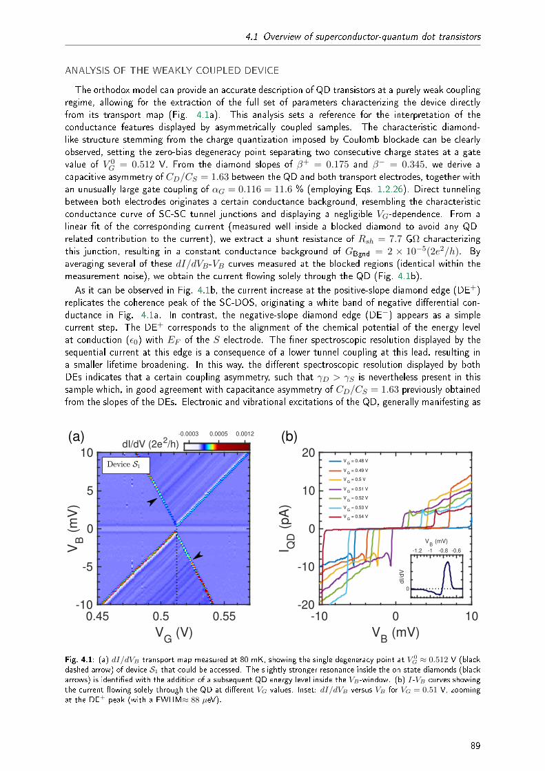
4.1 Overview of superconductor-quantum dot transistors
ANALYSIS OF THE WEAKLY COUPLED DEVICE
The orthodox model can provide an accurate description of QD transistors at a purely weak couplingregime, allowing for the extraction of the full set of parameters characterizing the device directlyfrom its transport map (Fig. 4.1a). This analysis sets a reference for the interpretation of theconductance features displayed by asymmetrically coupled samples. The characteristic diamond-like structure stemming from the charge quantization imposed by Coulomb blockade can be clearlyobserved, setting the zero-bias degeneracy point separating two consecutive charge states at a gatevalue of V 0
G = 0.512 V. From the diamond slopes of β+ = 0.175 and β− = 0.345, we derive acapacitive asymmetry of CD/CS = 1.63 between the QD and both transport electrodes, together withan unusually large gate coupling of αG = 0.116 = 11.6 % (employing Eqs. 1.2.26). Direct tunnelingbetween both electrodes originates a certain conductance background, resembling the characteristicconductance curve of SC-SC tunnel junctions and displaying a negligible VG-dependence. From alinear t of the corresponding current (measured well inside a blocked diamond to avoid any QD-related contribution to the current), we extract a shunt resistance of Rsh = 7.7 GΩ characterizingthis junction, resulting in a constant conductance background of GBgnd = 2 × 10⁻⁵(2e2/h). Byaveraging several of these dI/dVB-VB curves measured at the blocked regions (identical within themeasurement noise), we obtain the current owing solely through the QD (Fig. 4.1b).As it can be observed in Fig. 4.1b, the current increase at the positive-slope diamond edge (DE+)
replicates the coherence peak of the SC-DOS, originating a white band of negative dierential con-ductance in Fig. 4.1a. In contrast, the negative-slope diamond edge (DE−) appears as a simplecurrent step. The DE+ corresponds to the alignment of the chemical potential of the energy levelat conduction (ε0) with EF of the S electrode. The ner spectroscopic resolution displayed by thesequential current at this edge is a consequence of a lower tunnel coupling at this lead, resulting ina smaller lifetime broadening. In this way, the dierent spectroscopic resolution displayed by bothDEs indicates that a certain coupling asymmetry, such that γD > γS is nevertheless present in thissample which, in good agreement with capacitance asymmetry of CD/CS = 1.63 previously obtainedfrom the slopes of the DEs. Electronic and vibrational excitations of the QD, generally manifesting as
0.45 0.5 0.55
VG
(V)
-10
-5
0
5
10
VB
(m
V)
-0.0003 0.0005 0.0012
dI/dV (2e2/h)
-10 0 10
VB
(mV)
-20
-10
0
10
20
I QD
(p
A)
VG
= 0.48 V
VG
= 0.49 V
VG
= 0.5 V
VG
= 0.51 V
VG
= 0.52 V
VG
= 0.53 V
VG
= 0.54 V
-1.2 -1 -0.8 -0.6
VB
(mV)
0
dI/dV
(a) (b)
Fig. 4.1: (a) dI/dVB transport map measured at 80 mK, showing the single degeneracy point at V 0G ≈ 0.512 V (black
dashed arrow) of device S1 that could be accessed. The slightly stronger resonance inside the on-state diamonds (blackarrows) is identied with the addition of a subsequent QD energy level inside the VB-window. (b) I-VB curves showingthe current owing solely through the QD at dierent VG values. Inset: dI/dVB versus VB for VG = 0.51 V, zoomingat the DE+ peak (with a FWHM≈ 88 µeV).
89

4 Yu-Shiba-Rusinov states in superconductor-quantum dot transistors
additional lines inside the on-state diamonds, are probed at a higher resolution by the S lead, thereforeappearing only parallel to this diamond edge. The slight coupling asymmetry is also evidenced by thecurrent asymmetry displayed by the two on-state diamonds at ±VB around the single-level conductionregime (2∆ < |eVB| < Eδ + 2∆). The corresponding sequential currents at dierent bias polaritiesvaries over a range of I+QD ≈ 4 to 6 pA and I−QD ≈ −7 to -10 pA (Fig. 4.1b). We proceed now withthe identication of the energy scales:
Q The charging energy: It is only possible to give a lower limit for the value EU , as a singledegeneracy point is accessible in our gate voltage range of ±10 V. While it is tempting toconsider that the QD's level depth, ε0, increases uniformly with VG along such whole range, gateoset switches can introduce discontinuities in the ε0(VG) dependence (discussed in the followingsection). Sudden changes in the current background were observed at relative distances of 1.5and 0.6 V from V 0
G. By assuming a constant charging energy and gate coupling parameter, weobtain a minimum value of EU ≥ 1.5× αG = 174 meV.
Q The level spacing: Although many excitations are present in this device, that one intersectingthe diamond edges around VB = ±5 mV display a stronger intensity (marked with black arrowsin Fig. 4.1a). According to the expression derived in Ref. [1], a level spacing of Eδ ∼ 2π2~2
mkFV= 5
meV corresponds to a Au particle with a radius of about 3 nm. While this expression is onlyqualitatively correct, the order-of-magnitude agrees with the 5 nm of average size of the Auparticles in the commercial solution deposited in the samples.
Q The SC order parameter: The SC gap present in both leads generates a SC-induced spectro-scopic gap of magnitude ΩSC = 2∆S + 2∆D appearing around zero-bias in the characteristiccurves of the SC-QD-SC transistor, along the entire VG range of the transport map. Suchspectroscopic gap present an homogeneous value ΩSC = 1.00 meV in the device S1. Howeverthe SC gap of each lead cannot be extracted individually.
Q The thermal energy: A thermal energy of kBT = 7 µeV corresponds to the sample tempera-ture of 80 mK at which these measurements were acquired. The conductance peak integratingthe DE+ displays a FWHM of 88 µeV (see inset in Fig. 4.1b).
Q The tunnel couplings: From the direction of the coupling asymmetry (γD > γS) together withthe asymmetry of the sequential current at the single-level conduction regime (|I−QD| > |I
+QD|),
this degeneracy point would be ideally expected to be described by Eqs. 1.2.34, leading toa coupling asymmetry on the order of γD ∼ 10γS . However, the presence of such manyexcitations, together with the SC state of the leads, can introduce dramatic deviations fromthe simple sequential model. In general, the Green-function cotunneling model is required for aprecise determination of the couplings from measurements in the SC state of the junction [38].
TRANSPORT MAPS OF ASYMMETRICALLY COUPLED DEVICES
The pair of YSR resonances emerging inside the spectroscopic gap, ΩSC at one side of the degen-eracy point shown in the transport map of devices A1,A2,A3 and A4 (Fig. 4.2) reveals a strongcoupling asymmetry present in these junctions. The parity of the QD occupancy at both sides ofthe degeneracy point (respectively located at V deg
G = 0.4, 2.2,−0.8 and 4.12 V, indicated by blackdotted lines) can be determined straight away, as YSR resonances are caused by the competitionbetween superconductivity and Kondo eect, the latter exclusively manifesting at odd charge states.The conductance background measured well inside the even blocked diamond is respectively foundto be respectively being GBgnd = 6.5, 8.6, 0.4 and 1.1 in units of (2e2/h) × 10−4, corresponding toRsh ≈ 20, 15, 300 and 120 MΩ. The enhancement of cotunneling processes caused by Kondo eectat the odd blocked-diamond originates a conductance background with a slight dependence on VBand VG at the odd-parity side of V deg
G . While ΩSC is clearly identiable along the entire VG-range,the characteristic diamond structure appears blurred (clearly visible only in devices A1 and A4) andthe four DEs that integrate it display a strong asymmetry, being one of them much more intense than
90

4.1 Overview of superconductor-quantum dot transistors
0 0.2 0.4 0.6 0.8 1
VG
(V)
-10
-5
0
5
10
VB
(m
V)
-0.02 0.06 0.14
dI/dV (2e2/h)
0 1 2 3
VG
(V)
-6
-3
0
3
6
VB
(m
V)
-0.01 0.06 0.12
dI/dV (2e2/h)
-2 -1 0 1
VG
(V)
-4
-2
0
2
4
VB
(m
V)
0 0.0004 0.0009
dI/dV (2e2/h)
4 4.05 4.1 4.15 4.2
VG
(V)
-5
-2.5
0
2.5
5V
B (
mV
)
-0.002 0.005 0.012
dI/dV (2e2/h)
(a) (b)
(c) (d)
OddEven Odd Even
Odd Even OddEven
Fig. 4.2: dI/dVB maps as a function of VG and VB , measured in devices A1 (a), A2 (b), A3 (c) and A4 (d) at 80 mK,using the lock-in technique. A strong asymmetry in the coupling leads to the emergence of a pair of YSR resonances,which develop only at one side of the degeneracy points, V degG (black dashed line), indicating the odd parity of thecorresponding charge state. In all cases, the YSR display a crossing, signaling the gate position of the singletdoublettransition, V QPTG (red dashed line).
the others. In fact, it can be noticed that this enhanced DE appears always at the even charge state,either for positive (A2 and A4) or negative VB (A1 and A3). The origin of such asymmetries of theDEs is discussed in detail in section 4.2.1.The YSR states stick out as the most intense feature in the dI/dVB map of the four devices.
The bias position of the resonances display a certain gate dependence, in all cases making a kinkidentifying the gate position of the singletdoublet phase transition, or QPT (respectively located atV QPTG = 0.71, 0.4,−0.9 and 4.135 V, indicated by the red dotted lines). While the YSR resonances
surpass the gap edge, merging into the continuum DOS in samples A3 and A4, they remain belowthe SC gap in samples A1 and A2. Such distinct behavior can be linked to dierent relative values ofthe energy scales involved in the interplay between Kondo eect and superconductivity (EU ,∆ andγ), determining the location of the QPT boundary (illustrated in Fig. 1.23). As equivalent aluminumconstriction and metallic nanoparticles were employed in the fabrication of all the devices presented
91

4 Yu-Shiba-Rusinov states in superconductor-quantum dot transistors
in this chapter, we expect similar values of EU and ∆. Nevertheless, electromigration can introducelarge disparities in the coupling parameters from one sample to the other. Large EU/γ and ∆/γ ratioslead to the predominance of the doublet-GS phase, reducing the eective gate range of singlet-GSphase (between V deg
G and V QPTG ) and causing the YSR states to reach larger energies at the center
of the odd charge state, eventually surpassing the edges of the SC gap. A lower value of γ can thenbe attributed to devices A3 and A4, in comparison with devices A1 and A2, in good agreement withthe larger magnitude that the conductance features present in the two latter samples (see color scalesin Fig. 4.2). The faintness of the diamond structure caused by the enhancement of higher-orderprocess hinders the extraction of capacitive parameters and energy scales in asymmetrically coupledsamples. A relatively clear diamond structure is only present in device A1, allowing to identify thesubsequent electronic excitation (black arrow in Fig. 4.2a) of Eδ ≈ 6− 7 meV, similarly to device S1.The following sections are devoted to explain the methods employed to extract the energy scales ofsuch asymmetrical Kondo-weakly coupled samples from the transport measurements.
4.1.2 Electrostatic gate-oset switches
The apparison of stochastic charge-oset switches in QD junctions introduce random variations ofµQD, that result detrimental for the performance of the devices. Such switches are specially present inchemically-bounded molecular junctions, generally manifesting as stochastic jumps between dierentcharge states during the application of a relatively high VB. Several works have studied the subjectin detail, identifying restructurations of the molecule-metal interface as responsible for the switchingmechanisms [252]. While our samples are thought to be immune to such eects (as the QDs employedare not chemically linked to the electrodes but rather suspended in between them), a dierent kind ofcharge-oset switches, displaying a distinct behavior, appear commonly in QD transistors [253]. Gateswitches constitute one of our main limitations for the accessible VG-range and the sample-stabilityover a measurement.The equilibrium charge state of a QD transistor is determined by the number of electrons, N ,
present at the dot for VB and VG being set to zero. A certain oset, Noset, smaller than unity(0 < Noset < 1, appearing in Eq. 1.2.13) is typically present in actual devices, shifting the apparisonof a degeneracy point for a VG value dierent from zero. While such oset has been neglected in thederivation done in chapter 1, it can be accounted for by simply including a voltage-independent termof the form e2Noset/C in Eq. 1.2.28. In our devices, we observe sudden variations of Noset, alteringthe relative position of µQD in the VG coordinate, being highly recommended to keep VG stable, onlyvarying it slowly in between the acquirement of the I-VB curves for the measurement of a transportmap. Dierent manifestations of such gate switches show up in our devices, categorized as:
VG
(V)
VB (
mV
)
dI/dVB
VG
(V)
VB (
mV
)
dI/dVB
VG
(V)
VB (
mV
)
dI/dVB(a) (b) (c)
Fig. 4.3: Gate switches may manifest in the transport maps of our devices as purely stochastic (black arrows in a),occuring consistently at a certain VG value (black arrow in b), or a persistently over a measurement (c, device S3 wasmeasured in cryostat A and will be presented in Annex A).
92

4.2 Normal state characterization
Q Stochastic gate switches: Appear randomly during measurements and introduce a certainµQD-shift, as shown in Fig. 4.3a. They are attributed to charge trapped in the oxide layercovering the gate electrode, occasionally refraining after keeping the sample cold for long enough(one or two weeks). This behavior was consistently present in devices A3 and A4 (apparent inFig. 4.2c and d) making their characterization impossible in a reasonable time.
Q Permanent gate switches: Appearing consistently at a particular VG value, they are attributedto additional QDs around the nano-gap that change their charge state, modifying the electro-static environment of the conducting QD (Fig. 4.3b). These switches preclude measurementsabove/below the specic VG value, being the main reason that impede us to observe consecutivedegeneracy points in devices owning a large gate coupling.
Q Persistent gate switching: Involving typical times of a few seconds, they show up continuouslyover a measurement, typically inducing a switch in µQD between two close-by values (Fig. 4.3b).We ascribe this behavior to resist residues left over the sample surface, as it was found moreoften in devices kept under the protective resist layer for over a month or more.
4.2 Normal state characterization
The operation of Sionludi cryogenic setups allow to stabilize the sample environment either around4 K, or at the base temperature (80 mK for cryostat B). Although the N-state of our devices canbe accessed at 4 K, a great loss of the spectroscopic resolution, together with an increase of thebackground and noise, drastically reduces the measurement quality. To obtain well-resolved N-statetransport maps at base temperature, we applied a perpendicular magnetic eld (B) observing that,while certain SC-like features remain clearly visible for elds up to 40 mT (above the critical valuefor bulk Al of 10 mT, as expected for thin lms), superconductivity was totally suppressed at 60mT. Consequently, the YSR excitations present at the odd charge state of devices A1,A2 and A3
(Fig. 4.4a, b and c) turn into the characteristic Kondo resonance at zero-VB, appearing unperturbedat such low B values (Fig. 4.4d, e and f). While device A3 exhibits a faint resonance, stemmingfrom the relatively small value of γ in this sample, the prominent Kondo ridge arising in A1 and A2
allows for an exhaustive characterization of the Kondo phenomenon present in these devices. SampleA1 has been the subject of a more complete study, while we also include the analysis performed indevice A2 for comparison. The Kondo spectrum in these two samples is examined together with theasymmetries arising at the diamond edges, at the rst part of this section (4.2.1). Then, we comparethe conductance measurements of device A1 with NRG simulations that reproduced qualitatively thenite-bias asymmetries (4.2.3). Finally, we present the method followed for the extraction of kBTK ,determining its gate modulation (4.2.4).
4.2.1 Kondo spectrum analysis
The usual spectrum characterizing the Kondo eect appearing in a system composed by a magneticQD tunnel-coupled to a N-state lead consist in a resonance at VB = 0, as described by Anderson'smodel. The combination of Kondo eect with sequential tunneling originates strong asymmetries inthe intensity and width of the two DEs (DE± for ±VB) displayed in the I-VB or dI/dVB-VB curveat an even charge state. Actually, such asymmetries are present in the conductance maps of manyworks in the literature measuring dierent kinds of asymmetrically coupled QD junctions (like devicescontacting CNTs [14, 25, 43], NWs [42], molecules [107, 105] or semiconducting QDs [31]). Howeververy few of these studies focus on this aspect. Such asymmetries are specially remarkable in oursamples: out of the four edges conforming the diamond structure (DE+ and DE− both at the evenand odd side of charge degeneracy) only DE− at the even side constitute a well developed peak ofconductance in the N-state map of device A1 (Fig. 4.4d). Dierently, both DEs at the even side ofdevice A2 emerge as widely broadened peaks (Fig. 4.4e), hiding the odd-side DEs and surpassing theconductance of the zero-VB Kondo resonance.
93

4 Yu-Shiba-Rusinov states in superconductor-quantum dot transistors
0.2 0.4 0.6 0.8 1
VG
(V)
-2
-1
0
1
2
VB (
mV
)
-0.02 0.06 0.14
dI/dV (2e2/h)
-4 -2 0 2 4
VG
(V)
-1
-0.5
0
0.5
1
VB (
mV
)
0 0.06 0.12
dI/dV (2e2/h)
-0.2 0 0.2
VG
(V)
-0.5
0
0.5
VB (
mV
)
0 0.004 0.008
dI/dV (2e2/h)
0.2 0.4 0.6 0.8 1
VG
(V)
-2
-1
0
1
2
VB (
mV
)
0.001 0.012
dI/dV (2e2/h)
-4 -2 0 2 4
VG
(V)
-2
-1
0
1
2
VB (
mV
)
0.002 0.005
dI/dV (2e2/h)
-0.3 -0.2 -0.1 0
VG
(V)
-2
-1
0
1
2
VB (
mV
)
0.0002 0.0013
dI/dV (2e2/h)
(a) (b) (c)
(d) (e) (f)B = 60 mT B = 60 mT B = 60 mT
Fig. 4.4: dI/dVB maps of devices A1,A2 and A3 acquired at base temperature in the normal (respectively a, b andc, obtained by applying a perpendicular B-eld of 60 mT) and superconducting state (respectively d, e and f).
A dierent view illustrating this behavior is provided by slicing the transport maps into dI/dVB-VB curves at the dierent VG values (Fig. 4.5a). We proceed to characterize the resonance'sfeatures (the maximum value of the conductance peak, Gmax, and its full-width at half-maximum,FWHM) along its evolution from its appearance at zero-VB inside the odd diamond into the enhanced-DE at the even diamond2. As shown in Fig. 4.5b and c, the zero-VB resonance reaches stableline-shape well inside the odd diamond at both samples, where Gmax and the FWHM saturate,indicating the VG-range of the Kondo regime. While the Gmax of the zero-VB resonance (referred toas G0) is expected to reach values similar to the quantum of conductance, 2e2/h, for symmetricalcouplings, a strong renormalization of the conductance maximum is caused by the weakly-coupledlead. The corresponding expression for the maximum conductance of the zero-VB resonance derivedin Anderson's model (Eq. 1.2.48) can be approximated in the asymmetric-coupling limit (γ γW )as:
G0 =2e2
h
4γSγD(γS + γD)2
≈ 8e2
h
γWγ. (4.2.1)
A relation between the coupling parameters can be obtained by plugging the saturation value ofGmax at the Kondo regime, corresponding to G0 = 0.0125 for device A1 and G0 = 0.0015 for A2
(measured in units of 2e2/h), as seen in Fig. 4.5b and c. The respective relations obtained for bothsamples, γ ≈ 300γW and γ ≈ 2700γW .
2A constant conductance background of GBgnd = 1.4 × 10⁻³(2e2/h) was subtracted from the spectra of deviceA2, corresponding to the conductance baseline at the even diamond. The background is negligible for device A1.
94

4.2 Normal state characterization
-2 -1 0 1 2
VB
(mV)
dI/dV
B 0.2 0.4 0.6 0.8 1
VG
(V)
0
5
10
Gm
ax (
2e
2/h
x 1
0-3
)
0
1
2
3
FW
HM
(m
eV
)
-6 -4 -2 0 2
VG
(V)
0
1
2
3
4
5
Gm
ax (
2e
2/h
x 1
0-3
)
0
5
10
FW
HM
(m
eV
)
(a) (b)
(c) (d)
VGdeg
VGdeg
Diamondedge Zero-bias Kondo resonance
Zero-bias Kondo resonance
VG
= 0 V
VG
= 1 V
Fig. 4.5: (a) dI/dVB spectra at dierent VG for device A1 allowing for the extraction of the (b) gate-dependence ofthe corresponding resonance peak maximum and FWHM. (c) The same extraction performed in device A2. Verticaldashed lines indicate the position of charge degeneracy, V degG , separating even and odd charge states.
4.2.2 Coulomb diamond analysis in the normal state
While most of the studies focus on the Kondo regime, deep inside the odd charge state, a re-duced attention has been paid to the MV regime, around V deg
G , and to the characteristics of theCoulomb-diamond conductance structure. By taking into consideration the usual asymmetric-biasingconguration arranged in experiments (applying VB to the source lead, S, while keeping grounded thedrain lead, D) together with asymmetric tunnel and capacitive couplings, Aligia et al demonstrateddierent characteristics (Gmax, FWHM and VB location) are expected for the four DEs around a de-generacy point [254] (DE+ and DE−, appearing both at the even and odd side of V deg
G ). In their study,they consider a QD Kondo-coupled to D and weakly-coupled to S, described from the perspective ofAnderson's model. While the application of a voltage is considered to induce a positive displacementin the corresponding chemical potential at their work, we adopt the opposite convention here, takingµS = −eVB and µD = 0, allowing for a direct comparison with experiments. The chemical potentialof the QD, dened as the level depth with respect to the rst degeneracy point of an unoccupiedorbital in the QD (see section 1.2.4) can be expressed as
ε0(VB, VG) = µQD(VB, VG − V 0G) = −eαG(VG − V 0
G)− eαBVB = εG0 (VG) + εB0 (VB), (4.2.2)
separating its bias and gate components. As it is useful for understanding the following sections, weremind here the relation between the level depth and the distinct charge states of the QD, which issimplied as a single spin-degenerated orbital in Anderson's model: the rst even diamond extendsover EU > ε0 > 0 (corresponding to an empty orbital), the following odd diamond appears between0 > ε0 > −EU (corresponding to the half-lled orbital at which magnetic character arises), andthe next even diamond extends between −EU > ε0 > −2EU (where the double orbital occupancy isreached). These three charge states are consecutively separated by two degeneracy points, respectivelycalled V 0
G and V 1G and signaling the transitions empty→half-lled and half-lled→doubly-occupied.
95

4 Yu-Shiba-Rusinov states in superconductor-quantum dot transistors
0 0.2 0.4 0.6 0.8 1
VG
(V)
-2
-1
0
1
2
VB
(m
V)
0.001
0.006
0.012
dI/dVB
(2e2/h)(c)
(a) MV peak at VB
> 0 (b) STM peak at VB
> 0
(e) MV peak at VB
< 0(d) STM peak at VB
< 0
Fig. 4.6: Energy diagrams show-ing the energy-conguration of thechemical potentials at the four edgesthat integrate the diamond struc-ture of device A1 (indicated by blackdashed lines in c, obtained by the tsof the SC-state data shown in sec-tion 4.3.1). The degeneracy point,at V 0
G ≈ 0.4 V, corresponds to atransition of the QD occupancy fromempty to half-lled, implying a leveldepth variation from ε0 > 0 to ε0 <0. It can be deduced that the QDis strongly coupled to D, as a DE ofstronger intensity appears for VB < 0at the even side of V 0
G, identiedwith the STM peak described in Ref.[254]. Following this conclusion, it ispossible to assign the MV peak, de-ned at the alignment of the QD levelwith the Fermi level of the Kondo-coupled lead at µD (a and d), asthe diamond edge of negative slope(DE−), and the STM peak, whichdevelops for the alignment of ε0 withthe Fermi level of the probing lead atµS (b and e), as the diamond edgeof positive slop (DE+).
The above expression (Eq. 4.2.2) allows for the implementation the eect of a bias lever arm, αB,(as considered in the orthodox theory) into Anderson's model. While at zero bias, the level depth isxed at εG0 by VG, the application of a nite VB across the junction induces both a change in µSand a variation in ε0 with respect to its zero-bias value, of magnitude equal to εB0 , proportional toαB = CS/(CS + CD + CG) (ranging between 0 < αB < 1, acquiring values around 0.5 for ideallysymmetric capacitive couplings CS ≈ CD CG). Along the measurement of the characteristic curvesof the devices, ε0 is not xed but changes linearly with VB. The conductance peaks integrating theDEs (black dashed lines in Fig. 4.6c) appear when such oating level of the QD is aligned with µat one of the leads. Due to the coupling asymmetry, dierent kinds of tunneling processes appearbetween the QD and each lead, being necessary to distinguish between the DE at which ε0 is alignedwith µ of the strongly coupled lead (called MV peak, Fig. 4.6a and e) and the weakly coupled lead(called STM peak, Fig. 4.6b and d). The following expressions for the width and maximum value ofthese two peaks at particular VB values were obtained in Ref. [254] at the even diamond of a V 0
G-likecharge degeneracy, explicitly showing the dierent dependences of both peaks' features on αB:
MV peak at VB = +eαGVG/αBe
FWHM = 2γT /αBe,
Gmax = αBeCT /γT ,(4.2.3)
STM peak at VB = −eαGVG/(1− αB)e
FWHM = 2γT /(1− αB)e,
Gmax = (1− αB)eCT /γT ,(4.2.4)
where γT = γ + γW and CT = CS + CD + CG.
96

4.2 Normal state characterization
These theoretical results are obtained by considering a weak coupling of the QD to S and a strongcoupling to D, leading to αB < 0.5, at the even diamond on one side of the V 0
G-like degeneracy point.For such conditions, a higher and narrower STM peak was found to emerge at the even side of V 0
G
for VB < 03. The degeneracy point in device A1 is also V 0G-like, as the magnetic behavior appears
for higher VG values (burying the unoccupied level below µD, becoming half-lled). At the even side,DE− displays a much larger intensity and smaller width, emulating the theoretical results. Thus, wecan assign the strong coupling to the D lead in device A1, where S is the probing electrode. Whileconcluding that the more intense DE corresponds to the alignment of ε0 with µ of the weakly-coupledlead is rather counter-intuitive, the same kind of behavior is actually observed in device S1 found at thewell-understood weak-coupling regime (Fig. 4.1). The higher spectroscopic resolution stemming froma weaker coupling (implying a smaller life-time broadening) results in a replication of higher intensityof the divergent coherence peak at the weakly-coupled lead along DE+ (hence corresponding to theS lead also in this case), whereas the opposite DE− appears as a simple current step (revealed inthe transport map by the lack of a band of negative dierential conductance), as a consequence ofa stronger coupling to D that broadens the level too much to resolve the line-shape of its coherencepeaks.At the subsequent degeneracy point of V 1
G, the STM and MV peaks still corresponds to DE+ andDE− respectively , as it can be inferred from the work in Ref. [254]. Nevertheless, at the even sideof V 1
G, the STM peak appears at VB > 0 and the MV peak at VB < 0. In fact, the transport mapof sample A2 (Fig. 4.4d) shows that the QD occupancy transits from odd to even behavior as VG isincreased, identifying it as a change from half-lling to double occupancy of the resonant level and,therefore, recognizing the degeneracy point in this device as V 1
G-like. As the most intense DE at theeven side of V 1
G appears for VB > 0, we can conclude that the QD is, once more, strongly coupledto D and weakly-coupled to S in device A2. A strong coupling to S is found in devices A3 and A4
as it can be obtained by deducing the nature of the degeneracy point (respectively V 1G and V 0
G) andobserving the bias polarity at which the Kondo-enhance DE appears (Fig. 4.2c and d).
4.2.3 Comparison with NRG simulations
The Kondo model only provides an accurate description of the correlated QD-lead system aroundthe Kondo regime of the odd magnetic charge state, dened as −γ > ε0 > −(γ + EU ), but failsto describe it around the MV regime (close to V 0
G and V 1G) and at the even occupation diamonds.
Alternatively, the DOS of the system can be obtained from simulations based on the NRG methodalong the full level-depth range, from empty to double occupancy (between ε0 > 0 and ε0 < −EU ).In addition, the conductance of a Kondo-weakly coupled junction system can be computed as well,following dierent approaches. In a close collaboration with our research group, S. Florens carriedout several NRG simulations, obtaining the spectrum of the QD-lead correlated system, as well ascalculations of the corresponding conductance measured by a weakly-coupled electrode following themodel developed in Ref. [254]. Numerical results showed an accurate reproduction of the zero-biasexperimental data of device A1, allowing for a more precise determination of the EU/γ ratio presentin this sample, while a qualitative agreement was obtained at nite-bias for the consideration of abias lever-arm parameter.The NRG simulation maps the DOS of the QD-lead hybrid along the entire range of level positions
and energies for a relative scale of EU/γ = 6 (Fig 4.7b). The spectrum of the QD-lead system isobtained at each level-depth value, considering a xed level position at ε0 = εG0 . The correspondingconductance map (Fig 4.8a) was calculated by considering a probing lead at a biasing voltage, VB.In contrast to the xed level positions in the DOS-map, the conductance calculation accounts forthe otation of the QD level, as described in Eq. 4.2.2, imposing a bias lever arm of αB = 0.3.In this sense, the quantity, εG0 , in the horizontal axis of Fig 4.7a indicates the QD level position at
3The STM peak appears at positive VB in Ref. [254] due to the opposite sign of the chemical potential shift caused
by the biasing voltage, dening the level depth as ε0 = +eαGVG + eαBVB .
97

4 Yu-Shiba-Rusinov states in superconductor-quantum dot transistors
-2-101
0
G (E
U)
-1
0
1
eV
B (
EU
)0 15 30Conductance
(arb. units)
-2-101
0
G (E
U)
-1
0
1
Energ
y (
EU
)
1 15 30Density of states
(arb. units)
0 0.2 0.4 0.6 0.8 1
VG
(V)
-2
-1
0
1
2
VB
(m
V)
0.001 0.006 0.012
dI/dVB
(2e2/h)
0.2 0.4 0.6 0.8 1
VG
(V)
0
5
10
15
Gm
ax (
2e
2/h
x 1
0-3
)
0
1
2
3
FW
HM
(m
eV
)
NRG Gmax
Device Gmax
NRG FWHM
Device FWHM
(a) (b)
(c) (d)V
G0Diamond
edge Zero-bias resonance
Fig. 4.7: (a,b) NRG maps of the DOS and conductance (G) of a QD Kondo-coupled to a N-state lead, obtained for arelative energy scale of EU/γ = 6. A bias coupling parameter of αB = 0.3 was imposed for the calculation of the latterone. The region around V 0
G at the G-map (highlighted with a square) corresponds to the experimentally accessiblerange of device A1 (c). (d) The Gmax and FWHM values of the conductance resonance in the simulations is comparedwith the experimental data, showing signicant deviations around V 0
G (black dashed line) that sharpen at the DE.
VB = 0. In contrast, nite biases induce a linear deviation of εB0 in the level depth with respectto εG0 , tilting the map with a slope determined by αB with respect to the NRG-DOS map (thebottom-left and top-right corners lying out of the DOS-data range). For a direct comparison withexperiments, the level-depth axis is reversed in both graphs, corresponding to increasing values ofVG (as εG0 = −eαG(VG − V 0
G)). By comparing both numerical maps, it can be observed that theconductance replicates the zero-VB Kondo resonance in the NRG-DOS data at the odd charge state(0 > ε0 > −EU ), signaling the probing range of the asymmetrical QD junction. As the degeneracypoints, at εG0 = 0 (V 0
G) and εG0 = −1 (V 1G) are approached, the line-shape of the conductance
resonance starts to deviate from the DOS spectrum as sequential transport comes into play. At theeven charge states (ε0 > 0 and ε0 < −EU ) the resonance in theG-map evolves into a Kondo-enhanceddiamond edge (corresponding to the STM peak of Fig. 4.6d), appearing at approximately oppositeenergies than the Kondo resonance at the DOS (identied, in a junction conguration, with the MVpeak of Fig. 4.6a), reproducing the behavior displayed by our samples. In fact, the conductancecalculation is performed by considering a voltage, VB, applied to the weakly-coupled electrode (actingas S) while the QD is strongly coupled to the reference lead, D, emulating the conguration of deviceA1, and replicating its STM peak.
A substantial agreement with the experimental data (Fig 4.7c) is found at the corresponding rangeof numerical parameters, indicated by a gray square in Fig 4.7a. Both data sets can be comparedby adjusting the renormalization factor of the numerical conductance with the experimental height of
98

4.2 Normal state characterization
Fig. 4.8: (a) G-VG traces at VB = 0,obtained from NRG simulations fordierent values of the relative scaleEU/γ, are compared to the zero-bias conductance measured in de-vice A1 (renormalized with the max-imum conductance of the zero-VBresonance, G0 = 0.0125× (2e2/h)).The reference points chose for ad-justing the gate coupling are the cen-ter of the odd-diamond (extracted atVG = 1.08 V from the kBTK tshown in section 4.2.4) and the inter-ception of the NRG curves with theexperimental data at the midpoint ofthe Kondo ridge, G0/2.
the zero-VB resonance, as well as the adaptation of the horizontal axis by employing an experimentalgate lever arm of αG = 0.0089 and locating the degeneracy point at V 0
G = 0.40 V, as experimentallyextracted in section 4.3.1. While the saturation ofGmax → G0 and of the FWHM at the Kondo regimeis well-reproduced by the numerical conductance (Fig 4.7d), signicant deviations appear between theexperimental data and the simulations when approaching the degeneracy point, growing larger asthe even charge state is entered. This discrepancy is attributed to a certain disagreement betweenenergy scale and bias coupling considered (EU/γ = 6 and αB = 0.3) and the actual parametersin the device. Further NRG simulations were done for dierent EU/γ values. To avoid additionalinaccuracies induced by a diering bias coupling, we restrict the tting range to the conductancetrace at zero-VB (Fig. 4.8). The steepness displayed by the Kondo ridge formation in the sample ismissed by the NRG curve for EU/γ = 6. However the trace obtained for EU/γ = 9 captures thesefeatures, showing a quantitative agreement with the experimental data, xing the energy-scale ratiofor device A1. A slight overestimate of the conductance at the center of the diamond stems from thenite temperature of 80 mK at which the N-state map were acquired (just one order of magnitudebelow kBTK), as NRG simulations were done at the zero-temperature limit.
4.2.4 Extraction of the Kondo temperature scale
Changes in the line-shape of the zero-VB resonance at dierent VG indicates the variation of the Kondoenergy scale, which characterizes the amplitude of the Kondo correlations. Such gate modulation ofkBTK can be understood from its dependence on, ε0(VG, VB), appearing explicitly in the expressionderived by Haldane:
kBTK = C√γEU
2eπε0(ε0+EU )/2γEU , (4.2.5)
The precise value of the prefactor C depends on the relative scale of EU/γ and on the leveldepth, being well-dened (C = 0.182) only for EU γ and at the center of the odd charge state(for ε0 = −EU/2), where the system reaches the particle-hole symmetry. Actually, its value alsochanges if the spin correlations extend over both leads of the QD junction (in which case Kondoeect is brought out of equilibrium when applying a nite VB), or only one lead (conguration atwhich spectroscopy is performed). As these microscopic scales may not be easy to extract frommeasurements, numerous experimental works studying asymmetrically-coupled QD junctions at suchspectroscopic conguration take kBTK as the FWHM of the zero-VB resonance, sometimes multipliedby a prefactor smaller than unity (generally equal to 1/2). Alternatively, a more concrete criterion forthe experimental extraction of kBTK , regardless of the energy hierarchy present in the sample, lies inthe study of the temperature evolution of the zero-VB resonance maximum, Gmax.
99

4 Yu-Shiba-Rusinov states in superconductor-quantum dot transistors
-0.5 0 0.5
VB
(mV)
23456789
10111213
dI/dV
B (
2e
2/h
x 1
0-3
)
1
2
3
4
5
6
T (K) 0.4 0.6 0.8 1
VG
(V)
5
10
15
20
Gm
ax (
2e
2/h
x 1
0-3
)
T = 82 ± 0.5 mK
T = 102 ± 9 mK
T = 240 ± 20mK
T = 365 ± 18 mK
T = 503 ± 18 mK
T = 623 ± 15 mK
T = 939 ± 20mK
T = 3.39 ± 0.45 K
T = 5.53 ± 0.22 K
T = 6.74 ± 0.17 K
(a) (b)
Fig. 4.9: (a) dI/dVB-VB curves taken at dierent temperatures for a gate value of VG = 0.97 V. A non-uniform decayof the Kondo resonance with increasing temperature can be observed. (b) Gmax values forming the zero-bias Kondoridge along the VG range of the odd charge state, measured at dierent temperatures.
Exposing the strongly coupled lead to an external parameter favoring an specic electronic distri-bution (like voltage dierences, magnetic elds, temperature) have a disruptive eect on the Kondocorrelations induced by the QD. While our samples A1 and A2 have both been subjected to a biasvoltage and a magnetic eld for the acquirement of the N-state transport maps, these parameters arenot expected to disturb the formation of the Kondo cloud. On one hand, the VB applied does notgenerate a current through the strongly coupled lead that can perturb the Kondo eect, but the entirevoltage dierence essentially drops at the tunnel junction, keeping both leads a constant electrostaticpotential. On the other hand, the low B values between 60−75 mT applied to quench away SC at theleads originates Zeeman splittings of energies EZ = gµBB ∼ 1 µeV, in the same order of magnitudeas the thermal energy at the base temperature of the cryostat (kBT ≈ 7 µeV), both of them beenseveral orders below the actual Kondo energy of devices A1 and A2. Therefore, we can claim thatKondo eect in these two samples is at equilibrium. However, for increasing sample temperatures,the growing of electronic scattering rates in the metallic lead (∼ T 2) disturbs the screening cloud,eventually dissolving it for T TK . This eect manifest as a decline in the intensity of the zero-VBresonance in device A1 (Fig. 4.9a). In fact, we observe that such decay does not take over the Kondoresonance uniformly as the temperature is increased, limiting to a reduction of Gmax between 0.08-1.5K, and making the resonance to completely vanish above 2 K. Furthermore, the zero-VB resonanceexhibits a distinct reduction at dierent VG values along the odd diamond. The entire Kondo ridgemeasured at dierent temperatures is shown in (Fig. 4.9b). This data has been selected from a setof transport maps, measured at constant temperatures ranging from 80 mK to 6K while applying aconstant magnetic eld of 72 mT (see Fig.F.2 in Annex F).
The NRG simulations carried out by Costi et al [92], allowed them to demonstrate that the conduc-tance decay caused in the zero-VB resonance caused by a certain disruptive eect characterized by anenergy scale, Ex, depends exclusively on the ratio between this energy and kBTK . This constitutesthe main reason why kBTK is called an "universal" energy scale. Generic expressions of the formGmax(Ex) = G0 F (Ex/kBTK) characterize the evolution of Gmax, where the function, F , dependson the nature of the particular perturbation. Years later, Goldhaber-Gordon et al found an empiricalformula systematically tting the evolution Gmax(T ) in NRG simulations [100, 101], expressed as
100

4.2 Normal state characterization
0.1 1 10
T (K)
2
4
6
8
10
12
14G
ma
x (
2e
2/h
x 1
0-3
)
0.4 0.5 0.6 0.7 0.8 0.9 1
VG
(V)
0
2
4
6
8
TK
(K
)
0.01 0.1 1 10
T / TK
0.2
0.4
0.6
0.8
1
Gm
ax(T
) /
G0
Fit (s = 0.22)
VG
= 0.52 V
VG
= 0.57 V
VG
= 0.62 V
VG
= 0.67 V
VG
= 0.72 V
VG
= 0.77 V
VG
= 0.82 V
VG
= 0.87 V
VG
= 0.92 V
VG
= 0.97 V
(a) (b)
(c)
MV regime Kondo regime
Fig. 4.10: (a) Linear square ts of the temperature evolution of Gmax at dierent gate values are tted to Eq. 4.2.6using the least squares method. The colors identify the respective gate value. (b) Gate modulation of the Kondo scaleobtained from the ts. The accuracy of the tting formula is reduced at the MV regime, increasing signicantly theerror of the t. (c) The data in panel a, collapse onto a single curve after proper rescaling, coinciding with Eq. 4.2.6(black curve), indicating the nearness to the universal limit.
Gmax(T ) = G0
(T 2
T 2K
(21/s − 1) + 1
)−s, (4.2.6)
obtaining best ttings for a phenomenological parameter value of s = 0.22 (if the QD spin is equalto 1/2). For G0 = 0.0125× (2e2/h), we employed this formula to perform a t of the experimentalGmax(T ) at each VG value, adjusting the free-parameter, TK , by using the least-squares method (Fig.4.10a). The resulting Kondo temperature of device A1 is found to vary between 1-5 K, well insidethe VG-range of the odd diamond (Fig. 4.10b). A considerable error is obtained at the MV regime,as Eq. 4.2.6 is not strictly valid at such range, while the error bars inside the Kondo regime mainlystem from the measurement at a highest temperature. After adequate rescaling, the experimentaldata collapse on a single curve (Fig. 4.10c), which actually coincides with the theoretical black curve(Eq. 4.2.6). These facts demonstrate that the Kondo eect developing in device A1 approaches theuniversal regime and is in virtual agreement with NRG simulations, implying a standard Kondo eect.
101

4 Yu-Shiba-Rusinov states in superconductor-quantum dot transistors
0.5 1 1.5 2
VG
(V)
0.1
1
kB
TK
(m
eV
)
From Gmax
(T)
FWHM / 2.9
0 -2 -4 -6 -8 -10 -12 -140 (meV)
-10 -5 0
VG
(V)
0.1
1
kB
TK
(m
eV
)
(a) (b)
VGc
Fig. 4.11: (a) The FWHM of the zero-VB resonance measured in device A1 at base temperature displays an identicalVG-dependence as kBTK extracted from the ts of Gmax(T ). A parabolic t of Gmax(T ) (excluding the unframedmarkers lying at the MV regime) indicates the center of the odd diamond, at V cG (yellow marker). The precise relationbetween the level depth, ε0 (horizontal scale at the top of the graph) and VG could be established, for this sample,from the extraction of the gate coupling αG = 0.0089 and the degeneracy point V 0
G = 0.40 V in section 4.3.1. (b) Anidentical t was performed on the FWHM/2.9 data of device A2.
Contrarily to its usual application (the extraction of kBTK from the other microscopic scalesobtained via NRG), we considered to employ Haldane's formula (Eq. 4.2.5) to t the Kondo scaleobtained fromGmax(T ), as a method to estimate independently EU and γ. While the gate modulationof kBTK in Fig. 4.10b is not expected to follow rigorously this expression as its derivation is done fora strict universal limit, the agreement of the experimental data with Eq. 4.2.6 indicate the nearnessof device A1 to this regime. Such t can provide us additional information on the extension of theodd charge state, as Kondo eect displays an identical behavior between its center (at V c
G) and eachof both degeneracy points (V 0
G and V 1G). We rst extract the natural logarithm of Eq. 4.2.5, putting
into manifestation the parabolic dependence of kBTK on the level depth:
ln(kBTK) ∼(
π
2γEU
)ε20 +
(π
2γ
)ε0 + ln(const). (4.2.7)
The bias term of the level depth is not taken into consideration, as Gmax(T ) is measured atVB = 0, expressing it as ε0 = εG0 = −eαG(VG − V 0
G). The gate coupling factor, αG = 0.0089, andthe degeneracy point, V 0
G = 0.40 V, are extracted independently in section 4.3.1. By restricting thetted Gmax(T ) data to the Kondo regime (black-framed orange markers in Fig. 4.11a) a parabolic tof ln(kBTK) was performed using the least squares method, obtaining values of EU ≈ 12 meV andγ ≈ 2 meV. In addition, the minimum of the tting parabola signals the gate position of the centerof the odd-charge state, located at V c
G ≈ 1.08 V (yellow square in Fig. 4.11a).
Actually, we found that the FWHM of the Kondo resonance measured at base temperature followsan identical VG-dependence than kBTK , both data sets overlapping for a multiplicative factor ofkBTK = FWHM/2.9, indicating a variation of kBTK between 90-750 µeV (1-8 K), together withthe equivalence of both quantities close to the universal regime. The same multiplicative factor wasemployed to extract the Kondo scale of device A2 from the VG-dependence of its FWHM, obtaininga kBTK covering a range of 80-500 µeV (1-6 K), slightly below sample A1. An identical parabolic twas also performed, leaving αG as a tting parameter, as it could not be determined independentlyfor this sample. Energy scales of EU ≈ 11 meV and γ ≈ 1 meV, and a much smaller gate lever armof αG ≈ 0.0009 were obtained from the t, as well as the odd-diamond center, located at a gatevalue V c
G ≈ −4.0 V.
102

4.3 Superconducting state characterization
4.3 Superconducting state characterization
The pairing order established in the leads in the presence of superconductivity oppose to the formationof the Kondo cloud, caused by Kondo eect for an even parity of the QD occupations. The singlet anddoublet possible states of the QD-SC system conform its ground state (GS) and lowest excited state(LES), depending on the predominance of Kondo eect or superconductivity. The gate dependenceof the magnitude of the Kondo eect (via the level depth) makes possible to tune the system throughthe transition (QPT) from the singlet-GS phase to the doublet-GS phase, manifesting in the spectrumas a crossing of the YSR resonances at zero-energy. We start this section by performing a t of theCoulomb diamond edges of device A1, enhanced for the SC state of the leads (4.3.1). After that,we analyze the YSR spectrum and the evolution of its features for dierent gate voltages (4.3.2).Both studies, together with the analysis of the N-state data performed in the previous section enabledfor the determination of the ensemble of capacitances, relevant gate positions and energy scales insamples A1 and A2. Then, we study the response of the YSR spectrum in device A1 for increasingmagnetic B-eld (4.3.3) and temperatures (4.3.4).
4.3.1 Coulomb diamond analysis in the superconducting state
The strong variation of the SC-DOS on energy around the Fermi level introduce several changes inthe diamond structure appearing in the transport map for the SC state of the leads, as explainedin section 1.3.2. On one hand, shifts in the position of the DEs are caused by to the opening of aspectroscopic gap with an extension of ΩSC = 2(∆ + ∆W ) around zero-bias. In fact, the presence ofan energy gap at the SC leads makes possible to get rid of thermal broadening eects, as the amountof quasiparticles above the gap vanish exponentially for a sample temperature such that kBT ∆.On the other hand, the sequential current reproduces the divergences of the SC-DOS at the DEs,for the alignment of a discrete energy level in the QD with one the coherence peaks at one of theleads (Fig. 4.1). Not only thermal broadening is avoided, but spectroscopies are further sharpeneddue to such divergences, enhancing even more the resolution [38]. In good agreement with the abovediscussion, we systematically observe a considerable enhancement of the DEs intensities for the SCstate of the leads, with respect to those appearing in N-state measurements. Indeed, while the DEswere barely noticeable in the N-state data of device A1, they emerge clearly as local conductancemaxima in the transport map at the SC state, allowing to extract their location and obtain preciselythe gate value of V 0
G and some capacitive parameters of the junction from their slopes.A peak-detection algorithm was employed to extract the local conductance maxima in the transport
map of device A1 in the SC state, at the sectors of the four DEs (black dots in Fig. 4.12a). Linearts (dashed lines) allowed to obtain the precise location of the DEs, revealing the complete diamondstructure. By plugging the resulting slopes, of β+ = 0.0410 and β− = 0.0115, in Eqs. 1.2.26, weobtain a gate coupling parameter of αG ≈ 0.0089 ± 0.0001 ≈ 0.9%, and a coupling asymmetry tothe transport electrodes of CD/CS ≈ 3.5 ± 0.2, indicating a stronger capacitive coupling to D inagreement with our previous analysis showing a stronger tunnel coupling this lead. By zooming at thedegeneracy point area (Fig. 4.12b), it can be observed that the linear ts of the DEs at VB > 0 (dashedlines) and VB < 0 (dotted lines) respectively intersect at dierent gate values of VG = 0.396± 0.001and VG = 0.406±0.001 V. Such shift arises from the combination of the bias lever arm eect with theasymmetrical-biasing experimental conguration, explained in section 1.3.2, establishing the locationof charge degeneracy at the midpoint: V 0
G ≈ 0.401 V (indicated by a red cross). Considering now theposition of the odd diamond center at V c
G ≈ 1.08 V, taken as the minimum value of the parabolict of ln(kBTK) (indicated by a yellow diamond in Fig. 4.11a), the subsequent degeneracy point isexpected to be found at V 1
G = V 0G + 2(V c
G − V 0G) ≈ 1.76 V. The entire odd-diamond structure can
be reconstructed by duplicating the DEs' lines at V 1G. Furthermore, by subtracting half the total gap
ΩSC/2 from the bias component of each t, the two lines of equal slope at each degeneracy pointcollapse into a single one that signals the DE appearing for the N state of the leads (illustrated in Fig.4.12c and included in the N-state transport map shown in Fig. 4.6c). The resulting charging energy,
103

4 Yu-Shiba-Rusinov states in superconductor-quantum dot transistors
0 0.2 0.4 0.6 0.8 1
VG
(V)
-10
-5
0
5
10V
B (
mV
)-0.02 0.06 0.14
dI/dV (2e2/h)
0.3 0.35 0.4 0.45 0.5
VG
(V)
-1
-0.5
0
0.5
1
VB
(m
V)
-0.02 0.06 0.14
dI/dV (2e2/h)
0 0.5 1 1.5 2 2.5
VG
(V)
-15
-10
-5
0
5
10
15
VB
(m
V)
(a) (b)
(c)V
G0 V
Gc V
G1
Fig. 4.12: (a) dI/dVB map of device A1 in the SC state, acquired at base temperature at zero B-eld. Linear ts(dotted lines) of the extracted local conductance maxima (black dots) indicate the location of the DEs. (b) Zoom-in atthe degeneracy-point area, showing the intersection of the linear ts of the DEs at VB > 0 (dashed lines) and VB < 0(dotted lines) with the SC gap edges at VG = 0.396 V and VG = 0.406 V, respectively, allowing to extract precisely theposition of V 0
G as the mid point at VG = 0.401 V (red cross). (c) Taking as a reference the center of the odd diamondat V cG ≈ 1.1 V (indicated with the yellow marker, as in Fig. 4.11a), the position of V 1
G is extrapolated at VG ≈ 1.76 V.The entire odd diamond can be reconstructed by duplicating the linear ts at V 1
G (here, ΩSC/2 has been subtractedfrom the vertical component of each t, collapsing the four lines at the two DEs measured in the N state).
extracted either from the gate distance between both degeneracies as EU = −eαG(V 0G−V 1
G), or fromthe half-height of the diamond, collapse to a value of EU = 12.2±0.2 meV. By combining its denition,EU = e2/(CS+CD+CG) (Eq. 1.2.18), with the expressions for the diamond slopes, it is then possibleto extract values for the particular capacitive couplings: CD ≈ 3.5 CS ≈ 85.6 CG ≈ 1.01 × 10⁻¹⁷
F, and the bias coupling parameter: αB = CS/(CS + CD + CG) ≈ 0.22. From the relative scaleof EU/γ ≈ 9 obtained from the comparison of the N-state data with NRG simulations, we derivea strong coupling between the QD and the Kondo-coupled electrode of γ ≈ 1.4 meV. Finally, thecoupling ratio given by the renormalization of the zero-VB Kondo resonance (Eq. 4.2.1) results in aweak coupling of γW = γ/300 ≈ 5 µeV.While the characterization of the Kondo resonance and the derivation of the gate modulation
of kBTK could be also performed in device A2, the DEs at the odd side of the degeneracy pointaccessed in this device are completely buried, making impossible to repeat the linear ts in this sample.
104

4.3 Superconducting state characterization
Device αG αB CG (F) CS (F) CD (F) V 0G (V) V c
G (V) V 1G (V)
A1 0.0089 0.22 1.18× 10⁻¹⁹ 2.88× 10⁻¹⁸ 1.01× 10⁻¹⁷ 0.401 1.08 1.76
A2 ∼ 0.0009 - - - - −10.2 −4 2.2
Tab. 4.1: Experimentally extracted capacitive parameters and particular gate voltages.
The demanding NRG simulations (in terms of computational power) were restricted to the specicparameter range of device A1. Nevertheless, a similar EU/γ ratio was attributed to sample A2,stemming from the resemblance of the energy dispersion of the YSR resonances (Fig. 4.2a and b),and in agreement with the parabolic t of ln(kBTK) leading to EU ≈ 11 meV, γ ≈ 1 meV andαG ≈ 0.0009 and V c
G ≈ −4.0 V for this device. Based on such gate coupling and diamond centerposition, together with the position of the accessible degeneracy point in this device (V 1
G ≈ 2.2 V),we can estimate the location of the out-of-range degeneracy point as V 0
G = V 1G− 2(V 1
G−V cG) ≈ 10.2
V, which fullls the relation of EU = eαG|V 1G − V 0
G| for the estimated values of EU and αG. All theextracted capacitive parameters and energy scales are respectively summarized in Tabs. 4.1 and 4.2.
4.3.2 Yu-Shiba-Rusinov spectrum analysis
We center our attention now on the characterization of the YSR resonances, measured at basetemperature (around 80 mK) and in the absence of an external B eld. As VG is tuned inside the odddiamond, the YSR resonances detach from the edge of the total spectroscopic gap, ΩSC , appearingat almost perfectly symmetric bias positions (V Y SR
B ). While the conduction is completely suppressedbelow the resonances, for |V Y SR
B | > |VB| ≥ 0, a band of negative dierential conductance appearsbetween the YSR resonances and the total spectroscopic gap, for ΩSC/2e > |VB| > |V Y SR
B |, asa consequence of the SC-DOS at the probing lead (clearly observed in Fig. 4.13a). The value ofthe total spectroscopic gap, ΩSC = 2(∆ + ∆W ), appears around zero bias at the "even side" ofcharge degeneracy, where the entire SC spectral function is accumulated at the coherence peaks. Incontrast, the YSR emerging at the "odd side" absorb most of this spectral function, greatly reducingthe sharpness and intensity at the edges of ΩSC . Extremely sharpened YSR resonances4 arise in
-0.75 -0.5 -0.25 0 0.25 0.5 0.75
VB (mV)
-0.05
0
0.05
0.1
0.15
dI/dV
B (
2e
2/h
)
-0.75 -0.5 -0.25 0 0.25 0.5 0.75
VB (mV)
0
0.02
0.04
0.06
0.08
0.1
0.12
dI/dV
B (
2e
2/h
)
230 240 250 260
VB ( V)
(a) (b)W/e-
W/e-( +
W)/e ( +
W)/e
Fig. 4.13: (a,b) dI/dVB-VB curves of devices A1 and A2 acquired at the corresponding QPT gate positions ofV QPTG = 0.71 and V QPTG = 0.4 V. The vertical, gray, dashed lines in (a) indicate the extraction of ∆ and ∆W fromthe peak-to-peak distances. The inset zooms into the YSR resonance delimited by the gray rectangle in (b).
4Reliable measurements of the YSR resonance heights required a reduced VB sweeping speed of 1 µV/s
105

4 Yu-Shiba-Rusinov states in superconductor-quantum dot transistors
2W
2(
+W
)
0.2 0.4 0.6 0.8 1
VG
(V)
-0.6
-0.4
-0.2
0
0.2
0.4
VB
(m
V)
-0.02 0.06 0.14dI/dV
B (2e2/h)
0.2 0.4 0.6 0.8 1
VG
(V)
-0.2
-0.1
0
0.1
0.2
EY
SR
(m
eV
) EYSR+
EYSR-
1.5 1 0.7 0.5 0.4kB
TK
/
0.2 0.4 0.6 0.8 1
VG
(V)
0
0.05
0.1
0.15
0.2
GY
SR
(2
e2/h
) GYSR+
GYSR-
1.5 1 0.7 0.5 0.4kB
TK
/
(a) (b)
(c)
Fig. 4.14: (a) dI/dVB map of device A1 zooming at the YSR resonances, allowing to extract their energy dispersion(b) and evolution of their peak intensity (c) as a function of gate voltage, or equivalently, kBTK scale. The verticaldashed line indicates the position of V QPTG , corresponding to the characteristic curve shown in Fig. 4.13a.
2W
2(
+W
)
-6 -4 -2 0 2 4
VG
(V)
-0.6
-0.4
-0.2
0
0.2
0.4
0.6
VB
(m
V)
0 0.06 0.12dI/dV
B (2e2/h)
-6 -4 -2 0 2 4
VG
(V)
-0.4
-0.2
0
0.2
0.4
EY
SR
(m
eV
)
EYSR+
EYSR-
0.25 0.4 0.7 1.5kB
TK
/
-6 -4 -2 0 2 4
VG
(V)
0
0.05
0.1
0.15
GY
SR
(2e
2/h
)
GYSR+
GYSR-
0.25 0.4 0.7 1.5k
BT
K/
(a) (b)
(c)
Fig. 4.15: (a) dI/dVB map of device A2 zooming at the YSR resonances, allowing to extract their energy dispersion(b) and evolution of their peak intensity (c) as a function of gate voltage, or equivalently, kBTK scale. The verticaldashed line indicates the position of V QPTG , corresponding to the characteristic curve shown in Fig. 4.13b.
106

4.3 Superconducting state characterization
Device EU (meV) Eδ (meV) kBTK (µeV) ∆ (µeV) ∆W (µeV) γ (µeV) γW (µeV)
A1 12.2 5-7 90-750 248 203 1400 5
A2 ∼ 11 - 80-500 327 238 ∼ 1000 ∼ 0.4
Tab. 4.2: Experimentally extracted energy scales.
device A2 which has a lower value of γW with respect to device A1, displaying a FWHM between8-9 µeV (Fig. 4.13b). Such reduced line-width demonstrate the spectroscopic power of all-aluminumelectromigration junctions contacting metallic nanoparticles, allowing us to probe the YSR spectrumwith an unprecedented resolution.
YU-SHIBA-RUSINOV SPECTRUM DEPENDENCE ON THE GATE VOLTAGE
The dependence of the YSR resonances on VG can be appreciated in transport maps of devices A1
and A2 zooming at a low-VB range (Figs. 4.14a and 4.15a, respectively). The bias position, V ±Y SRB ,and the maximum conductance of both resonances were extracted along the accessible range byemploying a peak-detection homemade algorithm. The crossing of the YSR states at zero-energydoes not manifest as a crossing at zero-bias of the resonances due to the gapped SC-DOS at theprobing electrode. Instead, |V ±Y SRB | decreases when VG is swept from the degeneracy point into theodd charge state, until it makes a kink at a minimum VB. This feature identies the gate locationof the QPT, V QPT
G , where the singletdoublet GS transition takes place, obtaining V QPTG ≈ 0.7 for
device A1 and V QPTG ≈ 0.4 for device A2 (vertical dashed lines). Furthermore, the value of the SC
gap in the probing lead, ∆W , can be determined independently from the peak-to-peak distance ofthe YSR resonances in the spectrum acquired at V QPT
G (Fig. 4.13a). The extraction of ∆W at thecrossing point also allows to determine the SC gap of the correlated lead, ∆, from the measurementof the total spectroscopic gap ΩSC . The values of ∆ and ∆W obtained (indicated by vertical dashedlines in Fig. 4.13a) are given in Tab. 4.2, together with the other energy scales extracted in previoussections. Like this, the energies of the YSR states, E±Y SR, can be extracted by subtracting ∆W fromV ±Y SRB , taking into account the sign inversion at the transition5 (Figs. 4.14b and 4.15b). Minutedeviations of E±Y SR occurring at certain gate voltages (at VG ≈ 0.5 and 0.92 V for device A1 andVG ≈ 0.8 and -3.4 V for device A2), were systematically present in all measurements acquired andare attributed to slight but persistent gate switches. Then we associate the conductance maximaextracted, to the corresponding YSR state at E±Y SR, obtaining the gate-dependence of their peakintensities, G±Y SR (Figs. 4.14c and 4.15c). These peak intensities correspond to the spectral weightsof the YSR states, w±, renormalized by the tunnel coupling of the probing lead, γW . As in our case,the probing lead is in the SC state, the divergences at the coherence peaks enhance the intensity ofsuch spectral features in the conductance measurement with respect to the rest of the spectra. Itis therefore necessary to deconvolute the SC-DOS of the probe for obtaining precise values of w±.However, we lack the tools for performing such treatment.Keeping in mind that the Kondo energy scale is only approximately the parameter driving this
transition, the correspondence between kBTK and VG (Fig 4.11) is employed to derive the critical valueof kBTK/∆ in devices A1 and A2 (orange axis in Figs. 4.14 and 4.15) found at (kBTK/∆)c ≈ 0.67and 0.69, fairly coinciding for both samples (given the similarities in EU , γ and ∆) and consistent withexperiments on self-assembled QDs [12] (that also extract kBTK from the temperature dependenceof the zero-bias Kondo conductance). By taking the Kondo scale as the FWHM/2 of the Kondoresonance, the YSR crossing point would be displayed around (FWHM/2∆)c ≈ 0.97 and 1.00, ingood agreement with STM studies of magnetic molecules on SC substrates [10, 165, 147], as theSC-QD-SC systems in these works are very similar to those we obtained with our electromigrationjunctions (characterized by a large charging energy and an intermediate-coupling regime). The data
5Note that at the singlet phase, E±Y SR = eV ±Y SRB ∓∆W , whereas at the doublet phase, E±Y SR = eV ∓Y SRB ±∆W ,relating each YSR state with the resonance of opposite bias sign due to their crossing at the QPT.
107

4 Yu-Shiba-Rusinov states in superconductor-quantum dot transistors
can also be rescaled to the theoretical denition of the Kondo energy (Eq. 4.2.5, using a constantprefactor of C = 0.182 for the entire odd-diamond range), which leads to (kBTK/∆)theoc ≈ 0.26.While predictions based on NRG simulations that implement such denition obtain a critical valuearound 0.3− 0.4 [113, 164, 158], the discrepancy is attributed to the reduced value of EU/γ in ourdevices, constituting a regime where Eq. 4.2.5 is not strictly applicable.
Notably, multiple fainting replicas of the YSR states appearing for |VB| > |V Y SRB | can be observed
in the conductance map of device A2 (Fig. 4.15a). As mentioned at the end of section 1.3.1 structuraldisorder can lead to the apparison of spiky features at the DOS in the bands of aluminum, in principle,remaining at the SC state and appearing at energies above the gap in the quasiparticle DOS. Suchirregular DOS can explain these additional features, relating them with a measurement artifact of theprobe and emerging above the conductance baseline due to the high spectroscopic resolution of thissample.
PRECISE EXTRACTION OF THE GATE POSITION AT THE TRANSITION
For a precise extraction of the energies of the YSR states and the gate location of their crossing atthe QPT, it is necessary to take into consideration the gating eect of the probing lead. The niteenergy of the YSR states, E±Y SR, requires the application of a nite bias, V ±Y SRB , to observe thecorresponding resonances. By applying such VB the level depth, ε0, is displaced from its zero-biasvalue xed by VG at εG0 = −eαG(VG− V 0
G), by an amount equal to εB0 = −eαBV ±Y SRB (Eq. 4.2.2).Consequently, the level depth is slightly dierent for the two YSR resonances measured at V +Y SR
B andV −Y SRB in the characteristic dI/dVB-VB curve acquired at a constant VG. In fact, the absolute valuesof V +Y SR
B and V −Y SRB measured in sample A1, do not overlap completely (Fig. 4.16a) due to suchotation of the QD's energy level. For correcting the shear caused in the measurements by the biaslever arm, the VG coordinate of each data points is to be replaced by the value of the bias-dependentlevel depth, as eαG(VG−V 0
G) +αBV±Y SRB , transforming the horizontal axis into −ε0. By employing
the value of αB ≈ 0.22 previously derived for device A1, we can correct the shear eect of such biascoupling, leading to the collapse of the energies of both YSR states into a single curve (Fig. 4.16b).Such treatment allows for a more accurate extraction of ∆W and ∆ in this device, and for the ttingof E±Y SR with calculations based on the renormalized YSR theory developed in Ref. [162] (see thesupplemental material on Ref. [44] for further information). The previously obtained energy scalesof sample A1 were employed in these calculations, carried out by S. Florens in a close collaborationwith our research group, showing a very good agreement with the experimental data (black line inFig. 4.16c). The theoretical curves, adjusted by taking the references set by the particular gate values
0 0.2 0.4 0.6
VG
- VG0 (V)
0.2
0.25
0.3
0.35
0.4
|VBY
SR
| (m
V)
0 2 4
-0 (meV)
0
0.05
0.1
0.15
0.2
|EY
SR
| (m
eV
)
0 5 10
-0 (meV)
-1
-0.5
0
0.5
1
EY
SR
(m
eV
)
EYSR+
EYSR-
model
2.6 2.8 3
-0 (meV)
(a) (b) (c)
Fig. 4.16: (a) Absolute bias positions of the YSR resonances versus gate voltage. The two curves are not overlappingas a consequence of the shear induced in the measurement by the bias lever arm. (b) The separation between the twocurves disappears when plotted against the level depth, correspondingly calculated by taking into account the nite biasat which each data point was measured. (c) The YSR energies are well tted by the model developed in Ref. [162].
108

4.3 Superconducting state characterization
of the degeneracy point, V 0G = 0.401 V, and the center of the odd diamond, V c
G = 1.08 V (yellowmarker), reproduce the experimental data within a small error, enabling us to increase the precisionof the QPT gate value, roughly obtained to be around 0.7 V in the previous analysis. The modeldisplays the zero-energy crossing point taking place in a range of −εQPT0 ≈ 2.7 − 2.75 (see inset inFig. 4.16c), or equivalently, V QPT
G = −eαGεQPT0 ≈ 0.705− 0.71 V.
4.3.3 Magnetic eld dependence of the YSR spectrum
Once the transport characteristics of the Kondo-weakly coupled devices have been analyzed andunderstood, we move towards studying the eect that the external magnetic eld exerts on the YSRspectrum. This study was conveniently restricted to device A1, as more complete and precise set ofenergy scales and physical parameters could be extracted for this sample. We start this examination bymeasuring the VG-VB transport map of this sample at several constant B-elds (the raw data is shownin Fig.F.3 in Annex F), allowing us to extract the gate dependence of the energy of the YSR statesand intensities of both conductance resonances for each B-eld value (Fig. 4.17a and b, respectively).Equivalently to the analysis performed at zero-eld in the previous section, we start by extracting thevalues of ∆W and ∆, respectively from the resonances' crossing point at the QPT, and the totalspectroscopic gap (ΩSC = 2∆+2∆W ) measured at the even side of V 0
G (Fig. 4.17c). The SC energygaps at both leads remain stable for low B-eld values (presenting a tiny increase, attributed to theSC-DOS broadening induced by the B eld [255]), starting to decay above 20 mT. The energies ofthe YSR states were equivalently obtained by subtracting ∆W from the experimental data. As theeect of a magnetic eld was not implemented in the calculations previously employed to t the gatedependence of E±Y SR at zero eld (shown in Fig. 4.16c), spline interpolations on E±Y SR(VG) wereperformed (solid lines in Fig. 4.17a), improving the precision of the limited gate resolution of themeasurements for the extraction of V QPT
G (vertical black lines). The evolution of V QPTG with B eld
(Fig. 4.17d) is caused, in rst instance by the gradual suppression of superconductivity, which reducesthe eective pairing energy, ∆, and consequently, the value of kBTK at which the transition takesplace, as the critical value of the relative scale kBTK/∆ (found to be about 0.67 for sample A1) isexpected to remain constant. In fact, the reduction of ∆ above 20 mT eectively drives the QPT tohigher values of VG (or lower values of kBTK) towards the center of the odd diamond. However, itcan be observed that, at low B elds, V QPT
G moves towards the opposite direction, tracing a slight butclear upturn that crosses with the zero-eld value around 14 mT. Such eect arises as a consequenceof the Zeeman splitting of the doublet state.With the application of an external magnetic eld, the two spin projections of the doublet state
are Zeeman-split into at energies of EZ = ±gµBB/2 (where µB is Bohr's magneton and g is theLandé factor). If the SC-QD system is tuned into the doublet-GS phase and subjected to an externalB eld, the spin at the QD lies in the spin conguration of lowest energy (at equilibrium and lowtemperatures such that kBT EZ). As the excitation of the system with the probing lead (reachingthe corresponding YSR resonance by applying a certain bias) involves the injection/extraction of anelectron from the QD, the fermionic parity of the system changes, and only the singlet-like LES canbe accessed but not the higher-energy spin projection of the doublet. In contrast, at the singlet-GS phase, both spin projections can be reached by exciting the system with a N-state probe at|eVB| = E±Y SR ± EZ . Consequently, the conductance resonances can appear split, for a strongenough Zeeman eect and a suciently ne spectroscopic resolution. This has been previouslydemonstrated in SC-QD systems made by contacting semiconducting NWs [29, 41, 42], thanks tothe large Landé factor (g ∼ 20). While the SC materials employed in these studies was rather robustagainst the external magnetic eld necessary to observe well-split resonances, superconductivity rapidlyvanishes in our aluminum junctions. Moreover, several studies on QD junctions contacting metallicnanoparticles of dierent materials and sizes in the range of a few nanometers present a certainvariability in the g factors, in general being always lower than 2 [2, 256, 76]. In fact, previousexperiments carried out within our group [38] obtained a Landé factor of g ∼ 1.7 for devices madewith the same gold nanoparticles employed here. Therefore, the combination of such reduced values
109

4 Yu-Shiba-Rusinov states in superconductor-quantum dot transistors
0.4 0.6 0.8 1
VG
(V)
EY
SR
B = 0 mT
B = 3 mT
B = 6 mT
B = 9 mT
B = 12 mT
B = 15 mT
B = 18 mT
B = 21 mT
B = 24 mT
B = 27 mT
B = 30 mT
VGQPT
0.4 0.6 0.8 1
VG
(V)
Peak Inte
nsity
0 10 20 30 40 50
B (mT)
0
50
100
150
200
250
300
Superc
onducting g
ap (
eV
)
W
SC/4
0 10 20 30
B (mT)
0.65
0.7
0.75
0.8
0.85
0.9
0.95
VGQ
PT (
V)
(a) (b)
(c) (d)
Fig. 4.17: (a) Gate-dependence of the energies of the YSR states and intensities of the corresponding resonancesat dierent B elds. Precise values of V QPTG (vertical black lines) are extracted from the crossing point of splineinterpolations (solid lines) of the experimental data (dots). A vertical displacement of the curves has been articiallyintroduced for clarity. (c) Closening of the SC gaps in the weakly- (∆W ) and strongly-coupled (∆) electrodes, as wellas the total spectroscopic gap measured at the even diamond gate range (ΩSC). (d) The gate location of the QPT atdierent B-elds, delimits the boundary in the phase diagram.
110

4.3 Superconducting state characterization
E
VG
0
VQPTG
(B) VQPTG
(B=0)
continuum
singlet
doublet (B=0)
Zeeman split (B) singlet
doublet (B=0)spin-polarized (B)
kB
TK
/
0.65 0.7 0.75
VG
(V)
-0.03
-0.02
-0.01
0
0.01
0.02
0.03
EY
SR
(m
V)
B = 0 mT
B = 9 mT
B = 15 mT
0 5 10 15 20
B (mT)
0.65
0.7
0.75
VGQ
PT (
V)
(a)
(b) (c)
Fig. 4.18: (a) Sketch of level structure of YSR states at zero magnetic eld (continuous lines) and nite (dashed lines)magnetic eld, in vicinity of the ground-state transition. (b) Zoom in at low energies of E±Y SR at three dierent valuesof B eld, evidencing the oscillation of V QPTG (indicated by black arrows) moving from one side of its zero-eld valueto the other. (c) Zoom in at a low B eld range of the phase diagram shown in Fig. 4.17d. The horizontal dashed linecorresponds to the gate position of the measurements shown in Figs. 4.19 and 4.20, traversing the phase boundarytwice at elds around 4 and 12 mT.
of g with the relatively small B eld that our SC leads can tolerate makes dicult to detect thesplitting of the YSR resonance peaks. However, the upturn delineate by the critical gate voltage,V QPTG (B), can be understood from this perspective. Indeed, because one of the spin projections of
the doublet LES has a lower energy, the singlet-GS phase gradually shrinks, translated into a criticalvalue of VG moving to lower values (Fig. 4.18a and b). Such tendency can be clearly observedby zooming at the low-eld range of the phase-diagram of Fig. 4.17d (shown in Fig. 4.18c). Asthe magnetic eld is further increased, the reduction of the superconducting gap comes into play,with a quadratic-on-B dependence [255], overcoming the linear behavior of the Zeeman splitting andresulting in an increasing tendency of V QPT
G at higher elds.The magnetic-eld-induced oscillation of the phase boundary can, hence, be qualitatively explained
as a result of the complex competition between the the gap reduction and the Zeeman splitting ofthe doublet state [44]. Nevertheless, the underlying physics of our particular system appear to bemore complex. On one hand, it might seem reasonable to simplify the B-eld eect as inducing a
111

4 Yu-Shiba-Rusinov states in superconductor-quantum dot transistors
variation on a single microscopic scale of the system, equating EZ at 10 mT with the level-depthvariation corresponding to the displacement of V QPT
G from its zero-eld value (around 0.707 V) toits value at the lowest point of the upturn (around 0.690 V). However, this calculation leads toridiculously large values of g, implying that the eect that the B-eld exerts on the system goesbeyond the mere splitting of the energy level in the dot. On the other hand, intriguing behaviors areobserved at the singlet-GS phase, where an important increase of the conductance maximum of theYSR resonance appearing at negative bias, V −Y SRB , gradually takes place as the B eld is increased,while the resonance at V +Y SR
B remains almost unchanged (as it can be appreciated in Fig. 4.17b).A manifest inversion of the relative intensity of V +Y SR
B and V −Y SRB occurs at the degeneracy pointfor B ≈ 6 mT, advancing towards the center of the odd diamond as B is increased and becoming thedistinctive feature indicating the vicinity of the QPT. Similar inversions of the relative spectral weighthave been previously observed as a function of the impurity distance in STM measurements, linked todistance-dependent asymmetries in the particle and hole-like components of the YSR wavefunction.Unfortunately, no time was left over my thesis project to perform a more detailed analysis of theseaspects.
STUDY OF THE RE-ENTRANT PHASE BOUNDARY
To further examine the particular upturn traced by V QPTG (B), we tuned the system into the singlet-
GS phase at VG = 0 V, very close to V QPTG (B = 0) ≈ 0.705−0.71 V, and measured its characteristic
conductance at B elds from 0 up to 60 mT (Fig. 4.19), following the horizontal dashed line in Fig.4.18c. The resulting dI/dVB-B map shows the continuous evolution of the spectrum from the SC tothe N state of the leads, reached for B > 55 mT. The total spectroscopic gap is progressively reduced,as superconductivity in the leads vanishes, diminishing the values of ∆ and ∆W , and broadening theSC-DOS prole. The YSR resonances decrease in amplitude and widen, showing a clear reductionof EY SR above 40 mT until they collapse into the much less intense Kondo resonance at zero-bias,right below 60 mT.At rst sight, the position of the YSR resonances, appearing at positive and negative bias (re-
spectively labeled as V +Y SRB and V −Y SRB ), is rather symmetric with respect to zero, despite small
deviations caused by the bias lever arm. However a closer inspection of the two conductance peaksreveals that, while V +Y SR
B remains almost invariant for low B elds showing a slight increase that
0 20 40 60
B (mT)
-0.6
-0.4
-0.2
0
0.2
0.4
0.6
VB (
mV
)
-0.02 0.06 0.14dI/dV
B (2e2/h)
-0.5 0 0.5
VB (mV)
0
0.05
0.1
0.15
dI/dV
B (
2e
2/h
)
B = 0 mT
B = 6 mT
B = 12 mT
B = 18 mT
B = 24 mT
B = 30 mT
B = 36 mT
B = 42 mT
B = 48 mT
B = 54 mT
B = 60 mT
(a) (b)
VG
= 0.7 V
Fig. 4.19: (a) dI/dVB map of device A1 for dierent B elds, taken at VG = 0.7 V and showing the evolution of theYSR spectrum into the Kondo spectrum as the leads transit from the SC to the N state. (b) dI/dVB-VB curves atdierent B elds corresponding to the measurement shown in (a).
112

4.3 Superconducting state characterization
-0.26 -0.22 -0.18
VB (mV)
-0.02
0
0.02
0.04
0.06
0.08
0.1
0.12
0.14
0.16d
I/d
VB (
2e
2/h
)
0.18 0.22 0.26
VB (mV)
0 10 20 30
B (mT)
0.19
0.2
0.21
0.22
0.23
/VBY
SR
/ (m
V)
0 10 20 30
B (mT)
0
0.05
0.1
0.15
Pe
ak in
ten
sity (
2e
2/h
)
(a) (b)
(c)
(d)
B = 12 mT
Fig. 4.20: Zoom-in at the YSR resonances appearing in the dI/dVB-VB curves of Fig. 4.19a at negative and positivebias (respectively called V −Y SRB and V +Y SR
B , shown in panels a and b). (c) B-eld dependence of the extracted biasposition of V −Y SRB and V +Y SR
B , crossing twice at a eld around 4 mT and 14 mT. (d) B-eld dependence of thetop-conductance of both resonances (V −Y SRB and V +Y SR
B ), displaying a kink at 2 mT and crossing around 14 mT.
results from the SC-DOS broadening (Fig. 4.20b), the resonance at V −Y SRB starts a shifting tendencytowards more negative values starting at B = 10 mT until it levels o slightly below B = 20 mT(Fig. 4.20a). Nevertheless, shifts induced by the bias coupling characterized in the previous sectioncan be employed in this case, as they indicate a mismatch between V +Y SR
B and V −Y SRB of around3 µV at VG = 0.7 V. The rough oset correction performed by imposing the faint spectroscopicgap edges at symmetric bias positions was further adjusted by imposing such oset of 3 µV betweenV +Y SRB and V −Y SRB at zero-eld (considering that the oset remains constant as B is increased).
After carrying out this calibration (Fig. 4.20c), we found that V +Y SRB and V −Y SRB display a crossing
between 2 and 6 mT, crossing again later around 14 mT, in good agreement with the previouslyobtained interceptions of the phase boundary re-entrance with a measurement at constant VG = 0.7V (Fig. 4.18c). Finally, we comment on the B-eld dependence of the resonances' top-conductance(Fig. 4.20d). The characteristic kink, which signals the imminence of a transition at low B elds,shows up at 2 mT, whereas a crossing of the resonances' intensities is observed to occur around 14mT, indicating the second traversal of the transition, in good agreement with the exposed above.
4.3.4 Temperature dependence of the YSR spectrum
For completeness, an equivalent study of the features of the YSR resonances at dierent temperatures.The VG-VB transport map of device A1 was measured at several temperatures (the raw data is shownin Fig. F.1 in Annex F), extracting the gate dependence of E±Y SR, and intensities of the resonancesfor each temperature value (Fig. 4.21a and b, respectively). In contrast with the upturn displayed
113

4 Yu-Shiba-Rusinov states in superconductor-quantum dot transistors
0.4 0.6 0.8 1
VG
(V)
EY
SR
T = 0.08 K
T = 0.23 K
T = 0.3 K
T = 0.43 K
T = 0.57 K
T = 0.7 K
T = 0.89 K
T = 0.91 K
T = 0.94 K
VGQPT
0.4 0.6 0.8 1
VG
(V)
Peak Inte
nsity
0 0.5 1
T (mK)
0
50
100
150
200
250
300
W
SC/4
0 0.5 1
T (mK)
0.68
0.7
0.72
0.74
VGQ
PT (
V)
(a) (b)
(c) (d)
Fig. 4.21: (a) Gate-dependence of the energies of the YSR states and intensities of the corresponding resonances atdierent temperatures. Precise values of V QPTG (vertical black lines) are extracted from the crossing point of splineinterpolations (solid lines) of the experimental data (dots). A vertical displacement of the curves has been articiallyintroduced for clarity. (c) Closening of the SC gaps in the weakly- (∆W ) and strongly-coupled (∆) electrodes, as wellas the total spectroscopic gap measured at the even diamond gate range (ΩSC). (d) The gate location of the QPT atdierent temperatures delimits the boundary in the phase diagram.
114

4.3 Superconducting state characterization
0 0.2 0.4 0.6 0.8
VG
(V)
-0.4
-0.2
0
0.2
0.4V
B (
mV
)
0
0.025
0.05
dI/dVB
(2e2/h)
-0.5 0 0.5
VB (mV)
0
0.02
0.04
0.06
dI/d
VB (
2e
2/h
)
0 0.2 0.4 0.6 0.8 1
VG
(V)
0
0.05
0.1
0.15
0.2
/EY
SR
/ (m
V)
+
-
-
+
0 0.2 0.4 0.6 0.8 1
VG
(V)
0
0.02
0.04
0.06
GY
SR
(2e
2/h
)
+
-
-
+
(a) (b)
(c) (d)
+
-
+-
T = 940 mK
Fig. 4.22: (a) Transport map of device A1, measured at a temperature of 940 mK, showing the emergence of thermalreplicas (β±) of the main YSR resonances (α±). (b) Characteristic curve acquired at VG = 0.57 V (dashed vertical linein a). A signicant sub-gap conductance is caused both by the apparison of YSR thermal replicas as well as tunnelingof thermal quasiparticles between the SC leads. (c,d) Extracted energies and top-conductances of the main YSR statesand their thermal replicas.
by V QPTG (B), the evolution of V QPT
G with temperature (Fig. 4.17d) increases monotonically, as thenarrowing of the SC gap reduces the eective Kondo temperature at which the transition takes place,driving the QPT slightly inside the odd diamond. In this case, the top-conductance of the two YSRresonances at V ±Y SRB remains qualitatively equal to its low temperature value, up to T = 0.89 K,where the relative intensity of both resonances at V 0
G is slightly disturbed due to thermally-excitedquasiparticles that enhance rst-order processes, increasing the conductance at the diamond apexes(Fig. 4.21b). Both resonances decrease in intensity and increase in width as the temperature iscranked up, due to the thermal broadening of the spectrum.Remarkably, well-developed thermal replicas emerge in the YSR spectrum at temperatures above
900 mK, caused by the thermal excitation of the SC-QD system into its LES (Fig. 4.22a and b).Each thermal replica (β∓) appears at bias position of |eVB| = ∆W − E±Y SR, separated from itscorresponding main resonance (α±) by an amount of 2∆W , resulting from the possibility of injectingelectrons into the YSR state below EF , or extracting them from the YSR state above EF . Theirenergies can be equivalently extracted by subtracting ∆W from their bias position, collapsing with theenergies of the main YSR states (Fig. 4.22c, slight deviations are caused by the eect of the bias leverarm). Several works have observed and studied the characteristics of such thermal replicas before,either by STM [10, 257] or in devices contacting NWs [28, 40]. In such works, it has been observedthat the relative values of the excitation/de-excitation rates of the SC-QD system with respect to thetunneling rate of the probing lead play a fundamental role in determining the intensities of the YSRresonances and their corresponding replicas. While the tunnel couplings are xed in our case, we alsoobserved a certain gate dependence of the intensities of the thermal replicas, imitating that one ofthe main peaks (Fig. 4.22d).
115


Conclusions and perspectives
In this thesis, we employed these all-aluminum electromigration constrictions to contact metallicnanoparticles and fullerenes. Most of the QD transistors obtained along my work presented a couplingasymmetry of a few orders of magnitude. YSR states are often present in these samples, emergingfor odd fermionic occupancies and indicating the presence of signicantly intense Kondo correlationsbetween the QD and the strongly coupled lead. For a suciently weak coupling of the other lead,it can act as a tunneling probe that performs spectroscopies on the SC-QD correlated system at theother side of the junction, equivalently to an STM tip. Besides Kondo eect, the fundamental role thatthe bias lever arm play in these asymmetries, together with the asymmetric biasing conguration usedfor measuring the conduction, was put into manifestation. Only after accounting for these eects,the NRG simulations performed displayed a semi-quantitative agreement with the experimental data,demonstrating the importance of their consideration in the study of electromigration junctions.
Remarkably, the gate modulation of the Kondo scale, kBTK , could be extracted by tting the evo-lution of the normal-state zero-bias conductance at dierent temperatures, demonstrating a behaviorof the Kondo eect in one of our devices close to the universal regime. The resulting relation betweengate voltage and Kondo temperature could be used to derive a critical value of the relative scalekBTK/∆ at which the phase transition between the two ground states of the SC-QD system, result-ing from the interplay between superconductivity and Kondo eect, occurs. The obtained value of(kBTK/∆)c = 0.67−69, consistently found in two devices displaying similar energy scales, is in goodagreement with STM experiments and other devices contacting self-assembled QDs, as well as withtheoretical works, if the dierences between the Kondo scale denitions considered in each case aretaken into account. One of these devices was further studied at dierent magnetic elds, showing thecontinuous evolution of the spectrum of the correlated spectrum from YSR at the SC state to Kondoin the N state. A notable shift of the QPT gate position towards opposite directions at dierent eldswas characterized in detail, explained as being caused by the Zeeman splitting of the doublet excitedstate, eectively shrinking the gate range of the singlet ground-state phase. However, the progressivesuppression of superconductivity as the magnetic eld is cranked up, gradually reduces the value of ∆,displacing the critical gate voltage towards the opposite direction. The linear dependence of Zeemaneect governs the shift for low magnetic elds, while the quadratic dependence of the gap reductiondominates rapidly for increasing elds, being the upturn delineated by the critical gate voltage aconsequence of the competition between these two eects. An equivalent study of the critical gateposition was done for increasing sample temperatures, in this case obtaining a monotonic increasecorresponding to the gradual closing of the superconducting gap. Such a precise study was possiblethanks to the relatively high spectroscopic resolution achieved in our electromigration devices, in somecases displaying YSR resonances of conductance with a FWHM smaller than 10 µV, constituting thenest experimental spectroscopy of YSR states in the literature, to our knowledge.
Apart from the study of these competing quantum phenomena, it was of our interest to carryout charge pumping experiments and study the turnstile operation of our SC-QD-SC transistors,resulting from the application of a fast-oscillating AC voltage signal to the gate electrode. Previousexperiments within our group showed a reduced frequency range of the turnstile operation of SC-QD-SC transistors, attributed to impedance mismatches. The main technical aspects of my workinvolved to improving the accuracy of the turnstile operation by getting rid of such undesired eects.For this, a coplanar waveguide electrode conguration was designed and successfully implemented inour fabrication recipe, gating the aluminum constrictions. Home-made bias-tees were also createdin order to couple de AC and DC components of the gate signal at the sample-holder stage. An
117

Conclusions and perspectives
installation of several radiofrequency cryogenic lines was carried out in a recently acquired cryogenicsetup, devoted for these kind of experiments.
118

A Charge pumping experiments in
superconductor-quantum dot transistors
A.1 Turnstile operation of a superconductor-quantum dot
transistor
The current measured in the conduction diamonds of SET devices, consequence of sequential tunnel-ing, stems from electrons traversing the device one by one. While the tunnel couplings determines theaverage rate at which single electrons tunnel in/out of the central electrode, the occurrence of thesetunneling events is stochastic. An electron turnstile device, in contrast, is dened as a mesoscopicsystem that allows for restricting the time periods over which such individual tunneling events happen,allowing to gain control over the rate at which electrons ow through it. Like this, a turnstile currentcan be expressed as the charge of the individual particles (electrons in our case) times the frequencyf of the acquisition-delivery cycle, usually driven with an AC signal:
I∗ = ±ef. (A.1.1)
For such quantized currents to be measurable, turnstile devices must be operated at relativelyhigh frequencies, generally in the order of the radio-frequency (f ∼ 1 − 1000 MHz, leading toelectron turnstile currents of I∗ ∼ ±0.16 − 160 pA). The quality and performance of a turnstiledevice, understood as a quantum current source, is given by the range and maximum f at which themeasured current can maintain a certain accuracy (|I − ef |), and its stability is determined by therange over which other parameters (like temperature, biasing voltage, amplitude of the AC signal)can be varied without aecting I∗.As summarized in the introductory chapter, several kinds of turnstile devices have been developed
in the last decades, following distinct architectures and therefore achieving dierent performances,accuracies and stabilities. A rather simple conception, based on a SC-SET contacting a nanoisland,was demonstrated by Pekola et al either employing a SC island and N leads [46] or SC leads and aN island [47]. By combining the current suppression caused by the gapped SC-DOS and CoulombBlockade single-electron charging eects, it is possible to lock one electron tunneling into the islandfrom one lead (Fig. A.1b), and deliver it into the other one (Fig. A.1a), by moving the island'schemical potential across a charge degeneracy point with VG, while keeping the biasing voltage belowthe gap: 0 < |eVB| < 2∆. As this process simply consist in a mere variation of VG, it can be
Fig. A.1: Illustrative schematic of an SC-QD-SC SET data map around a degeneracy point V 0G for positive-VB . The
extension of the diamond slopes into the SC gap down to their zero-VB collapse at VG = V 0G ± ∆/eαG allows to
determine the regions (colored in gray) for the acquisition (b) and delivery (a) of single electrons in the turnstileoperation mode for a certain combination of V ∗B , V
∗G and Av parameters.
119

A Charge pumping experiments in superconductor-quantum dot transistors
Fig. A.2: (a) Illustrative current map of a SC-QD-SC SET device, while an AC signal is applied to the gate electrodeinducing a level depth oscillation of ±∆, leading to the development of turnstile current plateaus around V 0
G below thegap edge. Measurements performed in actual SC-QD-SC SET devices show the turnstile current plateaus as a functionof (b) VB (magenta, Aε = 0.64∆, and blue, Aε = ∆) and (c) VG (magenta, VB = 3∆/2e, and blue, VB = ∆/e, bothfor Aε = ∆). (d) The frequency-dependence of the plateaus shows a narrow working range around 50−66 MHz, wherethe measured current displays an accuracy uctuating at ±1% within the ideal value of ef (lower inset), and around190−206 MHz, where a systematic reduction of 0.7% is present, possibly due to missed tunneling events (upper inset).(extracted from [48]).
repeated iteratively at high frequencies by setting the DC gate voltage VG close to charge degeneracyand applying an additional AC component V AC
G to the gate electrode, for example, a sinusoidal signal:
V ACG (t) = Av sin(2πft). (A.1.2)
While the oscillation frequency of the signal determines the magnitude of I∗, the amplitude of thesignal Av determines the ranges of the DC voltages, VB and VG, at which the turnstile can operate(set-point). The well-dened hierarchy of energy scales present displayed our QD transistors, whenobtained in a weak-coupling regime (EU Eδ ∆ kBT γT ), allows the same operationprinciple to be valid for the generation of a turnstile current. The level depth's oscillation, inducedby the AC signal, as depicted in Fig. A.1, can be written as
εAC0 (t) = −eαACG V ACG (t) = Aε sin(2πft), (A.1.3)
where the proportionality between the level depth's oscillation amplitude Aε = −eαACG Av and theAC signal Av is given by the AC gate coupling αACG . The oscillation can be then included in the leveldepth expression, dened with respect to the zero-VB degeneracy point V 0
G (so that VG = VG−V 0G),
asε∗0(VB, VG, t) = ε0(VB, VG) + εAC0 (t) = −eαBVB − eαGVG +Aε sin(2πft), (A.1.4)
describing the system during turnstile operation and showing explicitly the experimental knobs (VB, VGand Aε) over which the eective electron-pumping areas can be mapped.It is possible to delimit the ranges for the turnstile set-point (dened by V ∗B, V
∗G and A∗ε , highlighted
in purple in Fig. A.1) and discriminate areas of optimal operation and of reduced functionality. Forexample, measuring the VB, VG current map while continuously applying a certain RF signal (Av andf), turnstile current plateaus are expected to emerge below the SC gap, around charge degeneracy(Fig. A.2a). Charge-pumping experiments have already been carried out in our aluminum SC-QD-SC transistors with voltage signals of square prole rather than sinusoidal ones [48] (mathematicallydescribed with the sign function, replacing sin(2πft) → sgn(sin(2πft)) in Eqs. A.1.2, A.1.3 andA.1.4). The study of the SC-QD-SC turnstile properties revealed a limited working frequency range,around 50 − 66 and 190 − 206 MHz (Fig. A.2d), attributed to impedance mismatches along theRF line that impede a proper signal transmission at the rest of the frequencies. Nevertheless, well-developed current plateaus were observed for the operative values of f , traced across the VB and VGparameters, as shown in Fig. A.2b and c respectively, approaching the standard ef value (indicated
120

A.1 Turnstile operation of a superconductor-quantum dot transistor
with grey dashed-dotted lines). In a theoretical way, the eect of those impedance mismatches canbe included in the parameter αACG , which expresses the transmissivity of the electrical line employedto send the RF signal through the cryogenic setup down to the QD transistor. A detailed analysis ofthe possible phenomena generating a frequency dependence of αACG is given in annex B. In order tocorrect for those detrimental mismatches, we designed and implemented an impedance-matched gateelectrode that could be combined with our all-aluminum electromigration junctions, as explain alongchapter 2. Additionally, an entire RF circuit was installed in cryostat A, employing adapted coaxialwires, connectors, and attenuators, that improve the quality of the cryogenic RF line (explained insection 3.1.3). Finally, we also prepared home-made bias tees by soldering lumped elements to oursampleholders (explained in section 3.1.4). All these technical improvements were done envisioningan improvement of the turnstile operation of our SC-QD-SC transistors.Apart from the technical limitations caused by impedance mismatches at the measurement RF line,
several fundamental mechanisms can induce errors in the electron-pumping operation of island-likeand dot-like SC-SETs, driving the current away from the ef metrological standard [258]. Attendingto the nature of its origin, error sources can be categorized into four dierent groups, related withthe pumping speed, thermal smearing, accumulation of quasiparticles and higher-order processes:
Q Missed tunneling events: The driving frequency determines the eective tunneling time, τ∗ ∼1/f , spent by µIsl,QD in the energy range to acquire/deliver an electron. This characteristictime must be τ∗ 1/ΓS,D for the electrons to have enough time to tunnel during each cycle.Otherwise, missed tunneling events appear, in which the electron did not have enough time totunnel into/out of the dot. The highest pumping f at which the turnstile can be operated,while keeping a maximum accuracy, is then limited by γS,D (or RS,DT ), which, at the same time,should be kept small to reduce the probability of higher-order processes. In any case, τ∗ canbe maximized by employing square waves (resulting in τ∗ = 1/(2f)− τrise), where τrise is therising time parameter of the wave generator), as done in the experiments shown in Fig. A.2b.
Q Thermal eects and backtunneling: The oscillation amplitude, Aε must be adapted foreach VB set-point, so that µIsl,QD surpasses only the gap edges of each corresponding lead inthe delivering/acquiring semi-cycles, remaining below the edge of the other lead. The thermalsmearing of the island's Fermi-distribution in SC-SETs results in high-energy electrons reachingthe opposite gap edge already at T ≈ 300 mK. Additional errors processes like the replacementof the electron tunneling out during the delivery semi-cycle (specially at high VB close to 2∆) orthe electron delivery to the same lead from which it was acquired (baptized as backtunneling,more important for VB ≈ 0) are then introduced, being minimized at an optimal set-pointof VB = ∆ [46, 47]. The large energy-discretization present in our SC-QD-SC transistorssuppresses such thermal-related errors [48], being, in principle, possible to operate the turnstileat higher temperatures (up to kBT ≈ Eδ) and for any VB set-point (0 < |eVB| < 2∆) providedthat the amplitude is congured adequately (∆− |eVB|/2 < Aε < ∆ + |eVB|/2).
Q Quasiparticle accumulation: More recently, the accumulation of quasiparticles in the SC leads(arising from residual electromagnetic radiation and/or as a consequence of the turnstile opera-tion itself) has been identied as an important source of errors [138], which results in undesiredtunneling events like the lost of an electron at the acquiring semi-cycles or vice versa. While theinclusion of on-chip ground planes has been proven ecient for reducing the radiation-inducedquasiparticles in SC-SET devices [202], grounded metallic structures in contact with the SCleads (acting as quasiparticle traps) can be employed to reduce the quasiparticle overpopulation[259]. On the contrary, the lack of available states into which quasiparticles can tunnel, grantsSC-QD-SC transistors immunity against this error source [48].
Q Higher-order tunneling: Elastic cotunneling processes own negligible probabilities in systemsowning SC leads and a N-state central electrode by the SC gap in the leads for |eVB| <2∆. However dierent kinds of inelastic higher-order processes, namely Andreev reections(second-order) and CP-electron cotunneling (third-order, sometimes referred to as an Andreevreection of successive order), may introduce non-negligible sub-gap leakage currents [260]. As
121

A Charge pumping experiments in superconductor-quantum dot transistors
both Andreev-type processes requires the simultaneous occupation of the dot by, at least, twoelectrons for the transmission of a CP, its associated rate reduces for EU/∆ 1 [261], as wellas for weaker couplings γ. The former condition is greatly satised in our SC-QD-SC transistor,in contrast with SC-SETs. However, the coupling per energy level is much stronger in QDdevices, overall resulting in similar rates for such higher order process in both systems (see thesupplemental information of Ref. [48]). Residual electromagnetic radiation in the sample cavitycan also promote the rate of these processes in turnstile devices [139].
In summary, single-electron charges are conveyed across the device by a single energy level in the SC-QD-SC transistor operated as a turnstile. The eect of several error sources, present in the SC-SET,are diminished or completely avoided thanks to the large energy-discretization in the QD. Injection ofelectrons at precise energies (within the lifetime broadening induced by the coupling) must be possiblewith this system, serving as a monochromatic single-electron source.
A.2 Overview of the devices
Several SC-QD-SC transistors were obtained by carrying out in-situ electromigration in cryostat A, ata temperature of 4 K and under high vacuum conditions, some of them presented here (Fig. A.3).Devices S3, S4, and S5 presented a well dened and relatively symmetric diamond structure, indicatinga weak coupling regime and the predominance of Coulomb blockade. While the diamond structure indevice S6 is also rather symmetric, classifying this sample as weakly-coupled, additional conductancefeatures of uncertain origin arise around the degeneracy point. On the other hand, devices A5 andA6 display YSR-like sub-gap states, developing only at one side charge degeneracy and merging backinto the continuum at the odd charge state. While charge pumping experiments were carried outin all of them, a complete characterization of the turnstile operation was not possible in any of thedevices. We restrict this Annex to the most relevant results.Notably, device S4 was obtained from one junctions employed to carry out the test of the in-situ
evaporator unit, depositing of C60 molecules (see Annex E), constituting the only molecular junctioncharacterized in this thesis. Gate switches continuously taking place in devices S3 and A5, impeded
Fig. A.3: (a-f) dI/dVB maps as a function of VG and VB , measured in QD transistors at 50 mK, using the lock-intechnique.
122

A.3 Charge pumping experiments
Fig. A.4: (a) Numerical transport map of a SC-QD-SC transistor showing the on-state conduction diamond anddisplaying CPE cotunneling (extracted from [262]). (b) dI/dVB maps of device S4 zooming at the degeneracy point,where the conduction features of CPE can be clearly observed.
us to stabilize the chemical potential of the QD. The charge-pumping measurements that will bepresented later, in section A.3, were carried out in device S5.
COOPER-PAIR ELECTRON COTUNNELING
Cooper pair electron cotunneling (CPE) consist in a second-order tunneling process appearing inSC-QD junctions, in which the two electrons forming a CP at one lead in the SC state tunnel throughthe QD, reaching the other lead of the junction as quasiparticles. For this process occurs for a nitebias such that |eVB| > ∆, becoming resonant for the alignment of an unnoccupied orbital at the QDwith EF of one of the SC leads, as well as with empty quasiparticle states at the other lead [262].The resulting pair current emerges in the transport map of SC-QD-SC transistors on the sides ofthe on-state diamond, showing a conductance resonance that runs parallel to the diamond edge at adistance equal to ∆ (Fig. A.4).CPE cotunneling processes have been identied as of the main physical eects limiting the accuracy
of the turnstile operation of SC-SET devices [47], as well as of QD transistors [48], since they introducea sub-gap current around the degeneracy point, where the set-point of turnstile operation is located.Several of our weakly-coupled devices display such eects, although sometimes it is extremely faint. Onthe other hand, it is clearly visible in the transistor contacting a C60 molecule (device S4). By zoomingat the degeneracy point, the transport map of this sample reveals the persistence of these conductancefeatures at energies below the gap (Fig. A.4b). Remarkably, the CPE conductance resonances appearonly along on diamond edge in device S4, which might be originated by an asymmetry in the couplingor by the specic parity of the QD occupation at this degeneracy point. Extremely faint sub-gapresonances of unknown origin also appear in the measurement, displaying a gate-independent behavior.
A.3 Charge pumping experiments
In this section, we briey discuss charge-pumping experiments performed in device S5, by applying asinusoidal RF signal to the gate electrode, resulting in an oscillation of ε0, according to Eq. A.1.4.First of all, we characterize the DC transport properties of the SC-QD-SC transistor. The dierentialconductance map (Fig. A.5a) reveals a well developed diamond structure which, together with theabsence of YSR resonances, indicates the weak coupling of the device. However, by taking a highly-amplied current map around the degeneracy point, we nevertheless observe that a certain sub-gapcurrent of ∼ 1 pA emerges (Fig. A.5b), attributed to CPE eects. In addition, charge oset switches
123

A Charge pumping experiments in superconductor-quantum dot transistors
Fig. A.5: (a)) dI/dVB map of device S5 acquired at base temperature with the lockin technique. (b) Current mat ofthe same device zooming at the gap region around the degeneracy point, acquired with a high amplication that enablesto detect emerging sub-gap currents. A gate oset switch displaced the degeneracy point between measurements in(a) and (b).
also occur at this sample (note that the degeneracy point is located at dierent gate positions atboth measurements shown in Fig. A.5). However, these switches are infrequent enough to acquirestable measurements in between them.As a rst characterization step, we record the current map of the device while applying a signal
of Av = 10 and 35 mV at the input of the cryogenic setup, oscillating at f = 100 MHz (Fig.A.6). At each experiment, we observe the emergence of two current plateaus at opposite VB signs,emerging below the SC-induced spectroscopic gap around charge degeneracy, in agreement with ourexpectations. While both current plateaus at both measurements display a similar intensity, reachingvalues ranging between (1.2 − 1.3) × ef at the negative current plateaus of both measurements,and between (1.02− 1.1)× ef , for the positive ones. The independence of the current plateau levelwith the amplitude of the RF signal apply indicate a rather good turnstile behavior were capacitivecrosstalks are not signicant at these frequencies. On the other hand, the asymmetry of the currentplateaus at dierent VB sign can be explained by a certain asymmetry in the in the couplings. Atlast, the systematic overshoot of ef is attributed to a parasitic current contribution caused by CPEprocesses. The triangular shape of the current plateaus in Fig. A.6a, reaching zero-bias at the apexes,
Fig. A.6: (a,b)) Current maps of device S5 acquired while applying a sinusoidal RF signal at the gate electrode of f= 100 MHz and respective amplitudes of 10 and 35 mV at the input of the cryostat.
124

A.3 Charge pumping experiments
Fig. A.7: (a,b) I-VG curves for dierent RF amplitudes and the corresponding map, acquired at VB = −0.05 mV andfor an oscillation frequency of f = 100 MHz. The current plateaus present a certain concave or tilted shape at theirsummit, and remain below ef .
indicates that the corresponding oscillation of ε0 is Aε ≈ 2∆, allowing the conveyance of electrons assoon as a nite VB is applied. In contrast, the large extension of the current plateaus in Fig. A.6bindicates a large overshooting of the SC-gap in the acquisition and delivery semi-cycles. Remarkable,a slight backtunneling onset can be seen in Fig. A.6b, corresponding to the injection of electrons intothe same lead from which the were acquired, above its SC-gap.
AMPLITUDE RESPONSE
When applying the RF signal to the gate electrode, the overall current of the junction increases.In order to ensure that the current plateaus are generated by a electron turnstile conveyed by a singleorbital in the QD, it is necessary to demonstrate the linear dependence of the VG-range of the plateauwith the amplitude of the signal. In fact, as the amplitude of the signal Av increases, so it does theoscillation of ε0 in an actual SC-QD-SC turnstile, resulting in a larger eective gate range. To prove so,we tune the system at a VB below the spectroscopic gap, and sweep VG across the degeneracy point,while the RF signal is applied. For arbitrarily small values of Av, the level-depth oscillation cannotsurpass the SC gaps at the leads, and turnstile current cannot be conveyed. However, for increasingvalues of Av, the SC gap edges are eventually reached, generating a turnstile current plateau thatincreases its VG range as Av is enlarged (Fig. A.7). The slope of such linear increase is given by αACG .While such linear increased is displayed by device S5 (Fig. A.7), the reduced current values at the
Fig. A.8: (a,b) I-VG curves for dierent RF frequencies and the corresponding map, acquired at VB = −0.15 mV andfor an oscillation amplitude of Av = 30 mV. The current plateaus present a certain convex or tilted shape at theirsummit, and approach ef .
125

A Charge pumping experiments in superconductor-quantum dot transistors
Fig. A.9: (a) Transmission of turnstile experiments carried out in a SC-QD-SC transistor by previous students. Thecurrent presents extremely large dierences and drastic changes of tendencies at each frequency for varying amplitudes(color)). The turnstile regime is reached only at two small frequency windows around 60 and 200 MHz (extracted from[37]). (b) Measurements carried out in our SC-QD-SC transistors show a quasilinear dependence of the current at theturnstile plateaus with frequency. Values have been extracted from the measurement shown in Fig. A.8 averaging thecurrent around the center of the plateau.
top of the plateaus are caused by the low bias at which this measurement is taken (VB = 50 µeV).
FREQUENCY RESPONSE
Once demonstrated that our device actually behaves as a SC-QD-SC transistor at turnstile oper-ation, we study the frequency response of the sample. Experiments carried out by previous studentsdemonstrated a reduced frequency range of the turnstile operation of SC-QD-SC transistors. Therange was limited between two narrow windows of 50 − 66 and 190 − 206 MHz. For the rest ofthe frequencies, currents showing enormous disparities with ef were observed (A.9a), attributed tothe generation of standing waves along the cryogenic RF line because of the presence of impedancemismatches. As primary objective of my thesis project was to improve the turnstile operation rangeand accuracy, we implemented the combination of coplanar waveguide gate electrodes (matched at 50Ω) with the electromigration constrictions, and carried out a careful installation of RF measurementlines in a new cryogenic setup (adapting as well the sampleholders). After all these improvements,the frequency response of SC-QD-SC transistors operated as turnstiles displayed a quasilinear andcontinuous dependence on f , carrying along an extraordinary increase of the frequency range of turn-stile operation, ranging between 1 − 430 MHz (A.9b). Extremely at plateaus are observed at lowfrequencies (1-100 MHz), nevertheless showing a current value that surpass ef , attributed to theCPE processes observed in this sample (Fig. A.8). At higher frequencies (300-400 MHz) the currentplateaus adopt a rather irregular shape at the summit, falling below ef . This behavior is in goodagreement with missed tunneling events, becoming more common as the frequency is increased.
126

B Modeling the AC gate coupling
The turnstile operation of S-QD-S junctions requires a fast oscillation of the dot's chemical potential(ε0), which can be induced by applying an AC signal to the gate electrode (as explained in AnnexA). The amplitude of the ε0 oscillation is denoted here by εACQD and is proportional to the oscillationamplitude selected in the wave signal generator of the laboratory (Av),being the proportionalityconstant αACG = εAC0 /Av denoted as the AC gate coupling parameter. In principle we assume thatthe change in ε0 induced by a voltage applied to the gate is instantaneous, meaning that αACG = αGwere αG is the DC gate coupling parameter that can be extracted from the stability diagram of a QDjunction. For turnstile currents to be detectable, the AC oscillation must be in the radio-frequency(RF) range (typically f = 0.1− 10000 MHz), which requires the installation of a transmission line inthe cryogenic set-up (see Section 3.1.3). Dierent eects (arising from the transmission line materials,the location of the QD junction along the line, impedance mismatches...) can aect the propagationof RF signals in the line, modifying the oscillation amplitude reaching the gate electrode, for instance,diminishing the AC with respect to the DC gate couplings αACG ≤ αG. Understanding how ACsignals travel through the transmission line of our experimental set-up becomes fundamental for acorrect interpretation of eects observed in turnstile operation. In this Annex we recall the theoreticaldescription of the propagation of electromagnetic (EM) waves through a waveguide (transmissionline), and particularize it to our system (antenna conguration) in an attempt to analyze the possiblesources that can aect αACG and reduce its eective value with respect to αG.
Fig. B.1: RF transmission line schematic. One end is connected to a wave signal generator, while the other side endsin the gate electrode edge. The line has been simplied as a single coaxial cable of length L divided into equivalentinnitesimal segments (dx), each of them modelled by the lumped elements Rx, Gx, Cx and Lx.
A transmission line is a circuit element that can propagate electromagnetic (EM) waves, where thevoltage and current magnitude and phase oscillate in time and space, acting as a wave-guide. For thispropagation to take place, two conductors are needed. Coaxial cables (with an inner conductor and acoaxial shield) or printed circuits with a CPW geometry (like our gate electrode) are dierent examplesof the transmission line concept. To start with, we model our RF transmission line as divided intoinnitesimal elements of length dx, as sketched in Fig. B.1, following the so-called lumped elementsapproximation [263]. Each of these elements is characterized by the following quantities:
Rx is the series resistance per unit length of the inner conductor.
Gx is the conductance per unit length between both conductors.
Lx is the series inductance per unit length of the inner conductor.
Cx is the capacitance per unit length between both conductors.
127

B Modeling the AC gate coupling
These four parameters dene the characteristic impedance (Z0) of the innitesimal transmission lineelement, where Lx and Cx dictate the dynamic behavior (introducing phases in the signals), andRx and Gx represent the power losses of the line (attenuating the signals amplitudes). Most of thetransmission line in our set-up consist of on-series coaxial cables, connected through SMA connectorsand attenuators, all of them with an specied characteristic impedance of Z0 = 50 Ω. Also, ourgate electrode GCPW design was done to ensure its impedance-matching at 50 Ω (see Chapter 2).However, the sample-holders RF bonding pads (including the home-made bias tee) and the micro-bonding wires are not impedance-matched. In this approximation we will consider Rx, Gx, Cx and Lx(and therefore Z0) constant along the whole transmission line length for the analytical calculation,and impedance mismatching eects will be discussed at the end of the Annex. To nish with, theimpedance at the extremes of the transmission line (x = 0,L), dened by the boundary conditions,will impose the transmission characteristics of the line, as it will be shown later.
TELEGRAPHER'S EQUATIONS SOLUTION
Our starting point is the Telegrapher's equations system, obtained by applying Kirchho's laws toan innitesimal transmission line element:
∂v(x, t)
∂x= −Rxi(x, t)− Lx
∂i(x, t)
∂t,
∂i(x, t)
∂x= −Gxv(x, t)− Cx
∂v(x, t)
∂t.
(B.0.1a)
(B.0.1b)
The Telegrapher's equations give an expression for the voltage (v) and the current (i) in the trans-mission line as a function of position (x) and time (t). We shall consider solutions in the form ofmonochromatic waves, with a time-frequency oscillation ω, which can be written as v(x, t) = V (x)ejωt
and i(x, t) = I(x)ejωt (j is the imaginary unit). If we insert these solutions in the Telegrapher's equa-tions, the time-dependent part disappears:
dV (x)
dx= −(Rx + jωLx)I(x),
dI(x)
dx= −(Gx + jωCx)V (x).
(B.0.2a)
(B.0.2b)
Now, by deriving and substituting the rst order derivatives, we arrive to a system of two uncoupledsecond-order wave equations:
d2V (x)
dx2− ν2V (x) = 0,
d2I(x)
dx2− ν2I(x) = 0,
(B.0.3a)
(B.0.3b)
where ν is a complex number, usually referred to as the propagation constant, whose real andimaginary parts (α and k) represent the line attenuation and the wave number:
ν = α+ jk =√
(Rx + jωLx)(Gx + jωCx). (B.0.4)
The particular solutions of this kind of wave equations are traveling waves propagating in oppositespace directions. Therefore, the general solution is a linear combination of both of them:
v(x, t) = V +0 e
jωte−νx + V −0 ejωte+νx
= V +0 e
j(ωt−kx)e−αx + V −0 ej(ωt+kx)e+αx,
(B.0.5)
i(x, t) = I+0 ejωte−νx + I−0 e
jωte+νx
= I+0 ej(ωt−kx)e−αx + I−0 e
j(ωt+kx)e+αx.(B.0.6)
128

The complex coecients V ±0 and I±0 represent the corresponding amplitudes and phases of eachtraveling wave. They are related by the characteristic impedance (Z0), whose dependence on thetransmission line parameters can be obtained by plugging these expressions for v and i in Eqs. (B.0.1):
Z0 =V +0
I+0= −V
−0
I−0=
√Rx + jωLxGx + jωCx
. (B.0.7)
GENERATOR/OPEN-CIRCUIT BOUNDARY CONDITIONS
The complex coecients V ±0 and I±0 can be determined by specic boundary conditions of aparticular problem. In the case of our interest, the transmission line is connected to a wave signalgenerator on one end (x = 0), that generates a voltage signal of frequency f = ω/2π and amplitudeAv. The voltage wave induces at the same time a current wave of amplitude Ai. This imposes theboundary conditions at this extreme of the line, leading to Eqs. (B.0.8a and b). It must be notedthat both amplitudes are related by Av = ZinAi, where Zin is called the input impedance of theequivalent circuit seen by the wave signal generator. Hence, Zin represents the total impedance ofthe whole transmission line and it will be calculated later. The output connectors of standard signalgenerators are matched at 50 Ω allowing us to neglect an internal impedance term.At the opposite extreme (x = L), the transmission line ends in the sample's gate electrode extremal
edge, which displays a very large resistance to ground (∼ 1 TΩ at base temperature). This deadend implies an open-circuit boundary condition that makes the characteristic impedance to diverge(ZL → inf). As the impedance becomes innite, the current at x = L must vanish at all timeswhich, combined with the rst Telegrapher's equation, imposes that the derivative of the voltage iszero, leading to Eqs. (B.0.8c and d). Grouping the four boundary conditions, we have:
v(0, t) = Avejωt,
i(0, t) = Aiejωt,
∂v(x, t)
∂x
∣∣∣x=L
= 0,
i(L, t) = 0.
(B.0.8a)
(B.0.8b)
(B.0.8c)
(B.0.8d)
This situation corresponds to an antenna, where the transmitted waves (sent in by the generator)get totally reected at the gate's extremity and the subsequent interference leads to the establishmentof a standing wave along the whole transmission line for both voltage and current. Paradoxically, inthe opposite case of a short-circuit at the end of the line (ZL → 0), the corresponding boundaryconditions for voltage and current appear interchanged, in the same way originating a total reectionthat also results in the generation of whole-line standing waves.By applying the corresponding boundary conditions into the expressions (B.0.5) and (B.0.6), we
obtain an equations system that relates the four complex coecients in terms of the characteristicsof the transmission line (implicit in ν) and the signal sent by the wave signal generator (Av and Ai):
V +0 + V −0 = Av,
I+0 + I−0 = Ai,
V +0
V −0= e2νL,
I+0I−0
= −e2νL.
(B.0.9a)
(B.0.9b)
(B.0.9c)
(B.0.9d)
129

B Modeling the AC gate coupling
If we solve the system, we obtain expressions for the traveling waves complex coecients:
V +0 =
Av1 + e−2νL
,
V −0 =Av
1 + e2νL,
I+0 =Ai
1− e−2νL,
I−0 =Ai
1− e2νL.
(B.0.10a)
(B.0.10b)
(B.0.10c)
(B.0.10d)
Having found the values of the standing waves complex coecients, the only remaining task to obtaina complete insight of the solution would be to extract the real part of the voltage and current wavesin Eqs. (B.0.5) and (B.0.6). In order to simplify it, we will take a last theoretical approximation byconsidering a lossless transmission line.
LOSSLESS TRANSMISSION LINE APPROXIMATION
In the lossless transmission line approximation, the resistive components (and therefore the atten-uation) are neglected (Rx, Gx = 0→ α = 0). As a consequence, the propagation constant becomesa pure imaginary number (ν = jk), and Eq. (B.0.4) results in a linear dispersion relation ω = kvp,where the propagation speed (phase velocity) vp = 1/
√LxCx is constant (independent of k). In
this situation, waves propagate at the same speed along the line for any wave number k, and thecharacteristic impedance of the line is a real number (Z0 =
√Lx/Cx). Under these considerations,
the expression for the complex coecients in Eqs. (B.0.10) can be rewritten as:
V +0 =
Av2 cos(kL)
ejkL =Av2
[1 + j tan(kL)
],
V −0 =Av
2 cos(kL)e−jkL =
Av2
[1− j tan(kL)
],
I+0 = −j Ai2 sin(kL)
ejkL =Ai2
[1− j cot(kL)
],
I−0 = jAi
2 sin(kL)e−jkL =
Ai2
[1 + j cot(kL)
].
(B.0.11a)
(B.0.11b)
(B.0.11c)
(B.0.11d)
Although Av is imposed by the wave signal generator and therefore it is a real number, in generalAi is a complex number. However, in an electromagnetic wave, Maxwell equations impose a phaseof π/2 between the electric and the magnetic elds, or equivalently, between the voltage and thecurrent of AC signals. Therefore, the amplitude Ai must be imaginary and it can be derived from Eq.(B.0.7), expressed in terms of Av and the transmission line characteristic impedance per unit lengthwhich, in our case, is Z0 = 50 Ω. In addition, it is possible to extract the equivalent input impedanceof the whole transmission line circuit Zin:
Z0 =V +0
I+0= −V
−0
I−0= j
AvAi
tan(kL)→
→ Ai = jAvZ0
tan(kL) = jAv√Lx/Cx
tan(kL) , (B.0.12)
→ Zin =AvAi
=Z0
jcot(kL) = −j
√Lx/Cx cot(kL) . (B.0.13)
We recover the well-known results of lossless transmission lines in an antenna conguration (withan open-circuit condition, see [264, 265]). We can rewrite Eqs. (B.0.11c and d), so that all the
130

complex coecients are expressed in real/imaginary and modulus/argument notation:
V +0 =
Av2 cos(kL)
ejkL =Av2
[1 + j tan(kL)
],
V −0 =Av
2 cos(kL)e−jkL =
Av2
[1− j tan(kL)
],
I+0 =Av
2Z0 cos(kL)ejkL =
Av2Z0
[1 + j tan(kL)
],
I−0 =Av
2Z0 cos(kL)ej(π−kL) =
Av2Z0
[− 1 + j tan(kL)
].
(B.0.14a)
(B.0.14b)
(B.0.14c)
(B.0.14d)
By injecting these coecients into Eqs. (B.0.5) and (B.0.6) and taking the real part, we obtainthe nal expressions for the voltage and the current:
v(x, t) =Av
2 cos(kL)
[ej(ωt−k(x−L)) + ej(ωt+k(x−L))
]→
→ Re(v) =Av
cos(kL)cos(ωt) cos(k(L − x)), (B.0.15)
i(x, t) =Av
2Z0 cos(kL)
[ej(ωt−k(x−L)) + ej(ωt+k(x−L)+π)
]→
→ Re(i) = − AiZ0 cos(kL)
sin(ωt) sin(k(L − x)). (B.0.16)
(a) (b)
(c) (d)
Fig. B.2: (a and b) The expressions obtained for the voltage (a) and current (b) stationary waves (Eqs. B.0.15 andB.0.16, colored in black) match with the sum of the real part of waves traveling to the right (cos(ωt− kx), in red)and to the left (cos(ωt+ kx), in blue) multiplied by the corresponding coecients (V ±0 and I±0 ). The voltage (c)and current (d) stationary waves plotted at dierent times display the complete oscillation, showing the distribution ofnodes and anti-nodes along the line. For graphic purposes we have chosen L = 3λ = 6π/k.
131

B Modeling the AC gate coupling
By representing the opposite-direction traveling waves (accounting for the π/2-phase shift betweenvoltage and current), we can observe that their sum corresponds to the voltage and current real partextracted in Eqs. B.0.15 and B.0.15 (Figs. B.2a and b respectively). The amplitude of the stationarywaves changes (as it can be observed in Figs. B.2c and d) while a series of nodes and anti-nodes(where the oscillation is zero and maximum, respectively) are distributed along the line's length.The variation of the oscillation amplitude introduces a dependence of the AC gate coupling pa-
rameter on the position of the QD junction (xQD) on the gate electrode. If xQD is placed at ananti-node, then the coupling is maximum and αACG = αG, whereas if it is placed at a node, theoscillation vanishes and αACG = 0, following a sinusoidal dependence in between. As imposed by theboundary conditions, we can see in Fig. B.2c that an anti-node of the voltage wave is present at theextreme of the gate electrode (xanti = L), while the closer node is at a distance of λ/4 from theedge, i.e., at xnode = L−λ/4 (where λ = 2π/k is the wavelength of the AC signal). The distributionof nodes and anti-nodes depends on k and, through the dispersion relation, on the selected oscillationfrequency ω = kvp. The nominal value for the propagation speed of the coaxial wires installed in ourmeasurement set-up (type UT85B-SS [251]) is vp = 0.7c = 2.1 108 m/s, being c the speed of light invacuum. In the turnstile experiments, we worked with signals of frequencies typically in the range of∆f = (0.1− 1000) MHz, or equivalently ∆ω = 2π(0.1− 1000) 106 s−1, leading to a wave numberrange of ∆k = 0.95π(0.001− 10) m−1 (or equivalently a wavelength range of ∆λ = 2.1(0.1− 1000)m). Therefore, the smaller wavelengths we use are λmin ≈ 0.2 m, meaning that the closer nodedistance to the gate end is dminnode = L − xnode = λmin/4 = 5 cm. On the other hand, the electro-migration junctions in our sample design extend over a length of 90 µm and they are at a distanceof dQD = L − xQD = 150− 240 µm from the edge of the gate electrode. We observe that this dis-tance is negligible compared with the closest node distance in our frequency range (dQD << dminnode),hence, we expect our junctions to be relatively close to the gate edge anti-node so that αACG ≈ αG.However, the frequency dependence of the nodes/anti-nodes distribution (λ = vp/f) may introducedetectable variations in αACG for dierent values of the AC signal frequency f = 2πω. We can derivethe following expression for αACG in terms of f and dQD from Eq. (B.0.15), corresponding to thespatial modulation of the stationary wave amplitude:
αACG (f) = cos(kdQD) αG = cos
(2πf
vpdQD
)αG (B.0.17)
RESONANCE OF THE CIRCUIT
Surprisingly, the presence of a dividing term with the form cos(kL) in the stationary waves in Eqs.(B.0.15) and (B.0.16) leads to a divergence of the oscillation amplitudes for values of k such thatkL = (2n−1)π/2 with n being a natural number (note that away from the dissipationless ideal case,the divergence vanishes). For a transmission line length of L = 2 m, the divergence wave numbersare kres = (2n − 1)π/4 ≈ 0.8, 2.4, 3.9, 5.5, ... m−1, which correspond to fres = vpk/2π = 2.1108(2n − 1)/8 ≈ 25, 75, 125, 175, ... MHz. These values are just in the range of frequencies weuse for turnstile experiments. Taking a look at the expression of the circuit input impedance Zin(B.0.13), proportional to cot(kL), we observe that if k = kres → Zin = 0 (Fig. B.3a). For values ofthe frequency such that f = fres, the circuit impedance from the wave generator point's of view iszero, and therefore the amplitude of the voltage and current oscillation diverges (Av, Ai → ∞). Inorder to study the magnitude of this eect, we modied the RF circuit, connecting the gate electrode'send to another RF line that brings the signal out of the cryostat to a transmission readout (whichconserves the open-circuit boundary condition), as depicted in Fig. B.3b. The transmission of theline follows a bumpy-like trace with a relatively at region at the range of 400800 MHz, and a spikyperiodic structure is superimposed indicating the resonance frequencies fres of the circuit (Fig. B.3c).From the perspective of turnstile operation, the divergences of Av will result in an tangent-function-
like increase of the oscillation of ε0 as f approaches fres, being equivalent to an eective increase
132

Fig. B.3: (a) Input impedance of a lossless transmission line in open-circuit conguration as a function of the wavenumber k. The impedance vanishes when k is an odd number of times π/2L leading to a divergence of the oscillationamplitudes. (b) Schematic of the transmission line testing circuit. The signal generator sends a wave of frequency fand amplitude Ain into the transmission line. The end of the gate electrode is connected to a secondary line that bringsthe signal out of the cryostat into a power detector (model ZX47-50LN-S+), that reads the output amplitude Aout.(c) Aout as a function of f for dierent Ain. Periodically-spaced peaks of Aout reveal at the resonance frequencies ofthe line.
of Av. This increment of εAC0 may lead to a surpass of the turnstile VB region (delimited by thesuperconducting gap ∆), eectively decreasing the net current below ef due to tunneling events ofelectrons in the QD to/from the wrong electrode. Taking these resonances into consideration, weshall introduce a diverging term in the previous expression for αACG (B.0.17):
αACG (f) =cos(kdQD)
cos(kL)αG =
cos(2πfdQD/vp)
cos(2πfL/vp)αG. (B.0.18)
VOLTAGE STANDING WAVE RATIO
From our previous analysis we concluded that when a wave traveling in a transmission line ofconstant impedance Z0 reaches a position x, where the impedance of the line changes (becomingZx), the mismatch induces a certain reection of the incoming wave. This eect is typically quantiedin terms of the voltage reection coecient, dened as:
Υx =V −0 e
νx
V +0 e−νx =
Zx − Z0
Zx + Z0. (B.0.19)
The expression for the voltage wave (B.0.5) can be rewritten as:
v(x, t) = V +0 e
jωte−νx + V −0 ejωte+νx
= V +0 e
jωte−νx[1 + Υx
]. (B.0.20)
A perfectly impedance-matched transmission line with an open-circuit end, as we have consideredso far, is an elementary case in which the line has a perfectly constant impedance per unit length Z0
along its whole extension (leading to Υx = 0), with exception of a load at its extremity L, whereZL diverges. By making ZL → inf, we that the reection coecient ΥL → 1 from Eq. (B.0.19),indicating the total reection of the wave. However, actual transmission lines may have many dierentimpedance mismatches (Z1, Z2, Z3, ...) distributed along their length (at positions x1, x2, x3, ...), forexample, originated by an excessive bending of the coaxial cable, which can induce some damage ofthe dielectric media. Commercial RF connectors and attenuators (present at dierent locations of theRF line as indicated in section 3.1.3) may also introduce a certain impedance mismatch. Dierentvalues of the reection coecient (Υ1,Υ2,Υ3, ...) at each mismatch will partially reect the wave andoriginate opposite traveling waves with an arbitrary phase, leading to a certain destructive interference
133

B Modeling the AC gate coupling
with the incoming wave, overall resulting in the generation of a standing waves distribution betweenthe mismatches, with dierent maximum oscillation amplitudes (Av1, Av2, Av3, ... 6 Av). Impedancemismatches are often dicult to detect and evaluate in experimental set-ups, which makes extremelyhard to extrapolate the values of Υx and Av(x) and each position along the line. Instead, anequivalent circuit perfectly matched (from its beginning at the wave signal generator to its extremityat the sample) is considered, where the equivalent impedance ZL = Z1 + Z2 + Z3 + ... is employedto estimate an equivalent reection coecient ΥL. The voltage-standing-wave-ratio (VSWR) is thendened as the ratio between the maximum (Amaxv , generally equal to Av for impedance-matchedsignal generators) and the minimum (Aminv ) standing-wave amplitudes:
VSWR =Aminv
Amaxv
=1 + |ΥL|1− |ΥL|
. (B.0.21)
In general, the quality of a transmission line is dened in terms of its VSWR, which ideally isequal to one (or equivalently, Υx = 0 at all x positions), indicating a perfect transmission. Inour experimental set-up, we intend to have a perfect transmission along the line except at the gateelectrode end (ΥL = 0). Per contra, our transmission line is not matched at the sample-holder stage(bias tee and micro-bonding wire), occasioning a VSWR < 1 that will induce certain reduction ofthe eective oscillation amplitude of the voltage wave that arrives to the gate electrode with respectto the generator's one. New technologies allowing to contact the lithography-dened electrodes toan RF line with an impendance-matched connection inside a cryogenic set-up are currently underdevelopment to replace the classical unmatched micro-bonding wires (explained in Annex C). Weexpect the micro-bonding wires connecting the sample and the sample-holder RF pads to induce acertain reection, that will reduce even further the oscillation amplitude at the gate electrode, andconsequently αACG . Since the gate electrode is at the end of the circuit, reached by the voltage signalafter traversing all possible mismatches, we assume the worst case scenario and take the oscillation atthe gate as Aminv . Taking this into account, the nal expression for αACG can be written simply like:
αACG (f) = VSWR(f)cos(kdQD)
cos(kL)αG = VSWR(f)
cos(2πfdQD/vp)
cos(2πfL/vp)αG, (B.0.22)
where the VSWR introduces an additional frequency dependence, dragged from the denition of Υ(B.0.19).
In conclusion, the AC coupling in our QD junction will generally depend on the frequency f ofthe RF signal, both for experimental reasons (impossibility of having a perfectly impedance-matchedtransmission line down to the gate electrode) and fundamental reasons (even if the electromigrationjunctions are placed precisely at the gate electrode end, the fact that the line has a nite length willoriginate divergences for certain frequencies). By patterning the electromigration constrictions closeto the gate end in our sample design, we tried to maximize the coupling to the voltage oscillationof the anti-node in the gate's end. In any case, the AC gate coupling parameter must be calibratedindependently in each dierent junction, using the turnstile current as tool to obtain information onthe frequency response of the QD.
134

C Grounded coplanar waveguide simulations
In the previous Annex (B), we discuss the importance of having an impedance-matched transmissionline to avoid the generation of standing waves due to partial reections inducing destructive interfer-ence of radio-frequency (RF) signals. In experimental nano-electronics, samples are commonly gluedto the sample-holder and their bonding pads are micro-bonded to the sample holder pads, which areconnected to the cryostat electrical lines. Since micro-bonding wires are not coaxial or impedance-matched, often few micro-bonding wires are bonded between the sample's and the sample-holder'sRF pad (instead of just a single wire, as it is done for DC lines). Microelectronics die-mounting tech-niques that allow an impedance-matched connection to an integrated planar circuit, like the chip-ipmethod [266, 267, 268] are currently under development for their adaptation to cryogenic set-ups andnano-circuit samples. However, transmission measurements performed with a vector network analyzershow that the transmittivity of sample-holder's RF pads connected by several micro-bonding wires donot decrease signicantly with respect to unity up to 1 GHz (equivalently, VSWR ≈ 1).In spite of proper transmission measured at the sample-holder connections, turnstile measurements
in S-QD-S junctions with an unmatched gate electrode carried out in the past by previous students,revealed a strong frequency-dependence of the RF signal amplitude arriving at the gate electrode.These results enlightened the necessity of changing the sample design in order to match the impedanceof the gate electrode to the rest of the RF cryogenic transmission line (50Ω), constituting the mainobjective of this project in terms of sample fabrication. The Grounded-CoPlanar-Waveguide (GCPW)geometry (Fig. C.1a), allows one to modify the impedance of a lithographically patterned electrodedepending on specic sizes of its design (which can be adapted in the lithographic virtual masks) andthe characteristics of the substrate (Fig. C.1b). We adopted this GCPW conguration for our gateelectrode model. The size parameters (ww,sw) of our design were calculated by performing simulationsfor dierent available substrate materials (εR) and thicknesses (hw), to match an impedance of 50Ω.In a GCPW conguration, the impedance of the transmission line Z0 is given by;
Z0 =60π√εeff
1K(k)K(k′) + K(kl)
K(kl′)
, (C.0.1)
where εeff represents an eective dielectric permittivity of the whole media, and K is the rst kindelliptical integral ([269]). The eective dielectric permittivity (εeff ) derives from an extrapolationof two semi-innite media around the transmission line, one of them being vacuum (ε0), and theother one a certain material with a certain relative dielectric permittivity, εR. The rst kind ellipticalintegral K also appears in the denition of εeff :
εeff =1 + εR
K(k′)K(k)
K(kl)K(kl′)
1 + K(k′)K(k)
K(kl)K(kl′)
, (C.0.2)
The four integration variables are related to the characteristic sizes of the design (w, sw, h):
k = ww/sw,
k′ =√
1− k2,
kl =tanh
(wwπ4hw
)tanh
(swπ4hw
) ,kl′ =
√1− kl2.
(C.0.3a)
(C.0.3b)
(C.0.3c)
(C.0.3d)
135

C Grounded coplanar waveguide simulations
Fig. C.1: (a) 3D model of a printed circuit following the GCPW architecture. The central electrode (the gate in ourcase), usually called transmission line electrode, carries the RF signal and it is placed in between two metallic plates ofthe same thickness that are connected to the ground of the system (often called ground planes). The circuit has beenprinted on a semiconducting or insulating substrate, and has a thickness of h. The whole sample is placed (glued orgrown) on a grounded metallic plate, which represents for us the sample-holder. (b) Cross-sectional view of (a), theparameters that dene the impedance of the transmission line are its width (w), the spacing with respect to the groundplanes (sw), the relative dielectric permittivity of the substrate εR and its thickness h.
The method employed to evaluate the elliptical integrals consists in the iterative calculation ofthree parameters (a, b, c), with initial values depending on the GCPW sizes through the integrationvariables k, k′, kl, kl′:
a0 = 1,
b0 =√
1− k2,c0 = k.
(C.0.4a)
(C.0.4b)
(C.0.4c)
In each iteration (N) of this method, the new parameters a, b and c depend on their values in theprevious round (N − 1), and an approximated evaluation of the integral K is obtained. After eachconsecutive iteration, the precision of the value for K (given by c) increases.
aN =aN−1 + bN−1
2,
bN =√aN−1bN−1,
cN =aN−1 − bN−1
2,
K(k) =π
2aN,
(C.0.5a)
(C.0.5b)
(C.0.5c)
(C.0.5d)
Turnstile current measurements (appearing in Annex A.3) carried out in one of our S-QD-S junctionsand driven with an impedance-matched GCPW-gate electrode fabricated following the specications ofthis model, illustrate that the induced oscillation in the QD's chemical potential is rather independenton the RF signal frequency. These results demonstrate the at transmittance of our GCPW designup to frequencies of, at least, few hundred MHz, above which missed tunneling events introduce adecrease of the current due to the feeble coupling of this particular QD. The comparison betweenunmatched and matched gate electrodes shows a great improvement in the turnstile current of oursamples at dierent frequencies, and the resounding success of the GCPW design implementation.
136

D Nano-fabrication recipe
This Annex is a compilation of all the adjusted fabrication parameters we employed in our samplefabrication. The substrate employed were 2-inch intrinsic silicon <110> wafers (with a resistivityaround 8000 Ω cm and a thickness of 275 µm). A procedure based on three lithography steps and anoxide layer growth allow us to fabricate simultaneously few hundreds of individual chips. Each chipcan be cooled down at a time and it contains 30 electromigration constrictions divided in two arrays.
In the rst lithography (Tab. D.1), we clean the substrate and pattern the structures correspond-ing to the gate electrode, the ground planes and the alignment marks. It is important to align thestructures with the crystalline axis of the substrate to avoid accidentally breaking the chips at thelater wafer-dicing stage.
Gate electrode lithography
Step Description Equipment Parameters
0 Cleaning Acetone, ethanol, IPA, N2 Rinse and dry
1 RIE O2 plasma Plassys Ion milling 5 min with 20 W,45 sccm, 0.07 mbars
2 Pre-Bake Hotplate 4 min at 185C
3 Spincoat LOR3A Spincoater Spin150 30 s at 6000 rpm
4 Bake LOR3A Hotplate 2 min at 185C
5 Spincoat S1805 Spincoater Spin150 30 s at 6000 rpm
6 Bake S1805 Hotplate 1 min at 115C
7 Laser exposure Heidelberg DWL 66 Dose of 68 mW/cm2
8 Development MF26ADI water and N2
60 srinse and dry
9 RIE O2 plasma Plassys Ion milling 5 s with 20 W,45 sccm, 0.07 mbars
10 Metal evaporation Plassys MEB550S 3 nm Ti (0.3 Å/s)30 nm Au (0.3 Å/s)
11 Lift o Acetone (pippeting)Sonication (optional)Remover PG
pippeting after 10 min1 min at 40-60% power≥ 1 hour at 80C
12 Cleaning Acetone, ethanol, IPA, N2 Rinse and dry
13 RIE O2 plasma Plassys Ion milling 5 min with 20 W,45 sccm, 0.07 mbars
Tab. D.1: Detailed recipe for laser lithography with a LOR3A-S1805 bilayer resist.
The last step in the gate electrode lithography (RIE O2 plasma) is not done directly after lift-o andcleaning but right before the oxide growth to ensure a clean surface, getting rid of any remaining resistresidues. For the ALD growth of ZrO2, we employed the standard TDMAZ precursor (Zr(N(CH3)2)4)
137

D Nano-fabrication recipe
sold by Sigma-Aldrich. All the measurements shown in this document were done in samples where180 growth cycles as the one shown in Tab. D.2 were done (corresponding to an oxide layer of ≈ 18nm). After the oxide layer is grown in the wafer, we restrict the duration of RIE O2 plasma at 20 Wfor cleaning the sample surface to a maximum of 5 seconds.
Insulating oxide growth
Fixed parameters Step Operation time(s)
Precursor temperature: 90 1 TDMAZ injection 0.015
Tee temperature: 150 2 Waiting time 120
Chamber temperature: 100 3 H2O injection 0.015
Bellow temperature: 150 4 Waiting time 120
Tab. D.2: Detailed recipe for the ALD growth of ZrO2.
Although the virtual mask laser lithography machine (Heidelberg DWL 66) can be used for theinsulation of the bonding lines lithography, we ordered a chromium hard mask to use a classical maskaligner due to its fast insulation speed (30 s) as it is shown in Tab. D.3. The minimum resolution of≈ 1 µm does not pose a problem, since the structures patterned in this step have a minimum size of5 µm. The hard-contact allows one to align the mask precisely but it can damage the ALD on somechips. Alignment and contact must be done extremely carefully in order not to induce any damagein the oxide.
Access lines lithography
Step Description Equipment Parameters
0 Cleaning Acetone, ethanol, IPA, N2 Rinse and dry
1 RIE O2 plasma Plassys Ion milling 5 s with 20 W,45 sccm, 0.07 mbars
2 Spincoat LOR3A Spincoater Spin150 30 s at 2000 rpm
3 Bake LOR3A Hotplate 1 min at 170C
4 Spincoat UV3 Spincoater Spin150 30 s at 4000 rpm
5 Bake UV3 Hotplate 1 min at 130C
6 DUV exposure Mask aligner MJB3 45 s with 0.5 mW/cm2)
7 Development MF26ADI water and N2
45 srinse and dry
8 RIE O2 plasma Plassys Ion milling 5 s with 20 W,45 sccm, 0.07 mbars
9 Metal evaporation Plassys MEB550S 3 nm Ti (0.3 Å/s)50 nm Au (0.3 Å/s)
10 Lift o Acetone (pippeting)Remover PG
10 min≥ 1 hour at 80C
11 Cleaning Acetone, ethanol, IPA, N2 Rinse and dry
Tab. D.3: Detailed recipe for DUV lithography with a LOR3A-UV3 bilayer resist.
The last lithography step concerns the electromigration constrictions. Electron beam lithography(EBL) is necessary to precisely pattern the sharp bow-tie shaped structures of the junctions. Since the
138

aluminum-gold contact degrade with time, signicantly aecting the electromigration quality after onemonth, it is recommended to dice the wafer into several pieces containing few chips and perform theEBL on single pieces, distributing them over measurement periods. We spincoated a protective resistlayer of S1818 at 2000 rpm for 30 seconds to safeguard the structures from the cutting procedure.The wafer was then diced using a manual diamond micron-scriber (S100-4 model). The protectiveresist layer was removed and the EBL process (described in Tab. D.4) was carried out.
Electromigration constrictions lithography
Step Description Equipment Parameters
0 Cleaning Acetone, ethanol, IPA, N2 Rinse and dry
1 RIE O2 plasma Plassys Ion milling 5 s with 20 W,45 sccm, 0.07 mbars
2 SpincoatPMMA/MMA 6%
Spincoater Spin150 30 s at 4000 rpm
3 BakePMMA/MMA 6%
Hotplate 5 min at 200C
4 Spincoat PMMA 3% Spincoater Spin150 30 s at 6000 rpm
5 Bake PMMA 3% Hotplate 5 min at 180C
6 EBL exposure NanoBeam nB5 8.5 C/m2 (access lines)11.05 C/m2 (constrictions)
7 Development MIBK/IPA (1/3)IPA and N2
1 min1 min and dry
8 RIE O2 plasma Plassys Ion milling 15 s with 10 W,45 sccm, 0.07 mbars
9 Metal evaporation Plassys MEB550S 14.5 nm Al(−25 at 0.5 Å/s)14.5 nm Al(+25 at 0.5 Å/s)80 nm Al(0 at 10 Å/s)
10 Lift o NMP solvent (pippeting) ≥ 1 hour at 80C
11 Cleaning Acetone, ethanol, IPA, N2 Rinse and dry
Tab. D.4: Detailed recipe for electron beam lithography with a PMMA/MMA-PMMA bilayer resist.
After the last metal evaporation in a wafer piece, we proceed immediately to probe station tests ofsome of the single chips in the piece. If room temperature electromigration parameters matched theelectrical characterization shown in section 2.4.2, we spincoated a protective resist layer of S1818 at2000 rpm for 30 seconds to safeguard the structures and prevent oxidation of the Al constrictions.The silicon piece was diced into single chips using again the manual diamond micron-scriber. Whenthe cryogenic set-up was available, the single-chip processing continued with the QDs deposition (af-ter removing the protective resist), gluing and bonding to the sample-holder and inserted into thecryostat, where in-situ electromigration was carried out at a temperature of T = 4 K in high vacuumconditions. The nal procedure of QD deposition and cooldown must be done within a few hours (awhole workday maximum) to avoid the oxidation of the thin Al constrictions.
139


E In-situ evaporator unit calibration and
tests
Our molecule evaporator unit is based on the Joule heating of a Pt ohmic element, by the ow of anelectrical current. It has been specically designed to be compatible with the base temperature stageof our Sionludi cryostats, facing the sample in order to carry out in-situ depositions of molecules atcryogenic temperatures (also called quench condensation [234]). However, once Al electromigrationis nished, holding the Sionludi inner stages at cryogenic temperatures is absolutely necessary tokeep activated the cryosorption process and maintain the high-vacuum level (∼ 10−8), avoiding theoxidation of the junction contact leads. Therefore, the objective is to verify if molecule evaporationscan be carried out without inducing a signicant heating, keeping the tunnel junctions resistancestable and evaluate its feasibility for the obtainment of QD junctions. In this Annex, we explain thecalibration and tests done for the optimization of an evaporation procedure of C60 fullerenes on AlEMBJs.As mentioned in section 3.1.5, the evaporator conguration evolved as tests were performed. The
design shown here (Fig. E.1a) is the nal version, containing all the improvements added by theend of my period of experiments. In this conguration, two π-lters, soldered to the lid, act as afeedthrough of the electrical lines into the evaporator cavity. Copper wires connects the π-ltersto other two feedthrough lters that bring the signal into the sample cavity when the evaporatoris plugged in the cryostat (ideally these copper wires can be replaced by lossy Thermocoax cables,which can lter out high-frequency noise). In the sample cavity side, Mn wires of 10 cm connect thefeedthrough lters to the Pt resistor leads by soldering pads in a PCB plate as depicted in Fig. E.1b.While the lters help thermalizing of the evaporator lines at the sample stage temperature, the lowthermal conductivity of Mn wires provide a certain thermal isolation of the Pt resistor, allowing toheat it up while reducing its impact in the sample stage temperature.
ROOM TEMPERATURE CALIBRATION OF THE EVAPORATOR UNIT
The Pt resistor lumped element (model PT100 class A) has a well-known linear dependence withtemperature (shown in blue in Fig. E.1c), with a nominal value of RPt(0 C) = 100 Ω. Whenapplying a voltage tension (Vev) between the evaporator leads (π-lters electrodes), a certain currentstarts owing through the circuit. Since the main resistive element is the Pt resistor (RPt(T )), its
Fig. E.1: (a) Picture of the molecule evaporator unit prior to mounting and soldering. The evaporator cavity is open,showing the feedthrough lters. On the side we can see the metallic lid with two π-lters, and the Pt resistor solderedto the PCB plate. (b) Schematic showing the structure of the evaporator once mounted. (c) Temperature dependenceof the Pt element resistance and the extrapolated resistance of the whole evaporator unit.
141

E In-situ evaporator unit calibration and tests
temperature will increase due to Joule eect heating, in turn increasing its resistance and altering thecurrent owing in the circuit. Like this, the system enters in a transient state, gradually reaching anstationary current (Iev), corresponding to an stationary temperature (TPt) and resistance (RPt) ofthe Pt element, determining the stationary resistance of the evaporator circuit (Rev = Vev/Iev). Thetotal resistance of the circuit is equal to the sum of the Pt element resistance (RPt) plus the seriesresistance brought in by the wires and lters (Rserev ):
Rev(T ) = RPt(T ) +Rserev . (E.0.1)
By performing a zero-bias measurement of the evaporator resistance at room temperature weobserve Rev(25 C) = 125Ω. Since the corresponding value of RPt(25 C) = 110 Ω, we canextrapolate a series circuit resistance of Rserev = 15 Ω. Considering the temperature dependence ofRserev negligible, we can dene a calibration curve for our evaporator unit by introducing Rserev as anoset in the RPt temperature dependence (shown in magenta in Fig. E.1c). In this way, by applyinga certain Vev, we can extract Rev by measuring the stationary current Iev, determining the stationarytemperature, TPt, of the Pt resistor.
ROOM TEMPERATURE FULLERENE EVAPORATION TESTS
From a theoretical point of view, the heating per unit mass (specic energy) is the relevant quantitythat determines the rate at which a certain material evaporates at a given temperature. However,it is a dicult magnitude to determine experimentally, so that evaporation and desorption processesare commonly characterized by the evaporator temperature. This is a rather imprecise parameterthat depends on the experimental set-up, since dierent evaporator congurations lead to rathernon-uniform temperature distributions in the molecular media (crystal powders, colloidal solutions,polymers matrices, etc) and its denition is usually linked to specic deposition rates, that dependson the vacuum level. On top of that, the desorption temperature of molecules adsorbed in a surface(by Van-der-Waals electrostatic forces) can also depend on their chemical composition. Although themaximum desorption rates of fullerene molecules takes place at a rather large range of temperatures(300 − 700 C) that depends on the fullerene type [270, 271, 244] and the adsorption surface [272,273, 274], in all these experiments it has been consistently found that the desorption of C60 moleculesstarts taking place at temperatures of TC60 = 200− 250 C. In this way, in-situ quench condensationof C60s has been already employed to obtain QD junctions from nano-spaced electrodes [243]. Basedon these results, we employ a colloidal solution of C60 molecules (with a concentration of CC60 = 1µg/µL) to impregnate the Pt resistor prior to each evaporation test, by drop-casting a droplet (10 µL)of solution and let the toluene solvent evaporate, so that the molecules get adsorbed on the resistorsurface.
A preliminary version of the evaporator was fabricated to be tested at room temperature in aprovisional high-vacuum set-up. For this purpose, we employed bare Si−SiO2 substrates, placed infront of the evaporator resistor. After casting the C60 solution on the Pt resistor and let it dry, theevaporator was mounted on the set-up and we started the vacuum pumping. When a high vacuumlevel (∼ 10−6 mbars) was reached, few evaporation attempts were carried out by applying a certainVev, while measuring Iev, for a duration of 5 minutes. After each evaporation, the testing substratewas extracted from the set-up and observed under an AFM microscope at dierent locations. Weexpected to observe indication of the C60 deposition for an evaporator temperature TPt ≥ TC60.While for a biasing voltage of Vev = 3.0 V and an stationary current of Iev = 16.9 mA (leading toa circuit resistance of Rev ≈ 177 Ω, indicating an evaporator temperature of TPt ≈ 160 C) we didnot observe any signicant changes in the substrate, for Vev = 3.5 V and Iev = 17.7 mA (leadingto a circuit resistance of Rev ≈ 198 Ω and a evaporator temperature of TPt ≈ 215 C) the AFMmeasurements showed the presence of multiple circular structures (of ∼ 1 nm height) indicating thesuccess of the evaporation at the expected temperature range (Fig. E.2).
142

Fig. E.2: (a,b) AFM topographic images on 500 nm thermal oxide doped-Si substrates after evaporation tests at roomtemperature. (a) After an evaporation attempt at TPt ≈ 160 C for 5 minutes, no particle is observed and the surfacepresents a standard substrate roughness of 350 nm. (b) After an evaporation attempt at TPt ≈ 215 C for 5 minutes,the image shows a surface covered by nano-particles with dierent sizes, displaying a vertical roughness around 4 nm.(c,d) Prole scans taken across some isolated particles of the smaller lateral diameter reveal a height around 1 nm,indicating the presence of C60 molecules on the surface.
CALIBRATION OF THE EVAPORATOR CRYOGENIC CIRCUIT AT LOW TEMPERATURES
The satisfactory results of the C60 evaporation tests performed at room temperature motivated usto further test in-situ evaporations at low temperatures (see section 3.1.5). For this, two electricallines connecting the evaporator leads at the sample stage, with terminals at the room temperatureshield were installed in refrigerator A. Superconducting wires were soldered to the π-lters leads,and descend to the 4 K stage where they were soldered to thermalizing leads. Usual copper cablesconnect the 4 K stage leads to external terminals at room temperature. The superconducting wiresare thermalized at the cold cryostat stages (temperatures of 1 K, 200 mK and 50 mK) employingcopper/aluminum stripes on a lm of kapton attached to the cold stages surfaces. At the warmercryostat stages (80 K, 20 K and 4 K), the evaporator lines are thermalized using massive metallicleads. A simplied schematic is shown in Fig. E.3a.Having the evaporator in place inside the cryostat, we measured the zero-bias total resistance of
the whole circuit of Rtotev (25 C) = 214 Ω at room temperature. In the same way as it was donefor the calibration of the evaporator circuit, we divided the total resistance of the whole evaporatorcryogenic circuit as a sum of resistances of individual parts:
Rtotev (T ) = RPt(T ) +Rserev +Rsercryo. (E.0.2)
Since the superconducting wires (with a critical temperature around 9 K) are in normal state,they add a signicant resistance of about 40Ω each, which we expect to disappear at cryogenictemperatures of 4 K or below, vanishing the Rsercryo term so that the only temperature dependence isdue to the Pt resistor.
143

E In-situ evaporator unit calibration and tests
Fig. E.3: (a) Schematic showing the conguration of the evaporator circuit inside the cryostat, indicating the super-conducting (S) wires with the thermalizations at the cold stages (aluminum/copper stripes on kapton lms) and thecopper cables at the warmer stages. (b) Temperature dependence of the cryogenic evaporator circuit, extrapolated byadding an oset of 9.5 Ω to the Pt calibration curve shown in magenta in Fig. E.1c.
Similarly to the electromigration routine (section 3.2.2), the cryostat is set into a stable operationmode during the evaporation process, so that all the colder stages and the 4 K stage are kept at atemperature around 45 K. Measuring the zero-bias resistance at 4 K, we obtain Rtotev (−269 C) =9.5 Ω. Since the cryogenic copper lines have a negligible resistance and the cold stage wires are insuperconducting state, and taking into account that the resistance of the Pt element is negligibleat these temperatures, we attribute it to the evaporator ltering elements, so that Rserev = 9.5Ω. Therefore, we can proceed in the same way as in the room temperature tests, and trace thecalibration line of the evaporator cryogenic circuit (Rtotev (T )) by adding an oset of 9.5 Ω to the Ptresistor temperature dependence (Fig. E.3b).
FULLERENE EVAPORATION TESTS AT LOW TEMPERATURES
The rst tests of in-situ fullerene evaporations at low temperatures were done on two real samplescontaining Al electromigration constrictions, in two dierent cooldowns. After gluing and micro-bonding a chip to the sample-holder, we insert the ensemble in the receptacle at the sample stage,put the evaporator in place, close the cryostat, pump vacuum and cool down to 4 K. The objectives ofthese two primary exams were to check the compatibility of a high temperature evaporation while thecryostat is kept cold, and test if, indeed, a C60 deposition on the surface of the sample takes place, aswell as trying electromigration after the evaporation. As usual, dierent voltage tensions, V tot
ev , wereapplied at the external terminals of the evaporator circuit, and the current, Itotev , owing through thecircuit was measured, allowing us to extract the total resistance of the circuit as Rtotev = V tot
ev /Itotev .
Our rst observation was an increased stabilization time until the stationary current was reached,from few seconds up to few minutes, for increasing voltages. In the rst try, we left the experimentevolve until current uctuations were below below 0.01 mA while applying a constant voltage (thewhole procedure took around 3 hours). In the second try we stop the voltage as soon as the currentwas uctuating an amount below 0.2 mA (with an overall duration of 45 minutes). During thestabilization time, the sample stage thermometer indicated a temperature increase between 4-10 K.After reaching the stationary current for each V tot
ev value, we let the system cool down again to 4 Kbefore applying the next V tot
ev step. In both cases we measured an identical Itotev , indicating that thesame Rtotev was reached (shown in Fig. E.4a). From the measurement of Rtotev , we extrapolated TPtfrom the calibration curve in Fig. E.3b, establishing the relation between V tot
ev and the Pt resistortemperature shown in Fig. E.4b.
144

V (V)
I (m
A)
R (
)
V (V)
TP
t (°C
)
(a) (b)
Fig. E.4: (a) Current measurement and resistance of the cryogenic evaporator circuit as a function of the bias voltageapplied to the cryostat external connectors. The deviation from the general behavior at low voltages may indicate thetransition into the normal state of part of the S wires due to the evaporator heating. (b) Temperature of the Pt resistoras a function of the voltage applied, extrapolated from the measured resistance by using the calibration curve in Fig.E.3b.
Although the sample stage thermometer (placed close to the mixing chamber, away from the sampleand evaporator location) did not increase above 10 K during both tests, we observe in Fig. E.4 thatthe Pt resistor possibly reached temperatures above 550 C for the highest values of V tot
ev (810 V).In fact, after nishing the evaporator calibration on the rst test, we observed that the constrictionsresistance had increased one order of magnitude from its usual value (about 200300 Ω, measured fromthe external connectors of the cryostat), and electromigration could not be carried out properly. Laterobservation of the sample in a SEM (Fig. E.5a and b) revealed small circular features appearing overthe whole surface (similar to those shown in Fig. 2.11d and e). At the same time, we observed that thealuminum-gold interface (at the constrictions access lines on the chip) displayed degradation featuresidentical to those shown in Fig. 2.11a and b, explaining the elevated resistance of the constrictionsin this sample after the evaporation procedure. Both behaviors (bubbles below the ALD oxide andthe formation of purple plague compounds) would be enhanced by the exposition of the sample athigh temperatures over a long time, conrming our suspicion on the high temperatures reached, butat the same time, in good agreement with the calibration curve of Fig. E.4b. However, in this SEMpictures, the constriction structures appear blurrier than usual, in good agreement with molecularlayer covering the sample surface, which may indicate the success of the fullerene evaporation.To avoid these problems, the total time of the evaporation procedure was reduced to less than
45 minutes in the second test. Although, the constrictions showed resistances between 300500Ω, slightly higher than usual, electromigration was carried out successfully and a QD junction wasobtained and characterized, shown in the main document of this thesis. Pictures of this sample (Fig.E.5c and d) taken with an SEM after warming up did not showed any of the problems found in therst test. These images show clearer indication that a non-uniform layer covers the whole surface,displaying wrinkles close to the structures edges.
OPTIMIZATION OF THE IN-SITU EVAPORATION PROCEDURE
The obtainment of a QD junction when electromigrating the constrictions right after the second cal-ibration test rearmed the correct functioning of the evaporator unit and its success as an alternativemethod for performing QD depositions in EMBJ samples. After this, we focus on the establishmentof an evaporation procedure for the deposition of molecular sub-mono layers (to minimize the oc-currence of charge-oset gate switches), while studying the compatibility of performing subsequentevaporations with stable tunnel resistances of junctions already electromigrated.
145

E In-situ evaporator unit calibration and tests
Fig. E.5: SEM images of constrictions electromigrated at 4 K, used for testing in-situ evaporations of fullerenes. (a,b)Bumps appeared all over the sample surface. Bright points about 50 nm diameter may be identied with C60 clusters.(c,d) An non-uniform layer seems to be covering the sample surface, making wrinkles around the Al structures. (e,f)Apart from an increased blurrier of the Al forming the constrictions, no indicative signs conrming the presence ofmolecules on the surface can be appreciated.
The deposition of molecules after breaking the Al constrictions can be dangerous for the barealuminum electrodes at the nano-gap formed by electromigration, since the heating of the samplecavity (caused by the evaporator operation) can lead to the interruption of the cryosorption processat the sample cavity and degrade the standard vacuum level of the cryostat (∼ 10−8). Actually, it hasbeen shown that extremely low oxygen pressures (∼ 10−7) can oxidize an exposed aluminum surfacein a matter of 100 seconds ([223]). In contrast, our aluminum electrodes are partially shielded by thewhole constriction structure, being only accessible from the nano-gap empty space, thus we expecta certain robustness of the tunnel resistance stability facing short evaporations that will not stop thecryosorption process notably. On top of that, a massive molecule evaporation (like those carried outon the rst tests) after electromigration can possibly result in a detrimental overpopulation of QDs
146

at the junction. In order not to saturate the electromigration nano-gap, nor degrade the vacuumlevel signicantly, we intend to perform ash evaporations of few seconds duration, ideally leading todepositions of a single sub-mono layers of molecules on the sample surface.The low-temperature TPt calibration curve (Fig. E.4b) shows the reach of TC60 (around 200− 250
C) at voltages around 3.5 V, in very good agreement with the room temperature tests, indicatingthe validity of the calibration. However, since the stationary state takes a signicant time to stabilize,and we want to keep the evaporation time short, we aimed for higher temperatures of the Pt resistor,namely around TPt ≈ 450 C (corresponding to V tot
ev = 7 V). We observed a typical stabilization timeof 45 s at the end of which Itotev oscillate less than 0.1 mA for V tot
ev = 7 V. Since we are overshootingTC60, there is no need to reach the steady state, so we established a ash evaporation durationbetween 30 and 60 s. Prior to electromigration and the consecutive ash evaporations, we performeda preliminary long evaporation at lower voltages (V tot
ev = 1− 5 V). This preliminary evaporation wasintended to eliminate solvent residues in the Pt resistor, desorb the oxygen molecules from the heatingparts of the evaporator (eventually getting cryosorpted in nearby cold surfaces) and provide a rstQD evaporation prior to electromigration, that can also result in a QD junction, as we saw in thecalibration tests. Two samples were electromigrated in separate cool downs, following an identicaliterative evaporation procedure:
1. A preliminary evaporation was performed by applying a voltage of 5 V for 30 minutes, leadingto an evaporator temperature of TPt ≈ 300 C.
2. All the constrictions were electromigrated and characterized.
3. Between one and three consecutive evaporations were performed later by applying three 7 Vvoltage ashes of 30 seconds (reaching TPt = 450 C), letting the sample stage temperaturerelax to 4 K after each ash.
4. The electrical characteristics of the tunnel junctions were explored again.
5. If no stable QD junction was found, the procedure was repeated from step number 2.
The I − VB curves indicated an increased of the tunnel resistance of a 0.525 MΩ in around 50%of the junctions after each cycle of three consecutive evaporations (in the rst chip cooled down),while after cycles of single evaporations the tunnel resistance remained approximately the same (inthe second chip cooled down). The I − VG traces showed a completely dierent gate dependenceof the tunnel junctions current in most cases in the rst sample, whereas only in around 30% ofthe constrictions of the second sample. In the rst sample, one QD junction was obtained directlyafter the preliminary evaporation, and a dierent junction showed clear QD conduction features afterthe rst cycle of three consecutive evaporations. In contrast, no stable QD junction was found inthe second sample. Additionally, most of the I − VB and I − VG measurements become extremelyunstable after a couple of iterations of the evaporation procedure, possibly due to the high numberof molecules around the junction, occasioning constant electrostatic switching noise. Posterior SEMimages of both samples (Figs. 2.20e and f respectively) do not show any clear indication pointingtowards the success of the evaporation, except for the aluminum structures appearing blurrier thanusual.In short, C60 evaporations were carried out on a total of 33 constrictions (electromigrated either
prior of after the deposition), out of which we obtained one QD junction and signatures of QDconduction in other two. In spite of the reduced yield of success, we consider that insucient sampleswere tested to be conclusive about this percentage. All these tests were done with dierent butequivalent versions of the evaporator unit. This evolution improved the evaporator integrity andreparation accessibility, allowing the next user to further optimize the process and electromigratemore constrictions for a ner tuning of the success rate.
147


F Conductance maps at dierent
temperatures and magnetic elds
In this annex we present the raw data of some of the measurements performed in A1 on which webased the extensive studied performed in this sample and discussed in chapter 4. This measurementsconsist in VB-VG conductance maps at several temperatures (Figs. F.1 and F.2), both for thesuperconducting and normal state of the leads, as well as for dierent magnetic elds (Figs. F.3and F.4). Apart from the conductance resonances caused by the emergence of YSR states, muchfainter sub-gap resonances arise additionally in some of these measurements. At temperatures around900 mK and above, these secondary resonances are identied as the well-known thermal replicas.The origin of secondary sub-gap resonances developing at base temperature, for intermediate B eldsbetween 18 and 36 mT, are attributed to the apparison of a nite density of states induced by the Beld below the superconducting gap of the leads, gradually reaching their Fermi level.
Fig. F.1: dI − dVB maps of device A1 as a function of VG and VB acquired at dierent temperatures and for zeromagnetic eld.
149

F Conductance maps at dierent temperatures and magnetic elds
Fig. F.2: dI − dVB maps of device A1 as a function of VG and VB acquired at dierent temperatures and a constantmagnetic eld of 72 mT.
150

Fig. F.3: dI − dVB maps of device A1 as a function of VG and VB acquired at base temperature at magnetic eldsranging between 0 and 33 mT.
151

F Conductance maps at dierent temperatures and magnetic elds
Fig. F.4: dI − dVB maps of device A1 as a function of VG and VB acquired at base temperature at magnetic eldsranging between 36 and 60 mT.
152

Bibliography
[1] D. Ralph, C. Black, and M. Tinkham, Spectroscopic measurements of discrete electronic statesin single metal particles, Physical review letters, vol. 74, no. 16, p. 3241, 1995.
[2] C. Black, D. Ralph, and M. Tinkham, Spectroscopy of the superconducting gap in individualnanometer-scale aluminum particles, Physical review letters, vol. 76, no. 4, p. 688, 1996.
[3] D. Ralph, C. Black, and M. Tinkham, Gate-voltage studies of discrete electronic states inaluminum nanoparticles, Physical review letters, vol. 78, no. 21, p. 4087, 1997.
[4] D. L. Klein, R. Roth, A. K. Lim, A. P. Alivisatos, and P. L. McEuen, A single-electron transistormade from a cadmium selenide nanocrystal, Nature, vol. 389, no. 6652, p. 699, 1997.
[5] M. Buitelaar, T. Nussbaumer, and C. Schönenberger, Quantum dot in the kondo regimecoupled to superconductors, Physical Review Letters, vol. 89, no. 25, p. 256801, 2002.
[6] Y.-J. Doh, J. A. van Dam, A. L. Roest, E. P. Bakkers, L. P. Kouwenhoven, and S. De Franceschi,Tunable supercurrent through semiconductor nanowires, science, vol. 309, no. 5732, pp. 272275, 2005.
[7] P. Jarillo-Herrero, J. A. Van Dam, and L. P. Kouwenhoven, Quantum supercurrent transistorsin carbon nanotubes, Nature, vol. 439, no. 7079, pp. 953956, 2006.
[8] H. I. Jørgensen, K. Grove-Rasmussen, T. Novotny, K. Flensberg, and P. E. Lindelof, Electrontransport in single-wall carbon nanotube weak links in the fabry-perot regime, Physical reviewletters, vol. 96, no. 20, p. 207003, 2006.
[9] P. Joyez, P. Lafarge, A. Filipe, D. Esteve, and M. Devoret, Observation of parity-inducedsuppression of josephson tunneling in the superconducting single electron transistor, Physicalreview letters, vol. 72, no. 15, p. 2458, 1994.
[10] K. Franke, G. Schulze, and J. Pascual, Competition of superconducting phenomena and kondoscreening at the nanoscale, Science, vol. 332, no. 6032, pp. 940944, 2011.
[11] M. R. Buitelaar, W. Belzig, T. Nussbaumer, B. Babi¢, C. Bruder, and C. Schönenberger, Mul-tiple andreev reections in a carbon nanotube quantum dot, Physical review letters, vol. 91,no. 5, p. 057005, 2003.
[12] C. Buizert, A. Oiwa, K. Shibata, K. Hirakawa, and S. Tarucha, Kondo universal scaling fora quantum dot coupled to superconducting leads, Physical review letters, vol. 99, no. 13,p. 136806, 2007.
[13] T. Sand-Jespersen, J. Paaske, B. M. Andersen, K. Grove-Rasmussen, H. I. Jørgensen, M. Aage-sen, C. Sørensen, P. E. Lindelof, K. Flensberg, and J. Nygård, Kondo-enhanced andreev tun-neling in inas nanowire quantum dots, Physical review letters, vol. 99, no. 12, p. 126603,2007.
[14] A. Eichler, M. Weiss, S. Oberholzer, C. Schönenberger, A. L. Yeyati, J. Cuevas, and A. Martín-Rodero, Even-odd eect in andreev transport through a carbon nanotube quantum dot, Phys-ical review letters, vol. 99, no. 12, p. 126602, 2007.
153

Bibliography
[15] A. Eichler, R. Deblock, M. Weiss, C. Karrasch, V. Meden, C. Schönenberger, and H. Bouchiat,Tuning the josephson current in carbon nanotubes with the kondo eect, Physical Review B,vol. 79, no. 16, p. 161407, 2009.
[16] J.-P. Cleuziou, W. Wernsdorfer, V. Bouchiat, T. Ondarçuhu, and M. Monthioux, Carbonnanotube superconducting quantum interference device, Nature nanotechnology, vol. 1, no. 1,p. 53, 2006.
[17] J. A. Van Dam, Y. V. Nazarov, E. P. Bakkers, S. De Franceschi, and L. P. Kouwenhoven,Supercurrent reversal in quantum dots, Nature, vol. 442, no. 7103, p. 667, 2006.
[18] H. I. Jørgensen, T. Novotny, K. Grove-Rasmussen, K. Flensberg, and P. E. Lindelof, Criticalcurrent 0- π transition in designed josephson quantum dot junctions, Nano letters, vol. 7,no. 8, pp. 24412445, 2007.
[19] S. De Franceschi, L. Kouwenhoven, C. Schönenberger, and W. Wernsdorfer, Hybridsuperconductorquantum dot devices, Nature nanotechnology, vol. 5, no. 10, p. 703, 2010.
[20] R. Maurand, T. Meng, E. Bonet, S. Florens, L. Marty, and W. Wernsdorfer, First-order 0- πquantum phase transition in the kondo regime of a superconducting carbon-nanotube quantumdot, Physical Review X, vol. 2, no. 1, p. 011009, 2012.
[21] M. Deng, S. Vaitiekenas, E. B. Hansen, J. Danon, M. Leijnse, K. Flensberg, J. Nygård,P. Krogstrup, and C. M. Marcus, Majorana bound state in a coupled quantum-dot hybrid-nanowire system, Science, vol. 354, no. 6319, pp. 15571562, 2016.
[22] M. Ruby, F. Pientka, Y. Peng, F. von Oppen, B. W. Heinrich, and K. J. Franke, End statesand subgap structure in proximity-coupled chains of magnetic adatoms, Physical review letters,vol. 115, no. 19, p. 197204, 2015.
[23] K. Grove-Rasmussen, H. I. Jørgensen, B. M. Andersen, J. Paaske, T. S. Jespersen, J. Nygård,K. Flensberg, and P. E. Lindelof, Superconductivity-enhanced bias spectroscopy in carbonnanotube quantum dots, Physical Review B, vol. 79, no. 13, p. 134518, 2009.
[24] J. Pillet, C. Quay, P. Morn, C. Bena, A. L. Yeyati, and P. Joyez, Andreev bound states insupercurrent-carrying carbon nanotubes revealed, Nature Physics, vol. 6, no. 12, pp. 965969,2010.
[25] J.-D. Pillet, P. Joyez, M. Goman, et al., Tunneling spectroscopy of a single quantum dotcoupled to a superconductor: From kondo ridge to andreev bound states, Physical Review B,vol. 88, no. 4, p. 045101, 2013.
[26] B.-K. Kim, Y.-H. Ahn, J.-J. Kim, M.-S. Choi, M.-H. Bae, K. Kang, J. S. Lim, R. López, andN. Kim, Transport measurement of andreev bound states in a kondo-correlated quantum dot,Physical review letters, vol. 110, no. 7, p. 076803, 2013.
[27] W. Chang, V. Manucharyan, T. S. Jespersen, J. Nygård, and C. M. Marcus, Tunneling spec-troscopy of quasiparticle bound states in a spinful josephson junction, Physical review letters,vol. 110, no. 21, p. 217005, 2013.
[28] E. J. Lee, X. Jiang, R. Aguado, G. Katsaros, C. M. Lieber, and S. De Franceschi, Zero-bias anomaly in a nanowire quantum dot coupled to superconductors, Physical review letters,vol. 109, no. 18, p. 186802, 2012.
[29] E. J. Lee, X. Jiang, M. Houzet, R. Aguado, C. M. Lieber, and S. De Franceschi, Spin-resolvedandreev levels and parity crossings in hybrid superconductorsemiconductor nanostructures,Nature nanotechnology, vol. 9, no. 1, p. 79, 2014.
154

Bibliography
[30] E. J. Lee, X. Jiang, R. Aguado, C. M. Lieber, S. De Franceschi, et al., Scaling of subgapexcitations in a superconductor-semiconductor nanowire quantum dot, Physical Review B,vol. 95, no. 18, p. 180502, 2017.
[31] R. Deacon, Y. Tanaka, A. Oiwa, R. Sakano, K. Yoshida, K. Shibata, K. Hirakawa, andS. Tarucha, Tunneling spectroscopy of andreev energy levels in a quantum dot coupled toa superconductor, Physical review letters, vol. 104, no. 7, p. 076805, 2010.
[32] A. Yazdani, B. Jones, C. Lutz, M. Crommie, and D. Eigler, Probing the local eects of magneticimpurities on superconductivity, Science, vol. 275, no. 5307, pp. 17671770, 1997.
[33] G. C. Ménard, S. Guissart, C. Brun, S. Pons, V. S. Stolyarov, F. Debontridder, M. V. Leclerc,E. Janod, L. Cario, D. Roditchev, et al., Coherent long-range magnetic bound states in asuperconductor, Nature Physics, vol. 11, no. 12, pp. 10131016, 2015.
[34] N. Hatter, B. W. Heinrich, M. Ruby, J. I. Pascual, and K. J. Franke, Magnetic anisotropy inshiba bound states across a quantum phase transition, Nature communications, vol. 6, no. 1,pp. 16, 2015.
[35] L. Farinacci, G. Ahmadi, G. Reecht, M. Ruby, N. Bogdano, O. Peters, B. W. Heinrich, F. vonOppen, and K. J. Franke, Tuning the coupling of an individual magnetic impurity to a super-conductor: quantum phase transition and transport, Physical review letters, vol. 121, no. 19,p. 196803, 2018.
[36] J. O. Island, R. Gaudenzi, J. de Bruijckere, E. Burzurí, C. Franco, M. Mas-Torrent, C. Rovira,J. Veciana, T. M. Klapwijk, R. Aguado, et al., Proximity-induced shiba states in a molecularjunction, Physical review letters, vol. 118, no. 11, p. 117001, 2017.
[37] D. Van Zanten, Quantum dynamics revealed in weakly coupled quantum dot-superconductorturnstiles. PhD thesis, 2015.
[38] D. van Zanten, F. Balestro, H. Courtois, and C. Winkelmann, Probing hybridization of a singleenergy level coupled to superconducting leads, Physical Review B, vol. 92, no. 18, p. 184501,2015.
[39] C. B. Winkelmann, N. Roch, W. Wernsdorfer, V. Bouchiat, and F. Balestro, Superconductivityin a single-c 60 transistor, Nature Physics, vol. 5, no. 12, p. 876, 2009.
[40] A. Kumar, M. Gaim, D. Steininger, A. L. Yeyati, A. Martín-Rodero, A. Hüttel, and C. Strunk,Temperature dependence of andreev spectra in a superconducting carbon nanotube quantumdot, Physical Review B, vol. 89, no. 7, p. 075428, 2014.
[41] A. Jellinggaard, K. Grove-Rasmussen, M. H. Madsen, and J. Nygård, Tuning yu-shiba-rusinovstates in a quantum dot, Physical Review B, vol. 94, no. 6, p. 064520, 2016.
[42] S. Li, N. Kang, P. Caro, and H. Xu, 0- π phase transition in hybrid superconductorinsbnanowire quantum dot devices, Physical Review B, vol. 95, no. 1, p. 014515, 2017.
[43] R. Delagrange, D. Luitz, R. Weil, A. Kasumov, V. Meden, H. Bouchiat, and R. Deblock, Manip-ulating the magnetic state of a carbon nanotube josephson junction using the superconductingphase, Physical Review B, vol. 91, no. 24, p. 241401, 2015.
[44] A. G. Corral, D. van Zanten, K. Franke, H. Courtois, S. Florens, and C. Winkelmann, Magnetic-eld-induced transition in a quantum dot coupled to a superconductor, Physical Review Re-search, vol. 2, no. 1, p. 012065, 2020.
155

Bibliography
[45] G. Yamahata, S. P. Giblin, M. Kataoka, T. Karasawa, and A. Fujiwara, Gigahertz single-electron pumping in silicon with an accuracy better than 9.2 parts in 107, Applied PhysicsLetters, vol. 109, no. 1, p. 013101, 2016.
[46] J. P. Pekola, J. J. Vartiainen, M. Möttönen, O.-P. Saira, M. Meschke, and D. V. Averin, Hybridsingle-electron transistor as a source of quantized electric current, Nature Physics, vol. 4, no. 2,p. 120, 2008.
[47] A. Kemppinen, M. Meschke, M. Möttönen, D. V. Averin, and J. P. Pekola, Quantized currentof a hybrid single-electron transistor with superconducting leads and a normal-metal island,The European Physical Journal Special Topics, vol. 172, no. 1, pp. 311321, 2009.
[48] D. Van Zanten, D. Basko, I. Khaymovich, J. Pekola, H. Courtois, and C. Winkelmann, Singlequantum level electron turnstile, Physical review letters, vol. 116, no. 16, p. 166801, 2016.
[49] N. Ashcroft and N. Mermin, Solid State Physics. Philadelphia: Saunders College, 1976.
[50] T. Ouisse, Electron transport in nanostructures and mesoscopic devices: an introduction. JohnWiley & Sons, 2013.
[51] S. Datta, Electronic transport in mesoscopic systems. Cambridge university press, 1997.
[52] M. A. Kastner, Articial atoms, Physics today, vol. 46, pp. 2424, 1993.
[53] B. Dutta, J. T. Peltonen, D. S. Antonenko, M. Meschke, M. A. Skvortsov, B. Kubala, J. König,C. B. Winkelmann, H. Courtois, and J. P. Pekola, Thermal conductance of a single-electrontransistor, Physical review letters, vol. 119, no. 7, p. 077701, 2017.
[54] E. Osorio, T. Bjørnholm, J. Lehn, M. Ruben, and H. Van der Zant, Single-molecule transportin three-terminal devices, Journal of Physics: Condensed Matter, vol. 20, no. 37, p. 374121,2008.
[55] K. Moth-Poulsen and T. Bjørnholm, Molecular electronics with single molecules in solid-statedevices, Nature nanotechnology, vol. 4, no. 9, p. 551, 2009.
[56] W. Chen, H. Ahmed, and K. Nakazoto, Coulomb blockade at 77 k in nanoscale metallic islandsin a lateral nanostructure, Applied Physics Letters, vol. 66, no. 24, pp. 33833384, 1995.
[57] Y. A. Pashkin, Y. Nakamura, and J.-S. Tsai, Room-temperature al single-electron transistormade by electron-beam lithography, Applied Physics Letters, vol. 76, no. 16, pp. 22562258,2000.
[58] C. Beenakker, Theory of coulomb-blockade oscillations in the conductance of a quantum dot,Physical Review B, vol. 44, no. 4, p. 1646, 1991.
[59] T. A. Fulton and G. J. Dolan, Observation of single-electron charging eects in small tunneljunctions, Physical review letters, vol. 59, no. 1, p. 109, 1987.
[60] U. Meirav, M. Kastner, and S. Wind, Single-electron charging and periodic conductance reso-nances in gaas nanostructures, Physical review letters, vol. 65, no. 6, p. 771, 1990.
[61] L. Kouwenhoven, N. Van der Vaart, A. Johnson, W. Kool, C. Harmans, J. Williamson, A. Star-ing, and C. Foxon, Single electron charging eects in semiconductor quantum dots, Zeitschriftfür Physik B Condensed Matter, vol. 85, no. 3, pp. 367373, 1991.
[62] L. Kouwenhoven, A. Johnson, N. Van der Vaart, A. Van der Enden, C. Harmans, and C. Foxon,Quantized current in a quantum dot turnstile, Zeitschrift für Physik B Condensed Matter,vol. 85, no. 3, pp. 381388, 1991.
156

Bibliography
[63] M. A. Kastner, The single-electron transistor, Reviews of modern physics, vol. 64, no. 3,p. 849, 1992.
[64] I. Kulik and R. Shekhter, Kinetic phenomena and charge-discreteness eects in granulatedmedia, Zhur. Eksper. Teoret. Fiziki, vol. 68, no. 2, pp. 623640, 1975.
[65] D. Averin and K. Likharev, Coulomb blockade of single-electron tunneling, and coherent os-cillations in small tunnel junctions, Journal of low temperature physics, vol. 62, no. 3-4,pp. 345373, 1986.
[66] D. Averin, A. Korotkov, and K. Likharev, Theory of single-electron charging of quantum wellsand dots, Physical Review B, vol. 44, no. 12, pp. 61996211, 1991.
[67] K. K. Likharev, Correlated discrete transfer of single electrons in ultrasmall tunnel junctions,IBM Journal of Research and Development, vol. 32, no. 1, pp. 144158, 1988.
[68] A. Hanna and M. Tinkham, Variation of the coulomb staircase in a two-junction system byfractional electron charge, Physical review B, vol. 44, no. 11, p. 5919, 1991.
[69] M. Amman, R. Wilkins, E. Ben-Jacob, P. Maker, and R. Jaklevic, Analytic solution for thecurrent-voltage characteristic of two mesoscopic tunnel junctions coupled in series, PhysicalReview B, vol. 43, no. 1, p. 1146, 1991.
[70] J. Park, Electron transport in single molecule transistors. PhD thesis, University of California,Berkeley, 2003.
[71] J. M. Thijssen and H. S. Van der Zant, Charge transport and single-electron eects in nanoscalesystems, physica status solidi (b), vol. 245, no. 8, pp. 14551470, 2008.
[72] M. Reed, J. Randall, R. Aggarwal, R. Matyi, T. Moore, and A. Wetsel, Observation of discreteelectronic states in a zero-dimensional semiconductor nanostructure, Physical Review Letters,vol. 60, no. 6, p. 535, 1988.
[73] S. Sapmaz, P. Jarillo-Herrero, J. Kong, C. Dekker, L. Kouwenhoven, and H. van der Zant,Electronic excitation spectrum of metallic carbon nanotubes, Physical Review B, vol. 71,no. 15, p. 153402, 2005.
[74] H. Park, J. Park, A. K. Lim, E. H. Anderson, A. P. Alivisatos, and P. L. McEuen, Nanome-chanical oscillations in a single-c 60 transistor, Nature, vol. 407, no. 6800, p. 57, 2000.
[75] E. A. Osorio, K. O'Neill, N. Stuhr-Hansen, O. F. Nielsen, T. Bjørnholm, and H. S. van der Zant,Addition energies and vibrational ne structure measured in electromigrated single-moleculejunctions based on an oligophenylenevinylene derivative, Advanced Materials, vol. 19, no. 2,pp. 281285, 2007.
[76] F. Kuemmeth, K. I. Bolotin, S.-F. Shi, and D. C. Ralph, Measurement of discrete energy-levelspectra in individual chemically synthesized gold nanoparticles, Nano letters, vol. 8, no. 12,pp. 45064512, 2008.
[77] K. Shibata, K. Seki, P. Luukko, E. Räsänen, K. Cha, I. Horiuchi, and K. Hirakawa, Electronicstructures in single self-assembled inas quantum dashes detected by nanogap metal electrodes,Applied Physics Letters, vol. 99, no. 18, p. 182104, 2011.
[78] E. A. Osorio, K. O'Neill, M. Wegewijs, N. Stuhr-Hansen, J. Paaske, T. Bjørnholm, and H. S.Van der Zant, Electronic excitations of a single molecule contacted in a three-terminal cong-uration, Nano letters, vol. 7, no. 11, pp. 33363342, 2007.
157

Bibliography
[79] N. Roch, S. Florens, V. Bouchiat, W. Wernsdorfer, and F. Balestro, Out-of-equilibrium singlet-triplet kondo eect in a single c 60 quantum dot, Journal of Low Temperature Physics, vol. 153,no. 5-6, pp. 350358, 2008.
[80] M. L. Perrin, E. Burzurí, and H. S. van der Zant, Single-molecule transistors, Chemical SocietyReviews, vol. 44, no. 4, pp. 902919, 2015.
[81] E. Foxman, U. Meirav, P. McEuen, M. Kastner, O. Klein, P. Belk, D. Abusch, and S. Wind,Crossover from single-level to multilevel transport in articial atoms, Physical Review B,vol. 50, no. 19, p. 14193, 1994.
[82] D. Averin and A. Korotkov, Inuence of discrete energy spectrum on correlated single-electrontunneling via a mezoscopically small metal granule, Zh. Eksp. Teor. Fiz, vol. 97, no. 5, p. 1661,1990.
[83] E. Bonet, M. M. Deshmukh, and D. Ralph, Solving rate equations for electron tunneling viadiscrete quantum states, Physical Review B, vol. 65, no. 4, p. 045317, 2002.
[84] M. M. Deshmukh, E. Bonet, A. Pasupathy, and D. Ralph, Equilibrium and nonequilibriumelectron tunneling via discrete quantum states, Physical Review B, vol. 65, no. 7, p. 073301,2002.
[85] S. De Franceschi, S. Sasaki, J. Elzerman, W. Van Der Wiel, S. Tarucha, and L. P. Kouwenhoven,Electron cotunneling in a semiconductor quantum dot, Physical review letters, vol. 86, no. 5,p. 878, 2001.
[86] H. Grabert and M. H. Devoret, Single charge tunneling: Coulomb blockade phenomena innanostructures, vol. 294. Springer Science & Business Media, 2013.
[87] Y. Meir and N. S. Wingreen, Landauer formula for the current through an interacting electronregion, Physical review letters, vol. 68, no. 16, p. 2512, 1992.
[88] W. De Haas and G. Van den Berg, The electrical resistance of gold and silver at low temper-atures, Physica, vol. 3, no. 6, pp. 440449, 1936.
[89] J. Kondo, Resistance minimum in dilute magnetic alloys, Progress of theoretical physics,vol. 32, no. 1, pp. 3749, 1964.
[90] A. Abrikosov, Physics long island city, 1965.
[91] I. V. Borzenets, J. Shim, J. C. Chen, A. Ludwig, A. D. Wieck, S. Tarucha, H.-S. Sim, andM. Yamamoto, Observation of the kondo screening cloud, Nature, vol. 579, no. 7798, pp. 210213, 2020.
[92] T. Costi, A. Hewson, and V. Zlatic, Transport coecients of the anderson model via the nu-merical renormalization group, Journal of Physics: Condensed Matter, vol. 6, no. 13, p. 2519,1994.
[93] P. W. Anderson, Localized magnetic states in metals, Physical Review, vol. 124, no. 1, p. 41,1961.
[94] P. Anderson, A poor man's derivation of scaling laws for the kondo problem, Journal of PhysicsC: Solid State Physics, vol. 3, no. 12, p. 2436, 1970.
[95] K. G. Wilson, The renormalization group: Critical phenomena and the kondo problem, Reviewsof modern physics, vol. 47, no. 4, p. 773, 1975.
158

Bibliography
[96] N. Andrei, Diagonalization of the kondo hamiltonian, Physical Review Letters, vol. 45, no. 5,p. 379, 1980.
[97] V. Filyov and P. Wiegmann, A method for solving the kondo problem, Physics Letters A,vol. 76, no. 3-4, pp. 283286, 1980.
[98] M. Pustilnik and L. Glazman, Kondo eect in quantum dots, Journal of Physics: CondensedMatter, vol. 16, no. 16, p. R513, 2004.
[99] M. Grobis, I. G. Rau, R. M. Potok, and D. Goldhaber-Gordon, The kondo eect in mesoscopicquantum dots, Handbook of Magnetism and Advanced Magnetic Materials, 2007.
[100] D. Goldhaber-Gordon, H. Shtrikman, D. Mahalu, D. Abusch-Magder, U. Meirav, and M. Kast-ner, Kondo eect in a single-electron transistor, Nature, vol. 391, no. 6663, pp. 156159,1998.
[101] D. Goldhaber-Gordon, J. Göres, M. Kastner, H. Shtrikman, D. Mahalu, and U. Meirav, Fromthe kondo regime to the mixed-valence regime in a single-electron transistor, Physical ReviewLetters, vol. 81, no. 23, p. 5225, 1998.
[102] S. M. Cronenwett, T. H. Oosterkamp, and L. P. Kouwenhoven, A tunable kondo eect inquantum dots, Science, vol. 281, no. 5376, pp. 540544, 1998.
[103] J. Nygård, D. H. Cobden, and P. E. Lindelof, Kondo physics in carbon nanotubes, Nature,vol. 408, no. 6810, pp. 342346, 2000.
[104] D. Ralph and R. Buhrman, Kondo-assisted and resonant tunneling via a single charge trap: Arealization of the anderson model out of equilibrium, Physical review letters, vol. 72, no. 21,p. 3401, 1994.
[105] N. Roch, C. Winkelmann, S. Florens, V. Bouchiat, W. Wernsdorfer, and F. Balestro, Kondoeects in a c60 single-molecule transistor, physica status solidi (b), vol. 245, no. 10, pp. 19941997, 2008.
[106] J. Parks, A. Champagne, G. Hutchison, S. Flores-Torres, H. Abruna, and D. Ralph, Tuning thekondo eect with a mechanically controllable break junction, Physical review letters, vol. 99,no. 2, p. 026601, 2007.
[107] W. Liang, M. P. Shores, M. Bockrath, J. R. Long, and H. Park, Kondo resonance in a single-molecule transistor, Nature, vol. 417, no. 6890, p. 725, 2002.
[108] J. Park, A. N. Pasupathy, J. I. Goldsmith, C. Chang, Y. Yaish, J. R. Petta, M. Rinkoski,J. P. Sethna, H. D. Abruña, P. L. McEuen, et al., Coulomb blockade and the kondo eect insingle-atom transistors, Nature, vol. 417, no. 6890, p. 722, 2002.
[109] V. Madhavan, W. Chen, T. Jamneala, M. Crommie, and N. S. Wingreen, Tunneling intoa single magnetic atom: spectroscopic evidence of the kondo resonance, Science, vol. 280,no. 5363, pp. 567569, 1998.
[110] L. Yu, Z. K. Keane, J. W. Ciszek, L. Cheng, M. Stewart, J. Tour, and D. Natelson, Inelas-tic electron tunneling via molecular vibrations in single-molecule transistors, Physical reviewletters, vol. 93, no. 26, p. 266802, 2004.
[111] N. Roch, S. Florens, V. Bouchiat, W. Wernsdorfer, and F. Balestro, Quantum phase transitionin a single-molecule quantum dot, Nature, vol. 453, no. 7195, pp. 633637, 2008.
[112] J. R. Schrieer and P. A. Wol, Relation between the anderson and kondo hamiltonians,Physical Review, vol. 149, no. 2, p. 491, 1966.
159

Bibliography
[113] T. Yoshioka and Y. Ohashi, Numerical renormalization group studies on single impurity ander-son model in superconductivity: A unied treatment of magnetic, nonmagnetic impurities, andresonance scattering, Journal of the Physical Society of Japan, vol. 69, no. 6, pp. 18121823,2000.
[114] F. Haldane, Scaling theory of the asymmetric anderson model, Physical Review Letters,vol. 40, no. 6, p. 416, 1978.
[115] P. Nozieres, A fermi-liquid description of the kondo problem at low temperatures, Journalof low température physics, vol. 17, no. 1-2, pp. 3142, 1974.
[116] M. Tinkham, Introduction to superconductivity. Courier Corporation, 2004.
[117] N. Court, A. Ferguson, and R. Clark, Energy gap measurement of nanostructured aluminiumthin lms for single cooper-pair devices, Superconductor Science and Technology, vol. 21,no. 1, p. 015013, 2007.
[118] T. Yamamoto, Y. Nakamura, Y. A. Pashkin, O. Astaev, and J. S. Tsai, Parity eect insuperconducting aluminum single electron transistors with spatial gap prole controlled by lmthickness, Applied physics letters, vol. 88, no. 21, p. 212509, 2006.
[119] H. Krakauer, M. Posternak, and A. J. Freeman, Linearized augmented plane-wave method forthe electronic band structure of thin lms, Physical Review B, vol. 19, no. 4, p. 1706, 1979.
[120] M. Croitoru, A. Shanenko, and F. Peeters, Dependence of superconducting properties on thesize and shape of a nanoscale superconductor: From nanowire to lm, Physical Review B,vol. 76, no. 2, p. 024511, 2007.
[121] P. Wójcik and M. Zegrodnik, Inuence of the electron density on the thickness-dependentenergy gap oscillations in superconducting metallic nanolms, physica status solidi (b), vol. 251,no. 5, pp. 10691075, 2014.
[122] S. Nik, P. Krantz, L. Zeng, T. Greibe, H. Pettersson, S. Gustafsson, P. Delsing, and E. Olsson,Correlation between al grain size, grain boundary grooves and local variations in oxide barrierthickness of al/alo x/al tunnel junctions by transmission electron microscopy, SpringerPlus,vol. 5, no. 1, pp. 17, 2016.
[123] A. Ghosal, M. Randeria, and N. Trivedi, Role of spatial amplitude uctuations in highly disor-dered s-wave superconductors, Physical review letters, vol. 81, no. 18, p. 3940, 1998.
[124] R. Dynes and J. Garno, Metal-insulator transition in granular aluminum, Physical ReviewLetters, vol. 46, no. 2, p. 137, 1981.
[125] M. Skvortsov and M. Feigel'man, Superconductivity in disordered thin lms: giant mesoscopicuctuations, Physical review letters, vol. 95, no. 5, p. 057002, 2005.
[126] F. Yang, T. Storbeck, T. Gozlinski, L. Gruenhaupt, I. M. Pop, and W. Wulfhekel, Mi-croscopic charging and in-gap states in superconducting granular aluminum, arXiv preprintarXiv:1911.02312, 2019.
[127] F. Levy-Bertrand, T. Klein, T. Grenet, O. Dupré, A. Benoît, A. Bideaud, O. Bourrion, M. Calvo,A. Catalano, A. Gomez, et al., Electrodynamics of granular aluminum from superconductor toinsulator: Observation of collective superconducting modes, Physical Review B, vol. 99, no. 9,p. 094506, 2019.
[128] N. Maleeva, L. Grünhaupt, T. Klein, F. Levy-Bertrand, O. Dupre, M. Calvo, F. Valenti,P. Winkel, F. Friedrich, W. Wernsdorfer, et al., Circuit quantum electrodynamics of granu-lar aluminum resonators, Nature communications, vol. 9, no. 1, pp. 17, 2018.
160

Bibliography
[129] T. Fulton, P. Gammel, D. Bishop, L. Dunkleberger, and G. Dolan, Observation of combinedjosephson and charging eects in small tunnel junction circuits, Physical review letters, vol. 63,no. 12, p. 1307, 1989.
[130] L. Geerligs, V. Anderegg, J. Romijn, and J. Mooij, Single cooper-pair tunneling in small-capacitance junctions, Physical review letters, vol. 65, no. 3, p. 377, 1990.
[131] L. Geerligs, V. Anderegg, P. Holweg, J. Mooij, H. Pothier, D. Esteve, C. Urbina, and M. Devoret,Frequency-locked turnstile device for single electrons, Physical review letters, vol. 64, no. 22,p. 2691, 1990.
[132] D. Gunnarsson, T. Duty, K. Bladh, and P. Delsing, Tunability of a 2 e periodic single cooperpair box, Physical Review B, vol. 70, no. 22, p. 224523, 2004.
[133] V. Maisi, O.-P. Saira, Y. A. Pashkin, J. S. Tsai, D. Averin, and J. P. Pekola, Real-timeobservation of discrete andreev tunneling events, Physical review letters, vol. 106, no. 21,p. 217003, 2011.
[134] J. P. Nacenta Mendivil, Direct imaging of electrical elds using a scanning single electrontransistor. Theses, Université Grenoble Alpes, Feb. 2019.
[135] D. Ginsberg, Upper limit for quasi-particle recombination time in a superconductor, PhysicalReview Letters, vol. 8, no. 5, p. 204, 1962.
[136] J. L. Levine and S. Hsieh, Recombination time of quasiparticles in superconducting aluminum,Physical Review Letters, vol. 20, no. 18, p. 994, 1968.
[137] R. Dynes, J. Garno, G. Hertel, and T. Orlando, Tunneling study of superconductivity near themetal-insulator transition, Physical review letters, vol. 53, no. 25, p. 2437, 1984.
[138] J. P. Pekola, V. Maisi, S. Kafanov, N. Chekurov, A. Kemppinen, Y. A. Pashkin, O.-P. Saira,M. Möttönen, and J. S. Tsai, Environment-assisted tunneling as an origin of the dynes densityof states, Physical review letters, vol. 105, no. 2, p. 026803, 2010.
[139] A. Di Marco, V. F. Maisi, F. W. Hekking, and J. P. Pekola, Eect of photon-assisted andreevreection in the accuracy of a sinis turnstile, Physical Review B, vol. 92, no. 9, p. 094514,2015.
[140] K. Bolotin, F. Kuemmeth, A. Pasupathy, and D. Ralph, Metal-nanoparticle single-electrontransistors fabricated using electromigration, Applied Physics Letters, vol. 84, no. 16, pp. 31543156, 2004.
[141] K. I. Bolotin, Spin-dependent transport in nanoscale structures. Cornell University, 2007.
[142] F. Kuemmeth, Spin states and spin-orbit coupling in nanostructures, vol. 69. 2008.
[143] A. L. Yeyati, J. Cuevas, A. López-Dávalos, and A. Martin-Rodero, Resonant tunneling througha small quantum dot coupled to superconducting leads, Physical Review B, vol. 55, no. 10,p. R6137, 1997.
[144] K. Kang, Transport through an interacting quantum dot coupled to two superconductingleads, Physical Review B, vol. 57, no. 19, p. 11891, 1998.
[145] K. Kang, Kondo resonance, coulomb blockade, and andreev transport through a quantum dot,Physical Review B, vol. 58, no. 15, p. 9641, 1998.
[146] A. V. Balatsky, I. Vekhter, and J.-X. Zhu, Impurity-induced states in conventional and uncon-ventional superconductors, Reviews of Modern Physics, vol. 78, no. 2, p. 373, 2006.
161

Bibliography
[147] B. W. Heinrich, J. I. Pascual, and K. J. Franke, Single magnetic adsorbates on s-wave super-conductors, Progress in Surface Science, vol. 93, no. 1, pp. 119, 2018.
[148] L. Yu, Bound state in superconductors with paramagnetic impurities, Acta Phys. Sin, vol. 21,no. 1, pp. 7591, 1965.
[149] H. Shiba, Classical spins in superconductors, Progress of theoretical Physics, vol. 40, no. 3,pp. 435451, 1968.
[150] A. Rusinov, Superconductivity near a paramagnetic impurity, Soviet Journal of Experimentaland Theoretical Physics Letters, vol. 9, p. 85, 1969.
[151] A. Rusinov, Theory of gapless superconductivity in alloys containing paramagnetic impurities,Sov. Phys. JETP, vol. 29, no. 6, pp. 11011106, 1969.
[152] S.-H. Ji, T. Zhang, Y.-S. Fu, X. Chen, X.-C. Ma, J. Li, W.-H. Duan, J.-F. Jia, and Q.-K. Xue,High-resolution scanning tunneling spectroscopy of magnetic impurity induced bound states inthe superconducting gap of pb thin lms, Physical review letters, vol. 100, no. 22, p. 226801,2008.
[153] M. Vojta, Quantum phase transitions, Reports on Progress in Physics, vol. 66, no. 12, p. 2069,2003.
[154] A. Kadlecová, M. onda, V. Pokorny, and T. Novotny, Practical guide to quantum phase tran-sitions in quantum-dot-based tunable josephson junctions, Physical Review Applied, vol. 11,no. 4, p. 044094, 2019.
[155] L. P. Kouwenhoven, T. Oosterkamp, M. Danoesastro, M. Eto, D. Austing, T. Honda, andS. Tarucha, Excitation spectra of circular, few-electron quantum dots, Science, vol. 278,no. 5344, pp. 17881792, 1997.
[156] T. Matsuura, The eects of impurities on superconductors with kondo eect, Progress ofTheoretical Physics, vol. 57, no. 6, pp. 18231835, 1977.
[157] V. Meden, The anderson-josephson quantum dot-a theory perspective, Journal of Physics:Condensed Matter, 2019.
[158] M.-S. Choi, M. Lee, K. Kang, and W. Belzig, Kondo eect and josephson current througha quantum dot between two superconductors, Physical Review B, vol. 70, no. 2, p. 020502,2004.
[159] C. Beenakker and H. Van Houten, Resonant josephson current through a quantum dot, inSingle-Electron Tunneling and Mesoscopic Devices, pp. 175179, Springer, 1992.
[160] E. Vecino, A. Martín-Rodero, and A. L. Yeyati, Josephson current through a correlated quantumlevel: Andreev states and π junction behavior, Physical Review B, vol. 68, no. 3, p. 035105,2003.
[161] J. Bauer, A. Oguri, and A. Hewson, Spectral properties of locally correlated electrons in abardeencooperschrieer superconductor, Journal of Physics: Condensed Matter, vol. 19,no. 48, p. 486211, 2007.
[162] T. Meng, S. Florens, and P. Simon, Self-consistent description of andreev bound states injosephson quantum dot devices, Physical Review B, vol. 79, no. 22, p. 224521, 2009.
[163] K. Satori, H. Shiba, O. Sakai, and Y. Shimizu, Numerical renormalization group study ofmagnetic impurities in superconductors, Journal of the Physical Society of Japan, vol. 61,no. 9, pp. 32393254, 1992.
162

Bibliography
[164] O. Sakai, Y. Shimizu, H. Shiba, and K. Satori, Numerical renormalization group study ofmagnetic impurities in superconductors. ii. dynamical excitation spectra and spatial variation ofthe order parameter, Journal of the Physical Society of Japan, vol. 62, no. 9, pp. 31813197,1993.
[165] J. Bauer, J. I. Pascual, and K. J. Franke, Microscopic resolution of the interplay of kondoscreening and superconducting pairing: Mn-phthalocyanine molecules adsorbed on supercon-ducting pb (111), Physical Review B, vol. 87, no. 7, p. 075125, 2013.
[166] R. Zitko, Kondo resonance line-shape of magnetic adatoms on decoupling layers, arXiv preprintarXiv:1110.4561, 2011.
[167] A. Aviram, C. Joachim, and M. Pomerantz, Evidence of switching and rectication by a singlemolecule eected with a scanning tunneling microscope, Chemical Physics Letters, vol. 146,no. 6, pp. 490495, 1988.
[168] H. He, C. Li, and N. Tao, Conductance of polymer nanowires fabricated by a combined elec-trodeposition and mechanical break junction method, Applied Physics Letters, vol. 78, no. 6,pp. 811813, 2001.
[169] B. Xu and N. J. Tao, Measurement of single-molecule resistance by repeated formation ofmolecular junctions, science, vol. 301, no. 5637, pp. 12211223, 2003.
[170] X. Xiao, B. Xu, and N. J. Tao, Measurement of single molecule conductance: Benzenedithioland benzenedimethanethiol, Nano Letters, vol. 4, no. 2, pp. 267271, 2004.
[171] M. A. Reed, C. Zhou, C. Muller, T. Burgin, and J. Tour, Conductance of a molecular junction,Science, vol. 278, no. 5336, pp. 252254, 1997.
[172] L. Wang, L. Wang, L. Zhang, and D. Xiang, Advance of mechanically controllable breakjunction for molecular electronics, in Molecular-Scale Electronics, pp. 4586, Springer, 2019.
[173] C. Kergueris, J.-P. Bourgoin, S. Palacin, D. Estève, C. Urbina, M. Magoga, and C. Joachim,Electron transport through a metal-molecule-metal junction, Physical Review B, vol. 59,no. 19, p. 12505, 1999.
[174] J. Reichert, R. Ochs, D. Beckmann, H. Weber, M. Mayor, and H. v. Löhneysen, Driving currentthrough single organic molecules, Physical Review Letters, vol. 88, no. 17, p. 176804, 2002.
[175] C. Li, I. Pobelov, T. Wandlowski, A. Bagrets, A. Arnold, and F. Evers, Charge transport insingle au| alkanedithiol| au junctions: coordination geometries and conformational degrees offreedom, Journal of the American Chemical Society, vol. 130, no. 1, pp. 318326, 2008.
[176] S. Y. Quek, M. Kamenetska, M. L. Steigerwald, H. J. Choi, S. G. Louie, M. S. Hybertsen,J. Neaton, and L. Venkataraman, Mechanically controlled binary conductance switching of asingle-molecule junction, Nature nanotechnology, vol. 4, no. 4, p. 230, 2009.
[177] C. Bruot, J. Hihath, and N. Tao, Mechanically controlled molecular orbital alignment in singlemolecule junctions, Nature nanotechnology, vol. 7, no. 1, p. 35, 2012.
[178] E. Lörtscher, J. W. Ciszek, J. Tour, and H. Riel, Reversible and controllable switching of asingle-molecule junction, Small, vol. 2, no. 8-9, pp. 973977, 2006.
[179] D. Xiang, H. Jeong, D. Kim, T. Lee, Y. Cheng, Q. Wang, and D. Mayer, Three-terminal single-molecule junctions formed by mechanically controllable break junctions with side gating, Nanoletters, vol. 13, no. 6, pp. 28092813, 2013.
163

Bibliography
[180] H. Park, A. K. Lim, A. P. Alivisatos, J. Park, and P. L. McEuen, Fabrication of metallicelectrodes with nanometer separation by electromigration, Applied Physics Letters, vol. 75,no. 2, pp. 301303, 1999.
[181] Y. Zhang, Y.-W. Tan, H. L. Stormer, and P. Kim, Experimental observation of the quantumhall eect and berry's phase in graphene, nature, vol. 438, no. 7065, p. 201, 2005.
[182] N. Roch, Transistors à molécule unique: des eets Kondo exotiques à la spintronique molécu-laire. PhD thesis, 2009.
[183] Y. Hu, H. O. Churchill, D. J. Reilly, J. Xiang, C. M. Lieber, and C. M. Marcus, A ge/siheterostructure nanowire-based double quantum dot with integrated charge sensor, Naturenanotechnology, vol. 2, no. 10, p. 622, 2007.
[184] S. Hermelin, S. Takada, M. Yamamoto, S. Tarucha, A. D. Wieck, L. Saminadayar, C. Bäuerle,and T. Meunier, Electrons surng on a sound wave as a platform for quantum optics withying electrons, Nature, vol. 477, no. 7365, p. 435, 2011.
[185] J. Saldaña, A. Vekris, R. itko, G. Steensen, P. Krogstrup, J. Paaske, K. Grove-Rasmussen,and J. Nygård, Two-impurity yu-shiba-rusinov states in coupled quantum dots, arXiv preprintarXiv:1812.09303, 2018.
[186] D. M. van Zanten, D. Sabonis, J. Suter, J. I. Väyrynen, T. Karzig, D. I. Pikulin, E. C. O'Farrell,D. Razmadze, K. D. Petersson, P. Krogstrup, et al., Photon assisted tunneling of zero modesin a majorana wire, arXiv preprint arXiv:1902.00797, 2019.
[187] N. Tao, Probing potential-tuned resonant tunneling through redox molecules with scanningtunneling microscopy, Physical Review Letters, vol. 76, no. 21, p. 4066, 1996.
[188] C. Huang, A. V. Rudnev, W. Hong, and T. Wandlowski, Break junction under electrochemicalgating: testbed for single-molecule electronics, Chemical Society Reviews, vol. 44, no. 4,pp. 889901, 2015.
[189] J. Martínez-Blanco, C. Nacci, S. C. Erwin, K. Kanisawa, E. Locane, M. Thomas, F. Von Oppen,P. W. Brouwer, and S. Fölsch, Gating a single-molecule transistor with individual atoms,Nature Physics, vol. 11, no. 8, pp. 640644, 2015.
[190] C. A. Martin, R. H. Smit, H. S. van der Zant, and J. M. van Ruitenbeek, A nanoelectrome-chanical single-atom switch, Nano letters, vol. 9, no. 8, pp. 29402945, 2009.
[191] A. R. Champagne, A. N. Pasupathy, and D. C. Ralph, Mechanically adjustable and electricallygated single-molecule transistors, Nano letters, vol. 5, no. 2, pp. 305308, 2005.
[192] C. A. Martin, J. M. van Ruitenbeek, and H. S. van der Zant, Sandwich-type gated mechanicalbreak junctions, Nanotechnology, vol. 21, no. 26, p. 265201, 2010.
[193] M. L. Perrin, C. J. Verzijl, C. A. Martin, A. J. Shaikh, R. Eelkema, J. H. Van Esch, J. M.Van Ruitenbeek, J. M. Thijssen, H. S. Van Der Zant, and D. Duli¢, Large tunable image-charge eects in single-molecule junctions, Nature nanotechnology, vol. 8, no. 4, p. 282, 2013.
[194] M. L. Perrin, E. Galán, R. Eelkema, J. M. Thijssen, F. Grozema, and H. S. van der Zant, Agate-tunable single-molecule diode, Nanoscale, vol. 8, no. 16, pp. 89198923, 2016.
[195] S. Ballmann and H. B. Weber, An electrostatic gate for mechanically controlled single-moleculejunctions, New Journal of Physics, vol. 14, no. 12, p. 123028, 2012.
164

Bibliography
[196] Y.-J. Doh, S. D. Franceschi, E. P. Bakkers, and L. P. Kouwenhoven, Andreev reection versuscoulomb blockade in hybrid semiconductor nanowire devices, Nano letters, vol. 8, no. 12,pp. 40984102, 2008.
[197] R. M. Barrett, Microwave printed circuits-a historical survey, IRE Transactions on microwavetheory and techniques, vol. 3, no. 2, pp. 19, 1955.
[198] D. D. Grieg and H. F. Engelmann, Microwave cable, Oct. 18 1955. US Patent 2,721,312.
[199] C. P. Wen, Coplanar waveguide: A surface strip transmission line suitable for nonreciprocalgyromagnetic device applications, IEEE Transactions on Microwave Theory and Techniques,vol. 17, no. 12, pp. 10871090, 1969.
[200] L. Planat, E. Al-Tavil, J. P. Martínez, R. Dassonneville, F. Foroughi, S. Léger, K. Bharadwaj,J. Delaforce, V. Milchakov, C. Naud, et al., Fabrication and characterization of aluminum squidtransmission lines, Physical Review Applied, vol. 12, no. 6, p. 064017, 2019.
[201] G. Roussely, E. Arrighi, G. Georgiou, S. Takada, M. Schalk, M. Urdampilleta, A. Ludwig, A. D.Wieck, P. Armagnat, T. Kloss, et al., Unveiling the bosonic nature of an ultrashort few-electronpulse, Nature communications, vol. 9, no. 1, pp. 16, 2018.
[202] O.-P. Saira, A. Kemppinen, V. Maisi, and J. P. Pekola, Vanishing quasiparticle density in ahybrid al/cu/al single-electron transistor, Physical Review B, vol. 85, no. 1, p. 012504, 2012.
[203] G. D. Wilk, R. M. Wallace, and J. Anthony, High-κ gate dielectrics: Current status andmaterials properties considerations, Journal of applied physics, vol. 89, no. 10, pp. 52435275,2001.
[204] J. Robertson, High dielectric constant oxides, The European Physical Journal-Applied Physics,vol. 28, no. 3, pp. 265291, 2004.
[205] K. Kukli, K. Forsgren, M. Ritala, M. Leskelä, J. Aarik, and A. Haårsta, Dielectric propertiesof zirconium oxide grown by atomic layer deposition from iodide precursor, Journal of TheElectrochemical Society, vol. 148, no. 12, pp. F227F232, 2001.
[206] K. Kukli, J. Aarik, M. Ritala, T. Uustare, T. Sajavaara, J. Lu, J. Sundqvist, A. Aidla, L. Pung,A. Hårsta, et al., Eect of selected atomic layer deposition parameters on the structure anddielectric properties of hafnium oxide lms, Journal of applied physics, vol. 96, no. 9, pp. 52985307, 2004.
[207] H. Kim, P. C. McIntyre, and K. C. Saraswat, Eects of crystallization on the electrical propertiesof ultrathin hfo 2 dielectrics grown by atomic layer deposition, Applied physics letters, vol. 82,no. 1, pp. 106108, 2003.
[208] V. Miikkulainen, M. Leskelä, M. Ritala, and R. L. Puurunen, Crystallinity of inorganic lmsgrown by atomic layer deposition: Overview and general trends, Journal of Applied Physics,vol. 113, no. 2, p. 2, 2013.
[209] H. Lin, P. Ye, and G. Wilk, Leakage current and breakdown electric-eld studies on ultrathinatomic-layer-deposited al 2 o 3 on gaas, Applied physics letters, vol. 87, no. 18, p. 182904,2005.
[210] S. S. Datta, D. R. Strachan, and A. C. Johnson, Gate coupling to nanoscale electronics,Physical Review B, vol. 79, no. 20, p. 205404, 2009.
[211] J. Chang and Y.-S. Lin, Dielectric property and conduction mechanism of ultrathin zirconiumoxide lms, Applied physics letters, vol. 79, no. 22, pp. 36663668, 2001.
165

Bibliography
[212] W. Seith and H. Wever, A new eect in the electrolytic transfer in solid alloys, Z. Elektrochem,vol. 57, no. 891, p. 61, 1953.
[213] V. Fiks, On the mechanism of the mobility of ions in metals, Soviet Physics-Solid State, vol. 1,no. 1, pp. 1428, 1959.
[214] H. Huntington and A. Grone, Current-induced marker motion in gold wires, Journal of Physicsand Chemistry of Solids, vol. 20, no. 1-2, pp. 7687, 1961.
[215] I. Blech and E. Meieran, Electromigration in thin al lms, Journal of Applied Physics, vol. 40,no. 2, pp. 485491, 1969.
[216] J. M. Baik, S. J. Lee, and M. Moskovits, Polarized surface-enhanced raman spectroscopyfrom molecules adsorbed in nano-gaps produced by electromigration in silver nanowires, Nanoletters, vol. 9, no. 2, pp. 672676, 2009.
[217] K. Luo and Z. Yao, Fabrication of nanometer-spaced superconducting pb electrodes, AppliedPhysics Letters, vol. 95, no. 11, p. 113115, 2009.
[218] L. Arzubiaga, F. Golmar, R. Llopis, F. Casanova, and L. E. Hueso, In situ electrical character-ization of palladium-based single electron transistors made by electromigration technique, AIPAdvances, vol. 4, no. 11, p. 117126, 2014.
[219] B. Dutta, D. Majidi, A. García Corral, P. A. Erdman, S. Florens, T. A. Costi, H. Courtois,and C. B. Winkelmann, Direct probe of the seebeck coecient in a kondo-correlated single-quantum-dot transistor, Nano letters, vol. 19, no. 1, pp. 506511, 2018.
[220] F. Prins, A. Barreiro, J. W. Ruitenberg, J. S. Seldenthuis, N. Aliaga-Alcalde, L. M. Vandersypen,and H. S. van der Zant, Room-temperature gating of molecular junctions using few-layergraphene nanogap electrodes, Nano letters, vol. 11, no. 11, pp. 46074611, 2011.
[221] K. Ullmann, P. B. Coto, S. Leitherer, A. Molina-Ontoria, N. Martín, M. Thoss, and H. B. Weber,Single-molecule junctions with epitaxial graphene nanoelectrodes, Nano letters, vol. 15, no. 5,pp. 35123518, 2015.
[222] R. Gaudenzi, J. Island, J. De Bruijckere, E. Burzurí, T. Klapwijk, and H. Van der Zant, Su-perconducting molybdenum-rhenium electrodes for single-molecule transport studies, AppliedPhysics Letters, vol. 106, no. 22, p. 222602, 2015.
[223] L. Nguyen, T. Hashimoto, D. N. Zakharov, E. A. Stach, A. P. Rooney, B. Berkels, G. E. Thomp-son, S. J. Haigh, and T. L. Burnett, Atomic-scale insights into the oxidation of aluminum,ACS applied materials & interfaces, vol. 10, no. 3, pp. 22302235, 2018.
[224] I. Giaever and H. Zeller, Superconductivity of small tin particles measured by tunneling,Physical Review Letters, vol. 20, no. 26, p. 1504, 1968.
[225] J. Lambe and R. Jaklevic, Charge-quantization studies using a tunnel capacitor, PhysicalReview Letters, vol. 22, no. 25, p. 1371, 1969.
[226] H. Zeller and I. Giaever, Tunneling, zero-bias anomalies, and small superconductors, PhysicalReview, vol. 181, no. 2, p. 789, 1969.
[227] L. Bumm, J. J. Arnold, M. Cygan, T. Dunbar, T. Burgin, L. Jones, D. L. Allara, J. M. Tour, andP. Weiss, Are single molecular wires conducting?, Science, vol. 271, no. 5256, pp. 17051707,1996.
166

Bibliography
[228] X. Cui, A. Primak, X. Zarate, J. Tomfohr, O. Sankey, A. L. Moore, T. A. Moore, D. Gust,G. Harris, and S. Lindsay, Reproducible measurement of single-molecule conductivity, science,vol. 294, no. 5542, pp. 571574, 2001.
[229] D. L. Klein, P. L. McEuen, J. E. B. Katari, R. Roth, and A. P. Alivisatos, An approach toelectrical studies of single nanocrystals, Applied Physics Letters, vol. 68, no. 18, pp. 25742576,1996.
[230] B. Alperson, I. Rubinstein, G. Hodes, D. Porath, and O. Millo, Energy level tunneling spec-troscopy and single electron charging in individual cdse quantum dots, Applied physics letters,vol. 75, no. 12, pp. 17511753, 1999.
[231] U. Banin, Y. Cao, D. Katz, and O. Millo, Identication of atomic-like electronic states inindium arsenide nanocrystal quantum dots, Nature, vol. 400, no. 6744, pp. 542544, 1999.
[232] N. Zhitenev, H. Meng, and Z. Bao, Conductance of small molecular junctions, Physical reviewletters, vol. 88, no. 22, p. 226801, 2002.
[233] S. I. Khondaker, K. Luo, and Z. Yao, The fabrication of single-electron transistors usingdielectrophoretic trapping of individual gold nanoparticles, Nanotechnology, vol. 21, no. 9,p. 095204, 2010.
[234] S. Kubatkin, A. Danilov, M. Hjort, J. Cornil, J.-L. Bredas, N. Stuhr-Hansen, P. Hedegård, andT. Bjørnholm, Single-electron transistor of a single organic molecule with access to severalredox states, Nature, vol. 425, no. 6959, pp. 698701, 2003.
[235] L. Yu, Z. K. Keane, J. W. Ciszek, L. Cheng, J. M. Tour, T. Baruah, M. Pederson, andD. Natelson, Kondo resonances and anomalous gate dependence in the electrical conductivityof single-molecule transistors, Physical review letters, vol. 95, no. 25, p. 256803, 2005.
[236] L. H. Yu and D. Natelson, The kondo eect in c60 single-molecule transistors, Nano Letters,vol. 4, no. 1, pp. 7983, 2004.
[237] A. N. Pasupathy, R. C. Bialczak, J. Martinek, J. E. Grose, L. A. Donev, P. L. McEuen, andD. C. Ralph, The kondo eect in the presence of ferromagnetism, Science, vol. 306, no. 5693,pp. 8689, 2004.
[238] L. Rincón-García, A. K. Ismael, C. Evangeli, I. Grace, G. Rubio-Bollinger, K. Porfyrakis,N. Agraït, and C. J. Lambert, Molecular design and control of fullerene-based bi-thermoelectricmaterials, Nature materials, vol. 15, no. 3, p. 289, 2016.
[239] C. Godfrin, A. Ferhat, R. Ballou, S. Klyatskaya, M. Ruben, W. Wernsdorfer, and F. Balestro,Operating quantum states in single magnetic molecules: implementation of grover's quantumalgorithm, Physical review letters, vol. 119, no. 18, p. 187702, 2017.
[240] https://nanocomposix.com/.
[241] A. Danilov, S. Kubatkin, S. Kafanov, P. Hedegård, N. Stuhr-Hansen, K. Moth-Poulsen, andT. Bjørnholm, Electronic transport in single molecule junctions: Control of the molecule-electrode coupling through intramolecular tunneling barriers, Nano Letters, vol. 8, no. 1, pp. 15, 2008.
[242] C. Joachim, J. K. Gimzewski, R. R. Schlittler, and C. Chavy, Electronic transparence of a singlec 60 molecule, Physical review letters, vol. 74, no. 11, p. 2102, 1995.
[243] A. V. Danilov, S. E. Kubatkin, S. G. Kafanov, and T. Bjørnholm, Strong electronic couplingbetween single c 60 molecules and gold electrodes prepared by quench condensation at 4 k. asingle molecule three terminal device study, Faraday discussions, vol. 131, pp. 337345, 2006.
167

Bibliography
[244] J. Weippert, L. Hohmann, D. Strelnikov, P. Weis, M. L. Pop, A. Bottcher, and M. M. Kappes,Desorption of fullerene dimers upon heating non-ipr fullerene lms on hopg, The Journal ofPhysical Chemistry C, vol. 123, no. 9, pp. 57215730, 2019.
[245] B. Dutta, Energétique dans les dispositifs à un seul électron basés sur des îlots métalliques etdes points quantiques. PhD thesis, Grenoble Alpes, 2018.
[246] N. Moussy, Supraconducteurs mésoscopiques étudiés par microscopie tunnel à très basse tem-pérature. PhD thesis, 2000.
[247] S. Thiele, Read-Out and Coherent Manipulation of an Isolated Nuclear Spin: Using a Single-Molecule Magnet Spin-Transistor. Springer, 2015.
[248] H. Bluhm and K. A. Moler, Dissipative cryogenic lters with zero dc resistance, Review ofScientic Instruments, vol. 79, no. 1, p. 014703, 2008.
[249] A. Zorin, The thermocoax cable as the microwave frequency lter for single electron circuits,Review of Scientic Instruments, vol. 66, no. 8, pp. 42964300, 1995.
[250] J. Campbell and R. Knobel, Feedback-controlled electromigration for the fabrication of pointcontacts, Applied Physics Letters, vol. 102, no. 2, p. 023105, 2013.
[251] https://assy.micro-coax.com/.
[252] Z. Keane, J. W. Ciszek, J. Tour, and D. Natelson, Three-terminal devices to examine single-molecule conductance switching, Nano letters, vol. 6, no. 7, pp. 15181521, 2006.
[253] M. D. Stewart and N. M. Zimmerman, Stability of single electron devices: charge oset drift,Applied Sciences, vol. 6, no. 7, p. 187, 2016.
[254] A. Aligia, P. Roura-Bas, and S. Florens, Impact of capacitance and tunneling asymmetrieson coulomb blockade edges and kondo peaks in nonequilibrium transport through molecularquantum dots, Physical Review B, vol. 92, no. 3, p. 035404, 2015.
[255] A. Anthore, H. Pothier, and D. Esteve, Density of states in a superconductor carrying asupercurrent, Physical review letters, vol. 90, no. 12, p. 127001, 2003.
[256] J. Petta and D. Ralph, Studies of spin-orbit scattering in noble-metal nanoparticles usingenergy-level tunneling spectroscopy, Physical review letters, vol. 87, no. 26, p. 266801, 2001.
[257] M. Ruby, F. Pientka, Y. Peng, F. von Oppen, B. W. Heinrich, and K. J. Franke, Tunnelingprocesses into localized subgap states in superconductors, Physical review letters, vol. 115,no. 8, p. 087001, 2015.
[258] J. P. Pekola, O.-P. Saira, V. F. Maisi, A. Kemppinen, M. Möttönen, Y. A. Pashkin, and D. V.Averin, Single-electron current sources: Toward a rened denition of the ampere, Reviewsof Modern Physics, vol. 85, no. 4, p. 1421, 2013.
[259] H. Knowles, V. Maisi, and J. P. Pekola, Probing quasiparticle excitations in a hybrid singleelectron transistor, Applied Physics Letters, vol. 100, no. 26, p. 262601, 2012.
[260] D. V. Averin and J. P. Pekola, Nonadiabatic charge pumping in a hybrid single-electron tran-sistor, Physical review letters, vol. 101, no. 6, p. 066801, 2008.
[261] T. Aref, V. Maisi, M. V. Gustafsson, P. Delsing, and J. Pekola, Andreev tunneling in chargepumping with sinis turnstiles, EPL (Europhysics Letters), vol. 96, no. 3, p. 37008, 2011.
168

Bibliography
[262] G. Johansson, E. Bratus, V. Shumeiko, and G. Wendin, Resonant multiple andreev reectionsin mesoscopic superconducting junctions, Physical Review B, vol. 60, no. 2, p. 1382, 1999.
[263] J. Puertas, Probing light-matter interaction in the many-body regime of superconducting quan-tum circuits. PhD thesis, 2018.
[264] N. N. Rao, Fundamentals of electromagnetics for electrical and computer engineering. PearsonPrentice Hall, 2009.
[265] C. R. Paul, Transmission lines in digital systems for EMC practitioners. John Wiley & Sons,2011.
[266] C. A. Mohwinkel, E. F. Johnson, and E. B. Stoneham, Coplanar waveguide-mounted ip chip,June 18 1996. US Patent 5,528,203.
[267] Y. K. Song and C. C. Lee, Rf modeling and design of ip-chip congurations of microwavedevices on pcbs, in 2004 Proceedings. 54th Electronic Components and Technology Conference(IEEE Cat. No. 04CH37546), vol. 2, pp. 18371842, IEEE, 2004.
[268] L. Zheng, K. Rodgers, A. Mathewson, B. O'Flynn, M. Hayes, and C. O'Mathuna, A simulation-based design method to transfer surface mount rf system to ip-chip die implementation, in3rd Electronics System Integration Technology Conference ESTC, pp. 15, IEEE, 2010.
[269] B. C. Wadell, Transmission line design handbook. Artech House, 1991.
[270] D. Cox, S. Behal, M. Disko, S. Gorun, M. Greaney, C. Hsu, E. Kollin, J. Millar, and J. Robbins,Characterization of c60 and c70 clusters, Journal of the American Chemical Society, vol. 113,no. 8, pp. 29402944, 1991.
[271] C. Kusch, N. Krawez, R. Tellgmann, B. Winter, and E. Campbell, Thermal desorption spec-troscopy of fullerene lms containing endohedral li@ c60, Applied Physics A, vol. 66, no. 3,pp. 293298, 1998.
[272] A. Tokmako, D. Haynes, and S. George, Desorption kinetics of c60 multilayers from al2o3(0001), Chemical physics letters, vol. 186, no. 4-5, pp. 450455, 1991.
[273] E. I. Altman and R. J. Colton, The interaction of c60 with noble metal surfaces, Surfacescience, vol. 295, no. 1-2, pp. 1333, 1993.
[274] A. O. Pozdnyakov, Thermal desorption of fullerene c60 from polymer matrices, Compositesscience and technology, vol. 66, no. 16, pp. 31383143, 2006.
169
Copyright © 2022 FDOKUMEN


![]YU?mo'Ll - Pragjyotish College](https://static.fdokumen.com/doc/165x107/631584f86ebca169bd0b311e/yumoll-pragjyotish-college.jpg)