
Work package 2 – Final report | CORDIS
76
Funded by the European Union 1 IAQSense Work package 2 – Final report Date 27/10/1016 Project IAQSense – FP7 - 604325 Starting date and duration 01/09/2013 – 36 months Author, company Mathias Holz, nano analytik GmbH Objectives – The Goals of nanoanalytik GmbH The duty of nano analytik GmbH was the development of three technologies from TRL4 to TRL6 with actions to design the manufacturing processes. The development process was focused on the manufacturing technology of the sensors and test structures for technology verification. It required development of manufacturing sub-processes of: spectrometer-FET-transistor, tip-FET-transistor and piezo-resistive cantilever beam functionalized with nanotubes. Subsequently these sub- processes have been integrated into technological blocks for final product manufacturing. Cantilever and Spectrometer on chip sensors were delivered to the partners concerned in characterization process concurrently with characterization platforms issued from WP3.
-
Upload
khangminh22 -
Category
Documents
-
view
2 -
download
0
Transcript of Work package 2 – Final report | CORDIS

Funded by the European Union
1
IAQSense
Work package 2 – Final report
Date 27/10/1016
Project IAQSense – FP7 - 604325
Starting date and duration 01/09/2013 – 36 months
Author, company Mathias Holz, nano analytik GmbH
Objectives – The Goals of nanoanalytik GmbH
The duty of nano analytik GmbH was the development of three technologies from TRL4
to TRL6 with actions to design the manufacturing processes.
The development process was focused on the manufacturing technology of the sensors
and test structures for technology verification. It required development of
manufacturing sub-processes of: spectrometer-FET-transistor, tip-FET-transistor and
piezo-resistive cantilever beam functionalized with nanotubes. Subsequently these sub-
processes have been integrated into technological blocks for final product
manufacturing. Cantilever and Spectrometer on chip sensors were delivered to the
partners concerned in characterization process concurrently with characterization
platforms issued from WP3.

Funded by the European Union
2
The key specifications of the sensors
• sensitivity <100ppb for the spectrometer and selectivity between the molecules of the
reference set;
• sensitivity to 1ppb with a set of 4 functionalization layers for the transistor on tip,
• sensitivity to ppt with a set of 2 functionalization layers for the cantilever with
nanorods;
• 70eV ionizer with controlled plasma sample reaching the sensing layer;
Design of building blocks (Design for Manufacturing oriented)
Sensor blocks were designed according to functional specifications (T1.1.), considering
the functionality, performances, life time expectancy by combining sensing elements
(FETsensing, cantilever, porous metal gate, self-aligned nanorods, nanoparticles or
nanotubes) and pre-conditioning blocks (ionizer, hot plate).
During the development process all definition of the sensor, production and testing
procedures were established, all dimensioning parameters identified and distribution
defined. In particular, the definition of the sensor geometry and sensor interface.
Testing and characterization equipment for MOSFET Spectrometer was realized and
delivered by FACET, in line with the sensor design and sensor geometry. Sensors were
developed and produced by NANO in cooperation with Efficience Marketing and FACET.
The functionalization technology for active cantilevers with piezo-resistive readout was
developed in close cooperation with ISL.
In the following section, the three sensor types (figure 1), and their critical parameters,
dimensions, manufacturing process flow and design are explained.
Figure 1 The 3 groundbreaking sensor concepts of IAQSense.

Funded by the European Union
3
Technology-Type 1: Integrated Mobility Spectrometer
MOSFET with porous gate sensor system is based on mobility, dynamics of ions and
operates as spectrometer on chip. The spectrometer sensor has high technological 3D-
manufacturing steps and highest complexity within the project.
A 2D model of the senor including the various components and illustrating the principle
of operation of the sensor technology is given in figure 2. The sensing transistor is
symmetrical, it means that drain and source are identical and perfectly exchangeable.
This property is used to dynamically change the drain/source polarity at high frequency
(up to 100 kHz). Ionized molecules adsorbed on the surface of the porous gate are then
moved in one direction, accumulating near one electrode and then moved in other
direction at different velocities depending on their surface mobility. The surface velocity
is 2 order of magnitudes than the speed of vertical adsorption from the ambient
environment which is not accelerated by any field. In total molecules of different types
are creating dynamic signals (current through the channel) due to their different time of
arrival (time of flight) at the sensitive point of the channel (situated near the source).
The length of the channel (100μm) creates reasonable timings in the range of 100ms to
1s depending on the molecule. The electrical pattern coming from the sensing transistor
contains signatures of different molecules which have been adsorbed on the surface on
the gate. The molecules on the surface create an additional potential to the gate voltage
which is trimmed to determine the detection threshold.
The example is given with N-channel MOSFET and Ions with three different colours. The
porous gate allows the Ions to reach a collective layer of SnO2. N-channel FET is
modulated with alternate voltage applied between the leads of symmetric Source and
Drain regions. In result the attached to the Gate Ions are concentrated to a certain
section of the Gate, locally changing the conductivity of the channel bellow.
The initial design of the Integrated Mobility Spectrometer sensor is based on a standard
CMOS technology and 3D-µ-integration of 5 MEMS ingredients. The components are: (1)
Figure 2 2D model of the MOSFET spectrometer sensor.

Funded by the European Union
4
ionizer-filament, (2) collective layer, (3) field-effect transistor, (4) heater, and (5)
temperature sensor.
Development:
In the beginning of the project the technology was at TRL4 level with proven working
principle and the set goal was to reach TRL6 at the end of the project.
The main objective of the first process step was amassing better knowledge of the
technology's intrinsic capability starting as follows:
• to define the structure able to reach the performance (all technical partners);
• to proceed with device simulation (MICRO);
• to prepare variants for DOE plan including intrinsic parameters and environmental
ones;
Initial assessment for the key parameters were the dimensions of (a) collection layer, (b)
FET dimensions, (c) ionizer dimensions and accelerating electrode place, (d) the overall
device cavity).
The relationship between target specifications and key parameter variation was planned
to be analysed with the characterization platform prepared by FACET at the established
specialized laboratory in Sofia - SOFIA LAB and ISL for analysis in a gas chamber.
First step of the development process was establishing the design of the transistor. To
define the structure of the sensor, able to meet the requirements, 8 different
configurations were approved and realized.
First layout was a transistor with narrow rectangular gate with dimensions 40µm length
and 4µm width. The design of the mask is shown in figure 3.
Second transistor designed with layout 1 was with gate dimensions 100µm length and
10µm width. The design of the mask is shown in figure 4. The gate length/width ratio for
“layout 1” is chosen 10.
Figure 3 Batch 1 – layout 1, 100x10.

Funded by the European Union
5
“Layout 2” is diamond shape gate with dimensions 40µm length and 4µm width (figure
5) and 100µm length and 10µm width (figure 6).
Figure 4 Batch 1 – layout 1, 40x4.
Figure 5 Batch 1 - layout 2, 40x4.
Figure 6 Batch1 - layout 2, 100x10.

Funded by the European Union
6
“Layout 3” is designed with rectangular shape of the gate as for “Layout 1”, but with
different gate length/width ratio. The transistor with the small gate is with dimensions
40µm length and 10µm width (figure 7). The transistor with big gate is with dimensions
100µm length and 25µm width (figure 8). The ratio for this layout is 4.
Figure 7 Batch 1 - layout 3, 40x10.
Figure 9 Batch 1 - layout 4, 40x40.
Figure 8 Batch 1 - layout 3, 100x25.

Funded by the European Union
7
The last “Layout 4” is a design with square shape of the gate. For this layout, again we
have 2 sizes of the channel, one small 40x40µm (figure 9), and one big 100x100µm
(figure 10).
All mask designs had to be modified because of an issue that came out during the
discussions of the layout. The “Al” line that connects the gate of the transistor with the
bonding pad was overlapping the gate itself, which is a standard layout technique for all
conventional transistors. Unlike the case with transistors with passivated gate, the gate
layer of the spectrometer transistor is fabricated from porous material and overlapping
the gate region with “Al” would cause interference with adsorption and dynamics on the
porous layer. Aluminum layer would passivate the region of overlapping. For this
reason, the layout design was modified as it is shown in figure 11.
The gate shape has additional sector on the side, where it is realized the aluminum-gate
connection. This allows the connection of the gate layer to the aluminum bonding pad to
be secured without influencing the adsorption properties of the porous gate.
Figure 10 Batch 1 - layout 4, 100x100.
Figure 11 Batch 1 - layout modification.

Funded by the European Union
8
Batch 1.
First batch of spectrometer transistors was started on 13/11/2013.
General block diagram of the chip:
The general block diagram of the sensor is illustrating the realization of ESD protection
of the sensor, using diodes connected to the gate of the spectrometer.
General description: Spectrometer on chip (naSe001A) designed for the purposes of the
IAQSense project consist of two N-channel field-effect transistors with Tin oxide porous
layer (SnO2). They were delivered in TO12 package with build-in heater and
temperature sensing diode. The design includes ESD protection.
Figure 13 Batch 1 - Chip layout with ESD protection.
Figure 12 Batch 1 - Chip block diagram.

Funded by the European Union
9
Chip layout is shown in figure 13. All chips have unique number which allows tracing
each chip to specific coordinates on the wafer(figure14).
Device features:
Chip dimensions 5x5 mm;
Two MOSFETs on each chip with different channel dimensions;
(1)T1: L=40µm, W=4µm T2: L=100µm, W=10µm (RECTANGULAR);
(2)T1: L=40µm, W=4µm T2: L=100µm, W=10µm (DIMOND);
(3)T1: L=40µm, W=10µm T2: L=100µm, W=25µm (RECTANGULAR);
(4)T1: L=40µm, W=40µm T2: L=100µm, W=100µm (SQUARE);
Interchangeability of transistor’s drain and source connections;
Two substitutable substrate (body) connections;
Consist of resistive structure H1 for providing heating to the die during cleaning
of the porous surface;
Consist of TSENS1 – diode based temperature sensor for temperature
measurement and control;
Housing:
Fabricated silicon chip is glued with insulating glue to the package
and certain contact pads are wire – bonded to the corresponding
leads of the TO 12-pin metal can package. Because of the
developmental and measuring purposes the housing cover is not
permanently attached to the package, and can be easily removed by
removing thin strips of paper-adhesive tape. Because of the wire-
bonding needs and to ease shipping, leads were bent to become flat
(parallel) relative to the package.
Figure 14 Batch 1 - Chip layout with addresses.
Figure 15 TO12 package.

Funded by the European Union
10
PIN DESCRIPTION SIGNAL TYPE
SIMPLIFIED OUTLINE
REALIZATION
1 G2 – T2 (40 µm) gate AI*
2 S2 – T2 (40 µm) source AIO*
3 SUB- substrate connection
4 H1 - heater contacts AI
5 H2- heater contacts AI
6 S1 – T1 (100 µm) source AIO
7 G1 – T1 (100 µm) gate AI
8 D1 – T1 (100 µm) drain AIO
9 SUB- substrate connection
10 DI1- temperature measurement diode- anode
AIO
11 DI2- temperature measurement diode- cathode
AIO
12 D2 – T2 (40 µm) drain AIO AI*- analog input, AIO*- analog input/output
After gluing the chip in the TO12 package and bonding the connection pins to the die pads, each sample was covered with protection metal cap and additionally placed in a plastic box for storage. In this way samples were ready for shipment to the project partners. In figure 15 are shown all 8 designs of MOSFET spectrometer on chip manufactured in the first production run. After production of Batch 1 finished in month 10, NANO started inspection of the sensors using digital microscope, scanning electron microscope(SEM) and electrical characterisation of the chips.
Figure 16 Spectrometer sensors, bonded in TO12 packages.

Funded by the European Union
11
Batch 1 – Analysis.
SEM-control
First measurements made after manufacturing the samples was the inspection with
scanning electron microscope. These measurements showed the lateral structure of the
SnO2 material deposited as a gate layer.
Figure 17 Batch 1 - all 8 designs realized on 4" wafer.
Figure 18 SEM images of MOSFET spectrometer T1:40x40, T2:100x100.

Funded by the European Union
12
Development of SnO2 Gate technology.
Unforeseen the deposition of proper Tin oxide layer was a big challenge.
Too high porosity;
Too high granulation during deposition;
Presence of micro cracks leads to impaired conductivity.
The key to best sensor performance is the quality of the collective layer of the sensor. A
few test runs were performed to establish the proper parameters for SnO2 deposition. In
figure 18 are presented 3 SEM images of the Tin oxide layer. In the early runs,
granulation and micro cracks are observed. These issues were solved and the technology
of deposition was improved.
After performing of the first electrical characterisation measurements, a problem with
the ESD-protection circuit was figured out. Design failure caused short-cut in the pull-
up/down diodes.
After SEM investigation, it was reviled that problem in the design of the mask causes
short-circuit. Immediately NANO started redesign of the chip corresponding to the
second redesign phase for lunching second batch of sensors which was approved by the
project partners.
Figure 19 SEM images of the Tin oxide layer.
Figure 20 Batch 1 - ESD layout. Figure 21 SEM image of the ESD diode.

Funded by the European Union
13
In parallel to these steps, as a
backup plan, sensors from the
peripheral dies were used for
further characterisation
experiments.
In general, single wafer consists
of 372 chips, of which 44 are
test devices, 32 are the chips
without ESD protection (4
groups of 8 pieces), and 296
main devices (also divided into
4 groups of 74).
Test chips are located on the
sides and in the center of wafer
to enable topographical
comparison of parameters across the wafer. MOSFET sensor from the peripheral regions
of the wafers V5, V6, V7 and V8 were usable for further experiment. In figure 22 is
shown the wafer map of the different chips position.
Electrical characterisation of the sensor devices.
The main tool used for electrical characterisation of the spectrometer sensors was dual
channel system source meter Keithley 2602A (Figure 23).
In figure 24 is illustrated the pinout diagram of all structures inside the package of the
sample. In every packed it is possible to be bonded just one die. Therefore, every sample
consist of 2 transistors with different designs, a diode for temperature measurement
Figure 22 Batch 1 - wafer map.
Figure 23 Dual Channel System Source Meter Keithley 2602A Figure 24 Sample pinout with electrical schematics of structures within

Funded by the European Union
14
and control and “Al” heater for cleaning the sensor from any molecules and Ions of
different substances attached to the sensing layer of the transistors.
In figure 25 is described the equivalent setup for measuring MOSFET output and
transfer characteristics.
Batch 1 - MOSFET spectrometer output characteristics.
Figure 25 MOSFET output and transfer characteristics equivalent measurement setup.
Figure 26 Output characteristics – Chip 05.04 T1(100 µm).

Funded by the European Union
15
Figure 27 Output characteristics – Chip 05.04 T2(40 µm).
Figure 28 Output characteristics – Chip 07.04 T2(40 µm).

Funded by the European Union
16
Batch 1 - MOSFET spectrometer transfer characteristics.
The transfer characteristic relates MOSFET drain current (Id) response to the gate-
source voltage (Vgs). Since the gate terminal is electrically isolated from the remaining
terminals (drain, source and bulk), the gate current is essentially zero, so that gate
current is not part of the device characteristics. The transfer characteristic curve can
locate the gate voltage at which the transistor passes current and leaves the OFF-state.
This is the device threshold voltage (Vth). As it is visible from graphs shown in figures
Figure 29 Output characteristics – Chip 07.04 T1(100 µm).
Figure 30 Transfer characteristics – Chip 05.04 T2(40 µm).

Funded by the European Union
17
30,31,32 and 33, the threshold voltage varies for the different transistors between 0,5V
(Chip 05.04 T1) up to 1,3V (Chip 07.04 T1).
Figure 31 Transfer characteristics – Chip 05.04 T1(100 µm).
Figure 32 Transfer characteristics – Chip 07.04 T1(100 µm).

Funded by the European Union
18
Batch 1 - MOSFET spectrometer breakdown voltage.
In figure 34 is presented the test circuit for measuring of the breakdown voltage for
MOSFET spectrometer on chip sensors. This setup includes current source realized with
Agilent Technologies E3648A DC Power Supply, a few passive components, Agilent
Technologies DSO1024A oscilloscope and digital multimeter FLUKE 179.
Figure 33 Transfer characteristics – Chip 07.04 T2(40 µm).
Figure 34 Test setup for MOSFET breakdown voltage measurements.
Funded by the European Union
19
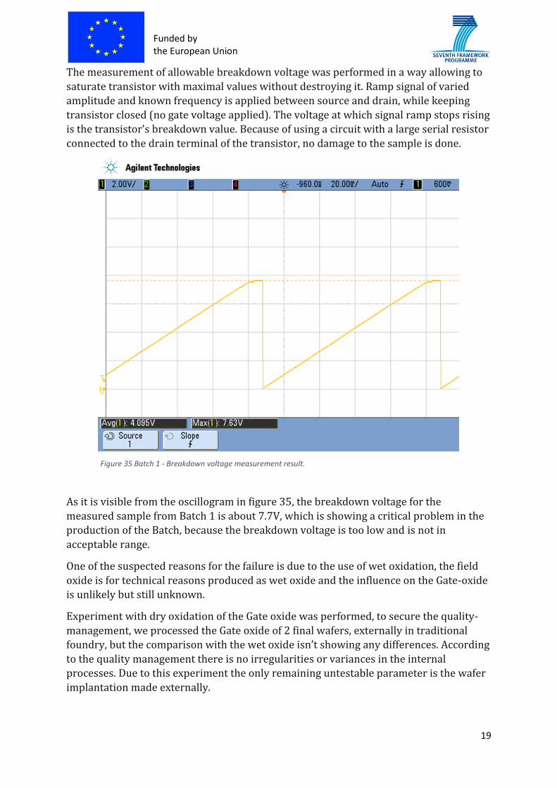
The measurement of allowable breakdown voltage was performed in a way allowing to
saturate transistor with maximal values without destroying it. Ramp signal of varied
amplitude and known frequency is applied between source and drain, while keeping
transistor closed (no gate voltage applied). The voltage at which signal ramp stops rising
is the transistor’s breakdown value. Because of using a circuit with a large serial resistor
connected to the drain terminal of the transistor, no damage to the sample is done.
As it is visible from the oscillogram in figure 35, the breakdown voltage for the
measured sample from Batch 1 is about 7.7V, which is showing a critical problem in the
production of the Batch, because the breakdown voltage is too low and is not in
acceptable range.
One of the suspected reasons for the failure is due to the use of wet oxidation, the field
oxide is for technical reasons produced as wet oxide and the influence on the Gate-oxide
is unlikely but still unknown.
Experiment with dry oxidation of the Gate oxide was performed, to secure the quality-
management, we processed the Gate oxide of 2 final wafers, externally in traditional
foundry, but the comparison with the wet oxide isn’t showing any differences. According
to the quality management there is no irregularities or variances in the internal
processes. Due to this experiment the only remaining untestable parameter is the wafer
implantation made externally.
Figure 35 Batch 1 - Breakdown voltage measurement result.

Funded by the European Union
20
The graphic shown in figure 36 presents the relation between the doping concentration
and the Break-down voltage which illustrates the problem with the transistor sensors
from Batch 1.
Key point after launching Batch 1:
Changing implantation company;
Improving the ESD-protection design – new mask;
Launching second Batch with MOSFET spectrometer sensors;
No ESD-protection for the new design;
ESD-protection – modification in the technology steps:
Regarding to the issue with the short-cut in the ESD-protection circuit, new set of
technological steps were tested and established.
Figure 36 Break-down voltage - Doping concentration relation.
Figure 37 Left: New set of manufacturing steps for ESD-protection. Right: image of the ESD-protection diode taken with digital microscope.

Funded by the European Union
21
After identification of the problem in the design, using a new mask there was introduced
an additional N-doped region in the bare silicon wafer. Just after this step opposite
doping is performed to create the substrate layer and the ESD diode with a modified
mask. At last N+ doping is performed for creation of transistor source and drain regions,
together with the other ESD diode.
Batch 2.
Batch 2 was launched in month 14 of the IAQSense project. The focus of the second
batch of sensors was solving the critical issues reviled during the analysis of the sensors
from Batch 1.
Spectrometer on chip (SoC) wafers were produced by Nano Analytik in the Ilmenau
facility of nano analytik GmbH on a 4” line inside cleanroom of class 100/1000.
Characterization included static and dynamic electrical tests with biggest focus on
sample’s detection capability.
The measurements were performed on naSE002A SoC samples manufactured according
to „Tentative Product Specifications (TPS) - Spectrometer on chip for VOC detection &
Tip based polar ionization detector of biomolecules - Test structure (Test)” and „Process
Specifications - Custom Process for Spectrometer on chip And Tip based detection”. The
samples are based on N-channel MOSFET produced without ESD protection and with
different doping/implantation parameters resulting in adjusted breakdown voltage
values. Sensors are realized on a die with dimensions 5 mm by 5 mm.
Measurements were performed solely on V2.1-type transistors on membrane, which are
characterized by 100 µm square symmetrical channel and tin oxide gate material, glued
and wire-bonded to 12-pin TO-package housing.
Second batch of spectrometer transistors were built within the membrane in order to
get a better thermal insulation. The power of the build in heater is not enough to heat
the regain with transistors to the needed temperature ratings to clean the surface of the
collective layer when transistors are not thermally insulated. That is why usage of a
membrane technology is necessary.
Figure 38 Left: The picture of SoC sample bonded to TO-housing (no cap), Right: Geometry of measured transistor with square geometry of the channel.

Funded by the European Union
22
Figure 39 Left: The layout of the mask for N-channel MOSFET spectrometer on membrane (Batch 2), Right: SEM image of a MOSFET is rectangular geometry.
Batch 2 - MOSFET spectrometer output and transfer characterization.
Characteristics collected have shown that transistors can conduct the drain current in the range of milliamps without any damage for the sample. For the purpose of testing maximum chosen gate voltage applied was 15V and drain source voltage 18 V, however, for future use values to apply can be bigger if needed. Observed VTh value is fluctuating near 0÷1V depending on sample.
Short comparison between the output charts of transistors manufactured in Batch 1 and
these produced in Batch 2 shows essential difference in the performance. The drain
current and drain-source voltage ratings are much higher for the transistors from Batch
2. The result from Batch 2 goes much closer to the calculated values, which is evident for
improvement of the wafer implantation manufacturing process.
Figure 40 Batch 2, output characteristics – Chip 14.11 T1(100 µm).

Funded by the European Union
23
Figure 41 Batch 2, output characteristics – Chip 13.09 T1(100 µm).
Figure 42 Batch 2, output characteristics – Chip 21.06 T1(100 µm).
Figure 43 Averaged transfer characteristics of 25% of total amount of V2.2 transistors.

Funded by the European Union
24
Batch 2 - MOSFET spectrometer symmetry test.
To check the symmetry of source/drain work of the transistor, measurements with
interchanged source/drain pins were conducted. In that case the lead which normally was
used as a source was connected to work as a drain; and typical drain was connected to the
substrate and worked as a source. All measurements have shown slight change in the
signal, but generally difference observed was not bigger than 20%. Exemplary output
characteristics comparing S/D-D/S behavior and showing typical size of response
variance are given below.
Figure 44 Output characteristics symmetry test.
Batch 2 - MOSFET spectrometer breakdown voltage.
Measurements carried out according to the description provided in figure 34 have
revealed that basing on measurement of 25% of V2.1 transistors, the breakdown voltage
is estimated at the level of 37.5 V with standard deviation of σ=4.46 V. Some of the
measurement results are listed below:
Break-down voltage for chip 13.09 – Transistor 100µx100µ: 35V
Break-down voltage for chip 14.11 – Transistor 100µx100µ: 34V
Break-down voltage for chip 21.06 – Transistor 100µx100µ: 37V
Batch 2 - MOSFET spectrometer – dynamic electrical response.
First dynamic measurements were performed with the samples from second batch.
Transistor used in this experiment is shown in figure 39 (right). The measurement setup
block diagram is shown in figure 45.

Funded by the European Union
25
The setup shown on the figure above consist of Measurement console, developed by
FACET, the NI platform with the software application developed for the needs of
IAQSense project for characterization of spectrometer transistors, a display monitor, a
test chamber where is placed the sensor itself. The chamber is supplied with different
substances via capsule filled with micropipette. The NI platform plays the role of a
process controller with integrated computer device that records the amplitude and the
shape of the current signal floating through the drain-source electrodes of the sample.
The FACET measurement platform plays the role of the transistor driver, connecting the
sensor in a diagonal of a Wheatstone bridge giving the possibility to switch the polarity
of the drain-source terminals. In addition, a heater is present inside the test chamber to
give flexibility of the measurement setup. In case of saturation of the MOSFET
spectrometer (that could happen when sensor is overdosed), heating up the whole chip
prevents a surface effect issues caused by the environmental reasons.
The parameters used in this measurement are listed below:
Bridge voltage – 5V;
Gate voltage – 4V;
Rsense – 3000Ω;
System overall gain – 6,35;
Sampling mode – Continuous;
Bridge mode – Toggle0;
Switching frequency – 1Hz;
Sampling rate – 20kHz;
Number of samples – 64000;
Temperature – 25°C;
The aim of this first chemical experiment with spectrometer MOSFET was to observe if
there is any change in sensor response. The principle of operation of the technology
includes set of parameters for driving the transistor itself. These parameters are the
applied voltage on the drain-source terminals, the frequency for switching the voltage
Figure 45 Test setup with NI platform and measurement realized by FACET and delivered on 7th July 2015 for dynamic characterization of spectrometer on chip sensors.

Funded by the European Union
26
and the gate potential. The other two parameters involved in regime of operation of the
spectrometer are the sampling mode and the bridge mode.
The second group of parameters are influencing the readout system, and this includes
the hardware resistor for conversion the drain current into voltage. Rsense is hardware
component that can’t be modified via the software console but must be considered for
further understanding of the spectrometer operation. The next parameters of this group
are the gain factor, sampling rate and the number of samples.
Apart of this two major groups, the temperature must be taken in to account when the
measurements are conducted.
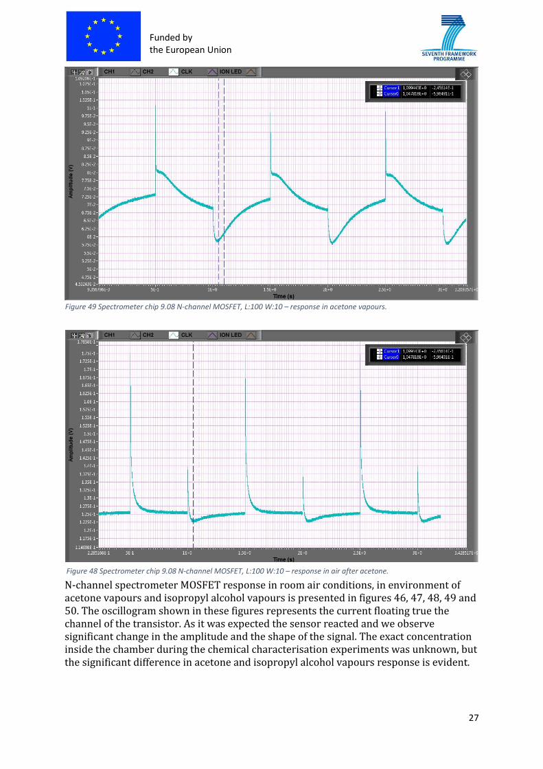
Figure 46 Spectrometer chip 9.08 N-channel MOSFET, L:100 W:10 – response in air.
Figure 47 Spectrometer chip 9.08 N-channel MOSFET, L:100 W:10 – response in acetone vapours in progress.
Funded by the European Union
27
N-channel spectrometer MOSFET response in room air conditions, in environment of acetone vapours and isopropyl alcohol vapours is presented in figures 46, 47, 48, 49 and 50. The oscillogram shown in these figures represents the current floating true the channel of the transistor. As it was expected the sensor reacted and we observe significant change in the amplitude and the shape of the signal. The exact concentration inside the chamber during the chemical characterisation experiments was unknown, but the significant difference in acetone and isopropyl alcohol vapours response is evident.
Figure 49 Spectrometer chip 9.08 N-channel MOSFET, L:100 W:10 – response in acetone vapours.
Figure 48 Spectrometer chip 9.08 N-channel MOSFET, L:100 W:10 – response in air after acetone.

Funded by the European Union
28
To understand the real current value, it is needed to be considered the gain of the front-
end amplifier and the sensing resistor from the current to voltage converter.
𝐼𝑑 =(
𝑈𝑜𝑢𝑡𝐺𝑎𝑖𝑛)
𝑅𝑠𝑒𝑛𝑠𝑒⁄ [𝐴]
Batch 3.
Batch 3 was launched in month 18 of the IAQSense project. The sensors manufactured in
this batch are P-channel based, realized on a die with dimensions 1 mm by 1 mm.
Spectrometer on chip (SoC) wafers were produced by Nano Analytik in the Ilmenau
facility of nano analytik GmbH on a 4” line inside
cleanroom of class 100/1000. Characterization
included static and dynamic electrical tests with
biggest focus on sample’s detection capability.
The measurements were performed on naSE001P
SoC samples manufactured according to
„Tentative Product Specifications (TPS) -
Spectrometer on chip for VOC detection & Tip
based polar ionization detector of biomolecules -
Test structure (Test)” and „Process Specifications
- Custom Process for Spectrometer on chip And
Tip based detection”. The samples are produced
without ESD protection, without integrated
heater and temperature control sensor.
Figure 50 Spectrometer chip 9.08 N-channel MOSFET, L:100 W:10 – response in isopropyl alcohol vapours.
Figure 51 P-channel spectrometer MOSFET, batch 3.

Funded by the European Union
29
Sensors manufactured in the third batch are P-channel MOSFETs, the charge carriers
mobility difference is 3 times smaller than the one for N-channel MOSFETs. This leads to
increasing of the transistor channel to keep the same output characteristics of the N-
channel sensors and the P-channel sensors. In figure 51 is shown the design of a P-
channel MOSFET sensor. There are 2 transistors on each chip. Transistor 1 is with Tin
oxide gate, but the second transistor on the chip is with “Al” gate, which purpose is to be
used as a reference transistor. Gate dimensions of the transistor are 100µm by 300µm.
The thickness of the Tin oxide layer is 80nm. The sheet resistance of the SnO2 layer is in
range of few hundreds of kiloohms.
Batch 3 – P-channel MOSFET spectrometer output characteristic:
Typical output characteristic measured for a P-channel MOSFET spectrometer is shown
on figure 52. This type of spectrometer sensor has been delivered to three of the project
partners and the measurement of the transistor output characteristic was established as
a part of a standard procedure of testing the bonded sensors.
Batch 3 – P-channel MOSFET spectrometer – dynamic electrical response:
This type of sensors was used in chemical parallel characterization test of a N-channel
spectrometer and P-channel spectrometer.
The aim of the parallel characterization test was to investigate the response behavior of
different sensor samples for different substances.
The parameters used in this measurement are listed below:
Bridge voltage – 5V;
Gate voltage – 1,5V;
Rsense – 3000Ω;
System overall gain – 6,35;
Sampling mode – Continuous;
Bridge mode – Toggle0;
Switching frequency – 0,5Hz;
Sampling rate – 8kHz;
Number of samples – 64000;
Temperature – 25°C;
Figure 52 Batch 3 - P-channel MOSFET spectrometer output characteristics.

Funded by the European Union
30
Tested substances:
Xylene Chlorbenzol Toluene Butyl acetate Methyl isobutyl
ketone
C8H10 C6H5Cl C7H8 C6H12O2 C6H12O
The measurement sequences consisted of reference measurement in room air. The
following measurements were done after injection of 100µl. of substance inside the
measurement chamber with volume of 0,75l. All rules of the safety measures are
followed strictly during the experiment. Spectrometer sensor board with the MOSFET
chips were in gas ventilation hood with constant airflow to prevent inhalation of the
measurement substances. Presented measurement result shows one period of the whole
measurement sequence.
Xylene measurement.
Figure 54 Full chart – Xylene measurement with P-channel MOSFET spectrometer.
Figure 53 Tested substances.

Funded by the European Union
31
For all charts, the reference measurement is present, so it is easy to evaluate the sensor
response. The separation of the graphs per parts makes the difference significant. There
is offset of the sensor signal in respect to the reference, aside of this fact amplitude
shape has changed in the process of environmental changes inside the chamber.
Figure 56 Xylene measurement with P-channel MOSFET spectrometer - part 1.
Figure 55 Xylene measurement with P-channel MOSFET spectrometer - part 2.

Funded by the European Union
32
Chlorbenzol measurement.
Figure 57 Xylene measurement with P-channel MOSFET spectrometer - part 3.
Figure 58 Chlorbenzol measured with P-channel MOSFET spectrometer.

Funded by the European Union
33
Toluene measurement.
Figure 60 Full chart – Toluene measurement with P-channel MOSFET spectrometer.
Figure 59 Selected signal – Chlorbenzol measurement with P-channel MOSFET spectrometer.

Funded by the European Union
34
Butyl acetate measurement.
Figure 63 Full chart – Butyl acetate measurement with P-channel MOSFET spectrometer.
Figure 62 Toluene measurement – P MOSFET Offset. Figure 61 Toluene measurement – P-channel MOSFET Offset.

Funded by the European Union
35
Results of the measurement illustrated in the Batch 3 section are commented in the section of Batch 4,
where is made parallel between the performance of both spectrometer sensors.
Figure 65 Butyl acetate measurement – P-channel MOSFET Offset.
Figure 64 Selected signal – Butyl acetate measurement with P-channel MOSFET spectrometer.

Funded by the European Union
36
Methyl isobutyl ketone measurement.
Figure 66 MIBK measurement with P-channel MOSFET spectrometer.
Figure 67 MIBK measurement with P-channel MOSFET spectrometer - part 1.

Funded by the European Union
37
Batch 4.
Batch 4 was launched in month 28 of the IAQSense project. Spectrometer on chip (SoC)
wafers were produced by Nano Analytik in the Ilmenau facility of nano analytik GmbH
on a 4” line inside cleanroom of class 100/1000. Characterization included static and
dynamic electrical tests focused on sample’s detection capability.
The measurements were performed on naSE005A SoC samples manufactured according
to „Tentative Product Specifications (TPS) - Spectrometer on chip for VOC detection &
Tip based polar ionization detector of biomolecules - Test structure (Test)” and „Process
Specifications - Custom Process for
Spectrometer on chip And Tip based detection”.
The samples are based on N-channel MOSFET
produced without ESD protection. Sensors are
realized on a die with dimensions 1 mm by 1
mm. The spectrometer sensor manufactured in
Batch 4 are with two different thickness of the
gate layer. For each chip, there is a transistor
with 80nm gate layer and 40nm gate layer. This
has been done to answer the Debye length
objective.
Figure 68 MIBK measurement with P-channel MOSFET spectrometer - part 3.
Figure 69 N-channel spectrometer MOSFET, batch 4.

Funded by the European Union
38
Batch 4 – N-channel MOSFET spectrometer output characteristic:
All sensors that were manufactured by NANO and provided to the project partners from
batch 4 are electrically characterised. The output characteristic of a sensor produced in
the fourth batch is shown in figure 70. The characteristics of N-channel transistor from
batch 4 and the characteristics of the P-channel transistors from the previous batch are
covering the expectations of the initially calculated values for the sensors. This is an
evidence that all CMOS processes were performed successful.
Batch 4 – N-channel MOSFET spectrometer AFM investigation:
Figure 70 Batch 4 - N-channel MOSFET spectrometer output characteristics.
Figure 71 Tin oxide gate layer of the MOSFET spectrometer investigated with Atomic-Force Microscope.

Funded by the European Union
39
The roughness of the gate layer of the N-channel MOSFET spectrometer has been
investigated with Atomic-Force Microscope. This measurement was performed in order
to get better understanding for the physical properties of the layer. The size of the Tin
oxide grains represents the material sheet resistance. The sheet resistance of the
collective layer plays important role in the performance of the whole sensor device. The
Debye length is the distance over which a charge Q is shielded by the surrounded
charges. When the conductivity of the collective layer is big, this means that in the Tin
oxide layer there are many free electrons that can shield the charge attached to the
collective layer surface and in this way, to prevents sensing of the charge (Ion) from the
sensor. This is the reason why the collective layer sheet resistance was investigated and
improved during this project.
Batch 4 – N-channel MOSFET spectrometer – dynamic electrical response:
This N type of sensors was used in chemical parallel characterization test of a N-channel
spectrometer and P-channel spectrometer.
The measurements were performed under the same conditions as the described for the
measurement of P-channel spectrometer sensors.
In figure 72 is shown the interface
spectrometer PCB for parallel
characterisation test of the spectrometer
MOSFET sensors. The layout of the
board allows attaching the sensors to
the flange of a gas chamber and easy
handling. On each PCB are glued and
bonded 2 spectrometer chips, one N-
channel and one P-channel MOSFET.
Sensors used in the current experiment,
imaged with digital microscope are
shown in figure 73.
Substances used for the characterisation of the chemical characterisation of the Batch 4
spectrometers are the same as in figure 53.
Figure 72 The interface spectrometer PCB for gas measurements.
Figure 73 Microscope image of N-channel spectrometer Batch 4(on the left)) and P channel-spectrometer Batch 3 (on the right).

Funded by the European Union
40
Set of parameters used for the characterisation measurement can be seen in figure 73.
The green signal of the oscillogram represents the switching drive signal of the
spectrometer. The white (N-channel MOSFET spectrometer) and the red (P-channel
MOSFET spectrometer) signals are the current true the drain-source terminals. The
application allows having both signals plotted on the oscillogram window
simultaneously and observation of the changes in the sensor behaviour. All rules of the
safety measures are followed strictly during the experiment. Spectrometer sensor board
with the MOSFET chips was in gas ventilation hood with constant airflow to prevent
inhalation of the measurement substances.
Xylene measurement.
Response of Spectrometer sensors for Xylene is different for N-channel MOSFET and P-
channel MOSFET. Well seen from experiment is that, for Xylene, the shape of the signal
for N MOSFET is changing a lot reaction is rapid and the measurement method does not
allow us to see the previous stages of the signal but only already the steady state. For P-
Figure 74 Image of the IAQSense software console developed by FACET.
Figure 75 Full chart – Xylene measurement with N-channel MOSFET spectrometer.

Funded by the European Union
41
channel MOSFET response is much slower, we observe an offset, signal is going down
slowly and then there is change in shape of the signal. Process is not as rapid as the one
for N-channel MOSFET.
Chlorbenzol measurement.
Results of Chlorbenzol measurement show very different behavior of both sensor in
comparison with Xylene measurement. Reaction of N-channel MOSFET is very slow, first
we observe offset, but no change in the amplitude. Later, some change in the shape of
the signal occur but in fact the pk-pk Amplitude does not differ some much from the
reference signal. Reaction of P-channel MOSFET spectrometer on the other hand is like
the reaction of N-channel MOSFET for this substance, but with more significant change
in signal shape.
Toluene measurement.
Spectrometer response for Toluene is very similar to response of Xylene. This can be
explained with the structure of the molecule – quite similar for both compounds. If we
have a look on N-channel MOSFET response we cannot see almost any difference, but P-
channel MOSFET spectrometer has different behavior. Reaction is faster and the change
in the amplitude is bigger. Slopes are steeper. Additional measurements are done after
the end of Toluene measurement to see if sensor is recovering after the experiment with
Toluene. This is shown in figures 61 and 78. Small offset is observed for both sensors,
but this can be considered as normal. We are not sure about the exact room conditions
and this offset can be caused by temperature or different composition of air.
Figure 76 Chlorbenzol measurement with N-channel MOSFET spectrometer.

Funded by the European Union
42
Figure 78 Toluene measurement – N-channel MOSFET Offset.
Figure 77 Full chart – Toluene measurement with N-channel MOSFET spectrometer.

Funded by the European Union
43
Butyl acetate measurement.
Both P-channel and N-channel spectrometer MOSFET sensors react to Butyl acetate. In
figure 80 are selected 4 of the most significant shapes of the drain current during the
change in the concentration of the substance inside the chamber.
Figure 79 Full chart – Butyl acetate measurement with N-channel MOSFET spectrometer.
Figure 80 Selected signals – Butyl acetate measurement with N-channel MOSFET spectrometer.

Funded by the European Union
44
Methyl isobutyl ketone measurement.
MIBK measurements were performed first and although we know very well that the
Spectrometer detects very good Acetone vapors, we did not expected so rapid and long reaction.
Process of detection was very strong for both N-channel MOSFET and P-channel MOSFET.
The big number of measurement imposed dividing the full chart on 5 small charts, registered as
a family of characteristics. Some of the most significant charts are illustrated below.
Results of MIBK measurement are the most significant and strongest of all five
presented in this document. Amplitude of the signal is much bigger than reference signal
for both – N MOSFET and P MOSFET. The most interesting is that for N MOSFET
spectrometer first we observe negative offset, then the offset becomes positive. As
expected, commonalities are observed between Butyl acetate measurement and MIBK
measurement. For all substances is observed response. For some chemical compounds,
we can see common behavior of the sensors. Combination of P-channel and N-channel
MOSFET spectrometer is important from point of selectivity. The two types of sensors
are complementary. The concentrations measured for this experiment are unknown, but
is evident that response time is different for different substances.
Figure 81 MIBK measurement with N-channel MOSFET spectrometer.

Funded by the European Union
45
Ionization measurements.
According to the principle of operation of the MOSFET spectrometer Ions have to reach
the surface of a collective layer of Tin oxide that plays the role of gate of a MOSFET
transistor. Modulating the drain current with a certain frequency brings the charges
attached to the surface of the collective layer to move and to modify
the field of the channel locally. Theoretically the ionised molecules
attracted to the Tin oxide layer would acquire a negative or positive
charge by gaining or losing electrons to form ions, often in
conjunction with other chemical changes. This leads to change in the
behaviour of the sensor.
To prove this experiment with LED Ionizer were conducted. The test
setup is shown on figure 85. The LED is installed in a way that it
influences only the N-channel spectrometer. Figure 82 LED Ionizer.
Figure 83 Measurement of Ammonium hydroxide with N-channel spectrometer plus Ion and P-channel without Ion.
Figure 84 Measurement of water vapours with N-channel spectrometer plus Ion and P-channel spectrometer without Ion.

Funded by the European Union
46
In figure 83 and figure 84 are presented the results of the measurement of 2 different
substances with MOSFET spectrometer transistors in the same measurement condition.
The blue line shows the time interval of LED Ion operation. The current via N-channel
MOSFET spectrometer is in white colour and the current via P-channel MOSFET
spectrometer is in red colour.
The measurement illustrated in figure 83 has been conducted with NH3. Both N and P
spectrometers respond to the substance but LED is spotted only over the N
spectrometer. In a result, it is observed significant difference in falling slope of the
current via N spectrometer when the LED is ON and when it is OFF. The same
experiment is performed with water vapours (figure 84). The result of the second
experiment approves the influence of the Ionizer to the N-channel spectrometer.
Measurement laboratory setups.
The manufactured samples were tested in three laboratories. In the laboratory in
Ilmenau, a test setup (figure 85) build by NANO was used for sensor pre-
characterisation. The main focus of these measurement was to preselect sensor for the
other project partners.
The characterization platform with software console for the setup was developed by
FACET Bulgaria. For the purpose of gas characterisation measurements NANO has built
a hermetic chamber that allowed experiments with volatile substances.
A second measurement setup delivered from FACET was installed in the labs of ISL. The
focus of their work was concentrated in testing the spectrometer samples with
hazardous substances.
Figure 85 Measurement setup in nano analytik GmbH labs.
Funded by the European Union
47
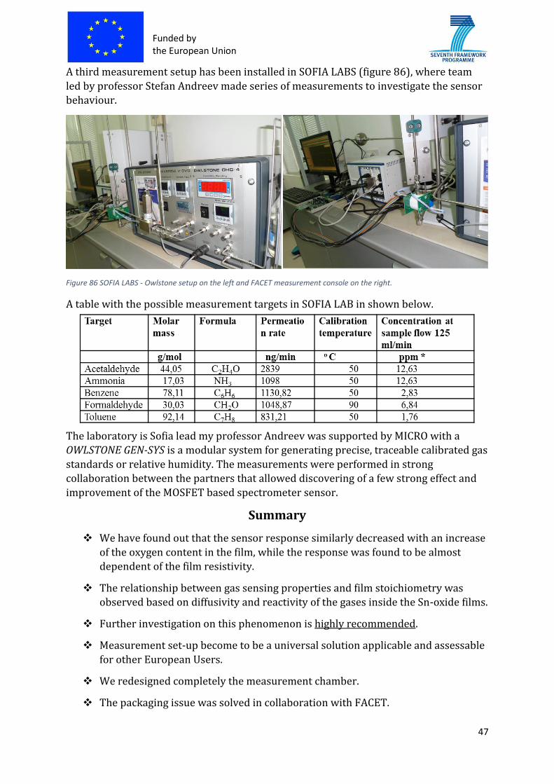
A third measurement setup has been installed in SOFIA LABS (figure 86), where team
led by professor Stefan Andreev made series of measurements to investigate the sensor
behaviour.
Figure 86 SOFIA LABS - Owlstone setup on the left and FACET measurement console on the right.
A table with the possible measurement targets in SOFIA LAB in shown below.
The laboratory is Sofia lead my professor Andreev was supported by MICRO with a
OWLSTONE GEN-SYS is a modular system for generating precise, traceable calibrated gas
standards or relative humidity. The measurements were performed in strong
collaboration between the partners that allowed discovering of a few strong effect and
improvement of the MOSFET based spectrometer sensor.
Summary
We have found out that the sensor response similarly decreased with an increase
of the oxygen content in the film, while the response was found to be almost
dependent of the film resistivity.
The relationship between gas sensing properties and film stoichiometry was
observed based on diffusivity and reactivity of the gases inside the Sn-oxide films.
Further investigation on this phenomenon is highly recommended.
Measurement set-up become to be a universal solution applicable and assessable
for other European Users.
We redesigned completely the measurement chamber.
The packaging issue was solved in collaboration with FACET.

Funded by the European Union
48
The measured procedure was established in collaboration with Eff. Marketing.
ISL developed successfully two sophisticated measurement chambers for each
sensor.
The obtained result is showing the operationally and performance of the
transistor-spectrometer confirming the measurements and conclusions done
during the meeting at NANO on 6-7.07.2015.
NANO developed a set-up where rough calibration of the transistor-spectrometer
is possible. Measurements in the range of 30 to 100ppm of Ammonia were
successfully done.
The experimentally observed dependence of the sheet resistance on the grain
size and grain orientation of SnxOy films is correlated to the dependence of the
electron mobility on grain boundary scattering.
The electrical resistance of gate-thin film depends on the film stoichiometry.
All theoretical predictions about the principle of operation and reproducibility
are confirmed.
The transistor-spectrometer selectivity for different species is evident.
Further investigation should be focused on stoichiometry of the SnO2-film with
respect to grain size, thickness and doping.
SnO2 Layer deposited at high O2 concentration, the SnO2 dramatically influences
the defect chemistry and the sintering behavior of tin oxide.
More oxygen vacancies in the SnO2-material, leading to a decrease in the free
electron concentration and an increase in sensitivity of the material.
Since film morphology has porous structure offer effectively more surface area
for the sensing gas molecules to interact, SnO2 thin films deposited at different
sputtering conditions have been investigated.

Funded by the European Union
49
Technology-Type 2: Tip-Field effect transistor
The second type of sensor is based on the patent of Prof. Ivo Rangelow – “Field effect
transistor sensor” (TIP FET sensor). NANO owns the patent on this technology and this
plays a key role in the protection of this sensor-technology and it is of strategic
importance for this project, as well the future of this unique innovation. The technology
type 2 is dedicated to specific species by its functionalization layer. The realization of the
functionalization coating and its adsorption and desorption mechanics was investigated
within this project.
The sensing principle has similarities with the sensor type 1, based on change of an
electric field due to the adsorption of certain species on a porous layer but works in
static regime only. The basic principle of this sensor is a FET placed on a micro-scale tip
to enhance the overall sensing sensitivity, operated in constant voltage mode and with
the source-drain current changing with the number of adsorbed species. The species are
adsorbed by special functionalization coating which ensures selectivity. A sketch of this
sensor-type is demonstrated (figure 87). The target operation of this sensor is the
detection of hazardous species such as fungus (mold).
TIP FET sensor was realized on 4” wafer in 16 designs in total. There are 4 layouts, and
each one with 2 different dimensions. For each layout exist version with and without
gate. The dimensions of all variations are listed below:
Figure 87 TIP FET transistor illustration.

Funded by the European Union
50
The layout includes a heater and a diode for temperature measurement and control.
Detailed layout of the TIP FET sensor is shown in figure 88. Below the mask is illustrated
the cross-section of the sensor. On a P substrate are implanted 1µm N+ source and drain
regions and the channel between them with thickness of 100nm decreasing to the tip of
the transistor. The channel is isolated with 50nm SiO2 and covered with 80nm gate
layer.
One of the biggest challenges in the process of developing this technology is the parasitic
N inversion at the surface due to the built-in positive charge at the SiO2 – Si interface. To
prevent this additional p-type implantation was performed at the surface in order to
eliminate the parasitic inversion. For this purpose, extra mask was used to protect
already implanted source, drain and channel.
Figure 88 TIP FET mask layout and cross-section.
Figure 89 Tip field-effect transistor - optical image.
Funded by the European Union
51
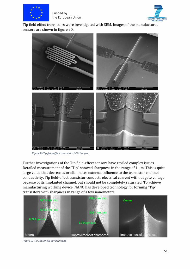
Tip field effect transistors were investigated with SEM. Images of the manufactured
sensors are shown in figure 90.
Further investigations of the Tip field-effect sensors have reviled complex issues.
Detailed measurement of the “Tip” showed sharpness in the range of 1 µm. This is quite
large value that decreases or eliminates external influence to the transistor channel
conductivity. Tip field-effect transistor conducts electrical current without gate voltage
because of its implanted channel, but should not be completely saturated. To achieve
manufacturing working device, NANO has developed technology for forming “Tip”
transistors with sharpness in range of a few nanometers.
Figure 90 Tip field-effect transistor - SEM images.
Figure 91 Tip sharpness development.

Funded by the European Union
52
Big challenge for NANO during the establishment of the technology for Tip field-effect
transistor was the “tip” height. This is another important parameter of the sensor
characteristics.
First runs of manufacturing tip transistor samples showed that the “tip” height is
undefined. This has been proved by the electrical measurements – the channel of the
transistor had to be modulated with external electrical field (see figure 93). Further runs
allowed improving the technology for the forming of the “tip”.
With a decision of the consortium, the development of this sensor type technology was
stop in order to switch all resources for developing of other two technologies.
Figure 92 Tip field-effect transistor -SEM investigation of the "tip" height.
Figure 93 Tip field-effect transistor experimental measurement setup.

Funded by the European Union
53
Technology -Type 3 (TT3): Nanostructured collectors on cantilevers for trace and
ultra-trace sensing.
Technology description
The sensor works as nano-balance. The cantilever is an oscillating and capable of
detecting atto mass-changes sensor.
The detection is based on reference, non-adsorbing device to be compared to the
adsorbing one in terms of oscillating frequency. This way one chip should be composed
of multiple different active layers/cantilevers and one reference using 4 places on the
chip.
This principle is widely used in gas and mass sensing for example of “artificial noses”.
The key aspects of this technology are: (a) sensor design, (b) sensor fabrication, (c)
mass-detection readout technique (piezo-resistive), and (d) special functional coating to
adsorb the species (nano-rods). NANO and ISL are the key partners in the development
of this technology – are in the possession of unique knowhow on these key aspects.
Cantilever theory and modes of operation
The microcantilever is widely used component in the microsystem devices. Its flexibility
and versatility make it a popular component for a variety of applications.
Cantilever static bending mode
This section is aimed at theoretical background of adsorption-induced stresses and
definition of cantilever’s spring constant, which will be widely used for further
explanations. Figure 94 introduces a cross sectional drawing of a cantilever along with
some designations. The most general relationship between the force exerted normally
on the cantilever apex (F) and its displacement (Δz) can be defined using Hook’s law:
𝐹 = −𝑘 ∙ Δ𝑧
Figure 94 Cross sectional drawing of a rectangular cantilever. σ1 and σ2 – induced stresses on the top (σ1) and bottom (σ2) of the cantilever.

Funded by the European Union
54
where k is spring constant of the cantilever beam, which denotes its elastic properties.
This is a very important parameter for cantilever as a chemical sensor, because k is a
subject to change when functionalized cantilever interacts with some media. In the
absence of external gravitational, magnetic, and electrostatic forces, cantilever
deformation is unambiguously related to a gradient of mechanical stress generated in
the device.
Differential surface stress:
∆𝜎 =𝑑𝜎1
𝑑𝑧+
𝑑𝜎2
𝑑𝑧
Differential surface stress causes the cantilever with length l, width w, and thickness h to
bend with the radius of bending R. A geometrical relation for R is:
1
𝑅=
𝑑2𝑧/𝑑𝑥2
[1 + (𝑑𝑧𝑑𝑥
)2]3
2⁄≈
3∆𝑧
2𝑙2
which for a small amount of bending may be simplified to:
1
𝑅≈
𝑑2𝑧
𝑑𝑥2≈
2∆𝑧
𝑙2≈
𝑀
𝑌 ∙ 𝐼
Where R is furthermore related to the moment of the bent body (M), the moment of
inertia (I) and the effective modulus of isotropic elasticity (Y):
𝑌 =𝐸
1 − 𝑣2
Where E is Young’s modulus and v is Poisson’s ratio for the substrate (for silicon
v=0.27). The area moment of inertia for a rectangular cantilever can be calculated as:
𝐼 = ∫ ∫ 𝑧2𝑑𝑧𝑑𝑦 =𝑤ℎ3
12
ℎ2⁄
−ℎ2⁄
𝑤
0
Where w is the width and h is the thickness of the cantilever. If the bending moment is:
𝑀 = ∆𝜎 ∙ 𝑤 ∙ ℎ/2
Then if cantilever length l>>w, Hooke’s law for small displacements can be re-written as:
1
𝑅≈
𝑑2𝑧
𝑑𝑥2=
𝑀
𝑌 ∙ 𝐼=
∆𝜎 ∙ 𝑤 ∙ ℎ ∙ (1 − 𝑣2) ∙ 12
2 ∙ 𝐸 ∙ 𝑤 ∙ ℎ3
And finally, we obtain “Stoney’s equation”, originally derived by Stoney and von Preissig,
which can in many cases accurately predict adsorbate-induced deformations of thin
plates:
1
𝑅=
6(1 − 𝑣2)
𝐸ℎ2∆𝜎

Funded by the European Union
55
where R is the radius of microcantilever curvature, ν and E are Poisson’s ratio and
Young’s modulus for the substrate, respectively, h is the thickness of the cantilever, and
Δσ is the differential surface stress. Knowledge of the radius of curvature R allows the
tip displacement of a microcantilever with length l to be determined by:
∆𝑧 =1
2
𝑙2
𝑅=
3𝑙2(1 − 𝑣)
𝐸ℎ2∆𝜎
The Stoney’s equation can be also equivalently presented as:
∆𝜎 =𝐸ℎ2
3𝑙2(1 − 𝑣)∆𝑧
So, measuring the tip deflection like in AFM, one can derive the differential surface
stress. The cantilever is rigidly clamped on one side and is free on the other. It has a
length, l, and a concentrated force, F, acting on the cantilever at a distance a from the
clamped side. The moment, which is produced by the force acting on the cantilever, is
given by:
𝑀 = 𝐹(𝑥 − 𝑎)
Then the displacement Δz can be derived. Furthermore, by then setting x=a=l we obtain:
∆𝑧 = −𝑙3
3𝑌𝐼𝐹
Inserting this in Hook’s law, given before and solve for k:
𝑘 = 3𝑌𝐼
𝑙3
Finally, assuming that 1-ν2 ≅ 1, the spring constant of a cantilever is calculated
according to:
𝑘 =𝐸ℎ3𝑤
4𝑙3
This interrelates the cantilever’s spring constant and its geometry along with its
material properties. Hereafter, this equation will be used for calculation of spring
constant k as
measure of cantilever stiffness.
Such the way, the static mode considers bending of the cantilever through modulation of
mechanical stresses due to either direct influence of the environment or thermal effects
caused
by this influence. In the latter case, the presence of analyte species can be detected due
to the
following phenomena:
the heat associated with their adsorption on the transducer;
the heat produced in the course of a subsequent chemical reaction on the
cantilever
surface.

Funded by the European Union
56
Cantilever bending can also be driven by external gravitational, electrical or magnetic
fields.
If the conversion of chemical energy into mechanical energy takes place directly, i.e.
independently on the thermal effects, then the surface stress σ can be expressed by
using the
Shuttleworth equation:
𝜎 = 𝛾 +𝜕𝛾
𝜕𝜀
Where γ is the surface free energy. The surface strain dε is defined as the relative change
in
surface area dε = dA/A. In many cases, the contribution from the surface strain term can
be
neglected and the free energy change approximately equals the change in surface stress.
In its own turn, the surface free energy γ (or interfacial tension) is interrelated with the
amount of adsorbed molecules on the cantilever surface by the Gibbs adsorption
equation:
Г = −𝐶
𝑅𝑇(
𝑑𝛾
𝑑𝐶)
where Γ is excess of adsorption at an interface in a two-phase system, dγ is the change in
surface free energy and C is the concentration of the solute.
Previous two equations are appropriate to describe molecular adsorption processes at
different
interfaces. Therefore, cantilever bending mechanism is compatible with many
responsive phases and can function in both gas and liquid environments. Despite the
static cantilever bending is a result of direct adsorbate influence, it is rather difficult to
estimate the adsorbed mass quantitatively because the surface coverage is basically not
known. However, cantilever operation at its eigenfrequency, enables accurate
calculation of the amount of molecules adsorbed.
Cantilever dynamic resonant mode
The dynamic mode of the cantilever operation considers motion of the cantilever beam,
which can take place either with or without forced excitation. The forced excitation can
be realised by alternated fields of electric, electromagnetic, thermal, or acoustic origin.
Furthermore, minute sizes and mass of microfabricated cantilevers makes them
susceptible to thermally induced noise, which has the same origin as Brownian motion
of small particles in liquids. Therefore, cantilever sensors may operate in the resonant
mode with or without external excitation. The mechanically excited cantilevers require
the presence of actuator, which causes the cantilever to vibrate. Practically, it can be
achieved by either oscillating quartz crystal, which is in firm mechanical contact with the
cantilever, or by integrated actuator employing bimorph effect. Normally, the actuator
provides with periodic oscillations of the cantilever beam over certain frequency range
near its natural or higher resonances.
Alternatively, pulsed excitation of the cantilever or amplification of the Brownian

Funded by the European Union
57
motion of the cantilever beam (i.e. without forced excitation) gives also information on
its frequency spectrum. Gain-frequency or phase-frequency responses of the
functionalized cantilever gathered over a time interval reflect chemical or biological
stimuli exerted on the cantilever. Resonance frequency shift of the cantilever under
analyte exposition is mostly due to the additional mass loading, which is considered in
the effective mass of a harmonic oscillator meff:
𝜔 = √𝑘
𝑚𝑒𝑓𝑓
However, adsorption-induced changes in the elasticity of the cantilever beam and
damping of the cantilever (its Q-factor modulation) are other two significant
mechanisms for resonance frequency modulation.
Main objective
Development of nanostructured cantilever sensors permits to lower the detection limit
of VOCs. The adsorption of VOCs molecules on the surface of an AFM cantilever modifies
its resonant frequency by changing the mass of the oscillation sensor.
Modification of the raw AFM cantilever with nanostructure (nanotubes) brings
selectivity of the measurement sensing construction, and in the same time increase the
sensitivity of the cantilever due to larger total surface of nanostructured cantilever.
A special designed electronic equipment and PC software for PLL (Phase-Locked Loop)
detection allows continuous monitoring and recording of the cantilever resonance
frequency and phase signal.
Figure 95 Development of nanostructured AFM cantilever.
Figure 96 Cantilever resonance detection plots.

Funded by the European Union
58
Any change in the cantilever measurement system leads to resonance frequency shift
according to the theory described in “Cantilever dynamic resonant mode”. The
deviation in the resonance frequency can be calculated with the following equation:
∆𝑓 = −𝑓𝑟
2𝑚0∆𝑚
Where Δm is the difference in the mass of the cantilever sensor, m0 is the initial mass
and fr is the resonant frequency that can be presented as:
𝑓𝑟 =1
2𝜋(
1.875
𝑙)
2
√𝐸𝐼
𝜌𝐴
where ρ and E are the mass density and the elastic modulus of the material of the lever,
respectively, I is its moment of inertia, A is its cross-sectional area and l is the cantilever
length.
The material chosen for nanostructuring of the cantilevers is Cupric oxide (CuO) because
it is commonly used for VOCs detection. It is popular material for sensing toluene1,
xylene1, NO2 2,3, CO3 …
Development
The processing technology for this sensor-type is known by NANO. The coating process
was transferred to NANO by ISL, to produce the entire sensor unit with one micro-
machining process plan. There are variation parameters for the sensor design in terms
of coating. The greatest challenge was to develop a straight-forward processing
technology.
Figure 97 Roadmap for the objective wafer level transfer.

Funded by the European Union
59
First important step of the realization of active piezo-resistive cantilevers with CuO
coating was the synthesis of the cupric oxide nanotubes at NANO laboratories. With the
support from ISL, the technology algorithm was transferred successfully.
Establishing of the synthesis of CuO nanatubes on silicon:
Step1 Evaporation under vacuum of a dense layer of copper.
Figure 98 Preparation of silicon wafer for synthesis of CuO nanotubes.
Step 2 Growth of Cu(OH)2 tubes with 2 successive reactions.
Both processes are running for 15 minutes each at room temperature. Diluted solutions
are:
- Aqueous solution of sodium hydroxide (NaOH)
- Aqueous solution of ammonium persulfate ((NH4)2S2O8)
- Distilled water
Reaction : Cu + 4NaOH + (NH4)2S2O8 → Cu(OH)2 + 2NH3↑ + 2Na2SO4 + 2H2O
Step 3 Synthesis of CuO tubes by dehydration of Cu(OH)2 tubes.
Sample annealed at 200°C during 1 hour under air
After the process of thermal dehydration of the Cu(OH)2 nanotubes, they are
transformed into CuO nanotubes. SEM investigation of the nanostructured layer was
performed to identify any morphological and dimensional in result of the annealing
process.
Figure 99 CuO nanotubes synthesis - wafer suspended upside-down very close to the bottom (100microns) on the left wafer upside-down, hight over the bottom on the right.

Funded by the European Union
60
The results of the measurement show that the morphology and the dimensions of the
nano tubes are almost identical before and after annealing.
Growth of CuO nanotubes on a cantilever with optical readout.
The process of nanostructuring was applied first on a single passive cantilever.
The experiment was unsuccessful. The SEM investigation of the used sample showed no
growth of tubes at the border of the cantilever.
A special procedure was developed for solving the “Boundary problem”. The whole
cantilever chip was introduced in resin.
In figure 102 is illustrated the mechanism to overcome the border effect.
Figure 100 SEM images of copper oxide nanotubes before (on the left) and after (on the right) annealing.
Figure 101 SEM image of nanostructured single passive cantilever.
Figure 102 Procedure developed to overcome the border effect.

Funded by the European Union
61
The cantilever chip is covered with layer of resin (a). The second step of the procedure is
evaporation of a titanium/copper layer and growth of CuO nanotubes (b), followed by
dissolution of the resin(c).
Result obtained with the procedure is shown in figure 103. No border effect observed.
Production
The production of the sensor is based on standard SOI-technology. The realization
requires only a few standard micro-fabrication steps, such as lithography and oxide etch.
The functionalization coating was done with collaboration with ISL at NANO
laboratories.
With a decision taken after discussion between NANO and ISL the synthesis of
nanotubes was transferred directly on a wafer level piezo-resistive cantilevers. The
active cantilevers have one side “busy” with the integrated thermos-mechanical actuator
for the excitation of the cantilever and Wheatstone bridge for measuring the cantilever
deflection. For this reason, the CuO had to cover only the opposite side of the cantilever
beam.
The process of growth of CuO nanotubes includes usage of NaOH, so the synthesis of
nanotubes on a ready silicon wafer (Membrane) before the final etching procedure that
allows the formation of the cantilever was challenging.
Nano found a resin able to protect the electrical circuits composed with aluminum,
because aluminum is immediately dissolved in the nanotubes reaction solution.
Figure 103 SEM images of nanostructured passive cantilever.
Figure 104 SEM image of an active piezo-resistive cantilever. Side with electrical circuits.

Funded by the European Union
62
The synthesis of CuO before final etching of the cantilevers was performed the SEM
investigation showed that the achieved result is much different than the expected one.
The morphology and the number of tubes for a given surface have been changed (See
image 105).
The solution of the problem was shifting the synthesis of nanotubes as a final step of the
sensor manufacturing. The ready cantilevers were protected with special resist to
protect the electrical circuits integrated on the cantilever and to prevent growth of
nanotubes on the sides.
Figure 106 SEM image showing the top side of piezo-resistive cantilever with CuO nanorods.
In figure 106 is presented SEM image of ready active cantilever with piezo-resistive
readout, functionalized with CuO nanorods. The technology was established and ready
for mass production on wafer scale.
Figure 105 SEM image of CuO nanotubes synthesized on a cantilever membrane before final etching procedure.

Funded by the European Union
63
High-frequency active piezo-resistive cantilever
This is the smallest cantilever in the world with integrated read-out. The activation of
this type of cantilevers is realized with external piezo crystal because the resonant
frequency of the samples is too high for thermos-mechanical actuation technology,
which is reaching the limits around 1MHz.
The functionalization available for this type of cantilever sensors is Cu(OH)2 and CuO.
The technology is processed on wafer scale and it is ready for mass production.
Development of the detection device. Principle of operation.
The measurement setup was developed by ISL, where all characterization
measurements with functionalized cantilevers have been performed.
Figure 107 Test setup for characterization of active piezo-resistive cantilevers.
In figure 107 are shown images of the measurement setup for cantilever sensor gas
characterization. The setup has 10 capsules that allow measurement with 10 different
substances. In the center of the chamber is mounted the cantilever sensor covered with chamber lid (2). Presence of 2 holes (1) allowing the elimination of the gases dynamic detection.
Cantilever sensor is bonded on a green PCB holder that is connected in a white board, that
produces the sensor supply voltage and amplifies the sensor signal. Via coaxial cable the sensor
signal is delivered to the input of system controller, where the signal is processed and the
frequency shit is measured.
Improvement of the detection device
A modification of the gas temperature and of the air flow allow to control the gas
concentration. This allows measurement of the real concentration of the pollutant.

Funded by the European Union
64
1. The air flow containing the pollutant goes through an inert tube
2. The tube is surrounded by a heater and by a thermocouple in order to avoid
possible condensation
3. Methanol solution. The flow containing the pollutant is bubbled in this solution to
dissolve the pollutant in the solution.
After dissolution of the pollutant in the methanol solution, the concentration is
measured by HPLC (with a calibration curve)
After measurement the real concentrations are relatively close to the theoretical ones
Improvement step - Addition of a bubbler to avoid external contamination.
3Modification of the lid - a top part is added to fix a tube which can be connected to a
bubbler to avoid possible contamination coming from outside. There is possibility to
measure the value of the flow and to detect possible leakages.
Figure 108 Image of the measurement setup for active piezo-resistive cantilevers - improved.

Funded by the European Union
65
Measurement results achieved with piezo-resistive cantilevers functionalized
with CuO nanorods.
Explosive detection results.
In figure 109 and 110 are presented the results of explosive gas measurements
performed with 3 different type of cantilevers. Sensors without functionalization do not
show sensitivity to the measurement substances, or at least no frequency deviation is
observed (figure 110 black line). The second type of sensor used in the characterisation
Figure 109 Concentration: 830 ppb of explosive.
Figure 110 Concentration: 15 ppb of explosive.

Funded by the European Union
66
measurement is active cantilever with Cu(OH)2 nanorods (figure 110 red line). At the
moment of the injection of the explosive (concentration 15 ppb) is observed frequency
shift of 20Hz. The result of the measurement with piezo-resistive cantilever with CuO
nanorods (figure 110 blue) is the most significant. The deviation of the frequency is
more than 90Hz for concentration of 15ppb.
At the moment when the gas emission is stopped the functionalized sensors slowly start
to recover, and return to the initial state.
NO2 detection results
Baseline: Air flow of 125 mL/min NO2 flow 125 mL/min
Cantilever temperature: 55°C NO2 temperature: 40°C
The result of the NO2 measurement presented in figure 111 compare the response of a
raw cantilever sensor to the response of nanostructured cantilever with Cu(OH)2
nanorods. After injection of the substance no change in the resonance frequency of the
raw cantilever (figure 111 black) is observed. The nanostructured cantilever (figure 111
red) result is very significant. Frequency shift is almost 40Hz.
Figure 111 Active piezo-resistive cantilever - Nitrogen dioxide measurement.

Funded by the European Union
67
Summary
• Modelling, development, fabrication and demonstration of small mass-sensitive
cantilever-resonators have been realized
• The measurement time are a few seconds and is based on the transduction of
chemical or physical processes into a mechanical response.
• The fabrication technology of small cantilever-resonators (fc>1MHz)
functionalized with Metal-Oxide-Nanotubes (MOxNT) and Metal-Oxide-Nanorods
(MOxNR), equipped with actuation have been shown. It allows the simultaneous
detection of cantilever oscillation and bending by means of nano-electronic piezo
resistive 1(2) DEG circuity.
• A novel Chemical - “lock-in” due to post-functionalization of the cantilever-
resonators for ultimate chemical selectivity and sensitivity have been shown.
Further investigation employing Chemically Modified Metal-Oxide Nanotubes
(ChMMOxNT) and Chemically Modified Metal-Oxide Nanorods (ChMMOxNR) are
needed.
• The development and realization of a portable, low-power device allowing
network operations is in place.
• Specialized characterization chamber for cantilever characterization is in place.

Funded by the European Union
68
Preparation of the test environment and the platform for system integration
(sensors + MEMS + IC) and preparation of the test environment (hardware and
software) for the sensing heads and follow-up of the test results.
Subtask – Detection system for nano-functionalized cantilevers.
Objectives
- To ensure the electrical test of the different components (technologies) and sub-
components of the sensing head to release working heads for further
characterization,
- To provide the characterization platform to the different actors of the
characterization step. It will provide datalogging of the responses to different
gases or molecules,
- The platform should also provide the necessary flexibility to install signal
processing of the data logs (batch processing) to prepare the future integrated
real time algorithms.
Results
Cantilever based mass detection system
Status and the end of period 1, reported Feb 2015
Two-channel system developed by MICRO and provided to WP3 partners. The system
consists of mass detection controller and control and data processing software.
The plan for further development was oriented in following directions:
- Decreasing the size and cost of the hardware;
- Adding wireless connectivity;
- Increasing the number of channels to eight;
- Performing experiments with functionalized cantilevers, proving the sensitivity
of the system to be same or better compared to one developed in Period 1.
System miniaturization
The first step towards the decreasing the system size was to develop an intermediate
prototype having two channels, but smaller size and cost. The system re-design done by
MICRO was based on Red Pitaya™ platform. The system fully covers the functionality of
the platform designed in Period 2. In addition:
- It has smaller size (credit-card footprint);
- Ethernet connectivity channel was added.

Funded by the European Union
69
Figure 112 shows the comparison in size between two system which have identical
functionality.
Eight channel system for sensor networks
The next step was to develop the eight-channel system with added wireless connectivity.
The new system is intended to serve also as an engineering / pre-production prototype
for further commercialization.
Figure 112 Comparison between two platforms. Same preamplifier head with two cantilevers used as a reference. New system based on Red Pitaya platform (on the left) and two channel system developed in Period 1 (on the right).
Figure 113 Functional diagram of eight channel system.

Funded by the European Union
70
The system architecture (Fig. 113) allows different actuation modes to be combined,
namely full parallel actuation using PWM DACs (up to 500 kHz) or subsequent channel
actuation using high resolution DAC (up to 2MHz).
The new system, designed by MICRO is based on newer Xilinx™ Artix device. It has
following main features:
- Eight full channels, cover the functionality of previous system; - Additional eight PWM DAC outputs allowing full parallel work; - Added PLL functionality; - USB and Wi-Fi connectivity; - Compact design (10cm x 8cm x 2cm, smaller than 1st system)
The system architecture allows different actuation modes to be combined, namely full
parallel actuation using PWM DACs (up to 500 kHz) or subsequent channel actuation
using high resolution DAC (up to 2MHz).
FPGA core Wi-Fi module
8-channel parallel
driving module
Output
connectors
Figure 114 Eight channel hardware platform for cantilever sensor networks.
Figure 115 Frequency sweep mode, four cantilevers connected (second channel not amplified).

Funded by the European Union
71
Both amplitude modulation and PLL tracking mode can be used for detection of the
frequency change.
The hardware platform passed full electrical tests. The final tests were performed by
connecting four cantilevers combining two x two preamplifier heads to different sets of
four selected channels. The screenshots from the control and data recording software
are shown in figures 115 and 116.
The wireless functionality was tested by a dedicated test design as follows: ASCII string
was send from serial terminal over USB cable to the eight-channel system. Then, the
received string was send from FPGA to the Wi-Fi module. A PC with TCP client software
was connected to the Wi-Fi module of the system, and the same string was observed on
the TCP client terminal. Finally, the analysis of the performance the eight-channel
system show that it covers the criteria “same or better”, compared to the two-channel
platform, developed in Period 2.
Deviations
No deviations from the planned work for this subtask.
Outcomes
Cantilever based mass detection system
MICRO developed a compact, eight-channel, very high-sensitive detection system for
nano-functionalized cantilevers. The performance of the system was checked against the
two-channel system, developed in Period 1 and already proven for very high sensitivity
detection of for explosive materials. The system design level corresponds to the pre-
production prototype; the technology is proven and the design is ready for production
implementation.
This result allows direct practical exploitation in a commercial product.
Figure 116 Screenshot from client software window with four cantilevers connected, showing frequency tracking (PLL) mode.

Funded by the European Union
72
Process porting package reporting for mass production
All three sensor technologies were developed and implemented on 4” silicon wafers due
to cost savings.
The second type of sensor technology based on the patent of Prof. Ivo Rangelow – “Field effect
transistor sensor” (TIP FET sensor) was stopped after first runs of manufacturing. TIP FET sensor was
pretested and the results were reported. With a decision of the consortium for relocation of
resources further development of TIP field-effect sensors was suspended and all resources were
relocated to the other sensor technologies.
Spectrometer MOSFET sensor and active piezo-resistive nanostructured cantilever technologies are
CMOS based sensors with a not CMOS compatible sensing layer – SnO2 collective gate layer for
spectrometer MOSFET sensor and nanostructured Cu(OH)2/CuO layer for active piezo-resistive
cantilever.
The sensing layer for both sensor technologies plays crucial role in the sensor selectivity and
sensitivity. For that reason, NANO concentrated on the establishment of sensing layer manufacturing
parameters.
In figure 117 are shown images of silicon substrates with spectrometer sensors and
cantilevers manufactured by NANO in their facilities.
All process steps for manufacturing MOSFET spectrometers and active cantilevers with
CuO nanorods are documented. The production technology is fully established and
ready for mass production.
Figure 117 A silicon 4" wafer with MOSFET spectrometer sensors (on the left) and a silicon 4" wafer with active piezo-resistive cantilevers (on the right).

Funded by the European Union
73
Achieved results
- Process is fully documented;
- One FAB placed an offer for part of the process for spectrometer fabrication;
- Negotiations with two other FAB’s are in progress;
No deviations
Functional material cannot be covered from the FAB – external process in
Ilmenau or other clean-room must be excepted;
4”-6” wafer production due to the functionalization and customization;
Several potential FAB have been identified;
The process identification according to the FAB-standards are in progress;
Spectrometer and Cantilever fabrication for gas sensing are not CMOS
compatible;
A combination of FAB and external production steps will be always required;
4” and 6” will be needed for mass production due to the process
opportunities in Ilmenau;

Funded by the European Union
74
List of figure:
Figure 1 The 3 groundbreaking sensor concepts of IAQSense. ............................................................... 2
Figure 2 2D model of the MOSFET spectrometer sensor. ....................................................................... 3
Figure 3 Batch 1 – layout 1, 100x10. ....................................................................................................... 4
Figure 4 Batch 1 – layout 1, 40x4. ........................................................................................................... 5
Figure 5 Batch 1 - layout 2, 40x4. ............................................................................................................ 5
Figure 6 Batch1 - layout 2, 100x10. ......................................................................................................... 5
Figure 7 Batch 1 - layout 3, 40x10. .......................................................................................................... 6
Figure 8 Batch 1 - layout 3, 100x25. ........................................................................................................ 6
Figure 9 Batch 1 - layout 4, 40x40. .......................................................................................................... 6
Figure 10 Batch 1 - layout 4, 100x100. .................................................................................................... 7
Figure 11 Batch 1 - layout modification. ................................................................................................. 7
Figure 12 Batch 1 - Chip block diagram. .................................................................................................. 8
Figure 13 Batch 1 - Chip layout with ESD protection. ............................................................................. 8
Figure 14 Batch 1 - Chip layout with addresses. ..................................................................................... 9
Figure 15 TO12 package. ......................................................................................................................... 9
Figure 16 Spectrometer sensors, bonded in TO12 packages. ............................................................... 10
Figure 17 Batch 1 - all 8 designs realized on 4" wafer. .......................................................................... 11
Figure 18 SEM images of MOSFET spectrometer T1:40x40, T2:100x100. ............................................ 11
Figure 19 SEM images of the Tin oxide layer. ....................................................................................... 12
Figure 20 Batch 1 - ESD layout............................................................................................................... 12
Figure 21 SEM image of the ESD diode. ................................................................................................ 12
Figure 22 Batch 1 - wafer map. ............................................................................................................. 13
Figure 23 Dual Channel System Source Meter Keithley 2602A ............................................................. 13
Figure 24 Sample pinout with electrical schematics of structures within ............................................ 13
Figure 25 MOSFET output and transfer characteristics equivalent measurement setup. .................... 14
Figure 26 Output characteristics – Chip 05.04 T1(100 µm). ................................................................. 14
Figure 27 Output characteristics – Chip 05.04 T2(40 µm). ................................................................... 15
Figure 28 Output characteristics – Chip 07.04 T2(40 µm). ................................................................... 15
Figure 29 Output characteristics – Chip 07.04 T1(100 µm). ................................................................. 16
Figure 30 Transfer characteristics – Chip 05.04 T2(40 µm). .................................................................. 16
Figure 31 Transfer characteristics – Chip 05.04 T1(100 µm). ................................................................ 17
Figure 32 Transfer characteristics – Chip 07.04 T1(100 µm). ................................................................ 17
Figure 33 Transfer characteristics – Chip 07.04 T2(40 µm). .................................................................. 18
Figure 34 Test setup for MOSFET breakdown voltage measurements. ................................................ 18
Figure 35 Batch 1 - Breakdown voltage measurement result. .............................................................. 19
Figure 36 Break-down voltage - Doping concentration relation. .......................................................... 20
Figure 37 Left: New set of manufacturing steps for ESD-protection. Right: image of the ESD-
protection diode taken with digital microscope. .................................................................................. 20
Figure 38 Left: The picture of SoC sample bonded to TO-housing (no cap), Right: Geometry of
measured transistor with square geometry of the channel. ................................................................ 21
Figure 39 Left: The layout of the mask for N-channel MOSFET spectrometer on membrane (Batch 2),
Right: SEM image of a MOSFET is rectangular geometry. ..................................................................... 22
Figure 40 Batch 2, output characteristics – Chip 14.11 T1(100 µm). .................................................... 22
Figure 41 Batch 2, output characteristics – Chip 13.09 T1(100 µm). .................................................... 23
Figure 42 Batch 2, output characteristics – Chip 21.06 T1(100 µm). .................................................... 23
Figure 43 Averaged transfer characteristics of 25% of total amount of V2.2 transistors. .................... 23

Funded by the European Union
75
Figure 44 Output characteristics symmetry test. .................................................................................. 24
Figure 45 Test setup with NI platform and measurement realized by FACET and delivered on 7th July
2015 for dynamic characterization of spectrometer on chip sensors. ................................................ 25
Figure 46 Spectrometer chip 9.08 N-channel MOSFET, L:100 W:10 – response in air. ........................ 26
Figure 47 Spectrometer chip 9.08 N-channel MOSFET, L:100 W:10 – response in acetone vapours in
progress. ................................................................................................................................................ 26
Figure 48 Spectrometer chip 9.08 N-channel MOSFET, L:100 W:10 – response in air after acetone. . 27
Figure 49 Spectrometer chip 9.08 N-channel MOSFET, L:100 W:10 – response in acetone vapours. . 27
Figure 50 Spectrometer chip 9.08 N-channel MOSFET, L:100 W:10 – response in isopropyl alcohol
vapours. ................................................................................................................................................. 28
Figure 51 P-channel spectrometer MOSFET, batch 3............................................................................ 28
Figure 52 Batch 3 - P-channel MOSFET spectrometer output characteristics. ..................................... 29
Figure 53 Tested substances. ................................................................................................................ 30
Figure 54 Full chart – Xylene measurement with P-channel MOSFET spectrometer. .......................... 30
Figure 55 Xylene measurement with P-channel MOSFET spectrometer - part 2. ................................ 31
Figure 56 Xylene measurement with P-channel MOSFET spectrometer - part 1. ................................ 31
Figure 57 Xylene measurement with P-channel MOSFET spectrometer - part 3. ................................ 32
Figure 58 Chlorbenzol measured with P-channel MOSFET spectrometer. ........................................... 32
Figure 59 Selected signal – Chlorbenzol measurement with P-channel MOSFET spectrometer. ......... 33
Figure 60 Full chart – Toluene measurement with P-channel MOSFET spectrometer. ........................ 33
Figure 61 Toluene measurement – P-channel MOSFET Offset. ............................................................ 34
Figure 62 Toluene measurement – P MOSFET Offset. .......................................................................... 34
Figure 63 Full chart – Butyl acetate measurement with P-channel MOSFET spectrometer. ................ 34
Figure 64 Selected signal – Butyl acetate measurement with P-channel MOSFET spectrometer. ...... 35
Figure 65 Butyl acetate measurement – P-channel MOSFET Offset. .................................................... 35
Figure 66 MIBK measurement with P-channel MOSFET spectrometer. ............................................... 36
Figure 67 MIBK measurement with P-channel MOSFET spectrometer - part 1.................................... 36
Figure 68 MIBK measurement with P-channel MOSFET spectrometer - part 3.................................... 37
Figure 69 N-channel spectrometer MOSFET, batch 4. .......................................................................... 37
Figure 70 Batch 4 - N-channel MOSFET spectrometer output characteristics. ..................................... 38
Figure 71 Tin oxide gate layer of the MOSFET spectrometer investigated with Atomic-Force
Microscope. ........................................................................................................................................... 38
Figure 72 The interface spectrometer PCB for gas measurements. ..................................................... 39
Figure 73 Microscope image of N-channel spectrometer Batch 4(on the left)) and P channel-
spectrometer Batch 3 (on the right)...................................................................................................... 39
Figure 74 Image of the IAQSense software console developed by FACET. ........................................... 40
Figure 75 Full chart – Xylene measurement with N-channel MOSFET spectrometer. .......................... 40
Figure 76 Chlorbenzol measurement with N-channel MOSFET spectrometer. .................................... 41
Figure 77 Full chart – Toluene measurement with N-channel MOSFET spectrometer. ....................... 42
Figure 78 Toluene measurement – N-channel MOSFET Offset. ....................................................... 42
Figure 79 Full chart – Butyl acetate measurement with N-channel MOSFET spectrometer. ............... 43
Figure 80 Selected signals – Butyl acetate measurement with N-channel MOSFET spectrometer. ..... 43
Figure 81 MIBK measurement with N-channel MOSFET spectrometer. ............................................... 44
Figure 82 LED Ionizer. ............................................................................................................................ 45
Figure 83 Measurement of Ammonium hydroxide with N-channel spectrometer plus Ion and P-
channel without Ion. ............................................................................................................................. 45
Figure 84 Measurement of water vapours with N-channel spectrometer plus Ion and P-channel
spectrometer without Ion. .................................................................................................................... 45

Funded by the European Union
76
Figure 85 Measurement setup in nano analytik GmbH labs. ................................................................ 46
Figure 86 SOFIA LABS - Owlstone setup on the left and FACET measurement console on the right. .. 47
Figure 87 TIP FET transistor illustration. ............................................................................................... 49
Figure 88 TIP FET mask layout and cross-section. ................................................................................ 50
Figure 89 Tip field-effect transistor - optical image. ............................................................................. 50
Figure 90 Tip field-effect transistor - SEM images. ............................................................................... 51
Figure 91 Tip sharpness development. ................................................................................................. 51
Figure 92 Tip field-effect transistor -SEM investigation of the "tip" height. ......................................... 52
Figure 93 Tip field-effect transistor experimental measurement setup. .............................................. 52
Figure 94 Cross sectional drawing of a rectangular cantilever. σ1 and σ2 – induced stresses on the top
(σ1) and bottom (σ2) of the cantilever. ................................................................................................ 53
Figure 95 Development of nanostructured AFM cantilever. ................................................................ 57
Figure 96 Cantilever resonance detection plots. .................................................................................. 57
Figure 97 Roadmap for the objective wafer level transfer. .................................................................. 58
Figure 98 Preparation of silicon wafer for synthesis of CuO nanotubes. .............................................. 59
Figure 99 CuO nanotubes synthesis - wafer suspended upside-down very close to the bottom
(100microns) on the left wafer upside-down, hight over the bottom on the right. ............................ 59
Figure 100 SEM images of copper oxide nanotubes before (on the left) and after (on the right)
annealing. .............................................................................................................................................. 60
Figure 101 SEM image of nanostructured single passive cantilever. .................................................... 60
Figure 102 Procedure developed to overcome the border effect. ....................................................... 60
Figure 103 SEM images of nanostructured passive cantilever. ............................................................ 61
Figure 104 SEM image of an active piezo-resistive cantilever. Side with electrical circuits. ................ 61
Figure 105 SEM image of CuO nanotubes synthesized on a cantilever membrane before final etching
procedure. ............................................................................................................................................. 62
Figure 106 SEM image showing the top side of piezo-resistive cantilever with CuO nanorods. .......... 62
Figure 107 Test setup for characterization of active piezo-resistive cantilevers. ................................. 63
Figure 108 Image of the measurement setup for active piezo-resistive cantilevers - improved. ........ 64
Figure 109 Concentration: 830 ppb of explosive. ................................................................................. 64
Figure 110 Concentration: 15 ppb of explosive. ................................................................................... 64
Figure 111 Active piezo-resistive cantilever - Nitrogen dioxide measurement. ................................... 64
Figure 112 Comparison between two platforms. Same preamplifier head with two cantilevers used as
a reference. New system based on Red Pitaya platform (on the left) and two channel system
developed in Period 1 (on the right). .................................................................................................... 64
Figure 113 Functional diagram of eight channel system. ..................................................................... 64
Figure 114 Eight channel hardware platform for cantilever sensor networks. .................................... 64
Figure 115 Frequency sweep mode, four cantilevers connected (second channel not amplified). ..... 64
Figure 116 Screenshot from client software window with four cantilevers connected, showing
frequency tracking (PLL) mode. ............................................................................................................. 64
Figure 117 A silicon 4" wafer with MOSFET spectrometer sensors (on the left) and a silicon 4" wafer
with active piezo-resistive cantilevers (on the right). ........................................................................... 64