WO 2008/068705 Al
27
(12) INTERNATIONAL APPLICATION PUBLISHED UNDER THE PATENT COOPERATION TREATY (PCT) (19) World Intellectual Property Organization International Bureau (43) International Publication Date (10) International Publication Number 12 June 2008 (12.06.2008) PCT WO 2008/068705 Al (51) International Patent Classification: (81) Designated States (unless otherwise indicated, for every H05B 33/08 (2006.01) kind of national protection available): AE, AG, AL, AM, AT, AU, AZ, BA, BB, BG, BH, BR, BW, BY, BZ, CA, CH, (21) International Application Number: CN, CO, CR, CU, CZ, DE, DK, DM, DO, DZ, EC, EE, EG, PCT/IB2007/054895 ES, FI, GB, GD, GE, GH, GM, GT, HN, HR, HU, ID, IL, IN, IS, JP, KE, KG, KM, KN, KP, KR, KZ, LA, LC, LK, (22) International Filing Date: LR, LS, LT, LU, LY, MA, MD, ME, MG, MK, MN, MW, 3 December 2007 (03.12.2007) MX, MY, MZ, NA, NG, NI, NO, NZ, OM, PG, PH, PL, PT, RO, RS, RU, SC, SD, SE, SG, SK, SL, SM, SV, SY, (25) Filing Language: English TJ, TM, TN, TR, TT, TZ, UA, UG, US, UZ, VC, VN, ZA, ZM, ZW (26) Publication Language: English (30) Priority Data: (84) Designated States (unless otherwise indicated, for every kind of regionalprotection available): ARIPO (BW, GH, 06125476.9 6 December 2006 (06.12.2006) EP GM, KE, LS, MW, MZ, NA, SD, SL, SZ, TZ, UG, ZM, (71) Applicant (for all designated States except US): NXP B.V. ZW), Eurasian (AM, AZ, BY, KG, KZ, MD, RU, TJ, TM), [NL/NL] ; High Tech Campus 60, NL-5656 AG Eindhoven European (AT, BE, BG, CH, CY, CZ, DE, DK, EE, ES, FI, (NL). FR, GB, GR, HU, IE, IS, IT, LT, LU, LV,MC, MT, NL, PL, PT, RO, SE, SI, SK, TR), OAPI (BF, BJ, CF, CG, CI, CM, (72) Inventors; and GA, GN, GQ, GW, ML, MR, NE, SN, TD, TG). (75) Inventors/Applicants (for US only): HOOGZAAD, Gian [NL/NL]; c/o NXP Semiconductors, IP Department, HTC Declaration under Rule 4.17: 60 1.31 Prof Holstlaan 4, NL-5656 AG Eindhoven (NL). — as to applicant's entitlement to applyfor and be granted a MOBERS, Antonius, M., G. [NL/NL]; c/o NXP Semi patent (Rule 4.17(U)) conductors, IP Department, HTC 60 1.31 Prof Holstlaan 4, NL-5656 AG Eindhoven (NL). Published: — with international search report (74) Agent: PENNINGS, Johannes, F., M.; c/o NXP Semi — before the expiration of the time limit for amending the conductors, IP Department, HTC 60 1.31 Prof Holstlaan 4, claims and to be republished in the event of receipt of NL-5656 AG Eindhoven, (NL). amendments (54) Title: CONTROLLED VOLTAGE SOURCE FOR LED DRIVERS (57) Abstract: The present invention relates to an electronic device for driving a light emitting semiconductor device, which includes controlling means (CNTL) being adapted for controlling a switch mode power supply for supplying the light emitting semiconductor device in response to a sensing value received by the controlling means which is indicative of a voltage across a current source for determining a current through the light emitting semico nductor device, wherein the switch-mode power supply is controlled such that the voltage across the current source is minimum.
-
Upload
khangminh22 -
Category
Documents
-
view
0 -
download
0
Transcript of WO 2008/068705 Al

(12) INTERNATIONAL APPLICATION PUBLISHED UNDER THE PATENT COOPERATION TREATY (PCT)
(19) World Intellectual Property OrganizationInternational Bureau
(43) International Publication Date (10) International Publication Number12 June 2008 (12.06.2008) PCT WO 2008/068705 Al
(51) International Patent Classification: (81) Designated States (unless otherwise indicated, for everyH05B 33/08 (2006.01) kind of national protection available): AE, AG, AL, AM,
AT,AU, AZ, BA, BB, BG, BH, BR, BW, BY, BZ, CA, CH,(21) International Application Number: CN, CO, CR, CU, CZ, DE, DK, DM, DO, DZ, EC, EE, EG,
PCT/IB2007/054895 ES, FI, GB, GD, GE, GH, GM, GT, HN, HR, HU, ID, IL,IN, IS, JP, KE, KG, KM, KN, KP, KR, KZ, LA, LC, LK,
(22) International Filing Date: LR, LS, LT, LU, LY, MA, MD, ME, MG, MK, MN, MW,3 December 2007 (03.12.2007) MX, MY, MZ, NA, NG, NI, NO, NZ, OM, PG, PH, PL,
PT, RO, RS, RU, SC, SD, SE, SG, SK, SL, SM, SV, SY,(25) Filing Language: English TJ, TM, TN, TR, TT, TZ, UA, UG, US, UZ, VC, VN, ZA,
ZM, ZW(26) Publication Language: English
(30) Priority Data: (84) Designated States (unless otherwise indicated, for everykind of regional protection available): ARIPO (BW, GH,06125476.9 6 December 2006 (06.12.2006) EPGM, KE, LS, MW, MZ, NA, SD, SL, SZ, TZ, UG, ZM,
(71) Applicant (for all designated States except US): NXP B.V. ZW), Eurasian (AM, AZ, BY, KG, KZ, MD, RU, TJ, TM),
[NL/NL] ; High Tech Campus 60, NL-5656 AG Eindhoven European (AT,BE, BG, CH, CY, CZ, DE, DK, EE, ES, FI,
(NL). FR, GB, GR, HU, IE, IS, IT, LT,LU, LV,MC, MT, NL, PL,PT, RO, SE, SI, SK, TR), OAPI (BF, BJ, CF, CG, CI, CM,
(72) Inventors; and GA, GN, GQ, GW, ML, MR, NE, SN, TD, TG).
(75) Inventors/Applicants (for US only): HOOGZAAD, Gian[NL/NL]; c/o NXP Semiconductors, IP Department, HTC Declaration under Rule 4.17:
60 1.31 Prof Holstlaan 4, NL-5656 AG Eindhoven (NL). — as to applicant's entitlement to applyfor and be granted a
MOBERS, Antonius, M., G. [NL/NL]; c/o NXP Semi patent (Rule 4.17(U))
conductors, IP Department, HTC 60 1.31 Prof Holstlaan4, NL-5656 AG Eindhoven (NL). Published:
— with international search report(74) Agent: PENNINGS, Johannes, F., M.; c/o NXP Semi — before the expiration of the time limit for amending the
conductors, IP Department, HTC 60 1.31 Prof Holstlaan 4, claims and to be republished in the event of receipt ofNL-5656 AG Eindhoven, (NL). amendments
(54) Title: CONTROLLED VOLTAGE SOURCE FOR LED DRIVERS
(57) Abstract: The present invention relates toan electronic device for driving a light emittingsemiconductor device, which includes controllingmeans (CNTL) being adapted for controlling a switchmode power supply for supplying the light emittingsemiconductor device in response to a sensing valuereceived by the controlling means which is indicativeof a voltage across a current source for determininga current through the light emitting semico nductordevice, wherein the switch-mode power supply iscontrolled such that the voltage across the currentsource is minimum.
CONTROLLED VOLTAGE SOURCE FOR LED DRIVERS
FIELD OF THE INVENTION
The present invention relates to an electronic device for driving a light
emitting diode, more specifically to a control mechanism for an electronic device for driving
a light emitting diode. The invention further relates to a system comprising the electronic
device and the light emitting diodes, and a method of driving the diodes.
BACKGROUND OF THE INVENTION
Light emitting diodes are to be driven at a constant current. Linear current
sources are broadly used for this purpose, as they are cheap and highly accurate. Further, the
linear current sources can be switched on and off quickly, a characteristic being advantageous
for implementing pulse width modulation (PWM) dimming. Amplitude modulation (AM)
dimming is also easy to implement by linear current sources, wherein different current levels
or current digital-to-analog converters are used. Typically, linear current sources are used in
one dimensional (ID) and two dimensional (2D) dimmable backlight systems, since many
independent current sources are required in those applications. Another approach consists in
switch-mode solutions, which is, however, more expensive, but less power consuming.
Linear current sources used for driving LED strings have only limited power efficiency,
which is mainly due to voltage variations of the LEDs. These voltage variations find their
origin in temperature dependence, spread, and aging. If a fixed voltage supply is used for
driving the light emitting diodes of a string, the current sources being coupled in series to the
LED strings may experience a large voltage. The large voltage entails a large power
dissipation, which in turn requires the current sources to be suitable to withstand high
temperatures. Accordingly, design considerations are to be made, which result in more
devices and packages in parallel, additional heat sinking mechanisms, and generally, in a
substantial increase in costs.
SUMMARY OF THE INVENTION
It is an object of the present invention to reduce the power consumption due to
voltage variations of the light emitting semiconductor device.
According to a first aspect of the present invention, an electronic device for
driving a light emitting semiconductor device is provided which includes controlling means
adapted for controlling a switch mode power supply for supplying the light emitting
semiconductor device in response to a sensing value received by the controlling means which
is indicative of a voltage across a current source for determining a current through the light
emitting semiconductor device, wherein the switch-mode power supply is controlled such
that the voltage across the current source is minimum. Although the following description
relates mainly to light emitting diodes as light emitting semiconductor devices, the present
invention covers all kinds of light emitting semiconductor devices, which may be driven by
the same or similar mechanisms as described here below. According to this aspect of the
present invention the electronic device provides means to control a switch-mode power
supply in response to the voltage across a current source that is e.g. coupled in series to the
light emitting diode. Accordingly, the control mechanisms of power supply and current
source are coupled to each other such that the power supply is adjusted in accordance with
the voltage drop across the current source. If current source and voltage supply were
controlled independently as provided by prior art solutions, the current through an LED is
held constant by the current source as long as the light emitted by the LED satisfies the
specific requirements as brightness or color. However, if the forward voltage across the LED,
or even worse across a string of LEDs, varies during operation, the supply voltage provided
by the controlled power supply may by higher than necessary. Any additional voltage drop
across the current source produces undesirable power losses by way of heat. This aspect of
the present invention takes account of this problem by providing a control mechanism that
reduces (or increases) the supply voltage such that the voltage across the current source
remains at a minimum voltage being just necessary to assure proper operation without
producing any excess voltage across the current source, which would be turned into heat. The
current source may be implemented as a linear or a switched current source being preferably
controllable to provide an appropriate current through a single or through multiple LEDs. A
current source in the present context, is to be understood as encompassing current sources or
current sinks. The current source may be implemented by a current mirror, wherein one
transistor is coupled in series with one or more light emitting diodes (e.g. a string of diodes).
As the current source (or current sink) is dimensioned and biased for a specific current, any
deviation from the predetermined value for the current will cause significant variations in the
voltage across the transistor. The control mechanism according to the present invention
allows to control the output voltage (and/or current) of the switch-mode power supply (such
as switch-mode power converter as buck- buck-boost or boost converter) in accordance with
a minimum voltage drop across the current source. The minimum voltage drop is the voltage
that is required to operate the current source, as for example a current mirror, in saturation.
To provide an appropriate sensing value that is indicative of the voltage drop across the
current source, the voltage level at the input of the current source (or sink) may be measured.
The so determined value may then be compared to a reference value, which is the minimum
value of the voltage drop across the current mirror. Any deviation from the reference value
may then be used to control the switch-mode power converter to re-establish the minimum
value. However, as apparent for those skilled in the art, the sensing value may be another
voltage or current that is suitable to indicate the voltage across the current source.
According to another aspect of the present invention, the electronic device as
set out above, includes further the current source, wherein the current source is either a
switched current source or a linear current source. The present invention is basically
applicable to all kinds of current sources. It is therefore irrelevant whether or not the current
source, or at least those components of the current source, which are coupled to the LED, are
implemented according to switch mode principles or linear driving mechanisms. As the
current source represents a component with a theoretically infinite impedance, the voltage
across the current source will take any value necessary to maintain a specific current. If the
supply voltage for the LEDs is increased, this may cause additional voltage across the current
source, at least across those parts of the current source which are coupled with the LEDs. The
present invention overcomes these problems by regulating the supply voltage in relation to
the voltage drop.
According to an aspect of the present invention, the electronic device is
adapted to switch the current through the LEDs on and off. The switching may in particular
occur in response to a pulse width modulated signal. This aspect relates to control
mechanisms using rapid pulse width modulated (PWM) signals for controlling the light
emission of LEDs. According to this aspect of the invention it is provided that the switching
activity of the current through the LEDs is in accordance with the control mechanism
according to the above aspects of the present invention. Instead, the control means take
account of the switching sequence and adapts the control appropriately in order to avoid any
conflict.
According to another aspect of the present invention, the controlling means is
further adapted to control the timing of a sample switch for sampling the sensing value,
which is indicative of the voltage across the current source, such that the sensing value is
sampled in accordance with the timing of switching of the current through the current source.
In particular, the sensing value is sampled if the current through the current source is
switched on. As switch-mode power converters must be switched according to a specific
timing in order to provide an appropriate output voltage, it is necessary to consider this
timing for the mechanism of retrieving the sensing value.
According to still another aspect of the present invention the switch-mode
power supply and the controlling means are adapted to control the output voltage of the
switch-mode power supply with a resolution or control accuracy of less than the variation of
the forward voltage of the light emitting diode to be driven. According to this aspect of the
invention, the control mechanism, and the switch-mode power supply provide a specific
control accuracy, such that the variations of the forward voltage of the light emitting diodes
are compensated. If a plurality of light emitting diodes is coupled in a string, this aspect of
the present invention relates to the total added variation of the forward voltages of the string.
If, for example, a single light emitting diode has a forward voltage variation of several
millivolts, this comparatively small value can add up, if multiple LEDs are coupled in series.
In this situation, the control range and accuracy take account of the overall variation as well
as the smallest possible variation. Generally, the switch-mode power supply, or parts of it
may be integrated on the same substrate as the control mechanism described here above with
respect to the other aspects of the present invention.
According to another aspect of the invention, the electronic device is further
adapted to provide pulse width modulation (PWM) signals for a plurality of strings of light
emitting diodes for individually dimming of each of the strings. This aspect of the present
invention relates to some typical applications, where a plurality of light emitting diodes is
coupled to form a string. The electronic device according to this aspect of the invention is
adapted such that these strings may be dimmed individually. This requires that the timing of
the control mechanism takes account of the control mechanism described here above.
According to still another aspect of the present invention a plurality of current
sources and a minimum selector is provided, wherein the plurality of light emitting diodes (or
as mentioned above a plurality of light emitting semiconductor devices) is coupled to the
plurality of current sources and the minimum selector is adapted to select the minimum
voltage across the plurality of current sources, wherein the selected minimum voltage is used
as a reference for controlling the switch-mode power supply. Accordingly, even if a plurality
of light emitting diodes, as for example three strings of light emitting diodes are driven by the
present electronic device, a mechanism is provided that allows to detect a current source with
a minimum voltage drop and to control all strings by the minimum voltage. This reduces
complexity of the required circuits.
According to an aspect of the present invention, the control unit is electrically
decoupled from the light emitting semiconductor devices (such as light emitting diodes), in
particular by an inductive power converter or by an opto-coupler or by both. Accordingly, the
present invention relates also to configurations, where the control unit, but also the switched
mode power supply is decoupled by means of transformers, opto-couplers, or the like from
the light emitting diodes.
According to an aspect of the present invention, an integrated semiconductor
device is provided being arranged according to one or several aspects of the present
invention, as set out here above. In particular, a integrated semiconductor device according to
present invention may provide input and output pins to provide the functionality in
accordance with the present invention. According to one aspect of the invention, a integrated
semiconductor device, as for example a packaged chip, provides an input pin being
configured to receive a sensing value to provide the control functions as described above.
The above aspects of the present invention may be combined in any number or configuration.
BRIEF DESCRIPTION OF THE DRAWINGS
These and other aspects of the invention will be apparent from and elucidated
with reference to the embodiments described hereinafter. In the following drawings
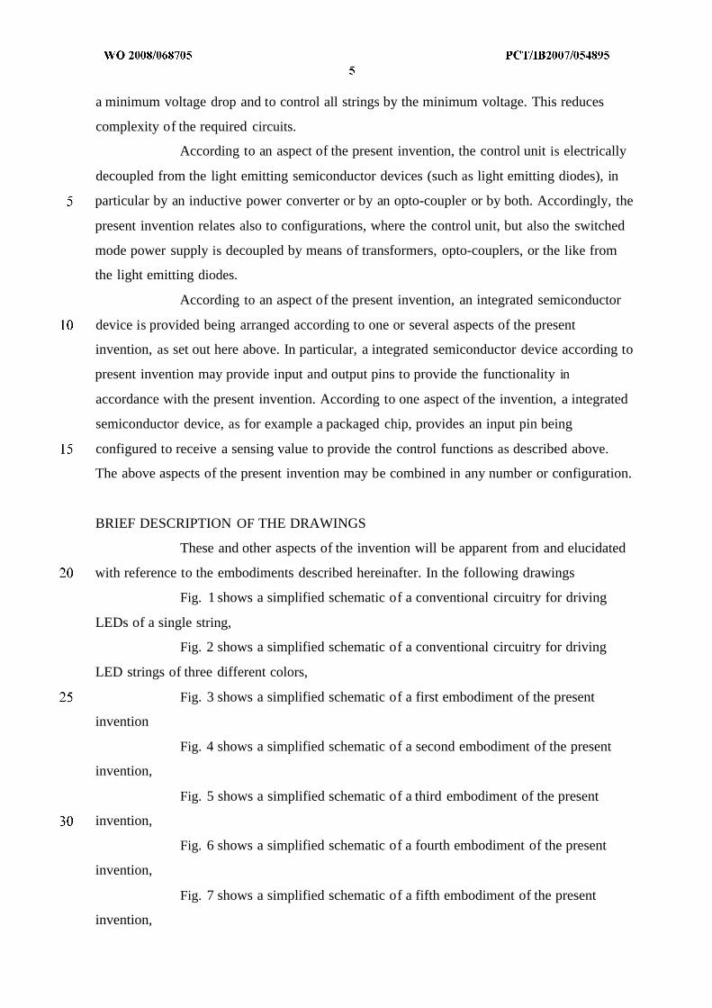
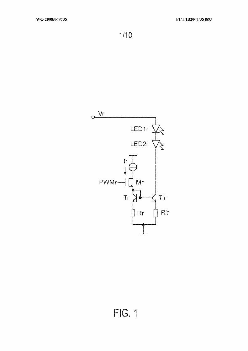
Fig. 1 shows a simplified schematic of a conventional circuitry for driving
LEDs of a single string,
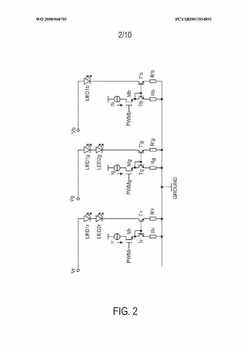
Fig. 2 shows a simplified schematic of a conventional circuitry for driving
LED strings of three different colors,
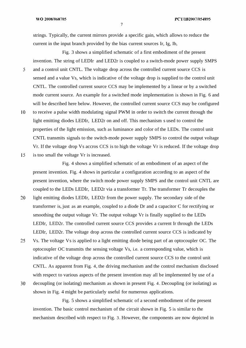
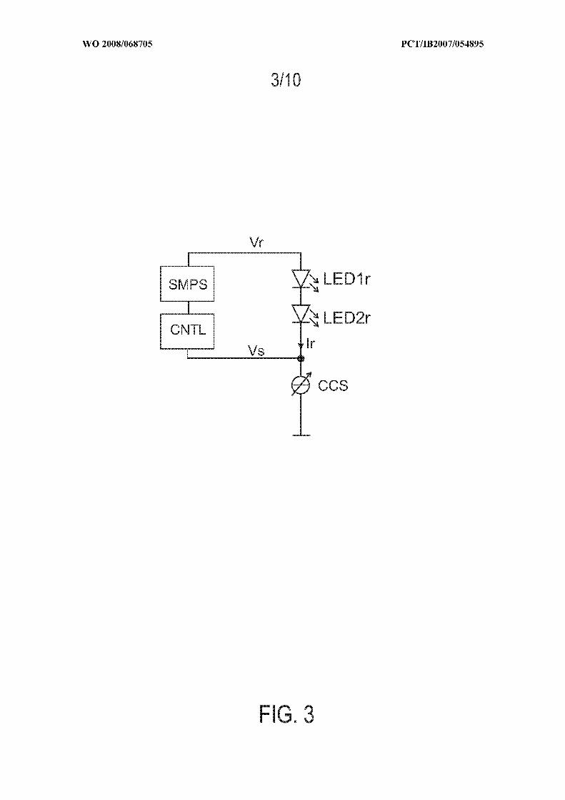
Fig. 3 shows a simplified schematic of a first embodiment of the present
invention
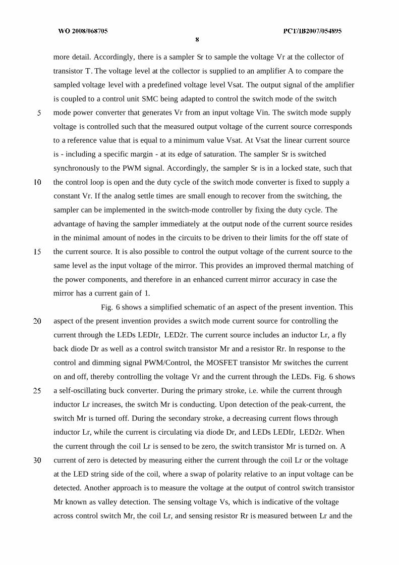
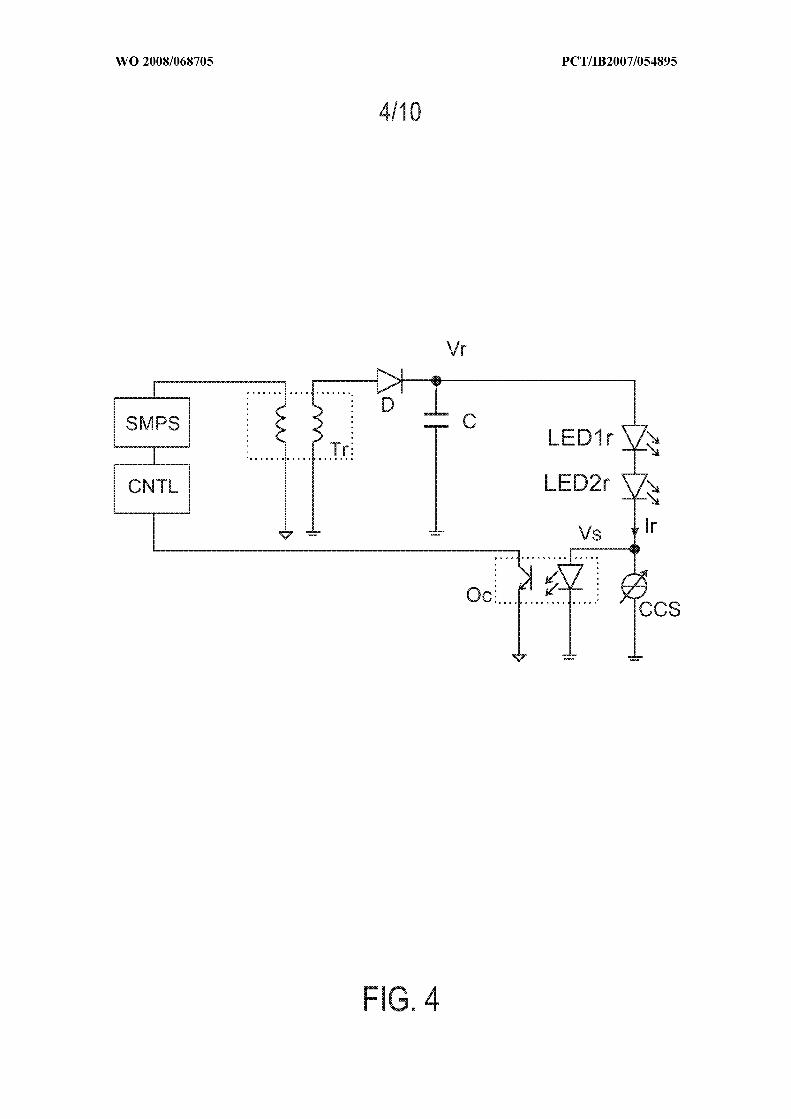
Fig. 4 shows a simplified schematic of a second embodiment of the present
invention,
Fig. 5 shows a simplified schematic of a third embodiment of the present
invention,
Fig. 6 shows a simplified schematic of a fourth embodiment of the present
invention,
Fig. 7 shows a simplified schematic of a fifth embodiment of the present
invention,
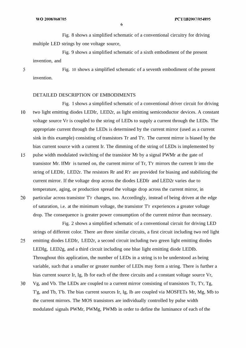
Fig. 8 shows a simplified schematic of a conventional circuitry for driving
multiple LED strings by one voltage source,
Fig. 9 shows a simplified schematic of a sixth embodiment of the present
invention, and
Fig. 10 shows a simplified schematic of a seventh embodiment of the present
invention.
DETAILED DESCRIPTION OF EMBODIMENTS
Fig. 1 shows a simplified schematic of a conventional driver circuit for driving
two light emitting diodes LEDIr, LED2r, as light emitting semiconductor devices. A constant
voltage source Vr is coupled to the string of LEDs to supply a current through the LEDs. The
appropriate current through the LEDs is determined by the current mirror (used as a current
sink in this example) consisting of transistors Tr and T'r. The current mirror is biased by the
bias current source with a current Ir. The dimming of the string of LEDs is implemented by
pulse width modulated switching of the transistor Mr by a signal PWMr at the gate of
transistor Mr. IfMr is turned on, the current mirror of Tr, T'r mirrors the current Ir into the
string of LEDIr, LED2r. The resistors Rr and R'r are provided for biasing and stabilizing the
current mirror. If the voltage drop across the diodes LEDIr and LED2r varies due to
temperature, aging, or production spread the voltage drop across the current mirror, in
particular across transistor T'r changes, too. Accordingly, instead of being driven at the edge
of saturation, i.e. at the minimum voltage, the transistor T'r experiences a greater voltage
drop. The consequence is greater power consumption of the current mirror than necessary.
Fig. 2 shows a simplified schematic of a conventional circuit for driving LED
strings of different color. There are three similar circuits, a first circuit including two red light
emitting diodes LEDIr, LED2r, a second circuit including two green light emitting diodes
LEDIg, LED2g, and a third circuit including one blue light emitting diode LEDIb.
Throughout this application, the number of LEDs in a string is to be understood as being
variable, such that a smaller or greater number of LEDs may form a string. There is further a
bias current source Ir, Ig, Ib for each of the three circuits and a constant voltage source Vr,
Vg, and Vb. The LEDs are coupled to a current mirror consisting of transistors Tr, T'r, Tg,
T'g, and Tb, T'b. The bias current sources Ir, Ig, Ib are coupled via MOSFETs Mr, Mg, Mb to
the current mirrors. The MOS transistors are individually controlled by pulse width
modulated signals PWMr, PWMg, PWMb in order to define the luminance of each of the
strings. Typically, the current mirrors provide a specific gain, which allows to reduce the
current in the input branch provided by the bias current sources Ir, Ig, Ib,
Fig. 3 shows a simplified schematic of a first embodiment of the present
invention. The string of LEDIr and LED2r is coupled to a switch-mode power supply SMPS
and a control unit CNTL. The voltage drop across the controlled current source CCS is
sensed and a value Vs, which is indicative of the voltage drop is supplied to the control unit
CNTL. The controlled current source CCS may be implemented by a linear or by a switched
mode current source. An example for a switched mode implementation is shown in Fig. 6 and
will be described here below. However, the controlled current source CCS may be configured
to receive a pulse width modulating signal PWM in order to switch the current through the
light emitting diodes LEDIr, LED2r on and off. This mechanism s used to control the
properties of the light emission, such as luminance and color of the LEDs. The control unit
CNTL transmits signals to the switch-mode power supply SMPS to control the output voltage
Vr. If the voltage drop Vs accros CCS is to high the voltage Vr is reduced. If the voltage drop
is too small the voltage Vr is increased.
Fig. 4 shows a simplified schematic of an embodiment of an aspect of the
present invention. Fig. 4 shows in particular a configuration according to an aspect of the
present invention, where the switch mode power supply SMPS and the control unit CNTL are
coupled to the LEDs LEDIr, LED2r via a transformer Tr. The transformer Tr decouples the
light emitting diodes LEDIr, LED2r from the power supply. The secondary side of the
transformer is, just as an example, coupled to a diode Dr and a capacitor C for rectifying or
smoothing the output voltage Vr. The output voltage Vr is finally supplied to the LEDs
LEDIr, LED2r. The controlled current source CCS provides a current Ir through the LEDs
LEDIr, LED2r. The voltage drop across the controlled current source CCS is indicated by
Vs. The voltage Vs is applied to a light emitting diode being part of an optocoupler OC. The
optocoupler OC transmits the sensing voltage Vs, i.e. a corresponding value, which is
indicative of the voltage drop across the controlled current source CCS to the control unit
CNTL. As apparent from Fig. 4, the driving mechanism and the control mechanism disclosed
with respect to various aspects of the present invention may all be implemented by use of a
decoupling (or isolating) mechanism as shown in present Fig. 4 . Decoupling (or isolating) as
shown in Fig. 4 might be particularly useful for numerous applications.
Fig. 5 shows a simplified schematic of a second embodiment of the present
invention. The basic control mechanism of the circuit shown in Fig. 5 is similar to the
mechanism described with respect to Fig. 3 . However, the components are now depicted in
more detail. Accordingly, there is a sampler Sr to sample the voltage Vr at the collector of
transistor T. The voltage level at the collector is supplied to an amplifier A to compare the
sampled voltage level with a predefined voltage level Vsat. The output signal of the amplifier
is coupled to a control unit SMC being adapted to control the switch mode of the switch
mode power converter that generates Vr from an input voltage Vin. The switch mode supply
voltage is controlled such that the measured output voltage of the current source corresponds
to a reference value that is equal to a minimum value Vsat. At Vsat the linear current source
is - including a specific margin - at its edge of saturation. The sampler Sr is switched
synchronously to the PWM signal. Accordingly, the sampler Sr is in a locked state, such that
the control loop is open and the duty cycle of the switch mode converter is fixed to supply a
constant Vr. If the analog settle times are small enough to recover from the switching, the
sampler can be implemented in the switch-mode controller by fixing the duty cycle. The
advantage of having the sampler immediately at the output node of the current source resides
in the minimal amount of nodes in the circuits to be driven to their limits for the off state of
the current source. It is also possible to control the output voltage of the current source to the
same level as the input voltage of the mirror. This provides an improved thermal matching of
the power components, and therefore in an enhanced current mirror accuracy in case the
mirror has a current gain of 1.
Fig. 6 shows a simplified schematic of an aspect of the present invention. This
aspect of the present invention provides a switch mode current source for controlling the
current through the LEDs LEDIr, LED2r. The current source includes an inductor Lr, a fly
back diode Dr as well as a control switch transistor Mr and a resistor Rr. In response to the
control and dimming signal PWM/Control, the MOSFET transistor Mr switches the current
on and off, thereby controlling the voltage Vr and the current through the LEDs. Fig. 6 shows
a self-oscillating buck converter. During the primary stroke, i.e. while the current through
inductor Lr increases, the switch Mr is conducting. Upon detection of the peak-current, the
switch Mr is turned off. During the secondary stroke, a decreasing current flows through
inductor Lr, while the current is circulating via diode Dr, and LEDs LEDIr, LED2r. When
the current through the coil Lr is sensed to be zero, the switch transistor Mr is turned on. A
current of zero is detected by measuring either the current through the coil Lr or the voltage
at the LED string side of the coil, where a swap of polarity relative to an input voltage can be
detected. Another approach is to measure the voltage at the output of control switch transistor
Mr known as valley detection. The sensing voltage Vs, which is indicative of the voltage
across control switch Mr, the coil Lr, and sensing resistor Rr is measured between Lr and the
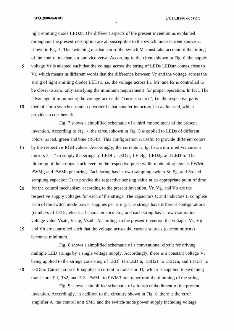
light emitting diode LED2r. The different aspects of the present invention as explained
throughout the present description are all susceptible to the switch mode current source as
shown in Fig. 6 . The switching mechanism of the switch Mr must take account of the timing
of the control mechanism and vice versa. According to the circuit shown in Fig. 6, the supply
voltage Vr is adapted such that the voltage across the string of LEDs LEDstr comes close to
Vr, which means in different words that the difference between Vr and the voltage across the
string of light emitting diodes LEDstr, i.e. the voltage across Lr, Mr, and Rr is controlled to
be closer to zero, only satisfying the minimum requirements for proper operation. In fact, The
advantage of minimizing the voltage across the "current source", i.e. the respective parts
thereof, for a switched-mode converter is that smaller inductors Lr can be used, which
provides a cost benefit.
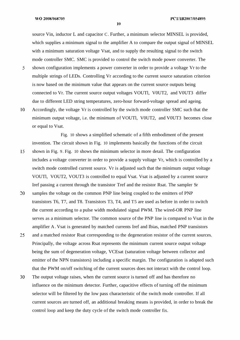
Fig. 7 shows a simplified schematic of a third embodiment of the present
invention. According to Fig. 7, the circuit shown in Fig. 5 is applied to LEDs of different
colors, as red, green and blue (RGB). This configuration is useful to provide different colors
by the respective RGB values. Accordingly, the currents Ir, Ig, Ib are mirrored via current
mirrors T, T ' to supply the strings of LEDIr, LED2r, LEDIg, LED2g and LEDIb. The
dimming of the strings is achieved by the respective pulse width modulating signals PWMr,
PWMg and PWMb per string. Each string has its own sampling switch Sr, Sg, and Sb and
sampling capacitor Cs to provide the respective sensing value at an appropriate point of time
for the control mechanism according to the present invention. Vr, Vg, and Vb are the
respective supply voltages for each of the strings. The capacitors C and inductors L complete
each of the switch mode power supplies per string. The strings have different configurations
(numbers of LEDs, electrical characteristics etc.) and each string has its own saturation
voltage value Vsatr, Vsatg, Vsatb. According, to the present invention the voltages Vr, Vg
and Vb are controlled such that the voltage across the current sources (current mirrors)
becomes minimum.
Fig. 8 shows a simplified schematic of a conventional circuit for driving
multiple LED strings by a single voltage supply. Accordingly, there is a constant voltage Vr
being applied to the strings consisting of LEDl 1 to LEDIn, LED21 to LED2n, and LED31 to
LED3n. Current source Ir supplies a current to transistor Tl, which is supplied to switching
transistors TsI, Ts2, and Ts3. PWMl to PWM3 are to perform the dimming of the strings.
Fig. 9 shows a simplified schematic of a fourth embodiment of the present
invention. Accordingly, in addition to the circuitry shown in Fig. 8, there is the error
amplifier A, the control unit SMC and the switch-mode power supply including voltage
source Vin, inductor L and capacitor C. Further, a minimum selector MINSEL is provided,
which supplies a minimum signal to the amplifier A to compare the output signal of MINSEL
with a minimum saturation voltage Vsat, and to supply the resulting signal to the switch
mode controller SMC. SMC is provided to control the switch mode power converter. The
shown configuration implements a power converter in order to provide a voltage Vr to the
multiple strings of LEDs. Controlling Vr according to the current source saturation criterion
is now based on the minimum value that appears on the current source outputs being
connected to Vr. The current source output voltages VOUTl, V0UT2, and V0UT3 differ
due to different LED string temperatures, zero-hour forward-voltage spread and ageing.
Accordingly, the voltage Vr is controlled by the switch mode controller SMC such that the
minimum output voltage, i.e. the minimum of VOUTl, V0UT2, and V0UT3 becomes close
or equal to Vsat.
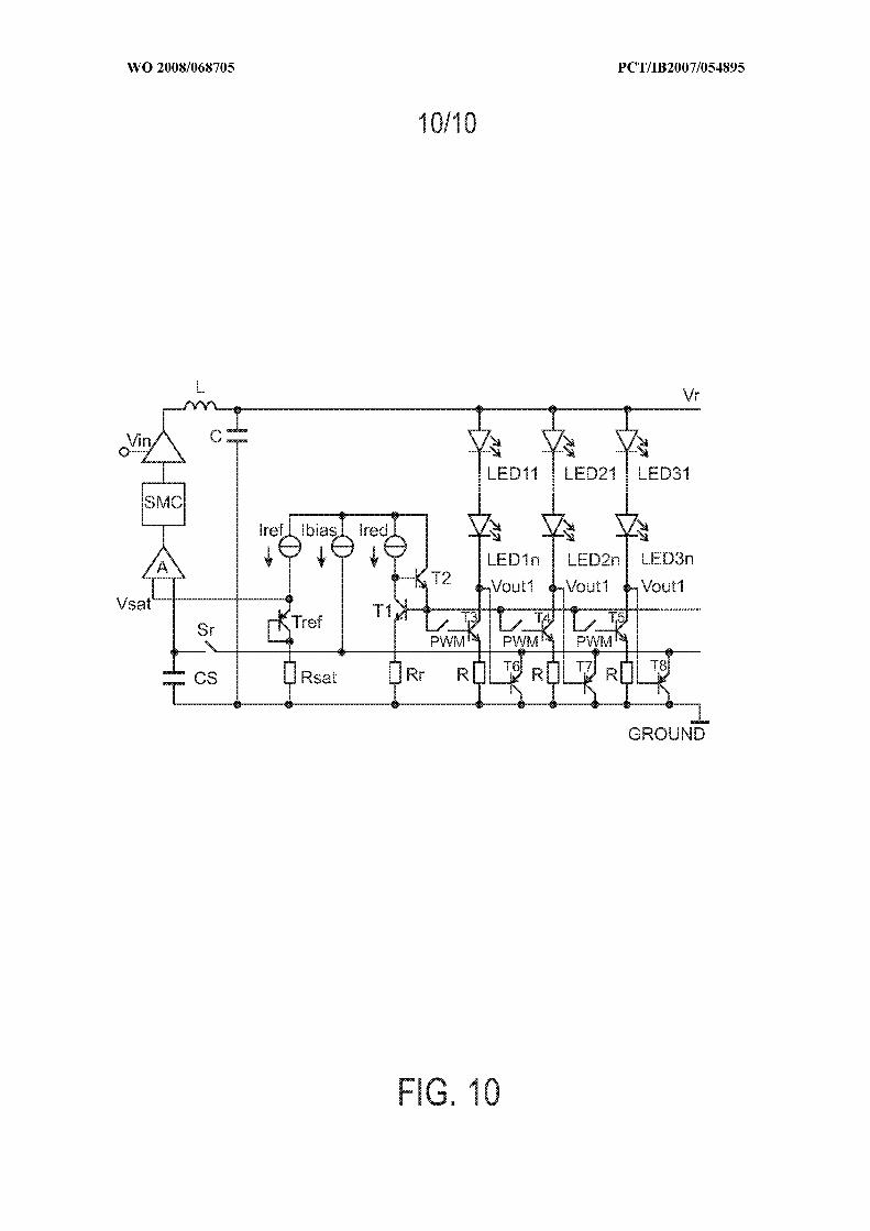
Fig. 10 shows a simplified schematic of a fifth embodiment of the present
invention. The circuit shown in Fig. 10 implements basically the functions of the circuit
shown in Fig. 9. Fig. 10 shows the minimum selector in more detail. The configuration
includes a voltage converter in order to provide a supply voltage Vr, which is controlled by a
switch mode controlled current source. Vr is adjusted such that the minimum output voltage
VOUTl, VOUT2, VOUT3 is controlled to equal Vsat. Vsat is adjusted by a current source
Iref passing a current through the transistor Tref and the resistor Rsat. The sampler Sr
samples the voltage on the common PNP line being coupled to the emitters of PNP
transistors T6, T7, and T8. Transistors T3, T4, and T5 are used as before in order to switch
the current according to a pulse width modulated signal PWM. The wired-OR PNP line
serves as a minimum selector. The common source of the PNP line is compared to Vsat in the
amplifier A. Vsat is generated by matched currents Iref and Ibias, matched PNP transistors
and a matched resistor Rsat corresponding to the degeneration resistor of the current sources.
Principally, the voltage across Rsat represents the minimum current source output voltage
being the sum of degeneration voltage, VCEsat (saturation voltage between collector and
emitter of the NPN transistors) including a specific margin. The configuration is adapted such
that the PWM on/off switching of the current sources does not interact with the control loop.
The output voltage raises, when the current source is turned off and has therefore no
influence on the minimum detector. Further, capacitive effects of turning off the minimum
selector will be filtered by the low pass characteristic of the switch mode controller. If all
current sources are turned off, an additional breaking means is provided, in order to break the
control loop and keep the duty cycle of the switch mode controller fix.
While the invention has been illustrated and described in detail in the drawings
and foregoing description, such illustration and description are to be considered illustrative or
exemplary and not restrictive; the invention is not limited to the disclosed embodiments.
Other variations to the disclosed embodiments can be understood and effected by those
skilled in the art in practicing the claimed invention, from a study of the drawings, the
disclosure, and the appended claims. A single LED may be replaced by multiple LEDs, in
particular a string thereof. A light emitting diode may also be another light emitting
semiconductor device as long as the aspects of the present invention are applicable. In the
claims, the word "comprising" does not exclude other elements or steps, and the indefinite
article "a" or "an" does not exclude a plurality. The mere fact that certain measures are
recited in mutually different dependent claims does not indicate that a combination of these
measured cannot be used to advantage. Any reference signs in the claims should not be
construed as limiting the scope.
CLAIMS:
1. Electronic device for driving a light emitting semiconductor device, the
electronic device comprising:
controlling means (CNTL) being adapted for controlling a switch mode power
supply (SMPS) for supplying the light emitting semiconductor device (LEDIr, LED2r) in
response to a sensing value (VS) received by the controlling means (CNTL) which is
indicative of a voltage across a current source for determining a current through the light
emitting semiconductor device (LEDIs, LED2r), wherein the switch-mode power supply
(SMPS) is controlled such that the voltage across the current source is minimum.
2 . The electronic device according to claim 1, comprising further the current
source, wherein the current source is a switched current source or a linear current source.
3 . The electronic device according to claim 1, wherein the control means (CNTL)
provide signals to switch the current through the light emitting semiconductor device
(LEDIr, LED2r) on and off, in particular by a pulse width modulated signal (PWMr).
4 . The electronic device according to one of the preceding claims, wherein the
controlling means (CNTL) is further adapted to control the timing of a sampling means for
sampling the sensing value, which is indicative of the voltage across the current source, such
that sampling occurs when the current through the current source is turned on.
5 . The electronic device according to one of the preceding claims, wherein the
light emitting semiconductor device is a light emitting diode, the electronic device
comprising further the switch-mode power supply (SMPS), wherein the switch-mode power
supply and the controlling means are adapted to control the output voltage of the switch-
mode supply with a control resolution of substantially less than the variation of the forward
voltage of the light emitting diode to be driven.

6 . The electronic device according to one of the preceding claims, comprising a
plurality of light emitting diodes as light emitting semiconductor devices, the electronic
device being further adapted to provide pulse width modulating signals for a plurality of light
emitting diodes for individually dimming each of the light emitting diodes.
7 . The electronic device according to claim 6, wherein the plurality of light
emitting diodes is arranged in at least one string.
8. The electronic device according to claim 7, being further adapted to provide a
pulse width modulated signal (PWMl) for dimming the diodes of the string.
9 . The electronic device according to claim 7 or 8, comprising further a plurality
of current sources and a minimum selector (MINSEL), wherein the plurality of light emitting
diodes is coupled to the plurality of current sources and the minimum selector (MINSEL) is
adapted to select the minimum voltage across the plurality of current sources, wherein the
selected minimum voltage is used as a reference for controlling the switch-mode power
supply.
10. The electronic device according to one of the preceding claims, wherein the
control unit is electrically decoupled from the light emitting semiconductor devices, in
particular by an inductive power converter or by an opto-coupler.
11. The electronic device according to one of the preceding claims, comprising an
input pin to receive the sensing value (Vs).

A. CLASSIFICATION OF SUBJECT MATTERINV . H05B33/08
According to International Patent Classification (IPC) or to both national classification and IPC
B. FIELDS SEARCHED
Minimum documentation searched (classification system followed by classification symbols)H05B
Documentation searched other than minimum documentation to the extent that such documents are included in the fields searched
Electronic data base consulted during the international search (name of data base and, where practical, search terms used)
EPO-Internal , WPI Data
C. DOCUMENTS CONSIDERED TO BE RELEVANT
Category * Citation of document, with indication, where appropriate, of the relevant passages Relevant to claim No.
WO 2006/097329 A (AUSTRIAMICROSYSTEMS AG 1-3,11[AT]; BUEHLER TOBIAS [AT]; JESSENIG THOMAS[AT]) 21 September 2006 (2006-09-21)page 1 , line 6 - page 9 , line 23; figure 1 7,9
US 2003/235062 Al (BURGYAN LAJOS [US] ET 1-3,11AL) 25 December 2003 (2003-12-25)paragraph [0011] - paragraph [0020]; 7,9figures 1,2
"48OmA White LED lx/l.5x/2x Charge Pump 1-3,6-9,for Backlighting and Camera Flash" 11
2005, MAXIM , SUNNYVALE, CA, USA ,XP002475922page 7 - page 10; figures 1-5 "
DE 100 13 216 Al (TRIDONIC BAUELEMENTE[AT]) 20 September 2001 (2001-09-20)
-/~
Further documents are listed in the continuation of Box C. See patent family annex.
* Special categories of cited documents :1T" later document published after the international filing date
or priority date and not in conflict with the application but'A' document defining the general state of the art which is not cited to understand the principle or theory underlying the
considered to be of particular relevance invention ,'E' earlier document but published on or after the international 'X* document of particular relevance; the claimed invention
filing date cannot be considered novel or cannot be considered to1L1 document which may throw doubts on priority claιm(s) or involve an inventive step when the document is taken alone
which is cited to establish the publication date of another 1Y1 document of particular relevance, the claimed inventioncitation or other special reason (as specified) cannot be considered to involve an inventive step when the
1O* document referring to an oral disclosure, use, exhibition or document is combined with one or mote other such docu¬other means ments, such combination being obvious to a person skilled
1P" document published prior to the international filing date but in the an.later than the priority date claimed '&' document member of the same patent family
Date of the actual completion of the international search Date of mailing of the international search report
10 Apri l 2008 28/04/2008
Name and mailing address of the ISA/ Authorized officerEuropean Patent Office, P B 5818 Patentlaan 2NL - 2280 HV Rijswijk
TeI. (+31-70) 340-2040, Tx. 3 1 651 epo nl,Fax: (+31-70) 340-3016 Albertsson, Gustav
Form PCT/ISA/210 (second sheet) (April 2005)

C(Continuatlon). DOCUMENTS CONSIDERED TO BE RELEVANT
Category * Citation of document, with indication, where appropriate, of the relevant passages Relevant to claim No.
DE 100 40 154 Al (WESTIFORM HOLDING AGNIEDERWAN [CH]) 7 March 2002 (2002-03-07)
Form PCT/ISA/210 (continuation ol second sheet) (April 2005)

Patent document Publication Patent family Publicationcited in search report date member(s) date
WO 2006097329 21-09-2006 DE 102005012663 Al 28-09-2006EP 1859655 Al 28-11-2007
US 2003235062 Al 25-12-2003 US 2004080301 Al 29-04-2004
DE 10013216 Al 20-09-2001 AT 256962 T 15-01-2004EP 1185147 Al 06-03-2002
DE 10040154 Al 07-03-2002 NONE
Form PCT/ISA/210 (patent family annex) (April 2005)