Wireless Low-Power Transfer for Galvanically Isolated High-Voltage ...
21
Citation: Hitzemann, M.; Lippmann, M.; Trachte, J.; Nitschke, A.; Burckhardt, O.; Zimmermann, S. Wireless Low-Power Transfer for Galvanically Isolated High-Voltage Applications. Electronics 2022, 11, 923. https://doi.org/10.3390/ electronics11060923 Academic Editor: Pablo García Triviño Received: 3 February 2022 Accepted: 13 March 2022 Published: 16 March 2022 Publisher’s Note: MDPI stays neutral with regard to jurisdictional claims in published maps and institutional affil- iations. Copyright: © 2022 by the authors. Licensee MDPI, Basel, Switzerland. This article is an open access article distributed under the terms and conditions of the Creative Commons Attribution (CC BY) license (https:// creativecommons.org/licenses/by/ 4.0/). electronics Article Wireless Low-Power Transfer for Galvanically Isolated High-Voltage Applications Moritz Hitzemann * , Martin Lippmann , Jonas Trachte , Alexander Nitschke , Olaf Burckhardt and Stefan Zimmermann Department of Sensors and Measurement Technology, Institute of Electrical Engineering and Measurement Technology, Leibniz Universität Hannover, Appelstr. 9A, 30167 Hannover, Germany; [email protected] (M.L.); [email protected] (J.T.); [email protected] (A.N.); [email protected] (O.B.); [email protected] (S.Z.) * Correspondence: [email protected]; Tel.: +49-511-762-14649 Abstract: For various applications, such as gate drivers for transistors, wireless chargers for mobile devices and cars, and isolated measurement equipment, an isolated DC power supply for electronic components is required. In this work, a new concept for an isolated power supply with insulation strength of 50 kV and power transmission of up to 60 W to supply measurement equipment with 12 or 24 V is presented. Furthermore, high overall efficiency of 82.5% at 55 W is achieved. Feasibility is demonstrated in a real application powering data acquisition electronics at high reference potential. Our new concept uses a coreless printed circuit board (PCB) transformer (15 cm × 10 cm × 4 cm and a weight of 480 g) designed for maximum efficiency via a coil layout and close proximity of adjacent coils on one PCB while reaching high isolation strength via the PCB material and potted coils. To increase efficiency, we investigated different coil geometries at different frequencies. A low-cost design consisting of two Qi charging coils mounted on one PCB is compared with our integrated PCB transformers manufactured from a four-layer PCB with ferrites applied on the outside. With this new design, high isolation voltages are possible while reaching high transformer efficiency of up to 90%. Keywords: power transformer; PCB transformer; PCB coils; high voltage isolation; gallium nitride GaN transistor; DC/DC converter; DCDC converter 1. Introduction The wireless transmission of electrical energy is used increasingly in different appli- cations. One of these applications is the supply of gate drivers for driving transistors on insulated potentials for all kinds of power electronics, such as DCDC converters for power supply systems (medium-voltage high-power applications) with isolation voltages up to 10 kV as presented in [1–8]. Different approaches using PCB-based transformers exist. For example, Xue et al. [1] and Zhang et al. [2] developed PCB transformers with E-shaped ferrite cores for a 1 kW DCDC converter having efficiencies of up to 98.3% [1] and for a 2.5 W DCDC converter having a maximum isolation strength of 20 kV [2]. High efficiencies are possible with this E-shaped ferrite, but the isolation voltage is limited by design, due to the electrically conductive ferrite being close to both the primary and secondary coil. This is one fundamental difference compared to our approach. Other PCB-based transformers are presented by Nguyen et al. [5], Tang et al. [6], Steiner et al. [7], and Marxgut et al. [8], mainly using two physically separated PCBs without any core. They reach isolation voltages of up to 40 kV and efficiencies of up to 80% with up to 100 W output power. In contrast, we use separated potted coils adjacent on one single PCB, thus increasing the efficiency and isolation voltage to 50 kV while reducing the size to 15 cm × 10 cm × 4 cm, giving a volume of 600 cm 3 . Classical transformers with an isolation voltage of 50 kV and 75 W output power have a volume of more than 2200 cm 3 and a weight >10 kg [9] (p 9). Thus, compared to classical transformers, our PCB transformer is quite compact. Unfortunately, no PCB Electronics 2022, 11, 923. https://doi.org/10.3390/electronics11060923 https://www.mdpi.com/journal/electronics
-
Upload
khangminh22 -
Category
Documents
-
view
2 -
download
0
Transcript of Wireless Low-Power Transfer for Galvanically Isolated High-Voltage ...

Citation: Hitzemann, M.; Lippmann,
M.; Trachte, J.; Nitschke, A.;
Burckhardt, O.; Zimmermann, S.
Wireless Low-Power Transfer for
Galvanically Isolated High-Voltage
Applications. Electronics 2022, 11, 923.
https://doi.org/10.3390/
electronics11060923
Academic Editor: Pablo
García Triviño
Received: 3 February 2022
Accepted: 13 March 2022
Published: 16 March 2022
Publisher’s Note: MDPI stays neutral
with regard to jurisdictional claims in
published maps and institutional affil-
iations.
Copyright: © 2022 by the authors.
Licensee MDPI, Basel, Switzerland.
This article is an open access article
distributed under the terms and
conditions of the Creative Commons
Attribution (CC BY) license (https://
creativecommons.org/licenses/by/
4.0/).
electronics
Article
Wireless Low-Power Transfer for Galvanically IsolatedHigh-Voltage ApplicationsMoritz Hitzemann * , Martin Lippmann , Jonas Trachte , Alexander Nitschke , Olaf Burckhardtand Stefan Zimmermann
Department of Sensors and Measurement Technology, Institute of Electrical Engineering and MeasurementTechnology, Leibniz Universität Hannover, Appelstr. 9A, 30167 Hannover, Germany;[email protected] (M.L.); [email protected] (J.T.); [email protected] (A.N.);[email protected] (O.B.); [email protected] (S.Z.)* Correspondence: [email protected]; Tel.: +49-511-762-14649
Abstract: For various applications, such as gate drivers for transistors, wireless chargers for mobiledevices and cars, and isolated measurement equipment, an isolated DC power supply for electroniccomponents is required. In this work, a new concept for an isolated power supply with insulationstrength of 50 kV and power transmission of up to 60 W to supply measurement equipment with 12or 24 V is presented. Furthermore, high overall efficiency of 82.5% at 55 W is achieved. Feasibility isdemonstrated in a real application powering data acquisition electronics at high reference potential.Our new concept uses a coreless printed circuit board (PCB) transformer (15 cm × 10 cm × 4 cm anda weight of 480 g) designed for maximum efficiency via a coil layout and close proximity of adjacentcoils on one PCB while reaching high isolation strength via the PCB material and potted coils. Toincrease efficiency, we investigated different coil geometries at different frequencies. A low-costdesign consisting of two Qi charging coils mounted on one PCB is compared with our integrated PCBtransformers manufactured from a four-layer PCB with ferrites applied on the outside. With this newdesign, high isolation voltages are possible while reaching high transformer efficiency of up to 90%.
Keywords: power transformer; PCB transformer; PCB coils; high voltage isolation; gallium nitrideGaN transistor; DC/DC converter; DCDC converter
1. Introduction
The wireless transmission of electrical energy is used increasingly in different appli-cations. One of these applications is the supply of gate drivers for driving transistors oninsulated potentials for all kinds of power electronics, such as DCDC converters for powersupply systems (medium-voltage high-power applications) with isolation voltages up to10 kV as presented in [1–8]. Different approaches using PCB-based transformers exist. Forexample, Xue et al. [1] and Zhang et al. [2] developed PCB transformers with E-shapedferrite cores for a 1 kW DCDC converter having efficiencies of up to 98.3% [1] and for a2.5 W DCDC converter having a maximum isolation strength of 20 kV [2]. High efficienciesare possible with this E-shaped ferrite, but the isolation voltage is limited by design, due tothe electrically conductive ferrite being close to both the primary and secondary coil. This isone fundamental difference compared to our approach. Other PCB-based transformers arepresented by Nguyen et al. [5], Tang et al. [6], Steiner et al. [7], and Marxgut et al. [8], mainlyusing two physically separated PCBs without any core. They reach isolation voltages ofup to 40 kV and efficiencies of up to 80% with up to 100 W output power. In contrast, weuse separated potted coils adjacent on one single PCB, thus increasing the efficiency andisolation voltage to 50 kV while reducing the size to 15 cm× 10 cm× 4 cm, giving a volumeof 600 cm3. Classical transformers with an isolation voltage of 50 kV and 75 W outputpower have a volume of more than 2200 cm3 and a weight >10 kg [9] (p 9). Thus, comparedto classical transformers, our PCB transformer is quite compact. Unfortunately, no PCB
Electronics 2022, 11, 923. https://doi.org/10.3390/electronics11060923 https://www.mdpi.com/journal/electronics
Electronics 2022, 11, 923 2 of 21
transformers having an isolating voltage of 50 kV exist, so direct comparison is difficult.However, the PCB transformer of Steiner et al. [7] is closest to our PCB transformer, butonly isolates 35 kV. Thus, this PCB transformer has a smaller volume of just 250 cm3. Otherrelevant fields of application of isolated power transmission include chargers for portabledevices such as electric toothbrushes, cell phones [10], and sensor networks [10]. However,these applications only require low power and low isolation voltage. In contrast, wirelesscharging of cars requires significantly more than 100 W but has no need for a compact highisolation setup [11–14]. In medical applications, implants such as cochlear implants donot need an output power of 60 W and high isolation voltages [15–17], whereas isolatedmeasurement and monitoring equipment partly requires high isolation voltages but doesnot use PCB transformers [18–21]. None of the employed concepts can be applied to powerour isolated measuring electronics.
There are different approaches to realize an isolated power transmission for differentapplications. For example, isolating transformers can be used for voltage isolation, whichis achieved by using two physically separated and insulated windings on one metal (iron-based) transformer core. However, due to the required metal transformer core for couplingthe coils, a corresponding insulation strength can only be achieved by large and heavyisolating transformers [22] (pp. 148–158). Another option is the use of accumulators andbatteries [20]. The use of accumulators enables a very high dielectric strength due tothe completely galvanically isolated structure, but the size of accumulators and batterydepends on the required capacity, and continuous operation is not possible. In contrast,commercially available isolated DCDC converters are usually smaller, but either insulationstrength and/or power transmission are limited. For example, isolated DCDC convertersfrom RECOM Power are capable of isolating 12 kV, as in the power supply used byLippmann et al. [23], but power transmission is limited to 6 W. For larger isolation strengths,DCDC converters are available from other manufacturers, such as the Advanced EnergyUltraVolt EFL Series, which provides isolation voltages of, e.g., 30 kV at 24 W [24].
Our new concept uses a coreless PCB transformer designed for maximum efficiencyvia the coil layout and close proximity of adjacent coils on one PCB, while reaching highisolation strength via the PCB material and potted coils. The functionality of the developedisolated DC power supply is demonstrated using an ion mobility spectrometer as a possibleapplication. In this context, ion mobility spectrometers (IMSs) with high analytical perfor-mance require electronic modules at different electrical potentials for operation, such as agalvanically isolated data acquisition of currents in the pA range [23] or ion gate controlsto influence the ion package to be analyzed [25]. Here, the isolated assemblies are operatedat high electrical potentials (drift voltage potential). According to Kirk et al. [26], resolvingpower of IMS increases with drift voltage; thus, high drift voltages are mandatory forultra-high resolving power. Depending on the design of the IMS, either the detector withthe isolated data acquisition of the ion current or the ion source with the ion gate control isat high drift voltage potential. If, for example, the detector is connected to the drift voltagepotential, the galvanically isolated DC power supply has to be designed in such a waythat no electromagnetic interference with the measurement signal exists. Although this isthe case with some of the commercially available insulation methods mentioned above,higher isolation voltages are required sometimes. The use of accumulators for the operationof the IMS is not suitable for performing long-term measurements, such as monitoringpollutants [27], whereas isolating transformers would be a good option. However, theymostly use mains voltage, which is rather impractical.
For the construction of small DCDC converters, an alternative is the use of transformersbased on printed circuit boards (PCB). Currently, the use of such PCB transformers is mainlylimited to the supply of gate drivers in the field of power electronics [6–8], but can possiblybe extended to isolated DCDC converters with higher insulation strength and higher powertransmission.
The basic insulation material in PCB construction is a composite material called FR4,consisting of fiberglass and epoxy resin, achieving very high dielectric strengths from 45

Electronics 2022, 11, 923 3 of 21
to 58 kV/mm [28] (pp. 154–155) [29]. This makes it possible to manufacture the completeisolation transformer, consisting of the primary and secondary coils, on one single PCB.In addition to the dielectric strength, the creepage distance of the material must also beconsidered when designing the transformer [30]. To reduce the size, it is also possible todistribute the coils over several PCB layers. Electromagnetic interference can be reduced byadditional ferrite foils, and plates mounted directly on the PCB [31]. Furthermore, the ferriteplates also contribute to improve coupling between the coils [31]. To date, Square or Circularcoil geometries are mainly used as PCB transformers or coils [2,4,8,32,33]. Furthermore,to the best of our knowledge, there are no known comparisons in the literature to date ofefficiency measurements of different coil geometries.
Therefore, in this paper, the influence of various geometries and arrangements of theprimary and secondary coils on the efficiency of the PCB transformer is investigated bymeasurement in a frequency range from 150 kHz to 2.5 MHz. For these measurements, thePCB transformers are integrated into an electronic control system that enables excitationof the transformers with different frequencies. The electronic control system also includesrectification and voltage regulation for the supply of the isolated electronics, also supportingthe frequency range from 150 kHz to 2.5 MHz. It was found that different coil geometriesare better suited for different frequencies. Furthermore, different rectifier diodes were testedin order to investigate the impact on the overall efficiency at higher frequencies. Finally,isolation measurements, and operation on the ion mobility spectrometer, are demonstrated.
2. Materials and Methods
The isolated DC power supply presented here is intended to supply the transimpedanceamplifier and the data acquisition of an IMS with extremely high resolving power at an elec-trical potential of at least 50 kV. With a minimum dielectric strength for FR4 of 45 kV/mm,the required insulation strength is achieved with a coil spacing between the primary andsecondary coils of at least 1.2 mm [29]. A PCB core with a minimum spacing of 2.4 mm isused to compensate for inhomogeneity in PCB thickness and dielectric strength of the FR4.In addition to the pure dielectric strength of the FR4, a creepage distance of at least 140 mmfor 50 kV DC is also required according to the IEC standard for consumer electronicsdevices (IEC 60950-1 [30]). This ensures functional insulation with a material group IIIband a pollution level of 1 (no pollution or only dry, non-conductive pollution). To achievepollution degree 1 in a normal environment, the transformer is additionally encapsulatedwith a DOW Corning Sylgard 527 potting compound and the complete insulated DC powersupply is installed in a plastic housing.
A transformer built of Würth 760308111 wireless charging coils having dimensions55 mm × 55 mm is used to verify the insulation strength and serves as a reference for thePCB transformers, in which the secondary and primary coils were manufactured directly ona single PCB. The wireless charging coils were bonded to a 150 mm × 100 mm × 3.2 mmPCB and encapsulated with a DOW Corning Sylgard 527 potting compound. Due to thesize and inductance of the wireless charging coils, a multilayer PCB transformer structure isrequired to achieve similar inductance of the PCB coils. Therefore, the PCB overall thicknessof the reference Qi transformer and the PCB transformers was chosen to be 3.2 mm.
Further constraints for the design of the PCB-based transformer result from the re-quired power of at least 30 W for the operation of the transimpedance amplifier, includingdata acquisition and the resulting current in the traces at a targeted supply voltage ofUaverage = 12 V. The current flowing through the coil Ipeak = 7.05 A was calculated fora sinusoidal voltage using Equation (1) and Paverage = 60 W of power for a sufficientsafety margin. All used variables including descriptions can be found in Table A3 in theAppendix A. Since we assume the worst-case scenario regarding the maximum possiblecurrent, only the resistance of the conductor path was considered.
Ipeak =Paverage·
√2
Uaverage(1)

Electronics 2022, 11, 923 4 of 21
From the calculated current Ipeak, a trace width of dwitdh = 3 mm and trace thicknessof dthickness = 70 µm can be determined for a two-layer PCB coil according to (IPC-2221 [34])Equation (A1) for ∆Trise = 30 C of the PCB by heating. From the manufacturing tolerancesof the PCBs for a copper thickness of 70 µm, the minimum trace spacing is dspace = 175 µm,and the spacing between the first trace layer and the second trace layer is 200 µm.
To ensure comparability with the 760308111 Würth charging coils, the PCB coilsare approximately dimensioned as 55 mm × 55 mm. Due to the previously calculatedtrace parameters and the dimensions of 55 mm × 55 mm, a maximum of 7 turns arepossible for a Square PCB coil on one layer. There are various approaches for calculat-ing the inductance of different coil geometries; for example, simple analytical methodsas proposed by Mohan et al. [35] or more advanced numerical methods as published byConstantinescu et al. [36]. Since the investigated inductances should have similar inductiv-ities, here, the simple analytical methods of Mohan et al. [35] seem more appropriate forestimating the inductivities of the different coil geometries. The real inductivities of thedifferent coils were measured as described later. With Equations (2) and (A2)–(A4), thisresults in an inductance of LSingle = 1.77 µH for a Square PCB coil on one layer, calculatedwith the current sheet expression [35]. Table A1 contains the values of c1–c4 taken fromMohan et al. [35]. According to Mohan et al. [35], just a minor error of 4% exists whencomparing measured inductivities with calculated values, even for different coil geometries.Using this method, we calculate a maximum error of 1.7% for our coil geometries, as shownlater. This is sufficient accuracy for us to lay out the different coil geometries.
LSingle =µ0n2davgc1
2
(ln(
c2
ρ
)+ c3ρ+ c4ρ
2)
(2)
In order to achieve the targeted inductance of the PCB coil in the range of the Würth760308111 charging coils of 6.3 µH, two PCB coils on different layers are used. Due to thedouble number of turns n of 14, this results in a (2·n)2 = 4 times larger total inductance ofthe coil of LPair = 7 µH. For the PCB transformer, an identical secondary coil is used. Thisresults in a transmission ratio of 1:1. The following layer structure for the PCB transformeris shown in Figure 1.
Electronics 2022, 11, x FOR PEER REVIEW 4 of 22
calculated for a sinusoidal voltage using Equation (1) and Paverage = 60 W of power for a
sufficient safety margin. All used variables including descriptions can be found in Table
A3 in the Appendix A. Since we assume the worst-case scenario regarding the maximum
possible current, only the resistance of the conductor path was considered.
Ipeak =Paverage ∙ √2
Uaverage (1)
From the calculated current Ipeak , a trace width of dwitdh = 3 mm and trace
thickness of dthickness = 70 µm can be determined for a two-layer PCB coil according to
(IPC-2221 [34]) Equation (A1) for ∆Trise = 30 °C of the PCB by heating. From the
manufacturing tolerances of the PCBs for a copper thickness of 70 µm, the minimum trace
spacing is dspace = 175 µm, and the spacing between the first trace layer and the second
trace layer is 200 µm.
To ensure comparability with the 760308111 Würth charging coils, the PCB coils are
approximately dimensioned as 55 mm × 55 mm. Due to the previously calculated trace
parameters and the dimensions of 55 mm × 55 mm, a maximum of 7 turns are possible for
a Square PCB coil on one layer. There are various approaches for calculating the
inductance of different coil geometries; for example, simple analytical methods as
proposed by Mohan et al. [35] or more advanced numerical methods as published by
Constantinescu et al. [36]. Since the investigated inductances should have similar
inductivities, here, the simple analytical methods of Mohan et al. [35] seem more
appropriate for estimating the inductivities of the different coil geometries. The real
inductivities of the different coils were measured as described later. With Equations (2)
and (A2)–(A4), this results in an inductance of LSingle = 1.77 µH for a Square PCB coil on
one layer, calculated with the current sheet expression [35]. Table A1 contains the values
of c1 − c4 taken from Mohan et al. [35]. According to Mohan et al. [35], just a minor error
of 4% exists when comparing measured inductivities with calculated values, even for
different coil geometries. Using this method, we calculate a maximum error of 1.7% for
our coil geometries, as shown later. This is sufficient accuracy for us to lay out the different
coil geometries.
LSingle =μ0n2davgc1
2(ln (
c2
ρ) + c3ρ + c4ρ2) (2)
In order to achieve the targeted inductance of the PCB coil in the range of the Würth
760308111 charging coils of 6.3 µH, two PCB coils on different layers are used. Due to the
double number of turns n of 14, this results in a (2 ∙ n)2 = 4 times larger total inductance
of the coil of LPair = 7 µH. For the PCB transformer, an identical secondary coil is used.
This results in a transmission ratio of 1:1. The following layer structure for the PCB
transformer is shown in Figure 1.
Figure 1. Schematic sectional view of the Square PCB transformer, showing the layer
structure. Figure 1. Schematic sectional view of the Square PCB transformer, showing the layer structure.
The connection between the individual coils on different layers is made by blindvertical interconnect accesses (vias). These vias connect the outer layer with the adjacentinner layer for one coil, and the same applies to the other coil. In addition to the Square coil,four other coil geometries were investigated, for which the above-mentioned parameterssuch as track width, track thickness, track spacing, number of turns and layer structure,were also used. The different coil geometries are shown in Figure 2. The second half of thecoil looks identical and is mirrored on the adjacent layer.
Electronics 2022, 11, 923 5 of 21
Electronics 2022, 11, x FOR PEER REVIEW 5 of 22
The connection between the individual coils on different layers is made by blind
vertical interconnect accesses (vias). These vias connect the outer layer with the adjacent
inner layer for one coil, and the same applies to the other coil. In addition to the Square
coil, four other coil geometries were investigated, for which the above-mentioned
parameters such as track width, track thickness, track spacing, number of turns and layer
structure, were also used. The different coil geometries are shown in Figure 2. The second
half of the coil looks identical and is mirrored on the adjacent layer.
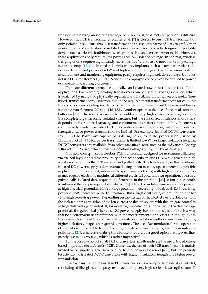
Figure 2. Different coil geometries with dimensions: Square, Circular, Octagonal, Square with
beveled corners constant trace spacing (Thick Corner), Square with beveled corners constant trace
width (Thin Corner).
Figure 2 shows the three coil geometries, Square, Octagonal and Circular, as also
described by Mohan et al. [35], and two additional coil shapes, Thick Corner and Thin
Corner, which are based on the Square coil geometry. The deviation from the Square coil
geometry is intended to reduce the excess current in the corners of the coil and to maintain
a relatively high inductance per area. The Thin Corner coil geometry has a constant trace
width but a larger trace spacing in the corners of 1.1 mm, whereas the Thick Corner design
has a constant trace spacing of 175 µm, resulting in wider traces of 4.2 mm in the corners.
The efficiency of the PCB transformer constructed from the coils is significantly
affected by the coupling efficiency of both coils [37] (pp. 77–101). According to Matsuki et
al. [38], the highest efficiency of the transformer can be achieved with identically sized
coils; therefore, the coils were designed with identical dimensions. As described by Soma
et al. [39], the coupling of both coils is determined by the alignment and position of the
coils with respect to each other [37] (pp. 156–158). Therefore, the coils are mirrored on the
adjacent layer. In addition, the coupling of the coils can also be improved by better field
guidance, for example, by using ferrite foils or plates [31]; we used ferrite foils to improve
the field guidance. Depending on the permeability and the thickness of the ferrite
material, the inductance of a single coil also increases [40]. Therefore, Würth 32405S ferrite
foils were used in the structure presented here. According to Hurley et al. [31,40], an
inductance increase of at least 1.7 can be expected. The efficiency of the transformers can
be increased by using additional capacitors, which improve the coupling of the
transformer to the electronics by means of capacitors connected in parallel and/or in series
[37,41]. The values of the series capacitors used were determined with the circuit
simulation program LTspice to 400 nF per coil, which allows an optimal efficiency for the
Figure 2. Different coil geometries with dimensions: Square, Circular, Octagonal, Square with beveledcorners constant trace spacing (Thick Corner), Square with beveled corners constant trace width(Thin Corner).
Figure 2 shows the three coil geometries, Square, Octagonal and Circular, as alsodescribed by Mohan et al. [35], and two additional coil shapes, Thick Corner and ThinCorner, which are based on the Square coil geometry. The deviation from the Square coilgeometry is intended to reduce the excess current in the corners of the coil and to maintaina relatively high inductance per area. The Thin Corner coil geometry has a constant tracewidth but a larger trace spacing in the corners of 1.1 mm, whereas the Thick Corner designhas a constant trace spacing of 175 µm, resulting in wider traces of 4.2 mm in the corners.
The efficiency of the PCB transformer constructed from the coils is significantly affectedby the coupling efficiency of both coils [37] (pp. 77–101). According to Matsuki et al. [38], thehighest efficiency of the transformer can be achieved with identically sized coils; therefore,the coils were designed with identical dimensions. As described by Soma et al. [39], thecoupling of both coils is determined by the alignment and position of the coils with respectto each other [37] (pp. 156–158). Therefore, the coils are mirrored on the adjacent layer.In addition, the coupling of the coils can also be improved by better field guidance, forexample, by using ferrite foils or plates [31]; we used ferrite foils to improve the fieldguidance. Depending on the permeability and the thickness of the ferrite material, theinductance of a single coil also increases [40]. Therefore, Würth 32405S ferrite foils wereused in the structure presented here. According to Hurley et al. [31,40], an inductanceincrease of at least 1.7 can be expected. The efficiency of the transformers can be increasedby using additional capacitors, which improve the coupling of the transformer to theelectronics by means of capacitors connected in parallel and/or in series [37,41]. The valuesof the series capacitors used were determined with the circuit simulation program LTspiceto 400 nF per coil, which allows an optimal efficiency for the measured frequencies. Itis advantageous to use 4 × 100 nF TDK C3216C0G1H104J160AA in parallel for a lowinternal resistance compared to one single capacitor. This means that all the optimizationapproaches described in the literature for the most efficient transformer possible were takeninto account in the design of the PCB transformers. This leaves only one optimizationparameter open—the coil geometry, which we investigate in this work.
The measurement of the inductance of the PCB transformers was performed at mea-surement frequencies of 1 kHz, 150 kHz, and 1 MHz with a Keysight E4980A LCR meter
Electronics 2022, 11, 923 6 of 21
and matching Keysight 16047A measurement adapter. Resistance measurements wereperformed using a Keysight 3458A with Keysight 11059A Kelvin probe tips.
To operate the galvanically isolated DC power supply, drive electronics for generatingan AC voltage on the input side and a corresponding rectification and voltage regulation ofthe transmitted AC voltage on the galvanically isolated output side are required.
The AC voltage should be generated with a high degree of efficiency in order to keepthe electrical losses of the overall system low. For this reason, a low internal resistanceand currents up to at least 7 A are required to handle the maximum current through thetransformer. In addition, the drive electronics must be suitable for higher frequencies in theMHz range.
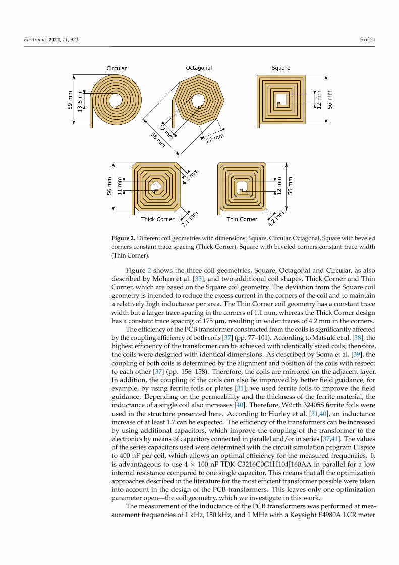
The AC voltage is generated with a full-bridge circuit, which allows an alternatingcurrent flow through the primary coil of the transformer. This full-bridge circuit is shownin Figure 3 and is constructed with GaN Systems GS61004B enhancement-mode GaNtransistors driven by a Texas Instrument LMG1210 half-bridge gate driver. The transistorsin combination with the gate drivers allow for rise times of 1.2 ns and fall times of 2.5 ns,enabling operation of the transformers at up to 10 MHz. At these switching frequencies, thePCB layout of the circuit is essential since additional parasitic capacitances or inductancesresult in a reduction in the maximum achievable switching frequency. Therefore, thetransistors should be connected to the gate driver with the shortest possible traces. Theuse of surface mounted devices (SMD) in small sizes is particularly useful for this purpose.To supply sufficient current in the switching moment, the supply voltage is supported by15 times 10 µF TDK C2012X5R1V106K125AC capacitors and a 68 µF Panasonic 50SVPF68Melectrolytic capacitor. An additional input filter, as shown in the upper left corner of Figure 3,smooths the supply voltage and suppresses common mode noise in both directions. Here,it is also possible to use one 2 µH inductor with similar current carrying capacity insteadof two single 1 µH inductors. The remaining components in Figure 3 are required foroperation of the gate drivers.
Electronics 2022, 11, x FOR PEER REVIEW 6 of 22
measured frequencies. It is advantageous to use 4 × 100 nF TDK C3216C0G1H104J160AA
in parallel for a low internal resistance compared to one single capacitor. This means that
all the optimization approaches described in the literature for the most efficient
transformer possible were taken into account in the design of the PCB transformers. This
leaves only one optimization parameter open—the coil geometry, which we investigate in
this work.
The measurement of the inductance of the PCB transformers was performed at
measurement frequencies of 1 kHz, 150 kHz, and 1 MHz with a Keysight E4980A LCR
meter and matching Keysight 16047A measurement adapter. Resistance measurements
were performed using a Keysight 3458A with Keysight 11059A Kelvin probe tips.
To operate the galvanically isolated DC power supply, drive electronics for
generating an AC voltage on the input side and a corresponding rectification and voltage
regulation of the transmitted AC voltage on the galvanically isolated output side are
required.
The AC voltage should be generated with a high degree of efficiency in order to keep
the electrical losses of the overall system low. For this reason, a low internal resistance and
currents up to at least 7 A are required to handle the maximum current through the
transformer. In addition, the drive electronics must be suitable for higher frequencies in
the MHz range.
The AC voltage is generated with a full-bridge circuit, which allows an alternating
current flow through the primary coil of the transformer. This full-bridge circuit is shown
in Figure 3 and is constructed with GaN Systems GS61004B enhancement-mode GaN
transistors driven by a Texas Instrument LMG1210 half-bridge gate driver. The transistors
in combination with the gate drivers allow for rise times of 1.2 ns and fall times of 2.5 ns,
enabling operation of the transformers at up to 10 MHz. At these switching frequencies,
the PCB layout of the circuit is essential since additional parasitic capacitances or
inductances result in a reduction in the maximum achievable switching frequency.
Therefore, the transistors should be connected to the gate driver with the shortest possible
traces. The use of surface mounted devices (SMD) in small sizes is particularly useful for
this purpose. To supply sufficient current in the switching moment, the supply voltage is
supported by 15 times 10 µF TDK C2012X5R1V106K125AC capacitors and a 68 µF
Panasonic 50SVPF68M electrolytic capacitor. An additional input filter, as shown in the
upper left corner of Figure 3, smooths the supply voltage and suppresses common mode
noise in both directions. Here, it is also possible to use one 2 µH inductor with similar
current carrying capacity instead of two single 1 µH inductors. The remaining
components in Figure 3 are required for operation of the gate drivers.
Figure 3. Circuit diagram of the control electronics for the transformers.
The pulses to drive the two half-bridges for the efficiency measurements were
generated by an Agilent 81150A function generator. For the integrated version of the drive
Figure 3. Circuit diagram of the control electronics for the transformers.
The pulses to drive the two half-bridges for the efficiency measurements were gen-erated by an Agilent 81150A function generator. For the integrated version of the driveelectronics, which can be seen later, a Texas Instruments CDCE906 with a programmablePhase-Lock-Loop (PLL) is used to generate two complementary square wave signals todrive the two half-bridges. The CDCE906 is controlled by a microcontroller MicrochipSAML21J18B, which sets a frequency specified by the microcontroller firmware when asupply voltage is applied. This frequency can be adjusted to match the optimal frequencyfound for the transformer.
On the secondary side, the isolated AC voltage signal transmitted by the transformerhas to be converted to a DC voltage again in order to be used with the IMS. The circuitused for this purpose is shown in Figure 4. For filtering and common mode rejection, aTDK ACM1211-701-2PL-TL01 coil is used. The filtered signal is then rectified by a full-

Electronics 2022, 11, 923 7 of 21
bridge rectifier. To achieve high efficiency and a high switching frequency, the four diodesrequired for the rectifier need low forward voltages and fast recovery times. Therefore, twodifferent types of diodes adapted to the frequency range were used for the experiments. Forfrequencies up to 150 kHz, a ON Semiconductor FSV8100V Schottky diode with forwardvoltages of typical UF = 0.62 V (@IF = 8 A) and recovery times of about 20 ns was used,whereas for higher frequencies, STMicroelectronics STPSC12065-Y silicon carbide Schottkydiodes with forward voltages of typical UF = 1.3 V (@IF = 12 A) were used. Due to thespecial structure of the silicon carbide Schottky diodes, there are no or only negligiblerecovery times. The rectified voltage is buffered by ten 10 µF TDK C2012X5R1V106K125ACcapacitors and a 68 µF Panasonic 50SVPF68M capacitor to provide sufficient current evenfor fast load changes e.g., for a high-voltage pulse generation.
Electronics 2022, 11, x FOR PEER REVIEW 7 of 22
electronics, which can be seen later, a Texas Instruments CDCE906 with a programmable
Phase-Lock-Loop (PLL) is used to generate two complementary square wave signals to
drive the two half-bridges. The CDCE906 is controlled by a microcontroller Microchip
SAML21J18B, which sets a frequency specified by the microcontroller firmware when a
supply voltage is applied. This frequency can be adjusted to match the optimal frequency
found for the transformer.
On the secondary side, the isolated AC voltage signal transmitted by the transformer
has to be converted to a DC voltage again in order to be used with the IMS. The circuit
used for this purpose is shown in Figure 4. For filtering and common mode rejection, a
TDK ACM1211-701-2PL-TL01 coil is used. The filtered signal is then rectified by a full-
bridge rectifier. To achieve high efficiency and a high switching frequency, the four diodes
required for the rectifier need low forward voltages and fast recovery times. Therefore,
two different types of diodes adapted to the frequency range were used for the
experiments. For frequencies up to 150 kHz, a ON Semiconductor FSV8100V Schottky
diode with forward voltages of typical UF = 0.62 V (@IF = 8 A) and recovery times of about
20 ns was used, whereas for higher frequencies, STMicroelectronics STPSC12065-Y silicon
carbide Schottky diodes with forward voltages of typical UF = 1.3 V (@IF = 12 A) were
used. Due to the special structure of the silicon carbide Schottky diodes, there are no or
only negligible recovery times. The rectified voltage is buffered by ten 10 µF TDK
C2012X5R1V106K125AC capacitors and a 68 µF Panasonic 50SVPF68M capacitor to
provide sufficient current even for fast load changes e.g., for a high-voltage pulse
generation.
For a load-independent output voltage, an additional buck-boost converter was
integrated to convert the rectified AC voltage into a constant DC voltage. The buck-boost
converter used here is an LM5176 with the required circuitry, which can be found in the
LM5176 data sheet on page 21. The output voltage generated is adjustable via a resistor
and further smoothed via additional capacitors.
Figure 4. Circuit diagram of the voltage rectification and regulation on the secondary side of the
isolated DC power supply.
For the investigations at higher frequencies, the secondary side was modified as
shown in Figure 5 and the ON Semiconductor FSV8100V rectifier diodes were exchanged
for the faster ST STPSC12065-Y rectifier diodes. To improve the efficiency in the lower
load range, the Texas Instruments LM5176 buck-boost converter was replaced by a Texas
Instruments LM3481 boost converter. The required circuitry for the LM3481 can be found
in the data sheet on page 26.
Figure 4. Circuit diagram of the voltage rectification and regulation on the secondary side of theisolated DC power supply.
For a load-independent output voltage, an additional buck-boost converter was in-tegrated to convert the rectified AC voltage into a constant DC voltage. The buck-boostconverter used here is an LM5176 with the required circuitry, which can be found in theLM5176 data sheet on page 21. The output voltage generated is adjustable via a resistorand further smoothed via additional capacitors.
For the investigations at higher frequencies, the secondary side was modified as shownin Figure 5 and the ON Semiconductor FSV8100V rectifier diodes were exchanged for thefaster ST STPSC12065-Y rectifier diodes. To improve the efficiency in the lower load range,the Texas Instruments LM5176 buck-boost converter was replaced by a Texas InstrumentsLM3481 boost converter. The required circuitry for the LM3481 can be found in the datasheet on page 26.
Electronics 2022, 11, x FOR PEER REVIEW 8 of 22
Figure 5. Circuit diagram of the voltage rectification and regulation on the secondary side of the
isolated DC power supply with faster diodes and high efficiency boost converter.
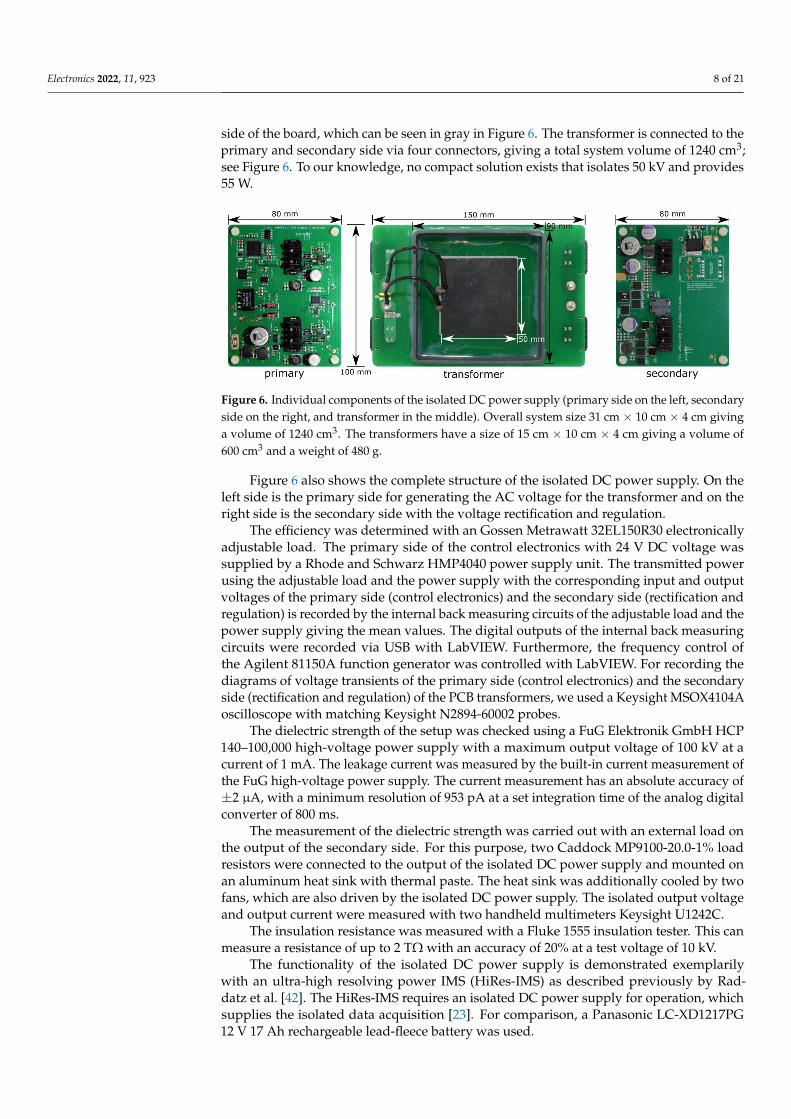
The completely assembled reference transformer with additional high-voltage
insulation is shown in Figure 6. This transformer consists of Würth 760308111 two
wireless charging coils, which are mounted on one PCB with the dimensions 150 mm ×
100 mm. To achieve the required insulation strength of 50 kV, the coils were encapsulated
with a DOW Corning Sylgard 527 potting compound to a height of approximately 20 mm
on each side after being glued to the circuit board. To prevent the potting compound from
running away during encapsulation, a PVC frame of 90 mm × 90 mm × 40 mm was glued
to each side of the board, which can be seen in gray in Figure 6. The transformer is
connected to the primary and secondary side via four connectors, giving a total system
volume of 1240 cm³; see Figure 6. To our knowledge, no compact solution exists that
isolates 50 kV and provides 55 W.
Figure 6 also shows the complete structure of the isolated DC power supply. On the
left side is the primary side for generating the AC voltage for the transformer and on the
right side is the secondary side with the voltage rectification and regulation.
Figure 6. Individual components of the isolated DC power supply (primary side on the left,
secondary side on the right, and transformer in the middle). Overall system size 31 cm × 10 cm × 4
cm giving a volume of 1240 cm³. The transformers have a size of 15 cm × 10 cm × 4 cm giving a
volume of 600 cm3 and a weight of 480 g.
The efficiency was determined with an Gossen Metrawatt 32EL150R30 electronically
adjustable load. The primary side of the control electronics with 24 V DC voltage was
supplied by a Rhode and Schwarz HMP4040 power supply unit. The transmitted power
using the adjustable load and the power supply with the corresponding input and output
voltages of the primary side (control electronics) and the secondary side (rectification and
regulation) is recorded by the internal back measuring circuits of the adjustable load and
the power supply giving the mean values. The digital outputs of the internal back
measuring circuits were recorded via USB with LabVIEW. Furthermore, the frequency
control of the Agilent 81150A function generator was controlled with LabVIEW. For
recording the diagrams of voltage transients of the primary side (control electronics) and
the secondary side (rectification and regulation) of the PCB transformers, we used a
Keysight MSOX4104A oscilloscope with matching Keysight N2894-60002 probes.
Figure 5. Circuit diagram of the voltage rectification and regulation on the secondary side of theisolated DC power supply with faster diodes and high efficiency boost converter.
The completely assembled reference transformer with additional high-voltage insu-lation is shown in Figure 6. This transformer consists of Würth 760308111 two wirelesscharging coils, which are mounted on one PCB with the dimensions 150 mm × 100 mm.To achieve the required insulation strength of 50 kV, the coils were encapsulated with aDOW Corning Sylgard 527 potting compound to a height of approximately 20 mm on eachside after being glued to the circuit board. To prevent the potting compound from runningaway during encapsulation, a PVC frame of 90 mm × 90 mm × 40 mm was glued to each
Electronics 2022, 11, 923 8 of 21
side of the board, which can be seen in gray in Figure 6. The transformer is connected to theprimary and secondary side via four connectors, giving a total system volume of 1240 cm3;see Figure 6. To our knowledge, no compact solution exists that isolates 50 kV and provides55 W.
Electronics 2022, 11, x FOR PEER REVIEW 8 of 22
Figure 5. Circuit diagram of the voltage rectification and regulation on the secondary side of the
isolated DC power supply with faster diodes and high efficiency boost converter.
The completely assembled reference transformer with additional high-voltage
insulation is shown in Figure 6. This transformer consists of Würth 760308111 two
wireless charging coils, which are mounted on one PCB with the dimensions 150 mm ×
100 mm. To achieve the required insulation strength of 50 kV, the coils were encapsulated
with a DOW Corning Sylgard 527 potting compound to a height of approximately 20 mm
on each side after being glued to the circuit board. To prevent the potting compound from
running away during encapsulation, a PVC frame of 90 mm × 90 mm × 40 mm was glued
to each side of the board, which can be seen in gray in Figure 6. The transformer is
connected to the primary and secondary side via four connectors, giving a total system
volume of 1240 cm³; see Figure 6. To our knowledge, no compact solution exists that
isolates 50 kV and provides 55 W.
Figure 6 also shows the complete structure of the isolated DC power supply. On the
left side is the primary side for generating the AC voltage for the transformer and on the
right side is the secondary side with the voltage rectification and regulation.
Figure 6. Individual components of the isolated DC power supply (primary side on the left,
secondary side on the right, and transformer in the middle). Overall system size 31 cm × 10 cm × 4
cm giving a volume of 1240 cm³. The transformers have a size of 15 cm × 10 cm × 4 cm giving a
volume of 600 cm3 and a weight of 480 g.
The efficiency was determined with an Gossen Metrawatt 32EL150R30 electronically
adjustable load. The primary side of the control electronics with 24 V DC voltage was
supplied by a Rhode and Schwarz HMP4040 power supply unit. The transmitted power
using the adjustable load and the power supply with the corresponding input and output
voltages of the primary side (control electronics) and the secondary side (rectification and
regulation) is recorded by the internal back measuring circuits of the adjustable load and
the power supply giving the mean values. The digital outputs of the internal back
measuring circuits were recorded via USB with LabVIEW. Furthermore, the frequency
control of the Agilent 81150A function generator was controlled with LabVIEW. For
recording the diagrams of voltage transients of the primary side (control electronics) and
the secondary side (rectification and regulation) of the PCB transformers, we used a
Keysight MSOX4104A oscilloscope with matching Keysight N2894-60002 probes.
Figure 6. Individual components of the isolated DC power supply (primary side on the left, secondaryside on the right, and transformer in the middle). Overall system size 31 cm × 10 cm × 4 cm givinga volume of 1240 cm3. The transformers have a size of 15 cm × 10 cm × 4 cm giving a volume of600 cm3 and a weight of 480 g.
Figure 6 also shows the complete structure of the isolated DC power supply. On theleft side is the primary side for generating the AC voltage for the transformer and on theright side is the secondary side with the voltage rectification and regulation.
The efficiency was determined with an Gossen Metrawatt 32EL150R30 electronicallyadjustable load. The primary side of the control electronics with 24 V DC voltage wassupplied by a Rhode and Schwarz HMP4040 power supply unit. The transmitted powerusing the adjustable load and the power supply with the corresponding input and outputvoltages of the primary side (control electronics) and the secondary side (rectification andregulation) is recorded by the internal back measuring circuits of the adjustable load and thepower supply giving the mean values. The digital outputs of the internal back measuringcircuits were recorded via USB with LabVIEW. Furthermore, the frequency control ofthe Agilent 81150A function generator was controlled with LabVIEW. For recording thediagrams of voltage transients of the primary side (control electronics) and the secondaryside (rectification and regulation) of the PCB transformers, we used a Keysight MSOX4104Aoscilloscope with matching Keysight N2894-60002 probes.
The dielectric strength of the setup was checked using a FuG Elektronik GmbH HCP140–100,000 high-voltage power supply with a maximum output voltage of 100 kV at acurrent of 1 mA. The leakage current was measured by the built-in current measurement ofthe FuG high-voltage power supply. The current measurement has an absolute accuracy of±2 µA, with a minimum resolution of 953 pA at a set integration time of the analog digitalconverter of 800 ms.
The measurement of the dielectric strength was carried out with an external load onthe output of the secondary side. For this purpose, two Caddock MP9100-20.0-1% loadresistors were connected to the output of the isolated DC power supply and mounted onan aluminum heat sink with thermal paste. The heat sink was additionally cooled by twofans, which are also driven by the isolated DC power supply. The isolated output voltageand output current were measured with two handheld multimeters Keysight U1242C.
The insulation resistance was measured with a Fluke 1555 insulation tester. This canmeasure a resistance of up to 2 TΩ with an accuracy of 20% at a test voltage of 10 kV.
The functionality of the isolated DC power supply is demonstrated exemplarilywith an ultra-high resolving power IMS (HiRes-IMS) as described previously by Rad-datz et al. [42]. The HiRes-IMS requires an isolated DC power supply for operation, whichsupplies the isolated data acquisition [23]. For comparison, a Panasonic LC-XD1217PG12 V 17 Ah rechargeable lead-fleece battery was used.
Electronics 2022, 11, 923 9 of 21
The measurement was carried out once with the rechargeable battery and once withtwo of the isolated DC power supplies connected in series to reach even higher isolationvoltages of up to 100 kV. Both power supplies were used to supply the isolated dataacquisition used by Lippmann et al. [23]. A Model XRT-50-2-Rh-0.6-125 X-ray source byNewton Scientific Inc., Cambridge, Massachusetts, USA was used as the ionization sourceto generate reactant ions. All other parameters of the IMS can be taken from Table A2.
3. Discussion
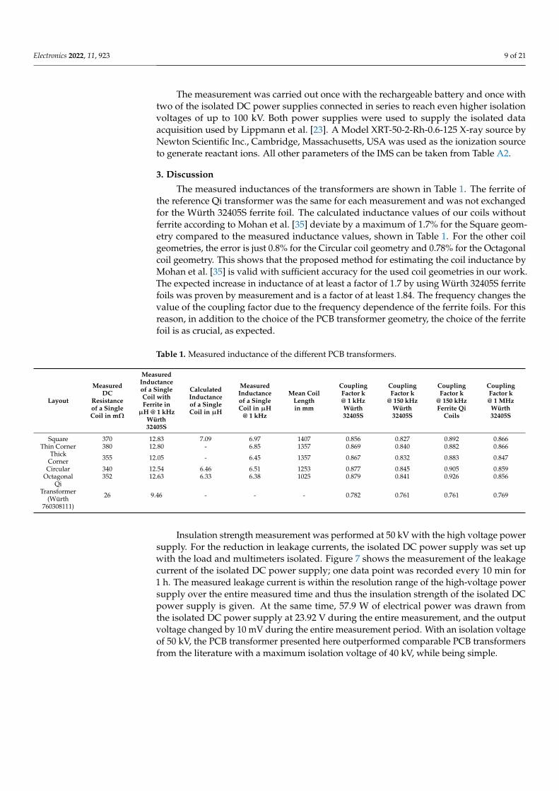
The measured inductances of the transformers are shown in Table 1. The ferrite ofthe reference Qi transformer was the same for each measurement and was not exchangedfor the Würth 32405S ferrite foil. The calculated inductance values of our coils withoutferrite according to Mohan et al. [35] deviate by a maximum of 1.7% for the Square geom-etry compared to the measured inductance values, shown in Table 1. For the other coilgeometries, the error is just 0.8% for the Circular coil geometry and 0.78% for the Octagonalcoil geometry. This shows that the proposed method for estimating the coil inductance byMohan et al. [35] is valid with sufficient accuracy for the used coil geometries in our work.The expected increase in inductance of at least a factor of 1.7 by using Würth 32405S ferritefoils was proven by measurement and is a factor of at least 1.84. The frequency changes thevalue of the coupling factor due to the frequency dependence of the ferrite foils. For thisreason, in addition to the choice of the PCB transformer geometry, the choice of the ferritefoil is as crucial, as expected.
Table 1. Measured inductance of the different PCB transformers.
Layout
MeasuredDC
Resistanceof a SingleCoil in mΩ
MeasuredInductanceof a SingleCoil withFerrite in
µH @ 1 kHzWürth32405S
CalculatedInductanceof a SingleCoil in µH
MeasuredInductanceof a SingleCoil in µH
@ 1 kHz
Mean CoilLengthin mm
CouplingFactor k@ 1 kHzWürth32405S
CouplingFactor k
@ 150 kHzWürth32405S
CouplingFactor k
@ 150 kHzFerrite Qi
Coils
CouplingFactor k
@ 1 MHzWürth32405S
Square 370 12.83 7.09 6.97 1407 0.856 0.827 0.892 0.866Thin Corner 380 12.80 - 6.85 1357 0.869 0.840 0.882 0.866
ThickCorner 355 12.05 - 6.45 1357 0.867 0.832 0.883 0.847
Circular 340 12.54 6.46 6.51 1253 0.877 0.845 0.905 0.859Octagonal 352 12.63 6.33 6.38 1025 0.879 0.841 0.926 0.856
QiTransformer
(Würth760308111)
26 9.46 - - - 0.782 0.761 0.761 0.769
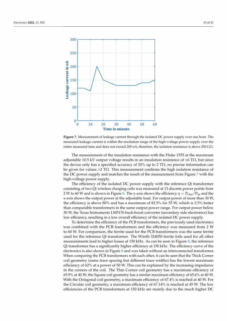
Insulation strength measurement was performed at 50 kV with the high voltage powersupply. For the reduction in leakage currents, the isolated DC power supply was set upwith the load and multimeters isolated. Figure 7 shows the measurement of the leakagecurrent of the isolated DC power supply; one data point was recorded every 10 min for1 h. The measured leakage current is within the resolution range of the high-voltage powersupply over the entire measured time and thus the insulation strength of the isolated DCpower supply is given. At the same time, 57.9 W of electrical power was drawn fromthe isolated DC power supply at 23.92 V during the entire measurement, and the outputvoltage changed by 10 mV during the entire measurement period. With an isolation voltageof 50 kV, the PCB transformer presented here outperformed comparable PCB transformersfrom the literature with a maximum isolation voltage of 40 kV, while being simple.
Electronics 2022, 11, 923 10 of 21
Electronics 2022, 11, x FOR PEER REVIEW 10 of 22
Qi Transformer
(Würth
760308111)
26 9.46 - - - 0.782 0.761 0.761 0.769
Insulation strength measurement was performed at 50 kV with the high voltage
power supply. For the reduction in leakage currents, the isolated DC power supply was
set up with the load and multimeters isolated. Figure 7 shows the measurement of the
leakage current of the isolated DC power supply; one data point was recorded every 10
min for 1 h. The measured leakage current is within the resolution range of the high-
voltage power supply over the entire measured time and thus the insulation strength of
the isolated DC power supply is given. At the same time, 57.9 W of electrical power was
drawn from the isolated DC power supply at 23.92 V during the entire measurement, and
the output voltage changed by 10 mV during the entire measurement period. With an
isolation voltage of 50 kV, the PCB transformer presented here outperformed comparable
PCB transformers from the literature with a maximum isolation voltage of 40 kV, while
being simple.
Figure 7. Measurement of leakage current through the isolated DC power supply over one hour.
The measured leakage current is within the resolution range of the high-voltage power supply over
the entire measured time and does not exceed 200 nA; therefore, the isolation resistance is above
250 GΩ.
The measurement of the insulation resistance with the Fluke 1555 at the maximum
adjustable 10.5 kV output voltage results in an insulation resistance of >6 TΩ, but since
the device only has a specified accuracy of 20% up to 2 TΩ, no precise information can be
given for values >2 TΩ. This measurement confirms the high isolation resistance of the
DC power supply and matches the result of the measurement from Figure 7 with the high-
voltage power supply.
The efficiency of the isolated DC power supply with the reference Qi transformer
consisting of two Qi wireless charging coils was measured at 13 discrete power points
from 2 W to 60 W and is shown in Figure 8. The y-axis shows the efficiency η = POut/PIn
and the x-axis shows the output power at the adjustable load. For output power of more
than 30 W, the efficiency is above 80% and has a maximum of 82.5% for 55 W, which is
2.5% better than comparable transformers in the same output power range. For output
power below 30 W, the Texas Instruments LM5176 buck-boost converter (secondary side
Figure 7. Measurement of leakage current through the isolated DC power supply over one hour. Themeasured leakage current is within the resolution range of the high-voltage power supply over theentire measured time and does not exceed 200 nA; therefore, the isolation resistance is above 250 GΩ.
The measurement of the insulation resistance with the Fluke 1555 at the maximumadjustable 10.5 kV output voltage results in an insulation resistance of >6 TΩ, but sincethe device only has a specified accuracy of 20% up to 2 TΩ, no precise information canbe given for values >2 TΩ. This measurement confirms the high isolation resistance ofthe DC power supply and matches the result of the measurement from Figure 7 with thehigh-voltage power supply.
The efficiency of the isolated DC power supply with the reference Qi transformerconsisting of two Qi wireless charging coils was measured at 13 discrete power points from2 W to 60 W and is shown in Figure 8. The y-axis shows the efficiency η = POut/PIn and thex-axis shows the output power at the adjustable load. For output power of more than 30 W,the efficiency is above 80% and has a maximum of 82.5% for 55 W, which is 2.5% betterthan comparable transformers in the same output power range. For output power below30 W, the Texas Instruments LM5176 buck-boost converter (secondary side electronics) haslow efficiency, resulting in a low overall efficiency of the isolated DC power supply.
To determine the efficiency of the PCB transformers, the previously used electronicswas combined with the PCB transformers and the efficiency was measured from 2 Wto 60 W. For comparison, the ferrite used for the PCB transformers was the same ferriteused for the reference Qi transformer. The Würth 32405S ferrite foils used for all othermeasurements lead to higher losses at 150 kHz. As can be seen in Figure 8, the referenceQi transformer has a significantly higher efficiency at 150 kHz. The efficiency curve of theelectronics is also shown in Figure 8 and was taken without an interconnected transformer.When comparing the PCB transformers with each other, it can be seen that the Thick Cornercoil geometry (same trace spacing but different trace widths) has the lowest maximumefficiency of 62% at a power of 50 W. This can be explained by the increasing impedancein the corners of the coil. The Thin Corner coil geometry has a maximum efficiency of65.9% at 40 W; the Square coil geometry has a similar maximum efficiency of 65.6% at 40 W.With the Octagonal coil geometry, a maximum efficiency of 67.4% is reached at 40 W. Forthe Circular coil geometry, a maximum efficiency of 67.14% is reached at 45 W. The lowefficiencies of the PCB transformers at 150 kHz are mainly due to the much higher DC

Electronics 2022, 11, 923 11 of 21
resistances, which can be seen in Table 1. In addition, the coupling factor of the Circularand Octagonal coil is best at 150 kHz, as shown in Table 1.
Electronics 2022, 11, x FOR PEER REVIEW 11 of 22
electronics) has low efficiency, resulting in a low overall efficiency of the isolated DC
power supply.
To determine the efficiency of the PCB transformers, the previously used electronics
was combined with the PCB transformers and the efficiency was measured from 2 W to
60 W. For comparison, the ferrite used for the PCB transformers was the same ferrite used
for the reference Qi transformer. The Würth 32405S ferrite foils used for all other
measurements lead to higher losses at 150 kHz. As can be seen in Figure 8, the reference
Qi transformer has a significantly higher efficiency at 150 kHz. The efficiency curve of the
electronics is also shown in Figure 8 and was taken without an interconnected
transformer. When comparing the PCB transformers with each other, it can be seen that
the Thick Corner coil geometry (same trace spacing but different trace widths) has the
lowest maximum efficiency of 62% at a power of 50 W. This can be explained by the
increasing impedance in the corners of the coil. The Thin Corner coil geometry has a
maximum efficiency of 65.9% at 40 W; the Square coil geometry has a similar maximum
efficiency of 65.6% at 40 W. With the Octagonal coil geometry, a maximum efficiency of
67.4% is reached at 40 W. For the Circular coil geometry, a maximum efficiency of 67.14%
is reached at 45 W. The low efficiencies of the PCB transformers at 150 kHz are mainly
due to the much higher DC resistances, which can be seen in Table 1. In addition, the
coupling factor of the Circular and Octagonal coil is best at 150 kHz, as shown in Table 1.
Figure 8. Measurement of the efficiency of the isolated DC power supply as a function of the output
power of the transformers and the control electronics at 150 kHz. The efficiency measurement of the
electronics was taken without an interconnected transformer, and therefore only the losses of the
primary and secondary side electronics were measured, as marked with a dashed line.
Subsequently, the transformers were measured at higher drive frequencies using the
modified secondary side (replaced LM5176 with LM3481) and fast rectifier diodes. For
this purpose, a fixed output power of 5 W was set at the electronic load and the
transformers were measured in the frequency range from 150 kHz to 2.5 MHz. The
relatively low power had to be chosen because the output voltage of the LM3481 is no
longer stable at higher powers and frequencies. The results of the measurements are
shown in Figure 9a, in which the PCB transformers are labeled with Octagonal, Thick
Corner, Thin Corner, Square, Circular, and Qi Transformer, and the losses without any
interconnected transformer are labeled Electronic. It can be seen that all PCB transformers
achieve efficiencies above 60% using drive frequencies of at least 1 MHz. Repeatedly, the
Thick Corner coil geometry is worse than the other coil geometries. This is presumably
Figure 8. Measurement of the efficiency of the isolated DC power supply as a function of the outputpower of the transformers and the control electronics at 150 kHz. The efficiency measurement of theelectronics was taken without an interconnected transformer, and therefore only the losses of theprimary and secondary side electronics were measured, as marked with a dashed line.
Subsequently, the transformers were measured at higher drive frequencies using themodified secondary side (replaced LM5176 with LM3481) and fast rectifier diodes. For thispurpose, a fixed output power of 5 W was set at the electronic load and the transformerswere measured in the frequency range from 150 kHz to 2.5 MHz. The relatively low powerhad to be chosen because the output voltage of the LM3481 is no longer stable at higherpowers and frequencies. The results of the measurements are shown in Figure 9a, inwhich the PCB transformers are labeled with Octagonal, Thick Corner, Thin Corner, Square,Circular, and Qi Transformer, and the losses without any interconnected transformer arelabeled Electronic. It can be seen that all PCB transformers achieve efficiencies above 60%using drive frequencies of at least 1 MHz. Repeatedly, the Thick Corner coil geometry isworse than the other coil geometries. This is presumably due to increasing impedance inthe corners, as the Thick corner geometry has a significantly higher trace width of 4.2 mmcompared to the other used track width of 3 mm, as seen in Figure 9a,b. This leads to areduction in the resistance but increases the capacity. At frequencies above 150 kHz upto about 1.4 MHz, the Thin Corner and Square coil geometries are most suitable due tothe higher coupling factors, as can be seen in Table 1. With the reference Qi transformer,operation is only possible up to a frequency of 950 kHz. Using higher frequencies, theoutput voltage on the secondary side collapses. For the PCB transformers, significantlyhigher efficiencies may be achieved with a more efficient control electronics since theefficiency curve of the electronics drops significantly to a value below 60% at frequenciesabove 2.5 MHz. However, the modified secondary side now shows higher efficiency atlower power outputs. There is still room for improvement in the electronics to increasethe overall efficiency at higher switching frequencies. At 150 kHz, the setup with the Qitransformer achieves the highest overall efficiency.

Electronics 2022, 11, 923 12 of 21
Electronics 2022, 11, x FOR PEER REVIEW 12 of 22
due to increasing impedance in the corners, as the Thick corner geometry has a
significantly higher trace width of 4.2 mm compared to the other used track width of 3
mm, as seen in Figure 9a,b. This leads to a reduction in the resistance but increases the
capacity. At frequencies above 150 kHz up to about 1.4 MHz, the Thin Corner and Square
coil geometries are most suitable due to the higher coupling factors, as can be seen in Table
1. With the reference Qi transformer, operation is only possible up to a frequency of 950
kHz. Using higher frequencies, the output voltage on the secondary side collapses. For
the PCB transformers, significantly higher efficiencies may be achieved with a more
efficient control electronics since the efficiency curve of the electronics drops significantly
to a value below 60% at frequencies above 2.5 MHz. However, the modified secondary
side now shows higher efficiency at lower power outputs. There is still room for
improvement in the electronics to increase the overall efficiency at higher switching
frequencies. At 150 kHz, the setup with the Qi transformer achieves the highest overall
efficiency.
Figure 9b shows the efficiencies of the PCB transformers (labeled Octagonal, Thick
Corner, Thin Corner, Square, Circular, Qi Transformer) excluding the losses of the
electronics. Figure 9b shows the result of subtracting each measured transformer
efficiency curve from Figure 9a from the losses of the electronics (labeled Electronic and
marked with a dashed line) from Figure 9a. Efficiencies of more than 90% are obtained for
all PCB transformers in a frequency range between 1.5 MHz and 2 MHz. For drive
frequencies of 150 kHz, the Octagonal and Circular coil geometries are most suitable. For
frequencies between 150 kHz and 1.4 MHz, the Thin Corner and Square coil geometries
are preferable. A significant improvement in the efficiency of PCB transformers may be
achieved by reducing the DC resistances, e.g., by using thicker copper layers or by using
primary and secondary coils connected in parallel on different copper layers. In addition,
further measurements of the voltage signals at different frequencies of 150 kHz and 1.75
MHz of the control electronics are shown in the Appendix A. The voltage curves at the
primary and secondary windings of all transformers can also be found in the Appendix
A for frequencies of 150 kHz and 1.75 MHz. Taking into account the optimization
strategies from the literature and the coil geometries investigated in this work, a
transformer efficiency of more than 90% excluding the electronics can be achieved with
an insulation strength of 50 kV and 60 W power transmission.
(a) (b)
Figure 9. (a) Measurement of the efficiency of the transformers (Octagonal, Thick Corner, Thin Corner,Square, Circular, Qi Transformer) including losses of the control electronics (Electronic marked witha dashed line) at a constant output power of 5 W. (b) Measurement of the efficiency of the PCBtransformers without losses caused by the control electronics at a constant output power of 5 W.
Figure 9b shows the efficiencies of the PCB transformers (labeled Octagonal, Thick Cor-ner, Thin Corner, Square, Circular, Qi Transformer) excluding the losses of the electronics.Figure 9b shows the result of subtracting each measured transformer efficiency curve fromFigure 9a from the losses of the electronics (labeled Electronic and marked with a dashedline) from Figure 9a. Efficiencies of more than 90% are obtained for all PCB transformersin a frequency range between 1.5 MHz and 2 MHz. For drive frequencies of 150 kHz, theOctagonal and Circular coil geometries are most suitable. For frequencies between 150 kHzand 1.4 MHz, the Thin Corner and Square coil geometries are preferable. A significantimprovement in the efficiency of PCB transformers may be achieved by reducing the DCresistances, e.g., by using thicker copper layers or by using primary and secondary coilsconnected in parallel on different copper layers. In addition, further measurements of thevoltage signals at different frequencies of 150 kHz and 1.75 MHz of the control electronicsare shown in the Appendix A. The voltage curves at the primary and secondary wind-ings of all transformers can also be found in the Appendix A for frequencies of 150 kHzand 1.75 MHz. Taking into account the optimization strategies from the literature andthe coil geometries investigated in this work, a transformer efficiency of more than 90%excluding the electronics can be achieved with an insulation strength of 50 kV and 60 Wpower transmission.
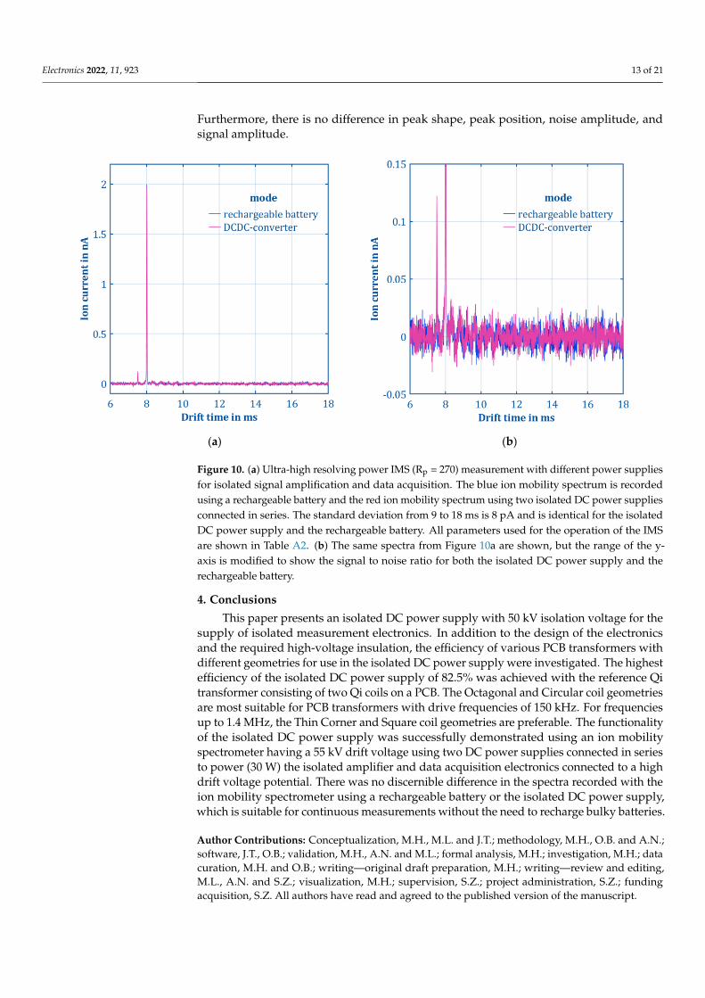
To test the isolated DC power supply in operation, an IMS with ultra-high resolvingpower of Rp = 270 was used. The isolated amplifier and data acquisition were at highdrift voltage potential of 55 kV. The output power was about 30 W. The noise of themeasured ion current was compared using the isolated DC power supply and using therechargeable battery. Figure 10 therefore shows two ion mobility spectra recorded with theIMS. The blue ion mobility spectrum shows the measurement using a rechargeable batteryas power supply for the isolated data acquisition of the instrument. The red ion mobilityspectrum shows the measurement using two isolated DC power supplies connected inseries. The spectra shown are an average of 16 individual measurements. The standarddeviation measured from 9 ms to 18 ms is 8 pA and is identical for both ion mobility spectra.
Electronics 2022, 11, 923 13 of 21
Furthermore, there is no difference in peak shape, peak position, noise amplitude, andsignal amplitude.
Electronics 2022, 11, x FOR PEER REVIEW 13 of 22
Figure 9. (a) Measurement of the efficiency of the transformers (Octagonal, Thick Corner, Thin
Corner, Square, Circular, Qi Transformer) including losses of the control electronics (Electronic
marked with a dashed line) at a constant output power of 5 W. (b) Measurement of the efficiency of
the PCB transformers without losses caused by the control electronics at a constant output power of
5 W.
To test the isolated DC power supply in operation, an IMS with ultra-high resolving
power of Rp = 270 was used. The isolated amplifier and data acquisition were at high drift
voltage potential of 55 kV. The output power was about 30 W. The noise of the measured
ion current was compared using the isolated DC power supply and using the rechargeable
battery. Figure 10 therefore shows two ion mobility spectra recorded with the IMS. The
blue ion mobility spectrum shows the measurement using a rechargeable battery as power
supply for the isolated data acquisition of the instrument. The red ion mobility spectrum
shows the measurement using two isolated DC power supplies connected in series. The
spectra shown are an average of 16 individual measurements. The standard deviation
measured from 9 ms to 18 ms is 8 pA and is identical for both ion mobility spectra.
Furthermore, there is no difference in peak shape, peak position, noise amplitude, and
signal amplitude.
(a) (b)
Figure 10. (a) Ultra-high resolving power IMS (Rp = 270) measurement with different power supplies
for isolated signal amplification and data acquisition. The blue ion mobility spectrum is recorded
using a rechargeable battery and the red ion mobility spectrum using two isolated DC power
supplies connected in series. The standard deviation from 9 to 18 ms is 8 pA and is identical for the
isolated DC power supply and the rechargeable battery. All parameters used for the operation of
the IMS are shown in Table A2. (b) The same spectra from Figure 10a are shown, but the range of
the y-axis is modified to show the signal to noise ratio for both the isolated DC power supply and
the rechargeable battery.
4. Conclusions
This paper presents an isolated DC power supply with 50 kV isolation voltage for the
supply of isolated measurement electronics. In addition to the design of the electronics
and the required high-voltage insulation, the efficiency of various PCB transformers with
different geometries for use in the isolated DC power supply were investigated. The
highest efficiency of the isolated DC power supply of 82.5% was achieved with the
Figure 10. (a) Ultra-high resolving power IMS (Rp = 270) measurement with different power suppliesfor isolated signal amplification and data acquisition. The blue ion mobility spectrum is recordedusing a rechargeable battery and the red ion mobility spectrum using two isolated DC power suppliesconnected in series. The standard deviation from 9 to 18 ms is 8 pA and is identical for the isolatedDC power supply and the rechargeable battery. All parameters used for the operation of the IMSare shown in Table A2. (b) The same spectra from Figure 10a are shown, but the range of the y-axis is modified to show the signal to noise ratio for both the isolated DC power supply and therechargeable battery.
4. Conclusions
This paper presents an isolated DC power supply with 50 kV isolation voltage for thesupply of isolated measurement electronics. In addition to the design of the electronicsand the required high-voltage insulation, the efficiency of various PCB transformers withdifferent geometries for use in the isolated DC power supply were investigated. The highestefficiency of the isolated DC power supply of 82.5% was achieved with the reference Qitransformer consisting of two Qi coils on a PCB. The Octagonal and Circular coil geometriesare most suitable for PCB transformers with drive frequencies of 150 kHz. For frequenciesup to 1.4 MHz, the Thin Corner and Square coil geometries are preferable. The functionalityof the isolated DC power supply was successfully demonstrated using an ion mobilityspectrometer having a 55 kV drift voltage using two DC power supplies connected in seriesto power (30 W) the isolated amplifier and data acquisition electronics connected to a highdrift voltage potential. There was no discernible difference in the spectra recorded with theion mobility spectrometer using a rechargeable battery or the isolated DC power supply,which is suitable for continuous measurements without the need to recharge bulky batteries.
Author Contributions: Conceptualization, M.H., M.L. and J.T.; methodology, M.H., O.B. and A.N.;software, J.T., O.B.; validation, M.H., A.N. and M.L.; formal analysis, M.H.; investigation, M.H.; datacuration, M.H. and O.B.; writing—original draft preparation, M.H.; writing—review and editing,M.L., A.N. and S.Z.; visualization, M.H.; supervision, S.Z.; project administration, S.Z.; fundingacquisition, S.Z. All authors have read and agreed to the published version of the manuscript.
Electronics 2022, 11, 923 14 of 21
Funding: Supported by the German Federal Ministry of Education and Research (BMBF) underthe Grant 13N14888. Funded by the Deutsche Forschungsgemeinschaft (DFG, German ResearchFoundation)—396430937. Funded by the Deutsche Forschungsgemeinschaft (DFG, German ResearchFoundation)—263334553.
Acknowledgments: We thank Christian-Robert Raddatz, Nic Solle and Eduard Sailer for their helpduring this work. We want to acknowledge Cameron Naylor for his advice during editing.
Conflicts of Interest: The authors declare no conflict of interest.
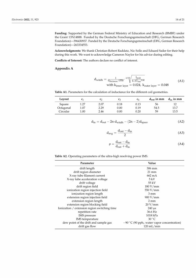
Appendix A
dwitdh = 1dthickness·1550 ·
0.725
√Ipeak
k·∆Trise0.44
with kinner layer = 0.024, kouter layer = 0.048(A1)
Table A1. Parameters for the calculation of inductance for the different coil geometries.
Layout c1 c2 c3 c4 dout in mm din in mm
Square 1.27 2.07 0.18 0.13 56 12Octagonal 1.07 2.29 0.00 0.19 54.5 13.7Circular 1.00 2.46 0.00 0.20 59 13.5
din = dout − 2n·dwitdh − (2n− 2)dspace (A2)
davg =dout − din
2(A3)
ρ =dout − din
dout + din(A4)
Table A2. Operating parameters of the ultra-high resolving power IMS.
Parameter Value
drift length 306 mmdrift region diameter 21 mm
X-ray tube filament current 662 mAX-ray tube acceleration voltage 5 kV
drift voltage 55 kVdrift region field 180 V/mm
ionization region injection field 550 V/mmionization region length 3 mm
extension region injection field 900 V/mmextension region length 2 mm
extension region blocking field 20 V/mmIonization / extension region switching time 240 µs
repetition rate 36.6 HzIMS pressure 1018 hPa
IMS temperature 30 Cdew point of the drift and sample gas −90 C (90 ppbv water vapor concentration)
drift gas flow 120 mL/min

Electronics 2022, 11, 923 15 of 21
Table A3. Notation list.
Symbol Description Unit
c1
current sheet expressionconstant 1 individual for each
coil geometry
c2
current sheet expressionconstant 2 individual for each
coil geometry
c3
current sheet expressionconstant 3 individual for each
coil geometry
c4
current sheet expressionconstant 4 individual for each
coil geometrydout coil outer diameter mmdin coil inner diameter mm
dwitdh PCB track witdh mmdthickness PCB copper thickness mm
dspacePCB distance between two
tracks mm
davg average diameter of the coil mmµ0 magnetic constant Vs/Amn number of turnsρ see Equation (A4)
kinner layerfactor for temperarture rise
inner layer
kouter layerfactor for temperarture rise
outer layerIpeak peak current A
∆Trise temperature rise K
Figure A1a,b show the voltage signals at the output of the control electronics drivingthe primary winding of the transformer before the coupling capacitor. Figure A1a showsthe left output, see Figure 3, of the control electronics in blue with the correspondinginput signal from the Agilent 81150A function generator in orange. Figure A1b shows theinverted signal of the right output of the control electronics at the same time; again, orangeindicates the function generator and blue the output signal. These signals are shown asan example at 150 kHz for the Circular PCB transformer; all other transformers show nosignificant difference.
Figure A2a,b show the voltage signals at the input of the voltage rectification andregulation electronics at the secondary winding of the transformer after the couplingcapacitor. Figure A2a shows the left input, see Figure 4, in blue at 150 kHz with the CircularPCB transformer, and Figure A2b shows the other input at the same time; both signals arereferenced to ground. These signals are shown as an example; all other transformers showno significant difference.
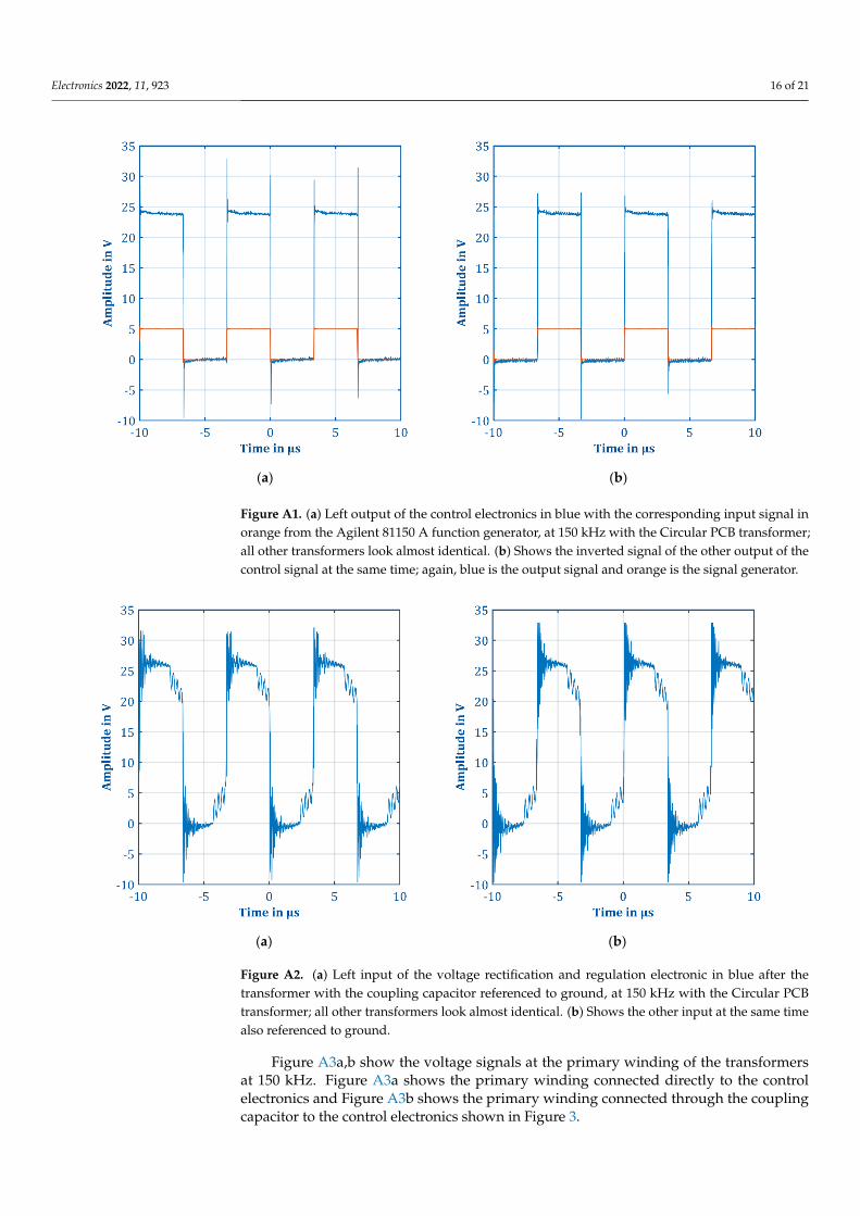
Electronics 2022, 11, 923 16 of 21
Electronics 2022, 11, x FOR PEER REVIEW 16 of 22
Figure A1a,b show the voltage signals at the output of the control electronics driving
the primary winding of the transformer before the coupling capacitor. Figure A1a shows
the left output, see Figure 3, of the control electronics in blue with the corresponding input
signal from the Agilent 81150A function generator in orange. Figure A1b shows the
inverted signal of the right output of the control electronics at the same time; again, orange
indicates the function generator and blue the output signal. These signals are shown as an
example at 150 kHz for the Circular PCB transformer; all other transformers show no
significant difference.
(a) (b)
Figure A1. (a) Left output of the control electronics in blue with the corresponding input signal in
orange from the Agilent 81150 A function generator, at 150 kHz with the Circular PCB transformer;
all other transformers look almost identical. (b) Shows the inverted signal of the other output of the
control signal at the same time; again, blue is the output signal and orange is the signal generator.
Figure A2a,b show the voltage signals at the input of the voltage rectification and
regulation electronics at the secondary winding of the transformer after the coupling
capacitor. Figure A2a shows the left input, see Figure 4, in blue at 150 kHz with the
Circular PCB transformer, and Figure A2b shows the other input at the same time; both
signals are referenced to ground. These signals are shown as an example; all other
transformers show no significant difference.
Figure A1. (a) Left output of the control electronics in blue with the corresponding input signal inorange from the Agilent 81150 A function generator, at 150 kHz with the Circular PCB transformer;all other transformers look almost identical. (b) Shows the inverted signal of the other output of thecontrol signal at the same time; again, blue is the output signal and orange is the signal generator.
Electronics 2022, 11, x FOR PEER REVIEW 17 of 22
(a) (b)
Figure A2. (a) Left input of the voltage rectification and regulation electronic in blue after the
transformer with the coupling capacitor referenced to ground, at 150 kHz with the Circular PCB
transformer; all other transformers look almost identical. (b) Shows the other input at the same time
also referenced to ground.
Figure A3a,b show the voltage signals at the primary winding of the transformers at
150 kHz. Figure A3a shows the primary winding connected directly to the control
electronics and Figure A3b shows the primary winding connected through the coupling
capacitor to the control electronics shown in Figure 3.
(a) (b)
Figure A3. (a,b) Show the voltage signals at the primary winding of the transformers at 150 kHz.
Figure A2. (a) Left input of the voltage rectification and regulation electronic in blue after thetransformer with the coupling capacitor referenced to ground, at 150 kHz with the Circular PCBtransformer; all other transformers look almost identical. (b) Shows the other input at the same timealso referenced to ground.
Figure A3a,b show the voltage signals at the primary winding of the transformersat 150 kHz. Figure A3a shows the primary winding connected directly to the controlelectronics and Figure A3b shows the primary winding connected through the couplingcapacitor to the control electronics shown in Figure 3.

Electronics 2022, 11, 923 17 of 21
Electronics 2022, 11, x FOR PEER REVIEW 17 of 22
(a) (b)
Figure A2. (a) Left input of the voltage rectification and regulation electronic in blue after the
transformer with the coupling capacitor referenced to ground, at 150 kHz with the Circular PCB
transformer; all other transformers look almost identical. (b) Shows the other input at the same time
also referenced to ground.
Figure A3a,b show the voltage signals at the primary winding of the transformers at
150 kHz. Figure A3a shows the primary winding connected directly to the control
electronics and Figure A3b shows the primary winding connected through the coupling
capacitor to the control electronics shown in Figure 3.
(a) (b)
Figure A3. (a,b) Show the voltage signals at the primary winding of the transformers at 150 kHz. Figure A3. (a,b) Show the voltage signals at the primary winding of the transformers at 150 kHz.
Figure A4a,b show the voltage signals at secondary winding of the transformer at150 kHz. Figure A3a shows the secondary winding connected directly to the voltage rectifi-cation and regulation electronics and Figure A4b shows the primary winding connectedthrough the coupling capacitor to the voltage rectification and regulation electronics inFigure 4.
Electronics 2022, 11, x FOR PEER REVIEW 18 of 22
Figure A4a,b show the voltage signals at secondary winding of the transformer at 150
kHz. Figure A3a shows the secondary winding connected directly to the voltage
rectification and regulation electronics and Figure A4b shows the primary winding
connected through the coupling capacitor to the voltage rectification and regulation
electronics in Figure 4.
(a) (b)
Figure A4. (a,b) Show the voltage signals at the secondary winding of the transformers at 150 kHz.
Figure A5a,b show the voltage signals at the output of the control electronics driving
the primary winding of the transformer before the coupling capacitor at higher
frequencies of 1.75 MHz for the Square PCB transformer; all other transformers show no
significant difference.
(a) (b)
Figure A4. (a,b) Show the voltage signals at the secondary winding of the transformers at 150 kHz.
Figure A5a,b show the voltage signals at the output of the control electronics drivingthe primary winding of the transformer before the coupling capacitor at higher frequencies of1.75 MHz for the Square PCB transformer; all other transformers show no significant difference.

Electronics 2022, 11, 923 18 of 21
Electronics 2022, 11, x FOR PEER REVIEW 18 of 22
Figure A4a,b show the voltage signals at secondary winding of the transformer at 150
kHz. Figure A3a shows the secondary winding connected directly to the voltage
rectification and regulation electronics and Figure A4b shows the primary winding
connected through the coupling capacitor to the voltage rectification and regulation
electronics in Figure 4.
(a) (b)
Figure A4. (a,b) Show the voltage signals at the secondary winding of the transformers at 150 kHz.
Figure A5a,b show the voltage signals at the output of the control electronics driving
the primary winding of the transformer before the coupling capacitor at higher
frequencies of 1.75 MHz for the Square PCB transformer; all other transformers show no
significant difference.
(a) (b)
Figure A5. (a) Left output of the control electronics in blue with the corresponding input signal inorange from the Agilent 81150A function generator, at 1.75 MHz with the Square PCB transformer;all other transformers look almost identical. (b) Shows the inverted signal of the other output of thecontrol signal at the same time; again blue is the output signal and orange the signal generator.
Figure A6a,b show the voltage signals at the input of the improved voltage rectificationand regulation electronics, see Figure 5, at a higher frequency of 1.75 MHz with the SquarePCB transformer.
Electronics 2022, 11, x FOR PEER REVIEW 19 of 22
Figure A5. (a) Left output of the control electronics in blue with the corresponding input signal in
orange from the Agilent 81150A function generator, at 1.75 MHz with the Square PCB transformer;
all other transformers look almost identical. (b) Shows the inverted signal of the other output of the
control signal at the same time; again blue is the output signal and orange the signal generator.
Figure A6a,b show the voltage signals at the input of the improved voltage
rectification and regulation electronics, see Figure 5, at a higher frequency of 1.75 MHz
with the Square PCB transformer.
(a) (b)
Figure A6. (a) Left input of the improved voltage rectification and regulation electronic, see Figure
5, in blue after the transformer with the coupling capacitor referenced to ground, at 1.75 MHz with
the Square PCB transformer; all other transformers look almost identical. (b) Shows the other input
at the same time, also referenced to ground.
Figure A7a,b show the voltage signals at the primary winding of the transformers at
1.75 MHz.
Figure A6. (a) Left input of the improved voltage rectification and regulation electronic, see Figure 5,in blue after the transformer with the coupling capacitor referenced to ground, at 1.75 MHz with theSquare PCB transformer; all other transformers look almost identical. (b) Shows the other input atthe same time, also referenced to ground.

Electronics 2022, 11, 923 19 of 21
Figure A7a,b show the voltage signals at the primary winding of the transformers at1.75 MHz.
Electronics 2022, 11, x FOR PEER REVIEW 20 of 22
(a) (b)
Figure A7. (a,b) Show the voltage signals at the primary winding of the transformers at 1.75 MHz.
Figure A8a,b show the voltage signals at the secondary winding of the transformers
at 1.75 MHz.
(a) (b)
Figure A8. (a,b) Show the voltage signals at the secondary winding of the transformers at 1.75 MHz.
References
1. Xue, F.; Yu, R.; Huang, A.Q. A 98.3% Efficient GaN Isolated Bidirectional DC–DC Converter for DC Microgrid Energy Storage
System Applications. IEEE Trans. Ind. Electron. 2017, 64, 9094–9103. https://doi.org/10.1109/TIE.2017.2686307.
2. Zhang, L.; Ji, S.; Gu, S.; Huang, X.; Palmer, J.; Giewont, W.; Wang, F.; Tolbert, L.M. Design Considerations of High-Voltage-
Insulated Gate Drive Power Supply for 10 kV SiC MOSFET in Medium-Voltage Application. In Proceedings of the 2019 IEEE
Figure A7. (a,b) Show the voltage signals at the primary winding of the transformers at 1.75 MHz.
Figure A8a,b show the voltage signals at the secondary winding of the transformers at1.75 MHz.
Electronics 2022, 11, x FOR PEER REVIEW 20 of 22
(a) (b)
Figure A7. (a,b) Show the voltage signals at the primary winding of the transformers at 1.75 MHz.
Figure A8a,b show the voltage signals at the secondary winding of the transformers
at 1.75 MHz.
(a) (b)
Figure A8. (a,b) Show the voltage signals at the secondary winding of the transformers at 1.75 MHz.
References
1. Xue, F.; Yu, R.; Huang, A.Q. A 98.3% Efficient GaN Isolated Bidirectional DC–DC Converter for DC Microgrid Energy Storage
System Applications. IEEE Trans. Ind. Electron. 2017, 64, 9094–9103. https://doi.org/10.1109/TIE.2017.2686307.
2. Zhang, L.; Ji, S.; Gu, S.; Huang, X.; Palmer, J.; Giewont, W.; Wang, F.; Tolbert, L.M. Design Considerations of High-Voltage-
Insulated Gate Drive Power Supply for 10 kV SiC MOSFET in Medium-Voltage Application. In Proceedings of the 2019 IEEE
Figure A8. (a,b) Show the voltage signals at the secondary winding of the transformers at 1.75 MHz.

Electronics 2022, 11, 923 20 of 21
References1. Xue, F.; Yu, R.; Huang, A.Q. A 98.3% Efficient GaN Isolated Bidirectional DC–DC Converter for DC Microgrid Energy Storage
System Applications. IEEE Trans. Ind. Electron. 2017, 64, 9094–9103. [CrossRef]2. Zhang, L.; Ji, S.; Gu, S.; Huang, X.; Palmer, J.; Giewont, W.; Wang, F.; Tolbert, L.M. Design Considerations of High-Voltage-
Insulated Gate Drive Power Supply for 10 kV SiC MOSFET in Medium-Voltage Application. In Proceedings of the 2019 IEEEApplied Power Electronics Conference and Exposition (APEC), Anaheim, CA, USA, 17–21 March 2019; IEEE: Piscataway, NJ,USA, 2019; pp. 425–430, ISBN 978-1-5386-8330-9.
3. Acharya, S.; Anurag, A.; Chattopadhyay, R.; Rengarajan, S.; Prabowo, Y.; Bhattacharya, S. A 10-kV SiC-MOSFET (Gen-3) Half-Bridge Module-Based Isolated Bidirectional DC—DC Converter Block for Medium-Voltage High-Power Applications. IEEJ Trans.Electr. Electron. Eng. 2021, 16, 127–138. [CrossRef]
4. Hui, S.Y.; Tang, S.C.; Chung, H.S.-H. Optimal operation of coreless PCB transformer-isolated gate drive circuits with wideswitching frequency range. IEEE Trans. Power Electron. 1999, 14, 506–514. [CrossRef]
5. Nguyen, V.T.; Veera Bharath, G.; Gohil, G. Design of Isolated Gate Driver Power Supply in Medium Voltage Converters usingHigh Frequency and Compact Wireless Power Transfer. In Proceedings of the 2019 IEEE Energy Conversion Congress andExposition (ECCE), Baltimore, MD, USA, 29 September–3 October 2019; IEEE: Piscataway, NJ, USA, 2019; pp. 135–142, ISBN978-1-7281-0395-2.
6. Tang, S.C.; Hui, S.Y.; Henry Shu-Hung Chung. Coreless printed circuit board (PCB) transformers with multiple secondarywindings for complementary gate drive circuits. IEEE Trans. Power Electron. 1999, 14, 431–437. [CrossRef]
7. Steiner, R.; Steimer, P.K.; Krismer, F.; Kolar, J.W. Contactless energy transmission for an isolated 100W gate driver supply of amedium voltage converter. In Proceedings of the IECON 2009—35th Annual Conference of IEEE Industrial Electronics (IECON),Porto, Portugal, 3–5 November 2009; IEEE: Piscataway, NJ, USA, 2009; pp. 302–307, ISBN 978-1-4244-4648-3.
8. Marxgut, C.; Biela, J.; Kolar, J.W.; Steiner, R.; Steimer, P.K. DC-DC converter for gate power supplies with an optimal airtransformer. In Proceedings of the 2010 Twenty-Fifth Annual IEEE Applied Power Electronics Conference and Exposition—APEC2010, Palm Springs, CA, USA, 21–25 February 2010; IEEE: Piscataway, NJ, USA, 2010; pp. 1865–1870, ISBN 978-1-4244-4782-4.
9. Berger, H.-H. Tauscher Transformatoren High Voltage and High Potential Transformers. Available online: https://www.tauscher-transformatoren.de/assets/pdf/Kapitel_HV_HTT.pdf (accessed on 10 March 2022).
10. Hui, S.Y. Planar Wireless Charging Technology for Portable Electronic Products and Qi. Proc. IEEE 2013, 101, 1290–1301.[CrossRef]
11. Miller, J.M.; Onar, O.C.; Chinthavali, M. Primary-Side Power Flow Control of Wireless Power Transfer for Electric VehicleCharging. IEEE J. Emerg. Sel. Top. Power Electron. 2015, 3, 147–162. [CrossRef]
12. Choi, S.Y.; Gu, B.W.; Jeong, S.Y.; Rim, C.T. Advances in Wireless Power Transfer Systems for Roadway-Powered Electric Vehicles.IEEE J. Emerg. Sel. Top. Power Electron. 2015, 3, 18–36. [CrossRef]
13. Rosu, S.G.; Khalilian, M.; Cirimele, V.; Guglielmi, P. A dynamic wireless charging system for electric vehicles based on DC/ACconverters with SiC MOSFET-IGBT switches and resonant gate-drive. In Proceedings of the IECON 2016—42nd AnnualConference of the IEEE Industrial Electronics Society, Florence, Italy, 23–26 October 2016; IEEE: Piscataway, NJ, USA, 2016; pp.4465–4470, ISBN 978-1-5090-3474-1.
14. Miller, J.M.; White, C.P.; Onar, O.C.; Ryan, P.M. Grid side regulation of wireless power charging of plug-in electric vehicles. InProceedings of the 2012 IEEE Energy Conversion Congress and Exposition (ECCE), Raleigh, NC, USA, 15–20 September 2012;IEEE: Piscataway, NJ, USA, 2012; pp. 261–268, ISBN 978-1-4673-0803-8.
15. Haerinia, M.; Shadid, R. Wireless Power Transfer Approaches for Medical Implants: A Review. Signals 2020, 1, 209–229. [CrossRef]16. Khan, S.R.; Pavuluri, S.K.; Cummins, G.; Desmulliez, M.P.Y. Wireless Power Transfer Techniques for Implantable Medical Devices:
A Review. Sensors 2020, 20, 3487. [CrossRef]17. Kim, H.-J.; Hirayama, H.; Kim, S.; Han, K.J.; Zhang, R.; Choi, J.-W. Review of Near-Field Wireless Power and Communication for
Biomedical Applications. IEEE Access 2017, 5, 21264–21285. [CrossRef]18. Xie, L.; Shi, Y.; Hou, Y.T.; Lou, A. Wireless power transfer and applications to sensor networks. IEEE Wireless Commun. 2013, 20,
140–145. [CrossRef]19. Zhang, C.; Lin, D.; Tang, N.; Hui, S.Y.R. A Novel Electric Insulation String Structure with High-Voltage Insulation and Wireless
Power Transfer Capabilities. IEEE Trans. Power Electron. 2018, 33, 87–96. [CrossRef]20. Bleys, C.A. Floating input, optically isolated, high-voltage measurement probe. Rev. Sci. Instrum. 1976, 47, 621–623. [CrossRef]21. Albesa, J.; Gasulla, M. Occupancy and Belt Detection in Removable Vehicle Seats via Inductive Power Transmission. IEEE Trans.
Veh. Technol. 2015, 64, 3392–3401. [CrossRef]22. van den Bossche, A.; Valchev, V.C. Inductors and Transformers for Power Electronics; Taylor & Francis: Boca Raton, FL, USA, 2005;
ISBN 9781574446791.23. Lippmann, M.; Kirk, A.T.; Hitzemann, M.; Zimmermann, S. IMS Instrumentation I: Isolated data acquisition for ion mobility
spectrometers with grounded ion sources. Int. J. Ion Mobil. Spec. 2020, 23, 69–74. [CrossRef]24. Advanced Energy. UltraVolt EFL Series. Available online: https://www.advancedenergy.com/globalassets/resources-root/data-
sheets/en-hv-efl-series-data-sheet.pdf (accessed on 10 March 2022).25. Bohnhorst, A.; Kirk, A.T.; Zimmermann, S. Toward Compact High-Performance Ion Mobility Spectrometers: Ion Gating in Ion
Mobility Spectrometry. Anal. Chem. 2021, 93, 6062–6070. [CrossRef]

Electronics 2022, 11, 923 21 of 21
26. Kirk, A.T.; Bakes, K.; Zimmermann, S. A universal relationship between optimum drift voltage and resolving power. Int. J. IonMobil. Spec. 2017, 20, 105–109. [CrossRef]
27. Thoben, C.; Dennhardt, N.; Krauß, T.; Sümpelmann, R.; Zimmermann, S.; Rüffert, H.; Heiderich, S. Preparation of anaesthesiaworkstation for trigger-free anaesthesia: An observational laboratory study. Eur. J. Anaesthesiol. 2019, 36, 851–856. [CrossRef]
28. Reisch, M. Elektronische Bauelemente: Funktion, Grundschaltungen, Modellierung Mit SPICE, 2nd ed.; Springer: Berlin/Heidelberg,Germany, 2007; ISBN 3-540-34014-9.
29. Isola Group HQ. DE104 Data Sheet. Available online: https://www.isola-group.com/wp-content/uploads/DE104-Laminate-and-Prepreg-Data-Sheet-0317.pdf (accessed on 10 March 2022).
30. International Electrotechnical Commission. Information Technology Equipment-Safety—Part 1: General Requirements [IEC 60950–1-Ed.1]; International Electrotechnical Commission: Geneva, Switzerland, 2001.
31. Tang, S.C.; Hui, S.Y.; Chung, H.-H. Evaluation of the shielding effects on printed-circuit-board transformers using ferrite platesand copper sheets. IEEE Trans. Power Electron. 2002, 17, 1080–1088. [CrossRef]
32. Constantinescu, C.; Munteanu, C.; Pacurar, C.; Giurgiuman, A.; Andreica, S.; Gliga, M. Numerical Modeling and ParametricAnalysis of Induction Plates. In Proceedings of the 2019 8th International Conference on Modern Power Systems (MPS), ClujNapoca, Romania, 21–23 May 2019; IEEE: Piscataway, NJ, USA, 2019; pp. 1–6, ISBN 978-1-7281-0750-9.
33. Tang, S.C.; Hui, S.Y.; Chung, H.-H. Characterization of coreless printed circuit board (PCB) transformers. IEEE Trans. PowerElectron. 2000, 15, 1275–1282. [CrossRef]
34. IPC. Generic Standard on Printed Board Design. IPC-2221A. 2003. Available online: https://shop.ipc.org/general-electronics/standards/2221-0-a-english (accessed on 10 March 2022).
35. Mohan, S.S.; Del Mar Hershenson, M.; Boyd, S.P.; Lee, T.H. Simple accurate expressions for planar spiral inductances. IEEE J.Solid-State Circuits 1999, 34, 1419–1424. [CrossRef]
36. Andreica, S.; Munteanu, C.; Gliga, M.; Pacurar, C.; Giurgiuman, A.; Constantinescu, C. Design of Multilayer Spiral Coils withDifferent Geometries to Determine the Inductance. In Proceedings of the 2020 International Conference and Exposition onElectrical and Power Engineering (EPE), Iasi, Romania, 22–23 October 2020; IEEE: Piscataway, NJ, USA, 2020; pp. 425–428,ISBN 978-1-7281-8126-4.
37. van Schuylenbergh, K.; Puers, R. Inductive Powering: Basic Theory and Application to Biomedical Systems; Springer: Dordrecht, TheNetherlands, 2009; ISBN 978-90-481-2411-4.
38. Matsuki, H.; Shiiki, M.; Murakami, K.; Yamamoto, T. Investigation of coil geometry for transcutaneous energy transmission forartificial heart. IEEE Trans. Magn. 1992, 28, 2406–2408. [CrossRef]
39. Soma, M.; Galbraith, D.C.; White, R.L. Radio-frequency coils in implantable devices: Misalignment analysis and design procedure.IEEE Trans. Biomed. Eng. 1987, 34, 276–282. [CrossRef]
40. Hurley, W.G.; Duffy, M.C. Calculation of self- and mutual impedances in planar sandwich inductors. IEEE Trans. Magn. 1997, 33,2282–2290. [CrossRef]
41. Bouattour, G.; Kallel, B.; Sasmal, K.; Kanoun, O.; Derbel, N. Comparative study of resonant circuit for power transmission viainductive link. In Proceedings of the 2015 12th International Multi-Conference on Systems, Signals & Devices (SSD), Mahdia,Tunisia, 16–19 March 2015; IEEE: Piscataway, NJ, USA, 2015; pp. 1–6, ISBN 978-1-4799-1758-7.
42. Raddatz, C.-R.; Allers, M.; Kirk, A.T.; Zimmermann, S. Acetone and perdeuterated acetone in UV-IMS. Int. J. Ion Mobil. Spec. 2018,21, 49–53. [CrossRef]