Wavelength division multiplexed loop buffer memory based optical packet switch
20
Opt Quant Electron (2007) 39:15–34 DOI 10.1007/s11082-007-9061-0 Wavelength division multiplexed loop buffer memory based optical packet switch Rajat Kumar Singh · Rajiv Srivastava · Yatindra Nath Singh Received: 21 July 2006 / Accepted: 7 February 2007 / Published online: 14 March 2007 © Springer Science+Business Media B.V. 2007 Abstract Photonic all-optical switching is widely considered as one of the technique to utilize the enormous optical bandwidth. Optical packet switching provides high speed, data rate transparency, data format transparency, efficient use of bandwidth and flexibility. To resolve the conflict during contention, packets are needed to be buffered. Due to the lack of optical RAM, fiber delay lines (FDLs) are the most suited option to buffer the packets. This paper proposes new optical packet switch architecture alongwith feedback shared buffer utilizing the advantage of WDM loop buffer memory. The loop buffer module used in this switch architecture is a new approach towards WDM buffering of packets. The mathematical modeling is done to validate the results obtained from simulation. Keywords Loop buffer memory · Optical packet switching · Wavelength division multiplexing (WDM) 1 Introduction The bandwidth demand due to more and more data intensive application and growth in userbase, is increasing day by day. Due to large bandwidth availability in the fiber, optical networks are the most suitable option to fulfill this increased bandwidth requirements. The optical network implementations can have electronic or all-opti- cal switches. Electronic switches are easy to implement due to mature electronics R. K. Singh (B ) Department of Electrical Engineering, Indian Institute of Technology Kanpur, ACES 301B, Kanpur, 208016, India e-mail: [email protected] R. Srivastava e-mail: [email protected] Y. N. Singh e-mail: [email protected]
Transcript of Wavelength division multiplexed loop buffer memory based optical packet switch
Opt Quant Electron (2007) 39:15–34DOI 10.1007/s11082-007-9061-0
Wavelength division multiplexed loop buffer memorybased optical packet switch
Rajat Kumar Singh · Rajiv Srivastava ·Yatindra Nath Singh
Received: 21 July 2006 / Accepted: 7 February 2007 / Published online: 14 March 2007© Springer Science+Business Media B.V. 2007
Abstract Photonic all-optical switching is widely considered as one of the techniqueto utilize the enormous optical bandwidth. Optical packet switching provides highspeed, data rate transparency, data format transparency, efficient use of bandwidthand flexibility. To resolve the conflict during contention, packets are needed to bebuffered. Due to the lack of optical RAM, fiber delay lines (FDLs) are the mostsuited option to buffer the packets. This paper proposes new optical packet switcharchitecture alongwith feedback shared buffer utilizing the advantage of WDM loopbuffer memory. The loop buffer module used in this switch architecture is a newapproach towards WDM buffering of packets. The mathematical modeling is done tovalidate the results obtained from simulation.
Keywords Loop buffer memory · Optical packet switching · Wavelength divisionmultiplexing (WDM)
1 Introduction
The bandwidth demand due to more and more data intensive application and growthin userbase, is increasing day by day. Due to large bandwidth availability in thefiber, optical networks are the most suitable option to fulfill this increased bandwidthrequirements. The optical network implementations can have electronic or all-opti-cal switches. Electronic switches are easy to implement due to mature electronics
R. K. Singh (B)Department of Electrical Engineering, Indian Institute of Technology Kanpur, ACES 301B,Kanpur, 208016, Indiae-mail: [email protected]
R. Srivastavae-mail: [email protected]
Y. N. Singhe-mail: [email protected]

16 R. K. Singh et al.
technology but they have fundamental limitations on rates at which data can be trans-ported from one switch to another switch. This limitation occurs due to the modulationand demodulation constraints in electronic transmitters and receivers respectively.
In optical transport networks, the current approach is to use optical switches toset up light paths. These all-optical switches are circuit switches and transparent toinformation carried over light path. Another alternative strategy could be to deployall-optical packet switches and use packet switching in optical layer for data trans-port. Since the data is generated by electronic sources, only motivation to build theall-optical packet switch is when ingress routers aggregate the large number of pack-ets optically for very high bit rate payload. This aggregated payload can be attachedwith low bit rate header and pushed into core optical network. The all-optical packetswitches will convert the header of the packet to electrical form and keep the payloadin optical form. The header information can be used to route the packet. Once thepacket reaches egress node, the aggregated packets can be separated using opticaldemultiplexing techniques and passed onto the client network. Many optical packetswitching (OPS) architectures have already been proposed in literature (Tucker andZhong 1999; Dittmanm et al. 2003). WDM technology had been incorporated (Dan-ielsen et al. 1997) to improve their performance.
The major problem in the OPS application is contention among the packets, whichoccurs when two or more packets arrives at same time for same destination. To avoidthis contention, one packet is directed towards the intended output and other contend-ing packets have to be stored in random access memory (RAM). All-optical RAMsuitable for photonic packet switching has not yet been developed (Singh and Singh2006). The alternative is to use deflection routing (Chlamtac and Fumagalli 1993)or optical fiber delay lines (traveling and recirculating type (Singh and Singh 2005,2006; Hass 1993). One can use recirculating buffers incorporating components such asoptical gate switches, optical couplers, optical amplifiers and wavelength convertersto realize the optical buffering (Verma et al. 2002; Shukla et al. 2004; Singh et al. 2006;Srivastava et al. 2006).
All-optical switching and optical buffering are the immediate requirement for thenext generation optical networks. The optical buffers are much better than the elec-tronic buffers because in case of optical buffers, the data path is: (i) all-optical i.e.,O/E and E/O conversion not required, (ii) having larger bandwidth, (iii) data ratetransparent, and (iv) WDM applicable. Several architectures are proposed and com-pared on the basis of the optical buffering technique and buffering capacity (Singhet al. 2006; Srivastava et al. 2006; Yao et al. 2000; Chia et al. 2001; Fow-Sen Choaet al. 2005; Papadimitriou et al. 2003). Each switch performs well with a specific typeof arrangement of traveling and recirculating buffer. Still, the research is going onto develop an optimal buffering strategy which will provide the lowest probability ofpacket loss with reasonable average delay.
In this paper, we are proposing the switch architecture as shown in Fig. 1 which usesmultiple loop buffers and WDM technique for contention resolution. Here, WDMbased fiber delay lines are used to store the contending packets and a space switchfabric is used to direct them appropriately. It considers the effect of noise to calculatethe number of maximum allowed circulations in the loop buffer before the correctreception of signal. The paper is organized in following ways. Detailed discussionabout the switch architecture is given in Sect. 2. Power budget analysis is performedin Sect. 3 by taking care of various noises in the loop buffer module. The schedulingalgorithm is explained in Sect. 4 while the simulation analysis and results for packet

WDM Memory Based Optical Packet Switch 17
Fig. 1 Optical packets switcharchitecture: modules (1 to M)represent optical loop buffermemories
loss probability and delay are presented in Sect. 5. Mathematical analysis is done inSect. 6 and its results are compared with simulation results in Sect. 7 to validate thesimulation analysis. Finally, Sect. 8 concludes the work.
2 Description of switch architecture
The proposed architecture of optical packet switch is shown in Fig. 1. The core ofthis architecture is a nonblocking space switch of dimension 2N × 2N. The lower Nports (indexed 1 to N) of the core switch are used as switch inputs/outputs and theupper N ports (indexed N+1 to 2N) are used for buffering the packets in the opticalloop buffer modules (Fig. 2). Under this condition, the maximum numbers of allowedbuffer modules are m = N/D, where D is the number of input/output at each loopbuffer module. This D and hence m depend upon desired packet loss probability. Ifthe switch is designed for M modules (M ≤ m), then rest of the upper half ports (i.e.,N − MD) will be left free and the switch fabric of size (N + MD) × (N + MD) is used.Hence, the effective size of core switch is (N + MD) × (N + MD) where N is theactual number of inputs. The length of delay line as well as the slot duration has beenassumed of one packet length. Newly arriving packets and already stored packetsmay also contend for the same output. In such case, one of the contending packetsis directed to the output port and remaining packets are kept in buffer according tothe scheduling algorithm given in Sect. 4. When contending packets can neither bedirected to assigned output port nor stored in buffer, it is dropped and assumed to belost.
Each buffer module (Fig. 2) consists of D tunable wavelength converters (TWC) atits input, a recirculating loop buffer, and D fixed filters (FF) at its output (Verma et al.2002; Shukla et al. 2004). The path followed by a packet while circulating inside theloop, consists of 3 dB coupler, DEMUX, TWC, combiner, erbium-doped fiber ampli-fier (EDFA), isolator and again the same 3 dB coupler. The number of TWC andthe size of DEMUX and combiner inside the loop depend upon the required buffercapacity (B) and hence, these are considered equal to B. Thus, the total number ofTWCs and FF used in the buffer module will be (B + D) and D respectively. EDFA isplaced inside the loop to compensate the power loss through the loop buffer duringcirculations.

18 R. K. Singh et al.
Fig. 2 Optical loop buffermemory module
Each buffer module uses (B + D) wavelengths where B is the number of bufferwavelengths used to store the packets in buffer modules, and D is the number ofwavelengths used for reading out the packets from the buffer modules. Packets fromall the D inputs use WDM technology to share the recirculating loop buffer. Thenumber of buffer wavelengths (B) inside the memory module depends on the switchdesign, desired traffic throughput, packet loss probability and size of the switch (Shunet al. 2003). The allocation of the packets to the loop buffer depends on the routingand priority algorithm for the switch. The packets to be buffered are converted to thewavelengths available in the buffer; if buffer is full then packets are dropped. Whena packet is forwarded for buffering, the respective TWC at the input of the availablebuffer module is tuned to any one of the B loop buffer wavelengths, which is free toaccept the packet. As long as a packet remains in the buffer, the TWC inside that mod-ule, corresponding to the wavelength assigned to this packet, will remain transparenttill it is desired to read out the packet or to have dynamic wavelength re-allocation.For reading out a packet when output contention is resolved, the corresponding TWCis tuned to the wavelength of appropriate output port fixed filters (FF). The packet isthen broadcasted towards FFs and received by the intended one. Then, these pack-ets can be directed to the destined output port through the space switch fabric. Wehave assumed an electronic control unit (not shown in the figures) which tunes var-ious components of the loop buffer as well as controls the whole switch. The similartype of electronic controlling technique is already described in Fow-Sen Choa et al.(2005). The control of packet buffering is also done by this controller according to thescheduling algorithm proposed in Sect. 4. We have used the SOA based TWC whichis proposed and fabricated in Fow-Sen Choa et al. (2005) and it is operated on thenano-second scale. The space switches are considered as SOA based electro-opticalswitch. The switching speed of this device is also of the order of nano-second while theinsertion loss will be 0.5 dB per stage. The crosstalk is low (−30 dB) and is neglectedin the calculation (Mynbaev and Scheiner 2001). Thus, the tuning speed of TWCsand the switching speed of space switch, do not put any constraint on the switchingoperation.
This paragraph explains about the clearance of buffer wavelength, once the bufferedpacket is delivered to the intended output port. While sending a packet into the loopthrough 3 dB coupler, half power of the packet is transmitted to the loop (Fig. 2) and
WDM Memory Based Optical Packet Switch 19
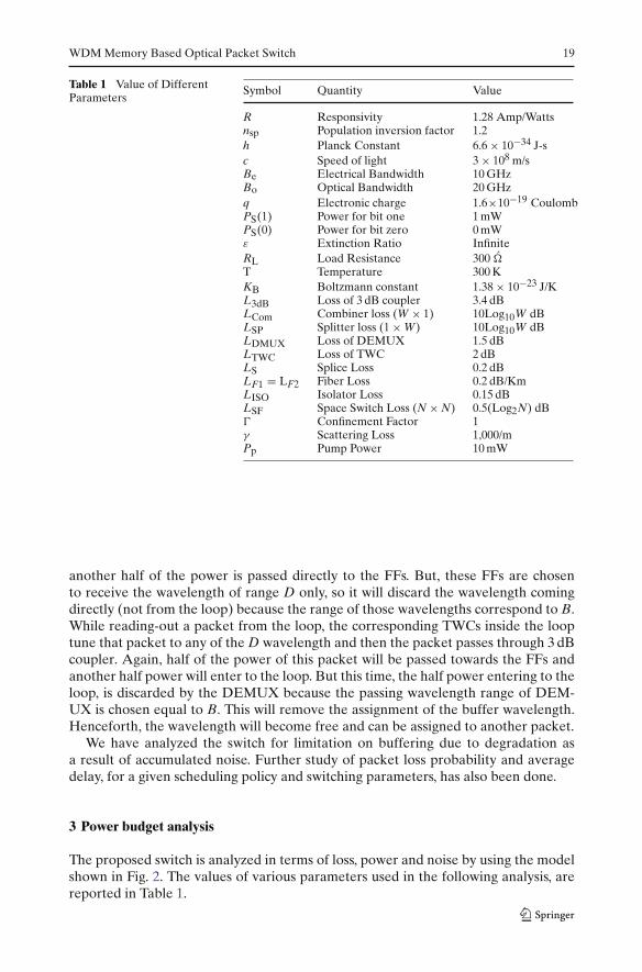
Table 1 Value of DifferentParameters
Symbol Quantity Value
R Responsivity 1.28 Amp/Wattsnsp Population inversion factor 1.2h Planck Constant 6.6 × 10⁻³⁴ J-sc Speed of light 3 × 10⁸ m/sBe Electrical Bandwidth 10 GHzBo Optical Bandwidth 20 GHzq Electronic charge 1.6×10⁻¹⁹ CoulombPS(1) Power for bit one 1 mWPS(0) Power for bit zero 0 mWε Extinction Ratio InfiniteRL Load Resistance 300 �́
T Temperature 300 KKB Boltzmann constant 1.38 × 10⁻²³ J/KL3dB Loss of 3 dB coupler 3.4 dBLCom Combiner loss (W × 1) 10Log10W dBLSP Splitter loss (1 × W) 10Log10W dBLDMUX Loss of DEMUX 1.5 dBLTWC Loss of TWC 2 dBLS Splice Loss 0.2 dBLF1 = LF2 Fiber Loss 0.2 dB/KmLISO Isolator Loss 0.15 dBLSF Space Switch Loss (N × N) 0.5(Log2N) dB� Confinement Factor 1γ Scattering Loss 1,000/mPp Pump Power 10 mW
another half of the power is passed directly to the FFs. But, these FFs are chosento receive the wavelength of range D only, so it will discard the wavelength comingdirectly (not from the loop) because the range of those wavelengths correspond to B.While reading-out a packet from the loop, the corresponding TWCs inside the looptune that packet to any of the D wavelength and then the packet passes through 3 dBcoupler. Again, half of the power of this packet will be passed towards the FFs andanother half power will enter to the loop. But this time, the half power entering to theloop, is discarded by the DEMUX because the passing wavelength range of DEM-UX is chosen equal to B. This will remove the assignment of the buffer wavelength.Henceforth, the wavelength will become free and can be assigned to another packet.
We have analyzed the switch for limitation on buffering due to degradation asa result of accumulated noise. Further study of packet loss probability and averagedelay, for a given scheduling policy and switching parameters, has also been done.
3 Power budget analysis
The proposed switch is analyzed in terms of loss, power and noise by using the modelshown in Fig. 2. The values of various parameters used in the following analysis, arereported in Table 1.
20 R. K. Singh et al.
3.1 Loss analysis
For the convenience of calculation, the loss in this architecture has been divided intothree parts.
1. The input section of the buffer module consists of TWC and combiner. Hence,loss from switch input up to the loop buffer input, termed as Insertion loss (Ains),is given as
Ains = LSFLTWCLCom (1)
2. Loss through the loop buffer is termed as Recirculation loss (ARe). This has beenobtained by breaking the loop in two parts for the ease of calculation. These aredefined as below,
A1 = L3dBLDEMUXLTWCLCom6LSLF1 (2)
A2 = LISO4LSLF2 (3)
where, A1 is loss of the buffer from entry port of loop buffer up to input of EDFA,and A2 is loss after EDFA up to 3 dB coupler. Other variables are defined withrelevant values in Table 1. Total loss of the loop buffer after one circulation, canbe given as AL = (A1A2). Hence, after K circulations the recirculation loss willbe ARe = (AL)K. All the losses in this model are fractional losses of power i.e.,output/input (Watts/Watts).
3. The output section of the buffer module consists of splitter and FF. Hence, lossfrom the loop buffer output up to the switch output, termed as Extraction loss(Aext), is given as,
Aext = LSPLFFLSF (4)
Thus, total loss through the switch architecture is
A = AinsAReL3dBAext (5)
3.2 Power analysis
The TWC is a noisy device i.e., it adds noise to the incoming signal whenever it per-forms tuning for wavelength conversion while it will not introduce any noise when itis transparent (no tuning). But, sometimes it is considered as noiseless device for theperformance observation because the introduction of noise may be compensated bythe regeneration of the signal in the TWC (Mamyshev 2004). So, we have done theanalysis in two ways considering: (i) TWC as the noiseless device and (ii) TWC as thenoisy device.
3.2.1 TWC as the noiseless device
If we follow the above model (Fig. 2) then the power of bit ‘1’ and bit ‘0’ [Pin(1) andPin(0)] entering through the input of loop buffer, are
Pin(1) = PavAins
(2ε
1 + ε
)and Pin(0) = PavAins
(2
1 + ε
)(6)
WDM Memory Based Optical Packet Switch 21
Pav is average signal power at the switch input and ‘ε’ is the extinction ratio, definedas ε = [P(1)/P(0)]. Thus the signal power, just before the 3 dB coupler after onecirculation, is given by
ALPin(b)G + (G − 1)nsphυBoA2 (7)
where, b = 1 for bit ‘1’ and b = 0 for bit ‘0’. In the Eq. (7), first term represents the sig-nal power and second term represents amplified spontaneous emission (ASE) noisepower (Olsson 1989). AL is loss of the loop in one circulation, G is the gain of ErbiumDoped Fiber Amplifier (EDFA) and Bo is the optical bandwidth.
Thus, the power for the bit ‘b’ afterK circulations, just before the 3 dB coupler, is
PK (b) = (AL)KPin(b)GK + (G − 1)nsphυBoA2F (8)
where,
F ={
1−(ALG)K
1−ALG , ALG < 1K, ALG = 1
}(9)
We have not considered the case of ALG >1 because under this condition, the fiberloop buffer will start behaving like an oscillator and finally the signal power starts tolase as the number of circulations increases. To achieve maximum SNR, product ofloop gain and loop loss must be equal to unity (Naik and Singh 2002) i.e., ALG = 1.Hence,
PK(b) = Pin(b) + K(G − 1)nsphυBoA2 (10)
Thus, the power at the output of loop buffer,
Pout(b) = PK (b) L3dB (11)
Finally, the power for bit ‘b’ at the output of the switch is given as,
P(b) = Pout(b)Aext (12)
3.2.2 TWC as the noisy device
We have considered the TWC model as given in Iannone and Sabella (1995). As longas, the packets circulate inside loop, the corresponding TWC will remain transparenti.e., the packet will be kept on revolving on same wavelength. Since, the tuning isnot required, so the TWC will not induce any noise. But, during the read-out/write-inprocess, the TWC will be tuned accordingly and thus, it will introduce the noise intothe signal power. Hence, the modified expression of the power for bit ‘1’ (as comparedto Eq. (6), entering the loop buffer, will be given as
Pin(1) = PavAins
(2ε
1 + ε
)
+[
nsp (Gc − 1) hν
(�g (0)
�g (0) − γ
) (1 + χ
Gc+ PavLTWCχ
PpGc
)AComBo
]
(13)
where, Gc is the gain of SOA used inside the TWC. The terms Gc and g(0) areobtained solving the set of equations given in Iannone and Sabella (1995). Conversion

22 R. K. Singh et al.
efficiency (χ) is assumed to be 1 in the calculations. Other parameter values are shownin Table 1. The second term in Eq. (13), is the noise added by TWC during conversionprocess. This term is added because whenever the packet is scheduled to be stored inthe buffer, it will be passed through the TWC, placed at the input of buffer module,for once and tuning will be performed to allocate the free buffer wavelength. For bit‘0’, the TWC does not contribute any noise term, so its power expression will remainsame as given in Eq.(6).
During the revolution of packet inside loop, if the number of maximum allowedcirculations are K, then the corresponding TWC placed inside the loop, will performtuning only in the Kth circulation. Since, the TWC will not be tuned till (K − 1)thcirculations so, the power for bit ‘b’ after (K − 1) circulations will become
PK−1(b) = Pin (b) + (K − 1) (G − 1)nsphυBoA2 (14)
The above power will enter TWC during the Kth revolution and now, the TWCnoise will be added to it because of tuning. The new term for power after K circulations,will be given as
PK(b) = Pin (b)
+[
nsp (Gc − 1) hν�g (0)
�g (0) − γ
(1 + χ
Gc+ PK−1 (b) L3dBLDEMUXLTWCχ
PpGc
)
× AComBoGA2
]+ K(G − 1)nsphυBoA2 (15)
Hence, the final power output for bit ‘b’ is shown as
P(b) = PK(b)L3dBAext (16)
3.3 Noise analysis
The optical amplifiers not only restore the signal, but also add ASE noise to the signal.Also, due to square law detection by the photodetector in the receiver, various noisecomponents are generated. These noise components are shot noise, ASE-ASE beatnoise, sig-ASE beat noise, ASE-shot beat noise and thermal noise with variances givenby σ 2
s , σ 2sp−sp, σ 2
sig−sp, σ 2s−sp and σ 2
th respectively (Olsson 1989). These noise terms forbit ‘b’, after K circulations are given as
σ 2s = 2qRP(b)Be (17)
σ 2sp−sp = R2P2
sp(K)(2Bo − Be)Be
B20
(18)
σ 2sig−sp = 4R2P(b)
Psp(K)Be
B0(19)
σ 2s−sp = 2qRPsp(K)Be (20)
σ 2th = 4kTBo
RL(21)

WDM Memory Based Optical Packet Switch 23
Table 2 Length of the EDFAto provide the required gain[22]
B G (dB) Length of EDFA (m)
4 16.85 108 21.75 1116 26.65 14
where,
Psp (K) = Knsp (G − 1) hυBeA2L3dBAext (22)
Till now, the TWC is considered as the noiseless device. If we consider the TWC asthe noisy device, then the Eq. (22) will be changed to
Psp(K) = [PK(b) − Pin(b)
]L3dBAext (23)
Thus, the total noise variance for bit ‘b’ is
σ 2 (b) = σ 2s + σ 2
sp−sp + σ 2sp−sig + σ 2
s−sp + σ 2th (24)
The bit-error rate (Olsson 1989) can be obtained as,
BER = Q(
I (1) − I (0)
σ (1) + σ (0)
)(25)
where Q(x), the error function, is defined as
Q (z) = 1√2π
∞∫z
exp(−z2/2) dz. (26)
Here I(1) = RP(1) and I(0) = RP(0) are photocurrent, sampled by receiver duringbit ‘1’ and bit ‘0’ respectively, and R is responsivity of the photodetector.
3.4 Calculation
For the calculation of gain of the EDFA, we used the model given in Giles and Desurv-ire (1991). The number of channels passing through EDFA will vary during differenttime slot. This will change the gain of EDFA. Hence, we have assumed automatic gaincontrol scheme (AGC), where gain of the EDFA will remain constant irrespective ofthe number of channels passing through it (Naik and Singh 2002; Richards et al. 1997).Since, we are using loop buffer module of capacity B with its various combination(i.e., B = 4, 8 and 16), hence the size as well as gain of the EDFA will also be changedin order to maintain the condition of ALG = 1 inside the loop. The gain of EDFAfor different buffer space has been computed by considering the loss through eachcomponent of loop while the corresponding doped fiber length has been taken fromGiles and Desurvire (1991) and is shown in Table 2.
The length of the loop is equal to the packet duration and is given by L = cb/nRb,where c is the speed of light, b is number of bits, n is the refractive index of fiber andRb is the bit rate. We have assumed equal length packets of 53 bytes alongwith 1 byteperiod of guard time on each side and n = 1.55. The length is plotted against bit ratein Fig. 3. Here, the minimum loop length should be equal to the length of EDFA,required to provide the sufficient gain. We can observe in Table 2 that the minimumlength of fiber is 10m which is needed to maintain the gain of 16.85 dB at B = 4. It is

24 R. K. Singh et al.
Fig. 3 Variation of loop lengthwith data rate
obvious from Fig. 3 that the maximum bit rate which can be used, is 8 Gbps for 10 mlength of fiber. Similarly for G = 26.65 dB at B = 16, the required minimum fiber lengthis 14 m and thus, the corresponding maximum bit rate will be 6 Gbps. If we considera bit rate of 5 Gbps, the required loop length will be 17.04 m. Thus for B = 4, sincethe EDFA length should be 10 m, the required fiber length will be 7.04 m to form thecomplete loop of 17.04 m.
The wavelength selection have been done by following the ITU grid and the cho-sen range of wavelength is from 1550.12 to 1552.52 nm with a spacing of 0.8 nm(f = 100 GHz). For the minimization of crosstalk, channel spacing should be greaterthan 6 times of the bit rate (Shun et al. 2003); Kartalopoulos 2000) (i.e., f ≥ 6Rb).Since, in this paper, the channel spacing (f ) is considered equal to 100 GHz andRb = 5 Gbps. Hence, we can ignore the effect of crosstalk because it satisfies the abovementioned condition i.e., 6 Rb = 30 Gbps and f > 6Rb.
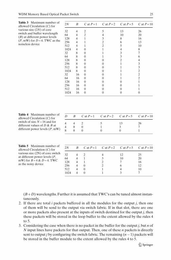
We have obtained (Table 3) the number of maximum allowed circulations (C) atdifferent power levels (in mW) with various combinations of switch size (N) and num-ber of buffer wavelength (B) considering TWC as the noiseless device. The numberof circulations C, is the largest value of K (circulations count) for which, BER ≤ 10−9.It was found in the computed results (Table 4) that if we increase B beyond D, thenthe number of maximum allowed circulations decreases which in turn, may degradesthe performance of large switch drastically. Hence, the maximum number of possiblewavelength in any of the buffer module is considered as 4 because, for larger value ofB (i.e., 8 and 16), the number of allowed circulations is zero at lower power and notmuch accountable at larger power. We have also calculated the number of maximumallowed circulations considering the TWC as the noisy device and the data is given inTable 5. If we compare these data with that one given in Table 3, then we can observethat there is not much effect of TWC noise on the number of maximum allowedcirculation. So, the results for loss probability will be nearly same for both the cases.
4 Scheduling algorithm
The buffering in the modules is done using the following scheduling algorithm:
1. The TWCs placed at the inputs of the loop buffer (Fig. 2), can be tuned to anyof the B wavelengths and the TWCs inside the loop can be tuned to any of the
WDM Memory Based Optical Packet Switch 25
Table 3 Maximum number ofallowed Circulation (C) forvarious size (2N) of coreswitch and buffer wavelength(B) at different power levels(P, mW) for D = 4. TWC as thenoiseless device
2N B C at P = 1 C at P = 2 C at P = 5 C at P = 10
32 4 2 5 13 2664 4 2 4 10 20128 4 1 3 8 16256 4 1 2 6 13512 4 1 2 5 101024 4 0 1 4 832 8 0 1 3 764 8 0 1 3 6128 8 0 0 2 4256 8 0 0 1 3512 8 0 0 1 31024 8 0 0 1 232 16 0 0 1 264 16 0 0 1 2128 16 0 0 0 1256 16 0 0 0 1512 16 0 0 0 11024 16 0 0 0 0
Table 4 Maximum number ofallowed Circulation (C) forswitch of size N = 16 and fordifferent values of D & B atdifferent power levels (P, mW)
D B C at P = 1 C at P = 2 C at P = 5 C at P = 10
4 4 2 5 13 264 8 0 1 3 78 8 0 0 0 1
Table 5 Maximum number ofallowed Circulation (C) forvarious size (2N) of core switchat different power levels (P,mW) for B = 4 & D = 4. TWCas the noisy device
2N B C at P = 1 C at P = 2 C at P = 5 C at P = 10
32 4 2 4 12 2564 4 1 3 10 20128 4 1 2 7 16256 4 0 2 6 12512 4 0 1 4 101024 4 0 1 3 7
(B+D) wavelengths. Further it is assumed that TWC’s can be tuned almost instan-taneously.
2. If there are total i packets buffered in all the modules for the output j, then oneof them will be send to the output via switch fabric. If in that slot, there are oneor more packets also present at the inputs of switch destined for the output j, thenthese packets will be stored in the loop buffer to the extent allowed by the rules 4to 5.
3. Considering the case when there is no packet in the buffer for the output j, but n ofN input lines have packets for that output. Then, one of these n packets is directlysent to output j by configuring the switch fabric. The remaining (n−1) packets willbe stored in the buffer module to the extent allowed by the rules 4 to 5.

26 R. K. Singh et al.
4. Number of packets xj for the output j, stored in all the buffer modules, shouldnever be greater than min(MB,C) i.e.,
xj ≤ min(MB, C), 1 ≤ j ≤ N
5. Total amount of buffered packets for all the outputs, cannot be larger than themaximum buffering capacity MB i.e.,
∑xj ≤ MB, 1 ≤ j ≤ N
6. The buffers in the loop are such that simultaneous read and write is allowed in thesame slot for the same wavelength.
7. The contending packets will try to occupy the lowest numbered (1 to M) availablemodule (Fig. 1).
8. During any time slot, priority will be given to the packets stored in the loop buffermodules than the packets at the switch input. Essentially for switch output, FIFOdiscipline will be maintained.
9. If there are total q packets in all modules for any output r, then oldest of q con-tending packets will leave first for the switch output.
10. Packet for different output will leave the switch at the same time, from theirmodules.
11. If any of the incoming packets will not be able to pass through the switch due tothe maximum buffer capacity limitation, then it will be dropped.
12. Packet will be stored in each module following the constraints specified in 4 to 5.There can be many strategies for storing the packets. Simplest is to find the lowestnumber memory module, which is empty, and store the packet in it subjected tothe constraints specified in 4 to 5. We are considering this algorithm in this paper.Another alternative approach could be to find out the module with minimumnumber of packets and store the packet on a wavelength such that wavelengthspacing for stored packet in the loop buffer is maximized. This will reduce impactof crosstalk due to imperfect filtering characteristics of various devices.
5 Simulation analysis and results
Using the above algorithm, the simulated results for ‘packet loss probability’ and‘average packet delay’ are obtained under various loading conditions. The optimiza-tion of switch performance is done considering different number of buffer modules(M), and the number of maximum allowed circulations (C) at different power levels.Figures 4–6 show results for the switch of size 2N = 32 with B = D = 4 and M = N/D.As defined earlier, 16 of 32 are the actual inputs and other 16 are used to connectdifferent number of buffer module. It has been observed that as the number of buffermodule (M) increase, packet loss probability decreases. We can observe in Fig. 4 that,as the signal power increases, the probability of packet loss decreases due to the incre-ment in C with power. But, this increment in power level beyond a value does not giveany further advantage as packet loss probability is same for P = 5 and 10 mW. Thishappens because at higher power, packet can be buffered for more time (Table 3) butdue to the limitation on maximum buffer space, higher values of C will have sameeffect as with lower one.

WDM Memory Based Optical Packet Switch 27
Fig. 4 Probability of packetloss with Load on the systemfor N = 16, B = 4, M = 4 anddifferent values of signalpower (P)
Fig. 5 Probability of packetloss with Load on the systemfor N = 16, B = 4, P = 5 mWand different values of numberof buffer modules (M)
Fig. 6 Probability of packetloss with number of buffermodule (M) for N = 16, B = 4,Load = 0.6 and different valuesof signal power (P)

28 R. K. Singh et al.
Fig. 7 Average Delay withLoad on the system for N = 16,B = 4, M = 4 and differentvalues of signal power (P).
Fig. 8 Average Delay withLoad on the system for N = 16,B = 4, P = 5 mW and differentnumbers of module (M)
The delay performance for this switch (2N = 32) is shown in Figs. 7–9. The aver-age delay increases with the number of modules. But, it remains same for P = 5 and10 mW because for N = 16, we are using maximum number of modules (i.e., M = 4)which provide 16 buffer spaces for any particular output. This indicate that in case ofP = 10 mW, although the packet can be stored for 26 slots (Table 3), but due to limitedmaximum buffer space of 16, the packet cannot be circulated more than 16 slots.Hence the results for case of P = 10 mW will be nearly same as P = 5 mW, since C = 13for P = 5 mW. Hence, the optimized result for 2N = 32, are achieved at D = B = 4,P = 5 mW and M = 4. We have obtained similar trend in results for this architecturewith larger size i.e., N = 32, 64 etc.
The results shown till now, is based on the assumption that the TWC is a noise-less device. We have also done the performance analysis of this switch architectureconsidering the TWC noise. We have found C = 2, 5, 13 & 26 at P = 1, 2, 5 & 10 mWand N = 16 for the noiseless case of TWC (Table 3) while C = 2, 4, 12 & 25 for thenoisy TWC (Table 5). There is not much difference among the number of maximumallowed circulations at various power levels. The comparative results for packet lossprobability and average delay for N = 16 at different power levels, are shown in Figs. 10and 11, respectively. We observed that the results at all power levels are overlapping

WDM Memory Based Optical Packet Switch 29
Fig. 9 Average Delay withnumber of buffer module (M)for N = 16, B = 4, Load = 0.6and different values of signalpower (P)
Fig. 10 Comparative resultsfor probability of packet losswith Load on the system forN = 16, B = 4, M = 4 anddifferent values of signalpower (noiseless TWC vs.noisy TWC)
except the case of P = 2 mW where, the loss probability is better and the average delayis more for the case of noiseless TWC. This will happen because, the case of C = 4 fornoisy TWC may rejects some more packets when the total capacity is 16 (=M × B) ascompared to the case of C = 5 for noiseless TWC.
6 Mathematical analysis
The packets are assumed to be randomly arriving with uniform rate between allsource–destination pairs. Depending upon the number of packets arriving and busyoutput port, various buffer states are attained. The state of the buffer is described bya vector ‘b’ of positive integers and of length N i.e., b = (b1, b2, . . . , bN) where ‘bi’(1 ≤ i ≤ N) represents the buffer state element for the ith output. Each such elementcan store packets ranging from 0 to min(MB,C). The sum of packets in any of thebuffer state b, will be less than or equal to MB i.e., �bi ≤ MB. As defined earlier,M is the number of module used in the architecture, B represents the total bufferingcapacity of each module, and C is the circulation limit allowed for any packet. Thus,min(MB,C) will be used as the maximum buffering capacity for individual output and

30 R. K. Singh et al.
Fig. 11 Comparative resultsfor average delay with load onthe system for N = 16, B = 4,M = 4 and different values ofsignal power (noiseless TWCvs. noisy TWC)
MB will be the maximum buffer capacity of whole switch. Here, the maximum valueof MB will always be equal to N.
Depending upon the arrival pattern during every slot, there will be transitionamong the buffer states. Each arriving pattern can be described by a vector of lengthN i.e., I = (I1, I2, . . . , IN) where the value of each element Ii represents the number ofpackets arrived for the output ‘i’. Total number of packet that can arrive during anytime slot, will not be more that N (i.e., �Ii ≤ N). For a given buffer state b and thearrival pattern I, the new buffer state will be an N length vector, d = (d1, d2, . . . , dN),where
di =⎧⎨⎩
0, bi = 0, Ii = 0bi + Ii − 1, bi + Ii − 1 ≤ min(Z, C)
min(Z, C), otherwise
⎫⎬⎭ (27)
Here,
Z =
⎧⎪⎪⎪⎨⎪⎪⎪⎩
MB −i−1∑j=1
dj −N∑
j=iR
(bj
), i > 1
MB −N∑
j=1R
(bj
), i = 1
(28)
and
R(bj) ={
bj − 1 bj > 00, bj = 0
(29)
The buffer space available, after completion of any time slot, will be equal to A definedas
A = MB −(
N∑i=1
bi −
)(30)
WDM Memory Based Optical Packet Switch 31
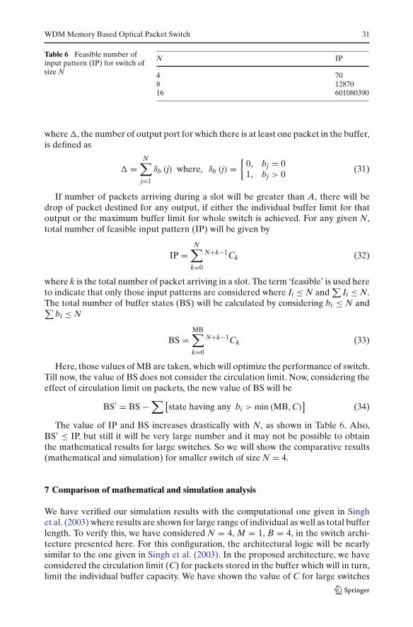
Table 6 Feasible number ofinput pattern (IP) for switch ofsize N
N IP
4 708 1287016 601080390
where , the number of output port for which there is at least one packet in the buffer,is defined as
=N∑
j=1
δb (j) where, δb (j) ={
0, bj = 01, bj > 0
(31)
If number of packets arriving during a slot will be greater than A, there will bedrop of packet destined for any output, if either the individual buffer limit for thatoutput or the maximum buffer limit for whole switch is achieved. For any given N,total number of feasible input pattern (IP) will be given by
IP =N∑
k=0
N+k−1Ck (32)
where k is the total number of packet arriving in a slot. The term ‘feasible’ is used hereto indicate that only those input patterns are considered where Ii ≤ N and
∑Ii ≤ N.
The total number of buffer states (BS) will be calculated by considering bi ≤ N and∑bi ≤ N
BS =MB∑k=0
N+k−1Ck (33)
Here, those values of MB are taken, which will optimize the performance of switch.Till now, the value of BS does not consider the circulation limit. Now, considering theeffect of circulation limit on packets, the new value of BS will be
BS′ = BS −∑[
state having any bi > min (MB, C)]
(34)
The value of IP and BS increases drastically with N, as shown in Table 6. Also,BS′ ≤ IP, but still it will be very large number and it may not be possible to obtainthe mathematical results for large switches. So we will show the comparative results(mathematical and simulation) for smaller switch of size N = 4.
7 Comparison of mathematical and simulation analysis
We have verified our simulation results with the computational one given in Singhet al. (2003) where results are shown for large range of individual as well as total bufferlength. To verify this, we have considered N = 4, M = 1, B = 4, in the switch archi-tecture presented here. For this configuration, the architectural logic will be nearlysimilar to the one given in Singh et al. (2003). In the proposed architecture, we haveconsidered the circulation limit (C) for packets stored in the buffer which will in turn,limit the individual buffer capacity. We have shown the value of C for large switches

32 R. K. Singh et al.
Fig. 12 Comparative resultsfor simulation withmathematical analysis
(N ≥ 16) in Table 3, and it indicate that the C will be larger than MB for N = 4,M = 1, B = 4. Thus, there will not be any limit on the number of maximum allowedcirculations because the net individual buffer capacity will be min(MB,C). Hence,for verification of the simulation results in the presence of circulation limit, we haveconsidered a hypothetical value of C = 2 for N = 4 and compared the obtained resultwith the one given in Singh et al. (2003). The comparative results are shown in Fig. 12and it is found that the variation of packet loss probability obtained from simulationmethod, strictly follows the mathematical analysis.
8 Conclusion
We have presented the architecture of an optical packet switch with feedback sharedbuffering using WDM loop buffer modules. The application of modular structurereduces the need for large range of wavelengths because the same set of wavelengthis used in all the buffer modules. One of the major advantages is that multiple loopbuffer modules act together as one single fully shared buffer. Due to reuse of wave-length range, the bandwidth of certain component e.g., EDFA and TWC, does notrestrain the total size of the buffers.
We have calculated the number of maximum allowed circulation in the loop bufferfor correct reception of a packet. In order to focus on performance of the switch, theanalysis is done under the assumption of single node network, instead of the networkconsisting of several such switches. The switch is optimized to achieve best packetloss probability at the reasonable delay performance. After comparing the results forseveral switch sizes, we found that the packet loss probability depends heavily onnumber of buffer modules. For smaller value of C, there will be no effect of increasingthe value of M. Hence M should be increased in accordance with C.
The simulation results are verified by comparing it with the performance of math-ematical model. This switch architecture is scalable but the main constraint is therequirement of large number of TWCs and other optical components. Other con-straint is the number of maximum allowed circulations which decreases with increasein the switch size.

WDM Memory Based Optical Packet Switch 33
We have considered the single switch network which implies that the fresh data isgenerated at the switch input and received at the switch output. In such network, thepacket will pass through the core switch only for two times. In a network where manysuch switches will be cascaded, packet may go through different amount of circula-tions in different switches. The packet will be passed through similar core switchesmany number of times (i.e., whenever it moves from one switch to other). Further, thelinks between these switches, will also attenuate the signal. Thus, the signal will haveto suffer loss from the additional core switches and the fiber links. Hence, the numberof maximum allowed circulations will be decreased and will depend on history of thepacket. The history of a packet will refer to the number of circulations already doneat the previous nodes, before reaching to any particular node. So, the total amount ofcirculations a packet performs in all the switches, have to be less than the number ofmaximum allowed circulations in a single switch, considering it as the single switchnetwork. In order to simplify and to focus only on the single switch performance, wehave taken this maximum limit. The degradation in the signal quality, demands forregeneration of signal, and is needed to be further investigated. In the future work,we will also find the performance of the network having multiple such switches.
References
1. Tucker, R.S., Zhong, W.D.: Photonic packet switching: an overview. IEICE Trans. Com-mun. E82B, 254–264 (1999)
2. Dittmann, L. et al.: The European IST project DAVID: a viable approach toward optical packetswitching. IEEE J. Sel. Areas Commun. 21, 1026–1040 (2003)
3. Danielsen, S.L., Mikkelsen, B., Jorgensen, C., Durhuus, T., Stubkjaer, K.E.: WDM packet switcharchitecture and analysis of the influence of tunable wavelength converters on the performance.J. Lightw. Technol. 15, 219–226 (1997)
4. Singh, R.K., Singh, Y.N.: An overview of photonic packet switching architectures. IETE Tech.Rev. 23, 15–34 (2006)
5. Chlamtac, I., Fumagalli, A.: An optical switch architecture for manhattan network. IEEE J. Sel.Areas Commun. 6, 550–559 (1993)
6. Hass, Z.: The staggering switch: an electronically controlled optical packet switch. J. Lightw.Technol. 11, 925–936 (1993)
7. Singh, R.K., Singh, Y.N.: A modified architecture for the staggering switch. In: Proc. NCC Conf.,186–187 (2005) (available at http://home.iitk.ac.in/∼ynsingh/papers/ncc05_rajat.pdf)
8. Verma, N., Srivastava, R., Singh, Y.N.: Novel design modification proposal for all optical fiberloop buffer switch. In: Proc. Photonics Conf., 181 (2002) (available at http://home.iitk.ac.in/∼yn-singh/papers/netp08.pdf)
9. Shukla, S., Srivastava, R., Singh, Y.N.: Modeling of fiber loop buffer switch. In: Proc. PhotonicsConf., 248 (2004) (available at http://home.iitk.ac.in/∼ynsingh/papers/rajiv.pdf)
10. Singh, R.K., Srivastava, R., Mangal, V., Singh, Y.N.: Wavelength routed shared buffer basedfeed-forward architectures for optical packet switching. In: Proc. IEEE INDICON Conf. (2006)
11. Srivastava, R., Mangal, V., Singh, R.K., Singh, Y.N.: A modified photonic switch architecturebased on fiber loop memory. In: Proc. IEEE INDICON Conf. (2006)
12. Yao, S., Mukherjee, B., Dixit, S.: Advances in photonic packet switching: an overview. IEEECommun. Mag. 38, 84–94 (2000)
13. Chia, M.C., Hunter, D.K., Andonovic, I., Ball, P., Wright, I., Ferguson, S.P., Guild, K.M., O’Mah-ony, M.J.: Packet loss and delay performance of feedback and feed-forward arrayed-waveguidegratings-based optical packet switches with WDM inputs-outputs.. J. Lightw. Technol. 19, 1241–1254 (2001)
14. Fow-Sen Choa, Zhao, Xiuqin, X., Lin, Yu., Zhang, J., Gu, J.P., Ru, Y., Guansong Zhang, G.,Longjun, Li, Huiping, Xiang, Hadimioglu, H., Chao, H.J.: An optical packet switch based onWDM technologies. J. Lightw. Technol. 23, 994–1014 (2005)
34 R. K. Singh et al.
15. Papadimitriou, G.I., Papazoglou, C., Pomportsis, A.S.: Optical switching: switch fabrics, tech-niques, and architectures. J. Lightw. Technol. 21, 384–405 (2003)
16. Shun, Y., Mukherjee, B., Yoo, S.J.B., Dixit, S.: A unified study of contention resolution schemesin optical packet switched networks. J. Lightw. Technol. 21, 672–683 (2003)
17. Mynbaev, D.K., Scheiner, L.L.: Fiber-optic communication technology. Prentice Hall, UpperSaddle River, NJ, USA (2001)
18. Mamyshev, P.V.: All-optical data regeneration based on self phase modulation effect. In: Proc.ECOC Conf. 475–476 (2004)
19. Olsson, N.A.: Lightwave systems with optical amplifiers. J. Lightw. Technol. 7, 1071–1082 (1989)20. Naik, M., Singh, Y.N.: Simulation of Fiber Loop Buffer Memory of All-Optical Packet Switch.
In: Proc. NCC Conf. 50–54 (2002) (available at http://home.iitk.ac.in/∼ynsingh/papers/ncc.pdf)21. Iannone, E., Sabella, R.: Performance evaluation of an optical multi-carrier network using wave-
length converters based on FWM in semiconductor optical amplifiers. J. Lightw. Technol. 13, 312–324 (1995)
22. Giles, C.R., Desurvire, E.: Modeling erbium-doped fiber amplifiers. J. Lightw. Technol. 9, 271–283 (1991)
23. Richards, D.H., Jackel, J.L., Ali, M.A.: A theoretical investigation of dynamic all-optical auto-matic gain control in multichannel EDFA’s and EDFA cascades. IEEE J. Sel. Top. Quant.Elect. 3, 1027–1036 (1997)
24. Kartalopoulos, S.V. : Introduction to DWDM technology. IEEE Press, Piscataway NJ USA (2000)25. Singh, Y.N., Kushwaha, A., Bose, S.K.: Exact and analytical modeling of a FLBM based all-optical
packet switch. J. Lightw. Technol. 21, 719–726 (2003)