Via wearout detection with on-chip monitors
12
Via wearout detection with on-chip monitors Fahad Ahmed, Linda Milor Georgia Institute of Technology, School of Electrical and Computer Engineering, Atlanta, GA 30332, USA article info Article history: Received 20 September 2009 Accepted 18 January 2010 Available online 11 February 2010 Keywords: Electromigration Built-in self-test Reliability monitor abstract This project aims to detect the onset of chip failure due to via voiding through monitoring the delays of paths in a chip. The proposed method relates the probability of failure of individual vias to an increase in delay for monitors of the system using data for 65 nm technology. The delay increase, as a function of the failure distribution parameters, the path length, gate type, and process variation, has been investigated. An on-chip, ring oscillator-based wearout monitoring circuit is presented. The proposed scheme monitors the delay through a data path using a delay detection circuit (DDC). & 2010 Elsevier Ltd. All rights reserved. 1. Introduction Many applications, ranging from automatic flight control systems, nuclear power control systems, on-line transaction processors for financial institutions, to hospital patient monitors, require systems to be extremely reliable. Fault-tolerant systems require finding a way to prevent a physical defect or failure from causing an error in system performance. Such systems incorpo- rate fault detection, fault masking, fault isolation, and recovery procedures. Fault-tolerant design at the circuit level focuses primarily on fault detection. The other aspects of fault tolerance (fault location, system reconfiguration, and recovery) are generally performed off-chip by the system architecture and software. The typical approach to fault detection on-chip involves the introduction of redundancy, in space, time, and information, at the cost of either extra computational time and/or extra hardware components. The cost of these approaches is a degradation in yield (and a concomitant increase in manufacturing cost), together with higher power dissipation, since all modules are operated in parallel. This paper aims to demonstrate an alternative approach, involving detection of the onset of failure through detection of component degradation over time. If component degradation can be detected, the cost of building highly reliable systems would be reduced. The additional area needed for fault detection is limited to the design-for-test (DfT) circuitry, which is a small fraction of the component being monitored. Similarly, the cost of operating such a system is similarly reduced, due to the reduced power dissipation, since the DfT circuitry is only turned on intermit- tently during test. A wide variety of faults can cause system failures, ranging from static to transient faults. This paper focuses on faults due to component wearout. The major causes of product wearout are electromigration, gate oxide breakdown, hot carrier injection, negative bias temperature instability, backend dielectric break- down, and stress migration [1]. This paper focuses on the detection of electromigration only. The proposed method to detect electromigration is through detection of increased delays in data paths. However, it should be noted that many other failure mechanisms can impact the delays of data paths. Hence, our results will only show that delay increases provide a quantifiable indication of electromigration in the absence of other failure mechanisms. Future work will look at the use of additional monitors, in combination with the proposed monitors, to attempt to determine the cause of failure. This paper is organized as follows. In the next section via degradation is related to path delay. Section 3 considers the sensitivity of this relationship to parameters describing the failure rate distribution of vias, chain length, the composition of the data path in terms of gate types, and process variation. Section 4 presents the proposed detection circuit. Section 5 considers the problems caused by power supply noise, jitter, and temperature variation and potential solutions to these problems. Section 6 compares this scheme with a conventional ring oscillator-based monitoring scheme. Section 7 concludes the paper with a summary. 2. Relating via degradation to path delay 2.1. Calculation of the via cumulative probability densities of failure Stress-inducted electromigration has been identified as a key concern in interconnect reliability, due to continued reduction in via dimensions and the resulting increase in current density with Contents lists available at ScienceDirect journal homepage: www.elsevier.com/locate/mejo Microelectronics Journal 0026-2692/$ - see front matter & 2010 Elsevier Ltd. All rights reserved. doi:10.1016/j.mejo.2010.01.006 Corresponding author. Tel.: + 1 404 894 4793; fax: + 1 404 898 0677. E-mail address: [email protected] (L. Milor). Microelectronics Journal 41 (2010) 789–800
Transcript of Via wearout detection with on-chip monitors
Microelectronics Journal 41 (2010) 789–800
Contents lists available at ScienceDirect
Microelectronics Journal
0026-26
doi:10.1
� Corr
E-m
journal homepage: www.elsevier.com/locate/mejo
Via wearout detection with on-chip monitors
Fahad Ahmed, Linda Milor �
Georgia Institute of Technology, School of Electrical and Computer Engineering, Atlanta, GA 30332, USA
a r t i c l e i n f o
Article history:
Received 20 September 2009
Accepted 18 January 2010Available online 11 February 2010
Keywords:
Electromigration
Built-in self-test
Reliability monitor
92/$ - see front matter & 2010 Elsevier Ltd. A
016/j.mejo.2010.01.006
esponding author. Tel.: +1 404 894 4793; fax
ail address: [email protected] (L. Milor).
a b s t r a c t
This project aims to detect the onset of chip failure due to via voiding through monitoring the delays of
paths in a chip. The proposed method relates the probability of failure of individual vias to an increase
in delay for monitors of the system using data for 65 nm technology. The delay increase, as a function
of the failure distribution parameters, the path length, gate type, and process variation, has been
investigated. An on-chip, ring oscillator-based wearout monitoring circuit is presented. The proposed
scheme monitors the delay through a data path using a delay detection circuit (DDC).
& 2010 Elsevier Ltd. All rights reserved.
1. Introduction
Many applications, ranging from automatic flight controlsystems, nuclear power control systems, on-line transactionprocessors for financial institutions, to hospital patient monitors,require systems to be extremely reliable. Fault-tolerant systemsrequire finding a way to prevent a physical defect or failure fromcausing an error in system performance. Such systems incorpo-rate fault detection, fault masking, fault isolation, and recoveryprocedures.
Fault-tolerant design at the circuit level focuses primarily onfault detection. The other aspects of fault tolerance (fault location,system reconfiguration, and recovery) are generally performedoff-chip by the system architecture and software. The typicalapproach to fault detection on-chip involves the introduction ofredundancy, in space, time, and information, at the cost of eitherextra computational time and/or extra hardware components.The cost of these approaches is a degradation in yield (and aconcomitant increase in manufacturing cost), together withhigher power dissipation, since all modules are operated inparallel.
This paper aims to demonstrate an alternative approach,involving detection of the onset of failure through detection of
component degradation over time. If component degradation can bedetected, the cost of building highly reliable systems would bereduced. The additional area needed for fault detection is limitedto the design-for-test (DfT) circuitry, which is a small fraction ofthe component being monitored. Similarly, the cost of operatingsuch a system is similarly reduced, due to the reduced powerdissipation, since the DfT circuitry is only turned on intermit-tently during test.
ll rights reserved.
: +1 404 898 0677.
A wide variety of faults can cause system failures, ranging fromstatic to transient faults. This paper focuses on faults due tocomponent wearout. The major causes of product wearout areelectromigration, gate oxide breakdown, hot carrier injection,negative bias temperature instability, backend dielectric break-down, and stress migration [1].
This paper focuses on the detection of electromigration only.The proposed method to detect electromigration is throughdetection of increased delays in data paths. However, it shouldbe noted that many other failure mechanisms can impact thedelays of data paths. Hence, our results will only show that delayincreases provide a quantifiable indication of electromigrationin the absence of other failure mechanisms. Future work will look atthe use of additional monitors, in combination with the proposedmonitors, to attempt to determine the cause of failure.
This paper is organized as follows. In the next section viadegradation is related to path delay. Section 3 considers thesensitivity of this relationship to parameters describing the failurerate distribution of vias, chain length, the composition of the datapath in terms of gate types, and process variation. Section 4presents the proposed detection circuit. Section 5 considers theproblems caused by power supply noise, jitter, and temperaturevariation and potential solutions to these problems. Section 6compares this scheme with a conventional ring oscillator-basedmonitoring scheme. Section 7 concludes the paper with asummary.
2. Relating via degradation to path delay
2.1. Calculation of the via cumulative probability densities of failure
Stress-inducted electromigration has been identified as a keyconcern in interconnect reliability, due to continued reduction invia dimensions and the resulting increase in current density with
Table 1MTF for vias of the inverter at the nodes indicated in Fig. 1.
Via PMOSS NMOSS PMOSG NMOSG OUTVIA
MTF (years) 5.2040 5.1721 18.8620 114.707 11.6598
0 5 10 15 200
0.2
0.4
0.6
0.8
1
Time-YrsC
DF
PMOSS
NMOSS
OUTVIA
PMOSG
NMOSG
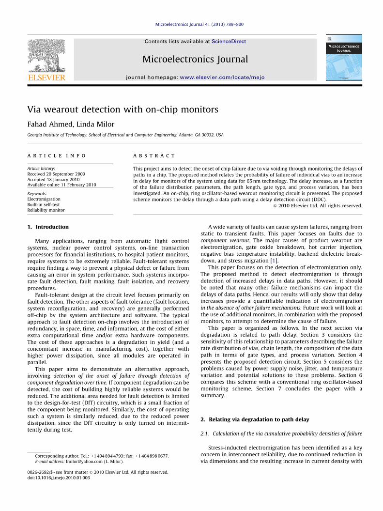
Fig. 2. CDF of vias at different nodes of an inverter for b=1.2. The difference in the
failure rates is due to the difference in the current through each node.
F. Ahmed, L. Milor / Microelectronics Journal 41 (2010) 789–800790
each technology generation. This has adversely affected theelectromigration lifetime of interconnects, particularly vias andcontacts, due to the higher current densities through them [2,3].
Electromigration is caused by the transfer of momentum fromthe moving ‘‘electron wind’’ to ions in the metallic lattice [4]. Itresults in the transport of these metallic ions into the neighboringmaterial, causing an increase in resistance.
Two different voiding features have been identified at the via–line interface [3]. Depending on the direction of flow of current,void formation could occur on the via side of the line liner or onthe line side. Once big enough to be electrically detectible, voidformation translates into an increase in the delay through the datapath. Thus by constantly monitoring the delay of a path, it ispossible to detect the onset of failure of the data path.
Median time-to-failure (MTF) of a via is a strong function ofcurrent density. Black’s equation [4] has been extensively used forelectromigration lifetime modeling. According to this model, theMTF of a conducting path is inversely proportional to the currentdensity, as follows:
MTF ¼ AJ�n expðF=KTÞ; ð1Þ
where J is the current density, F is the activation energy, T istemperature, K is Boltzmann’s constant, and A is a constant. In thisstudy, the activation energy and the value of n were calculatedusing experimental data from [5].
As a generic example, the data path considered is made up of achain of inverters, and each node is assumed to contain a via, asshown in Fig. 1.
Via dimensions are assumed to be typical via dimensions for65 nm technology [6]. Therefore, the current density through eachvia is only a function of the current through the node in which it islocated. The ring oscillator was simulated. Table 1 shows thecalculated MTFs for vias at different positions in the inverter.It can be seen that the vias at the sources have the least expectedlifetime due to the larger current through them.
The Weibull cumulative probability density function (CDF) forthe time-to-failure is used to model the probability of failure,
Fig. 1. The inverter chain consists of inverters, line the one shown, with a via at
every node.
P(tfail), of these vias as a function of time:
PðtfailÞ ¼ 1�exp �tfail
Z
� �b !
: ð2Þ
The Weibull distribution is described by two parameters: Zand b, which are the characteristic lifetime and shape parameter,respectively. The median time-to-failure is
MTF ¼ Zðln ð2ÞÞ1=b: ð3Þ
Substituting (3) into (2) enables us to relate the MTF of a via toits probability of failure. Fig. 2 shows the CDFs of the vias of aninverter.
2.2. Relationship between resistance and failure
The data path has been assumed to consist of an inverter chainwith 18 inverters. The initial via resistances, R0, for all vias in all ofthe inverters, were assumed to be normally distributed.
Experimental results [3] show that under stressed conditions,resistance increases very slowly, until a point where there is ajump in the via resistance. After the jump, the resistance eitherincreases gradually or there is an immediate open circuit at thevia–line contact. This resistance jump was explained as an occur-rence of a void at the contact. Once the void is formed, the rate ofincrease in resistance increases in comparison to the initialincrease in resistance.
The resistance jump is very critical, since it indicates the pointafter which a via could break at any time. The resistance valueafter the jump was taken as the point at which a via fails (RFail). Liet al. [3] had shown that the distribution of this value is a functionof the time zero resistance and is approximately distributedaround a mean value of 0.2R0 for most via configurations, i.e.
RFailMean ¼ 1:2R0: ð4Þ
For each via, RFail is assumed to be normally distributed withthe mean of 1.2R0.

0 1 2 3 4 50
5
10
15
20
25
30
Time-Yrs
Via
s E
xcee
ding
1.2
Ro
0
0.05
0.1
0.15
0.2
0.25
0.3
PFa
il
Fig. 4. Number of vias exceeding 1.2R0 as a function of time. PFail is the fraction of
vias that have failed in the inverter chain, which varies from zero to one.
0 1 2 3 4 52.385
2.39
2.395
2.4
2.405
2.41x 10⁻¹⁰
Time-Yrs
Del
ay-s
ec
F. Ahmed, L. Milor / Microelectronics Journal 41 (2010) 789–800 791
Under normal operating conditions it is assumed that the viaresistance is modeled as a time-dependent exponential function:
RðtÞ ¼ R0 et=G ð5Þ
where G models the rate of increase of the effective resistanceas a function of time. The time to fail for each via (tfail) iscalculated from the Weibull curve. Values for RFail and tfail arerelated by Eq. (5):
1:2R0 ¼ R0 expðtfail=GÞ: ð6Þ
Hence, we can calculate G for each via in the inverter chain:
G¼ tfail=lnð1:2Þ ð7Þ
and
G¼�MTF lnð1�PÞ
lnð1:2Þbðln 2Þ1=b: ð8Þ
Accounting for randomness involves assigning a probability,PA ½0;1�, to each via based on a uniform distribution. Thisprobability, P, impacts G for each via, according to (8). Eq. (5) isthen used to model the time evolution of each via resistance inthe inverter chain. Fig. 3 shows the increase in resistances of the90 vias in the inverter chain with respect to time for one inverterchain instance. Because P is a random variable, each inverter chainwill have a different distribution of resistances vs. time.
2.3. Relationship to inverter chain delay
The inverter chain has numerous vias exceeding RFail atvarious times. Fig. 4 plots the number of vias exceeding 1.2R0 vs.time.
An inverter chain with via resistances varying as shown inFig. 3 was simulated, to find the delay through the chain. Theresult is shown in Fig. 5. Fig. 6 combines Figs. 4 and 5, by plottingDDelay vs. the number of failing vias. We see that changes in delaygreater than 2e�14 s can clearly indicate the presence of anelectromigration problem that impacts the vias. This correspondsto detecting faulty chains at the point when only one or two viashave failed.
It can be noted from Fig. 5 that normally delay changes by 0.9%in the course of 5 years. Some of the sources of variation in delaynot related to wearout include on-chip temperature variation, IRdrops, and crosstalk. Consider, for example, temperature, whereover an operating temperature range from 0 to 105 1C, delay of the
Fig. 3. Simulated values of resistance for all vias in an inverter chain plotted
against time.
Fig. 5. Delay through the inverter chain. With increasing time, the via resistances
increase, causing an increase in delay.
inverter chain varies by 150 ps. This swamps out degradation dueto wearout. Hence, it is important that the operating conditionsare reproduced exactly for each test of delay degradation. Theability to reproduce operating conditions, and hence temperatureprofiles, IR drops, and crosstalk limits the resolution of themethod.
Delay increases due to other mechanisms that impacttransistors, i.e. hot carrier injection and negative temperaturebias instability, are likely to be more significant than delayincreases due to electromigration in vias. Nevertheless, therecould be processes with electromigration weaknesses which needto be monitored. Moreover, the delay increase trigger is anindicator of a potential reliability failure of any kind. Hence, if wehave other screens to determine the likely cause of failure,1 delay
1 Screens that can distinguish between electromigration and transistor
wearout mechanisms could be a set of heavily loaded overstressed ring oscillators,
some with large transistors driving single vias and some with the same transistors
driving multiple vias, so that electromigration is unlikely.
0 5 10 15 20 25 300
0.5
1
1.5
2
2.5x 10⁻¹²
Vias Exceeding 1.2Ro
Del
ta D
elay
-sec
0 0.05 0.1 0.15 0.2 0.25 0.3PFail
Fig. 6. Relationship between the change in delay through the chain and the
probability of failure of the inverter chain.
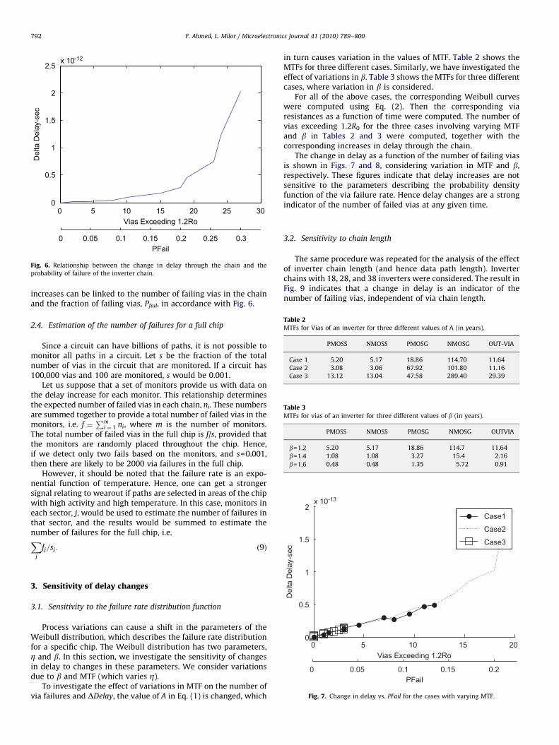
Table 2MTFs for Vias of an inverter for three different values of A (in years).
PMOSS NMOSS PMOSG NMOSG OUT-VIA
Case 1 5.20 5.17 18.86 114.70 11.64
Case 2 3.08 3.06 67.92 101.80 11.16
Case 3 13.12 13.04 47.58 289.40 29.39
Table 3
MTFs for vias of an inverter for three different values of b (in years).
PMOSS NMOSS PMOSG NMOSG OUTVIA
b=1.2 5.20 5.17 18.86 114.7 11.64
b=1.4 1.08 1.08 3.27 15.4 2.16
b=1.6 0.48 0.48 1.35 5.72 0.91
0 5 10 15 200
0.5
1
1.5
2x 10-13
Vias Exceeding 1.2Ro
Del
ta D
elay
-sec
Case1
Case2
Case3
0 0.05 0.1 0.15 0.2PFail
Fig. 7. Change in delay vs. PFail for the cases with varying MTF.
F. Ahmed, L. Milor / Microelectronics Journal 41 (2010) 789–800792
increases can be linked to the number of failing vias in the chainand the fraction of failing vias, Pfail, in accordance with Fig. 6.
2.4. Estimation of the number of failures for a full chip
Since a circuit can have billions of paths, it is not possible tomonitor all paths in a circuit. Let s be the fraction of the totalnumber of vias in the circuit that are monitored. If a circuit has100,000 vias and 100 are monitored, s would be 0.001.
Let us suppose that a set of monitors provide us with data onthe delay increase for each monitor. This relationship determinesthe expected number of failed vias in each chain, ni. These numbersare summed together to provide a total number of failed vias in themonitors, i.e. f ¼
Pmi ¼ 1 ni, where m is the number of monitors.
The total number of failed vias in the full chip is f/s, provided thatthe monitors are randomly placed throughout the chip. Hence,if we detect only two fails based on the monitors, and s=0.001,then there are likely to be 2000 via failures in the full chip.
However, it should be noted that the failure rate is an expo-nential function of temperature. Hence, one can get a strongersignal relating to wearout if paths are selected in areas of the chipwith high activity and high temperature. In this case, monitors ineach sector, j, would be used to estimate the number of failures inthat sector, and the results would be summed to estimate thenumber of failures for the full chip, i.e.X
j
fj=sj: ð9Þ
3. Sensitivity of delay changes
3.1. Sensitivity to the failure rate distribution function
Process variations can cause a shift in the parameters of theWeibull distribution, which describes the failure rate distributionfor a specific chip. The Weibull distribution has two parameters,Z and b. In this section, we investigate the sensitivity of changesin delay to changes in these parameters. We consider variationsdue to b and MTF (which varies Z).
To investigate the effect of variations in MTF on the number ofvia failures and DDelay, the value of A in Eq. (1) is changed, which
in turn causes variation in the values of MTF. Table 2 shows theMTFs for three different cases. Similarly, we have investigated theeffect of variations in b. Table 3 shows the MTFs for three differentcases, where variation in b is considered.
For all of the above cases, the corresponding Weibull curveswere computed using Eq. (2). Then the corresponding viaresistances as a function of time were computed. The number ofvias exceeding 1.2R0 for the three cases involving varying MTFand b in Tables 2 and 3 were computed, together with thecorresponding increases in delay through the chain.
The change in delay as a function of the number of failing viasis shown in Figs. 7 and 8, considering variation in MTF and b,respectively. These figures indicate that delay increases are notsensitive to the parameters describing the probability densityfunction of the via failure rate. Hence delay changes are a strongindicator of the number of failed vias at any given time.
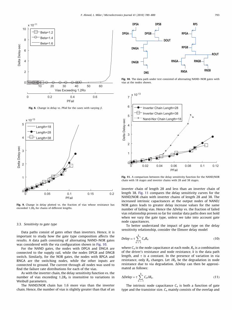
3.2. Sensitivity to chain length
The same procedure was repeated for the analysis of the effectof inverter chain length (and hence data path length). Inverterchains with 18, 28, and 38 inverters were considered. The result inFig. 9 indicates that a change in delay is an indicator of thenumber of failing vias, independent of via chain length.
10 20 30 40 50 600
2
4
6
8
10x 10-11
Vias Exceeding 1.2Ro
Del
ta D
elay
-sec
Beta=1.2
Beta=1.4
Beta=1.6
0 0.2 0.4 0.6PFail
Fig. 8. Change in delay vs. PFail for the cases with varying b.
0 0.05 0.1 0.15 0.20
1
2
3
4
5x 10-13
PFail
Del
ta D
elay
-sec
Length=18
Length=28
Length=38
Fig. 9. Change in delay plotted vs. the fraction of vias whose resistance has
exceeded 1.2R0 for chains of different lengths.
Fig. 10. The data path under test consisted of alternating NAND–NOR gates with
vias at the nodes shown.
0 0.02 0.04 0.06 0.08 0.1 0.120
1
2
3
4
5
6
7x 10-13
PFail
Del
ta D
elay
-sec
Inverter Chain Length=28
Inverter Chain Length=38
Nand-Nor Chain Length=18
Fig. 11. A comparison between the delay sensitivity function for the NAND/NOR
chain with 18 stages and inverter chains with 28 and 38 stages.
F. Ahmed, L. Milor / Microelectronics Journal 41 (2010) 789–800 793
3.3. Sensitivity to gate type
Data paths consist of gates other than inverters. Hence, it isimportant to study how the gate type composition affects theresults. A data path consisting of alternating NAND–NOR gateswas considered with the via configuration shown in Fig. 10.
For the NAND gates, the nodes with DPGA and DNGA areconnected to the supply rail, while the nodes DPGB and DNGBswitch. Similarly, for the NOR gates, the nodes with RPGA andRNGA are the switching nodes, while the other inputs areconnected to ground. The current through all nodes was used tofind the failure rate distributions for each of the vias.
As with the inverter chain, the delay sensitivity function vs. thenumber of vias exceeding 1.2R0 is insensitive to variations inWeibull parameters.
The NAND/NOR chain has 1.6 more vias than the inverterchain. Hence, the number of vias is slightly greater than that of an
inverter chain of length 28 and less than an inverter chain oflength 38. Fig. 11 compares the delay sensitivity curves for theNAND/NOR chain with inverter chains of length 28 and 38. Theincreased intrinsic capacitances at the output nodes of NAND/NOR gates leads to greater delay increase values for the samenumber of failing vias. Hence the DDelay vs. the fraction of failedvias relationship proven so far for similar data paths does not holdwhen we vary the gate type, unless we take into account gatenode capacitances.
To better understand the impact of gate type on the delaysensitivity relationship, consider the Elmore delay model
Delay¼ tXk
n ¼ 1
CnRn ð10Þ
where Cn is the node capacitance at each node, Rn is a combinationof the driver’s resistance and node resistance, k is the data pathlength, and t is a constant. In the presence of variation in viaresistance, only Rn changes. Let dRn be the degradation in noderesistance due to via degradation. DDelay can then be approxi-mated as follows:
DDelay¼ tXk
n ¼ 1
CndRn: ð11Þ
The intrinsic node capacitance Cn is both a function of gatetype and the transistor size. Cn mainly consists of the overlap and

1
1.2 x 10⁻¹³c
data1data2data3
F. Ahmed, L. Milor / Microelectronics Journal 41 (2010) 789–800794
junction capacitances and both are assumed to increase linearlywith transistor size. Let k0 be the number of nodes in an inverterchain, with capacitance Cl, l=1,y,k0. Let k be the number of nodesin a path containing arbitrary gates. At each of these nodes,n=1,y,k, jn is the number of nodes in the charge and/or dischargepath, which depends on the gate stack size in the pull-up and/orpull-down network, and hence the gate type. Let Cn,m, n=1,y,kand m=1,y,jn be the node capacitances associated with the mthnode in the pull-up and/or pull-down network of the nth gate inthe path. The capacitance ratio to the inverter chain is thefollowing:
g ¼
Pkn ¼ 1ð
Pjn
m ¼ 1 Cn;mÞPk0
l ¼ 1 Cl
: ð12Þ
Therefore, the relationship between the delay sensitivityfunction for an arbitrary gate, DDelay, and the delay sensitivityfunction for a reference inverter chain, DDelayinv is
DDelay¼ g �DDelayinv: ð13Þ
Table 4 contains a variety of capacitance ratios for the gatesconsidered. The differences in the capacitance ratios are partiallydue to gate sizing.
In Fig. 12 we plot DDelay=g for a variety of gates. From thisfigure it can be concluded that for an arbitrary data path, given g
and the delay sensitivity function for the inverter chain, DDelayinv,it is possible to estimate the number of failing vias for arbitrarypaths, irrespective of the type of gates that make up the data path.
0.2
0.4
0.6
0.8
Del
ta D
elay
-se data4
3.4. Sensitivity to process variations
Two major sources of process variations are the thresholdvoltage [7] and channel length [8–10]. Variation in threshold
Table 4Capacitance ratios for a variety of gates.
Gate/chain G
NOT 1
NAND 3.5
NOR 2.75
NAND–NOR (9 NAND and 9 NOR) 3.125
NAND–NOR-NOT (28 NOT, 9 NAND, 9 NOR, randomly placed) 1.23
0 0.02 0.04 0.06 0.08 0.1 0.120
1
2
3
4
5
6
7x 10-13
PFail
Nor
m-D
elta
Del
ay (s
ec)
NOT(L=28)
NOR(L=18)
NAND(L=18)
NAND-NOR(L=18)
NAND-NOR-NOT(L=46)
Fig. 12. Increase in the normalized delay of the data path with varying types pf
gates and length plotted against PFail.
voltage is due to statistical fluctuation in the number of dopantatoms per unit volume in the device channel. Channel lengthvariation is due to line edge roughness, which is induced by thepolymer characteristics of photoresist, and systematic variation inlithography (proximity effect, lens aberrations, and flare) [11].
Our analysis considers random variation in threshold voltageand channel length. Figs. 13 and 14 show that there is very littleimpact of random process variation on the delay sensitivitycurves. The impact is more pronounced in the presence of channellength variation. Hence, it may be desirable to include capacitancecompensation for channel length variations, as suggested in theprevious section. This is because channel length variations can belarge, and they impact both transistor drive strength and loadcapacitances.
4. DPRO-based delay detection
In this section, we present the design of an on-chip delaymonitoring system to detect changes in the delay of a data pathbeing monitored.
0 2 4 6 8 10 120
Vias Exceeding 1.2Ro
0 0.02 0.04 0.06 0.08 0.1 0.12PFail
Fig. 13. Change in delay plotted vs. the number of failing vias and PFail for a
random sample of threshold voltages. For 65 nm technology, the standard
deviation was assumed to be 30 mV.
0 0.02 0.04 0.06 0.08 0.1 0.120
0.5
1
1.5
2x 10-13
PFail
Del
ta-D
elay
(sec
)
NOT(28)
NOR(18)
NAND(18)
NAND-NOR(18)
NAND-NOR-NOT(46)
Fig. 14. Change in delay plotted vs. PFail for a random sample of channel lengths.
For 65 nm technology, the standard deviation was assumed to be 20 nm.
F. Ahmed, L. Milor / Microelectronics Journal 41 (2010) 789–800 795
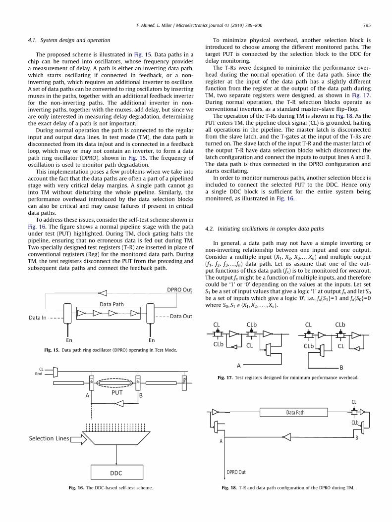
4.1. System design and operation
The proposed scheme is illustrated in Fig. 15. Data paths in achip can be turned into oscillators, whose frequency providesa measurement of delay. A path is either an inverting data path,which starts oscillating if connected in feedback, or a non-inverting path, which requires an additional inverter to oscillate.A set of data paths can be converted to ring oscillators by insertingmuxes in the paths, together with an additional feedback inverterfor the non-inverting paths. The additional inverter in non-inverting paths, together with the muxes, add delay, but since weare only interested in measuring delay degradation, determiningthe exact delay of a path is not important.
During normal operation the path is connected to the regularinput and output data lines. In test mode (TM), the data path isdisconnected from its data in/out and is connected in a feedbackloop, which may or may not contain an inverter, to form a datapath ring oscillator (DPRO), shown in Fig. 15. The frequency ofoscillation is used to monitor path degradation.
This implementation poses a few problems when we take intoaccount the fact that the data paths are often a part of a pipelinedstage with very critical delay margins. A single path cannot gointo TM without disturbing the whole pipeline. Similarly, theperformance overhead introduced by the data selection blockscan also be critical and may cause failures if present in criticaldata paths.
To address these issues, consider the self-test scheme shown inFig. 16. The figure shows a normal pipeline stage with the pathunder test (PUT) highlighted. During TM, clock gating halts thepipeline, ensuring that no erroneous data is fed out during TM.Two specially designed test registers (T-R) are inserted in place ofconventional registers (Reg) for the monitored data path. DuringTM, the test registers disconnect the PUT from the preceding andsubsequent data paths and connect the feedback path.
Fig. 15. Data path ring oscillator (DPRO) operating in Test Mode.
Fig. 16. The DDC-based self-test scheme.
To minimize physical overhead, another selection block isintroduced to choose among the different monitored paths. Thetarget PUT is connected by the selection block to the DDC fordelay monitoring.
The T-Rs were designed to minimize the performance over-head during the normal operation of the data path. Since theregister at the input of the data path has a slightly differentfunction from the register at the output of the data path duringTM, two separate registers were designed, as shown in Fig. 17.During normal operation, the T-R selection blocks operate asconventional inverters, as a standard master–slave flip–flop.
The operation of the T-Rs during TM is shown in Fig. 18. As thePUT enters TM, the pipeline clock signal (CL) is grounded, haltingall operations in the pipeline. The master latch is disconnectedfrom the slave latch, and the T-gates at the input of the T-Rs areturned on. The slave latch of the input T-R and the master latch ofthe output T-R have data selection blocks which disconnect thelatch configuration and connect the inputs to output lines A and B.The data path is thus connected in the DPRO configuration andstarts oscillating.
In order to monitor numerous paths, another selection block isincluded to connect the selected PUT to the DDC. Hence onlya single DDC block is sufficient for the entire system beingmonitored, as illustrated in Fig. 16.
4.2. Initiating oscillations in complex data paths
In general, a data path may not have a simple inverting ornon-inverting relationship between one input and one output.Consider a multiple input (X1, X2, X3,y,Xn) and multiple output(f1, f2, f3,y,fn) data path. Let us assume that one of the out-put functions of this data path (fx) is to be monitored for wearout.The output fx might be a function of multiple inputs, and thereforecould be ‘1’ or ‘0’ depending on the values at the inputs. Let setS1 be a set of input values that give a logic ‘1’ at output fx and let S0
be a set of inputs which give a logic ‘0’, i.e., fx{S1}=1 and fx{S0}=0where S0; S1AfX1;X2; . . . ;Xng.
Fig. 17. Test registers designed for minimum performance overhead.
Fig. 18. T-R and data path configuration of the DPRO during TM.
Fig. 21. The function inverting block.
F. Ahmed, L. Milor / Microelectronics Journal 41 (2010) 789–800796
If we eliminate the inputs that have the same value in both thesets S1 and S0, we are left with the inputs (XR) that toggle thefunction fx and that can make the data path oscillate.
Consider the logic function shown in Fig. 19. For this func-tion S1={X1=1, X2=1, X3=0} and S0 can consist of all otherinput combinations. Let us select S0={X1=0, X2=0, X3=0}. Then inorder to create oscillations, we need to toggle X1 and X2.Moreover, since X1=X2=1 results in fx=1, and X1=X2=0 results infx=0, fx must be inverted before it is fed back to the inputs X1
and X2.Consider a complex data path in a pipelined stage, shown in
Fig. 20. Of all the outputs, suppose we want to monitor one as aselected wearout monitor. In TM, the T-R register at the output offx feeds the selected data path into the function inverting block.
The function inverting block senses the value of the output fx
and generates a set of inputs to be inverted or non-inverted andfed back into the register file at the input of the data path. Forthese inputs, the regular registers are again replaced by the T-Rregisters which feedback the output of the function invertingblock into the data path, causing the value at the output fx totoggle.
Fig. 21 shows one possible implementation of the functioninverting block. Depending on the value of fx, the selection blockchooses the appropriate values independently of other selectionblocks for inverting fx.
It should be noted that this scheme of initiating oscillations incomplex data paths leads to insignificant performance overheaddue the insertion of the specially designed T-R registers.
4.3. DDC design
The oscillations of the DPRO output are fed into the DDC.Fig. 22 shows the block level implementation of the DDC. In theDDC, a counter counts the number of oscillations of the DPRO. Theother two blocks in the DDC generate the test start and stop
X1
X2
X3fx
Fig. 19. Logic function.
Fig. 20. A multiple input, multiple output complex data path in a pipelined stage.
Fig. 22. The DDC block connected to the DPRO in TM.
signal, PT. PT generation is divided into two parts. The VCOgenerates pulses of a predetermined frequency. Since the outputfrequency of the VCO and the VCO size are inversely proportional,an optimal VCO frequency was chosen, while keeping in mind therequired sensitivity and device overhead. The VCO feeds into afrequency divider, which generates a waveform with a period of2PT, by dividing the frequency of the VCO output.
As the PUT enters TM, the DPRO and the VCO are enabledsimultaneously. The counter is enabled on the rising edge of thesignal from the frequency divider and starts counting the numberof oscillations of the DPRO. The falling edge of PT disconnects thecounter from the DPRO, hence halting the counter.
To get an accurate measurement, the duration of oscillation(PT) must be large, to avoid false count triggers due to variationscaused by power supply noise and jitter.
The VCO makes the DDC more robust towards devicedegradation. As the DDC only becomes active intermittently, itis far more likely that the data paths fail before any significantdegradation in the DDC itself. However, slight degradation in the
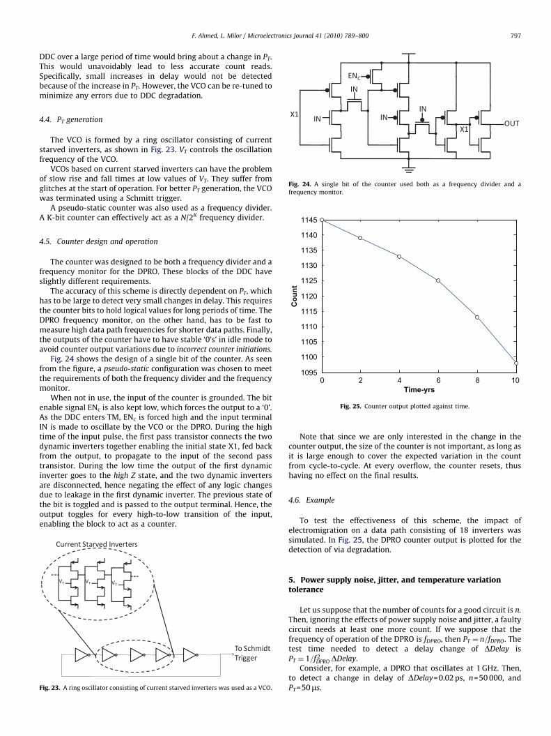
Fig. 24. A single bit of the counter used both as a frequency divider and a
frequency monitor.
0 2 4 6 8 101095
1100
1105
1110
1115
1120
1125
1130
1135
1140
1145
Time-yrs
Cou
nt
Fig. 25. Counter output plotted against time.
F. Ahmed, L. Milor / Microelectronics Journal 41 (2010) 789–800 797
DDC over a large period of time would bring about a change in PT.This would unavoidably lead to less accurate count reads.Specifically, small increases in delay would not be detectedbecause of the increase in PT. However, the VCO can be re-tuned tominimize any errors due to DDC degradation.
4.4. PT generation
The VCO is formed by a ring oscillator consisting of currentstarved inverters, as shown in Fig. 23. VT controls the oscillationfrequency of the VCO.
VCOs based on current starved inverters can have the problemof slow rise and fall times at low values of VT. They suffer fromglitches at the start of operation. For better PT generation, the VCOwas terminated using a Schmitt trigger.
A pseudo-static counter was also used as a frequency divider.A K-bit counter can effectively act as a N/2K frequency divider.
4.5. Counter design and operation
The counter was designed to be both a frequency divider and afrequency monitor for the DPRO. These blocks of the DDC haveslightly different requirements.
The accuracy of this scheme is directly dependent on PT, whichhas to be large to detect very small changes in delay. This requiresthe counter bits to hold logical values for long periods of time. TheDPRO frequency monitor, on the other hand, has to be fast tomeasure high data path frequencies for shorter data paths. Finally,the outputs of the counter have to have stable ‘0’s’ in idle mode toavoid counter output variations due to incorrect counter initiations.
Fig. 24 shows the design of a single bit of the counter. As seenfrom the figure, a pseudo-static configuration was chosen to meetthe requirements of both the frequency divider and the frequencymonitor.
When not in use, the input of the counter is grounded. The bitenable signal ENc is also kept low, which forces the output to a ‘0’.As the DDC enters TM, ENc is forced high and the input terminalIN is made to oscillate by the VCO or the DPRO. During the hightime of the input pulse, the first pass transistor connects the twodynamic inverters together enabling the initial state X1, fed backfrom the output, to propagate to the input of the second passtransistor. During the low time the output of the first dynamicinverter goes to the high Z state, and the two dynamic invertersare disconnected, hence negating the effect of any logic changesdue to leakage in the first dynamic inverter. The previous state ofthe bit is toggled and is passed to the output terminal. Hence, theoutput toggles for every high-to-low transition of the input,enabling the block to act as a counter.
Fig. 23. A ring oscillator consisting of current starved inverters was used as a VCO.
Note that since we are only interested in the change in thecounter output, the size of the counter is not important, as long asit is large enough to cover the expected variation in the countfrom cycle-to-cycle. At every overflow, the counter resets, thushaving no effect on the final results.
4.6. Example
To test the effectiveness of this scheme, the impact ofelectromigration on a data path consisting of 18 inverters wassimulated. In Fig. 25, the DPRO counter output is plotted for thedetection of via degradation.
5. Power supply noise, jitter, and temperature variationtolerance
Let us suppose that the number of counts for a good circuit is n.
Then, ignoring the effects of power supply noise and jitter, a faultycircuit needs at least one more count. If we suppose that thefrequency of operation of the DPRO is fDPRO, then PT ¼ n=fDPRO. Thetest time needed to detect a delay change of DDelay isPT ¼ 1=f 2
DPRO DDelay.Consider, for example, a DPRO that oscillates at 1 GHz. Then,
to detect a change in delay of DDelay=0.02 ps, n=50 000, andPT=50ms.

50 100 150 200 25050
150
250
0
0.0005
0.001
0.0015
0.002
0.0025
Prob
abili
tyof
Err
or
RMS Jitter on DPRO Output (ps)
RMS Jitte
r
on VCO
Output (ps)
Fig. 27. Test accuracy vs. jitter.
F. Ahmed, L. Milor / Microelectronics Journal 41 (2010) 789–800798
However, this scheme has to be tolerant to power supply noiseand jitter, since they cause false triggers, indicating the end of lifeof a chip still in working condition. Power supply noise and jitterincrease the appropriate value of PT.
5.1. Power supply noise
To investigate the effect of power supply noise, a zero meanGaussian noise source was added to the power supply, with astandard deviation of 10 mV. A varying power supply producesa varying DPRO oscillation frequency. The final count outputdepends on the mean oscillation frequency of the DPRO(fDPRO-Mean), i.e. Count= fDPRO-Mean� PT. A larger PT gives thefrequency more time to settle down to a steady mean value. Letf 0DPRO and fDPRO-Mean be the oscillation frequencies in the absence
and presence of noise, respectively. Given a difference,Dferr ¼ f 0
DPRO�fDPRO-Mean, then the degradation in frequency ofoscillation of the DPRO due to wearout (DfW) has to be greaterthan Dferr to be detectible.
To investigate the effect of power supply noise, simulations forthe detection of via degradation were repeated with Gaussiannoise added to the power supply. The impact of the noisyenvironment on the final count output is shown in Fig. 26.Although the trend is maintained, it clear that even a smallamount of noise in the power supply can have a large impact.
5.2. Jitter
Similarly, jitter in PT is another potential problem. Jitter may bedue to power supply noise and ground bounce, but may also bedue to coupling capacitance and local temperature variation. Jitterresults in random errors at the VCO and DPRO outputs, because ofrandomness in the switching times of the waveforms. This resultsin variation in the count. This can create an error if the countincreases by more than one. The case when the DPRO and VCOoscillate at 1 GHz, with jitter on the signals of the DPRO and VCO,is illustrated in Fig. 27.
A solution to this problem of potential false triggers due tojitter is to average multiple delay measurements with the counter.During PT, the counter runs and samples an output from the DPRO.During the high-to-low transition, the counter output is shiftedinto a register and the counter is reset. After N cycles we wouldhave N samples of the DPRO, which are then averaged. Theselection of N depends on the level of jitter on the signals.
0 1 2 3 4 5 6-20
-15
-10
-5
0
Time-Yrs
Cou
nts
5mv
10mv
Noise Free
Fig. 26. Count output with Gaussian noise source added to the power supply.
5.3. Temperature
Finally, it should be noted that delays are very sensitive totemperature. For example, over the operating temperature rangefrom 0 to 150 1C, delay of the inverter chain varies by 150 ps. Thiscan overwhelm any delay change due to wearout. To overcomethis problem, the operating conditions must be reproduced foreach test of delay degradation.
6. Comparison with conventional ring oscillator-basedmonitors
System aging is usually monitored by ring oscillators scatteredthroughout the chip. These monitors oscillate throughout the lifetime of the chip, and their frequency degradation indicates thetotal device degradation. These monitors operate on the assump-tion that the amount of degradation in the ring oscillator is a goodmeasure of the degradation of the operational parts of the chip.
One of the major causes of inaccuracy in this approach is thespatial and temporal variations in the operating environment of achip. Since most wearout mechanisms are exponentially depen-dent on temperature, it is very unlikely that isolated ring oscillatorscan accurately predict the complex degradation profile of the chip.As an example, Fig. 28 shows the variation in the MTF of a via in adata path undergoing degradation due to electromigration.
Another issue is the assumption of a high correlation betweenthe switching activity of nodes of a ring oscillator and those incomplex data paths. Consider the sum generation part of a fulladder, shown in Fig. 29, as a simple example.
‘A’ and ‘B’ are the two inputs to be added and ‘S’ is the outputsum. Let us assume we want to study the wearout at node ‘S’ ofthe full adder. The amount of wearout due to electromigration, forexample, is a function of current density though a via which inturn is a function of the switching activity. Fig. 30 plots theswitching activity of the node ‘S’ assuming no incoming carry anduncorrelated inputs. Compared to this, a ring oscillator oscillatesindependently of the clock frequency. Typically these oscillatingfrequencies are very high and a node in a ring oscillator may gothrough numerous charges and discharges in a single clock cycle.This means that ring oscillators have switching activities that arefar greater than one, and monitors based on ring oscillators couldprovide pessimistic estimates of chip aging.
As an example let us assume that a ring oscillator wearoutmonitor is designed whose frequency of oscillation is almost

280 300 320 340 360 3800
5
10
15
20
Temperature (K)
MTF
(yrs
)
Fig. 28. Variation in MTF of a via undergoing degradation due to electromigration
with varying temperature.
Fig. 29. The sum generation in a full adder.
00.5
1
0
0.5
10
0.1
0.2
0.3
P(A)P(B)
Sw
itchi
ng A
ctiv
ity
Fig. 30. Switching activity of a node of a full adder with varying switching
probabilities of the inputs.
00.5
1
0
0.5
10
50
100
150
200
P(A)P(B)
MTF
-yrs
Fig. 31. Variation in MTF of a via placed at the output node of a full adder with
varying input signal probabilities.
F. Ahmed, L. Milor / Microelectronics Journal 41 (2010) 789–800 799
equal to the clock frequency so that the nodes of the monitor haveswitching activities close to one. The median time to failure (MTF)for a via due to electromigration at such a node to be around12 years. Compared to that, Fig. 31 plots the MTF of a via placedat the output node of a full adder with varying input signalprobabilities. The variations in MTF of a via with varyingswitching activities is a clear indicator of the inaccuracy ofisolated ring oscillator monitors.
Our approach, unlike ring oscillators, requires the halting ofthe operation of the circuit during testing. However, all modulesare not active at all times in many applications, and wearout testscan be scheduled during times of inactivity, at startup, orshutdown.
7. Summary
This paper has shown that wearout of vias can be detected bymeasuring path delays. Analysis of via failure rates shows that thechange in delay as a function of time is independent of Weibulldistribution parameters and the number of stages in a path. Thisshows that a trigger point based on an increase in delay directlyrelates to the number of failing vias in an inverter chain. Hence,a delay detection circuit provides quantifiable evidence of viadegradation in the absence of other sources of wearout forinverter chains.
A self-test scheme to monitor the wearout of a chip bymeasuring the delay through data paths has been presented. Thispaper summarizes the circuit design, together with analysis of therequired test time and the impact of potential problems caused bypower supply noise, jitter, and temperature. Simulation resultsindicate that very small changes in delay can be detected.
The same procedure can be applicable to any degradation thatresults in a delay shift, such as hot carrier injection and negativebias temperature instability, which increase the device thresholdvoltage with time.
Acknowledgment
The authors thank the Semiconductor Research Corporation fortheir financial support, under Tasks 1645.001 and 1645.002.
References
[1] M.H. Woods, MOS VLSI reliability and yield trends, Proc. IEEE 74 (12) (1986)1715–1729.
[2] K. Banerjee, et al., Characterization of contact and via failure under shortduration high pulsed current stress, in: Proceedings of the InternationalReliability Physics Symposium, 1997, pp. 216–220.
[3] B. Li, et al., Impact of via–line contact on CU interconnect electromigrationperformance, in: Proceedings of the International Reliability Physics Sympo-sium, 2005, pp. 24–30.
[4] J. Black, Electromigration—a brief survey and some recent results, IEEE Trans.Electron Devices 16 (4) (1969) 338–347.
[5] G. Steinlesberger, et al., Copper damascene interconnects for the 65 nmtechnology node: a first look at the reliability properties, in: InternationalInterconnect Technical Conference, 2002, pp. 265–267.
[6] M. Lamy, et al., How effective are failure analysis methods for the 65 nmCMOS technology node? in: Proceedings of the International Symposium onPhysical and Failure Analysis, 2005, pp. 32–37.
[7] D. Markovic, et al., Methods for true energy-performance optimization, IEEE J.Solid-State Circuits 39 (8) (2004) 1282–1293 Aug.

F. Ahmed, L. Milor / Microelectronics Journal 41 (2010) 789–800800
[8] M. Orshansky, et al., Impact of spatial intrachip gate length variability on theperformance of high-speed digital circuits, IEEE Trans. Computer-Aided Des.21 (5) (2002) 544–553.
[9] B. Cline, et al., Analysis and modeling of CD variation for statistical statictiming, in: Proceedings of the International Conference on Computer-AidedDesign, 2006, pp. 60–66.
[10] K.A. Bowman, S.G. Duvall, J.D. Meindl, Impact of die-to-die and within-dieparameter fluctuations on the maximum clock frequency distribution forgigascale integration, IEEE J. Solid-State Circuits 37 (2) (2002) 183–190.
[11] M. Orshansky, L. Milor, C. Hu, Characterization of spatial intra-field gate CDvariability, its impact on circuit performance, and spatial mask-levelcorrection, IEEE Trans. Semicond. Manuf. 17 (1) (2004) 2–11.