Reliability Support for On-Chip Memories Using Networks-on-Chip

Lextar Proprietary & Confidential
Chip Scale Package
Presenter JD Guo
Title AVP Lextar
Date 2013/11/01

Lextar Proprietary & Confidential
Outline
• CSP introduction
– CSP名詞說明White chip, PFC, POD ,PCC , ELC,....
– 各家種類
– 優缺點比較
• Process introduction• White chip process
• White chip Testing, Sorting, Packing
• CSP application
– Direct-lit BLU
– High efficiency tube in HK Lighting show

Lextar Proprietary & Confidential
CSP introductionCSP introduction
Lextar Proprietary & Confidential

Lextar Proprietary & Confidential
What is CSP? Chip Scale Package
Search wiki or google, IC

Lextar Proprietary & Confidential
What is CSP? Chip Scale Package

Lextar Proprietary & Confidential
Lumileds
• Philips Lumileds的LUXEON Flip-Chip採用省略打線流程的倒裝CSP技術,除了達到可以通過高電流的特性外,體積的縮小也同步提升封裝的密集度
• Philips Lumileds看好Flip-Chip在光效、性價比與封裝體積優勢,預計將Flip-Chip技導入中功率LED。
2008 Luxeon Rebel2016– size 2.0mmx1.6mm
& 1.7mmx1.3mm
Thin film flip chip : yield issueAlN ceramic substrate : high cost
Trouble free for SMT
2012/Q4 – LUXEON Flip Chip
2013/Q4 – LUXEON Q
Lextar Proprietary & Confidential
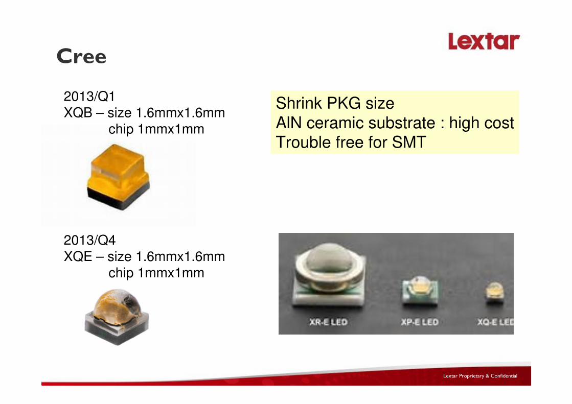
Cree
Shrink PKG size
AlN ceramic substrate : high costTrouble free for SMT
2013/Q1XQB – size 1.6mmx1.6mm
chip 1mmx1mm
2013/Q4XQE – size 1.6mmx1.6mm
chip 1mmx1mm

Lextar Proprietary & Confidential
TSMC-SSL
• 無封裝PoD模組採用台積固態照明所開發之倒裝式芯片結構,以先進製程螢光粉包覆晶片,無需額外的封裝製程,就能成為LED發光元件。這樣的元件具有:體積小流明密度高,150度大發光角度,彈性的流明組合,一致的色溫,高驅動電壓(Vf)組合。
Lextar Proprietary & Confidential
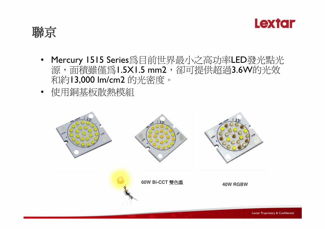
聯京聯京聯京聯京
• Mercury 1515 Series為目前世界最小之高功率LED發光點光源,面積雖僅為1.5X1.5 mm2,卻可提供超過3.6W的光效和約13,000 lm/cm2 的光密度。
• 使用銅基板散熱模組
40W RGBW60W Bi-CCT 雙色溫雙色溫雙色溫雙色溫

Lextar Proprietary & Confidential
Epistar--ELC

Lextar Proprietary & Confidential
Forepi--PFC

Lextar Proprietary & Confidential
White Chip(Die)
Package Free Chip (PFC)
Phosphor molding On Die (PoD)
Phosphor & glue
Flip Chip
Only Chip with Phosphor

Lextar Proprietary & Confidential
Chip Scale Package (CSP)
Phosphor & glue
Sub-mount
Flip Chip
White Chip on Substrate or Sub-mount
Sub-mount type
1.Ceramic (Al2O3, AlN)
2.MCPCB
3.Flat PLCC LF
4.Thin Metal (3um~20um)
5.Thick Metal (50um~250um)

Lextar Proprietary & Confidential
優缺點比較優缺點比較優缺點比較優缺點比較
產出分佈大產出分佈大產出分佈大產出分佈大( 波長波長波長波長,電壓電壓電壓電壓,亮度亮度亮度亮度))))
仍需封裝製程仍需封裝製程仍需封裝製程仍需封裝製程
光輸出密度高光輸出密度高光輸出密度高光輸出密度高
易於進行光學設計易於進行光學設計易於進行光學設計易於進行光學設計ELC
Wafer levelForepi
製程難度高製程難度高製程難度高製程難度高
RA risk
可直接可直接可直接可直接SMT
色均勻性佳色均勻性佳色均勻性佳色均勻性佳
光輸出密度高光輸出密度高光輸出密度高光輸出密度高
ELCEpistar
High cost
仍需封裝製程仍需封裝製程仍需封裝製程仍需封裝製程
可直接可直接可直接可直接SMT
光輸出密度高光輸出密度高光輸出密度高光輸出密度高
信賴性佳信賴性佳信賴性佳信賴性佳
LUXEON QLumileds
WeaknessAdvantageProduct
需晶片封裝整合能力需晶片封裝整合能力需晶片封裝整合能力需晶片封裝整合能力
光輸出密度高光輸出密度高光輸出密度高光輸出密度高
Low cost
信賴性佳信賴性佳信賴性佳信賴性佳
CSPLextar
RA risk
可直接可直接可直接可直接SMT
光輸出密度高光輸出密度高光輸出密度高光輸出密度高
Low cost
COB聯京聯京聯京聯京
RA risk光輸出密度高光輸出密度高光輸出密度高光輸出密度高
Low costPoDTSMC
High cost
仍需封裝製程仍需封裝製程仍需封裝製程仍需封裝製程
可直接可直接可直接可直接SMT
光輸出密度高光輸出密度高光輸出密度高光輸出密度高
易於進行光學設計易於進行光學設計易於進行光學設計易於進行光學設計
信賴性佳信賴性佳信賴性佳信賴性佳
XQB
XQECree

Lextar Proprietary & Confidential
White chipWhite chip
CChip hip SScale cale PPackage ackage (CSP)(CSP)
Bonding
LBLB
Die Bonder / flux Eutectic Process
High accuracy Bonding (±25~38μ)
Low thermal resistance
A new process for SMT fab
SMT / solder bond
Normal Accuracy Bonding(±100μup)
Need to control solder paste Rth
Existing process
How to bond white chip on Lightbar
(PCB/MCPCB) ?

Lextar Proprietary & Confidential
White Chip Product
Product Remark
L0 : Chip LevelL0 : Chip Level
Package Free Chip (PFC)
Sub-mount (1616)
L1 : PKG LevelL1 : PKG Level
Ceramic Substrate (3535)
L2 : Board LevelBonding process by
1.PKG
2.SMT
White chipWhite chip
CChip hip SScale cale PPackage ackage (CSP)(CSP)
White chip EmitterWhite chip Emitter
White chip PLCCWhite chip PLCC
White chip COBWhite chip COB

Lextar Proprietary & Confidential
White Chip processWhite Chip process
Lextar Proprietary & Confidential

Lextar Proprietary & Confidential
Chip Scale Package Process
Phosphor & glue
Sub-mount
Flip Chip
White Chip on Substrate or Sub-mount
Phosphor process
Submout process

Lextar Proprietary & Confidential
Concept
Phosphor Process 1
Realization (@ Lextar TD sample line)
Press molding & Curing Dicing & Sorting
Phosphor sheet sorting
Chip sorting
White Chip
White Chip PKG

Lextar Proprietary & Confidential
Sheet dicingSheet dicing
Check Item
�切割刀型號切割刀型號切割刀型號切割刀型號
�切割參數切割參數切割參數切割參數
Risk
Sheet bending
Die bonding testDie bonding test
Check Item
�Bonding head pick &place check
Risk
螢光膜片與藍膜能否脫離螢光膜片與藍膜能否脫離螢光膜片與藍膜能否脫離螢光膜片與藍膜能否脫離
螢光膜片是否會沾黏螢光膜片是否會沾黏螢光膜片是否會沾黏螢光膜片是否會沾黏
Hot plate curingHot plate curing
Check item
�Curing profile
Risk
螢光膜片偏移螢光膜片偏移螢光膜片偏移螢光膜片偏移
氣泡氣泡氣泡氣泡& Peeling
��ProcessProcess
Phosphor Process 2��Test Model: FB 40S +3535 CeramicTest Model: FB 40S +3535 Ceramic

Lextar Proprietary & Confidential
Phosphor Process 3: Flat Molding
Highlight
Towa 以重量進行厚度控制, 不同色點不同螢光粉比例之產品厚度將不同

Lextar Proprietary & Confidential
Phosphor Process 4
Chip on wafer Phosphor spray
coating
Window Attach
Release wafer &
dicingWhieWhie chipchip

Solder PAD type
Phosphor & glue
Sub-mount PAD
Flip ChipSolder PAD type
1. Bare chip Pad
2. Sub-mount type1subject to sub-mount process
1. Ceramic (Al2O3, AlN)
2. MCPCB
3. Flat PLCC LF (EMC/SMC…)3. Sub-mount type2
sub-mount integrated process
1. Thin Metal (3um~20um)2.Thick Metal (50um~250um)
Chip PAD

Lextar Proprietary & Confidential
Thin metal process flowThin metal process flow
Chip on wafer Phosphor spray
coating
Attach glass
Release wafer PR mask
lithography
E-gun pad metal
deposition
PR lift off Dicing
White ChipWhite Chip
PR mask
lithography

Lextar Proprietary & Confidential
Thick metal ProcessThick metal Process
�Wafer上需有對位孔
�White sheet+ Sheet 需合Metal carrier脫離
�光阻塗佈可行性
�Wafer上需有切割對位道
White chip on Carrier
Flip bonding to Wafer PR deposition
PR mask lithography E-gun pad metal
deposition
PR lift off
Dicing White chipWhite chip
�光罩需與Wafer對位�去光阻液對phosphor sheet影響未知�背鍍金屬層與膠材接著性

Lextar Proprietary & Confidential
White chip BEOLWhite chip BEOL
Lextar Proprietary & Confidential

Lextar Proprietary & Confidential
White chip back-end of the lineProcess flow :
B-Test
UPH: Testing 6~7K
Sorting
UPH:18~20K UPH:6~7K
TapingReverse
UPH:手動翻片 1K
0.370.380.390.40.410.420.430.39 0.4 0.41 0.42 0.43 0.44 0.45 0.46CIE_x
CIE_y色度分佈色度分佈色度分佈色度分佈、、、、亮度受相鄰晶片影響亮度受相鄰晶片影響亮度受相鄰晶片影響亮度受相鄰晶片影響掉料周圍掉料周圍掉料周圍掉料周圍、、、、方片外圍測試值失真方片外圍測試值失真方片外圍測試值失真方片外圍測試值失真

Lextar Proprietary & Confidential
White Chip Prober 校正評估
IS 標準機中柱+輔助光源量測
(3535ceramic on star)
Prober點測
K factor 校正 prober
FC prober
400pcs 點測
IS 標準機中柱+輔助光源量測300pcs 抽樣檢測
(3535ceramic on star)
校正模式:
確認色度及亮度規格符合IS標準機

Lextar Proprietary & Confidential
CSP application exampleCSP application example
: Direct: Direct--BLU proposalBLU proposal
Lextar Proprietary & Confidential

Lextar Proprietary & Confidential
New
PKG &
New lens
design
D-LED TV BLU concept
13” Q4 14” H1 H2
OD=45~25mm
Based on 32” D-LED TV
CCFL Replacement
OD=15~10 mm
6ea 3030_40FC or
eutectic_700mA
less than 18eaChip Scale Package & Wide View Angle
30mil-like FC or eutectic_450mA
可大量(>10k) 送樣時間

Lextar Proprietary & Confidential
Way to reduce # of LEDs in BLU
1. View angle=120
2. Color deviation at large angle
3. Difficult to meet small light emitting area
4. Limited operating current
5. Need TIR lens for further LED reduction
1. View angle=140~160
2. Uniform angular color conversion
3. Chip scale light emitting area
4. High operating current
chip
Phosphor slurryFlip chip
Phosphorglue
【【【【Convention】】】】 【【【【White Chip】】】】
Lextar Proprietary & Confidential
【【【【3030 photo】】】】
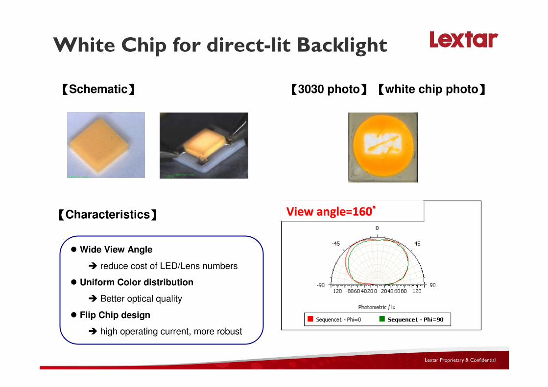
White Chip for direct-lit Backlight
【【【【Schematic】】】】 【【【【white chip photo】】】】
� Wide View Angle
� reduce cost of LED/Lens numbers
� Uniform Color distribution
� Better optical quality
� Flip Chip design
� high operating current, more robust
【【【【Characteristics】】】】 View angle=160View angle=160°°°°°°°°

Lextar Proprietary & Confidential
White Chip View Angle
【【【【View Angle】】】】
View angle=160View angle=160°°°°°°°°
White chip 40SWhite chip 40S
Chip size 40mil x40 mil
Top surface 1.032mm2
Side surface 0.609mm2
T/S ratio 1.69
View angle=138View angle=138°°°°°°°°
White chip 55SWhite chip 55S
Chip size 55mil x55 mil
Top surface 1.96mm2
Side surface 0.838mm2
T/S ratio 2.33

Lextar Proprietary & Confidential
2nd LensTraditional PKG or Emitter
White Chip Advantage(減少因二次光學產生的藍黃圈問題)
CCT 4450 CCT 3200
� CCT 600 � CCT 150
White Chip 2nd Lens

Lextar Proprietary & Confidential
CIE coordinates
0.00
0.10
0.20
0.30
0.40
0.50
0.60
0.70
0.80
0.90
0.00 0.10 0.20 0.30 0.40 0.50 0.60 0.70CIE-x
CIE-y
1616 @ (0.26,0.20)
Flux(lm) vs. CIE - x @ 350mA
0.0
20.0
40.0
60.0
80.0
100.0
0.220 0.240 0.260 0.280 0.300CIE - x
Lu
min
ou
s F
lux
(lm
)
1616 @ (0.26,0.20)
0
20
40
60
80
100
120
140
160
180
200
0 100 200 300 400 500 600 700 800 900 1000 1100 1200
Current (mA)
Flux (lm)
1616 @ (0.26,0.20)
Flux(lm) vs. Current
Phosphor Conversion Chip(PCC1616)

Lextar Proprietary & ConfidentialLextar Proprietary & Confidential
2013 2013 香港國際照明展香港國際照明展
200lm/W in L2 level

Lextar Proprietary & Confidential
Transparent High Efficiency LED Tube V1 (Demo sample)
Features:
5 W>80360o
5000 K1000 lm300 mm
PowerCRIBeam AngleCCTLumenDimension
Sample Spec.:
★ High efficacy: 200 lm/W
���� Package-free technologies (Without reflection & scattering & phosphor re-absorption loss )
���� High light extraction efficiency (Transparent substrate)
★ 360-degree wide beam angle
���� Same light view angle with traditional light tube
★ Low cost
���� PKG free & Substrate自製

Lextar Proprietary & Confidential
Copyright © 2022 FDOKUMEN