760A/760D/760N Stereo Audio Monitors Instruction Manual
178
x *P070599203* 070-5992-03 1100111001010 11011001111011 11010100101101 0011110110111 010101101010 760A/760D/760N Stereo Audio Monitors (760A SN B040000 & Above) (760D/760N SN B020000 & Above) Instruction Manual
-
Upload
khangminh22 -
Category
Documents
-
view
2 -
download
0
Transcript of 760A/760D/760N Stereo Audio Monitors Instruction Manual

x
*P070599203*
070-5992-03
1100111001010
11011001111011
11010100101101
0011110110111
010101101010
760A/760D/760N Stereo Audio Monitors (760A SN B040000 & Above)(760D/760N SN B020000 & Above)Instruction Manual


Instruction Manual
760A/760D/760NStereo Audio Monitors(760A S/N B040000 & Above)(760D/760N S/N B020000 & Above)
070-5992-03
WarningThe servicing instructions are for use by qualifiedpersonnel only. To avoid personal injury, do notperform any servicing unless you are qualified todo so. Refer to the Safety Summary prior toperforming service.
Please check for change information at the rear of this manual.
First Printing: April 1995

Copyright � Tektronix, Inc., 1986, 1992, 1995. All rights reserved. Printed in U.S.A.Tektronix products are covered by U.S. and foreign patents, issued and pending.
Information in this publication supersedes that in all previously published material.Specifications and price change privileges reserved. The following are registeredtrademarks: TEKTRONIX and TEK.
For product related information, phone: 800-TEKWIDE (800-835-9433), ext. TV.
For further information, contact: Tektronix, Inc., Corporate Offices, P.O. Box 1000,Wilsonville, OR 97070–1000, U.S.A. Phone: (503) 627–7111; TLX: 192825; TWX:(910) 467–8708; Cable: TEKWSGT.

WARRANTY
Tektronix warrants that this product will be free from defects in materials and workmanship for a period of one (1) year fromthe date of shipment. If any such product proves defective during this warranty period, Tektronix, at its option, either will repairthe defective product without charge for parts and labor, or will provide a replacement in exchange for the defective product.In order to obtain service under this warranty, Customer must notify Tektronix of the defect before the expiration of the warrantyperiod and make suitable arrangements for the performance of service. Customer shall be responsible for packaging and ship-ping the defective product to the service center designated by Tektronix, with shipping charges prepaid. Tektronix shall payfor the return of the product to Customer if the shipment is to a location within the country in which the Tektronix service centeris located. Customer shall be responsible for paying all shipping charges, duties, taxes, and any other charges for products re-turned to any other locations.This warranty shall not apply to any defect, failure or damage caused by improper use or improper or inadequate maintenanceand care. Tektronix shall not be obligated to furnish service under this warranty a) to repair damage resulting from attemptsby personnel other than Tektronix representatives to install, repair or service the product; b) to repair damage resulting fromimproper use or connection to incompatible equipment; c) to repair any damage or malfunction caused by the use of non-Tektro-nix supplies; or d) to service a product that has been modified or integrated with other products when the effect of such modifica-tion or integration increases the time or difficulty of servicing the product.THIS WARRANTY IS GIVEN BY TEKTRONIX WITH RESPECT TO THIS PRODUCT IN LIEU OF ANY OTHERWARRANTIES, EXPRESSED OR IMPLIED. TEKTRONIX AND ITS VENDORS DISCLAIM ANY IMPLIED WAR-RANTIES OF MERCHANTABILITY OR FITNESS FOR A PARTICULAR PURPOSE. TEKTRONIX’ RESPONSI-BILITY TO REPAIR OR REPLACE DEFECTIVE PRODUCTS IS THE SOLE AND EXCLUSIVE REMEDYPROVIDED TO THE CUSTOMER FOR BREACH OF THIS WARRANTY. TEKTRONIX AND ITS VENDORSWILL NOT BE LIABLE FOR ANY INDIRECT, SPECIAL, INCIDENTAL, OR CONSEQUENTIAL DAMAGES IR-RESPECTIVE OF WHETHER TEKTRONIX OR THE VENDOR HAS ADVANCE NOTICE OF THE POSSIBILITYOF SUCH DAMAGES.

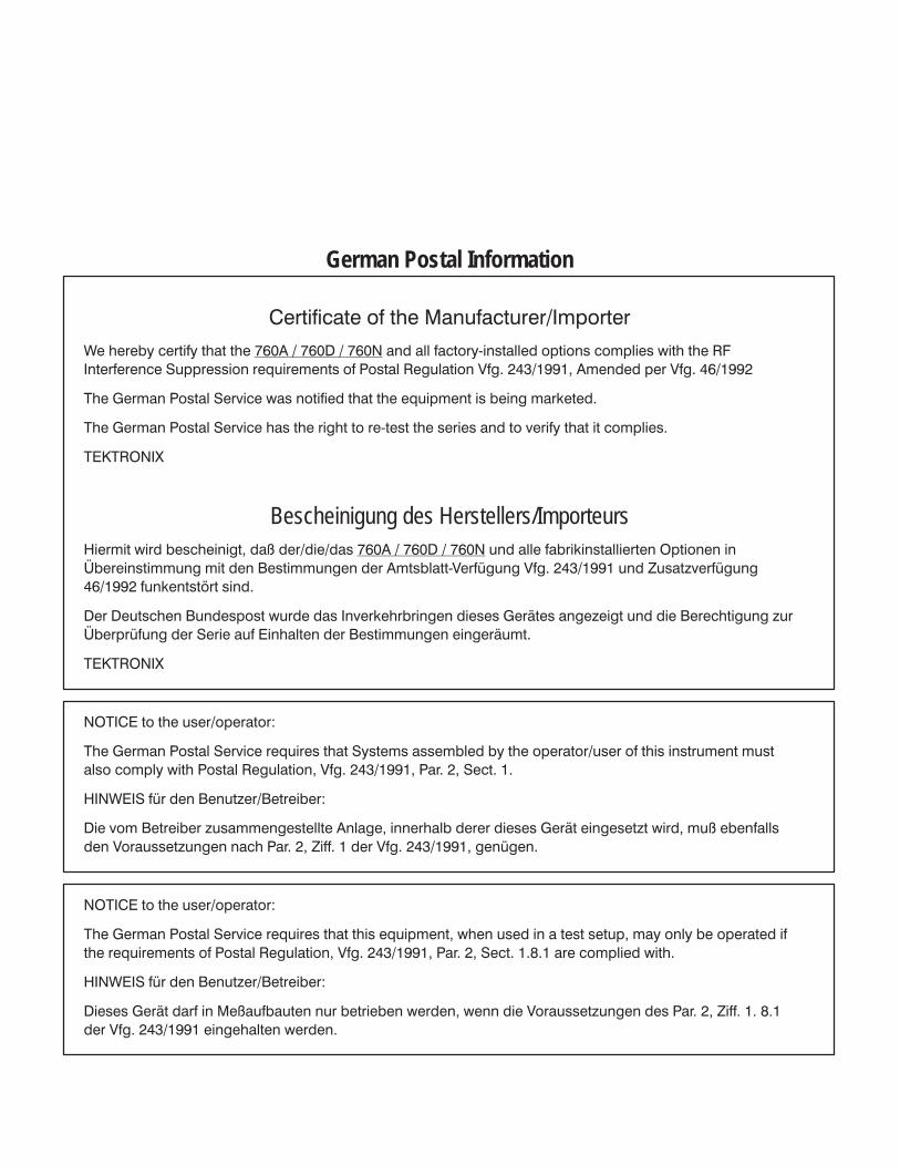
German Postal Information
���������� � ��� � ����������������
�� ������ ������� ��� ��� ���� � ���� � ���� � �� ������� ������ ��� � ������� ��� ��� !"� ������� �� #�������� ��$������ �� � %��� !�&���� '�&( )*+�,--,. ��� ��� ��� '�&( *��,--)
/�� 0��� %��� #��1��� � ������ ��� ��� �$����� � �� ��� & ��2����(
/�� 0��� %��� #��1��� �� ��� ��&�� � ������� ��� ������ � � 1����� ��� �� �������(
/34/!5��6
Bescheinigung des Herstellers/Importeurs7������ ��� ������� �&�. �8 ���������� ���� � ���� � ���� � � ��� ����2� ��������� 5��� � � 9����� ������ & ��� �� :������� &� ��� ���������'���;&� & '�&( )*+�,--, � � <���=1���;&� &*��,--) �� 2� ���>�� �� �(
��� �������� :� ������ ���� �� � 1��2������ &� ������ 0��?��� &�=��&� � � ��� :�������&� & =��9�����;�� & ��� #���� �� 3� ���� ��� :������� &� �� &��?���(
/34/!5��6
�5/��3 � ��� ����������@
/�� 0��� %��� #��1��� ��$����� ��� #������ �������� �� ��� ���������� � ���� � ������ � ������ ����� ��� %��� !�&���� . '�&( )*+�,--,. %�( ). #���( ,(
7���3�# �;� �� :� ��=���:��������@
��� 1� :�������� =����� &�������� � �&�. � ����� ����� ������ 0��?� �� &����=� ���. ��8 ��� ������ '������=� &� �� %�( ). <���( , ��� '�&( )*+�,--,. &� ;&� (
�5/��3 � ��� ����������@
/�� 0��� %��� #��1��� ��$����� ��� ���� �$����� �. �� ���� � ���� �����. �� �� �� ������ ����� ��$������ �� � %��� !�&���� . '�&( )*+�,--,. %�( ). #���( ,(A(, �� ������� ���(
7���3�# �;� �� :� ��=���:��������@
������ 0��?� ��� � ��8������ �� �������� ���� . � ��� '������=� &� ��� %�( ). <���( ,( A(,��� '�&( )*+�,--, �� &����� ���� (


760A / 760D / 760N i
Table of Contents
List of Figures iv. . . . . . . . . . . . . . . . . . . . . . . . . . . . . . . . . . . . . . . . . . . . . .
List of Tables v. . . . . . . . . . . . . . . . . . . . . . . . . . . . . . . . . . . . . . . . . . . . . . .
General Safety Summary vii. . . . . . . . . . . . . . . . . . . . . . . . . . . . . . . . . . . . . .
Service Safety Summary ix. . . . . . . . . . . . . . . . . . . . . . . . . . . . . . . . . . . . . .
Preface xi. . . . . . . . . . . . . . . . . . . . . . . . . . . . . . . . . . . . . . . . . . . . . . . . . . . .
Introduction and SpecificationsSection 1 Introduction and Specifications 1–1. . . . . . . . . . . . . . . . . . . . . . . . . Introduction 1–1. . . . . . . . . . . . . . . . . . . . . . . . . . . . . . . . . . . . . . . . . . . . . . . . . . . . . Features 1–1. . . . . . . . . . . . . . . . . . . . . . . . . . . . . . . . . . . . . . . . . . . . . . . . . . . . . . . .
CRT Display 1–1. . . . . . . . . . . . . . . . . . . . . . . . . . . . . . . . . . . . . . . . . . . . . . . . . Bar Graph 1–2. . . . . . . . . . . . . . . . . . . . . . . . . . . . . . . . . . . . . . . . . . . . . . . . . . . Dynamic response characteristics for peak program meters 1–2. . . . . . . . . . . . Return Time 1–3. . . . . . . . . . . . . . . . . . . . . . . . . . . . . . . . . . . . . . . . . . . . . . . . . Rear Panel 1–3. . . . . . . . . . . . . . . . . . . . . . . . . . . . . . . . . . . . . . . . . . . . . . . . . . . Safety Standards 1–3. . . . . . . . . . . . . . . . . . . . . . . . . . . . . . . . . . . . . . . . . . . . . .
Specifications 1–4. . . . . . . . . . . . . . . . . . . . . . . . . . . . . . . . . . . . . . . . . . . . . . . . . . . .
Operating InstructionsSection 2 Operating Instructions 2–1. . . . . . . . . . . . . . . . . . . . . . . . . . . . . . . . Introduction 2–1. . . . . . . . . . . . . . . . . . . . . . . . . . . . . . . . . . . . . . . . . . . . . . . . . . . . . Front–Panel Controls 2–1. . . . . . . . . . . . . . . . . . . . . . . . . . . . . . . . . . . . . . . . . . . . . . Rear–Panel Connectors 2–2. . . . . . . . . . . . . . . . . . . . . . . . . . . . . . . . . . . . . . . . . . . . CRT Display 2–3. . . . . . . . . . . . . . . . . . . . . . . . . . . . . . . . . . . . . . . . . . . . . . . . . . . . .
Display Orientation 2–3. . . . . . . . . . . . . . . . . . . . . . . . . . . . . . . . . . . . . . . . . . . . Graticule 2–4. . . . . . . . . . . . . . . . . . . . . . . . . . . . . . . . . . . . . . . . . . . . . . . . . . . .
LED BARS 2–5. . . . . . . . . . . . . . . . . . . . . . . . . . . . . . . . . . . . . . . . . . . . . . . . . . . . . . Using The 760A / 760D / 760N 2–6. . . . . . . . . . . . . . . . . . . . . . . . . . . . . . . . . . . . . .
Initial Alignment 2–6. . . . . . . . . . . . . . . . . . . . . . . . . . . . . . . . . . . . . . . . . . . . . . Level Setups 2–7. . . . . . . . . . . . . . . . . . . . . . . . . . . . . . . . . . . . . . . . . . . . . . . . . System Phase Error Measurements 2–7. . . . . . . . . . . . . . . . . . . . . . . . . . . . . . . . Energy Distribution 2–8. . . . . . . . . . . . . . . . . . . . . . . . . . . . . . . . . . . . . . . . . . . . Monaural Compatibility 2–9. . . . . . . . . . . . . . . . . . . . . . . . . . . . . . . . . . . . . . . . Polarity Reversal 2–9. . . . . . . . . . . . . . . . . . . . . . . . . . . . . . . . . . . . . . . . . . . . . . Clipping 2–10. . . . . . . . . . . . . . . . . . . . . . . . . . . . . . . . . . . . . . . . . . . . . . . . . . . . .
InstallationSection 3 Installation 3–1. . . . . . . . . . . . . . . . . . . . . . . . . . . . . . . . . . . . . . . . . Electrical Installation 3–1. . . . . . . . . . . . . . . . . . . . . . . . . . . . . . . . . . . . . . . . . . . . . .
Power Source 3–1. . . . . . . . . . . . . . . . . . . . . . . . . . . . . . . . . . . . . . . . . . . . . . . . Mains Frequency and Voltage Ranges 3–1. . . . . . . . . . . . . . . . . . . . . . . . . . . . . Changing Input Sensitivity (Standard 760A only) 3–1. . . . . . . . . . . . . . . . . . . . User–Definable Input Sensitivity (Standard 760A only) 3–2. . . . . . . . . . . . . . . Changing Input Termination 3–2. . . . . . . . . . . . . . . . . . . . . . . . . . . . . . . . . . . . . Changing Display Orientation 3–2. . . . . . . . . . . . . . . . . . . . . . . . . . . . . . . . . . .

Contents
ii 760A / 760D / 760N
MaintenanceSection 4 Maintenance 4–1. . . . . . . . . . . . . . . . . . . . . . . . . . . . . . . . . . . . . . .
Introduction 4–1. . . . . . . . . . . . . . . . . . . . . . . . . . . . . . . . . . . . . . . . . . . . . . . . . . Preventive Maintenance 4–1. . . . . . . . . . . . . . . . . . . . . . . . . . . . . . . . . . . . . . . . . . . .
Cleaning 4–1. . . . . . . . . . . . . . . . . . . . . . . . . . . . . . . . . . . . . . . . . . . . . . . . . . . . Visual Inspection 4–2. . . . . . . . . . . . . . . . . . . . . . . . . . . . . . . . . . . . . . . . . . . . . . Static–Sensitive Components 4–2. . . . . . . . . . . . . . . . . . . . . . . . . . . . . . . . . . . . Performance Checks and Readjustments 4–2. . . . . . . . . . . . . . . . . . . . . . . . . . .
Corrective Maintenance 4–2. . . . . . . . . . . . . . . . . . . . . . . . . . . . . . . . . . . . . . . . . . . . How To Use This Manual 4–2. . . . . . . . . . . . . . . . . . . . . . . . . . . . . . . . . . . . . . . Obtaining Replacement Parts 4–5. . . . . . . . . . . . . . . . . . . . . . . . . . . . . . . . . . . .
Troubleshooting Information 4–5. . . . . . . . . . . . . . . . . . . . . . . . . . . . . . . . . . . . . . . . DAC Servicing 4–5. . . . . . . . . . . . . . . . . . . . . . . . . . . . . . . . . . . . . . . . . . . . . . . PAL Signal Specification 4–6. . . . . . . . . . . . . . . . . . . . . . . . . . . . . . . . . . . . . . .
Power Supply Troubleshooting Procedure 4–7. . . . . . . . . . . . . . . . . . . . . . . . . . . . . . Introduction 4–7. . . . . . . . . . . . . . . . . . . . . . . . . . . . . . . . . . . . . . . . . . . . . . . . . . Low Volts Supply 4–8. . . . . . . . . . . . . . . . . . . . . . . . . . . . . . . . . . . . . . . . . . . . . High Volts Supply 4–10. . . . . . . . . . . . . . . . . . . . . . . . . . . . . . . . . . . . . . . . . . . . .
Mechanical Disassembly And Assembly 4–13. . . . . . . . . . . . . . . . . . . . . . . . . . . . . . . Bezel Removal 4–13. . . . . . . . . . . . . . . . . . . . . . . . . . . . . . . . . . . . . . . . . . . . . . . Graticule Light Removal and Replacement 4–14. . . . . . . . . . . . . . . . . . . . . . . . . CRT Removal 4–14. . . . . . . . . . . . . . . . . . . . . . . . . . . . . . . . . . . . . . . . . . . . . . . . CRT Replacement 4–14. . . . . . . . . . . . . . . . . . . . . . . . . . . . . . . . . . . . . . . . . . . . . Rear Panel Removal and Replacement 4–15. . . . . . . . . . . . . . . . . . . . . . . . . . . . . Front Panel Assembly Removal and Replacement 4–15. . . . . . . . . . . . . . . . . . . . LED Bar and Socket Removal and Replacement 4–16. . . . . . . . . . . . . . . . . . . . . Main Board Removal and Replacement 4–16. . . . . . . . . . . . . . . . . . . . . . . . . . . . Power Supply Board Removal and Replacement 4–17. . . . . . . . . . . . . . . . . . . . .
Repackaging 4–17. . . . . . . . . . . . . . . . . . . . . . . . . . . . . . . . . . . . . . . . . . . . . . . . . . . . .
Performance Check and CalibrationSection 5 Performance Check and Calibration Procedures 5–1. . . . . . . . . . . .
Introduction 5–1. . . . . . . . . . . . . . . . . . . . . . . . . . . . . . . . . . . . . . . . . . . . . . . . . . Required Test Equipment 5–1. . . . . . . . . . . . . . . . . . . . . . . . . . . . . . . . . . . . . . .
Performance Check Procedure 5–2. . . . . . . . . . . . . . . . . . . . . . . . . . . . . . . . . . . . . . . Calibration Procedure 5–11. . . . . . . . . . . . . . . . . . . . . . . . . . . . . . . . . . . . . . . . . . . . . .
Theory of OperationSection 6 Theory of Operation 6–1. . . . . . . . . . . . . . . . . . . . . . . . . . . . . . . . . Introduction 6–1. . . . . . . . . . . . . . . . . . . . . . . . . . . . . . . . . . . . . . . . . . . . . . . . . . . . . Block Diagram 6–1. . . . . . . . . . . . . . . . . . . . . . . . . . . . . . . . . . . . . . . . . . . . . . . . . . . Detailed Circuit Descriptions 6–1. . . . . . . . . . . . . . . . . . . . . . . . . . . . . . . . . . . . . . . .
INPUT AMPLIFIERS <1> 6–1. . . . . . . . . . . . . . . . . . . . . . . . . . . . . . . . . . . . . MATRIX & AGC CONTROL LOGIC <4> 6–2. . . . . . . . . . . . . . . . . . . . . . . . AGC & CRT DEFLECTION AMPLIFIERS <5> 6–3. . . . . . . . . . . . . . . . . . . . LEVEL INDICATORS 6–3. . . . . . . . . . . . . . . . . . . . . . . . . . . . . . . . . . . . . . . . . GRAPH DRIVERS <2> 6–4. . . . . . . . . . . . . . . . . . . . . . . . . . . . . . . . . . . . . . .
Dynamic Response Control (Left) 6–4. . . . . . . . . . . . . . . . . . . . . . . . . . . . . Signal Peak Processor (Left) 6–4. . . . . . . . . . . . . . . . . . . . . . . . . . . . . . . . . Bar Anode Driver (Left) 6–5. . . . . . . . . . . . . . . . . . . . . . . . . . . . . . . . . . . . Peak Hold On/Off 6–5. . . . . . . . . . . . . . . . . . . . . . . . . . . . . . . . . . . . . . . . .
BAR SCANNER/DRIVER & DAC <3> 6–6. . . . . . . . . . . . . . . . . . . . . . . . . . . Master Clock 6–6. . . . . . . . . . . . . . . . . . . . . . . . . . . . . . . . . . . . . . . . . . . . . Down Counter 6–6. . . . . . . . . . . . . . . . . . . . . . . . . . . . . . . . . . . . . . . . . . . . Scale Shaper Lookup Table 6–6. . . . . . . . . . . . . . . . . . . . . . . . . . . . . . . . . .

Contents
760A / 760D / 760N iii
DAC 6–6. . . . . . . . . . . . . . . . . . . . . . . . . . . . . . . . . . . . . . . . . . . . . . . . . . . . LOW VOLTAGE POWER SUPPLY <6> 6–6. . . . . . . . . . . . . . . . . . . . . . . . . .
Line Rectifier and Filter 6–7. . . . . . . . . . . . . . . . . . . . . . . . . . . . . . . . . . . . Pulse Width Modulator 6–7. . . . . . . . . . . . . . . . . . . . . . . . . . . . . . . . . . . . . Output Filters 6–8. . . . . . . . . . . . . . . . . . . . . . . . . . . . . . . . . . . . . . . . . . . . . Error Amplifier 6–8. . . . . . . . . . . . . . . . . . . . . . . . . . . . . . . . . . . . . . . . . . . Feedback Transformer Driver and Peak Detector 6–8. . . . . . . . . . . . . . . . . Output Under-Voltage Shutdown 6–8. . . . . . . . . . . . . . . . . . . . . . . . . . . . . .
HIGH VOLTAGE POWER SUPPLY <7> 6–9. . . . . . . . . . . . . . . . . . . . . . . . . . HV Osc and Error Amp 6–9. . . . . . . . . . . . . . . . . . . . . . . . . . . . . . . . . . . . . Power Supply Outputs 6–10. . . . . . . . . . . . . . . . . . . . . . . . . . . . . . . . . . . . . . Focus Amplifier 6–10. . . . . . . . . . . . . . . . . . . . . . . . . . . . . . . . . . . . . . . . . . . Grid Drive Circuit 6–10. . . . . . . . . . . . . . . . . . . . . . . . . . . . . . . . . . . . . . . . . Z-Axis Amplifier 6–10. . . . . . . . . . . . . . . . . . . . . . . . . . . . . . . . . . . . . . . . . . CRT 6–11. . . . . . . . . . . . . . . . . . . . . . . . . . . . . . . . . . . . . . . . . . . . . . . . . . . .
OptionsSection 7 Options 7–1. . . . . . . . . . . . . . . . . . . . . . . . . . . . . . . . . . . . . . . . . . . Options 7–1. . . . . . . . . . . . . . . . . . . . . . . . . . . . . . . . . . . . . . . . . . . . . . . . . . . . . . . . .
Replaceable Electrical PartsSection 8 Replaceable Electrical Parts 8–1. . . . . . . . . . . . . . . . . . . . . . . . . . . . . . Parts Ordering Information 8–1. . . . . . . . . . . . . . . . . . . . . . . . . . . . . . . . . . . . . . . . . Using the Replaceable Electrical Parts List 8–1. . . . . . . . . . . . . . . . . . . . . . . . . . . . . Column Descriptions 8–2. . . . . . . . . . . . . . . . . . . . . . . . . . . . . . . . . . . . . . . . . . . . . . Cross Index – Mfr. Code Number To Manufacturer 8–3. . . . . . . . . . . . . . . . . . . . . . Replaceable Electrical Parts 8–5. . . . . . . . . . . . . . . . . . . . . . . . . . . . . . . . . . . . . . . . .
Diagrams and Circuit Board IllustrationsDiagrams/Circuit Board Illustrations 9–1. . . . . . . . . . . . . . . . . . . . . . . . . . . . . . .
Replaceable Mechanical PartsReplaceable Mechanical Parts 10–1. . . . . . . . . . . . . . . . . . . . . . . . . . . . . . . . . . . . . Parts Ordering Information 10–1. . . . . . . . . . . . . . . . . . . . . . . . . . . . . . . . . . . . . . . . . Using the Replaceable Mechanical Parts List 10–1. . . . . . . . . . . . . . . . . . . . . . . . . . . Column Descriptions 10–2. . . . . . . . . . . . . . . . . . . . . . . . . . . . . . . . . . . . . . . . . . . . . . Cross Index–Mfr. Code Number to Manufacturer 10–1. . . . . . . . . . . . . . . . . . . . . . . .

Contents
iv 760A / 760D / 760N
List of Figures
Figure 1–1: LED Bar Graph scales for the 760A, 760D, and 760N 1–1. . . . .
Figure 2–1: 760A Front Panel 2–2. . . . . . . . . . . . . . . . . . . . . . . . . . . . . . . . . .
Figure 2–2: 760A Rear Panel 2–3. . . . . . . . . . . . . . . . . . . . . . . . . . . . . . . . . .
Figure 2–3: 760A Sound Stage Graticule 2–4. . . . . . . . . . . . . . . . . . . . . . . . .
Figure 2–4: 760A X–Y Graticule 2–4. . . . . . . . . . . . . . . . . . . . . . . . . . . . . . .
Figure 2–5: Ellipse with approximately 13� phase error 2–8. . . . . . . . . . . . .
Figure 2–6: Strong left content 2–8. . . . . . . . . . . . . . . . . . . . . . . . . . . . . . . . .
Figure 2–7: Well balanced stereo 2–9. . . . . . . . . . . . . . . . . . . . . . . . . . . . . . .
Figure 2–8: Stereo unsuited to monaural reception 2–9. . . . . . . . . . . . . . . . . .
Figure 2–9: Severe clipping of stereo signal 2–10. . . . . . . . . . . . . . . . . . . . . . .
Figure 3–1: 760A / 760D / 760N jumper locations 3–3. . . . . . . . . . . . . . . . . .
Figure 4–1: Using the foldout pages 4–3. . . . . . . . . . . . . . . . . . . . . . . . . . . . .
Figure 4–2: Circuit board locations in the 760A/760D/760N 4–4. . . . . . . . . .
Figure 4–3: Bezel removal 4–13. . . . . . . . . . . . . . . . . . . . . . . . . . . . . . . . . . . .
Figure 4–4: Retaining screw locations 4–16. . . . . . . . . . . . . . . . . . . . . . . . . . .
Figure 4–5: Repackaging the 760A/760D/760N 4–18. . . . . . . . . . . . . . . . . . . .
Figure 5–1: Jumper and adjustment locations on the A3 Main board 5–2. . . .
Figure 5–2: 760–Series adjustment locations 5–12. . . . . . . . . . . . . . . . . . . . . .
Figure 6–1: 760A / 760D / 760N Block Diagram 6–2. . . . . . . . . . . . . . . . . . .
Figure 6–2: Simplified Level Indicator block diagram 6–4. . . . . . . . . . . . . . .
Figure 6–3: Pinout of the CRT Socket 6–11. . . . . . . . . . . . . . . . . . . . . . . . . . .

Contents
760A / 760D / 760N v
List of Tables
Table 1–1: Response Time 1–3. . . . . . . . . . . . . . . . . . . . . . . . . . . . . . . . . . . .
Table 1–2: Return Time 1–3. . . . . . . . . . . . . . . . . . . . . . . . . . . . . . . . . . . . . .
Table 1–3: Electrical Characteristics 1–4. . . . . . . . . . . . . . . . . . . . . . . . . . . .
Table 1–4: Environmental Limits 1–6. . . . . . . . . . . . . . . . . . . . . . . . . . . . . . .
Table 1–5: Physical Characteristics 1–6. . . . . . . . . . . . . . . . . . . . . . . . . . . . .
Table 2–1: Front-Panel Controls 2–1. . . . . . . . . . . . . . . . . . . . . . . . . . . . . . .
Table 3–1: Factory Set Input Sensitivity 3–1. . . . . . . . . . . . . . . . . . . . . . . . .
Table 4–1: Power Supply Fault Symptoms 4–8. . . . . . . . . . . . . . . . . . . . . . .
Table 4–2: Low Volts Supply Voltages 4–8. . . . . . . . . . . . . . . . . . . . . . . . . . .
Table 4–3: Control Circuit Test Points 4–10. . . . . . . . . . . . . . . . . . . . . . . . . . .
Table 4–4: High Volts Supply Fault Symptoms 4–11. . . . . . . . . . . . . . . . . . . .
Table 4–5: High Voltage Oscillator Test Points 4–12. . . . . . . . . . . . . . . . . . . .
Table 5–1: Verifying Input Sensitivity (760A only) 5–5. . . . . . . . . . . . . . . . .
Table 5–2: LED Bar Gain Adjustment 5–15. . . . . . . . . . . . . . . . . . . . . . . . . . .
Table 5–3: LED Bar Reference Adjustment 5–15. . . . . . . . . . . . . . . . . . . . . . .
Table 7–1: Power Cord Options 7–1. . . . . . . . . . . . . . . . . . . . . . . . . . . . . . . .

Contents
vi 760A / 760D / 760N

760A / 760D / 760N vii
General Safety Summary
Review the following safety precautions to avoid injury and prevent damage tothis product or any products connected to it.
Only qualified personnel should perform service procedures.
Injury Precautions
To avoid fire hazard, use only the power cord specified for this product.
This product is grounded through the grounding conductor of the power cord. Toavoid electric shock, the grounding conductor must be connected to earthground. Before making connections to the input or output terminals of theproduct, ensure that the product is properly grounded.
To avoid electric shock or fire hazard, do not operate this product with covers orpanels removed.
To avoid fire hazard, use only the fuse type and rating specified for this product.
To avoid electric shock, do not operate this product in wet or damp conditions.
To avoid injury or fire hazard, do not operate this product in an explosiveatmosphere.
To avoid injury, remove jewelry such as rings, watches, and other metallicobjects. Do not touch exposed connections and components when power ispresent.
Product Damage Precautions
To prevent product overheating, provide proper ventilation.
If you suspect there is damage to this product, have it inspected by qualifiedservice personnel.
Use Proper Power Cord
Ground the Product
Do Not Operate WithoutCovers
Use Proper Fuse
Do Not Operate inWet/Damp Conditions
Do Not Operate inExplosive Atmosphere
Avoid Exposed Circuitry
Provide Proper Ventilation
Do Not Operate WithSuspected Failures

General Safety Summary
viii 760A / 760D / 760N
Safety Terms and Symbols
These terms may appear in this manual:
WARNING. Warning statements identify conditions or practices that could resultin injury or loss of life.
CAUTION. Caution statements identify conditions or practices that could result indamage to this product or other property.
These terms may appear on the product:
DANGER indicates an injury hazard immediately accessible as you read themarking.
WARNING indicates an injury hazard not immediately accessible as you read themarking.
CAUTION indicates a hazard to property including the product.
The following symbols may appear on the product:
DANGERHigh Voltage
Protective Ground(Earth) Terminal
ATTENTIONRefer toManual
Double Insulated
Certifications and Compliances
CSA Certification includes the products and power cords appropriate for use inthe North America power network. All other power cords supplied are approvedfor the country of use.
Terms in This Manual
Terms on the Product
Symbols on the Product
CSA Certified PowerCords

760A / 760D / 760N ix
Service Safety Summary
Only qualified personnel should perform service procedures. Read this ServiceSafety Summary and the General Safety Summary before performing any serviceprocedures.
Do not perform internal service or adjustments of this product unless anotherperson capable of rendering first aid and resuscitation is present.
To avoid electric shock, disconnect the main power by means of the power cordor, if provided, the power switch.
To avoid electric shock or injury, use extreme caution when handling the CRT.Only qualified personnel familiar with CRT servicing procedures and precautionsshould remove or install the CRT.
CRTs retain hazardous voltages for long periods of time after power is turned off.Before attempting any servicing, discharge the CRT by shorting the anode tochassis ground. When discharging the CRT, connect the discharge path to groundand then the anode. Rough handling may cause the CRT to implode. Do not nickor scratch the glass or subject it to undue pressure when removing or installing it.When handling the CRT, wear safety goggles and heavy gloves for protection.
Dangerous voltages or currents may exist in this product. Disconnect power,remove battery (if applicable), and disconnect test leads before removingprotective panels, soldering, or replacing components.
To avoid electric shock, do not touch exposed connections.
To avoid x-radiation exposure, do not modify or otherwise alter the high-voltagecircuitry or the CRT enclosure. X-ray emissions generated within this producthave been sufficiently shielded.
Do Not Service Alone
Disconnect Power
Use Caution WhenServicing the CRT
Use Care When ServicingWith Power On
X-Radiation

Service Safety Summary
x 760A / 760D / 760N

760A / 760D / 760N xi
Preface
This manual documents the TEKTRONIX 760A/760D/760N Stereo AudioMonitor and is intended for instrument operators and service technicians.Operatorsare assumed to be familiar with basic television terms and measure-ments. Qualified service technicians are also assumed to be familiar withtelevision terms and measurements, and have moderate experience with analogand logic circuits.
The manual is divided into two parts: Operator’s Information and ServiceInformation. The Operators information is useful to both operators and servicetechnicians. The Service Information is intended only for qualified servicetechnichians.
Features
The Operators part includes Sections 1 and 2.
Section 1, Introduction and Specification, includes a general description of theinstrument, followed by the Specifications. The Specifications include refer-ences to the corresponding Performance Check steps.
Section 2, Operating Instructions, familiarizes the user with the front– andrear–panel controls, connectors, and indicators; includes operator familiarizationinformation.
The Servfice part contains information required by service technicians to install,calibrate, maintain, and troubleshoot the instrument. This is included in theremaining sections of the manual.
Section 3, Installation, includes electrical and mechanical installation information.The electrical installation information includes operational changes availablewithin the instrument.
Section 4, Maintenance, includes preventive troubleshooting and correctiveinformation.
Section 5 Performance Check and Calibration Procedures, includes information toverify and restore the instrument to meet its specifications. The procedures arepreceded by list of recommended test equipment.
Operators Part
Service Part

Preface
xii 760A / 760D / 760N
Section 6, Theory of Operation, provides an overall block diagram and detailedcircuit descriptions. The detailed circuit descriptions should be used with theblock diagram and schematic diagrams in the foldout pages for specificinformation about the individual circuits.
Section 7, Options, documents available instrument options.
Section 8, Replaceable Electrical Parts List, includes order information and partnumbers for all rep,aceable electrical parts.
Section 9, Diagrams, contains servicing illustrations. These include adjsutmentlocations, circuit board part locations, a block diagram, schematic diagrams, andwaveforms. Parts locating tables are included that cross–reference the circuitboard illustrations and the schematic diagrams.
Section 10, replaceable Mechanical Parts List, includes ordering information andpart numbers for all replaceable mechanical aprts. This parts list is referenced toan exploded view mechanical drawing. Also included are lists of standard andoptional accessories.

Introduction andSpecifications


760A / 760D / 760N 1–1
Section 1Introduction and Specifications
IntroductionThe 760A Stereo Audio Monitor is a simple yet accurate tool that the audioengineer can use to perform setup, monitoring, measuring, and troubleshootingtasks in the studio. There are two special versions of the 760A Stereo AudioMonitor: the 760D and the 760N. All three operate in exactly the same manner,but are set to use different scales for the Bar Graph displays. The three differentscales are shown in Figure 1–1.
Features
The CRT provides a pattern display to monitor stereo separation, monaural phasecompatibility, and audio system phase errors.
Figure 1–1: LED Bar Graph scales for the 760A, 760D, and 760N
CRT Display

Introduction and Specifications
1–2 760A / 760D / 760N
The display is set for a “Sound Stage” orientation when the 760A is shippedfrom the factory. This provides a display where monaural amplitudes areoriented on the vertical axis of the CRT.
An alternate XY graticule is shipped as a standard accessory with the 760A.This graticule can be installed if you are familiar with or desire the displayorientation provided by an XY monitor. Instructions for installing the XYgraticule are found in SECTION 3 INSTALLATION.
Automatic or manual gain control is front panel selectable. This feature allowsflexible control of the pattern size over a wide range of input signal amplitudes.
In the absence of an input signal, Z–Axis dimming prolongs CRT life.
Three 100–segment LED bars indicate the levels of the left stereo channel, rightstereo channel and a selectable third channel. The third bar can be set to displaythe levels of (L+R)/2, (LR)/2, or the rear–panel AUXILIARY input. Both(L+R)/2 and (LR)/2 are internally derived, and represent half the sum ordifference of the input voltages ([VLVR] / 2). In this way when the left and rightchannels are balanced the sum will be displayed at that same level, while thedifference will be displayed at “0”.
The EXPAND SCALE control is a momentary contact front–panel push button,which greatly improves the accuracy of level setups. Pressing this buttonswitches to the blue expanded scale which allows accurate setting of the signallevel for alignment, as specified by broadcast authorities. For the 760A thealignment level is 8 dB. This level is labeled “TEST”, and is indicated by the“arrow head” scale marks.
For the 760D the alignment level is –9 dB, indicated by the “arrow head” scalemarks. The 760N alignment level is marked “TEST”, and is at 0 dB. In allcases, the normal scale lines up with the expanded scale at the alignment level.
The PEAK HOLD control is a latching front–panel push button. Indicated peaksare displayed for approximately three seconds when this function is selected.
The 760A, 760D, and 760N conform to the dynamic response characteristics of:
760A: EBU–3205, IEC 268–10, and IEEE Proposed PPM specification.
760D: DIN 45 406
760N: Nordic Technical Recommendation N9.
Table 1–1 shows the peak bar indication when an isolated tone burst of a givenduration is applied. The response shown is relative to the indication for acontinuous tone of the same amplitude. The burst must contain at least 5 cycles,which requires a frequency of at least 10 kHz for the shortest bursts.
Bar Graph
Dynamic responsecharacteristics for peak
program meters

Introduction and Specifications
760A / 760D / 760N 1–3
Table 1–1: Response Time
Inst Tone Burst (mS) Response (dB)
760A 100.0 0 �0.5
10.0 2 �0.5
5.0 4 �0.75
1.5 9 �1.0
0.5 17 �2.0
760D760N
10.0 1 �0.5760N
5.0 2 �1.0
3.0 4 �1.0
0.4 15 �2.0
Return Time is the elapsed time for the reading to decay a specified amount afterthe abrupt removal of a tone. See Table 1–2.
Table 1–2: Return Time
Inst Return Time
760A 2.8 �0.3 seconds to fall 24 dB
760D 1.5 �0.2 seconds to fall 20 dB
760N 1.7 �0.3 seconds to fall 20 dB
The rear–panel AUDIO INPUTs are female XLR connectors with balancedbridging and jumper selectable input sensitivity and termination.
This product is designed and tested in accordance with the requirements forindustry safety standards. These standards include the following:
UL1244, Second Edition –Standard for Electrical and Electronic Measuringand Testing Equipment.ANSI C39.5 –Safety Requirements for Electrical and Electronic Measuringand Controlling Instrumentation, 1984, Draft #11.CSA –Electrical Bulletin No. 556B.IEC-348, Second Edition –Safety Standards For Electronic MeasuringApparatus.VDE 0871.5 (Class B) –Radio Frequency Interference Suppression ofElectrical Equipment and Systems.FCC EMI Compatibility –FCC Rules Part 15 Subpart J, Class A.
Return Time
Rear Panel
Safety Standards

Introduction and Specifications
1–4 760A / 760D / 760N
SpecificationsThe Performance Requirements listed in Table 13 are warranted over an ambienttemperature range of 0�C to 50�C only when the 760A has been calibrated at25�C �5�C, following a warm–up period of 20 minutes.
A Performance Check procedure is provided in SECTION 5, PERFORMANCECHECK AND CALIBRATION PROCEDURES� to verify the Performance Require-ments listed in the following table.
Table 1–3: Electrical Characteristics
Characteristic Performance Requirement Supplemental InformationPerf Check
Step No.
Audio InputsBalanced Bridging >10 kΩ/side.
Termination Selectable from >20 kΩ, 600Ω, or150Ω
(internal jumper) 2
Protection Will withstand 50 V peak common–mode input, dc to 20kHz, withoutdamage.
Sensitivity760A Gain selectable for 0 dB bar indication
for sine waves of 0, +4, +8, +12, and+16 dBu.
(internal jumper)One user–definable position avail-able, on standard only.
3
760D 1.55 V rms for +0 dB indication.
760N 1.55 V rms for +6 dB indication.
CRT DisplayAutomatic Gain Control
Control Range760A760D760N
+8 dB to –20 dB (0 dB bar reference).+5 to –25 dB.+15 to –15 dB.
4
Gain Match and Tracking(over AGC range).
�0.3 dB. 5, 6
Phase Match �1� @ 0 dB. 7
Frequency Response �0.5 dB, 20 Hz to 20 kHz throughoutAGC Control Range.
8
Z– Axis Dimming With absence of signal. 10
Bar Graph100 Segment LED
760A760D760N
Green to 0 dB, red above.Green to 0 dB, red above.Green to +6 dB, red above.

Introduction and Specifications
760A / 760D / 760N 1–5
Table 1–3: Electrical Characteristics (Cont.)
CharacteristicPerf Check
Step No.Supplemental InformationPerformance Requirement
Display Range760A –Normal
–Expanded+8 dB to –45 dB 5 dB to –11 dB
760D –Normal–Expanded
+5 dB to –50 dB –5 dB to –13 dB
760N –Normal–Expanded
+15 dB to –36 dB+3 dB to –6 dB
Scale760A760D760N
dB linear from +8 to 20 dB.Progressively compressed.dB linear from +15 to –24 dB.
Resolution760A 0.4 dB/segment, from +8 to20 dB.
0.04 dB/ segment with EXPANDSCALE depressed.
760D 0.25 dB/segment from 0 to +5 dB,tapering to 2dB/segment from –40 to–50 dB. 0.125 dB/ segment withEXPAND SCALE depressed.
760N 0.5 dB/segment, from +15 to –24 dB. 0.1 dB/ segment with EXPANDSCALE depressed.
Accuracy 0.3 dB at 0 dB and 1 kHz 3
Peak Hold Indicated peaks held approximately3 seconds.
9
Attack/Decay Dynamics Conforms to DIN 45 406. 760N alsoconforms to Technical Recommen-dation N9.
Frequency Response760A760D760N
�0.5 dB, 20 Hz to 20 kHz:+8 to 20 dB+5 to 20 dB+15 to 18 dB
11
Gain Match 0.3 dB. 12
Crosstalk A full–scale indication on any barcauses no indication on any otherbars.
SELECT set to AUX. 13

Introduction and Specifications
1–6 760A / 760D / 760N
Table 1–4: Environmental Limits
Characteristic Supplemental Information
TemperatureStored –55B C to +75B C.
Operational 0B C to +50B C.
Humidity
Operational
Will operate at 95% relative humidity for up to five days. Do not operate with visible moistureon boards.
AltitudeStored 50,000 feet.
Operational 15,000 feet.
VibrationOperational 15 minutes each axis at 0.025 inch,with frequency varied from 10–55–10 Hz in 1 minute cycles
with instrument secured to vibration table.
10 minutes each axis at any resonant frequency or at 55 Hz if no resonant frequency is found .
ShockNon–Operating 50 g’s C sine, 11 ms duration, 3 shocks per surface.
Transportation Qualified under NTSB Test Procedure 1–A, Category II (30 inch drop).
Table 1–5: Physical Characteristics
Characteristic Supplemental Information
Height 5.25 inches (13.3 cm).
Width 8.424 inches (21.4 cm).
Length 16.875 inches (42.9 cm).
Weight Approximately 10 pounds.

Operating Instructions


760A / 760D / 760N 2–1
Section 2Operating Instructions
IntroductionThis section of the manual will familiarize you with the 760A Stereo AudioMonitor’s operation. The contents include a brief description of the controls,connectors, displays (including a discussion of the graticules), and the basic usesof the instrument.
Front–Panel ControlsTable 2–1 contains a brief description of the front–panel control functions. Thefront panel is shown in Figure 2–1.
Table 2–1: Front-Panel Controls
Control Function
Select Rotary switch; selects input to third bar from SUM, DIFF and AUX.
Expand Scale Momentary push button; increases sensitivity for precise level set–ups.While holding this button refer to the scale printed in blue.
Peak Hold Latching push button; ON when back lit.
Display Gain Double detent pot; CW detent is AGC, CCW detent is CAL; MAN GAIN range isbetween detents.
Power Switches instrument power ON and OFF.
Focus For optimum display definition.
Graticule Varies external graticule illumination.
Position(Vert & Horiz)
Center the display on the graticule.
Intensity Varies intensity of trace.
Trace Rot Rotates trace into alignment with graticule lines.

Operating Instructions
2–2 760A / 760D / 760N
POSITION
FOCUSTRACE
ROT
GRATICULE INTENSITY
HORIZVERT
Figure 2–1: 760A Front Panel
Rear–Panel ConnectorsThe three rear–panel AUDIO INPUTs: LEFT, RIGHT, and AUXILIARY, arebalanced bridging male XLR connectors. The connectors are wired as follows:
Pin 1: GroundPin 2: +Pin 3: –
The LEFT and RIGHT AUDIO INPUTS are for the left and right channels ofyour stereo signal. The AUXILIARY input can be used for an externally derivedmonaural signal or a SAP signal. The rear panel is shown in Figure 2–2.

Operating Instructions
760A / 760D / 760N 2–3
FUSE
333–3321–02
SA
LEFT RIGHT AUXILIARY
DIE IN DIESEM GERAT ENTSTEHENDERONTGENSTRAHLUNG IST AUSREICHEND ABGESCHIRMTBESCHLEUNIGUNGSSPANNUNG KLEINER ALSACCELERATION VOLTAGE LESS THAN
X–RAY EMISSION GENERATED WITHIN THISINSTRUMENT HAS BEEN SUFFICIENTLY SHIELDED.
AUDIO INPUTS !
ÏÏ
ÏÏ
ÏÏÏÏ
®�������
� ��� � ������� ����� ��� ������� �������� �������� ����������� �� �������� � ����� ������
���� ������������ !�� ��� ��� "��� � # ����
!�� !� " �#��
®
760 SERIES
20kV
Figure 2–2: 760A Rear Panel
CRT DisplayThe CRT display provides visual feedback of the amplitude and relative phasingof the stereo audio signal. With this display, you can determine the fitness ofaudio signals for monaural or stereo transmission/reception. Audio system phaseerrors can also be measured on the 760A CRT display.
The 760A is shipped from the factory set for “Sound Stage” display orientation.This orientation provides a display where monaural amplitudes are displayed onthe vertical axis, and stronger left content in the stereo signal would deflect thesignal toward the left 45� axis (“L” line on the Sound Stage graticule).
An alternate XY graticule is shipped as a standard accessory with the 760A.This graticule can be installed if you are familiar with or desire the displayorientation provided by an XY monitor. Instructions for installing the XYgraticule are found in SECTION 3, INSTALLATION.
Display Orientation

Operating Instructions
2–4 760A / 760D / 760N
The graticule provides calibrated reference marks for a variety of uses. Bothgraticule options have the same markings and differ only in their orientation.Figures 2–3 and 2–4 show the Sound Stage and XY graticules.
L=R RL
L= –R
AMPLITUDEMARKS
PHASEMARKS
PHASETANGENT
LINES
Figure 2–3: 760A Sound Stage Graticule
LL=R
R
L= –R
PHASETANGENTLINES
AMPLITUDEMARKS
PHASEMARKS
Figure 2–4: 760A X–Y Graticule
Graticule

Operating Instructions
760A / 760D / 760N 2–5
L indicates signal amplitude from the LEFT channel input.R indicates signal amplitude from the RIGHT channel input.L=R indicates monaural amplitudes and “in phase” left and right signalamplitudes.L=–R indicates “out of phase” left and right signals. A pattern displayoriented along this line is poorly suited for monaural reception.
Phase Marks and Phase Tangent Lines are used in conjunction with one another tomake system phase error measurements. This procedure is explained later in thissection. All other graticule markings are used for performance verification andadjustments in SECTION 5, PERFORMANCE CHECK AND CALIBRATION.
LED BARSThe three 100–segment LED bars allow direct readout of the signal levels. Twoof the bars are dedicated to the left and right channels, while the third bar can beswitched to display L+R
2(sum), or L–R
2 (difference) of the input voltages, or
to display the level of the AUXILIARY input. By dividing Left + Right by two,the third bar will read the same as the left and right bars do, when the twochannels are of the same phase and amplitude.
The standard 760A, the 760D (DIN scale), and the 760N (Nordic scale) employdifferent scales and resolutions for the LED bars, as described below:
760A The scale is dB linear between +8 and –20dB, with scale marks every 4 dB.Below –20 dB the scale is progressively tapered to –45 dB with marks every 5dB. Above –20 dB each LED segment represents a 0.4 dB increment. The LEDbars are green up to 0 dB, and red above that point. With the EXPAND SCALEbutton depressed, the scale is expanded by a factor of four, and the resolution isincreased to 0.1 dB. The scale range is –5 dB to –11 dB while the EXPANDSCALE button is being held in, as shown by the scale printed in blue. Thesensitivity for the standard 760A is jumper selectable (see SECTION 3, INSTALLA-TION).
760D The 760D uses a DIN scale in accordance with DIN 45 406, with a range of+5 to –50 dB. The scale is progressively compressed from top to bottom, havinga resolution of 0.25 dB from +5 to 0 dB, and tapering to 2 dB from –40 to–50 dB. With the EXPAND SCALE button depressed, the resolution is increased to0.125 dB and the scale range is –5 to –13 dB (shown in blue). The LED bars aregreen up to 0 dB, and red above that point. A 1.55 V rms sinusoidal input(+6 dBu) produces a reading of 0 dB, and there are arrows which indicate the–9 dB test level.

Operating Instructions
2–6 760A / 760D / 760N
760N The 760N uses a scale in accordance with Technical Recommendation N9of the Nordic broadcast authorities, with a range of +15 to –36 dB. The scale isdB linear from +15 dB to –24 dB, and is progressively compressed to –36 dBwith scale marks at 3 dB intervals. The resolution of this scale is 0.5 dB from+15 to –24 dB. With the EXPAND SCALE button depressed the resolution isincreased to 0.1 dB and the scale range is +3 to –6 dB (shown in blue). TheLED bars are green up to +6 dB, and red above that point. A 1.55 V rmssinusoidal input (+6 dBu) produces a reading of +6 dB, and there is a TEST markto indicate the 0 dB test level. This test level corresponds to an input level of0.775 V rms (0 dBu).
Using The 760A / 760D / 760NOnce the 760A / 760D / 760N has been properly configured for your applicationand installed, performing the following initial alignment procedure is necessaryprior to any other measurements. All 760A / 760D / 760N front–panel controlnames are upper case.
NOTE. All waveform photographs in this section were taken using the SoundStage graticule. Remember that your display will be shifted 45� clockwise fromthe figures in this section if you are using the XY graticule.
1. Connect power to the 760A / 760D / 760N and set the instrument POWERto ON.
2. With no input to the LEFT or RIGHT AUDIO INPUTs, set the front panelINTENSITY control fully clockwise.
3. Set the VERTICAL and HORIZONTAL POSITION controls so theilluminated dot is centered on the graticule.
4. Connect a sine wave signal between 20 Hz and 15kHz to the LEFT AUDIOINPUT, and set the INTENSITY control to your preference.
5. Set the FOCUS control for the sharpest trace possible.
6. Set the TRACE ROTATION control to overlay the trace on the L graticuleline.
Initial Alignment

Operating Instructions
760A / 760D / 760N 2–7
760A When a ppm such as the 760A is used in conjunction with vu meters. it isimportant to consider the difference in dynamic characteristics when aligningsystem levels. The vu meter is an average reading meter with a relatively longintegration time. Its slow response causes it to indicate between 6 and 15 dBbelow actual audio peaks, depending on program content. The ppm is aquasi–peak meter with a short (but not instantaneous) attack time and very slowdecay. It reads much closer to actual audio peaks, within 3 to 6 dB. So whenlining up a system with a test tone, the ppm must read lower than the vu meter tomake them read the same on program audio. Broadcast authorities have foundthat 8 dB is a good average difference between peak–to–reading ratio of the ppmand vu meter. Hence, they have specified that a line–up tone reading of 0 vu onthe vu meter should read –8 dB on the ppm. With this alignment, both meterswill read substantially the same with audio program material, with the ppmgiving more reliable control of program peak levels. The input sensitivity of the760A is set using internal jumpers. See SECTION 3 INSTALLATION for details.
760D The Alignment Signal Level should indicate –9 dB on either the normal(white) or the expanded (blue) scale. The two scales coincide at the –9 dB“arrowhead” marks. Very accurate level settings can be achieved using the blueexpanded scale, activated by pressing and holding the EXPAND SCALE button
760N System alignment is done at the 0 dB TEST level. Both the normal (white)and the expanded (blue) scales coincide at the TEST mark. Very accurate levelsettings can be achieved using the blue expanded scale, activated by pressing andholding the EXPAND SCALE button.
NOTE. Perform the preceding alignment procedure before making any measure-ments, to ensure accurate results.
Phase difference between LEFT and RIGHT sine waves of the same frequencycan be measured with the phase marks on the CRT graticule. The signals neednot have the same amplitude, though the measurement is easier if they areapproximately equal.
Adjust the MANual DISPLAY GAIN control to make the edges of the ellipsejust touch the Phase Tangent Lines (see Figure 2–3 or 2–4). Read the phasedifference where the ellipse crosses the axis with the phase marks. The longermarks represent 10� increments and the shorter ones represent 5�. Figure 2–5shows a stereo signal with approximately 13� phase error.
Level Setups
System Phase ErrorMeasurements

Operating Instructions
2–8 760A / 760D / 760N
Figure 2–5: Ellipse with approximately 13� phase error
If the ellipse closes to a single line, the LEFT and RIGHT channels are in phaseas long as the line is within 45� of the L=R axis. The line may tilt if theamplitudes are unequal. A line within 45� of the L=–R axis indicates thechannels are out of phase.
The 760A’s pattern display provides a graphic representation of the stereosignal’s overall energy distribution. The pattern orientation tells you at a glancewhether the present mix is balanced or concentrated to either side. Figures 2–6and 2–7 illustrate different energy distributions.
Figure 2–6: Strong left content
Energy Distribution

Operating Instructions
760A / 760D / 760N 2–9
Figure 2–7: Well balanced stereo
Transmitting a mono–compatible stereo television signal is, and will remain,critical for broadcasters since most viewers have monaural receivers. The 760Apattern display and the L+R bar indicate the fitness of your audio for monauralreception. Figures 2–7 and 2–8 show, respectively, a stereo signal well suited formonaural reception and a stereo signal unsuited for monaural use due to its largeL=–R (out–of–phase) component.
Figure 2–8: Stereo unsuited to monaural reception
Routing audio through a complex studio presents many opportunities tointroduce polarity reversals. Any time a polarity reversal occurs, the 760A canbe used to trace the problem back to its source quickly. By introducing a sine
Monaural Compatibility
Polarity Reversal

Operating Instructions
2–10 760A / 760D / 760N
wave into both channels of the system and checking outputs stage by stage, thesource of the phase reversal can be quickly identified.
Another problem illustrated clearly by the 760A is clipping. Regardless of itssource, clipping manifests itself on the 760A pattern display as a ”squaring off”of the pattern edges. Figure 2–9 illustrates a severe case of clipping. The 760A’sAGC keeps the pattern within the screen boundaries in spite of the amplitude ofthe signals
Figure 2–9: Severe clipping of stereo signal
Clipping

The following servicing instructions are for use only by qualified personnel. Toavoid injury, do not perform any servicing other than that stated in the operatinginstructions unless you are qualified to do so. Refer to all Safety Summaries beforeperforming any service.
WARNING


Installation


760A / 760D / 760N 3–1
Section 3Installation
At installation time, save the shipping carton and packaging materials forrepackaging in case shipment becomes necessary. See Repackaging forShipment in SECTION 6, MAINTENANCE, for repackaging instructions.
Electrical Installation
This instrument is intended to operate from a single–phase power source havingone of its current–carrying conductors at or near earth–ground (the neutralconductor). Only the Line conductor is fused for over–current protection.Systems that have both current–carrying conductors live with respect to ground(such as phase–to–phase in multiphase systems) are not recommended as powersources.
WARNING. For your protection and to avoid damage to the instrument, unplugthe instrument power cord before removing or replacing any circuit boards,connectors, or jumpers.
The 760A / 760D / 760N Stereo Audio Monitor operate over a frequency rangeof 48 to 66 Hz, at any mains voltage between 90 VAC and 250 VAC. Thesenewer versions of the 760–Series instruments do not require any internal changesto select their operating voltage range.
The 760A is factory set so that a specific level applied to each input will indicatea specific level on the bar graph scale (see Table 3–1). While this required inputlevel may be changed for the standard 760A, the 760D and 760N are constrainedto use only the factory set levels.
Table 3–1: Factory Set Input Sensitivity
Instrument Type Input Level Bar Graph Readout
760A +8 dBu 0 dB
760D +6 dBu 0 dB
760N +6 dBu +6 dB
Unpacking
Power Source
Mains Frequency andVoltage Ranges
Changing Input Sensitivity(Standard 760A only)

Installation
3–2 760A / 760D / 760N
To enable the 760A bar graph to indicate 0 dB with an input of 0, +4, +8, +12, or+16 dBm, move the jumpers on J185 (LEFT), J385 (RIGHT) and J657 (AUX-ILIARY) to the desired sensitivity, which is marked on the Main circuit board(Assembly A3) at each jumper location. Figure 3–3 shows all jumper locationson the Main board and what each jumper position represents.
NOTE. The specified level is that of a sine wave which reads 0 dB peak programlevel, not the line–up level. For a ppm, line–up level is 8 dB below peakprogram level. This means that if the house level is +4 dBu (the level thatindicates 0 on a VU meter), then the 760A sensitivity jumper should be set 8 dBhigher, or +12 dBu. The line–up tone should then read 8 dB. See the discussionabout ppm vs. VU meters under Level Setups in Section 2.
A User–definable jumper position is provided for installations that use areference level other than 0, +4, +8, +12, or +16 dBm. The following para-graphs explain the procedure for selecting the proper resistor value so any inputlevel will indicate 0 dB on the bars.
User–definable resistors may be installed at R183 (LEFT), R383 (RIGHT), andR658 (AUXILIARY) if the standard range of input sensitivities previously listeddoes not fit your needs. These resistor positions are already used in the 760Dand 760N. The following formula can be used to determine the value of resistorsneeded to achieve a 0 dB indication with your reference level:
RSET= 20K7.962
10G/20 –1
where RSET is the user–definable resistor value and G is the desired referencelevel in dBu.
Once the resistor value is determined and resistors are installed at R183, R383,and R658, move the jumpers on J385, J185, and J657 to the ”U” position. Thisis the factory set jumper position for the 760D and 760N.
The 760A is set at the factory for Infinite input termination, with 600 or 150termination being jumper selectable. The position of the jumper on J192(LEFT), J292 (RIGHT), or J664 (AUXILIARY) determines the input terminationfor that channel. The Main circuit board is marked at the jumper location toindicate the termination value that each jumper position represents. SeeFigure 3–1.
The 760A CRT display can be changed from the factory set ”sound stage”orientation (where L=R is vertical) to a standard X–Y orientation (where Left isvertical). To accomplish this change, you must install the optional external
User–Definable InputSensitivity (Standard 760A
only)
Changing InputTermination
Changing DisplayOrientation

Installation
760A / 760D / 760N 3–3
graticule supplied with the instrument. Detailed instructions for removing thebezel can be found under the Mechanical Assembly/Disassembly topic inSECTION 4, MAINTENANCE. Then move two jumpers on the Main circuit board,J273 and J373, to the position labeled X–Y (pins 2 & 3) in Figure 3–1.
Also for X–Y display orientation, rotate P886 (on back of A3, Main board) sopins 1 and 2 of the connector mate with pins 2 and 1 of J886 (connect back-ward). Repeat with P862/J862. Remember to return P886 and P862 to theirnormal (pin 1 to pin 1) positions for Sound Stage display orientation. Thisprovides correct phasing for both display orientations.
INPUTTERMINATIONJUMPERS
RIGHT INPUT
FRONT
ASSEMBLY A3MAIN BOARD
TOP
J385
J392
L+RL
R–L–R
SOUNDSTAGE
X–Y
J273
J373
DISPLAY ORIENTATION
J185
AUXILIARY INPUT
J657U
0 dB4 dB8 dB
12 dB16 dB
INF600150
J664 INPUTSENSITIVITYJUMPERS
LEFT INPUTJ192
INF600150
INF600150
U0 dB4 dB8 dB
12 dB16 dB
U0 dB4 dB8 dB
12 dB16 dB
Figure 3–1: 760A / 760D / 760N jumper locations for input and display orientation selections

Installation
3–4 760A / 760D / 760N

Maintenance


760A / 760D / 760N 4–1
Section 4Maintenance
This section discusses preventive maintenance, general troubleshootinginformation, and corrective maintenance. If the instrument does not functionproperly, troubleshooting and other corrective measures should be takenimmediately to prevent any additional problems.
Preventive MaintenancePreventive maintenance consists of cleaning, visual inspection, a performancecheck, and, if needed, readjustment. The preventive maintenance schedule thatis established for the instrument should be based on the environment in whichthe instrument is operated and the amount of use. Under average conditions, apreventive maintenance check should be performed every 2000 hours ofinstrument operation.
Clean the instrument often enough to prevent dust or dirt accumulation. Dirtacts as a thermal insulating blanket and prevents effective heat dissipation. Italso provides high resistance electrical leakage paths between conductors orcomponents in a humid environment.
Exterior. Clean the dust from the outside of the instrument by wiping orbrushing the surface with a soft cloth or small brush. The brush will removedust from around the selector buttons and connectors. Hardened dirt may beremoved with a cloth dampened in water that contains a mild detergent.Abrasive cleaners should not be used.
CRT. Clean the light filter, graticule and CRT face plate with a soft, lint–freecloth dampened in denatured alcohol.
Interior. Clean the interior by loosening the accumulated dust with a dry, softbrush, then remove the loosened dirt with low pressure air to blow the dust clear(high velocity air can damage some parts). Hardened dirt or grease may beremoved with a cotton tipped applicator dampened with a solution of milddetergent in water. Abrasive cleaners should not be used. If the circuit boardassemblies need cleaning, remove the circuit board by referring to the instruc-tions under Corrective Maintenance in this section.
After cleaning, allow the interior to thoroughly dry before applying power to theinstrument.
Introduction
Cleaning

Maintenance
4–2 760A / 760D / 760N
CAUTION. Do not allow water to get inside any enclosed assembly or component.Do not clean any plastic materials with organic cleaning solvents, such asbenzene, toluene, xylene, acetone, or similar compounds, because they maydamage the plastic.
After cleaning, carefully check the instrument for defective connections,damaged parts, and improperly seated transistors and integrated circuits. Theremedy for most visible defects is obvious; however, if heat damaged parts arediscovered, try to determine the cause of overheating before the damaged part isreplaced, otherwise the damage may be repeated.
CAUTION. Static discharge can damage any semiconductor component in thisinstrument.
This instrument contains electrical components that are susceptible to damagefrom static discharge. Static voltages of 1 kV to 30 kV are common in unpro-tected environments.
The instrument performance should be checked after each 2000 hours ofoperation, or every 12 months if the instrument is used intermittently, to ensuremaximum performance and assist in locating defects that may not be apparentduring regular operation. Instructions for conducting a performance check andan adjustment procedure are provided in SECTION 5 , PERFORMANCE CHECKAND CALIBRATION.
CORRECTIVE MAINTENANCE
NOTE. No repair should be attempted during the warranty period.
Foldout Pages. Figure 4–1 illustrates the foldout pages at the back of the manualwhich contain useful information for troubleshooting this instrument. Block andschematic diagrams, circuit board illustrations, and parts locating charts arelocated on the foldout pages.
Visual Inspection
Static–SensitiveComponents
Performance Checks andReadjustments
How To Use This Manual

Maintenance
760A / 760D / 760N 4–3
CIRCUIT BOARDILLUSTRATIONS
PARTS LOCATINGCHART SCHEMATIC
THEORY OF OPERATION ORADJUSTMENT PROCEDURE
SCHEMATIC
Figure 4–1: Using the foldout pages
Diagrams. Block and circuit diagrams are the most often used aids to trouble-shooting. The circuit number and electrical value of each component is shownon the diagram (see the first page in the Diagrams section for a definition of thereference symbology used to identify components in each circuit.) Refer to theReplaceable Electrical Parts List for a complete description of each component.Those portions of the circuits that are mounted on circuit boards or assembliesare enclosed in a gray border, with the name and assembly number shown on theborder.
Circuit board input and output signals are applied through multi–pin connectors.The connector holder has numbers that identify terminal connectors numbered 2and up. A triangular key symbol on the connector is also located on the circuitboard to identify pin 1 so that the connector can be properly oriented. A pinreplacement kit including necessary tools, instructions, and replacement pins isavailable from Tektronix, Inc.
Circuit Board Illustrations. Electrical components, connectors, and test points areidentified on circuit board illustrations located on the back of the precedingschematic diagram.
Theory of Operation. These pages can be turned to and read while the schematicdiagram for that circuit description is folded out.

Maintenance
4–4 760A / 760D / 760N
Replaceable Electrical Parts List. The Replaceable Electrical Parts List isarranged in assembly–by–assembly order, as designated by ANSI StandardY32.16–1975. The circuit number in the parts list is made up by combining theassembly number and the circuit number.
EXAMPLE: R117 on A4 would be listed in the Replaceable Electrical Parts Listas A4R117.
In the Replaceable Electrical Parts List, assemblies are listed first, followed bycircuit board mounted parts in alpha numeric order.
Parts Locating Charts. The schematic diagrams are assigned location grids. Aparts locating chart for each assembly gives grid locations of components on thatschematic.
Assembly and Circuit Numbering. . The circuit board assemblies are assignedassembly numbers. Figure 4–2 shows the location of the circuit board assem-blies in this instrument.
A1 POWER SUPPLY BOARD
A2 FRONT PANELBOARD
A3 MAIN BOARD
REAR PANEL
Figure 4–2: Circuit board locations in the 760A/760D/760N
The part numbers for ordering these boards are given in Section 8, ReplaceableElectrical Parts.
Generally, each component is assigned a circuit number according to itsgeographic location within an assembly.

Maintenance
760A / 760D / 760N 4–5
NOTE. The parts lists in this manual should be used when ordering replacementparts.
Replacement parts are available from or through the local Tektronix, Inc., fieldoffice or representative.
Changes to Tektronix instruments are sometimes made to accommodateimproved components as they become available, and to give you the benefit ofthe latest circuit improvements developed in our Engineering Department. It is,therefore, important when ordering parts to include the following information inyour order:
1. Part Number
2. Instrument Type or Number
3. Serial Number
4. Modification or Option Number (if applicable)
If a part that has been ordered has been replaced with a new or improved part, thelocal Tektronix field office or representative will contact the customer concern-ing any changes in the part number. After repair, the circuits may needreadjustment.
TROUBLESHOOTING INFORMATION
The following paragraphs describe information contained in ROMs in the 760A.It is intended to help the technician isolate any problems that appear to originatewith the DAC.
The service switch, S340, selects different look–up tables in the scale–shaperROM. (Positions 8 & 9 are unused).
Position 0 selects normal scale.
Position 1 is the Expanded scale that is also enabled when the EXPAND SCALEpush button is depressed.
Position 2 an absolute linear scale used for DAC linearity checks which has 35leading zero positions and two all–ones positions for markers.
Obtaining ReplacementParts
DAC Servicing

Maintenance
4–6 760A / 760D / 760N
Position 3 a step function used to check DAC linearity and bit transition glitches.The first nine addresses are one–bit steps. Single transitions are present untilone–quarter scale where three successive bits are used for position markers.Since maximum glitch occurs at half scale, the MSB transition is exhibited threetimes (the only times the scale goes down). The eight bits surrounding the MSBtransition are displayed. The upper addresses nearly mirror the lower 50.
Position 4 is all zeros which is maximum DAC output and is used to adjust gain.
Position 5 is all ones which is minimum DAC output and is used to set offset.
Position 6 is a linear scale with one–half LSB error on odd addresses and is usedto check system linearity with linear input.
Position 7 is the Expanded scale with 20 dB Offset that is used in the Perfor-mance Check procedure to check bar accuracy with a 20 dB (18 dB for 760N)input signal.
The following PAL signal specification details the operation of PALs U438,U638, and U848 and may be helpful when troubleshooting the Peak Hold circuit.
PIN 1 CLOCK from U825, approx. 30 kHz
PIN 2 CMP goes low when measured signal is equal to or greater than DACramp.
PIN 3 EQUALS goes low when DAC ramp is equal to stored peak.
PIN 4 TIMEOUT goes low while the monostable circuit is timing thethree–second peak–hold delay.
PIN 5 PK BLK (peak blank): a low level prevents peak segment from beingturned on. This line is controlled by a bit position in the scale–shaperROM, and is used to keep from displaying peaks below 20 dB.
PIN 6 PK ON (peak on): a high level from the PEAK–ON flip–flop U823turns on the PEAK–HOLD feature.
PIN 7 GREATER goes low when DAC ramp is greater than the stored peak.
PIN 8 (not used)
PIN 12 GATE goes low to reset the peak value latch after the three–secondtimer has timed out.
PAL Signal Specification

Maintenance
760A / 760D / 760N 4–7
PIN 18 DELAY makes a low–to–high transition when the current signal valueis ≥ the stored peak value. This clocks the current value into the peakvalue latch and starts the peak–hold time–out circuit.
PIN 19 BAR ENABLE goes low when a segment should be lit.
The following pins are internal nodes without external connection.
PIN 13 LCMP is a delayed and inverted CMP signal.
PIN 14 PEAK goes high when the first peak segment should be turned on.
PIN 15 DPEAK goes high when the second peak segment should be turned on.
PIN 16 S, S and CLEAR (PIN 17); are state variables for a state machine thatlooks for the low–to–high transition of TIMEOUT.
Power Supply Troubleshooting Procedure
NOTE. A review of the power supply theory of operation is recommended beforeattempting repairs.
The equipment needed to troubleshoot the power supply:
� Digital Multimeter (DMM), with a diode check function
� Oscilloscope
� 0 to 20 VDC Variable Power Supply
� Clip Lead – to short across a component
� High Voltage Probe, �1 G� input resistance
The Troubleshooting Procedure for the Power Supply (Assembly A1) is split intotwo sections, the Low Volts and High Volts Supplies. Start the procedure bydetermining which section of the power supply the problem is in. Apply ACpower and turn on the power supply. From Table 4–1, determine whichsymptom the power supply exhibits and refer to the corresponding procedure.
Introduction

Maintenance
4–8 760A / 760D / 760N
Table 4–1: Power Supply Fault Symptoms
Symptom Procedure
Line fuse open Rectifier/Switcher Check (Low Volts)
Power supply cycles OFF/ON Output Check (Low Volts), orHigh Voltage Oscillator Check (High Volts)
Does not power up Control Circuit Check (Low Volts)
5 V not regulating Error Amplifier Check (Low Volts)
Improper CRT display High Volts Supply
NOTE. A 20�, 2-watt resistor should be used as a load for the Low Volts Supply.Disconnect J4 and connect the 20� resistor between W1 (+5 V) and TP1(secondary ground).
1. Preliminary Checks
a. A properly functioning and loaded Low Volts supply will output thevoltages listed in Table 4–2. Use the DMM to measure the voltagesbetween TP1 and the voltage test points. If the supply is not regulatingproperly, continue with the procedure.
Table 4–2: Low Volts Supply Voltages
Test Point Voltage
W1 – (+5 V) +4.88 to +5.12 V
W4 – (+15 V) +14.0 to +16.0 V
W3 – (–15 V) –14.0 to –16.0 V
W2 – (+40 V) +39.0 to +41.0 V
NOTE. The Low Volts Power Supply troubleshooting is performed withoutapplying AC power.
b. Disconnect AC power from the instrument. Disconnect the instrumentfrom the Power Supply by removing the jumper from J4.
c. Use the digital multimeter to measure the voltage between TP2 and thetab (drain) of Q9. Be sure the voltage is near 0 V before proceeding.
Low Volts Supply

Maintenance
760A / 760D / 760N 4–9
CAUTION. Do not proceed until the the drain of Q9 is near 0 V. Dangerousvoltage potentials are present in the circuit until the capacitors discharge.
2. Rectifier/Switcher Check
a. Use the digital multimeter to measure the voltage between TP2 and thetab (drain) of Q9. Be sure the voltage is near 0 V before proceeding.
b. Unsolder and lift one end of R102.
c. With the negative lead of the digital multimeter connected to TP2 andthe positive lead connected to the tab of Q9, measure the circuitresistance. A resistance of less than 20 k� indicates a shorted mosfet(Q9). If the mosfet is shorted, replace it and perform the Control CircuitCheck.
d. Using the digital multimeter diode test function, test CR21, CR22,CR23, and CR24 for shorts. Diode replacements must be fast reverserecovery (300 ns) types to reduce conducted noise.
e. Reconnect the lifted end of R102.
3. Output Check
a. Connect the negative output from the 20 VDC Power Supply to TP1.Connect the positive output to W4 (+15 V). The circuit should draw lessthan 20 mA. Excessive current draw can be caused by CR11 or U2(High Volts Power Supply).
b. Connect the negative output from the 20 VDC Power Supply to TP1.Connect the positive output to W2 (+40 V). The circuit should draw lessthan 20 mA. Excessive current draw can be caused by CR14 or Q6(High Volts Power Supply).
c. Connect the positive output from the 20 VDC Power Supply to TP1.Connect the negative output to W3 (–15 V). The circuit should drawless than 20 mA. Excessive current draw can be caused by CR12.
d. Connect the negative output from the 5 VDC Power Supply to TP1.Connect the positive output to W1 (+5 V). The circuit should draw lessthan 20 mA. Excessive current draw can be caused by CR13 or Q1 andQ2 (High Volts Power Supply).
4. Control Circuit Check
a. Connect the negative output from the 20 VDC Power Supply to TP2.Connect the positive output to the cathode of CR17. Short C47 with aclip lead. Connect the oscilloscope probe ground to TP2.

Maintenance
4–10 760A / 760D / 760N
b. Table 4–3 lists the signal present in a properly functioning controlcircuit.
Table 4–3: Control Circuit Test Points
Circuit Location Signal
U5, pin 1 Approximately 5 VDC
U5, pin 2 Approximately 2 VDC
U5, pin 3 0 V
U5, pin 4 80 kHz triangle wave, 2 Vp-p
U5, pin 6 80 kHz square wave, 18 Vp-p
U3, pin 1 80 kHz square wave, 5 Vp-p
U3, pin 2 2.1 VDC
U3, pin 6 2.9 VDC
U3, pin 7 Approximately 5 VDC
U4, pin 13 80 kHz repetition rate, 300 ns width, approximately3 Vp-p
Q8, collector 80 kHz repetition rate, 400 ns width, switching from5 V to approximately 2 V
5. Error Amplifier Check
a. Connect the negative output from the variable DC power supply to TP1.Connect the positive output to W1 (+5 V).
b. Connect the negative output of another variable DC power supply toTP1. Connect the positive output to W4 (+15 V). Set the variablepower supply to 20 VDC.
c. Connect the digital multimeter between TP1 and the cathode of CR15.
d. Set the variable DC power supply connected to W1 (+5 V) to 4.8 V. Thecathode of CR15 should be approximately 20 V.
e. Set the variable DC power supply connected to W1 (+5 V) to 5.2 V. Thecathode of CR15 should be approximately 2 V.
f. If this check did not reveal the cause for the +5 V supply not regulating,refer to the Output Check and the Control Circuit Check.
Table 4–4 lists the High Volts Supply fault symptoms and procedures.High Volts Supply

Maintenance
760A / 760D / 760N 4–11
Load the Low Volts Supply with the instrument, or with the 20 � resistor asstated at the beginning of the Troubleshooting Procedure.
Table 4–4: High Volts Supply Fault Symptoms
Symptom Procedure
Unable to focus CRT using the front-panelcontrol
Focus Amplifier Check
Unable to adjust CRT intensity using thefront-panel control
Z-Axis Amplifier CheckGrid Drive Check
No CRT display High Voltage Oscillator CheckCRT Voltage Check
Focus Amplifier Check
� Unsolder and lift one end of R24.
� Turn on the power supply.
� Using the digital multimeter, measure the voltage between TP1 and thecollector of Q1. It should be approximately –140 V.
� Turn off the power supply.
� Reconnect the lifted end of R24.
Z-Axis Amplifier Check
� Unsolder and lift one end of R8.
� Turn on the power supply.
� Using the digital multimeter, measure the voltage between TP1 and thecollector of Q4. It should be approximately +10 V.
� Short together the base and emitter of Q5. The collector of Q4 should beapproximately +100 V.
� Turn off the power supply.
� Reconnect the lifted end of R8.
Grid Drive Check
� Turn off the power supply. Use the digital multimeter’s diode check totest CR1, CR2, CR3, CR5, and CR6 for shorts.
� Turn on the power supply.

Maintenance
4–12 760A / 760D / 760N
� Using the digital multimeter, measure the voltage between TP1 and thecathode of CR5. It should vary between approximately +75 and +200 Vas R58 (CRT Bias) is adjusted.
� Connect the oscilloscope probe to the anode of CR5 and the probeground to TP1. The signal should be a clipped sine wave of +75 to +200Vp-p.
High Voltage Oscillator Check
� Connect the oscilloscope probe to T1 pin 3 (Q6 collector) and the probeground to TP1. Turn on the power supply. The signal should be a +60Vp-p, 22 kHz sine wave.
� Check the following voltages using the digital multimeter:
Table 4–5: High Voltage Oscillator Test Points
Circuit Location Voltage
T1, pin 4 Approximately +40 V.
T1, pin 13 Less than +2 V.
U2, pin 2 Approximately +4.8 V.
U2, pin 6 +4 to +11 V.
CR9, cathode Approximately +100 V.
CRT Voltage Check
NOTE. This check requires a high voltage probe having an input resistance of1 G� or more.
� Connect the high voltage probe ground to TP1.
� Load the Low Volts supply with the instrument, or with a 20�, 2 wattresistor loading the 5 V supply.
� Turn on the power supply.
� Use the high voltage probe to measure the voltage at the anode of CR4.It should be approximately –2750 V.
� Measure the voltage at the anode end of CR3. It should be 50-150 Vmore negative than the reading from the anode of CR4.

Maintenance
760A / 760D / 760N 4–13
MECHANICAL DISASSEMBLY AND ASSEMBLYBefore removing parts from the 760A, disconnect the power cord and thenremove the instrument from its cabinet. Reassembly is performed by reversingthe steps used to disassemble the instrument.
WARNING. For your protection and to avoid damage to the instrument, whenremoving or replacing any of the circuit boards, shut the instrument off.
CAUTION. Do not reinsert screws in the rear panel when removed from thecabinet.
NOTE. All screws, unless otherwise noted, are TORX_ screws and can beremoved with a T15 screwdriver tip (Tektronix part number 006–3461–00). Theexception is #2 Pozidrive screws which fasten the front–panel POWER switchand rear–panel XLR connectors. They can be removed with a #1 Pozidrive tip(003–0443–00).
1. Remove the two bezel retaining screws. ��� ����� ��
bezel removal screws
Figure 4–3: Bezel removal
Bezel Removal

Maintenance
4–14 760A / 760D / 760N
2. Grasping the bottom of the bezel, pull out and upward. The bezel has twohinges that hold the top in place that need to be cleared.
3. To replace, reverse the procedure.
1. Remove the bezel, following the preceding procedure.
2. Using a pair of needle nose pliers, gently grasp the graticule light andcarefully pull straight out.
3. The light is replaced by carefully lining up the holders with the round pinsthat they are to be inserted into. Use the needle nose pliers to lock themback into place.
4. Replace the bezel.
1. Remove the bezel (with graticule) and the black plastic graticule mask.
2. Remove the anode connector and discharge it to ground.
WARNING. The CRT may retain a dangerous charge. Ground the conductor ofthe anode to discharge the CRT. Do not allow the conductor to touch your bodyor any circuitry.
3. Disconnect P419 (trace rotation) on the Main board and push the connectorthrough the hole in the Main board.
4. The CRT can now be pulled straight out (some pressure is needed).
5. If a new CRT is to be installed, remove the metal cover from the neck of theold CRT and place it around the neck of the new CRT. The notch at the endof the cover should be in the 3 o’clock position.
6. Remove the clear plastic cover from the back of the CRT holder. This willmake it easier to line up the connections on the CRT holder.
7. Slip the CRT part way back into position, so that the trace rotation wires canbe fed back through the hole in the Main board.
Graticule Light Removaland Replacement
CRT Removal
CRT Replacement

Maintenance
760A / 760D / 760N 4–15
8. Slide the CRT back into the rear CRT holder. Use your finger to help alignthe connection in the holder. The screws holding the rear mount down couldbe loosened slightly, if necessary. It should fit securely in place.
9. Press the CRT the rest of the way in by pressing straight back on the cornersof the faceplate.
10. Replace the rear cover on the CRT holder and screw the holder screws backdown (if they were loosened).
11. Wipe off the faceplate of the CRT to remove fingerprints.
12. Replace the anode and the trace rotation (P419 Main board) jumpers. (Toensure the correct orientation of P419, place the red lead so that it is towardsthe front of the instrument.)
13. Replace the bezel.
1. Remove the two Pozidrive screws from each rear–panel XLR connector.
2. Remove the five screws from the rear panel.
3. To replace, reverse the procedure.
1. Remove multi–pin connectors P110 and P135 from the Main board.
2. Remove the two screws that hold the front–panel assembly in place.
3. The assembly can now be removed by slipping it through the front.
4. To access the Front Panel board components:
a. Remove the two knobs from the front.
b. Remove the four screws from the rear.
c. The board may now be separated from the front panel and the compo-nents should be accessible.
5. To reassemble, reverse the procedure.
NOTE. When remounting the Front Panel board to the front panel, carefully lineup the LED bars so they fit inside the cut–outs in the front panel.
Rear Panel Removal andReplacement
Front Panel AssemblyRemoval andReplacement

Maintenance
4–16 760A / 760D / 760N
1. Disassemble the front–panel assembly using the procedure just given, andremove the LED bar.
2. Install the new LED bar so the end with the three leads closely spaced are atthe top of the LED bar socket. The LED bar will not work properly ifinstalled backwards.
3. To replace a damaged socket, unsolder the old socket. Notice that there aretwo sockets for each LED bar.
4. Replace the socket with two 20–pin sockets, trimming three pins from eitherone to provide the 37 pins necessary for the LED bar.
1. Remove the following connections: P110 and P135 (to Front Panel board),P153 (to Power Supply board), P419, trace rotation (to CRT), P862 (to Hdefl. amp) and P882 (to V defl. amp).
2. Push the trace rotation lead through its hole in the Main board.
3. Remove the knobs from the GRATICULE and ILLUMINATION controls.
4. Remove the eight retaining screws. See Figure 4–4 for locations.
REAR
A1 Power Supply board retaining screws
A3 Main board retaining screws
ÉÉÉÉÉÉÉÉÉÉÉÉÉÉÉÉÉÉÉÉÉÉÉÉÉÉÉÉÉÉÉÉÉÉÉÉÉÉÉÉÉÉÉÉÉÉÉÉÉÉÉÉÉÉ
FRONT
J1 J3
J2 J4
Ground strap
Figure 4–4: Retaining screw locations
5. To remove the board, slide it toward the rear panel until the potentiometershafts clear the front and then lift it out.
LED Bar and SocketRemoval andReplacement
Main Board Removal andReplacement

Maintenance
760A / 760D / 760N 4–17
6. To replace the Main board, lay the board flat and slide it back into place(there are grooves in the front molding for the board to slide into). Performsteps 1 through 4 above in reverse order.
1. Remove the plug from J4 on the Power Supply board (the connection to theMain board).
2. Remove the anode connection from the CRT and discharge it to ground.
WARNING. The CRT may retain a dangerous charge. Ground the conductor ofthe anode to discharge the CRT. Do not allow the conductor to touch your bodyor any circuitry.
3. Remove the plugs from J1 and J3 (the CRT wires). Remove the plug fromJ2 (the power switch).
4. Remove the two screws from the rear panel that hold the AC line filter inplace.
5. Using a #1 Pozidrive tip, disconnect the power ON/OFF switch from theFront Panel assembly.
6. Remove the seven screws that are holding the board down. See Figure 4–4.
7. Remove the board by sliding it forward and lifting it up.
8. To replace the board, reverse this procedure.
REPACKAGINGIf the instrument is to be shipped to a Tektronix Service Center for service orrepair, attach a tag to the instrument showing:
1. Owner (with complete address) and the name of the person at your firm thatcan be contacted.
2. Instrument serial number and a description of the service required.
Repackage the instrument in the original manner for maximum protection (seeFigure 4–5).
Power Supply BoardRemoval andReplacement

Maintenance
4–18 760A / 760D / 760N
ÏÏÏÏÏÏÏÏÏ
Figure 4–5: Repackaging the 760A/760D/760N
For best results, save and reuse the package in which your instrument wasshipped. If the original package is unfit for use or not available, repackage theinstrument as follows:
1. Obtain a carton of corrugated cardboard having inside dimensions of sixinches, or more, greater than the dimensions of the instrument. This willallow for cushioning. Use a shipping carton that has a test strength of atleast 275 pounds.
2. Surround the instrument with polyethylene sheeting to protect the finish.
3. Cushion the instrument on all sides by tightly packing dunnage or urethanefoam between the carton and the instrument. Allow three inches on all sidesfor cushioning.
4. Seal the carton with shipping tape or an industrial stapler.

Performance Check and Calibration


760A / 760D / 760N 5–1
Section 5Performance Check and Calibration Procedures
This section of the manual consists of two procedures. The Performance Checkprocedure is a guide to verifying warranted specifications of the 760A, while theAdjustment procedure, when properly performed, will result in a 760A thatperforms as warranted in SECTION 1, INTRODUCTION AND SPECIFICATION.
Throughout both procedures, all 760A front– and rear–panel nomenclature isfully capitalized, (e.g., DISPLAY GAIN). All 760A internal adjustment andjumper names have only the first letter capitalized, (e.g., Geometry).
The following list of test equipment and requirements are the minimumnecessary to perform the Performance Check and Adjustment procedures. Thespecific test gear that was used to develop this procedure is listed in parenthesisafter each generic test equipment name.
1. Leveled Audio Frequency Signal Generator (TEKTRONIX SG 505 Opt. 2)Balanced Output 50Ω impedanceFrequency Range 20 Hz to 20 kHzOutput Level Range 3.5 mVrms to 4.89 VrmsFrequency Response �0.1 dB from 20 Hz to 20 kHz (1 kHz reference)
2. RMS Voltmeter(TEKTRONIX DM 501A)
Accuracy: �2% of reading, 20 Hz to 20 kHz.
3. Digital Volt/Ohm meter(TEKTRONIX DM 501A)
Dc Accuracy: �0.5% of reading, –12 V to +12 V.
4. Test Oscilloscope with Differential Comparator, with two X1 probes.Adjustment procedure only(TEKTRONIX 7704 w/7A13)
Common–Mode Rejection: 1000:1
5. Variable Autotransformer(General Radio Metered Auto Transformer W10MT3W)
If 220 volt operation must be checked, a conversion transformer orappropriate 220 volt autotransformer is needed.
6. Male XLR adapter cables (3)Manufacture three cables that will interconnect the 760A rear–panel XLRconnectors with the Leveled and Second Audio Signal Generator outputs.
XLR pin 1 = GndXLR pin 2 = +XLR pin 3 = –
Introduction
Required Test Equipment

Performance Check and Calibration Procedures
5–2 760A / 760D / 760N
Performance Check Procedure1. Initial Alignment
NOTE. This step must be performed prior to beginning this procedure.
a. Set the 760A for a “Sound Stage” orientation (on A3 Main board, J273and J373 to pins 2 and 3) and install the “Sound Stage” graticule, if your760A is not set up in this way. See Figure 5–1 for jumper locations.
ASSEMBLY A3MAIN BOARD
J373
L+RL
J273
R347
R155
AUXILIARYINPUT
DISPLAYORIENTATION
J185
TOP
TOP
J664
J192
J392
INF600 �150 �
INF600 �150 �
LEGEND
RIGHTINPUT
FRONTASSEMBLY A3MAIN BOARD
INPUTSENSITIVITY
JUMPER
INPUTTERMINATIONJUMPER
LEFTINPUT
X–Y
INF600 �150 �
0 dB4 dB8 dB
12 dB16 dB
J385J657
0 dB4 dB8 dB
12 dB16 dB
FRONT S340
R252R253R351R352
R553 R556R546
R463
R262
R580
R758
R759
R789R776 R782
R786
STAGING
U0 dB4 dB8 dB
12 dB16 dB
U0 dB4 dB8 dB
12 dB16 dB
INF600 �150 �
R–L–R
Figure 5–1: Jumper (top) and adjustment (bottom) locations on the A3 Main board

Performance Check and Calibration Procedures
760A / 760D / 760N 5–3
b. Connect the 760–series AC power cord to the variable autotransformer.Turn power on and set the autotransformer to the local nominal mainsvoltage (either 110 or 220 volts). Set the GRATICULE illumination sothe graticule markings are clearly visible.
c. With no inputs to the LEFT or RIGHT AUDIO INPUTS, set theINTENSITY control for an easily visible dot.
d. Set the VERTICAL and HORIZONTAL POSITION controls so theilluminated dot is centered on the graticule.
e. Set the INTENSITY control to a comfortable display level.
f. Set the FOCUS control for the sharpest possible dot.
g. Connect the leveled audio signal generator balanced output to the LEFTAUDIO INPUT and set the equipment controls as follows:
760ASELECT AUXPEAK HOLD OFFDISPLAY GAIN AUTOINPUT TERMINATION INFiniteINPUT SENSITIVITY
760A 0 dB760D U760N U
Leveled Audio Signal GeneratorOutput Sine WaveFrequency 1 kHzOutput Level
760A 775 mVrms760D 550 mVrms760N 777 mVrms
NOTE. Unless directed otherwise, use these Leveled Audio Signal Generatorsettings for all steps of this procedure.
h. Set the INTENSITY control for an easily visible trace and set theTRACE ROTATION control to overlay the trace on the “L” graticuleline.
2. Check Power Supply Operation
a. Vary the autotransformer from low-line to high-line voltage (90 – 132 Vfor 110 V, or 180 – 250 V for 220 V operation).
b. CHECK – for stable instrument operation over the prescribed voltagerange.

Performance Check and Calibration Procedures
5–4 760A / 760D / 760N
c. Return the autotransformer to the local nominal mains voltage.
3. Check Input Termination
a. Disconnect the input from the LEFT AUDIO INPUT.
b. CHECK – that the resistance across pins 2 and 3 of each rear–panelXLR input is greater than 10k Ω.
c. Set the Input Termination for each AUDIO INPUT to the 600 Ω position(see Figure 5–1).
d. CHECK – that the resistance across pins 2 and 3 of each input is 600 Ω�50 Ω.
e. Set the Input Termination for each AUDIO INPUT to the 150 Ωposition.
f. CHECK – that the resistance across pins 2 and 3 of each input is 150 Ω�20 Ω.
g. Set the Input Termination for each AUDIO INPUT to the INF position.
4. Check Bar Graph Accuracy (0 dB �0.3 dB)
a. Connect the leveled audio signal generator output to the LEFT AUDIOINPUT.
b. Adjust the signal generator amplitude so that the bar graph’s top greenLED is just lit.
c. CHECK – that the signal generator amplitude is within the followinglimits:
760A: 748.7 – 802.1 mVrms(775 mVrms �0.3 dB)
760D: 531.4 – 569.3 mVrms(550 mVrms �0.3 dB)
760N: 750.7 – 804.2 mVrms(777 mVrms �0.3 dB)
d. Set the audio generator output level to:760A: 308.5 mVrms (–8 dB TEST)760D: 550 mVrms (–9 dB arrowhead)760N: 777 mVrms (0 dB TEST)
e. CHECK – the bar level while holding the EXPAND SCALE button in:760A: –8 dB �0.3 dB (3 segments)760D: –9 dB �0.3 dB (2 segments)760N: 0 dB �0.3 dB (3 segments)

Performance Check and Calibration Procedures
760A / 760D / 760N 5–5
Check the RIGHT and AUXILIARY bars in the same manner, connect-ing the input signal to one 760A AUDIO INPUT at a time.
f. (760A only) Set S340 to position 6.
g. CHECK – (760A only) that each bar indicates 0 dB �0.3 dB (6segments or less from 0 dB) with the combinations of 760A INPUTSENSITIVITY jumper settings and audio signal generator output levelsgiven in Table 5–1.
h. (760A only) Set S340 to position 0.
Table 5–1: Verifying Input Sensitivity (760A only)
Input Sensitivity JumperSetting Input Level 760A Bar Reading
+4 dB 1.228 Vrms 0 dB
+8 dB 1.947 Vrms 0 dB
+12 dB 3.085 Vrms 0 dB
+16 dB 4.890 Vrms 0 dB
0 dB 775 mVrms 0 dB
5. Check AGC Control Range
a. Connect the leveled audio signal generator output to the LEFT andRIGHT AUDIO INPUTs.
b. CHECK – that when the leveled audio signal generator output level isvaried (as indicated on the RIGHT and LEFT bars) between:
760A: +8dB and –20 dB760D: +5 dB and –25 dB760N: +15 dB and –15 dB
that the size of the CRT display changes very little.
6. Check Gain Match
a. Connect the leveled audio signal generator output to the LEFT AUDIOINPUT and set the DISPLAY GAIN control to CAL.
b. Set the leveled audio signal generator output level so the trace ends onthe center amplitude mark of the “L” graticule line. See Figure 2–3 for adescription of the graticule markings.
c. Move the input signal from the LEFT AUDIO INPUT to the RIGHTAUDIO INPUT.

Performance Check and Calibration Procedures
5–6 760A / 760D / 760N
d. CHECK – that the trace ends within one–half division of the centeramplitude mark of the “R” graticule line.
7. Check Gain Tracking
a. With the leveled audio signal generator output still connected to theRIGHT AUDIO INPUT, set the DISPLAY GAIN control to AUTO.
b. Align the trace with the “R” graticule line.
c. CHECK – that when the leveled audio signal generator output level isvaried (as indicated on the RIGHT bar) between:
760A: +8dB and –20 dB760D : +5 dB and –25 dB760N : +15 dB and –15 dB
that the trace rotates less than one–half the length of the minor amplitudemark (the distance from the axis to the end of the minor amplitudemark). See Figure 2–3 for a description of the graticule.
8. Check Phase Match
a. Set the 760A for an X–Y display orientation (P273 & P373 on pins 1 &2, lower pins). Do not change to the X–Y graticule.
b. Connect the leveled audio signal generator output to the LEFT andRIGHT AUDIO INPUTs.
c. CHECK – that when the leveled audio signal generator frequency is setat 20 Hz, 500Hz, 1 kHz and 20 kHz, any trace separation is less than onetrace width.
d. Reset the 760A for a “sound stage” display orientation (P273 & P373 onpins 2 & 3, upper pins).
9. Check CRT Frequency Response
a. Connect the leveled audio signal generator output to the RIGHT AUDIOINPUT and set the DISPLAY GAIN control to MANual.
b. Set the MANual GAIN control so the trace ends on the center amplitudemark.
c. CHECK – that when the leveled audio signal generator frequency isvaried from 20 Hz to 20 kHz, the trace length changes less than onedivision.

Performance Check and Calibration Procedures
760A / 760D / 760N 5–7
d. Move the leveled audio signal generator output from the RIGHT to theLEFT AUDIO INPUT and repeat part c of this step.
10. MANual Gain, CAL Gain and PEAK HOLD
a. Connect the leveled audio signal generator output to the LEFT andRIGHT AUDIO INPUTs.
b. CHECK – that when the DISPLAY GAIN is varied in its MANual gainrange (between detents), the CRT display size varies with no rotation ofthe trace.
c. Set the DISPLAY GAIN control to CAL and remove the signal from theRIGHT AUDIO INPUT.
d. CHECK – that the trace extends to the major amplitude mark on the Lgraticule line.
e. Connect inputs to all three AUDIO INPUTs.
f. CHECK – that when the audio inputs are removed from the 760A, twosegments at the top of the indicated levels remain lit for approximatelythree seconds.
11. Check Z–Axis Dimming
a. Connect the leveled audio signal generator output to the RIGHT AUDIOINPUT and set the DISPLAY GAIN control to MANual.
b. CHECK – that when the input signal is removed, the display disappears.
12. Check Bar Frequency Response
a. Connect the leveled audio signal generator outputs to the LEFT, RIGHT,and AUXILIARY AUDIO INPUTs, and set SELECT to AUX.
b. With the EXPAND SCALE push button depressed, set the audio signalgenerator output level so the LEFT bar indicates:
760A: –8 dB (TEST)760D: –9 dB760N: 0 dB (TEST)
c. CHECK – that when the audio signal generator frequency is varied from20 Hz to 20 kHz and the EXPAND SCALE push button is depressed,each bar amplitude changes less than 0.5 dB, which is:
760A: �5 bar segments760D: �4 bar segments

Performance Check and Calibration Procedures
5–8 760A / 760D / 760N
760N: �5 bar segments
d. Set S340 to Position 7 (expanded scale with offset).
e. Set the leveled audio signal generator output level so the LEFT barindicates:
760A: 0 dB760D : 0 dB on white scale760N : 0 dB on blue scale
f. CHECK – that when the audio signal generator frequency is varied from20 Hz to 20 kHz each bar amplitude changes less than 0.5 dB. WithS340 set to position 7, this is:
760A: �10 bar segments (+4 to –4 scale marks)760D: �4 bar segments760N: �5 bar segments
g. Set S340 to Position 0 (normal scale).
13. Check Bar Gain Match
a. Connect the leveled audio signal generator output to the LEFT AUDIOINPUT only, and set SELECT to AUX.
b. With the EXPAND SCALE push button depressed, set the audio signalgenerator output level so the LEFT bar indicates:
760A: –8 dB (TEST)760D: 0 dB760N: –9 dB
c. Move the input from the LEFT to the RIGHT AUDIO INPUT.
d. CHECK – that with the EXPAND SCALE push button depressed, theRIGHT bar amplitude matches the LEFT bar amplitude within 0.3dB:
760A: �3 bar segments760D: �2 bar segments760N: �3 bar segments
e. Move the input from the RIGHT to the AUXILIARY AUDIO INPUT.
f. CHECK – that with the EXPAND SCALE push button depressed, theAUXILIARY bar amplitude matches the LEFT bar amplitude within0.3 dB.

Performance Check and Calibration Procedures
760A / 760D / 760N 5–9
14. Check Bar Crosstalk
a. Connect the leveled audio signal generator output to the LEFT AUDIOINPUT and set SELECT to AUX.
b. Set the leveled audio signal generator for the following output:
Output Sine WaveFrequency 1 kHzOutput Level
760A 4.2 Vrms760D 5.5 Vrms760N 9.8 Vrms
c. CHECK – that none of the RIGHT or AUXILIARY bar segments arelit.
d. Move the input from the LEFT to the RIGHT AUDIO INPUT.
e. CHECK – that none of the LEFT or AUXILIARY bar segments are lit.
f. Move the input from the RIGHT to the AUXILIARY AUDIO INPUT.
g. CHECK – that none of the LEFT or RIGHT bar segments are lit.
15. Check Third Bar Selection
a. Connect the output of the leveled audio signal generator to the LEFT andRIGHT AUDIO INPUTs, and ensure there is no input to the AUXILIA-RY AUDIO INPUT. Set the audio generator output level to 775 mVrms(1.55 mVrms for 760D or 760N ).
b. Set the SELECT control to AUX and PEAK HOLD to ON.
c. CHECK – that no segments of the third bar are lit.
d. Set the SELECT control to L+R2
(SUM).
e. CHECK – that the third bar is at the same level as the LEFT andRIGHT LED bars.
f. Set the SELECT control to L–R2
(DIFF).
g. CHECK – that no segments are lit on the third bar.
h. (760D and 760N only) Reset the Input Termination, Sensitivity andOrientation jumpers to fit your application. Factory set positions are:
Input Sensitivity: UInput Termination: INFDisplay Orientation: Sound Stage
See Figure 5–1 for jumper locations.

Performance Check and Calibration Procedures
5–10 760A / 760D / 760N
16. Check Dynamic Response (760A only)
Attack Timea. Set S340 to position 6, and turn off (release) the PEAK HOLD control.
b. Connect the output of the audio signal generator to the LEFT AUDIOINPUT. Set the generator frequency to 10 kHz, and set the output levelfor a bar reading of 0 dB (top green LED on).
c. Set S340 to position 2, and turn on the PEAK HOLD control.
d. Without changing the frequency or output level of the audio generator,set it for:
On Cycles: 50Off Cycles: 50,000Mode: Tone Burst
e. CHECK – that the peak–held reading is between the +4 dB and –4 dBscale marks (�0.75 dB with S340 at position 2).
f. Set S340 to position 3, and change the audio generator On Cycles to 5.Do not change any other generator settings.
g. CHECK – that the peak–held reading is between the +4 dB and –4 dBscale marks (�2.0 dB with S340 at position 3).
Decay Timeh. Set S340 to position 0, and set the audio generator to:
On Cycles : 10,000Off Cycles: 25,000
i. CHECK – that the bar does not decay below –24 dB at it’s lowest point(between bursts).
j. Change the audio generator Off Cycles to 31,000.
k. CHECK – that the bar does decay below –24 dB at it’s lowest point(between bursts).
l. Repeat parts a through k of this step for the RIGHT and then theAUXILIARY AUDIO INPUTS in turn.
m. Set S340 to position 0. Reset the Input Termination, Sensitivity andOrientation jumpers to fit your application. Factory set positions are:
Input Sensitivity: 8 dBInput Termination: INFDisplay Orientation: Sound Stage
See Figure 5–1 for jumper locations.
This concludes the 760A / 760D / 760N Performance Check Procedure

Performance Check and Calibration Procedures
760A / 760D / 760N 5–11
Calibration Procedure1. Preliminary Set Up
NOTE. Unless otherwise stated, always set the Leveled Audio Signal Generatorfor a 1 kHz sine wave at the following level:
760A 775 mVrms760D 550 mVrms760N 777 mVrms
a. Set the display orientation to X–Y (on A3 Main board, J273 & J373 topins 1 & 2). Use the “sound stage” graticule even though the X–Yorientation is in use. Set the Input Termination (A3 – J192, J392, andJ664) to Inf, and the Input Sensitivity (A3 – J185, J385, and J657) asshown:
760A 0 dB760D, 760N U
b. Set the 760A front panel controls as follows:
SELECT AUXPEAK HOLD OFFDISPLAY GAIN AUTO
2. Adjust +5 V
a. Connect the DMM negative lead to TP1 (GND) and the positive lead toW1 (+5V).
b. ADJUST – R99 (+5V ADJ) for +5.0 V �0.5V. See Figure 5–2 foradjustment locations.
3. Adjust DAC Offset and Gain
a. Connect the digital voltmeter leads to TP248 (DAC output, on A3) andanalog ground (marked A GND).
b. Set S340 (on A3) to Position 5.
c. ADJUST – R253 (DAC offset, on A3) for 0.000 Vdc.
d. Set S340 to Position 4.
e. ADJUST – R252 (DAC gain, on A3) for 5.000 Vdc.
f. Set rotary switch S340 to Position 0 (normal operation).

Performance Check and Calibration Procedures
5–12 760A / 760D / 760N
R759
ÉÉÉÉÉÉÉÉÉÉÉÉÉÉÉÉÉÉÉÉÉÉÉÉÉÉÉÉÉÉÉÉÉÉÉÉÉÉÉÉÉÉÉÉÉÉÉÉÉÉÉÉÉÉÉÉÉÉÉÉÉÉÉÉÉÉÉÉÉÉÉÉÉÉÉÉÉÉÉÉÉÉÉÉÉÉÉÉÉÉÉÉÉÉÉÉÉÉÉÉÉÉÉÉÉÉÉÉÉÉÉÉÉÉÉÉÉÉÉÉÉÉÉÉÉÉÉÉÉÉÉÉÉÉÉÉÉÉÉÉÉÉÉÉÉÉÉÉÉÉÉÉÉÉÉÉÉÉÉÉÉÉÉÉÉÉÉÉÉÉÉÉÉÉÉÉÉÉÉÉÉÉÉÉÉÉÉ
CAUTION
MAINS
VOLTAGE
A1 PWR SPLY BD
R11
R45 R49 R58 W1 +5V
CRTBIASASTIGGEOM
FOCUS
W4 –15V
W3 +15V
FRONT
R347
R155TOP
S340
R252R253
R351R352
R553 R556R546
R463
R262
R580
R758
R789R776 R782
R786
A3 MAIN BOARD
+5VADJ *R99
Figure 5–2: 760–Series Adjustment Locations
4. Adjust CRT Bias
a. Connect the signal from the leveled audio signal generator to the LEFTAUDIO INPUT.
b. Turn the INTENSITY and GRATICULE controls fully counterclock-wise.
c. ADJUST – R58 (CRT BIAS) so that the display is just extinguished.
d. Set the INTENSITY and GRATICULE controls to a desired level.
e. Remove the signal at the LEFT AUDIO INPUT.

Performance Check and Calibration Procedures
760A / 760D / 760N 5–13
f. CHECK – that the crt is blanked out while there is no signal applied.
5. Adjust Focus and Astigmatism
a. Reconnect the signal from the leveled audio signal generator to theLEFT AUDIO INPUT.
b. Set the FOCUS control on the front panel so that it is approximately atthe center of its range.
c. ADJUST – R11 (CTR FOCUS) and R49 (ASTIG) for the most clearlydefined display.
6. Adjust Horizontal Position, Trace Rotation, and Geometry
a. Reconnect the signal from the leveled audio signal generator to theLEFT AUDIO INPUT.
b. ADJUST – The front panel HORIZontal POSition control (R600) tocenter the trace.
c. ADJUST – The front panel TRACE ROTation control (R400) to alignthe trace with the vertical (L=R) axis.
d. ADJUST – R45 (GEOM) for the straightest vertical line.
7. Adjust Horizontal Dynamic Stability
a. ADJUST – R777 (Horizontal Channel Offset Control, on A3) toeliminate any left–right motion of the vertical trace as the audiogenerator is turned on and off.
NOTE. If the audio generator is capable of tone burst operation, such as theTEKTRONIX SG5010, it may be set for one second on one second off tone burstoperation, instead of turning the generator on and off.
8. Adjust Vertical Position and Orthogonality
a. Move the leveled audio signal generator output to the RIGHT AUDIOINPUT.
b. ADJUST – The front panel VERTical POSition control (R601) to centerthe trace on the dotted horizontal line.

Performance Check and Calibration Procedures
5–14 760A / 760D / 760N
c. ADJUST – R463 (Orthogonality) on the A3 Main board, to align thetrace with the dotted horizontal line.
9. Adjust Vertical Dynamic Stability
a. ADJUST – R782 to eliminate updown motion of the horizontal trace asthe audio generator is turned on and off.
NOTE. If the audio generator is capable of tone burst operation, such as theTEKTRONIX SG5010, it may be set for one second on one second off tone burstoperation, instead of turning the generator on and off.
10. Adjust Vertical/Horizontal Gain Balance
a. Connect the leveled audio signal generator output to both the RIGHTand LEFT AUDIO INPUTs. Check that the trace is directly under the Rgraticule line.
b. Connect the X1 probes from the oscilloscope differential inputs toTP885 and TP866.
c. ADJUST – R580 for minimum differential signal (approximately5 mV).
11. Adjust Horizontal and Vertical Gains
a. Connect the leveled audio signal generator output to both the RIGHTand LEFT AUDIO INPUTs.
b. Ensure the DISPLAY GAIN control is set to AUTO.
c. ADJUST – R786 (Vertical Gain Adj, on A3) and R759 (Horiz Gain Adj)so the trace remains directly under the R graticule line (45) and ends atthe center amplitude mark.
12. Adjust CAL Gain
a. Set the front panel DISPLAY GAIN control to CAL.
b. ADJUST – R262 (Cal, on A3) to extend the trace to the end of the Rgraticule line.
c. Set the audio signal generator frequency to 20 kHz.
d. ADJUST – R789 (Channel Match, on A3) to close the sides of theellipse to a single line (no trace separation).

Performance Check and Calibration Procedures
760A / 760D / 760N 5–15
e. Set the audio signal generator frequency to 20 Hz.
f. CHECK – that the display shows no separation of the trace.
13. Adjust LED Bar Gains
a. Connect the leveled audio signal generator output to all three AUDIOINPUTs.
b. Set the leveled audio signal generator to the output level shown inTable 5–2.
Table 5–2: LED Bar Gain Adjustment
Inst SignalLevel
Left Right AuxR351 R352 R553
760A 7.75 mVrms Adjust for 5 segments lit.
760D 15.50 mVrms Adjust for 6 segments lit.
760N 15.50 mVrms Adjust for 4 segments lit.
c. ADJUST – R351 (Left Offset Adjust), R352 (Right Offset Adjust), andR553 (Aux Offset Adjust) so that the correct number of LED segmentsare lighted, as shown in Table 5–2.
d. (760A only) Set S340 to position 6 (expands around 0 dB, 0.05dB/segment resolution).
e. Set the audio signal generator to the output level shown in Table 5–3.
Table 5–3: LED Bar Reference Adjustment
Inst SignalLevel
Left Right AuxR347 R546 R758
760A 775 mVrms 0 dB
760D 550 mVrms –9 dB (arrowhead)
760N 777 mVrms 0 dB (TEST)
f. ADJUST – R347, R546, and R758 for the LED bar reading shown inTable 5–3. For the 760D and 760N, depress the EXPAND SCALEbutton while making this adjustment.
g. (760A only) Set S340 to position 0.
This concludes the 760A / 760D / 760N Calibration Procedure

Performance Check and Calibration Procedures
5–16 760A / 760D / 760N

Theory of Operation


760A / 760D / 760N 6–1
Section 6Theory of Operation
INTRODUCTIONThis section is intended to give a thorough understanding of the 760A / 760D /760N Stereo Audio Monitor’s operational theory. A block diagram is providedto show the relationships between major functional blocks of circuitry. Eachblock directly relates to a portion of circuitry on a schematic that is described indetail in this section.
The name of each schematic diagram is listed as a paragraph title (upper case)and is followed by the diagram number (in parenthesis). The circuit blocks oneach diagram follow the appropriate diagram title. When identical circuits existfor vertical and horizontal, or for left or right channels, only one will bedescribed.
BLOCK DIAGRAMFigure 6–1 (on the following page) is the 760A / 760D / 760N block diagram.
DETAILED CIRCUIT DESCRIPTIONS
The LEFT, RIGHT, and AUX input amplifiers are instrumentation amplifiercircuits. For the standard 760A/760D/760N, the gain (in dB) may be selected bymoving J185, J385, or J657 for the LEFT, RIGHT, or AUX, respectively, to theappropriate pins for reference levels of 0, +4, +8, +12, or +16 dBu. There is anadditional position, U, which is provided for installations which use a referencelevel other than these. See SECTION 3, INSTALLATION, for instructions oncalculating the proper resistor values.
The 760D and the 760N are designed to indicate 0 dB and +6 dB, respectively,with a 1.55 Vrms input.
This is in accordance with DIN 45 406 and, for the 760N, Technical Recommen-dation N9. In order to accomplish this, resistors of the appropriate value havebeen installed in the positions selected by the U settings of J185, J385, and J657;therefore, only the U positions may be used for the 760D and 760N.
The inputs may be terminated by 150 Ω, 600 Ω, or >20k Ω as selected by J192,J392 and J664 for LEFT, RIGHT and AUX, respectively.
INPUT AMPLIFIERS <1>

Theory of Operation
6–2 760A / 760D / 760N
45� Matrix. The Left and Right signals are added in U179 and subtracted inU379 to produce L+R and L–R signals. These signals, if applied to the CRT,will rotate the pattern 45� counterclockwise, so that the Left signals are indicatedalong the left 45� diagonal and Right signals along the right 45� diagonal. Avertical line indicates Left and Right signals are equal and in phase (mono). Thisorientation makes pattern interpretation more natural. The user may bypass thematrix using jumpers J273 and J373 so that Left signals are indicated on thevertical axis and Right signals on the horizontal. Equal Left and Right signals(Mono) are then indicated along the right 45� diagonal.
L+R–L
R–L –R
LEFTInput
Amplifier
RIGHTInput
Amplifier
AUXInput
Amplifier
45�Matrix
OrthogonalityCorrection
GainControlLogic
GainControl
GainControl
Low PassFilter
Low PassFilter
Z–AxisDimming
HorizontalDeflectionAmplifier
VerticalDeflectionAmplifier
Z–AxisAmplifier CRT
LEFTLEDBAR
10X10
LEFTBar Cathode
DriverRIGHT
LEDBAR
10X10
AUXLEDBAR
10X10
RIGHTBar Cathode
Driver
AUXBar Cathode
Driver
LEFTBar Anode
Driver
RIGHTBar Anode
Driver
AUXBar Anode
Driver
LEFTPeak
Processor
RIGHTPeak
Processor
AUXPeak
Processor
LEFTDynamic
Response
RIGHTDynamic
Response
AUXDynamic
Response
MasterClock
DownCounter DAC
ScaleShaper
PEAKHOLD
Select Logic
SELECT
EXPANDSCALE
DISPLAYGAIN
SUM DIFF
Circles represent Front–Panel Controls
.
.
.
.
H.POS.
V.POS.
INTEN–SITY
Figure 6–1: 760A / 760D / 760N Block Diagram
CRT Orthogonality Correction. A small amount of the signal from the horizontalsignal path (amplitude and polarity adjusted by R463) is applied to the verticalpath to correct for small differences in CRT deflection orthogonality.
MATRIX & AGC CONTROLLOGIC <4>

Theory of Operation
760A / 760D / 760N 6–3
Trace Rotation. A dc current through the trace rotation coil magnetically correctsrotation.
Gain Control Logic. The signal from the Input Amplifier is full wave rectified inthe precision rectifier, U462, and filtered and compared by U361 to determinethe largest signal. The comparator output is combined with AUTO and CAL inU153, a one of eight decoder. Depending on the input combination, analogswitches U172 and U167 select the appropriate signal to be applied to the GainControl circuit. AUTO is the clockwise detent position of the front–panelDISPLAY GAIN control, and CAL is the counterclockwise detent. The manualgain control applies a variable dc voltage to the Gain Control circuit. In theCAL detent, the voltage is set by an internal pot, R262. In the AUTO detent, thecontrol voltage is the larger of the Horizontal or Vertical signals as determinedby the comparator, U361.
Gain Control (Vertical). U680 is a dual gain control circuit. This circuit rectifies acontrol signal and buffers it to attack capacitor C586 and decay capacitor C581.The dc level controls the transconductance of the �G block. In the gain controlcircuit, the �G circuit is used to control the ac feedback of an op–amp such thatthe output level stays constant for an input signal between about –20dB toabout +8 dB, for the standard 760A. This range changes to about –25 dB to+5 dB for the 760D, and about –15 dB to +15 dB for the 760N. The attack anddecay capacitors allow for fast gain reduction on signal peaks, and for slowrecovery to keep low frequency signals from “pumping” the gain. The dcfeedback is provided by R593, R685 and C588. R686 corrects for dc offset,allowing maximum output amplitude. R782 (offset adj) trims out pattern“bounce” that would result from the control signal appearing at the output.
Low Pass Filter (Vertical). U894 is a four-pole low pass filter with a cutoff atabout 34 kHz. R789 is adjusted for phase match between the two channels.
Output Amplifier (Vertical). The output amplifier is a differential cascadedamplifier with R601 (VERT POSITION) adjusted for centering, and R786adjusted for gain.
Z–Axis Dimming. The Z–Axis circuit prevents CRT burn by turning off the CRTwhen the larger of the horizontal or vertical signals fall below a minimum level.The two signals are amplified, rectified, and filtered by U880, Q776, and C776.
The level indicator is a broad term that refers to all the circuitry associated withthe LED bar graph. This circuitry is found on diagrams 2 and 3, and is based onthe principle illustrated in Figure 6–2.
AGC & CRT DEFLECTIONAMPLIFIERS <5>
LEVEL INDICATORS

Theory of Operation
6–4 760A / 760D / 760N
ComparatorFilter &Rectifier Decoder /
DriverLED Bar
DAC
ROM LookupTable
CounterClock
DAC Ramp
InputSignal
–+
Figure 6–2: Simplified Level Indicator block diagram
The LED segments of a 100–segment bar are scanned from top to bottom about300 times per second by a down–counter and decoder. The counter simulta-neously addresses a ROM lookup table which contains the amplitudes repre-sented by each segment of the bar. A DAC converts this succession ofamplitudes to an analog voltage ramp which is compared with the rectified andfiltered input signal. When the ramp voltage becomes less than the input signal,the LED bar driver is enabled, lighting the LED segments. Hence, all segmentsrepresenting amplitudes less than the signal level are lit.
The ROM lookup table determines the shape and range of the scale. In additionto the normal scale range, the ROM also contains the magnified scale rangeactuated by the EXPAND SCALE button. Other scales for calibration andtroubleshooting are selected by a special service switch, S340. Refer to SECTION4, MAINTENANCE� for information on the settings and uses of S340.
The signal from the Input Amplifier is full–wave rectified in precision rectifierU445A & B, isolated by U445C & D, filtered with PPM time constants andbuffered by U453. The attack time constant is such that a 10 ms sine wave burstwill indicate 1 dB below true peak value. The fall time is 1.8 seconds for a20 dB indicator drop. R347, R546 and R758 provide calibration adjustments forthe LEFT, RIGHT and AUX indicators, respectively.
Comparator. U635B compares the rectified signal with the DAC ramp andprovides the bar enabling signal. This signal is passed through logic containedin a PAL, U438, which is part of the Peak Hold circuit description that follows.
GRAPH DRIVERS <2>
Dynamic ResponseControl (Left)
Signal Peak Processor(Left)

Theory of Operation
760A / 760D / 760N 6–5
Peak Hold Circuit. The Peak Hold circuit is entirely digital. It stores peak valuesas follows. On each scan of the bar (300 times per second) the Comparator(described above) provides a CMP signal to PAL U438. The PAL then assertsBAR ENABLE, which allows the Bar Anode Driver to operate. The PAL alsoasserts DELAY to clock the counter state corresponding to the signal level intothe latch, U428. On succeeding bar scans digital comparator U432 compares thelatched number, at its Q inputs, with the counter state corresponding to the newsignal level, at its P inputs. If the new state exceeds the old, the comparatorsignals the PAL through the GREATER line, and the PAL responds by againasserting DELAY, clocking the new peak value into the latch. Asserting DELAYalso clocks a retriggerable monostable circuit, U436, which has a three–secondperiod. If the monostable circuit reaches the end of this period without beingretriggered it raises the TIMEOUT line high, to signal the PAL that it is time tocancel the peak. The PAL then asserts GATE, clearing the latch. In this manner,the latch keeps track of the counter state corresponding to the peak to beindicated.
The circuit indicates peak values as follows. As the counter scans the bar, thecomparator monitors the counter and notifies the PAL, via the EQUALS line,when the counter state matches the stored peak. The PAL then turns on the barfor two clock periods using the BAR ENABLE line, lighting two successive barsegments to indicate the value of the stored peak. If a stored peak persists forthree seconds without being exceeded, it is canceled by the monostable circuit.If it is exceeded, the monostable circuit is retriggered to restart the time–outcycle.
Peaks below –20 dB are prevented from being indicated by the PK BLK line,which is controlled by a data line from the scale–shaper ROM, U132 on diagram(3).
A further description of the PAL signals for troubleshooting can be found inSECTION 4, MAINTENANCE
Since the LEDs comprising the bar are internally arranged in a 10–by–10 matrix,they are addressed by two BCD–to–decimal decoders; one driving the anodesand one driving the cathodes. U308 drives the anodes through buffers U208 andU223A. The cathode decoder/driver, U320, is located on the front–panel board(diagram 8). Gate U708 provides a way to turn the bar on and off by forcing thedecoder into a non–BCD state when the BAR ENABLE line is high. This forcesall the decoder outputs high, and the LED anodes low.
The PEAK HOLD front–panel switch is debounced by an RC network andSchmitt gate U825A & B, which toggles flip–flop U823 for on/off control.
Bar Anode Driver (Left)
Peak Hold On/Off

Theory of Operation
6–6 760A / 760D / 760N
U818 provides approximately 30 kHz clocking for the counter. Its output is asquare wave whose rising edge defines clock phase 1. An inverter U825provides clock phase 2, whose rising edge is delayed from phase 1 by one–halfthe clock period.
U828 and U623 form a two–digit BCD down–counter. The counter output isdelayed half a clock period by latch U424 which in turn drives the bar decoders.Monostable circuit U715 provides intersegment blanking by disabling the latchoutputs for a few microseconds after each clock pulse.
ROMs U127 and U137 form the look–up table, which determines the shape andrange of the scale. Twelve data bits provide the needed resolution. In additionto the normal scale information, the ROM also contains the magnified scaleactuated by the EXPAND SCALE button. Other scales for calibration andservice are selected by a special service switch S340. Refer to SECTION 4,MAINTENANCE, for information on settings and uses. The ROM data outputs arelatched by U132 and U142, to synchronize the output data, and applied to theDAC.
U146 is a 12–bit DAC with adjustments provided for gain (R252) and offset(R253). The DAC output range is from 0 V (all LED segments lit) when allDAC inputs are high, to +5 V (all LED segments off) with all DAC inputs low.
The Low Voltage Power Supply converts the mains line voltage (90–250 VAC)to supply the power requirements of the instrument. The voltages supplied bythe Low Voltage Power Supply are +40 V, �15 V, and +5 V.
BAR SCANNER/DRIVER &DAC <3>
Master Clock
Down Counter
Scale Shaper LookupTable
DAC
LOW VOLTAGE POWERSUPPLY <6>

Theory of Operation
760A / 760D / 760N 6–7
The Low Voltage Power Supply is called a Flyback Switcher. When switchermosfet Q9 is turned on, its drain voltage drops to approximately 0 V. Thecurrent through the 350 �H primary winding of T3 begins ramping up. Thevoltages present at all secondaries is such that the rectifier diodes are reversebiased. Energy is being stored in the magnetic field of T3. When Q9 turns off,the drain voltage “flies back” in a positive direction. Current now flows in all ofthe secondary windings and supplies power.
The input line voltage is filtered by the rear-panel connector to reduce theelectrical noise conducted into or out of the instrument. R89 limits the initialcharging current through the rectifier diodes and C54.
CR21, CR22, CR23, and CR24 form a bridge rectifier. C54 filters the 110 to350 VDC rectifier output. L4 filters the switching noise produced by theswitcher. R102 reduces the circulating current in the parallel circuit consisting ofL4 and C44. DS4, R93, and R94 form a line voltage indicator. R91 and R92charge C42. C42 provides power to U5 until the primary housekeeping windingprovides power through CR17.
U5 is a current-mode pulse width modulator (PWM). A current-mode PWMuses two feedback loops. The inner current feedback loop directly controls theswitcher mosfet peak current. The outer voltage feedback loop programs theinner loop peak current trip point.
Line Rectifier and Filter
Pulse Width Modulator

Theory of Operation
6–8 760A / 760D / 760N
U5 pin 2 is the inverting input of an internal op-amp. The noninverting input isset to 2.5 V by an internal voltage reference. Current from the peak detectorflows through R83 and R79. R84 provides a 100 �A offset. The voltage at U5pin 1 will vary in order to maintain U5 pin 2 at 2.5 V.
The voltage at U5 pin 1 is modified by an internal circuit and sets the trip pointof the internal comparator. U5 pin 3 is the external input to the comparator. R88and C52, connected to U5 pin 4, set the internal oscillator to 80 kHz.
The circuit works as follows: The oscillator resets the latch and U5 pin 6 goeshigh, turning the switcher mosfet on. The current through the switcher mosfetincreases, causing the voltage across R96 to increase. This voltage is divided byR87 and R101, and is applied to the comparator (pin 3). When the voltage at U5pin 3 reaches the comparator trip point, the latch toggles and the switcher mosfetis turned off. This process is repeated at an 80 kHz rate.
C58 increases the PWM noise immunity by rolling off the internal op-ampfrequency response. R82 holds the switcher mosfet off as the circuit is poweringup. R81 slows the turn-on of the switcher mosfet while CR27 speeds up theturn–off.
The three output windings supply four output voltages. Each output is rectifiedby a single diode and filtered by an LC pi filter.
The Error Amplifier regulates the +5 V output by feeding an error signal to thePulse Width Modulator. VR1 is a 2.5 V shunt regulator containing an op-ampand a voltage reference. The +5 V is divided by R69 and R70 to provide 2.5 Vto VR1, with fine adjustment provided by R99. C40 and R71 determine the gainand frequency response of VR1. VR4 controls overshoot of the +5 V at powerup. R98 and CR26 provide a minimum operating current for VR1. R68decouples C39 from VR1. Overvoltage protection for the +5V supply isprovided by a crowbar circuit formed by Q11, VR3, R13, and R14.
The 80 kHz sawtooth waveform at U3 pin 3 trips comparator U3. U3 pin 1 thenfeeds a trigger pulse to one-shot U4. U4 pin 13 outputs a 300 ns pulse to the130 mA current source consisting of Q7 and Q8. When Q8 turns on, T2 pin 2 ispulled down until CR15 (Error Amplifier) is forward biased. The negative-goingpulse at T2 pin 2 is peak detected by CR16 and C46. The DC voltage present atthe anode of CR16 feeds the pulse width modulator and the Output Under-Volt-age Shutdown circuit. CR29 resets T2 between pulses.
If the +5 V is below 4.9 V, the Error Amplifier will cause the Peak Detectoroutput to go below 2.9 V. The output of comparator U3B will pull low and shutdown pulse width modulator U5. C47 and R96 delay the operation of U3B longenough for the power supply to power up. If the +5 V does not reach 4.9 V
Output Filters
Error Amplifier
Feedback TransformerDriver and Peak Detector
Output Under-VoltageShutdown

Theory of Operation
760A / 760D / 760N 6–9
within 50 ms of power up, U3B will shut down the switcher. The power supplywill then cycle on and off every couple of seconds.
The High Voltage Power Supply generates the heater, cathode, control grid, focusanode, and post accelerating potentials required to display the outputs of theVertical and Horizontal Output Amplifiers.
The High Voltage Power Supply is generated by a sine wave oscillator andstep-up transformer. Q6 and T1 are the principal elements of an Armstrongoscillator running at about 22 kHz. Error Amplifier U2 regulates the +100 Voutput and keeps the High Voltage Power Supply constant under varying loadconditions by controlling the base current to Q6. The +100 V output is regulateddirectly, while the High Voltage Power Supply is indirectly regulated through acurrent feedback circuit.
R48, C16, R60, and R64 form the High Voltage Power Supply Current Feedbackcircuit. As the current from the High Voltage Power Supply is increased, thevoltage to the + side of the Error Amplifier (U2) increases, which increases thebase drive to Q6, the HV Osc. This current feedback compromises the regula-tion of the +100 V supply to keep the high voltage constant with varyingintensities.
C66 and Q10 are a Start Delay circuit that holds the Error Amplifier output low,through CR30, until C66 is charged. Delaying the start of the high voltageoscillator allows the Low Voltage Power Supply to start, unencumbered by theload from the high voltage oscillator.
HIGH VOLTAGE POWERSUPPLY <7>
HV Osc and Error Amp

Theory of Operation
6–10 760A / 760D / 760N
CR4 is the high voltage rectifier. Filter capacitors C3, C4, and C8 work withCR4 to provide –2750 V to the CRT cathode. U1 is a four-times multiplierproviding +11 kV to the CRT anode.
Q1 and Q2 form an operational amplifier that sets the voltage at the bottom ofthe focus divider. The front-panel FOCUS pot determines the voltage at thebottom of the focus divider. The Center Focus control, R11, is set for optimumbeam focus, as viewed on the CRT, with the front-panel FOCUS control set tomid range. Once the Center Focus adjustment has been set, adjusting thefront-panel FOCUS control changes the voltage at the bottom end of the dividerand, consequently, the voltage on the CRT focus anode.
The cathode of the CRT is at a –2750 V potential with the grid coupled to theZ-Axis Amplifier by the Grid Drive circuit. The grid is approximately 75 Vnegative with respect to the cathode. The 200 Vp-p sine wave present at thecathode of CR8 is input to the Grid Drive circuit where it is clipped for use asCRT control grid bias.
The sine wave from the cathode of CR8 is coupled through R47 to a clippingcircuit consisting of CR5 and CR6. Clipping level for the positive excursion ofthe sine wave is set by the CRT Bias adjustment, R58. The negative clippinglevel is set by the front-panel INTENSITY control through the Z-Axis Amplifier.The clipped sine wave is coupled through C11 to a rectifier made up of CR1 andCR3. The rectified, clipped sine wave is the CRT control grid bias voltage. C9couples the blanking signal from the Z-Axis Amplifier to the CRT control grid.DS1 and DS2 limit the CRT grid to cathode voltage at instrument turn on or off.DS3 limits the CRT heater to cathode voltage.
This is an inverting amplifier with negative feedback. R22 is the feedbackresistor while R7, R20, and R33 act to maintain the summing junction at +5 V.Without any Z-Axis input current, the amplifier output is approximately +10 V.Negative Z-Axis input current will cause the output to go positive.
Q5 is a current amplifier feeding the output stage. Q3 and Q4 form a push-pulloutput stage. Q3 acts as a 2.7 mA constant current pull-up, while Q4 is the
Power Supply Outputs
Focus Amplifier
Grid Drive Circuit
Z-Axis Amplifier

Theory of Operation
760A / 760D / 760N 6–11
pull-down transistor. C6 speeds up the amplifier by coupling AC signals to thebase of Q3. CR2 and R41 protect the amplifier during CRT arcing.
The pinout for the CRT is shown in Figure 6–3.
8
12
3
4
5
67
9
10
11
12
1314
OUTSIDE SOCKET VIEWLOOKING FROM BACKTEF = TEFLON™ INSULATION
1-N Filament TEF
9-1-2 Geom
D-4 6-N BLUE VERT PLATE
D-3 1-N BROWN VERT PLATE
D-2 5-N GREEN HORIZ PLATE9-8 1ST ANODE*
Numbers represent color codes of wires.*Wires from pin 8 (9-8 wire) and pin 5 (9-5 wire) are tied together on the Power Supply board.
9-0 Filament TEF
9-2 Cathode TEF
9-1 Grid TEF
1-2 Focus TEF
9-5 Vert Shield* TEF
2-N RED–1 HORZ9-6 ASTIG
Figure 6–3: Pinout of the CRT Socket
CRT

Theory of Operation
6–12 760A / 760D / 760N

Options


760A / 760D / 760N 7–1
Section 7Options
This section describes instrument options available for the 760–Series.
OPTIONS
The standard instrument is shipped with a P31 (green) phosphor CRT installed.If Option 74 is ordered, the instrument is shipped with a P4 (white) phosphorCRT installed. The CRT part numbers are given at the end of the ReplaceableElectrical Parts List.
Any of the power cord options shown in Table 7–1 can be ordered for the760–Series. If no power cord option is ordered, instruments are shipped with aNorth American 125 V locking power cord and one replacement fuse.
Table 7–1: Power Cord Options
Option Description of power cord*
A1 Universal Europe 220 V/16 A Locking
A2 United Kingdom 240 V/15 A
A3 Australian 240 V/10 A
* All power cord options include a captive power plug andone replacement fuse
Unless otherwise specified, power cords for use in North America are UL listedand CSA certified. Option cords are approved by at least one test houseacceptable in the country to which the product is shipped. Power cord types areillustrated on the exploded view in SECTION 10 REPLACEABLE MECHANICALPARTS.
Introduction
CRT Options
Power Cord Options

Options
7–2 760A / 760D / 760N

Replaceable Electrical Parts


8–1760A/760D/760N
Replaceable Electrical Parts
This section contains a list of the components that are replaceable for the760A/760D/760N. Use this list to identify and order replacement parts. There isa separate Replaceable Electrical Parts list for each instrument.
Parts Ordering InformationReplacement parts are available from or through your local Tektronix, Inc., FieldOffice or representative.
Changes to Tektronix instruments are sometimes made to accommodateimproved components as they become available and to give you the benefit ofthe latest circuit improvements. Therefore, when ordering parts, it is important toinclude the following information in your order.
� Part number� Instrument type or model number� Instrument serial number� Instrument modification number, if applicable
If a part you have ordered has been replaced with a new or improved part, yourlocal Tektronix, Inc., Field Office or representative will contact you concerningany change in part number.
Change information, if any, is located at the rear of this manual.
Using the Replaceable Electrical Parts ListThe tabular information in the Replaceable Electrical Parts list is arranged forquick retrieval. Understanding the structure and features of the list will help youfind all of the information you need for ordering replaceable parts.
The Mfg. Code Number to Manufacturer Cross Index for the electrical parts listis located immediately after this page. The cross index provides codes, names,and addresses of manufacturers of components listed in the electrical parts list.
Abbreviations conform to American National Standards Institute (ANSI)standard Y1.1.
A list of assemblies can be found at the beginning of the electrical parts list. Theassemblies are listed in numerical order. When the complete component numberof a part is known, this list will identify the assembly in which the part islocated.
Cross Index–Mfr. CodeNumber to Manufacturer
Abbreviations
List of Assemblies

Replaceable Electrical Parts
8–2 760A/760D/760N
Column Descriptions
The component circuit number appears on the diagrams and circuit boardillustrations, located in the diagrams section. Assembly numbers are also markedon each diagram and circuit board illustration, in the Diagram section and on themechanical exploded views, in the mechanical parts list. The component numberis obtained by adding the assembly number prefix to the circuit number.Example a. Component Number
A23R1234 A23 R1234
Assembly Number Circuit Number
Read: Resistor 1234 of Assembly 23
Example b. Component Number
A23A2R1234 A23 R1234
Assembly NumberCircuit
Number
Read: Resistor 1234 of Subassembly 2 of Assembly 23
A2
Subassembly Number
The electrical parts list is arranged by assemblies in numerical sequence (A1,with its subassemblies and parts, precedes A2, with its subassemblies and parts).
Mechanical subparts to the circuit boards are listed in the electrical parts list.These mechanical subparts are listed with their associated electrical part (forexample, fuse holder follows fuse).
Chassis-mounted parts and cable assemblies have no assembly number prefixand are located at the end of the electrical parts list.
Indicates part number to be used when ordering replacement part from Tektronix.
Column three (3) indicates the serial or assembly number at which the part wasfirst used. Column four (4) indicates the serial or assembly number at which thepart was removed. No serial or assembly number entered indicates part is goodfor all serial numbers.
An item name is separated from the description by a colon (:). Because of spacelimitations, an item name may sometimes appear as incomplete. Use the U.S.Federal Catalog handbook H6-1 for further item name identification.
The mechanical subparts are shown as *ATTACHED PARTS* / *END AT-TACHED PARTS* or *MOUNTING PARTS* / *END MOUNTING PARTS* incolumn five (5).
Indicates the code number of the actual manufacturer of the part. (Code to nameand address cross reference can be found immediately after this page.)
Indicates actual manufacturer’s part number.
Component No.(Column 1)
Tektronix Part No.(Column 2)
Serial/Assembly No.(Column 3 and 4)
Name and Description(Column 5)
Mfr. Code(Column 6)
Mfr. Part No. (Column 7)

Replaceable Electrical Parts
8–3760A/760D/760N
Cross Index – Mfr. Code Number To Manufacturer
Mfr.Code. Manufacturer Address City, State, Zip Code
D5243 ROEDERSTEIN ERNST GMBH LUDMILLASTRASSE 23 8300 LANDSHUT GERMANY
TK0435 LEWIS SCREW CO 4300 S RACINE AVE CHICAGO IL 60609–3320
TK0515 EVOX–RIFA INC 100 TRI–STATE INTERNATIONALSUITE 290
LINCOLNSHIRE IL 60015
TK0891 MICONICS 1 FAIRCHILD AVE PLAINVIEW NY 11803
TK1155 QUALITY PLSTC INJECTION MOLDING 3910 INDUSTRIAL AVE COEUR D’ALENE ID 83814
TK1352 INTERFACE ELECTRONICS CORP 300 2–ND AVENUE WEST SEATTLE WA 98119
TK1547 MOORE ELECTRONICS INC (DIST) 19500 SW 90TH COURTPO BOX 1030
TUALATIN OR 97062
TK1727 PHILIPS NEDERLAND BVAFD ELONCO
POSTBUS 90050 5600 PB EINDHOVEN THE NETHERLANDS
TK1743 UNITRODE (UK) LTD 6 CRESSWELL PARKBLACKHEATH
LONDON SE 3 9RD ENGLAND
TK1913 WIMATHE INTER–TECHNICAL GROUP IND
2269 SAW MILL RIVER ROADPO BOX 127
ELMSFORD NY 10523
TK2058 TDK CORPORATION OF AMERICA 1600 FEEHANVILLE DRIVE MOUNT PROSPECT, IL 60056
TK2073 TOKYO AMERICA INC 565 W GULF ROAD ARLINGTON HEIGHTS IL 60005
TK2469 UNITREK CORPORATION 3000 LEWIS & CLARK WAYSUITE #2
VANCOUVER WA 98601
0CVK3 ALLEGRO MICROSYSTEMS INCINTEGRATED CIRCUITS DIV
115 NE CUTOFFPO BOX 2036
WORCHESTER MA 01613–2036
0GV52 SCHAFFNER EMC INC 9–B FADEM ROAD SPRINGFIELD, NJ 07081
0H1N5 TOSHIBA MARCON ELECTRONICSAMERICA CORPORATION
998 FIRST EDGE DRIVE VERNON HILLS IL 60061
0JR03 ZMAN MAGNETICS INC 7633 S 180th KENT WA 98032
0JR04 TOSHIBA AMERICA INCELECTRONICS COMPONENTS DIV
9775 TOLEDO WAY IRVINE CA 92718
0JR05 TRIQUEST CORP 3000 LEWIS AND CLARK HWY VANCOUVER WA 98661–2999
0J9R2 HARISON ELECTRIC CO LTD ASAHIMACHI 5–CHOME IMABARI EHIME JAPAN
0LUA3 PHILIPS COMPONENTS 100 PROVIDENCE PIKE SLATERSVILLE, RI 02876
00779 AMP INC 2800 FULLING MILLPO BOX 3608
HARRISBURG PA 17105
01295 TEXAS INSTRUMENTS INCSEMICONDUCTOR GROUP
13500 N CENTRAL EXPYPO BOX 655303
DALLAS TX 75262–5303
04222 AVX/KYOCERADIV OF AVX CORP
19TH AVE SOUTHP O BOX 867
MYRTLE BEACH SC 29577
04713 MOTOROLA INCSEMICONDUCTOR PRODUCTS SECTOR
5005 E MCDOWELL RD PHOENIX AZ 85008–4229
09353 C AND K COMPONENTS INC 15 RIVERDALE AVE NEWTON MA 02158–1057
1CH66 PHILIPS SEMICONDUCTORS 811 E ARQUES AVENUEPO BOX 3409
SUNNYVALE CA 94088–3409
1ES66 MAXIM INTEGRATED PRODUCTS INC 120 SAN GABRIEL DRIVE SUNNYVALE CA 94086
11236 CTS CORPORATIONRESISTOR NETWORKS DIVISION
406 PARR ROAD BERNE IN 46711–9506
11502 IRC, INC PO BOX 1860
BOONE NC 28607–1860
12697 CLAROSTAT MFG CO INC 12055 ROJAS DRIVESUITE K
EL PASO, TX 79936

Replaceable Electrical Parts
8–4 760A/760D/760N
Mfr.Code. City, State, Zip CodeAddressManufacturer
12954 MICROSEMI CORP – SCOTTSDALE 8700 E THOMAS RDP O BOX 1390
SCOTTSDALE AZ 85252
12969 MICROSEMI CORPORATIONWATERTOWN DIVISION
530 PLEASANT STREET WATERTOWN MA 02172
13103 THERMALLOY CO INC 2021 W VALLEY VIEW LNPO BOX 810839
DALLAS TX 75381
13919 BURR–BROWN RESEARCH CORP 6730 S TUCSON BLVDP O BOX 11400
TUCSON AZ 85734
14552 MICROSEMI CORP 2830 S FAIRVIEW ST SANTA ANA CA 92704–5948
15454 KETEMARODAN DIVISION
2900 BLUE STAR STREET ANAHEIM CA 92806–2591
18796 MURATA ELECTRONICS NORTH AMERICA INC.STATE COLLEGE OPERATIONS
1900 W COLLEGE AVE STATE COLLEGE PA 16801–2723
19701 PHILIPS COMPONENTS DISCRETE PRODUCTSDIV RESISTIVE PRODUCTS FACILITYAIRPORT ROAD
PO BOX 760 MINERAL WELLS TX 76067–0760
2N936 VISHAY ELECTRONIC COMPONENTS 1122 23RD STREET COLUMBUS, NE 68601
22526 BERG ELECTRONICS INC (DUPONT) 857 OLD TRAIL RD ETTERS PA 17319
24546 DALE ELECTRONICSA VISHAY INTERTECHNOLOGY INC CO
550 HIGH ST BRADFORD PA 16701–3737
26364 COMPONENTS CORP 6 KINSEY PLACE DENVILLE NJ 07834–2611
27014 NATIONAL SEMICONDUCTOR CORP 2900 SEMICONDUCTOR DR SANTA CLARA CA 95051–0606
31918 ITT SCHADOW INC 8081 WALLACE RD EDEN PRAIRE MN 55344–2224
32997 BOURNS INCTRIMPOT DIV
1200 COLUMBIA AVE RIVERSIDE CA 92507–2114
34371 HARRIS SEMICONDUCTORSEMICONDUCTOR SECTOR
MS 58–71PO BOX 883
MELBOURNE, FL 32902–0883
48726 UNITRODE INTEGRATED CIRCUITS CORP(UICC)
7 CONTINENTAL BLVDPO BOX 399
MERRIMACK NH 03054–0399
50139 ALLEN–BRADLEY COELECTRONIC COMPONENTS
1414 ALLEN BRADLEY DR EL PASO TX 79936
50434 HEWLETT–PACKARD COOPTOELECTRONICS DIV
370 W TRIMBLE RD SAN JOSE CA 95131–1008
51406 MURATA ELECTRONICS NORTH AMERICA INCHEADQUARTERS AND GEORGIA OPERATIONS
2200 LAKE PARK DR SMYRNA GA 30080
53387 3M COMPANYELECTRONIC PRODUCTS DIV
3M AUSTIN CENTER AUSTIN TX 78769–2963
55680 NICHICON /AMERICA/ CORP 927 E STATE PKY SCHAUMBURG IL 60195–4526
56845 DALE ELECTRONICS INC 2300 RIVERSIDE BLVDPO BOX 74
NORFOLK NE 68701–2242
57668 ROHM CORPORATION 15375 BARRANCA PARKWAYSUITE B207
IRVINE CA 92718
57856 TELTEC INC 7890 12TH AVE SOUTH MINNEAPOLIS MN 55425
61935 SCHURTER INC 1016 CLEGG COURT PETALUMA CA 94952–1152
62643 UNITED CHEMICON INC 9801 W HIGGINS STSUITE 430
ROSEMONT, IL 60018–4771
64155 LINEAR TECHNOLOGY CORP 1630 MCCARTHY BLVD MILPITAS CA 95035–7417
64537 KDI/TRIANGLE ELECTRONICS 60 S JEFFERSON ROAD WHIPPANY, NJ 07981
71400 BUSSMANNDIV OF COOPER INDUSTRIES INC
114 OLD STATE RDPO BOX 14460
ST LOUIS MO 63178
71590 CGE SWITCHES – USA PO BOX 1587 FORT DODGE IA 50501

Replaceable Electrical Parts
8–5760A/760D/760N
Mfr.Code. City, State, Zip CodeAddressManufacturer
73743 FISCHER SPECIAL MFG CO 111 INDUSTRIAL RD COLD SPRING KY 41076–9749
75042 IRC ELECTRONIC COMPONENTSPHILADELPHIA DIVTRW FIXED RESISTORS
401 N BROAD ST PHILADELPHIA PA 19108–1001
75498 MULTICOMP INC 3005 SW 154TH TERRACE #3 BEAVERTON OR 97006
76493 BELL INDUSTRIES INCJW MILLER DIV
306 E ALONDRA BLVDPO BOX 2859
GARDENA, CA 90247–1059
80009 TEKTRONIX INC 14150 SW KARL BRAUN DRPO BOX 500
BEAVERTON OR 97077–0001
82389 SWITCHCRAFT INCSUB OF RAYTHEON CO
5555 N ELSTRON AVE CHICAGO IL 60630–1314
83701 ELECTRONIC DEVICES INC 21 GREY OAKS AVE YONKERS NY 10710–3205
84411 AMERICAN SHIZUKI CORPOGALLALA OPERATIONS
301 WEST O ST OGALLALA NE 69153–1844
86928 SEASTROM MFG CO INC 456 SEASTROM STREET TWIN FALLS, ID 83301
91637 DALE ELECTRONICS INC 2064 12TH AVEPO BOX 609
COLUMBUS NE 68601–3632

Replaceable Electrical Parts
8–6 760A/760D/760N
Replaceable Electrical Parts
ComponentNumber
TektronixPart Number
Serial / Assembly NumberEffective Discontinued Name & Description
Mfr.Code
Mfr. Part Number
A1 671–2890–08 CIRCUIT BD ASSY:POWER SUPPLY(760A ONLY)
80009 671289008
A1 671–2890–08 CIRCUIT BD ASSY:POWER SUPPLY(760D ONLY)
80009 671289008
A1 671–2890–08 CIRCUIT BD ASSY:POWER SUPPLY(760N ONLY)
80009 671289008
A2 670–9532–00 CIRCUIT BD ASSY:FRONT PANEL 80009 670953200A3 671–2383–02 CIRCUIT BD ASSY:MAIN,760A
(760A ONLY)80009 671238302
A3 671–1469–02 CIRCUIT BD ASSY:MAIN,760D(760D ONLY)
80009 671146902
A3 671–1472–02 CIRCUIT BD ASSY:MAIN,760N(760N ONLY)
80009 671147202
A1 671–2890–08 CIRCUIT BD ASSY:POWER SUPPLY(760A ONLY)
80009 671289008
A1 671–2890–08 CIRCUIT BD ASSY:POWER SUPPLY(760D ONLY)
80009 671289008
A1 671–2890–08 CIRCUIT BD ASSY:POWER SUPPLY(760N ONLY)
80009 671289008
A1C1 281–0775–01 CAP,FXD,CERAMIC:MCL;0.1UF,20%,50V,Z5U,0.170 04222 SA105E104MAAA1C2 283–0021–00 CAP,FXD,CER DI:0.001UF,20%,5000V TK2058 TCK45YS3H102M–AA1C3 283–0261–00 CAP,FXD,CER DI:0.01UF,20%,4000V 18796 DHR28Z5U103M4KVA1C4 283–0261–00 CAP,FXD,CER DI:0.01UF,20%,4000V 18796 DHR28Z5U103M4KVA1C5 285–1341–01 CAP,FXD,PLSTC:MTLZD FILM;0.1UF,20%,100V,POLYESTER TK1913 MKS 2 0.1UF 20%A1C6 281–0771–00 CAP,FXD,CER DI:2200PF,20%,200V 04222 SA102C222MAAA1C7 285–1470–00 CAP,FXD,PLSTC:MTLZD FILM;330PF,
1600VDC/500VAC,POLYPROPYLENE,11 X18TK1913 FKP1 330/1600/5
A1C8 283–0261–00 CAP,FXD,CER DI:0.01UF,20%,4000V 18796 DHR28Z5U103M4KVA1C9 283–0261–00 CAP,FXD,CER DI:0.01UF,20%,4000V 18796 DHR28Z5U103M4KVA1C10 281–0563–00 CAP,FXD,CERAMIC:MLC;0.47UF,20%,50V,0.150 X0.290 04222 SA305E474MAAA1C11 283–0021–00 CAP,FXD,CER DI:0.001UF,20%,5000V TK2058 TCK45YS3H102M–AA1C12 281–0707–00 CAP,FXD,CER DI:15000PF,10%,200V 04222 MA302C153KAAA1C13 281–0707–00 CAP,FXD,CER DI:15000PF,10%,200V 04222 MA302C153KAAA1C14 281–0707–00 CAP,FXD,CER DI:15000PF,10%,200V 04222 MA302C153KAAA1C15 285–1341–01 CAP,FXD,PLSTC:MTLZD FILM;0.1UF,20%,100V,POLYESTER TK1913 MKS 2 0.1UF 20%A1C16 290–1311–00 CAP,FXD,ALUM:10UF,20%,50V,ESR=1.4
OHM(100KHZ,20C),5X11MM,105C,5000HRS55680 UPL1H100MDH1TD
A1C17 285–1341–01 CAP,FXD,PLSTC:MTLZD FILM;0.1UF,20%,100V,POLYESTER TK1913 MKS 2 0.1UF 20%A1C18 281–0775–01 CAP,FXD,CERAMIC:MCL;0.1UF,20%,50V,Z5U,0.170 04222 SA105E104MAAA1C19 290–1310–00 CAP,FXD,ALUM:10UF,20%,160V,ESR=24.9 OHM
(120HZ,20C),LS=0.200 INCH,13X20MM,105C,5000HRS0H1N5 CEJSM2C100M
A1C20 281–0707–00 CAP,FXD,CER DI:15000PF,10%,200V 04222 MA302C153KAAA1C21 281–0707–00 CAP,FXD,CER DI:15000PF,10%,200V 04222 MA302C153KAAA1C22 281–0563–00 CAP,FXD,CERAMIC:MLC;0.47UF,20%,50V,0.150 X0.290 04222 SA305E474MAAA1C23 285–1328–00 CAP,FXD,PLSTC:MTLZD FILM;0.01UF,5%,2000V,POLYPRO-
PYLENE,1.25X.95TK1913 FKP1 .01/2000/5
A1C24 290–1310–00 CAP,FXD,ALUM:10UF,20%,160V,ESR=24.9 OHM(120HZ,20C),LS=0.200 INCH,13X20MM,105C,5000HRS
0H1N5 CEJSM2C100M
A1C25 281–0775–01 CAP,FXD,CERAMIC:MCL;0.1UF,20%,50V,Z5U,0.170 04222 SA105E104MAAA1C27 281–0775–01 CAP,FXD,CERAMIC:MCL;0.1UF,20%,50V,Z5U,0.170 04222 SA105E104MAAA1C28 281–0775–01 CAP,FXD,CERAMIC:MCL;0.1UF,20%,50V,Z5U,0.170 04222 SA105E104MAAA1C29 290–1267–00 CAP,FXD,ALUM:560UF,20%,50V,ESR=0.40 OHM
(100KHZ,20C)0H1N5 CEEFM1H561M7
A1C30 290–1267–00 CAP,FXD,ALUM:560UF,20%,50V,ESR=0.40 OHM(100KHZ,20C)
0H1N5 CEEFM1H561M7

Replaceable Electrical Parts
8–7760A/760D/760N
ComponentNumber
Mfr. Part Number
Mfr.CodeName & Description
Serial / Assembly NumberEffective Discontinued
TektronixPart Number
A1C31 290–1267–00 CAP,FXD,ALUM:560UF,20%,50V,ESR=0.40 OHM(100KHZ,20C)
0H1N5 CEEFM1H561M7
A1C32 290–1267–00 CAP,FXD,ALUM:560UF,20%,50V,ESR=0.40 OHM(100KHZ,20C)
0H1N5 CEEFM1H561M7
A1C33 290–1310–00 CAP,FXD,ALUM:10UF,20%,160V,ESR=24.9 OHM(120HZ,20C),LS=0.200 INCH,13X20MM,105C,5000HRS
0H1N5 CEJSM2C100M
A1C34 290–1310–00 CAP,FXD,ALUM:10UF,20%,160V,ESR=24.9 OHM(120HZ,20C),LS=0.200 INCH,13X20MM,105C,5000HRS
0H1N5 CEJSM2C100M
A1C35 290–1267–00 CAP,FXD,ALUM:560UF,20%,50V,ESR=0.40 OHM(100KHZ,20C)
0H1N5 CEEFM1H561M7
A1C36 290–1267–00 CAP,FXD,ALUM:560UF,20%,50V,ESR=0.40 OHM(100KHZ,20C)
0H1N5 CEEFM1H561M7
A1C37 290–1267–00 CAP,FXD,ALUM:560UF,20%,50V,ESR=0.40 OHM(100KHZ,20C)
0H1N5 CEEFM1H561M7
A1C38 290–1267–00 CAP,FXD,ALUM:560UF,20%,50V,ESR=0.40 OHM(100KHZ,20C)
0H1N5 CEEFM1H561M7
A1C39 281–0775–01 CAP,FXD,CERAMIC:MCL;0.1UF,20%,50V,Z5U,0.170 04222 SA105E104MAAA1C40 281–0772–00 CAP,FXD,CERAMIC:MLC;4700PF,10%,100V,0.100 X 04222 SA101C472KAAA1C41 281–0563–00 CAP,FXD,CERAMIC:MLC;0.47UF,20%,50V,0.150 X 0.290 04222 SA305E474MAAA1C42 290–1267–00 CAP,FXD,ALUM:560UF,20%,50V,ESR=0.40 OHM
(100KHZ,20C)0H1N5 CEEFM1H561M7
A1C43 281–0563–00 CAP,FXD,CERAMIC:MLC;0.47UF,20%,50V,0.150 X 0.290 04222 SA305E474MAAA1C44 285–1331–00 CAP,FXD,MTLZD:0.47UF,5%,400V TK1913 MKS4 .47/400/5A1C45 281–0563–00 CAP,FXD,CERAMIC:MLC;0.47UF,20%,50V,0.150 X 0.290 04222 SA305E474MAAA1C46 281–0773–00 CAP,FXD,CERAMIC:MLC;0.01UF,10%,100V TK1743 CGB103KEXA1C47 281–0563–00 CAP,FXD,CERAMIC:MLC;0.47UF,20%,50V,0.150 X 0.290 04222 SA305E474MAAA1C48 281–0809–00 CAP,FXD,CERAMIC:MLC;200 PF,5%,100V,0.100 X 0.170 04222 SA101A201JAAA1C49 281–0775–01 CAP,FXD,CERAMIC:MCL;0.1UF,20%,50V,Z5U,0.170 04222 SA105E104MAAA1C50 281–0563–00 CAP,FXD,CERAMIC:MLC;0.47UF,20%,50V,0.150 X 0.290 04222 SA305E474MAAA1C51 281–0773–00 CAP,FXD,CERAMIC:MLC;0.01UF,10%,100V TK1743 CGB103KEXA1C52 281–0773–00 CAP,FXD,CERAMIC:MLC;0.01UF,10%,100V TK1743 CGB103KEXA1C53 285–1437–00 CAP,FXD,PLSTC:100PF,5%,1600VDC/500VACSAFETY CONT TK1913 FKP1/100/1600/5A1C54 290–1275–00 CAP,FXD,ALUM:330UF,20%,400V,35X35MM,105C 55680 LGQ2G331MHSCA1C56 285–1246–00 CAP,FXD,PPR DI:0.022UF,20%,250VAC TK0515 PME 289 MB 5220A1C57 285–1222–00 CAP,FXD,PLSTC:0.068UF,20%,250V TK0515 PME 271 M 568A1C58 281–0809–00 CAP,FXD,CERAMIC:MLC;200 PF,5%,100V,0.100 X 0.170 04222 SA101A201JAAA1C59 281–0775–01 CAP,FXD,CERAMIC:MCL;0.1UF,20%,50V,Z5U,0.170 04222 SA105E104MAAA1C60 281–0775–01 CAP,FXD,CERAMIC:MCL;0.1UF,20%,50V,Z5U,0.170 04222 SA105E104MAAA1C61 281–0768–00 CAP,FXD,CER DI:470PF,20%,100V 04222 SA101A471KAAA1C65 281–0775–01 CAP,FXD,CERAMIC:MCL;0.1UF,20%,50V,Z5U,0.170 04222 SA105E104MAAA1C66 290–1311–00 CAP,FXD,ALUM:10UF,20%,50V,ESR=1.4 OHM
(100KHZ,20C),5X11MM,105C,5000HRS55680 UPL1H100MDH1TD
A1CR1 152–0061–00 DIODE,SIG:200V,0.1A,700NS,4.0PF 12969 PV122A1CR2 152–0061–00 DIODE,SIG:200V,0.1A,700NS,4.0PF 12969 PV122A1CR3 152–0061–00 DIODE,SIG:200V,0.1A,700NS,4.0PF 12969 PV122A1CR4 152–0409–00 DIODE,RECT:FAST RCVRY;12KV,10MA,250NS 83701 CRVT150A1CR5 152–0061–00 DIODE,SIG:200V,0.1A,700NS,4.0PF 12969 PV122A1CR6 152–0061–00 DIODE,SIG:200V,0.1A,700NS,4.0PF 12969 PV122A1CR7 152–0400–00 DIODE,RECT:FAST RCVRY;400V,1A,200NS 0LUA3 1N4936A1CR8 152–0400–00 DIODE,RECT:FAST RCVRY;400V,1A,200NS 0LUA3 1N4936A1CR9 152–0400–00 DIODE,RECT:FAST RCVRY;400V,1A,200NS 0LUA3 1N4936A1CR10 152–0400–00 DIODE,RECT:FAST RCVRY;400V,1A,200NS 0LUA3 1N4936A1CR11 152–0400–00 DIODE,RECT:FAST RCVRY;400V,1A,200NS 0LUA3 1N4936A1CR12 152–0400–00 DIODE,RECT:FAST RCVRY;400V,1A,200NS 0LUA3 1N4936A1CR13 152–1191–00 DIODE,RECT:SCHTKY;100V,10A,150A IFSM,800MVF AT 10A 04713 MBR10100A1CR14 152–0400–00 DIODE,RECT:FAST RCVRY;400V,1A,200NS 0LUA3 1N4936A1CR15 152–0400–00 DIODE,RECT:FAST RCVRY;400V,1A,200NS 0LUA3 1N4936A1CR16 152–0141–02 DIODE,SIG:ULTRA FAST;40V,150MA,4NS,2PF 27014 FDH9427A1CR17 152–0400–00 DIODE,RECT:FAST RCVRY;400V,1A,200NS 0LUA3 1N4936

Replaceable Electrical Parts
8–8 760A/760D/760N
ComponentNumber
Mfr. Part Number
Mfr.CodeName & Description
Serial / Assembly NumberEffective Discontinued
TektronixPart Number
A1CR19 152–0141–02 DIODE,SIG:ULTRA FAST;40V,150MA,4NS,2PF 27014 FDH9427A1CR20 152–0897–00 DIODE,RECT:FAST RCVRY;1000V,1.5A,300NS,SOFT RCVRY 0LUA3 BYV96EA1CR21 152–1165–00 DIODE,RECT:ULTRA FAST;600V,4A,50NS 04713 MUR460RLA1CR22 152–1165–00 DIODE,RECT:ULTRA FAST;600V,4A,50NS 04713 MUR460RLA1CR23 152–1165–00 DIODE,RECT:ULTRA FAST;600V,4A,50NS 04713 MUR460RLA1CR24 152–1165–00 DIODE,RECT:ULTRA FAST;600V,4A,50NS 04713 MUR460RLA1CR25 152–0141–02 DIODE,SIG:ULTRA FAST;40V,150MA,4NS,2PF 27014 FDH9427A1CR26 152–0141–02 DIODE,SIG:ULTRA FAST;40V,150MA,4NS,2PF 27014 FDH9427A1CR27 152–0400–00 DIODE,RECT:FAST RCVRY;400V,1A,200NS 0LUA3 1N4936A1CR29 152–0400–00 DIODE,RECT:FAST RCVRY;400V,1A,200NS 0LUA3 1N4936A1CR30 152–0141–02 DIODE,SIG:ULTRA FAST;40V,150MA,4NS,2PF 27014 FDH9427A1CR31 152–0400–00 DIODE,RECT:FAST RCVRY;400V,1A,200NS 0LUA3 1N4936A1DS1 150–0050–00 LAMP,GLOW:135V MAX,1.9MA,C2A–T,WIRE LEAD 0J9R2 NE–2Q–11R–TA1DS2 150–0050–00 LAMP,GLOW:135V MAX,1.9MA,C2A–T,WIRE LEAD 0J9R2 NE–2Q–11R–TA1DS3 150–0050–00 LAMP,GLOW:135V MAX,1.9MA,C2A–T,WIRE LEAD 0J9R2 NE–2Q–11R–TA1DS4 150–0050–00 LAMP,GLOW:135V MAX,1.9MA,C2A–T,WIRE LEAD 0J9R2 NE–2Q–11R–TA1F1 159–0021–00 FUSE,CARTRIDGE:3AG,2A,250V,FAST BLOW 71400 AGC–2
*MOUNTING PARTS*200–2264–00 CAP,FUSEHOLDER:3AG FUSES 61935 FEK 031 1666204–0906–00 BODY,FUSEHOLDER:3AG & 5 X 20MM FUSES 61935 TYPE FAU 031.35
*END MOUNTING PARTS*A1J1 131–5338–00 CONN,HDR:PCB/WIREWRAP;MALE,STR,1 X 7,0.15CTR,
0.230 MLG X 0.285 TAIL,30 GOLD,SIDE BYSIDE STACKABLE22526 65561–107
A1J2 131–4794–00 CONN,HDR:PCB;MALE,STR,1 X 2,0.1 CTR,0.235MLG X 0.112TAIL,30GOLD,0.035 DIA PCB,SAFETY CONTROLLED
53387 2402–6112 UB
A1J3 131–5337–00 CONN,HDR:PCB/WIREWRAP;MALE,STR,1 X 4,0.150 22526 65561–104A1J4 131–3392–00 CONN,HDR:PCB;MALE,STR,1 X 10,0.1 CTR,0.230 00779 1–102844–1A1J6 119–1946–00 FILTER,RFI:1A,250V,400HZ W/PC TERMINAL 0GV52 FX326–1/02–K–D–A1L1 108–1412–00 INDUCTOR,FXD:POWER;4.7UH,20%,I<3.7A,RDC<0.017
OHM,Q>10,SRF>30MHZ,BOBBINTK2058 TSL0807–4R7M3R0
A1L2 108–1412–00 INDUCTOR,FXD:POWER;4.7UH,20%,I<3.7A,RDC<0.017OHM,Q>10,SRF>30MHZ,BOBBIN
TK2058 TSL0807–4R7M3R0
A1L3 108–1412–00 INDUCTOR,FXD:POWER;4.7UH,20%,I<3.7A,RDC<0.017OHM,Q>10,SRF>30MHZ,BOBBIN
TK2058 TSL0807–4R7M3R0
A1L4 108–0205–00 INDUCTOR,FXD:POWER;1MH,5%,IDC<400 MA,RDC<2.12OHM,Q>[email protected]
76493 8209
A1Q1 151–0749–00 XSTR,SIG:BIPOLAR,PNP;400V,500MA,50MHZ,AMPL 04713 MPSA94A1Q2 151–0190–00 XSTR,SIG:BIPOLAR,NPN;40V,200MA,300MHZ,AMPL 0JR04 2N3904A1Q3 151–0350–03 XSTR,SIG:BIPOLAR,PNP;150V,600MA,100MHZ,AMPL 04713 2N5401RLRPA1Q4 151–0347–02 XSTR,SIG:BIPOLAR,NPN;160V,600MA,100MHZ,AMPL 04713 2N5551RLRPA1Q5 151–0350–03 XSTR,SIG:BIPOLAR,PNP;150V,600MA,100MHZ,AMPL 04713 2N5401RLRPA1Q6 151–0476–00 XSTR,PWR:BIPOLAR,NPN;100V,3.0A,3.0MHZ,AMPL 04713 TIP31C
*ATTACHED PARTS*214–3848–00 HEAT SINK,SEMIC:XSTR,TO–220;ALUM,CLIP–ON,BLK ANDZ 13103 6043PB
*END ATTACHED PARTS*A1Q7 151–0190–00 XSTR,SIG:BIPOLAR,NPN;40V,200MA,300MHZ,AMPL 0JR04 2N3904A1Q8 151–0190–00 XSTR,SIG:BIPOLAR,NPN;40V,200MA,300MHZ,AMPL 0JR04 2N3904A1Q9 151–1286–00 XSTR,PWR:MOS,N–CH;800V,4.0A,3.0 OHM 0LUA3 BUK456–800A
*ATTACHED PARTS*210–0406–00 NUT,PLAIN,HEX:4–40 X 0.188,BRS CD PL 73743 12161–50211–0008–00 SCREW,MACHINE:4–40 X 0.25,PNH,STL TK0435 ORDER BY DESC214–3841–00 HEAT SINK,SEMIC:XSTR,TO–220;VERTICAL-
MOUNT,(2)SOLDERABLE TABS,ALUM,BLACK ANODIZE13103 6021PB
*END ATTACHED PARTS*A1Q10 151–0350–03 XSTR,SIG:BIPOLAR,PNP;150V,600MA,100MHZ,AMPL 04713 2N5401RLRPA1Q11 151–0528–00 THYRISTOR,PWR:BIPOLAR,SCR;50V,16A RMS,PHASE 04713 2N6400A1R1 303–0155–00 RES,FXD,CMPSN:1.5M OHM,5%,1W 50139 GB1555A1R2 301–0225–02 RES,FXD,CMPSN:2.2M OHM,5%,0.5W 50139 EB2255A1R3 303–0155–00 RES,FXD,CMPSN:1.5M OHM,5%,1W 50139 GB1555

Replaceable Electrical Parts
8–9760A/760D/760N
ComponentNumber
Mfr. Part Number
Mfr.CodeName & Description
Serial / Assembly NumberEffective Discontinued
TektronixPart Number
A1R4 303–0155–00 RES,FXD,CMPSN:1.5M OHM,5%,1W 50139 GB1555A1R5 303–0155–00 RES,FXD,CMPSN:1.5M OHM,5%,1W 50139 GB1555A1R7 322–3385–00 RES,FXD:METAL FILM;100K OHM,1%,0.2W,TC=100 PPM 91637 CCF501G10002FA1R8 322–3097–00 RES,FXD:METAL FILM;100 OHM,1%,0.2W,TC=100 PPM 91637 CCF501G100R0FA1R11 311–1256–00 RES,VAR,TRMR:CERMET;2.5M OHM,10%,0.5W,0.375 32997 3386F–1–255A1R12 315–0471–03 RES,FXD,CMPSN:470 OHM,5%,0.25W 50139 CB4715A1R13 322–3097–00 RES,FXD:METAL FILM;100 OHM,1%,0.2W,TC=100 PPM 91637 CCF501G100R0FA1R14 322–3001–00 RES,FXD:METAL FILM;10 OHM,1%,0.2W,TC=100 PPM 91637 CCF501G10R00FA1R20 322–3248–00 RES,FXD,FILM:3.74K OHM,1%,0.2W,TC=T0TAPED & 91637 CCF50G37400FA1R22 322–3344–00 RES,FXD,FILM:37.4K OHM,1%,0.2W,TC=T0MI,SMALL BODY 91637 CCF501G37401FA1R24 322–3097–00 RES,FXD:METAL FILM;100 OHM,1%,0.2W,TC=100 PPM 91637 CCF501G100R0FA1R25 322–3097–00 RES,FXD:METAL FILM;100 OHM,1%,0.2W,TC=100 PPM 91637 CCF501G100R0FA1R26 322–3452–00 RES,FXD,FILM:499K OHM,1%,0.2W,TC=TOMI,SMALL 91637 CCF50–2–G4993FTA1R27 322–3300–02 RES,FXD,FILM:13K OHM,0.5%,0.2W,TC=T2 91637 CCF501D13001DA1R28 322–3344–00 RES,FXD,FILM:37.4K OHM,1%,0.2W,TC=T0MI,SMALL BODY 91637 CCF501G37401FA1R29 315–0470–03 RES,FXD,CMPSN:47 OHM,5%,0.25W 50139 CB4705A1R30 315–0103–03 RES,FXD,CMPSN:10K OHM,5%,0.25W 50139 CB1035A1R31 322–3385–00 RES,FXD:METAL FILM;100K OHM,1%,0.2W,TC=100 PPM 91637 CCF501G10002FA1R32 322–3452–00 RES,FXD,FILM:499K OHM,1%,0.2W,TC=TOMI,SMALL 91637 CCF50–2–G4993FTA1R33 322–3300–02 RES,FXD,FILM:13K OHM,0.5%,0.2W,TC=T2 91637 CCF501D13001DA1R34 322–3222–00 RES,FXD:METAL FILM;2K OHM,1%,0.2W,TC=100 PPM 91637 CCF501G20000FA1R35 322–3162–00 RES,FXD:METAL FILM;475 OHM,1%,0.2W,TC=100 PPM 91637 CCF50G475R0FA1R36 322–3222–00 RES,FXD:METAL FILM;2K OHM,1%,0.2W,TC=100 PPM 91637 CCF501G20000FA1R37 322–3034–00 RES,FXD:METAL FILM;22.1 OHM,1%,0.2W,TC=100 PPM 91637 CCF50–2–G22R10FA1R38 315–0226–01 RES,FXD,CMPSN:22 M OHM,5%,0.25WALLEN BRADLEY
ONLY50139 CB2265
A1R39 315–0471–03 RES,FXD,CMPSN:470 OHM,5%,0.25W 50139 CB4715A1R40 315–0103–03 RES,FXD,CMPSN:10K OHM,5%,0.25W 50139 CB1035A1R41 322–3121–00 RES,FXD:METAL FILM;178 OHM,1%,0.2W,TC=100 PPM 91637 CCF501G178R0FA1R42 322–3402–00 RES,FXD:METAL FILM;150K OHM,1%,0.2W,TC=100 PPM 91637 CCF50G15002FA1R43 315–0471–03 RES,FXD,CMPSN:470 OHM,5%,0.25W 50139 CB4715A1R44 315–0471–03 RES,FXD,CMPSN:470 OHM,5%,0.25W 50139 CB4715A1R45 311–2239–00 RES,VAR,TRMR:CERMET;100K OHM,20%,0.5W,0.197 TK2073 GF06UT2 104 M LA1R46 322–3001–00 RES,FXD:METAL FILM;10 OHM,1%,0.2W,TC=100 PPM 91637 CCF501G10R00FA1R47 322–3385–00 RES,FXD:METAL FILM;100K OHM,1%,0.2W,TC=100 PPM 91637 CCF501G10002FA1R48 322–3239–00 RES,FXD,FILM:3.01K OHM,1%,0.2W,TC=T0MI,SMALL BODY 91637 CCF501G30100FA1R49 311–2239–00 RES,VAR,TRMR:CERMET;100K OHM,20%,0.5W,0.197 TK2073 GF06UT2 104 M LA1R50 322–3001–00 RES,FXD:METAL FILM;10 OHM,1%,0.2W,TC=100 PPM 91637 CCF501G10R00FA1R51 322–3260–00 RES,FXD,FILM:4.99K OHM,1%,0.2W,TC=T0TAPED & 91637 CCF501G49900FA1R52 322–3001–00 RES,FXD:METAL FILM;10 OHM,1%,0.2W,TC=100 PPM 91637 CCF501G10R00FA1R53 322–3001–00 RES,FXD:METAL FILM;10 OHM,1%,0.2W,TC=100 PPM 91637 CCF501G10R00FA1R54 322–3260–00 RES,FXD,FILM:4.99K OHM,1%,0.2W,TC=T0TAPED & 91637 CCF501G49900FA1R55 322–3322–00 RES,FXD:METAL FILM;22.1K OHM,1%,0.2W,TC=100 91637 CCF501G22101FA1R56 322–3001–00 RES,FXD:METAL FILM;10 OHM,1%,0.2W,TC=100 PPM 91637 CCF501G10R00FA1R57 322–3034–00 RES,FXD:METAL FILM;22.1 OHM,1%,0.2W,TC=100 PPM 91637 CCF50–2–G22R10FA1R58 311–2239–00 RES,VAR,TRMR:CERMET;100K OHM,20%,0.5W,0.197 TK2073 GF06UT2 104 M LA1R59 322–3485–07 RES,FXD,FILM:5K OHM,0.1%,0.2W,TC=T9,SMALL BODY 91637 CCF501C50000BA1R60 322–3268–00 RES,FXD,FILM:6.04K OHM,1%,0.2W,TC=T0MI,SMALL BODY 91637 CCF501G60400FA1R61 322–3034–00 RES,FXD:METAL FILM;22.1 OHM,1%,0.2W,TC=100 PPM 91637 CCF50–2–G22R10FA1R62 322–3097–00 RES,FXD:METAL FILM;100 OHM,1%,0.2W,TC=100 PPM 91637 CCF501G100R0FA1R63 322–3222–00 RES,FXD:METAL FILM;2K OHM,1%,0.2W,TC=100 PPM 91637 CCF501G20000FA1R64 322–3385–00 RES,FXD:METAL FILM;100K OHM,1%,0.2W,TC=100 PPM 91637 CCF501G10002FA1R65 322–3385–00 RES,FXD:METAL FILM;100K OHM,1%,0.2W,TC=100 PPM 91637 CCF501G10002FA1R66 322–3452–00 RES,FXD,FILM:499K OHM,1%,0.2W,TC=TOMI,SMALL 91637 CCF50–2–G4993FTA1R67 322–3001–00 RES,FXD:METAL FILM;10 OHM,1%,0.2W,TC=100 PPM 91637 CCF501G10R00FA1R68 322–3121–00 RES,FXD:METAL FILM;178 OHM,1%,0.2W,TC=100 PPM 91637 CCF501G178R0FA1R69 322–3289–07 RES,FXD,FILM:10K OHM,0.1%,0.2W,TC=T9,T&R,SM BODY 91637 CCF501C10001BA1R70 322–3289–07 RES,FXD,FILM:10K OHM,0.1%,0.2W,TC=T9,T&R,SM BODY 91637 CCF501C10001B

Replaceable Electrical Parts
8–10 760A/760D/760N
ComponentNumber
Mfr. Part Number
Mfr.CodeName & Description
Serial / Assembly NumberEffective Discontinued
TektronixPart Number
A1R71 322–3418–00 RES,FXD:METAL FILM;221K OHM,1%,0.2W,TC=100 PPM 91637 CCF501G22102FA1R72 322–3001–00 RES,FXD:METAL FILM;10 OHM,1%,0.2W,TC=100 PPM 91637 CCF501G10R00FA1R73 322–3001–00 RES,FXD:METAL FILM;10 OHM,1%,0.2W,TC=100 PPM 91637 CCF501G10R00FA1R74 322–3260–00 RES,FXD,FILM:4.99K OHM,1%,0.2W,TC=T0TAPED & 91637 CCF501G49900FA1R75 322–3260–00 RES,FXD,FILM:4.99K OHM,1%,0.2W,TC=T0TAPED & 91637 CCF501G49900FA1R76 322–3248–00 RES,FXD,FILM:3.74K OHM,1%,0.2W,TC=T0TAPED & 91637 CCF50G37400FA1R77 322–3097–00 RES,FXD:METAL FILM;100 OHM,1%,0.2W,TC=100 PPM 91637 CCF501G100R0FA1R78 322–3248–00 RES,FXD,FILM:3.74K OHM,1%,0.2W,TC=T0TAPED & 91637 CCF50G37400FA1R79 322–3356–00 RES,FXD,FILM:49.9K OHM,1%,0.2W,TC=T0MI,SMALL BODY 91637 CCF501G49901FA1R80 322–3222–00 RES,FXD:METAL FILM;2K OHM,1%,0.2W,TC=100 PPM 91637 CCF501G20000FA1R81 322–3121–00 RES,FXD:METAL FILM;178 OHM,1%,0.2W,TC=100 PPM 91637 CCF501G178R0FA1R82 322–3260–00 RES,FXD,FILM:4.99K OHM,1%,0.2W,TC=T0TAPED & 91637 CCF501G49900FA1R83 322–3289–07 RES,FXD,FILM:10K OHM,0.1%,0.2W,TC=T9,T&R,SM BODY 91637 CCF501C10001BA1R84 322–3315–00 RES,FXD,FILM:18.7K OHM,1%,0.2W,TC=T0MI,SMALL BODY 91637 CCF501G18701FA1R85 322–3385–00 RES,FXD:METAL FILM;100K OHM,1%,0.2W,TC=100 PPM 91637 CCF501G10002FA1R86 308–0793–00 RES,FXD:0.51 OHM,5%,1WTC=150PPM/DEG C,MI 75042 BW20 .51OHM 5PEA1R87 322–3034–00 RES,FXD:METAL FILM;22.1 OHM,1%,0.2W,TC=100 PPM 91637 CCF50–2–G22R10FA1R88 322–3222–00 RES,FXD:METAL FILM;2K OHM,1%,0.2W,TC=100 PPM 91637 CCF501G20000FA1R89 307–0746–00 RES,THERMAL:5 OHM,10%,7A/DEG C 15454 SG200–S STRAIA1R90 305–0242–00 RES,FXD,CMPSN:2.4K OHM,5%,2W 11502 GF–3 OR GS–3 24A1R91 306–0104–00 RES,FXD,CMPSN:100K OHM,10%,2W 24546 FP42 OR FP2 100A1R92 306–0104–00 RES,FXD,CMPSN:100K OHM,10%,2W 24546 FP42 OR FP2 100A1R93 322–3402–00 RES,FXD:METAL FILM;150K OHM,1%,0.2W,TC=100 PPM 91637 CCF50G15002FA1R94 322–3402–00 RES,FXD:METAL FILM;150K OHM,1%,0.2W,TC=100 PPM 91637 CCF50G15002FA1R95 322–3256–00 RES,FXD,FILM:4.53K OHM,1%,0.2W,TC=T0MI,SMALL BODY 91637 CCF50–2–G4531FTA1R96 322–3356–00 RES,FXD,FILM:49.9K OHM,1%,0.2W,TC=T0MI,SMALL BODY 91637 CCF501G49901FA1R97 322–3222–00 RES,FXD:METAL FILM;2K OHM,1%,0.2W,TC=100 PPM 91637 CCF501G20000FA1R98 322–3289–07 RES,FXD,FILM:10K OHM,0.1%,0.2W,TC=T9,T&R,SM BODY 91637 CCF501C10001BA1R99 311–2239–00 RES,VAR,TRMR:CERMET;100K OHM,20%,0.5W,0.197 TK2073 GF06UT2 104 M LA1R101 322–3068–00 RES,FXD:METAL FILM;49.9 OHM,1%,0.2W,TC=100 PPM 91637 CCF501G49R90FA1R102 308–0290–00 RES,FXD,WW:8 OHM,5%,5W 91637 CW52–8R000J T/RA1R103 322–3452–00 RES,FXD,FILM:499K OHM,1%,0.2W,TC=TOMI,SMALL 91637 CCF50–2–G4993FTA1T1 120–1695–00 TRANSFORMER,PWR:HIGH VOLTAGE,FEEDBACK 3V,
RESONANT 231V, 100V 1MA,2750V 3.3MA, 6.3V 86MA75498 120–1695–00
A1T2 120–1945–00 XFMR,RF:PRI 8UH,2:7,ON–OFF,VERTICALMOUNT,PC MT 0JR03 120–1945–00A1T3 120–1944–00 TRANSFORMER,RF:PRI 88V,PRI 15V,SEC 40V AT0.385A,5V
AT 2A,15V AT 0.80,IDED,PC MOUNT,1.45 X 1.7 X 1.17H75498 129–2074–EC
A1TP1 214–4085–00 TERM,TEST POINT:0.070 ID,0.220 H,0.063 DIAPCB,0.015 X 0.032 BRASS,W/RED NYLON COLLAR
26364 104–01–02
A1TP2 214–4085–00 TERM,TEST POINT:0.070 ID,0.220 H,0.063 DIAPCB,0.015 X 0.032 BRASS,W/RED NYLON COLLAR
26364 104–01–02
A1U1 152–0900–00 MODULE,HV:7.5KVAC IN,15KVDC OUT,POTTED MODULE 51406 MSL2556A1U2 156–0067–00 IC,LINEAR:BIPOLAR,OP–AMP; 01295 UA741CPA1U3 156–1225–00 IC,LINEAR:BIPOLAR,COMPTR;DUAL,OPEN COLL,300NS 01295 LM393PA1U4 156–0733–04 IC,DIGITAL:LSTTL,MULTIVIBRATOR 04713 SN74LS221NA1U5 156–2524–00 IC,LINEAR:BIPOLAR,SW–REGULATOR CONTROLLER;
PWM,CURRENT MODE,SINGLE TOTEM POLE OUTPUT48726 UC3842N
A1VR1 156–1631–01 IC,LINEAR:BIPOLAR,VR;ADJUSTABLE,SHUNT,100MA,2.2% 01295 TL431CLPMA1VR2 152–0195–00 DIODE,ZENER:5.1V,5%,0.4W 14552 CD332125A1VR3 152–0195–00 DIODE,ZENER:5.1V,5%,0.4W 14552 CD332125A1VR4 152–0149–00 DIODE,ZENER:10V,5%,0.4W 04713 1N961BRLA1W1 131–0566–00 BUS,CONDUCTOR:DUMMY RES,0.094 OD X 0.225L 24546 OMA0207A1W2 131–0566–00 BUS,CONDUCTOR:DUMMY RES,0.094 OD X 0.225L 24546 OMA0207A1W3 131–0566–00 BUS,CONDUCTOR:DUMMY RES,0.094 OD X 0.225L 24546 OMA0207A1W4 131–0566–00 BUS,CONDUCTOR:DUMMY RES,0.094 OD X 0.225L 24546 OMA0207
A2 670–9532–00 CIRCUIT BD ASSY:FRONT PANEL 80009 670953200A2C355 281–0775–00 CAP,FXD,CERAMIC:MLC;0.1UF,20%,50V,Z5U,0.170 04222 SA105E104MAA

Replaceable Electrical Parts
8–11760A/760D/760N
ComponentNumber
Mfr. Part Number
Mfr.CodeName & Description
Serial / Assembly NumberEffective Discontinued
TektronixPart Number
A2DS115 150–1181–00 DIODE,OPTO:LED;RED,626NM,101 ELEMENTLINEAR 50434 QDSP–8838A2DS115 131–5251–00 CONN,BOX:PCB;FEMALE,STR,1 X 37,0.1CTR,0.350 H X
0.125 TAIL,30 GOLD00779 3–534237–5
A2DS215 150–1181–00 DIODE,OPTO:LED;RED,626NM,101 ELEMENTLINEAR 50434 QDSP–8838A2DS215 131–5251–00 CONN,BOX:PCB;FEMALE,STR,1 X 37,0.1CTR,0.350 H X
0.125 TAIL,30 GOLD00779 3–534237–5
A2DS315 150–1181–00 DIODE,OPTO:LED;RED,626NM,101 ELEMENTLINEAR 50434 QDSP–8838A2DS315 131–5251–00 CONN,BOX:PCB;FEMALE,STR,1 X 37,0.1CTR,0.350 H X
0.125 TAIL,30 GOLD00779 3–534237–5
A2DS412 150–1291–00 LED ASSEMBLY:DIRECTIONAL;3 IN 5 GREEN TK1155 150–1291–00A2DS416 ––––––––––– (PART OF A2DS412) A2DS418 ––––––––––– (PART OF A2DS412) A2DS432 150–1286–00 DIODE,OPTO:LED;ASSEMBLY,GRN,150–1109–00 IN TK1155 150–1286–00A2DS434 ––––––––––– (PART OF A2DS432) A2R423 315–0121–00 RES,FXD,FILM:120 OHM,5%,0.25W TK1727 SFR25 2322–181–A2R424 315–0121–00 RES,FXD,FILM:120 OHM,5%,0.25W TK1727 SFR25 2322–181–A2R425 315–0121–00 RES,FXD,FILM:120 OHM,5%,0.25W TK1727 SFR25 2322–181–A2R437 315–0121–00 RES,FXD,FILM:120 OHM,5%,0.25W TK1727 SFR25 2322–181–A2R438 315–0121–00 RES,FXD,FILM:120 OHM,5%,0.25W TK1727 SFR25 2322–181–A2R439 322–3258–00 RES,FXD:METAL FILM;4.75K OHM,1%,0.2W,TC=100 56845 CCF50–2–G4751FTA2R451 321–0274–00 RES,FXD,FILM:6.98K OHM,1%,0.125W,TC=T0MI TK1727 2322–151–6K98A2R544 311–2332–00 RES,VAR,NONWW:SPST,DOUBLE DETENT,10K
OHM,20%,0.25W12697 CM45225
*ATTACHED PARTS*210–1435–00 WASHER,FLAT:0.254 X 0.311 X 0.016,SST 86928 5710–56–15P366–1146–00 KNOB:GY,0.127 ID X 0.392 OD X 0.466 H 0JR05 ORDER BY DESC
*END ATTACHED PARTS*A2S516 260–2330–00 SWITCH,ROTARY:3 POSITION 09353 MA03L1NCG
*ATTACHED PARTS*366–1146–00 KNOB:GY,0.127 ID X 0.392 OD X 0.466 H 0JR05 ORDER BY DESC
*END ATTACHED PARTS*A2S525 260–2273–00 SWITCH,PUSH:SPST,LOW PROFILE,MOMENTARY 71590 ORDER BY DESCA2S534 260–2273–00 SWITCH,PUSH:SPST,LOW PROFILE,MOMENTARY 71590 ORDER BY DESCA2U320 156–0111–02 IC,DIGITAL:TTL,DEMUX/DECODER;BCD TO DECIMAL 01295 SN74145NA2U332 156–0111–02 IC,DIGITAL:TTL,DEMUX/DECODER;BCD TO DECIMAL 01295 SN74145NA2U347 156–0111–02 IC,DIGITAL:TTL,DEMUX/DECODER;BCD TO DECIMAL 01295 SN74145N
A3 671–2383–02 CIRCUIT BD ASSY:MAIN,760A(760A ONLY)
80009 671238302
A3 671–1469–02 CIRCUIT BD ASSY:MAIN,760D(760D ONLY)
80009 671146902
A3 671–1472–02 CIRCUIT BD ASSY:MAIN,760N(760N ONLY)
80009 671147202
*ATTACHED PARTS* 358–0723–00 STRAIN RLF,CA:1.9 L X 0.24 W X 0.56 HIGH,PLASTIC 53387 3448–3034
*END ATTACHED PARTS*A3C125 281–0775–00 CAP,FXD,CERAMIC:MLC;0.1UF,20%,50V,Z5U,0.170 04222 SA105E104MAAA3C127 281–0775–00 CAP,FXD,CERAMIC:MLC;0.1UF,20%,50V,Z5U,0.170 04222 SA105E104MAAA3C132 281–0775–00 CAP,FXD,CERAMIC:MLC;0.1UF,20%,50V,Z5U,0.170 04222 SA105E104MAAA3C145 281–0775–00 CAP,FXD,CERAMIC:MLC;0.1UF,20%,50V,Z5U,0.170 04222 SA105E104MAAA3C148 281–0775–00 CAP,FXD,CERAMIC:MLC;0.1UF,20%,50V,Z5U,0.170 04222 SA105E104MAAA3C149 283–0220–00 CAP,FXD,CERAMIC:MLC;0.01UF,20%,50V,X7R,0.20 04222 SR155C103MAAA3C165 290–0782–00 CAP,FXD,ALUM:4.7UF,20%,35V,ESR=42.33 OHM
(120HZ,20C)55680 UVX1V4R7MAA
A3C172 281–0775–00 CAP,FXD,CERAMIC:MLC;0.1UF,20%,50V,Z5U,0.170 04222 SA105E104MAAA3C179 281–0775–00 CAP,FXD,CERAMIC:MLC;0.1UF,20%,50V,Z5U,0.170 04222 SA105E104MAAA3C187 281–0765–00 CAP,FXD,CER DI:100PF,5%,100V 04222 SA102A101JAAA3C190 290–0990–01 CAP,FXD,ELCTLT:10UF,20%,50VTAPE & REEL 62643 511D296A3C206 281–0775–00 CAP,FXD,CERAMIC:MLC;0.1UF,20%,50V,Z5U,0.170 04222 SA105E104MAA

Replaceable Electrical Parts
8–12 760A/760D/760N
ComponentNumber
Mfr. Part Number
Mfr.CodeName & Description
Serial / Assembly NumberEffective Discontinued
TektronixPart Number
A3C211 281–0775–00 CAP,FXD,CERAMIC:MLC;0.1UF,20%,50V,Z5U,0.170 04222 SA105E104MAAA3C215 281–0775–00 CAP,FXD,CERAMIC:MLC;0.1UF,20%,50V,Z5U,0.170 04222 SA105E104MAAA3C251 290–0183–00 CAP,FXD,TANT:DRY;1UF,10%,35V,TANT OXD,0.151 X 0.317 12954 AT513A105K035NA3C254 290–0536–00 671–2383–02 CAP,FXD,ELCTLT:10UF,20%,25V TANTALUM D5243 ETP–3F 10UF 25VA3C254 290–1311–00 671–1469–02 CAP,FXD,ALUM:10UF,20%,50V,ESR=1.4 OHM
(100KHZ,20C),5X11MM,105C,5000HRS55680 UPL1H100MDH1TD
A3C254 290–1311–00 671–1472–02 CAP,FXD,ALUM:10UF,20%,50V,ESR=1.4 OHM(100KHZ,20C),5X11MM,105C,5000HRS
55680 UPL1H100MDH1TD
A3C255 290–0267–00 671–2383–02 CAP,FXD,TANT:DRY;1UF,20%,35V,TANT OXD,0.151 X 0.317 2N936 173D105X0035VA3C258 290–0536–04 671–2383–02 CAP,FXD,ELCTLT:10UF,20%,25V 2N936 199D106X0025CA1A3C258 290–0536–00 671–1469–02 CAP,FXD,ELCTLT:10UF,20%,25V TANTALUM D5243 ETP–3F 10UF 25VA3C258 290–0536–00 671–1472–02 CAP,FXD,ELCTLT:10UF,20%,25V TANTALUM D5243 ETP–3F 10UF 25VA3C261 281–0775–00 CAP,FXD,CERAMIC:MLC;0.1UF,20%,50V,Z5U,0.170 04222 SA105E104MAAA3C262 281–0775–00 CAP,FXD,CERAMIC:MLC;0.1UF,20%,50V,Z5U,0.170 04222 SA105E104MAAA3C263 281–0775–00 CAP,FXD,CERAMIC:MLC;0.1UF,20%,50V,Z5U,0.170 04222 SA105E104MAAA3C267 281–0775–00 CAP,FXD,CERAMIC:MLC;0.1UF,20%,50V,Z5U,0.170 04222 SA105E104MAAA3C268 281–0775–00 CAP,FXD,CERAMIC:MLC;0.1UF,20%,50V,Z5U,0.170 04222 SA105E104MAAA3C279 281–0775–00 CAP,FXD,CERAMIC:MLC;0.1UF,20%,50V,Z5U,0.170 04222 SA105E104MAAA3C287 281–0765–00 CAP,FXD,CER DI:100PF,5%,100V 04222 SA102A101JAAA3C290 290–0990–01 CAP,FXD,ELCTLT:10UF,20%,50VTAPE & REEL 62643 511D296A3C324 281–0775–00 CAP,FXD,CERAMIC:MLC;0.1UF,20%,50V,Z5U,0.170 04222 SA105E104MAAA3C328 281–0775–00 CAP,FXD,CERAMIC:MLC;0.1UF,20%,50V,Z5U,0.170 04222 SA105E104MAAA3C332 281–0775–00 CAP,FXD,CERAMIC:MLC;0.1UF,20%,50V,Z5U,0.170 04222 SA105E104MAAA3C333 281–0775–00 CAP,FXD,CERAMIC:MLC;0.1UF,20%,50V,Z5U,0.170 04222 SA105E104MAAA3C338 281–0775–00 CAP,FXD,CERAMIC:MLC;0.1UF,20%,50V,Z5U,0.170 04222 SA105E104MAAA3C343 281–0775–00 CAP,FXD,CERAMIC:MLC;0.1UF,20%,50V,Z5U,0.170 04222 SA105E104MAAA3C344 281–0775–00 CAP,FXD,CERAMIC:MLC;0.1UF,20%,50V,Z5U,0.170 04222 SA105E104MAAA3C349 290–0990–01 CAP,FXD,ELCTLT:10UF,20%,50VTAPE & REEL 62643 511D296A3C361 281–0775–00 CAP,FXD,CERAMIC:MLC;0.1UF,20%,50V,Z5U,0.170 04222 SA105E104MAAA3C368 281–0775–00 CAP,FXD,CERAMIC:MLC;0.1UF,20%,50V,Z5U,0.170 04222 SA105E104MAAA3C369 283–0164–00 CAP,FXD,CERAMIC:MLC;2.2UF,20%,25V,Z5U,0.40X 04222 SR403E225MAAA3C379 281–0775–00 CAP,FXD,CERAMIC:MLC;0.1UF,20%,50V,Z5U,0.170 04222 SA105E104MAAA3C387 281–0765–00 CAP,FXD,CER DI:100PF,5%,100V 04222 SA102A101JAAA3C390 290–0990–01 CAP,FXD,ELCTLT:10UF,20%,50VTAPE & REEL 62643 511D296A3C406 281–0775–00 CAP,FXD,CERAMIC:MLC;0.1UF,20%,50V,Z5U,0.170 04222 SA105E104MAAA3C411 281–0775–00 CAP,FXD,CERAMIC:MLC;0.1UF,20%,50V,Z5U,0.170 04222 SA105E104MAAA3C415 281–0775–00 CAP,FXD,CERAMIC:MLC;0.1UF,20%,50V,Z5U,0.170 04222 SA105E104MAAA3C436 281–0775–00 CAP,FXD,CERAMIC:MLC;0.1UF,20%,50V,Z5U,0.170 04222 SA105E104MAAA3C445 281–0775–00 CAP,FXD,CERAMIC:MLC;0.1UF,20%,50V,Z5U,0.170 04222 SA105E104MAAA3C448 285–0905–00 CAP,FXD,PLSTC:0.33UF,5%,50V 84411 TEK34 .33 5 50A3C450 281–0775–00 CAP,FXD,CERAMIC:MLC;0.1UF,20%,50V,Z5U,0.170 04222 SA105E104MAAA3C453 281–0775–00 CAP,FXD,CERAMIC:MLC;0.1UF,20%,50V,Z5U,0.170 04222 SA105E104MAAA3C457 281–0775–00 CAP,FXD,CERAMIC:MLC;0.1UF,20%,50V,Z5U,0.170 04222 SA105E104MAAA3C458 290–0782–00 CAP,FXD,ALUM:4.7UF,20%,35V,ESR=42.33 OHM
(120HZ,20C)55680 UVX1V4R7MAA
A3C459 290–0782–00 CAP,FXD,ALUM:4.7UF,20%,35V,ESR=42.33 OHM(120HZ,20C)
55680 UVX1V4R7MAA
A3C461 283–0164–00 CAP,FXD,CERAMIC:MLC;2.2UF,20%,25V,Z5U,0.40X 04222 SR403E225MAAA3C462 281–0775–00 CAP,FXD,CERAMIC:MLC;0.1UF,20%,50V,Z5U,0.170 04222 SA105E104MAAA3C468 281–0775–00 CAP,FXD,CERAMIC:MLC;0.1UF,20%,50V,Z5U,0.170 04222 SA105E104MAAA3C469 281–0775–00 CAP,FXD,CERAMIC:MLC;0.1UF,20%,50V,Z5U,0.170 04222 SA105E104MAAA3C479 281–0775–00 CAP,FXD,CERAMIC:MLC;0.1UF,20%,50V,Z5U,0.170 04222 SA105E104MAAA3C487 281–0765–00 CAP,FXD,CER DI:100PF,5%,100V 04222 SA102A101JAAA3C490 290–0990–01 CAP,FXD,ELCTLT:10UF,20%,50VTAPE & REEL 62643 511D296A3C502 281–0775–00 CAP,FXD,CERAMIC:MLC;0.1UF,20%,50V,Z5U,0.170 04222 SA105E104MAAA3C510 290–0973–00 CAP,FXD,ELCTLT:100UF,20%,25VDC 0H1N5 CEUSM1E101A3C523 281–0775–00 CAP,FXD,CERAMIC:MLC;0.1UF,20%,50V,Z5U,0.170 04222 SA105E104MAAA3C527 281–0775–00 CAP,FXD,CERAMIC:MLC;0.1UF,20%,50V,Z5U,0.170 04222 SA105E104MAA

Replaceable Electrical Parts
8–13760A/760D/760N
ComponentNumber
Mfr. Part Number
Mfr.CodeName & Description
Serial / Assembly NumberEffective Discontinued
TektronixPart Number
A3C530 281–0775–00 CAP,FXD,CERAMIC:MLC;0.1UF,20%,50V,Z5U,0.170 04222 SA105E104MAAA3C535 281–0775–00 CAP,FXD,CERAMIC:MLC;0.1UF,20%,50V,Z5U,0.170 04222 SA105E104MAAA3C536 290–0297–00 CAP,FXD,ELCTLT:39UF,10%,10V 12954 D39B10K1A3C538 281–0775–00 CAP,FXD,CERAMIC:MLC;0.1UF,20%,50V,Z5U,0.170 04222 SA105E104MAAA3C543 290–0297–00 CAP,FXD,ELCTLT:39UF,10%,10V 12954 D39B10K1A3C545 281–0775–00 CAP,FXD,CERAMIC:MLC;0.1UF,20%,50V,Z5U,0.170 04222 SA105E104MAAA3C546 281–0810–00 671–2383–02 CAP,FXD,CERAMIC:MLC;5.6PF,+/–0.5PF,100V,0.100 X 0.170 04222 SA102A5R6DAAA3C547 285–1349–00 CAP,FXD,MTLZD:0.1UF,5%,63VDC TK1913 MKS2 .1/63/5A3C547 285–0808–00 671–2383–02 CAP,FXD,PLSTC:0.1UF,10%,50V 84411 TEK34–1049R5A3C548 290–0990–01 CAP,FXD,ELCTLT:10UF,20%,50VTAPE & REEL 62643 511D296A3C548 290–1313–00 CAP,FXD,ALUM:10UF,20%,50V,8 X 11MM;105 DEG,RDL,T&A 55680 UET1H100MPH1TAA3C554 281–0775–00 CAP,FXD,CERAMIC:MLC;0.1UF,20%,50V,Z5U,0.170 04222 SA105E104MAAA3C556 290–0974–03 CAP,FXD,ELCTLT:10UF,20%,60VDC 55680 UVX1H100MAA1TDA3C557 290–0974–03 CAP,FXD,ELCTLT:10UF,20%,60VDC 55680 UVX1H100MAA1TDA3C562 281–0775–00 CAP,FXD,CERAMIC:MLC;0.1UF,20%,50V,Z5U,0.170 04222 SA105E104MAAA3C570 290–0782–00 CAP,FXD,ALUM:4.7UF,20%,35V,ESR=42.33 OHM
(120HZ,20C)55680 UVX1V4R7MAA
A3C571 281–0775–00 CAP,FXD,CERAMIC:MLC;0.1UF,20%,50V,Z5U,0.170 04222 SA105E104MAAA3C573 290–0488–00 CAP,FXD,ELCTLT:2.2UF,10%,20V 2N936 150D225X9020A2A3C574 290–0488–00 CAP,FXD,ELCTLT:2.2UF,10%,20V 2N936 150D225X9020A2A3C575 290–0183–00 CAP,FXD,TANT:DRY;1UF,10%,35V,TANT OXD,0.151 X 0.317 12954 AT513A105K035NA3C578 290–0512–00 CAP,FXD,ELCTLT:22UF,20%,15V 2N936 199D226X0015DA1A3C580 281–0775–00 CAP,FXD,CERAMIC:MLC;0.1UF,20%,50V,Z5U,0.170 04222 SA105E104MAAA3C581 290–0512–00 CAP,FXD,ELCTLT:22UF,20%,15V 2N936 199D226X0015DA1A3C584 290–0488–00 CAP,FXD,ELCTLT:2.2UF,10%,20V 2N936 150D225X9020A2A3C586 290–0183–00 CAP,FXD,TANT:DRY;1UF,10%,35V,TANT OXD,0.151 X 0.317 12954 AT513A105K035NA3C587 290–0488–00 CAP,FXD,ELCTLT:2.2UF,10%,20V 2N936 150D225X9020A2A3C588 290–0782–00 CAP,FXD,ALUM:4.7UF,20%,35V,ESR=42.33 OHM
(120HZ,20C)55680 UVX1V4R7MAA
A3C589 281–0775–00 CAP,FXD,CERAMIC:MLC;0.1UF,20%,50V,Z5U,0.170 04222 SA105E104MAAA3C612 281–0775–00 CAP,FXD,CERAMIC:MLC;0.1UF,20%,50V,Z5U,0.170 04222 SA105E104MAAA3C616 281–0775–00 CAP,FXD,CERAMIC:MLC;0.1UF,20%,50V,Z5U,0.170 04222 SA105E104MAAA3C618 281–0775–00 CAP,FXD,CERAMIC:MLC;0.1UF,20%,50V,Z5U,0.170 04222 SA105E104MAAA3C646 281–0775–00 CAP,FXD,CERAMIC:MLC;0.1UF,20%,50V,Z5U,0.170 04222 SA105E104MAAA3C649 285–1349–00 CAP,FXD,MTLZD:0.1UF,5%,63VDC TK1913 MKS2 .1/63/5A3C650 285–0905–00 CAP,FXD,PLSTC:0.33UF,5%,50V 84411 TEK34 .33 5 50A3C660 281–0765–00 CAP,FXD,CER DI:100PF,5%,100V 04222 SA102A101JAAA3C663 290–0990–01 CAP,FXD,ELCTLT:10UF,20%,50VTAPE & REEL 62643 511D296A3C670 281–0775–00 CAP,FXD,CERAMIC:MLC;0.1UF,20%,50V,Z5U,0.170 04222 SA105E104MAAA3C690 281–0775–00 CAP,FXD,CERAMIC:MLC;0.1UF,20%,50V,Z5U,0.170 04222 SA105E104MAAA3C695 290–0488–00 CAP,FXD,ELCTLT:2.2UF,10%,20V 2N936 150D225X9020A2A3C708 281–0775–00 CAP,FXD,CERAMIC:MLC;0.1UF,20%,50V,Z5U,0.170 04222 SA105E104MAAA3C711 281–0775–00 CAP,FXD,CERAMIC:MLC;0.1UF,20%,50V,Z5U,0.170 04222 SA105E104MAAA3C712 281–0812–00 CAP,FXD,CERAMIC:MLC;1000PF,10%,100V,0.100 X 04222 SA101C102KAAA3C715 281–0775–00 CAP,FXD,CERAMIC:MLC;0.1UF,20%,50V,Z5U,0.170 04222 SA105E104MAAA3C718 283–0142–00 CAP,FXD,CER DI:0.0027UF,5%,200V TK2058 CK45YE2D272J–AA3C724 290–0297–00 CAP,FXD,ELCTLT:39UF,10%,10V 12954 D39B10K1A3C725 290–0297–00 CAP,FXD,ELCTLT:39UF,10%,10V 12954 D39B10K1A3C728 281–0775–00 CAP,FXD,CERAMIC:MLC;0.1UF,20%,50V,Z5U,0.170 04222 SA105E104MAAA3C731 281–0775–00 CAP,FXD,CERAMIC:MLC;0.1UF,20%,50V,Z5U,0.170 04222 SA105E104MAAA3C735 281–0775–00 CAP,FXD,CERAMIC:MLC;0.1UF,20%,50V,Z5U,0.170 04222 SA105E104MAAA3C738 281–0775–00 CAP,FXD,CERAMIC:MLC;0.1UF,20%,50V,Z5U,0.170 04222 SA105E104MAAA3C744 281–0775–00 CAP,FXD,CERAMIC:MLC;0.1UF,20%,50V,Z5U,0.170 04222 SA105E104MAAA3C745 281–0775–00 CAP,FXD,CERAMIC:MLC;0.1UF,20%,50V,Z5U,0.170 04222 SA105E104MAAA3C746 281–0810–00 671–2383–02 CAP,FXD,CERAMIC:MLC;5.6PF,+/–0.5PF,100V,0.100 X 0.170 04222 SA102A5R6DAAA3C748 281–0775–00 CAP,FXD,CERAMIC:MLC;0.1UF,20%,50V,Z5U,0.170 04222 SA105E104MAAA3C753 281–0775–00 CAP,FXD,CERAMIC:MLC;0.1UF,20%,50V,Z5U,0.170 04222 SA105E104MAAA3C754 281–0775–00 CAP,FXD,CERAMIC:MLC;0.1UF,20%,50V,Z5U,0.170 04222 SA105E104MAA

Replaceable Electrical Parts
8–14 760A/760D/760N
ComponentNumber
Mfr. Part Number
Mfr.CodeName & Description
Serial / Assembly NumberEffective Discontinued
TektronixPart Number
A3C755 290–0990–01 CAP,FXD,ELCTLT:10UF,20%,50VTAPE & REEL 62643 511D296A3C758 281–0765–00 CAP,FXD,CER DI:100PF,5%,100V 04222 SA102A101JAAA3C764 290–0990–01 CAP,FXD,ELCTLT:10UF,20%,50VTAPE & REEL 62643 511D296A3C768 290–0488–00 CAP,FXD,ELCTLT:2.2UF,10%,20V 2N936 150D225X9020A2A3C772 290–0512–00 CAP,FXD,ELCTLT:22UF,20%,15V 2N936 199D226X0015DA1A3C776 290–0944–01 CAP,FXD,ELCTLT:220UF,20%,10V,LEADSPACING 0.2 0H1N5 CEBSM1C221M–T4A3C778 283–0623–00 CAP,FXD,MICA DI:1200PF,1%,100V TK0891 RDM19FD122F03A3C785 290–0512–00 CAP,FXD,ELCTLT:22UF,20%,15V 2N936 199D226X0015DA1A3C794 281–0775–00 CAP,FXD,CERAMIC:MLC;0.1UF,20%,50V,Z5U,0.170 04222 SA105E104MAAA3C815 283–0728–00 CAP,FXD,MICA DI:120PF,1%,500V TK0891 RDM15FD121F03A3C818 281–0775–00 CAP,FXD,CERAMIC:MLC;0.1UF,20%,50V,Z5U,0.170 04222 SA105E104MAAA3C819 281–0773–00 CAP,FXD,CERAMIC:MLC;0.01UF,10%,100V TK1743 CGB103KEXA3C823 281–0775–00 CAP,FXD,CERAMIC:MLC;0.1UF,20%,50V,Z5U,0.170 04222 SA105E104MAAA3C825 281–0775–00 CAP,FXD,CERAMIC:MLC;0.1UF,20%,50V,Z5U,0.170 04222 SA105E104MAAA3C841 290–0297–00 CAP,FXD,ELCTLT:39UF,10%,10V 12954 D39B10K1A3C853 281–0775–00 CAP,FXD,CERAMIC:MLC;0.1UF,20%,50V,Z5U,0.170 04222 SA105E104MAAA3C854 281–0810–00 671–2383–02 CAP,FXD,CERAMIC:MLC;5.6PF,+/–0.5PF,100V,0.100 X 0.170 04222 SA102A5R6DAAA3C855 285–1349–00 671–2383–02 CAP,FXD,MTLZD:0.1UF,5%,63VDC TK1913 MKS2 .1/63/5A3C858 285–0905–00 CAP,FXD,PLSTC:0.33UF,5%,50V 84411 TEK34 .33 5 50A3C870 283–0623–00 CAP,FXD,MICA DI:1200PF,1%,100V TK0891 RDM19FD122F03A3C872 283–0728–00 CAP,FXD,MICA DI:120PF,1%,500V TK0891 RDM15FD121F03A3C873 281–0775–00 CAP,FXD,CERAMIC:MLC;0.1UF,20%,50V,Z5U,0.170 04222 SA105E104MAAA3C874 281–0775–00 CAP,FXD,CERAMIC:MLC;0.1UF,20%,50V,Z5U,0.170 04222 SA105E104MAAA3C876 283–0789–00 CAP,FXD,MICA DI:600PF,1%,300V,0.41 X 0.48 TK0891 RDM15FC601F03A3C880 281–0775–00 CAP,FXD,CERAMIC:MLC;0.1UF,20%,50V,Z5U,0.170 04222 SA105E104MAAA3C881 281–0775–00 CAP,FXD,CERAMIC:MLC;0.1UF,20%,50V,Z5U,0.170 04222 SA105E104MAAA3C890 283–0623–00 CAP,FXD,MICA DI:1200PF,1%,100V TK0891 RDM19FD122F03A3C891 283–0728–00 CAP,FXD,MICA DI:120PF,1%,500V TK0891 RDM15FD121F03A3C894 281–0775–00 CAP,FXD,CERAMIC:MLC;0.1UF,20%,50V,Z5U,0.170 04222 SA105E104MAAA3C895 283–0789–00 CAP,FXD,MICA DI:600PF,1%,300V,0.41 X 0.48 TK0891 RDM15FC601F03A3C897 283–0623–00 CAP,FXD,MICA DI:1200PF,1%,100V TK0891 RDM19FD122F03A3CR186 152–0141–02 DIODE,SIG:ULTRA FAST;40V,150MA,4NS,2PF 27014 FDH9427A3CR187 152–0141–02 DIODE,SIG:ULTRA FAST;40V,150MA,4NS,2PF 27014 FDH9427A3CR254 152–0066–00 DIODE,RECT:400V,1A,IFSM=30A,1.2VF,2US 0LUA3 1N5060A3CR255 152–0066–00 DIODE,RECT:400V,1A,IFSM=30A,1.2VF,2US 0LUA3 1N5060A3CR286 152–0141–02 DIODE,SIG:ULTRA FAST;40V,150MA,4NS,2PF 27014 FDH9427A3CR287 152–0141–02 DIODE,SIG:ULTRA FAST;40V,150MA,4NS,2PF 27014 FDH9427A3CR356 152–0066–00 DIODE,RECT:400V,1A,IFSM=30A,1.2VF,2US 0LUA3 1N5060A3CR386 152–0141–02 DIODE,SIG:ULTRA FAST;40V,150MA,4NS,2PF 27014 FDH9427A3CR387 152–0141–02 DIODE,SIG:ULTRA FAST;40V,150MA,4NS,2PF 27014 FDH9427A3CR442 152–0141–02 DIODE,SIG:ULTRA FAST;40V,150MA,4NS,2PF 27014 FDH9427A3CR443 152–0141–02 DIODE,SIG:ULTRA FAST;40V,150MA,4NS,2PF 27014 FDH9427A3CR456 152–0066–00 DIODE,RECT:400V,1A,IFSM=30A,1.2VF,2US 0LUA3 1N5060A3CR458 152–0141–02 DIODE,SIG:ULTRA FAST;40V,150MA,4NS,2PF 27014 FDH9427A3CR459 152–0141–02 DIODE,SIG:ULTRA FAST;40V,150MA,4NS,2PF 27014 FDH9427A3CR486 152–0141–02 DIODE,SIG:ULTRA FAST;40V,150MA,4NS,2PF 27014 FDH9427A3CR487 152–0141–02 DIODE,SIG:ULTRA FAST;40V,150MA,4NS,2PF 27014 FDH9427A3CR536 152–0141–02 DIODE,SIG:ULTRA FAST;40V,150MA,4NS,2PF 27014 FDH9427A3CR542 152–0141–02 DIODE,SIG:ULTRA FAST;40V,150MA,4NS,2PF 27014 FDH9427A3CR543 152–0141–02 DIODE,SIG:ULTRA FAST;40V,150MA,4NS,2PF 27014 FDH9427A3CR545 152–0141–02 DIODE,SIG:ULTRA FAST;40V,150MA,4NS,2PF 27014 FDH9427A3CR546 152–0141–02 DIODE,SIG:ULTRA FAST;40V,150MA,4NS,2PF 27014 FDH9427A3CR558 152–0141–02 DIODE,SIG:ULTRA FAST;40V,150MA,4NS,2PF 27014 FDH9427A3CR559 152–0141–02 DIODE,SIG:ULTRA FAST;40V,150MA,4NS,2PF 27014 FDH9427A3CR563 152–0141–02 DIODE,SIG:ULTRA FAST;40V,150MA,4NS,2PF 27014 FDH9427A3CR564 152–0141–02 DIODE,SIG:ULTRA FAST;40V,150MA,4NS,2PF 27014 FDH9427A3CR565 152–0141–02 DIODE,SIG:ULTRA FAST;40V,150MA,4NS,2PF 27014 FDH9427A3CR566 152–0141–02 DIODE,SIG:ULTRA FAST;40V,150MA,4NS,2PF 27014 FDH9427

Replaceable Electrical Parts
8–15760A/760D/760N
ComponentNumber
Mfr. Part Number
Mfr.CodeName & Description
Serial / Assembly NumberEffective Discontinued
TektronixPart Number
A3CR616 152–0400–00 DIODE,RECT:FAST RCVRY;400V,1A,200NS 0LUA3 1N4936A3CR638 152–0141–02 DIODE,SIG:ULTRA FAST;40V,150MA,4NS,2PF 27014 FDH9427A3CR642 152–0141–02 DIODE,SIG:ULTRA FAST;40V,150MA,4NS,2PF 27014 FDH9427A3CR643 152–0141–02 DIODE,SIG:ULTRA FAST;40V,150MA,4NS,2PF 27014 FDH9427A3CR658 152–0141–02 DIODE,SIG:ULTRA FAST;40V,150MA,4NS,2PF 27014 FDH9427A3CR659 152–0141–02 DIODE,SIG:ULTRA FAST;40V,150MA,4NS,2PF 27014 FDH9427A3CR742 152–0141–02 DIODE,SIG:ULTRA FAST;40V,150MA,4NS,2PF 27014 FDH9427A3CR743 152–0141–02 DIODE,SIG:ULTRA FAST;40V,150MA,4NS,2PF 27014 FDH9427A3CR746 152–0141–02 DIODE,SIG:ULTRA FAST;40V,150MA,4NS,2PF 27014 FDH9427A3CR747 152–0141–02 DIODE,SIG:ULTRA FAST;40V,150MA,4NS,2PF 27014 FDH9427A3CR757 152–0141–02 DIODE,SIG:ULTRA FAST;40V,150MA,4NS,2PF 27014 FDH9427A3CR758 152–0141–02 DIODE,SIG:ULTRA FAST;40V,150MA,4NS,2PF 27014 FDH9427A3CR780 152–0141–02 DIODE,SIG:ULTRA FAST;40V,150MA,4NS,2PF 27014 FDH9427A3CR790 152–0141–02 DIODE,SIG:ULTRA FAST;40V,150MA,4NS,2PF 27014 FDH9427A3CR791 152–0141–02 DIODE,SIG:ULTRA FAST;40V,150MA,4NS,2PF 27014 FDH9427A3CR846 152–0141–02 DIODE,SIG:ULTRA FAST;40V,150MA,4NS,2PF 27014 FDH9427A3CR850 152–0141–02 DIODE,SIG:ULTRA FAST;40V,150MA,4NS,2PF 27014 FDH9427A3CR851 152–0141–02 DIODE,SIG:ULTRA FAST;40V,150MA,4NS,2PF 27014 FDH9427A3CR852 152–0141–02 DIODE,SIG:ULTRA FAST;40V,150MA,4NS,2PF 27014 FDH9427A3CR853 152–0141–02 DIODE,SIG:ULTRA FAST;40V,150MA,4NS,2PF 27014 FDH9427A3CR854 152–0141–02 DIODE,SIG:ULTRA FAST;40V,150MA,4NS,2PF 27014 FDH9427A3CR855 152–0141–02 DIODE,SIG:ULTRA FAST;40V,150MA,4NS,2PF 27014 FDH9427A3CR876 152–0141–02 DIODE,SIG:ULTRA FAST;40V,150MA,4NS,2PF 27014 FDH9427A3J115 131–3363–00 CONN,HDR:PCB;MALE,RTANG,2 X 17,0.1CTR,0.33D 53387 2534–5002UBA3J153 175–9797–00 CA ASSY,SP:FLAT FLEX;FLX,10,27 AWG,2.5 L,1X10,BOX X
STR,SLDR TAB,CONN NON PLZTK2469 175–9797–00
A3J185 131–4750–00 CONN,HDR:PCB;MALE,STR,1 X 6,0.100 CTR,0.230 MLG X0.110 TAIL,30 GOLD
53387 2406–6112TB
A3J186 131–4750–00 CONN,HDR:PCB;MALE,STR,1 X 6,0.100 CTR,0.230 MLG X0.110 TAIL,30 GOLD
53387 2406–6112TB
A3J191 131–4530–00 CONN,HDR:PCB;MALE,STR,1 X 3,0.1 CTR,0.230MLG X0.120 TAIL,30GOLD,BD RETENTION
00779 104344–1
A3J192 131–4530–00 CONN,HDR:PCB;MALE,STR,1 X 3,0.1 CTR,0.230MLG X0.120 TAIL,30GOLD,BD RETENTION
00779 104344–1
A3J198 131–4530–00 CONN,HDR:PCB;MALE,STR,1 X 3,0.1 CTR,0.230MLG X0.120 TAIL,30GOLD,BD RETENTION
00779 104344–1
A3J273 131–4530–00 CONN,HDR:PCB;MALE,STR,1 X 3,0.1 CTR,0.230MLG X 0.120 TAIL,30GOLD,BD RETENTION
00779 104344–1
A3J373 131–4530–00 CONN,HDR:PCB;MALE,STR,1 X 3,0.1 CTR,0.230MLG X 0.120 TAIL,30GOLD,BD RETENTION
00779 104344–1
A3J385 131–4750–00 CONN,HDR:PCB;MALE,STR,1 X 6,0.100 CTR,0.230 MLG X0.110 TAIL,30 GOLD
53387 2406–6112TB
A3J386 131–4750–00 CONN,HDR:PCB;MALE,STR,1 X 6,0.100 CTR,0.230 MLG X0.110 TAIL,30 GOLD
53387 2406–6112TB
A3J391 131–4530–00 CONN,HDR:PCB;MALE,STR,1 X 3,0.1 CTR,0.230MLG X 0.120 TAIL,30GOLD,BD RETENTION
00779 104344–1
A3J392 131–4530–00 CONN,HDR:PCB;MALE,STR,1 X 3,0.1 CTR,0.230MLG X 0.120 TAIL,30GOLD,BD RETENTION
00779 104344–1
A3J398 131–4530–00 CONN,HDR:PCB;MALE,STR,1 X 3,0.1 CTR,0.230MLG X 0.120 TAIL,30GOLD,BD RETENTION
00779 104344–1
A3J413 131–4421–00 CONN,HDR:PCB;MALE,STR,2 X 10,0.1 CTR,0.235 53387 2420–6142TBA3J419 131–3766–00 CONN,HDR:PCB;MALE,RTANG,1 X 2,0.1 CTR,0.235 MLG X
0.110 TAIL,30 GOLD,0.025 SQ00779 87232–2
A3J657 131–4750–00 CONN,HDR:PCB;MALE,STR,1 X 6,0.100 CTR,0.230 MLG X0.110 TAIL,30 GOLD
53387 2406–6112TB
A3J658 131–4750–00 CONN,HDR:PCB;MALE,STR,1 X 6,0.100 CTR,0.230 MLG X0.110 TAIL,30 GOLD
53387 2406–6112TB
A3J663 131–4530–00 CONN,HDR:PCB;MALE,STR,1 X 3,0.1 CTR,0.230MLG X 0.120 TAIL,30GOLD,BD RETENTION
00779 104344–1

Replaceable Electrical Parts
8–16 760A/760D/760N
ComponentNumber
Mfr. Part Number
Mfr.CodeName & Description
Serial / Assembly NumberEffective Discontinued
TektronixPart Number
A3J664 131–4530–00 CONN,HDR:PCB;MALE,STR,1 X 3,0.1 CTR,0.230MLG X 0.120 TAIL,30GOLD,BD RETENTION
00779 104344–1
A3J668 131–4530–00 CONN,HDR:PCB;MALE,STR,1 X 3,0.1 CTR,0.230MLG X 0.120 TAIL,30GOLD,BD RETENTION
00779 104344–1
A3L513 108–1262–00 INDUCTOR,FXD:POWER;100UH,10%,I<0.75A,RDC<0.23OHM,Q>15,SRF>5.4MHZ,BOBBIN CORE
TK2058 TSL0807–101KR75
A3P185 131–3199–00 CONN,SHUNT:SHUNT;FEMALE,STR,1 X 2,0.1 CTR,0.2H,LOW PROFILE,JUMPER
22526 68786–202
A3P192 131–3199–00 CONN,SHUNT:SHUNT;FEMALE,STR,1 X 2,0.1 CTR,0.2 H,LOW PROFILE,JUMPER
22526 68786–202
A3P273 131–3199–00 CONN,SHUNT:SHUNT;FEMALE,STR,1 X 2,0.1 CTR,0.2 H,LOW PROFILE,JUMPER
22526 68786–202
A3P373 131–3199–00 CONN,SHUNT:SHUNT;FEMALE,STR,1 X 2,0.1 CTR,0.2 H,LOW PROFILE,JUMPER
22526 68786–202
A3P385 131–3199–00 CONN,SHUNT:SHUNT;FEMALE,STR,1 X 2,0.1 CTR,0.2 H,LOW PROFILE,JUMPER
22526 68786–202
A3P392 131–3199–00 CONN,SHUNT:SHUNT;FEMALE,STR,1 X 2,0.1 CTR,0.2 H,LOW PROFILE,JUMPER
22526 68786–202
A3P657 131–3199–00 CONN,SHUNT:SHUNT;FEMALE,STR,1 X 2,0.1 CTR,0.2 H,LOW PROFILE,JUMPER
22526 68786–202
A3P664 131–3199–00 CONN,SHUNT:SHUNT;FEMALE,STR,1 X 2,0.1 CTR,0.2 H,LOW PROFILE,JUMPER
22526 68786–202
A3Q507 151–0190–00 XSTR,SIG:BIPOLAR,NPN;40V,200MA,30MHZ,0AMPL 0JR04 2N3904A3Q603 151–0190–00 XSTR,SIG:BIPOLAR,NPN;40V,200MA,300MHZ,AMPL 0JR04 2N3904A3Q604 151–0188–00 XSTR,SIG:BIPOLAR,PNP;40V,200MA,250MHZ,AMPL 0JR04 2N3906A3Q620 151–0710–00 XSTR,SIG:BIPOLAR,NPN;40V,1.0A,50MHZ,AMPLIFIER 04713 MPSW01AA3Q695 151–0190–00 XSTR,SIG:BIPOLAR,NPN;40V,200MA,300MHZ,AMPL 0JR04 2N3904A3Q761 151–0190–00 XSTR,SIG:BIPOLAR,NPN;40V,200MA,300MHZ,AMPL 0JR04 2N3904A3Q766 151–0190–00 XSTR,SIG:BIPOLAR,NPN;40V,200MA,300MHZ,AMPL 0JR04 2N3904A3Q769 151–0190–00 XSTR,SIG:BIPOLAR,NPN;40V,200MA,300MHZ,AMPL 0JR04 2N3904A3Q776 151–0190–00 XSTR,SIG:BIPOLAR,NPN;40V,200MA,300MHZ,AMPL 0JR04 2N3904A3Q795 151–0190–00 XSTR,SIG:BIPOLAR,NPN;40V,200MA,300MHZ,AMPL 0JR04 2N3904A3Q861 151–0347–00 XSTR,SIG:BIPOLAR,NPN;160V,600MA,10MHZ,0AMPL 0JR04 2N5551A3Q864 151–0347–00 XSTR,SIG:BIPOLAR,NPN;160V,600MA,100MHZ,AMPL 0JR04 2N5551A3Q865 151–0190–00 XSTR,SIG:BIPOLAR,NPN;40V,200MA,300MHZ,AMPL 0JR04 2N3904A3Q883 151–0190–00 XSTR,SIG:BIPOLAR,NPN;40V,200MA,300MHZ,AMPL 0JR04 2N3904A3Q884 151–0347–00 XSTR,SIG:BIPOLAR,NPN;160V,600MA,100MHZ,AMPL 0JR04 2N5551A3Q885 151–0190–00 XSTR,SIG:BIPOLAR,NPN;40V,200MA,300MHZ,AMPL 0JR04 2N3904A3Q886 151–0347–00 XSTR,SIG:BIPOLAR,NPN;160V,600MA,100MHZ,AMPL 0JR04 2N5551A3R122 322–3001–00 RES,FXD:METAL FILM;10 OHM,1%,0.2W,TC=100 PPM 91637 CCF501G10R00FA3R123 322–3001–00 RES,FXD:METAL FILM;10 OHM,1%,0.2W,TC=100 PPM 91637 CCF501G10R00FA3R124 322–3001–00 RES,FXD:METAL FILM;10 OHM,1%,0.2W,TC=100 PPM 91637 CCF501G10R00FA3R155 311–2230–00 RES,VAR,TRMR:CERMET;500 OHM,20%,0.5W,0.197
SQ,TOP ADJUSTTK2073 GF06UT2 501 M L
A3R156 322–3258–00 RES,FXD:METAL FILM;4.75K OHM,1%,0.2W,TC=100 56845 CCF50–2–G4751FTA3R157 322–3289–00 RES,FXD:METAL FILM;10K OHM,1%,0.2W,TC=100 PPM 91637 CCF50G10001FA3R158 322–3289–00 RES,FXD:METAL FILM;10K OHM,1%,0.2W,TC=100 PPM 91637 CCF50G10001FA3R168 322–3289–00 RES,FXD:METAL FILM;10K OHM,1%,0.2W,TC=100 PPM 91637 CCF50G10001FA3R169 322–3289–00 RES,FXD:METAL FILM;10K OHM,1%,0.2W,TC=100 PPM 91637 CCF50G10001FA3R170 322–3289–00 RES,FXD:METAL FILM;10K OHM,1%,0.2W,TC=100 PPM 91637 CCF50G10001FA3R174 322–3289–07 RES,FXD,FILM:10K OHM,0.1%,0.2W,TC=T9,T&R,SM BODY 91637 CCF501C10001BA3R175 322–3289–07 RES,FXD,FILM:10K OHM,0.1%,0.2W,TC=T9,T&R,SM BODY 91637 CCF501C10001BA3R176 321–0816–07 RES,FXD,FILM:5K OHM,0.1%,0.125W,TC=T9MI TK1727 MPR24–2322–141–A3R177 322–3289–07 RES,FXD,FILM:10K OHM,0.1%,0.2W,TC=T9,T&R,SM BODY 91637 CCF501C10001BA3R180 322–3373–00 RES,FXD,FILM:75K OHM,1%,0.2W,TC=T0MI,SMALL BODY 91637 CCF501G75001FA3R181 321–0748–06 RES,FXD,FILM:4.95K OHM,0.25%,0.125W,TC=T9 19701 5033RE4K950CA3R182 322–3237–00 RES,FXD,FILM:2.87K OHM,1%,0.2W,TC=T0MI,SMALL BODY 91637 CCF501G28700FA3R183 322–3373–00 RES,FXD,FILM:75K OHM,1%,0.2W,TC=T0MI,SMALL BODY 91637 CCF501G75001FA3R183 322–3254–00 671–1469–02 RES,FXD,FILM:4.32K OHM,1%,0.2W,TC=T0MI,SMALL BODY 91637 CCF502G4321FT

Replaceable Electrical Parts
8–17760A/760D/760N
ComponentNumber
Mfr. Part Number
Mfr.CodeName & Description
Serial / Assembly NumberEffective Discontinued
TektronixPart Number
A3R183 322–3286–00 671–1472–02 RES,FXD,FILM:9.31K OHM,1%,0.2W,TC=T0MI,SMALL BODY 91637 CCF501G93100FA3R187 321–1612–07 RES,FXD,FILM:4.455K OHM,0.1%,0.125W,TC=T9 19701 5033RE4K455BA3R188 321–0603–07 RES,FXD,FILM:15K OHM,0.1%,0.125W,TC=T9MI 19701 5033RE15K00BA3R195 323–0114–00 RES,FXD,FILM:150 OHM,1%,0.5W,TC=T0 91637 CMF65116G150R0FA3R196 323–0172–00 RES,FXD,FILM:604 OHM,1%,0.5W,TC=T0 91637 CMF65116G604ROFA3R247 315–0275–00 RES,FXD,FILM:2.7M OHM,5%,0.25W TK1727 SFR25 2322–181–A3R248 315–0755–00 RES,FXD,FILM:7.5M OHM,5%,0.25W 19701 5043CX7M500JA3R252 311–2239–00 RES,VAR,TRMR:CERMET;100K OHM,20%,0.5W,0.197 TK2073 GF06UT2 104 M LA3R253 311–2239–00 RES,VAR,TRMR:CERMET;100K OHM,20%,0.5W,0.197 TK2073 GF06UT2 104 M LA3R255 322–3350–00 RES,FXD,FILM:43.2K OHM,1%,0.2W,TC=T0MI,SMALL BODY 91637 CCF502G4322FTA3R262 311–2230–00 RES,VAR,TRMR:CERMET;500 OHM,20%,0.5W,0.197
SQ,TOP ADJUSTTK2073 GF06UT2 501 M L
A3R263 322–3265–00 RES,FXD:METAL FILM;5.62K OHM,1%,0.2W,TC=100 91637 CCF501G56200FA3R264 322–3289–00 RES,FXD:METAL FILM;10K OHM,1%,0.2W,TC=100 PPM 91637 CCF50G10001FA3R265 315–0302–00 RES,FXD,FILM:3K OHM,5%,0.25W TK1727 SFR25 2322–181–A3R274 322–3289–07 RES,FXD,FILM:10K OHM,0.1%,0.2W,TC=T9,T&R,SM BODY 91637 CCF501C10001BA3R275 322–3289–07 RES,FXD,FILM:10K OHM,0.1%,0.2W,TC=T9,T&R,SM BODY 91637 CCF501C10001BA3R276 322–3289–07 RES,FXD,FILM:10K OHM,0.1%,0.2W,TC=T9,T&R,SM BODY 91637 CCF501C10001BA3R277 322–3289–00 RES,FXD:METAL FILM;10K OHM,1%,0.2W,TC=100 PPM 91637 CCF50G10001FA3R280 322–3289–07 RES,FXD,FILM:10K OHM,0.1%,0.2W,TC=T9,T&R,SM BODY 91637 CCF501C10001BA3R281 322–3318–00 RES,FXD,FILM:MET FILM;20K OHM,1%,0.2W,TC=100 PPM 91637 CCF501G20001FA3R282 322–3373–00 RES,FXD,FILM:75K OHM,1%,0.2W,TC=T0MI,SMALL BODY 91637 CCF501G75001FA3R287 321–1612–07 RES,FXD,FILM:4.455K OHM,0.1%,0.125W,TC=T9 19701 5033RE4K455BA3R288 321–0603–07 RES,FXD,FILM:15K OHM,0.1%,0.125W,TC=T9MI 19701 5033RE15K00BA3R306 322–3001–00 RES,FXD:METAL FILM;10 OHM,1%,0.2W,TC=100 PPM 91637 CCF501G10R00FA3R311 322–3001–00 RES,FXD:METAL FILM;10 OHM,1%,0.2W,TC=100 PPM 91637 CCF501G10R00FA3R315 322–3001–00 RES,FXD:METAL FILM;10 OHM,1%,0.2W,TC=100 PPM 91637 CCF501G10R00FA3R319 322–3001–00 RES,FXD:METAL FILM;10 OHM,1%,0.2W,TC=100 PPM 91637 CCF501G10R00FA3R320 322–3001–00 RES,FXD:METAL FILM;10 OHM,1%,0.2W,TC=100 PPM 91637 CCF501G10R00FA3R321 322–3001–00 RES,FXD:METAL FILM;10 OHM,1%,0.2W,TC=100 PPM 91637 CCF501G10R00FA3R336 322–3289–00 RES,FXD:METAL FILM;10K OHM,1%,0.2W,TC=100 PPM 91637 CCF50G10001FA3R337 322–3289–00 RES,FXD:METAL FILM;10K OHM,1%,0.2W,TC=100 PPM 91637 CCF50G10001FA3R344 322–3289–00 RES,FXD:METAL FILM;10K OHM,1%,0.2W,TC=100 PPM 91637 CCF50G10001FA3R347 311–2230–00 RES,VAR,TRMR:CERMET;500 OHM,20%,0.5W,0.197
SQ,TOP ADJUSTTK2073 GF06UT2 501 M L
A3R351 311–2236–00 RES,VAR,TRMR:CERMET;20K OHM,20%,0.5W,0.197SQ,SIDE ADJUST
TK2073 GF06UT2 203 M L
A3R352 311–2236–00 RES,VAR,TRMR:CERMET;20K OHM,20%,0.5W,0.197SQ,SIDE ADJUST
TK2073 GF06UT2 203 M L
A3R353 322–3481–00 RES,FXD,FILM:1M OHM.1%,0.2W,TC=T0MI,SMALL BODY 91637 CCF501G10003FA3R354 322–3481–00 RES,FXD,FILM:1M OHM.1%,0.2W,TC=T0MI,SMALL BODY 91637 CCF501G10003FA3R355 322–3222–00 RES,FXD:METAL FILM;2K OHM,1%,0.2W,TC=100 PPM 91637 CCF501G20000FA3R356 322–3350–00 RES,FXD,FILM:43.2K OHM,1%,0.2W,TC=T0MI,SMALL BODY 91637 CCF502G4322FTA3R357 322–3172–00 RES,FXD,FILM:604 OHM,1%,0.2W,TC=T0MI,SMALL BODY 91637 CCF501G604ROFA3R358 322–3289–00 RES,FXD:METAL FILM;10K OHM,1%,0.2W,TC=100 PPM 91637 CCF50G10001FA3R359 315–0205–00 RES,FXD,FILM:2M OHM,5%,0.25W TK1727 SFR25 2322–181–A3R362 322–3289–00 RES,FXD:METAL FILM;10K OHM,1%,0.2W,TC=100 PPM 91637 CCF50G10001FA3R363 322–3289–00 RES,FXD:METAL FILM;10K OHM,1%,0.2W,TC=100 PPM 91637 CCF50G10001FA3R364 322–3289–00 RES,FXD:METAL FILM;10K OHM,1%,0.2W,TC=100 PPM 91637 CCF50G10001FA3R366 322–3385–00 RES,FXD:METAL FILM;100K OHM,1%,0.2W,TC=100 PPM 91637 CCF501G10002FA3R370 322–3289–00 RES,FXD:METAL FILM;10K OHM,1%,0.2W,TC=100 PPM 91637 CCF50G10001FA3R371 322–3289–00 RES,FXD:METAL FILM;10K OHM,1%,0.2W,TC=100 PPM 91637 CCF50G10001FA3R373 321–0816–07 RES,FXD,FILM:5K OHM,0.1%,0.125W,TC=T9MI TK1727 MPR24–2322–141–A3R374 322–3289–07 RES,FXD,FILM:10K OHM,0.1%,0.2W,TC=T9,T&R,SM BODY 91637 CCF501C10001BA3R375 321–0816–07 RES,FXD,FILM:5K OHM,0.1%,0.125W,TC=T9MI TK1727 MPR24–2322–141–A3R376 322–3289–07 RES,FXD,FILM:10K OHM,0.1%,0.2W,TC=T9,T&R,SM BODY 91637 CCF501C10001BA3R380 322–3373–00 RES,FXD,FILM:75K OHM,1%,0.2W,TC=T0MI,SMALL BODY 91637 CCF501G75001FA3R381 321–0748–06 RES,FXD,FILM:4.95K OHM,0.25%,0.125W,TC=T9 19701 5033RE4K950C

Replaceable Electrical Parts
8–18 760A/760D/760N
ComponentNumber
Mfr. Part Number
Mfr.CodeName & Description
Serial / Assembly NumberEffective Discontinued
TektronixPart Number
A3R382 322–3237–00 RES,FXD,FILM:2.87K OHM,1%,0.2W,TC=T0MI,SMALL BODY 91637 CCF501G28700FA3R383 322–3373–00 671–2383–02 RES,FXD,FILM:75K OHM,1%,0.2W,TC=T0MI,SMALL BODY 91637 CCF501G75001FA3R383 322–3254–00 671–1469–02 RES,FXD,FILM:4.32K OHM,1%,0.2W,TC=T0MI,SMALL BODY 91637 CCF502G4321FTA3R383 322–3286–00 671–1472–02 RES,FXD,FILM:9.31K OHM,1%,0.2W,TC=T0MI,SMALL BODY 91637 CCF501G93100FA3R387 321–1612–07 RES,FXD,FILM:4.455K OHM,0.1%,0.125W,TC=T9 19701 5033RE4K455BA3R388 321–0603–07 RES,FXD,FILM:15K OHM,0.1%,0.125W,TC=T9MI 19701 5033RE15K00BA3R400 311–2269–00 RES,VAR,NONWW:TRMR,20K OHM,20%,0.5WLINEAR,MI TK2073 GF06VT2 203 M LA3R423 307–0446–00 RES NTWK,FXD,FI:10K OHM,20%,(9)RES 11236 750–101–R10KA3R441 322–3289–00 RES,FXD:METAL FILM;10K OHM,1%,0.2W,TC=100 PPM 91637 CCF50G10001FA3R443 322–3289–00 RES,FXD:METAL FILM;10K OHM,1%,0.2W,TC=100 PPM 91637 CCF50G10001FA3R446 322–3258–00 RES,FXD:METAL FILM;4.75K OHM,1%,0.2W,TC=100 56845 CCF50–2–G4751FTA3R447 321–1720–00 RES,FXD,FILM:3.24M OHM,1%,0.125W,TC=T0MI 64537 PME55 3.24 MEGOA3R451 322–3222–00 RES,FXD:METAL FILM;2K OHM,1%,0.2W,TC=100 PPM 91637 CCF501G20000FA3R455 322–3258–00 RES,FXD:METAL FILM;4.75K OHM,1%,0.2W,TC=100 56845 CCF50–2–G4751FTA3R456 322–3172–00 RES,FXD,FILM:604 OHM,1%,0.2W,TC=T0MI,SMALL BODY 91637 CCF501G604ROFA3R458 322–3289–00 RES,FXD:METAL FILM;10K OHM,1%,0.2W,TC=100 PPM 91637 CCF50G10001FA3R460 322–3289–00 RES,FXD:METAL FILM;10K OHM,1%,0.2W,TC=100 PPM 91637 CCF50G10001FA3R463 311–2236–00 RES,VAR,TRMR:CERMET;20K OHM,20%,0.5W,0.197
SQ,SIDE ADJUSTTK2073 GF06UT2 203 M L
A3R466 322–3289–00 RES,FXD:METAL FILM;10K OHM,1%,0.2W,TC=100 PPM 91637 CCF50G10001FA3R467 322–3289–00 RES,FXD:METAL FILM;10K OHM,1%,0.2W,TC=100 PPM 91637 CCF50G10001FA3R469 322–3289–00 RES,FXD:METAL FILM;10K OHM,1%,0.2W,TC=100 PPM 91637 CCF50G10001FA3R470 322–3289–00 RES,FXD:METAL FILM;10K OHM,1%,0.2W,TC=100 PPM 91637 CCF50G10001FA3R471 322–3289–00 RES,FXD:METAL FILM;10K OHM,1%,0.2W,TC=100 PPM 91637 CCF50G10001FA3R472 322–3289–00 RES,FXD:METAL FILM;10K OHM,1%,0.2W,TC=100 PPM 91637 CCF50G10001FA3R473 322–3289–00 RES,FXD:METAL FILM;10K OHM,1%,0.2W,TC=100 PPM 91637 CCF50G10001FA3R474 322–3289–07 RES,FXD,FILM:10K OHM,0.1%,0.2W,TC=T9,T&R,SM BODY 91637 CCF501C10001BA3R475 322–3289–07 RES,FXD,FILM:10K OHM,0.1%,0.2W,TC=T9,T&R,SM BODY 91637 CCF501C10001BA3R476 322–3289–07 RES,FXD,FILM:10K OHM,0.1%,0.2W,TC=T9,T&R,SM BODY 91637 CCF501C10001BA3R477 322–3289–07 RES,FXD,FILM:10K OHM,0.1%,0.2W,TC=T9,T&R,SM BODY 91637 CCF501C10001BA3R478 322–3289–00 RES,FXD:METAL FILM;10K OHM,1%,0.2W,TC=100 PPM 91637 CCF50G10001FA3R480 322–3289–07 RES,FXD,FILM:10K OHM,0.1%,0.2W,TC=T9,T&R,SM BODY 91637 CCF501C10001BA3R481 322–3318–00 RES,FXD,FILM:MET FILM;20K OHM,1%,0.2W,TC=100 PPM 91637 CCF501G20001FA3R482 322–3373–00 RES,FXD,FILM:75K OHM,1%,0.2W,TC=T0MI,SMALL BODY 91637 CCF501G75001FA3R487 321–1612–07 RES,FXD,FILM:4.455K OHM,0.1%,0.125W,TC=T9 19701 5033RE4K455BA3R488 321–0603–07 RES,FXD,FILM:15K OHM,0.1%,0.125W,TC=T9MI 19701 5033RE15K00BA3R495 323–0114–00 RES,FXD,FILM:150 OHM,1%,0.5W,TC=T0 91637 CMF65116G150R0FA3R496 323–0172–00 RES,FXD,FILM:604 OHM,1%,0.5W,TC=T0 91637 CMF65116G604ROFA3R520 311–2212–01 RES,VAR,NONWW:CKT BD,20K OHM,10%,0.25WLINEAR 12697 CM45228A3R520 366–1701–01 KNOB:GY,0.127 ID X 0.392 OD X 0.4 H 80009 366170101A3R541 321–0418–00 RES,FXD,FILM:221K OHM,1%,0.125W,TC=T0MI 19701 5043ED221K0FA3R543 322–3289–00 RES,FXD:METAL FILM;10K OHM,1%,0.2W,TC=100 PPM 91637 CCF50G10001FA3R546 311–2230–00 RES,VAR,TRMR:CERMET;500 OHM,20%,0.5W,0.197
SQ,TOP ADJUSTTK2073 GF06UT2 501 M L
A3R547 322–3282–00 RES,FXD,FILM:8.45K OHM,1%,0.2W,TC=T0MI,SMALL BODY 91637 CCF501G84500FA3R548 322–3314–00 671–2383–02 RES,FXD:METAL FILM;18.2K OHM,1%,0.2W,TC=100 91637 CCF501G18201FA3R550 322–3350–00 RES,FXD,FILM:43.2K OHM,1%,0.2W,TC=T0MI,SMALL BODY 91637 CCF502G4322FTA3R551 322–3222–00 RES,FXD:METAL FILM;2K OHM,1%,0.2W,TC=100 PPM 91637 CCF501G20000FA3R553 311–2236–00 RES,VAR,TRMR:CERMET;20K OHM,20%,0.5W,0.197
SQ,SIDE ADJUSTTK2073 GF06UT2 203 M L
A3R554 322–3481–00 RES,FXD,FILM:1M OHM.1%,0.2W,TC=T0MI,SMALL BODY 91637 CCF501G10003FA3R556 311–2230–00 RES,VAR,TRMR:CERMET;500 OHM,20%,0.5W,0.197
SQ,TOP ADJUSTTK2073 GF06UT2 501 M L
A3R558 322–3289–00 RES,FXD:METAL FILM;10K OHM,1%,0.2W,TC=100 PPM 91637 CCF50G10001FA3R560 322–3289–00 RES,FXD:METAL FILM;10K OHM,1%,0.2W,TC=100 PPM 91637 CCF50G10001FA3R562 322–3289–00 RES,FXD:METAL FILM;10K OHM,1%,0.2W,TC=100 PPM 91637 CCF50G10001FA3R563 322–3289–00 RES,FXD:METAL FILM;10K OHM,1%,0.2W,TC=100 PPM 91637 CCF50G10001FA3R564 322–3289–00 RES,FXD:METAL FILM;10K OHM,1%,0.2W,TC=100 PPM 91637 CCF50G10001F

Replaceable Electrical Parts
8–19760A/760D/760N
ComponentNumber
Mfr. Part Number
Mfr.CodeName & Description
Serial / Assembly NumberEffective Discontinued
TektronixPart Number
A3R565 322–3289–00 RES,FXD:METAL FILM;10K OHM,1%,0.2W,TC=100 PPM 91637 CCF50G10001FA3R566 322–3289–00 RES,FXD:METAL FILM;10K OHM,1%,0.2W,TC=100 PPM 91637 CCF50G10001FA3R568 322–3385–00 RES,FXD:METAL FILM;100K OHM,1%,0.2W,TC=100 PPM 91637 CCF501G10002FA3R576 322–3469–00 RES,FXD,FILM:750K OHM,1%,0.2W,TC=T0MI,SMALL 91637 CCF501G75002FA3R577 322–3306–00 RES,FXD:METAL FILM;15K OHM,1%,0.2W,TC=100 PPM 91637 CCF50–2–G1502FA3R580 311–2232–00 RES,VAR,TRMR:CERMET;2K OHM,20%,0.5W,0.197 SQ,TOP
ADJUSTTK2073 GF06UT2 202 M L
A3R582 322–3469–00 RES,FXD,FILM:750K OHM,1%,0.2W,TC=T0MI,SMALL 91637 CCF501G75002FA3R583 321–0303–00 RES,FXD,FILM:14.0K OHM,1%,0.125W,TC=T0MI 19701 5043ED14K00FA3R593 322–3385–00 RES,FXD:METAL FILM;100K OHM,1%,0.2W,TC=100 PPM 91637 CCF501G10002FA3R594 322–3193–00 RES,FXD:METAL FILM;1K OHM,1%,0.2W,TC=100 PPM 91637 CCF501G10000FA3R600 311–2269–00 RES,VAR,NONWW:TRMR,20K OHM,20%,0.5WLINEAR,MI TK2073 GF06VT2 203 M LA3R601 311–2269–00 RES,VAR,NONWW:TRMR,20K OHM,20%,0.5WLINEAR,MI TK2073 GF06VT2 203 M LA3R602 322–3097–00 RES,FXD:METAL FILM;100 OHM,1%,0.2W,TC=100 PPM 91637 CCF501G100R0FA3R603 322–3097–00 RES,FXD:METAL FILM;100 OHM,1%,0.2W,TC=100 PPM 91637 CCF501G100R0FA3R604 301–0181–00 RES,FXD,FILM:180 OHM,5%,0.5W TK1727 SFR30 2322–182–A3R605 322–3193–00 RES,FXD:METAL FILM;1K OHM,1%,0.2W,TC=100 PPM 91637 CCF501G10000FA3R606 322–3385–00 RES,FXD:METAL FILM;100K OHM,1%,0.2W,TC=100 PPM 91637 CCF501G10002FA3R607 322–3385–00 RES,FXD:METAL FILM;100K OHM,1%,0.2W,TC=100 PPM 91637 CCF501G10002FA3R608 322–3385–00 RES,FXD:METAL FILM;100K OHM,1%,0.2W,TC=100 PPM 91637 CCF501G10002FA3R609 322–3322–00 RES,FXD:METAL FILM;22.1K OHM,1%,0.2W,TC=100 91637 CCF501G22101FA3R610 322–3354–00 RES,FXD:METAL FILM;47.5K OHM,1%,0.2W,TC=100 91637 CCF501G47501FA3R613 322–3193–00 RES,FXD:METAL FILM;1K OHM,1%,0.2W,TC=100 PPM 91637 CCF501G10000FA3R615 308–0344–00 RES,FXD,WW:18.2 OHM,1%,3W 91637 RS2B–18R2OF–TRA3R617 322–3193–00 RES,FXD:METAL FILM;1K OHM,1%,0.2W,TC=100 PPM 91637 CCF501G10000FA3R632 321–0418–00 RES,FXD,FILM:221K OHM,1%,0.125W,TC=T0MI 19701 5043ED221K0FA3R637 322–3097–00 RES,FXD:METAL FILM;100 OHM,1%,0.2W,TC=100 PPM 91637 CCF501G100R0FA3R641 322–3289–00 RES,FXD:METAL FILM;10K OHM,1%,0.2W,TC=100 PPM 91637 CCF50G10001FA3R643 322–3289–00 RES,FXD:METAL FILM;10K OHM,1%,0.2W,TC=100 PPM 91637 CCF50G10001FA3R646 322–3258–00 RES,FXD:METAL FILM;4.75K OHM,1%,0.2W,TC=100 56845 CCF50–2–G4751FTA3R647 321–1720–00 RES,FXD,FILM:3.24M OHM,1%,0.125W,TC=T0MI 64537 PME55 3.24 MEGOA3R648 322–3282–00 RES,FXD,FILM:8.45K OHM,1%,0.2W,TC=T0MI,SMALL BODY 91637 CCF501G84500FA3R649 322–3314–00 671–2383–02 RES,FXD:METAL FILM;18.2K OHM,1%,0.2W,TC=100 91637 CCF501G18201FA3R652 322–3289–07 RES,FXD,FILM:10K OHM,0.1%,0.2W,TC=T9,T&R,SM BODY 91637 CCF501C10001BA3R653 322–3289–07 RES,FXD,FILM:10K OHM,0.1%,0.2W,TC=T9,T&R,SM BODY 91637 CCF501C10001BA3R655 322–3373–00 RES,FXD,FILM:75K OHM,1%,0.2W,TC=T0MI,SMALL BODY 91637 CCF501G75001FA3R656 321–0748–06 RES,FXD,FILM:4.95K OHM,0.25%,0.125W,TC=T9 19701 5033RE4K950CA3R657 322–3237–00 RES,FXD,FILM:2.87K OHM,1%,0.2W,TC=T0MI,SMALL BODY 91637 CCF501G28700FA3R658 322–3373–00 671–2383–02 RES,FXD,FILM:75K OHM,1%,0.2W,TC=T0MI,SMALL BODY 91637 CCF501G75001FA3R658 322–3254–00 671–1469–02 RES,FXD,FILM:4.32K OHM,1%,0.2W,TC=T0MI,SMALL BODY 91637 CCF502G4321FTA3R658 322–3286–00 671–1472–02 RES,FXD,FILM:9.31K OHM,1%,0.2W,TC=T0MI,SMALL BODY 91637 CCF501G93100FA3R660 321–1612–07 RES,FXD,FILM:4.455K OHM,0.1%,0.125W,TC=T9 19701 5033RE4K455BA3R661 321–0603–07 RES,FXD,FILM:15K OHM,0.1%,0.125W,TC=T9MI 19701 5033RE15K00BA3R672 322–3258–00 RES,FXD:METAL FILM;4.75K OHM,1%,0.2W,TC=100 56845 CCF50–2–G4751FTA3R673 322–3147–00 RES,FXD:METAL FILM;332 OHM,1%,0.2W,TC=100 PPM 91637 CCF501G332R0FA3R674 322–3193–00 RES,FXD:METAL FILM;1K OHM,1%,0.2W,TC=100 PPM 91637 CCF501G10000FA3R675 322–3385–00 RES,FXD:METAL FILM;100K OHM,1%,0.2W,TC=100 PPM 91637 CCF501G10002FA3R676 321–0340–00 RES,FXD,FILM:34.0K OHM,1%,0.125W,TC=T0MI TK1727 2322–151–34K0A3R677 322–3450–00 RES,FXD,FILM:475K OHM,1%,0.2W,TC=T0MI,SMALL 91637 CCF50–2G47502FA3R678 322–3481–00 RES,FXD,FILM:1M OHM.1%,0.2W,TC=T0MI,SMALL BODY 91637 CCF501G10003FA3R682 321–0340–00 RES,FXD,FILM:34.0K OHM,1%,0.125W,TC=T0MI TK1727 2322–151–34K0A3R683 322–3450–00 RES,FXD,FILM:475K OHM,1%,0.2W,TC=T0MI,SMALL 91637 CCF50–2G47502FA3R684 322–3193–00 RES,FXD:METAL FILM;1K OHM,1%,0.2W,TC=100 PPM 91637 CCF501G10000FA3R685 322–3385–00 RES,FXD:METAL FILM;100K OHM,1%,0.2W,TC=100 PPM 91637 CCF501G10002FA3R686 322–3481–00 RES,FXD,FILM:1M OHM.1%,0.2W,TC=T0MI,SMALL BODY 91637 CCF501G10003FA3R687 322–3147–00 RES,FXD:METAL FILM;332 OHM,1%,0.2W,TC=100 PPM 91637 CCF501G332R0FA3R688 322–3258–00 RES,FXD:METAL FILM;4.75K OHM,1%,0.2W,TC=100 56845 CCF50–2–G4751FTA3R693 322–3354–00 RES,FXD:METAL FILM;47.5K OHM,1%,0.2W,TC=100 91637 CCF501G47501F

Replaceable Electrical Parts
8–20 760A/760D/760N
ComponentNumber
Mfr. Part Number
Mfr.CodeName & Description
Serial / Assembly NumberEffective Discontinued
TektronixPart Number
A3R694 322–3222–00 RES,FXD:METAL FILM;2K OHM,1%,0.2W,TC=100 PPM 91637 CCF501G20000FA3R700 311–2262–00 RES,VAR,NONWW:TRMR,1M OHM,20%,0.5WLINEAR,MI TK2073 GF06VT2 105 M LA3R716 322–3158–00 RES,FXD,FILM:432 OHM,1%,0.2W,TC=T0MI,SMALL BODY 57668 CRB2D FXE 432A3R717 322–3281–00 RES,FXD:METAL FILM;8.25K OHM,1%,0.2W,TC=100 91637 CCF501G82500FA3R720 311–2212–01 RES,VAR,NONWW:CKT BD,20K OHM,10%,0.25WLINEAR 12697 CM45228A3R720 366–1701–01 KNOB:GY,0.127 ID X 0.392 OD X 0.4 H 80009 366170101A3R732 322–3097–00 RES,FXD:METAL FILM;100 OHM,1%,0.2W,TC=100 PPM 91637 CCF501G100R0FA3R733 322–3097–00 RES,FXD:METAL FILM;100 OHM,1%,0.2W,TC=100 PPM 91637 CCF501G100R0FA3R734 322–3289–00 RES,FXD:METAL FILM;10K OHM,1%,0.2W,TC=100 PPM 91637 CCF50G10001FA3R735 322–3097–00 RES,FXD:METAL FILM;100 OHM,1%,0.2W,TC=100 PPM 91637 CCF501G100R0FA3R736 322–3097–00 RES,FXD:METAL FILM;100 OHM,1%,0.2W,TC=100 PPM 91637 CCF501G100R0FA3R737 322–3289–00 RES,FXD:METAL FILM;10K OHM,1%,0.2W,TC=100 PPM 91637 CCF50G10001FA3R738 322–3097–00 RES,FXD:METAL FILM;100 OHM,1%,0.2W,TC=100 PPM 91637 CCF501G100R0FA3R743 322–3289–00 RES,FXD:METAL FILM;10K OHM,1%,0.2W,TC=100 PPM 91637 CCF50G10001FA3R751 322–3289–07 RES,FXD,FILM:10K OHM,0.1%,0.2W,TC=T9,T&R,SM BODY 91637 CCF501C10001BA3R752 322–3289–07 RES,FXD,FILM:10K OHM,0.1%,0.2W,TC=T9,T&R,SM BODY 91637 CCF501C10001BA3R753 322–3289–00 RES,FXD:METAL FILM;10K OHM,1%,0.2W,TC=100 PPM 91637 CCF50G10001FA3R755 322–3289–07 RES,FXD,FILM:10K OHM,0.1%,0.2W,TC=T9,T&R,SM BODY 91637 CCF501C10001BA3R756 322–3318–00 RES,FXD,FILM:MET FILM;20K OHM,1%,0.2W,TC=100 PPM 91637 CCF501G20001FA3R757 322–3373–00 RES,FXD,FILM:75K OHM,1%,0.2W,TC=T0MI,SMALL BODY 91637 CCF501G75001FA3R758 311–2230–00 RES,VAR,TRMR:CERMET;500 OHM,20%,0.5W,0.197
SQ,TOP ADJUSTTK2073 GF06UT2 501 M L
A3R759 311–2234–00 RES,VAR,TRMR:CERMET;5K OHM,20%,0.5W,0.197 SQ,TOPADJUST
TK2073 GF06UT2 502 M L
A3R760 322–3246–00 RES,FXD,FILM:3.57K OHM,1%,0.2W,TC=T0MI,SMALL BODY 91637 CCF501G35700FA3R761 322–3130–00 RES,FXD:METAL FILM;221 OHM,1%,0.2W,TC=100 PPM 57668 RB20FX221EA3R762 321–1612–07 RES,FXD,FILM:4.455K OHM,0.1%,0.125W,TC=T9 19701 5033RE4K455BA3R763 321–0603–07 RES,FXD,FILM:15K OHM,0.1%,0.125W,TC=T9MI 19701 5033RE15K00BA3R764 323–0114–00 RES,FXD,FILM:150 OHM,1%,0.5W,TC=T0 91637 CMF65116G150R0FA3R766 323–0172–00 RES,FXD,FILM:604 OHM,1%,0.5W,TC=T0 91637 CMF65116G604ROFA3R767 322–3289–00 RES,FXD:METAL FILM;10K OHM,1%,0.2W,TC=100 PPM 91637 CCF50G10001FA3R769 322–3354–00 RES,FXD:METAL FILM;47.5K OHM,1%,0.2W,TC=100 91637 CCF501G47501FA3R770 322–3222–00 RES,FXD:METAL FILM;2K OHM,1%,0.2W,TC=100 PPM 91637 CCF501G20000FA3R771 322–3193–00 RES,FXD:METAL FILM;1K OHM,1%,0.2W,TC=100 PPM 91637 CCF501G10000FA3R772 322–3177–00 RES,FXD:METAL FILM;681 OHM,1%,0.2W,TC=100 PPM 91637 CCF50–2G681R0FA3R773 322–3097–00 RES,FXD:METAL FILM;100 OHM,1%,0.2W,TC=100 PPM 91637 CCF501G100R0FA3R774 322–3267–00 RES,FXD,FILM:5.9K OHM,1%,0.2W,TC=T0MI,SMALL 56845 CCF50–2–G5901FTA3R775 322–3097–00 RES,FXD:METAL FILM;100 OHM,1%,0.2W,TC=100 PPM 91637 CCF501G100R0FA3R776 322–3250–00 RES,FXD:METAL FILM;3.92K OHM,1%,0.2W,TC=100 91637 CCF50–2F39200FA3R777 311–2236–00 RES,VAR,TRMR:CERMET;20K OHM,20%,0.5W,0.197
SQ,SIDE ADJUSTTK2073 GF06UT2 203 M L
A3R778 322–3269–00 RES,FXD,FILM:6.19K OHM,1%,0.2W,TC=T0MI,SMALL BODY 91637 CCF501G61900FA3R779 322–3289–00 RES,FXD:METAL FILM;10K OHM,1%,0.2W,TC=100 PPM 91637 CCF50G10001FA3R780 322–3289–00 RES,FXD:METAL FILM;10K OHM,1%,0.2W,TC=100 PPM 91637 CCF50G10001FA3R781 322–3193–00 RES,FXD:METAL FILM;1K OHM,1%,0.2W,TC=100 PPM 91637 CCF501G10000FA3R782 311–2236–00 RES,VAR,TRMR:CERMET;20K OHM,20%,0.5W,0.197
SQ,SIDE ADJUSTTK2073 GF06UT2 203 M L
A3R783 322–3246–00 RES,FXD,FILM:3.57K OHM,1%,0.2W,TC=T0MI,SMALL BODY 91637 CCF501G35700FA3R784 322–3130–00 RES,FXD:METAL FILM;221 OHM,1%,0.2W,TC=100 PPM 57668 RB20FX221EA3R785 322–3218–00 RES,FXD:METAL FILM;1.82K OHM,1%,0.2W,TC=100 91637 CCF501G18200FA3R786 311–2234–00 RES,VAR,TRMR:CERMET;5K OHM,20%,0.5W,0.197 SQ,TOP
ADJUSTTK2073 GF06UT2 502 M L
A3R787 322–3230–00 RES,FXD,FILM:2.43K OHM,1%,0.2W,TC=T0MI,SMALL BODY 91637 CCF50–2–G2431FTA3R788 322–3218–00 RES,FXD:METAL FILM;1.82K OHM,1%,0.2W,TC=100 91637 CCF501G18200FA3R789 311–2231–00 RES,VAR,TRMR:CERMET;1K OHM,20%,0.5W,0.197 SQ,TOP
ADJUSTTK2073 GF06UT2 102 M L
A3R790 321–0263–00 RES,FXD,FILM:5.36K OHM,1%,0.125W,TC=T0MI 19701 5043ED5K360FA3R794 322–3222–00 RES,FXD:METAL FILM;2K OHM,1%,0.2W,TC=100 PPM 91637 CCF501G20000FA3R797 322–3097–00 RES,FXD:METAL FILM;100 OHM,1%,0.2W,TC=100 PPM 91637 CCF501G100R0F

Replaceable Electrical Parts
8–21760A/760D/760N
ComponentNumber
Mfr. Part Number
Mfr.CodeName & Description
Serial / Assembly NumberEffective Discontinued
TektronixPart Number
A3R798 322–3097–00 RES,FXD:METAL FILM;100 OHM,1%,0.2W,TC=100 PPM 91637 CCF501G100R0FA3R815 321–0720–00 RES,FXD,FILM:60K OHM,1%,0.125W,TC=T0 91637 CMF55–116–G–600A3R820 322–3289–00 RES,FXD:METAL FILM;10K OHM,1%,0.2W,TC=100 PPM 91637 CCF50G10001FA3R821 322–3289–00 RES,FXD:METAL FILM;10K OHM,1%,0.2W,TC=100 PPM 91637 CCF50G10001FA3R824 322–3001–00 RES,FXD:METAL FILM;10 OHM,1%,0.2W,TC=100 PPM 91637 CCF501G10R00FA3R842 321–0418–00 RES,FXD,FILM:221K OHM,1%,0.125W,TC=T0MI 19701 5043ED221K0FA3R843 322–3097–00 RES,FXD:METAL FILM;100 OHM,1%,0.2W,TC=100 PPM 91637 CCF501G100R0FA3R844 322–3289–00 RES,FXD:METAL FILM;10K OHM,1%,0.2W,TC=100 PPM 91637 CCF50G10001FA3R845 322–3097–00 RES,FXD:METAL FILM;100 OHM,1%,0.2W,TC=100 PPM 91637 CCF501G100R0FA3R846 322–3097–00 RES,FXD:METAL FILM;100 OHM,1%,0.2W,TC=100 PPM 91637 CCF501G100R0FA3R847 321–1720–00 RES,FXD,FILM:3.24M OHM,1%,0.125W,TC=T0MI 64537 PME55 3.24 MEGOA3R849 322–3289–00 RES,FXD:METAL FILM;10K OHM,1%,0.2W,TC=100 PPM 91637 CCF50G10001FA3R851 322–3289–00 RES,FXD:METAL FILM;10K OHM,1%,0.2W,TC=100 PPM 91637 CCF50G10001FA3R852 322–3289–00 RES,FXD:METAL FILM;10K OHM,1%,0.2W,TC=100 PPM 91637 CCF50G10001FA3R853 322–3314–00 671–2383–02 RES,FXD:METAL FILM;18.2K OHM,1%,0.2W,TC=100 91637 CCF501G18201FA3R854 322–3258–00 RES,FXD:METAL FILM;4.75K OHM,1%,0.2W,TC=100 56845 CCF50–2–G4751FTA3R855 322–3282–00 RES,FXD,FILM:8.45K OHM,1%,0.2W,TC=T0MI,SMALL BODY 91637 CCF501G84500FA3R856 322–3481–00 RES,FXD,FILM:1M OHM.1%,0.2W,TC=T0MI,SMALL BODY 91637 CCF501G10003FA3R858 308–0549–00 RES,FXD,WW:6.3K OHM,1%,3W 91637 RS2B–B63000FA3R861 322–3097–00 RES,FXD:METAL FILM;100 OHM,1%,0.2W,TC=100 PPM 91637 CCF501G100R0FA3R863 322–3097–00 RES,FXD:METAL FILM;100 OHM,1%,0.2W,TC=100 PPM 91637 CCF501G100R0FA3R864 322–3178–00 RES,FXD,FILM:698 OHM,1%,0.2W,TC=T0MI,SMALL BODY 91637 CCF50–2G698ROFA3R865 322–3178–00 RES,FXD,FILM:698 OHM,1%,0.2W,TC=T0MI,SMALL BODY 91637 CCF50–2G698ROFA3R866 322–3210–00 RES,FXD:METAL FILM;1.5K OHM,1%,0.2W,TC=100 PPM 91637 CCF501G15000FA3R867 308–0549–00 RES,FXD,WW:6.3K OHM,1%,3W 91637 RS2B–B63000FA3R868 322–3324–00 RES,FXD,FILM:23.2K OHM,1%,0.2W,TC=T0MI,SMALL BODY 91637 CCF50–2F23201FA3R875 322–3232–00 RES,FXD,FILM:2.55K OHM,1%,0.2W,TC=T0MI,SMALL BODY 91637 CCF501G25500FA3R876 322–3296–00 RES,FXD,FILM:11.8K OHM,1%,0.2W,TC=T0MI,SMALL BODY 91637 CCF501G11801FA3R877 322–3193–00 RES,FXD:METAL FILM;1K OHM,1%,0.2W,TC=100 PPM 91637 CCF501G10000FA3R878 322–3289–00 RES,FXD:METAL FILM;10K OHM,1%,0.2W,TC=100 PPM 91637 CCF50G10001FA3R881 322–3269–00 RES,FXD,FILM:6.19K OHM,1%,0.2W,TC=T0MI,SMALL BODY 91637 CCF501G61900FA3R882 322–3097–00 RES,FXD:METAL FILM;100 OHM,1%,0.2W,TC=100 PPM 91637 CCF501G100R0FA3R887 322–3097–00 RES,FXD:METAL FILM;100 OHM,1%,0.2W,TC=100 PPM 91637 CCF501G100R0FA3R888 322–3269–00 RES,FXD,FILM:6.19K OHM,1%,0.2W,TC=T0MI,SMALL BODY 91637 CCF501G61900FA3R889 322–3324–00 RES,FXD,FILM:23.2K OHM,1%,0.2W,TC=T0MI,SMALL BODY 91637 CCF50–2F23201FA3R895 322–3296–00 RES,FXD,FILM:11.8K OHM,1%,0.2W,TC=T0MI,SMALL BODY 91637 CCF501G11801FA3R896 322–3232–00 RES,FXD,FILM:2.55K OHM,1%,0.2W,TC=T0MI,SMALL BODY 91637 CCF501G25500FA3S340 260–2233–00 SWITCH,ROTARY:DIP;BCD,10 POSITION,30V,125MA,5
PIN,GOLD/NICKEL,GLASSREINFORCED NYLON57856 KDS 10–312
A3TP151 214–4085–00 TERM,TEST POINT:0.070 ID,0.220 H,0.063 DIAPCB,0.015 X 0.032 BRASS,W/RED NYLON COLLAR
26364 104–01–02
A3TP248 214–4085–00 TERM,TEST POINT:0.070 ID,0.220 H,0.063 DIAPCB,0.015 X 0.032 BRASS,W/RED NYLON COLLAR
26364 104–01–02
A3TP255 214–4085–00 TERM,TEST POINT:0.070 ID,0.220 H,0.063 DIAPCB,0.015 X 0.032 BRASS,W/RED NYLON COLLAR
26364 104–01–02
A3TP323 214–4085–00 TERM,TEST POINT:0.070 ID,0.220 H,0.063 DIAPCB,0.015 X 0.032 BRASS,W/RED NYLON COLLAR
26364 104–01–02
A3TP351 214–4085–00 TERM,TEST POINT:0.070 ID,0.220 H,0.063 DIAPCB,0.015 X 0.032 BRASS,W/RED NYLON COLLAR
26364 104–01–02
A3TP357 214–4085–00 TERM,TEST POINT:0.070 ID,0.220 H,0.063 DIAPCB,0.015 X 0.032 BRASS,W/RED NYLON COLLAR
26364 104–01–02
A3TP454 214–4085–00 TERM,TEST POINT:0.070 ID,0.220 H,0.063 DIAPCB,0.015 X 0.032 BRASS,W/RED NYLON COLLAR
26364 104–01–02
A3TP548 214–4085–00 TERM,TEST POINT:0.070 ID,0.220 H,0.063 DIAPCB,0.015 X 0.032 BRASS,W/RED NYLON COLLAR
26364 104–01–02
A3TP551 214–4085–00 TERM,TEST POINT:0.070 ID,0.220 H,0.063 DIAPCB,0.015 X 0.032 BRASS,W/RED NYLON COLLAR
26364 104–01–02
A3TP552 214–4085–00 TERM,TEST POINT:0.070 ID,0.220 H,0.063 DIAPCB,0.015 X 0.032 BRASS,W/RED NYLON COLLAR
26364 104–01–02

Replaceable Electrical Parts
8–22 760A/760D/760N
ComponentNumber
Mfr. Part Number
Mfr.CodeName & Description
Serial / Assembly NumberEffective Discontinued
TektronixPart Number
A3TP554 214–4085–00 TERM,TEST POINT:0.070 ID,0.220 H,0.063 DIAPCB,0.015 X 0.032 BRASS,W/RED NYLON COLLAR
26364 104–01–02
A3TP568 214–4085–00 TERM,TEST POINT:0.070 ID,0.220 H,0.063 DIAPCB,0.015 X 0.032 BRASS,W/RED NYLON COLLAR
26364 104–01–02
A3TP621 214–4085–00 TERM,TEST POINT:0.070 ID,0.220 H,0.063 DIAPCB,0.015 X 0.032 BRASS,W/RED NYLON COLLAR
26364 104–01–02
A3TP672 214–4085–00 TERM,TEST POINT:0.070 ID,0.220 H,0.063 DIAPCB,0.015 X 0.032 BRASS,W/RED NYLON COLLAR
26364 104–01–02
A3TP688 214–4085–00 TERM,TEST POINT:0.070 ID,0.220 H,0.063 DIAPCB,0.015 X 0.032 BRASS,W/RED NYLON COLLAR
26364 104–01–02
A3TP725 214–4085–00 TERM,TEST POINT:0.070 ID,0.220 H,0.063 DIAPCB,0.015 X 0.032 BRASS,W/RED NYLON COLLAR
26364 104–01–02
A3TP745 214–4085–00 TERM,TEST POINT:0.070 ID,0.220 H,0.063 DIAPCB,0.015 X 0.032 BRASS,W/RED NYLON COLLAR
26364 104–01–02
A3TP778 214–4085–00 TERM,TEST POINT:0.070 ID,0.220 H,0.063 DIAPCB,0.015 X 0.032 BRASS,W/RED NYLON COLLAR
26364 104–01–02
A3TP866 214–4085–00 TERM,TEST POINT:0.070 ID,0.220 H,0.063 DIAPCB,0.015 X 0.032 BRASS,W/RED NYLON COLLAR
26364 104–01–02
A3TP885 214–4085–00 TERM,TEST POINT:0.070 ID,0.220 H,0.063 DIAPCB,0.015 X 0.032 BRASS,W/RED NYLON COLLAR
26364 104–01–02
A3U127 160–4232–01 671–2383–02 IC,MEMORY:CMOS,EPROM;8K X 8 W/3–STATE OUT 80009 160423201A3U127 160–6134–00 671–1469–02 MICROCKT,DGTL:8192 X 8 EPROM,PRGM 80009 160613400A3U127 160–6136–00 671–1472–02 MICROCKT,DGTL:8192 X 8 EPROM,PRGM 80009 160613600
*MOUNTING PARTS*136–0755–00 SKT,DIP:PCB;FEMSTR,2 X 14,28 POS,0.1 X 0.6 CTR,0.175 H
X0.130 TAIL,BECU,TIN,ACCOM 0.008–0.0015 X 0.014–0.02200779 2–641605–3
*END MOUNTING PARTS*A3U132 156–0913–00 IC,DIGITAL:LSTTL,FLIP FLOP;OCTAL D–TYPE, ENABLE 01295 SN74LS377NA3U137 160–4233–01 671–2383–02 IC,MEMORY:CMOS,EPROM;8K X 8 W/3–STATE OUT 80009 160423301A3U137 160–6135–00 671–1469–02 MICROCKT,DGTL:8192 X 8 EPROM,PRGM 80009 160613500A3U137 160–6137–00 671–1472–02 MICROCKT,DGTL:8192 X 8 EPROM,PRGM 80009 160613700
*MOUNTING PARTS*136–0755–00 SKT,DIP:PCB;FEM,STR,2 X 14,28 POS,0.1 X 0.6 CTR,0.175 H
X0.130 TAIL,BECU,TIN,ACCOM 0.008–0.0015 X 0.014–0.02200779 2–641605–3
*END MOUNTING PARTS*A3U142 156–0913–00 IC,DIGITAL:LSTTL,FLIP FLOP;OCTAL D–TYPE, ENABLE 01295 SN74LS377NA3U146 156–2819–00 IC,CONVERTER:BIPOLAR,D/A;12 BIT,VOLTAGE OUT,REF 13919 DAC80P–CBI–VA3U158 156–0469–00 IC,DIGITAL:LSTTL,DEMUX/DECODER;3–TO–8DECODER 01295 SN74LS138NA3U161 156–0480–02 IC,DIGITAL:LSTTL,GATES 01295 SN74LS08NA3U167 156–0858–00 IC,MISC:CMOS,ANALOG SWITCH;QUAD SPST 1ES66 DG201ACJ/C30248A3U172 156–0858–00 IC,MISC:CMOS,ANALOG SWITCH;QUAD SPST 1ES66 DG201ACJ/C30248A3U179 156–2817–00 IC,LINEAR:BIFET,OP–AMP;QUAD 04713 MC34084PA3U208 156–2818–00 IC,LINEAR:TTL,DRVR;8–CHAN SCE DRVR, LOW VOUT(SAT) 0CVK3 UDN2585AA3U213 156–2818–00 IC,LINEAR:TTL,DRVR;8–CHAN SCE DRVR, LOW VOUT(SAT) 0CVK3 UDN2585AA3U217 156–2818–00 IC,LINEAR:TTL,DRVR;8–CHAN SCE DRVR, LOW VOUT(SAT) 0CVK3 UDN2585AA3U223 156–2818–00 IC,LINEAR:TTL,DRVR;8–CHAN SCE DRVR, LOW VOUT(SAT) 0CVK3 UDN2585AA3U308 156–0736–02 IC,DIGITAL:LSTTL,DEMUX/DECODER 01295 SN74LS42NA3U313 156–0736–02 IC,DIGITAL:LSTTL,DEMUX/DECODER 01295 SN74LS42NA3U317 156–0736–02 IC,DIGITAL:LSTTL,DEMUX/DECODER 01295 SN74LS42NA3U357 156–1451–00 IC,LINEAR:BIPOLAR,VR;NEGATIVE,ADJUSTABLE,1.5A,4% 01295 LM337KCA3U361 156–1126–00 IC,LINEAR:BIPOLAR,COMPARATOR;OPEN COLL,200NS 01295 LM311PA3U368 156–1149–00 IC,LINEAR:BIFET,OP–AMP; 27014 LF351NA3U379 156–2817–00 IC,LINEAR:BIFET,OP–AMP;QUAD 04713 MC34084PA3U424 156–0982–02 IC,DIGITAL:LSTTL,FLIP FLOP 01295 SN74LS374NA3U428 156–0865–00 IC,DIGITAL:LSTTL,FLIP FLOP;OCTAL D–TYPE, CLEAR 01295 SN74LS273NA3U432 156–2336–00 IC,DIGITAL:LSTTL,COMPARATOR;8–BIT MAGNITUDE 01295 SN74LS684NA3U436 156–1600–00 IC,DIGITAL:LSTTL,MISC;DUAL RETRIG MNSTBMV 01295 SN74LS123NA3U438 160–4234–00 IC,DIGITAL:STTL,PLD;PAL,16R6,28.5MHZ,180MA 80009 160423400
*MOUNTING PARTS*

Replaceable Electrical Parts
8–23760A/760D/760N
ComponentNumber
Mfr. Part Number
Mfr.CodeName & Description
Serial / Assembly NumberEffective Discontinued
TektronixPart Number
136–0752–00 SOCKET,DIP:PCB;FEMALE,STR,2 X 10,0.3 CTR,0.210 H X0.128 TAIL,TIN,PHOS BRONZE
00779 2–641602–3
*END MOUNTING PARTS*A3U445 156–2817–00 IC,LINEAR:BIFET,OP–AMP;QUAD 04713 MC34084PA3U453 156–2817–00 IC,LINEAR:BIFET,OP–AMP;QUAD 04713 MC34084PA3U456 156–1161–00 IC,LINEAR:BIPOLAR,VR;POSITIVE,ADJUSTABLE,1.5A,4% 04713 LM317T
*MOUNTING PARTS*210–0586–00 NUT,PL,ASSEM WA:4–40 X 0.25,STL CD PL TK0435 ORDER BY DESC211–0008–00 SCREW,MACHINE:4–40 X 0.25,PNH,STL TK0435 ORDER BY DESC
*END MOUNTING PARTS*A3U462 156–2817–00 IC,LINEAR:BIFET,OP–AMP;QUAD 04713 MC34084PA3U468 156–1149–00 IC,LINEAR:BIFET,OP–AMP; 27014 LF351NA3U590 156–1156–01 IC,LINEAR:BIFET,OP–AMP;BURN–IN,NOT FOR NEW DSGN 27014 LF356N/A+ (D/CA3U612 156–1225–00 IC,LINEAR:BIPOLAR,COMPTR;DUAL,OPEN COLL,300NS 01295 LM393PA3U623 156–4440–00 IC,DIGITAL:HCTCMOS,COUNTER;4–BIT UP/DOWN
DECADE,PRESETTABLE1CH66 74HCT190N
A3U627 156–0865–00 IC,DIGITAL:LSTTL,FLIP FLOP;OCTAL D–TYPE, CLEAR 01295 SN74LS273NA3U630 156–2336–00 IC,DIGITAL:LSTTL,COMPARATOR;8–BIT MAGNITUDE 01295 SN74LS684NA3U635 156–2901–00 IC,LINEAR:BIPOLAR,COMPARATOR;DUAL,10US,LOW
OFFSET,LOW POWER64155 LT1018CN8
A3U638 160–4234–00 IC,DIGITAL:STTL,PLD;PAL,16R6,28.5MHZ,180MA 80009 160423400 *MOUNTING PARTS*
136–0752–00 SOCKET,DIP:PCB;FEMALE,STR,2 X 10,0.3 CTR,0.210 H X0.128 TAIL,TIN,PHOS BRONZE
00779 2–641602–3
*END MOUNTING PARTS*A3U645 156–2817–00 IC,LINEAR:BIFET,OP–AMP;QUAD 04713 MC34084PA3U654 156–2817–00 IC,LINEAR:BIFET,OP–AMP;QUAD 04713 MC34084PA3U670 156–1156–01 IC,LINEAR:BIFET,OP–AMP;BURN–IN,NOT FOR NEW DSGN 27014 LF356N/A+ (D/CA3U680 156–2815–00 IC,MISC:BIPOLAR,MISC;ANALOG COMPANDOR 1CH66 NE572NA3U708 156–0479–00 IC,DIGITAL:LSTTL,GATES;QUAD 2–INPUT OR 01295 SN74LS32NA3U711 156–0479–00 IC,DIGITAL:LSTTL,GATES;QUAD 2–INPUT OR 01295 SN74LS32NA3U715 156–0733–04 IC,DIGITAL:LSTTL,MULTIVIBRATOR 04713 SN74LS221NA3U818 156–1408–00 IC,MISC:CMOS,TIMER 34371 ICM7555IPAA3U823 156–0039–02 IC,DIGITAL:TTL,FLIP FLOP;DUAL J–K, W/CLEAR 27014 DM7473NA3U825 156–0721–00 IC,DIGITAL:LSTTL,GATES;QUAD 2–INPUT NAND,
W/SCHMITT TRIGGER01295 SN74LS132N
A3U828 156–4440–00 IC,DIGITAL:HCTCMOS,COUNTER;4–BIT UP/DOWNDECADE,PRESETTABLE
1CH66 74HCT190N
A3U831 156–0865–00 IC,DIGITAL:LSTTL,FLIP FLOP;OCTAL D–TYPE, CLEAR 01295 SN74LS273NA3U835 156–2336–00 IC,DIGITAL:LSTTL,COMPARATOR;8–BIT MAGNITUDE 01295 SN74LS684NA3U838 156–1600–00 IC,DIGITAL:LSTTL,MISC;DUAL RETRIG MONOSTABLE
MULTIVIBRATOR01295 SN74LS123N
A3U844 156–2901–00 IC,LINEAR:BIPOLAR,COMPARATOR;DUAL,10US,LOWOFFSET,LOW POWER
64155 LT1018CN8
A3U848 160–4234–00 IC,DIGITAL:STTL,PLD;PAL,16R6,28.5MHZ,180MA 80009 160423400 *MOUNTING PARTS*
136–0752–00 SOCKET,DIP:PCB;FEMALE,STR,2 X 10,0.3 CTR,0.210 H X0.128 TAIL,TIN,PHOS BRONZE
00779 2–641602–3
*END MOUNTING PARTS*A3U853 156–2817–00 IC,LINEAR:BIFET,OP–AMP;QUAD 04713 MC34084PA3U873 156–1272–00 IC,LINEAR:BIPOLAR,OP–AMP;DUAL,HIGH OUTPUT
DRIVE,LOW NOISE01295 NE5532P
A3U880 156–0158–00 IC,LINEAR:BIPOLAR,OP–AMP;DUAL 01295 MC1458PA3U894 156–1272–00 IC,LINEAR:BIPOLAR,OP–AMP;DUAL,HIGH OUTPUT
DRIVE,LOW NOISE01295 NE5532P
J100 131–3208–00 CONN,CIRC:XLR,FEMALE,3 POS,SAFTEY CONTROLLED 82389 D3F *MOUNTING PARTS*

Replaceable Electrical Parts
8–24 760A/760D/760N
ComponentNumber
Mfr. Part Number
Mfr.CodeName & Description
Serial / Assembly NumberEffective Discontinued
TektronixPart Number
211–0097–00 SCREW,MACHINE:4–40 X 0.312,PNH,STL(QUANTITY 2)
TK0435 ORDER BY DESC
*END MOUNTING PARTS*J200 131–3208–00 CONN,CIRC:XLR,FEMALE,3 POS,SAFTEY CONTROLLED 82389 D3F
*MOUNTING PARTS*211–0097–00 SCREW,MACHINE:4–40 X 0.312,PNH,STL
(QUANTITY 2)TK0435 ORDER BY DESC
*END MOUNTING PARTS*J300 131–3208–00 CONN,CIRC:XLR,FEMALE,3 POS,SAFTEY CONTROLLED 82389 D3F
*MOUNTING PARTS*211–0097–00 SCREW,MACHINE:4–40 X 0.312,PNH,STL
(QUANTITY 2)TK0435 ORDER BY DESC
*END MOUNTING PARTS*P110 174–0455–00 CA ASSY,SP,ELEC:20,28 AWG,6.75 L,RIBBON TK1547 TO BE ASSIGNEDP135 174–0456–00 CA ASSY,SP,ELEC:34,28 AWG,4.5 L,RIBBON TK1547 TO BE ASSIGNEDP198 174–0485–00 CA ASSY,SP,ELEC:3,26 AWG,2.5 L,RIBBON TK1352 TO BE ASSIGNEDP398 174–0485–00 CA ASSY,SP,ELEC:3,26 AWG,2.5 L,RIBBON TK1352 TO BE ASSIGNEDP668 174–0405–00 CA ASSY,SP,ELEC:3,26 AWG,7.0 L,RIBBON TK1352 TO BE ASSIGNEDS1 260–2465–00 SWITCH,PUSH:0.4A,125VAC,W/SOLDER LUG,BUTTON W/
YELLOW INDICATOR31918 602844
*ATTACHED PARTS*174–2648–00 CA ASSY,SP: 80009 174–2648–00
*END ATTACHED PARTS*V1 154–0908–00 CRT,FINISHED:T1710–3.40
(STANDARD ONLY)80009 154090800
V1 154–0908–16 ELECTRON TUBE:T1710–P4–3.40(OPTION 74 ONLY)
80009 154090816

Diagrams/Circuit BoardIllustrations


9–1760A / 760D / 760N
Section 9Diagrams/Circuit Board Illustrations
SymbolsGraphic symbols and class designation letters are based on ANSI StandardY32.2–1975.
Logic symbology is based on ANSI Y32.14–1973 in terms of positive logic.Logic symbols depict the logic function performed and may differ from themanufacturer’s data.
Overline, parenthesis, or leading slash indicate a low asserting state.
Example: ID CONTROL, (ID CONTROL), or /ID CONTROL.
Abbreviations are based on ANSI Y1.1–1972.
Other ANSI standards that are used in the preparation of diagrams by Tektronix,Inc. are:
Y14.15, 1966 — Drafting Practices.Y14.2, 1973 — Line Conventions and Lettering.Y10.5, 1968 — Letter Symbols for Quantities Used in Electrical
Science and Electrical Engineering.
American National Standard Institute1430 Broadway, New York, New York 10018
Component ValuesElectrical components shown on the diagrams are in the following units unlessnoted otherwise:
Capacitors Values one or greater are in picofarads (pF).Values less than one are in microfarads (�F).
Resistors Ohms (�).

Diagrams/Circuit Board Illustrations
9–2 760A / 760D / 760N
The following information and special symbols may appear in this manual.
Assembly NumbersEach assembly in the instrument is assigned an assembly number (e.g., A20).The assembly number appears on the diagram (in circuit board outline), circuitboard illustration title, and lookup table for the schematic diagram.
The Replaceable Electrical Parts List is arranged by assembly number innumerical sequence; the components are listed by component number. Example:
Chassis–mounted componentshave no Assembly No. prefix.See end of Replaceable ElectricalParts List
AssemblyNumber
Component Number
��� �� �����
���� ����� � ��� � �� Schematic Circuit
Number
Grid CoordinatesThe schematic diagram and circuit board component location illustration havegrids. A lookup table with the grid coordinates is provided for ease of locatingthe component. Only the components illustrated on the facing diagram are listedin the lookup table.
When more than one schematic diagram is used to illustrate the circuitry on acircuit board, the circuit board illustration will only appear opposite the firstdiagram; the lookup table will list the diagram number of other diagrams that theother circuitry appears on.
��!3D#/!�%
�5�EF3
%FE0
%, �30�/�'3%5!/#
��D/G%3
�7��03�%�!/
H,)'
�3�5E%F3�D5!"�F/3!3�D'5F/�03
!I��)�4
H,)'+!3�!%��3F
��%E/
:��
J,
K"3��F3L%��
"!5�/D%��3F�5�3��F�/E!3
�,,�E"
DD)
DD+D�
�
*
E,�*,
M,)'
!I,(�
��
!5/�/3
773�/D#��4
)!3"3!D/5��'3"5!�
, ) +J,
!*)�4 NA
�*�D57�
H,,(A' H,I'
M,,(A'
/%,
�'��35
K'��35L
!II,��(�
�F5�4��#3�JE#/�3�/
DD,DD)J+
,)
��I,
�+���F50:5�!�
#�73��/��DO:5�!�D!3"
%�!/D���3.
)
!,��
!AI#3F
#33D%�!/#DF�#/"5!D#3F3�/�5��!�/3!��
#NE�!3D%���5��3�/5!
%�!/D5"D�,D����D:5�!�
!I�,��(�
N�
M,I'
#33D%�!/#DF�#/D"5!3�!F�3!D'�FE3#D���#3!��FD�E�:3!D!��03#(
�)��(,E"
#�!3��!�'3!��JE#/�3�/
��!�E�/D:5�!�5E/F��3
OD#�E::3!:�#3D�!�'3
/�/F3"E��/�5�D:F5�4
��#/!E�3�/D���3#�73��/��D���3DOD�E�:3! �##3�:FGD�E�:3!
'3!/���FD��%E/ ,�,
�5�%5�3�/ F5��/5! 0!��

C125 1 G3C127 1 G3C132 1 G3C145 1 H3C148 1 G2C149 3 G4
C165 4 G3C172 1 G2C179 1 G2C187 1 C2C190 1 B2
C206 2 H1C211 1 H3C215 3 H1C251 3 G5C254 1 F5
C255 1 F5C258 1 F5C261 1 H3C262 1 G3C263 1 H2
C267 1 G4C268 1 H2C279 1 G4C287 1 C3C290 1 B3
C324 1 G3C328 1 G3C332 1 H3C333 1 H3C338 1 H3
C343 1 G3C344 1 G4C349 2 A1C361 1 H4C368 1 H4
C369 4 D1C379 1 H2C387 1 C4C390 1 B4C406 1 G3
C411 1 G3C415 1 H3C436 1 H3C445 1 G2C448 2 C1
C450 1 H4C453 1 G2C457 1 F2C458 4 D2C459 4 D3
C461 4 D4C462 1 G5C468 1 G2C469 1 G5C479 1 G5
C487 1 C5C490 1 B4
C502 4 G5C510 5 E3C523 1 H3
C527 1 G4C530 1 G4C535 1 H2C536 2 D4C538 1 G4
C543 2 D1C545 1 H5C546 2 B1C547 2 C1C548 2 A4
C554 1 H2C556 1 F2C557 1 F2C562 1 H2C570 5 C4
C571 1 G2C573 5 B5C574 5 B4C575 5 A4C578 5 A4
C580 1 G2C581 5 A1C584 5 B1C586 5 A1C587 5 B2
C588 5 C1C589 1 G2C612 1 H4C616 5 D3C618 5 D3
C646 1 H5C649 2 C4C650 2 C4C660 1 C1C663 1 B1
C670 1 H5C690 1 G5C695 5 D1C708 1 H4C711 1 H4
C712 5 C3C715 1 G4C718 3 A3C724 2 B3C725 2 A3
C728 1 G4C731 1 G4C735 1 H4C738 1 H4C744 1 H2
C745 1 H2C746 2 B4C748 1 H4C753 1 H2C754 1 G5
C755 3 A1C758 1 C2C764 1 B2C768 5 D4C772 5 B4
C776 5 G3C778 5 F4C785 5 B1C794 1 G3C815 3 C3
C818 3 C2C819 3 B3C823 1 G4C825 1 G4
C841 3 D1C853 1 G5C854 3 B1C855 3 C1C858 3 C1
C870 5 E4C872 5 E4C873 1 G3C874 1 H5C876 5 F5
C880 1 G3C881 1 H5C890 5 E1C891 5 E2C894 1 H5
C895 5 F2C897 5 F1
CR186 1 C2CR187 1 C2CR254 1 F5CR255 1 F5CR286 1 C3
CR287 1 C3CR356 1 F2CR386 1 C3CR387 1 C4CR442 2 B1
CR443 2 B1CR456 1 F2CR458 4 D2CR459 4 D2CR486 1 C4
CR487 1 C5CR536 2 E1CR542 2 B1CR543 2 B1CR545 2 B1
CR546 2 B1CR558 4 D2CR559 4 D2CR563 4 D3CR564 4 D3
CR565 4 D3CR566 4 D3CR616 5 D3CR638 2 E4CR642 2 B4
CR643 2 B4CR658 1 C1CR659 1 C1CR742 2 B4CR743 2 B4
CR746 2 B4CR747 2 B4CR757 1 C2CR758 1 C2CR780 5 G3
CR790 5 G3CR791 5 H3CR846 3 E1CR850 3 B1CR851 3 B1
CR852 3 B1CR853 3 B1CR854 3 B1CR855 3 B1CR876 5 G3
J115 2 H2J153 1 B5J185 1 D3J186 1 D2J191 1 B3
J192 1 B3J198 1 B2J273 4 B2J373 4 B3J385 1 D4
J386 1 D4J391 1 B4J392 1 B4J398 1 B3J409 5 E3
J413 4 A4J419 4 H5J657 1 D1J658 1 D1J663 1 B1
J664 1 B1J668 1 B1J862 5 H4J886 5 H1
L513 5 E3
Q507 2 C3Q603 4 G5Q604 4 G5Q620 5 D3Q695 5 G2
Q761 5 G4Q766 5 G5
Q769 5 G5Q776 5 G3Q795 5 G2
Q861 5 G4Q864 5 G4Q865 5 G4Q883 5 G2Q884 5 G1Q885 5 G2Q886 5 G1
R122 2 H3R123 2 H2R124 2 H1R155 1 F4R156 1 F4
R157 4 C4R158 4 C4R168 4 D4R169 4 C4R170 4 C4
R174 4 A2R175 4 A2R176 4 A2R177 1 D3R180 1 D3
R181 1 D3R182 1 D3R183 1 D3R187 1 B2R188 1 B2
R195 1 B2R196 1 B2R247 3 G4R248 3 G4R252 3 G4R253 3 G4
R255 2 C1R262 4 G3R263 4 G3R264 4 G3R265 4 G3
R274 1 E2R275 1 D2R276 1 C2R277 1 D3R280 1 C3
R281 1 D3R282 1 C3R287 1 B3R288 1 B3R306 2 H1
R311 2 H4R315 3 H1R319 2 H3R320 2 H3R321 2 H3
R336 3 D5R337 3 D5
R344 3 D5R347 2 A1R351 2 C1
R352 2 C4R353 2 C1R354 2 C4R355 3 C1R356 3 C1
R357 1 F5R358 4 E2R359 4 E2R362 4 D2R363 4 D3
R364 4 C2R366 4 B2R370 4 C2R371 4 B2R373 4 A3
R374 4 A3R375 4 A3R376 1 D4R380 1 D4R381 1 D4
R382 1 D4R383 1 D4R387 1 B4R388 1 B4R400 4 G5
R423 3 E3R441 2 B1R443 2 A1R446 2 B1R447 2 C1
R451 2 C1R455 1 F3R456 1 F2R458 4 D2R460 4 D2
R463 4 B3R466 4 C3R467 4 B3R469 4 C3R470 4 C3
R471 5 B1R472 4 B3R473 5 B2R474 4 A3R475 1 E4
R476 1 D4R477 1 C4R478 1 D4R480 1 C4R481 1 D4
R482 1 C4R487 1 B5R488 1 B4R495 1 B4R496 1 B4
R520 1 B5R541 2 D1
R543 2 B1R546 2 A4R547 2 C1R548 2 C1R550 2 C4
R551 2 C4R553 3 C1R554 3 C1R556 1 F2R558 4 C2
R560 4 D1R562 4 C3R563 4 D3R564 4 D3R565 5 B4R566 5 B4
R568 5 C4R576 5 A4R577 5 A4R580 5 A1R582 5 A1R583 5 A1
R593 5 C1R594 5 D1R600 5 H4R601 5 H2R602 4 G5
R603 4 G5R604 4 H5R605 2 C3R606 5 C3R607 5 C2
R608 5 D2R609 5 C3R610 5 D3R613 5 D3R615 5 D2
R617 2 A3R632 2 D4R637 2 D1R641 2 B3R643 2 A4
R646 2 B4R647 2 C4R648 2 C4R649 2 C4R652 1 E1
R653 1 D2R655 1 D1R656 1 D1R657 1 D1
R658 1 D1R660 1 B1R661 1 B1R672 5 C4
R673 5 B4R674 5 B5R675 5 C4R676 5 C4R677 5 A5
R678 5 C4R682 5 C1R683 5 A2R684 5 B2
R685 5 C1R686 5 C1R687 5 B1R688 5 C1R693 5 D2
R694 5 D2R700 1 B5R716 3 A2R717 3 A3R720 5 D3
R732 2 D4R733 2 D4R734 2 D4R735 2 E4R736 2 D1
R737 2 D1R738 2 D1R743 2 B4R751 1 D1
R752 1 C1R753 1 D2R755 1 C2R756 1 D1R757 1 C1
R758 3 A1R759 5 G5R760 5 H4R761 5 G5R762 1 B2
R763 1 B2R764 1 B1R766 1 B1R767 5 H2R769 5 D4
R770 5 D4R771 5 D4R772 5 G5R773 5 G5R774 5 D4
R775 5 G5R776 5 G3R777 5 A5R778 5 G3R779 5 G3
R780 5 F3R781 5 F3R782 5 A2R783 5 H2
R784 5 G2
R785 5 G2R786 5 G2R787 5 G2R788 5 G2R789 5 D1
R790 5 D1R794 5 G2R797 5 G2R798 5 G2R815 3 C3
R820 2 B3R821 2 B3R824 2 A3R842 3 D1R843 3 D1
R844 3 D1R845 3 E1R846 3 D1R849 3 B1R851 3 A1
R852 3 B1R853 3 C1R854 3 B1R855 3 C1R856 4 H1
R857 3 C1R858 5 G4R861 5 H4R863 5 G4R864 5 G5
R865 5 G5R866 5 G5R867 5 G4R868 5 D4R875 5 E4
R876 5 E4R877 5 F3R878 5 F3R881 5 G1R882 5 H1
R887 5 G1R888 5 G1R889 5 D1R895 5 E2R896 5 E2
S340 3 C5
TP151 1 C5TP248 3 H4TP255 1 G5TP323 1 D5TP351 1 E2
TP357 1 G2TP454 3 D1TP548 1 E4TP551 2 C1
TP552 2 C4TP554 1 E1TP568 1 C5TP621 1 D5TP672 5 C4
TP688 5 C1TP725 3 C5TP745 1 D5TP778 1 D5TP866 5 F3TP885 5 F3
U127 3 D5U132 3 E5U137 3 D4U142 3 E4U146 3 F4
U158 4 E2U161A 4 F3U161B 4 F2U167 4 H3U172 4 H1
U179A 4 A2U179B 1 E2U179C 1 C3U179D 1 C2U208 2 G1
U213 2 G4U217 3 G1U223 2 G3U308 2 G1U313 2 G4
U317 3 G1U357 1 F5U361 4 E2U368 4 C2U379A 4 A3
U379B 1 E4U379C 1 C4U379D 1 C4U424 3 E3U428 2 D2
U432 2 E2U436A 2 D2U436B 2 D4U438 2 F1U445A 2 A1
U445B 2 A1U445C 2 B1U445D 2 B1U453A 2 C1U453B 2 C4
U453C 2 C2U453D 3 C1U456 1 F2U462A 4 C2U462B 4 C2
U462C 4 C3U462D 4 C3U468 4 C3U590 5 C1U612A 5 C3U612B 5 D3
U623 3 C5U627 2 D2U630 2 E5U635A 2 D4U635B 2 D1
U638 2 F4U645A 2 A4U645B 2 A4U645C 2 B4U645D 2 B4
U654A 1 E1U654B 1 E1U654C 1 C2U654D 1 C1U670 5 C4
U680A 5 B4U680B 5 B1U708A 2 F1U708B 2 F1
U708C 2 F4U708D 2 F4U711A 3 F1U711B 3 F1U711C 3 F1
U711D 3 F2U715A 3 B3U715B 3 C3U818 3 B3U823A 2 B3
U823B 2 B2U825A 2 A3U825B 2 B3U825C 3 C3U828 3 C4
U831 3 D2U835 3 E2U838A 3 D1U838B 3 C2U844A 3 D1
U844B 3 D1U848 3 F1U853A 3 B1U853B 3 B1U853C 3 B1
U853D 3 B1U873A 5 E4U873B 5 F4U880A 5 F3
U880B 5 F3U894A 5 E1U894B 5 F2
����� ����� ������ � �������� ������� �� �� �� �� ��� ���
������
����
�����
A3 Main Board Diagram Component Locator
������
����
�����
������
����
�����
������
����
�����
������
����
�����
������
����
�����
������
����
�����
������
����
�����
������
����
�����
������
����
�����
������
����
�����

Assembly A3 Schematic Diagram <1> Component Locator Chart ��� �������� ������� �� �� ������������ ���� � ��� �� ������� ���� ������ ���� ��������
C125 G3C127 G3C132 G3C145 H3C148 G2
C172 G2C179 G2C187 C2C190 B2C211 H3
C254 F5C255 F5C258 F5
C261 H3C262 G3
C263 H2C267 G4C268 H2C279 G4C287 C3
C290 B3C324 G3C328 G3C332 H3C333 H3
C338 H3C343 G3C344 G4C361 H4C368 H4
C379 H2C387 C4C390 B4C406 G3C411 G3
C415 H3C436 H3C445 G2
C450 H4C453 G2
C457 F2C462 G5C468 G2C469 G5C479 G5
C487 C5C490 B4C523 H3C527 G4C530 G4
C535 H2C538 G4C545 H5C554 H2C556 F2
C557 F2C562 H2C571 G2C580 G2C589 G2
C612 H4C646 H5C660 C1
C663 B1C670 H5
C690 G5C708 H4C711 H4C715 G4C728 G4
C731 G4C735 H4C738 H4C744 H2C745 H2
C748 H4C753 H2C754 G5C758 C2C764 B2
C794 G3C823 G4C825 G4C853 G5C873 G3
C874 H5C880 G3C881 H5
C894 H5
CR186 C2CR187 C2CR254 F5CR255 F5CR286 C3
CR287 C3CR356 F2CR386 C3CR387 C4CR456 F2
CR486 C4
CR487 C5CR658 C1CR659 C1CR757 C2CR758 C2
J153 B5J185 D3J186 D2J191 B3J192 B3
J198 B2J385 D4J386 D4
J391 B4J392 B4
J398 B3J657 D1J658 D1J663 B1J664 B1J668 B1
R155 F4R156 F4R177 D3R180 D3R181 D3
R182 D3R183 D3R187 B2R188 B2R195 B2
R196 B2R274 E2R275 D2R276 C2R277 D3
R280 C3
R281 D3R282 C3R287 B3R288 B3
R357 F5R376 D4R380 D4R381 D4R382 D4
R383 D4R387 B4R388 B4
R455 F3R456 F2
R475 E4R476 D4R477 C4R478 D4R480 C4
R481 D4R482 C4R487 B5R488 B4R495 B4
R496 B4R520 B5R556 F2R652 E1R653 D2
R655 D1R656 D1R657 D1R658 D1R660 B1
R661 B1
R700 B5R751 D1R752 C1R753 D2
R755 C2R756 D1R757 C1R762 B2R763 B2R764 B1R766 B1
TP151 C5
TP255 G5TP323 D5TP351 E2TP357 G2
TP548 E4TP554 E1TP568 C5TP621 D5TP745 D5TP778 D5
U179B E2U179C C3
U179D C2U357 F5U379B E4
U379C C4U379D C4U456 F2U654A E1U654B E1
U654C C2U654D C1
������
�����
������
�����
������
�����
������
�����
A3 Main Board
������
�����
������
�����
������
�����
������
�����
������
�����
������
�����
������
�����
������
�����
������
�����
������
�����
������
�����
������
�����
������
�����
Static Sensitive DevicesSee Maintenance Section
760A / 760D / 760N

���������
��������
��������
����
���� � ��
���������
���������
��������
���
����
��� ���� ��
�����
�����
��������
����
� �
�
���������
����
�� �����
����� ��
������
��� ���
��!�����"
�������#��
����$�#���%
� � � ��
� � � ���
&���
����
��#% �����
�����#���$#�#���
�������������$��
�������������$��
����������#��#���
INPUT AMPLIFIERLEFT
��������
��#% �����
%�#%������"�#���
�����������'�(
�����������'�(
�����������'�(
��� ����� '�(
�����������'�(
�����
�������
�������
� � � � � ��
� � � � � ���
������
�������
���� ���
&���
����
��!
���
�����
��
��� ���� ��
����
���
����
��� ���� ��
��
VOLTAGE REGULATORSAND DECOUPLING
��������
�������
��� ����
��������
&���&���
&��� &���
�� �����
�������
�������
��������
� �����
� ������
� ������
��������
&���
&���&���&���&���
&��� &��� &��� &����
��
� ����
�� ��
� �����
� ������
����
�������
��������
�������
&���
�����
���������
�� �����
��������
����
������� ��
����� �#���
��������
��������
�������
&���
��������
��� � ��
��������
����
&���
���������
��� � ��
��������
�� ����
���
��������
���
�����
��� ���� ��
����
���
����
������� ��
�����
����
��������
����
���������
����
���������
������ ��
������
���� �
�
���
����
�������#��
����$�#���%
� � � ���
� � � ���
����
��#% �����
�����#���$#�#���
�������������$��
�������������$��
����������#��#���
��������� ���
�����
������� ��
INPUT AMPLIFIERRIGHT
��������� �
��������
��#% %�#%������"
�����������'�(
�����������'�(
�����������'�(
��� ����� '�(
�����������'�(
���������
�������
�������
������
� � � � � ���
� � � � � ���
�������
��������
�������
���� ���
�����
��
��
� � �� ��
��������
�������
��������
�� �����
�������
��������
��������
� ����
�� ����
�������
��������
&���&���&���&���
&��� &��� &���
&��&��&��&��
��������
��������
� �����
�������
&��
&���&���
&��
��������
��������
� ������
��������
�������
�������
�������
� �����
&��&��
&��&��
&��&��
&��&��
��������
��� ����
��������
��������
�� �����
� ������
� ������
� ������
�������
��������
��������
��������
�������
�������
�������
�������
&��&��&��&��
&��&��&��&��
&��&��&��&��
&��&��&��&��
�������
� ������
���)��
��� �
���
����
������� ��
��#% �����
%�#%������"�#���
�����������'�(
� �����
� ������
&���
����
&���
��� � ��
��������
���������
��� � ��
��������
�������� �
����
�������������
���
����
������� �� ���
�����
����
���������
����
� �������
� ���� ��
������
���� �
�
���
��)��
�������#��
� � � ���
� � � ���
����
��#% �����
�����#���$#�#���
�������������$��
�������������$��
����������#��#���
� �������
� � � ��
� ������
INPUT AMPLIFIERAUX
� ������
�� ��
�� �
���
�����
������� ��
�����������'�(
�����������'�(
��� ����� '�(
�����������'�(
� �������
�������
� �����
���� ���
� � � � �
���
� � � � � ���
�������
� ������
� �����
�������
��������
��
�
�
���� ��
��� ����
��������
�������
��������
��������
�������
�������
�� ����
��������
� ������
� ������
� �����
�� �����
&��&��
����������������
��������
� ������
�� �����
�������
��������
��������
��� ����
��������
���� ����
��������
�� ����
��������
�� ����
����
����������������
���� ���� ���� ���������
�
� �
�����
�����
�������
����
�������
�����������#%���������%�%�$�%
����*�����*�����
#$��+
�%�������#��
���
������#
���
���)#�
��������������� �����������
&���
����
&���
�#��#%��"
�$��%
���#�#)
��
�
�����
�#��#%��"
��
�
������� �����������
& ��&����
����������� �����������
���
����$##���%
�$�
���$���%����"
�
������
&���&��
����
760A/760D/760N STEREO AUDIO MONITOR
��� &��
INPUT AMPLIFIERS AND DECOUPLING �
�����$��������#��$���

C206 H1C349 A1C448 C1C536 D4C543 D1
C546 B1C547 C1C548 A4C649 C4C650 C4
C724 B3C725 A3C746 B4
CR442 B1CR443 B1CR536 E1CR542 B1CR543 B1
CR545 B1CR546 B1CR638 E4CR642 B4CR643 B4
CR742 B4CR743 B4CR746 B4CR747 B4
J115 H2
Q507 C3
R122 H3R123 H2R124 H1R255 C1R306 H1
R311 H4R319 H3R320 H3R321 H3R347 A1
R351 C1R352 C4R353 C1R354 C4R441 B1
R443 A1R446 B1R447 C1R451 C1R541 D1
R543 B1R546 A4R547 C1R548 C1R550 C4
R551 C4R605 C3R617 A3
R632 D4R637 D1
R641 B3R643 A4R646 B4R647 C4R648 C4
R649 C4R732 D4R733 D4R734 D4R735 E4
R736 D1R737 D1R738 D1R743 B4R820 B3
R821 B3R824 A3
TP551 C1TP552 C4
U208 G1U213 G4U223 G3U308 G1U313 G4
U428 D2U432 E2
U436A D2U436B D4U438 F1
U445A A1U445B A1U445C B1U445D B1U453A C1
U453B C4U453C C2U627 D5U630 E5U635A D4
U635B D1U638 F4U645A A4U645B A4U645C B4
U645D B4U708A F1U708B F1U708C F4U708D F4
U823A B3U823B B2U825A A3U825B B3
Schematic Diagram <2> Component Locator Chart
��� �������� ������� �� �� ������������ ���� � ��� �� ������� ���� ������ ���� ��������
Assembly A3������
�����
������
�����
������
�����
������
�����
760A / 760D / 760N

���� ��
��� ��
��� ��
��
�������
����� $� ��
$� ��
$� ��
$� �
$ ��
$� ��
$� �
$ ��
$� ��
$� ��
�����
����
�����
���� �% �
�����
�����
�����
����
� ���
�����
����
����
$� ��
$� �
$� ��
$� ��
$ �
$� ��
$� ��
$ ��
)#��%�� ����� ��
������#����
���
�����
���� �%��
���
���
��,����-
LEFT BAR ANODE DRIVER��,����-
&��
�����
&��
��
�
&���
������
&���
� �����
� �����
���
�����
�� �� �� �
�� �
�����
��
�
����
���##�������
�� �����
�� ���
�� �����
���
����
� ����� ��
��� �
��� �
� � ��
����
&���
�� �� �
�� ����� ����
���$��%��
� ��� ��� �
�����
���
�����
� ����� ��
��� �
��� �
��
����
� ����� ��
������
���������
� ������
�� ����
&������
��������
�����
��
� ���
� ������
������
������
�� �����
�� ����
�!
�
�!
��
����
���� ��
�
. ��
. �
� ��� �%���
���
����
�����������
��
/����0
/�1��0
������
���
���
��
�����
���� �%��
���
���
�����
�����
����
� ���
�����
����
����
�����
�����
$����
�$� ��
$� ��
$� �
$ ��
$� ��
$� �
$ ��
�$� ��
� ������
��������
&��
��������
��
��
��� �����
��� ����
��������
��
����
�
����
���
�����
��
����
�
����
���
�����
����$##���%�$� ���
����$#���#���$���
�
����������� ���������������������������� ���������������������������� ����������������������������
���
��������� �����
�����
����
�����
�����
� ���
�����
�����
���
.����
.����
.���
.����
. ���
.���
.����
.���
�2. ��
�3. ��
� �� �%��
����� .� ��
���� .� ��
���� .� ��
� ��� . ��
����� .� ��
���� .� ��
��� . ��
����� .� ��
�����
������
� �� �%��
�����$��
PEAK PROCESSORLEFT SIGNAL
&��
��
���
�,���-�,���-
���
�����
� ������ ��
�
�
�
�
�� . ��
����
��� . ��
��
�
����� �
LEFT DYNAMIC RESPONSE CONTROL (PPM)
����$��
��� ����
�
&��
PEAK HOLD ON/OFF
�������
���
�����
����� �%���
��
�����
����� �%���
&��
&��
�� . ��
����
��� . ��
��
�
)#� ����� �
����� �
�����
/�1$#0
.��
��������
�������� ��
����
������� �����
�����"
��
�
�
/�)���0�����"
���
������
��
������
�����
�������
���
���
��������
��������
��
��
� ������������
��������
��������
�����
�����
�����
��� ���
�����
����
����
$� ��
$� �
$� ��
$� ��
$ �
$� ��
$� ��
$ ��
)#��%�� ����� ��
������#����
&��
��!���!�
����� $� ��
$� ��
$� ��
$� �
$ ��
$� ��
$� �
$ ��
$� ��
$� ��
�����
����
�����
���� �% �
�����
�����
�����
����
� ���
�����
����
����
$� ��
$� �
$� ��
$� ��
$ �
$� ��
$� ��
$ ��
)#��%�� ����� ��
������#����
)�
�
���
�����
���� �%��
���
���
���
�����
�����
����
� ���
�����
����
����
�����
�����
$����
�$� ��
$� ��
$� �
$ ��
$� ��
$� �
$ ��
�$� ��
��������
&��
/����0
������
�� ���� �����
&��
&���
���
�����
�
�����������
���
����
� ������ ��
�����������
������
&��
�� ��� �
�� ��� �
��������
���
�����
�� ����� ��
��
&���
����
�� �����
�� �����
�� ����
�� ����� ��� �
��� �
���
�����
��
�� ��
���)��
�������
�
� ���##�������
� �����
���
����
�� ����� ��
�� �
�� �
�� � ��
����
&���
�� ����� ����
���$��%��
���������� �
�����
�� �
��
����
�� ����� ��
�� �����
������
��� �����
&��
��������
��������
�������
�!
�
�!
����
���� ��
��
. ��
. ��
� ��� �%���
�����$��
��
RIGHT SIGNALPEAK PROCESSOR
���
�����
���� �%��
���
RIGHT BAR ANODE DRIVER
��,�����-
��������
��
�
&��
��
��,�����-
�����
����
�����
�����
� ���
�����
�����
���
.����
.����
.���
.����
. ���
.���
.����
.���
�2. ��
�3. ��
���� �%��
��������� �����
����� .� ��
���� .� ��
���� .� ��
� ��� . ��
����� .� ��
���� .� ��
��� . ��
����� .� ��
�����
������
��� �%��
&��
��������� �����
�����"
#$��+�� *���
��� �
�����
�������#
���
���
RIGHT DYNAMIC RESPONSE CONTROL (PPM)
��)�����)�$�#�
�#��$)�)�$�#�
760A/760D/760N STEREO AUDIO MONITOR
/�)���0�����"
GRAPH DRIVERS �
�����$��������#��$���

Schematic Diagram <3> Component Locator Chart
��� �������� ������� �� �� ������������ ���� � ��� �� ������� ���� ������ ���� ��������
Assembly A3.������
�����
������
�����
������
�����
������
�����
C149 G4C215 H1C251 G5C718 A3C755 A1C815 C3
C818 C2C819 B3C841 D1C854 B1C855 C1C858 C1
CR846 E1CR850 B1CR851 B1CR852 B1
CR853 B1CR854 B1CR855 B1
R247 G4R248 G4R252 G4
R253 G4R315 H1
R336 D5R337 D5R344 D5R355 C1R356 C1
R423 E3R553 C1R554 C1R716 A2R717 A3
R758 A1R815 C3R842 D1R843 D1
R844 D1R845 E1R846 D1R849 B1R851 A1
R852 B1R853 C1R854 B1R855 C1R857 C1
S340 C5
TP248 H4TP454 D1TP725 C5
U127 D5U132 E5U137 D4U142 E4U146 F4
U217 G1U317 G1U424 E3U453D C1U623 C5U711A F1
U711B F1U711C F1U711D F2U715A B3U715B C3
U818 B3U825C C3U828 C4U831 D2U835 E2U838A D1
U838B C2U844A D1U844B D1U848 F1U853A B1
U853B B1U853C B1U853D B1
760A / 760D / 760N

��,�����- ��,�����-
�
������ $� ��
$� ��
$� ��
$� �
$ ��
$� ��
$� �
$ ��
$� ��
$� ��
�����
����
�����
��� �% �
�����
�����
�����
����
� ���
�����
����
����
$� ��
$� �
$� ��
$� ��
$ �
$� ��
$� ��
$ ��
)#��%�� ����� ��
�����#����
����
AUX BAR ANODE DRIVER
���&�� &��
AUX SIGNAL PEAK PROCESSOR&���
���
�����
�
�� �������
#$��+����
��� �
�����
�����
���
���
��#
&���
�� �����
��������
���
�����
��
�������� ��
�����
�����
%�����1���
��
����
���##�������
��������
�������
������
�����
��������
����
�������� ��
����
&���
������ �
�������� ����
���$��%��
��������
������ �
���
�����
�������� ��
�����
��� �����
����
��� �� ��
����
�������� ��
������
���������
��� �����
&��
�!
�
�!
��
����
���� ��
�
. ��
. �
����� �%���
��������
���
����
� ������ �� �� �
���
����
�� ��������� �
���
�� ����
�� �����
�� ������
/�1$#0
�� ����
/����0
�� ���� ��� �
��
�
���
�����
���� �%��
��
�����
���� �%��
������
���
���
�����
���� �%��
&��
�����
�����
����
� ���
�����
����
����
�����
�����
$����
�$� ��
$� ��
$� �
$ ��
$� ��
$� �
$ ��
�$� ��
�� �����
����� ��������������
��!���!�
)�
�
��������
&��
��������
���
�����
���� �%��
&��
��������� �����
����� .� ��
���� .� ��
���� .� ��
� ��� . ��
����� .� ��
���� .� ��
��� . ��
����� .� ��
�����
������
���� �%��
�����
����
�����
�����
� ���
�����
�����
���
.����
.����
.���
.����
. ���
.���
.����
.���
�2. ��
�3. ��
���� �%��
�����$��
&��
��������� �����
�!
�
�!
����
���� ��
��
. ��
. ��
����� �%���
&��
AUX DYNAMIC RESPONSE CONTROL (PPM)
��� ��
&��
MASTER CLOCK
���������
������
��������
��%��
������
����� ���)���
�%���
������
)#����
$�� ��
�������
��
&��
��������
���
�����
����� �%���
��
�
�����"
&��
/�)���0�����"
������ ���������
� ����
��
�
��
��,����-��,����-
��, ��-��, ��-
��������
� �����
������������
�� ��������
����� .� ��
���� .� ��
���� .� ��
����� .� ��
� ��� . ��
���� .� ��
���� .� ��
���� . ��
$���� �����
� � �%�
�,���-�,���-
&��
&��
�!
�
�!
����
���� ��
��
. ��
. ��
���� �%���
��������4����
�����&��
�!
�
�!
��
����
���� ��
�
. ��
. �
���� �%���
DOWN COUNTER
&��
��������
��$�
���� .� ��
���� .� ��
���� .� ��
���� .� �
��$ ��
����
����
�5���� �����
�!5�# ��
���� ������#
���� .� ��
���� .� ��
���� .� ��
���� .� �
��$ ��
����
����
�5���� �����
�!5�#��
���� ������#
��������� �����
��
�
&��
�����
�����
�����
����
����
�����
� ���
����
����
����
.� ��
.� ��
.� ��
.� ��
. ��
.� ��
.� ��
. ��
�� � �%�
������������������
SCALE SHAPER/LOOK–UP TABLE
�����
�����
�����
����
� ���
�����
����
����
�����
����
������
������
������
�����
$����
�)���
��� ��
�� ��
�� ��
�� ��
�� ��
� ��
�� �
�� ��
� ��
#� ��
�����
������� ������������������
��/�%�0��� ����� ����� � �� ����� ����� ��� �����
������� � ������
������
������
����� )��#�� ��
�$�� ��
����# ��
$��%�� �
%� ��
%� ��
%� ��
���& ��
)#� ��
���� � #����
�� �������
DAC
&���
&���
����
&���
����
�� ����
�� ���
$��%��
)��#
��� �
�������
�� ������
�������
���
��
�
�����������
&��
/�1��0
��
�
&��
&��
&��
�������
����� �����
����� ���� ���� ����� � ��� ���� ���� ����
.� ��.� ��.� ��.� ��. ��.� ��.� ��. ��
���� �%�
�����
�����
�����
����
� ���
�����
����
����
�����
����
������
������
������
�����
$����
�)���
��� ��
�� ��
�� ��
�� ��
�� ��
� ��
�� �
�� ��
� ��
#� ��
�����
��������� �����
&�� &�� &��
�!��#�1%����
��������
�������
�� ����
�
&��
� �����
��$�
���
��
��
�
��
%� �
����
760A/760D/760N STEREO AUDIO MONITOR
��$�
BAR SCANNER / DRIVER AND DAC �
�����$��������#��$���

Schematic Diagram <4> Component Locator Chart
��� �������� ������� �� �� ������������ ���� � ��� �� ������� ���� ������ ���� ��������
Assembly A3.������
�����
������
�����
������
�����
������
�����
C165 G3C369 D1C458 D2C459 D3C461 D4C502 G5
CR458 D2CR459 D2CR558 D2CR559 D2CR563 D3CR564 D3CR565 D3CR566 D3
J273 B2J373 B3J413 A4J419 H5
Q603 G5Q604 G5
R157 C4R158 C4R168 D4R169 C4R170 C4
R174 A2R175 A2R176 A2R262 G3R263 G3
R264 G3R265 G3R358 E2R359 E2R362 D2
R363 D3R364 C2R366 B2R370 C2
R371 B2
R373 A3R374 A3R375 A3R400 G5R458 D2
R460 D2R463 B3R466 C3R467 B3R469 C3
R470 C3R472 B3R474 A3R558 C2R560 D1
R562 C3R563 D3R564 D3
R602 G5R603 G5R604 H5R856 H1
U158 E2U161A F3U161B F2U167 H3U172 H1
U179A A2U361 E2U368 C2U379A A3U462A C2
U462B C2U462C C3U462D C3U468 C3
760A / 760D / 760N

����$��
%�����1���
���������
��
�
%��1�#����
��!1�#���� ���
��� ��
���
��� �
���
��� ��
���
�� ��
�������
����)���
��!
��
�
��
���)�
��������&�
���������
45 DEGREEMATRIX
�������
��
ORTHOGONALITYCORRECTION
�������
��������
��������
�����
��������
����
� ������ ��
���������
GAIN CONTROL LOGIC
&�������
����1�#����
�)��
%��/�&�0
����/���0
AUX BAR SELECT
�)�1�$#�
��
�
���
����
�
�
�
�
���������
&���
&��
������
��������
��������
&���
����
� �� ���
� ������
� ������
�� ��
�� ��
���
�����
��
� ������ ��
����
&���
���
�����
�
�������������
����
�������
&���
������ �����
��������
���
�����
��
������� ��
��� ��
���)��
�����
�
�
��
�
&���
����������
���������
��
� �����
���
�����
��
������� ��
�������
��� ��
&���
� ����
�������
$���$)$#����"
� �����
� ������
� ������
��������
��������
��� ����
�����
��������
�����
� ������ ��
���� &��
������$�$��
���
�����
����� �%��
��
�����
����� �%��
����
����
����
)����
)����
)�����
"� ��
"� �
"� ��
"� ��
" ��
"� ��
"� ��
" �
���� �%���
����&���
��#���&���
�������
���� ���
�)��
���
���
��� ��
���
��� �
���
��� ��
���
�� ��
�������
����)���
��������
��� ����
�������
���
����
����
#$��+�����
���
���
��#
� �� ���
��������
� �������
�
�
�����
���� ���
����
� ������ ��
����
� �����
���
�����
�
�� �������� �
����������
�����
�������
������� ������������������ �����������
��
&���
��#���
�����
�!��#�1%����
����
�
��
�
&�� &��
��������
�������
��)�
&�� &�� &��
�������
��������
��������
TRACE ROTATION
��� ���
���$##���%�$�����$#����
��
������
��
&���
����
����
&��� �������
�������
�������$���������
.���
.��
� ����
&��
�� ��������
��, ��- ��, ��-
������$%��1�#��������1�#������!1�#����
�
�
�$##���%
����$#���#���$���
�
��
�$� ���
760A/760D/760N STEREO AUDIO MONITOR MATRIX AND AGC CONTROL LOGIC
�����$��������#��$���

C510 E3C570 C4C573 B5C574 B4C575 A4
C578 A4C581 A1C584 B1C586 A1C587 B2
C588 C1C616 D3C618 D3C695 D1C712 C3
C768 D4C772 B4C776 G3C778 F4C785 B1
C870 E4C872 E4C876 F5C891 E2C895 F2C897 F1
CR616 D3CR780 G3CR790 G3CR791 H3CR876 G3
J409 E3J862 H4J886 H1
L513 E3
Q620 D3Q695 G2Q761 G4Q766 G5
Q769 G5Q776 G3
Q795 G2Q861 G4Q864 G4Q865 G4Q883 G2
Q884 G1Q885 G2Q886 G1
R471 B1R473 B2R565 B4R566 B4R568 C4
R576 A4R577 A4R580 A1R582 A1R583 A1
R593 C1R594 D1R600 H4R601 H2R606 C3
R607 C2R608 D2R609 C3R610 D3R613 D3
R615 D2R672 C4R673 B4R674 B5R675 C4
R676 C4R677 A5R678 C4
R682 C1R683 A2
R684 B2R685 C1R686 C1R687 B1R688 C1
R693 D2R694 D2R720 D3R759 G5R760 H4
R761 G5R767 H2R769 D4R770 D4R771 D4
R772 G5R773 G5R774 D4R775 G5R776 G3
R777 A5R778 G3R779 G3R780 F3R781 F3
R782 A2R783 H2R784 G2R785 G2R786 G2
R787 G2R788 G2R789 D1R790 D1R794 G2
R797 G2
R798 G2R858 G4R861 H4R863 G4
R864 G5R865 G5R866 G5R867 G4R868 D4
R875 E4R876 E4R877 F3R878 F3R881 G1
R882 H1R887 G1R888 G1R889 D1R895 E2R896 E2
TP672 C4TP688 C1TP866 F3TP885 F3
U590 C1U612A C3U612B D3U670 C4U680A B4U680B B1
U873A E4U873B F4U880A F3U880B F3U894A E1
U894B F2
Schematic Diagram <5> Component Locator Chart
��� �������� ������� �� �� ������������ ���� � ��� �� ������� ���� ������ ���� ��������
Assembly A1.������
�����
������
�����
������
�����
������
�����
760A / 760D / 760N

VERTICAL OUTPUT AMPLIFIER&���
���� ��
������
���������
�������
�)�1�$#�
��
��)�
��������##��
�������
������
����� ��
�����
)��#��� )�$�� ��
�������� ���������
�������
���������
����#���
�����#���
��������
��
����
� �����
� �����
&���
�������
�������
���� ���
����� ��
��� �����
���
�����
�
�
��������� ���
���������
���##��
�����
��� ����
����
�������
���������
&���
��������
���������
��������
LOW PASS FILTER
���
�����
�
��� �����
����������
&���
��������
���������
���������
���
����
��� �����
������
&���
& �� & ��
.���
.���
.��
.���
��������
�������
�� ���
������
��������
&���
��$�#
����
�$������������
��������$#
������
���
���
���
#$���#%������
����
��������
��
�����
)��#��������
�������
������
�����
����
���� �
�������
�� ����
.���
.��
����
#$��+� ����%��������"���%$���%�$#��$����
GRATICULE ILLUMINATION
���� ��
&���
����
$��%��
���� �
VERTICAL GAIN CONTROL
�����
��� ����
��������
�������
&��
���
�����
�
����������
&�� &��
&��
�������
���� ��
&��
��������
������ ����
����
���������
���
����
����������
&���
���������
��������
��������������
.���
��������
������
�����
��
)�����������)��%
�����
���
����
������ ��
�������
�������
����&��
�������.�
���������
������ ���� ����
������
���#�#)
��
�
�#��#%��"
������
Z–AXIS DIMMING
����
&���
����
HORIZONTAL OUTPUT AMPLIFIER
�����
���
�����
�
������ ��
���������
����
)�������� ��������
�����
&���
��������
��� ��
�������
������
������
HORIZONTAL GAIN CONTROL
������
)��#�� )�$�� ��
�������� ���������
��������
��������
����#���
)#� ����� ��
�����#���
��)�
�����
������
������
�������
�
����
&���
��������
��������
&���
���� ��
��� ���
�� �����
���
�����
�
�
��������
� ����
������
����
������
��� ��
��������
&���
����
��������
���������
���
�����
�
�������� ���
����
LOW PASS FILTER
��������
&���
�������
��������
���
����
��������
�������� ����
���&���
&����&����
�������
.���
.��
������
������
.��
.���
�������
������
����
&���
�$��6$#���
)���#
���
�$����
��������$#
�$��6$#���
������
���
���
���
#$���#%������
����
�����
�����
��� ���
����
�$��6)��#
��������
�������
�����
.��
.��
&���
����
$��%��
�� �
���
��������
�� ����
760A/760D/760N STEREO AUDIO MONITOR AGC AND CRT DEFLECTION AMPS
���� �����$��������#��$���
�

A1 Power Supply BoardStatic Sensitive DevicesSee Maintenance Section
C1 7 C4 A4C2 7 D3 D1C3 7 D3 A2C4 7 D3 A2C5 7 D4 B3
C6 7 C4 B4C7 7 F3 B1C8 7 D3 B2C9 7 E2 B2C10 7 C5 B4
C11 7 E2 B1C12 7 D2 C4C13 7 D2 C4C14 7 D2 C4C15 7 F2 C4
C16 7 C2 C3C17 7 F2 D4C18 7 F3 E1C19 7 C1 D4C20 7 C2 D4
C21 7 C1 D4C22 7 B2 E2C23 7 B2 E3C24 7 D1 E4C25 7 A3 E2
C27 7 B1 E3C28 7 B1 E3C29 6 F2 F1C30 6 F2 F2C31 6 F3 F3
C32 6 F2 F3C33 6 G2 F4C34 7 D1 F4C35 6 F3 G3C36 6 G2 G3
C37 6 G3 G4C38 6 G2 G4C39 6 E4 G4C40 6 F4 H4C41 6 E4 I4
C42 6 D3 I1C43 6 C4 J4C44 6 D2 I3C45 6 D4 I4C46 6 C5 I4
C47 6 A3 J3C48 6 C4 J4C49 6 D3 J2C50 6 C3 J2C51 6 C4 K2
C52 6 C4 J2C53 6 E3 I2C54 6 C2 M2C55 6 E3 H3C56 6 B2 M3
C57 6 B2 N5C58 6 B3 J2C59 6 B4 J3C60 6 B5 J4C61 6 D4 I4
C62 6 E1 H1C63 6 E1 G1C65 7 B2 E4C66 7 A2 E2CR1 7 E2 B1
CR2 7 D4 B3CR3 7 E2 B1CR4 7 C2 B2CR5 7 D2 C3CR6 7 E2 C3
CR7 7 C2 D4CR8 7 C2 D4CR9 7 C1 E4CR10 6 F1 G2
CR11 6 F2 G2
CR12 6 F2 G1CR13 6 F3 G2CR14 6 E2 G3CR15 6 E4 G5CR16 6 D5 I4
CR17 6 E2 I2CR18 6 D2 I2CR19 6 B3 K3CR20 6 E3 I3CR21 6 B2 L4
CR22 6 B2 L4CR23 6 B2 L4CR24 6 B2 L4CR25 6 B3 J2CR26 6 F4 G4
CR27 6 D3 J1CR29 6 E4 H5CR30 7 A2 E2CR31 7 A2 E2
DS1 7 E2 B2DS2 7 E2 B2DS3 7 E3 B1DS4 6 D2 L2
F1 6 B2 M4FIL1 7 C3 C1FIL2 7 C3 C1
J1 7 F3 B1J2 6 H5 B5J3 7 F2 D1J4 6 H3 F5J5 6 H1 F1
J6 6 A2 M3J10 6 A2 N1J11 7 F4 A2
L1 6 F3 F2L2 6 F2 G1L3 6 F2 G2L4 6 C2 N1
Q1 7 E5 B3Q2 7 E5 A3Q3 7 D4 B4Q4 7 D4 B4Q5 7 C4 B4
Q6 7 B2 E1Q7 6 D5 I4Q8 6 E4 I4
Q9 6 D3 J1Q10 7 A2 E2Q11 6 G3 G3
R1 7 E3 A1R2 7 E4 A2R3 7 E4 A2R4 7 E4 A3R5 7 E5 A3
R7 7 B4 A4R8 7 B4 A4R11 7 F4 A2R12 7 D3 C1R13 6 F3 H4
R14 6 F3 H4R20 7 C4 A4R21 7 C5 A4R22 7 D5 A4R23 7 B4 A4
R24 7 D5 A4R25 7 B4 A4R26 7 E5 A3R27 7 E5 A4R28 7 E5 A4
R29 7 D2 B1
R30 7 D2 A2R31 7 D4 B3R32 7 E5 B3R33 7 C4 B4
R34 7 C4 B4R35 7 D4 B3R36 7 D4 B3R37 7 C5 B4R38 7 E2 B1
R39 7 E2 B1R40 7 D2 B2R41 7 D4 B3R42 7 E3 C1R43 7 E2 B3
R44 7 D2 B3R45 7 F2 C4R46 7 E3 C1R47 7 D2 C3R48 7 C2 C4
R49 7 F2 C4R50 7 F2 E1R51 7 F3 E1R52 7 F2 E1R53 7 F2 E1
R54 7 F2 E1R55 7 D2 D4R56 7 F3 E1R57 7 B2 E1R58 7 D2 E4
R59 7 B1 E2R60 7 C1 E3R61 7 D1 E4R62 6 D4 I4R63 7 A2 E2
R64 7 C2 E2R65 7 B1 E3R66 7 B1 E3R67 6 F2 F4R68 6 F4 G5
R69 6 G4 G5R70 6 G4 G4R71 6 F4 H4R72 6 D5 H4R73 6 E5 H4
R74 6 C4 J5R75 6 B5 J4R76 6 C5 I4R77 6 D4 I4R78 6 B4 J4
R79 6 B3 J2R80 6 C4 J4R81 6 D3 J1R82 6 C3 J2R83 6 C5 J2
R84 6 B5 J2
R85 6 G4 G5R86 6 D3 J1R87 6 D3 K2R88 6 B4 J2R89 6 B2 M4
R90 6 E3 I3R91 6 D2 K1R92 6 D2 K1R93 6 D2 L2R94 6 D2 L2
R95 6 B4 J3R96 6 A4 K3R97 6 A3 J3R98 6 F4 G5R99 6 G4 H5
R101 6 C3 K2R102 6 C2 M1
R103 7 A2 E2
RV1 6 D2 I3
T1 7 B2 C4T2 6 E4 H5T3 6 E2 G3
TP1 6 F5 F4TP2 6 E5 K4
U1 7 D1 C1U2 7 B1 F4U3A 6 C4 J3U3B 6 B3 J3U4A 6 D4 I5U4B 6 C4 I5U5 6 C3 J2
VR1 6 F4 H4VR2 7 A2 E2VR3 6 F3 H4VR4 6 F4 H4
W1 6 G3 E4W2 6 G3 E4W3 6 G2 E4W4 6 G2 E5
����� ����� ������ � �������� ������� � ��� ��
������
����
�����
����
������
����
�����
����
������
����
�����
����
������
����
�����
����
������
����
�����
����
������
����
�����
����
������
����
�����
����
������
����
�����
����
A1 Board and Diagram <6> Component Locator
������
����
�����
����
������
����
�����
����
760A / 760D / 760N

�
�$���
����
����
����
��
����
����
��
����
����
�����
�����
�
�����$#+ ������������"��$����
�$�#��#)
LINE RECTIFIERAND FILTER
� ���
�����$�������%$����$#�$�#���"��%�����$������#��$��#������#����.����%�#��%$����$#����#%�$�����$�%������
#$��+�#$���#%������
�$�#���"�%$����$#
CLAMP
��� ���
OUTPUT FILTERS��
���
����
������
/���$����0
��)����$#�"
�%�������
����$��
� ��$��
&���
&���
& ��
����
����
��������
��������
�� ���
����
����
��������
��������
������
��
��
�
��
��
��
��
���
���
���
���
��
���
���
����
�%
�����
������
������
������
�� ���
� � ������ ����
��� ����
�� �����
�������
����
����
����
������
���������
������#��
�
OUTPUT UVSHUTDOWN
���
����
��������
&���
����
����
������
� � ��
PULSEWIDTH
MODULATOR
�$�����
������
�%�#���
��5����
��� ��
��� �
$�� ��
)#� ��
������ �
&���
SWITCHERMOSFET
���
� ������
���� ��
� �����
SNUBBER
���
��������
���
�� ���
&��
����
��������
��������
��������
����$��
����$��
& ���
&��
&��
�������
�������
#�
�$##���%
�����#
&����
&��
&���
& ��
�$� ���
����
����
����
��
����
����
��
����
����
�����
�
6�!�%
�$��%
��
&��
.��
�
��
�
ERROR
������� ��
����
������
�
�$�#���"�%$����$#
.�
.�
���������
������
��� ���
�����
������
���� ���
#�
#�
��
��
�!���
�!��
����
����
. ��
. ��
� � �%���
&���
�� ���
��������
�������
��������
��� ���
�������
&���
��� ���
����
�� ���
���
�����
�
���
�����
&���&���
��������
� �� ��
� ���
FEEDBACKTRANSFORMER
DRIVER
#�
#�
#���
�
��� ��
)#� ��
�!��
�!���
����
����
. �
. ��
� � �%���
&���
&���
&���
������� � �
������ �
� ��
����
) � %
AMPLIFIER
&���
�������
���
�
��
����
.�
������
��� ���
� �� ��
�������
�����
& ��
�����
��������
����
��� ���
� � ����
�����
&��
&��
&����� �%�
��������
�������
������
������
�$���
��$#���#��
/$��#�2�$#0
����
%�
��
������
���
��#��%�����$��$#%��$#���"�)�$�#�/���%%�%�)�$�#�0
���
������
������
&���
&���
����
.
� ������
PEAKDETECTOR
&���
���� ���
�����
�� ���
�������
760A/760D/760N STEREO AUDIO MONITOR LOW VOLTS POWER SUPPLY
�����$������$����%����"
�

Schematic Diagram <7> Component Locator Chart
������
��� �������� ������� �� �� ������������ ���� � ��� �� ������� ���� ������ ���� ��������
�����
����
������
Assembly A1. ����
�����
������
�����
����
C1 C4 A4C2 D3 D1C3 D3 A2C4 D3 A2C5 D4 B3
C6 C4 B4C7 F3 B1C8 D3 B2C9 E2 B2C10 C5 B4C11 E2 B1
C12 D2 C4C13 D2 C4C14 D2 C4C15 F2 C4
C16 C2 C3C17 F2 D4C18 F3 E1C19 C1 D4C20 C2 D4
C21 C1 D4C22 B2 E2C23 B2 E3C24 D1 E4C25 A3 E2
C27 B1 E3C28 B1 E3C34 D1 F4C65 B2 E4C66 A2 E2
CR1 E2 B1CR2 D4 B3CR3 E2 B1CR4 C2 B2CR5 D2 C3
CR6 E2 C3CR7 C2 D4CR8 C2 D4CR9 C1 E4CR30 A2 E2CR31 A2 E2
DS1 E2 B2DS2 E2 B2DS3 E3 B1
FIL1 C3 C1FIL2 C3 C1
J1 F3 B1J3 F2 D1J11 F4 A2
Q1 E5 B3Q2 E5 A3Q3 D4 B4Q4 D4 B4Q5 C4 B4Q6 B2 E1Q10 A2 E2
R1 E3 A1R2 E4 A2R3 E4 A2R4 E4 A3R5 E5 A3
R7 B4 A4R8 B4 A4R11 F4 A2R12 D3 C1R20 C4 A4
R21 C5 A4R22 D5 A4R23 B4 A4R24 D5 A4R25 B4 A4
R26 E5 A3R27 E5 A4R28 E5 A4R29 D2 B1R30 D2 A2R31 D4 B3
R32 E5 B3R33 C4 B4
R34 C4 B4R35 D4 B3R36 D4 B3
R37 C5 B4R38 E2 B1R39 E2 B1R40 D2 B2R41 D4 B3
R42 E3 C1R43 E2 B3R44 D2 B3R45 F2 C4R46 E3 C1
R47 D2 C3R48 C2 C4R49 F2 C4R50 F2 E1R51 F3 E1
R52 F2 E1R53 F2 E1R54 F2 E1R55 D2 D4R56 F3 E1
R57 B2 E1R58 D2 E4R59 B1 E2R60 C1 E3R61 D1 E4
R63 A2 E2R64 C2 E2R65 B1 E3R66 B1 E3R103 A2 E2
T1 B2 C4
U1 D1 C1U2 B1 F4
VR2 A2 E2
760A / 760D / 760N

������%�����$�������
&����
�������
�� ����
�� ����
�������HV OSC &
ERROR AMP
��
�����
�� �
&���
�������
������
��� ��
�������
��������
&��
��������
������
�������
������
�� ���
���
��
�#��� $�� �
)
�
��
���������
��������� GRID DRIVE
&����
� ����
�������
�$%�
��
�$�$��$��%
&���
�����5��5���
�������
����
�$����$#�����
������
��
����
�
��
��
�$��6$#�����������$#
��������$#��������
)���#
����
��$�#
�
�
��
�
�%��)
������5)���#
)�$����"
�%��)
&����
����
����
����
����
����
��
�
�������
�������
������
� ����
���
�%�
���
������
���������
�������
� � �
� �
���
������%
���
���������
���������
���������
�� ������
� ���
�������
���� ��
���
��
���
���
���
��
��
�
��
��
��
��
� �����
�������
������
�����
& ���
&���
���� ��
.��
���
����
.�
��������
�������
����
������� ����
������ ���
��� ���
�������
� �����
�������
��� �
��������
� ����
�%�
�%�
���
��� �
�����
#�
#�
��� ���
�������
& ���
����
����
����
��
����
����
��
�
�������
�������
�� ���
�78��#$��
�$��%
�
�
�����$��
�
�����5����
�����5)��"
�����5��$�#
�����5���
��$�#5���
�
PIN NUMBERSON TUBE SOCKET
�����5����
��$�#
��#����$��%
���������
������
� �����
��������
�������5��
&����
&�������
��� �Z AXIS
6�!�%
��
��
�
��
�
�����
������
���
AMPLIFIER
�������
&����
&���
����
������
�� ����
.�
�����
������
.�
.
�������
������
��������
���� ��
FOCUSAMPLIFIER
&��
��������
� ������
�����
� ���
�����#���$�#�����������
��� ���#����������������
�
�
�
�
�
�
�
��
��
��
��
�
�����9:;<=>8����
�����;8?@'=����
����)�������
�����@A(7����
�����=B8�%?9=:'����
��#��9:;<=>8���
������)=@<
V1 TUBE SOCKETVISUAL AID
��#��������$�6
�����%��)�����78��#$��
�������#�)���#��$��6������&��
����
��������
.�
.�
������
�� ���
��� ��
��� ��
�$�������
�$��%
��
�
�����
����
���
������
#$��+�#$���#%������
760A/760D/760N STEREO AUDIO MONITOR HIGH VOLTS POWER SUPPLY
PART OF A1 POWER SUPPLY

R437 G1R438 F1R439 G2R451 G1
S516 F4S525 G3S534 G2S544A G1S544B G1
U320 C1U332 C3U347 C4
Schematic Diagram <8> Component Locator Chart
��� �������� ������� �� �� ������������ ���� � ��� �� ������� ���� ������ ���� ��������
Assembly A2.������
�����
Static Sensitive DevicesSee Maintenance Section
A2 Front Panel Board
C355 C3
DS115 D1DS215 D3DS315 D4DS412 G3DS416 G4DS418 G4DS432 G2DS434 F2
J110 H3J135 A3
R423 G4R424 G4R425 G3
������
�����
760A / 760D / 760N

�$���
�������
����
���
����
����
� ��
� ��
� ��
� �
��
� ��
� �
��
� ��
� ��
���� � �
���� ���� ���� ��� ��� ���� ��� ��� ���� ����
���� ����� ����� ����� ��� ����� ����� ���� ����� �����%��� &��
� �����
� ����
&���
���
���$
��#���
� ������
� �� ��
����
%� �
��%���")��#
��
�
%� ���
��� ���$
%��
�% ���% �
����$��
����
������� ������������
������� ������������������ ������������������ ������������������
���
�
�������
� ������������
����
���
����
����
� ��
� ��
� ��
� �
��
� ��
� �
��
� ��
� ��
���� � �
��)��
���� ���� ���� ��� ��� ���� ��� ��� ���� ����
���� ����� ����� ����� ��� ����� ����� ���� ����� �����%���
%���
�!��#�%����
&�� ������
� �����
&���
&��
����������� ���������������������������� �����������������
���
�$##���%
���#
�$� ��
���
��
&��
�
�% ��
�% ��
� � ���
�&��
����
%�����
���� ���� ���� ��� ��� ���� ��� ��� ���� ����
���� ����� ����� ����� ��� ����� ����� ���� ����� �����%���
������
&��
����
���
����
����
� ��
� ��
� ��
� �
��
� ��
� �
��
� ��
� ��
�� � �
���
�������
��
����
����
���
�����
��
����
�
����
���
�����
�����
���
����$##���%�$� ���
�
�����#�$���
������
������
��
�������
����
����������� ������������������
��!
���
���
%��� &��
�% ��
� �����
��!
���&��
760A/760D/760N STEREO AUDIO MONITOR
�����$#����#��
FRONT PANEL �


Replaceable Mechanical Parts


10–1760A/760D/760N
Replaceable Mechanical Parts
This section contains a list of the components that are replaceable for the760A/760D/760N. Use this list to identify and order replacement parts. There isa separate Replaceable Mechanical Parts list for each instrument.
Parts Ordering InformationReplacement parts are available from or through your local Tektronix, Inc., FieldOffice or representative.
Changes to Tektronix instruments are sometimes made to accommodateimproved components as they become available and to give you the benefit ofthe latest circuit improvements. Therefore, when ordering parts, it is important toinclude the following information in your order.
� Part number� Instrument type or model number� Instrument serial number� Instrument modification number, if applicable
If a part you have ordered has been replaced with a new or improved part, yourlocal Tektronix, Inc., Field Office or representative will contact you concerningany change in part number.
Change information, if any, is located at the rear of this manual.
Using the Replaceable Mechanical Parts ListThe tabular information in the Replaceable Mechanical Parts list is arranged forquick retrieval. Understanding the structure and features of the list will help youfind all of the information you need for ordering replaceable parts.
The Mfg. Code Number to Manufacturer Cross Index for the mechanical partslist is located immediately after this page. The cross index provides codes,names, and addresses of manufacturers of components listed in the mechanicalparts list.
Abbreviations conform to American National Standards Institute (ANSI)standard Y1.1.
Chassis-mounted parts and cable assemblies are located at the end of theReplaceable Electrical Parts list.
Cross Index–Mfr. CodeNumber to Manufacturer
Abbreviations
Chassis Parts

Replaceable Mechanical Parts
10–2 760A/760D/760N
Column Descriptions
Items in this section are referenced by figure and index numbers to the illustra-tions.
Indicates part number to be used when ordering replacement part from Tektronix.
Column three (3) indicates the serial number at which the part was first used.Column four (4) indicates the serial number at which the part was removed. Noserial number entered indicates part is good for all serial numbers.
This indicates the quantity of mechanical parts used.
An item name is separated from the description by a colon (:). Because of spacelimitations, an item name may sometimes appear as incomplete. Use the U.S.Federal Catalog handbook H6-1 for further item name identification.
Following is an example of the indentation system used to indicate relationship.
1 2 3 4 5 Name & DescriptionAssembly and/or ComponentMounting parts for Assembly and/or Component*MOUNTING PARTS*/*END MOUNTING PARTS*
Detail Part of Assembly and/or ComponentMounting parts for Detail Part*MOUNTING PARTS*/*END MOUNTING PARTS*
Parts of Detail PartMounting parts for Parts of Detail Part*MOUNTING PARTS*/*END MOUNTING PARTS*
Mounting Parts always appear in the same indentation as the Item it mounts,while the detail parts are indented to the right. Indented items are part of andincluded with, the next higher indentation. Mounting parts must be purchasedseparately, unless otherwise specified.
Indicates the code number of the actual manufacturer of the part. (Code to nameand address cross reference can be found immediately after this page.)
Indicates actual manufacturer’s part number.
Figure & Index No.(Column 1)
Tektronix Part No.(Column 2)
Serial No.(Column 3 and 4)
Qty (Column 5)
Name and Description(Column 6)
Mfr. Code(Column 7)
Mfr. Part Number(Column 8)

Replaceable Mechanical Parts
10–3760A/760D/760N
Cross Index – Mfr. Code Number To Manufacturer
Mfr.Code Manufacturer Address City, State, Zip Code
S3109 FELLER U.S. CORPORATION 72 Veronica AveUnit 4
Summerset NJ 08873
TK0435 LEWIS SCREW CO 4300 S RACINE AVE CHICAGO IL 60609–3320TK1155 QUALITY PLASTIC INJECTION MOLDING 3910 INDUSTRIAL AVE COEUR D’ALENE ID 838140JR05 TRIQUEST CORP 3000 LEWIS AND CLARK HWY VANCOUVER WA 98661–29990J9P9 GEROME MFG CO INC PO BOX 737
403 NORTH MAINNEWBERG OR 97132
0KB01 STAUFFER SUPPLY 810 SE SHERMAN PORTLAND OR 9721406383 PANDUIT CORP 17301 RIDGELAND TINLEY PARK IL 60477–304807416 NELSON NAME PLATE CO 3191 CASITAS LOS ANGELES CA 90039–24102K262 BOYD CORP 6136 NE 87th AVE
PO BOX 20038PORTLAND OR 97220
22670 G M NAMEPLATE INC 2040 15TH AVE WEST SEATTLE WA 98119–27283L462 QUALITY PLASTICS
DIV. OF MOLL PLASTICRAFTERS L.P.2101 CRESTVIEW DRIVE NEWBERG, OR 97132–9518
31918 ITT SCHADOW INC 8081 WALLACE RD EDEN PRAIRIE MN 55344–222434785 DEK INC 3480 SWENSON AVE ST CHARLES IL 60174–345050434 HEWLETT–PACKARD CO
OPTOELECTRONICS DIV370 W TRIMBLE RD SAN JOSE CA 95131–1008
73743 FISCHER SPECIAL MFG CO 111 INDUSTRIAL RD COLD SPRING KY 41076–974980009 TEKTRONIX INC 14150 SW KARL BRAUN DR
PO BOX 500BEAVERTON OR 97077–0001
80126 PACIFIC ELECTRICORD CO 747 W REDONDO BEACHPO BOX 10
GARDENA CA 90247–4203
85471 BOYD CORP 13885 RAMOMA AVE CHINO CA 917109M860 ELECTRONIC SUB ASSEMBLY MFG CORP
(ESAM)930 SE M STREETPO BOX 376
GRANTS PASS OR 97526–3248
93907 TEXTRON INCCAMCAR DIV
600 18TH AVE ROCKFORD IL 61108–5181

Replaceable Mechanical Parts
10–4 760A/760D/760N
Replaceable Mechanical Parts
Fig. &IndexNo.
TektronixPart No.
Serial NumberEffective Dscont Qty
Name & Description
Mfr.Code Mfr. Part No.
1–1 426–2174–02 1 FRAME,CRT:BEZEL *MOUNTING PARTS*
80009 426217402
–2 211–0690–02 2 SCREW,MACHINE:6–32 X 0.875,PNH,SST *END MOUNTING PARTS*
93907 B20–70430
–3 361–1515–00 1 SPACER,RING:4.9 X3.35,POLYCARBONATE 3L462 TO BE ASSIGNED–4 333–3320–01 1 PANEL,FRONT:760 80009 333332001–5 378–0258–00 1 FLTR,CONTRASTIN:GRAY,POLYCARBONATE 80009 378025800–6 331–0495–00 1 SCALE,CRT:SOUND STAGE GRATICULE,760 0JR05 331–0495–00–7 331–0245–01 1 MASK,CRT SCALE:760 2K262 ORDER BY DESC–8 348–0660–00 4 CUSHION,CRT:POLYURETHANE 80009 348066000–9 333–3986–00
333–3787–00
333–3788–00
1
1
1
PANEL,FRONT:760A(760A ONLY)PANEL,FRONT:760D(760D ONLY)PANEL,FRONT:760N(760N ONLY) *MOUNTING PARTS*
80009
22670
22670
333398600
333–3788–00
333–3788–00
–10 211–0721–00 2 SCREW,MACH:6–32 X 0.375,PNH,STL,CDPL,T–15 TORX DR *END MOUNTING PARTS*
0KB01 ORDER BY DESC
–11 ––––––––––– 1 CIRCUIT BD ASSY:FRONT PANEL(SEE A2 REPL) *MOUNTING PARTS*
–12 211–0721–00 4 SCREW,MACH:6–32 X 0.375,PNH,STL,CDPL,T–15 TORX DR *END MOUNTING PARTS*
0KB01 ORDER BY DESC
–13 426–2101–01 1 FRAME SECT,CAB:FRONT *MOUNTING PARTS*
3L462 ORDER BY DESC
–14 211–0721–00 3 SCREW,MACH:6–32 X 0.375,PNH,STL,CDPL,T–15 TORX DR *END MOUNTING PARTS*
0KB01 ORDER BY DESC
–15 ––––––––––– 1 SWITCH,PUSH:0.4A,125VAC,W/SOLDER LUG,BUTTONW/YELLOW INDICATOR(SEE S1 REPL) *MOUNTING PARTS*
–16 210–0405–00 2 NUT,PLAIN,HEX:2–56 X 0.188,BRS CD PL 73743 12157–50–17 211–0100–00 2 SCREW,MACHINE:2–56 X 0.750,PNH,STL
*END MOUNTING PARTS*TK0435 ORDER BY DESC
–18 ––––––––––– 1 CIRCUIT BD ASSY:MAIN(SEE A3 REPL) *MOUNTING PARTS*
–19 211–0721–00 8 SCREW,MACH:6–32 X 0.375,PNH,STL,CDPL,T–15 TORX DR *END MOUNTING PARTS*
0KB01 ORDER BY DESC
–20 337–3321–00 1 SHIELD,ELEC:CKT BD 1730 85471 337–3321–00–21 ––––––––––– 1 CIRCUIT BD ASSY:POWER SUPPLY
(SEE A1 REPL) *MOUNTING PARTS*
–22 211–0721–00 7 SCREW,MACH:6–32 X 0.375,PNH,STL,CDPL,T–15 TORX DR 0KB01 ORDER BY DESC–23 211–0014–00 2 SCREW,MACHINE:4–40 X 0.5,PNH,STL TK0435 ORDER BY DESC–24 337–3796–01 1 SHIELD,ELEC:0.032 BRASS,C26000,0.5 HARD
*END MOUNTING PARTS*80009 337379601
–25 131–3573–00 1 CONN,PLUG,ELEC:MALE,W/LOCKING ADAPTER 80126 B–0779–26 337–3257–00 2 SHIELD,CKT BD:LV PWR SUPPLY 2K262 ORDER BY DESC–27 337–3931–00 1 SHIELD,ELEC:ALUMINUM 80009 337393100–28 333–3321–02 1 PANEL,REAR:
*MOUNTING PARTS*80009 333332102
–29 211–0721–00 3 SCREW,MACH:6–32 X 0.375,PNH,STL,CDPL,T–15 TORX DR *END MOUNTING PARTS*
0KB01 ORDER BY DESC
–30 211–0720–01 2 SCREW,MACH:6–32 X 0.50,PNH,STL,TORX T–15WITH SLOT 0KB01 211–0720–01–31 200–2519–00 1 CAP,CRT SOCKET:NATURAL LEXAN 80009 200251900

Replaceable Mechanical Parts
10–5760A/760D/760N
Fig. &IndexNo. Mfr. Part No.
Mfr.Code
Name & DescriptionQty
Serial NumberEffective Dscont
TektronixPart No.
–32 426–2096–00 1 MOUNT,RESILIENT:CRT REAR *MOUNTING PARTS*
TK1155 426–2096–00
–33 210–0457–00 2 NUT,PL,ASSEM WA:6–32 X 0.312,STL CD PL *END MOUNTING PARTS*
TK0435 ORDER BY DESC
–34 136–1167–00 1 SKT,CRT ASSY:HARNESS;14 POS 136–0202–04X 13,24–26AWG,300V,UL1430WIRE W/ULTRA–HI CRIMP TERMINALS
9M860 136–1167–00
–35 343–0916–00 1 CLAMP,LOOP:0.5 ID,NYLON 34785 029–500–36 252–0571–00 1 NEOPRENE EXTR:CHAN,0.234 X 0.156 85471 ORDER BY DESC–37 386–4443–00 1 SUPPORT,SHIELD:CRT,FRONT,PLASTIC 80009 386444300–38 346–0120–00 1 STRAP,TIEDOWN,E:5.5 L MIN,PLASTIC,WHITE 06383 SST1.5M–39 337–3487–00 1 SHIELD,ELEC:CRT,STL 0J9P9 337–3487–00–40 334–1379–00 1 MARKER,IDENT:MKD HI VACUUM 07416 ORDER BY DESC–41 426–2103–06 1 FRAME,CHASSIS:ALUMINUM
STANDARD ACCESSORIES
80009 426210306
–42 331–0496–00070–5992–03150–1181–00
113
SCALE,CRT:X–Y GRATICULE,760MANUAL,TECH:INST,760A,760D,760NDIODE,OPTO:LED;RED,626NM,101 ELEMENTLINEARARRAY,0.100” SIP,COM–CATH
0JR058000950434
331–0496–00070599203QDSP–8838
–43 161–0216–00
161–0215–00
161–0066–10
161–0066–11
–––––––––––––––––––––––––––––––––––––––––––––––––––––––
1
1
1
1
11111
CABLE ASSY,PWR,:3,18 AWG,2.5M L,BLACK
0PTIONAL ACCESSORIESCABLE ASSY,PWR:3,0.75MU,2.5MM L,GREY(EUROPEAN OPTION A1 ONLY)CA ASSY,PWR:3,0.1MM SQ,250V/10A,2.5 METER,STR,IEC320,RCPT X 13A,FUSED UK PLUG(13A FUSE),UNITEDKINGDOM,SAFTEY CONTROLLED(UNITED KINGDOM OPTION A2 ONLY)CA ASSY,PWR:3,1.0MM SQ,250V/10A,2.5 METER,STR,IEC320,RCPT,AUSTRALIA,SAFTEY CONTROLLED(AUSTRALIAN OPTION A3 ONLY)PLAIN CASE:1700F00PTD CASE ASSY:1700F02RACK ADAPTER,SIDE–BY–SIDE:1700F05FILLER PANEL:1700F06DRAWER,UTILITY:1700F07
80126
80126
S3109
S3109
C7120–25M–BL
0–5335–008–GY
BS/13–H05VVF3G0
198–000

Replaceable Mechanical Parts
10–6 760A/760D/760N

760A/760D/760N
�
FIG
. 1 EX
PL
OD
ED
VIE
W
�
A2
A3
A1
�
�
�
�
�
��
��
��
��
��
����
��
�
�
��
��
��
��
��
��
����
�
�
��
��
��
��
��
��
��
��
�
�
��
��
��
��


Manual Change Information
Tektronix products are constantly under development for increased performanceor lower cost to the customer. Often, changes are incorporated into a product assoon as they are shown to meet the highest quality standards.
This aggressive policy of product improvement can result in changes that are notreflected in the appropriate sections of the manual. Information regarding suchchanges will appear on the following pages. If no change notices are inserted af-ter this page, the manual is correct as printed.
Please review any included change information and note the changes that willaffect your use of the product. A single change may apply to several sections ofthe manual. Because change information sheets are inserted until all the changesare incorporated into every applicable section of the manual, some duplicationmay result.


MANUAL CHANGE INFORMATIONDate: Change Reference:
Product: Manual P/N: Effective S/N:
6/10/95 M81956
Page 1 of 11
760A 070–5992–03 B050000760D 070–5992–03 B030000760N 070–5992–03 B030000
Text, Schematic, and Replaceable Parts ChangesSECTION 4 MAINTENANCECRT Voltage Check, Page 4–12CHANGE the 4th item TO READ:
� Use the high voltage probe to measure the voltage at the anodeof CR4. It should be approximately –2530 V.
SECTION 4 MAINTENANCEMechanical Assembly and Disassembly, Page 4–14CHANGE CRT Removal and Replacement instructions AS FOLLOWS:
1 Remove the bezel.
WARNING. The CRT may retain a dangerous charge. Ground theconductor of the anode to discharge the CRT. Do not allow theconductor to touch your body or any circuitry.
2 Slide a screwdriver with an insulated handle under the anode cap onthe side of the CRT, and ground the anode to the chassis, todischarge the CRT. DO NOT touch the metal shaft of the screw-driver while doing this. Disconnect the anode cap by prying itgently away from the CRT.
3 Disconnect J225 (trace rotation) on the Main board and push theconnector through the hole in the board.
4 The CRT can now be pulled straight out (some pressure may beneeded). The CRT shield, along with the grommet around its front and therubber manchet around its back, should come out with the CRT.
1 If the CRT is to be replaced, remove the metal shield from the neckof the old CRT and place it around the neck of the new CRT, withthe WARNING sticker towards the top of the instrument. Thisshould place the opening in the grommet on the front edge of the
Removal of the CRT
Replacing the CRT

Date: Change Reference: 6/10/95 M81956
Page 2 of 11
shield towards the bottom of the instrument. Ensure that the rubbermanchet is on the back edge of the shield.
2 Slip the CRT part way back into position and feed the trace rotationwires (and plug) back through the hole in the Main board.
WARNING. The CRT may retain a dangerous charge. Ground the theanode connector to discharge the CRT. Do not allow the conductor totouch your body or any circuitry.
3 Use a screwdriver to ground the anode connector on the CRT to thechassis.
4 Slide the CRT into the instrument, guiding the rubber manchet onthe end of the shield into the rear CRT support.
5 Align the socket on the A10 CRT Socket board with the pins andkey on the CRT. Gently push the CRT and the socket board togetheruntil the CRT pins are fully seated in the socket.
6 Replace the trace rotation connector (J225, Main board), and snapthe anode lead onto the anode connector on the side of the CRT.
7 Wipe the faceplate of the CRT to remove fingerprints, then replacethe bezel. If the fit is too tight to allow the bezel to go into position,or if the CRT has a loose fit after the bezel is completely tighteneddown, then the rear CRT support must be repositioned.
To reposition the rear CRT support, loosen the two nuts that hold thesupport in place. With the CRT and bezel in place, push the supporttowards the front of the instrument until it is snug against the rubbermanchet on the rear of the CRT shield. Tighten the two supportnuts.
SECTION 5 PERFORMANCE CHECK AND CALIBRATIONAdjustment Procedure, Page 5–13CHANGE Steps 5 and 6 TO READ:
5. Adjust Geometry, Focus, and Astigmatism
a. ADJUST – R45 (GEOM) for 35V �1V at pin 1 of J3.
b. Reconnect the signal from the leveled audio signal generator tothe LEFT AUDIO INPUT.
c. Set the FOCUS control on the front panel so that it is approxi-mately at the center of its range.

Date: Change Reference: 6/10/95 M81956
Page 3 of 11
d. ADJUST – R11 (CTR FOCUS) and R49 (ASTIG) for the mostclearly defined display.
6. Adjust Horizontal Position and Trace Rotation
a. Reconnect the signal from the leveled audio signal generator tothe LEFT AUDIO INPUT.
b. ADJUST – the front panel HORIZontal POSition control(R600) to center the trace.
c. ADJUST – the front panel TRACE ROTation control (R400) toalign the trace with the vertical (L=R) axis.
SECTION 6 THEORY OF OPERATIONPower Supply Outputs, Page 6–10CHANGE Power Supply Outputs discussion TO READ:
CR4 is the high voltage rectifier. Filter capacitors C3, C4, and C8 workwith CR4 to provide –2530 V to the CRT cathode. U1 is a four-timesmultiplier providing +11 kV to the CRT anode.
Power Supply Outputs, Page 6–11CHANGE FIGURE 6–3 AS SHOWN:
The pinout for the CRT is shown in Figure 6–3.
Pin Description1 Filament (f)2 Cathode (k)3 GRID (g1)4 FOCUS (g3)5 ASTIG (g4)6 GEOM (g5)7 VERT PLATE (y2)9 VERT PLATE (y1)11 HORIZ PLATE (x2)12 1st ANODE (g2)13 HORIZ PLATE (x1)14 Filament (f)
14
1312 11
9
7
654
3
2
1
Figure 6–3: Pinout of the CRT Socket
Power Supply Outputs
CRT

Date: Change Reference: 6/10/95 M81956
Page 4 of 11
SECTION 8 REPLACEABLE ELECTRICAL PARTS LIST
Change to Read:
A1 671–2890–10 CKT BD ASSY:POWER SUPPLY BOARDA1R22 322–3329–00 RES,FXD,FILM:26.1K OHM,1%,0.2W
A3 671–2382–04 CKT BD ASSY:MAIN BOARD (760A ONLY)A3 671–1469–04 CKT BD ASSY:MAIN BOARD (760D ONLY)A3 671–1472–04 CKT BD ASSY:MAIN BOARD (760N ONLY)A3R604 301–0101–00 RES,FXD,FILM:100 OHM,5%,0.5W
V1 154–0987–00 ELECTRON TUBE:CRT,D14–375GH/987 (STD ONLY)V1 154–0987–16 ELECTRON TUBE:CRT,D14–375WA/987 (OPT 74 ONLY)
**V1 ATTACHED PARTS**131–6014–00 CA ASSY,CRT:DISCRETE,ANODE LEAD;CRT,1,22 AWG,30KV
**END ATTACHED PARTS**
Add:A1VR5 152–0287–00 DIODE,ZENER:110V,5%,0.4W;1N986BA1VR6 152–0287–00 DIODE,ZENER:110V,5%,0.4W;1N986B
A10 671–3637–00 CKT BD ASSY:CRT SOCKET BOARDA10J1 131–5338–00 CONN,HDR:PCB/WIREWRAP,;MALE,STR,1 X 7,0.15 CTRA10J2 131–5337–00 CONN,HDR:PCB/WIREWRAP,;MALE,STR,1 X 4,0.15 CTRA10J3 131–5338–00 CONN,HDR:PCB/WIREWRAP,;MALE,STR,1 X 7,0.15 CTRA10SKT1 136–1289–00 SOCKET:CRT,TUBE;1730,SAFETYCONTROLLED
W1 179–2997–00 WIRE HARNESS:DISCRETE,CRT ASSY;5,24AWG,5,26 AWGW3 174–3511–00 CA ASSY,SP:DISCRETE,CPD,4,26 AWG,8.0L,1X7,0.1CTR
** ATTACHED PARTS**344–0111–00 INSUL,SPREADER:DEFL LEADS,POLYPROPYLENE
**END ATTACHED PARTS**
SECTION 10 REPLACEABLE MECHANICAL PARTS LISTREPLACE the Replaceable Mechanical Parts List WITH THE FOLLOWING:
Fig. &IndexNo.
TektronixPart No.
Serial NumberEffective Dscont Qty
Name & Description
Mfr.Code Mfr. Part No.
1–1 426–2174–02 1 FRAME,CRT:BEZEL *MOUNTING PARTS*
80009 426217402
–2 211–0690–02 2 SCREW,MACHINE:6–32 X 0.875,PNH,SST *END MOUNTING PARTS*
93907 B20–70430
–3 361–1515–00 1 SPACER,RING:4.9 X3.35,POLYCARBONATE 3L462 TO BE ASSIGNED–4 333–3320–01 1 PANEL,FRONT:760 80009 333332001–5 378–0258–00 1 FLTR,CONTRASTIN:GRAY,POLYCARBONATE 80009 378025800–6 331–0495–00 1 SCALE,CRT:SOUND STAGE GRATICULE,760 0JR05 331–0495–00–7 331–0245–01 1 MASK,CRT SCALE:760 2K262 ORDER BY DESC–8 348–0660–00
348–0660–00
348–0660–00
B040000
B020000
B020000
B049999
B029999
B029999
4
4
4
CUSHION,CRT:POLYURETHANE(760A ONLY)CUSHION,CRT:POLYURETHANE(760D ONLY)CUSHION,CRT:POLYURETHANE(760N ONLY)
80009
80009
80009
348066000
348066000
348066000

Date: Change Reference: 6/10/95 M81956
Page 5 of 11
Fig. &IndexNo. Mfr. Part No.
Mfr.Code
Name & DescriptionQty
Serial NumberEffective Dscont
TektronixPart No.
–9 333–3986–00
333–3787–00
333–3788–00
1
1
1
PANEL,FRONT:760A(760A ONLY)PANEL,FRONT:760D(760D ONLY)PANEL,FRONT:760N(760N ONLY) *MOUNTING PARTS*
80009
22670
22670
333398600
333–3788–00
333–3788–00
–10 211–0721–00 2 SCREW,MACH:6–32 X 0.375,PNH,STL,CDPL,T–15 TORX DR *END MOUNTING PARTS*
0KB01 ORDER BY DESC
–11 ––––––––––– 1 CIRCUIT BD ASSY:FRONT PANEL(SEE A2 REPL) *MOUNTING PARTS*
–12 211–0721–00 4 SCREW,MACH:6–32 X 0.375,PNH,STL,CDPL,T–15 TORX DR *END MOUNTING PARTS*
0KB01 ORDER BY DESC
–13 426–2101–01 1 FRAME SECT,CAB:FRONT *MOUNTING PARTS*
3L462 ORDER BY DESC
–14 211–0721–00 3 SCREW,MACH:6–32 X 0.375,PNH,STL,CDPL,T–15 TORX DR *END MOUNTING PARTS*
0KB01 ORDER BY DESC
–15 ––––––––––– 1 SWITCH,PUSH:0.4A,125VAC,W/SOLDER LUG,BUTTONW/YELLOW INDICATOR(SEE S1 REPL) *MOUNTING PARTS*
–16 210–0405–00 2 NUT,PLAIN,HEX:2–56 X 0.188,BRS CD PL 73743 12157–50–17 211–0100–00 2 SCREW,MACHINE:2–56 X 0.750,PNH,STL
*END MOUNTING PARTS*TK0435 ORDER BY DESC
–18 ––––––––––– 1 CIRCUIT BD ASSY:MAIN(SEE A3 REPL) *MOUNTING PARTS*
–19 211–0721–00 8 SCREW,MACH:6–32 X 0.375,PNH,STL,CDPL,T–15 TORX DR *END MOUNTING PARTS*
0KB01 ORDER BY DESC
–20 337–3321–00 1 SHIELD,ELEC:CKT BD 1730 85471 337–3321–00–21 ––––––––––– 1 CIRCUIT BD ASSY:POWER SUPPLY
(SEE A1 REPL) *MOUNTING PARTS*
–22 211–0721–00 7 SCREW,MACH:6–32 X 0.375,PNH,STL,CDPL,T–15 TORX DR 0KB01 ORDER BY DESC–23 211–0014–00 2 SCREW,MACHINE:4–40 X 0.5,PNH,STL TK0435 ORDER BY DESC–24 337–3796–01 1 SHIELD,ELEC:0.032 BRASS,C26000,0.5 HARD
*END MOUNTING PARTS*80009 337379601
–25 131–3573–00 1 CONN,PLUG,ELEC:MALE,W/LOCKING ADAPTER 80126 B–0779–26 337–3257–00 2 SHIELD,CKT BD:LV PWR SUPPLY 2K262 ORDER BY DESC–27 337–3931–00 1 SHIELD,ELEC:ALUMINUM 80009 337393100–28 333–3321–02 1 PANEL,REAR:REAR PANEL,METAL;760
*MOUNTING PARTS*80009 333332102
–29 211–0721–00 3 SCREW,MACH:6–32 X 0.375,PNH,STL,CDPL,T–15 TORX DR *END MOUNTING PARTS*
0KB01 ORDER BY DESC
–30 211–0720–01 2 SCREW,MACH:6–32 X 0.50,PNH,STL,TORX T–15 WITH SLOT 0KB01 211–0720–01–31 200–2519–00
348–1464–00
200–2519–00348–1464–00
200–2519–00348–1464–00
B050000
B030000
B030000
B049999
B029999
B029999
11
11
11
CAP,CRT SOCKET:NATURAL LEXANMANCHET:CRT,END RUBBER MANCHET,31.5MM THKX63MM OD,50.5 ID(760A ONLY)CAP,CRT SOCKET:NATURAL LEXANMANCHET:CRT,END RUBBER MANCHET,31.5MM THKX63MM OD,50.5 ID(760D ONLY)CAP,CRT SOCKET:NATURAL LEXANMANCHET:CRT,END RUBBER MANCHET,31.5MM THKX63MM OD,50.5 ID(760N ONLY)
8000980009
8000980009
8000980009
200251900348146400
200251900348146400
200251900348146400

Date: Change Reference: 6/10/95 M81956
Page 6 of 11
Fig. &IndexNo. Mfr. Part No.
Mfr.Code
Name & DescriptionQty
Serial NumberEffective Dscont
TektronixPart No.
–32 426–2096–00407–4395–00
426–2096–00407–4395–00
426–2096–00407–4395–00
B050000
B030000
B030000
B049999
B029999
B029999
11
11
11
MOUNT,RESILIENT:CRT REARBRACKET,CRT:BACK,0.062,AL(760A ONLY)MOUNT,RESILIENT:CRT REARBRACKET,CRT:BACK,0.062,AL(760D ONLY)MOUNT,RESILIENT:CRT REARBRACKET,CRT:BACK,0.062,AL(760N ONLY) *MOUNTING PARTS*
TK115580009
TK115580009
TK115580009
426–2096–00407439500
426–2096–00407439500
426–2096–00407439500
–33 210–0457–00 2 NUT,PL,ASSEM WA:6–32 X 0.312,STL CD PL *END MOUNTING PARTS*
TK0435 ORDER BY DESC
–34 136–1167–00
–––––––––––
136–1167–00
–––––––––––
136–1167–00
–––––––––––
B050000
B030000
B030000
B049999
B029999
B029999
1
1
1
1
1
1
SKT,CRT ASSY:HARNESS;14 POS 136–0202–04X 13,24–26AWG,300V,UL1430WIRE W/ULTRA–HI CRIMP TERMINALSCIRCUIT BD ASSY:CRT SOCKET BD(SEE A10 760A REPL)SKT,CRT ASSY:HARNESS;14 POS 136–0202–04X 13,24–26AWG,300V,UL1430WIRE W/ULTRA–HI CRIMP TERMINALSCIRCUIT BD ASSY:CRT SOCKET BD(SEE A10 760D REPL)SKT,CRT ASSY:HARNESS;14 POS 136–0202–04X 13,24–26AWG,300V,UL1430WIRE W/ULTRA–HI CRIMP TERMINALSCIRCUIT BD ASSY:CRT SOCKET BD(SEE A10 760N REPL)
9M860
9M860
9M860
136–1167–00
136–1167–00
136–1167–00
–35 343–0916–00 1 CLAMP,LOOP:0.5 ID,NYLON 34785 029–500–36 252–0571–00 1 NEOPRENE EXTR:CHAN,0.234 X 0.156 85471 ORDER BY DESC–37 386–4443–00 1 SUPPORT,SHIELD:CRT,FRONT,PLASTIC 80009 386444300–38 346–0120–00
346–0133–00
346–0120–00346–0133–00
346–0120–00346–0133–00
B050000
B030000
B030000
B049999
B029999
B029999
11
11
11
STRAP,TIEDOWN,E:5.5 L MIN,PLASTIC,WHITESTRAP,TIEDOWN,E:14.0 X 0.091,NYLON(760A ONLY)STRAP,TIEDOWN,E:5.5 L MIN,PLASTIC,WHITESTRAP,TIEDOWN,E:14.0 X 0.091,NYLON(760D ONLY)STRAP,TIEDOWN,E:5.5 L MIN,PLASTIC,WHITESTRAP,TIEDOWN,E:14.0 X 0.091,NYLON(760N ONLY)
0638359730
0638359730
0638359730
SST1.5MTY234M EURO DIR
SST1.5MTY234M EURO DIR
SST1.5MTY234M EURO DIR
–39 337–3487–00337–4064–00
337–3487–00337–4064–00
337–3487–00337–4064–00
B050000
B030000
B030000
B049999
B029999
B029999
11
SHIELD,ELEC:CRT,STLSHIELD,ELEC:MU–METAL CRT SHIELD(760A ONLY)SHIELD,ELEC:CRT,STLSHIELD,ELEC:MU–METAL CRT SHIELD(760D ONLY)SHIELD,ELEC:CRT,STLSHIELD,ELEC:MU–METAL CRT SHIELD(760N ONLY)
0J9P9 337–3487–00337–4064–00
337–3487–00337–4064–00
337–3487–00337–4064–00
–40 334–1379–00 1 MARKER,IDENT:MKD HI VACUUM 07416 ORDER BY DESC–41 –––––––––––
–––––––––––
–––––––––––
1
1
1
ELECTRON TUBE:CRT,FINISHED(SEE V1 760A REPL)ELECTRON TUBE:CRT,FINISHED(SEE V1 760D REPL)ELECTRON TUBE:CRT,FINISHED(SEE V1 760N REPL)
–42 426–2103–07 1 FRAME,CHASSIS:ALUMINUM 80009 426210307
STANDARD ACCESSORIES–43 331–0496–00
070–5992–03150–1181–00
113
SCALE,CRT:X–Y GRATICULE,760MANUAL,TECH:INST,760A,760D,760NDIODE,OPTO:LED;RED,626NM,101 ELEMENT LINEARARRAY,0.100” SIP,COM–CATH
0JR058000950434
331–0496–00070599203QDSP–8838
–44 161–0216–00 1 CABLE ASSY,PWR:3,18 AWG,2.5M L,BLACK 80126 C7120–25M–BL

Date: Change Reference: 6/10/95 M81956
Page 7 of 11
Fig. &IndexNo. Mfr. Part No.
Mfr.Code
Name & DescriptionQty
Serial NumberEffective Dscont
TektronixPart No.
0PTIONAL ACCESSORIES–45 161–0215–00 1 CABLE ASSY,PWR:3,0.75MU,2.5MM L,GREY
(EUROPEAN OPTION A1 ONLY)80126 0–5335–008–GY
–46 161–0066–10 1 CA ASSY,PWR:3,0.1MM SQ,250V/10A,2.5 METER,STR,IEC320,RCPT X 13A,FUSED UK PLUG(13A FUSE),UNITEDKINGDOM,SAFTEY CONTROLLED(UNITED KINGDOM OPTION A2 ONLY)
S3109 BS/13–H05VVF3G0
–47 161–0066–11
–––––––––––––––––––––––––––––––––––––––––––––––––––––––
1
11111
CA ASSY,PWR:3,1.0MM SQ,250V/10A,2.5 METER,STR,IEC320,RCPT,AUSTRALIA,SAFTEY CONTROLLED(AUSTRALIAN OPTION A3 ONLY)PLAIN CASE:1700F00PTD CASE ASSY:1700F02RACK ADAPTER,SIDE–BY–SIDE:1700F05FILLER PANEL:1700F06DRAWER,UTILITY:1700F07
S3109 198–000
Circuitry changes and added parts are shown in the following schematics and exploded drawing

8

����
����
����
����
����
����
��
��
����
�����
�����
�
�������� ��������������������
��������
LINE RECTIFIERAND FILTER
�����
������������������������� ����������!�"�������!����������� ���#�����������������������������������$���%
���� ������������
CLAMP
������������
��� ���
OUTPUT FILTERS��
�%��
����
��������
�������
"������
"������
&���
&��$
&��$
'���
'��$
��������
��������
���%��
����
����%�
����
��
�
��
��
��
��
��
���
���
���
���
��
����
�$�
���
���%���
������(
������(
������(
������(
��
����
������������ ����
��������
��'���$
���%�����
����
��%����
���
������!����
�
OUTPUT UVSHUTDOWN
���
����
��������
���%��(
&�$�
��%���
����
����
PULSEWIDTH
MODULATOR
���!���
$�����
�������
��)�����
��� �
$�� �
��� ��
�� ��
�������
&�$�
SWITCHERMOSFET
���%���
��������
���%���
���
SNUBBER
������!�
���
������������
���
��������
���%��
��������
��������
����
&�$
"������
"������
&��$�
&�
&�$
�������
�������
�� �
��������
����������
&���$
&�$
&��$
&��$
��� ���
����
����
����
����
����
����
��
��
����
�����
�
*�+��
�����
�'���
��
�
&�$
#��
ERROR
�����%�
$���%�$
������
�
���� ������������
#�
���%��
����%�( ����
#�
���%�
���%��(
������%�
���
��
��
��
��
�+���
�+��
����
����
# ��
# ��
���������
��%��(
&�$�
����%�(
���%����
�����!�
���%���
�����%�(
���%��(
&�$�
����%��(
��%�( ���
�����
�
��������
���%��(
���%���
���%����
&�$� &�$�
FEEDBACKTRANSFORMER
DRIVER
��
��
��
���%���
�����!�
��
�
$�� ��
�� �
�+���
�+���
����
����
# ��
# ��
���������
���%��(
&�$�
&�$�
&�$�
����
� � AMPLIFIER
���%���
���%���
&�$�
#
����
���
���
�
�
������
�����!�
������
$������
������!�
����%��(
����
&��$
$����$
�����(
���
&�$
�����%��(
����%��(
������(
&�$
&�$�� ���
�����(
!�"��
�����!����
,�!���-���.
'��$
��
��
������
�
�!�
������� ������������� ��������� ,������������� .
����%�
����%�
�!�
���%����
&�$�
&�$�
����
#
PEAKDETECTOR
����%��(
&�$�
���%�(
���%(
���%���
760A/760D/760N STEREO AUDIO MONITOR LOW VOLTS POWER SUPPLY <6>
!����������!�"�����!!��
CROWBAR
�
M81956

C1 C4 A4C2 D3 D1C3 D3 A2C4 D3 A2C5 D4 B3
C6 C4 B4C7 F3 B1C8 D3 B2C9 E2 B2C10 C5 B4
C11 E2 B1C12 D2 C4C13 D2 C4C14 D2 C4C15 F2 C4
C16 C2 C3C17 F2 D4C18 F3 E1C19 C1 D4C20 C2 D4
C21 C1 D4C22 B2 E2C23 B2 E3C24 D1 E4C25 A3 E2
C27 B1 E3C28 B1 E3C34 D1 F4C65 B2 F4C66 A2 E2
CR1 E2 B1CR2 D4 B3CR3 E2 B1CR4 C2 B2CR5 D2 C3
CR6 E2 C3CR7 C2 D4CR8 C2 D4CR9 C1 E4CR30 A2 E2
CR31 A2 E2
DS1 E2 B2DS2 E2 B2DS3 E3 B2
FIL1 C3 C1FIL2 C3 C1
J1 F3 B1J3 F2 D1J11 F4 A2
Q1 E5 B3Q2 E5 A3Q3 D4 B4Q4 D4 B4Q5 C4 B4Q6 B2 E1Q10 A2 E2
R1 E3 A1R2 E4 A2R3 E4 A2R4 E4 A3R5 E5 A3
R7 B4 A4R8 B4 A4R11 F4 A2R12 D3 C1R20 C4 A4
R21 C5 A4R22 D5 A4R23 B4 A4R24 D5 A4R25 B4 A4
R26 E5 A3R27 E5 A4R28 E5 A4R29 D2 B1R30 D2 A2
R31 D4 B3R32 E5 B3
R33 C4 B4R34 C4 B4R35 D4 B3
R36 D4 B3R37 C5 B4R38 E2 B1R39 E2 B1R40 D2 B2
R41 D4 B3R42 E3 C1R43 E2 B3R44 D2 B3R45 F2 C4
R46 E3 C1R47 D2 C3R48 C2 C4R49 F2 C4R50 F2 E1
R51 F3 E1R52 F2 E1R53 F2 E1R54 F2 E1R55 D2 D4
R56 F3 E1R57 B2 E1R58 D2 E4R59 B1 E2R60 C1 E3
R61 D1 E4R63 A2 E2R64 C2 E2R65 B1 E3R66 B1 E3R103 A2 E2
T1 B2 C4
U1 D1 C1U2 B1 F4
VR2 A2 E2
Schematic Diagram <7> Component Locator Chart
��� ������� ��� �� ��� �� ��������� � � � � ���� ������� �� � ��� �� ��� ���
Assembly A1. Partial Assembly A1 also shown on Schematic 6.
������
�����
����
760A/760D/760N
������
�����
����
������
�����
����
A10 CRT Socket Board (Front of Board)
A10 CRT Socket Board (Back of Board)
M81956

�
�
�
�
760A/760D/760N STEREO AUDIO MONITOR
!�������!���������
$�
�����%�
&���$
�������
�������
�������
HV OSC &ERROR AMP
��
��
�����
�
����
&���
��
����%��(
������(
�%�($�!'!
������(
���%�����
&�$
����%��(
����%���(
����%����
���
������(
���%�����
����� ��� �
�
�
��
�� GRID DRIVE������(
�����%�
&���$
!���&��($
���
�,/�.
,/.
��!���
�������������
������
,0�.
�
��
��
,0�.
,1�.
,1�.
������� ��
"���
������,/�.
��������
�����
���%���
��%���
�����%�
������(
&���$
'���
'���
����
����
����
����
�
���%�����
��%�������
���
���
��
�����
�����
�����
�����
�������
�����(
���%�����
���%�����
���%�����
�����(
�����%�(
��
������
����%�
���%��(
����������
���
���
���
���
�
��
�
��
��
��
��
��%�$
���%����
&��$�
&���
�������(
#�
$��
����
#��
�������
����
���
����
����
�����
��%�����
��%����
��%����
�%����
�����(
�����(��� $��$��
������(
����
��
��
'����$
��
��
�����%�
�����%�
����%��(
����%��(
��%���
&��$�
����
����
����
����
����
����
��
�
"��)����
"��)����
���)��
"��)��
"��)���
"��)��()��
"��)���
�23���� �
�����
��
�
� ����� �
�
�
,/�.
��,/�.
,/�.
,4.
,5. ,5.
��
��
�������������
��������������������
��������
�������
����*����� ���������
"��)��(
���
������������
��������������������
��������
�
�������������
�
,5.,/�.,4.
,/�.
� � � � � � �����������
�(��
,/�.
,/�.,/�.
����%��
����!�
��
�"
�)�"
���%��
���%��
�����%�
����%��(
�����
&���$
&���$���
Z AXIS
*�+��
�'���
��
������������
���
������
����
AMPLIFIER
����%��(
�����%�(
��%���
&���$
&���
����%�(
����(
#�
������(
��%���
������!�
���%���
#�
#�FOCUS
AMPLIFIER
�"
�"
���%�(
���%��
���%��&�
����
�����������
V1 TUBE SOCKETVISUAL AID
,5.
�����������(�������
���������$�������
��
���� ��
�
���
�
�
�
������,/�.
�����,/�.
$����!�����,1�.
$����!�����,1�.
,/�.��23���� �
,0�.�����*�!����
,5.��6789:;3
,5.��6789:;3
,4.��83<=>:
,/�.����
,/�.������
����*�!�����,0�.
�"
����%�(
���%��
&�
'���
#�
#�
������
������(
������(
���� ���!
�������
�����%�(
����%�
'���
���
������������
HIGH VOLTS POWER SUPPLY <7>
!����������!�"�����!!��
�%���
�%���
�%���
�%����
�
�
M81956


760A/760D/760N
�
FIG
. 1 EX
PL
OD
ED
VIE
W
�
A2
A3
A1�
�
�
�
�
��
��
��
����
����
�
�
��
��
��
��
��
��
��
��
�
�
��
��
��
��
��
��
��
��
�
�
��
��
��
��
��
A10
��
��
��
�
��
��
��
��
�
�
��
��
M81956