VHF Instruction / Field Service Manual - of Manuals
329
MTR2000 TM Base Station, Repeater and Receiver For Analog Conventional, and Trunking Systems 132 - 174 MHz Instruction / Field Service Manual 68P81096E30-F
-
Upload
khangminh22 -
Category
Documents
-
view
2 -
download
0
Transcript of VHF Instruction / Field Service Manual - of Manuals

MTR2000TM
Base Station, Repeaterand Receiver
For Analog Conventional,and Trunking Systems
132 - 174 MHz
Instruction / Field Service Manual68P81096E30-F
Compliance with FCC guidelines for human exposure to Electromagnetic Energy (EME) at Transmitter Antenna sites generally requires that Personnel working at a site shall be aware of the potential for exposure to EME and can exercise control of exposure by appropriate means, such as adhering to warning sign instructions, using standard operating procedures (work practices), wearing personal protective equipment, or limiting the duration of exposure. For more details and specific guidelines, see Appendix A of the R56 Standards and Guidelines for Communications Sites (6881089E50) manual.
C a u t i o n
General Safety and InstallationStandards and Guidelines
ATTENTION!
Observe the following general safety precautions during all phases of operation, service and repairof the equipment described in this manual. Follow the safety precautions listed below and all otherwarnings and cautions necessary for the safe operation of all equipment. Refer to the appropriatesection of the product service manual for additional pertinent safety information. Because of thedanger of introducing additional hazards, do not install substitute parts or perform any unauthorizedmodifications of equipment.
The installation process requires preparation and knowledge of the site before installation begins.Review installation procedures and precautions in the Motorola R56 manual Standards andGuidelines for Communications Sites (6881089E50) before performing any site or componentinstallation.Always follow all applicable safety procedures, such as Occupational Safety and HealthAdministration (OSHA) requirements, National Electrical Code (NEC) requirements, local coderequirements, safe working practices, and good judgment must be used by personnel. Generalsafety precautions include the following:• Read and follow all warning notices and instructions marked on the product or included in thismanual before installing, servicing, or operating the equipment. Retain these safety instructionsfor future reference.• If troubleshooting the equipment while power is on, be aware of the live circuits.• Do not operate the radio transmitters unless all RF connectors are secure and all connectorsare properly terminated.• All equipment must be properly grounded in accordance with the Motorola R56 manualStandards and Guidelines for Communications Sites (6881089E50) and specified installationinstructions for safe operation.• Slots and openings in the cabinet are provided for ventilation. Do not block or cover openingsthat protect the devices from overheating.• Only a qualified technician familiar with similar electronic equipment should service equipment.
NOTE
• Some equipment components can become extremely hot during operation. Turn off all power tothe equipment and wait until sufficiently cool before touching.• Maintain emergency first aid kits at the site.• Have personnel call in with their travel routes to help ensure their safety while traveling betweenremote sites.• Institute a communications routine during certain higher risk procedures where the on-site techniciancontinually updates management or safety personnel of the progress so that help can bedispatched if needed.• Never store combustible materials in or near equipment racks. The combination of combustiblematerial, heat and electrical energy increases the risk of a fire safety hazard.• Equipment shall be installed in site meeting the requirements of a “restricted access location,”per UL60950-1, which is defined as follows: "Access can only be gained by service persons orby user who have been warned about the possible burn hazard on equipment metal housing.Access to the equipment is through the use of a tool or lock and key, or other means of security,and is controlled by the authority responsible for the location.”
Burn hazard. The metal housing of the product may becomeextremely hot. Use caution when working around the equipment. The warning label for hot surfaces is shown on the right.
RF energy burn hazard. Disconnect power in the cabinet toprevent injury while disconnecting and connecting antennas.
All TX and RX RF cables’ outer shields must be grounded perMotorola R56 requirements.
DC input voltage shall be no higher than 60VDC. Thismaximum voltage shall include consideration of the batterycharging "float voltage" associated with the intended supplysystem, regardless of the marked power rating of theequipment. Failure to follow this guideline may result inelectric shock.
All TX and RX RF cables shall be connected to a surgeprotection device according to Motorola R56 documents. Donot connect TX and RX RF cables directly to an outside antenna.
C a u t i o n
IMPORTANT: All equipment must be serviced by Motorola trained personnel.
C a u t i o n
C a u t i o n
W A R N I N G
W A R N I N G
The Safety and Installation Information contained below supersedes any other safety information associated with the MTR 2000 product line.Dated October 2009.

COMPUTER SOFTWARE COPYRIGHTSThe Motorola products described in this instructions manual may include copyrighted Motorola computer programs stored in semiconductor memories orother media. Laws in the United States and other countries preserve for Motorola certain exclusive rights for copyrighted computer programs. Includingthe exclusive right to copy or reproduce in any form the copyrighted computer program. Accordingly, any copyrighted Motorola computer programs con-tained in the Motorola products described in this Instruction manual may not be copied or reproduced in any manner without the express written permissionof Motorola. Furthermore, the purchase of Motorola products shall not be deemed to grant either directly or by implication, estoppel or otherwise, any licenseunder the copyrights, patents or patent applications of Motorola, except for the normal nonexclusive, royalty free license to use that arises by operation oflaw in the sale of a product.
COMMERCIAL WARRANTY (U.S. Only)
Motorola radio communications products are warrantied to be free from defects in material and workmanship for a period ofONE (1) YEAR, (except for crystals and channel elements which are warrantied for a period of ten (10) years from the dateof shipment. Parts, including crystals and channel elements, will be replaced and labor will be provided free of charge for thefull warranty period, from the date of shipment. Thereafter purchaser must pay for the labor involved in repairing the productand replacing the parts at the prevailing rates together with any transportation charges to or from the place where warrantyservice is provided. This express warranty is extended by Motorola Communications and Electronics Inc., 1301 E. AlgonquinRoad, Schaumburg, Illinois 60196, to the original purchaser only, and only to those purchasing for purpose of leasing or solelyfor commercial, industrial, or government use.
THIS WARRANTY IS GIVEN IN LIEU OF ALL OTHER WARRANTIES EXPRESSED OR IMPLIED WHICHARE SPECIFICALLY EXCLUDED, INCLUDING WARRANTIES OF MERCHANTABILITY OR FITNESS FORA PARTICULAR PURPOSE. IN NO EVENT SHALL MOTOROLA BE LIABLE FOR INCIDENTAL OR CONSE-QUENTIAL DAMAGES TO THE FULL EXTENT SUCH MAY BE DISCLAIMED BY LAW.
In the event of a defect, malfunction or failure to conform to specifications established be seller, or if appropriate, to specifi-cations accepted by Seller in writing, during the period shown, Motorola, at its option, will either repair or replace the productor refund the purchase price thereof, and such action on the part of Motorola shall be the full extent of Motorola’s liabilityhereunder.
This warranty is void if:a. the product is used in other than its normal and customary manner;b. the product has been subject to misuse, accident, neglect or damage;c. unauthorized alterations or repairs have been made, or unapproved parts used in the equipment.
This warranty extends only to individual products, batteries are excluded. Because each radio system is unique, Motoroladisclaims liability for range, coverage, or operation of the system as a whole under this warranty except by a separate writtenagreement signed by an officer of Motorola.
LICENSED PROGRAMS -- Motorola software provided in connection with this order is warrantied to be free from repro-ducible defects for a period of one (1) year. All material and labor to repair any such defects will be provided free of chargefor the full warranty period, and SUBJECT TO THE DISCLAIMER IN BOLD FACE TYPE.
Non-Motorola manufactured products are excluded from this warranty, but subject to the warranty provided by their manu-facturers, a copy of which will be suppled to you on specific written request.
In order to obtain performance of this warranty, purchaser must contact its Motorola salesperson or Motorola at the addressfirst above shown, attention Quality Assurance Department.
FCC INTERFERENCE WARNING
The FCC requires that manuals pertaining to Class A and Class B computing devices must contain warnings about possibleinterference with local residential radio and TV reception. This warning reads as follows:
NOTE: The equipment has been tested and found to comply with the limits for a Class B digital device, pursuant to Part15 of the FCC Rules. These limits are designed to provide reasonable protection against harmful interference when theequipment is operated in a commercial or residential environment. This equipment generates, uses, and can radiate radiofrequency energy and, if not installed and used in accordance with its instruction manual, may cause harmful interferenceto radio communication.
ELECTROMAGNETIC COMPATIBILITY
This product conforms with the protection requirements of Council Directive 89/336/EEC of 3rdMay 1989 (EMC) on the approximation of the laws of the Member States relating to electromag-netic compatibility.

ENVIRONMENTAL INFORMATION
Material Content
The material content of the MTR2000 is 16% of the product it replaces.
The following table provides a rough estimate of the material content of the station. The ac-tual percentages vary in relation to the station configuration. The power supply is not includ-ed in the percentage of weights since the end-of -life value is dependent on the model of supply used in the station.
Most of the Material categories are self explanatory. Copper bearing materials:
• include any material that contains copper.
• primarily consist of circuit boards.
• exclude cables (separate Material category).
Beryllium Oxide has been used in the power amplifier. Beryllium Oxide should not be sub-jected to any process which will generate dust.
Features
Over 92% of the station is made of aluminum, one of the most recycled materials commonly available today. In addition, the aluminum used in the station consists of 90-95% recycled content.
Plastic use has been minimized since the market for recycled engineering plastics is limited. The plastic which has been used for the front panel is a relatively clean and pure resin.
Material % by weight
Aluminum 92%
Steel 2%
Copper Bearing 4%
Cable 1%
Polycarbonate 1%
08/06/07 68P81096E30-F i
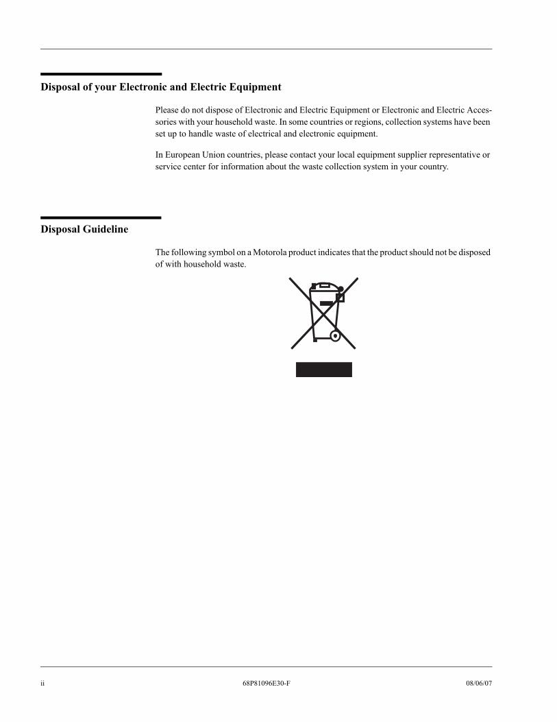
Disposal of your Electronic and Electric Equipment
Please do not dispose of Electronic and Electric Equipment or Electronic and Electric Acces-sories with your household waste. In some countries or regions, collection systems have been set up to handle waste of electrical and electronic equipment.
In European Union countries, please contact your local equipment supplier representative or service center for information about the waste collection system in your country.
Disposal Guideline
The following symbol on a Motorola product indicates that the product should not be disposed of with household waste.
ii 68P81096E30-F 08/06/07
Table of Contents
Model & Option Selection Procedure . . . . . . . . . . . . . . . . . . . . . . . . . . . . . . . . . . . . . . . . . . . . . . . . . . . . . . . . . . xxiiiProduct Maintenance Philosophy . . . . . . . . . . . . . . . . . . . . . . . . . . . . . . . . . . . . . . . . . . . . . . . . . . . . . . . . . . . . xxviiScope of Manual . . . . . . . . . . . . . . . . . . . . . . . . . . . . . . . . . . . . . . . . . . . . . . . . . . . . . . . . . . . . . . . . . . . . . . . . . xxviiDocumentation Conventions . . . . . . . . . . . . . . . . . . . . . . . . . . . . . . . . . . . . . . . . . . . . . . . . . . . . . . . . . . . . . . . . xxviiiService and Replacement Modules . . . . . . . . . . . . . . . . . . . . . . . . . . . . . . . . . . . . . . . . . . . . . . . . . . . . . . . . . . . . xxixGeneral Safety Information . . . . . . . . . . . . . . . . . . . . . . . . . . . . . . . . . . . . . . . . . . . . . . . . . . . . . . . . . . . . . . . . . . xxxiPerformance Specifications . . . . . . . . . . . . . . . . . . . . . . . . . . . . . . . . . . . . . . . . . . . . . . . . . . . . . . . . . . . . . . . . . xxxiiGlossary . . . . . . . . . . . . . . . . . . . . . . . . . . . . . . . . . . . . . . . . . . . . . . . . . . . . . . . . . . . . . . . . . . . . . . . . . . . . . . . . xxxiv
DESCRIPTION 68P81096E36Introduction . . . . . . . . . . . . . . . . . . . . . . . . . . . . . . . . . . . . . . . . . . . . . . . . . . . . . . . . . . . . . . . . . . . . . . . . . .1
Flexible Mechanical Design . . . . . . . . . . . . . . . . . . . . . . . . . . . . . . . . . . . . . . . . . . . . . . . . . . . . . . .1Electrical Design . . . . . . . . . . . . . . . . . . . . . . . . . . . . . . . . . . . . . . . . . . . . . . . . . . . . . . . . . . . . . . . .2Trunking Capability . . . . . . . . . . . . . . . . . . . . . . . . . . . . . . . . . . . . . . . . . . . . . . . . . . . . . . . . . . . . . .2Summary of Operating Features . . . . . . . . . . . . . . . . . . . . . . . . . . . . . . . . . . . . . . . . . . . . . . . . . . . .3
Station Components . . . . . . . . . . . . . . . . . . . . . . . . . . . . . . . . . . . . . . . . . . . . . . . . . . . . . . . . . . . . . . . . . . .4
DESCRIPTION
MTR2000™
Base Station, Repeaterand Receiver
For Analog Conventional,and Trunking Systems
132 - 174 MHz
, MOTOROLA, MTR2000, Spectra-TAC, DIGITAC, Private Line, Digital Private Line, DVP, Digital Voice Protection, Smart-Zone and Smartnet are trademarks of Motorola Inc. TORX is a trademark of Camcar Division of Textron Inc.
68P81096E30-F08/06/07-UP
Motorola Inc., 2005All Rights ReservedPrinted in U.S.A. 1301 E. Algonquin Road, Schaumburg, IL 60196
Government & Enterprise Mobility Solutions

Table of Contents
Functional Theory Of Operation . . . . . . . . . . . . . . . . . . . . . . . . . . . . . . . . . . . . . . . . . . . . . . . . . . . . . . . . . 5Transmitter Circuitry Operation . . . . . . . . . . . . . . . . . . . . . . . . . . . . . . . . . . . . . . . . . . . . . . . . . . . . 5Receiver Circuitry Operation . . . . . . . . . . . . . . . . . . . . . . . . . . . . . . . . . . . . . . . . . . . . . . . . . . . . . . 7Station Control Module Operation . . . . . . . . . . . . . . . . . . . . . . . . . . . . . . . . . . . . . . . . . . . . . . . . . . 8Wireline Interface Board Operation . . . . . . . . . . . . . . . . . . . . . . . . . . . . . . . . . . . . . . . . . . . . . . . . . 9Auxiliary I/O Board . . . . . . . . . . . . . . . . . . . . . . . . . . . . . . . . . . . . . . . . . . . . . . . . . . . . . . . . . . . . 10Power Supply Module Operation . . . . . . . . . . . . . . . . . . . . . . . . . . . . . . . . . . . . . . . . . . . . . . . . . . 11
INSTALLATION 68P81096E37Pre-installation Considerations . . . . . . . . . . . . . . . . . . . . . . . . . . . . . . . . . . . . . . . . . . . . . . . . . . . . . . . . . . 1
Installation Overview . . . . . . . . . . . . . . . . . . . . . . . . . . . . . . . . . . . . . . . . . . . . . . . . . . . . . . . . . . . . 1Environmental Conditions at Intended Installation Site . . . . . . . . . . . . . . . . . . . . . . . . . . . . . . . . . . 2Equipment Ventilation . . . . . . . . . . . . . . . . . . . . . . . . . . . . . . . . . . . . . . . . . . . . . . . . . . . . . . . . . . . 3AC Input Power Requirements . . . . . . . . . . . . . . . . . . . . . . . . . . . . . . . . . . . . . . . . . . . . . . . . . . . . . 4Equipment Mounting Methods . . . . . . . . . . . . . . . . . . . . . . . . . . . . . . . . . . . . . . . . . . . . . . . . . . . . . 5Site Grounding and Lightning Protection . . . . . . . . . . . . . . . . . . . . . . . . . . . . . . . . . . . . . . . . . . . . 10Recommended Tools and Equipment . . . . . . . . . . . . . . . . . . . . . . . . . . . . . . . . . . . . . . . . . . . . . . . 11Equipment Unpacking and Inspection . . . . . . . . . . . . . . . . . . . . . . . . . . . . . . . . . . . . . . . . . . . . . . 11Cabinet Unpacking . . . . . . . . . . . . . . . . . . . . . . . . . . . . . . . . . . . . . . . . . . . . . . . . . . . . . . . . . . . . . 11
Mechanical Installation . . . . . . . . . . . . . . . . . . . . . . . . . . . . . . . . . . . . . . . . . . . . . . . . . . . . . . . . . . . . . . . 12Unpacking Equipment . . . . . . . . . . . . . . . . . . . . . . . . . . . . . . . . . . . . . . . . . . . . . . . . . . . . . . . . . . 12Mounting Procedures . . . . . . . . . . . . . . . . . . . . . . . . . . . . . . . . . . . . . . . . . . . . . . . . . . . . . . . . . . . 16
Board Configuration. . . . . . . . . . . . . . . . . . . . . . . . . . . . . . . . . . . . . . . . . . . . . . . . . . . . . . . . . . . . . . . . . . 224-wire Wireline Interface Board . . . . . . . . . . . . . . . . . . . . . . . . . . . . . . . . . . . . . . . . . . . . . . . . . . . 224-wire Euro Wireline Interface Board . . . . . . . . . . . . . . . . . . . . . . . . . . . . . . . . . . . . . . . . . . . . . . 22Auxiliary I/O Board . . . . . . . . . . . . . . . . . . . . . . . . . . . . . . . . . . . . . . . . . . . . . . . . . . . . . . . . . . . . 24
Electrical Connections . . . . . . . . . . . . . . . . . . . . . . . . . . . . . . . . . . . . . . . . . . . . . . . . . . . . . . . . . . . . . . . . 27Power Supply Connections . . . . . . . . . . . . . . . . . . . . . . . . . . . . . . . . . . . . . . . . . . . . . . . . . . . . . . . 28RF Antenna Connections . . . . . . . . . . . . . . . . . . . . . . . . . . . . . . . . . . . . . . . . . . . . . . . . . . . . . . . . 31System Cable Connections . . . . . . . . . . . . . . . . . . . . . . . . . . . . . . . . . . . . . . . . . . . . . . . . . . . . . . . 32Telephone Line Connections. . . . . . . . . . . . . . . . . . . . . . . . . . . . . . . . . . . . . . . . . . . . . . . . . . . . . . 38Station Maintenance Connections. . . . . . . . . . . . . . . . . . . . . . . . . . . . . . . . . . . . . . . . . . . . . . . . . . 42
Post Installation Checklist . . . . . . . . . . . . . . . . . . . . . . . . . . . . . . . . . . . . . . . . . . . . . . . . . . . . . . . . . . . . . 43Applying Power . . . . . . . . . . . . . . . . . . . . . . . . . . . . . . . . . . . . . . . . . . . . . . . . . . . . . . . . . . . . . . . 43Verifying Proper Operation. . . . . . . . . . . . . . . . . . . . . . . . . . . . . . . . . . . . . . . . . . . . . . . . . . . . . . . 44
Optimization. . . . . . . . . . . . . . . . . . . . . . . . . . . . . . . . . . . . . . . . . . . . . . . . . . . . . . . . . . . . . . . . . . . . . . . . 47Optimizing Tasks . . . . . . . . . . . . . . . . . . . . . . . . . . . . . . . . . . . . . . . . . . . . . . . . . . . . . . . . . . . . . . 47Copying Station Codeplug Data to a PC-compatible Computer . . . . . . . . . . . . . . . . . . . . . . . . . . 47
Installing Station Hardware Options . . . . . . . . . . . . . . . . . . . . . . . . . . . . . . . . . . . . . . . . . . . . . . . . . . . . . 48
INSTALLATION
iv 68P81096E30-F 08/06/07

Table of Contents
STATION OPERATION 68P81096E38Description . . . . . . . . . . . . . . . . . . . . . . . . . . . . . . . . . . . . . . . . . . . . . . . . . . . . . . . . . . . . . . . . . . . . . . . . . .1
LED Indicators. . . . . . . . . . . . . . . . . . . . . . . . . . . . . . . . . . . . . . . . . . . . . . . . . . . . . . . . . . . . . . . . . .2External Device Connection . . . . . . . . . . . . . . . . . . . . . . . . . . . . . . . . . . . . . . . . . . . . . . . . . . . . . . .3Service Connections. . . . . . . . . . . . . . . . . . . . . . . . . . . . . . . . . . . . . . . . . . . . . . . . . . . . . . . . . . . . . .4
ROUTINE MAINTENANCE 68P81096E39Introduction . . . . . . . . . . . . . . . . . . . . . . . . . . . . . . . . . . . . . . . . . . . . . . . . . . . . . . . . . . . . . . . . . . . . . . . . . .1Recommended Test Equipment. . . . . . . . . . . . . . . . . . . . . . . . . . . . . . . . . . . . . . . . . . . . . . . . . . . . . . . . . . .2Calibrating Station Reference Oscillator. . . . . . . . . . . . . . . . . . . . . . . . . . . . . . . . . . . . . . . . . . . . . . . . . . . .2
TROUBLESHOOTING 68P81096E17Introduction . . . . . . . . . . . . . . . . . . . . . . . . . . . . . . . . . . . . . . . . . . . . . . . . . . . . . . . . . . . . . . . . . . . . . . . . . .1Recommended Test Equipment. . . . . . . . . . . . . . . . . . . . . . . . . . . . . . . . . . . . . . . . . . . . . . . . . . . . . . . . . . .2Troubleshooting Procedures . . . . . . . . . . . . . . . . . . . . . . . . . . . . . . . . . . . . . . . . . . . . . . . . . . . . . . . . . . . . .3Module Replacement Procedures . . . . . . . . . . . . . . . . . . . . . . . . . . . . . . . . . . . . . . . . . . . . . . . . . . . . . . . .20Preselector Field Tuning Procedures. . . . . . . . . . . . . . . . . . . . . . . . . . . . . . . . . . . . . . . . . . . . . . . . . . . . . .34
OPERATION
MAINTENANCE AND TROUBLESHOOTING
08/06/07 68P81096E30-F v

Table of Contents
RECEIVER MODULE, 132 to 174 MHzModels CLN1211 and CLN1212 68P81096E19
Description . . . . . . . . . . . . . . . . . . . . . . . . . . . . . . . . . . . . . . . . . . . . . . . . . . . . . . . . . . . . . . . . . . . . . . . . . . 1Inputs and Output Connections . . . . . . . . . . . . . . . . . . . . . . . . . . . . . . . . . . . . . . . . . . . . . . . . . . . . . . . . . . 2Functional Theory of Operation. . . . . . . . . . . . . . . . . . . . . . . . . . . . . . . . . . . . . . . . . . . . . . . . . . . . . . . . . . 3
EXCITER MODULEModel CLN1233 68P81096E22
Description . . . . . . . . . . . . . . . . . . . . . . . . . . . . . . . . . . . . . . . . . . . . . . . . . . . . . . . . . . . . . . . . . . . . . . . . . . 1Input and Output Connections . . . . . . . . . . . . . . . . . . . . . . . . . . . . . . . . . . . . . . . . . . . . . . . . . . . . . . . . . . . 2Functional Theory of Operation. . . . . . . . . . . . . . . . . . . . . . . . . . . . . . . . . . . . . . . . . . . . . . . . . . . . . . . . . . 3
30/40 W POWER AMPLIFIER MODULEModels CLN1227 and CLN1226 68P81096E26
Description . . . . . . . . . . . . . . . . . . . . . . . . . . . . . . . . . . . . . . . . . . . . . . . . . . . . . . . . . . . . . . . . . . . . . . . . . . 1Identification of Inputs/Outputs . . . . . . . . . . . . . . . . . . . . . . . . . . . . . . . . . . . . . . . . . . . . . . . . . . . . . . . . . . 2Functional Theory of Operation. . . . . . . . . . . . . . . . . . . . . . . . . . . . . . . . . . . . . . . . . . . . . . . . . . . . . . . . . . 3
100 W POWER AMPLIFIER MODULEModels CLN1224 and CLN1225 68P81096E24
Description . . . . . . . . . . . . . . . . . . . . . . . . . . . . . . . . . . . . . . . . . . . . . . . . . . . . . . . . . . . . . . . . . . . . . . . . . . 1Identification of Inputs/Outputs . . . . . . . . . . . . . . . . . . . . . . . . . . . . . . . . . . . . . . . . . . . . . . . . . . . . . . . . . . 2Functional Theory of Operation. . . . . . . . . . . . . . . . . . . . . . . . . . . . . . . . . . . . . . . . . . . . . . . . . . . . . . . . . . 3
STATION MODULES
RECEIVER CIRCUITRY
TRANSMITTER CIRCUITRY
vi 68P81096E30-F 08/06/07

Table of Contents
STATION CONTROL MODULE Model CLN1465 68P81096E32
Description . . . . . . . . . . . . . . . . . . . . . . . . . . . . . . . . . . . . . . . . . . . . . . . . . . . . . . . . . . . . . . . . . . . . . . . . . .1Indicators and Input/Output Connections . . . . . . . . . . . . . . . . . . . . . . . . . . . . . . . . . . . . . . . . . . . . . . . . . . .3Functional Theory of Operation . . . . . . . . . . . . . . . . . . . . . . . . . . . . . . . . . . . . . . . . . . . . . . . . . . . . . . . . . .4
4 WIRE, EURO WIRELINE INTERFACE BOARDModel CLN1204 68P81096E28
Description . . . . . . . . . . . . . . . . . . . . . . . . . . . . . . . . . . . . . . . . . . . . . . . . . . . . . . . . . . . . . . . . . . . . . . . . . .1Inputs and Output Connections . . . . . . . . . . . . . . . . . . . . . . . . . . . . . . . . . . . . . . . . . . . . . . . . . . . . . . . . . . .2Functional Theory of Operation . . . . . . . . . . . . . . . . . . . . . . . . . . . . . . . . . . . . . . . . . . . . . . . . . . . . . . . . . .3
4 WIRE, WIRELINE INTERFACE BOARDModel CLN1203 68P81096E29
Description . . . . . . . . . . . . . . . . . . . . . . . . . . . . . . . . . . . . . . . . . . . . . . . . . . . . . . . . . . . . . . . . . . . . . . . . . .1
Inputs and Output Connections . . . . . . . . . . . . . . . . . . . . . . . . . . . . . . . . . . . . . . . . . . . . . . . . . . . . . . . . . . .2
Functional Theory of Operation . . . . . . . . . . . . . . . . . . . . . . . . . . . . . . . . . . . . . . . . . . . . . . . . . . . . . . . . . .3
8 WIRE, WIRELINE INTERFACE BOARDModel CLN1205 68P81096E31
Description . . . . . . . . . . . . . . . . . . . . . . . . . . . . . . . . . . . . . . . . . . . . . . . . . . . . . . . . . . . . . . . . . . . . . . . . . .1
Inputs and Output Connections . . . . . . . . . . . . . . . . . . . . . . . . . . . . . . . . . . . . . . . . . . . . . . . . . . . . . . . . . . .2
Functional Theory of Operation . . . . . . . . . . . . . . . . . . . . . . . . . . . . . . . . . . . . . . . . . . . . . . . . . . . . . . . . . .3
AUXILIARY I/O BOARDModel CLN1206 68P81096E53
Description . . . . . . . . . . . . . . . . . . . . . . . . . . . . . . . . . . . . . . . . . . . . . . . . . . . . . . . . . . . . . . . . . . . . . . . . . .1
Input and Output Connections. . . . . . . . . . . . . . . . . . . . . . . . . . . . . . . . . . . . . . . . . . . . . . . . . . . . . . . . . . . .2
Functional Theory of Operation . . . . . . . . . . . . . . . . . . . . . . . . . . . . . . . . . . . . . . . . . . . . . . . . . . . . . . . . . .3
STATION CONTROL CIRCUITRY
WIRELINE CIRCUITRY
AUXILIARY I/O CIRCUITRY
08/06/07 68P81096E30-F vii

Table of Contents
BACKPLANE INTERCONNECT BOARDModel CLN1202 68P81096E46
Description . . . . . . . . . . . . . . . . . . . . . . . . . . . . . . . . . . . . . . . . . . . . . . . . . . . . . . . . . . . . . . . . . . . . . . . . . . 1Location of Backplane Connectors . . . . . . . . . . . . . . . . . . . . . . . . . . . . . . . . . . . . . . . . . . . . . . . . . . . . . . . 3Backplane Connectors Information . . . . . . . . . . . . . . . . . . . . . . . . . . . . . . . . . . . . . . . . . . . . . . . . . . . . . . . 4
500 W POWER SUPPLY, AC with DC Backup ConnectorModels CLN1220 and DLN6458 68P81096E33
Description . . . . . . . . . . . . . . . . . . . . . . . . . . . . . . . . . . . . . . . . . . . . . . . . . . . . . . . . . . . . . . . . . . . . . . . . . . 1Performance Specifications . . . . . . . . . . . . . . . . . . . . . . . . . . . . . . . . . . . . . . . . . . . . . . . . . . . . . . . . . . . . . 3Identification of Inputs/Outputs . . . . . . . . . . . . . . . . . . . . . . . . . . . . . . . . . . . . . . . . . . . . . . . . . . . . . . . . . . 4Functional Theory of Operation. . . . . . . . . . . . . . . . . . . . . . . . . . . . . . . . . . . . . . . . . . . . . . . . . . . . . . . . . . 5
500 W POWER SUPPLY, AC with DC Backup ConnectorModel DLN6622 68P81011Y31
Description . . . . . . . . . . . . . . . . . . . . . . . . . . . . . . . . . . . . . . . . . . . . . . . . . . . . . . . . . . . . . . . . . . . . . . . . . . 1Performance Specifications . . . . . . . . . . . . . . . . . . . . . . . . . . . . . . . . . . . . . . . . . . . . . . . . . . . . . . . . . . . . . 2Identification of Inputs/Outputs . . . . . . . . . . . . . . . . . . . . . . . . . . . . . . . . . . . . . . . . . . . . . . . . . . . . . . . . . . 3Functional Theory of Operation. . . . . . . . . . . . . . . . . . . . . . . . . . . . . . . . . . . . . . . . . . . . . . . . . . . . . . . . . . 4
250 W POWER SUPPLY, AC with DC Backup ConnectorModel CLN1221 68P81096E34
Description . . . . . . . . . . . . . . . . . . . . . . . . . . . . . . . . . . . . . . . . . . . . . . . . . . . . . . . . . . . . . . . . . . . . . . . . . . 1Performance Specifications . . . . . . . . . . . . . . . . . . . . . . . . . . . . . . . . . . . . . . . . . . . . . . . . . . . . . . . . . . . . . 2Identification of Inputs/Outputs . . . . . . . . . . . . . . . . . . . . . . . . . . . . . . . . . . . . . . . . . . . . . . . . . . . . . . . . . . 3Functional Theory of Operation. . . . . . . . . . . . . . . . . . . . . . . . . . . . . . . . . . . . . . . . . . . . . . . . . . . . . . . . . . 4
250 W POWER SUPPLY, AC with DC Backup ConnectorModel DLN6624 68P81011Y29
Description . . . . . . . . . . . . . . . . . . . . . . . . . . . . . . . . . . . . . . . . . . . . . . . . . . . . . . . . . . . . . . . . . . . . . . . . . . 1Performance Specifications . . . . . . . . . . . . . . . . . . . . . . . . . . . . . . . . . . . . . . . . . . . . . . . . . . . . . . . . . . . . . 2Identification of Inputs/Outputs . . . . . . . . . . . . . . . . . . . . . . . . . . . . . . . . . . . . . . . . . . . . . . . . . . . . . . . . . . 3Functional Theory of Operation. . . . . . . . . . . . . . . . . . . . . . . . . . . . . . . . . . . . . . . . . . . . . . . . . . . . . . . . . . 4
STATION BACKPLANE
POWER SUPPLIES
viii 68P81096E30-F 08/06/07

Table of Contents
500 W POWER SUPPLY, DC-OnlyModel CLN1222 68P81096E51
Description . . . . . . . . . . . . . . . . . . . . . . . . . . . . . . . . . . . . . . . . . . . . . . . . . . . . . . . . . . . . . . . . . . . . . . . . . .1
Performance Specifications. . . . . . . . . . . . . . . . . . . . . . . . . . . . . . . . . . . . . . . . . . . . . . . . . . . . . . . . . . . . . .2
Identification of Inputs/Outputs . . . . . . . . . . . . . . . . . . . . . . . . . . . . . . . . . . . . . . . . . . . . . . . . . . . . . . . . . .3
Functional Theory of Operation . . . . . . . . . . . . . . . . . . . . . . . . . . . . . . . . . . . . . . . . . . . . . . . . . . . . . . . . . .4
250 W POWER SUPPLY, DC-OnlyModel CLN1223 68P81096E52
Description . . . . . . . . . . . . . . . . . . . . . . . . . . . . . . . . . . . . . . . . . . . . . . . . . . . . . . . . . . . . . . . . . . . . . . . . . .1
Performance Specifications. . . . . . . . . . . . . . . . . . . . . . . . . . . . . . . . . . . . . . . . . . . . . . . . . . . . . . . . . . . . . .2
Identification of Inputs/Outputs . . . . . . . . . . . . . . . . . . . . . . . . . . . . . . . . . . . . . . . . . . . . . . . . . . . . . . . . . .3
Functional Theory of Operation . . . . . . . . . . . . . . . . . . . . . . . . . . . . . . . . . . . . . . . . . . . . . . . . . . . . . . . . . .4
SATELLLITE RECEIVER 68P81096E44Description . . . . . . . . . . . . . . . . . . . . . . . . . . . . . . . . . . . . . . . . . . . . . . . . . . . . . . . . . . . . . . . . . . . . . . . . . .1Input and Output Connections. . . . . . . . . . . . . . . . . . . . . . . . . . . . . . . . . . . . . . . . . . . . . . . . . . . . . . . . . . . .3
SATELLITE RECEIVER
08/06/07 68P81096E30-F ix

Table of Contents
ANTENNA RELAY MODULEModel CLN6680 68P81096E41
Description . . . . . . . . . . . . . . . . . . . . . . . . . . . . . . . . . . . . . . . . . . . . . . . . . . . . . . . . . . . . . . . . . . . . . . . . . . 1Inputs and Output Connections . . . . . . . . . . . . . . . . . . . . . . . . . . . . . . . . . . . . . . . . . . . . . . . . . . . . . . . . . . 2Option Complement . . . . . . . . . . . . . . . . . . . . . . . . . . . . . . . . . . . . . . . . . . . . . . . . . . . . . . . . . . . . . . . . . . . 7Performance Specifications . . . . . . . . . . . . . . . . . . . . . . . . . . . . . . . . . . . . . . . . . . . . . . . . . . . . . . . . . . . . . 7Mounting Locations . . . . . . . . . . . . . . . . . . . . . . . . . . . . . . . . . . . . . . . . . . . . . . . . . . . . . . . . . . . . . . . . . . . 8Functional Theory of Operation. . . . . . . . . . . . . . . . . . . . . . . . . . . . . . . . . . . . . . . . . . . . . . . . . . . . . . . . . . 9
VHF EXTERNAL PRESELECTOR MODULEModels CLN1216 and CLN1217 68P81096E43
Description . . . . . . . . . . . . . . . . . . . . . . . . . . . . . . . . . . . . . . . . . . . . . . . . . . . . . . . . . . . . . . . . . . . . . . . . . . 1Inputs and Output Connections . . . . . . . . . . . . . . . . . . . . . . . . . . . . . . . . . . . . . . . . . . . . . . . . . . . . . . . . . . 2Options Complement . . . . . . . . . . . . . . . . . . . . . . . . . . . . . . . . . . . . . . . . . . . . . . . . . . . . . . . . . . . . . . . . . . 4Mounting Location. . . . . . . . . . . . . . . . . . . . . . . . . . . . . . . . . . . . . . . . . . . . . . . . . . . . . . . . . . . . . . . . . . . . 4
VHF EXTERNAL DOUBLE CIRCULATOR MODULEModels CLN1207, CLN1208 and CLN1209 68P81096E49
Description . . . . . . . . . . . . . . . . . . . . . . . . . . . . . . . . . . . . . . . . . . . . . . . . . . . . . . . . . . . . . . . . . . . . . . . . . . 1Inputs and Output Connections . . . . . . . . . . . . . . . . . . . . . . . . . . . . . . . . . . . . . . . . . . . . . . . . . . . . . . . . . . 2Options Complement . . . . . . . . . . . . . . . . . . . . . . . . . . . . . . . . . . . . . . . . . . . . . . . . . . . . . . . . . . . . . . . . . . 6Performance Specifications . . . . . . . . . . . . . . . . . . . . . . . . . . . . . . . . . . . . . . . . . . . . . . . . . . . . . . . . . . . . . 7Functional Theory of Operation. . . . . . . . . . . . . . . . . . . . . . . . . . . . . . . . . . . . . . . . . . . . . . . . . . . . . . . . . . 8
VHF DUPLEXER MODULEModels TYD4031, TYD4032, and TYD4033 68P81085E16
Description . . . . . . . . . . . . . . . . . . . . . . . . . . . . . . . . . . . . . . . . . . . . . . . . . . . . . . . . . . . . . . . . . . . . . . . . . . 1Adjustment Screws and Input/Output Connectors . . . . . . . . . . . . . . . . . . . . . . . . . . . . . . . . . . . . . . . . . . . . 2Performance Specifications . . . . . . . . . . . . . . . . . . . . . . . . . . . . . . . . . . . . . . . . . . . . . . . . . . . . . . . . . . . . . 7Typical Interconnection . . . . . . . . . . . . . . . . . . . . . . . . . . . . . . . . . . . . . . . . . . . . . . . . . . . . . . . . . . . . . . . . 8Field Tuning Procedure . . . . . . . . . . . . . . . . . . . . . . . . . . . . . . . . . . . . . . . . . . . . . . . . . . . . . . . . . . . . . . . . 9
ZETRON REPEATER PANELModel TDN9946 68P81095E71
Description . . . . . . . . . . . . . . . . . . . . . . . . . . . . . . . . . . . . . . . . . . . . . . . . . . . . . . . . . . . . . . . . . . . . . . . . . . 1Option Information. . . . . . . . . . . . . . . . . . . . . . . . . . . . . . . . . . . . . . . . . . . . . . . . . . . . . . . . . . . . . . . . . . . . 4
ANCILLARY EQUIPMENT
x 68P81096E30-F 08/06/07
Table of Contents
List of Figures
DESCRIPTION 68P81096E36Figure 1. MTR2000 Station . . . . . . . . . . . . . . . . . . . . . . . . . . . . . . . . . . . . . . . . . . . . . . . . . . . . . . . . . . . . 1
Figure 2. MTR2000 Station Components . . . . . . . . . . . . . . . . . . . . . . . . . . . . . . . . . . . . . . . . . . . . . . . . . 4
Figure 3. Functional Block Diagram . . . . . . . . . . . . . . . . . . . . . . . . . . . . . . . . . . . . . . . . . . . . . . . . . . . . 14
INSTALLATION 68P81096E37Figure 1. Floor-mount Cabinet – Dimensions and Clearances . . . . . . . . . . . . . . . . . . . . . . . . . . . . . . . . . 7
Figure 2. Modular Rack – Dimensions and Clearances. . . . . . . . . . . . . . . . . . . . . . . . . . . . . . . . . . . . . . . 9
Figure 3. Unpacking Procedure - Station. . . . . . . . . . . . . . . . . . . . . . . . . . . . . . . . . . . . . . . . . . . . . . . . . 13
Figure 4. Unpacking Procedures - Floormount Cabinets. . . . . . . . . . . . . . . . . . . . . . . . . . . . . . . . . . . . . 15
Figure 5. Slide Rail Installation; Option X968AA. . . . . . . . . . . . . . . . . . . . . . . . . . . . . . . . . . . . . . . . . . 19
Figure 6. Slide Rail Installation; Option X346AB. . . . . . . . . . . . . . . . . . . . . . . . . . . . . . . . . . . . . . . . . . 21
Figure 7. CLN1203 Wireline Interface Board Jumper Settings. . . . . . . . . . . . . . . . . . . . . . . . . . . . . . . . 22
Figure 8. CLN1204 Wireline Interface Board Jumper Settings. . . . . . . . . . . . . . . . . . . . . . . . . . . . . . . . 23
Figure 9. CLN1206 Auxiliary I/O Board Jumpers. . . . . . . . . . . . . . . . . . . . . . . . . . . . . . . . . . . . . . . . . . 24
Figure 10. Location of External Connectors at Rear of Station. . . . . . . . . . . . . . . . . . . . . . . . . . . . . . . . . 28
Figure 11. Connecting the Station to a Power Factor Correction Choke. . . . . . . . . . . . . . . . . . . . . . . . . . 29
Figure 12. Making Connections to Storage Battery. . . . . . . . . . . . . . . . . . . . . . . . . . . . . . . . . . . . . . . . . . 31
DESCRIPTION
INSTALLATION
08/06/07 68P81096E30-F xi

Table of Contents
STATION OPERATION 68P81096E38Figure 1. Front Panel LEDs . . . . . . . . . . . . . . . . . . . . . . . . . . . . . . . . . . . . . . . . . . . . . . . . . . . . . . . . . . . . 2
Figure 2. SCM Connectors . . . . . . . . . . . . . . . . . . . . . . . . . . . . . . . . . . . . . . . . . . . . . . . . . . . . . . . . . . . . . 4
ROUTINE MAINTENANCE 68P81096E39Figure 1. Front Panel Removal . . . . . . . . . . . . . . . . . . . . . . . . . . . . . . . . . . . . . . . . . . . . . . . . . . . . . . . . . . 3
TROUBLESHOOTING 68P81096E17Figure 1. Procedure 1 – Routine Site Visit . . . . . . . . . . . . . . . . . . . . . . . . . . . . . . . . . . . . . . . . . . . . . . . . 5
Figure 2. Procedure 2 – Station Troubleshooting . . . . . . . . . . . . . . . . . . . . . . . . . . . . . . . . . . . . . . . . . . . 7
Figure 3. Front Panel Removal . . . . . . . . . . . . . . . . . . . . . . . . . . . . . . . . . . . . . . . . . . . . . . . . . . . . . . . . . . 8
Figure 4. SCM Service Connectors. . . . . . . . . . . . . . . . . . . . . . . . . . . . . . . . . . . . . . . . . . . . . . . . . . . . . . . 9
Figure 5. Service Mic Buttons . . . . . . . . . . . . . . . . . . . . . . . . . . . . . . . . . . . . . . . . . . . . . . . . . . . . . . . . . 11
Figure 6. Test Equipment Setup for Verifying Transmitter Circuitry . . . . . . . . . . . . . . . . . . . . . . . . . . . 14
Figure 7. Test Equipment Setup for Verifying Receiver Circuit . . . . . . . . . . . . . . . . . . . . . . . . . . . . . . . 18
Figure 8. Test Equipment Setup for External Preselector Field Tuning . . . . . . . . . . . . . . . . . . . . . . . . . . 37
Figure 9. Location of Tuning Screws and Cavity Probe Holes. . . . . . . . . . . . . . . . . . . . . . . . . . . . . . . . . 39
Figure 10. Location of RSSI Monitoring Point (Trunking Stations Only) . . . . . . . . . . . . . . . . . . . . . . . . . 40
OPERATION
MAINTENANCE AND TROUBLESHOOTING
xii 68P81096E30-F 08/06/07

Table of Contents
RECEIVER MODULE, 132 to 174 MHzModels CLN1211 and CLN1212 68P81096E19
Figure 1. VHF Receiver Module Inputs/Outputs . . . . . . . . . . . . . . . . . . . . . . . . . . . . . . . . . . . . . . . . . . . 2
Figure 2. VHF Receiver Module Functional Block Diagram . . . . . . . . . . . . . . . . . . . . . . . . . . . . . . . . . . 7
EXCITER MODULEModel CLN1233 68P81096E22
Figure 1. VHF Exciter Module Input/Outputs . . . . . . . . . . . . . . . . . . . . . . . . . . . . . . . . . . . . . . . . . . . . . 2
Figure 2. VHF Exciter Module Functional Block Diagram. . . . . . . . . . . . . . . . . . . . . . . . . . . . . . . . . . . . 7
30/40 W POWER AMPLIFIER MODULEModels CLN1227 and CLN1226 68P81096E26
Figure 1. VHF 30/40 W Power Amplifier Module Input/Outputs. . . . . . . . . . . . . . . . . . . . . . . . . . . . . . . 2
Figure 2. VHF 30/40 W Power Amplifier Module Functional Block Diagram . . . . . . . . . . . . . . . . . . . . 5
100 W POWER AMPLIFIER MODULEModels CLN1224 and CLN1225 68P81096E24
Figure 1. VHF 100 W Power Amplifier Module Input/Outputs . . . . . . . . . . . . . . . . . . . . . . . . . . . . . . . . 2
Figure 2. VHF 100 W Power Amplifier Module Functional Block Diagram . . . . . . . . . . . . . . . . . . . . . . 5
STATION CONTROL MODULE Model CLN1465 68P81096E32
Figure 1. Station Control Module Indicators and Input/Output Connections . . . . . . . . . . . . . . . . . . . . . . 3
Figure 2. Station Control Module Functional Block Diagram – Supply Voltage Circuitry. . . . . . . . . . . . . . . . . . . . . . . . . . . . . . . . . . . . . . . . . . . . . . . . . . . . 14
Figure 3. Station Control Module Functional Block Diagram – Station Control Circuitry . . . . . . . . . . . . . . . . . . . . . . . . . . . . . . . . . . . . . . . . . . . . . . . . . . . . 15
STATION MODULES
RECEIVER CIRCUITRY
TRANSMITTER CIRCUITRY
STATION CONTROL CIRCUITRY
08/06/07 68P81096E30-F xiii
Table of Contents
4 WIRE, EURO WIRELINE INTERFACE BOARDModel CLN1204 68P81096E28
Figure 1. CLN1204 Wireline Interface Board Jumpers and Input/Output Connections . . . . . . . . . . . . . . . . . . . . . . . . . . . . . . . . . . . . . . . . . . . . . . . . . . . . . . 2
Figure 2. CLN1204 Wireline Interface Board Jumpers Settings . . . . . . . . . . . . . . . . . . . . . . . . . . . . . . . . 4
Figure 3. CLN1204; 2-Wire Voice Audio Path Functional Block Diagram. . . . . . . . . . . . . . . . . . . . . . . . 7
Figure 4. CLN1204; 4-Wire Voice Audio Path Functional Block Diagram. . . . . . . . . . . . . . . . . . . . . . . . 7
4 WIRE, WIRELINE INTERFACE BOARDModel CLN1203 68P81096E29
Figure 1. CLN1203 Wireline Interface Board Jumpers and Input/Output Connections . . . . . . . . . . . . . . . . . . . . . . . . . . . . . . . . . . . . . . . . . . . . . . . . . . . . . . 2
Figure 2. CLN1203 Wireline Interface Board Jumpers Settings . . . . . . . . . . . . . . . . . . . . . . . . . . . . . . . . 4
Figure 3. CLN1203; 2-Wire Voice Audio Path Functional Block Diagram. . . . . . . . . . . . . . . . . . . . . . . . 7
Figure 4. CLN1203; 4-Wire Voice Audio Path Functional Block Diagram. . . . . . . . . . . . . . . . . . . . . . . . 7
8 WIRE, WIRELINE INTERFACE BOARDModel CLN1205 68P81096E31
Figure 1. CLN1205 Wireline Interface Board Jumpers and Input/Output Connections . . . . . . . . . . . . . . . . . . . . . . . . . . . . . . . . . . . . . . . . . . . . . . . . . . . . . . 2
Figure 2. CLN1205; 8 Wire Voice Audio Data Path Functional Block Diagram . . . . . . . . . . . . . . . . . . . 7
AUXILIARY I/O BOARDModel CLN1206 68P81096E53
Figure 1. CLN1206 Auxiliary I/O Input/Output Connections . . . . . . . . . . . . . . . . . . . . . . . . . . . . . . . . . . 2
Figure 2. CLN1206 Auxiliary I/O Board Jumpers . . . . . . . . . . . . . . . . . . . . . . . . . . . . . . . . . . . . . . . . . . . 9
Figure 3. CLN1206 Auxiliary I/O Board Functional Block Diagram . . . . . . . . . . . . . . . . . . . . . . . . . . . 12
WIRELINE CIRCUITRY
AUXILIARY I/O CIRCUITRY
xiv 68P81096E30-F 08/06/07

Table of Contents
BACKPLANE INTERCONNECT BOARDModel CLN1202 68P81096E46
Figure 1. Backplane Interconnect Board . . . . . . . . . . . . . . . . . . . . . . . . . . . . . . . . . . . . . . . . . . . . . . . . . . 2
Figure 2. Station Backplane Connector Locations. . . . . . . . . . . . . . . . . . . . . . . . . . . . . . . . . . . . . . . . . . . 3
Figure 3. Backplane Rear Connector Pinout Information . . . . . . . . . . . . . . . . . . . . . . . . . . . . . . . . . . . . 11
500 W POWER SUPPLY, AC with DC Backup ConnectorModels CLN1220 and DLN6458 68P81096E33
Figure 1. Model CLN1220/DLN6458 Power Supply Module Input/Output Connections . . . . . . . . . . . . 4
Figure 2. Model CLN1220/DLN6458 500 W Power Supply Functional Block Diagram. . . . . . . . . . . . . 7
500 W POWER SUPPLY, AC with DC Backup ConnectorModels DLN6622 68P81011Y31
Figure 1. Model DLN6622 Power Supply Module Input/Output Connections . . . . . . . . . . . . . . . . . . . . . 3
Figure 2. Model DLN6622 500 W Power Supply Functional Block Diagram . . . . . . . . . . . . . . . . . . . . . 7
250 WPOWER SUPPLY, AC with DC Backup ConnectorModel CLN1221 68P81096E34
Figure 1. Model CLN1221 Power Supply Module Input/Output Connections . . . . . . . . . . . . . . . . . . . . . 3
Figure 2. Model CLN1221 250 W Power Supply Functional Block Diagram . . . . . . . . . . . . . . . . . . . . . 5
250 W POWER SUPPLY, AC with DC Backup ConnectorModel DLN6624 68P81011Y29
Figure 1. Model DLN6624 Power Supply Module Input/Output Connections . . . . . . . . . . . . . . . . . . . . . 3
Figure 2. Model DLN6624 250 W Power Supply Functional Block Diagram . . . . . . . . . . . . . . . . . . . . . 5
500 W POWER SUPPLY, DC-OnlyModel CLN1222 68P81096E51
Figure 1. Model CLN1222 DC-Only Power Supply Module Input/Output Connections. . . . . . . . . . . . . . . . . . . . . . . . . . . . . . . . . . . . . . . . . . . . . . . . . . . . . . 3
Figure 2. Model CLN1222 DC-Only 500 W Power Supply Functional Block Diagram . . . . . . . . . . . . . . . . . . . . . . . . . . . . . . . . . . . . . . . . . . . . . . . . . . . . . 5
STATION BACKPLANE
POWER SUPPLIES
08/06/07 68P81096E30-F xv
Table of Contents
250 W POWER SUPPLY, DC-OnlyModel CLN1223 68P81096E52
Figure 1. Model CLN1223 DC-Only Power Supply Module Input/Output Connections . . . . . . . . . . . . . . . . . . . . . . . . . . . . . . . . . . . . . . . . . . . . . . . . . . . . . . 3
Figure 2. Model CLN1223 DC-Only 250 W Power Supply Functional Block Diagram. . . . . . . . . . . . . . . . . . . . . . . . . . . . . . . . . . . . . . . . . . . . . . . . . . . . . . 5
SATELLLITE RECEIVER 68P81096E44Figure 1. Typical MTR2000 Satellite Receiver . . . . . . . . . . . . . . . . . . . . . . . . . . . . . . . . . . . . . . . . . . . . . 1
Figure 2. Satellite Receiver Input/Output Connections . . . . . . . . . . . . . . . . . . . . . . . . . . . . . . . . . . . . . . . 3
Figure 3. Satellite Receiver Connections Within a Voting System . . . . . . . . . . . . . . . . . . . . . . . . . . . . . . 4
Figure 4. Satellite Receiver Functional Block Diagram . . . . . . . . . . . . . . . . . . . . . . . . . . . . . . . . . . . . . . . 5
SATELLITE RECEIVER
xvi 68P81096E30-F 08/06/07
Table of Contents
ANTENNA RELAY MODULEModel CLN6680 68P81096E41
Figure 1. Typical Antenna Relay Module – Inputs/Outputs . . . . . . . . . . . . . . . . . . . . . . . . . . . . . . . . . . . 2
Figure 2. Antenna Relay Only – Cable Kits . . . . . . . . . . . . . . . . . . . . . . . . . . . . . . . . . . . . . . . . . . . . . . . 3
Figure 3. Antenna Relay and External Preselector – Cable Kits . . . . . . . . . . . . . . . . . . . . . . . . . . . . . . . . 4
Figure 4. Antenna Relay and External Double Circulator– Cable Kits . . . . . . . . . . . . . . . . . . . . . . . . . . . 5
Figure 5. Antenna Relay, External Preselector, and External Double Circulator– Cable Kits. . . . . . . . . . . . . . . . . . . . . . . . . . . . . . . . . . . . . . . . . . . 6
Figure 6. Mounting Position for Antenna Relay Module . . . . . . . . . . . . . . . . . . . . . . . . . . . . . . . . . . . . . 8
Figure 7. Functional Block Diagram and Interconnect Diagram for Antenna Relay Module . . . . . . . . . . . . . . . . . . . . . . . . . . . . . . . . . . . . . . . . . . . . . . . . . . . . . 9
VHF EXTERNAL PRESELECTOR MODULEModels CLN1216 and CLN1217 68P81096E43
Figure 1. External Preselector – Input/Output Connectors and Tuning Screws/Cavities . . . . . . . . . . . . . . . . . . . . . . . . . . . . . . . . . . . . . . . . . . . . . . . . . . . . 2
Figure 2. External Preselector Only – Cable Kit . . . . . . . . . . . . . . . . . . . . . . . . . . . . . . . . . . . . . . . . . . . . 3
Figure 3. Mounting Position for External Preselector . . . . . . . . . . . . . . . . . . . . . . . . . . . . . . . . . . . . . . . 4
VHF EXTERNAL DOUBLE CIRCULATOR MODULEModels CLN1207, CLN1208 and CLN1209 68P81096E49
Figure 1. VHF Double Circulator Module Mounted in Peripheral Tray – Inputs/Outputs . . . . . . . . . . . . . . . . . . . . . . . . . . . . . . . . . . . . . . . . . . . . . . . . 2
Figure 2. External Double Circulator Only – Cable Kits. . . . . . . . . . . . . . . . . . . . . . . . . . . . . . . . . . . . . . 4
Figure 3. External Double Circulator and External Preselector– Cable Kits . . . . . . . . . . . . . . . . . . . . . . 5
Figure 4. Functional Block Diagram and Interconnect Diagram for Double Circulator Module . . . . . . . . . . . . . . . . . . . . . . . . . . . . . . . . . . . . . . . . . . . . . . . . . . 8
ANCILLARY EQUIPMENT
08/06/07 68P81096E30-F xvii

Table of Contents
VHF DUPLEXER MODULEModels TYD4031, TYD4032, and TYD4033 68P81085E16
Figure 1. Typical VHF Duplexer Module. . . . . . . . . . . . . . . . . . . . . . . . . . . . . . . . . . . . . . . . . . . . . . . . . . 1
Figure 2. VHF Duplexer Module – Adjustment Screws and Input/Output Connectors . . . . . . . . . . . . . . . . . . . . . . . . . . . . . . . . . . . . . . . . . . . . . . . . . . . . . . . 2
Figure 3. Duplexer Only – Cable Kits . . . . . . . . . . . . . . . . . . . . . . . . . . . . . . . . . . . . . . . . . . . . . . . . . . . . 3
Figure 4. Duplexer and External Double Circulator – Cable Kits . . . . . . . . . . . . . . . . . . . . . . . . . . . . . . . 4
Figure 5. Duplexer and External Preselector – Cable Kits . . . . . . . . . . . . . . . . . . . . . . . . . . . . . . . . . . . . . 5
Figure 6. Duplexer, External Preselector, and External Double Circulator – Cable Kits . . . . . . . . . . . . . . . . . . . . . . . . . . . . . . . . . . . . . . . . . . . . . . . . . . . . . . . . 6
Figure 7. Typical Duplexer Interconnect Diagram . . . . . . . . . . . . . . . . . . . . . . . . . . . . . . . . . . . . . . . . . . . 8
Figure 8. Preliminary Tasks Prior to Tuning Duplexer. . . . . . . . . . . . . . . . . . . . . . . . . . . . . . . . . . . . . . . 11
Figure 9. VHF Duplexer Field Tuning Procedure . . . . . . . . . . . . . . . . . . . . . . . . . . . . . . . . . . . . . . . . . . 13
ZETRON REPEATER PANELModel TDN9946 68P81095E71
Figure 1. Zetron Repeater Tone Panel . . . . . . . . . . . . . . . . . . . . . . . . . . . . . . . . . . . . . . . . . . . . . . . . . . . . 1
Figure 2. MTR2000 to Zetron Panel - Cable Connection. . . . . . . . . . . . . . . . . . . . . . . . . . . . . . . . . . . . . . 2
xviii 68P81096E30-F 08/06/07
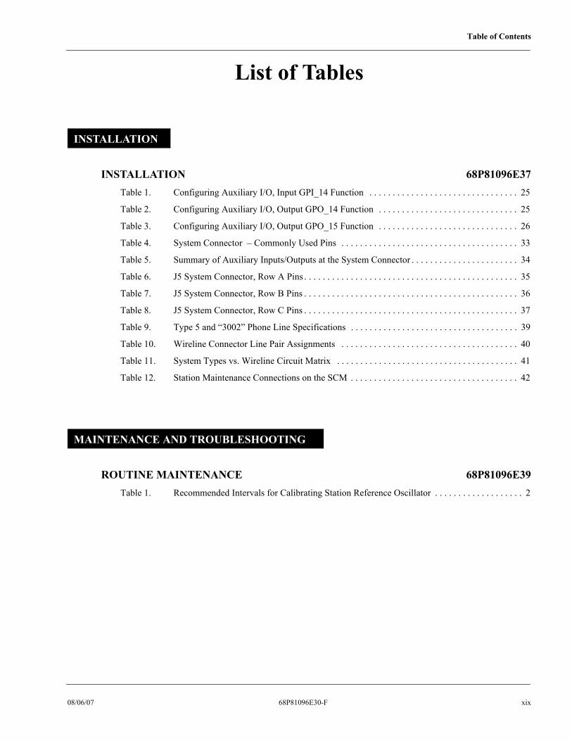
Table of Contents
List of Tables
INSTALLATION 68P81096E37Table 1. Configuring Auxiliary I/O, Input GPI_14 Function . . . . . . . . . . . . . . . . . . . . . . . . . . . . . . . . 25
Table 2. Configuring Auxiliary I/O, Output GPO_14 Function . . . . . . . . . . . . . . . . . . . . . . . . . . . . . . 25
Table 3. Configuring Auxiliary I/O, Output GPO_15 Function . . . . . . . . . . . . . . . . . . . . . . . . . . . . . . 26
Table 4. System Connector – Commonly Used Pins . . . . . . . . . . . . . . . . . . . . . . . . . . . . . . . . . . . . . . 33
Table 5. Summary of Auxiliary Inputs/Outputs at the System Connector . . . . . . . . . . . . . . . . . . . . . . . 34
Table 6. J5 System Connector, Row A Pins . . . . . . . . . . . . . . . . . . . . . . . . . . . . . . . . . . . . . . . . . . . . . . 35
Table 7. J5 System Connector, Row B Pins . . . . . . . . . . . . . . . . . . . . . . . . . . . . . . . . . . . . . . . . . . . . . . 36
Table 8. J5 System Connector, Row C Pins . . . . . . . . . . . . . . . . . . . . . . . . . . . . . . . . . . . . . . . . . . . . . . 37
Table 9. Type 5 and “3002” Phone Line Specifications . . . . . . . . . . . . . . . . . . . . . . . . . . . . . . . . . . . . 39
Table 10. Wireline Connector Line Pair Assignments . . . . . . . . . . . . . . . . . . . . . . . . . . . . . . . . . . . . . . 40
Table 11. System Types vs. Wireline Circuit Matrix . . . . . . . . . . . . . . . . . . . . . . . . . . . . . . . . . . . . . . . 41
Table 12. Station Maintenance Connections on the SCM . . . . . . . . . . . . . . . . . . . . . . . . . . . . . . . . . . . . 42
ROUTINE MAINTENANCE 68P81096E39Table 1. Recommended Intervals for Calibrating Station Reference Oscillator . . . . . . . . . . . . . . . . . . . 2
INSTALLATION
MAINTENANCE AND TROUBLESHOOTING
08/06/07 68P81096E30-F xix

Table of Contents
AUXILIARY I/O BOARDModel CLN1206 68P81096E53
Table 1. General Purpose Inputs . . . . . . . . . . . . . . . . . . . . . . . . . . . . . . . . . . . . . . . . . . . . . . . . . . . . . . . . 4
Table 2. SPI Bus Input Circuitry Signals . . . . . . . . . . . . . . . . . . . . . . . . . . . . . . . . . . . . . . . . . . . . . . . . . 5
Table 3. Option Interrupt Request Signal . . . . . . . . . . . . . . . . . . . . . . . . . . . . . . . . . . . . . . . . . . . . . . . . . 5
Table 4. SPI Bus Output Circuitry Signals . . . . . . . . . . . . . . . . . . . . . . . . . . . . . . . . . . . . . . . . . . . . . . . . 7
Table 5. General Purpose Output Electrical Characteristics . . . . . . . . . . . . . . . . . . . . . . . . . . . . . . . . . . . 8
Table 6. Configuring Input GPI_14 Function . . . . . . . . . . . . . . . . . . . . . . . . . . . . . . . . . . . . . . . . . . . . . 10
Table 7. Configuring Output GPO_14 Function . . . . . . . . . . . . . . . . . . . . . . . . . . . . . . . . . . . . . . . . . . . 10
Table 8. Configuring Output GPO_15 Function . . . . . . . . . . . . . . . . . . . . . . . . . . . . . . . . . . . . . . . . . . . 10
STATION MODULES
AUXILIARY I/O CIRCUITRY
xx 68P81096E30-F 08/06/07

Table of Contents
BACKPLANE INTERCONNECT BOARDModel CLN1202 68P81096E46
Table 1. Assigned Connector Number Vs. Function/Location Information . . . . . . . . . . . . . . . . . . . . . . 4
Table 2. Backplane Signal Description . . . . . . . . . . . . . . . . . . . . . . . . . . . . . . . . . . . . . . . . . . . . . . . . . . 5
Table 3. J5 System Connector . . . . . . . . . . . . . . . . . . . . . . . . . . . . . . . . . . . . . . . . . . . . . . . . . . . . . . . 12
Table 4. J4 Wireline Connector . . . . . . . . . . . . . . . . . . . . . . . . . . . . . . . . . . . . . . . . . . . . . . . . . . . . . . 13
Table 5. J1 Option1 Connector . . . . . . . . . . . . . . . . . . . . . . . . . . . . . . . . . . . . . . . . . . . . . . . . . . . . . . . 14
Table 6. J2 Option2 Connector . . . . . . . . . . . . . . . . . . . . . . . . . . . . . . . . . . . . . . . . . . . . . . . . . . . . . . . 15
Table 7. J3 Controller Connector . . . . . . . . . . . . . . . . . . . . . . . . . . . . . . . . . . . . . . . . . . . . . . . . . . . . . 16
500 W POWER SUPPLY, AC with DC Backup ConnectorModels CLN1220 and DLN6458 68P81096E33
Table 1. CLN1220/DLN6458 Power Supply Module Performance Specifications . . . . . . . . . . . . . . . . 3
500 W POWER SUPPLY, AC with DC Backup ConnectorModels DLN6622 68P81011Y31
Table 1. DLN6622 Power Supply Module Performance Specifications . . . . . . . . . . . . . . . . . . . . . . . . . 2
250 W POWER SUPPLY, AC with DC Backup ConnectorModel CLN1221 68P81096E34
Table 1. CLN1221 Power Supply Module Performance Specifications . . . . . . . . . . . . . . . . . . . . . . . . . 2
250 W POWER SUPPLY, AC with DC Backup ConnectorModel DLN6624 68P81011Y29
Table 1. DLN6624 Power Supply Module Performance Specifications . . . . . . . . . . . . . . . . . . . . . . . . . 2
500 W POWER SUPPLY, DC-OnlyModel CLN1222 68P81096E51
Table 1. CLN1222 DC-Only Power Supply Module Performance Specifications . . . . . . . . . . . . . . . . . 2
250 W POWER SUPPLY, DC-OnlyModel CLN1223 68P81096E52
Table 1. CLN1223 DC-Only Power Supply Module Performance Specifications . . . . . . . . . . . . . . . . . 2
STATION BACKPLANE
POWER SUPPLIES
08/06/07 68P81096E30-F xxi

Table of Contents
ANTENNA RELAY MODULEModel CLN6680 68P81096E41
Table 1. Antenna Relay Option X371AG Complement . . . . . . . . . . . . . . . . . . . . . . . . . . . . . . . . . . . . . . 7
Table 2. Performance Specifications for Antenna Relay . . . . . . . . . . . . . . . . . . . . . . . . . . . . . . . . . . . . . 7
VHF EXTERNAL PRESELECTOR MODULEModels CLN1216 and CLN1217 68P81096E43
Table 1. VHF External Preselector Option Complement . . . . . . . . . . . . . . . . . . . . . . . . . . . . . . . . . . . . . 4
VHF EXTERNAL DOUBLE CIRCULATOR MODULEModels CLN1207, CLN1208 and CLN1209 68P81096E49
Table 1. VHF External Double Circulator Options Complement . . . . . . . . . . . . . . . . . . . . . . . . . . . . . . . 6
Table 2. Performance Specifications for VHF External Double Circulator . . . . . . . . . . . . . . . . . . . . . . . 7
VHF DUPLEXER MODULEModels TYD4031, TYD4032, and TYD4033 68P81085E16
Table 1. Performance Specifications for VHF Duplexer Module . . . . . . . . . . . . . . . . . . . . . . . . . . . . . . . 7
ANCILLARY EQUIPMENT
xxii 68P81096E30-F 08/06/07

MODEL AND OPTION SELECTION PROCEDURE(INCLUDES MODEL/OPTION COMPLEMENTS)
The following equipment ordering process is used by the sales representative to equip a VHF station with the proper hardware and firmware for specific system types and customer-defined options and features. This process is described here, showing the structure and contents of the various models and options.
The Factory ID Model numbers are:
Option numbers are used to determine the configuration of an MTR2000 station. The suffixes of these option numbers (i.e., the last 2 characters) may change.
The sales model includes the following items which are common to all stations:
• Station Control Module.
• Backplane Interconnect Board.
• Backplane hardware.
• Station chassis hardware.
• Front panel.
• Cables.
For Receivers, the sales model determines that the:
• 250W Power Supply module is included in the station, Option X30AM.
MTR2000… Factory ID Model No. Station Description
Base Stations or Repeaters T5544, T5766 MTR2000 Station
Receivers T5731, T5769 MTR2000 Receiver
1
Note
08/06/07 68P81096E30-F xxiii
If the station is a Base Station or a Repeater, the power/frequency option is now selected. The power/frequency option is determined based on the power specified by the customer. The following table shows the available pow-er/frequency options:
For Base Stations and Repeaters, the power/frequency option determines which:• Power Supply module (based on power level) is included in the station; either Option X30AM for the 250W
power supply, or X30AL for the 500W power supply.• Power Amplifier module (based on frequency band and power level) is included in the station. • Exciter module (based on frequency band) is included in the station. • Receiver module (based on frequency band) is included in the station; Option X333AE.
OR
If the station is a Receiver, the frequency option is now selected. The frequency option is determined based on the frequency specified by the customer. The following table shows the available frequency options:
The frequency option determines which:• Receiver module (based on frequency band) is included in the station; Option X333AE.
A System Software Option must be selected for Base Stations, Repeaters and Receivers as follows:
If the station is a Receiver, go to step 5.
For Trunking Analog Operation the software option determines that the Auxiliary I.O Board is included in the station; Option X151AH.
Output Power
Frequency Range – VHF 30 W 40 W 100 W
132 to 154 MHz – – Option X530AC
132 to 174 MHz Option X345AA Option X330AD –
150 to 174 MHz – – Option X530AD
Frequency Range – VHF Receiver Option
132 to 174 MHz Option X319AC
System Type Software Option
Conventional Analog Operation X597AF
Conventional Analog RECEIVER X597AG
6809 Trunking Analog Operation X997AE
6809 Trunking Analog Receiver X997AF
2
3
xxiv 68P81096E30-F 08/06/07

A Station Operation Option must be selected as follows:
The following lists available options that may be selected in addition to the standard model and options (described in steps 1 through 4).
Operation Type Operation Option
Repeater Operation X580AC
Base Station Operation X622AC
AVAILABLE OPTIONS FOR VHF STATIONS
Option Category Option and Complement
DC-Only Power Supplies
X121AC
CPN6059ACPN6060A
500W DC-Only power supply.When this option is ordered, it automatically replaces Option X30AL.
500W DC Power SupplyDC Power Input Cable
X121AB
CPN6058ACPN6060A
250W DC-Only power supply.When this option is ordered, it automatically replaces Option X30AM.
250W DC Power SupplyDC Power Input Cable
Mounting Racks
X741AFTHN6752ACLN6679A
X742AFTHN6753ACLN6679A
X743AFTHN6754ACLN6679A
76.2cm (30 in) Modular RackModular Rack, 16-Rack UnitRack Mounting Hardware
1.143m (45 in) Modular RackModular Rack, 24-Rack UnitRack Mounting Hardware
1.32m (52in) Modular RackModular Rack, 27-Rack UnitRack Mounting Hardware
Slide Rail (for rackmounted station)
X968AATHN6788A
X346ABCLN6833A
Slides, Motorola CabinetSlide rails for mounting station
Slides, Non-Motorola CabinetUniversal slide rails for mounting station
Indoor Cabinets
X52AFTHN6701ATTN5040A
X308ADTHN6702ATTN5040A
X180ACTHN6703ATTN5040A
76.2cm (30 in) Indoor Cabinet30″ Indoor Cabinet, 2 RailsGrommet Channel Kit
1.168m (46 in) Indoor Cabinet46″ Indoor Cabinet, 2 RailsGrommet Channel Kit
1.524m (60in) Indoor Cabinet60″ Indoor Cabinet, 2 RailsGrommet Channel Kit
4
5
08/06/07 68P81096E30-F xxv

Duplexer ModuleTYD4031ATYD4032ATYD4033A
RF Duplexer (132 to 146MHz)RF Duplexer (144 to 160MHz)RF Duplexer (158 to 174MHz)
External Preselector
X265AATRN7799A
X265ABTRN7799A
External Preselector Module (132 to 154 MHz)VHF/UHF Tuning Kit
External Preselector Module (150 to 174 MHz)VHF/UHF Tuning Kit
When either of the above options is ordered, Receiver Option X333AE is auto-matically replaced by Option X333AF
Wireline Interface Board (WIB)
X216ACTTN5066A
Add 4-Wire Euro Wireline Interface Board (WIB)4-Wire Euro Wireline Interface Board
X264AA
TTN5067A
Add 4-Wire Wireline Interface Board (WIB)This WIB is the factory default, unless X216AC is ordered.
4-Wire Wireline Interface Board
External Double Circulator
X676ASTYD4001ATYD4010ATRN7751ATKN9133ATLN3391A
External Double Circulator Module (132 to 146 MHz)Double Circulator (132 to 146 MHz)Low Pass FilterPeripheral TrayCables, Peripheral TrayCirculator Load (heat sink)
X676ATTYD4002ATYD4010ATRN7751ATKN9133ATLN3391A
External Double Circulator Module (144 to 160 MHz)Double Circulator (144 to 160 MHz)Low Pass FilterPeripheral TrayCables, Peripheral TrayCirculator Load (heat sink)
X676AUTYD4003ATYD4010ATRN7751ATKN9133ATLN3391A
External Double Circulator Module (158 to 174 MHz)Double Circulator (158 to 174 MHz)Low Pass FilterPeripheral TrayCables, Peripheral TrayCirculator Load (heat sink)
Antenna Relay X371AGCLN6680A
Antenna RelayAntenna Relay
External Reference X747ABCKN6682A
Add External ReferenceExternal Reference Cable
Trunking Cables
3083765X043083765X053083765X063083765X07
7.62m (25ft) Trunk Cable15.24m (50ft) Trunk Cable22.86m (75ft) Trunk Cable30.48m (100ft) Trunk Cable
MiscellaneousHSN10000185180U01GMN6147
External SpeakerExternal Speaker CableService Microphone
AVAILABLE OPTIONS FOR VHF STATIONS
Option Category Option and Complement
xxvi 68P81096E30-F 08/06/07

FOREWORD
Product Maintenance Philosophy
Due to the high percentage of surface-mount components and multi-layer circuit boards, the maintenance philosophy for this product is one of Field Replaceable Unit (FRU) substitution. The station is comprised of self-contained modules (FRUs) which, when determined to be faulty, may be quickly and easily re-placed with a known good module to bring the equipment back to normal oper-ation. The faulty module must then be shipped to the Motorola System Support Center for further troubleshooting and repair to the component level.
The System Support Center can be contacted at:
For other issues call:
(800) 448-3245
or
(847) 576-7300
Scope of Manual
This manual is intended for use by experienced technicians familiar with similar types of equipment. In keeping with the maintenance philosophy of Field Re-placeable Units (FRU), this manual contains functional information sufficient to give service personnel an operational understanding of all FRU modules, allow-ing faulty FRU modules to be identified and replaced with known good FRU re-placements.
The information in this manual is current as of the printing date. Changes which occur after the printing date are incorporated by Instruction Manual Revisions (SMR). These SMRs are added to the manuals as the engineering changes are incorporated into the equipment.
Address Phone No. FAX No.
Motorola Systems Support Center1311 East Algonquin Rd.Schaumburg Il, 60196, USA
(800) 925-0911 (847) 576-2172
08/06/07 68P81096E30-F xxvii

Documentation Conventions
Documentation conventions are used in this manual to highlight certain infor-mation.
The area to the left of the text column contains key words and graphic symbols which allow the reader to quickly identify desired information.
The following text highlight symbols are used:
A note symbol indicates important information that helps improve the described function.
A caution symbol indicates a potential problem, unless the proper actions are taken. A caution also explains how to avoid the problem.
A WARNING symbol indicates the potential for personal injury or serious system degradation unless the proper actions are taken. A WARNING also explains how to avoid the problem.
An IMPORTANT symbol indicates the potential for damaging the station unless the proper actions are taken. An IMPORTANT note also explains how to avoid the problem.
This graphic symbol appears in this manual and on the station front panel (and other station surfaces) as a reminder that the station can become ex-tremely hot during normal station operation. Turn off all power to the sta-tion, and wait until sufficiently cool before touching the station.
Note
CAUTION!
STOP
WARNING
STOP
IMPORTANT
xxviii 68P81096E30-F 08/06/07
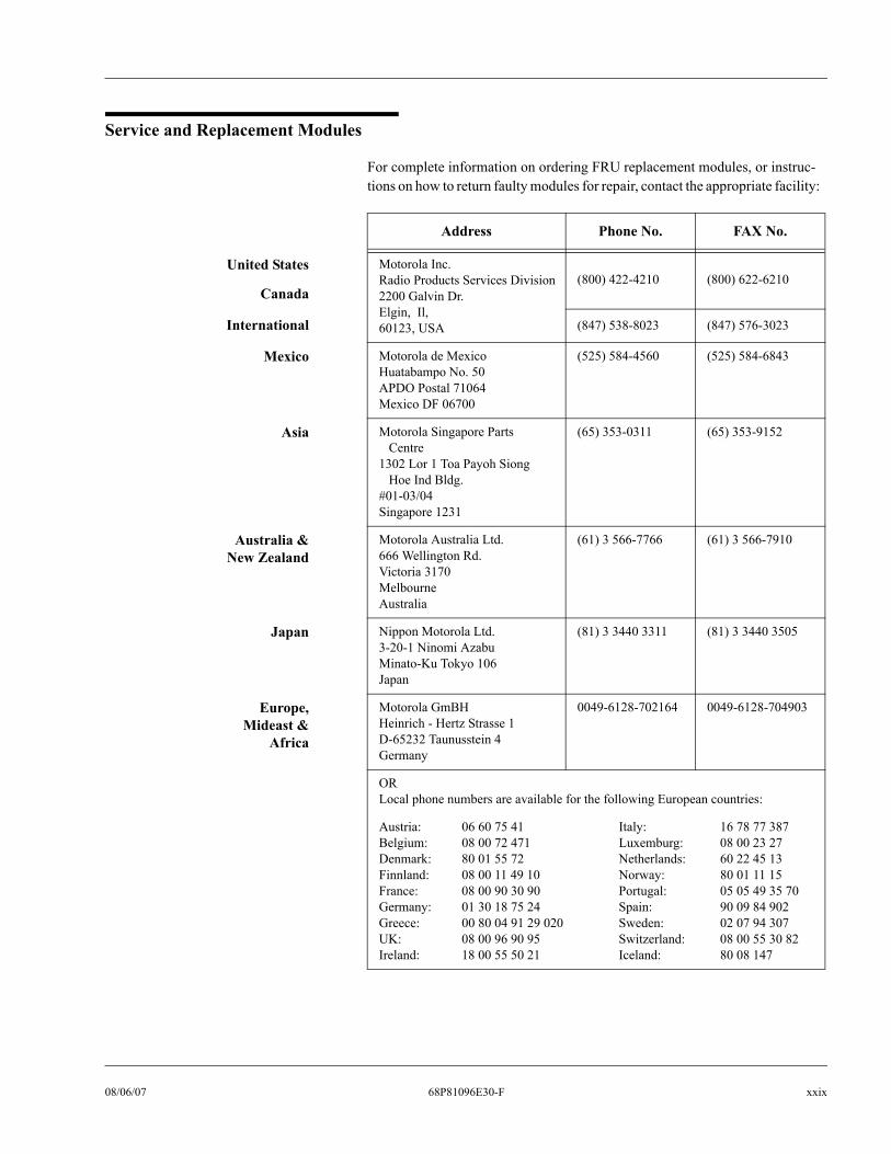
Service and Replacement Modules
For complete information on ordering FRU replacement modules, or instruc-tions on how to return faulty modules for repair, contact the appropriate facility:
Address Phone No. FAX No.
United States Motorola Inc.Radio Products Services Division2200 Galvin Dr.Elgin, Il, 60123, USA
(800) 422-4210 (800) 622-6210Canada
International (847) 538-8023 (847) 576-3023
Mexico Motorola de MexicoHuatabampo No. 50APDO Postal 71064Mexico DF 06700
(525) 584-4560 (525) 584-6843
Asia Motorola Singapore Parts Centre1302 Lor 1 Toa Payoh Siong Hoe Ind Bldg.#01-03/04Singapore 1231
(65) 353-0311 (65) 353-9152
Australia &New Zealand
Motorola Australia Ltd.666 Wellington Rd.Victoria 3170MelbourneAustralia
(61) 3 566-7766 (61) 3 566-7910
Japan Nippon Motorola Ltd.3-20-1 Ninomi AzabuMinato-Ku Tokyo 106 Japan
(81) 3 3440 3311 (81) 3 3440 3505
Europe,Mideast &
Africa
Motorola GmBHHeinrich - Hertz Strasse 1D-65232 Taunusstein 4Germany
0049-6128-702164 0049-6128-704903
ORLocal phone numbers are available for the following European countries:
Austria: 06 60 75 41 Italy: 16 78 77 387Belgium: 08 00 72 471 Luxemburg: 08 00 23 27Denmark: 80 01 55 72 Netherlands: 60 22 45 13Finnland: 08 00 11 49 10 Norway: 80 01 11 15France: 08 00 90 30 90 Portugal: 05 05 49 35 70Germany: 01 30 18 75 24 Spain: 90 09 84 902Greece: 00 80 04 91 29 020 Sweden: 02 07 94 307UK: 08 00 96 90 95 Switzerland: 08 00 55 30 82Ireland: 18 00 55 50 21 Iceland: 80 08 147
08/06/07 68P81096E30-F xxix

Station FRU Components
If help is required to identify a partnumber, call
(847) 538-0021
The following Field Replacement Units (FRUs) can be ordered for an MTR2000 VHF station::
Module Description FRU Kit #
Receiver Module (132 to 174 MHz)- with varactor preselector
CLN1211
Receiver Module (132 to 174 MHz- without varactor preselector
CLN1212
Exciter Module (132 to 174 MHz) CLN1233
Station Control Module CLN1465
Power Amplifier (30 W, 132 to 174 MHz) CLN1227
Power Amplifier (40 W, 132 to 174 MHz) CLN1226
Power Amplifier (100 W, 132 to 154 MHz) CLN1224
Power Amplifier (100 W, 150 to 174 MHz) CLN1225
Station Backplane Board CLN1202Power Supply (250 W), AC with DC Battery Connect- provided with all low power stations using AC input.
CLN1221
Power Supply (500 W), AC with DC Battery Connect- provided with high power stations installed outside of the European
Union (EU) countries and installed in EU countries prior to January 1, 2001.
CLN1220
Power Supply (500 W), AC with DC Battery Connect- provided with high power stations installed in EU countries after
January 1, 2001.- operates in conjuction with a Power Factor Correction choke.
DLN6458
Power Supply (250 W), DC-Only CLN1223
Power Supply (500 W), DC-Only CLN1222
4-Wire Wireline Interface Board CLN1203
4-Wire Euro Wireline Interface Board CLN1204
8-Wire Wireline Interface Board CLN1205
Auxiliary I/O Board CLN1206
Antenna Relay CLN6680
External (metal) Preselector (132 to 154 MHz) CLN1216
External (metal) Preselector (150 to 174 MHz) CLN1217
External Double Circulator (132 to 146 MHz) CLN1207
External Double Circulator (144 to 160 MHz) CLN1208
External Double Circulator (158 to 174 MHz) CLN1209
Duplexer Module (132 to 146 MHz) TYD4031
Duplexer Module (144 to 160 MHz) TYD4032
Duplexer Module (158 to 174 MHz) TYD4033
Zetron Repeater Panel TDN9946
xxx 68P81096E30-F 08/06/07

GENERAL SAFETY INFORMATION
The United States Department of Labor, through the provisions of the Occupational Safety and Health Act of 1970 (OSHA), has established an electromagnetic energy safety standard which applies to the use of this equipment. Proper use of this radio will result in exposure below the OSHA limit. The following precautions are recommended:
• DO NOT operate the transmitter of a mobile radio when someone outside the vehicle is within two feet (0.6 meter) of the antenna.
• DO NOT operate the transmitter of a fixed radio (base station, microwave and rural telephone RF equipment) or marine radio when someone is within two feet (0.6 meter) of the antenna.
• DO NOT operate the transmitter of any radio unless all RF connectors are secure and any open connectors are properly terminated.
In addition:
• DO NOT operate this equipment near electrical blasting caps or in an explosive atmosphere.
• All equipment must be properly grounded according to Motorola installation instructions for safe operation.
• All equipment should be serviced only by a qualified technician.
• An operating license may be required to operate this station.
Refer to the appropriate section of the product service manual for additional pertinent safety information.
Some station components can become extremely hot during station opera-tion. Turn off all power to the station, and wait until sufficiently cool before touching the station.
CAUTION
08/06/07 68P81096E30-F xxxi

PERFORMANCE SPECIFICATIONS
General
Frequency Range: 132 to 174 MHzNumber of Channels: 32Frequency Generation: SynthesizedPower Supply Type: SwitchingPower Supply Input Voltage: 85 to 264Vac (for Models CLN1220 and CLN1221)
180 to 264Vac (for Model DLN6458; used in conjunction with a PFC choke)
Power Supply Input Frequency: 47 to 63HzCurrent Consumption (typical):
Low Power station
High Power station
DC 120Vac 240VacStandby 1.5A 0.5 A 0.3ATransmit 9.5A 2.3 A 1.25AStandby 0.85A 0.6A 0.4ATransmit 10.0 A 4.45A 2.45A
Note: DC voltage is 14Vdc for low power stations and 28Vdc for high power stations. Current consumption values during transmit are at full rated output.
Temperature Range (ambient): –30°C (–22°F) to +60°C (+140°F), measured at station
Dimensions: 48.3 cm (19") x 41.3 cm (16.5") x 13.4 cm (5.25")Approximate Weight: 19 kg. (40 lbs.)Environmental Spec. I.P. 20
Transmitter
Power Output: 1 to 30 W1 to 40 W25 to 100 W
Electronic Bandwidth ≤ 40W: 132 to 174 MHzElectronic Bandwidth > 40W: 132 to 154 MHz, 150 to 174 MHzIntermodulation: 40 dB (40 W and 100 W)
70 dB (30 W)Spurious and Harmonic Emissions: –85 dBcDeviation: ±5 kHz (30 kHz)
±5 kHz (25 kHz)±4 kHz (20 kHz)±2.5 kHz (12.5 kHz)
Audio Sensitivity: –20 dBm to 0 dBm (variable)
xxxii 68P81096E30-F 08/06/07

PERFORMANCE SPECIFICATIONS (Continued)
Due to Motorola’s commitment to quality, all specifications subject to change without notice.
Transmitter (continued)
Audio Response: +1, –3 dB from 6 dB per octave pre-emphasis; 300 to 3000 Hz referenced to 1000 Hz at line input
Audio Distortion: <3% @ 1000 Hz; 60%RSDFM Hum and Noise: 50 dB nominal (30 kHz)
50 dB nominal (25 kHz)45 dB nominal (12.5 kHz)
Frequency Stability: 1.5 ppm
Receiver
Electronic Bandwidth w/o Narrow Preselector:
132 to 174 MHz
Narrow Preselector Bandwidth: 4 MHzChannel Spacing: 12.5 kHz, 20 kHz, 25 kHz, 30 kHzSensitivity (12 dB SINAD) 0.35 μV Selectivity: 80 dB (25 kHz, 30 kHz)
75 dB (12.5 kHz)Intermodulation: 85 dB (25 kHz, 30 kHz)
80 dB (12.5 kHz)Spurious and Image Rejection: 90 dB with external Preselector,
85 dB nominal with internal PreselectorOff Channel Acceptance: 2 kHzFM Hum and Noise: 50 dB nominal (25 kHz, 30 kHz)
45 dB nominal (12.5 kHz)Wireline Output: -20 dBm to 7 dBm @ 100% RSD, 1 kHzAudio Response (@ Wireline output): +1, –3 dB from 6 dB per octave de-emphasis; 300 to 3000 Hz referenced to
1000 Hz outputAudio Distortion: <3 % @ 1000 Hz; 60 % RSDFrequency Stability: 1.5 ppm
08/06/07 68P81096E30-F xxxiii

GLOSSARY OF TERMS AND ACRONYMS
AAGC Automatic Gain Control
Alert tone Audio signal produced by the station, providing feedback to the user.
ASIC Application Specific Integrated Circuit
AUX Auxiliary.
CCCI Control Channel Indicate
CDCSS Continuous Digital-Controlled Squelch Systems (DPL)
CTCSS Continuous Tone-Controlled Squelch Systems (PL)
CIT Central Interconnect Terminal. Used to provide telephone interconnect capabil-ity in a trunked station.
CIU Console Interface Unit. Interface between operator console and station to pro-vide encryption/decryption functions.
Clear Channel modulation type in which voice information is transmitted over the channel using analog modulation.
Code detect Traditional term used to indicate that a 12kbps CVSD signal is being received on the RF channel.
Conventional Term used for standard non-trunked radio system (usually using TRC/DC con-sole).
CPI Console Priority Interface - option allowing console control of a trunked station.
xxxiv 68P81096E30-F 08/06/07

DDDM Dual Device Module
DPL Digital Private Line (See PL)
DSP Digital Signal Processor, microprocessor specifically designed to perform digi-tal signal processing algorithms.
DVP Digital Voice Protection, or Digital Voice Privacy, applies to the Vulcan encryp-tion algorithm and the Motorola product in which it is sold.
EEIA Electronic Industries Association
E/M Telephone circuit signalling lines (Ear/Mouth, Ernie/Mary)
EOM End-Of-Message, 6 kHz signal transmitted at the end of a 12 kbps CVSD signal that is used by the receiving unit for fast muting of the speaker audio for squelch tail elimination.
ESD Electro Static Discharge
ETS European Telecommunications Standards
EU European Union
08/06/07 68P81096E30-F xxxv
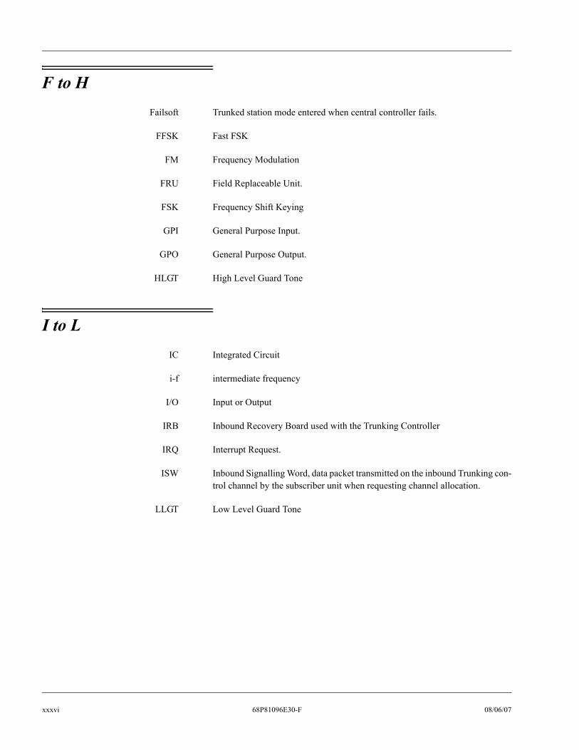
F to HFailsoft Trunked station mode entered when central controller fails.
FFSK Fast FSK
FM Frequency Modulation
FRU Field Replaceable Unit.
FSK Frequency Shift Keying
GPI General Purpose Input.
GPO General Purpose Output.
HLGT High Level Guard Tone
I to LIC Integrated Circuit
i-f intermediate frequency
I/O Input or Output
IRB Inbound Recovery Board used with the Trunking Controller
IRQ Interrupt Request.
ISW Inbound Signalling Word, data packet transmitted on the inbound Trunking con-trol channel by the subscriber unit when requesting channel allocation.
LLGT Low Level Guard Tone
xxxvi 68P81096E30-F 08/06/07

M to OMAN_CS Manual Channel Select.
MDC Motorola Data Communications. 1200 or 4800 baud data signalling scheme.
MISO Master In, Slave Out.
MON Monitor.
MOSI Master Out, Slave In.
MRTI Microprocessor Radio-Telephone Interconnect; a Motorola system that pro-vides a repeater connection to the telephone network (The MRTI allows the ra-dio to access the telephone network when the proper access code is received).
MSK Minimum Shift Keying
OSW Outbound Signalling Word, data packet transmitted on the outbound Trunking control channel by the central controller that contains call assignment informa-tion for the subscriber.
08/06/07 68P81096E30-F xxxvii

PPA Power Amplifier that transmits final RF signal to transmit antenna
PFC Power Factor Correction
PL Private-Line tone squelch; a continuous subaudible tone that is transmitted along with the carrier (A radio that has PL on the receive frequency will require both the presence of carrier and the correct PL tone before it will unmute). Also, if there is PL on the transmit frequency, all transmissions by the radio will be modulated with the PL tone. Modulation will be continuous.
PLL Phase locked loop; a circuit in which an oscillator is kept in phase with a refer-ence, usually after passing through a frequency divider.
PSTN Public Switched Telephone Network
PTT Push-to-talk; the switch located on the left side of the radio which, when pressed causes the radio to transmit.
RRA/RT Remote Access/Remote Transmit
RAC Repeater Access Control
RdStat Receiver Data Status
Repeater Remote transmit/receive facility that retransmits received signals in order to im-prove communications range and coverage.
RF Radio Frequency
RSS Radio Service Software; the software application used to program and service the station.
RSSI Received Signal Strength Indicator; a dc voltage proportional to the received RF signal strength.
xxxviii 68P81096E30-F 08/06/07

SSCM Station Control Module; station controller.
SINAD Acronym for the ratio of signal plus noise plus distortion and noise plus distor-tion.
SMR Schaumburg Manual Revision
Smart Repeater Trunking system in which channel control is distributed among several repeat-ers.
Spectra-TAC Analog Total Area Coverage voting comparator used to select wide area receiv-ers.
SPI Serial Peripheral Interface (clock and data lines); simple synchronous serial in-terface for data transfer between processors and peripheral ICs.
Squelch Automatic receiver quieting accomplished by muting audio circuits when re-ceived signal levels fall below a pre-determined value.
SRAM Static RAM, memory chip used for scratchpad memory.
TTCC Trunking Central Controller; main control unit of the trunked dispatch system;
handles ISW and OSW messages to and from radios in the field (See ISW and OSW).
TOC Turn Off Code; alternating binary pattern used by DPL signalling to provide fast muting of the receiving radio.
TRC Tone Remote Control
Trunking Radio control system which permits efficient frequency utilization and en-hanced control features.
Type II Trunking Motorola trunking system which provides extended features.
08/06/07 68P81096E30-F xxxix

U, VUHF Ultra High Frequency
VHF Very High Frequency
VCO Voltage-Controlled Oscillator; an oscillator whereby the frequency of oscilla-tion can be varied by changing a control voltage.
VOX Voice Operated Switch; Used with MRTI.
VSWR Voltage Standing Wave Ratio.
W to ZWCI Wildcard Input
WCO Wildcard Output
WFI Word Frame Interrupt; used to synchronize trunking data messages in a Smart Repeater system.
Wide Area Wide area systems allow expanded radio coverage by using multiple receivers and/or transmitters.
WL Wireline
WL Rx Wireline Receive; information from station rf receiver sent to wireline equip-ment.
WL Tx Wireline Transmit; information from wireline equipment sent to station rf trans-mitter.
xl 68P81096E30-F 08/06/07

DESCRIPTION
The Motorola MTR2000 Base Station/Repeater provides analog conventional and trunking capabilities in a reliable, software-controlled design. An innovative modular design and microprocessor-controlled Station Control Module (SCM) allows for superior station flexibility and simplified system upgrades.
All of the features described in this manual may not be currently supported. Refer to the “Summary of Operating Features” section for a list of standard features, optional features, and planned future features.
Flexible Mechanical Design
All elements of the station are designed for EIA 48.3cm (19") rack mounting, allowing the equipment to be mounted in standard telephone-style equipment racks, or various sizes of Motorola cabinets. Figure 1 shows a typical 40W station.
1 INTRODUCTION
Note
Figure 1. MTR2000 Station
68P81096E36-H06/28/05-UP
Motorola Inc., 2005All Rights ReservedPrinted in U.S.A.
1301 E. Algonquin Road, Schaumburg, IL 60196Government & Enterprise Mobility Solutions

Description
Electrical Design
Transmitter Circuitry
The station transmitter circuitry is designed for continuous duty operation and may be oper-ated at full rated power. Output power is continually monitored by an internal directional cou-pler. The forward power voltage from the coupler feeds a power control loop which continually adjusts and maintains the desired output power. All adjustments are electronic, including deviation and output power.
Receiver Circuitry
The station receiver circuitry features multiple bandwidth (12.5kHz, 20kHz, 25kHz, and 30kHz) capability. Injection signals for the first and second mixers are generated by frequen-cy synthesizer circuitry electronically controlled by the Station Control Module. All receive signals (analog) are detected and digitized before being sent to the Station Control Module, providing improved, consistent audio quality throughout the coverage area.
Station Control Module
The Station Control Module is microprocessor-based and features extensive use of ASIC and digital signal processing technology. The module serves as the main controller for the station, providing signal processing and operational control for the station modules.
Wireline Circuitry
The station wireline circuitry options provide a wide variety of telephone interfaces and con-trol mechanisms such as Tone Control. Telephone line connections are easily made to the wireline circuitry via connectors on the rear of the station.
Trunking Capability
When equipped for trunking capability, the station can operate in Motorola's Smartnet™ or the most advanced wide-area trunking system – SmartZone. The station can operate as a re-mote voice channel or control channel repeater. The station interfaces to a Trunking Central Controller (TCC) which provides the call processing and channel assignment tasks.
2 68P81096E36-H06/28/05

Description
Summary of Operating Features
Standard Features
The following are a few of the standard features:• FRU maintenance philosophy (reducing down time). • Easily programmed via Radio Service Software (RSS). • Extensive Self-Test Diagnostics and Alarm Reporting through RSS. • Expansion and upgrades performed by module replacement. • Highly reliable and accurate continuous duty transmitter circuitry. • Compatible (with appropriate options) with conventional analog signaling. • Wide operating temperature range: -30°C to +60°C (-22°F to +140°F). • Battery Backup Connector – allows connection to battery backup system which auto-
matically reverts to battery backup operation in the event of ac power failure. • RA/RT• Wide voltage supply range (AC or DC), with no setup configuration.
Optional Features
The following are some of the leading optional features for the station:• Double Circulator Option – provides additional isolation and intermodulation protection
for rf-congested transmitter sites (not available on 350MHz stations). • Microprocessor Radio Telephone Interconnect (MRTI) – allows connection of conven-
tional station to the telephone network. • Trunking – allows trunking repeater to operate as part of a Smartnet or SmartZone sys-
tem; through Auxiliary I/O board (CLN1206).• Wildcard Input/Output; through Auxiliary I/O board (CLN1206).• Main Standby; through Auxiliary I/O board (CLN1206).• Multi-coded Squelch Interface; through Zetron Model 38 Repeater Panel.• Console Priority Interface; through 8-Wire Wireline Interface Board (CLN1205).• Auxiliary Input/Output for conventional operation; through Auxiliary I/O board
(CLN1206).
Features Not Offered
Please disregard any references to the following items since they are not available for the MTR2000:• DC Remote control for the 4-wire Wireline Interface Board, CLN1203.• Second Receiver configuration of the MTR2000.
68P81096E36-H 306/28/05

Description
Figure 2 shows the modules and components that comprise a station.
2 STATION COMPONENTS
Figure 2. MTR2000 Station Components
Power SupplyModule
Bottom Plate
Exciter Module
Receiver Module
Station Control Module
Power Amplifier Module
Front Cover
NOTE: Fans and fan covers are only used on high power Power Amplifier modules and Power Supplies.
Backplane
NOTE: Fans and fan covers are only used on high power Power Amplifier modules and Power Supplies.
Fan Cover
Auxiliary I/O Board
Top Plate
Fan
WirelineInterface Board
4 68P81096E36-H06/28/05

Description
The following functional theory of operation provides an overview of the station circuitry. For a more thorough functional description of a particular module, refer to the STATION MODULES section of the appropriate band-specific Instruction Manual. The block diagram in Figure 3 supports the following functional theory of operation.
Transmitter Circuitry Operation
Introduction
The Transmitter Circuitry comprises two modules, the Exciter Module and the Power Ampli-fier (PA) Module. These modules combine to generate, modulate, and amplify the rf signal which is transmitted via the site transmit antenna. Modulation sensitivity and power output are adjusted electronically for each channel (through the Radio Service Software), under the direct control of the Station Control Module (SCM).
Exciter Module Operation
The Exciter Module, which interfaces directly to the SCM, generates a modulated rf signal at the desired transmit frequency and sends this signal to the PA for amplification. The circuitry operates as follows.
The transmit synthesizer and VCO (voltage-controlled oscillator) circuitry on the Exciter Module accept frequency programming data from the SCM (via the SPI bus) and generate an rf carrier at the specified frequency. The VCO is directly modulated by transmit audio/data from the SCM. The resulting modulated rf signal (at a level of approximately +12 dBm) is then fed to the PA.
Power Amplifier Module Operation
The PA modules are designed for continuous-duty operation across all bands and power lev-els. The actual circuit stages employed in a PA depend on the specific frequency band, power output level and intermodulation requirements. All PA modules contain an Intermediate Pow-er Amplifier (IPA) at the input, a low-pass filter/directional coupler at the output, and diag-nostic and power control circuitry.
High power (100 W) PA modules employ a single internal circulator to protect the PA from transmitter intermodulation and antenna mismatch (VSWR). The low power 30 W PA mod-ule employs two internal circulators. All PA stages and circulators are broad-band devices and require no tuning to operate at the station site.
The modulated rf signal from the Exciter Module is input to the IPA in the PA Module, and amplified to within a range of 0 to 10 W (depending on power control signals from the SCM). In PA Modules operating below 600MHz, the rf signal is fed to either a Butterfly Module (30W/40W PA models) or a Dual Device Module (DDM – 100 W PA models). In PA Mod-ules operating above 600 MHz, a 15 W driver is introduced between the Pre-driver stage and the Final Module. The gain of the Pre-driver stage is controlled by a power control voltage
3 FUNCTIONAL THEORY OF OPERATION
68P81096E36-H 506/28/05
Description
which is derived from power control signals (from the SCM) and high VSWR/thermal pro-tection circuitry on the PA output board.
A combination of hardware and software controls are used to regulate the power output level. To set the power and current limits, the SCM provides software control through a D/A con-verter connected to the SPI bus. This control relies on various monitored PA signals which are fed back to the SCM via an A/D converter (also connected to the SPI bus).
The directional coupler is essentially a calibrated wattmeter which feeds a dc voltage propor-tional to the output power to the power control circuitry to serve as the feedback signal in the power control loop. Under normal operating conditions, the power control circuitry compares this dc voltage from the directional coupler to a reference voltage from the D/A converter which represents the desired output power. Based on the comparison, a power control voltage is generated to control the output power from the PA Module.
The modulated rf signal is amplified by the Driver/Final Module and is output to the site trans-mit antenna via a circulator and a harmonic filter/coupler. During excessive output VSWR, the ratio of the forward and reflected voltages from the directional coupler may be used to re-duce, or turn off, the transmitter power. Additional circuitry is also provided to reduce output power during excessive current drain and high temperature conditions, and to control the fan used in high power PA Modules.
6 68P81096E36-H06/28/05

Description
Receiver Circuitry Operation
Introduction
The Receiver Circuitry accepts receive rf signals from the site receive antenna, performs fil-tering and dual conversion, and outputs a digitized receive signal to the Station Control Mod-ule. The receiver module utilized may have either an internal varactor-tuned preselector filter, or an external metal preselector filter.
Receiver Module Operation
The receive signal is input from the site receive antenna to the receiver module, or to an ex-ternal preselector filter (a separate assembly attached to the rear of the station which provides highly selective bandpass filtering). The signal is fed through a low-pass filter, varactor-tuned preselector (if external preselector is not used), rf amplifier and image filter to the rf input of the first mixer. The filtered signal is mixed with an injection signal generated by the receive synthesizer/VCO, resulting in a first i-f (intermediate frequency) signal. The injection signal frequency is determined by frequency programming data from the Station Control Module via the SPI bus. The specific frequency of the first i-f depends on the frequency band of the sta-tion.
The first i-f signal is filtered and input to a custom receiver IC. This component contains circuitry for generating the second injection signal, mixing down the first i-f to 450 KHz, amplification and A/D (analog-to-digital) conversion of the second i-f signal, resulting in a digitized receive signal. This signal is fed as differential data to the Station Control Module.
68P81096E36-H 706/28/05

Description
Station Control Module Operation
Introduction
The Station Control Module (SCM) is the microprocessor-based controller for the station. Major components include an MC68356 microprocessor, which combines a 68302 Integrated Multiprotocol Processor (IMP) with a 56002 Digital Signal Processor (DSP), a DSP ASIC de-vice, and several Codec filter devices.
Station Control Module Operation
The MC68356 forms the heart of the SCM. The 68302 portion is the Host Microprocessor (µP), which serves as the controller for the SCM and operates from station software stored in FLASH memory. This software determines the system capabilities of the station. The Host µP communicates with the station modules and the SCM circuitry via address and data buses, three SCI (Serial Communication Interface) ports, and an SPI bus.
The DSP portion of the MC68356, with the support of the DSP ASIC, perform the necessary digital processing for the station audio and data signals. The DSP circuitry interfaces with the Receiver Module (receive audio), the Exciter Module (VCO modulation signal), the Wireline Interface Board (wireline audio), and external audio devices (microphone and speaker).
The 2.1 MHz Reference Oscillator generates the reference signal used by the Receiver and Exciter Modules.
8 68P81096E36-H06/28/05
Description
Wireline Interface Board Operation
Introduction
The Wireline Interface Board (WIB) serves as the interface between the customer analog tele-phone lines and the serial data signals of the station. WIBs are offered to handle 2-wire, 4-wire and 8-wire configurations. In general, the WIB processes and routes all wireline audio signals between the station and the landline equipment (such as consoles, modems, etc.). Landline-to-station and station-to-landline audio signals are connected to the WIB via copper pairs at the rear of the station.
Wireline Interface Board Operation
The WIB contains a PCM Codec-filter device to perform the audio digitization and reconstruc-tion, as well as the band-limiting and smoothing required by PCM systems. Analog signals are routed as follows:
- Inbound analog signals are converted to digital signals and routed to the SCM as wire-line transmit data (WL TxD).
- Outbound PCM data signals are converted to analog signals and routed to the Line 2 out-put.
- A latch receives control signals from the SCM (via the SPI bus) to control the gating of the audio signals.
For a list of the actual features supported, refer to the “Summary of Operating Features” on page 3, or the MTR2000 System Planner.
Note
68P81096E36-H 906/28/05

Description
Auxiliary I/O Board Operation
Introduction
The Auxiliary I/O Board serves as the interface between the customer auxiliary equipment and the Station Control Module (SCM). In general, the Auxiliary I/O Board routes all auxil-iary equipment control signals between the SCM and the auxiliary equipment (e.g., a trunking controller).
Auxiliary I/O Board Operation
The Auxiliary I/O Board contains SPI Input Buffers and associated circuitry which provides an input signal path from auxiliary equipment to the station SCM.
The input circuitry supports 16 general purpose inputs:
- 14 are transistor buffered inputs; 16V maximum, 10kΩ.- 2 are opto isolated inputs; 60mA forward current, 3V dropout voltage, 2kV isolation.
The Auxiliary I/O Board contains SPI Output Latches and associated circuitry which provides an output signal path from the station SCM to auxiliary equipment.
The output circuitry supports 16 general purpose outputs:
- 14 are open collector transistor outputs; maximum 40V, 100mA sink current - 2 are dry contact outputs (relay); maximum 250V, 1A)
Not all inputs and outputs are supported, seeTable 4, on page 33 through Table 8, on page 37.
Note
10 68P81096E36-H06/28/05

Description
Power Supply Module Operation
Power Supply Modules are offered to handle:• ac or dc input power • low power (250 W) or high power (500 W) station requirements
A high power Power Supply Module (500 W) is used in a station with a high power Power Amplifier Module (e.g., rated at 100 W or 75 W output power).
A low power Power Supply Module (250 W) is used in a station with a low power Power Am-plifier Module (e.g., rated at 40 W output power), or if the station is configured as a Satellite Receiver.
ac Input Power The 250 W models generates the +5.1 V and +14.2 V operating voltages for the station mod-ules.
The 500 W models generates the +5.1 V, +14.2 V, and +28 V operating voltages for the sta-tion modules.
These modules have power factor correction and include a connection for battery backup.
Table 1. Power Supply Module Models
Model Supplied by Input Voltage Range Output Voltages Power Factor Correction
Stations with Low Power PA
DLN6624 ASTEC 85 to 264 Vac, 47 to 63 Hz +5.1 V and +14.2 V
Provided internally within power supply module.
Stations with High Power PA
DLN6622 ASTEC 85 to 264 Vac, 47 to 63 Hz+5.1 V, +14.2 V, and +28 V
Provided internally within power supply module.
68P81096E36-H 1106/28/05

Description
dc Input Power For dc-only operation the 250 W Power Supply Module (DLN6624) accepts a dc input (+10.8 to +16 Vdc). The output voltages are:- the input filtered voltage.- a regulated +5.1 Vdc.
For dc-only operation the 500 W Power Supply Module (DLN6622) accepts a dc input (+21 to +32 Vdc).
The output voltages are:- the input filtered voltage.- a regulated +5.1 Vdc.- a regulated +14.2 Vdc.
12 68P81096E36-H06/28/05

Description
THIS PAGE INTENTIONALLY LEFT BLANK
68P81096E36-H 1306/28/05

Description
14
E INTERFACE BOARD
2.1 MHz FERENCE CILLATOR
Fig
SPI BUS
RSSI CIRCUITRY
TRUNKING AUDIO
MRTI AUDIO
RECEIVER SIGNAL STRENGTH INDICATOR
(OPTION DEPENDENT)
AUXILIARY TX AUDIO
DISC AUDIO
MICROPHONE AUDIO
EXTERNAL SPEAKER
2.1 MHz REF
SPI BUS
LINERX
LINETX
WIRE VERSION SHOWN)OUTBOUND
WIRELINE AUDIO FROM
STATIONTO
LANDLINE
LINE 2 OUT
A
B
VCO & REF MOD AUDIO
SPI BUS
AUDIOPROCESSING/INTERFACE CIRCUITRY
CODEC #3(8 KHz PCM)
GENERAL PURPOSE
OUTPUTS TO AUXILIARY EQUIPMENT
GENERAL PURPOSE INPUTS
FROM AUXILIARY EQUIPMENT
AUXILIARY I / O BOARD
INPUT BUFFERS
OUTPUT LATCHES
I
I
68P81096E36-H06/28/05
RECEIVER MODULE
LOW PASS FILTER/PRESELECTOR/ IMAGE FILTER
1STMIXER
1ST I-F
CUSTOM RECEIVER
IC
HOST MEMORY
WIRELIN
REOS
RECEIVE ANTENNA
RF INPUT/OUTPUT CONNECTOR BRACKET
(REAR OF STATION)
BANDPASS FILTERING
1ST LO INPUT
ure 3. MTR2000 Station Functional Block Di-agram (Sheet 1 of 2)
(2ND INJECTION, AMPLIFICATION,
A/D CONVERSION)
DIFFERENTIAL DATA
2.1 MHz REF
STATION CONTROL MODULE
HOST ADDRESS BUS
HOST DATA BUS
PCM CODEC BUS
RSSI DATA
CURRENT-TO-VOLTAGE
CONVERTER
DSPASIC
EIA-232 INTERFACE
RSS TERMINAL(IBM-PC LAPTOP
TYPICAL)
SPI BUS
20 KHz CODEC BUS
24 KHz CODEC BUS
2.1 MHz REF
DSP MEMORY
DSP ADDRESS BUS
DSP DATA BUS
24 KHz CODEC BUS
DSP
HOSTMICROPROCESSOR
SSI
68356
SPI BUS
(4-LINE 1 ININBOUND
WIRELINE AUDIO FROM
LANDLINETO
STATION
PCM CODEC BUS
SYNTHESIZER/VCO
POWER SUPPLY MODULE
ACNPUT
TRANSFORMER and PFC REGULATOR
CIRCUITRY
+14.2 VDC
+5.1 VDC
+28.6 VDC(HIGH POWER
PA ONLY)
AC/DC POWER SUPPLY with DC Backup Connector
DCNPUT

Description
68P81096E36-H 1506/28/05
CIRCULATOR
50 OHMLOAD
15 WDRIVER
LOW-PASSFILTER/
DIRECTIONALCOUPLER
FINALMODULE
TRANSMIT ANTENNA
ER AMPLIFIER (800 & 900 MHz)
L Y
TWO CIRCULATORS
50 OHMLOAD
E50 W
BUTTERFLYMODULE
LOW-PASSFILTER/
DIRECTIONALCOUPLER
L Y
CIRCULATOR
50 OHMLOAD
E
LOW-PASSFILTER/
DIRECTIONALCOUPLER
DUALDEVICE
MODULE
ER AMPLIFIER (<600 MHz)
L Y
Figure 3. MTR2000 Station Functional Block Di-agram (Sheet 2 of 2)
50 OHMLOAD
OR OR
POWER AMPLIFIER
EXCITER MODULE
RF SWITCH CIRCUITRY
TX ENABLE
MODULATED RF2.1 MHz REF
A
B
SYNTHESIZER/VCO
SPI BUS
VCO & REF MOD AUDIO
FROMSTATION
CONTROLMODULE
MODULATED RF
1.5 WPRE-DRIVER
75 W POW
BSPI BUS POWER
CONTROCIRCUITR
15 WINTERMEDIAT
POWER AMP
BSPI BUS POWER
CONTROCIRCUITR
10 WINTERMEDIAT
POWER AMP
100 W POW
BSPI BUS POWER
CONTROCIRCUITR
30 W & 40 W
PA ENABLE

INSTALLATION
Proper installation ensures the best possible performance and reliability of the station equipment. Pre-installation planning is required. This includes considering the mounting location of the equipment in relation to input power, antennas, and tele-phone interfaces. Also to be considered are site environment conditions, the particular mounting method (several available), and required tools and equipment.
If this is the first time installing this type of equipment, it is highly recommended that the user read:
• this entire installation section before beginning the actual installation, and
• the Motorola Quality Standards Fixed Network Equipment Installation manual, R56 (68P81089E50); specifically refer to the information on ground connection for lightning protection.
Installation Overview
The following information is an overview for installing the station and ancillary equipment. Step-by-step procedures for each of the major installation tasks are then provided beginning in Section 2, Mechanical Installation.
• Plan the installation, paying particular attention to environmental conditions at the site, ventilation requirements, and grounding and lightning protection.
• Unpack and inspect the equipment
• Mechanically install the equipment at the site
• If a Wireline Interface Board or an Auxiliary I/O Board is included with the station, configure the board jumpers for required operation
• Make necessary electrical and cabling connections, including the following:- AC input cabling- Coaxial cables to transmit and receive antennas- Phone line connections- System cables
• Perform a post-installation functional checkout test of the equipment to ver-ify proper installation
1 PRE-INSTALLATION CONSIDERATIONS
68P81096E37-N06/28/05-UP
Motorola Inc., 2005All Rights ReservedPrinted in U.S.A.
1301 E. Algonquin Road, Schaumburg, IL 60196Government & Enterprise Mobility Solutions
Installation
• Proceed to the Optimization procedures to customize the station parameters per customer specifications (e.g., operating frequency, PL, codes, etc.)
Regulatory requirements may require the use of an optional high stability refer-ence for some modes of operation. It is recommended that the user check current local regulations prior to operation.
Environmental Conditions at Intended Installation Site
If the station is to be installed in an environment which is unusually dusty or dirty (and so does not meet the air quality requirements), the air used to cool the station modules must be treated using appropriate filtering devices. Dust or dirt accumulating on the internal circuit boards and modules is not easily removed, and can cause such malfunctions as overheating and intermittent electrical connections.
The station may be installed in any location suitable for electronic communica-tions equipment, provided that the environmental conditions do not exceed the equipment specifications for temperature, humidity, and air quality. These are:
Operating TemperatureRange
–30°C (–22°F) to +60°C (+140°F)This is the temperature measured in close proximity to the station. For example, if the station is mounted in a cabinet, the temperature within the cabinet would be measured.
Humidity Not to exceed 95% relative humidity @ 50°C (122°F).
Air Quality For equipment operating in an environmentally controlled environment with the station(s) rack mounted, the airborne particulates level must not exceed 25 µg/m3.
For equipment operating in an area which is not environmentally controlled (sta-tion(s) cabinet mounted), the airborne particulates level must not exceed 90 µg/m3.
Note
STOP
IMPORTANT
2 68P81096E37-N06/28/05

Installation
Equipment Ventilation
The high-power (100/75W) stations are equipped with cooling fans that are used to provided forced convection cooling.
When planning the installation, observe the following ventilation guidelines:
Mounting the MTR2000 ina Cabinet
• Customer-supplied cabinets must be equipped with ventilation slots or open-ings in the front (for air entry) and back or side panels (for air to exit). If sev-eral stations are installed in a single cabinet, be sure ventilation openings surround each station to allow for adequate cooling.
• All cabinets must have a least 15cm (6in) of open space between the air vents and any wall or other cabinets. This allows adequate air flow.
• When multiple cabinets (each equipped with several stations) are installed in an enclosed area, make sure the temperature within each cabinet does not ex-ceed the recommended / maximum operating temperature of +60°C (+140°F). It may be necessary to have air conditioning or other climate con-trol equipment installed to satisfy the environmental requirements.
High Power Stations: The mounting of only ONE STATION PER CABINET is recommended. More than one station per cabinet will result in degradation of thermal specifications at high ambient temperatures.
Low Power Stations: In order to maintain thermal specification of –30°C (–22°F) to +60°C (+140°F), the low power stations must be mounted in a cabi-net with additional cooling. A single low power station mounted in a cabinet without additional cooling, will operate at thermal specification performance of –30°C (–22°F) to +54°C (+129°F).
Appropriate precautions should be taken to ensure that station ambient tem-perature does not exceed +60°C (+140°F).
If multiple stations are required, AND THERMAL SPECIFICATION DEG-RADATION IS ACCEPTABLE, the following is recommended when no cab-inet fans are used. Up to three stations can be mounted in a 76.2cm (30in) or larger cabinet with two rack units of spacing between each station. This will result in thermal specification performance of –30°C (–22°F) to +40°C (+104°F).
Mounting the MTR2000 ina Rack
When mounting multiple stations in a rack, ensure that the minimum spacing between stations is:• 3 rack units (13.3cm or 5.25in) for VHF and UHF low power stations, and 350MHz stations.• 1 rack unit (4.4cm or 1.75in) for VHF and UHF high power stations, 800MHz stations, and 900MHz stations.This spacing needs to be complied with to ensure that the thermal rating of the station is not exceeded.
STOP
IMPORTANT
CAUTION!
68P81096E37-N 306/28/05
Installation
AC Input Power Requirements
The station is equipped with a switching power supply, this assembly operates from 85 Vac to 264 Vac at 47 to 63 Hz ac input power. A standard 3-prong line cord is supplied to connect the power supply to the ac source.
It is recommended that a standard 3-wire grounded electrical outlet be used as the ac source.
The ac socket-outlet must be installed near the equipment and must be easily accessible.
The outlet must be connected to an ac source capable of supplying a maximum of 1020 VA. For a nominal 110/120Vac input, the ac source must supply 8.5A and should be protected by a circuit breaker rated at 15A. For a nominal 220/240Vac input, the ac source must supply 4.25A and should be protected by a circuit break-er rated at 10A.
Requirement for EuropeanUnion (EU) Countries
Beginning January 1, 2001, input harmonic current specifications were changed for most electronic telecommunication equipment installed in EU countries. Ac-cordingly, power factor correction is necessary for MTR2000 stations.
Power Supply models DLN6622 and DLN6624 have internal power factor correc-tion.
CAUTION!
4 68P81096E37-N06/28/05

Installation
Equipment Mounting Methods
The station equipment may be mounted in a rack or cabinet (available as options).
The station can be shipped:• …in an floor-mount indoor cabinet. Each floor-mount cabinet has front and
rear vented doors and has the capacity to hold a minimum of a single station (see thermal limitations described under Equipment Ventilation), and re-quired ancillary equipment. The larger cabinets provide additional room for supplementary peripheral equipment.
• …in a rack. Open frame racks accept multiple stations and ancillary equip-ment; EIA 48.3cm (19in) rack configuration.
68P81096E37-N 506/28/05
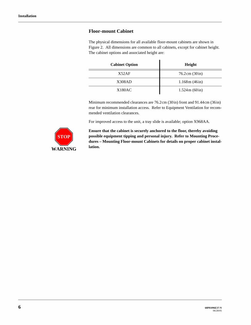
Installation
Floor-mount Cabinet
The physical dimensions for all available floor-mount cabinets are shown in Figure 2. All dimensions are common to all cabinets, except for cabinet height. The cabinet options and associated height are:
Minimum recommended clearances are 76.2cm (30in) front and 91.44cm (36in) rear for minimum installation access. Refer to Equipment Ventilation for recom-mended ventilation clearances.
For improved access to the unit, a tray slide is available; option X968AA.
Ensure that the cabinet is securely anchored to the floor, thereby avoiding possible equipment tipping and personal injury. Refer to Mounting Proce-dures – Mounting Floor-mount Cabinets for details on proper cabinet instal-lation.
Cabinet Option Height
X52AF 76.2cm (30in)
X308AD 1.168m (46in)
X180AC 1.524m (60in)
STOP
WARNING
6 68P81096E37-N06/28/05
Installation
5.1 cm(2 in)
5.1 cm(2 in) 5.1 cm
(2 in)9.6 cm(3.8 in)
5.1 cm(2 in)
5.1 cm(2 in)
Figure 1. Floor-mount Cabinet – Dimensions and Clearances
55.9 cm(22 in)46.5 cm(18.3 in)45.2 cm(17.8 in)
55.9 cm(22 in)
46.5 cm(18.3 in)
FRONT
Mounting Rails (4)
76.2 cm(30 in)
0.64 cm(0.25 in)
FRONT VIEW SIDE VIEW
BASE MOUNTING DETAIL
VIEWED FROM TOP
5.1 cm(2 in)
49 cm(19.3 in)
5.1 cm(2 in)
9.6 cm(3.8 in)
5.1 cm(2 in)
9.2 cm (3.625 in) holes (2)
1.575 cm (0.62 in) holes (4)
1.524m(60 in)
1.168m (46 in)
49 cm(19.3 in)
Station Support
Brackets (2)
68P81096E37-N 706/28/05
Installation
Modular Racks
The rack options, associated height and available number of racking units are:
The physical dimensions and clearances for all available modular racks are shown in Figure 2. The top and bottom plates are identical. All dimensions and clear-ances are common to all racks, except for the 2 dimensions identified below. The rack options and associated dimensions are:
Recommended clearance front and rear is 91.44cm (36in) minimum for servicing access. Refer to Equipment Ventilation for recommended ventilation clearances.
FRU kit CLN6679A (MTR2000 Rack Mounting Hardware) is included with each Rack Option. This allows proper installation of the MTR2000 station within the rack’s centre of gravity.
This kit includes two rack mount standoffs and eight mounting screws.
Rack Option Rack Height Number of Racking Units
X741AF 76.2cm (30in) 16
X742AF 1.143m (45in) 24
X743AF 1.32 m (52 in) 27
Rack Option Dimension A Dimension B
X741AF 79.2cm (31.2in) 26.1cm (10.27in)
X742AF 1.147m (45in) 27.25cm (10.73in)
X743AF 1.28 m (52in) 31.15cm (12.26in)
Note
8 68P81096E37-N06/28/05

Installation
Figure 2. Modular Rack – Dimensions and Clearances
9.22cm (3.63in)
1.59cm (0.625in)
20.58cm (8.1in)
76.2cm (3in)
Dimension BDimension B
17.78cm (7in)
3.81cm (1.5in)
17.78cm (7in)
7.22cm (2.85in)
38.74cm (15.25in)
5cm (2in)
15.9mm Diam (0.625in)
9.4mm Diam (0.37in)52.7cm
(20.75in)45.36cm (17.86in)
48.77cm (19.2in)
38.74cm (15.25in)
13.45cm (5.3in)
5cm (2in)
9.4mm Diam (0.37in)
Rack Center
SIDE VIEW
TOP / BOTTOM
Dimension BDimension B
Dimension BDimension A
10.97cm (4.375in)
13.21cm (5.25in)
0784384T0313.21cm
5.25in Standoff
68P81096E37-N 906/28/05

Installation
Site Grounding and Lightning Protection
Site Grounding Lightning Protection Recommendations
Proper site grounding and lightning protection are vitally important consid-erations. Failure to provide proper lightning protection may result in perma-nent damage to the radio equipment.
One of the most important considerations when designing a communications site is the ground and lightning protection system. While proper grounding techniques and lightning protection are closely related, the general category of site grounding may be divided as follows:
Electrical Ground Ground wires carrying electrical current from circuitry or equipment at the site is included in the category of electrical ground. Examples include the ac or dc elec-trical power used to source equipment located at the site, telephone lines, and wires or cables connected to alarms or sensors located at the site.
RF Ground This type of ground is related to the transmission of radio frequency energy to earth ground. An example of rf grounding is the use of shielding to prevent or at least minimize the leakage of unwanted rf transmissions from communications equipment and cables.
Lightning Ground Providing adequate lightning protection is critical to a safe and reliable communi-cations site. Telephone lines, rf transmission cables, and ac and dc power lines must all be protected to prevent lightning energy from entering the site building.
Although a comprehensive coverage of site grounding techniques and lighting protection is not within the scope of this manual, there are several excellent indus-try sources for rules and guidelines on ground and lightning protection at commu-nications sites.
Motorola recommends the following reference source:
Motorola Quality Standards Fixed Network Equipment Installation manual, R56. . . . . . . . . . . . . . . . . . . . . . . . . . . . . . .68P81089E50
Equipment Grounding Guidelines
The station is equipped with a ground screw located on the rear of the station Power Supply module. This screw is used to connect the station to the site ground point. It is assumed that all telephone lines, antenna cables, and ac or dc power cabling has been properly grounded and lightning protected by following the rules and guidelines provided in the above reference.
STOP
IMPORTANT
Note
10 68P81096E37-N06/28/05

Installation
Recommended Tools and Equipment
In addition to the typical compliment of hand tools, the following tools and equip-ment are recommended for proper installation of the station equipment.
• Tarpaulin or plastic drop cloth or cover surrounding equipment while drilling concrete anchor holes (for installations where cabinet or rack is being an-chored to concrete).
• Vacuum cleaner for removing concrete dust caused by drilling.
Equipment Unpacking and Inspection
The station equipment may be shipped by either air freight or electronic van (as specified by customer), except where noted.
• If no cabinet or rack is desired, the station is shipped in a box; the station is positioned between pieces of cushioned corrugated cardboard.
• All available cabinets are shipped with the station(s) installed in the cabinet, with the cabinet bolted to a wooden skid and covered with a cardboard box with corrugated interior corner braces.
• Stations to be used in open frame racks are shipped with the station and an-cillary equipment mounted in the rack and covered by an antistatic plastic bag. All rack shipments are electronic van only.
Thoroughly inspect the equipment as soon as possible after delivery. If any part of the equipment has been damaged in transit, immediately report the extent of the damage to the transportation company and to Motorola.
Antistatic plastic bags should be kept for future shipping/transporting of station.
Cabinet Unpacking
When a station (mounted in a cabinet) is delivered from Motorola, it arrives in suitable packing materials. If the unpacked equipment is damaged, return it to Motorola in its original packaging.
Equipment should be handled in its original packaging until it is delivered to its final destination. If the equipment is damaged while being moved without the original packaging, the warranty claim is not valid.
Note
STOP
WARNING
68P81096E37-N 1106/28/05

Installation
This section describes the procedures to unpack and mechanically install the station equipment. A variety of mounting meth-ods are possible, depending on whether a cabinet or rack (if any) has been selected to house the station(s). Installation pro-cedures are provided for each of the cabinet and rack types, as well as the slide rail.
Be sure to observe proper electrostatic discharge precautions if modules must be removed from the station.
Unpacking Equipment
Introduction
Station equipment packing methods vary depending upon the type of optional rack or cabinet selected by the customer. Unpacking procedures for these various methods are provided in the following paragraphs.
The equipment must be immediately inspected for damage after unpacking, and a report of the extent of any damage made to the transportation company and to Motorola.
Unpacking Stations
The station is shipped in a carton, cushioned by four plastic inserts at the corners of the carton.
Improper handling of the station may cause personal injury or damage to the station. DO NOT pick up the station by holding the Preselector (if so equipped). Use the handles on the front of the station, or the Power Supply and Power Amplifier casings when picking up the station.
Front Panel – Removal and Replacement
Remove station front panel by inserting a small flat-blade screwdriver into one of two access holes at either end of the panel and, by carefully moving the handle of the screwdriver away from the center, release the front panel locking clip from the chassis and pull away the panel. Replace station front panel by inserting one of the front panel locking clips into corresponding latch on the station housing, and carefully pressing the panel on the opposite side until the second locking clip snaps into place.
2 MECHANICAL INSTALLATION
STOP
IMPORTANT
STOP
IMPORTANT
STOP
WARNING
12 68P81096E37-N06/28/05

Installation
Unpacking Floor-mount Cabinets
The floor-mount cabinets are shipped mounted to a wooden skid, secured with corrugated corner braces held by a plastic strap, and covered with a cardboard cov-er. Unpack the equipment as described in Figure 3.
68P81096E37-N 1306/28/05
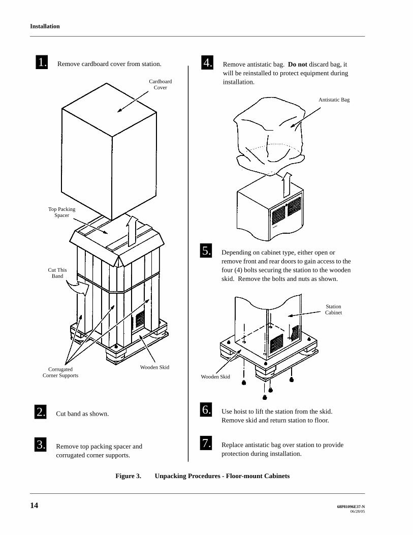
Installation
Figure 3. Unpacking Procedures - Floor-mount Cabinets
1. Remove cardboard cover from station.
2. Cut band as shown.
3. Remove top packing spacer and corrugated corner supports.
4. Remove antistatic bag. Do not discard bag, it will be reinstalled to protect equipment during installation.
5. Depending on cabinet type, either open or remove front and rear doors to gain access to the four (4) bolts securing the station to the wooden skid. Remove the bolts and nuts as shown.
6. Use hoist to lift the station from the skid. Remove skid and return station to floor.
7. Replace antistatic bag over station to provide protection during installation.
Cardboard Cover
Corrugated Corner Supports
Wooden Skid
Cut This Band
Top Packing Spacer
Antistatic Bag
Wooden Skid
Station Cabinet
1
4 68P81096E37-N06/28/05
Installation
Mounting Procedures
Introduction
In most cases, stations are shipped in the selected cabinet or rack (i.e., the station is mounted and cabled), and may be installed by following the procedures below. However, the following three scenarios require special mounting procedures:
• Customer plans to mount equipment in customer-supplied rack or cabinet, and orders equipment to ship from the factory without a rack or cabinet.
• Customer orders two stations in a single rack.
• Customer requires slide rail assembly.
Installing Racks
In a typical installation, the rack is bolted to a concrete floor to provide stability.
The following procedure describes the steps necessary to bolt the rack to a con-crete floor. Be sure to check with local authorities to verify that the following pro-cedure conforms to local building codes and regulations before permanently installing the rack.
1. Carefully align the rack at the desired anchoring location.
2. Use the rack mounting foot as a template and mark the location of the six 19mm (3/4in) diameter mounting holes. All six anchoring positions must be used.
3. Move the rack aside, drill holes in the concrete floor, and install the mount-ing anchors (RAM RD-56 anchors recommended) per instructions provided with the anchors. Make sure that none of the anchors comes in contact with the reinforcing wire mesh buried in the concrete; the rack must be electrical-ly isolated from any other equipment or materials at the site.
4. Align the rack with the installed anchors and lightly secure the rack to the floor using the proper mounting hardware. Do not tighten the mounting hardware at this time.
5. Check the vertical plumb of the rack. Also check that the top is level. Use shims (flat washers or flat aluminum plates) as necessary under the rack mounting foot to achieve vertical plumb and horizontal level.
6. Tightly secure the rack to the floor anchors making sure that it remains ver-tically plumb and horizontally level.
7. After all debris is removed and cement dust is cleared away, remove what-ever protective covering has been placed on the equipment, including the an-tistatic bag.
Cement dust from concrete flooring is harmful to electronic equipment and wiring. Make sure that the rack and any collocated equipment are protected prior to drilling holes in the concrete floor. Use a tarpaulin, cloth, or plastic sheeting to cover exposed equipment. (The rack should be already covered CAUTION
!
68P81096E37-N 1506/28/05

Installation
with an antistatic bag; do not remove the bag at this time.) Use a vacuum while drilling the holes to minimize the spread of concrete dust. Carefully clean up any accumulated dust and debris from the anchor installation before uncovering the equipment.
Mounting Floor-mount Cabinets
Each cabinet bottom is pre-drilled with four (4) mounting holes to allow attach-ment to the site floor. If installing on a concrete floor, use the cabinet as a tem-plate, mark the hole locations, and follow the procedures above for anchoring equipment racks. If installing on a wooden floor, use lag bolts and washers (cus-tomer supplied) to secure the cabinet to the floor.
Transferring Equipment from Shipping Container to Rack or Cabinet
As mentioned under Equipment Unpacking and Inspection, a station can be shipped in a box. Upon delivery, the equipment must be removed from the con-tainer and transferred to a Motorola-supplied rack or cabinet, or to a customer-sup-plied rack or cabinet.
Customer-supplied cabinets and racks must have mounting rails and hole spacing compatible with EIA Universal 48.3cm (19in) specifications. Cabinets must pro-vide adequate ventilation (as detailed under Equipment Ventilation) and must meet the following criteria:- 41.3cm (16.25in) deep- 48.3cm (19in) wide- 13.4cm (5.25in) high- Two mounting rails 5cm (2in) from front of cabinet with front mounting holes
5.7 cm (2.25in) apart (center to center).
Contact Motorola Engineering for specific questions regarding mounting equip-ment in customer-supplied cabinets.
Note
16 68P81096E37-N06/28/05

Installation
Installing Slide Rail Assembly in a Motorola Cabinet
Referring to Figure 4, perform the following procedure to install slide rail option X968AA.
On a bench-top, working onone side of the slide rail as-
sembly at a time…
1. Remove the Inner-Slide Rail from the slide assembly (left and right) by de-pressing the Slide Locking Latch and sliding the Inner-Slide Rail out from the slide assembly.
2. Install the Inner-Slide Rail (left) on the Power Supply side by:
- removing the 2 bottom screws from the station power supply EMI cover, and
- installing the Inner-Slide Rail (left) with the supplied screws.
3. Install the Inner-Slide Rail (right) on the PA side using the holes in the PA casing.
4. Attach each Outer-Slide Rail to a Cabinet Bracket with supplied screws.
The left and right Cabinet Brackets are identical. The Locking Tab of each Outer-Slide Rail must face towards the rear of the cabinet.
Working in the cabinet… 5. The cabinet must have a set of vertical cabinet rails in the back as well as the front. If there is no set in the back, these must be installed. The back rail is installed the same as the front rail, with the supplied screws.
6. Install each assembled Cabinet Bracket (with attached Outer-Slide Rail) to the appropriate side of the cabinet.
The U-shaped cutout of the Cabinet Bracket must face up.
7. Slide the station (with an Inner-Slide Rails mounted on each side) into the Outer-Slide Rails in the cabinet; an audible snap is heard. Continue sliding the station in until the station is fully seated.
8. Secure the station to the cabinet front rails with the supplied screws.
Note
Note
68P81096E37-N 1706/28/05
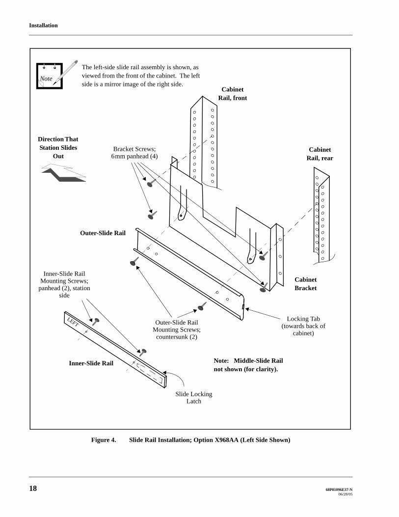
Installation
Figure 4. Slide Rail Installation; Option X968AA (Left Side Shown)
Bracket Screws; 6mm panhead (4)
Locking Tab(towards back of
cabinet)
Outer-Slide Rail Mounting Screws;
countersunk (2)
Inner-Slide Rail Mounting Screws;
panhead (2), station side
Inner-Slide Rail
Outer-Slide Rail
Cabinet Bracket
Cabinet Rail, front
Note
The left-side slide rail assembly is shown, as viewed from the front of the cabinet. The left side is a mirror image of the right side.
Slide Locking Latch
Cabinet Rail, rear
Direction That Station Slides
Out
LEFT
Note: Middle-Slide Rail not shown (for clarity).
18 68P81096E37-N06/28/05
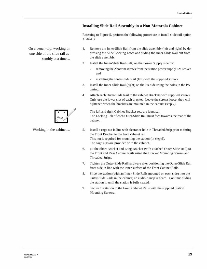
Installation
Installing Slide Rail Assembly in a Non-Motorola Cabinet
Referring to Figure 5, perform the following procedure to install slide rail option X346AB.
On a bench-top, working onone side of the slide rail as-
sembly at a time…
1. Remove the Inner-Slide Rail from the slide assembly (left and right) by de-pressing the Slide Locking Latch and sliding the Inner-Slide Rail out from the slide assembly.
2. Install the Inner-Slide Rail (left) on the Power Supply side by:
- removing the 2 bottom screws from the station power supply EMI cover, and
- installing the Inner-Slide Rail (left) with the supplied screws.
3. Install the Inner-Slide Rail (right) on the PA side using the holes in the PA casing.
4. Attach each Outer-Slide Rail to the cabinet Brackets with supplied screws. Only use the lower slot of each bracket. Leave the screws loose; they will tightened when the brackets are mounted in the cabinet (step 7).
The left and right Cabinet Bracket sets are identical. The Locking Tab of each Outer-Slide Rail must face towards the rear of the cabinet.
Working in the cabinet… 5. Install a cage nut in line with clearance hole in Threaded Strip prior to fitting the Front Bracket to the front cabinet rail. This nut is required for mounting the station (in step 9). The cage nuts are provided with the cabinet.
6. Fit the Short Bracket and Long Bracket (with attached Outer-Slide Rail) to the Front and Rear Cabinet Rails using the Bracket Mounting Screws and Threaded Strips.
7. Tighten the Outer-Slide Rail hardware after positioning the Outer-Slide Rail front side in line with the inner surface of the Front Cabinet Rails.
8. Slide the station (with an Inner-Slide Rails mounted on each side) into the Outer-Slide Rails in the cabinet; an audible snap is heard. Continue sliding the station in until the station is fully seated.
9. Secure the station to the Front Cabinet Rails with the supplied Station Mounting Screws.
Note
68P81096E37-N 1906/28/05

Installation
Figure 5. Slide Rail Installation; Option X346AB (Left Side Shown)
Locking Tab(towards back of
cabinet)
Outer-Slide Rail Mounting Hardware
sets; (4)
Inner-Slide Rail Mounting Screws; panhead (2),
station side
Inner-Slide Rail
Outer-Slide Rail
Note
The left-side slide rail assembly is shown, as viewed from the front of the cabinet. The left side is a mirror image of the right side.
Direction That Station Slides
Out
Station Mounting
Screws; (2)
Mount Outer-Slide Rails to Brackets; ONLY use lower
slot of Brackets.
Long Bracket
Short Bracket
Install a cage nut in line with clearance hole in Threaded Strip prior to fitting bracket to the front cabinet rail. This nut is required for mounting the station. The cage nuts are provided with the cabinet.
Threaded Strip
Front Cabinet Rail
Rear Cabinet Rail
Bracket Mounting
Screws; (4)
LEFTNote: Middle-Slide Rail not shown (for clarity).
20 68P81096E37-N06/28/05

Installation
Most station configuration parameters are altered through the Radio Service Software (RSS) with the exception of some pa-rameters for the following boards, which are configured through jumpers:
• 4-Wire Wireline Interface Board (CLN1203),
• 4-Wire Euro Wireline Interface Board (CLN1204),
• Auxiliary I/O Board(CLN1206).
4-Wire Wireline Interface Board
Model CLN1203 WIB supports tone control of the station. CLN1203 provides a fixed impedance of 600Ω to the wireline. Figure 6 shows the jumper locations for tone control.
.
4-Wire Euro Wireline Interface Board
Figure 7 shows the correct settings of impedance matching jumpers for the model CLN1204 WIB, as determined by the country in which the station is being oper-ated. Incorrect jumper settings may violate local telecommunications authority regulations and place the equipment in an unapproved status. Some countries also specify a maximum allowed line input level. Refer to the RSS Online Help, under Line Level.
3 BOARD CONFIGURATION
C84
T1
T2
C15
C74P11P15P13P17
P10P14P12P16
P6
P2
Figure 6. CLN1203 Wireline Interface Board Jumper Settings
P10,P11
P12,P13
P14,P15
P16,P17
Tone Remote Control2-wire/4-wire configurations out
68P81096E37-N 2106/28/05

Installation
P1, P5, P8, P9
Country Reference Impedance A * B C D E P3, P7
Australia √ √
Spain √ √
Austria √ √Germany (2-wire) √ √
Luxemburg √ √South Africa √ √Switzerland √
Belgium √ √
Cyprus √ √Former USSR √ √
Former Yugoslavia √ √Germany (4-wire) √ √
Greece √ √Italy √ √
Netherlands √ √Portugal √ √
Denmark √ √
Ireland √ √
UK √ √
Finland √ √
France √ √
Norway √
Sweden √
820Ω
120ηF
220Ω
820Ω
115ηF
220Ω
830Ω
72ηF
150Ω
600Ω
500Ω
330ηF
400Ω
620Ω
310ηF
370Ω
820Ω
115ηF
220Ω
820Ω
115ηF
220Ω
820Ω
115ηF
220Ω
900Ω
30ηF
Figure 7. CLN1204 Wireline Interface Board Jumper Settings
C74
T1
T2
C15
C84P3
E D C B A
P7
P1
P9
P5
P8E D C B A
E D C
B A
E D
C B
A
√ = Jumper In
A = Pin 1 connects to Pin 2* This setting represents a standard 600 ohm matching and is the factory default.
B = Pin 3 connects to Pin 4
C = Pin 5 connects to Pin 6
D = Pin 7 connects to Pin 8
E = Pin 9 connects to Pin 10
Canada and the U.S wireline requirements are supported by Wireline board model CLN1203.
Note
22 68P81096E37-N06/28/05

Installation
Auxiliary I/O Board
Jumpers are provided to route inputs and outputs in a specific direction to and from the SCM; the SCM determines the functionality of the inputs and outputs.
The board jumpers are shown in Figure 8.
GPI_14 is a special input which can be jumpered to be a transistor input or opto isolated. In addition it can be dedicated to the Ext_PTT* Line routed to the SCM. This function is a fast external PTT* (an active low function).
The board jumper settings for P2, P9, P6 are provided in Table 1. Settings for P5 are provided in Table 2. Settings for P3, P4 are provided in Table 3.
P7 and P8 are not used.
Figure 8. CLN1206 Auxiliary I/O Board Jumpers
P5
P9
P6
P2
P3 P4P1
134 2
4 2
13
2 1
10 9
2 4
1 3
2 4
1 3P8
10 9
2 1
P710 9
2 1
68P81096E37-N 2306/28/05

Installation
Table 1. Configuring Input GPI_14 Function
Table 2. Configuring Output GPO_14 Function
The shaded areas indicate default manufacturing settings.
Note 1: This is an active low; that is, no current to the Opto Input.
Note 2: This configuration, with P6 out (PTT when current to the Opto Input) represents the E Signal of 4 wire E&M Trunk Type I Phone Signalling. The opposite direction of the E&M is covered in Note 3.
In this configuration the second remaining unused input type must be jumpered to the SPI Buffer. The Buffer Input should never be left floating; otherwise the IRQ Generator will not function prop-erly (i.e., use either P2-1&2 or P9-7&8).
Function on GPI_14 Input TypeSystem
Connector Input Pins
Auxiliary I/O Board Jumpers
P2 P9 P6(See Note 1)
Fast External PTT*via Optocoupler (E/M sub). (See Note 2)
A29 Opto +A26 Opto –
3 - 4, 1 - 2 In
via Transistor B26 9 - 10, 7 - 8 In
Fast External PTTvia Optocoupler (E/M sub) A29 Opto +
A26 Opto –3 - 4, 1 - 2 Out
via Transistor B26 9 - 10, 7 - 8 Out
Function on GPO_14 Output Type System Connector (J5) Output Pins
Auxiliary I/O Board Jumper P5
AC Fail via Relay Closure B29, A30 2 - 4
SPI Latch for GPO_14 (software defined) via Relay Closure B29, A30 1 - 2
Notes
CAUTION!
24 68P81096E37-N06/28/05

Installation
Table 3. Configuring Output GPO_15 Function
Note 3: This configuration represents the M Signal of 4 wire E&M Trunk Type I Phone Signalling. The opposite direction of the E&M is covered in Note 2.
Note 4: Indicates that the configuration is only available when the board is plugged into Option slot 1.
Function on GPO_15 Output Type System Connector (J5) Output Pins
Auxiliary I/O Board Jumpers
P3 P4
Fast Carrier Detectvia Relay Closure C3, B3 2 - 4 2 - 4
via Open Collector B21 (see Note 4) 3 - 4 2 - 4
RdStatvia Relay Closure(see Note 3)
C3, B3 2 - 4 1 - 3
via Open Collector B21 (see Note 4) 3, 4 1, 3
SPI Latch for GPO_15 (soft-ware defined)
via Relay Closure C3, B3 1 - 2
via Open Collector B21 (see Note 4) 1 - 3
Notes
68P81096E37-N 2506/28/05

Installation
After the station equipment has been mechanically installed, electrical connections must be made. This involves making the following connections to:
• power supply,
• antenna coax cables,
• system cables, and
• telephone lines.
There are also electrical connections associated with maintenance and troubleshooting of the station. These connectors are located on the front of the Station Control Module (see Station Operation section for position of these connectors).
4 ELECTRICAL CONNECTIONS
STOP
IMPORTANT
When installing option boards, ensure that an Electro-Static Discharge (ESD) cable is connected (via banana plug) to the hole in the front-right handle of the station when installing option boards. Otherwise, the option boards may be damaged.
ESD Connect
26 68P81096E37-N06/28/05

Installation
Figure 9 shows the position of the station external connectors located at the rear of the station.
Figure 9. Location of External Connectors at Rear of Station
Battery Backup and DC Input Connector
Rx RF ConnectorTx RF Connector Wireline Connector System Connector
Trunking / MRTI Connector
AC Power Connector(Not used in DC mode)
GroundScrew
68P81096E37-N 2706/28/05

Installation
Power Supply Connections
AC Input Power Connection
Do not apply ac power to the station at this time. Make sure that the circuit breaker associated with the ac outlet is turned to OFF.
The ac socket-outlet must be installed near the equipment and must be easily accessible.
Each station is shipped with an 2.5m (8ft) 3-conductor line cord. Figure 9 shows the ac line cord connector. Insert the plug into an appropriate grounded outlet.
The North American line cord is equipped with a NEMA 5–15 plug, intended for 110/120Vac operation.
The optional European line cord (Option X189AA) is equipped with a “Schuko” style CEE VII (7) plug, intended for 220/240VAC operation.
Plugs for other countries are available as the following options:
If an alternate line cord is required, obtain a line cord employing “HAR” flexible cord with fittings approved by the safety testing agency in the end- use country.
CAUTION!
CAUTION!
Location Option Number
U. K. X162AD
Australia X191AD
28 68P81096E37-N06/28/05

Installation
Ground Connection
The station is equipped with a ground screw located on the rear of the station Pow-er Supply module. Connect the ground screw to the site ground point.
Refer to Motorola Quality Standards Fixed Network Equipment Installation manual, R56 (68P81089E50) for complete information regarding lightning protection.
The station is to be connected to a battery supply that is in accordance with the applicable electrical codes for the end use country; for example, the Na-tional Electrical Code ANSI/NFPA No. 70 in the U.S.
DC Input Power Connection
For DC-only operation, the DC source power is connected to the station through the battery backup connector shown in Figure 9, and described in “Battery Con-nection” on page 29.
Ensure that the appropriate voltage is connected; that is, Nominal 14.2 Vdc (10.8 to 16.0 Vdc) for a low power station, or Nominal 28.6 Vdc(21.0 to 32.0 Vdc) for the high power station.
Battery Connection
Battery backup interface offers the capability of connecting to battery backup power in the event of an AC power line failure.
The battery backup system is connected to the station through the red and black connector mounted at the rear of the station. The connector has a cover with the following label. This label directs the technician to read the information provided below:
This battery backup system must have, at a minimum, a disconnect relay con-trolled by an AC fail detector.
DO NOT connect a battery directly to the station. Damage to batteries as well as to the station may occur. Batteries must be connected to the station through an Argus Technologies Battery Reverting Charger, Model #010-519-20 (Motorola Model #L1883) for 12V charging systems, and Argus Technol-ogies Model #010-523-20 (Motorola Model #L1884) for 24V charging sys-tems. These systems were developed specifically for this interface and tested by Motorola for proper station operation. Damage resulting from use of any other charging systems will void the warranty. Refer to qualified sales/ser-vice representative for charger ordering information.
CAUTION!
CAUTION!
STOP
WARNING
CAUTION: See manual before removing cover.
STOP
WARNING
68P81096E37-N 2906/28/05

Installation
The station is to be connected to a battery supply that is in accordance with the applicable electrical codes for the end use country; for example, the Na-tional Electric Code ANSI/NFPA No.70 for the U.S.
Cables are supplied with the charging option. Do not make connections directly from the station to the storage battery. Connect as shown in Figure 10.
CAUTION!
Figure 10. Making Connections to Storage Battery
DC input Connector located at rear of the station for hooking up the Battery backup system.Required input power:
• Voltage - 14.2 Vdc Low Power (LP)28.4 Vdc High Power (HP)
• Current - 11.5 Amps LP13.0 Amps HP
Both positive and negative terminals must be protected with appropriate fast acting fuses.Secondary circuitry must be SELV type and be installed nearby, preferable in the same building.All installations shall be carried out by trained service personnel only. Connector ESD cover
must be in place when Battery Backup cable is not in use – to prevent exposure to live contacts.
CAUTION!
30 68P81096E37-N06/28/05

Installation
RF Antenna ConnectionsThe transmit and receive antenna rf connections are made using two separate N-type connectors. Coax cables from the receive and transmit antennas must be con-nected to the two N-type connectors. The position of these connectors is shown in Figure 9.
In the case where an optional Antenna Relay is used on the station, the coax cable from the single transmit/receive antenna is connected to the middle N-type con-nector of the Antenna Relay.
68P81096E37-N 3106/28/05

Installation
System Cable Connections
System connections are made through one or both of the following connectors:- the Trunking/MRTI connector and - the System connector.
Trunking/MRTI Connector The location of the Trunking/MRTI connector and System connector on the sta-tion rear panel is shown in Figure 9.
The following cables are available for trunking system applications:- 7.62m (25ft) Trunk Cable, part # 3083765X04- 15.24m (50ft) Trunk Cable, part # 3083765X05- 22.86m (75ft) Trunk Cable, part # 3083765X06- 30.48m (100ft) Trunk Cable, part # 3083765X07
The following cable is available for MRTI applications:- Interface cable for Zetron model 30, kit # TTO4097
System Connector The cable connected to the System connector can be configured for various system options.
A generic System cable is available for variety of applications such as Wild Card, Main Standby, and Auxiliary Input/Output:- generic System cable, kit # TKN9205A
This cable provides a housing shell for connection to the 96 pin backplane con-nector, 30 loose pins, and a quantity of 30 of 24 gauge wires (2 meter long with a pin for header on one end and unterminated at the other end).
Table 4 provides a description of commonly used System Connector pins.
32 68P81096E37-N06/28/05
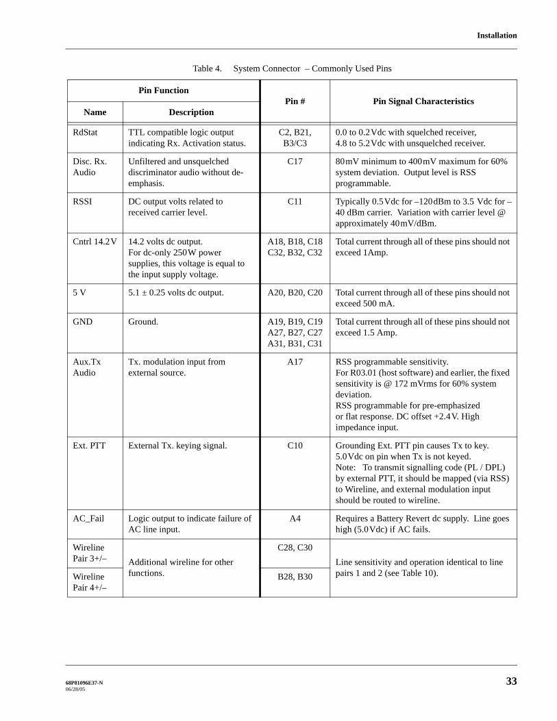
Installation
Table 4. System Connector – Commonly Used Pins
Pin FunctionPin # Pin Signal Characteristics
Name Description
RdStat TTL compatible logic output indicating Rx. Activation status.
C2, B21, B3/C3
0.0 to 0.2Vdc with squelched receiver, 4.8 to 5.2Vdc with unsquelched receiver.
Disc. Rx. Audio
Unfiltered and unsquelched discriminator audio without de-emphasis.
C17 80mV minimum to 400mV maximum for 60% system deviation. Output level is RSS programmable.
RSSI DC output volts related to received carrier level.
C11 Typically 0.5Vdc for –120dBm to 3.5 Vdc for –40 dBm carrier. Variation with carrier level @ approximately 40mV/dBm.
Cntrl 14.2V 14.2 volts dc output.For dc-only 250W power supplies, this voltage is equal to the input supply voltage.
A18, B18, C18C32, B32, C32
Total current through all of these pins should not exceed 1Amp.
5 V 5.1 ± 0.25 volts dc output. A20, B20, C20 Total current through all of these pins should not exceed 500 mA.
GND Ground. A19, B19, C19A27, B27, C27A31, B31, C31
Total current through all of these pins should not exceed 1.5 Amp.
Aux.Tx Audio
Tx. modulation input from external source.
A17 RSS programmable sensitivity. For R03.01 (host software) and earlier, the fixed sensitivity is @ 172 mVrms for 60% system deviation. RSS programmable for pre-emphasizedor flat response. DC offset +2.4V. High impedance input.
Ext. PTT External Tx. keying signal. C10 Grounding Ext. PTT pin causes Tx to key.5.0Vdc on pin when Tx is not keyed. Note: To transmit signalling code (PL / DPL) by external PTT, it should be mapped (via RSS) to Wireline, and external modulation input should be routed to wireline.
AC_Fail Logic output to indicate failure of AC line input.
A4 Requires a Battery Revert dc supply. Line goes high (5.0Vdc) if AC fails.
Wireline Pair 3+/– Additional wireline for other
functions.
C28, C30Line sensitivity and operation identical to line pairs 1 and 2 (see Table 10).Wireline
Pair 4+/–B28, B30
68P81096E37-N 3306/28/05
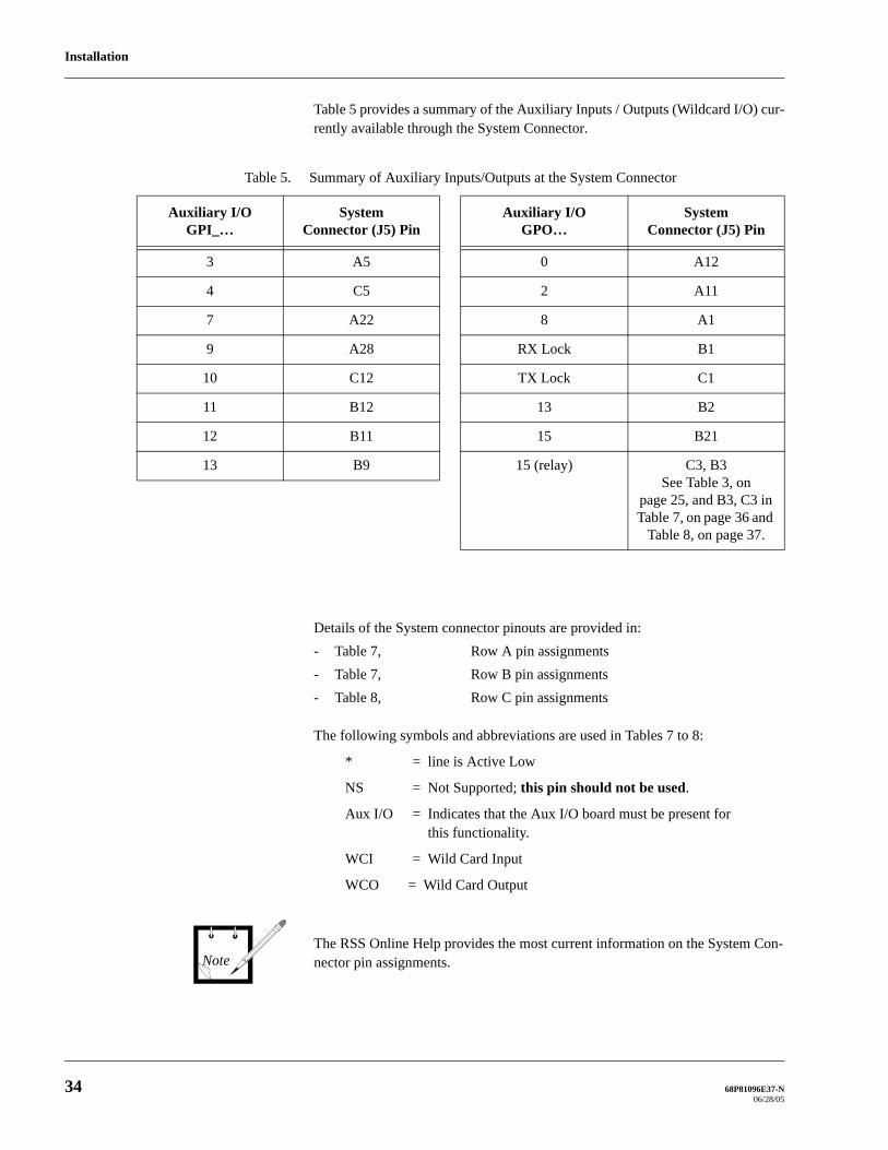
Installation
Table 5 provides a summary of the Auxiliary Inputs / Outputs (Wildcard I/O) cur-rently available through the System Connector.
Details of the System connector pinouts are provided in:- Table 7, Row A pin assignments- Table 7, Row B pin assignments- Table 8, Row C pin assignments
The following symbols and abbreviations are used in Tables 7 to 8:
* = line is Active Low
NS = Not Supported; this pin should not be used.
Aux I/O = Indicates that the Aux I/O board must be present for this functionality.
WCI = Wild Card Input
WCO = Wild Card Output
The RSS Online Help provides the most current information on the System Con-nector pin assignments.
Table 5. Summary of Auxiliary Inputs/Outputs at the System Connector
Auxiliary I/O GPI_…
System Connector (J5) Pin
Auxiliary I/O GPO…
System Connector (J5) Pin
3 A5 0 A12
4 C5 2 A11
7 A22 8 A1
9 A28 RX Lock B1
10 C12 TX Lock C1
11 B12 13 B2
12 B11 15 B21
13 B9 15 (relay) C3, B3See Table 3, on
page 25, and B3, C3 in Table 7, on page 36 and
Table 8, on page 37.
Note
34 68P81096E37-N06/28/05

Installation
Table 6. J5 SYSTEM CONNECTOR, Row A Pins
Pin # Pin Assignment Input/Output To/From Signal Characteristics
1 GPO_8 (WCO) O J1-C32, J2-C32 OCO, 100mA, 40V
2 PA Fail (Aux I/O) O J1-C31, J2-C31 OCO, 100mA, 40V, active low
3 SCI_CLCK1 O J1-C30, J2-C30, J3-C28 Do not use.
4 AC Fail O P8-5, J1-C29, J2-C29, J3-C24 TTL output, active high
5 GPI_3 (WCI) I J1-C28, J2-C28 Pulled up transistor input, 16V max
6 GP1_15 (–) (NS) I J1-C27, J2-C27 Negative side opto-isolated input, see C7
7 Ext Failsoft (Aux I/O) I J1-C26, J2-C26Pulled up transistor input, 16V max
8 GPI_1 (NS) I J1-C25, J2-C25
9 GPI_2 (NS) I J1-C24, J2-C24 Pulled up transistor input, 16V max
10 VSWR_Fail* (Aux I/O) O J1-C23, J2-C23 Pulled up transistor output (10kohms to +5Vdc), active low
11 GPO_2 (WCO) O J1-C22, J2-C22Pulled up transistor output (10kohms to +5Vdc)
12 GPO_0 (WCO) O J1-B25, J2-B25
13 Antenna Relay O P10-1, J3-C26 OCO, 200mA, active low
14 Not Supported O J1-C18, J2-C18, J3-C19
15 Spare 310 – –
16 Spare 308 – –
17 Aux TX Audio I J1-C16, J2-C16, J3-C16 RSS programmable input sensitivity
18 Cntrl 14.2 VDC O P8 pins 3, 4 (thru F2) +14.2Vdc, Note 1
19 GND – Station ground
20 5 VDC O P8 pins 7, 8 +5.1 ± 0.25 Vdc
21 Not Supported O J3-C12
22 GP1_7 (WCI) I J1-C11, J2-C11 Pulled up transistor input, 16V max.
23 Spare 323 – –
24 Spare 320 – –
25 Spare 903 – –
26 Ext PTT or GP1_14 (–), Note 2 I J1-C7, J2-C7 Negative side opto-isolated input, see A29
27 GND – Station ground
28 GPI_9 (WCI) or GPO_3 (NS) I/O J1-C6, J2-C6 Caution: See Auxiliary I/O section for jumpering information
29 Ext PTT or GPI_14 (+), Note 2 I J1-C5, J2-C5 Positive side opto-isolated input, see A26
30 AC Fail or GPO_14, Note 3 O J1-C4, J2-C4 One side of normally open relay, see B29
31 GND – Station ground
32 Cntrl 14.2 VDC O P8 pins 3, 4 (thru F2) +14.2Vdc, Note 1
Note 1: For dc-only 250W power supplies, this voltage is equal to the input supply voltage.
Note 2: This pin can be jumpered for Ext PTT (supported) or GPI_14 (not supported). See Aux I/O jumpers P2 and P9.
Note 3: This pin can be jumpered for AC Fail (sup-ported) or GPO_14 (not supported). See Aux I/O jumper P5.
68P81096E37-N 3506/28/05
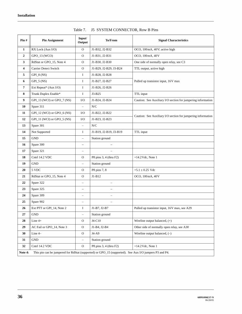
Installation
Table 7. J5 SYSTEM CONNECTOR, Row B Pins
Pin # Pin Assignment Input/Output To/From Signal Characteristics
1 RX Lock (Aux I/O) O J1-B32, J2-B32 OCO, 100mA, 40V; active high
2 GPO_13 (WCO) O J1-B31, J2-B31 OCO, 100mA, 40V
3 RdStat or GPO_15, Note 4 O J1-B30, J2-B30 One side of normally open relay, see C3
4 Carrier Detect Switch O J1-B29, J2-B29, J3-B24 TTL output, active high
5 GPI_8 (NS) I J1-B28, J2-B28
Pulled up transistor input, 16V max6 GPI_5 (NS) I J1-B27, J2-B27
7 Ext Repeat* (Aux I/O) I J1-B26, J2-B26
8 Trunk Duplex Enable* I J3-B25 TTL input
9 GPI_13 (WCI) or GPO_7 (NS) I/O J1-B24, J2-B24 Caution: See Auxiliary I/O section for jumpering information
10 Spare 311 – N/C
11 GPI_12 (WCI) or GPO_6 (NS) I/O J1-B22, J2-B22Caution: See Auxiliary I/O section for jumpering information
12 GPI_11 (WCI) or GPO_5 (NS) I/O J1-B23, J2-B23
13 Spare 301 – N/C
14 Not Supported I J1-B19, J2-B19, J3-B19 TTL input
15 GND – Station ground
16 Spare 300 – –
17 Spare 321 – –
18 Cntrl 14.2 VDC O P8 pins 3, 4 (thru F2) +14.2Vdc, Note 1
19 GND – Station ground
20 5 VDC O P8 pins 7, 8 +5.1 ± 0.25 Vdc
21 RdStat or GPO_15, Note 4 O J1-B12 OCO, 100mA, 40V
22 Spare 322 – –
23 Spare 325 – –
24 Spare 309 – –
25 Spare 902 – –
26 Ext PTT or GPI_14, Note 2 I J1-B7, J2-B7 Pulled up transistor input, 16V max, see A29
27 GND – Station ground
28 Line 4+ O J4-C10 Wireline output balanced, (+)
29 AC Fail or GPO_14, Note 3 O J1-B4, J2-B4 Other side of normally open relay, see A30
30 Line 4– O J4-A9 Wireline output balanced, (–)
31 GND – Station ground
32 Cntrl 14.2 VDC O P8 pins 3, 4 (thru F2) +14.2Vdc, Note 1
Note 4: This pin can be jumpered for RdStat (supported) or GPO_15 (supported). See Aux I/O jumpers P3 and P4.
36 68P81096E37-N06/28/05

Installation
Table 8. J5 SYSTEM CONNECTOR, Row C Pins
Pin # Pin Assignment Input/Output To/From Signal Characteristics
1 TX Lock (Aux I/O) O J1-A32, J2-A32 OCO, 100mA, 40V; active high
2 Rdstat-R2 Control O J1-A31, J2-A31, J3-A26 TTL output, high when unsquelched
3 RdStat or GPO_15, Note 4 O J1-A30, J2-A30 Other side of normally open relay, see B3
4 Failsoft Output (Aux I/O) O J1-A29, J2-A29 OCO, 100mA, 40V, active low
5 GPI_4 (WCI) I J1-A28, J2-A28 Pulled up transistor input, 16V max
6 Rx Inhibit I J1-A27, J2-A27, J3-B26 TTL input; active low
7 GPI_15 (+) (NS) I J1-A26, J2-A26 Positive side opto-isolated input, see A6
8 Trunk TX Inhibit* I J3-A25 TTL input
9 RF Relay Control Out (Aux I/O) O J1-B5, J2-B5 OCO, 200mA, 40V, active high
10 Ext PTT* Out (Aux I/O), Note 5 I J1-A23, J2-A23, J3-A23 TTL input
11 RSSI O J1-A22, J2-A22, J3-A22 Typically 0.5Vdc for –120dBm to 3.5 Vdc for –40 dBm carrier. Variation with carrier level @ approximately 40mV/dBm.
12 GPI_10 (WCI) or GPO_4 (NS) I/O J1-A24, J2-A24 Caution: See Auxiliary I/O section for jumpering information
13 Spare 304 – –
14 Not Supported O J1-A19, J2-A19, J3-A19
15 GND – Station ground
16 GND – Station ground
17 Disc RX Audio O J1-A16, J2-A16, J3-A16 Discriminator audio, flat response; 80mV to 400mV for 60% deviation
18 Cntrl 14.2 VDC O P8 pins 3, 4 (thru F2) +14.2Vdc, Note 1
19 GND – Station ground
20 5 VDC O P8 pins 7, 8 +5.1 ± 0.25 Vdc
21 Not Supported O J3-A12
22 Spare 302 – –
23 Spare 324 – –
24 GPIO_0 (CNTR I/O) I/O J1-A9, J2-A9, J3-A17 TTL input/output
25 Spare 317 – –
26 Spare 901 – –
27 GND – Station ground
28 Line 3+ I J4-C12 Wireline input balanced, (+)
29 GPIO_1 (CNTR I/O) I/O J1-A4, J2-A4, J3-A13 TTL input/output
30 Line 3– I J4-A11 Wireline input balanced, (–)
31 GND – Station ground
32 Cntrl 14.2 VDC O P8 pins 3, 4 (thru F2) +14.2Vdc, Note 1
Note 5: Ext PTT signal output, taken from Ext PTT input. The output signal can be inverted, depending on jumper settings. See jumpers P2, P6, P9.
68P81096E37-N 3706/28/05

Installation
Telephone Line Connections
Introduction
In conventional systems where the station is controlled by a remote console, or in wide area systems utilizing comparators, phone lines must be connected between the station and the remote equipment. The phone lines may carry analog voice, or encoded voice. Also carried on the phone lines are Tone Remote Control (type of remote control signalling). The following information defines the specifications for the phone lines, the location on the station backplane for phone line connec-tions, and which of the four (4) wireline circuits to use for various system types.
38 68P81096E37-N06/28/05
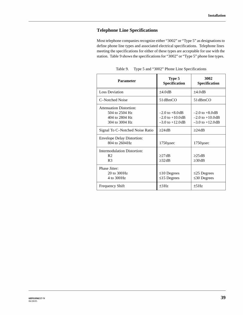
Installation
Telephone Line Specifications
Most telephone companies recognize either “3002” or “Type 5” as designations to define phone line types and associated electrical specifications. Telephone lines meeting the specifications for either of these types are acceptable for use with the station. Table 9 shows the specifications for “3002” or “Type 5” phone line types.
Table 9. Type 5 and “3002” Phone Line Specifications
Parameter Type 5 Specification
3002 Specification
Loss Deviation ±4.0dB ±4.0dB
C–Notched Noise 51dBmCO 51dBmCO
Attenuation Distortion:504 to 2504 Hz404 to 2804 Hz304 to 3004 Hz
–2.0 to +8.0dB–2.0 to +10.0dB–3.0 to +12.0dB
–2.0 to +8.0dB–2.0 to +10.0dB–3.0 to +12.0dB
Signal To C–Notched Noise Ratio ≥24dB ≥24dB
Envelope Delay Distortion:804 to 2604Hz 1750µsec 1750µsec
Intermodulation Distortion:R2R3
≥27dB≥32dB
≥25dB≥30dB
Phase Jitter:20 to 300Hz4 to 300Hz
≤10 Degrees≤15 Degrees
≤25 Degrees≤30 Degrees
Frequency Shift ±3Hz ±5Hz
68P81096E37-N 3906/28/05
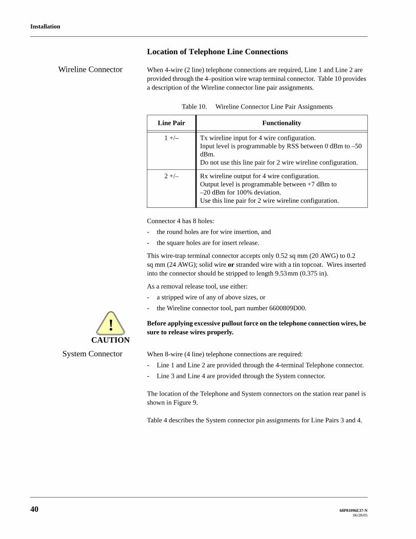
Installation
Location of Telephone Line Connections
Wireline Connector When 4-wire (2 line) telephone connections are required, Line 1 and Line 2 are provided through the 4–position wire wrap terminal connector. Table 10 provides a description of the Wireline connector line pair assignments.
Connector 4 has 8 holes:- the round holes are for wire insertion, and - the square holes are for insert release.
This wire-trap terminal connector accepts only 0.52 sq mm (20 AWG) to 0.2 sq mm (24 AWG); solid wire or stranded wire with a tin topcoat. Wires inserted into the connector should be stripped to length 9.53mm (0.375 in).
As a removal release tool, use either:- a stripped wire of any of above sizes, or- the Wireline connector tool, part number 6600809D00.
Before applying excessive pullout force on the telephone connection wires, be sure to release wires properly.
System Connector When 8-wire (4 line) telephone connections are required:- Line 1 and Line 2 are provided through the 4-terminal Telephone connector. - Line 3 and Line 4 are provided through the System connector.
The location of the Telephone and System connectors on the station rear panel is shown in Figure 9.
Table 4 describes the System connector pin assignments for Line Pairs 3 and 4.
Table 10. Wireline Connector Line Pair Assignments
Line Pair Functionality
1 +/– Tx wireline input for 4 wire configuration.Input level is programmable by RSS between 0 dBm to –50 dBm. Do not use this line pair for 2 wire wireline configuration.
2 +/– Rx wireline output for 4 wire configuration. Output level is programmable between +7 dBm to –20 dBm for 100% deviation.Use this line pair for 2 wire wireline configuration.
CAUTION!
40 68P81096E37-N06/28/05

Installation
System Type vs. Wireline Circuit
Table 11 shows which of the four (4) wireline circuits to use for various system types.
Stations equipped with a 4–wire Wireline Interface can support a single 4–wire or a single 2–wire telephone line connection.Stations equipped with an 8–wire Wireline Interface can for example support a two 4–wire or a single 2–wire telephone line connection.
i) For 4–wire systems, Line 1 is transmit audio (landline to station), and Line 2 is receive audio (station to landline). For 2–wire systems, Line 2 is trans-mit and receive audio.
ii) A CPI is a Console Priority Interface.; used in Trunking systems. A CIT is a Central Interconnect Terminal; used in Trunking systems.
iii) Transmit audio with respect to consoles, comparators, CIT, and DVM mo-dems are outputs. Transmit audio with respect to stations is an input.
iv) Receive audio with respect to consoles, comparators, CIT, and DVM mo-dems are inputs. Receive audio with respect to stations is an output.
Note
Table 11. System Types vs. Wireline Circuit Matrix
System Type Line 1(Note i)
Line 2(Note i) Line 3 Line 4
Conventional Local Area Analog Console Console Not used Not used
Conventional Wide Area Analog Comparator or Console
Comparator Not used Not used
Trunked Local Area Clear, without CPI CIT CIT Not used Not used
Trunked Local Area Clear, with CPI Console Console CIT CIT
Trunked Wide Area Clear without CPI Comparator Comparator Not used Not used
Trunked Wide Area Clear, with CPI Console Console Comparator Comparator
Trunked AMSS Clear Comparator Comparator Not used Not used
Redundant Trunking Clear, Wide Area without CPI
Comparator Comparator Not used Not used
Note
68P81096E37-N 4106/28/05
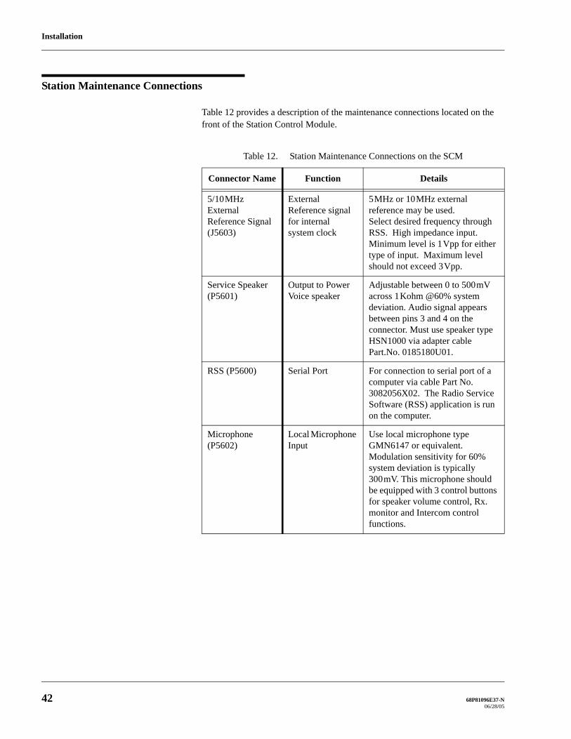
Installation
Station Maintenance Connections
Table 12 provides a description of the maintenance connections located on the front of the Station Control Module.
Table 12. Station Maintenance Connections on the SCM
Connector Name Function Details
5/10MHz External Reference Signal (J5603)
External Reference signal for internal system clock
5MHz or 10MHz external reference may be used.Select desired frequency through RSS. High impedance input. Minimum level is 1Vpp for either type of input. Maximum level should not exceed 3Vpp.
Service Speaker (P5601)
Output to Power Voice speaker
Adjustable between 0 to 500mV across 1Kohm @60% system deviation. Audio signal appears between pins 3 and 4 on the connector. Must use speaker type HSN1000 via adapter cable Part.No. 0185180U01.
RSS (P5600) Serial Port For connection to serial port of a computer via cable Part No. 3082056X02. The Radio Service Software (RSS) application is run on the computer.
Microphone (P5602)
Local Microphone Input
Use local microphone type GMN6147 or equivalent. Modulation sensitivity for 60% system deviation is typically 300mV. This microphone should be equipped with 3 control buttons for speaker volume control, Rx. monitor and Intercom control functions.
42 68P81096E37-N06/28/05

Installation
After the station equipment has been mechanically installed and all electrical connections have been made, power may now be applied and the station checked for proper operation.
Applying Power
Before applying power to the station, make sure all boards are securely seated in the appropriate connectors on the backplane and that all rf cables are securely con-nected.
Turn ON the circuit breaker controlling the ac outlet that is supplying power to the station Power Supply Module, or switch on the DC-supply to a station with a DC-only Power Supply Module.
Changing Fuse To replace the station fuse:
1. Turn off station power at source (e.g., ac breaker).
2. Remove fuse cover plate located on the backplane shield by unscrewing one M4 screw.
3. Pull defective fuse carefully with small needle nose pliers.
4. Replace new fuse (part # 6583049X16) carefully with small needle nose pli-ers.
For continued protection of the station against risk of fire, replace the fuse only with the same type and rating of fuse.
5. Restore power to the station.
5 POST INSTALLATION CHECKLIST
CAUTION!
68P81096E37-N 4306/28/05
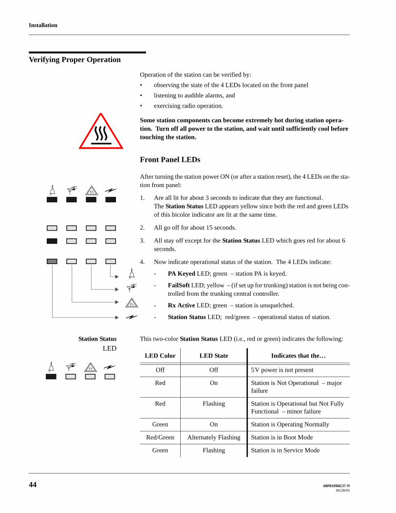
Installation
Verifying Proper Operation
Operation of the station can be verified by:• observing the state of the 4 LEDs located on the front panel• listening to audible alarms, and • exercising radio operation.
Some station components can become extremely hot during station opera-tion. Turn off all power to the station, and wait until sufficiently cool before touching the station.
Front Panel LEDs
After turning the station power ON (or after a station reset), the 4 LEDs on the sta-tion front panel:
1. Are all lit for about 3 seconds to indicate that they are functional. The Station Status LED appears yellow since both the red and green LEDs of this bicolor indicator are lit at the same time.
2. All go off for about 15 seconds.
3. All stay off except for the Station Status LED which goes red for about 6 seconds.
4. Now indicate operational status of the station. The 4 LEDs indicate:
- PA Keyed LED; green – station PA is keyed.
- FailSoft LED; yellow – (if set up for trunking) station is not being con-trolled from the trunking central controller.
- Rx Active LED; green – station is unsquelched.
- Station Status LED; red/green – operational status of station.
Station StatusLED
This two-color Station Status LED (i.e., red or green) indicates the following:
FS
FS
FS
LED Color LED State Indicates that the…
Off Off 5V power is not present
Red On Station is Not Operational – major failure
Red Flashing Station is Operational but Not Fully Functional – minor failure
Green On Station is Operating Normally
Red/Green Alternately Flashing Station is in Boot Mode
Green Flashing Station is in Service Mode
44 68P81096E37-N06/28/05

Installation
A major failure renders the station unusable. These failure could be caused by one of the following conditions:- Rx or Tx synthesizer out of lock- PA failure,- Sharp (i.e., 10dB) rf power cutback, - self test failure
A random flashing of the Station Status LED indicates major failure of the Station Control Module; since a control module reset turns the LEDs on.
A minor failure limits the functionality of the station. These failures could be caused by one of the following conditions:- ac source power failure- exciter or receiver analog metering voltage degradation- wireline loopback failure- invalid local channel selection
Boot mode is the mode the station is in during the loading of software into the sta-tion’s Flash memory.
Service mode is the mode the station is in during normal maintenance and service periods. These modes include the following conditions:- Intercom - PL Disable- Access Disable - Failsoft Disable- Power Control Disable - Service PTT
The Radio Service Software (RSS) can be used to determine which failure or ser-vice modes are active.
Service mode indicates that the station is not fully functional.
RX ActiveLED
This RX Active LED indicates the following:
This LED is lit when receive activation criteria (user defined) are satisfied; i.e., the radio is unsquelched.
CAUTION!
CAUTION!
FS
LED Color LED State Indicates that the…
Green On Receiver is active.
68P81096E37-N 4506/28/05
Installation
FailSoftLED
This FailSoft LED indicates the following:
This LED is lit when no activity is detected on the transmit data signal from the trunking central controller; the station is in Failsoft mode. This condition usually indicates a failed link to the trunking central controller.
PA KeyedLED
This PA Keyed LED indicates the following:
Listening For Audible Alarms
With a Service Speaker connected to the station (see Station Operation, Service Connections), any active audible alarms can be heard.
The audible alarms are repeated every 10 seconds. If more than one alarm is ac-tive, they are offset by 2 seconds.
Exercising Radio Operation
Operation of the station radio can be verified by exercising the radio’s two-way operation. This may be carried out when an external speaker and microphone are connected to the Station Control Module (SCM).
The kit # for the speaker is HSN1000. The external speaker requires an adaptor cable, part # 0185180U01.
Using a speaker other than the recommended HSN1000 may result in the sta-tion blowing a fuse.
The kit number for the microphone is GMN6147B.
FS
LED Color LED State Indicates that the …
Yellow Flashing station is in the Trunking system Failsoft mode.
FS
LED Color LED State Indicates that the …
Green On PA is keyed.
Green Flashing PA is keyed, but operating with power cutback.
Alarm Sound Indicates that …
AC Fail a single short beep a station configured with DC-revert has detected an AC power failure.
PA Fail two short beeps the station has been keyed, and the Power Amplifier has failed.
CAUTION!
46 68P81096E37-N06/28/05
Installation
After the station and ancillary equipment have been mechanically installed, properly cabled, and power applied, the equip-ment must then be optimized; that is, before placing the station in operation. Optimizing is performed through the Radio Ser-vice Software (RSS), kit number RVN4148.
After the station is operational, the station’s codeplug data must be copied to a PC- compatible computer.
In order to program an MTR2000 station for Trunking operation, kit num-ber RVN4148C (or later) of the RSS must be used. The current version is available through the U.S. and Canada Americas Aftermarket Division (AAD).
Optimizing Tasks
Optimization involves the following tasks:
1. Reading the station codeplug from the station (this ensures a match between the station serial number (resident in the codeplug) and the serial number (part of the customized station codeplug data) that is written back to the sta-tion (see task 5).
2. Customizing the station codeplug and saving the data to the station
3. Aligning the station for:
- Rx Wireline
- Tx Wireline
- Receiver RSSI calibration (option)
- Receiver Squelch Adjust
4. Performing post-optimization procedures.
5. Writing the customized codeplug to the station codeplug.
For details on these tasks, refer to the Optimizing a New Installation topic of the Radio Service Software (RSS) Online Help.
Copying Station Codeplug Date To a PC-compatible Computer
A copy of each station’s codeplug data must be made on an IBM-PC compat-ible computer. This is done through the Radio Service Software (RSS). See the RSS Startup Manual, 68P81096E15.
6 OPTIMIZATION
CAUTION!
CAUTION!
68P81096E37-N 4706/28/05

Installation
When a station is ordered with an Antenna Relay or External Preselector option, the respective module is attached to the sta-tion when delivered.
When a station is ordered with an External Double Circulator option, this circulator is provided in a peripheral tray.
In the case where an option is later added to the station, it can be installed according to the information provided in the An-cillary Equipment sections of the appropriate Instruction manual. Also refer to the Troubleshooting section for information on tuning the External Preselector.
7 INSTALLING STATION HARDWARE OPTIONS
48 68P81096E37-N06/28/05

STATIONOPERATION
This section describes the LED indicators and connectors provided on the station.
The set of LEDs indicate the operational status of the station.
There are two sets of connectors for devices external to the station:
• One set connects to external devices to enable full operation of the station. These are located at the back of the station.
• Another set connects to external devices for servicing the station. These are located on the Station Control Module.
1 DESCRIPTION
68P81096E38-D09/30/05-UP
Motorola Inc., 2005All Rights ReservedPrinted in U.S.A.
1301 E. Algonquin Road, Schaumburg, IL 60196Government & Enterprise Mobility Solutions

Station Operation
LED Indicators
A set of 4 LEDs is located on the station front panel. The position of the 4 LEDs on the front panel is shown in Figure 1. These LEDs indicate the status of the sta-tion during normal operation.
For further information on the states indicated by these LEDs, refer to the IN-STALLATION section, Post Installation Checklist, Verifying Proper Operation.
Red/GreenStation Status LED
YellowFailSoft LED
GreenRx Active LED
Figure 1. Front Panel LEDs
GreenPA Keyed LED
FS
Function Color Indicates …
Station Status red / green … operational status of station.
Rx Active green … that the station Rx activation criteria are satisfied. This could be:- RF carrier only,- PL/DPL only, or- RF carrier plus PL/DPL.
FailSoft yellow … (if set up for trunking) that the station is not being controlled from the trunking central controller.
PA Keyed green … that station PA is keyed.
FS
2 68P81096E38-D09/30/05

Station Operation
External Device Connections
Refer to INSTALLATION, Electrical Connections for the position of the station external connectors and line cord, located on the back panel.
A BNC connector on the front of the SCM allows the station to be connected to a 5 MHz or 10 MHz external reference signal.
Figure 2 shows the position of the BNC connector on the SCM.
68P81096E38-D 309/30/05

Station Operation
Service Connections
Service ports and LEDs are located on the front of the Station Control Module (SCM).
Figure 2 shows the position of the connectors on the SCM.
The service ports include connectors for:- 5/10 MHz External Reference Signal- Service Speaker:
connects between the telephone connector on the Station Control Module and an external speaker/amplifier (with a 6 pin molex connector) via an adaptor cable; part number 0185180U01.
- RSS:connects between the telephone connector on the Station Control Module and the DB9 connector on a PC. A DB25 connector can also be used to con-nect to the PC, when used with a DB25-DB9 adaptor.
- Service Microphone:connects between the telephone connector on the Station Control Module and a service microphone.
Figure 2. SCM Connectors
5/10MHz External Reference Signal
Service Microphone
RSSService Speaker
Front of station with Front Panel
removed.
4 68P81096E38-D09/30/05
68P81096E39-B09/30/05-UP
Motorola Inc., 2005All Rights ReservedPrinted in U.S.A.
1301 E. Algonquin Road, Schaumburg, IL 60196Government & Enterprise Mobility Solutions
ROUTINE MAINTENANCEFor MTR2000 Station
and Ancillary Equipment
This section provides routine maintenance recommendations and procedures for the station and associated ancillary equip-ment.
Routine Maintenance Overview
It is recommended that the station be cleaned with a soft dry cloth when the station is being serviced.
The station and ancillary equipment have been designed with state-of-the-art tech-nology and operate under software control, thus requiring minimal routine main-tenance. Virtually all station operating parameters are monitored and self-corrected by the Station Control Module, making virtually all periodic adjust-ments and tuning unnecessary.
Providing that the equipment is installed in an area which meets the specified en-vironmental requirements (see Installation section, Pre-Installation Consider-ations for environmental specifications), the only routine maintenance task required is the calibration of the station reference oscillator circuit. Details are provided under the heading Calibrating Station Reference Oscillator.
1 INTRODUCTION
Note

Routine Maintenance
2 68P81096E39-B09/30/05
The following list of test equipment is recommended to perform calibration of the station reference oscillator.
List of Test Equipment
• R2001 or R2600 Communications Analyzer with optional external frequen-cy standard
• 2 portable radios (for the operating band) if available
• In-line wattmeter
• IBM PC (or 100% compatible) equipped with Microsoft Windows™ 3.1, 95, 98 or 2000, and Motorola Radio Service Software (RSS) application.
The circuit devices responsible for determining the station reference frequency exhibit slight variations in their operating characteristics over time (“infant aging”). Approximately 90% of the component aging process occurs during the first year of operation. After the first year, the devices remain stable for a substantially longer period of time. Therefore, it is recom-mended that the station reference oscillator (internal) be calibrated after one year of operation, and thereafter less often; Table 1 provides a recommended schedule of periodic calibration.
Station Reference Calibration Schedule
After performing the initial one year calibration procedure, periodic calibration is required according to the schedule shown below. Note that the intervals are af-fected by the accuracy (in PPM) required either for regulatory compliance or by the system requirements, whichever is more stringent.
2 RECOMMENDED TEST EQUIPMENT
3 CALIBRATING STATION REFERENCE OSCILLATOR
Table 1. Recommended Intervals for Calibrating Station Reference Oscillator
(After Initial One-Year Calibration)
Accuracy Desired/Required Recommended Interval
±5 PPM Every 4 years
±3.5 PPM Every 2 years
±2 PPM Once yearly
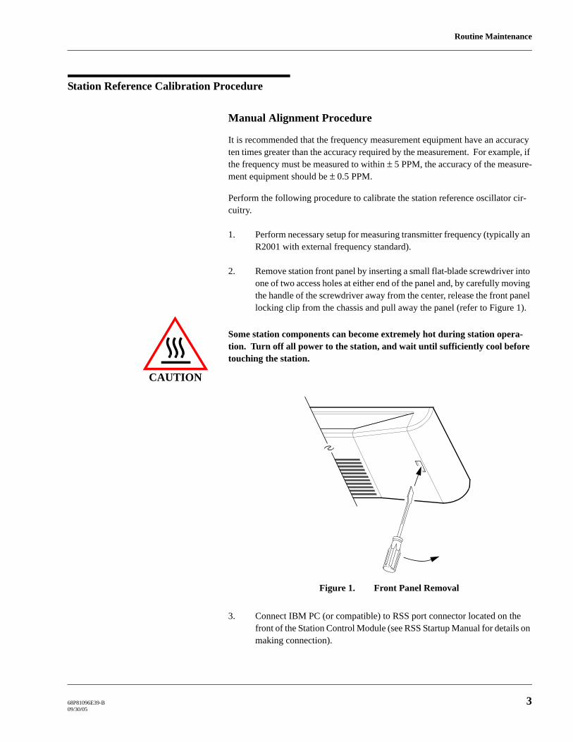
Routine Maintenance
68P81096E39-B 309/30/05
Station Reference Calibration Procedure
Manual Alignment Procedure
It is recommended that the frequency measurement equipment have an accuracy ten times greater than the accuracy required by the measurement. For example, if the frequency must be measured to within ± 5 PPM, the accuracy of the measure-ment equipment should be ± 0.5 PPM.
Perform the following procedure to calibrate the station reference oscillator cir-cuitry.
1. Perform necessary setup for measuring transmitter frequency (typically an R2001 with external frequency standard).
2. Remove station front panel by inserting a small flat-blade screwdriver into one of two access holes at either end of the panel and, by carefully moving the handle of the screwdriver away from the center, release the front panel locking clip from the chassis and pull away the panel (refer to Figure 1).
Some station components can become extremely hot during station opera-tion. Turn off all power to the station, and wait until sufficiently cool before touching the station.
3. Connect IBM PC (or compatible) to RSS port connector located on the front of the Station Control Module (see RSS Startup Manual for details on making connection).
CAUTION
Figure 1. Front Panel Removal
Routine Maintenance
4 68P81096E39-B09/30/05
4. Launch the RSS application (under Microsoft Windows 3.1 , 95, 98 or 2000) and access the Alignment panel.
Refer to the RSS Startup Manual, 68P81096E15, for complete details on installing and starting the RSS application.
5. With the mouse, press the PTT button on the Station Operation Controls panel to key the station.
6. Adjust the reference oscillator slider (if necessary) by dragging it with the mouse while observing the frequency reading on the frequency measuring equipment. Continue adjustment until you obtain a reading as close as pos-sible to the transmit frequency. (The RSS display indicates the current set-ting of the transmit frequency within the possible range. This graph is provided as a guide only and may not be used to adjust the frequency.)
Auto-Calibrate Alignment Procedure (Standard SCM Only)
Perform the following procedure to calibrate the station reference oscillator using a 5/10 MHz external reference signal.
The accuracy of this procedure depends on the accuracy of the 5/10 MHz external reference signal. Be sure the 5/10 MHz external reference signal provides the nec-essary accuracy (as described in Table 1).
1. Connect the output of a stable 5/10 MHz reference source to the BNC con-nector located on the front of the Station Control Module.
2. Set the 5/10 MHz source for a 1.0 ±0.5 Vrms output. The Station Control Module senses the 5/10 MHz input and commences calibrating the refer-ence oscillator using the 5/10 MHz signal as a reference.
3. Connect the station RSS port to a PC and start up the MTR2000 Radio Ser-vice Software application.
4. Within the RSS application, access the Service menu Alignment window. The Online Help associated with this window provides details for the fol-lowing alignment functions:
- Reference Oscillator
- Audio Input/Output
- Receiver
- Transmitter
Note

TROUBLESHOOTINGFor MTR2000 VHF Stationand Ancillary Equipment
This section provides troubleshooting recommendations and procedures for the VHF station and associated an-cillary equipment.
Troubleshooting Overview
The troubleshooting procedures and supporting diagrams provided in this section allow the service technician to isolate station faults to the Field Replaceable Unit (FRU) level. Defective FRUs are then replaced with known good ones to restore the station to proper operation.
Troubleshooting information includes:
• Troubleshooting flow charts
• Interpreting front panel LED indicators
• Module replacement procedures
• Post-repair procedures for performing alignment following replace-ment of defective modules.
1 INTRODUCTION
68P81096E17-E09/30/05-UP
Motorola Inc., 2005All Rights ReservedPrinted in U.S.A.
1301 E. Algonquin Road, Schaumburg, IL 60196
Government & Enterprise Mobility Solutions
Troubleshooting
The following list of test equipment is recommended to perform troubleshooting procedures on the VHF station and ancillary equipment.
List of Test Equipment
• Motorola R2001 or R2600 Communications Analyzer
• PC running Microsoft Windows™ 3.1 or Windows™ 95, and Radio Service Software (RSS)
• RSS cable; part #3082056X02
• In-Line Wattmeter (Motorola S-1350 or equivalent)
• Dummy Load (50 Ω, station wattage or higher)
• Microphone with PTT switch (GMN6147B or equivalent).
• Service speaker (HSN1000)
• Service Speaker adaptor cable; part # 0185180U01
2 RECOMMENDED TEST EQUIPMENT
2 68P81096E17-E09/30/05
Troubleshooting
The troubleshooting and repair philosophy for the MTR2000 station and ancillary equipment is one of Field Re-placeable Unit (FRU) substitution. The station comprises self-contained FRUs which, when determined to be faulty, may be replaced with known good FRUs to quickly bring the station back to normal operation. The faulty FRU must then be shipped to the Motorola System Support Center repair depot for further troubleshooting and repair to the component level.
Because the station is computer-controlled and employs state-of-the-art digital signal processing techniques, many of the troubleshooting procedures require the use of the Radio Service Software (RSS) application. The RSS is run on a PC (or compatible) with Microsoft Windows 3.1 or Windows™ 95, and RS-232 communication port ca-pabilities. The RSS allows the technician to run diagnostics, and set up the equipment for various audio and RF tests. Complete details on RSS operation are provided within the RSS application via Online Help facilities. The RSS Startup Manual (68P81096E15) provides complete details on installing and starting the RSS program.
3 TROUBLESHOOTING PROCEDURES
68P81096E17-E 309/30/05
Troubleshooting
Troubleshooting Overview
Introduction
Two procedures are provided for troubleshooting the station and ancillary equipment. Each procedure is designed to quickly identify faulty mod-ules, which may then be replaced with known good modules to restore proper station operation.
Procedure 1 – Routine Site Visit Functional Checkout
Procedure 1 consists of a quick series of non-intrusive tests performed dur-ing a routine site visit. This procedure allows the technician to verify the proper station operation without taking the station out of service. An overview of the procedure is shown in the flow chart of Figure 1.
Procedure 2 – Troubleshooting A Reported/Suspected Problem
Procedure 2 should be used when an equipment problem has been either reported or is suspected. This procedure comprises both non-intrusive (equipment not taken out of service) and intrusive (requiring the equip-ment be temporarily taken out of service) tests that allow the technician to troubleshoot reported or suspected equipment malfunctions. An over-view of the procedure is shown in the flow chart of Figure 2.
Some station components can become extremely hot during station op-eration. Turn off all power to the station, and wait until sufficiently cool before touching the station.
How to Use These Troubleshooting Procedures
Perform the following basic steps in order to efficiently troubleshoot the station equipment.
1. Select the appropriate troubleshooting procedure flow chart (Proce-dure 1 or Procedure 2).
2. Perform the tasks given in the selected flow chart. Tasks requiring additional explanation are identified with an arrow ( ) and an ap-propriate reference. Locate the additional information, perform the tasks (if any), and return to the flow chart.
3. Once the faulty module has been identified, proceed to Module Re-placement Procedures, Section 4.
The station circuitry contains many CMOS and other static-sensitive de-vices. When servicing the equipment, take precautionary measures to prevent damage of station modules by static discharge. Refer to Anti-Static Precautions of Section 3 before servicing the station.
CAUTION
STOP
IMPORTANT
4 68P81096E17-E09/30/05

Troubleshooting
PROCEDURE 1
YES
NOCheck AC power, and battery backup (if applicable).
Is Station Status LED
on?
Is there 5 Vdc at
J5-20?
NO
Is there 14.2 Vdc at
J5-18?
NOReplace Power Supply Module.
YES
NOTE: J5 is the System connector on the Backplane.
YES
NO
Remove power from station for 15 seconds and then restore power.
Is Station Status LED continuous
red?
If Status LED still continuous red, possible failures are:- SCM, or - Rx/Tx Synthesizer out of
lock.
YES
NO
Is Station Status LED
flashing red?
Possible failures are:- AC source for battery backup system.- Exciter or Receiver analog metering
voltage degradation.- Wireline loopback failure.
- Invalid channel selection.
Station LED is continuous green. Station is operating normally.
See Section 4.
Replace Power Supply Module.
See Section 4.
See Figure 2.
See RSS Channel Info window.
Figure 1. Procedure 1 – Routine Site Visit (Sheet 1 of 2)
Through RSS:- Check Error Log.- Act on error
messages.- Run Diagnostics if
more detail needed.
YESIs Station Status LED
flashing green?
YESIs Station Status LED
alternately flashing red/green?
Through RSS:- Check Error
Log.- Act on error
messages.
NO
NO
Switch Station out of Service mode through RSS.
Disconnect microphone and force Station reset (remove power).
NOTE: The RSS Online Help describes Error Log messages and how to fix a problem.
See Figure 2.
If Status LED still alternating red/green, replace Station Control Module.
See Section 4.
Observe Station Status LED on Station Front Panel (see Installation section – Post-Installation Checklist – Verifying Proper Operation.
NOTE: Service mode (e.g., Intercom, Access disable) can be switched from the RSS Station Operation Controls screen.
68P81096E17-E 509/30/05
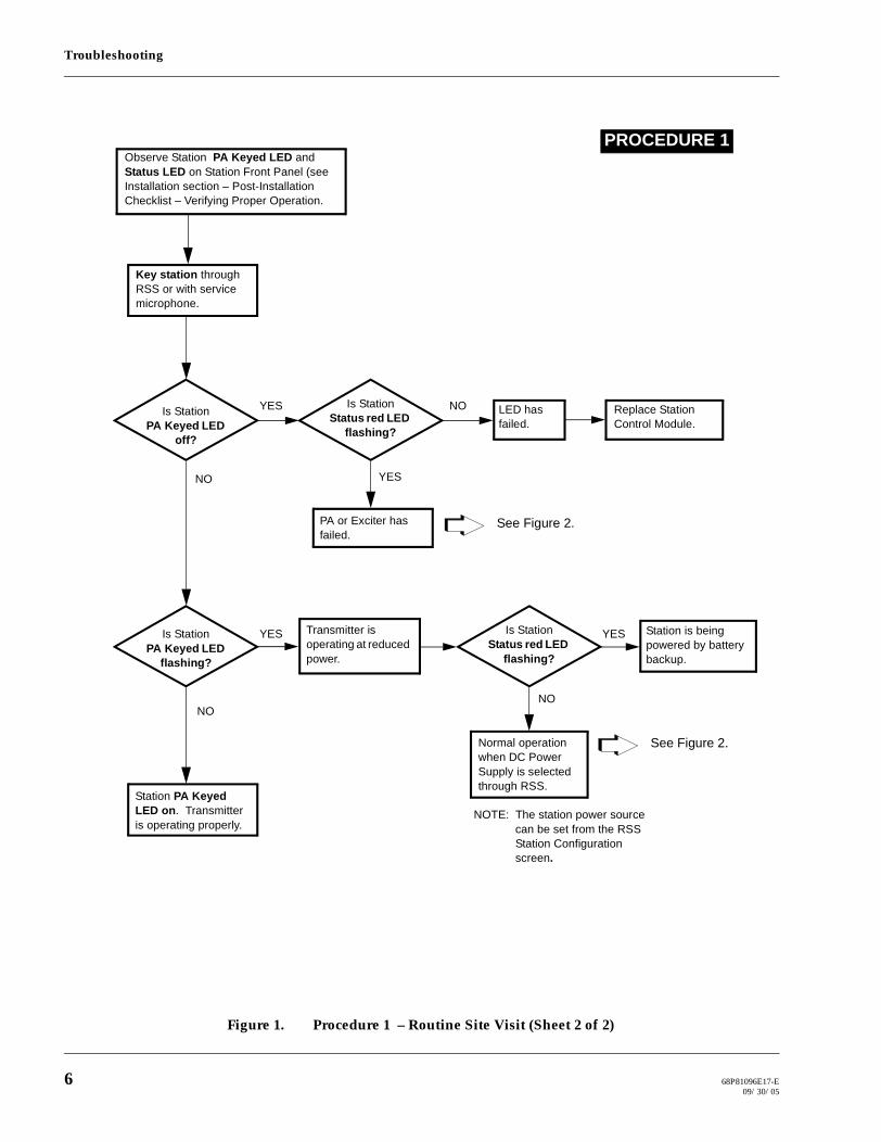
Troubleshooting
Figure 1. Procedure 1 – Routine Site Visit (Sheet 2 of 2)
PROCEDURE 1Observe Station PA Keyed LED and Status LED on Station Front Panel (see Installation section – Post-Installation Checklist – Verifying Proper Operation.
NO
PA or Exciter has failed.
Is Station PA Keyed LED
off?
Key station through RSS or with service microphone.
YES
NO
Transmitter is operating at reduced power.
Is Station PA Keyed LED
flashing?
YES
Station PA Keyed LED on. Transmitter is operating properly.
See Figure 2.
NOIs Station Status red LED
flashing?
YES
Station is being powered by battery backup.
Is Station Status red LED
flashing?
YES
Normal operation when DC Power Supply is selected through RSS.
See Figure 2.
NO
Replace Station Control Module.
LED has failed.
NOTE: The station power source can be set from the RSS Station Configuration screen.
6 68P81096E17-E09/30/05

Troubleshooting
Replace PA Module.
PROCEDURE 2
Figure 2. Procedure 2 – Station Troubleshooting
Check Error Log messages through RSS.
NOTE: The RSS Online Help describes Error Log and Diagnostic messages and how to fix a problem.
Failure occurred for Receiver?
Replace Receiver Module. See Section 4.
NO
Run Station Diagnostics through RSS while in transmit mode
Failure occurred for Exciter?
YESSee Section 4.
NO
Failure occurred for PA?
YESSee Section 4.
An equipment problem is reported or suspected.
Run Station Diagnostics through RSS while in receive mode.
Failure occurred for SCM?
Replace Station Control Module.
See Section 4.
NO
Failure occurred for DC supply to
module?
Check module connections; e.g., between SCM and Receiver, and between SCM and Exciter.
YES
NO
YES
YES
Replace Exciter Module.
68P81096E17-E 709/30/05

Troubleshooting
Interpreting LED Indicators
Four LED indicators are provided on the front of the Station Control Mod-ule (viewable on the front panel) that indicate specific operating condi-tions. The service technician may observe these LEDs to obtain a quick status indication of the station equipment.
For information on the operating conditions indicated by these LEDs, refer to the INSTALLATION section, Post-Installation Checklist, Verifying Proper Operation.
Removing/Replacing Station Front Panel
Connection of service aids (mic, speaker, etc.) or removal of any of the sta-tion modules or option cards necessitates first removing the front panel.
Removal Procedure
Remove station front panel by inserting a small flat-blade screwdriver into one of two access holes at either end of the panel and, by carefully moving the handle of the screwdriver away from the center, release the front panel locking clip from the chassis and pull away the panel (refer to Figure 3).
Replacement Procedure
Replace station front panel by inserting one of the front panel locking clips into corresponding latch on the station housing, and carefully pressing the panel on the opposite side until the second locking clip snaps into place.
Figure 3. Front Panel Removal
8 68P81096E17-E09/30/05
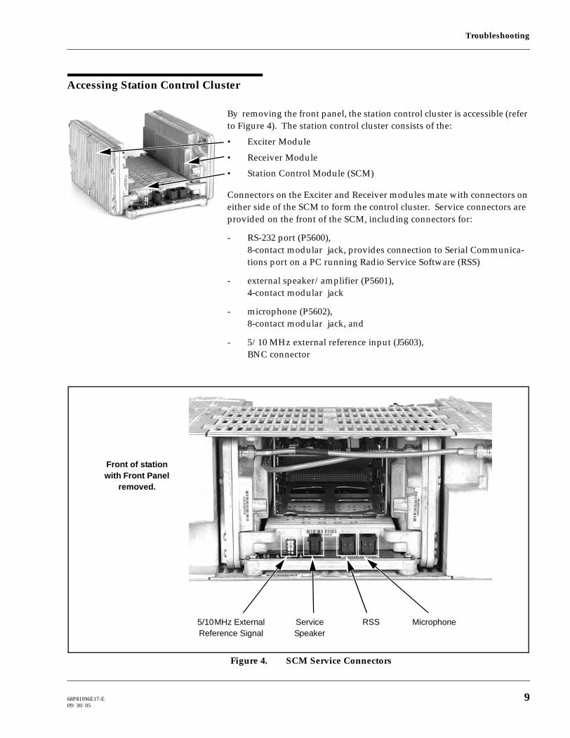
Troubleshooting
Accessing Station Control Cluster
By removing the front panel, the station control cluster is accessible (refer to Figure 4). The station control cluster consists of the:
• Exciter Module
• Receiver Module
• Station Control Module (SCM)
Connectors on the Exciter and Receiver modules mate with connectors on either side of the SCM to form the control cluster. Service connectors are provided on the front of the SCM, including connectors for:
- RS-232 port (P5600),8-contact modular jack, provides connection to Serial Communica-tions port on a PC running Radio Service Software (RSS)
- external speaker/amplifier (P5601),4-contact modular jack
- microphone (P5602),8-contact modular jack, and
- 5/10 MHz external reference input (J5603),BNC connector
Figure 4. SCM Service Connectors
5/10MHz External Reference Signal
MicrophoneRSSService Speaker
Front of station with Front Panel
removed.
68P81096E17-E 909/30/05

Troubleshooting
Using the Service Mic
The Service mic buttons (see Figure 5) provide local control of station op-eration. All of these operating functions can also be controlled through the RSS (through the Station Control area of the Station Operation Controls window).
Speaker Volume Control To increase the speaker volume, press this button. Each button press in-creases the volume by one step (approximately 2dB). There are 16 steps from the lowest volume level.
To set the speaker to the lowest volume, press and hold this button longer than 2 seconds.
The speaker volume cannot be decreased in steps. To lower the volume, reset the volume to the lowest setting and then increase it to the desired level.
Monitor Button To step through the sequence of station audio monitor modes, press this button. The selectable modes are:
- Off (no carrier squelch and no PL/DPL)Listen to the channel with the station unsquelched and PL/DPL dis-abled; that is, hear everything on the channel.
- CSQ (carrier squelch and no PL/DPL) If the station is already unsquelched (as determined by station code-plug value) then no change is heard when the CSQ mode is selected. This mode enables the station to operate in carrier squelch mode; that is, with PL/DPL disabled.
- Normal (carrier squelch and PL/DPL set by codeplug)Listen to normal radio audio operation for the channel, which is deter-mined by the station codeplug.
Intercom On/Off Button To toggle the Intercom mode, press this button. Intercom mode provides communication between the station and a Remote Controller (over a wire-line connection).
When in Intercom mode (indicated by the Station Status LED flashing green), press the PTT button to communicate over the wireline without keying the transmitter
10 68P81096E17-E09/30/05
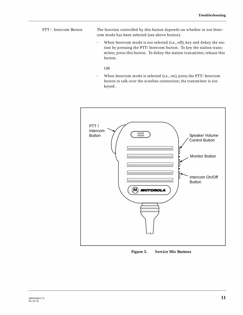
Troubleshooting
PTT / Intercom Button The function controlled by this button depends on whether or not Inter-com mode has been selected (see above button).
- When Intercom mode is not selected (i.e., off), key and dekey the sta-tion by pressing the PTT/Intercom button. To key the station trans-mitter, press this button. To dekey the station transmitter, release this button.
OR
- When Intercom mode is selected (i.e., on), press the PTT/Intercom button to talk over the wireline connection; the transmitter is not keyed.
Figure 5. Service Mic Buttons
PTT /Intercom Button Speaker Volume
Control Button
Monitor Button
Intercom On/Off Button
68P81096E17-E 1109/30/05

Troubleshooting
Verifying Transmitter Circuitry
Performing this procedure requires that the station be taken out of ser-vice. It is recommended that, unless the station is already out of service due to an equipment malfunction, this procedure be performed during off-peak hours so as to minimize the disruption of service to the system subscribers.
Introduction
While most module faults can be detected by running the station diagnos-tics provided by the RSS, the following procedure provides a more tradi-tional method of troubleshooting the transmitter circuitry. This procedure is useful in the event that the RSS is not at hand or for some reason cannot be utilized (PC malfunction, etc.).
This procedure allows the service technician to make minor adjustments and verify proper operation of the station transmit circuitry, including:
• Exciter Module
• Power Amplifier Module
• Power Supply Module
• Transmitter-related circuitry in the SCM
• Wireline Board
In general, the transmitter circuitry is exercised by injecting and measur-ing signals using a Motorola R2001 or R2600 Communications Analyzer (or equivalent). Incorrect measurement values indicate a faulty module(s); measurement values within the acceptable range verify proper operation of the above listed modules and circuitry.
Required Test Equipment
The following test equipment is required to perform the procedure:
• Motorola R2001 or R2600 Communications Analyzer (or equivalent)
• Microphone with PTT switch (GMN6147B or equivalent)
• In-Line Wattmeter (Motorola Model S-1350 or equivalent)
• Dummy Load (50Ω, station wattage or higher)
CAUTION
!
12 68P81096E17-E09/30/05

Troubleshooting
Verifying Transmitter Circuitry Procedure
1. Connect test equipment by performing Steps 1 to 5 shown in Figure 6.
In the following steps, suspected faulty modules are ranked in order of most to least likelihood.
2. Press the PTT button of the microphone and observe the PA Keyed LED indicator (DSG5602) on the Station Control Module.
• If PA Keyed fails to light, suspect the following:
Faulty Power Amplifier Module
Faulty Exciter Module
Loose or bad Exciter-to-PA RF cable
Loose or bad PA-to-antenna RF output cable
Improperly terminated PA RF output cable
Faulty Station Control Module
Faulty Backplane
Faulty Antenna Relay
3. Measure output power by pressing the PTT button and observing reading on in-line wattmeter.
• If PA output not at proper power (as set for particular site), adjust the output power as described in the RSS online help.
4. If PA output power OK, set up R2001 or R2600 for spectrum analyzer display. Press the PTT button and observe the display. The display should show a single frequency carrier:
• If the display shows multiple carriers evenly spaced about the carrier, suspect a faulty Exciter module or PA module.
• If the display shows a solid carrier but off frequency, suspect the following:
Faulty Exciter or Station Control Module
Faulty external 5/10 MHz reference source (if used)
• If the display shows a single carrier moving erratically, suspect:
Faulty Station Control Module
Faulty Exciter Module
Note
68P81096E17-E 1309/30/05

Troubleshooting
Figure 6. Test Equipment Setup for Verifying Transmitter Circuitry
1. Disconnect cable (N-type connector) from transmitter antenna at station.
2. Connect an N-to-N type cable between the station and the inline wattmeter.
3. Connect the inline wattmeter to a dummy load.
4. Connect the transmitter antenna to the R2001 antenna input. Be sure to pull the RF PORT SELECT knob out and select antenna rf input.
DummyLoad
Inline Wattmeter
Station Receive Input
Station Transmit Output
Motorola R2001Communications
Analyzer
Antenna RF port select knob (pull out)
To Receive Antenna
Station - rear
Station - front
Service MIcrophone
5. Remove front panel from station, and connect microphone to RJ-45 connector (P5602) on front of Station Control Module.
Microphone Connector on SCM
14 68P81096E17-E09/30/05

Troubleshooting
5. If display OK, set up R2001 or R2600 to display modulation. Using the microphone, push the PTT button and speak into the micro-phone. Verify that the display shows an audio signal.
• If proper display is not obtained, suspect faulty SCM or Exciter Module.
6. Set the R2001 or R2600 for GEN/MON MTR. Press the PTT button and speak loudly into the microphone to cause maximum deviation. Display should read:
- ±5 kHz maximum for a 25 or 30 kHz system.
- ±4 kHz maximum for a 20 kHz system.
- ±2.5 kHz maximum for a 12.5 kHz system.
• If proper display is not obtained, suspect faulty SCM or Exciter Module.
7. This completes the Verifying Transmitter Circuitry test procedure. If all displays and measurements are correct, the transmitter circuitry may be considered to be operating properly. Remove test equipment, restore the station to normal service, and return to the troubleshoot-ing flow chart to resume troubleshooting sequence.
Station Reset
In the event that the station repeatedly resets:
1. Disconnect dc power to PA and connect a load to the PA Module.
2. Power on the station.
3. If the station is not resetting, there is a problem with the PA.
If the station is resetting, there is a problem with another module in the station.
4. Reconnect dc power to PA.
5. If the station is resetting, there is a problem with the PA.
6. If the station does not reset, key the station.
7. If the station is resetting, there is problem with the PA.
If the station is not resetting, there is a problem with the antenna, feed line, or peripherals.
DC Power Connector
PA – Inner-facing Side
68P81096E17-E 1509/30/05

Troubleshooting
Verifying Receiver Circuitry
Performing this procedure requires that the station be taken out of ser-vice. It is recommended that, unless the station is already out of service due to an equipment malfunction, this procedure be performed during off-peak hours so as to minimize the disruption of service to the system subscribers.
If the station operates as a repeater, the transmit output from the station must be connected to a dummy load to prevent over-the-air broadcast during receiver testing.
Introduction
While most module faults can be detected by running the station diagnos-tics provided by the RSS, the following procedure provides a more tradi-tional method of troubleshooting the receiver circuitry. This procedure is useful in the event that the RSS is not at hand or for some reason cannot be utilized (PC malfunction, etc.).
This procedure allows the service technician to make minor adjustments and verify proper operation of the station receive circuitry, including:
• Receiver Module
• Power Supply Module
• Station Control Module
In general, the receiver circuitry is exercised by injecting and measuring signals using a Motorola R2001 or R2600 Communications Analyzer (or equivalent). Incorrect measurement values indicate a faulty module(s); measurement values within the acceptable range verify proper operation of the above listed modules and circuitry.
Required Test Equipment
The following test equipment is required to perform the procedure:
• Motorola R2001 or R2600 Communications Analyzer (or equivalent)
• Male N-type to Male N-type coaxial cable
• RJ-45 to BNC 15cm (6 inch) cable; part # 3083191X02
• Service Speaker; part # HSN1000
• Service Speaker adaptor cable; part # 0185180U01
• Dummy Load (50Ω, station wattage or higher) required for repeater stations only
CAUTION
!
CAUTION
!
16 68P81096E17-E09/30/05

Troubleshooting
Verifying Receiver Circuitry Procedure
1. Connect test equipment by performing Steps 1 to 3 shown in Figure 7.
2. Using the RSS, disable PL and unsquelch the Receiver such that noise is heard through the external speaker. If no audio is heard, sus-pect the following:
• Faulty Receiver Module
• Faulty Station Control Module
• R2001 or R2600 is outputting a carrier signal without modulation
3. Set R2001 or R2600 to generate a 0.5 µV (-113 dBm) FM signal at the receiver frequency, modulated by a 1 kHz tone at 3 kHz deviation for 25 /30 kHz channel spacing. The 1 kHz tone should be audible through the external speaker. If no audio is heard, suspect the following:
• Faulty Receiver Module
• Faulty antenna-to-Receiver preselector RF cable (for station with external metal preselector)
• Faulty R2001- or R2600-to-station RF cable
• Faulty Antenna Relay
4. If audio is heard, connect the external speaker RJ-45 jack to the Oscil-loscope input BNC connector, as shown in step 4 of Figure 7.
5. Using the RSS or Servie mic, increase the audio volume to maximum. Measure the audio level using the R2001 or R2600.
• Audio level should measure approximately 0.75 to 1.5 Vpp. If not, suspect faulty SCM.
6. Change R2001 or R2600 injection signal level to 0.25 µV (-119 dBm).
7. Measure the receiver 12 dB SINAD sensitivity. Set the signal strength of the communications analyser to the rated sensitivity of –116 dBm (0.35 µV).
• If the SINAD level is less than 12 dB, suspect faulty Receiver Module or SCM.
8. This completes the Verifying Receiver Circuitry test procedure. If all displays and measurements are correct, the receiver circuitry may be considered to be operating properly. Remove test equipment, restore the station to normal service, and return to the troubleshooting flow chart to resume troubleshooting sequence.
68P81096E17-E 1709/30/05

Troubleshooting
Figure 7. Test Equipment Setup for Verifying Receiver Circuit
1. Disconnect antenna cable from N-type connector on station.
2. Connect an N-to-N type cable between the station receive input and RF In / Out connector on R2001.
3. Connect service speaker to speaker connector on Station Control Module.
Motorola R2001 Communications Analyzer
RF In / Out
To Receive Antenna
Station - rear
Station - front
ServiceSpeaker
External Speaker Connector on SCM
Station Receive Input
18 68P81096E17-E09/30/05

Troubleshooting
Figure 7. Test Equipment Setup for Verifying Receiver Circuit (Continued)
Motorola R2001 Communications Analyzer
Oscilloscope Input
Station - front
External Speaker Connector on SCM
Station Receive Input
Station - rear
4. If audio is heard, connect the external speaker RJ-45 jack to the Oscilloscope input BNC connector.
RF In / Out
68P81096E17-E 1909/30/05
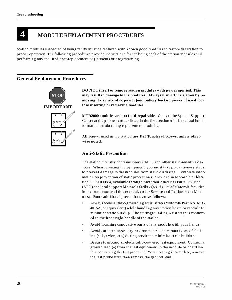
Troubleshooting
Station modules suspected of being faulty must be replaced with known good modules to restore the station to proper operation. The following procedures provide instructions for replacing each of the station modules and performing any required post-replacement adjustments or programming.
General Replacement Procedures
DO NOT insert or remove station modules with power applied. This may result in damage to the modules. Always turn off the station by re-moving the source of ac power (and battery backup power, if used) be-fore inserting or removing modules.
MTR2000 modules are not field-repairable. Contact the System Support Center at the phone number listed in the first section of this manual for in-formation on obtaining replacement modules.
All screws used in the station are T-20 Torx-head screws, unless other-wise noted.
Anti-Static Precaution
The station circuitry contains many CMOS and other static-sensitive de-vices. When servicing the equipment, you must take precautionary steps to prevent damage to the modules from static discharge. Complete infor-mation on prevention of static protection is provided in Motorola publica-tion 68P81106E84, available through Motorola Americas Parts Division (APD) or a local support Motorola facility (see the list of Motorola facilities in the front matter of this manual, under Service and Replacement Mod-ules). Some additional precautions are as follows:
• Always wear a static-grounding wrist strap (Motorola Part No. RSX-4015A, or equivalent) while handling any station board or module to minimize static buildup. The static-grounding wrist strap is connect-ed to the front-right handle of the station.
• Avoid touching conductive parts of any module with your hands.
• Avoid carpeted areas, dry environments, and certain types of cloth-ing (silk, nylon, etc.) during service to minimize static buildup.
• Be sure to ground all electrically-powered test equipment. Connect a ground lead (–) from the test equipment to the module or board be-fore connecting the test probe (+). When testing is complete, remove the test probe first, then remove the ground lead.
4 MODULE REPLACEMENT PROCEDURES
STOP
IMPORTANT
Note
Note
20 68P81096E17-E09/30/05

Troubleshooting
• All spare modules should be kept in a conductive bag for storage and transporting.
• When shipping modules to the repair depot, always pack in conduc-tive material.
When wearing a Conductive Wrist Strap, be careful near sources of high voltage. The low impedance provided by the wrist strap also increases the danger of lethal shock from accidentally touching high voltage sources.
Care of Gold-Plated Connector Contacts
The connections between the modules and the station backplane board are made with gold-plated connector contacts to provide maximum reliability. Gold-plated materials do not form a non-conductive oxide layer, and therefore should not require cleaning under normal conditions.
When the modules have been subjected to many extraction/insertion cy-cles, or if the station is operated in a dusty environment, the contacts may require cleaning. Do not use an eraser or any type of abrasive substance to clean either the module or backplane connector contacts. Any type of abrasive cleaning (typically employed for cleaning non gold-plated con-tacts) can result in the removal of the gold plating or bending of the con-nector contacts.
If cleaning of the gold-plated contacts is required, use a soft cloth damp-ened with alcohol to lightly wipe the contacts. Be sure not to touch the contact surfaces with your fingers, as finger oils and salts can contaminate the contact surfaces.
Power Down Station Before Removing/Inserting Modules
Before removing or inserting the station cluster or an option module into the station to engage the backplane connector, be sure to turn off the sta-tion power by turning off the breaker at the ac source, or disconnecting the station ac line cord.
If the station is equipped with battery backup, disconnecting the station ac line cord will not turn the station off. You must also disconnect the battery backup cable from the station power supply module. Remem-ber to reconnect the battery cable before restoring the station to opera-tion.
Front Panel Removal
Removal of any of the station modules or option cards necessitates first re-moving the front panel, as detailed in Section 3, Removing/Replacing Sta-tion Front Panel.
STOP
WARNING
STOP
IMPORTANT
STOP
IMPORTANT
68P81096E17-E 2109/30/05

Troubleshooting
Validating Repairs
After replacing a faulty module with a known good module, perform one of the following tests to validate the repair before leaving the site.
• If the faulty module was detected as the result of running station di-agnostics via the RSS, run the diagnostics again after the repair is made to ensure that the replacement module passes all diagnostic tests.
• If the faulty module was detected by an operational failure, perform the operation to ensure that the repair corrected the reported/detect-ed failure.
Replacing Fans
If a fan on a 500 W Power Supply Module or on a high power Power Am-plifier fails, it can be replaced without having to exchange the entire mod-ule. The fan can be ordered with part number 59-83663R09.
The procedure is:
1. Turn off station power by turning off breaker at ac source.
2. Remove screws (4) securing fan to PA or Power Supply casting.
3. Unplug fan electrical power connector.
4. Lift the fan away from the casting (the electrical power connector willdetach when the fan is lifted).
5. Ensure that the correct fan is being installed.
6. Position the fan on the casting.
7. Push the power connector into the plug in the casting.
8. Secure the fan to the casting with the 4 screws.
9. Restore power to the station.
Replacing Fuses
The procedure is:
1. Turn off station power from source (e.g., ac breaker).
2. Remove fuse cover plate located on the backplane shield by unscrew-ing one M4 screw.
3. Pull defective fuse carefully with small needle nose pliers.
4. Replace new fuse (part # 6583049X16) carefully with small needlenose pliers.
For continued protection of the station against risk of fire, replace the fuse only with the same type and rating of fuse.
5. Restore power to the station.
STOP
IMPORTANT
22 68P81096E17-E09/30/05

Troubleshooting
Ordering Replacement Modules
All FRU Modules are ordered through the Americas Parts Division or an-other appropriate facility (see Service and Replacement Modules in front of this manual).
Replacing Power Amplifier Module
Replacement Procedure
1. Turn off station power by turning off breaker at ac source.
2. If station is equipped with an external preselector, label and discon-nect corresponding RF coax cables to preselector and remove screws securing preselector to station.
3. Label and disconnect all cables, as follows:
• RF output coax cable to antenna port
• RF input coax cable from Exciter Module
• Control Cable (10-conductor ribbon cable which connects to J03)
• PA Power Cable (6-conductor cable which connects to J02)
4. Remove screws securing battery backup connector to PA casting.
5. Remove the station from the rack, cabinet, or wallmount bracket (if so mounted).
6. Remove six screws securing top and bottom plates to PA casting and remove PA Module.
7. Ensure that the correct PA Module is being installed.
8. Install replacement PA Module.
1. Line up holes in the PA casting with corresponding holes in the top and bottom plates.
2. Replace the screws according to the order indicated by the label numbers on the top and bottom plates; that is start with screw #1, positioned toward the front of the station.
3. Reconnect all cables.
4. Secure battery backup connector to PA casting.
9. If required, reinstall external preselector and reconnect all cables.
10. Restore power to the station.
68P81096E17-E 2309/30/05

Troubleshooting
11. Integrate the PA Module into the station.
1. Access the appropriate RSS application screen through path: Service –> Station Alignmentt –> Transmitter –> Power Amplifier.
2. Enter the PA Module Calibration number into the appropriate data field. The Calibration number is printed on the label located on the front of the PA Module.
Post-Replacement Optimization Procedure
Perform the Power Output alignment procedure located in the RSS Service menu online help facility.
24 68P81096E17-E09/30/05

Troubleshooting
Replacing Power Supply Module
Replacement Procedure
1. Turn off station power by turning off breaker at ac source.
2. If station is equipped with an external preselector, label and discon-nect corresponding RF coax cables to preselector and remove screws securing preselector to station.
3. If station is equipped with an antenna relay, disconnect control cable and remove screws securing relay to station.
4. Remove screws (2) securing battery backup connector to PA casting.
5. Label and disconnect all wires/cables, as follows:
• PA Power Cable (6-conductor cable which routes power to PA)
• Station Power Cable (8-conductor cable which routes power to backplane)
6. Remove six screws securing top and bottom plates to Power Supply casting and remove Power Supply Module.
7. Remove the station from the rack, cabinet, or wallmount bracket (if so mounted).
8. Ensure that the correct Power Supply Module is being installed.
9. Install replacement Power Supply Module.
1. Line up holes in the PA casting with corresponding holes in the top and bottom plates.
2. Replace the screws according to the order indicated by the label numbers on the top and bottom plates; that is start with screw #1, positioned toward the front of the station.
3. Reconnect all cables.
4. Secure battery backup connector to PA casting.
10. If required, reinstall external preselector and antenna relay, and re-connect all cables.
11. Restore power to the station.
Post-Replacement Optimization Procedure
Replacement Power Supply Modules are factory aligned. Therefore, no post-replacement optimization is required for this module.
68P81096E17-E 2509/30/05
Troubleshooting
Replacing Exciter Module
Replacement Procedure
1. Turn off station power by turning off breaker at ac source.
2. Remove the station control cluster:
1. Remove module lock screws (2) from front of station control clus-ter.
2. Disconnect BNC connectors on RF cables connecting PA Module to Exciter Module, and Receiver Module to Receive antenna port.
3. By pulling forward on cluster pull tabs, carefully slide station control cluster out of station.
3. Remove screws (4) securing Exciter Module to cluster and disconnect Exciter Module from Station Control Module (SCM).
4. Ensure that the correct Exciter Module is being installed.
5. Install replacement Exciter Module by plugging module into connec-tor on SCM, replacing screws (4), and sliding the cluster back into the station (along the guide rails) to mate with the connector on the back-plane. (Do not slam the station control cluster against the backplane or push any harder than necessary to seat the connector.)
6. Install module lock screws (2) to front of station control cluster and reconnect the RF cables from the PA Module and the Receive antenna port to their respective modules.
7. Restore power to the station.
Post-Replacement Optimization Procedure
1. Perform the TX Deviation Gain Adjust alignment procedure, located in the RSS Service menu online help facility. Access the RSS applica-tion screen through path Service –> Station Alignment –> Transmit-ter –> Tx Deviation.
2. Perform the Reference Modulation alignment procedure, located in the RSS Service menu online help facility. Access the RSS application screen through path Service –> Station Alignment –> Transmitter –> Ref. Modulation.
26 68P81096E17-E09/30/05

Troubleshooting
Replacing Station Control Module
Replacement Procedure
1. If the Station Control Module (SCM) is capable of communicating with the RSS, connect the PC to the RSS port, start the RSS program, and save the codeplug from the station to a file on the PC hard disk. This will allow the codeplug information to be downloaded to the codeplug located on the replacement SCM. If the module cannot communicate with the RSS, an archive file (if present on hard disk) of the particular codeplug may be downloaded. If no archive codeplug file exists, you must program the codeplug as described in the RSS online help facility.
2. Turn off station power by turning off breaker at ac source.
3. Remove the station control cluster:
1. Remove module lock screws (2) from front of station control clus-ter.
2. Disconnect BNC connectors on RF cables connecting PA Module to Exciter Module, and Receiver Module to Receive antenna port.
3. By pulling forward on cluster pull tabs, carefully slide station control cluster out of station.
4. Remove screws (4) securing Exciter Module, and screws (4) securing Receiver Module to the SCM, and disconnect both modules from the SCM.
5. Ensure that the correct Station Control Module is being installed.
6. Install replacement Station Control Module by plugging Exciter Module and Receiver Module into respective connectors on new SCM, replacing screws, and sliding the cluster back into the station (along the guide rails) to mate with the connector on the backplane. (Do not slam the station control cluster against the backplane or push any harder than necessary to seat the connector.)
7. Install module lock screws (2) to front of station control cluster and reconnect the RF cables from the PA Module and the Receive antenna port to their respective modules.
8. Restore power to the station.
Post-Replacement Optimization Procedure
1. Replacement Station Control Modules are shipped with default data programmed into the codeplug (Flash EPROM located on board). After replacing a Station Control Module, you must download code-plug data (unique to the particular station) to the replacement mod-
68P81096E17-E 2709/30/05

Troubleshooting
ule codeplug. Simply retrieve the file from your archive and follow the instructions in the RSS online help facility for saving data to the codeplug.
2. Calibrate the reference oscillator (station reference) by performing the procedure in the Routine Maintenance section of this manual.
3. Perform the TX Deviation Gain Adjust alignment procedure located in the RSS Service menu online help facility.
4. Perform the Reference Modulation alignment procedure located in the RSS Service menu online help facility.
28 68P81096E17-E09/30/05

Troubleshooting
Replacing Receiver Module
Replacement Procedure
1. Turn off station power by turning off breaker at ac source.
2. Remove the station control cluster:
1. Remove module lock screws (2) from front of station control clus-ter.
2. Disconnect BNC connectors on RF cables connecting PA Module to Exciter Module, and Receiver Module to Receive antenna port.
3. By pulling forward on cluster pull tabs, carefully slide station control cluster out of station.
3. Remove screws (4) securing Receiver Module to cluster and discon-nect Receiver Module from Station Control Module (SCM).
4. Ensure that the correct Receiver Module is being installed.
5. Install replacement Receiver Module by plugging module into con-nector on SCM, replacing screws, and sliding the cluster back into the station (along the guide rails) to mate with the connector on the back-plane. (Do not slam the station control cluster against the backplane or push any harder than necessary to seat the connector.)
6. Install module lock screws (2) to front of station control cluster and reconnect the RF cables from the PA Module and the Receive antenna port to their respective modules.
7. Restore power to the station.
Post-Replacement Optimization Procedure
1. Perform the Squelch Adjust procedure and the RSSI alignment pro-cedure (if applicable) located in the RSS Service menu online help fa-cility.
2. If the station includes an external Preselector, perform the Preselector Field Tuning Procedure of this section.
3. Perform the Preselector Field Tuning Procedure for the internal var-actor-tuned preselector of this section.
68P81096E17-E 2909/30/05

Troubleshooting
Replacing External Preselector
Replacement Procedure
1. Turn off station power by turning off breaker at ac source.
2. Disconnect cable to Receive antenna connection and cable to Receiv-er Module.
3. Remove screws (2) securing External Preselector to back of station.
4. Ensure that the correct External Preselector is being installed.
5. Install replacement External Preselector by reconnecting the 2 cables and securing the External Preselector to the station with the 2 screws.
6. Restore power to the station.
Post-Replacement Optimization Procedure
1. Perform the Preselector Field Tuning Procedure of this section.
30 68P81096E17-E09/30/05

Troubleshooting
Replacing Wireline Interface Board
Replacement Procedure
1. Turn off station power by turning off breaker at ac source.
2. Ensure that an ESD cable is connected to the station.
3. Remove Wireline Interface Board from top option card slot by care-fully pulling straight out from the station. Use the Option Card tool (part # 6683334X01) to pull the card out. Make sure that the board is placed on properly grounded anti-static surface.
4. Ensure that the correct Wireline Board is being installed.
5. Set all jumpers on replacement board to match those on the faulty board. These include input/output impedance matching jumpers (refer to Wireline Interface Board section of this manual for more in-formation).
6. Install replacement Wireline Interface Board by sliding board into top option card slot, and firmly seating the board Euro-card connector into the mating backplane connector. (Do not slam the board against the backplane or push any harder than necessary to seat the connec-tors.)
7. Restore power to the station.
Post-Replacement Optimization Procedure
1. Perform the Rx Wireline and Tx Wireline adjustment procedures lo-cated in the RSS Service menu online help facility. This includes se-lecting the 2-wire or 4-wire configuration. Ensure that the Wireline Board is aligned according to relevant leased line specifications.
68P81096E17-E 3109/30/05

Troubleshooting
Replacing Auxiliary I/O Board
Replacement Procedure
1. Turn off station power by turning off breaker at ac source.
2. Ensure that an ESD cable is connected to the station.
3. Remove Auxiliary I/O Board from middle (Option Cart #1) or bot-tom (Option Card #2) card slot by carefully pulling straight out from the station. Use the Option Card tool (part # 6683334X01) to pull the card out. Make sure that the board is placed on properly grounded anti-static surface.
4. Ensure that the correct Auxiliary I/O Board is being installed.
5. Set all jumpers on replacement board to match those on the faulty board. Refer to Auxiliary I/O Board section of this manual for more information.
6. Install replacement Auxiliary I/O Board by sliding board into mid-dle or bottom option card slot, and firmly seating the board Euro-card connector into the mating backplane connector. (Do not slam the board against the backplane or push any harder than necessary to seat the connectors.)
7. Restore power to the station.
Post-Replacement Optimization Procedure
1. Perform the Auxiliary I/O adjustment procedures located in the RSS Service menu online help facility. Ensure that the Auxiliary I/O Board is aligned according to auxiliary equipment specifications.
32 68P81096E17-E09/30/05

Troubleshooting
Replacing Backplane Board
Replacement Procedure
1. Turn off station power by turning off breaker at ac source.
2. Remove all option boards from the option card slots as described in Replacing Wireline Interface Board. Make sure that all boards are placed on properly grounded anti-static surface.
3. Remove the station control cluster:
1. Remove module lock screws (2) from front of station control clus-ter.
2. Disconnect BNC connectors on RF cables connecting PA Module to Exciter Module, and Receiver Module to Receive antenna port.
3. By pulling forward on cluster pull tabs, carefully slide station control cluster out of station.
4. If station is equipped with an external preselector, label and discon-nect corresponding RF coax cables to preselector and remove screws securing preselector to station.
5. If station is equipped with an antenna relay, disconnect control cable and remove screws securing relay to station.
6. Remove ty-wraps securing battery backup cable and Power Supply-to-PA cable.
7. Label all cables/wirelines connected to the rear of the Backplane Board and disconnect all cables/wirelines.
8. Remove screws which secure the metal shield and backplane board to the top and bottom plates.
9. Remove the metal shield and backplane.
10. Ensure that the correct Backplane Board is being installed.
11. Install the replacement Backplane Board and metal shield using the screws removed previously, reconnect all cables, and reinstall all modules, boards and assemblies.
Post-Replacement Optimization Procedure
Using the RSS, run a complete set of diagnostics to exercise all boards and modules.
68P81096E17-E 3309/30/05

Troubleshooting
Depending on the configuration, the station may have an external preselector assembly, an internal preselector, or both. The external preselector assembly is a 5-pole bandpass filter equipped with tuning slugs to adjust the pass-band corresponding to the operating frequency(s) of the station. For the internal preselector, circuitry in the Re-ceiver Module provides a varactor-tuned bandpass filter which adapts to the required frequency range under the control of the Station Control Module.
The external preselector must be retuned if the preselector assembly or Receiver Module are replaced in the field, or if the station operating frequency(s) are modified. The internal varactor-tuned preselector is factory-tuned to cover the relevant frequency band in its entirety, and is retuned only if the Receiver Module is replaced in the field or if there is a suspected problem with the Receiver alignment. The tuning procedures follows.
If the station has both an external preselector assembly and an internal varactor-tuned preselector which must be retuned, you must bypass the external preselector and retune the varactor-tuned preselector first, then reconnect the external preselector and retune it. Also, since this is a non-standard configuration, you can expect a slight degradation in the re-ceiver sensitivity (approximately 1.5 dB) due to preselector insertion losses.
External Preselector Tuning Procedure
Tuning for best SINAD response DOES NOT result in optimum tuning of the preselector assembly. You must use this field tuning procedure to obtain optimum preselector performance.
Required Test Equipment
The following test equipment is required to properly tune the external pre-selector assembly:
• RF signal generator – Motorola R2600 or R2001 Communications An-alyzer (see note below), or HP8656A signal generator (or equivalent)
• Dip/Peak Monitor – HP435B Power Meter (or equivalent) with HP8484A sensitive power head, Boonton Model 92E with BNC input, or R2001/R2600 using the spectrum analyzer function
• Torque driver capable of delivering 1.36Nm (12 in-lb) of torque and 10 mm deep well socket
• Tuning probe – Motorola Part No. 0180763D22, p/o TRN7799A
• Flat-blade screwdriver
5 PRESELECTOR FIELD TUNING PROCEDURES
STOP
IMPORTANT
STOP
IMPORTANT
34 68P81096E17-E09/30/05

Troubleshooting
The R2600 Communications Analyzer can both generate and measure si-multaneously. The R2001 may be used for either the generator or the mon-itor function, but not both simultaneously. When using R2001 as the signal generator, the RF signal must be taken from the Antenna port.
Calculating Proper Alignment Frequency
Use one of the following two methods to calculate the alignment frequen-cy to be generated by the signal generator.
For stations which are equipped with both an external preselector and an internal varactor-tuned preselector, always tune the external preselector to an actual receive frequency after first tuning the varactor-tuned preselec-tor (if required).
For stations with a single receive frequency, calculate the alignment fre-quency as follows:
1. The station receive frequency is the midpoint frequency (Fmid).
2. If the receive frequency is in the range of 132 to 150 MHz, determine the alignment frequency as follows:
• If frequency (from Step 1) is ≤ 148 MHz, then:alignment frequency = Fmid – 250 kHz
• Otherwise, use actual frequency from Step 1 (see above note).
3. If the receive frequency is in the range of 150 to 174 MHz, determine the alignment frequency as follows:
• If frequency (from Step 1) is ≤ 156 MHz, then:alignment frequency = Fmid – 250 kHz
• Otherwise, use actual frequency from Step 1 (see above note).
For stations with multiple receive frequencies, calculate the alignment frequency as follows:
1. Determine the midpoint (Fmid) of the station receive frequency range.
2. Calculate a midpoint frequency as follows:
Fmid = (Fhighest + Flowest) ÷ 2
3. Using Fmid in place of the station receive frequency, perform Step 2 and Step 3 from previous procedure (i.e., calculation of alignment for single receive frequency).
Note
Note
68P81096E17-E 3509/30/05

Troubleshooting
Preparing Equipment
1. Make sure the preselector assembly is connected to a functional Re-ceiver Module.
2. Using the torque driver and deep well socket, loosen the five tension nuts on the adjustment screws.
3. Detune the preselector by turning the 5 tuning screws (see Figure 9) clockwise (Be careful not to apply more than 0.34Nm (3 in-lb) of torque to the tuning screws in order to prevent warping the preselec-tor cover and housing):
- for frequencies > 148 MHz (in the 132 to 150 MHz range),or frequencies > 156 MHz (in the 150 MHz to 174 MHz range),turn clockwise until they are 3 mm (0.125 in.) beyond the tension nut.
- for frequencies ≤ 148 MHz (in the 132 to 150 MHz range),or frequencies ≤ 156 MHz (in the 150 MHz to 174 MHz range),turn clockwise until threaded portions are 19 mm (0..75 in.) beyond the tension nut.
4. Tighten the tension nuts to 0.68Nm (6 in-lb).
5. Connect the test equipment as shown in Figure 8.
36 68P81096E17-E09/30/05

Troubleshooting
RF In / Out
Figure 8. Test Equipment Setup for External Preselector Field Tuning
TuningProbe
To Dip/Peak Monitor (RF Millivoltmeter or power meter)
Tension Nut
Tuning Screw
Preselector Assembly
To antennaconnector
To ReceiverModule
Station Receive Input
To Receive Antenna
Station - rear
Motorola R2001 Communications Analyzer
68P81096E17-E 3709/30/05

Troubleshooting
Tuning Procedure
1. Apply ac power to the station power supply (to provide an active 50 Ω termination).
2. Adjust the signal generator to the frequency calculated in the previ-ous steps. Set the level to +5 dBm.
When tuning for a peak or dip, turn the tuning screw a 1/2 turn past the peak or dip to ensure that tuning is to a true peak or dip. Return the screw to the location of the peak or dip after verifying that it is a true peak or dip.
3. Insert tuning probe into cavity H1 (refer to Figure 9) and adjust tun-ing screw 1 for a PEAK.
4. Tighten tension nut on tuning screw 1 to at least 1.36Nm (12 in-lb) and fine tune tuning screw 1 for a PEAK.
5. Keep tuning probe in cavity H1 and adjust tuning screw 2 for a DIP.
6. Tighten tension nut on tuning screw 2 to at least 1.36Nm (12 in-lb) and fine tune tuning screw 2 for a DIP.
7. Insert tuning probe into cavity H2 and adjust tuning screw 3 for a DIP.
8. Tighten tension nut on tuning screw 3 to at least 1.36Nm (12 in-lb) and fine tune tuning screw 3 for a DIP.
9. Insert tuning probe into cavity H3 and adjust tuning screw 4 for a DIP.
10. Tighten tension nut on tuning screw 4 to at least 1.36Nm (12 in-lb) and fine tune tuning screw 4 for a DIP.
11. Insert tuning probe into cavity H4. Decrease output from signal gen-erator to –5 dBm.
12. Adjust tuning screw 5 for a DIP.
13. Tighten tension nut on tuning screw 5 to at least 1.36Nm (12 in-lb) and fine tune tuning screw 5 for a DIP.
The dip of tuning screw 5 will not be as sharp as that for tuning screws 2, 3, and 4.
14. Turn tuning screw 5 counter-clockwise 6 mm (0.25 in.).
Note
38 68P81096E17-E09/30/05

Troubleshooting
Varactor-Tuned Preselector Tuning Procedure
The Receiver Module may contain a varactor-tuned preselector which must be retuned whenever the Receiver Module CLN1211 replaced in the field. The tuning procedure requires application of an RF signal into the receiver and use of the RSS Service menu to set the high and low align-ment values of the varactor-tuned preselector. Either the Received Signal Strength Indicator (RSSI) value (if available) or SINAD is read and peaked by changing the preselector alignment values via the RSS. The alignment values 132.025 MHz, 146.025 MHz, 160.025 MHz, and 173.975.025 MHz are stored in memory (within the Station Control Module).
These four alignment values are the only information required to interpo-late the tuning voltage of the preselector to any frequency within the 132 to 174 MHz band. To retune this preselector, perform the Varactor-Tuned Preselector alignment procedure located in the RSS Service menu Online Help facility.
The RSSI can be monitored at pin C11 of the Systems connector (J5) on the station backplane (refer to Figure 10 for the location).
Figure 9. Location of Tuning Screws and Cavity Probe Holes
Preselector Assembly
To antenna connector
To Receiver Module
TuningCavities
HI
H2
H3
Tuning Screws
H4
54321
Note
68P81096E17-E 3909/30/05
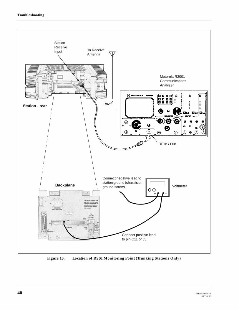
Troubleshooting
Figure 10. Location of RSSI Monitoring Point (Trunking Stations Only)
Voltmeter
+–
Connect positive lead to pin C11 of J5.
Connect negative lead to station ground (chassis or ground screw).
RF In / Out
Station Receive Input To Receive
Antenna
Station - rear
Motorola R2001 Communications Analyzer
Backplane
40 68P81096E17-E09/30/05

RECEIVER MODULE132 to 174 MHz
MODEL CLN1211 (with Varactor Preselector)MODEL CLN1212 (without Varactor Preselector)
The CLN1211 and CLN1212 Receiver Modules are described in this section. A general description, identification of inputs and outputs, a functional block diagram, and functional theory of operation are provided. The informa-tion provided is sufficient to give service personnel a functional understanding of the module, allowing mainte-nance and troubleshooting to the module level. (Refer also to the Maintenance and Troubleshooting section of this manual for detailed troubleshooting procedures for all modules in the station.)
General Description
The Receiver Module provides the receiver functions for the VHF station. The CLN1211 receiver module includes a varactor-tuned preselector; a metal external preselector, which replaces the varactor-tuned preselector, is also available. The receiver module performs highly selective bandpass filtering and dual down conversion of the station receiver RF signal. A custom receiver IC then performs an analog-to-digital conversion of the received signal and outputs a differential data signal to the Station Control Module.
Overview of Circuitry
The Receiver Module contains the following circuitry:• Frequency Synthesizer Circuitry – consisting of a phase-locked loop
and VCO, generates the first LO injection signal• Varactor-tuned Preselector Filter – provides bandpass filtering of the
station receiver RF input (not used if metal external preselector is specified).
• Receiver Front End Circuitry – performs filtering, amplification, and the first down conversion of the receiver RF signal
• Custom Receiver IC Circuitry – consists of a custom IC which per-forms the second down conversion, filtering, amplification, and ana-log-to-digital conversion of the receive signal
• A/D Converter Circuitry – converts analog receiver status signals to digital format for transfer, upon request, to Station Control Module
• Local Power Supply Regulation – accepts +8V, +10V and +15V inputs and outputs +5V, +10V, and +15V operating voltages.
1 DESCRIPTION
68P81096E19-B09/30/05-UP
Motorola Inc., 2005All Rights ReservedPrinted in U.S.A.
1301 E. Algonquin Road, Schaumburg, IL 60196
Government & Enterprise Mobility Solutions

VHF Receiver Module
Figure 1 shows the receiver module input and output external connections.
2 INPUTS AND OUTPUT CONNECTIONS
Figure 1. VHF Receiver Module Inputs/Outputs
Receiver I/O Connector – To SCM
Receive RF Input Connector
2 68P81096E19-B09/30/05

VHF Receiver Module
The following theory of operation describes the operation of the receiver circuitry at a functional level. The infor-mation is presented to give the service technician a basic understanding of the functions performed by the module in order to facilitate maintenance and troubleshooting to the module level. Refer to Figure 2 for a block diagram of the receiver module.
Synthesizer and VCO Circuitry
Introduction
The synthesizer and VCO circuitry generates the first LO injection signal for the first mixer in the receiver front end circuitry. Functional operation of these circuits is as follows.
Phase-Locked Loop
The phase-locked loop (PLL) IC receives frequency selection data from the Station Control Module microprocessor. Once programmed, the PLL IC compares a 2.1MHz reference signal (from Station Control Module) with a divided-down feedback sample of the VCO output. Depending on whether the feedback signal is higher or lower in frequency than the 2.1MHz reference, correction pulses are generated. The width of these correction pulses is dependent on the amount of difference between the 2.1MHz reference and the VCO feedback.
The up/down pulses from the PLL IC are fed to a charge pump which out-puts a dc voltage proportional to the pulse widths. This dc voltage is then low-pass filtered and fed to the VCO as the CONTROL VOLTAGE.
If a frequency change is requested by the microprocessor, the low-pass loop filter is momentarily bypassed to accelerate the frequency change.
VCO
The dc control voltage from the synthesizer is fed to dual VCOs which generate the first LO injection signal. One VCO generates signals in the upper half of the band, while the other VCO generates signals in the lower half of the band. Only one VCO is active at a time. Selection of the active VCO is provided by a BANDSHIFT signal from the PLL IC.
The active VCO responds to the dc control voltage and generates the ap-propriate RF signal. This signal is fed through a buffer amplifier and im-pedance matching and output to the first LO injection amplifier in the receiver front end circuitry. A sample of the injection signal is returned to the PLL IC (via a feedback buffer) to serve as a VCO feedback signal.
3 FUNCTIONAL THEORY OF OPERATION
Note
68P81096E19-B 309/30/05

VHF Receiver Module
Receiver Front End Circuitry
The receiver RF input is fed from the antenna to the receiver module (or a 5-pole external preselector filter, if specified, which provides highly selec-tive bandpass filtering). The signal is low-pass filtered, routed through a varactor-tuned preselector (if specified), amplified, image filtered, and fed to one input of the first mixer. The signal is mixed with the first LO injec-tion signal (generated by the synthesizer/VCO circuitry) to produce a 44.85 MHz first i-f signal.
The first i-f signal is 2-pole bandpass filtered and fed to a FET amplifier. The amplifier gain is controlled by AGC properties inherent in the ampli-fier design. The amplified first i-f signal is then 4-pole bandpass filtered and fed to the RF input of the custom receiver IC.
Custom Receiver IC Circuitry
The custom receiver IC provides additional amplification, filtering, a sec-ond down conversion, and finally analog-to-digital conversion of the sec-ond i-f signal. The digital receive signal is then sent via differential drive circuitry to the Station Control Module. The data signal contains the nec-essary I and Q quadrature information, AGC information, and other data transfer information required by the Station Control Module to process the receive signal.
The recovered audio signal is in digital format throughout the station cir-cuitry, resulting in a more noise-free, linear receiver. Analog audio is present only in the external speaker driver circuitry on the Station Control Module and on the Wireline Interface Board at the phone line connection to and from the station.
The remainder of the custom receiver IC circuitry consists of timing and tank circuits to support the internal oscillator, second LO synthesizer cir-cuitry, and second i-f circuitry.
A serial bus allows data communications between the custom receiver IC and a Digital Signal Processor (DSP) located on the Station Control Mod-ule (via a DSP ASIC device). This bus allows the DSP to control various current and gain settings, establish the data bus clock rate, program the second LO, and perform other control functions.
Note
4 68P81096E19-B09/30/05

VHF Receiver Module
A/D Circuitry
Analog signals from various strategic operating points throughout the re-ceiver board are fed to an A/D converter, which converts them to a digital signal and, upon request by the Station Control Module, outputs the signal to the Station Control Module via the SPI bus.
Voltage Regulator Circuitry
The voltage regulator circuitry consists of two +5V regulators, and filter-ing circuitry. The +5V regulators accepts a +8V input (from a regulator on the backplane) to generate Custom Analog +5V and Custom Digital +5V operating voltages to supply the custom Receiver IC and Synthesizer IC.
In addition to the voltage regulator circuitry, +15V from the Station Con-trol Module is filtered for the synthesizer charge pump. Also, +10V (from a regulator on the backplane) is filtered to supply a +10V operating volt-age for the receiver board circuitry.
68P81096E19-B 509/30/05

VHF Receiver Module
THIS PAGE INTENTIONALLY LEFT BLANK
6 68P81096E19-B09/30/05

VHF Receiver Module
6881096E19-B 709/30/05
PHASE LOCKED LOOP IC
VCO CIRCUITRY
STEERING LINECONTROL VOLTAGECHARGE
PUMP
LO-PASS LOOP
FILTER (+2.5 TO +7.5VDC)
UP
DOWN
AUX1BANDSHIFT
REFERENCE BUFFER
2.1 MHzRIN
FIN
DIVIDER BUFFER
SY
NT
H A
DA
PT
2.1MHz REFERENCE
VCO CIRCUITRY (UPPER 1/2 OF BAND)
BUFFER AMP
OSCILLATOR
SUPER FILTER
VCO CIRCUITRY (LOWER 1/2 OF BAND)
BUFFER AMP
OSCILLATOR
SERIAL BUS INTERFACE FROM SCM
VCO SELECT
CIRCUITRY
+8.7V
9
P/OP2001
2.1 MHz REF FROM SCM
RECEIVER FRONT END CIRCUITRY
LO-PASS FILTER
VARACTOR-TUNED PRESELECTOR
FILTER
PREAMPLIFIER CIRCUITRY
IMAGE FILTER
CIRCUITRY
MIXER 44.85 MHz1ST I-F 2-POLE
BANDPASS FILTER
AMPLIFIER
INJECTION FILTER
1ST LO INJECTION AMPLIFIER
CUSTOM RECEIVER
IC CIRCUITRY
CUSTOM RECEIVER
IC
44.85 MHz1ST I-F
DRIVER CIRCUITRY
450KHz FILTER
CIRCUITRY
14.4MHz TIMING
CIRCUITRY
2ND LO TANK
CIRCUITRY
2.1MHz REFERENCE
REGULATOR CIRCUITRY
+5V REGULATOR
+15V SOURCE FOR SYNTH
CHARGE PUMP
ANALOG+5V SOURCE
DIGITAL+5V SOURCE
+10VSOURCE
+10 VFROM
BACKPLANE(VIA SCM)
+15V FROM SCM
RECEIVE RF FROM
RX ANTENNA (OR ANTENNA
RELAY)
RF INPUT/OUTPUT CONNECTOR BRACKET
(REAR OF STATION)
BNC CONNECTORS
D/A CONVERTER
SPI BUS (CLOCK & DATA)TUNING VOLTAGES
A/D CONVERTER (METERING)
SPI BUS (CLOCK & DATA)VARIOUSSIGNALS
FROMRECEIVER BOARD TO BE MONITORED
METERING CIRCUITRY
VCO FEEDBACK
VCO FEEDBACK
SYNTHESIZER CIRCUITRY
FREQUENCY CHANGE
FILTER BYPASS (ANALOG SWITCHES)
CHIP SELECT
OUTPUT IMPEDANCE MATCHING+8.7V
+10 V+8.7V
3
P/OP2001
DIFF DATATO SCM
4-POLE BANDPASS
FILTER
VCO FEEDBACK
1ST LO INPUT
CHIP SELECT
25
P/OP2001
SYNTH ADAPTAND
CHIP SELECT FROM SCM
13
P/OP2001
SPI BUS TO/FROM
SCM
SPI BUS (CLOCK & DATA)
A/DCHIP
SELECT FROM SCM
17
SYNTH ADAPT
SYNTH CHIP SELECT
N-TYPE CONNECTOR
COAXIAL CABLE FROMN-TYPE CONNECTOR ON
RF INPUT/OUTPUTCONNECTOR BRACKET
TO LO-PASS FILTER
5
P/OP2001
4
Figure 2. VHF Receiver Module FunctionalBlock Diagram
+15VFILTER
+10VFILTER
+5V REGULATOR
+8 VFROM
BACKPLANE(VIA SCM)
Jumpered when used with optional External
Preselector.
EXTERNAL PRESELECTOR
(optional)

EXCITER MODULEMODEL CLN1233 (132 to 174 MHz)
The CLN1233 Exciter Module is described in this section. A general description, identification of inputs and out-puts, a functional block diagram, and functional theory of operation are provided. The information provided is sufficient to give service personnel a functional understanding of the module, allowing maintenance and trouble-shooting to the module level. (Refer also to the Maintenance and Troubleshooting section of this manual for de-tailed troubleshooting procedures for all modules in the station.)
General Description
The Exciter Module (in conjunction with the Power Amplifier Module) provides the transmitter functions for the station. Contained within a met-al module housing, the exciter board generates a low-level modulated RF signal which is input to the power amplifier module for further amplifica-tion and output to the transmit antenna. The Exciter Module interfaces directly with the Station Control Module, which provides control signals and monitoring, and routes transmit audio to the exciter.
These Exciter Modules differ only in the range of operation, as shown in the title of this section. Unless otherwise noted, the information provided in this section applies to all models.
Overview of Circuitry
The exciter board contains the following circuitry:
• Frequency Synthesizer Circuitry – consisting of a phase-locked loop and VCO, generates a modulated RF signal at the transmitter carrier frequency
• RF Isolation Switch – allows the SCM to turn on/off the exciter out-put signal to the power amplifier module
• A/D Converter Circuitry – converts analog exciter status signals to digital format for transfer, upon request, to Station Control Module
• Local Power Supply Regulation/Filtering – accepts +8V, +10V and +15V inputs and outputs +5V, +10V, and +15V operating voltages.
1 DESCRIPTION
68P81096E22-C09/30/05-UP
Motorola Inc., 2005All Rights ReservedPrinted in U.S.A.
1301 E. Algonquin Road, Schaumburg, IL 60196
Government & Enterprise Mobility Solutions

VHF Exciter Module
Figure 1 shows the exciter module input and output external connections.
2 INPUT AND OUTPUT CONNECTIONS
Figure 1. VHF Exciter Module Input/Outputs
Exciter I/O Connector – To SCM
RF Output to Power Amplifier Module
2 68P81096E22-C09/30/05

VHF Exciter Module
The following theory of operation describes the operation of the exciter circuitry at a functional level. The infor-mation is presented to give the service technician a basic understanding of the functions performed by the module in order to facilitate maintenance and troubleshooting to the module level. Refer to Figure 2 for a block diagram of the exciter module.
Synthesizer and VCO Circuitry
Introduction
As mentioned previously, the exciter module generates a low-level modu-lated RF signal which is input to the power amplifier module. The RF car-rier is generated by a frequency synthesizer consisting of synthesizer circuitry and VCO circuitry. Exciter module control signals, monitoring, and audio processing are handled by the Station Control Module. Func-tional operation of the exciter circuits is as follows.
Phase-Locked Loop
The phase-locked loop (PLL) IC receives frequency selection data from the SCM microprocessor (via the SPI bus). Once programmed, the PLL IC compares a 2.1MHz reference signal (from the SCM) with a divided-down feedback sample of the VCO output. Depending on whether the feedback signal is higher or lower in frequency than the 2.1MHz reference, up/down correction pulses are generated. (The width of these correction puls-es depends on the quantitative difference between the 2.1MHz reference and the VCO feedback.)
The up/down pulses from the PLL IC are fed to a charge pump which out-puts a dc voltage proportional to the pulse widths. This dc voltage is then low-pass filtered and fed to the VCO as the CONTROL VOLTAGE.
If a frequency change is requested by the SCM microprocessor, the low-pass loop filter is momentarily bypassed to accelerate the frequency change (via a SYNTH ADAPT signal from the SCM).
VCO
The dc control voltage from the synthesizer is fed to dual VCOs which generate the RF carrier signal. Within each band, one VCO generates sig-nals in the upper half of the band, while the other VCO generates signals in the lower half of the band. Only one VCO is active at a time. Selection of the active VCO is provided by a BANDSHIFT signal from the PLL IC.
3 FUNCTIONAL THEORY OF OPERATION
Note
68P81096E22-C 309/30/05

VHF Exciter Module
The active VCO responds to the dc control voltage and generates the ap-propriate RF signal. This signal is fed through impedance matching, am-plification, and filtering and is output to the RF Switch Circuitry. A sample of the output is returned to the PLL IC to serve as a VCO feedback signal.
Modulation
The active VCO receives an audio/data modulation signal from the Sta-tion Control Module via a splatter filter and a low-pass filter/attenuator. This VCO modulation signal modulates the active VCO to produce a mod-ulated low-level RF carrier signal.
Low-frequency modulation signals (below the loop filter corner) tend to be interpreted by the PLL as VCO frequency error. A modulation com-pensation signal is added to the PLL control voltage to cancel out this ef-fect and allow for low frequency modulation.
RF Switch Circuitry
The modulated RF signal from the VCO is fed through a buffer/attenuator to an RF switch circuit. Signal TX ENABLE from the SCM controls the switch. The RF signal is output to a BNC connector mounted in one corner of the module, just outside the module cover. A short coaxial cable con-nects the exciter output to the power amplifier module.
Data Communications
Communications with Station Control Module
Data communications between the exciter and the Station Control Module microprocessor (μP) is performed via a Serial Peripheral Interface (SPI) bus. This bus allows the SCM μP to send data to the synthesizer PLL IC (to select frequency) and to read the A/D Converter IC (next paragraph).
A/D Converter Circuitry
Analog signals from various strategic operating points throughout the ex-citer board are fed to an A/D converter, which converts them to a digital signal and, upon request by the Station Control Module, outputs the signal to the Station Control Module via the SPI bus.
4 68P81096E22-C09/30/05
VHF Exciter Module
Voltage Regulator/Filter Circuitry
The voltage regulator circuitry consists of a +5V regulator and filtering cir-cuitry. The +5V regulator accepts a +8V input (from a regulator on the backplane) and generates a +5V operating voltage for the exciter board cir-cuitry.
In addition to the voltage regulator circuitry, +15V from the Station Con-trol Module is filtered for the synthesizer charge pump. Also, +10V (from a regulator on the backplane) is filtered to supply a +10V operating volt-age for the exciter board circuitry.
68P81096E22-C 509/30/05

VHF Exciter Module
THIS PAGE INTENTIONALLY LEFT BLANK
6 68P81096E22-C09/30/05

VHF Exciter Module
68P81096E22-C 709/30/05
PHASE LOCKED LOOP IC
VCOCIRCUITRY
STEERING LINECONTROL VOLTAGECHARGE
PUMP
LO-PASS LOOP
FILTER +2.5 TO +11.0VDC
UP
DOWN
AUX1BANDSHIFT
REFERENCE BUFFER
2.1 MHzRIN
FIN
DIVIDER BUFFER
MIN
SPLATTER FILTER
REF AUDIO DELAY
EQUALIZATION
SY
NT
H A
DA
PT
VCO AUDIO FROM SCM
MODULATION LOW PASS FILTER/
ATTENUATOR
VCO CIRCUITRY (UPPER 1/2 OF BAND)
BUFFER AMP
OSCILLATOR
SUPER FILTER
PIN DIODES
VCO CIRCUITRY (LOWER 1/2 OF BAND)
BUFFER AMP
OSCILLATOR
MODULATION
RF SWITCH CIRCUITRY
J3000 BNC
MODULATED RF OUTPUT TO POWER AMPLIFIER MODULE
TX ENABLE
RF ISOLATIONCIRCUITRY
VCO FEEDBACK
VCO SELECT
CIRCUITRY
+8.5V
SPI BUS (CLOCK & DATA)
21
P/OP3601
2.1 MHz REF FROM SCM
BUFFER AMP
A/D CONVERTER (METERING)
SPI BUS (CLOCK & DATA)VARIOUSSIGNALS
FROMEXCITER BOARD TO
BE MONITORED
METERING CIRCUITRY
CHIP SELECT
13
P/OP3601
A/DCHIP
SELECT FROM SCM
+15 V FILTER
REGULATOR CIRCUITRY
+15V SOURCE FOR SYNTH
CHARGE PUMP
+5V SOURCE
+10VSOURCE
+10 VFROM
BACKPLANE (VIA SCM)
+15 V FROM SCM
4
P/OP3601
REF MOD FROM SCM
3
P/OP3601
8
P/OP3601
SYNTH ADAPT
FROM SCM
+8.7V
11
P/OP3601
TX ENABLE FROM SCM
+10V
SPI BUS TO/FROM
SCM
SYNTHESIZERCIRCUITRY
+8.5V
MODULATION
Figure 2. VHF Exciter Module FunctionalBlock Diagram
CHIP SELECT
18
P/OP3601
SYNTHCHIP
SELECT FROM SCM
+5V REGULATOR
+8 VFROM
BACKPLANE (VIA SCM)
+10 V FILTER
POWER AMPLIFIERMODULE132 to 174 MHz
MODEL CLN1226, 40 WMODEL CLN1227, 30 W
The Models CLN1226, CLN1227 Power Amplifier Modules are described in this section. A general description, identification of inputs/outputs, functional block diagram, and functional theory of operation are provided. The information provided is sufficient to give service personnel a functional understanding of the module, allowing maintenance and troubleshooting to the module level. (Refer also to the Troubleshooting section of this manual for detailed troubleshooting procedures for all modules in the station.)
General Description
The Power Amplifier Module (PA) accepts a low-level modulated RF sig-nal from the Exciter Module and amplifies the signal for transmission via the site transmit antenna. The output power is continually monitored and regulated by a feedback and control loop, with a power output control voltage being generated by the transmitter control circuitry located on the PA Input/Output boards.
Overview of Circuitry
The PA contains the following circuitry:
• Intermediate Power Amplifier (IPA) – hybrid substrate amplifier stage which accepts low-level input from Exciter Module, amplifies the signal, and outputs a 0 W to 10 W RF signal
• Butterfly Module – hybrid substrate amplifier stage which accepts output from IPA Hybrid and provides final amplification to 50 W (maximum)
• Directional Coupler/Power Detector/Low Pass Filter – couples am-plified RF signal to transmit antenna connector; also generates dc voltages proportional to forward and reflected power for use in TX power control loop; provides harmonic suppression for the station
• Dual Circulator – provides isolation between Power Amplifier out-put and transmit antenna
• Temperature Sense Circuitry – provides variable resistance signal proportional to heat sink temperature; signal is monitored by the PA power control circuitry
1 DESCRIPTION
68P81096E26-B09/30/05-UP
Motorola Inc., 2005All Rights ReservedPrinted in U.S.A.
1301 E. Algonquin Road, Schaumburg, IL 60196
Government & Enterprise Mobility Solutions

VHF 30/40 W Power Amplifier Modules
Figure 1 shows the PA Module input and output external connections.
2 IDENTIFICATION OF INPUTS/OUTPUTS
Figure 1. VHF 30 / 40 W Power Amplifier Module Inputs/Outputs
Transmit RF Output Connector
Outside View
Inside View
Front
Back
Front
Back
PA I/O Connector – To SCM through Backplane
Input From Power Supply
RF Input From Exciter Module
2 68P81096E26-B09/30/05

VHF 30/40 W Power Amplifier Modules
The following theory of operation describes the operation of the PA circuitry at a functional level. The informa-tion is presented to give the service technician a basic understanding of the functions performed by the module in order to facilitate maintenance and troubleshooting to the module level. Refer to Figure 2 for the following functional theory of operation.
RF Signal Path
A low-level modulated RF signal (approximately +13 dBm) from the Excit-er Module enters the PA Input board via a coax cable. The signal is input to the IPA and amplified to approximately 0 to 10 W (depending on the dc power control voltage (V_CNTL) from the PA output board). The IPA out-put is then fed to the Butterfly Module where final amplification occurs. The output of the Butterfly (40 W maximum) exits from the PA Output board via an N-type coax connector.
Circulator
A double circulator is built into the CLN1227 Power Amplifier Module to provide isolation between the PA module and the transmit antenna.
Heat Sink Temperature Sense
A thermistor mounted on the PA printed circuit board outputs a variable resistance proportional to the heat sink temperature. This signal is fed to the power control circuitry on the PA output board, which monitors the sig-nal and reduces the PA output power if the PA temperature exceeds set lim-its.
Output Power Control
A feedback and control loop configuration is used to regulate the PA output power. The Directional Coupler generates a dc voltage proportional to the PA Module output power. This voltage is fed to power control circuitry on the PA output board where it is compared to reference voltages to generate a dc power control voltage. The Station Control Module sends current and power limit signals to a D/A converter (via the SPI bus) to control the max-imum current/control voltage levels. The control voltage is fed to the IPA module where it controls the IPA output, thus controlling the overall out-put from the PA Module.
3 FUNCTIONAL THEORY OF OPERATION
68P81096E26-B 309/30/05

VHF 30/40 W Power Amplifier Modules
A/D Converter Circuitry
Analog signals from various strategic operating points throughout the PA module are fed to an A/D converter, which converts them to a digital sig-nal and, upon request by the Station Control Module, outputs the signal to the Station Control Module via the SPI bus.
For example, the directional coupler generates a dc voltage proportional to the reflected power. This signal is converted to a digital signal and sent to the SCM. If the sense line indicates an impedance mismatch (high VSWR), the PA is either cut back in power or shut down completely.
4 68P81096E26-B09/30/05
VHF 30/40 W Power Amplifier Modules
68P81096E26-B 509/30/05
PA AD CS*
V_CNTL
Figure 2. VHF 30/40 W Power AmplifiersFunctional Block Diagram
T°
CIRCULATOR *
50 OHMLOAD
INTERMEDIATE POWER AMPLIFIER
(IPA)
0 to 10 WMODULATED RF FROM EXCITER
MODULE
DIRECTIONAL COUPLER
LOW PASS FILTER
DIRECTIONAL COUPLER/LOW PASS FILTER
TRANSMIT RF OUTPUT TO TRANSMIT
PWR SET
I LIMIT SET
ID
PA TEMP
V_CNTLSPI BUS (CLOCK & DATA)
VOLTAGE TRANSLATOR
V_OMNI
SPI BUSTO/FROM SCM
(VIA BACKPLANE)
D/ACONVERTER
+5 V REGULATOR
+5 VdcSOURCE
+14.2 Vdc FROM POWER SUPPLY
+14.2 VdcSOURCE
+28.6 Vdc FROM POWER SUPPLY
+28.6 VdcSOURCE
V_FWD
V_RFLD
A/D CONVERTER
SPI BUS (CLOCK & DATA)
CHIP SELECT
CHIP SELECTD/A AND A/D
CHIP SELECTS
FROM SCM
14.2 Vdc
30/40 W OUTPUT BOARD
30/40 W INPUT BOARD
CLN1226 (40 W) and CLN1227 (30 W) POWER AMPLIFIER MODULE
PA DA CS*
14.2 Vdc
ΣFINAL CURRENT
V_OMNI
PA IDCIRCUIT
PA ID A
PA ID B
PA TEMP
PA ENABLE
LOW PASS FILTER **
CIRCULATOR *
50 OHMLOAD
* TTD1921 ONLY
** TTD1781 ONLY
BUTTERFLY MODULE

POWER AMPLIFIERMODULE
MODELS CLN1224 (132 to 154 MHz), 100WCLN1225 (150 to 174 MHz), 100W
The Models CLN1224, CLN1225 Power Amplifier Modules are described in this section. A general description, identification of inputs/outputs, functional block diagram, and functional theory of operation are provided. The information provided is sufficient to give service personnel a functional understanding of the module, allowing maintenance and troubleshooting to the module level. (Refer also to the Troubleshooting section of this manual for detailed troubleshooting procedures for all modules in the station.)
General Description
The Power Amplifier Module (PA) accepts a low-level modulated RF sig-nal from the Exciter Module and amplifies the signal for transmission via the site transmit antenna. The output power is continually monitored and regulated by a feedback and control loop, with a power output control voltage being generated by the transmitter control circuitry located on the PA Input/Output boards.
Overview of Circuitry
The PA contains the following circuitry:
• Final Device Module – a three stage amplifier which accepts output from the Exciter Module and provides final amplification up to 135 W. All the RF amplification transistors are included in this module
• Directional Coupler/Power Detector/Low Pass Filter – couples am-plified RF signal to transmit antenna connector; also generates dc volt-ages proportional to forward and reflected power for use in TX power control loop; provides harmonic suppression for the station
• Single Circulator – provides isolation between Power Amplifier out-put and transmit antenna
• Temperature Sense Circuitry – provides variable resistance signal pro-portional to heat sink temperature; signal is monitored by the PA power control circuitry
1 DESCRIPTION
68P81096E24-C06/30/06-UP
Motorola Inc., 2006All Rights ReservedPrinted in U.S.A.
1301 E. Algonquin Road, Schaumburg, IL 60196
Government & Enterprise Mobility Solutions
VHF 100 W Power Amplifier Module
Figure 1 shows the PA Module input and output external connections.
2 IDENTIFICATION OF INPUTS/OUTPUTS
Figure 1. VHF 100 W Power Amplifier Module Inputs/Outputs
Transmit RF Output Connector
Outside View
Inside View
Front
Back
Front
Back
PA I/O Connector – To SCM through Backplane
Input From Power Supply
RF Input From Exciter Module
2 68P81096E24-C06/30/06

VHF 100 W Power Amplifier Module
The following theory of operation describes the operation of the PA circuitry at a functional level. The informa-tion is presented to give the service technician a basic understanding of the functions performed by the module in order to facilitate maintenance and troubleshooting to the module level. Refer to Figure 2 for the following functional theory of operation.
RF Signal Path
A low-level modulated RF signal (approximately +12 dBm) from the Excit-er Module enters the PA Input board via a coax cable. The signal is input to the Final Module and amplified up to 135 W (depending on the dc power control voltage (V_CNTL) from the PA output board). The output of the Fi-nal Module is fed to the circulator.
The output of the circulator exits from the PA Output board via an N-type coax connector.
Circulator
A single circulator is built into the Power Amplifier Module to provide iso-lation between the PA module and the transmit antenna.
Heat Sink Temperature Sense
A thermistor mounted on the PA printed circuit board outputs a variable resistance proportional to the heat sink temperature. This signal is fed to the power control circuitry on the PA output board, which monitors the sig-nal and reduces the PA output power (and enables a fan) if the PA temper-ature exceeds set limits.
Output Power Control
A feedback and control loop configuration is used to regulate the PA output power. The Directional Coupler generates a dc voltage proportional to the PA Module output power, which is a maximum of 100 W. This voltage is fed to power control circuitry on the PA output board where it is compared to reference voltages to generate a dc power control voltage. The Station Control Module sends current and power limit signals to a D/A converter (via the SPI bus) to control the maximum current/control voltage levels. The control voltage is fed to the Final Module where it controls the Final Module output, thus controlling the overall output from the PA Module.
3 FUNCTIONAL THEORY OF OPERATION
68P81096E24-C 306/30/06
VHF 100 W Power Amplifier Module
A/D Converter Circuitry
Analog signals from various strategic operating points throughout the PA module are fed to an A/D converter, which converts them to a digital sig-nal and, upon request by the Station Control Module, outputs the signal to the Station Control Module via the SPI bus.
For example, the directional coupler generates a dc voltage proportional to the reflected power. This signal is converted to a digital signal and sent to the SCM. If the sense line indicates an impedance mismatch (high VSWR), the PA is either cut back in power or shut down completely.
4 68P81096E24-C06/30/06

VHF 100 W Power Amplifier Module
68P81096E24-C 506/30/06
Figure 1. VHF 100 W Power AmplifiersFunctional Block Diagram
PA AD CS*
V_CNTL
T°
CIRCULATOR
50 OHMLOAD
FINAL MODULE
DIRECTIONAL COUPLER
LOW PASS FILTER
DIRECTIONAL COUPLER/LOW PASS FILTER
PWR SET
I LIMIT SET
ID
FAN ENABLE2
PA TEMP
V_CNTLSPI BUS (CLOCK & DATA)
VOLTAGE TRANSLATOR
V_OMNI
SPI BUSTO/FROM SCM
(VIA BACKPLANE)
D/ACONVERTER
+5 V REGULATOR
+5 VdcSOURCE
+14.2 Vdc FROM POWER SUPPLY
+14.2 VdcSOURCE
+28.6 Vdc FROM POWER SUPPLY
+28.6 VdcSOURCE
V_FWD
V_RFLD
FANENABLE/SUPPLY
A/D CONVERTER
SPI BUS (CLOCK & DATA)
CHIP SELECT
CHIP SELECT
14.2 Vdc
14.2 Vdc
DC FAN
100 W OUTPUT BOARD
100 W INPUT BOARD
PA DA CS*
28.6 Vdc
Σ
FAN ENABLE1
FAN SUPPLY
FAN VOLTAGE
FINAL CURRENT
V_OMNI
PA IDCIRCUIT
PA ID A
PA ID B
PA TEMP
STATION CONTROL MODULE
MODEL CLN1465
The CLN1465 Station Control Module (SCM) is described in this section. A general description, identification of controls, indicators, and inputs/outputs, a functional block diagram, and functional theory of operation are provided. The information provided is sufficient to give service personnel a functional understanding of the module, allowing maintenance and trouble-shooting to the module level. (Refer also to the Maintenance and Troubleshooting section of this manual for detailed trou-bleshooting procedures for all modules in the station.)
General Description
The SCM serves as the main controller of the station. The SCM contains an MC68356 microprocessor which forms the heart of the module. This IC combines a 68302 Integrated Multiprotocol Processor (IMP) with a 56002 Digital Signal Processor (DSP) which, along with the support circuitry, provides signal process-ing and operational control over the other station modules.
The CLN1465 provides for Motorola Radio-Telephone Interconnect (MRTI) and 6809 trunking capabilities. In addition, the CLN1465 provides a Receiver Signal Strength Indication (RSSI) output and an external reference input for connection to a high stability oscillator.
1 DESCRIPTION
68P81096E32-E08/06/07-UP
Motorola Inc., 2005All Rights ReservedPrinted in U.S.A.
1301 E. Algonquin Road, Schaumburg, IL 60196Government & Enterprise Mobility Solutions
Station Control Modules
Overview of Circuitry
The SCM contains the following circuitry:
• Host Microprocessor – that part of the MC68356 which serves as the central controller for the station and the SCM
• Non-Volatile Memory – consists of Flash EPROM memory, containing both the system operating software and the station codeplug data
• SRAM Memory – Static RAM serves as short term storage for data• Digital Signal Processing (DSP) and DSP ASIC Circuitry – that part of the
MC68356 (and associated ASIC) which performs high-speed processing of all audio and signalling data signals
• Station Reference Circuitry – generates the 2.1 MHz reference signal used throughout the station
• Serial Peripheral Interface (SPI) Input/Output Circuitry – provides high-speed serial bus to pass control and diagnostic information between the Host microprocessor, the station modules (receiver, exciter, PA, etc.) and various serially-controlled devices on the SCM
• Serial Input/Output Circuitry – provides bus circuitry to buffer two of the Host microprocessor Serial Communication Interface (SCI) ports (SCC1 and SCC2) for communication with optional modules, and an external IBM-PC running Radio Service Software (RSS)
• Audio Processing Circuitry – routes the various audio input signals (such as microphone, wireline, and receiver audio) to output devices (such as external speaker and exciter modulation inputs) and converts (via various codecs) the audio signals between digital and analog formats for serial transmission to/from the DSP
• Parallel I/O Circuitry – provides the necessary logic interface for the Host microprocessor to send/receive miscellaneous control signals to/from vari-ous station modules and externally connected equipment, and to control the status LEDs on the front panel
• Supply Voltage Circuitry – contains filtering, voltage doubling and regulato-ry circuitry which accepts various input voltages from backplane regulators and the power supply, and generates the operating voltages required by the Receiver and Exciter modules, and the SCM
2 68P81096E32-E08/06/07
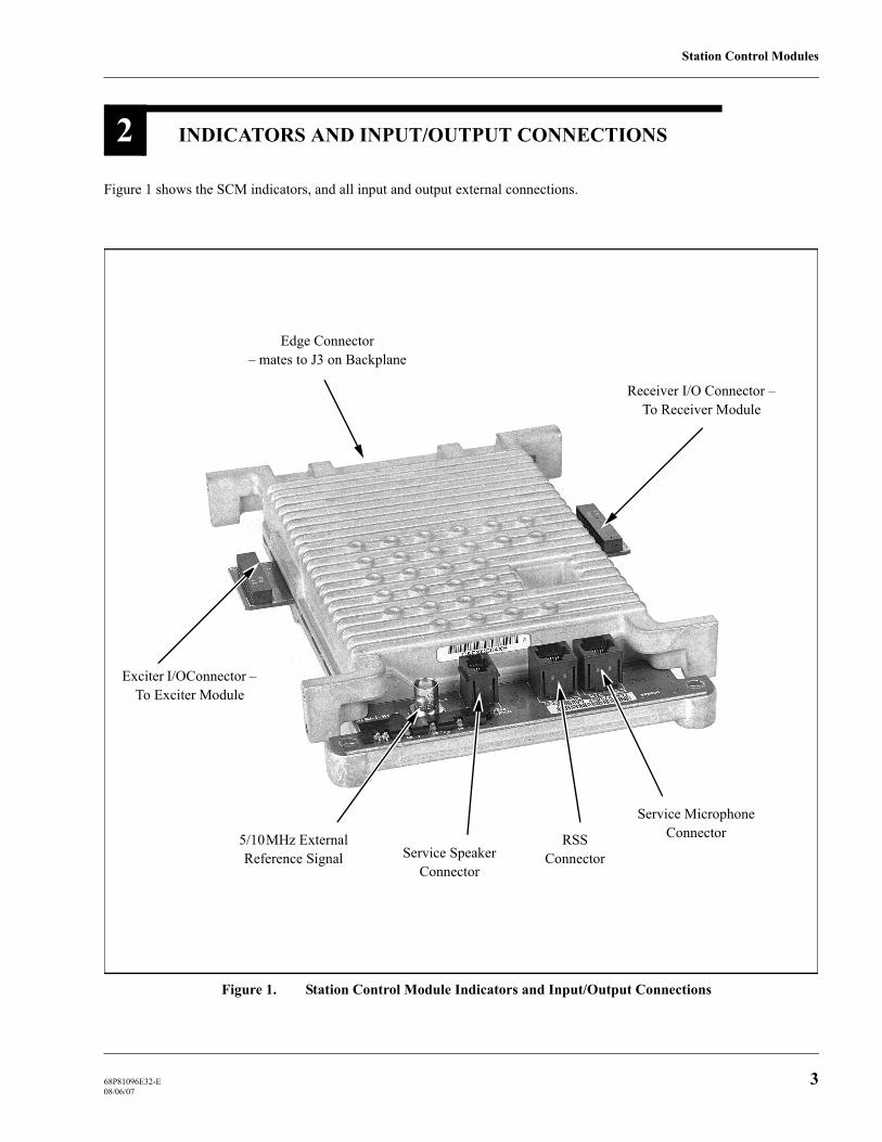
Station Control Modules
Figure 1 shows the SCM indicators, and all input and output external connections.
2 INDICATORS AND INPUT/OUTPUT CONNECTIONS
Figure 1. Station Control Module Indicators and Input/Output Connections
Receiver I/O Connector – To Receiver Module
Exciter I/OConnector – To Exciter Module
5/10MHz External Reference Signal Service Speaker
Connector
RSSConnector
Service Microphone Connector
Edge Connector – mates to J3 on Backplane
68P81096E32-E 308/06/07

Station Control Modules
The following theory of operation describes the operation of the SCM at a functional level. The information is presented to give the service technician a basic understanding of the functions performed by the module in order to facilitate maintenance and troubleshooting to the module level. Refer to Figure 2 for a block diagram of the SCM supply voltage circuitry. Refer to Figure 1 for a block diagram of the other sections of the SCM circuitry.
Host Microprocessor
General
The SCM utilizes an MC68356 Microprocessor which combines microprocessor and DSP capabilities on a single device. The Host Microprocessor (μP) functions of the SCM are performed by an MC68302 Integrated Multiprotocol Processor (IMP) which is one part of the MC68356. This part serves as the main controller for the SCM (and station), controlling the operation of the station as determined by the station software and codeplug (both stored in a non-volatile Flash EPROM device).
The μP is equipped with a 23-line address bus; only 18 lines are required to access the non-volatile Flash memory, SRAM memory, and provide control (via memory mapping) for Parallel I/O circuitry in the SCM. The Host μP operates in MC68008 mode, providing an 8-bit data bus which (buffered for the Flash and SRAM memory) is used to transfer data to/from the SCM memory, as well as Par-allel I/O circuitry. The Host μP also provides the signals controlling the demulti-plexers used to route various audio inputs/outputs in the Audio Processing circuitry of the SCM.
Station Software/Codeplug Flash Memory
The station control software and the data which determines the station personality (i.e. codeplug) both reside in one 1 MB x 8 Flash EPROM. This device is access-ed by the Host μP via the Host Address Bus and the (buffered) 8-line Host Master Data Bus.
Stations are shipped from the factory with generic default data programmed into the codeplug portion of the Flash. Field programming is performed during instal-lation using the RSS to enter additional customer-specific data, such as site output power, time-out timer settings, etc.
SRAM Memory
Each SCM contains 256 Kbyte of SRAM which provides short-term storage for data generated/required during normal operation.
3 FUNCTIONAL THEORY OF OPERATION
4 68P81096E32-E08/06/07

Station Control Modules
Host μP Clock Generation
The Host μP operates at a 20.4 MHz rate, generated internally from a reference clock. A high-stability VCO in the Station Reference circuitry generates the sta-tion master clock (16.8 MHz) which is divided by 14 (in the DSP ASIC) to 1.2 MHz and routed to the EXTAL pin of the Host μP. The Host μP multiplies this reference (under software control) by 17 to produce an internal system clock of 20.4 MHz.
Address Decoding
Host μP read and write operations are performed using the Host Address and Data buses in conjunction with four programmable chip select lines from the internal MC68356 chip select generators, CS0 to CS3, which are used in the following manner.
• CS0 is used to control access to the Flash (EPROM) memory space. Since the Flash device stores station control software, CS0 is also enabled after a reset to access the boot ROM upon system start-up.
• CS1, CS2 are used to control access of up to two SRAM devices.
• CS3 is used to control access to the Parallel I/O circuitry (control signals and SPI bus chip selects for station modules and external options).
Serial I/O Circuitry
The Serial I/O circuitry interfaces with two of the Serial Communications Inter-face (SCI) ports (SCC1 and SCC2) on the Host μP to provide general-purpose se-rial communications buses, as follows:
• SCC1 – this port is buffered to provide a high-speed Interprocessor Commu-nications Bus, allowing the Host μP to communicate with optional modules (via the backplane)
• SCC2 – serves as a serial RSS port. An 8-pin Telco connector is provided on the front of the SCM to allow service personnel to connect a PC loaded with the Radio Service Software (RSS) to the station, and perform program-ming and maintenance tasks. EIA-232 Bus Receivers/Drivers interface the connector to the SCC2 port.
68P81096E32-E 508/06/07

Station Control Modules
SPI I/O Circuitry
The Serial Peripheral Interface (SPI) I/O circuitry provides a SPI bus which is used as a general-purpose communications bus to allow the Host μP to communi-cate with other modules in the station. The SPI I/O circuitry also includes an A/D converter which allows the Host μP to determine (via the SPI bus) the connect-ed optional modules and other station characteristics.
The SCM is always configured as the SPI bus master, while other modules (Re-ceiver, Exciter, PA, etc.) are configured as bus slaves. Two slave configurations are possible:
• Basic slave – these are SPI-compatible ICs, located on the slave modules (e.g., A/D and D/A converters, and frequency synthesizers).
• Intelligent slave – these are slave modules which contain a microprocessor having a local SPI bus (e.g., intelligent equipment connected to the station via the Systems connector on the backplane).
There are three SPI signals, as follows:
• SPI CLK – derived from the internal Host μP clock. With a Host μP clock frequency of 20.4 MHz, the minimum SPI CLK is approximately 319 KHz. It is used to shift serial data from the Host μP to a slave, and from the slave back to the Host μP.
• MOSI (Master Out Slave In) – provides the data path containing information from the master (SCM) to the slave (Receiver, Exciter, PA, etc.). This is an output from the Host μP.
• MISO (Master In Slave Out) – provides the data path containing information from the slave to the master. This is an input to the Host μP.
Station Reference Circuitry
The Station Reference Circuitry incorporates a high-stability VCO (CMAC Oscil-lator Circuitry) to generate a stable 16.8 MHz signal which is fed to the DSP ASIC. The ASIC divides the signal by 8 and outputs a 2.1 MHz signal which is buffered and filtered by a splitter and output to the Exciter Module and Receiver Module as 2.1 MHz REF.
The CLN1465 SCM includes a phase-locked loop (PLL) IC. Higher stability is achieved by phase-locking the CMAC Oscillator Circuitry to a 5/10 MHz external reference source from an external high-stability oscillator, allowing the CMAC Oscillator Circuitry to be automatically adjusted to this source (referred to as “au-to-netting”).
6 68P81096E32-E08/06/07
Station Control Modules
A BNC connector (located on the front of the CLN1465) is provided to allow the highly-stable external 5 /10 MHz source to be input to the OSCIN input of the PLL to perform frequency netting. Refer to the Routine Maintenance section in this manual for recommended intervals and procedures for netting the station refer-ence.
The Station Reference Circuitry may operate in one of three modes:
• Normal Mode – In this mode, the control voltage is turned off (via control voltage enable switch) and the high-stability VCO operates in an open loop mode; stability of the VCO in this mode is 2 PPM per year.
• Manual Netting Mode – Periodically, an external 5 / 10 MHz source is re-quired to fine tune, or “net”, the 16.8 MHz reference signal. In this mode, the PLL compares the 5/10 MHz reference and a sample of the 16.8 MHz VCO output and generates up/down pulses. The Host μP reads the pulses (via SPI bus) and sends correction signals (via SPI bus) to the VCO to adjust the output frequency to 16.8 Mhz ±0.3 ppm.
• High-Stability Mode – For some systems, the free-running stability of the VCO is unacceptable for optimum system performance. Therefore, an exter-nal 5/10 MHz source is connected permanently to the BNC connector. In this mode, the PLL compares the 5/10 MHz reference and a sample of the 16.8 MHz VCO output and generates a dc correction voltage. The control voltage enable switch is closed, allowing the control voltage from the PLL to adjust the high-stability VCO frequency to 16.8 Mhz ±0.3 ppm. The VCO operates in this closed loop mode and is continually being frequency-con-trolled by the control voltage from the PLL.
Digital Signal Processor (DSP) and DSP ASIC Circuitry
General
The second half of the MC68356 contains a 56002 Digital Signal Processor (DSP). All station transmit and receive audio/data is processed by the DSP and related circuitry. This circuitry includes the DSP, the DSP ASIC, and the Audio Processing circuitry. All audio signals input to or output from the DSP ASIC are in digitized format. The digitized audio is transfered to/from various codec ICs in the Audio Processing circuitry along corresponding serial buses (dependent on the particular routing of an audio signal).
Note
68P81096E32-E 708/06/07
Station Control Modules
Inputs to the DSP circuitry are:
• Digitized receive signals from the Receiver Module
• Audio from handset or microphone connected to appropriate SCM connector (behind the station front panel)
• Digitized voice audio/data from Wireline Interface Board via PCM Codec Bus
• Auxiliary TX Audio from Systems connector on backplane
• MRTI TX Audio from Trunking/MRTI connector on backplane
• Trunk TX Data from Trunking/MRTI connector on backplane
Outputs from the DSP circuitry are:
• Digitized voice audio/data from DSP to Wireline Interface Board via PCM Codec Bus
• Digitized voice audio/data from DSP to Exciter Module (modulation sig-nals) via Audio Processing circuitry
• Digitized voice audio from DSP to external speaker via Audio Processing circuitry; speaker is connected to appropriate SCM connector behind the sta-tion front panel
• Trunk RX Audio (voice and control channel) to Trunking/MRTI connector on backplane
• MRTI RX Audio to Trunking/MRTI connector on backplane
Digital Signal Processor (DSP)
The DSP operates at a clock speed of 60 MHz with no wait states. The DSP ac-cepts and transmits digitized audio to/from the various modules in the station. The DSP provides address and data buses to receive/transmit digitized audio (via the DSP ASIC) and to access the DSP program and signal processing algorithms con-tained in three 32K x 8 SRAM ICs. It also provides a serial bus (SSI) to interface directly with linear Codec #1.
8 68P81096E32-E08/06/07

Station Control Modules
DSP ASIC
The DSP ASIC operates under control of the DSP to provide a number of func-tions, as follows:
• Interfaces with the DSP via the DSP address and data buses and interrupt re-quest lines
• Accepts 16.8 MHz signal from Station Reference circuitry and outputs a 2.1 MHz reference signal used throughout the station, and a 1.2 MHz pro-cessor clock used by the MC68356 to generate the core clocks for the DSP and Host μP.
• Provides serial interfaces for linear Codec #5 and PCM codecs
• Provides serial interface for programming custom IC on Receiver Module, and accepts digitized data from custom IC via differential-to TTL converter circuitry
• Provides Receiver Signal Strength Indication (RSSI) data ouput
Audio Processing Circuitry
General
The Audio Processing circuitry interfaces external analog audio inputs and out-puts with the DSP circuitry. The CLN1465 uses two linear codec ICs (referred to as Codec #1 and Codec #5) to handle wideband codec operation and the additional signal line requirements of trunking operation. Since audio signals input to or out-put from the DSP are in a digitized format, the codecs convert the audio signals between analog and digital formats as required.
Microphone and MRTI audio signals are digitized by Codec #2 (p/o Audio Pro-cessing Circuitry) before being sent to DSP ASIC via PCM Codec Bus
Speaker Audio
Speaker audio (to external speaker) is provided by codec #2. This signal is shared with MRTI RX Audio. The MRTI level is set (via the RSS) to suit MRTI output requirements. The adjustment is accomplished using a digital potentiometer which is controlled by the Host μP (via the SPI bus).
When the station is configured for operation with a full-duplex MRTI unit (the de-fault is half-duplex), MRTI TX Audio is not routed to the speaker to prevent echo problems on the phone line. However, this also prevents use of the local micro-phone input and external speaker for MRTI testing.
Since trunking and MRTI share the same backplane connector, they are mutually exclusive.Note
68P81096E32-E 908/06/07

Station Control Modules
Microphone
Microphone audio passes through preamp/bias generator circuitry to a switch which selects mic or MRTI TX Audio, and routes the result to Codec #2. A sep-arate path from the preamp output routes mic audio to the MRTI RX Audio output. This allows mic audio to reach the MRTI output without appearing on the local speaker. Gain in the mic audio paths is chosen to match the required MRTI levels.
Discriminator Audio
DISC RX Audio is generated by linear Codec #5. Normally it is a wideband RX audio signal, available on the backplane for the system connector, the TCC con-nector (as Trunk RX Data), and for any option cards. However, it has three other functions as well:
• Under the influence of the Audio Mode input on the system connector, the signal is changed to band-limited RX audio with optional de-emphasis and squelch.
• In line test mode, Line 1 input audio from the Wireline Interface Board (WIB) is routed to this output for level checking and test purposes.
Auxiliary TX Audio
The system connector input, Aux TX Audio, provides a path for audio from exter-nal equipment to reach the transmitter without passing through the wireline. The Audio Mode input switches it between wideband audio which is only splatter-fil-tered, and audio which is band-limited and pre-emphasized before being splatter-filtered. In either case, the audio reaches the DSP via codec #1. In line test mode, this input is routed to the Line 2 output for level setting and test purposes. In ad-dition, for special applications, the signal can be routed directly to the exciter (i.e., does not pass through the DSP). There is no adjustable gain required for this in-put.
10 68P81096E32-E08/06/07

Station Control Modules
Wireline Interface Board Audio
Each of the wireline inputs/outputs has a programmable gain stage on the Wireline Interface Board (WIB). Digitized audio is carried to/from the DSP ASIC via the PCM Codec bus. When the line 1/2 pair carries narrow-band audio, the audio is converted to/from digital format by a PCM Codec on the WIB.
For the 8-wire model WIB, the line 3/4 pair are restricted to narrow-band audio, and are converted to/from digital format by a PCM Codec on the WIB.
MRTI Audio
MRTI audio is handled by Codec #2. In most installations, the MRTI is a half duplex device. This allows MRTI TX Audio to be routed to the local speaker (and thus to the MRTI RX AUDIO line) without causing echo problems (since the MRTI RX AUDIO line is muted in the MRTI). Gain in the MRTI paths is set by station software.
Full duplex MRTI operation is available, with the limitation that MRTI TX Audio does is not heard from the local speaker.
Trunking Audio
A trunking station can operate as either a control channel or a voice channel. In either case, wideband audio is routed to/from the Trunking Central Controller (TCC) as Trunk TX Data (through Codec #1) and Trunk RX Data (through Codec #5), providing paths for control and status tones. For voice channel operation, voice audio is routed to the WIB as described in the Wireline Audio section.
Exciter Modulation Signals
Digitized audio/data intended to be transmitted from the station is output from the DSP circuitry to Codec #1. The digitized signal is converted to analog, level shift-ed and amplified. The output is then fed to one of the inputs of a multiplexer switch. The output of the multiplexer is fed to two individual digitally-controlled potentiometers (each of which is adjusted by the Host μP via the SPI Bus) and out-put to the Exciter Module as modulation signals VCO MOD AUDIO and REF MOD AUDIO.
Parallel I/O Circuitry
General
The Parallel I/O circuitry allows the Host μP to generate SPI bus chip selects and to send/receive control signals to/from station modules and external options (via the backplane).
68P81096E32-E 1108/06/07

Station Control Modules
Refer to the Backplane section of this manual for complete details on the input/output signals which are routed to/from the backplane.
Input Circuitry
A buffer is provided to route serial station information (SERIAL ID IN) to the Host μP from a serial ID device on the station backplane.
An octal buffer is used to allow various input control signals from optional station circuitry (connected to the backplane) to be accepted and sent to the Host μP. This includes input signals from MRTI and trunking equipment.
Output Circuitry
Two 1-of-16 demultiplexers are used to provide various SPI bus chip selects and four octal D flip-flops provide control signals to be output to the SCM, the Receiv-er and Exciter modules, and station circuitry (via the backplane). Control of the demultiplexers and flip-flops comes via the Host Data bus and associated chip se-lect signals from the Host μP.
Front Panel LEDs
Four status LEDs are provided on the front panel to provide visual indications of various station operating conditions. The LEDs are driven, via software control, by five lines from an octal D flip-flop in the Parallel I/O circuitry.
The front panel Station Status indicator actually comprises two LEDs, one red and one green, which produce a bicolor effect to indicate different informational messages, depending on the particular LED(s) and duty cycle enabled. The result-ing bicolor effect is achieved by locating the two LEDs adjacent to each other on the SCM board and combining the light sources through a single light pipe to the front panel.
Refer to the Station Operation section of this manual for complete details on the interpretation of the LEDs.
Supply Voltage Circuitry
The SCM contains on-board regulator and filtering circuitry to generate the vari-ous operating voltages required by the SCM circuitry. The SCM routes +10 V and +8 V from two regulators on the backplane to the Receiver and Exciter modules.
Note
Note
12 68P81096E32-E08/06/07

Station Control Modules
+14.2 V and +5V from the power supply (via the backplane) are used as sources for the following supply voltage circuits:
• +15 V Regulator Circuitry – voltage doubler circuit accepts +14.2 V input and feeds +15 V regulator to provide +15 V for the Receiver and Exciter modules.
• +12 V Regulator Circuitry – accepts input from the +15 V regulator to gen-erate the voltage required (under Host μP control) for powering the Flash memory device during programming and erasing cycles.
• +5 V Regulator Circuitry – provides VCCA (analog +5 V) for the Audio Processing circuitry in the SCM.
• Filtering Circuitry – filters the +14.2 V and +5 V from the power supply (via backplane) to provide +14.2 V and VCC (digital +5 V) for the SCM digital circuitry.
68P81096E32-E 1308/06/07

Station Control Modules
FILTERCIRCUITRY
SUPPLY VOLTAGE CIRCUITRY
VOLTAGEDOUBLER
+5 VREGULATOR
+15 VREGULATOR
+12 VREGULATOR
INHIBIT
+12 V
+15 V RX
TORECEIVER MODULE+10 V RX
+8 V
+15 V TX
+10 V EX
+8 V
TOEXCITER MODULE
VCCA(ANALOG +5 V)
+14.2 V
+14.2 VdcFROM POWER SUPPLY
(VIA BACKPLANE)
+5 VdcFROM POWER SUPPLY
(VIA BACKPLANE)
+10 Vdc(FROM BACKPLANE
REGULATOR)
+8 Vdc(FROM BACKPLANE
REGULATOR)
FLASH PWR EN*
VCC(+5 V)
DIGITALGROUND
STATICGROUND
ANALOGGROUND
GROUND(FROM BACKPLANE)
2.1 MHz FROMDSP ASIC
FROM HOST MICROPROCESSOR
TOEXTERNAL SPEAKER
FILTERCIRCUITRY
Figure 2. Station Control Module Functional Block Diagram - Supply Voltage Circuitry
14 68P81096E32-E08/06/07

Station Control Modules
68P81096E32-E 1508/06/07
Figure 1. Station Control Module Functional BlockDiagram
- Station Control Circuitry (1 of 2)
PHASE-LOCKED
LOOPIC
SPI BUS
STATION REFERENCE CIRCUITRY
BUFFER/SPLITTER
2.1 MHz REFTO EXCITER MODULE
2.1 MHz REFTO RECEIVER MODULE
OSCIN
FIN
5 MHz REF
16.8 MHz TO DSP ASIC
16.8 MHz
HIGHSTABILITY VCO
(CMAC)
SPI BUSL
CE
EXTERNAL REF ENABLE
CONTROL VOLTAGEENABLE SWITCH
CONTROL VOLTAGE
2.1 MHz FROM DSP ASIC
32K X 8RAM
32K X 8RAM
32K X 8RAM
DSP DATA BUS
DSPASIC
P) / DSP ASIC
RX DATA
ABA_IRQ*
CODEC_IRQ*
1.2 MHzOUT
2.1 MHzOUT
16.8 MHzIN
RSSI7
RSSI DATA
ODC/SBIRECEIVER SERIAL BUS
DIFFERENTIAL-TO-TTLCONVERTER/BUFFER
DIFFERENTIAL DATAFROM
RECEIVER MODULE
PCM CODEC I/F
LINEAR CODEC I/F
DSP ADDRESS BUS
PCM CODEC BUS
20 KHz CODEC BUS
S
H
16.8 MHz TO DSP ASIC
INTERNAL SPI BUS (MOSI/SPI CLK)
ECTORCTOR
M)
2.1 MHz
F
G
I
TOSUPPLY
VOLTAGECIRCUITRY
TO/FROMRECEIVE MODULE
J
TOWIB CODEC(S)
VIABACKPLANE
AND WIB(CLEAR AUDIO ONLY)
PCM CODEC BUS
2
RESETX
VCC
CLK_RSTX
3
A0 – A3, A15
D0 – D23 D8 – D23
D0 – D7
D16 – D23
D8 – D15
5 MHzFROM
EXTERNAREFEREN
DIGITALSIGNAL
PROCESSOR(DSP)
DIGITAL SIGNAL PROCESSOR (DS
256K X 8RAM
HOST MASTER DATA BUSHOST ADDRESS BUS
BUFFER
HOST DATA BUS
HOSTMICROPROCESSOR
1-OF-8DEMUX
5
1.2 MHzIN
HOST MICROPROCESSOR
SERIAL I/O CIRCUITRY
SCC2
SPI
SCC1
WDOG SSI
EIA–232TRANSCEIVER
RSS PORT(8-PIN TELCO CONNECTOR
ON FRONT OF SCM)6
2NON-INVERTING
BUFFERS
SCC1 CS*
FLASH PWR EN*
OPTION1 SCI
OPTION2 SCI
INTER-PROCESSOR SERIAL COMMUNICATIONS I/F
TO OPTION BOARDS(VIA BACKPLANE)
PARALLEL I/O CHIP SELECTS
CS LATCH*
SPI CLK/MOSI
BUFFERS3
MISO GATE
HOST SPI BUS
TO/FROMBACKPLANE
TO/FROMEXCITER MODULE
TO/FROMRECEIVER MODULE
DATA IN
PTEMP+
OPTION1 ID
OPTION2 ID
WIRELINE ID
WL DC CONTROL
SCM VERSION
EXT. (MIC) SWITCHES
A/DDATA OUT
FROMBACKPLANE
HOST MISO
INTERNAL SPI BUS (MOSI/SPI CLK)
INTERNAL MISO
2
SPI I/O CIRCUITRY
B
C
24 KHz CODEC BU
1.2 MHz CLOCK
TO MICROPHONE CONN(8-PIN TELCO CONNE
ON FRONT OF SC
P5602
P5600
6
PB8
(PART OF 68356)
(PART OF 68356)
TOSUPPLY VOLTAGE
CIRCUITRY
SERIAL ID IN* D
E
AUDIO PROCESSING CONTROL BUS A12
D0 – D7
SPI CLK
SPI CLK
RESETCIRCUITRY
1M X 8FLASH
RESET*
RP*
RESET*DRESET*
VCC
TO BACKPLANE,PARALLEL I/O AND
AUDIO PROCESSING CIRCUITRY
2
2
AC FAIL
OPT IRQ*
EXT PTT*
MIC PTT*
PB0
PB11
PB9
RESET*
FROMBACKPLANE
WL DC CONTROL REQ*
PB10
RESET*
16
A0 – A18
A15 – A17
A0 – A15

Station Control Modules
16
OCTAL DFLIP-FLOP
(U4105)
4
4
SYN2T CS*
SYN1T CS*
ADT CS*
TO EXCITER MODULE
SYN2R CS*
SYN1R CS*
ADR CS*
DAR CS*
PEND CS*
WL2 LATCH CS*
EXT SPI CS2*
EXT SPI CS1*
WL1 LATCH CS*
PA A/D CS*
TRUNK DUPLEX EN*
MRTI MONITOR*
PL STRIP* or CCI
TRUNK TX INHIBIT*
TRUNK MUTE*
7
CHIP SELECTS TO OPTION BOARDS
PA DA CS*
MRTI POT CS*
AD CS*
ANTENNA RELAY
RF RELAY CONTROL
PA ENABLE
TO/FROM BACKPLANE
SCCI CS*
TX ENABLE
ADAPT T*ADAPT R*
AUX CARRIER
MRTI RX CARRIER*
RDSTAT-R2CONT
PATCH INHIBIT*
RX CODE DETECT*
TX CODE DETECT*
NOISE B CONT2
NOISE B CONT1
TO RECEIVER MODULE
CS*
CARRIER DETECT SW
TRUNK MRTI PTT*
EXT CODE DETECT
RX INHIBIT-R2 STATUS
LED CONTROL LINES
MOD POT CS*
SYNTH CS*
TO SPI I/OA/D
CONVERTER
EXTERNAL REF ENABLETO STATIONREFERENCECIRCUITRY
SERIAL ID IN*
SERIAL ID OUT*
SERIAL ID1*
OCTAL DFLIP-FLOP
(U4103)
OCTAL DFLIP-FLOP
(U4107)
1 OF 16DEMUX(U4101)
OCTAL DFLIP-FLOP
(U4104)
1 OF 16DEMUX(U4102)
CHIP SELECT*
OCTALBUFFER(U4106)
STATUS
RX ACTIVE
PA ON
FAILSOFT
2FRONTPANELLEDS
SCCI CS*
LINE
BAA
E
F
5
68P81096E32-E08/06/07
PARALLEL I/O CIRCUITRY
D0 – D7
HOST DATA BUS
CS LATCH*
OCTAL DFLIP-FLOP
(U4100)
SWITCH
CLEAR TX AUDIO
AUX TX AUDIO
MRTI RX AUDIO
TRUNK TX DATA
AUX TX AUDIO
SWITCH
TO 2 OUTPUTVIA
CKPLANEND WIB
BUFFER
PCM1 DI
PCM1 DO
SPEAKER AUDIO
MRTI TX AUDIO
MIC AUDIO
MICPREAMP
SWITCH
SWITCH
CODEC2 MUX CONT
SPKR MUTE
SWITCH
TRUNK RX AUDIO
DISC RX AUDIO
(24 KHz LINEAR)
VCO MOD AUDIOTO
EXCITER MODULE
REF MOD AUDIOTO
EXCITER MODULEDIGITAL
MOD POTS
MOSI / SPI CLK
MOD MUX CONT
R–2R LADDER
RSSI (DC VOLTAGE) TOOPTION BOARDSVIA BACKPLANE
FROMSYSTEMS CONNECTOR
VIA BACKPLANE
RAW WL TX AUDIO
(CONTROL CHANNEL)
(VOICE CHANNEL)
TCC MUX CONT
CODEC1 MUX CONT1/2
AUDIO PROCESSING CIRCUITRY
FROMMRTI CONNECTOR
ON BACKPLANE
20 KHz CODEC BUS
(20 KHz LINEAR)CODEC #5
D/A
A/D
PCM CODEC BUS
CODEC #2
D/A
A/D
(8 KHz PCM)
VAG
RSSI DATA
7
24 KHz CODEC BUS
TO EXTERNAL SPEAKER(4-PIN TELCO CONNECTOR
ON FRONT OF SCM)
P5601
TO MIC CONNECTOR(8-PIN TELCO CONNECTOR
ON FRONT OF SCM)
P5602
TOMRTI CONNECTOR
ON BACKPLANE
CODEC #1
A/D
D/ASSI_STD
SSI_SRD
TO OPTION BOARDSVIA BACKPLANE
F
MOSI / SPI CLK
H
G
5
PARALLEL I/O CHIP SELECTSC
MOD POT CS*
MRTI POT CS*
D
A
D0 – D7
FROM LINE 1 INPUTVIA BACKPLANE AND WIB
TRUNK TX DATATO/FROM
TRUNKING CONTROLLERVIA BACKPLANE
I
J
B
TO OPTION BOARDSVIA BACKPLANE
igure 1. Station Control Module Functional BlockDiagram - Station Control Circuitry (2 of 2)
LIN_DI
LIN_DO
2
DIGITALMRTI POT
Σ
DIGITAL SIGNALS
AUDIO SIGNALS
DISC RX AUDIO
DIGITALAUX TX POT
68P81096E28-C09/30/05-UP
Motorola Inc., 2005All Rights ReservedPrinted in U.S.A.
1301 E. Algonquin Road, Schaumburg, IL 60196
Government & Enterprise Mobility Solutions
The Model CLN1204 Wireline Interface Board is described in this section. A general description, identification of jumpers, and inputs/outputs, functional block diagrams, and functional theory of operation are provided. The information provided is sufficient to give service personnel a functional understanding of the module, allowing maintenance and troubleshooting to the module level. (Refer also to the Maintenance and Troubleshooting sec-tion of this manual for detailed troubleshooting procedures for all modules in the station.)
General Description
The Wireline Interface Board (WIB) serves as the interface between the customer telephone lines and the station equipment. Each WIB contains circuitry to interface with a variety of telephone line configurations and signal types.
The WIB is installed behind the front panel, above the Station Control Module within the option-card bracket, and is connected to a 96-pin Euro connector located on the backplane of the station. The phone line connec-tions are routed from a wire-trap terminal block mounted on the rear of the backplane to the WIB connector.
Overview of Circuitry
The WIB contains the following circuitry:
• Audio and Data Circuits – the WIB provides inbound and outbound voice and data circuits which interface with the customer phone lines
• Line Impedance Selection – jumper fields provide impedance match-ing to satisfy several different wireline telecom specifications.
1 DESCRIPTION
4 WIRE, EUROWIRELINE INTERFACE
BOARDMODEL CLN1204
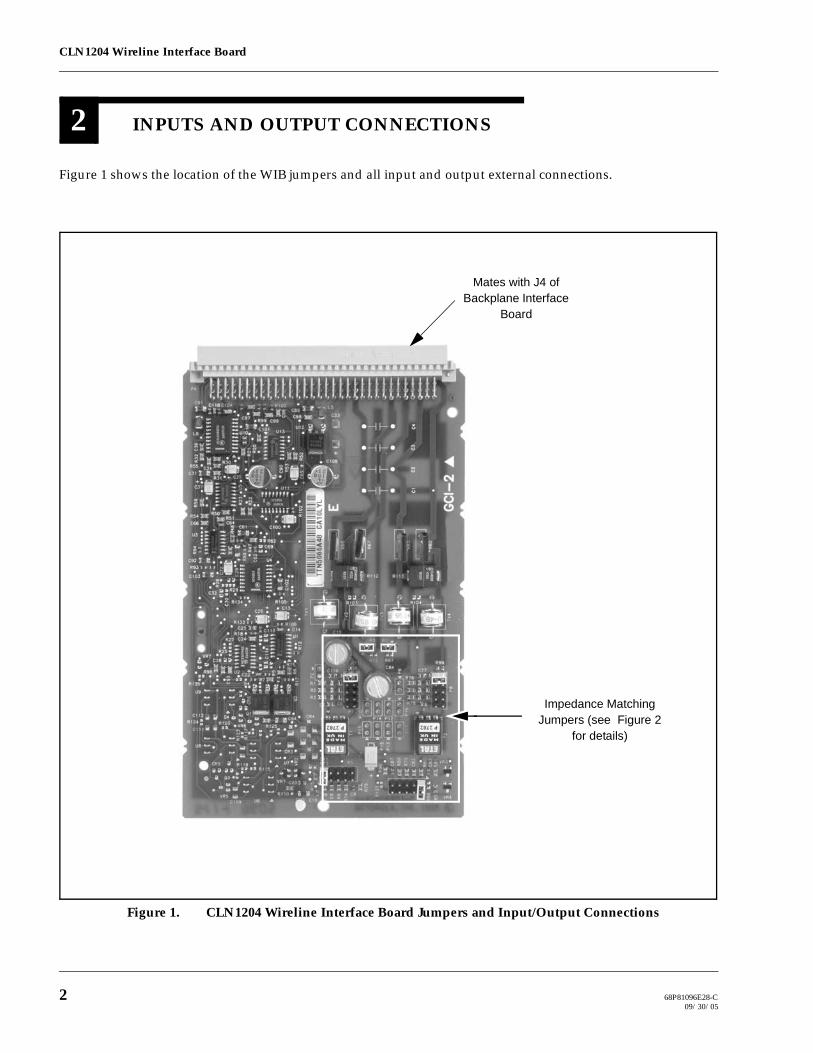
CLN1204 Wireline Interface Board
2 68P81096E28-C09/30/05
Figure 1 shows the location of the WIB jumpers and all input and output external connections.
2 INPUTS AND OUTPUT CONNECTIONS
Figure 1. CLN1204 Wireline Interface Board Jumpers and Input/Output Connections
Mates with J4 of Backplane Interface
Board
Impedance Matching Jumpers (see Figure 2
for details)

CLN1204 Wireline Interface Board
68P81096E28-C 309/30/05
The following theory of operation describes the operation of the WIB circuitry at a functional level. The informa-tion is presented to give the service technician a basic understanding of the functions performed by the module in order to facilitate maintenance and troubleshooting to the module level. Refer to Figure 3 for a block diagram of the 2-wire voice signal path, and to Figure 4 for the 4-wire voice signal path.
Functional Overview(Refer to Figures 3 & 4)
Introduction
As mentioned previously, the WIB serves as the interface between the cus-tomer analog telephone lines and the serial PCM data signals of the station equipment. In general, the WIB routes all voice and/or remote control sig-nals between the station equipment and the landline equipment (e.g., a control center, modem, etc.).
As shown in the block diagrams in Figures 3 and 4, the WIB contains one 2-wire audio circuit and one 4-wire audio circuit. Also provided is imped-ance-matching jumper fields which are used to meet various wireline specifications.
Audio/Data Circuits
As shown in the block diagrams, each WIB contains a PCM Codec-filter, SPI latch and associated circuitry which can be configured to provide the following signal paths:
• 2-wire voice audio/data from landline to station, and from station to landline
• 4-wire voice audio/data from landline to station, and from station to landline
These audio signals may include Tone Remote Control signals
3 FUNCTIONAL THEORY OF OPERATION

CLN1204 Wireline Interface Board
4 68P81096E28-C09/30/05
Description of Audio/Data Signal Paths
For 2-wire and 4-wire configurations, phone line connections are made at the wire-trap terminal connector on the station backplane, with the re-quired line impedance match being selected on the WIB. 2-wire audio con-nections are made at Line 2 Audio.
Refer to Figure 2 for the correct settings of impedance matching jump-ers, as determined by the country in which the station is being operated. Incorrect jumper settings may violate local telecommunications author-ity regulations and place the equipment in an unapproved status. Some countries also specify a maximum allowed line input level. Refer to the RSS Online Help, under Line Level.
Coarse gain adjustments are provided by circuitry on the WIB for Land-line-to-Station and Station-to-Landline audio paths. Additional fine level adjustments are performed in software in the Station Control Module.
2-Wire Voice Audio Path (Refer to Figure 3)
Voice audio signals sent to/from the station via 2-wire copper pair are pro-cessed by the 2-wire audio circuit on the WIB (Line 2 Audio). The audio transformer in this circuit may have both inbound and outbound audio signals present simultaneously. In this case, the outbound and inbound signals are mixed and routed via the inbound audio path to the SCM, where an adaptive cancellation routine in the DSP isolates the inbound au-dio. The 2-wire audio circuit operates as follows:
Landline-to-Station balanced audio is input to the primary of an audio transformer. The signal is induced into the transformer secondary and fed to a buffer. (Note that jumpers in parallel with the transformer primary and secondary provide for selectable impedance matching. Refer to Fig-ure 2 for impedance matching information.)
The buffer sums the inbound and outbound signals and feeds this signal, via an analog switch (not shown), to pre-emphasis and gain adjust circuit-ry. To compensate for line losses, the gain adjust circuitry provides coarse adjustment for eight levels of gain adjust (5, 10, 15, 20, 25, 30, 35, and 40dB) which is under the control of the SCM (via the SPI latch).
The output of the gain adjust circuitry is de-emphasized and then fed to an A/D converter in the PCM codec, which digitizes the audio signal into a PCM output. This output is fed serially to the DSP ASIC on the SCM, which provides a memory-mapped interface with the DSP and other SCM audio circuitry (refer to the Station Control Module section).
Station-to-Landline audio is input to the WIB as PCM data (WL 1/2 RXD) and fed to a D/A converter in the PCM codec, which takes the PCM data and converts it to an analog audio signal. The audio signal is fed to gain
Note
CAUTION
!

CLN1204 Wireline Interface Board
68P81096E28-C 509/30/05
adjust circuitry. The SCM controls the gain adjust circuitry (via the SPI latch) to provide four coarse levels of gain (0dB, -6dB, -12dB, and -20dB).
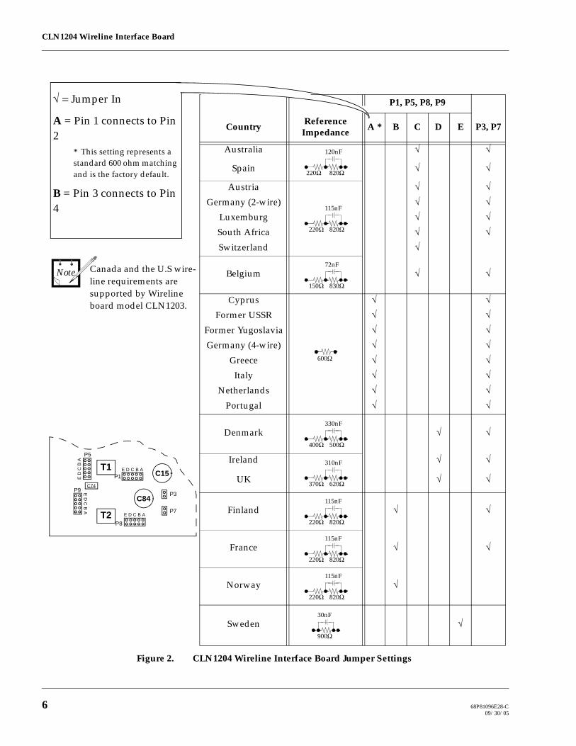
CLN1204 Wireline Interface Board
6 68P81096E28-C09/30/05
P1, P5, P8, P9
CountryReference
ImpedanceA * B C D E P3, P7
Australia √ √
Spain √ √
Austria √ √Germany (2-wire) √ √
Luxemburg √ √South Africa √ √Switzerland √
Belgium √ √
Cyprus √ √Former USSR √ √
Former Yugoslavia √ √Germany (4-wire) √ √
Greece √ √Italy √ √
Netherlands √ √Portugal √ √
Denmark √ √
Ireland √ √
UK √ √
Finland √ √
France √ √
Norway √
Sweden √
820Ω
120nF
220Ω
820Ω
115nF
220Ω
830Ω
72nF
150Ω
600Ω
500Ω
330nF
400Ω
620Ω
310nF
370Ω
820Ω
115nF
220Ω
820Ω
115nF
220Ω
820Ω
115nF
220Ω
900Ω
30nF
Figure 2. CLN1204 Wireline Interface Board Jumper Settings
C74
T1
T2
C15
C84P3
E D C B A
P7
P1
P9
P5
P8
E D C B A
E D
C B
A
E D
C B
A
√ = Jumper In
A = Pin 1 connects to Pin 2
* This setting represents a standard 600 ohm matching and is the factory default.
B = Pin 3 connects to Pin 4
Canada and the U.S wire-line requirements are supported by Wireline board model CLN1203.
Note

CLN1204 Wireline Interface Board
68P81096E28-C 709/30/05
The output of the gain adjust circuitry is fed through a 2-pole low-pass fil-ter and into the inputs of two amplifiers. The outputs of the amplifiers are fed to two transistors which are connected in a push-pull configuration to drive the primary of the audio transformer. The audio signal is induced into the secondary and output to the landline system (via the wire-trap ter-minal connector) as balanced audio.
4-Wire Voice Audio Path (Refer to Figure 4)
For 4-wire configurations, phone line connections are made at the wire-trap terminal connector on the station backplane. Landline-to-Station sig-nals are connected at Line 1 Audio. Station-to-Landline signals are con-nected at Line 2 Audio.
Voice audio signals sent to/from the station via 4-wire copper pair are pro-cessed by the 4-wire audio path on the WIB (Line 1 Audio & Line 2 Audio). The 4-wire audio path operates as follows:
Landline-to-Station balanced audio (Line 1 Audio) is input to the primary of an audio transformer. The signal is induced into the transformer sec-ondary and fed to a buffer. (Note that jumpers in parallel with the trans-former primary and secondary provide for selectable impedance matching. Refer to Figure 2 for impedance matching information.)
The buffer feeds the audio signal to the pre-emphasis and gain adjust cir-cuitry. To compensate for line losses, the gain adjust circuitry provides coarse adjustment for eight levels of gain adjust (5, 10, 15, 20, 25, 30, 35, and 40dB), which is under the control of the SCM (via the SPI latch).
The output of the gain adjust circuitry is de-emphasized and then fed to an A/D converter in the PCM codec, which digitizes the audio signal into a PCM output. This output is fed serially to the DSP ASIC on the SCM, which provides a memory-mapped interface with the DSP and other SCM audio circuitry (refer to the Station Control Module section).
Station-to-Landline audio is input to the WIB as PCM data (WL 1/2 RXD) and fed to a D/A converter in the PCM codec, which takes the PCM data and converts it to an analog audio signal. The audio signal is fed to the gain adjust circuitry. Under control of the SCM (via the SPI latch), the gain adjust circuitry provides four coarse levels of gain (0dB, -6dB, -12dB, and -20dB). The output of the gain adjust circuitry is fed through a 2-pole low-pass filter and into the inputs of two amplifiers (line drivers).
The outputs of the amplifiers are fed to two transistors which are connect-ed in a push-pull configuration to drive the primary of an audio trans-former. The audio signal is induced into the secondary and output to the landline system (via the wire-trap terminal connector on the backplane) as balanced audio.
The outputs of the amplifiers are fed to two transistors which are connect-ed in a push-pull configuration to drive the primary of an audio trans-
Note

CLN1204 Wireline Interface Board
8 68P81096E28-C09/30/05
former. The audio signal is induced into the secondary and output to the landline system (via the screw terminal connector) as balanced audio.

CLN1204 Wireline Interface Board
68P81096E28-C 709/30/05
P/OLINE CONNECTOR
ONSTATION BACKPLANE
Figure 3. CLN1204 2-Wire Voice Audio Path Func-tional Block Diagram
+
–2-POLE
LOW-PASSFILTER
GAINADJUST
CIRCUITRY
A/DCONVERTER
D/ACONVERTER
LANDLINE TO STATION VOICE AUDIO PATH
–+
LINE DRIVER
LINE DRIVER
PCM VOICEAND DATAFROM SCM
PCM VOICEAND DATA
TO SCM
LINE 2 AUDIOFROM STATIONTO LANDLINE
DE-EMPHASIS
4-WIRE VOICE SIGNAL PATHS
P/OLINE CONNECTOR
ONSTATION BACKPLANE
LINE 1 AUDIOFROM LANDLINE
TO STATION
BUFFER
SPI LATCH BIT 4/5
SPI LATCH BIT 2
PRE-EMPHASIS/AMPLIFIER
GAIN ADJUSTAMPLIFIER
SPI LATCH BIT 1
P/OLINE CONNECTOR
ONSTATION BACKPLANE
+
–
2-POLELOW-PASS
FILTER
GAINADJUST
CIRCUITRY
A/DCONVERTER
D/ACONVERTER
STATION TO LANDLINE VOICE AUDIO PATH
+
–
LINE DRIVER
LINE DRIVER
PCM VOICEAND DATAFROM SCM
PCM VOICEAND DATA
TO SCM
LINE 2 AUDIOFROM STATION TO LANDLINE
ANDFROM LANDLINE TO STATION
DE-EMPHASIS
2-WIRE VOICE SIGNAL PATHS
BUFFER
SPI LATCH BIT 4/5SPI LATCH BIT 2
GAIN ADJUSTAMPLIFIER
SPI LATCH BIT 1
PRE-EMPHASIS/AMPLIFIER
+
–
Figure 4. CLN1204 4-Wire Voice Audio Path Func-tional Block Diagram
SPI LATCH BIT 0
SPI LATCH BIT 0
PCM CODEC/FILTER
LANDLINE TO STATION VOICE AUDIO PATH
STATION TO LANDLINE VOICE AUDIO PATH
MATCHINGJUMPERFIELD
MATCHINGJUMPERFIELD
MATCHINGJUMPERFIELD
MATCHINGJUMPERFIELD
SPI LATCH
01234567
MOSI/SPI CLK
SPI BUS/ CHIPSELECT FROM
SCM
WL 1 LATCH CS*
SPI LATCH BITS –
PCM CODEC/FILTER
SPI LATCH
01234567
MOSI/SPI CLK
SPI BUS/ CHIPSELECT FROM
SCM
WL 1 LATCH CS*
SPI LATCH BITS –
MATCHINGJUMPERFIELD
MATCHINGJUMPERFIELD

68P81096E29-F09/30/05-UP
Motorola Inc., 2005All Rights ReservedPrinted in U.S.A.
1301 E. Algonquin Road, Schaumburg, IL 60196
Government & Enterprise Mobility Solutions
The Model CLN1203 Wireline Interface Board is described in this section. A general description, identification of jumpers, and inputs/outputs, functional block diagrams, and functional theory of operation are provided. The information provided is sufficient to give service personnel a functional understanding of the module, allowing maintenance and troubleshooting to the module level. (Refer also to the Maintenance and Troubleshooting sec-tion of this manual for detailed troubleshooting procedures for all modules in the station.)
Some station operational features associated this board may not be sup-ported by the MTR2000 station at this time. Refer to the Summary of Op-erational Features, in the Description section, for a list of all currently available features.
General Description
The Wireline Interface Board (WIB) serves as the interface between the customer telephone lines and the station equipment. Each WIB contains circuitry to interface with a 600 Ω impedance telephone line configuration with various signal types.
The WIB is installed behind the front panel, above the Station Control Module within the option-card bracket, and is connected to a 96-pin Euro connector located on the backplane of the station. The phone line connec-tions are routed from a wire-trap terminal block mounted on the rear of the backplane to the WIB connector.
Overview of Circuitry
The WIB contains the following circuitry:
• Audio and Data Circuits – the WIB provides a number of voice and data circuits which interface with the customer phone lines
1 DESCRIPTION
Note
4 WIRE, WIRELINEINTERFACE BOARD
MODEL CLN1203

CLN1203 Wireline Interface Board
2 68P81096E29-F09/30/05
Figure 1 shows the location of the WIB jumpers and all input and output external connections.
2 INPUTS AND OUTPUT CONNECTIONS
Figure 1. CLN1203 Wireline Interface Board Jumpers and Input/Output Connections
Remote Control Type Select Jumpers (see Figure 2 for details)
Card edge Connector (mates to J4 Backplane)

CLN1203 Wireline Interface Board
68P81096E29-F 309/30/05
The following theory of operation describes the operation of the WIB circuitry at a functional level. The informa-tion is presented to give the service technician a basic understanding of the functions performed by the module in order to facilitate maintenance and troubleshooting to the module level. Refer to Figure 3 for a block diagram of the 2-wire voice signal path, and to Figure 4 for the 4-wire voice signal path.
Functional Overview(Refer to Figures 3 & 4)
Introduction
As mentioned previously, the WIB serves as the interface between the cus-tomer analog telephone lines and the serial PCM data signals of the station equipment. In general, the WIB routes all voice and/or data signals be-tween the station equipment and the landline equipment (e.g., a control center, modem, etc.).
As shown in the block diagrams in Figures 3 and 4, the WIB contains one 2-wire audio circuit and one 4-wire audio circuit.
Audio/Data Circuits
As shown in the block diagrams, each WIB contains a PCM Codec-filter, SPI latch and associated circuitry which can be configured to provide the following signal paths:
• 2-wire voice audio/data from landline to station, and from station to landline
• 4-wire voice audio/data from landline to station, and from station to landline
3 FUNCTIONAL THEORY OF OPERATION

CLN1203 Wireline Interface Board
4 68P81096E29-F09/30/05
Description of Audio/Data Signal Paths
For 2-wire and 4-wire configurations, phone line connections are made at the wire-trap terminal connector on the station backplane, providing a standard 600 Ω line matching impedance. 2-wire audio connections are made at Line 2 Audio.
Coarse gain adjustments are provided by circuitry on the WIB for Land-line-to-Station and Station-to-Landline audio paths. Additional fine level adjustments are performed in software in the Station Control Module.
Model CLN1203 WIB supports tone remote control of the station. Refer to Figure 2 for the jumper locations and correct settings for each type of re-mote control.
2-Wire Voice Audio Path (Refer to Figure 3)
Voice audio signals sent to/from the station via 2-wire copper pair are pro-cessed by the 2-wire audio circuit on the WIB (Line 2 Audio). The audio transformer in this circuit may have both inbound and outbound audio signals present simultaneously. In this case, the outbound and inbound signals are mixed and routed via the inbound audio path to the SCM, where an adaptive cancellation routine in the DSP isolates the inbound au-dio. The 2-wire audio circuit operates as follows:
Landline-to-Station balanced audio is input to the primary of an audio transformer (input has standard 600 Ω line matching impedance). The sig-nal is induced into the transformer secondary and fed to a buffer.
The buffer sums the inbound and outbound signals and feeds this signal, via an analog switch (not shown), to pre-emphasis and gain adjust circuit-ry. To compensate for line losses, the gain adjust circuitry provides coarse
Note
C84
T1
T2
C15
C74P11
P15P13
P17
P10
P14P12
P16
P6
P2
Figure 2. CLN1203 Wireline Interface Board Jumpers Settings
P10,P11
P12,P13
P14,P15
P16,P17
Tone Remote Control2-wire/4-wire configurations out
CLN1203 Wireline Interface Board
68P81096E29-F 509/30/05
adjustment for eight levels of gain adjust (5, 10, 15, 20, 25, 30, 35, and 40dB), which is under the control of the SCM (via the SPI latch).
The output of the gain adjust circuitry is de-emphasized and then fed to an A/D converter in the PCM codec, which digitizes the audio signal into a PCM output. This output is fed serially to the DSP ASIC on the SCM, which provides a memory-mapped interface with the DSP and other SCM audio circuitry (refer to the Station Control Module section).
Station-to-Landline audio is input to the WIB as PCM data (WL 1/2 RXD) and fed to a D/A converter in the PCM codec, which takes the PCM data and converts it to an analog audio signal. The audio signal is fed to gain adjust circuitry. Under control of the SCM (via the SPI latch), the gain ad-just circuitry provides four coarse levels of gain adjust (0dB, -6dB, -12dB, and -20dB).
The output of the gain adjust circuitry is fed through a 2-pole low-pass fil-ter and into the inputs of two amplifiers. The outputs of the amplifiers are fed to two transistors which are connected in a push-pull configuration to drive the primary of the audio transformer. The audio signal is induced into the secondary and output to the landline system (via the wire-trap ter-minal connector) as balanced audio.
4-Wire Voice Audio Data Path (Refer to Figure 4)
For 4-wire configurations, phone line connections are made at the wire-trap terminal connector on the station backplane. Landline-to-Station sig-nals are connected at Line 1 Audio. Station-to-Landline signals are con-nected at Line 2 Audio.
For systems using tone remote control of the station, refer to Figure 2 for the jumper locations and correct settings for each type of remote control
Voice audio signals sent to/from the station via 4-wire copper pair are pro-cessed by the 4-wire audio path on the WIB (Line 1 Audio & Line 2 Audio). The 4-wire audio path operates as follows:
Landline-to-Station balanced audio (Line 1 Audio) is input to the primary of an audio transformer (input has standard 600 Ω line matching imped-ance). The signal is induced into the transformer secondary and fed to a buffer.
The buffer output feeds the audio signal to the pre-emphasis and gain ad-just circuitry. To compensate for line losses, the gain adjust circuitry pro-vides coarse adjustment for eight levels of gain adjust (5, 10, 15, 20, 25, 30, 35, and 40dB), which is under the control of the SCM (via the SPI latch).
The output of the gain adjust circuitry is de-emphasized and then fed to an A/D converter in the PCM codec, which digitizes the audio signal into a PCM output. This output is fed serially to the DSP ASIC on the SCM,
Note

CLN1203 Wireline Interface Board
6 68P81096E29-F09/30/05
which provides a memory-mapped interface with the DSP and other SCM audio circuitry (refer to the Station Control Module section).
Station-to-Landline audio is input to the WIB as PCM data (WL 1/2 RXD) and fed to a D/A converter in the PCM codec, which takes the PCM data and converts it to an analog audio signal. The audio signal is fed to the gain adjust circuitry. Under control of the SCM (via the SPI latch), the gain adjust circuitry provides four coarse levels of gain adjustment (0dB, -6dB, -12dB, and -20dB). The output of the gain adjust circuitry is fed through a 2-pole low-pass filter and into the inputs of two amplifiers (line drivers).
The outputs of the amplifiers are fed to two transistors which are connect-ed in a push-pull configuration to drive the primary of an audio trans-former. The audio signal is induced into the secondary and output to the landline system (via the wire-trap terminal connector on the backplane) as balanced audio.

CLN1203 Wireline Interface Board
68P81096E29-F 709/30/05
P/OLINE CONNECTOR
ONSTATION BACKPLANE
Figure 3. CLN1203; 2-Wire Voice Audio PathFunctional Block Diagram
+
–2-POLE
LOW-PASS FILTER
GAINADJUST
CIRCUITRY
A/D CONVERTER
D/A CONVERTER
STATION TO LANDLINE VOICE AUDIO DATA PATHS
LANDLINE TO STATION VOICE AUDIO PATH
+
–
LINE DRIVER
LINE DRIVER
PCM VOICE AND DATA
FROM SCM
PCM VOICE AND DATA TO SCM
LINE 2 AUDIO FROM STATION TO LANDLINE
DE-EMPHASIS
VOICE
SPI LATCH BIT 3
4-WIRE VOICE SIGNAL PATHS
P/OLINE CONNECTOR
ONSTATION BACKPLANE
LINE 1 AUDIO FROM LANDLINE
TO STATION
BUFFER
SPI LATCH BIT 4/5
SPI LATCH BIT 2
PRE-EMPHASIS/AMPLIFIER
GAIN ADJUST AMPLIFIER
SPI LATCH BIT 1
P/OLINE CONNECTOR
ONSTATION BACKPLANE
+
–
2-POLELOW-PASS
FILTER
GAINADJUST
CIRCUITRY
A/D CONVERTER
D/A CONVERTER
STATION TO LANDLINE VOICE AUDIO PATH
+
–
LINE DRIVER
LINE DRIVER
PCM VOICE AND DATA FROM SCM
PCM VOICE AND DATA TO SCM
LINE 2 AUDIOFROM STATION TO LANDLINE
ANDFROM LANDLINE TO STATION
DE-EMPHASIS
2-WIRE VOICE SIGNAL PATHS
BUFFER
SPI LATCH BIT 4/5SPI LATCH BIT 2
GAIN ADJUST AMPLIFIER
SPI LATCH BIT 1
PRE-EMPHASIS/AMPLIFIER
+
–
Figure 4. CLN1203; 4-Wire Voice Audio DataPath Functional Block Diagram
LANDLINE TO STATION VOICE AUDIO DATA PATHS
SPI LATCH BIT 0
SPI LATCH BIT 0
PCM CODEC/FILTER
PCM CODEC/FILTER
SPI LATCH
01234567
MOSI/SPI CLK
SPI BUS/ CHIP SELECT
FROM SCM
WL 1 LATCH CS*
SPI LATCH BITS –
SPI LATCH
01234567
MOSI/SPI CLK
SPI BUS/ CHIP SELECT
FROM SCM
WL 1 LATCH CS*
SPI LATCH BITS –

68P81096E31-B09/20/05-UP
Motorola Inc., 2005All Rights ReservedPrinted in U.S.A.
1301 E. Algonquin Road, Schaumburg, IL 60196
Government & Enterprise Mobility Solutions
The Model CLN1205 Wireline Interface Board (WIB) is described in this section. A general description, identifi-cation of jumpers, and inputs/outputs, functional block diagrams, and functional theory of operation are provid-ed. The information provided is sufficient to give service personnel a functional understanding of the module, allowing maintenance and troubleshooting to the module level. (Refer also to the Maintenance and Troubleshoot-ing section of this manual for detailed troubleshooting procedures for all modules in the station.)
General Description
The Wireline Interface Board (WIB) serves as the interface between the customer telephone lines and the station equipment. Each WIB contains circuitry to interface with a 600 Ω impedance telephone line configuration with various signal types.
The WIB is installed behind the front panel, above the Station Control Module within the option-card bracket, and is connected to a 96-pin Euro connector located on the backplane of the station. The phone line1 and line2 connections are routed from a wire-trap terminal block mounted on the rear of the backplane to the WIB connector. Phone line3 and line4 con-nections are routed from the system connector.
Overview of Circuitry
The WIB contains the following circuitry:
• Audio and Data Circuits – the WIB provides a number of voice and data circuits which interface with the customer phone lines
1 DESCRIPTION
8 WIRE, WIRELINEINTERFACE BOARD
MODEL CLN1205

CLN1205 Wireline Interface Board
2 68P81096E31-B09/20/05
Figure 1 shows the location of the WIB jumpers and all input and output external connections.
2 INPUTS AND OUTPUT CONNECTIONS
Figure 1. CLN1205 Wireline Interface Board Input/Output Connections
Card edge Connector (mates to J4 Backplane)

CLN1205 Wireline Interface Board
68P81096E31-B 309/20/05
The following theory of operation describes the operation of the WIB circuitry at a functional level. The informa-tion is presented to give the service technician a basic understanding of the functions performed by the module in order to facilitate maintenance and troubleshooting to the module level.
The CLN1205 WIB can provide:
• 8-wire to support the Console Priority Interface (CPI) function,
The 8-wire capability is described in the following subsections. Refer to Figure 2 for a block diagram of the 8-wire voice signal paths.
• 4-wire, or
• 2-wire operation.
The 4-wire and 2-wire capability is described in the following subsections, and is identical to that provided by the 4-wire WIB (CLN1203), except that there is no circuitry to support DC Remote. The 4-wire WIB oper-ation is the same as that described in the 4 WIRE, WIRELINE INTERFACE BOARD WITH DC REMOTE, MODEL CLN1203 section of this manual.
3 FUNCTIONAL THEORY OF OPERATION
CLN1205 Wireline Interface Board
4 68P81096E31-B09/20/05
Functional Overview(Refer to Figure 2)
Introduction
As mentioned previously, the WIB serves as the interface between the cus-tomer analog telephone lines and the serial PCM data signals of the station equipment. In general, the WIB routes all voice and/or data signals be-tween the station equipment and the landline equipment (e.g., a control center, modem, etc.).
As shown in the block diagrams in Figure 2, the WIB contains one 8-wire audio circuit.
Audio/Data Circuits
As shown in the block diagram of Figure 2, each WIB contains 2 PCM Co-dec-filters, 2 SPI latches and associated circuitry which can be configured to provide the following signal paths:
• 8-wire voice audio/data from landline to station, and from station to landline; to support CPI operation only.
• OR 4-wire full duplex operation on half of the board using lines 1 and 2. This mode of operation is identical to that described in the CLN1203 section.
• OR 2-wire half duplex operation using line 2.

CLN1205 Wireline Interface Board
68P81096E31-B 509/20/05
Description of Audio/Data Signal Paths
8-Wire Voice Audio Data Path(Refer to Figure 2, Lines 1 to 4)
For this 8-wire configuration:
- phone line1 and line2 connections are made at the wire-trap terminal connector on the station backplane, providing a standard 600 Ω line matching impedance.
- line3 and line4 connections are made at the system connector on the station backplane, providing a standard 600 Ω line matching imped-ance.
Coarse gain adjustments are provided by circuitry on the WIB for Land-line-to-Station and Station-to-Landline audio paths. Additional fine level adjustments are performed in software within the Station Control Module.
8-wire operation is provided through two sets of circuitry; each set pro-vides a 4-wire voice audio data path.
4-Wire Voice Audio Data Path(Refer to Figure 2, Lines 1 and 2)
For 4-wire configurations, phone line1 and line2 connections are made at the wire-trap terminal connector on the station backplane. Landline-to-Station signals are connected at Line 1 Audio. Station-to-Landline signals are connected at Line 2 Audio.
Voice audio signals sent to/from the station via 4-wire copper pair are pro-cessed by the 4-wire audio path on the WIB (Line 1 Audio & Line 2 Audio). The 4-wire audio path operates as follows:
Landline-to-Station balanced audio (Line 1 Audio) is input to the primary of an audio transformer (input has standard 600 Ω line matching imped-ance). The signal is induced into the transformer secondary and fed to a buffer.
Station-to-Landline audio is input to the WIB as PCM data (WL 1/2 RXD) and fed to a D/A converter in the PCM codec, which takes the PCM data and converts it to an analog audio signal. The audio signal is fed to the gain adjust circuitry. Under control of the SCM (via the SPI latch), the gain adjust circuitry provides four coarse levels of gain adjustment (0dB, -6dB, -12dB, and -20dB). The output of the gain adjust circuitry is fed through a 2-pole low-pass filter and into the inputs of two amplifiers (line drivers).
The outputs of the amplifiers are fed to two transistors which are connect-ed in a push-pull configuration to drive the primary of an audio trans-
Note
Note

CLN1205 Wireline Interface Board
6 68P81096E31-B09/20/05
former. The audio signal is induced into the secondary and output to the landline system (via the wire-trap terminal connector on the backplane) as balanced audio.
2-Wire Voice Audio Path(Refer to Figure 3 of the CLN1203 section, Line 2)
Voice audio signals sent to/from the station via 2-wire copper pair are processed by the 2-wire audio circuit on the WIB (Line 2 Audio). The audio transformer in this circuit may have both inbound and outbound audio signals present simultaneously. In this case, the outbound and inbound signals are mixed and routed via the inbound audio path to the SCM. The 2-wire audio circuit operates as follows.
Landline-to-Station balanced audio is input to the primary of an audio transformer (input has standard 600 Ω line matching impedance). The signal is induced into the transformer secondary and fed to a buffer.
The buffer sums the inbound and outbound signals and feeds this signal, via an an-alog switch (not shown), to pre-emphasis and gain adjust circuitry. To compensate for line losses, the gain adjust circuitry provides coarse adjustment for eight levels of gain adjust (5, 10, 15, 20, 25, 30, 35, and 40dB), which is under the control of the SCM (via the SPI latch).
The output of the gain adjust circuitry is de-emphasized and then fed to an A/D con-verter in the PCM codec, which digitizes the audio signal into a PCM output. This output is fed serially to the DSP ASIC on the SCM, which provides a memory-mapped interface with the DSP and other SCM audio circuitry (refer to the Station Control Module section).
Station-to-Landline audio is input to the WIB as PCM data (WL 1/2 RXD) and fed to a D/A converter in the PCM codec, which takes the PCM data and converts it to an analog audio signal. The audio signal is fed to gain adjust circuitry. Under control of the SCM (via the SPI latch), the gain adjust circuitry provides four coarse levels of gain adjust (0dB, -6dB, -12dB, and -20dB).
The output of the gain adjust circuitry is fed through a 2-pole low-pass filter and into the inputs of two amplifiers. The outputs of the amplifiers are fed to two transistors which are connected in a push-pull configuration to drive the primary of the audio transformer. The audio signal is induced into the secondary and output to the land-line system (via the wire-trap terminal connector) as balanced audio.
In a CPI system (trunked systems with console control), the 8-wire WIB is used to car-ry additional control signals remotely over lines. Usually lines 1 and 2 are connected to the console and lines 3 and 4 are connected to the Central Interconnect Terminal (CIT). The 8-wire version of WIB generally consists of a duplicated 4-wire WIB. Two SPI switches control Lines 1 through 4.

CLN1205 Wireline Interface Board
68P81096E31-B 709/20/05
Figure 2. CLN1205 8-Wire Voice Audio Data PathFunctional Block Diagram
P/OLINE CONNECTOR
ONSTATION BACKPLANE
+
–2-POLE
LOW-PASS FILTER
GAINADJUST
CIRCUITRY
A/D CONVERTER
D/A CONVERTER
STATION TO LANDLINE VOICE AUDIO DATA PATHS
+
–
LINE DRIVER
LINE DRIVER
PCM VOICE AND DATA FROM SCM
PCM VOICE AND DATA TO SCM
LINE 2 AUDIO FROM STATION TO LANDLINE
DE-EMPHASIS
VOICE
SPI LATCH 1 BIT 3
P/OLINE CONNECTOR
ONSTATION BACKPLANE
LINE 1 AUDIO FROM LANDLINE
TO STATION
BUFFER
SPI LATCH 1 BIT 4/5
SPI LATCH 1 BIT 2
PRE-EMPHASIS/AMPLIFIER
GAIN ADJUST AMPLIFIER
SPI LATCH 1 BIT 1
LANDLINE TO STATION VOICE AUDIO DATA PATHS
SPI LATCH 1 BIT 0
P/OSYSTEM CONNECTOR
ONSTATION BACKPLANE
+
–2-POLE
LOW-PASS FILTER
GAINADJUST
CIRCUITRY
A/D CONVERTER
D/A CONVERTER
+
–
LINE DRIVER
LINE DRIVER
PCM VOICE AND DATA FROM SCM
PCM VOICE AND DATA TO SCM
LINE 4 AUDIO FROM STATION TO LANDLINE
DE-EMPHASIS
VOICE
P/OSYSTEM CONNECTOR
ONSTATION BACKPLANE
LINE 3 AUDIO FROM LANDLINE
TO STATION
BUFFER
SPI LATCH 2 BIT 4/5
SPI LATCH 2 BIT 2
PRE-EMPHASIS/AMPLIFIER
GAIN ADJUST AMPLIFIER
SPI LATCH 2 BIT 1
SPI LATCH 2 BIT 0
STATION TO LANDLINE VOICE AUDIO PATH
LANDLINE TO STATION VOICE AUDIO PATH
SPI LATCH
01234567
MOSI/SPI CLK
SPI BUS/ CHIP SELECT FROM
SCM
WL 1 LATCH CS*
SPI LATCH BITS –
SPI LATCH
01234567
MOSI/SPI CLK
SPI BUS/ CHIP SELECT FROM
SCM
WL 1 LATCH CS*
SPI LATCH BITS –
8-WIRE VOICE SIGNAL PATHSNote: For 2-WIRE configurations see the CLN1203
WIB Functional Block Diagram, Figure 3.

68P81096E53-C09/30/05-UP
Motorola Inc., 2005All Rights ReservedPrinted in U.S.A.
1301 E. Algonquin Road, Schaumburg, IL 60196
Government & Enterprise Mobility Solutions
The Model CLN1206 Auxiliary I/O Board is described in this section. A general description, identification of jumpers, and inputs/outputs, functional block diagrams, and functional theory of operation are provided. The information provided is sufficient to give service personnel a functional understanding of the module, allowing maintenance and troubleshooting to the module level. (Refer also to the Maintenance and Troubleshooting sec-tion of this manual for detailed troubleshooting procedures for all modules in the station.)
General Description
The Auxiliary I/O Board serves as the interface between a variety of aux-iliary equipment external to the station (e.g., Trunking Controller) and the Station Control Module (SCM). The auxiliary equipment can be Motorola or non-Motorola equipment. If the Wild Card option is included with the station, then some System connector inputs and outputs can be configured through the RSS.
The Auxiliary I/O Board is installed behind the front panel, above the Station Control Module within the option-card bracket, and is connected to a 96-pin Euro connector (either J1 or J2) located on the backplane of the station. The auxiliary equipment connections are routed from the System connector (labeled J5, SYSTEM) to the Auxiliary I/O Board connector.
Overview of Circuitry
The Auxiliary I/O Board contains the following circuitry:
• 11 general purpose inputs (GPIs) which interface with customer equipment.
• 11 general purpose outputs (GPOs) plus one dedicated relay driver, which interface with customer equipment.
• Jumper fields provide routing of signals to and from the SCM.
1 DESCRIPTION
AUXILIARY I/O BOARDMODEL CLN1206

Auxiliary I/O Board
2 68P81096E53-C09/30/05
Refer to the RSS Online Help for further detail on the GPIs, GPOs, and jumpers available on the Auxiliary I/O Board.Notes

Auxiliary I/O Board
68P81096E53-C 309/30/05
Figure 1 shows the location of the Auxiliary I/O Board input and output external connections.
2 INPUT AND OUTPUT CONNECTIONS
Figure 1. CLN1206 Auxiliary I/O Board Input/Output Connections
Mates with J1 or J2 of Backplane
Interface Board
Refer to Figure 2 for the position of board jumpers.
Auxiliary I/O Board
4 68P81096E53-C09/30/05
The following theory of operation describes the operation of the Auxiliary I/O Board circuitry at a functional lev-el. The information is presented to give the service technician a basic understanding of the functions performed by the module in order to facilitate maintenance and troubleshooting to the module level. Refer to Figure 3 for a block diagram of the Auxiliary I/O Board.
Functional Overview
Introduction
The Auxiliary I/O Board serves as the interface between the customer aux-iliary equipment and the Station Control Module (SCM). In general, the Auxiliary I/O Board routes parallel input and output auxiliary equipment control signals between the SCM and the auxiliary equipment. There are 23 inputs and outputs available on the Auxiliary I/O Board, for connec-tion with external equipment at any one time. There are 11 inputs and 12 outputs.
The SCM host processor reads and writes the auxiliary information with 16 bit data telegrams via the Serial Peripheral Interface (SPI). The hard-ware functionality of the Auxiliary I/O Board (e.g., Ext_Failsoft, Rx_Lock and Ext_Alarms) is determined by the SCM software.
As shown in the block diagrams in Figures 3, the Auxiliary I/O Board con-tains signal buffer and latch circuits. Also provided are jumper fields which are used for various system configuration requirements.
3 FUNCTIONAL THEORY OF OPERATION

Auxiliary I/O Board
68P81096E53-C 509/30/05
Input Circuits
As shown in the block diagrams, the Auxiliary I/O Board contains SPI In-put Buffers and associated circuitry which provides an input signal path from auxiliary equipment to the station SCM.
The input circuitry comprises 16 general purpose inputs (GPI_0 to GPI_15) of which 11 are available; 3 of these 11 inputs are dedicated inputs and 8 are user programmable (see Table 1 or RSS Online Help for details):
- GPI_0 to GPI_13 are transistor buffered inputs.All transistor inputs can accept an open collector device from the aux-iliary side. The impedance is 10 kOhm and if no open collector input drive is used, the input withstands a pull up to maximum 16V.
- GPI_14 and GPI_15 are opto isolated inputs; rated at 2500Vrms isola-tion. Input voltage between 15 and 50V to activate input.
GPI_14 can be configured as either an opto isolated or transistor input. This input can also be jumpered to the SPI Latch or to the EXT_PTT SCM direct input (jumpers P2 and P9). When jumpered to the EXT_PTT, GPI_14 is used as fast External PTT control. The External PTT line has a direct path to the SCM in order to decrease reaction time by eliminating SPI process-ing delay.
Table 1. General Purpose Inputs
GPI# Auxiliary I/O (P1) Pin # Backplane System Connector (J5) Pin# GPI Function
GPI_0 B26 B7 Dedicated to Ext_Repeat input
GPI_1 C25 A8 Not Supported (Do Not Use)
GPI_2 C24 A9 Not Supported (Do Not Use)
GPI_3 C28 A5 Wild Card input
GPI_4 A28 C5 Wild Card input
GPI_5 B27 B6 Not Supported (Do Not Use)
GPI_6 C26 A7 Dedicated to Ext_Failsoft input
GPI_7 C11 A22 Wild Card input
GPI_8 B28 B5 Not Supported (Do Not Use)
GPI_9 C6 A28 Wild Card input
GPI_10 A24 C12 Wild Card input
GPI_11 B23 B12 Wild Card input
GPI_12 B22 B11 Wild Card input
GPI_13 B24 B9 Wild Card input
GPI_14 B7 or C5 + C7 B26 or A29 + A26 Fast Ext_PTT input or Not Supported (jumper depen-dent)
GPI_15 A26 + C27 C7 + A6 Not Supported (Do Not Use)

Auxiliary I/O Board
6 68P81096E53-C09/30/05
When data is routed from auxiliary equipment through the Auxiliary I/O Board to the SCM, it is stored in an SPI Input Buffer. At this time, an option interrupt request (OPT_IRQ) is generated and sent to the SCM, indicating that data is available to be read. (During Reset and Initialization the IRQ is not sent to the SCM.) These inputs are then interrogated by the SCM applying OP1/2_CS (Option Board 1 or 2 Chip Select), SPI_Clock and se-rially reading via MISO (Master In / Slave Out). The IRQ also triggers the Latch Clock of the Input Buffers and sets the Comparator to the new sta-tus. The Comparators monitor old and new GPI status.
The minimum time within which GPI changes can be detected is 40 msec and the slowest slope that the signal can be is 1V/sec.
Table 2 provides a description of the SPI Bus input circuitry signals.
Table 3 provides a description of input circuitry for the Option Interrupt Request signal.
Note 1: OP1/2 represent two different signals routed to either:- Option Slot 1 (P1/B11): that is, signal OP1_CS1,
or- Option Slot 2 (which is also P1/B11): that is, signal OP2_CS1.
Note 2: All signals are 5V TTL signals.
Table 2. SPI Bus Input Circuitry Signals
Signal Name
FunctionAuxiliary I/O
Board Connector P1
DescriptionSignal
Direction
MISO Master In/ Slave Out Pin B8 serial SPI Latch Data Output
SPI _CLK SPI Bit Clock Pin C8 A low to high transition shifts serial data bit out of the shift register Input
OP1/2_CS1(see Note 1) SPI Select Line Pin B11 A high to low transition activates the se-
rial shift mode Input
Table 3. Option Interrupt Request Signal
Signal Name
FunctionAuxiliary I/O
Board Connector P1
Description(see Note 2)
Signal Direction
Opt_IRQ*Interrupt when Status
Change at GPI XX(active low)
Pin A25 Negative pulse with 350uS duration30 mS delay after GPI Status change Output
Note

Auxiliary I/O Board
68P81096E53-C 709/30/05
Output Circuits
As shown in the block diagrams, the Auxiliary I/O Board contains SPI Output Latches and associated circuitry which provides an output signal path from the station SCM to auxiliary equipment.
The Latches are selected by using the OP1/2_CS2 (Chip Select).
A serial SPI data block is routed from the Controller which contains the ac-tual 16 Bit Output Pattern and is stored in the SPI Output Latches. After buffering by transistor stages the output information is made available for the auxiliary equipment.
The output circuitry comprises 16 general purpose outputs of which 12 are available; 7 of these 12 outputs are dedicated and 5 are user programmable (see Table 5 or the RSS Online Help for details):
- GPO_0 to GPO_2 are TTL outputs; maximum 40V, 50mA sink cur-rent. GPO_8 to GPO_13 are open collector transistor outputs; maxi-mum 40V, 100mA sink current.
- GPO_14 and GPO_15) can be configured as dry (potential free) con-tact outputs (relay); contact rating is 250V, 1 A maximum.
- In addition there is a RF Relay Transistor Drive Stage provided which can be used for base station backup configurations; 40V, 100 to 200mA maximum sink current.
The Auxiliary I/O Board also provides some fast reacting outputs which are directly controlled by the SCM processor and which bypass the SPI Latches. This avoids the time consuming SPI write and store process. The fast reacting output functions are Fast Carrier Detect, AC Fail, and RdStat. They are jumper selectable and routed to the Output Transistors of GPO_14 (see Table 7) and GPO_15 (see Table 8).
The Initialization and Reset Control Circuit of this board provides a con-trolled startup and reset of the output registers during the powerup or re-set process. This ensures that no erroneous data is seen by the auxiliary equipment before the Controller defines the outputs. This circuit also suppresses the Opt IRQs generated during reset and startup.
Table 2 provides a description of the SPI Bus input circuitry signals.

Auxiliary I/O Board
8 68P81096E53-C09/30/05
Note 1: OP1/2 represent two different signals routed to either:
- Option Slot 1 (P1/A10): that is, signal OP1_CS2,or
- Option Slot 2 (which is also P1/A10): that is, signal OP2_CS2.
Table 4. SPI Bus Output Circuitry Signals
Signal Name
FunctionAuxiliary I/O
Board Connector P1
DescriptionSignal
Direction
MOSI Master Out/ Slave In Pin A7 serial SPI Latch Data Input
SPI _CLK SPI Bit Clock Pin C8 A low to high transition shifts serial data bit in to the shift register Input
OP1/2_CS1(see Note 1) SPI Select Line Pin A10 A high to low transition activates the
serial shift mode Input
Notes

Auxiliary I/O Board
68P81096E53-C 909/30/05
* = Active Low
Note 1: The output types are:LCO = Loaded Collector Output (RL = 10 kOhm pulled up to
+5Vdc)OCO = Open Collector Output (reverse diode protected)RC = Relay Contact (dry: both Output Pins potential free)
Note 2: These alternate jumper settings also put different functions on the GPO (see Tables 7 and 8)
Note 3: Only available in Option slot 1.
Table 5. General Purpose Output Electrical Characteristics
Output Auxiliary I/O (P1) Pin #
Backplane System
Connector (J5) Pin#
Output Type
(see Note 1)
Maximum Sink Current
(mA)
Maximum Voltage (V) Output Function
Jumper Settings (see Tables 6 & 7)(see Note 2)
GPO_0 B25 A12 LCO 50 40 Wild Card output -
GPO_1 C23 A10 LCO 50 40 Dedicated to VSWR_Fail* out-put
-
GPO_2 C22 A11 LCO 50 40 Wild Card output -
GPO_3 C6 A28 LCO 50 40 Not Supported (Do Not Use)
GPO_4 A24 C12 LCO 50 40 Not Supported (Do Not Use)
GPO_5 B23 B12 LCO 50 40 Not Supported (Do Not Use)
GPO_6 B22 B11 LCO 50 40 Not Supported (Do Not Use)
GPO_7 B24 B9 LCO 50 40 Not Supported (Do Not Use)
GPO_8 C32 A1 OCO 100 40 Wild Card output -
GPO_9 B32 B1 OCO 100 40 Dedicated to Rx_Lock output -
GPO_10 A32 C1 OCO 100 40 Dedicated to Tx_Lock output -
GPO_11 C31 A2 OCO 100 40 Dedicated to PA_Fail output -
GPO_12 A29 C4 OCO 100 40 Dedicated to FailSoft output -
GPO_13 B31 B2 OCO 100 40 Wild Card output -
GPO_14 C4 / B4 A30/B29 RC Contact rating = 1A
- AC_Fail output or Not sup-ported (jumper dependent)
P5 (2/4) or (1/2)
GPO_15 A30 / B30 C3 / B3 RC Contact rating = 1A
- Wild Card output or RdStat (jumper dependent)
P3 (2/4) P4 (1/3) or P4 (2/4)
GPO_15 B12 (see Note 3)
B21(see Note 3)
OCO 100 40 Wild Card output or RdStat (jumper dependent)
P3 (3/4)
RF Relay B5 C9 OCO 200 40 Dedicated to RF Relay driver -
Notes

Auxiliary I/O Board
10 68P81096E53-C09/30/05
Auxiliary I/O Configuration Jumpers
Jumpers are provided to route inputs and outputs in a specific direction to and from the SCM; the SCM determines the functionality of the inputs and outputs.
The board jumpers are shown in Figure 2.
GPI_14 is a special input which can be jumpered to be a transistor input or opto isolated.
In addition it can be dedicated to the Ext_PTT* Line routed to the SCM. This function is a fast external PTT* (an active low function).
The board jumper settings for P2, P9, P6 are provided in Table 6. Settings for P5 are provided in Table 7. Settings for P3, P4 are provided in Table 8.
P7 and P8 are not used.
Figure 2. CLN1206 Auxiliary I/O Board Jumpers
P5
P9
P6
P2
P3 P4P1
134 2
4 2
13
2 1
10 9
2 4
1 3
2 4
1 3P8
10 9
2 1
P710 9
2 1

Auxiliary I/O Board
68P81096E53-C 1109/30/05
Table 6. Configuring Input GPI_14 Function
Table 7. Configuring Output GPO_14 Function
Table 8. Configuring Output GPO_15 Function
Function on GPI_14
Input Type
System Connector Input Pins
Auxiliary I/O Board Jumpers
P2 P9 P6
Fast External PTT*(See Note 1)
via Optocoupler (E/M sub). A29 Opto +A26 Opto – 3 - 4, 1 - 2 In
via Transistor B26 9 - 10, 7 - 8 In
Fast External PTT(See Note 2)
via Optocoupler (E/M sub) A29 Opto +A26 Opto –
3 - 4, 1 - 2 Out
via Transistor B26 9 - 10, 7 - 8 Out
Function on GPO_14 Output TypeSystem Connector
Output Pins
Auxiliary I/O Board Jumper P5
AC Fail via Relay Closure B29, A30 2 - 4
SPI Latch for Bit 14 (software defined) via Relay Closure B29, A30 1 - 2
Function on GPO_15 Output Type System Connector Output Pins
Auxiliary I/O Board Jumpers
P3 P4
Fast Carrier Detectvia Relay Closure C3, B3 2 - 4 2 - 4
via Open Collector B21 (see Note 4) 3 - 4 2 - 4
RdStat
via Relay Closure(see Note 3) C3, B3 2 - 4 1 - 3
via Open Collector B21 (see Note 4) 3, 4 1, 3
SPI Latch for Bit 15 (soft-ware defined)
via Relay Closure C3, B3 1 - 2
via Open Collector B21 (see Note 4) 1 - 3

Auxiliary I/O Board
12 68P81096E53-C09/30/05
The shaded areas indicate default manufacturing settings.
Note 1: This is an active low; that is, no current to the Opto Input.
Note 2: This configuration, with P6 out (PTT when current to the Opto Input) represents the E Signal of 4 wire E&M Trunk Type I Phone Signalling. The opposite direction of the E&M is covered in Note 3.
In this configuration the second remaining unused input type must be jumpered to the SPI Buffer. The Buffer Input should never be left floating; otherwise the IRQ Generator will not function properly (i.e., use either P2-1&2 or P9-7&8).
Note 3: This configuration represents the M Signal of 4 wire E&M Trunk Type I Phone Signalling. The opposite direction of the E&M is covered in Note 2.
Note 4: Indicates that the configuration is only available when the board is plugged into Option slot 1.
Note 5: See also Table 5 for detailed information.
Notes
CAUTION
!

Auxiliary I/O Board
68P81096E53-C 1309/30/05
GENERAL PURPOSE INPUTS (SYSTEM
CONNECTOR)
SPI INPUT
BUFFERS
TO/FROM SCM
Figure 3. CLN1206 – Auxiliary I/O Board Functional Block Diagram
SCM TO AUXILIARY EQUIPMENT
AUXILIARY EQUIPMENT TO SCM
14OPEN
COLLECTORTRANSISTOR
OUTPUTS
2DRY
CONTACT OUTPUTS
16 OUTPUTS
SPI OUTPUT LATCHES
INTERRUPT GENERATOR
INITIALISATION & RESET
CONTROL
14TRANSISTOR BUFFERED
INPUTS
2OPTO
ISOLATED INPUTS
16 INPUTS
GENERAL PURPOSE OUTPUTS (SYSTEM
CONNECTOR)
SPI BUS
SPI BUS
RF RELAY OUTPUT

68P81096E46-E09/30/05-UP
Motorola Inc., 2005All Rights ReservedPrinted in U.S.A.
1301 E. Algonquin Road, Schaumburg, IL 60196
Government & Enterprise Mobility Solutions
The CLN1202 Backplane Interconnect Board provides the electrical interconnections between the Station Control Module (SCM), the Power Supply, the Power Amplifier, and any optional plug-in modules of the station. The board also provides the connectors necessary to interface the station to phone lines, peripheral RF equipment, and other communications and maintenance equipment. This section provides a general description, identification of inputs/outputs, and a pin-out listing for all connectors, including information on signal names, functions, and levels.
General Description
The Backplane Interconnect Board (mounted across the rear of the station) is constructed with connectors on both sides. The connectors on one side mate with various station plug-in modules (such as the SCM, Wireline Interface Board and Aux-iliary I/O option board); the connectors on the other side al-low interface connections between the station and the phone lines, Power Supply, PA control signals, antenna relay, and other communications and maintenance equipment.
1 DESCRIPTION
BACKPLANEINTERCONNECT BOARD
MODEL CLN1202

CLN1202 Station Backplane
2 68P81096E46-E09/30/05
A metal shield mounts over the rear of the backplane board to provide pro-tection for the circuit board runners and connector solder pads, ESD pro-tection, and EMI/RFI shielding, as shown in Figure
.
Figure 1. Backplane Interconnect Board

CLN1202 Station Backplane
68P81096E46-E 309/30/05
Figure 2 shows the location of the connectors on each side of the Backplane Interconnect Board.
2 LOCATION OF BACKPLANE CONNECTORS
P10Antenna Relay/
Ptemp+ Connector(see Figure 3
for details)
F1, F2A+ Fuses
Figure 2. Station Backplane Connector Locations (Front and Rear Views)
J4Mates With
Wireline Interface Board
(see Table 4 for details)
J1Mates With
Option Board #1(see Table 5 for
details)
J2Mates With
Option Board #2(see Table 6 for
details)
J3Mates With
Station Control Module
P7Mates With
Control Cable From Power Amplifier
(see Figure 3 for details)
P8Mates With Power
Supply Cable(see Figure 3
for details)J5System Connector
(see Table 3 for details)
J7Trunking/MRTI
Connector (see Figure 3
for details)
Front View
Rear View
J6Wireline Wire-Trap
Terminal Block(see Figure 3 for details)

CLN1202 Station Backplane
4 68P81096E46-E09/30/05
Each connector on the backplane has been assigned a connector designation number. For rear connectors, the con-nector number is stamped into the metal shield covering the rear of the backplane board. Labels for connectors which accept the plug-in modules are viewable when the front panel is removed. Table 1 lists each connector and its assigned designation number. Table 2 provides a detailed description of all of the backplane signals, arranged in alphanumeric order. NOTE: An asterisk (*) indicates an active low signal.
Figure 3 provides pin-out information for all non-Eurocard connectors located on the rear side of the backplane board. For the 96-pin Eurocard connectors, Tables 3 through 7 provide pinout information for each of these con-nectors. As shown, each connector pin is defined by signal name, input or output (with reference to connector), and the to/from location(s).
3 BACKPLANE CONNECTORS INFORMATION
Table 1. Assigned Connector Number Vs. Function/Location Information
Connector Function/Location
J1 96-pin Eurocard connector; accepts plug-in Option Board 1 (from front of station, behind front panel)
J2 96-pin Eurocard connector; accepts plug-in Option Board 2 (from front of station, behind front panel)
J3 96-pin Eurocard connector; accepts plug-in Station Control Module (from front of station, behind front panel)
J4 96-pin Eurocard connector; accepts plug-in Wireline Interface Board (from front of station, behind front panel)
J5 96-pin Eurocard connector; provides System connection to external communications equip-ment (on back of station)
J6
Wireline self-clamping terminals; accept customer phone line connections for 2-wire and 4-wire WIB configurations (on back of station)Note: This wire-trap terminal block accepts between .052 sq mm (20 AWG) and 0.2 sq mm (24AWG) solid wire or stranded wire. A stripped wire of any of these sizes can serve as a removable release tool.
J7 DB-25 connector; can be used for connection to trunking controller in wide-area trunking sys-tem, or to a Microprocessor Radio Telephone Interconnect (MRTI) (on back of station)
P7 10-pin connector; provides for connection to Power Amplifier (PA); routes SPI bus and chip selects from Station Control Module to PA (on back of station)
P8 8-pin connector; provides for connection to Power Supply module; routes dc supply voltages to station modules; routes AC Fail signal to Station Control Module (on back of station)
P10Antenna Relay 3-pin connector; supplies control signals to antenna relay module; provides connection to a peripheral temperature sensing device such as found in an external circulator (on back of station)

CLN1202 Station Backplane
68P81096E46-E 509/30/05
Table 2. Backplane Signal Descriptions
Signal Name Type Function/Signal Levels
5 VDC Power +5 Vdc from Power Supply (1.5 Amp maximum)
8 VDC Power +8 Vdc from Regulator U102-3 (0.4 Amp maximum)
10 VDC EX Power +10 Vdc from U101-3 to Exciter Module via SCM (0.3 Amp maximum)
10 VDC RX Power +10 Vdc from U101-3 to Receiver Module via SCM (0.75 Amp maximum)
14.2 VDC Power +14.2 Vdc from Power Supply (8 Amp maximum from 500 W power supply; 16.5 Amp maximum from 250 W power supply)
28.6 VDC Power +28.6 Vdc from Power Supply directly to PA - 500 W power supply only (11.5 Amp maximum)
AC Fail Digital AC status signal from power supply to SCM; Active high indicates AC Mains failure
Antenna Relay Digital Open-collector control signal from SCM to antenna relay; Low to energize relay
Aux Carrier* or TSTAT Digital
From SCM to MRTI (Aux Carrier*) to indicate RF channel activity (i.e. PA is keyed or second receiver is unsquelched); Active low (open-collector output)
From SCM to TCC (“Transmitter Status”); Active high to indicate station is transmitting at rated power with an acceptable level of reflected power; low for any other condition; To opto-isolated input in TCC
Aux TX Audio Analog To SCM; Accepts wideband or voice-band audio from second receiver (selected by Aux TX Audio Mode (WCI)
Aux TX Audio Mode (WCI) Digital To SCM; Wild-Card Input selects mode of Disc RX Audio output & Aux TX Au-dio input
Carrier Detect Switch Digital From SCM to indicate carrier present; TTL active high
Carrier SQ Override (WCI) Digital Wild-Card Input disables carrier squelch gating qualifier; TTL active high
Chassis GND Power Station ground
Cntrl 14.2 VDC Analog +14.2 Vdc from Power Supply to Systems connector J5 (0.75 Amp maximum)
Coded WL RX Audio Analog Wideband (coded) audio to WIB; 5 Vdc maximum level
Disc RX Audio AnalogDiscriminator audio output from SCM; can be switched (by Aux TX Audio Mode) to be either buffered disc audio or de-emphasized RX audio (300 to 3 KHz)
Ext Code Detect Digital To SCM from external CIU; indicates code detect to reduce station turn-on de-lay; TTL active high
Ext Failsoft (WCI) Digital Wild-Card Input for wide-area trunking systems; TTL active high
Ext PTT* Digital Interrupt request to SCM to key transmitter; TTL active low
Ext Repeat* (WCI) Digital Wild-Card Input controls audio routing in wide-area trunking systems; TTL ac-tive low
Ext SPI CS1* Digital From SCM to Systems connector; SPI bus chip select; TTL active low
Ext SPI CS2* Digital From SCM to Systems connector; SPI bus chip select; TTL active low
Failsoft OUTPUT (WCO) Digital Wild-Card Output; active during failsoft to signal console in coded systems; TTL active low

CLN1202 Station Backplane
6 68P81096E46-E09/30/05
GND Power Station ground
GPI_0 to GPI_15 (WCI) Digital General Purpose Inputs from external equipment (into the station at the System connector, through the Auxiliary I/O board, to the SCM).
GPO_0 to GPO_15 (WCO) Digital General Purpose Outputs to external equipment (from the SCM, through the Auxiliary I/O board, to the System connector).
GPIO_0 and GPIO_1 Digital General Purpose Inputs and Outputs, to and from the SCM.
Line 1+Analog
4-wire Phone Line (differential) inputs for clear audio and 12 kbps coded data; 300 to 3400 Hz (clear), or 30 to 6000 Hz (coded); 600Ω typical impedance (coun-try-specific)Line 1–
Line 2+Analog
2-wire Phone Line (differential) inputs/outputs or, 4-wire Phone Line outputs for clear audio and 12 kbps coded data; 300 to 3400 Hz (clear), or 30 to 6000 Hz (coded); 600Ω typical impedance (country-specific)Line 2–
Line 3+Analog Second Phone Line (differential) input pair for clear audio (8-wire WIB only);
300 to 3400 Hz; 600Ω typical impedance (country-specific)Line 3–
Line 4+Analog Second Phone Line (differential) output pair for clear audio (8-wire WIB only);
300 to 3400 Hz; 600Ω typical impedance (country-specific)Line 4–
MISO (Master In Slave Out) Digital SPI data from Slave devices to Master (SCM); standard TTL
MOSI (Master Out Slave In) Digital SPI data from Master (SCM) to Slave devices; standard TTL
MRTI RX Audio AnalogFrom SCM; Station clear audio signals (RX, Wireline TX, or Mic) bound for landline via MRTI; MRTI accepts a 1.3 Vpp ±8 dB input level (MRTI has an ALC)
MRTI RX Carrier* Digital
From SCM to MRTI to indicate squelch status of station and control direction of audio between SCM and MRTI for half-duplex patch modes (when signal is ac-tive, MRTI PTT is forced inactive and MRTI TX Audio is muted); Active during clear/coded reception and coded Repeater hang time, but not clear Repeater hang time; Also active for any PTT with higher priority than MRTI (i.e. normal-ly active during Wireline PTT to force MRTI to mute MRTI TX Audio and in-stead route WL TX Audio to landline; Active low (open-collector output)
MRTI TX Audio Analog
To SCM; MRTI audio from landline to be transmitted by station, or routed to WIB; Consists of subscriber signaling (i.e. selective signalling), call alert tones, and regular voice audio; Audio levels: either 80 mVrms to 2 Vrms open circuit, or 15 mVrms to 0.5 Vrms into 600Ω; Nominal level is 165 mVrms for ‘#’ tone pair into 600Ω (used to set 60% FSD)
OP1 CS1*
Digital From SCM to Option 1 module; SPI bus chip selects; TTL active lowOP1 CS2*
OP1 CS3*
OP1 CS4*
OP2 CS1*
Digital From SCM to Option 2 module; SPI bus chip selects; TTL active lowOP2 CS2*
OP2 CS3*
Opt IRQ* Digital Interrupt request to SCM from Option cards; TTL active low
Table 2. Backplane Signal Descriptions (Continued)
Signal Name Type Function/Signal Levels

CLN1202 Station Backplane
68P81096E46-E 709/30/05
Option1 ID Analog Option 1 ID to SCM A/D; module ID determined by specific voltage; 0 to 5 Vdc
Option2 ID Analog Option 2 ID to SCM A/D; module ID determined by specific voltage; 0 to 5 Vdc
PA A/D CS* Digital From SCM; during SPI signalling, selects A/D converter in PA; TTL active low
PA D/A CS* Digital From SCM; during SPI signalling, selects D/A converter in PA; TTL active low
PA Enable* Digital From SCM; controls final module bias in low power PAs; TTL active low
PA Fail (WCO) Digital Auxiliary I/O board output indicates a PA failure; active high
PA Reset* Digital Resets D/A converter in PA; TTL active low (not used)
Patch Inhibit* or RSTAT Digital
From SCM to MRTI to inhibit phone patch; Open-collector output (active low); While active, MRTI will not receive or place any calls
From SCM to TCC to indicate receiver status; Open-collector output to opto-isolated input in TCC; Low when receiver is squelched, high when receiver is unsquelched
PL Detect Switch (WCO) Digital Wild-Card Output active when PL/DPL present; TTL active high
PL Strip* or CCI Digital
Relay-closure input from MRTI to SCM (PL Strip*); Active low inhibits station TX PL; Typically used when MRTI transmits signalling information
Logic input from TCC to provide Control Channel Indicate (CCI); Voice channel = high; Control channel = low; Driven by an opto-isolated open-collector with a Vcesat of 1.0 V (maximum) @ a 2 mA load
Ptemp+ Analog Input to SCM from peripheral temperature sensing device on circulator
Raw WL TX Audio Analog Wideband (coded) TX audio to SCM; 5 Vdc maximum level (if clipped)
Rdstat-R2 Control Digital From SCM to control second receiver; TTL active high
Repeater ON/OFF (WCI) Digital Wild-Card Input controls audio routing and repeater keyup; TTL
Reset* Digital System reset from SCM; TTL active low
RF Relay Control In Digital From SCM to control external RF relay driver; TTL active high
RF Relay Control Out Relay Closure
From Auxiliary I/O to System connector to control external RF relay driver; TTL active high
RSSI Analog From SCM; DC voltage proportional to the receive RF signal strength; 0 to 5 Vdc
RX Inhibit-R2 Status Digital To SCM from second receiver to inhibit receiver audio to WIB
RX Lock (WCO) Digital Wild-Card Output indicates RX synthesizer is locked; TTL active high
RX PL Override (WCI) Digital Wild-Card Input disables PL gating qualifier; TTL active high
SCI RX Option1 Digital To SCM from Option 1 card; for interprocessor communications; standard TTL
SCI RX Option2 Digital To SCM from Option 2 card; for interprocessor communications; standard TTL
SCI TX Option1 Digital From SCM to Option 1 card; for interprocessor communications; standard TTL
SCI TX Option2 Digital From SCM to Option 2 card; for interprocessor communications; standard TTL
SpectraTac Enc Disable (WCI) Digital Wild-Card Input to disable SpectraTac status tone; TTL active high
Table 2. Backplane Signal Descriptions (Continued)
Signal Name Type Function/Signal Levels

CLN1202 Station Backplane
8 68P81096E46-E09/30/05
Serial ID Digital Serial ID data to SCM from backplane serial ID device
SPI CLK Digital SCM SPI bus clock; Low-to-high transition shifts data; 310 KHz (minimum); standard TTL
Trunk Duplex Enable* Digital To SCM from TCC; active during full duplex phone calls to inhibit station re-peat audio; TTL active low
Trunk /MRTI PTT* Digital To SCM from relay-closure (MRTI) or opto-isolated open-collector (TCC) to key transmitter; Active low
Trunk Mute* Digital
Multi-purpose control signal to SCM from TCC; In some systems, active low mutes the repeat audio path and active high unmutes the audio path; Or, used by TCC to keep station out of failsoft by toggling this line periodically; Or, used to request a fast unmute of the Connect Tone (PL) decoder by receipt of a 1.6 ms pulse at start of voice calls; Driven by an opto-isolated open-collector with a Vc-esat of 1.0 V (maximum) @ a 2 mA load
Trunk RX Audio Analog
Buffered RX discriminator audio sent to TCC; For control channels, it contains Inbound Signaling Words (ISW) (1.4 Vpp minimum, on a quiescent dc bias of 4.05 V ±1.5 Vdc); On voice channels, it contains connect and disconnect tones (0.7 to 2.0 Vpp, on a quiescent dc bias of 5 V ±0.25 Vdc), and high-speed ac-knowledge tones (2.5 to 6.0 Vpp, on a quiescent dc bias of 5 V ±0.25 Vdc)
Trunk TX Data+ AnalogOutbound TX modulation from TCC; Contains all trunking transmit data, in-cluding 3600 bps control channel data (8.8 Vpp ±0.4 V, 0 Vdc) and 300 or 150 bps voice channel data (2.8 Vpp ±0.3 V, 0 Vdc)
Trunk TX Data– Analog Trunking data signal ground
Trunk TX Inhibit* Digital To SCM; inhibits standby station; TTL active low
TX Lock (WCO) Digital Wild-Card Output indicates TX synthesizer is locked; TTL active high
TX PL On/Off (WCI) Digital Wild-Card Input To SCM; disables TX PL/DPL modulation; TTL active high
V Control Analog PA control voltage (P7 pin 4 only); 0 to 10 Vdc
Voltage Forward Analog DC voltage proportional to actual RF power output (P7 pin 1 only); 0 to 10 Vdc (Goes nowhere)
VSWR Fail* Digital VSWR falure indicated by active low.
Wireline 1/2 FSYNC Codec From SCM to WIB codec; 8 KHz frame sync clock initiates sampling of PCM transmit data output
Wireline 1/2 RXD Codec PCM receive data from SCM to WIB; standard TTL
Wireline 1/2 TXD Codec PCM transmit data from WIB; standard TTL
Wireline 3/4 FSYNC Codec From SCM to second WIB codec (8-wire WIB only); 8 KHz frame sync clock ini-tiates sampling of PCM transmit data output
Wireline 3/4 RXD Codec PCM receive data to WIB (8-wire WIB only); standard TTL
Wireline 3/4 TXD Codec PCM transmit data from WIB (8-wire WIB only); standard TTL
Wireline BCLK Codec From SCM to WIB codec; 256 KHz (average) bit clock serially shifts data into/out of codec
Wireline ID Analog To SCM A/D from WIB; module ID determined by specific voltage; 0 to 5 Vdc
Table 2. Backplane Signal Descriptions (Continued)
Signal Name Type Function/Signal Levels
CLN1202 Station Backplane
68P81096E46-E 909/30/05
Wireline MCLK Codec From SCM to WIB codec; 256 KHz (average) master clock generates internal co-dec clock and sequencing signals; rising-edge aligned to frame sync clock
Wireline1 Latch CS* Digital Chip select for SPI latch on WIB; TTL active low
Wireline2 Latch CS* Digital Chip select for SPI latch #2 on 8-wire WIB only; TTL active low
WL DC Control Analog To SCM A/D from WIB which has DC remote control capability; voltage level corresponds to detected wireline current level
WL DC Control REQ* Digital Interrupt request to SCM from WIB which has DC remote control capability; TTL active low when control current detected on wireline
Table 2. Backplane Signal Descriptions (Continued)
Signal Name Type Function/Signal Levels

CLN1202 Station Backplane
10 68P81096E46-E09/30/05
In Tables 3 to 7…
…the "To/From" column provides the source or destination of the signal as a connector number followed by a pin number. The first part (e.g. J3) represents the assigned connector number, followed by the specific con-nector pin number(s).
…symbols ′ and ′′ indicate pin assignment functions which are jumper configurable. This applies to some General Purpose Inputs (GPIs) and some General Purpose Outputs (GPOs).
…an asterisk (*) indicates an active low signal.
Note

CLN1202 Station Backplane
68P81096E46-F 1109/30/05
Figure 3. Backplane Rear ConnectorPinout Information
P8 POWER SUPPLY CONNECTOR
Pin No. Signal
1 GND
2 GND
3 14.2 VDC
4 14.2 VDC
5 AC Fail
6 GND
7 5 VDC
8 5 VDC
P7 PA CONTROL CONNECTOR
Pin No. Signal
1 Voltage Forward
2 PA Enable*
3 PA Reset
4 V Control
5 GND
6 PA D/A CS*
7 SPI CLK
8 MOSI
9 MISO
10 PA A/D CS*P10 ANTENNA RELAY / PTEMP+ CONNECTOR
Pin No. Signal
1 Antenna Relay
2 14.2 VDC
3 PTemp+
J7 TRUNKING/MRTI CONNECTOR
Pin No. Signal
1 MRTI TX Audio
2 Trunk MRTI PTT*
3 Spare
4 MRTI Monitor*
5 Spare
6 Spare
7 MRTI RX Audio
8 Patch Inhibit* or RSTAT
9 GND
10 Aux Carrier* or TSTAT
11 Trunk MRTI PTT*
12 Aux Carrier* or TSTAT
13 Trunk TX Data+
14 Spare
15 MRTI RX Carrier*
16 GND
17 GND
18 GND
19 GND
20 Spare
21 Trunk TX Data–
22 Trunk RX Audio
23 Trunk Mute*
24 PL Strip* or CCI*
25 Patch Inhibit* or RSTAT
The following symbols and abbreviations are used in Table 3:
* = line is Active Low
NS = Not Supported; this pin should not be used.
Aux I/O = Indicates that the Aux I/O board must be present for this functionality.
WCI = Wild Card Input
WCO = Wild Card Output
The RSS Online Help provides the most current information on the System Con-nector pin assignments.
J5 SYSTEM CONNECTOR
See Table 3
J6 WIRELINE TERMINALS
Pin No. Signal
1 Line 1– (Tx)
2 Line 1+ (Tx)
3 Line 2– (Rx)
4 Line 2+ (Rx)
Notes

CLN1202 Station Backplane
12 68P81096E46-F09/30/05
Table 3. J5 SYSTEM CONNECTOR
Pin # Row AInput/Output
To/From Signal Characteristics Row BInput/Output
To/From Signal Characteristics Row CInput/Output
To/From Signal Characteristics
1 GPO_8 (WCO) O J1-C32, J2-C32 OCO, 100mA, 40V RX Lock (Aux I/O) O J1-B32, J2-B32 OCO, 100mA, 40V; RX Lock, active high TX Lock (Aux I/O) O J1-A32, J2-A32 OCO, 100mA, 40V; TX Lock, active
high
2 PA Fail (Aux I/O) O J1-C31, J2-C31 OCO, 100mA, 40V, active low GPO_13 (WCO) O J1-B31, J2-B31 OCO, 100mA, 40V RdStat-R2 Control O J1-A31, J2-A31, J3-A26 TTL output, high when unsquelched
3 SCI_CLCK1 O J1-C30, J2-C30, J3-C28 Do not use. RdStat or GPO_15, Note 4 O J1-B30, J2-B30 One side of relay closure, see C3 RdStat or GPO_15, Note 4 O J1-A30, J2-A30 Other side of normally open relay,
see B3
4 AC Fail O P8-5, J1-C29, J2-C29, J3-C24 TTL output, active high Carrier Detect Switch O J1-B29, J2-B29, J3-B24 TTL output, active high Failsoft Output (Aux I/O) O J1-A29, J2-A29 OCO, 100mA, 40V, active low
5 GPI_3 (WCI) I J1-C28, J2-C28 Pulled up transistor input, 16V max GPI_8 (NS) I J1-B28, J2-B28Pulled up transistor input, 16V max
GPI_4 (WCI) I J1-A28, J2-A28 Pulled up transistor input, 16V max
6 GP1_15 (–) (NS) I J1-C27, J2-C27 –ve side opto-isolated input, see C7 GPI_5 (NS) I J1-B27, J2-B27 Not Supported I J1-A27, J2-A27, J3-B26
7 Ext Failsoft (Aux I/O) I J1-C26, J2-C26Pulled up transistor input, 16V max
Ext Repeat* (Aux I/O) I J1-B26, J2-B26 GPI_15 (+) (NS) I J1-A26, J2-A26 +ve side opto-isolated input, see A6
8 GPI_1 (NS) I J1-C25, J2-C25 Trunk Duplex Enable* I J3-B25 TTL input Trunk TX Inhibit* I J3-A25 TTL input
9 GPI_2 (NS) I J1-C24, J2-C24 Pulled up transistor input, 16V max GPI_13 (WCI) or GPO_7 (NS) I/O J1-B24, J2-B24
Caution: See Auxiliary I/O section for jumpering infor-mation
RF Relay Control Out (Aux I/O) O J1-B5, J2-B5 OCO, 200mA, 40V, active high
10 VSWR_Fail* (Aux I/O) O J1-C23, J2-C23 Pulled up transistor output (10kohms to +5Vdc), active low Spare 311 – N/C Ext PTT Out (Aux I/O) *,
Note 5 I J1-A23, J2-A23, J3-A23 TTL input
11 GPO_2 (WCO) O J1-C22, J2-C22Pulled up transistor output (10kohms to +5Vdc)
GPI_12 (WCI) or GPO_6 (NS) I/O J1-B22, J2-B22 Caution: See Auxiliary I/O
section for jumpering infor-mation
RSSI O J1-A22, J2-A22, J3-A22 RSS programmable sensitivity, Note 6
12 GPO_0 (WCO) O J1-B25, J2-B25 GPI_11 (WCI) or GPO_5 (NS) I/O J1-B23, J2-B23 GPI_10 (WCI) or
GPO_4 (NS) I/O J1-A24, J2-A24 Caution: See Auxiliary I/O section for jumpering information
13 Antenna Relay O P10-1, J3-C26 OCO, 200mA, active low Spare 301 – N/C Spare 304 – –
14 Not Supported O J1-C18, J2-C18, J3-C19 Not Supported I J1-B19, J2-B19, J3-B19 TTL input Not Supported O J1-A19, J2-A19, J3-A19
15 Spare 310 – – GND – Station ground GND – Station ground
16 Spare 308 – – Spare 300 – – GND – Station ground
17 Aux TX Audio I J1-C16, J2-C16, J3-C16 RSS programmable input sensitivity Spare 321 – – Disc RX Audio O J1-A16, J2-A16, J3-A16 Discriminator audio, flat response; 80mV to 400mV for 60% deviation
18 Cntrl 14.2 VDC O P8 pins 3, 4 (thru F2) +14.2Vdc, Note 1 Cntrl 14.2 VDC O P8 pins 3, 4 (thru F2) +14.2Vdc, Note 1 Cntrl 14.2 VDC O P8 pins 3, 4 (thru F2) +14.2Vdc, Note 1
19 GND – Station ground GND – Station ground GND – Station ground
20 5 VDC O P8 pins 7, 8 +5.1 ± 0.25 Vdc 5 VDC O P8 pins 7, 8 +5.1 ± 0.25 Vdc 5 VDC O P8 pins 7, 8 +5.1 ± 0.25 Vdc
21 Not Supported O J3-C12 RdStat or GPO_15, Note 4 O J1-B12 OCO, 100mA, 40V Not Supported O J3-A12
22 GP1_7 (WCI) I J1-C11, J2-C11 Pulled up transistor input, 16V max. Spare 322 – – Spare 302 – –
23 Spare 323 – – Spare 325 – – Spare 324 – –
24 Spare 320 – – Spare 309 – – GPIO_0 (CNTR I/O) I/O J1-A9, J2-A9, J3-A17 TTL input/output
25 Spare 903 – – Spare 902 – – Spare 317 – –
26 Ext PTT or GP1_14 (–), Νote 1 I J1-C7, J2-C7 –ve side opto-isolated input, see A29 Ext PTT or GPI_14, Note 2 I J1-B7, J2-B7 Pulled up transistor input,
16V max, see A29 Spare 901 – –
27 GND – Station ground GND – Station ground GND – Station ground
28 GPI_9 (WCI) or GPO_3 (NS) I/O J1-C6, J2-C6 Caution: See Auxiliary I/O section
for jumpering information Line 4+ O J4-C10 Wireline output, balanced (+) Line 3+ I J4-C12 Wireline input, balanced (+)
29 Ext PTT or GPI_14 (–), Note 2 I J1-C5, J2-C5 +ve. side opto-isolated input, see A26 AC Fail or GPO_14, Note 3 O J1-B4, J2-B4 Other side of relay closure,
see A30 GPIO_1 (CNTR I/O) I/O J1-A4, J2-A4, J3-A13 TTL input/output
30 AC Fail or GPO_14, Note 3 O J1-C4, J2-C4 One side of normally open relay, see B29 Line 4– O J4-A9 Wireline output, balanced
(–) Line 3– I J4-A11 Wireline input, balanced (+)
31 GND – Station ground GND – Station ground GND – Station ground
32 Cntrl 14.2 VDC O P8 pins 3, 4 (thru F2) +14.2Vdc, Note 1 Cntrl 14.2 VDC O P8 pins 3, 4 (thru F2) +14.2Vdc, Note 1 Cntrl 14.2 VDC O P8 pins 3, 4 (thru F2) +14.2Vdc, Note 1
Note 2: This pin can be jumpered for Ext PTT (supported) or GPI_14 (not supported). See Aux I/O jumpers P2 and P9.
Note 1: For dc-only 250W power supplies, this voltage is equal to the input supply voltage.
Note 3: This pin can be jumpered for AC Fail (supported) or GPO_14 (not sup-ported). See Aux I/O jumper P5.
Note 4: This pin can be jumpered for RdStat (supported) or GPO_15 (supported). See Aux I/O jumpers P3 and P4.
Note 5: Ext PTT signal output, taken from Ext PTT input. The output signal can be inverted, depending on jumper settings. See jump-ers P2, P6, P9.
Note 6: For R03.01 (host software) and earlier, the fixed sen-sitivity is @ 172 mVrms for 60% system deviation. RSS programmable for pre-emphasized or flat response. DC offset +2.4V. High impedance input.

CLN1202 Station Backplane
68P81096E46-F 1309/30/05
Table 4. J4 WIRELINE CONNECTOR
Pin # Row A Input/Output To/From Row B Input/Output To/From Row C Input/Output To/From
1 Wireline MCLK I J3-B6 Spare 5 – – Wireline BCLK I J3-C5
2 GND – Station ground GND – Station ground GND – Station ground
3 5 VDC I P8 pins 7, 8 5 VDC I P8 pins 7, 8 5 VDC I P8 pins 7, 8
4 GPIO_1 (CNTR I/O) I/O J1-A4, J2-A4, J5-C29, J3-A13 Wireline 3/4 TXD O J3-B4 Wireline 3/4 RXD I J3-C4
5 Wireline 1/2 TXD O J3-A5 Wireline 1/2 RXD I J3-B5 Spare 45 – –
6 Wireline 3/4 FSYNC I J3-A6 Wireline2 Latch CS* I J3-B7 Wireline 1/2 FSYNC I J3-C6
7 MOSI I P7-8, J1-A7, J2-A7, J3-A7 Spare 18 – – Wireline1 Latch CS* I J3-C7
8 GND – Station ground MISO O J1-B8, J2-B8, J3-B8, P7-9 SPI CLK I P7-7, J1-C8, J2-C8, J3-C8
9 Line 4– O J5-B30 GND – Station ground GND – Station ground
10 Spare 28 – – Spare 37 – – Line 4+ O J5-B28
11 Line 3– I J5-C30 Spare 19 – – Spare 10 – –
12 Spare 1 – – Spare 38 – – Line 3+ I J5-C28
13 WL DC Control O J3-A27 WL DC Control REQ* O J3-B27 Spare 46 – –
14 GND – Station ground GND – Station ground GND – Station ground
15 14.2 VDC I P8 pins 3, 4 (thru F1) 14.2 VDC I P8 pins 3, 4 (thru F1) 14.2 VDC I P8 pins 3, 4 (thru F1)
16 Spare 2 – – Reset* I J1-B16, J2-B16,J3-B16, P7-3 Spare 47 – –
17 Spare 29 – – Spare 6 – – Spare 24 – –
18 Spare 15 – – Spare 20 – – Spare 25 – –
19 Spare 30 – – Spare 39 – – Wireline ID O J3-C22
20 Spare 16 – – Coded WL RX Audio I J1-B20, J2-B20, J3-B20 Raw WL TX Audio O J1-C20, J2-C20, J3-C20
21 Chassis GND – – Chassis GND – – Chassis GND – –
22 Spare 31 – – Spare 40 – – Spare 27 – –
23 Spare 3 – – Spare 7 – – Spare 11 – –
24 Spare 32 – – Spare 41 – – Spare 48 – –
25 Spare 17 – – Spare 21 – – Spare 49 – –
26 Line 2+ I/O J6-4 Line 2+ I/O J6-4 Line 2+ I/O J6-4
27 Spare 4 – – Spare 8 – – Spare 12 – –
28 Line 2– I/O J6-3 Spare 22 – – Spare 50 – –
29 Spare 34 – – Spare 43 – – Spare 26 – –
30 Line 1+ I J6- 2 Line 1+ I J6-2 Line 1+ I J6-2
31 Spare 36 – – Spare 23 – – Spare 51 – –
32 Line 1– I J6-1 Spare 9 – – Spare 13 – –

CLN1202 Station Backplane
14 68P81096E46-F09/30/05
Table 5. J1 OPTION1 CONNECTOR
Pin No. Row AInput/Output
To/From Row BInput/Output
To/From Row CInput/Output
To/From
1 Spare – – Spare A12 – J2-B1 Spare A1 – –
2 GND – Station ground GND – Station ground GND – Station ground
3 5 VDC I P8 pins 7, 8 5 VDC I P8 pins 7, 8 5 VDC I P8 pins 7, 8
4 GPIO_1 (CNTR I/O) I/O J2-A4, J3-A13, J4-A4, J5-C29 GPO_14′ (WCO) O J2-B4, J5-B29 GPO_14 (WCO) O J2-C4, J3-A30
5 Spare – J2-A5 RF Relay Control Out O J2-B5, J5-C9 GPI_14′ (WCI) I J2-C5, J5-A29
6 Spare – J2-A6 RF Relay Control In I J2-B6, J3-A24 GPI_9 or GPO_3 (WCIO) I/O J2-C6, J5-A28
7 MOSI I P7-8, J2-A7, J3-A7, J4-A7 GPI_14 (WCI) I J2-B7, J5-B26 GPI_14′′ (WCI) I J2-C7, J5-A26
8 GND – Station ground MISO O P7-9, J2-B8, J3-B8, J4-B8 SPI CLK I P7-7, J2-C8, J3-C8, J4-C8
9 GPIO_0 (CNTR I/O) I/O J2-A9, J3-A17, J5-C24 GND – Station ground GND – Station ground
10 OP1 CS2* I J3-A10 OP1 CS4* I J3-B10 OP1 CS3* I J3-C10
11 Secure Control2 – N/C OP1 CS1* I J3-B11 GPI_7 (WCI) I J2-C11, J5-A22
12 SCI RX Option1 O J3-A9 GPO_15′′ (WCO) O J5-B21 Spare A11 – J2-C12
13 Spare – – Spare A18 – J2-B13 SCI TX Option1 I J3-B9
14 GND – Station ground GND – Station ground GND – Station ground
15 14.2 VDC I P8 pins 3, 4 (thru F1) 14.2 VDC I P8 pins 3, 4 (thru F1) 14.2 VDC I P8 pins 3, 4 (thru F1)
16 Disc RX Audio I J2-A16, J3-A16, J5-C17 Reset* I J2-B16, J3-B16, J4-B16 Aux TX Audio I J2-C16, J3-C16, J5-A17
17 GND – Station ground Decrypted RX Audio I J2-B17, J3-B17 Clear TX Audio I J2-C17, J3-C17
18 GND – Station ground GND – Station ground TX Code Detect* I J2-C18, J3-C19, J5-A14
19 RX Code Detect* (Future) I J2-A19, J3-A19, J5-C14 Ext Code Detect I J2-B19, J3-B19, J5-B14 Option1 ID O J3-C18
20 Coded Mod Audio I J2-A20, J3-A20 Coded WL RX Audio I J2-B20, J3-B20, J4-B20 Raw WL TX Audio I J2-C20, J3-C20, J4-C20
21 GND – Station ground Secure RX Audio I J2-B21, J3-B21 GND – Station ground
22 RSSI I J2-A22, J3-A22, J5-C11 GPI_12 or GPO_6 (WCIO) I/O J2-B22, J5-B11 GPO_2 (WCO) O J2-C22, J5-A11
23 Ext PTT* I J2-A23, J3-A23, J5-C10 GPI_11 or GPO_5 (WCIO) I/O J2-B23, J5-B12 VSWR FAIL* (WCO) O J2-C23, J5-A10
24 GPI_10 or GPO_4 (WCIO) I/O J2-A24, J5-C12 GPI_13 or GPO_7 (WCIO) I/O J2-B24, J5-B9 GPI_2 (WCI) I J2-C24, J5-A9
25 Opt_IRQ* O J2-A25, J3-C23 GPO_0 (WCO) O J2-B25, J5-A12 GPI_1 (WCI) I J2-C25, J5-A8
26 GPI_15 (WCI) I J2-A26, J5-C7 Ext Repeat* (WCI) I J2-B26, J5-B7 Ext Failsoft (WCI) I J2-C26, J5-A7
27 RX Inhibit-R2 Status I J2-A27, J3-B26, J5-C6 GPI_5 (WCI) I J2-B27, J5-B6 GPI_15′ (WCI) I J2-C27, J5-A6
28 GPI_4 (WCI) I J2-A28, J5-C5 GPI_8 (WCI) I J2-B28, J5-B5 GPI_3 (WCI) I J2-C28, J5-A5
29 Failsoft OUTPUT (WCO) O J2-A29, J5-C4 Carrier Detect Switch I J2-B29, J3-B24, J5-B4 AC Fail I P8-5, J2-C29, J3-C24, J5-A4
30 GPO_15 (WCO) O J2-A30, J5-C3 GPO_15′ (WCO) O J2-B30, J5-B3 SCI_CLCK1 O J2-C30, J5-A3, J3-C28
31 Rdstat-R2 Control I J2-A31, J5-C2, J3-A26 GPO_13 (WCO) O J2-B31, J5-B2 PA Fail (WCO) O J2-C31, J5-A2
32 TX Lock (WCO) O J2-A32, J5-C1 RX Lock (WCO) O J2-B32, J5-B1 GPO_8 (WCO) O J2-C32, J5-A1

CLN1202 Station Backplane
68P81096E46-F 1509/30/05
Table 6. J2 OPTION2 CONNECTOR
Pin No. Row AInput/Output
To/From Row BInput/Output
To/From Row CInput/Output
To/From
1 Spare A14 – – Spare A12 – J1-B1 Spare A15 – –
2 GND – Station ground GND – Station ground GND – Station ground
3 5 VDC I P8 pins 7, 8 5 VDC I P8 pins 7, 8 5 VDC I P8 pins 7, 8
4 GPIO_1 (CNTR I/O) I/O J1-A4, J3-A13, J4-A4, J5-C29 GPO_14′ (WCO) O J1-B4, J5-B29 GPO_14 (WCO) O J1-C4, J3-A3
5 Spare A16 – J1-A5 RF Relay Control Out O J1-B5, J5-C9 GPI_14′ (WCI) I J1-C5, J5-A29
6 Spare A19 – J1-A6 RF Relay Control In I J1-B6, J3-A24 GPI_19 or GPO_3 (WCIO) I/O J1-C6, J5-A28
7 MOSI I P7-8, J1-A7, J3-A7, J4-A7 GPI_14 (WCI) I J1-B7, J5-B26 GPI_14′′ (WCI) I J1-C7, J5-A26
8 GND – Station ground MISO O P7-9, J1-B8, J3-B8, J4-B8 SPI CLK I P7-7, J1-C8, J3-C8, J4-C8
9 GPIO_0 (CNTR I/O) I/O J1-A9, J3-A17, J5-C24 GND – Station ground GND – Station ground
10 OP2 CS2* I J3-A11 N/C – – OP2 CS3* I J3-C11
11 Secure Control2 – N/C OP2 CS1* I J3-B12 GPI_7 (WCI) I J1-C11, J5-A22
12 SCI RX Option2 O J3-C9 N/C – – Spare A11 – J1-C12
13 Spare A17 – – Spare A18 – J1-B13 SCI TX Option2 I J3-A8
14 GND – Station ground GND – Station ground GND – Station ground
15 14.2 VDC I P8 pins 3, 4 (thru F1) 14.2 VDC I P8 pins 3, 4 (thru F1) 14.2 VDC I P8 pins 3, 4 (thru F1)
16 Disc RX Audio I J1-A16, J3-A16, J5-C17 Reset* – J1-B16, J3-B16, J4-B16 Aux TX Audio I J1-C16, J3-C16, J5-A17
17 GND – Station ground Decrypted RX Audio I J1-B17, J3-B17 Clear TX Audio I J1-C17, J3-C17
18 GND – Station ground GND – Station ground TX Code Detect* I J1-C18, J3-C18, J5-A14
19 RX Code Detect* (Future) I J1-A19, J3-A19, J5-C14 Ext Code Detect I J1-B19, J3-B19, J5-B14 Option2 ID O J3-B18
20 Coded Mod Audio I J1-A20, J3-A20 Coded WL RX Audio I J1-B20, J3-B20, J4-B20 Raw WL TX Audio I J1-C20, J3-C20, J4-C20
21 GND – Station ground Secure RX Audio I J1-B21, J3-B21 GND – Station ground
22 RSSI I J1-A22, J3-A22, J5-C11 GPI_12 or GPO_6 (WCIO) I/O J1-B22, J5-B11 GPO_2 (WCO) O J1-C22, J5-A11
23 Ext PTT* I J1-A23, J3-A23, J5-C10 GPI_11 or GPO_5 (WCIO) I/O J1-B23, J5-B12 VSWR FAIL* (WCO) O J1-C23, J5-A10
24 GPI_10 or GPO_4 (WCIO) I/O J1-A24, J5-C12 GPI_13 or GPO_7 (WCIO) I/O J1-B24, J5-B9 GPI_2 (WCI) I J1-C24, J5-A9
25 OPT_IRQ* O J1-A25, J3-C23 GPO_0 (WCO) O J1-B25, J5-A12 GPI_1 (WCI) I J1-C25, J5-A8
26 GPI_15 (WCI) I J1-A26, J5-C7 Ext Repeat* (WCI) I J1-B26, J5-B7 Ext Failsoft (WCI) I J1-C26, J5-A7
27 RX Inhibit-R2 Status I J1-A27, J3-B26, J5-C6 GPI_5 (WCI) I J1-B27, J5-B6 GPI_15′ (WCI) I J1-C27, J5-A6
28 GPI_4 (WCI) I J1-A28, J5-C5 GPI_8 (WCI) I J1-B28, J5-B5 GPI_3 (WCI) I J1-C28, J5-A5
29 Failsoft OUTPUT (WCO) O J1-A29, J5-C4 Carrier Detect Switch I J1-B29, J3-B24, J5-B4 AC Fail I P8-5, J1-C29, J3-C24, J5-A4
30 GPO_15 (WCO) O J1-A30, J5-C3 GPO_15′ WCO) O J1-B30, J5-B3 SCI_CLCK1 O J1-C30, J5-A3, J3-C28
31 Rdstat-R2 Control I J1-A31, J5-C2, J3-A26 PL Detect Switch (WCO) O J1-B31, J5-B2 PA Fail (WCO) O J1-C31, J5-A2
32 TX Lock (WCO) O J1-A32, J5-C1 RX Lock (WCO) O J1-B32, J5-B1 GPO_8 (WCO) O J2-C32, J5-A1

CLN1202 Station Backplane
16 68P81096E46-F09/30/05
Table 7. J3 CONTROLLER CONNECTOR
Pin # Row A Input/Output To/From Row B Input/Output To/From Row C Input/Output To/From
1 14.2 VDC I P8 pins 3, 4 (thru F1) 14.2 VDC I P8 pins 3, 4 (thru F1) 14.2 VDC I P8 pins 3, 4 (thru F1)
2 GND – Station ground GND – Station ground GND – Station ground
3 5 VDC I P8 pins 7, 8 5 VDC I P8 pins 7, 8 5 VDC I P8 pins 7, 8
4 8 VDC I U102-3 Wireline 3/4 TXD I J4-B4 Wireline 3/4 RXD O J4-C4
5 Wireline 1/2 TXD I J4-A5 Wireline 1/2 RXD O J4-B5 Wireline BCLK O J4-C1
6 Wireline 3/4 FSYNC O J4-A6 Wireline MCLK O J4-A1 Wireline 1/2 FSYNC O J4-C6
7 MOSI O P7-8, J1-A7, J2-A7, J4-A7 Wireline2 Latch CS* O J4-B6 Wireline1 Latch CS* O J4-C7
8 SCI TX Option2 O J2-C13 MISO I P7-9, J1-B8, J2-B8, J4-B8 SPI CLK O P7-7, J1-C8, J2-C8, J4-C8
9 SCI RX Option1 I J1-A12 SCI TX Option1 O J1-C13 SCI RX Option2 I J2-A12
10 OP1 CS2* O J1-A10 OP1 CS4* O J1-B10 OP1 CS3* O J1-C10
11 OP2 CS2* O J2-A10 OP1 CS1* O J1-B11 OP2 CS3* O J2-C10
12 Ext SPI CS1* O J5-C21 OP2 CS1* O J2-B11 Ext SPI CS2* O J5-A21
13 GPIO_1 (CNTR I/O) I/O J1-A4, J2-A4, J5-C29 PA D/A CS* O P7-6 PA A/D CS* O P7-10
14 10 VDC EX I Regulator U101-3 10 VDC EX I Regulator U101-3 GND – Station ground
15 10 VDC RX I Regulator U101-3 10 VDC RX I Regulator U101-3 GND – Station ground
16 Disc RX Audio O J1-A16, J2-A16, J5-C17 Reset* O J1-B16, J2-B16, J4-B16, P7-3 Aux TX Audio I J1-C16, J2-C16, J5-A17
17 GPIO_0 (CNTR I/O) I/O J1-A9, J2-A9, J5-C24 Decrypted RX Audio I J1-B17, J2-B17 Clear TX Audio O J1-C17, J2-C17
18 Ptemp+ I P10-3 Option2 ID I J2-C19 Option1 ID I J1-C19
19 RX Code Detect* O J1-A19, J2-A19, J5-C14 Ext Code Detect I J1-B19, J2-B19, J5-B14 TX Code Detect* O J1-C18, J2-C18, J5-A14
20 Coded Mod Audio I J1-A20, J2-A20 Coded WL RX Audio O J1-B20, J2-B20, J4-B20 Raw WL TX Audio I J1-C20, J2-C20, J4-C20
21 GND – Station ground Secure RX Audio I J1-B21, J2-B21 GND – Station ground
22 RSSI O J1-A22, J2-A22, J5-C11 GND – Station ground Wireline ID I J4-C19
23 Ext PTT* I J1-A23, J2-A23, J5-C10 N/C – Opt IRQ* O J1-A25, J2-A25
24 RF Relay Control O J1-B6, J2-B6 Carrier Detect Switch O J1-B29, J2-B29, J5-B4 AC Fail I P8-5, J1-C29, J2-C29, J5-A4
25 Trunk TX Inhibit* I J5-C8 Trunk Duplex Enable* I J5-B8 Serial ID I U100-2
26 Rdstat-R2 Control O J1-A31, J2-A31, J5-C2 RX Inhibit-R2 Status I J1-A27, J2-A27, J5-C6 Antenna Relay O P10-1, J5-A13
27 WL DC Control I J4-A13 WL DC Control REQ* I J4-B13 PA Enable* O P7-2
28 GND – Station ground GND – Station ground SCI_CLCK1 O J1-C30, J5-A3, J2-C30
29 Trunk RX Audio O J7-22 Trunk TX Data+ I J7-13 Trunk TX Data– I J7-21
30 MRTI RX Audio O J7-7 MRTI TX Audio I J7-1 Aux Carrier* or TSTAT O J7-12, J7-10
31 Trunk Mute* I J7-23 MRTI RX Carrier* O J7-15 PL Strip* or CCI I J7-24
32 Patch Inhibit* or RSTAT O J7-25 MRTI Monitor* I J7-4 Trunk MRTI PTT* I J7-2, J7-11

68P81096E33-D09/30/05-UP
Motorola Inc., 2005All Rights ReservedPrinted in U.S.A.
1301 E. Algonquin Road, Schaumburg, IL 60196
Government & Enterprise Mobility Solutions
The CLN1220 and DLN6458 Power Supply Modules are described in this section. These Power Supplies are used on high power (i.e., >75 W) stations. A general description, identification of inputs and outputs, a functional block diagram, and functional theory of operation are provided. The information provided is sufficient to give service personnel a functional understanding of the module, allowing maintenance and troubleshooting to the module level. (Refer also to the Maintenance and Troubleshooting section of this manual for detailed troubleshooting pro-cedures for all modules in the station.)
The DLN6458 Power Supply Module is provided with stations delivered in Europe (after January 1, 2001). It op-erates in conjunction with the Power Factor Correction Choke (DLN6456).
If a station with a CLN1220 Power Supply module is connected to a choke, the station equipment may be damaged. Do NOT connect a sta-tion with a CLN1220 Power Supply module to a Power Factor Correction Choke.
There is one choke for each station mounted in a rack or cabinet. Each station is connected to a choke. The choke is connected to the ac power source with the interconnect cable supplied as part of the choke FRU (DLN6456).
General Description
The CLN1220 Power Supply Module accepts an ac input (85 to 264 Vac, 50/60 Hz) and generates three output dc voltages to power the station modules: +5.1 Vdc, +14.2 Vdc, and +28.6 Vdc.
The DLN6458 Power Supply Module accepts an ac input (180 to 264 Vac, 50/60 Hz) and generates three output dc voltages to power the station modules: +5.1 Vdc, +14.2 Vdc, and +28.6 Vdc.
The power supply is a high-frequency switched mode design, utilizing Pulse Width Modulation (PWM) control, all contained in a metal heat-sink, mounted on the left-hand side of the station. The design provides for output over-voltage/over-current protection.
1 DESCRIPTION
STOP
WARNING
POWER SUPPLYMODULE500 W, 50/60 Hz,
MODEL CLN1220 (85 to 264 Vac Input)MODEL DLN6458 (180 to 264 Vac Input)
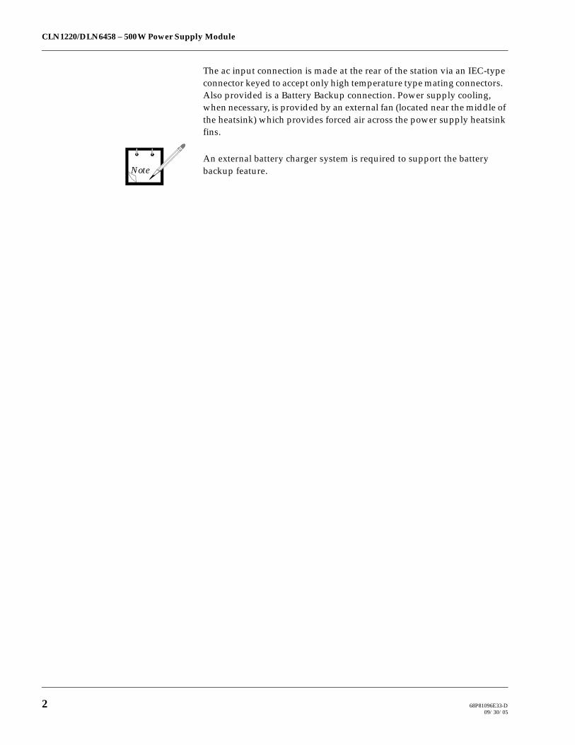
CLN1220/DLN6458 – 500W Power Supply Module
2 68P81096E33-D09/30/05
The ac input connection is made at the rear of the station via an IEC-type connector keyed to accept only high temperature type mating connectors. Also provided is a Battery Backup connection. Power supply cooling, when necessary, is provided by an external fan (located near the middle of the heatsink) which provides forced air across the power supply heatsink fins.
An external battery charger system is required to support the battery backup feature. Note

CLN1220/DLN6458 – 500W Power Supply Module
68P81096E33-D 309/30/05
Table 1 shows the electrical performance specifications for Model CLN1220 & DLN6458 Power Supply Modules.
2 PERFORMANCE SPECIFICATIONS
Table 1. CLN1220/DLN6458 Power Supply Module Performance Specifications
ParameterSpecification
CLN1220 DLN6458
Input Voltage Range 85 to 264 Vac 180 to 264 Vac
Operating Temperature –30° to +60° C (–22° to +140° F)
Input Frequency Range 47 to 63 Hz
Steady State Output Voltage 28.6 V @ 13 A, 14.2 V @ 8 A, 5.1 V @ 2 A
Output Power (Rated) 500 W
Load Transient 28.6 Vdc output ≤ ± 4% of steady state value
Output Ripple: +28.6 Vdc+14.2 Vdc+5.1 Vdc
50 mV p-p, @ 25° C (77° F)50 mV p-p, @ 25° C (77° F)100 mV p-p, @ 25° C (77° F)
Efficiency Greater than 75% (full load)

CLN1220/DLN6458 – 500W Power Supply Module
4 68P81096E33-D09/30/05
Figure 1 shows the Model CLN1220 and DLN6458 Power Supply Module input and output external connections.
3 IDENTIFICATION OF INPUTS/OUTPUTS
Figure 1. Model CLN1220/DLN6458 Power Supply Module Input/Output Connections
Battery Backup Connector
Outside View
Inside View
Front
Back
Front
Back
Mates To Backplane
DC Output To PA Module
Battery Backup Connector
AC Power Connector

CLN1220/DLN6458 – 500W Power Supply Module
68P81096E33-D 509/30/05
The following theory of operation describes the operation of the power supply circuitry at a functional level. The information is presented to give the service technician a basic understanding of the functions performed by the module in order to facilitate maintenance and troubleshooting to the module level. Refer to Figure 2 for a block diagram of the power supply module.
Supply Circuitry
Output Over-Current Protection
An over-current condition on either the 28.6 Vdc or 14.2 Vdc outputs caus-es the total supply to shutdown and try to restart. If the over-current con-tinues to exist, the power supply will ‘hiccup’ until the overload condition is removed, and will not be damaged by the overload. The 28.6 Vdc out-put is protected by a primary current sense method such that its current limit point varies depending on the load on the other outputs at the time. The trip point for the 14.2 Vdc and 5.1 Vdc outputs is greater than 115% of the maximum current specified for the outputs. The power supply recov-ers automatically after the removal of the overload condition.
Over-Voltage Detection and Shutdown
The 28.6 V and 14.2 V dc outputs are protected from continuous over-volt-ages by detection circuits that cause the supply to shutdown and then try to restart itself. If the over-voltage condition continues to occur, the supply goes into a ‘hiccup’ mode of shutting down and trying to restart. If the over-voltage condition is removed, the supply automatically recovers. In addition, the 14.2 Vdc output is protected by a crowbar circuit if failure of any part would cause the 28.6 Vdc output to connect directly to the 14.2 Vdc output. In addition, the 5.1 Vdc output is protected by an over-voltage detect circuit that shuts down both series regulators at the same time. The trip point of the over-voltage detection circuit is less than 30.5 Vdc for 28.6 Vdc, less than 16.8 Vdc for 14.2 Vdc, and less than 6.0 Vdc for 5.1 Vdc.
AC Fail Detect
An AC Fail detect signal is provided to indicate (when used with battery backup option) that the power supply is operating from an external dc source rather than the ac mains. This signal is an open collector output ca-pable of sinking 1 mA, and is routed to the Station Control Module. The active-low state indicates ac operation. For the nominal 120 Vac operation, the signal is active-high impedance (indicating an ac mains failure) when
4 FUNCTIONAL THEORY OF OPERATION
Note

CLN1220/DLN6458 – 500W Power Supply Module
6 68P81096E33-D09/30/05
the ac voltage is less than 85 Vrms, but more than the minimum voltage that guaran-tees that all outputs will be in regulation at full load. For the nominal 240 Vac opera-tion, the detect point is less than 170 Vrms but more than the minimum ac input voltage that guarantees that all outputs be in regulation at full load.
Fan Control Line
The supply incorporates temperature sense/fan enable circuitry for controlling a 12Vdc fan mounted on the surface of the heatsink assembly. The power supply cir-cuitry senses the internal temperature of the power supply. When the internal tem-perature exceeds +60°C (± 5°C), +12 V is enabled at J1–1 to turn on the fan. The +12 V fan supply is derived from the +14.2 V output. Power to the fan is off when the tem-perature is below the set limit. The fan turns for approximately 10 seconds when power is first applied as a diagnostic indicator that the fan is functional.

CLN1220/DLN6458 – 500 W Power Supply Module
68P81096E33-D 709/30/05
TEMP SENSE
CIRCUIT
FAN SWITCH ENABLE
EMIAC MAINS INPUT
(85 – 264 Vac,50/60 Hz)
INPUT POWER STAGE
J5
14.2 Vdc
Figure 2. CLN1220/DLN6458 – 500 W PowerSupply Functional Block Diagram
INPUT RECTIFIER
AC VOLTAGE RANGE SWITCH
INPUT DC
FILTER
AC FAIL DETECT
OVER-CURRENT DETECT
THERMAL PROTECT CIRCUIT
SHUTDOWN CIRCUIT
MAIN SWITCHER
POWER STAGE
MAIN OUTPUT
RECTIFIER
MAIN OUTPUT FILTER
OPTO-ISOLATOR
OVER-VOLTAGE DETECT
OVER-VOLTAGE
CROWBAR
PRE-REGULATOR
OVER-CURRENT
AMP
MAINPULSE WIDTH MODULATOR
14.2 VDC/DC
SWITCHER
RECTIFIER AND
FILTER
OVER-VOLTAGE DETECT
OVER-CURRENT
SENSE
5.1 VREGULATOR
OVER-VOLTAGE SENSE AND SHUTDOWN
14.2 VOLT FEEDBACK
28.6 VOLT FEEDBACK
14.2 VOLT CONVERTER
SHUTDOWN
14.2 VPULSE WIDTH
MODULATOR
OVER-VOLTAGE DETECT
28.6 VOLT FEEDBACK
OVERVOLTAGE PROTECTION
OPTO-ISOLATOR
REFAMP
SHUTDOWN
5.1 VOLT FEEDBACK
1
4
2
5
GROUND
3
6
28.6 Vdc
1
2
BATT NEG
BATT POS
J3
TO PA MODULE
J2
1
4
5
6
5.1 Vdc
3
4
14.2 Vdc14.2 VOLT INPUT
2
7
GROUND
8
TO BACKPLANE
1
J1
TO FAN
FROM BATTERY
INTERFACE
AC FAIL
INPUT START-UP CIRCUIT

68P81011Y31-O03/10/06-UP
Motorola Inc., 2006All Rights ReservedPrinted in U.S.A.
1301 E. Algonquin Road, Schaumburg, IL 60196
Government & Enterprise Mobility Solutions
The DLN6622 Power Supply Module is described in this section. This Power Supply is used on high power (i.e., >75 W) stations. A general description, identification of inputs and outputs, a functional block diagram, and func-tional theory of operation are provided. The information provided is sufficient to give service personnel a func-tional understanding of the module, allowing maintenance and troubleshooting to the module level. (Refer also to the Maintenance and Troubleshooting section of this manual for detailed troubleshooting procedures for all modules in the station.)
The DLN6622 Power Supply Module has built in power factor correction and includes a connection for battery backup that also serves as the DC input when the supply is used in dc only input mode.
General Description
The DLN6622 Power Supply Module accepts an ac or a dc input (ac input = 85 to 264 Vac, 50/60 Hz, dc input = 21.6 to 32 Vdc) and generates three output dc voltages to power the station modules: +5.1 Vdc, +14.2 Vdc, and +28.6 Vdc.
When used in dc input mode the 28.6 Vdc output is determined by the dc input minus 0.5 Vdc.
The power supply is a high-frequency switched mode design, all con-tained in a metal heat-sink, mounted on the left-hand side of the station. The design provides for output over-voltage/over-current protection.
The ac input connection is made at the rear of the station via an IEC-type connector keyed to accept only high temperature type mating connectors. Also provided is a Battery Backup connection (see dc mode above). Power supply cooling, when necessary, is provided by an external fan (located near the middle of the heatsink) which provides forced air across the pow-er supply heatsink fins.
An external battery charger system is required to support the battery backup feature.
1 DESCRIPTION
Note
Note
AC/DC POWER SUPPLYMODULE
MODEL DLN6622(500 W, 50/60 Hz, 85 to 264 Vac Input
or 21.6 to 32 Vdc Input)
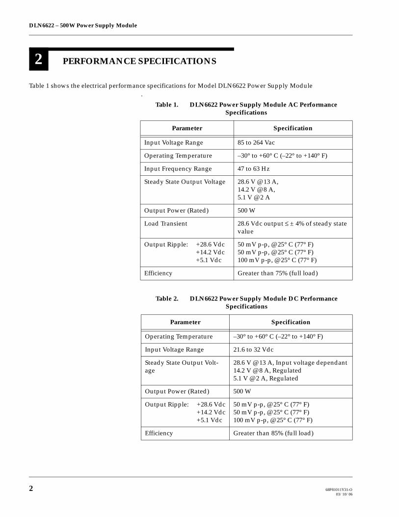
DLN6622 – 500W Power Supply Module
2 68P81011Y31-O03/10/06
Table 1 shows the electrical performance specifications for Model DLN6622 Power Supply Module.
2 PERFORMANCE SPECIFICATIONS
Table 1. DLN6622 Power Supply Module AC Performance Specifications
Parameter Specification
Input Voltage Range 85 to 264 Vac
Operating Temperature –30° to +60° C (–22° to +140° F)
Input Frequency Range 47 to 63 Hz
Steady State Output Voltage 28.6 V @ 13 A, 14.2 V @ 8 A, 5.1 V @ 2 A
Output Power (Rated) 500 W
Load Transient 28.6 Vdc output ≤ ± 4% of steady state value
Output Ripple: +28.6 Vdc+14.2 Vdc+5.1 Vdc
50 mV p-p, @ 25° C (77° F)50 mV p-p, @ 25° C (77° F)100 mV p-p, @ 25° C (77° F)
Efficiency Greater than 75% (full load)
Table 2. DLN6622 Power Supply Module DC Performance Specifications
Parameter Specification
Operating Temperature –30° to +60° C (–22° to +140° F)
Input Voltage Range 21.6 to 32 Vdc
Steady State Output Volt-age
28.6 V @ 13 A, Input voltage dependant14.2 V @ 8 A, Regulated 5.1 V @ 2 A, Regulated
Output Power (Rated) 500 W
Output Ripple: +28.6 Vdc+14.2 Vdc+5.1 Vdc
50 mV p-p, @ 25° C (77° F)50 mV p-p, @ 25° C (77° F)100 mV p-p, @ 25° C (77° F)
Efficiency Greater than 85% (full load)

DLN6622 – 500W Power Supply Module
68P81011Y31-O 303/10/06
Figure 1 shows the Model DLN6622 Power Supply Module input and output external connections.
3 IDENTIFICATION OF INPUTS/OUTPUTS
Figure 1. Model DLN6622 Power Supply Module Input/Output Connections
Battery Backup/DC Input
Connector
Outside View
Inside View
Front
Back
Front
Back
Mates To Backplane
DC Output To PA Module
AC Power Connector
Battery Backup/DC Input
Connector

DLN6622 – 500W Power Supply Module
4 68P81011Y31-O03/10/06
The following theory of operation describes the operation of the power supply circuitry at a functional level. The information is presented to give the service technician a basic understanding of the functions performed by the module in order to facilitate maintenance and troubleshooting to the module level. Refer to Figure 2 for a block diagram of the power supply module.
Supply Circuitry
Output Over-Current Protection
An over-current condition on either the 28.6 Vdc or 14.2 Vdc outputs caus-es the total supply to shutdown and try to restart. If the over-current con-tinues to exist, the power supply will ‘hiccup’ until the overload condition is removed, and will not be damaged by the overload. The 28.6 Vdc out-put is protected by a primary current sense method such that its current limit point varies depending on the load on the other outputs at the time. The trip point for the 14.2 Vdc and 5.1 Vdc outputs is greater than 115% of the maximum current specified for the outputs. The power supply recov-ers automatically after the removal of the overload condition.
Over-Voltage Detection and Shutdown
The 28.6 V and 14.2 V dc outputs are protected from continuous over-volt-ages by detection circuits that cause the supply to shutdown and then try to restart itself. If the over-voltage condition continues to occur, the supply goes into a ‘hiccup’ mode of shutting down and trying to restart. If the over-voltage condition is removed, the supply automatically recovers. In addition, the 14.2 Vdc and the 5 Vdc outputs are protected by crowbar cir-cuits.
AC Fail Detect
An AC Fail detect signal is provided to indicate (when used with battery backup option) that the power supply is operating from an external dc source rather than the ac mains. This signal is a TTL compatible output ca-pable of sinking 1 mA, and is routed to the Station Control Module. The active-low state indicates ac operation. For the nominal 120 Vac operation, the signal is active-high impedance (indicating an ac mains failure) when the ac voltage is less than 85 Vrms, but more than the minimum voltage that guarantees that all outputs will be in regulation at full load. For the nominal 240 Vac operation, the detect point is less than 170 Vrms but more than the minimum ac input voltage that guarantees that all outputs be in regulation at full load.
4 FUNCTIONAL THEORY OF OPERATION

DLN6622 – 500W Power Supply Module
68P81011Y31-O 503/10/06
Fan Control Line
The supply incorporates temperature sense/fan enable circuitry for con-trolling a 12Vdc fan mounted on the surface of the heatsink assembly. The power supply circuitry senses the internal temperature of the power sup-ply. When the internal temperature exceeds +60°C (± 5°C), +12 V is en-abled at J1–1 to turn on the fan. The +12 V fan supply is derived from the +14.2 V output. Power to the fan is off when the temperature is below the set limit. The fan turns for approximately 5 seconds when power is first applied as a diagnostic indicator that the fan is functional.
Overtemperature Protection
The power supply will turn off all outputs when an operational ambient temperature of +80°C (±2°C) has been reached with the supply operating at any input within its operating input voltage range (dc and ac).

DLN6622 – 500W Power Supply Module
6 68P81011Y31-O03/10/06
THIS PAGE INTENTIONALLY LEFT BLANK

DLN6622 – 500 W Power Supply Module
68P81011Y31-O 703/10/06
THERMAL SENSOR
FAN CONTROL
FILTER CHOKE
DC INPUT(21.6 – 32 Vdc)
J5
14.2 Vdc
Figure 1. DLN6622 – 500 W Power SupplyFunctional Block Diagram
I/P SWITCH WITH REVERSE POLARITY PROTECTION CIRCUIT
AUXILIARY POWER SUPPLY
CROWBAR CIRCUIT
PFC CIRCUIT
FORWARD CONVERTER
1
4
2
5
GROUND
3
6
28.6 Vdc
1
2
BATT NEG
BATT POS
J3
TO PA MODULE
J2
1
4
5
6
5.1 Vdc
3
4
14.2 Vdc
2
7
GROUND
8
TO BACKPLANE
1
J1
TO FAN
FROM BATTERY
INTERFACE
AC FAIL
BRIDGE RECTIFIER AND INRUSH
EMI FILTER
AC MAINS INPUT(85 – 264 Vac,
50/60 Hz)
DRV
BULK +
SVCC
LSPVCC
+28.6VP
STEP-DOWN BULK CONVERTER
+14.2VP
OUTPUT FILTER
OUTPUT FILTER
STEP-DOWN BULK CONVERTER
OUTPUT FILTER
CROWBAR CIRCUIT
PWM CONTROLLER
PWM CONTROLLER
SYNC
HOUSEKEEPING CIRCUIT
OFF LS
THERMAL SENSOR
DRV
THERMAL SENSOR
PWM CONTROLLER & GATE DRIVE CIRCUIT
SYNC, OFF

68P81096E34-C09/30/05-UP
Motorola Inc., 2005All Rights ReservedPrinted in U.S.A.
1301 E. Algonquin Road, Schaumburg, IL 60196
Government & Enterprise Mobility Solutions
The CLN1221 Power Supply Module is described in this section. This Power Supply is used on low power (i.e.,30/40 W) stations. A general description, identification of inputs and outputs, a functional block diagram, and functional theory of operation are provided. The information provided is sufficient to give service personnel a functional understanding of the module, allowing maintenance and troubleshooting to the module level. (Refer also to the Maintenance and Troubleshooting section of this manual for detailed troubleshooting procedures for all modules in the station.)
General Description
The CLN1221 Power Supply Module accepts an ac input (85 to 264 Vac, 50/60 Hz) and generates two output dc voltages to power the station modules: +5.1 Vdc and +14.2 Vdc. The power supply is a high-frequency switched mode design, utilizing Pulse Width Modulation (PWM) control, all contained in a metal heatsink, mounted on the left-hand side of the sta-tion. The design provides for over-voltage/over-current protection.
The ac input connection is made at the rear of the station via an IEC-type connector keyed to accept only high temperature type mating connectors. Also provided is a Battery Backup connection. Power supply cooling is provided by natural convection via the heatsink which is coplanar with the power supply circuit board assembly.
An external battery charger system is required to support the battery backup feature.
1 DESCRIPTION
Note
POWER SUPPLY MODULEMODEL CLN1221
(250 W, 50/60 Hz, 85 to 264 Vac Input)

CLN1221 – 250W Power Supply Module
2 68P81096E34-C09/30/05
Table 1 shows the electrical performance specifications for the Model CLN1221 Power Supply Module.
2 PERFORMANCE SPECIFICATIONS
Table 1. CLN1221 Power Supply Module Performance Specifications
Parameter Specification
Operating Temperature –30° to +60° C (–22° to +140° F)
Input Voltage Range 85 to 264 Vac
Input Frequency Range 47 to 63 Hz
Steady State Output Voltage 14.2 V @ 16.5 A,5.1 V @ 2 A
Output Power (Rated) 250 W
Load Transient 14.2 Vdc output ≤ ± 2.5% of steady state value
Output Ripple +14.2 Vdc+5.1 Vdc
50 mV p-p, @ 25° C (77° F)100 mV p-p, @ 25° C (77° F)
Efficiency Greater than 75% (full load)

CLN1221 – 250W Power Supply Module
68P81096E34-C 309/30/05
Figure 1 shows the model CLN1221 Power Supply Module input and output external connections.
3 IDENTIFICATION OF INPUTS/OUTPUTS
Figure 1. Model CLN1221 Power Supply Module Input/Output Connections
Outside View
Inside View
Front
Back
AC Power Connector Battery Backup
Connector
Front
Back
Mates To Backplane
DC Output To PA Module
Battery Backup Connector

CLN1221 – 250W Power Supply Module
4 68P81096E34-C09/30/05
The following theory of operation describes the operation of the power supply circuitry at a functional level. The information is presented to give the service technician a basic understanding of the functions performed by the module in order to facilitate maintenance and troubleshooting to the module level. Refer to Figure 2 for a block diagram of the power supply module.
Supply Circuitry
Output Over-Current Protection
An over-current condition on the 14.2 Vdc output causes the total supply to shutdown and try to restart. If the over-current continues to exist, the power supply will ‘hiccup’ until the overload condition is removed, and will not be damaged by the overload. The 14.2 Vdc output goes into the hiccup mode when its output current is greater than 18 A. The trip point for the 5.1 Vdc output is greater than 115% of the maximum current spec-ified for the output. The power supply recovers automatically after the re-moval of the overload condition.
Over-Voltage Detection and Shutdown
The 14.2 Vdc output is protected from continuous over-voltages by detec-tion circuits that cause the supply to shutdown and then try to restart it-self. If the over-voltage condition continues to occur, the supply goes into a ‘hiccup’ mode of shutting down and trying to restart. If the over-voltage condition is removed, the supply automatically recovers. In addition, the 5.1 Vdc output is protected by an over-voltage detect circuit that shuts down both series regulators at the same time. The trip point of the over-voltage detection circuit is less than 16.8 Vdc for 14.2 Vdc, and less than 6.0 Vdc for 5.1 Vdc.
AC Fail Detect
An AC Fail detect signal is provided to indicate (when used with battery backup option) that the power supply is operating from an external dc source rather than the ac mains. This signal is an open collector output ca-pable of sinking 1mA, and is routed to the Station Control Module. The active low state indicates ac operation. For the nominal 120 V ac opera-tion, the signal is active-high impedance (indicating an ac mains failure) when the ac voltage is less than 85 Vrms, but more than the minimum volt-age that guarantees that all outputs will be in regulation at full load. For the nominal 240 Vac operation, the detect point is less than 170 Vrms but more than the minimum ac input voltage that guarantees that all outputs be in regulation at full load.
4 FUNCTIONAL THEORY OF OPERATION
Note
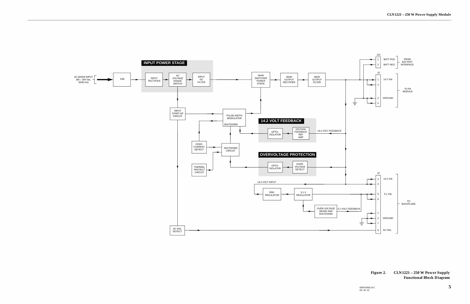
CLN1221 – 250 W Power Supply Module
68P81096E34-C 509/30/05
EMIAC MAINS INPUT
(85 – 264 Vac,50/60 Hz)
INPUT POWER STAGE
J3
14.2 Vdc
Figure 2. CLN1221 – 250 W Power SupplyFunctional Block Diagram
INPUT RECTIFIER
AC VOLTAGE RANGE SWITCH
INPUT DC
FILTER
AC FAIL DETECT
OVER-CURRENT DETECT
THERMAL PROTECT CIRCUIT
SHUTDOWN CIRCUIT
MAIN SWITCHER
POWER STAGE
MAIN OUTPUT
RECTIFIER
MAIN OUTPUT FILTER
OPTO-ISOLATOR
PRE-REGULATOR
PULSE WIDTH MODULATOR
5.1 VREGULATOR
OVER-VOLTAGE SENSE AND SHUTDOWN
14.2 VOLT FEEDBACK
OVER-VOLTAGE DETECT
14.2 VOLT FEEDBACK
OVERVOLTAGE PROTECTION
OPTO-ISOLATOR
VOLTAGE FEEDBACK
REFAMP
SHUTDOWN
5.1 VOLT FEEDBACK
2
5
GROUND
1
4
1
2
BATT POS
BATT NEG
J10
TO PA MODULE
J2
1
4
5
6
5.1 Vdc
3
4
14.2 Vdc14.2 VOLT INPUT
2
7
GROUND
8
TO BACKPLANE
FROM BATTERY
INTERFACE
AC FAIL
INPUT START-UP CIRCUIT

68P81011Y29-O03/10/06-UP
Motorola Inc., 2006All Rights ReservedPrinted in U.S.A.
1301 E. Algonquin Road, Schaumburg, IL 60196
Government & Enterprise Mobility Solutions
The DLN6624 Power Supply Module is described in this section. This Power Supply is used on low power (i.e.,30/40 W) stations. A general description, identification of inputs and outputs, a functional block diagram, and functional theory of operation are provided. The information provided is sufficient to give service personnel a functional understanding of the module, allowing maintenance and troubleshooting to the module level. (Refer also to the Maintenance and Troubleshooting section of this manual for detailed troubleshooting procedures for all modules in the station.)
General Description
The DLN6624 Power Supply Module accepts an ac or a dc input (85 to 264 Vac, 50/60 Hz, dc input = 10.8 to 16 Vdc) and generates two output dc voltages to power the station modules: +5.1 Vdc and +14.2 Vdc.
When used in dc input mode the 14.2 Vdc output is determined by the dc input minus 0.5 Vdc.
The power supply is a high-frequency switched mode design, all con-tained in a metal heatsink, mounted on the left-hand side of the station. The design provides for over-voltage/over-current protection.
The ac input connection is made at the rear of the station via an IEC-type connector keyed to accept only high temperature type mating connectors. Also provided is a Battery Backup connection (see dc mode above). Power supply cooling is provided by natural convection via the heatsink which is coplanar with the power supply circuit board assembly.
An external battery charger system is required to support the battery backup feature.
1 DESCRIPTION
Note
POWER SUPPLY MODULEMODEL DLN6624
(250 W, 50/60 Hz, 85 to 264 Vac Inputor 10.8 to 16 Vdc Input)

DLN6624 – 250W Power Supply Module
2 68P81011Y29-O03/10/06
Table 1 shows the electrical performance specifications for the Model DLN6624 Power Supply Module.
2 PERFORMANCE SPECIFICATIONS
Table 1. DLN6624 Power Supply Module AC Performance Specifications
Parameter Specification
Operating Temperature –30° to +60° C (–22° to +140° F)
Input Voltage Range 85 to 264 Vac
Input Frequency Range 47 to 63 Hz
Steady State Output Voltage 14.2 V @ 16.5 A,5.1 V @ 2 A
Output Power (Rated) 250 W
Load Transient 14.2 Vdc output ≤ ± 2.5% of steady state value
Output Ripple +14.2 Vdc+5.1 Vdc
50 mV p-p, @ 25° C (77° F)100 mV p-p, @ 25° C (77° F)
Efficiency Greater than 75% (full load)
Table 2. DLN6624 Power Supply Module DC Performance Specifications
Parameter Specification
Operating Temperature –30° to +60° C (–22° to +140° F)
Input Voltage Range 10.8 to 16 Vdc
Steady State Output Voltage 10.8V to 16V @ 16.5 A, Input voltage dependant5.1 V ± 3% @ 2 A, Regulated
Output Power (Rated) 250 W
Output Ripple: +14.2 Vdc+5.1 Vdc
50 mV p-p, @ 25° C (77° F)100 mV p-p, @ 25° C (77° F)
Efficiency Greater than 85% (full load)

DLN6624 – 250W Power Supply Module
68P81011Y29-O 303/10/06
Figure 1 shows the model DLN6624 Power Supply Module input and output external connections.
3 IDENTIFICATION OF INPUTS/OUTPUTS
Figure 1. Model DLN6624 Power Supply Module Input/Output Connections
Outside View
Inside View
Front
Back
AC Power Connector Battery Backup/
DC Input Connector
Front
Back
Mates To Backplane
DC Output To PA Module
Battery Backup/DC Input
Connector

DLN6624 – 250W Power Supply Module
4 68P81011Y29-O03/10/06
The following theory of operation describes the operation of the power supply circuitry at a functional level. The information is presented to give the service technician a basic understanding of the functions performed by the module in order to facilitate maintenance and troubleshooting to the module level. Refer to Figure 2 for a block diagram of the power supply module.
Supply Circuitry
Output Over-Current Protection
An over-current condition on the 14.2 Vdc output causes the total supply to shutdown and try to restart. If the over-current continues to exist, the power supply will ‘hiccup’ until the overload condition is removed, and will not be damaged by the overload. The 14.2 Vdc output goes into the hiccup mode when its output current is greater than 18 A. The trip point for the 5.1 Vdc output is greater than 115% of the maximum current spec-ified for the output. The power supply recovers automatically after the re-moval of the overload condition.
Over-Voltage Detection and Shutdown
The 14.2 Vdc output is protected from continuous over-voltages by detec-tion circuits that cause the supply to shutdown and then try to restart it-self. If the over-voltage condition continues to occur, the supply goes into a ‘hiccup’ mode of shutting down and trying to restart. If the over-voltage condition is removed, the supply automatically recovers. In addition, the 5 Vdc output is protected by a crowbar circuit.
AC Fail Detect
An AC Fail detect signal is provided to indicate (when used with battery backup option) that the power supply is operating from an external dc source rather than the ac mains. This signal is a TTL compatible output ca-pable of sinking 1mA, and is routed to the Station Control Module. The active low state indicates ac operation. For the nominal 120 V ac operation, the signal is active-high impedance (indicating an ac mains failure) when the ac voltage is less than 85 Vrms, but more than the minimum voltage that guarantees that all outputs will be in regulation at full load. For the nominal 240 Vac operation, the detect point is less than 170 Vrms but more than the minimum ac input voltage that guarantees that all outputs be in regulation at full load.
4 FUNCTIONAL THEORY OF OPERATION
Note

DLN6624 – 250W Power Supply Module
68P81011Y29-O 503/10/06
Overtemperature Protection
The power supply will turn off all outputs when an operational ambient temperature of +80°C (±2°C) has been reached with the supply operating at any input within its operating input voltage range (dc and ac).

DLN6624 – 250W Power Supply Module
6 68P81011Y29-O03/10/06
THIS PAGE INTENTIONALLY LEFT BLANK

DLN6624 – 250 W Power Supply Module
68P81011Y29-O 703/10/06
Figure 1. DLN6624 – 250 W Power SupplyFunctional Block Diagram
FILTER CHOKE
J3
14.2 VdcI/P SWITCH WITH REVERSE POLARITY
PROTECTION CIRCUIT
AUXILIARY POWER SUPPLY
PFC CIRCUIT
THERMAL SENSOR
FORWARD CONVERTER
2
5
GROUND
1
4
TO PA MODULE
J2
1
4
5
6
5.1 Vdc
3
4
14.2 Vdc
2
7
GROUND
8
TO BACKPLANE
AC FAIL
BRIDGE RECTIFIER AND INRUSH
EMI FILTER
AC MAINS INPUT(85 – 264 Vac,
50/60 Hz)
DRV
BULK +
SVCC
LSPVCC
OUTPUT FILTER
STEP-DOWN BULK CONVERTER
OUTPUT FILTER
CROWBAR CIRCUIT
PWM CONTROLLER
+14.2VP
DC INPUT(10.8 – 16 Vdc)
1
2
BATT NEG
BATT POS
J3
FROM BATTERY
INTERFACE
PWM CONTROLLER & GATE DRIVE CIRCUIT
SYNC, OFF
HOUSEKEEPING CIRCUIT
OFF LS
THERMAL SENSOR
DRV
68P81096E51-A09/30/05-UP
Motorola Inc., 2005All Rights ReservedPrinted in U.S.A.
1301 E. Algonquin Road, Schaumburg, IL 60196
Government & Enterprise Mobility Solutions
The CLN1222 Power Supply Module is described in this section. This Power Supply is used on high power (i.e., >75 W) stations. A general description, identification of inputs and outputs, a functional block diagram, and func-tional theory of operation are provided. The information provided is sufficient to give service personnel a func-tional understanding of the module, allowing maintenance and troubleshooting to the module level. (Refer also to the Maintenance and Troubleshooting section of this manual for detailed troubleshooting procedures for all modules in the station.)
General Description
The CLN1222 Power Supply Module accepts a dc input (21 to 32 Vdc) and generates three output dc voltages to power the station modules: +5.1 Vdc, +14.2 Vdc, and +28.6 Vdc (input voltage dependent). The power supply is a high-frequency switched mode design, utilizing Pulse Width Modula-tion (PWM) control, all contained in a metal heat-sink, mounted on the left-hand side of the station. The design provides for input reverse-voltage protection, and output over-voltage/over-current protection.
The dc input connection is made at the rear of the station via an AMP Pow-er Lock connector. Power supply cooling is provided by natural convec-tion via the heatsink which is coplanar with the power supply circuit board assembly.
1 DESCRIPTION
POWER SUPPLYMODULE; DC-Only
MODEL CLN1222(500 W, 21 to 32 Vdc Input)

CLN1222 – 500W DC-Only Power Supply Module
2 68P81096E51-A09/30/05
Table 1 shows the electrical performance specifications for the Model CLN1222 Power Supply Module.
2 PERFORMANCE SPECIFICATIONS
Table 1. CLN1222 Power Supply Module Performance Specifications
Parameter Specification
Operating Temperature –30° to +60° C (–22° to +140° F)
Input Voltage Range 21 to 32 Vdc
Input AC Ripple 100 / 120 Hz and harmonics10 kHz to 10 MHz
Steady State Output Voltage Input voltage dependent 28.6 V @ 13 A, 14.2 V @ 8 A, 5.1 V @ 2 A
Output Power (Rated) 500 W
Output Ripple: +28.6 Vdc+14.2 Vdc+5.1 Vdc
50 mV p-p, @ 25° C (77° F)50 mV p-p, @ 25° C (77° F)100 mV p-p, @ 25° C (77° F)
Efficiency Greater than 90% (full load)

CLN1222 – 500W DC-Only Power Supply Module
68P81096E51-A 309/30/05
Figure 1 shows the model CLN1222 Power Supply Module input and output external connections.
3 IDENTIFICATION OF INPUTS/OUTPUTS
Figure 1. Model CLN1222 Power Supply Module Input/Output Connections
Outside View
Inside View
Front
Back
Front
Back
Mates To Backplane
DC Output To PA Module
DC Power Connector
CLN1222 – 500W DC-Only Power Supply Module
4 68P81096E51-A09/30/05
The following theory of operation describes the operation of the power supply circuitry at a functional level. The information is presented to give the service technician a basic understanding of the functions performed by the module in order to facilitate maintenance and troubleshooting to the module level. Refer to Figure 2 for a block diagram of the power supply module.
Supply Circuitry
Input Reverse-Voltage Protection
The Power Supply Module includes protection from input dc voltage with reverse-polarity.
The power supply is protected from damage and ensures that no reverse polarity voltages are supplied to the station modules. If a reverse-voltage is present, the in-line fuse will blow. This fuse is in line with the input power cable and not part of the station.
Output Over-Current Protection
An over-current condition on the 28.6 Vdc output is limited by an external in-line fuse or the external power supply. This fuse is in-line with the input power cable and not part of the station.
The trip point for the 14.2 Vdc and 5.1 Vdc outputs is greater than 115% of the maximum current specified for the outputs. The power supply recov-ers automatically after the removal of the overload condition.
Over-Voltage Detection and Shutdown
The 14.2 Vdc and 5.1 Vdc outputs are protected from continuous over-voltages by detection circuits that cause the supply to shutdown and then try to restart itself.
Also, the 14.2 Vdc output is protected by a crowbar circuit if failure of any part causes the 28.6 Vdc output to connect directly to the 14.2 Vdc output. The trip point of the over-voltage detection circuit is less than 16.8 Vdc for 14.2 Vdc, and less than 6.0 Vdc for 5.1 Vdc.
4 FUNCTIONAL THEORY OF OPERATION
Note

CLN1222 – 500W DC-Only Power Supply Module
68P81096E51-A 509/30/05
INPUT POWER STAGE
INPUT DC
FILTER
MAIN OUTPUT FILTER
REVERSE VOLTAGE
PROTECTION
DC INPUT(21 – 32 Vdc)
J5
14.2 Vdc
Figure 2. CLN1222 – 500 W DC-Only Power Supply Functional Block Diagram
OVER-VOLTAGE DETECT
OVER-VOLTAGE
CROWBAR
PRE-REGULATOR
OVER-CURRENT
AMP
14.2 VDC/DC
SWITCHER
RECTIFIER AND
FILTER
OVER-VOLTAGE DETECT
OVER-CURRENT
SENSE
5.1 VREGULATOR
OVER-VOLTAGE SENSE AND SHUTDOWN
14.2 VOLT FEEDBACK
14.2 VOLT CONVERTER
SHUTDOWN
14.2 VPULSE WIDTH
MODULATOR
5.1 VOLT FEEDBACK
1
4
2
5
GROUND
3
6
28.6 Vdc
TO PA MODULE
J2
1
4
5
6
5.1 Vdc
3
4
14.2 Vdc14.2 VOLT INPUT
2
7GROUND
8
TO BACKPLANE
68P81096E52-A09/30/05-UP
Motorola Inc., 2005All Rights ReservedPrinted in U.S.A.
1301 E. Algonquin Road, Schaumburg, IL 60196
Government & Enterprise Mobility Solutions
The CLN1223 Power Supply Module is described in this section. This Power Supply is used on low power (i.e.,30/40 W) stations. A general description, identification of inputs and outputs, a functional block diagram, and functional theory of operation are provided. The information provided is sufficient to give service personnel a functional understanding of the module, allowing maintenance and troubleshooting to the module level. (Refer also to the Maintenance and Troubleshooting section of this manual for detailed troubleshooting procedures for all modules in the station.)
General Description
The CLN1223 Power Supply Module accepts a dc input (10.8 to 16 Vdc) and generates two output dc voltages to power the station modules: +5.1 Vdc and +14.2 Vdc. The power supply is contained in a metal heat-sink, mounted on the left-hand side of the station. The design provides for input reverse-voltage protection, and output over-voltage/over-current protection.
The dc input connection is made at the rear of the station via an AMP Pow-er Lock connector. Power supply cooling is provided by natural convec-tion via the heatsink which is coplanar with the power supply circuit board assembly.
1 DESCRIPTION
POWER SUPPLYMODULE; DC-Only
MODEL CLN1223(250 W, 10.8 to 16 Vdc Input)

CLN1223 – 250W DC-Only Power Supply Module
2 68P81096E52-A09/30/05
Table 1 shows the electrical performance specifications for the Model CLN1223 Power Supply Module.
2 PERFORMANCE SPECIFICATIONS
Table 1. CLN1223 DC-Only Power Supply Module Performance Specifications
Parameter Specification
Operating Temperature –30° to +60° C (–22° to +140° F)
Input Voltage Range 10.8 to 16 Vdc
Input AC Ripple 100 / 120 Hz and harmonics10 kHz to 10 MHz
Steady State Output Voltage Input dependent: 10.8V to 16V @ 16.5 A, 5.1 V ± 3% @ 2 A
Output Power (Rated) 250 W
Output Ripple: +14.2 Vdc+5.1 Vdc
50 mV p-p, @ 25° C (77° F)100 mV p-p, @ 25° C (77° F)
Efficiency Greater than 90% (full load)

CLN1223 – 250W DC-Only Power Supply Module
68P81096E52-A 309/30/05
Figure 1 shows the model CLN1223 Power Supply Module input and output external connections.
3 IDENTIFICATION OF INPUTS/OUTPUTS
Figure 1. Model CLN1223 DC-Only Power Supply Module Input/Output Connections
Outside View
Inside View
FrontBack
Front
Back
Mates To Backplane
DC Output To PA Module
DC Power Connector

CLN1223 – 250W DC-Only Power Supply Module
4 68P81096E52-A09/30/05
The following theory of operation describes the operation of the power supply circuitry at a functional level. The information is presented to give the service technician a basic understanding of the functions performed by the module in order to facilitate maintenance and troubleshooting to the module level. Refer to Figure 2 for a block diagram of the power supply module.
Supply Circuitry
Input Reverse-Voltage Protection
The Power Supply Module includes protection from input dc voltage with reverse-polarity.
The power supply is protected from damage and ensures that no reverse polarity voltages are supplied to the station modules. If a reverse-voltage is present, the in-line fuse will blow. This fuse is in line with the input power cable and not part of the station.
Output Over-Current Protection
An over-current condition on the 14.2 Vdc output is limited by an external in-line fuse or by the external power source. This fuse is in-line with the input power cable and not part of the station.
The 5.1Vdc regulator is protected by internal current limiting. The trip point for the 5.1 Vdc output is greater than 115% of the maximum current specified for the outputs. The 5.1Vdc recovers automatically after the re-moval of the overload condition.
Over-Voltage Detection and Shutdown
The 5.1 Vdc output is protected from continuous over-voltages by detec-tion circuits that cause the supply to shutdown and then try to restart it-self.
4 FUNCTIONAL THEORY OF OPERATION
Note
CLN1223 – 250W DC-Only Power Supply Module
68P81096E52-A 509/30/05
DC INPUT(10.8 – 16 Vdc)
INPUT POWER STAGE
J3
14.2 Vdc(Input Dependent)
INPUT DC
FILTER
MAIN OUTPUT FILTER
PRE-REGULATOR
5.1 VREGULATOR
OVER-VOLTAGE SENSE AND SHUTDOWN
5.1 VOLT FEEDBACK
2
5
GROUND
1
4
TO PA MODULE
J2
5
6
5.1 Vdc
3
4
14.2 Vdc14.2 VOLT INPUT
TO BACKPLANE
1
42
7GROUND
8
REVERSE VOLTAGE
PROTECTION
Figure 2. CLN1223 – 250 W DC-Only Power Supply Functional Block Diagram

68P81096E44-E09/28/05-UP
Motorola Inc., 2005All Rights ReservedPrinted in U.S.A.
1301 E. Algonquin Road, Schaumburg, IL 60196
Government & Enterprise Mobility Solutions
The Motorola MTR2000 Satellite Receiver provides satellite receiver functionality in a reliable, software-controlled design. The innovative modular design and microprocessor-controlled Station Control Module (SCM) allows for superior station flexibility and simplified system upgrades. By eliminating “dead zones” in a communications system, the Satellite Receiver improves coverage on a particular receive frequency when used in a receiver voting system.
General Mechanical Design
All elements of the satellite receiver are designed for EIA 48.3cm (19") rack mounting, using the same mechanical parts as the MTR2000 Base Station/Repeater. This allows the equipment to be mounted in standard tele-phone-style equipment racks or various sizes of Motorola cabinets. Figure 1 shows a typical satellite receiver.
1 DESCRIPTION
Figure 1. Typical MTR2000 Satellite Receiver
SATELLITERECEIVER

Satellite Receiver
2 68P81096E44-E09/28/05
Overview of Circuitry
The satellite receiver contains the following circuitry:
• Receiver Module
• Station Control Module
• Power Supply Module (250 W)
• Backplane Board
• Wireline Interface Board
• Auxiliary I/O Board (optional)
For detailed information on these modules, refer to the previous sections of this manual.

Satellite Receiver
68P81096E44-E 309/28/05
Figure 2 shows the satellite receiver input and output external connections.
2 INPUT AND OUTPUT CONNECTIONS
Figure 2. Satellite Receiver Input/Output Connections
Rx RF Connector
Telephone Connector
System Connector
AC PowerConnector
GroundScrew
Battery Backup Connector

Satellite Receiver
4 68P81096E44-E09/28/05
Satellite Receiver Configuration
Typically, the Satellite Receiver connects to either a Spectra-TAC™ comparator or, through a Digital Voice Modem (DVM), to a DigiTAC™ comparator. In the case of a Spectra-TAC system, the only external connection required is audio output from the receiver’s Wireline Interface Board (WIB) which is connected, by dedicated telephone line, to the Spectra-TAC comparator. In the case of a DigiTAC system, the RX Code Detect* signal is connected to the DVM as well as the wireline audio connections. The DVM is then connected, by dedicated telephone line, to the DigiTAC comparator. Figure 2 shows a typical voting system and the connections of the Satellite Receivers.
Figure 3. Satellite Receiver Connections Within a Voting System
Repeater
T1
R2
Dispatch Site
ComparatorControl Console
R2
Satellite Receiver
R2
Satellite Receiver
R2
Satellite Receiver
Phone Line
Phone Line
Phone Line
Phone Line

Satellite/Second Receiver
68P81096E44-E 509/30/05
Figure 5. MTR2000 Satellite ReceiverFunctional Block Diagram
RECEIVER MODULE
LOW PASS FILTER/PRESELECTOR/ IMAGE FILTER
1STMIXER
1ST I-F
CUSTOM RECEIVER
IC
HOST MEMORY
WIRELINE INTERFACE BOARD
2.1 MHz REFERENCE OSCILLATOR
RECEIVE ANTENNA
RF INPUT/OUTPUT CONNECTOR BRACKET
(REAR OF STATION)
BANDPASS FILTERING
1ST LO INPUT
(2ND INJECTION, AMPLIFICATION,
A/D CONVERSION)
DIFFERENTIAL DATA
2.1 MHz REF
STATION CONTROL MODULE
HOST ADDRESS
HOST DATA BUS
SPI BUS
PCM CODEC BUS
RSSI DATA RSSI CIRCUITRY
CURRENT-TO-VOLTAGE
CONVERTER
DSPASIC
EIA-232 INTERFACE
RSS TERMINAL(IBM-PC LAPTOP
TYPICAL)
SPI BUS
TRUNKING AUDIO
MRTI AUDIO
RECEIVER SIGNAL STRENGTH INDICATOR
(OPTION DEPENDENT)
AUXILIARY TX AUDIO
DISC AUDIO
MICROPHONE AUDIO
EXTERNAL SPEAKER
20 KHz CODEC BUS
24 KHz CODEC BUS
2.1 MHz REF
DSP MEMORY
DSP ADDRESS BUS
DSP DATA BUS
24 KHz CODEC BUS
DSP
HOSTMICROPROCESSOR
SSI
68356
SPI BUSSPI BUS
LINERX
LINETX
CODEC #3(8 KHz PCM)
(4-WIRE VERSION SHOWN)
LINE 1 ININBOUNDWIRELINE AUDIO
FROMLANDLINE
TOSTATION
OUTBOUNDWIRELINE AUDIO
FROMSTATION
TOLANDLINE
PCM CODEC BUS
LINE 2 OUT
SYNTHESIZER/VCO
AUDIOPROCESSING/
INTERFACE CIRCUITRY
POWER SUPPLY MODULE
ACINPUT
TRANSFORMER REGULATORCIRCUITRY
+14.2 VDC
+5.1 VDC
AC POWER SUPPLY with DC REVERT
GENERAL PURPOSE
OUTPUTS TO AUXILIARY
EQUIPMENT
GENERAL PURPOSE
INPUTS FROM AUXILIARY
EQUIPMENT
AUXILIARY I / O BOARD
INPUT BUFFERS
OUTPUT LATCHES
SPI BUS

68P81096E41-D09/30/05-UP
Motorola Inc., 2005All Rights ReservedPrinted in U.S.A.
1301 E. Algonquin Road, Schaumburg, IL 60196
Government & Enterprise Mobility Solutions
Model CLN6680 provides an Antenna Relay module for use with the MTR2000 station. This section provides a general description, option complement, identification of inputs/outputs, and functional theory of operation. The information provided is sufficient to give service personnel a functional understanding of the module, allowing maintenance and troubleshooting to the module level. (Refer also to the Maintenance and Troubleshooting sec-tion of this manual for detailed troubleshooting procedures for all modules in the station.)
General Description
This Antenna Relay module allows a single antenna to be used for both transmit and receive functions (base station applications only). The An-tenna Relay is controlled by a signal from the Station Control Module to connect the antenna to either the Power Amplifier Module (transmit) or Receiver Module (receive). The Antenna Relay module is mounted on a flange provided on the rear of the Power Supply Module.
1 DESCRIPTION
ANTENNA RELAYMODULEModel CLN6680

Antenna Relay Module
2 68P81096E41-D09/30/05
Figure 1 shows the Antenna Relay module input and output connections.
2 INPUTS AND OUTPUT CONNECTIONS
Figure 1. Typical Antenna Relay Module – Inputs/Outputs
Connects toStation Transmit RF Output
(From Power Amplifier Module)
Connects toStation Receive RF Input
(To Receiver Module or to optional External Preselector)
Connects toSingle Transmit/Receive Antenna
Mates WithConnector P10
on Station Backplane
Antenna RelayControl Cable
Connects to Peripheral Tray, if so equipped

Antenna Relay Module
68P81096E41-D 309/30/05
Cables
The set of cables used to connect an Antenna Relay to the MTR2000 station depends on what ancillary equipment is connected to the station.
A station can be configured with the following ancillary equipment:
- an Antenna Relay only. Figure 2 shows the kits required when only an Antenna Relay is in-stalled on a station.
- an Antenna Relay and an External Preselector.Figure 3 shows the kits required when an Antenna Relay and an Ex-ternal Preselector are installed on a station.
- an Antenna Relay and an External Double Circulator.Figure 4 shows the kits required when an Antenna Relay and Exter-nal Double Circulator are installed on a station.
- an Antenna Relay, an External Preselector, and an External Double Circulator.Figure 5 shows the kits required when an Antenna Relay, External Preselector, and External Double Circulator are installed on a station.
Some of the ancillary equipment listed above is not available on all sta-tions. For example, an External Preselector is not available for 800 or 900MHz stations.
Note
Figure 2. Antenna Relay Only – Cable Kits
From Receive Antenna
To Receiver Module
To Tx RF Connector
To Backplane
CLN6680(cable and Antenna Relay) TKN9132
TKN9136
Antenna Relay45 cm(18 in)
61 cm (24 in)
Not Connected

Antenna Relay Module
4 68P81096E41-D09/30/05
Figure 3. Antenna Relay and External Preselector – Cable Kits
From Receive Antenna
To Receiver Module
To Tx RF Connector
To Backplane
CLN6680(cable and Antenna Relay)
TKN9132
Antenna Relay
External Preselector
TKN9135(2 cables)
45 cm(18 in)
56 cm(22 in)
23 cm(9 in)
Not Connected
Note: An External Preselector is not used in 800, 900, or 350MHz stations.

Antenna Relay Module
68P81096E41-D 509/30/05
Figure 4. Antenna Relay and External Double Circulator– Cable Kits
From Receive Antenna
To Receiver Module
To Backplane
TKN9132
Antenna Relay
Peripheral Tray (back)
Low Pass Filter
External Double Circulator
To Tx RF Connector
50Ω Load
TKN9133(3 cables)
30 cm(12 in)
30 cm(12 in)
76 cm(30 in)
To Thermistor
61 cm (24 in)
TKN9136
CLN6680Antenna Relay and 45 cm (18 in) cable
If a longer cable, 76 cm (30 in), is required, use the TKN9007 kit along with the Antenna Relay
in kit CLN6680.

Antenna Relay Module
6 68P81096E41-D09/30/05
Figure 5. Antenna Relay, External Preselector, and External Double Circulator– Cable Kits
From Receive Antenna
To Receiver Module
To Backplane
TKN9132
Antenna Relay
External Preselector
TKN9135(2 cables)
Peripheral Tray (back)
Low Pass Filter
External Double Circulator
To Tx RF Connector
50Ω Load
45 cm(18 in)
56 cm(22 in)
23 cm(9 in)
TKN9133(3 cables)
30 cm(12 in)
30 cm(12 in)
76 cm(30 in)
To Thermistor
Note: An External Preselector is not used in 800, 900, or 350MHz stations.
CLN6680Antenna Relay and 45 cm (18 in) cable
If a longer cable, 76 cm (30 in), is required, use the TKN9007 kit along with the Antenna Relay
in kit CLN6680.

Antenna Relay Module
68P81096E41-D 709/30/05
Table 1 shows the contents for the Option X371AG Antenna Relay module.
Option Complement Chart
Table 2 shows the electrical performance specifications for the Antenna Relay used in Model CLN6680.
Performance Specifications
Table 1. Antenna Relay Option X371AG Complement
Description Motorola Part No.
Antenna Relay Module 8082894X02
Control Cable 0112004B03
Mounting Screws (2) 0312016A26
Table 2. Performance Specifications for Antenna Relay
Parameter Specifications
Operating Frequency DC to 4 GHz @ 20° C
Maximum Input Power 500 W @ 1 GHz
Coil Specifications:Pull-in voltageDrop-out voltageResistance
9.5 Vdc maximum≥ 2 Vdc
100 Ω ±10% @ 20° C
Contact Specifications:TypeActuationPull-in timeDrop-out time
SPDTFailsafe (break before make)
20 ms maximum @ 20° C10 ms maximum @ 20° C
Insertion Loss 0.3 dB maximum
Isolation 70 dB minimum
VSWR Maximum 1.3:1
Temperature Range -30° C to +80° C
Terminations Female N-Type
Input and Output Impedance 50 Ohms
3 OPTION COMPLEMENT
4 PERFORMANCE SPECIFICATIONS

Antenna Relay Module
8 68P81096E41-D09/30/05
The Antenna Relay Module is installed on a flange on the rear of the Power Supply Module. Stations equipped with the Antenna Relay module option are shipped with the antenna relay module installed as shown in Figure 6, allowing the RF cables to be routed out from the back of the cabinet or rack.
5 MOUNTING LOCATION
Figure 6. Mounting Position for Antenna Relay Module
Antenna Relay
Antenna Relay Module
68P81096E41-D 909/30/05
The following theory of operation describes the operation of the Antenna Relay Module at a functional level. The information is presented to give the service technician a basic understanding of the functions performed by the module in order to facilitate maintenance and troubleshooting to the module level. Refer to Figure 7 for a block and interconnect diagram of the Antenna Relay Module.
The Antenna Relay Module contains a relay with a set of normally open and normally closed contacts. The relay coil is controlled by the Antenna Relay signal from the Station Control Module to connect either the Receiv-er Module or the Power Amplifier Module to a single transmit/receive an-tenna.
With the relay de-energized, the antenna is connected to the Receiver Module. To connect the antenna to the Power Amplifier Module, the Sta-tion Control Module must energize the relay (one side of which is connect-ed to +14.2 Vdc) by grounding the Antenna Relay signal.
6 FUNCTIONAL THEORY OF OPERATION
Note
Figure 7. Functional Block and Interconnect Diagram for Antenna Relay Module
Receiver Module
Power Amplifier Module
Antenna Relay Module
N.C.
Antenna
Mates With3-pin Connector (P10)
On Backplane
2-wireControlCable
N.O.
+ –
+14.2 Vdc
Antenna Relay

VHF EXTERNALPRESELECTOR MODULE
Model CLN1216 (132 to 154 MHz)Model CLN1217 (150 to 174 MHz)
The VHF External Preselector, Models CLN1216, CLN1217, provide 5 poles of bandpass filtering for the station receive RF input signal. The filter assembly is mounted at the rear of the station. It includes mini-UHF connectors for input from the receive antenna and output to the Receiver module.
The information provided is sufficient to give service personnel a functional understanding of the module, allow-ing maintenance and troubleshooting to the module level. (Refer also to the Maintenance and Troubleshooting section of this manual for detailed troubleshooting procedures for all modules in the station.)
General Description
The external Preselector assembly is a 5-pole bandpass filter equipped with tuning slugs to adjust the passband corresponding to the operating frequency(s) of the station.
If the external Preselector option is being added to a station:
1. Attach the Preselector to the station according the mounting posi-tion and cable connection information provided in this section.
2. Tune the preselector assembly by following the Preselector Field Tun-ing Procedures, located in the Troubleshooting section of this manual.
1 DESCRIPTION
68P81096E43-C09/30/05-UP
Motorola Inc., 2005All Rights ReservedPrinted in U.S.A.
1301 E. Algonquin Road, Schaumburg, IL 60196
Government & Enterprise Mobility Solutions

VHF External Preselector Module
Figure 1 shows the VHF External Preselector input and output connections and the tuning cavities and tuning screws.
2 INPUTS AND OUTPUT CONNECTIONS
Figure 1. VHF External Preselector – Input/Output Connectors and Tuning Screws/Cavities
To Receiver Module
To Receive Antenna
Connector
Tuning Cavities
H2
H3
TuningScrews
H4
1
2
3
4
5
H1
2 68P81096E43-C09/30/05

VHF External Preselector Module
Cables
The set of cables used to connect an External Preselector to the MTR2000 station depends on what ancillary equipment is connected to the station.
A station can be configured with the following ancillary equipment:
- an External Preselector only. Figure 2 shows the kit required when only an External Preselector is installed on a station.
- an External Preselector and an Antenna Relay. See the Antenna Relay, Cables section for details.
- an External Preselector and an External Double Circulator. See the External Double Circulator, Cables section for details.
- an External Preselector, an Antenna Relay, and an External Double Circulator.See the Antenna Relay, Cables section for details.
Figure 2. External Preselector Only – Cable Kit
To Receiver Module
External Preselector
TKN9134(2 cables)
56 cm(22 in)
23 cm(9 in)
Rx RF Connector on station
From ReceiveAntenna
68P81096E43-C 309/30/05
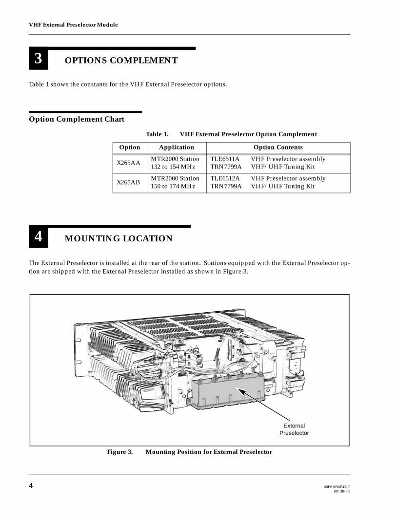
VHF External Preselector Module
Table 1 shows the constants for the VHF External Preselector options.
Option Complement Chart
The External Preselector is installed at the rear of the station. Stations equipped with the External Preselector op-tion are shipped with the External Preselector installed as shown in Figure 3.
Table 1. VHF External Preselector Option Complement
Option Application Option Contents
X265AA MTR2000 Station132 to 154 MHz
TLE6511A VHF Preselector assemblyTRN7799A VHF/UHF Tuning Kit
X265AB MTR2000 Station150 to 174 MHz
TLE6512A VHF Preselector assemblyTRN7799A VHF/UHF Tuning Kit
3 OPTIONS COMPLEMENT
4 MOUNTING LOCATION
Figure 3. Mounting Position for External Preselector
External Preselector
4 68P81096E43-C09/30/05

VHF EXTERNAL DOUBLECIRCULATOR MODULE
Model CLN1207 (132 to 146 MHz)Model CLN1208 (144 to 160 MHz)Model CLN1209 (158 to 174 MHz)
The VHF External Double Circulator Module, models CLN1207, CLN1208, CLN1209, provides an additional 45 dB (minimum) of isolation between the Power Amplifier Module and the transmit antenna.
This section provides a general description, option matrix chart, identification of inputs/outputs, and functional theory of operation. The information provided is sufficient to give service personnel a functional understanding of the module, allow maintenance and troubleshooting to the module level. (Refer also to the Maintenance and Troubleshooting section of this manual for detailed troubleshooting procedures for all modules in the station.)
General Description
The double circulator assembly consists of two RF circulators (contained in a single housing, a 50Ω load with heat sink and Low Pass Filter, all mounted in the peripheral tray. The RF output from the Power Amplifier module connects to the input of the assembly, while the output connects to an external low pass filter. The low pass filter provides harmonic sup-pression for the MTR2000 station. The output of the filter connects to the transmit antenna (directly, via antenna relay module, or via duplexer).
The double circulator model is typically used in high density radio site ap-plications where other co-located transmitters near the frequency of the station can cause intermodulation products. The addition of the double circulator improves transmitter intermodulation by 45dB.
1 DESCRIPTION
Note
68P81096E49-C09/30/05-UP
Motorola Inc., 2005All Rights ReservedPrinted in U.S.A.
1301 E. Algonquin Road, Schaumburg, IL 60196
Government & Enterprise Mobility Solutions

VHF External Double Circulator Module
Figure 1 shows the VHF External Double Circulator input and output connections.
2 INPUTS AND OUTPUT CONNECTIONS
Figure 1. VHF External Double Circulator Mounted in Peripheral Tray – Inputs/Outputs
Connected To Transmit Antenna
Connected to Tx RF
Connector
Connected through TKN9132 Cable To
Backplane
Low Pass FilterExternal Double Circulator
50Ω Load
Front of Peripheral Tray
2 68P81096E49-C09/30/05

VHF External Double Circulator Module
Cables
The set of cables used to connect an External Double Circulator to the MTR2000 station depends on what ancillary equipment is connected to the station.
A station can be configured with the following ancillary equipment:- an External Double Circulator only.
Figure 2 shows the kits required to install this equipment on a station. - an External Double Circulator and an External Preselector.
Figure 3 shows the kits required to install this equipment on a station.- an External Double Circulator and an Antenna Relay.
See the Antenna Relay, Cables section for details.- an External Double Circulator, an Antenna Relay, and an External
Preselector.See the Antenna Relay, Cables section for details.
- an External Double Circulator and a Duplexer.See the Duplexer, Cables section for details.
68P81096E49-C 309/30/05

VHF External Double Circulator Module
Figure 2. External Double Circulator Only – Cable Kits
TKN9132
Peripheral Tray (back)
Low Pass Filter
External Double Circulator
To Tx RF Connector on
station
50Ω Load
TKN9133(3 cables)
30 cm(12 in)
30 cm(12 in)
76 cm(30 in)
To Thermistor
Not Connected
To Transmit Antenna
To Backplane (P10) on station
4 68P81096E49-C09/30/05
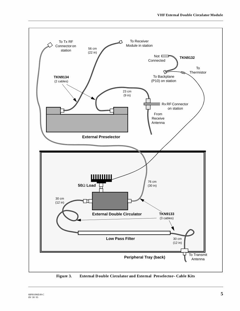
VHF External Double Circulator Module
Figure 3. External Double Circulator and External Preselector– Cable Kits
To Receiver Module in station
TKN9132
External Preselector
TKN9134(2 cables)
Peripheral Tray (back)
Low Pass Filter
External Double Circulator
To Tx RF Connector on
station
50Ω Load
56 cm(22 in)
TKN9133(3 cables)
30 cm(12 in)
30 cm(12 in)
76 cm(30 in)
To Thermistor
From ReceiveAntenna
Rx RF Connector on station
23 cm(9 in)
Not Connected
To Transmit Antenna
To Backplane (P10) on station
68P81096E49-C 509/30/05

VHF External Double Circulator Module
Table 1 shows the contents of the Double Circulator options.
Option Complement Chart
Table 1. VHF External Double Circulator Options Complement
Option Application Option Contents
X676ASX676ATX676AU
MTR2000 Station132 to 174 MHz
TYD4010A Low Pass FilterTRN7751A Peripheral Mounting TrayTKN9133A Cables (peripheral tray)TLN3391A 50Ω Load (head sink mounted)
X676AS MTR2000 Station132 to 146 MHz TYD4001A Double Circulator assembly
X676AT MTR2000 Station144 to 160 MHz TYD4002A Double Circulator assembly
X676AU MTR2000 Station158 to 174 MHz TYD4003A Double Circulator assembly
3 OPTIONS COMPLEMENT
6 68P81096E49-C09/30/05

VHF External Double Circulator Module
Table 2 shows the electrical performance specifications for the external Dual Circulators used in Models CLN1207, CLN1208, and CLN1209.
Performance Specifications
Table 2. Performance Specifications for VHF External Double Circulator
Parameter Specifications
Operating FrequencyCLN1207CLN1208CLN1209
132 to 146 MHz144 to 160 MHz158 to 174 MHz
Maximum RF Input Power 400 W
Insertion Loss 1.2dB maximum
Isolation 45dB
Operating Temperature Range –20° C to +70° C
Terminations Female N-Type
Input / Output Return Loss 19.1dB minimum
Input and Output Impedance 50 Ohms
Thermistor Value 20kΩ @ 25°C2.6kΩ @ 80°C
4 PERFORMANCE SPECIFICATIONS
68P81096E49-C 709/30/05

VHF External Double Circulator Module
The following theory of operation describes the operation of the Dual Circulator Assembly at a functional level. The information is presented to give the service technician a basic understanding of the functions performed by the double circulator in order to facilitate maintenance and troubleshooting to the module level. Refer to Figure 4 for a block and interconnect diagram of the Double Circulator assembly.
Functional Operation
The double circulator assembly accepts transmit RF output power from the Power Amplifier module and provides 45 dB of isolation between the Power Amplifier module and the transmit antenna. The assembly consists of two circulators in a single case, each with a 50Ω load. Each circulator allows forward RF energy to pass through to the output, while routing any reflected RF energy to the corresponding 50Ω load.
Most of the reflected energy is absorbed by the 50Ω load (heat sink) mounted) connected to the second circulator. A thermistor mounted on the head sink provides a variable resistance signal proportional to the heat sink temperature. This signal is routed to the Station Control Module via the Temp Sense cable and backplane. If the heat sink temperature exceeds a preset threshold, the Station Control Module enables PA cutback mode.
5 FUNCTIONAL THEORY OF OPERATION
Figure 4. Functional Block and Interconnect Diagram for External Double Circulator Module
50 Ohm Load
Transmit RF From Power
Amplifier Module
Circulator CirculatorLow Pass Filter RF Output
To Transmit Antenna
To Station Backplane
T°
50 Ohm Load
Thermistor20K @25°C
Heat Sink
Double Circulator
8 68P81096E49-C09/30/05

VHF DUPLEXER MODULEModel TYD4031 (132 to 146 MHz)Model TYD4032 (144 to 160 MHz)Model TYD4033 (158 to 174 MHz)
Kits TYD4031/32/33 provide band-dependent duplexer modules for use with MTR2000 VHF stations. This sec-tion provides a general description, identification of adjustments and inputs/outputs, performance specifications, and typical connection. While the duplexer module is considered non-repairable, tuning screws are provided for field tuning should replacement become necessary due to module failure, or if retuning is necessary due to a change in operating channels. A single channel field tuning procedure is provided in this section.
General Description
The duplexer module (shown in Figure 1) allows a transmit and receive channel pair to share a common Tx/Rx antenna. Each duplexer module consists of six resonant cavities (three for transmit and three for receive) contained in a temperature-compensated copper enclosure designed to mount in a standard EIA 48.26cm (19") equipment rack.
Each set of three cavities is designed and tuned to pass the respective transmit or receive channel frequency (or bandwidths) while providing maximum Tx noise suppression at the Rx frequency and maximum Rx iso-lation at the Tx frequency.
Figure 1. Typical VHF Duplexer Module
1 DESCRIPTION
68P81085E16-B09/30/05-UP
Motorola Inc., 2005All Rights ReservedPrinted in U.S.A.
1301 E. Algonquin Road, Schaumburg, IL 60196
Government & Enterprise Mobility Solutions
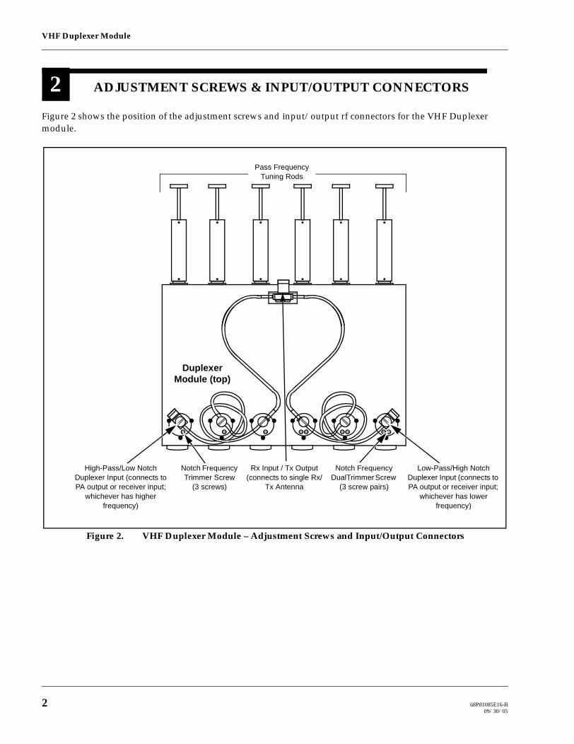
VHF Duplexer Module
Figure 2 shows the position of the adjustment screws and input/output rf connectors for the VHF Duplexer module.
2 ADJUSTMENT SCREWS & INPUT/OUTPUT CONNECTORS
Figure 2. VHF Duplexer Module – Adjustment Screws and Input/Output Connectors
High-Pass/Low Notch Duplexer Input (connects to PA output or receiver input;
whichever has higher frequency)
Rx Input / Tx Output (connects to single Rx/
Tx Antenna
Notch Frequency Trimmer Screw
(3 screws)
Pass Frequency Tuning Rods
Low-Pass/High Notch Duplexer Input (connects to PA output or receiver input;
whichever has lower frequency)
Notch Frequency DualTrimmer Screw
(3 screw pairs)
Duplexer Module (top)
2 68P81085E16-B09/30/05

VHF Duplexer Module
Cables
The set of cables used to connect a Duplexer to the MTR2000 station de-pends on what ancillary equipment is connected to the station.
A station can be configured with the following ancillary equipment:- a Duplexer only.
Figure 3 shows the kits required to install this equipment on a station. - an External Double Circulator and a Duplexer.
Figure 4 shows the kits required to install this equipment on a station.- an External Preselector and a Duplexer.
Figure 5 shows the kits required to install this equipment on a station.- an External Double Circulator, an External Preselector and a
Duplexer.Figure 6 shows the kits required to install this equipment on a station.
Figure 3. Duplexer Only – Cable Kits
X249CY (2 cables)
Tx RF Connector on station
Duplexer
To Receive/Transmit Antenna
Lowest Frequency RF; i.e., Rx or Tx
Highest Frequency RF; i.e., Rx or Tx
Connection on Duplexer Depends on Which Is Higher - Rx or Tx
Rx RF Connector on station
68P81085E16-B 309/30/05

VHF Duplexer Module
Figure 4. Duplexer and External Double Circulator– Cable Kits
TKN9132To Tx RF Connector on station To
Thermistor
Not Connected
X249CY (2 cables)
Rx RF Connector on station
Duplexer
To Receive/Transmit Antenna
Lowest Frequency RF; i.e., Rx or Tx
Highest Frequency RF; i.e., Rx or Tx
Connection on Duplexer Depends on Which Is Higher - Rx or Tx
To Backplane (P10) on station
Peripheral Tray (back)
Low Pass Filter
External Double Circulator
50Ω Load
TKN9133(3 cables)
30 cm(12 in)
30 cm(12 in)
76 cm(30 in)
4 68P81085E16-B09/30/05

VHF Duplexer Module
Figure 5. Duplexer and External Preselector– Cable Kits
X249CY (2 cables)
Tx RF Connector on station
Duplexer
To Receive/Transmit Antenna
Lowest Frequency RF; i.e., Rx or Tx
Highest Frequency RF; i.e., Rx or Tx
Connection on Duplexer Depends on Which Is Higher - Rx or Tx
To Receiver Module
External Preselector
TKN9134(2 cables)
56 cm(22 in)
23 cm(9 in) Rx RF Connector
on station
From ReceiveAntenna
68P81085E16-B 509/30/05

VHF Duplexer Module
Figure 6. Duplexer, External Preselector, and External Double Circulator– Cable Kits
TKN9132
Peripheral Tray (back)
Low Pass Filter
External Double Circulator
To Tx RF Connector on station
50Ω Load
TKN9133(3 cables)
30 cm(12 in)
30 cm(12 in)
76 cm(30 in)
To Thermistor
Not Connected
X249CY (2 cables)
Rx RF Connector on
station
Duplexer
To Receive/Transmit Antenna
Lowest Frequency RF; i.e., Rx or Tx
Highest Frequency RF; i.e., Rx or Tx
Connection on Duplexer Depends on Which Is Higher - Rx or Tx
To Backplane (P10) on station
External Preselector
56 cm(22 in)
23 cm(9 in)
TKN9134(2 cables)
6 68P81085E16-B09/30/05
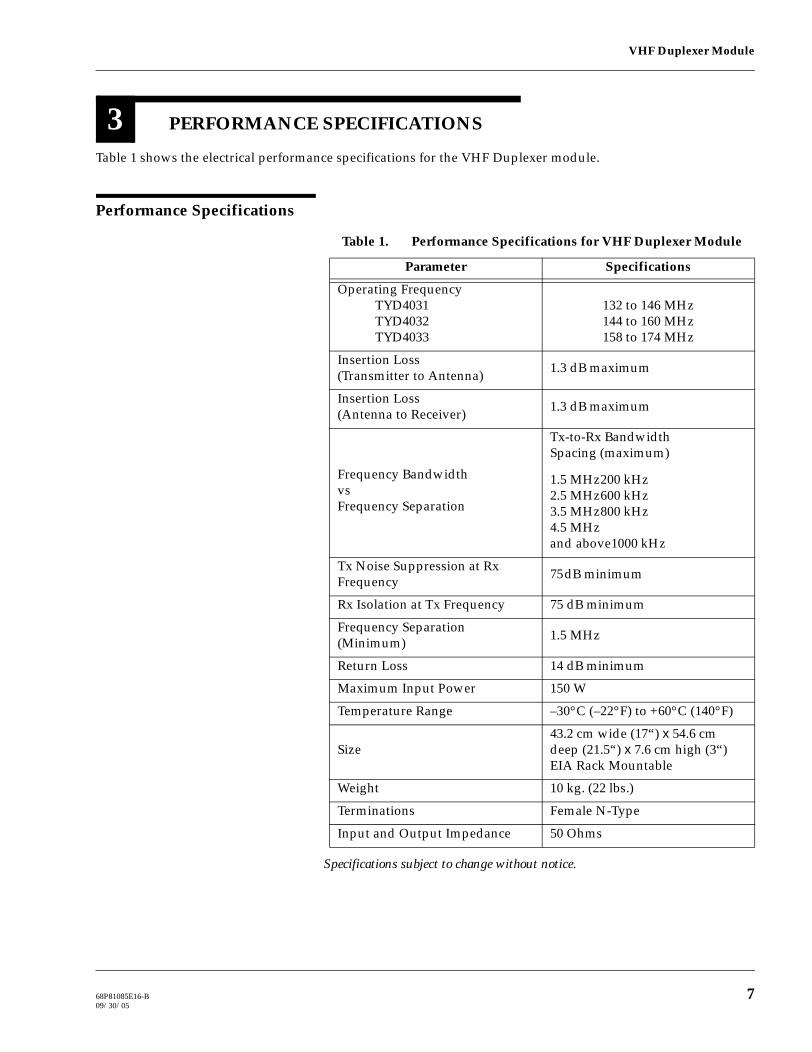
VHF Duplexer Module
Table 1 shows the electrical performance specifications for the VHF Duplexer module.
Performance Specifications
Specifications subject to change without notice.
Table 1. Performance Specifications for VHF Duplexer Module
Parameter Specifications
Operating FrequencyTYD4031TYD4032TYD4033
132 to 146 MHz144 to 160 MHz158 to 174 MHz
Insertion Loss(Transmitter to Antenna) 1.3 dB maximum
Insertion Loss(Antenna to Receiver) 1.3 dB maximum
Frequency Bandwidth vs Frequency Separation
Tx-to-Rx BandwidthSpacing (maximum)
1.5 MHz200 kHz2.5 MHz600 kHz3.5 MHz800 kHz4.5 MHz and above1000 kHz
Tx Noise Suppression at Rx Frequency 75dB minimum
Rx Isolation at Tx Frequency 75 dB minimum
Frequency Separation (Minimum) 1.5 MHz
Return Loss 14 dB minimum
Maximum Input Power 150 W
Temperature Range –30°C (–22°F) to +60°C (140°F)
Size43.2 cm wide (17“) x 54.6 cm deep (21.5“) x 7.6 cm high (3“)EIA Rack Mountable
Weight 10 kg. (22 lbs.)
Terminations Female N-Type
Input and Output Impedance 50 Ohms
3 PERFORMANCE SPECIFICATIONS
68P81085E16-B 709/30/05
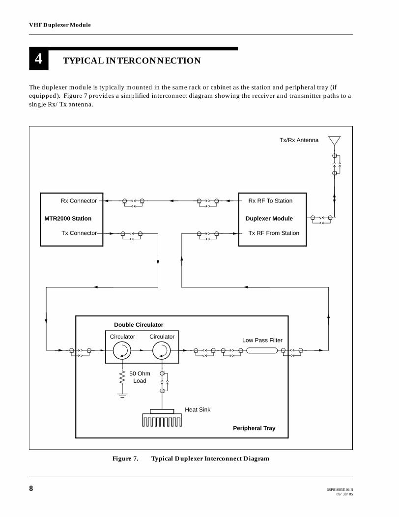
VHF Duplexer Module
The duplexer module is typically mounted in the same rack or cabinet as the station and peripheral tray (if equipped). Figure 7 provides a simplified interconnect diagram showing the receiver and transmitter paths to a single Rx/Tx antenna.
Figure 7. Typical Duplexer Interconnect Diagram
4 TYPICAL INTERCONNECTION
50 Ohm Load
Circulator CirculatorLow Pass Filter
Heat Sink
Double Circulator
MTR2000 Station
Tx Connector
Rx Connector
Duplexer Module
Rx RF To Station
Tx RF From Station
Peripheral Tray
Tx/Rx Antenna
8 68P81085E16-B09/30/05

VHF Duplexer Module
Duplexer modules shipped with stations are tuned at the factory. If a duplexer must be replaced in the field, the unit must be installed and tuned specifically to the transmit and receive frequency pair for the particular station.
Field Tuning Overview
The duplexer module is comprised of three low-pass/high-notch cavities and three high-pass/low-notch cavities. Each set of three cavities provides bandpass filtering for either the transmit rf signal or the receive rf signal. In general, the duplexer must be tuned so that the transmit cavity set pass-es the transmit signal and rejects the receive signal; concurrently, the re-ceive cavity set must be tuned to pass the receive signal and reject the transmit signal.
This tuning procedure is valid for channels with a bandwidth of 200kHz or less. If bandwidth is more than 200kHz, the duplexer must be tuned by the service depot.
Tuning is performed by injecting rf signals and making tuning adjust-ments (using the tuning rods and trimmer screws) while monitoring for maximum or minimum readings on the rf millivoltmeter. Field tuning the duplexer module requires the following general adjustments:
• Tune high-pass/low-notch cavities for maximum pass and reject re-sponse
• Tune low-pass/high-notch cavities for maximum pass and reject re-sponse
• Check high-pass/low-notch and low-pass/high-notch cavities for in-sertion loss
• Check high-pass/low-notch and low-pass/high-notch cavities for isolation
5 FIELD TUNING PROCEDURE
CAUTION
!
68P81085E16-B 909/30/05

VHF Duplexer Module
Required Test Equipment
Field tuning of the duplexer module requires the following test equip-ment:
• Motorola R2001/R2600 Communications Analyzer (or equivalent)
• RF Millivoltmeter (Boonton 92E or equivalent)
• RF Signal Generator (HP8565 or equivalent)
• 50Ω N-type terminator
• Male-to-Females N-Type "T" connector (UG-107B/U or equivalent)
• Slotted screwdriver
• 2.4mm (3/32") allen wrench
• Tuning tool (thin blade)
• N-to-N bullet connector (UG29A/U or equivalent)
• N-to-BNC Adapter (UG349A/U)
• N-to-N Connector (UG57B/U)
10 68P81085E16-B09/30/05

VHF Duplexer Module
Setting Up for Tuning Duplexer
Perform the preliminary tasks shown in Figure 8 to prepare the duplexer module for tuning.
Figure 8. Preliminary Tasks Prior to Tuning Duplexer
1. Disconnect N-type connector from each cavity (6).
2. For each cavity, unscrew and re-move trimmer screw dust covers (9).
3. Use allen wrench and loosen tuning rod locking screws (6).
Trimmer Screw
Dust Cover
Antenna Connector
Low-Pass High -Notch Cavities
High-Pass Low-Notch Cavities
Resonator Tuning Rods
68P81085E16-B 1109/30/05
VHF Duplexer Module
Duplexer Tuning Procedure
The duplexer field tuning procedures are provided in Figure 9. The proce-dures are most easily performed with the duplexer module removed from the station rack or cabinet. Be sure to make note of the transmit and receive frequencies for the particular station before beginning.
If the duplexer module is tuned according to instructions and does not meet specifications for return loss, insertion loss, and/or isolation, you must return the duplexer for repair.
The notch (reject) frequency will maintain its spacing to the pass frequency when the pass adjustment of a cavity is moved several MHz. For example, a system operating at 135 and 138MHz, which is moved to 138 and 141MHz will require a minimum of readjustment if the pass adjustment is made first. It is therefore recommended that the pass adjustments be made first and that the procedure provided in Figure 9 be followed.
12 68P81085E16-B09/30/05
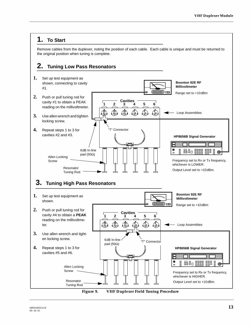
VHF Duplexer Module
Boonton 92E RF Millivoltmeter
Range set to +10dBm
Figure 9. VHF Duplexer Field Tuning Procedure
2. Tuning Low Pass Resonators
1. Set up test equipment as shown, connecting to cavity #1.
2. Push or pull tuning rod for cavity #1 to obtain a PEAK reading on the millivoltmeter.
3. Use allen wrench and tighten locking screw.
4. Repeat steps 1 to 3 for cavities #2 and #3.
1 2 3 4 5 6Cavities
Frequency set to Rx or Tx frequency, whichever is LOWER.
Output Level set to +10dBm.
Loop Assemblies
“T” Connector
Resonator Tuning Rod
Allen Locking Screw
6dB In-line pad (50Ω)
Boonton 92E RF Millivoltmeter
Range set to +10dBm
3. Tuning High Pass Resonators
1. Set up test equipment as shown.
2. Push or pull tuning rod for cavity #4 to obtain a PEAK reading on the millivoltme-ter.
3. Use allen wrench and tight-en locking screw.
4. Repeat steps 1 to 3 for cavities #5 and #6.
1 2 3 4 5 6Cavities
Frequency set to Rx or Tx frequency, whichever is HIGHER.
Output Level set to +10dBm.
Loop Assemblies
“T” Connector
Resonator Tuning Rod
Allen Locking Screw
6dB In-line pad (50Ω)
HP8656B Signal Generator
HP8656B Signal Generator
1. To Start
Remove cables from the duplexer, noting the position of each cable. Each cable is unique and must be returned to the original position when tuning is complete.
68P81085E16-B 1309/30/05

VHF Duplexer Module
Boonton 92E RF Millivoltmeter
Range set to +10dBm
Figure 9. VHF Duplexer Field Tuning Procedure (Continued)
4. Tuning High Notch Loop Assemblies
1. Set up test equipment as shown, connecting to cavity #1.
2. Use tuning tool to adjust trimmer screws for cavity #1 to obtain minimum reading on millivoltmeter. (Adjust trimmer screws equally to obtain minimum. Reduce the range on the millivoltme-ter as necessary to reach true minimum reading.)
3. Repeat steps 1 and 2 for cavities #2 and #3.
1 2 3 4 5 6Cavities
Frequency set to Rx or Tx frequency, whichever is HIGHER.
Output Level set to +10dBm.
Loop Assemblies
“T” Connector
6dB In-line pad (50Ω)
Boonton 92E RF Millivoltmeter
Range set to +10dBm
5. Tuning Low Notch Loop Assemblies
1. Set up test equipment as shown.
2. Use tuning tool to adjust trimmer screw for cavity #4 to obtain minimum reading on millivoltmeter. (Adjust trimmer screw to obtain minimum. Reduce the range on the millivoltmeter as necessary to reach true minimum reading.)
3. Repeat steps 1 and 2 for cavities #5 and #6.
4. Reconnect the cables on the duplexer. Make sure that the cables are returned to their original position on the Duplexer.
1 2 3 4 5 6Cavities
Frequency set to Rx or Tx frequency, whichever is LOWER.
Output Level set to +10dBm.
HP8656B Signal Generator
Loop Assemblies
“T” Connector6dB In-line pad (50Ω)
HP8656B Signal Generator
Trimmer Screws (2)
Trimmer Screw
14 68P81085E16-B09/30/05

VHF Duplexer Module
Boonton 92E RF Millivoltmeter
Range set to +10dBm
Figure 9. VHF Duplexer Field Tuning Procedure (Continued)
6. Verifying Insertion Loss
1. Connect test equipment as shown.
2. Observe and note the level in dBm as shown on the millivolt-meter.
3. Connect the duplexer cable as-sembly and test equipment to the duplexer as shown.
4. Observe and note the level in dBm as shown on the millivolt-meter.
5. Subtract the absolute number noted in Step 2 from the number noted in Step 4. The difference should be less than 1.3 dB to meet specification for Insertion Loss.
6. Repeat Steps 1 to 5 for Low- Pass/High Notch cavities with the following exceptions:
a) Set Frequency Generator for Rx or Tx frequency, whichever is LOWER
b) Connect Signal Generator to Low Pass duplexer input (cavity #1)
c) Connect terminator to cavity #6.
Frequency set to Rx or Tx frequency, whichever is HIGHER.
Output Level set to +10dBm.
Boonton 92E RF Millivoltmeter
HP8656B Signal Generator
HP8656B Signal Generator6dB In-line pad (50Ω)
UG349A N-to-BNC Connector
Terminator
6dB In-line pad (50Ω)
1 2 3 4 5 6
68P81085E16-B 1509/30/05

VHF Duplexer Module
Figure 9. VHF Duplexer Field Tuning Procedure (Continued)
7. Verifying Isolation
1. Connect test equipment as shown.
2. Observe and note the level in dBm as shown on the R2001 dis-play.
3. Connect the test equipment to the duplexer as shown.
4. Observe and note the level in dBm as shown on the R2001 dis-play. (If no number is displayed, consider isolation to be greater than 105 dB, which exceeds the specification.)
5. Subtract the absolute number noted in Step 4 from the number noted in Step 2. The difference should be higher than 75 dB to meet specification for Isolation.
6. Repeat Steps 1-5 for Low- Pass/High Notch cavities with the fol-lowing exceptions:
a) Set Frequency Generator and R2001 for Rx or Tx frequency, whichever is HIGHER
b) Connect Signal Generator to Low Pass duplexer input (cavity #1)
c) Connect terminator to cavity #6.
Frequency set to Rx or Tx frequency, whichever is LOWER.
Output Level set to +10dBm.
HP8656B Signal Generator
HP8656B Signal GeneratorUG29A/U Bullet Connector
Terminator
6dB In-line pad (50Ω)
R2001 Communications Monitor Function.
Center frequency set to Tx or Rx frequency, whichever is LOWER
Attenuator set to –50dBm
1 2 3 4 5 6
R2001 Communications
Attenuator set to 0dBm
16 68P81085E16-B09/30/05

VHF Duplexer Module
Figure 9. VHF Duplexer Field Tuning Procedure (Continued)
8. Post-Tuning Checks
1. Make sure all locking screws are tight. Reinstall dust covers on all trimmer capacitors.
2. Make sure all tuning rod locking screws (6) are tight.
Locking Screw (3)
68P81085E16-B 1709/30/05

68P81095E71-A09/30/05-UP
Motorola Inc., 2005All Rights ReservedPrinted in U.S.A.
1301 E. Algonquin Road, Schaumburg, IL 60196
Government & Enterprise Mobility Solutions
The MTR2000 is capable of Multi Coded Squelch through the Zetron Model 38 Repeater Panel, model TDN9946. The Model 38 Repeater Panel interconnects to the MTR2000 and provides 38 PL tones and 22 DPL tones standard. This section provides a general description, cable connection, and option information.
Refer to the ZETRON Repeater Panel Instruction Manual (supplied with the panel) for panel specifications, oper-ation, installation, programming, and repair information.
General Description
The Zetron panel, shown in Figure 1, is a community repeater panel. The Zetron panel can be mounted in a cabinet or rack and is 4.3 cm (1.7 in.) high.
Figure 1. Zetron Repeater Tone Panel
1 DESCRIPTION
ZETRON REPEATER PANELModel TDN9946
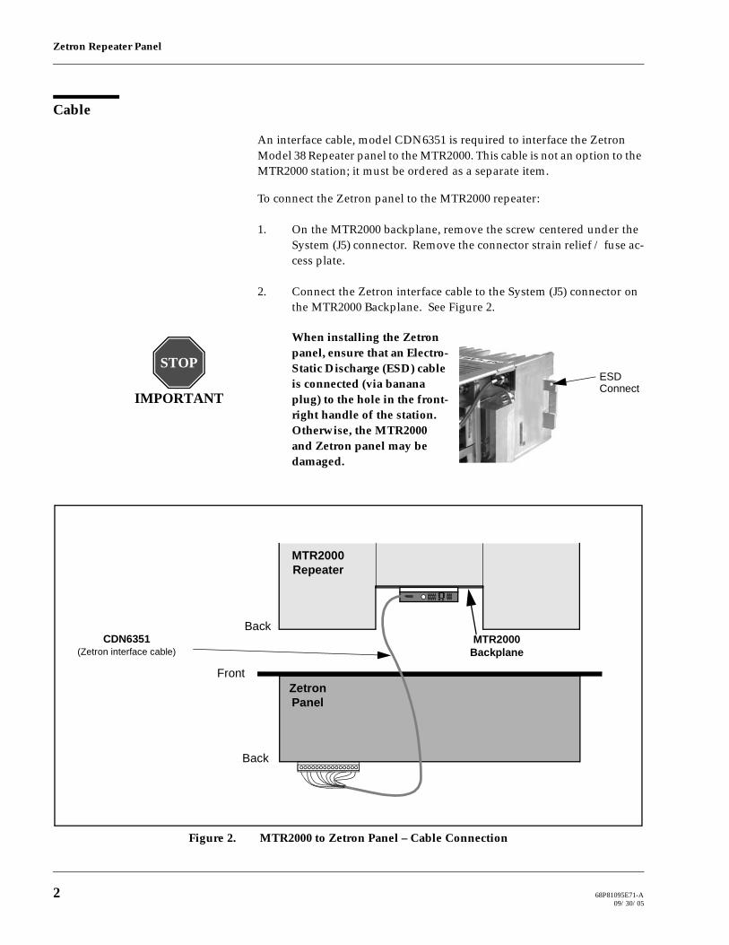
Zetron Repeater Panel
2 68P81095E71-A09/30/05
Cable
An interface cable, model CDN6351 is required to interface the Zetron Model 38 Repeater panel to the MTR2000. This cable is not an option to the MTR2000 station; it must be ordered as a separate item.
To connect the Zetron panel to the MTR2000 repeater:
1. On the MTR2000 backplane, remove the screw centered under the System (J5) connector. Remove the connector strain relief / fuse ac-cess plate.
2. Connect the Zetron interface cable to the System (J5) connector on the MTR2000 Backplane. See Figure 2.
When installing the Zetron panel, ensure that an Electro-Static Discharge (ESD) cable is connected (via banana plug) to the hole in the front-right handle of the station. Otherwise, the MTR2000 and Zetron panel may be damaged.
STOP
IMPORTANT
ESD Connect
Figure 2. MTR2000 to Zetron Panel – Cable Connection
CDN6351(Zetron interface cable)
MTR2000 Backplane
MTR2000 Repeater
Zetron Panel
Front
Back
Back
Zetron Repeater Panel
68P81095E71-A 309/30/05
3. The component side of the Zetron interface circuit board should be facing up when connected to the MTR2000. If the components are facing down, this is an older version of the MTR2000 that does not support connection to the Zetron panel.
4. Re-install the connector strain relief / fuse access plate.
5. Configure the MTR2000 Radio Service Software (RSS) for operation with the Zetron panel. See the RSS Online Help for details.
6. Connect the interface cable to the Zetron panel.
7. Configure the Zetron panel as indicated in the Zetron Instruction manual.
8. Follow the initial power up and adjustment instructions in the Zetron panel Instruction manual.
Zetron Repeater Panel
4 68P81095E71-A09/30/05
The Zetron Model 38 Repeater Panel is not an option to the MTR2000; it must be ordered as a separate item. The interface cable (between the Zetron panel and the MTR2000 repeater) must also be ordered as a separate item.
The Zetron Selective Calling option, E380, replaces 38 PL tones and 22 DPL tones with 50 PL tones and 18 DPL tones. If this option is required, it must be ordered as a sub-item to the Model 38 Repeater Panel (model, TDN9946).
2 OPTION INFORMATION