Untitled - PAS Journals Repository
212
-
Upload
khangminh22 -
Category
Documents
-
view
0 -
download
0
Transcript of Untitled - PAS Journals Repository


METROLOGY AND MEASUREMENT SYSTEMS
Quarterly of Polish Academy of Sciences
INTERNATIONAL PROGRAMME
COMMITTEE
Andrzej ZAJĄC, Chairman Military University of Technology, Poland
Bruno ANDO University of Catania, Italy
Martin BURGHOFF Physikalisch-Technische Bundesanstalt, Germany
Marcantonio CATELANI University of Florence, Italy
Numan DURAKBASA Vienna University of Technology, Austria
Domenico GRIMALDI University of Calabria, Italy
Laszlo KISH Texas A&M University, USA
Eduard LLOBET Universitat Rovira i Virgili, Tarragona, Spain
Alex MASON Liverpool John Moores University, The United Kingdom
Subhas MUKHOPADHYAY Massey University, Palmerston North, New Zealand
Janusz MROCZKA Wrocław University of Technology, Poland
Antoni ROGALSKI Military University of Technology, Poland
Wiesław WOLIŃSKI Warsaw University of Technology, Poland
Language Editor
Andrzej Stankiewicz [email protected]
Technical Editor and Secretary
Agnieszka KONDRATOWICZ Gdańsk University of Technology [email protected]
Webmaster
Michał Kowalewski Gdańsk University of Technology [email protected]
EDITORIAL BOARD
Editor-in-Chief
Janusz SMULKO Gdańsk University of Technology, Poland [email protected]
Associate Editors
Zbigniew BIELECKI Military University of Technology, Poland [email protected]
Vladimir DIMCHEV Ss. Cyril and Methodius University, Macedonia [email protected]
Krzysztof DUDA AGH University of Science and Technology, Poland [email protected]
Janusz GAJDA AGH University of Science and Technology, Poland [email protected]
Teodor GOTSZALK Wrocław University of Technology, Poland [email protected]
Ireneusz JABŁOŃSKI Wrocław University of Technology, Poland [email protected]
Piotr JASIŃSKI Gdańsk University of Technology, Poland [email protected]
Piotr KISAŁA
Lublin University of Technology, Poland [email protected]
Manoj KUMAR University of Hyderabad, Telangana, India [email protected]
Fernando PUENTE LEÓN University Karlsruhe, Germany [email protected]
Czesław ŁUKIANOWICZ Koszalin University of Technology, Poland [email protected]
Rosario MORELLO University Mediterranean of Reggio Calabria, Italy [email protected]
Petr SEDLAK Brno University of Technology, Czech Republic [email protected]
Hamid M. SEDIGHI Shahid Chamran University of Ahvaz, Ahvaz, Iran [email protected]
Roman SZEWCZYK Warsaw University of Technology, Poland [email protected]
Journal is indexed by Journal Citation Reports/Science. Impact Factor: 1.140 (5-Year Impact Factor 1.092). More information about aims and scope of the journal – inner side of the back cover.
Instructions for Authors – last pages of the issue.
Edition was financially supported by the Polish Academy of Science and Gdańsk University of Technology,
Faculty of Electronics, Telecommunications and Informatics.
Ark. wyd. 16,56 Ark. druk. 13,25 Papier offsetowy kl. III 80g 70 x 100 cm
Print run 120 copies
Druk: Centrum Poligrafii Sp. z o.o.
ul. Łopuszańska 53 02-232 Warszawa

Metrol. Meas. Syst., Vol. 24 (2017), No. 2, pp. 229–240.
_____________________________________________________________________________________________________________________________________________________________________________________
Article history: received on Mar. 01, 2017; accepted on Apr. 26, 2017; available online on Jun. 30, 2017; DOI: 10.1515/mms-2017-0036.
METROLOGY AND MEASUREMENT SYSTEMS
Index 330930, ISSN 0860-8229
www.metrology.pg.gda.pl
EFFECT OF FEATURE EXTRACTION ON AUTOMATIC SLEEP STAGE
CLASSIFICATION BY ARTIFICIAL NEURAL NETWORK
Monika Prucnal, Adam G. Polak
Wrocław University of Science and Technology, Faculty of Electronics, B. Prusa 53/55, 50-317 Wrocław, Poland ( [email protected], +48 71 320 6247, [email protected])
Abstract
EEG signal-based sleep stage classification facilitates an initial diagnosis of sleep disorders. The aim of this study
was to compare the efficiency of three methods for feature extraction: power spectral density (PSD), discrete
wavelet transform (DWT) and empirical mode decomposition (EMD) in the automatic classification of sleep stages
by an artificial neural network (ANN). 13650 30-second EEG epochs from the PhysioNet database, representing five sleep stages (W, N1-N3 and REM), were transformed into feature vectors using the aforementioned methods
and principal component analysis (PCA). Three feed-forward ANNs with the same optimal structure (12 input
neurons, 23 + 22 neurons in two hidden layers and 5 output neurons) were trained using three sets of features,
obtained with one of the compared methods each. Calculating PSD from EEG epochs in frequency sub-bands
corresponding to the brain waves (81.1% accuracy for the testing set, comparing with 74.2% for DWT and 57.6%
for EMD) appeared to be the most effective feature extraction method in the analysed problem.
Keywords: sleep stage classification, EEG signal, power spectral density, discrete wavelet transform, empirical
mode decomposition, artificial neural network.
© 2017 Polish Academy of Sciences. All rights reserved
1. Introduction
Sleep is one of the basic modes of human brain activity. It is a recurring state of mind and body characterised by altered consciousness and body stillness. It is well known that adults spend about 1/3 of their life in sleeping, therefore a right quality and amount of sleep have
a significant impact on human mood and health. There is a large group of sleep disorders related to the respiratory, nervous and other
physiological systems, typically monitored by polysomnography [1]. Among them, hyperventilation and sleep apnea are the most prevalent ones. Interrelations between pathology,
system functions and recorded biophysical signals are generally complex [2]. One of approaches to improve at-home patient care is the use of tele-monitoring [3].
Loomis at al. were the first observing that the pattern of brain potentials alters systematically
in a sleeping person [4]. These cyclic shifts of brain waves are known as the sleep phases. Asernisky and Kleitman observed that normal, healthy sleep is divided into two main phases:
REM (Rapid Eye Movement) and NREM (Non-Rapid Eye Movement) [5]. REM sleep is also known as paradoxical or active sleep, which generally occurs about from 90 to 120 minutes during sleep in adults [6]. The remaining time of sleep is NREM sleep and night awakenings.
There has been reported recently that the sleep macrostructure is strongly associated with apnea episodes [7].
The most important signal for the classification of sleep stages is the electroencephalogram (EEG), one of signals recorded during polysomnography (PSG) [8]. It is used for distinguishing the wake and sleep phases [6]. The first EEG was recorded by Hans Berger. He was also the first
who observed the brain waves and described two of them: the alpha (8−14 Hz) and beta

M. Prucnal, A. G. Polak: EFFECT OF FEATURE EXTRACTION ON AUTOMATIC SLEEP …
(14−30 Hz) waves [9]. The other brain waves are delta (0.5−4 Hz), theta (4−8 Hz) and gamma
(30−80 Hz) ones [6]. Other brain activities, besides the waves, are artefacts like: saw-tooth waves, sleep spindles and K complexes [6].
Because of EEG signal complexity, the traditional manual sleep stage classification is time-consuming and depends on knowledge and experience of the expert. Therefore, an automatic
sleep stage classification is expected to be more objective, faster and more efficient. There are two approaches to scoring the sleep stages [6]. The first one follows the standardised scoring
systems introduced by Rechtschaffen and Kales [10], where the following phases are distinguished: wakefulness (W), rapid eye movement (REM), non-rapid eye movement (NREM) and movement time (MT). The NREM phase is additionally divided into light sleep (S1 and S2
stages) and deep sleep (S3 and S4 stages) [10]. Currently, a new method proposed by the American Academy of Sleep Medicine is used [1]. The main difference in stage definition is
that the S1-S4 stages are replaced by N1, N2 and N3 (joined S3 and S4) ones and the MT stage is no longer distinguished [1].
An automatic sleep stage classification usually takes the following steps: dataset preparation,
signal pre-processing, feature extraction and final classification [11, 12]. The dataset preparation includes splitting the EEG signal into 30-second epochs and organising subsets
of epochs from the same sleep stages: W, REM, N1, N2 and N3. The pre-processing consists mainly of filtering and normalisation of the signals. The crucial step is, however, the extraction of discriminative features form the prepared epochs, simultaneously reducing the number of
data for further processing. It is usually performed in the time, frequency or time-frequency/scale domains. Particularly the analyses in the frequency domain are very fruitful
[13, 14]. The time domain methods include statistical analyses [12, 15−20], the Hjorth approach
focused on activity, mobility and complexity [12, 16, 20, 21], and singular spectrum analysis (SSA) [22]. The methods in the frequency or time-frequency/scale domains describe the EEG
spectral or scale properties using the Fourier transform (FT) [11, 23, 24], power spectral density (PSD) [12, 25], short-time Fourier transform (STFT) [12, 26], adaptive directional time-frequency distribution (ADTFD) [27], Wigner-Ville distribution (WV) [12, 16], matching
pursuit (MP) [28], wavelet transform (WT) [12, 15, 16, 18, 29, 30], empirical mode
decomposition (EMD) [19, 31−35] or Hilbert-Huang transform (HHT) [36]. The methods most commonly used for classification are artificial neural networks (ANN) [11, 12, 15, 16, 18, 20,
23−25, 30, 32, 37], support vector machine (SVM) [12, 16, 17, 22, 23, 38], decision trees (DT) [16, 19, 33], random forest algorithm (RF) [12, 16, 29], and fuzzy systems [39].
The best reported accuracy of sleep stage classification exceeded 90%, e.g. 97.03% [16],
96.75% [40], 95.42% [18], 93.93% [41], 93.84% [42], 93.0% [15] and 90.11% [33]. In these works, the discriminative features were extracted using, among others, such methods as power
spectral density (PSD) [41], discrete wavelet transform (DWT) [15, 16], complex wavelet transform [18, 42] and empirical mode decomposition (EMD) [19, 33, 34]. Simultaneously, ANNs were used as classifiers in some of these approaches, e.g. [15, 16, 18, 40, 42].
It follows from the literature survey that often different classifiers of sleep stages were compared using only one feature extraction method [16, 19, 23]. There are only a few works
analysing combinations of some feature extractors and classifiers [22, 40], therefore comparing effects of the most promising feature extraction methods on the automatic sleep stage
classification results is desirable. For this reason, in this paper we examine three of such methods: power spectral density (PSD), discrete wavelet transform (DWT) and empirical mode decomposition (EMD) applied to signals from a single EEG channel, using a feedforward
multilayer neural network (FFNN) as the automatic sleep stage classifier.
230

Metrol. Meas. Syst., Vol. 24 (2017), No. 2, pp. 229–240.
2. Materials and methods
An automatic classification of sleep phases proposed in this work assumes the following steps: preparation of a database, signal pre-processing, feature extraction and final classification.
All the above processes were performed using MATLAB software (The MathWorks, USA).
2.1. Data
Data from the Sleep-EDF Database, available at the PhysioBank, were used. This dataset
contains polysomnographic (PSG) recordings from 10 healthy females and 10 males (25−34
years old) without any medication, registered during two subsequent day-night periods (about 20 hours in total each). One of these 40 records had been destroyed, so we have analysed all
remaining 39 files. The sleep recordings include signals from two EEG channels (Fpz-Cz and Pz-Oz) and the horizontal EEG, sampled with 100 Hz. All hypnograms were manually scored
by well-trained technicians according to the Rechtschaffen and Kales manual [10] (based, however, on Fpz-Cz/Pz-Oz instead of C4-A1/C3-A2 EEGs). The signals were divided into 30-second epochs and each epoch was assigned to one of the following sleep stages: W, S1, S2,
S3, S4 and REM. From these sets we selected 13650 epochs of a single Pz-Oz EEG channel (2730 epochs for each sleep stage) to prepare a maximally large and evenly distributed database.
Finally, the selected epochs were organized into 5 classes: W, N1, N2, N3 (combined S3 and S4) and REM, according to the AASM scoring system [1].
2.2. Signal pre-processing
At the beginning, the linear trend was removed from each of EEG epochs to eliminate the effect of a slow drift of electrode potential, amending the low frequency spectrum of a signal [44]. Then the epochs were normalised into a range between –1 and 1, aligning the energy
of signals coming from different subjects, electrodes and periods [44].
2.3. Feature extraction
The aim of feature extraction is to transform the 3000-sample epochs into much smaller, yet
still containing maximally discriminative information, vectors – i.e. into the feature vectors (FVs). The main idea of this work is to compare the three popular data processing methods used
for extraction of features from an EEG signal, which are: power spectral density, wavelet transform and empirical mode decomposition.
2.3.1. Power spectral density
Power spectral density (PSD) describes the distribution of average signal power in the frequency domain. The used Welch method is one of the most popular approaches to calculating
PSD from the fast Fourier transform [45]. It averages signal spectra from succeeding, overlapping time intervals, returning the estimate called a periodogram. In this work, the analysed epochs consisting of 3000 samples were split up into 512-sample segments,
overlapped by 50%, and then windowed using the Hanning window. As a result, 257 PSD values were received in a range from 0 Hz to 50 Hz with a resolution of approximately 0.19 Hz.
Admittedly, all the brain waves (delta, theta, alpha, beta and gamma) can be observed in each of the sleep stages, yet in a given stage some of them are dominant. Since the periodograms
characterising diverse sleep stages are different [6, 8], they can be used to generate discriminative features. The available frequency range of PSD was divided into five bands
231

M. Prucnal, A. G. Polak: EFFECT OF FEATURE EXTRACTION ON AUTOMATIC SLEEP …
corresponding to the five brain waves spectra. Power density in each of the bands was integrated
over three equal intervals (with midpoints at 0.59, 1.56, 2.54, 3.81, 5.37, 7.03, 8.69, 10.35, 12.11, 14.94, 18.95, 23.05, 29.20, 37.4 and 45.70 Hz), resulting in 15-element FVs characterising the analysed epochs.
2.3.2. Discrete wavelet transform
Discrete wavelet transform (DWT) enables the time-frequency (or time-scale) analysis of non-stationary signals and it is often used to study EEG [46]. This transform is similar to the
Fourier one, but it applies wavelets as the basic functions instead of sinusoids. A single wavelet, discretely sampled at n, is given in a general form as:
( )
⋅−=
j
j
jkj
knn
2
2
2
1
,
ψψ , (1)
where ψ is a wavelet prototype (or mother-wavelet). Wavelets are localised in time (a shift parameter k) and frequency (a scale parameter j), have a limited duration, zero mean and
normalised energy [46]. Using DWT, an original signal is decomposed by low-pass and high-pass filters, returning
appropriate signal components together with approximation coefficients a and detailed coefficients d for a given level, respectively. Then the low-frequency component can be further processed at the next level of decomposition. Finally, the signal x is decomposed into
a weighted sum of J-level series of basic wavelet functions ψ and a scaling function φ (covering all wavelets of higher levels) [15]:
( ) ( ) ( )∑∑∑ +=
= k
kJkJ
J
j k
kjkj nandnx,,
1
,,ϕψ . (2)
The sets of detailed coefficients Dj = dj,k and approximation coefficients AJ = aJ,k are then commonly used to create the FVs.
Practical application of DWT requires identification of an appropriate wavelet type, which should be similar to the analysed signal [15]. EEG signals are usually decomposed using the
Daubechies wavelets of order 2 or 4 [15, 16, 29, 47], so in this work the wavelet of order 3 (db3), particularly well resembling a local structure of this signal sampled with 100 Hz, has been applied. Additionally, it is necessary to determine the maximal level of decomposition,
depending on the required frequency range. Because EEG carries important information in a
range of 0.5−50 Hz, 5 levels of decomposition have been chosen, resulting in the following
frequency sub-bands: D1 (25−50 Hz), D2 (12.5−25 Hz), D3 (6.25−12.5 Hz), D4 (3.125−6.25 Hz),
D5 (1.5625−3.125 Hz), and A5 (0−1.5625).
The last step of extracting features using DWT is transforming the wavelet coefficients into
numbers. Finally, the average powers Pj of D1−D5 and A5 are calculated in each sub-band [15, 16, 18, 29, 30, 47], and expressed in dB (first six entries of the FV):
= ∑
=
jN
k
kj
j
j cN
P
1
2
,10
1log10 , (3)
where cj,k denotes dj,k or aJ,k, and Nj is the number of coefficients in the respective set at level j,
as well as standard deviations Sj of these coefficients [15, 16, 18, 47] (next six entries):
( )∑=
−
−
=
jN
k
jkj
j
j ccN
S
1
2
,1
1, (4)
232

Metrol. Meas. Syst., Vol. 24 (2017), No. 2, pp. 229–240.
where cj are appropriate means. Although both Pj and Sj are proportional to epoch energy, this
energy is then such nonlinearly transformed, that Pj represents small differences between the features with higher resolution, improving the discriminative properties of the FV. Finally, each EEG epoch is represented by a 12-element vector of features extracted from the wavelet
decomposition.
2.3.3. Empirical mode decomposition
Empirical mode decomposition (EMD) is a method used in analysing nonlinear and
nonstationary signals, and it is often applied to EEGs [19, 31−35]. EMD is implemented as an
efficient iterative algorithm, which decomposes a signal into a finite number of non-parametric intrinsic mode functions (IMFs), having two properties [31]: 1) the number of extrema is the
same as the number of zero crossings (± 1); and 2) their envelopes are symmetrical in relation to the zero line. A signal x(t) after decomposition is represented as:
)()()(1
trtctxp
p
j
j∑=
+= , (5)
where: p is the number of IMFs depending on signal complexity; cj(t) are IMFs and rp(t) is the final residue. The iterative procedure is automatically terminated when either cj or rp are
negligible, or rp becomes a monotonic function. It is common to further apply the Hilbert transform to each of IMFs (the combined procedure
known as the Hilbert-Huang transform, HHT) to compute the instantaneous frequencies and amplitudes of these signals [36]. In this work, however, the FVs of the EEG epochs are calculated directly from IMFs as the average powers of IMFs expressed in dB (according to
(3)).
2.3.4. Alignment of feature vectors
Three methods used for feature extraction from EEG epochs were based on PSD, DWT and
EMD. They returned, however, feature vectors of different lengths: 15, 12 and 12−22, respectively. To objectively compare efficiency of these methods in classification of sleep
stages, the same classifier should be used, i.e. an ANN with a fixed structure, particularly with the same number of input neurons. Next, the principal component analysis (PCA) of the FVs obtained from PSD and EMD arranged as matrices was applied. This procedure transforms
orthogonally an original feature matrix F into a matrix S of linearly uncorrelated columns called the principal components, ordered according to the decreasing variabilities of data (related to
their discriminative abilities) [48]: S = FQ, (6)
where Q is a matrix constructed with eigenvectors of FTF. Finally, 12 first principal
components of the transformed PSD and EMD features were chosen for classification purposes, after standardisation of relevant Fs.
2.4. Classification
Artificial neural networks (ANNs) are widely applied to automatic classification of sleep
stages using an EEG signal [11, 15, 16, 18, 20, 23−25, 30, 32, 37]. They are popular for their high classification efficiency and relatively simple implementation [25]. A very important task
when creating an ANN is selecting a type and architecture of the network. Generally, an ANN consists of several layers of neurons: the input layer, one or more hidden layers and the output
layer. The numbers of hidden layers and neurons within them influence the ANN classification
233

M. Prucnal, A. G. Polak: EFFECT OF FEATURE EXTRACTION ON AUTOMATIC SLEEP …
capability [25]. It is known that an ANN with two hidden layers can approximate any
continuous mapping arbitrarily well. Also, most of classification problems can be solved by ANNs with only one hidden layer [25, 49].
In this paper, a feedforward neural network (FFNN) with the input layer consisting of 12
neurons (the size of FVs), two hidden layers with neurons characterised by a log-sigmoid transfer function and the output layer with 5 linear nodes (indicating the sleep stages: W, N1,
N2, N3, and REM) was used as the classifier. The optimal number of hidden neurons depends on the numbers of input and output neurons, the volume of training data and information covered by the data. It is common to determine it empirically. Thus, the FFNN structure was
selected by training FFNNs with different numbers of hidden neurons using the FVs obtained from PSD. Performance of each FFNN was assessed regarding the classification mean squared
error (MSE) and classification accuracy (a percentage of properly identified sleep phases) [25]. The whole procedure of classification was carried out in the following steps. For the three
examined feature extraction methods, the training, validation and testing sets were prepared by
randomly selecting feature vectors in a proportion of 70%, 15% and 15%, respectively. In each of these sets, the classes were systematically mixed in the sequence: W, N1, N2, N3 and REM.
Next, the PSD and EMD feature vectors were reduced to 12 principal components applying the PCA procedure (validation and testing matrices F were transformed into S according to (6), using standardisation parameters and matrices Q computed from the training sets). To find the
optimal FFNN structure, the supervised training process with an increasing number of hidden neurons (until 10 consecutive MSEs were larger than the smallest one) was performed by the
Levenberg-Marquardt algorithm, using the PSD features. It began with a random initialisation of neurons’ biases and weights [25], and took into account the validation set. In each case this process was restarted 30 times to increase the chance of finding the global minimum. The best
FFNN structure (returning the minimal MSE), found using the PSD data, was then used also for classifications based on the features obtained from DWT and EMD, repeating the training
procedure with 30 random initialisations. Such an approach enabled to show the differences in discriminative potential of the three examined methods of feature extraction from EEG
epochs.
3. Results
To analyse the feature extraction methods, 13650 30-second epochs of an EEG signal,
suitable for this work and assigned by the experts to 5 sleep stages, were finally extracted from the PhysioNet database, with the same number of elements in each class (2730 epochs). These data were evenly and randomly divided into the training (9100 epochs), validation and testing
sets (2275 epochs each). PSD was used as the first feature extraction method of calculating the average signal power
in 15 frequency intervals. The resulting feature vectors representing the N1, N2, N3, and REM sleep stages from the testing set (before PCA) are shown in Fig. 1.
The second method to concisely characterise the EEG epochs was DWT. According to the
characteristic spectrum of EEG signal sampled with 100 Hz, 5 levels of decomposition were chosen, resulting in 6 vectors of detailed and approximation coefficients for each EEG epoch
(Fig. 2), recalculated then into average powers and standard deviations. Similarly, all EEG epochs were processed by EMD, returning from 12 to 22 intrinsic mode
functions (Fig. 3), and then averaged powers and standard deviations were calculated from these
components. The next step of the study, where FFNNs with different numbers of neurons in two hidden
layers were trained using the 12-element feature vectors obtained from PSD and PCA, yielded the optimal structure of this classifier, i.e. the FFNN with 23+22 hidden neurons (Fig. 4a),
234

Metrol. Meas. Syst., Vol. 24 (2017), No. 2, pp. 229–240.
characterised by the minimal MSE (0.0567) and the classification accuracy of 81.1% (Fig. 4b).
FFNNs with the same optimal architecture were further used to test the efficiency of sleep stage classification based on the features extracted from the EEG epochs also by DWT and EMD. The final results are summarised in Table 1.
Fig. 1. Original features extracted by PSD for: N1(a); N2 (b); N3 (c) and REM sleep stages (d).
Fig. 2. Approximation and detailed coefficients from DWT (db3 wavelet) of an EEG epoch representing
the REM sleep stage.
235

M. Prucnal, A. G. Polak: EFFECT OF FEATURE EXTRACTION ON AUTOMATIC SLEEP …
Fig. 3. Intrinsic mode functions (from 3 to 8 of 18 IMFs ) derived by EMD from an EEG epoch
representing the REM sleep stage.
a)
Fig. 4. The optimal structure of classifier –FFNN with 23+22 neurons in the hidden layers (a);
dependencies of MSE and classification accuracy on the number of hidden neurons for the testing set
(the best results from repetitions of training restarted 30 times) (b).
Table 1. Accuracy of sleep stage classification using the FFNN with 23+22 hidden neurons
and the feature vectors extracted from EEG epochs by PSD, DWT and EMD.
Data Classification accuracy (%)
PSD DWT EMD
Training set 81.2 74.2 58.7
Testing set 81.1 74.2 57.6
236

Metrol. Meas. Syst., Vol. 24 (2017), No. 2, pp. 229–240.
4. Discussion
The aim of this work was to compare the feature extraction efficiency of three methods: PSD, DWT and EMD in the automatic classification of sleep stages with the use of an ANN as the
classifier. The feature vectors extracted from PSD of N1, N2, N3 and REM sleep stages are shown
in Fig. 1. A pretty wide dispersion of values for particular features can be observed within a single sleep stage and similarities between FVs of N1 and REM, as well as FVs of N2 and N3. The differences represent the inter-subject variability following the fact that the analysed
epochs are obtained from two all-night EEGs of 20 subjects (10 females and 10 males). The widest dispersion of averaged powers can be observed during the N1 stage. This is possible
because N1 is the first stage of sleep, accompanying the process of falling asleep. N2 and N3
sleep stages characterise slow-wave sleep in which the delta waves (0.5−4 Hz) dominate, but
there are also the theta waves (4−8 Hz) during the N2 stage – the longest part of sleep. The similarity between the N1 and REM stages is caused by a large variety of frequencies within
them. Nevertheless, during the N1 stage the highest amplitude is in a range of 2−7 Hz. An example of approximation and detailed coefficients from DWT of one EEG epoch is
shown in Fig. 2. In this work, the EEG signal is transformed using the Daubechies wavelets
of order 3 (db3) at 5 levels of decomposition. In the literature, the Daubechies wavelets of order 2 [15, 29, 47] or 4 [16] were often used. Moreover, they were analysed for 4 [47] to 7 levels
[15]. An additional difference is that usually FVs were prepared using far more features, such as: energy of coefficients in selected sub-bands, total energy, ratio of different energy values, or standard deviation and mean of the absolute values of coefficients in each sub-band [15, 47].
In the work [29] also 5 levels of DWT were used, but the coefficients were transformed into a more rich FV by computing their variance, skewness and kurtosis.
Figure 3 presents intrinsic mode functions (from 3 to 8 of 18 IMFs in this case) derived by EMD from one EEG epoch. In this work, the FVs are created by calculating only average powers and standard deviations from all IMFs for each epoch, and then selecting the first 12
principal components using the PCA procedure. Because EMD yields different numbers of IMFs for different epochs, preselected quantities of IMFs are used in the literature to produce
larger feature vectors. For example, the features based on statistical moments (mean, variance, skewness and kurtosis) were calculated from the first 4 IMFs [19], and from the first 7 IMFs [34].
The optimal structure of FFNN for the PSD feature vectors with 12 neurons in the input layer, 23 + 22 neurons in two hidden layers, and 5 neurons in the output layer has been found
in this work (Fig. 4a). In the literature, other structures of FFNN for the PSD FVs were used. For example, a network with 30 input neurons (PSD for 30 spectral bands from 0.5 Hz to 30 Hz), 6 output neurons (W, S1, S2, S3, S4 and REM) and 11 neurons in one hidden layer revealed
a classification accuracy of 76.7%, and an ANN with 4 output neurons (W, S1/S2, S3/S4 and REM) and 7+7 neurons in two hidden layers demonstrated a classification accuracy of 81.5%
[25]. Hsu et al. [11] proposed an FFNN with 6 input neurons, 6 neurons in one hidden layer and 5 output neurons with a classification accuracy of 81.1% as the optimal structure from the three
types of neuron classifiers: Elman Recurrent ANN, FFNN and Probabilistic ANN. In another work, a structure with 15 input neurons, 32 neurons in the hidden layer and 3 output neurons (alert, drowsy and sleep) was chosen, returning accuracies over 92% [47]. That work, however,
was not focused on the classification of sleep phases. The final classification results are presented in Table 1. The best accuracy (81.1% for the
testing set) is obtained for extracting the features from EEG epochs by PSD and then calculating averaged powers in 15 sub-bands related to the brain waves spectra. This result is comparable to the former works using ANNs [11, 25]. The primary difference between the used feature
237

M. Prucnal, A. G. Polak: EFFECT OF FEATURE EXTRACTION ON AUTOMATIC SLEEP …
extraction methods based on PSD, DWT and EMD is that the first one takes directly into
account the bounds of spectra of the brain waves, and the other two do not. Achieving higher accuracy for 5 classes using only the EEG signal is very difficult, because of the similarities between the N1 and REM, and the N2 and N3 sleep stages (compare Fig. 1). This is due to the
fact that PSD presents information about the average spectral nature of signal in 30-second epochs. The classification results obtained with DWT could be probably better if the FVs were
extended by either such features like energy of coefficients [15, 47] or statistical features: mean, variance, skewness and kurtosis [29], or by using DWT with the Daubechies wavelets of order other than 3 [16]. Especially the approach combining the decomposition coefficients related to
the specific brain wave bounds seems to be very promising [15]. A classification accuracy with FVs from EMD is surprisingly low (57.6%). Moreover, this approach is computationally less
efficient due to an iterative procedure of finding the intrinsic mode functions. Probably better results can be achieved if the Hilbert transform is applied to IMFs (the Hilbert-Huang Transform [31]) and then specific frequency sub-bands are selected to produce features [36], or
if the statistical features of the IMFs are also taken into account [19, 34]. The best reported results of sleep stage classification from an EEG signal (e.g. [16, 18, 41, 42]) used mixed signals
or methods of feature extraction and larger FVs, but such approaches are beyond the scope of this paper.
5. Conclusion
Three methods of feature extraction from EEG epochs: power spectral density, discrete wavelet transform and empirical mode decomposition, were tested for the purpose of sleep stage classification by artificial neural networks with the same structure. The best result,
characterised by a classification accuracy of 81.1%, was yielded when the features were prepared using averaged powers from the frequency sub-bands of PSD and a feedforward neural
network with 12 input neurons, 23 + 22 hidden neurons and 5 output neurons was applied as the classifier. Such an outcome shows that the efficiency of PSD is better than DWT and EMD
in this specific classification problem. Also, it stresses the importance of using the frequency sub-bands characteristic for the brain waves to detect the sleep stages from EEG.
Although this preliminary study has unambiguously shown that PSD returns the best results
in comparison with other tested methods of feature extraction, it is worth to continue this study focusing on some selected issues. First of all, a possibility of extracting the characteristic
frequency sub-bands from DWT (by combining selected approximation and detailed coefficients) and EMD (by using the Hilbert transform) should be tested. Also, computing larger sets of features within these approaches to EEG processing, besides average powers and
standard deviations used in this work, can be tried. And finally, other classification methods, e.g. the support vector machine or decision trees, may suit better dealing with this particular
problem. Analysing all the above possibilities should lead to obtaining even better classification accuracy than that achieved in this study.
References
[1] Berry, R.B., Brooks, R., Gamaldo, C.E., Harding, S.M., Lloyd, R.M., Marcus, C.L., Vaughn, B.V. (2015). The American Academy of Sleep Medicine Manual for the Scoring of Sleep and Associated Events: Rules,
Terminology and Technical Specifications, Version 2.2. Darien, Illinois: American Academy of Sleep Medicine.
[2] Jabłoński, I. (2013). Modern methods for description of complex couplings in neurophysiology of respiration. IEEE Sensors J., 13, 3182–3192.
[3] Polak, A.G., Głomb, G., Guszkowski, T., Jabłoński, I., Kasprzak, B., Pękala, J., Stępień, A.F., Świerczyński, Z., Mroczka, J. (2009). Development of a telemedical system for monitoring patients with chronic respiratory
238

Metrol. Meas. Syst., Vol. 24 (2017), No. 2, pp. 229–240.
diseases. In: O. Dössel and W.C. Schlegel (Eds): World Congress on Medical Physics and Biomedical
Engineering, IFMBE Proceedings, Springer, 25/V, 51–54.
[4] Loomis, A.L., Harvey, E.N., Hobart, G. (1937). Cerebral states during sleep, as studied by human brain
potentials. J. Exp. Psychol., 21(2), 127–144.
[5] Kleitman, N., Asernisky, E. (1953). Regularly occurring periods of eye motility, and concomitant
phenomena, during sleep. Science, 118(3062), 273–274.
[6] Chokroverty, S., Thomas, R., Bhatt, M. (2014). Atlas of Sleep Medicine. Philadelphia: Elsevier Saunders.
[7] Hwang, S.H., Lee, Y.J., Jeong, D.U., Park, K.S. (2016). Apnea-hypopnea index estimation using quantitative
analysis of sleep macrostructure. Physiol. Meas., 37, 554–563.
[8] Attarian, H.P., Undevia, N.S. (2012). Atlas of Electroencephalography in Sleep Medicine. New York:
Springer.
[9] Berger, H. (1929). Uber das Elektrnkephalogramm des Menschen. Arch Psychiat Nernenkr, 87, 527–570.
[10] Rechtschaffen, A., Kales, A. (1968). A Manual of Standardized Terminology, Techniques and Scoring
System for Sleep Stages of Human Subjects. Los Angeles: Brain Information Service.
[11] Hsu, Y.L., Yang, Y.T., Wang, J.S., Hsu, Ch.Y. (2013). Automatic sleep stage recurrent neural classifier
using energy features of EEG signals. Neurocomputing. 104, 105–114.
[12] Boostani, R., Karimzadeh, F., Nami, M. (2017). A comparative rewiev on sleep stage classification methods
in patients and healthy individuals. Comput. Methods Programs Biomed., 140, 77–91.
[13] Jabłoński, I., Mroczka, J. (2009). Frequency-domain identification of the respiratory system during airflow
interruption. Measurement, 42, 390–398.
[14] Jabłoński, I., Polak A.G., Mroczka, J. (2011). A preliminary study on the accuracy of respiratory input
measurement using the interrupter technique. Comput. Methods Programs Biomed., 101, 115–125.
[15] Ebrahimi, F., Mikaeili, M., Estrada, E., Nazeran, H. (2008). Automatic sleep stage classification based on EEG signals by using neural networks and wavelet packet coefficients. Conf. Proc. IEEE Eng. Med. Biol.
Soc., 1151–1154.
[16] Sen, B., Peker, M., Cavusoglu, A., Celebi, F. (2014). A Comparative Study on Classification of Sleep Stage
Based on EEG Signals Using Feature Selection and Classification Algorithms. J. Med. Syst., 38, 18.
[17] Diykh, M., Li, Y. (2016). Complex networks approach for EEG signal sleep stages classification. Expert
Syst. Appl., 63, 241–248.
[18] Peker, M. (2016). A new approach for automatic sleep scoring: Combining Taguchi based complex-valued
neural network and complex wavelet transform. Comput. Methods Programs Biomed., 129, 203–216.
[19] Hassan, A.R., Bhuiyan, M.I.H. (2016). Computer-aided sleep staging using Complete Ensemble Empirical
Mode Decomposition with Adaptive Noise and bootstrap aggregating. Biomed. Signal Process. Control., 24,
1–10.
[20] Yucelbas, S., Ozsen, S., Yucelbas, C., Tezel, G., Kuccukturk, S., Yosunkaya, S. (2016). Effect of EEG Time
Domain Features on the Classification of Sleep Stages. Indian J. Sci. Technol., 9, 1–8.
[21] Oh, S.H., Lee, Y.R., Kim, H.N. (2014). A Novel EEG Feature Extraction Method Using Hjorth Parameter.
J. Electron. Electr. Eng., 2, 106–110.
[22] Mohammadi, S.M., Kouchaki, S., Ghavami, M., Sanei, S. (2016). Improving time–frequency domain sleep
EEG classification via singular spectrum analysis. J. Neurosci. Methods, 273, 96–106.
[23] Lee, J., Yoo, S. (2013). Electroencephalography Analysis Using Neural Network and Support Vector
Machine during Sleep. Engineering, 5, 88–92.
[24] Dong, H., Supratak, A., Pan, W., Wu, Ch., Matthews, P., Guo, Y. (2016). Mixed neural network approach
for temporal sleep stage classification. arXiv preprint arXiv:1610.06421.
[25] Ronzhina, M., Janousek, O., Kolarova, J., Novakova, M., Honzik, P., Provaznik, I. (2012). Sleep scoring
using artificial neural networks. Sleep Med. Rev., 16, 251–263.
[26] Sanders, T.H., McCurry, M., Clements, M.A. (2014). Sleep Stage Classification with Cross Frequency
Coupling. Conf. Proc. IEEE Eng. Med. Biol. Soc., 2014, 4579–82.
[27] Khan, N.A., Ali, S. (2016). Classification of EEG signal using adaptive time-frequency distributions. Metrol.
Meas. Syst., 2(23), 251‒260.
239

M. Prucnal, A. G. Polak: EFFECT OF FEATURE EXTRACTION ON AUTOMATIC SLEEP …
[28] Malinowska, U., Durka, P., Blinowska, K.J., Szelenberger, W., Wakarow, A. (2006). Micro- and
Macrostructure of Sleep EEG. IEEE Eng. Med. Biol. Mag., 25, 26–31.
[29] Silveira, T.L.T., Kozakevicius, A.J., Rodrigues, C.R. (2017). Single‑channel EEG sleep stage classification
based on a streamlined set of statistical features in wavelet domain. Med. Biol. Eng. Comput., 55, 343–352.
[30] Tsinalis, O., Matthews, P.M., Guo, Y., Zafeiriou, S. (2016). Automatic Sleep Stage Scoring with Single-
Channel EEG Using Convolutional Neural Networks. Ann. Biomed. Eng., 44, 1587–1597.
[31] Huang, N.E., Shen, Z., Long, S.R., Wu, M.C., Shih, H.H., Zheng, Q., Yen, N.Ch., Tung, Ch.Ch., Liu, H.H.
(1998). The empirical mode decomposition and the Hilbert spectrum for nonlinear and non-stationary time
series analysis. Proc. R. Soc. Lond. A, 454, 903–995.
[32] Djemili, R., Bourouba, H., Korba, M.C.A. (2016). Application of empirical mode decomposition and
artificial neural network for the classification of normal and epileptic EEG signals. Biocybern. Biomed. Eng.,
36, 285–291.
[33] Hassan, A.R., Bhuiyan, M.I.H. (2016). Automatic sleep scoring using statistical features in the EMD domain and ensemble methods. Biocybern. Biomed. Eng., 36, 248–255.
[34] Hassan, A.R., Bhuiyan, M.I.H. (2017). Automated identification of sleep states from EEG signals by means
of ensemble empirical mode decomposition and random under sampling boosting. Comput. Methods
Programs Biomed., 140, 201–210.
[35] Bajaj, V., Pachori, R.B. (2012). Classification of seizure and nonseizure EEG signals using empirical mode
decomposition. IEEE Trans. Inf. Technol. Biomed., 16, 1135–1142.
[36] Liu, Y., Yan, L., Zeng, B., Wang, W. (2010). Automatic Sleep Stage Scoring using Hilbert-Huang Transform
with BP Neural Network. Proceedings of ICBEE, 1–4.
[37] Becq, G., Charbonnier, S., Chapotot, F., Buguet, a., Bourdon, L., Baconnier, P. (2005). Comparison Between
Five Classifiers for Automatic Scoring of Human Sleep Recordings. Stud. Comput. Intell., 4, 113–127.
[38] Wu, H.T., Talmon, R., Lo, Y.L. (2015). Assess Sleep Stage by Modern Signal Processing Techniques. IEEE
Trans. Biomed. Eng., 62, 1159–1168.
[39] Pinero, P., Garcia, P., Arco, L., Alvarez, A., Garcia, M.M., Bonal, R. (2004). Sleep stage classification using
fuzzy sets and machine learning techniques. Neurocomputing, 58−60, 1137–1143.
[40] Yulita, I.N., Fanany, M.I., Arymurthy, A.M. (2016). Sequence-based sleep stage classification using
conditional neural fields. arXiv preprint arXiv:1610.01935.
[41] Güneş, S., Polat, K., Yosunkaya, S., Dursun, M. (2009). A novel data pre-processing method on automatic
determining of sleep stages: K-means clustering based feature weighting. Complex Syst. Appl. ICCSA, 112–
117.
[42] Peker, M. (2016). An efficient sleep scoring system based on EEG signal using complex-valued machine
learning algorithms. Neurocomputing, 207, 165–177.
[43] Goldberger, A.L., Amaral, L.A.N., Glass, L., Hausdorff, J.M., Ivanov, P.Ch., Mark, R.G., Mietus, J.E.,
Moody, G.B., Peng, C.K., Stanley, H.E. (2000). PhysioBank, PhysioToolkit, and PhysioNet: Components
of a New Research Resource for Complex Physiologic Signals. Circulation, 101, 215–220.
[44] Varsavsky, A., Mareels, I., Cook, M. (2011). Epileptic Seizures and the EEG: Measurement, Models,
Detection and Prediction. Boca Raton: CRC Press Taylor & Francis Group.
[45] Welch, P.D. (1967). The Use of Fast Fourier Transform for the Estimation of Power Spectra: A Method
Based on Time Averaging Over Short, Modified Periodograms. IEEE Trans. Audio Electroacoust., 15, 70–73.
[46] Adeli, H., Zhou, Z., Dadmehr, N. (2003). Analysis of EEG records in an epileptic patient using wavelet
transform. J. Neurosci. Methods, 123, 69–87.
[47] Subasi, A. (2005). Automatic recognition of alertness level from EEG by using neural network and wavelet
coefficients. Expert Syst. Appl., 28, 701–711.
[48] Abdi, H., Williams, L.J. (2010). Principal component analysis. Wiley Interdiscip. Rev. Comput. Stat., 2, 433–
459.
[49] Cybenko, G. (1989). Approximation by superpositions of a sigmoidal function. Math. Control Signals Syst.,
2, 303–314.

Metrol. Meas. Syst., Vol. 24 (2017), No. 2, pp. 241–254.
_____________________________________________________________________________________________________________________________________________________________________________________
Article history: received on Oct. 14, 2016; accepted on Jan. 14, 2017; available online on Jun. 30, 2017; DOI: 10.1515/mms-2017-0026.
METROLOGY AND MEASUREMENT SYSTEMS
Index 330930, ISSN 0860-8229
www.metrology.pg.gda.pl
INTERFEROMETRIC SET-UP FOR MEASURING THERMAL DEFORMATIONS OF PRECISION CONSTRUCTION ELEMENTS Marek Dobosz, Mariusz Kożuchowski, Marek Ściuba, Olga Iwasińska-Kowalska, Adam Woźniak Warsaw University of Technology, Faculty of Mechatronics, Św. A. Boboli 8, 02-525 Warsaw, Poland ([email protected], [email protected], [email protected], [email protected], [email protected], +48 22 234 7665)
Abstract
Many precision devices, especially measuring devices, must maintain their technical parameters in variable
ambient conditions, particularly at varying temperatures. Examples of such devices may be super precise balances
that must keep stability and accuracy of the readings in varying ambient temperatures. Due to that fact, there is
a problem of measuring the impact of temperature changes, mainly on geometrical dimensions of fundamental constructional elements of these devices. In the paper a new system for measuring micro-displacements of chosen
points of a constructional element of balance with a resolution of single nanometres and accuracy at a level
of fractions of micrometres has been proposed.
Keywords: interferometric measurements, thermal deformations, precise balance.
© 2017 Polish Academy of Sciences. All rights reserved
1. Introduction
Many precision devices, especially measuring devices, must maintain their technical
parameters in variable ambient conditions, particularly at varying temperatures. An example of such a device may be a super precise balance produced by Radwag [1]. This device must
keep stability and accuracy of its readings in varying ambient temperatures. Due to that fact, there is a problem of measuring the impact of temperature changes, mainly on geometrical dimensions of the device’s fundamental constructional elements. An assumption was made that
precise balances should operate in air-conditioned laboratory conditions, where the ambient temperature is kept equal to approximately 20ºC and allowed changes in temperature can be
very slow (e.g. 1ºC/h). Due to the size of construction parts that ranges from single to several centimetres, we had to be prepared for dimensional changes ranging from fractions to single micrometres. This meant the necessity to develop a system for measuring micro-displacements
of chosen points of a balance constructional element with a resolution of single nanometres and accuracy at a level of fractions of micrometres. In order to analyse the impact of temperature
changes on the geometrical changes of elements, a need emerged for setting the temperature changes with high accuracy and stability (at a level of 0.01ºC per 8 hours), while keeping
minimal (below 0.01ºC) gradients of temperature in the environment of a tested element. It could seem that the problem of setting the temperature changes of a tested element can be solved by using climatic chambers available on the market.
Typical temperature changes in the available climatic chambers which could possibly be used range from zero to tens of degrees. While the range of temperature changes exceeds the
required one, also accurate setting temperature and distributing it appropriately inside the chamber becomes a problem. It has been proved that typical accuracies of the set temperatures are about 0.1ºC with gradients inside the chamber reaching 0.2ºC [2]. This meant the necessity

M. Dobosz, M. Kożuchowski, et al.: INTERFEROMETRIC SET-UP FOR MEASURING THERMAL …
of developing a specialized research set-up including a chamber and a system for non-invasive
measurement of micro-displacements. In this paper we demonstrated a set-up with a temperature stability level in the chamber
reaching the value of 0.01ºC per 8 hours. This value is at least about one order of magnitude
better than that offered by commercially available climatic chambers. The described optical set-up in the chamber is able to measure components of various scale.
Most of the known solutions are designed to measure a thermal expansion coefficient of the
prepared block or tube samples [3−5] and gauge blocks [6]
2. Construction of appliance
The analysis of the problem has led to the following general concept of the measuring set-
up. It is composed of two basic units: a thermal chamber for setting controlled changes in temperature of a tested element and a laser interferometric system for measuring micro-
displacements of a chosen test element. Inside the chamber, there is a unit of the measuring interferometer. The tested element is placed on a base made of a material with almost zero thermal expansion coefficient.
2.1. Thermal chamber for setting changes and stabilizing ambient temperature The purpose of the chamber is to stabilize air temperature at a level of 0.01ºC per 8 hours
in the points ranging from 15 to 35ºC, chosen by the operator. In the stabilized area, long-term
interferometric measurements are to be performed, thus the level of temperature stability is the main parameter of the set-up. Therefore, when developing the concept and construction of the
chamber, the greatest emphasis has been put on the elements affecting the level of obtained
temperature stability, then − on the dynamics of changes between thermal points set by the operator.
Chamber assembly and its power supply
Precise setting of temperature in a volume not exceeding 0.5 m3 requires extremely precise
control of the heat flow. Thus, semiconductor Peltier modules were applied as a thermal pump,
which − due to a close relationship between the current and supply voltage and the efficiency
of heating and cooling − enables precise controlling the heat conveyor. In the chamber there are to be performed long-term measurements of the dimensional stability of metal elements with
the use of interferometric technique. As the target level of uncertainty of these measurements is expected to be several to several dozen nanometres, it was crucial to minimize temperature
gradients in the stabilized space, as well as to reduce mechanical vibrations caused by the system of temperature stabilization. These vibrations would affect the readings of the interferometric system. In order to minimize mechanical vibrations, two technical solutions
were applied. First, the chamber was put on a special table, the top of which floats on airbags and its construction is optimized with the use of vibro-insulation.
Secondly, the system has been divided into two parts: the chamber and a separate system of setting changes and stabilization of temperature. The temperature in the chamber is set with the use of a water jacket surrounding all walls of the chamber. The water jacket is made
of flexible plastic tubes transporting liquid of a predetermined temperature. The applied water jacket surrounding the entire chamber separates the stabilized area from external conditions.
Additionally, it ensures a proportional distribution of heating and cooling of the entire volume of the chamber, what minimizes thermal gradients and eliminates the need for forced (e.g. by ventilators) air mixing. The water jacket is supplied with water from a tank located on a rack
not mechanically connected with the chamber. In the tank, the temperature of water is stabilized and then provided to the chamber by flexible hoses. Thanks to the separating the chamber from
242

Metrol. Meas. Syst., Vol. 24 (2017), No. 2, pp. 241–254.
the system controlling temperature, vibrations of the necessary ventilators responsible for heat
removal from cooling/heating elements (peltiers) of the electronic system are not transferred into the thermal chamber.
A schematic diagram of the appliance is presented in Fig. 1. The climatic chamber (1) is
placed on an optical table (2), characterized by a high mechanical stability due to using the honeycomb structure in its interior. The whole is supported by vibro-insulation legs (3),
containing pneumatic systems levelling the table. The water jacket of the chamber is supplied with water from a tank (4) with a capacity of about 25 litres. It is covered by a 5 cm layer of styrodur (5) separating the stabilized liquid from influence of the ambient temperature. The
liquid is transported to the chamber through flexible hoses, its circulation is forced by a set of pumps (6). Change of temperature in the tank is controlled by Peltier modules (7), which are
put between two water blocks acting as heat-exchangers between the liquid and the surface of the modules. Heat flows between the hydraulic circuit of the chamber and the system supplying or receiving heat from Peltier modules. This system consists of pumps (8) and an air
cooling system (9), the efficiency of which was improved by adding ventilators forcing the air flow. At the highest point of the system surge tanks are located (10), the task of which is to
maintain an adequate level of liquid and to compensate its thermal expansion. An electronic module (11) is responsible for controlling the Peltier module.
Fig. 1. A schematic diagram of the set-up for temperature stabilization in the chamber with an interferometer.
Chamber construction
In order to obtain a stable temperature in the chamber without the necessity of additional air
mixing, we decided to create a water jacket, which surrounds the stabilized space. There were used specialised synthetic hoses, with their construction optimized by reducing internal wall
roughness and increasing a bending radius. It influenced the resistance of liquid flow and enabled to avoid folding a hose when putting it in the walls of the chamber. Since the total length of the hydraulic circuit in the chamber is 45 meters, reducing the flow resistance was
crucial for obtaining an appropriate capacity of the system when using pumps which − while
ensuring negligible pressure (and vibration) fluctuations − were characterized by an insignificant pressure.
The structure of the wall and chamber base is presented in Fig. 2. Hoses (2) were squeezed between the inner wall of the chamber (1) and the intermediate wall (4). This was made in order to increase the contact surface of the hoses with the chamber walls, making the flow of heat
more efficient. Moreover, the chamber had to be made of non-magnetic elements. Sheet metal was good heat exchanger with the interior of the chamber and at the same time distributed heat
evenly. The hose system was separated from the surroundings with a layer of foamed
243

M. Dobosz, M. Kożuchowski, et al.: INTERFEROMETRIC SET-UP FOR MEASURING THERMAL …
polystyrene (3) to reduce a power loss in the system stabilizing the liquid temperature.
The whole was surrounded by painted stainless metal sheet (5).
Fig. 2. The structure of the thermal chamber’s wall.
The base of the chamber was integrated with the optical table equipped with threaded holes. They enabled pulling the hoses to the top of the table, which thus was thermally stabilized, just like the interior of the chamber. This was a barrier to the influence of ambient temperature on
the chamber’s space. Additionally, the thermal stabilization of the top of the table improved the mechanical stability between the measured elements in the chamber and the located outside the
chamber elements of measuring interferometer, which was mechanically linked to the top of the table. In one of the side walls of the chamber, two electric passes were made with cable connectors for insulation and an optical hole enabling to introduce a laser beam of the
interferometer into the chamber. The assembled chamber is presented in Fig. 3.
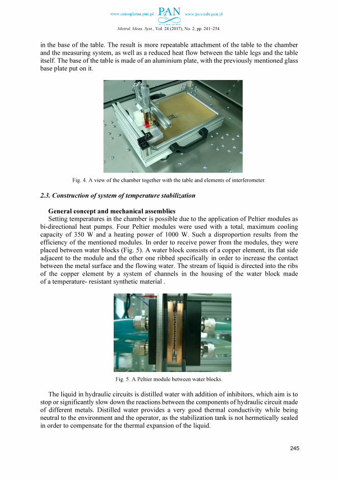
Fig. 3. A view of the chamber together with the table and elements of interferometer.
2.2. Measuring base
In order to enable thermal measurements of the changes of geometrical dimensions of small elements, it was necessary to solve the issue of thermal expansion of the base to which a tested
element was attached. The theoretical analysis of the problem proved that, in general, the only solution was the application of a measuring base made of material of a negligibly small coefficient of thermal expansion. Such materials are special optical glasses, from among which
we selected ZERODUR glass manufactured by the Schott company. The coefficient of thermal
expansion of this glass in the described application can be regarded as zero (α = 0.1∙10−6 K−1
[7]). We ordered a ZERODUR plate of the following dimensions: 140 × 260 mm2 and
a thickness of 25 mm. It is used as a measuring base, on which we place elements which geometrical changes caused by temperature changes are measured.
Inside the chamber there is a table (Fig. 4) supported by 3 legs screwed into the top of the optical table. The legs are equipped with cermet balls, that penetrate into appropriate sockets
244
Metrol. Meas. Syst., Vol. 24 (2017), No. 2, pp. 241–254.
in the base of the table. The result is more repeatable attachment of the table to the chamber
and the measuring system, as well as a reduced heat flow between the table legs and the table itself. The base of the table is made of an aluminium plate, with the previously mentioned glass base plate put on it.
Fig. 4. A view of the chamber together with the table and elements of interferometer.
2.3. Construction of system of temperature stabilization
General concept and mechanical assemblies
Setting temperatures in the chamber is possible due to the application of Peltier modules as bi-directional heat pumps. Four Peltier modules were used with a total, maximum cooling
capacity of 350 W and a heating power of 1000 W. Such a disproportion results from the efficiency of the mentioned modules. In order to receive power from the modules, they were placed between water blocks (Fig. 5). A water block consists of a copper element, its flat side
adjacent to the module and the other one ribbed specifically in order to increase the contact between the metal surface and the flowing water. The stream of liquid is directed into the ribs
of the copper element by a system of channels in the housing of the water block made of a temperature- resistant synthetic material .
Fig. 5. A Peltier module between water blocks.
The liquid in hydraulic circuits is distilled water with addition of inhibitors, which aim is to stop or significantly slow down the reactions between the components of hydraulic circuit made
of different metals. Distilled water provides a very good thermal conductivity while being neutral to the environment and the operator, as the stabilization tank is not hermetically sealed in order to compensate for the thermal expansion of the liquid.
245
M. Dobosz, M. Kożuchowski, et al.: INTERFEROMETRIC SET-UP FOR MEASURING THERMAL …
A hydraulic circuit responsible for exchanging heat from Peltier modules with the
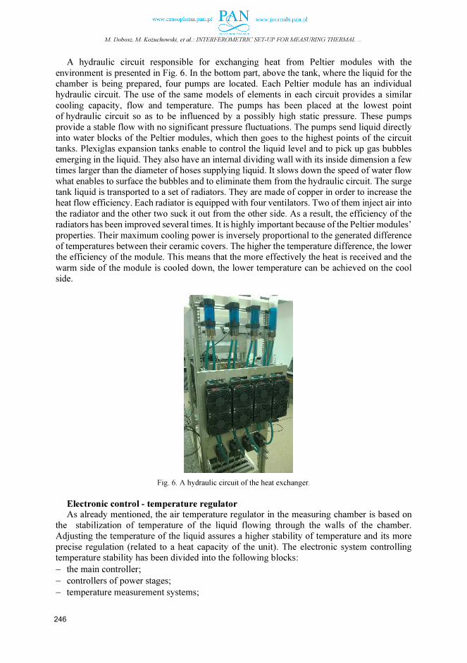
environment is presented in Fig. 6. In the bottom part, above the tank, where the liquid for the chamber is being prepared, four pumps are located. Each Peltier module has an individual hydraulic circuit. The use of the same models of elements in each circuit provides a similar
cooling capacity, flow and temperature. The pumps has been placed at the lowest point of hydraulic circuit so as to be influenced by a possibly high static pressure. These pumps
provide a stable flow with no significant pressure fluctuations. The pumps send liquid directly into water blocks of the Peltier modules, which then goes to the highest points of the circuit tanks. Plexiglas expansion tanks enable to control the liquid level and to pick up gas bubbles
emerging in the liquid. They also have an internal dividing wall with its inside dimension a few times larger than the diameter of hoses supplying liquid. It slows down the speed of water flow
what enables to surface the bubbles and to eliminate them from the hydraulic circuit. The surge tank liquid is transported to a set of radiators. They are made of copper in order to increase the heat flow efficiency. Each radiator is equipped with four ventilators. Two of them inject air into
the radiator and the other two suck it out from the other side. As a result, the efficiency of the radiators has been improved several times. It is highly important because of the Peltier modules’
properties. Their maximum cooling power is inversely proportional to the generated difference of temperatures between their ceramic covers. The higher the temperature difference, the lower the efficiency of the module. This means that the more effectively the heat is received and the
warm side of the module is cooled down, the lower temperature can be achieved on the cool side.
Fig. 6. A hydraulic circuit of the heat exchanger.
Electronic control - temperature regulator
As already mentioned, the air temperature regulator in the measuring chamber is based on the stabilization of temperature of the liquid flowing through the walls of the chamber. Adjusting the temperature of the liquid assures a higher stability of temperature and its more
precise regulation (related to a heat capacity of the unit). The electronic system controlling temperature stability has been divided into the following blocks:
− the main controller;
− controllers of power stages;
− temperature measurement systems;
246

Metrol. Meas. Syst., Vol. 24 (2017), No. 2, pp. 241–254.
− a power supply. The main controller is a system controlling particular modules and is responsible for:
− communication with the control master computer (setting temperature changes, sending the results of measurement to the master computer, determining the operation mode);
− communication with temperature sensors (through intermediate processors used because of the necessity of changes in the transmission protocol, as well as for reducing the distance between processor and sensor);
− implementation of an algorithm of temperature regulation;
− controlling power stages (regulation of the level of heating/cooling);
− controlling correctness of the system operation. The power controllers are systems supplying Peltier modules which enable:
− regulation of the power supply of the module (and the related efficiency);
− switching between the heating/cooling functions. The temperature measurement is carried out with the use of integrated semiconductor
thermometers of ADT7320 type with a high measuring accuracy (0.2ºC guaranteed with no
additional calibration, 0.002ºC typical accuracy and repeatability better than 0.02ºC). Thus, such systems are equipped with an SPI interface and an additional microcontroller located near
the thermometers, applied to control the measurement and to send the results to the main controller via an RS485 interface. Separating the microcontroller from the temperature sensor is necessary to reduce the influence of heating of the microcontroller on the measurement.
Communication of the main controller with other modules is made on the basis of an RS485 interface (two channels). It enables a two-way transmission between multiple systems with the
use of two wires. If necessary, it makes possible adding other systems without a need of rewiring.
The entire system is supplied from a 24V 1000 W chopper power supply. Each plate has local stabilizers generating voltage necessary for the operation of each module. The power control modules need 190 W each when fully controlled. Other systems take approximately
3−4 W. The main controller is made on the basis of an ATMega64 microcontroller. Additionally, it
has two UART hardware systems that are used for transmission to sub-systems. UART
conversion systems − RS485 (SN75176) and USB-FT245 bridge are located in the surroundings of the microcontroller. SN75176 (U4 and U5) systems convert TTL level signals (RxD and TxD of the processor) into differential signals required for the RS485 transmission. Since it is
two-way transmission, a signal of choosing the transmission direction is required. In order to ensure correctness of the transmission and protect it against a possibility of simultaneous
transmission through different systems, the receiver module is still on and the microcontroller is able to view the signal on the main line. If the received signal is in accordance with the sent one, the transmission is correct.
To communicate with the master computer, an FT245 (USB converter) system has been used. This system is seen as a serial port, what simplifies the control (it is possible to use the
terminal for sending and receiving data). An LCD display is used for indicating a current condition of the processor and peripheral
systems. It enables to display current settings of temperature, the results of its measurement and to signal whether the system is currently in a heating or cooling mode.
The system of power supply and control of the Peltier modules has been made in the form
of four identical control modules. These modules enable independent controlling any voltage of any polarization (as regards the voltage of Peltier cells operation) of one of the four cells.
The adjustable power supply is a pulse converter lowering the supply voltage (24 V) to the
voltage required by a Peltier cell (0−16 V) at the required load current equal to 10 A. The converter is controlled by PWM signals from the outlets of the processor. The PWM signals
247

M. Dobosz, M. Kożuchowski, et al.: INTERFEROMETRIC SET-UP FOR MEASURING THERMAL …
are provided to the inputs of the controller system of IR2113 transistor half-bridge, which gives
a current output sufficient to drive the power transistors. A frequency of PWM is 55 kHZ. The PWM is operated on 55% and 35% cooling and heating duty cycles, respectively. These values were determined to achieve similar speeds of heating and cooling.
At the same time, this driver provides voltage higher than the power supply voltage, what is required for correct operation of the keying transistor. As the module must provide a change
of polarization of the output voltage that is required to switch between the heating and cooling modes, it was inevitable to use an H-bridge for producing the switching voltage.
To reduce the influence of other elements on the temperature sensors (especially when
heating), the systems were located on the plates only with elements reducing interference. In order to provide a good heat exchange with the environment, the elements were assembled
on the aluminium base. As thermometer systems are equipped with an SPI interface, it becomes necessary to use an
intermediate microprocessor system between the thermometer and the main controller module.
This intermediate system is based on an ATMega8 microcontroller. It provides control of 4 digital thermometers, as well as communication with the control module via an RS485
interface. The microcontroller controls the thermometer system in such a way that temperature
measurements are made at intervals of 1 second, with the maximum resolution of thermometers.
Between the measurements the systems are put to sleep, what reduces the heating of thermometers.
3. Measurement of micro-displacements
3.1. Assumptions for construction of specialized interferometer
Measurement of the geometrical changes of mechanical parts having dimensions starting from a few centimetres at a change of temperature to 10ºC requires providing a measurement
resolution of displacements of a nanometre level. In practice, this means the need for applying an interference method.
Because of testing the influence of ambient temperature on an examined element, we were
not able to use incremental or contactless encoders, which would require placing a detector in the thermal chamber. Due to that fact, we suggested a solution in the form of a laser
interferometer, where a laser beam would be brought to the thermal chamber from the outside. Assuming the use of a conventional interferometer with a reflector operating in one of its
arms for measuring displacements of often quite flexible mechanical elements of the balances,
it was necessary to adopt the following assumptions:
− minimization of weight, and thus a size of the measuring reflector together with its fastening, what leads to:
− inability to precisely adjust the position of the reflector towards the laser beam (an accuracy
of linear − in the order of 0.3 mm, and angular positioning – in the order of 1º). Taking the above into consideration, it was necessary to use a cube corner prism of possibly
small weight and small dimensions as the measuring reflector. It resulted in another problem − commercially available prisms having such small dimensions are characterized by low accuracy (non-parallelism of the outgoing beam to the incoming beam is approx. 15ˮ). This means that
conventional reading systems of interferometers designed to operate with prisms of 2ˮ accuracy are not suitable for use in this case. That is why it was necessary to apply a special receiving
system of interference fringes which would give a correct reception of a signal disturbed as a result of the non-parallelism of interfering beams.
248

Metrol. Meas. Syst., Vol. 24 (2017), No. 2, pp. 241–254.
The above mentioned problems led to the need of developing from scratch a specialised laser
interferometer which could operate according to the principle of counting interference fringes.
3.2. Description of construction
Laser
When constructing the interferometer, we assumed the use of a single-frequency He-Ne laser-based interferometer. The rationale is a simple construction providing significantly lower costs of construction and the possibility of greater miniaturization of the measuring system,
while homodyne are similar to heterodyne systems in terms of their metrological parameters. The final argument for selecting this type of solution was adopting the concept of a receiving
system insensitive to the interference angle, which, by definition, cannot operate on high frequencies of signals.
Due to a variable difference in optical paths, which may occur when measuring elements
of different dimensions, it was indispensable to use a stabilized He-Ne laser. A requirement was formulated that the uncertainty of determination of light wavelength is at a level of 0.001 nm
what gives a relative measurement error of displacement coming from this source at a level
of 1.5 ∙ 10−6 nm. Such a value is entirely sufficient due to a small range of the measured displacements. As an example, when measuring changes in the dimensions of elements of the
order of 10 µm, this component of uncertainty will generate a negligible error of 1.5 ∙ 10−2 nm. A two-frequency Thorlabs HRS015 laser has been used. In the further described system,
only one mode was used.
General configuration of interferometer
A general scheme of the interferometer with particular subassemblies, is presented in Fig. 7.
Fig. 7. A general scheme of the interferometer construction.
At the beginning, from the beam of the two-frequency He-Ne laser, one frequency of linear polarization is separated with the use of a polarizer P1. In the next stage the beam is expanded
to a diameter of 2 mm adjusted to dimensions of the applied cube corner reflectors. A collimation telescope K1 is used for this purpose. Next, the beam passes through a quarter-wave plate QR, which transforms the linear polarization into the circular polarization being an
effect of putting together two linear disturbances which are mutually perpendicular and phase-shifted by 1/4 of a light wavelength. The such prepared beam is emitted outside the laser head
towards the interferometer assembly. This beam is directed via prisms/mirrors M1 and M2 to a polarizing cube beam-splitter BS. The mirror M1 directs the beam perpendicularly to the Zerodur base surface. The prism M2 cemented with the beam-splitting element is moved along
the axis of the beam behind the mirror M1 enabling the interferometer to operate at different heights depending on the height of measured detail. A reference cube corner reflector RCCR
is cemented to one side of the cube beam-splitter. It has identical dimensions as the measuring cube corner reflector MCCR. Due to that fact, changes in temperature in the chamber change
P1
K1QR
K2
M1
M2BS
RS
Zerodur
M3M4
RCCR
MCCR
249

M. Dobosz, M. Kożuchowski, et al.: INTERFEROMETRIC SET-UP FOR MEASURING THERMAL …
the optical paths in both cube corners in the same way, without generating an error significant
for the measurement. The polarizing cube beam-splitter directs a component of type P light polarization to the referential prism and then, after reflecting the beam, directs it back to the
laser head. A type S polarization component is transmitted through the beam-splitting layer to the measuring cube corner reflector which is glued to the tested surface for the time
of measurement. The reflector directs the beam back to the beam-splitter, which − after passing
through it − returns to the laser head. Both beams are at the beginning introduced into the laser telescope K2, which expands them to a diameter of approx. 4 mm. adjusted to the receiving photo-detection system RS.
Specialized photo-detection system
There are two main types of receiving systems of interferometer: (i) photo-detective systems
operating with zones of interference fringes of an infinite period [8] (classic solution) and (ii) systems operating with fringes of a finite period [9].
As already mentioned, due to insufficient angular accuracy of the cube corner reflector-
prisms applied in the system of interferometer it was not possible to apply a classic photo-detection system because of a finite and unstable (dependent on the settings of the reflector)
period of the fringes. This problem has been solved by applying a special photo-detection system based on a patent [10] and developed in the Institute of Metrology and Biomedical
Engineering within an earlier research project and presented in detail in [11]. The receiving system is composed of the following elements:
− birefringent wedge;
− polarizer;
− cylindrical lens;
− photodetector. The adopted receiving system is presented in Fig. 8. When passing through the birefringent
wedge W the measuring and reference beams MB and RB, respectively, having mutually perpendicular linear polarization, are refracted at different angles dependent on their own
polarization. This is a result of different values of the refractive index of ordinary and extraordinary rays. The wedge is made of birefringent crystal and the refraction angle depends
on the wedge direction and the angle of its cut, so behind the wedge the beams run at some non-zero angles. The wedge itself must be able to rotate in order to be regulated. Next, the set P2 polarizer brings the measuring and referential beams to the common surface in order to enable
their interference. The cylindrical lens CL together with properly designed regulation of the photodetector P position enable adjusting the area of interference to the surface of the
photodetector.
Fig. 8. A chart of the receiving system of interferometer.
Assembly of polarizing beam-splitter
The purpose of the polarizing beam-splitter assembly is precise introduction of the laser beam into the cube corner reflector placed on the tested element surface. Its construction must
eliminate the influence of temperature changes on the result of measurement. A possibility of precise adjustment and fastening of the system on the measuring table is equally important
as regulation of height at which the cube beam-splitter is set. These conditions are fulfilled by a mechano-optical system, a diagram of which is presented in Fig. 9. The assembly
of interferometer beam-splitter is composed of three optical elements cemented together:
250

Metrol. Meas. Syst., Vol. 24 (2017), No. 2, pp. 241–254.
a rectangular prism M2 directing the beam, a polarization cube beam-splitter BS dividing the
beam and a reference cube corner reflector RCCR. This assembly is mounted to a carriage, which is able to move along a slide perpendicular to the Zerodur base surface. It enables to run the measurement beam both parallel to the Zerodur base and at the desired height determined
by the tested element size. The height of cube and prisms is precisely regulated by a micrometre screw
After adjusting the desired height the assembly can be stiffly fixed. Locking the assembly position by a bolt is supposed to guarantee mechanical stability of the beam splitting assembly during measurements. It was extremely important to design a stable attachment of the assembly
and the tested detail together with the corner mirror to the Zerodur plate. The point of reference which has to be provided with a possibility to keep an unchanged position is the assembly
of beam-splitter together with the reference reflector. Even a slight thermal change of the position of this reference assembly may significantly affect the result of measurement. Thus, in the project of assembly construction two support surfaces were made, located symmetrically
to the cube, situated in the same vertical line as its centre. The shape and dimensions of the beam splitting element provides minimal influence
of thermal deformations on the result of measurements. Fastening the assembly to the base plate may be carried out by pressing the whole assembly to the Zerodur base in such a way that the points of pressure are located symmetrically on both sides of the cube beam-splitter. However,
in the majority of measurements, the assembly was stuck to the base with the use of some protruding surfaces located symmetrically in relation to the referential prism.
Fig. 9. A schematic diagram of the interferometer beam-splitter assembly.
Measuring reflector
The construction of measuring reflector is based on the use of a cube corner prism with dimensions enabling to work with a laser beam with a diameter of approx. 2 mm. In the project
we have used an Edmund Optics corner prism with an outer diameter of 7.16 mm, what enabled
to keep an optimal size of the housing with the following dimensions: 8 × 8 × 6.3 mm3. The housing of cube reflector make it possible to be mounted in various arrangements (Fig. 10).
On the external surfaces of the housing there are made outlets, one of which located on the axis of the tip of the prism can be glued at the desired point of the part, the displacements
of which are to be measured. The assembly weighs about 0.8 g. An atempt was made to reduce mass of the optical element in order to decrease the influence of weight on the geometry of the measuring part. Small dimensions are required to limit the mounting area.
Attaching element to base
On each tested element two points are determined − the first, a reference point towards which geometrical changes of the detail are measured, and the second, a measuring point to which the
measuring reflector of interferometer is attached. Depending on the position of base point on the part, additional intermediate elements are used. Fig. 11 a shows a fragment of the part with a hole the axis of which acts as the base point. In this case, attaching to the surface at this point
was carried out with the use of a screw stuck by a conical head to the Zerodur surface and
251

M. Dobosz, M. Kożuchowski, et al.: INTERFEROMETRIC SET-UP FOR MEASURING THERMAL …
pressing the measured element by a conical nut, as shown in Fig. 11b. Depending on a form
of the reference point, various specifically designed intermediate elements were used.
a) b)
Fig. 10. A simplified design drawing of the assembly of a measuring cube corner reflector (a);
a view of mounting of the measuring reflector to a tested part (b).
a) b)
Fig. 11. Attaching the reference point to the Zerodur base surface. A fragment of construction drawing
of the tested part (a); a view of a cone nut clamping the element to the base screw (b).
The place of sticking the screw to the base plate is here invisible.
4. Tests of appliance and discussion
The basis for evaluation of the feasibility of performing the necessary tests using the
developed appliance was verification of stability of the interferometer readings during changes of temperature in the chamber. In this case, the measuring reflector was glued with the use of its housing directly to the Zerodur base (the measured element was not used). A distance between
the measuring and reference reflectors was approximately 105 mm. Next, temperature in the chamber was periodically changed and the interferometer readings were saved. Two options
of data saving were used − without and with the numerical correction of light wavelength changes. The sensors of temperature, pressure and humidity installed in the chamber were used to evaluate the actual air refractive index and to calculate the actual wavelength basing on the
Edlen formula [12] and its subsequent amendments [13, 14]. An amplitude of changes in temperature was 9.5ºC. The test duration was 64 hours. Sample test results are presented
in Fig. 12. A purple line shows the applied temperature changes. A red line shows differences in the interferometer readings obtained without the wavelength correction. A green line shows the interferometer readings including the influence of environment on the air refractive index
(and the light wavelength).
252

Metrol. Meas. Syst., Vol. 24 (2017), No. 2, pp. 241–254.
a)
b)
Fig. 12. Changes of the readings of the position of measuring reflector caused by changes of temperature (a);
an enlarged part of the corrected readings (b).
When analysing the graph we can notice that in the first several hours of changing
temperature the response of interferometer is incorrect. It results from deformation of the
mechanical elements of interferometer under the influence of temperature gradients. However, after 10 hours of increasing temperature and after 8 hours of stabilization at a high level, the
readings of interferometer reach a level of systematic error of about −0.12 ÷ −0.11 µm. This
corresponds to the relative inaccuracy of measurement equal to approximately 10−6. When cooling the chamber, stable readings are achieved slightly earlier, after about 8 hours from the beginning of cooling and after 6 hours from the beginning of stabilization in the lower
temperature; the systematic error is at a level of about −0.1 ÷ −0.08 µm. This corresponds to
the relative inaccuracy of measurement equal to approximately 10−6. These are satisfactory values. However, obtaining this level of inaccuracy in practice requires approx. 8 hours for
temperature stabilization after its change. Unfortunately, it significantly extends the duration of measurements. The noise of interference signal is a result of fluctuations of the
253

M. Dobosz, M. Kożuchowski, et al.: INTERFEROMETRIC SET-UP FOR MEASURING THERMAL …
interferometer indications caused by temperature gradients of the air in the chamber and
vibration of the set-up. This random noise does not exceed 10 nm with a signal resolution of 1 nm.
If the systematic error value exceeds the required value, the only way to solve the problem
is to carry out the measurement in a different way, i.e. with the use of a measured detail, and then without it, but with the same difference of optical paths.
The last horizontal section of the graph shows at the same time the achieved level of temperature stability in the chamber, which reaches a value of 0.01ºC per 8 hours. This value is at least about one order of magnitude better than in commercially available climatic
chambers. Summing up, the following technical parameters of the calibration system were obtained,
which were confirmed by the experimental test results:
− a relative inaccuracy of displacements’ measurement is equal to about of 10−6;
− a time interval required for stabilization of temperature (after a change of about 10ºC) in order to achieve the assumed uncertainty is approx. 8 hours;
− a level of temperature stabilization is of about 0.01ºC per 8 hours;
− a range of possible operating temperatures is equal to 15ºC−35ºC.
Acknowledgements
The research has been funded from the research budget for 2013-2016 as a research project
PBS2/B6/16/2013 of The National Centre for Research and Development of Poland.
References
[1] http://radwag.com/pl/
[2] http://www.binder-world.com/pl/Produkty/Komory-klimatyczne-do-test%C3%B3w-
stabilno%C5%9Bci/Seria-KBF/KBF-115#1
[3] Schödel, R. (2008). Ultra-high accuracy thermal expansion measurements with PTB’s precision
interferometer. Meas. Sci. Technol., 19. 084003, 11.
[4] James, J.D., Spittle, J.A., Brown, S.G.R., Evans, R.W. (2000). A review of measurement techniques for the
thermal expansion coefficient of metals and alloys at elevated temperatures. Meas. Sci. Technol., 12, R1–
R15.
[5] Cordero, J., Heinrich, T., Schuldt, T., Gohlke, M., Lucarelli, S., Weise, D., Johann, U., Braxmaier, C. (2009).
Interferometry based high-precision dilatometry for dimensional characterization of highly stable materials
Meas. Sci. Technol., 20.
[6] Okaji, M., Yamada, N,. Moriyama, H. (2000). Ultra-precise thermal expansion measurements of ceramic
and steel gauge blocks with an interferometric dilatometer. Metrologia, 37, 165−171.
[7] Demtröder, W. (2008). Laser Spectroscopy: Vol. 1: Basic. Principles Springer-Verlag Berlin Heidelberg.
[8] Petru, F., Cip, O. (1999). Problems regarding linearity of data of a laser interferometer with a single
frequency laser. Precis. Eng., 23(1), 39–50.
[9] McMurtry, D. (2002). Interferometer. WO 02/34321 A1.
[10] Patent no PL387343.
[11] Dobosz, M., Zamiela, G. (2012). Interference fringe detection system for distance measuring interferometer.
Optics and Laser Technology, 44, 1620−1628.
[12] Edlén, B. (1966). The refractive index of air. Metrologia, 2, 71−80.
[13] Birch, K.P. Downs, M.J. (1993). An updated Edlén equation for the refractive index of air. Metrologia, 30,
155−162.
[14] Birch, K.P., Downs, M.J. (1994). Correction to the updated Edlén equation for the refractive index of air.
Metrologia, 31, 315−316.
Metrol. Meas. Syst., Vol. 24 (2017), No. 2, pp. 255–264.
_____________________________________________________________________________________________________________________________________________________________________________________
Article history: received on Sep. 26, 2016; accepted on Jan. 29, 2017; available online on Jun. 30, 2017; DOI: 10.1515/mms-2017-0034.
METROLOGY AND MEASUREMENT SYSTEMS
Index 330930, ISSN 0860-8229
www.metrology.pg.gda.pl
LEAKAGE CURRENT DEGRADATION DUE TO ION DRIFT AND DIFFUSION IN TANTALUM AND NIOBIUM OXIDE CAPACITORS
Martin Kuparowitz, Vlasta Sedlakova, Lubomir Grmela
Brno University of Technology, Faculty of Electrical Engineering and Communication, Technicka 8, 616 00 Brno, Czech Republic ([email protected], [email protected], +420 541 146 025, [email protected])
Abstract
High temperature and high electric field applications in tantalum and niobium capacitors are limited by the mechanism of ion migration and field crystallization in a tantalum or niobium pentoxide insulating layer.
The study of leakage current (DCL) variation in time as a result of increasing temperature and electric field might
provide information about the physical mechanism of degradation. The experiments were performed on tantalum
and niobium oxide capacitors at temperatures of about 125°C and applied voltages ranging up to rated voltages
of 35 V and 16 V for tantalum and niobium oxide capacitors, respectively. Homogeneous distribution of oxygen
vacancies acting as positive ions within the pentoxide layer was assumed before the experiments. DCL vs. time characteristics at a fixed temperature have several phases. At the beginning of ageing the DCL increases
exponentially with time. In this period ions in the insulating layer are being moved in the electric field by drift
only. Due to that the concentration of ions near the cathode increases producing a positively charged region near
the cathode. The electric field near the cathode increases and the potential barrier between the cathode and
insulating layer decreases which results in increasing DCL. However, redistribution of positive ions in the insulator
layer leads to creation of a ion concentration gradient which results in a gradual increase of the ion diffusion current in the direction opposite to the ion drift current component. The equilibrium between the two for a given
temperature and electric field results in saturation of the leakage current value. DCL vs. time characteristics are
described by the exponential stretched law. We found that during the initial part of ageing an exponent n = 1
applies. That corresponds to the ion drift motion only. After long-time application of the electric field at a high
temperature the DCL vs. time characteristics are described by the exponential stretched law with an exponent
n = 0.5. Here, the equilibrium between the ion drift and diffusion is achieved. The process of leakage current degradation is therefore partially reversible. When the external electric field is lowered, or the samples are
shortened, the leakage current for a given voltage decreases with time and the DCL vs. time characteristics are
described by the exponential stretched law with an exponent n = 0.5, thus the ion redistribution by diffusion
becomes dominant.
Keywords: niobium oxide capacitors, tantalum capacitors, leakage current, ion diffusion, ion drift.
© 2017 Polish Academy of Sciences. All rights reserved
1. Introduction
Quality and life time of capacitor and supercapacitor devices have been studied for the last
decades by many scientists [1−11]. The degradation of tantalum (Ta) and niobium oxide (NbO)
capacitors in steady-state conditions at elevated temperatures was studied in [6−11]. The
capacitor leakage current (DCL) is a parameter most sensitive to defects and irreversible processes in the insulating pentoxide layer. Changes of DCL in time at increased temperature
and applied electric field might provide information on the physical mechanism of degradation. High temperature and high electric field applications are considered to be limited by field
crystallization mechanisms and by migration of positively charged oxygen vacancies (ions)
in pentoxide film [6−9]. The field crystallization model assumes that tantalum or niobium oxide crystals grow with time of operation under the amorphous anodic oxide and eventually disrupt

M. Kuparowitz, V.Sedlakova, L. Grmela: LEAKAGE CURRENT DEGRADATION DUE TO ION DRIFT …
the dielectric layer, causing a breakdown. Until the moment of disruption no changes in leakage
currents are observed. It is assumed that the rate of crystallization increases with increasing thickness of the anodic pentoxide [7] and then high-voltage capacitors should be more vulnerable to this type of failure.
The model of redistribution of positive ions in pentoxide film [7] assumes that ions move from the capacitor anode to its cathode in electric field by diffusion only and create an internal
electric field in the vicinity of insulating layer-cathode interface which affects the potential barrier on this interface according to a modified Schottky conduction mechanism and consequently changes DCL.
Leakage current variations are partially reversible [10−12]. Increasing temperature results in a gradual decrease of leakage currents either without applying an external electric field or with
applying a very low voltage. In some cases initial values of DCL were restored altogether. When the leakage current changes are reversible and the field crystallization is not involved, the source of DCL change must only be the ion redistribution.
Both Ta and NbO capacitors pass through high temperature technological steps which should ensure homogeneous distribution of oxygen vacancies in the dielectric layer. Therefore, we
assume that the concentration of positive ions – oxygen vacancies in the pentoxide volume is constant if the experiments are performed on as-prepared samples (not subjected to an external electric field prior to the experiment). In this case the ion diffusion cannot be involved in the
charge redistribution in the pentoxide volume, because no concentration gradient exists within the pentoxide layer at the beginning of ageing. Drift of charges in the external electric field
must be observed first, whereas diffusion of charges occurs only after the concentration gradient is formed within the structure.
The ageing process in Ta and NbO capacitors can be divided into two separate phases.
During the initial stage of ageing the drift process is dominant due to the application of external electric field at an elevated temperature. The second stage of ageing is affected by both the
external electric field and the ion concentration gradient created in the vicinity of Ta2O5 or Nb2O5 – cathode interface. In this case both drift and diffusion of ions are pronounced.
In this paper we show a method of the qualitative evaluation of ion drift and diffusion
processes during the ageing of Ta and NbO capacitors. Time dependencies of the leakage current are measured and evaluated and mechanisms responsible for the DCL increase are
determined. The reversibility of DCL changes and their source are verified.
2. Experiment
The experiments were performed on tantalum capacitors with capacitance 33 µF and
nominal voltage 35 V and niobium oxide capacitors with capacitance 2.2 µF and nominal voltage 16 V. All capacitors contain an MnO2 cathode and are placed in an SMD type D case
with dimensions 7.3 × 4.3 × 2.9 millimetres (length × width × height). The working temperature
is in a range of −55 to +125°C. The dielectric thickness is about 190 nm for Ta capacitors and 170 nm for NbO capacitors. We have evaluated two sets of Ta capacitors denoted further as Ta1 and LT8, and a set of NbO capacitors denoted as NbO2. 20 samples were evaluated within each set.
We measured the leakage current evolution in time for samples powered at a nominal voltage and placed in a climatic chamber at temperature 120°C for NbO capacitors and 125°C for Ta
capacitors. The leakage currents were monitored using a PC-based data acquisition system (see Fig. 1).
Here, the samples under test were soldered on an FR4 board with printed connectors, which
enables simultaneous charging of up to 20 samples. PCBs with soldered samples were placed in a climatic chamber, where an appropriate value of temperature can be maintained within
256

Metrol. Meas. Syst., Vol. 24 (2017), No. 2, pp. 255–264.
a range from 30 to 300°C. The samples were connected to load resistors using multiple cables
with temperature-proof PTFE insulation. The 10 kΩ load resistors were placed outside the
climatic chamber. The samples were powered using a DC digital power source Agilent 6614C. To measure the voltage on the load resistors an Agilent 34970A meter with 3 pcs of a 20-channel multiplexer card 34901A was used. The climatic chamber, multi-meter and power
source were interconnected via an IEEE 488 (GPIB) bus which was connected to the computer via a GPIB/USB interface Agilent 82357A.
Fig. 1. A measurement system.
For measurement of the leakage current time dependence at an elevated temperature
a required voltage of the power source was fixed. A voltage on the load resistor was measured periodically every 10 seconds. The leakage current value was calculated from the voltage measured on the load resistor and the load resistor value. The values of load resistors should
meet the condition that the voltage on the load resistor during the experiment does not exceed 5% of the power source output voltage. Then the voltage on the measured capacitor was
assumed to be constant during the experiment. The total duration of ageing experiment was near 400 hours.
Fig. 2. A DCL vs. time characteristic for the niobium oxide capacitor NbO2-3 ageing at a nominal voltage
V = 16 V and temperature T = 120°C.
A typical dependence measured during the experiment is shown in Fig. 2. Here, the time
dependence of leakage current is shown for the niobium oxide capacitor NbO2-3 for applied
nominal voltage V = 16 V at temperature T = 120°C. The monitored leakage current value
increases from 19 µA up to 88 µA within a time interval of 400 hours (see Fig. 2).
0
20
40
60
80
100
00.4x10
60.8x10
61.2x10
61.6x10
6
0 1x10²
2x10²
3x10²
4x10²
t / h
Nb02-3T = 120 °CU = 16 V1TT
I=a+c(1-exp(-(t/b)n))
a=19, b=1.97E5, c=71.9, n=0.572
t / s
I / µ
A
257

M. Kuparowitz, V.Sedlakova, L. Grmela: LEAKAGE CURRENT DEGRADATION DUE TO ION DRIFT …
After this the leakage current recovery was studied. The voltage was lowered down to 5 V
for Ta capacitors and to 2 V for NbO capacitors. The leakage current was then monitored in about 40 to 170 hours.
Figure 3 shows DCL recovery for the niobium oxide capacitor NbO2-3. After long-time
application of a nominal voltage at 120°C (see Fig. 2) the voltage was lowered to 2 V and the
sample was left at 120°C. The monitored leakage current value decreased from 1.8 µA to 0.2 µA
within a time interval of about 40 hours. A drop of current from 88 µA to 1.8 µA is caused by a decrease of the applied voltage from 16 V to 2 V.
Fig. 3. A DCL vs. time characteristic for the niobium oxide capacitor NbO2-3 during leakage current recovery
for applied voltage V = 2 V at temperature T = 120°C.
3. Results and discussion
The effect of electric field and high temperature on the ion drift and diffusion in tantalum
and niobium oxide capacitors will be discussed. We suppose that oxygen vacancies in a tantalum or niobium pentoxide layer act as positive ions. The samples are, as produced, stored at a room temperature without application of voltage before this experiment. Therefore, we
suppose that oxygen vacancies in the insulating layer are homogeneously distributed according to the thermodynamic equilibrium. This ion distribution is altered by applying an electric field.
The concentration of positive ions near cathode increases due to the ion drift in the electric field. The increase of concentration of positive ions in the vicinity of insulator/cathode interface results in an exponential increase of the leakage current.
Redistribution of positive ions in the insulator volume leads to the creation of an ion concentration gradient which results in a gradual increase of the ion diffusion current in the
direction opposite to that of the ion drift current component. The equilibrium between the ion drift in the electric field (from anode to cathode) and the ion diffusion due to the formed concentration gradient (in the direction from cathode to anode) for a given temperature and
electric field results in saturation of the leakage current value. The leakage current time dependence during ageing of a capacitor is described by an
exponential function:
)))/(exp(1()(10
n
tIItI τ−−+= , (1)
where: I0 is a DCL value at the beginning of ageing; I1 is a change of DCL due to the ageing, τ is a time constant of the ageing process. The value of exponent n = 1 when the potential barrier
0
0.5
1.0
1.5
2.0
00.5x10
51.0x10
51.5x10
5
0 10 20 30 40 t/h
y=a+cexp(-(x/b)n)
a=0.202, b=6076, c=1.60, n=0.5
Nb02-3T = 120 °CV = 2 V
t / s
I / µA
258

Metrol. Meas. Syst., Vol. 24 (2017), No. 2, pp. 255–264.
on the insulating layer/cathode interface linearly decreases due to the ion drift in the electric
field [13]. The value of exponent n = 0.5 is only for the ion diffusion [6, 7].
3.1. Effect of ion drift on leakage current at beginning of ageing
DCL vs. time characteristics for initial 1 to 10 hours of ageing of tantalum capacitors
at a rated voltage 35 V and temperature 125°C and niobium oxide capacitors at a rated voltage 16 V and temperature 120°C are shown in Figs. 4 and 5, respectively.
Fig. 4. DCL vs. time characteristics for a nominal voltage V = 35 V at temperature T = 125°C − beginning
of the ageing process for the tantalum capacitor Ta1-6.
Fig. 5. DCL vs. time characteristics for a nominal voltage V = 16 V at temperature T = 120°C − beginning
of the ageing process for the niobium oxide capacitor NbO2-3.
At the beginning of ageing the electron transport is mostly controlled by the ion drift from
anode to cathode. The measured time dependencies of leakage current can be modelled by (1)
using an exponent n = 1 during the first 1 hour for a tantalum capacitor and during the first 10 hours for a niobium oxide capacitor. A starting value of DCL at the beginning of ageing is
9
10
11
12
13
01x10
32x10
33x10
34x10
35x10
3
0 0.2 0.4 0.6 0.8 1.0 1.2
6
I=a+c(1-exp(-t/b))
a=10, b=2979, c=3.29
t / h
Ta1-6
T = 125 °C
V = 35 V
t / s
I / µA
20
30
40
01x10
42x10
43x10
44x10
4
0 2 4 6 8 10
3
I=a+c(1-exp(-t/b))
a=18.6, b=3.79E4, c=34.5
t / h
Nb02-3
T = 120 °CV = 16 V
t / s
I / µA
259

M. Kuparowitz, V.Sedlakova, L. Grmela: LEAKAGE CURRENT DEGRADATION DUE TO ION DRIFT …
I(0) = 10 µA for sample Ta1-6 and I(0) = 18.9 µA for sample Nb02-3. A time constant of ageing process determined from the fit of experimental data is about 3000 s for sample Ta1-6 and about
3.8 × 10⁴ s for sample NbO2-3 considering the ion redistribution caused only by drift in the
electric field. A time constant for niobium oxide capacitors is higher due to a lower applied electric field and a slightly lower temperature during the ageing process.
3.2. Effect of medium-term application of electric field on ion transport in insulating layer
A time dependence of the leakage current of tantalum sample Ta1-4 within the initial 5 hours
of ageing is shown in Fig. 6. Here, the experimental data are modelled by (1) using the exponent
value n = 0.629.
Fig. 6. DCL vs. time characteristics for the tantalum capacitor Ta1-4 for a nominal voltage V = 35 V
at temperature T = 125°C – initial 5 hours of the ageing process. A model of experimental data includes
the ion movement by both drift and diffusion.
The exponent n values in a range from 0.5 to 1 correspond to the ion movement by both drift
and diffusion. The drift transport from anode to cathode is a result of the external electric field.
The ion diffusion in the opposite direction appears as a result of the ion concentration gradient formed in the vicinity of cathode interface. However, during medium-term application of the
electric field the drift transport mechanism still remains dominant. During long-term application of the electric field the equilibrium of the ionic drift and the
diffusion transport mechanism is achieved.
3.3. Effect of long-term application of electric field on ion transport in insulating layer
A DCL vs. time characteristic for tantalum capacitor Ta1-4 when a voltage V = 35 V
at temperature 125°C was applied within a time interval of 80 hours is shown in Fig. 7. Fig. 2 shows the time dependence of leakage current for niobium oxide capacitor NbO2-3 for an applied nominal voltage V = 16 V at temperature T = 120°C in a time interval of 400 hours.
In both cases the measured time dependencies of leakage current can be modelled by (1)
with an exponent n ≈ 0.5. A starting value of DCL at the beginning of ageing is I(0) = 10 µA
for sample Ta1-4 and I(0) = 19 µA for sample Nb02-3. A time constant of the ageing process
is τ = 2.10 × 10⁴ s for sample Ta1-4 and τ = 1.97x10⁵
s for sample NbO2-3 considering the ion redistribution by both drift in electric field and the diffusion mechanism. A time constant for
0
20
40
60
00.5x10
41.0x10
41.5x10
42.0x10
4
0 1 2 3 4 5
4
t / h
Ta1-4T = 125 °CV = 35 V
I=a+c(1-exp(-(t/b)n))
a=10, b=5922, c=47.6, n=0.629
t / s
I / µA
260

Metrol. Meas. Syst., Vol. 24 (2017), No. 2, pp. 255–264.
niobium oxide capacitors is about one order of magnitude higher due to a lower applied electric
field and a slightly lower temperature during ageing.
The monitored leakage current value increases from 10 µA to 73 µA within a time interval
of 80 hours for sample Ta1-4, while the expected DCL value at saturation is 74.46 µA. The
monitored leakage current value increases from 19 µA to 88 µA within a time interval of 400
hours for sample NbO2-3, while the expected DCL value at saturation is 90.9 µA.
Fig. 7. DCL vs. time characteristics for the tantalum capacitor Ta1-4 for a nominal voltage
V = 35 V at temperature T = 125°C.
3.4. Reversibility of leakage current changes
When the external electric field is lowered or switched off, the ion drift component decreases or drops down to zero. The concentration of positive ions in the vicinity of insulating layer/cathode interface is higher compared with its value in the insulating layer volume. The
diffusion of ions due to the concentration gradient becomes the dominant ion transport mechanism in the tantalum or niobium pentoxide layer. The ions – oxygen vacancies – diffuse
in the direction from cathode to anode to restore the homogeneous distribution of ions in the pentoxide layer volume. A decrease of the positive ion concentration, in the vicinity of insulating layer/cathode interface, results in an increase of the corresponding potential barrier
and consequently in a decrease of the capacitor’s leakage current. A leakage current vs. time dependence during the recovery process is described by:
))/(exp()(10
n
tIItI τ−+= , (2)
where: I0 is an expected value of the leakage current for the time at infinity; I1 is a value of the
leakage current lowering due to the ion redistribution in the pentoxide layer and τ is a time
constant of the recovery process. The exponent is n ≈ 0.5 for both short-time and long-time
periods. It means that the ion diffusion is the dominant transport mechanism within the recovery process.
Figure 3 shows DCL recovery after long-time application of a nominal voltage V = 16 V at 120°C. Here, a time dependence of the leakage current is shown for niobium oxide capacitor NbO2-3 for a voltage lowered down to V = 2 V at temperature T = 120°C. The monitored
leakage current value decreases from 1.8 µA to 0.2 µA within a time interval of about 40 hours. A time constant of the recovery process for niobium oxide sample NbO2-3 is about 6000
0
20
40
60
80
01x10
52x10
53x10
5
0 20 40 60 80
10
4
t / h
Ta1-4T = 125 °CV = 35 V
I=a+c(1-exp(-(t/b)n))
a=10, b=2.10E4, c=64.46, n=0.5
t / s
I / µA
261

M. Kuparowitz, V.Sedlakova, L. Grmela: LEAKAGE CURRENT DEGRADATION DUE TO ION DRIFT …
seconds. We can see that an equilibrium value I0 = 0.20 µA is achieved within the monitored time interval.
Fig. 8. DCL vs. time characteristics for the tantalum capacitor LT8-1 with an applied voltage
V = 5 V at temperature T = 125°C during a leakage current recovery.
A similar experiment was performed on the tantalum capacitor LT8-1. A DCL recovery after
long-time application of a nominal voltage V = 35 V at 125°C is shown in Fig. 8. Here, a time dependence of the leakage current is shown for a voltage lowered down to V = 5 V at
temperature T = 125°C. The monitored leakage current value decreases from 2.3 µA to 0.1 µA within a time interval of about 170 hours. A time constant of the recovery process for tantalum
sample LT8-1 is 3.25 × 10⁴ seconds. We can see that an equilibrium value I0 = 0.076 µA is not achieved within the monitored time interval. The higher time constant determined for the
tantalum sample is probably affected by a higher external electric field acting on the sample during the recovery experiment.
4. Conclusions
A method for the qualitative evaluation of ion drift and diffusion processes during ageing of Ta and NbO capacitors at an elevated temperature is presented. Time dependencies of DCL are measured for a rated voltage at temperature 125°C for Ta capacitors and 120°C for NbO
capacitors. The mechanisms responsible for a DCL increase are determined using the parameters of exponential fit of the measured data.
Oxygen vacancies in a tantalum and niobium pentoxide layer act as positive ions. The homogenous distribution of ions corresponding to the thermodynamic equilibrium is supposed to have occurred before ageing. After application of an electric field the ion distribution is
changed due to ability of the ions to move. The concentration of positive ions near cathode increases due to the ion drift in the electric field. An increase of the positive ion concentration
in the vicinity of insulator/cathode interface results in an exponential increase of the leakage current. A time constant of the ageing process due to the ion drift decreases with increasing the
electric field and an exponent n = 1 for a linear decrease of the potential barrier on the insulating layer/cathode interface due to the ion drift in the electric field only.
Redistribution of positive ions in the insulator volume leads to creation of an ion
concentration gradient, which results in a gradual increase of the ion diffusion current in the
0
0.5
1.0
1.5
2.0
2.5
02x10
54x10
56x10
5
0 50 100 150 t / h
LT8-1
T = 125 °CV = 5 VRecovery
I=a+cexp(-(t/b)n)
a=0.0761, b=3.25E4, c=2.22, n=0.5
t / s
I / µA
262

Metrol. Meas. Syst., Vol. 24 (2017), No. 2, pp. 255–264.
direction opposite to that of the ion drift current component. The equilibrium between the two,
for a given temperature and electric field, results in saturation of the leakage current value. The exponent n value decreases with an increase of value ion diffusion current from 1 to 0.5, whereas n = 0.5 when the equilibrium between the ion drift and diffusion is achieved.
DCL changes are fully reversible when the source of DCL increase is only the ion redistribution by drift and diffusion. The samples left at an elevated temperature react to an
external electric field drop with a progressive decrease of DCL in time. From the exponential
fit of measured DCL time dependence we derived the exponent value n ≈ 0.5 for both short-
time and long-time periods. It means that the ion diffusion is the dominant transport mechanism
within the DCL recovery process. A time constant of the recovery process is directly proportional to the external electric field value.
Acknowledgements
Research described in this paper was financed by Czech Ministry of Education in the frame of National Sustainability Program under grant LO1401. For research, the infrastructure of the SIX Center was used.
References
[1] Sedlakova, V., Sikula, J., Majzner, J., Sedlak, P., Kuparowitz, T., Buergler, B., Vasina, P. (2016).
Supercapacitor Degradation Assesment by Power Cycling and Calendar Life Tests. Metrol. Meas. Syst.,
23(3), 345−358.
[2] Szewczyk, A., Sikula, J., Sedlakova, V., Majzner, J., Sedlak, P., Kuparowitz, T. (2016). Voltage Dependence
of Supercapacitor Capacitance. Metrol. Meas. Syst., 23(3), 403−411.
[3] Smulko, J., Józwiak, K., Olesz, M., Hasse, L. (2011). Acoustic emission for detecting deterioration
of capacitors under aging. Microelectronics Reliability, 51(3), 621−627.
[4] Smulko, J., Józwiak, K., Olesz, M. (2012). Quality testing methods of foil-based capacitors. Microelectronics
Reliability, 52(3), 603−609.
[5] Pavelka, J., Sikula, J., Vasina, P., Sedlakova, V., Tacano, M., Hashiguchi, S. (2002). Noise and transport
characterisation of tantalum capacitors. Microelectronics Reliability, 42, 841−847.
[6] Teverovsky, A. (2010). Effect of Post-HALT Annealing on Leakage Currents in Solid Tantalum Capacitors,
CARTS USA 2010, 43–59.
[7] Teverovsky, A. (2010). Degradation of leakage currents in solid tantalum capacitors under steady-state bias
conditions. Electronic Components and Technology Conference (ECTC). Proc. 60th, 2010, 752−757.
[8] Zednicek, T., Sikula, J., Leibovitz, H. (2009). A Study of Field Crystallization in Tantalum Capacitors and
its effect on DCL and Reliability. 29th CARTS 2009, Jacksonville, FL, 5.3.1–11.
[9] Sikula, J., Sedlakova, V., Navarova, H., Hlavka, J., Tacano, M., Zednicek, T. (2008). Tantalum and Niobium
Oxide High Voltage Capacitors: Field Crystallization and Leakage Current Kinetics. CARTS Europe 2008,
Helsinki, Finland, Oct. 20–23, 2008, 267–276.
[10] Laleko, V.A., Odinets, L.L., Stefanovich, G.B. (1982) Ionic current and kinetics of activation of the
conductivity of anodic oxide films on tantalum in strong electric fields. Soviet Electrochemistry, 18,
743−746.
[11] Chaneliere, C., et al. (1998). Tantalum pentoxide (Ta2O5) thin films for advanced dielectric applications.
Material Science and Eng., R22, 269−322.
[12] Sikula, J., Sedlakova, V., Navarova, H., Kopecky, M., Zednicek, T. (2011). Ion Diffusion and Field
Crystallization in Niobium Oxide Capacitors. CARTS Europe 2011, Nice, France, 33–41.
263

M. Kuparowitz, V.Sedlakova, L. Grmela: LEAKAGE CURRENT DEGRADATION DUE TO ION DRIFT …
[13] Elhadidy, H., Grill, R., Franc, J., Sik, O., Moravec, P., Schneeweiss, O. (2015). Ion electromigration in CdTe
Schottky metal-semiconductor-metal structure. Solid State Ionics, 278, 20−25.

Metrol. Meas. Syst., Vol. 24 (2017), No. 2, pp. 265–276.
_____________________________________________________________________________________________________________________________________________________________________________________
Article history: received on Jun. 30, 2016; accepted on Oct. 22, 2016; available online on Jun. 30, 2017; DOI: 10.1515/mms-2017-0021.
METROLOGY AND MEASUREMENT SYSTEMS
Index 330930, ISSN 0860-8229
www.metrology.pg.gda.pl
SEQUENTIAL CLASSIFICATION OF PALM GESTURES BASED
ON A* ALGORITHM AND MLP NEURAL NETWORK FOR QUADROCOPTER
CONTROL
Marek Wodziński, Aleksandra Krzyżanowska
AGH University of Science and Technology, Faculty of Electrical Engineering, Automatics Computer Science and Biomedical Engineering, A. Mickiewicza 30, 30-059 Cracow, Poland ( [email protected], + 48 12 617 2222 , [email protected])
Abstract
This paper presents an alternative approach to the sequential data classification, based on traditional machine
learning algorithms (neural networks, principal component analysis, multivariate Gaussian anomaly detector) and
finding the shortest path in a directed acyclic graph, using A* algorithm with a regression-based heuristic. Palm
gestures were used as an example of the sequential data and a quadrocopter was the controlled object. The study
includes creation of a conceptual model and practical construction of a system using the GPU to ensure the real-
time operation. The results present the classification accuracy of chosen gestures and comparison of the
computation time between the CPU- and GPU-based solutions.
Keywords: machine learning, shortest path, sequential data, quadrocopter, GPU, CUDA.
© 2017 Polish Academy of Sciences. All rights reserved
1. Introduction
Object control using biomedical signals, which are an example of the sequential data, is an important area of current research because a lot of disabled persons need an alternative way
to interact with their surroundings. So far, many attempts were made to control various systems and devices, using biomedical signals. For example, partially paralyzed people can still use EEG [1], EMG [2], EOG [3] signals, as an HMI interface to perform basic actions, or visually impaired people can interact with a computer using palm gestures [4].
Most common difficulties arising during such projects include the requirement of real-time
control and generalization due to inter-individual variation [1−6]. A typical approach to the
problem of generalization is the machine learning technique. The stronger the requirement of generalization, the more training data is required, which implies a higher model complexity
and a greater computational cost [7]. The real-time implementation of machine learning algorithms is difficult when the model has a high complexity [7]. Therefore, parallel
implementations based on GPU and FPGA have been developed [8−10]. However, GPU parallelization of the sequential data classification using, for example, Hidden Markov Models [11], is not easy and varies strongly with the data type [12]. Moreover, the implementation
process is quite difficult and requires the programming expertise. We suggest an alternative approach to the problem of sequential data classification, which
involves separation of a single classification frame from the result conjunction by using
traditional machine learning algorithms and finding the shortest path in a directed acyclic graph to determine the most probable outcome. Such a solution enables highly parallelizable
implementation and effective use of GPU. We decided to use a quadrocopter as the controlled object. Regarding its high complexity and six degrees of freedom, it is important to design a precise and reliable control scheme. The palm movements were registered using a Leap Motion

M. Wodziński, A. Krzyżanowska: SEQUENTIAL CLASSIFICATION OF PALM GESTURES BASED …
sensor which is described in detail in Subsection 2.2. We primarily focus on the requirement
of real-time system operation. To our knowledge, this is the first work that shows how to bring down classification of the sequential data to the problem of finding the shortest path.
2. Suggested solution
2.1. Solution concept
A conceptual model was divided into several parts, including: registration of palm
movements, creation of a palm model, feature extraction, anomaly detection, gesture classification, an update of the graph structure, solving the shortest path problem using A*
algorithm, mapping of the results, creation and transmission of commands − as shown in
a processing graph in Fig. 1.
Fig. 1. A scheme of acquisition, processing, classification and control.
Palm
movements
registration
Palm model
creation
Features
extraction
Gestures
classification
Anomaly
detection
Graph
structure
update
Finding
shortest path
with A*
algorithm
Classification
results
mapping
Command
transmission to
quadrocopter
Training
Data
CPU
GPU
Legend:
Signal
Command
266

Metrol. Meas. Syst., Vol. 24 (2017), No. 2, pp. 265–276.
2.2. Data acquisition and feature extraction
For registration of palm movements, a Leap Motion (Fig. 2a) sensor was used, which
measures various parameters of palm and fingers, including their position, velocity, direction and geometry (Fig. 2b), using monochromatic infrared cameras and LEDs [13]. The operation
range varies from 25 to 650 millimetres above the controller. The average accuracy of the sensor is about 0.7 millimetres [14]. The Leap Motion controller does not perform any computations, therefore the acquisition and processing speed depend strongly on the used PC specification.
The details of Leap Motion hardware specification and software operations were not disclosed by the manufacturer. The Leap Motion sensor software is able to recognize palm gestures by
itself, without using external algorithms. The recognized gestures include circle, swipe, key tap, and screen tap [15]. However, due to the lack of customization capability and a relatively high computational cost, we decided to not use this feature and the customized recognition
algorithms were implemented. Each frame of raw data contained 104 features (36 positions, 36 velocities, 12 directions, 10 finger widths, 10 finger lengths). The acquisition frequency
depended on the used hardware and varied from 90 Hz to 180 Hz. a) b)
Fig. 2. A photo of a Leap Motion sensor and visualization of a palm.
Leap Motion Controller (a); palm skeleton frame (b).
The raw data acquired using the Leap Motion sensor were not enough to accurately classify
gestures, so a palm model including additional information was built. We added extra categorical variables mapping fingers to their types and determining which hand is left, and
which is right. In addition, we normalized the palm size. All calculations used to create the palm model were based on the position, direction, and geometry data. If the model could not be created, e.g. because one hand had been unavailable, the data frame was rejected. The output
frame contained 160 features. To reduce the frame size, the principal component analysis (PCA) was used, based on the
singular decomposition of a covariance matrix (1−2) [7].
∑
, (1)
, (2)
where denotes a covariance matrix; denotes the n-th feature vector; diagonal entries of
are the singular values of , and columns of and are left-singular vectors and right-singular
vectors of , respectively. We retained 99% of data variance (3), which decreased the frame size to 124 features.
∑
∑
0.99, (3)
where K denotes the size of output data.
267

M. Wodziński, A. Krzyżanowska: SEQUENTIAL CLASSIFICATION OF PALM GESTURES BASED …
A summary of the data processing performed in this paragraph is shown in Fig. 3.
Fig. 3. A summary of the data processing performed in Paragraph 2.2.
2.3. Single frame classification
The purpose of next step was to perform fast detection of invalid gestures. To achieve this, we decided to use a multivariate Gaussian anomaly detector (4) [7]. Another possibility was to
use a standard Gaussian anomaly detector, which was computationally cheaper, but greatly increased the problem complexity due to the requirement of manual creation of correlated
features.
| , =
||
−
− − , (4)
where denotes the anomaly feature vector and D is a dimension of the vector .
Since the goal was to perform fast anomaly detection, we could not use all features used in further classification. Therefore, a small subset of features was chosen and separate training
data were created, based on experimental results. We chose a subset of finger positions and directions from the training data and created additional data not related to any desired gesture,
which denoted an anomaly. In general, 95% of training data were considered as a normal entry, and 5% as an anomaly. If an anomaly was detected, the data frame was rejected.
To classify a gesture frame we used a single-direction multilayer perceptron (MLP) −
regularized artificial neural network with sigmoid neurons (with a cost function as shown in (5) [7]) trained with a backpropagation algorithm, because of its highly parallelizable structure and ease of implementation.
= −
∑ ∑
ℎ
+ 1 − 1 − ℎ
+
∑ ∑ ∑
()
, (5)
where is the reduced size feature vector after applying PCA; denotes a cost function; is
the matrix of network parameters; ℎ is a sigmoid function; is a desired classification output;
denotes a regularization coefficient; M is the input data size; K denotes the number of classes
and L − the number of layers. A summary of the data processing performed in this paragraph is shown in Fig. 4.
Palm
movements
registration
Palm model
creation
Features
extraction
Raw data (104
features per
frame)
Additional
features (160
features per
frame)
PCA reduces
frame size
(124 features
per frame)
268

Metrol. Meas. Syst., Vol. 24 (2017), No. 2, pp. 265–276.
Fig. 4. A summary of the data processing performed in Paragraph 2.3.
Fig. 5. Visualisation of the classified gestures.
269

M. Wodziński, A. Krzyżanowska: SEQUENTIAL CLASSIFICATION OF PALM GESTURES BASED …
The gestures (as shown by visualization of gestures in Fig. 5) were classified as follows:
1. take off (the left palm assemble); 2. landing (the right palm assemble); 3. position maintenance (keeping palms horizontally);
4. taking a snapshot (fast both hands’ assemble); 5. magnetometer calibration (circles with both hands simultaneously in the same direction);
6. falloff simulation (circles with both hands simultaneously in opposite directions); 7. flip right (a circle with the right hand to the right); 8. flip left (a circle with the right hand to the left);
9. flip forward (a circle with the right hand forward); 10. flip backward (a circle with the right hand backward);
11. yaw control (changing the yaw angle of the left hand); 12. emergency call (slow both hands’ assemble); 13. roll/pitch control (changing the pitch angle of the left hand);
14. vertical speed control (changing the pitch of the right hand); 15. both roll/pitch and vertical control (changing the pitch and roll of the right hand),
which resulted in the output layer containing 15 neurons.
2.4. Sequential data classification
The classification process described in Subsection 2.3 takes into account only single frames.
However, a palm gesture is an example of sequential data, which spreads over time. Therefore, an appropriate structure needs to maintain the relation between classification frames. The chosen structure was a directed acyclic graph (DAG), as shown in Fig. 6, with a virtual root
(VR), where each level represents a single classification frame, each vertex represents a single classification possibility and each edge contains a normalized inverse probability of transition
to a particular vertex, calculated by MLP. The graph was not created in each iteration but circularly updated with a predefined buffer size (i.e. one calculated to accommodate around 2
seconds of input data) based on the array implementation, which greatly improved the execution time in comparison with the list or object relation. Each successful classification replaced one row in the array and pointed VR output edges to the oldest maintained frame.
Fig. 6. A DAG structure used to classify the sequential data.
In the next step the shortest path in DAG was searched with A* algorithm. This process enabled to find the most probable gesture based on the preceding observations. The heuristic
V11 V12 V13 V1N...
V21 V22 V23 V2N...
VM1 VM2 VM3 VMN...VM1
Classification
Frame
---------------------------------------------------------------------------------------------------------------------------------
VR
270
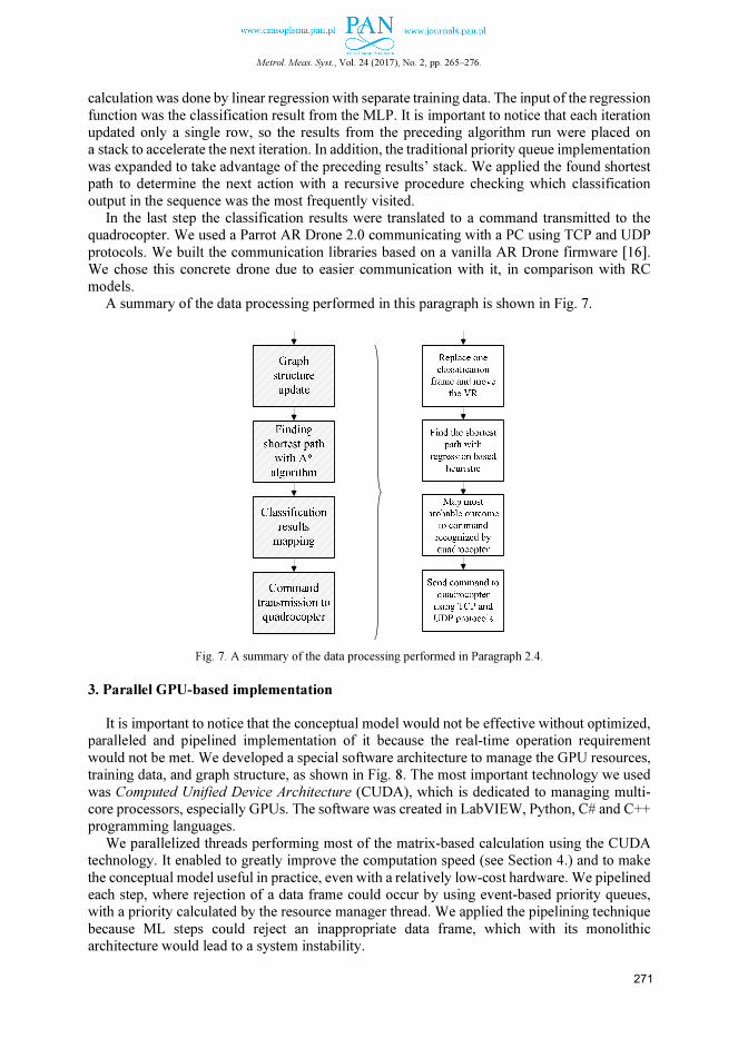
Metrol. Meas. Syst., Vol. 24 (2017), No. 2, pp. 265–276.
calculation was done by linear regression with separate training data. The input of the regression
function was the classification result from the MLP. It is important to notice that each iteration updated only a single row, so the results from the preceding algorithm run were placed on a stack to accelerate the next iteration. In addition, the traditional priority queue implementation
was expanded to take advantage of the preceding results’ stack. We applied the found shortest path to determine the next action with a recursive procedure checking which classification
output in the sequence was the most frequently visited. In the last step the classification results were translated to a command transmitted to the
quadrocopter. We used a Parrot AR Drone 2.0 communicating with a PC using TCP and UDP
protocols. We built the communication libraries based on a vanilla AR Drone firmware [16]. We chose this concrete drone due to easier communication with it, in comparison with RC
models. A summary of the data processing performed in this paragraph is shown in Fig. 7.
Fig. 7. A summary of the data processing performed in Paragraph 2.4.
3. Parallel GPU-based implementation
It is important to notice that the conceptual model would not be effective without optimized,
paralleled and pipelined implementation of it because the real-time operation requirement
would not be met. We developed a special software architecture to manage the GPU resources, training data, and graph structure, as shown in Fig. 8. The most important technology we used
was Computed Unified Device Architecture (CUDA), which is dedicated to managing multi-core processors, especially GPUs. The software was created in LabVIEW, Python, C# and C++ programming languages.
We parallelized threads performing most of the matrix-based calculation using the CUDA technology. It enabled to greatly improve the computation speed (see Section 4.) and to make
the conceptual model useful in practice, even with a relatively low-cost hardware. We pipelined each step, where rejection of a data frame could occur by using event-based priority queues, with a priority calculated by the resource manager thread. We applied the pipelining technique
because ML steps could reject an inappropriate data frame, which with its monolithic architecture would lead to a system instability.
271

M. Wodziński, A. Krzyżanowska: SEQUENTIAL CLASSIFICATION OF PALM GESTURES BASED …
We separated the teaching process from the usage of trained models. Such a separation
enabled to implement a manual, adaptive learning scheme without interrupting the system operation. All model learning parameters were stored in XML and binary files. The binary files were streamed to GPU memory in regular time intervals, while the XML files were used in the
prototype solution.
Fig. 8. Implementation of machine learning blocks based on the CUDA technology.
The graph computations were performed by the CPU due to the sequential nature and relatively low usage of resources. We applied a separate data set to compute the heuristic
function and threshold its output to ensure admissibility and consistency. In practice, it decreased the classification accuracy (by 2.3% on average), but guaranteed derivation of the
shortest path. 4. Results
The GPU-based implementation increased the conceptual model frequency (the number
of commands send to the quadrocopter, based on palm movements, per second) around 10 times in comparison with the pure CPU implementation, as shown in Fig. 6. The implementation based only on CPU could not be used in practice due to noticeable delays in the quadrocopter
control, which made users unable to synchronize hand movements. The computations performed by GPU made the control smooth, even with a relatively low-cost hardware. Fig. 9
CUDA Resource
Pool Manager
A* Graph Solver
with regression
based heuristic
Pipe I
CUDA
Thread I
CUDA
Thread II
CUDA
Thread III
CUDA
Thread N
...
Features
extraction
CUDA
Thread I
CUDA
Thread II
CUDA
Thread III
CUDA
Thread N
...
Anomaly
detection
Pipe II
CUDA
Thread I
CUDA
Thread II
CUDA
Thread III
CUDA
Thread N
...
Gestures
classification
Pipe III
Anomaly
Data
Classification
Data
Heuristic
Data
Training Data
Learning
Structures
Trainer
CPU
GPU
Legend:
272

Metrol. Meas. Syst., Vol. 24 (2017), No. 2, pp. 265–276.
shows also that A* algorithm is not in the hot path since in both solutions it was implemented
on CPU. The accuracy of gesture detection varied strongly on the gesture type and the environmental
conditions (as the accuracy we define a ratio of valid/invalid commands sent to the quadrocopter
when a given action was requested). The averaged accuracies are shown in Table 1.
Fig. 9. Comparison of the computing frequency between CPU- and GPU-based solutions.
Table 1. Comparison of the palm gesture detection accuracy in different environmental conditions.
Gesture type Acc. inside building [%] Acc. low insolation [%] Acc. high insolation [%]
Takeoff 100.00 96.27 81.78
Landing 100.00 97.09 77.47
Position maintenance 100.00 100.00 97.82
Taking snapshot 91.34 81.98 62.62
Mag. calibration 87.45 83.51 64.05
Falloff simulation 88.52 84.22 65.17
Flip right 95.91 93.23 72.48
Flip left 95.42 93.38 75.81
Flip forward 84.51 81.03 64.40
Flip backward 85.68 79.13 65.91
Yaw control 98.02 95.39 79.08
Vertical speed control 96.33 94.63 77.37
Emergency call 88.79 80.73 59.93
Roll/pitch control 97.93 95.44 77.78
Roll/pitch/vertical control 97.40 95.69 75.49
Even though the data set included 15 complex gestures, a high recognition efficiency was
obtained, especially for gestures based on slow angle changes and single hand assembling. However, it was observed that too high insolation may decrease the detection efficiency because the input data become corrupted. In addition, a strong wind makes control with palm
movements much harder than with a dedicated controller, because the visual feedback is not enough to sense an additional resistance. To address the insolation issue, it is possible either to
use a different signal acquisition hardware or to expand the training data and increase the model complexity.
Moreover, the classification of four gestures (circle, swipe, screen tap and key tap) using the
proposed algorithm was compared with the built-in Leap Motion classification algorithms.
273
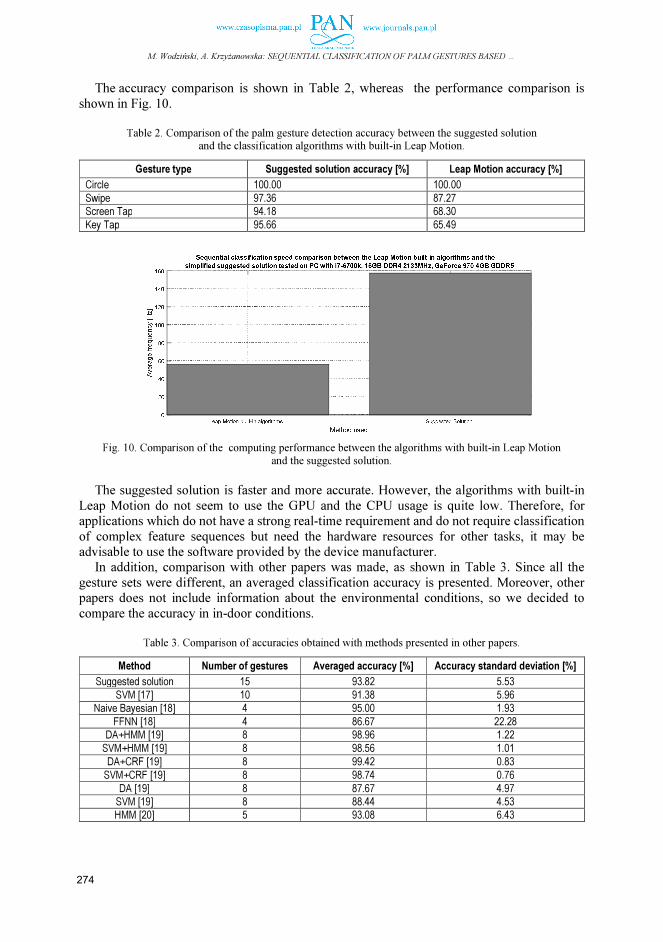
M. Wodziński, A. Krzyżanowska: SEQUENTIAL CLASSIFICATION OF PALM GESTURES BASED …
The accuracy comparison is shown in Table 2, whereas the performance comparison is
shown in Fig. 10.
Table 2. Comparison of the palm gesture detection accuracy between the suggested solution
and the classification algorithms with built-in Leap Motion.
Gesture type Suggested solution accuracy [%] Leap Motion accuracy [%]
Circle 100.00 100.00
Swipe 97.36 87.27
Screen Tap 94.18 68.30
Key Tap 95.66 65.49
Fig. 10. Comparison of the computing performance between the algorithms with built-in Leap Motion
and the suggested solution.
The suggested solution is faster and more accurate. However, the algorithms with built-in
Leap Motion do not seem to use the GPU and the CPU usage is quite low. Therefore, for applications which do not have a strong real-time requirement and do not require classification
of complex feature sequences but need the hardware resources for other tasks, it may be advisable to use the software provided by the device manufacturer.
In addition, comparison with other papers was made, as shown in Table 3. Since all the
gesture sets were different, an averaged classification accuracy is presented. Moreover, other papers does not include information about the environmental conditions, so we decided to
compare the accuracy in in-door conditions.
Table 3. Comparison of accuracies obtained with methods presented in other papers.
Method Number of gestures Averaged accuracy [%] Accuracy standard deviation [%]
Suggested solution 15 93.82 5.53
SVM [17] 10 91.38 5.96
Naive Bayesian [18] 4 95.00 1.93
FFNN [18] 4 86.67 22.28
DA+HMM [19] 8 98.96 1.22
SVM+HMM [19] 8 98.56 1.01
DA+CRF [19] 8 99.42 0.83
SVM+CRF [19] 8 98.74 0.76
DA [19] 8 87.67 4.97
SVM [19] 8 88.44 4.53
HMM [20] 5 93.08 6.43
274

Metrol. Meas. Syst., Vol. 24 (2017), No. 2, pp. 265–276.
The table does not contain the most important aspect, i.e. comparison of the computation
efficiency, because the necessary information is not provided in other publications. The available and comparable papers do not present quantitative performance results. One of the papers ([19]) classifies only gestures made with a single palm, which is a relatively easier task.
The results presented in Table 3 show that the solution presented in the paper achieved a high average accuracy for the larger set of classified gestures in comparison with other solutions.
Moreover, it was proved that the classification algorithm speed is high enough to achieve the
real-time control, which is not confirmed for other solutions presented in the literature [17−20].
5. Conclusion and future work
The suggested solution enables the real-time quadrocopter control using palm gestures
recognized by machine learning algorithms. The new approach involves the sequential data classification with separation of the frame classification from the result conjunction, which
enables an easy parallel implementation. The system meets the requirement of gesture recognition in real-time using the approach of searching the shortest path. However, more research is planned to address the issue of environmental conditions.
In the future, it is possible to replace A* algorithm by exploring the DAG properties, which may lead to a more efficient implementation (like that with the Seam Carving technique [21]).
Moreover, we consider using the Kohonen NN to perform automatic adaptive learning [22] during the system operation, instead of the presented manual teaching.
Further optimization of the computation speed is possible by applying FPGA instead of GPU
[8−10, 23−24]. With the FPGA it would be possible to obtain the real-time operation with more sophisticated models containing more training data, resulting in a better classification accuracy. On the other hand, this would also lead to an increase of the hardware cost and system
complexity.
References
[1] Diwakar, S., Bodda, S., Nutakki, C., Nair B.G. (2014). Neural Control using EEG as a BCI Technique for
Low Cost Prosthetic Arms. Conference: Proc. of the International Conference on Neural Computation
Theory and Applications (NCTA-2014).
[2] Bitzer, S., Van der Smagt, P. (2006). Learning EMG control of a robotic hand: towards active prostheses.
Proceedings 2006 IEEE International Conference on Robotics and Automation.
[3] Kim, M.R., Yoon, G. (2013). Control Signal from EOG Analysis and Its Application. International Journal
of Electrical, Computer, Energetic, Electronic and Communication Engineering., 7(10), 1352−1355.
[4] Hackenberg, G., Mccall, R., Broll, W. (2011). Lightweight palm and finger tracking for real-time 3D gesture
control. Conference: IEEE Virtual Reality Conference, VR 2011, Singapore.
[5] Kim, B.H., Kim, M., Joevaluated, S. (2014). Quadcopter flight control using a low-cost hybrid interface with
EEG-based classification and eye tracking. Computers in Biology and Medicine., (51), 82−92.
[6] LaFleur, K., Cassady, K., Doud, A., Shades, K., Rogin, E., He, B. (2013). Quadcopter control in three-
dimensional space using a noninvasive motor imagery-based brain-computer interface. Journal of Neural Engineering, 10(4).
[7] Bishop, C. (2006). Pattern Recognition and Machine Learning. New York: Springer
[8] Asano, S., Maruyama, T., Yamaguchi, Y. (2009). Performance comparison of FPGA, GPU and CPU in
image processing. 2009 International Conference on Field Programmable Logic and Applications.
[9] Papadonikolakis. M., Bouganis. C.S., Constantinides. G. (2010). Performance comparison of GPU and
FPGA architectures for the SVM training problem. International Conference on Field-Programmable
Technology, 2009.
275

M. Wodziński, A. Krzyżanowska: SEQUENTIAL CLASSIFICATION OF PALM GESTURES BASED …
[10] Rabieah. M.B., Bouganis. C.S. (2015). FPGA based nonlinear Support Vector Machine training using an
ensemble learning. 2015 25th International Conference on Field Programmable Logic and Applications.
[11] Panuccio, A., Bicego, M., Murino, V. (2002). A Hidden Markov Model-Based Approach to Sequential Data
Clustering. Conference: Structural, Syntactic, and Statistical Pattern Recognition.
[12] Li, J., Chen, S., Li, Y. (2009). The fast evaluation of hidden Markov models on GPU. IEEE International
Conference on Intelligent Computing and Intelligent Systems. ICIS 2009., (4), 426−430.
[13] Leap Motion API Reference: Classes. https://developer.leapmotion.com/documentation/python/api/ Leap_
Classes.html
[14] Weichert, F., Bachmann, D., Rudak, B., Fisseler, D. (2013). Analysis of the Accuracy and Robustness of the
Leap Motion Controller. Sensors., 13(5), 6380–6393.
[15] Leap Motion API Reference: Gestures. https://developer.leapmotion.com/documentation/ python/devguide/
Leap_Gestures.html
[16] Parrot (2012). AR Drone Developer Guide SDK. http://www.msh-tools.com/ardrone/ARDrone _Developer
_Guide.pdf
[17] Xu, Y., Wang, Q., Bai, X., Chen, Y.L., Wu, X. (2014). A Novel Feature Extracting Method for Dynamic
Gesture Recognition Based on Support Vector Machine. Proc. of the IEEE International Conference on
Information and Automation.
[18] She, Y., Wang, Q., Jia, Y., Gu, T., He, Q., Yang, B. (2014). A Real-time Hand Gesture Recognition Approach
Based on Motion Features of Feature Points. IEEE 17th International Conference on Computational Science and Engineering.
[19] Vamsikrishna, K.M., Dogra, D.P. (2016). Computer-Vision-Assisted Palm Rehabilitation With Supervised
Learning. IEEE Transactions On Biomedical Engineering., 63(5), 991−1001.
[20] Sreejith, M., Siddharth, R., Samik, G., Samprit, B., Partha, P.D. (2015). Real-time hands-free immersive
image navigation system using Microsoft Kinect 2.0 and Leap Motion Controller. 2015 Fifth National
Conference on Computer Vision, Pattern Recognition, Image Processing and Graphics (NCVPRIPG).
[21] Avidan, S., Shamir, A. (2007). Seam Carving for Content-Aware Image Resizing. ACM Transactions on
Graphics (TOG), 26(3), 10.
[22] Kohonen, T. (1989). Self-organization and associative memory. 3rd ed. New York: Springer.
[23] Kapre, N. (2009). Performance comparison of single-precision SPICE Model-Evaluation on FPGA, GPU,
Cell, and multi-core processors. 2009 International Conference on Field Programmable Logic and
Applications.
[24] Stratix® 10 DSP Specification Table: https://www.altera.com/products/fpga/stratix-series/stratix-10/
features.html#dsp

Metrol. Meas. Syst., Vol. 24 (2017), No. 2, pp. 277–288.
_____________________________________________________________________________________________________________________________________________________________________________________
Article history: received on Jul. 27, 2016; accepted on Oct. 22, 2016; available online on Jun. 30, 2017; DOI: 10.1515/mms-2017-0020.
METROLOGY AND MEASUREMENT SYSTEMS
Index 330930, ISSN 0860-8229 www.metrology.pg.gda.pl
VERIFICATION OF A NOVEL METHOD OF DETECTING FAULTS IN MEDIUM-VOLTAGE SYSTEMS WITH COVERED CONDUCTORS
Stanislav Mišák1), Štefan Hamacek1), Mikołaj Bartłomiejczyk2) 1) VŠB-Technical University of Ostrava, Faculty of Safety, Engineering, 17 Listopadu 15/2172, 708 33 Ostrava-Poruba, Czech Republic ([email protected], [email protected]) 2) Gdańsk University of Technology, Faculty of Electrical and Control Engineering, G. Narutowicza 11/12, 80-233 Gdańsk, Poland ( [email protected], +48 58 347 1416)
Abstract
This paper describes the use of new methods of detecting faults in medium-voltage overhead lines built of covered
conductors. The methods mainly address such faults as falling of a conductor, contacting a conductor with a tree
branch, or falling a tree branch across three phases of a medium-voltage conductor. These faults cannot be detected
by current digital relay protection systems. Therefore, a new system that can detect the above mentioned faults
was developed. After having tested its operation, the system has already been implemented to protect medium-
voltage overhead lines built of covered conductors.
Keywords: fault trees, partial discharges, fault diagnosis, power engineering, power overhead lines.
© 2017 Polish Academy of Sciences. All rights reserved
1. Introduction
In today’s technologically developed times, great emphasis is put on providing a reliable supply of electrical energy to households and the transport, industrial and other sectors. New,
advanced technologies and methods of timely fault detection help to faster remove of faults, thus increasing reliability of the electrical energy supplies. A new system of overhead lines with
SAX-type covered conductors (hereinafter CCs) was developed in Finland in 1976 [1−3].
Such overhead lines were built in Norway and Sweden as well, and gradually appeared in other member states of the European Union. Employing CCs in the construction of these overhead lines is not much different from using bare wires in outdoor overhead lines; the only
difference is in using XLPE insulation in the former [4−6]. By using the insulation, a fault rate of these overhead lines is reduced and it is possible to build the lines in places that are not easily
accessible, e.g. in densely forested areas. Unlike typical outdoor overhead lines with AlFe conductors, when a tree branch falls on overhead lines with CCs, an immediate interphase short-circuit does not occur; therefore, the risk of disconnection from the electrical energy supply
is reduced [7, 8]. A disadvantage of operating overhead lines with CCs is the inability to detect a fault, e.g.
in the case of falling of a conductor [9]. When this kind of fault occurs, there is no earth fault and the limit values of digital relay protection starting elements are not exceeded [10, 11]. Hence, digital relay protection systems are not able to detect this type of fault. For such faults,
as well as other types of faults associated with CCs, such as a tree branch falling on or merely
contacting with a CC, partial discharges (hereinafter PDs) – inner, outer and surface PDs − appear in the fault location (e.g. the point of contact between a conductor and the ground or between a tree branch and CC) [12]. These PDs gradually damage the insulation of the lines. The activity of PDs enlarges the area of a fault, and other insulated areas are being degraded.

S. Mišák, Š. Hamacek, M. Bartłomiejczyk: VERIFICATION OF A NOVEL METHOD OF DETECTING …
During this process, the conductor insulation breaks down and causes a fault (interphase or earth fault). The VŠB-TUO team developed a methodology based on the principle of finding a relation between the occurrence and characteristics of PDs and the origin of faults in overhead lines with CCs. Based on this methodology, a number of measurements were made. Using these measurements, procedures for detecting fault indicators in real medium-voltage overhead lines with CCs were gradually created. The effects of PDs can be worsened by other factors, such as humidity, temperature, solar radiation, atmospheric pressure, rainfall, aerosols, dust, sand, micro- and macro-organisms and the mechanical deterioration of conductors. Based on the information provided above, the occurrence of PDs is the best indicator of overhead line faults [9, 12, 13].
The current worldwide research is focused on the development of methodologies for detecting the above mentioned faults in the operation of overhead lines with CCs. Most of these methodologies are based on evaluation of PD current pulses, and their selectivity and sensitivity depend on the measurement technique, which must meet high standards, especially the ability to detect pulse sources, and which must include a high-resolution A/D converter and efficient hardware for data processing [14−16].
The system developed by the team at VŠB-Technical University of Ostrava in the Czech Republic (hereinafter VŠB-TUO) and presented in this study, is able to specify the location and type of a fault [17, 18]. The system operation is based on analysing PD voltage signal pulses using suggested indicators of faults [9] and is not technically demanding.
2. Method’s principles
The method developed by the VŠB-TUO team is based on finding a relation between the occurrence and characteristics of PDs and the origin of faults in overhead lines with CCs. As was stated above, in the first part, the occurrence of PDs is characterized by damaging the insulation system of a variety of devices. These PDs arise in areas of small cavities in the insulation system as an effect of extreme local electrical tension. A simple model and substitution diagram of simulating the voltage and current conditions inside the insulation system is shown in Fig. 1.
Fig. 1. A simple model of an insulation system with a cavity [19].
A cavity capacitance (the damaged part of the insulation) is represented by C1, C2 is
a capacitance of the residual part of “healthy” insulation (a serial connection of C2 and C1), and C3 presents a significant capacitance of other parts of insulation. A sphere gap (SG) represents flashover in the cavity area and R is a resistivity of the discharge puncture after flashover on SG. When the insulation system is damaged and cavities inside it exist, the voltage on the cavity varies in time according to the formula:
278

Metrol. Meas. Syst., Vol. 24 (2017), No. 2, pp. 277–288.
)()(21
2
10tv
CC
Ctv
+
= , (1)
where v(t) is the power supply voltage. When the value of voltage on the cavity equals the
voltage ignition value, a PD occurs. These frequent PDs are superposed onto the carrier of capacitive current component.
2.1. Pulse component measurements
The basic part of capacitive current is caused by the supply voltage and for evaluation of PD activity it is not relevant. However, PDs superposed onto the carrier capacitive current, named
a pulse component, are very important for evaluation of PD activity inside the insulation system. Two basic methods can be used for indirect evaluation of PD activity:
i) evaluation of PD activity in the insulation system of CC by measuring the current signal
in CC by a Rogowski sensor [2], and ii) evaluation of PD activity in the insulation system of CC by measuring the voltage signal
of electrical stray field along the CC. Both methods use for evaluation of PD activity a pulse component. The pulse component
is generated by PD activity in the insulation system and its occurrence is characterized by
a frequency domain of hundreds of kH to MHz. The first method evaluates the pulse component generated by PD activity from the current measured by a Rogowski sensor. The main advantage
of this method is a high selectivity of evaluation of PD activity. However, this high selectivity of PD evaluation requires both high sensitivity and accuracy of the Rogowski sensor over a wide frequency range because the pulse component is low-energetic and the measurement
period is in the order of microseconds. These high requirements on the Rogowski sensor increase a price of the measurement chain, which is a great disadvantage of this method (i) [2].
The aim of this paper is to show the possibility of using the second method that evaluates the pulse component generated by PD activity as a voltage signal of the electrical stray field measured along an insulation system, in this case the insulation system of CC. The requirements
for development of this method were: high selectivity of fault detection, high reliability and a low price of the prototype CC fault detector.
As was stated in the previous section, the pulse component generated by PD activity in an insulation system of CC is measured as the voltage signal of electrical stray field along the CC. This voltage signal was measured by a capacitor voltage divider (CA-CB) from a circular metal
sensor (a circular coil; see Ccoil in Fig. 2) through its coupling capacitor Ccoup to the CC. As a sensor it is possible to use, for example, an inductor wound on the CC surface, where Ccoup
will be given by the number of turns (see Fig. 2).
Fig. 2. The principle of measuring the pulse component of voltage signal including an analogue low-pass filter.
279

S. Mišák, Š. Hamacek, M. Bartłomiejczyk: VERIFICATION OF A NOVEL METHOD OF DETECTING …
The time characteristic of voltage signal of the electrical stray field on the CC surface is then
amplitude-conditioned by means of a capacitor voltage divider with a fixed dividing ratio given by the capacities CA and CB; see Fig. 2. When the capacitor voltage divider is loaded via
a properly selected resistor R1, which may be additionally equipped with a self-inductance, a low pass with advantageous amplitude characteristic occurs; see Fig. 3 (the vertical axis –
a damping characteristic in dB, the horizontal axis – a frequency in Hz).
Fig. 3. Frequency characteristics of a coupling circuit in CC for various endings of the capacitor voltage divider
(C-divider, C-divider with R, C-divider with RL).
The voltage signal of the electrical stray field measured by the sensor as a function of time
is shown in Fig. 4, where the red line defines the output voltage signal using a C-divider and
the green line defines the output voltage signal using a C-divider with a resistor R1 connected in parallel. From the green line in Fig. 4, the required pulse component of voltage signal
generated by PD activity is visible. This signal can be filtered using a digital filter for elimination of the carrier frequency of power supply and for further specification of a typical
frequency range for PD activity (mostly 1−10 MHz). In this way, the original pattern of PD (hereinafter the PD-pattern) arises, corresponding to the actual state of CC insulation system. Next, detection of a CC fault is possible by evaluating this PD-pattern. It means that the shape
of the PD-pattern shows the actual state of CC insulation system. For evaluation of the PD-pattern it is possible to use some indicators in the time and frequency domain, whereas the
requirements for selection of the indicators are: (i) a short evaluation time; (ii) low memory requirements and (iii) selective evaluation.
Fig. 4. The functions of output voltage signal vs time using: a C-divider (red line), a C-divider with a resistor R1
connected in parallel for the no-fault state (green line), a C-divider with a resistor R1 connected in parallel
for a fault state (blue line).
280

Metrol. Meas. Syst., Vol. 24 (2017), No. 2, pp. 277–288.
So, for example, calculations of the True Root Mean Square value (hereinafter the TRMS) of the PD-pattern and the mean value of the PD-pattern or the frequency (s−1) of PDs in the PD-pattern (hereinafter n) for the first time were verified as indicators in evaluation of the actual state of CC insulation by the research team at VŠB-TU Ostrava. A function of the TRMS of PD-pattern (hereinafter VTRMS) vs time is approximately zero in the case of fault-free operation, because the PD activity is irrelevant (see the green line in Fig. 4). If a fault in the CC insulation exists, the PD activity is relevant and the TRMS value is increased; see the blue line in Fig. 4.
The next modification of the PD-pattern is extraction of a low-level PD signal from the background of an interfering signal source, which is composed of signal sources from the external environment (e.g. radio transmitters).
Therefore, to modify the electrical stray field voltage signal, we used an IIR Butterworth digital filter with an infinite pulse response and maximally flat permeable and impermeable ranges.
Based on the selected basic measurement system for recording and modifying the signal, we developed a fault-detecting system able to analyse the processed data, which is described in the following section.
3. Pulse component measurements
The main requirement for a fault-detecting system is the oscilloscopic measurement
of varying the PD-pattern voltage of electrical stray fields around medium-voltage overhead lines with CCs. We used a measuring card connected via a PCI interface for this purpose. In addition to measuring the PD-pattern, the fault detector measures other conditions, such as temperature, pressure, humidity and global radiation (exposure), since the discharge activity is affected by these factors. These conditions affect, for example, the frequency of PD occurrence, the PD amplitude shape and size .
All measured and processed data are sent by the GSM network to an external computer, where they are processed and an overhead line fault condition is analysed. If the threshold values of indicators are exceeded, the fault detector sends a warning signal to the CC operator.
The fault detector also includes additional control electronic circuits which are used to switch the PC to automatic control, and to measure temperature inside the switchboard (in the case of unnecessary heating). The device is powered by a battery which is charged by photovoltaic panels. Thus, it is possible to use the detector anytime on overhead lines with CCs, even when there is no possibility to get energy from the distributed system power supply.
4. Measurement of real medium-voltage overhead lines with CCs
4.1. Verification of fault detector function
The CC fault detector prototype was installed on 22-kV overhead lines with CCs (Fig. 5).
The main aim was to verify the effect of CC network topology on sensitivity and selectivity of the fault detector prototype and its long-term application in a chosen location with medium-voltage overhead lines.
To confirm the conclusions and to assess the fault detector functionality, experimental measurements were performed on real overhead lines with CCs (22 kV) in December 2012 and February 2013. The aim of measurements was to obtain new data and to verify the results already gained during the previous period, particularly setting the frequency threshold values (n = 100 s−1) and the voltage level of the generated PD voltage signal pulse component root-mean-square (VTRMS = 39 mV). The indicator n (s−1) is a frequency of PDs’ activity and, as well as VTRMS, was analysed during experimental measurements in the laboratory conditions [9, 13].
281

S. Mišák, Š. Hamacek, M. Bartłomiejczyk: VERIFICATION OF A NOVEL METHOD OF DETECTING …
When these values are exceeded, the fault detector sends a report about a fault in the
overhead lines. Different types of faults were simulated on overhead lines with CCs, particularly faults that cannot be detected by current digital relay protection systems. In particular, selectivity and sensitivity of both the methodology and fault detector were verified
for such faults as a contact between a tree branch and a phase conductor, a conductor falling on the ground and a contact between two phase conductors. Due to the insulation of conductors,
these faults do not have to be cleared immediately. However, the tested fault detector can detect these faults before degradation factors destroy integrity of the insulation in the fault location and cause a single phase-to-earth short-circuit.
Fig. 5. Arrangement of the fault detector on a post of medium-voltage overhead lines with CCs [21]:
MS − Measuring System, BAT − Battery, SM − Sensing Member, CD − C-Divider, PP − Photovoltaic Panel.
The results of these experimental measurements are presented below:
Fault no. 1 – the point of contact between a tree and CC; Fault no. 2 – breaking off of a CC and its subsequent falling on the ground.
To compare the faulty and fault-free conditions (Fig. 6), we had to measure the PD-pattern in the operating conditions. From the PD-pattern (Fig. 6), the existence of a pulse component is evident, although the overhead lines with CCs were free of fault generated by a corona
discharge at the connector endings on towers with CCs and also by modulation of interfering signals (e.g. radio waves). The software component of fault detection system can recognize
the interference and evaluate the signal as fault-free.
Fig. 6. The VTRMS of PD-pattern of CC for the no-fault state.
282

Metrol. Meas. Syst., Vol. 24 (2017), No. 2, pp. 277–288.
Fault no. 1 – point of contact between tree and phase conductor.
The first measurement was simulation of the point of contact with a phase conductor. This fault was simulated by considering a tree branch located near the outer phase of CC (Fig. 7a). This type is the worst detectable fault because a contact between a tree and a conductor can, in
real situations, be a result of transitory conditions, e.g. wind. Another fact contributing to the difficulty in detecting this type of fault is the minimal area of conductor damage and the
corresponding minimal occurrence of PDs in the fault location. By further analysing the pulse component of the generated PD-pattern in the fault location, we determined the following
indicator values: n = 272 s−1; VTRMS = 68 mV. Considering the exceeded indicator threshold values, selectivity and sensitivity of the
methodology as well as the fault detector functionality were verified. Changing of the measured signal in time, shown below (Fig. 7b), clearly indicates that over a period of 0.06 s no PD
occurred. This lack of PD was caused by an imperfect connection between a tree branch and CC. The fault detector evaluates faults continually; therefore, this transient effect on the general
selectivity of fault detector is eliminated.
Fig. 7. Fault no. 1 – a contact between a tree branch and overhead lines with CC (a);
the change of PD-pattern in time, fault no. 1 (b).
283

S. Mišák, Š. Hamacek, M. Bartłomiejczyk: VERIFICATION OF A NOVEL METHOD OF DETECTING …
Fault no. 2 – breaking off of CC and its subsequent falling on ground.
The second simulated fault was the breaking off of a CC and the conductor’s subsequent falling on the ground. The fault was simulated by connecting an SAX-W-type conductor (22-kV) to the overhead lines. The CC end was then placed down on the ground (Fig. 8a). At the
point of contact between the conductor and the ground, PDs evolve and the voltage signal, which afterwards travels along the insulation of the conductor as a wave, is recorded by the
fault detector. This type of fault is easily detected; therefore, in the step the conductor was placed on the ground covered with grass. The contact with the ground was partly weakened by grass. Fig. 8b shows the PD-pattern recorded after using the IIR Butterworth filter; the measured
values were: n = 174 s−1 ; VTRMS = 68 mV.
Fig. 8. Fault no. 2 – falling of a CC on the ground (a); the PD-pattern, fault no. 2 (b).
To provide a general summary of the measured values, we created a table of climatic
conditions (Table 1) and a table of chosen fault indicators (Table 2). As shown in Table 1, the measurements were performed in unfavourable weather conditions. Thus, if the temperature
was approximately equal to zero and humidity was high, we presumed the occurrence of PD in overhead lines in the form of a corona. Coronas frequently occur in areas of high local electrical
gradients, where inhomogeneous electrical fields are generated, such as sharp edges, bushings, connectors and other construction parts of overhead lines. Table 2 shows that the highest
284

Metrol. Meas. Syst., Vol. 24 (2017), No. 2, pp. 277–288.
frequency values n occurred during a contact between a tree branch and a phase conductor (fault
no. 1). The high values were caused mainly by the fact that tree bark was soaked with water; thus, when the conductivity increased, the PD activity increased as well. When the conductor fell on the ground, we presumed that the highest energy of the PD voltage pulses occurred; thus,
the VTRMS value was also the highest of all the measured values in this case.
Table 1. The measured values of climatic conditions.
Temperature of the surroundings (°C) 3,2
Humidity (%) 85,1
Dew point (°C) 1
Atmospheric pressure (hPa) 968.5
Global radiation (W.m-2) 0
Temperature in switchboard (°C) 5,4
Table 2. The values of frequency and VTRMS.
VTRMS (mV) n (s-1)
Operating condition 9 17
Fault no. 1 45 272
Fault no. 2 68 174
4.2. Long-term measurement of medium-voltage (22 kV) overhead lines with CCs
After long-term experimental measurements, the fault detector was put into operation on MV (22 kV) overhead lines with CCs. During its operation in May and October, the fault detector sent to the local CC overhead lines’ operator a warning report indicating that the
threshold values of indicators had been exceeded . In particular, the following values were
measured by the detector: n = 150 s−1 (150 > 100) and VTRMS = 42mV (42 > 39) of PD-pattern. At first, during May, the breakdown service of distribution system operator made a round along
MV overhead lines with CCs and detected a fault in a site at a 3 km distance from the detector. The breakdown service detected falling of a tree branch across three phases.
The observed values (VTRMS and n) were analysed step by step every day and the mean value of these data was evaluated at the end of individual month. Next, the tangent of these values was evaluated, too. The graphical output of this analysis for VTRMS and n can be seen in Fig. 9.
Fig. 9. Mean values of n and VTRMS of PD-pattern for individual months of the year.
285

S. Mišák, Š. Hamacek, M. Bartłomiejczyk: VERIFICATION OF A NOVEL METHOD OF DETECTING …
From these graphical outputs a decrease in PD activity after elimination of the fault is evident
until July. However, the second warning report was sent by the detector during October, when the threshold values (VTRMS and n of PD-pattern) were exceeded again. The breakdown service of distribution system operator made a round along MV overhead lines with CCs again.
However, no fault in CCs has been found. Nevertheless, the detector sent the warning report because the threshold values (VTRMS and n of PD-pattern) were exceeded. The PD-pattern from
the detector is shown in Fig. 10b (red line – left axis). Therefore, the breakdown service scanned the overhead lines with CCs in more detail using
a corona camera and detected a fault in the same place as the previous fault. A photo illustrating
the fault is presented in Fig. 10a. From this photo there is visible a damage on the CC surface. This damage was caused by the PD activity of the previous fault when a tree branch fell across
three phases. This fault was cleared by the breakdown service during May. However, the insulation system of CC at the contact point of a tree branch with the insulation system had already been degraded. This degradation of the insulation system stopped during the summer
months when high temperatures in the surroundings of CC caused “softening” of the insulation system and these small ruptures in the insulation system were eliminated. The opposite effect
was caused during the autumn and winter months when the insulation system dried out and became more brittle as a result of low temperatures and low values of relative humidity. Therefore, the PD activity increased and degradation of the insulation system increased. The
damaged line with CC was changed and − to prevent another similar accident − the trees in the area occupied by the MV overhead lines were trimmed. As a result, the PD activity (see Fig. 10b – green line – right axis) and monitored values (VTRMS and n of PD-pattern) decreased
immediately (see Fig. 9) after executing these corrective and preventive steps.
Fig. 10. The details of damage on a conductor in the measured location (a); the PD-pattern from the detector after
it sent a warning report (left axis − red line) and the PD-pattern from the detector after carrying out the corrective and preventive steps (right axis – green line) (b).
286

Metrol. Meas. Syst., Vol. 24 (2017), No. 2, pp. 277–288.
5. Conclusion
A system for detecting faults in overhead lines with CCs was designed based on a methodology developed by the research team at VŠB-Technical University of Ostrava. Prior to the construction of the fault detector, a number of experimental measurements [7, 8] and mathematical calculations using non-linear multi-physical programs (Lab View, ATP-DRAW, ANSYS) were carried out. Based on the results of these measurements and mathematical simulations, a fault detector prototype was constructed. The detector’s functionality was tested by the long-term measurement of real MV overhead lines with CCs. During the measurement process, the performance of particular CC fault indicators defined in the research part of the project was gradually verified. Using these results, the evaluation component of calculating algorithm of the fault detector prototype was optimized. The fault detector was powered by storage batteries recharged by solar panels.
Based on the test results obtained for the fault detector by long-term measurements in real conditions, the ability of the detector to operate in the autonomous mode was successfully verified. The indicator threshold values applied to a signal on occurring a fault in MV overhead lines with CCs were specified. The fault detector is able to specify faults based on the measured threshold frequency values and the True Root Mean Square value of the electrical stray field voltage signal around the conductor. The fault detector recognizes faults in the overhead lines and sends a signal informing about the faults to the central computer. Further confirmation of the fault detector’s ability to detect faults was obtained when the fault detector was put into operation. When the overhead lines were checked, it was observed that the cause of the detected fault was a tree branch that had fallen across all three phases of the lines. The fault caused partial damage to the conductor insulation, but due to the timely warning, there was no inter-phase short-circuit. Thus, the faults could be cleared within a short time, and more serious damage that could possibly cut the power supply to consumers could be prevented. Moreover, the repair costs were reduced.
In this study, we not only achieved the project objectives of producing a fault detector prototype and verifying its performance, but we also gathered a significant amount of information about the discharge activity of various insulation systems in various climatic conditions. This information can be used in developing other methods of protecting CCs as well as all other types of outdoor overhead lines and cable lines, and even insulation systems of other devices. In the future research, we aim to enhance the measurement quality of the fault detector, so that it is able to specify the location and type of faults that are detected.
Acknowledgments
This study was carried out within the framework of the IT4 Innovations Centre of Excellence project, reg. no. CZ.1.05/1.1.00/02.0070, supported by the Operational Programme “Research and Development for Innovations” funded by Structural Funds of the European Union and the state budget of the Czech Republic and the project Opportunity for Young Researchers, reg. no. CZ.1.07/2.3.00/30.0016, supported by the Operational Programme Education for Competitiveness and co-financed by the European Social Fund and the state budget of the Czech Republic and project reg. no. SP2014/49.
References
[1] Agarwal, H.K., Mukherjee, K., Barna, P. (2014). Partially and fully insulated conductor systems for low and
medium voltage overhead distribution lines. Condition Assessment Techniques in Electrical Systems
(CATCON). IEEE 1st International Conference, 104 (6−8), 100−104.
287

S. Mišák, Š. Hamacek, M. Bartłomiejczyk: VERIFICATION OF A NOVEL METHOD OF DETECTING …
[2] Hemmati, E., Shahrtash, S.M. (2012). Evaluation of shielded Rogowski coil for measuring partial discharge signals. Environment and Electrical Engineering (EEEIC), 11th International Conference, 446−450.
[3] Hemmati, E., Shahrtash, S.M. (2012). Evaluation of unshielded Rogowski coil for measuring partial discharge signals. Environment and Electrical Engineering (EEEIC), 11th International Conference, 434−439.
[4] Samimi, M.H., Mahari, A., Farahnakian, M.A., Mohseni, H. (2014). A Review on the Rogowski Coil Principles and Applications. Sensors Journal, IEEE, (99), 1, 1.
[5] Shafiq, M., Kutt, L., Lehtonen, M., Nieminen, T., Hashmi, M. (2013). Parameters Identification and Modeling of High-Frequency Current Transducer for Partial Discharge Measurements. Sensors Journal, IEEE, 13(3), 1081−1091.
[6] Nobrega, A.M., Martinez, M. L. B., de Queiroz, A.A.A. (2104). Analysis of the XLPE Insulation of Distribution Covered Conductors in Brazil. Journal of Materials Engineering and Performance, 23, 723−735.
[7] Misak, S., Hamacek, S. (2010). Utilization of the Finite Element Method For Optimizing of Overhead Covered Conductors. Conference DAAAM 2010, Austria, Vienna.
[8] Makhkamova, I., Taylor, P.C., Bumby, J.R., Mahkamov, K. (2208). CFD analysis of the thermal state of an overhead line conductor. Universities Power Engineering Conference, UPEC 2008. 43rd International, 1−4.
[9] Hamacek, S. (2012). Problems of Covered Conductors Running. PhD Thesis. VŠB-TUO: VŠB-Technical University of Ostrava.
[10] Hashmi, G.M., Lehtonen, M., Nordman, M. (2010). Modeling and Experimental Verification of On-line PD Detection in MV Covered-conductor Overhead Networks. IEEE Trans. Dielectr. Electr. Insul., 17, 167–180.
[11] Hashmi, G.M., Lehtonen, M., Ametani, A. (2010). Modeling and Experimental Verification of Covered-conductor for PD Detection in Overhead Distribution Networks. IEEJ Trans. Power Energy, 130(7), Sec. B, 670−678.
[12] Misak, S., Hamacek, S., Bilık, P., Horinek, M., Petvaldsky, P. (2011). Problems associated with covered conductor fault detection. Electrical Power Quality and Utilisation (EPQU), 2011 11th International Conference, 1−5.
[13] Hashmi, G.M., Lehtonen, M., Nordman, M. (2011). Calibration of on-line partial discharge measuring system using Rogowski coil in covered-conductor overhead distribution networks. Science, Measurement & Technology, IET, 5(1), 5−13.
[14] Hashmi, G.M., Lehtonen, M. (2010). Effects of Rogowski Coil and Covered-Conductor Parameters on the Performance of PD Measurements in Overhead Distribution Networks. Int. J. Innovations Energy Syst. Power, 4(2), 14–20.
[15] Sudha, G., Valluvan, K.R. (2014). A novel approach to fault diagnosis of transmission line with Rogowski coil. International Review of Electrical Engineering, 9(3), 656−662.
[16] Isa, M., Elkalashy, N.I., Lehtonen, M., Hashmi, G.M., Elmusrati, M.S. (2012). Multi-end correlation-based PD location technique for medium voltage covered-conductor lines. IEEE Transactions on Dielectrics and Electrical Insulation, 19(3), 6215097, 936−946.
[17] Misak, S., Pokorny, V. (2015).Testing of a covered conductor's fault detectors. IEEE Transactions on Power Delivery, 30(3), 6957620, 1096−1103.
[18] Hamacek, S., Misak, S. (2013). Fault indicators of partial discharges in medium-voltage systems. Advances in Electrical and Electronic Engineering, 11(4), 284−289.
[19] Záliš, K. (2005). Částečné výboje v izolačních systémech elektrických strojů. 1st. ed. Praha: Academia.
Metrol. Meas. Syst., Vol. 24 (2017), No. 2, pp. 289–301.
_____________________________________________________________________________________________________________________________________________________________________________________
Article history: received on Aug. 03, 2016; accepted on Jan. 14, 2017; available online on Jun. 30, 2017; DOI: 10.1515/mms-2017-0031.
METROLOGY AND MEASUREMENT SYSTEMS
Index 330930, ISSN 0860-8229
www.metrology.pg.gda.pl
APPLICATION OF IMPROVED ROBUST KALMAN FILTER IN DATA FUSION
FOR PPP/INS TIGHTLY COUPLED POSITIONING SYSTEM
Zengke Li, Yifei Yao, Jian Wang, Jingxiang Gao
China University of Mining and Technology, School of Environment and Spatial Informatics, Xuzhou, China ([email protected], [email protected], [email protected], [email protected], +86 516 8388 5785)
Abstract
A robust Kalman filter improved with IGG (Institute of Geodesy and Geophysics) scheme is proposed and used to resist the harmful effect of gross error from GPS observation in PPP/INS (precise point positioning/inertial
navigation system) tightly coupled positioning. A new robust filter factor is constructed as a three-section function
to increase the computational efficiency based on the IGG principle. The results of simulation analysis show that
the robust Kalman filter with IGG scheme is able to reduce the filter iteration number and increase efficiency. The
effectiveness of new robust filter is demonstrated by a real experiment. The results support our conclusion that the
improved robust Kalman filter with IGG scheme used in PPP/INS tightly coupled positioning is able to remove the ill effect of gross error in GPS pseudorange observation. It clearly illustrates that the improved robust Kalman
filter is very effective, and all simulated gross errors added to GPS pseudorange observation are successfully
detected and modified.
Keywords: PPP/INS tightly coupled positioning, robust filter, IGG scheme, Mahalanobis distance.
© 2017 Polish Academy of Sciences. All rights reserved
1. Introduction
Integration of Global Positioning System (GPS) and Inertial Navigation System (INS) is being used more often for obtaining several high precision navigation data (position, velocity
and attitude) [1]. The past integration research has been performed in different application areas (i.e., monitoring, transportation, etc.). GPS provides highly accurate position and velocity results over extended periods in the GPS/INS integrated system, and short-term position,
velocity, and attitude values are provided by INS. The GPS-alone positioning is difficult in challenging environments due to weakness and blockage of signals. INS is a self-contained
velocity and attitude measurement system that does not require an external signal. Therefore, integration of GPS and INS provides enhanced performance in comparison with each individual system [2]. The Precise Point Positioning (PPP) using un-differenced carrier phase and
pseudorange observations has been developed recently, and is capable of obtaining positions with a centimetre precision in the static mode and sub-centimetre precision in the dynamic
mode. This is accomplished by using precise satellite orbits and clock correction products (e.g. the International GNSS Service) [3]. Some PPP and INS integration research results enable to obtain more accurate position and attitude values in the single receiver mode. With an aid
of INS aid cycle slip detection and repair methods for the un-differenced GPS/MEMS (Micro-Electromechanical Systems) INS integrated system are proposed. These methods are capable
of efficient cycle slip detection and repair, effectively increasing the positioning accuracy of the integrated system [4].
The key process between INS and other sensors in the integrated positioning system
is information fusion. During the kinematic positioning, GPS signals are prone to be disturbed

Z. Li, Y. Yao, et al.: APPLICATION OF IMPROVED ROBUST KALMAN FILTER …
by trees, buildings and other shelters. Thus, the performance of integrated positioning will be
seriously degraded because of the gross error from GPS observation in GPS challenging environments. A robust Kalman filter could be employed to reduce the effect of gross error in GPS observation. Many forms of robust Kalman filters have been proposed in the literature.
A robust Kalman filter has been researched in the last dozen or so years in different application fields, such as in-motion alignment of INS [5], SINS/SAR integrated system [6], real-time
estimation of satellite clock offset [7], precise point positioning (PPP) [8], and others. A robust Kalman filter using the Chi square test to detect outliers in measurement was proposed in [9]. The outlier judging index was defined as the square of the Mahalanobis distance between the
observed and predicted results. Based on the robust Kalman filter using the Chi square test, a robust Kalman filter improved with IGG (Institute of Geodesy and Geophysics) scheme is
proposed and applied in PPP/INS tightly coupled positioning to increase its computational efficiency. The new robust filter factor is constructed as a three-section function on the basis of IGG principle.
The paper is divided into 5 sections. Following this introduction, a PPP/INS tightly coupled positioning model is overviewed in Section 2. Section 3 presents the robust Kalman filter
improved with IGG scheme, and the simulation analysis corresponding to it. The field test results are then presented and analysed in Section 4, followed by a summary of the main conclusions.
2. PPP/INS tightly coupled positioning
2.1. PPP observation model
The observation models of un-differenced GPS pseudo-range, carrier phase and Doppler
measurements for PPP can be expressed as follows [10]:
1 1
1 1( )
s P PP c dt dt I T Mρ ε= + ⋅ − + + + + , (1)
2 2
2
1
2 12
2
( )s P P
fP c dt dt I T M
fρ ε= + ⋅ − + + + + , (2)
1 1
1 1 1 1( )
s Φ ΦΦ c dt dt I T N Mρ λ ε= + ⋅ − − + + + + , (3)
2 2
2
1
2 1 2 22
2
( )s Φ Φ
fΦ c dt dt I T N M
fρ λ ε= + ⋅ − − + + + + , (4)
1
1 1( )
s DD c dt dt I Tρ ε= + ⋅ − − + +
ɺ ɺ ɺ ɺɺ , (5)
2
2
1
2 12
2
( )s D
fD c dt dt I T
fρ ε= + ⋅ − − + +
ɺ ɺ ɺ ɺɺ , (6)
where: P, Φ and D are pseudo-range, carrier phase and Doppler observations, respectively; ρ
is a geometric distance between the receiver antenna and satellite phase centres; ρɺ is a
geometric range rate; c is the velocity of light in vacuum; dt and s
dt are satellite and receiver
clock errors, respectively; dtɺ and s
dtɺ are the satellite clock error drift and receiver clock error
drift, respectively; I and Iɺ are a first-order ionospheric delay and an ionospheric delay drift,
respectively; f1 and f2 are frequencies of the carrier phases 1
Φ and 2;Φ T and Tɺ are
290

Metrol. Meas. Syst., Vol. 24 (2017), No. 2, pp. 289–301.
a tropospheric delay and a tropospheric delay drift. Because the hydrostatic part of tropospheric
delay can be predicted using models, T represents the wet component of tropospheric delay;
PM and
ΦM are multipath errors of the pseudo-range and carrier phase measurements;
Pε ,
Φε
and D
ε are combination noise values of the pseudo-range, carrier phase and Doppler
measurements, and subscripts 1 and 2 refer to the observations at different frequencies. By using the high-accuracy GPS satellite orbit and clock products, the errors in the satellite
orbit and clock corrections can be significantly reduced. Other error sources including the satellite antenna phase centre offset, phase wind up, earth tide, ocean tide loading and
atmosphere loading can be removed by a correction model. The widely used ionosphere-free combination makes use of the GPS radio frequency’s dispersion property to mitigate the first-order ionospheric delay effect. The observation model of ionosphere-free combination can be
expressed as follows [11]:
2 2
1 2
1 22 2 2 2
1 2 1 2
( )if ifif s P P
f fP P P c dt dt T M
f f f fρ ε= − = + ⋅ − + + +
− −
, (7)
2 2
1 2
1 22 2 2 2
1 2 1 2
( )if ifif s if if Φ Φ
f fΦ Φ Φ c dt dt T N M
f f f fρ λ ε= − = + ⋅ − + + + +
− −
, (8)
2 2
1 2
1 22 2 2 2
1 2 1 2
( )ifif s D
f fD D D c dt dt T
f f f fρ ε= − = + ⋅ − + +
− −
ɺ ɺ ɺɺ , (9)
where a subscript if refers to the ionosphere-free combination observation.
Because the change of tropospheric delay is very slow, the tropospheric delay drift can be considered to be zero. The variables estimated in PPP resolution are: the three-dimensional position, receiver clock error, receiver clock error drift, zenith tropospheric delay, and
ionosphere-free combination ambiguity.
2.2. Tightly coupled dynamics model
The dynamics error model of PPP/INS integrated positioning for the Kalman filter is
constructed on the basis of INS error equations. The insignificant terms are neglected in the linear approximation process [12]. The error equations of INS navigation could be theoretically
expressed as [13]:
en
δ δ δ= − × +r ω r vɺ , (10)
ie en
(2 )δ δ δ= − + × − × +v ω ω v ψ f ηɺ , (11)
ie en
( )δ δ= − + × +ψ ω ω ψ εɺ , (12)
where: δ r , δv and δψ are position, velocity and orientation error vectors, respectively; en
ω
is an angular rate of the navigation frame with respect to the earth frame, and ie
ω is an angular
rate of the earth frame with respect to the inertial frame. The system dynamics error of PPP/INS
integration navigation is obtained by expanding the accelerometer bias error vector η and the
gyro drift error vector ε .
The dynamic behaviour of accelerometer bias error η and gyro drift error ε usually can be
modelled as a first-order Gauss-Markov process, which can be represented as follows [14]:
1
η
ηλ
= +ɺη η u , (13)
291

Z. Li, Y. Yao, et al.: APPLICATION OF IMPROVED ROBUST KALMAN FILTER …
1
ε
ελ
= +ɺε ε u , (14)
where:ηλ and
ελ are correlation times for the accelerometers and the gyros, respectively;
ηu
and ε
u are white noise vectors of the accelerometer bias error and the gyro drift error,
respectively. The state dynamic equations of receiver clock, tropospheric delay and ionosphere-free
carrier ambiguity which are related to PPP can be written as [11]:
dt
dt dt uδ= +ɺ , (15)
dt
dt uδ
δ =ɺ , (16)
T
T u=ɺ , (17)
if NN u=ɺ , (18)
where dt
u , dt
uδ
, Tu and
Nu are white noise vectors of the receiver clock error, receiver clock
error drift, zenith tropospheric delay and ionosphere-free carrier ambiguity, respectively. According to the equations (10) to (18), the system dynamics model can be generalized in a
matrix and vector form:
= +X FX uɺ , (19)
wherein: X is an error state vector; F is a transition matrix and u is a process noise vector.
2.3. Tightly coupled observation model
The observation model of Kalman filter in PPP/INS integrated positioning is a vector
composed of the pseudo-range, carrier phase and Doppler difference between the GPS observation and INS prediction values [15]:
GPS INS
GPS INS
GPS INS
j j
j j
j j
P P
Φ Φ
D D
−
− = −
Z
⋮
, (20)
where: GPS
jP , GPS
jΦ and GPS
jD are ionosphere-free pseudo-range, carrier phase and Doppler
values of the jth satellite observed by GPS, respectively; INS
jP , INS
jΦ and INS
jD are ionosphere-
free pseudo-range, carrier phase and Doppler measurement values of the jth satellite predicted by INS with the satellite position and velocity information, respectively.
The variable form of tightly coupled observation equation for Kalman filter can be generalized in a matrix and vector form:
k k k= +Z H X τ , (21)
where: k
Z is an observation matrix; k
H is an observation equation coefficient matrix and τ is
a vector of the observation noise, assumed to be white Gaussian noise.
292

Metrol. Meas. Syst., Vol. 24 (2017), No. 2, pp. 289–301.
2.4. Tightly coupled positioning flow
Figure 1 shows a PPP/INS tightly coupled positioning system. INS mechanization is an algorithm that calculates the current position, velocity, and attitude solutions from the IMU
information. Exact satellite position and clock correction information is obtained from the precise orbit and clock products. The position and velocity outputs from the INS mechanization
are used to predict the pseudo-range, carrier phase, and Doppler measurements for GPS. After correcting the errors (i.e. satellite antenna phase centre offset, phase wind up, earth tide, ocean tide loading) in the raw GPS measurements, the difference value between the corrected pseudo-
range, carrier phase, and Doppler measurement results from PPP and the INS-predicted measurement results is input into the Kalman filter as the observation vector. The final position,
velocity and attitude are obtained by the filter fusion and update. Higher accuracy predictions of pseudo-range, carrier phase, and Doppler are input into the filter and compared with the traditional PPP algorithm without INS.
Fig. 1. A PPP/INS tightly coupled positioning system.
3. Robust Kalman filter with IGG scheme
3.1. Kalman filter
When GPS is available, the Kalman filter estimation will be employed to update the state
parameters by time and observation updates in PPP/INS tightly coupled positioning. The time update process is expressed as:
, 1 1ˆ
k k k k− −
=X F X , (22)
T
, 1 1 , 1 1k k k k k k k− − − −
= +P F P F Q . (23)
The observation update equation of Kalman filter is written as:
k k k k= −V Z H X , (24)
T
kk k k k
= +VP H P H R , (25)
T -1
kk k k=
VG P H P , (26)
293

Z. Li, Y. Yao, et al.: APPLICATION OF IMPROVED ROBUST KALMAN FILTER …
ˆk k k k= +X X G V , (27)
( )k k k k= −P I G H P , (28)
where: k
X is an a priori state estimation; ˆk
X is an a posteriori state estimation; k
G is a gain
matrix of Kalman filter; k
P is an a priori covariance matrix of the state vector; kP is an a
posteriori covariance matrix of the state vector; k
R is a covariance matrix of the observation
noise vector; 1k−
Q is a covariance matrix of the process noise, a subscript k denotes a moment,
and a subscript -1k,k represents the state or covariance estimates in a period between k-1 and
k moments.
In a closed loop integration scheme, a feedback loop is used for correcting the systematic errors of INS. In this way, the assumption of small errors can be employed [16]. Thus, an a posteriori state estimate is expressed as:
( )-1
T Tˆk k k k k k k k= +X P H H P H R Z . (29)
In a closed loop, the a posteriori state estimation will be used for correcting the positioning
parameters which set the a priori state estimation k
X to zero in the next filter prediction.
3.2. Robust Kalman filter based on Mahalanobis distance
Under the Gaussian assumption, k
Z should obey a Gaussian distribution with mean k
H X
and covariance k
VP . Therefore, the squared Mahalanobis distance of
kZ should be a Chi square
distribution [17], and its freedom is equal to the number of dimensions for the observation
vector:
( ) ( ) ( )-1T
2 2~
kk k k k k k m
Mγ χ= = − −V
Z H X P Z H X , (30)
where k
M is the Mahalanobis distance.
In order to find whether there is gross error in an observation k
Z , a Chi square test is formed
to determine whether the actual observation k
Z obeys a Gaussian distribution. A significant
level α, the probability threshold below which the null hypothesis will be rejected, is selected.
In this contribution 1% is adopted, and the corresponding upper α-quantile is 2
,m αχ :
2
,Pr
k m αγ χ α > < , (31)
where Pr[·] represents the probability of a random event. According to the law of Chi square
distribution, the probability of k
γ being larger than 2
,m αχ should be minute. Therefore, if the
actual k
γ is larger than this α-quantile, the basic assumptions are very likely incorrect, which
means that the observation is profoundly more likely disturbed by gross error.
If the index k
γ is larger than 2
,m αχ , a robust factor β is introduced to inflate the covariance
matrix of measurement noise vector:
k k kβ=R R . (32)
The robust factor is calculated as:
2
,
k
k
m α
γβ
χ= . (33)
294

Metrol. Meas. Syst., Vol. 24 (2017), No. 2, pp. 289–301.
According to the above method, when k
γ is larger than 2
,m αχ , the observation
kZ is
presumed to be disturbed by gross error.
3.3. Robust Kalman filter improved with IGG scheme
In the above robust Kalman filter, only one threshold value is used to identify whether the observation is with gross error or not. If the observation is disturbed by gross error, the robust
factor β is calculated to implement the robust filter algorithm. In the engineering projects, the
observation usually is disturbed by different levels of gross error. If the gross error is small, the observation will play a part role in the filter update by expanding the covariance matrix of measurement noise vector. If the gross error is large, the observation is of no any positive
effect. In that case, the covariance matrix of measurement noise vector can be directly set to infinity to remove the negative effect of observation with gross error. So an improved robust
Kalman filter is constructed by adding a new robust factor with IGG scheme to improve the calculation efficiency using a piecewise function [18]:
0
0 1
1
2
,
2 2
, ,2
,
2
,
1k m
k
k m k m
m
m k
α
α α
α
α
γ χ
γβ χ γ χ
χ
χ γ
≤
= < ≤ ∞ <
. (34)
The probabilities 0α and
1α are set to 1% and 0.01%, respectively. If the actual
kγ is larger
than this 1-quantileα , the equivalent covariance matrix
kR is set to ∞ rather than iteratively
computed. The stage of detecting a gross error is slightly more complex and the computational
efficiency is increased. Comparing the above with a plain robust Kalman filter, the main difference is in the condition when the gross error is large. An easier algorithm will be implemented and a higher efficiency will be achieved in this situation for the improved filter.
3.4. Simulation analysis
The two-dimensional kinematic positioning simulation with a constant velocity is employed. The dynamic model can be written as:
N N
E E
N N N
E E E
00 0 1 0
00 0 0 1
0 0 0 0
0 0 0 0
p p
p p
v v
v v
α
α
= = +
= +
X
ΦX u
ɺ
ɺɺ
ɺ
ɺ
, (35)
where N
p , E
p , Nv and
Ev are positions and velocities in the north and east directions,
respectively, Nα and
Eα are the north and east accelerations, which are considered random
noise in the constant velocity model. A discrete time form of the dynamical model is as follows:
, 1 1k k k k k− −
= +X F X u . (36)
The simulation test’s observation data are positions in the north and east directions, so the observation model of Kalman filter is:
295

Z. Li, Y. Yao, et al.: APPLICATION OF IMPROVED ROBUST KALMAN FILTER …
N
E N
N E
E
1 0 0 0
0 1 0 0
k k k k
p
p
v
v
τ
τ
+
= +
=
Z H X τ
. (37)
The process noise u and observation noise τ obey a Gaussian distribution. The standard
deviations of process noise and observation noise are set to 0.15 m/s2 and 1 m, respectively. The gross error case is studied to compare the performance of different construction methods
of the robust factor. In the gross error case, gross errors with values of 5 m, 8 m and 20 m are added into the position observations in the north and east directions every 100 s, 200 s and 300 s, respectively, and a standard Kalman filter (scheme 1), a robust Kalman filter (scheme 2) and
a robust Kalman filter with IGG scheme (scheme 3) are employed.
Figure 2 shows the values of judgment statistic k
γ . The red and green lines represent the
threshold values (9.2 and 18.4) of significance levels 0α and
1α , respectively. There are 28
values of k
γ which are less than 18.4 and greater than 9.2 and 28 values of k
γ which are greater
than 18.4. Different strategies using the IGG scheme are employed to process the various levels of gross error. The position error series for different schemes is plotted in Fig. 3. The RMSs
of position errors for three schemes are illustrated in Table 2. The position error for a standard Kalman filter is large due to the fact that gross errors with values of 5 m, 8 m, and 20 m are added to the position observation. As expected, both scheme 2 and scheme 3 show a very similar
robust performance. The position error of scheme 2 is somewhat larger than the position error of scheme 3, which demonstrates that the robust Kalman filter with IGG principle achieves
a better performance. Fig. 4 shows the filter iteration numbers for schemes 2 and 3 when gross error occurs. The sum total of filter iteration numbers for scheme 2 is greater than that for scheme 3. The filter iteration numbers of schemes 2 and 3 for the situation with gross error are
1391 and 983, respectively. Scheme 3 achieves nearly the same performance as scheme 2 and even a slightly better efficiency than scheme 2. In conclusion, scheme 3 achieves a better
performance and a higher efficiency than scheme 2.
Fig. 2. The value of judgement statistic for gross error.
0 500 1000 1500 2000 2500 30000
10
20
30
time (s)
γk
value of judgment statistic
296

Metrol. Meas. Syst., Vol. 24 (2017), No. 2, pp. 289–301.
a) b) c)
Fig. 3. Position errors for different schemes without gross error:
a standard Kalman filter (a); a robust Kalman filter (b); an improved robust Kalman filter (c).
Fig. 4. The filter iteration numbers for different schemes with gross error.
Table 1. Comparison of RMSs for different schemes regarding a position error.
Scheme North (m) East (m)
Standard filter 0.955 0.968
Robust filter 0.654 0.653
Improved robust filter 0.651 0.649
4. Field test and analysis
A field test with one MEMS grade IMU (Inertial Measurement Unit), one tactical grade
IMU, and two GPS receivers was performed on the roof of the Nottingham Geospatial Institute (NGI), and its intent was to validate performance of the proposed filter method. Initially, one Leica AS10 GNSS dual-frequency antenna was installed on the top of a pillar above the NGI
locomotive. The MEMS IMU, connected to the Leica antenna, recorded raw observations onto an SD card for post-processing from inside the locomotive. The reference station consisted
of another GPS receiver placed on one of the NGI roof pillars. Sampling rates of GPS receivers and IMU were set to 10 Hz and 200 Hz, respectively. The sky plots (azimuth vs. elevation) of GPS at the moving station are shown in Fig. 5. Observations from PRN3, PRN7, PRN8,
PRN16, PRN18, PRN19, PRN21, PRN22 and PRN27 during the field test were available.
0 500 1000 1500 2000 2500 3000-10
-5
0
5
10
no
rth
(m
)
position error of standard Kalman filter
0 500 1000 1500 2000 2500 3000-10
-5
0
5
10
time (s)
east
(m
)
0 500 1000 1500 2000 2500 3000-10
-5
0
5
10
no
rth
(m
)
position error of robust Kalman filter
0 500 1000 1500 2000 2500 3000-10
-5
0
5
10
time (s)
east
(m
)
0 500 1000 1500 2000 2500 3000-10
-5
0
5
10
no
rth
(m
)
position error of improved robust Kalman filter
0 500 1000 1500 2000 2500 3000-10
-5
0
5
10
time (s)
east
(m
)
0 500 1000 1500 2000 2500 30000
10
20
30
40
time (s)
number
filter iteration number
standard filter improved robust filter
297
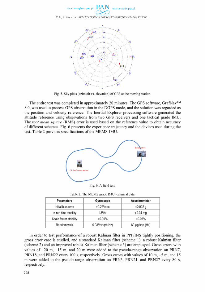
Z. Li, Y. Yao, et al.: APPLICATION OF IMPROVED ROBUST KALMAN FILTER …
Fig. 5. Sky plots (azimuth vs. elevation) of GPS at the moving station.
The entire test was completed in approximately 20 minutes. The GPS software, GrafNavTM 8.0, was used to process GPS observation in the DGPS mode, and the solution was regarded as
the position and velocity reference. The Inertial Explorer processing software generated the attitude reference using observations from two GPS receivers and one tactical grade IMU. The root mean square (RMS) error is used based on the reference value to obtain accuracy
of different schemes. Fig. 6 presents the experience trajectory and the devices used during the test. Table 2 provides specifications of the MEMS-IMU.
GPS reference station
Locomotive
Fig. 6. A field test.
Table 2. The MEMS grade IMU technical data.
Parameters Gyroscope Accelerometer
Initial bias error ±0.25º/sec ±0.002 g
In-run bias stability 18º/hr ±0.04 mg
Scale factor stability ±0.05% ±0.05%
Random walk 0.03º/s/sqrt (Hz) 80 µg/sqrt (Hz)
In order to test performance of a robust Kalman filter in PPP/INS tightly positioning, the gross error case is studied, and a standard Kalman filter (scheme 1), a robust Kalman filter
(scheme 2) and an improved robust Kalman filter (scheme 3) are employed. Gross errors with
values of −20 m, −15 m, and 20 m were added to the pseudo-range observation on PRN7,
PRN18, and PRN22 every 100 s, respectively. Gross errors with values of 10 m, −5 m, and 15 m were added to the pseudo-range observation on PRN3, PRN21, and PRN27 every 80 s, respectively.
298

Metrol. Meas. Syst., Vol. 24 (2017), No. 2, pp. 289–301.
In Fig. 7 field test trajectories for different schemes are compared. Fig. 8 shows the time
series of position errors in the north, east and down directions for scheme 1, scheme 2 and scheme 3. The RMSs of position errors of three schemes are presented in Table 3. Fig. 9 shows a histogram of position errors’ RMSs in the north, east and down directions for schemes 1, 2
and 3. The positioning resolution trajectory by the standard Kalman filter seriously deviates from the reference. Similarly to the simulation analysis results, accuracies of schemes 2 and 3
are again almost of the same quality. So the field test trajectories and position error curves from schemes 2 and 3 almost coincide. Scheme 3 achieves nearly the same performance as scheme 2 and even a slightly better efficiency than scheme 2 from the statistical result of RMS, which
is also similar to the simulation test results. The improved robust Kalman filter is able to remove the ill effect of gross error. The RMSs of position errors in the north, east and down direction
are 0.695 m, 0.875 m and 0.548 m, respectively, when the standard Kalman filter is used. However, the RMSs of position errors are 0.465 m, 0.524 m and 0.293 m, respectively, when the improved robust Kalman filter is applied. In comparison with scheme 1, the improvements
are about 33%, 40% and 47% for using scheme 3 in the north, east and down directions, respectively. The position RMS of scheme 3 is 0.759 m which is better than that of scheme 1
with an improvement of 39% in the three-dimensional component. It clearly illustrates that the robust Kalman filter with IGG scheme is very effective, and all gross errors are successfully identified. Significantly, there are obvious improvements for PPP/INS tightly coupled
positioning if a robust Kalman filter with IGG scheme is used. IGG scheme can be used as a very efficient filtering tool.
Fig. 7. Field test trajectories for different schemes with gross error.
Fig. 8. Position error series for different schemes with gross error.
-1.1842 -1.1840 -1.1838 -1.1836 -1.183452.9518
52.9519
52.9520
52.9521
longitude/(°)
latitude/(°)
trajectory
standard filter
robust filter
improved robust filter
reference
486100 486300 486500 486700 486900 487100-6
0
6
north/m
position error
486100 486300 486500 486700 486900 487100-6
0
6
east/m
standard filter robust filter improved robust filter
486100 486300 486500 486700 486900 487100-6
0
6
time/s
down/m
299

Z. Li, Y. Yao, et al.: APPLICATION OF IMPROVED ROBUST KALMAN FILTER …
Fig. 9. Comparison of position errors for different schemes with gross error.
Table 3. Comparison of RMSs for different schemes regarding a position error.
Scheme North (m) East (m) Down (m)
Standard filter 0.695 0.875 0.548
Robust filter 0.481 0.527 0.293
Improved robust filter 0.465 0.524 0.293
5. Conclusions
During the robust filter process, iterative computations will take much time, thus reducing the computational efficiency. To increase it, an improved robust scheme is proposed based on
the robust Kalman filter with Mahalanobis distance and a new robust filter factor is constructed as a three-section function using the IGG principle. By simulation and comparing errors obtained for a standard Kalman filter, a robust Kalman filter based on Mahalanobis distance
and an improved robust Kalman filter with the IGG principle, the improved robust Kalman filter provides the best performance and fewer filter iteration numbers than the robust Kalman
filter based on Mahalanobis distance. A PPP/INS tightly coupled positioning experiment was carried out to further validate the
performance of the proposed filtering method. The position accuracy for PPP/INS integrated
positioning can be degraded by the gross error in GPS observation. The improved robust Kalman filter with the IGG principle was employed in PPP/INS tightly coupled positioning to
remove the harmful effects from gross error of GPS pseudorange observation. Compared with the standard Kalman filter, the improved robust Kalman filter accuracy regarding the east, north
and down components can be improved by 33%, 40% and 47%, respectively. The improved robust Kalman filter is very effective in identifying a simulated gross error added to GPS pseudo-range observation, which proves its good performance.
Acknowledgements
The work was partially sponsored by China’s Post-doctoral Science Fund (grant number:
2015M580490) and partially sponsored by Natural Science Foundation of Jiangsu Province (grant number: BK20160247). The authors would like to thank Dr. Xiaolin Meng and all experienced members in the University of Nottingham for their help in collecting and
processing the field test data.
North East Down0
0.5
1
direction
error/m
position error
standard filter robust filter improved robust filter
300

Metrol. Meas. Syst., Vol. 24 (2017), No. 2, pp. 289–301.
References
[1] Chu, H.J., Tsai, G.J., Chiang, K.W., Duong, T.T. (2013). GPS/MEMS INS data fusion and map matching in
urban areas. Sensors, 13(9), 11280−11288.
[2] Nassar, S. (2003). Improving the Inertial Navigation System (INS) Error Model for INS and INS/DGPS
Applications. Ph.D. Thesis. The University of Calgary.
[3] Kouba, J., Héroux, P. (2001). Precise point positioning using IGS orbit and clock products. GPS Solut., 5(2),
12−28.
[4] Du, S., Gao, Y. (2012). Inertial aided cycle slip detection and identification for integrated PPP GPS and INS.
Sensors, 12(11), 14344−14362.
[5] Ali, J., Ushaq, M. (2009). A consistent and robust Kalman filter design for in-motion alignment of inertial
navigation system. Measurement, 42(4), 577−582.
[6] Gao, S., Zhong, Y., Li, W. (2011). Robust adaptive filtering method for SINS/SAR integrated navigation
system. Aerosp. Sci. Technol., 15(6), 425−430.
[7] Huang, G., Zhang, Q. (2012). Real-time estimation of satellite clock offset using adaptively robust Kalman
filter with classified adaptive factors. GPS Solut., 16(4), 531−539.
[8] Guo, F., Zhang, X. (2014). Adaptive robust Kalman filtering for precise point positioning. Meas. Sci.
Technol., 25(10), 1−8.
[9] Chang, G. (2014). Robust Kalman filtering based on Mahalanobis distance as outlier judging criterion. J.
Geod., 88(4), 391−401.
[10] Du, S. (2010). Integration of precise point positioning and low cost MEMS IMU. Ph.D. Thesis. The
University of Calgary.
[11] Abdel-salam, M.A. (2005). Precise point positioning using un-differenced code and carrier phase
observations. Ph.D. Thesis. The University of Calgary.
[12] Titterton, D. (2004). Strapdown inertial navigation technology. 2nd ed. MIT Lincoln Laboratory.
[13] Han, S., Wang, J. (2012). Integrated GPS/INS navigation system with dual-rate Kalman Filter. GPS Solut.,
16(3), 389−404.
[14] Li, Z., Wang, J., Li, B., Gao, J., Tan, X. (2014). GPS/INS/Odometer integrated system using fuzzy neural
network for land vehicle navigation applications. J. Navigation, 67(6), 967−983.
[15] Zhang, Y., Gao, Y. (2008). Integration of INS and un-differenced GPS measurements for precise position
and attitude determination. J. Navigation, 61(1), 87−97.
[16] Nassar, S., El-Sheimy, N. (2006). A combined algorithm of improving INS error modeling and sensor
measurements for accurate INS/GPS navigation. GPS Solut., 10(1), 29−39.
[17] Chang, G. (2014). Kalman filter with both adaptivity and robustness. J. Process Contr., 24(3), 81−87.
[18] Yang, Y. (1994). Robust estimation for dependent observations. Manuscripta Geodaetica, 19(1), 10−17.


Metrol. Meas. Syst., Vol. 24 (2017), No. 2, pp. 303–312.
_____________________________________________________________________________________________________________________________________________________________________________________
Article history: received on Aug. 15, 2016; accepted on Jan. 28, 2017; available online on Jun. 30, 2017; DOI: 10.1515/mms-2017-0035.
METROLOGY AND MEASUREMENT SYSTEMS
Index 330930, ISSN 0860-8229 www.metrology.pg.gda.pl
ASSESSMENT OF FREE-FORM SURFACES’ RECONSTRUCTION ACCURACY
Artur Wójcik1), Magdalena Niemczewska-Wójcik2), Jerzy Sładek2)
1) University of Agriculture in Cracow, Department of Mechanical Engineering and Agrophysics, Balicka 120, 30-149 Cracow, Poland ( [email protected], +48 12 662 4678) 2) Cracow University of Technology, Faculty of Mechanical Engineering, Jana Pawła II 37, 31-864 Cracow, Poland ([email protected], [email protected])
Abstract
The paper presents the problem of assessing the accuracy of reconstructing free-form surfaces in the
CMM/CAD/CAM/CNC systems. The system structure comprises a coordinate measuring machine (CMM) PMM
12106 equipped with a contact scanning probe, a 3-axis Arrow 500 Vertical Machining Center, QUINDOS
software and Catia software. For the purpose of surface digitalization, a radius correction algorithm was
developed. The surface reconstructing errors for the presented system were assessed and analysed with respect to
offset points. The accuracy assessment exhibit error values in the reconstruction of a free-form surface in a range
of ± 0.02 mm, which, as it is shown by the analysis, result from a systematic error.
Keywords: reverse engineering, accuracy assessment, free-form surface, coordinate measuring machine, radius
correction
© 2017 Polish Academy of Sciences. All rights reserved
1. Introduction
The measurement method based on CMM technology has found widespread use in those areas of industry which require high accuracy and reliability of measurement, or to which other methods cannot be applied due to the nature of measurement, e.g. in measuring free-form
surfaces within the scope of industrial design. In this case, an initial design of such products is entrusted to craftsmen who construct the first physical model (a reference object) of the
structure of a designed product. Naturally, the design consists of far more complicated forms
than simple regular shapes − such as spherical, cylinder, or conic ones − which are not explicitly described in mathematical terms. The subsequent stages of design involve making a digital
cloud of points of the reference object and creating a prototype from a material suitable for manufacturing of, e.g., injection moulds. For this purpose, it is necessary to create an integrated system comprising tools for measurement, analysis, and manufacturing. These issues fall within
the area of widely-understood reverse engineering (RE) [1, 2]. In this process (RE) errors not only result from many factors related to digitizing, CAD/CAM
modelling, and manufacturing processes (CMM/CAD/CAM/CNC), but also are being induced by the applied machine tools and measuring strategies. This problem has been comprehensively
analysed in many papers [3−6].
The paper focuses on presentation of a method developed for creating a free-form surface of a reference object, along with its digitizing using a coordinate measuring machine (CMM). Next, it creates a free-form surface copy and evaluates reconstruction errors of the
CMM/CAD/CAM/CNC system (Fig. 1). The digitizing process was carried out with a CMM equipped with a contact scanning probe.
A surface made of aluminium (AlZnMgCu0.5) was examined. For the purposes of the described
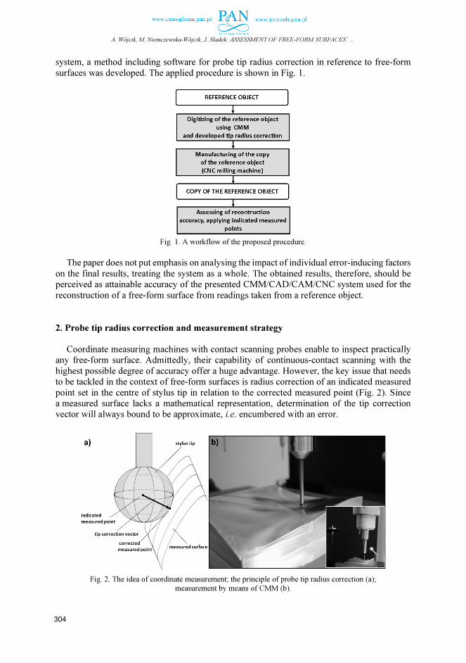
A. Wójcik, M. Niemczewska-Wójcik, J. Sładek: ASSESSMENT OF FREE-FORM SURFACES’ …
system, a method including software for probe tip radius correction in reference to free-form
surfaces was developed. The applied procedure is shown in Fig. 1.
Fig. 1. A workflow of the proposed procedure.
The paper does not put emphasis on analysing the impact of individual error-inducing factors
on the final results, treating the system as a whole. The obtained results, therefore, should be perceived as attainable accuracy of the presented CMM/CAD/CAM/CNC system used for the
reconstruction of a free-form surface from readings taken from a reference object.
2. Probe tip radius correction and measurement strategy
Coordinate measuring machines with contact scanning probes enable to inspect practically any free-form surface. Admittedly, their capability of continuous-contact scanning with the
highest possible degree of accuracy offer a huge advantage. However, the key issue that needs to be tackled in the context of free-form surfaces is radius correction of an indicated measured
point set in the centre of stylus tip in relation to the corrected measured point (Fig. 2). Since a measured surface lacks a mathematical representation, determination of the tip correction vector will always bound to be approximate, i.e. encumbered with an error.
Fig. 2. The idea of coordinate measurement; the principle of probe tip radius correction (a);
measurement by means of CMM (b).
304

Metrol. Meas. Syst., Vol. 24 (2017), No. 2, pp. 303–312.
This issue has been discussed at length in the literature. The methods of probe tip radius
correction may be grouped into several areas. One of them is approximation of a cloud of points obtained from scanning a surface with the use of sets of mathematical formulas, most often B-
spline functions or others [7]. This approach is commonly known as the least-squares method [8]. However, this leads to averaging the values of respective measuring points, which adversely
affects the accuracy of the reconstruction of a measured surface. In another method of probe radius compensation there are determined normal vectors, drawn in the positions
of neighbouring measuring points [9−11].
A fundamentally different approach has been offered by Wozniak et al.; they use an algorithm which does not calculate the probe tip radius correction vector, but directly determines adjusted measuring points. This approach is based on fuzzy logic algorithms [12]
and a geometric method [13]. For the purpose of probe tip radius correction and finding a vector normal to the surface at
a given point, it is possible to employ a method analysing force distribution in the transducer of an active probe head [14].
In order to avoid errors resulting from the probe tip radius correction in accuracy assessment
on the basis of a CAD model, measurements can be performed without that correction. In this case the indicated measured points are compared with points distributed on an off-set surface
in a stylus tip radius distance from the CAD model in the normal direction [15]. Taking into consideration that not every computer program running on CMMs has separate
modules for probe tip radius correction in reference to free-form surfaces and bearing in mind that the tip radius compensation algorithm does not produce expected results, in this work a computer software used for probe tip radius correction has been developed. The input data for
the presented stylus tip radius correction method is a grid of points (the indicated measured points) displaced from the reference object by a length of the stylus ball radius. The algorithm
is based on determination of vectors starting from a given indicated measured point and pointing to all neighbouring points as well as being based on indication of a normal vector for each of the
determined vector pairs. The normal vector is estimated by a mean vector determined from a bunch of vectors starting from an indicated measured point (Fig. 3). What provides a distinct advantage of the presented solution is that the selection of an appropriate measuring strategy
ensures satisfactory results and may be used for any cloud of points grouped in the measuring paths.
Fig. 3. The strategy of determining the direction of the probe tip radius correction vector.
With the view of verifying the developed method, a set of reference spheres with known
diameters were measured. In the first place, the radii of the spheres and sphericity deviations
305
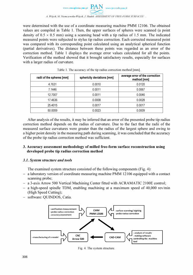
A. Wójcik, M. Niemczewska-Wójcik, J. Sładek: ASSESSMENT OF FREE-FORM SURFACES’ …
were determined with the use of a coordinate measuring machine PMM 12106. The obtained
values are compiled in Table 1. Then, the upper surfaces of spheres were scanned (a point
density of 0.5 × 0.5 mm) using a scanning head with a tip radius of 1.5 mm. The indicated measured points were subjected to stylus tip radius correction. Each corrected measured point
was compared with its corresponding point calculated using an analytical spherical function (partial derivatives). The distance between these points was regarded as an error of the
correction method. Table 1 displays the average error values calculated for all the points. Verification of the method showed that it brought satisfactory results, especially for surfaces
with a larger radius of curvature.
Table 1. The accuracy of the tip radius correction method [mm].
radii of the spheres [mm] sphericity deviations [mm] average error of the correction
method [mm]
4.7631 0.0010 0.0120
7.1446 0.0011 0.0067
12.7007 0.0011 0.0046
17.4636 0.0008 0.0028
25.4015 0.0017 0.0017
50.0059 0.0023 0.0009
After analysis of the results, it may be inferred that an error of the presented probe tip radius
correction method depends on the radius of curvature. Due to the fact that the radii of the
measured surface curvatures were greater than the radius of the largest sphere and owing to a higher point density in the measuring path during scanning, it was concluded that the accuracy
of the probe tip radius correction method was sufficient.
3. Accuracy assessment methodology of milled free-form surface reconstruction using
developed probe tip radius correction method
3.1. System structure and tools
The examined system structure consisted of the following components (Fig. 4):
− a laboratory version of coordinate measuring machine PMM 12106 equipped with a contact scanning probe;
− a 3-axis Arrow 500 Vertical Machining Center fitted with ACRAMATIC 2100E control;
− a high-speed spindle TDM, enabling machining at a maximum speed of 40,000 rev/min (High Speed Cutting);
− software: QUINDOS, Catia.
Fig. 4. The system structure.
306
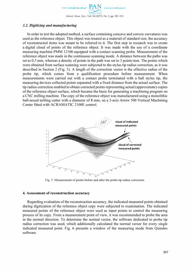
Metrol. Meas. Syst., Vol. 24 (2017), No. 2, pp. 303–312.
3.2. Digitizing and manufacturing
In order to test the adopted method, a surface containing concave and convex curvatures was
used as the reference object. This object was treated as a material of standard size; the accuracy of reconstructed items was meant to be referred to it. The first step in research was to create
a digital cloud of points of the reference object. It was made with the use of a coordinate measuring machine PMM 12106 equipped with a contact scanning probe. Measurement of the reference object was made in the continuous scanning mode. A distance between the paths was
set to 0.5 mm, whereas a density of points in the path was set to 3 points/mm. The points which were obtained from surface scanning were subjected to the stylus tip radius correction, as it was
described in Section 2 (Fig. 5). A length of the correction vector is the effective radius of the probe tip, which comes from a qualification procedure before measurement. When measurements were carried out with a contact probe terminated with a ball stylus tip, the
measuring devices collected points separated with a fixed distance from the actual surface. The tip radius correction enabled to obtain corrected points representing actual (approximate) copies
of the reference object surface, which became the basis for generating a machining program on a CNC milling machine. The copy of the reference object was manufactured using a monolithic
ball-nosed milling cutter with a diameter of 8 mm, on a 3-axis Arrow 500 Vertical Machining Center fitted with ACRAMATIC 2100E control.
Fig. 5. Measurement of points before and after the probe tip radius correction.
4. Assessment of reconstruction accuracy
Regarding evaluation of the reconstruction accuracy, the indicated measured points obtained
during digitization of the reference object copy were subjected to examination. The indicated
measured points of the reference object were used as input points to control the measuring process of its copy. From a measurement point of view, it was recommended to probe the area
in the normal direction. To determine the normal vector, the software dedicated to probe tip radius correction was used, which additionally calculated the normal versor for every single
indicated measured point. Fig. 6 presents a window of the measuring mode from Quindos software.
307

A. Wójcik, M. Niemczewska-Wójcik, J. Sładek: ASSESSMENT OF FREE-FORM SURFACES’ …
Fig. 6. A window of the measuring mode from Quindos software.
The input points (the indicated measured points from the reference object) were imported to
Quindos metrology software cooperating with a CMM. The prepared input data, after setting the local coordinates, enabled to measure the reference object copy in the automated mode.
Comparison between the coordinates of points obtained from the performed measurements
and the (input) measured points enabled to determine a map of errors. In the ideal case, measurement should be taken in the same point. In order to minimize the impact of stress change
within the measured surface, a constant contact force in the vices of the machine tool and the measuring machine was applied. Fig. 7 shows graphical interpretations of reconstruction error
calculation for each measured point.
Fig. 7. The principle of determining a reconstruction error in a point.
A mapping error is determined by the following equation:
, , ,
, , ), (1)
308
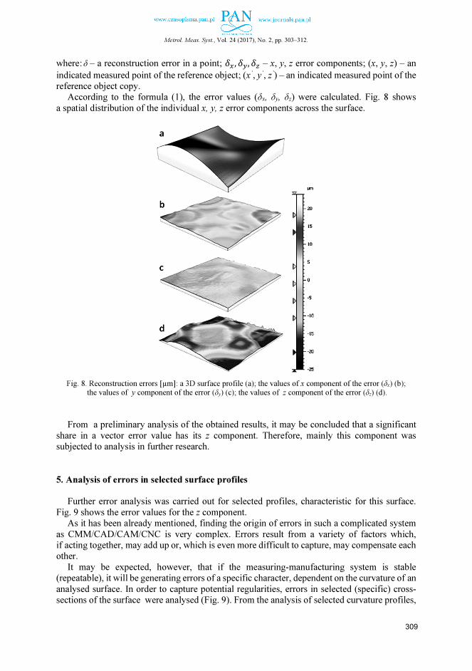
Metrol. Meas. Syst., Vol. 24 (2017), No. 2, pp. 303–312.
where:δ – a reconstruction error in a point; , , – x, y, z error components; (x, y, z) – an
indicated measured point of the reference object; (x’, y’, z’) – an indicated measured point of the reference object copy.
According to the formula (1), the error values (δx, δy, δz) were calculated. Fig. 8 shows
a spatial distribution of the individual x, y, z error components across the surface.
Fig. 8. Reconstruction errors [µm]: a 3D surface profile (a); the values of x component of the error (δx) (b);
the values of y component of the error (δy) (c); the values of z component of the error (δz) (d).
From a preliminary analysis of the obtained results, it may be concluded that a significant
share in a vector error value has its z component. Therefore, mainly this component was subjected to analysis in further research.
5. Analysis of errors in selected surface profiles
Further error analysis was carried out for selected profiles, characteristic for this surface.
Fig. 9 shows the error values for the z component. As it has been already mentioned, finding the origin of errors in such a complicated system
as CMM/CAD/CAM/CNC is very complex. Errors result from a variety of factors which, if acting together, may add up or, which is even more difficult to capture, may compensate each other.
It may be expected, however, that if the measuring-manufacturing system is stable (repeatable), it will be generating errors of a specific character, dependent on the curvature of an
analysed surface. In order to capture potential regularities, errors in selected (specific) cross-sections of the surface were analysed (Fig. 9). From the analysis of selected curvature profiles,
309
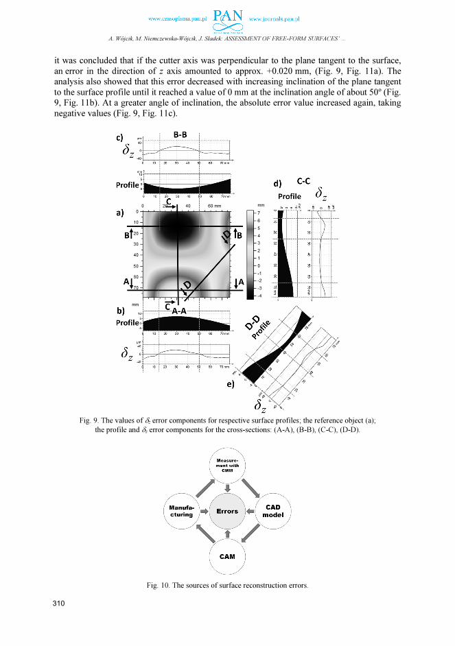
A. Wójcik, M. Niemczewska-Wójcik, J. Sładek: ASSESSMENT OF FREE-FORM SURFACES’ …
it was concluded that if the cutter axis was perpendicular to the plane tangent to the surface,
an error in the direction of z axis amounted to approx. +0.020 mm, (Fig. 9, Fig. 11a). The analysis also showed that this error decreased with increasing inclination of the plane tangent
to the surface profile until it reached a value of 0 mm at the inclination angle of about 50º (Fig. 9, Fig. 11b). At a greater angle of inclination, the absolute error value increased again, taking
negative values (Fig. 9, Fig. 11c).
Fig. 9. The values of δz error components for respective surface profiles; the reference object (a);
the profile and δz error components for the cross-sections: (A-A), (B-B), (C-C), (D-D).
Fig. 10. The sources of surface reconstruction errors.
310

Metrol. Meas. Syst., Vol. 24 (2017), No. 2, pp. 303–312.
Fig. 11. The contact of the cutter with the machined surface.
A conclusion from the above considerations is that, if such a relationship reoccurs, it must be resulting from a strong (regular) factor, which in turn might be eliminated, e.g. at the level of software controlling the CNC machine.
6. Summary
The proposed method makes it possible to assess the reconstruction accuracy of complex-shaped products. It can be used along with the developed software as an effective tool
supporting the work of constructors and technologists in designing and manufacturing of complex-shaped products limited by free-form surfaces (in RE).
The points in which measurement is performed result from scanning a reference object. An advantage of the proposed method is that there is no need to make another probe tip radius
correction, which would contribute to further accumulation of errors. The probe tip radius correction is performed only once in order to manufacture a copy of the reference object. Regarding reconstruction accuracy assessment, both the indicated measured points obtained
from scanning the reference object and normal versors are used, the latter calculated with the use of the developed correction method. The presented method was verified for a free-form
surface reference object. The results showed that the reconstruction errors of the reference object exhibited values in a range of ±0.02 mm, which, as it is obtained from the analysis,
resulted from a systematic error.
Acknowledgments
This Research was financed by the Ministry of Science and Higher Education of the Republic
of Poland
References
[1] Li, Y., Gu, P. (2004). Free-form surface inspection techniques state of the art review. Comput. Aided. Des.,
36, 1395–1417.
[2] Werner, A., Skalski, K., Piszczatowski, S., Świeszkowski, W., Lechniak, Z.(1998). Reverse engineering of
free-form surfaces. J. Mater. Process Technol., 76(1–3), 128–132.
[3] Sladek, J.A. (2016). Coordinate Metrology Accuracy of Systems and Measurements. Springer-Verlag Berlin
Heidelberg.
[4] Poniatowska, M. (2008). Determining uncertainty of fitting discrete measurement data to a nominal surface.
Metrol. Meas. Syst., 15(4), 595–606.
[5] Poniatowska, M. (2012). Deviation model based method of planning accuracy inspection of free-form
surfaces using CMMs. Measurement, 45, 927–937.
311

A. Wójcik, M. Niemczewska-Wójcik, J. Sładek: ASSESSMENT OF FREE-FORM SURFACES’ …
[6] Poniatowska, M. (2015). Free-form surface machining error compensation applying 3D CAD machining
pattern model. Comput. Aided. Des., 62, 227–235.
[7] Zhongwei, Y., Yuping, Z., Shouwei, J. (2003). Methodology of NURBS surface fitting based on off-line
software compensation of errors of a CMM. Precis. Eng., 27, 299–303.
[8] Xiong, Z., Li, Z. (2003). Probe radius compensation of workpiece localization. J. Manuf. Sci. Eng., 125,
100–104.
[9] Lee, R.T., Shiou, F.J. (2010). Calculation of the unit normal vector using the cross-curve moving mask
method for probe radius compensation of a freeform surface measurement. Measurement, 43, 469–478.
[10] Lin, Y.C., Sun, W.I. (2003). Probe radius compensated by the multicross product method in freeform surface
measurement with touch trigger probe CMM. Int. J. Adv. Manuf. Technol., 21, 902–909.
[11] Wójcik, A. (2005). The method of evaluation of mapping free form surface accuracy in reverse engieering
system. Dissertation, Cracow University of Technology.
[12] Woźniak, A., Mayer, R., Bałaziński, M. (2009). Stylus tip envelop method: corrected measured point
determination in high definition coordinate metrology. Int. J. Adv. Manuf. Technol., 42, 505–514.
[13] Woźniak, A., Mayer, R. (2012). Robust method for probe tip radius correction in coordinate metrology.
Meas. Sci. Technol., 23(2).
[14] Park, J.J., Kwon, K., Cho, N. (2006).Development of a coordinate measuring machine (CMM) touch probe
using a multi-axis force sensor. Meas. Sci. Technol., 17, 2380–2386.
[15] Savio, E., De Chiffre, L., Schmitt, R. (2007). Metrology of freeform shaped parts. Annals of the CIRP, 56/2,
810–835.

Metrol. Meas. Syst., Vol. 24 (2017), No. 2, pp. 313–324.
_____________________________________________________________________________________________________________________________________________________________________________________
Article history: received on Sep. 21, 2016; accepted on Jan. 14, 2016; available online on Jun. 30, 2017; DOI: 10.1515/mms-2017-0023.
METROLOGY AND MEASUREMENT SYSTEMS
Index 330930, ISSN 0860-8229
www.metrology.pg.gda.pl
SINGLE-FRAME ATTITUDE DETERMINATION METHODS
FOR NANOSATELLITES
Demet Cilden Guler, Ece S. Conguroglu, Chingiz Hajiyev
Istanbul Technical University, Faculty of Aeronautics and Astronautics, 34469, Maslak, Istanbul, Turkey ( [email protected], +90 543 740 0405, [email protected], [email protected])
Abstract
Single-frame methods of determining the attitude of a nanosatellite are compared in this study. The methods
selected for comparison are: Single Value Decomposition (SVD), q method, Quaternion ESTimator (QUEST),
Fast Optimal Attitude Matrix (FOAM) − all solving optimally the Wahba’s problem, and the algebraic method using only two vector measurements. For proper comparison, two sensors are chosen for the vector observations
on-board: magnetometer and Sun sensors. Covariance results obtained as a result of using those methods have a
critical importance for a non-traditional attitude estimation approach; therefore, the variance calculations are also
presented. The examined methods are compared with respect to their root mean square (RMS) error and variance results. Also, some recommendations are given.
Keywords: attitude determination, single-frame methods, algebraic method, covariance analysis, vector
observation.
© 2017 Polish Academy of Sciences. All rights reserved
1. Introduction
The attitude determination and control subsystem of a nanosatellite is important for
maintaining a required direction of the spacecraft and its instruments. There are several methods for determining the satellite’s attitude using attitude sensors. Sun sensors and magnetometers
are very common sensors for nanosatellites because of their cost-effectiveness and commercial availability on the market with various mass and size versions. After determination of its attitude, using the actuators, a satellite should be oriented towards a specified direction. For
doing that, two or more vectors should be used as reference directions in a single-frame method which this paper is mainly focused on. Commonly used reference vectors are the Earth’s
magnetic field and unit vectors in the direction of the Sun, a known star or the centre of the Earth. Given a reference vector, the orientations of these vectors can be obtained from the measurement results of the attitude sensor.
The algebraic attitude determination methods [1−4] are based only on the vector observations. These methods are based on computing any two analytical vectors in the reference frame and measuring them in the body coordinate system [2]. The paper [3] deals with
estimating and enhancing the accuracy of an algebraic method of attitude determination. This method was examined with the use of three different vector pairs: 1) Earth’s magnetic field and
Sun vectors; 2) Earth’s magnetic field and nadir vectors; 3) Sun and nadir vectors. In order to determine the attitude accuracy, some analytical relations were found for the attitude angles
(pitch, roll and yaw). These relations include terms of the measured and theoretical vectors, used in the attitude determination. The effects of various factors on the attitude determination were examined and those which most significantly affect the accuracy were determined.
In order to increase the attitude determination accuracy, a redundant data processing algorithm,

D. Cilden Guler, E. S. Conguroglu, C. Hajiyev: SINGLE-FRAME ATTITUDE DETERMINATION METHODS …
based on the Maximum Likelihood method, was used to carry out the statistical operation on
the measurement results of three algorithms mentioned above and appropriate formulas were derived. As a result, the attitude was determined with a high accuracy in a wide range (even when the reference vectors were almost parallel). This method involves different vector pairs,
therefore it may require redundant hardware and a substantial computational load. The vectors obtained from selected sensor data and the developed models can be used in
solving the Wahba’s problem [2, 5]. Coordinate systems used as the reference frame and the body frame can be transformed to each other with necessary input parameters. The system uses single-frame methods: SVD, q, QUEST and FOAM to minimize the Wahba’s loss function and
to determine the attitude of the satellite. They are different from the algebraic method, because they use an unlimited number of direction vectors and can process all of them in one attitude
determination algorithm. In [6], the algebraic and SVD methods are compared to find an optimum attitude determination method. Also, the effects of magnetometer biases are examined in the study.
Kalman filters can give more improved results than the single-frame methods. In [7], a sigma-point Kalman filter is derived using the modified Rodrigues parameters and the real
data of attitude sensors of CBERS-2 (China Brazil Earth Resources Satellite). The unscented Kalman filter algorithm is used for attitude estimation and a gyro-based model is considered for attitude propagation. The estimated attitude is very similar to the one obtained by the Euler
angles’ propagation. Single-frame methods can also be used in filtering techniques as measurement of inputs in order to estimate the satellite’s attitude with a high accuracy. Also,
the covariance analysis can be used directly in a non-traditional method which is an integrated algorithm using linear measurements. In [8, 9], a non-traditional attitude estimation scheme has been presented and it is shown that the non-traditional methods give the attitude results for
a satellite that are superior to the traditional Kalman filters, even in the eclipse period. In [10], the performance of several methods is examined regarding their computational load
and accuracy of used algorithms. Attitude determination and estimation methods are divided into two categories: those that use and those that do not use spacecraft attitude motion models
inside their algorithms. The attitude determination methods which are considered in this paper as single-frame methods do not use knowledge about the attitude motion because they find the attitude at a single moment from the sensor-model data. In that paper, the attitude determination
algorithms are characterized as ones with a low computation load in addition to a low accuracy of spacecraft attitude angles, in comparison with such attitude estimation methods as the
extended Kalman filter, which is obvious. There were examined only methods based on observation of two vectors. Also, classification of the methods (attitude determination and estimation methods) is different; thus, there only the single-frame methods are compared to find
the most robust and the fastest method in their classification. The goal of this study is to examine the errors and variances of errors for most of the vector-
observation-based satellite attitude determination methods which are single-frame methods. Also, based on this error and variance analysis, these attitude determination methods are compared.
2. Measurement models and attitude determination methods
To find the attitude of a spacecraft, minimum two vectors should be known. In order to find these vectors, many different sensors can be applied. In this study, the sensors of magnetic field
and Sun direction vectors are used because these sensors are very common for on-board use in small satellites. In this paper, the orbital parameters are calculated using the orbit propagation
from the Two Line Elements (TLE) data for the TIMED satellite. Using mathematical models, the Sun vector (SR) and the Earth’s magnetic field vector (HR) are calculated in the orbital frame
314
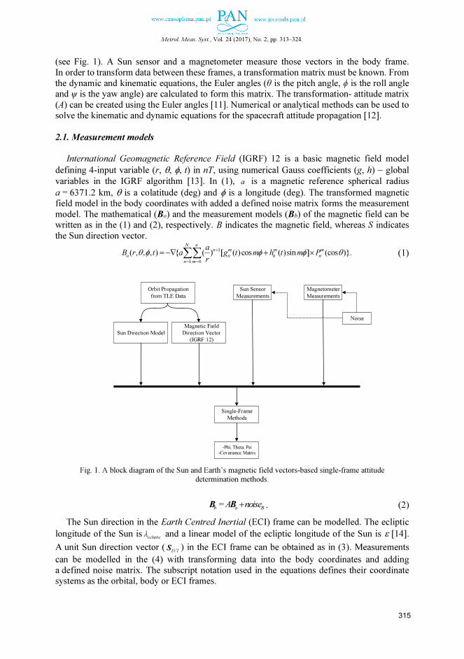
Metrol. Meas. Syst., Vol. 24 (2017), No. 2, pp. 313–324.
(see Fig. 1). A Sun sensor and a magnetometer measure those vectors in the body frame.
In order to transform data between these frames, a transformation matrix must be known. From the dynamic and kinematic equations, the Euler angles (θ is the pitch angle, ϕ is the roll angle and ψ is the yaw angle) are calculated to form this matrix. The transformation- attitude matrix
(A) can be created using the Euler angles [11]. Numerical or analytical methods can be used to solve the kinematic and dynamic equations for the spacecraft attitude propagation [12].
2.1. Measurement models
International Geomagnetic Reference Field (IGRF) 12 is a basic magnetic field model
defining 4-input variable (r, θ, φ, t) in nT, using numerical Gauss coefficients (g, h) − global
variables in the IGRF algorithm [13]. In (1), a is a magnetic reference spherical radius
a = 6371.2 km, θ is a colatitude (deg) and φ is a longitude (deg). The transformed magnetic field model in the body coordinates with added a defined noise matrix forms the measurement
model. The mathematical (Bo) and the measurement models (Bb) of the magnetic field can be written as in the (1) and (2), respectively. B indicates the magnetic field, whereas S indicates
the Sun direction vector.
1
1 0
( , , , ) ( ) [ ( )cos ( )sin ] (cos ).N n
n m m m
o n n n
n m
aB r t a g t m h t m P
rθ φ φ φ θ
+
= =
= −∇ + ×∑∑ (1)
Fig. 1. A block diagram of the Sun and Earth’s magnetic field vectors-based single-frame attitude
determination methods.
b o B
=A noise+B B . (2)
The Sun direction in the Earth Centred Inertial (ECI) frame can be modelled. The ecliptic
longitude of the Sun is eclipticλ and a linear model of the ecliptic longitude of the Sun is ε [14].
A unit Sun direction vector (ECI
S ) in the ECI frame can be obtained as in (3). Measurements
can be modelled in the (4) with transforming data into the body coordinates and adding
a defined noise matrix. The subscript notation used in the equations defines their coordinate systems as the orbital, body or ECI frames.
Orbit Propagation
from TLE Data
Sun Direction Model
Magnetic Field
Direction Vector
(IGRF 12)
Noise
Sun Sensor
Measurements
Magnetometer
Measurements
Single-Frame
Methods
-Phi, Theta, Psi
-Covariance Matrix
315

D. Cilden Guler, E. S. Conguroglu, C. Hajiyev: SINGLE-FRAME ATTITUDE DETERMINATION METHODS …
cos
s
cos
sin
in nsi
ecliptic
ECI ecliptic
ecliptic
λ
λ ε
λ ε
=
S , (3)
2b o
= A η+S S . (4)
2.2. Algebraic method
In the algebraic method, transformation-attitude matrix (A) is determined by the observations
of two vectors. u and v are any vectors which define an orthogonal coordinate system. In this
study u and v are chosen as the Sun direction (S) and magnetic field (B) vectors.
The equations can be defined as follows [15]:
ˆ ˆ,q u= (5)
ˆ ˆ
ˆ ,ˆ ˆ
u v
r
u v
×
=
×
(6)
ˆ ˆ .s q xr= (7)
A reference matrix MR can be calculated using two reference vectors in the orbital
coordinates, ˆR
u and ˆ .Rv
[ ]ˆ ˆ ˆ .R R R R
M q r s= ⋮ ⋮ (8)
A body matrix MB can be calculated using two measured vectors in the spacecraft body
coordinates, ˆB
u and ˆ .Bv
[ ]ˆ ˆ ˆ .B B B B
M q r s= ⋮ ⋮ (9)
An attitude matrix is calculated as:
,R B
AM M=1.
B RA M M
−
= (10)
To calculate the attitude covariance matrix [1] which is in the Euler form, first the Cartesian attitude covariance matrix (Pθθ) must be known.
( ) ( )( )2 2 2 2
1 2 1 12
1[ . ],
T T T
B B B B B B B B
B B
P I u u u v u v v u
u vθθσ σ σ σ= + − + +
×
(11)
where 2
1σ is a variance of the magnetometer;
2
2σ is a variance of the Sun sensor and I is a unit
matrix with a dimension of 3 × 3. The attitude covariance matrix is a set of Euler angles:
,
TP BP Bφφ θθ= (12)
where 1B
− :
3
1
1
1,
2
k
k
k j i
AB A
φ
−
=
∂= × ∂ ∑ (13)
jφ are the Euler angles (ϕ, θ, ψ), respectively [1] .
2.3. SVD method
In 1965, Wahba defined a problem which aims to minimize the loss (L(A)) between chosen reference and measured unit vectors [5]. In the (14), bi (a set of unit vectors in the body frame)
316

Metrol. Meas. Syst., Vol. 24 (2017), No. 2, pp. 313–324.
and ri (a set of unit vectors in the reference frame) with their ai (a non-negative weight) are the
loss function variables obtained for instant time intervals.
21
( ) | b Ar | ,2
i i i
i
L A a= −∑ (14)
*
,
T
i i iB abr=∑ (15)
*
0( ) ( ).
TL A tr ABλ= − (16)
To simplify the loss function, *B matrix can be defined. The (16) shows that the trace of the
product of transformation matrix A and transposition of the defined matrix *B in (15) should be
maximized using statistical methods. In this study, the Singular Value Decomposition (SVD) Method is chosen to minimize the loss function problem as the optimal statistical method [16, 17].
11 22 3
*
3U VT Udiag VTB ∑ = ∑ ∑ ∑= , (17)
[1 1 det( )det( )] .T
optA Udiag U V V= (18)
The matrices U and V are orthogonal left and right matrices, respectively, and the primary
singular values (11 22 33, ,∑ ∑ ∑ ) obey the inequalities
11 22 330∑ ≥ ∑ ≥ ∑ ≥ . To find the rotation
angles of the satellite, a transformation matrix should be found from the (18) first with the
determinant of one.
A rotation angle error covariance matrix (SVDP ) is necessary for determining the instant time
intervals which give higher error results than desired.
1 1 1
2 3 3 1 1 2[(s s ) (s s ) (s s ) ] ,
T
SVDP Udiag U− − −
= + + + (19)
where the secondary singular values are 1 11 2 22 3 33
, , det(U)det(V)s s s= Σ = Σ = Σ . The
satellite has only two sensors (e.g. Sun and magnetic field sensors), thus the SVD-method fails
when the satellite is in eclipse and when two observations are parallel with the same trend of the absolute error results.
2.4. q method
In (14), a Wahba’s loss function has been defined. The attitude matrix can be parameterized with quaternions. Davenport suggested a useful solution with a unit quaternion denoted q
[16, 18]:
4
,
q
=
(20)
[ ]22
4 4( ) (q ) I 2q q 2 ,T
v v v vA q q q q= − + − × (21)
*(AB ) .T Ttr q Kq= (22)
Because of the quaternion definition by the Euler theorem, there will be a rotation of the axis
and the angle. The quadratic function from (21) includes scalar and vector quaternion elements. If K is defined as a traceless matrix, the eigenvector corresponding to the maximum eigenvalue
is the optimum quaternion vector qopt in (26).
*
( ),
( )T
S Itr B zK
z tr B
− ≡
(23)
317
D. Cilden Guler, E. S. Conguroglu, C. Hajiyev: SINGLE-FRAME ATTITUDE DETERMINATION METHODS …
* *
,
TS B B≡ + (24)
* *
23 32
*
31 13
* *
12 21
,
i i i
i
B B
z B B ab r
B B
−
≡ − = × −
∑ (25)
maksimum.
opt optKq qλ≡ (26)
There is only one problem: if the eigenvectors are equal, then the correct solution cannot be obtained. Markley stated in [19] that it is not a problem of the q method, since in this situation the available data are not suitable to determine attitude (2010). The expected results in this
situation are, like the results with a Sun sensor in the eclipse, going to infinity. The q method is used in various projects and studies [16, 20] .
The rotation angle error covariance matrix can be found from the (19). A covariance goes to infinity if the eigenvectors are equal. Also, if the attitude cannot be observed then the covariance would be infinite, too.
2.5. QUEST method
The QUEST method as one of the single-frame methods aims to minimize the Wahba’s loss function in (14). Iterative techniques can be used to solve the characteristic equation in the q
method. Additionally, some assumptions can be made to obtain the solutions faster. QUEST is one of methods that uses numerical iterative techniques. In this paper, QUEST is using the
Newton Raphson method as an iterative approach with a Gibbs vector. However, with the Gibbs vector a singularity problem is associated that studies like [21] are working on to remove. The q and QUEST methods use only quaternions to obtain the attitude, but the SVD method can
solve the Wahba’s problem with Euler angles directly besides using quaternions. An advantage to the method can be brought by comparing both results obtained in the same conditions.
2 2) ( ),*
max(trB tr adjSα λ≡ − + (27)
,
*
maxtrBβ λ≡ − (28)
( ) ( ) ,
* *
max maxdet I S det StrB trBγ αλ λ ≡ − = −+ + (29)
( )2 ,I S Sα β≡ + +x z (30)
2 2
1
optq .
γγ
=
+
x
| x | (31)
To find max
,imum
λ from the ( ) 0max
det K Iλ− = characteristic equation, a defined0
λ can be used as
the initial value for simplicity [16]. The parameters are the same as in the q method.
Also, from the reference [19], the covariance matrix can be obtained as follows:
( )1
.
TiQUEST i iiaP I bb
−
= − ∑ (32)
The covariance matrix ( QUESTP ) is a result that can be used as the initial value for filtering
approaches like EKF, UKF or variance values for the whole mission period. Besides, instantaneous time intervals when the algorithm should be switched to another one can be found
out by the covariance analysis.
318

Metrol. Meas. Syst., Vol. 24 (2017), No. 2, pp. 313–324.
2.6. FOAM method
The loss function in (14) can be also minimized using the FOAM method [22]. First of all, the Frobenius norm should be defined in (33) using the G symbol. From this definition, the
optimal attitude matrix can be determined (35):
( )2 2
,
T
i, jFi, j
G G tr GG= =∑ (33)
( )221
2,
max FBκ λ= − (34)
( ) ( ) ( )1 2
,
T T
opt max maxFA det B B B adj B BB Bκλ κ λ
− = − + + − (35)
( )T
max opttr A B .λ = (36)
Using the FOAM method, the optimal attitude matrix can be found, and from that
a quaternion or Euler angle representation can be used. The covariance Matrix (PFOAM):
( ) ( )1
T
FOAM maxP I BBdet B κκλ
−
= +− . (37)
The matrix B defined in (17) is directly used in (37) to find the error covariance.
3. Simulation results
The simulations were performed in order to estimate the attitude of the satellite and compare
the methods to find the optimum one. The simulations were based on the orbital parameters of TIMED satellite. The algorithm was run for almost one orbital period (6000 seconds) with 1 second sampling time of the sensors. Direction cosines of standard deviations for the
magnetometer and Sun sensors were taken as 0.008 and 0.002, respectively. The attitude angle
errors found by using single-frame methods are presented in Figs. 3−7. In Fig. 2, the angles between the vector observations coming from the sensors and the pitch angle propagation can be seen in the respective frames. The angles between the vectors are close neither to 0 degree nor 180 degrees; therefore, they are not parallel to each other and will not affect the attitude
of the satellite by being not observable vectors. On the other hand, the pitch angle is closing up to 90 degrees (at about 1000th sec and 3800th sec) which causes oscillations because of the
trigonometric calculations in the methods, especially in the algebraic method.
Fig. 2. From top to bottom: An angle between measurement vectors and a pitch angle.
0 1000 2000 3000 4000 5000 6000140
145
150
155
Ang
le (
de
g)
Angle between Magnetometer and Sun Sensor Vectors
0 1000 2000 3000 4000 5000 6000-50
0
50
100
θ (
de
g)
time (sec)
319
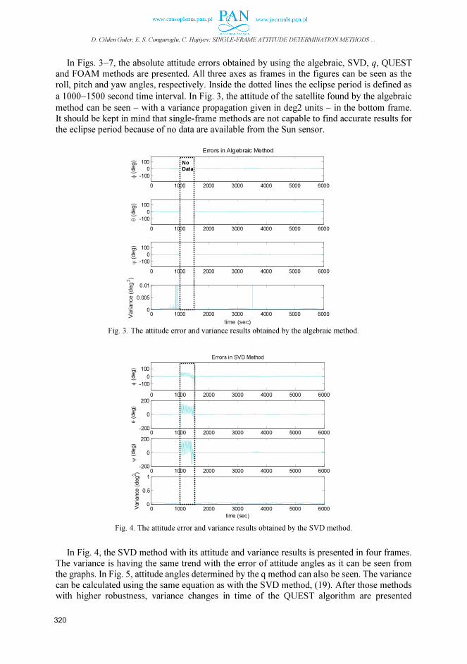
D. Cilden Guler, E. S. Conguroglu, C. Hajiyev: SINGLE-FRAME ATTITUDE DETERMINATION METHODS …
In Figs. 3−7, the absolute attitude errors obtained by using the algebraic, SVD, q, QUEST and FOAM methods are presented. All three axes as frames in the figures can be seen as the
roll, pitch and yaw angles, respectively. Inside the dotted lines the eclipse period is defined as
a 1000−1500 second time interval. In Fig. 3, the attitude of the satellite found by the algebraic
method can be seen − with a variance propagation given in deg2 units − in the bottom frame. It should be kept in mind that single-frame methods are not capable to find accurate results for
the eclipse period because of no data are available from the Sun sensor.
Fig. 3. The attitude error and variance results obtained by the algebraic method.
Fig. 4. The attitude error and variance results obtained by the SVD method.
In Fig. 4, the SVD method with its attitude and variance results is presented in four frames.
The variance is having the same trend with the error of attitude angles as it can be seen from the graphs. In Fig. 5, attitude angles determined by the q method can also be seen. The variance
can be calculated using the same equation as with the SVD method, (19). After those methods with higher robustness, variance changes in time of the QUEST algorithm are presented
0 1000 2000 3000 4000 5000 6000
-100
0
100
φ (
deg)
Errors in Algebraic Method
0 1000 2000 3000 4000 5000 6000
-100
0
100
θ (
deg)
0 1000 2000 3000 4000 5000 6000
-100
0
100
ψ (
deg
)
0 1000 2000 3000 4000 5000 60000
0.005
0.01
time (sec)
Varia
nce (
deg2)
No
Data
0 1000 2000 3000 4000 5000 6000
-100
0
100
Errors in SVD Method
φ (
deg
)
0 1000 2000 3000 4000 5000 6000-200
0
200
θ (
de
g)
0 1000 2000 3000 4000 5000 6000-200
0
200
ψ (
de
g)
0 1000 2000 3000 4000 5000 60000
0.5
1
Vari
ance
(d
eg2)
time (sec)
320

Metrol. Meas. Syst., Vol. 24 (2017), No. 2, pp. 313–324.
in Fig. 6. Here, QUEST is not able to follow the trend of the error as the error covariance values.
Lastly, the absolute attitude errors and variances found by the FOAM method are shown in Fig. 7. The results of FOAM have some gaps in their propagation even if the algorithm uses measurements at a single moment, and there are some jumps in the determined attitude.
Fig. 5. The attitude error and variance results obtained by the q method.
Fig. 6. The attitude error and variance results obtained by the QUEST method.
Both magnetometer and Sun sensors are assumed to be calibrated before running the
algorithm. The Root Mean Square (RMS) error results for different time intervals are presented in Table 1 for each method. Therefore, it is possible to recognize the most reliable method for
single-frame attitude determination.
In Table 1, the 2nd, 5th, 8th, 11th, and 14th rows (Error 1) represent the interval of 0−1000
sec. The eclipse period can be seen as Error 2 within the 1000−1500 sec interval. The last rows of all methods, denoted Error 3, concern the period between 1500 sec and 6000 sec which is outside of the eclipse. Those three ranges have been selected in order to separate the periods before, during and after the eclipse period which is a crucial time interval for nanosatellites
0 1000 2000 3000 4000 5000 6000
-100
0
100
Errors in q Method
φ (
de
g)
0 1000 2000 3000 4000 5000 6000
-100
0
100
θ (
de
g)
0 1000 2000 3000 4000 5000 6000
-100
0
100
ψ (
de
g)
time (sec)
0 1000 2000 3000 4000 5000 6000
-100
0
100
Errors in QUEST Method
φ (
de
g)
0 1000 2000 3000 4000 5000 6000
-100
0
100
θ (
de
g)
0 1000 2000 3000 4000 5000 6000
-100
0
100
ψ (
de
g)
0 1000 2000 3000 4000 5000 60000
0.5
1
Vari
ance
(d
eg2)
time (sec)
321

D. Cilden Guler, E. S. Conguroglu, C. Hajiyev: SINGLE-FRAME ATTITUDE DETERMINATION METHODS …
having Sun sensors. Here, as seen from the table, the SVD and q methods are the most reliable
ones regarding robustness. If the computational burden is concerned, then the QUEST or algebraic method can possibly be selected as the base method to determine the attitude of a satellite.
Fig. 7. The attitude error and variance results obtained by the FOAM method.
Table 1. The RMS results for attitude angles obtained with different single-frame methods.
RMS Error (deg)
Roll Pitch Yaw
Algebraic Method
Error 1 5,53 1,81 5,42
Error 2 nd nd nd
Error 3 4,07 1,70 1,14
SVD Method
Error 1 3,38 1,79 0,96
Error 2 100,09 28,33 200,10
Error 3 2,69 1,64 1,07
Q Method
Error 1 3,38 1,79 0,97
Error 2 100,19 30,09 194,19
Error 3 2,69 1,65 1,07
QUEST Method
Error 1 3,39 1,87 0,98
Error 2 93,19 30,12 194,21
Error 3 2,72 1,65 1,11
FOAM Method
Error 1 4,26 2,21 1,00
Error 2 nd nd nd
Error 3 2,93 0,84 1,98
4. Conclusions
The Single Value Decomposition (SVD), q, Quaternion Estimator (QUEST), Fast Optimal Attitude Matrix (FOAM) and algebraic methods can determine the attitude with using two
0 1000 2000 3000 4000 5000 6000
-100
0
100
Errors in FOAM Method
φ (
de
g)
0 1000 2000 3000 4000 5000 6000
-100
0
100
θ (
de
g)
0 1000 2000 3000 4000 5000 6000
-100
0
100
ψ (
de
g)
0 1000 2000 3000 4000 5000 60000
0.5
1
Vari
ance
(d
eg2)
time (sec)
322

Metrol. Meas. Syst., Vol. 24 (2017), No. 2, pp. 313–324.
vector observations. The orbit propagation of a satellite is achieved by using chosen satellite’s
orbital parameters for 1 period of the mission. In this study, magnetometer and Sun sensors are selected as attitude sensors because of their common usage on nanosatellites. According to the simulation results, the optimal attitude results can be obtained by using the SVD or q methods.
However, the suggested methods may fail in the process of finding the desired solutions in some situations. Neither methods can estimate the attitude angles if at least one of the sensors cannot
send any measurement data. Moreover, if the Sun direction and magnetic field vectors are parallel to each other, both algorithms would also fail. In the paper there is demonstrated that the SVD gives more accurate and robust results and the QUEST is the fastest of the other
methods. Filtering methods such as the extended Kalman filter or unscented Kalman filter can be used
after those coarse attitude determination methods, to improve the results with an integration. Also, the variance information becomes an important issue to make the filter naturally adapt to the measurement results by direct using the attitude error covariance values.
Acknowledgements
The work was supported by TUBITAK (The Scientific and Technological Research Council of Turkey), Grant 113E595.
References
[1] Shuster, M.D., Oh, S.D. (1981). Three-Axis Attitude Determination from Vector Observations. Journal
of Guidance and Control., 4(1), 70−77.
[2] Wertz, J.R. (1978). Spacecraft Attitude Determination and Control. Kluwer Academic Publishers.
[3] Hajiyev, C., Bahar, M. (2002). Increase of accuracy of the small satellite attitude determination using
redundancy techniques. Acta Astronautica., 50(11), 673−679.
[4] Shuster, M.D. (2004). Deterministic Three-Axis Attitude Determination. Journal of Astronaut Sci., 52(3),
405−419.
[5] Wahba, G. (1965). Problem 65-1: A Least Squares Estimate of Satellite Attitude. Siam Review., 7(3), 409.
[6] Cilden, D., Conguroglu, E.S., Hajiyev, C. (2015). Covariance Analysis of Three-Axis Attitude Determination
Using Two Vector Measurements. 7th International Conference on Recent Advances in Space Technologies-
RAST, Istanbul, Turkey.
[7] Garcia, R.V., Matos, N.D.F.O., Kuga, H.K., Zanardi, M.C. (2015). Unscented Kalman filter for spacecraft
attitude estimation using modified Rodrigues parameters and real data. Comp. Appl. Math., 1−12.
[8] Cilden, D., Hajiyev, C., Soken, H.E. (2015). Attitude and Attitude Rate Estimation for a Nanosatellite Using
SVD and UKF. Recent Advances in Space Technologies, Istanbul, Turkey.
[9] Hajiyev, C., Cilden, D. (2016). Nontraditional Approach to Satellite Attitude Estimation. International
Journal of Control Systems and Robotics., (1), 19−28.
[10] Habib, T.M.A. (2013). A comparative study of spacecraft attitude determination and estimation algorithms
(a cost–benefit approach). Aerospace Science and Technology., 26(1), 211−215.
[11] Pasicane, V.L., Moore, R.C. (1994). Fundamentals of Space Systems. Oxford University Press, New York.
[12] Zanardi, M.C., Orlando, V., Motta, G.B., Pelosi, T., Silva, W.R. (2016). Numerical and analytical approach
for the spin-stabilized satellite attitude propagation. Comp. Appl. Math., 1−13.
[13] Finlay, C., Maus, S., Beggan, C.D., Bondar, T.N., Chambodut, A., Chernova, T.A., et al. (2010).
International Geomagnetic Reference Field: the eleventh generation. Commerce USDo.
[14] Vallado, D.A. (2001). Fundamentals of Astrodynamics and Applications. Springer Science & Business
Media.
323

D. Cilden Guler, E. S. Conguroglu, C. Hajiyev: SINGLE-FRAME ATTITUDE DETERMINATION METHODS …
[15] Wertz, J.R. (1978). Spacecraft Attitude Determination and Control. Kluwer Academic Publishers, 424−425.
[16] Markley, F.L., Mortari, D. (2000). Quaternion attitude estimation using vector observations. Journal of the
Astronautical Sciences., 48(2), 359−380.
[17] Vinther, K., Jensen, K.F., Larsen, J.A., Wisniewski, R. (2011). Inexpensive Cubesat Attitude Estimation
Using Quaternions And Unscented Kalman Filtering. Automatic Control in Aerospace., 4.
[18] Shuster, M.D. (1993). A Survey of Attitude Representations. The Journal of the Astronautical Sciences.,
41(4).
[19] Markley, F.L. (1991). Attitude Determination And Parameter-Estimation Using Vector Observations −
Application. Journal of the Astronautical Sciences., 39(3), 367−381.
[20] Zanetti, R., Ainscoughy, T., Christianz, J., Spanosx, P.D. (2012). Q Method Extended Kalman Filter. NASA
Technical Reports.
[21] Bar-Itzhack, I.Y. (1996). REQUEST − A Recursive QUEST Algorithm for Sequential Attitude
Determination. Journal of Guidance, Control, and Dynamics., 19(5), 1034−1038.
[22] Markley, F.L. (1993). Attitude Determination Using Vector Observations: a Fast Optimal Matrix Algorithm.
Jouranl of Astronaut Sci., 41(2), 261−280.

Metrol. Meas. Syst., Vol. 24 (2017), No. 2, pp. 325–335.
_____________________________________________________________________________________________________________________________________________________________________________________
Article history: received on Sep. 30, 2016; accepted on Jan. 02, 2017; available online on Jun. 30, 2017; DOI: 10.1515/mms-2017-0027.
METROLOGY AND MEASUREMENT SYSTEMS
Index 330930, ISSN 0860-8229
www.metrology.pg.gda.pl
METROLOGICAL ASPECTS OF SURFACE TOPOGRAPHIES PRODUCED BY DIFFERENT MACHINING OPERATIONS REGARDING THEIR POTENTIAL FUNCTIONALITY Krzysztof Żak, Wit Grzesik Opole University of Technology, Faculty of Mechanical Engineering, Mikolajczyka 5, 45-271 Opole, Poland ( [email protected], +48 77 449 8462, [email protected])
Abstract
This paper presents a comprehensive methodology for measuring and characterizing the surface topographies
on machined steel parts produced by precision machining operations. The performed case studies concern a wide
spectrum of topographic features of surfaces with different geometrical structures but the same values of the
arithmetic mean height Sa. The tested machining operations included hard turning operations performed with CBN
tools, grinding operations with Al2O3 ceramic and CBN wheels and superfinish using ceramic stones. As a result,
several characteristic surface textures with the Sa roughness parameter value of about 0.2 µm were thoroughly
characterized and compared regarding their potential functional capabilities. Apart from the standard 2D and 3D
roughness parameters, the fractal, motif and frequency parameters were taken in the consideration.
Keywords: surface metrology, surface topography, surface roughness, areal parameters, machining operations.
© 2017 Polish Academy of Sciences. All rights reserved
1. Introduction
The visible progress in surface metrology enables the surface features generated by modern manufacturing processes to be characterized with a higher accuracy using, apart from standardized 2D roughness parameters, a number of the areal field (3D) parameters. In general,
they are defined as sets of S-parameters and V-parameters [1, 2]. This metrological challenge
concerns a big group of machine parts with an increased hardness of 45−60 HRC produced by
precision (Rz = 2.5−4 µm) and high-precision (Rz < 1µm) machining operations using super-hard (mainly PCBN) cutting tools. These advanced machining processes have been an alternative to grinding for three decades [3, 4] due to their high flexibility, possible complete machining, smaller ecological impact and higher material removal rate (MRR) [5, 6]. However,
grinding offers essential advantages in higher part dimensional accuracy and achievable higher productivity in comparison with alternative machining processes. Conventional grinding using
ceramic wheels is unable to meet the production requirements concerning hardened steels. Thus, grinding with super abrasive (CBN and PCD) wheels becomes the optimum solution,
especially in automotive industry. The discussion platform concerning the economically and technologically motivated
replacement of grinding by cutting with superhard cutting tools also focuses on the capabilities
of produced profiles against the functionality of the machined surfaces [7]. This is because cutting and abrasive processes generate different surface structures which influence distinctly
their functional properties such as resistance to abrasive wear, fluid retention ability and fatigue and contact strength [8]. Earlier concepts presented in [7] include only 2D height and amplitude parameters and the bearing area curves (BACs). Moreover, it has been observed that produced
surface topographies are not geometrically similar, although the Ra or Rz roughness parameters

K. Żak, W. Grzesik: METROLOGICAL ASPECTS OF SURFACE TOPOGRAPHIES …
are nearly of the same values. This implies the necessity of performing more extended and
advanced measurements. The first characterization and comparison of surface textures produced by turning and
grinding operations on hardened steel parts using a set of 3D roughness parameters is presented
in [9]. The 2D and 3D comparison, more oriented towards bearing area parameters, related to precision cutting and abrasive operations, is provided in [10]. The objective of this study is a
comprehensive characterization and comparison of the surface textures of representative hard turned, and differently ground and honed surfaces using a number of standardized 3D roughness parameters as well as the fractal dimension, motif and frequency parameters. This wide
spectrum of measurement techniques seems to be adequate for the description of complex textures produced by random machining processes.
2. Machining tests and measurements of surface roughness
Cylindrical samples made of a 41Cr4 hardened (57 ± 1 HRC) steel with an initial roughness
average value of Sa = 0.42 µm were differently finished by turning, grinding and superfinishing
in order to reduce the Sa parameter value to about 0.2 µm. The machine tools were an Okuma Genos L200E-M CNC lathe and a conventional
cylindrical grinding machine. The machining conditions are as follows: 1. Hard turning (HT) using a CBN TNGA 160408 S01030 chamfered insert, vc = 150 m/min,
f = 0.06 mm/rev, ap = 0.15 mm. 2. Cylindrical grinding using an electro-corundum (Al2O3) (GR-CW), a 350 × 25 × 127 32A
grinding wheel, vc = 11.9 m/s, ae = 0.025 mm, fa = 3.5 mm/rev. 3. Cylindrical grinding using an INTER DIAMENT B107 K100 SV grinding wheel (GR-
CBNW), vc = 36 m/s, ae = 0.025 mm, fa = 1.6 mm/rev.
4. External honing (super-finish) SF using a 99A320N10V ceramic stone, an oscillation frequency of 680 osc/min and an amplitude of 3.5 mm, an applied force of 40 N, a cooling
and lubrication medium − 85% kerosene and 15% machine oil.
Surface topographies generated by selected machining operations were recorded using a 3D
contact profilometer with a diamond stylus radius of 2 ± 0.5 µm. The scanning process was
performed on small, 250 µm × 250 µm square shape surfaces in order to generate 201 different
surface profiles by the diamond stylus. The measurement resolution along X and Z axes
obtained with an inductive transducer for roughness measurements is equal to 0.001 µm. The measuring signals were filtered using a Gaussian digital filter. The raw data were automatically
inserted into a Digital Surf, Mountains Map package in order to determine both 2D and 3D
roughness parameters and perform 3D visualization of the machined surfaces. In consequence, the representative values of surface roughness were determined as the average values from each
of 201 sets of measurements performed on individual profiles. The obtained surface topographies were described based on the following four groups of
parameters: a) standardized 2D and 3D surface roughness parameters: height, amplitude,
horizontal, hybrid and functional defined in the ISO 25178 standard [2, 11]; b) fractal dimension; c) standardized motif parameters and d) frequency spectra characteristics.
3. Experimental results and discussion
3.1. Characterization of surface topographies
Representative surface topographies obtained in hard turning (HT) and abrasive (both GR and SF) operations are visualized in Figs. 1a to 1d. Regarding the surface quality criterion these
326

Metrol. Meas. Syst., Vol. 24 (2017), No. 2, pp. 325–335.
operations can be classified as precision machining, because the maximum roughness height
Rz < 2 µm [10].
a) Sa = 0.21µm, Sz = 1.56 µm
b) Sa = 0.21 µm, Sz = 3.86 µm
c) Sa = 0.22 µm, Sz = 2.87µm
d) Sa = 0.20 µm, Sz = 2.59 µm
Fig. 1. Surface textures produced by HT (a); ground using Al2O3 (b); CBN wheel (c) and honed (d).
The measured Sa values range between 0.20 and 0.22 µm. As specified in Fig. 1, Sz
parameter increases from 1.56 µm for hard turning to 3.86 µm for grinding with Al2O3 wheel, which evidently suggests different surface functionality.
a) Sal = 0.07 mm, isotropy: 6.74%
b) Sal = 0.01 mm, isotropy: 3.88%
c) Sal = 0.02 mm, isotropy: 5.38%
d) Sal = 0.02 mm, isotropy: 1.99%
Fig. 2. Representative autocorrelation functions for turned (a); ground (b, c) and honed (d) surfaces.
327

K. Żak, W. Grzesik: METROLOGICAL ASPECTS OF SURFACE TOPOGRAPHIES …
The autocorrelation function (ACF) enables to distinguish the isotropic content from mixed
isotropic-anisotropic surfaces which represent typical machined surfaces. As shown in Fig. 2, all machined surfaces have a strong anisotropy. This is because the autocorrelation has a central lobe which extends along one direction. The turned and honed surfaces are periodic-anisotropic
(Figs. 2a and 2d) because they have other maxima which indicate the periodicity of these surfaces. The ground surfaces are mixed, between anisotropic and random structures (Figs. 2b
and 2c) because the ACF represents one central lobe. The values of the fastest decay autocorrelation length (Sal) are equal to 0.07 for hard turned and 0.01 or 0.02 for abrasive treated surfaces, respectively. A larger value of Sal = 0.07 for the turned surface denotes that it
is dominated by low spatial frequency components (see Fig. 12a). Dynamic influences of the machining system are reproduced along the lays and, as a result, the “central lobe” of the ACF
decays faster in the direction parallel to the periodicity of the lay.
3.2. Characterization of function related parameters
Figure 3 presents shapes of 3D BACs and associated ADF curves obtained for the compared
machining operations. In particular, hard turning (1) produces surfaces with a positive skew
Ssk = 0.24 but finish grinding (2 and 3) generates surfaces with a negative skew Ssk − (−0.31)
for GR-CW versus (−0.48) for GR-CBNW. Moreover, Fig. 3b suggests that hard turning and grinding produced topographies with diametrically different ADF shapes which result in
various bearing and contact properties. The superior bearing properties (Ssk = −0.69) were obtained when sharp irregularities produced by hard turning were removed by abrasive stone during additional honing (BAC #4 in Fig. 3a). Additionally, values of the areal material ratio
Smr(c), the inverse areal material ratio Sdc(mr) and the peak extreme height Sxp are given in Fig. 3a.
a) 1. Sdc = 0.66 µm, Sxp = 0.44 µm, 2. Sdc = 1.97 µm,
Sxp = 0.60 µm, 3. Sdc = 1.13 µm, Sxp = 0.65µm, 4. Sdc
= 0.46 µm, Sxp = 0.61 µm
b) 1. Ssk = 0.24, Sku = 2.56, 2. Ssk = −0.31, Sku = 5.41,
3. Ssk = −0.48, Sku = 3.70, 4. Ssk = −0.69, Sku = 3.03
Fig. 3. 3D BAC shapes (a) and ADF distributions (b) for turned (1); ground (2 and 3) and honed (4) surfaces;
the initial hard-turned surface (5).
Additional information on the fluid retention can be obtained using a technique of vectorisation of micro-valleys’ network (Fig. 4) available in the used Mountain Map package
[12] generated on the machined surface. The maximum depth of valleys is between 1 and 2 µm
and their width is predominantly equal to 0.5 µm. Additionally, the average density of valleys is between 500 and 700 cm/cm2, respectively. This comparison indicates that abrasive
operations produce surfaces with a greater number of deeper valleys (Fig. 4b). These data coincide well with the distributions of the volume functional parameter (Vmp and Vvv) shown in Fig. 5. The functional analysis of 3D BACs is based on four volume parameters, including:
0
20
40
60
80
100
0 20 40 60 80 100
Cu
t l
ev
el
c
Smr (c), %
(1) HT
(2) GR-CW
(3) GR-CBNW
(4) SF
(5) INIT
100 %
57.9 %
48.9 %
60.5 %
1
3
2
82.4 %4
5
74.5 %
0
3
6
9
12
15
18
21
0 5 10 15 20 25 30 35
(1) HT
(2) GR-CW
(3) GR-CBNW
(4) SF
(5) INIT
1
2
3
4
5
328

Metrol. Meas. Syst., Vol. 24 (2017), No. 2, pp. 325–335.
the peak material volume (Vmp), the core material volume (Vmc), the core void volume (Vvc)
and the valley void volume (Vvv) ones. [1, 2]. Their values obtained for HT and abrasive operations are as follows (in order HT/GR-CW/GR-CBNW/SF): Vmp = 0.0125/ 0.0150/
0.0112/0.0063 µm3/µm2; Vmc = 0.254/0.225/0.247/0.252 µm3/µm2; Vvc = 0.342/0.292/
0.310/0.255 µm3/µm2; Vvv = 0.0213/0.0383/0.0403/0.0353 µm3/µm2. For instance, higher
values of Vvv = 0.0383 and 0.0403 µm3/µm2 suggest better fluid retention ability of ground
surfaces (for a turned surface Vvv = 0.0213 µm3/µm2).
a) HT
1.07 µm/0.50 µm/523 cm/cm2
b) GR-CRW
1.98 µm/0.46µm/709 cm/cm2
c) GR- CBNW
1.76 µm/0.46µm/708 cm/cm2
d) SF
1.61 µm/0.34µm/663 cm/cm2
Fig. 4. Vectorised micro-valley networks for turned (a); ground with Al2O3 wheel (b); ground with CBN wheel
(c) and honed (d) surfaces. Three values give the average depth, width and density of micro-valleys.
a)
b)
Fig. 5. Functional volumetric parameters for different finishing operations: distribution of volume parameters
for hard turning (a); distributions for all machining operations (b).
0
0.05
0.1
0.15
0.2
0.25
0.3
0.35
0.4
HT GR-CW GR-CBNW SF
Vo
lum
e f
un
cti
on
al
pa
ram
ete
rs
, µ
m3/µ
m2
Vmp
Vmc
Vvc
Vvv
329

K. Żak, W. Grzesik: METROLOGICAL ASPECTS OF SURFACE TOPOGRAPHIES …
The comparison of function-related parameters [2] is given in Figs. 6 and 7. In these case
studies three areal (V) material ratio parameters − the reduced core (Sk), peak (Spk) and valley
(Svk) height (Fig. 6) and their ratios − Spk/Sk, Svk/Sk, Spk/Svk (Fig. 7) were used in order to assess the nature of specific surface textures. In particular, the ratio of Spk/Sk may be helpful to
distinguish between two surfaces with indistinguishable roughness average Sa [11].
a)
b)
Fig. 6. Areal bearing area parameters for different finishing operations: distribution for hard turning (a);
distributions for all machining processes (b).
It can be seen in Fig. 6b that all cutting and abrasive operations generated surfaces with
comparable values of the reduced core height between 0.6−0.7 µm. On the other hand, visible differences between the reduced peak (Spk) height and reduced valley (Svk) height can be
observed in Fig. 6b. Moreover, both ground surfaces with the same Sa have vastly different Spk/Sk values
of 0.426 and 0.282 (Fig. 7a). They are further reduced to 0.145 by honing. As shown in Fig. 7b, the ratio of Spk/Sk correlates well also with the Vmp volume parameter, whereas the ratio
of Svk/Sk with the Vvc volume parameter and micro-valleys density. Additional relationships can be observed (Fig. 7a) between the ratio of Spk/Svk and Sdc and Sxp material ratio parameters.
a)
b)
Fig. 7. Functional relationships between selected 3D V-parameters.
3.3. Characterization of spatial and hybrid parameters
The set of 3D parameters includes four spatial parameters, three of which are texture
parameters. The ground and − especially − honed surfaces contain distinctly more summits
within the scanned area − Sds = 2006.1 1/mm2 (SF) versus 1440.7 1/mm2 (HT). The comparable
0
0.1
0.2
0.3
0.4
0.5
0.6
0.7
0.8
HT GR-CW GR-CBNW SF
Be
ar
ing
pa
ra
me
ter
s, µ
m
Sk
Spk
Svk
0
0.5
1
1.5
2
2.5
0
0.5
1
1.5
2
2.5
HT GR-CW GR-CBNW SF
Ma
ter
ial
ra
tio
pa
ram
ete
rs
,
µm
He
igh
t p
ara
me
ter
s, µ
m
Spk/Sk
Svk/Sk
Spk/Svk
Sdc (20)
Sxp
0
100
200
300
400
500
600
700
800
0
0.005
0.01
0.015
0.02
0.025
0.03
0.035
0.04
0.045
HT GR-CW GR-CBNW SF
Mic
ro-v
all
ey
s d
en
sit
y,
cm
/c
m2
Fu
nc
tio
na
l v
olu
me
pa
ram
ete
rs
, µm
3/µ
m2
Vmp
Vvv
M-VD
330
Metrol. Meas. Syst., Vol. 24 (2017), No. 2, pp. 325–335.
small texture aspect ratio Str = 0.02−0.07 for all machined surfaces indicates stronger directionality (anisotropy) but its values for both cutting and abrasive operations, which are less
than 0.1, are characteristic for highly anisotropic surfaces [13]. The texture direction Std close to 90º for all three surfaces indicates that the dominant surface lay is perpendicular to the measurement direction. The values of Sal parameter are given in Fig. 2.
The values of three 3D hybrid parameters emphasize additional geometrical differences in the compared textures. Higher slopes Sdq of about 6º were obtained for ground surfaces versus
3° for turned and honed surfaces. The values of average summit curvature Ssc of about 0.007
µm−1 for the turned and honed surface and about 0.02 µm−1 for the ground surfaces are typical
for machined surfaces (0.004−0.03 µm−1 given in [13]). The Sdr parameter (the developed interfacial area ratio) of 0.16% is higher for the ground surfaces (Fig. 1b and c) than for the
turned and honed surface (Figs. 1a and 1 d) − 0.04%/0.03%.
3.4. Motifs and fractals
The motif analysis is performed on an unfiltered surface profile divided into a series
of windows [13, 14], as shown for all machining variants in Fig. 8. In this study the mean depth of roughness motif R, the mean spacing of roughness motif AR and the largest motif height Rx
were analysed.
a)
b)
c)
d)
Fig. 8. Examples of the motif graphs for hard turned (a); ground with Al2O3 wheel (b);
ground with CBN wheel (c) and honed (d) surfaces.
R = 0.618 µm AR = 0.0994 mm Rx = 1.37 µm Pt = 1.47 µm
0 0.5 1 1.5 2 2.5 mm
µm
-2
-1
0
1
2
R = 0.635 µm AR = 0.0523 mm Rx = 3.24 µm Pt = 3.31 µm
0 0.5 1 1.5 2 2.5 mm
µm
-2
-1
0
1
2
R = 0.706 µm AR = 0.0851 mm Rx = 1.68 µm Pt = 1.98 µm
0 0.5 1 1.5 2 2.5 mm
µm
-2
-1
0
1
2
R = 0.739 µm AR = 0.130 mm Rx = 1.18 µm Pt = 1.40 µm
0 0.5 1 1.5 2 2.5 mm
µm
-1
-0.5
0
0.5
331
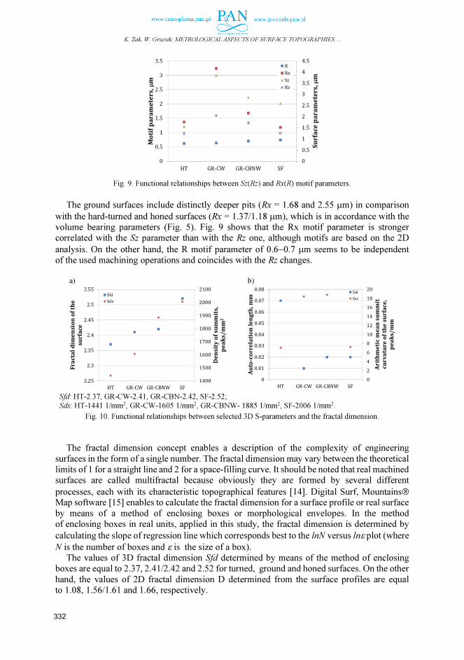
K. Żak, W. Grzesik: METROLOGICAL ASPECTS OF SURFACE TOPOGRAPHIES …
Fig. 9. Functional relationships between Sz(Rz) and Rx(R) motif parameters.
The ground surfaces include distinctly deeper pits (Rx = 1.68 and 2.55 µm) in comparison
with the hard-turned and honed surfaces (Rx = 1.37/1.18 µm), which is in accordance with the volume bearing parameters (Fig. 5). Fig. 9 shows that the Rx motif parameter is stronger correlated with the Sz parameter than with the Rz one, although motifs are based on the 2D
analysis. On the other hand, the R motif parameter of 0.6−0.7 µm seems to be independent of the used machining operations and coincides with the Rz changes.
a)
b)
Sfd: HT-2.37, GR-CW-2.41, GR-CBN-2.42, SF-2.52;
Sds: HT-1441 1/mm2, GR-CW-1605 1/mm2, GR-CBNW- 1885 1/mm2, SF-2006 1/mm2.
Fig. 10. Functional relationships between selected 3D S-parameters and the fractal dimension.
The fractal dimension concept enables a description of the complexity of engineering
surfaces in the form of a single number. The fractal dimension may vary between the theoretical limits of 1 for a straight line and 2 for a space-filling curve. It should be noted that real machined surfaces are called multifractal because obviously they are formed by several different
processes, each with its characteristic topographical features [14]. Digital Surf, Mountains Map software [15] enables to calculate the fractal dimension for a surface profile or real surface
by means of a method of enclosing boxes or morphological envelopes. In the method of enclosing boxes in real units, applied in this study, the fractal dimension is determined by
calculating the slope of regression line which corresponds best to the lnN versus lnε plot (where
N is the number of boxes and ε is the size of a box). The values of 3D fractal dimension Sfd determined by means of the method of enclosing
boxes are equal to 2.37, 2.41/2.42 and 2.52 for turned, ground and honed surfaces. On the other
hand, the values of 2D fractal dimension D determined from the surface profiles are equal to 1.08, 1.56/1.61 and 1.66, respectively.
0
0.5
1
1.5
2
2.5
3
3.5
4
4.5
0
0.5
1
1.5
2
2.5
3
3.5
HT GR-CW GR-CBNW SF
Su
rfa
ce
pa
ra
me
ter
s, µ
m
Mo
tif
pa
ra
me
ter
s, µ
m
R
Rx
Sz
Rz
1400
1500
1600
1700
1800
1900
2000
2100
2.25
2.3
2.35
2.4
2.45
2.5
2.55
HT GR-CW GR-CBNW SF
De
ns
ity
of
su
mm
its,
pe
ak
s/
mm
2
Fra
cta
l d
ime
nsi
on
of
the
surf
ace
Sfd
Sds
0
2
4
6
8
10
12
14
16
18
20
0
0.01
0.02
0.03
0.04
0.05
0.06
0.07
0.08
HT GR-CW GR-CBNW SF
Ar
ith
me
tic
me
an
su
mm
it
cu
rv
atu
re o
f th
e s
ur
fac
e,
pe
ak
s/m
m
Au
to-c
or
rela
tio
n l
en
gth
, mm
Sal
Ssc
332
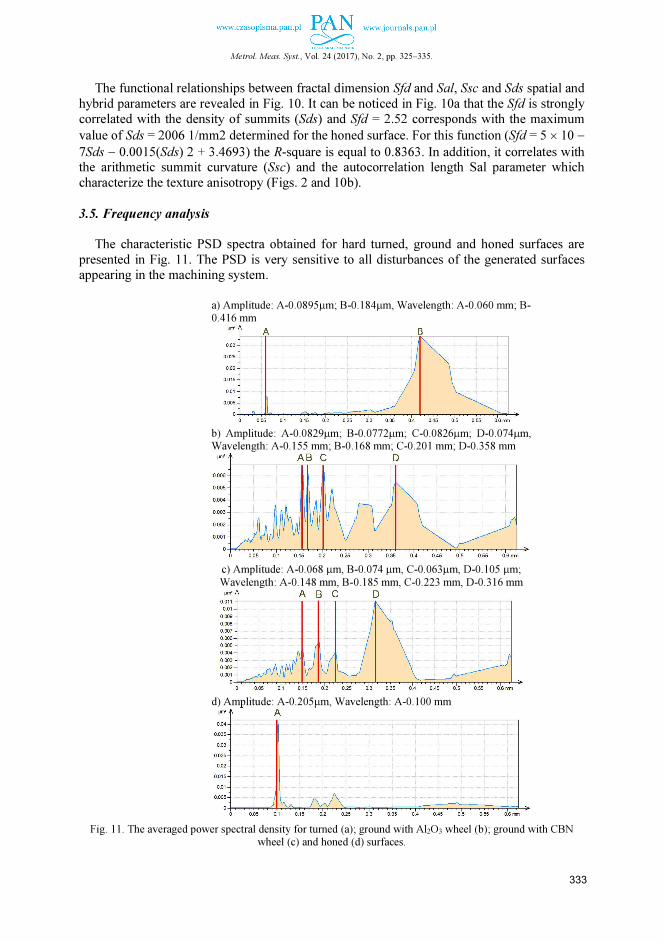
Metrol. Meas. Syst., Vol. 24 (2017), No. 2, pp. 325–335.
The functional relationships between fractal dimension Sfd and Sal, Ssc and Sds spatial and
hybrid parameters are revealed in Fig. 10. It can be noticed in Fig. 10a that the Sfd is strongly correlated with the density of summits (Sds) and Sfd = 2.52 corresponds with the maximum
value of Sds = 2006 1/mm2 determined for the honed surface. For this function (Sfd = 5 × 10 −
7Sds − 0.0015(Sds) 2 + 3.4693) the R-square is equal to 0.8363. In addition, it correlates with the arithmetic summit curvature (Ssc) and the autocorrelation length Sal parameter which
characterize the texture anisotropy (Figs. 2 and 10b).
3.5. Frequency analysis
The characteristic PSD spectra obtained for hard turned, ground and honed surfaces are
presented in Fig. 11. The PSD is very sensitive to all disturbances of the generated surfaces appearing in the machining system.
a) Amplitude: A-0.0895µm; B-0.184µm, Wavelength: A-0.060 mm; B-
0.416 mm
b) Amplitude: A-0.0829µm; B-0.0772µm; C-0.0826µm; D-0.074µm, Wavelength: A-0.155 mm; B-0.168 mm; C-0.201 mm; D-0.358 mm
c) Amplitude: A-0.068 µm, B-0.074 µm, C-0.063µm, D-0.105 µm;
Wavelength: A-0.148 mm, B-0.185 mm, C-0.223 mm, D-0.316 mm
d) Amplitude: A-0.205µm, Wavelength: A-0.100 mm
Fig. 11. The averaged power spectral density for turned (a); ground with Al2O3 wheel (b); ground with CBN
wheel (c) and honed (d) surfaces.
333

K. Żak, W. Grzesik: METROLOGICAL ASPECTS OF SURFACE TOPOGRAPHIES …
It is evident from Fig. 11a that the PSD spectrum contains only one low-frequency
component with the same wavelength as the feed rate of 0.06 mm (60 µm) and the amplitude
of 0.09 µm. On the other hand (Figs. 11b and 11c), the ground surfaces contain several
components with longer wavelengths but distinctly lower amplitudes of 0.04−0.07 µm than the
hard-turned surfaces. In particular, very small amplitudes of about 0.07 µm were recorded for the surfaces produced by grinding using a CBN wheel (Fig. 11c). On the other hand, the highest
amplitude of about 0.2 µm appeared during the honing operation which was performed on
a conventional lathe.
4. Conclusions
1. Distinct changes of topographical features of machined surfaces produced by different
cutting and abrasive processes are revealed using both standardized and non-standardized measuring techniques. According to the engineering knowledge this enables to generate
surfaces with desired functional properties, for instance with required bearing or locking properties, resistance to abrasive wear, fluid retention capability, fatigue and contact strength, depending on their engineering applications.
2. Precision grinding and super-finish operations cause that successively more material is concentrated in the vicinity of surface peaks. For these cases the ADF function has
a symmetrical shape with a large kurtosis and/or a large skew. 3. Comparing surface topographies using the autocorrelation operator indicates their strong
anisotropy and the necessity of 3D measurement. 4. 3D bearing area curves and appropriate functional parameters suggest, according to [13],
that the ground hard surfaces have enhanced fluid retention abilities. This is due to a large
negative Ssk value and higher Vvv volumes for ground textures. 5. The hard turned and CBN-ground textures have comparable Vmp and Spk parameter values
and similar tribological properties. According to the engineering practice demonstrated in [12] and [13] the best tribological performance of the honed surface is due to minimum Vmp and Spk values.
6. The fractal dimension Sdf correlates well with the density of summits. Because a higher value of the Sdf parameter denotes a large surface area (a larger Sdr parameter), a possible
consequence should be that in such a case the normal contact pressure decreases and the wear rate decreases with increasing the Sdf value.
7. The PSD charts enable directly to recognize a possible influence of the machining system
stability on the surface texture and, as a result, also to eliminate inconvenient machining conditions causing excessive vibrations.
List of abbreviations
GR − grinding
HT − hard turning
SF − super finishing
S-parameters − Surface-parameters
V-parameters – Volume-parameters
ACF − autocorrelation function
ADF − amplitude density function
BAC − bearing area (material ratio) curve
CBN − cubic boron nitride
MRR – machining removal rate
334

Metrol. Meas. Syst., Vol. 24 (2017), No. 2, pp. 325–335.
PCD − polycrystalline diamond
PSD − power spectral density AACF – autocorrelation function
GR-CW − grinding (GR) using conventional wheel (CW)
GR-CBNW − grinding (GR) using CBN wheel (CBNW)
HT/GR-CW − hard turning/grinding using conventional wheel sequential process HT/ GR-CBNW – hard turning/ grinding using CBN wheel sequential process
References
[1] Jiang, X.Jm, Whitehouse, D.J. (2012). Technological shifts in surface metrology. CIRP Annals-Manuf.
Technol., 61(2), 815−836.
[2] Leach, R. (ed.) (2013). Characterization of areal surface texture. Berlin, Springer-Verlag.
[3] Grzesik, W. (2008). Advanced machining processes of metallic materials. Elsevier, Amsterdam.
[4] Klocke, F. (2011). Manufacturing processes 1. Cutting, Berlin, Springer.
[5] König, W., Berktold, A., Koch, K.F. (1993). Turning versus grinding- a comparison of surface integrity
aspects and attainable accuracies. CIRP Annals-Manuf. Technol., 42(1), 39−43.
[6] Davim, J.P. (ed.) (2011). Machining of hard materials. London, Springer.
[7] Klocke, F., Brinksmeier, E., Weinert, K. (2005). Capability profile of hard cutting and grinding processes.
CIRP Annals-Manuf. Technol., 54(2), 557−580.
[8] Grzesik, W., (2016). Prediction of the functional performance of machined components based on surface
topography: a survey. J. Mater. Eng. Perf., 25(10), 4460−4468.
[9] Waikar, R.A., Guo, Y.B. (2008). A comprehensive characterization of 3D surface topography induced by
hard turning versus grinding. J. Mat. Proc. Technol., 197, 189−199.
[10] Grzesik, W., Rech, J., Wanat, T. (2007). Surface finish on hardened bearing steel parts produced by superhard
and abrasive tools. Int. J. Mach. Tools and Manuf., 47, 255−262.
[11] ISO 25178, part 2 (2012), Geometrical product specification (GPS)− surface texture: areal. Terms, definitions and surface texture parameters, ISO.
[12] Digital Surf, Mountains Map software, www. digitalsurf.com.
[13] Griffiths, B. (2001). Manufacturing surface technology. Surface integrity and functional performance.
London, Penton Press.
[14] Dietzsch, M., Papenfuss, K., Hartman, T. (1998). The MOTIF-method (ISO 12085)- a suitable description
for functional, manufactural and metrological requirements. Int. J. Mach. Tools and Manuf., 38, 625−632.
[15] Thomas, T.R., (1999). Rough Surfaces. London, Imperial College Press.


Metrol. Meas. Syst., Vol. 24 (2017), No. 2, pp. 337–346.
_____________________________________________________________________________________________________________________________________________________________________________________
Article history: received on Oct. 14, 2016; accepted on Jan. 21, 2017; available online on Jun. 30, 2017; DOI: 10.1515/mms-2017-0030.
METROLOGY AND MEASUREMENT SYSTEMS
Index 330930, ISSN 0860-8229
www.metrology.pg.gda.pl
RAPID DESIGN OPTIMIZATION OF MULTI-BAND ANTENNAS BY MEANS
OF RESPONSE FEATURES
Sławomir Kozieł, Adrian Bekasiewicz
Reykjavik University, School of Science and Engineering, Menntavegur 1, 101 Reykjavik, Iceland ([email protected], [email protected], +354 599 6886)
Abstract
This work examines the reduced-cost design optimization of dual- and multi-band antennas. The primary challenge is independent yet simultaneous control of the antenna responses at two or more frequency bands. In order to
handle this task, a feature-based optimization approach is adopted where the design objectives are formulated on
the basis of the coordinates of so-called characteristic points (or response features) of the antenna response. Due to
only slightly nonlinear dependence of the feature points on antenna geometry parameters, optimization can be
attained at a low computational cost. Our approach is demonstrated using two antenna structures with the optimum
designs obtained in just a few dozen of EM simulations of the respective structure.
Keywords: antenna design, antenna measurements, computer-aided design, surrogate modelling, feature-based
optimization.
© 2017 Polish Academy of Sciences. All rights reserved
1. Introduction
Contemporary antenna engineering heavily relies on full-wave electromagnetic (EM) analysis. EM solvers offer accurate performance analysis, as well as account for interactions
of the structure with environmental components (e.g. connectors, housing) [1, 2]. However, EM simulations tend to be expensive, especially for complex structures, so that their use in automated design, e.g. parametric optimization, may be impractical [3]. EM-driven design becomes even
more challenging in the case of multi-objective design (e.g. antenna size vs. electrical performance) [4, 5] or in the case of dual- and multi-band antennas, where requirements on the
reflection response have to be satisfied for several frequency bands of interest [6, 7]. Traditional methods involving parameter sweeps become problematic in such cases, especially for compact antennas with considerable EM cross-couplings, that make independent control of frequency
bands difficult [8]. Computationally efficient EM-driven design of antennas can be achieved by means
of surrogate-based optimization (SBO) methods [9, 10]. SBO involving physics-based surrogates are particularly promising due to combining the speed of the underlying low-fidelity
model and reasonable accuracy obtained by applying suitable correction techniques. The low-fidelity models are typically obtained from coarse-discretization EM simulations. The popular methods for surrogate construction include space mapping [10], frequency scaling [10], shape-
preserving response prediction [11], adaptive response correction [12], manifold mapping [13], and adaptively adjusted design specifications [14]. Combining physics-based modelling with
data-driven modelling may also produce promising results [1, 5]. In terms of conventional optimization methods, only gradient-based search seems to ensure comparable efficiency if derivative data are obtained through cheap adjoint sensitivities [15, 16].
Recently, feature-based optimization (FBO) has been proposed for the design of microwave filters [17], where the original design problem is reformulated in a so-called feature space,

S. Koziel, A. Bekasiewicz: RAPID DESIGN OPTIMIZATION OF MULTI-BAND …
leading to a less nonlinear functional landscape to be optimized compared with the original
formulation (typically, w.r.t. S-parameters versus frequency). This work is based on our original conference publication of [18], where FBO concept has been adopted for the design of dual-band antennas. Here, we reformulate the considered framework to allow for optimization
of multi-band structures.". We demonstrate that reformulating the antenna design task with the use of suitably defined features leads to considerable simplifications, so that the optimization
process can be accomplished at a much lower computational cost compared with that of conventional algorithms. Two application examples are provided. Numerical results are supported by experimental verification of the fabricated antenna prototypes.
2. Feature-based optimization for multi-band antennas
The purpose of this section is to formulate a feature-based optimization algorithm for multi-
band antenna design. There are several challenges that need to be addressed, such as highly nonlinear responses, multiple objectives (in particular, independent control of several operating
frequencies), but also a large number of adjustable geometry parameters of the antenna at hand.
2.1. Response features of dual-band antennas
Figure 1 shows typical responses of a dual-band antenna and, more importantly, their changes
resulting from modification of the antenna geometry (the responses correspond to the example considered in Section 3.1). The responses are evaluated along a selected line segment in the design
space defined as y(t) = t⋅y1 + (1 – t)⋅y2, where 0 ≤ t ≤ 1, whereas y1 and y2 are the two reference
designs. High nonlinearity and considerable variability of the responses can be observed. Fig. 2 shows changes of the response features, here selected as the minima of the reflection responses (i.e. the points corresponding to the antenna resonances) and the point corresponding to –10 dB
reflection levels. Each point is described by its two coordinates (frequency and level). Note that, despite of a high nonlinearity of the reflection response, the behavior of the feature points is close
to linear. Consequently, expressing the design goals based on the feature points and using feature-based surrogates, the optimization process is expected to be considerably speeded up .
2.2. Antenna design in feature space
The original design problem (in S-parameter vs. frequency domain) is formulated as: * argmin ( ( ))=
x
x R xU , (1)
where U is an objective function defined with the EM model response, i.e. S11 versus frequency.
Fig. 1. A family of dual-band responses corresponding to their geometries along a certain line segment in the design
space showing highly nonlinear dependence of the reflection characteristic on the geometry variables
of the structure.
3 3.5 4 4.5 5 5.5 6-25
-20
-15
-10
-5
0
Frequency [GHz]
|S11|
338
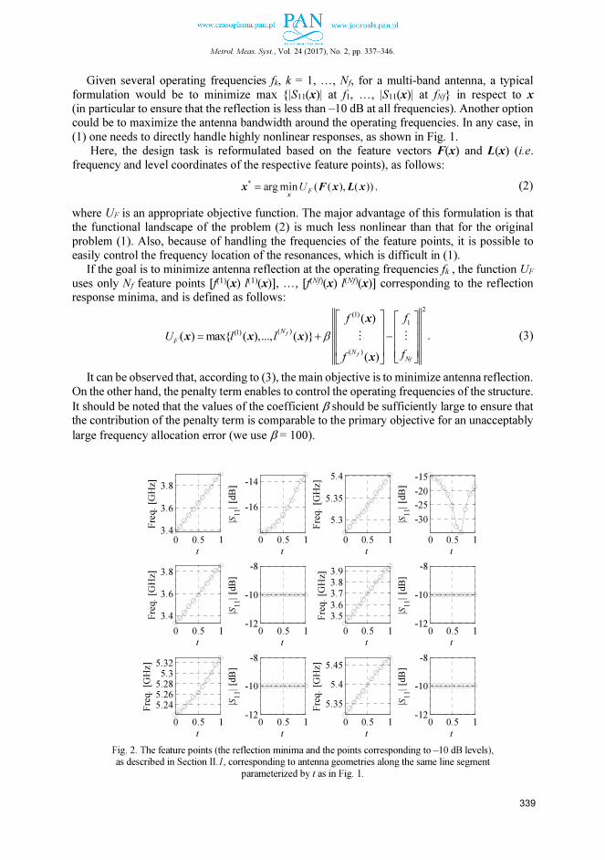
Metrol. Meas. Syst., Vol. 24 (2017), No. 2, pp. 337–346.
Given several operating frequencies fk, k = 1, …, Nf, for a multi-band antenna, a typical
formulation would be to minimize max |S11(x)| at f1, …, |S11(x)| at fNf in respect to x (in particular to ensure that the reflection is less than –10 dB at all frequencies). Another option could be to maximize the antenna bandwidth around the operating frequencies. In any case, in
(1) one needs to directly handle highly nonlinear responses, as shown in Fig. 1. Here, the design task is reformulated based on the feature vectors F(x) and L(x) (i.e.
frequency and level coordinates of the respective feature points), as follows:
* argmin ( ( ), ( ))=
x
x F x L xF
U , (2)
where UF is an appropriate objective function. The major advantage of this formulation is that the functional landscape of the problem (2) is much less nonlinear than that for the original
problem (1). Also, because of handling the frequencies of the feature points, it is possible to easily control the frequency location of the resonances, which is difficult in (1).
If the goal is to minimize antenna reflection at the operating frequencies fk , the function UF
uses only Nf feature points [f(1)(x) l(1)(x)], …, [f(Nf)(x) l(Nf)(x)] corresponding to the reflection response minima, and is defined as follows:
2(1)
1
( )(1)
( )
( )
( ) max ( ),..., ( )
( )
β
= + −
x
x x x
x
⋮ ⋮f
ff
N
F
N
N
ff
U l l
ff
. (3)
It can be observed that, according to (3), the main objective is to minimize antenna reflection.
On the other hand, the penalty term enables to control the operating frequencies of the structure.
It should be noted that the values of the coefficient β should be sufficiently large to ensure that the contribution of the penalty term is comparable to the primary objective for an unacceptably
large frequency allocation error (we use β = 100).
Fig. 2. The feature points (the reflection minima and the points corresponding to –10 dB levels),
as described in Section II.1, corresponding to antenna geometries along the same line segment
parameterized by t as in Fig. 1.
0 0.5 1
3.4
3.6
3.8
t
Fre
q.
[GH
z]
0 0.5 1
-16
-14
t
|S11|
[dB
]
0 0.5 1
5.3
5.35
5.4
t
Fre
q.
[GH
z]
0 0.5 1
-30
-25
-20
-15
t
| S11|
[dB
]
0 0.5 1
3.4
3.6
3.8
t
Fre
q.
[GH
z]
0 0.5 1-12
-10
-8
t
|S11|
[dB
]
0 0.5 1
3.5
3.6
3.7
3.8
3.9
t
Fre
q.
[GH
z]
0 0.5 1-12
-10
-8
t
| S11|
[dB
]
0 0.5 1
5.24
5.26
5.28
5.3
5.32
t
Fre
q.
[GH
z]
0 0.5 1-12
-10
-8
t
|S11|
[dB
]
0 0.5 1
5.35
5.4
5.45
t
Fre
q.
[GH
z]
0 0.5 1-12
-10
-8
t
| S11|
[dB
]
339

S. Koziel, A. Bekasiewicz: RAPID DESIGN OPTIMIZATION OF MULTI-BAND …
2.3. Optimization algorithm The problem (2) is solved iteratively as:
( ) ( )
( 1) ( ) ( )
|| ||arg min ( ( ), ( ))+
− ≤
=
x x
x F x L xi i
i i i
F S Sr
U , (4)
where x(i), i = 0, 1, …, is a sequence approximating x*, whereas FS(i) and LS
(i) are linear approximation models of the feature point vectors F(x) and L(x) determined in the current design x(i). Finite differentiation is used to establish the models with n perturbed designs around
x(i), i.e., x(i) + hk, k = 1, …, n, where hk = [0 … 0 dk 0 … 0]T, dk > 0 [19], and the corresponding feature points F(x(i) + hk), L(x(i) + hk) are extracted from the respective antenna responses. We
have:
( ) ( )
1 1
( ) ( ) ( )
( ) ( )
[ ( ) ( )] /
( ) ( ) ... ( )
[ ( ) ( )] /
+ −
= + ⋅ − + −
F x h F x
F x F x x x
F x h F x
Ti i T
i i i
S
i i T
n n
d
d
, (5)
( ) ( )
1 1
( ) ( ) ( )
( ) ( )
[ ( ) ( )] /
( ) ( ) ... ( )
[ ( ) ( )] /
+ −
= + ⋅ − + −
L x h L x
L x L x x x
L x h L x
Ti i T
i i i
S
i i T
n n
d
d
. (6)
The algorithm (4) is embedded in a trust-region framework with the search radius r(i) updated using standard rules [19].
3. Verification examples
In this section, the considered feature-based method for fast design of multi-band antennas is verified. Two design examples are considered: a dual-band patch antenna with 8 design variables and a triple-band uniplanar dipole with 10 adjustable parameters. For the latter
structure, the numerical results are supported with measurements of the fabricated antenna prototypes.
3.1. Dual-band patch antenna
Our first example is concerned with verification of a dual-band planar antenna shown in Fig. 3 [20]. The structure consists of two radiating elements in the form of a quasi-micro-strip patch
with an inset feed and a monopole radiator, both connected in a cascade. The antenna is excited through a 50 ohm microstrip line. The lower and upper resonant frequencies are introduced by the monopole and the patch, respectively. The ground plane is trimmed below the patch
component to increase the number of degrees of freedom (hence, it is referred to as a quasi-micro-strip patch).
The antenna is constructed on a 0.762 mm thick Taconic RF-35 dielectric substrate with a relative permittivity of 3.5 and a loss tangent of 0.0018. The design variables are x = [L l1 l2 l3
W w1 w2 g]T. The parameters o = 7, w0 = 1.7, l0 = 10, and s = 0.5 are fixed. The unit for all parameters is mm. The lower and upper bounds for the parameters are l = [10 1 5 1 4 0.2 1 –4]T and u = [20 6 17 7 16 4 6 6]T, respectively. Note that negative g results in trimming ground
plane below the patch component of the radiator The EM antenna model R is implemented in CST Microwave Studio and contains
~1,900,000 hexahedral mesh cells. Its average simulation time on a dual Xeon E5540 machine with 6 GB RAM is 12 minutes.
340

Metrol. Meas. Syst., Vol. 24 (2017), No. 2, pp. 337–346.
Two cases were considered regarding the design requirements:
− Case I: operating frequencies 3.5 GHz and 5.3 GHz; − Case II: operating frequencies 2.4 GHz and 4.8 GHz.
In both cases, the goal is to allocate the resonances at the respective operating frequencies and
to minimize reflection at these frequencies. The initial design is xinit = [17.0 1.8 11.7 4.1 12.9 0.7 1.3 0.2]T mm. As shown in Fig. 4, this design is poor and very far from satisfying design
specifications in both considered cases. More importantly, as the reflection response is flat and close to zero in the initial design in the vicinity of the operating frequencies, local optimization would be stuck in the initial design when the original formulation of the problem is considered
(cf. (1)). This was verified using a pattern-search algorithm [21]. Consequently, global optimization methods would have to be used with an associated very high computational cost.
Figure 4 shows the antenna responses in the initial and in the final design x*I = [17.17 2.19 13.20 5.00 12.78 0.94 4.00 2.62]T mm found by FBO. Note that the design quality is very good with the resonances well centred at the operating frequencies of interest and with the reflection levels
< – 25 dB. The optimization cost was 72 evaluations of the EM model (8 algorithm iterations), which is
low, given the complexity of the problem and the fact that FBO is a derivative-free method. Local optimization working for the original formulation of the problem failed to find an acceptable design.
Figure 5 shows the results for Case II. The optimum design is x*II = [17.64 2.89 13.84 6.90
13.55 0.20 5.03 4.09]T mm, and it was obtained at the cost of 90 evaluations of the EM antenna model (10 algorithm iterations). Again, the design quality is very good with resonances centred
at the operating frequencies and the reflection minima below –30 dB. Note that the optimum design is at a considerable distance from the initial one (response-wise). If the optimization starts from x*I, a solution comparable to x*II is obtained in just four iterations.
Fig. 3. The dual-band patch antenna geometry [20]. The ground plane is marked using the lighter shade of grey.
Fig. 4. The optimization results, Case I. Antenna responses in the initial design (- - -) and in the design found
by the feature-based optimization algorithm (—).
L
l1
l2
l3
W
w1
w2
o
g
s
w0
l0
o
1 2 3 4 5 6 7-30
-20
-10
0
Frequency [GHz]
|S11| [d
B]
341

S. Koziel, A. Bekasiewicz: RAPID DESIGN OPTIMIZATION OF MULTI-BAND …
Fig. 5. The optimization results, Case II. Antenna responses in the initial design (- - -) and in the design
found by the feature-based optimization algorithm (—).
3.2. Triple-band planar dipole antenna
Our second example is a triple-band uniplanar dipole antenna shown in Fig. 6. The structure
is based on the geometry introduced in [22]. The used substrate is a 0.762 mm thick Taconic RF-35 (see Section 3.1). The antenna is constructed as a stack of three narrow, long ground
plane slits separated by two thicker, short slots. The radiator is fed through a 50 ohm coplanar waveguide (CPW). The vector of adjustable parameters is x = [l1 l2 l3 l4 l5 w1 w2 w3 w4 w5]T, whereas dimensions l0 = 30, w0 = 3, s0 = 0.15 and o = 5 remain fixed. The unit for all geometric
parameters is mm. The search space is defined using the following lower and upper bounds: l = [30 5 22 5 15 0.2 1.2 0.2 1.2 0.2]T and u = [50 15 29 15 21 2.2 4.2 2.2 4.2 2.2]T. The EM
antenna model R (~100,000 cells; simulation: 6 min) is prepared in CST Microwave Studio and simulated using its time domain solver.
Two sets of design specifications are considered:
− Case I: operating frequencies: 2.45 GHz, 3.65 GHz, and 5.77 GHz; − Case II: operating frequencies: 1.85 GHz, 2.95 GHz, and 5.15 GHz.
Similarly to Section 3.1, the goal of the optimization was to minimize the antenna reflection for the selected operating frequencies. The initial design parameters are xinit = [36 14 26 12 20
1 3 1 2 1]T mm. As it can be seen from Fig. 7, the initial design is closer to the desired specifications compared with the example discussed in Section 3.1. Consequently, for the Case I, the original formulation of the design problem given by (1) can be used to find the
desired design solution using a local search algorithm (here, the pattern-search one). However, for the Case II, the algorithm was stuck at the local minimum which was away from the desired
solution. For Case I, the comparison of the antenna responses in the initial design and in the design
optimized using the feature-based method is shown in Fig. 7. The final vector of parameters is
x*I = [39.04 14.99 28.26 12.26 18.91 1.20 1.2 0.2 1.35 0.77]T. It should be noted that the structure response is well centred at the chosen operating frequencies with the reflection levels
below –22 dB. The cost of the algorithm operation was 130 evaluations of the antenna model (12 iterations).
At the same time, the pattern-search algorithm required 278 EM simulations to obtain a similar
antenna solution. Thus, for the considered case, the numerical cost of pattern-search optimization is almost 50 percent higher than that of FBO.
For Case II, the vector of optimal parameters is: x*II = [45.28 9.48 28.99 10.63 19.29 1.45 3.55 0.62 1.68 0.43]T. The frequency characteristics of the structure in the initial and optimized design are compared in Fig. 8. Again, the antenna features good electrical performance at the
selected operating frequencies with the reflection level below –12 dB. The numerical cost of the design process is 100 evaluations of the EM antenna model (9
iterations). Having in mind noticeable distance of the first two operating frequencies from the initial design, the cost is very low.
1 2 3 4 5 6 7-30
-20
-10
0
Frequency [GHz]|S11| [d
B]
342

Metrol. Meas. Syst., Vol. 24 (2017), No. 2, pp. 337–346.
Fig. 6. The triple-band dipole antenna geometry with highlighted design parameters.
Fig. 7. The triple-band dipole antenna optimization results: Case I. Antenna responses in the initial design (- - -)
and in the design found by the feature-based optimization algorithm (—).
Fig. 8. The triple-band dipole antenna optimization results: Case II. Antenna responses in the initial design (- - -)
and in the design found by the feature-based optimization algorithm (—).
The results obtained for both antenna designs have been experimentally validated.
Photographs of the fabricated structures are shown in Fig. 9, whereas Fig. 10 presents comparison of their simulated and measured reflection characteristics. For Case I, the measured
lowest operating frequency is slightly shifted down by about 50 MHz. Nonetheless, the remaining bands are well aligned. For Case II (Fig. 10(b)), the measured bandwidth is slightly broader around the second operating frequency compared with the simulated one.
The difference, however, is only about 60 MHz. Generally, the results are in a good agreement. Small discrepancies between the simulated and measured responses are due to the use of a
simplified antenna EM model without an EM connector. The latter has been excluded from simulations in order to reduce the computational cost of the optimization process.
l1
l2
l3
l4
l5
w1
w2
w3
w4
w5
l0
w0
s0
1 2 3 4 5 6 7 8-25
-20
-15
-10
-5
0
Frequency [GHz]
| S11| [d
B]
1 2 3 4 5 6 7 8-25
-20
-15
-10
-5
0
Frequency [GHz]
| S11| [d
B]
343

S. Koziel, A. Bekasiewicz: RAPID DESIGN OPTIMIZATION OF MULTI-BAND …
Fig. 9. Photographs of the fabricated dipole antenna prototypes: Case I (top), and Case II (bottom).
a)
b)
Fig. 10. Comparison of the simulated (– –) and measured (––) reflection characteristics obtained
for the triple-band dipole antenna: Case I (a); and Case II (b).
4. Conclusion
Rapid and precise design optimization of dual- and multi-band antennas has been presented. The key component of the optimization procedure that ensures its computational efficiency is
reformulation of the design problem in a feature space of suitably-defined characteristic points, where the objectives are less nonlinear functions of the geometry parameters of the antenna (as compared with the original formulation, typically, in the space of S-parameters versus
frequency). This enables to yield the optimized design at a low cost corresponding to just a few dozen of EM simulations. Working examples of a dual- and triple-band antennas as well as
their experimental verification confirm validity of the proposed approach. Our further work will
1 2 3 4 5 6 7 8-25
-20
-15
-10
-5
0
Frequency [GHz]
| S11| [
dB
]
1 2 3 4 5 6 7 8-25
-20
-15
-10
-5
0
Frequency [GHz]
| S11| [d
B]
344

Metrol. Meas. Syst., Vol. 24 (2017), No. 2, pp. 337–346.
focus on application to the method for other multi-band microwave structures, such as filters,
couplers or power dividers.
Acknowledgement
The authors would like to thank Computer Simulation Technology AG, Darmstadt,
Germany, for making CST Microwave Studio available. This work is partially supported by the Icelandic Centre for Research (RANNIS) Grants 141272051, 163299051 and by National Science Centre of Poland Grant 2014/15/B/ST7/04683.
References
[1] Bekasiewicz, A., Koziel, S. (2015). Structure and computationally-efficient simulation-driven design
of compact UWB monopole antenna. IEEE Ant. Wireless Prop. Lett., 14, 1282−1285.
[2] Koziel, S., Ogurtsow, S., Zieniutycz, W., Bekasiewicz, A. (2015). Design of a planar UWB dipole antenna
with an integrated balun using surrogate-based optimization. IEEE Ant. Wireless Prop. Lett., 14, 366−369.
[3] Lizzi, L., Viani, F., Azaro, R., Massa, A. (2007). Optimization of a spline-shaped UWB antenna by PSO.
IEEE Ant. Wireless Prop. Lett., 6, 182−185.
[4] Chamaani, S., Abrishamian, M.S., Mirtaheri, S.A. (2010). Time-domain design of UWB Vivaldi antenna
array using multiobjective particle swarm optimization. IEEE Ant. Wireless Prop. Lett., 9, 666−669.
[5] Koziel, S., Bekasiewicz, A. (2015). Fast multi-objective optimization of narrow-band antennas using RSA
models and design space reduction. IEEE Ant. Wireless Prop. Lett., 14, 450−453.
[6] Bod, M., Hassani, H.R., Taheri, M.M.S. (2012). Compact UWB printed slot antenna with extra Bluetooth,
GSM, and GPS bands. IEEE Ant. Wireless Prop. Lett., 11, 531−534.
[7] Liu, Y.F., Wang, P., Qin, H. (2014). Compact ACS-fed UWB monopole antenna with extra Bluetooth band.
Electronics Lett., 50(18), 1263−1264.
[8] Wang, L., Xu, L., Chen, X., Yang, R., Han, L., Zhang, W. (2014). A compact ultrawideband diversity antenna
with high isolation. IEEE Ant. Wireless Prop. Lett., 13, 35−38.
[9] Queipo, N.V., Haftka, R.T., Shyy, W., Goel, T., Vaidynathan, R., Tucker, P.K. (2005). Surrogate-based
analysis and optimization. Prog. Aerospace Sci., 41(1), 1−28.
[10] Bandler, J.W., Cheng, Q.S., Dakroury, S.A., Mohamed, A.S., Bakr, M.H., Madsen, K., Søndergaard, J.
(2004). Space mapping: the state of the art. IEEE Trans. Microwave Theory Tech., 52(1), 337−361.
[11] Koziel, S., Ogurtsov, S., Szczepanski, S. (2012). Rapid antenna design optimization using shape-preserving
response prediction. Bulletin of the Polish Academy of Sciences. Tech. Sci., 60, 143−149.
[12] Koziel, S., Bandler, J.W., Madsen, K. (2005). Towards a rigorous formulation of the space mapping
technique for engineering design. IEEE Int. Symp. Circuits Syst., 6, 5605−5608.
[13] Koziel, S., Leifsson, L., Ogurtsov, S. (2013). Reliable EM-driven microwave design optimization using
manifold mapping and adjoint sensitivity. Microwave Opt. Tech. Lett., 55, 809−813.
[14] Koziel, S., Ogurtsov, S. (2013). Rapid optimization of omnidirectional antennas using adaptively adjusted
design specifications and kriging surrogates. IET Microwaves, Ant. Prop., 7(15), 1194−1200.
[15] El Sabbagh, M.A., Bakr, M.H., Bandler, J.W. (2006). Adjoint higher order sensitivities for fast full-wave
optimization of microwave filters. IEEE Trans. Microw Theory Tech., 54, 3339−3351.
[16] Koziel, S., Bekasiewicz, A. (2015). Fast EM-driven size reduction of antenna structures by means of adjoint
sensitivities and trust regions. IEEE Ant. Wireless Prop. Lett., 14, 1681−1684
[17] Koziel, S., Bandler, J.W. (2015). Rapid yield estimation and optimization of microwave structures exploiting
feature-based statistical analysis. IEEE Trans. Microwave Theory Tech., 63(1), 107−114.
[18] Koziel, S., Bekasiewicz, A., Leifsson, L. (2016). Expedited design of dual-band antennas using feature-based
optimization. European Conf. Ant. Prop., Davos, 1−4.
345

S. Koziel, A. Bekasiewicz: RAPID DESIGN OPTIMIZATION OF MULTI-BAND …
[19] Conn, A.R., Gould, N.I.M., Toint, P.L. (2000). Trust-region methods. MPS-SIAM Series on Optimization,
Philadelphia.
[20] Koziel, S., Bekasiewicz, A., Leifsson, L. (2016). Rapid EM-driven antenna dimension scaling through
inverse modeling. IEEE Ant. Wireless Prop. Lett., 15, 714−717.
[21] Kolda, T.G., Lewis, R.M., Torczon, V. (2003). Optimization by direct search: new perspectives on some
classical and modern methods. SIAM Review, 45(3), 385–482.
[22] Chen, Y.C., Chen, S.Y., Hsu, P. (2006). Dual-band slot dipole antenna fed by a coplanar waveguide. IEEE Int.
Symp. Ant. Prop., 3589−3592.

Metrol. Meas. Syst., Vol. 24 (2017), No. 2, pp. 347–356.
_____________________________________________________________________________________________________________________________________________________________________________________
Article history: received on Nov. 19, 2016; accepted on Jan. 14, 2017; available online on Jun. 30, 2017; DOI: 10.1515/mms-2017-0025.
METROLOGY AND MEASUREMENT SYSTEMS
Index 330930, ISSN 0860-8229 www.metrology.pg.gda.pl
NOVEL VARIABLE STRUCTURE MEASUREMENT SYSTEM
WITH INTELLIGENT COMPONENTS FOR FLIGHT VEHICLES
Kai Shen1,2), Maria S. Selezneva2), Konstantin A. Neusypin2), Andrey V. Proletarsky2)
1) Nanjing University of Science and Technology, School of Mechanical Engineering, Nanjing, 210094, P.R. China ( [email protected], +8 925 373 8978) 2) Bauman Moscow State Technical University, Faculty of Computer Science and Control Systems, Moscow, 105005, Russia ([email protected], [email protected], [email protected])
Abstract
The paper presents a method of developing a variable structure measurement system with intelligent components
for flight vehicles. In order to find a distinguishing feature of a variable structure, a numerical criterion for selecting
measuring sensors is proposed by quantifying the observability of different states of the system. Based on the Peter K. Anokhin’s theory of functional systems, a mechanism of “action acceptor” is built with intelligent components,
e.g. self-organization algorithms. In this mechanism, firstly, prediction models of system states are constructed
using self-organization algorithms; secondly, the predicted and measured values are compared; thirdly, an optimal
structure of the measurement system is finally determined based on the results of comparison. According to the
results of simulation with practical data and experiments obtained during field tests, the novel developed
measurement system has the properties of high-accuracy, reliable operation and fault tolerance.
Keywords: flight vehicle, variable structure measurement system, the degree of observability, self-organization
algorithm, integrated navigation system.
© 2017 Polish Academy of Sciences. All rights reserved
1. Introduction
Vehicles that are capable of sustained motion through air and space are termed as flight vehicles (FV), and they are generally classified as aircrafts, space-crafts and rockets. All flight
vehicles require manipulation (i.e. control or adjustment) of their position, velocity and orientation for efficient completion of flight missions based upon the measurement information about operation states [1]. However, in practice the measurement information is usually
disturbed by internal and external noise. Thus, in order to improve accuracy of on-board measurement systems, a novel design scheme is developed with intelligent components based
on the Peter K. Anokhin’s functional system theory [2, 3]. As we all know, on-board measurement systems usually consist of an inertial navigation
system (INS), a global navigation satellite system (GNSS), a ground-based radio navigation
system (GRNS), a terrain-referenced navigation system (TRNS), a continuous visual navigation system (CVNS) etc. [4]. The above mentioned systems are generally integrated using
Kalman filtering [4, 5] to fuse navigation information with different characteristics. However, the operability of those sensors varies all the time with changes of external environment.
For example, when our flight vehicles are working in a battlefield environment, it may be impossible to access the position, navigation, and timing (PNT) information with ordinary GNSS receivers. Therefore, the novel measurement system presented in this paper is designed
with a variable structure. To achieve this goal, some selection criteria of measurement information, e.g. a numerical criterion of the degree of observability (DoO), must be formulated
for time-varying conditions.

K. Shen, M. S. Selezneva, et al.: NOVEL VARIABLE STRUCTURE MEASUREMENT SYSTEM …
In addition, according to the Peter K. Anokhin functional system theory, a mechanism
of “acceptor of the results of action” [2] (or just “action acceptor”) is necessary for our new developed measurement system, because it can help us to select an optimal combination of measuring sensors and to determine a better measurement structure for a current working
period. To introduce this mechanism, self-organization algorithms (SOA) [6] functioning as an intelligent component are suggested to be put into use.
The paper is organized as follows. In Section 2, a methodology of quantitative observability analysis with the degree of observability, functioning as a kind of selection criterion of measurement information, is introduced for linear time-varying (LTV) systems. In Section 3,
self-organization algorithms used for constructing prediction models are briefly examined. In Section 4, an analytical methodology for optimizing system parameters and modelling
in synthesis of a measurement system is presented. In Section 5, a novel measurement system is developed on the basis of the Peter K. Anokhin’s functional system theory. In order to clearly demonstrate performance and effectiveness of the proposed measurement system, the results
of simulation using practical data and field test results are presented.
2. Measurement selection criterion and degree of observability
In this section, we are interested in finding a figure of merit for each state-variable that can
reflect how observable the state-variable is. A criterion having this function may be termed the numerical criterion of the degree of observability. Moreover, the degree of observability can
further serve as an indicator in selecting better measuring sensors for a current working period in formulating variable structure measurement systems [1]. As we have mentioned above, the external environment and internal system states are continuously changing in time.
Therefore, the system of interest is commonly expressed as a linear time-varying system:
, 1 1 1k k k k k− − −
= +x F x w , (1)
k k k k= +z H x v , (2)
where k
x is a vector of state; 1k−
w is a vector of input noise; k
z is a vector of measurement;
kv is a vector of measurement noise;
, 1k k−F is a state transfer matrix;
kH is a measurement
matrix.
We assume that the input 1k−
w and measurement k
v noise is the white Gaussian noise, and
there is no evident correlation between them, i.e. 0T
j kE = v w for any j and k .
In respect to the system represented by (1) and (2), a measurement kz may be reformulated
as follows [7]:
1 1 1, 1 1
1 1 1, 2 1, 1 1, 2 2, 1
1 2 1,
k k k k
k k k k k k k k
k n k n k n k n k k k k n k n k n k k k
k n k n k n
+ + + + +
+ − + − + − + − + + − + − + − + +
+ − + − + −
= +
= + +
= +
+ + +
⋯ ⋯ ⋯
⋯ ⋯
⋯
z H x v
z H F x H w v
z H F F x H F F w
H w v
(3)
where n is the order of the system. Then, we can rewrite the expression (3) in a matrix form as:
* *
k k k k= +z O x v , (4)
348

Metrol. Meas. Syst., Vol. 24 (2017), No. 2, pp. 347–356.
where 1*
1
...
k
k
k
k n
+
+ −
=
z
z
z
z
, 1 1,
1 1, 2 1,
k
k k k
k
k n k n k n k k
+ +
+ − + − + − +
=
H
H FO
H F F
⋯
⋯
;
1 1* 1
1 1, 2 2, 1 1 2 11
...
kk
k k kk
k
k n k n k n k k k k n k n k nk n
+
+
+ ++
+
+ − + − + − + + + − + − + −+ −
+ = =
+ + +
vv
H w vvv
H F F w H w vv
⋯ ⋯ ⋯
⋯ ⋯
.
A matrix k
O is termed the local observability matrix of an LTV system [8]. To examine
the local observability over a period from k to 1k n+ − , we can use as the observability rank
criterion being the local observability matrix k
O of rank n for the period, i.e.
krank n=O . (5)
Considering (4), we can step by step obtain a relationship of state-variables and measurement as:
T T T
k k k k k k k
∗ ∗
= +O z O O x O v , (6)
or
T T T
k k k k k k k
∗ ∗
= −O O x O z O v , (7)
then
1 1
T T T T
k k k k k k k k k
− −∗ ∗ = − x O O O z O O O v , (8)
and finally
† †
k k k k k
∗ ∗
= −x O z O v , (9)
where † means the Moore-Penrose pseudoinverse of matrix.
Let †
k k k
∗
=y O z , considering (4), we can obtain a scalar form of vector k
y as:
1, 2, 1 , 1
i i i i
k k k k k n k k ny a z a z a z
+ + −= + + +⋯ , (10)
where i
ky is the i-th component of vector
ky ,
,
( 1, , )i
j ka j n= ⋯ are time-varying elements of the
i-th row in the matrix †
kO .
Correspondingly, the measurement noise * † *
k k k=ς O v in a scalar form is:
*
1, 2, 1 , 1
i i i i
k k k k k n k k na v a v a vς
+ + +
+ + −= + + +⋯ , (11)
where *i
kς is the i-th component of vector *
kς .
Furthermore, the variance of measurement noise *i
kς may be expressed as:
( ) ( ) ( )2 2 2
*
1, 2, ,
i i i i
k k k n k kR a a a R
+ = + + + ⋯ , (12)
where k
R+ is the variance of direct measurement noise
kv+ .
Therefore, the degree of observability for an LTV system can be defined as [7]:
( )
( )
2
2*
i
ki
ki i
k
E x R
DE y R
+ =
. (13)
349

K. Shen, M. S. Selezneva, et al.: NOVEL VARIABLE STRUCTURE MEASUREMENT SYSTEM …
From (12), we know that the ratio of the variance values of measurement noise is ( )2
,
1
,
ni
j k
j
a
=
∑
thus we can rewrite (13) and finally obtain:
( )
( ) ( )
2
22
,
1
i
i
k ni i
j k
j
E x
D
E y a=
=
∑
. (14)
In practice, ( )2
iE x
and ( )2
iE y
in (14) are usually calculated as:
( ) ( )1
2 21k n
i i
l
l k
E x xn
+ −
=
= ∑
, (15)
( ) ( )1
2 21k n
i i
l
l k
E y yn
+ −
=
= ∑. (16)
It is apparent from (14) that the system parameters in the matrix , 1k k−
F have an indirect
influence on the degree of observability by the elements ,
( 1, , )i
j ka j n= ⋯ in the pseudoinverse
matrix of observability †
kO . In practical applications, this feature makes it possible to optimize
physical model parameters and to determine optimal variable structures for measurement
systems.
3. Algorithms for constructing prediction models
In order to guarantee high-precision selection and fusion of information, the mechanism of “action acceptor” is necessary in our novel variable structure measurement systems. In this mechanism, except for the application of the degree of observability, algorithms for
constructing prediction models are also required for further comparing the a posteriori and predicted information. From the results of comparison [2, 9], an optimal structure of the
measurement system can be finally determined for the current working period in accordance with the operation conditions of flight vehicles. In this section, we shall introduce some algorithms, e.g. self-organization algorithms, for constructing mathematical prediction models.
In general, we define a mathematical prediction model as:
( )1
,
L
k i i i k
i
M a f xµ
=
=∑ , (17)
where i
µ is a basic function from the function set s
F ( ) ( ), | 1, ,s i i i k
F a f x i Lµ= = ⋯ and ia is
an amplitude, if is a frequency, L is the number of basic functions.
As the basic functions, we usually select three types of functions to build mathematical prediction models owing to the dynamic features of flight vehicles. a) A linear trend (function) has a form:
( )ˆ ,L l l
k l l k k kx a b k t d= + , (18)
where ˆLkx is a predicted value, ,
l l
k kk d are a slope and a constant of the linear function, ,
l la b
are coordinates of the reference point.
b) A nonlinear harmonic trend (function) is:
( ) ( )ˆ sin cosN s s c c
k k k k k k k k kx A t B tω ϕ ω ϕ= + + + , (19)
where ˆNkx is a predicted value, , , , , ,
s c s c
k k k k k kA B ω ω ϕ ϕ are amplitudes, frequencies and phases
of the trigonometric functions.
350

Metrol. Meas. Syst., Vol. 24 (2017), No. 2, pp. 347–356.
c) A Modified Demark trend is expressed as:
1 1
ˆ ˆD D
k k kx x C
− −
= + , (20)
where ˆDkx is a predicted value and
1 1 1 1 1ˆ ˆ
L L N N
k k k k kC x xζ ζ
− − − − −
= +, (21)
where 1 1,
L N
k kζ ζ
− −
are weighing factors within a range from 0 to 1.
In order to find an optimal solution j
χ for mathematical prediction models, we would like
to introduce a quadratic criterion [10] with respect to the amplitude ia as:
( ) ( )1
22 , 2 , 0
k n
j i i j i i i j
j k
f x a f xχ µ µ
+ −
=
− + = ∑ . (22)
Then, we may differentiate it by the amplitude ia and obtain:
( )
( )
1
1
2
,
,
k n
j i i j
j k
i k n
i i j
j k
f x
a
f x
χ µ
µ
+ −
=
+ −
=
=
∑
∑. (23)
With (23) we can easily find a good optimal solution of prediction models based on the self-organization selection criteria [6]:
a) the minimum deviation criterion:
( )2
2 1
2
1
ˆ ˆ
min,
LP Q
i i
i
M L
i
i
x x
z
=
=
−
∆ = →
∑
∑ (24)
where ˆPix and ˆQ
ix designate two parts of a predicted value,
iz is a measurement value.
b) the regularity criterion:
( )2
2 1
2
1
ˆ
min
L
i i
i
R L
i
i
z x
z
=
=
−
∆ = →
∑
∑, (25)
where ˆix is a predicted value.
Based on the above-mentioned basic functions (18) ‒ (20), we can thus build some self-
organization algorithms by utilizing the self-organization selection criteria (24) and (25). One of the most effective algorithms is a so-called self-organization algorithm with redundant
trends, as shown in Fig. 1, where SC are selection criteria, C are competitive prediction models.
Fig. 1. A functional scheme of self-organization algorithm with redundant trends.
351
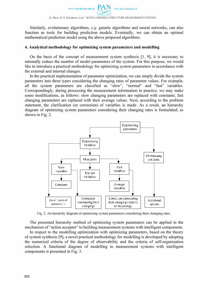
K. Shen, M. S. Selezneva, et al.: NOVEL VARIABLE STRUCTURE MEASUREMENT SYSTEM …
Similarly, evolutionary algorithms, e.g. genetic algorithms and neural networks, can also
function as tools for building prediction models. Eventually, we can obtain an optimal mathematical prediction model using the above proposed algorithms.
4. Analytical methodology for optimizing system parameters and modelling
On the basis of the concept of measurement system synthesis [1, 9], it is necessary to rationally reduce the number of model parameters of the system. For this purpose, we would like to introduce a practical methodology for optimizing system parameters in accordance with
the external and internal changes. In the practical implementation of parameter optimization, we can simply divide the system
parameters into three types considering the changing rates of parameter values. For example, all the system parameters are classified as “slow”, “normal” and “fast” variables. Correspondingly, during processing the measurement information in practice, we may make
some modifications, as follows: slow changing parameters are replaced with constants; fast changing parameters are replaced with their average values. Next, according to the problem
statement, the clarification (or correction) of variables is made. As a result, an hierarchy diagram of optimizing system parameters considering their changing rates is formulated, as shown in Fig. 2.
Fig. 2. An hierarchy diagram of optimizing system parameters considering their changing rates.
The presented hierarchy method of optimizing system parameters can be applied in the
mechanism of “action acceptor” to building measurement systems with intelligent components. In respect to the modelling optimization with optimizing parameters, based on the theory
of system synthesis [9], a novel practical methodology for modelling is developed by adopting the numerical criteria of the degree of observability and the criteria of self-organization selection. A functional diagram of modelling in measurement systems with intelligent
components is presented in Fig. 3.
352

Metrol. Meas. Syst., Vol. 24 (2017), No. 2, pp. 347–356.
Fig. 3. A functional diagram of modelling in measurement systems with intelligent components.
In Fig. 3, dominant parameters are selected using the criterion of the degree of observability
with a low threshold. Furthermore, different types of models are formulated depending on the operation modes of flight vehicles. However, it should be noted that for intensive manoeuvring
modes a high threshold value of the degree of observability is further suggested to be used to guarantee effective information processing and high accuracy of parameter determination.
In this section, we examine the analytical methodology for optimizing system parameters and modelling, and illustrate practical techniques by their functional diagrams. According to the above proposed design concepts, the novel developed measurement system structure is
guaranteed to be compact, which is beneficial in practical applications.
5. Variable structure measurement system with intelligent components
Rapid development of cybernetics, computer engineering, biotechnology and artificial intelligence leads to the appearance of measurement systems with intelligent components. Based on the systematic synthesis concept and the Peter K. Anokhin’s functional system theory
[1, 3], in this section we present a new type of measurement system with a variable structure and show its working principles as well as practical advantages.
As we all know, the operation environments (external and internal) of flight vehicles are constantly changing. Thus, a variable structure of the measurement system should be designed to adapt to those changes. In order to do that, the degree of observability must be used as an automatic selection criterion (or indicator) of measurement information. Except for that, the mechanism of “action acceptor”, consisting of a block of information fusion and selection
(BIFS), an algorithm for constructing models (ACM) and a block of prediction algorithms (BPA), also needs to be formulated.
Based on the above-mentioned numerical criterion of the degree of observability, self-organization algorithms and other practical methodologies, a novel variable structure measurement system with intelligent components has been developed, as shown in Fig. 4, where
Sensor 1 is the basic navigation sensor (e.g. an inertial navigation system), Sensors 2 ‒ N are external supporting navigation systems (e.g. GNSS, TRNS, CVNS, and so on) [4, 11, 12], BEA
is a block of estimation algorithms (e.g. Kalman filtering [5, 13]), θ is actual navigation
353

K. Shen, M. S. Selezneva, et al.: NOVEL VARIABLE STRUCTURE MEASUREMENT SYSTEM …
information, x is a navigation error, z is measurement information, x is an estimate, ˆx is
a predicted value, xɶ is an estimation error.
Fig. 4. A functional scheme of a novel variable structure measurement system with intelligent components.
In the block of information fusion and selection, the optimal structure of measurement
system is determined by comparing the measured and predicted information on the basis of the
degree of observability. With the changes of external and internal conditions, the structure of measurement systems is always in the process of change. Therefore, this process is similar
to an intelligent decision-making procedure and thus guarantees the optimization of the system structure.
In order to comprehensively explain the working principles of the proposed novel measurement system, we carried out simulations with the use of practical data. To measure the position and velocity of our flight vehicles, we used GNSS receivers, TRNS and CVNS
cameras. Accordingly, the degrees of observability of velocity errors obtained by using different measuring sensors were calculated, as shown in Fig. 5.
Fig. 5. The degrees of observability of navigation errors obtained by different sensors.
Figure 5 clearly shows the variant trend and the percentage of having the degree
of observability for different navigation sensors. The results are advantageous in calculation of information-sharing factors during the information fusion [13, 14]. In addition, the calculated
354

Metrol. Meas. Syst., Vol. 24 (2017), No. 2, pp. 347–356.
degree of observability can serve as an indicator in selection of better external supporting
navigation systems for a current working period. On the basis of the above results, it is easy to decide which of the supporting sensors should
be selected during a current period and how to change or optimize the structure of the measurement system in order to adapt to the changes of internal states and external conditions.
Moreover, the field tests were also carried out in a semi-real environment. During the tests, we set a change period of the measurement structure equal to 20 seconds taking into account the practical requirement and on-board computation capability. The test results are shown in Fig. 6.
Fig. 6. The field test results of the novel developed variable structure measurement system.
As shown in Fig. 6, based on analysis of the observability, a combination of basic INS and
supporting TRNS worked with a better accuracy than that of other measurement functional structures in an interval from 640 to 660 sec. Thus, in order to obtain an optimal measurement
structure, TRNS was selected as the external supporting navigation system. Similarly, in the next intervals CVNS and GNSS were successively selected. According to the results of simulation and experiments, the novel developed measurement system is characterized by
high accuracy, self-adaption and fault tolerance. In the novel developed measurement system, we set INS as the basic navigation system,
because it has the advantages of strong autonomy, instantaneous navigation parameters and good concealment, which lead to the all-weather global operation of the system. During functioning of the novel developed measurement system, we always select only one external
supporting sensor to combine with the INS in each time interval, which can guarantee strong anti-interference capability (e.g. anti-electromagnetic interference in battlefield environments)
of the whole measurement system.
6. Conclusions
The paper presents a method of developing a variable structure measurement system with
intelligent components. In order to achieve this goal, a numerical criterion of the degree of observability and algorithms for constructing prediction algorithms (e.g. modified self-organization algorithms) are proposed. On the basis of the Peter K. Anokhin’s functional system
theory, a novel measurement system with a variable structure is developed for improving accuracy of the system and adapting it to changes of environment. The new proposed
measurement system has an intelligent decision-making capability and guarantees continuous
640 650 660 670 680 690 700
0.2
0.25
0.3
0.35
0.4
0.45
0.5
Time (s)
Na
vig
atio
n E
rro
r (m
/s)
CVNS
TRNS
Reference
GNSS
Selected TRNS
Selected CVNS
Selected GNSS
355

K. Shen, M. S. Selezneva, et al.: NOVEL VARIABLE STRUCTURE MEASUREMENT SYSTEM …
optimization of the system structure. According to the results of simulation with the use
of practical data as well as the results of field tests, the novel developed measurement system is characterized by high accuracy, self-adaption, strong anti-interference capability and fault tolerance.
Acknowledgement
This research was supported by the Programme of Introducing Talents of Discipline to Universities in P.R. China (“111 program” No. B 16025) and the Russian Foundation for Basic
Research (Project No. 16-8-00522).
References
[1] Selezneva, M.S., Neusypin, K.A. (2016). Development of a measurement complex with intelligent
component. Measurement Techniques, 59(9), 916–922.
[2] Anokhin, P.K. (1974). Biology and neurophysiology of the conditioned reflex and its role in adaptive
behavior. Pergamon Press, 190–254.
[3] Proletarsky, A.V., Shen, K., Neusypin, K.A. (2015). Intelligent control systems: Contemporary problems in theory and implementation in practice. 2015 5th International Workshop on Computer Science and
Engineering: Information Processing and Control Engineering, Apr. 15–17, Moscow, 39–47.
[4] Groves, P.D. (2013). Principles of GNSS, inertial, and multisensor integrated navigation systems. Artech House, Inc., Boston, MA, USA, 419–448.
[5] Mirosław, Ś., Magdalena, D. (2015). Application of Kalman filter in navigation process of automated guided vehicles. Metrol. Meas. Syst., 22(3), 443–454.
[6] Neusypin, K.A., Proletarsky, A.V., Shen, K., et al. (2014). Aircraft self-organization algorithm with redundant trend. Journal of Nanjing University of Science and Technology, 5, 602–607.
[7] Shen, K., Neusypin, K.A., Proletarsky, A.V. (2014). On state estimation of dynamic systems by applying scalar estimation algorithms. Proceedings of 2014 IEEE Chinese Guidance, Navigation and Control
Conference, Aug. 8–10, Yantai, China, 124–129.
[8] Chen, Z. (1991). Local observability and its application to multiple measurement estimation. IEEE
Transactions on Industrial Electronics, 38(6), 491‒496.
[9] Proletarsky, A.V., Nikiforov, V.M., Neusypin, K.A. (2014). Certain aspects of designing the control complex of an advanced spacecraft. Systemy I Pribory Upravleniia, 1, 5‒11.
[10] Shen, K., Proletarsky, A.V., Neusypin, K.A. (2016). Algorithms of constructing models for compensating navigation systems of unmanned aerial vehicles. 2016 International Conference on Robotics and Automation
Engineering, Aug. 27–29, Jeju-Do, South Korea, 104‒108.
[11] Groves, P.D., Handley, R.J., Runnalls, A.R. (2006). Optimising the integration of terrain-referenced navigation with INS and GPS. Journal of Navigation, 59 (1), 71‒89.
[12] Won, D.H., Lee, E., Heo, M., Sung, S. Lee, J., Lee, Y.J. (2014). GNSS integration with vision-based navigation for low GNSS visibility conditions. GPS Solutions, 18(2), 177‒187.
[13] Carlson, N.A. (1990). Federated square root filter for decentralized parallel processors. IEEE Transactions
on Aerospace and Electronic Systems, 26(3), 517‒525.
[14] Xing, Z.R., Xia, Y.Q. (2016). Distributed federated Kalman filter fusion over multi-sensor unreliable networked systems. IEEE Transactions on Circuits and Systems, 63(10), 1714‒1725.

Metrol. Meas. Syst., Vol. 24 (2017), No. 2, pp. 357–368.
_____________________________________________________________________________________________________________________________________________________________________________________
Article history: received on Dec. 01, 2016; accepted on Jan. 14, 2017; available online on Jun. 30, 2017; DOI: 10.1515/mms-2017-0024.
METROLOGY AND MEASUREMENT SYSTEMS
Index 330930, ISSN 0860-8229 www.metrology.pg.gda.pl
MODELLING OF INFLUENCE OF HYPERSONIC CONDITIONS
ON GYROSCOPIC INERTIAL NAVIGATION SENSOR SUSPENSION
Igor Korobiichuk1), Volodimir Karachun2), Viktorij Mel’nick2), Maciej Kachniarz3)
1) Warsaw University of Technology, Faculty of Mechatronics, Św. A. Boboli 8, 02-525, Warsaw, Poland ( [email protected], +48 22 234 8506) 2) National Technical University of Ukraine, Kyiv Polytechnic Institute, 37 Peremogy, Kyiv, Ukraine ([email protected], [email protected]) 3) Industrial Research Institute for Automation and Measurements PIAP, Al. Jerozolimskie 202, 02-486 Warsaw, Poland ([email protected])
Abstract
The upcoming hypersonic technologies pose a difficult task for air navigation systems. The article presents
a designed model of elastic interaction of penetrating acoustic radiation with flat isotropic suspension elements
of an inertial navigation sensor in the operational conditions of hypersonic flight. It has been shown that the
acoustic transparency effect in the form of a spatial-frequency resonance becomes possible with simultaneous
manifestation of the wave coincidence condition in the acoustic field and equality of the natural oscillation
frequency of a finite-size plate and a forced oscillation frequency of an infinite plate. The effect can lead to
additional measurement errors of the navigation system. Using the model, the worst and best case suspension
oscillation frequencies can be determined, which will help during the design of a navigation system.
Keywords: hypersonic technologies, gimbals, oscillation modes, acoustic transparency, navigation system.
© 2017 Polish Academy of Sciences. All rights reserved
1. Introduction
Today, ships are armed with 100−145 mm calibre automatic cannons which have not only limited range but also insufficient shooting accuracy in a modern combat. Therefore, the main range of possible targets is acquired by missiles, which are very expensive and, besides, have
considerable dimensions. To solve this problem, the United States Navy plans by 2025 to supply a rail gun capable of destroying any targets with cheap projectiles and at long ranges. The electromagnetic rail gun is developed by BAE SYSTEMS and GENERAL ATOMICS (Fig. 1). The testing is scheduled to take place on board of the newest high-speed vessel JHSV
Millinocket. Moreover, the developers of railguns offer to equip also usual powder cannons with
hypersonic projectiles, which would dramatically improve their ability to hit any targets,
including airborne ones. Rail guns can project at a speed of 5M at a distance of 400 km. According to the military
forecasts, such guns can hit any target. According to the Department for Development of Marine Systems of NAVSEA NAVY, the rail gun features are planned to be partly implemented in
traditional powder cannons. It means, that an HVR hypersonic projectile is planned to be developed in two major United States Navy calibres: 155 mm and 127 mm. Thus, a universal core would serve for two types of both powder cannon and rail gun. Naturally, when firing from
a powder cannon, the HVR speed would be lower than when firing from a rail gun. The difference would be 3 M and 5 M, respectively. Nevertheless, the speed will be twice higher
than while using gunpowder. An HVR projectile should become an alternative to expensive

I. Korobiichuk, V. Karachun, et al.: MODELLING OF INFLUENCE OF HYPERSONIC CONDITIONS …
anti-aircraft missiles and 155 mm LRLAP projectiles which cost $ 400,000 per unit for Zumwalt class destroyers.
Fig. 1. A hypersonic projectile of a rail gun can replace expensive missiles.
However, advantages that create new means of fire support give rise to a lot of air navigation
problems. They consist in high temperatures, extreme vibration, shock N-wave and penetrating acoustic radiation. Diffuse sound fields would fundamentally change the dynamics of on-board equipment mechanical systems’ features and affect the performance characteristics of avionic instruments in general, such as inertial navigation systems.
Two-stage gyroscopic instruments are widely used as sensitive elements of gyroscopically stabilized platforms and inertial navigation systems. Therefore, the requirement of high precision indications is crucial for accurate building of reference directions on mobile objects. This applies primarily to the launch vehicles (LV) and hypersonic aircraft, the propulsion systems of which create a high sound pressure (up to 180 dB) in a rather broad frequency range. This will also apply to hypersonic projectiles, since the existing solid-state and MEMS systems are not accurate and simultaneously robust enough for such applications.
The main feature of penetrating radiation impact is its spatial nature. On the one hand, traditional means of combating external perturbations are ineffective, and, on the other hand, there is a need of a fundamentally new approach to design diagrams, namely a change from lumped parameter systems to distributed parameter systems. Let us demonstrate how this is applied to gimbals’ flat fragments.
The goal of the research is to evaluate the risk of manifestation of local resonance peculiarities in gimbals when using an aircraft.
In order to achieve the aim, the following tasks should be accomplished: 1. Building a design diagram of the studied phenomenon. 2. Choosing a method of building a mathematical model with which particularities of resonance
type would have been obvious and visible for further analysis when studying the dynamics of gimbals in general, especially to evaluate additional errors of autonomous positioning.
3. Evaluating feasibility and effectiveness of studying the phenomena using two-fold trigonometric series by normal functions in the rectangular area.
4. Assessing, according to two mutually perpendicular directions, the degree of influence of the plate vibration mode on the fullness of sound energy transmission through a flat barrier.
2. Material and methods
2.1. Sound wave diffraction at cross elastic gyroscope suspension
Supports with elasticity friction are used mainly in systems having limited rotation angles. In practice, such supports do not create a friction torque (as the value of elasticity friction is very low), have low accuracy of fixing the axis direction, but operate satisfactorily under heavy vibration. Depending on a type of elastic element deformation, there are bending supports and torsion supports.
358

Metrol. Meas. Syst., Vol. 24 (2017), No. 2, pp. 357–368.
A simple ribbon hinge is a plate connecting the fixed element to the moving element. This
hinge is used, for example, as a pendulum suspension. The elastic hinge consists of a lever, two resilient plates and a fixed base. Such a hinge is used for small rotation angles of the moving part (1 ... 2 degrees). The track formed by intersection of extensions of the middle planes
of elastic plates is taken as the rotation centre. Figure 2 shows a cross hinge for two-stage gyroscope suspension 3, which is mounted on
plate 1. Plate 1 is fixed on base 4 with a support consisting of four elastic plates 2, intersecting
at an angle of α = 60º... 90º and attached to base 4 and plate 1. The rotation angle of these hinges may reach 30º.
Fig. 2. A cross elastic hinge for a two-stage gyroscope suspension.
2.2. Cross elastic hinge. Mechanical model of interaction with acoustic radiation
We assume the cross angle 2
radπ
α = and analyse the structure of elastic interaction
of acoustic radiation with a two-stage gyroscope suspension mounted on two cross hinges.
To better understand the nature of this phenomenon, we confine ourselves to consideration of the lowest forms of vibrations only. Moreover, for clarity, it is enough to study the waveform
only in one direction. We suppose that under the influence of an acoustic wave, elastic plates make a bending
movement, taking only the first, lower form. Then, in the normal direction, one will receive
movement 1r and the other −
2r , which are represented as components of
11, zy and
22, zy ,
and enable establishing that the notional pivot axis of the movable part of gyroscope will be
moving along axis Y − ( )21yy + and axis Z − ( )
21zz − (Fig. 3a). If these forms are manifested
in phase at both cross hinges, the angular oscillations occur in respect to the conditional output axis O-O of the device (Fig. 3d). If they are manifested in antiphase, the gyroscope torsional
oscillations occur in respect to Z axis (Fig. 3c). If the first forms of plate flexural vibrations have a form shown in Fig. 3b, the form
of gyroscope movements changes and upon the in-phase movement of the extreme points of O-
O axis, the gyroscope makes the reciprocating movement along Z axis (Fig. 3e), while upon
the antiphase movement the angular oscillations along the output axis occur. Thus, the gyroscope suspension, upon acoustic loading, will produce straight fluctuations
relative to axes, Y, Z and angular oscillations relative to axes X, Z. In this case a two-stage differentiating gyroscope has a bias, whereas a two-stage integrating gyroscope has a systematic drift. Furthermore, the device output signal also shows periodic components.
Leaving aside the issue of passing the acoustic wave through the proper gyroscope, a mechanical model of calculating the interaction of the overpressure wave P10 with the
suspension can be represented in a form of two not interconnected elastic plates affected by a flat monochromatic wave (Fig. 4). Here, 1, 2, 3 are the falling, reflected and transmitted waves
through the first plate, respectively, and 1′, 2′, 3′ − through the second plate.
359

I. Korobiichuk, V. Karachun, et al.: MODELLING OF INFLUENCE OF HYPERSONIC CONDITIONS …
a) b)
c) d)
e)
Fig. 3. A mechanism of elastic interaction of acoustic radiation with the device on an elastic suspension.
A number of issues of the plate dynamics, their physical structure and others under the
influence of acoustic radiation is not completely understood yet. First of all, it refers to consideration of the boundary conditions when studying the plate with finite extent, which leads to an infinite system of equations describing the mechanical model.
Fig. 4. A mechanism of pressure wave passing through an elastic suspension.
A characteristic feature of the geometry of boundary surfaces of elastic bodies is the presence
of angular lines. Based on the formulation of boundary problems in the theory of elasticity in displacements (on the basis of the G. Lame’s vector equation), there are three basic boundary problems, i.e. setting the vector of external forces on the body surface, setting the elastic
360

Metrol. Meas. Syst., Vol. 24 (2017), No. 2, pp. 357–368.
displacement vector on the body surface, and a mixed problem consisting of the fact that
the forces are set on a part of the boundary surface, and a displacement vector is defined on the rest of the surface.
At present, two approaches have been developed, i.e. the method of homogeneous solutions,
first applied by P. A. Schiff and V. A. Steklov, and the G. Lame’s method of exact solutions. The first became a powerful means of asymptotic analysis of approximate shell theories.
A prerequisite for the revival of the second one was the presence of a coherent theory of infinite systems and the emergence of PCs. Here, it is appropriate to mention the opening of asymptotic expression law by B. M. Koyalovich, which enabled establishing the lack of features in the
expressions for stresses at the corner points and solving the first basic boundary problem. The analysis of flexural vibrations of finite plane bodies, i.e. elastic suspension plates, can also be
carried out using the method described in the works of S. P. Tymoshenko. Its essence is to represent a mechanical disturbance and deflection of the plate as a double row by normal functions in the rectangular region. This method has the simplest mathematical interpretation,
but still enables to investigate the dynamics of finite bodies deep enough. The dynamic
properties of a flat infinite barrier in acoustic field have been studied in [1−7]. Sandwich-type
constructions have been considered in [8−12]. The effect of sound waves on gimbals and other
materials has been discussed in [13−24]. With regard to resonance manifestations in gimbals,
they are usually focused on the impact of pedestal vibration and on the parametric resonance. Such external perturbations as spatial waves has not been studied in terms of manifestations
of gimbals’ local peculiarities. We assume further that the elastic suspension plates have hinge fastenings at the ends, and thus the acoustic radiation energy will be absorbed completely by the oscillating plates, without affecting the adjacent structures.
3. Model of occurrence of plate resonant peculiarities
Transmission of acoustic waves through flat components in a form of infinite plates is
thoroughly described by a simplified mathematical apparatus and significantly reduces analysis effort. This is quite enough for studying certain issues. Study of the dynamics of elastic
interaction between flat barriers and an acoustic wave is limited to such models. However, the approximate simulation modelling process has led to simplifications in which
theoretical and experimental results lead to inconsistent findings. This primarily concerns the
occurrence of local peculiarities. The way out is to maximally approximate simulation models to real designs. In relation to
the studied phenomena, it requires a transition from infinite to finite plates. In this case flexural motion of finite flat bodies is advisable to be studied on the basis
of external impact and plate flexure in a form of trigonometric series in the rectangular area.
Let us consider a bi-dimensional problem. Let us suppose that the plate length is equal to a ,
its width to b , thickness to δ2 and is constant in the cross section. We also assume that the
plate thickness is much less than other dimensions, i.e.: ;2 a<<δ .2 b<<δ
The plate material would be absolutely elastic, homogeneous and isotropic. The length of flexural waves would be more than six times greater than the plate thickness, which would
enable to use the equation of a thin plate. Let us consider an acoustic field to be diffused.
In the light of those simplifications, it can be argued that the lateral sides of area element
with a length of dy and width of dx remain in their motion parallel to xOz and yOz planes
and perpendicular to the median plane (Fig. 5).
361

I. Korobiichuk, V. Karachun, et al.: MODELLING OF INFLUENCE OF HYPERSONIC CONDITIONS …
Fig. 5. A diagram of loading a spatial plate.
Whatever function of coordinates x, y would the plate flexion W be of, it can always be expressed by a two-fold series in the rectangular area in normal functions, i.e.:
b
yn
a
xmWyxW
m n
mn
ππ
sinsin),(1 1
∑∑∞
=
∞
=
= , (1)
where: m = 1, 2, …, n = 1, 2, … are numbers of flexion half-waves along x and y axes,
respectively; ),( yxW is transmission of plate surface with coordinates x, y in the direction of z;
( )tWWmnmn
= (Fig. 6).
It is easy to see that each term of series (1) meets the boundary conditions of:
.0;0;0;0
,0;0;0;0
2
2
0
2
2
0
2
2
0
2
2
0
=∂
∂=
∂
∂==
=∂
∂=
∂
∂==
==
==
==
==
byy
byy
axx
axx
y
W
y
WWW
x
W
x
WWW
(2)
The relations (1) enable to calculate the maximum potential energy M0, which accumulates
in flexural plate deformation. For this purpose, it is sufficient to determine the maximum value of potential energy dM0 of a surface element and then integrate the expression obtained in two
ways:
( ) ( )
( ) ( )( )
( ),
,12
,,2
,,
2
1
2
2
2
2
2
0 0
2
2
22
2
2
0
dxdyyx
yxW
y
yxW
x
yxW
y
yxW
x
yxWDM
b a
∂∂
∂−+
∂
∂
∂
∂+
+
∂
∂+
∂
∂= ∫ ∫
σσ
(3)
where: ( )[ ] 131128
−
−= σδED is cylindrical plate stiffness; E is the modulus of elasticity; σ is
the Poisson’s ratio.
The value of maximum kinetic energy T0 at lateral oscillations of a plate is determined by the formula:
362

Metrol. Meas. Syst., Vol. 24 (2017), No. 2, pp. 357–368.
( )dxdyyxWT
b a
∫ ∫=
0 0
22
0,
2
1µω , (4)
where: µ is the specific weight; ω is a cyclical frequency.
Fig. 6. Distribution of plate flexures: m, n are numbers of half-waves.
Let us apply the general equation of dynamics to build a differential equation of the plate
in principal coordinates. This gives the following:
112
2
2
2
4
nmmnmnQW
b
n
a
mDW =
++ πµ , (5)
where: ( )1 2 2
2 1 2
2 2 mn
m nD
a bπ µ ω
−
+ =
is a natural oscillation frequency;
11nm
Q is a generalized force.
So, if an incident sound wave P(x, y)would be represented in a form of:
( )b
yn
a
xmPyxP
m n
nm
ππ1
0 0
1 sinsin,11
∑∑∞
=
∞
=
= , (6)
where: 11nm
P is a pressure amplitude of the appropriate form; 1
m , 1n are forms of sound pressure
half-waves occurring both in length and width, then its virtual work will be calculated according
to the formula:
( ) dxdyb
yn
a
xmWtyxPA
b a
mn
ππδδ
1
0 0
1
1sinsin,,∫ ∫= . (7)
Setting for specificity:
( ) ( )[ ]
+−+−=2
cossinexp,,101
πθδθω yxktiPtyxP , (8)
where: P10 is a pressure amplitude; k is a wave number, we obtain:
( )[ ] ( )[
( ) ] ( ) ( )[ ]( ) ( )[ ] ,sincoscosexp
sinexpsincosexp2
cosexp
21
1
221
1
2
21
1
12
1
111011
−−−
−
++−−
−−
+−=
amkbnkSSkbibnS
kaiamSabkiktiPQnm
πθπθθπ
θπθθπ
θδω
(9)
from the expression (7).
When 101<<<m , 10
1<<< n , which corresponds to loading evenly distributed over
the plate area, the formula (9) would be converted to the form:
( ) ( )( )ππ11
1
1110cos1cos1
11
nmnmabPQnm
−−=
−
. (10)
363

I. Korobiichuk, V. Karachun, et al.: MODELLING OF INFLUENCE OF HYPERSONIC CONDITIONS …
The generalized force Q will be zero for even values m1 and n1, i.e.:
011
=nm
Q . (11)
And vice versa, for odd values:
( ) 12
11104
11
−
= πnmabPQnm
. (12)
By calculating the maximum work A0 of an incident sound pressure wave, according to the
formula:
( ) ( )dxdyyxWyxPA
b a
,,
0 0
0 ∫ ∫= , (13)
let us establish the law of plate flexural vibrations on the basis of extreme properties of its
bending:
( ) 0000=+−
∂
∂AMT
Wmn
. (14)
If consideration of energy dissipation due to the internal friction is required, it would be
enough to consider the work of these forces in the expression (14), i.e.:
( ) 00000=−+−
∂
∂RAMT
Wmn
, (15)
where:
( ) ∑∑∫ ∫∞
=
∞
=
==
1 1
22
0 0
2
0
8
1,
2 m n
mn
b a
WabdxdyyxWR ωµηχ
, (16)
2
mnηµωχ = is an internal friction coefficient; η is a coefficient of losses.
Let us suppose that mm =1
, nn =1
.
These conditions imply the coincidence of a number of acoustic radiation half-waves and
plate vibration generated in two directions: along axis x ( mm =1
) and along axis y ( nn =1
).
Substituting the relation (1), (8) in the expressions (3), (4) and (13), we obtain the following:
( )yxWb
n
a
mBabM
m n
mn,
8
1
1 1
2
2
2
2
2
4
0 ∑∑∞
=
∞
=
+= π ,
( )yxWabTm n
mn,
8
1
1 1
22
0 ∑∑∞
=
∞
=
= ωµ , (17)
( )yxWPabAm n
mnmn,
4
1
1 1
0 ∑∑∞
=
∞
=
= .
On the basis of the extrenality condition (15), the expressions (17) give an opportunity to find out the value of bend for each pair of indices m and n:
( )( )22
,
ωωµ −
=
mn
mn
mn
PyxW , (18)
where mnω is a natural frequency calculated from the above formula.
It is clear that under the occurrence of mnωω = , the plate flexure constantly grows and it
becomes acoustically transparent.
Substituting the value of generalized force mn
Q (19) in the differential equation of motion
(5), the law of plate flexural vibrations can be established on the mnform at the continuous action of sound radiation in a time interval [0, t]. It contains its natural and forced vibrations, i.e.:
364

Metrol. Meas. Syst., Vol. 24 (2017), No. 2, pp. 357–368.
( ) ( )
( )[ ] ( )
( ) ( )[ ] ( )
( )( ) ( )[ ]( ) ( )[ ] .sincos
cosexpsinexp
2sincosexp
sin,,
12
1221222
12
21
1
2
1
1
10
0
11
11
−
−−
−−−
−−
++−×
×+−−×
×
++−−+=
=−= ∫
amkbnk
abmnSSkbibnSkaiamS
ttgabktiP
dtttQtyxW
mn
t
mnmnmnmn
πθπθωωµ
πθπθπ
ϕπ
θθδω
ωµω
(19)
Finally, considering the relation (19) we obtain:
( ) ( )
( ) ( )( ) ( )[ ]( ) ( )[ ]
( )[ ] ( )
( ) ( )[ ] ( )
,sinsin
cosexpsinexp
2sincosexp
sincos
sinsin,,,,
12
21
1
2
1
1
1 1
12
1221222
10
1 1
b
yn
a
xm
abmnSSkbibnSkaiamS
ttgabkti
amkbnktP
b
yn
a
xmtyxWtyxW
m n
mn
m n
mn
ππ
πθπθπ
ϕπ
θθδω
πθπθωωµρ
ππ
×
×+−−×
×
++−−+×
×++−=
==
−−−
∞
=
∞
=
−
−−
∞
=
∞
=
∑∑
∑∑
(20)
from the expression (1),where: ( ) ( ) ( )[ ]21
212
sinsincoscos tttttmnmnmn
ωωωωωωρ−
−+−= ;
( ) ( )( ) 11coscossinsin
−−
−−= ttttttgmnmnmn
ωωωωωωϕ .
The same is for the case of acoustic loading uniformly distributed over the plate area. For this purpose, it is enough to substitute the relations (12) in (5). We obtain:
( ) ( ) ( )tmngPtyxWmnmnmn
ωωπµ cos116,,1
22
10−=
−
. (21)
Now the pattern of plate flexural motion can be established:
( ) ( ) ( ) ( )b
yn
a
xmtmngPtyxW
mn
m n
mn
ππωωµπ sinsincos116,,
1 1
12
12
10−= ∑∑
∞
=
∞
=
−−
, (22)
where m and n are odd numbers. For a finite plate, the flexural motion can be represented as the superposition of forced
vibrations of an infinite plate and natural vibrations that occur in the plate given its size. If a plate impedance on the mn form is:
( ) ( )[ ]214
1
3
1sin
mnmnmnmncciVPZ ωωθµω −−−
−== , (23)
then it becomes clear that − even fulfilling the wave coincidence condition θ1
3sin
−
= cc , but
if there is no equality of frequencies ωmn of finite plate natural vibrations and frequencies ω
of infinite plate forced vibrations − the flexures would have a fixed value. The plate would be
acoustically transparent, i.e. the equality 0=mn
Z would occur only if both conditions are
fulfilled:
.
,sin1
3
mn
cc
ωω
θ
=
=−
(24)
365

I. Korobiichuk, V. Karachun, et al.: MODELLING OF INFLUENCE OF HYPERSONIC CONDITIONS …
4. Discussion of results of plate flexures by vibration forms
Let us perform a numerical analysis of lower vibration forms, having assumed the following
parameters for the sake of clarity: 32 2 10 ,mδ
−
= ⋅ 0,3,σ = 2710 .E Nm
−
= ,4rad
πθ = 1
100 ,sω−
=
0,1 ,а m= 0,2 .b m= The quantitative analysis shows that the maximum deflection of an elastic
suspension plate is observed at the first (lowest) waveform, that is when 1
1,k
m m= = 1
1.k
n n= =
Higher waveforms have a more complex structure of the bending motion. For example, upon
1 11 , 2,
k km m n n= = = = each of the plates has, unlike the first form, two local extrema
of opposite polarity, while upon 1 1
1 , 3k k
m m n n= = = = they have three extrema. The higher
the form number, the more complex the bending movement of the suspension plates. Obviously,
the number of extrema is determined by the product .
k km n⋅
The analysis shows that upon an odd n, the bend magnitude is much larger in absolute terms than upon an even n. Thus, these forms will contribute to a more intense sonic energy pumping. The numerical values of maximum plate flexures for the first five forms of vibration are shown
in Table 1. The values of natural frequencies mnω of vibration
k km n − forms are shown in
Table 2. Here, P10 is a normalizing factor.
The numerical analysis proves that the maximum plate flexures are on the first − the lowest
− form, i.e. when 1
1;m m= =1
1.n n= =
Thus, the most favourable for the device is a combination of 1 waveforms of one plate with even waveforms of the other one, i.e. 2, 4, 6, etc. (Fig. 7a). In this case, as can be seen, the
movement of the device output axis in the direction of Y axis is only due to fluctuations of the
first plate 1r , and there is no movement towards Z axis. If there is a combination of the first
waveform of one plate and odd forms (1, 3, 5, 7, etc.) of the other, there is the most complex
motion of the suspension axis, both in the direction of Y axis and in the direction of Z axis (Fig. 7b). There is both translational and angular acoustic suspension vibration.
a) b)
Fig. 7. The effect of a plate waveform on the movement of the device output axis.
Table 1. The maximum plate flexures.
m = m1 n = n1 Wmax/P10, m
1 1 15
1 2 12*10−4
1 3 4,8
1 4 5,9*10−4
1 5 2,9
2 2 11,8*10−4
3 3 4,8
4 4 5,6*10−4
5 5 2,9
366
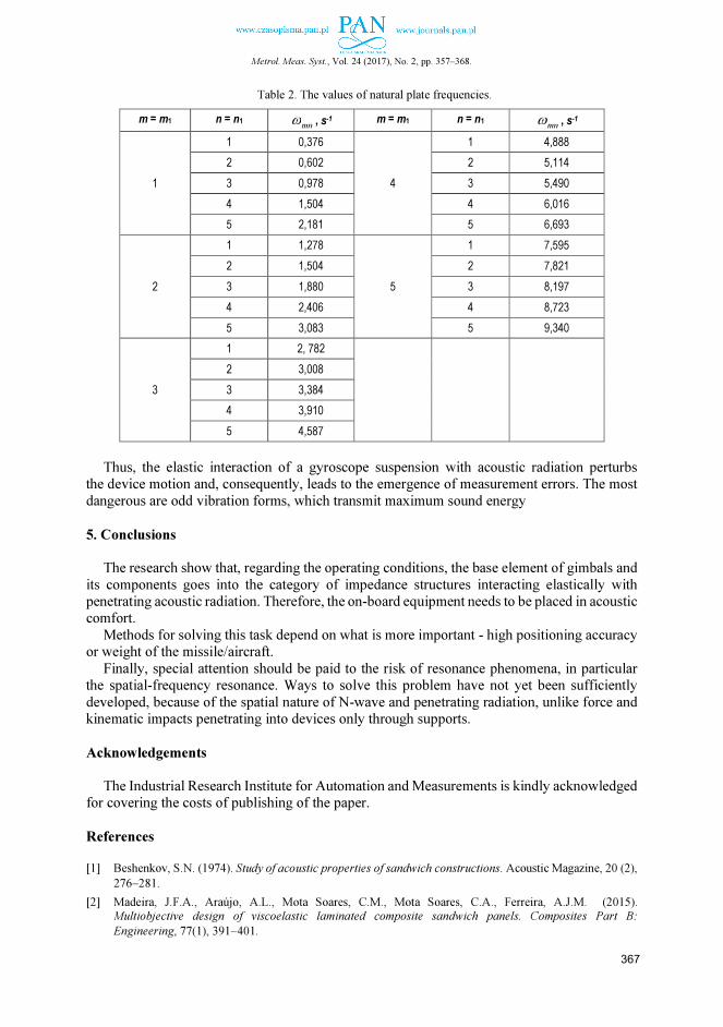
Metrol. Meas. Syst., Vol. 24 (2017), No. 2, pp. 357–368.
Table 2. The values of natural plate frequencies.
m = m1 n = n1 mnω , s-1 m = m1 n = n1
mnω , s-1
1
1 0,376
4
1 4,888
2 0,602 2 5,114
3 0,978 3 5,490
4 1,504 4 6,016
5 2,181 5 6,693
2
1 1,278
5
1 7,595
2 1,504 2 7,821
3 1,880 3 8,197
4 2,406 4 8,723
5 3,083 5 9,340
3
1 2, 782
2 3,008
3 3,384
4 3,910
5 4,587
Thus, the elastic interaction of a gyroscope suspension with acoustic radiation perturbs the device motion and, consequently, leads to the emergence of measurement errors. The most
dangerous are odd vibration forms, which transmit maximum sound energy
5. Conclusions
The research show that, regarding the operating conditions, the base element of gimbals and
its components goes into the category of impedance structures interacting elastically with penetrating acoustic radiation. Therefore, the on-board equipment needs to be placed in acoustic comfort.
Methods for solving this task depend on what is more important - high positioning accuracy or weight of the missile/aircraft.
Finally, special attention should be paid to the risk of resonance phenomena, in particular the spatial-frequency resonance. Ways to solve this problem have not yet been sufficiently
developed, because of the spatial nature of N-wave and penetrating radiation, unlike force and kinematic impacts penetrating into devices only through supports.
Acknowledgements
The Industrial Research Institute for Automation and Measurements is kindly acknowledged for covering the costs of publishing of the paper.
References
[1] Beshenkov, S.N. (1974). Study of acoustic properties of sandwich constructions. Acoustic Magazine, 20 (2),
276−281.
[2] Madeira, J.F.A., Araújo, A.L., Mota Soares, C.M., Mota Soares, C.A., Ferreira, A.J.M. (2015).
Multiobjective design of viscoelastic laminated composite sandwich panels. Composites Part B:
Engineering, 77(1), 391−401.
367

I. Korobiichuk, V. Karachun, et al.: MODELLING OF INFLUENCE OF HYPERSONIC CONDITIONS …
[3] Wang, T., Li, S., Nutt, S.R. (2009). Optimal design of acoustical sandwich panels with a genetic algorithm.
Applied Acoustics, 70(3), 416−425.
[4] Chronopoulos, D., Collet, M., Ichchou, M., Antoniadis, I. (2015).Wave based design optimisation
of composite structures operating in dynamic environments. COMPDYN 2015 − 5th ECCOMAS Thematic
Conference on Computational Methods in Structural Dynamics and Earthquake Engineering, 4390−4408.
[5] Bogolepov, I.I. (1986). Industrial soundproofing. Monograph. L. Sudostroenie, 386.
[6] Brekhovskih, I.M. (1973). Waves in layered structures. Monograph. M. Nauka, 344.
[7] Valeev, K.G. (1970). Definition of stress state of flat panels in the acoustic field of the exhaust stream.
Adventure of Mechanic, VI(4), 30−43.
[8] Goloskokov, E.G. (1980). Elastic and acoustic problems of sandwich construction dynamics. Monograph.
Kharkiv. Vyshcha shkola, 189.
[9] Kanibolotskiy, M.A. (1980). Optimal design of layered structures. Monograph. Novosibirsk. Nauka. Sib.
Department, 176.
[10] Xu, F., Wang, W., Shao, X., Liu, X., Liang, Y. (2015). Optimization of surface acoustic wave-based rate
sensors. Sensors, 15(10,12), 25761−25773.
[11] Hamdaoui, M., Robin, G., Jrad, M., Daya, E.M. (2014). Optimal design of frequency dependent three-
layered rectangular composite beams for low mass and high damping. Composite Structures, 120, 174−182.
[12] Karachun, V., Mel’nick, V., Korobiichuk, I., Nowicki, M., Szewczyk, R., Kobzar, S. (2016). The Additional
Error of Inertial Sensor Induced by Hypersonic Flight Condition. Sensors, 16(3).
[13] Karachun, V.V. (2012). Influence of Diffraction Effects on the Inertial Sensorg of a Gyroscopically
Stabilized Platform: Three-Dimansional Problem. International Applied Mechanics, 48(4), 458−464.
[14] Karachun, V.V. (2014). Ware coincidence and errors of floating gyroscope at the resonance Level. News
of Science and Education, Technical Science, Mathematics. Science and Education Ltd, 31(21), 56−62.
[15] Karachun, V.V. (1989). Vibration of a plate under an acoustic load. Engineering, Technology Science, PA,
20(37), 391−394.
[16] Mostafapour, A., Ghareaghaji, M., Davoodi, S., Ebrahimpour, A. (2016). Theoretical analysis of plate
vibration due to acoustic signals. Applied Acoustics, 103, 82−89.
[17] Geng, Q., Li, Y. (2012). Analysis of dynamic and acoustic radiation characters for a flat plate under thermal
environments. International Journal of Applied Mechanics, 4(3).
[18] Alzahabi, B., Almic, E. (2011). Sound radiation of cylindrical shells. International Journal of Multiphysics,
5(2), 173−185.
[19] Korobiichuk, I. (2016). Mathematical model of precision sensor for an automatic weapons stabilizer system.
Measurement, 89, 151–158.
[20] Lee, S.W., Rhim, J.W., Park, S.W., Yang, S.S. (2007). A novel micro rate sensor using a surface-acoustic-
wave (SAW) delay-line oscillator. Proc. of IEEE Sensors, 1156−1159.
[21] Korobiichuk, I., Nowicki, M., Szewczyk, R. (2015). Design of the novel double-ring dynamical gravimeter.
Journal of Automation, Mobile Robotics and Intelligent Systems, 9(3), 47−52.
[22] Mehta, A., Jose, K.A., Varadan, V.K. (2002). Numerical simulation of a surface acoustic wave (SAW)
gyroscope using HP EEsof. Proc. of SPIE. The International Society for Optical Engineering. 4700,
169−177.
[23] Korobiichuk, I., Koval, A., Nowicki, M., Szewczyk, R. (2016). Investigation of the Effect of Gravity
Anomalies on the Precession Motion of Single Gyroscope Gravimeter. Solid State Phenomena, 251,
139−145.
[24] Creagh, M.A., Beasley, P., Dimitrijevic, I., Brown, M., Tirtey, S. (2012). A Kalman-filter based Inertial
navigation system processor for the SCRAMSPACE 1 hypersonic flight experiment. 18th AIAA/3AF
International Space Planes and Hypersonic Systems and Technologies Conference 2012, Tours, France.

Metrol. Meas. Syst., Vol. 24 (2017), No. 2, pp. 369–380.
_____________________________________________________________________________________________________________________________________________________________________________________
Article history: received on Dec. 12, 2016; accepted on Jan. 30, 2017; available online on Jun. 30, 2017; DOI: 10.1515/mms-2017-0032.
METROLOGY AND MEASUREMENT SYSTEMS
Index 330930, ISSN 0860-8229 www.metrology.pg.gda.pl
IMPEDANCE SENSORS MADE IN PCB AND LTCC TECHNOLOGIES
FOR MONITORING GROWTH AND DEGRADATION OF PSEUDOMONAL
BIOFILM
Konrad Chabowski1), Adam F. Junka2), Tomasz Piasecki1), Damian Nowak1),
Karol Nitsch1), Danuta Smutnicka2), Marzenna Bartoszewicz2), Magdalena Moczała1),
Patrycja Szymczyk3)
1) Wrocław University of Science and Technology, Faculty of Microsystem Electronics and Photonics, Z. Janiszewskiego 11/17, 50-372 Wrocław, Poland ( [email protected], +48 71 320 3223, [email protected], [email protected], [email protected], [email protected]) 2) Medical University of Wrocław, Department of Pharmaceutical Microbiology and Parasitology, Borowska 211a, 50-556 Wrocław, Poland ([email protected], [email protected], [email protected]) 3) Wrocław University of Science and Technology Centre for Advanced Manufacturing Technologies, I. Łukasiewicza 5, 50-371 Wrocław, Poland ([email protected])
Abstract
The suitability of low-cost impedance sensors for microbiological purposes and biofilm growth monitoring was
evaluated. The sensors with interdigitated electrodes were fabricated in PCB and LTCC technologies.
The electrodes were golden (LTCC) or gold-plated (PCB) to provide surface stability. The sensors were used for
monitoring growth and degradation of the reference ATCC 15442 Pseudomonas aeruginosa strain biofilm in in-
vitro setting. During the experiment, the impedance spectra of the sensors were measured and analysed using
electrical equivalent circuit (EEC) modelling. Additionally, the process of adhesion and growth of bacteria on a
sensor’s surface was assessed by means of the optical and SEM microscopy. EEC and SEM microscopic analysis
revealed that the gold layer on copper electrodes was not tight, making the PCB sensors susceptible to corrosion
while the LTCC sensors had good surface stability. It turned out that the LTCC sensors are suitable for monitoring
pseudomonal biofilm and the PCB sensors are good detectors of ongoing stages of biofilm formation.
Keywords: Pseudomonas aeruginosa, biofilm, interdigitated sensor, impedance spectroscopy.
© 2017 Polish Academy of Sciences. All rights reserved
1. Introduction
The vast majority of microorganisms exist as attached and organized communities referred to as biofilms [1]. These communities are predominantly embedded within various extracellular polymeric substances (sugars, proteins, DNA) also known as a “biofilm matrix” [2]. The matrix
serves microorganisms as a shelter and a shield protecting them from not only drugs and other xenobiotics but also from activity of the immune system. The biofilms are able to form on
virtually every type of surface, including tissues and abiotic biomaterials used for medical purposes [3]. It is estimated that biofilms are responsible for up to 80% of nosocomial infections [4]. Therefore, there is an urgent need of developing new tools for rapid detection of “medical
biofilm” enabling to apply suitable eradication procedures. The tools designed for rapid detection of biofilms may be helpful in virtually all flow systems
endangered by the development of microbes. Among the examples of such systems in nosocomial settings are indwelling catheters, nutrition accesses or hospital water distribution pipes [5]. The usage of impedance sensors providing possibilities of non-invasive, label-free
and real-time measurements is promising in the above mentioned clinical situations. Using the sensors combined with the impedance spectroscopy method for detecting attachment

K. Chabowski, A. F. Junka, et al.: IMPEDANCE SENSORS MADE IN PCB AND LTCC TECHNOLOGIES …
of microbial cells and biofilm formation has been already reported by other authors who tested
the impedance potential using such nosocomial strains as Escherichia coli [6−9],
Staphylococcus aureus [7, 10, 11], Staphylococcus epidermis [11, 12], Pseudomonas aerugino-
sa [5, 13−15], Bacillus subtilis [13] and Salmonella typhimurium [9, 16]. The impedance micro-sensors with interdigitated electrodes were used for this purpose by
some researchers [9, 11, 12, 17] because of their advantages: a small size enabling to perform small-scale experiments using very small samples, fast establishment of a steady-state signal,
a low ohmic drop of potential, an increased signal-to-noise ratio and − last but not least − higher
sensitivity comparing with conventional-size macro-electrodes. Typical sensors with interdigitated electrodes designed for microbiological sensing are
usually fabricated using the lithography technique on silicon and glass substrates [18]. The main
disadvantages are their high cost and complicated process of manufacturing. The sensors made in the printed circuit board (PCB) technology may be a promising
alternative as they are cost-effective and relatively easy to manufacture [19]. The PCB sensors were already employed in microbiological, oncologic or immunologic applications, namely for:
bacteriuria screening [7], analysis of colorectal carcinoma cells [20] and Interleukin-12 detection [19, 21]. The sensors made in low temperature co-fired ceramics (LTCC) could be also a constructive option. LTCC devices were reported to be used in microbiological
applications, i.e. monitoring cell cultures [22], monitoring water solutions [23], monitoring glucose concentration [24], an electronic tongue [25] and cortisol detection [26]. However, the
mentioned devices used mostly voltamperometric measurement systems, avoiding the impedance spectroscopy.
In the impedance spectroscopy the electrical equivalent circuit modelling is a method
of analysing impedance spectra [27]. It consists in the numerical fitting of the electrical equivalent circuit (EEC) impedance to the measured impedance spectrum. As specific
components of the EEC are correlated with various conduction and polarisation processes, such an approach enables to identify and separate them. This method is not widely used in analysis of the impedimetric sensors’ responses in microbiological applications despite of the fact that
it may provide detailed information about the measured object [14, 17, 28, 29]. The aim of this work was to combine advantages of the interdigitated electrodes with the
cost-effective PCB technology and the more accurate LTCC technology, and to determine whether such sensors may be used for detection of the P. aeruginosa biofilm presence and for monitoring particular stages of this structure formation. The presented research is related to the
authors’ previous work [17], in which impedance micro-sensors on glass substrates were used.
2. Materials and methods
2.1. Preparation of impedance sensors
The layout of impedance sensor interdigitated electrodes was designed using CadSoft Eagle
software. Each electrode consisted of five digits with 1.9 mm length and 0.25 mm width. The distance between electrodes was 0.25 mm. Sensors in the PCB technology were fabricated in
Satland Prototype (Gdańsk, Poland) on a glass-reinforced epoxy laminate (FR4 type) commonly used for electronics purposes. The copper layer on the laminate was 35 μm thick. The electrodes were electroplated with gold to improve surface stability (Fig. 1a). Sensors in
the LTCC technology were formed using 4 layers of green tape (DP 951, DuPont). To obtain an appropriate shape of each layer, the laser beam cutting (LPKF Protolaser U cutting system) was
performed. The metallic electrodes and their conductive paths together with contacts were screen-printed (Au conductive paste ESL 8880-H, Electroscience Laboratories) on the last ceramic layer. Additional ceramic layers were then applied to insulate electrode leads (Fig. 1b).
370

Metrol. Meas. Syst., Vol. 24 (2017), No. 2, pp. 369–380.
Fig. 1. An impedance sensor fabricated in: the PCB technology (a); the LTCC technology (b);
a close-up view of sensing area dimensions (c); sensors inserted in sockets (d).
Due to a low cost of production all sensors were disposable. The dimensions and thickness
of PCB and the distance between contacts enabled to mount a sensor directly in a micro-USB connector (Fig. 1d).
2.2. Impedance spectroscopy measurement setup
The impedance spectra were measured in a frequency range from 0.1 Hz to 100 kHz with 25 mVrms excitation signal using an IMP-STM32 [30] impedance analyser and applying an
accelerated method for low frequency impedance evaluation [31]. The impedance analyser was linked with a 24-channel multiplexer designed to accommodate a 24-well titrate plate and
enabling sequential switching between up to 24 impedance sensors placed vertically in the titrate plate wells (Fig. 2a).
Prior to any experiments the sensors were cleaned using distilled water and acetone to
remove any residue and sterilized with isopropyl alcohol. Then, they were aseptically placed into sockets of the multiplexer and irradiated with UVC light for 20 minutes.
All devices were controlled by a home-built software ImpeDancer. A measurement setup and an incubator in which the experiment was performed are presented in Fig. 2b.
2.3. Pseudomonal strain preparation
A reference P. aeruginosa ATCC14454 strain was used for experimental purposes. The ability of the aforementioned strain to form a biofilm on abiotic surfaces has been already recognized in the authors’ previous work [17]. An overnight culture of the examined strain was
diluted to 1 McFarland using a densitometer (Biomerieux, Poland) and subsequently diluted to 106, 104, 102 colony forming units per millilitre (cfu/ml) in the Tryptic Soy Broth (TSB, Becton
Dickinson) medium.
a) b)
Fig. 2. A measurement setup: components of the measurement setup: a personal computer,
an impedance analyser (left) and a 24-channel multiplexer with a titrate plate (right) (a);
the 24-channel multiplexer placed inside an incubating chamber (b).
371
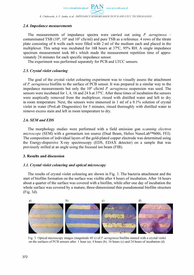
K. Chabowski, A. F. Junka, et al.: IMPEDANCE SENSORS MADE IN PCB AND LTCC TECHNOLOGIES …
2.4. Impedance measurements
The measurements of impedance spectra were carried out using P. aeruginosa –
contaminated TSB (106, 104 and 102 cfu/ml) and pure TSB as a reference. 4 rows of the titrate
plate consisting of 6 wells each were filled with 2 ml of the medium each and placed in the multiplexer. This setup was incubated for 168 hours at 37ºC, 95% RH. A single impedance
spectrum measurement took 60 s which made the measurement repetition time of appro-ximately 24 minutes for each specific impedance sensor.
The experiment was performed separately for PCB and LTCC sensors.
2.5. Crystal violet colouring
The goal of the crystal violet colouring experiment was to visually assess the attachment
of P. aeruginosa biofilm to the surface of PCB sensor. It was prepared in a similar way to the
impedance measurements but only the 106 cfu/ml P. aeruginosa suspension was used. The sensors were incubated for 1, 4, 16 and 24 h at 37ºC. After these times of incubation the sensors
were aseptically removed from the multiplexer, rinsed with distilled water and left to dry in room temperature. Next, the sensors were immersed in 1 ml of a 0.1% solution of crystal violet in water (ProLab Diagnostics) for 5 minutes, rinsed thoroughly with distilled water to
remove excess stain and left in room temperature to dry.
2.6. SEM and EDS
The morphology studies were performed with a field emission gun scanning electron
microscope (SEM) with a germanium ion source (Dual Beam, Helios NanoLab™600i, FEI). The composition of individual layers of the gold-plated copper electrode was determined using
the Energy-dispersive X-ray spectroscopy (EDS, EDAX detector) on a sample that was previously milled at an angle using the focused ion beam (FIB).
3. Results and discussion
3.1. Crystal violet colouring and optical microscopy
The results of crystal violet colouring are shown in Fig. 3. The bacteria attachment and the start of biofilm formation on the surface was visible after 4 hours of incubation. After 16 hours about a quarter of the surface was covered with a biofilm, while after one day of incubation the
whole surface was covered by a mature, three-dimensional thin pseudomonal biofilm structure (Fig. 3d).
a) b) c) d)
Fig. 3. Optical microscopy images (magnitude 40 x) of P. aeruginosa biofilm stained with a crystal violet on the surfaces of PCB sensors after: 1 hour (a); 4 hours (b); 16 hours (c) and 24 hours of incubation (d).
372
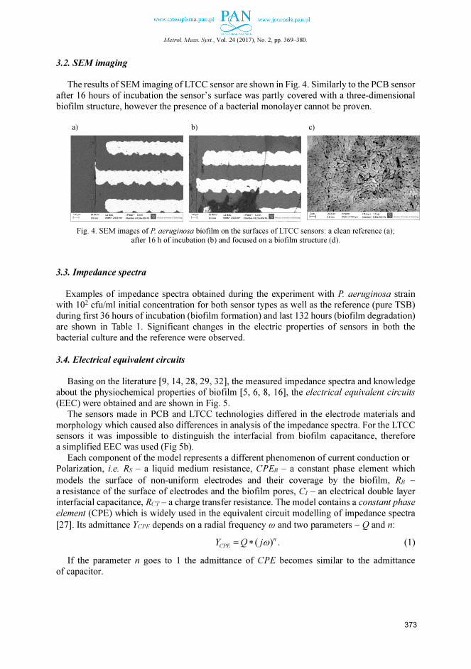
Metrol. Meas. Syst., Vol. 24 (2017), No. 2, pp. 369–380.
3.2. SEM imaging
The results of SEM imaging of LTCC sensor are shown in Fig. 4. Similarly to the PCB sensor
after 16 hours of incubation the sensor’s surface was partly covered with a three-dimensional
biofilm structure, however the presence of a bacterial monolayer cannot be proven. a) b) c)
Fig. 4. SEM images of P. aeruginosa biofilm on the surfaces of LTCC sensors: a clean reference (a);
after 16 h of incubation (b) and focused on a biofilm structure (d).
3.3. Impedance spectra
Examples of impedance spectra obtained during the experiment with P. aeruginosa strain with 102 cfu/ml initial concentration for both sensor types as well as the reference (pure TSB) during first 36 hours of incubation (biofilm formation) and last 132 hours (biofilm degradation)
are shown in Table 1. Significant changes in the electric properties of sensors in both the bacterial culture and the reference were observed.
3.4. Electrical equivalent circuits
Basing on the literature [9, 14, 28, 29, 32], the measured impedance spectra and knowledge about the physiochemical properties of biofilm [5, 6, 8, 16], the electrical equivalent circuits
(EEC) were obtained and are shown in Fig. 5. The sensors made in PCB and LTCC technologies differed in the electrode materials and
morphology which caused also differences in analysis of the impedance spectra. For the LTCC sensors it was impossible to distinguish the interfacial from biofilm capacitance, therefore a simplified EEC was used (Fig 5b).
Each component of the model represents a different phenomenon of current conduction or Polarization, i.e. RS – a liquid medium resistance, CPEB – a constant phase element which
models the surface of non-uniform electrodes and their coverage by the biofilm, RB −
a resistance of the surface of electrodes and the biofilm pores, CI – an electrical double layer interfacial capacitance, RCT – a charge transfer resistance. The model contains a constant phase
element (CPE) which is widely used in the equivalent circuit modelling of impedance spectra
[27]. Its admittance YCPE depends on a radial frequency ω and two parameters − Q and n:
n
CPEjQY )( ω∗= . (1)
If the parameter n goes to 1 the admittance of CPE becomes similar to the admittance
of capacitor.
373

K. Chabowski, A. F. Junka, et al.: IMPEDANCE SENSORS MADE IN PCB AND LTCC TECHNOLOGIES …
Table 1. Typical impedance spectra of sensors placed in a medium with P. aeruginosa strain (102 cfu/ml initial concentration). Black arrows point to changes of impedance spectra in time.
Stage\Sensor PCB LTCC
Biofilm formation
Biofilm
degradation
Reference
a) b)
Fig. 5. Electrical equivalent circuits of PCB (a) and LTCC (b) sensors placed in a medium with bacteria.
374

Metrol. Meas. Syst., Vol. 24 (2017), No. 2, pp. 369–380.
3.5. Electrical equivalent circuit analysis of PCB sensors The impedance spectra obtained in the experiment were analysed using ZView software
(Scribner) and EEC modelling using the EEC shown in Fig. 5a. Each experiment was repeated 6 times. Changes of the calculated mean values and standard deviations of EEC parameters
during 168 hours of incubation are shown in Fig. 6a-6f while a result of the impedance spectra fitting is shown in Fig 6g.
The most eye-catching EEC parameter is RCT. For the PCB sensors in P.aeruginosa-
containing wells a rapid rise of RCT can be observed in the third, fifth and seventh hour of measurement for 106, 104 and 102 cfu/ml initial concentrations, respectively. The RCT value
for sensors in P.aeruginosa with lower initial concentrations achieves a quasi-plateau state while for the reference it slowly decreases. This parameter is a sensitive indicator of the moment, when the area of sensor’s electrodes is fully covered by the biofilm because the biofilm
can be regarded as an electrical insulator [29].
a) b) c)
d) e) f)
g)
Fig. 6. Changes of mean value (points) and standard deviation (error bars) of EEC parameters in time during
incubation: RCT (a); RS (b); CPEB-Q (c); CPEB-n (d); CI (e); RB (f); and examples of measured (dots)
and fitted (lines) impedance spectra for 102 cfu/ml at 36th hour (g).
The value of liquid resistance RS almost continuously decreases in samples with
P.aeruginosa while for the reference it achieves a plateau state between the fourth and sixteenth
hours – then it decreases too − probably because of the increased ionic concentration caused
375

K. Chabowski, A. F. Junka, et al.: IMPEDANCE SENSORS MADE IN PCB AND LTCC TECHNOLOGIES …
by corrosion of electrodes. Additionally, the behaviour of CPEB is very interesting. The values
of Q and n parameters of CPEB in the first stage of measurement fluctuate for each data series. The situation becomes stable in the eighth hour of measurement when CPEB-Q slowly decreases for sensors in P.aeruginosa solution and after the thirty-second hour it increases again, while
for the reference it grows continuously. The same situation − inversely − occurs for the CPEB-
n parameter values. The CI and RB seem to not carry any useful information as changes of their values were observed also in the reference and values of their standard deviations are quite
high.
3.6. Electrical equivalent circuit analysis of LTCC sensors
As previously, the impedance spectra obtained in the experiments repeated 6 times were
analysed using ZView software (Scribner) and EEC modelling using the EEC simpler than that in the case of PCB sensors, shown in Fig. 5b. Changes of the calculated values of EEC
parameters during 168 hours of incubation are shown in Fig. 7a − 7d while a result of the impedance spectra fitting is shown in Fig. 7e.
In this case the most important EEC component is CPEB, which clearly reflects a current
state of pseudomonal biofilm. The adhesion stage is finished during first hours of the
experiment and − depending on the initial cell concentration − goes to the growth phase which is represented by a constant growth of CPEB-Q value and a corresponding decrease of CPEB-n
value. About the 36th hour (depending on the initial concentration) the biofilm enters the degradation phase resulting in a smooth decrease of CPEB-Q value and a slow growth of CPEB-n value. There should be noted that the CPEB reference value is quasi-constant during the whole
experiment.
a) b) c)
e) f)
Fig. 7. Changes of mean value (points) and standard deviation (error bars) of EEC parameters in time during
incubation: CPEB-Q (a); CPEB-n (b); RS (c); RB (d); and examples of measured (dots) and fitted (lines)
impedance spectra for 102 cfu/ml at 36th hour (e).
376

Metrol. Meas. Syst., Vol. 24 (2017), No. 2, pp. 369–380.
A plot of RS values does not show any significant difference between the biofilm and
reference. Similarly, RB with one additional phenomenon – in the first 30 hours of experiment
the RB reference value exceeds 10 MΩ, then decreases and − after about 80 hours − achieves the same level as the rest. It is caused by the lack of bacterial biofilm in the reference and probably slow adhesion of TSB nutrients to the sensor surface which creates some kind of a
conductive layer between electrodes.
3.7. SEM and EDS examination of PCB electrodes
As shown in Sections 3.3 and 3.5 the impedance spectra of reference sensors and their EEC
parameters varied in time. It may suggest that − despite the absence of bacteria − the sensor’s surface degrades in a corrosive environment. To examine that possibility a single sensor
prepared as in Section 2.2 was incubated in 0.9% NaCl aqueous solution for 48 hours. This solution in respect of a corrosive factor is very similar to TSB but does not leave any residue on the sensor.
Fig. 8. A SEM image of a sensor’s gold-plated electrode after incubation in 0.9% NaCl aqueous solution
for 48 hours. Corrosion of metal layers under gold plates can be seen.
Fig. 9. A SEM image of a sensor’s electrode etched by FIB and EDS place marked red (left).
The elemental results of EDS analysis (right).
The sensor surface after incubation was assessed using SEM (Fig. 8). In several points the pitting corrosion of the electrodes can be seen. It means that the gold layer was not tight and in
a pure corrosive environment corrosion of the electrodes can occur, influencing the EEC parameters.
A typical gold-electroplated metallic layer of PCB consists of three layers in a sandwich
structure: copper, nickel-phosphorus alloy and − finally − gold [32]. The percentage of each mentioned element in the sensor’s electrode was checked using the EDS analysis. Firstly, the sensor was prepared as described in Section 2.2 and then milled using the focused ion beam
(FIB), as shown in Fig. 9. Then, the EDS analysis was performed. The obtained results confirmed a sandwich structure of metal layers – copper is the bottom one, covered by nickel-
phosphorus and gold. As can be seen in Fig. 8. and in Table 2, the percentage of gold layer is very low. In effect the gold layer is not tight and the metallic layers under it are not protected
from corrosion.
377
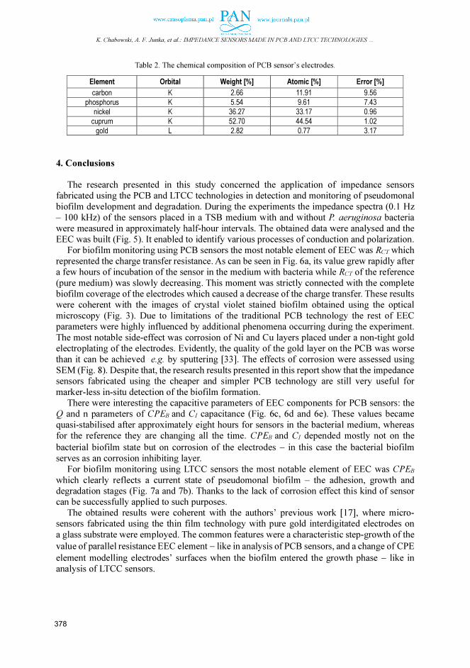
K. Chabowski, A. F. Junka, et al.: IMPEDANCE SENSORS MADE IN PCB AND LTCC TECHNOLOGIES …
Table 2. The chemical composition of PCB sensor’s electrodes.
Element Orbital Weight [%] Atomic [%] Error [%]
carbon K 2.66 11.91 9.56
phosphorus K 5.54 9.61 7.43
nickel K 36.27 33.17 0.96
cuprum K 52.70 44.54 1.02
gold L 2.82 0.77 3.17
4. Conclusions
The research presented in this study concerned the application of impedance sensors fabricated using the PCB and LTCC technologies in detection and monitoring of pseudomonal
biofilm development and degradation. During the experiments the impedance spectra (0.1 Hz – 100 kHz) of the sensors placed in a TSB medium with and without P. aeruginosa bacteria
were measured in approximately half-hour intervals. The obtained data were analysed and the EEC was built (Fig. 5). It enabled to identify various processes of conduction and polarization.
For biofilm monitoring using PCB sensors the most notable element of EEC was RCT which
represented the charge transfer resistance. As can be seen in Fig. 6a, its value grew rapidly after a few hours of incubation of the sensor in the medium with bacteria while RCT of the reference
(pure medium) was slowly decreasing. This moment was strictly connected with the complete biofilm coverage of the electrodes which caused a decrease of the charge transfer. These results were coherent with the images of crystal violet stained biofilm obtained using the optical
microscopy (Fig. 3). Due to limitations of the traditional PCB technology the rest of EEC parameters were highly influenced by additional phenomena occurring during the experiment.
The most notable side-effect was corrosion of Ni and Cu layers placed under a non-tight gold electroplating of the electrodes. Evidently, the quality of the gold layer on the PCB was worse than it can be achieved e.g. by sputtering [33]. The effects of corrosion were assessed using
SEM (Fig. 8). Despite that, the research results presented in this report show that the impedance sensors fabricated using the cheaper and simpler PCB technology are still very useful for
marker-less in-situ detection of the biofilm formation. There were interesting the capacitive parameters of EEC components for PCB sensors: the
Q and n parameters of CPEB and CI capacitance (Fig. 6c, 6d and 6e). These values became
quasi-stabilised after approximately eight hours for sensors in the bacterial medium, whereas for the reference they are changing all the time. CPEB and CI depended mostly not on the
bacterial biofilm state but on corrosion of the electrodes − in this case the bacterial biofilm
serves as an corrosion inhibiting layer. For biofilm monitoring using LTCC sensors the most notable element of EEC was CPEB
which clearly reflects a current state of pseudomonal biofilm – the adhesion, growth and degradation stages (Fig. 7a and 7b). Thanks to the lack of corrosion effect this kind of sensor can be successfully applied to such purposes.
The obtained results were coherent with the authors’ previous work [17], where micro-sensors fabricated using the thin film technology with pure gold interdigitated electrodes on
a glass substrate were employed. The common features were a characteristic step-growth of the
value of parallel resistance EEC element − like in analysis of PCB sensors, and a change of CPE
element modelling electrodes’ surfaces when the biofilm entered the growth phase − like in analysis of LTCC sensors.
378

Metrol. Meas. Syst., Vol. 24 (2017), No. 2, pp. 369–380.
Acknowledgements
This work was supported by Wrocław University of Technology statutory grant.
References
[1] O’Toole, G.A. (2002). A resistance switch. Nature, 416, 695−696.
[2] Flemming, H.C., Wingender, J. (2010). The biofilm matrix. Nat. Rev. Microbiol., 8, 623–633.
[3] Costerton, J.W., Stewart, P.S., Greenberg, E.P. (1999). Bacterial Biofilms: A Common Cause of Persistent
Infections. Science, 284, 1318-1332.
[4] James, G.A., Swogger, E., Wolcott, R., Pulcini, E., Secor, P., Sestrich, J., Costerton, J.W., Stewart, P.S.
(2008). Biofilms in chronic wounds. Wound Repair Reg., 16, 37–44.
[5] Kim, T., Kang, J., Lee, J.H., Yoon, J. (2011). Influence of attached bacteria and biofilm on double-layer capacitance during biofilm monitoring by electrochemical impedance spectroscopy. Water Res., 45, 4615–
4622.
[6] Ben-Yoav, H., Freeman, A., Sternheim, M., Shacham-Diamand, Y. (2011). An electrochemical impedance
model for integrated bacterial biofilms. Electrochim. Acta, 56, 7780–7786.
[7] Cady, P., Dufour, S.W., Lawless, P., Nunke, B., Kraeger, S. J. (1978). Impedimetric screening for bacteriuria.
J. Clin. Microbiol., 7, 273–278.
[8] Muñoz-Berbel, X., Vigués, N., Jenkins, A.T.A., Mas, J., Muñoz, F.J. (2008). Impedimetric approach for
quantifying low bacteria concentrations based on the changes produced in the electrode-solution interface
during the pre-attachment stage. Biosens. Bioelectron., 23, 1540–1546.
[9] Yang, L., Li, Y., Griffis, C.L., Johnson, M.G. (2004). Interdigitated microelectrode (IME) impedance sensor
for the detection of viable Salmonella typhimurium. Biosens. Bioelectron., 19, 1139–1147.
[10] Farrow, M.J., Hunter, I.S., Connolly, P. (2012). Developing a Real Time Sensing System to Monitor Bacteria
in Wound Dressings. Biosensors, 4, 171–188.
[11] Paredes, J., Becerro, S., Arizti, F., Aguinaga, A., Del Pozo, J.L., Arana, S. (2013). Interdigitated
microelectrode biosensor for bacterial biofilm growth monitoring by impedance spectroscopy technique in
96-well microtiter plates. Sensor. Actuat. B-Chem., 178, 663–670.
[12] Paredes, J., Becerro, S., Arizti, F., Aguinaga, A., Del Pozo, J.L., Arana, S. (2012). Real time monitoring of the impedance characteristics of Staphylococcal bacterial biofilm cultures with a modified CDC reactor
system. Biosens. Bioelectron., 38, 226–322.
[13] Dheilly, A., Linossier, I., Darchen, A., Hadjiev, D., Corbel, C., Alonso, V. (2008). Monitoring of microbial
adhesion and biofilm growth using electrochemical impedancemetry. Appl. Microbiol. Biot., 79, 157–164.
[14] Piasecki, T., Guła, G., Nitsch, K., Waszczuk, K., Drulis-Kawa, Z., Gotszalk, T. (2013). Evaluation
of Pseudomonas aeruginosa biofilm formation using Quartz Tuning Forks as impedance sensors. Sensor.
Actuat. B-Chem., 189, 60−65.
[15] Muñoz-Berbel, X., Muñoz, F.J., Vigués, N., Mas, J. (2006). On-chip impedance measurements to monitor
biofilm formation in the drinking water distribution network. Sensor. Actuat. B-Chem., 118, 129–134.
[16] Yang, L., Ruan, C., Li, Y. Detection of viable Salmonella typhimurium by impedance measurement
of electrode capacitance and medium resistance. Biosens. Bioelectron., 19, 495–502.
[17] Chabowski, K., Junka, A.F., Szymczyk, P., Piasecki, T., Sierakowski, A., Mączyńska, B., Nitsch, K. (2015).
The Application of Impedance Microsensors for Real-Time Analysis of Pseudomonas aeruginosa Biofilm Formation. Pol. J. Microbiol., 64, 115–120.
[18] Tsouti, V., Boutopoulos, C., Zergioti, I., Chatzandroulis, S. (2011). Capacitive microsystems for biological
sensing. Biosens. Bioelectron., 27, 1−11.
[19] Bhavsar, K., Fairchild, A., Alonas, E., Bishop, D.K., La Belle, J.T., Sweeney, J., Alford, T.L., Joshi, L. (2009).
A cytokine immunosensor for Multiple Sclerosis detection based upon label-free electrochemical impedance
spectroscopy using electroplated printed circuit board electrode. Biosens. Bioelectron., 25, 506−509.
379

K. Chabowski, A. F. Junka, et al.: IMPEDANCE SENSORS MADE IN PCB AND LTCC TECHNOLOGIES …
[20] Nordin, A.N., Tarmizi, A.U., Ariff, M., Ghani, A., Mel, M. (2012). Printed Circuit Board Cultureware for
Analysis of Colorectal Carcinoma Cells using Impedance Spectroscopy. 2012 IEEE EMBS International
Conference on Biomedical Engineering and Sciences, 574–578.
[21] La Belle, J.T., Fairchild, A., Demirok, U.K., Verma, A. (2013). Method for fabrication and verification of
conjugated nanoparticle-antibody tuning elements for multiplexed electrochemical biosensors. Methods, 61,
39–51.
[22] Ciosek, P., Zawadzki, K., Łopacińska, J., Skolimowski, M., Bembnowicz, P., Golonka, L. J., Brzózka, Z.,
Wróblewski, W. (2009). Monitoring of cell cultures with LTCC microelectrode array. Anal. Bioanal. Chem.,
393, 2029–2038.
[23] Jędrychowska, A., Malecha, K., Cabaj, J., Sołoducho, J. (2015). Laccase biosensor based on low temperature
co-fired ceramics for the permanent monitoring of water solutions. Electrochim. Acta, 165, 372–382.
[24] Malecha, K., Pijanowska, D.G., Golonka, L.J., Kurek, P. (2011). Low temperature co-fired ceramic (LTCC)-
based biosensor for continuous glucose monitoring. Sensor. Actuat. B-Chem., 155, 923–929.
[25] Ciosek, P., Zawadzki, K., Stadnik, D., Bembnowicz, P., Golonka, L., Wróblewski, W. (2009). Microelectrode
array fabricated in low temperature cofired ceramic (LTCC) technology. J. Solid State Electrochem., 13, 129–
135.
[26] Vasudev, A., Kaushik, A., Tomizawa, Y., Norena, N., Bhansali, S. (2013). An LTCC-based microfluidic
system for label-free, electrochemical detection of cortisol. Sensor. Actuat. B-Chem., 182, 139−146.
[27] Barsoukov, E., Macdonald, J.R. (2005). Impedance Spectroscop. Theory, Experiment and Applications. John
Wiley & Sons.
[28] Zheng, L.Y., Congdon, R.B., Sadik, O.A., Marques, C.N.H., Davies, D.G., Sammakia, B.G., Turner, J.N.
(2013). Electrochemical measurements of biofilm development using polypyrrole enhanced flexible sensors,
Sensor. Actuat. B-Chem., 182, 725–732.
[29] Muñoz-Berbel, X., García-Aljaro, C., Muñoz, F.J. (2008). Impedimetric approach for monitoring the
formation of biofilms on metallic surfaces and the subsequent application to the detection of bacteriophages,
Electrochim. Acta, 53, 5739–5744.
[30] Piasecki, T., Chabowski, K., Nitsch, K. (2016). Design, calibration and tests of versatile low frequency
impedance analyser based on ARM microcontroller. Measurement, 91, 155−161.
[31] Piasecki, T. (2015). Fast impedance measurements at very low frequencies using curve fitting algorithms.
Meas. Sci. Technol., 26, 065002.
[32] Babauta, J.T., Beyenal, H. (2014). Mass transfer studies of Geobacter sulfurreducens biofilms on rotating
disk electrodes, Biotechnol. Bioeng., 111, 285–294.
[33] Bozkurt, A., Lal, A. (2011). Low-cost flexible printed circuit technology based microelectrode array for
extracellular stimulation of the invertebrate locomotory system. Sensor. Actuat. A-Phys., 169, 89–97.

Metrol. Meas. Syst., Vol. 24 (2017), No. 2, pp. 381–390.
_____________________________________________________________________________________________________________________________________________________________________________________
Article history: received on Aug. 03, 2016; accepted on Dec. 16, 2016; available online on Jun. 30, 2017; DOI: 10.1515/mms-2017-0028.
METROLOGY AND MEASUREMENT SYSTEMS
Index 330930, ISSN 0860-8229 www.metrology.pg.gda.pl
MEASUREMENT OF SURFACE PROFILE AND SURFACE ROUGHNESS
OF FIBRE-OPTIC INTERCONNECT BY FAST FOURIER TRANSFORM
Chern S. Lin1), Shih W. Yang2), Hung L. Lin1), Jhih W. Li1)
1) Feng Chia University, Department of Automatic Control Engineering, 100 Wenhwa Road, Seatwen, Taichung, Taiwan ( [email protected], +886 4 2451 7250 3900, [email protected], [email protected]) 2) National Chiao Tung University, College of Electrical and Computer Engineering, 1001 University Road, Hsinchu, Taiwan ([email protected])
Abstract
This study proposes a surface profile and roughness measurement system for a fibre-optic interconnect based
on optical interferometry. On the principle of Fizeau interferometer, an interference fringe is formed on the fibre
end-face of the fibre-optic interconnect, and the fringe pattern is analysed using the Fast Fourier transform method to reconstruct the surface profile. However, as the obtained surface profile contains some amount of tilt, a rule for
estimating this tilt value is developed in this paper. The actual fibre end-face surface profile is obtained by
subtracting the estimated tilt amount from the surface profile, as calculated by the Fast Fourier transform method,
and the corresponding surface roughness can be determined. The proposed system is characterized by non-contact
measurement, and the sample is not coated with a reflector during measurement. According to the experimental
results, the difference between the roughness measurement result of an Atomic Force Microscope (AFM) and the
measurement result of this system is less than 3 nm.
Keywords: surface profile, surface roughness, fibre end-face, Fast Fourier transform.
© 2017 Polish Academy of Sciences. All rights reserved
1. Introduction
Fibre-optic communication has become the main media of the present communication transmission. For example, the fibre-optic interconnect technology “Thunderbolt” released by
Intel transmits data as light signals via optical fibre instead of copper wire [1−2], so the optical
fibre and traditional USB joint are interconnected to increase the transmission rate. The Thunderbolt technology has a key fibre-optic interconnect. The entire fibre module comprises
three connectors: an optical/electric conversion part (O/E part), a receptacle lens (Re-Lens), and a plug lens. The O/E Part is a connector for the O/E module and optical fibre, laser cut optical fibres are directly inserted in four holes in the front end of the O/E Part, and the end faces
of these fibres and the holes are aligned with a co-plane (fibre tips were not polished), as shown in Fig. 1.
Fig. 1. The O/E Part and a fibre end-face measured in this study.
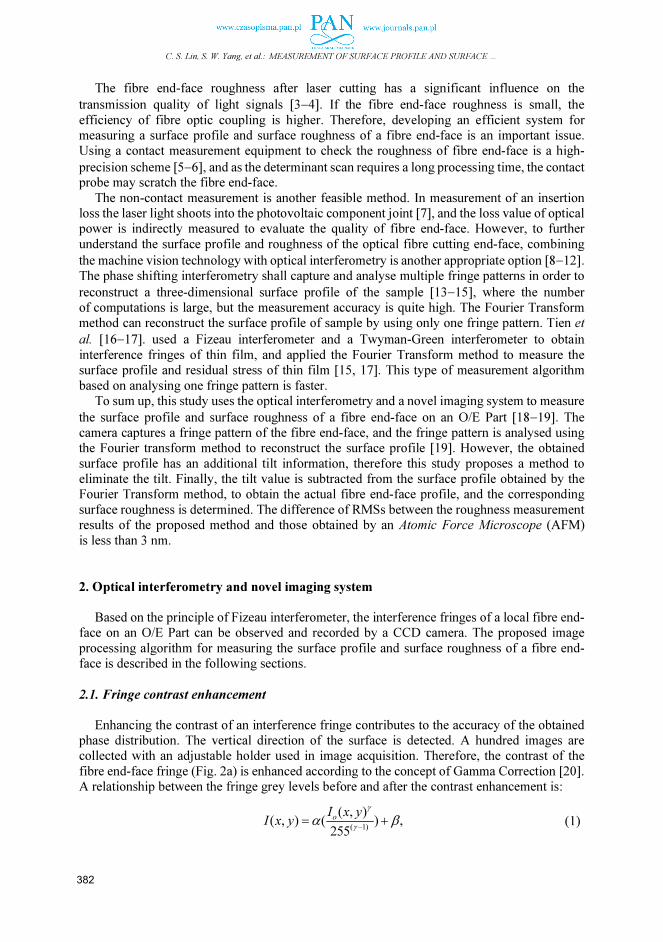
C. S. Lin, S. W. Yang, et al.: MEASUREMENT OF SURFACE PROFILE AND SURFACE …
The fibre end-face roughness after laser cutting has a significant influence on the
transmission quality of light signals [3−4]. If the fibre end-face roughness is small, the
efficiency of fibre optic coupling is higher. Therefore, developing an efficient system for measuring a surface profile and surface roughness of a fibre end-face is an important issue. Using a contact measurement equipment to check the roughness of fibre end-face is a high-
precision scheme [5−6], and as the determinant scan requires a long processing time, the contact probe may scratch the fibre end-face.
The non-contact measurement is another feasible method. In measurement of an insertion loss the laser light shoots into the photovoltaic component joint [7], and the loss value of optical power is indirectly measured to evaluate the quality of fibre end-face. However, to further
understand the surface profile and roughness of the optical fibre cutting end-face, combining
the machine vision technology with optical interferometry is another appropriate option [8−12]. The phase shifting interferometry shall capture and analyse multiple fringe patterns in order to
reconstruct a three-dimensional surface profile of the sample [13−15], where the number of computations is large, but the measurement accuracy is quite high. The Fourier Transform method can reconstruct the surface profile of sample by using only one fringe pattern. Tien et
al. [16−17]. used a Fizeau interferometer and a Twyman-Green interferometer to obtain
interference fringes of thin film, and applied the Fourier Transform method to measure the surface profile and residual stress of thin film [15, 17]. This type of measurement algorithm
based on analysing one fringe pattern is faster. To sum up, this study uses the optical interferometry and a novel imaging system to measure
the surface profile and surface roughness of a fibre end-face on an O/E Part [18−19]. The camera captures a fringe pattern of the fibre end-face, and the fringe pattern is analysed using the Fourier transform method to reconstruct the surface profile [19]. However, the obtained
surface profile has an additional tilt information, therefore this study proposes a method to eliminate the tilt. Finally, the tilt value is subtracted from the surface profile obtained by the Fourier Transform method, to obtain the actual fibre end-face profile, and the corresponding
surface roughness is determined. The difference of RMSs between the roughness measurement results of the proposed method and those obtained by an Atomic Force Microscope (AFM)
is less than 3 nm.
2. Optical interferometry and novel imaging system
Based on the principle of Fizeau interferometer, the interference fringes of a local fibre end-
face on an O/E Part can be observed and recorded by a CCD camera. The proposed image
processing algorithm for measuring the surface profile and surface roughness of a fibre end-face is described in the following sections.
2.1. Fringe contrast enhancement
Enhancing the contrast of an interference fringe contributes to the accuracy of the obtained phase distribution. The vertical direction of the surface is detected. A hundred images are collected with an adjustable holder used in image acquisition. Therefore, the contrast of the
fibre end-face fringe (Fig. 2a) is enhanced according to the concept of Gamma Correction [20]. A relationship between the fringe grey levels before and after the contrast enhancement is:
( 1)
( , )( , ) ( ) ,
255
oI x y
I x yγ
γα β
−
= + (1)
382
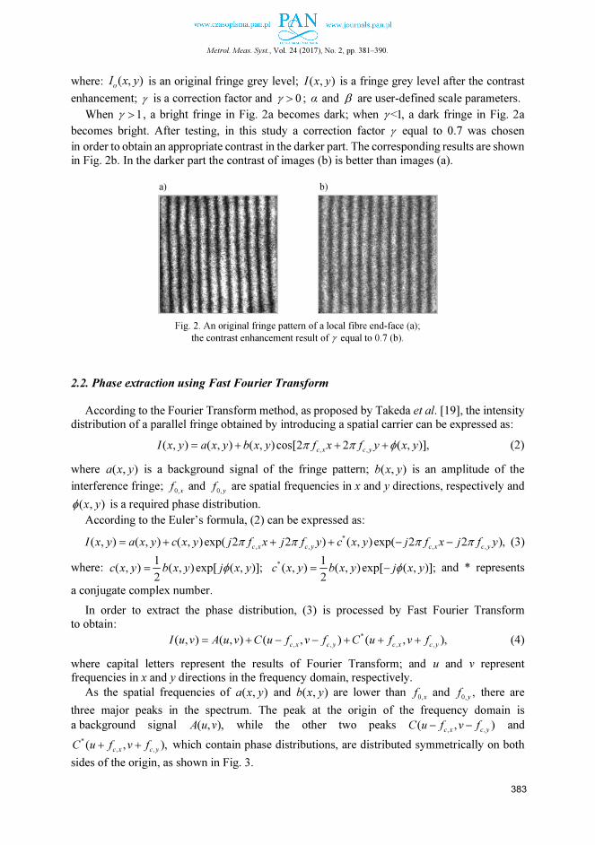
Metrol. Meas. Syst., Vol. 24 (2017), No. 2, pp. 381–390.
where: ( , )oI x y is an original fringe grey level; ( , )I x y is a fringe grey level after the contrast
enhancement; γ is a correction factor and 0γ > ; α and β are user-defined scale parameters.
When 1γ > , a bright fringe in Fig. 2a becomes dark; when <1,γ a dark fringe in Fig. 2a
becomes bright. After testing, in this study a correction factor γ equal to 0.7 was chosen
in order to obtain an appropriate contrast in the darker part. The corresponding results are shown
in Fig. 2b. In the darker part the contrast of images (b) is better than images (a). a) b)
Fig. 2. An original fringe pattern of a local fibre end-face (a);
the contrast enhancement result of γ equal to 0.7 (b).
2.2. Phase extraction using Fast Fourier Transform
According to the Fourier Transform method, as proposed by Takeda et al. [19], the intensity distribution of a parallel fringe obtained by introducing a spatial carrier can be expressed as:
, ,
( , ) ( , ) ( , ) cos[2 2 ( , )],c x c y
I x y a x y b x y f x f y x yπ π φ= + + + (2)
where ( , )a x y is a background signal of the fringe pattern; ( , )b x y is an amplitude of the
interference fringe; 0,xf and
0, yf are spatial frequencies in x and y directions, respectively and
( , )x yφ is a required phase distribution.
According to the Euler’s formula, (2) can be expressed as:
*
, , , ,( , ) ( , ) ( , ) exp( 2 2 ) ( , ) exp( 2 2 ),
c x c y c x c yI x y a x y c x y j f x j f y c x y j f x j f yπ π π π= + + + − − (3)
where: 1
( , ) ( , ) exp[ ( , )];2
c x y b x y j x yφ= * 1( , ) ( , ) exp[ ( , )];
2c x y b x y j x yφ= − and * represents
a conjugate complex number.
In order to extract the phase distribution, (3) is processed by Fast Fourier Transform to obtain:
*
, , , ,( , ) ( , ) ( , ) ( , ),
c x c y c x c yI u v A u v C u f v f C u f v f= + − − + + + (4)
where capital letters represent the results of Fourier Transform; and u and v represent frequencies in x and y directions in the frequency domain, respectively.
As the spatial frequencies of ( , )a x y and ( , )b x y are lower than 0,xf and
0,,
yf there are
three major peaks in the spectrum. The peak at the origin of the frequency domain is
a background signal ( , ),A u v while the other two peaks , ,
( , )c x c y
C u f v f− − and
*
, ,( , ),
c x c yC u f v f+ + which contain phase distributions, are distributed symmetrically on both
sides of the origin, as shown in Fig. 3.
383
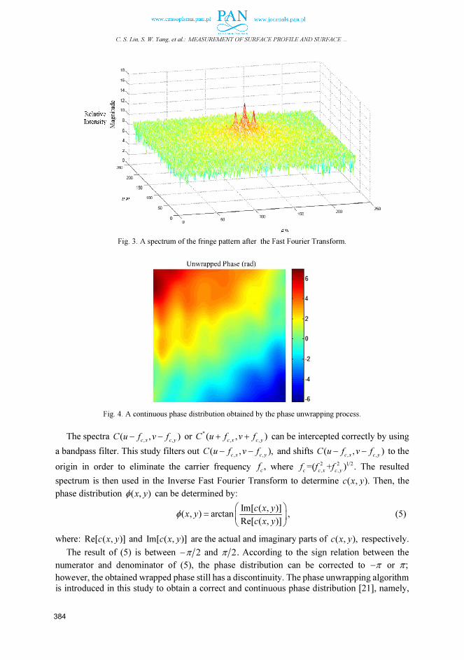
C. S. Lin, S. W. Yang, et al.: MEASUREMENT OF SURFACE PROFILE AND SURFACE …
Fig. 3. A spectrum of the fringe pattern after the Fast Fourier Transform.
Fig. 4. A continuous phase distribution obtained by the phase unwrapping process.
The spectra , ,
( , )c x c y
C u f v f− − or *
, ,( , )
c x c yC u f v f+ + can be intercepted correctly by using
a bandpass filter. This study filters out , ,
( , ),c x c y
C u f v f− − and shifts , ,
( , )c x c y
C u f v f− − to the
origin in order to eliminate the carrier frequency ,
cf where 2 2 1 2
, ,=( + ) .
c c x c yf f f The resulted
spectrum is then used in the Inverse Fast Fourier Transform to determine ( , ).c x y Then, the
phase distribution ( , )x yφ can be determined by:
Im[ ( , )]
( , ) arctan ,Re[ ( , )]
c x yx y
c x yφ
=
(5)
where: Re[ ( , )]c x y and Im[ ( , )]c x y are the actual and imaginary parts of ( , ),c x y respectively.
The result of (5) is between 2π− and 2.π According to the sign relation between the
numerator and denominator of (5), the phase distribution can be corrected to π− or ;π
however, the obtained wrapped phase still has a discontinuity. The phase unwrapping algorithm is introduced in this study to obtain a correct and continuous phase distribution [21], namely,
384
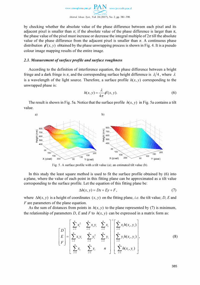
Metrol. Meas. Syst., Vol. 24 (2017), No. 2, pp. 381–390.
by checking whether the absolute value of the phase difference between each pixel and its
adjacent pixel is smaller than π; if the absolute value of the phase difference is larger than π, the phase value of the pixel must increase or decrease the integral multiple of 2π till the absolute value of the phase difference from the adjacent pixel is smaller than π. A continuous phase
distribution ( , )x yφ′ obtained by the phase unwrapping process is shown in Fig. 4. It is a pseudo
colour image mapping results of the entire image.
2.3. Measurement of surface profile and surface roughness
According to the definition of interference equation, the phase difference between a bright
fringe and a dark fringe is π, and the corresponding surface height difference is 4λ , where λ
is a wavelength of the light source. Therefore, a surface profile ( , )h x y corresponding to the
unwrapped phase is:
( , ) ( , ).4
h x y x yλ
φπ
′= (6)
The result is shown in Fig. 5a. Notice that the surface profile ( , )h x y in Fig. 5a contains a tilt
value.
a) b)
Fig. 5. A surface profile with a tilt value (a); an estimated tilt value (b).
In this study the least square method is used to fit the surface profile obtained by (6) into a plane, where the value of each point in this fitting plane can be approximated as a tilt value
corresponding to the surface profile. Let the equation of this fitting plane be:
( , ) ,h x y Dx Ey F∆ = + + (7)
where ( , )h x y∆ is a height of coordinates ( , )x y on the fitting plane, i.e. the tilt value; D, E and
F are parameters of the plane equation.
As the sum of distances from points in ( , )h x y to the plane represented by (7) is minimum,
the relationship of parameters D, E and F to ( , )h x y can be expressed in a matrix form as:
1
2
1 1 1 1
2
1 1 1 1
1 1 1
( , )
( , ) ,
( , )
n n n n
i i i i i i i
i i i i
n n n n
i i i i i i i
i i i i
n n n
i i i i
i i i
x x y x x h x y
D
E x y y y y h x y
F
x y n h x y
−
= = = =
= = = =
= = =
=
∑ ∑ ∑ ∑
∑ ∑ ∑ ∑
∑ ∑ ∑
(8)
385

C. S. Lin, S. W. Yang, et al.: MEASUREMENT OF SURFACE PROFILE AND SURFACE …
where: n is the total number of pixels in the fringe pattern; ( , )i ix y are the coordinates of No. i
pixel in ( , )h x y ; and ( , )i i
h x y is a height of the pixel ( , )i ix y .
According to the parameters obtained by (8), the tilt value in Fig. 5a can be estimated, as
shown in Fig. 5b. The actual fibre end-face surface profile ( , )H x y can be calculated by:
( , ) ( , ) ( , ).H x y h x y h x y= − ∆ (9)
The surface roughness of the fibre end-face can be calculated based on the result of (9). In this study mean roughness (Ra) and root-mean-square roughness (Rq) are selected as the
measurement targets:
=
∑ |(
,) − ⟨,⟩|, (10)
=
∑ [(
,) − ⟨(,)⟩]/, (11)
where ( , )i i
H x y is an actual height of No. i pixel in the fringe pattern; and ( , )H x y is an
average of the actual height.
3. Experimental results and discussion
3.1. Experimental setup
This system obtains the fringe pattern of a fibre end-face on the principle of Fizeau
interferometer, and analyses the fringe pattern in order to measure the surface roughness. The O/E Part is placed on a mounting device, and an optical flat (λ/20 flat, Edmund Optics) is set up above the O/E Part. A red light semiconductor laser is used as the system light source
(λ = 632.8 nm). The laser light is expanded by the fibre bundle, the coaxial light is formed by a beam splitter, and two light beams with similar intensities are split. One light beam irradiates
the optical flat (reference surface) through a high magnification objective lens, while the other light beam irradiates the fibre end-face of the O/E Part; this beam is then reflected to the beam splitter to form the interference fringe with the reference light. Finally, a CCD camera captures
the fringe pattern. The proposed system framework is shown in Fig. 6.
Fig. 6. A structure of the proposed system.
386
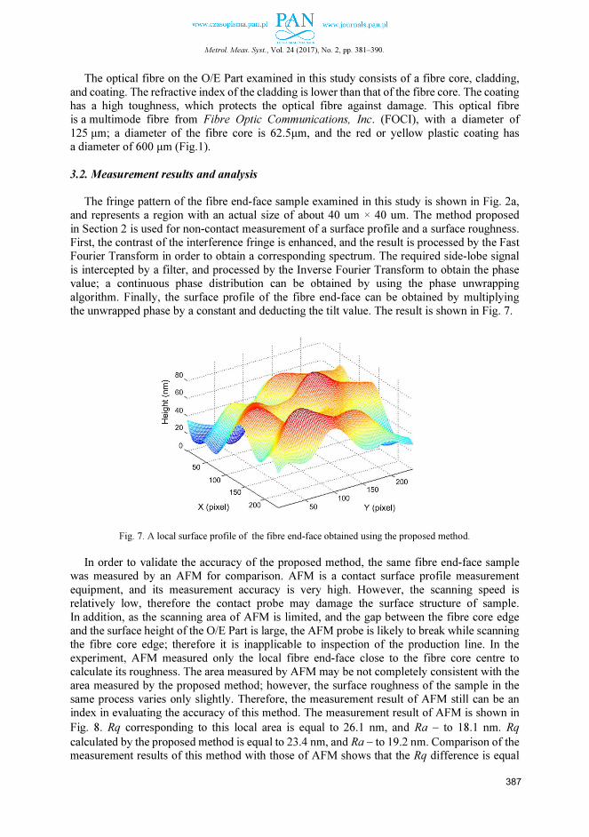
Metrol. Meas. Syst., Vol. 24 (2017), No. 2, pp. 381–390.
The optical fibre on the O/E Part examined in this study consists of a fibre core, cladding,
and coating. The refractive index of the cladding is lower than that of the fibre core. The coating has a high toughness, which protects the optical fibre against damage. This optical fibre is a multimode fibre from Fibre Optic Communications, Inc. (FOCI), with a diameter of
125 μm; a diameter of the fibre core is 62.5μm, and the red or yellow plastic coating has a diameter of 600 μm (Fig.1).
3.2. Measurement results and analysis
The fringe pattern of the fibre end-face sample examined in this study is shown in Fig. 2a, and represents a region with an actual size of about 40 um × 40 um. The method proposed
in Section 2 is used for non-contact measurement of a surface profile and a surface roughness. First, the contrast of the interference fringe is enhanced, and the result is processed by the Fast Fourier Transform in order to obtain a corresponding spectrum. The required side-lobe signal
is intercepted by a filter, and processed by the Inverse Fourier Transform to obtain the phase value; a continuous phase distribution can be obtained by using the phase unwrapping
algorithm. Finally, the surface profile of the fibre end-face can be obtained by multiplying the unwrapped phase by a constant and deducting the tilt value. The result is shown in Fig. 7.
Fig. 7. A local surface profile of the fibre end-face obtained using the proposed method.
In order to validate the accuracy of the proposed method, the same fibre end-face sample
was measured by an AFM for comparison. AFM is a contact surface profile measurement
equipment, and its measurement accuracy is very high. However, the scanning speed is relatively low, therefore the contact probe may damage the surface structure of sample.
In addition, as the scanning area of AFM is limited, and the gap between the fibre core edge and the surface height of the O/E Part is large, the AFM probe is likely to break while scanning the fibre core edge; therefore it is inapplicable to inspection of the production line. In the
experiment, AFM measured only the local fibre end-face close to the fibre core centre to calculate its roughness. The area measured by AFM may be not completely consistent with the
area measured by the proposed method; however, the surface roughness of the sample in the same process varies only slightly. Therefore, the measurement result of AFM still can be an index in evaluating the accuracy of this method. The measurement result of AFM is shown in
Fig. 8. Rq corresponding to this local area is equal to 26.1 nm, and Ra − to 18.1 nm. Rq
calculated by the proposed method is equal to 23.4 nm, and Ra − to 19.2 nm. Comparison of the measurement results of this method with those of AFM shows that the Rq difference is equal
387

C. S. Lin, S. W. Yang, et al.: MEASUREMENT OF SURFACE PROFILE AND SURFACE …
to 2.7 nm, and the Ra difference − to 1.1 nm. Thus, the difference is within 3 nm. The scope of random variation in results and differences can be neglected as statistically insignificant.
Fig. 8. The measurement result of AFM of the local part of sample.
The measurement result of AFM can validate the accuracy of the method presented in this study. The structure of it is simple, and its cost is lower than AFM’s [21]. In addition, when a contact equipment is used to measure the body surface of unknown materials, SEM is
sometimes required to evaluate the measurement feasibility in advance. However, this study concerns a non-contact measurement; the surface profile of sample can be reconstructed, and
the surface roughness can be measured by only one fringe pattern with a spatial carrier, which is quite easily visualised and convenient. It should be considered in this system that, when a magnitude of the introduced spatial carrier is changed by adjusting the angle of the optical
flat if the introduced spatial carrier is too small, the side-lobe peak position and background signal peak position would be too close to each other after applying the Fast Fourier Transform.
As a result of this phenomenon, a partial background signal will be captured along with capturing the side-lobe, resulting in a measurement error. If the introduced spatial carrier is too large, the fringe contrast decays and cannot be correctly analysed.
4. Conclusions
As the flatness of a fibre end-face after laser cutting can significantly influence the coupling efficiency of the O/E Part and the fibre optic coupler, in this study there is proposed a surface
profile and roughness measurement system as a solution to analysing a fibre end-face. The hardware is based on the Fizeau interferometer in order to obtain the interference fringe
of a local fibre end-face on the O/E Part. Then, the phase data are calculated using the Fast Fourier Transform, and the local surface profile and surface roughness are reconstructed. In addition, the accuracy of the proposed algorithm is validated experimentally and with
a program. Compared with the measurement result of AFM, the corresponding roughness difference is less than 3 nm. This system can assist manufacturers to accurately screen too rough
optical fibre samples, and its measurement results can be a reference frame for improving the process.
388

Metrol. Meas. Syst., Vol. 24 (2017), No. 2, pp. 381–390.
Acknowledgements
This research project was supported by the Ministry of Science and Technology, under Grant No. MOST 105-2221-E-035 -027.
References
[1] Chow, C.W., Yeh, C.H., Yang, L.G., Sung, J.Y., Huang, S.P. (2012). Design and characterization of large-
core optical fiber for Light Peak applications. Opt. Eng., 51(1), 015006.
[2] Yajima, Y., Watanabe, H., Kihara, M., Toyonaga, M. (2011). Optical performance of field assembly
connectors using incorrectly cleaved fiber ends. Opto-Electronics and Communications Conference (OECC),
617−618.
[3] Berdinskikh, T., Bragg, J., Tse, E., Daniel, J., Arrowsmith, P., Fisenko, A., Mahmoud, S. (2002). The
contamination of fiber optics connectors and their effect on optical performance. Optical Fiber
Communication Conference and Exhibit, 617−619.
[4] Garnaes, J., Kofod, N., Kühle, A., Nielsen, C., Dirscherl, K., Blunt, L. (2003). Calibration of step heights
and roughness measurements with atomic force microscopes. Precision Engineering, 27(1), 91−98.
[5] Poon, C.Y., Bhushan, B. (1995). Comparison of surface roughness measurements by stylus profiler. AFM
and non-contact optical profiler. Wear, 190(1), 76–88.
[6] Kihara, M., Okada, M., Hosoda, M., Iwata, T., Yajima, Y., Toyonaga, M. (2012). Tool for inspecting faults
from incorrectly cleaved fiber ends and contaminated optical fiber connector end surfaces. Optical Fiber
Technology, 18(6) 470−479.
[7] Lin, C.S., Lin, C.H., Lin, C.C., Yeh, M.S. (2010). Three-dimensional profile measurement of small lens
using subpixel localization with color grating. Optik, 121(23), 2122−2127.
[8] Lin, C.S., Loh, G.H., Tien, C.L., Lin, T.C., Chiou, Y.C. (2013). Automatic Optical Inspection System for
the Micro-lens of Optical Connector with Fuzzy Ratio Analysis. Optik, 124(17), 3085−3090.
[9] Lu, J., Chen, J., Xie, J., Wang, F., Tan, Z. (2013). A novel automatic method of fringe counter for equally
tilting fringe. Optik, 124(15), 2062−2066.
[10] Lin, C.S., Tzeng, G.A., Cheng, C.T., Lay, Y.L., Tien, C.L. (2014). An Automatic Optical Inspection System
for the Detection of Three Parallel Lines in Solar Panel End Face. Optik, 125(2), 688−693.
[11] Yang, S.W., Lin, S.K. (2014). Automatic Optical Inspection System for 3D Surface Profile Measurement
of Multi-Microlenses using Optimal Inspection Path. Measurement Science & Technology, 25(7), 075006.
[12] Wang, W.H., Wong, Y.S., Hong, G.S. (2006). 3D measurement of crater wear by phase shifting method.
Wear, 261(2), 164−171.
[13] Fu, Y., Wang, Z., Yang, J., Wang, J., Jiang, G. (2014). Three-dimensional profile measurement of the blade
based on multi-value coding. Optik, 125(11), 2592−2596.
[14] Chatterjee, S., Kumar, Y.P., Bhaduri, B. (2007). Measurement of surface figure of plane optical surfaces
with polarization phase-shifting Fizeau interferometer. Optics and Laser Technology, 39(2), 268−274.
[15] Tien, C.L., Yang, H.M., Liu, M.C. (2009). The measurement of surface roughness of optical thin films based
on fast Fourier transform. Thin Solid Films, 517(17), 5110−5115.
[16] Hu, E., Zhu, Y. (2013). 3D online measurement of spare parts with variable speed by using line-scan non-
contact method. Optik, 124(13), 1472−1476.
[17] Tien, C.L., Zeng, H.D. (2010). Measuring residual stress of anisotropic thin film by fast Fourier transform.
Optics Express, 18(16), 16594−16600.
[18] Park, C.W., Ryu, J.Y. (2008). Development of a new automatic gamma control system for mobile LCD
applications. Displays, 29(4), 393−400.
[19] Takeda, M., Mutoh, K. (1983). Fourier transform profilometry for the automatic measurement of 3-D object
shapes. Applied Optics, 22(24), 3977−3982.
389

C. S. Lin, S. W. Yang, et al.: MEASUREMENT OF SURFACE PROFILE AND SURFACE …
[20] Zhao, M., Huang, Q.H., Zhu, L.J., Qiu, Z.M. (2015). Automatic laser interferometer and vision measurement
system for stripe rod calibration. Metrol. Meas. Syst., 22(4), 491–502.
[21] Macy, W.W. (1983). Two-dimensional fringe-pattern analysis. Applied Optics, 22(23), 3898−3901.

Metrol. Meas. Syst., Vol. 24 (2017), No. 2, pp. 391–399.
_____________________________________________________________________________________________________________________________________________________________________________________
Article history: received on Jun. 13, 2016; accepted on Jan. 22, 2017; available online on Jun. 30, 2017; DOI: 10.1515/mms-2017-0029.
METROLOGY AND MEASUREMENT SYSTEMS
Index 330930, ISSN 0860-8229
www.metrology.pg.gda.pl
DOPANT-BASED CHARGE SENSING UTILIZING P-I-N NANOJUNCTION
Roland Nowak, Ryszard Jabłoński Warsaw University of Technology, Faculty of Mechatronics, Św. A. Boboli 8, 02-525 Warsaw, Poland ([email protected], [email protected], +48 22 234 8633)
Abstract
We studied lateral silicon p-i-n junctions, doped with phosphorus and boron, regarding charge sensing feasibility.
In order to examine the detection capabilities and underlying mechanism, we used in a complementary way two
measurement techniques. First, we employed a semiconductor parameter analyzer to measure I−V characteristics
at a low temperature, for reverse and forward bias conditions. In both regimes, we systematically detected Random
Telegraph Signal. Secondly, using a Low Temperature Kelvin Probe Force Microscope, we measured surface
electronic potentials. Both p-i-n junction interfaces, p-i and i-n, were observed as regions of a dynamic behaviour,
with characteristic time-dependent electronic potential fluctuations. Those fluctuations are due to single charge
capture/emission events. We found analytically that the obtained data could be explained by a model of two-
dimensional p-n junction and phosphorus-boron interaction at the edge of depletion region. The results
of complementary measurements and analysis presented in this research, supported also by the previous reports,
provide fundamental insight into the charge sensing mechanism utilizing emergence of individual dopants.
Keywords: nanosensor, silicon, p-i-n junction, dopant, Kelvin probe force microscope.
© 2017 Polish Academy of Sciences. All rights reserved
1. Introduction
Rapid development of nanotechnology in the past 20 years also inevitably influences the field of metrology. The conventional sensors are not suitable anymore to be used in nano-
sized objects,due to their extremely small size and appearance of non-classical (i.e., quantum) effects. This is the main force driving the development of a new class of sensors – nanosensors.
Shortly, such sensors are able to detect and transduce information about objects (e.g. DNA molecules, nanoparticles, elementary charges) or phenomena (e.g. emission of photon, tunneling) in nanoscale. Nanosensors are constantly finding new potential applications
in medicine [1], biology, chemistry or physics [2]. Such sensors not only exhibit unique measuring capabilities, but are also expected to satisfy ever-growing demands regarding cost
effectiveness and considerably reduced power consumption. One of the main fields of interest is detection of single electrons or holes, mainly
in nanoelectronics or nanophotonics. Such sensors play an important role in nano-circuits,
where detection of changes of charge states is a critical and challenging task. Charge sensors are often constructed from various novel materials, including carbon nanotubes (CNTs) [3],
graphene [4] or molybdenum disulphide (MoS2) [5]. Such materials exhibit extraordinary properties, but fabrication processes are still challenging and the yield of successfully working devices remains relatively low.
In this work, we demonstrate a concept of charge (hole) [6] detection using a doped ultrathin silicon-on-insulator p-i-n junction. The p-i-n junctions, so far, are most commonly used
in applications involving light (photons) – photodiodes [7] or solar cells [8]. The study presented here attempts to elucidate also the possibility of charge detection.

R. Nowak, R. Jabłoński: DOPANT-BASED CHARGE SENSING UTILIZING …
The devices were fabricated in a clean room environment, by means of standard, widely-
used CMOS-compatible processes. Current-voltage (I−V) measurements, combined with the
results of surface electronic potential maps measured by a Low Temperature Kelvin Probe Force Microscope (LT-KFM), reveal importance of individual dopants in nanostructured silicon. In particular, mutual interaction between phosphorus (P) and boron (B) turns out to be
critical, thus classifying our device as a dopant-based sensor. As shown, such a P-B complex, when located at the boundary of depletion region, may determine operation of the entire device.
In addition, it is evidenced that, in fact, our devices are two-dimensional. Finally, we shortly address future steps concerning structure basic simulation and outline how to significantly raise a level of fabrication controllability.
The paper is organized in the following way: the device fabrication is described in Section 2,
in Section 3 we present and explain the results of I−V curves’ and surface electronic potential measurements, providing a detection mechanism concept based on P-B mutual interaction; Section 4 shortly addresses future works towards first-principle simulations and well-controlled fabrication processes. Finally, Section 5 concludes the paper.
2. Device fabrication process
The fabrication process of prototype devices is shown schematically in Fig. 1. In the first step, an original silicon-on-insulator (SOI) wafer was cut into 1 × 1 cm2 squares (Fig. 1a). After
that, the wafer squares were cleaned by means of ultrapure water, piranha solution (H2SO4 + H2O2, ratio 3:1) and with a help of an ultrasonic generator. Next, the top silicon layer was
thinned– the wafers were subjected to wet (with water vapor, 1000, 60 min × 2) and dry (900, 22 min) thermal oxidation and subsequent etching by a hydrofluoric (HF) acid. As a result, the top silicon layer was around20 nm thick, as confirmed by ellipsometer
measurements (Fig. 1b). In the next step, we proceeded with Electron Beam (EB) Lithography patterning, in order to create the desired shape of devices. Silicon etching was done by dry
Reactive Ion Etching (RIE). The anisotropic Si etching can use chemically reactive plasma (SF6
24 SCCM, O2 6 SCCM, RF Power 30 W, 15 s).
As shown in Fig. 1c, our devices consist of two relatively large SOI pads, connected by a constriction (channel). This specific shape arises from two reasons. First, our intention was to limit a parasitic capacitance that might affect LT-KFM measurements [9]. Such a capacitance
occurs between the cantilever pad and the underlying silicon layer. In our case, this silicon layer does not exist and the cantilever pad moves mainly over the SiO2 layer (buried oxide, BOX).
Secondly, as we attempted to examine the effects caused by discrete dopant atoms (donors or acceptors), it was convenient to have a limited number of them (in a statistical sense).
Fig. 1. 1 × 1 cm2 SOI wafers after cutting (a); the top silicon layer with a thickness of ~20 nm(b);
the top silicon layer with an EB-patterned structure of p-i-n junction (c); phosphorus doping (d);
boron doping(e); deposition of aluminum electrodes (f).
392
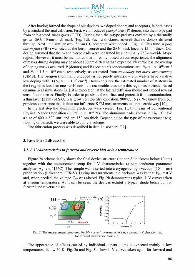
Metrol. Meas. Syst., Vol. 24 (2017), No. 2, pp. 391–399.
After having formed the shape of our devices, we doped donors and acceptors, in both cases
by a standard thermal diffusion. First, we introduced phosphorus (P) donors into the n-type pad from spin-coated silica glass (OCD). During that, the p-type pad was covered by a thermally grown SiO2 10-nm-thick mask (Fig. 1d). Such a thickness assured that no donors diffused
through. Next, in a similar way, boron (B) acceptors were doped – Fig. 1e. This time, a poly boron film (PBF) was used as the boron source and the SiO2 mask became 15 nm thick. Our
design assumed that the p- and n-type pads were separated by a nominally 250-nm-wide i-type region. However, it must be mentioned that in reality, based on our experience, the alignment of masks during doping may be about 100 nm different than expected. Nevertheless, no overlap
of doping masks occurred. P (donors) and B (acceptors) concentrations are: ND ≈ 1 × 1018 cm−3
and NA ≈ 1.5 × 1018 cm−3, respectively, as estimated from secondary ion mass spectrometry (SIMS). The i-region (nominally undoped) is not purely intrinsic – SOI wafers have a native
low doping with B (NA ≈ 1 × 1015 cm−3). However, since the estimated number of B atoms in
the i-region is less than one per 10 nm3, it is reasonable to assume this region as intrinsic. Based on numerical simulations [31], it is expected that the lateral diffusion should not exceed several
tens of nanometres. Finally, in order to passivate the surface and protect it from contamination, a thin layer (2 nm) of SiO2 was grown on top (dry oxidation, 900ºC, 15 s). We know from our previous experience that it does not influence KFM measurements in a noticeable way [10].
In the last step the aluminum electrodes were created, Fig. 1f, by means of conventional
Physical Vapor Deposition (660ºC, 6 × 10⁻⁴ Pa). The aluminum pads, shown in Fig. 1f, have
a size of 600 × 600 µm2 and are 150 nm thick. Depending on the type of measurement (e.g.
floating or biased), we were able to apply a voltage. The fabrication process was described in detail elsewhere [32].
3. Results and discussion
3.1. I−V characteristics in forward and reverse bias at low temperature
Figure 2a schematically shows the final device structure (the top Si thickness below 10 nm)
together with the measurement setup for I−V characteristics (a semiconductor parameter
analyzer, Agilent 4156C). The sample was inserted into a cryogenic high-vacuum (10−7 Torr) probe station (Lakeshore CPX-V). During measurements, the backgate was kept at VBG = 0 V
and, when needed, the voltage VSD was altered. Fig. 2b demonstrates typical I−V curves taken at a room temperature. As it can be seen, the devices exhibit a typical diode behaviour for forward and reverse biases.
Fig. 2. The measurement setup used for I-V curves’ measurements (a); a general I-V characteristic
for forward and reverse biases (b).
The appearance of effects caused by individual dopant atoms is expected mainly at low
temperatures, below 50 K. Fig. 3a and Fig. 3b show I−V curves taken again for forward and
393

R. Nowak, R. Jabłoński: DOPANT-BASED CHARGE SENSING UTILIZING …
reverse bias conditions. As demonstrated, the nanoscale p-i-n junction also exhibits a typical
diode behaviour. However, the effect of parasitic resistance appeared and was reflected in the separation in the voltage domain – the threshold voltage of forward current shifted towards the positive direction (Fig. 3a), whereas the breakdown voltage shifted towards the negative
direction (Fig. 3b). This is caused by the insulating behaviour of silicon and dopant freeze-out effect [6, 23], both due to a low temperature. In order to overcome such a voltage drop in the
leads and to reach the junction area, a larger voltage must be applied. The dashed ovals in Fig. 3a and Fig. 3b indicate current fluctuations, which are not observed
at a room temperature. This current instability was confirmed by tracing the current as
a function of time. As a result, we detected step-like features, resembling current switching known as Random Telegraph Signal (RTS) [11]. In Fig. 3a, repeatability of RTS onset was
estimated to be at 9%, whereas in Fig. 3b − at 12%. RTS is well-known in submicron silicon
MOSFETs [12, 13] and also other similar devices. In those structures, however, RTS is primarily caused by deep-level traps located near an Si/SiO2 interface. This effect is not
considered in our study, as it will be explained in Section 3.2. Since the effects caused by individual dopants are more likely to emerge in smaller
structures, we also measured a narrower device, with its nominal constriction width
WC = 300 nm. As seen in Fig. 3c, the current measured for several values of VSD fluctuates mainly between two levels. Next, the raw RTS from Fig. 3c was digitized [14] and average time
intervals were plotted as a histogram – Fig. 3d. There are two prominent durations of time intervals. These time intervals correspond to a dopant charge state (ionized or neutral), as will be described in Section 3.3.
Fig. 3. I−V characteristics taken for the forward (a) and the reverse bias (b); the insets show RTS signals,
mainly with two levels; (c) two-level RTS vs. time measured for different VSD values;
(d) a histogram of low and high current levels.
3.2. Observation of surface electronic potential by Kelvin probe force microscope
In order to further study the observed RTS, we carried out surface electronic potential measurements by a Kelvin probe force microscope [15] (Unisoku Co., Ltd.). It proved to be a powerful tool for characterization of nanodevices, able to achieve even atomic resolution [16].
We used gold-coated silicon cantilevers (Seiko Instruments Inc.), which were scanning ~10 nm over the device surface (the constant height mode). The p-i-n nanojunction was measured
394

Metrol. Meas. Syst., Vol. 24 (2017), No. 2, pp. 391–399.
in ultra-high vacuum (UHV, 10−9 Torr). Since our read-out setup is based on piezoelectric crystals, the common problems with light-induced effects [17] do not appear here. The backgate
voltage was set to VBG = 0 V and no bias was applied to the n- or p-type pads, as shown in Fig. 4a (VREV = 0 V). The third voltage source, VKFM, is a part of KFM circuit. It is used to nullify the electrostatic force, which builds up between the point charge (e.g. an ionized dopant)
and the cantilever apex. The AFM image with a scan area for KFM mapping, marked by a dashed rectangle, is presented in Fig. 4b. Location of i-region (intrinsic) was estimated based
on the topography profile and marked by orange dashed lines. It is important to mention here that, due to the measurement conditions, the device was mounted upside-down, so in fact electronic potential mapping was done from the n- towards the p-type pad.
First, we measured the p-i-n junction at a low temperature T = 15 K. The result is presented in Fig. 4c. As we anticipated, based on the device structure, we observed 3 major flat electronic
potential sections, i.e. n-, i- and p-type regions. These regions are separated by localized-noise areas, which are marked in Fig. 4c by blue dashed ovals.
Based on the CMOS-compatible device fabrication process performed in a clean-room
environment, a density of interface states is expected to be in the order of 1010–1011 cm−2eV−1 or smaller [18, 19]. Thus, it can be estimated that in a 100 × 100 nm2 area around a given
interface (n-i or p-i), the number of interface traps (1–10) is negligible compared with the number of dopants (more than 200 dopants, P donors, and B acceptors). Based on that, dopant atoms (rather than interface states) are expected to give rise to any charging-related phenomena.
Hence, in analogy to the RTS described in the previous section, these temporal electronic potential fluctuations are also caused by the dynamic charging/discharging of dopant atoms that
are located within the n-i (and also i-p) interface.
Fig. 4. The KFM measurement setup (a); an AFM picture of the measured device with a scan area for KFM
measurements marked by a black rectangle (b); the surface electronic potential map with n-i
and i-p interfaces marked by blue dashed ovals (c); the n-i (d) and i-p depletion regions (e).
In the next step, we performed electronic potential mapping around depletion regions (n-i or p-i interfaces) marked in Fig. 4c. The results for n-i and i-p junctions are presented in Figs. 4d and 4e, respectively. As it can be clearly seen, time-dependent electronic potential fluctuations
395
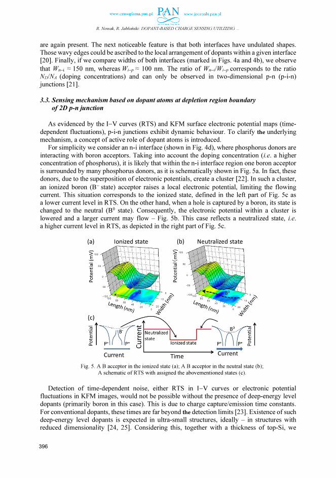
R. Nowak, R. Jabłoński: DOPANT-BASED CHARGE SENSING UTILIZING …
are again present. The next noticeable feature is that both interfaces have undulated shapes.
Those wavy edges could be ascribed to the local arrangement of dopants within a given interface [20]. Finally, if we compare widths of both interfaces (marked in Figs. 4a and 4b), we observe
that Wn−i ≈ 150 nm, whereas Wi−p ≈ 100 nm. The ratio of Wn−i/Wi−p corresponds to the ratio ND/NA (doping concentrations) and can only be observed in two-dimensional p-n (p-i-n)
junctions [21].
3.3. Sensing mechanism based on dopant atoms at depletion region boundary
of 2D p-n junction
As evidenced by the I−V curves (RTS) and KFM surface electronic potential maps (time-
dependent fluctuations), p-i-n junctions exhibit dynamic behaviour. To clarify the underlying
mechanism, a concept of active role of dopant atoms is introduced. For simplicity we consider an n-i interface (shown in Fig. 4d), where phosphorus donors are
interacting with boron acceptors. Taking into account the doping concentration (i.e. a higher concentration of phosphorus), it is likely that within the n-i interface region one boron acceptor
is surrounded by many phosphorus donors, as it is schematically shown in Fig. 5a. In fact, these donors, due to the superposition of electronic potentials, create a cluster [22]. In such a cluster,
an ionized boron (B− state) acceptor raises a local electronic potential, limiting the flowing current. This situation corresponds to the ionized state, defined in the left part of Fig. 5c as a lower current level in RTS. On the other hand, when a hole is captured by a boron, its state is changed to the neutral (B0 state). Consequently, the electronic potential within a cluster is
lowered and a larger current may flow – Fig. 5b. This case reflects a neutralized state, i.e. a higher current level in RTS, as depicted in the right part of Fig. 5c.
Fig. 5. A B acceptor in the ionized state (a); A B acceptor in the neutral state (b);
A schematic of RTS with assigned the abovementioned states (c).
Detection of time-dependent noise, either RTS in I−V curves or electronic potential fluctuations in KFM images, would not be possible without the presence of deep-energy level
dopants (primarily boron in this case). This is due to charge capture/emission time constants.
For conventional dopants, these times are far beyond the detection limits [23]. Existence of such deep-energy level dopants is expected in ultra-small structures, ideally – in structures with reduced dimensionality [24, 25]. Considering this, together with a thickness of top-Si, we
396

Metrol. Meas. Syst., Vol. 24 (2017), No. 2, pp. 391–399.
concluded that the measured devices are truly two dimensional (2D). Another supporting fact
comes directly from the KFM images and is related to the width of depletion regions, as discussed in Section 3.2.
The two-dimensional character of our device brings further consequences regarding its basic
properties. It was theoretically predicted that the electric field within a depletion region, due to limited screening of host silicon, is very high [21] and penetrates outwards (confirmed
experimentally [18, 28]), which may increase efficiency of electron-hole separation and, thus, increase sensitivity. Next, the electric field is also almost independent of the applied bias; therefore the breakdown voltage is considerably higher than in conventional p-n junctions.
Moreover, the junction capacitance is very small, thus enabling to apply thedevice as a high-frequency diode, e.g. a photodetector. Finally, the width of depletion region is a linear function
of applied voltage, which makes the adjustment also linear [21]. It is important to mention that the proposed model is valid for a cluster located favorably
close to the edge of depletion region. Otherwise, charging/discharging boron atoms does not
alter the local electronic potential sufficiently and RTS becomes unobservable. In other studies, for the purpose of RTS characterization, a concept of “sensitive region” was introduced
[26, 27]. Such a region starts at the edge of depletion region (interface) and extends up to some length, usually several nanometres, towards the junction. Finally, the described model
of sensing mechanism can also be adapted to the opposite case – when a phosphorus atom is
embedded in a cluster of boron atoms.
4. Future steps
At a current level, location of dopants within a silicon lattice is random by nature and cannot be controlled. This is due to the fabrication processes, mainly the thermal diffusion used for
introduction of dopant atoms into the host silicon. Therefore, as the next step of research, it is desired to produce such devices with a highest possible accuracy regarding a precise location
of dopant atoms. In other words – by means of deterministic doping, e.g. using either ion implantation (SII) [29] or so called STM-Lithography [30].
Together with the experimental approach, theoretical studies are strongly desired.
In particular, the basic electrical properties should be simulated. In fact, we performed first steps in this direction. We obtained first results performing ab initio calculations (Atomistix
ToolKit) for a simple P-B-P complex inserted into a 2-nm-long Si nanowire (Fig. 6a) [31]. The results are presented in Fig. 6b. The Density of States (DOS) as a function of energy reveals that, despite a very short separation (0.5 nm), the ground states of P (a blue dashed line) and B
(a red dashed line) atoms are preserved. It means that, even in such an extremely small structure, dopants can be ionized and work as charge traps. This finding further supports our model
presented in the previous section. It is necessary, however, to carry out an ongoing study and simulation of larger structures with more dopants.
Fig. 6. The calculated structure containing a P atom surrounded by two B atoms (a);
DOS with marked the ground states of donor and acceptor (b).
397

R. Nowak, R. Jabłoński: DOPANT-BASED CHARGE SENSING UTILIZING …
5. Conclusions
Summarizing, we have presented the results of basic studies devoted to modern p-i-n junctions. The examined devices, due to the used fabrication methods, offer a potentially high
integration level for integrated circuits’ applications. The charge detection mechanism is ascribed to the charging/discharging of a deep-level
boron atom. Such a charging/discharging phenomenon is manifested by current fluctuations
(RTS) in the I−V characteristics and time-dependent electronic potential fluctuations in the KFM images. The mutual interaction between donors and acceptors has been proposed as a model of charge sensing mechanism.
Our devices combine unique properties due to reduced dimensionality and individuality of dopants, which exhibit deeper-energy levels. We believe that this work will contribute to
a better understanding of new class of sensors – dopant-based nanosensors.
References
[1] Mahadevan, V., Sethuraman, S. (2003). Nanomaterials and Nanosensors for Medical Applications. Trends
in Nanoscale Mechanics, 9, 207.
[2] Khanna, V.K. (2011). Nanosensors: Physical, Chemical, and Biological. CRC Press.
[3] Guo, J., Kan, E.C., Ganguly, U., Zhang Y. (2006). High sensitivity and nonlinearity of carbon nanotube
charge-based sensors. J. Appl. Phys., 99, 084301.
[4] Neumann, C., Volk, C., Engels, S., Stampfer, C. (2013). Graphene-based charge sensors. Nanotechnology
24, 44.
[5] Kang, M., Kim, Y.A., Yun, J.M., Khim, D., Kim, J., Noh, Y.Y., Baeg, K.J., Kim, D.Y. (2014). Stable charge
storing in two-dimensional MoS2 nanoflake floating gates for multilevel organic flash memory. Nanoscale,
6, 12315.
[6] Sze, S.M. (1981). Physics of Semiconductor Devices. 2nd ed. John Wiley & Sons, New York.
[7] Yang, C., Barrelet, C.J., Capasso, F., Lieber, C.M. (2006). Single p-Type/Intrinsic/n-Type Silicon Nanowires
as Nanoscale Avalanche Photodetectors. Nano Lett., 6, 2929.
[8] Nowak, R., Moraru, D., Mizuno, T., Jabłoński, R., Tabe, M. (2014). Potential profile and photovoltaic effect in nanoscale lateral pn junction observed by Kelvin probe force microscopy. Thin Solid Films, 557, 249.
[9] Rommel, M., Jambreck, J.D., Lemberger, M., Bauer, A.J., Frey, L., Murakami, K., Richter, C., Weinzierl,
P. (2013). Influence of parasitic capacitances on conductive AFM I-V measurements and approaches for its
reduction. J. Vac. Sci. Technol., B 31, 01A108.
[10] Ligowski, M., Moraru, D., Anwar, M., Mizuno, T., Jabloński, R., Tabe, M. (2008). Observation of individual
dopants in a thin silicon layer by low temperature Kelvin Probe Force Microscope. Appl. Phys. Lett. 93,
14210.
[11] Simoen, E., Dierickx, B., Claeys, C.L., Declerck, G.J. (1992). Explaining the amplitude of RTS noise in
submicrometer MOSFETs. IEEE Trans. Electron Devices, 39, 422.
[12] Amarasinghea, N.V., Çelik-Butlerb, Z., Zlotnicka, A., Wang, F. (2003). Model for random telegraph signals
in sub-micron MOSFETS. Solid-State Electron., 47, 1443.
[13] Lee, J.W., Shin, H., Lee, J.H. (2010). Characterization of random telegraph noise in gate induced drain
leakage current of n- and p-type metal-oxide-semiconductor field-effect transistors. Appl. Phys. Lett., 96,
043502.
[14] Udhiarto, A., Moraru, D., Purwiyanti, S., Mizuno, T., Tabe, M. (2012). Photon-Induced Random Telegraph
Signal Due to potential Fluctuation of a Single Donor-Acceptor Pair in Nanoscale Si p-n Junctions. Appl.
Phys. Express, 5, 112201.
[15] Nonnenmacher, M., O’Boyle, M.P., Wickramasinghe, H.K. (1991). Kelvin probe force microscopy. Appl.
Phys. Lett., 58, 2921.
398

Metrol. Meas. Syst., Vol. 24 (2017), No. 2, pp. 391–399.
[16] Anwar, M., Nowak, R., Moraru, D., Udhiarto, A., Mizuno, T., Jabłoński, R., Tabe, M. (2011). Effect
of electron injection into phosphorus donors in silicon-on-insulator channel observed by Kelvin probe force
microscopy. Appl. Phys. Lett., 99, 213101.
[17] Kassies, R., van der Werf, K.O., Bennink, M.L., Otto, C. (2004). Removing interference and optical feedback
artifacts in atomic force microscopy measurements by application of high frequency laser current
modulation. Rev. Sci. Instrum., 75, 689.
[18] Nowak, R., Moraru, D., Mizuno, T., Jabłoński, R., Tabe, M. (2013). Effects of deep-level dopants on the
electronic potential of thin Si pn junctions observed by Kelvin probe force microscope. Appl. Phys. Lett.,
102, 083109.
[19] White, M.H., Cricchi, J.R. (1972). Characterization of thin-oxide MNOS memory transistors. IEEE Trans.
Electron Devices, 19, 1280.
[20] Nowak, R., Anwar, M., Moraru, D., Mizuno, T., Jablonski, R., Tabe, M. (2012). Observation of charging
and discharging effects of dopant atoms in nanoscale lateral pn junction by Kelvin probe force microscope.
International Conference on Solid State Devices and Materials, Kyoto.
[21] Achoyan, A.S., Yesayan, A.E., Kazaryan, E.M., Petrosyan, S.G. (2002). Two-dimensional p-n-junction
under equilibrium conditions. Semiconductors, 36, 903.
[22] Tyszka, K., Moraru, D., Samanta, A., Mizuno, T., Jabłoński, R., Tabe, M. (2015). Comparative study
of donor-induced quantum dots in Si nano-channels by single-electron transport characterization and Kelvin
probe force microscopy. J. Appl. Phys., 117, 244307.
[23] Foty, D. (1990). Impurity ionization in MOSFETs at very low temperature. Cryogenics, 30, 1056.
[24] Diarra, M., Niquet, Y.M., Delerue, C., Allan, G. (2007). Ionization energy of donor and acceptor impurities
in semiconductor nanowires: Importance of dielectric confinement. Phys. Rev. B, 75, 045301.
[25] Pierre, M., Wacquez, R., Jehl, X., Sanquer, M., Vinet, M., Cueto, O. (2010). Single-donor ionization energies in a nanoscale CMOS channel. Nat. Nanotechnol., 5, 133.
[26] Purwiyanti, S., Nowak, R., Moraru, D., Mizuno, T., Hartanto, D., Jabłoński, R., Tabe, M. (2013). Dopant-
induced random telegraph signal in nanoscale lateral silicon pn diodes at low temperatures. Appl. Phys. Lett.,
103, 243102.
[27] Moraru, D., Purwiyanti, S., Nowak, R., Mizuno, T., Udhiarto, A., Hartanto, D., Jabłoński, R., Tabe, M.
(2014). Individuality of dopants in silicon nano-pn junctions. Materials Science, 20, 129.
[28] Reuter, D., Werner, C., Wieck, A.D., Petrosyan, S. (2005). Depletion characteristics of two-dimensional
lateral pn-junctions. Appl. Phys. Lett., 86, 162110.
[29] McCallum, J.C., Jamieson, D.N., Yang, C., Alves, A.D., Johnson, B.C., Hopf, T., Thompson, S.C., van
Donkelaar, J.A. (2012). Single-ion implantation for the development of Si-based MOSFET devices with
quantum functionalities. Adv. Mater. Sci. Eng., 2012, 272694.
[30] Lee, W., McKibbin, S., Thompson, D., Xue, K., Scappucci, G., Bishop, N., Celler, G., Carroll, M., Simmons,
M. (2014). Lithography and doping in strained Si towards atomically precise device fabrication.
Nanotechnology, 25, 145302.
[31] Kuzuya, Y.,Moraru, Mizuno, T., Tabe, M., Mizuta, H. (2012). Electronic states of pn junction in silicon nano
structure. The 59th JSAP Spring Meeting, Matsuyama.
[32] Nowak, R. (2013). Observation of Dopant-induced potential in Nanoscale Si pn Junctions by Kelvin Probe
Force Microscope. Ph.D. Thesis. Shizuoka University.

Metrol. Meas. Syst., Vol. 24 (2017), No. 2, pp. 401–412.
_____________________________________________________________________________________________________________________________________________________________________________________
Article history: received on Jun. 06, 2016; accepted on Jan. 29, 2017; available online on Jun. 30, 2017; DOI: 10.1515/mms-2017-0033.
METROLOGY AND MEASUREMENT SYSTEMS
Index 330930, ISSN 0860-8229
www.metrology.pg.gda.pl
COMPARISON OF INTERPOLATORS USED FOR TIME-INTERVAL
MEASUREMENT SYSTEMS BASED ON MULTIPLE-TAPPED DELAY LINE
Dariusz Chaberski, Robert Frankowski, Maciej Gurski, Marek Zieliński
Nicolaus Copernicus University, Faculty of Physics, Astronomy and Informatics, Grudziądzka 5, 87-100 Toruń, Poland ( [email protected], +48 56 611 2417, [email protected], [email protected], [email protected])
Abstract
The paper describes the construction, operation and test results of three most popular interpolators from
a viewpoint of time-interval (TI) measurement systems consisting of many tapped-delay lines (TDLs) and
registering pulses of a wide-range changeable intensity. The comparison criteria include the maximum intensity
of registered time stamps (TSs), the dependency of interpolator characteristic on the registered TSs’ intensity, the
need of using either two counters or a mutually-complementing pair counter-register for extending a measurement range, the need of calculating offsets between TDL inputs and the dependency of a resolution increase on the
number of used TDL segments. This work also contains conclusions about a range of applications, usefulness and
methods of employing each described TI interpolator. The presented experimental results bring new facts that can
be used by the designers who implement precise time delays in the field-programmable gate arrays (FPGA).
Keywords: time interval, multiple-tapped delay line, quantization-and-nonlinearity minimization, FPGA, time-to-
digital converter.
© 2017 Polish Academy of Sciences. All rights reserved
1. Introduction
The task of a TI interpolator is to increase resolution of TI measurements. It simply reduces to the measurement of a distance between one chosen type of edge (usually the rising edge) of a signal and the beginning of the standard-clock period that directly precedes this edge. A typical
TI interpolator consists of one or two TDLs and a register [1−4]. The way the register and TDL(s) are connected determines the way of TI interpolator operation and its use in the system.
Time-to-digital converters (TDCs) can have many applications and can be constructed
in many ways [1, 5−16]. TDCs can be used directly or indirectly to measure other quantities by converting them temporarily to TIs. Depending on a use domain and implementation technology TDCs can vary in properties and can differ in cost. The most important parameters
of TDCs are: a resolution of TI measurement, a measurement range and a maximum intensity of registered TSs [1, 4].
A measurement resolution of TDC can be improved by applying the Vernier method, interpolation and multiple-stage interpolation, time stretching or multiple measurement [1, 4]. The first three mentioned methods use TDLs and the TDC resolution is determined by the TDL
segment delay value. The TDL segment delay value can be decreased by changing the implementation technology to a finer one. The time stretching strongly decreases the maximum intensity of registered TSs but can be applied in conjunction with any other method. The multiple measurement can also be used jointly with any other method and can be performed
either in parallel or sequentially [17, 18]. When the multiple measurement is carried out in parallel there is no need to duplicate the whole meter. For TDL-based TDC only TDLs, code-converters and memory blocks have to be duplicated. In that case it can also be called

D. Chaberski, R. Frankowski, et al.: COMPARISON OF INTERPOLATORS USED FOR TIME-INTERVAL…
as multiple-TDL (MTDL)-based one. When the multiple measurement of TI is performed
sequentially, only a TI repetition block must be added to the measurement module. A measurement-range can be extended by implementation of a standard-clock period
counter, but it is limited by the long-term standard-clock stability. The maximum intensity
of registered TSs usually can be increased either by parallelization of critical TDC blocks or by changing the implementation technology to a faster one [19].
Currently the FPGA and Application Specific Integrated Circuit (ASIC) are two technologies that play an important role in implementation of TDC. Both these technologies enable to implement regularly placed elements of equal delay that are necessary to construct
TDLs [6, 7, 9−12, 19, 20].
When the multiple measurement is used, the correlation of measurement results plays an important role. If the measurement results are not correlated, the average value of standard
deviation of n measurements is decreased n times. If they are correlated, the correlation
degree and its nature should be considered. Highly correlated measurement results enable
to obtain more precise information about the real value − in comparison with those totally
uncorrelated measurements − when each measurement complements any other one [17, 18]. The way of using TDLs in this paper takes just advantage of this.
The results and conclusions contained in this paper can be useful for the designers who
implement and use time delays in FGPA structures. It mainly concerns TI generation systems as well as TI measurement ones. In the literature one can find information about the influence
of FPGA structure temperature deviations on the time delay of some FPGA primitives, such as look-up-tables (LUT). However, the influence of a clock frequency on the FPGA element delay value has not yet been published. We have noticed this effect during activation of a high-
resolution TI generator (an incremental resolution of 1 ps) based on TDLs constructed of LUTs, so we have decided to check whether a similar effect would appear in the case of TI
measurement systems. We suspect that this effect would play an important role in ring oscillators equipped with the enable input. When a ring oscillator has been enabled (started), the structure it has been implemented in is warming up, so a frequency of the generated clock
decreases till the temperature is stabilized.
2. Characterization of tested interpolators
There are many different ways of connecting TDL(s) and a register in order to obtain the possibility of TI interpolating. Fig. 1 shows the three ones tested by the authors. The first TI
interpolator (Fig. 1a) registers the state of TDL every rising edge of PULSES signal. The resolution of this interpolator depends on the TDL segment delay values [1, 19, 21]. It is very
convenient for this type of interpolator that the delay values of 1−n TDL segments
[ ]( , 0, 2 )ii nτ ∈ − directly create 1−n interpolator characteristic bins (quantization steps,
[ ]2,0, −∈ niqi
), but the 1−n -th TI interpolator quantization step is equal to the difference
between the standard-clock period T and the sum of just mentioned 1−n bin values, so:
∑−
=
−−=
2
0
1
n
i
inTq τ . (1)
In this case, when the TI characteristic changes, the number of quantization steps is constant. This fact simplifies the construction of further data processing blocks.
402

Metrol. Meas. Syst., Vol. 24 (2017), No. 2, pp. 401–412.
a)
b)
c)
Fig. 1. Three types of tested TI interpolators. PULSES signal registers the TDL state that represents the phase
of CLOCK (a); the TDL state that stores the history of PULSES signal is registered periodically
(every CLOCK cycle) (b); STOP signal chases START signal (c).
The second tested TI interpolator (Fig. 1b) stores the history of PULSES signal in the TDL. This history is periodically (every rising edge of CLOCK signal) written to the register and then
− if necessary (the chosen edge of PULSES signal appeared) − further written to memory. Please notice that in this case the register and memory write-ins are synchronized with the CLOCK signal rising edge. In the first type of tested TI interpolator the register and memory
write-ins are non-synchronous with CLOCK signal and synchronous with PULSES signal. This implicates that extension of a measuring range of this type of interpolator demands either a Grey
code counter (in this case the error is equal maximally to 1 and can be corrected later), two natural-binary counters or a mutually-complementing pair counter-register (in these both cases either the first or the second counter or either the counter or the register contains a proper state)
[22]. To extend a measuring range of the second type of TI interpolator (Fig. 1b) only one binary counter is sufficient. The third type of TI interpolator register and memory write-ins are
also (as it was in the case of the second type of tested interpolator) synchronized with CLOCK signal, so here also one binary counter suffices to extend the range of measurements.
For the second type of tested TI interpolator assigning a quantization step to the TDL delays
can be done in the same way as it has been done for the first type of interpolator. However, such an assignment for the third type of tested TI interpolator is usually done differently. Here, STOP
signal chases START signal. The shortest and the longest distances between START and STOP signals determine which flip-flops are active and which ones are not. So in this case the best
solution seems to be assigning the delay of the first active segment to the 0-th quantization step, assigning the delay of the second active segment to the 1-st quantization step, and so on. Please
notice that the segment delay is here equal to the difference ABττ − . The first and the last active
segments are usually used only partly, so statistically (the code-density test [2, 21, 23]) the
measured sizes of these segments are usually smaller than this difference. Three tested types of TI interpolators have different maximum intensities of interpolations.
The first one (Fig. 1a) has the highest maximum intensity of interpolations. Here, PULSES
signal can register the state of TDL independently of CLOCK signal. The maximal intensity of interpolation is limited only by the flip-flop propagation time. The maximum intensity
of interpolation of the second tested TI interpolator (Fig. 1b) is limited by the CLOCK signal
403

D. Chaberski, R. Frankowski, et al.: COMPARISON OF INTERPOLATORS USED FOR TIME-INTERVAL…
period. In this case, if two rising edges appear in the same CLOCK signal period, the first result
is overwritten by the second result. The third type of TI interpolator (Fig. 1c) has the lowest maximum intensity of interpolation, because it is limited by the total delay (the sum of all active segments delays) of the slower TDL.
It was found that, when the frequency of the clock that is passed through the TDL changes, the TDL segment delay value also changes. This is caused by the local semiconductor structure
temperature changes. This effect has been noticed for TI interpolators implemented in FPGA and it is supposed that a very similar effect appears also in ASIC. The TDL segment delay of the first type of TI interpolator is independent of the PULSES signal frequency because the TDL
is fed by CLOCK signal of a constant frequency. However, the characteristics of the second and the third TI interpolators depend on the PULSES signal frequency changes. This effect has
been examined thoroughly by the authors and the test results are described in the next sections of this paper.
When m TI interpolators are used, then the number of measurements increases m times.
A quantization step size of the measurement system that consists of m interpolators presented in Figs. 1a, 1b are inversely proportional to mn, where n is the number of TDL segments. However, when the measurement system consists of m TI interpolators presented in Fig. 1c, the
quantization step is proportional merely to mn – n +1. A deeper discussion about this feature is contained in Subsection 4.1.
To obtain a proper value of high-resolution quantisation step when m TI interpolators are
used, one has to calculate relative time offsets between TDL inputs when two first types of interpolators are used (Figs. 1a, 1b) [17]. When the third type of TI interpolator is used (Fig. 1c) these time offsets influence the selection of the first active segment in each TDL and
such calculations are needless [18].
Other types of TI interpolators can be found in [1−4, 20]. For example, in [20] the TDL delay elements have been created regarding the fact that the flip-flop propagation time tCQ is limited.
We have not tested this type of TI interpolator but we suspect that a similar influence of the intensity of registered pulses on the TDL characteristic would appear also for this solution.
3. Selected research topics
This section contains a description of some research issues that aim to complete the image of described research results. The following subsections describe the TI generator responsible
for providing a double PULSES signal and the methods used for examining the influence of the intensity of an event on the TI interpolator characteristic as well as the dependency of the maximum intensity of registered events on the TI interpolator type. The last subsection
describes some implementation details of tested TI interpolators.
3.1. TI generator
In order to compare TI interpolators the TI generator presented in Fig. 2 has been used.
The programmable frequency divider generates a rising edge every N CLK1 signal periods
(please refer also to Fig. 3). The programmable delay generates one CLK1 period-wide pulse
after M clock cycles since the CLKN1 signal rising edge appeared. Both pulse generators unify a width of the pulses (PULSE0 and PULSE1) and finally both these pulses are connected by the OR function. The signal created in this way is then just provided to the TI interpolator PULSES input.
404

Metrol. Meas. Syst., Vol. 24 (2017), No. 2, pp. 401–412.
Fig. 2. A block diagram of the TI generator used for testing TI interpolators.
Fig. 3. A timing diagram of the TI generator presented in Fig. 2.
The programmable generator is cycled by the CLK1 clock that is non-synchronous with the
standard-clock (CLK0) of TI interpolators. This feature enables to test every segment of TI interpolator. If these clocks were synchronous only a few selected segments would be tested.
The PULSES signal (Fig. 2) contains two TIs. The longer TI of a length ( )TMN − enables
to controllably test TI interpolator heating. The shortest TI of a length MT is measured by the
TI interpolator and the result (TI histogram) determines whether the tested interpolator works properly or not.
3.2. TI interpolator characteristic change observation method
It is generally known that the TDL characteristic depends on its temperature. For the
XILINX Virtex5 FPGA structure a temperature increase causes an increase of the TDL segment
delay. Fig. 4 shows an example of the dependence of TI interpolator characteristic on its
temperature. Please notice (the heating case) that, when the temperature increases, all (0−5, 7) but one (6) of TI interpolator quantization steps also increase. The 6-th quantization step decreases because its value is calculated accordingly to (1). Its value is not equal to the corresponding TDL segment value as it happens for the remaining quantization steps.
When all, except one, TI interpolator quantization steps have the same trend of changes and this one TI interpolator quantization step depends on the sum of remaining TI quantization
steps, then this one quantization step is the most sensitive to the temperature changes. The TI interpolator characteristic change observation method utilizes this fact. To obtain an average
TDL segment delay value q , the following formula is used:
1−
−
=
n
qTq m , (2)
where T is a standard-clock period; n is the number of quantization steps and qm is a quantization step given by (1).
In this paper not just the TDL segment delay dependence on ambient or average structure temperature has been examined, but also its dependence on the intensity of registered pulses.
When the intensity of these pulses increases, the temperature of TDL also increases and finally the TDL segment delay increases, too.
405
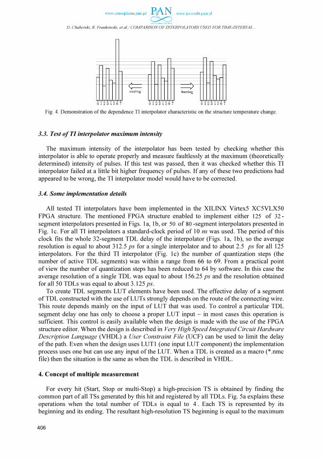
D. Chaberski, R. Frankowski, et al.: COMPARISON OF INTERPOLATORS USED FOR TIME-INTERVAL…
Fig. 4. Demonstration of the dependence TI interpolator characteristic on the structure temperature change.
3.3. Test of TI interpolator maximum intensity
The maximum intensity of the interpolator has been tested by checking whether this interpolator is able to operate properly and measure faultlessly at the maximum (theoretically
determined) intensity of pulses. If this test was passed, then it was checked whether this TI interpolator failed at a little bit higher frequency of pulses. If any of these two predictions had
appeared to be wrong, the TI interpolator model would have to be corrected.
3.4. Some implementation details
All tested TI interpolators have been implemented in the XILINX Virtex5 XC5VLX50
FPGA structure. The mentioned FPGA structure enabled to implement either 125 of 32 -
segment interpolators presented in Figs. 1a, 1b, or 50 of 80 -segment interpolators presented in
Fig. 1c. For all TI interpolators a standard-clock period of 10 ns was used. The period of this
clock fits the whole 32-segment TDL delay of the interpolator (Figs. 1a, 1b), so the average resolution is equal to about 312.5 ps for a single interpolator and to about 2.5 ps for all 125
interpolators. For the third TI interpolator (Fig. 1c) the number of quantization steps (the number of active TDL segments) was within a range from 66 to 69. From a practical point
of view the number of quantization steps has been reduced to 64 by software. In this case the average resolution of a single TDL was equal to about 156.25 ps and the resolution obtained for all 50 TDLs was equal to about 3.125 ps.
To create TDL segments LUT elements have been used. The effective delay of a segment of TDL constructed with the use of LUTs strongly depends on the route of the connecting wire.
This route depends mainly on the input of LUT that was used. To control a particular TDL
segment delay one has only to choose a proper LUT input − in most cases this operation is sufficient. This control is easily available when the design is made with the use of the FPGA
structure editor. When the design is described in Very High Speed Integrated Circuit Hardware Description Language (VHDL) a User Constraint File (UCF) can be used to limit the delay
of the path. Even when the design uses LUT1 (one input LUT component) the implementation process uses one but can use any input of the LUT. When a TDL is created as a macro (*.nmc file) then the situation is the same as when the TDL is described in VHDL.
4. Concept of multiple measurement
For every hit (Start, Stop or multi-Stop) a high-precision TS is obtained by finding the
common part of all TSs generated by this hit and registered by all TDLs. Fig. 5a explains these
operations when the total number of TDLs is equal to 4 . Each TS is represented by its beginning and its ending. The resultant high-resolution TS beginning is equal to the maximum
406

Metrol. Meas. Syst., Vol. 24 (2017), No. 2, pp. 401–412.
value of all TS beginnings, and − analogously − the ending of the high-resolution TS is equal
to the minimum value of all TS endings [17, 18, 24].
Please notice (Fig. 5a) that when the number (m ) of TDLs increases, the high resolution TS
is usually becoming narrower in this example (the resultant TS is better located). Finally, the
beginning of the high resolution TS for Start is determined by the beginning of 1,2 +i
E TS,
whereas its ending is determined by the ending of 1,3 −i
E TS. For the Stop hit the high resolution
TS is equally precise for 1=m or 2=m , but finally ( 4=m ) it becomes narrower and is
determined by the beginning of j
E,3
TS and the ending of 1,2 +j
E TS.
a)
b)
Fig. 5. The concept of multiple-measurement time-interval PDF calculation; an example of obtaining high-
precision time stamps from time stamps generated by four TDLs for two consecutive hits (a); time-interval PDFs
obtained for two consecutive time-stamp pairs depending on the number m of used TDLs (b).
It is very convenient to determine TIs as Probability Density Functions (PDFs). Then, while constructing a TI histogram not just only one point is added to it, but the PDF of this TI is added
and finally TI histograms are more accurate. These PDFs for TI can be calculated by the use of the Quantization and Non-linearity Minimization (QNM) method [24]. Fig. 5b explains obtaining PDFs for TS pairs (Start and Stop) in the case of multiple-measurement TDC. Here,
the PDF is a modified convolution (the sign of the first argument has been changed) of high-resolution TSs obtained for Start and Stop events. When TSs for Start and Stop are narrower,
then a TI can be determined more precisely and its PDF is higher and narrower (this is clearly visible in Fig. 5b).
Inaccuracy of calculation of the TDL offsets for TDCs based on both first interpolators (Figs. 1a, 1b) based on MTDL is the main source of TI calculation errors [17]. Every TS that depends on any quantization step of j-th TDL will be corrupted when j-th TDL offset is
inappropriately pointed out. Before calculating a high-resolution TS one has to calculate this offsets.
407
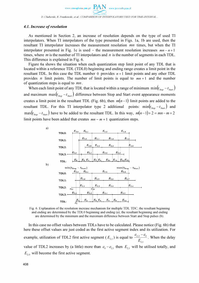
D. Chaberski, R. Frankowski, et al.: COMPARISON OF INTERPOLATORS USED FOR TIME-INTERVAL…
4.1. Increase of resolution
As mentioned in Section 2, an increase of resolution depends on the type of used TI
interpolators. When TI interpolators of the type presented in Figs. 1a, 1b are used, then the
resultant TI interpolator increases the measurement resolution mn times, but when the TI
interpolator presented in Fig. 1c is used − the measurement resolution increases 1+− nmn
times, where m is the number of TI interpolators and n is the number of segments in each TDL.
This difference is explained in Fig. 6.
Figure 6a shows the situation when each quantization step limit point of any TDL that is located within a reference TDL (TDL0) beginning and ending range creates a limit point in the
resultant TDL. In this case the TDL number 0 provides 1+n limit points and any other TDL
provides n limit points. The number of limit points is equal to 1+mn and the number
of quantization steps is equal to mn .
When each limit point of any TDL that is located within a range of minimum ( )StartStop tt −min
and maximum ( )StartStop tt −max difference between Stop and Start event appearance moments
creates a limit point in the resultant TDL (Fig. 6b), then ( )1−nm limit points are added to the
resultant TDL. For this TI interpolator type 2 additional points: ( )StartStop tt −min and
( )StartStop tt −max have to be added to the resultant TDL. In this way, ( ) 221 +−=+− mmnnm
limit points have been added that creates 1+− mmn quantization steps. a)
b)
Fig. 6. Explanation of the resolution increase mechanism for multiple TDL TDC; the resultant beginning
and ending are determined by the TDL0 beginning and ending (a); the resultant beginning and ending
are determined by the minimum and the maximum difference between Start and Stop pulses (b).
In this case no offset values between TDLs have to be calculated. Please notice (Fig. 6b) that
here these offset values are just coded as the first active segment index and its utilization. For
example, utilization of TDL2 first active segment (1,2
E ) is equal to 1,2
02,2
E
ee −
. When the delay
value of TDL2 increases by (a little) more than 1,20
ee − then 1,2
E will be utilised totally, and
0,2E will become the first active segment.
408
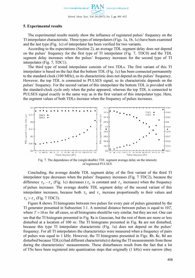
Metrol. Meas. Syst., Vol. 24 (2017), No. 2, pp. 401–412.
5. Experimental results
The experimental results mainly show the influence of registered pulses’ frequency on the
TI interpolator characteristic. Three types of interpolators (Figs. 1a, 1b, 1c) have been examined and the last type (Fig. 1c) of interpolator has been verified for two variants.
According to the expectations (Section 2), an average TDL segment delay does not depend on the pulses’ frequency for the first type of TI interpolator (Fig. 7, TDC0) and the TDL segment delay increases when the pulses’ frequency increases for the second type of TI
interpolator (Fig. 7, TDC1). The third type of tested interpolator consists of two TDLs. The first variant of this TI
interpolator is based on the fact that the bottom TDL (Fig. 1c) has been connected permanently to the standard clock (100 MHz), so its characteristic does not depend on the pulses’ frequency. However, the top TDL is connected to PULSES signal, so its characteristic depends on the
pulses’ frequency. For the second variant of this interpolator the bottom TDL is provided with the standard-clock cycle only when the pulse appeared, whereas the top TDL is connected to
PULSES signal exactly in the same way as in the first variant of this interpolator type. Here, the segment values of both TDLs increase when the frequency of pulses increases.
Fig. 7. The dependence of the (single/double) TDL segment average delay on the intensity
of registered PULSES.
Concluding, the average double TDL segment delay of the first variant of the third TI
interpolator type decreases when the pulses’ frequency increases (Fig. 7 TDC2), because the
difference ABττ − (Fig. 1c) decreases (
Bτ is constant and
Aτ increases) when the frequency
of pulses increases. The average double TDL segment delay of the second variant of this
interpolator increases, because both Bτ and
Aτ increase proportionally to their values and
ABττ > (Fig. 7 TDC3).
Figure 8 shows TI histograms between two pulses for every pair of pulses generated by the TI generator presented in Subsection 3.1. A nominal distance between pulses is equal to 10T,
where nsT 10= for all cases, so all histograms should be very similar, but they are not. One can
see that the TI histogram presented in Fig. 8a is Gaussian, but the rest of them are more or less disturbed at a location of 100 ns. The TI histograms presented in Fig. 8a are not disturbed, because this type TI interpolator characteristic (Fig. 1a) does not depend on the pulses’
frequency. For all TI interpolators the characteristics were measured when a frequency of pairs of pulses was equal to 1 kHz. However, the TI histograms presented in Figs. 8b, 8c, 8d are
disturbed because TDL(s) had different characteristic(s) during the TI measurements from those during the characteristics’ measurements. These disturbances result from the fact that a lot
of TSs have been registered into quantization steps that originally (1 kHz) were narrow (they
409
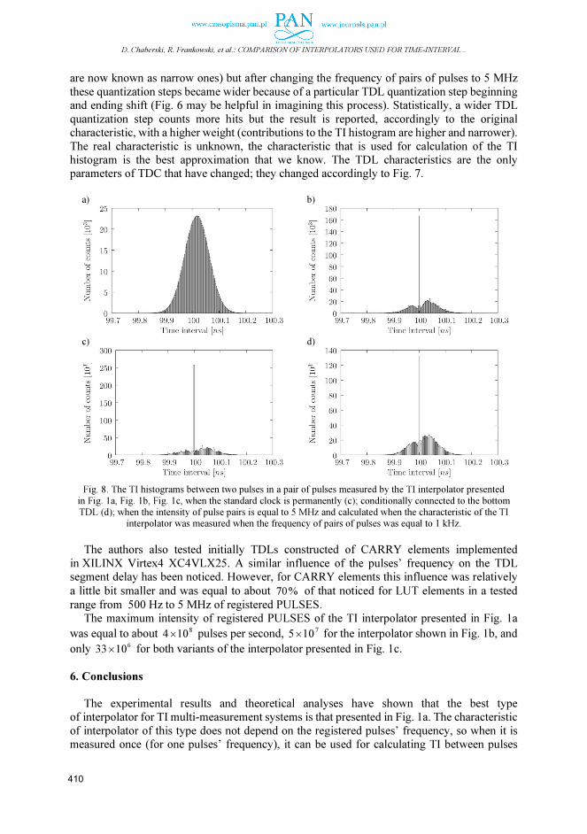
D. Chaberski, R. Frankowski, et al.: COMPARISON OF INTERPOLATORS USED FOR TIME-INTERVAL…
are now known as narrow ones) but after changing the frequency of pairs of pulses to 5 MHz
these quantization steps became wider because of a particular TDL quantization step beginning and ending shift (Fig. 6 may be helpful in imagining this process). Statistically, a wider TDL
quantization step counts more hits but the result is reported, accordingly to the original characteristic, with a higher weight (contributions to the TI histogram are higher and narrower).
The real characteristic is unknown, the characteristic that is used for calculation of the TI histogram is the best approximation that we know. The TDL characteristics are the only parameters of TDC that have changed; they changed accordingly to Fig. 7.
a) b)
c) d)
Fig. 8. The TI histograms between two pulses in a pair of pulses measured by the TI interpolator presented
in Fig. 1a, Fig. 1b, Fig. 1c, when the standard clock is permanently (c); conditionally connected to the bottom
TDL (d); when the intensity of pulse pairs is equal to 5 MHz and calculated when the characteristic of the TI
interpolator was measured when the frequency of pairs of pulses was equal to 1 kHz.
The authors also tested initially TDLs constructed of CARRY elements implemented
in XILINX Virtex4 XC4VLX25. A similar influence of the pulses’ frequency on the TDL segment delay has been noticed. However, for CARRY elements this influence was relatively
a little bit smaller and was equal to about %70 of that noticed for LUT elements in a tested
range from 500 Hz to 5 MHz of registered PULSES. The maximum intensity of registered PULSES of the TI interpolator presented in Fig. 1a
was equal to about 8104× pulses per second, 7
105× for the interpolator shown in Fig. 1b, and
only 61033× for both variants of the interpolator presented in Fig. 1c.
6. Conclusions
The experimental results and theoretical analyses have shown that the best type of interpolator for TI multi-measurement systems is that presented in Fig. 1a. The characteristic
of interpolator of this type does not depend on the registered pulses’ frequency, so when it is measured once (for one pulses’ frequency), it can be used for calculating TI between pulses
410

Metrol. Meas. Syst., Vol. 24 (2017), No. 2, pp. 401–412.
of other frequencies without causing errors. The measured TI histograms presented in Fig. 8
clearly confirm this statement. The authors performed in-depth tests of TDLs made of LUT elements and initial tests of TDLs made of CARRY elements. For both types of TDLs these characteristic changes are observed.
However, using this type of interpolator to extend a measurement range either two counters, a Grey code counter or a mutually-complementing counter-register pair are required, but this
hardware is needed only for one selected TI interpolator (the other interpolators just inherit this information). The only real difficulty of using TI interpolator of this type for multi-measurement systems is the need of calculating TDL offsets. Unfortunately, this operation
requires a lot of measurements and demands a lot of computational time. Also, for this type of TI interpolator the largest measuring intensity is allowed. The maximum intensities of other
interpolators are either limited by the standard-clock frequency or by the reverse of total TDL propagation time. Additionally, this one and the TI interpolators presented in Fig. 1b enable to obtain the highest ratio of resolution increase and the number of TDL segments.
The experimental results presented in this work show that for devices that use delay elements it is necessary to introduce an additional parameter that determines the frequency range within
which either control or measurement can be carried out with a guaranteed precision. To minimize the influence of pulses’ frequency change on the TDL characteristic change
one could use either a delay-locked or a phase-locked loop [20] for the TI interpolators
presented in Figs. 1b, 1c. This loop can be created by implementation of a dummy delay element that is placed nearby the stabilised TDL, so that this delay is sensitive to the temperature
of stabilised TDL and − what follows − is sensitive to the pulses’ intensity.
References
[1] Henzler, S. (2010). Time-to-Digital Converters. Springer Series in Advanced Microelectronics. 29, Springer
Publishing Company, Incorporated.
[2] Zieliński, M. (2009). Review of single-stage time-interval measurement modules implemented in FPGA
devices. Metrol. Meas. Syst., 16(4), 641−647.
[3] Kalisz, J. (2004). Review of methods for time interval measurements with picosecond resolution. Metrologia,
41(1), 17−32.
[4] Szplet, R. (2014). Time-to-Digital Converters. In Carbone, P., Kiaei, S., Xu, F. Design, Modeling and Testing
of Data Converters. Springer Berlin Heidelrberg, 211−246.
[5] Zieliński, M., Chaberski, D., Grzelak, S. (2003). Time-interval measuring modules with short deadtime.
Metrol. Meas. Syst., 10(3), 241−251.
[6] Torres, J., Aguilar, A., Garcia-Olcina, R., Martinez, P., Martos, J., Soret, J., Benlloch, J., Conde, P.,
Gonzalez, A., Sanchez, F. (2014). Time-to-digital converter based on FPGA with multiple channel
capability. IEEE Trans. Nucl. Sci., 61(1) 107−114.
[7] Song, J., An, Q., Liu, S. (2006). A high-resolution time-to-digital converter implemented in field-
programmable-gate-arrays. Nuclear Science, IEEE Transactions on, 53(1), 236−241.
[8] Mandai, S., Charbon, E. (2012). A 128-Channel, 8.9-ps LSB, Column-Parallel Two-Stage TDC Based on
Time Difference Amplification for Time-Resolved Imaging. Nuclear Science, IEEE Transactions on, 59(5),
2463−2470.
[9] Young-Hun, S., Jun-Seok, K., Hong-June, P., Jae-Yoon, S. (2012). A 1.25 ps Resolution 8b Cyclic TDC in
0.13 μm CMOS. Solid-State Circuits. IEEE Journal, 47(3), 736−743.
[10] Jansson, J.P., Koskinen, V., Mäntyniemi, A., Kostamovaara, J. (2012). A Multichannel High-Precision
CMOS Time-to-Digital Converter for Laser-Scanner-Based Perception Systems. Instrumentation and
Measurement, IEEE Transactions on, 61(9), 2581−2590.
411

D. Chaberski, R. Frankowski, et al.: COMPARISON OF INTERPOLATORS USED FOR TIME-INTERVAL…
[11] Fishburn, M., Menninga, L., Favi, C., Charbon, E. (2013). A 19.6 ps, FPGA-Based TDC With Multiple
Channels for Open Source Applications. Nuclear Science, IEEE Transactions on, 60(3), 2203−2208.
[12] Perktold, L., Christiansen, J. (2014). A multichannel time-to-digital converter ASIC with better than 3 ps
RMS time resolution. Journal of Instrumentation, 9(1), C01060.
[13] Wu, J., Shi, Z. (2008). The 10-ps wave union TDC: Improving FPGA TDC resolution beyond its cell delay.
Nuclear Science Symposium Conference Record, 3440−3446.
[14] Grzelak, S., Kowalski, M., Czoków, J., Zieliński, M. (2014). High resolution time-interval measurement
systems applied to flow measurement. Metrol. Meas. Syst., 21(1), 77−84.
[15] Grzelak, S., Czoków, J., Kowalski, M., Zieliński, M. (2014). Ultrasonic flow measurement with high
resolution. Metrol. Meas. Syst., 21(2), 305−316.
[16] Frankowski, R., Gurski, M., Płóciennik, P. (2016). Optical methods of the delay cells characteristics
measurements and their applications. Opt. Quantum Electron., 48(3), 1−19.
[17] Chaberski, D. (2016). Time-to-digital-converter based on multiple-tapped-delay-line. Measurement, 89,
87−96.
[18] Szplet, R., Jachna, Z., Kwiatkowski, P., Różyc, K. (2013). A 2.9 ps equivalent resolution interpolating time
counter based on multiple independent coding lines. Measurement Science and Technology, 24(3), 1−15.
[19] Zieliński, M., Chaberski, D., Kowalski, M., Frankowski, R., Grzelak, S. (2004). High-resolution time-
interval measuring system implemented in single FPGA device. Measurement, 35(3), 311−317.
[20] Rahkonen, T., Kostamovaara, J. (1993). The Use of Stabilized CMOS Delay Lines for the Digitization
of Short Time Intervals. IEEE Journal of Solid-State Circuits, 28(8), 887−894.
[21] Frankowski, R., Chaberski, D., Kowalski, M. (2015). An optical method for the time-to-digital converters
characterization. Proc. IEEE ICTON 2015, Budapest, Hungary, We.P.14, 1−4.
[22] Wu, J. (2010). Several key issues on implementing delay line based TDCs using FPGAs. Nuclear Science,
IEEE Transaction on, 57(3), 1543−1548.
[23] Frankowski, R., Zieliński, M. (2015). A sub-channel method for the time-intervals histogram calculation.
Proc. IEEE ICTON 2015, Budapest, Hungary, We.P.14, 1−5.
[24] Chaberski, D., Zieliński, M., Grzelak, S. (2009). The new method of calculation sum and difference
histogram for quantized data. Measurement, 42(9), 1388−1394.
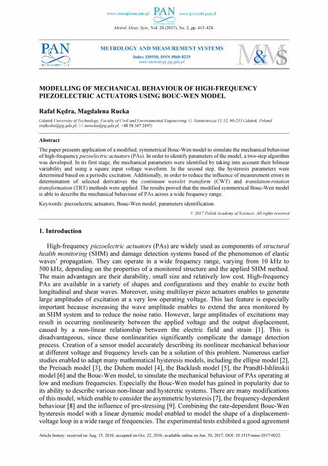
Metrol. Meas. Syst., Vol. 24 (2017), No. 2, pp. 413–424.
_____________________________________________________________________________________________________________________________________________________________________________________
Article history: received on Aug. 15, 2016; accepted on Oct. 22, 2016; available online on Jun. 30, 2017; DOI: 10.1515/mms-2017-0022.
METROLOGY AND MEASUREMENT SYSTEMS
Index 330930, ISSN 0860-8229
www.metrology.pg.gda.pl
MODELLING OF MECHANICAL BEHAVIOUR OF HIGH-FREQUENCY
PIEZOELECTRIC ACTUATORS USING BOUC-WEN MODEL
Rafał Kędra, Magdalena Rucka
Gdańsk University of Technology, Faculty of Civil and Environmental Engineering, G. Narutowicza 11/12, 80-233 Gdańsk, Poland ([email protected], [email protected], +48 58 347 2497)
Abstract
The paper presents application of a modified, symmetrical Bouc-Wen model to simulate the mechanical behaviour of high-frequency piezoelectric actuators (PAs). In order to identify parameters of the model, a two-step algorithm
was developed. In its first stage, the mechanical parameters were identified by taking into account their bilinear
variability and using a square input voltage waveform. In the second step, the hysteresis parameters were
determined based on a periodic excitation. Additionally, in order to reduce the influence of measurement errors in
determination of selected derivatives the continuum wavelet transform (CWT) and translation-rotation
transformation (TRT) methods were applied. The results proved that the modified symmetrical Bouc-Wen modelis able to describe the mechanical behaviour of PAs across a wide frequency range.
Keywords: piezoelectric actuators, Bouc-Wen model, parameters identification.
© 2017 Polish Academy of Sciences. All rights reserved
1. Introduction
High-frequency piezoelectric actuators (PAs) are widely used as components of structural health monitoring (SHM) and damage detection systems based of the phenomenon of elastic waves’ propagation. They can operate in a wide frequency range, varying from 10 kHz to
500 kHz, depending on the properties of a monitored structure and the applied SHM method. The main advantages are their durability, small size and relatively low cost. High-frequency
PAs are available in a variety of shapes and configurations and they enable to excite both longitudinal and shear waves. Moreover, using multilayer piezo actuators enables to generate large amplitudes of excitation at a very low operating voltage. This last feature is especially
important because increasing the wave amplitude enables to extend the area monitored by an SHM system and to reduce the noise ratio. However, large amplitudes of excitations may
result in occurring nonlinearity between the applied voltage and the output displacement, caused by a non-linear relationship between the electric field and strain [1]. This is disadvantageous, since these nonlinearities significantly complicate the damage detection
process. Creation of a sensor model accurately describing its nonlinear mechanical behaviour at different voltage and frequency levels can be a solution of this problem. Numerous earlier
studies enabled to adapt many mathematical hysteresis models, including the ellipse model [2], the Preisach model [3], the Duhem model [4], the Backlash model [5], the Prandtl-Ishlinskii
model [6] and the Bouc-Wen model, to simulate the mechanical behaviour of PAs operating at low and medium frequencies. Especially the Bouc-Wen model has gained in popularity due to its ability to describe various non-linear and hysteretic systems. There are many modifications
of this model, which enable to consider the asymmetric hysteresis [7], the frequency-dependent behaviour [8] and the influence of pre-stressing [9]. Combining the rate-dependent Bouc-Wen
hysteresis model with a linear dynamic model enabled to model the shape of a displacement-voltage loop in a wide range of frequencies. The experimental tests exhibited a good agreement
R. Kędra, M. Rucka: MODELLING OF MECHANICAL BEHAVIOUR OF HIGH-FREQUENCY …
of the experimental and numerical results obtained for single [10] and multi-frequency
excitations [11]. The research have also indicated that a higher-order dynamic model is required to capture accurately the PA’s response for a wide range of excitation frequencies [12].
However, the previous studies have been carried out mainly for the voltage signal frequency not exceeding 1 kHz.
This paper presents the use of a modified symmetrical Bouc-Wen model for simulation of the mechanical behaviour of high-frequency piezoelectric actuators. A two-step algorithm dedicated to parameter identification is developed and experimentally verified on an example
of a multilayer piezoelectric plate actuator. The obtained results show that the Bouc-Wen model is able to describe the mechanical behaviour of piezoelectric actuators across a wide frequency
range.
2. Bouc-Wen model of hysteresis
The Bouc-Wen model has the ability to describe various non-linear and hysteretic systems.
It was formulated by Bouc [13] and extended by Wen [14]. Despite the fact that it does not have an exact analytical solution, the Bouc-Wen model has become a widely used one, due to its
comprehensiveness and mathematical tractability. In the case of PAs, besides their conventional formulation, a modified Bouc-Wen model is also used, wherein the hysteresis component is a function of the input voltage. That model can be expressed in a form of two differential
equations [15]:
hukxxkxcxm +=−++10000
)(ɺɺɺ , (1)
( [ sgn( ) ] ),n
h u A uh hβ γ= − +ɺ ɺ ɺ (2)
where: 0
m – the mass; 0c – the damping;
0k – the stiffness;
1k – the ratio of the input voltage
and the driving force; 0x – the initial displacement; x – a displacement; xɺ – the velocity; xɺɺ –
the acceleration; u – the input voltage; h – the restoring (hysteresis) component; and A, β, γ, n
– the hysteresis parameters. In a physical sense, the hysteresis component h may be treated as a non-linear component of the voltage-strain relation.
Fig. 1. Variability of the hysteresis component according to (2) for the following parameters:
β = 0.8, γ = –0.4, n = 1(a); A = 1, γ = –0.4, n = 1 (b); A = 1, β = 0.8, γ = –0.4 (c);
A = 1, β = 0.8, n = 1 (d); A = 1, β = 0.8, γ = –0.4, n = 1 (e); A = 0.5, γ = –0.04 (f).
414

Metrol. Meas. Syst., Vol. 24 (2017), No. 2, pp. 413–424.
Figures 1a–1d show the influence of individual parameters A, β, γ, n on a change
of hysteresis loops for the harmonic input voltage. An increase of the parameter A value causes a proportional increase in the value of hysteresis component h. The opposite effect has a change of the values of parameters β and γ. Moreover, an increase of those parameters reduces the slip
effect in the highest voltage area. An increase of the parameter n value leads to reduction of the hysteresis width and, to a smaller extent it is responsible for the smoothing effect. It can be seen
that, unlike other parameters, a change of the n value does not lead to a change of the hysteresis component variability in the initial period.
Figure 1e shows the result of a growth of the input voltage amplitude at constant hysteresis parameters. It does not affect the hysteresis amplitude but leads to an extension of the loop. The
effect of changing parameter values in the time domain is presented in Fig. 1f. Small values of β and γ result in a similarity of the hysteresis and the input voltage. The effect of the phase
shift may be obtained by disproportionate increasing one of them. It should be also noticed that (2) is frequency-independent for a mono-harmonic input voltage.
3. Methodology of parameter identification
Due to a strong nonlinearity of (1) and (2) describing the hysteresis behaviour of PAs, simultaneous identification of all its parameters is possible only by using iterative optimization
techniques such as the particle swarm optimization (PSO) [16], the genetic algorithm (GA) [17] and the differential evolution (DE) algorithm [18]. In PSO-based algorithms the initially
generated random groups of model and method parameters are called particles. The positions of particles are updated in subsequent steps, taking into account the defined velocity formula. By evaluating the model and calculating the fitness functions, the best location for each particle
and the entire group can be determined. Genetic algorithms are based on genetic operations. The response and the fit of a model are evaluated for all initial parameter sets. The best fitting
sets are selected to reproduction, crossover and mutation processes resulting in creation of new sets of model parameters. The selection and genetic operations are repeated until the stopping
criterion is achieved. DE is similar to GA, the differences lie in the way of carrying out genetic operations. Each new set of parameters is compared with a parent set and the set for which evaluation of the fitness value gives better results is passed to the next iteration. The main
problems of iterative approaches are their sensitivity to the initially selected parameters, the possibility of finding only a local minimum, and a relatively slow convergence. Therefore,
considering the equations (1) – (2) separately and determining parameters in subsequent steps without iteration is a very convenient alternative [8–9]. This approach significantly reduces the computational cost, simplifies the estimation procedure and enables to avoid ambiguity
in determining the parameters related to the occurrence of local minima of optimized functions. It may be used when the hysteresis amplitude is negligible in comparison with the amplitude
of the applied input voltage. Such a situation can occur in the case of excitation in a form of a periodic square function and, respectively, a low amplitude. This type of input signal can be defined by an infinite series of sine functions:
1
1
sin(2 (2 1) )4
2 1
Ssquare
k
k T tu B
k
π
π
−∞
=
−
=
−
∑ , (3)
where B denotes the amplitude and S
T − the period of the square function. In experimental studies the series (3) is limited to a finite number of initial terms. This feature of the excitation
signal significantly reduces the hysteresis component value. In the case of PAs operating in a range of frequencies below 1 Hz it is also possible to separate determination of parameters
associated with the static hysteresis [7].
415

R. Kędra, M. Rucka: MODELLING OF MECHANICAL BEHAVIOUR OF HIGH-FREQUENCY …
3.1. Assessment of mechanical constants If only the first quarter of the square function period is considered, it can be approximated
by the Heaviside step function and used to determine the mechanical parameters using the limit
theorem. However, such a simplification does not take into account the time taken by a signal
to change from zero to its maximum value (the rise time) and − for the analysed high frequency
PAs, where the damping and mass values are much smaller than the stiffness one − it causes large errors. In order to reflect more accurately the variability of the input signal, it can be described as the difference of two time-shifted ramp functions with the same slope:
1 1 1
( ) ( ) ( )u at H t a t T H t T= ⋅ − − ⋅ − , (4)
where 1T is the rise time and a − the slope. Assuming that the influence of the hysteresis is
neglected ( uh << ) for the input voltage described by (4), the relation (1) after applying the Laplace transform can be written as:
2
0 0 0 1 1[ ( ) (0 ) (0 )] [ ( ) (0 )] ( ) ( )m s X s s x x c s X s x k X s k U s
− − −
− − + − + =ɺ , (5)
where: ( )( ) ( )X s x t= L ; ( )1 1( ) ( )U s u t= L and (0 )x
− , (0 )x−
ɺ are the initial displacement and
velocity of the PA, respectively. For the zero initial conditions, the relation (5) becomes:
1
1 1
12 2 2
0 0 0 0 0 0
(1 )( ) ( )
T sk k a e
X s U sm s c s k m s c s k s
−
−= =
+ + + +
. (6)
Using the theorem of the limit value, a series of steady-state parameters 0 1, , ,
nK K K… ,
can be specified. The first parameter is defined as:
0
1
1
0
2
0
3
0
1
0000
)1(lim)(lim)(lim)(lim
1
k
kTa
skscsm
eaksXstxtgK
sT
sstt
=
++
−
====
−
→→∞→∞→
, (7)
and the next ones are described by the following formula:
)(1
lim)(lim0
sgs
tgKi
si
ti
→→∞
== , (8)
where i
g is given by the recursive relationship:
∫ −−
−=
t
iiidgKtg
0
11)]([)( ττ . (9)
Calculation of the limits occurring in the previous formulas for i = 0, 1, 2, 3 enables to write
the following system of four nonlinear equations with four unknowns: 0
m , 0c ,
0k and
1k :
1
1 0
0
2 01
1 0 1
0 0
03 01
1 1 0 2
0 0 0
04 01
1 2 1 3
0 0 0
,
,2
,6
.24
kaT K
k
ckaT K K
k k
mckaT K K K
k k k
mckaT K K K
k k k
=
+ = + − = + − =
(10)
416
Metrol. Meas. Syst., Vol. 24 (2017), No. 2, pp. 413–424.
After multiplying all the equations by the stiffness factor k0, a linear system of equations
with zero values of all free terms will be obtained. This implies that the system (10) is indefinite and it enables to determine a solution only in the case when one of the unknown values is parameterized. In practice, it means that the model does not require determination of all
parameters but only their proportions. As a result, (10) can be written in a matrix form using only the first three equations:
=
−
−3
1
2
1
1
1
0
0
0
012
01
0
3
6
60
00
Ta
Ta
Tak
m
c
k
KKK
KK
K
. (11)
The mechanical parameters of the model are given by:
,1
k0
110
KTak = (12)
,2
k 0
1
2
0
1
110
−=
K
T
K
KTac (13)
.26
k2
0
11
3
0
20
2
1
0
2
1
110
−
−+=
K
KT
K
KKK
K
TTam (14)
The steady-state parameters 0
K , 1
K and 2
K can be determined experimentally using the
input voltage in a form of the square function with a sufficiently low amplitude and a long
period. The rise time 1T and the slope a can be determined based on the time variation of input
voltage. Finally, the equations (12) to (14) enable to determine the parameters 0
m , 0c and
0k
in relation to the parameter 1k . In order to avoid ambiguity, in the subsequent considerations
the arbitrary value of parameter 1k ,
1k = 1 V−1 was set.
3.2. Estimation of hysteretic parameters
Based on the known mechanical parameters, for any input voltage u it is possible to reproduce the corresponding hysteresis time variation h. The time derivatives of the hysteresis hɺ and input voltage uɺ can be also calculated using a simple differential scheme or other techniques of numerical differentiation. The parameters A, β, γ and n appearing in (2) can be
estimated using the averaging and the least squares methods. After denoting 1−= uhz ɺɺ and
hh = , deriving both sides of the (2) gives:
1
[ sgn( ) ] .n
z n u h h hβ γ−
=− +ɺɺɺ (15)
For time points, where 0>iihuɺ , the above equation can be rewritten in a discrete form:
1
( )n
i iiz n h hβ γ
−
= − +ɺɺ . (16)
After taking the logarithms of both sides and doing some mathematical manipulations, (16) can be rewritten as:
ln ln[ ( )] ( 1) lni
i
i
zn n h
hβ γ= − + + −
ɺ
ɺ. (17)
417

R. Kędra, M. Rucka: MODELLING OF MECHANICAL BEHAVIOUR OF HIGH-FREQUENCY …
Linearization of (17) has been finally made by substituting )/ln(iii
hzq ɺɺ= , ii
hp ln= and
)](ln[ γβν +−= n . Thus, (17) can be written as a linear equation:
ν+−=iipnq )1( . (18)
The parameters n and ν can be determined using the least squares method:
( )
( )
( ) ( )∑∑
∑∑∑∑
∑∑
∑∑∑∑−
−
=
−
−
=2
1
2
2
2
1
2
2
lnln
lnlnlnlnln
ii
i
i
i
i
i
i
i
ii
iiiii
hNh
hh
zh
h
zh
pNp
pqpqp ɺ
ɺ
ɺ
ɺ
ν , (19)
( ) ( ) ( )∑∑
∑∑∑
∑∑
∑∑∑−
−
+=
−
−
+=2
1
2
1
2
1
2
1
lnln
lnlnlnln
11
ii
i
i
i
i
i
i
ii
iiii
hNh
h
zhN
h
zh
pNp
qpNqpn
ɺ
ɺ
ɺ
ɺ
, (20)
where 1
N denotes the number of considered time points. For the same set of time points, using the calculated value and a discrete form of (2), the parameter A can be computed according to
the formula:
∑ ∑−=
n
iih
n
e
Nz
NA
ν
11
11. (21)
In order to identify all hysteresis parameters, determination of ξ β γ= − is required. It can
be done by calculation of the average value of parameter ξ in 2
N time points for which the
relation 0<jj
huɺ occurs:
∑−
=n
jh
Az
N2
1ξ . (22)
Finally, the parameters β and γ can be calculated on the basis of ν and ξ:
n
e
22
νξβ −= , (23)
22
ξγ
ν
−−=
n
e
. (24)
The main disadvantage of the estimation procedure described above is the necessity of using
the second derivative, which significantly increases the effect of measurement errors. For this reason, in order to determine selected derivatives, the continuum wavelet transform (CWT) and the translation-rotation transformation (TRT) were used [19]. This method can significantly
reduce the impact of noise and it enables to eliminate the boundary effect of traditional wavelet differentiation. Firstly, the TRT of function f is defined by:
btatftf TRT−−= )()( , (25)
where:
max min
max min
( ) ( )f t f ta
t t
−
=
−
,
min min( )b f t a t= − . (26)
Afterwards, the derivative of function f can be calculated according to the formula:
1.5
( )TRT CWT
t
ff a
Ks ∆= +
ɺ, (27)
418

Metrol. Meas. Syst., Vol. 24 (2017), No. 2, pp. 413–424.
where ( )TRT CWTf is CWT of TRTf ,
t∆ is a time increment, s is the scale of CWT and K is
a parameter depending on the used wavelet function ψ and it is defined as:
∫∞
∞−
= dttK )(θ . (28)
A smoothing function θ is a time integral of the wavelet ψ with respect to time.
4. Determination of parameters of high-frequency piezoelectric actuators
In order to verify the described above method and its suitability for simulation of high-
frequency PAs, experimental examinations were made. The object of research was a Noliac
NAC2024 multilayer plate actuator (Fig. 2a) with dimensions 3 mm × 3 mm × 2 mm and an operating voltage in the range 0–200 V. A scheme of the experimental set-up is shown in
Fig. 2b. The input voltage signal was generated by a Tektronix AFG 3022 function generator and enhanced by an EC Electronics PPA 2000 high-voltage amplifier. The signal was then transmitted to the actuator causing its displacement, which was recorded by the scanning head
of Polytec PSV-3D-400-M laser vibrometer with a sampling frequency of 2.56 MHz.
Fig. 2. Laboratory tests: a scheme of the experimental set-up (a); high-frequency PAs (centimetre scale) (b).
Determination of the mechanical parameters was made using a rectangular excitation with
an amplitude of 7.8335 V and a period equal to 0.1 ms. Based on the measured input voltage
signal, two parameters (1T = 1.8672 μs and a = 4.1954 MVs-1) characterizing the excitation
were identified. In the second step, based on the PA displacements in a period of 0–45 μs,
a series of functions (0
g , 1
g , and 2
g ) and the steady-state parameters 0
K , 1
K and 2
K were
defined (Fig. 3). It can be seen that the values of functions 0
g and 1
g rapidly converge to their
limits, whereas for the function 2
g some oscillations are visible. It is related to the order
of magnitude of this function and can result in inaccuracies in the identified steady-state value
2.K The mechanical parameters determined based on the above-mentioned values are
summarized in Table 1.
Fig. 3. The functions used for identification of the mechanical parameters
of NAC2024 actuator: g0 (a); b) g1 (b); g2 (c).
419

R. Kędra, M. Rucka: MODELLING OF MECHANICAL BEHAVIOUR OF HIGH-FREQUENCY …
The procedure described in Section 3.2 can be applied to any type of excitation. However, the numerical tests showed that the best results can be obtained for a sinusoidal input voltage
with a relatively large amplitude. The numerical tests also showed that in order to minimize the error associated with linearization, the identification procedure should be limited to a period in which the input voltage value is in a range of 25–75% of its amplitude. Therefore, to determine
the hysteresis parameters for the actuator, a harmonic excitation with a frequency of 10 kHz and a magnitude of 9.738 V was used. The time variability of hysteresis component was
determined on the basis of pre-determined mechanical parameters and the measured signal. In order to reduce the influence of noise, in determination of hɺ and hɺ the CWT-TRT method was applied (Figs. 4b–4c). In numerical calculations the first order Gaussian wavelet (Fig. 4a)
with a scale parameter 4s = and the parameter 42π=K
were used. It can be observed that using wavelet differentiation for h caused excessive smoothing in the jump area. However, this
interval was not considered in the identification process. All other derivatives, including the PA velocity and acceleration time variations were determined using the central differential scheme.
Fig. 4. Noise reduction for the hysteresis derivative: Gaussian wavelet of order 1 (a);
comparison of finite difference and CWT-TRT differentiation of hɺ (b);
comparison of finite difference and CWT-TRT differentiation of hɺ (c).
The three-stage process of determining the hysteresis parameters is visualised in Fig. 5.
In the first stage, the values of parameters ν and n were determined using the least squares method and fitting the linear regression model to experimental data (Fig. 5a). In next stages,
the values of A (Fig. 5b) and ξ (Fig. 5c) were determined by an averaging process. It can be noticed, that the experimentally determined data are scattered and no trend is clearly visible.
This is a result of using the second derivative and occurring noise which influence can be limited using the CWT-TRT method by increasing the scale parameter s. However, the performed numerical tests using the Gaussian noise have shown that it does not affect
correctness of the identification process. All identified parameters of (2) are listed in Table 1. Relatively low values of β and γ parameters indicate a small impact of non-linearity on the PA
behaviour.
Fig. 5. Visualization of determining the hysteresis parameters: identification of ν and n values using the least
square method (a); identification of A value (b); identification of ξ value (c).
420

Metrol. Meas. Syst., Vol. 24 (2017), No. 2, pp. 413–424.
Table 1. A list of identified parameters of NAC2024 actuator for the modified symmetrical
Bouc-Wen hysteresis model.
Parameter m0
[kg]
c0
[kgs−1]
k0
[Nm−1]
k1
[V−1]
A
[−]
β
[−]
γ
[−]
n
[−]
Identified
value
3.419 ×
10−4 491.632 3.725 × 10⁸ 1 0.192 0.034 −0.0463 1.419
5. Experimental validation and accuracy analysis
In order to assess suitability of the model, additional tests comparing the experimental data with the results of numerical calculations were carried out. The simulations were performed using MATLAB® ordinary differential equation solver ode45 on the basis of the identified
mechanical and hysteresis parameters and the experimentally measured input voltage signal. Selected results of the time variability of displacements and the hysteresis displacement-voltage
loop are given in Fig. 6. It can be seen that the numerical and experimental results are in a good agreement in both initial and steady-state periods. The qualitative assessment of the model accuracy was made on the basis of global goodness-of-fit measures: the error sum of squares
(SSE), the total sum of squares (SST), the R-squared (R2), as well as a local correctness coefficient – the maximum relative deviation (MRD):
2
1
ˆ( )N
i i
i
SSE x x
=
= −∑ , (29)
2
1
( )N
i
i
SST x x
=
= −∑ , (30)
21
SSER
SST= − , (31)
ˆmax| |
100%max
i i
i
x xMRD
x
−
= ⋅ , (32)
where: ix is the measured displacement;
ix is the numerically simulated displacement and x
is the mean value of ix . The calculated values of specified error measures at different
frequencies are summarized in Table 2.
Table 2. Statistical quantities characterizing the accuracy of predicted NAC2024 actuator displacements.
f [kHz] 10 20 40 60 80 100 120 140 160 180 200
SSE
[m]
2,22
× 10−15
2,52
× 10−14
5,78
× 10−15
2,27
× 10-15
2,14
× 10−15
2,46
× 10−15
3,19
× 10−15
3,28
× 10−15
3,34
× 10−15
5,2
× 10−15
4,39
× 10−15
SST
[m]
1,971
× 10−12
9,6
× 10−13
4,32
× 10−13
2,56
× 10−13
1,71
× 10−13
1,19
× 10−13
8,69
× 10−14
5,99
×10−14
4,33
× 10−14
3,26
× 10−14
1,94
× 10−14
x
[m]
−3,55×
10−11
−2,33×
10−11
−4,06×
10−11
1,08
× 10−10
−1,12×
10−10
−6,0
× 10−12
−2,25×
10−10
−3,41×
10−10
−1,12×
10−10
−1,44×
10−10
2,33
× 10−10
R2 [−] 0,999 0,974 0,987 0,991 0,987 0,979 0,963 0,945 0,923 0,840 0,774
MRD
[%] 5,776 17,317 12,080 10,538 12,333 16,065 17,073 23,027 34,450 49,211 63,879
The results of the error analysis indicate effectiveness of the Bouc-Wen model and the proposed parameter identification method of simulating high-frequency PA motion. For all
executed simulations in a range of 10–120 kHz, the correlation coefficient (R-square) between
421

R. Kędra, M. Rucka: MODELLING OF MECHANICAL BEHAVIOUR OF HIGH-FREQUENCY …
the numerical and experimental results was greater than 0.95, which proves a good
correspondence of the theoretical model results with the actual physical PA behaviour. The best fit was obtained for a frequency of 10 kHz, which was used for the model calibration. Fig. 6 shows that the maximum absolute error occurs in the maximum applied voltage area.
An inaccuracy of the applied model significantly increases for frequencies of above 140 kHz. It is confirmed by a large value of MRD, at a level of 23% and more. An increase of the error
value is caused by a relatively high uncertainty in determination of the mass, which influences high frequency oscillations. In addition, the available sampling frequency in experimental studies does not provide a sufficient number of sampling points for a period in a range above
100 kHz.
Fig. 6. Comparison of the numerical and experimental results for NAC2024 actuator – displacement versus time
and displacement versus voltage in the initial stage, for a sinusoidal excitation with a frequency:
10 kHz (a); 60 kHz (b); 100 kHz (c); 140 kHz (d).
6. Conclusions
In the paper an improved two-step algorithm was proposed, dedicated to identifying the mechanical parameters of a modified, symmetrical Bouc-Wen model, adapted to characterize
high-frequency piezoelectric actuators. An increase of accuracy in the first step of identification process, compared with algorithms used for low frequency PAs, was obtained by taking into account the initial variability of the excitation signal and assuming the ability of its
approximation by a bilinear function. The hysteresis parameters of the Bouc-Wen model were determined in the second step, based on a single measured signal and using the CWT-TRT
method for reducing an influence of noise.
422

Metrol. Meas. Syst., Vol. 24 (2017), No. 2, pp. 413–424.
The proposed algorithm was applied to modelling the mechanical behaviour of a high
frequency PA. The Bouc-Wen model parameters were determined from the results of experimental tests using square and harmonic input voltage signals. Next, in order to validate the identification procedure, a comparative analysis was carried out. The tests aimed to compare
the experimentally measured displacements of the tested PA and the numerical results obtained for the identified parameters of the Bouc-Wen model. The performed analyses have shown
a good agreement between the experimental and numerical results in a range of 10–120 kHz. Above this range the model accuracy significantly decreases. It is caused primarily by inaccurate identification of the mass and by limitations of the assumed dynamic model.
The proposed method of identification can be used for different types of hysteretic systems. The obtained results can be also useful in numerical modelling piezoelectric transducers for
SHM systems.
References
[1] Sohrabi, M.A., Muliana, A. H. (2015). Nonlinear and time dependent behaviors of piezoelectric materials
and structures. Int. J. Mech. Sci., 94–95, 1–9.
[2] Gu, G., Zhu, L. (2011). Modeling of rate-dependent hysteresis in piezoelectric actuators using a family
of ellipses. Sensors Actuat. A-Phys., 165(2), 303–309.
[3] Wang, X., Pommier-Budinger, V., Reysset, A., Gourinat Y. (2014). Simultaneous compensation of hysteresis
and creep in a single piezoelectric actuator by open-loop control for quasi-static space active optics
applications. Control Eng. Pract., 33, 48–62.
[4] Lin, C.-J., Lin, P.-T. (2012). Tracking control of a biaxial piezo-actuated positioning stage using generalized
Duhem model. Comput. Math. Appl., 64(5), 766–787.
[5] Liu X., Wang Y., Geng J., Chen Z. (2013). Modeling of hysteresis in piezoelectric actuator based on adaptive
filter. Sensors Actuat. A-Phys., 189, 420–428.
[6] Ghafarirad, H., Rezaei, S.M., Sarhan, A.A.D., Mardi, N.A., Zareinejad, M. (2014). A novel time dependent
Prandtl-Ishlinskii model for sensorless hysteresis compensation in piezoelectric actuators. IFAC Proceedings
Volumes, 47(3), 2703–2708.
[7] Zhu, W., Wang, D.H. (2012). Non-symmetrical Bouc-Wen model for piezoelectric ceramic actuators.
Sensors Actuat. A-Phys., 181, 51–60.
[8] Zhu, W., Rui, X.-T. (2016). Hysteresis modeling and displacement control of piezoelectric actuators with the
frequency-dependent behavior using a generalized Bouc-Wen model. Precis. Eng., 43, 299–307.
[9] Wang, D.H., Zhu, W. (2011). A phenomenological model for pre-stressed piezoelectric ceramic stack
actuators. Smart Mater. Struct., 20(3), 035018, (11 pp.).
[10] Wang, Z., Zhang, Z., Mao, J., Zhou, K. (2012). A Hammerstein-based model for rate-dependent hysteresis
in piezoelectric actuator. Proc. of the 2012 24th Chinese Control and Decision Conference. Taiyuan, China,
1391−1396.
[11] Wang, G., Chen, G., Bai, F. (2015). High-speed and precision control of a piezoelectric positioner with
hysteresis, resonance and disturbance compensation. Microsyst. Technol., (11 pp).
[12] Xu, Q. (2013). Identification and compensation of piezoelectric hysteresis without modeling hysteresis
inverse. IEEE T. Ind. Electron., 60(60), 3927−3937.
[13] Bouc, R. (1967). Forced vibration of mechanical systems with hysteresis. Proc. of the 4th Conference on
Nonlinear Oscillation., Prague, Czechoslovakia, 315.
[14] Wen, Y.K. (1976). Method for random vibration of hysteretic systems. J. Eng. Mech.-ASCE, 102(2), 249–
263.
[15] Low, T.S., Guo, W. (1995). Modeling of three-layer piezoelectric bimorph beam with hysteresis. IEEE J.
Microelectromech. Syst., 4(4), 230–237.
423

R. Kędra, M. Rucka: MODELLING OF MECHANICAL BEHAVIOUR OF HIGH-FREQUENCY …
[16] Wang, Z., Mao, J. (2010). On PSO based Bouc-Wen modeling for piezoelectric actuator. 3rd International
Conference on Intelligent Robotics and Applications., Shanghai, China, 125−134.
[17] Ha, J.L., Kung, Y.S., Fung, R.F., Hsien, S.C. (2006). A comparison of fitness functions for the identification
of a piezoelectric hysteretic actuator based on the real-coded genetic algorithm. Sensors Actuat. A-Phys., 132,
643–650.
[18] Wang, G., Chen, G., Bai, F. (2015). Modeling and identification of asymmetric Bouc-Wen hysteresis for
piezoelectric actuator via a novel differential evolution algorithm. Sensors Actuat. A-Phys., 235, 105–118.
[19] Luo J.W., Bai J., Shao J.H., (2006). Application of the wavelet transforms on axial strain calculation in
ultrasound elastography. Prog. Nat. Sci., 16(9), 942–947.
Metrol. Meas. Syst., Vol. 24 (2017), No. 2, pp. 425–436.
_____________________________________________________________________________________________________________________________________________________________________________________
Article history: received on Feb. 17, 2016; accepted on Oct. 22, 2016; available online on Jun. 30, 2017; DOI: 10.1515/mms-2017-0019.
METROLOGY AND MEASUREMENT SYSTEMS
Index 330930, ISSN 0860-8229
www.metrology.pg.gda.pl
EFFECT OF ADC RESOLUTION ON LOW-FREQUENCY ELECTRICAL
TIME-DOMAIN IMPEDANCE SPECTROSCOPY
Reyhaneh L. Namin, Shahin J. Ashtiani
University of Tehran, College of Engineering, P.O. Box 14395/515 Tehran, Iran ([email protected], [email protected], +98 21 8208 4952)
Abstract
In this paper, the effect of the resolution of an analogue-to-digital converter (ADC) on the accuracy of time-
domain low-frequency electrical impedance spectroscopy is examined. For the first time, we demonstrated that
different wideband stimuli signals used for impedance spectroscopy have different sensitivities to the resolution
of ADC used in impedance spectroscopy systems. We also proposed Ramp and Half-Gaussian signals as new
wideband stimulating signals for EIS. The effect of ADC resolution was studied for Sinc, Gaussian, Half-Gaussian,
and Ramp excitation signals using both simulation and experiments. We found that Ramp and Half-Gaussian
signals have the best performance, especially at low frequencies. Based on the results, a wideband electrical
impedance spectroscopy circuit was implemented with a high accuracy at frequencies bellow 10 Hz.
Keywords: electrical impedance spectroscopy, analogue-to-digital converter, Ramp signal, Fast Furrier transform,
Nyquist plot.
© 2017 Polish Academy of Sciences. All rights reserved
1. Introduction
Electrical impedance spectroscopy (EIS) is a non-destructive, inexpensive and simple
measurement method for testing properties of electrochemical or biological systems [1].This technique is widely used in several industrial and biological applications such as corrosion monitoring [2], study of the solar cells [3] fuel cells [4] and batteries [5], distinction between
normal and cancerous cells [6], and measurement of flowing blood to predict white thrombus formation [7].
The spectrum of impedance is a Nyquist plot, consisting of points that describe the magnitude and phase of the impedance for a specific frequency. The spectrum shape characterizes the order, structure, and the equivalent electrical model of a sample under test.
In EIS, the precision, frequency range, and test duration are very important. Since there is a possibility of change in the structure of the sample under test due to applying an excitation
signal for a long time, the duration of EIS has a high significance, particularly in studying biomaterials and medical applications.
The frequency range in which EIS is performed is determined by the sample. For instance, while in medicine the desired frequency range can be in the range of hundreds to a few thousand Hertz, it can be as low as a few mili-Hertz in battery and fuel cell applications [8, 9].
There are two general techniques used in EIS: the frequency domain and the time domain. In the frequency domain spectroscopy, a frequency is the independent variable and the
excitation signal is sinusoidal. To produce the impedance spectrum, the sinusoidal signal frequency is swept in the desired range [1].
While applying a sinusoidal excitation signal to the tested sample is one of the most
comprehensive and simplest methods for extraction of the impedance spectrum, it takes a long

R. L. Namin, S. J. Ashtiani: EFFECT OF ADC RESOLUTION ON LOW-FREQUENCY ELECTRICAL …
test time, especially at frequencies under 1 Hz [10]. Another issue of the method is its discrete
frequency components: for each desired test frequency, at least one period of sinusoidal signal in that frequency should be applied to the sample. Therefore, the number of frequency steps in the impedance spectrum is associated with the number of sinusoidal signals that are applied to
the sample under test. This results in lengthened test times, especially in low frequency ranges. In the time domain spectroscopy, time is the independent variable. To extract the impedance
as a function of frequency, a time-to-frequency transformation is needed. The transformation methods are generally based on Fourier [4], Laplace [11] or Wavelet [12] transforms. The excitation in the time domain spectroscopy is a wideband signal such as a multi-sinusoidal,
chirp, Sinc signal [10], a pulse or white noise [12]. An advantage of using a wideband signal is that by applying a single excitation, the impedance spectrum of the entire desired frequency
range can be obtained at once. This results in faster obtaining a more accurate spectrum, especially in low frequency ranges.
Since time-to-frequency transformations have to be done in the digital domain, an analogue-
to-digital converter (ADC) should be used. The resolution and sampling frequency of ADC has a significant effect on a precision of the impedance spectrum. If the ADC has an infinite
resolution and sampling frequency, the impedance spectrum has no error. However, in practice, using an ADC with a limited resolution and sampling frequency causes an error in the resulted impedance spectrum.
The ADC error associated with the limited resolution is generally modelled by the quantization noise. The general quantization noise theory predicts that the ADC error due to
a limited resolution is almost independent of the input signal and it just depends on the resolution [13]. However, our findings based on simulations and experimental results for the first time show that the shape of the excitation signals used in time domain EIS, has a significant
effect on the error of the measured impedance, when the ADC resolution is limited. In this paper, we examine the effect of ADC resolution on the error of the measured
impedance for several excitation signals, including Sinc, Gaussian, and half-Gaussian ones. In addition, we propose Ramp as a simple and accurate excitation signal for the time domain
EIS with a low sensitivity to ADC resolution. The purpose of this paper is − using a specific
hardware − to find an excitation signal which can result in an impedance spectrum with less errors.
In the next section, some excitation signals including the Ramp one, are introduced. In the
third section, the proposed method of implementing a wide-band impedance spectroscopy measurement system is presented. Finally, the results of the measurements are reported,
compared and analysed.
2. Excitation signals
To obtain an impedance spectrum, a small alternate current or voltage as the excitation signal
is applied to the sample and the response signal is monitored and measured. The ratio of the Fast Furrier Transform (FFT) of the response signal and the FFT of the excitation signal, as a transfer function, indicates the sample impedance.
Selection of an appropriate excitation signal − especially at low frequencies − is an important issue in EIS. A multi-sinusoidal excitation signal has been used in some previous research works [5]. This signal consists of 10 to 15 frequencies and the duration of applying the signal
is equal to the period of its lowest frequency. Using a multi-sinusoidal signal results in a shorter measurement time, in comparison with sinusoidal signals. A disadvantage of the multi-
sinusoidal signal is its discrete frequency components and elevated amplitudes. In some previous works a pulse signal is used as the excitation signal. It has a continuous
frequency spectrum. However, its high-frequency components drop off rapidly, resulting
426

Metrol. Meas. Syst., Vol. 24 (2017), No. 2, pp. 425–436.
in a lower accuracy at higher frequencies [14]. Moreover, for some specific frequencies,
the amplitudes of its components are equal to zero. A chirp excitation signal is also used in impedance spectroscopy systems. An advantage
of using this signal is its independent scalability in frequency and time. While it is an appropriate signal for EIS at higher frequencies, it is not very accurate at low frequencies
[12]. In this work, we used four excitation signals including Sinc, Gaussian, half-Gaussian and
Ramp ones for comparison. Fig. 1 shows the signals in the time and frequency domains. All
of these four signals have the same energy.
Fig. 1. Sinc, Gaussian, half-Gaussian and Ramp signals in the time and frequency domains.
Equations (1) to (4) define Sinc, Gaussian, Half-Gaussian and Ramp signals, respectively:
, (1)
, 0.98, (2)
0
, 2, (3)
∗ 15
0 " 15. (4)
Because of the presence of ADC and DAC the excitation signal is not ideal and the resolution and sampling frequency of ADC and DAC cause an error in the impedance spectrum. To extract
the impedance spectrum for frequencies below 1 Hz, the excitation signal should have a high amplitude in the time domain. Also, the excitation signal in the frequency domain should have a sufficient magnitude in a wide range of frequencies.
Figures 1a and 1b show a Sinc signal in the time and frequency domains, respectively. As can be seen, an amplitude of the Sinc signal in the time domain drops
427

R. L. Namin, S. J. Ashtiani: EFFECT OF ADC RESOLUTION ON LOW-FREQUENCY ELECTRICAL …
rapidly. As a result, an ADC with a high resolution and sampling frequency is required. In the
frequency domain, the Sinc signal has an almost flat frequency spectrum but with a small value compared with other tree signals. In Figs. 1c and 1d a Gaussian signal in the time and frequency domains is shown. An amplitude of the Gaussian signal in the time domain is higher and is
changing slower than that of the Sinc signal. A magnitude of the Gaussian signal in the frequency domain is higher at lower frequencies and an increase of the frequency causes
a decrease of its magnitude, eventually dropping its value to zero. Figs. 1e and 1f show a half-Gaussian signal in the time and frequency domains. This signal is almost similar to the Gaussian one, but in the frequency domain its magnitude drops to zero in higher frequencies.
In Figs. 1g and 1h a Ramp signal in the time and frequency domains is shown. This signal has a higher amplitude in the time domain, and it also has a very high frequency-domain
magnitude at very low frequencies and its magnitude decreases by increasing the frequency. But, like the half-Gaussian signal, its magnitude drops to zero in frequencies higher than those for the Gaussian signal.
3. Effect of ADC quantization on impedance spectrum
As mentioned earlier, in the time domain EIS, the impedance signal should be converted to a digital one by an ADC. In this section, we briefly study the effect of the ADC resolution and an excitation signal on the accuracy of the impedance spectrum. To do this, an excitation signal with 3000 samples in 100 s, with a rate of 30 S/s, is applied to the first-order impedance, and then the response signal is quantized by a 14-bit ADC model in MATLAB. The difference
between the quantized signal at the ADC output and the input signal is calculated and then normalized to the amplitude of the least significant bit (LSB) of the ADC. Fig. 2 shows the
simulated quantization errors for Sinc, Gaussian, half-Gaussian and Ramp signals in the time domain. As can be seen, the quantization error of the Sinc signal has a larger value and exists in the entire duration of sampling. One explanation for the higher error of the Sinc signal is the
abrupt reduction in its time-domain amplitude. As a result, for a considerable part of the test duration, the signal amplitude goes well below the resolution of the ADC. While Gaussian,
half-Gaussian and Ramp signals have non-perfect frequency spectra compared with the Sinc signal, they have a smoother shape in the time-domain and for most of the test duration their
amplitudes are large enough to be detected by the ADC.
Fig. 2. The time-domain quantization error of Sinc, Gaussian, half-Gaussian and Ramp signals.
The errors are normalized to the amplitude of the least significant bit (LSB) of the ADC.
0 500 1000 1500 2000 2500 3000-1
-0.8
-0.6
-0.4
-0.2
0
Plot of Sinc signal
(a)
Error(L
SB
)
0 500 1000 1500 2000 2500 3000-1
-0.8
-0.6
-0.4
-0.2
0
Plot of Gaussian signal
(b)
Error (
LS
B)
0 500 1000 1500 2000 2500 3000-1
-0.8
-0.6
-0.4
-0.2
0
Plot of Half-Gaussian signal
(c)
Erro
r(L
SB
)
0 500 1000 1500 2000 2500 3000-1
-0.8
-0.6
-0.4
-0.2
0
Plot of Ramp signal
(d)
Erro
r(L
SB
)
428

Metrol. Meas. Syst., Vol. 24 (2017), No. 2, pp. 425–436.
For comparison, the root mean square (RMS) and mean quantization errors of the four
signals in LSB, are calculated and listed in Table 1.
Table 1. The RMS and mean quantization errors of Sinc, Gaussian, half-Gaussian and Ramp signals.
Signal Mean error (normalized to LSB) RMS error (Normalized to LSB)
Sinc −0.4608 0.3228
Gaussian −0.2428 0.1678
half-Gaussian −0.2147 0.1353
Ramp −0.2586 0.1664
As can be seen, the smallest quantization error is that of the half-Gaussian signal. The Ramp and Gaussian signals also have lower errors compared with the Sinc one.
To examine the effect of ADC on the impedance spectrum, Nyquist plots of the first-order impedance using the previous excitation signals are obtained by simulation using MATLAB. In the simulations, the ADC has a 14-bit resolution, its sampling frequency is 30 S/s, and
a duration of applying the excitation signal is 100 s. To obtain the electrical impedance spectrum in MATLAB, the excitation signal is quantized
and the FFT of the excitation signal is calculated, then this signal applied to the sample is again quantized and the FFT of the response is calculated. Eventually, by using some math operations,
the impedance spectrum is extracted. Figure 3 shows the sample circuit which has been used in the simulations. Table 2 contains
the values of components used in the simulations.
Fig. 3. The sample impedance circuit used for the measurements and simulations.
Table 2. The component values used in the simulations.
R1 R2 R3 C1 C2
0.5 KΩ 0.5 KΩ 0.5 KΩ 6.8 mF 10 uF
Figure 4 shows the simulation results. The ideal Nyquist plot is shown by the blue dots,
whereas the red dots represent the impedance spectrum obtained from the simulation.
According to the Nyquist plots resulted from Sinc, Gaussian, half-Gaussian and Ramp excitation signals, we perceive that the impedance spectrum errors for the Ramp and half-
Gaussian excitation signals are lower than the error which have been obtained by other excitation signals.
The effect of reduction of the ADC resolution on the impedance error is studied. Figs. 5 and 6 show average magnitude and phase errors of the impedance spectrum as a function of the
ADC resolution. As can be seen, for the Sinc signal, both phase and magnitude errors of the impedance considerably increase with decreasing the ADC resolution. The lowest sensitivity to the ADC resolution can be achieved by using Ramp or half-Gaussian signals.
429

R. L. Namin, S. J. Ashtiani: EFFECT OF ADC RESOLUTION ON LOW-FREQUENCY ELECTRICAL …
Fig. 4. The Nyquist plots of the first-order sample obtained with Sinc (a); Gaussian (b);
half-Gaussian (c); Ramp excitation signals (d).
Fig. 5. The average magnitude error of simulated impedance spectrum as a function of the ADC resolution
for different excitation signals.
Fig. 6. The average phase error of simulated impedance spectrum as a function of the ADC resolution
for different excitation signals.
-500 0 500 1000 1500
-400
-200
0
200
400
Nyquist Diagram of Half-Gaussian excitation signal
Real Axis
(c)
-Im
ag
inary
Axis
-500 0 500 1000 1500-400
-200
0
200
400
Nyquist Diagram of Gaussian excitation signal
Real Axis
(b)
-Im
ag
ina
ry A
xis
-500 0 500 1000 1500
-400
-200
0
200
400
Nyquist Diagram of Sinc excitation signal
Real Axis
(a)
-Im
ag
ina
ry A
xis
-500 0 500 1000 1500-400
-200
0
200
400
Nyquist Diagram of Ramp excitation signal
Real Axis
(d)
-Im
ag
inary
Axis
8 9 10 11 12 13 14 15 160
0.5
1
1.5
2
2.5
Magnitude Error
ADC Resolution (Bit)
Ma
gn
itu
de
Err
or (
%)
Half-Gaussian
Ramp
Gaussian
Sinc
8 9 10 11 12 13 14 15 160
0.5
1
1.5
2
2.5
3
Phase Error
ADC Resolution (Bit)
Ph
ase
Err
or
(deg
ree)
Half-Gaussian
Ramp
Gaussian
Sinc
430

Metrol. Meas. Syst., Vol. 24 (2017), No. 2, pp. 425–436.
4. Measurement and Test Setup
4.1. Design of Test Circuit
To test the effect of the ADC quantization error on the impedance spectrum for the four excitation signals, a test circuit has been designed. Impedance analyser designs use either
custom circuits [15] or application-specific integrated circuits (ICs), such as AD5833 [16]. In our case, since we need to study the effect of ADC resolution, we designed a simple specific
circuit with monolithic ADC and DAC ICs. Fig. 7 shows a block diagram of the test circuit. The circuit has analogue and digital sections. The analogue circuitry regulates the voltage applied to the sample and monitors the output current from the sample under test. It contains
op-amps U1-U5 and an instrumentation amplifier U6. The digital section executes signal processing and calculates the Fast Fourier transform.
Fig. 7. A block diagram of the electrical impedance spectroscopy system.
An excitation signal is generated by a microcontroller in the digital domain and is converted
to an analogue form by a digital-to-analogue converter (DAC). The amplitude signal is set by U2. Since a wide range of samples are non-linear, and because the Fast Fourier transform can be used only for linear systems, the amplitude of excitation signal should be small. In some
cases it is necessary to bias the sample with a specific DC voltage. U3 provides the DC voltage. U4 acts as a summing circuit and adds the DC and AC voltages. The excitation voltage is
applied to the sample by U5. The sample is placed between the inverting input of U5 and the ground. When the excitation voltage is applied to the sample, a current passes through the sample and then flows into the reference resistors. According to the impedance range of the
sample, one of the reference resistors is selected and the current passes through it. The voltage across the reference resistor has a linear relationship with the current passing through the
sample. This voltage is amplified by the instrument amplifier U6. The output of the instrument amplifier is connected to the analogue-to-digital converter, and afterwards the digital data are sent to the microcontroller for processing. The ADC resolution is 16 bits, but the effective
number of bits is 14 bits. Since the DAC output voltage is only positive, the DAC DC voltage source is used to adjust
the DC level of the excitation signal. In addition, in some EIS applications − such as
measurement of batteries and fuel or electrochemical cells − there is a need for a constant DC bias. In this case, the sample DC voltage along with the DAC DC voltage sources provide the required DC bias for the sample.
431

R. L. Namin, S. J. Ashtiani: EFFECT OF ADC RESOLUTION ON LOW-FREQUENCY ELECTRICAL …
In the microcontroller, FFT of the response is calculated and used in the calculated FFT
of the excitation signal. In this case, the input signal is a voltage one and the output signal is a current one. Therefore, the transfer function represents the admittance of the sample under test. It is necessary to reverse the transfer function to obtain the impedance of the sample.
The DAC used in this system is AD5663 with a resolution of 16 bits. Op-amps U1-U4 are OP27 with a low offset voltage. AD620 is selected as the instrument amplifier due to its low
offset and noise level. The noise associated with the analogue electronic components, including the U1 to U6 and resistors at the ADC input, is simulated with SPICE. It is close to 850 nV rms which is much lower than the LSB of ADC. The selected ADC type is AD7988-5 that has
a sampling frequency of up to 500 kHz. The PIC33Fj128GP804 microcontroller type is used in this prototype for digital calculations. Fig. 8 illustrates the circuit board of complete test
circuit for impedance spectrum measurement.
Fig. 8. The circuit board of the electrical impedance spectroscopy system.
To transfer data from the microcontroller to PC and to plot the impedance spectrum, a USB interface is used. By deploying the serial interface, the real and imaginary parts of impedance
are separately sent to the computer and − with help of MATLAB − Nyquist plots of the measured impedance of samples are drawn.
4.2. Measurement results
To calculate the magnitude and phase errors of impedance spectrum, Sinc, Gaussian, half Gaussian and Ramp excitation signals are applied to the sample circuit shown in Fig. 3.
The values of components used in this measurement are the same as those in simulation, which is shown in Table 2. The impedance spectrum for various resolutions of the ADC is calculated. Figs. 9 and 10 show the RMS error in the measured impedance spectrum phase and magnitude
versus the ADC resolution. Figure 11 shows the impedance spectrum extracted by all the four excitation signals
presented in Fig. 1. As indicated in Fig. 11, the RMS error of the impedance spectra which are obtained from
the Ramp and half-Gaussian excitation signals are much smaller than the error obtained from
the Sinc excitation signal. As a result of reduction of the ADC resolution, the impedance spectrum error from the Sinc excitation signal has a faster increase rate. It should be noted that
the errors are obtained for the frequency range of 5 mHz to 10Hz. In all measurements, an ADC sampling frequency is set to 30 S/s. Also, the DAC generates data at a rate of 30 S/s.
432
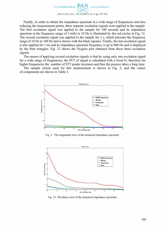
Metrol. Meas. Syst., Vol. 24 (2017), No. 2, pp. 425–436.
Finally, in order to obtain the impedance spectrum in a wide range of frequencies and also
reducing the measurement points, three separate excitation signals were applied to the sample. The first excitation signal was applied to the sample for 100 seconds and its impedance spectrum in the frequency range of 5 mHz to 10 Hz is illustrated by the red circles in Fig. 12.
The second excitation signal was applied to the sample for 1 s, which presents the frequency range of 10 Hz to 100 Hz and is shown with the black squares. Finally, the last excitation signal
is also applied for 1 ms and its impedance spectrum frequency is up to 600 Hz and is displayed by the blue triangles. Fig. 12 shows the Nyquist plot obtained from these three excitation signals.
The reason of applying several excitation signals is that by using only one excitation signal for a wide range of frequencies, the FFT of signal is calculated with a fixed N; therefore for
higher frequencies the number of FFT points increases and thus the process takes a long time. The sample circuit used for this measurement is shown in Fig. 2, and the values
of components are shown in Table 3.
Fig. 9. The magnitude error of the measured impedance spectrum.
Fig. 10. The phase error of the measured impedance spectrum.
8 9 10 11 12 13 14 15 160
0.5
1
1.5
2
2.5
3
Magnitude Error
ADC Resolution (Bit)
Mag
nit
ud
e E
rror
(%)
Half-Gaussian
Ramp
Gaussian
Sinc
8 9 10 11 12 13 14 15 160
0.5
1
1.5
2
2.5
3
3.5
4
Phase Error
ADC Resolution (Bit)
Ph
ase
Erro
r (d
eg
ree)
Half-Gaussian
Ramp
Gaussian
Sinc
433
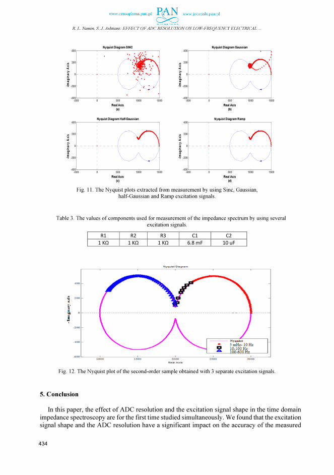
R. L. Namin, S. J. Ashtiani: EFFECT OF ADC RESOLUTION ON LOW-FREQUENCY ELECTRICAL …
Fig. 11. The Nyquist plots extracted from measurement by using Sinc, Gaussian,
half-Gaussian and Ramp excitation signals.
Table 3. The values of components used for measurement of the impedance spectrum by using several
excitation signals.
R1 R2 R3 C1 C2
1 KΩ 1 KΩ 1 KΩ 6.8 mF 10 uF
Fig. 12. The Nyquist plot of the second-order sample obtained with 3 separate excitation signals.
5. Conclusion
In this paper, the effect of ADC resolution and the excitation signal shape in the time domain
impedance spectroscopy are for the first time studied simultaneously. We found that the excitation signal shape and the ADC resolution have a significant impact on the accuracy of the measured
-500 0 500 1000 1500-400
-200
0
200
400
Nyquist Diagram Half-Gaussian
Real Axis
(c)
-Im
ag
ina
ry A
xis
-500 0 500 1000 1500-400
-200
0
200
400
Nyquist Diagram Gaussian
Real Axis
(b)
-Im
ag
ina
ry A
xis
-500 0 500 1000 1500-400
-200
0
200
400
Nyquist Diagram SINC
Real Axis
(a)
-Im
ag
ina
ry A
xis
-500 0 500 1000 1500-400
-200
0
200
400
Nyquist Diagram Ramp
Real Axis
(d)-I
ma
gin
ary
Ax
is
434

Metrol. Meas. Syst., Vol. 24 (2017), No. 2, pp. 425–436.
impedance spectrum. Several excitation signals are used in the time domain impedance
spectroscopy, such as Sinc and Gaussian ones. In this paper Ramp and half-Gaussian signals are also studied for the first time. These two new excitation signals are compared with the Sinc and Gaussian ones to figure out which of them generate a more accurate impedance spectrum when
the ADC resolution is limited. By applying all the four excitation signals for 100 s, the impedance spectra of each of them for a frequency range from 5 mHz to 5 Hz are extracted. Based on the
simulation and measurement results, the Ramp and half-Gaussian excitation signals result in lower RMS errors than those obtained from the Sinc and Gaussian signals. Also, with reduction of ADC resolution, an increase of the impedance spectrum error is higher than resulted from other signals.
Reference
[1] Lvovich, V.F. (2012). Impedance spectroscopy: applications to electrochemical and dielectric phenomena.
John Wiley & Sons.
[2] Hoja, J., et al. (2011). Method using square pulse excitation for high-impedance spectroscopy of
anticorrosion coatings. IEEE Trans. Instrum. Meas., 60(3), 957−964.
[3] Lohrasbi, M., et al. (2013). Degradation study of dye-sensitized solar cells by electrochemical impedance
and FTIR spectroscopy. Proc. of IEEE Energytech 2013, Cleveland OH, US, 1−4.
[4] Debenjak, A., et al. (2012). An assessment of water conditions in a PEM fuel cell stack using electrochemical
impedance spectroscopy. IEEE PHM 2012, Beijing, China, 23−25.
[5] Lindahl, P.A., et al. (2012). A time-domain least squares approach to electrochemical impedance
spectroscopy. IEEE Trans. Instrum. Meas., 61(12), 3303−3311.
[6] Kang, G., et al. (2012). Differentiation between normal and cancerous cells at the single cell level using 3-
D electrode electrical impedance spectroscopy. IEEE Sensors J., 12(5), 1084−1089.
[7] Affanni, A., et al. (2012). Electrical impedance spectroscopy on flowing blood to predict white thrombus
formation in artificial microchannels. IEEE I2MTC 2012, Graz, Autria, 1477−1480.
[8] Sanchez, B., Vandersteen, G., Rosell-Ferrer, J., Cinca, J., Bragos, R. (2011). In-cycle myocardium tissue
electrical impedance monitoring using broadband impedance spectroscopy. Engineering in Medicine and
Biology Society, EMBC, 2011, Boston, US, 2518−2521.
[9] Rojo, L., Mandayo, G.G., Castafio, E. (2013). Thin film YSZ solid state electrolyte characterization
performed by electrochemical impedance spectroscopy. Spanish Conference on Electron Devices (CDE),
Valladolid, Spain, 233−236.
[10] Kowalewski, M., Lentka, G. (2013). Fast high-impedance spectroscopy method using sinc signal excitation.
Metrol. Meas. Syst., 20(4), 645–654.
[11] Karp, F.B., Bernotski, N.A., Valdes, T.I., Bohringer, K.F., Ratner, Buddy, D. (2008). Foreign body response
investigated with an implanted biosensor by in situ electrical impedance spectroscopy. Sensors Journal,
IEEE, 8(1), 104−112.
[12] Nahvi, M. Hoyle, B.S. (2009). Electrical impedance spectroscopy sensing for industrial processes. IEEE
Sensors J., 9(12), 1808−1816.
[13] Widrow, B., Kollar, I. (2008). Quantization noise. Cambridge University Press.
[14] Ensheng, D., et al. (2010). A pulsed approach for electrical impedance spectroscopy measurement. ISDEA
2010, 1(150), 154, 13−14.
[15] Hoja, J., Lentka, G. (2013). A family of new generation miniaturized impedance analyzers for technical
object diagnostics. Metrol. Meas. Syst., 20(1), 43–52.
[16] Chabowski, K., Piasecki, T., Dzierka, A., Nitsch, K. (2015). Simple wide frequency range impedance meter
based on AD5933 integrated circuit. Metrol. Meas. Syst., 22(1), 13–24.
435

R. L. Namin, S. J. Ashtiani: EFFECT OF ADC RESOLUTION ON LOW-FREQUENCY ELECTRICAL …
[17] Morrison, J.L., Morrison, W.H., Christophersen, J.P., Motloch, C.G. (2014). Method of estimating pulse
response using an impedance spectrum. United States Patent.

Instructions for Authors
Types of contributions
The following types of papers are published in Metrology and Measurement Systems:
− invited review papers presenting the current stage of the knowledge (max. 20 edited pages, 3000
characters each),
− research papers reporting original scientific or technological advancements (10‒12 pages),
− papers based on extended and updated contributions presented at scientific conferences (max. 12 pages),
− short notes, i.e. book reviews, conference reports, short news (max. 2 pages).
Manuscript preparation
The text of a manuscript should be written in clear and concise English. The form similar to “camera-ready”
with an attached separate file – containing illustrations, tables and photographs – is preferred. For the details
of the preferred format of the manuscripts, Authors should consult a recent issue of the journal or the sample
article and the guidelines for manuscript preparation. The text of a manuscript should be printed on A4
pages (with margins of 2.5 cm) using a font whose size is 12 pt for main text and 10 pt for the abstract; an
even number of pages is strongly recommended. The main text of a paper can be divided into sections
(numbered 1, 2, ...), subsections (numbered 1.1., 1.2., ...) and – if needed – paragraphs (numbered 1.1.1.,
1.1.2., ...). The title page should include: manuscript title, Authors’ names and affiliations with e-mail
addresses. The corresponding Author should be identified by the symbol of an envelope and phone number.
A concise abstract of approximately 100 words and with 3–5 keywords should accompany the main text.
Illustrations, photographs and tables provided in the camera-ready form, suitable for reproduction (which
may include reduction) should be additionally submitted one per page, larger than final size. All illustrations
should be clearly marked on the back with figure number and author’s name. All figures are to have
captions. The list of figures captions and table titles should be supplied on separate page. Illustrations must
be produced in black ink on white paper or by computer technique using the laser printer with the resolution
not lower than 300 dpi, preferably 600 dpi. The thickness of lines should be in the range 0.2–0.5 mm, in
particular cases the range 0.1–1.0 mm will be accepted. Original photographs must be supplied as they are to
be reproduced (e.g. black and white or colour). Photocopies of photographs are not acceptable.
References should be inserted in the text in square brackets, e.g. [4]; their list numbered in citation order
should appear at the end of the manuscript. The format of the references should be as follows: for a journal
paper – surname(s) and initial(s) of author(s), year in brackets, title of the paper, journal name (in italics),
volume, issue and page numbers. The exemplary format of the references is available at the sample article.
Manuscript submission and processing
Submission procedure. Manuscript should be submitted via Internet Editorial System (IES) ‒ an online
submission and peer review system http://www.editorialsystem.com/mms
In order to submit the manuscript via IES, the authors (first-time users) must create an author account to
obtain a user ID and password required to enter the system. From the account you create, you will be able to
monitor your submission and make subsequent submissions.
The submission of the manuscript in two files is preferred: “Paper File” containing the complete manuscript
(with all figures and tables embedded in the text) and “Figures File” containing illustrations, photographs
and tables. Both files should be sent in DOC and PDF format as well as. In the submission letter or on
separate page in “Figures File”, the full postal address, e-mail and phone numbers must be given for all co-
authors. The corresponding Author should be identified.
Copyright Transfer. The submission of a manuscript means that it has not been published previously in the
same form, that it is not under consideration for publication elsewhere, and that – if accepted – it will not be
published elsewhere. The Author hereby grants the Polish Academy of Sciences (the Journal Owner) the
license for commercial use of the article according to the Open Access License which has to be signed before
publication.
Review and amendment procedures. Each submitted manuscript is subject to a peer-review procedure, and
the publication decision is based on reviewers’ comments; if necessary, Authors may be invited to revise
their manuscripts. On acceptance, manuscripts are subject to editorial amendment to suit the journal style.

An essential criterion for the evaluation of submitted manuscripts is their potential impact on the scientific
community, measured by the number of repeated quotations. Such papers are preferred at the evaluation and
publication stages.
Proofs. Proofs will be sent to the corresponding Author by e-mail and should be returned within 48 hours of
receipt.
Other information
Author Benefits. The publication in the journal is free of charge. A sample copy of the journal will be sent to
the corresponding Author free of charge.
Colour. For colour pages the Authors will be charged at the rate of 160 PLN or 80 EUR per page. The
payment to the bank account of main distributor (given in “Subscription Information”) must be acquitted
before the date pointed to Authors by Editorial Office.
Contact:
E-mail: [email protected] URL: www.metrology.pg.gda.pl Phone: (+48) 58 347-1357
Post address: Editorial Office of Metrology and Measurement Systems
Gdańsk University of Technology, Faculty of Electronics, Telecommunications and Informatics
ul. Narutowicza 11/12, 80-233 Gdańsk, Poland