Universidad de Granada Doctoral Thesis Modeling and Simulation ...
331
Universidad de Granada Doctoral Thesis Modeling and Simulation of Semiconductor Nanowires for Future Technology Nodes Author: Supervisors: Enrique Gonz´ alez Mar´ ın Dr. Andr´ es Godoy Medina Dr. Francisco Javier Garc´ ıa Ruiz A thesis submitted in fulfillment of the requirements to obtain the International Doctor degree as part of the Programa de Doctorado en F´ ısica y Ciencias del Espacio in the Nanoelectronics Research Group Departamento de Electr´ onica y Tecnolog´ ıa de los Computadores Granada, 14 th May, 2014
-
Upload
khangminh22 -
Category
Documents
-
view
5 -
download
0
Transcript of Universidad de Granada Doctoral Thesis Modeling and Simulation ...
Universidad de Granada
Doctoral Thesis
Modeling and Simulation of Semiconductor
Nanowires for Future Technology Nodes
Author: Supervisors:
Enrique Gonzalez Marın Dr. Andres Godoy Medina
Dr. Francisco Javier Garcıa Ruiz
A thesis submitted in fulfillment of the requirements
to obtain the International Doctor degree as part of the
Programa de Doctorado en Fısica y Ciencias del Espacio
in the
Nanoelectronics Research Group
Departamento de Electronica y Tecnologıa de los Computadores
Granada, 14th May, 2014

Editor: Editorial de la Universidad de Granada Autor: Enrique González Marín D.L.: 2133-2014 ISBN: 978-84-9083-153-3

Declaration of authorship
Mr. Enrique Gonzalez Marın, as Ph.D Candidate, and Dr. Francisco Javier Garcıa
Ruiz and Dr. Andres Godoy Medina, as Ph.D Supervisors and Professors of Elec-
tronics at the Departamento de Electronica y Tecnologıa de los Computadores of the
Universidad de Granada in Spain,
Guarantee by signing this thesis:
that the research work contained in the present report, entitled Modeling and Sim-
ulation of Semiconductor Nanowires for Future Technology Nodes, has been
performed under the full guidance of the Ph.D Supervisors and, as far as our knowledge
reaches, during the work, it has been respected the right of others authors to be cited,
when their publications or their results have been used.
Granada, 14th May, 2014.
Dr. Andres Godoy Medina
Enrique Gonzalez Marın Full Professor of Electronics
Ph.D Candidate
Dr. Francisco Javier Garcıa Ruiz
Tenured Professor of Electronics
I

To Laura
III

Why is there something rather than nothing?
The Principles of Nature and Grace, Based on Reason
Gottfried Wilhelm Leibniz (1646-1716)
V

Acknowledgements
I would like to acknowledge in these few lines a number of people who helped me
during my PhD work, and to whom I am indebted.
Foremost, I would like to express my most sincere gratitude to my advisors Prof.
Francisco J. Garcıa Ruiz and Prof. Andres Godoy Medina for giving me the opportunity
to start this exciting experience a little over three years ago. They have been a constant
source of good advice and encouragement, patience and knowledge. We have spent
many hours carrying out stimulating scientific discussion and I hope we will be able
to continue this into the future. Without their help this Thesis would not have been
possible
I wish to thank the directors of the Departamento de Electronica y Tecnologıa de
los Computadores: Prof. Juan E. Carceller Beltran and Prof. Juan Antonio Lopez
Villanueva. Their classes during my degrees in Telecommunications and Electronics
Engineering were tremendously motivating and awoke my sincere interest in electronics.
I am indebted to Prof. Fracisco Gamiz Perez, manager of the Nanoelectonics Re-
search Group to which I belong. Shortly after starting my PhD work, the Nanoelec-
tronics Group was awarded by the Universidad de Granada, due to its outstanding
contributions, the best research group of the year. After this time, I fully understand
why it was so. Prof. Gamiz’s passion for research and his ability to convey it set an
example for me.
It is difficult to overstate my appreciation to Prof. Heike Riel for giving me the
occasion to visit the IBM Research Lab in Zurich during the three months of spring
2013. My internship in the Nanoscale Electronics Group, that she manages, was both
a thrilling professional and personal experience. I would also express my gratitude to
Prof. Volker Schmidt who guided my research there and made me feel like a true friend.
I take the opportunity to thank all the members of the Nanoscale Electronic Team for
their treatment and their hospitality. I felt like I was at home during the working time
VII

of these months.
I am thankful to all the members of the Departamento de Electronica y Tecnologıa
de los Computadores for their enthusiasm during these years. I wish to specially apol-
ogise to Prof. Isabel Marıa Tienda Luna and Prof. Blanca Biel for frequently invading
their offices to fill the board with formulas. Prof. Tienda Luna was an essential part of
that work and I want to thank her for all her help. I could not forget to acknowledge
Prof. Pablo Sanchez Moreno from the Departamento de Matematica Aplicada and his
enthusiastic mathematical talks. During this time I shared the office with Prof. Diego
P. Morales Santos. It is priceless that your officemate is always in a good mood, ready
to encourage you and to aid you always but also to detach when you need it. I wish to
not forget Prof. Carlos Sampedro Matarın who facilitated my Lab classes, providing
me all the material and knowledge needed, and Prof. Encaranacion Castillo Morales
who gave me very thorough Lab tutorials. I am also indebted to Prof. Luca Donneti
who showed how to use the cluster for the simulations. I would also like to convey my
public gratitude to the rest of PhD students in the department. It was heartwarming
to share the PhD candidate typical anxieties as a group.
I wish to remember my friends, some of whom are now quite far. I feel fortunate
that they are part of my life. Thanks for all the unforgettable shared moments. Since
I am an only child, you are the siblings I choose.
I could not forget my family: my grandfather, my aunt and cousins, and Laura’s
parents and siblings. This is also thanks to them. My parents, Marıa Amalia and
Cristobal, put the right amount of love and demand in my education. They make me
feel like the happiest child in the world, and I intend to make them proud of everything
I do in life.
Finally, I could not finish without writing a few words to Laura. Now that a period
is finishing in our lives and the future seems uncertain, there is only one sure thing.
Wherever and however it will be, it will find us together.
VIII
Contents
Declaration of authorship I
Acknowledgements VIII
I Prologue 1
Abstract 4
Resumen 6
1 Introduction 7
1.1 A success story . . . . . . . . . . . . . . . . . . . . . . . . . . . . . . . . 7
1.2 Hurdles in the way . . . . . . . . . . . . . . . . . . . . . . . . . . . . . . 8
1.3 Present and future boosters . . . . . . . . . . . . . . . . . . . . . . . . . 11
1.4 Objectives . . . . . . . . . . . . . . . . . . . . . . . . . . . . . . . . . . . 15
1.5 Methodology . . . . . . . . . . . . . . . . . . . . . . . . . . . . . . . . . 16
II Electrostatics 19
2 Electrostatics of nanowires: background 21
2.1 Introduction . . . . . . . . . . . . . . . . . . . . . . . . . . . . . . . . . . 21
2.2 Independent particle Schrodinger equation . . . . . . . . . . . . . . . . . 21
2.3 Effective Mass approximation . . . . . . . . . . . . . . . . . . . . . . . . 24
2.4 Poisson equation . . . . . . . . . . . . . . . . . . . . . . . . . . . . . . . 26
2.5 Particularization for 2D structures . . . . . . . . . . . . . . . . . . . . . 27
2.6 Non-parabolic corrections to the parabolic Schrodinger equation . . . . 28
IX
2.7 Quantum electron concentration . . . . . . . . . . . . . . . . . . . . . . 29
3 2D Schrodinger-Poisson simulator for MuG structures 33
3.1 Introduction . . . . . . . . . . . . . . . . . . . . . . . . . . . . . . . . . . 33
3.2 Simulator description . . . . . . . . . . . . . . . . . . . . . . . . . . . . . 34
3.3 Finite Element Method . . . . . . . . . . . . . . . . . . . . . . . . . . . 39
3.4 Energy and potential reference system . . . . . . . . . . . . . . . . . . . 40
3.5 Arbitrary geometry . . . . . . . . . . . . . . . . . . . . . . . . . . . . . . 42
3.6 Arbitrary orientation . . . . . . . . . . . . . . . . . . . . . . . . . . . . . 43
3.7 Non-parabolicity of the conduction band . . . . . . . . . . . . . . . . . . 46
3.8 Insulator and interface charges . . . . . . . . . . . . . . . . . . . . . . . 48
3.9 Convergence algorithm . . . . . . . . . . . . . . . . . . . . . . . . . . . . 54
3.10 SP2D flow diagram . . . . . . . . . . . . . . . . . . . . . . . . . . . . . . 56
3.11 Conclusions . . . . . . . . . . . . . . . . . . . . . . . . . . . . . . . . . . 58
4 Electrostatic analysis of MuG devices using SP2D 59
4.1 Introduction . . . . . . . . . . . . . . . . . . . . . . . . . . . . . . . . . . 59
4.2 Validation of SP2D . . . . . . . . . . . . . . . . . . . . . . . . . . . . . . 60
4.3 Comparison of III-V cylindrical NWs . . . . . . . . . . . . . . . . . . . . 66
4.4 Comparison of Si and III-V Trigate MOSFETs . . . . . . . . . . . . . . 70
4.5 Trigate versus DG comparison . . . . . . . . . . . . . . . . . . . . . . . 73
4.6 Influence of the back-gate bias on the electrostatics of Si Trigates . . . . 77
4.7 Effects of interfacial states on the technological variability of Si Trigates 81
4.8 Conclusions . . . . . . . . . . . . . . . . . . . . . . . . . . . . . . . . . . 90
5 Charge, potential and current analytical models for III-V NWs 91
5.1 Introduction . . . . . . . . . . . . . . . . . . . . . . . . . . . . . . . . . . 91
5.2 Subband modeling . . . . . . . . . . . . . . . . . . . . . . . . . . . . . . 92
5.3 Potential modeling . . . . . . . . . . . . . . . . . . . . . . . . . . . . . . 99
5.4 Charge modeling . . . . . . . . . . . . . . . . . . . . . . . . . . . . . . . 104
5.5 Interfacial states modeling . . . . . . . . . . . . . . . . . . . . . . . . . . 106
5.6 Iterative scheme . . . . . . . . . . . . . . . . . . . . . . . . . . . . . . . 107
5.7 Drain current model . . . . . . . . . . . . . . . . . . . . . . . . . . . . . 109
5.7.1 Drain current when Dit = 0 . . . . . . . . . . . . . . . . . . . . . 111
5.7.2 Drain current for a constant Dit profile . . . . . . . . . . . . . . 111
5.8 Results and discussion . . . . . . . . . . . . . . . . . . . . . . . . . . . . 112
X
5.9 Conclusions . . . . . . . . . . . . . . . . . . . . . . . . . . . . . . . . . . 124
6 Gate capacitance and threshold voltage models 125
6.1 Introduction . . . . . . . . . . . . . . . . . . . . . . . . . . . . . . . . . . 125
6.2 Gate Capacitance Model . . . . . . . . . . . . . . . . . . . . . . . . . . . 127
6.3 Capacitance model validation . . . . . . . . . . . . . . . . . . . . . . . . 132
6.4 Results and discussion of the Cg model . . . . . . . . . . . . . . . . . . . 135
6.4.1 Assessment of gate capacitance components. . . . . . . . . . . . 135
6.4.2 Material comparison . . . . . . . . . . . . . . . . . . . . . . . . . 137
6.4.3 Effect of the wavefunction penetration . . . . . . . . . . . . . . . 141
6.5 Threshold voltage modeling . . . . . . . . . . . . . . . . . . . . . . . . . 142
6.6 Non-parabolic correction for the VT model . . . . . . . . . . . . . . . . . 146
6.7 Influence of interface states on VT . . . . . . . . . . . . . . . . . . . . . 148
6.8 Validation and Results of the VT model . . . . . . . . . . . . . . . . . . 150
6.9 Conclusions . . . . . . . . . . . . . . . . . . . . . . . . . . . . . . . . . . 155
III Transport 157
7 BTE and MRT in a 1D electron gas 159
7.1 Introduction . . . . . . . . . . . . . . . . . . . . . . . . . . . . . . . . . . 159
7.2 Boltzmann Transport Equation . . . . . . . . . . . . . . . . . . . . . . . 160
7.3 Scattering rate and perturbation potentials. Fermi Golden Rule . . . . . 162
7.4 Momentum Relaxation Time . . . . . . . . . . . . . . . . . . . . . . . . 165
7.5 Explicit calculation of the MRT . . . . . . . . . . . . . . . . . . . . . . . 169
7.6 Implicit calculation of the MRT . . . . . . . . . . . . . . . . . . . . . . . 170
7.7 Mobility calculation . . . . . . . . . . . . . . . . . . . . . . . . . . . . . 174
7.8 Conclusions . . . . . . . . . . . . . . . . . . . . . . . . . . . . . . . . . . 175
8 Modeling of scattering mechanisms in NWs 177
8.1 Introduction . . . . . . . . . . . . . . . . . . . . . . . . . . . . . . . . . . 177
8.2 Surface roughness . . . . . . . . . . . . . . . . . . . . . . . . . . . . . . . 178
8.2.1 Derivation for open cross sections curves . . . . . . . . . . . . . . 180
8.2.2 Derivation for closed cross-sections . . . . . . . . . . . . . . . . . 181
8.2.3 SR power spectrum . . . . . . . . . . . . . . . . . . . . . . . . . 183
8.2.4 Form factor . . . . . . . . . . . . . . . . . . . . . . . . . . . . . . 183
8.3 Coulomb dispersion . . . . . . . . . . . . . . . . . . . . . . . . . . . . . . 184
XI
8.4 Bulk non-polar phonons . . . . . . . . . . . . . . . . . . . . . . . . . . . 188
8.4.1 Acoustic phonons . . . . . . . . . . . . . . . . . . . . . . . . . . . 190
8.4.2 Optical phonons . . . . . . . . . . . . . . . . . . . . . . . . . . . 191
8.5 Polar Optical Phonons . . . . . . . . . . . . . . . . . . . . . . . . . . . . 192
8.6 Alloy Disorder . . . . . . . . . . . . . . . . . . . . . . . . . . . . . . . . 194
8.7 Dielectric Screening . . . . . . . . . . . . . . . . . . . . . . . . . . . . . 195
8.7.1 Screening formulation . . . . . . . . . . . . . . . . . . . . . . . . 197
8.8 Conclusions . . . . . . . . . . . . . . . . . . . . . . . . . . . . . . . . . . 198
9 Transport studies of MuG devices 199
9.1 Introduction . . . . . . . . . . . . . . . . . . . . . . . . . . . . . . . . . . 199
9.2 Electron mobility in InAs nanowires . . . . . . . . . . . . . . . . . . . . 199
9.3 Comparison of Si and InGaAs mobility in Trigate FETs . . . . . . . . . 206
9.4 Influence of back gate bias on the electron mobility of Si Trigates . . . . 213
9.5 Conclusion . . . . . . . . . . . . . . . . . . . . . . . . . . . . . . . . . . 216
IV Conclusions 219
10 Conclusions 221
V Appendixes 225
A Numerical implementation of surface interface charge 227
B Charge, potential and drain current models related calculi 233
B.1 Normalization of the wavefunctions . . . . . . . . . . . . . . . . . . . . . 233
B.2 Resolution of the Poisson equation . . . . . . . . . . . . . . . . . . . . . 234
B.3 Determination of Ci and Di from Poisson boundary conditions . . . . . 239
B.4 Drain current analytical model related calculi . . . . . . . . . . . . . . . 243
B.4.1 Drain current if no Dit is considered . . . . . . . . . . . . . . . . 245
B.4.2 Drain current for a constant Dit . . . . . . . . . . . . . . . . . . 247
C Capacitance and threshold voltage models related calculi 251
C.1 Determination of the centroid capacitance . . . . . . . . . . . . . . . . . 251
C.2 Validity of the approximations for the Cg and VT models . . . . . . . . . 253
XII
D Scattering elements 257
D.1 Inelastic anisotropic mechanism . . . . . . . . . . . . . . . . . . . . . . . 257
D.2 Elastic anisotropic mechanism . . . . . . . . . . . . . . . . . . . . . . . . 259
D.3 Isotropic mechanism . . . . . . . . . . . . . . . . . . . . . . . . . . . . . 261
E Scattering mechanisms related calculi 263
E.1 Surface Roughness: axial and qz integrations . . . . . . . . . . . . . . . 263
E.2 Coulombian dispersion hard-sphere model . . . . . . . . . . . . . . . . . 264
E.3 Acoustic phonon: contributions over all q . . . . . . . . . . . . . . . . . 266
E.4 Non polar phonons: qx and qy contributions . . . . . . . . . . . . . . . . 268
F Materials parameters 273
VI References 277
XIII

XIV
Part I
Prologue

Abstract
Nanoelectronics Research Group
Departamento de Electronica y Tecnologıa de los Computadores
Modeling and Simulation of Semiconductor Nanowires for Future
Technology Nodes
by Enrique Gonzalez Marın
The main purpose of this PhD Thesis is the analytical and numerical study of Mul-
tiple Gate (MuG) architectures and III-V compound semiconductors as technological
alternatives to continue the downscaling process of the MOSFET beyond the 22nm
node.
To do so, electrostatic and transport simulators, able to solve the Schrodinger,
Poisson and Boltzmann equations for a 1D electron gas, have been implemented. The
electrostatic solver is based on a non-parabolic effective mass approximation being able
to deal with arbitrary geometries, materials and orientations, to achieve the charge and
potential distribution in the 2D cross-section of a MuG structure. The transport solver
linearizes the 1D Boltzmann equation using the momentum relaxation time approxima-
tion (MRT), solving it by a rigorous implicit approach not common in the literature. It
includes novel models for surface roughness, coulomb dispersion, bulk phonons, polar
optical phonons and alloy disorder scattering mechanisms, including static dielectric
screening, constituting a state-of-the-art mobility simulator.
In addition, a fully analytical model able to accurately describe the electrostatic
behavior of III-V cylindrical NWs is developed. It is, to the best of our knowledge, the
most complete analytical description of the charge and potential distributions in III-V
NWs presented in the literature up-to-date. The model provides analytical expressions
for the calculation of the subband energies and the wavefunctions of the Γ-valley, taking
into account the wavefunction penetration into the gate insulator and the effective
mass discontinuity in the semiconductor-insulator interface, Fermi-Dirac statistics, two-
dimensional confinement of the carriers and non-parabolic effects. It also allows the
inclusion of arbitrary analytical profiles of interfacial states.
Using the numerical and analytical approaches, several relevant electrostatic and
transport studies of Trigates and NWs are accomplished. These two structures are
specially significant as they constitute the most consolidated architectures among MuG
transistor devices. Trigate FET introduces the fewest changes to conventional planar
transistor processing, enhancing the electrostatic control of the channel. NWs are the
ultimate evolution of the MuG architectures providing the best suppression of short
channel effects. Thus, our analytical approach allows to study the influence of the
device size and material type on the inversion charge, the drain current, the gate
capacitance and the threshold voltage of III-V NWs. To complete the analytical study,
the numerical solvers are used to elucidate the role of the L-valley on the electrostatic
and transport properties, concluding in a non-negligible influence as the NW diameter
is reduced. The numerical approach is also used to compare the performance of Si
and III-V Trigate structures. The impact of the fin width and the back gate bias is
analyzed, showing that a) the mobility enhance observed for III-V Trigates is degraded
when the width is reduced; b) the back gate bias control of the threshold voltage directly
affects to the mobility. Finally the surface roughness is revealed as the main scattering
mechanism limiting the mobility for the big majority of the sizes and materials at high
inversion charges, being the mobility behavior at low inversion charges more complex
and very dependent on size and materials.
4 Prologue
Resumen
Nanoelectronics Research Group
Departamento de Electronica y Tecnologıa de los Computadores
Modeling and Simulation of Semiconductor Nanowires for Future
Technology Nodes
by Enrique Gonzalez Marın
El principal objetivo de esta Tesis de Doctorado es el estudio analıtico y numerico
de arquitecturas multipuerta, MuG del ingles Multiple Gate, y compuestos semicon-
ductores III-V, como alternativas tecnologicas para continuar el proceso de escalado
del transistor MOSFET mas alla del nodo tecnologico de 22nm.
Con este objetivo, se han implementado simuladores electrostaticos y de transporte
capaces de resolver las ecuaciones de Schrodinger, Poisson y Boltzmann en un gas de
electrones unidimensional. El simulador electrostatico esta basado en la aproximacion
de masa efectiva no parabolica, siendo capaz de tratar con geometrıas, materiales y ori-
entaciones arbitrarias para obtener las distribuciones de carga y potencial en la seccion
transversal bidimensional de la estructura MuG. El simulador de transporte linealiza
la ecuacion de transporte unidimensional de Boltzmann, usando la aproximacion de
tiempo de relajacion del momento, MRT del ingles Momentum Relaxation Time, re-
solviendo el sistema resultante de manera implıcta. Ademas incluye modelos novedosos
de dispersion debida a rugosidad superficial, cargas coulombianas, fonones bulk, fonones
opticos polares y desorden por aleacion.
Adicionalmente, se ha desarrollado un modelo completamente analıtico que de-
scribe el comportamiento electrostatico de nanohilos, NW del ingles nanowire. Es,
hasta donde alcanza nuestro conociemiento, la descripcion analıtica mas completa de
la distribucion de la carga y el potencial en NWs cilındricos de materiales III-V pre-
sentada en la literatura hasta la fecha. El modelo proporciona expresiones analıticas
para calcular la energıa de las subbandas y las funciones de onda del valle Γ, teniendo
en cuenta la penetracion de la funcion de onda en el aislante y la discontinuidad en la
masa efectiva en la interfaz entre el aislante y el semiconductor, ası como estadıstica de
Fermi-Dirac, confinamiento bidimensional de los portadores y efectos no parabolicos.
Tambien permite incluir un perfil arbitrario de estados en la interfaz.
Haciendo uso de las aproximaciones numerica y analıtica, se realizan varios estu-
dios relevantes de caracter electrostatico y del transporte en Trigates y NWs. Estas dos
estructuras son especialmente siginificativas puesto que constituyen las arquitecturas
MuG mas consolidadas. Los Trigate introducen pocos cambios en el proceso de fab-
ricacion planar tradicional, al mismo tiempo que incrementan el control electrostatico
del canal. Los NWs son la evolucion ultima de las arquitecturas MuG, proveyendo de
la mejor supresion de los efectos de canal corto. De esta manera, usando el enfoque
analıtico se estudia la influencia del tamano del dispositivo y el tipo de material en la
carga en inversion, la corriente de dreandor, la capacidad de puerta y la tension umbral
en NWs III-V. Para completar el estudio analıtico, los simuladores numericos desarrol-
lados se usan para comprender el papel del valle L en las propiedades electrostaticas
y de transporte, concluyendo que tiene un influencia no despreciable a medida que el
tamano del dispositivo se reduce. El enfoque numerico se usa tambien para comparar
el desempeno de estructuras Trigate de Si y materiales III-V. El impacto de la anchura
del Trigate y de la puerta trasera es analizada, mostrando que: a) el incremento de
la movilidad observado para Trigates III-V se degrada cuando la anchura se reduce
y b) el control de la puerta trasera sobre la tension umbral afecta directamente a la
movilidad. Finalmente, la rugosidad superficial se revela como el principal mecanismo
de dispersion limitador de la movilidad para la gran mayorıa de tamanos y materi-
ales a alto campo, siendo su comportamiento a bajo campo mas complicado y muy
dependiente del tamano y material.
6 Prologue
Chapter 1
Introduction
1.1 A success story
The story of the Metal Oxide Semiconductor Field Effect Transistor (MOSFET) and
the integrated circuits (IC), is probably the most successful example of the curiosity,
passion and effort characteristics of the human being nature. There is not such a
comparable level of progress in a such short period of time in any other human activity
during the history. In the brief lapse of time which goes from the appearance of the first
implementation of the MOSFET by D. Kahng and M. Atalla [1] to nowadays, MOS
technology has augmented its performance by a factor 106 [2]. If we look a little bit
further in the past, to the precursors of the MOSFET, the vacuum tubes, or the Bipolar
Juntion Transistor invented by J. Bardeen, W. Brattain and W. Shockley [3, 4], the
evolution is even more astonishing. No other human development holds the comparison.
The workhorse for the increase of the MOSFET performance has been the down-
scaling of the transistor dimensions. Guided by the Dennard rules [5], the size of the
MOSFET has been reduced from 20µm to 22nm in the last 45 years. That scaling of
the transistor dimensions had one main objective: the reduction of the capacitances
associated to the MOSFET, and consequently the increase of its switching time and
of the IC speed [6]. In addition, the reduction of the transistor area had two aside
consequences: the reduction of the switching energy and the increase in the number of
transistors per chip (which also contribute to increase the IC performance).
The continuous progress in the transistor scaling was fed by the sustained economic
progress of the last quarter of the twenty century. In the context of the capitalism
1.2. Hurdles in the way
market economy, the electronic revolution offered novel goods to be consumed, which
rapidly became first order necessities. In the last decade of the past century the ex-
plosion of the information technology (IT), Internet and the global society continued
pushing the revolution. In a kind of virtuous circle, we can state that the aforemen-
tioned factors are as much causes as consequences of the revolution. Now, the IT
market is perfectly consolidated, and the electronic devices occupy every place in our
life.
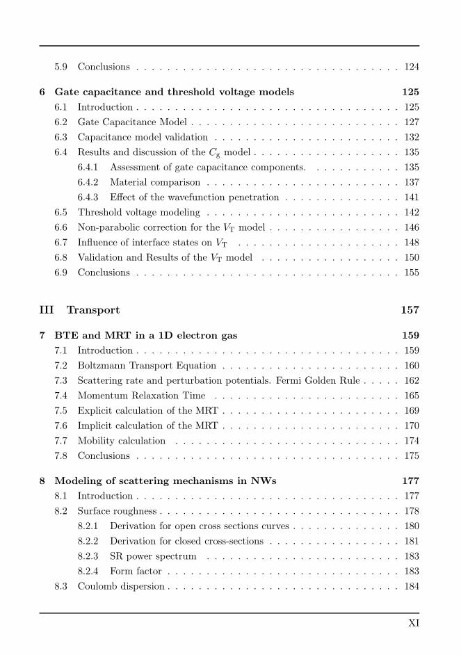
( c)
(a)
(b)
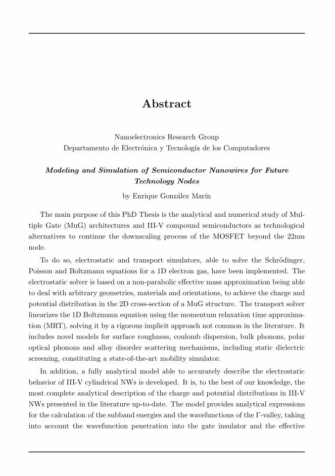
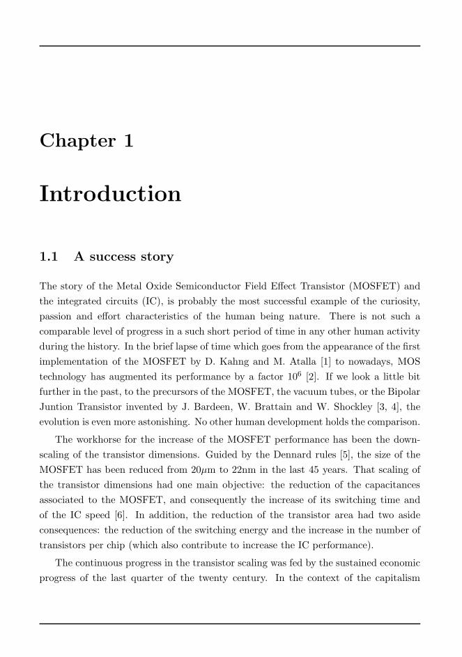
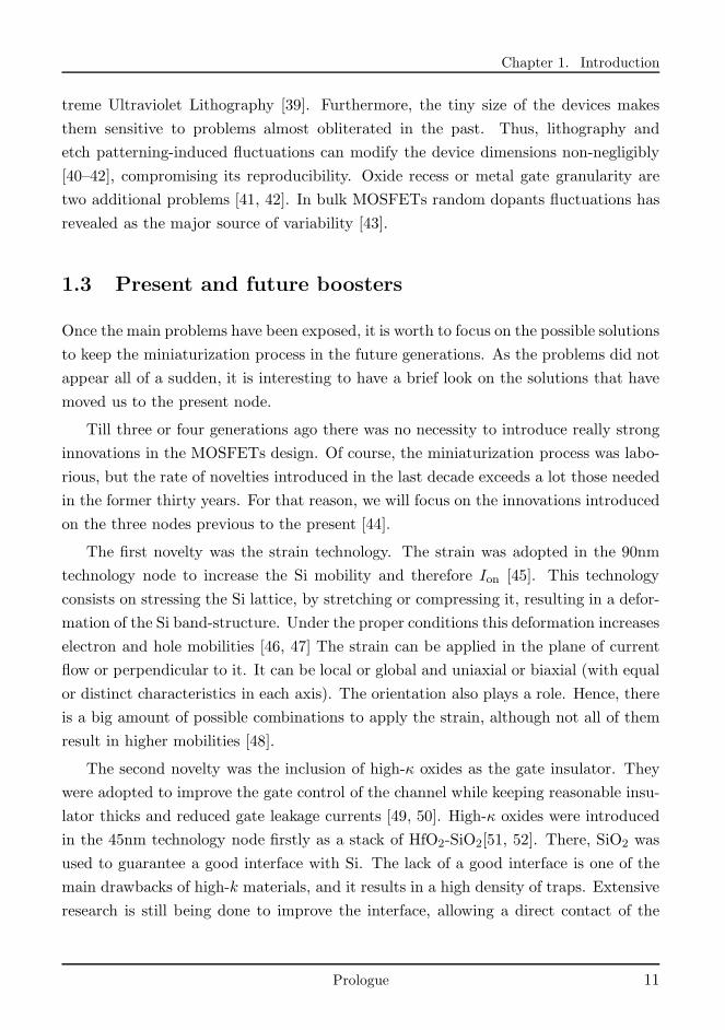
Figure 1.1: The market demand is secured by: a) the diversity ofapplications, b) the creation of new necessities, c) the voracity of ITconsumers.
1.2 Hurdles in the way
While the market demand is secured by: 1) the diversity of applications, 2) the cre-
ation of new necessities, and 3) the voracity of IT consumers, the downscaling of the
MOSFET is reaching the end of the road [7]. It is not the first time that we face this
challenge, although previous statements on the downscaling halt were technological:
in the seventies the spatial resolution of the IC was thought to be determined by the
lithography wavelength [8], [9]; while in the early eighties direct tunneling through the
SiO2 gate insulator was asserted to lead to a disastrous leakage [10], [11]. Nevertheless,
8 Prologue
Chapter 1. Introduction
the present scenario points out that we are approaching to unavoidable physical limits.
The smallest of these limits is the Si interatomic distance (∼ 0.3nm) [12]. Probably
before that, at transistor channel lengths around 3nm, the direct drain to source tunnel
will distort the MOSFET operation [13]. Whether the limit is 3nm or 0.3nm, the end
is not far as the 22nm technology node is now in production.
An evidence of the proximity of the end is the continuous relentless of the scaling
process. The shrink rate of the gate length, till the last technological nodes, was
0.7 per 3 years in average, according to Moore’s law [14]. For the future nodes it
is predicted to move to 0.85 per 3 years [6]. This deceleration has been reflected
by the International Technology Roadmad for Semiconductor (ITRS) [15] which has
successively relaxed their predictions for the future technology nodes, delaying their
appearance. According to Prof. Iwai, that deceleration gives us 4 or 5 generations
(in the most optimistic case up to 7 more generations) and around 20-25 years of
continued scaling [16]. What will be the substitute once the end of the road is reached
is an open question. 2D materials: as graphene and molybdenum disulfide [17, 18];
Carbon Nanotubes (CNT) [19], molecular electronics [20] or single-atom transistors
[21] are good positioned alternatives. But there is still a lot of work to do to reach the
limit and this manuscript works out on some of the most promising alternatives.
To be able to continue the MOSFET scaling beyond the 22nm technology node, it
is worth to know why has the scaling process slowed down. Actually, it is a multiple
answer question. Some main reasons are [22–30]:
(a) The increase in the power density of the IC, which leads to critical situations related
to both the heat evacuation and the energy consumption.
(b) The short channel effects (SCEs) which result in an increased drain control of the
channel in detriment of the gate control.
(c) The extreme reduction of the ON current, Ion and of the ON/OFF current ratio
Ion/Ioff.
(d) Technological issues concerning the fabrication process which lead to non-viable
device variabilities.
The aforementioned reasons are actually quite interrelated. Thus, the increase of
the IC power density is the result of the necessity of keeping a reasonable Ion/Ioff ratio,
which imply the non-observance of the Dennard’s scaling rules. According to these
Prologue 9
1.2. Hurdles in the way
scaling rules, if the device dimensions are reduced in a factor, K, then so must be the
IC supply voltage. That ensures a constant IC power density at the same time that
guarantees a K factor increment in the IC speed [5].
However, the reduction of the supply voltage has the side effect of strongly degrading
the Ion/Ioff ratio. Thus, the reduction of the supply voltage by a factor 1/K implies
an equal reduction of Ion. That would not affect the Ion/Ioff ratio as long as Ioff was
reduced in the same amount. But, instead of decreasing with reducing supply voltage,
Ioff increases exponentially (assuming that the threshold voltage, VT, is also decreased
to keep some symmetry in the switch operation) [13, 31].
The rate of increase in Ioff with reducing VT is controlled by the sub-treshold swing,
SS, which at room temperature under ideal conditions cannot be lower than 60mV/dec.
Best MOSFET implementations cannot bring SS < 70 − 80mV/dec which makes the
scenario even worse [32, 33]. One consequence of the trade-off between IC power density
and Ion/Ioff ratio was the alteration of the main contributions to the IC consumed
power, becoming the passive power density dominant in the last nodes[7].
The detention of the supply voltage reduction has not avoided anyway the degra-
dation of the Ion current with the MOSFET scaling. The higher vertical electric field
which results from the size reduction and constant supply voltage has leaded to a strong
degradation of the mobility. This is pointed out as the main reason for the low current
of small MOSFET implemented up to now [34, 35].
The increase of the IC power density is not the unique consequence of the supply
voltage scaling halt as SCEs are also powered. Among them, Drain Induced Barrier
Lowering (DIBL) becomes dominant [36]. For the ON state, DIBL reduces the gate
control of the channel and affects to the circuit performance, reducing severely the IC
speed. For the OFF state, DIBL can yield a punch-trough between the source and
the drain, increasing the leakage current and therefore the passive power density. One
classical way to reinforce the gate control over the channel was scaling the gate insulator
thickness [5, 37, 38]. The main difficulty with the insulator scaling is the increase of
the gate leakage current which increases the dissipated power density. The limit for the
scaling in the SiO2 thickness is around 1nm, which correspond to 3 atomic layers.
The technological issues related to the fabrication processes are not a minor ques-
tion. As the devices get smaller, the fabrication process becomes more complex. The
development of the technology requires more time and inversion, reducing the number
of companies available to compete in the process. A good example of that is the Ex-
10 Prologue
Chapter 1. Introduction
treme Ultraviolet Lithography [39]. Furthermore, the tiny size of the devices makes
them sensitive to problems almost obliterated in the past. Thus, lithography and
etch patterning-induced fluctuations can modify the device dimensions non-negligibly
[40–42], compromising its reproducibility. Oxide recess or metal gate granularity are
two additional problems [41, 42]. In bulk MOSFETs random dopants fluctuations has
revealed as the major source of variability [43].
1.3 Present and future boosters
Once the main problems have been exposed, it is worth to focus on the possible solutions
to keep the miniaturization process in the future generations. As the problems did not
appear all of a sudden, it is interesting to have a brief look on the solutions that have
moved us to the present node.
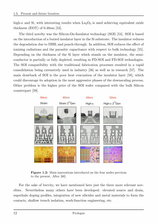
Till three or four generations ago there was no necessity to introduce really strong
innovations in the MOSFETs design. Of course, the miniaturization process was labo-
rious, but the rate of novelties introduced in the last decade exceeds a lot those needed
in the former thirty years. For that reason, we will focus on the innovations introduced
on the three nodes previous to the present [44].
The first novelty was the strain technology. The strain was adopted in the 90nm
technology node to increase the Si mobility and therefore Ion [45]. This technology
consists on stressing the Si lattice, by stretching or compressing it, resulting in a defor-
mation of the Si band-structure. Under the proper conditions this deformation increases
electron and hole mobilities [46, 47] The strain can be applied in the plane of current
flow or perpendicular to it. It can be local or global and uniaxial or biaxial (with equal
or distinct characteristics in each axis). The orientation also plays a role. Hence, there
is a big amount of possible combinations to apply the strain, although not all of them
result in higher mobilities [48].
The second novelty was the inclusion of high-κ oxides as the gate insulator. They
were adopted to improve the gate control of the channel while keeping reasonable insu-
lator thicks and reduced gate leakage currents [49, 50]. High-κ oxides were introduced
in the 45nm technology node firstly as a stack of HfO2-SiO2[51, 52]. There, SiO2 was
used to guarantee a good interface with Si. The lack of a good interface is one of the
main drawbacks of high-k materials, and it results in a high density of traps. Extensive
research is still being done to improve the interface, allowing a direct contact of the
Prologue 11
1.3. Present and future boosters
high-κ and Si, with interesting results when La2O3 is used achieving equivalent oxide
thickness (EOT) of 0.48nm [53].
The third novelty was the Silicon-On-Insulator technology (SOI) [54]. SOI is based
on the introduction of a buried insulator layer in the Si substrate. The insulator reduces
the degradation due to DIBL and punch-through. In addition, SOI reduces the effect of
ionizing radiations and the parasitic capacitance with respect to bulk technology [55].
Depending on the thickness of the Si layer which stands on the insulator, the semi-
conductor is partially or fully depleted, resulting in PD-SOI and FD-SOI technologies.
The SOI compatibility with the traditional fabrication processes resulted in a rapid
consolidation being extensively used in industry [56] as well as in research [57]. The
main drawback of SOI is the poor heat evacuation of the insulator layer [58], which
could discourage its adoption in the most aggressive phases of the downscaling process.
Other problem is the higher price of the SOI wafer compared with the bulk Silicon
counterpart [59].
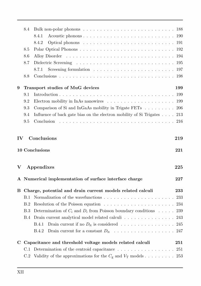
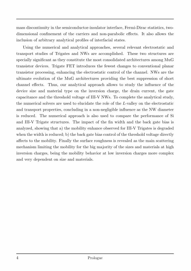
Strain Strain 2 Gen High-k High- 2 Genk
90nm 65nm 45nm 32nm
nd nd
Figure 1.2: Main innovations introduced on the four nodes previousto the present. After [60].
For the sake of brevity, we have mentioned here just the three more relevant nov-
elties. Nevertheless many others have been developed: elevated source and drain,
superhalo doping profiles, integration of new silicides and metal materials to form the
contacts, shallow trench isolation, work-function engineering, etc.
12 Prologue
Chapter 1. Introduction
In spite of the outstanding nature of these innovations, the gravity of the problems
makes them not enough to keep the downscaling process. For that reason some new
alternatives must be found. This does not mean that the aforementioned solutions are
not going to be used in the future, but they should be combined with other innovations.
The main question is: what will be these new innovations? The answer to that question
is not simple. There are several technological alternatives which have being presented
as potential solutions. Two of the most promising are III-V compound semiconductors
and Multiple Gate (MuG) architectures [6, 61]. The study of the combination of both
of them is the main goal of this work.
III-V materials are a well known player in the microelectronics industry. Their
properties make them specially appropriate for optical applications, being used in the
implementation of lasers, light-emitting diodes or light detectors. In addition, they are
supported by a well consolidated manufacturing industry, which provides big volumes
of electronic circuits for a demanding and diverse market, going from smartphones and
domestic entertainment to fiber-optics and satellite communications [61].
What makes III-V materials a promising alternative to Si is their potentiality to
increase Ion. That would allow to reduce the supply voltage (and therefore the IC
power density consumption) keeping the Ion/Ioff ratio, or increase the IC performance
without augmenting the supply voltage. Moreover, this property is not altered by the
downscaling of the channel. The increase of Ion is explained attending to the higher
velocity, v, of the carriers in III-V materials. As the channel length is downscaled, the
physical processes which limit v vary. Thus, for not too short channel lengths (& 10nm
according to Ref. [62]), the carrier transport is diffusive, due to the carrier scattering,
while for ultrashort channel lengths the transport is expected to be ballistic [63–65]. For
the first case, v ∝ µ, where µ is the mobility, while for the second case v = vinj, being
vinj the injection velocity of the electron at the source. In between the two regimes
the transport is called quasi-ballistic and v = vinj(1 − r)/(1 + r) being r ∝ µ a back
scattering rate near to the source edge [64, 65]. Therefore, high µ and vinj must be
guaranteed to keep high Ion regardless of the channel length. III-V materials fulfill the
requirement at least for electrons.
The cause of the main advantage of III-V materials (their lower effective mass in the
Γ-valley) is also one of their possible limitations, as Ion is proportional to the carrier
concentration, Ni, which is degraded due to the density of states bottleneck [66]. A
reasonable trade-off between carrier concentration and carrier velocity is the sought
solution. There are other challenges concerning III-V materials which should not be
Prologue 13
1.3. Present and future boosters
obliterated: 1) The outstanding electron transport properties of these materials have
not been observed for holes. Consequently, the implementation of CMOS technology
would imply the use of different materials for NMOS and PMOS [? ]. 2) Their high
permittivity is detrimental for SCEs. 3) Technological issues such as the use of an
appropriate gate insulator, or the co-integration on the Si fabrication process are not
minor issues [61]. In spite of the aforementioned matters, III-V materials are addressed
as one of the best positioned future technology booster by the ITRS [15].
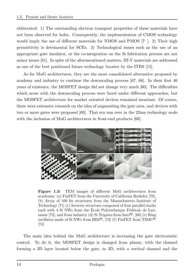
As for MuG architectures, they are the most consolidated alternative proposed by
academy and industry to continue the downscaling process [67, 68]. In their first 40
years of existence, the MOSFET design did not change very much [60]. The difficulties
which arose with the downscaling process were faced under different approaches, but
the MOSFET architecture for market oriented devices remained invariant. Of course,
there were extensive research on the idea of augmenting the gate area, and devices with
two or more gates were proposed [69]. That era was over in the 22nm technology node
with the inclusion of MuG architectures in front-end products [60].
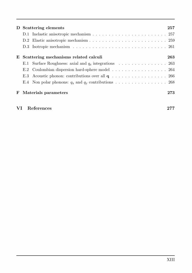
(a) (b) (c )
(d) (e) (f)
Figure 1.3: TEM images of different MuG architectures fromacademia: (a) FinFET from the University of California Berkeley [70],(b) Array of 100 fin structures from the Massachusetts Institute ofTechnology [71] (c) Inverter structure composed of four parallel stackseach with 4 Si NWs from the Ecole Polytechnique Federale de Lau-sanne [72]; and from industry (d) Si Trigates from Intelr, [60] (e) Ringoscillator made of Si NWs from IBMr, [73] (f) FinFET from TSMCr
[74]
The main idea behind the MuG architecture is increasing the gate electrostatic
control. To do it, the MOSFET design is changed from planar, with the channel
forming a 2D layer located below the gate, to 3D, with a vertical channel and the
14 Prologue
Chapter 1. Introduction
gate, partially or completely, surrounding it. Depending on the region of the channel
surrounded by the gate, the MOSFET is renamed as FinFET, in which two opposite
faces of the channel are covered by the gate [75, 76], Trigate when three faces of the
channel are covered by the gate [77, 78], and gate all around (GAA) or nanowires (NW)
[79, 80] when the gate completely surrounds the channel. Other geometries such as the
Ω FET [81] or the Π FET [82] are intermediate structures between Trigate and GAA,
with some penetration of the gate into the buried insulator. We have intentionally
omitted in the previous enumeration the planar double gate (DG) MOSFET, in which
a back gate is introduced under the channel. Strictly speaking it is a MuG structure,
but it does not share with the rest of the MuG structures a vertical channel and can
be interpreted as a derivative of the SOI technology [83, 84]. Since the gate control on
the channel is increased, several beneficial effect appears such as: 1) DIBL is reduced,
2) SS is decreased, being possible to achieve almost ideal values of 60mV/dec [36] and
3) punch-through and leakage current are almost suppressed [85].
Moreover, the fabrication process of MuG devices is CMOS compatible, and the
same boosters proposed for the CMOS technology can be applied here: high-κ oxides,
strain, SOI, epitaxial grew or metal silicide for the source and drain contacts.
1.4 Objectives
As the dimensions of the transistor have entered in the sub-50nm regime the down-
scaling process has slowed down. The aggressive reduction of the device size without
a proper supply voltage scaling has enhanced the short channel effects and the power
consumption, seriously compromising its performance. The solutions to that prob-
lems need to be assertive and new paradigms in the MOSFET structure and material
composition are being addressed.
This PhD Thesis is devoted to the study of two of the most promising alterna-
tives to continue the MOSFET downscaling process beyond the 22nm technology node:
Multiple Gate architectures and III-V compounds semiconductors. Multiple Gate ar-
chitectures increase the gate control on the channel resulting in reduced short channel
effects. III-V materials have the potentiality to increase the ON current, allowing to
reduce the supply voltage and the power consumption while keeping the device perfor-
mance. This work aims areS:
• The analytical and numerical study of the behavior of III-V nanowires, focused
Prologue 15
1.5. Methodology
on the influence of the device size and material type on the inversion charge, the
gate capacitance and the threshold voltage and the I-V characteristic.
• The numerical study of Trigate geometries made of III-V semiconductors and
their comparison with their Silicon counterparts.
• The study of the electron mobility in III-V and Si NWs and Trigates in the dif-
fusive regime including the most relevant scattering mechanisms which influence
the mobility.
1.5 Methodology
Once the objectives have been established, a brief description of the methodology fol-
lowed in this work is presented. The study of MuG architectures and III-V compound
semiconductors is divided in two parts. The first one is consigned to the electrostatics
of these devices while the second comprises the transport issues. Both parts have been
worked out according to the following scheme:
• First the theoretical background necessary for the numerical and analytical res-
olution of the 2D Schrodinger and Poisson equations is summarized in Chapter
2.
• In Chapter 3, the 2D electrostatic simulator is described and its main charac-
teristics (arbitrary geometries, orientation effects, non-parabolic bands, inclusion
of interface charges, etc.) are highlighted. Later, in Chapter 4 the numerical
solver is validated using experimental data, and used to study several relevant
electrostatic magnitudes of Trigates and NWs such as: a) the population of satel-
lite valleys of different III-V semiconductor NWs, b) the performance of III-V
and SOI Trigates c) the effect of back gate bias on the threshold voltage of SOI
Trigates.
• The analytical model for the potential, inversion charge and drain current of III-V
cylindrical NWs is proposed in Chapter 5. To develop the model, the cylindrical
symmetry of the device and the isotropic effective mass of Γ valley is taken into
consideration to solve the Poisson and Schrodinger equations in polar coordinates.
The results of this model are used to elaborate physically based analytical models
for the gate capacitance and the threshold voltage in Chapter 6. Comparisons
16 Prologue
Chapter 1. Introduction
with numerical simulations are accomplished for different materials, sizes and
applied gate voltages.
• In Chapter 7 the necessary background on the Boltzmann Transport Equation
(BTE) in a 1D electron gas is set, spotlighting those issues which need clear
understanding. Later the linearization of the BTE, which is used for its solution,
is presented, showing the implicit approach of the resulting equation system. The
diffusive transport paradigm is completed in Chapter 8 with the calculation of
the matrix elements in a 1D electron gas due to five different scattering processes:
surface roughness, coulomb dispersion, bulk phonons (optical and acoustic), polar
optical phonons and alloy disorder.
• Making use of the transport solver, in Chapter ?? the electron mobility of Si and
III-V Trigates and NWs is studied. Specifically, the electron mobility of InAs
NWs, and its dependence on the NW diameter, carrier density and population
of the Γ, L and X valleys is analyzed. The mobility behavior of Si and InGaAs
Trigate’s architectures of different widths is compared; and the influence of the
back gate bias on the transport properties of SOI Trigates is discussed.
• The mathematical details are included in the Appendixes A-E-
• Finally, the main conclusions of the work are present in Chapter 10.
Prologue 17

Part II
Electrostatics

Chapter 2
Electrostatics of nanowires:
background
2.1 Introduction
The rest of the Chapter is organized as follows. In Section 2.2 we present the indepen-
dent particle Schrodinger equation, and we summarize the main assumptions needed to
apply equivalent Hamiltonian approximation. Section 2.3 goes on the simplification of
the Schrodinger equation presenting the effective mass approximation particularized for
parabolic bands. In Section, 2.4 the Poisson equation is introduced. Both, Schrodinger
and Poisson equations compose the physical background for the solution of the electro-
static problems studied in this part of the manuscript. In Section 2.5 we particularize
both equations for 2D confined structures. In Section 2.6 we present a non-parabolic
correction of the parabolic Schrodinger equation introduced in Section 2.3. Section 2.7
remind the density of states concept in a 1D electron gas, bringing the expression for
the quantum electron concentration. Finally, Section ?? sums up the main conclusions
of this Chapter.
2.2 Independent particle Schrodinger equation
The electron behavior in a semiconductor nano-device is governed by the laws of quan-
tum mechanics. Its position, energy and momentum are probabilistic functions deter-
Electrostatics 21
2.2. Independent particle Schrodinger equation
mined by the independent particle Schrodinger equation [86]:
ı~∂
∂tΞ(r, t) = − ~
2
2m0∇2Ξ(r, t) + Φ(r, t)Ξ(r, t) (2.1)
where ı is the imaginary unit, ~ = h/2π, h is the Planck constant, r is the position
vector, t is the time, Ξ(r, t) is the electron wavefunction, m0 is the electron mass and
Φ(r, t) is the electron potential energy due to the average force exerted by the rest of
the electrons and atoms nuclei as well as by the external forces.
Equation (2.1) can be analytically solved only for simple idealized problems which
is not case of our interest. Nevertheless, there are several approaches that may simplify
Eq. (2.1).
In this manuscript we make use of the equivalent Hamiltonian and the effective mass
(EMA) approximations, which have been proven as a accurate and efficient approaches
[? ]. A rigorous and detailed derivation of equivalent Hamiltonian approximation and
EMA can be found in several textbooks [86], [87], [88]. Here we just spotlight the
main assumptions of these approaches, presenting the necessary background for the
numerical and analytical solution of EMA performed in Chapters 3 and 5.
First, let us consider Eq. (2.1) in absence of external forces. Then, Φ(r, t) = φc(r)
where φc(r) is the electron potential energy due to the semiconductor crystal lattice
(comprised by other electrons and atoms nuclei). φc(r) is assumed to be static and
periodic following the spatial periodicity of the crystal.
For a static potential energy, Eq. (2.1) can be simplified by writing the electron
wavefunction as:
Ξ(r, t) = Ξ(r)ζ(t) (2.2)
Substituting Eq. (2.2) into Eq. (2.1) and multiplying it by 1/Ξ(r)ζ(t):
ı~1
ζ(t)
∂
∂tζ(t) = − ~
2
2m0
1
Ξ(r)∇2Ξ(r) + φc(r) (2.3)
So after applying separation of variables we get
ı~1
ζ(t)
∂
∂tζ(t) = E −→ı~
∂
∂tζ(t) = Eζ(t) (2.4)
− ~2
2m0
1
Ξ(r)∇2Ξ(r) + φc(r) = E −→
[
− ~2
2mo∇2 + φc(r)
]
Ξ(r) = EΞ(r) (2.5)
22 Electrostatics
Chapter 2. Electrostatics of nanowires: background
where the separation constant, E, is actually the electron energy [? ]. Equation (2.4)
results into:
ζ(t) = ζ(0)e−ıE~t
(2.6)
Equation (2.5) is an eigenvalue problem where E and Ξ are the eigenvalues and eigen-
functions of the Hamiltonian (Hc). Therefore, they can be renamed as Ei and Ξi,
where i is the solution index.
The Bloch theorem imposes the periodicity of the electron wavefunction which is
given by [86]:
Ξi(r,k) =1√Ωeıkrui(r, r) (2.7)
where ui(r,k) is the so-called Bloch function and is directly related to the lattice
potential φc(r) []; Ω is the volume of the semiconductor unit cell and k is the electron
wavevector.
The periodicity of the crystal lattice and the electron wavefunction leads to a dis-
cretization of the reciprocal wavevector space. Therefore, there is a solution of Eq. (2.5)
for each k value, but if the crystal is large enough k can be assumed as continuous and
Ei = Ei(k) is a band structure. Moreover Ei(k) can be demonstrated to be periodic
and therefore it study can be restricted to primitive cell of the wave-vector space.
The determination of the energy band structure has been accomplished in the lit-
erature for most semiconductors by approaches such as the pseudo-potential method
[89], the k ·p method [], the tight binding [? ] method or ab-initio approaches [90]. For
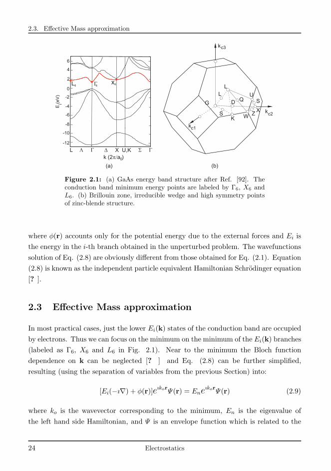
example, Fig. 2.1(a) shows the GaAs band structure as a function of the wave-vector,
obtained by the pseudo-potential method by Chelikowsky et al. in Ref [91]. The wave-
vector space can be reduced, using the crystal symmetry, to the irreducible wedge of
the Brillouin zone showed for the zinc-blende structure in Fig. 2.1(b).
When the crystal lattice potential is perturbed by the lattice vibrations, impurities
or external forces, the Hamiltonian of the Schrodinger equation can be written as
perturbation of the crystal lattice Hamiltonian: Hc + φ(r), where φ(r) is the electron
potential energy due to the external forces. If φ(r) is slowly varying function of the
position and the branches of the band structure are enough separated (as it is the case
for the first branch of the conduction band in Fig. 2.1), the Schrodinger equation can
be written for the i-th branch of the dispersion relation as:
ı~∂
∂tΞ(r) = [Ei(−ı∇) + φ(r, t)]Ξ(r, t) (2.8)
Electrostatics 23
2.3. Effective Mass approximation
k
k
k
G
L
D
S
L
QU
S
XZWK
c3
c2
c1
6
4
2
0
-2
-4
-6
-8
-10
-12
L L G D X U,K S G
6x6G6L
E (
eV
)i
(a) (b)
k (2 a )p/ 0
Figure 2.1: (a) GaAs energy band structure after Ref. [92]. Theconduction band minimum energy points are labeled by Γ6, X6 andL6. (b) Brillouin zone, irreducible wedge and high symmetry pointsof zinc-blende structure.
where φ(r) accounts only for the potential energy due to the external forces and Ei is
the energy in the i-th branch obtained in the unperturbed problem. The wavefunctions
solution of Eq. (2.8) are obviously different from those obtained for Eq. (2.1). Equation
(2.8) is known as the independent particle equivalent Hamiltonian Schrodinger equation
[? ].
2.3 Effective Mass approximation
In most practical cases, just the lower Ei(k) states of the conduction band are occupied
by electrons. Thus we can focus on the minimum on the minimum of the Ei(k) branches
(labeled as Γ6, X6 and L6 in Fig. 2.1). Near to the minimum the Bloch function
dependence on k can be neglected [? ] and Eq. (2.8) can be further simplified,
resulting (using the separation of variables from the previous Section) into:
[Ei(−ı∇) + φ(r)]eıkorΨ(r) = EneıkorΨ(r) (2.9)
where ko is the wavevector corresponding to the minimum, En is the eigenvalue of
the left hand side Hamiltonian, and Ψ is an envelope function which is related to the
24 Electrostatics
Chapter 2. Electrostatics of nanowires: background
wavefunction Ξ of Eq. (2.1) as [86]:
Ξ(r, t) = u(r, ko)e−ıEnt
~ eıkorΨ(r) (2.10)
In other words the envelope function Ψ is a softy approximation of the electron wave-
function Ξ where the potential due to the crystal lattice is somehow averaged [? ], [?
]. Anyway, Ψ is accurate enough to describe the electron behavior in a vast majority
of nanodevices studies (including those contained in this manuscript).
In Eq. (2.9), the potential due to the crystal lattice φc is not explicitly present.
Its influence is modeled through the energy branch Ei(k) which can be expanded into
Taylor series (up to second order) around, ko = (ko1, ko2, ko3) as:
Ei(k) = Ei(ko)+∑
j
∣
∣
∣
∣
∂E
∂kj
∣
∣
∣
∣
ko
(kj−kjo)+1
2
∑
j, m
∣
∣
∣
∣
∂2E
∂kj∂km
∣
∣
∣
∣
ko
(kj−kmo)(km−kmo) (2.11)
with j, m = 1, 2, 3. As Ei(ko) is a minimum of Ei(k), the first derivatives evaluated
at that point are null and Ei(k) can be formulated, in matrix notation, as:
Ei(k) = Ei(ko) + [k− ko]
12
∣
∣
∣
∂2Ei
∂k21
∣
∣
∣
ko· · · 1
2
∣
∣
∣
∂2Ei
∂k1∂k3
∣
∣
∣
ko...
. . ....
12
∣
∣
∣
∂2Ei
∂k3∂k1
∣
∣
∣
ko· · · 1
2
∣
∣
∣
∂2Ei
∂k23
∣
∣
∣
ko
[k− ko]T (2.12)
It is possible to define an electron effective mass as:
m−1ij =
∣
∣
∣
∣
∂2E
∂ki∂kj
∣
∣
∣
∣
ko
(2.13)
which characterizes the dispersion relation around the energy minimum. Then:
Ei(k) = E(ko) +~2
2[k− ko]W [k− ko]
T (2.14)
where;
W =
1m11
1m12
1m13
1m21
1m22
1m23
1m31
1m32
1m33
(2.15)
W is a symmetric matrix and therefore can be diagonalized. The dispersion relation,
Electrostatics 25
2.4. Poisson equation
E − k, can the be written as:
Ei(k) = Ei(ko) +~2(kx − kxo)
2
2mx+
~2(ky − kyo)
2
2my+
~2(kz − kzo)
2
2mz(2.16)
If the point ko is selected as the origin of the wavevector space, Eq. (2.16) can be
further simplified:
Ei(k) = Ei(ko) +~2k2x2mx
+~2k2y2my
+~2k2z2mz
(2.17)
Using the parabolic dispersion relation of Eq. (2.17) into Eq. (2.9) results into the
parabolic EMA Schrodiger equation:
~2
2∇W∇T + φ(r)Ψ(r) = E′nΨ(r) (2.18)
where E′n = En − Ei(ko) is the eigenvalue referred to the minimum of the branch and
represents an energy subband being n the subband index. The truncation of the Taylor
series in the second derivative term allows to reach a simple parabolic expression for
the dispersion relation, but it can lead to a non-negligible error when Ei(k) is not a
parabolic function, as it is the case for III-V materials.
2.4 Poisson equation
In order to solve Eq. (2.18) we need to know the electron potential energy, φ(r), due
to the external forces. It can be determined from the Poisson equation which relates
the electrostatic potential, ψ, and the charge distribution in the device, ρ. The Poisson
equation together with the Schrodinger equation presented in Section 2.2 completes the
physical background necessary for the resolution of the electrostatic problems studied
in this part of the manuscript and it is formulated as:
∇[ǫ(r)∇ψ(r)] = −ρ(r) (2.19)
where ǫ(r) is the dielectric constant. The electrostatic potential, ψ(r), and the electron
potential energy, φ(r), are related as φ(r) = −qψ(r) where q is the electron charge.
The charge distribution, ρ(r) is given by:
ρ(r) = q[
p(r)− n(r) +N+d −N−a
]
(2.20)
26 Electrostatics
Chapter 2. Electrostatics of nanowires: background
where p(r) and n(r) are the electron and hole concentrations, and N+d and N+
a are the
donors and acceptor ionized impurities concentrations.
2.5 Particularization for 2D structures
In this manuscript we are interested structures that confine the electrons in two dimen-
sion, giving rise to 1D electron gases. In that case the wavefunction can be described
as a plane wave in the non-confined direction. Then:
Ψi(r) = ξi(s)eıkzz√L
(2.21)
where s is the vector position in the 2D confinement plane. Thus, introducing Eq.
(2.21) into Eq. (2.18) we get:
[
~2
2∇W∇T + φ(s)
]
ξi(s)eıkzz√L
= E′nξi(s)eıkzz√L
(2.22)
which decomposing the ∇ operator into the confined and non-confined variables results
into:[
~2
2∇sw∇T
s +∇z1
mz∇Tz + φ(s)
]
ξi(s)eıkzz√L
= E′nξi(s)eıkzz√L
(2.23)
where w is the 2 × 2 first submatrix of the diagonal matrix W given in Eq. (2.15).
Thus:
eıkzz√L
[
~2
2∇sw∇T
s ξi(s) + ξ(s)~2
2mzı2kz + φ(s)ξi(s)
]
= E′nξi(s)eıkzz√L
(2.24)
canceling terms and rearranging we get:
∇sw∇Ts ξi(s) + φ(s)ξi(s) = εnξi(s) (2.25)
where εn = E′n − ~2kz2mz
. This is the 2D Schrodinger equation which will be numerically
and analytically solved in Chapters 3 and 5, respectively.
Regarding the Poisson equation, the particularization for a 1D electron gas can be
readily accomplished. As the potential is assumed to vary slowly along non-confined
direction, also is the charge density ρ. Then, the z component of the ∇ operator is
Electrostatics 27
2.6. Non-parabolic corrections to the parabolic Schrodinger equation
canceled out and the Poisson equation reduces to:
∇s[ǫ(s)∇sψ(s)] = −ρ(s) (2.26)
2.6 Non-parabolic corrections to the parabolic Schrodinger
equation
Up to this point, we have approximated Ei(k) as a parabolic function. However, at can
be seen in Fig. 2.1(a), near to the conduction band minimums the dispersion relation
is not always parabolic (see points X6 and L6). When the parabolic approximation is
not accurate, the most common solution in the literature consists on introducing a non
linear correction term βvEi(k)2, where βv is called the non-parabolicity factor of the
v-th valley. Thus, the dispersion relation is expressed as [93], [66],:
Ei(k)(1 + βvEi(k)) =~2k2x2mx
+~2k2y2my
+~2k2z2mz
(2.27)
Solving for Ei(k):
Ei(k) =−1 +
√1 + 4βvγk2βv
(2.28)
where we have defined:
γk =~2k2x2mx
+~2k2y2my
+~2k2z2mz
(2.29)
Eq. (2.28) makes difficult the resolution of the Schrodinger equation since Ei(k) can not
be decomposed into confined and non-confined components [94]. In this work we follow
the approach developed by Jin et al. [95], which proposed a non-parabolic dispersion
relation written as:
Ei(k) ≃ φi +−1 +
√
1 + 4βv(γk,nc +Ei − φi)
2βV(2.30)
where Ei is i-th energy subband achieved from the parabolic Schrodinger equation and
φi is the expectation value of the potential energy with respect to the wavefunction of
the i-subband, defined as:
φ=
∫
A
ξ∗i (s)φ(s)ξi(s) dA (2.31)
28 Electrostatics
Chapter 2. Electrostatics of nanowires: background
where the integral is carried out in the 2D cross-section of the device. In Eq. (2.30)
γk,nc = ~2k2z/2mz is the non-confined component of γk. This non-parabolic approxima-
tion does not require the solution of the non-parabolic Schrodinger equation as it uses
the result from the parabolic EMA approximation, resulting in a simpler procedure.
2.7 Quantum electron concentration
To determine the quantum electron concentration, it is necessary to characterize the
electron density in both the real and wave-vector space. In the real space, the electron
distribution is fully determined by the square modulus of the electron wavefunction. In
the wave-vector space, it is necessary to count the number of available electron states
and their occupancy. In this Section we briefly remind the concept of density of states
particularizing it to a 1D electron gas with a non-parabolic dispersion relation.
The wave-vector density of states, g(k), is just the number of k states divided by the
semiconductor volume. As previously mentioned, the periodicity of the crystal lattice
involves a discretization of the wave-vector space. Each k state occupies a volume in the
wave-vector space given by ΩB/N where ΩB is the volume of the Brillouin zone and N
is the number of unit cells in the real space for the given volume, V, of semiconductor:
N = V/ΩC, being ΩC the unit cell volume. Then, the wave-vector density of states is
given by:
g(k) = 2ΩB/N
V =(V/ΩC)/ΩB
V =2
(2π)3(2.32)
where ΩBΩC = (2π)3 where the factor 2 accounts for the electron spin degeneracy.
When a 1D electron as is considered, two of the three space direction are confined.
Consequently ΩB and ΩC do not represent volumes but lengths and ΩBΩC = 2π. The
wave-vector density of states is given by:
g(kz) = 2ΩB/N
L =(L/ΩC)ΩB
L =2
2π(2.33)
The energy density of states, g(E), can be determined changing the variable from k to
E and using Ei(k):
g(kz)dkz = g(E)dE → g(E) = g(k)dk
dE(2.34)
Electrostatics 29
2.7. Quantum electron concentration
Using the non-parabolic dispersion relation of Eq. (2.30) and rearranging terms we get:
g(E) =1 + 2βv(E − φi)
√
2m∗ [E − Ei + βv(E − φi)2](2.35)
The states occupancy is determined by the Fermi-Dirac function:
f(E) =1
1 + eE−EFkBT
(2.36)
being kB the Boltzmann constant and EF the Fermi level. Therefore the electron density
in the i-th branch in both real and energy spaces is given by:
n(s, E) =
∣
∣
∣
∣
∣
ξi(s)eıkzz√L
∣
∣
∣
∣
∣
21 + 2βv(E − φi)
√
2m∗ [E − Ei + βv(E − φi)2]
1
1 + eE−EFkBT
(2.37)
Integrating along the device total volume and the energy space gives the electron con-
centration under non-parabolic dispersion relation:
n =
∫
dE1 + 2βv(E − φi)
√
2m∗ [E − Ei + βv(E − φi)2]
1
1 + eE−EFkBT
(2.38)
where we have used the normalization of the wavefunction:
∫
V|ξi(s)
eıkzz√L
|2dV = 1 (2.39)
Equation (2.38) is the expression used along this manuscript to determine the quantum
electron concentration. As for holes, and ionized impurities due to dopants, classical
expressions are considered.
p = 2
(
2πmhkBT
~2
)3/2
e−EF−Ev
kBT (2.40)
N−a = Na f(Ea) =Na
1 + 1gae
Ea−EFkBT
(2.41)
N+d = Nd[1− f(Ed)] =
Nd
1 + gde−Ed−EF
kBT
(2.42)
where mh is the hole effective mass, Ev is the valence band energy, Na (Nd), ga (gd)
30 Electrostatics
Chapter 2. Electrostatics of nanowires: background
and Ea (Ed) are the acceptor (donor) concentration, level degeneracy and energy, re-
spectively.
Electrostatics 31

Chapter 3
2D Schrodinger-Poisson
simulator for MuG structures
3.1 Introduction
The analytical calculus of the integral and differential equations which govern the elec-
trostatic behavior of a Multiple Gate device (MuG) is not straightforward. Only in a
few cases, and considering some approximations, these equations can be analytically
solved, obtaining expressions for the involved physical quantities [96],[97],[98]. One of
that cases is included in this manuscript in Chapter 5.
However, even assuming that analytical expressions are helpful to understand the
device behavior, they are limited by the approximations made to solve the initial equa-
tions. The simplicity required for the analytical treatment is confronted to the com-
plexity needed to properly describe the device’s underlying physics.
Moreover, the study of technologically realistic devices involve among others: 1) not
idealized geometries [99],[100],[101],[79], which complicate the analysis; 2) experimental
inputs to the equations [102],[103] that cannot be reduced to analytical expressions; 3)
fabrication dependent issues that cannot be treated from an analytical point of view
[104][105].
For these reasons, the development of numerical tools able to study the device
physics have played a main role in the nanoelectronics field from the very beginning
[106], [107], [? ]. In response to this requirement, several commercial simulators
have been developed, allowing the study of 3D structures, such as SentaurusTM from
Electrostatics 33
3.2. Simulator description
Synopsisr[108] or AtlasTM from Silvacor [109], as well as 2D quantized devices, such as
VPS from TU Wien [110]. The assessment of variability and fabrication processes has
also been accomplished, for example by Gold Semiconductors Std. [111] and AthenaTM
from Silvacor [112].
In this Chapter, we describe the main characteristics of a two dimensional simulator
fully implemented within our group at UGR from scratch. Taking into consideration
the extensive collection of commercial simulators, it can be questioned why to develop
our own simulator. There are several reasons, among them
• Code control: most commercial simulators are black boxes which just allow an
user-end control of the code.
• Versatility and extensibility: opposite to commercial simulators having our own
code allows us to easily modify and extend it.
• Complete knowledge of the resolution process and its limitations: we know exactly
how the equations are solved, what is included in the resolution and what it is
neglected.
• Economic saving: usually commercial simulator licenses are expensive.
Of course there are also some disadvantages when developing our own simulator:
• Time consuming: putting down all the equations, testing and verifying the code
requires much more time than just studying and configuring a commercial simu-
lator.
• Not-optimized programming: it can affect to the simulation time.
The rest of the Chapter is organized as follows. Section 3.2 describes the main
characteristics of the two dimensional Schrodinger-Poisson (SP2D) simulator. Section
3.3 outlines the development environment: MATLABr and PDE toolboxTM. Sections
3.4, 3.5, 3.6, 3.7 3.8, 3.9 and 3.10 detail the implementation of the main characteristics
of SP2D and present a flux diagram. Finally, Section 3.11 sums up some conclusions.
3.2 Simulator description
In this Section, we outline the main characteristics of SP2D code which solves self-
consistently the Schrodinger and Poisson equations for a 2D cross-section of the channel
34 Electrostatics
Chapter 3. 2D Schrodinger-Poisson simulator for MuG structures
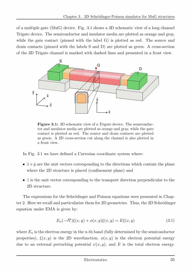
of a multiple gate (MuG) device. Fig. 3.1 shows a 3D schematic view of a long channel
Trigate device. The semiconductor and insulator media are plotted as orange and gray,
while the gate contact (pinned with the label G) is plotted as red. The source and
drain contacts (pinned with the labels S and D) are plotted as green. A cross-section
of the 3D Trigate channel is marked with dashed lines and presented in a front view.
GS
D
yx
z
x
y
Figure 3.1: 3D schematic view of a Trigate device. The semiconduc-tor and insulator media are plotted as orange and gray, while the gatecontact is plotted as red. The source and drain contacts are plottedas green. A 2D cross-section cut along the channel is also plotted ina front view.
In Fig. 3.1 we have defined a Cartesian coordinate system where:
• x e y are the unit vectors corresponding to the directions which contain the plane
where the 2D structure is placed (confinement plane) and
• z is the unit vector corresponding to the transport direction perpendicular to the
2D structure.
The expressions for the Schrodinger and Poisson equations were presented in Chap-
ter 2. Here we recall and particularize them for 2D geometries. Thus, the 2D Schrodinger
equation under EMA is given by:
En(−ı∇)ξ(x, y) + φ(x, y)ξ(x, y) = Eξ(x, y) (3.1)
where En is the electron energy in the n-th band (fully determined by the semiconductor
properties), ξ(x, y) is the 2D wavefunction, φ(x, y) is the electron potential energy
due to an external perturbing potential ψ(x, y), and E is the total electron energy.
Electrostatics 35
3.2. Simulator description
The numerical solution of the Schrodinger equation accomplished by SP2D assumes
parabolic bands. This dispersion relation is later corrected using the method proposed
by Jin et al. in Ref. [95] and presented in Chapter 2 (see Section 3.7 for details on
the implementation of non-parabolicity). Under parabolic bands approximation we can
write Eq. (3.1) in the semiconductor as:
− ~2
2
[
∂∂x
∂∂y
]
[
1mxx
1mxy
1myx
1myy
][
∂∂x∂∂y
]
ξs(x, y) + φs(x, y)ξs(x, y) = Eξs(x, y) (3.2)
where the matrix element 1/mij , with i, j = [x, y], is related to the electron energy
ellipsoid in the way explained in Section 3.6. For the insulator, we assume an isotropic
electron effective mass, mins, and the Schrodinger equation is simplified to:
− ~2
2mins
[
∂2
∂x2+
∂2
∂y2
]
ξins(x, y) + φins(x, y)ξins(x, y) = Eξins(x, y) (3.3)
where the electron potential energy in the insulator φins takes into consideration the
band offset (∆φ) between the insulator and the semiconductor. The procedure followed
to determine it is summarized in Section 3.4. In Eqs. (3.2) and (3.3) we have used the
superscripts s and ins to distinguish the electron wavefunctions and potential energies
in the semiconductor and insulator, respectively. Hereinafter in this Chapter, s and ins
will be used to indicate that a variable is circumscribed to the semiconductor or the
insulator media, respectively.
We do not solve the Schrodinger equation on the metal as the electron wavefunction
is assumed to vanish at the metal-insulator interface.
For the solution of Eqs. (3.2) and (3.3) we impose boundary conditions which guar-
antee the continuity of the flux density through the semiconductor-insulator interface1 [115]. They enforce:
(a) The electron wavefunction continuity at the semiconductor-insulator interface
ξs(x, y)
∣
∣
∣
∣
x,y∈Cs-i= ξins(x, y)
∣
∣
∣
∣
x,y∈Cs-i(3.4)
where Cs-i is the semiconductor-insulator interface path.
1An interesting discussion on the generalization of these boundary conditions can be found in Refs.[113] and [114].
36 Electrostatics
Chapter 3. 2D Schrodinger-Poisson simulator for MuG structures
(b) The continuity of the wavefunction derivative in the direction perpendicular to the
semiconductor-insulator interface
n ·[
∂
∂xx,
∂
∂yy
]
[
1mxx
1mxy
1myx
1myy
]
ξs(x, y)
∣
∣
∣
∣
x,y ∈ Cs-i= n ·
[
∂
∂xx,
∂
∂yy
]
1
minsξins(x, y)
∣
∣
∣
∣
x,y ∈ Cs-i(3.5)
being n the unit vector perpendicular to the interface at each point (x, y) ∈ Cs-i.
The 2D Poisson equation is given by:
∇ · ǫ∇ψ(x, y) = −ρ(x, y) (3.6)
where ǫ is the dielectric constant and ρ(x, y) is the charge density. We have considered
homogeneous isotropic dielectric constants in each media. This way, Eq. (3.6) can be
particularized for the semiconductor as:
ǫs
(
∂2
∂x2+
∂2
∂y2
)
ψs(x, y) = −q[
−n(x, y) + p(x, y)−N+d (x, y) +N−a (x, y)
]
(3.7)
where n, p, are the electron and holes concentrations and N+d and N−a are donor and
acceptor ionized impurities concentrations, respectively. Equivalently for the insulator
the Poisson equation is:
ǫins
(
∂2
∂x2+
∂2
∂y2
)
ψins(x, y) = −q [−n(x, y) +Nins(x, y)] (3.8)
where Nins refers to the insulator charge concentration, also including interface states
(see Section 3.8 for a complete description). Note that the charge density in the in-
sulator considers n. This is due to the electron wavefunction penetration into this
media.
As already mentioned, SP2D assumes an ideal metal gate. Therefore, the Poisson
equation is not solved on it and ψ in the metal is determined by the applied gate
voltage, Vg. The metal properties are introduced through a boundary condition which
determines the bias of the structure:
ψins(x, y)
∣
∣
∣
∣
x,y ∈ Cm-i
= Vg − (Φm − χs) (3.9)
where Cm-i is the path along the metal-insulator interface, Φm is the metal work function
Electrostatics 37
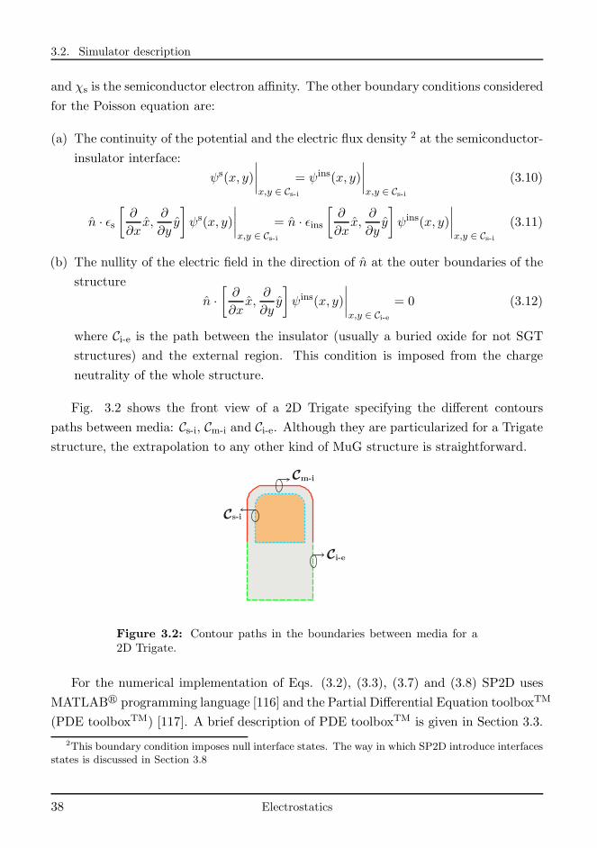
3.2. Simulator description
and χs is the semiconductor electron affinity. The other boundary conditions considered
for the Poisson equation are:
(a) The continuity of the potential and the electric flux density 2 at the semiconductor-
insulator interface:
ψs(x, y)
∣
∣
∣
∣
x,y ∈ Cs-i= ψins(x, y)
∣
∣
∣
∣
x,y ∈ Cs-i(3.10)
n · ǫs[
∂
∂xx,
∂
∂yy
]
ψs(x, y)
∣
∣
∣
∣
x,y ∈ Cs-i= n · ǫins
[
∂
∂xx,
∂
∂yy
]
ψins(x, y)
∣
∣
∣
∣
x,y ∈ Cs-i(3.11)
(b) The nullity of the electric field in the direction of n at the outer boundaries of the
structure
n ·[
∂
∂xx,
∂
∂yy
]
ψins(x, y)
∣
∣
∣
∣
x,y ∈ Ci-e= 0 (3.12)
where Ci-e is the path between the insulator (usually a buried oxide for not SGT
structures) and the external region. This condition is imposed from the charge
neutrality of the whole structure.
Fig. 3.2 shows the front view of a 2D Trigate specifying the different contours
paths between media: Cs-i, Cm-i and Ci-e. Although they are particularized for a Trigate
structure, the extrapolation to any other kind of MuG structure is straightforward.
Cm-i
Cs-i
Ci-e
Figure 3.2: Contour paths in the boundaries between media for a2D Trigate.
For the numerical implementation of Eqs. (3.2), (3.3), (3.7) and (3.8) SP2D uses
MATLABr programming language [116] and the Partial Differential Equation toolboxTM
(PDE toolboxTM) [117]. A brief description of PDE toolboxTM is given in Section 3.3.
2This boundary condition imposes null interface states. The way in which SP2D introduce interfacesstates is discussed in Section 3.8
38 Electrostatics
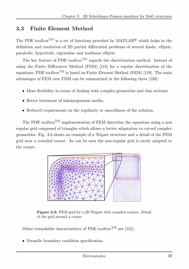
Chapter 3. 2D Schrodinger-Poisson simulator for MuG structures
3.3 Finite Element Method
The PDE toolboxTM is a set of functions provided by MATLABr which helps in the
definition and resolution of 2D partial differential problems of several kinds: elliptic,
parabolic, hyperbolic, eigenvalue and nonlinear elliptic.
The key feature of PDE toolboxTM regards the discretization method. Instead of
using the Finite Differences Method (FDM) [118] for a regular discretization of the
equations, PDE toolboxTM is based on Finite Element Method (FEM) [119]. The main
advantages of FEM over FDM can be summarized in the following three [120]:
• More flexibility in terms of dealing with complex geometries and thin sections.
• Better treatment of inhomogeneous media.
• Reduced requirements on the regularity or smoothness of the solution.
The PDE toolboxTM implementation of FEM discretize the equations using a non
regular grid composed of triangles which allows a better adaptation to curved complex
geometries. Fig. 3.3 shows an example of a Trigate structure and a detail of the FEM
grid near a rounded corner. As can be seen the non-regular grid is nicely adapted to
the corner.
Figure 3.3: FEM grid for a 2D Trigate with rounded corners. Detailof the grid around a corner
Other remarkable characteristics of PDE toolboxTM are [121]:
• Versatile boundary condition specification.
Electrostatics 39
3.4. Energy and potential reference system
• Flexible non-linear solvers
• Visualization tools for solutions, mesh and geometries.
The definition of equations and boundary conditions in PDE toolboxTM is easy. It
is not the aim of this Chapter to describe them. Extensive information can be found in
Refs. [117] and [121]. In the next Sections, we detail the key features of the developed
SP2D simulator.
3.4 Energy and potential reference system
In Section 3.2, we proposed a Cartesian coordinate system to spatially describe the 2D
MuG geometry and particularized Schrodinger and Poisson equations for that system.
We defined the paths which limit each media in the MuG device and imposed conditions
to relate ξ and ψ in adjacent medias. However, the resolution of Schrodinger and
Poisson equations requires an extra consideration: the definition of a reference system
for the energies and the potential. This is the aim of this Section.
Two main issues constrain the specification of the energy reference system: (a) the
origin, which, to allow an easy referencing, must be constant along the whole structure;
and (b) the relation between the potential, ψ, the potential energy, φ, and the energy
band diagram of the metal-insulator-semiconductor (MIS) structure.
Regarding the origin, no charge is expected to flow along the MuG 2D cross-section.
Therefore, the Fermi level can be assumed constant (EF(x, y) = EF). For this reason,
we choose it as the origin of the energy reference system.
Concerning the band diagram-potential relation, since SP2D is thought to study
N-type devices, we have opted to identify the conduction band and the potential:
−qψ(x, y) = φ(x, y) = Ec(x, y).
These definitions have three consequences: (a) the eigenvalues, E, of the Schrodinger
equation and φ(x, y) are referred to EF (b) the band offset between φs and φins is given
by the conduction band offset (CBO) of the MIS heterostructure; and (c) the gate
applied voltage, imposed as a boundary condition to the Poisson equation must be
referred to the potential origin, EF (see Section 3.2).
The CBO determination is not a straightforward question. While the Schottky bar-
rier model [122] has given very good results for Si-SiO2 structures, it has been revised
when other heterostructures are considered [123], [124], [125], [126]. The limitation
40 Electrostatics
Chapter 3. 2D Schrodinger-Poisson simulator for MuG structures
of the Schottky barrier model regards the lack of consideration of the heterostructure
surface properties, which have revealed to play an important role on the CBO forma-
tion. Some discussion still remains on the underlying physical process which determine
the band alignment of the heterostructure. The two main explanations refer to: (a)
extrinsic defects: unsatisfied atomic bonds at the interface, [127], [128], [129], (b) in-
trinsic defects: metal induced gap states (MIGS),[130], [131], [132], [133], due to the
penetration of the metal wavefunctions into the semiconductor gap. Although both
theories suggest different physical origins, both conclude in the appearance of energetic
states in the gap which lead to a pinning of the Fermi level in the semiconductor. The
gap states distribution is then characterized, in both theories, by a charge neutrality
level (CNL) which indicates a change in the polarity of those states. In both theories
the band alignment expressions are equivalent.
Even if these theories are not fully correct, there is an agreement in their ability to
explain experimental results [134], [135], [136]. Based on this experimental support we
have considered the expression resulting from those models as appropriate to determine
the CBO. Then, ∆φ is given by:
∆φ = (χs − φCNL,s)− (χins − φCNL,ins) + S(φCNL,s − φCNL,ins) (3.13)
where χs and χins are the electron affinities of the semiconductor and the insulator,
φCNL,s and φCNL,ins are the CNL of the semiconductor and the insulator, the values of
which are obtained from Refs. [134], [135] and summarized (for the materials used
thorough this manuscript) in Appendix F. S is the so-called pinning factor and deter-
mines how strong the Fermi level pinning is for a given heterostructure: S = 1, means
no pinning, while for S = 0, EF is fully pinned. It is worth to note that for S = 1
Eq. (3.13) results into the difference of electron affinities which is the Schottky bar-
rier model applied to a semiconductor insulator interface. S was found to empirically
depend on the dielectric constant of the wider gap material as given by [133]:
S =1
1 + 0.1(ǫins,∞/ǫ0 − 1)2(3.14)
where ǫins,∞ is the dielectric constant of the insulator at high frequency and ǫ0 is the
vacuum absolute permittivity.
Electrostatics 41
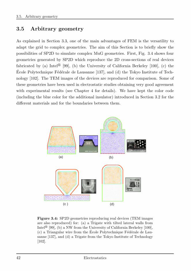
3.5. Arbitrary geometry
3.5 Arbitrary geometry
As explained in Section 3.3, one of the main advantages of FEM is the versatility to
adapt the grid to complex geometries. The aim of this Section is to briefly show the
possibilities of SP2D to simulate complex MuG geometries. First, Fig. 3.4 shows four
geometries generated by SP2D which reproduce the 2D cross-sections of real devices
fabricated by (a) Intelr [99], (b) the University of California Berkeley [100], (c) the
Ecole Polytechnique Federale de Lausanne [137], and (d) the Tokyo Institute of Tech-
nology [102]. The TEM images of the devices are reproduced for comparison. Some of
these geometries have been used in electrostatic studies obtaining very good agreement
with experimental results (see Chapter 4 for details). We have kept the color code
(including the blue color for the additional insulator) introduced in Section 3.2 for the
different materials and for the boundaries between them.
(a) (b)
(c ) (d)
Figure 3.4: SP2D geometries reproducing real devices (TEM imagesare also reproduced) for: (a) a Trigate with tilted lateral walls fromIntelr [99], (b) a NW from the University of California Berkeley [100],(c) a Triangular wire from the Ecole Polytechnique Federale de Lau-sanne [137], and (d) a Trigate from the Tokyo Institute of Technology[102].
42 Electrostatics
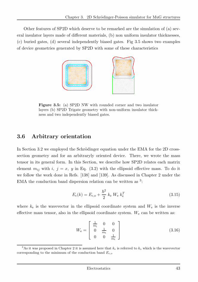
Chapter 3. 2D Schrodinger-Poisson simulator for MuG structures
Other features of SP2D which deserve to be remarked are the simulation of (a) sev-
eral insulator layers made of different materials, (b) non uniform insulator thicknesses,
(c) buried gates, (d) several independently biased gates. Fig 3.5 shows two examples
of device geometries generated by SP2D with some of these characteristics
Figure 3.5: (a) SP2D NW with rounded corner and two insulatorlayers (b) SP2D Trigate geometry with non-uniform insulator thick-ness and two independently biased gates.
3.6 Arbitrary orientation
In Section 3.2 we employed the Schrodinger equation under the EMA for the 2D cross-
section geometry and for an arbitraryly oriented device. There, we wrote the mass
tensor in its general form. In this Section, we describe how SP2D relates each matrix
element mij with i, j = x, y in Eq. (3.2) with the ellipsoid effective mass. To do it
we follow the work done in Refs. [138] and [139]. As discussed in Chapter 2 under the
EMA the conduction band dispersion relation can be written as 3:
Ec(k) = Ec,o +~2
2ke We k
Te (3.15)
where ke is the wavevector in the ellipsoid coordinate system and We is the inverse
effective mass tensor, also in the ellipsoid coordinate system. We can be written as:
We =
1ml
0 0
0 1mt
0
0 0 1mt
(3.16)
3As it was proposed in Chapter 2 it is assumed here that ke is referred to ko which is the wavevectorcorresponding to the minimum of the conduction band Ec,o
Electrostatics 43
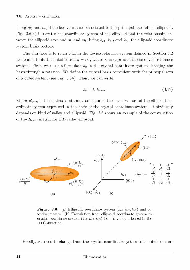
3.6. Arbitrary orientation
being ml and mt the effective masses associated to the principal axes of the ellipsoid.
Fig. 3.6(a) illustrates the coordinate system of the ellipsoid and the relationship be-
tween the ellipsoid axes and ml and mt, being ke1, ke,2 and ke,3 the ellipsoid coordinate
system basis vectors.
The aim here is to rewrite ke in the device reference system defined in Section 3.2
to be able to do the substitution k = ı∇, where ∇ is expressed in the device reference
system. First, we must reformulate ke in the crystal coordinate system changing the
basis through a rotation. We define the crystal basis coincident with the principal axis
of a cubic system (see Fig. 3.6b). Thus, we can write:
ke = kcRe←c (3.17)
where Re←c is the matrix containing as columns the basis vectors of the ellipsoid co-
ordinate system expressed in the basis of the crystal coordinate system. It obviously
depends on kind of valley and ellipsoid. Fig. 3.6 shows an example of the construction
of the Re←c matrix for a L-valley ellipsoid.
k e3
k o k e1
ke2
( )E-Ec
h2m
l
( )E-Ec
h2m
t
mt
k e3
k
k e1
e2
( )E-Ec
h2
kc3
k c2
kc1
h111i
h010i
h001i
h100i
h111i
h10-1i
h-12-1 i
(a) (b)
R =e c
1 1 -1
1
1 -1 -1
3 2 626
6
3
23
0
Figure 3.6: (a) Ellipsoid coordinate system (ke1, ke2, ke3) and ef-fective masses. (b) Translation from ellipsoid coordinate system tocrystal coordinate system (kc1, kc2, kc3) for a L-valley oriented in the〈111〉 direction.
Finally, we need to change from the crystal coordinate system to the device coor-
44 Electrostatics
Chapter 3. 2D Schrodinger-Poisson simulator for MuG structures
dinate system. To do so, we write
kc = kRc←d (3.18)
where Rc←d is the matrix containing as columns the basis vector of the crystal co-
ordinate system expressed in the basis of the device coordinate system. Usually, for
comparison with technological results, what is given is the wafer orientation and/or
the transport direction of the device referenced to the crystal cubic system. Then, the
device coordinate system basis directions can be identified with the wafer orientation
and the transport direction. To determine Rc←d we write the device basis vectors in
columns (they are already expressed in the crystal coordinate system), and we do the
inverse. But as the device basis vectors form an orthonormal basis, the inverse is just
the transpose of the matrix. So Rc←d just contains the device basis vectors written in
rows. Using Eqs. (3.17) and (3.18) we can write:
Ec(k) = Ec,0 +~2
2k Wd k
T (3.19)
where Wd = Re←c Rc←d We (Re←c Rc←d)T corresponds to the matrix tensor in the
device coordinate system:
Wd =
1mxx
1mxy
1mxz
1myx
1myy
1myz
1mzx
1mxy
1mzz
(3.20)
As SP2D solves the Schrodinger equation in the 2D cross-section of the device, just the
projection of Wd into the x− y plane was considered in Section 3.2. There is another
effective mass related parameter taken into consideration by SP2D and obtained from
Wd: the conduction effective mass, m∗v, which determines the effective mass in the
transport direction, z; where v stands for the valley index. m∗v is used in the determi-
nation of n(x, y), as it is shown in Section 3.7, and is calculated as the (3, 3) element
of the Wd inverse matrix.
Electrostatics 45
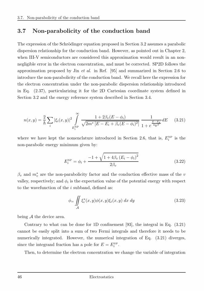
3.7. Non-parabolicity of the conduction band
3.7 Non-parabolicity of the conduction band
The expression of the Schrodinger equation proposed in Section 3.2 assumes a parabolic
dispersion relationship for the conduction band. However, as pointed out in Chapter 2,
when III-V semiconductors are considered this approximation would result in an non-
negligible error in the electron concentration, and must be corrected. SP2D follows the
approximation proposed by Jin et al. in Ref. [95] and summarized in Section 2.6 to
introduce the non-parabolicity of the conduction band. We recall here the expression for
the electron concentration under the non-parabolic dispersion relationship introduced
in Eq. (2.37), particularizing it for the 2D Cartesian coordinate system defined in
Section 3.2 and the energy reference system described in Section 3.4.
n(x, y) =2
~
∑
i
|ξi(x, y)|2∞∫
ENPi
1 + 2βv(E − φi)√
2m∗ [E − Ei + βv(E − φi)2]
1
1 + eE−EFkBT
dE (3.21)
where we have kept the nomenclature introduced in Section 2.6, that is, ENPi is the
non-parabolic energy minimum given by:
ENPi = φi +
−1 +√
1 + 4βv (Ei − φi)2
2βv(3.22)
βv and m∗v are the non-parabolicity factor and the conduction effective mass of the v
valley, respectively; and φi is the expectation value of the potential energy with respect
to the wavefunction of the i subband, defined as:
φ=
∫∫
A
ξ∗i (x, y)φ(x, y)ξi(x, y) dx dy (3.23)
being A the device area.
Contrary to what can be done for 1D confinement [93], the integral in Eq. (3.21)
cannot be easily split into a sum of two Fermi integrals and therefore it needs to be
numerically integrated. However, the numerical integration of Eq. (3.21) diverges,
since the integrand fraction has a pole for E = ENPi .
Then, to determine the electron concentration we change the variable of integration
46 Electrostatics
Chapter 3. 2D Schrodinger-Poisson simulator for MuG structures
from energy, E, to wavevector, k, and n(x, y) can be obtained as:
n(x, y) =∑
i
|ξi(x, y)|2∑
k
g(k)fi(k) (3.24)
where g(k) = 2πdk is the density of states in the k space for 2D confinement and fi(k)
is the occupation probability of the state with k wavevector in the i-th subband, that
is the Fermi function evaluated at ENPi (k)
fi(k) =1
1 + eENPi (k)−EF
kBT
(3.25)
Therefore:
n(x, y) =2
π
∑
i
|ξi(x, y)|2∞∫
−∞
1
1 + eENPi (k)−EF
kBT
dk (3.26)
where ENPi (k) is given by:
ENPi (k) = φi +
−1 +
√
1 + 4βv
(
~2k2
2m∗v+ Ei − φi
)2
2βv(3.27)
Eq. (3.26) does not diverge but it is computationally expensive. It should be done
for each energy level and each point of the FEM grid (due to the accelerator convergence
algorithm, see Section 3.9 for details). For a not very demanding simulation with 50
levels and a 1500 grid points it means 75000 integrals. But SP2D needs several iterations
to achieve convergence in the solutions. Let us consider 5 iterations, which is a very
favorable case. Then the number of integrations would be 375.000 for just one bias
point. To reduce the computational cost of Eq. (3.26), SP2D tabulates the integral at
the beginning of the simulation as a function of two parameters a and b. The tabulated
integral is
2
π
∞∫
−∞
1 + e
akBT
+−1+
√
1+4βv
(
~2k2
2m∗v
+b
)
2kBT βv
−1dk (3.28)
which is valley dependent. Therefore, SP2D tabulates as many integrals as valleys are
considered in the simulation. The range of variation of the parameters a and b depends
on the size of the structure and the bias, but the integral is actually saturated for a
small range of a. Fig. 3.7 shows the integral as a function of a and b for m∗v = 0.0453
Electrostatics 47
3.8. Insulator and interface charges
and βv = 1 which are the values corresponding to the Γ valley of InGa0.53As0.47. Similar
trends are found for different m∗v and βv values. The result for different m∗v and βv
does not significantly vary.
0
1
2
3
-4-2
02
0
1
2
a (eV)
b (eV)
Eq
. (2
.28
) (c
m
)-1
Figure 3.7: Integral of Eq. (3.28) as a function of a and b for m∗
v =0.0453 and βv = 1.
3.8 Insulator and interface charges
SP2D considers the presence of fixed insulator charges as well as interface traps. The
implementation of fixed charges is straightforward. It merely implies the introduction
of a constant (not dependent on ψ) in the insulator Poisson equation. For this reason,
in this Section, we will focus just on the implementation of interface traps in the SP2D
simulator. If we assume an amphoteric nature for the interface traps, Qit can be related
to the density of interface states, Dit, as given by [140]:
Qit(x, y) = q
Ei(x,y)∫
Ev(x,y)
Ddit(E)[1 − f(E)]dE − q
Ec(x,y)∫
Ei(x,y)
Dait(E)f(E)dE (3.29)
where x, y ∈ Cs-i, and the superscript a (d) refers to acceptor (donor) kind of traps.
In Eq. (3.29) we have explicitly assumed that the energies associated to the interface
traps are present only in the band gap of the semiconductor. Nevertheless, SP2D allows
an arbitrary range of energies for the traps as well as arbitrary Dit profiles, including
both: experimental profiles, such as [102], [141] or [142], and analytical profiles.
Using the energy reference system proposed in Section 3.4, Eq (3.29) can be rewrit-
48 Electrostatics
Chapter 3. 2D Schrodinger-Poisson simulator for MuG structures
ten as:
Qit(x, y) = q
−qψ(x,y)−Eg/2∫
−qψ(x,y)−Eg
Ddit(E)[1 − f(E)]dE − q
−qψ(x,y)∫
−qψ(x,y)−Eg/2
Dait(E)f(E)dE (3.30)
where it should be kept in mind that x, y ∈ Cs-i.Mathematically the interface traps have been commonly treated as a boundary
condition to the Poisson equation (affecting to the continuity of the dielectric flux). This
mathematical treatment implies that Qit is located at a sheet of infinitesimal thickness
at the insulator-semiconductor interface. However, Qit is actually distributed in a thin
region of the insulator near to the semiconductor interface. For micrometric devices,
tins was several order of magnitude thicker than the Qit distribution region, and the
infinitesimal sheet approximation was appropriate. Nevertheless, the device scaling has
leaded to thinner tins (actually of the order of the Qit distribution region) questioning
the infinitesimal sheet approximation. Indeed, the vision ofQit as a spatially distributed
charge (for nanometric devices) has been assessed by several studies in the literature
[143][144].
In agreement with this point of view, SP2D deals with Qit as a volumetric charge
distributed along the insulator. Although some studies have provided experimental
spatial distribution profiles for Qit [144], there is still not conclusive knowledge about
it. For this reason, we have considered in SP2D to four different kinds of spatial
distributions: constant, linear, exponential and Gaussian.
The implementation of Qit as a volumetric charge has one drawback: most of the
literature published studies provide just Dit energy profiles [102], [141], [145], [142].
From Dit it is easy to determine the corresponding surface Qit as in Eq. (3.29). How-
ever, we need to establish a correspondence between the surface Qit and the volumetric
Qit. To do it, the Gauss law is used, so that we can write:
ψ|i-m − ψ|i-s =Qit,sf
Cins,sf(3.31)
where ψ|i-m = ψ(x, y)|x,y ∈ Cm-iand ψ|i-s = ψ(x, y)|x,y ∈ Ci-s denote potentials at the
metal-insulator interface, and at the semiconductor-insulator interface respectively, and
we have used the subscript sf to denote Qit and Cins per unit surface. In Eq. (3.31)
one assumption is implicit: Cm-i and Cs-i are equipotential paths. This assumption,
Electrostatics 49
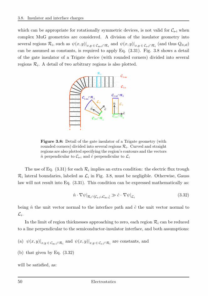
3.8. Insulator and interface charges
which can be appropriate for rotationally symmetric devices, is not valid for Cs-i whencomplex MuG geometries are considered. A division of the insulator geometry into
several regions Ri, such as ψ(x, y)|x,y ∈ Cm-i∩Riand ψ(x, y)|x,y ∈ Cs-i∩Ri
(and thus Qit,sf)
can be assumed as constants, is required to apply Eq. (3.31). Fig. 3.8 shows a detail
of the gate insulator of a Trigate device (with rounded corners) divided into several
regions Ri. A detail of two arbitrary regions is also plotted.
L
C
C
i-m
i-s
i
C i-s\ Ri
Ci-m
\ Ri
Li
Ci-m\ Ri
Ci-s\ Ri
n c
c
n
Ri
Figure 3.8: Detail of the gate insulator of a Trigate geometry (withrounded corners) divided into several regions Ri. Curved and straightregions are also plotted specifying the region’s contours and the vectorsn perpendicular to Cs-i and c perpendicular to Li
The use of Eq. (3.31) for each Ri implies an extra condition: the electric flux trough
Ri lateral boundaries, labeled as Li in Fig. 3.8, must be negligible. Otherwise, Gauss
law will not result into Eq. (3.31). This condition can be expressed mathematically as:
n · ∇ψ|Ri∩[Cs-i∪Cm-i]≫ c · ∇ψ|Li
(3.32)
being n the unit vector normal to the interface path and c the unit vector normal to
Li.In the limit of region thicknesses approaching to zero, each region Ri can be reduced
to a line perpendicular to the semiconductor-insulator interface, and both assumptions:
(a) ψ(x, y)|x,y ∈ Cm-i∩Riand ψ(x, y)|x,y ∈ Cs-i∩Ri
are constants, and
(b) that given by Eq. (3.32)
will be satisfied, as:
50 Electrostatics
Chapter 3. 2D Schrodinger-Poisson simulator for MuG structures
(a) Cm-i ∩Ri and Cs-i ∩Ri are reduced to points and ψ is a single-valued function, and
(b) ψ is only defined for the coordinate in the n direction, and its derivative in the c
direction must be zero.
However, for a numerical solution using FEM the regions cannot be infinitesimally thin
and finite thickness regions must be defined as SP2D does. Finally, it is worth to note
that Cins,sf in Eq. (3.31) comes from the path integral of the electric field and, therefore,
depends on the region considered.
After discussing the conditions of validity of Eq. (3.31), we now use the Poisson
equation to determine the difference ψ|i-m − ψ|i-s at each Ri as a function of the
volumetric interface charge, Qit,vl. But to be able to get this relationship, we make
first the following premise for a given Ri:
∇‖ψ = 0 (3.33)
where ∇‖ = c · ∇. In other words, ψ just varies (in each region) in the n direction.
This premise is coherent and actually stronger than the one imposed in Eq. (3.32) and
it forces (through Poisson equation):
∇‖Qit,vl = 0 (3.34)
Thus, the differential form of Gauss law for a certain region Ri leads to:
∇⊥ǫins∇⊥ψ = −Qit,vl (3.35)
being ∇⊥ = n · ∇. It is worth to note that ∇⊥ and ∇‖ have been defined as scalar
operators. Moreover, as shown in Fig. 3.8, n cannot be equally treated in regions where
Cs-i ∩Ri is a straight segment and those where it is a curved segment. In the first case
it is not position dependent while in the second case it is. The mathematical procedure
to integrate Eq. (3.35) is detailed in Appendix A. The results are:
ψ|i-m − ψ|i-s =1
ǫins
tins∫
0
dϑ
tins∫
ϑ
Qit,vl(ϑ)dϑ (3.36)
Electrostatics 51
3.8. Insulator and interface charges
for straight segments and
ψ|i-m − ψ|i-s =1
ǫins
ςc+tins∫
ςc
1
ςdς
ςc+tins∫
ς
ςQit,vl(ς)dς (3.37)
for curved segments, where ςc is the radius of the curved segment (SP2D actually
implements curved segments as sections of circumference). Then, using Eq. (3.31), the
relationship between Qit,sf and Qit,vl is given by:
Qit,sftinsǫins
=1
ǫins
tins∫
0
dϑ
tins∫
ϑ
Qit,vl(ϑ)dϑ (3.38)
and:
Qit,sfςcln(1 + tins/ςc)
ǫins=
1
ǫins
ςc+tins∫
ςc
1
ςdς
ςc+tins∫
ς
ςQit,vl(ς)dς (3.39)
for straight and curved segments, respectively. These integral equations are underde-
termined: there is not a unique expression of Qit,vl for a given value of Qit,sf.
As aforementioned, SP2D implements four different Qit,vl profiles: constant, linear,
exponential and Gaussian. The four profiles are defined in a region of thickness to,
being to ≤ tins, and their amplitude is determined by Qit,sf. The expressions for the
Qit,vl profiles, corresponding to linear and curved segment regions are summarized in
Table 3.1.
Profile Straight Curved
Constant Qit,vl(ϑ) = ActeUst(ϑ) Qit,vl(ς) = ActeUcv(ς)
Linear Qit,vl(ϑ) = Alin
(
1− ϑto
)
Ust(ϑ) Qit,vl(ς) = Alin
(
1− ς−ςcto
)
Ucv(ς)
Exponential Qit,vl(ϑ) = Aexpe− ϑ
σeUst(ϑ) Qit,vl(ς) = Aexpe− ς−Rc
σe Ucv(ς)
Gaussian Qit,vl(ϑ) = Agaue− ϑ2
2σ2g Ust(ϑ) Qit,vl(ς) = Agaue
− (ς−ςc)2
2σ2g Ucv(ς)
Table 3.1: Qit,vl profiles implemented by SP2D.
52 Electrostatics
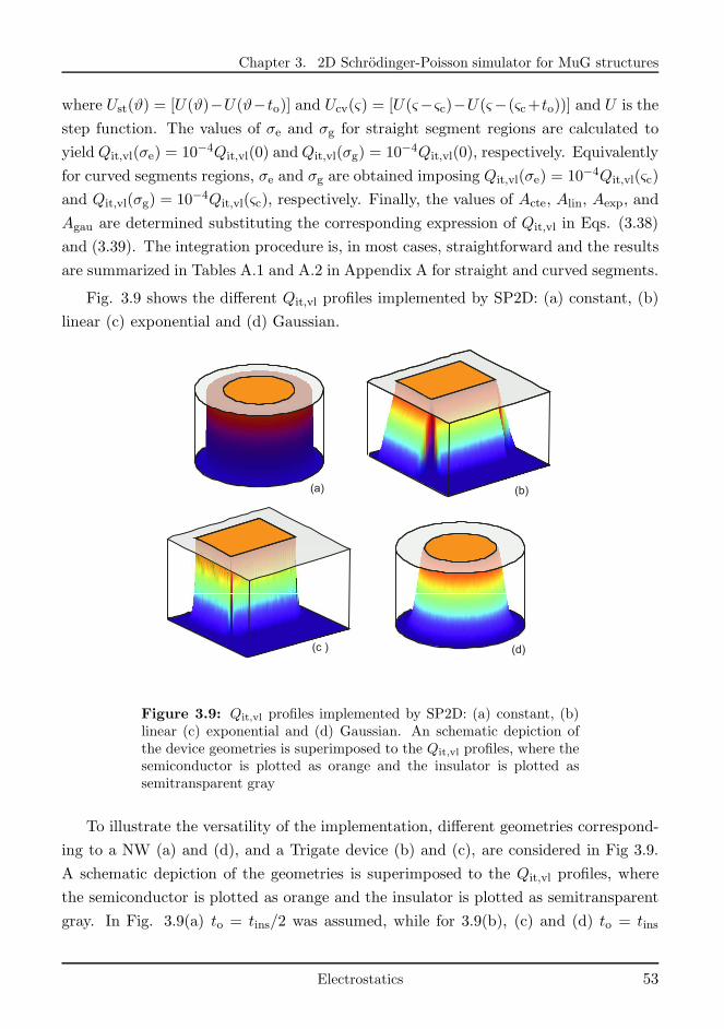
Chapter 3. 2D Schrodinger-Poisson simulator for MuG structures
where Ust(ϑ) = [U(ϑ)−U(ϑ−to)] and Ucv(ς) = [U(ς−ςc)−U(ς−(ςc+to))] and U is the
step function. The values of σe and σg for straight segment regions are calculated to
yield Qit,vl(σe) = 10−4Qit,vl(0) andQit,vl(σg) = 10−4Qit,vl(0), respectively. Equivalently
for curved segments regions, σe and σg are obtained imposing Qit,vl(σe) = 10−4Qit,vl(ςc)
and Qit,vl(σg) = 10−4Qit,vl(ςc), respectively. Finally, the values of Acte, Alin, Aexp, and
Agau are determined substituting the corresponding expression of Qit,vl in Eqs. (3.38)
and (3.39). The integration procedure is, in most cases, straightforward and the results
are summarized in Tables A.1 and A.2 in Appendix A for straight and curved segments.
Fig. 3.9 shows the different Qit,vl profiles implemented by SP2D: (a) constant, (b)
linear (c) exponential and (d) Gaussian.
(a) (b)
(c ) (d)
Figure 3.9: Qit,vl profiles implemented by SP2D: (a) constant, (b)linear (c) exponential and (d) Gaussian. An schematic depiction ofthe device geometries is superimposed to the Qit,vl profiles, where thesemiconductor is plotted as orange and the insulator is plotted assemitransparent gray
To illustrate the versatility of the implementation, different geometries correspond-
ing to a NW (a) and (d), and a Trigate device (b) and (c), are considered in Fig 3.9.
A schematic depiction of the geometries is superimposed to the Qit,vl profiles, where
the semiconductor is plotted as orange and the insulator is plotted as semitransparent
gray. In Fig. 3.9(a) to = tins/2 was assumed, while for 3.9(b), (c) and (d) to = tins
Electrostatics 53
3.9. Convergence algorithm
was set. To keep the figure simple, we have assumed a constant potential along the
insulator-semiconductor interface and the same Dit energy profile for all regions.
3.9 Convergence algorithm
The wavefunctions, ξi, and energy levels, Ei obtained from Schrodinger equation de-
termine the electron concentration, n. But n enters in the Poisson equation. Then,
the Poisson solution for the potential, ψ, is translated into potential energy φ = −qψ(where the potential barrier ∆φ must be added in the insulator). φ is part of the
Hamiltonian of the Schrodinger equation and affects the resulting eigenfunctions, ξi,
and eigenvalues, Ei.
Thus, the equation system must be solved self-consistently. However, a simple
iteration rarely converges. One common alternative scheme is underrelaxing the solu-
tion for the electron concentration. Then, for each iteration n is expressed as n(j) =
υ(j)n(j) + (1 − υ(j))n(j−1), where (j) is the iteration index and υ is an adaptive relax-
ation parameter [107]. However, the election of υ, which is iteration dependent, is not
easy. A large υ(j) results in oscillations while small υ(j) slows the convergence [146].
This problem was solved in a very elegant and illustrative way by Trellakis et al. in
Refs. [147],[148]. They used perturbation theory to determine the electron concen-
tration when a perturbing potential energy was introduced in the Hamiltonian. Using
a suitable approximation for a ratio of Fermi integrals, they found that the electron
concentration in the j-th iteration could be expressed as:
n(x, y) =−qNc
kBT
∑
i
|ξi(x, y)|2F− 12
(
Ei − EF + φ(j)−φ(j−1)
kBT
)
(3.40)
where Nc is the density of states of the conduction band:
Nc =
√
2m∗vkBT
π~2(3.41)
and F− 12is the complete Fermi-Dirac integral [149], [150]. Eq. (3.40) assumes a
parabolic dispersion relation for the conduction band.
We need to adapt this algorithm for the non-parabolic dispersion relation of Eq
(3.21). Trellakis’ approach to the problem defines a perturbation to the potential δψ
such that ψ → ψ + δψ. The Hamiltonian became H → H − qδψ while the energy
54 Electrostatics
Chapter 3. 2D Schrodinger-Poisson simulator for MuG structures
levels and wavefunctions change to Ei → Ei + δEi and ξ → ξ + δξ, respectively; where
δEi = −q〈ξi|δψ|ξi〉.For the non-parabolic case we have:
ENPi = φi + δφi +
−1 +
√
1 + 4βv
(
~2k2
2m∗v+ Ei + δEi − φi − δφi
)2
2βv(3.42)
where using Eq. (3.23) it is straightforward to see that δφi = −q〈ξi|δψ|ξi〉 canceling
out with δEi as defined previously. Then, comparing Eqs. (3.21) and (3.42), we can
conclude that the non-parabolic dispersion relation is transformed by the perturbation
as:
ENPi → ENP
i + δφi → ENPi + δEi (3.43)
The determination of the variation in the electron concentration, δn, due to the per-
turbation potential δφ is equivalent to that proposed in Ref. [147]. We replicate here
only the first step from Trellakis mathematical elaboration to show the equivalence:
n→ n+ δn (3.44)
where δn is obtained as:
δn =∂n
∂ψδψ =
2
π
∂
∂ψ
∑
i
|ξi(x, y)|2∞∫
−∞
1
1 + eEi(k)−EF
kBT
dkδψ = (3.45)
2
π
∑
i
|ξi(x, y)|2∂
∂Ei(k)
∞∫
−∞
1
1 + eEi(k)−EF
kBT
dk∂Ei(k)
∂ψδψ (3.46)
+2
π2∑
i
|ξi(x, y)|∂ξi∂ψ
δψ
∞∫
−∞
1
1 + eEi(k)−EF
kBT
dk (3.47)
where ∂Ei(k)∂ψ δψ and ∂ξi
∂ψ δψ are the perturbation in the non-parabolic dispersion relation
and the wavefunction due to the perturbation in the potential δψ, respectively. We can
rename them as δENPi and δξi. But δE
NPi was determined in Eq. (3.43) as equal to the
Electrostatics 55
3.10. SP2D flow diagram
perturbation of the parabolic energy level δEi. Then:
δn =2
π
∑
i
|ξi(x, y)|2∞∫
−∞
−1
kBT
eEi(k)−EF
kBT
(
1 + eEi(k)−EF
kBT
)2 dk δEi+ (3.48)
2
π2∑
i
|ξi(x, y)|δξi∞∫
−∞
1
1 + eEi(k)−EF
kBT
dk (3.49)
In addition, it is easy to get the equivalence of the derivative given by:
∂
∂Ei(k)
∞∫
−∞
1
1 + eEi(k)−EF
kBT
dk =
∞∫
−∞
−1kBT
eEi(k)−EF
kBT
(
1 + eEi(k)−EF
kBT
)2dk (3.50)
and the derivative of the Fermi Dirac integral particularized for order 0.
∂
∂x
∞∫
0
1
1 + eǫ−xdx =
∞∫
0
−eǫ−x
(1 + eǫ−x)2dx (3.51)
If we assume that the approximation made by Trellakis et al. for the quotient of Fermi
integrals of order −12 and −3
2 is also valid for orders 0 and 1, the procedure to determine
δn with a non-parabolic dispersion relation is equivalent to that for parabolic bands.
Then, we can reformulate the electron density under non-parabolic approximation using
the Trellakis algorithm as:
n(x, y) =2
π
∑
i
|ξi(x, y)|2∞∫
−∞
(
1 + eEi(k)+φ(j)−φ(j−1)−EF
kBT
)−1
dk (3.52)
In the next Section we depict the flow diagram of SP2D including the adapted Trellakis
algorithm.
3.10 SP2D flow diagram
In this Section, we briefly describe the SP2D flow diagram. Fig. 3.10 shows the flow
diagram of a common run of SP2D.
56 Electrostatics
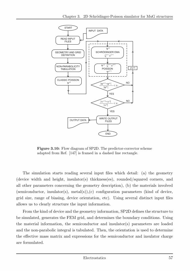
Chapter 3. 2D Schrodinger-Poisson simulator for MuG structures
READ INPUTFILES
GEOMETRY AND GRIDDEFINITION
NON-PARABOLICITYTABULATION
CLASSIC POISSONy (0)
SCHRÖDINGER EMA
POISSONy (j+1)
x(j+1)
E(j+1)
y (j)
x(j+1)
E(j+1)y (j)
|y -(j+1) y |(j)
|y |(j)< ey
|n -(j+1) n |(j)
| |n (j)< en
j=j+1
YES
YES
NO
NO
WRITE OUTPUTFILES
START
END
OUTPUT DATA
INPUT DATA
Figure 3.10: Flow diagram of SP2D. The predictor-corrector schemeadapted from Ref. [147] is framed in a dashed line rectangle.
The simulation starts reading several input files which detail: (a) the geometry
(device width and height, insulator(s) thickness(es), rounded/squared corners, and
all other parameters concerning the geometry description), (b) the materials involved
(semiconductor, insulator(s), metal(s)),(c) configuration parameters (kind of device,
grid size, range of biasing, device orientation, etc). Using several distinct input files
allows us to clearly structure the input information.
From the kind of device and the geometry information, SP2D defines the structure to
be simulated, generates the FEM grid, and determines the boundary conditions. Using
the material information, the semiconductor and insulator(s) parameters are loaded
and the non-parabolic integral is tabulated. Then, the orientation is used to determine
the effective mass matrix and expressions for the semiconductor and insulator charge
are formulated.
Electrostatics 57
3.11. Conclusions
Next step is the self-consistent solutions of the Schrodinger and Poisson equations.
A first solution for the potential is obtained using a classical approximation. After
that, SP2D enters in the predictor-corrector scheme adapted from Trellakis which for
the iteration (j+1) can be summarized as:
(a) Solve the Schrodinger equation using the solution for ψ(j) obtained from previous
Poisson iteration (ψ(0) is obtained from a classical simulation). That provides ξ(j+1)i
and E(j+1)i .
(b) Solve the non-linear Poisson equation using ξ(j+1)i , E
(j+1)i , ψ(j) into the electron
concentration expression given by Eq. (3.52). That gives ψ(j+1).
(c) Check the convergence criteria and come back to step (a) or continua.
Fig. 3.10 frames the predictor-corrector algorithm in dashed line. We use a double
convergence criteria: for the potential and the electron concentration. As they are
spatial dependent magnitudes we look for the worst case:
max∣
∣ψ(j) − ψ(j+1)∣
∣
max∣
∣ψ(j)∣
∣
< εψ (3.53)
max∣
∣n(j) − n(j+1)∣
∣
max∣
∣n(j)∣
∣
< εn (3.54)
where ǫψ and ǫn are convergence thresholds set to 10−4. Once the convergence has been
achieved, SP2D save all the results calculated in an output file and the run is ended.
3.11 Conclusions
In this Chapter, a self-consistent Schrodinger-Poisson solver was developed, which is
able to deal with arbitrary geometries, materials and orientations to achieve the charge
and potential distribution in the cross-section of a MuG structure. A non-parabolic
effective mass approach was employed for the Schrodinger equation, and the contribu-
tion of Γ, X (∆ for Silicon) and L valleys was included. In addition, the developed
simulator allowed the inclusion of arbitrary profile of interface states.
58 Electrostatics
Chapter 4
Electrostatic analysis of MuG
devices using SP2D
4.1 Introduction
In this chapter we apply SP2D to the study of several relevant electrostatic magnitudes
in MuG architectures. Specifically, here we focus on two structures, Trigates and NWs
due to their technological performance. The Trigate architecture introduces the fewest
changes to conventional planar transistor processing, while allowing a very good control
of the channel [151]. Indeed, as aforementioned Intelr has recently taken to production
microprocessors based on the Trigate architecture on bulk wafers [60]. Meanwhile,
NW FETs, first experimentally achieved by IBMr [79], have demonstrated superior
electrostatic control of the channel thanks to their surrounding gate.
In addition to the geometrical versatility of SP2D, we make use of its non-parabolic
dispersion relation description to study, besides SOI substrates, III-V materials. Other
characteristics of SP2D such as arbitrary orientation and the inclusion of interface
states are also exploited in the five electrostatic studies performed in this Chapter.
The rest of this Chapter is organized as follows. In Section 4.2 we compare SP2D
results with those obtained from a two-bands k · p simulator and we validate SP2D
using experimental data taken from a Trigate architecture. In Section 4.3 we focus on
the study of III-V NWs. In particular we analyze the population of satellite valleys of
different III-V semiconductors and we briefly discuss their implications on the conduc-
tion effective mass and the gate capacitance. In Sections 4.4 and 4.5 a comparative
Electrostatics 59
4.2. Validation of SP2D
study of III-V and Si MuG architectures is performed. Thus, Section 4.4 is focused
on the performance of III-V and SOI Trigates as a function of the device width while
Section 4.5 compares DG and Trigate architectures, emphasizing the need of 2D stud-
ies to achieve a proper understanding of Trigate behavior. Sections 4.6 and 4.7 pay
attention to SOI Trigate architectures. Section 4.6 deals with the effect of back gate
bias on VT and analyze the body effect. In Section 4.7 we analyze the influence of Dit
on the threshold voltage, VT, and subthreshold swing, SS, of MuG structures. Finally,
Section 4.8 sums up some conclusions.
4.2 Validation of SP2D, non-parabolic EMA and semicon-
ductor parameters
In this Section we validate the SP2D simulator presented in Chapter 3 justifying its
use in the electrostatic studies proposed in subsequent Sections.
First we check the EMA for the electrons. To do so, the results from SP2D are
compared to those obtained from a two-band k · p simulator also implemented in the
Nanoelectronics Research Group [152]. Fig 4.1 shows the linear electron concentration,
Ni, as a function of the applied gate voltage, Vg, for several Si-SiO2 cylindrical NWs
(see Fig. 4.2 for a schematic depiction) with sizes ranging from 3nm to 10nm and
tins = 1nm. Two transport orientations have been considered (a) < [111] and (b) [110].
EMA non-parabolic results are plotted as dashed lines while k · p results are plotted as
solid lines.
As can be seen in Fig. 4.1, the non-parabolic SP2D accurately reproduces the results
for all NWs sizes in both orientations. Only for the smallest size there is slight difference
in the results between EMA and k · p. This result is in good correspondence with other
validations of EMA pointed out in the literature [153]. The non-parabolicity parameter
of Si is small, β∆ = 0.5eV−1, and therefore Si does not imply a very disadvantageous
scenario for parabolic EMA. For this reason, and in order to keep it clear, we have not
plotted parabolic EMA results on Fig. 4.1.
In contrast if III-V semiconductors are considered, the non-parabolic factor is higher
and the differences between parabolic and non-parabolic dispersion relation results are
larger. Fig. 4.3 presents Ni versus Vg for (a) InAs and (b) GaAs cylindrical NWs with
Rs = 5nm (circles) and Rs = 15nm (squares) considering parabolic (dashed) and non-
parabolic dispersion relations (solid). Al2O3 with tins = 2nm was employed as insulator
60 Electrostatics
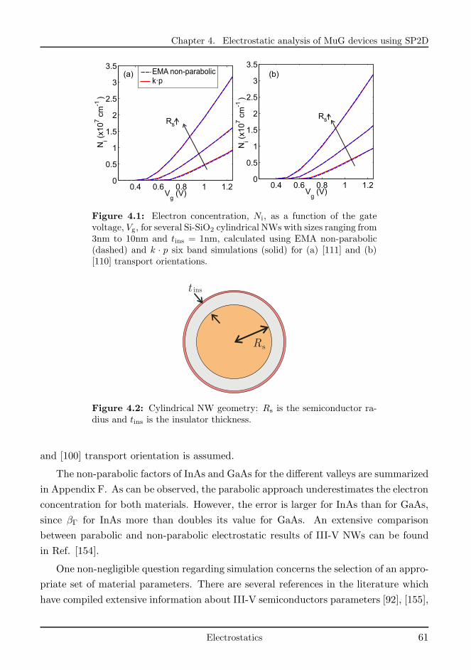
Chapter 4. Electrostatic analysis of MuG devices using SP2D
0.4 0.6 0.8 1 1.20
0.5
1
1.5
2
2.5
3
3.5
Vg
(V)
Ni(x
10
7cm
-1)
0.4 0.6 0.8 1 1.20
0.5
1
1.5
2
2.5
3
3.5
Vg
(V)
Ni(x
10
7cm
-1)
(b)(a) EMA non-parabolick·p
RsRs
Figure 4.1: Electron concentration, Ni, as a function of the gatevoltage, Vg, for several Si-SiO2 cylindrical NWs with sizes ranging from3nm to 10nm and tins = 1nm, calculated using EMA non-parabolic(dashed) and k · p six band simulations (solid) for (a) [111] and (b)[110] transport orientations.
R
inst
s
Figure 4.2: Cylindrical NW geometry: Rs is the semiconductor ra-dius and tins is the insulator thickness.
and [100] transport orientation is assumed.
The non-parabolic factors of InAs and GaAs for the different valleys are summarized
in Appendix F. As can be observed, the parabolic approach underestimates the electron
concentration for both materials. However, the error is larger for InAs than for GaAs,
since βΓ for InAs more than doubles its value for GaAs. An extensive comparison
between parabolic and non-parabolic electrostatic results of III-V NWs can be found
in Ref. [154].
One non-negligible question regarding simulation concerns the selection of an appro-
priate set of material parameters. There are several references in the literature which
have compiled extensive information about III-V semiconductors parameters [92], [155],
Electrostatics 61
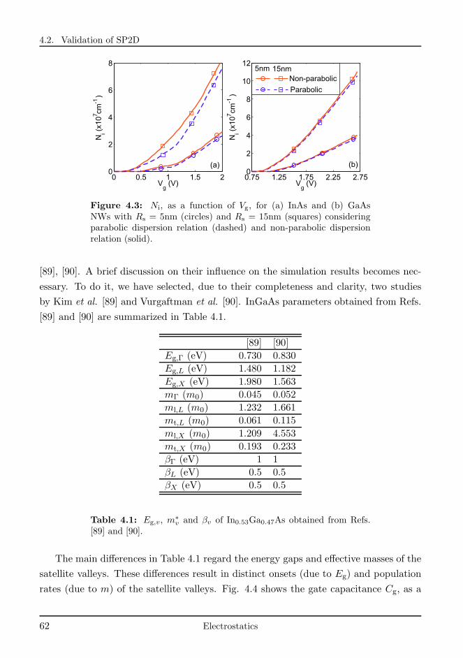
4.2. Validation of SP2D
0 0.5 1 1.5 20
2
4
6
8
Vg
(V)
Ni(x
10
7 cm-1
)
0.75 1.25 1.75 2.25 2.750
2
4
6
8
10
12
Vg
(V)
Ni(x
10
7cm
-1)
5nm
Parabolic
Non-parabolic15nm
(a) (b)
Figure 4.3: Ni, as a function of Vg, for (a) InAs and (b) GaAsNWs with Rs = 5nm (circles) and Rs = 15nm (squares) consideringparabolic dispersion relation (dashed) and non-parabolic dispersionrelation (solid).
[89], [90]. A brief discussion on their influence on the simulation results becomes nec-
essary. To do it, we have selected, due to their completeness and clarity, two studies
by Kim et al. [89] and Vurgaftman et al. [90]. InGaAs parameters obtained from Refs.
[89] and [90] are summarized in Table 4.1.
[89] [90]
Eg,Γ (eV) 0.730 0.830
Eg,L (eV) 1.480 1.182
Eg,X (eV) 1.980 1.563
mΓ (m0) 0.045 0.052
ml,L (m0) 1.232 1.661
mt,L (m0) 0.061 0.115
ml,X (m0) 1.209 4.553
mt,X (m0) 0.193 0.233
βΓ (eV) 1 1
βL (eV) 0.5 0.5
βX (eV) 0.5 0.5
Table 4.1: Eg,v, m∗
v and βv of In0.53Ga0.47As obtained from Refs.[89] and [90].
The main differences in Table 4.1 regard the energy gaps and effective masses of the
satellite valleys. These differences result in distinct onsets (due to Eg) and population
rates (due to m) of the satellite valleys. Fig. 4.4 shows the gate capacitance Cg, as a
62 Electrostatics
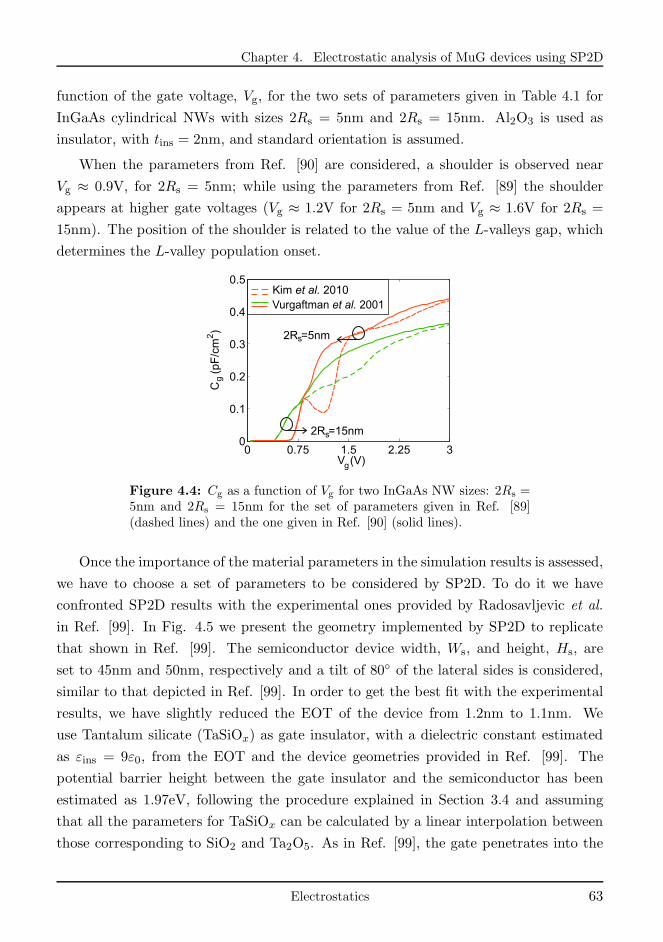
Chapter 4. Electrostatic analysis of MuG devices using SP2D
function of the gate voltage, Vg, for the two sets of parameters given in Table 4.1 for
InGaAs cylindrical NWs with sizes 2Rs = 5nm and 2Rs = 15nm. Al2O3 is used as
insulator, with tins = 2nm, and standard orientation is assumed.
When the parameters from Ref. [90] are considered, a shoulder is observed near
Vg ≈ 0.9V, for 2Rs = 5nm; while using the parameters from Ref. [89] the shoulder
appears at higher gate voltages (Vg ≈ 1.2V for 2Rs = 5nm and Vg ≈ 1.6V for 2Rs =
15nm). The position of the shoulder is related to the value of the L-valleys gap, which
determines the L-valley population onset.
0 0.75 1.5 2.25 30
0.1
0.2
0.3
0.4
0.5
Vg(V)
Cg
(pF
/cm
2)
Vurgaftman 2001et al.
Kim 2010et al.
2R =5nm
2R =15nm
s
s
Figure 4.4: Cg as a function of Vg for two InGaAs NW sizes: 2Rs =5nm and 2Rs = 15nm for the set of parameters given in Ref. [89](dashed lines) and the one given in Ref. [90] (solid lines).
Once the importance of the material parameters in the simulation results is assessed,
we have to choose a set of parameters to be considered by SP2D. To do it we have
confronted SP2D results with the experimental ones provided by Radosavljevic et al.
in Ref. [99]. In Fig. 4.5 we present the geometry implemented by SP2D to replicate
that shown in Ref. [99]. The semiconductor device width, Ws, and height, Hs, are
set to 45nm and 50nm, respectively and a tilt of 80 of the lateral sides is considered,
similar to that depicted in Ref. [99]. In order to get the best fit with the experimental
results, we have slightly reduced the EOT of the device from 1.2nm to 1.1nm. We
use Tantalum silicate (TaSiOx) as gate insulator, with a dielectric constant estimated
as εins = 9ε0, from the EOT and the device geometries provided in Ref. [99]. The
potential barrier height between the gate insulator and the semiconductor has been
estimated as 1.97eV, following the procedure explained in Section 3.4 and assuming
that all the parameters for TaSiOx can be calculated by a linear interpolation between
those corresponding to SiO2 and Ta2O5. As in Ref. [99], the gate penetrates into the
Electrostatics 63
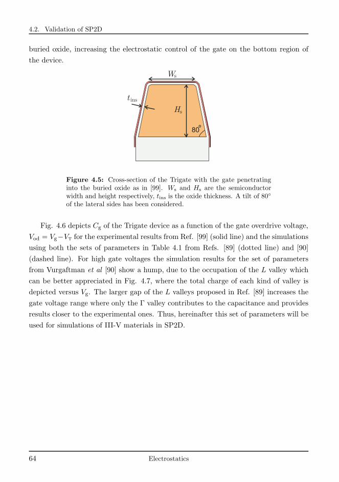
4.2. Validation of SP2D
buried oxide, increasing the electrostatic control of the gate on the bottom region of
the device.
80
H
W
s
s
t ins
º
Figure 4.5: Cross-section of the Trigate with the gate penetratinginto the buried oxide as in [99]. Ws and Hs are the semiconductorwidth and height respectively, tins is the oxide thickness. A tilt of 80
of the lateral sides has been considered.
Fig. 4.6 depicts Cg of the Trigate device as a function of the gate overdrive voltage,
Vod = Vg−VT for the experimental results from Ref. [99] (solid line) and the simulations
using both the sets of parameters in Table 4.1 from Refs. [89] (dotted line) and [90]
(dashed line). For high gate voltages the simulation results for the set of parameters
from Vurgaftman et al [90] show a hump, due to the occupation of the L valley which
can be better appreciated in Fig. 4.7, where the total charge of each kind of valley is
depicted versus Vg. The larger gap of the L valleys proposed in Ref. [89] increases the
gate voltage range where only the Γ valley contributes to the capacitance and provides
results closer to the experimental ones. Thus, hereinafter this set of parameters will be
used for simulations of III-V materials in SP2D.
64 Electrostatics
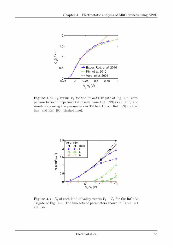
Chapter 4. Electrostatic analysis of MuG devices using SP2D
-0.25 0 0.25 0.5 0.75 10
0.5
1
1.5
2
Vg-VT (V)
Cg( m
F/c
m)
Exper. Rad. 2010et al.
Kim 2010et al.
Vurg. 2001et al.
Figure 4.6: Cg versus Vg for the InGaAs Trigate of Fig. 4.5: com-parison between experimental results from Ref. [99] (solid line) andsimulations using the parameters in Table 4.1 from Ref. [89] (dottedline) and Ref. [90] (dashed line).
0 0.5 1 1.50
0.5
1
1.5
2
2.5
Vg -VT(V)
Ni(x
10
8 cm-1
)
KimTotal
X
ΓL
Vurg.
Figure 4.7: Ni of each kind of valley versus Vg − VT for the InGaAsTrigate of Fig. 4.5. The two sets of parameters shown in Table. 4.1are used.
Electrostatics 65
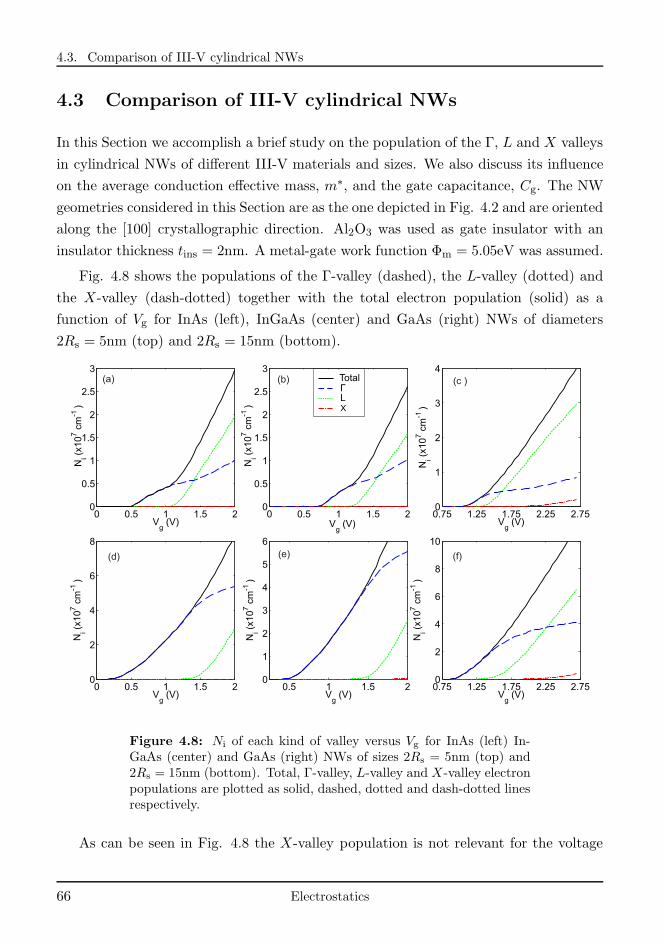
4.3. Comparison of III-V cylindrical NWs
4.3 Comparison of III-V cylindrical NWs
In this Section we accomplish a brief study on the population of the Γ, L and X valleys
in cylindrical NWs of different III-V materials and sizes. We also discuss its influence
on the average conduction effective mass, m∗, and the gate capacitance, Cg. The NW
geometries considered in this Section are as the one depicted in Fig. 4.2 and are oriented
along the [100] crystallographic direction. Al2O3 was used as gate insulator with an
insulator thickness tins = 2nm. A metal-gate work function Φm = 5.05eV was assumed.
Fig. 4.8 shows the populations of the Γ-valley (dashed), the L-valley (dotted) and
the X-valley (dash-dotted) together with the total electron population (solid) as a
function of Vg for InAs (left), InGaAs (center) and GaAs (right) NWs of diameters
2Rs = 5nm (top) and 2Rs = 15nm (bottom).
0 0.5 1 1.5 20
2
4
6
8
Vg
(V)
Ni(x
10
7cm
-1)
0.5 1 1.5 20
1
2
3
4
5
6
Vg
(V)
Ni(x
10
7cm
-1)
0 0.5 1 1.5 20
0.5
1
1.5
2
2.5
3
Vg
(V)
Ni(x
10
7cm
-1)
0 0.5 1 1.5 20
0.5
1
1.5
2
2.5
3
0.75 1.25 1.75 2.25 2.750
1
2
3
4
Vg
(V)
Ni(x
10
7cm
-1)
0.75 1.25 1.75 2.25 2.750
2
4
6
8
10
Vg
(V)
Ni(x
10
7cm
-1)
Total
X
ΓL
(a) (b) (c )
(d) (e) (f)
Ni(x
10
7cm
-1)
Vg
(V)
Figure 4.8: Ni of each kind of valley versus Vg for InAs (left) In-GaAs (center) and GaAs (right) NWs of sizes 2Rs = 5nm (top) and2Rs = 15nm (bottom). Total, Γ-valley, L-valley and X-valley electronpopulations are plotted as solid, dashed, dotted and dash-dotted linesrespectively.
As can be seen in Fig. 4.8 the X-valley population is not relevant for the voltage
66 Electrostatics
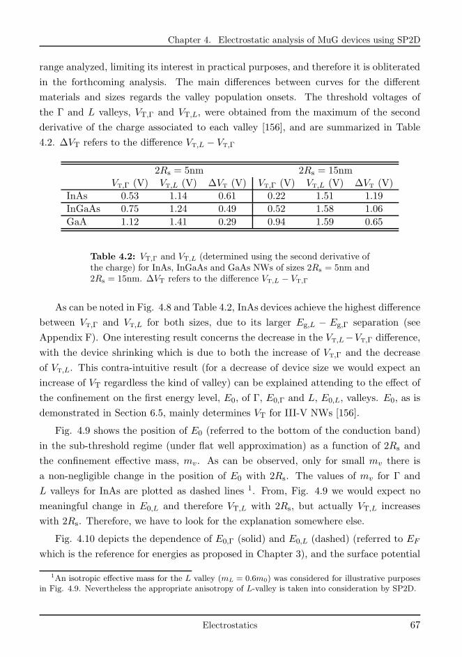
Chapter 4. Electrostatic analysis of MuG devices using SP2D
range analyzed, limiting its interest in practical purposes, and therefore it is obliterated
in the forthcoming analysis. The main differences between curves for the different
materials and sizes regards the valley population onsets. The threshold voltages of
the Γ and L valleys, VT,Γ and VT,L, were obtained from the maximum of the second
derivative of the charge associated to each valley [156], and are summarized in Table
4.2. ∆VT refers to the difference VT,L − VT,Γ
2Rs = 5nm 2Rs = 15nmVT,Γ (V) VT,L (V) ∆VT (V) VT,Γ (V) VT,L (V) ∆VT (V)
InAs 0.53 1.14 0.61 0.22 1.51 1.19
InGaAs 0.75 1.24 0.49 0.52 1.58 1.06
GaA 1.12 1.41 0.29 0.94 1.59 0.65
Table 4.2: VT,Γ and VT,L (determined using the second derivative ofthe charge) for InAs, InGaAs and GaAs NWs of sizes 2Rs = 5nm and2Rs = 15nm. ∆VT refers to the difference VT,L − VT,Γ
As can be noted in Fig. 4.8 and Table 4.2, InAs devices achieve the highest difference
between VT,Γ and VT,L for both sizes, due to its larger Eg,L − Eg,Γ separation (see
Appendix F). One interesting result concerns the decrease in the VT,L−VT,Γ difference,
with the device shrinking which is due to both the increase of VT,Γ and the decrease
of VT,L. This contra-intuitive result (for a decrease of device size we would expect an
increase of VT regardless the kind of valley) can be explained attending to the effect of
the confinement on the first energy level, E0, of Γ, E0,Γ and L, E0,L, valleys. E0, as is
demonstrated in Section 6.5, mainly determines VT for III-V NWs [156].
Fig. 4.9 shows the position of E0 (referred to the bottom of the conduction band)
in the sub-threshold regime (under flat well approximation) as a function of 2Rs and
the confinement effective mass, mv. As can be observed, only for small mv there is
a non-negligible change in the position of E0 with 2Rs. The values of mv for Γ and
L valleys for InAs are plotted as dashed lines 1. From, Fig. 4.9 we would expect no
meaningful change in E0,L and therefore VT,L with 2Rs, but actually VT,L increases
with 2Rs. Therefore, we have to look for the explanation somewhere else.
Fig. 4.10 depicts the dependence of E0,Γ (solid) and E0,L (dashed) (referred to EF
which is the reference for energies as proposed in Chapter 3), and the surface potential
1An isotropic effective mass for the L valley (mL = 0.6m0) was considered for illustrative purposesin Fig. 4.9. Nevertheless the appropriate anisotropy of L-valley is taken into consideration by SP2D.
Electrostatics 67
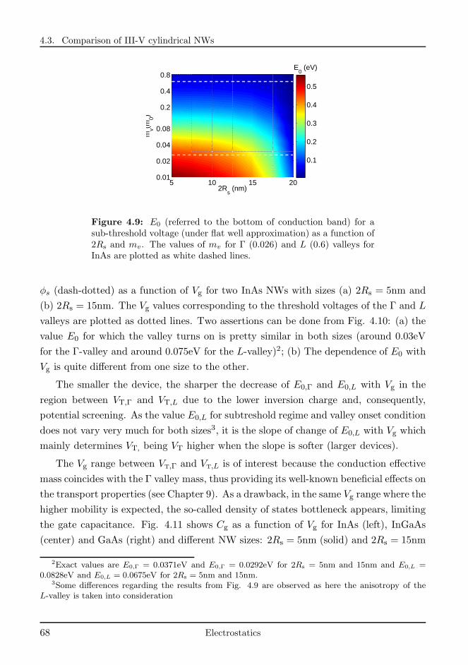
4.3. Comparison of III-V cylindrical NWs
5 10 15 200.01
0.02
0.04
0.08
0.2
0.4
0.8
2Rs (nm)
mv(m
0)
E0 (eV)
0.1
0.2
0.3
0.4
0.5
Figure 4.9: E0 (referred to the bottom of conduction band) for asub-threshold voltage (under flat well approximation) as a function of2Rs and mv. The values of mv for Γ (0.026) and L (0.6) valleys forInAs are plotted as white dashed lines.
φs (dash-dotted) as a function of Vg for two InAs NWs with sizes (a) 2Rs = 5nm and
(b) 2Rs = 15nm. The Vg values corresponding to the threshold voltages of the Γ and L
valleys are plotted as dotted lines. Two assertions can be done from Fig. 4.10: (a) the
value E0 for which the valley turns on is pretty similar in both sizes (around 0.03eV
for the Γ-valley and around 0.075eV for the L-valley)2; (b) The dependence of E0 with
Vg is quite different from one size to the other.
The smaller the device, the sharper the decrease of E0,Γ and E0,L with Vg in the
region between VT,Γ and VT,L due to the lower inversion charge and, consequently,
potential screening. As the value E0,L for subtreshold regime and valley onset condition
does not vary very much for both sizes3, it is the slope of change of E0,L with Vg which
mainly determines VT, being VT higher when the slope is softer (larger devices).
The Vg range between VT,Γ and VT,L is of interest because the conduction effective
mass coincides with the Γ valley mass, thus providing its well-known beneficial effects on
the transport properties (see Chapter 9). As a drawback, in the same Vg range where the
higher mobility is expected, the so-called density of states bottleneck appears, limiting
the gate capacitance. Fig. 4.11 shows Cg as a function of Vg for InAs (left), InGaAs
(center) and GaAs (right) and different NW sizes: 2Rs = 5nm (solid) and 2Rs = 15nm
2Exact values are E0,Γ = 0.0371eV and E0,Γ = 0.0292eV for 2Rs = 5nm and 15nm and E0,L =0.0828eV and E0,L = 0.0675eV for 2Rs = 5nm and 15nm.
3Some differences regarding the results from Fig. 4.9 are observed as here the anisotropy of theL-valley is taken into consideration
68 Electrostatics
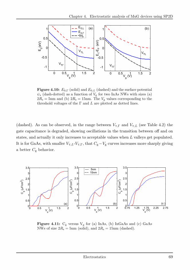
Chapter 4. Electrostatic analysis of MuG devices using SP2D
0 0.5 1 1.5 2
-1
-0.5
0
0.5
1
Vg
(V)
E0(e
V)
0 0.5 1 1.5 2
-1
-0.5
0
0.5
1
Vg
(V)
E
0,ΓE0,L (b)(a)
VTΓ
VTL
VTΓ
VTLE1-E
F(e
V)
-qys
Figure 4.10: E0,Γ (solid) and E0,L (dashed) and the surface potentialψs (dash-dotted) as a function of Vg for two InAs NWs with sizes (a)2Rs = 5nm and (b) 2Rs = 15nm. The Vg values corresponding to thethreshold voltages of the Γ and L are plotted as dotted lines.
(dashed). As can be observed, in the range between VT,Γ and VT,L (see Table 4.2) the
gate capacitance is degraded, showing oscillations in the transition between off and on
states, and actually it only increases to acceptable values when L valleys get populated.
It is for GaAs, with smaller VT,L-VT,Γ, that Cg−Vg curves increases more sharply giving
a better Cg behavior.
0 0.5 1 1.5 20
0.5
1
1.5
2
2.5
3
3.5
Vg
(V)
Cg
(mF
/cm
2)
0 0.5 1 1.5 20
0.5
1
1.5
2
2.5
3
3.5
Vg
(V)
Cg
(mF
/cm
2)
0.75 1.25 1.75 2.25 2.750
0.5
1
1.5
2
2.5
3
3.5
Vg
(V)
Cg
(mF
/cm
2)
15nm5nm
(a) (b) (c )
Figure 4.11: Cg versus Vg for (a) InAs, (b) InGaAs and (c) GaAsNWs of size 2Rs = 5nm (solid), and 2Rs = 15nm (dashed).
Electrostatics 69
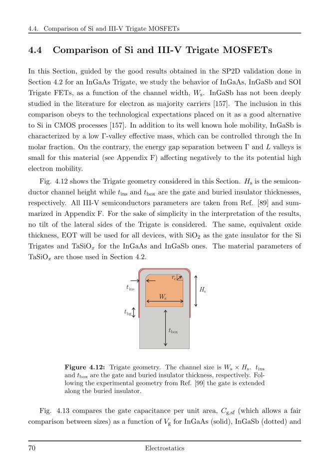
4.4. Comparison of Si and III-V Trigate MOSFETs
4.4 Comparison of Si and III-V Trigate MOSFETs
In this Section, guided by the good results obtained in the SP2D validation done in
Section 4.2 for an InGaAs Trigate, we study the behavior of InGaAs, InGaSb and SOI
Trigate FETs, as a function of the channel width, Ws. InGaSb has not been deeply
studied in the literature for electron as majority carriers [157]. The inclusion in this
comparison obeys to the technological expectations placed on it as a good alternative
to Si in CMOS processes [157]. In addition to its well known hole mobility, InGaSb is
characterized by a low Γ-valley effective mass, which can be controlled through the In
molar fraction. On the contrary, the energy gap separation between Γ and L valleys is
small for this material (see Appendix F) affecting negatively to the its potential high
electron mobility.
Fig. 4.12 shows the Trigate geometry considered in this Section. Hs is the semicon-
ductor channel height while tins and tbox are the gate and buried insulator thicknesses,
respectively. All III-V semiconductors parameters are taken from Ref. [89] and sum-
marized in Appendix F. For the sake of simplicity in the interpretation of the results,
no tilt of the lateral sides of the Trigate is considered. The same, equivalent oxide
thickness, EOT will be used for all devices, with SiO2 as the gate insulator for the Si
Trigates and TaSiOx for the InGaAs and InGaSb ones. The material parameters of
TaSiOx are those used in Section 4.2.
tbox
t ins
Ws
Hs
tbg
rc
Figure 4.12: Trigate geometry. The channel size is Ws × Hs. tinsand tbox are the gate and buried insulator thickness, respectively. Fol-lowing the experimental geometry from Ref. [99] the gate is extendedalong the buried insulator.
Fig. 4.13 compares the gate capacitance per unit area, Cg,sf (which allows a fair
comparison between sizes) as a function of Vg for InGaAs (solid), InGaSb (dotted) and
70 Electrostatics
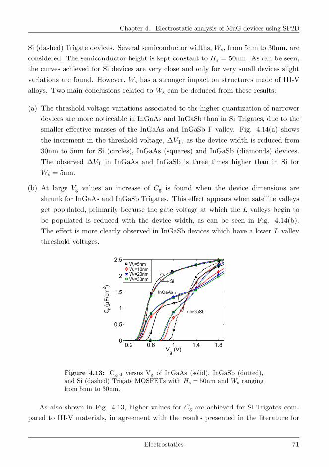
Chapter 4. Electrostatic analysis of MuG devices using SP2D
Si (dashed) Trigate devices. Several semiconductor widths, Ws, from 5nm to 30nm, are
considered. The semiconductor height is kept constant to Hs = 50nm. As can be seen,
the curves achieved for Si devices are very close and only for very small devices slight
variations are found. However, Ws has a stronger impact on structures made of III-V
alloys. Two main conclusions related to Ws can be deduced from these results:
(a) The threshold voltage variations associated to the higher quantization of narrower
devices are more noticeable in InGaAs and InGaSb than in Si Trigates, due to the
smaller effective masses of the InGaAs and InGaSb Γ valley. Fig. 4.14(a) shows
the increment in the threshold voltage, ∆VT, as the device width is reduced from
30nm to 5nm for Si (circles), InGaAs (squares) and InGaSb (diamonds) devices.
The observed ∆VT in InGaAs and InGaSb is three times higher than in Si for
Ws = 5nm.
(b) At large Vg values an increase of Cg is found when the device dimensions are
shrunk for InGaAs and InGaSb Trigates. This effect appears when satellite valleys
get populated, primarily because the gate voltage at which the L valleys begin to
be populated is reduced with the device width, as can be seen in Fig. 4.14(b).
The effect is more clearly observed in InGaSb devices which have a lower L valley
threshold voltages.
0.2 0.6 1 1.4 1.80
0.5
1
1.5
2
2.5
Vg
(V)
Cg(m
F/c
m2)
W =30nmW =20nmW =10nmW =5nm
InGaSb
Si
InGaAs
s
s
s
s
Figure 4.13: Cg,sf versus Vg of InGaAs (solid), InGaSb (dotted),and Si (dashed) Trigate MOSFETs with Hs = 50nm and Ws rangingfrom 5nm to 30nm.
As also shown in Fig. 4.13, higher values for Cg are achieved for Si Trigates com-
pared to III-V materials, in agreement with the results presented in the literature for
Electrostatics 71
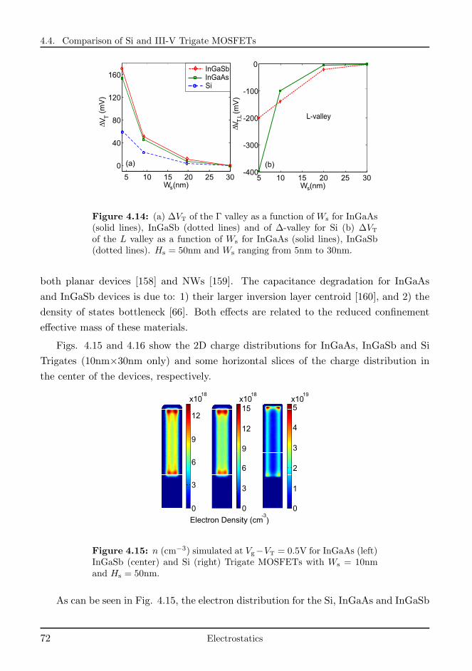
4.4. Comparison of Si and III-V Trigate MOSFETs
5 10 15 20 25 30
0
40
80
120
160
W (nm)
∆V
T(m
V)
5 10 15 20 25 30-400
-300
-200
-100
0
W (nm)
∆V T,
L(m
V)
SiInGaAsInGaSb
L-valley
(a) (b)
s s
Figure 4.14: (a) ∆VT of the Γ valley as a function of Ws for InGaAs(solid lines), InGaSb (dotted lines) and of ∆-valley for Si (b) ∆VT
of the L valley as a function of Ws for InGaAs (solid lines), InGaSb(dotted lines). Hs = 50nm and Ws ranging from 5nm to 30nm.
both planar devices [158] and NWs [159]. The capacitance degradation for InGaAs
and InGaSb devices is due to: 1) their larger inversion layer centroid [160], and 2) the
density of states bottleneck [66]. Both effects are related to the reduced confinement
effective mass of these materials.
Figs. 4.15 and 4.16 show the 2D charge distributions for InGaAs, InGaSb and Si
Trigates (10nm×30nm only) and some horizontal slices of the charge distribution in
the center of the devices, respectively.
6
9
12
0
6
9
12
0
3
15
1
3
4
5
2
x1018
x1018
x1019
Electron Density (cm-3
0
)
3
Figure 4.15: n (cm−3) simulated at Vg−VT = 0.5V for InGaAs (left)InGaSb (center) and Si (right) Trigate MOSFETs with Ws = 10nmand Hs = 50nm.
As can be seen in Fig. 4.15, the electron distribution for the Si, InGaAs and InGaSb
72 Electrostatics
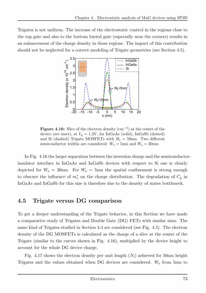
Chapter 4. Electrostatic analysis of MuG devices using SP2D
Trigates is not uniform. The increase of the electrostatic control in the regions close to
the top gate and also to the bottom buried gate (especially near the corners) results in
an enhancement of the charge density in those regions. The impact of this contribution
should not be neglected for a correct modeling of Trigate geometries (see Section 4.5).
-20 -15 -10 -5 0 5 10 15 200
0.5
1
1.5
2
2.5
3
3.5
x (nm)
Ele
ctro
n d
en
sity
(x
10
19
cm-3
)SiInGaAsInGaSb
W =30nm
W =5nms
s
Figure 4.16: Slice of the electron density (cm−3) at the center of thedevice (see inset), at Vg = 1.2V, for InGaAs (solid), InGaSb (dotted)and Si (dashed) Trigate MOSFETs with Hs = 50nm. Two differentsemiconductor widths are considered: Ws = 5nm and Ws = 30nm.
In Fig. 4.16 the larger separation between the inversion charge and the semiconductor-
insulator interface in InGaAs and InGaSb devices with respect to Si one is clearly
depicted for Ws = 30nm. For Ws = 5nm the spatial confinement is strong enough
to obscure the influence of m∗v on the charge distribution. The degradation of Cg in
InGaAs and InGaSb for this size is therefore due to the density of states bottleneck.
4.5 Trigate versus DG comparison
To get a deeper understanding of the Trigate behavior, in this Section we have made
a comparative study of Trigates and Double Gate (DG) FETs with similar sizes. The
same kind of Trigates studied in Section 4.4 are considered (see Fig. 4.5). The electron
density of the DG MOSFETs is calculated as the charge of a slice at the center of the
Trigate (similar to the curves shown in Fig. 4.16), multiplied by the device height to
account for the whole DG device charge.
Fig. 4.17 shows the electron density per unit length (Ni) achieved for 50nm height
Trigates and the values obtained when DG devices are considered. Ws from 5nm to
Electrostatics 73
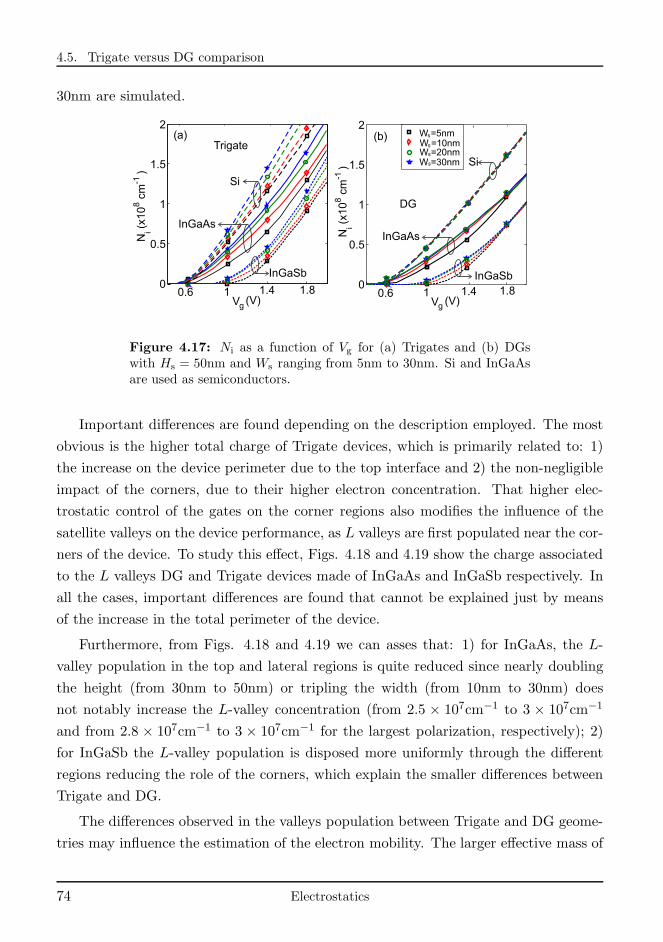
4.5. Trigate versus DG comparison
30nm are simulated.
0.6 1 1.4 1.80
0.5
1
1.5
2
Ni(x
10
8cm
-1)
Vg (V)0.6 1 1.4 1.8
0
0.5
1
1.5
2
Ni(x
10
8cm
-1)
Vg (V)
Trigate
Si
InGaSb
InGaAs
(a)
DG
W =30nmW =20nmW =10nmW =5nm
Si
InGaSb
InGaAs
(b) s
s
s
s
Figure 4.17: Ni as a function of Vg for (a) Trigates and (b) DGswith Hs = 50nm and Ws ranging from 5nm to 30nm. Si and InGaAsare used as semiconductors.
Important differences are found depending on the description employed. The most
obvious is the higher total charge of Trigate devices, which is primarily related to: 1)
the increase on the device perimeter due to the top interface and 2) the non-negligible
impact of the corners, due to their higher electron concentration. That higher elec-
trostatic control of the gates on the corner regions also modifies the influence of the
satellite valleys on the device performance, as L valleys are first populated near the cor-
ners of the device. To study this effect, Figs. 4.18 and 4.19 show the charge associated
to the L valleys DG and Trigate devices made of InGaAs and InGaSb respectively. In
all the cases, important differences are found that cannot be explained just by means
of the increase in the total perimeter of the device.
Furthermore, from Figs. 4.18 and 4.19 we can asses that: 1) for InGaAs, the L-
valley population in the top and lateral regions is quite reduced since nearly doubling
the height (from 30nm to 50nm) or tripling the width (from 10nm to 30nm) does
not notably increase the L-valley concentration (from 2.5 × 107cm−1 to 3 × 107cm−1
and from 2.8 × 107cm−1 to 3 × 107cm−1 for the largest polarization, respectively); 2)
for InGaSb the L-valley population is disposed more uniformly through the different
regions reducing the role of the corners, which explain the smaller differences between
Trigate and DG.
The differences observed in the valleys population between Trigate and DG geome-
tries may influence the estimation of the electron mobility. The larger effective mass of
74 Electrostatics
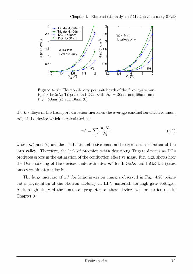
Chapter 4. Electrostatic analysis of MuG devices using SP2D
1.2 1.4 1.6 1.8 20
0.5
1
1.5
2
2.5
3
Vg
(V)
Ni(x
10
7cm
-1)
1.2 1.4 1.6 1.8 20
0.5
1
1.5
2
2.5
3
Vg
(V)
Ni(x
10
7cm
-1)
DG H =30nmDG H =50nm
Trigate H =30nmTrigate H =50nm
W =30nmLvalleys only
W =10nmLvalleys only
(b)(a)
ss
s
s
s
s
s
Figure 4.18: Electron density per unit length of the L valleys versusVg for InGaAs Trigates and DGs with Hs = 30nm and 50nm, andWs = 30nm (a) and 10nm (b).
the L valleys in the transport direction increases the average conduction effective mass,
m∗, of the device which is calculated as:
m∗ =∑
v
m∗vNv
Ni(4.1)
where m∗v and Nv are the conduction effective mass and electron concentration of the
v-th valley. Therefore, the lack of precision when describing Trigate devices as DGs
produces errors in the estimation of the conduction effective mass. Fig. 4.20 shows how
the DG modeling of the devices underestimates m∗ for InGaAs and InGaSb trigates
but overestimates it for Si.
The large increase of m∗ for large inversion charges observed in Fig. 4.20 points
out a degradation of the electron mobility in III-V materials for high gate voltages.
A thorough study of the transport properties of these devices will be carried out in
Chapter 9.
Electrostatics 75
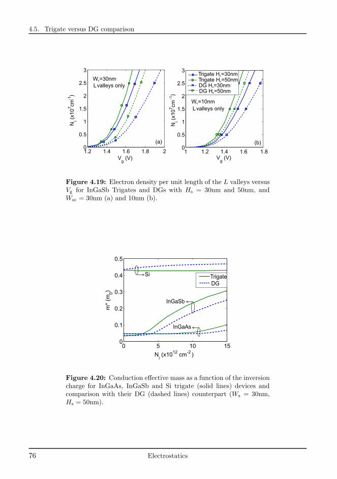
4.5. Trigate versus DG comparison
1.2 1.4 1.6 1.8 20
0.5
1
1.5
2
2.5
3
Vg
(V)
Ni(x
10
7 cm-1
)
1 1.2 1.4 1.6 1.80
0.5
1
1.5
2
2.5
3
Vg
(V)
Ni(x
10
7 cm-1
)
W =30nmLvalleys only
W =10nmLvalleys only
DG H =30nmDG H =50nm
Trigate H =30nmTrigate H =50nm
(a) (b)
s
s
s
s
s
s
Figure 4.19: Electron density per unit length of the L valleys versusVg for InGaSb Trigates and DGs with Hs = 30nm and 50nm, andWsc = 30nm (a) and 10nm (b).
0 5 10 150
0.1
0.2
0.3
0.4
0.5
Ni(x1012 cm-2 )
m*
(m0)
Si
InGaAs
DGTrigate
InGaSb
Figure 4.20: Conduction effective mass as a function of the inversioncharge for InGaAs, InGaSb and Si trigate (solid lines) devices andcomparison with their DG (dashed lines) counterpart (Ws = 30nm,Hs = 50nm).
76 Electrostatics
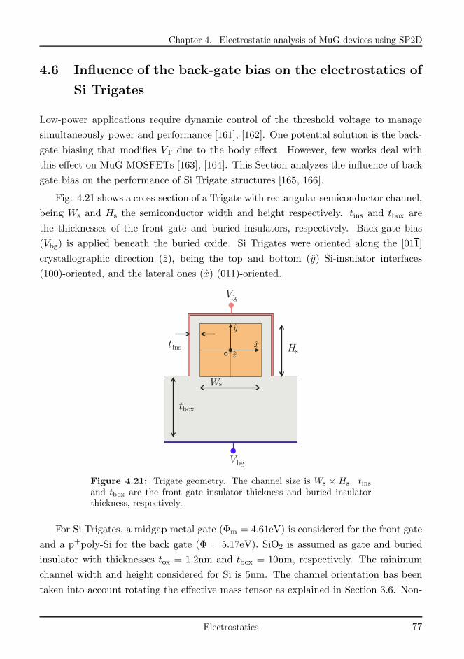
Chapter 4. Electrostatic analysis of MuG devices using SP2D
4.6 Influence of the back-gate bias on the electrostatics of
Si Trigates
Low-power applications require dynamic control of the threshold voltage to manage
simultaneously power and performance [161], [162]. One potential solution is the back-
gate biasing that modifies VT due to the body effect. However, few works deal with
this effect on MuG MOSFETs [163], [164]. This Section analyzes the influence of back
gate bias on the performance of Si Trigate structures [165, 166].
Fig. 4.21 shows a cross-section of a Trigate with rectangular semiconductor channel,
being Ws and Hs the semiconductor width and height respectively. tins and tbox are
the thicknesses of the front gate and buried insulators, respectively. Back-gate bias
(Vbg) is applied beneath the buried oxide. Si Trigates were oriented along the [011]
crystallographic direction (z), being the top and bottom (y) Si-insulator interfaces
(100)-oriented, and the lateral ones (x) (011)-oriented.
tbox
t ins
Ws
Hs
Vfg
Vbg
y
x
zo
Figure 4.21: Trigate geometry. The channel size is Ws × Hs. tinsand tbox are the front gate insulator thickness and buried insulatorthickness, respectively.
For Si Trigates, a midgap metal gate (Φm = 4.61eV) is considered for the front gate
and a p+poly-Si for the back gate (Φ = 5.17eV). SiO2 is assumed as gate and buried
insulator with thicknesses tox = 1.2nm and tbox = 10nm, respectively. The minimum
channel width and height considered for Si is 5nm. The channel orientation has been
taken into account rotating the effective mass tensor as explained in Section 3.6. Non-
Electrostatics 77
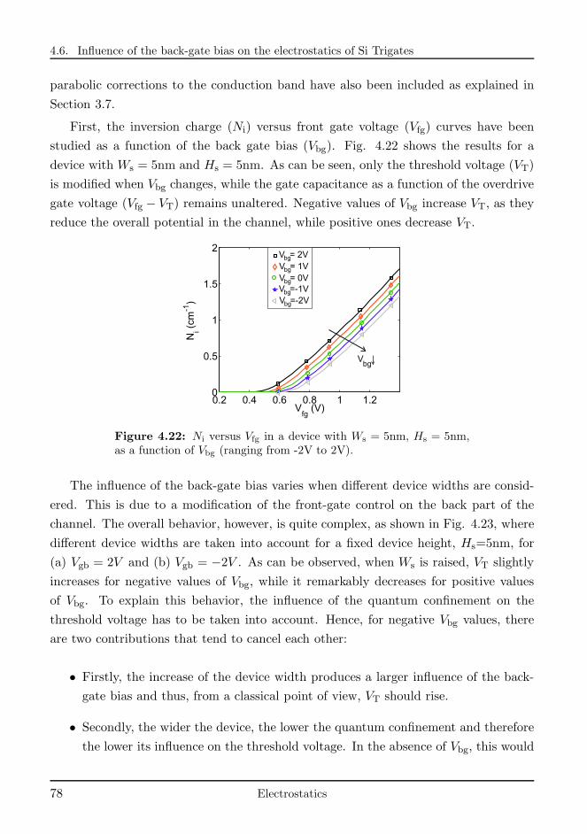
4.6. Influence of the back-gate bias on the electrostatics of Si Trigates
parabolic corrections to the conduction band have also been included as explained in
Section 3.7.
First, the inversion charge (Ni) versus front gate voltage (Vfg) curves have been
studied as a function of the back gate bias (Vbg). Fig. 4.22 shows the results for a
device with Ws = 5nm and Hs = 5nm. As can be seen, only the threshold voltage (VT)
is modified when Vbg changes, while the gate capacitance as a function of the overdrive
gate voltage (Vfg − VT) remains unaltered. Negative values of Vbg increase VT, as they
reduce the overall potential in the channel, while positive ones decrease VT.
0.2 0.4 0.6 0.8 1 1.20
0.5
1
1.5
2
Vfg
(V)
Ni(c
m-1
)
Vbg
V =-2Vbg
V =-1Vbg
V = 0Vbg
V = 1Vbg
V = 2Vbg
Figure 4.22: Ni versus Vfg in a device with Ws = 5nm, Hs = 5nm,as a function of Vbg (ranging from -2V to 2V).
The influence of the back-gate bias varies when different device widths are consid-
ered. This is due to a modification of the front-gate control on the back part of the
channel. The overall behavior, however, is quite complex, as shown in Fig. 4.23, where
different device widths are taken into account for a fixed device height, Hs=5nm, for
(a) Vgb = 2V and (b) Vgb = −2V . As can be observed, when Ws is raised, VT slightly
increases for negative values of Vbg, while it remarkably decreases for positive values
of Vbg. To explain this behavior, the influence of the quantum confinement on the
threshold voltage has to be taken into account. Hence, for negative Vbg values, there
are two contributions that tend to cancel each other:
• Firstly, the increase of the device width produces a larger influence of the back-
gate bias and thus, from a classical point of view, VT should rise.
• Secondly, the wider the device, the lower the quantum confinement and therefore
the lower its influence on the threshold voltage. In the absence of Vbg, this would
78 Electrostatics
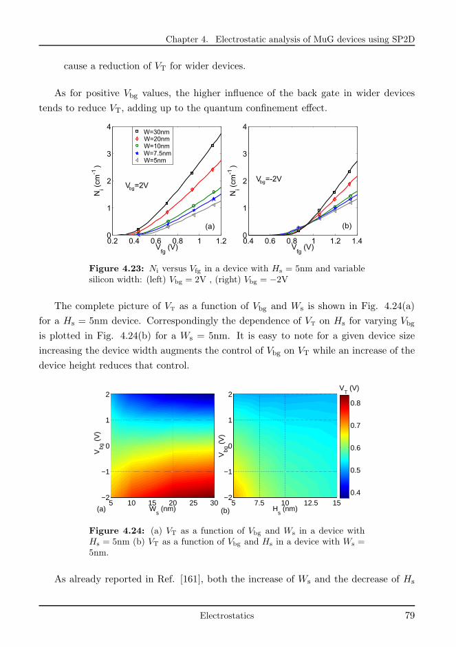
Chapter 4. Electrostatic analysis of MuG devices using SP2D
cause a reduction of VT for wider devices.
As for positive Vbg values, the higher influence of the back gate in wider devices
tends to reduce VT, adding up to the quantum confinement effect.
0.2 0.4 0.6 0.8 1 1.20
1
2
3
4
Vfg
(V)
Ni(c
m-1
)
0.4 0.6 0.8 1 1.2 1.40
1
2
3
4
Vfg
(V)
Ni(c
m-1
)
W=7.5nmW=10nmW=20nmW=30nm
W=5nm
V =2Vbg
V =-2Vbg
(a) (b)
Figure 4.23: Ni versus Vfg in a device with Hs = 5nm and variablesilicon width: (left) Vbg = 2V , (right) Vbg = −2V
The complete picture of VT as a function of Vbg and Ws is shown in Fig. 4.24(a)
for a Hs = 5nm device. Correspondingly the dependence of VT on Hs for varying Vbg
is plotted in Fig. 4.24(b) for a Ws = 5nm. It is easy to note for a given device size
increasing the device width augments the control of Vbg on VT while an increase of the
device height reduces that control.
−2
−1
0
1
2
5 10 15 20 25 30(b)
Ws (nm)
Vbg
(V
)
(a)
−2
−1
0
1
2
5 7.5 10 12.5 15H
s (nm)
Vbg
(V
)
VT (V)
0.4
0.5
0.6
0.7
0.8
Figure 4.24: (a) VT as a function of Vbg and Ws in a device withHs = 5nm (b) VT as a function of Vbg and Hs in a device with Ws =5nm.
As already reported in Ref. [161], both the increase of Ws and the decrease of Hs
Electrostatics 79
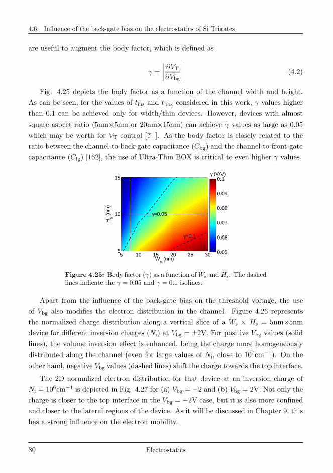
4.6. Influence of the back-gate bias on the electrostatics of Si Trigates
are useful to augment the body factor, which is defined as
γ =
∣
∣
∣
∣
∂VT∂Vbg
∣
∣
∣
∣
(4.2)
Fig. 4.25 depicts the body factor as a function of the channel width and height.
As can be seen, for the values of tins and tbox considered in this work, γ values higher
than 0.1 can be achieved only for width/thin devices. However, devices with almost
square aspect ratio (5nm×5nm or 20nm×15nm) can achieve γ values as large as 0.05
which may be worth for VT control [? ]. As the body factor is closely related to the
ratio between the channel-to-back-gate capacitance (Cbg) and the channel-to-front-gate
capacitance (Cfg) [162], the use of Ultra-Thin BOX is critical to even higher γ values.
5
10
15
5 10 15 20 25 30
γ=0.1
Ws (nm)
γ=0.05
Hs (
nm)
γ (V/V)
0.05
0.06
0.07
0.08
0.09
0.1
Figure 4.25: Body factor (γ) as a function ofWs andHs. The dashedlines indicate the γ = 0.05 and γ = 0.1 isolines.
Apart from the influence of the back-gate bias on the threshold voltage, the use
of Vbg also modifies the electron distribution in the channel. Figure 4.26 represents
the normalized charge distribution along a vertical slice of a Ws × Hs = 5nm×5nm
device for different inversion charges (Ni) at Vbg = ±2V. For positive Vbg values (solid
lines), the volume inversion effect is enhanced, being the charge more homogeneously
distributed along the channel (even for large values of Ni, close to 107cm−1). On the
other hand, negative Vbg values (dashed lines) shift the charge towards the top interface.
The 2D normalized electron distribution for that device at an inversion charge of
Ni = 106cm−1 is depicted in Fig. 4.27 for (a) Vbg = −2 and (b) Vbg = 2V. Not only the
charge is closer to the top interface in the Vbg = −2V case, but it is also more confined
and closer to the lateral regions of the device. As it will be discussed in Chapter 9, this
has a strong influence on the electron mobility.
80 Electrostatics
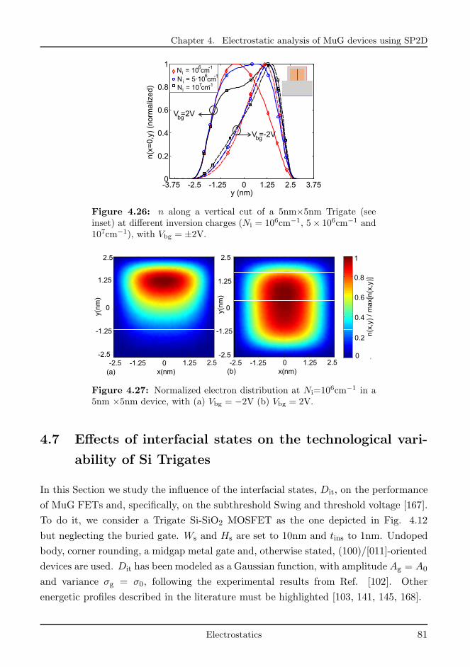
Chapter 4. Electrostatic analysis of MuG devices using SP2D
-3.75 -2.5 -1.25 0 1.25 2.5 3.750
0.2
0.4
0.6
0.8
1
y (nm)
n(x
=0
,y)
(no
rma
lize
d) N = 10 cmi
N = 10 cmi
N = 5·10 cmi
6
6
7
-1
-1
-1
V =2Vbg
V =-2Vbg
Figure 4.26: n along a vertical cut of a 5nm×5nm Trigate (seeinset) at different inversion charges (Ni = 106cm−1, 5× 106cm−1 and107cm−1), with Vbg = ±2V.
-2.5 0 2.5-1.25 1.25 -2.5 0 2.5-1.25 1.25
2.5
0
-2.5
1.25
-1.25
2.5
0
-2.5
1.25
-1.25
x(nm)x(nm)
y(n
m)
y(n
m)
1
0
0.2
0.4
0.6
0.8
n(x
,y)
/ m
ax[
n(x
,y)]
(a) (b)
Figure 4.27: Normalized electron distribution at Ni=106cm−1 in a5nm ×5nm device, with (a) Vbg = −2V (b) Vbg = 2V.
4.7 Effects of interfacial states on the technological vari-
ability of Si Trigates
In this Section we study the influence of the interfacial states, Dit, on the performance
of MuG FETs and, specifically, on the subthreshold Swing and threshold voltage [167].
To do it, we consider a Trigate Si-SiO2 MOSFET as the one depicted in Fig. 4.12
but neglecting the buried gate. Ws and Hs are set to 10nm and tins to 1nm. Undoped
body, corner rounding, a midgap metal gate and, otherwise stated, (100)/[011]-oriented
devices are used. Dit has been modeled as a Gaussian function, with amplitude Ag = A0
and variance σg = σ0, following the experimental results from Ref. [102]. Other
energetic profiles described in the literature must be highlighted [103, 141, 145, 168].
Electrostatics 81
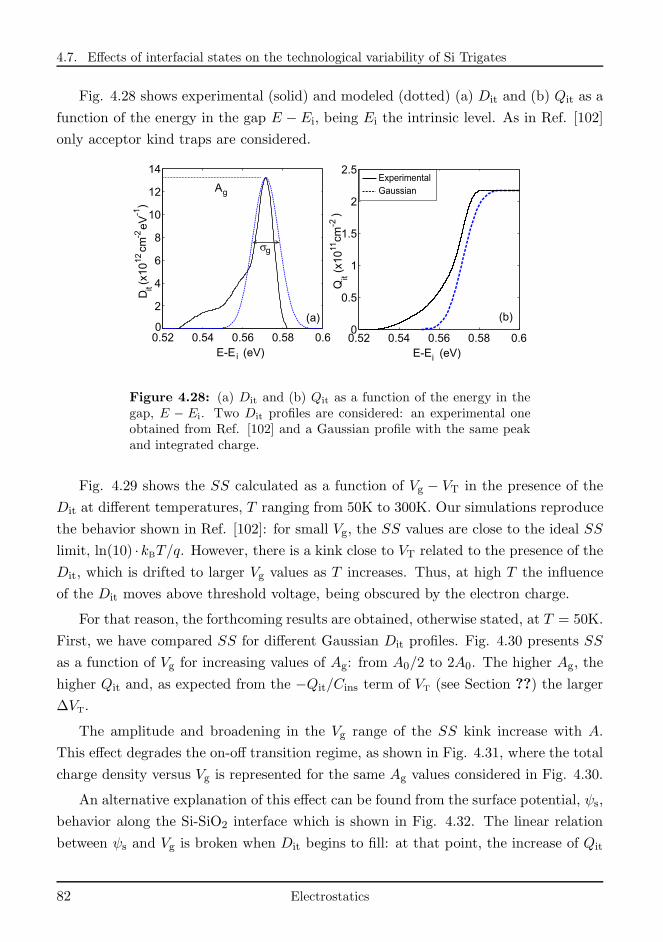
4.7. Effects of interfacial states on the technological variability of Si Trigates
Fig. 4.28 shows experimental (solid) and modeled (dotted) (a) Dit and (b) Qit as a
function of the energy in the gap E − Ei, being Ei the intrinsic level. As in Ref. [102]
only acceptor kind traps are considered.
0.52 0.54 0.56 0.58 0.60
2
4
6
8
10
12
14
E-E (eV)
Dit(x
10
12cm
-2e
V-1
)
0.52 0.54 0.56 0.58 0.60
0.5
1
1.5
2
2.5
Qit
(x1
011
cm-2
)
E-E (eV)
A
i
g
i
ExperimentalGaussian
sg
(a) (b)
Figure 4.28: (a) Dit and (b) Qit as a function of the energy in thegap, E − Ei. Two Dit profiles are considered: an experimental oneobtained from Ref. [102] and a Gaussian profile with the same peakand integrated charge.
Fig. 4.29 shows the SS calculated as a function of Vg − VT in the presence of the
Dit at different temperatures, T ranging from 50K to 300K. Our simulations reproduce
the behavior shown in Ref. [102]: for small Vg, the SS values are close to the ideal SS
limit, ln(10) ·kBT/q. However, there is a kink close to VT related to the presence of the
Dit, which is drifted to larger Vg values as T increases. Thus, at high T the influence
of the Dit moves above threshold voltage, being obscured by the electron charge.
For that reason, the forthcoming results are obtained, otherwise stated, at T = 50K.
First, we have compared SS for different Gaussian Dit profiles. Fig. 4.30 presents SS
as a function of Vg for increasing values of Ag: from A0/2 to 2A0. The higher Ag, the
higher Qit and, as expected from the −Qit/Cins term of VT (see Section ??) the larger
∆VT.
The amplitude and broadening in the Vg range of the SS kink increase with A.
This effect degrades the on-off transition regime, as shown in Fig. 4.31, where the total
charge density versus Vg is represented for the same Ag values considered in Fig. 4.30.
An alternative explanation of this effect can be found from the surface potential, ψs,
behavior along the Si-SiO2 interface which is shown in Fig. 4.32. The linear relation
between ψs and Vg is broken when Dit begins to fill: at that point, the increase of Qit
82 Electrostatics
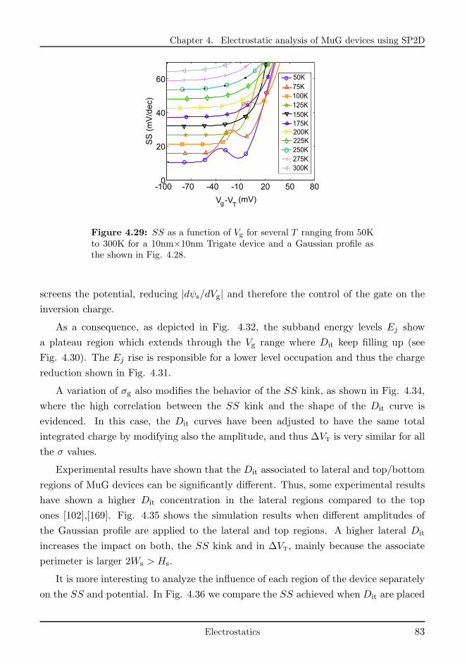
Chapter 4. Electrostatic analysis of MuG devices using SP2D
-100 -70 -40 -10 20 50 800
20
40
60
SS
(m
V/d
ec)
Vg -VT
(mV)
50K75K100K125K150K175K200K225K250K275K300K
Figure 4.29: SS as a function of Vg for several T ranging from 50Kto 300K for a 10nm×10nm Trigate device and a Gaussian profile asthe shown in Fig. 4.28.
screens the potential, reducing |dψs/dVg| and therefore the control of the gate on the
inversion charge.
As a consequence, as depicted in Fig. 4.32, the subband energy levels Ej show
a plateau region which extends through the Vg range where Dit keep filling up (see
Fig. 4.30). The Ej rise is responsible for a lower level occupation and thus the charge
reduction shown in Fig. 4.31.
A variation of σg also modifies the behavior of the SS kink, as shown in Fig. 4.34,
where the high correlation between the SS kink and the shape of the Dit curve is
evidenced. In this case, the Dit curves have been adjusted to have the same total
integrated charge by modifying also the amplitude, and thus ∆VT is very similar for all
the σ values.
Experimental results have shown that the Dit associated to lateral and top/bottom
regions of MuG devices can be significantly different. Thus, some experimental results
have shown a higher Dit concentration in the lateral regions compared to the top
ones [102],[169]. Fig. 4.35 shows the simulation results when different amplitudes of
the Gaussian profile are applied to the lateral and top regions. A higher lateral Dit
increases the impact on both, the SS kink and in ∆VT, mainly because the associate
perimeter is larger 2Ws > Hs.
It is more interesting to analyze the influence of each region of the device separately
on the SS and potential. In Fig. 4.36 we compare the SS achieved when Dit are placed
Electrostatics 83
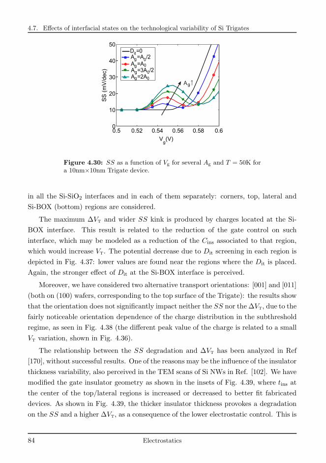
4.7. Effects of interfacial states on the technological variability of Si Trigates
0.5 0.52 0.54 0.56 0.58 0.60
10
20
30
40
50
SS
(m
V/d
ec)
Vg(V)
Dit=0A =A0/2A =A0A =3A0/2A =2A0
g
g
g
gAg
Figure 4.30: SS as a function of Vg for several Ag and T = 50K fora 10nm×10nm Trigate device.
in all the Si-SiO2 interfaces and in each of them separately: corners, top, lateral and
Si-BOX (bottom) regions are considered.
The maximum ∆VT and wider SS kink is produced by charges located at the Si-
BOX interface. This result is related to the reduction of the gate control on such
interface, which may be modeled as a reduction of the Cins associated to that region,
which would increase VT. The potential decrease due to Dit screening in each region is
depicted in Fig. 4.37: lower values are found near the regions where the Dit is placed.
Again, the stronger effect of Dit at the Si-BOX interface is perceived.
Moreover, we have considered two alternative transport orientations: [001] and [011]
(both on (100) wafers, corresponding to the top surface of the Trigate): the results show
that the orientation does not significantly impact neither the SS nor the ∆VT, due to the
fairly noticeable orientation dependence of the charge distribution in the subthreshold
regime, as seen in Fig. 4.38 (the different peak value of the charge is related to a small
VT variation, shown in Fig. 4.36).
The relationship between the SS degradation and ∆VT has been analyzed in Ref
[170], without successful results. One of the reasons may be the influence of the insulator
thickness variability, also perceived in the TEM scans of Si NWs in Ref. [102]. We have
modified the gate insulator geometry as shown in the insets of Fig. 4.39, where tins at
the center of the top/lateral regions is increased or decreased to better fit fabricated
devices. As shown in Fig. 4.39, the thicker insulator thickness provokes a degradation
on the SS and a higher ∆VT, as a consequence of the lower electrostatic control. This is
84 Electrostatics
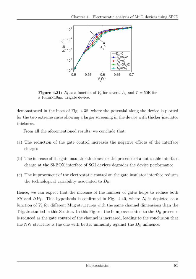
Chapter 4. Electrostatic analysis of MuG devices using SP2D
0.5 0.55 0.6 0.65 0.710
-2
100
102
104
106
Vg(V)
Ni(c
m-1
)
A
Dit=0A =A0/2A =A0A =3A0/2A =2A0
g
g
g
g
g
Figure 4.31: Ni as a function of Vg for several Ag and T = 50K fora 10nm×10nm Trigate device.
demonstrated in the inset of Fig. 4.38, where the potential along the device is plotted
for the two extreme cases showing a larger screening in the device with thicker insulator
thickness.
From all the aforementioned results, we conclude that:
(a) The reduction of the gate control increases the negative effects of the interface
charges
(b) The increase of the gate insulator thickness or the presence of a noticeable interface
charge at the Si-BOX interface of SOI devices degrades the device performance
(c) The improvement of the electrostatic control on the gate insulator interface reduces
the technological variability associated to Dit.
Hence, we can expect that the increase of the number of gates helps to reduce both
SS and ∆VT. This hypothesis is confirmed in Fig. 4.40, where Ni is depicted as a
function of Vg for different Mug structures with the same channel dimensions than the
Trigate studied in this Section. In this Figure, the hump associated to the Dit presence
is reduced as the gate control of the channel is increased, leading to the conclusion that
the NW structure is the one with better immunity against the Dit influence.
Electrostatics 85
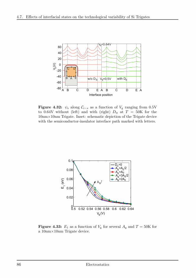
4.7. Effects of interfacial states on the technological variability of Si Trigates
Interface position
ys(V
)
A B C D E A-80
-60
-40
-20
0
20
40
60
V =0.5Vg
V =0.64Vg
w/o D it with Dit
B C D E A
C
B A E
D
Figure 4.32: ψs along Ci−s as a function of Vg ranging from 0.5Vto 0.64V without (left) and with (right) Dit at T = 50K for the10nm×10nm Trigate. Inset: schematic depiction of the Trigate devicewith the semiconductor-insulator interface path marked with letters.
0.5 0.52 0.54 0.56 0.58 0.6 0.62 0.640
0.02
0.04
0.06
0.08
0.1
E1
(eV
)
Vg (V)
A
Dit=0A =A0/2A =A0A =3A0/2A =2A0
g
g
g
g
g
Figure 4.33: E1 as a function of Vg for several Ag and T = 50K fora 10nm×10nm Trigate device.
86 Electrostatics
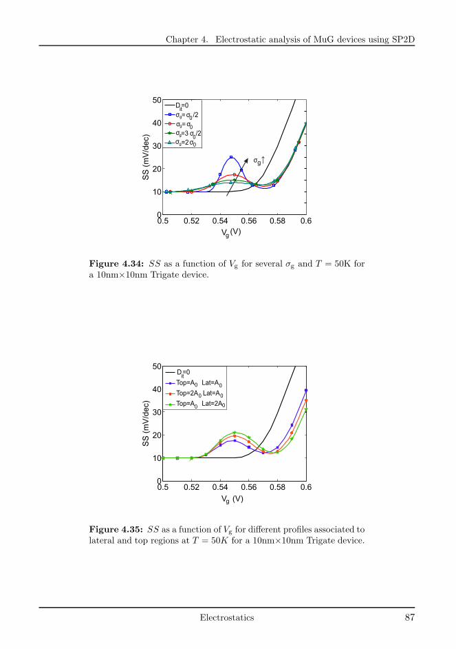
Chapter 4. Electrostatic analysis of MuG devices using SP2D
0.5 0.52 0.54 0.56 0.58 0.60
10
20
30
40
50
V (V)
SS
(m
V/d
ec)
Dit=0
σ = σ0 /2σ = σ0σ =3 σ
0/2
σ =2 σ0
g
g
g
g
g
gσ
Figure 4.34: SS as a function of Vg for several σg and T = 50K fora 10nm×10nm Trigate device.
0.5 0.52 0.54 0.56 0.58 0.60
10
20
30
40
50
V (V)
SS
(m
V/d
ec)
Dit=0
Top=A0 Lat=A0
Top=2A0 Lat=A0
Top=A0 Lat=2A0
g
Figure 4.35: SS as a function of Vg for different profiles associated tolateral and top regions at T = 50K for a 10nm×10nm Trigate device.
Electrostatics 87
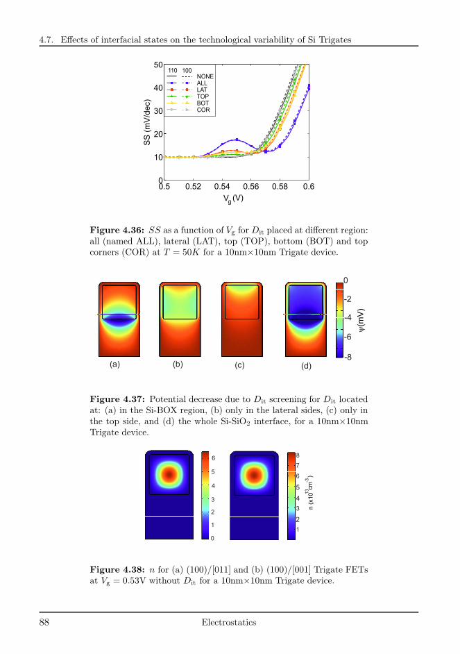
4.7. Effects of interfacial states on the technological variability of Si Trigates
0.5 0.52 0.54 0.56 0.58 0.60
10
20
30
40
50
V (V)
SS
(m
V/d
ec)
NONEALLLATTOPBOTCOR
100110
g
Figure 4.36: SS as a function of Vg for Dit placed at different region:all (named ALL), lateral (LAT), top (TOP), bottom (BOT) and topcorners (COR) at T = 50K for a 10nm×10nm Trigate device.
Figure 4.37: Potential decrease due to Dit screening for Dit locatedat: (a) in the Si-BOX region, (b) only in the lateral sides, (c) only inthe top side, and (d) the whole Si-SiO2 interface, for a 10nm×10nmTrigate device.
6
5
4
3
2
1
0
8
5
4
3
2
1
6
7
n (
x10
-3)
cm13
Figure 4.38: n for (a) (100)/[011] and (b) (100)/[001] Trigate FETsat Vg = 0.53V without Dit for a 10nm×10nm Trigate device.
88 Electrostatics
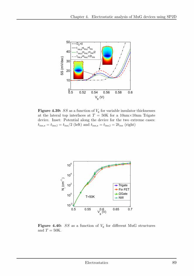
Chapter 4. Electrostatic analysis of MuG devices using SP2D
0.5 0.52 0.54 0.56 0.58 0.60
10
20
30
40
50
V (V)
SS
(m
V/d
ec)
Dit=0
t ins,s=tins,l=t
ins
g
t ins,s=tins,l=t /2ins
t ins,s=tins,l=2t ins
Figure 4.39: SS as a function of Vg for variable insulator thicknessesat the lateral top interfaces at T = 50K for a 10nm×10nm Trigatedevice. Inset: Potential along the device for the two extreme cases:tins,s = tins,l = tins/2 (left) and tins,s = tins,l = 2tins (right)
0.5 0.55 0.6 0.65 0.710
-2
100
102
104
106
Vg
(V)
Ni(c
m-1
)
Trigate
Fin FETΩGateNWT=50K
Figure 4.40: SS as a function of Vg for different MuG structuresand T = 50K.
Electrostatics 89
4.8. Conclusions
4.8 Conclusions
In this Chapter, Trigates and NWs made of Si and III-V semiconductors have been
studied using the SP2D simulator. It has been demonstrated that the low density
of states has a strong influence on the charge density and gate capacitance behavior
of III-V NWs. Moreover, the population of higher energy valleys (in particular, of
L valleys) can strongly modify the small conduction effective mass associated to III-V
semiconductors. Additionally, we have studied the behavior of InGaAs, and SOI Trigate
FETs, as a function of the channel width, showing that the semiconductor width has
a strong impact on InGaAs Trigates: both the threshold voltage and the gate voltage
at which the L valleys begin to be populated depend on the width. Besides, it has
been demonstrated the importance of considering the two-dimensional confinement for
III-V materials to accurately reproduce the electron distribution near the corners. This
effect produces a noticeable impact on the conduction effective mass as a result of the
different population of each valley. The control of the threshold voltage and the charge
distribution of Trigate SOI devices by modifying the back-gate bias has been studied,
confirming the possibility of achieving body factors higher than γ=0.1 as long as the
channel width over height ratio is increased as much as possible. Finally, the influence
of the interfacial states, Dit, on the performance of Si MuG FET and, specifically,
on the subthreshold swing and threshold voltage has been analyzed observing relevant
variations with the temperature and the oxide thickness. It is concluded that the higher
the number of gates the lower the degradation due to the interface states.
90 Electrostatics
Chapter 5
Charge, potential and current
analytical models for III-V NWs
5.1 Introduction
In this Chapter, an analytical model is proposed to calculate the potential, inversion
charge and drain current of III-V cylindrical NWs. To develop the model, we make use
of the cylindrical symmetry of the device and the isotropic effective mass of Γ valley to
solve the Poisson and Schrodinger equations in polar coordinates. From Schrodinger
solution we obtain expressions for the subband energies and their corresponding wave-
functions, taking into account their penetration into the gate insulator and the effective
mass discontinuity in the semiconductor-insulator interface. A complete expression for
the potential in the NW is achieved by solving the Poisson equation for an arbitrary
number of subbands. The model considers Fermi-Dirac Statistics, two-dimensional
quantum confinement of the carriers, non-parabolicity effects and interface states.
Several differences must be highlighted between this work and other models pro-
posed in the literature for cylindrical NWs [171]: 1) the inclusion of the wavefunction
penetration into the gate insulator, which has to be considered to accurately model
low-effective-mass materials [96]; 2) The non-parabolic dispersion relationship, which
is non-negiglible in III-V materials [154]; and 3) The possibility of including an arbi-
trary analytical profile of interface states, which strongly affects the operation of III-V
NWs [128].
The rest of the Chapter is organized as follows. In Section 5.2 we solve the
Electrostatics 91
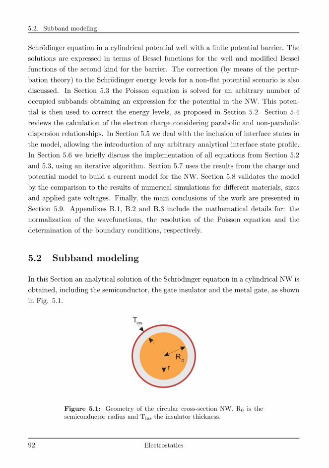
5.2. Subband modeling
Schrodinger equation in a cylindrical potential well with a finite potential barrier. The
solutions are expressed in terms of Bessel functions for the well and modified Bessel
functions of the second kind for the barrier. The correction (by means of the pertur-
bation theory) to the Schrodinger energy levels for a non-flat potential scenario is also
discussed. In Section 5.3 the Poisson equation is solved for an arbitrary number of
occupied subbands obtaining an expression for the potential in the NW. This poten-
tial is then used to correct the energy levels, as proposed in Section 5.2. Section 5.4
reviews the calculation of the electron charge considering parabolic and non-parabolic
dispersion relationships. In Section 5.5 we deal with the inclusion of interface states in
the model, allowing the introduction of any arbitrary analytical interface state profile.
In Section 5.6 we briefly discuss the implementation of all equations from Section 5.2
and 5.3, using an iterative algorithm. Section 5.7 uses the results from the charge and
potential model to build a current model for the NW. Section 5.8 validates the model
by the comparison to the results of numerical simulations for different materials, sizes
and applied gate voltages. Finally, the main conclusions of the work are presented in
Section 5.9. Appendixes B.1, B.2 and B.3 include the mathematical details for: the
normalization of the wavefunctions, the resolution of the Poisson equation and the
determination of the boundary conditions, respectively.
5.2 Subband modeling
In this Section an analytical solution of the Schrodinger equation in a cylindrical NW is
obtained, including the semiconductor, the gate insulator and the metal gate, as shown
in Fig. 5.1.
R
insT
r0
Figure 5.1: Geometry of the circular cross-section NW. R0 is thesemiconductor radius and Tins the insulator thickness.
92 Electrostatics
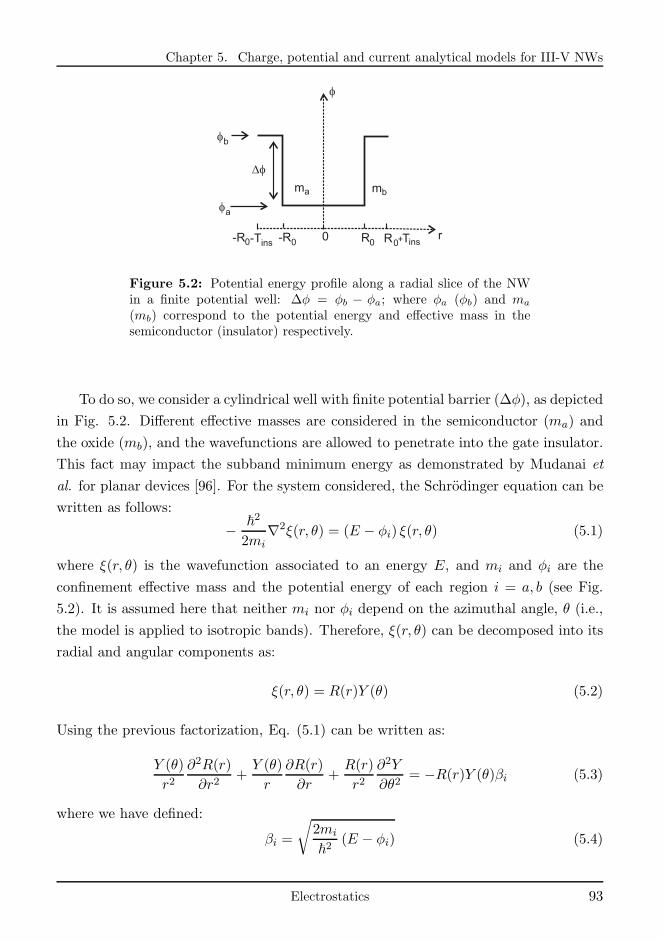
Chapter 5. Charge, potential and current analytical models for III-V NWs
R0 insTins-T -R0 0
af
bf
f
am bm
r
Df
R0+-R0
Figure 5.2: Potential energy profile along a radial slice of the NWin a finite potential well: ∆φ = φb − φa; where φa (φb) and ma
(mb) correspond to the potential energy and effective mass in thesemiconductor (insulator) respectively.
To do so, we consider a cylindrical well with finite potential barrier (∆φ), as depicted
in Fig. 5.2. Different effective masses are considered in the semiconductor (ma) and
the oxide (mb), and the wavefunctions are allowed to penetrate into the gate insulator.
This fact may impact the subband minimum energy as demonstrated by Mudanai et
al. for planar devices [96]. For the system considered, the Schrodinger equation can be
written as follows:
− ~2
2mi∇2ξ(r, θ) = (E − φi) ξ(r, θ) (5.1)
where ξ(r, θ) is the wavefunction associated to an energy E, and mi and φi are the
confinement effective mass and the potential energy of each region i = a, b (see Fig.
5.2). It is assumed here that neither mi nor φi depend on the azimuthal angle, θ (i.e.,
the model is applied to isotropic bands). Therefore, ξ(r, θ) can be decomposed into its
radial and angular components as:
ξ(r, θ) = R(r)Y (θ) (5.2)
Using the previous factorization, Eq. (5.1) can be written as:
Y (θ)
r2∂2R(r)
∂r2+Y (θ)
r
∂R(r)
∂r+R(r)
r2∂2Y
∂θ2= −R(r)Y (θ)βi (5.3)
where we have defined:
βi =
√
2mi
~2(E − φi) (5.4)
Electrostatics 93
5.2. Subband modeling
Rearranging terms we get:
1
R(r)
∂2R(r)
∂r2+
r
R(r)
∂R(r)
∂r+ r2βi =
1
Y (θ)
∂2Y (θ)
∂θ2(5.5)
which can be split into:∂2Y (θ)
∂θ2= −l2Y (θ) (5.6)
r2∂2R(r)
∂r2+ r
∂R(r)
∂r+(
βir2 − l2
)
R(r) = 0 (5.7)
The solution of Eq. (5.6) is:
Y (θ) =1√2πeılθ (5.8)
where l ∈ Z (to enforce Y is single-valued) and ı is the imaginary unit
Assuming φa < E < φb, the solution of Eq. (5.7) is:
Ri(r) =
A · Jl (γr) for i = a
C ·Kl (αr) for i = b(5.9)
being Jl(γr) the Bessel function of order l, Kl(αr) the modified Bessel function of the
second kind and order l, γ = βa and α = jβb. Thus, the set of solutions for ξ(r, θ) in
Eq. (5.1) is as wide as Z.
The values of γ, α and E can be determined by applying the usual boundary
conditions to ξ in the interface between media [115]:
ξa(Rs, θ) = ξb(Rs, θ) (5.10)
1
ma
dξa(r, θ)
dr
∣
∣
∣
∣
r=Rs
=1
mb
dξb(r, θ)
dr
∣
∣
∣
∣
r=Rs
(5.11)
Here, it is convenient to use the substitution E = E − φa. Then γ and α can be
rewritten as:
γ2 =2ma
~2E, α2 =
2mb
~2
(
∆φ− E)
(5.12)
where ∆φ = φb − φa is the difference between the potential energies in both mediums,
that is the barrier between their conduction band levels (see Fig. 5.2).
94 Electrostatics
Chapter 5. Charge, potential and current analytical models for III-V NWs
Then applying Eqs. (5.10) and (5.11) we get:
A · Jl(γRs) = C ·Kl(αRs) (5.13)
A
maγ [Jl−1(γRs)− Jl+1(γRs)] = − C
mbα [Kl−1(αRs) +Kl+1(αRs)] (5.14)
The unknown constants, A and C, can be eliminated by dividing the two previous
equations:η
ma
Jl−1(η)− Jl+1(η)
Jl(η)= − ζ
mb
Kl−1(ζ) +Kl+1(ζ)
Kl(ζ)(5.15)
where η = γRs and ζ = αRs. An additional relationship between η and ζ can be
achieved from the definition of γ and α:
η2 +ma
mbζ2 =
2ma∆φR2s
~2(5.16)
Equations (5.15) and (5.16) form a system from which we can calculate η and ζ.
The device dimensions and the semiconductor and insulator properties determine the
right-hand-side of Eq. (5.16); and, consequently, the solution of the system. Some
aspects must be taken into account when solving Eqs. (5.15) and (5.16):
(a) There are multiple solutions for the system: as many as values of l in Eq. (5.15).
(b) For a given l there are also several solutions as the Bessel functions involved in Eq.
(5.15) are not monotonic.
(c) Every solution with l = m, being m = 1, 2, . . . , is degenerate; having its degenerate
solution l = −m. This result can be deduced from the properties of Bessel and
modified Bessel functions:
Jv(x) = (−1)vJ−v(x)
Kv(x) = K−v(x) with v ∈ Z (5.17)
It is easy to observe that, applying these properties, Eq. (5.15) is completely
equivalent for l = m and l = −m
(d) For l = 0 the solution is non-degenerate.
For each solution pair ηj, ζj , with j = 0, 1 . . ., one can easily calculate a corre-
Electrostatics 95
5.2. Subband modeling
sponding pair γj and αj and, using Eq. (5.12), a discrete energy level Ej as:
Ej =~2
2ma
η2jR2
s
(5.18)
For the sake of clarity, let us briefly explain the subscript notation used in this Chapter.
On the one hand, we use the subscript j to enumerate the subbands, from the lowest
(j = 0) to the highest (j = N) value of Ej (where N is the number of subbands
considered). On the other hand, the subscript l indicates the order of the Bessel
function associated to the j subband; in other words the value of l in Eq. (5.15) for
which Ej is solution. Therefore, hereafter we assume l = l(j).
To better appreciate the solutions provided by the system of Eqs. (5.15) and (5.16),
Fig. 5.3 shows the first 24-th wavefunctions, sorted (left to right and top to bottom)
attending to the value of Ej , for a In0.53Ga0.47As-Al2O3 NW with 2Rs = 20nm and
tins = 1nm. The material parameters of In0.53Ga0.47As and Al2O3 are summed up in
Appendix ??. To get a more meaningful representation of the wavefunctions, we have
plotted the real part of ξj(r, j) for l ≥ 0. Plotting |ξj(r, θ)| –which actually reflects
the charge distribution– in its stead, will obscure the differences between l-values.
Nevertheless, it is easy to figure out the corresponding imaginary parts of ξj(r, θ). As
Ri(r) is real and Y (θ) = eılθ/√2π, the imaginary parts are just a rotation given by
π/2l (with l 6= 0) of the plotted real parts. For l = 0 the wavefunction is real. Each
wavefunction in Fig. 5.3 is labeled with its corresponding values of j and l. The missing
values of j correspond to the l < 0 results which are not plotted. The wavefunctions
for l < 0 will be equal to their l > 0 counterparts except for a factor −1 multiplying
the real parts for odd l and the imaginary parts for even l. As expected the cylindrical
symmetry of |ξj(r, θ)| is always preserved.Hitherto, the values of the constants A and C in Eq. (5.9) have not been determined.
They can be obtained from the normalization of the wavefunction:
∫ ∫
|ξj(r, θ)|2rdrdθ = 1 (5.19)
Using Eqs. (5.2), (5.8) and (5.9), Eq. (5.19) is rewritten as:
A2j
Rs∫
0
rJ2l (γjr) dr + C2
j
Rs+tins∫
Rs
r K2l (αjr) dr = 1 (5.20)
96 Electrostatics
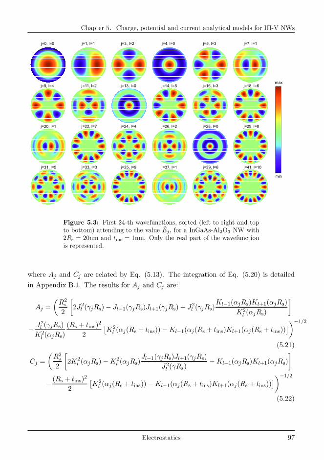
Chapter 5. Charge, potential and current analytical models for III-V NWs
j=0, l=0 j=1, l=1 j=3, l=2 j=4, l=0 j=5, l=3 j=7, l=1
max
min
j=9, l=4 j=11, l=2 j=13, l=0 j=14, l=5 j=16, l=3 j=18, l=6
j=20, l=1 j=22, l=7 j=24, l=4 j=26, l=2 j=28, l=0 j=29, l=8
j=31, l=5 j=33, l=3 j=35, l=9 j=37, l=1 j=39, l=6 j=41, l=10
Figure 5.3: First 24-th wavefunctions, sorted (left to right and topto bottom) attending to the value Ej , for a InGaAs-Al2O3 NW with2Rs = 20nm and tins = 1nm. Only the real part of the wavefunctionis represented.
where Aj and Cj are related by Eq. (5.13). The integration of Eq. (5.20) is detailed
in Appendix B.1. The results for Aj and Cj are:
Aj =
(
R2s
2
[
2J2l (γjRs)− Jl−1(γjRs)Jl+1(γjRs)− J2
l (γjRs)Kl−1(αjRs)Kl+1(αjRs)
K2l (αjRs)
]
− J2l (γjRs)
K2l (αjRs)
(Rs + tins)2
2
[
K2l (αj(Rs + tins))−Kl−1(αj(Rs + tins)Kl+1(αj(Rs + tins))
]
)−1/2
(5.21)
Cj =
(
R2s
2
[
2K2l (αjRs)−K2
l (αjRs)Jl−1(γjRs)Jl+1(γjRs)
J2l (γRs)
−Kl−1(αjRs)Kl+1(αjRs)
]
−(Rs + tins)2
2
[
K2l (αj(Rs + tins))−Kl−1(αj(Rs + tins)Kl+1(αj(Rs + tins))
]
)−1/2
(5.22)
Electrostatics 97
5.2. Subband modeling
Up to now we have solved the Schrodinger equation for a flat potential well obtaining
expressions for the energy levels, Eq. (5.18), and the wavefunctions, Eqs. (5.8) and
(5.9). However, the flat potential well is not a realistic scenario as far as the population
associated to the subbands, and therefore the charge in the NW, becomes not negligible.
Then, the potential in the NW gets curved in a way determined by the Poisson equation,
and the solution of the simplified problem proposed in this Section is no longer accurate.
This variation of the potential in the NW can be taken in account using the pertur-
bation theory. Here the perturbation is due to the non-flat potential, ψ(r)1, in the NW.
This term only affects the potential energy of the Hamiltonian. Thus, H = −qψ(r), be-ing ψ(r) = ψ(r)− φa/q. The term −φa/q enforces the precept that ψ(r) is a difference
between unperturbed and perturbed scenarios. ∆φ is not included in H as it was part
of the original Hamiltonian. For a non-degenerate subband, the first-order correction
of the energy level is given by [172]:
∆Ej = 〈ξ∗j |H|ξj〉 (5.23)
which for the NW can be written as,
∆Ej = −q2π∫
0
Rs+tins∫
0
ξj(r, θ) ψ(r) ξ∗j (r, θ) r drdθ = −q
Rs+tins∫
0
Rj(r) ψ(r) R∗j (r) r dr
(5.24)
where we have used:
2π∫
0
Yj(θ)Y∗j (θ)dθ =
2π∫
0
eılθ√2π
e−ılθ√2πdθ = 1 (5.25)
For degenerate energy levels Ej = Ek, the correction factors ∆Ej and ∆Ek can be
obtained as [172]:
∆Ej,k =1
2(Vjj + Vkk)±
1
2
√
(Vjj − Vkk)2 + 4 |Vjk|2 (5.26)
where Vjk = 〈ξ∗j |H|ξk〉. As previously explained, for degenerate energy levels k and j
1We have assumed no azimuthal dependence of ψ, as can be expected due to the cylindrical symmetryof the structure. This assumption will be demonstrated later in Section 5.3.
98 Electrostatics
Chapter 5. Charge, potential and current analytical models for III-V NWs
it holds that l(j) = m and l(k) = −m. Then it is proved that:
Vjk = −q2π∫
0
eımθ√2π
(
e−ımθ√2π
)∗
dθ
Rs+tins∫
0
Rj(r) ψ(r) R∗k(r) r dr = 0 (5.27)
Therefore:
∆Ej,k =1
2(Vjj + Vkk) (5.28)
But it can be readily checked that Vjj = Vkk as Rj(r)R∗j (r) = Rk(r)R
∗k(r) –see Eqs.
(5.9) and (5.17)–. Then,
∆Ej,k = Vjj = Vkk = −qRs+tins∫
0
Rj(r) ψ(r) R∗j (r) r dr (5.29)
Thus, to calculate the perturbation to the energy levels necessary to correct the flat
potential well approximation, we need to determine the potential ψ in the structure.
In the next Section we deal with the Poisson equation to determine the potential.
5.3 Potential modeling
In the present Section we undertake the calculation of the potential in the NW, ψ, due
to the charge associated to an arbitrary number of subbands. The Poisson equation in
cylindrical coordinates is:
1
r2∂2ψ
∂θ2+
1
r
∂
∂r
(
r∂ψ
∂r
)
= −ρi(r, θ)ǫi
(5.30)
where ǫi and ρi are the dielectric constant and charge density in the media i, respec-
tively. ρi is given by:
ρi = −qn(r, θ)− qNa δi,a (5.31)
where δi,a is the Kronecker delta and n(r, θ) and Na are the electron and acceptor
impurities concentrations respectively. Na is assumed constant and n(r, θ) is given by:
n(r, θ) =
N∑
j=0
g(Ej)|ξj(r, θ)|2 (5.32)
Electrostatics 99
5.3. Potential modeling
which for the media i can be written as:
n(r, θ) =N∑
j=0
g(Ej)|Rij(r)|2|Yj(θ)|2 (5.33)
being g(Ej) the density of states associated to level j. Using |Y (θ)|2 = 1/2π, the
resulting Poisson equation for the media i is:
1
r2∂2ψ
∂θ2+
1
r
∂
∂r
(
r∂ψ
∂r
)
=q
2πǫi
N∑
j=0
g(Ej)|Rij(r)|2 +q
ǫiNaδi,a (5.34)
As there is no azimuthal dependence of the charge density and taking into account
the cylindrical symmetry of the NW, we can assume no azimuthal dependence for the
potential (coherently with Section 5.2). Then, the resulting Poisson equation is:
1
r
∂
∂r
(
r∂ψ
∂r
)
=q
2πǫi
N∑
j=0
g(Ej)|Rij(r)|2 +q
ǫiNaδi,a (5.35)
A first integration of Eq. (5.35) gives:
∫
dr∂
∂r
(
r∂ψ
∂r
)
=q
2πǫi
N∑
j=0
g(Ej)
∫
r|Rij(r)|2dr +qδi,aǫi
∫
rNadr + Ci (5.36)
where Ci is the integration constant in media i. A second integration of Eq. (5.36)
results in:
∫ (
∂ψ
∂r
)
dr =q
2πǫi
N∑
j=0
g(Ej)
∫
1
r
∫
r|Rij(r)|2drdr +qδi,aǫi
∫
r
2Nadr +
∫
Cirdr +Di
(5.37)
where, in both cases, the integral and sum in the right-hand-side were interchanged as
Fubini-Tonelli’s theorem is satisfied, and we have used the symbol ˆ to distinguish the
two integrations variables.
Therefore, the potential in the media i can be written as,
ψi(r) =
N∑
j=0
q
2πǫig(Ej)ϕ
ij(r) +
q
ǫi
r2
4Naδi,a + Ci ln(r) +Di (5.38)
100 Electrostatics
Chapter 5. Charge, potential and current analytical models for III-V NWs
where the termq
2πǫig(Ej)ϕ
ij(r) is the contribution of the j subband to the potential
in media i; and,
ϕij(r) =
∫
1
r
∫
r |Rij(r)|2drdr (5.39)
determines the spatial distribution of this j subband contribution to the potential.
Substituting Eq. (5.9) into Eq. (5.39) we have:
ϕij(r) =
A2j
∫
1
r
∫
r J2l (γjr) drdr i = a
C2j
∫
1
r
∫
rK2l (αjr) drdr i = b
(5.40)
We conclude from Eq. (5.17), that degenerate energy levels j and k (with l(j) = m
and l(k) = −m ) have the same contribution to the potential. Eq. (5.40) is solved in
detail in Appendix B.2 providing the following expression:
ϕij(r) =
A2j
(
r2
2J2l (γjr) +
r2
2J2l−1(γjr) + (−l + 1
2)r
γjJl−1(γjr)Jl(γjr)+
+l
γ2j
l∑
m=1
J2m−1(γjr)−
l
2γ2jJ20 (γjr)
)
i = a
C2j
(
r2
2K2l (αjr)−
r2
2K2l−1(αjr) + (−l + 1
2)r
αjKl−1(αjr)Kl(αjr)+
+l
α2j
l∑
m=1
(−1)l−mK2m−1(αjr)− (−1)l−1
l
2α2j
K20 (αjr)
)
i = b
(5.41)
To clarify the contribution of each subband to the potential, Fig. 5.4 shows ϕj for
the first 24-th subbands, sorted left to right and top to bottom, for an InGaAs-Al2O3
NW with 2Rs = 20nm and tins = 1nm. Each ϕj was labeled with its corresponding
value of j and l. Since degenerate subbands contribute equally to the potential, their
corresponding ϕj was plotted just once.
Two conclusions can be extracted from Fig. 5.4: (a) As the order l of the Bessel
function associated to the subband increases, its contribution to the potential is more
step-like; (b) For a given l, ϕj depends softly on r for higher j. Nevertheless, ϕj is
weighted by the population of the corresponding subbands g(Ej), as proposed in Eq.
(5.38), being the first contributions always more relevant than the last ones.
Once the expression for the spatial distribution of the contribution of the subband
Electrostatics 101
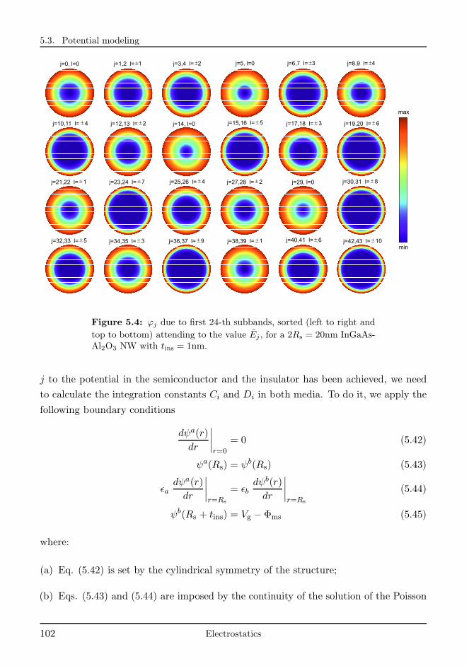
5.3. Potential modeling
j=0, l=0 j=5, l=0j=1,2 l=±1 j=3,4 l=±2
max
min
j=14, l=0
j=6,7 l=±3 j=8,9 l=±4
j=10,11 l= ± 4 j=12,13 l= ± 2 j=15,16 l= ± 5 j=17,18 l= ± 3 j=19,20 l= ± 6
j=29, l=0j=21,22 l= ± 1 j=23,24 l= ± 7 j=25,26 l= ± 4 j=27,28 l= ± 2 j=30,31 l= ± 8
j=32,33 l= ± 5 j=34,35 l= ± 3 j=36,37 l= ± 9 j=38,39 l= ± 1 j=40,41 l= ± 6 j=42,43 l= ± 10
Figure 5.4: ϕj due to first 24-th subbands, sorted (left to right and
top to bottom) attending to the value Ej , for a 2Rs = 20nm InGaAs-Al2O3 NW with tins = 1nm.
j to the potential in the semiconductor and the insulator has been achieved, we need
to calculate the integration constants Ci and Di in both media. To do it, we apply the
following boundary conditions
dψa(r)
dr
∣
∣
∣
∣
r=0
= 0 (5.42)
ψa(Rs) = ψb(Rs) (5.43)
ǫadψa(r)
dr
∣
∣
∣
∣
r=Rs
= ǫbdψb(r)
dr
∣
∣
∣
∣
r=Rs
(5.44)
ψb(Rs + tins) = Vg − Φms (5.45)
where:
(a) Eq. (5.42) is set by the cylindrical symmetry of the structure;
(b) Eqs. (5.43) and (5.44) are imposed by the continuity of the solution of the Poisson
102 Electrostatics
Chapter 5. Charge, potential and current analytical models for III-V NWs
equation in the interface between media
(c) Eq. (5.45) is obtained from the polarization of the NW, being Vg the voltage applied
in the gate contact located at the outer shell of the NW and Φms the difference
between the metal gate work function and the semiconductor electron affinity.
The step by step procedure to determine Ca, Da, Cb and Db from these equations is
accomplished in Appendix B.3. For the sake of clarity, we write here just the final
solutions.
Ca = 0 (5.46)
Da =q
2πǫb
N∑
j=0
g(Ej)ϕbj(Rs)+Cbln(Rs)+Db−
q
2πǫa
N∑
j=0
g(Ej)ϕaj (Rs)−
q
ǫa
R2s
4Na (5.47)
Cb =Rs
ǫb
1
2π
N∑
j=0
g(Ej)ϕ′aj (Rs) +
qNaRs
2− 1
2π
N∑
j=0
g(Ej)ϕ′bj (Rs)
(5.48)
Db = Vg − Φms −1
2πǫb
N∑
j=0
g(Ej)ϕbj(Rs + tins)− Cbln(Rs + tins) (5.49)
where ψ′aj and ψ′bj are the derivatives of ψaj and ψbj and their expressions are proposed
in Appendix B.3. Summing up, the potential in the semiconductor can be calculated
as:
ψa(r) =q
2πǫa
N∑
j=0
g(Ej)ϕaj (r) +
q
ǫa
r2
4Na +Da (5.50)
where ϕaj and Da are given by Eqs. (5.41) and (5.47). Correspondingly, the potential
in the insulator is given by:
ψb(r) =q
2πǫb
N∑
j=0
g(Ej)ϕbj(r) + Cbln(r) +Db (5.51)
where ϕbj , Cb and Db are given by Eqs. (5.41), (5.48) and (5.49).
Once we have a complete close expression for the potential in the NW, we can briefly
discuss about the main factors influencing its behavior. In the semiconductor, the radial
dependence of ψ(r) is governed by two terms (remind that Da is just a constant): the
first of them is associated to the electron concentration, the second one is controlled
Electrostatics 103
5.4. Charge modeling
by the acceptor impurities. For low gate voltages the acceptor impurities term is the
main contribution to Eq. (5.50), and the potential has a quadratic dependence on
the radial coordinate. However, for low Na concentrations (< 1014cm−3) the total
variation of the potential due to Na is of the order of 10−6V or 10−7V. This variation
is negligible and the flat band approximation works well. When higher gate voltages
are considered, the potential is controlled by the first term of Eq. (5.50). Then,
the potential curvature along the semiconductor radius cannot be neglected and the
flat potential well approximation starts to fail, being necessary to correct the energy
levels as explained in Section 5.2. Regarding the potential in the insulator, there
are also two contributions, one controlled by the electron concentration and one with
logarithmic dependence on r. However, in the insulator, due to the low penetration of
the wavefunctions, the electron concentration term is, even for large Vg, much smaller
than the logarithmic term, being the potential controlled by this one.
5.4 Charge modeling
In this Section we model the electron charge, Qi, considering a parabolic and a non-
parabolic dispersion relationship. The electron charge can be calculated as:
Qi = −q2π∫
0
Rs+tins∫
0
n(r, θ) rdrdθ = −qN∑
j=0
g(Ej)
2π∫
0
Rs+tins∫
0
|ξj(r, θ)|2 rdrdθ = −qN∑
j=0
g(Ej)
(5.52)
where we have used Eq. (5.19). For a parabolic dispersion relationship the density of
states associated to an energy level Ej is well known:
g(E) = gv
(
2m∗akBTπ~2
)1/2
F−1/2(
EF − EjkBT
)
(5.53)
where gv is the valley degeneracy (gv = 1 for the Γ valley) andm∗a the transport effective
mass in the semiconductor. The rest of the terms keep their usual meaning. This
expression can be related to the solution, Ej , obtained in Section 5.2, by rearranging
the term EF − Ej in the following way:
Ej − EF = (Ej − φa) + (φa − EF ) = Ej + φa = Ej − qψc (5.54)
104 Electrostatics
Chapter 5. Charge, potential and current analytical models for III-V NWs
where EF = 0 is assumed as a reference for energies, and φa = −qψc, being ψc = ψa(0)
the potential at the center of the NW. Then, for a parabolic approximation, g(Ej) can
be written as:
g(Ej) = gv
(
2m∗akBTπ~2
)1/2
F−1/2
(
− Ej − qψckBT
)
(5.55)
However, as discussed in Section 5.2, the solution Ej is not accurate if the potential is
not flat, which is the case whenever the semiconductor charge is not negligible. The
energy level Ej must be corrected by the perturbation energy ∆Ej . Then:
g(Ej) = gv
(
2m∗akBTπ~2
)1/2
F−1/2
(
− Ej +∆Ej − qψckBT
)
(5.56)
Up to this point, we have considered a parabolic band approximation. However, the
non-parabolicity of the conduction band in III-V materials modifies the energy levels
and the dispersion relationship. To study its effects, we recall here the model presented
by Jin et al. [95], where the following expression for the non-parabolic dispersion
relationship is proposed (see Section 2.6):
ENPj (k) = φj +
−1 +
√
1 + 4βv
(
~2k2
2m∗a+ Ej − φj
)
2βv(5.57)
where βv is the non-parabolicity factor of the v valley; k is the wavevector component
in the non-confined dimension; and φj is the expectation value of the potential energy
with respect to the wavefunction of the j subband, defined as:
φj =
2π∫
0
Rs+tins∫
0
ξj(r, θ)φ(r)ξ∗j (r, θ)rdrdθ (5.58)
where φ(r) is the total potential energy:
φ(r) =
−q(ψa(r)− ψc) 0 < r < Rs
−q(ψb(r)− ψc) + ∆φ Rs < r < Rs + tins(5.59)
which, to be coherent with Ej, is referred to the potential energy at the center of
the NW, −qψc. φj should not be confused with −qψ(r) as here the potential barrier
Electrostatics 105
5.5. Interfacial states modeling
between the semiconductor and the insulator must be taken into consideration.
To introduce the non-parabolicity in the model, we have considered two different
approaches. In the first approximation we introduced a non-parabolic correction which
only shifts the parabolic energy minimum:
∆ENPj = ENP
j (0)− Ej = φj +
−1 +
√
1 + 4βv
(
Ej − φj
)
2βv− Ej (5.60)
Then ∆ENPj is introduced into (5.56) leading to:
g(Ej) = gv
√
2m∗akBTπ~2
F- 12
(
−Ej +∆Ej − qψc +∆ENP
j
kBT
)
(5.61)
The second approximation takes into consideration the non-parabolic dispersion
relationship defined in Eq. (5.57). Therefore, g(Ej) is not determined by Eq. (5.61)
and it cannot be expressed as a function of a Fermi integral of any order. In its stead,
it is given by:
g(Ej) =gvπ
∞∫
−∞
(
1 + e−ENP
j (k)
kBT
)−1
dk (5.62)
where ENPj (k) is calculated as in Eq. (5.57) and again EF = 0. The first approximation
is simpler than the second one, but it is not accurate for large gate voltages. For this
reason, it will only be used for the threshold voltage model presented in Chapter 6.
In any other case involving non-parabolicity, the second approximation is the most
appropriate.
5.5 Interfacial states modeling
In this Section, we deal with the inclusion of interfacial states, Dit, in the model. The
presence of a non null surface charge, Qit, at the semiconductor-insulator interface mod-
ifies the boundary condition which imposes the continuity of the electric displacement
field at the interface. This boundary condition must be, then, reformulated taking into
consideration Qit:
ǫadψa(r)
dr
∣
∣
∣
∣
r=Rs
− ǫbdψb(r)
dr
∣
∣
∣
∣
r=Rs
= Qit (5.63)
106 Electrostatics
Chapter 5. Charge, potential and current analytical models for III-V NWs
with Qit and Dit are related by
Qit = q
Ei(Rs)∫
Ev(Rs)
Ddit(E)[1 − f(E)]dE − q
Ec(Rs)∫
Ei(Rs)
Dait(E)f(E)dE (5.64)
where the superscript d (a) refers to donors (acceptors) traps, and f(E) is the Fermi
function. Ec, Ev and Ei are the conduction band, the valence band and the intrinsic
Fermi level respectively. Using the references for energies proposed in Section 5.4, we
can write Ec(r) = −qψ(r). Then Ec(Rs) = −qψ(Rs) = −qψs. Thus, Eq. (5.64) can be
rewritten in terms of ψs as:
Qit = q
−qψs−Eg/2∫
−qψs−Eg
Ddit(E)
eE
kBT
1 + eE
kBT
dE − q
−qψs∫
−qψs−Eg/2
Dait(E)
1
1 + eE
kBT
dE (5.65)
where Eg is the band gap. The new boundary condition in Eq. (5.63) modifies the
determination of Cb in Eq. (5.48) which now is reformulated as:
Cb =Rs
ǫb
1
2π
N∑
j=0
g(Ej)ϕ′bj (Rs) +
qNaRs
2− 1
2π
N∑
j=0
g(Ej)ϕ′bj (Rs)
− Rs
ǫbQit (5.66)
The remaining solutions from the Poisson equation obtained in Section 5.3 are kept as
aforementioned.
5.6 Iterative scheme
In this Section we discuss the implementation of the model. It is straightforward to
appreciate that the expressions for g(Ej) and ψ(r) are coupled. This interdependency is
observed in the factor ψc in Eq. (5.56) and g(Ej) in Eqs. (5.50) and (5.51). Therefore,
the model requires an iterative solution scheme. Fig. 5.5 shows a flux diagram of the
procedure employed to solve the model.
The initial solution considers a flat potential well ψ(r) = 0 (therefore ∆Ej = 0) and
a given polarization in the outer shell of the NW (given by Vg). Then we solved the
Schrodinger equation obtaining Ej and ξj from Eqs. (5.18) and (5.2). In the next step
we determine g(Ej) using Eq. (5.56) for parabolic bands or Eq. (5.62) for non-parabolic
Electrostatics 107
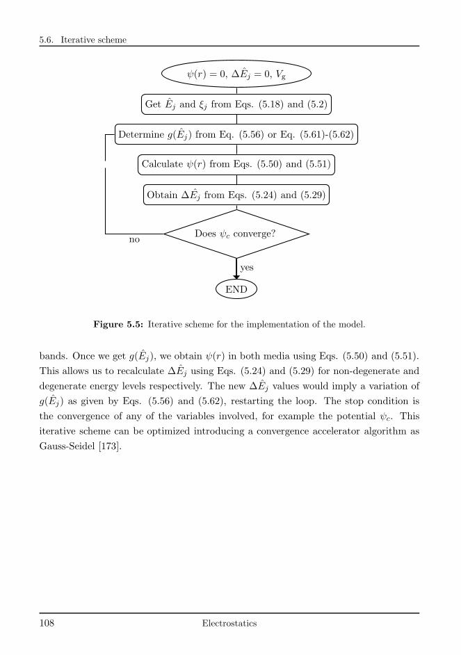
5.6. Iterative scheme
ψ(r) = 0, ∆Ej = 0, Vg
Get Ej and ξj from Eqs. (5.18) and (5.2)
Determine g(Ej) from Eq. (5.56) or Eq. (5.61)-(5.62)
Calculate ψ(r) from Eqs. (5.50) and (5.51)
Obtain ∆Ej from Eqs. (5.24) and (5.29)
Does ψc converge?
END
no
yes
Figure 5.5: Iterative scheme for the implementation of the model.
bands. Once we get g(Ej), we obtain ψ(r) in both media using Eqs. (5.50) and (5.51).
This allows us to recalculate ∆Ej using Eqs. (5.24) and (5.29) for non-degenerate and
degenerate energy levels respectively. The new ∆Ej values would imply a variation of
g(Ej) as given by Eqs. (5.56) and (5.62), restarting the loop. The stop condition is
the convergence of any of the variables involved, for example the potential ψc. This
iterative scheme can be optimized introducing a convergence accelerator algorithm as
Gauss-Seidel [173].
108 Electrostatics
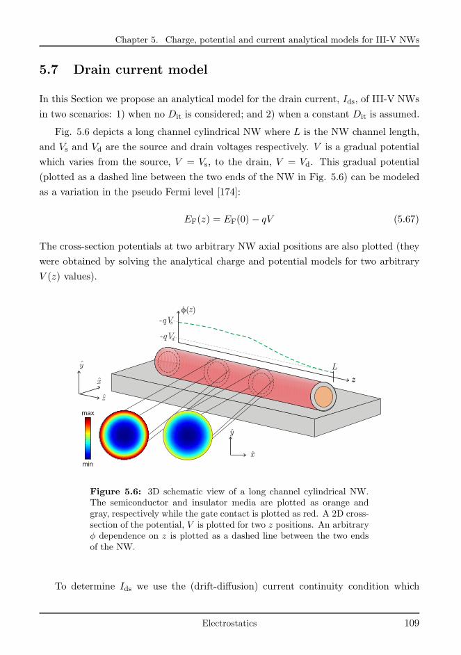
Chapter 5. Charge, potential and current analytical models for III-V NWs
5.7 Drain current model
In this Section we propose an analytical model for the drain current, Ids, of III-V NWs
in two scenarios: 1) when no Dit is considered; and 2) when a constant Dit is assumed.
Fig. 5.6 depicts a long channel cylindrical NW where L is the NW channel length,
and Vs and Vd are the source and drain voltages respectively. V is a gradual potential
which varies from the source, V = Vs, to the drain, V = Vd. This gradual potential
(plotted as a dashed line between the two ends of the NW in Fig. 5.6) can be modeled
as a variation in the pseudo Fermi level [174]:
EF(z) = EF(0) − qV (5.67)
The cross-section potentials at two arbitrary NW axial positions are also plotted (they
were obtained by solving the analytical charge and potential models for two arbitrary
V (z) values).
y
x
z
y
z
f( )
z
z
-qVs
-qVd
L
x
max
min
Figure 5.6: 3D schematic view of a long channel cylindrical NW.The semiconductor and insulator media are plotted as orange andgray, respectively while the gate contact is plotted as red. A 2D cross-section of the potential, V is plotted for two z positions. An arbitraryφ dependence on z is plotted as a dashed line between the two endsof the NW.
To determine Ids we use the (drift-diffusion) current continuity condition which
Electrostatics 109
5.7. Drain current model
imposes [175], [176], [177]:
µ2πRsQidV
dz= constant (5.68)
being µ the mobility (which for the sake of simplicity is assumed to be constant2). To
determine Ids we integrate Eq. (5.68) from the source, z = 0, to the drain, z = L,
getting:
Ids =2πRsµ
L
Vd∫
Vs
Qi(V )dV (5.69)
The electron charge per unit surface is given by Eq. (5.52):
Qi(V ) = − qNc
2πRs
N∑
j=0
F− 12
(
− Ej +∆Ej − qψs + qV
kBT
)
(5.70)
where EF has been replaced by the pseudo Fermi level EF(z) = EF(0)−qV to take into
consideration its variation along the NW length; and, consistently with the previous
Section, the Fermi level at the source was used as a reference for energies, EF(0) = 0.
The surface potential, ψs, can be calculated as:
ψs = Vgs − (Φm − χs)−Qi
Cins− Qit
Cins(5.71)
being Qit the surface charge due to interface states given, as in Eq. (5.64), by:
Qit = q
∫
Ddit(E)[1 − f(E)]dE − q
∫
Dait(E)f(E)dE (5.72)
As already seen in Section 5.6, Eqs. (5.70) and (5.71) are coupled. Furthermore, Qit
can have an arbitrary dependence on V . Therefore, the integration in Eq. (5.69) is
not straightforward. However there are at least two cases where the integration can be
successfully accomplished:
(A) If no interface traps are considered.
(B) If a constant profile for the interface traps is assumed and the Fermi function is
approximated by a step function.
The integration procedure in both cases is detailed in Appendix B.4. Here we recall
2This simplification, although not pretty realistic (see Chapter 7), is quite used in the literature forlong channel devices [174, 176].
110 Electrostatics
Chapter 5. Charge, potential and current analytical models for III-V NWs
the resulting expressions.
5.7.1 Drain current when Dit = 0
When no interface traps are considered, Ids is given by:
Ids =µ
L(f1(Vd) + f2(Vd)− f1(Vs)− f2(Vs)) (5.73)
where f1 and f2 are defined as:
f1(V ) = −kBT
q
N∑
j=0
F 12
(
− Ej +∆Ej − qψs + qV
kBT
)
(5.74)
f2(V ) = − 1
CΥ
N∑
j=0
F− 12
(
− Ej +∆Ej − qψs + qV
kBT
)
2
(5.75)
being CΥ a capacitance term defined in Eq. (B.75) in Appendix B.4. It is important
to remind that ψs and ∆Ej in Eqs. (5.74) and (5.75) are the surface potential and the
correction of the energy level j for a given value V of the pseudo Fermi level. Therefore,
when evaluating f1 and f2 at Vs (Vd) in Eq. (5.73), ψs and ∆Ej would be ψss (ψsd)
and ∆Esj (∆E
dj ), that is the surface potential and the correction to the energy level at
the source (drain) respectively. Thus, Eq. (5.73) requires the resolution of the charge
model for V = Vs and V = Vd.
5.7.2 Drain current for a constant Dit profile
When a constant Dit profile is assumed in a certain range of energies between Ea and
Eb, Ids is given by:
Ids =µ
L
f1(Vd) + f2(Vd)− f1(Vs)− f2(Vs) +f1(Vb) + f2(Vb)− f1(Va)− f2(Va)
1 +qDit
Cins
(5.76)
being f1 and f2 already defined in Eqs. (5.74) and (5.75) respectively. Vb and Va are the
gradual potentials corresponding to the pseudo Fermi potential for which EF(z) = Eb
Electrostatics 111
5.8. Results and discussion
and EF(z) = Ea, respectively.
It is worth to particularize the range of energies where the traps are present to
the upper half of the band gap, in accordance with an amphoteric perspective of the
interface traps nature [178]. Then, Ea = Ei and Eb = Ec being Ei and Ec the intrinsic
Fermi level and the conduction band edge, respectively. Then, Ids will be:
Ids =µ
L
f1(Vd) + f2(Vd)− f1(Vs)− f2(Vs) +f1(Vc) + f2(Vc)− f1(Vi)− f2(Vi)
1 +qDit
Cins
(5.77)
Now, Vc and Vi are the gradual potentials for which the pseudo Fermi level crosses
trough Ec and Ei, respectively. Using the references for energies in the charge mode,
where Ec(r) = −qψ(r), it is easy to check that −qVc = −qψs and −qVi = −qψs+Eg/2.
It is noted that Eqs. (5.74) and (5.75) are pretty simplified when V is evaluated at Vi
and Vc. In fact, ∆Ej can be obliterated for V = Vi, as EF(z) = Ei and no relevant
charge concentration or potential curvature is expected; thus the arguments of F 12are
simplified and F− 12to Ej . For V = Vc, ∆Ej cannot be neglected and the solution of
the charge model is mandatory.
5.8 Results and discussion
In this Section, the results from the proposed analytical models are compared with the
solution of the 2D self-consistent Schrodinger-Poisson solver (see Chapter 3) for different
NW sizes and gate voltages. InAs and In0.53Ga0.47As are considered as semiconductor
materials while Al2O3 is used as gate insulator. The parameters of the simulation of
Γ, X and L valleys are summarized in Appendix F.
First we study the validity of the proposed solution of the Schrodinger equation.
A subthreshold gate voltage (Vg = 0.2V) was considered to limit the effect of: 1) the
conduction band curvature in the semiconductor and 2) the logarithmic potential well in
the insulator as much as possible. Fig. 5.7(a) shows the three lower energies calculated
with the developed analytical model (solid lines) and with the self consistent simulator
(symbols) as a function of the device size. The model energy levels corresponding to
an infinite potential well are also plotted (dashed lines). The infinite potential well
112 Electrostatics
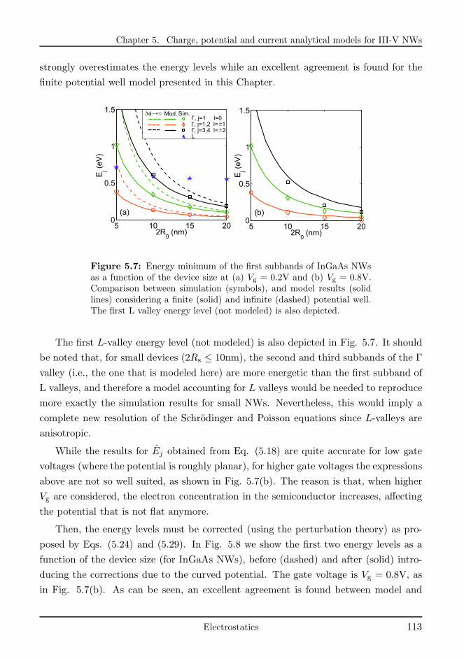
Chapter 5. Charge, potential and current analytical models for III-V NWs
strongly overestimates the energy levels while an excellent agreement is found for the
finite potential well model presented in this Chapter.
5 10 15 200
0.5
1
1.5
2R0
(nm)
Ej(e
V)
5 10 15 200
0.5
1
1.5
2R0
(nm)E
j(e
V)
Mod.Γ, j=1 l=0
L
Df
, j=1,2 l=Γ ±1
→∞ Sim.
, j=3,4 l=Γ ±2
(a) (b)
Figure 5.7: Energy minimum of the first subbands of InGaAs NWsas a function of the device size at (a) Vg = 0.2V and (b) Vg = 0.8V.Comparison between simulation (symbols), and model results (solidlines) considering a finite (solid) and infinite (dashed) potential well.The first L valley energy level (not modeled) is also depicted.
The first L-valley energy level (not modeled) is also depicted in Fig. 5.7. It should
be noted that, for small devices (2Rs ≤ 10nm), the second and third subbands of the Γ
valley (i.e., the one that is modeled here) are more energetic than the first subband of
L valleys, and therefore a model accounting for L valleys would be needed to reproduce
more exactly the simulation results for small NWs. Nevertheless, this would imply a
complete new resolution of the Schrodinger and Poisson equations since L-valleys are
anisotropic.
While the results for Ej obtained from Eq. (5.18) are quite accurate for low gate
voltages (where the potential is roughly planar), for higher gate voltages the expressions
above are not so well suited, as shown in Fig. 5.7(b). The reason is that, when higher
Vg are considered, the electron concentration in the semiconductor increases, affecting
the potential that is not flat anymore.
Then, the energy levels must be corrected (using the perturbation theory) as pro-
posed by Eqs. (5.24) and (5.29). In Fig. 5.8 we show the first two energy levels as a
function of the device size (for InGaAs NWs), before (dashed) and after (solid) intro-
ducing the corrections due to the curved potential. The gate voltage is Vg = 0.8V, as
in Fig. 5.7(b). As can be seen, an excellent agreement is found between model and
Electrostatics 113
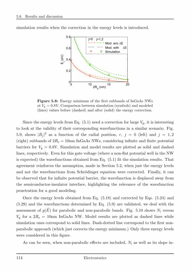
5.8. Results and discussion
simulation results when the correction in the energy levels is introduced.
5 10 15 200
0.2
0.4
0.6
0.8
2R0
(nm)
Ej(e
V)
Mod w/o ED
Mod. withSimulation
j=0 j=1,2.
ED
Figure 5.8: Energy minimum of the first subbands of InGaAs NWsat Vg = 0.8V. Comparison between simulation (symbols) and modeled(lines) values before (dashed) and after (solid) the energy correction.
Since the energy levels from Eq. (5.1) need a correction for large Vg, it is interesting
to look at the validity of their corresponding wavefunctions in a similar scenario. Fig.
5.9, shows |Rj |2 as a function of the radial position, r, j = 0 (left) and j = 1, 2
(right) subbands of 2Rs = 10nm InGaAs NWs, considering infinite and finite potential
barriers for Vg = 0.8V. Simulation and model results are plotted as solid and dashed
lines, respectively. Even for this gate voltage (where a non-flat potential well in the NW
is expected) the wavefunctions obtained from Eq. (5.1) fit the simulation results. That
agreement reinforces the assumption, made in Section 5.2, when just the energy levels
and not the wavefunctions from Schrodinger equation were corrected. Finally, it can
be observed that for infinite potential barrier, the wavefunction is displaced away from
the semiconductor-insulator interface, highlighting the relevance of the wavefunction
penetration for a good modeling.
Once the energy levels obtained from Eq. (5.18) and corrected by Eqs. (5.24) and
(5.29) and the wavefunctions determined by Eq. (5.9) are validated, we deal with the
assessment of g(E) for parabolic and non-parabolic bands. Fig. 5.10 shows Ni versus
Vg for a 2Rs = 10nm InGaAs NW. Model results are plotted as dashed lines while
simulation ones correspond to solid lines. Dash-dotted line correspond to the first non-
parabolic approach (which just corrects the energy minimum.) Only three energy levels
were considered in this figure.
As can be seen, when non-parabolic effects are included, Ni as well as its slope in-
114 Electrostatics
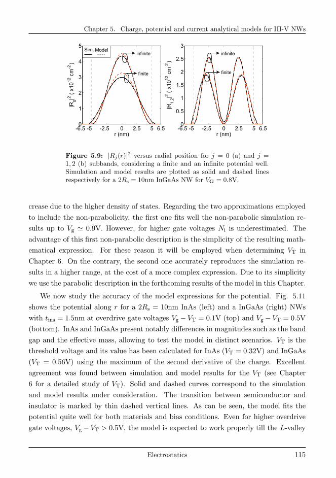
Chapter 5. Charge, potential and current analytical models for III-V NWs
-6.5 -5 -2.5 0 2.5 5 6.50
1
2
3
4
5
r (nm)
|R0|2
(x1
012
cm-2
)
-6.5 -5 -2.5 0 2.5 5 6.50
0.5
1
1.5
2
2.5
3
r (nm)
|R1,2
|2(
x101
2cm
-2)
Sim. Model
finite
infinite
finite
infinite
Figure 5.9: |Rj(r)|2 versus radial position for j = 0 (a) and j =1, 2 (b) subbands, considering a finite and an infinite potential well.Simulation and model results are plotted as solid and dashed linesrespectively for a 2Rs = 10nm InGaAs NW for VG = 0.8V.
crease due to the higher density of states. Regarding the two approximations employed
to include the non-parabolicity, the first one fits well the non-parabolic simulation re-
sults up to Vg ≃ 0.9V. However, for higher gate voltages Ni is underestimated. The
advantage of this first non-parabolic description is the simplicity of the resulting math-
ematical expression. For these reason it will be employed when determining VT in
Chapter 6. On the contrary, the second one accurately reproduces the simulation re-
sults in a higher range, at the cost of a more complex expression. Due to its simplicity
we use the parabolic description in the forthcoming results of the model in this Chapter.
We now study the accuracy of the model expressions for the potential. Fig. 5.11
shows the potential along r for a 2Rs = 10nm InAs (left) and a InGaAs (right) NWs
with tins = 1.5nm at overdrive gate voltages Vg − VT = 0.1V (top) and Vg − VT = 0.5V
(bottom). InAs and InGaAs present notably differences in magnitudes such as the band
gap and the effective mass, allowing to test the model in distinct scenarios. VT is the
threshold voltage and its value has been calculated for InAs (VT = 0.32V) and InGaAs
(VT = 0.56V) using the maximum of the second derivative of the charge. Excellent
agreement was found between simulation and model results for the VT (see Chapter
6 for a detailed study of VT). Solid and dashed curves correspond to the simulation
and model results under consideration. The transition between semiconductor and
insulator is marked by thin dashed vertical lines. As can be seen, the model fits the
potential quite well for both materials and bias conditions. Even for higher overdrive
gate voltages, Vg − VT > 0.5V, the model is expected to work properly till the L-valley
Electrostatics 115
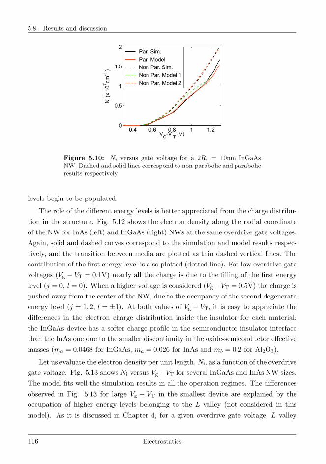
5.8. Results and discussion
0.4 0.6 0.8 1 1.20
0.5
1
1.5
2
Ni(x
10
7cm
-1)
VG
-VT
(V)
Par. Sim.
Par. Model
Non Par. Model 1
Non Par. Model 2
Non Par. Sim.
Figure 5.10: Ni versus gate voltage for a 2Rs = 10nm InGaAsNW. Dashed and solid lines correspond to non-parabolic and parabolicresults respectively
levels begin to be populated.
The role of the different energy levels is better appreciated from the charge distribu-
tion in the structure. Fig. 5.12 shows the electron density along the radial coordinate
of the NW for InAs (left) and InGaAs (right) NWs at the same overdrive gate voltages.
Again, solid and dashed curves correspond to the simulation and model results respec-
tively, and the transition between media are plotted as thin dashed vertical lines. The
contribution of the first energy level is also plotted (dotted line). For low overdrive gate
voltages (Vg − VT = 0.1V) nearly all the charge is due to the filling of the first energy
level (j = 0, l = 0). When a higher voltage is considered (Vg−VT = 0.5V) the charge is
pushed away from the center of the NW, due to the occupancy of the second degenerate
energy level (j = 1, 2, l = ±1). At both values of Vg − VT, it is easy to appreciate the
differences in the electron charge distribution inside the insulator for each material:
the InGaAs device has a softer charge profile in the semiconductor-insulator interface
than the InAs one due to the smaller discontinuity in the oxide-semiconductor effective
masses (ma = 0.0468 for InGaAs, ma = 0.026 for InAs and mb = 0.2 for Al2O3).
Let us evaluate the electron density per unit length, Ni, as a function of the overdrive
gate voltage. Fig. 5.13 shows Ni versus Vg−VT for several InGaAs and InAs NW sizes.
The model fits well the simulation results in all the operation regimes. The differences
observed in Fig. 5.13 for large Vg − VT in the smallest device are explained by the
occupation of higher energy levels belonging to the L valley (not considered in this
model). As it is discussed in Chapter 4, for a given overdrive gate voltage, L valley
116 Electrostatics
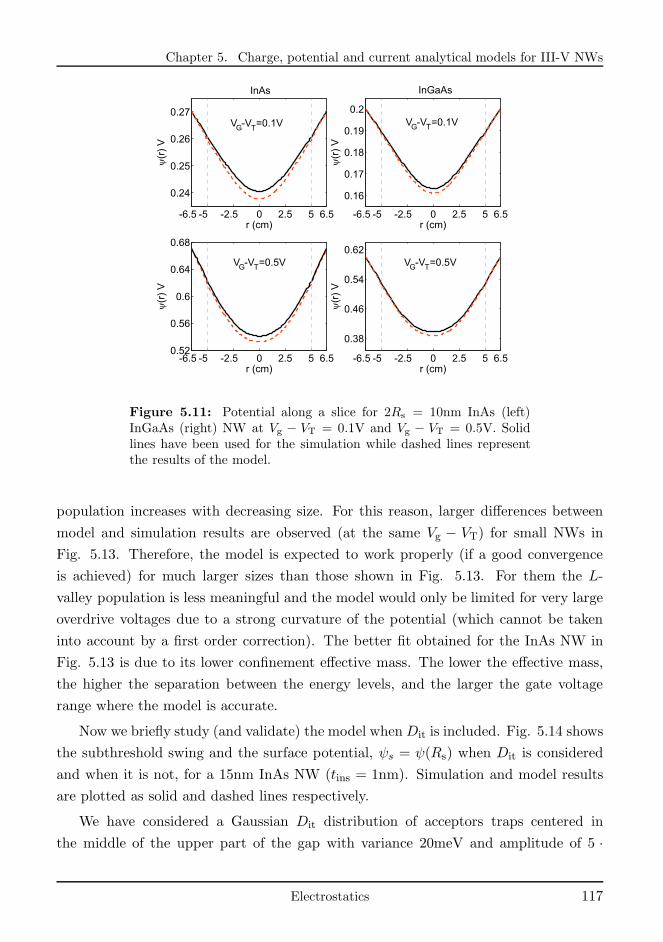
Chapter 5. Charge, potential and current analytical models for III-V NWs
-6.5 -5 -2.5 0 2.5 5 6.50.52
0.56
0.6
0.64
0.68
r (cm)
y(r
) V
-6.5 -5 -2.5 0 2.5 5 6.5
0.38
0.46
0.54
0.62
r (cm)
y(r
) V
-6.5 -5 -2.5 0 2.5 5 6.5
0.24
0.25
0.26
0.27
r (cm)
y(r
) V
-6.5 -5 -2.5 0 2.5 5 6.5
0.16
0.17
0.18
0.19
0.2
r (cm)
y(r
) V
VG-VT=0.1V
InAs
VG-VT=0.1V
VG-VT=0.5V VG-VT=0.5V
InGaAs
Figure 5.11: Potential along a slice for 2Rs = 10nm InAs (left)InGaAs (right) NW at Vg − VT = 0.1V and Vg − VT = 0.5V. Solidlines have been used for the simulation while dashed lines representthe results of the model.
population increases with decreasing size. For this reason, larger differences between
model and simulation results are observed (at the same Vg − VT) for small NWs in
Fig. 5.13. Therefore, the model is expected to work properly (if a good convergence
is achieved) for much larger sizes than those shown in Fig. 5.13. For them the L-
valley population is less meaningful and the model would only be limited for very large
overdrive voltages due to a strong curvature of the potential (which cannot be taken
into account by a first order correction). The better fit obtained for the InAs NW in
Fig. 5.13 is due to its lower confinement effective mass. The lower the effective mass,
the higher the separation between the energy levels, and the larger the gate voltage
range where the model is accurate.
Now we briefly study (and validate) the model whenDit is included. Fig. 5.14 shows
the subthreshold swing and the surface potential, ψs = ψ(Rs) when Dit is considered
and when it is not, for a 15nm InAs NW (tins = 1nm). Simulation and model results
are plotted as solid and dashed lines respectively.
We have considered a Gaussian Dit distribution of acceptors traps centered in
the middle of the upper part of the gap with variance 20meV and amplitude of 5 ·
Electrostatics 117
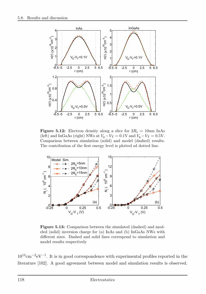
5.8. Results and discussion
-6.5 -5 -2.5 0 2.5 5 6.50
0.4
0.8
1.2
r (cm)-6.5 -5 -2.5 0 2.5 5 6.50
0.5
1
1.5
2
r (cm)
-6.5 -5 -2.5 0 2.5 5 6.50
1
2
3
4
r (cm)
n(r
)(x
101
8cm
-3
-6.5 -5 -2.5 0 2.5 5 6.50
1
2
3
4
5
r (cm)
InAs InGaAs
VG-VT=0.1V VG-VT=0.1V
VG-VT=0.5VVG-VT=0.5V
)n(r
)(x
101
8cm
-3)
n(r
)(x
101
8cm
-3)
n(r
)(x
101
8cm
-3)
Figure 5.12: Electron density along a slice for 2Rs = 10nm InAs(left) and InGaAs (right) NWs at Vg−VT = 0.1V and Vg−VT = 0.5V.Comparison between simulation (solid) and model (dashed) results.The contribution of the first energy level is plotted sd dotted line.
-0.25 0 0.25 0.50
2
4
6
8
10
VG
-VT
(V)
Ni(×
10
6cm
-1)
-0.25 0 0.25 0.50
3
6
9
12
15
VG
-VT
(V)
Ni(×
10
6cm
-1)
2R0=5nm
Model Sim.
2R0=10nm
2R0=15nm
(a) (b)
Figure 5.13: Comparison between the simulated (dashed) and mod-eled (solid) inversion charge for (a) InAs and (b) InGaAs NWs withdifferent sizes. Dashed and solid lines correspond to simulation andmodel results respectively
1013cm−2eV−1. It is in good correspondence with experimental profiles reported in the
literature [102]. A good agreement between model and simulation results is observed.
118 Electrostatics
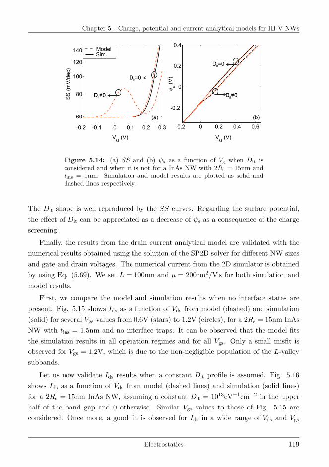
Chapter 5. Charge, potential and current analytical models for III-V NWs
-0.2 -0.1 0 0.1 0.2 0.3
60
80
100
120
140
VG
(V)
SS
(m
V/d
ec)
-0.2 0 0.2 0.4 0.6
-0.2
0
0.2
0.4
VG
(V)
ys
(V)
ModelSim.
D =0it
D =0it
(a) (b)
D =0 D =0itD =0
D =0it
Figure 5.14: (a) SS and (b) ψs as a function of Vg when Dit isconsidered and when it is not for a InAs NW with 2Rs = 15nm andtins = 1nm. Simulation and model results are plotted as solid anddashed lines respectively.
The Dit shape is well reproduced by the SS curves. Regarding the surface potential,
the effect of Dit can be appreciated as a decrease of ψs as a consequence of the charge
screening.
Finally, the results from the drain current analytical model are validated with the
numerical results obtained using the solution of the SP2D solver for different NW sizes
and gate and drain voltages. The numerical current from the 2D simulator is obtained
by using Eq. (5.69). We set L = 100nm and µ = 200cm2/V s for both simulation and
model results.
First, we compare the model and simulation results when no interface states are
present. Fig. 5.15 shows Ids as a function of Vds from model (dashed) and simulation
(solid) for several Vgs values from 0.6V (stars) to 1.2V (circles), for a 2Rs = 15nm InAs
NW with tins = 1.5nm and no interface traps. It can be observed that the model fits
the simulation results in all operation regimes and for all Vgs. Only a small misfit is
observed for Vgs = 1.2V, which is due to the non-negligible population of the L-valley
subbands.
Let us now validate Ids results when a constant Dit profile is assumed. Fig. 5.16
shows Ids as a function of Vds from model (dashed lines) and simulation (solid lines)
for a 2Rs = 15nm InAs NW, assuming a constant Dit = 1013eV−1cm−2 in the upper
half of the band gap and 0 otherwise. Similar Vgs values to those of Fig. 5.15 are
considered. Once more, a good fit is observed for Ids in a wide range of Vds and Vgs
Electrostatics 119
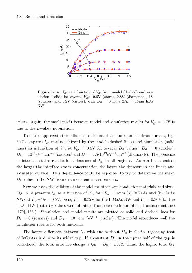
5.8. Results and discussion
0 0.2 0.4 0.6 0.8 1 1.20
5
10
15
20
25
30
35
I ds
(mA
)
Vds
(V)
Vgs
ModelSim.
Figure 5.15: Ids as a function of Vds from model (dashed) and sim-ulation (solid) for several Vgs: 0.6V (stars), 0.8V (diamonds), 1V(squares) and 1.2V (circles), with Dit = 0 for a 2Rs = 15nm InAsNW.
values. Again, the small misfit between model and simulation results for Vgs = 1.2V is
due to the L-valley population.
To better appreciate the influence of the interface states on the drain current, Fig.
5.17 compares Ids results achieved by the model (dashed lines) and simulation (solid
lines) as a function of Vds at Vgs = 0.8V for several Dit values: Dit = 0 (circles),
Dit = 1013eV−1cm−2 (squares) andDit = 1.5·1013eV−1cm−2 (diamonds). The presence
of interface states results in a decrease of Ids in all regimes. As can be expected,
the larger the interface states concentration the larger the decrease in the linear and
saturated current. This dependence could be exploited to try to determine the mean
Dit value in the NW from drain current measurements.
Now we asses the validity of the model for other semiconductor materials and sizes.
Fig. 5.18 presents Ids as a function of Vds for 2Rs = 15nm (a) InGaAs and (b) GaAs
NWs at Vgs−VT = 0.5V, being VT = 0.52V for the InGaAs NW and VT = 0.90V for the
GaAs NW (both VT values were obtained from the maximum of the transconductance
[179],[156]). Simulation and model results are plotted as solid and dashed lines for
Dit = 0 (squares) and Dit = 1013cm−2eV−1 (circles). The model reproduces well the
simulation results for both materials.
The larger difference between Ids with and without Dit in GaAs (regarding that
of InGaAs) is due to its wider gap. If a constant Dit in the upper half of the gap is
considered, the total interface charge is Qit = Dit × Eg/2. Thus, the higher total Qit
120 Electrostatics
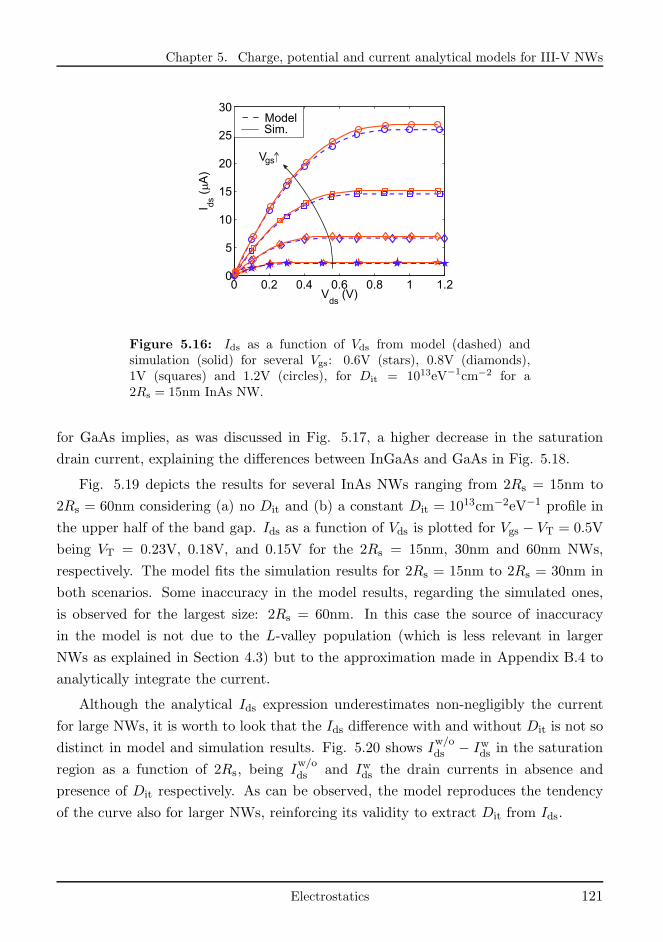
Chapter 5. Charge, potential and current analytical models for III-V NWs
0 0.2 0.4 0.6 0.8 1 1.20
5
10
15
20
25
30
Vds
(V)
I ds
( mA
)
Vgs
ModelSim.
Figure 5.16: Ids as a function of Vds from model (dashed) andsimulation (solid) for several Vgs: 0.6V (stars), 0.8V (diamonds),1V (squares) and 1.2V (circles), for Dit = 1013eV−1cm−2 for a2Rs = 15nm InAs NW.
for GaAs implies, as was discussed in Fig. 5.17, a higher decrease in the saturation
drain current, explaining the differences between InGaAs and GaAs in Fig. 5.18.
Fig. 5.19 depicts the results for several InAs NWs ranging from 2Rs = 15nm to
2Rs = 60nm considering (a) no Dit and (b) a constant Dit = 1013cm−2eV−1 profile in
the upper half of the band gap. Ids as a function of Vds is plotted for Vgs − VT = 0.5V
being VT = 0.23V, 0.18V, and 0.15V for the 2Rs = 15nm, 30nm and 60nm NWs,
respectively. The model fits the simulation results for 2Rs = 15nm to 2Rs = 30nm in
both scenarios. Some inaccuracy in the model results, regarding the simulated ones,
is observed for the largest size: 2Rs = 60nm. In this case the source of inaccuracy
in the model is not due to the L-valley population (which is less relevant in larger
NWs as explained in Section 4.3) but to the approximation made in Appendix B.4 to
analytically integrate the current.
Although the analytical Ids expression underestimates non-negligibly the current
for large NWs, it is worth to look that the Ids difference with and without Dit is not so
distinct in model and simulation results. Fig. 5.20 shows Iw/ods − Iwds in the saturation
region as a function of 2Rs, being Iw/ods and Iwds the drain currents in absence and
presence of Dit respectively. As can be observed, the model reproduces the tendency
of the curve also for larger NWs, reinforcing its validity to extract Dit from Ids.
Electrostatics 121
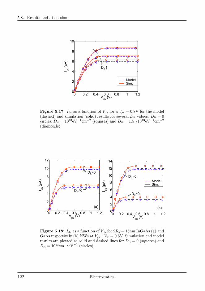
5.8. Results and discussion
0 0.2 0.4 0.6 0.8 1 1.20
2
4
6
8
10
Vds
(V)
I ds
(mA
)
ModelSim.
Dit
Figure 5.17: Ids as a function of Vds for a Vgs = 0.8V for the model(dashed) and simulation (solid) results for several Dit values: Dit = 0circles, Dit = 1013eV−1cm−2 (squares) and Dit = 1.5 ·1013eV−1cm−2
(diamonds)
0 0.2 0.4 0.6 0.8 1 1.20
2
4
6
8
10
12
I ds
(mA
)
Vds
(V) 0 0.2 0.4 0.6 0.8 1 1.20
2
4
6
8
10
12
14
I ds
(mA
)
Vds
(V)
(a) (b)
Dit=0Dit=0
Dit=0Dit=0
ModelSim.
Figure 5.18: Ids as a function of Vds for 2Rs = 15nm InGaAs (a) andGaAs respectively (b) NWs at Vgs−VT = 0.5V. Simulation and modelresults are plotted as solid and dashed lines for Dit = 0 (squares) andDit = 1013cm−2eV−1 (circles).
122 Electrostatics
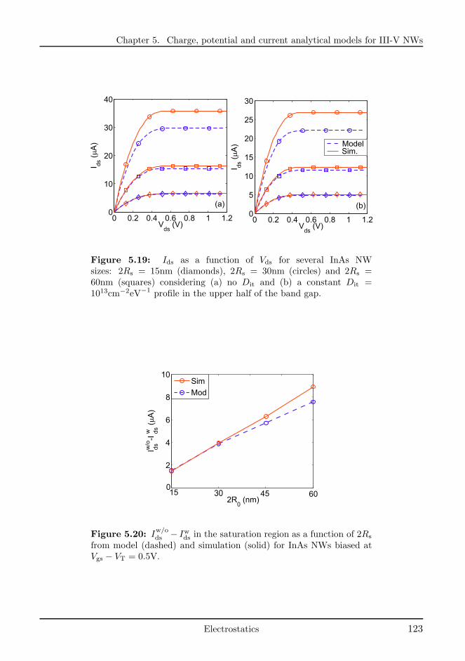
Chapter 5. Charge, potential and current analytical models for III-V NWs
0 0.2 0.4 0.6 0.8 1 1.20
10
20
30
40
Vds
(V)
I ds
(mA
)
0 0.2 0.4 0.6 0.8 1 1.20
5
10
15
20
25
30
Vds
(V)I d
s(m
A) Model
Sim.
(a) (b)
Figure 5.19: Ids as a function of Vds for several InAs NWsizes: 2Rs = 15nm (diamonds), 2Rs = 30nm (circles) and 2Rs =60nm (squares) considering (a) no Dit and (b) a constant Dit =1013cm−2eV−1 profile in the upper half of the band gap.
15 30 45 600
2
4
6
8
10
I ds
w/o
-Ids
w(m
A)
2R0
(nm)
Sim
Mod
Figure 5.20: Iw/ods − Iwds in the saturation region as a function of 2Rs
from model (dashed) and simulation (solid) for InAs NWs biased atVgs − VT = 0.5V.
Electrostatics 123
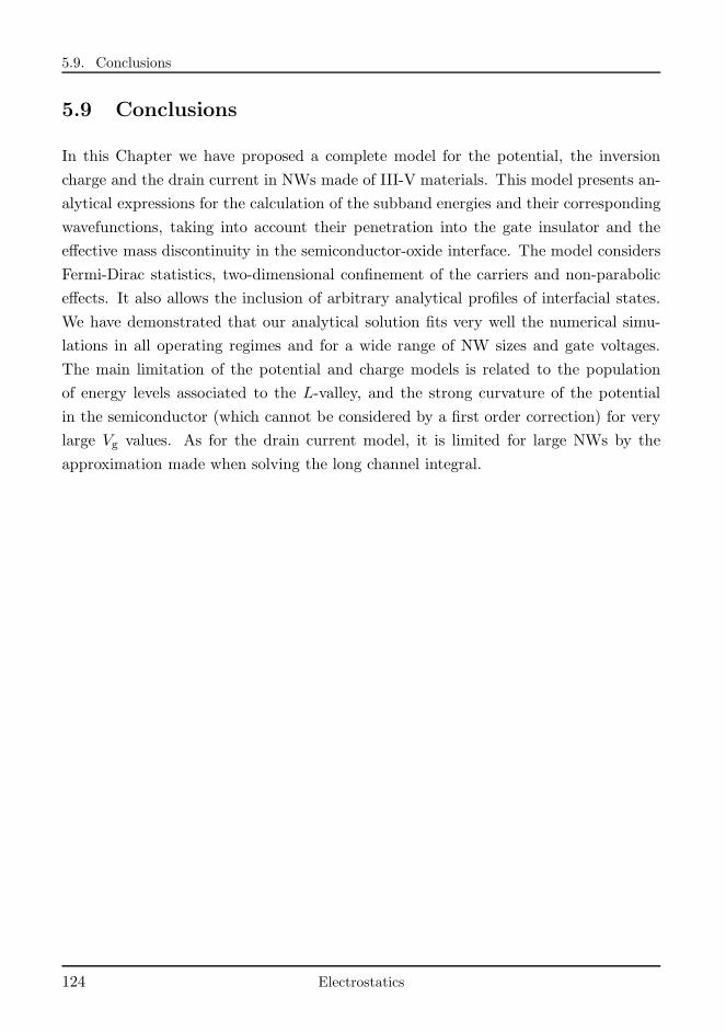
5.9. Conclusions
5.9 Conclusions
In this Chapter we have proposed a complete model for the potential, the inversion
charge and the drain current in NWs made of III-V materials. This model presents an-
alytical expressions for the calculation of the subband energies and their corresponding
wavefunctions, taking into account their penetration into the gate insulator and the
effective mass discontinuity in the semiconductor-oxide interface. The model considers
Fermi-Dirac statistics, two-dimensional confinement of the carriers and non-parabolic
effects. It also allows the inclusion of arbitrary analytical profiles of interfacial states.
We have demonstrated that our analytical solution fits very well the numerical simu-
lations in all operating regimes and for a wide range of NW sizes and gate voltages.
The main limitation of the potential and charge models is related to the population
of energy levels associated to the L-valley, and the strong curvature of the potential
in the semiconductor (which cannot be considered by a first order correction) for very
large Vg values. As for the drain current model, it is limited for large NWs by the
approximation made when solving the long channel integral.
124 Electrostatics
Chapter 6
Gate capacitance and threshold
voltage models
6.1 Introduction
In this chapter, we develop physically based analytical models for the gate capacitance
(Cg), and the threshold voltage (VT), in III-V NWs. To do so, we use the results from
charge, potential and drain current achieved in Chapter 5. All the features from the
analytical model of Chapter 5 are kept: two-dimensional quantum confinement of the
carriers, wavefunction penetration into the gate insulator, Fermi-Dirac statistics and
the conduction band non-parabolicity.
There are two main concepts that strongly affect the behavior of electrostatic mag-
nitudes in III-V NWs:
(1) The 2D quantum confinement of the carriers which leads to: (a) a displacement
of the charge density, pushed away from the semiconductor-insulator interface [62]
and (b) a change (regarding bulk) in the behavior of the density of states, which
decrease with increasing energy [140].
(2) The low effective mass (characteristic of III-V materials) which reduces the density
of states, leading to the so-called density of states bottleneck [66].
Regarding the gate capacitance, this scenario implies that Cg is reduced much below
the insulator capacitance (Cins) and the so called quantum capacitance limit can be
reached [180]. That possibility may degrade the device performance, although some
Electrostatics 125
6.1. Introduction
authors have found positive consequences regarding the control of SCEs and power-
delay product [181],[182]. In the gate capacitance model presented here we try to
achieve a better understanding, shedding light on the different terms that contribute
to Cg.
As for the threshold voltage, the traditional definition of VT (as Vg for which ψs =
2ψF being ψF the Fermi potential [183–185]) is no longer valid for III-V NWs. The
low density of states implies high surface band bendings to reach a non-negligible
electron concentration, and, consequently, a reformulation of the concept is required.
To overcome this issue, several new proposals to estimate VT have recently come up
and various articles have reviewed the different VT definitions and methods available
for its extraction [97, 179, 186–196]. However, to the best of our knowledge there is
no analytical physically based study in the literature on III-V NWs VT modeling. In
the threshold voltage model presented here we analyze the various factors which are
involved in the onset condition of the NWs providing a complete analytical expression.
The rest of this Chapter is organized as follows. Section 6.2 explains the procedure
to achieve the gate capacitance model for III-V NWs, and the different capacitance
terms are defined. In Section 6.3 we validate the gate capacitance model results with
those from the simulator presented in Chapter 3. In Section 6.4 we evaluate the contri-
bution of the different capacitance terms (the insulator capacitance, the finite density
of states and the charge distribution in the NW) to the total gate capacitance and
compare the model results with those corresponding to a Si NW. Section 6.5 explains
the process followed to achieve a VT model for III-V NWs under the parabolic band as-
sumption. In Section 6.6 we propose a non-parabolic band correction to VT. In Section
6.7 we discuss the variation on VT due to a non-null Dit. In Section 6.8 we validate the
model results with those obtained from simulation for several semiconductor materials,
NW sizes and insulator thicknesses. We also evaluate the different contributions to VT,
discuss the influence of the wavefunction penetration into the gate insulator on VT and
its dependence on the confinement effective mass of the Γ-valley. Section 6.9 sums up
the main conclusions of this Chapter. Finally, in Appendix ?? is included some calculi
related to the capacitance and threshold voltage models.
126 Electrostatics
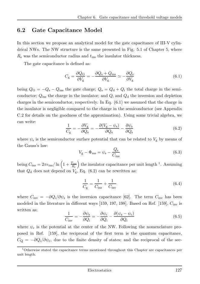
Chapter 6. Gate capacitance and threshold voltage models
6.2 Gate Capacitance Model
In this section we propose an analytical model for the gate capacitance of III-V cylin-
drical NWs. The NW structure is the same presented in Fig. 5.1 of Chapter 5, where
Rs was the semiconductor radius and tins the insulator thickness.
The gate capacitance is defined as:
Cg =∂QG
∂Vg= −∂Qs +Qins
∂Vg≃ −∂Qs
∂Vg(6.1)
being QG = −Qs − Qins the gate charge; Qs = Qd + Qi the total charge in the semi-
conductor; Qins the charge in the insulator; and Qi and Qd the inversion and depletion
charges in the semiconductor, respectively. In Eq. (6.1) we assumed that the charge in
the insulator is negligible compared to the charge in the semiconductor (see Appendix
C.2 for details on the goodness of the approximation). Using some trivial algebra, we
can write:1
Cg= − ∂Vg
∂Qs= −∂(Vg − ψs)
∂Qs− ∂ψs
∂Qs(6.2)
where ψs is the semiconductor surface potential that can be related to Vg by means of
the Gauss’s law:
Vg − Φms = ψs −Qs
Cins(6.3)
being Cins = 2πǫins/ ln(
1 + TinsRs
)
the insulator capacitance per unit length 1. Assuming
that Qd does not depend on Vg, Eq. (6.2) can be rewritten as:
1
Cg=
1
Cins+
1
Cinv(6.4)
where Cinv = −∂Qi/∂ψs is the inversion capacitance [62]. The term Cinv has been
modeled in the literature in different ways [159, 197, 198]. Based on Ref. [159], Cinv is
written as:1
Cinv= −∂ψs
∂Qi= −∂ψc
∂Qi− ∂(ψs − ψc)
∂Qi(6.5)
where ψc is the potential at the center of the NW. Following the nomenclature pro-
posed in Ref. [159], the reciprocal of the first term is the quantum capacitance,
CQ = −∂Qi/∂ψc, due to the finite density of states; and the reciprocal of the sec-
1Otherwise stated the capacitance terms mentioned throughout this Chapter are capacitances perunit length.
Electrostatics 127
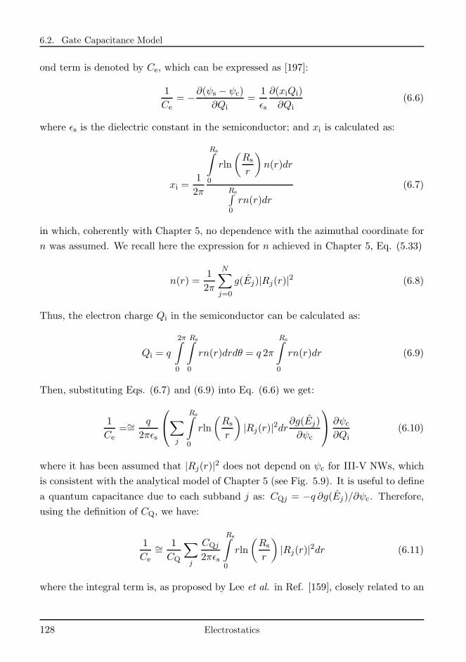
6.2. Gate Capacitance Model
ond term is denoted by Ce, which can be expressed as [197]:
1
Ce= −∂(ψs − ψc)
∂Qi=
1
ǫs
∂(xiQi)
∂Qi(6.6)
where ǫs is the dielectric constant in the semiconductor; and xi is calculated as:
xi =1
2π
Rs∫
0
rln
(
Rs
r
)
n(r)dr
Rs∫
0
rn(r)dr
(6.7)
in which, coherently with Chapter 5, no dependence with the azimuthal coordinate for
n was assumed. We recall here the expression for n achieved in Chapter 5, Eq. (5.33)
n(r) =1
2π
N∑
j=0
g(Ej)|Rj(r)|2 (6.8)
Thus, the electron charge Qi in the semiconductor can be calculated as:
Qi = q
2π∫
0
Rs∫
0
rn(r)drdθ = q 2π
Rs∫
0
rn(r)dr (6.9)
Then, substituting Eqs. (6.7) and (6.9) into Eq. (6.6) we get:
1
Ce=∼= q
2πǫs
∑
j
Rs∫
0
rln
(
Rs
r
)
|Rj(r)|2dr∂g(Ej)
∂ψc
∂ψc
∂Qi(6.10)
where it has been assumed that |Rj(r)|2 does not depend on ψc for III-V NWs, which
is consistent with the analytical model of Chapter 5 (see Fig. 5.9). It is useful to define
a quantum capacitance due to each subband j as: CQj = −q ∂g(Ej)/∂ψc. Therefore,
using the definition of CQ, we have:
1
Ce
∼= 1
CQ
∑
j
CQj
2πǫs
Rs∫
0
rln
(
Rs
r
)
|Rj(r)|2dr (6.11)
where the integral term is, as proposed by Lee et al. in Ref. [159], closely related to an
128 Electrostatics
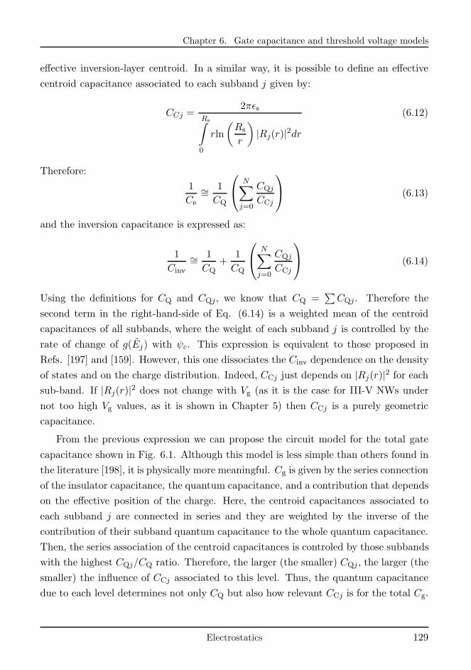
Chapter 6. Gate capacitance and threshold voltage models
effective inversion-layer centroid. In a similar way, it is possible to define an effective
centroid capacitance associated to each subband j given by:
CCj =2πǫs
Rs∫
0
rln
(
Rs
r
)
|Rj(r)|2dr
(6.12)
Therefore:
1
Ce
∼= 1
CQ
N∑
j=0
CQj
CCj
(6.13)
and the inversion capacitance is expressed as:
1
Cinv
∼= 1
CQ+
1
CQ
N∑
j=0
CQj
CCj
(6.14)
Using the definitions for CQ and CQj, we know that CQ =∑
CQj . Therefore the
second term in the right-hand-side of Eq. (6.14) is a weighted mean of the centroid
capacitances of all subbands, where the weight of each subband j is controlled by the
rate of change of g(Ej) with ψc. This expression is equivalent to those proposed in
Refs. [197] and [159]. However, this one dissociates the Cinv dependence on the density
of states and on the charge distribution. Indeed, CCj just depends on |Rj(r)|2 for each
sub-band. If |Rj(r)|2 does not change with Vg (as it is the case for III-V NWs under
not too high Vg values, as it is shown in Chapter 5) then CCj is a purely geometric
capacitance.
From the previous expression we can propose the circuit model for the total gate
capacitance shown in Fig. 6.1. Although this model is less simple than others found in
the literature [198], it is physically more meaningful. Cg is given by the series connection
of the insulator capacitance, the quantum capacitance, and a contribution that depends
on the effective position of the charge. Here, the centroid capacitances associated to
each subband j are connected in series and they are weighted by the inverse of the
contribution of their subband quantum capacitance to the whole quantum capacitance.
Then, the series association of the centroid capacitances is controled by those subbands
with the highest CQj/CQ ratio. Therefore, the larger (the smaller) CQj , the larger (the
smaller) the influence of CCj associated to this level. Thus, the quantum capacitance
due to each level determines not only CQ but also how relevant CCj is for the total Cg.
Electrostatics 129
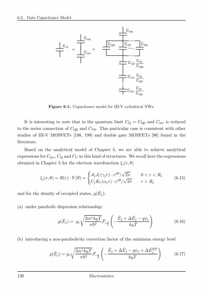
6.2. Gate Capacitance Model
GC
insC
invC
insC
Q1C QnCQ0C
C0C
C1C
CnC
QC
Q0C
QC
Q1C
QC
QnC
= =
Figure 6.1: Capacitance model for III-V cylindrical NWs.
It is interesting to note that in the quantum limit CQ = CQ0 and Cinv is reduced
to the series connection of CQ0 and CC0. This particular case is consistent with other
studies of III-V MOSFETs [198, 199] and double gate MOSFETs [96] found in the
literature.
Based on the analytical model of Chapter 5, we are able to achieve analytical
expressions for Cinv, CQ and CC in this kind of structures. We recall here the expressions
obtained in Chapter 5 for the electron wavefunction ξj(r, θ)
ξj(r, θ) = R(r) · Y (θ) =
AjJl (γjr) · eılθ/√2π 0 < r < Rs
CjKl (αjr) · eılθ/√2π r > Rs
(6.15)
and for the density of occupied states, g(Ej):
(a) under parabolic dispersion relationship:
g(Ej) = gv
√
2m∗kBTπ~2
F- 12
(
− Ej +∆Ej − qψc
kBT
)
(6.16)
(b) introducing a non-parabolicity correction factor of the minimum energy level
g(Ej) = gv
√
2m∗kBTπ~2
F- 12
(
−Ej +∆Ej − qψc +∆ENP
j
kBT
)
(6.17)
130 Electrostatics
Chapter 6. Gate capacitance and threshold voltage models
(c) considering a full non-parabolic dispersion relationship
g(Ej) =gvπ
∞∫
−∞
(
1 + e−ENP
j (k)
kBT
)−1
dk (6.18)
In Eqs. (6.15)-(6.18) we have kept the nomenclature introduced in Chapter 5. Now
we proceed to obtain an analytical expressions for CCj and CQj from the previous equa-
tions. First, substituting Eq. (6.15) in Eq. (6.12), the centroid capacitance associated
to level j is found:
CCj =2πǫs
Rs∫
0
rln
(
Rs
r
)
|AjJl(γjr)|2dr
(6.19)
where the integral in the denominator is solved for any level j in Appendix (C.1). The
resulting expression is:
CCj =2πǫsA2j
(
R2s
2J2l (γjRs) +
R2s
2J2l−1(γjRs) + (−l + 1
2)Rs
γjJl−1(γjRs)Jl(γjRs)+
+l
γ2j
l∑
m=1
J2m−1(γjRs)−
l
2γ2jJ20 (γjRs)−
l
2γ2jJ20 (0)
)−1
(6.20)
To calculate the quantum inversion-layer capacitance due to level j we derive Eqs.
(6.16), (6.17) and (6.18) with respect to ψc getting:
(a) under parabolic dispersion relation:
CQj = q2gv
√
2m∗akBTπ~2
F- 32
(
− Ej +∆Ej − qψc
kBT
)(
1− 1
q
∂∆Ej∂ψc
)
(6.21)
(b) introducing a non-parabolicity correction factor of the minimum energy level
CQj = q2gv
√
2m∗akBTπ~2
F- 32
(
−Ej +∆Ej − qψc +∆ENP
j
kBT
)(
1− 1
q
∂(∆Ej +∆ENPj )
∂ψc
)
(6.22)
Electrostatics 131
6.3. Capacitance model validation
(c) considering a full non-parabolic dispersion relation as proposed by Jin et al. [95]
CQj =1
kBT
gvπ
∞∫
−∞
e−ENP
j (k)
kBT
(
∂ENPj (k)
∂ψc
)(
1 + e−ENP
j (k)
kBT
)−2
dk (6.23)
where the derivative rule for the Fermi-Dirac integral, Fi−1(x) = dFi(x)/dx, was used.It should be noted that centroid capacitances are not modified regardless the dispersion
relation considered.
6.3 Capacitance model validation
Our intention here is to validate the analytical gate capacitance model by comparing
its results with those provided by the simulator presented in Chapter 3. To do so,
three different semiconductor materials (InAs, InxGa1−xAs (x = 0.53) and GaAs) and
three NW diameters (2Rs = 5nm, 10nm and 15nm) have been considered. Γ, X and
L valleys were taken into consideration in the simulations. Al2O3 was used as gate
insulator and tins was held to 1.5nm, which corresponds to an EOT of 0.6nm [200],
following to previous works [201]. The validity of the model was also checked for other
insulator materials and thicknesses. All material parameters are presented in Appendix
(F).First, a parabolic conduction band is assumed.
Fig. 6.2 shows the simulated (solid lines) and modeled (dashed lines) gate capac-
itance results as a function of the gate voltage for three different InGaAs NW sizes.
A good agreement is found for Vg < 0.7V in the 2Rs = 15nm case, and Vg < 1V in
the 2Rs = 5nm and 2Rs = 10nm cases. In its range of validity, the model accurately
reproduces the humps in the gate capacitance which are due to the occupation of the
first three energy levels. They are better observed in the 2Rs = 10nm NW for j = 0
around Vg = 0.6V and for j = 1, 2 around Vg = 0.9V (the inset of Fig. 6.2 shows g(Ej)
associated to these levels versus the gate voltage for this NW size). As shown in the
figure, the range of validity for the 2Rs = 15nm device can be extended taking into
account higher energy levels of the Γ-valley (j = 3, 4, l = ±2 and j = 5, 6, l = ±3).
However, for the 2Rs = 5nm and 2Rs = 10nm NWs, the upper energy levels are the first
sub-bands of the L-valley, which are not modeled in this work, and therefore considering
higher energy levels of the Γ-valley does not improve the results.
Fig. 6.3 compares the model (dashed lines) and simulation (solid lines) results for
132 Electrostatics
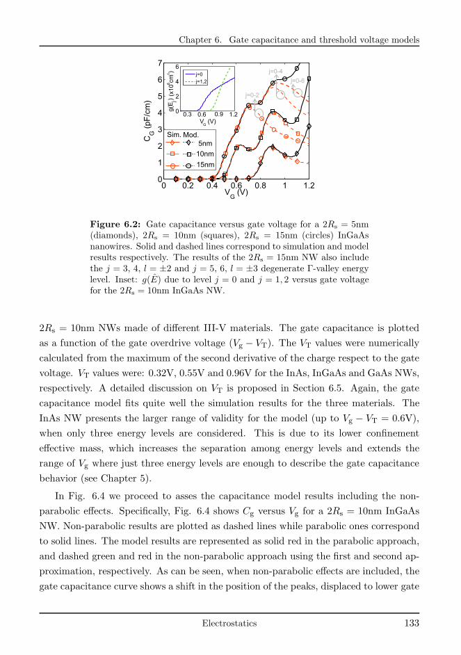
Chapter 6. Gate capacitance and threshold voltage models
0 0.2 0.4 0.6 0.8 1 1.20
1
2
3
4
5
6
7
VG
(V)
CG
(pF
/cm
)
0.3 0.6 0.9 1.20
2
4
6
VG
(V)
g(E
) j(x
106 cm
-1)
j=0
j=1,2
5nmMod.Sim.
10nm
15nm
j=0-2
j=0-6
j=0-4
Figure 6.2: Gate capacitance versus gate voltage for a 2Rs = 5nm(diamonds), 2Rs = 10nm (squares), 2Rs = 15nm (circles) InGaAsnanowires. Solid and dashed lines correspond to simulation and modelresults respectively. The results of the 2Rs = 15nm NW also includethe j = 3, 4, l = ±2 and j = 5, 6, l = ±3 degenerate Γ-valley energylevel. Inset: g(E) due to level j = 0 and j = 1, 2 versus gate voltagefor the 2Rs = 10nm InGaAs NW.
2Rs = 10nm NWs made of different III-V materials. The gate capacitance is plotted
as a function of the gate overdrive voltage (Vg − VT). The VT values were numerically
calculated from the maximum of the second derivative of the charge respect to the gate
voltage. VT values were: 0.32V, 0.55V and 0.96V for the InAs, InGaAs and GaAs NWs,
respectively. A detailed discussion on VT is proposed in Section 6.5. Again, the gate
capacitance model fits quite well the simulation results for the three materials. The
InAs NW presents the larger range of validity for the model (up to Vg − VT = 0.6V),
when only three energy levels are considered. This is due to its lower confinement
effective mass, which increases the separation among energy levels and extends the
range of Vg where just three energy levels are enough to describe the gate capacitance
behavior (see Chapter 5).
In Fig. 6.4 we proceed to asses the capacitance model results including the non-
parabolic effects. Specifically, Fig. 6.4 shows Cg versus Vg for a 2Rs = 10nm InGaAs
NW. Non-parabolic results are plotted as dashed lines while parabolic ones correspond
to solid lines. The model results are represented as solid red in the parabolic approach,
and dashed green and red in the non-parabolic approach using the first and second ap-
proximation, respectively. As can be seen, when non-parabolic effects are included, the
gate capacitance curve shows a shift in the position of the peaks, displaced to lower gate
Electrostatics 133
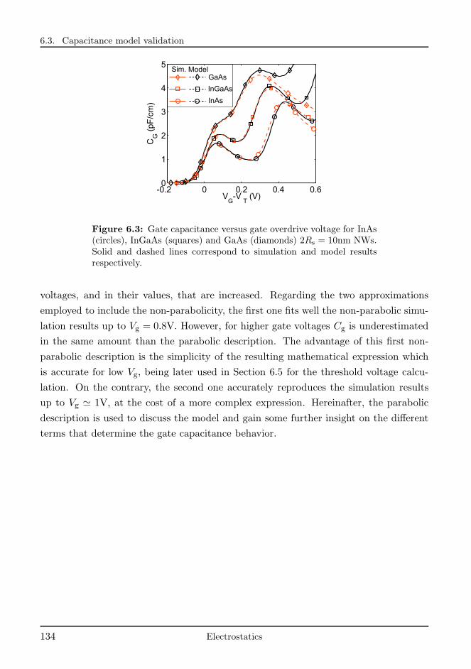
6.3. Capacitance model validation
-0.2 0 0.2 0.4 0.60
1
2
3
4
5
CG
(pF
/cm
)
VG
-VT
(V)
GaAsModelSim.
InGaAs
InAs
Figure 6.3: Gate capacitance versus gate overdrive voltage for InAs(circles), InGaAs (squares) and GaAs (diamonds) 2Rs = 10nm NWs.Solid and dashed lines correspond to simulation and model resultsrespectively.
voltages, and in their values, that are increased. Regarding the two approximations
employed to include the non-parabolicity, the first one fits well the non-parabolic simu-
lation results up to Vg = 0.8V. However, for higher gate voltages Cg is underestimated
in the same amount than the parabolic description. The advantage of this first non-
parabolic description is the simplicity of the resulting mathematical expression which
is accurate for low Vg, being later used in Section 6.5 for the threshold voltage calcu-
lation. On the contrary, the second one accurately reproduces the simulation results
up to Vg ≃ 1V, at the cost of a more complex expression. Hereinafter, the parabolic
description is used to discuss the model and gain some further insight on the different
terms that determine the gate capacitance behavior.
134 Electrostatics
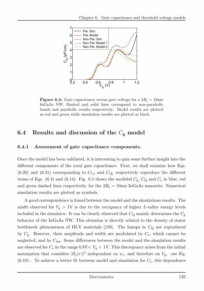
Chapter 6. Gate capacitance and threshold voltage models
0.2 0.4 0.6 0.8 1 1.20
1
2
3
4
5
6
7
CG
(pF
/cm
)
VG
(V)
Par. Sim.Par. Model
Non Par. Model 1Non Par. Model 2
Non Par. Sim.
Figure 6.4: Gate capacitance versus gate voltage for a 2Rs = 10nmInGaAs NW. Dashed and solid lines correspond to non-parabolicbands and parabolic results respectively. Model results are plottedas red and green while simulation results are plotted as black.
6.4 Results and discussion of the Cg model
6.4.1 Assessment of gate capacitance components.
Once the model has been validated, it is interesting to gain some further insight into the
different components of the total gate capacitance. First, we shall examine how Eqs.
(6.20) and (6.21) corresponding to CCj and CQj respectively reproduce the different
terms of Eqs. (6.4) and (6.14). Fig. 6.5 shows the modeled Cg, CQ and Ce in blue, red
and green dashed lines respectively, for the 2Rs = 10nm InGaAs nanowire. Numerical
simulation results are plotted as symbols.
A good correspondence is found between the model and the simulations results. The
misfit observed for Vg > 1V is due to the occupancy of higher L-valley energy levels
included in the simulator. It can be clearly observed that CQ mainly determines the Cg
behavior of the InGaAs NW. This situation is directly related to the density of states
bottleneck phenomenon of III-V materials [159]. The humps in CQ are reproduced
by Cg. However, their amplitude and width are modulated by Ce, which cannot be
neglected, and by Cins. Some differences between the model and the simulation results
are observed for Ce in the range 0.8V< Vg < 1V. This discrepancy arises from the initial
assumption that considers |Rj(r)|2 independent on ψc, and therefore on Vg, –see Eq.
(6.10)–. To achieve a better fit between model and simulation for Ce, this dependence
Electrostatics 135
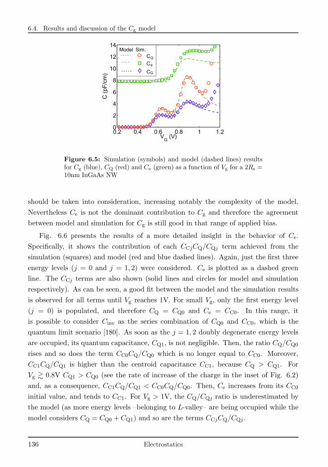
6.4. Results and discussion of the Cg model
0.2 0.4 0.6 0.8 1 1.20
2
4
6
8
10
12
14
VG
(V)
C (
pF
/cm
)
Model Sim.CQ
Ce
CG
Figure 6.5: Simulation (symbols) and model (dashed lines) resultsfor Cg (blue), CQ (red) and Ce (green) as a function of Vg for a 2Rs =10nm InGaAs NW
should be taken into consideration, increasing notably the complexity of the model.
Nevertheless Ce is not the dominant contribution to Cg and therefore the agreement
between model and simulation for Cg is still good in that range of applied bias.
Fig. 6.6 presents the results of a more detailed insight in the behavior of Ce.
Specifically, it shows the contribution of each CCjCQ/CQj term achieved from the
simulation (squares) and model (red and blue dashed lines). Again, just the first three
energy levels (j = 0 and j = 1, 2) were considered. Ce is plotted as a dashed green
line. The CCj terms are also shown (solid lines and circles for model and simulation
respectively). As can be seen, a good fit between the model and the simulation results
is observed for all terms until Vg reaches 1V. For small Vg, only the first energy level
(j = 0) is populated, and therefore CQ = CQ0 and Ce = CC0. In this range, it
is possible to consider Cinv as the series combination of CQ0 and CC0, which is the
quantum limit scenario [180]. As soon as the j = 1, 2 doubly degenerate energy levels
are occupied, its quantum capacitance, CQ1, is not negligible. Then, the ratio CQ/CQ0
rises and so does the term CC0CQ/CQ0 which is no longer equal to CC0. Moreover,
CC1CQ/CQ1 is higher than the centroid capacitance CC1, because CQ > CQ1. For
Vg & 0.8V CQ1 > CQ0 (see the rate of increase of the charge in the inset of Fig. 6.2)
and, as a consequence, CC1CQ/CQ1 < CC0CQ/CQ0. Then, Ce increases from its CC0
initial value, and tends to CC1. For Vg > 1V, the CQ/CQj ratio is underestimated by
the model (as more energy levels –belonging to L-valley– are being occupied while the
model considers CQ = CQ0 + CQ1) and so are the terms CCjCQ/CQj .
136 Electrostatics
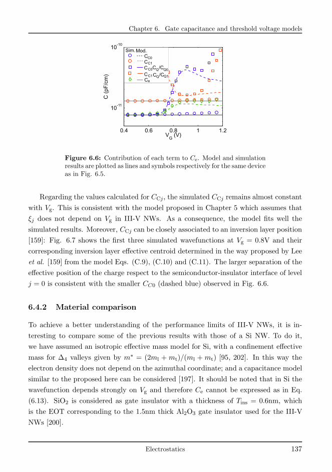
Chapter 6. Gate capacitance and threshold voltage models
0.4 0.6 0.8 1 1.2
10-11
10-10
C (
pF
/cm
)
VG
(V)
C /C
Mod.Sim.CC0CC1
CC0 Q Q0
C /CQ Q1CC1Ce
Figure 6.6: Contribution of each term to Ce. Model and simulationresults are plotted as lines and symbols respectively for the same deviceas in Fig. 6.5.
Regarding the values calculated for CCj, the simulated CCj remains almost constant
with Vg. This is consistent with the model proposed in Chapter 5 which assumes that
ξj does not depend on Vg in III-V NWs. As a consequence, the model fits well the
simulated results. Moreover, CCj can be closely associated to an inversion layer position
[159]: Fig. 6.7 shows the first three simulated wavefunctions at Vg = 0.8V and their
corresponding inversion layer effective centroid determined in the way proposed by Lee
et al. [159] from the model Eqs. (C.9), (C.10) and (C.11). The larger separation of the
effective position of the charge respect to the semiconductor-insulator interface of level
j = 0 is consistent with the smaller CC0 (dashed blue) observed in Fig. 6.6.
6.4.2 Material comparison
To achieve a better understanding of the performance limits of III-V NWs, it is in-
teresting to compare some of the previous results with those of a Si NW. To do it,
we have assumed an isotropic effective mass model for Si, with a confinement effective
mass for ∆4 valleys given by m∗ = (2ml +mt)/(ml +mt) [95, 202]. In this way the
electron density does not depend on the azimuthal coordinate; and a capacitance model
similar to the proposed here can be considered [197]. It should be noted that in Si the
wavefunction depends strongly on Vg and therefore Ce cannot be expressed as in Eq.
(6.13). SiO2 is considered as gate insulator with a thickness of Tins = 0.6nm, which
is the EOT corresponding to the 1.5nm thick Al2O3 gate insulator used for the III-V
NWs [200].
Electrostatics 137
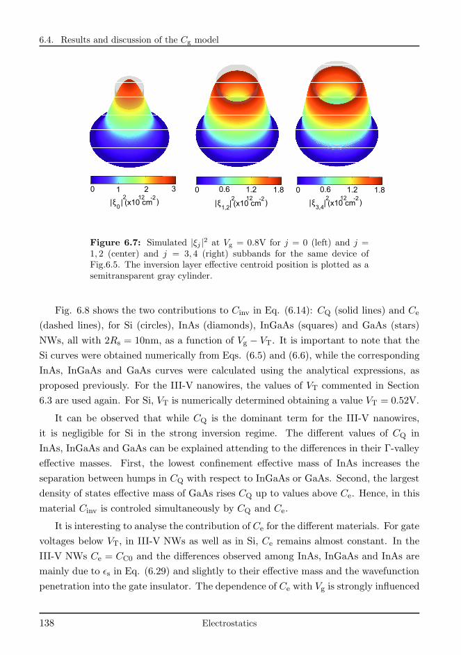
6.4. Results and discussion of the Cg model
0 1 2 3 0 0.6 1.2 1.8
|ξ0|2 -2
)(x10 cm12
|ξ1,2
|2 -2
)(x10 cm12
|ξ3,4
|2 -2
)(x10 cm12
0 0.6 1.2 1.8
Figure 6.7: Simulated |ξj |2 at Vg = 0.8V for j = 0 (left) and j =1, 2 (center) and j = 3, 4 (right) subbands for the same device ofFig.6.5. The inversion layer effective centroid position is plotted as asemitransparent gray cylinder.
Fig. 6.8 shows the two contributions to Cinv in Eq. (6.14): CQ (solid lines) and Ce
(dashed lines), for Si (circles), InAs (diamonds), InGaAs (squares) and GaAs (stars)
NWs, all with 2Rs = 10nm, as a function of Vg − VT. It is important to note that the
Si curves were obtained numerically from Eqs. (6.5) and (6.6), while the corresponding
InAs, InGaAs and GaAs curves were calculated using the analytical expressions, as
proposed previously. For the III-V nanowires, the values of VT commented in Section
6.3 are used again. For Si, VT is numerically determined obtaining a value VT = 0.52V.
It can be observed that while CQ is the dominant term for the III-V nanowires,
it is negligible for Si in the strong inversion regime. The different values of CQ in
InAs, InGaAs and GaAs can be explained attending to the differences in their Γ-valley
effective masses. First, the lowest confinement effective mass of InAs increases the
separation between humps in CQ with respect to InGaAs or GaAs. Second, the largest
density of states effective mass of GaAs rises CQ up to values above Ce. Hence, in this
material Cinv is controled simultaneously by CQ and Ce.
It is interesting to analyse the contribution of Ce for the different materials. For gate
voltages below VT, in III-V NWs as well as in Si, Ce remains almost constant. In the
III-V NWs Ce = CC0 and the differences observed among InAs, InGaAs and InAs are
mainly due to ǫs in Eq. (6.29) and slightly to their effective mass and the wavefunction
penetration into the gate insulator. The dependence of Ce with Vg is strongly influenced
138 Electrostatics
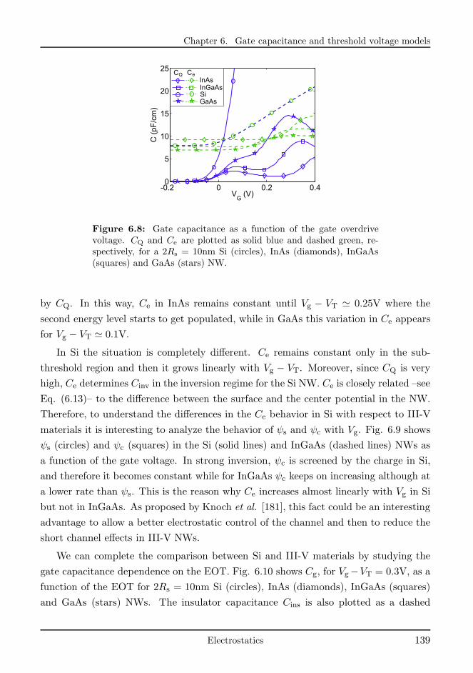
Chapter 6. Gate capacitance and threshold voltage models
-0.2 0 0.2 0.40
5
10
15
20
25
C (
pF
/cm
)
VG
(V)
GaAs
CC
InGaAsInAs
Si
Q e
Figure 6.8: Gate capacitance as a function of the gate overdrivevoltage. CQ and Ce are plotted as solid blue and dashed green, re-spectively, for a 2Rs = 10nm Si (circles), InAs (diamonds), InGaAs(squares) and GaAs (stars) NW.
by CQ. In this way, Ce in InAs remains constant until Vg − VT ≃ 0.25V where the
second energy level starts to get populated, while in GaAs this variation in Ce appears
for Vg − VT ≃ 0.1V.
In Si the situation is completely different. Ce remains constant only in the sub-
threshold region and then it grows linearly with Vg − VT. Moreover, since CQ is very
high, Ce determines Cinv in the inversion regime for the Si NW. Ce is closely related –see
Eq. (6.13)– to the difference between the surface and the center potential in the NW.
Therefore, to understand the differences in the Ce behavior in Si with respect to III-V
materials it is interesting to analyze the behavior of ψs and ψc with Vg. Fig. 6.9 shows
ψs (circles) and ψc (squares) in the Si (solid lines) and InGaAs (dashed lines) NWs as
a function of the gate voltage. In strong inversion, ψc is screened by the charge in Si,
and therefore it becomes constant while for InGaAs ψc keeps on increasing although at
a lower rate than ψs. This is the reason why Ce increases almost linearly with Vg in Si
but not in InGaAs. As proposed by Knoch et al. [181], this fact could be an interesting
advantage to allow a better electrostatic control of the channel and then to reduce the
short channel effects in III-V NWs.
We can complete the comparison between Si and III-V materials by studying the
gate capacitance dependence on the EOT. Fig. 6.10 shows Cg, for Vg−VT = 0.3V, as a
function of the EOT for 2Rs = 10nm Si (circles), InAs (diamonds), InGaAs (squares)
and GaAs (stars) NWs. The insulator capacitance Cins is also plotted as a dashed
Electrostatics 139
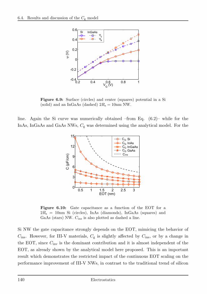
6.4. Results and discussion of the Cg model
0.2 0.4 0.6 0.8 1-0.4
-0.2
0
0.2
0.4
0.6
VG
(V)
y(V
)
Si
cy
InGaAs
ys
Figure 6.9: Surface (circles) and center (squares) potential in a Si(solid) and an InGaAs (dashed) 2Rs = 10nm NW.
line. Again the Si curve was numerically obtained –from Eq. (6.2)– while for the
InAs, InGaAs and GaAs NWs, Cg was determined using the analytical model. For the
0.5 1 1.5 2 2.5 30
3
6
9
12
15
EOT (nm)
C (
pF
/cm
)
SiInAsInGaAsGaAs
Cins
CG
CGCGCG
Figure 6.10: Gate capacitance as a function of the EOT for a2Rs = 10nm Si (circles), InAs (diamonds), InGaAs (squares) andGaAs (stars) NW. Cins is also plotted as dashed a line.
Si NW the gate capacitance strongly depends on the EOT, mimicing the behavior of
Cins. However, for III-V materials, Cg is slightly affected by Cins, or by a change in
the EOT, since Cinv is the dominant contribution and it is almost independent of the
EOT, as already shown by the analytical model here proposed. This is an important
result which demonstrates the restricted impact of the continuous EOT scaling on the
performance improvement of III-V NWs, in contrast to the traditional trend of silicon
140 Electrostatics
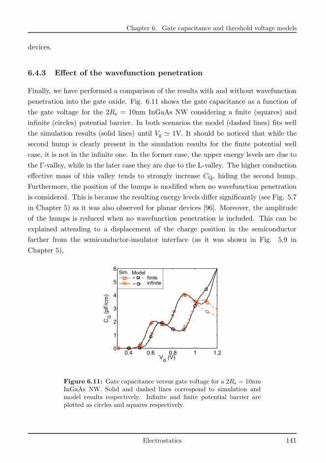
Chapter 6. Gate capacitance and threshold voltage models
devices.
6.4.3 Effect of the wavefunction penetration
Finally, we have performed a comparison of the results with and without wavefunction
penetration into the gate oxide. Fig. 6.11 shows the gate capacitance as a function of
the gate voltage for the 2Rs = 10nm InGaAs NW considering a finite (squares) and
infinite (circles) potential barrier. In both scenarios the model (dashed lines) fits well
the simulation results (solid lines) until Vg ≃ 1V. It should be noticed that while the
second hump is clearly present in the simulation results for the finite potential well
case, it is not in the infinite one. In the former case, the upper energy levels are due to
the Γ-valley, while in the later case they are due to the L-valley. The higher conduction
effective mass of this valley tends to strongly increase CQ, hiding the second hump.
Furthermore, the position of the humps is modified when no wavefunction penetration
is considered. This is because the resulting energy levels differ significantly (see Fig. 5.7
in Chapter 5) as it was also observed for planar devices [96]. Moreover, the amplitude
of the humps is reduced when no wavefunction penetration is included. This can be
explained attending to a displacement of the charge position in the semiconductor
farther from the semiconductor-insulator interface (as it was shown in Fig. 5.9 in
Chapter 5),
0.4 0.6 0.8 1 1.20
1
2
3
4
5
6
VG
(V)
CG
(pF
/cm
)
Sim. Modelfiniteinfinite
Figure 6.11: Gate capacitance versus gate voltage for a 2Rs = 10nmInGaAs NW. Solid and dashed lines correspond to simulation andmodel results respectively. Infinite and finite potential barrier areplotted as circles and squares respectively.
Electrostatics 141
6.5. Threshold voltage modeling
6.5 Threshold voltage modeling
In this Section we propose an analytical model for the threshold voltage of III-V NWs
under a parabolic dispersion relation. Due to the relevance of non-parabolicity in III-V
materials, the resulting expression will be modified in Sections 6.6 and 6.7 to consider
non-parabolicity of the conduction band and interface states, respectively. The NW
structure is the same as depicted in Fig. 5.1. As mentioned in the Introduction of
the present Chapter, when small MuG devices are considered, the traditional definition
of VT corresponding to a semiconductor surface potential band bending equal to two
times the Fermi potential is no longer valid [183–185].
Here, VT is calculated as the maximum of the second derivative of the electron
charge per unit length as a function of the gate voltage, d2Qs/dV2g , where Qs = Qi +
Qd, is the total charge in the semiconductor. Here Qi and Qd are the inversion and
depletion charges in the semiconductor and we assume that Qd = qNaπR2s does not
depend on Vg. This definition of VT has been satisfactorily used in the study of the
corner effects in MuG MOSFETs [203]. We recall the expression for Qi under parabolic
dispersion relation introduced in Chapter 5. There, we showed that, around VT, Qi can
be calculated by the carriers in the first subband (see Fig. 5.7 in Chapter 5). Thus,
the resulting expression for Qi around threshold is:
Qi = qg(E0) = qgv
√
2mtkBT
π~2F- 1
2
(
− E0 +∆E0 − qψc
kBT
)
(6.24)
where the nomenclature introduced in Chapter 5 is kept.
However, in order to develop a simple compact model, Qi in Eq. (6.24) can be
further simplified. For low gate voltages ∆E0 can be neglected since the potential in
the cross section of the NW is nearly flat and, consequently, this factor is not relevant
(see Fig. 5.7a in Chapter 5). So, after renaming Nc = qgv√
2mtkBT/π~2, we can write
Qi = Nc F- 12
(
− E0 − qψc
kBT
)
(6.25)
Additionally, the gate capacitance, Cg, was defined in Eq. (6.1) as:
Cg ≡dQG
dVg= −dQs
dVg= −dQi
dVg(6.26)
142 Electrostatics
Chapter 6. Gate capacitance and threshold voltage models
where QG is the gate charge. For just one subband, we got in Section 6.2 that Cg can
be expressed as:
Cg =
(
1
Cins+
1
CQ0+
1
CC0
)-1
(6.27)
where CQ0 and CC0 were the quantum and centroid capacitances due to the first sub-
band:
CQ0 =dQi
dψc=
q
kBTNcF- 3
2
(
− E0 − qψc
kBT
)
(6.28)
CC0 =4πǫs
A20R
2s
(
J21 (γ0Rs) + J2
0 (γ0Rs)−J0(γ0Rs)J1(γ0Rs)
γ0Rs
) (6.29)
For the sake of simplicity we define:
1
Cgeom≡ 1
Cins+
1
CC0(6.30)
Then:
d2Qi
dV 2g
= − d
dVg
11
Cgeom+
1
CQ0
=
dCQ0
dVg(
1 +CQ0
Cgeom
)2 (6.31)
Using the Gauss law we can write:
Vg −Φms − ψs =Qi
Cins+
Qd
Cins(6.32)
The surface potential can be expressed in terms of ψc as:
ψs = ψ(Rs) =qg(E0)
2πǫs
R2s
2
(
J21 (γ0Rs) + J2
0 (γ0Rs)−J0(γ0Rs)J1(γ0Rs)
γ0Rs
)
+qNaR
2s
4ǫs+ ψc
(6.33)
where we have particularized Eq. (5.50) for just one subband. Using Eqs. (6.24) and
(6.29) we can reformulate:
ψs =Qi
CC0+
Qd
4πǫs+ ψc (6.34)
Therefore, using Eq. (6.32) and assuming dQd/dψc = 0, Eq. (6.34) can be rewritten
as:dVgdψc
=dQi
dψc
1
Cins+dQi
dψc
1
CC0+ 1 (6.35)
Electrostatics 143
6.5. Threshold voltage modeling
Using Eqs. (6.28) and (6.30) Eq. (6.35) transforms into:
dVgdψc
=
(
1 +CQ0
Cgeom
)
(6.36)
So, applying the chain rule to dCQ0/dVg in Eq. (6.31) and substituting Eq. (6.36) we
get:
d2Qi
dV 2g
=
dCQ0
dψc(
1 +CQ0
Cgeom
)3 (6.37)
Although the maximum of d2Qs/dV2g could be determined differentiating Eq. (6.37)
with respect to Vg and equaling the resulting expression to zero, the procedure would
result in a non linear second order differential equation. Obtaining VT from such
expression is non trivial.
In its stead, we can consider having a deeper insight in the behavior of d2Qi/dV2g .
Substituting Eq. (6.28) into Eq. (6.37) leads to:
d2Qi
dV 2g
=
(
q
kBT
)2
NcF- 52
(
− E0 − qψc
kBT
)
[
1 +
qkBT
Nc
CgeomF- 3
2
(
− E0 − qψc
kBT
)]3 (6.38)
where we have used the derivative rule for the Fermi-Dirac integral: Fi−1(u) = dFi(u)/du.The value of ψc that maximizes this expression is the center potential at threshold volt-
age: ψ(T)c . Hereinafter we use the superscript (T) to denote the value of a potential at
Vg = VT.
For the sake of clarity let us define: x =(
−E0 + qψc
)
/kBT , and A = qkBT
NcCgeom
.
Then, determining ψ(T)c in (6.38) is equivalent to obtaining the value xm that maximizes
f(x) =F- 5
2(x)
[
1 +AF- 32(x)]3 (6.39)
The inset of Fig. 6.12 shows f(x) around its maximum for four values of A. As can
be seen, xm varies with A, which is a function of device geometry (through Cgeom) and
of the material parameters (through Nc). We have found that for all device geometries
144 Electrostatics
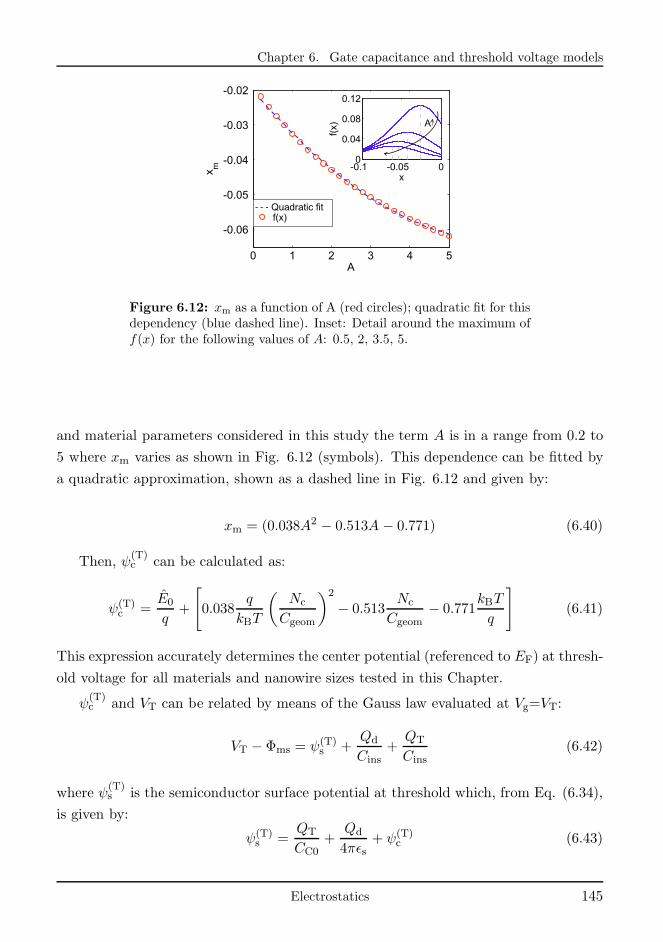
Chapter 6. Gate capacitance and threshold voltage models
0 1 2 3 4 5
-0.06
-0.05
-0.04
-0.03
-0.02
A
x m -0.1 -0.05 00
0.04
0.08
0.12
x
f(x) A
Quadratic fitf(x)
Figure 6.12: xm as a function of A (red circles); quadratic fit for thisdependency (blue dashed line). Inset: Detail around the maximum off(x) for the following values of A: 0.5, 2, 3.5, 5.
and material parameters considered in this study the term A is in a range from 0.2 to
5 where xm varies as shown in Fig. 6.12 (symbols). This dependence can be fitted by
a quadratic approximation, shown as a dashed line in Fig. 6.12 and given by:
xm = (0.038A2 − 0.513A − 0.771) (6.40)
Then, ψ(T)c can be calculated as:
ψ(T)c =
E0
q+
[
0.038q
kBT
(
Nc
Cgeom
)2
− 0.513Nc
Cgeom− 0.771
kBT
q
]
(6.41)
This expression accurately determines the center potential (referenced to EF) at thresh-
old voltage for all materials and nanowire sizes tested in this Chapter.
ψ(T)c and VT can be related by means of the Gauss law evaluated at Vg=VT:
VT − Φms = ψ(T)s +
Qd
Cins+QT
Cins(6.42)
where ψ(T)s is the semiconductor surface potential at threshold which, from Eq. (6.34),
is given by:
ψ(T)s =
QT
CC0+
Qd
4πǫs+ ψ(T)
c (6.43)
Electrostatics 145
6.6. Non-parabolic correction for the VT model
being QT the inversion charge at threshold,
QT = Nc F- 12
(
− E0 − qψ(T)c
kBT
)
(6.44)
and where ψ(T)c was given in (6.41).
6.6 Non-parabolic correction for the VT model
To provide a complete and accurate description of the threshold voltage in III-V NWs,
the effect of non-parabolic bands should not be neglected. In this Section we propose
a correction factor to Eq. (6.42) which takes into consideration the non-parabolicity
of the Γ-valley dispersion relationship. To do it, we use the correction of the parabolic
energy minimum introduced in Chapter 5, Eq. (5.60). As discussed in Fig. 5.10 in
Chapter 5, this correction is accurate enough to model the Qi versus Vg relation for low
Vg values, and it is much simpler than the complete non-parabolic dispersion relation.
Thus, using Eq. (5.60), the non-parabolic correction factor of the first energy level is:
∆ENP0 = ENP
0 − E0 (6.45)
where E0 is the parabolic band minimum and ENP0 is the non-parabolic band minimum
given by:
ENP0 = φ0 +
−1 +
√
1 + 4β(
E0 − φ0
)
2β(6.46)
being β the non-parabolic factor and φ0 defined in Eq. (5.58):
φ0 =
2π∫
0
Rs+tins∫
0
ξ0(r, θ)φ(r)ξ∗0(r, θ)rdrdθ (6.47)
where φ(r) is the total potential energy referred to ψc (see Section 5.4 for details).
Consistently with the assumption made in Section 6.5 when neglecting the energy
correction factor ∆E0, we can approximate the potential in the semiconductor as flat
and equal to ψc. In the insulator we have to add the potential barrier ∆φ to consider
the total potential energy. Therefore, φ(r) can be approximated by zero inside the
146 Electrostatics
Chapter 6. Gate capacitance and threshold voltage models
semiconductor and by ∆φ in the insulator. Then φ0 is given by2:
φ0 =1
2π
2π∫
0
Rs+tins∫
Rs
C0K0(α0r)∆φC∗0K∗0 (α0r)rdrdθ = ∆φC2
0
Rs+tins∫
Rs
|K0(α0r)|2rdr =
∆φC20
(
R2s
2[K2
0 (α0Rs) +K21 (αRs)]−
Rs + tins2
[K20 (α0(Rs + tins)) +K2
1 (α0(Rs + tins))]
)
(6.48)
where we have used Eqs. (6.15) and (B.5) However, a more compact expression for φ0
can be easily obtained if we approximate K0 by [204]:
K0(α0r) ∼=√
π
2α0re−α0r (6.49)
which for the expected values of α0r > 10 (all practical cases have been checked)
introduces an error lower than 3%. The validation of such an approximation is showed
in Appendix ??. Therefore, substituting Eq. (6.49) into Eq. (6.48) gives:
φ0 =∆φC2
0π
4α20
e−2α0Rs(
1− e−2α0tins)
(6.50)
The term e−2α0tins is actually much smaller than 1 for all practical values of the potential
barrier, semiconductor radius, confinement effective mass (which determine α0) and tins
and therefore it can be neglected. Then, using Eq. (6.50) in Eqs. (6.46) and (6.45) the
non-parabolic correction factor becomes:
∆ENP0 =
∆φC20π
4α20
e−2α0Rs − E0 +
−1 +
√
1 + 4β(
E0 −∆φC20πe
−2α0Rs/4α20
)
2β(6.51)
This non-parabolic correction factor modifies the energy level in Eq. (6.25). But, as
can be inferred from Eqs. (6.41) and (6.42), this is equivalent to a shift in VT given
by ∆ENP0 /q. Therefore, the threshold voltage expression taking into consideration
non-parabolic bands is:
VT = Φms +QT
CC0+
Qd
4πǫs+QT
Cins+
Qd
Cins+ ψ(T)
c +∆ENP
0
q(6.52)
2Please remind that C0 is not a capacitance, but the normalization constant of the wavefunction inthe insulator
Electrostatics 147
6.7. Influence of interface states on VT
where ψ(T)c is given by Eq. (6.41), QT by Eq. (6.44) and ∆ENP by Eq. (6.51).
6.7 Influence of interface states on VT
In this Section we discuss the effect of an arbitrary profile of interface states on the
threshold voltage. To this end we first determine the variation of ψc due to a non-null
Dit. As shown by Eq. (6.52) this variation of ψc can be right away translated into a
variation in VT. Therefore, we define the correction factor of VT due to a non-null Dit
as:
∆VDit= ψwDit
c − ψw/oDitc (6.53)
where the superscript wDit and w/oDit are used henceforth to refer to quantities with
and without Dit. To determine this difference we make use the model equations from
Sections 5.3 and 5.5. From Eq. (5.50) we get a generic expression for the center
potential, which taking into account that Jv(0) = 0 for v 6= 0 and J0(0) = 1:
ψc =q
2πǫa
N∑
j=0
g(Ej)A2j l
2γ2j+Da (6.54)
The first term in the right-hand-side of Eq. (6.54) is not modified ifDit is considered. As
explained in Section 5.5 the presence of a non-null Dit modify the insulator integration
constant Cb, see Eq. (5.48), and consequently constants Db and Da which depend on
it, see Eqs. (5.47) and (5.49). Therefore, we can reformulate Eq. (6.53) as:
∆VDit= DwDit
a −Dw/oDita (6.55)
where Da is given by:
Da =q
2πǫb
N∑
j=0
g(Ej)ϕbj(Rs)+Cbln(Rs)+Db−
q
2πǫa
N∑
j=0
g(Ej)ϕaj (Rs)−
q
ǫa
R2s
4Na (6.56)
Since the expression for ϕaj , ϕbj and g(Ej) do not depend on Dit we get:
DwDita −Dw/oDit
a = (CwDitb − C
w/oDit
b )ln(Rs) + (DwDitb −D
w/oDit
b ) (6.57)
148 Electrostatics
Chapter 6. Gate capacitance and threshold voltage models
with CwDitb and C
w/oDit
b given by Eqs. (5.66) and (5.48). We recall them here:
CwDitb =
Rs
ǫb
1
2π
N∑
j=0
g(Ej)ψ′aj (Rs) +
qNaRs
2− 1
2π
N∑
j=0
g(Ej)ψ′bj (Rs)
− Rs
ǫbQit (6.58)
Cw/oDit
b =Rs
ǫb
1
2π
N∑
j=0
g(Ej)ψ′aj (Rs) +
qNaRs
2− 1
2π
N∑
j=0
g(Ej)ψ′bj (Rs)
(6.59)
where Qit is the charge due to active interface traps. As discussed in Section 5.5
it comes from an integration of Dit whose limits depends on ψs. For the sake of
simplicity, we consider here that all the traps are active at threshold voltage, which is
not an unrealistic scenario looking at ψs for voltage values close to VT (see Fig. 5.14 in
Chapter 5). From Eq. (6.59) is it straightforward to find:
CwDitb − C
w/oDit
b =Rs
ǫbQit (6.60)
Finally, Db was given by Eq. (5.49):
Db = Vg − Φms −1
2πǫb
N∑
j=0
g(Ej)ϕbj(Rs + tins)− Cbln(Rs + tins) (6.61)
None of the terms in the right hand side of Eq. (6.61), except Cb, depend on Dit. Then,
introducing Eq. (6.60) into Eq. (6.61),
DwDitb −D
w/oDit
b = −Rs
ǫbQitln(Rs + tins) (6.62)
Substituting Eqs. (6.57), (6.60) and (6.62) into Eq. (6.55) we get:
∆VDit= − Qit
Cins,s(6.63)
being Cins,s = ǫb/Rsln(
1 + tinsRs
)
the insulator capacitance per unit surface Although
Eq. (6.63) is a commonly used formula in the literature, getting it reinforces the validity
of the aforementioned model equations. The resulting threshold voltage expression
Electrostatics 149
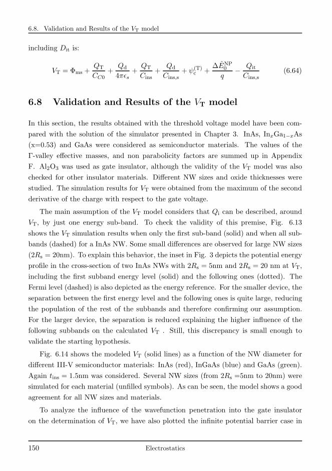
6.8. Validation and Results of the VT model
including Dit is:
VT = Φms +QT
CC0+
Qd
4πǫs+QT
Cins+
Qd
Cins,s+ ψ(T)
c +∆ENP
0
q− Qit
Cins,s(6.64)
6.8 Validation and Results of the VT model
In this section, the results obtained with the threshold voltage model have been com-
pared with the solution of the simulator presented in Chapter 3. InAs, InxGa1−xAs
(x=0.53) and GaAs were considered as semiconductor materials. The values of the
Γ-valley effective masses, and non parabolicity factors are summed up in Appendix
F. Al2O3 was used as gate insulator, although the validity of the VT model was also
checked for other insulator materials. Different NW sizes and oxide thicknesses were
studied. The simulation results for VT were obtained from the maximum of the second
derivative of the charge with respect to the gate voltage.
The main assumption of the VT model considers that Qi can be described, around
VT, by just one energy sub-band. To check the validity of this premise, Fig. 6.13
shows the VT simulation results when only the first sub-band (solid) and when all sub-
bands (dashed) for a InAs NW. Some small differences are observed for large NW sizes
(2Rs = 20nm). To explain this behavior, the inset in Fig. 3 depicts the potential energy
profile in the cross-section of two InAs NWs with 2Rs = 5nm and 2Rs = 20 nm at VT,
including the first subband energy level (solid) and the following ones (dotted). The
Fermi level (dashed) is also depicted as the energy reference. For the smaller device, the
separation between the first energy level and the following ones is quite large, reducing
the population of the rest of the subbands and therefore confirming our assumption.
For the larger device, the separation is reduced explaining the higher influence of the
following subbands on the calculated VT . Still, this discrepancy is small enough to
validate the starting hypothesis.
Fig. 6.14 shows the modeled VT (solid lines) as a function of the NW diameter for
different III-V semiconductor materials: InAs (red), InGaAs (blue) and GaAs (green).
Again tins = 1.5nm was considered. Several NW sizes (from 2Rs =5nm to 20nm) were
simulated for each material (unfilled symbols). As can be seen, the model shows a good
agreement for all NW sizes and materials.
To analyze the influence of the wavefunction penetration into the gate insulator
on the determination of VT, we have also plotted the infinite potential barrier case in
150 Electrostatics
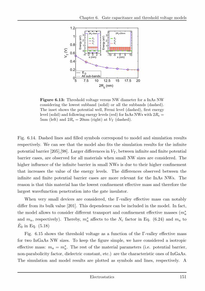
Chapter 6. Gate capacitance and threshold voltage models
5 7.5 10 12.5 15 17.5 200
0.2
0.4
0.6
0.8
1
1.2
2R0
(nm)
VT
(V)
-4 -2 0 2 4
0
1
2
3
x (nm)
Energ
y (e
V)
-10 -5 0 5 10x (nm)
2RS=5nm 2RS=20nm
EF
E0
Ej
EF
E0
E j
0
1
2
3
Energ
y (e
V)
EAll sub-bands
0
Figure 6.13: Threshold voltage versus NW diameter for a InAs NWconsidering the lowest subband (solid) or all the subbands (dashed).The inset shows the potential well, Fermi level (dashed), first energylevel (solid) and following energy levels (red) for InAs NWs with 2Rs =5nm (left) and 2Rs = 20nm (right) at VT (dashed).
Fig. 6.14. Dashed lines and filled symbols correspond to model and simulation results
respectively. We can see that the model also fits the simulation results for the infinite
potential barrier [205],[98]. Larger differences in VT, between infinite and finite potential
barrier cases, are observed for all materials when small NW sizes are considered. The
higher influence of the infinite barrier in small NWs is due to their higher confinement
that increases the value of the energy levels. The differences observed between the
infinite and finite potential barrier cases are more relevant for the InAs NWs. The
reason is that this material has the lowest confinement effective mass and therefore the
largest wavefunction penetration into the gate insulator.
When very small devices are considered, the Γ-valley effective mass can notably
differ from its bulk value [201]. This dependence can be included in the model. In fact,
the model allows to consider different transport and confinement effective masses (m∗aand ma, respectively). Thereby, m∗a affects to the Nc factor in Eq. (6.24) and ma to
E0 in Eq. (5.18)
Fig. 6.15 shows the threshold voltage as a function of the Γ-valley effective mass
for two InGaAs NW sizes. To keep the figure simple, we have considered a isotropic
effective mass: ma = m∗a. The rest of the material parameters (i.e. potential barrier,
non-parabolicity factor, dielectric constant, etc.) are the characteristic ones of InGaAs.
The simulation and model results are plotted as symbols and lines, respectively. A
Electrostatics 151
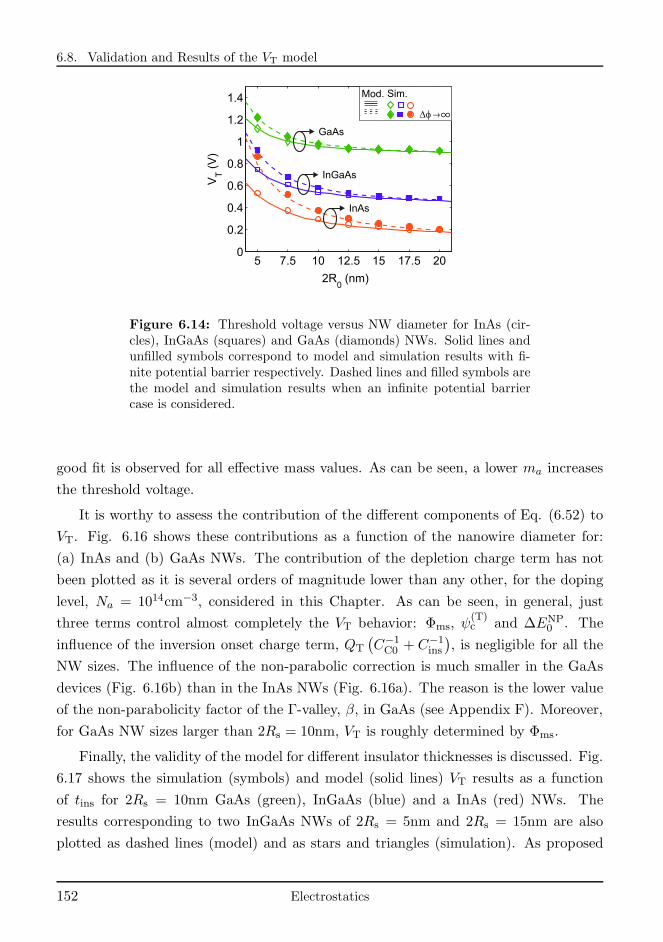
6.8. Validation and Results of the VT model
5 7.5 10 12.5 15 17.5 200
0.2
0.4
0.6
0.8
1
1.2
1.4
2R0
(nm)
VT
(V)
Mod. Sim.
Df →∞
InAs
InGaAs
GaAs
Figure 6.14: Threshold voltage versus NW diameter for InAs (cir-cles), InGaAs (squares) and GaAs (diamonds) NWs. Solid lines andunfilled symbols correspond to model and simulation results with fi-nite potential barrier respectively. Dashed lines and filled symbols arethe model and simulation results when an infinite potential barriercase is considered.
good fit is observed for all effective mass values. As can be seen, a lower ma increases
the threshold voltage.
It is worthy to assess the contribution of the different components of Eq. (6.52) to
VT. Fig. 6.16 shows these contributions as a function of the nanowire diameter for:
(a) InAs and (b) GaAs NWs. The contribution of the depletion charge term has not
been plotted as it is several orders of magnitude lower than any other, for the doping
level, Na = 1014cm−3, considered in this Chapter. As can be seen, in general, just
three terms control almost completely the VT behavior: Φms, ψ(T)c and ∆ENP
0 . The
influence of the inversion onset charge term, QT
(
C−1C0 + C−1ins
)
, is negligible for all the
NW sizes. The influence of the non-parabolic correction is much smaller in the GaAs
devices (Fig. 6.16b) than in the InAs NWs (Fig. 6.16a). The reason is the lower value
of the non-parabolicity factor of the Γ-valley, β, in GaAs (see Appendix F). Moreover,
for GaAs NW sizes larger than 2Rs = 10nm, VT is roughly determined by Φms.
Finally, the validity of the model for different insulator thicknesses is discussed. Fig.
6.17 shows the simulation (symbols) and model (solid lines) VT results as a function
of tins for 2Rs = 10nm GaAs (green), InGaAs (blue) and a InAs (red) NWs. The
results corresponding to two InGaAs NWs of 2Rs = 5nm and 2Rs = 15nm are also
plotted as dashed lines (model) and as stars and triangles (simulation). As proposed
152 Electrostatics
Chapter 6. Gate capacitance and threshold voltage models
0 0.02 0.04 0.06 0.08 0.1
0.5
0.6
0.7
0.8
0.9
ma
VT
(V)
Mod. Sim.
2R =10nm0
2R =5nm0
Figure 6.15: Threshold voltage for 2Rs = 5nm and 2Rs = 10nm In-GaAs NWs considering different Γ-valley effective masses. Model andsimulation results are plotted as solid lines and symbols, respectively.
in Section 6.5, VT in III-V NWs remains approximately constant with tins as long as
Cins is not comparable to CQ (see Section 6.2). The model reproduces the simulation
results accurately for all proposed cases.
Electrostatics 153
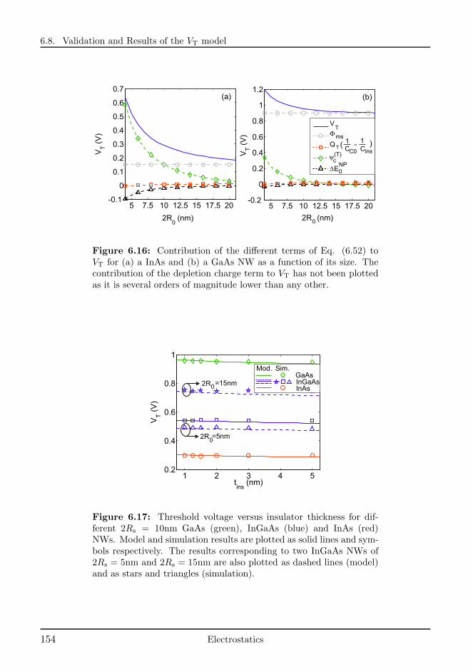
6.8. Validation and Results of the VT model
5 7.5 10 12.5 15 17.5 20-0.1
0
0.1
0.2
0.3
0.4
0.5
0.6
0.7
2R0
(nm)
VT
(V)
5 7.5 10 12.5 15 17.5 20-0.2
0
0.2
0.4
0.6
0.8
1
1.2
2R (nm)
VT
(V)
VT
ms
Q T1
C0- )
c(T)
E0NP
F
D
y
C1
insC(
(b)(a)
0
Figure 6.16: Contribution of the different terms of Eq. (6.52) toVT for (a) a InAs and (b) a GaAs NW as a function of its size. Thecontribution of the depletion charge term to VT has not been plottedas it is several orders of magnitude lower than any other.
1 2 3 4 50.2
0.4
0.6
0.8
1
tins
(nm)
VT
(V)
Mod. Sim.GaAsInGaAsInAs
2R =15nm
2R =5nm
0
0
Figure 6.17: Threshold voltage versus insulator thickness for dif-ferent 2Rs = 10nm GaAs (green), InGaAs (blue) and InAs (red)NWs. Model and simulation results are plotted as solid lines and sym-bols respectively. The results corresponding to two InGaAs NWs of2Rs = 5nm and 2Rs = 15nm are also plotted as dashed lines (model)and as stars and triangles (simulation).
154 Electrostatics
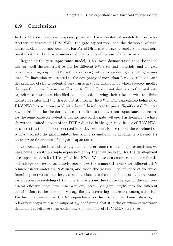
Chapter 6. Gate capacitance and threshold voltage models
6.9 Conclusions
In this Chapter, we have proposed physically based analytical models for two elec-
trostatic quantities in III-V NWs: the gate capacitance, and the threshold voltage.
These models took into consideration Fermi-Dirac statistics, the conduction band non-
parabolicity, and the two-dimensional quantum confinement of the carriers.
Regarding the gate capacitance model, it has been demonstrated that the model
fits very well the numerical results for different NW sizes and materials, and for gate
overdrive voltages up to 0.4V (in the worst case) without considering any fitting param-
eters. Its limitation was related to the occupancy of more than L-valley subbands and
the presence of strong potential curvatures in the semiconductor which severely modify
the wavefunctions obtained in Chapter 5. The different contributions to the total gate
capacitance have been identified and modeled, showing their relation with the finite
density of states and the charge distribution in the NWs. The capacitance behavior of
III-V NWs has been compared with that of their Si counterparts. Significant differences
have been found for the dominant contribution to the inversion capacitance, as well as
for the semiconductor potential dependence on the gate voltage. Furthermore, we have
shown the limited impact of the EOT reduction in the gate capacitance of III-V NWs,
in contrast to the behavior observed in Si devices. Finally, the role of the wavefunction
penetration into the gate insulator has been also analyzed, evidencing its relevance for
an accurate description of the gate capacitance.
Concerning the threshold voltage model, after some reasonable approximations, we
have come up with a simple expression of VT that will be useful for the development
of compact models for III-V cylindrical NWs. We have demonstrated that the thresh-
old voltage expression accurately reproduces the numerical results for different III-V
semiconductor materials, NW sizes, and oxide thicknesses. The influence of the wave-
function penetration into the gate insulator has been discussed, illustrating its relevance
for an accurate modeling of VT. The VT variations due to the changes in the semicon-
ductor effective mass have also been evaluated. We gave insight into the different
contributions to the threshold voltage finding interesting differences among materials.
Furthermore, we studied the VT dependence on the insulator thickness, showing no
relevant changes in a wide range of tins confirming that it is the quantum capacitance
the main capacitance term controlling the behavior of III-V MOS structures.
Electrostatics 155


Part III
Transport

Chapter 7
Boltzmann Transport Equation
and Momentum Relaxation Time
in a 1D electron gas
7.1 Introduction
The semi-classical study of the transport properties of a 1D electron gas implies the
resolution of the Boltzmann Transport Equation (BTE) [88, 206] . As it happened with
the Schrodinger and Poisson equations in the electrostatic part of this manuscript, the
BTE is not straightforward to solve in complex structures. An analytical resolution is
nearly unapproachable for most practical cases. For that reason, numerical solutions
of the BTE are commonly used to analyze the transport behavior of electronic devices.
Among them, we can highlight the Monte Carlo method, which solves the BTE col-
lecting statistics [207–211] Deterministic approaches have also been implemented [212].
Other usual approach is the linearization of the BTE using the Momentum Relaxation
Time (MRT) approximation [213–217]
In this work, we opted for evaluating the low-field electron mobility using the MRT
approximation. Thus, the main goals of this Chapter are: 1) to set up the necessary
background on the BTE in a 1D electron gas, spotlighting those issues which needs
clear understanding and 2) present the linearization of the BTE which is used for its
resolution showing the approaches needed to carry it out.
The rest of the Chapter is organized as follows. In Section 7.2 we introduce the
Transport 159
7.2. Boltzmann Transport Equation
BTE and particularize it for the description of the electron transport in a 1D gas.
Section 7.3 discuss the collision term of the BTE, that includes the effect of the the
scattering phenomena and the perturbing potential that they induce through the Fermi
Golden Rule. In Section 7.4, the linearization of the BTE and the definition of the
MRT are presented, and highlighting their implications. Sections 7.5 and 7.6 compare
two approaches (explicit and implicit) to solve the equations presented in Section 7.4.
In Section 7.7, we introduce the Kubo-Greenwood formula for the calculation of the
mobility from the solutions of the linearized BTE. This Chapter also includes Appendix
D that deals with the scattering mechanism employed in this work. Finally, Section
7.8 recapitulate the main conclusions obtained thorough the Chapter.
7.2 Boltzmann Transport Equation
In this Section we introduce the BTE and we particularize it to characterize the trans-
port phenomena in a 1D electron gas. The BTE describes the evolution in the real
space, momentum space and time of a statistical distribution of classical particles. Its
derivation can be found in several textbooks [88, 206, 218–220]. The most general
formulation is:df
dt=
[
∂f
∂t
]
diffusion
+
[
∂f
∂t
]
forces
+
[
∂f
∂t
]
collisions
(7.1)
where f is the distribution function and describes the probability of finding a particle
with a certain position and momentum at a given instant of time. Equation (7.1) reads
as follows: the distribution function f changes with time by three different mechanisms:
(i) particle’s motion diffusion (which implies a change in position), (ii) external forces
(which implies a change in momentum), and (iii) particle collisions.
When the particles to be modeled by the BTE are electrons in a semiconductor,
f = f(r,k, t), describes the electron distribution, and the first two factors of Eq. (7.1)
can be particularized as [219], [206]:
[
∂f
∂t
]
diffusion
= −1
~∇kEj(k) · ∇f(r,k, t) (7.2)
and[
∂f
∂t
]
forces
= −qF~
· ∇kf(r,k, t) (7.3)
being F the external applied electric field.
160 Transport
Chapter 7. BTE and MRT in a 1D electron gas
The derivation of Eq. (7.2) reads as follows: the net change in the electron distri-
bution due to electron diffusion is equal to the product of the spatial gradient, which
points in the direction of spatial change of the electron distribution, times the veloc-
ity which determines the rate of spatial change of the position with time. A similar
statement can be derived for Eq. (7.3).
Finally, distribution’s change with time due to collisions can be written as:
[
∂f
∂t
]
collisions
= Sin(r,k, t) − Sout(r,k, t) (7.4)
where Sin and Sout stand for the rate of particles changing their wavevector to k and/or
their position to r after a collision and the rate of particles changing their wavevector
from k and/or their position from r after a collision, respectively.
Using Eqs. (7.2), (7.3) and (7.4), the BTE for electrons in semiconductors can be
reformulated as 1:
df(r,k, t)
dt+
1
~∇kEj(k) ·∇f(r,k, t)+
qF
~·∇kf(r,k, t) = Sin(r,k, t)−Sout(r,k, t) (7.5)
Equation (7.5) determines the change with time of the electron distribution in a
3D electron gas under a semi-classical approach2. However the object of interest along
this manuscript is the study of MuG structures with 2D spatial confinement. The two
paradigms, quantum mechanical (provided by the solution of the 2D Schrodinger and
Poisson equations in the cross-section of the MuG structure in Chapter 2) and semi-
classical (determined by the Boltzmann transport equation) need to be reassembled.
The main assumption is to consider that the potential along the transport direction, z,
of the MuG structure varies pretty slowly and thus the electron wavefunction in that
direction can be approximated by a plane wave.
Then, the 2D Schrodinger and Poisson equations are solved for the NW cross-section
(as proposed in Chapter 2) at each position z (and potential V ) along the NW length.
Since no dependence on z of the semiconductor Hamiltonian is expected, the inclusion
of V (z) can be modeled as a variation of the Fermi level along the NW length [213].
1The derivation of Eq. (7.5) is completely equivalent to that done by some authors in the literature[88] by just applying the chain rule to df(r,k, t)/dt and assuming that r and k are independent andfunctions of time. We have opted for the one presented here as it provides a deeper understanding onthe physics.
2Electrons in Eq. (7.5) are considered classical particles, but the collisions can be treated quantummechanically, as will be shown in Section 7.3.
Transport 161
7.3. Scattering rate and perturbation potentials. Fermi Golden Rule
From the previous discussion we conclude that the six dimensional phase space r−k
of Eq. (7.5) is reduced to a 2D space z − kz and Eq. (7.5) is particularized for the 1D
electron gas as:
dfj(z, kz, t)
dt+
1
~
∂Ej(kz)
∂kz
∂fj(z, kz, t)
∂z+qFz
~
∂fj(z, kz, t)
∂kz=
= Sin,j(z, kz, t)− Sout,j(z, kz, t) (7.6)
where f , Sin and Sout are discretized for each subband j and Fz = −∂V (z)/∂z is the
longitudinal component of the electric field.
In the next Section, the rates of change in the electron states due to collisions,
Sin and Sout, are presented and their relation to the scattering phenomena and the
perturbing potentials that they generate are discussed.
7.3 Scattering rate and perturbation potentials. Fermi
Golden Rule
For an electron gas, Sin and Sout can be attributed to scattering events which perturb
the electron free-flights, changing their ballistic trajectory. Three assumptions are made
for the physical modeling of the scattering events: (a) the collisions occur in a very
short time scale and can be considered as instantaneous; (b) the collisions produce a
change in the particles trajectory modifying their wavenumber but they do not change
the particles’ position; and (c) the scattering interaction is weak [206].
Under these three assumptions, Sout,j can be written as:
Sout,j(z, kz, t) = fj(z, kz, t)∑
j′,k′z
Sj,j′(kz, k′z)[
1− fj′(z, k′z, t)
]
(7.7)
Eq. (7.7) reads as: the rate of electrons leaving the subband j and wavenumber kz
after a collision (also called the scattering output flux) at a given position z and time
t, is equal to the probability of finding the (kz, j) state3 occupied, fj(z, kz, t), times the
sum for all possible final states (k′z, j′) of the probability of finding the state empty,
[1 − fj′(z, k′z, t)], times the scattering rate from the state (j, kz) to the state (j′, k′z),
3We use the notation (kz, j) to refer to an electron belonging to the subband j with wavenumberkz.
162 Transport
Chapter 7. BTE and MRT in a 1D electron gas
Sj,j′(kz, k′z). A similar reasoning can be used to obtain the scattering input flux, Sin,j :
Sin,j(z, kz, t) = [1− fj(z, kz, t)]∑
j′,k′z
Sj′,j(k′z, kz)fj′(z, k
′z, t) (7.8)
Using Eqs. (7.7) and (7.8) into Eq. (7.6) the resulting 1D Boltzman equation for the
subband j is:
dfj(z, kz, t)
dt− 1
~
∂Ej(kz)
∂kz
∂fj(z, kz, t)
∂z+qFz
~
∂fj(z, kz, t)
∂kz=
[1− fj(z, kz, t)]∑
j′,k′z
Sj,j′(k′z, kz)fj′(z, k
′z, t)− fj(z, kz, t)
∑
j′,k′z
Sj′,j(k′z, kz)
[
1− f ′j(z, k′z, t)
]
(7.9)
To determine Sj,j′(kz, k′z) we use the Fermi Golden Rule which provides an expres-
sion for Sj,j′(k, k′) given the perturbation potential, ψ, caused by the corresponding
scattering mechanism. A detailed derivation of the Fermi Golden Rule for systems con-
fined in one dimension can be found in several textbooks [88], [206], [220]. Here we just
present the main steps applied to the 2D MuG structures studied in this manuscript,
where the electron is confined in two dimensions.
The derivation of the Fermi Golden Rule starts with the time dependent Schrodinger
equation for the electron including a perturbing potential due to the scattering mech-
anism. Using the EMA and particularizing for a 1D electron gas, it can be rewritten
as:
[H(r) + φ(r, t)]Ψj(r, t) = ı~dΨj(r, t)
dt(7.10)
where H(r) is the Hamiltonian operator of the electrostatic unperturbed problem pre-
sented in Chapter 2, in Eq. (2.9), and φ = −qψ is the electron potential energy due
to the perturbing potential. The solution of the perturbed problem can be written
as a linear combination in the wavenumber space of the solutions of the unperturbed
problem, Ψ(r, t) [206]. Thus:
Ψ(r, t) =∑
i,kz
ckz(t)ξi,kz(x, y)eıkzz√Le−
ıEi(kz)t
~ (7.11)
where the unperturbed solution was written as in Chapter 2 and assuming a plane wave
dependency with time, where i and kz are the indexes for the subband and wavenumber,
Transport 163
7.3. Scattering rate and perturbation potentials. Fermi Golden Rule
respectively. To determine the coefficients cktextz(t), Eq. (7.11) is substituted into Eq.
(7.10) leading to:
φ(r, t)∑
i,kz
ckz(t)ξi,kz(x, y)eıkzz√Le−
ıEi(kz)t
~ = ı~∑
i,kz
ξi,kz(x, y)eıkzz√Le−
ıEi(kz)t
~dckz(t)
dt
(7.12)
The scattering process moves the electron from an initial state (kzo, j) to a final
state (k′zo, j′). Multiplying both sides of Eq. (7.12) by the electron wavefunction after
the collision, ξ∗j′,k′zo(x, y)eık
′zoz√L
, integrating over the volume of the device, V, and taking
into consideration the orthonormality of the solutions of the Schrodinger equation we
get:
∑
i,kz
ckz(t)
∫
Vξi,kz (x, y)
eıkzz√Lφ(r, t)ξ∗j′,k′zo(x, y)
e−ık′zoz
√L
dV e−ıEi(kz)t
~ eıE
j′ (k′zo)t
~ = ı~dck′zo(t)
dt
(7.13)
For the mechanisms of interest, a plane wave time dependency of the perturbing po-
tential is assumed [206]:
φ(r, t) = φ(r)e±ıωt (7.14)
Then:∑
i,kz
ckz(t)Mi,j′(kz, k′zo)e
−ı(Ei(kz)−E
j′ (k′zo)±~ω)t
~ = ı~dck′zo(t)
dt(7.15)
where
Mi,j′(kz, k′zo) =
∫
Vξi,kz(x, y)
eıkzz√Lφ(r, t)ξ∗j′,k′zo(x, y)
e−ık′zoz
√L
dV (7.16)
is the matrix element for the interaction between states (kz, i) and (kzo, j′). Since the
scattering interaction is weak we can assume that the electron initial wavenumber kzo
is the main contribution to the sum in Eq. (7.12). In other words ck(t) ≪ ckzo(t) = 1
Then:
Mj,j′(kzo, k′zo)e
−ı(Ej (kzo)−E
j′ (k′zo)±~ω)t
~ = ı~dck′zo(t)
dt(7.17)
Integrating Eq. (7.15) for a certain period of time, T , in which the scattering event
takes place, we can write:
ck′zo(T ) =2
ı~Mj,j′(kzo, k
′zo)e
−ı(Ej (kzo)−E
j′ (k′zo)±~ω)T
2~ sin
(
Ej(kzo)− Ej′(k′zo)± ~ω
2~T
)
(7.18)
164 Transport
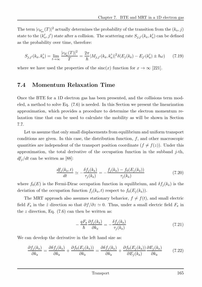
Chapter 7. BTE and MRT in a 1D electron gas
The term |ck′zo(T )|2 actually determines the probability of the transition from the (ko, j)
state to the (k′o, j′) state after a collision. The scattering rate Sj,j′(kz, k
′z) can be defined
as the probability over time, therefore:
Sj,j′(kz, k′z) = lim
t→∞|ck′z(T )|2
T=
2π
~|Mj,j′(kz, k
′z)|2δ(Ej(kz)− Ej′(k
′z)± ~ω) (7.19)
where we have used the properties of the sinc(x) function for x→ ∞ [221].
7.4 Momentum Relaxation Time
Once the BTE for a 1D electron gas has been presented, and the collisions term mod-
eled, a method to solve Eq. (7.6) is needed. In this Section we present the linearization
approximation, which provides a procedure to determine the electron momentum re-
laxation time that can be used to calculate the mobility as will be shown in Section
7.7.
Let us assume that only small displacements from equilibrium and uniform transport
conditions are given. In this case, the distribution function, f , and other macroscopic
quantities are independent of the transport position coordinate (f 6= f(z)). Under this
approximation, the total derivative of the occupation function in the subband j-th,
dfj/dt can be written as [88]:
dfj(kz, t)
dt≃ −δfj(kz)
τj(kz)= −fj(kz)− f0(Ej(kz))
τj(kz)(7.20)
where f0(E) is the Fermi-Dirac occupation function in equilibrium, and δfj(kz) is the
deviation of the occupation function fj(kz, t) respect to f0(Ej(kz)).
The MRT approach also assumes stationary behavior, f 6= f(t), and small electric
field Fz in the z direction so that ∂f/∂z ≃ 0. Thus, under a small electric field Fz in
the z direction, Eq. (7.6) can then be written as:
− qFz
~
∂fj(kz)
∂kz= −δfj(kz)
τj(kz)(7.21)
We can develop the derivative in the left hand size as:
∂fj(kz)
∂kz=∂δfj(kz)
∂kz+∂f0(Ej(kz))
∂kz=∂δfj(kz)
∂kz+∂f0(Ej(kz))
∂Ej(kz)
∂Ej(kz)
∂kz(7.22)
Transport 165
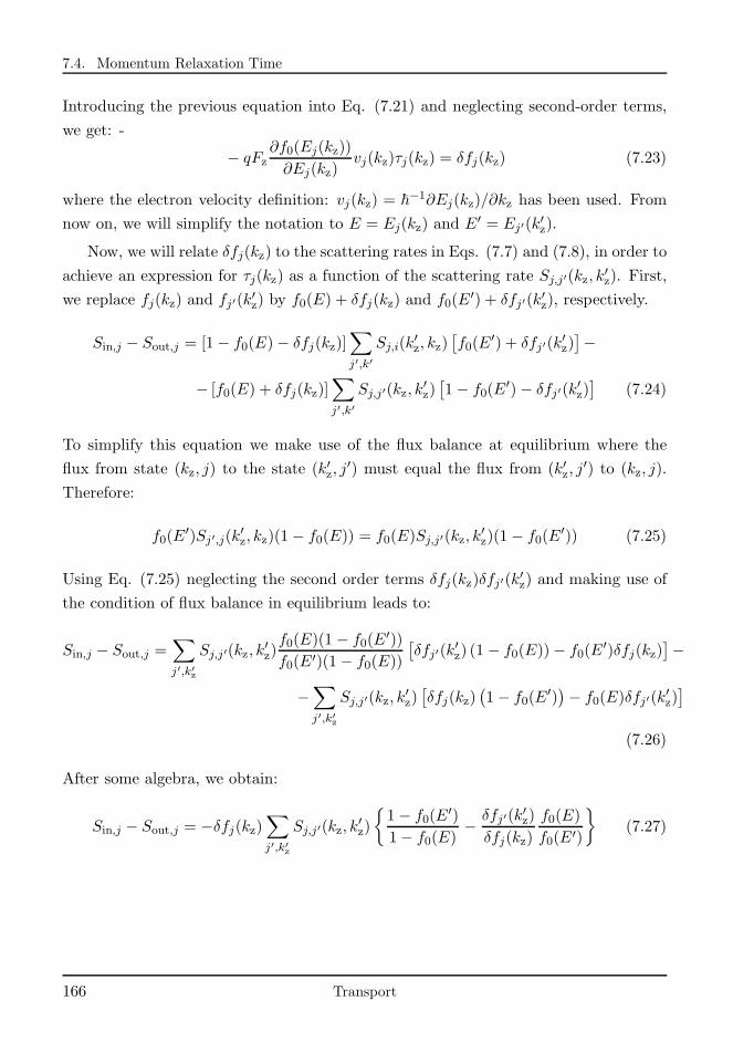
7.4. Momentum Relaxation Time
Introducing the previous equation into Eq. (7.21) and neglecting second-order terms,
we get: -
− qFz∂f0(Ej(kz))
∂Ej(kz)vj(kz)τj(kz) = δfj(kz) (7.23)
where the electron velocity definition: vj(kz) = ~−1∂Ej(kz)/∂kz has been used. From
now on, we will simplify the notation to E = Ej(kz) and E′ = Ej′(k
′z).
Now, we will relate δfj(kz) to the scattering rates in Eqs. (7.7) and (7.8), in order to
achieve an expression for τj(kz) as a function of the scattering rate Sj,j′(kz, k′z). First,
we replace fj(kz) and fj′(k′z) by f0(E) + δfj(kz) and f0(E
′) + δfj′(k′z), respectively.
Sin,j − Sout,j = [1− f0(E)− δfj(kz)]∑
j′,k′
Sj,i(k′z, kz)
[
f0(E′) + δfj′(k
′z)]
−
− [f0(E) + δfj(kz)]∑
j′,k′
Sj,j′(kz, k′z)[
1− f0(E′)− δfj′(k
′z)]
(7.24)
To simplify this equation we make use of the flux balance at equilibrium where the
flux from state (kz, j) to the state (k′z, j′) must equal the flux from (k′z, j
′) to (kz, j).
Therefore:
f0(E′)Sj′,j(k
′z, kz)(1− f0(E)) = f0(E)Sj,j′(kz, k
′z)(1− f0(E
′)) (7.25)
Using Eq. (7.25) neglecting the second order terms δfj(kz)δfj′(k′z) and making use of
the condition of flux balance in equilibrium leads to:
Sin,j − Sout,j =∑
j′,k′z
Sj,j′(kz, k′z)f0(E)(1 − f0(E
′))f0(E′)(1− f0(E))
[
δfj′(k′z) (1− f0(E))− f0(E
′)δfj(kz)]
−
−∑
j′,k′z
Sj,j′(kz, k′z)[
δfj(kz)(
1− f0(E′))
− f0(E)δfj′(k′z)]
(7.26)
After some algebra, we obtain:
Sin,j − Sout,j = −δfj(kz)∑
j′,k′z
Sj,j′(kz, k′z)
1− f0(E′)
1− f0(E)− δfj′(k
′z)
δfj(kz)
f0(E)
f0(E′)
(7.27)
166 Transport
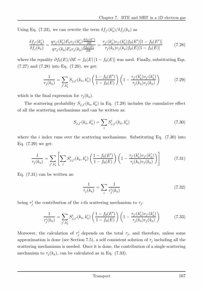
Chapter 7. BTE and MRT in a 1D electron gas
Using Eq. (7.23), we can rewrite the term δfj′(k′z)/δfj(kz) as
δfj′(k′z)
δfj(kz)=qτj′(k
′z)Fzvj′(k
′z)∂f0(E′)∂E
qτj′(kz)Fzvj(kz)∂f0(E)∂E
=τj′(k
′z)vj′(k
′z)f0(E
′)[1− f0(E′)]
τj(kz)vj(kz)f0(E)[1 − f0(E)](7.28)
where the equality ∂f0(E)/∂E = f0(E) [1− f0(E)] was used. Finally, substituting Eqs.
(7.27) and (7.28) into Eq. (7.20), we get:
1
τj(kz)=∑
j′,k′z
Sj,j′(kz, k′z)
(
1− f0(E′)
1− f0(E)
)(
1− τj′(k′z)vj′(k
′z)
τj(kz)vj(kz)
)
(7.29)
which is the final expression for τj(kz).
The scattering probability Sj,j′(kz, k′z) in Eq. (7.29) includes the cumulative effect
of all the scattering mechanisms and can be written as:
Sj,j′(kz, k′z) =
∑
i
Sij,j′(kz, k′z) (7.30)
where the i index runs over the scattering mechanisms. Substituting Eq. (7.30) into
Eq. (7.29) we get:
1
τj(kz)=∑
j′,k′z
[
∑
i
Sij,j′(kz, k′z)
(
1− f0(E′)
1− f0(E)
)(
1− τj′(k′z)vj′(k
′z)
τj(kz)vj(kz)
)
]
(7.31)
Eq. (7.31) can be written as:
1
τj(kz)=∑
i
1
τ ij(kz)(7.32)
being τ ij the contribution of the i-th scattering mechanism to τj:
1
τ ij(kz)=∑
j′,k′z
Sij,j′(kz, k′z)
(
1− f0(E′)
1− f0(E)
)(
1− τj′(k′z)vj′(k
′z)
τj(kz)vj(kz)
)
(7.33)
Moreover, the calculation of τ ij depends on the total τj , and therefore, unless some
approximation is done (see Section 7.5), a self consistent solution of τj including all the
scattering mechanisms is needed. Once it is done, the contribution of a single scattering
mechanism to τj(kz), can be calculated as in Eq. (7.33).
Transport 167
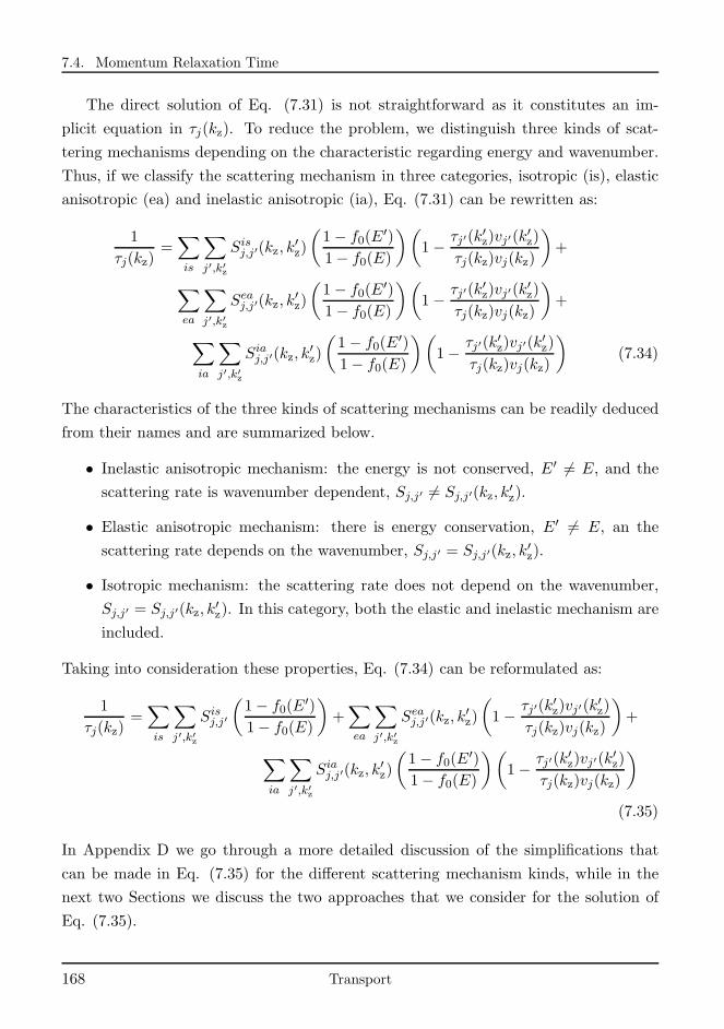
7.4. Momentum Relaxation Time
The direct solution of Eq. (7.31) is not straightforward as it constitutes an im-
plicit equation in τj(kz). To reduce the problem, we distinguish three kinds of scat-
tering mechanisms depending on the characteristic regarding energy and wavenumber.
Thus, if we classify the scattering mechanism in three categories, isotropic (is), elastic
anisotropic (ea) and inelastic anisotropic (ia), Eq. (7.31) can be rewritten as:
1
τj(kz)=∑
is
∑
j′,k′z
Sisj,j′(kz, k′z)
(
1− f0(E′)
1− f0(E)
)(
1− τj′(k′z)vj′(k
′z)
τj(kz)vj(kz)
)
+
∑
ea
∑
j′,k′z
Seaj,j′(kz, k′z)
(
1− f0(E′)
1− f0(E)
)(
1− τj′(k′z)vj′(k
′z)
τj(kz)vj(kz)
)
+
∑
ia
∑
j′,k′z
Siaj,j′(kz, k′z)
(
1− f0(E′)
1− f0(E)
)(
1− τj′(k′z)vj′(k
′z)
τj(kz)vj(kz)
)
(7.34)
The characteristics of the three kinds of scattering mechanisms can be readily deduced
from their names and are summarized below.
• Inelastic anisotropic mechanism: the energy is not conserved, E′ 6= E, and the
scattering rate is wavenumber dependent, Sj,j′ 6= Sj,j′(kz, k′z).
• Elastic anisotropic mechanism: there is energy conservation, E′ 6= E, an the
scattering rate depends on the wavenumber, Sj,j′ = Sj,j′(kz, k′z).
• Isotropic mechanism: the scattering rate does not depend on the wavenumber,
Sj,j′ = Sj,j′(kz, k′z). In this category, both the elastic and inelastic mechanism are
included.
Taking into consideration these properties, Eq. (7.34) can be reformulated as:
1
τj(kz)=∑
is
∑
j′,k′z
Sisj,j′
(
1− f0(E′)
1− f0(E)
)
+∑
ea
∑
j′,k′z
Seaj,j′(kz, k′z)
(
1− τj′(k′z)vj′(k
′z)
τj(kz)vj(kz)
)
+
∑
ia
∑
j′,k′z
Siaj,j′(kz, k′z)
(
1− f0(E′)
1− f0(E)
)(
1− τj′(k′z)vj′(k
′z)
τj(kz)vj(kz)
)
(7.35)
In Appendix D we go through a more detailed discussion of the simplifications that
can be made in Eq. (7.35) for the different scattering mechanism kinds, while in the
next two Sections we discuss the two approaches that we consider for the solution of
Eq. (7.35).
168 Transport
Chapter 7. BTE and MRT in a 1D electron gas
7.5 Explicit calculation of the MRT
In this Section we present an explicit approximation for the calculation of the MRT that
has been extensively used in the literature, see for example Refs. [213–217, 222]. Instead
of solving the equation system previously proposed, the explicit approach manipulates
Eq. (7.35) under some approximations to achieve a simpler explicit solution for τj .
The main assumption of the explicit calculation considers that there are small dif-
ferences between τj(kz) and τj′(k′z) for all sub-bands, j, j
′ and wave-vectors kz and k′z.
Using that approximation, τj(k′z)/τi(kz) ≃ 1, and the MRT of an elastic anisotropic
mechanism can be written as:
1
τ eaj (kz)=∑
j′,k′z
Seaj,j′(kz, k′z)
(
1− vj′(k′z)
vj(kz)
)
(7.36)
Equivalently, the MRT of an inelastic anisotropic mechanism is calculated as:
1
τ iaj (kz)=∑
j,k′z
Siaj,j′(kz, k′z)
(
1− f0(E′)
1− f0(E)
)(
1− vj′(k′z)
vj(kz)
)
(7.37)
Then the total MRT for state (kz, j) is:
1
τj(kz)=∑
ii
1
τ isj (kz)+∑
ea
1
τ eaj (kz)+∑
ia
1
τ iaj (kz)(7.38)
where each contribution τ iaj (kz), τeaj (kz) and τ
iij (kz) is calculated as in Appendix D by
just simplifying Eqs. (D.7), (D.10) and (D.14) using τj(k′z) = τi(kz). Therefore, the
explicit approach allows the independent and explicit calculation of the MRT due to
each scattering mechanism. The total MRT is then obtained by applying the so-called
Matthiessen rule at each kz value [223] as in Eq. (??)
The assumption made in Eqs. (7.36) and (7.37) seems quite arguable as it implies
that τ does not depend on k neither on the subband. However, the explicit calculation
does work in many cases. The reason concerns the scattering rate Sj,j′ and the sym-
metry of the structures studied. When symmetric structures are considered, most of
the scattering mechanisms result in a nearly diagonal Sj,j′ matrix. Consequently, the
highest weight of the(
1− τj′ (k′z)vj′ (k
′z)
τj(kz)vj (kz)
)
term in the (j′, k′z) sum correspond to k′z = kz
where the approximation τj(k′)/τi(k) ≃ 1 is fully satisfied.
Transport 169
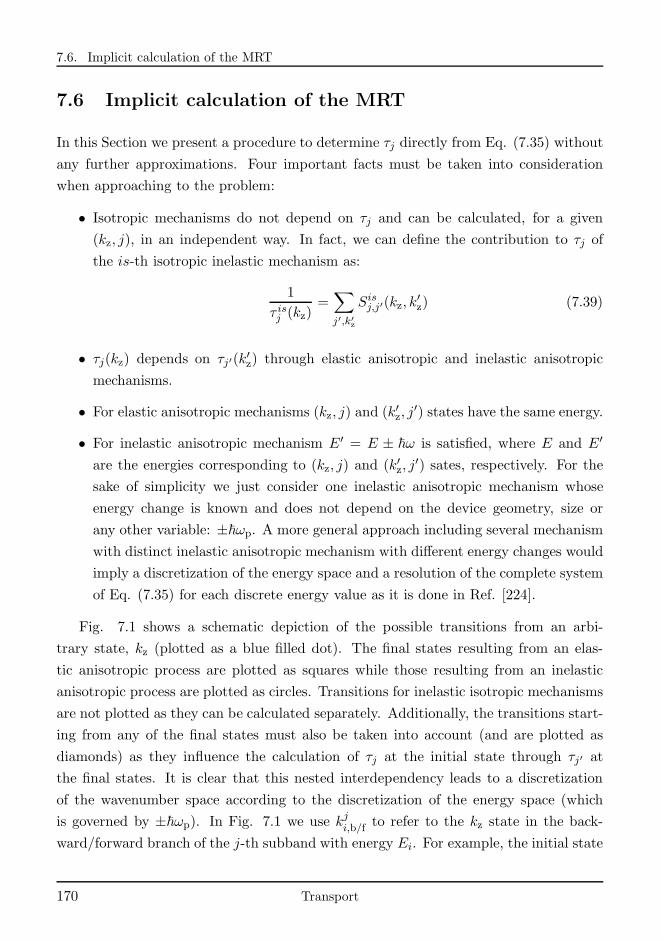
7.6. Implicit calculation of the MRT
7.6 Implicit calculation of the MRT
In this Section we present a procedure to determine τj directly from Eq. (7.35) without
any further approximations. Four important facts must be taken into consideration
when approaching to the problem:
• Isotropic mechanisms do not depend on τj and can be calculated, for a given
(kz, j), in an independent way. In fact, we can define the contribution to τj of
the is-th isotropic inelastic mechanism as:
1
τ isj (kz)=∑
j′,k′z
Sisj,j′(kz, k′z) (7.39)
• τj(kz) depends on τj′(k′z) through elastic anisotropic and inelastic anisotropic
mechanisms.
• For elastic anisotropic mechanisms (kz, j) and (k′z, j′) states have the same energy.
• For inelastic anisotropic mechanism E′ = E ± ~ω is satisfied, where E and E′
are the energies corresponding to (kz, j) and (k′z, j′) sates, respectively. For the
sake of simplicity we just consider one inelastic anisotropic mechanism whose
energy change is known and does not depend on the device geometry, size or
any other variable: ±~ωp. A more general approach including several mechanism
with distinct inelastic anisotropic mechanism with different energy changes would
imply a discretization of the energy space and a resolution of the complete system
of Eq. (7.35) for each discrete energy value as it is done in Ref. [224].
Fig. 7.1 shows a schematic depiction of the possible transitions from an arbi-
trary state, kz (plotted as a blue filled dot). The final states resulting from an elas-
tic anisotropic process are plotted as squares while those resulting from an inelastic
anisotropic process are plotted as circles. Transitions for inelastic isotropic mechanisms
are not plotted as they can be calculated separately. Additionally, the transitions start-
ing from any of the final states must also be taken into account (and are plotted as
diamonds) as they influence the calculation of τj at the initial state through τj′ at
the final states. It is clear that this nested interdependency leads to a discretization
of the wavenumber space according to the discretization of the energy space (which
is governed by ±~ωp). In Fig. 7.1 we use kji,b/f to refer to the kz state in the back-
ward/forward branch of the j-th subband with energy Ei. For example, the initial state
170 Transport
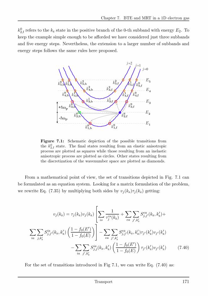
Chapter 7. BTE and MRT in a 1D electron gas
k02,f refers to the kz state in the positive branch of the 0-th subband with energy E2. To
keep the example simple enough to be afforded we have considered just three subbands
and five energy steps. Nevertheless, the extension to a larger number of subbands and
energy steps follows the same rules here proposed.
+hw
E5
E4
E3
E2
E1
-hwk2,f
0
k3,f0
k2,b0
k3,b0
k4,f0
k4,b0
k5,f0k5,b
0
k1,f0
k1,b0
k3,f1
k3,b1
k4,f1
k4,b1
k5,f1
k4,f2
k5,b2 k5,f
2
k4,b2
j =0j =1
j =2
P
P
k5,b1
Figure 7.1: Schematic depiction of the possible transitions fromthe k02,f state. The final states resulting from an elastic anisotropicprocess are plotted as squares while those resulting from an inelasticanisotropic process are plotted as circles. Other states resulting fromthe discretization of the wavenumber space are plotted as diamonds.
From a mathematical point of view, the set of transitions depicted in Fig. 7.1 can
be formulated as an equation system. Looking for a matrix formulation of the problem,
we rewrite Eq. (7.35) by multiplying both sides by vj(kz)τj(kz) getting:
vj(kz) = τj(kz)vj(kz)
∑
is
1
τ isj (kz)+∑
ea
∑
j′,k′z
Seaj,j′(kz, k′z)+
∑
ia
∑
j,k′z
Siaj,j′(kz, k′z)
(
1− f0(E′)
1− f0(E)
)
−∑
ea
∑
j′,k′z
Seaj,j′(kz, k′z)τj′(k
′z)vj′(k
′z)
−∑
ia
∑
j′,k′z
Siaj,j(kz, k′z)
(
1− f0(E′)
1− f0(E)
)
τj′(k′z)vj′(k
′z) (7.40)
For the set of transitions introduced in Fig 7.1, we can write Eq. (7.40) as:
Transport 171
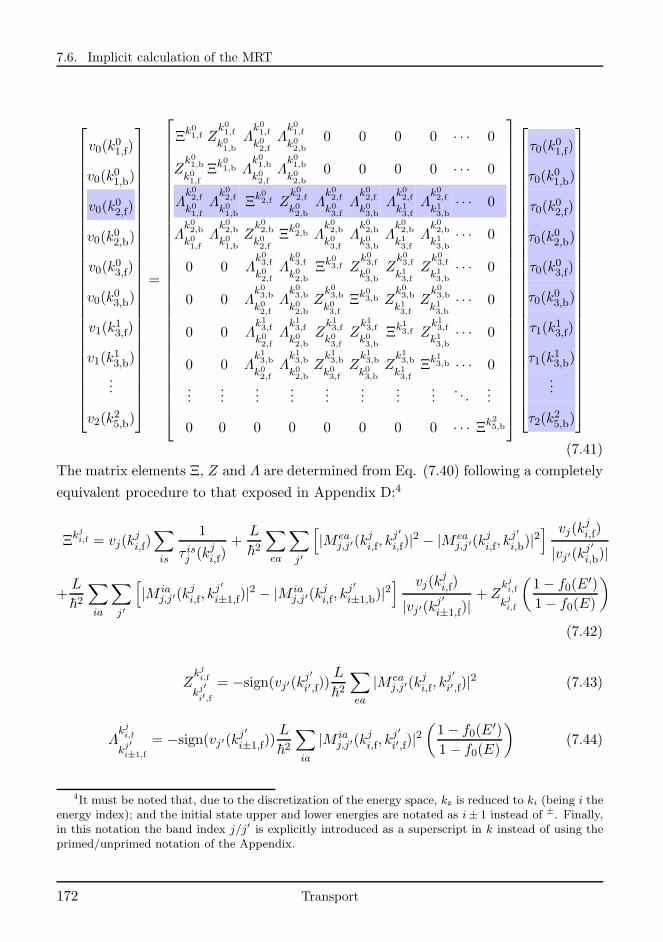
7.6. Implicit calculation of the MRT
v0(k01,f)
v0(k01,b)
v0(k02,f)
v0(k02,b)
v0(k03,f)
v0(k03,b)
v1(k13,f)
v1(k13,b)
...
v2(k25,b)
=
Ξk01,f Z
k01,fk01,b
Λk01,fk02,f
Λk01,fk02,b
0 0 0 0 · · · 0
Zk01,bk01,f
Ξk01,b Λ
k01,bk02,f
Λk01,bk02,b
0 0 0 0 · · · 0
Λk02,fk01,f
Λk02,fk01,b
Ξk02,f Z
k02,fk02,b
Λk02,fk03,f
Λk02,fk03,b
Λk02,fk13,f
Λk02,fk13,b
· · · 0
Λk02,bk01,f
Λk02,bk01,b
Zk02,bk02,f
Ξk02,b Λ
k02,bk03,f
Λk02,bk03,b
Λk02,bk13,f
Λk02,bk13,b
· · · 0
0 0 Λk03,fk02,f
Λk03,fk02,b
Ξk03,f Z
k03,fk03,b
Zk03,fk13,f
Zk03,fk13,b
· · · 0
0 0 Λk03,bk02,f
Λk03,bk02,b
Zk03,bk03,f
Ξk03,b Z
k03,bk13,f
Zk03,bk13,b
· · · 0
0 0 Λk13,fk02,f
Λk13,fk02,b
Zk13,fk03,f
Zk13,fk03,b
Ξk13,f Z
k13,fk13,b
· · · 0
0 0 Λk13,bk02,f
Λk13,bk02,b
Zk13,bk03,f
Zk13,bk03,b
Zk13,bk13,f
Ξk13,b · · · 0
......
......
......
......
. . ....
0 0 0 0 0 0 0 0 · · · Ξk25,b
τ0(k01,f)
τ0(k01,b)
τ0(k02,f)
τ0(k02,b)
τ0(k03,f)
τ0(k03,b)
τ1(k13,f)
τ1(k13,b)
...
τ2(k25,b)
(7.41)
The matrix elements Ξ, Z and Λ are determined from Eq. (7.40) following a completely
equivalent procedure to that exposed in Appendix D:4
Ξkji,f = vj(k
ji,f)∑
is
1
τ isj (kji,f)+L
~2
∑
ea
∑
j′
[
|M eaj,j′(k
ji,f, k
j′
i,f)|2 − |M eaj,j′(k
ji,f, k
j′
i,b)|2] vj(k
ji,f)
|vj′(kj′
i,b)|
+L
~2
∑
ia
∑
j′
[
|M iaj,j′(k
ji,f, k
j′
i±1,f)|2 − |M iaj,j′(k
ji,f, k
j′
i±1,b)|2] vj(k
ji,f)
|vj′(kj′
i±1,f)|+ Z
kji,f
kji,f
(
1− f0(E′)
1− f0(E)
)
(7.42)
Zkji,f
kj′
i′,f= −sign(vj′(k
j′
i′,f))L
~2
∑
ea
|M eaj,j′(k
ji,f, k
j′
i′,f)|2 (7.43)
Λkji,f
kj′
i±1,f
= −sign(vj′(kj′
i±1,f))L
~2
∑
ia
|M iaj,j′(k
ji,f, k
j′
i′,f)|2(
1− f0(E′)
1− f0(E)
)
(7.44)
4It must be noted that, due to the discretization of the energy space, kz is reduced to ki (being i theenergy index); and the initial state upper and lower energies are notated as i± 1 instead of ±. Finally,in this notation the band index j/j′ is explicitly introduced as a superscript in k instead of using theprimed/unprimed notation of the Appendix.
172 Transport
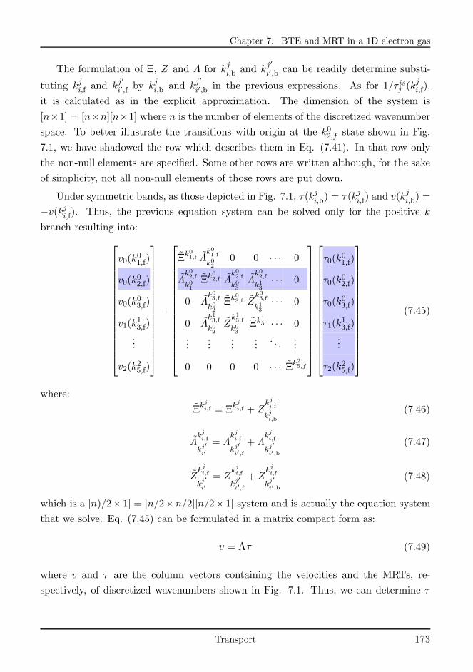
Chapter 7. BTE and MRT in a 1D electron gas
The formulation of Ξ, Z and Λ for kji,b and kj′
i′,b can be readily determine substi-
tuting kji,f and kj′
i′,f by kji,b and kj′
i′,b in the previous expressions. As for 1/τ isj (kji,f),
it is calculated as in the explicit approximation. The dimension of the system is
[n×1] = [n×n][n×1] where n is the number of elements of the discretized wavenumber
space. To better illustrate the transitions with origin at the k02,f state shown in Fig.
7.1, we have shadowed the row which describes them in Eq. (7.41). In that row only
the non-null elements are specified. Some other rows are written although, for the sake
of simplicity, not all non-null elements of those rows are put down.
Under symmetric bands, as those depicted in Fig. 7.1, τ(kji,b) = τ(kji,f) and v(kji,b) =
−v(kji,f). Thus, the previous equation system can be solved only for the positive k
branch resulting into:
v0(k01,f)
v0(k02,f)
v0(k03,f)
v1(k13,f)
...
v2(k25,f)
=
Ξk01,f Λ
k01,fk02
0 0 · · · 0
Λk02,fk01
Ξk02,f Λ
k02,fk03
Λk02,fk13
· · · 0
0 Λk03,fk02
Ξk03,f Z
k03,fk13
· · · 0
0 Λk13,fk02
Zk13,fk03
Ξk13 · · · 0
......
......
. . ....
0 0 0 0 · · · Ξk25,f
τ0(k01,f)
τ0(k02,f)
τ0(k03,f)
τ1(k13,f)
...
τ2(k25,f)
(7.45)
where:
Ξkji,f = Ξk
ji,f + Z
kji,f
kji,b
(7.46)
Λkji,f
kj′
i′= Λ
kji,f
kj′
i′,f+ Λ
kji,f
kj′
i′,b(7.47)
Zkji,f
kj′
i′= Z
kji,f
kj′
i′,f+ Z
kji,f
kj′
i′,b(7.48)
which is a [n)/2× 1] = [n/2×n/2][n/2× 1] system and is actually the equation system
that we solve. Eq. (7.45) can be formulated in a matrix compact form as:
v = Λτ (7.49)
where v and τ are the column vectors containing the velocities and the MRTs, re-
spectively, of discretized wavenumbers shown in Fig. 7.1. Thus, we can determine τ
Transport 173
7.7. Mobility calculation
as:
τ = Λ−1v (7.50)
It is worth to note that Eq. (7.45) has been proposed starting at an arbitrary wavenum-
ber, k02f , and it has resulted in the determination of τ for a set of n wavenumber values
interdependent among them. This process is respected for different scattering wavenum-
bers, k02,f, until τ is modeled with enough precision for its numerical integration.
In Fig. 7.1 we have considered just five energy steps and three subbands, but
the formulation of the matrix Λ for a more complex set of transitions, with more
energy steps and more subbands can be performed following the same procedure already
shown. One non-negligible issue regarding more complex formulations, concerns the
truncation of the wavenumber set. In Fig. 7.1 we have considered just five energy steps,
but from the monotonically increase of E with kz (assumed for non-parabolic EMA),
it is easy to conclude that a non-limited number of energy steps (and wavenumber
values) result from the discretization of the wavenumber space. Moreover, due to
the nested interdependency of the transitions, τ(k02,f ) will depend on these higher k′z.
Nevertheless, Sj,j′ tends to decrease for anisotropic mechanisms with increasing |kz−k′z|,and therefore, the influence of higher states on the determination of τ for the initial
state rapidly decreases, allowing the truncation of the discretized wavenumber space
with a simple Neumann boundary condition, that is ∂τj(E)/∂E ≃ 0 [224].
7.7 Mobility calculation
As explained in Section 7.4, in the MRT approximation only small displacements from
equilibrium are allowed and macroscopic quantities are assumed to not depend on the
transport direction. This assumption is used by the so-called Kubo-Greenwood formula
to determine the electron mobility, µ, of an electron gas [225],[226]. Here we summarize
the main steps which lead to the Kubo-Greenwood formula modified for 1D transport
under non-parabolic dispersion relation. In first place, the current density per unit
length due to the j-th subband of a 1D electron gas can be defined as [219]:
Jj = − q
L
∑
kz
vj(kz)fj(kz) = − q
L
∑
kz
vj(kz)δfj(kz) (7.51)
174 Transport
Chapter 7. BTE and MRT in a 1D electron gas
where fj(kz) = f0(Ej(kz)) + δfj(kz) and the product term vj(kz)f0(Ej(kz)) vanishes
due to its odd symmetry with kz. Using Eq. (7.23) we can write:
Jj =q2
LFz
∑
kz
v2j (kz)τj(kz)∂f0(Ej(kz))
∂E(7.52)
Assuming a linear relation between current and electric field we have:
Jj = qNjµjFz (7.53)
where Nj is the population of the j-th band. So, equaling Eqs. (7.52) and (7.53) and
solving for µ we get:
µj =q
Nj2π
∫
dkzv2j (kz)τj(kz)
∂f0(Ej(kz))
∂E(7.54)
So, the result is the Kubo-Greenwood formula for the mobility of a 1D electron gas
[95, 225–227]:
µj =q
Nj2πkBT
∫
dkzv2j (kz)τj(kz)f0(Ej(kz))(1 − f0(Ej(kz))) (7.55)
The previous integral can be expressed in terms of energy using the relation dk =
dE/~vi(k):
µj =q
Nj~πkBT
∫
dEvj(E)τj(E)f0(Ej)(1− f0(Ej)) (7.56)
where we keep the nomenclature of the previous Chapters.
7.8 Conclusions
In this Chapter, we have developed an approach to calculate the electron mobility of a
1D electron gas based on the linearization of the Boltzmann Transport Equation using
the momentum relaxation time approximation (MRT). Besides the explicit approach
for the calculation of the MRT which has been extensively used in the literature, we
showed the implicit approach resolution. The formulation of the implicit equation
system was exemplified, focusing on the nested interdependency of the transitions, and
the truncation of the discretized wavenumber space with a simple Neumann boundary
condition. The implicit resolution of the MRT must be highlighted for its rigorousness
Transport 175

7.8. Conclusions
and singularity in the literature.
176 Transport
Chapter 8
Modeling of scattering
mechanisms in NWs
8.1 Introduction
In the previous Chapter we presented the procedure to determine the momentum re-
laxation time which depends on the matrix elements corresponding to the scattering
mechanisms. In this Chapter we focus on the calculation of these matrix elements in a
1D electron gas due to five different processes: surface roughness, coulomb dispersion,
bulk phonons (optical and acoustic), polar optical phonons and alloy disorder.
Although obtaining the final expression of the matrix element of each scattering
element involves intricate mathematics, we have attempted to keep the derivations as
rigorous as possible. Thus, in order to relieve the Chapter reading, we have moved to
Appendix E some of the calculi. Despite of the mentioned mathematical complexity, the
resulting matrix element expressions are in general simple functions which can be easily
implemented. For that reason, we have not included, in this part of the manuscript,
a description of the numerical particularities of the solution process. Thus, we utilize
the wavefunctions and energy levels obtained using SP2D, and solve the expressions
numerically using MATLABr.
The rest of the Chapter is organized as follows. In Section 8.2, we discuss the surface
roughness scattering mechanism assuming that it can be characterized by a random
variable with an exponential power spectrum. In Section, 8.3 we determine the coulomb
scattering element for a fully uncorrelated distribution of impurities in the confinement
Transport 177
8.2. Surface roughness
plane and a hard-sphere model in the transport direction. Section 8.4 presents the
matrix elements due to acoustic and optical phonons while Section 8.5 doest it for
polar optical phonons. Section 8.6 introduces the matrix element due to alloy disorder
in compound semiconductors. In Section 8.7, we introduce the tensorial dielectric
screening for static mechanisms: surface roughness, coulomb and alloy disorder. Finally,
Section 8.8 summarizes the main conclusions of the Chapter. Appendix E collects the
mathematical details of some of the derivations.
8.2 Surface roughness
The set of irregularities found at the interface between the insulator and the semi-
conductor media in a MIS heterostructure (known as Surface Roughness, SR) is an
unavoidable consequence of the fabrication process, which affects negatively to the carri-
ers displacement in the direction parallel to the insulator-semiconductor interface [228].
Surface roughness is a very important scattering mechanism in bulk MOSFETs, spe-
cially at high gate voltages, when the carriers get closer to the semiconductor-insulator
interface. This process gets even more relevant when the device size is reduced and
thinner films are considered [95, 229]. Therefore, it is expected to play an important
role in the transport as the size of nanowires decreases. On the one hand, the vol-
ume inversion, due to higher confinement, shifts electrons far from the aforementioned
interface, potentially reducing the effect of SR. On the other hand, the ratio of device-
surface to device-volume ratio is augmented with respect to that of planar structures
increasing the relevance of surface related processes such as SR [230].
The modeling of the perturbing potential due to SR and the corresponding scat-
tering matrix elements has been extensively visited in the literature for 1D-confined
devices [208, 229, 231–234]. Nevertheless, only a few researchers have worked in the
modeling of 2D confined devices. We can highlight the works in Ref. [95] in which
the SR for cylindrical structures was modeled. Later works [235] extend their calcula-
tion for rectangular devices but considering only for Line Edge Roughness calculation.
Alternatives approaches can be found in Ref. [214, 236], based on Ando’s one [237],
which, according to Ref. [95], cannot capture the body thickness dependence. Only
very recently an alternative approach has been introduced almost simultaneously by
Stanojevic and Kosina in Ref. [230] and Jin et al. in Ref. [238] without constraining
the model to LER nor specific geometries or orientations. These two independent, but
178 Transport
Chapter 8. Modeling of scattering mechanisms in NWs
coincident, studies are, to the best of our knowledge, the most realistic approximations
to the SR physics in 2D confined devices.
In this manuscript, we have implemented this SR-model as follows. SR is defined
by a random variable ∆SR(r), being r ∈ Si-s the position vector and Si-s the surface
which delimits the insulator-semiconductor interface. The perturbing potential due to
SR is:
ψSR(r) = ∆φ∆SR(r) (8.1)
where, as proposed previously in this manuscript, ∆φ is the potential energy barrier
between the semiconductor and the insulator, and ψSR is only defined in Si-s
The derivation of the SR scattering element between states (kz, j) and (k′z, j′), fol-
lows that proposed in Refs. [230] and [238]. Our aim is just to spotlight some key steps
introducing minor modifications. As proposed in Section 7.3, under the Fermi golden
rule, the scattering element is defined as:
Mj,j′(kz, k′z) = ∆φ
∫
Si-sdS ξj,kz(x, y)
e−ıkzz√L
∆(r)ξ∗j′,k′z(x, y)eık
′zz
√L
(8.2)
where te volume integral has been reduced to a surface integration as ψSR is only
defined at the surface Si-s. As ∆(r) is a random variable, Eq. (8.2) cannot be directly
integrated. To avoid that problem Eq. (8.2) is reformulated as a function of ∆(r)
autocorrelation function defined as:
C(r) = 〈∆(r)∆(r′)〉 (8.3)
Keeping the random nature of ∆(r), C(r) is the inverse transformation of the SR power
spectrum, a quantity which can be realistically modeled (see Subsection 8.2.3).
Thus, squaring the matrix element and applying the expected value operator 〈〉 weget:
〈∣
∣Mj,j′(kz, k′z)∣
∣
2〉 = ∆φ2
L2
∫
Si-sdS
∫
Si-sdS′ξj,kz(x, y)e
−ıkzzξ∗j′,k′z(x, y)eık′zz〈∆(r)∆(r′)〉
ξ∗j,kz(x′, y′)eıkzz
′ξj′,k′z(x
′, y′)e−ık′zz
′(8.4)
Transport 179
8.2. Surface roughness
The previous integral can be rewritten as.
〈∣
∣Mj,j′(kz, k′z)∣
∣
2〉 = ∆φ2
L2
∫
Ci-sdc
∫
Ci-sdc′∫ L
0dz
∫ L
0dz′ξj,kz(c)ξ
∗j′,k′z
(c)ξ∗j,kz(c′)ξj′,k′z(c
′)
eı(kz−k′z)(z
′−z)C(r) (8.5)
where Ci-s and L are the curve which describes the insulator-semiconductor interface
in the cross-section and the device length, respectively; c is a 1D variable describing
the confinement position (x, y) along Ci-s and z is the transport coordinate. For the
sake of clarity let us define the function:
fj,j′,kz,k′z(c) = ∆φξj,kz(c)ξ∗j′,k′z
(c) (8.6)
Then,
〈∣
∣Mj,j′(kz, k′z)∣
∣
2〉 = 1
L2
∫
Ci-sdc
∫
Ci-sdc′∫ L
0dz
∫ L
0dz′fj,j′,kz,k′z(c)fj,j′,kz,k′z(c
′)eı(kz−k′z)(z
′−z)C(r)
(8.7)
The integration procedure for Eq. (8.5) requires the transformation of the real space
into its reciprocal wavenumber space. In this transformation the periodicity of the real
space variable determines the properties of the reciprocal space. For that reason, a
distinction must be done between open and close Ci-s paths. This distinction, althoughnot explicitly exposed, is the main difference in the approaches followed by Stanojevic
et al. in Ref. [230] and Jin et al. in Ref. [238].
8.2.1 Derivation for open cross sections curves
Let us first consider the case when Ci-s is an open curve, for example, a bulk FinFET.
Then the autocorrelation function can be expressed in terms of the SR power spectrum,
C(q), as:
C(c, z) =1
4π2
∫ ∫
C(q)eıqc(c′−c)eıqz(z
′−z)dqcdqz (8.8)
where q is used here to denote the wavevector space of the scattering mechanism,
keeping k to denote the wavevector space of electrons.
180 Transport
Chapter 8. Modeling of scattering mechanisms in NWs
Introducing Eq. (8.8) into Eq. (8.5) one obtains:
〈∣
∣Mj,j′(kz, k′z)∣
∣
2〉 = 1
4π2L2
∫
Ci-sdc
∫
Ci-sdc′∫ L
0dz
∫ L
0dz′∫
dqz
∫
dqcfj,j′,kz,k′z(c)f∗j,j′,kz,k′z
(c′)
e−ıqc(c−c′)eı(kz−k
′z+qz)(z
′−z)C(q)
(8.9)
As shown in Appendix E the integration on z and z′ leads to 2πLδ(kz − k′z + qz).
Applying the δ function properties to the integral on qz, the following expression is
achieved:
〈∣
∣Mj,j′(kz, k′z)∣
∣
2〉 = 1
2πL
∫
Ci-sdc
∫
Ci-sdc′∫
dqc fj,j′,kz,k′z(c)f∗j,j′,kz,k′z
(c′)e−ıqc(c−c′)C(qc, q
fz )
(8.10)
being qfz = k′z − kz. Rearranging Eq. (8.10) leads to:
〈∣
∣Mj,j′(kz, k′z)∣
∣
2〉 = 1
2πL
∫
dqcC(qc, qfz )
[∫
Ci-sdcfj,j′,kz,k′z(c)e
−ıqcc]
[∫
Ci-sdc′f∗j,j′,kz,k′z(c
′)eıqcc′]
(8.11)
where, assuming that Ci−s is an open curve, the first term into brackets is the Fourier
transform of fj,j′,kz,k′z , and the second term is the complex conjugate of its Fourier
transform. Therefore:
〈∣
∣Mj,j′(kz, k′z)∣
∣
2〉 = 1
2πL
∫
dqcC(qc, qfz )∣
∣
∣Fj,j′,kz,k′z’(qc)∣
∣
∣
2(8.12)
which is the final expression for the SR matrix element due to a transition between
states (kz, j) and (k′z, j′).
8.2.2 Derivation for closed cross-sections
When Ci-s is a closed curve (for example in a NW FET), some variations must be
introduced in the determination of 〈∣
∣Mj,j′(kz, k′z)∣
∣
2〉. First, ∆(r) = ∆(c, z) is a periodic
function in c, and therefore its spectrum in the qc direction is a summation of δ functions
Transport 181
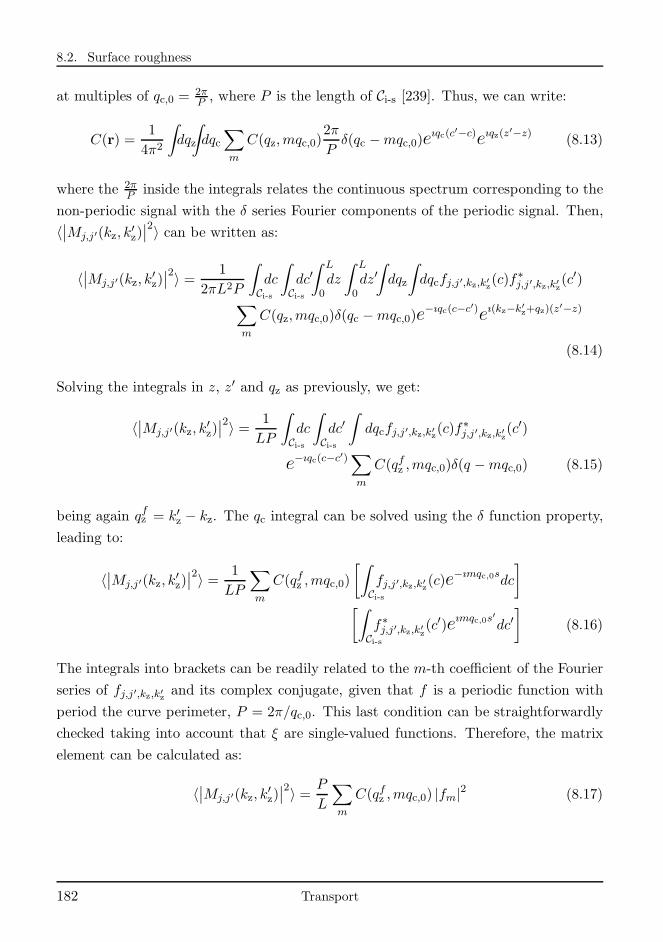
8.2. Surface roughness
at multiples of qc,0 =2πP , where P is the length of Ci-s [239]. Thus, we can write:
C(r) =1
4π2
∫
dqz
∫
dqc∑
m
C(qz,mqc,0)2π
Pδ(qc −mqc,0)e
ıqc(c′−c)eıqz(z′−z)
(8.13)
where the 2πP inside the integrals relates the continuous spectrum corresponding to the
non-periodic signal with the δ series Fourier components of the periodic signal. Then,
〈∣
∣Mj,j′(kz, k′z)∣
∣
2〉 can be written as:
〈∣
∣Mj,j′(kz, k′z)∣
∣
2〉 = 1
2πL2P
∫
Ci-sdc
∫
Ci-sdc′∫ L
0dz
∫ L
0dz′∫
dqz
∫
dqcfj,j′,kz,k′z(c)f∗j,j′,kz,k′z
(c′)
∑
m
C(qz,mqc,0)δ(qc −mqc,0)e−ıqc(c−c′)eı(kz−k
′z+qz)(z
′−z)
(8.14)
Solving the integrals in z, z′ and qz as previously, we get:
〈∣
∣Mj,j′(kz, k′z)∣
∣
2〉 = 1
LP
∫
Ci-sdc
∫
Ci-sdc′∫
dqcfj,j′,kz,k′z(c)f∗j,j′,kz,k′z
(c′)
e−ıqc(c−c′)∑
m
C(qfz ,mqc,0)δ(q −mqc,0) (8.15)
being again qfz = k′z − kz. The qc integral can be solved using the δ function property,
leading to:
〈∣
∣Mj,j′(kz, k′z)∣
∣
2〉 = 1
LP
∑
m
C(qfz ,mqc,0)
[∫
Ci-sfj,j′,kz,k′z(c)e
−ımqc,0sdc
]
[∫
Ci-sf∗j,j′,kz,k′z(c
′)eımqc,0s′dc′]
(8.16)
The integrals into brackets can be readily related to the m-th coefficient of the Fourier
series of fj,j′,kz,k′z and its complex conjugate, given that f is a periodic function with
period the curve perimeter, P = 2π/qc,0. This last condition can be straightforwardly
checked taking into account that ξ are single-valued functions. Therefore, the matrix
element can be calculated as:
〈∣
∣Mj,j′(kz, k′z)∣
∣
2〉 = P
L
∑
m
C(qfz ,mqc,0) |fm|2 (8.17)
182 Transport
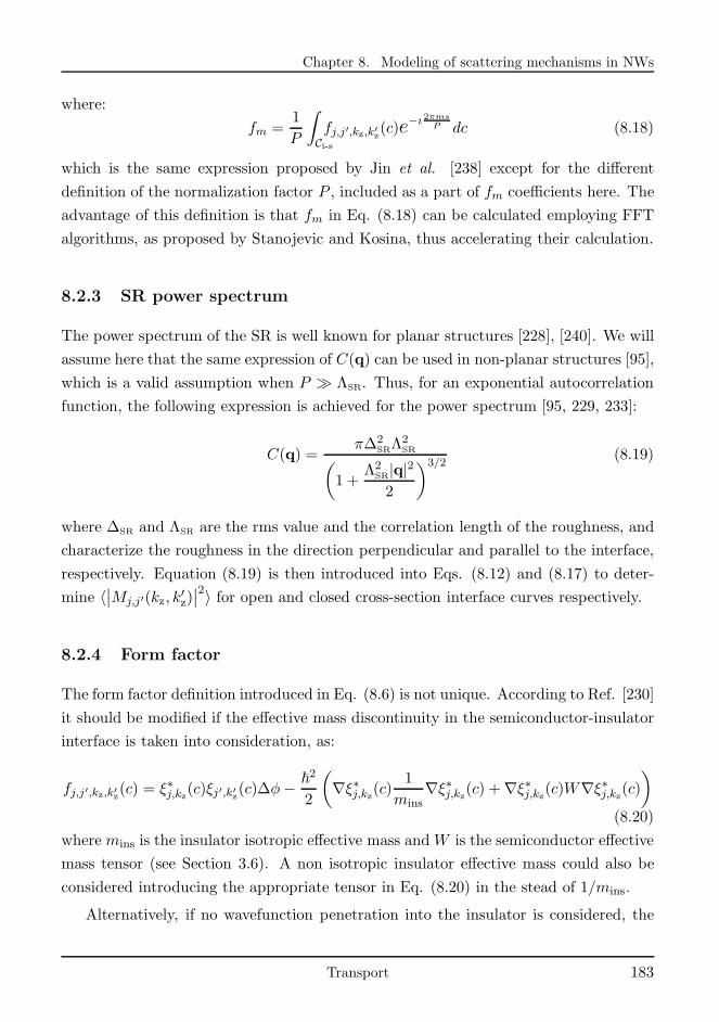
Chapter 8. Modeling of scattering mechanisms in NWs
where:
fm =1
P
∫
Ci-sfj,j′,kz,k′z(c)e
−ı 2πmsP dc (8.18)
which is the same expression proposed by Jin et al. [238] except for the different
definition of the normalization factor P , included as a part of fm coefficients here. The
advantage of this definition is that fm in Eq. (8.18) can be calculated employing FFT
algorithms, as proposed by Stanojevic and Kosina, thus accelerating their calculation.
8.2.3 SR power spectrum
The power spectrum of the SR is well known for planar structures [228], [240]. We will
assume here that the same expression of C(q) can be used in non-planar structures [95],
which is a valid assumption when P ≫ ΛSR. Thus, for an exponential autocorrelation
function, the following expression is achieved for the power spectrum [95, 229, 233]:
C(q) =π∆2
SRΛ2SR
(
1 +Λ2
SR|q|22
)3/2(8.19)
where ∆SR and ΛSR are the rms value and the correlation length of the roughness, and
characterize the roughness in the direction perpendicular and parallel to the interface,
respectively. Equation (8.19) is then introduced into Eqs. (8.12) and (8.17) to deter-
mine 〈∣
∣Mj,j′(kz, k′z)∣
∣
2〉 for open and closed cross-section interface curves respectively.
8.2.4 Form factor
The form factor definition introduced in Eq. (8.6) is not unique. According to Ref. [230]
it should be modified if the effective mass discontinuity in the semiconductor-insulator
interface is taken into consideration, as:
fj,j′,kz,k′z(c) = ξ∗j,kz(c)ξj′,k′z(c)∆φ− ~2
2
(
∇ξ∗j,kz(c)1
mins∇ξ∗j,kz(c) +∇ξ∗j,kz(c)W∇ξ∗j,kz(c)
)
(8.20)
wheremins is the insulator isotropic effective mass andW is the semiconductor effective
mass tensor (see Section 3.6). A non isotropic insulator effective mass could also be
considered introducing the appropriate tensor in Eq. (8.20) in the stead of 1/mins.
Alternatively, if no wavefunction penetration into the insulator is considered, the
Transport 183
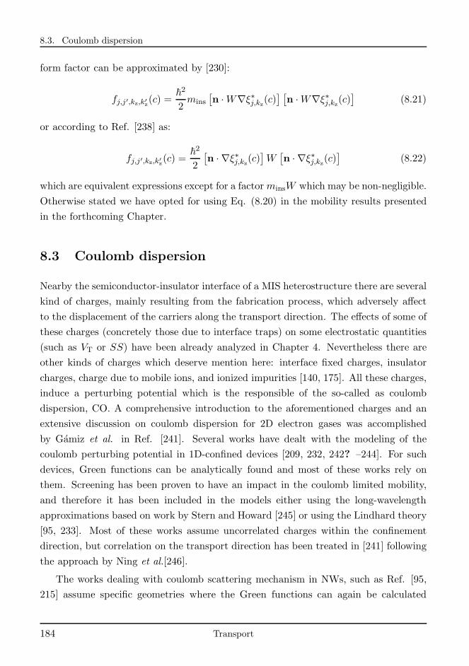
8.3. Coulomb dispersion
form factor can be approximated by [230]:
fj,j′,kz,k′z(c) =~2
2mins
[
n ·W∇ξ∗j,kz(c)] [
n ·W∇ξ∗j,kz(c)]
(8.21)
or according to Ref. [238] as:
fj,j′,kz,k′z(c) =~2
2
[
n · ∇ξ∗j,kz(c)]
W[
n · ∇ξ∗j,kz(c)]
(8.22)
which are equivalent expressions except for a factorminsW which may be non-negligible.
Otherwise stated we have opted for using Eq. (8.20) in the mobility results presented
in the forthcoming Chapter.
8.3 Coulomb dispersion
Nearby the semiconductor-insulator interface of a MIS heterostructure there are several
kind of charges, mainly resulting from the fabrication process, which adversely affect
to the displacement of the carriers along the transport direction. The effects of some of
these charges (concretely those due to interface traps) on some electrostatic quantities
(such as VT or SS) have been already analyzed in Chapter 4. Nevertheless there are
other kinds of charges which deserve mention here: interface fixed charges, insulator
charges, charge due to mobile ions, and ionized impurities [140, 175]. All these charges,
induce a perturbing potential which is the responsible of the so-called as coulomb
dispersion, CO. A comprehensive introduction to the aforementioned charges and an
extensive discussion on coulomb dispersion for 2D electron gases was accomplished
by Gamiz et al. in Ref. [241]. Several works have dealt with the modeling of the
coulomb perturbing potential in 1D-confined devices [209, 232, 242? –244]. For such
devices, Green functions can be analytically found and most of these works rely on
them. Screening has been proven to have an impact in the coulomb limited mobility,
and therefore it has been included in the models either using the long-wavelength
approximations based on work by Stern and Howard [245] or using the Lindhard theory
[95, 233]. Most of these works assume uncorrelated charges within the confinement
direction, but correlation on the transport direction has been treated in [241] following
the approach by Ning et al.[246].
The works dealing with coulomb scattering mechanism in NWs, such as Ref. [95,
215] assume specific geometries where the Green functions can again be calculated
184 Transport
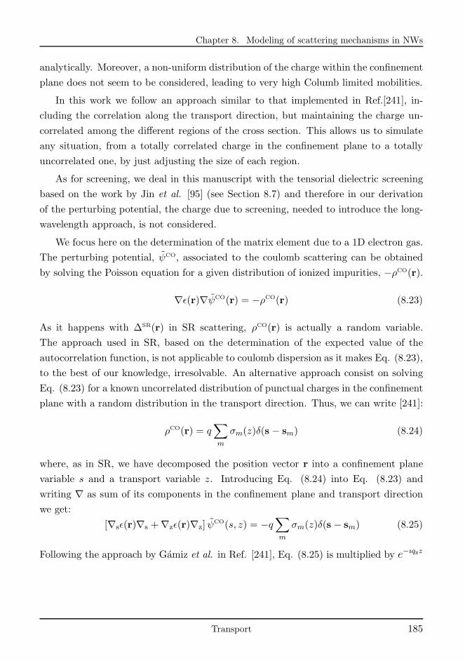
Chapter 8. Modeling of scattering mechanisms in NWs
analytically. Moreover, a non-uniform distribution of the charge within the confinement
plane does not seem to be considered, leading to very high Columb limited mobilities.
In this work we follow an approach similar to that implemented in Ref.[241], in-
cluding the correlation along the transport direction, but maintaining the charge un-
correlated among the different regions of the cross section. This allows us to simulate
any situation, from a totally correlated charge in the confinement plane to a totally
uncorrelated one, by just adjusting the size of each region.
As for screening, we deal in this manuscript with the tensorial dielectric screening
based on the work by Jin et al. [95] (see Section 8.7) and therefore in our derivation
of the perturbing potential, the charge due to screening, needed to introduce the long-
wavelength approach, is not considered.
We focus here on the determination of the matrix element due to a 1D electron gas.
The perturbing potential, ψCO, associated to the coulomb scattering can be obtained
by solving the Poisson equation for a given distribution of ionized impurities, −ρCO(r).
∇ǫ(r)∇ψCO(r) = −ρCO(r) (8.23)
As it happens with ∆SR(r) in SR scattering, ρCO(r) is actually a random variable.
The approach used in SR, based on the determination of the expected value of the
autocorrelation function, is not applicable to coulomb dispersion as it makes Eq. (8.23),
to the best of our knowledge, irresolvable. An alternative approach consist on solving
Eq. (8.23) for a known uncorrelated distribution of punctual charges in the confinement
plane with a random distribution in the transport direction. Thus, we can write [241]:
ρCO(r) = q∑
m
σm(z)δ(s − sm) (8.24)
where, as in SR, we have decomposed the position vector r into a confinement plane
variable s and a transport variable z. Introducing Eq. (8.24) into Eq. (8.23) and
writing ∇ as sum of its components in the confinement plane and transport direction
we get:
[∇sǫ(r)∇s +∇zǫ(r)∇z] ψCO(s, z) = −q
∑
m
σm(z)δ(s − sm) (8.25)
Following the approach by Gamiz et al. in Ref. [241], Eq. (8.25) is multiplied by e−ıqzz
Transport 185
8.3. Coulomb dispersion
and integrated over z, to take the Fourier transform on the longitudinal direction:
[
∇sε(r)∇s + ε(r)q2z]
ψCO(s, qz) = −q∑
m
σm(qz)δ(s − sm) (8.26)
where the derivative ∇z in the real space is transformed into a factor, qz, in the
wavenumber space. Using the superposition principle we can write the perturbing
potential as:
ψCO(s, qz) =∑
m
Gqz(s, sm)σm(qz) (8.27)
where Eq. (8.26) can be separately solved for each contribution to the potential:
[
∇sǫ(r)∇s + ǫ(r)q2z]
Gqz(s, sm) = −qδ(s− sm) (8.28)
being Gqz(s, sm) in Eq. (8.28) the impulse response of the differential equation; in other
words its Green function.
The matrix element for a transition between states (kz, j) and (k′z, j′) was introduced
in Eq. (7.17):
Mj,j′(kz, k′z) =
∫
VdV ξj,kz(x, y)
e−ıkzz√L
ψCO(s, z)ξ∗j′,k′z(x, y)eık
′zz
√L
(8.29)
Decomposing the integral in the confinement plane and transport direction we have:
Mj,j′(kz, k′z) =
1
L
∫
Ads ξj,kz(x, y)ξ
∗j′,k′z
(x, y)
∫
dze−ı(kz−k′z)zψCO(s, z) (8.30)
Then, the expected value of the squared matrix element can be written as:
〈|Mj,j′(kz, k′z)|2〉 =
1
L2
∫
Ads
∫
Ads′ fj,j′,kz,k′z(s)f
∗j,j′,kz,k′z
(s′)∫
dz
∫
dz′e−ı(kz−k′z)(z−z′)〈ψCO(s, z)ψCO(s′, z′)〉 (8.31)
where equivalently to what was done for SR, we have defined:
fj,j′,kz,k′z(s) = ξj,kz(x, y)ξ∗j′,k′z
(x, y) (8.32)
being, s = (x, y).
The Fourier transform of the autocorrelation function, 〈ψCO(s, z)ψCO(s′, z′)〉, gives
186 Transport
Chapter 8. Modeling of scattering mechanisms in NWs
us:
C(s, qz) = 〈ψCO(s, qz)ψCO(s′, qz)〉 =
∑
m
∑
i
G∗qz(s′, s′i)Gqz(s, sm)〈σm(qz)σ∗i (qz)〉 (8.33)
We assume that the charge is uncorrelated for different regions in the confinement plane,
so that the previous sum is null for m 6= i. Then we can define the autocorrelation of
the perturbing potential as:
〈ψCO(s, z)ψCO(s′, z′)〉 = C(s, z) =1
2π
∫
C(s, qz)e−ıqz(z′−z)dqz (8.34)
Thus, Eq. (8.31) can be rewritten as:
〈|Mj,j′(kz, k′z)|2〉 =
1
2πL2
∫
Ads
∫
Ads′ fj,j′,kz,k′z(s)f
∗j,j′,kz,k′z
(s′)∫
dz
∫
dz′∫
dqze−ı(kz−k′z−qz)(z−z′)
∑
m
G∗qz(s′, s′m)Gqz(s, sm)〈σm(qz)σ∗m(qz)〉 (8.35)
The integration along qz, z, and z′ can be simplified as in Appendix E for SR. Thus:
〈|Mj,j′(kz, k′z)|2〉 =
1
L
∫
Ads
∫
Ads′fj,j′,kz,k′z(s)f
∗j,j′,kz,k′z
(s′)∑
m
G∗qfz(s′, s′m)Gqfz (s, sm)〈σm(q
fz )σ∗m(q
fz )〉 (8.36)
where qfz = kz − kz′ . 〈σm(qfz )σ∗i (qfz )〉 is the power spectrum of the random distribution
of charges along the axial direction which can be determined under the hard-sphere
model, as proposed for a 2D electron gas by Ning et al. in Ref. [246] and also studied
by Gamiz et al. in Ref. [241]. In Appendix E we detail the calculus of the hard-sphere
model for a 1D electron gas. The resulting power spectrum is:
〈σm(qfz )σ∗m(qfz )〉 = Navg (1− C sinc(qzRt)) (8.37)
where, as explained in Appendix E, Navg is the average ionized impurities per unit
length and Rt is the radius of the hard sphere which determines the minimum distance
between ionized impurities. C = RtNavg is a measure of the degree of correlation
in the transport direction: C = 0 correspond to a completely uncorrelated random
distribution while C = 1 is a uniform fully correlated distribution. In Eq. (8.37) we have
assumed that the axial distribution of charges corresponding to different confinement
Transport 187
8.4. Bulk non-polar phonons
plane positions are completely uncorrelated. Therefore Eq. (8.36) can be reformulated
as:
〈|Mj,j′(kz, k′z)|2〉 =
Navg
L
∫
Ads
∫
Ads′fj,j′,kz,k′z(s)f
∗j,j′,kz,k′z
(s′)
∑
m
Gqfz(s, sm)G
∗qfz(s′, sm)
(
1− C sinc(qfzRt))
(8.38)
Eq. (8.38) is the final expression for the coulomb dispersion matrix element due to a
transition between states (kz, j) and (k′z, j′).
8.4 Bulk non-polar phonons
For a non-null temperature the atoms in the semiconductor lattice vibrate, oscillating
around their equilibrium positions. Phonons (PH) are the result of a quantum mechan-
ical analysis of these semiconductor lattice vibrations. The mathematical derivation
of the phonon-electron interaction can be found in several textbooks [247], [88]. We
briefly summarize here the main ideas to understand the perturbation potential due to
phonons. In this manuscript, we neglect the confinement effects that may influence the
behavior of phonons in small devices [236, 248, 249].
The vibrations can be modeled as a set of harmonic oscillators. For a crystal with
a diatomic unit cell, there are six allowed modes of oscillation: two for each direction
in real space. In the first of these two modes, the two atoms of the unit cell oscillate
in phase while for the second one atoms vibrate in opposite phase. The two modes are
known as acoustic, A, (due to its similarities with the propagation of an acoustic wave
on air) and optic, O, (because in some ionic crystal they are excited by electromagnetic
radiation), respectively [247]. Regarding the direction of vibration of the modes they
are called transverse, T, when the atoms vibrate perpendicularly to the phonon wave-
vector, q direction (there are two transverse modes) and longitudinal, L, when the
atoms vibrate aligned with q (there is one longitudinal mode).
The modes of oscillation for Si obtained from Refs. [88, 250, 251] are shown in
Fig. 8.1 where the phonon energy is plotted as a function of the phonon wavevector
magnitude |q|. Transversal modes (TA, TO) are degenerated. For low |q| values,
acoustic phonons modes (LA and TA), show a linear E(|q|) − |q| dependence and the
energy is commonly modeled by a term EPH = ~vs|q|, where vs is the slope of the ω-|q|
188 Transport
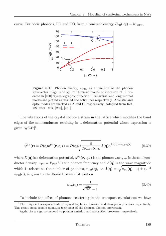
Chapter 8. Modeling of scattering mechanisms in NWs
curve. For optic phonons, LO and TO, keep a constant energy EPH(|q|) = ~ωOPH,
60
40
50
70
20
10
30
00.2 0.4 0.6 0.8 10
TL
A
O
| | (2 a )q p/
E
(||)
(m
eV
)q
PH
0
Figure 8.1: Phonon energy, EPH, as a function of the phononwavevector magnitude |q| for different modes of vibration of Si ori-ented in [100] crystallographic direction. Transversal and longitudinalmodes are plotted as dashed and solid lines respectively. Acoustic andoptic modes are marked as A and O, respectively. Adapted from Ref.[88] after Refs. [250], [251].
The vibrations of the crystal induce a strain in the lattice which modifies the band
edges of the semiconductor resulting in a deformation potential whose expression is
given by[247]1:
ψPH(r) = D(q)uPH(r,q, t) = D(q)
√
~
2sωPH(q)LA(q)e±ı(qr−ωPH(q)t)
(8.39)
whereD(q) is a deformation potential, uPH(r,q, t) is the phonon wave, s is the semicon-
ductor density, ωPH = EPH/~ is the phonon frequency and A(q) is the wave magnitude
which is related to the number of phonons, nPH(q), as A(q) =√
nPH(q) +12 ± 1
2 .2
nPH(q), is given by the Bose-Einstein distribution
nPH(q) =1
eEPHkBT − 1
(8.40)
To include the effect of phonons scattering in the transport calculations we have
1The ± sign in the exponential correspond to phonon emission and absorption processes respectively.This result stems from a quantum treatment of the electron-phonon interaction.
2Again the ± sign correspond to phonon emission and absorption processes, respectively.
Transport 189
8.4. Bulk non-polar phonons
assumed that only small |q| phonons play a relevant role in the scattering process.
8.4.1 Acoustic phonons
As seen in Fig. 8.1, for acoustic phonons a small value of |q| implies a small value of
energy, EPH, which in most of cases is negligible compared with the electron energy,
Ei(kz), and can therefore be obliterated in the calculus. As a consequence, acous-
tic phonon mechanism is assumed to be elastic 3. Two implication derive from this
assumption [206]:
(a) The term ωt in the exponential of Eq. (8.39), which as explained in Section 7.3
determines the energy transfer due to the scattering process, is removed.
(b) The Bose-Einstein function in Eq. (8.40) is simplified to kBT/EPH and nPH(|q|) =kBT/EPH = kBT/~vs|q|
Moreover, the deformation potential for acoustic phonons is proportional to the wavenum-
ber: D(q) = DAPHq. Thus, for acoustic phonons Eq. (8.39) is simplified to:
ψAPH(r) = DAPH
√
kBT
2ALs
1
vse±ıqr (8.41)
where we have used Ω = AL. The matrix element due to a transition between states
(kz, j) and (k′z, j′) is:
Mj,j′(kz, k′z) =
∫ L
0dz
∫
AdA ξj,kz(x, y)
e−ıkzz√L
(
DAPH
√
kBT
2sAL
1
vse±ıqr
)
ξ∗j′,k′z(x, y)eık
′zz
√L
(8.42)
which can be written as4:
Mj,j′(kz, k′z) =
DAPH
L
√
kBT
2sAL
1
vs
∫ L
0dz
∫
AdA ξj,kz(x, y)e
−ı(qxx+qyy)ξ∗j′,k′z(x, y)e−ı(kz−k′z+qz)z
(8.43)
3This approximation is not valid for low temperatures and highly confined structures [249].4For the sake of simplicity just the minus branch was considered. Equivalent derivation can be
found for the positive branch.
190 Transport
Chapter 8. Modeling of scattering mechanisms in NWs
The squared matrix element can then be calculated as:
|Mj,j′(kz, k′z)|2 =
D2APH
L2
kBT
2sAL
1
v2s
∫
Ads
∫
Ads′∫ L
0dz
∫ L
0dz′ fj,j′,kz,k′z(x, y)e
−ı(qxx+qyy)
f∗j,j′,kz,k′z(x′, y′)eı(qxx
′+qyy′)e−ı(kz−k′z−qz)(z′−z)
(8.44)
where fj,j′,kz,k′z(x, y) was defined in Eq. (8.32). The mathematical details of the inte-
gration procedure are given in Appendix E. The resulting expression is:
|Mj,j′(kz, k′z)|2 =
D2APH
L
kBT
2s
1
v2s
∫
AdA fj,j′,kz,k′z(x, y)f
∗j,j′,kz,k′z
(x, y) (8.45)
which is the same expression proposed in Refs. [95, 227]. It is important to highlight
that the matrix element does not depend on qz and, therefore, it is isotropic.
8.4.2 Optical phonons
For optical phonons a small qz does not imply a small energy, EPH, and therefore neither
of the previous approximations for acoustic phonons can be made. Instead, ωPH(|q|)weakly depends on |q| and can be assumed as constant ωPH(|q|) = ωOPH, see Fig. 8.1.
Consequently the energy, EPH, and the number of phonons nPH(qz) = nPH are also
constant. In addition, for optical phonons the deformation potential is assumed to be
constant D(qz) = DOPH. Thus, the perturbing potential can be written as:
ψOPH(z) = DOPH
√
~
2ALsωOPH
√
nPH +1
2± 1
2e±ı(|qr|−ωOPHt) (8.46)
One main difference between the perturbing potential presented in Eq. (8.46) and
those obtained for other scattering mechanisms such as surface roughness, coulomb
dispersion and acoustic phonons in Eqs. (8.1), (8.27), and (8.41) respectively, is the
factor eıωOPHt. As explained in Section 7.3, this factor implies a change in the energy
between the initial and final states E and E′ of states (kz, j) and (k′z, j′) such that
E′ = E ± ~ωPH.
The matrix element due to a transition between states (kz, j) and (k′z, j′) is given
Transport 191
8.5. Polar Optical Phonons
by:
Mj,j′(kz, k′z) =
∫ L
0dz
∫
AdA fj,j′,kz,k′z(s)
e−ıkzz√L
(
DOPH
√
~
2ALsωOPH
√
nPH +1
2± 1
2e±ıqss±ıqzz
)
eık′zz
√L
(8.47)
The square matrix element can then be written after the appropriate integration for
qx, qy, qz, z, z′ equivalent to the carried ot for acoustic phonons in Appendix E as:
|Mj,j′(kz, k′z)|2 =
D2OPH
L
~
2sωOPH
(
nPH +1
2± 1
2
)∫
AdA fj,j′,kz,k′z(s)f
∗j,j′,kz,k′z
(s) (8.48)
which also coincides with the expression proposed in Refs. [95, 227] As in acoustic
phonons the matrix element is not dependent on qz, being therefore modeled as an
inelastic isotropic mechanism.
8.5 Polar Optical Phonons
Similarly to non-polar bulk phonons, polar optical phonons (POP) result from vibra-
tions of the crystal lattice. The main difference is related to the ionic nature of POP.
In polar crystals, such as III-V compound semiconductors, there is a net electronic
charge transfer between atoms of both compounds. This charge transfer leads to an
effective dipole which results into a contribution to the dielectric function and modifies
the potential induced by the lattice vibrations. The term optical comes from the high
frequency and weakly wavevector dependent nature of these phonons. The mathemat-
ical derivation of the perturbing potential due to POP can be found elsewhere [252]
leading to the so-called Frohlich potential given by [217, 253, 254]:
ψPOP(r) = −ı√
q2~ωPOP
2AL
(
1
ǫ∞− 1
ǫ0
)
1
|q|
√
nPH +1
2± 1
2e±ıqr−ωPOPt (8.49)
being ωPOP the phonon frequency, ǫ(∞) the high-frequency dielectric constant and ǫ(0)
the static dielectric constant. The rest of the terms keep the meaning used in Section
8.4. We have assumed that ωPOP does not depend on |q| and consequently neither does
nPH. As proposed in Section 7.3 and previously discussed in Section 8.4 for optical
phonons, the factor e−ıωPOPt implies a change of energy in the scattering process. The
192 Transport
Chapter 8. Modeling of scattering mechanisms in NWs
derivation of the matrix element for 2D-confined devices has been addressed in Ref.
[217, 253, 254]. We reproduce it here for the sake of completeness. The matrix element
can then be calculated as:
Mj,j′(kz, k′z) =
1√AL
∫ L
0dz
∫
AdA ξj,kz(x, y)
e−ıkzz√L
(
C POP
|q| eıqr)
ξ∗j′,k′z(x, y)eık
′zz
√L
(8.50)
where we have defined the constant:
CPOP = −ı√
q2~ωPOP
2
(
1
ǫ∞− 1
ǫ0
)(
nPH +1
2± 1
2
)
(8.51)
The square matrix element is then given by:
∣
∣Mj,j′(kz, k′z)∣
∣
2=C2
POP
L2
1
AL
∫ L
0dz
∫ L
0dz′∫
AdA
∫
A′dA′ fj,j′,kz,k′z(s)fj,j′,kz,k′z(s
′)
e∓ıqx(x−x′)∓iqy(y−y′)
q2x + q2y + q2zeı(kz−k
′z−qz)z (8.52)
where have used the fj,j′,kz,k′z(s) definition of Eq. (8.32). If we account for all the
possible qx, qy and qz contributions, and transforming the qx, qy and qz sums in integrals
as in Eqs. (E.23), we obtain:
∣
∣Mj,j′(kz, k′z)∣
∣
2=C2
POP
L2
1
8π3
∫
dqz
∫ L
0dz
∫ L
0dz′∫
AdA
∫
A′dA′ fj,j′,kz,k′z(s)fj,j′,kz,k′z(s
′)
∫ ∫
dqxdqye∓ıqx(x−x
′)∓iqy(y−y′)
q2x + q2y + q2zeı(kz−k
′z−qz)z
(8.53)
The axial and qz integration of Eq. (8.53) leads to:
∣
∣Mj,j′(kz, k′z)∣
∣
2=C2
POP
L
1
4π2
∫
AdA
∫
A′dA′ fj,j′,kz,k′z(s)fj,j′,kz,k′z(s
′)
∫ ∫
dqxdqye∓ıqx(x−x
′)∓iqy(y−y′)
q2x + q2y + q2fz(8.54)
where qfz = kz− k′z and we have substituted q by its components. The inner integral in
Eq. (8.54) is analytically solved in Appendix E. Substituting the result into Eq. (8.53)
Transport 193
8.6. Alloy Disorder
we get:
∣
∣Mj,j′(kz, k′z)∣
∣
2=C2
POP
2πL
∫
AdA
∫
A′dA′fj,j′,kz,kz′ (s)fj,j′,kz,kz′ (s
′)K0
(
qfz∣
∣s− s′∣
∣
)
(8.55)
where K0 is the modified Bessel function of the second kind and order zero. This is the
final expression for the POP matrix element due to a transition between states (kz, j)
and (k′z, j′), which coincides with the expression achieved by Wang et al. in Ref. [253].
8.6 Alloy Disorder
In alloy semiconductors, there is some randomness in the distribution of atoms in the
positions of the zinc-blende structure. Commonly one the semiconductors occupy one
fcc lattice while the other two semiconductors distribute themselves randomly in the
second fcc lattice [255]. As a consequence, the crystal potential is not periodic. The
most common treatment of the problem consists on assuming that the alloy is actually
ordered and the resulting virtual periodic crystal potential can be calculated as an
average of those corresponding to the different semiconductor involved. The actual
non-periodic potential influence is then modeled by a scattering mechanism called alloy
disorder (AD). The expected value of the squared perturbing potential due to AD can
be determined from a statistical analysis of the differences between actual and virtual
potentials [234, 255], resulting into:
〈|ψAD|2〉 = a30x(1− x)
L|Va − Vb|2 (8.56)
where x is the alloy molar fraction, |Va−Vb| is the potential variation due to the presence
of the alloys atoms and a0 is the lattice constant (therefore a30 is the integration volume
of the perturbation potential). According to Harrison et al. [256], although |Va − Vb|could be taken as the difference in energy band gaps for the two components of the
alloy, a more reasonable assumption is to take the vacuum level as the reference energy
level. This last option is also chosen by Bastard [255]. The matrix element between
states (kz, j) and (k′z, j′) is:
Mj,j′(kz, k′z) =
∫ L
0dz
∫
Ads ξj,kz(x, y)
e−ıkzz√LψADξ∗j′,k′z(x, y)
eık′zz
√L
(8.57)
194 Transport
Chapter 8. Modeling of scattering mechanisms in NWs
Then, the expected value of the squared matrix element is:
〈|Mj,j′(kz, k′z)|2〉 =
a30x(1− x)
4L|Va − Vb|2
∫
Ads fj,j′,kz,k′z(s)f
∗j,j′,kz,k′z
(s) (8.58)
where f∗j,j′,kz,k′z(s) was defined in Eq. (8.32).
8.7 Dielectric Screening
Dielectric screening of the surface roughness, coulomb dispersion and alloy disorder
scattering potentials needs to be included in order to get the correct dependence of
the electron mobility on the effective field [95]. Moreover as it was pointed out in Ref.
[257], a tensorial dielectric screening approach is needed for an accurate model.
In this Section, we introduce screening following Lindhard theory for 2D confined
devices as in Ref. [95], but extending their approach to deal with arbitrary geometries
and with scattering mechanisms for which the unscreened matrix element, Mj,j′(kz, k′z),
cannot be calculated directly, and only their mean quadratic value, 〈|Mj,j′(kz, k′z)|〉 can
be attained. This is the case for AD and for SR when calculated as proposed in this
manuscript following Refs. [238, 258? ? ]. The influence of screening on the phonon-
electron interaction is neglected [95, 229, 233, 257]. The effective screened perturbing
potential, ψs, for a given value of qz is written as [95]:
ψsqz(s) = ψus
qz (s) +
∫
dsGqz(s, s′)ρindqz (s)
ǫs(8.59)
where ψus is the unscreened perturbing potential and ρind is the charge induced by the
perturbing potential and can be calculated as:
ρindqz (s) = −∑
j,j′
Πqz,j,j′ψsqz,j,j′ξ(s)ξj′(s) (8.60)
with
Πqz,j,j′ = e22gvL
∑
k
fj,k+q − fj′,kEj′,k − Ej,k+q
(8.61)
where e is the electron charge, Ej,k = Ej(k) corresponds to the sum of potential and
kinetic energy of a state of subband j with wave number k, and fj,k is the occupation of
such state, namely the Fermi-Dirac function evaluated at Ej,k. The 2gv term accounts
Transport 195
8.7. Dielectric Screening
for spin and valley degeneracy. Finally, ψsqz,j,j′ is calculated as:
ψsqz,j,j′ =
∫
Adsξj(s)ψ
sqz(s)ξ
∗j′(s) (8.62)
Equation (8.62) can be readily identified with the definition of the matrix element
proposed in Eq. (??).
ψsqz,j,j′ = M s
j,j′(kz, k′z)∣
∣
qz=kz−kz’(8.63)
Multiplying Eq. (8.59) by ξi(s)ξi′(s) and integrating in the confinement plane we
can write:
ψsqz,i,i′ = ψus
qz,i,i′ +
∫
dsξi(s)ξi′(s)
∫
dr′Gqz(s, s′)∑
j,j′
Πqz,j,j′ψsqz,j,j′ξ(s
′)ξj′(s′) (8.64)
which can be rewritten as:
ψsqz,i,i′ = ψus
qz,i,i′ +∑
j,j′
Πqz,j,j′ψsqz,j,j′νqz,i,i′,j,j′ (8.65)
where νqz,i,i′,j,j′ is defined as:
νqz,i,i′,j,j′ =
∫
dsξi(s)ξi′(s)
∫
ds′Gq(s, s′)ξj(s
′)ξj′(s′) (8.66)
Therefore, to achieve the screened matrix elements, the following equation system has
to be solved
ψusqz,i,i′ =
∑
j,j′
(
δij,i′j′ −Πqz,j,j′νqz,i,i′,j,j′)
ψsqz,j,j′ = εqz,i,i′,j,j′ψ
sqz,j,j′ (8.67)
where εqz,i,i′,j,j′ is the dielectric tensor. Thus, the screened matrix elements are given
by:
ψsqz,j,j′ =
∑
i,i′
ε−1qz,i,i′,j,j′ψusqz,i,i′ (8.68)
The calculation of Gqz(s, s′) for cylindrical devices was addressed by Jin et al. in
[95] and later extended for cylindrical structures with several insulator layers by Dura
et al. [215]. Nevertheless, their work deals with a isotropic effective mass, where the
angular wave number of the calculated wave functions is known a priori when solving
the Schrodinger equation. However, when the effective mass tensor is anisotropic (as,
196 Transport
Chapter 8. Modeling of scattering mechanisms in NWs
for example, at X and L valleys of III-V semiconductors), it is necessary to expand the
wave functions into a series of cylindrical functions in order to use those Gqz functions
even for cylindrical geometries. Moreover, these Green function are not appropriate
for any other geometry. In our simulator we have chosen to numerically solve Eq.
(8.59) for a discrete set of qz values, interpolating between them when needed. This
makes possible to work with arbitrary geometries, at the cost of a higher computational
burden.
8.7.1 Screening formulation
In this subsection we shed light on the introduction of screening in the matrix elements
of surface roughness, coulomb dispersion and alloy disorder. The process is equivalent
for all of them and therefore we will detail it in a general formulation similar to that
proposed in Ref. [259] for AD. Let us start with the unscreened expression of the
matrix element given by Eq. (8.68): Attending to the equivalence between Eqs. (8.62)
and (8.63, the screened, M sj,j′(kz, kz′), and unscreened, Mus
i,i′(kz, kz′), matrix elements
are related by:
M sj,j′(kz, kz′) =
∑
j,j′
ε−1qz,i,i′,j,j′Musi,i′(kz, kz′) (8.69)
being as previously proposed qz = k′z−kz. Thus, if the matrix element can be calculated,
the screening can be directly applied using Eq. (8.69). When this is not possible, from
the definition of the matrix element in Eq. (8.62) we have:
M si,i′(kz, kz′) =
1
L
∫
Adsψus
qz (s)∑
j,j′
ε−1qz,i,i′,j,j′fj,j′,kz,k′z(s)eı(k′z−kz)z (8.70)
with fj,j′,kz,k′z(s) as in Eq. (8.32). We can define the screened function form factor as:
f si,i′,kz,k′z(s) =∑
j,j′
ε−1qz,i,i′,j,j′fj,j′,kz,k′z(s) (8.71)
and rewrite (8.70) as:
M si,i′(kz, kz′) =
1
L
∫
Adsψus
qz (s)fsi,i′,kz,k′z
(s) (8.72)
The former equation proves that the screened matrix element can be calculated using
the same expressions developed in the previous Sections but with a screened form factor,
Transport 197
8.8. Conclusions
defined in (8.71).
8.8 Conclusions
In this Chapter, the main scattering mechanisms for III-V and Silicon nanowires have
been modeled for 2D confined devices. Novel models of surface roughness, coulomb,
bulk phonons, polar optical phonons and alloy disorder scattering mechanisms have
been developed. Moreover, tensorial dielectric screening has been considered and im-
plemented. It should be highlighted that our simulator is useful for any device geometry
and for both Silicon and III-V semiconductor materials, therefore constituting a state-
of-the-art nanowire mobility simulator.
198 Transport
Chapter 9
Transport studies of MuG
devices
9.1 Introduction
The previous two Chapters were devoted to the theoretical frame in which the electron
mobility of MuG devices can be calculated under the MRT approximation. In this
Chapter we study the electron mobility of Si and III-V Trigates and NWs. Specifically
we 1) discuss the electron mobility of InAs NWs, analyzing its dependence on the NW
diameter, carrier density and population of the Γ, L and X valleys; 2) compare the
mobility behavior of Si and InGaAs Trigate’s architectures of different widths; and 3)
analyze the influence of the back gate bias on the transport properties of SOI Trigates.
9.2 Electron mobility in InAs nanowires
During the last few years, numerous studies on the behavior of III-V NWs have been
carried out [260–265]. In particular, InAs NWs have received a lot of attention due
to their high electron mobility and ease of near-ohmic metal contact formation [262].
Different experiments have analyzed their transport properties as a function of param-
eters such as the temperature or the NW diameter [100? ]. However, in spite of this
interest there is a lack of knowledge about the detailed role played by each one of the
scattering mechanisms that influence on the electron mobility. So that, the main goal
of this Section is to carry out a comprehensive analysis of the electron mobility in InAs
Transport 199
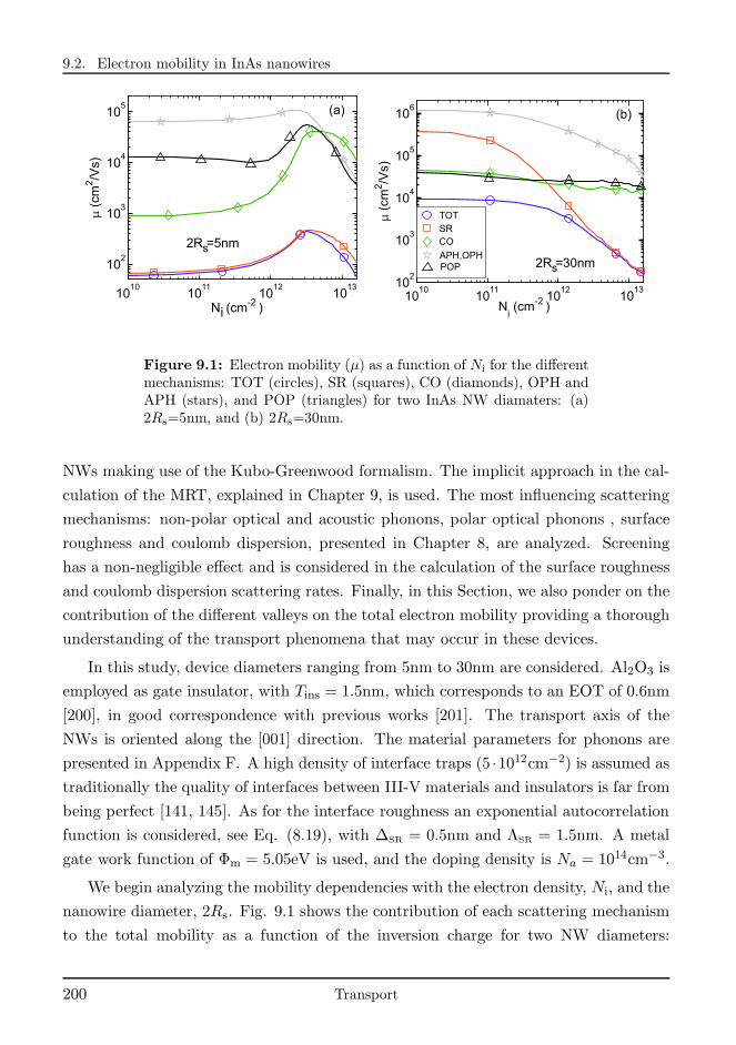
9.2. Electron mobility in InAs nanowires
1010
1011
1012
1013
102
103
104
105
N (cm-2 )
m(c
m2/V
s)
i
2R =5nms
(a)
1010
1011
1012
1013
102
103
104
105
106
Ni(cm-2 )
m(c
m2/V
s)
(b)
2R =30nms
TOT
SR
CO
APH,OPHPOP
Figure 9.1: Electron mobility (µ) as a function of Ni for the differentmechanisms: TOT (circles), SR (squares), CO (diamonds), OPH andAPH (stars), and POP (triangles) for two InAs NW diamaters: (a)2Rs=5nm, and (b) 2Rs=30nm.
NWs making use of the Kubo-Greenwood formalism. The implicit approach in the cal-
culation of the MRT, explained in Chapter 9, is used. The most influencing scattering
mechanisms: non-polar optical and acoustic phonons, polar optical phonons , surface
roughness and coulomb dispersion, presented in Chapter 8, are analyzed. Screening
has a non-negligible effect and is considered in the calculation of the surface roughness
and coulomb dispersion scattering rates. Finally, in this Section, we also ponder on the
contribution of the different valleys on the total electron mobility providing a thorough
understanding of the transport phenomena that may occur in these devices.
In this study, device diameters ranging from 5nm to 30nm are considered. Al2O3 is
employed as gate insulator, with Tins = 1.5nm, which corresponds to an EOT of 0.6nm
[200], in good correspondence with previous works [201]. The transport axis of the
NWs is oriented along the [001] direction. The material parameters for phonons are
presented in Appendix F. A high density of interface traps (5 ·1012cm−2) is assumed as
traditionally the quality of interfaces between III-V materials and insulators is far from
being perfect [141, 145]. As for the interface roughness an exponential autocorrelation
function is considered, see Eq. (8.19), with ∆SR = 0.5nm and ΛSR = 1.5nm. A metal
gate work function of Φm = 5.05eV is used, and the doping density is Na = 1014cm−3.
We begin analyzing the mobility dependencies with the electron density, Ni, and the
nanowire diameter, 2Rs. Fig. 9.1 shows the contribution of each scattering mechanism
to the total mobility as a function of the inversion charge for two NW diameters:
200 Transport
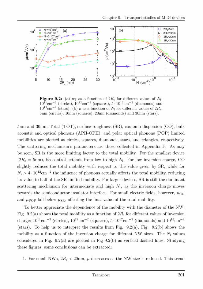
Chapter 9. Transport studies of MuG devices
5 10 15 20 25 30
102
103
104
2Rs
(nm)
m(c
m2/V
s)N =10N =10N =5·10N =10
i
i
i
i
11
12
12
13
cm-2
cm-2
cm-2
cm-2
(a)
1010
1011
1012
1013
101
102
103
104
105
Ni(cm-2 )
m(c
m2/V
s)
2R =5nm
2R =10nm
2R =20nm
2R =30nm
s
s
s
s
(b)
Figure 9.2: (a) µT as a function of 2Rs for different values of Ni:1011cm−2 (circles), 1012cm−2 (squares), 5 · 1012cm−2 (diamonds) and1013cm−2 (stars). (b) µ as a function of Ni for different values of 2Rs:5nm (circles), 10nm (squares), 20nm (diamonds) and 30nm (stars).
5nm and 30nm. Total (TOT), surface roughness (SR), coulomb dispersion (CO), bulk
acoustic and optical phonons (APH-OPH), and polar optical phonons (POP) limited
mobilities are plotted as circles, squares, diamonds, stars, and triangles, respectively.
The scattering mechanism’s parameters are those collected in Appendix F. As may
be seen, SR is the more limiting factor to the total mobility. For the smallest device
(2Rs = 5nm), its control extends from low to high Ni. For low inversion charge, CO
slightly reduces the total mobility with respect to the value given by SR, while for
Ni > 4 · 1012cm−2 the influence of phonons actually affects the total mobility, reducing
its value to half of the SR-limited mobility. For larger devices, SR is still the dominant
scattering mechanism for intermediate and high Ni, as the inversion charge moves
towards the semiconductor insulator interface. For small electric fields, however, µCO
and µPOP fall below µSR, affecting the final value of the total mobility.
To better appreciate the dependence of the mobility with the diameter of the NW,
Fig. 9.2(a) shows the total mobility as a function of 2Rs for different values of inversion
charge: 1011cm−2 (circles), 1012cm−2 (squares), 5 ·1012cm−2 (diamonds) and 1013cm−2
(stars). To help us to interpret the results from Fig. 9.2(a), Fig. 9.2(b) shows the
mobility as a function of the inversion charge for different NW sizes. The Ni values
considered in Fig. 9.2(a) are plotted in Fig 9.2(b) as vertical dashed lines. Studying
these figures, some conclusions can be extracted:
1. For small NWs, 2Rs < 20nm, µ decreases as the NW size is reduced. This trend
Transport 201
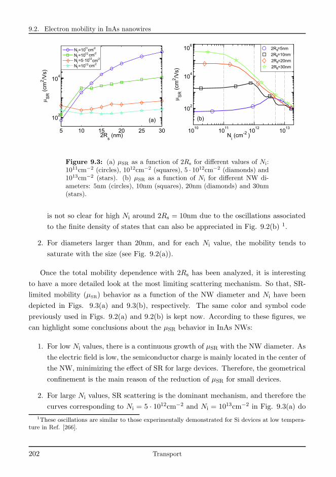
9.2. Electron mobility in InAs nanowires
5 10 15 20 25 30
102
104
2Rs
(nm)
mS
R(c
m2/V
s)N =10N =10N =5·10N =10
i
i
i
i
11
12
12
13
cm-2
cm-2
cm-2
cm-2
(a)
1010
1011
1012
1013
102
104
106
Ni(cm-2 )
mS
R(c
m2/V
s)
2R =5nm
2R =10nm
2R =20nm
2R =30nm
s
s
s
s
(b)
Figure 9.3: (a) µSR as a function of 2Rs for different values of Ni:1011cm−2 (circles), 1012cm−2 (squares), 5 · 1012cm−2 (diamonds) and1013cm−2 (stars). (b) µSR as a function of Ni for different NW di-ameters: 5nm (circles), 10nm (squares), 20nm (diamonds) and 30nm(stars).
is not so clear for high Ni around 2Rs = 10nm due to the oscillations associated
to the finite density of states that can also be appreciated in Fig. 9.2(b) 1.
2. For diameters larger than 20nm, and for each Ni value, the mobility tends to
saturate with the size (see Fig. 9.2(a)).
Once the total mobility dependence with 2Rs has been analyzed, it is interesting
to have a more detailed look at the most limiting scattering mechanism. So that, SR-
limited mobility (µSR) behavior as a function of the NW diameter and Ni have been
depicted in Figs. 9.3(a) and 9.3(b), respectively. The same color and symbol code
previously used in Figs. 9.2(a) and 9.2(b) is kept now. According to these figures, we
can highlight some conclusions about the µSR behavior in InAs NWs:
1. For low Ni values, there is a continuous growth of µSR with the NW diameter. As
the electric field is low, the semiconductor charge is mainly located in the center of
the NW, minimizing the effect of SR for large devices. Therefore, the geometrical
confinement is the main reason of the reduction of µSR for small devices.
2. For large Ni values, SR scattering is the dominant mechanism, and therefore the
curves corresponding to Ni = 5 · 1012cm−2 and Ni = 1013cm−2 in Fig. 9.3(a) do
1These oscillations are similar to those experimentally demonstrated for Si devices at low tempera-ture in Ref. [266].
202 Transport
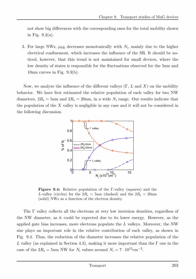
Chapter 9. Transport studies of MuG devices
not show big differences with the corresponding ones for the total mobility shown
in Fig. 9.2(a).
3. For large NWs, µSR decreases monotonically with Ni, mainly due to the higher
electrical confinement, which increases the influence of the SR. It should be no-
ticed, however, that this trend is not maintained for small devices, where the
low density of states is responsible for the fluctuations observed for the 5nm and
10nm curves in Fig. 9.3(b).
Now, we analyze the influence of the different valleys (Γ, L and X) on the mobility
behavior. We have first estimated the relative population of each valley for two NW
diameters, 2Rs = 5nm and 2Rs = 20nm, in a wide Ni range. Our results indicate that
the population of the X valley is negligible in any case and it will not be considered in
the following discussion.
0 5 10 150
0.2
0.4
0.6
0.8
1
Ni(x10 cm-2)
% o
f N
i
2R =5nms2R =20nms
L valley
G valley
12
Figure 9.4: Relative population of the Γ-valley (squares) and theL-valley (circles) for the 2Rs = 5nm (dashed) and the 2Rs = 20nm(solid) NWs as a function of the electron density.
The Γ valley collects all the electrons at very low inversion densities, regardless of
the NW diameter, as it could be expected due to its lower energy. However, as the
applied gate bias increases, more electrons populate the L valleys. Moreover, the NW
size plays an important role in the relative contribution of each valley, as shown in
Fig. 9.4. Thus, the reduction of the diameter increases the relative population of the
L valley (as explained in Section 4.3), making it more important than the Γ one in the
case of the 2Rs = 5nm NW for Ni values around Ni = 7 · 1012cm−2.
Transport 203
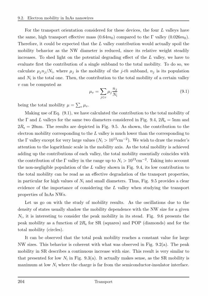
9.2. Electron mobility in InAs nanowires
For the transport orientation considered for these devices, the four L valleys have
the same, high transport effective mass (0.64m0) compared to the Γ valley (0.026m0).
Therefore, it could be expected that the L valley contribution would actually spoil the
mobility behavior as the NW diameter is reduced, since its relative weight steadily
increases. To shed light on the potential degrading effect of the L valley, we have to
evaluate first the contribution of a single subband to the total mobility. To do so, we
calculate µjnj/Ni, where µj is the mobility of the j-th subband, nj is its population
and Ni is the total one. Then, the contribution to the total mobility of a certain valley
v can be computed as
µv =∑
j∈vµjnjNi
(9.1)
being the total mobility µ =∑
v µv.
Making use of Eq. (9.1), we have calculated the contribution to the total mobility of
the Γ and L valleys for the same two diameters considered in Fig. 9.4, 2Rs = 5nm and
2Rs = 20nm. The results are depicted in Fig. 9.5. As shown, the contribution to the
electron mobility corresponding to the L valley is much lower than the corresponding to
the Γ valley except for very large values (Ni > 1013cm−2). We wish to draw the reader’s
attention to the logarithmic scale in the mobility axis. As the total mobility is achieved
adding up the contributions of each valley, the total mobility essentially coincides with
the contribution of the Γ valley in the range up to Ni > 1013cm−2. Taking into account
the non-negligible population of the L valley shown in Fig. 9.4, its low contribution to
the total mobility can be read as an effective degradation of the transport properties,
in particular for high values of Ni and small diameters. Thus, Fig. 9.5 provides a clear
evidence of the importance of considering the L valley when studying the transport
properties of InAs NWs.
Let us go on with the study of mobility results. As the oscillations due to the
density of states usually shadow the mobility dependence with the NW size for a given
Ni, it is interesting to consider the peak mobility in its stead. Fig. 9.6 presents the
peak mobility as a function of 2Rs for SR (squares) and POP (diamonds) and for the
total mobility (circles).
It can be observed that the total peak mobility reaches a constant value for large
NW sizes. This behavior is coherent with what was observed in Fig. 9.2(a). The peak
mobility in SR describes a continuous increase with size. This result is very similar to
that presented for low Ni in Fig. 9.3(a). It actually makes sense, as the SR mobility is
maximum at low Ni where the charge is far from the semiconductor-insulator interface.
204 Transport
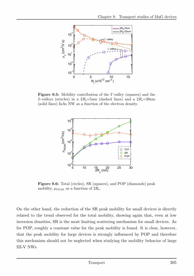
Chapter 9. Transport studies of MuG devices
0 5 10 1510
-1
101
103
Ni(x1012 cm-2 )
mv
(cm
2/V
s) G valley
L valley
2R =5nms2R =20nms
100
102
Figure 9.5: Mobility contribution of the Γ-valley (squares) and theL-valleys (scircles) in a 2Rs=5nm (dashed lines) and a 2Rs=20nm(solid lines) InAs NW as a function of the electron density.
5 10 15 20 25 3010
2
103
104
105
106
2Rs
(nm)
mP
EA
K(c
m2/V
s)
TOT
SR
POP
Figure 9.6: Total (circles), SR (squares), and POP (diamonds) peakmobility, µPEAK as a function of 2Rs.
On the other hand, the reduction of the SR peak mobility for small devices is directly
related to the trend observed for the total mobility, showing again that, even at low
inversion densities, SR is the most limiting scattering mechanism for small devices. As
for POP, roughly a constant value for the peak mobility is found. It is clear, however,
that the peak mobility for large devices is strongly influenced by POP and therefore
this mechanism should not be neglected when studying the mobility behavior of large
III-V NWs
Transport 205
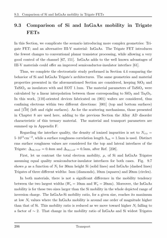
9.3. Comparison of Si and InGaAs mobility in Trigate FETs
9.3 Comparison of Si and InGaAs mobility in Trigate
FETs
In this Section, we complicate the scenario introducing more complex geometries: Tri-
gate FET; and an alternative III-V material: InGaAs. The Trigate FET introduces
the fewest changes to conventional planar transistor processing, while allowing a very
good control of the channel [67, 151]. InGaAs adds to the well known advantages of
III-V materials could offer an improved semiconductor-insulator interface [61].
Thus, we complete the electrostatic study performed in Section 4.4 comparing the
behavior of Si and InGaAs Trigate’s architectures. The same geometries and material
properties presented in the aforementioned Section are considered, keeping SiO2 and
TaSiOx as insulators with and EOT 1.1nm. The material parameters of TaSiOx were
calculated by a linear interpolation between those corresponding to SiO2 and Ta2O5.
In this work, [110]-oriented devices fabricated on (001) wafers are considered, thus
confining electrons within two different directions: [001] (top and bottom surfaces)
and [110] (left and right surfaces). As for the scattering mechanisms, those presented
in Chapter 8 are used here, adding to the previous Section the Alloy AD disorder
characteristic of this ternary material. The material and transport parameters are
summed up in Appendix F.
Regarding the interface quality, the density of ionized impurities is set to NCO =
5·1011cm−2, while a surface roughness correlation length ΛSR = 1.5nm is used. Distinct
rms surface roughness values are considered for the top and lateral interfaces of the
Trigate: ∆SR,TOP = 0.4nm and ∆SR,LAT = 0.5nm, after Ref. [238].
First, let us contrast the total electron mobility, µ, of Si and InGaAs Trigates
assuming equal quality semiconductor-insulator interfaces for both cases. Fig. 9.7
shows µ as a function of Ni for 30nm height Si (solid lines) and InGaAs (dashed lines)
Trigates of three different widths: 5nm (diamonds), 10nm (squares) and 20nm (circles).
In both materials, there is not a significant difference in the mobility tendency
between the two largest widths (Ws = 10nm and Ws = 20nm). Moreover, the InGaAs
mobility is for these two sizes larger than the Si mobility in the whole depicted range of
inversion charge. The InGaAs-Si mobility ratio, for a given size, reaches its maximum
at low Ni values where the InGaAs mobility is around one order of magnitude higher
than that of Si. This mobility ratio is reduced as we move toward higher Ni falling to
a factor of ∼ 2. That change in the mobility ratio of InGaAs and Si widest Trigates
206 Transport
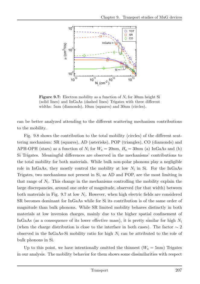
Chapter 9. Transport studies of MuG devices
1010
1011
1012
1013
102
103
104
Ni(cm-2 )
m(c
m2/V
s)
TOT
SR
CO
InGaAs
Si
Figure 9.7: Electron mobility as a function of Ni for 30nm height Si(solid lines) and InGaAs (dashed lines) Trigates with three differentwidths: 5nm (diamonds), 10nm (squares) and 30nm (circles).
can be better analyzed attending to the different scattering mechanism contributions
to the mobility.
Fig. 9.8 shows the contribution to the total mobility (circles) of the different scat-
tering mechanism: SR (squares), AD (asterisks), POP (triangles), CO (diamonds) and
APH-OPH (stars) as a function of Ni for Ws = 20nm, Hs = 30nm (a) InGaAs and (b)
Si Trigates. Meaningful differences are observed in the mechanisms’ contributions to
the total mobility for both materials. While bulk non-polar phonons play a negligible
role in InGaAs, they mostly control the mobility at low Ni in Si. For the InGaAs
Trigates, two mechanisms not present in Si, as AD and POP, are the most limiting in
that range of Ni. This change in the mechanisms controlling the mobility explain the
large discrepancies, around one order of magnitude, observed (for that width) between
both materials in Fig. 9.7 at low Ni. However, when high electric fields are considered
SR becomes dominant for InGaAs while for Si its contribution is of the same order of
magnitude than bulk phonons. While SR limited mobility behaves distinctly in both
materials at low inversion charges, mainly due to the higher spatial confinement of
InGaAs (as a consequence of its lower effective mass), it is pretty similar for high Ni
(when the charge distribution is close to the interface in both cases). The factor ∼ 2
observed in the InGaAs-Si mobility ratio for high Ni can be attributed to the role of
bulk phonons in Si.
Up to this point, we have intentionally omitted the thinnest (Ws = 5nm) Trigates
in our analysis. The mobility behavior for them shows some dissimilarities with respect
Transport 207
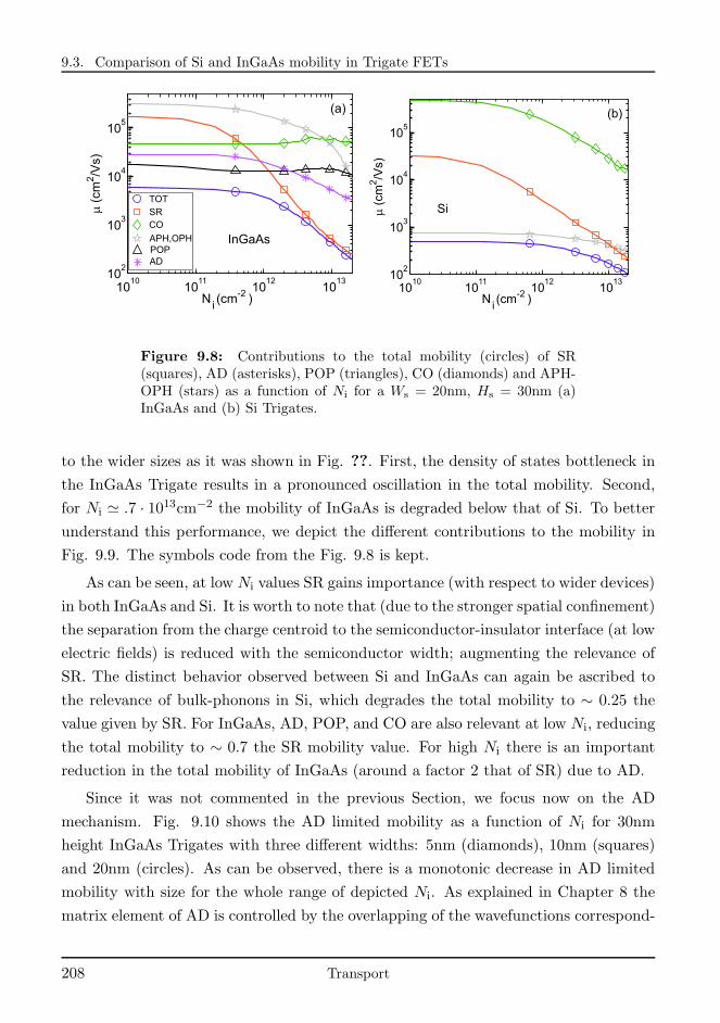
9.3. Comparison of Si and InGaAs mobility in Trigate FETs
1010
1011
1012
1013
102
103
104
105
N (cm-2 )
m(c
m2/V
s)
i
TOT
SR
CO
APH,OPHPOPAD
(a)
InGaAs
1010
1011
1012
1013
102
103
104
105
N (cm-2 )
m(c
m2/V
s)
i
(b)
Si
Figure 9.8: Contributions to the total mobility (circles) of SR(squares), AD (asterisks), POP (triangles), CO (diamonds) and APH-OPH (stars) as a function of Ni for a Ws = 20nm, Hs = 30nm (a)InGaAs and (b) Si Trigates.
to the wider sizes as it was shown in Fig. ??. First, the density of states bottleneck in
the InGaAs Trigate results in a pronounced oscillation in the total mobility. Second,
for Ni ≃ .7 · 1013cm−2 the mobility of InGaAs is degraded below that of Si. To better
understand this performance, we depict the different contributions to the mobility in
Fig. 9.9. The symbols code from the Fig. 9.8 is kept.
As can be seen, at low Ni values SR gains importance (with respect to wider devices)
in both InGaAs and Si. It is worth to note that (due to the stronger spatial confinement)
the separation from the charge centroid to the semiconductor-insulator interface (at low
electric fields) is reduced with the semiconductor width; augmenting the relevance of
SR. The distinct behavior observed between Si and InGaAs can again be ascribed to
the relevance of bulk-phonons in Si, which degrades the total mobility to ∼ 0.25 the
value given by SR. For InGaAs, AD, POP, and CO are also relevant at low Ni, reducing
the total mobility to ∼ 0.7 the SR mobility value. For high Ni there is an important
reduction in the total mobility of InGaAs (around a factor 2 that of SR) due to AD.
Since it was not commented in the previous Section, we focus now on the AD
mechanism. Fig. 9.10 shows the AD limited mobility as a function of Ni for 30nm
height InGaAs Trigates with three different widths: 5nm (diamonds), 10nm (squares)
and 20nm (circles). As can be observed, there is a monotonic decrease in AD limited
mobility with size for the whole range of depicted Ni. As explained in Chapter 8 the
matrix element of AD is controlled by the overlapping of the wavefunctions correspond-
208 Transport
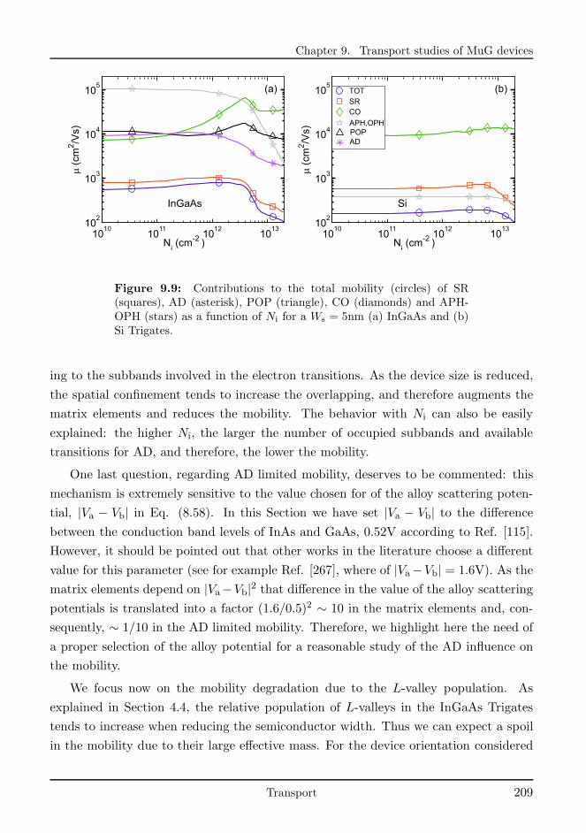
Chapter 9. Transport studies of MuG devices
1010
1011
1012
1013
102
103
104
105
N (cm-2 )
m(c
m2/V
s)
(a)
InGaAs
1010
1011
1012
1013
102
103
104
105
N (cm-2 )
m(c
m2/V
s)
TOT
SR
CO
APH,OPHPOPAD
(b)
Si
Figure 9.9: Contributions to the total mobility (circles) of SR(squares), AD (asterisk), POP (triangle), CO (diamonds) and APH-OPH (stars) as a function of Ni for a Ws = 5nm (a) InGaAs and (b)Si Trigates.
ing to the subbands involved in the electron transitions. As the device size is reduced,
the spatial confinement tends to increase the overlapping, and therefore augments the
matrix elements and reduces the mobility. The behavior with Ni can also be easily
explained: the higher Ni, the larger the number of occupied subbands and available
transitions for AD, and therefore, the lower the mobility.
One last question, regarding AD limited mobility, deserves to be commented: this
mechanism is extremely sensitive to the value chosen for of the alloy scattering poten-
tial, |Va − Vb| in Eq. (8.58). In this Section we have set |Va − Vb| to the difference
between the conduction band levels of InAs and GaAs, 0.52V according to Ref. [115].
However, it should be pointed out that other works in the literature choose a different
value for this parameter (see for example Ref. [267], where of |Va−Vb| = 1.6V). As the
matrix elements depend on |Va−Vb|2 that difference in the value of the alloy scattering
potentials is translated into a factor (1.6/0.5)2 ∼ 10 in the matrix elements and, con-
sequently, ∼ 1/10 in the AD limited mobility. Therefore, we highlight here the need of
a proper selection of the alloy potential for a reasonable study of the AD influence on
the mobility.
We focus now on the mobility degradation due to the L-valley population. As
explained in Section 4.4, the relative population of L-valleys in the InGaAs Trigates
tends to increase when reducing the semiconductor width. Thus we can expect a spoil
in the mobility due to their large effective mass. For the device orientation considered
Transport 209
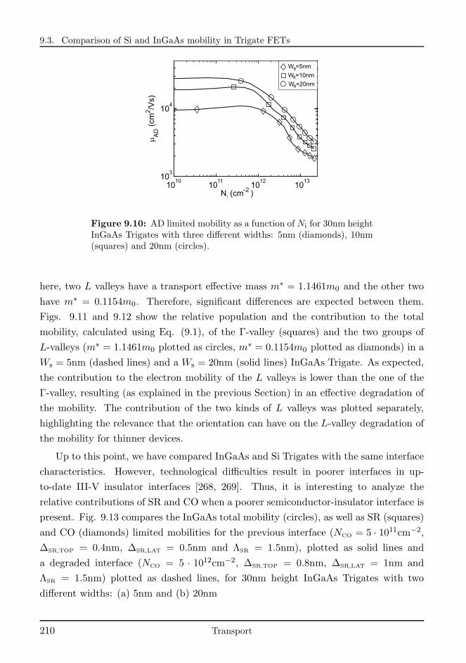
9.3. Comparison of Si and InGaAs mobility in Trigate FETs
1010
1011
1012
1013
103
104
N (cm-2 )
mA
D(c
m2/V
s)
W =5nm
W =10nm
W =20nm
s
s
s
Figure 9.10: AD limited mobility as a function of Ni for 30nm heightInGaAs Trigates with three different widths: 5nm (diamonds), 10nm(squares) and 20nm (circles).
here, two L valleys have a transport effective mass m∗ = 1.1461m0 and the other two
have m∗ = 0.1154m0. Therefore, significant differences are expected between them.
Figs. 9.11 and 9.12 show the relative population and the contribution to the total
mobility, calculated using Eq. (9.1), of the Γ-valley (squares) and the two groups of
L-valleys (m∗ = 1.1461m0 plotted as circles, m∗ = 0.1154m0 plotted as diamonds) in a
Ws = 5nm (dashed lines) and a Ws = 20nm (solid lines) InGaAs Trigate. As expected,
the contribution to the electron mobility of the L valleys is lower than the one of the
Γ-valley, resulting (as explained in the previous Section) in an effective degradation of
the mobility. The contribution of the two kinds of L valleys was plotted separately,
highlighting the relevance that the orientation can have on the L-valley degradation of
the mobility for thinner devices.
Up to this point, we have compared InGaAs and Si Trigates with the same interface
characteristics. However, technological difficulties result in poorer interfaces in up-
to-date III-V insulator interfaces [268, 269]. Thus, it is interesting to analyze the
relative contributions of SR and CO when a poorer semiconductor-insulator interface is
present. Fig. 9.13 compares the InGaAs total mobility (circles), as well as SR (squares)
and CO (diamonds) limited mobilities for the previous interface (NCO = 5 · 1011cm−2,∆SR,TOP = 0.4nm, ∆SR,LAT = 0.5nm and ΛSR = 1.5nm), plotted as solid lines and
a degraded interface (NCO = 5 · 1012cm−2, ∆SR,TOP = 0.8nm, ∆SR,LAT = 1nm and
ΛSR = 1.5nm) plotted as dashed lines, for 30nm height InGaAs Trigates with two
different widths: (a) 5nm and (b) 20nm
210 Transport
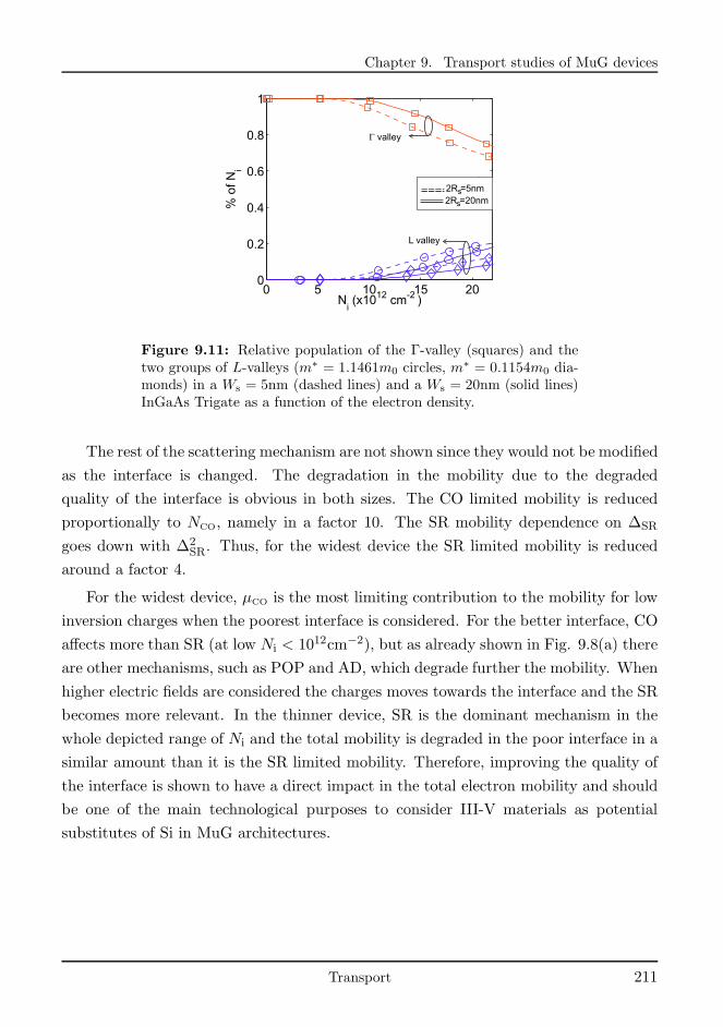
Chapter 9. Transport studies of MuG devices
0 5 10 15 200
0.2
0.4
0.6
0.8
1
Ni(x1012 cm-2 )
% o
f N
i
2R =5nms2R =20nms
G valley
L valley
Figure 9.11: Relative population of the Γ-valley (squares) and thetwo groups of L-valleys (m∗ = 1.1461m0 circles, m∗ = 0.1154m0 dia-monds) in a Ws = 5nm (dashed lines) and a Ws = 20nm (solid lines)InGaAs Trigate as a function of the electron density.
The rest of the scattering mechanism are not shown since they would not be modified
as the interface is changed. The degradation in the mobility due to the degraded
quality of the interface is obvious in both sizes. The CO limited mobility is reduced
proportionally to NCO, namely in a factor 10. The SR mobility dependence on ∆SR
goes down with ∆2SR. Thus, for the widest device the SR limited mobility is reduced
around a factor 4.
For the widest device, µCO is the most limiting contribution to the mobility for low
inversion charges when the poorest interface is considered. For the better interface, CO
affects more than SR (at low Ni < 1012cm−2), but as already shown in Fig. 9.8(a) there
are other mechanisms, such as POP and AD, which degrade further the mobility. When
higher electric fields are considered the charges moves towards the interface and the SR
becomes more relevant. In the thinner device, SR is the dominant mechanism in the
whole depicted range of Ni and the total mobility is degraded in the poor interface in a
similar amount than it is the SR limited mobility. Therefore, improving the quality of
the interface is shown to have a direct impact in the total electron mobility and should
be one of the main technological purposes to consider III-V materials as potential
substitutes of Si in MuG architectures.
Transport 211
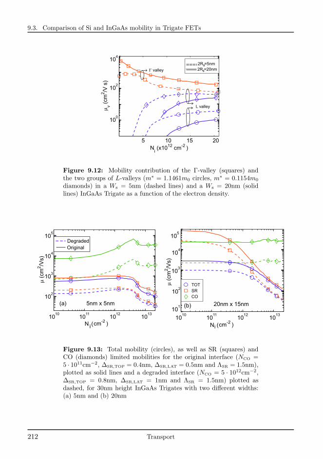
9.3. Comparison of Si and InGaAs mobility in Trigate FETs
5 10 15 20
100
102
104
Ni(x1012 cm-2 )
mv
(cm
2/V
s)
G valley
L valley
2R =5nms2R =20nms
Figure 9.12: Mobility contribution of the Γ-valley (squares) andthe two groups of L-valleys (m∗ = 1.1461m0 circles, m∗ = 0.1154m0
diamonds) in a Ws = 5nm (dashed lines) and a Ws = 20nm (solidlines) InGaAs Trigate as a function of the electron density.
1010
1011
1012
1013
102
103
104
105
N (cm-2 )
m(c
m2/V
s)
i
(a) 5nm x 5nm
OriginalDegraded
1010
1011
1012
1013
N (cm-2 )
m(c
m2/V
s)
101
102
103
104
105
i
TOT
SR
CO
(b) 20nm x 15nm
Figure 9.13: Total mobility (circles), as well as SR (squares) andCO (diamonds) limited mobilities for the original interface (NCO =5 · 1011cm−2, ∆SR,TOP = 0.4nm, ∆SR,LAT = 0.5nm and ΛSR = 1.5nm),plotted as solid lines and a degraded interface (NCO = 5 · 1012cm−2,∆SR,TOP = 0.8nm, ∆SR,LAT = 1nm and ΛSR = 1.5nm) plotted asdashed, for 30nm height InGaAs Trigates with two different widths:(a) 5nm and (b) 20nm
212 Transport
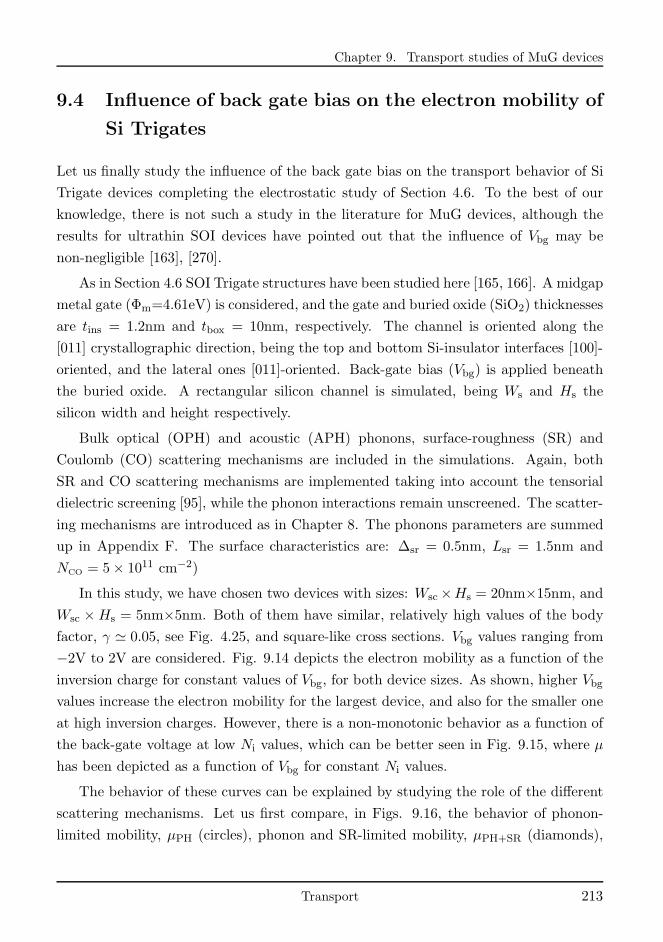
Chapter 9. Transport studies of MuG devices
9.4 Influence of back gate bias on the electron mobility of
Si Trigates
Let us finally study the influence of the back gate bias on the transport behavior of Si
Trigate devices completing the electrostatic study of Section 4.6. To the best of our
knowledge, there is not such a study in the literature for MuG devices, although the
results for ultrathin SOI devices have pointed out that the influence of Vbg may be
non-negligible [163], [270].
As in Section 4.6 SOI Trigate structures have been studied here [165, 166]. A midgap
metal gate (Φm=4.61eV) is considered, and the gate and buried oxide (SiO2) thicknesses
are tins = 1.2nm and tbox = 10nm, respectively. The channel is oriented along the
[011] crystallographic direction, being the top and bottom Si-insulator interfaces [100]-
oriented, and the lateral ones [011]-oriented. Back-gate bias (Vbg) is applied beneath
the buried oxide. A rectangular silicon channel is simulated, being Ws and Hs the
silicon width and height respectively.
Bulk optical (OPH) and acoustic (APH) phonons, surface-roughness (SR) and
Coulomb (CO) scattering mechanisms are included in the simulations. Again, both
SR and CO scattering mechanisms are implemented taking into account the tensorial
dielectric screening [95], while the phonon interactions remain unscreened. The scatter-
ing mechanisms are introduced as in Chapter 8. The phonons parameters are summed
up in Appendix F. The surface characteristics are: ∆sr = 0.5nm, Lsr = 1.5nm and
NCO = 5× 1011 cm−2)
In this study, we have chosen two devices with sizes: Wsc×Hs = 20nm×15nm, and
Wsc ×Hs = 5nm×5nm. Both of them have similar, relatively high values of the body
factor, γ ≃ 0.05, see Fig. 4.25, and square-like cross sections. Vbg values ranging from
−2V to 2V are considered. Fig. 9.14 depicts the electron mobility as a function of the
inversion charge for constant values of Vbg, for both device sizes. As shown, higher Vbg
values increase the electron mobility for the largest device, and also for the smaller one
at high inversion charges. However, there is a non-monotonic behavior as a function of
the back-gate voltage at low Ni values, which can be better seen in Fig. 9.15, where µ
has been depicted as a function of Vbg for constant Ni values.
The behavior of these curves can be explained by studying the role of the different
scattering mechanisms. Let us first compare, in Figs. 9.16, the behavior of phonon-
limited mobility, µPH (circles), phonon and SR-limited mobility, µPH+SR (diamonds),
Transport 213
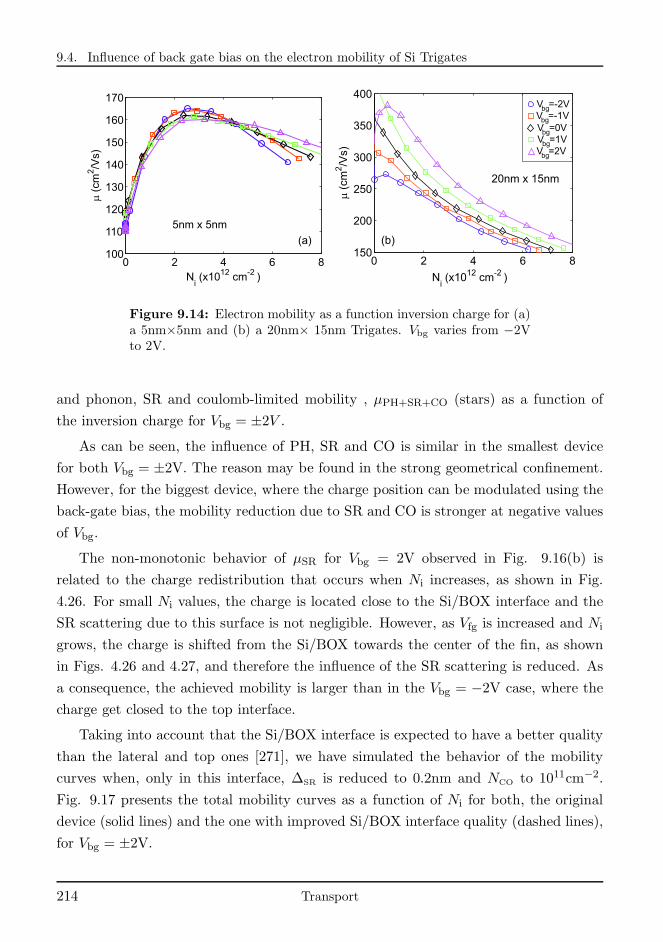
9.4. Influence of back gate bias on the electron mobility of Si Trigates
0 2 4 6 8100
110
120
130
140
150
160
170
Ni(x1012 cm-2 )
m(c
m2/V
s)
(a)
5nm x 5nm
0 2 4 6 8150
200
250
300
350
400
Ni(x1012 cm-2 )
m(c
m2/V
s)
V =-2VbgV =-1VbgV =0VbgV =1VbgV =2Vbg
(b)
20nm x 15nm
Figure 9.14: Electron mobility as a function inversion charge for (a)a 5nm×5nm and (b) a 20nm× 15nm Trigates. Vbg varies from −2Vto 2V.
and phonon, SR and coulomb-limited mobility , µPH+SR+CO (stars) as a function of
the inversion charge for Vbg = ±2V .
As can be seen, the influence of PH, SR and CO is similar in the smallest device
for both Vbg = ±2V. The reason may be found in the strong geometrical confinement.
However, for the biggest device, where the charge position can be modulated using the
back-gate bias, the mobility reduction due to SR and CO is stronger at negative values
of Vbg.
The non-monotonic behavior of µSR for Vbg = 2V observed in Fig. 9.16(b) is
related to the charge redistribution that occurs when Ni increases, as shown in Fig.
4.26. For small Ni values, the charge is located close to the Si/BOX interface and the
SR scattering due to this surface is not negligible. However, as Vfg is increased and Ni
grows, the charge is shifted from the Si/BOX towards the center of the fin, as shown
in Figs. 4.26 and 4.27, and therefore the influence of the SR scattering is reduced. As
a consequence, the achieved mobility is larger than in the Vbg = −2V case, where the
charge get closed to the top interface.
Taking into account that the Si/BOX interface is expected to have a better quality
than the lateral and top ones [271], we have simulated the behavior of the mobility
curves when, only in this interface, ∆SR is reduced to 0.2nm and NCO to 1011cm−2.
Fig. 9.17 presents the total mobility curves as a function of Ni for both, the original
device (solid lines) and the one with improved Si/BOX interface quality (dashed lines),
for Vbg = ±2V.
214 Transport
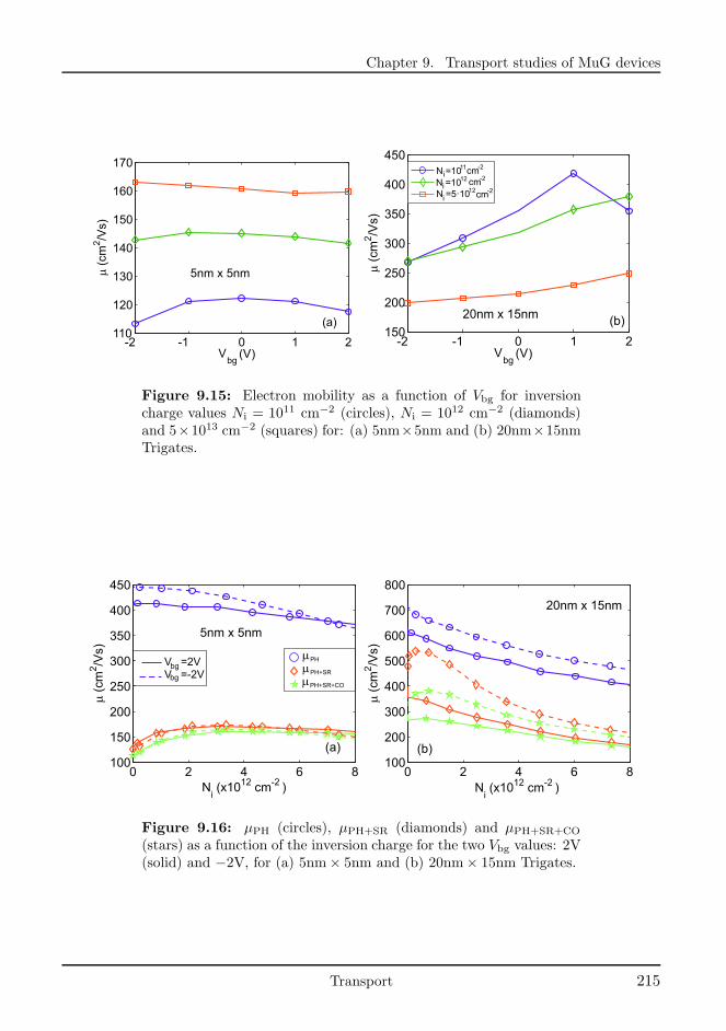
Chapter 9. Transport studies of MuG devices
-2 -1 0 1 2110
120
130
140
150
160
170
m(c
m2/V
s)
Vbg
(V)
(a)
5nm x 5nm
-2 -1 0 1 2150
200
250
300
350
400
450
Vbg
(V)
m(c
m2/V
s)
N =10N =10N =5·10
i
i
i
11
12
12
cm-2
cm-2
cm-2
(b)20nm x 15nm
Figure 9.15: Electron mobility as a function of Vbg for inversioncharge values Ni = 1011 cm−2 (circles), Ni = 1012 cm−2 (diamonds)and 5×1013 cm−2 (squares) for: (a) 5nm×5nm and (b) 20nm×15nmTrigates.
0 2 4 6 8100
150
200
250
300
350
400
450
Ni(x1012 cm-2 )
m(c
m2/V
s) mPH
mPH+SR
mPH+SR+CO
(a)
5nm x 5nm
V =2VV =-2V
bg
bg
0 2 4 6 8100
200
300
400
500
600
700
800
Ni(x1012 cm-2 )
m(c
m2/V
s)
(b)
20nm x 15nm
Figure 9.16: µPH (circles), µPH+SR (diamonds) and µPH+SR+CO
(stars) as a function of the inversion charge for the two Vbg values: 2V(solid) and −2V, for (a) 5nm× 5nm and (b) 20nm× 15nm Trigates.
Transport 215
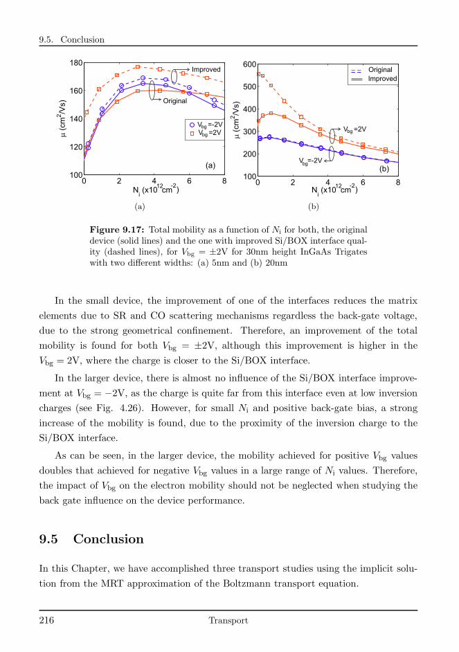
9.5. Conclusion
0 2 4 6 8100
120
140
160
180
Ni(x10 cm
-2)
m(c
m2/V
s)
V =2Vbg
V =-2Vbg
Original
Improved
(a)
12
(a)
0 2 4 6 8100
200
300
400
500
600
m(c
m2/V
s)
V =-2V
V =2V
bg
bg
OriginalImproved
(b)
Ni(x10 cm
-2)12
(b)
Figure 9.17: Total mobility as a function of Ni for both, the originaldevice (solid lines) and the one with improved Si/BOX interface qual-ity (dashed lines), for Vbg = ±2V for 30nm height InGaAs Trigateswith two different widths: (a) 5nm and (b) 20nm
In the small device, the improvement of one of the interfaces reduces the matrix
elements due to SR and CO scattering mechanisms regardless the back-gate voltage,
due to the strong geometrical confinement. Therefore, an improvement of the total
mobility is found for both Vbg = ±2V, although this improvement is higher in the
Vbg = 2V, where the charge is closer to the Si/BOX interface.
In the larger device, there is almost no influence of the Si/BOX interface improve-
ment at Vbg = −2V, as the charge is quite far from this interface even at low inversion
charges (see Fig. 4.26). However, for small Ni and positive back-gate bias, a strong
increase of the mobility is found, due to the proximity of the inversion charge to the
Si/BOX interface.
As can be seen, in the larger device, the mobility achieved for positive Vbg values
doubles that achieved for negative Vbg values in a large range of Ni values. Therefore,
the impact of Vbg on the electron mobility should not be neglected when studying the
back gate influence on the device performance.
9.5 Conclusion
In this Chapter, we have accomplished three transport studies using the implicit solu-
tion from the MRT approximation of the Boltzmann transport equation.
216 Transport
Chapter 9. Transport studies of MuG devices
First, we have analyzed the electron mobility behavior for InAs NWs as a function
of their diameter and inversion charge. We have demonstrated that surface roughness
is the most limiting mechanism as the device size is shrunk. However, polar optical
phonons and Coulomb interactions should also be considered in order to explain the
trend observed for the total mobility as a function of the device size and the electron
density. We have also demonstrated the importance of including the L valley in the
calculations as its increasing population when the diameter is reduced strongly degrades
the mobility. Therefore, neglecting the contribution of the L valley would lead to wrong
conclusions.
Second, we have compared the mobility performance of InGaAs and Si Trigates.
The mechanism contributions to the mobility have been studied for different Trigate
widths, observing relevant differences in the InGaAs-Si ratio with size.
We have analyzed the influence of the back-gate bias on the electron mobility of
Trigate silicon devices. It has been confirmed the strong impact of the back-gate bias
on the electron mobility. Positive back-gate bias pushes the charge further from the top
and lateral Si/insulator interfaces, reducing the influence of SR and Coulomb scattering
mechanisms and therefore increasing the carrier mobility. On the contrary, the carrier
mobility is degraded for negative back-gate bias.
Transport 217

Part IV
Conclusions

Chapter 10
Conclusions
As explained in the Objectives section, the main objective of this PhD Thesis was the
study of MuG architectures and III-V compounds semiconductors. In this context, the
main contributions of this work are listed next:
1. A self-consistent Schrodinger-Poisson solver was developed, which is able to deal
with arbitrary geometries, materials and orientations to achieve the charge and
potential distribution in the cross-section of a MuG structure. A non-parabolic
effective mass approach was employed for the Schrodinger equation, and the con-
tribution of Γ, X (∆ for Silicon) and L valleys was included. In addition, the
developed simulator allows the inclusion of an arbitrary profile of interface states.
2. Using this self-consistent Schrodinger-Poisson solver, Trigates and NWs made of
Si and III-V semiconductors were analyzed. It was demonstrated that the low
density of states has a strong influence on the charge density and gate capaci-
tance behavior of III-V NWs. Moreover, the population of higher energy valleys
(in particular, of L valleys) can strongly modify the small conduction effective
mass associated to III-V semiconductors. Additionally, we studied the behavior
of InGaAs, and SOI Trigate FETs, as a function of the channel width, showing
that the semiconductor width has a strong impact on InGaAs Trigates: both
the threshold voltage and the gate voltage at which the L valleys begin to be
populated depend on the width. Besides, it was demonstrated the importance
of considering the two-dimensional confinement for III-V materials to accurately
reproduce the electron distribution near the corners. This effect produces a notice-
able impact on the conduction effective mass as a result of the different population
of each valley. The control the threshold voltage and the charge distribution of
Trigate SOI devices by modifying the back-gate bias was studied, confirming the
possibility of achieving body factors higher than γ=0.1 as long as the channel
width over height ratio is increased as much as possible. Finally, the influence of
the interfacial states, Dit, on the performance of Si MuG FET and, specifically,
on the subthreshold swing and the threshold voltage was analyzed observing rel-
evant variations with the temperature and the oxide thickness. It was concluded
that the higher the number of gates the lower the degradation due to the interface
states, caused by the higher electrostatic control of the semiconductor-insulator
interface.
3. A fully analytical model for the charge and potential distributions in cylindrical
III-V nanowires was developed. This model presented analytical expressions for
the calculation of the subband energies and their corresponding wavefunctions,
taking into account their penetration into the gate insulator and the effective
mass discontinuity in the semiconductor-oxide interface, Fermi-Dirac statistics,
two-dimensional confinement of the carriers and non-parabolic effects. It also
allowed the inclusion of arbitrary analytical profiles of interfacial states. We
demonstrated that our analytical solution fits very well the numerical simulations
in all operating regimes for a wide range of NW sizes and gate voltages. The model
was extended to calculate the current in a long-channel nanowire including the
interface charge.
4. Using the results from the charge and potential models, we proposed physically
based analytical models for the gate capacitance and the threshold voltage in
III-V NWs. Regarding the gate capacitance model, it was demonstrated that the
model fits very well the numerical results for different NW sizes and materials,
without considering any fitting parameters. The different contributions to the
total gate capacitance were identified and modeled, showing their relation with
the finite density of states and the charge distribution in the NWs. The capaci-
tance behavior of III-V NWs were compared with that of their Si counterparts.
Significant differences were found for the dominant contribution to the inversion
capacitance, as well as for the semiconductor potential dependence on the gate
voltage. Furthermore, we showed the limited impact of the EOT reduction in
the gate capacitance of III-V NWs, in contrast to the behavior observed in Si
devices. The role of the wavefunction penetration into the gate insulator was
222 Conclusions
Chapter 10. Conclusions
also analyzed, evidencing its relevance for an accurate description of the gate
capacitance. Concerning the threshold voltage model, after some reasonable ap-
proximations, we came up with a simple expression of VT that will be useful for
the development of compact models for III-V cylindrical NWs. We demonstrated
that the threshold voltage expression accurately reproduces the numerical results
for different III-V semiconductor materials, NW sizes, and oxide thicknesses. The
influence of the wavefunction penetration into the gate insulator was discussed,
illustrating its relevance for an accurate modeling of VT. The VT variations due
to the changes in the semiconductor effective mass were evaluated. We gave in-
sight into the different contributions to the threshold voltage finding interesting
differences among materials. Furthermore, we studied the VT dependence on the
insulator thickness, showing no relevant changes in a wide range of tins, contrary
to what is observed in Si devices.
5. We have developed a model to calculate the electron mobility of a 1D electron
gas based on the linearization of the Boltzmann Transport Equation using the
momentum relaxation time approximation (MRT). Besides the explicit approach
for the calculation of the MRT, which has been extensively used in the literature,
we implemented an implicit approach resolution. The formulation of the implicit
equation system was exemplified, considering the nested interdependency of the
transitions, and the truncation of the discretized wavenumber space with a Neu-
mann boundary condition. We have to highlight that this implicit solution of the
MRT, taking into account several scattering mechanisms is, to the best of our
knowledge, unique in the literature for 2D confined devices.
6. The main scattering mechanisms for III-V and Silicon nanowires have been mod-
eled for 2D confined devices. Novel models for surface roughness, Coulomb, bulk
phonons, polar optical phonons and alloy disorder scattering mechanisms have
been developed. Moreover, tensorial dielectric screening has been considered and
implemented. It should be stressed that our simulator is useful for any device
geometry and for both Silicon and III-V semiconductor materials, therefore con-
stituting a state-of-the-art nanowire mobility simulator.
7. Finally, the mobility behavior of III-V and Silicon nanowires has been addressed.
In our studies, which include InAs nanowires and InGaAs trigate devices, we
have shown that the surface quality has to be improved in order to fulfil the high
electron mobility expected for III-V nanowires. In particular, surface roughness
Conclusions 223
seems to be the most critical scattering mechanism, and for very small sizes it
limits the mobility of III-V nanowires to that of Si nanowires, therefore can-
celing the potential improvement on the device performance given by the low
conduction effective mass. We observed that polar optical phonons and Coulomb
interactions should also be considered in order to explain the trend for the total
mobility as a function of the device size and the electron density. We have also
demonstrated the importance of including the L valley in the calculations as its
increasing population when the diameter is reduced strongly degrades the mobil-
ity. Therefore, neglecting the contribution of the L valley would lead to wrong
conclusions. We analyzed the influence of the back-gate bias on the electron mo-
bility of Trigate SOI devices confirming its strong impact. Positive back-gate bias
pushes the charge further from the top and lateral Si/insulator interfaces, reduc-
ing the influence of surface roughnes and Coulomb scattering mechanisms and
therefore increasing the carrier mobility. On the contrary, the carrier mobility
was degraded for negative back-gate bias.
224 Conclusions

Part V
Appendixes

Appendix A
Numerical implementation of
surface interface charge
In this Appendix we deal with the mathematical details regarding the relation between
surface interface charge, Qit,sf, and volumetric interface charge, Qit,vl, discussed in
Chapter 3. Specifically we: 1) detail the procedure to obtain a relation between Qit,vl
and ψ|i-m − ψ|i-s in both Cartesian and cylindrical coordinates; and 2) we determine
the values of Acte, Alin, Aexp, and Agau for a given value of Qit,sf.
First, we determine the relation between ψ|i-m − ψ|i-s and Qit,vl for regions with
straight and curved segments. To do it, let us properly define both problems. Fig. A.1
shows a region, Ri, corresponding to a curved segment (left) and another corresponding
to a straight segment (right).
O
C i-s\ Ri
Ci-m
\ Ri
i-s\ Ri
C i-si
i-s\ Ri
Ci-m
\ Ri
#
& #
& &= c
& &= c+tins
=0
#=t ins
cOs
Figure A.1: Definition of system references to find a relation ψ|i-m−ψ|i-s Qit,vl and Qit,sf for a curved segment (left) and a straight region(right).
It is straightforward to see that the reference system which easiest describe the
Appendixes 227
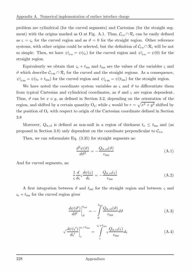
Appendix A. Numerical implementation of surface interface charge
problem are cylindrical (for the curved segments) and Cartesian (for the straight seg-
ment) with the origins marked as O at Fig. A.1. Thus, Ci-s ∩Ri can be easily defined
as ς = ςc for the curved region and as ϑ = 0 for the straight region. Other reference
systems, with other origins could be selected, but the definition of Ci-s ∩Ri will be not
so simple. Then, we have ψ|i-s = ψ(ςc) for the curved region and ψ|i-s = ψ(0) for the
straight region.
Equivalently we obtain that ςc + tins and tins are the values of the variables ς and
ϑ which describe Ci-m ∩ Ri for the curved and the straight regions. As a consequence,
ψ|i-m = ψ(ςc + tins) for the curved region and ψ|i-m = ψ(tins) for the straight region.
We have noted the coordinate system variables as ς and ϑ to differentiate them
from typical Cartesian and cylindrical coordinates, as ϑ and ς are region dependent.
Thus, ϑ can be x o y, as defined in Section 3.2, depending on the orientation of the
region, and shifted by a certain quantity Os; while ς would be r =√
x2 + y2 shifted by
the position of Oc with respect to origin of the Cartesian coordinate defined in Section
3.8
Moreover, Qit,vl is defined as non-null in a region of thickness to ≤ tins and (as
proposed in Section 3.8) only dependent on the coordinate perpendicular to Ci-s.Then, we can reformulate Eq. (3.35) for straight segments as:
d2ψ(ϑ)
dϑ2= −Qit,vl(ϑ)
ǫins(A.1)
And for curved segments, as:
1
ς
d
dςςdψ(ς)
dς= −Qit,vl(ς)
ǫins(A.2)
A first integration between ϑ and tins for the straight region and between ς and
ςc + tins for the curved region gives
dψ(ϑ′)dϑ′
∣
∣
∣
∣
tins
ϑ
= −tins∫
ϑ
Qit,vl(ϑ)
ǫinsdϑ (A.3)
ς ′dψ(ς ′)dς ′
∣
∣
∣
∣
ςc+tins
ς
=
ςc+tins∫
ς
ςQit,vl(ς)
ǫinsdς (A.4)
228 Appendixes
Appendix A. Numerical implementation of surface interface charge
But due to the charge neutrality of the whole structure, no electric field is expected at
Ci-m, and, therefore:dψ(ϑ′)dϑ′
|ϑ′=tins = 0, for straight regions, anddψ(ς ′)dς ′
|ς′=ςc+tins = 0
for curved regions. So:
dψ(ϑ)
dϑ= −
tins∫
ϑ
Qit,vl(ϑ)
ǫinsdϑ (A.5)
ςdψ(ς)
dς=
ςc+tins∫
ς
ςQit,vl(ς)
ǫinsdς (A.6)
A second integration between 0 and tins for straight region and between ςc and
ςc + tins for curved region gives:
ψ|i-m − ψ|i-s =1
ǫins
tins∫
0
dϑ
tins∫
ϑ
Qit,vl(ϑ)dϑ (A.7)
for straight segments and
ψ|i-m − ψ|i-s =1
ǫins
ςc+tins∫
ςc
1
ςdς
ςc+tins∫
ς
ςQit,vl(ς)dς (A.8)
for curved segments.
Now, we determine Acte, Alin, Aexp, and Agau for a given value of Qit,sf. Let us
recall Eqs. (3.38) and (3.39):
Qit,sf tins =
tins∫
0
dϑ
tins∫
ϑ
Qit,vl(ϑ)dϑ (A.9)
and:
Qit,sf ςcln(1 + tins/ςc) =
ςc+tins∫
ςc
1
ςdς
ςc+tins∫
ς
ςQit,vl(ς)dς (A.10)
To determine Acte, Alin, Aexp, and Agau we substitute the expressions for Qit,vl given
in Tab. 3.1 into Eqs. (3.38) and (3.39) and we solve for A.
To keep this manuscript (to the best of our possibilities) clear and legible, we have
omitted the integration procedure for each profile in Table (3.1). They mostly consist
Appendixes 229
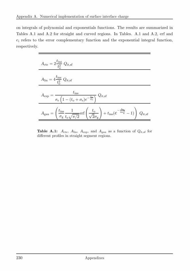
Appendix A. Numerical implementation of surface interface charge
on integrals of polynomial and exponentials functions. The results are summarized in
Tables A.1 and A.2 for straight and curved regions. In Tables. A.1 and A.2, erf and
ei refers to the error complementary function and the exponential integral function,
respectively.
Acte = 2tinst2o
Qit,sf
Alin = 4tinst2o
Qit,sf
Aexp =tins
σe
(
1− (to + σe)e− to
σe
) Qit,sf
Agau =
(
tinsσg
1
to√
π/2erf
(
to√2σg
)
+ tins(e− to
2σ2g − 1)
)
Qit,sf
Table A.1: Acte, Alin, Aexp, and Agau as a function of Qit,sf fordifferent profiles in straight segment regions.
230 Appendixes
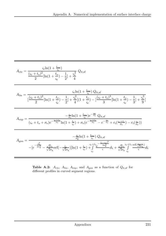
Appendix A. Numerical implementation of surface interface charge
Acte =ςcln(1 +
tinsςc
)
(ςc + to)2
2[ln(1 +
toςc)− 1
2] +
ς2c4
Qit,sf
Alin =ςcln(1 +
tinsςc
) Qit,sf
[(ςc + to)
2
2[ln(1 +
toςc)− 1
2] +
ς2c4](1 +
toςc)− [
(ςc + to)3
3[ln(1 +
toςc)− 1
3] +
ς3c9]
Aexp =− ςcσeln(1 + tins
ςc)e−
ςcσe Qit,sf
(ςc + to + σe)e− ςc+to
σe ln(1 + toςc) + σe(e
− ςc+toσe − e
− ςcσe + ei(
ςc+toσe
)− ei(ςcσe))
Agau =− ςcσ2gln(1 + tins
ςc) Qit,sf
−[e− t2o
2σ2g −
√πςc√2σg
erf(− to√2σg
)]ln(1 + toςc) +
ςc+to∫
ςc
e− (ς−ςc)
2
2σ2g
ς dς +√πςc√2σg
ςc+to∫
ςc
erf( ςc−ς√2σg
)
ς dς
Table A.2: Acte, Alin, Aexp, and Agau as a function of Qit,sf fordifferent profiles in curved segment regions.
Appendixes 231

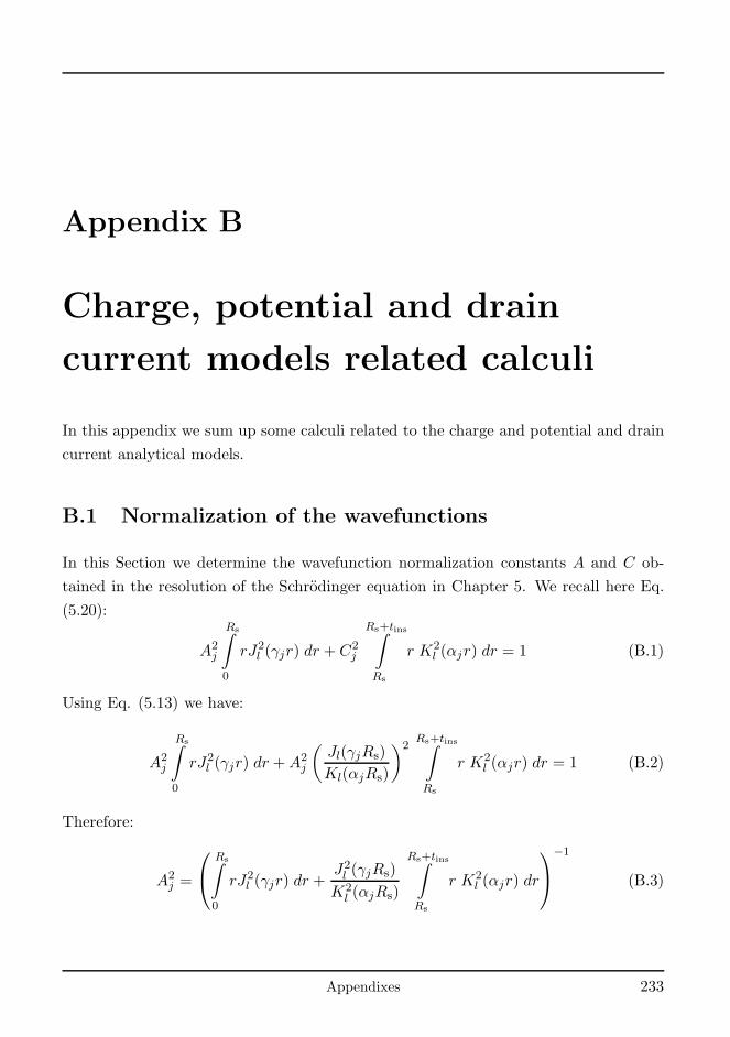
Appendix B
Charge, potential and drain
current models related calculi
In this appendix we sum up some calculi related to the charge and potential and drain
current analytical models.
B.1 Normalization of the wavefunctions
In this Section we determine the wavefunction normalization constants A and C ob-
tained in the resolution of the Schrodinger equation in Chapter 5. We recall here Eq.
(5.20):
A2j
Rs∫
0
rJ2l (γjr) dr + C2
j
Rs+tins∫
Rs
r K2l (αjr) dr = 1 (B.1)
Using Eq. (5.13) we have:
A2j
Rs∫
0
rJ2l (γjr) dr +A2
j
(
Jl(γjRs)
Kl(αjRs)
)2Rs+tins∫
Rs
r K2l (αjr) dr = 1 (B.2)
Therefore:
A2j =
Rs∫
0
rJ2l (γjr) dr +
J2l (γjRs)
K2l (αjRs)
Rs+tins∫
Rs
r K2l (αjr) dr
−1
(B.3)
Appendixes 233
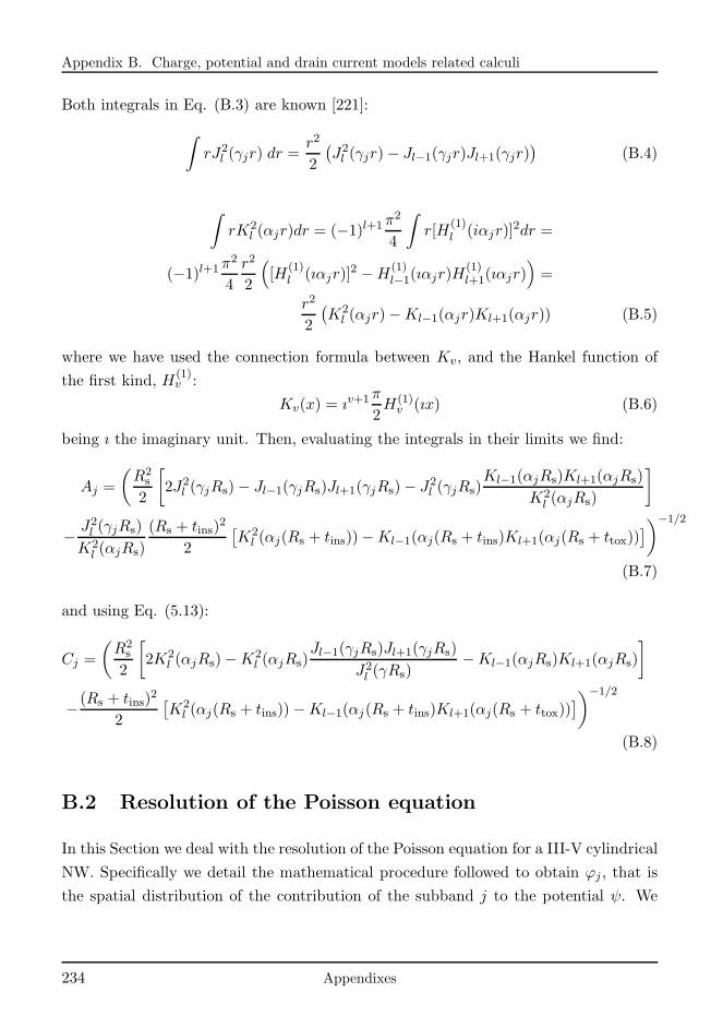
Appendix B. Charge, potential and drain current models related calculi
Both integrals in Eq. (B.3) are known [221]:
∫
rJ2l (γjr) dr =
r2
2
(
J2l (γjr)− Jl−1(γjr)Jl+1(γjr)
)
(B.4)
∫
rK2l (αjr)dr = (−1)l+1π
2
4
∫
r[H(1)l (iαjr)]
2dr =
(−1)l+1π2
4
r2
2
(
[H(1)l (ıαjr)]
2 −H(1)l−1(ıαjr)H
(1)l+1(ıαjr)
)
=
r2
2
(
K2l (αjr)−Kl−1(αjr)Kl+1(αjr)) (B.5)
where we have used the connection formula between Kv , and the Hankel function of
the first kind, H(1)v :
Kv(x) = ıv+1π
2H(1)v (ıx) (B.6)
being ı the imaginary unit. Then, evaluating the integrals in their limits we find:
Aj =
(
R2s
2
[
2J2l (γjRs)− Jl−1(γjRs)Jl+1(γjRs)− J2
l (γjRs)Kl−1(αjRs)Kl+1(αjRs)
K2l (αjRs)
]
− J2l (γjRs)
K2l (αjRs)
(Rs + tins)2
2
[
K2l (αj(Rs + tins))−Kl−1(αj(Rs + tins)Kl+1(αj(Rs + ttox))
]
)−1/2
(B.7)
and using Eq. (5.13):
Cj =
(
R2s
2
[
2K2l (αjRs)−K2
l (αjRs)Jl−1(γjRs)Jl+1(γjRs)
J2l (γRs)
−Kl−1(αjRs)Kl+1(αjRs)
]
−(Rs + tins)2
2
[
K2l (αj(Rs + tins))−Kl−1(αj(Rs + tins)Kl+1(αj(Rs + ttox))
]
)−1/2
(B.8)
B.2 Resolution of the Poisson equation
In this Section we deal with the resolution of the Poisson equation for a III-V cylindrical
NW. Specifically we detail the mathematical procedure followed to obtain ϕj , that is
the spatial distribution of the contribution of the subband j to the potential ψ. We
234 Appendixes
Appendix B. Charge, potential and drain current models related calculi
recall here Eq. (5.40):
ϕj(r) =
A2j
∫ ∫
r J2l (γjr) dr
1
rdr i = a
C2j
∫ ∫
rK2l (αjr) dr
1
rdr = (−1)l+1 π
2
4C2j
∫ ∫
r[H(1)l (ıαjr)]
2dr1
rdr i = b
(B.9)
where Kl was rewritten in terms of H(1)l using the definition of Eq. (B.6). Expressing
ϕj(r) in this way allows us to give a unified treatment to the integral. This is because
H(1)l (also called Bessel function of the third kind) shares with Jl many recurrence
relations and connection formulas. Thus, we use the notation M(νx) to refer to both
functions, Jl (γjr) and H(1)l (ıαjr), in the forthcoming integration. The inner integral
in Eq. (B.9) is known:
∫
xM2v (ax)dx =
x2
2
[
M2v (ax)−Mv−1(ax)Mv+1(ax)
]
(B.10)
being the equality valid for both Jv and H(1)v as proposed in Eqs. (B.4) and (B.5).
Therefore:
∫ ∫
r′M2l (νjr
′)dr′1
rdr =
1
2
∫
rM2l (νjr)dr −
1
2
∫
rM1−1(νjr)Ml+1(νjr)dr (B.11)
The first integral in the right-hand side of Eq. (B.11) can again be solved using Eq.
(B.10). The second one can be written as:
∫
rMl−1(νjr)Ml+1(νjr)dr =
∫
rMl−1(νjr)Ml−1(νjr)dr−2
νj
∫
rMl−1(νjr)dMl(νjr)
drdr
(B.12)
where we have used the recurrence relation:
Mv+1(ax) =Mv−1(ax)−2
a
dMv(ax)
dx(B.13)
which is valid for both Jv and H(1)v . Again the first integral in the right-hand side can
be solved using Eq. (B.10). The second integral can be integrated by parts as:
∫
rMl−1(νjr)dMl(νjr)
drdr = rMl−1(r)Ml(r)−
∫
Ml(νjr) [lMl−1(νjr)− rνjMl(νjr)] dr
(B.14)
Appendixes 235
Appendix B. Charge, potential and drain current models related calculi
where:
u = rMl−1(νjr) −→ du = lMl−1(νjr)− νjrMl(νjr) (B.15)
dv =dMl(νjr)
dr−→ v =Ml(νjr) (B.16)
and where the recurrence relation:
dMv(ax)
dx= a
[ v
axMv(ax)−Mv+1(ax)
]
(B.17)
holds for both Jv and H(1)v . Then, the integral in the right-hand side of Eq. (B.14):
∫
Ml(νjr) [lMl−1(νjr)− νjrMl(νjr)] dr = l
∫
Ml(νjr)Ml−1(νjr)dr− νj
∫
rM2l (νjr)dr
(B.18)
where the second integral in the right-hand side of Eq. (B.18) can be calculated using
Eq. (B.10). Applying Eq. (B.13) to Ml(νjr) with l = v + 1 in the first integral we
obtain:
l
∫
Ml(νjr)Ml−1(νjr)dr = l
∫
Ml−2(νjr)Ml−1(νjr)dr −2l
νj
∫
dMl−1(νjr)dr
Ml−1(νjr)dr
(B.19)
where the first integral is direct:
2l
νj
∫
Ml−1(νjr)dMl−1(νjr)
drdr =
l
νjM2l−1(νjr) (B.20)
and:
l
∫
Ml(νjr)Ml−1(νjr)dr = l
∫
Ml−1(νjr)Ml−2(νjr)dr −l
νjM2l−1(νjr) (B.21)
but it is easy to see that the first integral in the right-hand side of Eq. (B.21) is just
the integral in the left-hand side of Eq. (B.18) with a reduction of 1 in the order of M
functions. We can apply this rule recursively until we reach,
∫
M1(νjr)M0(νjr)dr = −M20 (νjr)
2νj(B.22)
236 Appendixes
Appendix B. Charge, potential and drain current models related calculi
which is satisfied for both Jv and H(1)v . Then, the complete integral is:
∫ ∫ r
0r′ |Ml(νjr
′)|2dr′ 1rdr =
1
2
r2
2M2l (νjr)−
1
2
r2
2Ml−1(νjr)Ml+1(νjr)−
1
2
r2
2M2l−1(νjr) +
1
2
r2
2Ml−2(νjr)Ml(νjr) +
1
2
2
νjrMl−1(νjr)Ml(νjr) +
1
2
2
νjνjr2
2M2l (νjr)
− 1
2
2
νjνjr2
2Ml−1(νjr)Ml+1(νjr) +
1
2
2
νj
l
νjM2l−1(νjr)−
1
2
2
νjl
∫
Ml−1(νjr)Ml−2(νjr)dr
(B.23)
Rearranging terms we have:
3
4r2M2
l (νjr)−3
4r2Ml−1(νjr)Ml+1(νjr)−
r2
4M2l−1(νjr) +
r2
4Ml−2(νjr)Ml(νjr)+
+r
νjMl−1(νjr)Ml(νjr) +
l
ν2jM2l−1(νjr)−
l
νj
∫
Ml−1(νjr)Ml−2(νjr) (B.24)
We can use the recurrence relation:
Mv+1(ax) +Mv−1(ax) =2v
axMv(ax) (B.25)
valid for Jv as well as for H(1)v to rewrite Ml−2 as:
Ml−2(νjr) =2(l − 1)
νjrMl−1(νjr)−Ml(νjr) (B.26)
Using it in Eq. (B.24) and simplifying we get:
1
2r2M2
l (νjr)−3
4r2Ml−1(νjr)Ml+1(νjr)−
r2
4M2l−1(νjr) + (
l + 1
2)r
νjMl−1(νjr)Ml(νjr)+
+l
ν2jM2l−1(νjr) +
l
νj
∫
Ml−1(νjr)Ml−2(νjr)dr (B.27)
Now we use again Eq. (B.25) for Ml+1(νjr) and we obtain:
1
2r2M2
l (νjr) +1
2r2M2
l−1(νjr) + (−l + 1
2)r
νjMl−1(νjr)Ml(νjr) +
l
ν2jM2l−1(νjr)−
− l
νj
∫
Ml−1(νjr)Ml−2(νjr)dr (B.28)
Appendixes 237
Appendix B. Charge, potential and drain current models related calculi
Or applying the recursive integral in Eq. (B.21) and the result from Eq. (B.22) we get:
1
2r2M2
l (νjr) +1
2r2M2
l−1(νjr) + (−l + 1
2)r
νjMl−1(νjr)Ml(νjr) +
l
ν2j
l∑
m=1
M2m−1(νjr)
− l
2ν2jM2
0 (νjr) (B.29)
Now, we can undo the change of notation to establish the contribution of the subband
j to the potential in the semiconductor:
ϕaj (r) = A2j
(
r2
2J2l (γjr) +
r2
2J2l−1(γjr) + (−l + 1
2)r
γjJl−1(γjr)Jl(γjr)+
+l
γ2j
l∑
m=1
J2m−1(γjr)−
l
2γ2jJ20 (γjr)
)
(B.30)
Equivalently, using Eq. (B.6), with νj = iαj
ϕbj(r) = C2j
(
(−1)(l+1)
(−1)(l+1)
1
2r2K2
l (αjr) +(−1)(l+1)
(−1)l1
2r2K2
l−1(αjr)+
(−1)(l+1)
ıl+1ıl(− l
2+ 1)
r
ıαjKl−1(αjr)Kl(αjr) +
l
ı2α2j
l∑
m=1
(−1)l+1
(−1)mK2m−1(αjr)−
−(−1)l+1
(−1)
l
2ı2α2j
K20 (αjr)
)
(B.31)
and simplifying the powers of ı, the contribution of the subband j to the potential in
the insulator is:
ϕbj(r) = C2j
(
rR2
2K2l (αjr)−
r2
2K2l−1(αjr) + (−l + 1
2)r
αjKl−1(αjr)Kl(αjr)+
+l
α2j
l∑
m=1
(−1)l−mK2m−1(αjr)− (−1)l−1
l
2α2j
K20 (αjr)
)
(B.32)
238 Appendixes
Appendix B. Charge, potential and drain current models related calculi
B.3 Determination of Ci and Di from Poisson boundary
conditions
In this Section we apply the boundary conditions of Eqs. (5.42)-(5.45) to the solution
of the Poisson equation obtained in Chapter 5 to determine the constants of integration
Ca, Da, Cb and Db. Two of these boundary conditions, given by Eqs. (5.42) and (5.44),
involve the derivatives of the potential in both media. For the sake of clarity, let us
first calculate expressions for these derivatives. Thus, we recall the expression for the
potential in the media i:
ψi(r) =q
2πǫi
N∑
j=0
g(Ej)ϕij(r) +
q
ǫi
r2
4Naδi,a + Ci ln(r) +Di (B.33)
Then its derivative is:
ψ′i(r) =dψi(r)
dr=
q
2πǫi
N∑
j=0
g(Ej)ϕ′ij (r) +
q
ǫi
r
4Naδi,a +
Cir
(B.34)
where ϕ′ij (r) = dϕij(r)/dr can be written, using Eqs. (B.29), (B.30) and (B.32) as:
ϕ′ij (r) = (Bij)
2 d
dr
(
1
2r2M2
l (νjr)+1
2r2M2
l−1(νjr) + (−l + 1
2)r
νjMl−1(νjr)Ml(νjr)+
+l
ν2j
l∑
m=1
M2m−1(νjr)−
l
2ν2jM2
0 (νjr)
)
(B.35)
being Bij equal to Aj (ıl+1πCj/2) for the media a (b). This way of expressing the
potential allows (as in Appendix B.2) a unique treatment of Jv and Kv (trough H(1)v )
simplifying the forthcoming calculus. Thus, applying the derivative relation:
dMv(ax)
dx=
1
2a (Ml−1(ax)−Ml+1(ax)) (B.36)
Appendixes 239
Appendix B. Charge, potential and drain current models related calculi
which is valid for both Jv and H(1)v , we have:
ϕ′ij (r) = (Bij)
2
(
rM2l (νjr) +
νjr2
2Ml(νjr) [Ml−1(νjr)−Ml+1(νjr)] +
+rM2l−1(νjr) +
νjr2
2Ml−1(νjr) [Ml−2(νjr)−Ml(νjr)] + (−l + 1
2)1
νjMl−1(νjr)Ml(νjr)
(−l + 1
2)r
2
[
Ml−2(νjr)Ml(νjr)−M2l (νjr) +M2
l−1(νjr)−Ml−1(νjr)Ml+1(νjr)]
+l
νj
l∑
m=1
Mm−1(νjr) [Mm−2(νjr)−Mm(νjr)] +l
νjM0(νjr)M1(νjr)
)
(B.37)
which rearranging terms can be expressed as:
ϕ′ij (r) = (Bij)
2
(
(− l
2+
3
4)rM2
l (νjr) +νjr
2
2Ml(νjr)Ml+1(νjr) + (− l
2+
5
4)rM2
l−1(νjr)+
+νjr
2
2Ml−1(νjr)Ml−2(νjr)+
+(−l + 1
2)1
νjMl−1(νjr)Ml(νjr) + (−l + 1
2)r
2[Ml−2(νjr)Ml(νjr)−Ml−1(νjr)Ml+1(νjr)]
+l
νj
l∑
m=1
Mm−1(νjr) [Mm−2(νjr)−Mm(νjr)] +l
νjM0(νjr)M1(νjr)
)
(B.38)
Then, using Eq. (B.26) for the first appearance of Ml−2 in Eq. (B.38), we get:
ϕ′ij (r) = (Bij)
2
(
[− l
2+
3
4]rM2
l (νjr) + [l
2+
1
4]rM2
l−1(νjr)+
+(−l + 1
2)1
νjMl−1(νjr)Ml(νjr) + (−l + 1
2)r
2[Ml−2(νjr)Ml(νjr)−Ml−1(νjr)Ml+1(νjr)]
+l
νj
l∑
m=1
Mm−1(νjr) [Mm−2(νjr)−Mm(νjr)] +l
νjM0(νjr)M1(νjr)
)
(B.39)
In addition, we can write:
(−l + 1
2)r
2[Ml−2(νjr)Ml(νjr)−Ml−1(νjr)Ml+1(νjr)] = (B.40)
(−l + 1
2)
[
l − 1
νjMl−1(νjr)Ml(νjr)−
r
2M2l (νjr)−
l
νjMl(νjr)Ml−1(νjr) +
r
2M2l−1(νjr)
]
240 Appendixes
Appendix B. Charge, potential and drain current models related calculi
where we have used the recurrence relation in Eq. (B.25) with v − 1 = l − 2 for Ml−2and with v + 1 = l + 1 for Ml+1. Thus, substituting Eq. (B.40) into Eq. (B.39) gives:
ϕ′ij (r) = (Bij)
2
(
r
2M2l (νjr) +
r
2M2l−1(νjr) +
l
νj
l∑
m=1
Mm−1(νjr) [Mm−2(νjr)−Mm(νjr)]
+l
νjM0(νjr)M1(νjr)
)
(B.41)
This expression can be particularized for each media giving:
ϕ′aj (r) = A2j
(
r
2J2l (γjr) +
r
2J2l−1(γjr) +
l
γj
l∑
m=1
Jm−1(γjr) [Jm−2(γjr)− Jm(γjr)]
+l
γjJ0(νjr)J1(γjr)
)
(B.42)
ϕ′bj (r) = C2j
(r
2K2l (αjr)−
r
2K2l−1(αjr)− (B.43)
l
αj
l∑
m=1
(−1)l−mKm−1(αjr) [Km−2(αjr) +Km(αjr)] +l
γj(−1)l−1K0(αjr)K1(αjr)
)
where we have used Eq. (B.6) with νj = ıα as it was done in Appendix B.2 to express
Eq. (B.41) in terms of Kv(αjr). Eqs. (B.34), (B.42) and (B.43) completely determine
ψ′i.
Now we can go on with the determination of the integration constants. The first
boundary condition is:dψa(r)
dr
∣
∣
∣
∣
r=0
= 0. (B.44)
Then
q
2πǫa
N∑
j=0
g(Ej)ϕ′bj (0) +
Car
∣
∣
∣
∣
r=0
= 0. (B.45)
Since Jv(0) = 0 for v 6= 0, then it is easy to check that ϕ′aj (0) = 0 and, consequently,
Ca = 0 (B.46)
Appendixes 241
Appendix B. Charge, potential and drain current models related calculi
From the second boundary condition we get:
ǫadψa(r)
dr
∣
∣
∣
∣
r=Rs
= ǫbdψb(r)
dr
∣
∣
∣
∣
r=Rs
(B.47)
Therefore:
q
2π
N∑
j=0
g(Ej)ϕ′bj (Rs) +
q
2NaRs =
q
2π
N∑
j=0
g(Ej)ϕ′bj (Rs) + Cb
ǫbRs
(B.48)
So,
Cb =Rs
ǫb
q
2π
N∑
j=0
g(Ej)ϕ′aj (Rs) +
q
2NaRs −
q
2π
N∑
j=0
g(Ej)ϕ′bj (Rs)
(B.49)
where ϕ′bj and ϕ′bj are given by Eqs. (B.42) and (B.43). The third boundary condition
imposes:
ψb(Rs + tins) = VG − Φms (B.50)
Then:
q
2πǫb
N∑
j=0
g(Ej)ϕbj(Rs + tins) + Cb ln(Rs + tins) +Db = VG − Φms (B.51)
and:
Db = VG − Φms −q
2πǫi
N∑
j=0
g(Ej)ϕbj(Rs + tins) + Cb ln(Rs + tins) (B.52)
where ϕbj is given by Eq. (B.32) and Cb was obtained in Eq. (B.49). Finally the last
boundary condition is:
ψa(Rs) = ψb(Rs) (B.53)
So:
q
2πǫa
N∑
j=0
g(Ej)ϕaj (Rs)+
q
ǫa
R2s
4Na+Da =
q
2πǫb
N∑
j=0
g(Ej)ϕbj(Rs)+Cb ln(Rs)+Db (B.54)
242 Appendixes
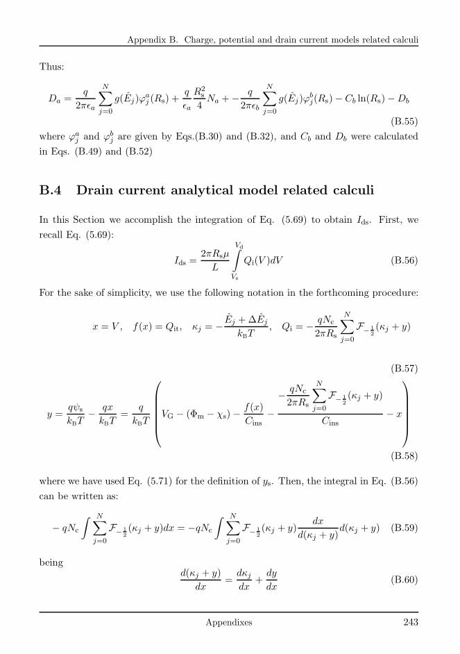
Appendix B. Charge, potential and drain current models related calculi
Thus:
Da =q
2πǫa
N∑
j=0
g(Ej)ϕaj (Rs) +
q
ǫa
R2s
4Na +− q
2πǫb
N∑
j=0
g(Ej)ϕbj(Rs)− Cb ln(Rs)−Db
(B.55)
where ϕaj and ϕbj are given by Eqs.(B.30) and (B.32), and Cb and Db were calculated
in Eqs. (B.49) and (B.52)
B.4 Drain current analytical model related calculi
In this Section we accomplish the integration of Eq. (5.69) to obtain Ids. First, we
recall Eq. (5.69):
Ids =2πRsµ
L
Vd∫
Vs
Qi(V )dV (B.56)
For the sake of simplicity, we use the following notation in the forthcoming procedure:
x = V , f(x) = Qit, κj = − Ej +∆EjkBT
, Qi = − qNc
2πRs
N∑
j=0
F− 12(κj + y)
(B.57)
y =qψs
kBT− qx
kBT=
q
kBT
VG − (Φm − χs)−f(x)
Cins−
− qNc
2πRs
N∑
j=0
F− 12(κj + y)
Cins− x
(B.58)
where we have used Eq. (5.71) for the definition of ys. Then, the integral in Eq. (B.56)
can be written as:
− qNc
∫ N∑
j=0
F− 12(κj + y)dx = −qNc
∫ N∑
j=0
F− 12(κj + y)
dx
d(κj + y)d(κj + y) (B.59)
beingd(κj + y)
dx=dκjdx
+dy
dx(B.60)
Appendixes 243
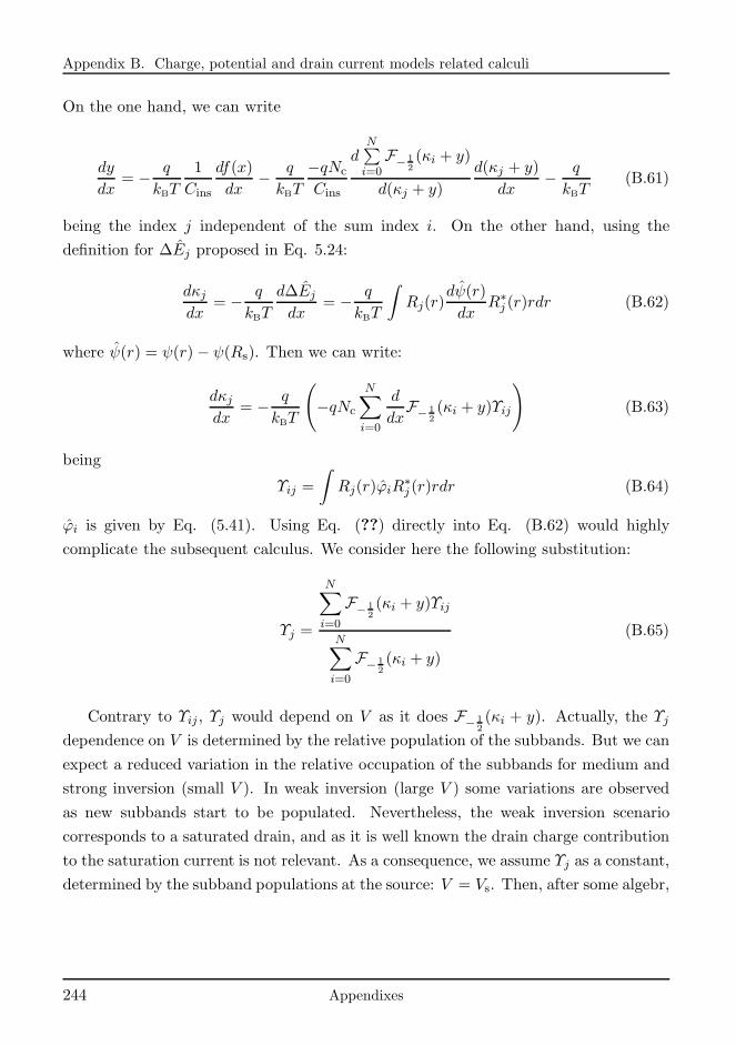
Appendix B. Charge, potential and drain current models related calculi
On the one hand, we can write
dy
dx= − q
kBT
1
Cins
df(x)
dx− q
kBT
−qNc
Cins
dN∑
i=0F− 1
2(κi + y)
d(κj + y)
d(κj + y)
dx− q
kBT(B.61)
being the index j independent of the sum index i. On the other hand, using the
definition for ∆Ej proposed in Eq. 5.24:
dκjdx
= − q
kBT
d∆Ejdx
= − q
kBT
∫
Rj(r)dψ(r)
dxR∗j (r)rdr (B.62)
where ψ(r) = ψ(r)− ψ(Rs). Then we can write:
dκjdx
= − q
kBT
(
−qNc
N∑
i=0
d
dxF− 1
2(κi + y)Υij
)
(B.63)
being
Υij =
∫
Rj(r)ϕiR∗j (r)rdr (B.64)
ϕi is given by Eq. (5.41). Using Eq. (??) directly into Eq. (B.62) would highly
complicate the subsequent calculus. We consider here the following substitution:
Υj =
N∑
i=0
F− 12(κi + y)Υij
N∑
i=0
F− 12(κi + y)
(B.65)
Contrary to Υij , Υj would depend on V as it does F− 12(κi + y). Actually, the Υj
dependence on V is determined by the relative population of the subbands. But we can
expect a reduced variation in the relative occupation of the subbands for medium and
strong inversion (small V ). In weak inversion (large V ) some variations are observed
as new subbands start to be populated. Nevertheless, the weak inversion scenario
corresponds to a saturated drain, and as it is well known the drain charge contribution
to the saturation current is not relevant. As a consequence, we assume Υj as a constant,
determined by the subband populations at the source: V = Vs. Then, after some algebr,
244 Appendixes
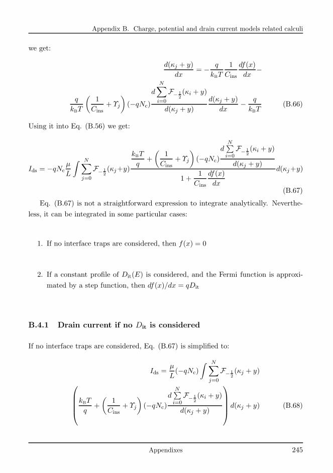
Appendix B. Charge, potential and drain current models related calculi
we get:
d(κj + y)
dx= − q
kBT
1
Cins
df(x)
dx−
q
kBT
(
1
Cins+ Υj
)
(−qNc)
dN∑
i=0
F− 12(κi + y)
d(κj + y)
d(κj + y)
dx− q
kBT(B.66)
Using it into Eq. (B.56) we get:
Ids = −qNcµ
L
∫ N∑
j=0
F− 12(κj+y)
kBT
q+
(
1
Cins+ Υj
)
(−qNc)
dN∑
i=0F− 1
2(κi + y)
d(κj + y)
1 +1
Cins
df(x)
dx
d(κj+y)
(B.67)
Eq. (B.67) is not a straightforward expression to integrate analytically. Neverthe-
less, it can be integrated in some particular cases:
1. If no interface traps are considered, then f(x) = 0
2. If a constant profile of Dit(E) is considered, and the Fermi function is approxi-
mated by a step function, then df(x)/dx = qDit
B.4.1 Drain current if no Dit is considered
If no interface traps are considered, Eq. (B.67) is simplified to:
Ids =µ
L(−qNc)
∫ N∑
j=0
F− 12(κj + y)
kBT
q+
(
1
Cins+ Υj
)
(−qNc)
dN∑
i=0F− 1
2(κi + y)
d(κj + y)
d(κj + y) (B.68)
Appendixes 245
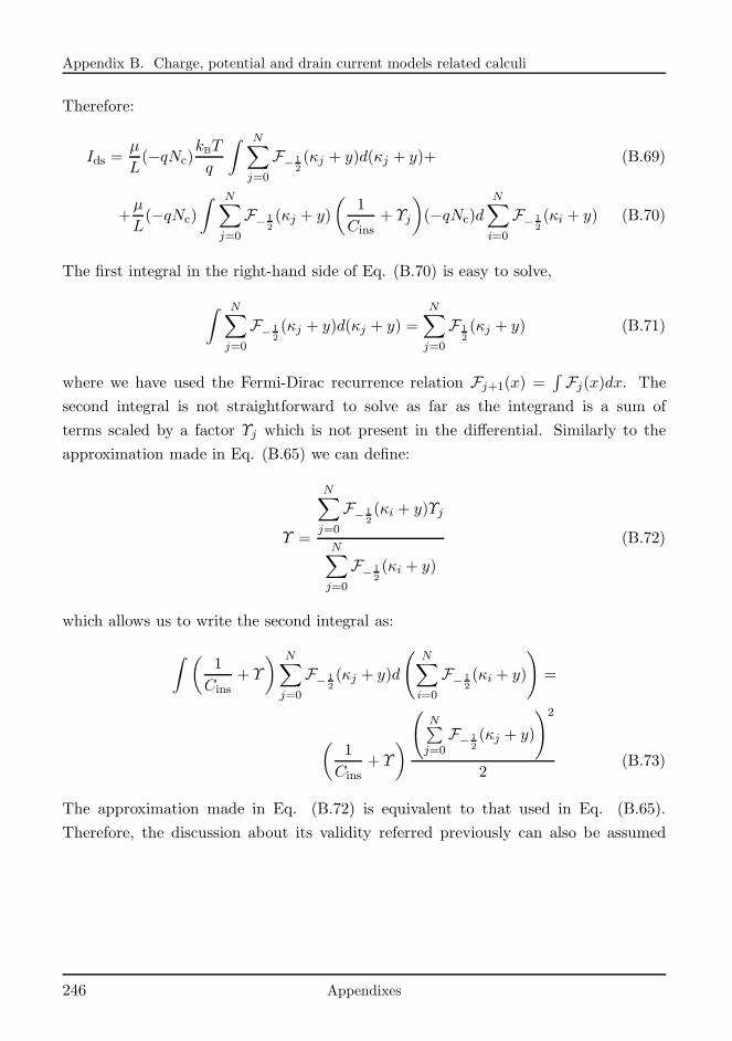
Appendix B. Charge, potential and drain current models related calculi
Therefore:
Ids =µ
L(−qNc)
kBT
q
∫ N∑
j=0
F− 12(κj + y)d(κj + y)+ (B.69)
+µ
L(−qNc)
∫ N∑
j=0
F− 12(κj + y)
(
1
Cins+ Υj
)
(−qNc)d
N∑
i=0
F− 12(κi + y) (B.70)
The first integral in the right-hand side of Eq. (B.70) is easy to solve,
∫ N∑
j=0
F− 12(κj + y)d(κj + y) =
N∑
j=0
F 12(κj + y) (B.71)
where we have used the Fermi-Dirac recurrence relation Fj+1(x) =∫
Fj(x)dx. The
second integral is not straightforward to solve as far as the integrand is a sum of
terms scaled by a factor Υj which is not present in the differential. Similarly to the
approximation made in Eq. (B.65) we can define:
Υ =
N∑
j=0
F− 12(κi + y)Υj
N∑
j=0
F− 12(κi + y)
(B.72)
which allows us to write the second integral as:
∫(
1
Cins+ Υ
) N∑
j=0
F− 12(κj + y)d
(
N∑
i=0
F− 12(κi + y)
)
=
(
1
Cins+ Υ
)
(
N∑
j=0F− 1
2(κj + y)
)2
2(B.73)
The approximation made in Eq. (B.72) is equivalent to that used in Eq. (B.65).
Therefore, the discussion about its validity referred previously can also be assumed
246 Appendixes
Appendix B. Charge, potential and drain current models related calculi
here. Finally, substituting Eqs. (B.71) and (B.73) into (B.70) we get:
Ids =µ
L
(−qNc)
N∑
j=0
F 12(κj + y) +
1
Cds(−qNc)
(
N∑
j=0F− 1
2(κj + y)
)2
2
Vd
Vs
(B.74)
where CΥ was defined as:1
CΥ=
(
1
Cins+ Υ
)
(B.75)
For the sake of clarity we can define the functions:
f1(V ) = −qNckBT
q
N∑
j=0
F 12
(
− Ej +∆Ej − qψs + qV
kBT
)
(B.76)
f2(V ) = −qNc1
Cds
N∑
j=0
F− 12
(
− Ej +∆Ej − qψs + qV
kBT
)
2
(B.77)
being the resulting drain current in absence of Dit:
Ids =µ
L(f1(Vd) + f2(Vd)− f1(Vs)− f2(Vs)) (B.78)
where ψss (ψsd) and ∆Esj (∆E
dj ) are the surface potential and correction to the energy
level at the source (drain) respectively; and can be obtained solving the charge model
for V = Vs (V = Vd).
B.4.2 Drain current for a constant Dit
Now, we extend the drain current model assuming a constant Dit profile in the gap.
To do it we approximate the Fermi function by a step function. Furthermore, for the
sake of simplicity, let us consider just acceptors traps. The extension to a profile with
both kind of traps is straightforward. We can define Dit(E) as
Dit(E) = Dit × [U(E − Ei(Rs))− U(E − Ec(Rs))] (B.79)
that is a constant Dit in a certain range of energies between the conduction band at
the interface, Ec(Rs), and the intrinsic Fermi level at the interface, Ei(Rs), being U the
Appendixes 247
Appendix B. Charge, potential and drain current models related calculi
step function. Introducing Eq. (B.79) into the expression for Qit, given by Eq. (5.64),
we get
Qit = −qDit
∫
U(E − Ei)− U(E − Ec)
1 + eE+qV
kBT
dE = (B.80)
where we have substituted EF by the pseudo Fermi level. Using the references for
energies proposed in Section 5.2, we can write Ec(r) = −qψ(r). Then Ec(Rs) =
−qψ(Rs) = −qψs. Thus, Eq. (5.64) can be rewritten in terms of ψs as:
Qit = −qDit
∫
U(E + qψs + Eg/2)− U(E + qψs)
1 + eE+qVkBT
dE (B.81)
Assuming that the Fermi function can be approximated by a step function, its derivative
is a Dirac delta function. Then, we can write:
dQit
dV= −qDit × [U(−qV + qψs + Eg/2) − U(−qV + qψs)] (B.82)
which using the definition in Eq. (B.58) can be reformulated as:
f(x)
x= −qDit [U(y + Eg/2)− U(y)] (B.83)
Now we can substitute it in Eq. (B.67) resulting:
Ids = −−qNc
∫ N∑
j=0
F− 12(κj+y)
kBT
q+
(
1
Cins+ Υj
)
(−qNc)
dN∑
i=0F− 1
2(κi + y)
d(κj + y)
1− q Dit
Cins[U(y + Eg/2) − U(y)]
d(κj+y)
(B.84)
248 Appendixes
Appendix B. Charge, potential and drain current models related calculi
Using the properties of the step function, we can split the previous integrals into three
integrals:
Ids = −q2N2c
yc∫
ys
N∑
j=0
F− 12(κj + y)
kBT
q2Nc−(
1
Cins+ Υj
) dN∑
i=0F− 1
2(κi + y)
d(κj + y)
d(κj + y)
− −q2N2c
1− qDit
Cins
yi∫
yc
N∑
j=0
F− 12(κj + y)
kBT
q2Nc−(
1
Cins+ Υj
) dN∑
i=0F− 1
2(κi + y)
d(κj + y)
d(κj + y)
−q2Nc2
yd∫
yi
N∑
j=0
F− 12(κj + y)
kBT
q2Nc−(
1
Cins+ Υj
) dN∑
i=0F− 1
2(κi + y)
d(κj + y)
d(κj + y)
(B.85)
where the integral limits ys, yd are the y-values corresponding to V = Vs and V = Vd;
and yc = 0 and yi = −Eg/2 correspond to V -values Vc and Vi such as ψs − Vc = 0
(that is EF(z) = Ec) and ψs − Vi = Eg/2 (that is EF(z) = Ei). The three integrals
in Eq. (B.85) are the same than that solved in Eq. (B.70). Then, following the afore
explained procedure and using the definitions for f1 and f2 in Eqs. (B.76) and (B.77)
we get:
Ids =µ
L[f1(Vc) + f2(Vc)− f1(Vs)− f2(Vs) +
+f1(Vi) + f2(Vi)− f1(Vc)− f2(Vc)
1 +qDit
Cins
+f1(Vd) + f2(Vd)− f1(Vi)− f2(Vi)] (B.86)
which can be simplified to:
Ids =µ
L
f1(Vd) + f2(Vd)− f1(Vs)− f2(Vs) +f1(Vc) + f2(Vc)− f1(Vi)− f2(Vi)
1 +qDit
Cins
(B.87)
It should be noted that this Ids expression requires solving the model for four Fermi
Appendixes 249

Appendix B. Charge, potential and drain current models related calculi
pseudo-potentials: Vs and Vd as it was in Eq. (B.68) and V1 and V2 which correspond
to the cross of EF trough Ec(Rs) = −qψs and Ei = −qψs − Eg/2. As it was in Eq.
(B.68), the values of Ej are constant and independent of V but not ∆Ej and ψs which
need to be calculated for each case.
In the linear region, Vds < Vgs − VT, just the first two integrals of Eq. (B.86) make
sense. Vd is not high enough as to move the pseudo Fermi potential below the intrinsic
level. Then, the third integral in Eq. (B.85) can be removed and the upper limit in
the second one is changed from yi to yc.
250 Appendixes
Appendix C
Capacitance and threshold
voltage models related calculi
In this Appendix we sum up some calculi related to the capacitance and threshold
voltage analytical models.
C.1 Determination of the centroid capacitance
In this Section we obtain an expression for the centroid capacitance of an arbitrary
subband j, solving the integral proposed in Chapter 6. We recall here Eq. (6.12):
CCj =2πǫs
R0∫
0
rln
(
R0
r
)
|AjJl(γjr)|2dr
(C.1)
The integral in the denominator of Eq. (C.1) can be reformulated as:
R0∫
0
rln
(
R0
r
)
|AjJl(γjr)|2dr = ln(R0)
R0∫
0
r |AjJl(γjr)|2dr −R0∫
0
r ln(r)|AjJl(γjr)|2dr
(C.2)
Appendixes 251
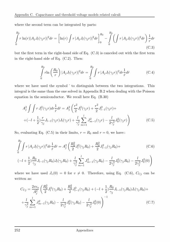
Appendix C. Capacitance and threshold voltage models related calculi
where the second term can be integrated by parts:
R0∫
0
r ln(r)|AjJl(γjr)|2dr =[
ln(r)
∫
r |AjJl(γjr)|2dr]R0
0
−R0∫
0
(∫
r |AjJl(γjr)|2dr)
1
rdr
(C.3)
but the first term in the right-hand side of Eq. (C.3) is canceled out with the first term
in the right-hand side of Eq. (C.2). Then:
R0∫
0
rln
(
R0
r
)
|AjJl(γjr)|2dr =R0∫
0
∫
r |AjJl(γjr)|2dr1
rdr (C.4)
where we have used the symbol ˆ to distinguish between the two integrations. This
integral is the same than the one solved in Appendix B.2 when dealing with the Poisson
equation in the semiconductor. We recall here Eq. (B.30)
A2j
∫ ∫
r J2l (γjr)dr
1
rdr = A2
j
(
r2
2J2l (γjr) +
r2
2J2l−1(γjr)+
+(−l + 1
2)r
γjJl−1(γjr)Jl(γjr) +
l
γ2j
l∑
m=1
J2m−1(γjr)−
l
2γ2jJ20 (γjr)
)
(C.5)
So, evaluating Eq. (C.5) in their limits, r = R0 and r = 0, we have::
R0∫
0
∫
r |AjJl(γjr)|2dr1
rdr = A2
j
(
R20
2J2l (γjR0) +
R20
2J2l−1(γjR0)+ (C.6)
(−l + 1
2)R0
γjJl−1(γjR0)Jl(γjR0) +
l
γ2j
l∑
m=1
J2m−1(γjR0)−
l
2γ2jJ20 (γjR0)−
l
2γ2jJ20 (0)
)
where we have used Jv(0) = 0 for v 6= 0. Therefore, using Eq. (C.6), CCj can be
written as:
CCj =2πǫsA2j
(
R20
2J2l (γjR0) +
R20
2J2l−1(γjR0) + (−l + 1
2)R0
γjJl−1(γjR0)Jl(γjR0)+
+l
γ2j
l∑
m=1
J2m−1(γjR0)−
l
2γ2jJ20 (γjR0)−
l
2γ2jJ20 (0)
)−1
(C.7)
252 Appendixes
Appendix C. Capacitance and threshold voltage models related calculi
Furthermore, looking at the similarities between the resolution proposed here for the
centroid capacitance and the one carried out in Appendix B.2 for ϕj it is easy to
conclude that:
CCj =2πǫs
ϕj(R0)− ϕj(0)(C.8)
Therefore, from ϕj properties (see Section 5.3), we can assume that degenerate energy
levels have equal centroid capacitances.
To conclude this Appendix we give the particular centroid capacitance expressions
for the first five subbands: j = 0, l = 0; j = 1, 2, l = ±1; and j = 3, 4, l = ±2. They
are used later in Section 6.3. For j = 0, l = 0;
CC0 =2πǫsA2j
2
R20
(
J20 (γ0R0) + J2
1 (γ0R0)−1
γ0R0J1(γ0R0)J0(γ0R0)
)−1(C.9)
For j = 1, 2, l = ±1;
CC1,2 =2πǫsA2
1
2
R20
(
J21 (γ1R0) + J2
0 (γ1R0)−1
γ1R0J0(γ1R0)J1(γ1R0)+
J20 (γ1R0)− J2
0 (0)
γ21R20
)−1(C.10)
For j = 3, 4, l = ±2;
CC3,4 =2πǫsA2
3
2
R20
(
J22 (γ3R0) + J2
1 (γ3R0)−3
γ3R0J1(γ3R0)J2(γ3R0)+
+4
γ23R20
J21 (γ3R0) + 2
J20 (γ3R0)− J2
0 (0)
γ23R20
)−1(C.11)
where in all cases J20 (0) = 1
C.2 Validity of the approximations for the Cg and VT mod-
els
In this Section we check the validity of the approximations made in Chapter 6, specif-
ically in Eqs. (6.1) and (6.49), for the capacitance and threshold voltage models.
Appendixes 253
Appendix C. Capacitance and threshold voltage models related calculi
First, we deal with the approximation in Eq. (6.1). We recall it here:
CG =∂QG
∂VG= −∂Qs +Qins
∂VG≃ −∂Qs
∂VG(C.12)
Here, we supposed that Qins was negligible compared to Qs. In the model, Qins (as-
suming no Dit) is determined by the wavefunction penetration into the insulator. For
a subband j, the ratio between the electron charge in the semiconductor (neglecting
Na) and the electron charge in the insulator is proved to be:
ϑC =
R0+tins∫
R0
C2jKl(αjr)rdr
R0∫
0
A2jJl(γjr)rdr
=1
R0∫
0
A2jJl(γjr)rdr
− 1 (C.13)
where we have applied Eq. (B.1). From, ϑ we can get an estimation of the relative
error committed in Eq. (C.12). The exact value of the error depends on the relative
occupations of the different subbands and the corresponding errors associated to each
subband. Fig. shows ϑ as a function of the NW size for several materials InGaAs (solid
lines), InAs (dashed lines) and GaAs (dash-dotted lines) and subbands: j = 0, l = 0
(blue), j = 1, 2, l = ±1 (green) and j = 3, 4, l = ±2.
InAs shows the maximum error as it has the lower confinement effective mass and
consequently higher wavefunction penetration (see Fig 5.12 in Chapter 5). The behavior
of the error is non-monotonic as the penetration of the wavefunction into the insulator
is a not simple result which depends of several factors: the potential barrier height,
the size of the NW or the effective mass in the insulator and the semiconductor among
others. Nevertheless the maximum error achieved is around 5% (corresponding to
j = 3, 4, l = ±2 subband in InAs for 2R0 = 5nm), but this subband for this size is
nearly empty for a reasonable range of gate voltage (see Fig. 5.13 in Chapter 5), so
its contribution to the error in Eq. (6.1) is negligible. From Fig. C.1 we can conclude
that the approximation in Eq. (6.1) is appropriate.
In second place, we discuss the approximation in Eq. (6.49). It is a well known
approximation for K0 when the argument is high [204]. We define the relative error
254 Appendixes
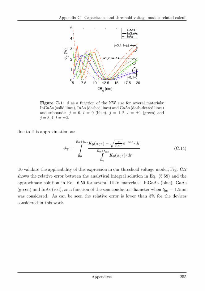
Appendix C. Capacitance and threshold voltage models related calculi
5 7.5 10 12.5 15 17.5 200
1
2
3
4
5
ϑC
(%)
2R0
(nm)
GaAsInGaAsInAs
j=3,4, l= 2±
j=0, l=0
j=1,2, l= 1±
Figure C.1: ϑ as a function of the NW size for several materials:InGaAs (solid lines), InAs (dashed lines) and GaAs (dash-dotted lines)and subbands: j = 0, l = 0 (blue), j = 1, 2, l = ±1 (green) andj = 3, 4, l = ±2.
due to this approximation as:
ϑT =
R0+tins∫
R0
K0(α0r)−√
π2α0r
e−α0rrdr
R0+tins∫
R0
K0(α0r)rdr
(C.14)
To validate the applicability of this expression in our threshold voltage model, Fig. C.2
shows the relative error between the analytical integral solution in Eq. (5.58) and the
approximate solution in Eq. 6.50 for several III-V materials: InGaAs (blue), GaAs
(green) and InAs (red), as a function of the semiconductor diameter when tins = 1.5nm
was considered. As can be seen the relative error is lower than 3% for the devices
considered in this work.
Appendixes 255
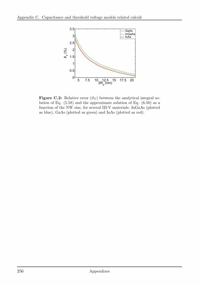
Appendix C. Capacitance and threshold voltage models related calculi
5 7.5 10 12.5 15 17.5 200
0.5
1
1.5
2
2.5
3
3.5
2R0
(nm)
ϑT
(%)
GaAsInGaAsInAs
Figure C.2: Relative error (ϑT) between the analytical integral so-lution of Eq. (5.58) and the approximate solution of Eq. (6.50) as afunction of the NW size, for several III-V materials: InGaAs (plottedas blue), GaAs (plotted as green) and InAs (plotted as red).
256 Appendixes
Appendix D
Scattering elements
In this Appendix we briefly discuss the characteristic of the three kinds of scattering
mechanisms distinguished in Section 7.4 and their implication in the formulation of the
implicit problem given by Eq. (7.34).
D.1 Inelastic anisotropic mechanism
For an inelastic anisotropic mechanism the energy is not conserved and Sj,j′ is wavenum-
ber dependent. This can be written in the general formulation given in Eq. (7.19) as:
Siaj,j′(kz, k′z) =
2π
~
∣
∣Mj,j′(kz, k′z)∣
∣
2δ(
Ej′(k′z)− Ej(kz)± ~ω
)
(D.1)
where the delta function restricts the non null elements of Sj,j′ to those with Ej′(k′z) =
Ej(kz)± ~ω. We assume that the scattering mechanism is not kz dependent itself, and
ω 6= ω(kz − k′z). Using the equivalence [88]:
∑
kz
=L
2π
∫
dkz (D.2)
Appendixes 257
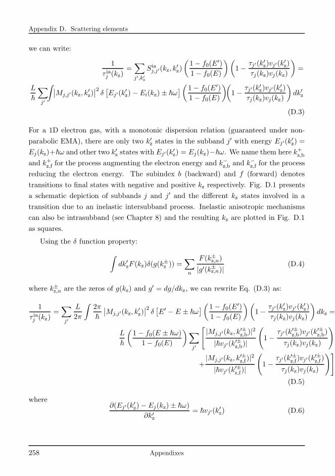
Appendix D. Scattering elements
we can write:
1
τ iaj (kz)=∑
j′,k′z
Siaj,j′(kz, k
′z)
(
1− f0(E′)
1− f0(E)
)(
1− τj′(k′z)vj′(k
′z)
τj(kz)vj(kz)
)
=
L
~
∑
j′
∫
∣
∣Mj,j′(kz, k′z)∣
∣
2δ[
Ej′(k′z)− Ei(kz)± ~ω
]
(
1− f0(E′)
1− f0(E)
)(
1− τj′(k′z)vj′(k
′z)
τj(kz)vj(kz)
)
dk′z
(D.3)
For a 1D electron gas, with a monotonic dispersion relation (guaranteed under non-
parabolic EMA), there are only two k′z states in the subband j′ with energy Ej′(k′z) =
Ej(kz)+~ω and other two k′z states with Ej′(k′z) = Ej(kz)−~ω. We name them here k+z,b
and k+z,f for the process augmenting the electron energy and k−z,b and k−z,f for the process
reducing the electron energy. The subindex b (backward) and f (forward) denotes
transitions to final states with negative and positive kz respectively. Fig. D.1 presents
a schematic depiction of subbands j and j′ and the different kz states involved in a
transition due to an inelastic intersubband process. Inelastic anisotropic mechanisms
can also be intrasubband (see Chapter 8) and the resulting kz are plotted in Fig. D.1
as squares.
Using the δ function property:
∫
dk′zF (kz)δ(g(k±z )) =
∑
n
F (k±z,n)
|g′(k±z,n)|(D.4)
where k±z,n are the zeros of g(kz) and g′ = dg/dkz, we can rewrite Eq. (D.3) as:
1
τ iaj (kz)=∑
j′
L
2π
∫
2π
~
∣
∣Mj,j′(kz, k′z)∣
∣
2δ[
E′ − E ± ~ω]
(
1− f0(E′)
1− f0(E)
)(
1− τj′(k′z)vj′(k
′z)
τj(kz)vj(kz)
)
dkz =
L
~
(
1− f0(E ± ~ω)
1− f0(E)
)
∑
j′
[
|Mj,j′(kz, k′±z,b)|2
|~vj′(k′±z,b)|
(
1−τj′(k
′±z,b)vj′(k
′±z,b)
τj(kz)vj(kz)
)
+|Mj,j′(kz, k
′±z,f)|2
|~vj′(k′±z,f)|
(
1−τj′(k
′±z,f)vj′(k
′±z,f)
τj(kz)vj(kz)
)]
(D.5)
where∂(Ej′(k
′z)− Ej(kz)± ~ω)
∂k′z= ~vj′(k
′z) (D.6)
258 Appendixes
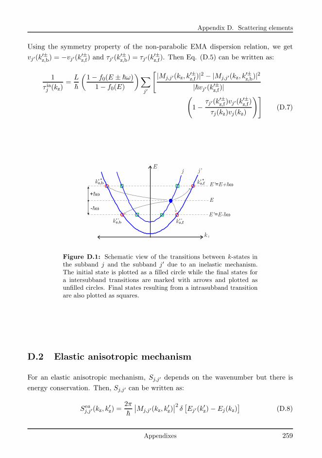
Appendix D. Scattering elements
Using the symmetry property of the non-parabolic EMA dispersion relation, we get
vj′(k′±z,b) = −vj′(k′±z,f) and τj′(k′±z,b) = τj′(k
′±z,f). Then Eq. (D.5) can be written as:
1
τ iaj (kz)=L
~
(
1− f0(E ± ~ω)
1− f0(E)
)
∑
j′
[
|Mj,j′(kz, k′±z,f)|2 − |Mj,j′(kz, k
′±z,b)|2
|~vj′(k′±z,f)|(
1−τj′(k
′±z,f)vj′(k
′±z,f)
τj(kz)vj(kz)
)]
(D.7)
+hw
E’ E+h= w
E
E’ E-h= w-hw
j’j
k’z,b+
k’z,f+
k’z,b-
k’z,f-
E
k z
Figure D.1: Schematic view of the transitions between k-states inthe subband j and the subband j′ due to an inelastic mechanism.The initial state is plotted as a filled circle while the final states fora intersubband transitions are marked with arrows and plotted asunfilled circles. Final states resulting from a intrasubband transitionare also plotted as squares.
D.2 Elastic anisotropic mechanism
For an elastic anisotropic mechanism, Sj,j′ depends on the wavenumber but there is
energy conservation. Then, Sj,j′ can be written as:
Seaj,j′(kz, k′z) =
2π
~
∣
∣Mj,j′(kz, k′z)∣
∣
2δ[
Ej′(k′z)− Ej(kz)
]
(D.8)
Appendixes 259
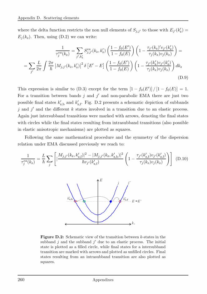
Appendix D. Scattering elements
where the delta function restricts the non null elements of Sj,j′ to those with Ej′(k′z) =
Ej(kz). Then, using (D.2) we can write:
1
τ eaj (kz)=∑
j′,k′z
Seaj,j′(kz, k′z)
(
1− f0(E′)
1− f0(E)
)(
1− τj′(kz)′vj′(k′z)
τj(kz)vj(kz)
)
=
=∑
j′
L
2π
∫
2π
~
∣
∣Mj,j′(kz, k′z)∣
∣
2δ[
E′ −E]
(
1− f0(E′)
1− f0(E)
)(
1− τj′(k′z)vj′(k
′z)
τj(kz)vj(kz)
)
dkz
(D.9)
This expression is similar to (D.3) except for the term [1− f0(E′)] / [1− f0(E)] = 1.
For a transition between bands j and j′ and non-parabolic EMA there are just two
possible final states k′z,b and k′z,f. Fig. D.2 presents a schematic depiction of subbands
j and j′ and the different k states involved in a transition due to an elastic process.
Again just intersubband transitions were marked with arrows, denoting the final states
with circles while the final states resulting from intrasubband transitions (also possible
in elastic anisotropic mechanisms) are plotted as squares.
Following the same mathematical procedure and the symmetry of the dispersion
relation under EMA discussed previously we reach to:
1
τ eaj (kz)=L
~
∑
j
[
|Mj,j′(kz, k
′z,f)|2 − |Mj,j′(kz, k
′z,b)|2
~vj′(k′z,f)
(
1−τj′(k
′z,f)vj′(k
′z,f)
τj(kz)vj(kz)
)]
(D.10)
k’z,bE E’=
E
k z
j’j
k’z,f
Figure D.2: Schematic view of the transition between k-states in thesubband j and the subband j′ due to an elastic process. The initialstate is plotted as a filled circle, while final states for a intersubbandtransition are marked with arrows and plotted as unfilled circles. Finalstates resulting from an intrasubband transition are also plotted assquares.
260 Appendixes
Appendix D. Scattering elements
D.3 Isotropic mechanism
For isotropic mechanisms (both elastic and inelastic), Sj,j′ does not depend on the
wavenumber and there is not energy conservation. Thus, Sj,j′ can be written as:
Sisj,j′(kz, k′z) = Sisj,j′(E) =
2π
~|Mj,j′|2δ[Ej′(k′z)−Ej(kz)± ~ω)] (D.11)
where the Mj,j′ dependence on kz was annulled and we assumed inelastic process. The
derivation for elastic processes is the same except for the factor ±~ω. As in the inelastic
anisotropic mechanisms, we assume that the scattering mechanism is not kz dependent
itself and ω 6= ω(kz − k′z). Then, the sum over all k′z states which contribute to the
inelastic isotropic τj would be:
1
τ isj (kz)=∑
j′,k′z
Sisj,j′
(
1− f0(E′)
1− f0(E)
)(
1− τj′(k′z)vj′(k
′z)
τj(kz)vj(kz)
)
=
2π
~
∑
j′
|Mj,j′|2∑
k′z
δ[E′ − E ± ~ω]
(
1− f0(E′)
1− f0(E)
)
(D.12)
Here the term[
1− τj′(k′z)vj′(k
′z)/τj(kz)vj(kz)
]
drops in the sum. This is because for
symmetric bands: vj′(k′±z,f) = −vj′(k′±z,b), being k′±z,b and k′±z,f the possible final sates (see
Fig. D.1). Due to the isotropy: τj′(k′±z,f) = τj′(k
′±z,b) = τj′(E
′).
Then using (D.2) we get:
∑
j
L
2π
∣
∣Mj,j′∣
∣
2∫
2π
~δ[
E′ − E ± ~ω]
(
1− f0(E′)
1− f0(E)
)
dk′z (D.13)
This expression is similar to (D.3) except for the term[
1− τj′(k′z)vj′(k
′z)/τj(kz)vj(kz)
]
.
Following the same mathematical procedure and the approximations for a monotonic
symmetric dispersion relation we reach:
1
τ isj (kz)=L
~
(
1− f0(E ± ~ω)
1− f0(E)
)
∑
j′
[
2Mj,j′
|~vj′(k′±z,f)|
]
(D.14)
Unlike in anisotropic scattering mechanisms, the momentum relaxation time of an
isotropic mechanism can be calculated independently of the rest of scattering mecha-
nism as no implicit dependence on τj is present.
Appendixes 261

Appendix E
Scattering mechanisms related
calculi
In this Appendix we sum up some of the necessary calculi for the determination of the
matrix element of the different scattering mechanisms.
E.1 Surface Roughness: axial and qz integrations
In this Section we detail the space and wavenumber axial integration of Eq. (8.9)
paying attention to the normalization of the delta Dirac function. We recall space and
wavenumber axial integration in Eq. (8.9) as:
∫
dqz
∫ L
0dz
∫ L
0dz′eı(kz−k
′z+qz)(z−z′)C(qz, qs) =
∫
dqzC(qz, qs)
∫ L
0dzeı(kz−k
′z+qz)z
∫ L
0dz′e−ı(kz−k
′z+qz)z
′(E.1)
Each of the previous space axial integrations can be solved, assuming L −→ ∞, taking
into account that:∫ ∞
−∞e−ıqzdz = 2πδ(q) (E.2)
Then, we can rewrite Eq. (E.1) as:
2π
∫
dqzC(qz, qs)
∫ L
0dzeı(kz−k
′z+qz)zδ(kz − k′z + qz) (E.3)
Appendixes 263
Appendix E. Scattering mechanisms related calculi
Let us now define, for simplicity, g(qz) =∫ L0 dzeı(kz−k
′z+qz)z . Then the previous integral
leads to:
2πC(qfz , qs)g(qfz ) (E.4)
being qfz = k′z − kz. From the definition of g(qz), it is clear that g(qfz ) =∫ L0 dz = L,
and therefore Eq. (E.1):
2πLC(qfz , qs) (E.5)
E.2 Coulombian dispersion hard-sphere model
In this Section we apply the hard-spheres model proposed by Ning et al. [246] to a 1D
electron gas. The aim is to determine a power spectrum CCOm,i(qz) from the autocorre-
lation function of a random distribution of ionized impurities along the axial direction.
The first approximation made here assumes that the distribution of charges along the
axial direction for a given position s = si in the confinement plane is completely inde-
pendent of the axial distribution corresponding to another position s = sm.1
Now we assume that for each position sm in the confinement plane there is a random
distribution of N punctual particles along the axial direction. As explained in [241], it is
not the charge density, but its fluctuations, the responsible of the Coulomb scattering.
Therefore, we will define:
σm(z) =
N∑
i=1
δ(z − zi)−Navg (E.6)
where Navg is the average charge density per unit length, and is related to N as,
Navg = N/L.S Taking the Fourier transform we get:
σm(qz) =
N∑
i=1
e−ıqzzi −Navgδ(qz) (E.7)
1The approximation makes sense as far as the positions si and sm are far from each other but canbe criticizes otherwise. For the sake of simplicity we go on with it here.
264 Appendixes
Appendix E. Scattering mechanisms related calculi
The power spectrum CCOm,m(qz) is given by:
CCOm,m(qz) = 〈σm(qz)σ∗m(qz)〉 =
∫
(
N∑
i=1
e−ıqzzi −Navgδ(qz)
)
N∑
j=1
eıqzzj −Navgδ(qz)
P (z1, ..., zN )dz1...dzN (E.8)
where P (z1, ..., zN )dz1...dzN is the probability of a set of particles 1...N to be placed
near the set of positions z1...zN . We will call W (zi, zj)dzidzj the joint probability of
particles i and j being at zi and zj regardless the positions of the rest of the particles:
W (zi, zj) =
∫
P (z1...zN )dz1...dzNdzidzj
(E.9)
After Ning et al. [246], Eq. (E.8) can be written as:
CCOm,m(qz) = Navg +
∑
i,j,i6=j
∫
W (zi, zj)e−ıqz(zi−zj)dzidzj −N2
avgδ (qz) (E.10)
The hard sphere model assumes that two particles cannot be closer than Rt, and can
be uniformly distributed otherwise. Thus, W (zi, zj) is:
W (zi, zj) =
0 if|zi − zj | < Rt
1(L−Rt)L
if|zi − zj | > Rt
(E.11)
where 1/L is the probability of a particle being at position zi and 1/(L − Rt) is the
probability of a particle being at a position zj given that there is a particle at position
zi. W (zi, zj) can be written in a more compact way as
W (zi, zj) =1
(L−Rt)L
[
1− rect
(
zi − zjRt
)]
(E.12)
The integral in Eq. (E.10) results into:
∫
eıqzzjdzj
∫[
1− rect
(
zi − zjRt
)]
e−ıqzzidzi (E.13)
Appendixes 265
Appendix E. Scattering mechanisms related calculi
where the inner integral is the Fourier transform of[
1− rect(
zj−ziRt
)]
. Thus: (E.13)
∫
eıqzzj[
δ(qz)−Rte−ıqzzjsinc(Rtqz)
]
dzj (E.14)
which results in:
δ(qz)δ(−qz)− LRtsinc(Rtqz) (E.15)
Then we can write Eq. (E.10) as:
CCOm,m(qz) = Navg+
1
L (L−Rt)
∑
i,j,i6=j[δ(qz)δ(−qz)− LRtsinc(Rtqz)]−N2
avgδ (qz) (E.16)
The terms accompanying δ (qz) will only appear in the calculation when qz = 0. But
qz does not affect in CO scattering mechanisms. Thus, they can be neglected:
CCOm,m(qz) = Navg −
1
L2(N)(N − 1)LRtsinc(Rtqz) (E.17)
which can be rewritten, taking into account the relation L = N/Navg, and assuming
N ≃ N − 1 and L ≃ L−Rt, as:
CCOm,m(qz) = Navg
[
1− N
LRtsinc(Rtqz)
]
(E.18)
where C = NLRt = NavgRt is defined as the autocorrelation coefficient: C = 0 corre-
spond to a completely uncorrelated random distribution while C = 1 us a uniform fully
correlated distribution.
E.3 Acoustic phonon: contributions over all q
In this Section, we sum up the mathematical details for the determination of the squared
matrix element due to acoustic phonons. An equivalent procedure is followed in the
determination of |Mj,j′(kz, k′z)|2 in Eq. (8.48) for optical phonons. First we recall the
squared matrix element from Eq. (8.44):
|Mj,j′(kz, k′z)|2 =
D2APH
L2
kBT
2s
1
v2s
1
AL
∫
Ads
∫
Ads′∫ L
0dz
∫ L
0dz′ fj,j′,kz,k′z(s)e
−ı(qxx+qyy)
f∗j,j′,kz,k′z(s′)eı(qxx
′+qyy′)e−ı(kz−k′z−qz)(z′−z) (E.19)
266 Appendixes
Appendix E. Scattering mechanisms related calculi
We will focus in the term which is common to acoustic and optical phonon:
1
AL
∫
Ads
∫
Ads′dz∫ L
0dz′ fj,j′,kz,k′z(s)e
−ı(qxx+qyy)
f∗j,j′,kz,k′z(s′)eı(qxx
′+qyy′)e−ı(kz−k′z−qz)(z′−z) (E.20)
We can define the Fourier transform of fj,j′,kz,k′z(x, y) as:
fj,j′,kz,k′z(qs) =
∫
Adsfj,j′,kz,k′z(s)e
−ıqss (E.21)
where qss = qxx+ qyy Then:
1
AL
∫ L
0dz
∫ L
0dz′ fj,j′,kz,k′z(qs)f
∗j,j′,kz,k′z
(qs)e−ı(kz−k′z−qz)(z′−z) (E.22)
Now we sum over all possible states qx, qy and qz to take into consideration all the q
contributions. We convert the summation into integrals taking into consideration that:
∑
qx,qy,qz
=AL
8π4(E.23)
to rewrite Eq. (E.20) as:
1
8π3
∫ L
0dz
∫ L
0dz′∫
dqz
∫
dqx
∫
dqy fj,j′,kz,k′z(qs)f∗j,j′,kz,k′z
(qs)e−ı(kz−k′z−qz)(z′−z) (E.24)
Using the Parserval theorem:
1
4π2
∫
dqx
∫
dqy fj,j′,kz,k′z(qs)f∗j,j′,kz,k′z
(qs) =
∫
Ads fj,j′,kz,k′z(s)f
∗j,j′,kz,k′z
(s) (E.25)
Eq. (E.24) can be written as:
1
2π
∫ L
0dz
∫ L
0dz′∫
AdA fj,j′,kz,k′z(s)f
∗j,j′,kz,k′z
(s)
e−ı(kz−k′z−qz)(z′−z) (E.26)
where the axial and qz integration can be done as in Appendix ?? resulting into:
L
∫
AdA fj,j′,kz,k′z(s)f
∗j,j′,kz,k′z
(s) (E.27)
Appendixes 267
Appendix E. Scattering mechanisms related calculi
Then substituting into Eq. (E.19)
|Mj,j′(kz, k′z)|2 =
D2APH
L
kBT
2s
1
v2s
∫
AdA fj,j′,kz,k′z(s)f
∗j,j′,kz,k′z
(s) (E.28)
where the matrix element does not depend on qz and therefore it is isotropic.
E.4 Non polar phonons: qx and qy contributions
In this Section we deal with the integration of all qx and qy contributions to the matrix
element of polar optical phonons. Thus, we recall here the inner integral in Eq. (8.54).
∫ ∫
dqxdqye∓ıqx(x−x
′)∓iqy(y−y′)
q2x + q2y + q2z(E.29)
I can be simplified to:
∞∫
−∞
dqyπ
√
q2y + q2z
e±ıqy(y−y′)e−
√q2y+q
2z |x−x′| (E.30)
To simplify the notation of the integral we rename:
y=qy
a=|x− x′|c=qz
b=(y − y′)
(E.31)
Then, the integral to be solved is,
∞∫
−∞
e±ıbye−a√y2+c2
√
y2 + c2dy (E.32)
For the sake of clearness we will consider first just the minus sign in the exponential.
We will analyze the plus sign of the exponential later. Now we can rearrange the square
268 Appendixes
Appendix E. Scattering mechanisms related calculi
root terms as:
∞∫
−∞
e−ıbye−a√y2+c2
√
y2 + c2dy =
∞∫
−∞
e−ıbye−a|c|√
(y/c)2+1
|c|√
(y/c)2 + 1dy (E.33)
where√c2 = |c|. We can use the change of variable:
y/c = sinh(ϕ) −→ dy = ccosh(ϕ)dϕ (E.34)
which keeps the integral limits: y → ∞ ⇒ ϕ → ∞; y → −∞ ⇒ ϕ → −∞ Here we
have supposed c > 0. If not the integral limits are inverted:∫ −∞∞ = −
∫∞−∞. But the
minus sign of this integral would be cancelled with the minus sign of c in dy. So we
can write dy = |c| cosh(ϕ)dϕ regardless of the sign of c and keep the integral limits
between −∞ and ∞ . Then,
∞∫
−∞
e−ıbye−a|c|√
(y/c)2+1
|c|√
(y/c)2 + 1dy =
∞∫
−∞
e−ıbc sinh(ϕ)e−a|c|√
sinh2(ϕ)+1
|c|√
sinh2(ϕ) + 1|c| cosh(ϕ)dϕ (E.35)
Using the relation cosh2(x)− senh2(x) = 1 we get:
∞∫
−∞
e−ıb|c| sinh(ϕ)e−a|c| cosh(ϕ)
|c| cosh(ϕ) |c| cosh(ϕ)dϕ =
∞∫
−∞
e−ıbc sinh(ϕ)−a|c| cosh(ϕ)dϕ (E.36)
This integral can be identified with the integral representations of the Hankel functions,
(
z + ξ
z − ξ
)12v
H(1)v
(
(z2 − ξ2)12
)
=1
iπe−
12vπı
∞∫
−∞
eız cosh(t)+ıξsinh(t)−vtdt if Im(z ± ξ) > 0
(E.37)
(
z + ξ
z − ξ
)12v
H(2)v
(
(z2 − ξ2)12
)
= − 1
ıπe
12vπı
∞∫
−∞
e−ız cosh(t)−ıξsinh(t)−vtdt if Im(z ± ξ) < 0
(E.38)
Appendixes 269
Appendix E. Scattering mechanisms related calculi
which for v = 0 are particularized as:
H(1)0
(
(z2 − ξ2)12
)
=1
iπ
∞∫
−∞
eız cosh(t)+ıξsinh(t)dt if Im(z ± ξ) > 0 (E.39)
H(2)0
(
(z2 − ξ2)12
)
= − 1
iπ
∞∫
−∞
e−ız cosh(t)−ıξsinh(t)dt if Im(z ± ξ) < 0 (E.40)
Then, we can rearrange (E.36) as:
∞∫
−∞
e−ıbc sinh(ϕ)−a|c| cosh(ϕ)dϕ =
∞∫
−∞
eıa|c|ı cosh(ϕ)−ıbc sinh(ϕ)dϕ (E.41)
It is easy to identify z = a|c|ı and ξ = −bc. Then Im(a|c|ı ± −bc)=a|c|, and, as a is
always positive –see the definition in equation (E.31)–, a|c| is always positive, and we
use the first Hankel function
∞∫
−∞
eıa|c|ı cosh(ϕ)−ibc sinh(ϕ)dϕ = iπH(1)0 [(
(a|c|ı)2 − (−bc)2)
12 ] = sign(c)ıπH
(1)0 [ı
(
c2(a2 + b2))
12 ]
(E.42)
The first Hankel function is related to the modified Bessel function of the second kind,
Kv(x) =π
2ıv+1H(1)
v (ix) (E.43)
Then, we can write:
∞∫
−∞
eıacı cosh(ϕ)−ıbc sinh(ϕ)dϕ = 2K0[(
c2(a2 + b2))
12 ] (E.44)
Regarding the plus sign in the first exponential in equation (E.30), the procedure to
solve the integral keeps. The only modification would be ξ = bc instead of ξ = −bc inthe first Hankel function, but as ξ is squared, the solution will be:
∞∫
−∞
eıbye−a√y2+c2
√
y2 + c2dy = 2K0[
(
c2(a2 + b2))
12 ] (E.45)
270 Appendixes

Appendix E. Scattering mechanisms related calculi
which is the same. Therefore we have:
∞∫
−∞
dqyπ
√
q2y + q2z
e±ıqy(y−y′)e−
√q2y+q
2z |x−x′| = 2πK0
(
|qz|√
(x− x′)2 + (y − y′)2)
(E.46)
Appendixes 271

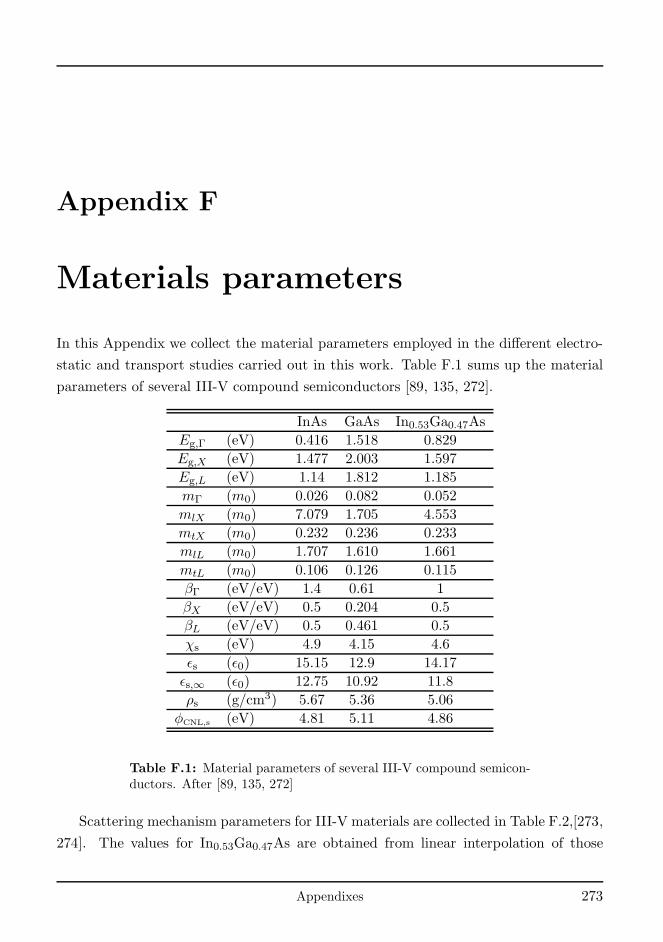
Appendix F
Materials parameters
In this Appendix we collect the material parameters employed in the different electro-
static and transport studies carried out in this work. Table F.1 sums up the material
parameters of several III-V compound semiconductors [89, 135, 272].
InAs GaAs In0.53Ga0.47As
Eg,Γ (eV) 0.416 1.518 0.829
Eg,X (eV) 1.477 2.003 1.597
Eg,L (eV) 1.14 1.812 1.185
mΓ (m0) 0.026 0.082 0.052
mlX (m0) 7.079 1.705 4.553
mtX (m0) 0.232 0.236 0.233
mlL (m0) 1.707 1.610 1.661
mtL (m0) 0.106 0.126 0.115
βΓ (eV/eV) 1.4 0.61 1
βX (eV/eV) 0.5 0.204 0.5
βL (eV/eV) 0.5 0.461 0.5
χs (eV) 4.9 4.15 4.6
ǫs (ǫ0) 15.15 12.9 14.17
ǫs,∞ (ǫ0) 12.75 10.92 11.8
ρs (g/cm3) 5.67 5.36 5.06
φCNL,s (eV) 4.81 5.11 4.86
Table F.1: Material parameters of several III-V compound semicon-ductors. After [89, 135, 272]
Scattering mechanism parameters for III-V materials are collected in Table F.2,[273,
274]. The values for In0.53Ga0.47As are obtained from linear interpolation of those
Appendixes 273
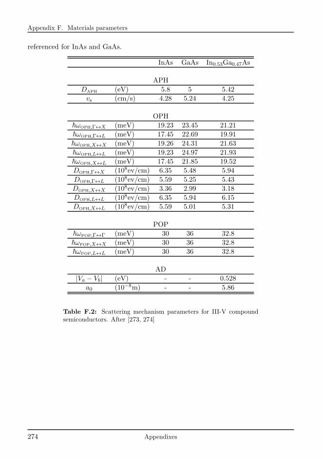
Appendix F. Materials parameters
referenced for InAs and GaAs.
InAs GaAs In0.53Ga0.47As
APH
DAPH (eV) 5.8 5 5.42
vs (cm/s) 4.28 5.24 4.25
OPH
~ωOPH,Γ↔X (meV) 19.23 23.45 21.21
~ωOPH,Γ↔L (meV) 17.45 22.69 19.91
~ωOPH,X↔X (meV) 19.26 24.31 21.63
~ωOPH,L↔L (meV) 19.23 24.97 21.93
~ωOPH,X↔L (meV) 17.45 21.85 19.52
DOPH,Γ↔X (108ev/cm) 6.35 5.48 5.94
DOPH,Γ↔L (108ev/cm) 5.59 5.25 5.43
DOPH,X↔X (108ev/cm) 3.36 2.99 3.18
DOPH,L↔L (108ev/cm) 6.35 5.94 6.15
DOPH,X↔L (108ev/cm) 5.59 5.01 5.31
POP
~ωPOP,Γ↔Γ (meV) 30 36 32.8
~ωPOP,X↔X (meV) 30 36 32.8
~ωPOP,L↔L (meV) 30 36 32.8
AD
|Va − Vb| (eV) - - 0.528
a0 (10−8m) - - 5.86
Table F.2: Scattering mechanism parameters for III-V compoundsemiconductors. After [273, 274]
274 Appendixes
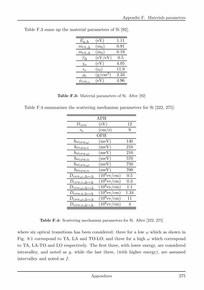
Appendix F. Materials parameters
Table F.3 sums up the material parameters of Si [92].
Eg,∆ (eV) 1.11
mlX,∆ (m0) 0.91
mtX,∆ (m0) 0.19
β∆ (eV/eV) 0.5
χs (eV) 4.05
ǫs (ǫ0) 11.9
ρs (g/cm3) 2.33
φCNL,s (eV) 4.96
Table F.3: Material parameters of Si. After [92]
Table F.4 summarizes the scattering mechanism parameters for Si [222, 275]:
APH
DAPH (eV) 12
vs (cm/s) 9
OPH
~ωOPH,g1 (meV) 140
~ωOPH,f1 (meV) 210
~ωOPH,g2 (meV) 210
~ωOPH,f2 (meV) 570
~ωOPH,g3 (meV) 750
~ωOPH,f3 (meV) 700
DOPH,g1,∆↔∆ (108ev/cm) 0.5
DOPH,f1,∆↔∆ (108ev/cm) 0.3
DOPH,g2,∆↔∆ (108ev/cm) 1.1
DOPH,f2,∆↔∆ (108ev/cm) 1.34
DOPH,g3,∆↔∆ (108ev/cm) 11
DOPH,f3,∆↔∆ (108ev/cm) 4
Table F.4: Scattering mechanism parameters for Si. After [222, 275]
where six optical transitions has been considered: three for a low ω which as shown in
Fig. 8.1 correspond to TA, LA and TO-LO; and three for a high ω which correspond
to TA, LA-TO and LO respectively. The first three, with lower energy, are considered
intravalley, and noted as g, while the last three, (with higher energy), are assumed
intervalley and noted as f .
Appendixes 275
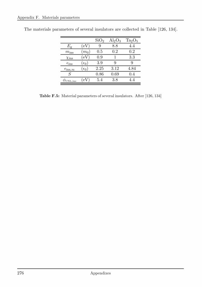
Appendix F. Materials parameters
The materials parameters of several insulators are collected in Table [126, 134].
SiO2 Al2O3 Ta2O5
Eg (eV) 9 8.8 4.4
mins (m0) 0.5 0.2 0.2
χins (eV) 0.9 1 3.3
ǫins (ǫ0) 3.9 9 9
ǫins,∞ (ǫ0) 2.25 3.12 4.84
S 0.86 0.69 0.4
φCNL,ins (eV) 5.4 3.8 4.4
Table F.5: Material parameters of several insulators. After [126, 134]
276 Appendixes
Part VI
References

List of publications
Referenced papers
• E. G. Marin, F. G. Ruiz, I. M. Tienda-Luna, A. Godoy, P. Sachez-Moreno, and
F. Gamiz. Analytic potential and charge model for III-V Surrounding GateMOS-
FETs. Journal of Applied Physics, 112:084512, Oct 2012
• E.G. Marin, F.J.G. Ruiz, I.M. Tienda-Luna, A. Godoy, and F. Gamiz. Analyt-
ical gate capacitance modeling of III-V nanowire transistors. IEEE Transactions
on Electron Devices, 60(5):1590, May 2013.
• E.G. Marin, F.G. Ruiz, I.M. Tienda-Luna, A. Godoy, and F. Gamiz. Analytical
model for the threshold voltage of III-V nanowire transistors including quantum
effects. Solid-State Electronics, 92:28, Feb 2014.
Conference Contributions
• E. G. Marin, and F. G. Ruiz, and A. Godoy, and I. M. Tienda-Luna, and
F. Gamiz. Effect of interfacial states on the technological variability of Trigate
MOSFETs. Silicon Nanoelectronics Workshop (SNW), 2012 IEEE. 2012.
• E. G. Marin, and F. G. Ruiz, and I. M. Tienda-Luna, and A. Godoy, and F.
Gamiz. Study of the Gate Capacitance of GaAs, InAs and InGaAs Nanowires 36th
Workshop on Compound Semiconductor Devices and Integrated Circuits 2012.
2012.
• I. M. Tienda-Luna, and F. G. Ruiz, and A. Godoy, and E. G. Marin. and F.
Gamiz. Dependence of the Phonon-Limited Mobility in Arbitrarily Oriented Si-
Nanowires. 15th International Workshop on Computational Electronics (IWCE
References 279
2012). 2012.
• F. G. Ruiz, and E. G. Marin, and I. M. Tienda-Luna, and A. Godoy, and
C.Martinez-Blanque, and F. Gamiz Ruiz. Influence of the back-gate bias on the
electron mobility of trigate MOSFETs. Simulation of Semiconductor Processes
and Devices (SISPAD), 2013. International Conference on. 2013.
• F. G. Ruiz, and E. G. Marin, and I. M. Tienda-Luna, and A. Godoy, and
C.Martinez-Blanque, and F. Gamiz Ruiz. Back-Gate Biasing Influence on the
Electron Mobility and the Threshold Voltage of Ultra Thin Box Multigate MOS-
FET. Silicon Nanoelectronics Workshop (SNW), 2013 IEEE. 2013.
280 References
Bibliography
[1] D. Kahng. Silicon-silicon dioxide field induced surface devices. In Technical
memorandum issued by Bell Labs, Jan 1961.
[2] H. Iwai. Evolution of Si CMOS technologies to sub-10 nm generation. Electron
Devices Colloquium IMEC, Leuven, Belgium, Jan 2012.
[3] J. Bardeen and W. H. Brattain. The transistor, a semi-conductor triode. Physical
Review, 74:230, Jul 1948.
[4] M. Riordan, L. Hoddeson, and C. Herring. The invention of the transistor. Re-
views of Modern Physics, 71(2):S336, 1999.
[5] R. H. Dennard, F. H. Gaensslen, V. L. Rideout, E. Bassous, and A. R. LeBlanc.
Design of ion-implanted MOSFET’s with very small physical dimensions. IEEE
Journal of Solid-State Circuits, 9(5):256, 1974.
[6] H. Iwai. Roadmap for 22 nm and beyond. Microelectronic Engineering, 86:1520,
Sep 2009.
[7] W. Haensch, E. J. Nowak, R. H. Dennard, P. M. Solomon, A. Bryant, O. H.
Dokumaci, A. Kumar, X. Wang, J. B. Johnson, and M. V. Fischetti. Silicon
CMOS devices beyond scaling. IBM Journal of Research and Development, 50
(4.5):339, July 2006.
[8] B. Hoeneisen and C.A. Mead. Fundamental limitations in microelectronics-I.
MOS technology. Solid-State Electronics, 15:819, 1972.
[9] J. T. Wallmark. Fundamental physical limitations in integrated electronic cir-
cuits. In Institute of Physics Conference Series, page 133, 1975.
References 281
[10] Chenming Hu. Gate oxide scaling limits and projection. In Electron Devices
Meeting (IEDM), 1996 IEEE International, page 319, Dec 1996.
[11] J. H. Stathis and D. J. DiMaria. Reliability projection for ultra-thin oxides at
low voltage. In Electron Devices Meeting (IEDM), 1998 IEEE International, page
167, Dec 1998.
[12] H. Iwai. CMOS downsizing toward sub-10 nm. Solid-State Electronics, 48(4):497,
2004.
[13] H. Iwai. Future of Nano-CMOS technology. CINVESTAV, Mexico City, Mexico,
Apr 2014.
[14] G. E. Moore. Cramming more components onto integrated circuits, 1965.
[15] International Technology Roadmap for Semiconductors. Available online:
http://www.itrs.net, 2013.
[16] H. Iwai. Si nanowire FET technology. ECS Tutorial, Montreal, Canada, May
2011.
[17] Y.-M. Lin, K. A. Jenkins, A. Valdes-Garcia, J. P. Small, D. B. Farmer, and
P. Avouris. Operation of graphene transistors at Gigahertz frequencies. Nano
Letters, 9(1):422–426, 2009.
[18] Y. Yoon, K. Ganapathi, and S. Salahuddin. How good can monolayer MoS2
transistors be? Nano Letters, 11(9):3768, 2011.
[19] S. J. Tans, A. R. Verschueren, and C. Dekker. Room-temperature transistor
based on a single carbon nanotube. Nature, 393:49, 1998.
[20] J. M. Tour. Molecular electronics. synthesis and testing of components. Accounts
of Chemical Research, 33:791, 2000.
[21] M. Fuechsle, J. A. Miwa, S. Mahapatra, H. Ryu, S. Lee, O. Warschkow, L. C.
Hollenberg, G. Klimeck, and M. Y. Simmons. A single-atom transistor. Nature
Nanotechnology, 7(4):242, 2012.
[22] Y. Taur, D. A. Buchanan, W. Chen, D. J. Frank, K. E. Ismail, S.-H. Lo, G. A.
Sai-Halasz, R. G. Viswanathan, H.-J. C. Wann, S. J. Wind, and H.-S. Wong.
CMOS scaling into the nanometer regime. Proceedings of the IEEE, 85:486, Apr
1997.
282 References
[23] A. P. Chandrakasan and R. W. Brodersen. Minimizing power consumption in
digital CMOS circuits. Proceedings of the IEEE, 83(4):498, 1995.
[24] D. J. Frank. Power-constrained CMOS scaling limits. IBM Journal of Research
and Development, 46:235, 2002.
[25] M. Horowitz, E. Alon, D. Patil, S. Naffziger, R. Kumar, and K. Bernstein. Scaling,
power, and the future of CMOS. In Electron Devices Meeting (IEDM), 2005 IEEE
International, page 7, 2005.
[26] N.C.-C. Lu and J. M. Sung. Reverse short-channel effects on threshold voltage
in submicrometer salicide devices. IEEE Electron Device Letters, 10:446, 1989.
[27] A. Chaudhry and M. J. Kumar. Controlling short-channel effects in deep-
submicron SOI MOSFETs for improved reliability: a review. IEEE Transactions
on Device and Materials Reliability, 4:99, 2004.
[28] A. Asenov. Simulation of statistical variability in nano MOSFETs. In VLSI
Technology, 2007. Digest of Technical Papers. 2007 Symposium on, page 86, 2007.
[29] A. Cathignol, B. Cheng, D. Chanemougame, A. R. Brown, K. Rochereau,
G. Ghibaudo, and A. Asenov. Quantitative evaluation of statistical variabil-
ity sources in a 45-nm technological node LP N-MOSFET. IEEE Electron Device
Letters, 29(6):609, 2008.
[30] X. Wang, A. R. Brown, B. Cheng, and A. Asenov. Statistical variability and
reliability in nanoscale FinFETs. In Electron Devices Meeting (IEDM), 2011
IEEE International, page 5, 2011.
[31] M. Ieong, B. Doris, J. Kedzierski, K. Rim, and M. Yang. Silicon device scaling
to the sub-10-nm regime. Science, 306(5704):2057, 2004.
[32] J. P. Colinge, J. C. Alderman, W. Xiong, and C. R. Cleavelin. Quantum-
mechanical effects in trigate SOI MOSFETs. IEEE Transactions on Electron
Devices, 53(5):1131, 2006.
[33] C.-W. Lee, A. N. Nazarov, I. Ferain, N. D. Akhavan, R. Yan, P. Razavi, R. Yu,
R. T. Doria, and J.-P. Colinge. Low subthreshold slope in junctionless multigate
transistors. Applied Physics Letters, 96(10):102106, 2010.
References 283
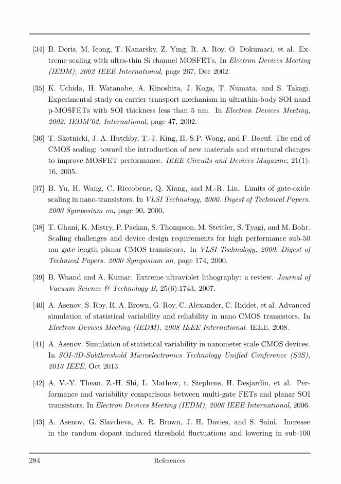
[34] B. Doris, M. Ieong, T. Kanarsky, Z. Ying, R. A. Roy, O. Dokumaci, et al. Ex-
treme scaling with ultra-thin Si channel MOSFETs. In Electron Devices Meeting
(IEDM), 2002 IEEE International, page 267, Dec 2002.
[35] K. Uchida, H. Watanabe, A. Kinoshita, J. Koga, T. Numata, and S. Takagi.
Experimental study on carrier transport mechanism in ultrathin-body SOI nand
p-MOSFETs with SOI thickness less than 5 nm. In Electron Devices Meeting,
2002. IEDM’02. International, page 47, 2002.
[36] T. Skotnicki, J. A. Hutchby, T.-J. King, H.-S.P. Wong, and F. Boeuf. The end of
CMOS scaling: toward the introduction of new materials and structural changes
to improve MOSFET performance. IEEE Circuits and Devices Magazine, 21(1):
16, 2005.
[37] B. Yu, H. Wang, C. Riccobene, Q. Xiang, and M.-R. Lin. Limits of gate-oxide
scaling in nano-transistors. In VLSI Technology, 2000. Digest of Technical Papers.
2000 Symposium on, page 90, 2000.
[38] T. Ghani, K. Mistry, P. Packan, S. Thompson, M. Stettler, S. Tyagi, and M. Bohr.
Scaling challenges and device design requirements for high performance sub-50
nm gate length planar CMOS transistors. In VLSI Technology, 2000. Digest of
Technical Papers. 2000 Symposium on, page 174, 2000.
[39] B. Wuand and A. Kumar. Extreme ultraviolet lithography: a review. Journal of
Vacuum Science & Technology B, 25(6):1743, 2007.
[40] A. Asenov, S. Roy, R. A. Brown, G. Roy, C. Alexander, C. Riddet, et al. Advanced
simulation of statistical variability and reliability in nano CMOS transistors. In
Electron Devices Meeting (IEDM), 2008 IEEE International. IEEE, 2008.
[41] A. Asenov. Simulation of statistical variability in nanometer scale CMOS devices.
In SOI-3D-Subthreshold Microelectronics Technology Unified Conference (S3S),
2013 IEEE, Oct 2013.
[42] A. V.-Y. Thean, Z.-H. Shi, L. Mathew, t. Stephens, H. Desjardin, et al. Per-
formance and variability comparisons between multi-gate FETs and planar SOI
transistors. In Electron Devices Meeting (IEDM), 2006 IEEE International, 2006.
[43] A. Asenov, G. Slavcheva, A. R. Brown, J. H. Davies, and S. Saini. Increase
in the random dopant induced threshold fluctuations and lowering in sub-100
284 References
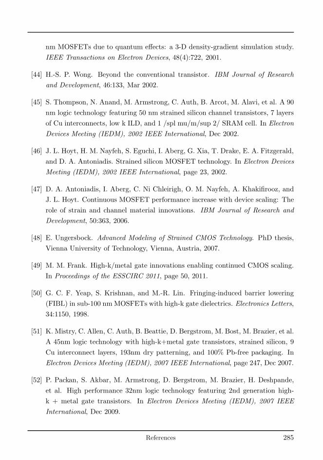
nm MOSFETs due to quantum effects: a 3-D density-gradient simulation study.
IEEE Transactions on Electron Devices, 48(4):722, 2001.
[44] H.-S. P. Wong. Beyond the conventional transistor. IBM Journal of Research
and Development, 46:133, Mar 2002.
[45] S. Thompson, N. Anand, M. Armstrong, C. Auth, B. Arcot, M. Alavi, et al. A 90
nm logic technology featuring 50 nm strained silicon channel transistors, 7 layers
of Cu interconnects, low k ILD, and 1 /spl mu/m/sup 2/ SRAM cell. In Electron
Devices Meeting (IEDM), 2002 IEEE International, Dec 2002.
[46] J. L. Hoyt, H. M. Nayfeh, S. Eguchi, I. Aberg, G. Xia, T. Drake, E. A. Fitzgerald,
and D. A. Antoniadis. Strained silicon MOSFET technology. In Electron Devices
Meeting (IEDM), 2002 IEEE International, page 23, 2002.
[47] D. A. Antoniadis, I. Aberg, C. Ni Chleirigh, O. M. Nayfeh, A. Khakifirooz, and
J. L. Hoyt. Continuous MOSFET performance increase with device scaling: The
role of strain and channel material innovations. IBM Journal of Research and
Development, 50:363, 2006.
[48] E. Ungersbock. Advanced Modeling of Strained CMOS Technology. PhD thesis,
Vienna University of Technology, Vienna, Austria, 2007.
[49] M. M. Frank. High-k/metal gate innovations enabling continued CMOS scaling.
In Proceedings of the ESSCIRC 2011, page 50, 2011.
[50] G. C. F. Yeap, S. Krishnan, and M.-R. Lin. Fringing-induced barrier lowering
(FIBL) in sub-100 nmMOSFETs with high-k gate dielectrics. Electronics Letters,
34:1150, 1998.
[51] K. Mistry, C. Allen, C. Auth, B. Beattie, D. Bergstrom, M. Bost, M. Brazier, et al.
A 45nm logic technology with high-k+metal gate transistors, strained silicon, 9
Cu interconnect layers, 193nm dry patterning, and 100% Pb-free packaging. In
Electron Devices Meeting (IEDM), 2007 IEEE International, page 247, Dec 2007.
[52] P. Packan, S. Akbar, M. Armstrong, D. Bergstrom, M. Brazier, H. Deshpande,
et al. High performance 32nm logic technology featuring 2nd generation high-
k + metal gate transistors. In Electron Devices Meeting (IEDM), 2007 IEEE
International, Dec 2009.
References 285
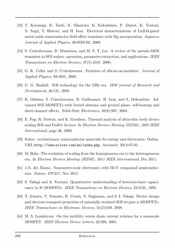
[53] T. Koyanagi, K. Tachi, K. Okamoto, K. Kakushima, P. Ahmet, K. Tsutsui,
N. Sugii, T. Hattori, and H. Iwai. Electrical characterization of La2O3-gated
metal oxide semiconductor field effect transistor with Mg incorporation. Japanese
Journal of Applied Physics, 48:05DC02, 2009.
[54] S. Cristoloveanu, D. Munteanu, and M. S. T. Liu. A review of the pseudo-MOS
transistor in SOI wafers: operation, parameter extraction, and applications. IEEE
Transactions on Electron Devices, 47(5):1018, 2000.
[55] G. K. Celler and S. Cristoloveanu. Frontiers of silicon-on-insulator. Journal of
Applied Physics, 93:4955, 2003.
[56] G. G. Shahidi. SOI technology for the GHz era. IBM journal of Research and
Development, 46:121, 2002.
[57] K. Oshima, S. Cristoloveanu, B. Guillaumot, H. Iwai, and S. Deleonibus. Ad-
vanced SOI MOSFETs with buried alumina and ground plane: self-heating and
short-channel effects. Solid-State Electronics, 48(6):907, 2004.
[58] E. Pop, R. Dutton, and K. Goodson. Thermal analysis of ultra-thin body device
scaling SOI and FinFet devices. In Electron Devices Meeting (IEDM), 2005 IEEE
International, page 36, 2003.
[59] Soitec: revolutionary semiconductor materials for energy and electronics. Online.
URL http://www.soitec.com/en/index.php. Accessed: 2014-07-05.
[60] M. Bohr. The evolution of scaling from the homogeneous era to the heterogeneous
era. In Electron Devices Meeting (IEDM), 2011 IEEE International, Dec 2011.
[61] J.A. del Alamo. Nanometre-scale electronics with III-V compound semiconduc-
tors. Nature, 479:317, Nov 2011.
[62] S. Takagi and A. Toriumi. Quantitative understanding of inversion-layer capaci-
tance in Si MOSFETs. IEEE Transactions on Electron Devices, 42:2125, 1995.
[63] T. Irisawa, T. Numata, K. Usuda, N. Sugiyama, and S.-I. Takagi. Device design
and electron transport properties of uniaxially strained-SOI tri-gate n-MOSFETs.
IEEE Transactions on Electronic Devices, 55(2):649, 2008.
[64] M. S. Lundstrom. On the mobility versus drain current relation for a nanoscale
MOSFET. IEEE Electron Device Letters, 22:293, 2001.
286 References
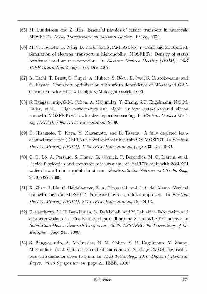
[65] M. Lundstrom and Z. Ren. Essential physics of carrier transport in nanoscale
MOSFETs. IEEE Transactions on Electron Devices, 49:133, 2002.
[66] M. V. Fischetti, L. Wang, B. Yu, C. Sachs, P.M. Asbeck, Y. Taur, and M. Rodwell.
Simulation of electron transport in high-mobility MOSFETs: Density of states
bottleneck and source starvation. In Electron Devices Meeting (IEDM), 2007
IEEE International, page 109, Dec 2007.
[67] K. Tachi, T. Ernst, C. Dupre, A. Hubert, S. Becu, H. Iwai, S. Cristoloveanu, and
O. Faynot. Transport optimization with width dependence of 3D-stacked GAA
silicon nanowire FET with high-κ/Metal gate stack, 2009.
[68] S. Bangsaruntip, G.M. Cohen, A. Majumdar, Y. Zhang, S.U. Engelmann, N.C.M.
Fuller, et al. High performance and highly uniform gate-all-around silicon
nanowire MOSFETs with wire size dependent scaling. In Electron Devices Meet-
ing (IEDM), 2009 IEEE International, 2009.
[69] D. Hisamoto, T. Kaga, Y. Kawamoto, and E. Takeda. A fully depleted lean-
channel transistor (DELTA)-a novel vertical ultra thin SOI MOSFET. In Electron
Devices Meeting (IEDM), 1989 IEEE International, page 833, Dec 1989.
[70] C. C. Lo, A. Persaud, S. Dhuey, D. Olynick, F. Borondics, M. C. Martin, et al.
Device fabrication and transport measurements of FinFETs built with 28Si SOI
wafers toward donor qubits in silicon. Semiconductor Science and Technology,
24:105022, 2009.
[71] X. Zhao, J. Lin, C. Heidelberger, E. A. Fitzgerald, and J. A. del Alamo. Vertical
nanowire InGaAs MOSFETs fabricated by a top-down approach. In Electron
Devices Meeting (IEDM), 2013 IEEE International, Dec 2013.
[72] D. Sacchetto, M. H. Ben-Jamaa, G. De Micheli, and Y. Leblebici. Fabrication and
characterization of vertically stacked gate-all-around Si nanowire FET arrays. In
Solid State Device Research Conference, 2009. ESSDERC’09. Proceedings of the
European, page 245, 2009.
[73] S. Bangsaruntip, A. Majumdar, G. M. Cohen, S. U. Engelmann, Y. Zhang,
M. Guillorn, et al. Gate-all-around silicon nanowire 25-stage CMOS ring oscilla-
tors with diameter down to 3 nm. In VLSI Technology, 2010. Digest of Technical
Papers. 2010 Symposium on, page 21. IEEE, 2010.
References 287
[74] TSMC 2013 Symposium: Progress in 20nm, 16nm Fin-
FET, and 3D-IC Technologies. Online. URL http://
www.cadence.com/Community/blogs/ii/archive/2013/04/14/
tsmc-2013-symposium-progress-in-20nm-16nm-finfet-and-3d-ic-technologies.
aspx. Accessed: 2014-07-04.
[75] N. Collaert, A. Dixit, M. Goodwin, K. G. Anil, R. Rooyackers, B. Degroote,
et al. A functional 41-stage ring oscillator using scaled FinFET devices with
25-nm gate lengths and 10-nm fin widths applicable for the 45-nm CMOS node.
Electron Device Letters, IEEE, 25(8):568, 2004.
[76] M. J. H. Van Dal, N. Collaert, G. Doornbos, G. Vellianitis, G. Curatola, B. J.
Pawlak, et al. Highly manufacturable FinFETs with sub-10nm fin width and high
aspect ratio fabricated with immersion lithography. In VLSI Technology, 2007.
Digest of Technical Papers. 2007 Symposium on, page 110, 2007.
[77] B. Doyle, B. Boyanov, S. Datta, M. Doczy, S. Hareland, B. Jin, J. Kavalieros,
T. Linton, R. Rios, and R. Chau. Tri-gate fully-depleted CMOS transistors:
Fabrication, design and layout. In VLSI Technology, 2003. Digest of Technical
Papers. 2003 Symposium on, page 133, 2003.
[78] B. Lu, E. Matioli, and T. Palacios. Tri-gate normally-off GaN power MISFET.
Electron Device Letters, IEEE, 33(3):360, 2012.
[79] V. Schmidt, H. Riel, S. Senz, S. Karg, W. Riess, and U. Gosele. Realization of a
silicon nanowire vertical surround-gate field-effect transistor. Small, 2:85, 2006.
[80] S. D. Suk, K. H. Yeo, K. H. Cho, M. Li, Y. Y. Yeoh, S.-Y. Lee, et al. High-
performance twin silicon nanowire MOSFET (TSNWFET) on bulk Si wafer.
IEEE Transactions on Nanotechnology, 7(2):181, 2008.
[81] F.-L. Yang, H.-Y. Chen, F.-C. Chen, C.-C. Huang, C.-Y. Chang, H.-K. Chiu,
et al. 25 nm CMOS Omega FETs. In Electron Devices Meeting (IEDM), 2002
IEEE International, page 255, 2002.
[82] J.-T. Park, J. P. Colinge, and C. H. Diaz. Pi-gate SOI MOSFET. IEEE Electron
Device Letters, 22:405, 2001.
288 References
[83] S. Cristoloveanu, T. Ernst, D. Munteanu, and T. Ouisse. Ultimate MOSFETs on
SOI: Ultra thin, single gate, double gate, or ground plane. International journal
of high speed electronics and systems, 10(01):217, 2000.
[84] T. Ernst, S. Cristoloveanu, G. Ghibaudo, T. Ouisse, S. Horiguchi, Y. Ono,
Y. Takahashi, and K. Murase. Ultimately thin double-gate SOI MOSFETs. IEEE
Transactions on Electron Devices, 50(3):830, 2003.
[85] J. P. Colinge. Multiple-gate SOI MOSFETs. Solid-State Electronics, 48:897, Jun
2004.
[86] S. Datta. Quantum phenomena. Addison-Wesley Longman, Incorporated, 1989.
ISBN 9780201079562.
[87] C. Hamaguchi. Basic Semiconductor Physics. Springer, 2001. ISBN
9783540416395.
[88] D. Esseni, P. Palestri, and L. Selmi. Nanoscale MOS Transistors: Semi-classical
Transport And Applications. Cambridge University Press, New York. USA, 2011.
ISBN 9780521516846.
[89] J. Kim and M.V. Fischetti. Electronic band structure calculations for biaxially
strained Si, Ge, and III-V semiconductors. Journal of Applied Physics, 108:
013710, Jul 2010.
[90] I. Vurgaftman, J. R. Meyeer, and L. R. Ram-Mohan. Band parameters for III-V
compound semiconductors and their alloys. Journal of Applied Physics, 89(11):
5815, 2001.
[91] J. R. Chelikowsky and M. L. Cohen. Nonlocal pseudopotential calculations for the
electronic structure of eleven diamond and zinc-blende semiconductors. Physical
Review B, 14:556, Jul 1976.
[92] Landolt-Bornstein. Numerical Data and Functional Relationships in Science and
Technology.Semiconductor Quantum Structures. Springer, Berlin. Germany, 1st
edition, 2001. ISBN 3540617418.
[93] V. Ariel Altschul, A. Fraenkel, and E. Finkman. Effects of band nonparabolicity
on two-dimensional electron gas. Journal of Applied Physics, 71(9):4382, Jan
1992.
References 289
[94] A. Godoy, Z. Yang, U. Ravaioli, and F. Gamiz. Effects of nonparabolic bands in
quantum wires. Journal of Applied Physics, 98, 2005.
[95] S. Jin, M. V. Fischetti, and T. Tang. Modeling of electron mobility in gated
silicon nanowires at room temperature: Surface roughness scattering, dielectric
screening, and band nonparabolicity. Journal of Applied Physics, 102:083715,
Oct 2006.
[96] S. Mudanai, A. Roy, R. Kotlyar, T. Rakshit, and M. Stettler. Capacitance com-
pact model for ultrathin low-electron-effective-mass materials. IEEE Transactions
on Electron Devices, 58:4202, Dec 2011.
[97] Y. Yuan, B. Yu, J. Song, and Y Taur. An analytic model for threshold voltage
shift due to quantum confinement in surrounding gate MOSFETs with anisotropic
effective mass. Solid State Electronics, 53:140, 2009.
[98] E. G. Marin, F. G. Ruiz, I. M. Tienda-Luna, A. Godoy, P. Sanchez-Moreno,
and F. Gamiz. Analytic potential and charge model for III-V Surrounding Gate
MOSFETs. Journal of Applied Physics, 112:084512, Oct 2012.
[99] M. Radosavljevic, G. Dewey, J. M. Fastenau, J. Kavalieros, R. Kotlyar, B. Chu-
Kung, et al. Non-planar, multi-gate InGaAs quantum well field effect transistors
with high-k gate dielectric and ultra-scaled gate-to-drain/gate-to-source separa-
tion for low power logic applications. In Electron Devices Meeting (IEDM), 2010
IEEE International, page 126, Dec 2010.
[100] A. C. Ford, S. B. Kumar, R. Kapadia, J. Guo, and A. Javey. Observation of de-
generate one-dimensional sub-bands in cylindrical InAs nanowires. Nano Letters,
12:1340, Jan 2012.
[101] M. Radosavljevic, G. Dewey, D. Basu, J. Boardman, B. Chu-Kung, J. M. Fas-
tenau, et al. Electrostatics improvement in 3-D tri-gate over ultra-thin body
planar InGaAs quantum well field effect transistors with high-κ gate dielectric
and scaled gate-to-drain/gate-to-source separation. In Electron Devices Meeting
(IEDM), 2011 IEEE International, 2011.
[102] S. Sato, W. Li, K. Kakushima, K. Ohmori, K. Natori, K. Yamada, and H. Iwai.
Extraction of additional interfacial states of silicon nanowire field-effect transis-
tors. Applied Physics Letters, 98:233506, Jun 2011.
290 References
[103] M. Casse, K. Tachi, S. Thiele, and T. Ernst. Spectroscopic charge pumping in
Si nanowire transistors with a high-κ metal gate. Applied Physics Letters, 96:
123506, Mar 2010.
[104] E. Dornel, T. Ernst, J. C. Barbe, J. M. Hartmann, V. Delaye, F. Aussenac,
C. Vizioz, S. Borel, V. Maffini-Alvaro, C. Isheden, and J. Foucher. Hydrogen
annealing of arrays of planar and vertically stacked Si nanowires. Applied Physics
Letters, 91(23):233502, 2007.
[105] K. Ohmori, T. Matsuki, D. Ishikawa, T. Morooka, T. Aminaka, Y. Sugita, et al.
Impact of additional factors in threshold voltage variability of metal/high-k gate
stacks and its reduction by controlling crystalline structure and grain size in the
metal gates. In Electron Devices Meeting (IEDM), 2008 IEEE International,
2008.
[106] S.E. Laux and M.V. Fischetti. Monte-carlo simulation of submicrometer Si n-
MOSFETs at 77 and 300 k. Electron Device Letters, IEEE, 9:467, Sept 1988.
[107] T. Kerkhoven, A. T. Galick, U. Ravaioli, J. H. Arends, and Y. Saad. Efficient
numerical simulation of electron states in quantum wires. Journal of Applied
Physics, 68:3461, Jun 1990.
[108] Sentaurus Device. Online.
[109] Atlas Device Simulation Framework. Online.
[110] VSP - Global TCAD Solutions. Online. URL http://www.globaltcad.com/en/
products/vsp.html. Accessed: 2014-24-03.
[111] Gold Standard Simulations. Online. URL http://www.
goldstandardsimulations.com. Accessed: 2014-24-03.
[112] Athena Process Simulation Framework. Online. URL http://www.silvaco.com/
products/tcad/process simulation/athena/athena.html. Accessed: 2014-
03-14.
[113] B. Laikhtman. Boundary conditions for envelope functions in heterostructures.
Phyical Review B, 46:4769, Aug 1992.
References 291
[114] A. V. Rodina, A. Yu. Alekseev, Al. L. Efros, M. Rosen, and B. K. Meyer. General
boundary conditions for the envelope function in the multiband kp model. Phyical
Review B, 65:125302, Feb 2002.
[115] P. Harrison. Quantum Wells, Wires and Dots. John Willey & Sons, Chichester.
UK, 2000.
[116] MATLAB. The Language of Technical Computing. Online. URL http://www.
mathworks.com/products/matlab/. Accessed: 2014-02-28.
[117] Partial Differential Equation ToolboxTM. Online. URL http://www.mathworks.
es/products/pde/. Accessed: 2014-02-28.
[118] G. Smith. Numerical Solution of Partial Differential Equations: Finite Diference
Methods. Oxford University Press, New York. USA, 3rd edition, 1985. ISBN
0198596502.
[119] O. Zienkiewicz and R. Taylor. The Finite Element Method. Volume 1: The Basis.
Butterworth and Heinemann, Oxford. UK, 5th edition, 2000. ISBN 0750650494.
[120] J. Peiro and S. Sherwin. Finite Difference, Finite Element and Finite. Methods
for partial differential equations. In Y. Sip, editor, Handbook of Materials Mod-
eling. Volume I: Methods and Models. Springer, Dordrecht. The Netherlands, 1st
edition, 2005. ISBN 1402032870.
[121] The MathWorks, Inc. Partial Differential Equation ToolboxTMUser’s Guide. The
MathWorks, Inc.
[122] W. Schottky. Halbleitertheorie der sperrschicht. Naturwissenschaften, 26:843,
1938.
[123] J. Bardeen. Surface states and rectification at metal-semiconductor contact. Phys-
ical Review, 71:717, 1947.
[124] V. Heine. Theory of surface states. Physical Review, 138:A1689, 1965.
[125] J. Tersoff. Schottky barrier height and the continuum of gap states. Physical
Review Letters, 52:465, 1984.
[126] J. Robertson. Band offsets of wide-band-gap oxides and implications for future
electronic devices. Journal of Vacuum Science Technology, 18:1785, 2000.
292 References
[127] A. M. Cowley and S.M. Sze. Surface states and barrier height of metal semicon-
ductor system. Journal of Applied Physics, 36:3212, 1965.
[128] J. Robertson. Model of interface states at III-V oxide interfaces. Journal of
Applied Physics, 94:152104, 2009.
[129] L. Lin, H. Li, and J. Robertson. Control of schottky barrier heights by inserting
thin dielectric layers. Applied Physics Letters, 101:172907, 2012.
[130] J. Tersoff. Theory of semiconductors heterojunctions: The role of quantum
dipoles. Physical Review B, 30:4874, 1984.
[131] J. Tersoff. Schottky barriers and semiconductors band structures. Physical Review
B, 32:6968, 1985.
[132] J. Tersoff and W. Harrison. Transition-metal impurities in semiconductors: Their
connection with band lineups and schottky barriers. Physical Review Letters, 58:
2367, 1987.
[133] W. Monch. Role of virtual gap states and defects in metal-semiconductor contacts.
Journal of Applied Physics, 58:1260, 1987.
[134] J. Robertson. Band offsets of high dielectric constant gate oxides on silicon.
Journal of Non-Crystalline Solids, 303:94, 2002.
[135] J. Robertson and B. Falabretti. Band offsets of high-κ gate oxides on III-V
semiconductors. Journal of Applied Physics, 100:014111, Jul 2006.
[136] J. Robertson and L. Lin. Fermi level pinning in Si, Ge and GaAs systems – migs
or defects? In Electron Devices Meeting (IEDM), 2009 IEEE International, page
119, Jun 2009.
[137] V. Pott, K.E. Moselund, D. Bouvet, L. De Michielis, and A.M. Ionescu. Fabri-
cation and characterization of gate-all-around silicon nanowires on bulk silicon.
Nanotechnology, IEEE Transactions on, 7(6):733, Nov 2008.
[138] TA. Rahman, M. Lundstrom, and A. Ghosh. Generalize effective mass approach
for n-type semiconductor field-effect transistors on arbitrarily oriented wafers.
Journal of Applied Physics, 97:053702–1–12, 2005.
References 293
[139] M. Bescond, N. Cavassilas, and M. Lannoo. Effective-mass approach for n-
type semiconductor nanowire MOSFETs arbitrarily oriented. Nanotechnology,
18:255201, 2007.
[140] S. M. Sze. Physics of semiconductor devices. New York. USA, 2nd edition, 1981.
ISBN 0471056618.
[141] G. Brammertz, H. C. Lin, K. Martens, D. Mercier, S. Sioncke, A. Delabie, W.-E.
Wang, M. Caymax, M. Meuris, and M. Heyns. Capacitance-voltage characteri-
zation of GaAs-Al2O3 interfaces. Applied Physics Letters, 93:183504, Nov 2008.
[142] Y.C. Chang, C. Merckling, J. Penaud, C. Y. Lu, G. Brammertz, W. E Wang,
M. Hong, J. Kwo, J. Dekoster, M. Caymax, M. Meuris, and M. Heyns. Great
reduction of interfacial traps in Al2O3/GaAs (100) starting with Ga-rich sur-
face and through systematic thermal annealing. In Device Research Conference
(DRC), 2010, pages 51–52, Jun 2010.
[143] X. Sun, S. Cui, A. Alian, G. Brammertz, C. Merckling, D. Lin, and T-P Ma.
AC transconductance dispersion (ACGD): A method to profile oxide traps in
MOSFETs without body contact. Electron Device Letters, IEEE, 33:438, Mar
2012.
[144] X. Sun, O. I. Saadat, K. S. Chang-Liao, T. Palacios, S. Cui, and T. P. Ma.
Study of gate oxide traps in HfO2/AlGaN/GaN metal-oxide-semiconductor high-
electron-mobility transistors by use of ac transconductance method. Applied
Physics Letters, 102:103504, 2013.
[145] G. Brammertz, H. C. Lin, M. Caymax, M. Meuris, M. Heyns, and M. Passlack.
On the interface state density at In0.53Ga0.47As/oxide interfaces. Applied Physics
Letters, 95(20):202109, Nov 2009.
[146] T. Kerkhoven, M. W. Raschke, and U. Ravaioli. Self-consistent simulation of
quantum wires in periodic heterojunction structures. Journal of Applied Physics,
74:1119, Jul 1993.
[147] A. Trellakis, A.T. Galick, A. Pacelli, and U. Ravaioli. Iteration scheme for the
solution of the two-dimensional schrodinger-poisson equations in quantum struc-
tures. Journal of Applied Physics, 81(12):7880, Mar 1997.
294 References
[148] A. Trellakis and U. Ravaioli. Computational issues in the simulation of semicon-
ductor quantum wires. Computer Methods in Applied Mechanics and Engineering,
181:437–449, 2000.
[149] R.B. Dingle. The fermi-dirac integrals Fp(η) = (p!)−1∞∫
0
εp(eε−η+1)−1dε. Applied
Scientific Research, Section B, 6:225, 1957.
[150] J.S. Blakemore. Approximations for fermi-dirac integrals, especially the func-
tion F−1/2(η) used to describe electron density in a semiconductor. Solid-State
Electronics, 25:1067 – 1076, 1982.
[151] J. Kavalieros, B. Doyle, S. Datta, G. Dewey, M. Doczy, B. Jin, D. Lionberger,
M. Metz, W. Rachmady, M. Radosavljevic, U. Shah, N. Zelick, and R. Chau.
Tri-gate transistor architecture with high-κ gate dielectrics,metal gates and strain
engineering. In VLSI Technology, 2006. Digest of Technical Papers. 2006 Sym-
posium on, page 50, Jun .
[152] C. Martinez-Blanque, F.G. Ruiz, L. Donneti, I.M. Tienda Luna, A. Godoy, and
F. Gamiz. Two-band k·p solver for arbitrarily oriented Si-nanowires. InWorkshop
on Silicon on Insulator Technology, Devices and Circuits, EUROSOI 2012,, Sep
2012.
[153] J. Wang, A. Rahman, A. Ghosh, G. Klimeck, and M. Lundstrom. On the validity
of the parabolic effective-mass approximation for the I-V calculation of silicon
nanowire transistors. IEEE Transactions on Electron Devices, 52:1589, Jul 2005.
[154] K. Jansson, E. Lind, and L.-E. Wernersson. Intrinsic performance of InAs
nanowire capacitors. IEEE Transactions on Electron Devices, 61(2):452, Feb
2014.
[155] Fundamentals of III-V Semiconductor MOSFETs. Springer, New York. USA, 3rd
edition, 2010. ISBN 144191546X.
[156] E.G. Marin, F.G. Ruiz, I.M. Tienda-Luna, A. Godoy, and F. Gamiz. Analytical
model for the threshold voltage of III-V nanowire transistors including quantum
effects. Solid-State Electronics, 92:28, Feb 2014.
[157] Z. Yuan, A. Nainani, A. Kumar, X. Guan, B. R. Bennett, J. B. Boos, M. G.
Ancona, and K. C. Saraswat. InGaSb: Single channel solution for realizing III-V
References 295
CMOS. In VLSI Technology, 2012. Digest of Technical Papers. 2012 Symposium
on, page 185, Jun 2012.
[158] T. P. O’Regan and P. K. Hurley. Calculation of the capacitance-voltage charac-
teristic of GaAs, In0.53Ga0.47As and InAs metal-oxide-semiconductor structures.
Applied Physic Letters, 99:163502, 2011.
[159] Y. Lee, K. Kakushima, K. Natori, and H. Iwai. Gate capacitance modeling and
diameter-dependent performance of nanowire MOSFETs. IEEE Transactions on
Electron Devices, 59:1037, Apr 2012.
[160] L. Ge, F. Gamiz, and G.O. Workman. On the gate capacitance limits of nanoscale
DG and FD SOI MOSFETs. IEEE Transactions on Electron Devices, 53:753, Mar
2006.
[161] T. Nagumo and T. Hiramoto. Design guideline of Multi-Gate MOSFETs with
substrate-bias control. IEEE Transactions on Electron Devices, 53(12):3025,
2006.
[162] T. Ohtou, T. Saraya, and T. Hiramoto. Variable-body-factor SOI MOSFET with
ultrathin buried oxide for adaptative threshold voltage and leakage control. IEEE
Transactions on Electron Devices, 55:40, 2008.
[163] C. Tanaka K. Uchida M. Saitoh, K. Ota and T. Numata. 10nm-diameter tri-gate
silicon nanowire MOSFETs with enhanced high-field transport and vth tunability
through thin BOX. In VLSI Technology, 2012. Digest of Technical Papers. 2012
Symposium on, page 11, Jun 2012.
[164] K. Ota, M. Saitoh, C. Tanaka, and T. Numata. Threshold voltage control by
substrate bias in 10-nm-diameter tri-gate nanowire MOSFET on ultrathin BOX.
IEEE Electron Device Letters, 34:187, 2013.
[165] F. G. Ruiz, E. G. Marin, I. M. Tienda-Luna, A. Godoy, C.Martinez-Blanque,
and F. Gamiz Ruiz. Back-gate biasing influence on the electron mobility and the
threshold voltage of ultra thin box Multigate MOSFET. In Silicon Nanoelectron-
ics Workshop (SNW), 2013 IEEE, 2012.
[166] F. G. Ruiz, E. G. Marin, I. M. Tienda-Luna, A. Godoy, C.Martinez-Blanque, and
F. Gamiz Ruiz. Influence of the back-gate bias on the electron mobility of trigate
296 References
mosfets. In Simulation of Semiconductor Processes and Devices (SISPAD), 2013
International Conference on, page 304, 2013.
[167] E. G. Marin, F. G. Ruiz, A. Godoy, I. M. Tienda-Luna, and F. Gamiz. Effect of
interfacial states on the technological variability of Trigate MOSFETs. In Silicon
Nanoelectronics Workshop (SNW), 2012 IEEE, 2012.
[168] P Mensch, KE Moselund, S Karg, E Lortscher, MT Bjork, H Schmid, and H Riel.
Cv measurements of single vertical nanowire capacitors. In Device Research Con-
ference (DRC), 2011 69th Annual, page 119, 2011.
[169] G. Kapila, B. Kaczer, A. Nackaerts, N. Collaert, and G.V. Groeseneken. Direct
measurement of top and sidewall interface trap density in SOI finfets. IEEE
Electron Device Letters, 28:232, Mar 2007.
[170] B. H Hong, N. Cho, S. J. Lee, Y. S. Yu, L. Choi, Y.C. Jung, K. H. Cho, K. H.
Yeo, D.-W. Kim, G. Y. Jin, K. S. Oh, D. Park, Song S.-H, J.-S. Rieh, and S.W.
Hwang. Subthreshold degradation of gate-all-around silicon nanowire field-effect
transistors: Effect of interface trap charge. IEEE Electron Device Letters, 32:
1179, Sep 2011.
[171] B. Yu, L. Wang, Y. Yuan, P.M. Asbeck, and Y. Taur. Scaling of nanowire
transistors. IEEE Transactions on Electron Devices, 55:2846, Oct 2008.
[172] B. H. Bransden and C.J. Joachain. Quantum Mechanics. Pearson, London. UK,
2000.
[173] H. Jeffreys and B. Jeffreys. Methods of Mathematical Physics. Cambridge Uni-
versity Press, 1999. ISBN 9780521664028.
[174] H. Jin, Z. Jian, Z. Lining, M. Chenyue, and C. Mansun. A surface potential-based
non-charge-sheet core model for undoped surrounding-gate MOSFETs. Journal
of Semiconductors, 30(2):024001, Feb 2009.
[175] J. R. Brews. A charge-sheet model of the MOSFET. Solid State Electronics, 21
(2):345–355, Feb 2978.
[176] D. Jimenez, B. Inıguez, J. Sune, L.F. Marsal, J. Pallares, J. Roig, and D. Flores.
Continuous analytic I-V model for surrounding-gate MOSFETs. Electron Device
Letters, IEEE, 25(8):571–573, Aug 2004.
References 297
[177] B. Iniguez, D. Jimenez, J. Roig, H. A. Hamid, L. F. Marsal, and J. Pallares.
Explicit continuous model for long-channel undoped surrounding gate MOSFETs.
IEEE Transactions on Electron Devices, 52:1868, Aug 2005.
[178] E. H. Poindexter, G. J. Gerardi, M. E. Rueckel, P. J. Caplan, N. M. Johnson,
and D. K. Biegelsen. Electronic traps and Pb centers at the Si-SiO2 interface:
Band-gap energy distribution. Journal of Applied Physics, 56(10):2844, 1984.
[179] T. Rudenko, V. Kilchytska, M.K.M Arshad, J.-P. Raskin, A. Nazarov, and
D. Flandre. On the MOSFET threshold voltage extraction by transconductance
and transconductance-to-current ratio change methods: Part II-effect of drain
voltage. IEEE Transactions on Electron Devices, 58:4180, Dec 2011.
[180] S. Luryi. Quantum capacitance devices. Applied Physics Letters, 52:501, Nov
1987.
[181] J. Knoch, W. Riess, and J. Appenzeller. Outperforming the conventional scaling
rules in the quantum-capacitance limit. IEEE Electron Device Letters, 29:372,
Apr 2008.
[182] Khayer M. A and R. K. Lake. Diameter dependent performance of high-speed,
low-power InAs nanowire field-effect transistors. Journal of Applied Physics, 107:
014502, Jan .
[183] H. A. Hamid, B. Iniguez, and J.Roig Guitart. Analytical model of the thresh-
old voltage and subthreshold swing of undoped cylindrical gate-all-around-based
MOSFETs. IEEE Transactions on Electron Devices, 54:572, Mar 2007.
[184] Q. Chen, E. M. Harrell, and J. D. Meindl. A physical short-channel threshold
voltage model for undoped symmetric double-gate MOSFETs. IEEE Transac-
tions on Electron Devices, 50:1631, Jul 2003.
[185] J. Lacord, J.L. Huguenin, T. Skotnicki, G. Ghibaudo, and F. Boeuf. Simple
and efficient MASTAR threshold voltage and subthreshold slope models for low-
doped double-gate MOSFET. IEEE Transactions on Electron Devices, 59:2534,
Sep 2012.
[186] H. S. Wong, M. H. White, T. Krutsick, and R. V. Bocrr. Modeling of transconduc-
tance degradation and extraction of threshold voltage in this oxide MOSFETs.
Solid State Electronics, 30:953, Feb 1987.
298 References
[187] M. Tsuno, M. Suga, K. Shibahara M. Tanaka, M. Miura-Mattausch, and M. Hi-
rose. Physically-based threshold voltage determination for MOSFETs of all gate
lengths. IEEE Transactions on Electron Devices, 46:1929, Jul 1999.
[188] G. Ghibaudo. New method for the extraction of MOSFET pameters. Electronic
Letters, 24:545, Apr 1988.
[189] K. Terada and K. I. Hatanaka K. Nishiyama. New method for the extraction of
MOSFET pameters. Solid State Electronics, 45:35, Jul 2000.
[190] A. Ortiz-Conde, F.J. Garcıa Sanchez, J.J. Liou, A. Cerdeira, M. Estrada, and
Y. Yue. A review of recent MOSFET threshold voltage extraction methods.
Microelectronics Reliability, 42:583, Dec 2002.
[191] K. Nehari, J.L. Autran, D. Munteanu, and M. Bescond. A compact model for
the threshold voltage of silicon nanowire MOS transistors including 2D-quantum
confinement effects. In NSTI Nanotech 2005. NSTI Nanotechnology Conference
and Trade Show. Technical Proceedings, page 175, May 2005.
[192] A. S. Medury, K. N. Bhat, and N. Bhat. Threshold voltage modeling under size
quantization for ultra-thin silicon double-gate metal-oxide-semiconductor field-
effect transistor. Journal of Applied Physics, 112:024513, Jul 2010.
[193] P. R. Kumar and S. Mahapatra. Quantum threshold voltage modeling of short
channel quad gate silicon nanowire transistor. IEEE Transactions on Electron
Devices, 10:121, Sep 2011.
[194] Denis Flandre, Valeria Kilchytska, and Tamara Rudenko. gm/id method for
threshold voltage extraction applicable in advanced MOSFETs with nonlinear
behavior above threshold. IEEE Transactions on Electron Devices, 31:930, Sep
2010.
[195] T. Rudenko, V. Kilchytska, M.K.M Arshad, J.-P. Raskin, A. Nazarov, and
D. Flandre. On the MOSFET threshold voltage extraction by transconductance
and transconductance-to-current ratio change methods: Part I-effect of gate-
voltage-dependent mobility. IEEE Transactions on Electron Devices, 58:4172,
Dec 2011.
[196] A. Kloes, M. Weidemann, D. Goebel, and B. T. Bosworth. Three-dimensional
closed-form model for potential barrier in undoped finFETs resulting in analytical
References 299
equations for vt and subthreshold slope. IEEE Transactions on Electron Devices,
55(12):3467, 2008.
[197] F. J. G. Ruiz, I. M. Tienda-Luna, A. Godoy, L. Donetti, and F. Gamiz. A
model of the gate capacitance of surrounding gate transistors: Comparison with
double-gate MOSFETs. IEEE Transactions on Electron Devices, 57:2477, Oct
2010.
[198] D. Jin, D. Kim, T. Kim, and J. A. del Alamo. Quantum capacitance in scaled
down III-V FETs. In Electron Devices Meeting (IEDM), 2007 IEEE Interna-
tional, page 495, Dec 2009.
[199] H.S. Pal, K.D. Cantley, S.S. Ahmed, and M.S. Lundstrom. Influence of the
bandstructure and channel structure on the inversion layer capacitance of silicon
and GaAs MOSFETs. IEEE Transactions on Electron Devices, 55:904, Mar 2008.
[200] I.M. Tienda-Luna, F.J. Garcıa Ruiz, L. Donetti, A. Godoy, and F. Gamiz. Mod-
eling the equivalent oxide thickness of surrounding gate SOI devices with high-κ
insulators. Solid-State Electronics, 52:1854, Dec 2008.
[201] S. H. Park, Y. Liu, N. Kharche, M.S. Jelodar, G. Klimeck, M.S. Lundstrom, and
M. Luisier. Performance comparisons of III-V and strained-Si in planar FETs
and nonplanar FinFETs at ultrashort gate length (12 nm). IEEE Transactions
on Electron Devices, 59:2107, Aug 2012.
[202] I. M. Tienda-Luna, F. J. G. Ruiz, A. Godoy, B. Biel, and F. Gamiz. Influence
of orientation, geometry, and strain on electron distribution in silicon gate-all-
around (GAA) MOSFETs. IEEE Transactions on Electron Devices, 58:3350, Dec
2011.
[203] F.J. Garcıa Ruiz, A. Godoy, F. Gamiz, C. Sampedro, and L. Donetti. A com-
prehensive study of the corner effects in Pi-gate MOSFETs including quantum
effects. IEEE Transactions on Electron Devices, 54:3369, Dec 2007.
[204] M. Abramowitz and I. A. Stegun. Handbook of mathematical functions: with
formulas, graphs, and Mathematical tables. Dover Publications, New York. USA,
1970. ISBN 0486612724.
300 References
[205] E.G. Marin, F.J.G. Ruiz, I.M. Tienda-Luna, A. Godoy, and F. Gamiz. Analytical
gate capacitance modeling of III-V nanowire transistors. IEEE Transactions on
Electron Devices, 60(5):1590, May 2013.
[206] M. Lundstrom. Fundamentals of Carrier Transport. Cambridge University Press,
New York. USA, 2009. ISBN 9780521637244.
[207] Francisco Gamiz, Juan A Lopez-Villanueva, Juan B Roldan, Juan E Carceller,
and Pedro Cartujo. Monte carlo simulation of electron transport properties in
extremely thin SOI MOSFET’s. IEEE Transactions on Electron Devices, 45:
1122, 1998.
[208] F. Gamiz, J. B. Roldan, P. Cartujo-Cassinello, J. E. Carceller, J. A. Lopez-
Villanueva, and S. Rodriguez. Electron mobility in extremely thin single-gate
silicon-on-insulator inversion layers. Journal of applied physics, 86:6269, 1999.
[209] F. Gamiz, F. Jimenez-Molinos, J. B. Roldan, and P. Cartujo-Cassinello. Coulomb
scattering model for ultrathin silicon-on-insulator inversion layers. Applied
Physics Letters, 80:3835, 2002.
[210] F. Gamiz, J. B. Roldan, A. Godoy, J. E. Carceller, and P. Cartujo. Double gate
silicon on insulator transistors. a monte carlo study. Solid-State Electronics, 48:
937, 2004.
[211] C. Sampedro, F. Gamiz, A. Godoy, R. Valın, A. Garcıa-Loureiro, and F. J. G.
Ruiz. Multi-subband Monte Carlo study of device orientation effects in ultra-short
channel DGSOI. Solid-State Electronics, 54:131, 2010.
[212] M. Lenzi, P. Palestri, E. Gnani, S. Reggiani, A. Gnudi, D. Esseni, L. Selmi,
and G. Baccarani. Investigation of the transport properties of silicon nanowires
using deterministic and Monte Carlo approaches to the solution of the Boltzmann
transport equation. IEEE Transactions on Electron Devices, 55(8):2086, Aug
2008.
[213] S. Jin, T.-W. Tang, and M. V. Fischetti. Simulation of silicon nanowire transistors
using Boltzmann transport equation under relaxation time approximation. IEEE
Transactions on Electron Devices, 55:727, 2008.
References 301
[214] N. Neophytou and H. Kosina. Atomistic simulations of low-field mobility in Si
nanowires: Influence of confinement and orientation. Physical Review B, 84:
085313, 2011.
[215] J. Dura, F. Triozon, S. Barraud, D. Munteanu, S. Martinie, and J. L. Au-
tran. Kubo-greenwood approach for the calculation of mobility in gate-all-around
nanowire metal-oxide-semiconductor field-effect transistors including screened re-
mote Coulomb scattering. Comparison with experiment. Journal of Applied
Physics, 111:103710, 2012.
[216] S. Barraud, E. Sarrazin, and A. Bournel. Temperature and size dependences of
electrostatics and mobility in gate-all-around MOSFET devices. Semiconductor
Science and Technology, 26:025001, 2011.
[217] T. P. ORegan, M. V. Fischetti, B. Soree, S. Jin, W. Magnus, and M. Meuris. Cal-
culation of the electron mobility in III-V inversion layers with high-κ dielectrics.
Journal of Applied Physics, 108:103705, 2010.
[218] S. Harris. An Introduction to the Theory of the Boltzmann Equation. Dover
Publications, New York. USA, 2004. ISBN 9780486438313.
[219] D.K. Ferry and C. Jacoboni. Quantum Transport in Semiconductors. Berlin.
Germany, 1992. ISBN 9780306438530.
[220] S. Datta. Quantum Transport: Atom to Transistor. Cambridge University Press,
New York. USA, 2013. ISBN 9781107632134.
[221] F. W. J. Olver, D. W. Lozier, R. F. Boisvert, and C. W. Clark, editors. NIST
Handbook of Mathematical Functions. Cambridge University Press, New York.
USA, 2010.
[222] R. Kotlyar, C. Weber, L. Shifren, S. Cea, M.D. Giles, and M. Stettler. Effect of
band warping and wafer orientation on NMOS mobility under arbitrary applied
stress. Journal of Computational Electronics, 7:95, 2008.
[223] D. Esseni and F. Driussi. A quantitative error analysis of the mobility extraction
according to the Matthiessen rule in advanced MOS transistors. IEEE Transac-
tions on Electron Devices, 58:2415, 2011.
302 References
[224] A. Paussa and D. Esseni. An exact solution of the linearized Boltzmann transport
equation and its application to mobility calculations in graphene bilayers. Journal
of Applied Physics, 113:093702, 2013.
[225] R. Kubo. Statistical-mechanical theory of irreversible processes. I. General theory
and simple applications to magnetic and conduction problems. Journal of the
Physical Society of Japan, 12(6):570, 1957.
[226] D.A. Greenwood. The Boltzman equation in the theory of electrical conduction
in metals. Proc. Phys. Soc., 71:585, 1958.
[227] R. Kotlyar, B. Obradovic, P. Matagne, M. Stettler, and M. D. Giles. Assessment
of room-temperature phonon-limited mobility in gated silicon nanowires. Applied
Physics Letters, 84:5270, 2004.
[228] S. M. Goodnick, D. K. Ferry, C. W. Wilmsen, Z. Liliental, D. Fathy, and O. L.
Krivanek. Surface roughness at the Si(100)-SiO2 interface. Physical Review B,
32(12):8171, 1985.
[229] F. Gamiz, J. B. Roldan, P. Cartujo-Cassinello, J. A. Lopez-Villanueva, and
P. Cartujo. Role of surface-roughness scattering in double gate silicon-on-insulator
inversion layers. Journal of Applied Physics, 89:1764, 2001.
[230] Z. Stanojevic and H. Kosina. Surface-roughness-scattering in non-planar chan-
nels: The role of band anisotropy. In Simulation of Semiconductor Processes and
Devices (SISPAD), 2013 International Conference on, page 352, Sept 2013.
[231] Y. Ando and A. Cappy. Ensemble Monte Carlo simulation for electron transport
in quantum wire structures. Journal of Applied Physics, 74:3983, 1993.
[232] M. V. Fischetti and S. E. Laux. Long-range coulomb interactions in small Si
devices. Part I: Performance and reliability. Journal of Applied Physics, 89:1205,
2001.
[233] D. Esseni, A. Abramo, L. Selmi, and E. Sangiorgi. Physically based modeling of
low field electron mobility in ultrathin single-and double-gate SOI n-MOSFETs.
IEEE Transactions onElectron Devices, 50:2445, 2003.
[234] A.-T. Pham, C. Jungemann, and B. Meinerzhagen. Physics-based modeling of
hole inversion-layer mobility in strained-SiGe-on-insulator. IEEE Transactions
on Electron Devices, 54:2174, 2007.
References 303
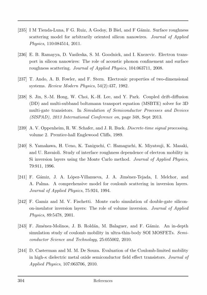
[235] I M Tienda-Luna, F G. Ruiz, A Godoy, B Biel, and F Gamiz. Surface roughness
scattering model for arbitrarily oriented silicon nanowires. Journal of Applied
Physics, 110:084514, 2011.
[236] E. B. Ramayya, D. Vasileska, S. M. Goodnick, and I. Knezevic. Electron trans-
port in silicon nanowires: The role of acoustic phonon confinement and surface
roughness scattering. Journal of Applied Physics, 104:063711, 2008.
[237] T. Ando, A. B. Fowler, and F. Stern. Electronic properties of two-dimensional
systems. Review Modern Physics, 54(2):437, 1982.
[238] S. Jin, S.-M. Hong, W. Choi, K.-H. Lee, and Y. Park. Coupled drift-diffusion
(DD) and multi-subband boltzmann transport equation (MSBTE) solver for 3D
multi-gate transistors. In Simulation of Semiconductor Processes and Devices
(SISPAD), 2013 International Conference on, page 348, Sept 2013.
[239] A. V. Oppenheim, R. W. Schafer, and J. R. Buck. Discrete-time signal processing,
volume 2. Prentice-hall Englewood Cliffs, 1989.
[240] S. Yamakawa, H. Ueno, K. Taniguchi, C. Hamaguchi, K. Miyatsuji, K. Masaki,
and U. Ravaioli. Study of interface roughness dependence of electron mobility in
Si inversion layers using the Monte Carlo method. Journal of Applied Physics,
79:911, 1996.
[241] F. Gamiz, J. A. Lopez-Villanueva, J. A. Jimenez-Tejada, I. Melchor, and
A. Palma. A comprehensive model for coulomb scattering in inversion layers.
Journal of Applied Physics, 75:924, 1994.
[242] F. Gamiz and M. V. Fischetti. Monte carlo simulation of double-gate silicon-
on-insulator inversion layers: The role of volume inversion. Journal of Applied
Physics, 89:5478, 2001.
[243] F. Jimenez-Molinos, J. B. Roldan, M. Balaguer, and F. Gamiz. An in-depth
simulation study of coulomb mobility in ultra-thin-body SOI MOSFETs. Semi-
conductor Science and Technology, 25:055002, 2010.
[244] D. Casterman and M. M. De Souza. Evaluation of the Coulomb-limited mobility
in high-κ dielectric metal oxide semiconductor field effect transistors. Journal of
Applied Physics, 107:063706, 2010.
304 References
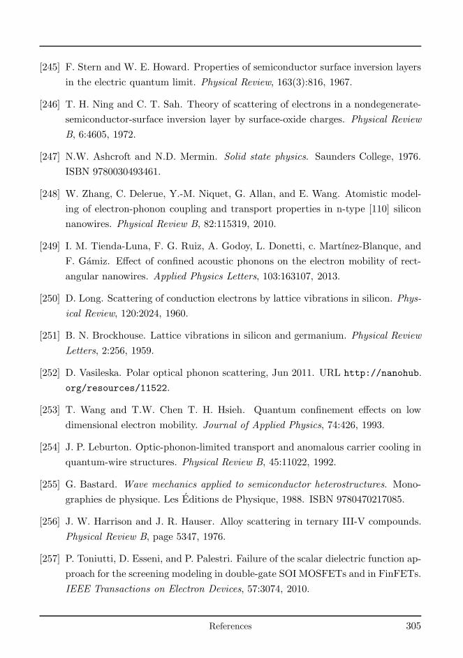
[245] F. Stern and W. E. Howard. Properties of semiconductor surface inversion layers
in the electric quantum limit. Physical Review, 163(3):816, 1967.
[246] T. H. Ning and C. T. Sah. Theory of scattering of electrons in a nondegenerate-
semiconductor-surface inversion layer by surface-oxide charges. Physical Review
B, 6:4605, 1972.
[247] N.W. Ashcroft and N.D. Mermin. Solid state physics. Saunders College, 1976.
ISBN 9780030493461.
[248] W. Zhang, C. Delerue, Y.-M. Niquet, G. Allan, and E. Wang. Atomistic model-
ing of electron-phonon coupling and transport properties in n-type [110] silicon
nanowires. Physical Review B, 82:115319, 2010.
[249] I. M. Tienda-Luna, F. G. Ruiz, A. Godoy, L. Donetti, c. Martınez-Blanque, and
F. Gamiz. Effect of confined acoustic phonons on the electron mobility of rect-
angular nanowires. Applied Physics Letters, 103:163107, 2013.
[250] D. Long. Scattering of conduction electrons by lattice vibrations in silicon. Phys-
ical Review, 120:2024, 1960.
[251] B. N. Brockhouse. Lattice vibrations in silicon and germanium. Physical Review
Letters, 2:256, 1959.
[252] D. Vasileska. Polar optical phonon scattering, Jun 2011. URL http://nanohub.
org/resources/11522.
[253] T. Wang and T.W. Chen T. H. Hsieh. Quantum confinement effects on low
dimensional electron mobility. Journal of Applied Physics, 74:426, 1993.
[254] J. P. Leburton. Optic-phonon-limited transport and anomalous carrier cooling in
quantum-wire structures. Physical Review B, 45:11022, 1992.
[255] G. Bastard. Wave mechanics applied to semiconductor heterostructures. Mono-
graphies de physique. Les Editions de Physique, 1988. ISBN 9780470217085.
[256] J. W. Harrison and J. R. Hauser. Alloy scattering in ternary III-V compounds.
Physical Review B, page 5347, 1976.
[257] P. Toniutti, D. Esseni, and P. Palestri. Failure of the scalar dielectric function ap-
proach for the screening modeling in double-gate SOI MOSFETs and in FinFETs.
IEEE Transactions on Electron Devices, 57:3074, 2010.
References 305
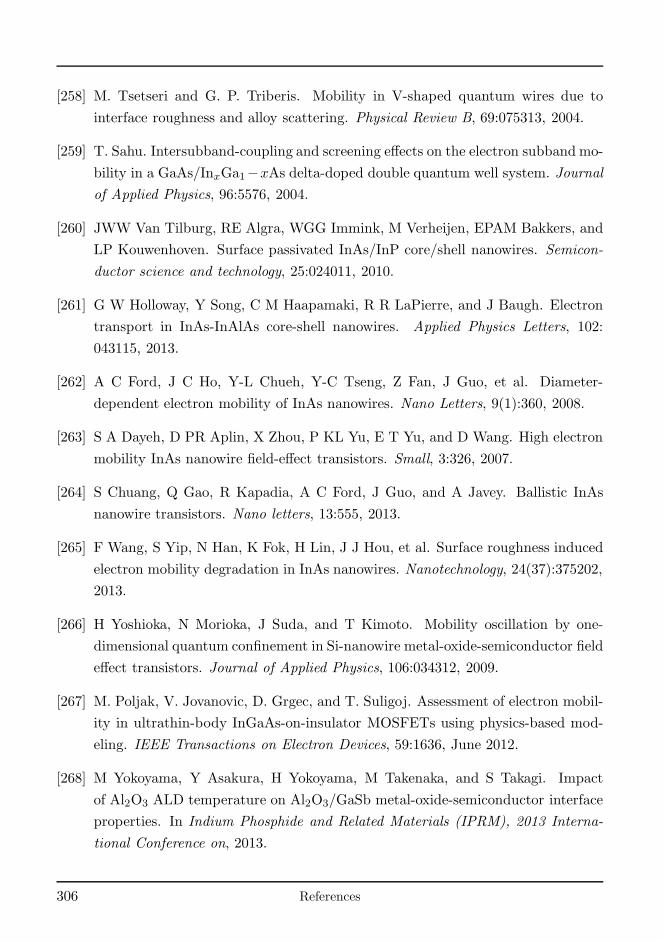
[258] M. Tsetseri and G. P. Triberis. Mobility in V-shaped quantum wires due to
interface roughness and alloy scattering. Physical Review B, 69:075313, 2004.
[259] T. Sahu. Intersubband-coupling and screening effects on the electron subband mo-
bility in a GaAs/InxGa1−xAs delta-doped double quantum well system. Journal
of Applied Physics, 96:5576, 2004.
[260] JWW Van Tilburg, RE Algra, WGG Immink, M Verheijen, EPAM Bakkers, and
LP Kouwenhoven. Surface passivated InAs/InP core/shell nanowires. Semicon-
ductor science and technology, 25:024011, 2010.
[261] G W Holloway, Y Song, C M Haapamaki, R R LaPierre, and J Baugh. Electron
transport in InAs-InAlAs core-shell nanowires. Applied Physics Letters, 102:
043115, 2013.
[262] A C Ford, J C Ho, Y-L Chueh, Y-C Tseng, Z Fan, J Guo, et al. Diameter-
dependent electron mobility of InAs nanowires. Nano Letters, 9(1):360, 2008.
[263] S A Dayeh, D PR Aplin, X Zhou, P KL Yu, E T Yu, and D Wang. High electron
mobility InAs nanowire field-effect transistors. Small, 3:326, 2007.
[264] S Chuang, Q Gao, R Kapadia, A C Ford, J Guo, and A Javey. Ballistic InAs
nanowire transistors. Nano letters, 13:555, 2013.
[265] F Wang, S Yip, N Han, K Fok, H Lin, J J Hou, et al. Surface roughness induced
electron mobility degradation in InAs nanowires. Nanotechnology, 24(37):375202,
2013.
[266] H Yoshioka, N Morioka, J Suda, and T Kimoto. Mobility oscillation by one-
dimensional quantum confinement in Si-nanowire metal-oxide-semiconductor field
effect transistors. Journal of Applied Physics, 106:034312, 2009.
[267] M. Poljak, V. Jovanovic, D. Grgec, and T. Suligoj. Assessment of electron mobil-
ity in ultrathin-body InGaAs-on-insulator MOSFETs using physics-based mod-
eling. IEEE Transactions on Electron Devices, 59:1636, June 2012.
[268] M Yokoyama, Y Asakura, H Yokoyama, M Takenaka, and S Takagi. Impact
of Al2O3 ALD temperature on Al2O3/GaSb metal-oxide-semiconductor interface
properties. In Indium Phosphide and Related Materials (IPRM), 2013 Interna-
tional Conference on, 2013.
306 References
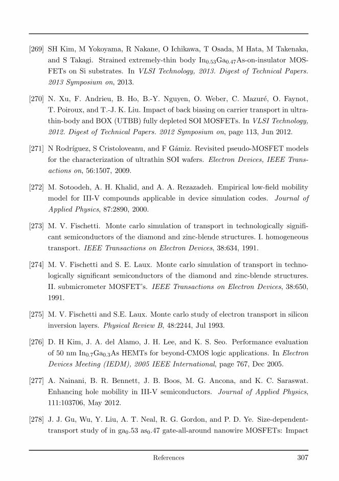
[269] SH Kim, M Yokoyama, R Nakane, O Ichikawa, T Osada, M Hata, M Takenaka,
and S Takagi. Strained extremely-thin body In0.53Ga0.47As-on-insulator MOS-
FETs on Si substrates. In VLSI Technology, 2013. Digest of Technical Papers.
2013 Symposium on, 2013.
[270] N. Xu, F. Andrieu, B. Ho, B.-Y. Nguyen, O. Weber, C. Mazure, O. Faynot,
T. Poiroux, and T.-J. K. Liu. Impact of back biasing on carrier transport in ultra-
thin-body and BOX (UTBB) fully depleted SOI MOSFETs. In VLSI Technology,
2012. Digest of Technical Papers. 2012 Symposium on, page 113, Jun 2012.
[271] N Rodrıguez, S Cristoloveanu, and F Gamiz. Revisited pseudo-MOSFET models
for the characterization of ultrathin SOI wafers. Electron Devices, IEEE Trans-
actions on, 56:1507, 2009.
[272] M. Sotoodeh, A. H. Khalid, and A. A. Rezazadeh. Empirical low-field mobility
model for III-V compounds applicable in device simulation codes. Journal of
Applied Physics, 87:2890, 2000.
[273] M. V. Fischetti. Monte carlo simulation of transport in technologically signifi-
cant semiconductors of the diamond and zinc-blende structures. I. homogeneous
transport. IEEE Transactions on Electron Devices, 38:634, 1991.
[274] M. V. Fischetti and S. E. Laux. Monte carlo simulation of transport in techno-
logically significant semiconductors of the diamond and zinc-blende structures.
II. submicrometer MOSFET’s. IEEE Transactions on Electron Devices, 38:650,
1991.
[275] M. V. Fischetti and S.E. Laux. Monte carlo study of electron transport in silicon
inversion layers. Physical Review B, 48:2244, Jul 1993.
[276] D. H Kim, J. A. del Alamo, J. H. Lee, and K. S. Seo. Performance evaluation
of 50 nm In0.7Ga0.3As HEMTs for beyond-CMOS logic applications. In Electron
Devices Meeting (IEDM), 2005 IEEE International, page 767, Dec 2005.
[277] A. Nainani, B. R. Bennett, J. B. Boos, M. G. Ancona, and K. C. Saraswat.
Enhancing hole mobility in III-V semiconductors. Journal of Applied Physics,
111:103706, May 2012.
[278] J. J. Gu, Wu, Y. Liu, A. T. Neal, R. G. Gordon, and P. D. Ye. Size-dependent-
transport study of in ga0.53 as0.47 gate-all-around nanowire MOSFETs: Impact
References 307
of quantum confinement and volume inversion. IEEE Electron Device Letters, 33:
967, Jul 2012.
[279] Y. Yuan, B. Yu, J. Song, and Y. Taur. An analytic model for threshold voltage
shift due to quantum confinement in surrounding gate MOSFETs with anisotropic
effective mass. Solid State Electronics, 53:140, Jan 2009.
[280] T. Bryllert, L. E. Wernersson, L. E. Froberg, and L. Samuelson. Vertical high-
mobility wrap-gated InAs nanowire transistor. IEEE Electron Device Letters, 27:
323, 2006.
[281] R. Granzner, S. Thiele, C. Schippel, and F. Schwierz. Quantum effects on the gate
capacitance of trigate SOI MOSFETs. IEEE Transactions on Electron Devices,
57:3231, Dec 2010.
[282] A. Ali, H. Madan R. Misra, A. Agrawal, P. Schiffer, B.R. Bennett, and S. Datta.
Experimental determination of quantum and centroid capacitance in arsenide-
antimonide quantum-well MOSFETs incorporating nonparabolicity effect. IEEE
Transactions on Electron Devices, 58:1397, May 2011.
[283]
[284] R. Chau, B. Doyle, S. Datta, J. Kavalieros, and K. Zhang. Integrated nanoelec-
tronics for the future. Nature Materials, 6:810, Nov 2007.
[285] I. Ferain, C. A. Colinge, and J.P. Colinge. Multigate transistors as the future of
classical metal-oxide-semiconductor field-effect transistors. Nature, 410:310, Nov
2010.
[286] R. Chau, S. Datta, M. Doczy, B. Doyle, B. Jin, J. Kavalieros, A. Majum-
dar, M. Metz, and M. Radosavljevic. Benchmarking nanotechnology for high-
performance and low-power logic transistor applications. IEEE Transactions on
Nanotechnology, 4:153, Mar 2005.
[287] H. Werner and G. Raymann. An approximation to the fermi integral f1/2(x).
Mathematical Computing, 17:193, Mar 1963.
[288] K. Terada, K. Nishiyama, and K.-I. Hatanaka. Comparison of MOSFET-
threshold-voltage extraction methods. Solid-State Electronics, 45:35, Jan 2001.
308 References
[289] G.N. Watson. A treatise on the theory of Bessel functions. Cambridge University
Press, Cambridge. UK, 1966. ISBN 0521483913.
[290] J. P. Colinge, J.W. Park, and W. Xiong. Threshold voltage and subthreshold
slope of multiple-gate SOI MOSFETs. IEEE Electron Device Letters, 24:515,
Aug 2003.
[291] Y. Nishi, K. Tanaka, and A. Ohwada. Study of silicon-silicon dioxide structure
by electron spin resonance. Japanese Journal of Applied Physics, 11:85, Jul 1972.
[292] Y. Tsividis and C. McAndrew. Operation and Modeling of the MOS Transistor.
Oxford University Press, Oxford. UK, 2010. ISBN 0195170156.
[293] C. Dupre, A. Hubert, S. Becu, M. Jublot, V. Maffini-Alvaro, C. Vizioz, et al.
15nm-diameter 3D stacked nanowires with independent gates operation: φ FET.
In Electron Devices Meeting (IEDM), 2008 IEEE International, Dec 2008.
[294] C. Dupre, T. Ernst, S. Borel, Y. Morand, S. Descombes, B. Guillaumot, et al.
Impact of isotropic plasma etching on channel Si surface roughness measured with
AFM and on NMOS inversion layer mobility. In 9th International Conference on
Ultimate Integration of Silicon, page 133, 2008.
[295] C. Dupre, T. Ernst, V. Maffini-Alvaro, V. Delaye, J.-M. Hartmann, S. Borel,
et al. 3D nanowire gate-all-around transistors: Specific integration and electrical
features. Solid-State Electronics, 52:519, 2008.
[296] T. Ernst, E. Bernard, C. Dupre, A. Hubert, S. Becu, B. Guillaumot, et al. 3D
multichannels and stacked nanowires technologies for new design opportunities in
nanoelectronics. In Integrated Circuit Design and Technology and Tutorial, 2008.
ICICDT 2008. IEEE International Conference on, pages 265–268, Jun 2008.
[297] M.V. Fischetti, T.P. O’Regan, N. Sudarshan, C. Sachs, S. Jin, J. Kim, and
Y. Zhang. Theoretical study of some physical aspects of electronic transport in
nMOSFETs at the 10-nm gate-length. IEEE Transactions on Electron Devices,
54:2116, Sept 2007.
[298] J.M. Hinckley and J. Singh. Influence of substrate composition and crystallo-
graphic orientation on the band structure of pseudomorphic Si-Ge alloy films.
Physical Review B, 42(6):3546, 1990.
References 309
[299] L. Lin and J. Robertson. Defect states at III-V semiconductor oxide interfaces.
App. Phys. Let., 98:082903, 2011.
[300] S. Takagi, A. Toriumi, M. Iwase, and H. Tango. On the universality of inversion
layer mobility in Si MOSFETs: Part II - effects of surface orientation. IEEE
Transactions on Electronic Devices, 41(12):2363, 1994.
[301] S. Takagi, J. Koga, and A. Toriumi. Subband structure engineering for perfor-
mance enhancement of Si MOSFETs. In Electron Devices Meeting (IEDM), 1997
IEEE International, page 219, 1997.
[302] N. Takiguchi, S. Koba, H. Tsuchiya, and Matsuto Ogawa. Comparisons of per-
formance potentials of Si and InAs nanowire MOSFETs under ballistic transport.
IEEE Transactions on Electron Devices, 59:206, Jan 2012.
[303] Y. Sun, S.E. Thompson, and T. Nishida. Physics of strain effects in semiconduc-
tors and metal-oxide-semiconductor field-effect transistors. Journal of Applied
Physics, 101:104503, 2007.
[304] I. M. Tienda-Luna, F. J. Garcia Ruiz, A. Godoy, and F. Gamiz. The influence of
orientation and strain on the transport properties of SOI trigate nMOSFETs. In
Solid State Device Research Conference, 2009. ESSDERC’09. Proceedings of the
European, 2009.
[305] K. Uchida, T. Krishnamohan, K. C. Saraswat, and Y. Nishi. Physical mecha-
nisms of electron mobility enhancement in uniaxial stressed MOSFETs and im-
pact of uniaxial stress engineering in ballistic regime. In Electron Devices Meeting
(IEDM), 2005 IEEE International, page 135, 2005.
[306] C. Auth, C. Allen, A. Blattner, D. Bergstrom, M. Brazier, M. Bost, et al. A 22nm
high performance and low-power CMOS technology featuring fully-depleted tri-
gate transistors, self-aligned contacts and high density mim capacitors. In VLSI
Technology, 2012. Digest of Technical Papers. 2012 Symposium on, page 131, Jun
2012.
[307] R.V. Booth, M.H. White, H.-S. Wong, and T.J. Krutsick. The effect of channel
implants on MOS transistor characterization. IEEE Transactions on Electron
Devices, 34:2501, Dec 1987.
310 References
[308] O. Moldovan, D. Jimenez, J.R. Guitart, F.A. Chaves, and B. Iniguez. Explicit
analytical charge and capacitance models of undoped double-gate MOSFETs.
IEEE Transactions on Electron Devices, 54:1718, Jul 2007.
[309] M. K. Hudait, G. Dewey, S. Datta, J. M. Fastenau, J. Kavalieros, W. K. Liu, et al.
As quantum well transistor on silicon substrate using thin (< 2µm) composite
buffer architecture for high-speed and low-voltage (0.5V) logic applications. In
Electron Devices Meeting (IEDM), 2007 IEEE International, page 625, Dec 2005.
[310] DLMF. NIST Digital Library of Mathematical Functions. http://dlmf.nist.gov/,
Release 1.0.6 of 2013-05-06. URL http://dlmf.nist.gov/. Online companion to
[221].
[311] W. Monch. Metal-semiconductor contacts: Electronics properties. Surface Sci-
ence, 300:928, 1994.
[312] C. Tejedor, F. Flores, and E. Louis. The metal-semiconductor interface: Si (111)
and zincblende (110) junctions. Journal of Physics C: Solid State Physics, 10:
2163, 1977.
[313] T. V. Perevalov, V. A. Gritsenko, and V. V. Kaichev. Electronic structure of
aluminum oxide: ab initio simulations of α and γ phases and comparison with
experiment for amorphous films. The European Physical Journal Applied Physics,
52, Dec 2010.
[314] S. Meng, C. Basceri, B. W. Busch, G. Derderian, and G. Sandhu. Leakage
mechanisms and dielectric properties of Al2O3/TiN-based metal-insulator-metal
capacitors. Applied Physics Letters, 83:4429, Nov 2003.
[315] B.G. Stretman. Solid State Electronic Devices. Pearson Education, Limited,
1972. ISBN 9780138220235.
[316] Intels revolutionary 22 nm transistor technology. On-
line. URL http://www.intel.com/content/www/us/en/energy/
intel-22nm-3-d-tri-gate-transistor-technology.html. Accessed: 2014-
07-04.
[317] J. Bardeen and W. Shockley. Deformation potentials and mobilities in non-polar
crystal. Physical Review, 80(1):72, 1950.
References 311
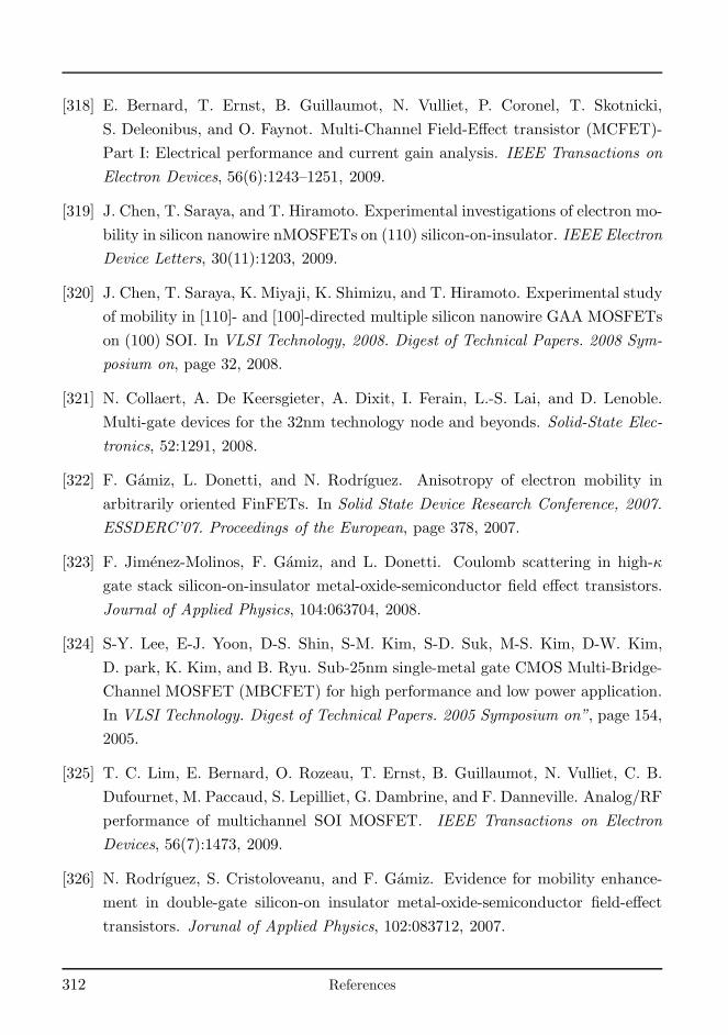
[318] E. Bernard, T. Ernst, B. Guillaumot, N. Vulliet, P. Coronel, T. Skotnicki,
S. Deleonibus, and O. Faynot. Multi-Channel Field-Effect transistor (MCFET)-
Part I: Electrical performance and current gain analysis. IEEE Transactions on
Electron Devices, 56(6):1243–1251, 2009.
[319] J. Chen, T. Saraya, and T. Hiramoto. Experimental investigations of electron mo-
bility in silicon nanowire nMOSFETs on (110) silicon-on-insulator. IEEE Electron
Device Letters, 30(11):1203, 2009.
[320] J. Chen, T. Saraya, K. Miyaji, K. Shimizu, and T. Hiramoto. Experimental study
of mobility in [110]- and [100]-directed multiple silicon nanowire GAA MOSFETs
on (100) SOI. In VLSI Technology, 2008. Digest of Technical Papers. 2008 Sym-
posium on, page 32, 2008.
[321] N. Collaert, A. De Keersgieter, A. Dixit, I. Ferain, L.-S. Lai, and D. Lenoble.
Multi-gate devices for the 32nm technology node and beyonds. Solid-State Elec-
tronics, 52:1291, 2008.
[322] F. Gamiz, L. Donetti, and N. Rodrıguez. Anisotropy of electron mobility in
arbitrarily oriented FinFETs. In Solid State Device Research Conference, 2007.
ESSDERC’07. Proceedings of the European, page 378, 2007.
[323] F. Jimenez-Molinos, F. Gamiz, and L. Donetti. Coulomb scattering in high-κ
gate stack silicon-on-insulator metal-oxide-semiconductor field effect transistors.
Journal of Applied Physics, 104:063704, 2008.
[324] S-Y. Lee, E-J. Yoon, D-S. Shin, S-M. Kim, S-D. Suk, M-S. Kim, D-W. Kim,
D. park, K. Kim, and B. Ryu. Sub-25nm single-metal gate CMOS Multi-Bridge-
Channel MOSFET (MBCFET) for high performance and low power application.
In VLSI Technology. Digest of Technical Papers. 2005 Symposium on”, page 154,
2005.
[325] T. C. Lim, E. Bernard, O. Rozeau, T. Ernst, B. Guillaumot, N. Vulliet, C. B.
Dufournet, M. Paccaud, S. Lepilliet, G. Dambrine, and F. Danneville. Analog/RF
performance of multichannel SOI MOSFET. IEEE Transactions on Electron
Devices, 56(7):1473, 2009.
[326] N. Rodrıguez, S. Cristoloveanu, and F. Gamiz. Evidence for mobility enhance-
ment in double-gate silicon-on insulator metal-oxide-semiconductor field-effect
transistors. Jorunal of Applied Physics, 102:083712, 2007.
312 References
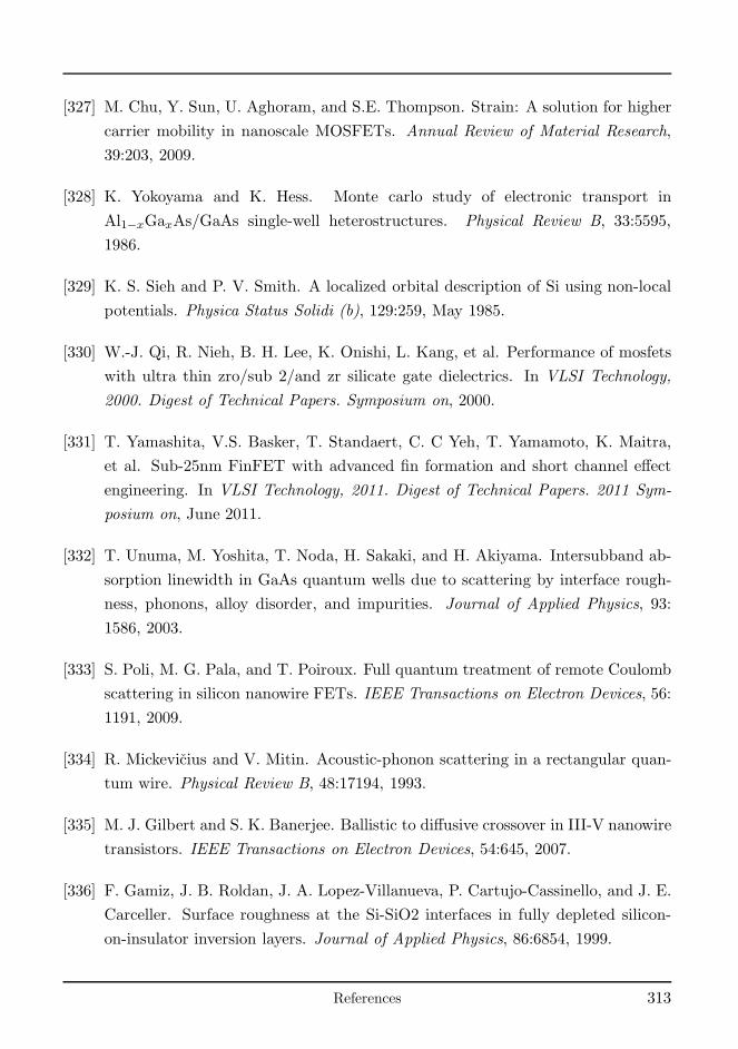
[327] M. Chu, Y. Sun, U. Aghoram, and S.E. Thompson. Strain: A solution for higher
carrier mobility in nanoscale MOSFETs. Annual Review of Material Research,
39:203, 2009.
[328] K. Yokoyama and K. Hess. Monte carlo study of electronic transport in
Al1−xGaxAs/GaAs single-well heterostructures. Physical Review B, 33:5595,
1986.
[329] K. S. Sieh and P. V. Smith. A localized orbital description of Si using non-local
potentials. Physica Status Solidi (b), 129:259, May 1985.
[330] W.-J. Qi, R. Nieh, B. H. Lee, K. Onishi, L. Kang, et al. Performance of mosfets
with ultra thin zro/sub 2/and zr silicate gate dielectrics. In VLSI Technology,
2000. Digest of Technical Papers. Symposium on, 2000.
[331] T. Yamashita, V.S. Basker, T. Standaert, C. C Yeh, T. Yamamoto, K. Maitra,
et al. Sub-25nm FinFET with advanced fin formation and short channel effect
engineering. In VLSI Technology, 2011. Digest of Technical Papers. 2011 Sym-
posium on, June 2011.
[332] T. Unuma, M. Yoshita, T. Noda, H. Sakaki, and H. Akiyama. Intersubband ab-
sorption linewidth in GaAs quantum wells due to scattering by interface rough-
ness, phonons, alloy disorder, and impurities. Journal of Applied Physics, 93:
1586, 2003.
[333] S. Poli, M. G. Pala, and T. Poiroux. Full quantum treatment of remote Coulomb
scattering in silicon nanowire FETs. IEEE Transactions on Electron Devices, 56:
1191, 2009.
[334] R. Mickevicius and V. Mitin. Acoustic-phonon scattering in a rectangular quan-
tum wire. Physical Review B, 48:17194, 1993.
[335] M. J. Gilbert and S. K. Banerjee. Ballistic to diffusive crossover in III-V nanowire
transistors. IEEE Transactions on Electron Devices, 54:645, 2007.
[336] F. Gamiz, J. B. Roldan, J. A. Lopez-Villanueva, P. Cartujo-Cassinello, and J. E.
Carceller. Surface roughness at the Si-SiO2 interfaces in fully depleted silicon-
on-insulator inversion layers. Journal of Applied Physics, 86:6854, 1999.
References 313
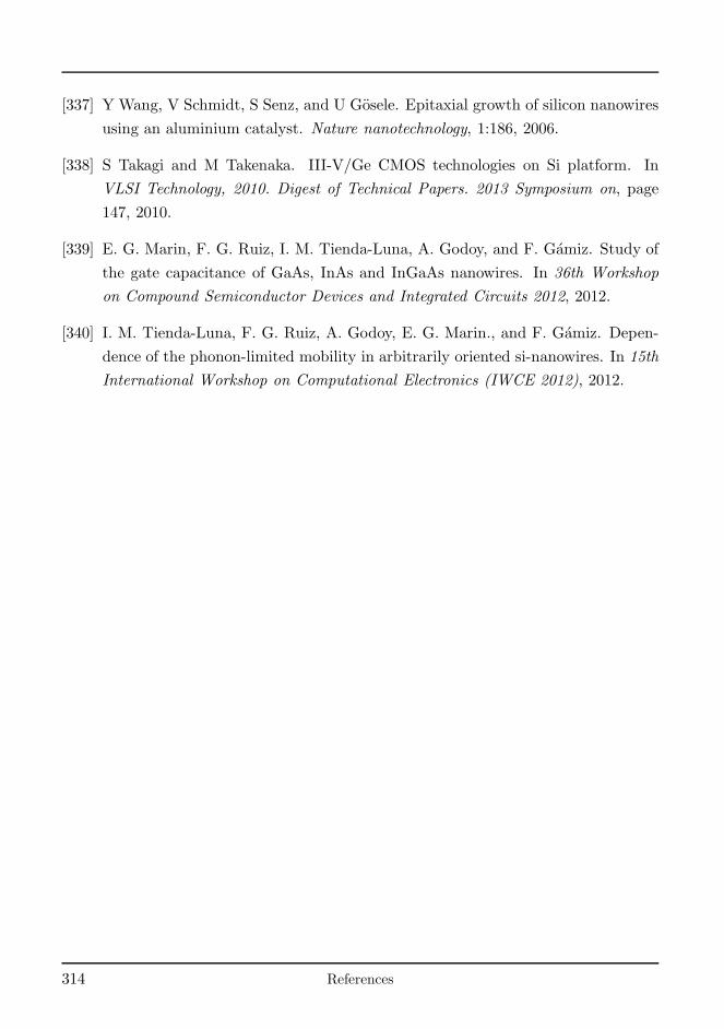
[337] Y Wang, V Schmidt, S Senz, and U Gosele. Epitaxial growth of silicon nanowires
using an aluminium catalyst. Nature nanotechnology, 1:186, 2006.
[338] S Takagi and M Takenaka. III-V/Ge CMOS technologies on Si platform. In
VLSI Technology, 2010. Digest of Technical Papers. 2013 Symposium on, page
147, 2010.
[339] E. G. Marin, F. G. Ruiz, I. M. Tienda-Luna, A. Godoy, and F. Gamiz. Study of
the gate capacitance of GaAs, InAs and InGaAs nanowires. In 36th Workshop
on Compound Semiconductor Devices and Integrated Circuits 2012, 2012.
[340] I. M. Tienda-Luna, F. G. Ruiz, A. Godoy, E. G. Marin., and F. Gamiz. Depen-
dence of the phonon-limited mobility in arbitrarily oriented si-nanowires. In 15th
International Workshop on Computational Electronics (IWCE 2012), 2012.
314 References