UNIT I - fmcet
145
UNIT I THE8085AND8086MICROPROCESSORS (9) 8085Microprocessorarchitecture-Addressingmodes-Instructionset-Programmingthe8085 1 INTRODUCTIONTOMICROPROCESSORBASEDSYSTEM The microprocessor is a semiconductor device(Integrated Circuit) manufactured by the VLSI(Very Large Scale Integration) technique. It includes the ALU, register arrays and control circuit on a single chip.To perform a function or useful task we have to form a system by using microprocessor as a CPU and interfacing memory, input and output devices to it. A system designed using a microprocessor as its CPU is called a microcomputer. The Microprocessor based system(single board microcomputer)consists of microprocessor as CPU, semiconductor memories like EPROM and RAM, input device, output device and interfacing devices.The memories, input device, output device and interfacing devices are called peripherals. The popular input devices are keyboard and floppy disk and the output devices are onitor .The above block diag ramshows the organization O F a microprocessor based system. In this system, the microprocessor is the master and all other peripherals are slaves. The master controls all the peripherals andinitiatesall operations. The work done bythe processor can be classified into the following three groups. 1.Work done internal tothe processor 2.Work done externaltothe processor 3.Operations initiated by the slaves or peripherals. Theworkdoneinternaltothe processors is addition,subtraction,logical operations, datatransfer Operations, etc.The workdone external totheprocessor are reading/writingthe memoryand Reading/writing theJ/Odevices ortheperipherals. If the peripheralrequires the attentionofthe master thenit caninterruptthe master andinitiate an operation. Themicroprocessoristhemaster, which controls allthe activities ofthesystem.To performa specificjob or task, the microprocessorhasto executea programstored in memory. The program consists ofa set of instructions. It issues address and control signalsandfetches the instruction and datafrommemory. The instructionisexecuted one byone internal totheprocessor and based on theresult ittakes appropriateaction. BUSES: Thebuses are group oflines that carries data,addressor control signals.
-
Upload
khangminh22 -
Category
Documents
-
view
2 -
download
0
Transcript of UNIT I - fmcet
UNIT I
THE8085AND8086MICROPROCESSORS (9)
8085Microprocessorarchitecture-Addressingmodes-Instructionset-Programmingthe8085
1 INTRODUCTIONTOMICROPROCESSORBASEDSYSTEM
The microprocessor is a semiconductor device(Integrated Circuit)
manufactured by the VLSI(Very Large Scale Integration) technique. It includes the ALU,
register arrays and control circuit on a single chip.To perform a function or useful task
we have to form a system by using microprocessor as a CPU and interfacing memory,
input and output devices to it. A system designed using a microprocessor as its CPU is
called a microcomputer. The Microprocessor based system(single board
microcomputer)consists of microprocessor as CPU, semiconductor memories like
EPROM and RAM, input device, output device and interfacing devices.The memories,
input device, output device and interfacing devices are called peripherals. The popular
input devices are keyboard and floppy disk and the output devices are
printer, LED/LCDdisplays, CRT monitor .The above block diag ramshows the organization O F a microprocessor based system. In this
system, the microprocessor is the master and all other peripherals are slaves. The
master controls all the peripherals andinitiatesall operations.
The work done bythe processor can be classified into the following three groups.
1.Work done internal tothe processor
2.Work done externaltothe processor
3.Operations initiated by the slaves or peripherals.
Theworkdoneinternaltothe processors is addition,subtraction,logical operations,
datatransfer Operations, etc.The workdone external totheprocessor are
reading/writingthe memoryand Reading/writing theJ/Odevices ortheperipherals. If the
peripheralrequires the attentionofthe master thenit caninterruptthe master andinitiate an
operation.
Themicroprocessoristhemaster, which controls allthe activities ofthesystem.To performa
specificjob or task, the microprocessorhasto executea programstored in memory. The
program consists ofa set of instructions. It issues address and control signalsandfetches
the instruction and datafrommemory. The instructionisexecuted one byone internal
totheprocessor and based on theresult ittakes appropriateaction.
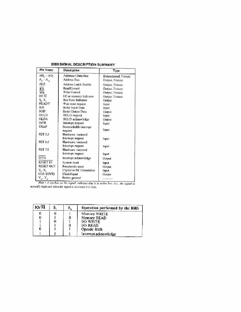
BUSES:
Thebuses are group oflines that carries data,addressor control signals.
· The CPU Bus has multiplexed lines, i.e., same line is used to carry different signals.
TheCPUinterface is provided todemultiplex the multiplexedlines,to generate chip select
signalsand additional control signals.
· The system bus has separate lines for each signal.
All the slavesin the systemareconnected tothe same system bus. At anytime instant
communication takes placebetween the masterand oneof.the slaves. All the slaves have
tristatelogic andhence normallyremain in high impedance state. Onlywhentheslave is
selectedit.
· The EPROM memoryis used to storepermanent programs and data. · The RAM
memoryis used to store temporaryprograms and data.
· The inputdeviceis usedto enterthe program, dataand to operatethe system.
· The outputdeviceis usedfor examiningtheresults.
microprocessor, an
interface
device is provided betweensystembus and I/Odevices. Generally I/O devices are slow
devices.
Advantages of Microprocessorbasedsystem
1.Computational/processingspeed ishigh.
2.Intelligence has been brought to systems.
3.Automationofindustrialprocesses andoffice administration.
4.Since the devices are programmable, there is flexibilityto
alterthesystembychangingthe softwarealone.
5.Lessnumber of components, compact in size and cost less. Alsoitis more reliable.
6.Operation andmaintenance are easier.
Disadvantages of Microprocessor based System
1.It has limitations on the size of data.
2.The applications arelimited bythephysical addressspace.
3.The analogsignals cannot be processed directlyanddigitizingthe analogsignals
introduces errors.
4.The speed of execution is slowand so realtime applications are not possible.
5.Most of the microprocessorsdoesnotsupportfloatingpoint operations.
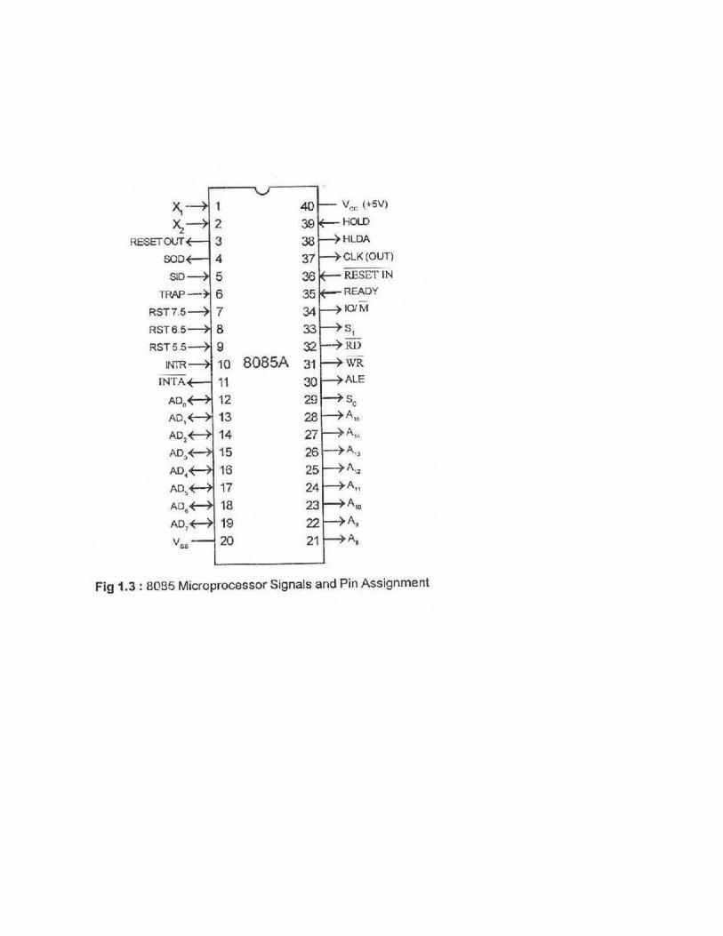
8085 Microprocessor:
The salientfeaturesof 8085 μp are:
• It is a8 bit microprocessor.
• It is manufactured with N-MOS technology.
• It has 16-bit address bus and hence can address upto216 = 65536
bytes(64KB)memory locationsthrough A0-A15.
•Thefirst 8lines of address bus and 8lines of data bus aremultiplexed AD0 – AD7.
•Data bus is a group of 8lines D0 – D7.
• It supportsexternalinterrupt request.
•A16 bitprogramcounter(PC)
•A16 bitstackpointer (SP)
•Six 8-bit general purposeregisterarranged inpairs: BC, DE, HL.
• It requires asignal+5V power supplyand operates at3.2 MHZsingle phaseclock.
• It is enclosed with40 pinsDIP (Dual inline package).
ARCHITECTURE:
OPERATIONSPERFORMEDBY 8085
The ALUperforms thearithmetic andlogical operations.The operations performed
byALUof 8085 are addition, subtraction,increment, decrement, logical AND, OR, EXCL
U8IVE -OR, compare,complement and left /right shift.Theaccumulatorand temporary
registerareusedto holdthedataduringan arithmetic/logical operation. Afteranoperation the
resultisstoredintheaccumulator and the flags are set orreset accordingto the result of the operation.
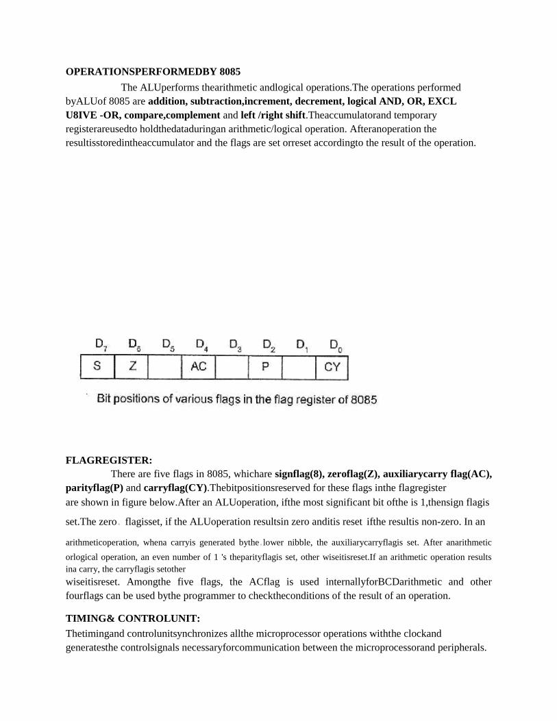
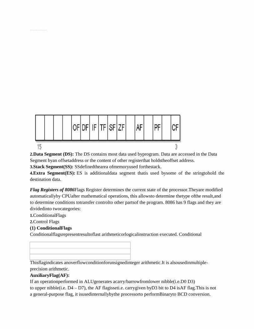
FLAGREGISTER:
There are five flags in 8085, whichare signflag(8), zeroflag(Z), auxiliarycarry flag(AC),
parityflag(P) and carryflag(CY).Thebitpositionsreserved for these flags inthe flagregister
are shown in figure below.After an ALUoperation, ifthe most significant bit ofthe is 1,thensign flagis
set.The zero. flagisset, if the ALUoperation resultsin zero anditis reset ifthe resultis non-zero. In an
arithmeticoperation, whena carryis generated bythe.lower nibble, the auxiliarycarryflagis set. After anarithmetic
orlogical operation, an even number of 1 's theparityflagis set, other wiseitisreset.If an arithmetic operation results
ina carry, the carryflagis setother
wiseitisreset. Amongthe five flags, the ACflag is used internallyforBCDarithmetic and other
fourflags can be used bythe programmer to checktheconditions of the result of an operation.
TIMING& CONTROLUNIT:
Thetimingand controlunitsynchronizes allthe microprocessor operations withthe clockand
generatesthe controlsignals necessaryforcommunication between the microprocessorand peripherals.
INSTRUCTIONREGISTER& DECODER:
Whenan instruction is fetched frommemoryit is placed ininstructionregister.Then it is decoded and
encodedinto various machine cycles.
REGISTERARRAY:
·ApartfromAccumulator (A-register),there are six general-purpose programmable registers B, C, D,
E, Hand L.
·Theycan be usedas 8-bitregistersor pairedto store l6-bit data.The allowed pairs areB-C,D-E and H-L.
·The temporaryregistersW and Zareintended forinternaluse ofthe processorand it cannot be used
bythe programmer.
STACK POINTER(SP):
Thestackpointer SP, holdsthe address ofthe stacktop. The stackisa sequence ofRAM
memorylocations definedbythe programmer.The stackis usedtosave the content of
registersduringtheexecution of aprogram.
PROGRAM COUNTER(PC):
Theprogramcounter(PC)keeps trackof programexecution.Toexecutea programthe
startingaddress ofthe programis loadedin programcounter.ThePCsends out an addressto fetch a
byteofinstructionfrommemoryand incrementitscontent automatically. Hence, when a byte of
instruction is fetched, the PCholdstheaddress of the next byteofthe instruction or next instruction.
Memory
•Program, data andstackmemories occupythe same memoryspace.The total addressable memorysize
is 64KB.
•Program memory -programcan belocatedanywhere in memory. Jump, branch and call instructions
use 16-bitaddresses, i.e. theycan beusedtojump/branchanywherewithin 64KB. Alljump/branch
instructions useabsolute addressing.
•Data memory -the processoralways uses 16-bit addresses so that data can be placed anywhere.
•Stackmemoryislimitedonlybythe size of memory. Stackgrows downward.
•First 64bytes in a zero memorypage should bereserved for vectors used byRSTinstructions.
Interrupts
•Theprocessor has 5interrupts.Theyare presented belowintheorder of their priority(from lowest
tohighest):
•INTRis maskable 8080Acompatible interrupt.When the.interrupt occursthe processorfetches
fromthe bus oneinstruction, usuallyone ofthese instructions:
•One ofthe 8 RSTinstructions(RST0 -RST7).The processor. saves current programcounter
intostackand branchestomemory location N*8 (where Nis a3-bit number from0 to 7 supplied withthe
RST instruction).
•CALLinstruction(3 byteinstruction).The processorcallsthesubroutine,address of whichis
specifiedinthe secondandthird bytesoftheinstruction.
•RST5.5 is a maskableinterrupt.Whenthisinterruptis received the processorsaves the contents of the
PCregister intostackand branchesto 2CH(hexadecimal)address.
•RST6.5 is a maskableinterrupt.Whenthisinterruptis received the processorsaves the contents of the
PCregister intostackand branchesto 34H(hexadecimal)address.
•RST7.5 is a maskableinterrupt.Whenthisinterruptis received the processorsaves the contents of the
PCregister intostackand branches to 3CH(hexadecimal)address.
•TRAP isa non-maskableinterrupt.When thisinterrupt is received theprocessorsaves the contentsofthe
PCregisterinto stackandbranches to24H(hexadecimal) address.
•All maskable interruptscan be enabled ordisabled usingEIand DIinstructions.RST 5.5, RST6.5and
RST7.5interrupts can beenabledor disabled individuallyusingSIM instruction.
Reset Signals
•RESETIN: Whenthis signal goes low, the programcounter(PC)is setto Zero,μp isreset and
resetstheinterrupt enable and HLDAflip-flops.
•Thedata and address buses andthecontrol linesare 3-stated duringRESET andbecause of
asynchronous nature of RESET,the processorinternalregistersandflags maybe alteredby RESET with
unpredictableresults.
•RESET INis a Schmitt-triggered input,allowingconnectionto an R-Cnetworkfor power-onRESET
delay.
•Upon power-up, RESET INmust remain lowfor at least 10 ms after minimumVcc has been reached.
•For properresetoperationafterthepower –up duration, RESET INshouldbe keptlowa minimumof
three clockperiods.
•TheCPUis heldinthereset condition aslongas RESET INis applied.Typical Power-onRESET
RCvalues R1 = 75KΩ, C1 = 1μF.
•RESETOUT: Thissignal indicates that μpisbeingreset.This signal can be used to reset other
devices.The signal is synchronizedtothe processor clockand lastsanintegral number of clock periods.
Serial communication Signal
•SID- Serial Input DataLine:The data on thislineis loaded into accumulatorbit 7whenevera RIM
instruction is executed.
•SOD– Serial OutputData Line:The SIM instruction loadsthe value ofbit 7 of the
accumulatorintoSODlatch if bit 6 (SOE) oftheaccumulator is 1.
DMASignals
•HOLD: Indicates thatanothermasterisrequestingthe use ofthe addressand data buses.The CPU, upon
receivingthe hold request, will relinquishthe useofthe bus as soonasthe completion of the current
bustransfer.
•Internal processingcan continue.Theprocessorcanregain/the busonlyafter theHOLDis removed.
•Whenthe HOLDis acknowledged, the Address, Data.RD, WRand IO/M linesare 3-stated.
•HLDA: Hold Acknowledge: Indicates the CPUhas received the HOLDrequestandthat it
willrelinquish the bus inthe next clock cycle.
•HLDAgoes lowaftertheHold requestis removed. The CPUtakesthe bus onehalf-clockcycleafter
HLDAgoes low.
•READY:This signal Synchronizes the fast CPUandthe slowmemory, peripherals.
•If READYis high duringa read or write cycle, itindicates thatthememoryor peripheralis readytosend
orreceive data.
•If READYis low, the CPUwill wait anintegral number of clockcycle for READYto go high before
completingthe reador writecycle.
•READY must conformto specifiedsetup and hold times.
Registers
•Accumulator orAregister is an8-bit registerusedfor arithmetic,logic, I/Oandload/store operations.
•Flag Register hasfive 1-bitflags.
•Sign -set if the most significantbit oftheresult is set.
•Zero -set if the resultis zero.
•Auxiliarycarry -set ifthere was a carryout frombit3 to bit4 oftheresult.
•Parity -set if the parity(the number ofsetbitsin theresult) is even.
•Carry -set if therewas acarryduringaddition, or borrowduring subtraction/comparison/rotation.
General Registers
• 8-bitB and 8-bit Cregisterscan be usedasone 16-bit BC register pair. When used asa pair the C
register containslow-order byte. Some instructionsmayuse BC register asa data pointer.
•8-bitDand 8-bit Eregisterscan be usedasone 16-bit DE register pair. When used asa pair
theEregistercontainslow-order byte.Some instructionsmayuse DE registerasa data pointer.
•8-bitHand 8-bit Lregisterscan be usedasone 16-bit HLregister pair. When used asa pair the
Lregister containslow-order byte. HLregister usuallycontainsa data pointer used to reference
memoryaddresses.
•Stackpointer isa 16 bitregister. Thisregister isalwaysdecremented/incrementedby2 duringpush and
pop.
•Programcounter isa 16-bit register.
INSTRUCTIONEXECUTIONANDDATAFLOW in 8085
The programinstructions are stored in memory, which is anexternal device.Toexecute a
programin 8085,the startingaddress of the programshould beloaded in programcounter.The 8085
output the content ofprogramcounter inaddressbus andassertsreadcontrolsignallow.
Also,the programcounter is incremented.The addressand the read controlsignalenable the
memoryto outputthecontent of memory location onthe data bus. Nowthe content ofdata bus is
the opcodeof an instruction. The read controlsignalismade high bytimingand control unitafter a
specified time. At therisingedge of readcontrol signals,.theopcode is latchedinto microprocessor
internal busand placed ininstruction register.
Theinstruction-decodingunit,decodestheinstructions.and providesinformationto timingand
controlunit to takefurtheractions.
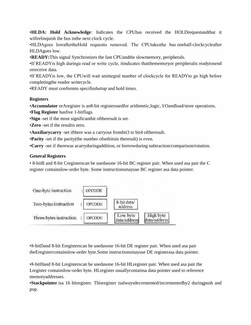
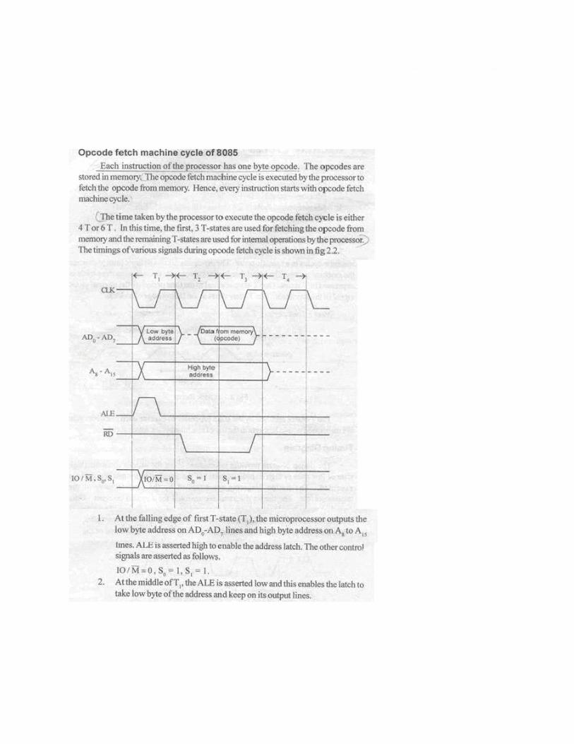
INSTRUCTIONFORMATOF 8085The8085 have 74 basicinstructionsand 246 total instruct ions.T he instruct ion setof 8085is defined by the manufacturer Intel Corporation. Each ins truction of 8085 has 1 by teopcode.With 8 bi tbinarycode,we can generate256 differentbinarycodes.In this, 246codes have been used for opcodes.
Thesize of 8085instructions canbe 1 byte,2 bytesor3 bytes.
·The 1-byte instructionhasan opcode alone.
·The 2 bytesinstructionhas an opcodefollowedbyan eight-bit address ordata. ·The 3 by tesinstructionhas an opcodefollowedby16 bi t addressor data. While storing the 3 by tes ins truction in memory , the sequenceofstorage is, opcode firstfollowedby lowby te of address or dataandthen high by te of addressor data.
ADDRESSINGMODES Every instruction of aprogramhas tooperate ona data.The method ofspecify ingthe datato be operated by the instruction iscalledAddressing. The8085 has thefollow ing5 d ifferent types ofaddressing.
1.Immediate Addressing
2.Direct Addressing
3.Register Addressing
4.Register Indirect Addressing
5.Implied Addressing
Immediate Addressing
In immediate addressingmode, the dataisspecifiedintheinstructionitself.Thedata will beapart of the
programinstruction.All instructionsthat have „I‟ intheir mnemonics are ofImmediate addressingtype.
Eg. MVIB, 3EH -Move the data 3EHgiven intheinstructionto Bregister.
Direct Addressing
In direct addressingmode, the address ofthedata is specifiedintheinstruction.The data will be
in memory. In this addressing mode, the programinstructionsand datacan be stored in
different
memoryblocks. Thistypeof addressingcan beidentified by16-bit address present inthe
instruction.
Eg. LDA1050H -Load thedataavailable in memorylocation 1050Hinaccumulator.
Register Addressing
In register addressingmode, theinstructionspecifiesthe name of the register in whichthe datais
available.Thistype ofaddressingcan beidentified byregister names (such as„A‟, „B‟, …)in the
In register indirect addressing modetheinstruction specifies the name oftheregister in whichthe address of the
dataisavailable. Herethe data will be inmemoryand the address will beinthe
instruction.
Eg. MOV A, B -Move thecontent of Bregisterto Aregister.
RegisterIndirect Addressingregister pair.This type of addressingcanbeidentifiedbyletter„M‟
presentin theinstruction. Eg.MOV A,M -The memorydataaddressed byHL pairis moved to Aregister.
Implied Addressing
In implied addressingmode, theinstructionitself specifiesthetype of operation and location of datato
be operated.Thistype ofinstruction does not have anyaddress, register name, immediate dataspecified
alongwithit.
Eg. CMA-Complement the content ofaccumulator.
INSTRUCTIONSET
The8085instructionsetcan be classified intothefollowingfive functional headings.
Group I - DATATRANSFERINSTRUCTIONS:
Includes the instructions that moves ( copies)data between registers or betweenmemory locations and
registers. In all datatransfer operations the content of sourceregister isnotaltered.Hencethe
datatransfer iscopyingoperation.
Ex: i) MOV A,Bii) LDA4600 iii) LHLD4200
Group II -ARITHMETICINSTRUCTIONS:
Includes the instructions which performs theaddition,subtraction, increment or decrement
operations.The flagconditions are altered after execution of an instruction inthisgroup. Ex: i)
ADDBii) SUBCiii) INRDiv) INX H
Group III- LOGICALINSTRUCTIONS:
Theinstructions which performs the logicaloperationslike AND, OR, Exclusive-OR, complement,
compare androtate instructionsare grouped under thisheading.Theflagconditions are altered after
execution of aninstructionin this group.
Ex: i) ORABii)XRAAiii) RAR
Group IV -BRANCHINGINSTRUCTIONS:
Theinstructions thatare used totransfertheprogramcontrolfromone memorylocationto another
memorylocationare grouped underthis heading.
Ex: i)JZ4200ii) RST 7 iii)CALL 4300
Group V- MACHINECONTROLINSTRUCTIONS:
Includes the instructions relatedtointerrupts and the instruction usedto halt programexecution. Ex: i)
SIM ii)RIM iii)HLT
The74 basic instructions of8085 are listedinTable.The opcode ofeach instruction, size, machine
cycles, number ofT -state andthetotal number ofinstructions in each type are alsoshown intablein
nextpage. The instructions affectingthe status flagarelistedintablefollowed .
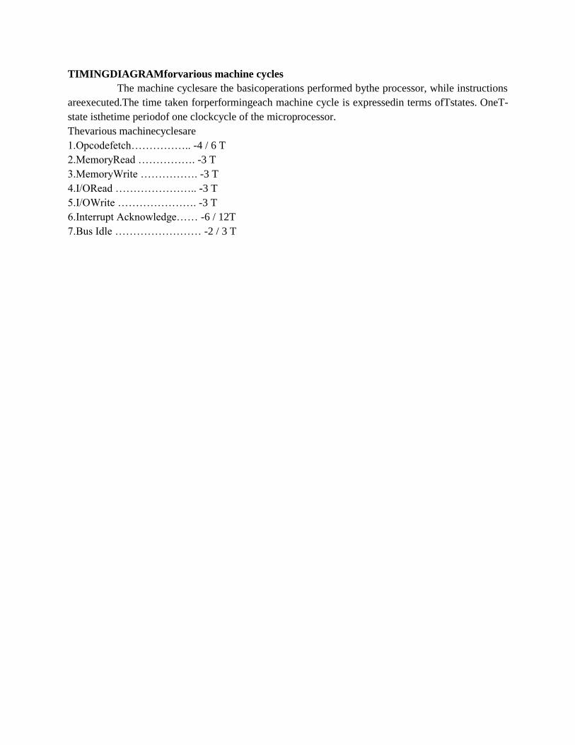
TIMINGDIAGRAMforvarious machine cycles
The machine cyclesare the basicoperations performed bythe processor, while instructions
areexecuted.The time taken forperformingeach machine cycle is expressedin terms ofTstates. OneT-
state isthetime periodof one clockcycle of the microprocessor.
Thevarious machinecyclesare
1.Opcodefetch…………….. -4 / 6 T
2.MemoryRead ……………. -3 T
3.MemoryWrite ……………. -3 T
4.I/ORead ………………….. -3 T
5.I/OWrite …………………. -3 T
6.Interrupt Acknowledge…… -6 / 12T
7.Bus Idle …………………… -2 / 3 T
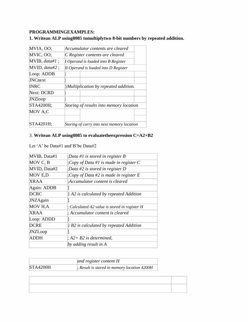
PROGRAMMINGEXAMPLES:
1. Writean ALP using8085 tomultiplytwo 8-bit numbers by repeated addition.
MVIA, OO; Accumulator contents are cleared
MVIC, OO; C Register contents are cleared
MVIB, data#1 ; I Operand is loaded into B Register
MVID, data#2 ; II Operand is loaded into D Register
Loop: ADDB |
JNCnext |
INRC }Multiplication by repeated addition.
Next: DCRD |
JNZloop |
STA4200H; Storing of results into memory location
MOV A,C
STA4201H;
Storing of carry into next memory location
3. Writean ALP using8085 to evaluatetheexpression C=A2+B2
Let „A‟ be Data#1 and„B‟be Data#2
MVIB, Data#1 ;Data #1 is stored in register B
MOV C, B ;Copy of Data #1 is made in register C
MVID, Data#2 ;Data #2 is stored in register D
MOV E,D ;Copy of Data #2 is made in register E
XRAA ;Accumulator content is cleared
Again: ADDB ]
DCRC } A2 is calculated by repeated Addition
JNZAgain ]
MOV H,A ; Calculated A2 value is stored in register H
XRAA ; Accumulator content is cleared
Loop: ADDD ]
DCRE } B2 is calculated by repeated Addition
JNZLoop ]
ADDH ; A2+ B2 is determined,
by adding result in A
and register content H
STA4200H ; Result is stored in memory location 4200H
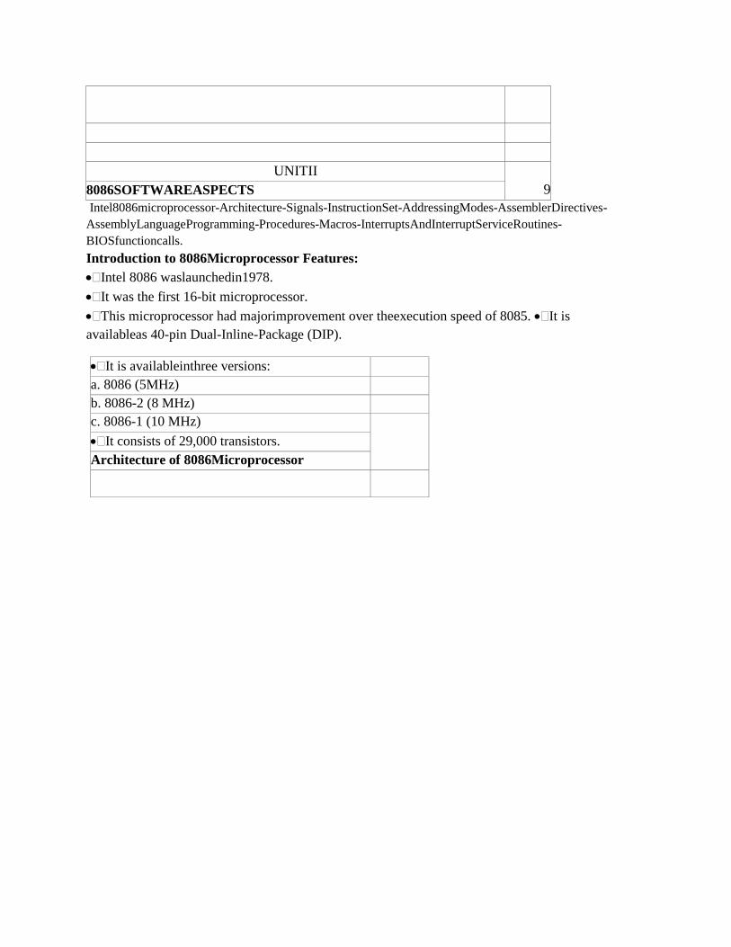
UNITII
9 8086SOFTWAREASPECTS
Intel8086microprocessor-Architecture-Signals-InstructionSet-AddressingModes-AssemblerDirectives-
AssemblyLanguageProgramming-Procedures-Macros-InterruptsAndInterruptServiceRoutines-
BIOSfunctioncalls.
Introduction to 8086Microprocessor Features:
Intel 8086 waslaunchedin1978.
It was the first 16-bit microprocessor.
This microprocessor had majorimprovement over theexecution speed of 8085. It is
availableas 40-pin Dual-Inline-Package (DIP).
It is availableinthree versions:
a. 8086 (5MHz)
b. 8086-2 (8 MHz)
c. 8086-1 (10 MHz)
It consists of 29,000 transistors.
Architecture of 8086Microprocessor
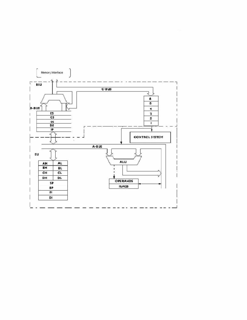
Bus Interface Unit (BIU):
Thefunction of BIUis to
Fetchtheinstructionor data frommemory.
Writethedata to memory.
Writethedata to the port.
Read datafromthe port.
Instruction Queue
1.Toincreasetheexecution speed, BIUfetchesas manyas sixinstruction bytes aheadtotime
frommemory.
2.Allsixbytes arethenheld in firstinfirst out6 byteregister called instruction queue.
3.Then allbytes have to begiven to EUone byone.
4. Thisprefetchingoperation of BIU maybe in parallel with execution operationof EU, whichimproves
the speed execution oftheinstruction.
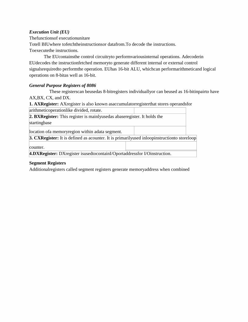
Execution Unit (EU)
Thefunctionsof executionunitare
Totell BIUwhere tofetchtheinstructionsor datafrom.To decode the instructions.
Toexecutethe instructions.
The EUcontainsthe control circuitryto performvariousinternal operations. Adecoderin
EUdecodes the instructionfetched memoryto generate different internal or external control
signalsrequiredto performthe operation. EUhas 16-bit ALU, whichcan performarithmeticand logical
operations on 8-bitas well as 16-bit.
General Purpose Registers of 8086
These registerscan beusedas 8-bitregisters individuallyor can beused as 16-bitinpairto have
AX,BX, CX, and DX.
1. AXRegister: AXregister is also known asaccumulatorregisterthat stores operandsfor
arithmeticoperationlike divided, rotate.
2. BXRegister: This register is mainlyusedas abaseregister. It holds the
startingbase
location ofa memoryregion within adata segment.
3. CXRegister: It is defined as acounter. It is primarilyused inloopinstructionto storeloop
counter.
4.DXRegister: DXregister isusedtocontainI/Oportaddressfor I/Oinstruction.
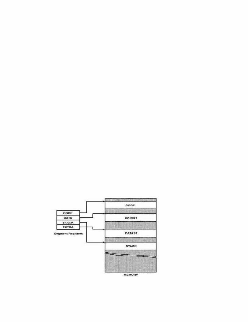
Segment Registers
Additionalregisters called segment registers generate memoryaddress when combined
with other in the microprocessor. In 8086 microprocessor, memory is divided into4 segments as follow :
2.Data Segment (DS): The DS contains most data used byprogram. Data are accessed in the Data
Segment byan offsetaddress or the content of other registerthat holdstheoffset address.
3.Stack Segment(SS): SSdefinedthearea ofmemoryused forthestack.
4.Extra Segment(ES): ES is additionaldata segment thatis used bysome of the stringtohold the
destination data.
Flag Registers of 8086Flags Register determines the current state of the processor.Theyare modified
automaticallyby CPUafter mathematical operations, this allowsto determine thetype ofthe result,and
to determine conditions totransfer controlto other partsof the program. 8086 has 9 flags and they are
dividedinto twocategories:
1.ConditionalFlags
2.Control Flags
(1) ConditionalFlags
Conditionalflagsrepresentresultoflast arithmeticorlogicalinstruction executed. Conditional
Thisflagindicates anoverflowconditionforunsignedinteger arithmetic.It is alsousedinmultiple-
precision arithmetic.
AuxiliaryFlag(AF):
If an operationperformed in ALUgenerates acarry/barrowfromlower nibble(i.e.D0 D3)
to upper nibble(i.e. D4 – D7), the AF flagisseti.e. carrygiven byD3 bit to D4 isAF flag.This is not
a general-purpose flag, it isusedinternallybythe processorto performBinaryto BCD conversion.
ParityFlag (PF):
Thisflagis used toindicatethe parityofresult. If lower order 8-bitsofthe result containseven
number of 1‟s,the ParityFlagis set andfor odd number of 1‟s, the ParityFlagis reset.
Zero Flag (ZF):
It is set; if the resultof arithmetic orlogical operation is zero elseitisreset.
SignFlag (SF):
In sign magnitudeformat the sign ofnumber isindicated byMSBbit. If the resultof operationis
negative, sign flagisset.
OverflowFlag(OF):
It occurs whensigned numbersareadded orsubtracted. An OF indicatesthat theresulthas
exceededthecapacityof machine.
ControlFlags
Control flags are set or reset deliberatelyto controltheoperations of the executionunit.
Control flags are as follows:
1. TrapFlag (TP):
It is usedforsinglestep control.
It allows userto execute one instructionof aprogramat atime fordebugging. Whentrap
flagisset,programcan be runin singlestepmode.
2. InterruptFlag (IF):
It is an interrupt enable/disableflag.
If it is set,themaskable interrupt of 8086 isenabled and ifit isreset, the interruptis
disabled.
It can be set byexecutinginstructionsit and canbe clearedbyexecutingCLI
instruction.
3. DirectionFlag (DF):
It is usedin stringoperation.
If it is set,stringbytesareaccessedfromhigher memoryaddresstolowermemory
address.
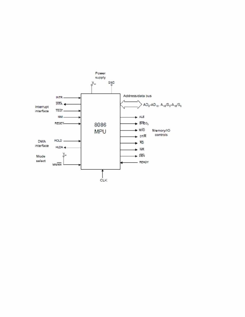
Minimum Mode Interface
Address/Data bus: 20 bitsvs 8 bitsmultiplexed
Status signals: A16-A19 multiplexed withstatussignals S3-S6 respectively.S3and S4together forma
2 bit binarycode that identifieswhich oftheinternal segment registers wasusedto generate the
physicaladdress that was output on the address busduringthecurrentbus cycle. S5 isthelogiclevel of
the internalinterrupt enable flag, S6 isalways logic 0.
Control Signals:
Address Latch Enable(ALE) isa pulseto logic 1 that signals external circuitrywhen a valid address
is onthebus.This addresscan be latchedin external circuitryon the1-to-0edge of the pulseat ALE.
IO/Mline: memoryor I/O transferis selected (complement for 8086)DT/Rline: direction of data
isselected
SSO (System StatusOutput)line: =1 when dataisread frommemoryand =0 when codeis
readfrommemory(onlyfor 8088)
BHE(BankHighEnable)line : =0 for most significant byte of datafor 8086 andalso carries S7
RDline: =0 when aread cycle isin progressWRline: =0 whena writecyle isin progress
DENline:(Data enable) Enables the external devicesto supplydata tothe processor.Ready line: can
be used toinsert wait statesintothe bus cycleso thatit isextended bya number of clockperiods
Interruptsignals:
INTR(Interrupt request) :=1 shows there is a servicerequest,sampled atthefinal clockcycle of
eachinstruction acquisition cycle.
INTA: Processorrespondswithtwo pulses goingto 0when it servicestheinterrupt and waitsfor the
interruptservice number after the secondpulse.
TEST: Processor suspendsoperation when=1. Resumes operation when=0. Usedto syncronizethe
processor toexternal events.
NMI (Nonmaskableinterrupt): Aleadingedge transitioncausesthe processorgo to theinterruptroutine
afterthe current instruction is executed.
RESET: =0 Startsthereset sequence.
Maximum Mode Interface
•For multiprocessor environment
•8288 Bus Controller is used for bus control
•WR¯,IO/M¯,DT/R¯,DEN¯,ALE, INTA¯ signalsare notavailable.
o MRDC¯ (memoryread command)
o MWRT¯ (memorywrite command)
o AMWC¯ (advanced memorywrite.command)
o IORC¯ (I/O read command)
o IOWC¯ (I/O writecommand)
o AIOWC¯ (Advanced I/O writecommand)
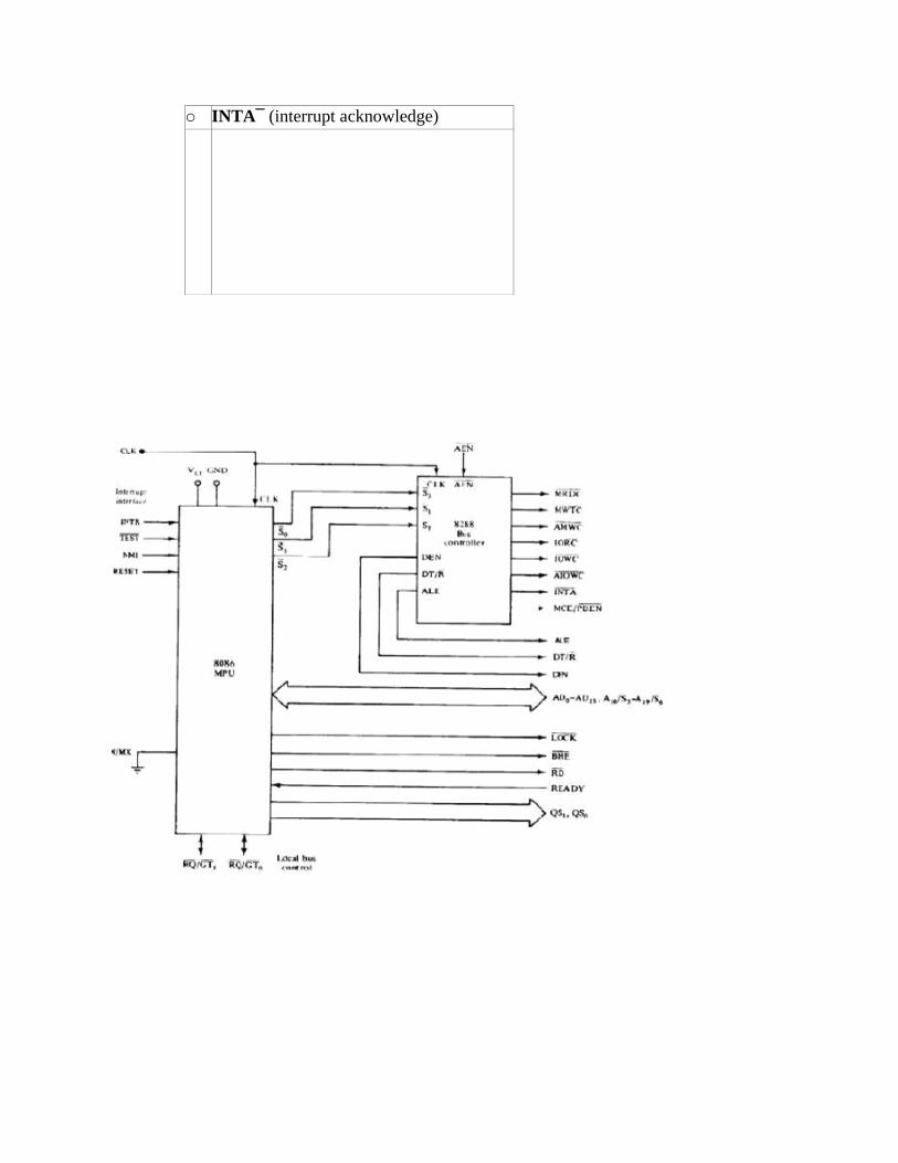
o INTA¯ (interrupt acknowledge)
Addressing Modes
A] Data CategoryB] Branch Category
Data Category:
1)Immediate Addressing 2)Direct Addressing( Segment Override prefix) 3) Register addressing4)
Register Indirect Addressing . 5)Registerrelative addressing.6)Base Index addressing7)Relative
baseindexaddressing.
Branch Category:
1) IntrasegmentDirect2) IntersegmentIndirect.
InstructionSet
We onlycover the small subsetofthe 8088 instruction setthatis essential. In particular, we will not
mentionvarious registers, addressingmodes and instructions thatcould oftenprovide faster ways of
doingthings.Asummaryof the 80x86 protected-mode instructionsetisavailable onthe course Web page
and should be printed outif you don‟t have another reference.
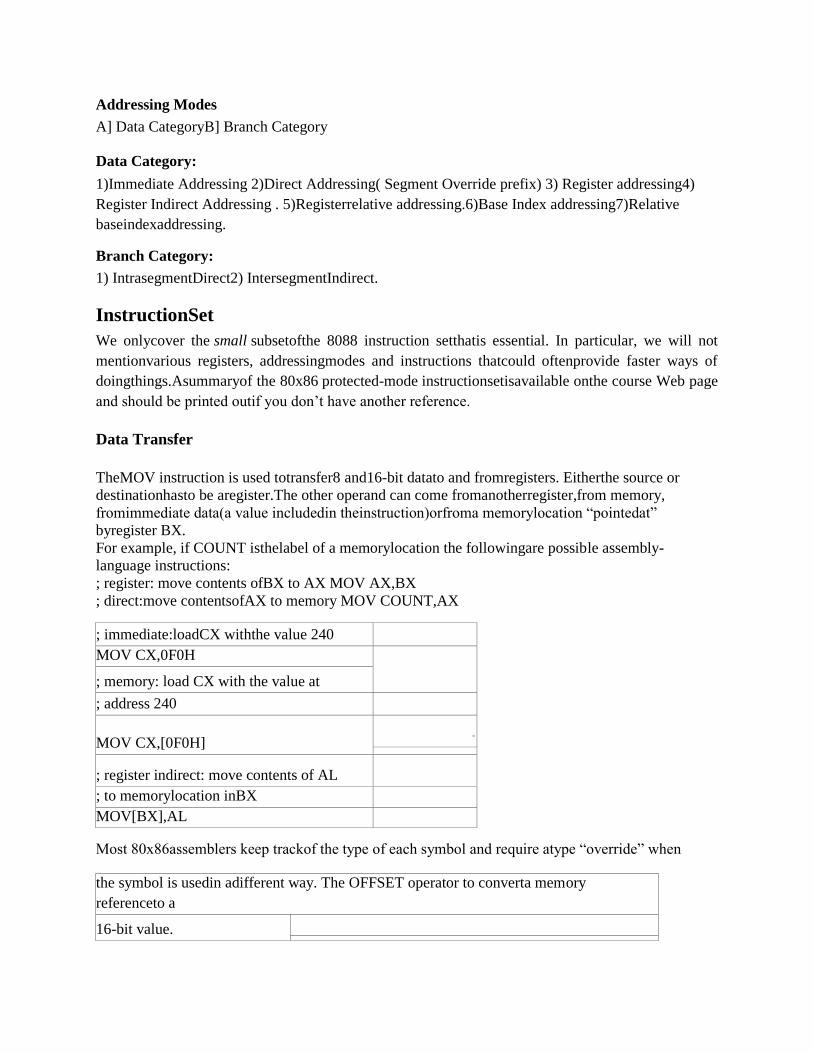
Data Transfer
TheMOV instruction is used totransfer8 and16-bit datato and fromregisters. Eitherthe source or
destinationhasto be aregister.The other operand can come fromanotherregister,from memory,
fromimmediate data(a value includedin theinstruction)orfroma memorylocation “pointedat”
byregister BX.
For example, if COUNT isthelabel of a memorylocation the followingare possible assembly-
language instructions:
; register: move contents ofBX to AX MOV AX,BX
; direct:move contentsofAX to memory MOV COUNT,AX
; immediate:loadCX withthe value 240
MOV CX,0F0H
; memory: load CX with the value at
; address 240
MOV CX,[0F0H] .
; register indirect: move contents of AL
; to memorylocation inBX
MOV[BX],AL
Most 80x86assemblers keep trackof the type of each symbol and require atype “override” when
the symbol is usedin adifferent way. The OFFSET operator to converta memory
referenceto a
16-bit value.
For example:
MOV BX,COUNT; loadthe value atlocation COUNT MOV BX,OFFSET COUNT; load the offsetof
COUNT
16-bit registers canbe pushed (the SPisfirst decremented bytwo and thenthe value stored atSP) or
popped (the valueis restoredfromthe memoryat SP and then SPisincremented by2).
For example:
PUSHAX ; push contentsof AX
POP BX ;restore into BX
Therearesome thingsto note about Intelassembly language syntax:
the order oftheoperands is destination,source _thereverse ofthat used onthe68000!
semicolons begin acomment
the suffix_H_is usedto indicate ahexadecimal
constant, if the constantbegins witha letterit
must be prefixed with azero to distinguish it
froma label thesuffix_B_indicates a binaryconstant
square bracketsindicateaccessesto memory
the size ofthetransfer(byte or word)is determined
bythe size of the destination
I/O Operations
The8086 has separate I/Oand memoryaddress spaces. Values intheI/Ospace are accessed with INand
OUT instructions. The port addressisloaded into DXandthe data is read/writtento/from AL or AX:
MOV DX,372H; load DXwith portaddress OUT DX,AL; output bytein AL toport ;372 (hex)
INAX,DX ;input word toAX
Arithmetic/Logic
Arithmetic and logicinstructions has to bea register andtheresult
;increment BX by4 ADDBX,4
;subtract1 fromAL SUBAL,1
;increment BX INCBX
;compare(subtractandsetflags CMP AX,[MAX]
;maskin LS 4 bits of AL ANDAL,0FH
;divideAX bytwo
SHRAX
;set MSbit of CX ORCX,8000H
;clear AX
XORAX,AX
can beperformed on byte and 16-bit values.Thefirstoperand isstoredinthat register.
.
ControlTransfer
Conditionaljumps transfercontrolto anotheraddressdependingon thevaluesofthe flags inthe
flagregister. Conditionaljumps are restrictedtoa range of -128 to +127 bytesfromthe next instruction
whileunconditionaljumps can be toanypoint.
;jump iflastresultwas zero (two values equal) JZskip
;jump ifcarryset(below) JCneg
;jump on carrynotset JNCsmaller
;unconditionaljump: JMP loop
Theassembly-language equivalent ofan if statement ina high-level language is aCoMPare operation
followed bya conditionaljump.
TheCALL and RET instructions call and return fromsubroutines.The processorpushesIP on the stack
duringa CALL instruction and the contents of IP are poppedbythe RET instructions. For example:
CALL readchar
...
readchar:
...
RET
Segment/Offset Addressing
Sinceaddressregisters andaddress operandsareonly 16 bits theycan onlyaddress64kbytes. In order
toaddress the 20-bitaddressrange ofthe8086,physical addresses(thosethat are put onthe address bus)
arealwaysformed byaddingthe values of one ofthe segment registers tothe 16-bit addressto forma 20-
bit address.Thesegment registers themselves onlycontainthe most-significant 16 bits ofthe 20-
bit valuethat is contributed bythesegment registers.Theleast significant fourbits of the segment
addressarealways zero.
Bydefault, the DS (data segment) isusedfor datatransfer instructions (e.g. MOV), CS (code
segment)is used with control transfer instructions (e.g. JMPnr/or CALL), and SS isused withthe
stackpointer(e.g. PUSHorto save/restore addresses during.CALL/RET or INT instructions).Theuseof
segment registers reducesthe size of pointers to 16 bits.Thisreducesthe codesize but
In additionto interrupts caused by events(such asan IRQsignal), certain instructions such as a
dividingbyzero or the INT instruction generate exceptions.
alsorestrictstheaddressingrange ofa pointerto 64kbytes. Performingaddress arithmetic within
datastructureslargerthan 64kis awkward.This is thebiggest drawbackof the 8086 architecture.
We willrestrict ourselves to short programs where allof the code, dataand stackare placedinto the
same 64ksegment (i.e.CS=DS=SS).
Interrupts and Exceptions
The8086reservesthelower 1024 bytes ofmemory for an interrupt vectortable.Thereis one 4-bytevector
for each ofthe 256 possibleinterrupt/exception numbers.When aninterrupt or exception occurs, the
processor: (1) clearstheinterrupt flagintheflags register, (2) pushesthe flags register, CS,and IP (in
that order),(3)loads IP and CS (in that order)fromthe appropriate interrupt vectorlocation, and
(4)transfers controltothat location. Forexternalinterrupts(IRQor NMI) the interrupt numberis
readfromthe data busduringan interrupt acknowledge bus cycle. For internal interrupts(e.g. INT
instruction) the interrupt number is determined fromthe instruction.TheINT instructionallowsa
programto generate anyof the 256interrupts.This “software interrupt” istypicallyused to access
operatingsystemservices.
Pseudo-Ops
Anumber of assembler directives(“pseudo-ops”)are also requiredto write assemblylanguage
programs.ORGspecifies the location of code or data withinthe segment, DBand DW assemble bytes
and words of constantdatarespectively.
Assembler Directives :
ASSUME
DB -Defined Byte.
DD -Defined DoubleWord
DQ -Defined QuadWord
DT -DefineTenBytes
DW -Define Word
ASSUMEDirective -TheASSUME directive is usedto tell the assemblerthatthe name of the logical
segment should beused for aspecified segment. The 8086 works directlywith only 4
physicalsegments: a Codesegment, a data segment, a stacksegment, and an extrasegment.
Example:
ASUMECS:CODE ;Thistellstheassembler thatthe logical segment named CODE containsthe
instruction statementsforthe programand shouldbe treated as a codesegment.
ASUMEDS:DATA;Thistells the assembler that for anyinstruction whichrefersto a datainthe
datasegment, data will found inthelogical segment DATA.
DB -DBdirective isusedto declare a bytetype variable orto store a bytein memory location.
2.NAMEDB‘ABCDEF’;Declare anarrayof 6 by tes.andcoinitialize with A SCIIcode for letters 3.TEMP DB 100 DUP(?);Set100h ttp: // by tes ofstorage inmemoryand give it the name as TEMP, but leave the 100 by tes unini tialized. Programinstructions wil l load values intotheselocations.
DW-TheDW directive isusedto define a variable oftype word or toreserve storage location of type word in memory .
Example: MULTIP LIERDW437Ah ;this declares a variableof type word andnamed itas MULTIPLIER. This variable is initial ized w ith thevalue 437Ah w hen it is loaded into memory to run.
EXP1 DW 1234h, 3456h,5678h ;this declares an arrayof 3 wordsandinitialized withspecified values.
STOR1 DW 100 DUP(0);Reserve anarray of 100 words of memoryand initialize all words with 0000.Array is named as STOR1.
END-ENDdirectiveis p laced afterthelast statementof a programto telltheassembler that this is the end oftheprogrammodule.The assemblerwillignore any sta tement after an END directive. Carriage returnisrequired after the ENDdirective.
ENDP-ENDPdirective isused alongwiththe name of the proceduretoindicate the end of a procedure tothe assembler.
Example: SQ UARE_NUM PROCE; I t start the procedure ;Some steps to f indthe squarerootof anumberSQ UARE_NUM ENDP;Hearitisthe Endfor the procedure.
END -End Program
ENDP -End Procedure
ENDS -End Segment
EQU-Equate
EVEN -Align on Even MemoryAddress
EXTRN
ENDS -This ENDS directive is usedwith name of thesegment to indicatetheend of thatlogic segment.
Example:
CODESEGMENT ;Hearit Startthe logic segment containingcode Some instructions statementsto
performthe logical operation.
CODEENDS ;End ofsegment named as CODE
EQU-This EQUdirective is usedto give a name to some value orto asymbol. Each time the
assemblerfinds thename inthe program, it willreplacethe name with the valueorsymbol you given to
that name.
Example:
FACTOREQU03H ; youhas to writethis statementat the startingof your programand laterin the
programyou can use this asfollows
ADDAL, FACTOR ; When it codesthis instruction the assembler willcodeit asADDAL, 03H
Theadvantage of usingEQUin this manneris,ifFACTORisnr/used manyno of times in a programand
you want tochange the value, all you had to do.ischange the EQUstatement at
beginning, it will changes the rest of all. .co EVEN -This EVENdirective instructsthe assemblerto increment the location ofthe counterto the
nexteven addressif it isnot alreadyintheeven address. If the wordisateven address 8086 can reada
memoryin 1 buscycle.If the wordstarts at an odd address,the 8086 will take 2 bus cyclesto get the
data. Aseries of words can beread much more quicklyif theyare ateven
address.When EVENis used the locationcounter will simplyincremented tonextaddressand
NOP instruction is insertedin thatincrementedlocation.
Example:
DATA1 SEGMENT ; Location counter willpointto 0009 after assemblerreads next
statementSALES DB 9 DUP(?);declare anarrayof 9 bytes
EVEN; increment locationcounterto 000AH
RECORDDW 100 DUP(0 ) ;Arrayof100 words will start froman even address for quicker read
DATA1 ENDS
GROUP - Group RelatedSegments
LABLE
NAME
OFFSET
ORG– Originate
GROUP -The GROUP directive is used to group thelogical segments named after the directive
intoonelogical group segment.
INCLUDE -This INCLUDEdirective is usedto insert ablockof sourcecodefromthe named file
intothecurrent sourcemodule.
PROC -Procedure
PTR -Pointer
PUBLC
SEGMENT
SHORT
TYPE
PROC -ThePROC directive is usedtoidentifythe start of a procedure.Thetermnearorfaris usedto
specifythe type ofthe procedure.
Example:
SMARTPROCFAR;This identifies that the start ofa procedure named as SMART and instructsthe
assemblerthatthe procedure is far .
SMARTENDP This PROCis used with ENDP toindicatethe breakof theprocedure.
PTR -ThisPTR operator is usedtoassign a specifictype of a variable ortoa label. Example:
INC[BX] ;Thisinstruction will not knowwhether to increment the byte pointedto byBX or a word
pointed toby BX.
INCBYTEPTR[BX] ;increment the byte pointedtobyBXnr/This PTRoperator can also beused to
overridethe declaredtype of variable . If we wanttoaccess. the abyte inan array
WORDS DW 437Ah,0B97h, .co
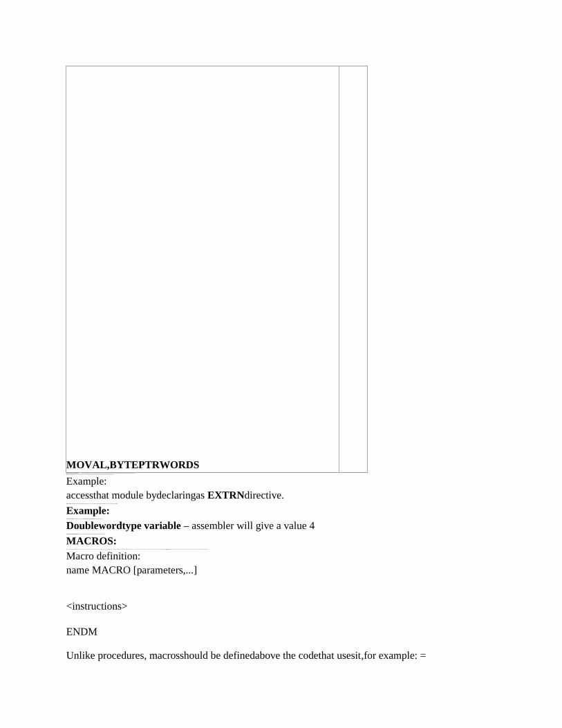
MOVAL,BYTEPTRWORDS PUBLICDIVISOR, D IVIDEND http :// ;thesetwo variablesare publicso theseare available to all modules.If an ins truction ina module refersto a variable in another assembly module, wecan
PUBLIC-ThePUBLICdirective is usedto instruct the assemblerthat a specified name or label willbe accessedfromothermodules.
Example:
accessthat module bydeclaringas EXTRNdirective. TYPE- TYPEoperatorinstructs the assemblerto determine the type of a variable and determines the number of by tes specified tothat variable.
Example: Byte type variable–assemblerwill give a value 1Wor d type variable–assemblerwill give a value 2
Doublewordtype variable – assembler will give a value 4 ADDBX, TYP EWORD_ARRAY ;hear we wanttoincrement BXto poin t tonext word inan arrayof words.
MACROS: Macros arejust like procedures,butnotreally . Macros=ooklike procedures, buttheyexist only unti l your codeis compiled, after= compilation all macrosarereplaced withrealinstructions. If you = declared a macro andnever used it inyour code,compiler will = imply ignore it.e mu8086.incisa good example of howmacros can be used,this file contains=everal macrosto make codingeasierfor you.
Macro definition:
name MACRO [parameters,...]
<instructions>
ENDM
Unlike procedures, macrosshould be definedabove the codethat usesit,for example: =
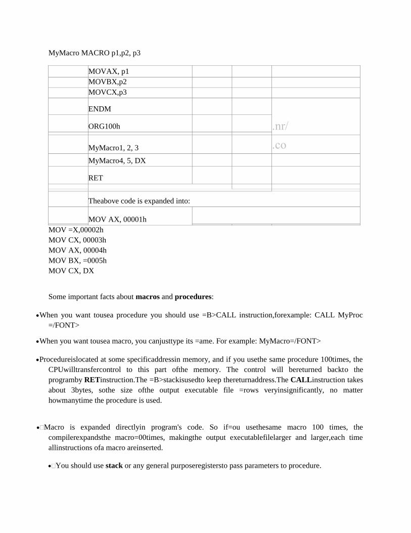
MyMacro MACRO p1,p2, p3
MOVAX, p1
MOVBX,p2
MOVCX,p3
ENDM
.nr/ ORG100h
MyMacro1, 2, 3
.co
MyMacro4, 5, DX
RET
Theabove code is expanded into:
MOV AX, 00001h MOV =X,00002h
MOV CX, 00003h
MOV AX, 00004h
MOV BX, =0005h
MOV CX, DX
Some important facts about macros and procedures:
When you want tousea procedure you should use =B>CALL instruction,forexample: CALL MyProc
=/FONT>
When you want tousea macro, you canjusttype its =ame. For example: MyMacro=/FONT>
Procedureislocated at some specificaddressin memory, and if you usethe same procedure 100times, the
CPUwilltransfercontrol to this part ofthe memory. The control will bereturned backto the
programby RETinstruction.The =B>stackisusedto keep thereturnaddress.The CALLinstruction takes
about 3bytes, sothe size ofthe output executable file =rows veryinsignificantly, no matter
howmanytime the procedure is used.
Macro is expanded directlyin program's code. So if=ou usethesame macro 100 times, the
compilerexpandsthe macro=00times, makingthe output executablefilelarger and larger,each time
allinstructions ofa macro areinserted.
You should use stack or any general purposeregistersto pass parameters to procedure.
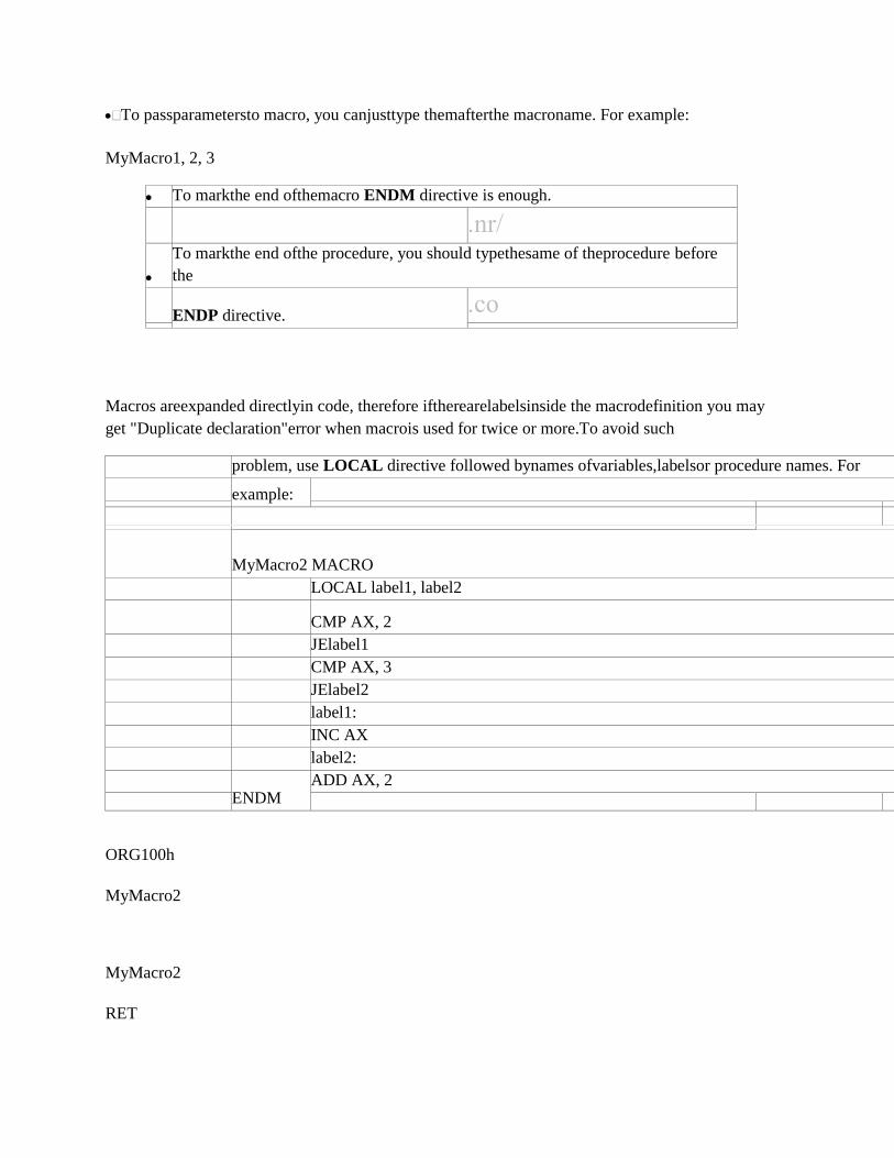
To passparametersto macro, you canjusttype themafterthe macroname. For example:
MyMacro1, 2, 3
To markthe end ofthemacro ENDM directive is enough.
.nr/
To markthe end ofthe procedure, you should typethesame of theprocedure before
the
ENDP directive. .co
Macros areexpanded directlyin code, therefore iftherearelabelsinside the macrodefinition you may
get "Duplicate declaration"error when macrois used for twice or more.To avoid such
problem, use LOCAL directive followed bynames ofvariables,labelsor procedure names. For
example:
MyMacro2 MACRO
LOCAL label1, label2
CMP AX, 2
JElabel1
CMP AX, 3
JElabel2
label1:
INC AX
label2:
ENDM
ADD AX, 2
ORG100h
MyMacro2
MyMacro2
RET
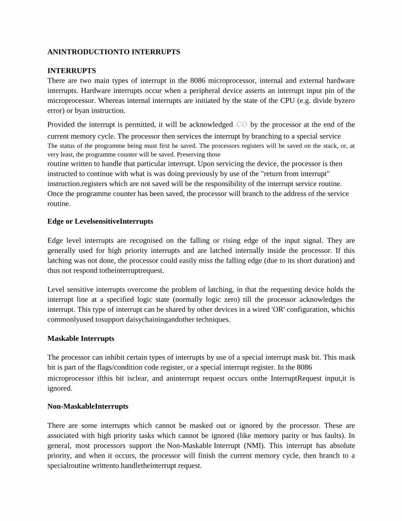
ANINTRODUCTIONTO INTERRUPTS
INTERRUPTS
There are two main types of interrupt in the 8086 microprocessor, internal and external hardware
interrupts. Hardware interrupts occur when a peripheral device asserts an interrupt input pin of the
microprocessor. Whereas internal interrupts are initiated by the state of the CPU (e.g. divide byzero
error) or byan instruction.
Provided the interrupt is permitted, it will be acknowledged.co by the processor at the end of the
current memory cycle. The processor then services the interrupt by branching to a special service
The status of the programme being must first be saved. The processors registers will be saved on the stack, or, at
very least, the programme counter will be saved. Preserving those
routine written to handle that particular interrupt. Upon servicing the device, the processor is then
instructed to continue with what is was doing previously by use of the "return from interrupt"
instruction.registers which are not saved will be the responsibility of the interrupt service routine.
Once the programme counter has been saved, the processor will branch to the address of the service
routine.
Edge or LevelsensitiveInterrupts
Edge level interrupts are recognised on the falling or rising edge of the input signal. They are
generally used for high priority interrupts and are latched internally inside the processor. If this
latching was not done, the processor could easily miss the falling edge (due to its short duration) and
thus not respond totheinterruptrequest.
Level sensitive interrupts overcome the problem of latching, in that the requesting device holds the
interrupt line at a specified logic state (normally logic zero) till the processor acknowledges the
interrupt. This type of interrupt can be shared by other devices in a wired 'OR' configuration, whichis
commonlyused tosupport daisychainingandother techniques.
Maskable Interrupts
The processor can inhibit certain types of interrupts by use of a special interrupt mask bit. This mask
bit is part of the flags/condition code register, or a special interrupt register. In the 8086
microprocessor ifthis bit isclear, and aninterrupt request occurs onthe InterruptRequest input,it is
ignored.
Non-MaskableInterrupts
There are some interrupts which cannot be masked out or ignored by the processor. These are
associated with high priority tasks which cannot be ignored (like memory parity or bus faults). In
general, most processors support the Non-Maskable Interrupt (NMI). This interrupt has absolute
priority, and when it occurs, the processor will finish the current memory cycle, then branch to a
specialroutine writtento handletheinterrupt request.
Advantages of Interrupts
Interrupts are used to ensure adequate service response times by the processing. Sometimes, with
software polling routines, service times by the processor cannot be guaranteed, and data may be lost.
The use of interrupts guarantees that the processor will service the request within a specified
Interrupt Response Time
The time interval from when the interrupt is first asserted to the time the CPU recognises it. This will
depend much upon whether interrupts are disabled, prioritized and what the processor is
currentlyexecuting. At times, a processor might ignore requests whilst executingsome indivisible
instruction stream (read-write-modify cycle). The figure that matters most is the longest possible
interruptlatencytime.
The time interval between the CPU recognising the interrupt to the time when the first instruction of
the interrupt service routine is executed. This is determined by the processor architecture and
clockspeed.
The Operation of an Interrupt sequence on the 8086Microprocessor:
1.External interfacesendsan interrupt signal,to the Interrupt Request(INTR) pin,or aninternal
interruptoccurs.
2.The CPUfinishesthe presentinstruction(for ahardwareinterrupt) andsends Interrupt Acknowledge
(INTA) to hardware interface.
3.The interrupttype Nissentto the Central ProcessorUnit(CPU) via the Data bus fromthe
hardwareinterface.
4.The contentsoftheflagregisters are pushed onto thestack.
5.Boththeinterrupt (IF) and (TF)flags arecleared.This disables the INTRpin and thetrap orsingle-
step feature.
6.The contentsofthecodesegment register (CS) are pushed ontothe Stack.
7.The contentsoftheinstruction pointer(IP) are pushed onto the Stack.
8.The interrupt vectorcontentsare fetched, from(4 xN) andthen placedinto theIP and from(4 x
N+2)into the CS sothatthe nextinstruction executes attheinterrupt service procedure addressed
bytheinterruptvector.
9.Whilereturningfromthe interrupt-serviceroutine bythe Interrupt Return(IRET)instruction, the IP, CS
and Flagregisters arepopped fromthe Stackand returnto their state priortothe interrupt.
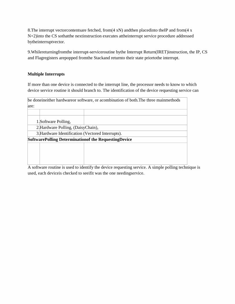
Multiple Interrupts
If more than one device is connected to the interrupt line, the processor needs to know to which
device service routine it should branch to. The identification of the device requesting service can
be doneineither hardwareor software, or acombination of both.The three mainmethods
are:
1. Software Polling,
2. Hardware Polling, (DaisyChain),
3. Hardware Identification (Vectored Interrupts).
SoftwarePolling Determinationof the RequestingDevice
A software routine is used to identify the device requesting service. A simple polling technique is
used, each deviceis checked to seeifit was the one needingservice.
Havingidentifiedthe device, theprocessorthen branches to the appropriateinterrupt-handling-
routineaddressfor the given device.The orderin which the devicesappearinthepolling sequence
determinestheir priority.
DOSFunction Calls
AH 00H :Terminate a Program
AH 01H : ReadtheKeyboard
AH 02H :Write toa Standard Output Device
AH 08H : Read a StandardInput withoutEcho
AH 09H : Displaya Character String
AH 0AH: Buffered keyboard Input
INT21H : Call DOS Function
UNIT-III
MULTIPROCESSORCONFIGURATIONS 9
CoprocessorConfiguration–CloselyCoupledConfiguration–LooselyCoupledConfiguration–
8087NumericData
Processor–DataTypes–Architecture–8089I/OProcessor–Architecture–
CommunicationbetweenCPUandIOP.
Each processor in the 80x86 familyhas acorrespondingcoprocessor with whichitis compatible.
Math Coprocessor isknown as NPX,NDP,FUP. Numeric processor extension (NPX),
Numeric data processor(NDP), Floatingpoint unit (FUP).
Processors
1.8086 &8088
2.80286
3.80386DX
4.80386SX
5.80486DX
6.80486SX
Coprocessors
1.8087
2.80287,80287XL
3.80287,80387DX
4.80387SX
5.It is Inbuilt
6.80487SX
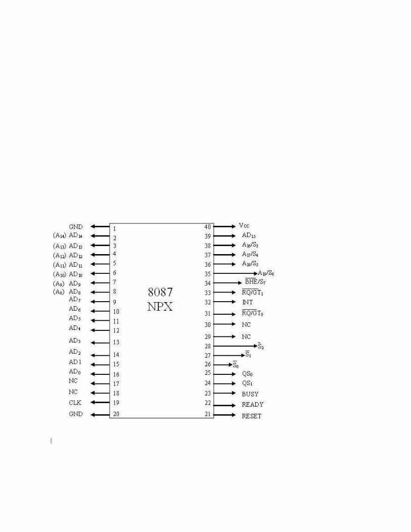

8087Numeric DataProcessor:Architecture of 8087
Control Unit
Execution Unit


ControlUnit
Control unit:Tosynchronize theoperationofthe coprocessor andthe processor. Thisunit has a Control
word and Statuswordand Data Buffer
If instructionis an ESCape (coprocessor) instruction,the coprocessorexecutes it,if not
the microprocessor executes.
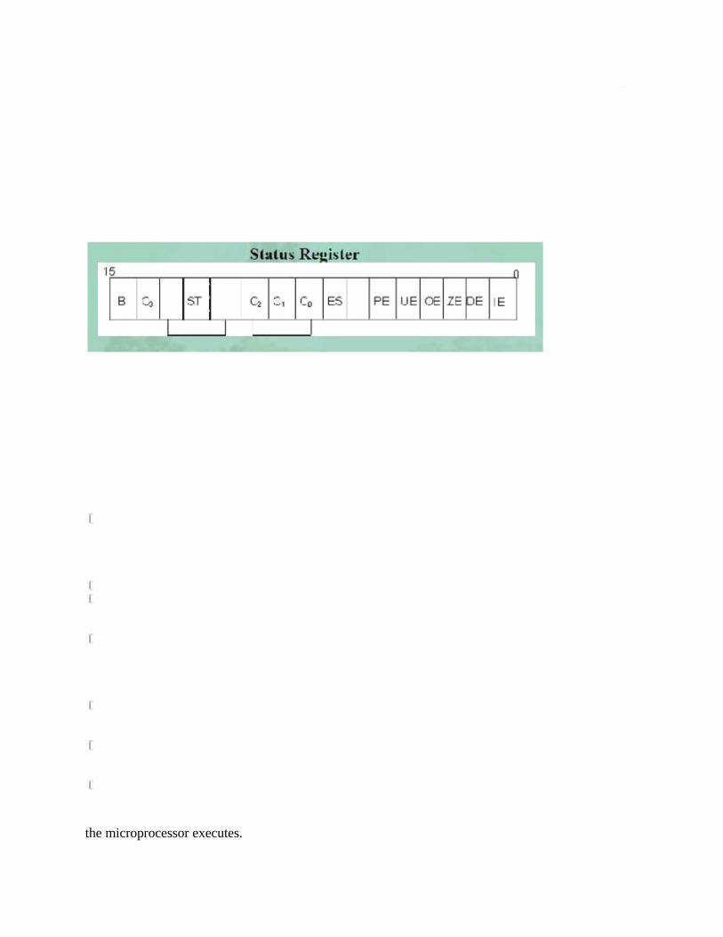
Statusregisterreflects theover all operation ofthecoprocessor.
B-Busybit indicates thatcoprocessorhttp:// is busyexecutinga task. Busycan betested by examiningthestatusor
byusingtheFWAIT instruction. Newer coprocessor
automaticallysynchronize withthe microprocessor,sobusyflagneednotbetested before
performingadditional coprocessortasks.
C3-C0 Condition code bits indicates conditions aboutthe coprocessor.
TOP-Top of the stack(ST)bit indicatesthecurrentregisteraddressasthetop of the stack.
ES-Error summarybit issetifanyunmasked errorbit(PE, UE, OE, ZE, DE, orIE) is set. In the 8087
the error summaryis also causeda coprocessor interrupt.
PE-Precision error indicatesthat the resultor operand executes selected precision.
UE-Under flowerrorindicates the resultistoolarge to be represent withthe current precision selected
bythecontrol word.
OE-Over flowerrorindicatesa resultthatis too largeto berepresented.If this error is masked,
thecoprocessor generatesinfinityfor anoverflowerror.
ZE-A Zero error indicatesthe divisor was zero whilethe dividendisa non-infinityornon-zero number.
DE-Denormalized errorindicates at least oneoftheoperand is denormalized.
IE-Invalid errorindicatesa stackoverflowor underflow, indeterminatefrom(0/0,0,-0, etc) ortheuseof a
NANasan operand.Thisflagindicateserrorsuchasthose produced bytakingthe squareroot ofa negative
number.
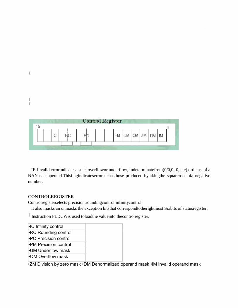
CONTROLREGISTER
Controlregisterselects precision,roundingcontrol,infinitycontrol.
It also masks an unmasks the exception bitsthat correspondtotherightmost Sixbits of statusregister.
Instruction FLDCWis used toloadthe valueinto thecontrolregister.
•IC Infinity control
•RC Rounding control
•PC Precision control
•PM Precision control
•UM Underflow mask
•OM Overflow mask •ZM Division by zero mask •DM Denormalized operand mask •IM Invalid operand mask
IC –Infinity control selects either affine or projective infinity. Affine allows positive
and negative infinity, while projective assumes infinity is unsigned.
INFINITY CONTROL
0 = Projective
1 = Affine
RC –Rounding control determines the type of rounding.
ROUNDINGCONTROL
00=Round to nearest or even 01=Round down towards minus infinity 10=Round up towards
plus infinity 11=Chop or truncate towards zero
PC- Precision control sets the precision of he result as define in table
PRECISIONCONTROL
00=Single precision (short) 01=Reserved
10=Double precision (long) 11=Extended precision (temporary)
Exception Masks – It Determines whether the error indicated by the exception affects
the error bit in the status register. If a logic1 is placed in one of the exception control bits,
corresponding status register bit is masked off.
Numeric ExecutionUnit
This performs all operations that access and manipulate the numeric data in
the
. coprocessor’s registers.
Numeric registers in NUE are 80 bits wide.
NUE is able to perform arithmetic, logical and transcendental operations as
well as
supply a small number of mathematical constants from its on-chip ROM.
Numeric data is routed into two parts ways a 64 bit mantissa bus and
a 16 bit sign/exponent bus.
DataTypes
Internally, all data operands are converted to the 80-bit temporary real format.
We have 3 types. •Integer data type •Packed BCD data type •Real data type
Coprocessor datatypes
Integer Data Type
Packed BCD
Real data type
Example
Converting a decimal number into a Floating-point number.
1)Converting the decimal number into binary form.
2)Normalize the binary number
3)Calculate the biased exponent.
4)Store the number in the floating-point format.
Example
Step Result
1) 100.25
2) 1100100.01 = 1.10010001 * 26
3) 110+01111111=10000101
4 ) Sign = 0
Exponent =10000101
Significand = 10010001000000000000000
•In step 3 the biased exponent is the exponent a 26 or 110,plus a bias of 01111111(7FH)
,single precision no use 7F and double precision no use 3FFFH.
•IN step 4 the information found in prior step is combined to form the floating point no.
INSTRUCTIONSET
The 8087 instruction mnemonics begins with.theco letter F which stands for Floating
point and distinguishes from 8086.
These are grouped into Four functional groups.
The 8087 detects an error condition usually called an exception when it executing an
instruction it will set the bit in its Status register.
Types
I. DATA TRANSFER INSTRUCTIONS. II. ARITHMETIC INSTRUCTIONS. III. COMPARE
INSTRUCTIONS.
IV. TRANSCENDENTAL INSTRUCTIONS.
(Trigonometric and Exponential)
DataTransfers Instructions REALTRANSFER
FLDLoad real
FSTStore real
FSTP Store real and popFXCHExchange registers
INTEGERTRANSFER
FILD Load integer
FIST Store integer
FISTP Store integer and pop
PACKEDDECIMALTRANSFER(BCD)
FBLDLoad BCD
FBSTP Store BCD and pop
Example
FLDSource- Decrements the stack pointer by one and copies a real number from a
stack element or memory location to the new ST. •FLD ST(3) ;Copies ST(3) to ST.
•FLD LONG_REAL[BX] ;Number from memory ;copied to ST.
FLDDestination- Copies ST to a specified stack position or to a specified
FXCH Destination– Exchange the contents of ST with the contents of a
specified
stack element.
•FXC
H ST(5) ;Swap ST and ST(5)
FILDSource– Integer load. Convert integer number from memory to temporary- real
format and push on 8087 stack.
•FILD DWORD PTR[BX] ;Short integer from memory at [BX].
FISTDestination- Integer store. Convert number from ST to integer and copy to memory.
•FIST LONG_INT ;ST to memory locations named LONG_INT.
FISTPDestination-Integer store and pop. Identical to FIST except that stack pointer is
incremented after copy.
FBLDSource-Convert BCD number from memory to temporary- real format and push on
top of 8087 stack.
ArithmeticInstructions.
Four basic arithmetic functions:
Addition, Subtraction, Multiplication, and
Division.
Addition
FADDAdd real
FADDP Add real and pop
FIADDAdd integer
FPRNDINT Round to integer
FSCALEScale
FSQRT Square root
FXTRACTExtract exponent and mantissa.
Example
FADD– Add real from specified source to specified destination Source can be a stack
or memory location. Destination must be a stack element. If no source or destination is
specified, then ST is added to ST(1) and stack pointer is incremented so that the result of
addition is at ST.
•FADD ST(3), ST ;Add ST to ST(3), result in ST(3) •FADD ST,ST(4) ;Add ST(4) to ST,
result in ST. •FADD ;ST + ST(1), pop stack result at ST
•FADDP ST(1) ;Add ST(1) to ST. Increment stack ;pointer so ST(1) become ST.
•FIADD Car_Sold ;Integer number from memory + ST
FSUB -Subtract the real number at the specified source from the real number at the
specified destination and put the result in the specified destination. •FSUB ST(2), ST
;ST(2)=ST(2) – ST.
•FSUB Rate ;ST=ST – real no from memory. •FSUB ;ST=( ST(1) – ST)
FSUBP - Subtract ST from specified stack element and put result in specified stack
element .Then increment the pointer by one.
•FSUBP ST(1) ;ST(1)-ST. ST(1) becomes new ST
FISUB – Integer from memory subtracted from ST, result in ST. •FISUB Cars_Sold ;ST
becomes ST – integer from memory
Transcendental Instruction.
Transcendental
FPTANPartial tangent
FPATANPartial arctangent
F2XM1 2x - 1
FYL2XY log2XFYL2XP1 Y log2(X+1)
Example
FPTAN– Compute the values for a ratio of Y/X for an angle in ST. The angle
must be
in radians, and the angle must be in the range of 0 < angle < π/4. F2XM1 – Compute
Y=2x-1 for an X value in ST. The result Y replaces X in ST. X must be in the range
0≤X≤0.5.
FYL2X-Calculate Y(LOG2X).X must be in the range of 0 < X < ∞ any Y must be in the
range -∞<Y<+∞.
FYL2XP1 –Compute the function Y(LOG2(X+1)).This instruction is almost identical
to FYL2X except that it gives more accurate results when compute log of a number very
close to one.
ConstantInstructions.
Load Constant Instruction
FLDZLoad +0.0
FLDI Load+1.0
FLDPI Load π
FLDL2T Load log210
FLDL2E Load log2e
FLDLG2 Load log102
FLDLN2 Load loge2
8089 I/OProcessor:
Features:
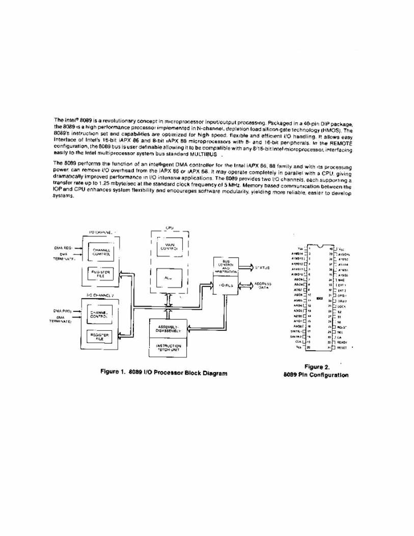
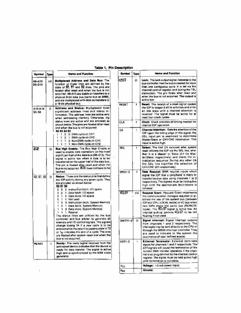

.
Communication between CPU and IOP:
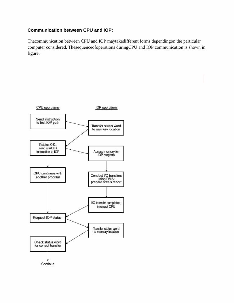
Thecommunication between CPU and IOP maytakedifferent forms dependingon the particular
computer considered. Thesequenceofoperations duringCPU and IOP communication is shown in
figure.
TheCPU sends atest I/O instruction to IOP to test the IOP path.
Theresponds byinsertingastatus word in memorylocation.
TheCPU refers to thestatus word in memory. Ifeverythingis in order, the CPU sends thestart I/O
instruction to start the I/O transfer.
The IOP accesses memoryfor IOP program.
TheCPU can now continuewith anotherprogram whilethe IOP is busywith the program. Both
programs referto memorybymeans ofDMA transfer.
When the IOP terminates theexecution ofits program, it sends an interrupt request to theCPU.
TheCPU then issues aread I/O instruction to read thestatus from the IOP.
The IOP transfers thestatus word to memorylocation.
Thestatus word indicates whetherthetransferhas been completed satisfactorily orifanyerrorhas
occurred during thetransfer.
UNIT IV I/O INTERFACING
Unit no: 4
I/OINTERFACING 9
MemoryinterfacingandI/Ointerfacingwith8085–parallelcommunicationinterface–serialcommunicationinterface–
timer-keyboard/displaycontroller–interruptcontroller–DMAcontroller(8237)–applications–steppermotor–
temperaturecontrol..
Memory Interfacing
Thememoryis made up ofsemiconductor material used to store the programs anddata. Threetypes of
memoryis,
Process memory
Primaryor main memory
Secondarymemory
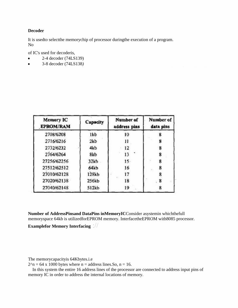
Typical EPROMand Static RAM
Atypical semiconductor memory ICwill have n address pins, mdatapins(oroutput
pins).Havingtwo powersupplypins(onefor connectingrequired supplyvoltage(Vandthe
other for connectingground).
Thecontrol signalsneededforstatic RAM arechipselect(chip enable),read control
(outputenable) and write control(writeenable).
The control signalsneededforread operation in EPROM arechip select(chip
enable)
and read control(output enable).
Decoder
It is usedto selectthe memorychip of processor duringthe execution of a program.
No
of IC's used for decoderis, 2-4 decoder (74LS139)
3-8 decoder (74LS138)
Number of AddressPinsand DataPins inMemoryICConsider asystemin whichthefull
memoryspace 64kb is utilizedforEPROM memory. InterfacetheEPROM with8085 processor.
Examplefor Memory Interfacing ://
The memorycapacityis 64Kbytes.i.e
2^n = 64 x 1000 bytes where n = address lines.So, n = 16.
In this system the entire 16 address lines of the processor are connected to address input pins of
memory IC in order to address the internal locations of memory.
The chip select (CS) pin of EPROM is permanently tied to logic low (i.e., tied to ground).Since the
processor is connected to EPROM, the active low RD pin is connected to active low output enable
pin of EPROM.
The range of address for EPROM is 0000H to FFFFH.
Programmableperipheral interface(8255):
.
Architecture of 8255:
The parallel input‟ -output port chip :// 8255 is also called‟ as programmable peripheral inputoutput port. The Intel s 8255 is
designed for use with Intel s 8-bit, 16-bit and higher capability
microprocessors. It has 24 input/output lines which may be individually programmed in two groups
of twelve lines each, or three groups of eight lines. The two groups of I/O pins are named as Group A
and Group B. Each of these two groups contains a subgroup of eight I/O lines called as 8-bit port and
another subgroup of four lines or a 4-bit port. Thus Group A contains an 8-bitport A along with a 4-
bit port. C upper.The port A lines are identified by symbols PA0-PA7while the port C lines are
identified as PC4-PC7. Similarly, GroupB contains an 8-bit port B, containing lines PB0-PB7 and
a 4-bit port C with lower bits PC0- PC3. The port C upper and port C lower can be used in
combination as an 8-bit port C. Both the port C are assigned the same address. Thus one may have
either three 8-bit I/O ports or two 8-bit and two 4-bit ports from 8255. All of these ports can function
independently either as input or as output ports. This can be achieved by programming the bits of an
internal register of 8255 called as control word register ( CWR ). This buffer receives or transmits
data upon the execution of input or output instructions by the microprocessor. The control words or
status information is also transferred through the buffer.
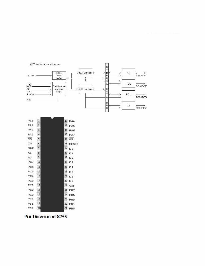
The signal description of 8255 are briefly presented as follows :
PA7-PA0: These are eight port A lines that acts as either latched output or buffered input lines
depending upon the control word loaded into the control word register.
PC7-PC4: Upper nibble of port C lines. They may act as either output latches or input buffers
lines.This port also can be used for generation of handshake lines in mode 1 or mode 2.
PC3-PC0: These are the lower port C lines, other details are the same as PC7-PC4 lines.
PB0-PB7: These are the eight port B lines which are used as latched output lines or buffered input
lines in the same way as port A.
RD: This is the input line driven by the microprocessor and should be low to indicate read
operation to 8255.
WR: This is an input line driven by the microprocessor. A low on this line indicates write
operation.
CS : This is a chip select line. If this line goes low, it enables the 8255 to respond to RD and
WRsignals, otherwise RD and WR signal are neglected.
A1-A0 : These are the address input lines and are driven by the microprocessor. These lines A1-
A0 with RD, WR and CS from the following operations for 8255. These address lines are used for addressing any one of the four registers,i.e. three ports and a control word
register as given in table below. . In case of 8086 systems, if the 8255 is to be interfacedwith lower order data bus, the A0 and A1
pins of 8255 are connected with A1 and A2 respectively.
D0-D7 :These are the data bus lines those carry data or control word to/from the microprocessor.
RESET : A log ic high on th is l ine :/ / clears the control word register of 8255. A ll ports are set as input ports by default aftOperational Modesof8255
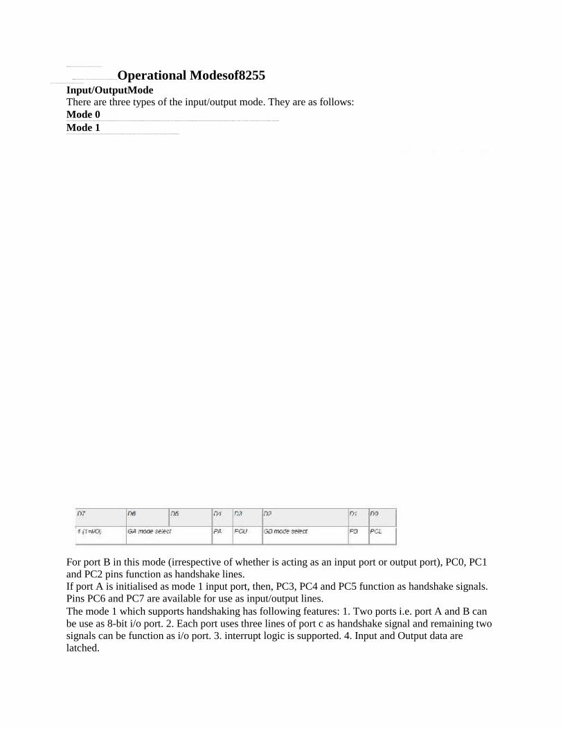
There are two main operational modes of 8255: 1. Inpu t/output mode 2. Bit set/reset mode
Input/OutputMode
There are three types of the input/output mode. They are as follows:
Mode 0 In this mode, the por ts can be used for simple input/outpu t operations without handsha king. If bo th port A and B are ini tialized in mode 0, the two halves of port C can be either used together as an additional8-bitport, or they can be used as indiv idual4-b itports. Since the two halves of port C are independent, they may be used such thatone-halfis in itial ized as an input port wh ile the other half is in itial ized as an ou tput port. The input outpu t features in mode 0 are as follows: 1 . O/p are latched. 2. I/p are buffered not latched. 3. Port do not have handsha ke or interrupt capabil ity .
Mode 1 When we wish to u se port A or port B for handshake (s trobed) inpu t or output operation , we ini tialise that port in mode 1 (port A and port B can be in iti lalised to operate in different modes,ie, for eg, port A can operate in mode 0 and port B in mode 1). Some of the pin s of port C function as handsha ke l ines .
For port B in this mode (irrespective of whether is acting as an input port or output port), PC0, PC1
and PC2 pins function as handshake lines.
If port A is initialised as mode 1 input port, then, PC3, PC4 and PC5 function as handshake signals.
Pins PC6 and PC7 are available for use as input/output lines.
The mode 1 which supports handshaking has following features: 1. Two ports i.e. port A and B can
be use as 8-bit i/o port. 2. Each port uses three lines of port c as handshake signal and remaining two
signals can be function as i/o port. 3. interrupt logic is supported. 4. Input and Output data are
latched.
Mode 2
Only group A can be initialised in this mode. Port A can be used for bidirectional handshake data
transfer. This means that data can be input or output on the same eight lines (PA0 - PA7). Pins PC3 -
PC7 are used as handshake lines for port A. The remaining pins of port C (PC0 - PC2) can be used as
input/output lines if group B is initialised in mode 0. In this mode, the 8255 may be used to extend
the system bus to a slave microprocessor or to transfer data bytes to and from a floppy disk
controller.
Bit Set/Reset (BSR)mode
In this mode only port b can be used (as an output port). Each line of port C (PC0 - PC7) can be
set/reset by suitably loading the command word register.no effect occurs in input-
output mode.
The individual bits of port c can be set or reset by sending the signal OUT instruction to
the
control register.
://
Control WordFormat
Input/output modeformat
ControlWordformat ininput/outputmode
The figure shows the control word format in the input/output mode. This mode is selected by
making D7 ='1' .
D0, D1, D3, D4 are for lower port C, port B, upper port C and port A respectively. When D0 or D1
or D3 or D4 are "SET", the corresponding ports act as input ports. For eg, if D0 = D4 = '1', then
lower port C and port A act as input ports. If these bits are "RESET",
then the corresponding ports act as output ports. For eg, if D1 = D3 = '0', then port B and upper port
C act as output ports.
D2 is used for mode selection for group B (Port B and Lower Port C). When D2 = '0', mode 0 is
selected and when D2 = '1', mode 1 is selected.
D5, D6 are used for mode selection for group A (Upper Port C and Port A). The format is as
follows:
D6 D5 mode
0 0 0
0 1 1
1 x 2
BSRmodeformat
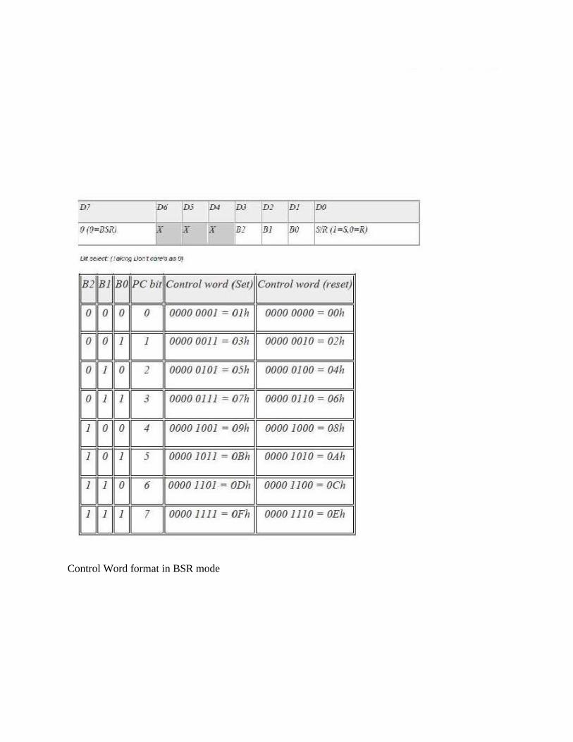
Control Word format in BSR mode
The figure shows the control word format in BSR mode. This mode is selected by making
D7='0'.
D0 is used for bit set/reset. When D0= '1', the port C bit selected (selection of a port C bit is shown
in the next point) is SET, when D0 = '0', the port C bit is RESET.
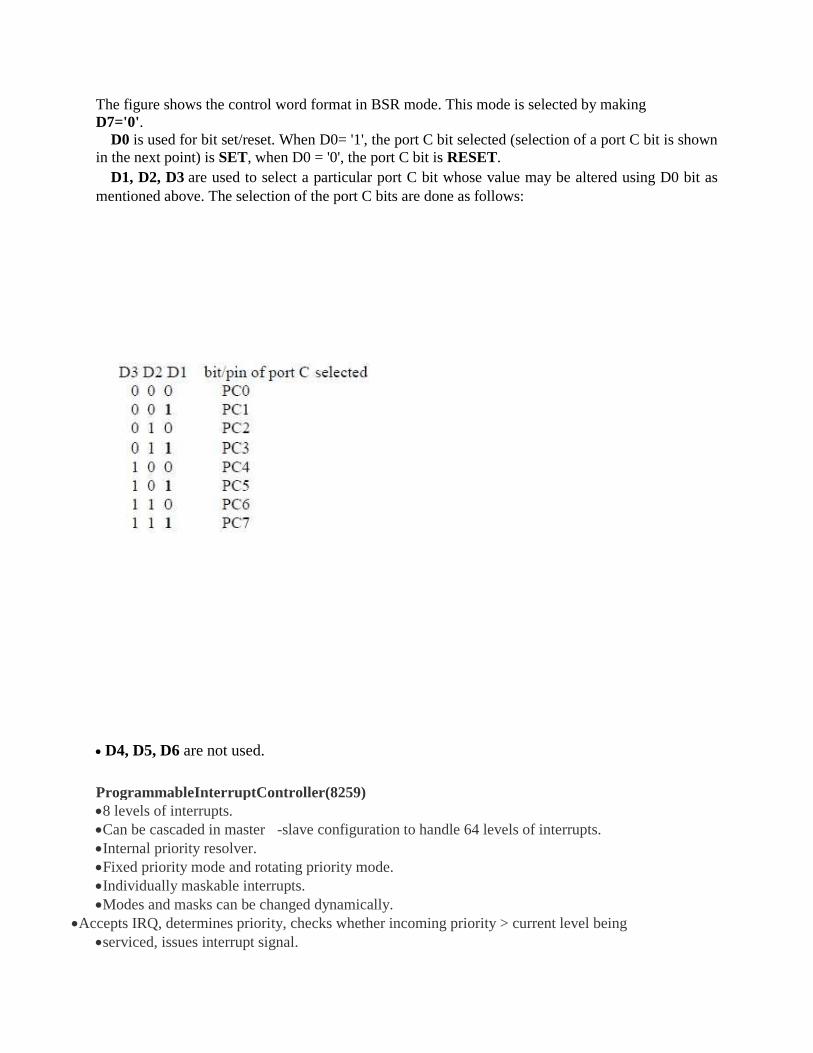
D1, D2, D3 are used to select a particular port C bit whose value may be altered using D0 bit as
mentioned above. The selection of the port C bits are done as follows:
D4, D5, D6 are not used.
ProgrammableInterruptController(8259)
8 levels of interrupts.
Can be cascaded in master -slave configuration to handle 64 levels of interrupts.
Internal priority resolver.
Fixed priority mode and rotating priority mode.
Individually maskable interrupts.
Modes and masks can be changed dynamically.
Accepts IRQ, determines priority, checks whether incoming priority > current level being
serviced, issues interrupt signal.
In 8085 mode, provides 3 byte CALL instruction. In 8086 mode, provides 8 bit vector
number.
Polled and vectored mode.
Starting address of ISR or vector number is programmable.
No clock required. .Features
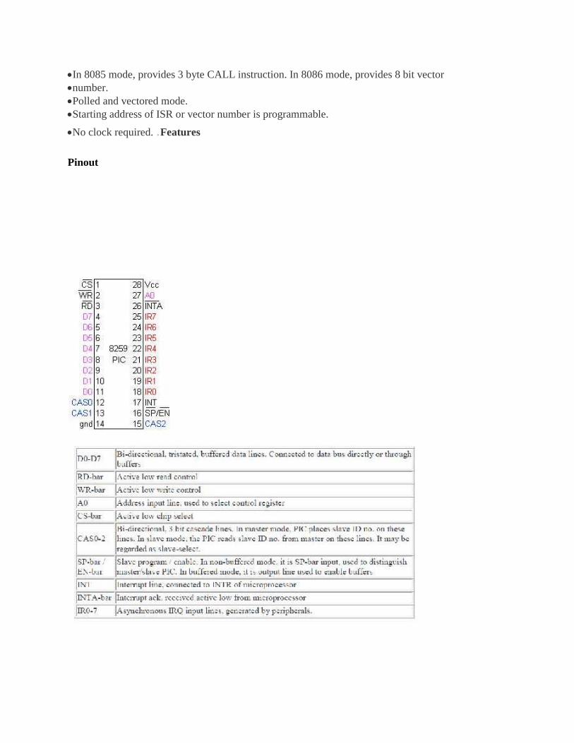
Pinout
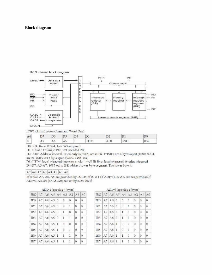
Block diagram
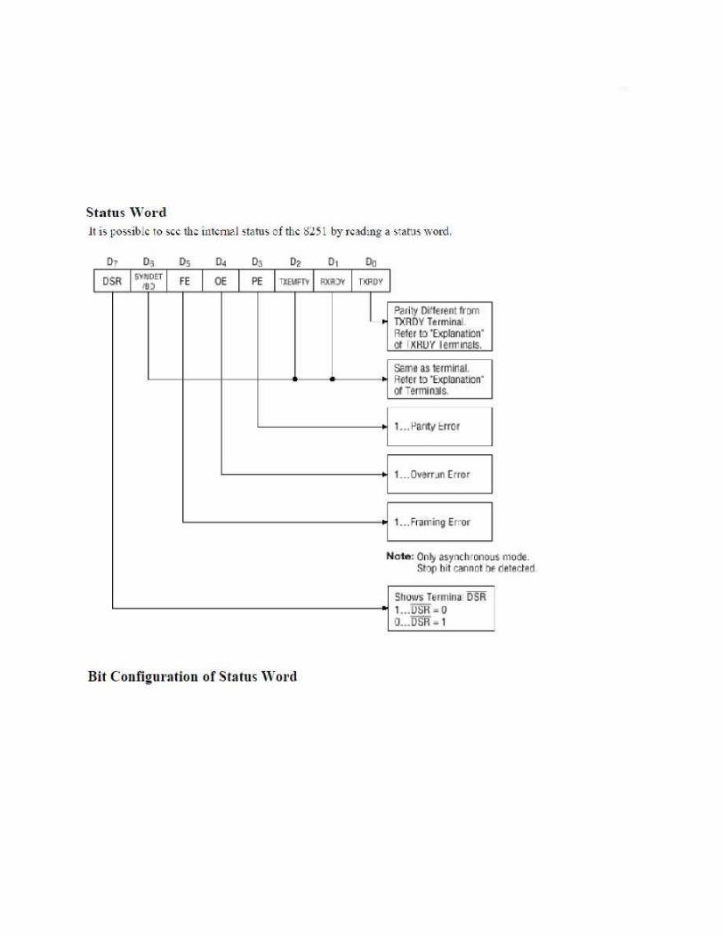
UNIVERSALSYNCHRONOUS ASYNCHRONOUS RECEIVER TRANSMITTER(USART)
The 8251 is a USART (Universal Synchronous Asynchronous Receiver Transmitter) for
serial data communication. As a peripheral device of a microcomputer system, the 8251receives
parallel data from the CPU and transmits serial data after conversion. This device also receives serial
data from the outside and transmits parallel data to the CPU after conversion.
Block Diagram of 8251
Control Words
There are two types of control word.
1.Mode instruction (setting of function)
2.Command (setting of operation)
1) Mode Instruction
Mode instruction is used for setting the function of the 8251. Mode instruction will be in "wait for
write" at either internal reset or external reset. That is, the writing of a control word after resetting
will be recognized as a "mode instruction."
Items set by mode instruction are as follows:
Synchronous/asynchronous mode
Stop bit length (asynchronous mode)
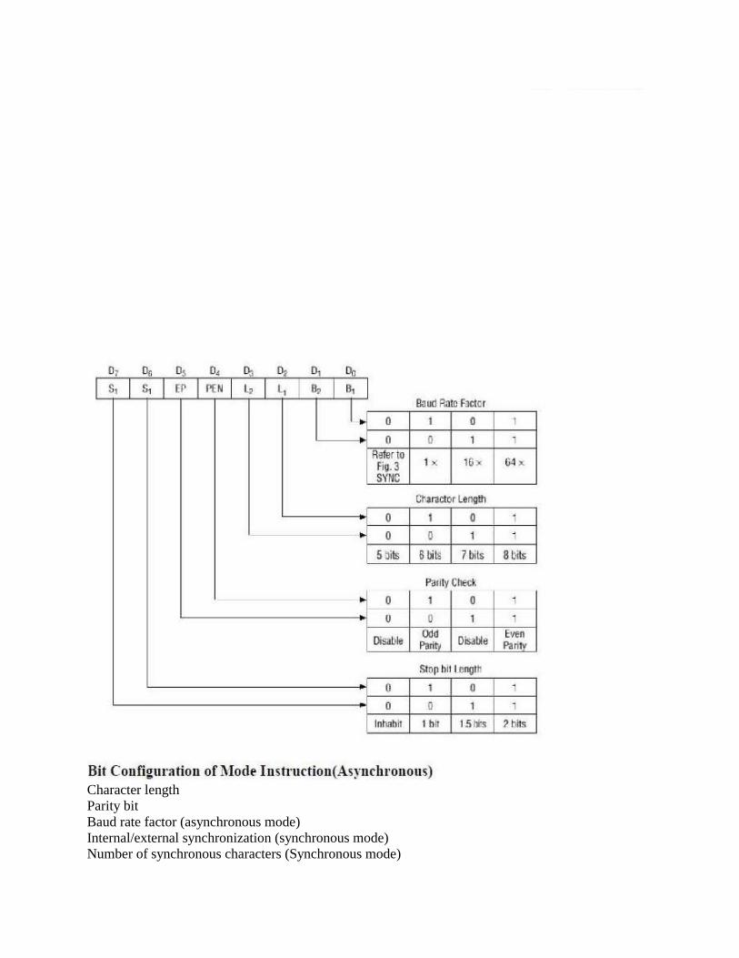
Character length
Parity bit
Baud rate factor (asynchronous mode)
Internal/external synchronization (synchronous mode)
Number of synchronous characters (Synchronous mode)
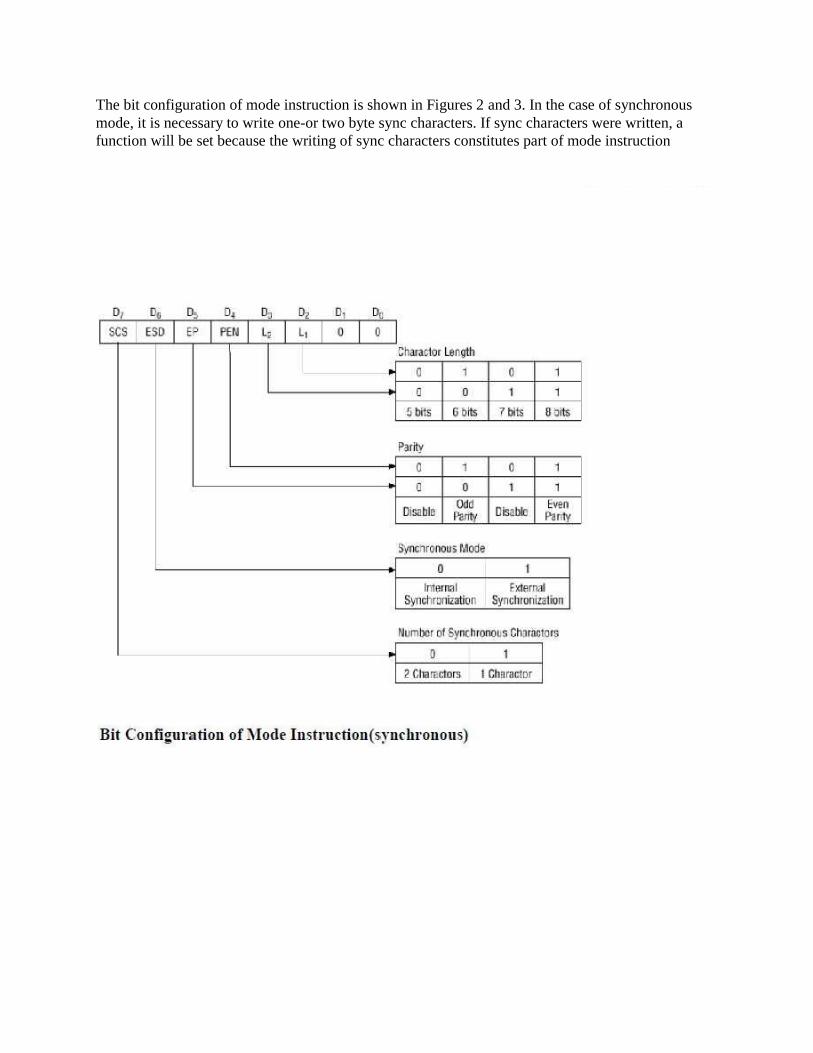
The bit configuration of mode instruction is shown in Figures 2 and 3. In the case of synchronous
mode, it is necessary to write one-or two byte sync characters. If sync characters were written, a
function will be set because the writing of sync characters constitutes part of mode instruction
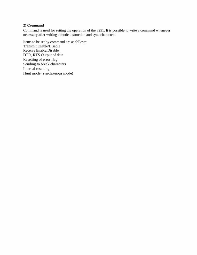
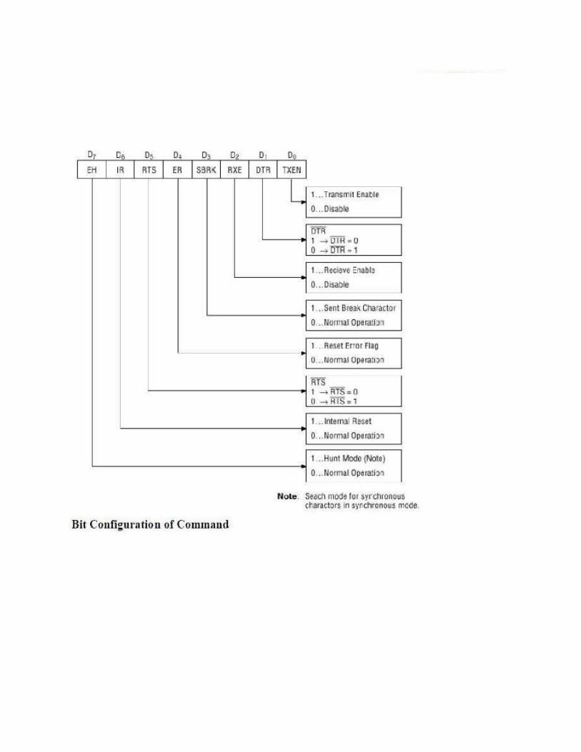
2) Command
Command is used for setting the operation of the 8251. It is possible to write a command whenever
necessary after writing a mode instruction and sync characters.
Items to be set by command are as follows:
Transmit Enable/Disable
Receive Enable/Disable
DTR, RTS Output of data.
Resetting of error flag.
Sending to break characters
Internal resetting
Hunt mode (synchronous mode)
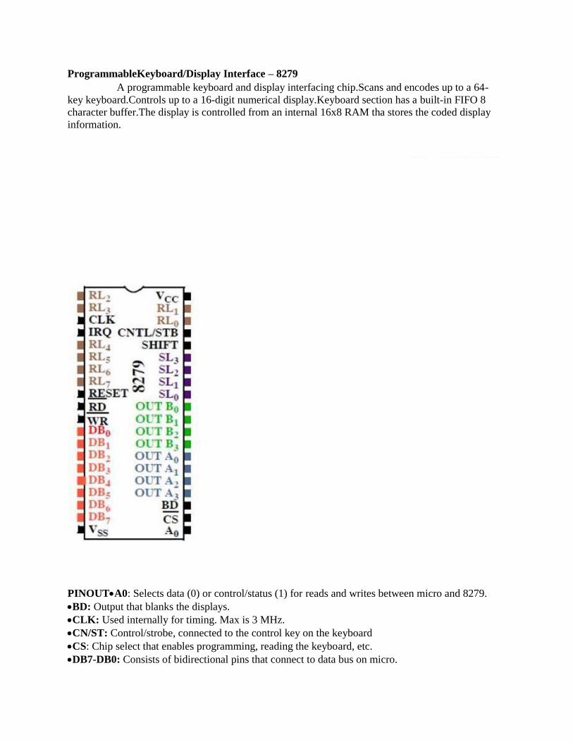
ProgrammableKeyboard/Display Interface – 8279
A programmable keyboard and display interfacing chip.Scans and encodes up to a 64-
key keyboard.Controls up to a 16-digit numerical display.Keyboard section has a built-in FIFO 8
character buffer.The display is controlled from an internal 16x8 RAM tha stores the coded display
information.
PINOUTA0: Selects data (0) or control/status (1) for reads and writes between micro and 8279.
BD: Output that blanks the displays.
CLK: Used internally for timing. Max is 3 MHz.
CN/ST: Control/strobe, connected to the control key on the keyboard
CS: Chip select that enables programming, reading the keyboard, etc.
DB7-DB0: Consists of bidirectional pins that connect to data bus on micro.
IRQ: Interrupt request, becomes 1 when a key is pressed, data is available.
OUTA3-A0/B3-B0: Outputs that sends data to the most significant/least significant
nibble of display.
RD(WR): Connects to micro's IORC or RD signal, reads data/status registers.
RESET: Connects to system RESET.
RL7-RL0: Return lines are inputs used to sense key depression in the keyboard matrix.
Shift: Shift connects to Shift key on keyboard.
SL3-SL0: Scan line outputs scan both the keyboard and displays.
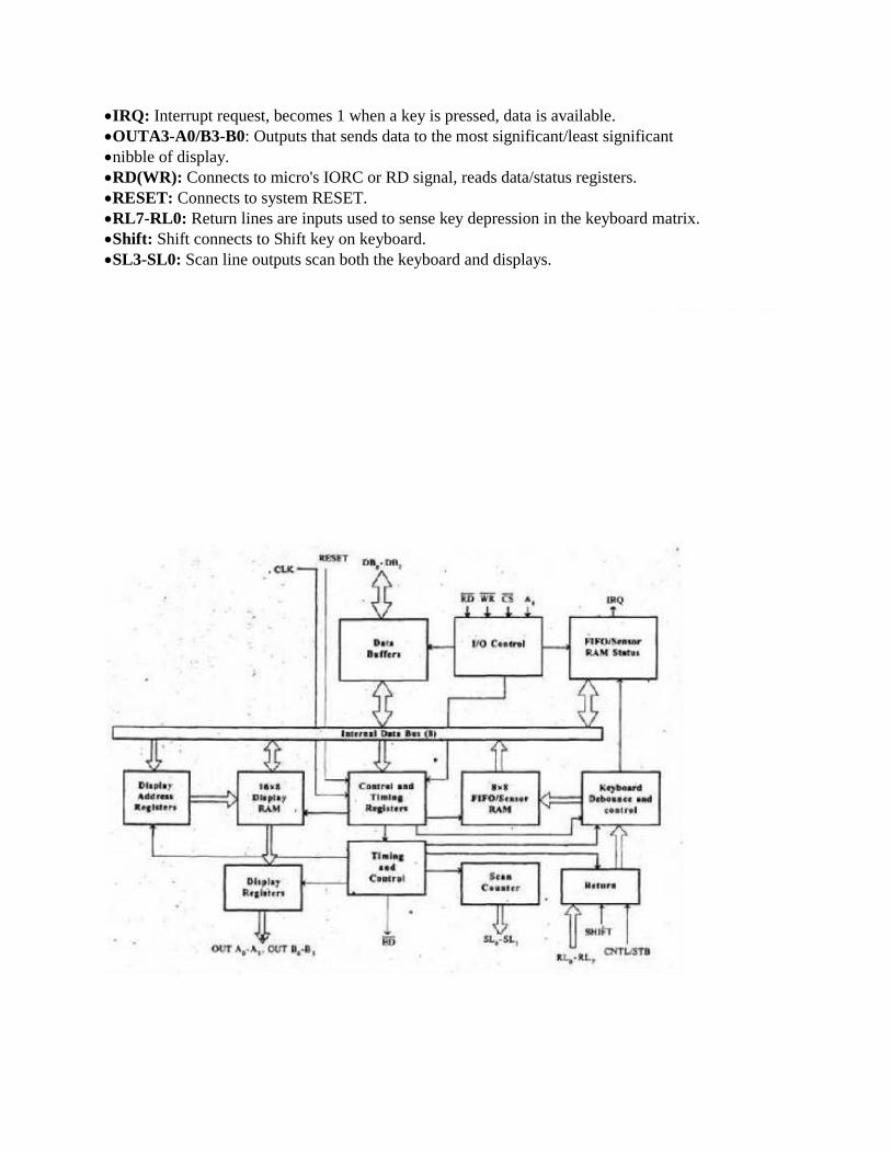
Block Diagram of 8279
Display section:
The display section haseightoutput lines dividedintotwo groups A0-A3 and B0-B3.
The outputlines can beused either asa single group of eightlinesor astwo groups
of four lines, inconjunctionwiththe scan linesfora multiplexed display.
The outputlines are connectedtothe anodesthrough drivertransistorincase of
common cathode7-segment LEDs.
The cathodes are connectedto scan lines throughdriver transistors.
The display can be blanked byBD(low) line.
The display section consists of 16 x8 display RAM. The CPUcan readfrom orwrite
into any location of the display RAM.
Scan section:
The scan section has a scan counter andfourscanlines, SL0to SL3.
In decodedscanmode,the output of scan lineswill besimilar toa 2-to-4 decoder.
Inencodedscanmode,the output of scan lineswill bebinary count, andsoan external decoder should be
usedto convert thebinary count to decodedoutput.
The scan lines are commonfor keyboard and display.
The scan lines are usedtoformtherows of amatrixkeyboard and also connectedto digit drivers of
a multiplexed display,toturnON/OFF.
CPUinterface section:
The CPUinterface section takes care of datatransferbetween 8279and the processor.
Thissection haseight bidirectional data lines DB0 to DB7for data transferbetween
8279 and CPU.
It requires twointernaladdress A=0forselecting data buffer and A=1for selecting control
registerof8279.
The control signalsWR(low), RD(low), CS (low)and A0 are usedfor read/writeto
8279.
It has aninterrupt requestline IRQ,for interrupt driven data transferwith processor.
The 8279 require an internalclockfrequency of 100 kHz. Thiscan beobtained by
dividingthe input clock by an internal prescaler.
The RESETsignalsetsthe 8279 in 16-characterdisplaywith two -keylockout
keyboardmodes.
DMACONTROLLER8237:
://
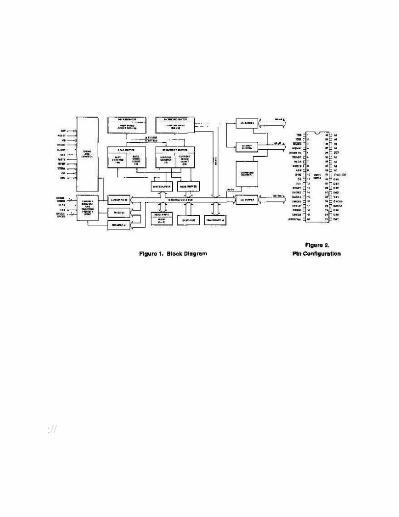
://
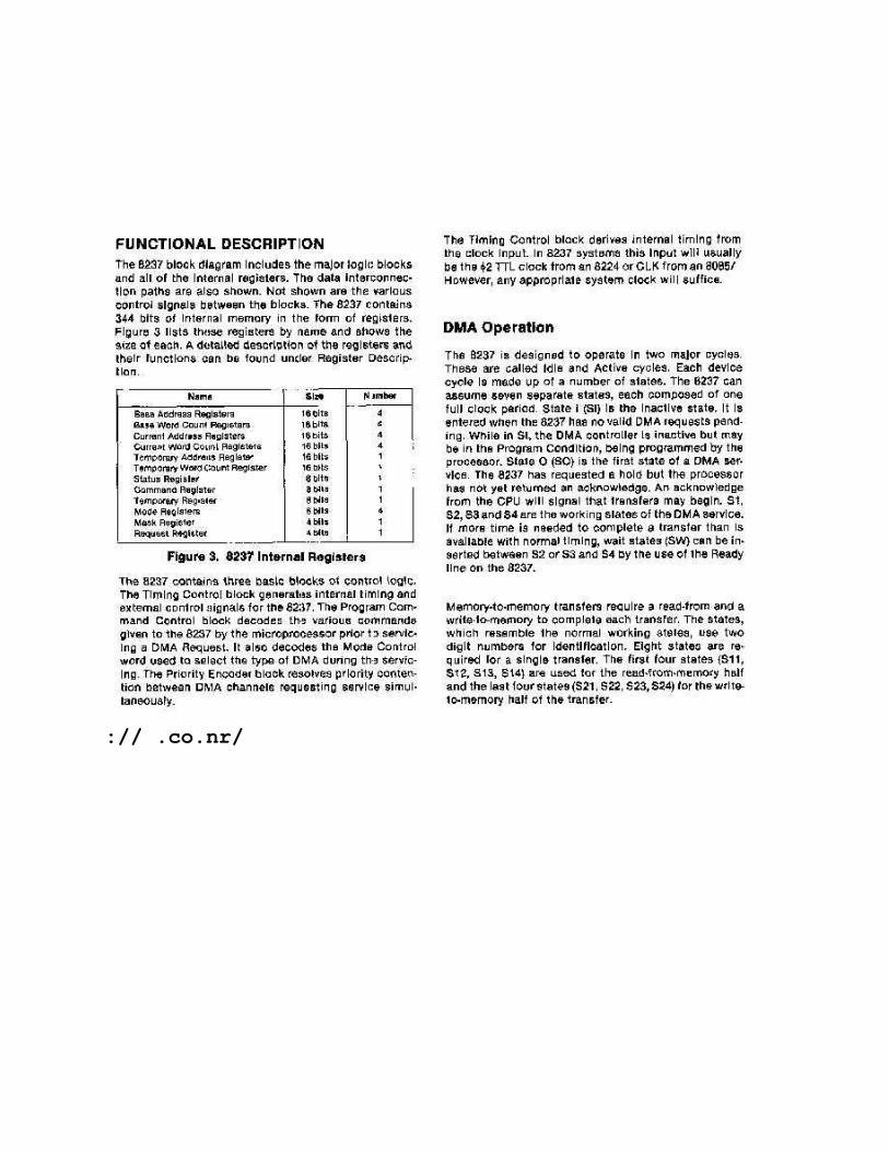
:// .co.nr/
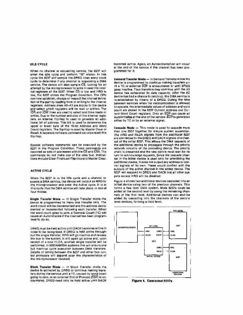

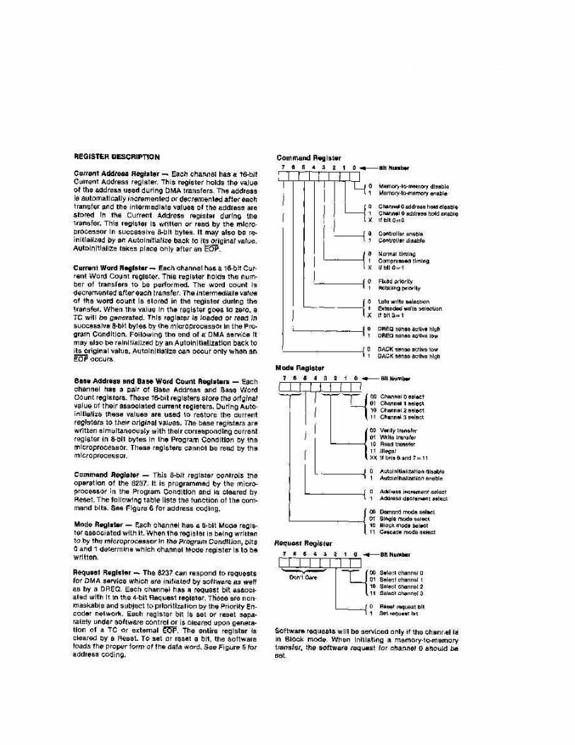

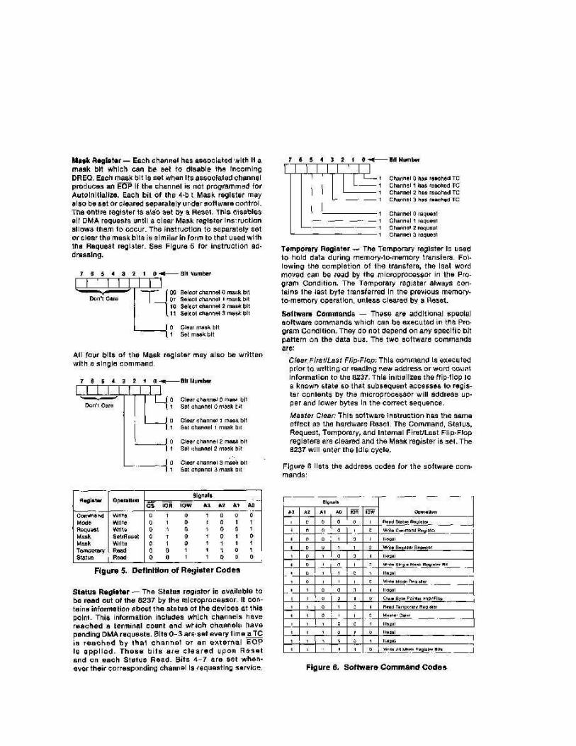
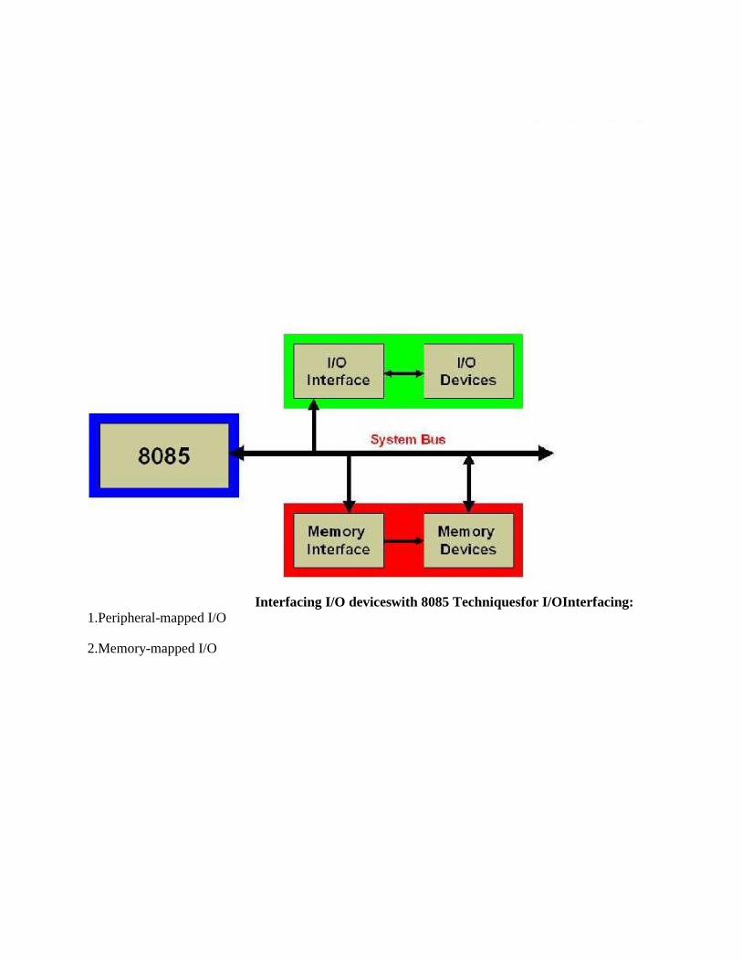
Interfacing I/O deviceswith 8085 Techniquesfor I/OInterfacing:
1.Peripheral-mapped I/O
2.Memory-mapped I/O
Memory-mapped I/O
8085 uses its 16-bit address bus to identify a memory location
Memory address space: 0000H to FFFFH
8085 needs to identify I/O devices also
I/O devices can be interfaced using addresses from memory space
8085 treats such an I/O device as a memory location
This is called Memory-mapped I/O
Peripheral-mappedI/O
8085 has a separate 8-bit addressing scheme for I/O devices
I/O address space: 00H to FFH
This is called Peripheral-mapped I/O or I/O-mapped I/O
8085 Communicationwith I/O devices
Involves the following three steps
1.Identify the I/O device (with address)
2.Generate Timing & Control signals
3.Data transfer takes place
8085 communicates with a I/O device only if there is a Program Instruction to do so
IdentifytheI/O device (with address)
1. Memory-mapped I/O (16-bit address)
2. Peripheral-mapped I/O (8-bit address)
Timing &Control Signals:
Memory-mapped I/O
Reading Input: IO/M = 0, RD = 0
Write to Output: IO/M = 0, WR = 0
Peripheral-mappedI/O
Reading Input: IO/M = 1, RD = 0
Write to Output: IO/M = 1, WR = 0
8085 Communicationwith I/O devices
Involves the following three steps
Identify the I/O device (with address) Generate Timing & Control signals Data transfer takes
place
8085 communicates with a I/O device only if there is a Program Instruction to do so
PeripheralI/OInstructions
INInstruction
Inputs data from input device into the accumulator
It is a 2-byte instruction
Format: IN 8-bit port address
Example: IN 01H
OUTInstruction
Outputs the contents of accumulator to an output device
It is a 2-byte instruction
://
Format: OUT 8-bit port address
Example: OUT 02H
Memory-mapped I/OInstructions
I/O devices are identified by 16-bit addresses
8085 communicates with an I/O device as if it were one of the memory locations
Memory related instructions are used
For e.g. LDA, STA LDA 8000H
Loads A with data read from input device with 16-bit address 8000H STA 8001H
Stores (Outputs) contents of A to output device with 16-bit address
8001H
Applications:
StepperMotor:
The hardware setup consists of a microprocessor motherboard and stepper motor interface
board. The motherboard consists of 8085 MPU, 8KB EPROM, 8KB RAM, Keyboard and display
controller 8279, 21-key Hex-keypad and six numbers of seven segment LEDs and
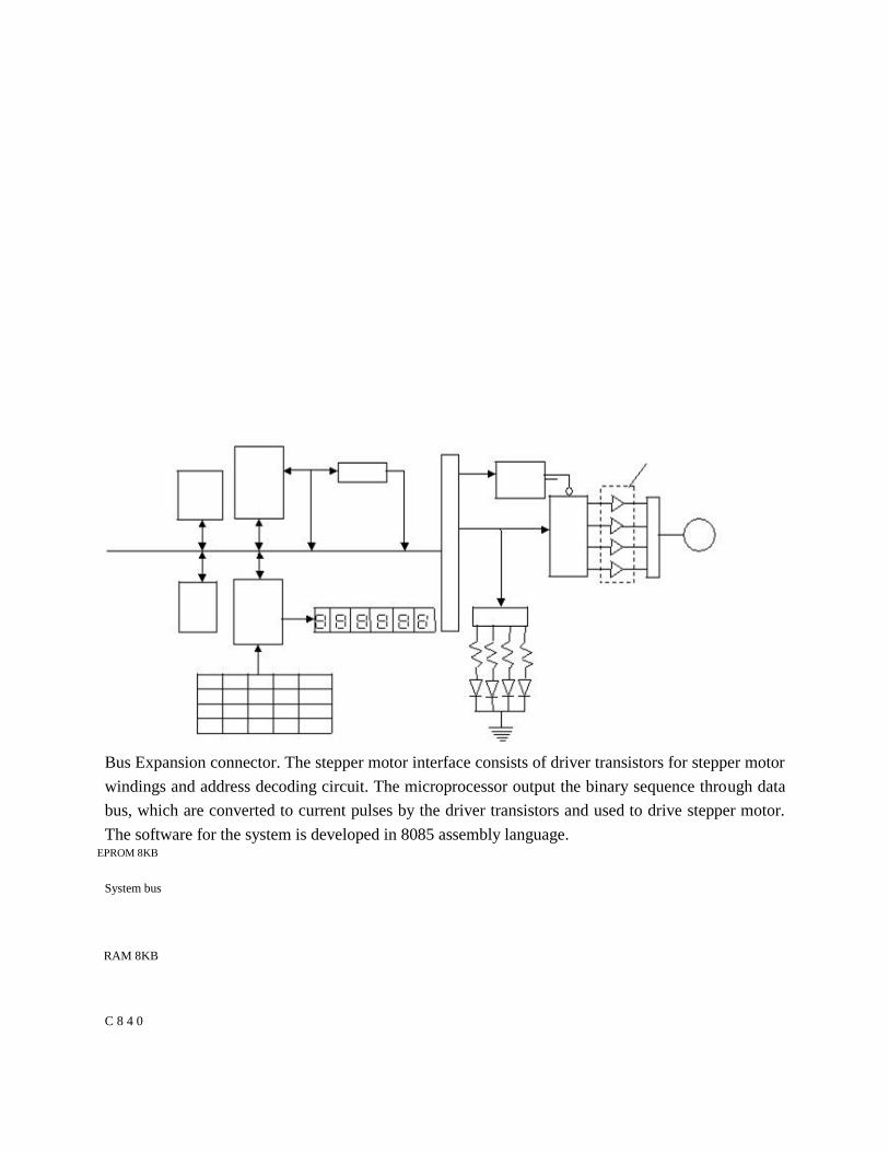
Bus Expansion connector. The stepper motor interface consists of driver transistors for stepper motor
windings and address decoding circuit. The microprocessor output the binary sequence through data
bus, which are converted to current pulses by the driver transistors and used to drive stepper motor.
The software for the system is developed in 8085 assembly language. EPROM 8KB
System bus
RAM 8KB
C 8 4 0
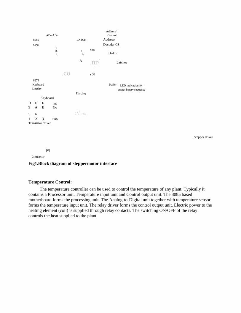
Address/
AD0-AD7
Control
8085
LATCH
Address/
CPU
Connector
Decoder CS
7
-D 7
D0-D3
0 A-
D 0
A .nr/
Latches
Expansion
.co 00 Pin
8279
Buffer
Keyboard LED indication for
Display
output binary sequence
Display
Keyboard
D E
F int
9 A
B Go
5 6
:// 7 Nxt
1 2
3 Sub
Transistor driver
Stepper driver
Connector
M
Fig1.Block diagram of steppermotor interface
Temperature Control:
The temperature controller can be used to control the temperature of any plant. Typically it
contains a Processor unit, Temperature input unit and Control output unit. The 8085 based
motherboard forms the processing unit. The Analog-to-Digital unit together with temperature sensor
forms the temperature input unit. The relay driver forms the control output unit. Electric power to the
heating element (coil) is supplied through relay contacts. The switching ON/OFF of the relay
controls the heat supplied to the plant.
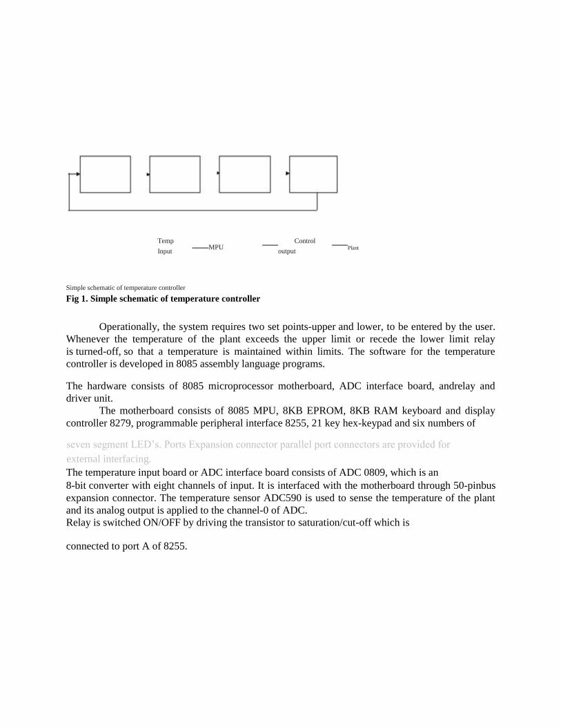
Temp
MPU
Control
Plant Input
output
Simple schematic of temperature controller
Fig 1. Simple schematic of temperature controller
Operationally, the system requires two set points-upper and lower, to be entered by the user.
Whenever the temperature of the plant exceeds the upper limit or recede the lower limit relay
is turned-off, so that a temperature is maintained within limits. The software for the temperature
controller is developed in 8085 assembly language programs.
The hardware consists of 8085 microprocessor motherboard, ADC interface board, andrelay and
driver unit.
The motherboard consists of 8085 MPU, 8KB EPROM, 8KB RAM keyboard and display
controller 8279, programmable peripheral interface 8255, 21 key hex-keypad and six numbers of
seven segment LED‟s. Ports Expansion connector parallel port connectors are provided for
external interfacing.
The temperature input board or ADC interface board consists of ADC 0809, which is an
8-bit converter with eight channels of input. It is interfaced with the motherboard through 50-pinbus
expansion connector. The temperature sensor ADC590 is used to sense the temperature of the plant
and its analog output is applied to the channel-0 of ADC.
Relay is switched ON/OFF by driving the transistor to saturation/cut-off which is
connected to port A of 8255.
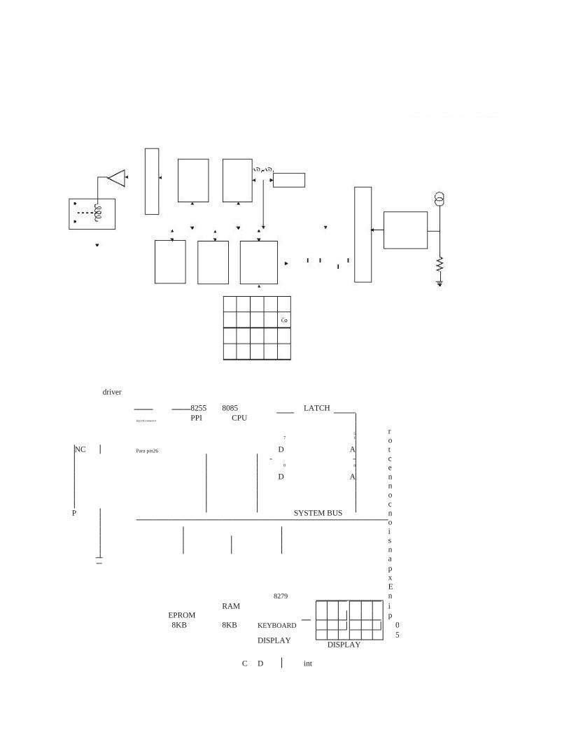
driver
8255 8085 LATCH
lelportl connector
PPI
CPU
Para pin26
7
5
r
1 o
NC
D
A
t
-
-
c
0
8 e
D
A
n
n
o
SYSTEM BUS
c
P n
o
i
s
n
a
p
x
RAM
8279
E
EPROM
n
i
8KB KEYBOARD
p
8KB
0
DISPLAY
5 DISPLAY
C D
int
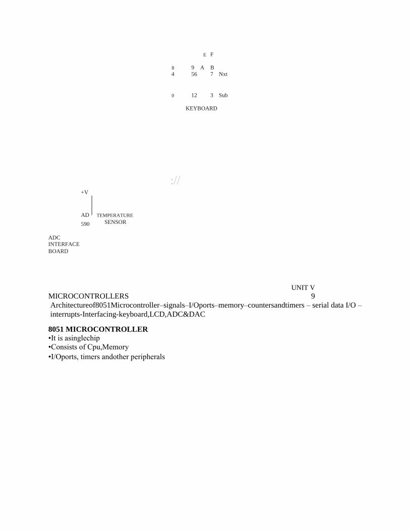
E F
8 9 A B
4 5 6
7
Nxt
0 1 2
3
Sub
KEYBOARD
://
+V
AD
TEMPERATURE
590
SENSOR
ADC
INTERFACE
BOARD
UNIT V
MICROCONTROLLERS 9
Architectureof8051Microcontroller–signals–I/Oports–memory–countersandtimers – serial data I/O –
interrupts-Interfacing-keyboard,LCD,ADC&DAC
8051 MICROCONTROLLER
•It is asinglechip
•Consists of Cpu,Memory
•I/Oports, timers andother peripherals
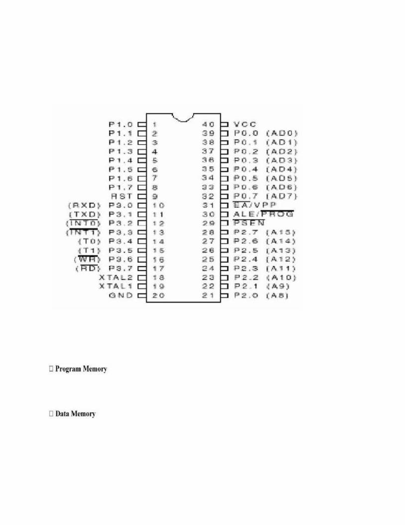
Memory Organization
-Logical separation of programand data memory
-Separate address spaces for Program(ROM) and Data(RAM)Memory
-AllowDataMemoryto beaccessedby8-bit addressesquicklyand manipulated by 8-bitCPU
-Onlybe read, not writtento
-The addressspace is 16-bit, so maximumof 64K bytes-Up to 4K bytes can be on-chip(internal) of
8051 core
-PSEN(ProgramStore Enable)isusedfor access toexternal ProgramMemory
-Includes 128bytes of on-chip Data Memorywhich are more easilyaccessible directlybyits
instructions
-There is also anumber ofSpecial Function Registers(SFRs)
-InternalDataMemorycontains four banks ofeight registers anda special32- byte longsegment
whichisbitaddressable by8051 bit-instructions -Externalmemoryof maximum64K bytes isaccessible
by“movx”
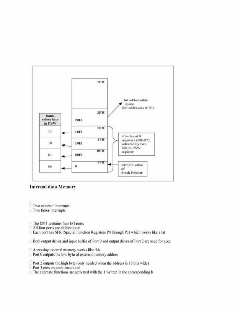
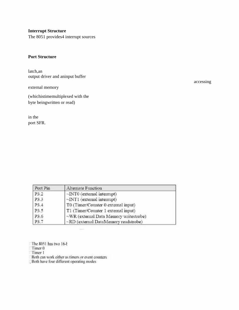
Interrupt Structure
The 8051 provides4 interrupt sources
Port Structure
latch,an
output driver and aninput buffer
accessing
external memory
(whichistimemultiplexed with the
byte beingwritten or read)
in the
port SFR.
Timer/Counter
bitTimer/Counterregisters . .co
An instruction isa command tothe :// microprocessortoperforma given taskon a specified data. Each instruction has two parts:
one is taskto be performed, calledthe operation code (opcode),
Instruction Format
and the secondisthedata to be operated on, calledthe operand. The operand (ordata) can be
specifiedin various ways. It mayinclude 8-bit(or 16-bit) data, an internal register, a memory
location, or8-bit (or 16-bit)address. In some instructions, the operandisimplicit.
Instruction word size
The8051instructionsetisclassified intothefollowingthree groups accordingto word size:
1.One-word or 1-byte instructions
2.Two-word or 2-byte instructions
3.Three-word or 3-byte instructions
One-Byte Instructions
A1-byte instruction includes the opcode and operand in thesame byte. Operand(s) are internal
registerand are codedinto the instruction.These instructions are 1-byte instructionsperforming three
differenttasks. In the first instruction,bothoperand registers are specified. In thesecond instruction,the
operand Bis specified andtheaccumulatorisassumed. Similarly, in the third instruction,the
accumulator isassumed to betheimplicitoperand.Theseinstructions are stored in8-bit binaryformat in
memory; eachrequires one memorylocation.
Two-Byte Instructions
In a two-byte instruction,the first byte specifiestheoperationcode andthesecond byte specifies the
operand. Sourceoperand is adata byteimmediatelyfollowingthe opcode.
Three-Byte Instructions
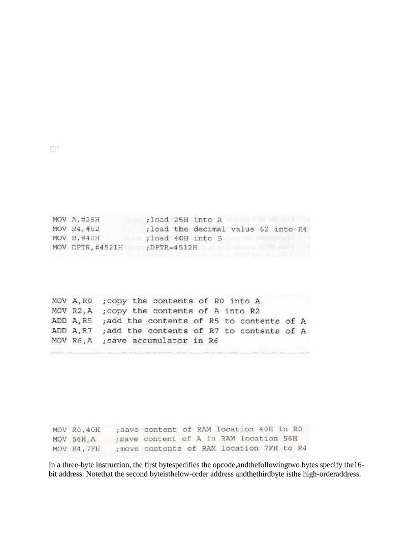
In a three-byte instruction, the first bytespecifies the opcode,andthefollowingtwo bytes specify the16-
bit address. Notethat the second byteisthelow-order address andthethirdbyte isthe high-orderaddress.
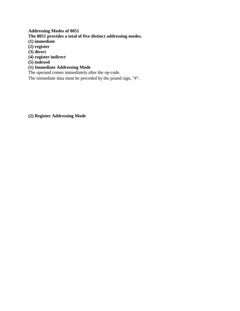
Addressing Modes of 8051
The 8051 provides a total of five distinct addressing modes.
(1) immediate
(2) register
(3) direct
(4) register indirect
(5) indexed
(1) Immediate Addressing Mode
The operand comes immediately after the op-code.
The immediate data must be preceded by the pound sign, "#".
(2) Register Addressing Mode
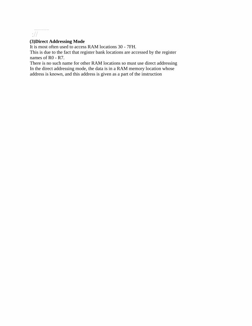
Register addressing mode involves the use of regis ters to ho ld the data to be manipulated.
:// (3)Direct Addressing Mode
It is most often used to access RAM locations 30 - 7FH.
This is due to the fact that register bank locations are accessed by the register
names of R0 - R7.
There is no such name for other RAM locations so must use direct addressing
In the direct addressing mode, the data is in a RAM memory location whose
address is known, and this address is given as a part of the instruction
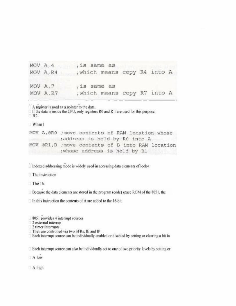
(4)Register Indirect Addressing Mode
R7 cannot be used to hold the address of an operand located in RAM when using indirect
addressing mode.
RO and R 1 are used as pointers they must be preceded by the @ sign.
(5) Indexed Addressing Mode
up table
entries
located in the program ROM space of the 8051.
used for this purpose is :
MOVC A, @ A+DPTR ://
bit register DPTR and register A are used to form the address of the data element stored
in on-chip ROM.
instruction MOVC is used instead of MOV. The "C" means code.
register DPTR to form the 16-bit
address of the needed data.
Interrupt Structure
IE
(Interrupt Enable). IE also exists a global disable bit, which can be cleared to disable all interrupts at
once
clearing a bit in IP (Interrupt Priority)
-priority interrupt can be interrupted by high-priority interrupt, but not by another low-
priority one
priority interrupt can‟t be interrupted by any other interrupt source
Handling Interrupt activated activated
sequence determines which request is serviced, so within each priority lever there is a second priority
structure
following
table
External Interrupt
routine is vectored to, but only if the interrupt was transition-activated
activated, then the external requesting source is contro lling the request flag, not theon-chiphardware
. .cochip hardware clears that flag :// that generated an external interrupt when the service when the flag for an enabled interrupt is found to be set (1)), the in terrupt sy stem generates an LCALL to the appropriate location in Program Memory , unless some other conditions block the in terrupt
terrupt of equal or higher priority level is already in progress
progress flag is active but not being responded to for one of the above conditions, must be s till active when the blocking cond ition is removed, or the denied interrupt will no t be serviced
generated LCALL causes only the contents of the Program Counter to be pushed onto the stac k, and reloads the PC with the beginning address of the service routine
doesn‟t. It clears an external interrupt flag (IE0 or IE1) only if it was transitionavtivated.
decide how much time to spend saving other registers. Programmer must also be more careful with proper selection, which regis ter to save. are spaced at8-by teinterval, beginning at 0003H for Ex ternal Interrupt 0, 000BH for Timer 0, 0013H for Ex ternal Interrupt 1 and 001BH for T imer 1.
I/O Ports
output driver and an input buffer
buffer of Port 0 and output driver of Port 2 are used for
accessing
external memory .co
byte being written or read)
the
rt 2 outputs the high byte (only needed when the address is 16 bits wide)
://
SFR
Timers
The 8051 comes equipped with two timers, both of which may be controlled, set, read, and
configured individually. The 8051 timers have three general functions: 1) Keeping time and/or
calculating the amount of time between events, 2) Counting the events themselves, or 3) Generating
baud rates for the serial port.
one of the primary uses of timers is to measure time. We will discuss this use of timers first and will
subsequently discuss the use of timers to count events. When a timer is used to measure time it is
also called an "interval timer" since it is measuring the time of the interval between two events.
Timer SFR
8051 has two timers which each function essentially the same way. One timer is TIMER0 and the
other is TIMER1. The two timers share two SFRs (TMOD and TCON) which control the timers, and
each timer also has two SFRs dedicated solely to itself (TH0/TL0 and TH1/TL1).
13-bit Time Mode (mode 0)
Timer mode "0" is a 13-bit timer. This is a relic that was kept around in the 8051 to maintain
compatability with its predecesor, the 8048. Generally the 13-bit timer mode is not used in new
development.
When the timer is in 13-bit mode, TLx will count from 0 to 31. When TLx is incremented from 31, it
will "reset" to 0 and increment THx. Thus, effectively, only 13 bits of the two timer bytes are being
used: bits 0-4 of TLx and bits 0-7 of THx. This also means, in essence, the timer can only contain
8192 values. If you set a 13-bit timer to 0, it will overflow back to zero 8192 machine cycles later.
Again, there is very little reason to use this mode and it is only mentioned so you wont be surprised
if you ever end up analyzing archaeic code which has been passed down through the generations
(a generation in a programming shop is often on the order of about 3 or 4 months).
16-bit Time Mode (mode 1)
Timer mode "1" is a 16-bit timer. This is a very commonly used mode. It functions just like13-
bit mode except that all 16 bits are used.
TLx is incremented from 0 to 255. When TLx is incremented from 255, it resets to 0 and causes
THx to be incremented by 1. Since this is a full 16-bit timer, the timer may contain up to 65536
distinct values. If you set a 16-bit timer to 0, it will overflow back to 0 after 65,536 machine
cycles.
8-bit Time Mode (mode 2)
Timer mode "2" is an 8-bit auto-reload mode. When a timer is in mode 2, THx holds the "reload
value" and TLx is the timer itself. Thus, TLx starts counting up. When TLx reaches 255 and is
subsequently incremented, instead of resetting to 0 (as in the case of modes 0 and 1), it will be
reset to the value stored in THx.
Split Timer Mode (mode 3)
Timer mode "3" is a split-timer mode. When Timer 0 is placed in mode 3, it essentially becomes
two separate 8-bit timers. That is to say, Timer 0 is TL0 and Timer 1 is TH0. Both timers count
from 0 to 255 and overflow back to 0. All the bits that are related to Timer 1 will now be tied to
TH0.
While Timer 0 is in split mode, the real Timer 1 (i.e. TH1 and TL1) can be put into
modes 0, 1 or 2 normally--however, you may not start or stop the real timer 1 since the
bits that do that are now linked to TH0. The real timer.1,in this case, will be incremented
every machine cycle no matter what.
USING TIMERS AS EVENT COUNTERS
We've discussed how a timer can be used for the obvious purpose of keeping track of time.
However, the 8051 also allows us to use the timers to count events.How can this be useful? Let's
say you had a sensor placed across a road that would send a pulse every time a car passed over it.
This could be used to determine the volume of traffic on
the road. We could attach this sensor to one of the 8051's I/O lines and constantly monitor it,
detecting when it pulsed high and then incrementing our counter when it went back to a low
state. This is not terribly difficult, but requires some code. Let's say we hooked the sensor to
P1.0; the code to count cars passing would look something like this:
JNB P1.0,$ ;If a car hasn't raised the signal, keep waiting
JB P1.0,$ ;The line is high which means the car is on the sensor right now INC COUNTER ;The
car has passed completely, so we count it
Serial Communication
Some of the external I/0 devices receive only the serial data.Normally serial communication is
used in the Multi Processor environment.8051 has two pins for serial communication.
(1)SID- Serial Input data.(2)SOD-Serial Output data.
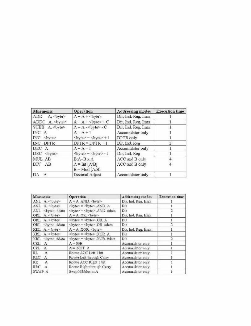
Instruction Set:
Arithmetic Instructions
Logical Instructions
Data Transfer Instructions that access the Internal Data Memory
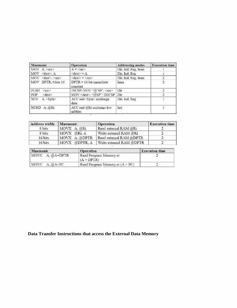
Data Transfer Instructions that access the External Data Memory
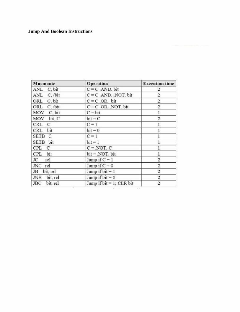
Jump And Boolean Instructions
Interfacing Keyboard to 8051 Microcontroller
The key board here we are interfacing is a matrix keyboard. This key board is designed with a
particular rows and columns. These rows and columns are connected to the microcontroller through
its ports of the micro controller 8051. We normally use 8*8 matrix key board. So only two ports of
8051 can be easily connected to the rows and columns of the key board.
When ever a key is pressed, a row and a column gets shorted through that pressed key and all the
other keys are left open. When a key is pressed only a bit in the port goes high. Which indicates
microcontroller that the key is pressed. By this high on the bit key in the corresponding column is
identified.
Once we are sure that one of key in the key board is pressed next our aim is to identify that key. To
do this we firstly check for particular row and then we check the corresponding column the key
board.
To check the row of the pressed key in the keyboard, one of the row is made high by making one of
bit in the output port of 8051 high . This is done until the row is found out. Once we get the row next
out job is to find out the column of the pressed key. The column is detected by contents in the input
ports with the help of a counter. The content of the input port is rotated with carry until the carry bit
is set.
The contents of the counter is then compared and displayed in the display. This display is designed
using a seven segment display and a BCD to seven segment decoder IC 7447. The BCD equivalent
number of counter is sent through output part of 8051 displays the number of pressed key.
Interfacing Keyboard to 8051 Microcontroller
Circuit Diagram of Interfacing Keyboard to 8051

Program for Keyboard Interfacing with 8051
Start of main program:
to check that whether any key is pressed start: mov a,#00h
mov p1,a ;making all rows of port p1 zero mov a,#0fh
mov p1,a ;making all rows of port p1 high press: mov a,p2
jz press ;check until any key is pressed
after making sure that any key is pressed mov a,#01h ;make one row high at a time mov r4,a
mov r3,#00h ;initiating counter next: mov a,r4
mov p1,a ;making one row high at a time mov a,p2 ;taking input from port A
jnz colscan ;after getting the row jump to check column
mov a,r4
rl a ;rotate left to check next row mov r4,a
mov a,r3
add a,#08h ;increment counter by 08 count mov r3,a
sjmp next ;jump to check next row
after identifying the row to check the colomn following steps are followe colscan: mov r5,#00h
in: rrc a ;rotate right with carry until get the carry jc out ;jump on getting carry
inc r3 ;increment one count
jmp in
out: mov a,r3
da a ;decimal adjust the contents of counter
before display
mov p2,a
jmp start ;repeat for check next key.
Interfacing LCD to 8051:
Liquid Crystal Display also called as LCD is very helpful in providing user
interface as well as for debugging purpose. The most common type of LCD controller is
HITACHI 44780 which provides a simple interface between the controller & an LCD.
These LCD's are very simple to interface with the controller as well as are cost
effective.
The most commonly used ALPHANUMERICdisplays are
1x16 (Single Line & 16 characters),
2x16 (Double Line & 16 character per line),
4x20 (four lines & Twenty characters per line).
The LCD requires 3 control lines (RS, R/W & EN) & 8 (or 4) data lines. The number on data
lines depends on the mode of operation. If operated in 8-bit mode then 8 data lines + 3 control
lines i.e. total 11 lines are required. And if operated in 4-bit mode then 4 data lines + 3 control
lines i.e. 7 lines are required. How do we decide which mode to use? It‟s simple if you have
sufficient data lines you can go for 8 bit mode & if there is a time constrain i.e. display should be
faster then we have to use 8-bit mode because basically 4- bit mode takes twice as more time as
compared to 8-bit mode.
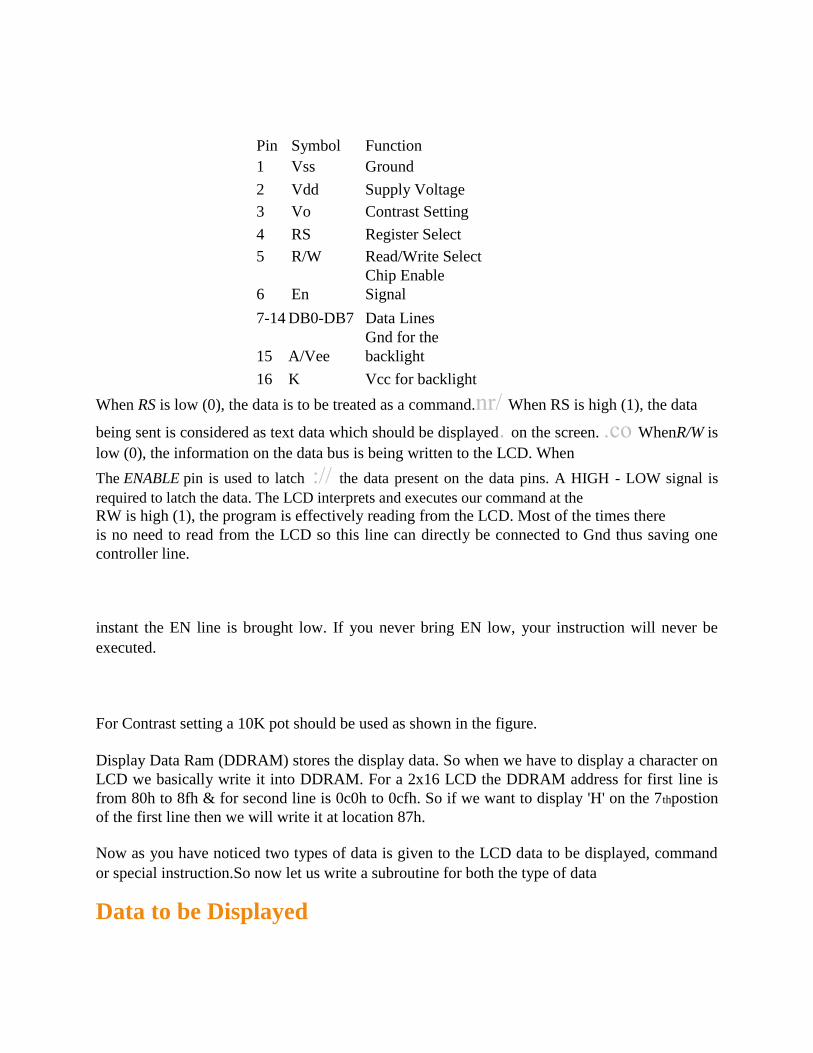
Pin Symbol Function
1 Vss Ground
2 Vdd Supply Voltage
3 Vo Contrast Setting
4 RS Register Select
5 R/W Read/Write Select
6 En
Chip Enable
Signal
7-14 DB0-DB7 Data Lines
15 A/Vee
Gnd for the
backlight
16 K Vcc for backlight
When RS is low (0), the data is to be treated as a command.nr/ When RS is high (1), the data
being sent is considered as text data which should be displayed. on the screen. .co WhenR/W is
low (0), the information on the data bus is being written to the LCD. When
The ENABLE pin is used to latch :// the data present on the data pins. A HIGH - LOW signal is
required to latch the data. The LCD interprets and executes our command at the
RW is high (1), the program is effectively reading from the LCD. Most of the times there
is no need to read from the LCD so this line can directly be connected to Gnd thus saving one
controller line.
instant the EN line is brought low. If you never bring EN low, your instruction will never be
executed.
For Contrast setting a 10K pot should be used as shown in the figure.
Display Data Ram (DDRAM) stores the display data. So when we have to display a character on
LCD we basically write it into DDRAM. For a 2x16 LCD the DDRAM address for first line is
from 80h to 8fh & for second line is 0c0h to 0cfh. So if we want to display 'H' on the 7thpostion
of the first line then we will write it at location 87h.
Now as you have noticed two types of data is given to the LCD data to be displayed, command
or special instruction.So now let us write a subroutine for both the type of data
Data to be Displayed
lcd_datadisplay:
SETB RS
//Telling the LCD that the data which is being send is to
be displayed
MOV P1,A
//Character to be displayed is in Acc
SETB EN
CLR EN
//High to Low pulse on EN to latch the data
CALL DELAY
//Delay so that LCD finishes its internal operations
ret ://
Command or Special Instruction lcd_command:
CLR RS //Telling the LCD that the data which is being send is a
command
MOV P1,A //Character to be displayed is in Acc
SETB EN
CLR EN //High to Low pulse on EN to latch the data
CALL DELAY //Delay so that LCD finishes its internal operations
ret Here I have used delay at the end of both the subroutines this is done to wait until the instruct ion is completely executed by the LCD. This will assure that our program gives the L CD the t ime it needs to execute ins tructions and also ma kes our program compatible with any LCD, regardless of how fast or slow it is.
"*" - Not Used/Ignored. This bit can be either "1" or "0"
Set Cursor Move Direction:
ID - Increment the Cursor After Each Byte Written to Display if Set
S - Shift Display when Byte Written to Display Enable Display/Cursor
D - Turn Display On(1)/Off(0) C - Turn Cursor On(1)/Off(0)
B - Cursor Blink On(1)/Off(0)
Set Cursor Move Direction:
ID - Increment the Cursor After Each Byte Written to Display if Set
S - Shift Display when Byte Written to Display Enable Display/Cursor D - Turn Display
On(1)/Off(0) C - Turn Cursor On(1)/Off(0)
B - Cursor Blink On(1)/Off(0)
Move Cursor/Shift Display
SC - Display Shift On(1)/Off(0) RL - Direction of Shift Right(1)/Left(0)
Set Interface Length
DL - Set Data Interface Length 8(1)/4(0)
N - Number of Display Lines 1(0)/2(1)
F - Character Font 5x10(1)/5x7(0)
Poll the "Busy Flag" BF - This bit is set while the LCD is processing
Move Cursor to CGRAM/Display
A - Address
Read/Write ASCII to the Display
D - Data
The above Table shows the different commands for the LCD. I wont go into its details.
Before starting to display on LCD we need to Initialize it. Firstly we must tell the LCD
whether we'll be using 8-bit or 4-bit mode. Also we will be telling the LCD that we need
5x8 character font. Both these options are selected using.a single command i.e. 38h. So
to
activate both these options we must execute following instructions:
MOV A,#38h
://
CALL lcd_command
Now that we have to Turn On the display & set the cursor option i.e. cursor ON/OFF &
Cursor blinking ON/OFF for that we will use the command 0Eh i.e. Display On , Cursor ON but
Cursor blinking OFF.
MOV A,#0Eh
CALL lcd_command
And the last command we require is to configure the LCD in such a way that everytime we send
a character to it the cursor position automatically increments by one & moves to right i.e. 06h.
MOV A,#06h
CALL lcd_command
So the lcd_initialize contains the following instructions
lcd_initialize:
MOV A,#38h
CALL lcd_command
MOV A,#38h
CALL lcd_command
MOV A,#38h
CALL lcd_command
ret
Similarly another important instruction that we require is Clearing the LCD i.e.
lcd_clr:
://
MOV A,#01h
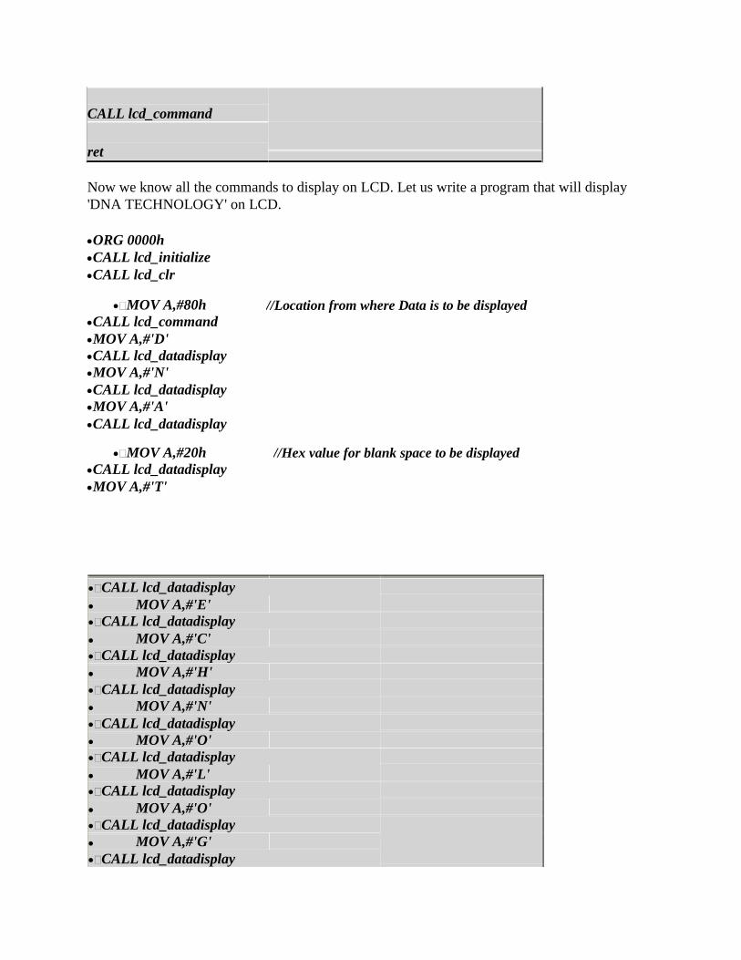
CALL lcd_command
ret
Now we know all the commands to display on LCD. Let us write a program that will display
'DNA TECHNOLOGY' on LCD.
ORG 0000h
CALL lcd_initialize
CALL lcd_clr
MOV A,#80h //Location from where Data is to be displayed
CALL lcd_command
MOV A,#'D'
CALL lcd_datadisplay
MOV A,#'N'
CALL lcd_datadisplay
MOV A,#'A'
CALL lcd_datadisplay
MOV A,#20h //Hex value for blank space to be displayed
CALL lcd_datadisplay
MOV A,#'T'
CALL lcd_datadisplay
MOV A,#'E'
CALL lcd_datadisplay
MOV A,#'C'
CALL lcd_datadisplay
MOV A,#'H'
CALL lcd_datadisplay
MOV A,#'N'
CALL lcd_datadisplay
MOV A,#'O'
CALL lcd_datadisplay
MOV A,#'L'
CALL lcd_datadisplay
MOV A,#'O'
CALL lcd_datadisplay
MOV A,#'G'
CALL lcd_datadisplay
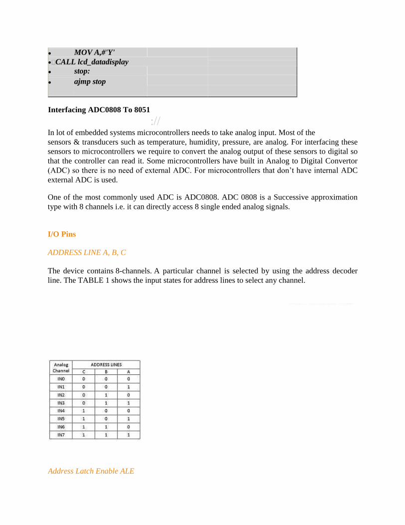
MOV A,#'Y'
CALL lcd_datadisplay
stop:
ajmp stop
Interfacing ADC0808 To 8051
:// In lot of embedded systems microcontrollers needs to take analog input. Most of the
sensors & transducers such as temperature, humidity, pressure, are analog. For interfacing these
sensors to microcontrollers we require to convert the analog output of these sensors to digital so
that the controller can read it. Some microcontrollers have built in Analog to Digital Convertor
(ADC) so there is no need of external ADC. For microcontrollers that don‟t have internal ADC
external ADC is used.
One of the most commonly used ADC is ADC0808. ADC 0808 is a Successive approximation
type with 8 channels i.e. it can directly access 8 single ended analog signals.
I/O Pins
ADDRESS LINE A, B, C
The device contains 8-channels. A particular channel is selected by using the address decoder
line. The TABLE 1 shows the input states for address lines to select any channel.
Address Latch Enable ALE

The address is latched on the Low – High transition of ALE.
START
The ADC‟s Successive Approximation :// Regis ter (SAR) is reset on the posit ive edge i.e. Low- High of the Start Conversion pulse. Whereas the conversion is begun on the falling
edge i.e. High – Low of the pulse.
Output Enable Whenever data has to be read from the ADC, Output Enable p in has to be pulled high thus enabling theTRI-STAT Eoutpu ts, al lowing data to be read from the data pins D0- D7.
End of Conversion (EOC) This Pin becomes High when the conversion has ended, so the con troller comes to know that the data can now be read from the data pins.
Clock External clock pulses are to be g iven to the ADC; this can be given either from LM 555 in Astable mode or the controller can also be used to give the pulses .
Calculating Step Size ALGORITHM 1. Start. 2. Select the channel. 3. A Low – High transition on ALE to latch in the
address. 4. A Low – High transition on Start to reset the ADC‟s SAR. 5. A High – Low transition
on ALE. 6. A High – Low transition on start to start the conversion. 7. Wait for End of cycle
(EOC) pin to become high. 8. Make Output Enable pin High. 9. Take Data from the ADC‟s
output 10. Make Output Enable pin Low. 11. Stop
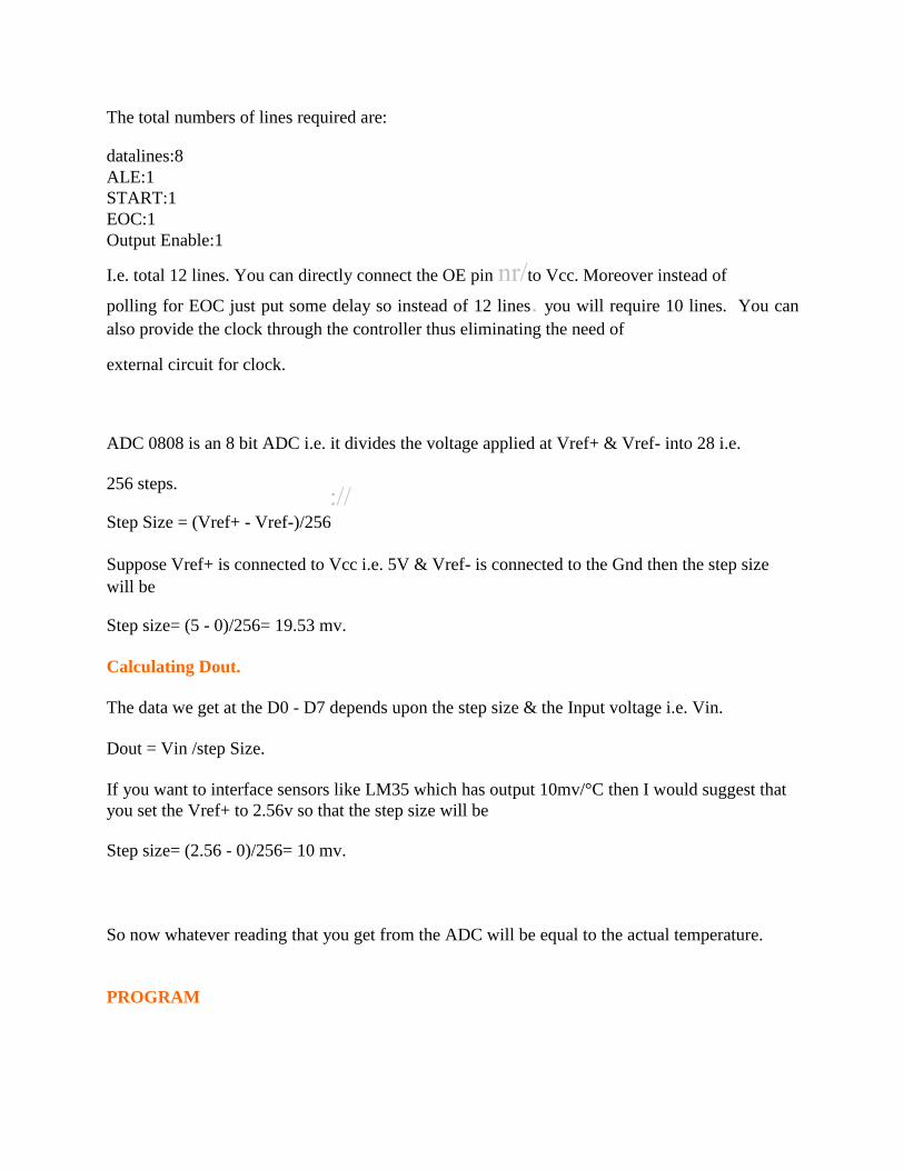
The total numbers of lines required are:
datalines:8
ALE:1
START:1
EOC:1
Output Enable:1
I.e. total 12 lines. You can directly connect the OE pin nr/to Vcc. Moreover instead of
polling for EOC just put some delay so instead of 12 lines. you will require 10 lines. You can
also provide the clock through the controller thus eliminating the need of
external circuit for clock.
ADC 0808 is an 8 bit ADC i.e. it divides the voltage applied at Vref+ & Vref- into 28 i.e.
256 steps. ://
Step Size = (Vref+ - Vref-)/256
Suppose Vref+ is connected to Vcc i.e. 5V & Vref- is connected to the Gnd then the step size
will be
Step size= (5 - 0)/256= 19.53 mv.
Calculating Dout.
The data we get at the D0 - D7 depends upon the step size & the Input voltage i.e. Vin.
Dout = Vin /step Size.
If you want to interface sensors like LM35 which has output 10mv/°C then I would suggest that
you set the Vref+ to 2.56v so that the step size will be
Step size= (2.56 - 0)/256= 10 mv.
So now whatever reading that you get from the ADC will be equal to the actual temperature.
PROGRAM
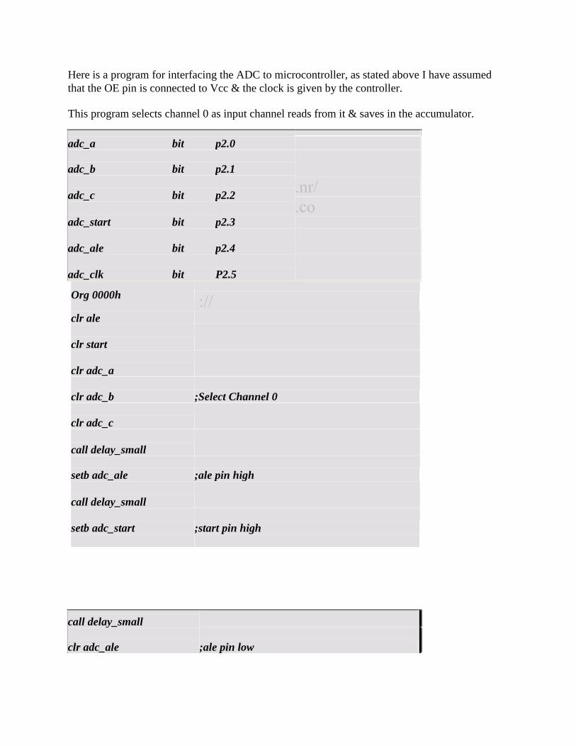
Here is a program for interfacing the ADC to microcontroller, as stated above I have assumed
that the OE pin is connected to Vcc & the clock is given by the controller.
This program selects channel 0 as input channel reads from it & saves in the accumulator.
adc_a bit p2.0
adc_b bit p2.1
.nr/
adc_c bit p2.2
.co
adc_start bit p2.3
adc_ale bit p2.4
adc_clk bit P2.5
Org 0000h ://
clr ale
clr start
clr adc_a
clr adc_b ;Select Channel 0
clr adc_c
call delay_small
setb adc_ale ;ale pin high
call delay_small
setb adc_start ;start pin high
call delay_small
clr adc_ale ;ale pin low
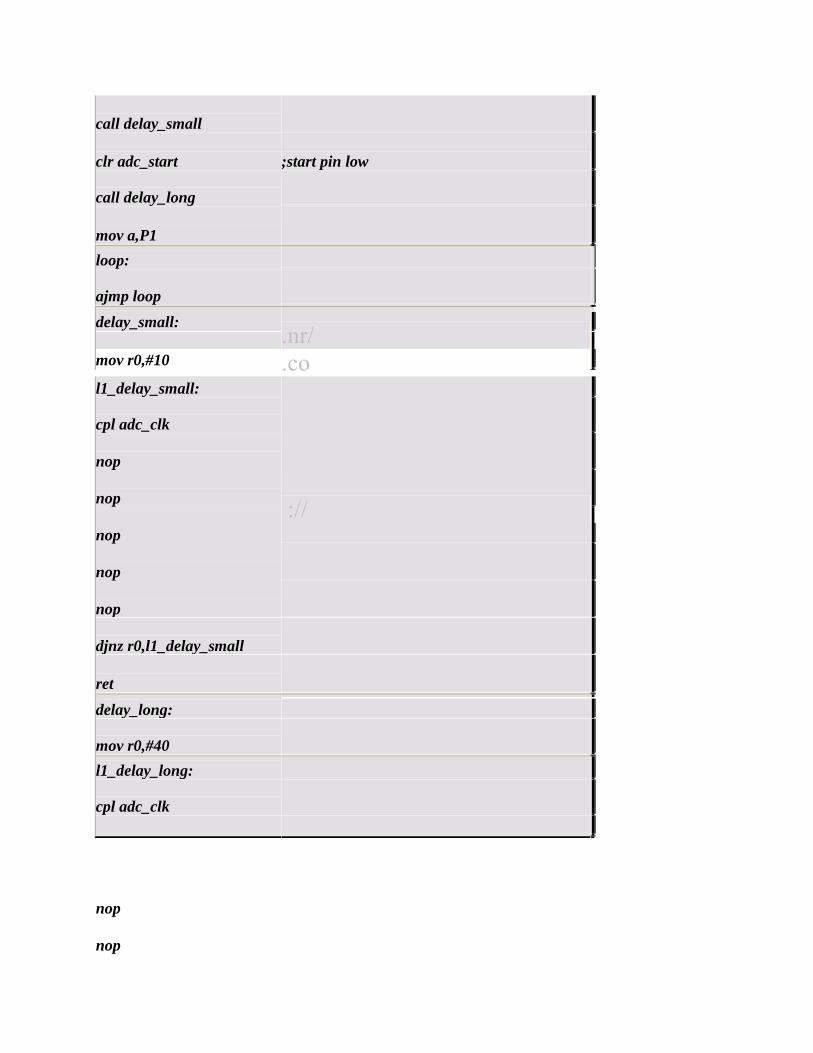
call delay_small
clr adc_start ;start pin low
call delay_long
mov a,P1
loop:
ajmp loop
delay_small: .nr/
mov r0,#10 .co
l1_delay_small:
://
cpl adc_clk
nop
nop
nop
nop
nop
djnz r0,l1_delay_small
ret
delay_long:
mov r0,#40
l1_delay_long:
cpl adc_clk
nop
nop

nop
nop
nop
djnz r0,l1_delay_long
ret
End
.