Fatima Michael College of Engineering & Technology - fmcet
109
FATIMA MICHAEL COLLEGE OF ENGINEERING & TECHNOLOGY Madurai – Sivagangai Main Road, Madurai - 625 020. An ISO 9001:2008 Certified Institution DEPARTMENT OF ELECTRONICS AND COMMUNIUCATION ENGG EC6011 ELECTROMAGNETIC INTERFERENCE AND COMPATIBILITY Regulation: 2013 Final year odd semester 1 Fatima Michael College of Engineering & Technology Fatima Michael College of Engineering & Technology
-
Upload
khangminh22 -
Category
Documents
-
view
1 -
download
0
Transcript of Fatima Michael College of Engineering & Technology - fmcet

FATIMA MICHAEL COLLEGE OF ENGINEERING & TECHNOLOGY Madurai – Sivagangai Main Road,
Madurai - 625 020.
An ISO 9001:2008 Certified Institution
DEPARTMENT OF ELECTRONICS AND
COMMUNIUCATION ENGG
EC6011 ELECTROMAGNETIC INTERFERENCE AND COMPATIBILITY
Regulation: 2013
Final year odd semester
1
Fatima Michael College of Engineering & Technology
Fatima Michael College of Engineering & Technology

SYLLABUS
EC6011 ELECTROMAGNETIC INTERFERENCE AND COMPATIBILITY L T PC
3 0 0 3
UNIT I BASIC THEORY 8
Introduction to EMI and EMC, Intra and inter system EMI, Elements of Interference, Sources andVictims of
EMI, Conducted and Radiated EMI emission and susceptibility, Case Histories, Radiationhazards to
humans, Various issues of EMC, EMC Testing categories, EMC Engineering Application.
UNIT II COUPLING MECHANISM 9
Electromagnetic field sources and Coupling paths, Coupling via the supply network, Common mode
coupling, Differential mode coupling, Impedance coupling, Inductive and Capacitive coupling,Radiative
coupling, Ground loop coupling, Cable related emissions and coupling, Transient sources, Automotive
transients.
UNIT III EMI MITIGATION TECHNIQUES 10
Working principle of Shielding and Murphy‘s Law, LF Magnetic shielding, Apertures and shielding
effectiveness, Choice of Materials for H, E, and free space fields, Gasketting and sealing, PCB Level
shielding, Principle of Grounding, Isolated grounds, Grounding strategies for Large systems, Grounding for
mixed signal systems, Filter types and operation, Surge protection devices, Transientprotection.
UNIT IV STANDARDS AND REGULATION 9
Need for Standards, Generic/General Standards for Residential and Industrial environment, Basic Standards,
Product Standards, National and International EMI Standardizing Organizations; IEC,ANSI, FCC, AS/NZS,
CISPR, BSI, CENELEC, ACEC. Electro Magnetic Emission and susceptibility standards and specifications,
MIL461E Standards.
UNIT V EMI TEST METHODS AND INSTRUMENTATION 9
Fundamental considerations, EMI Shielding effectiveness tests, Open field test, TEM cell for
immunity test, Shielded chamber , Shielded anechoic chamber, EMI test receivers, Spectrum
analyzer, EMI test wave simulators, EMI coupling networks, Line impedance stabilization networks,Feed
through capacitors, Antennas, Current probes, MIL -STD test methods, Civilian STD testmethods.
TOTAL: 45 PERIODS
TEXT BOOK:
1. Clayton Paul, ―Introduction to Electromagnetic Compatibility‖, Wiley Interscience, 2006
REFERENCES:
1. V Prasad Kodali, ―Engineering Electromagnetic Compatibility‖, IEEE Press, Newyork, 2001.
2. Henry W. Ott, ―Electromagnetic Compatibility Engineering‖, John Wiley & Sons Inc, Newyork, 2009
3. Daryl Gerke and William Kimmel, ―EDN‘s Designer‘s Guide to Electromagnetic Compatibility‖,
Elsevier Science & Technology Books, 2002
4. W Scott Bennett, ―Control and Measurement of Unintentional Electromagnetic Radiation‖, John
Wiley & Sons Inc., (Wiley Interscience Series) 1997.
5. Dr Kenneth L Kaiser, ―The Electromagnetic Compatibility Handbook‖, CRC Press 2005
Fatima Michael College of Engineering & Technology
Fatima Michael College of Engineering & Technology

UNIT I Basic Theroy
INTRODUCTION TO ELECTROMAGNETIC COMPATIBILITY (EMC) Since the early days of radio and telegraph communications, it has been known that a
spark gap generates electromagnetic waves rich in spectral content (frequency components) and
that these waves can cause interference or noise in various electronic and electrical devices such
as radio receivers and telephone communications. Numerous other sources of electromagnetic
emissions such as lightning, relays, dc electric motors, and fluorescent lights also generate
electromagnetic waves that are rich in spectral content and can cause interference in those
devices. There are also sources of electromagnetic emissions that contain only a narrow band of
frequencies. High-voltage power transmission lines generate electromagnetic emissions at the
power frequency [60 Hz; 50 Hz in Europe]. Radio transmitters transmit desired emissions by
encoding information (voice, music, etc.) on a carrier frequency. Radio receivers intercept these
electromagnetic waves, amplify them, and extract the information that is encoded in the wave.
Radar transmitters also transmit pulses of a single-frequency carrier. As this carrier frequency is
pulsed on and off, these pulses radiate outward from the antenna, strike a target, and return to
the radar antenna. The total transit time of the wave is directly related to the distance of the
target from the radar antenna. The spectral content of this radar pulse is distributed over a larger
band of frequencies around the carrier than are radio transmissions. Another important and
increasingly significant source of electromagnetic emissions is associated with digital computers
in particular and digital electronic devices in general. These digital devices utilize pulses to
signify a binary number, 0 (off) or 1 (on). Numbers and other symbols are represented as
sequences of these binary digits. The transition time of the pulse from off to on and vice versa is
perhaps the most important factor in determining the spectral content of the pulse. Fast (short)
transition times generate a wider range of frequencies than do slower (longer) transition times.
The spectral content of digital devices generally occupies a wide range of frequencies and can
also cause interference in electrical and electronic devices.
This text is concerned with the ability of these types of electromagnetic emissions to
cause interference in electrical and electronic devices. The reader has no doubt experienced
noise produced in an AM radio by nearby lightning discharges. The lightning discharge is rich
in frequency components, some of which pass through the input filter of the radio, causing noise
to be superimposed on the desired signal. Also, even though a radio may not be tuned to a
particular transmitter frequency, the transmission may be received, causing the reception of an
unintended signal. These are examples of interference produced in intentional receivers. Of
equal importance is the interference produced in unintentional receivers. For example, a strong
transmission from an FM radio station or TV station may be picked up by a digital computer,
causing the computer to interpret it as data or a control signal resulting in incorrect function of
the computer. Conversely, a digital computer may create emissions that couple into a TV,
causing interference.
This text is also concerned with the design of electronic systems such that interference
from or to that system will be minimized. The emphasis will be on digital electronic systems.
An electronic system that is able to function compatibly with other electronic systems and not
produce or be susceptible to interference is said to be electromagnetically compatible with its
environment.
The objective of this text is to learn how to design electronic systems for electromagnetic
compatibility (EMC). A system is electromagnetically compatible with its environment if it
satisfies three criteria:
Fatima Michael College of Engineering & Technology
Fatima Michael College of Engineering & Technology

1. It does not cause interference with other systems.
2. It is not susceptible to emissions from other systems.
3. It does not cause interference with itself.
Designing for EMC is not only important for the desired functional performance; the
device must also meet legal requirements in virtually all countries of the world before it can be
sold. Designing an electronic product to perform a new and exciting function is a waste of effort
if it cannot be placed on the market!
EMC design techniques and methodology have become as integral a part of design as,
for example, digital design. Consequently the material in this text has become a fundamental
part of an electrical engineer‘s background. This will no doubt increase in importance as the
trend toward increased clock speeds and data rates of digital systems continues.
The most important aspect in successfully dealing with EMC design is to have a sound
understanding of the basic principles of electrical engineering (circuit analysis, electronics,
signals, electromagnetics, linear system theory, digital system design, etc.). We will therefore
review these basics so that the fundamentals will be understood and can be used effectively and
correctly by the reader in solving the EMC problem.
ASPECTS OF EMC
As illustrated above, EMC is concerned with the generation, transmission, and reception of
electromagnetic energy. These three aspects of the EMC problem form the basic framework
of any EMC design. This is illustrated in Fig. 1.1. A source (also referred to as an emitter)
produces the emission, and a transfer or coup- ling path transfers the emission energy to a
receptor (receiver), where it is processed, resulting in either desired or undesired behavior.
Interference occurs if the received energy causes the receptor to behave in an undesired
manner. Transfer of electromagnetic energy occurs frequently via unintended coupling modes.
However, the unintentional transfer of energy causes interference only if the received energy is
of sufficient magnitude and/or spectral content at the receptor input to cause the receptor to
behave in an undesired fashion. Unintentional trans- mission or reception of electromagnetic
energy is not necessarily detrimental; unde- sired behavior of the receptor constitutes
interference. So the processing of the received energy by the receptor is an important part of the
question of whether interference will occur. Quite often it is difficult to determine, a priori,
whether a signal that is incident on a receptor will cause interference in that receptor. For
example, clutter on a radar scope may cause a novice radar operator to incorrectly interpret the
desired data, whereas the clutter may not create problems for an operator who has considerable
experience. In one case we have interference and in the other we do not, although one could
argue that the receptor is the radar operator and not the radar receiver. This points out that it is
often difficult to uniquely identify the three aspects of the problem shown in Fig. 1.1.
FIGURE 1.1 The basic decomposition of the EMC coupling problem.
It is also important to understand that a source or receptor may be classified as intended
or unintended. In fact, a source or receptor may behave in both modes. Whether the source or
the receptor is intended or unintended depends on the coup- ling path as well as the type of
source or receptor. As an example, an AM radio station transmitter whose transmission is picked
up by a radio receiver that is tuned to that carrier frequency constitutes an intended emitter. On
the other hand, if the same AM radio transmission is processed by another radio receiver that is
not tuned to the carrier frequency of the transmitter, then the emission is unintended. (Actually
the emission is still intended but the coupling path is not.) There are some emitters whose
emissions can serve no useful purpose. An example is the (nonvisible) electromagnetic emission
from a fluorescent light.
Fatima Michael College of Engineering & Technology
Fatima Michael College of Engineering & Technology

This suggests that there are three ways to prevent interference:
1. Suppress the emission at its source.
2. Make the coupling path as inefficient as possible.
3. Make the receptor less susceptible to the emission.
As we proceed through the examination of the EMC problem, these three alternatives
should be kept in mind. The ―first line of defense‖ is to suppress the emission as much as
possible at the source. For example, we will find that fast (short) rise/ fall times of digital pulses
are the primary contributors to the high-frequency spectral content of these signals. In general,
the higher the frequency of the signal to be passed through the coupling path, the more efficient
the coupling path. So we should slow (increase) the rise/fall times of digital signals as much as
possible. However, the rise/fall times of digital signals can be increased only to a point at which
the digital circuitry malfunctions. This is not sufficient reason to use digital signals having 100
ps rise/fall times when the system will properly function with 1 ns rise/fall times. Remember
that reducing the high-frequency spectral content of an emission tends to inherently reduce the
efficiency of the coupling path and hence reduces the signal level at the receptor. There are
―brute force‖ methods of reducing the efficiency of the coupling path that we will discuss. For
example, placing the receptor in a metal enclosure (a shield) will serve to reduce the efficiency
of the coupling path. But shielded enclosures are more expensive than reducing the rise/fall time
of the emitter, and, more often than not, their actual performance in an installation is far less
than ideal. Reducing the susceptibility of the receptor is quite often difficult to implement and
still preserve the desired function of the product. An example of implementing reduced
susceptibility of a receptor to noise would be the use of error-correcting codes in a digital
receptor. Although undesired electromagnetic energy is incident on the receptor, the error-
correcting codes may allow the receptor to function properly in the presence of a potentially
troublesome signal.
If the reader will think in terms of reducing the coupling by working from left to right in
Fig. 1.1, success will usually be easier to achieve and with less additional cost to the system
design. Minimizing the cost added to a system to make it electro- magnetically compatible will
continue to be an important consideration in EMC design. One can put all electronic products in
metallic enclosures and power them with internal batteries, but the product appearance, utility,
and cost would be unacceptable to the customer.
We may further break the transfer of electromagnetic energy (with regard to the
prevention of interference) into four subgroups: radiated emissions, radiated susceptibility,
conducted emissions, and conducted susceptibility, as illustrated in Fig. 1.2. A typical electronic
system usually consists of one or more subsystems that communicate with each other via cables
(bundles of wires). A means for providing power to these subsystems is usually the commercial
ac (alternating- current) power system of the installation site. A power supply in a particular
electronic system converts this ac 120 V, 60 Hz voltage (240 V, 50 Hz in Europe) to the various
dc (direct-current) voltage levels required to power the internal electronic components of the
system. For example, 5 V dc is required to power the digital logic, þ12 V, and – 12 V dc
voltages are required to power analog electronics. Other dc voltages are required to power
devices such as motors. Sometimes the 60 Hz (50 Hz) ac power is required to power other
components such as small cooling fans. The 60 Hz, 120 V ac system power is obtained from the
commercial power net via a line cord. Other cables are required to interconnect subsystems so
that functional signals can be passed between them. All of these cables have the potential for
emitting and/or picking up electromagnetic energy, and are usually quite efficient in doing so.
Generally speaking, the longer the cable, the more efficient it is in emitting or picking up
electromagnetic energy. Interference signals can also be passed directly between the subsystems
via direct conduction on these cables. If the subsystems are enclosed in metallic enclosures,
currents may be induced on these enclosures by internal signals or external signals. These
induced currents can then radiate to the external environment or to the interior of the enclosure.
It is becoming more common, particularly in low-cost systems, to use nonmetallic enclosures,
usually plastic. The electronic circuits contained in these nonmetallic enclosures are, for the
Fatima Michael College of Engineering & Technology
Fatima Michael College of Engineering & Technology

most part, completely exposed to electromagnetic emissions, and as such can directly radiate or
be susceptible to these emissions. The four aspects of the EMC problem, radiated emissions,
radiated susceptibility, conducted emissions, and conducted susceptibility, illustrated in Fig. 1.2,
reflect these considerations.
FIGURE 1.2 The four basic EMC sub problems: (a) radiated emissions; (b) radiated
susceptibility; (c) conducted emissions; (d) conducted susceptibility.
Electromagnetic emissions can occur from the ac power cord, a metallic enclosure
containing a subsystem, a cable connecting subsystems or from an electronic component
within a nonmetallic enclosure as Fig. 1.2a illustrates. It is important to point out that
―currents radiate.‖ This is the essential way in which radiated emissions (intentional or
unintentional) are produced. A time-varying current is, in effect, accelerated charge. Hence the
fundamental process that produces radiated emissions is the acceleration of charge.
Throughout the text we will be trying to replace certain misconceptions that prevent an
understanding of the problem. An example is the notion that the ac power cord carries only
60-Hz signals. Although the primary intent of this cable is to transfer 60 Hz commercial
power to the system, it is import- ant to realize that other much higher-frequency signals may
and usually do exist on the ac power cord! These are coupled to the ac power cord from the
internal subsystems via a number of coupling paths that we will discuss. Once these high-
frequency currents appear on this long (1 m or more) cable, they will radiate quite efficiently.
Also, this long cable may function as an efficient ―antenna‖ and pick up radiated emissions
from other nearby electronic systems as shown in Fig. 1.2b. Once these external signals are
induced on this cable as well as any cables connecting the sub- systems, they may be
transferred to the internal components of the subsystems, where they may cause
interference in those circuits. To summarize, undesired signals may be radiated or
picked up by the ac power cord, interconnection cables, metallic cabinets, or internal
circuitry of the subsystems, even though these structures or wires are not intended to carry the
signals.
Emissions of and susceptibility to electromagnetic energy occur not only by
electromagnetic waves propagating through air but also by direct conduction on metallic
conductors as illustrated in Figs. 1.2c,d. Usually this coupling path is inherently more efficient
Fatima Michael College of Engineering & Technology
Fatima Michael College of Engineering & Technology

than the air coupling path. Electronic system designers realize this, and intentionally place
barriers, such as filters, in this path to block the undesired transmission of this energy. It is
particularly important to realize that the interference problem often extends beyond the
boundaries shown in Fig. 1.2. For example, currents conducted out the ac power cord are
placed on the power distribution net of the installation. This power distribution net is an
extensive array of wires that are directly connected and as such may radiate these signals quite
efficiently. In this case, a conducted emission produces a radiated emission. Consequently,
restrictions on the emissions conducted out the product‘s ac power cord are intended to reduce
the radiated emissions from this power distribution system.
Our primary concern will be the design of electronic systems so that they will comply
with the legal requirements imposed by governmental agencies. However, there are also a
number of other important EMC concerns that we will discuss. Some of these are depicted in
Fig. 1.3. Figure 1.3a illustrates an increasingly common susceptibility problem for today‘s
small-scale integrated circuits, electro- static discharge (ESD). Walking across a nylon carpet
with rubber-soled shoes can cause a buildup of static charge on the body. If an electronic
device such as a keyboard is touched, this static charge may be transferred to the device, and
an arc is created between the finger tips and the device. The direct transfer of charge can cause
permanent destruction of electronic components such as integrated circuit chips. The arc also
bathes the device in an electromagnetic wave that is picked up by the internal circuitry. This
can result in system malfunction. ESD is a very pervasive problem today.
FIGURE 1.3 Other aspects of EMC: (a) electrostatic discharge (ESD); (b) electromagnetic
pulse (EMP); (c) lightning; (d) TEMPEST (secure communication and data processing).
After the first nuclear detonation in the mid-1940s, it was discovered that the
semiconductor devices (a new type of amplifying element) in the electronic systems that were
Fatima Michael College of Engineering & Technology
Fatima Michael College of Engineering & Technology

used to monitor the effects of the blast were destroyed. This was not due to the direct physical
effects of the blast but was caused by an intense electromagnetic wave created by the charge
separation and movement within the detonation as illustrated in Fig. 1.3b. Consequently, there
is significant interest within the military communities in regard to ―hardening‖
communication and data processing facilities against the effect of this electromagnetic pulse
(EMP). The concern is not with the physical effects of the blast but with the inability to direct
retaliatory action if the communication and data processing facilities are rendered
nonfunctional by the EMP. This represents a radiated susceptibility problem. We will find that
the same principles used to reduce the effect of radiated emissions from neighboring
electronic systems also apply to this problem, but with larger numbers.
Lightning occurs frequently and direct strikes illustrated in Fig. 1.3c are obviously
important. However, the indirect effects on electronic systems can be equally devastating.
The ―lightning channel‖ carries upward of 50,000 A of current. The electromagnetic fields
from this intense current can couple to electronic systems either by direct radiation or by
coupling to the commercial power system and subsequently being conducted into the device
via the ac power cord. Consequently, it is important to design and test the product for its
immunity to transient voltages on the ac power cord. Most manufacturers inject ―surges‖ onto
the ac power cord and design their products to withstand these and other undesired transient
voltages.
It has also become of interest to prevent the interception of electromagnetic emissions
by unauthorized persons. It is possible, for example, to determine what is being typed on an
electronic typewriter by monitoring its electromagnetic emissions as illustrated in Fig. 1.3d.
There are also other instances of direct interception of radiated emissions from which the
content of the communications or data can be determined. Obviously, it is imperative for the
military to contain this problem, which it refers to as TEMPEST. The commercial community
is also interested in this problem from the standpoint of preserving trade secrets, the
knowledge of which could affect the competitiveness of the company in the marketplace.
There are several other related problems that fit within the purview of the EMC
discipline. However, it is important to realize that these can be viewed in terms of the four
basic sub problems of radiated emissions, radiated susceptibility, conducted emissions, and
conducted susceptibility shown in Fig. 1.2. Only the context of the problem changes.
The primary vehicle used to understand the effects of interference is a mathematical
model. A mathematical model quantifies our understanding of the phenomenon and also may
bring out important properties that are not so readily apparent. An additional, important
advantage of a mathematical model is its ability to aid in the design process. The criterion that
determines whether the model adequately rep- resents the phenomenon is whether it can be
used to predict experimentally observed results. If the predictions of the model do not
correlate with experimentally observed behavior of the phenomenon, it is useless. However,
our ability to solve the equations resulting from the model and extract insight from them quite
often dictates the approximations used to construct the model. For example, we often model
non- linear phenomena with linear, approximate models.
Calculations will be performed quite frequently, and correct unit conversion is
essential. Although the trend in the international scientific community is toward the metric or
SI system of units, there is still the need to use other systems. One must be able to convert a
unit in one system to the equivalent in another system, as in an equation where certain
constants are given in another unit system. A simple and flawless method is to multiply by
unit ratios between the two systems and cancel the unit names to insure that the quantity
should be multiplied rather than divided and vice versa. For example, the units of distance in
the English system (used extensively in the USA) are inches, feet, miles, yards, etc. Some
representative conversions are 1 inch ¼ 2.54 cm, 1 mil ¼ 0.001 inch, 1 foot ¼ 12 inches, 1 m
¼ 100 cm, 1 mile ¼ 5280 feet, 1 yard ¼ 3 feet, etc. For example, suppose we wish to convert
a distance of 5 miles to kilometers.
Fatima Michael College of Engineering & Technology
Fatima Michael College of Engineering & Technology

Review E x ercis e 1.1 Convert the following dimensions to those indicated:
(a) 10 ft to meters, (b) 50 cm to inches, (c) 30 km to miles.
Answers: (a) 3.048 m (meters), (b) 19.685 in. (inches), (c) 18.64 mi (miles).
It is important to ―sanity-check‖ any calculations done with a calculator. For example,
10 cm is approximately 4 in. (3.94 in.).
HISTORY OF EMC
It may be said that interference and its correction arose with the first spark-gap
experiment of Marconi in the late 1800s. In 1901 he provided the first transatlantic
transmission using an array of copper wires. The only receptors of significance at that time
were radio receivers. These were few and widely separated, so that the correction of an
interference problem was relatively simple. However, technical papers on radio interference
began to appear in various technical journals around 1920. The radio receivers and antennas
were rather crude and were prone to interference either from external sources or from within
as with self-induced oscillations. Improvements in design technology cured many of these
problems. Radio interference from electrical apparatus such as electric motors, electric
railroads, and electric signs soon began to appear as a major problem around 1930.
During World War II, the use of electronic devices, primarily radios, navigation
devices, and radar, accelerated. Instances of interference between radios and navigational
devices on aircraft began to increase. These were usually easily corrected by reassignment of
transmitting frequencies in an uncrowded spectrum or physically moving cables away from
noise emission sources to prevent the cables from picking up those emissions. Because the
density of the electronics (primarily vacuum tube electronics) was considerably less than it is
today, these interference remedies could be easily implemented on a case-by-case basis in
order to correct any electromagnetic interference (EMI) problem. However, the most
significant increases in the interference problem occurred with the inventions of high-density
electronic components such as the bipolar transistor in the 1950s, the integrated circuit (IC) in
the 1960s, and the microprocessor chip in the 1970s. The frequency spectrum also became
more crowded with the increased demand for voice and data transmission. This required
considerable planning with regard to spectrum utilization and continues today.
Perhaps the primary event that brought the present emphasis on EMC to the fore- front
was the introduction of digital signal processing and computation. In the early 1960s digital
computers used vacuum tubes as switching elements. These were rather slow (by today‘s
standards) and required large power consumption and considerable ―real estate.‖ In the 1970s
the integrated circuit allowed the construction of computers that consumed far less power and
required much less physical space. Toward the end of the 1970s the trend toward replacing
analog signal processing with digital signal processing began to accelerate. Almost all
electronic functions were being implemented digitally because of the increased switching
speed and miniaturization of the ICs. The implementation of various tasks ranging from
computation to word processing to digital control became widespread, and continues today.
This meant that the density of noise sources rich in spectral content (switching waveforms)
was becoming quite large. Consequently, the occurrence of EMI problems began to rise.
Because of the increasing occurrence of digital system interference with wire and radio
communication, the Federal Communications Commission (FCC) in the United States
published a regulation in 1979 that required the electromagnetic emissions of all ―digital
devices‖ to be below certain limits. The intent of this rule was to try to limit the
―electromagnetic pollution‖ of the environment in order to prevent, or at least reduce, the
number of instances of EMI. Because no ―digital device‖ could be sold in the United States
unless its electromagnetic emissions met these limits imposed by the FCC, the subject of
EMC generated intense interest among the manufacturers of commercial electronics ranging
from digital computers to electronic typewriters.
Fatima Michael College of Engineering & Technology
Fatima Michael College of Engineering & Technology
This is not intended to imply that the United States was at the forefront of ―clean- ing
up the electromagnetic environment‖ in mandating limits on electromagnetic emissions.
Countries in Europe imposed similar requirements on digital devices well before the FCC
issued its rule. In 1933 a meeting of the International Electro- technical Commission (IEC) in
Paris recommended the formation of the Inter- national Special Committee on Radio
Interference (CISPR) to deal with the emerging problem of EMI. The committee produced a
document detailing measurement equipment for determining potential EMI emissions. The
CISPR reconvened after World War II in London in 1946. Subsequent meetings yielded
various technical publications, which dealt with measurement techniques as well as
recommended emission limits. Some European countries adopted versions of CISPR‘s
recommended limits. The FCC rule was the first regulation for digital systems in the United
States, and the limits follow the CISPR recommendations with variations peculiar to the U.S.
environment. Most manufacturers of electronic products within the United States already had
internal limits and standards imposed on their products in order to prevent ―field problems‖
associated with EMI. However, the FCC rule made what had been voluntary a matter of legal
compliance.
The military community in the United States also imposed limits on the electro-
magnetic emissions of electronic systems to prevent EMI through MIL-STD-461 prior to the
FCC issuing its rule. These had been in effect from the early 1960s and were imposed to
insure ―mission success.‖ All electronic and electrical equipment ranging from hand drills to
sophisticated computers were required to meet the emission limits of these standards. Another
aspect of the military‘s regulations is the imposition of a susceptibility requirement.
Interfering signals are purposely injected into the equipment, which must then operate
properly in the presence of these signals. Even though an electronic product complies with the
emission requirements, it could cause interference with or be susceptible to the emissions of
another electronic device in close proximity. The emission requirements simply attempt to
limit electromagnetic pollution. Susceptibility requirements go one step further in attempting
to insure electromagnetically compatible operation of all equipment.
These regulations have made EMC a critical aspect in the marketability of an electronic
product. If the product does not comply with these regulations for a particular country, it
cannot be sold in that country. The fact that the product performs some very desirable task
and customers are willing to purchase it is unimportant if it does not comply with the
regulatory requirements. Throughout this text the reader should keep in mind that the
evolution of technology has caused the subject of EMC design to be as critical a part of
electronic design as any of the traditional aspects.
EXAMPLES
There are numerous examples of EMI, ranging from the commonplace to the
catastrophic. In this section we will mention a few of these.
Probably one of the more common examples is the occurrence of ―lines‖ across the face
of a television screen when a blender, vacuum cleaner, or other household device containing a
universal motor is turned on. This problem results from the arcing at the brushes of the
universal motor. As the commutator makes and breaks contact through the brushes, the
current in the motor windings (an inductance) is being interrupted, causing a large voltage (L
di/dt) across the contacts. This voltage is similar to the Marconi spark-gap generator and is
rich in spectral content. The problem is caused by the radiation of this signal to the TV
antenna caused by the passage of this noise signal out through the ac power cord of the
device. This places the interference signal on the common power net of the house- hold. As
mentioned earlier, this common power distribution system is a large array of wires. Once the
signal is present on this efficient ―antenna,‖ it radiates to the TV antenna, creating the
interference.
Fatima Michael College of Engineering & Technology
Fatima Michael College of Engineering & Technology

A manufacturer of office equipment placed its first prototype of a new copying machine
in its headquarters. An executive noticed that when someone made a copy, the hall clocks
would sometimes reset or do strange things. The problem turned out to be due to the silicon-
controlled rectifiers (SCRs) in the power conditioning circuitry of the copier. These devices
turn on and off to ―chop‖ the ac current to create a regulated dc current. These signals are also
rich in spectral content because of the abrupt change in current, and were coupled out through
the copier‘s ac power cord onto the common ac power net in the building. Clocks in hallways
are often set and synchronized by use of a modulated signal imposed on the 60 Hz ac power
signal. The ―glitch‖ caused by the firing of the SCRs in the copier coupled into the clocks via
the common ac power net and caused them to interpret it as a signal to reset.
A new version of an automobile had a microprocessor-controlled emission and fuel
monitoring system installed. A dealer received a complaint that when the customer drove
down a certain street in the town, the car would stall. Measurement of the ambient fields on
the street revealed the presence of an illegal FM radio transmitter. The signals from that
transmitter coupled onto the wires leading to the processor and caused it to shut down.
Certain trailer trucks had electronic breaking systems installed. Keying a citizens band
(CB) transmitter in a passing automobile would sometimes cause the brakes on the truck to
―lock up.‖ The problem turned out to be the coupling of the CB signal into the electronic
circuitry of the braking system. Shielding the circuitry cured the problem.
A large computer system was installed in an office complex near a commercial airport.
At random times the system would lose or store incorrect data. The problem turned out to be
synchronized with the sweep of the airport surveillance radar as it illuminated the office
complex. Extensive shielding of the computer room prevented any further interference.
In 1982 the United Kingdom lost a destroyer, the HMS Sheffield, to an Exocet missile
during an engagement with Argentinian forces in the battle of the Falkland Islands. The
destroyer‘s radio system for communicating with the United Kingdom would not operate
properly while the ship‘s antimissile detection system was being operated due to interference
between the two systems. To temporarily prevent interference during a period of
communication with the United Kingdom, the antimissile system was turned off.
Unfortunately, this coincided with the enemy launch of the Exocet missile.
The U.S. Army purchased an attack helicopter designated as the UH-60 Black Hawk.
On Sunday, November 8, 1988, various news agencies reported that the helicopter was
susceptible to electromagnetic emissions. Evidence was revealed that indicated most of the
crashes of the Black Hawk since 1982, which killed 22 service- people, were caused by flying
too close to radar transmitters, radio transmitters, and possibly even a CB transmitter. The
susceptibility of the helicopter‘s electronically controlled flight control system to these
electromagnetic emissions was thought to have caused these crashes.
On July 29, 1967, the U.S. aircraft carrier Forrestal was deployed off the coast of North
Vietnam. The carrier deck contained numerous attack aircraft that were fueled and loaded
with 1000-pound (lb) bombs, as well as air-to-air and air-to-ground missiles. One of the
aircraft missiles was inadvertently deployed, striking another air- craft and causing an
explosion of its fuel tanks and the subsequent death of 134 service people. The problem was
thought to be caused by the generation of radio- frequency (RF) voltages across the contacts
of a shielded connector by the ship‘s high-power search radar.
These are a few of the many instances of EMI in our dense electronic world. The life-
threatening results clearly demand remedies. The occurrences that merely result in annoyance
or loss of data in a computer are not as dramatic, but still create considerable disruption and
also require resolution. We will discuss design principles that solve many of these problems.
Fatima Michael College of Engineering & Technology
Fatima Michael College of Engineering & Technology

EMI-EMC DEFINITIONS AND UNITS OF PARAMETERS
An electromagnetic disturbance is any electromagnetic phenomenon which may degrade
the performance of a device, or equipment, or a system. The electromagnetic disturbance can be
in the nature of an electromagnetic noise, or an unwanted signal, or a change in the propagation
medium itself.
Electromagnetic interference is the degradation in the performance of a device, or
equipment, or a system caused by an electromagnetic disturbance. The words electromagnetic
interference and radiofrequency interference (RFI) are sometimes used interchangeably. This is
not exactly correct. Radiofrequency interference is the degradation in the reception of a wanted
signal caused by radio frequency disturbance, which is an electromagnetic disturbance having
components in the radio frequency range (see Figure 1-1).
Let us consider how electromagnetic interference can travel from its source to a receptor,
which may be a device or equipment or a system. We use the term receptor to convey that it
receives the electromagnetic interference. Figure 12 illustrates various mechanisms in which
electromagnetic interference can travel from its source to the receptor. These are:
• direct radiation from source to receptor (path 1)
• direct radiation from source picked up by the electrical power cables or the signal/control
cables connected to the receptor, which reaches the receptor via conduction (path 2)
• electromagnetic interference radiated by the electrical power, signal, or control cables of
the source (path 3)
• electromagnetic interference directly conducted from its source to the receptor via
common electrical power supply lines, or via common signal/control cables (path 4)
• the electromagnetic interference carried by various power/signal/control cables
connected to the source, which gets coupled to the power/signal/control cables of the
receptor, especially when cable harnesses are bundled (such interference reaches the
receptor via conduction, even when common power/signal/control cables do not exist)
Fatima Michael College of Engineering & Technology
Fatima Michael College of Engineering & Technology

13 Fatima Michael College of Engineering & Technology
Fatima Michael College of Engineering & Technology

The electromagnetic interference so coupled from its source, or sources, to the receptor
can interfere with the normal or satisfactory operation of the receptor. A receptor becomes a
victim when the intensity of the electromagnetic interference is above a tolerable limit. The
ability of a receptor (a device, or an equipment, or a system) to function satisfactorily in its
electromagnetic environment without at the same time introducing intolerable electromagnetic
disturbances to any other device/equipment/system in that environment is called electromagnetic
compatibility (EMC). Over the past 75 years, the discipline of electromagnetic interference and
electromagnetic compatibility has matured into an exact engineering. However, many analytical
and experimental topics in this area require further detailed study.
Electromagnetic environment: The totality of electromagnetic phenomena existing at a given
location.
Radio environment: The electromagnetic environment in the radio frequency range. The totality
of electromagnetic fields created at a given location by operation of radio transmitters.
Electromagnetic noise: A time-varying electromagnetic phenomenon apparently not conveying
information and which may be superimposed or combined with a wanted signal.
Natural (atmospheric) noise: Electromagnetic noise having its source in natural (atmospheric) phenomena and not generated by man-made devices.
Man-made (equipment) noise: Electromagnetic noise having its source in man-made devices.
Radio frequency noise: Electromagnetic noise having components in the radio frequency range.
Environmental radio noise: The total electromagnetic disturbance complex in which an
equipment, subsystem, or system may be immersed exclusive of its own electromagnetic
contribution.
Narrowband radio noise: Radio noise having a spectrum exhibiting one or more sharp peaks,
narrow in width compared to the nominal bandwidth of, and far enough apart to be resolvable
by, the measuring instrument (or the communication receiver to be protected).
Broadband radio noise: Radio noise having a spectrum broad in width as compared to the
nominal bandwidth of the measuring instrument, and whose spectral components are sufficiently
close together and uniform that the measuring instrument cannot resolve them.
Electromagnetic radiation: The phenomenon by which energy in the form of electromagnetic
waves emanates from a source into space. Energy transferred through space in the form of
electromagnetic waves. (By extension, the term electromagnetic radiation sometimes also covers
induction phenomena.)
Electromagnetic disturbance: Any electromagnetic phenomenon that 'may degrade the
performance of a device, equipment, or system, or adversely affect living or inert matter. (An
electromagnetic disturbance may be electromagnetic noise, an unwanted signal or a change in
the propagation medium itself.)
Radio frequency disturbance: An electromagnetic disturbance having components in the radio
frequency range.
Unwanted signal; undesired signal: A signal that may impair the reception of a wanted signal.
Interfering signal: A signal that impairs the reception of a wanted signal.
Degradation (of performance): An undesired departure in the operational performance of any
device, equipment, or system from its intended performance. (The term degradation can apply to
temporary or permanent failure.)
Electromagnetic interference (EMI): Degradation of the performance of a device, equipment, or
system caused by an electromagnetic disturbance.
Radio frequency interference (RFI): Degradation of the reception of wanted signal caused by
radio frequency disturbance.
Digital device: Information technology equipment (ITE) that falls into the class of unintentional
radiators, uses digital techniques and generators, and uses timing signals or pulses at a rate in
excess of 9000 pulses per second.
Incidental radiator: A device that produces RF energy during the course of its operation,
although the device is not intentionally designed to generate or emit RF energy. Examples of
incidental radiators are DC motors and mechanical light switches.
Intentional radiator: A device that intentionally generates and emits RF energy by radiation or
induction.
Fatima Michael College of Engineering & Technology
Fatima Michael College of Engineering & Technology

EMI/EMC UNITS
Radiated emissions and radiation susceptibility are measured in terms of field strength
(volts per meter, or tesla). Conducted emissions and conducted susceptibility are measured as
voltages and currents (volts, or amperes).
Single-frequency or very narrowband measurements are expressed as amplitude,
whereas broadband measurements are expressed on a per unit bandwidth (e.g., per Hertz) basis.
Voltage
volts = 103 millivolts (mV) = 106 microvolts 0V)
d.BV = dB above one volt reference level dBmV = dB above one millivolt reference level
dBp.V = dB above one microvolt reference level
dBV = 20 log10 [(V in volts)/1 volt]
Current
amps = 103 milliamps (mA) = 106 microamps (JJ-A) dBA, dBmA, dBJJ-A
Power
watts = 103 milliwatts (mW) = 106 microwatts (JJ-W) = 1012 picowatts (pW) dBW, dBmw,
dBJJ-W
dEW= 10log10 [(Pin watts)/1 watt]
Electric field
volts per meter dBv/meter, dBmv/meter, etc.
Magnetic field (B =µ H)
Tesla = webers/m = 104 Gauss
Source strength of weak celestial sources
Flux unit (FU) = -260 dBW/m2/Hz
SOURCES AND VICTIM OF EMI
The sources of electromagnetic interference are both natural and human-made. Natural
sources include sun and stars, as well as phenomena such as atmospherics, lightning,
thunderstorms, and electrostatic discharge. On the other hand, electromagnetic interference is
also generated during the practical use of a variety of electrical, electronic, and
electromechanical apparatus. This interference, which is generated by various equipment and
appliances, is human-made. Table 2-1 gives a list of several sources of electromagnetic
interference.
This chapter presents a description of the sources and nature of natural electromagnetic
noise. Although electromagnetic pulses (EMP) caused by nuclear explosions cannot be said to
be a natural phenomenon, the nature of electromagnetic disturbances generated by an EMP are
analogous to disturbances caused by natural atmospheric phenomena in their most severe and
extreme form. It is, therefore, convenient for the purpose of analysis to treat electromagnetic
pulse along with natural phenomena like lightning and electrostatic discharge.
CELESTIAL ELECTROMAGNETIC NOISE
It is well known that celestial bodies like the sun, stars, and galaxy are at a very high
temperature. The electromagnetic radiation from these bodies can be attributed to the random
motion of charged ions resulting from thermal ionization at very high temperatures. The process
of burning has subsided in celestial bodies like planets and moon. However, for some interval of
time, one side of these bodies is exposed to the sun and gets heated to extremely high
temperatures as it captures thermal radiation from the sun. These heated parts of the celestial
bodies emit thermal noise. The characteristics of such emissions depend upon the temperature
attained by these bodies.
The sources of extraterrestrial emissions have approximately continuous as well as
discrete distribution. Potential sources of discrete emission are the sun, moon, and Jupiter. They
emit broadband as well as narrowband electromagnetic noise. Radiation from the sun changes
Fatima Michael College of Engineering & Technology
Fatima Michael College of Engineering & Technology

drastically during solar flares and sunspot activity. Continuous sources like the galaxy normally
emit broadband electromagnetic noise.
LIGHTNING DISCHARGE
Atmospheric electromagnetic noise is caused by electric discharges in the atmosphere.
This can be either a localized or an area phenomenon. Strong sources of atmospheric noise are
lightning and electrostatic discharge. Lightning occurs as a result of electric discharge in the
atmosphere from a charge-bearing cloud. Clouds capture charges from the atmosphere. As a
cumulative result of charge accumulation, clouds acquire sufficiently high potential with respect
to ground. When the field intensity in a charged cloud exceeds the breakdown level, the result
will be an electric discharge. This discharge takes place from a cloud to the ground, as well as
from one cloud to another. In the following, we will review these discharges and a model for the
associated electromagnetic (EM) fields.
ELECTROSTATIC DISCHARGE
Electrostatic discharge (ESD) is a natural phenomenon in which accumulated static
electric charges are discharged. This discharge produces electromagnetic interference. Static
electricity is generated when two materials of different dielectric constants, for example wool
and glass, rub against each other. Charging of a material body may also result from heating (loss
of electrons), or through contact with a charged body. This static charge is discharged to another
object which has a lower resistance to the ground. The effects of such a discharge, which results
in electromagnetic interference, could vary from noise and disturbances in audio or measuring
instruments to unpleasant electrical shocks to the equipment or person involved. Several
materials which exhibit ESD are listed [8] in Table 2-2. These are commonly known as the
triboelectric series of materials. Materials listed at the beginning of the table generally acquire a
Fatima Michael College of Engineering & Technology
Fatima Michael College of Engineering & Technology

positive charge relative to materials at the lower end of the table. Further, the farther apart the
materials are in the table, the larger the magnitude of static electric charge buildup will be.
ELECTROMAGNETIC PULSE
A nuclear explosion results in the generation of an electromagnetic pulse which is highly
intense compared to any natural source. The saying "it is more intense than one thousand
lightning" is indeed an apt description. Nuclear, electromagnetic pulse (NEMP) leads to the
generation of electromagnetic interference (EMI) in its most severe form. Two broad
phenomena of EMI generation are associated with nuclear explosions. When equipment or a
system is located in the close proximity of a nuclear burst, the weapon's X-rays or γ-rays (the
incident photons) interact with different materials of the system and lead to uncontrolled
emission of electrons. Motion of these electrons creates electromagnetic fields, which may cause
upset or burnout of system electronics. This is the system generated electromagnetic pulse
(SGEMP).
CONDUCTED AND RADIATED EMI EMISSION AND SUSCEPTIBILITY
Measurement of Emissions for Verification of Compliance It is as important to clearly specify how one is to measure the product emissions when
attempting to verify compliance with the limits as it is to clearly specify the limits. Measurement
of radiated and conducted emissions is a complex subject. It is fair to say that if the
measurement procedures are not clearly spelled out but are left to the interpretation of the
measurement personnel, one can obtain different sets of measured data at different measurement
sites for the same product. Every standard that sets out limits on radiated and conducted
emissions (FCC, CISPR 22, and MIL-STD-461) clearly defines how the data are to be
measured. This includes test procedure, test equipment, bandwidth, and test antennas. Once
again, the specification of the method for gathering the data is critically important so that the
governing agency can be sure that data gathered on a product at one company‘s test site can be
validly compared to the limits and to data gathered at another test site. Otherwise the governing
agency as well as the product manufacturer cannot be assured that the product‘s emissions
comply with the limits. The measurement procedure for the FCC measurements is contained in
the American National Standards Institute (ANSI) standard ANSI C63.4-2003 [6]. The
measurement procedures for CISPR 22 (EN 55022) and for MIL-STD-461E are self-contained
in the same standard that defines the limits although CISPR 22 references CISPR 16.
Radiated Emissions The radiated electric fields for the commercial tests (FCC and CISPR 22)
are to be measured either at an open-area test site (OATS) or in a semi anechoic chamber
(SAC). While the OATS is preferred, the SAC provides all- weather measurement capability as
well as security. A semi anechoic chamber is a shielded room having radio-frequency absorber
material on the sides and at the top of the room to prevent reflections and simulate free space as
illustrated in Fig. 2.7. The product is placed 1 m above the floor of the chamber. A ground plane
without absorber constitutes the floor of the room. Hence there will be reflections (multipath) at
the floor. Figure 2.8 shows a typical commercial semi anechoic chamber used for compliance
testing. There are two purposes for the semi anechoic chamber. The first is to prevent
electromagnetic emissions from outside the room from contaminating the test. This is provided
by the shielded room. The second is to prevent reflections at the walls of the shielded room so as
to simulate free space, and this feature is provided by the radio-frequency absorber material that
lines the walls. The military standard MIL-STD-461E also provides that the radiated emissions
be measured in a shielded room lined with absorber material to prevent reflections. The
measurement receiver uses a quasi-peak detector for the FCC and CISPR 22 measurements,
whereas the MIL-STD-461E receiver must use a peak detector. The FCC Class B measurement
distance is 3 m, and the Class A distance is 10 m. The CISPR 22 measurement distance is 10 m
for both Class B and Class A ITE equipment. The preferred measurement antenna for the FCC
measurements is a tuned, half-wave dipole. A half-wave dipole is a linear antenna whose length
is 0.5l at the measurement frequency. If the frequency is changed, the dipole physical length
Fatima Michael College of Engineering & Technology
Fatima Michael College of Engineering & Technology

must also be changed in order to maintain electrical length of 0.5l. The standards cover a wide
frequency range; hence, resizing the dipole for every frequency would be a very time-
consuming task. In order to speed the measurement over a wide frequency band, the receiver is
swept across the band and the radiated electric field at each frequency is automatically recorded.
Because of the inability to use a tuned, half-wave dipole in an automated, swept-frequency
measurement, antennas having large band- widths are used (see Chapter 7). The biconical
antenna may be used from 30 to 200 MHz, and the log-periodic antenna is used from 200 MHz
to 1 GHz. The biconical and log-periodic antennas are discussed in Section 7.7 of Chapter 7.
The CISPR 22 test uses these antennas also. The measurement antennas in the FCC and CISPR
22 tests are to be scanned from a height of 1 m above the floor to 4 m and the maximum level
recorded. Also the antennas are to be placed in horizontal polarization (parallel to the floor) and
in vertical polarization (perpendicular to the floor) and the maximum recorded emissions in both
polarizations must not exceed the standard. The antennas for the MIL-STD-461E measurement
antennas are specified as a 104-cm rod dipole antenna from 10 kHz to 30 MHz, a biconical
antenna from 30 to 200 MHz, and a double-ridge horn antenna above 200 MHz [5].
Conducted Emissions The intent of the conducted emission limits is to restrict the noise current
passing out through the product‘s ac power cord. The reason for this is that these noise currents
will be placed on the common power net of the installation. The common power net of an
installation is an array of interconnected wires in the installation walls, and as such represents a
large antenna. Noise currents that are placed on this power net will therefore radiate quite
efficiently, which can produce interference. An example of this is the lines that appear on a TV
set when a blender or other device powered by a universal motor is turned on. The noise
generated by the arcing at the brushes of the universal motor pass out through the ac power cord
of the blender, are placed on the household ac power system, and are then radiated and picked
up by the TV, where they show up as interference.
Therefore the conducted emission that should be measured is the noise current conducted
out through the ac power cord of the product. Yet the FCC and CISPR conducted emission
limits are given in units of volts. This is because the tests are to be conducted by inserting a line
impedance stabilization network (LISN) in series with the ac power cord of the product. In order
to understand the performance of this device, we need to discuss the standard ac power
distribution system shown in Fig. 2.9. In the United States, ac voltage utilized in residential and
business environments has a frequency of 60 Hz and an RMS voltage of 120 V. This power is
trans- mitted to these sites at various other, higher voltages. For example, the distribution wiring
entering a typical residence is composed of two wires and a ground wire connected to earth. The
voltage between the two wires is 240 V. At the service entrance panel in the home, the 120 V is
obtained between one wire and the ground and between the other wire and ground. A third or
safety wire (referred to as the green wire) is carried throughout the residence along with these
two wires that carry the desired 60 Hz power. The two wires that carry the desired 60 Hz power
are referred to as the phase and neutral wires. The currents to be measured are those exiting the
product via the phase and the neutral wires. Thus, like the radiated emission measurements, two
measurements are needed for conducted emissions, phase and neutral.
The commercial (FCC/CISPR22) LISN and its use is illustrated in Fig. 2.10.
There are two purposes of the LISN. The first, like the shielded room of the radiated
emission measurements, is to prevent noise external to the test (on the common ac power net)
from contaminating the measurement. The inductor L1 and capacitor C2 are for this purpose: L1
blocks noise whereas C2 diverts noise. The value of L1 is 50 mH, and its impedance ranges
from 47 to 9425 V over the conducted emission frequency range (150 kHz – 30 MHz). The
value of C2 is 1 mF, and its impedance ranges from 1.06 to 0.005 V over this frequency range.
The second purpose of the LISN is to ensure that measurements made at one test site will be
correlatible with measurements at another test site. The possibility of this inconsistency between
test sites is in the variability of the ac impedance seen looking into the ac power net from site to
site. Measurements of the ac impedance seen looking into the ac power net at different locations
show variability from site to site in addition to the variability with frequency [7]. (Remember
Fatima Michael College of Engineering & Technology
Fatima Michael College of Engineering & Technology

that our interest in this measurement is not the power frequency but noise signals superimposed
on the ac power conductors at frequencies from 150 kHz to 30 MHz.) In order to ensure that
conducted emissions measured at one site correlate with those measured at another, we must be
sure that the impedance seen by the product looking into its power cord is the same from site to
site at corresponding frequencies. This is the second purpose of the LISN: to present a constant
impedance in frequency and from site to site to the product between phase and ground and
between neutral and ground. The capacitor C1 and the 50V resistor (which represents the input
impedance to the receiver) accomplish this task. The capacitor C1 is included to prevent any dc
from overloading the test receiver, and the R1 ¼ 1 kV resistor is used to provide a discharge
path for C1 in the event that the 50 V resistor is disconnected. The value of C1 is 0.1 mF, so that
the impedance of C1 over the conducted emission frequency range (150 kHz – 30 MHz) ranges
from 10.6 to 0.05 V. The inductor L1 and capacitor C2 prevent noise on the commercial power
distribution system from being measured, but also pass the required 60 Hz power necessary to
operate the product. The impedances of L1 and C2 at 60 Hz are 0.019 and 2653 V, respectively.
FIGURE 2.9 A typical household power distribution system in the United States.
FIGURE 2.10 The line impedance stabilization network (LISN) for the measurement of conducted emissions.
Over the frequency range of the regulatory limit (150 kHz – 30 MHz), L1 and C2 essentially
give an open circuit looking into the commercial power distribution system. Thus the impedance
Fatima Michael College of Engineering & Technology
Fatima Michael College of Engineering & Technology

seen by the product between phase and green wire (ground) and between neutral and green wire
is essentially 50 V. Further- more, this is fairly constant over the frequency range of the
conducted emission measurement. The 50 V resistors represent the standard 50 V input
impedance to the spectrum analyzer or receiver that is used to measure the phase VP and neutral
VN voltages. Now it is clear that these measured voltages are directly related to the noise
currents passed out the phase and neutral conductors, IP and IN:
Radiated Susceptibility (Immunity)
The purpose of these tests is to ensure that the product will operate properly when it is
installed in the vicinity of high-power transmitters. The common types of such transmitters are
AM and FM transmitters and airport surveillance radars. Manufacturers test their products to
these types of emitters by illuminating the product with a typical waveform and signal level
representing the worst-case exposure of the product and determining whether the product will
perform satisfactorily. If the product cannot perform satisfactorily in such installations, this
deficiency should be determined prior to its marketing so that ―fixes‖ can be applied to prevent a
large number of customer complaints and service calls. The EU and MIL-STD-461E standards
include a radiated susceptibility test; the FCC requirements do not.
Conducted Susceptibility (Immunity)
Products can be susceptible to a wide variety of interference signals that enter it via the
ac power cord. An obvious example is lightning-induced transients. Thunderstorms frequently
strike power transmission lines and substations. Circuit breakers are intended to momentarily
clear any faults and reclose after a few cycles of the ac wave- form. The product must be
insensitive to these types of momentary power interruptions as well as the transient spikes that
are generated on the power line. Of course, there is little that the manufacturer can do about a
complete power ―blackout,‖ but consumers consider it reasonable to expect the product to
operate so long as only momentary surges occur. Most manufacturers subject their products to
these scenarios by intentionally injecting spikes into the product‘s ac power cord to simulate
lightning- induced transients. The ac voltage is also momentarily reduced and/or interrupted to
ensure that the product will operate through any such event. These types of tests represent
conducted susceptibility tests. The EU and MIL-STD-461E standards include conducted
susceptibility tests; the FCC standards do not.
ELECTROSTATIC DISCHARGE (ESD)
This phenomenon has been mentioned previously and is becoming an increasingly
important concern with today‘s integrated circuit technology. The basic phenomenon is the
buildup of static charge on a person‘s body or furniture with the sub- sequent discharge to the
product when the person or the furniture touches the product. The static voltage can approach 25
kV in magnitude. When the discharge occurs, large currents momentarily course through the
product. These currents can cause IC memories to clear, machines to reset, etc. Consumers do
not view these events as being normal operation of a well-designed product. Consequently,
manufacturers test their products for susceptibility to the ESD phenomenon by subjecting their
products to a controlled ESD event that represents a typical field scenario and determining whether the product operates successfully. Typical ESD tests used by a manufacturer are
described in [8]. The phenomenon of ESD is investigated in more detail in Chapter 11. The EU
standards include an ESD test. The FCC and MIL- STD-461E standards do not.
Fatima Michael College of Engineering & Technology
Fatima Michael College of Engineering & Technology

INTRODUCTION EMI FROM APPARATUS AND CIRCUITS
In this topic, we present a description of several sources of electromagnetic noise in
electrical, electromechanical, and electronics apparatus. The electromagnetic noise or
interference generated in these apparatus is a result of electromagnetic interactions inside such
circuits and systems.
Table 3-1 gives representative data about the level of electric field intensities in various
rooms of a typical American home. The levels of electric and magnetic field intensities inside
industrial plants, where heavy machinery operates, or where heavy electrical load switching
takes place as part of the plant operation, are substantially higher than those given in Table 3-1.
These field intensities constitute electromagnetic interference (EMI). The origins of this EMI are
in the equipment, apparatus, or systems. This is human-generated EMI, which is different from
the EMI from natural sources. The designer or an engineer has greater degree of control on this
class of electromagnetic interferences. An understanding of the sources of this interference is
fundamental for exercising control or in reducing this EMI. Table 3 1 Intensity of electric field levels in various rooms of a typical American home
Location
Electric field intensity
(volts per meter)
Laundry room 0.8 Dining room 0.9 Bathroom 1.2-1.5 Kitchen 2.6 Bedroom 2.4-7.8 Living room 3.3 Hallway 13.0
A problem in approaching this topic is, however, that any circuit model for describing
the EMI generated in equipment, apparatus, or system becomes specific to that item or
situation. It is often difficult, if not altogether impossible, to generalize the applicability of
these models. Keeping this limitation in view, our approach in this chapter is to describe the
origins and extent of EMI generated by several types of systems and apparatus. This part of the
treatment is necessarily descriptive, because any analytical or circuit model is unlikely to have
universal applicability. We then identify some basic sources of EMI in the circuits which are
part of these systems or apparatus. A discussion and some models is then presented to cover the
nature of
• EMI generated by make or break contacts (e.g., switches and relays) in circuits
• EMI generated by amplifiers and modulators in circuits
• EMI coupling mechanism in power or signal transmission lines, and
cable harnesses
• Coupling of radiated interferences into power or signal transmission lines
We conclude this discussion with identification of radiation and conduction as the two
fundamental modes of electromagnetic interference.
ELECTROMAGNETIC EMISSIONS
Various electrical, electromechanical, and electronics apparatus emit electromagnetic
energy in the course of their normal operation. Such emissions may be broadly divided into two
categories: (1) Intentionally emitted signals, and (2) Unintentional electromagnetic emissions
during the operation of equipment. Let us consider a few examples of both these types of
emissions.
Systems
Practical examples of systems that emit strong electromagnetic signals during their
operation are the radars, communication equipment, television and radio broadcast transmitters,
and transmitters used for navigational aids. Several of these are illustrated in Figure 3-1. These
are intentionally emitted electromagnetic radiations. While performing its regular function,
equipment also often generates certain unintended and undesired electromagnetic emissions.
Such emissions could interfere with the operation of other sensitive electronics apparatus.
Fatima Michael College of Engineering & Technology
Fatima Michael College of Engineering & Technology

Further, in practice, the desired signals emitted by a transmitter could interfere with the
operation of other electronics equipment. This will happen when proper frequency planning is
not done or implemented.
Oscillators, amplifiers, and transmitters are normally designed to generate
electromagnetic energy at an intended or designated frequency, In real life, however, they emit
energy over a range of frequencies centered around the desired frequency (generally referred to
as noise in the vicinity of carrier). The transmitters also emit harmonics, and in some cases
subharmonics of the intended frequency of emission. Nonlinearities in active devices, and
modulators in transmitters, are mainly responsible for the generation of such unintentional
emissions. The process of modulation is inherently an EM noise generating phenomenon.
Generally, sources of coherent radiation are intentional emissions from some equipment
at a specified frequency of operation. However, such equipment may also emit unintentional
radiation around the same or some other frequency. Both coherent and noncoherent radiations
are potential sources of electromagnetic interference.
Appliances
A prime source of electromagnetic noise generation in appliances are the transient
currents (commonly called arcing) during a make or break of contact, and the sudden changes in
magnitude and direction of currents. Thus switches and relays are a source of EM noise.
Operation of an electric motor or generator in which a commutator is used involves making and
breaking electrical contacts and, as a consequence, transient currents are generated. Most
appliances operating on AC or DC power supplies use universal motors. Further, even the static
electrical power supplies in which no commutator is used can also be the sources of EMI,
because these power supplies use nonlinear devices such as rectifiers, limiters, and filters.
Current flow in these devices is not a pure sinusoidal wave. The resulting electromagnetic noise
(or interference) in various devices and appliances covers a broad frequency spectrum.
Appliances in which the above d vices (switches, relays, rotating motors/generators with
a commutator, or static power supplies) are incorporated are potential sources of
electromagnetic noise. Thus electric fans, electric shavers, thermostatic control devices such as
refrigerators, timers, and even kitchen appliances such as mixers generate electromagnetic noise.
Data given in Tables 3-2 and 3-3 is indicative of the levels of electric and magnetic field
emissions from various appliances.
Automobile ignition systems generate electromagnetic noise as a result of the large
transient currents associated with ignition. Electrical traction (locomotive) produces similar EM
noise caused by transient changes in current resulting from making or breaking electrical
contact. Solid state chopper circuits and the DC motors are also sources of electromagnetic noise
in electrical traction.
In the strict and formal definition sense (see Appendix 1), the noise or interference
generated by various systems and appliances described above are in the radio frequency range. It
must therefore be termed radiofrequency interference (RFI), rather than electromagnetic
interference, but we have used the term electromagnetic noise or interference in the generic or
broader sense.
Fatima Michael College of Engineering & Technology
Fatima Michael College of Engineering & Technology

UNIT II COUPLING MECHANISM
CONDUCTED, RADIATED AND TRANSIENT COUPLING
The undesired or unintentional coupling of electromagnetic energy from one equipment
(called emitter) to another equipment (called receptor) is the electromagnetic interference. The
various methods of electromagnetic interference coupling between an emitter and a receptor are
illustrated in Figure. We will briefly describe these in the following
Figure. Electromagnetic energy (interference) coupling between emitter and receptor.(a)
Radiation from source case to receptor case and cables (1 and 2),(b)Radiation from source
cables (especially the power cable to receptor case and cables (3 and 4),(c) Direct conduction
from source to receptor via a common conductor, f x example, the power line (5)
Radiation Coupling
The radiation coupling between an emitter and a receptor results from a transfer of
Electromagnetic energy through a radiation path. Various types of radiation coupling are:
• Coupling of natural and similar electromagnetic environment (See Chapter 2) to the
receptor, such as a power line. The power transmission line here acts as a receiving
antenna. A receptor may also receive electromagnetic environmental noise or
interference through exposed connectors (or connections) and from exposed signal or
other lines in the equipment or circuit.
• Coupling of electromagnetic energy from nearby equipment via direct radiation.
Conduction Coupling
The conduction coupling between an emitter and a receptor occurs via a direct
conduction path between the emitter and receptor. Examples of such coupling are:
• Interferences can be carried by power supply lines when emitter and receptor operate
from the same power supply line. For example, common mains power supply is a
frequent source of conducted interference.
• Interferences are also carried from emitter to receptor by signal or control lines, which
are connected between the two.
Fatima Michael College of Engineering & Technology
Fatima Michael College of Engineering & Technology
Combination of Radiation and Conduction
A combined result of the above two basic interference coupling mechanisms, radiation
and conduction, is a most common source of electromagnetic energy coupling, or interference
coupling in many circuits and systems. Some practical examples of such interference coupling
are:
• Coupling of electric and magnetic fields in cable harnesses and multi conductor
transmission lines and so forth.
• Radiation from an emitter picked up by the power supply lines and/or signal lines
connected to other equipment (this interference enters the receptor as a conducted
interference on these power and signal lines).
• Radiation from power transmission lines (especially strong transients or surges) and
from signal or control cables (see for example Section 1-4-9 in Chapter 1) coupling into
the power or signal cables connected to other equipment (these interferences also enter
the receptor as conducted interferences).
The interference coupling in cable harnesses, multi conductor transmission lines and closely
spaced wires on printed circuit boards is a result of the inductive coupling or capacitive coupling
of electromagnetic energy. The inductive coupling between two loops (current carrying
conductors) is predominant in low series impedance circuits and at lower frequencies. The
capacitive transfer of interference occurs in the presence of high impedance to ground, and is
more predominant at higher frequencies. Apart from a reactive transfer of interference, a
resistive transfer may also take place through voltage drop in common ground path between two
equipment. The voltage drop across common ground impedance caused by a current flow in one
circuit acts as an interference signal source to the second circuit. The interference current so
generated is conducted along the line and presents itself at the load terminals of the neighboring
circuit.
Radiation of electromagnetic energy can occur when cables or signal transmission lines are
poorly shielded. Radiation may also occur from exposed wires carrying signals, especially in
printed circuit boards, and at exposed solder joints. In a transmission line connected to a source
at one end, and terminated in an arbitrary load at the other end, there are three main components
of the electromagnetic energy. These are (l) an axial wave transferring signal power from its
source to the load, (2) a radial component supplying line losses, and (3) a radiated wave which
represents losses into the surrounding space. The first component also readily offers a path for
conducted interferences. The last path, which facilitates radiation coupling, is more significant at
high frequencies when the seper8.tion between transmission lines is comparable to the
wavelength. Radiation coupling is also a significant factor in digital circuits where sub
microsecond and sub nanosecond pulses are involved. In case of steady state excitation with a
waveform represented by a harmonic function, the strength of interfering signals received via
radiation depends on the ratio of a distance between the conductors to the line length. In case of
an excitation of a line by a pulse, the radiation coupling depends on the ratio of the distance
between conductors to the pulse duration.
COMMON GROUND IMPEDANCE COUPLING
METHODS OF NOISE COUPLING
Conductively Coupled Noise
One of the most obvious, but often overlooked, ways to couple noise into a circuit is on a
conductor. A wire run through a noisy environment may pick up noise and then conduct it to
another circuit. There it causes interference. The solution is to prevent the wire from picking up
the noise or to remove the noise from it by filtering before it interferes with the susceptible
circuit.
The major example in this category is noise conducted into a circuit on the power supply
leads. If the designer of the circuit has no control over the power supply, or if other equipment is
connected to the power supply, it becomes necessary to decouple or filter the noise from the
Fatima Michael College of Engineering & Technology
Fatima Michael College of Engineering & Technology

wires before they enter the circuit. A second example is noise coupled into or out of a shielded
enclosure by the wires that pass through the shield.
FIGURE. In this example, the noise source is the motor, and the receptor is the low-level circuit.
The coupling channel consists of conduction on the motor leads and radiation from the leads.
Common Impedance Coupling
Common impedance coupling occurs when currents from two different circuits flow
through a common impedance. The voltage drop across the impedance observed by each circuit
is influenced by the other circuit. This type of coupling usually occurs in the power and/or
ground system. The classic example of this type of coupling is shown in Fig. 1-9. The ground
currents1 and 2 both flow through the common ground impedance. As far as circuit 1 is
concerned, its ground potential is modulated by ground current 2 flowing in the common ground
impedance. Some noise, therefore, is coupled from circuit 2 to circuit 1, and vice versa, through
the common ground impedance.
Another example of this problem is illustrated in the power distribution circuit shown in
Fig. 1-10. Any change in the supply current required by circuit 2 will affect the voltage at the
terminals of circuit 1 because of the common impedances of the power supply lines and the
internal source impedance of the power supply. A significant improvement can be obtained
by connecting the leads from circuit 2 directly to the power supply output terminals, thus
bypassing the common line impedance. However, some noise coupling through the power
supply‘s internal impedance will remain.
FIGURE 1-9. When two circuits share a common ground, the ground voltage of each
one is affected by the ground current of the other circuit.
Fatima Michael College of Engineering & Technology
Fatima Michael College of Engineering & Technology

FIGURE 1-10. When two circuits share a common power supply, current drawn by one circuit
affects the voltage at the other circuit.
Electric and Magnetic Field Coupling
Radiated electric and magnetic fields provide another means of noise coupling. All
circuit elements, including conductors, radiate electromagnetic fields when- ever a charge is
moved. In addition to this unintentional radiation, there is the problem of intentional radiation
from sources such as broadcast stations and radar transmitters. When the receiver is close to the
source (near field), electric and magnetic fields are considered separately. When the receiver is
far from the source (far field), the radiation is considered as combined electric and magnetic or
electromagnetic radiation.
COMMON MODE AND GROUND LOOP COUPLING,DIFFERENTIAL MODE
COUPLING, NEAR FIELD CABLE TO CABLE COUPLING, FIELD TO CABLE
COUPLING Refer: Henry W.Ott.,‖EMC Engineering‖, A Wiley Inter Science Publications, John Wiley and Sons, Newyork,
1988. Chapter-2.
Clayton R.Paul,‖ Introduction to Electromagnetic Compatibility‖, John Wiley Publications, 2008. Chapter-6.
Cables are important because they are usually the longest parts of a system and therefore
act as efficient antennas that pick up and/or radiate noise. This chapter covers the coupling
mechanisms that occur between fields and cables, and between cables (crosstalk), both
unshielded and shielded cables are considered.
In this, we assume the following:
1. Shields are made of nonmagnetic materials and have a thickness much less than a skin
depth at the frequency of interest.
2. The receptor is not coupled so tightly to the source that it loads down the source.
3. Induced currents in the receptor circuit are small enough not to distort the original field.
(This does not apply to a shield around the receptor circuit.)
4. Cables are short compared with a wavelength.
Because cables are assumed short compared with a wavelength, the coupling between
circuits can be represented by lumped capacitance and inductance between the conductors. The
circuit can then be analyzed by normal network theory.
Three types of couplings are considered. The first is capacitive or electric coupling,
which results from the interaction of electric fields between circuits. This type of coupling is
commonly identified in the literature as electrostatic coupling, an obvious misnomer because the
fields are not static.
The second is inductive, or magnetic, coupling, which results from the interaction
between the magnetic fields of two circuits. This type of coupling is commonly described as
electromagnetic, which again is misleading terminology because no electric fields are involved.
The third is a combination of electric and magnetic fields and is appropriately called
electromagnetic coupling or radiation. The techniques developed to cope with electric coupling
are also appropriate for the electromagnetic case. For analysis in the near field, we normally
consider the electric and magnetic fields separately, whereas the electromagnetic field case is
Fatima Michael College of Engineering & Technology
Fatima Michael College of Engineering & Technology

considered when the problem is in the far field. The circuit causing the interference is called the
source, and the circuit being affected by the interference is called receptor.
CAPACITIVE COUPLING
A simple representation of capacitive coupling between two conductors is shown in Fig. 2.1. Capacitance C12 is the stray capacitance between conductors 1 and 2. Capacitance C1G is
the capacitance between conductor 1 and ground, C2G is the total capacitance between
conductor 2 and ground, and R is the resistance of circuit 2 to ground. The resistance R results
from the circuitry connected to conductor 2 and is not a stray component. Capacitance C2G
consists of both the stray capacitance of conductor 2 to ground and the effect of any circuit
connected to conductor 2.
The equivalent circuit of the coupling is also shown in Fig. 2-1. Consider the voltage V1 on
conductor 1 as the source of interference and conductor 2 as the affected circuit or receptor. Any
capacitance connected directly across the source, such as C1G in Fig 2-1 can be neglected
because it has no effect on the noise coupling. The noise voltage VN produced between
conductor 2 and ground can be expressed as follows:
Equation 2-1 does not show clearly how the pickup voltage depends on the various
parameters. Equation 2-1 can be simplified for the case when R is a lower impedance than the
impedance of the stray capacitance C12 plus C2G. In most practical cases this will be true.
Therefore, for
Electric field (capacitive) coupling can be modeled as a current generator, connected between
the receptor circuit and ground, with a magnitude of jo C12V1. This is shown in Fig. 2-9A.
Equation 2-2 is the most important equation to describe the capacitive coupling
Fatima Michael College of Engineering & Technology
Fatima Michael College of Engineering & Technology

between two conductors, and it shows clearly how the pickup voltage depends on the
parameters. Equation 2-2 shows that the noise voltage is directly proportional to the frequency
(o = 2pf) of the noise source, the resistance R of the affected circuit to ground, the mutual
capacitance C12 between conductors 1 and 2, and the magnitude of the voltage V1.
Assuming that the voltage and frequency of the noise source cannot be changed, this
leaves only two remaining parameters for reducing capacitive coupling. The receiver circuit can
be operated at a lower resistance level, or the mutual capacitance C12 can be decreased.
Capacitance C12 can be decreased by proper orientation of the conductors, by shielding
(described in Section 2.2), or by physically separating the conductors. If the conductors are
moved farther apart, C12 decreases, thus decreasing the induced voltage on conductor 2.The
effect of conductor spacing on capacitive coupling is shown in Fig. 2-2. As a reference, 0 dB is
the coupling when the conductors are separated by three times the conductor diameter. As can
be observed in the figure, little additional attenuation is gained by spacing the conductors a
distance greater than 40 times their diameter (1 in in the case of 22-gauge wire).
If the resistance from conductor 2 to ground is large, such that
then Eq. 2-1 reduces to
Under this condition, the noise voltage produced between conductor 2 and ground is the
result of the capacitive voltage divider C12 and C2G. The noise voltage is independent of
frequency and is of a larger magnitude than when R is small.
The sources of electromagnetic interference (EMI) are many. These may be from
individual circuit design, engineering, or layout. Electromagnetic radiations and consequent
interactions, or conducted interferences from one part of a circuit, equipment, or system to
another, also result in EMI.
Several techniques and technologies are available to control EMI, and achieve
electromagnetic compatibility (EMC). No one technique or approach may result in a solution to
all EMI problems. In many practical situations, more than one approach is required to solve a
single EMI problem.
We describe three approaches to combat EMI. These are Grounding, Shielding, Bonding.
In addition to these four approaches, selection and use of specially designed cables,
connectors, gaskets, isolating transformers, and other transient suppression components and
circuits are also used in practice to control EMI. Proper frequency engineering, that is, careful
frequency planning and assignment and spectrum conservation, is a fundamental approach for
eliminating or controlling EMI.
INDUCTIVE COUPLING
When a current I flows through a conductor, it produces a magnetic flux F, which is
proportional to the current. The constant of proportionality is the inductance L; hence, we
can write
Rewriting above equation, we get for the self-inductance of a conductor
The inductance depends on the geometry of the circuit and the magnetic
properties of the media containing the field. When current flow in one circuit produces a
Fatima Michael College of Engineering & Technology
Fatima Michael College of Engineering & Technology

flux in a second circuit, there is a mutual inductance M12 between circuits 1 and 2 defined
as
The symbol Φ12 represents the flux in circuit 2 because of the current I1 in circuit 1.
The voltage VN induced in a closed loop of area A resulting from a magnetic field of flux density B can be derived from Faraday‘s law and is
where B and A are vectors. If the closed loop is stationary and the flux density is
sinusoidally varying with time but constant over the area of the loop, above Eq. reduces to
As shown in Fig. 2-7, A is the area of the closed loop, B is the root mean square
(rms) value of the sinusoidally varying flux density of frequency ω radians per second, and
VN is the rms value of the induced voltage.
Equations 2-12 and 2-13 are the basic equations describing inductive coupling
between two circuits. Figure 2-8 shows the inductive (magnetic) coupling between two
circuits as described by Eq. 2-13. I1 is the current in the interfering circuit, and M is the
term that accounts for the geometry and the magnetic properties of the medium between the
two circuits. The presence of ω in Eqs. 2- 12 and 2-13 indicates that the coupling is directly
proportional to frequency. To reduce the noise voltage, B, A, or cosθ must be reduced. The
B term can be reduced by physical separation of the circuits or by twisting the source wires,
provided the current flows in the twisted pair and not through the ground plane. Under these
conditions, twisting causes the B fields from each of the wires to cancel. The area of the
receiver circuit can be reduced by placing the conductor closer to the ground plane (if the
return current is through the ground plane) or by using two conductors twisted together (if
the return current is on one of the pair instead of the ground plane). The cosθ term can be
reduced by proper orientation of the source and receiver circuits.
It may be helpful to note some differences between magnetic and electric field
coupling. For magnetic field coupling, a noise voltage is produced in series with the
receptor conductor (Fig. 2-9B), whereas for electric field coupling, a noise current is
Fatima Michael College of Engineering & Technology
Fatima Michael College of Engineering & Technology

produced between the receptor conductor and ground (Fig. 2- 9A). This difference can be
used in the following test to distinguish between electric and magnetic coupling. Measure
the noise voltage across the impedance at one end of the cable while decreasing the
impedance at the opposite end of the cable (Fig. 2-9). If the measured noise voltage
decreases, the pickup is electric, and if the measured noise voltage increases, the pickup is
magnetic.
SHIELDING TO PREVENT MAGNETIC RADIATION
To prevent radiation, the source of the interference may be shielded. Figure 2-19
shows the electric and magnetic fields that surround a current-carrying conductor located in
free space. If a non-magnetic shield is placed around the conductor, then the electric field
lines will terminate on the shield, but there will be very little effect on the magnetic field, as
shown in Fig. 2-20. If a shield current equal and opposite to that in the center conductor is
made to flow on the shield, it generates an equal but opposite external magnetic field. This
field cancels the magnetic field caused by the current in the center conductor external to the
shield, which results in the condition shown in Fig. 2-21, with no fields external to the
shield.
FIG.2-19.Fields surrounding a current-carrying conductor. FIG.2-20.Fields around shielded conductor; shield grounded at one point.
FIGURE 2-21. Fields around shielded conductor; shield grounded and carrying a current equal to the conductor current but in
the opposite direction.
PHYSICAL REPRESENTATION EQUIVALENT CIRCUIT
FIGURE 2-22. Division of current between shield and ground plane.
Figure 2-22 shows a circuit that is grounded at both ends and carries a current I1.
To prevent magnetic field radiation from this circuit, the shield must be grounded at
both ends, and the return current must flow from A to B in the shield (IS in the figure)
instead of in the ground plane (IG in the figure). But why should the current return from
point A to B through the shield instead of through the zero-resistance ground plane?
The equivalent circuit can be used to analyze this configuration. By writing a mesh
equation around the ground loop (A-RS-LS-B-A), the shield current IS can be
determined:
where M is the mutual inductance between the shield and center conductor and as
previously shown (Eq. 2-21), M = LS. Making this substitution and rearranging produces
this expression for IS:
As can be observed from the preceding equation, if the frequency is much above the
shield cutoff frequency ωc, the shield current approaches the center conductor current.
Fatima Michael College of Engineering & Technology
Fatima Michael College of Engineering & Technology

Because of the mutual inductance between the shield and center conductor, a coaxial cable
acts as a common-mode choke (see Fig. 3-36), and the shield provides a return path with
lower total circuit inductance than the ground plane at high frequency. As the frequency
decreases below 5ωc, the cable provides less and less magnetic shielding as more of the
current returns via the ground plane.
To prevent radiation of a magnetic field from a conductor grounded at both ends, the
conductor should be shielded, and the shield should be grounded at both ends. This
approach provides good magnetic field shielding at frequencies considerably above the
shield cutoff frequency. This reduction in the radiated magnetic field is not because of the
magnetic shielding properties of the shield as such. Rather, the return current on the shield generates a field that cancels the center conductor‘s field.
If the ground is removed from one end of the circuit, as shown in Fig. 2-23, then the
shield should not be grounded at that end because the return current must now all flow on
the shield. This is true especially at frequencies less than the shield cutoff frequency.
Grounding both ends of the shield, in this case, reduces the shielding because some current
will return via the ground plane.
COMMON IMPEDANCE SHIELD COUPLING
When a coaxial cable is used at low frequencies and the shield is grounded at both
ends, only a limited amount of magnetic field protection is possible because of the noise
current induced into the shield Because the induced current flows through the shield, which
is also one of the signal conductors, a noise voltage is produced in the shield, that is equal
to the shield current times the shield resistance. This is shown in Fig. 2-25. The current IS is
the noise current caused by a ground differential or by external magnetic field coupling. If
the voltages are summed around the input loop, then the following expression is obtained:
Because, as previously shown, LS = M, aboveEq. reduces to
Notice that the two inductive noise voltages cancel, which leaves only the resistive noise
voltage term.
This example shows common impedance coupling and is the result of the shield having
to serve two functions. First, it is the return conductor for the signal, and second it is a shield
and carries the induced noise current. This problem can be eliminated, or at least minimized,
by using a three-conductor cable (e.g., a shielded twisted pair). In this case, the two twisted
Fatima Michael College of Engineering & Technology
Fatima Michael College of Engineering & Technology

pair conductors carry the signal and the shield only carries the noise current; therefore, the
shield is not performing two functions.
Common impedance shield coupling is often a problem in consumer audio systems that
use unbalanced interconnections, which usually consist of a cable with a center conductor and
a shield terminated in a phono plug. The problem can be minimized by reducing the resistance
of the cable shield or by using a balanced interconnection and a shielded twisted pair.
Even if the shield is grounded at only one end, noise currents may still flow in the shield
because of electromagnetic field coupling (that is, the cable acts as an antenna and picks up
radio frequency (rf) energy). This is often referred to as shield current induced noise (SCIN)
(Brown and Whitlock, 2003).
This problem does not occur at high frequencies, because as the result of skin effect, a
coaxial cable actually contains the following three isolated conductors: (1) the center
conductor, (2) the inner surface of the shield conductor, and (3) the outer surface of the shield
conductor. The signal return current flows only on the inside surface of the shield, and the
noise current flows only on the outer surface of the shield. Therefore, the two currents do not
flow through common impedance, and the noise coupling discussed above does not occur.
GROUNDING
An ideal electrical earth is the soil having zero potential in which a rod, or wire of
electrically conducting material, is driven to provide a low (ideally zero) impedance sink for
unwanted currents. An electrical ground is a low-impedance plane at a reference potential (often
0 V with respect to earth) to which all the voltages in systems and circuits can be related.
Grounding is a technique that provides a low-resistance path between electrical or electronic
equipment and the earth or common reference low-impedance plane to bypass fault current or
EMI signal. Thus, electrical grounding is essential for the protection of personnel against
electrical shock, fire threat because of insulation burnout from lightning or electrical short
circuit, and protection of equipment and systems against electromagnetic interference (EMI).
While there are standard practices available for safety grounding or earthlings, EMI grounding
requires a better understanding of the problem because of the involvement of a large number of
electrical parameters.
Principles and Practice of Earthing
MIL-STD 454C (Oct. 1970) published several general requirements for electronic
equipment, giving the various shock hazard current levels for AC and DC long with some of the
physical effects of each, as shown in Table 9-1.
At frequencies above 300 Hz, the current levels required to produce the above effects
begin to increase because of skin effect. Above 100-200 kHz, the sensation of shock changes
from tingling to heat or burns.
Figures 9-1 and 9-2 show two examples of the effects of improper grounding. In Figure
9-1, it is seen that a typical hazardous electrical current flows because of a faulty appliance used
in a hospital. 1f the power distribution panel is 15 m away and the power wiring is 12 gauge, the
15 m of ground wire has 0.08 Q of resistance. The faulty appliance causes a difference in ground
potential between two devices and allows a possibly lethal current to flow through the patient.
Figure 9-2 shows how an unequal reference potential results between the two equipments due to
lightning-induced current when the grounding is not proper because of the inductance of the
ground conductor.
Earth Impedance. The closest approximation to the zero impedance ground reference plane
would be an extremely large sheet of a good conductor such as copper or silver buried under
ground to distribute the flow of current over an area large enough to reduce the voltage gradients
to safe levels. This approach is extremely costly and impractical. A more practical approach is to
utilize a plane of wire grids or meshes of large area embedded in the earth at a convenient depth.
Fatima Michael College of Engineering & Technology
Fatima Michael College of Engineering & Technology

It is necessary to use enough material in an earth electrode to prevent excessive local
heating when large currents flow in the electrode because of power line faults or lightning
strikes. There could be a substantial voltage developed at the surface of the earth near the
electrode. The magnitude of this voltage decreases with increased distance. A person walking on
the surface may therefore experience a voltage gradient or "step voltage" between his two feet.
The maximum safe step voltage for a shock depends upon the duration of the individual's
exposure to the voltage and upon the resistivity of the earth at the surface. This voltage gradient
along the surface of the earth can be reduced by placing the ground rod with its top buried inside
the earth. The voltage gradient near the earth can be further reduced by burying a grid beneath
the earth, surrounding the earth electrode, and connecting with the ground rod or rods (Figure 9-
3).
Fatima Michael College of Engineering & Technology
Fatima Michael College of Engineering & Technology

The resistance R of a simple one conductor earth electrode system is defined as
Where ρ is the resistivity of the conducting medium, l is the length of the current path in
the earth, A is the cross-sectional area of the conducting path, I is the current into the electrode,
and V is the voltage at the electrode measured with respect to infinity.
The soil of the earth consists of solid particles and dissolved salts. Broad variations in
resistivity occur as a function of soil types as shown in Table 9-2. In addition to variation with
soil type, the resistivity of a given type of soil will vary several orders of magnitude with
changes in the moisture content, salt concentration, and soil temperature.
A more technical definition of ground resistance may be given by considering a metal
hemisphere buried in uniform earth as shown in Figure 9-4. The injected current I flows radially
and equipotential surfaces are concentric with the electrode. Since the areas of successive
equipotential surfaces become larger and larger, the current density J decreases with increase in
radius as per the equation:
Fatima Michael College of Engineering & Technology
Fatima Michael College of Engineering & Technology

Cable Shield Grounding
When a shielded cable is used for interconnection between two subsystems or systems,
the shield must be connected to a single ground reference at both ends. In order to avoid leakage
of electromagnetic energy through the shield, the outer surface of the shield has to be grounded
(Figure 9-17). Often, doubts arise in a designer's mind as to whether the shield has to be
grounded at one end (asymmetric) or grounded at both ends (symmetric) or grounded at
intervals along the length of the cable. The effectiveness of grounding of these schemes depends
on the electromagnetic coupling mode and the electrical length of the cable (1/"A) used for
interconnection.
There are two basic modes of electromagnetic coupling in a cable: (1) Electric field
coupling-the incident wave is polarized parallel to the conductor length, and
(2) magnetic field coupling-the incident wave is polarized normal to the loop formed by
the cable and the ground plane.
It is seen that EMI voltage pickup in the cable increases with frequency in general. As
the frequency increases, resonance phenomena produce maximum induced voltages for a cable
length L such that
• Both ends grounded + H-field excitation -+ no resonance
• Both ends grounded + E-field excitation -+ resonance for l = ki-/2
• One end grounded + H-field excitation -> resonance for l = (2k + 1)A/4 Ill One end
grounded + E-field excitation -> resonance for l = (2k + 1)A./4
For a cable, both ends grounded configuration is more efficient for E-field excitation at
low frequencies, whereas for H-field excitation, one end grounded is more efficient since this
eliminates the formation of a current loop by the cable and ground plane. However, both ends
grounded configuration avoids resonances at high frequencies for both E-field and H-field
excitations. To avoid possible ground loops, one ground connection at the source end is often
preferred. For short cables, at low frequency, the EMI induced voltages at both ends of the
coaxial cable become nearly equal and one end grounding is needed for both E-field and H-field
excitations.
CROSS TALK
In this topic we will discuss another important aspect of the design of an electro-
magnetically compatible product—crosstalk. This essentially refers to the unintended
electromagnetic coupling between wires and PCB lands that are in close proximity. Crosstalk is
distinguished from antenna coupling in that it is a near- field coupling problem. Crosstalk
between wires in cables or between lands on PCBs concerns the intra system interference
performance of the product; that is, the source of the electromagnetic emission and the receptor
of this emission are within the same system. Thus this reflects the third concern in EMC: the
design of the product such that it does not interfere with itself. With clock speeds and data
transfer rates in digital computers steadily increasing, crosstalk between lands on PCBs is
becoming a significant mechanism for interference in modern digital systems.
There are also cases where crosstalk can affect the radiated and/or conducted emissions
of the product. Suppose that a ribbon cable internal to a product is placed in close proximity to
wires that connect to a peripheral cable that exits the product. Crosstalk between the two cables
can induce signals on the peripheral cable that may radiate externally to the product, causing the
Fatima Michael College of Engineering & Technology
Fatima Michael College of Engineering & Technology

product to be out of compliance with the radiated emission regulatory limits. If this internal
coupling occurs to the power cord of the product, these coupled signals may cause it to fail the
conducted emission regulatory requirements. Crosstalk can also affect the susceptibility of a
product to emissions from another product. For example, emissions from some other product
that are coupled to a peripheral cable of this product may couple, internal to the product, to some
other cable internal to it where the susceptibility to this signal may be enhanced.
In order to understand how to model crosstalk, it is important to understand the analysis
of two-conductor transmission lines. For a two-conductor transmission line there is no crosstalk.
In order to have crosstalk, we must have three or more conductors. However, the notions
involved in two-conductor transmission-line theory carry over to a large degree to the case of
multiconductor transmission lines and simplify the understanding of the behavior of those lines.
THREE-CONDUCTOR TRANSMISSION LINES AND CROSSTALK
Virtually all of the techniques developed in Chapter 4 for the analysis of two- conductor
transmission lines can be directly extended to the case of coupled trans- mission lines that
consist of any number of parallel conductors. These types of transmission lines are referred to as
multiconductor transmission lines (MTLs). In this section we will consider the first logical
extension of the two-conductor line results: a three-conductor transmission line. An exhaustive
treatment of the solution of the MTL equations for predicting crosstalk is given in the textbook
in [3]. Additional short summaries of the solution of the MTL equations for the prediction of
crosstalk are given in [4 – 6].
Adding a third conductor to the two-conductor system provides the possibility of
generating interference between the circuits attached to the ends of the line conductors resulting
from crosstalk. In order to illustrate this important phenomenon, con- sider the three-conductor
line shown in Fig. 9.1. A source consisting of a source resistance RS and a source voltage VS(t)
is connected to a load RL via a generator conductor and a reference conductor. Two other
terminations, represented by resistors RNE and RFE, are also connected by a receptor conductor
and this reference conductor. These terminations represent the input circuitry looking into the
terminals of the terminations. Linear, resistive terminations will be shown for illustration, but all
results that we will develop will hold for more general terminations, which may include
capacitors and/or inductors. The line conductors are assumed to be parallel to the z axis and are
of uniform cross section along the line. We will also assume that any surrounding dielectric in
homogeneities also have uniform cross sections along the line axis, so that the lines we will
consider will be uniform lines. The generator circuit consists of the generator conductor and the
reference conductor and has current IG (z, t) along the conductors and voltage VG (z, t) between
them. All the voltages are with respect to the reference conductor. The current and voltage
associated with the generator circuit will generate electromagnetic fields that interact with the
receptor circuit, which consists of the receptor conductor and the reference conductor. This
interaction will induce current IR (z, t) and voltage VR (z, t) along the receptor circuit. This
induced current and voltage will produce voltages VNE(t) and VFE(t) at the input terminals of the
terminations that are attached to the ends of the receptor circuit. The subscripts NE and FE refer
to ―near end‖ and ―far end,‖ respectively, with reference to the end of the line adjacent to the
end of the generator circuit that contains the driving source VS(t). The line is of total length L
and extends from z ¼ 0 to z ¼ L.
FIGURE 9.1 The general three-conductor transmission line, illustrating crosstalk.
Fatima Michael College of Engineering & Technology
Fatima Michael College of Engineering & Technology

The objective in a crosstalk analysis is to determine (predict) the near-end and far-end
voltages VNE (t) and VFE (t) given the line cross-sectional dimensions, and the termination
characteristics VS (t), RS, RL, RNE, and RFE. There are two types of analysis that we might be
interested in: time-domain analysis and frequency- domain analysis. Time-domain crosstalk
analysis is the determination of the time form of the receptor terminal voltages VNE (t) and VFE
(t) for some general time form of the source voltage VS(t). Frequency-domain crosstalk analysis
is the determination of the magnitude and phase of the receptor terminal phasor voltages
for a sinusoidal source voltage .
Frequency-domain analysis also presumes a steady state, i.e., the sinusoidal source has been
attached a sufficient length of time that the transient response has decayed to zero. This is
referred to as phasor analysis similar to that for electric circuits as described in Appendix A. Of
course, these notions are the same as for two-conductor lines, but here we are interested in
voltages and currents that are generated in another circuit.
Some typical three-conductor lines representing typical configurations to which this
analysis applies are shown in Figs. 9.2 and 9.3. Figure 9.2 shows wire-type lines consisting of
conductors of circular cylindrical cross section (wires). Figure 9.2a shows a configuration of
three wires where one wire serves as the reference conductor for the line voltages. A ribbon
cable is typical of this configuration. Figure 9.2b shows two wires where an infinite, perfectly
conducting (ground) plane serves as the reference conductor. The third wire-type configuration
shown in Fig. 9.2c consists of two wires within an overall cylindrical shield that serves as the
reference conductor. There are many applications where cables are surrounded by an overall
shield as in Fig. 9.2c in order to prevent unwanted coupling of external electromagnetic fields to
the interior wires. We have shown all these configurations as being bare wires, i.e., without
dielectric insulations. They are then said to be in a homogeneous medium since the surrounding
medium has one relative permittivity (that of free space = 1). Practical wires (with the exception
of high-voltage power transmission lines) have cylindrical dielectric insulations surrounding
them for obvious reasons. We will need to develop equations for the per-unit-length
capacitances and inductances of these configurations. Determining these per-unit-length
parameters in simple, closed-form equations is not possible if we include dielectric insulations,
and numerical approximation methods must be used [7]. These approximate numerical methods
will be discussed for ribbon cables in Section 9.3.3.1. Computer programs for determining the
parameters are given in Appendix C. Approximate, simple equations for these parameters for
wire-type lines with dielectric insulations ignored will be obtained in Section 9.3.2. For these
homogeneous medium cases, all voltage and current waves on the wires will travel down the
line with the same velocity:
where V0=108
m/s and ξr is the relative permittivity of the surrounding (assumed
homogeneous) medium. If wire insulations are included in the analysis, the surrounding medium
will be inhomogeneous and the voltage and current waves will travel down the line with
different velocities of propagation further complicating the analysis.
Figure 9.3 shows configurations that are typical on printed circuit boards (PCBs). The
generator and receptor conductors have rectangular cross section and are referred to as lands
with reference to grooves in a rifle barrel. Figure 9.3a shows what is referred to as a coupled
stripline. The reference conductor consists of two infinite planes. The lands are immersed in a
homogeneous medium between the two planes. This configuration represents PCBs that have inner planes. The lands are buried between these inner planes. Because the medium surrounding
the lands is homogeneous, all voltages and currents on these lands will travel down the line with
the same velocity given by (9.1). Typical PCBs are constructed of glass-epoxy, which has a
relative permittivity of approximately ξ ¼ 4:7. Hence the voltage and current waves on the line
travel at velocities of v ¼ 1:38 x 108 m/s or v ¼ 5:45 in./ns. Figure 9.3b shows what is referred
to as a coupled microstrip.
This is common in microwave circuitry and is represented on PCBs by outer lands of an
inner plane board. Because the electric fields lie partly in the board material and partly in the
Fatima Michael College of Engineering & Technology
Fatima Michael College of Engineering & Technology

surrounding air, there are two velocities of propagation of the voltage and current waves and
both differ from the speed of light. Figure 9.3c represents the lands on the outer surfaces of a
PCB where one land serves as the reference conductor. Again, since the electric fields about
these lands lie partly in the board material and partly in air, there are two velocities of
propagation of the voltage and current waves and neither is the speed of light. The requisite per-
unit-length parameters of capacitance and inductance for these three configurations consisting of
lands cannot be determined as simple equations. Instead, numerical approximate methods must
be used to determine the per-unit- length parameters, and these methods will be discussed in
Section 9.3.3.2. Computer programs for determining the parameters are given in Appendix C.
FIGURE 9.2 Wire-type line cross sections whose reference conductors are (a) another wire,
(b) an infinite ground plane, or (c) an overall, cylindrical shield.
FIGURE 9.3 Printed circuit board line cross sections: (a) coupled stripline representing inner plane boards; (b)
coupled microstrip lines representing inner plane boards and the lands on the outer surface; (c) single-sided PCBs.
Fatima Michael College of Engineering & Technology
Fatima Michael College of Engineering & Technology

CONDUCTED EM NOISE ON POWER SUPPLY LINES
Low voltage (up to 1000 V) electric power supply lines in several countries are three-
wire lines. In North America, for example, the three wires are the line (or phase), neutral, and
safety ground conductors. The neutral and ground conductors are bonded together at each
service entrance. The distance between the equipment/apparatus connected to the power supply
line, and the actual location of electrical earth is thus limited, or small. In this situation,
common-mode surges, and interference, would be smaller than the differential-mode
interferences. In power distribution systems with two-wire lines, the bond between neutral and
earth is located remotely, or far away, from the service entrance to the building. In this case, the
common-mode interferences would predominate over the differential-mode interferences.
Transients on Power Supply Lines
Electrical transients and other disturbances are induced in the power supply lines as a
result of natural electromagnetic phenomena, and from the operation of a variety of equipment
The most common natural phenomena of lightning can induce transients on overhead power
supply lines either by a direct strike, or by way of induction from a strike on a nearby structure
(see Chapter 2). Machine operations such as local load switching, switching-off or switching-on
of heavy electrical equipment, motor control activation, arc welders, and industrial cranes can
induce substantial electrical transients in the power supply lines (see Chapter 3).
Transients can appear on the AC power line as a transient voltage difference between
the phase and neutral conductors, between the line and ground conductors, or between the
neutral and ground conductors. A comprehensive treatment of the measurement and
characterization of such electrical transients on power supply lines is outside the scope of this
chapter. We will look at this subject here from the limited angle of getting familiar with some
basic techniques for quantitatively measuring the conducted electrical transients on power
supply lines. The selection of instrumentation for monitoring or measuring these transients
depends on the objective of the measurement. Thus, for some applications, a knowledge of one
single parameter such as the actual transient voltage peak amplitude or the fact that the transient
voltage exceeded a specific threshold may be required. On the other hand, a variety of
monitoring instruments and techniques are also available that enable the monitoring and
continuous recording of voltage waveforms as a function of time.
In a simple setup, a digital oscilloscope with a pair of voltage probes can be used to
measure the voltage VPG between the phase and ground conductors, and the voltage VNG
between the neutral and ground conductors. It is necessary to carefully select the probes so that
the time response function of each probe is able to respond accurately to the anticipated rise-
time of the transient voltage or disturbance. When the probe detects a transient, the oscilloscope
is triggered and the data are sent to a computer for storage and processing. For reliable data, the
oscilloscope as a whole, and the probes, should have sufficient operating bandwidth, and the
ability to detect transient voltages at the expected sample rates. Where the expected voltage of a
transient is high, the voltage from the power supply lines can be sampled by using a properly
and accurately calibrated voltage divider.
Other available approaches and instrumentation for recording the transient voltage or
surge data include the use of digital peak recorders in which the transients are converted into
digital values. These are recorded in a buffer memory for later playback or printout for analysis.
Usually, the recorders are capable of recording information about the peak voltage, as well as
Fatima Michael College of Engineering & Technology
Fatima Michael College of Engineering & Technology

the duration and rise-time of the transients. More sophisticated instrumentation may include a
digital storage oscilloscope in which the transient voltage or surge is digitized and stored in a
shift register for a subsequent playback and analysis, and/or digital waveform recorders in which
the transient is digitized and stored just as in a digital storage oscilloscope, with additional
information and data processing facilities available. Thus, depending on the desired information
(peak voltage, rise-time, duration of the transients, a record of events as a function of time, etc.),
appropriate instrumentation can be selected to monitor the purity of the electric power supply
delivered by the supply lines.
A more complex voltage probe incorporating a broadband network, which enables the
monitoring of disturbances with frequency components ranging from a few hundred hertz to
well beyond 20MHz has also been described in the literature. In this circuit, a steep skirt
response high-pass filter is connected in parallel with a high frequency pass-over branch.
Propagation of Surges in Low-Voltage AC Lines
Voltage/current surges propagating along the power supply lines and their behavior has
been a subject of considerable study. Some findings are:
1. For typical voltage or current surges produced by lightning or switching of loads, their
propagation in power distribution lines may be considered as a case of classical transmission
line only if the lines are long enough to contain the surge front. In that case, the characteristic
impedance of the transmission line Zo or surge impedance, is given by the equation:
line per unit length.
where L and C are the inductance and capacitance of the transmission
2. In most practical examples, Zo is not the significant parameter. The frequency spectrum of
the impulse, and the line impedance at significant frequencies of that spectrum, will need to
be taken into consideration for an accurate analysis. These considerations call for a
characterization of the complex (real and imaginary) impedance of a network, which takes into
consideration the distributed resistance, inductance, and capacitance of the wiring configuration.
3. In a study of the effect of a transient or surge, or in the testing for surge protection
evaluation, the timing of the surge with respect to the power line frequency can be significant.
4. The pure and sanitary test waves specified by test standards are intended to obtain
reproducible results. Such test waves do not duplicate transients or surges occurring in reality.
Complex wiring (within a building, or within the equipment) will transform the pure
waveform into a distorted waveform. In practice, even the generation and delivery of a clear
test waveform (as defined in the standards) is difficult. Complex wiring reactances and
impedance functions presented to the test waveform generators (by the equipment under test)
lead to a distortion of the test waveform. However, this does not prevent consistent test results if
there is prior agreement on the test waveform, test configuration, and other details.
5. Isolating power transformers in circuits and systems are intended to serve as ground isolators,
or ground-loop breaks. They do not provide appreciable attenuation of line-to-line transients
unless they are operating with their series reactance combined with a properly matched shunt
load on the secondary. This is illustrated in Figure 7-3, where the propagation of a 0.5µs rise-
time 100-kHz ring wave transient of 6 kV peak, in a 1:1isolating power transformer is shown.
With the transformer output terminals open, the 6 kV incoming transient appears as a 7 kV crest
on the output side. When a 150-Q 100-W load is connected across the output terminals, the
output wave has a 3-kV peak, and when a 1500-Q 10-W load is connected across the output terminals, the peak value of the transient appearing at the output terminals is slightly higher than
the 6-kV input peak.
Fatima Michael College of Engineering & Technology
Fatima Michael College of Engineering & Technology

POWER SUPPLIES
The primary source of conducted emissions is generally the power supply of the product.
There are some important exceptions to this that we will discuss. For example, routing wires
carrying digital data or clock signals near the output power wires will cause these digital signals
to be coupled to the power cord, where they will be measured by the LISN, possibly causing the
product to be out of compliance. For the present we will address the noise that is generated in
the product‘s power supply. There are numerous points within a power supply that generate
noise measured by the LISN. Each particular type of power supply has unique noise- generating
properties. In the previous section we addressed the reduction of conducted emissions by use of
a power supply filter. This represents a somewhat ―brute force‖ method of reducing the conducted emissions. However, any power supply filter is capable of reducing the conducted
emissions only to a certain degree. The most effective method for reducing conducted emissions
is to suppress them at their source. This should be attempted where possible. But the noise can
be reduced at its source only to a certain degree and still retain the functional performance of the
supply. Pulses with sharp rise/falltimes have high-frequency spectral content, as was discussed
in Chapter 3. Some power supplies such as switched- mode power supplies (switchers) rely on
fast-rise/falltime pulses to operate and to reduce power losses in the supply. These types of noise
sources can be reduced only to a certain point, so that compromises must be made between
retaining the desired functional performance and reduction of the noise source.
It is worthwhile to consider the purpose of the product‘s power supply. The electronic
components of the product (transistors, gates, microprocessors, memory storage, etc.) require dc
voltages for proper operation. For example, the digital electronic components typically require
+5 V dc for proper operation. This voltage must remain within certain tolerances about the
nominal value of 5 V, or the logic function will be impaired. Maintaining this output voltage
within certain bounds regardless of the changing load on the power supply as the product per-
forms its required function is an important function of a power supply, and is referred to as
regulation. Certain linear electronic components such as operational amplifiers, line drivers
and receivers, and comparators require dc voltages of +12 V. Still other devices within the
product, such as dc and stepper motors, require other dc voltages for proper operation. (DC and
stepper motors typically require dc voltages on the order of 30 V.) This process of converting
120 V, 60 Hz commercial ac power to the dc voltage levels required by the product‘s
components and maintaining those levels under varying load conditions are the primary
functions of the power supply.
Linear Power Supplies: For many years the linear power supply was the predominant
method for converting the ac commercial power to the dc voltages needed to power the
electronic devices of the product. It contains transformer, rectifier, filter & regulator.
Switched-Mode Power Supplies (SMPS): In this section we will discuss a popular type
of power supply; the switched-mode power supply (SMPS). This is frequently referred to as a
―switcher.‖ Linear supplies typically have quite low efficiencies of order 20 – 40%. Switching
power supplies discussed in this section have much higher efficiencies of order 60 – 90%, which
explains their popularity. Switching power supplies also tend to be much lighter in weight than
linear power supplies. This is due to the fact that linear supplies require a transformer that will
operate efficiently at 60 Hz. Losses due to eddy cur- rents in the transformer are minimized by
the use of a large volume of core material. Thus the 60-Hz transformer tends to be heavy.
Switching power supplies require transformers to operate at the switching frequency of the
supply, which is of order 20 – 100 kHz. Consequently switching power supplies have
transformers that are lighter in weight than those of linear supplies. (There are switchers
available that operate at frequencies as high as 1 MHz, which further reduces their required
weight.) Therefore switching power supplies are lighter in weight than linear supplies, which is
an additional feature that makes them desirable.
Fatima Michael College of Engineering & Technology
Fatima Michael College of Engineering & Technology

Illustration of a linear, regulated power supply
A simple ―buck regulator‖ switching power supply
Fatima Michael College of Engineering & Technology
Fatima Michael College of Engineering & Technology

UNIT III EMI MITIGATION TECHNIQUES
SHIELDING- SHIELDING MATERIAL-SHIELDING INTEGRITY AT
DISCONTINUITIES
EMC TECHNOLOGY
The sources of electromagnetic interference (EMI) are many. These may be from
individual circuit design, engineering, or layout. Electromagnetic radiations and consequent
interactions, or conducted interferences from one part of a circuit, equipment, or system to
another, also result in EMI.
Several techniques and technologies are available to control EMI, and achieve
electromagnetic compatibility (EMC). No one technique or approach may result in a solution to
all EMI problems. In many practical situations, more than one approach is required to solve a
single EMI problem. In this unit, we describe three approaches to combat EMI is Shielding. .
SHIELDING
Electromagnetic shielding is the technique that reduces or prevents coupling of undesired
radiated electromagnetic energy into equipment, so to enable it to operate compatibly in its
electromagnetic environment. Electromagnetic shielding is effective in varying degrees over a
large part of the electromagnetic spectrum from DC to microwave frequencies. Shielding
problems are difficult to handle because perfect shielding integrity is not possible because of the
presence of intentional discontinuities in shielding walls. Such as shielding panel joints,
ventilation holes, visual access windows, or switches. This section presents a discussion and
analysis of shielding including these problems. The calculations have been extracted from a
large variety of sources including personal experience.
Apparently, shielding is produced by putting a metallic barrier in the path of
electromagnetic waves between the culprit emitter and a receptor. The electromagnetic waves,
while penetrating through the metallic barrier, experience an intrinsic impedance of the metal
given by
The value of this impedance is extremely low for good conductors at frequencies below
the optical region.
Two basic mechanisms, reflection loss and absorption loss, are responsible for a major
part of the shielding. Therefore, shielding theory is based on transmission behavior through
metals and reflection from the surface of the metal (Figure 9-19). Electromagnetic waves from
the emitter get partially reflected from the low impedance shielding surface because of
impedance mismatch between the waves and the shield. The remaining part gets transmitted
through the shield after partial absorption in the shield.
Fatima Michael College of Engineering & Technology
Fatima Michael College of Engineering & Technology

There are also multiple reflections between the interfaces of the shielding materials when
absorption loss is small. Total shielding effectiveness SE( dB) of a solid conducting barrier can
be expressed [8] as the sum of the reflection loss, aR(dB), absorption loss, aA(dB) and internal
reflection losses, aiR( dB),
Shielding Theory and Shielding Effectiveness
There exists a wide difference between plane-wave shielding theory and practice.
Practical shielding performance depends. on a number of parameters such as frequency, distance
of interference source from the shielding walls, polarization of the fields, discontinuities in a
shield, and so on. The regions located close to the radiating sources are most likely to have high
intensity fields, and the fields can have both longitudinal and transverse components. Such fields
may be predominantly E-field or H-field if most of the energy is stored in the dominant
component£ or if, respectively. The two fields are related by the wave impedance, which is
defined by the ratio of tangential component of E-field and H-field:
Therefore, for predominantly E-field, the wave impedance is very large; and for
predominantly H-field, the wave impedance is very small.
Fatima Michael College of Engineering & Technology
Fatima Michael College of Engineering & Technology

Figure shows the impedance variations for these fields as a function of distance from the source.
Figure. Wave impedance variation as a function of distance from source
The shielding effectiveness SE of these fields can be defined as the ratio of powers at the
receptor without the barrier and with barrier:
where suffix 1 represents quantities at the receptor without shielding barrier, and suffix 2
represents quantities at the receptor with a shielding barrier between the emitter and susceptor.
Expressions for the E-field and H-field shielding effectiveness assume that the wave impedance
is the same before and after the shield.
Fatima Michael College of Engineering & Technology
Fatima Michael College of Engineering & Technology

SHIELDING MATERIALS
Low-Impedance H-Field. At all frequencies, reflection of a low-impedance H-field
from a low-impedance electrical conductor is small. Therefore, magnetic fields try to enter the
conductor and are exponentially attenuated inside the conductor. Hence the magnetic shielding
primarily depends on absorption loss. Thus ferromagnetic materials (high µ) are the proper
choice. However, care must be exercised for ferrous materials because µ varies with the
magnetizing force.
High-Impedance E-Field and Plane-Wave Field. For a high-impedance electric field, and
also for plane-wave fields, reflection from a low-impedance metal wall increases along with
absorption loss, providing better shielding for E-fields and plane- waves. Therefore, for £-fields
and plane-waves, materials having high conductivities are preferred for shielding. Table gives a
list of shielding materials with their values of conductivities, permeabilities, and uses. The
thickness of the material should be more than the skin depth at the highest frequency of interest.
Table:
SHIELDING INTEGRITY AT DISCONTINUITIES
A practical application of shields to exclude and to confine electromagnetic
interference is illustrated in Figure 9-27, where electronics circuitry is enclosed in a shielded
box. Material of the shielding box is invariably a good conductor. .All external fields are
reflected by the walls of the shield, and all currents or charges induced on the outside surface
remain on the outside surface, because the skin depth in a good conductor is extremely small.
All external currents or charges are grounded, because the shield itself is grounded. The
grounding arrangement in such a setup (R and L in Figure 9-27) usually has negligible
impedance. The shields discussed above cannot be completely closed. The shielding surface is
intentionally made discontinuous to provide utility services, and to render the construction or
assembling of the shields easier.
Common types of discontinuities that exist in shielding walls may be in the form of slots
in the weld seam gaps between shielding panel joints, ventilation holes, visual access windows,
and so forth. The leakage of electromagnetic energy in a metallic enclosure is dominated not• by
the physical characteristic of metal, but by the size, shape, and location of discontinuities. When
the size of these discontinuities becomes equal to their resonant values, shielding effectiveness
at corresponding frequencies would be very low. This situation is explained in Figure 9-28.
Effects of discontinuity at joints when the joining material (gasket) is different from that of the
shield wall is shown in Figure 9-29.The induced currents flow on the opposite side of the
enclosure and result in a decrease in the shielding effectiveness.
Fatima Michael College of Engineering & Technology
Fatima Michael College of Engineering & Technology

Figure 9-27. Potential produced by non-zero impedance of ground conductor
Fatima Michael College of Engineering & Technology
Fatima Michael College of Engineering & Technology

Apertures in Shielding Wall. The apertures in a shielding wall can be modeled as simple geometrical shapes, such as rectangular slots and circular holes in order to obtain simple
mathematical expressions for shielding effectiveness in presence of these discontinuities. A
penetration of the external fields through apertures that are small compared to a wavelength is
illustrated in Figure 9-30. If the size of the aperture and the wavelength of the field are such that
the linear dimension of an aperture is much smaller than λ/2π, the field in the vicinity of the hole
may be represented approximately by the fields existing at the site of the aperture before it is cut
in the wall, plus the fields of electric and magnetic dipoles located at the center of the aperture.
The field transmitted to the other side of the conducting wall may be considered as a
dipole field, and can be calculated from the electric and magnetic dipole moments induced by
the incident field.
If the aperture is large compared to the wavelength, the incident wave can propagate
considerably through the aperture as shown in Figure 9-31. In this case, the shielding
effectiveness becomes very poor.
Shielding effectiveness of some common discontinuities are discussed in the following
paragraphs:
Holes in thin barriers: For normal incidence of plane-waves, the fields penetrating a small
aperture depend on the aperture size. A good rule to follow in general design practice is to avoid
openings larger than λ/50 to λ/20 at the highest frequency of operation. For wavelengths greater
than two times the maximum hole diameter the shielding effectiveness is primarily given by the
reflection loss, and is approximately given by
where d is the diameter of the hole and t is the thickness of the shielding barrier.
Multiple apertures in thin barriers: For proper air circulation, most RF shielding screens are
perforated with more than one aperture of the same size (Figure 9-32). The apertures are
either circular or square geometries, and arranged in a square lattice. This arrangement reduces
the total effectiveness of shielding. The amount of shielding reduction depends on the spacing
between any two adjacent apertures, the wavelength of the interference, and the total number of
apertures. Since the size of these apertures is usually well below cut off, only the dominant
waveguide mode is of significance in the region of these openings. For the case of normal
incidence and for aperture spacing s < λ/2, the shielding is approximately given by
where n is the total number of apertures
Fatima Michael College of Engineering & Technology
Fatima Michael College of Engineering & Technology

Hole in thick barriers (d ≫t): More shielding can be obtained with thick barriers. A hole in a
thick barrier acts as a waveguide. For EMI shielding, the size of the bole should be selected such that it remains below the lowest cut-off frequency at the highest interference frequency.
Fields transmitted through a waveguide below cut-off are attenuated approximately
exponentially with distance along the guide. The attenuation constant for a waveguide below
cut-off frequency is given by:
where λc is the cut-off wavelength and f c is the cut-off frequency, much above the
operating frequency f. Cut-off wavelength is a function of the cross-sectional geometry of the
waveguides. The cut-off frequency for the polarization vector perpendicular to the width d of
a rectangular opening will be determined by λc = 2d and that for the polarization vector
parallel to the width will be determined by λc = 2h where h is the gap height. Substituting
this value of λc = 2d in equation (9.57), the attenuation constant becomes
Fatima Michael College of Engineering & Technology
Fatima Michael College of Engineering & Technology

the absorption loss is given by
Therefore, the total shielding effectiveness is given by
Honeycomb air vents: Shielding integrity of RF shielded enclosure is maintained at points
whose air ventilation ducts and view ports must penetrate the shielding. Panels made of metallic
hexagonal honeycomb materials are used for this purpose as shown in Figure 9-33. Air vent
panels take advantage of the waveguide principles as they apply 1o the individual
honeycomb cell. Common honeycomb material has a depth-to- width (t/w) ratio of
approximately 4:1 for more than 100-dB attenuation. Total shielding effectiveness for n number
of rectangular cells is given by
If the hexagonal cells are roughly approximated by circular waveguides, about 100-dB
shielding can be achieved up to frequencies given approximately by the relation
where d is the diameter of circular waveguide, t is the length of the guide, and A is the
wavelength corresponding to the highest frequency.
Seams: The total shielding effectiveness of a shielded compartment is limited by the failure of
seams to make current flow in the shield. The shielding performance of seams depends primarily
upon their ability to create a low-contact resistance across the joint. Contact resistance is a
function of the materials, the conductivity of their surface contaminants, and the contact
pressure. The following three considerations will increase the shielding effectiveness
significantly:
1. Conductive contact: All seam mating surfaces must be electrically conductive.
2. Seam Overlap: Seam surface should overlap to as large an extent as practical to provide
sufficient capacitive coupling for the seam to function as an electrical short at high frequencies.
A minimum seam overlap to gap between surfaces ratio of 5:1 is a good choice.
3. Gasket/Seam Contact Points: Good contact between mating surfaces can be obtained by using
conductive gaskets. The electrical properties of the gaskets should be nearly identical to those
of the shield to maintain a high degree of electrical conductivity at the interface and to avoid
air or high-resistance gaps. The current induced in a shield flows essentially in the same
Fatima Michael College of Engineering & Technology
Fatima Michael College of Engineering & Technology

direction as the incident electric field. A gasket placed transverse to the flow of current is less
effective than one placed parallel to the flow of current. A circularly polarized wave contains
equal vertical and horizontal components. Therefore, the gaskets must be equally effective in
both directions. Where polarization is unknown, gasketed junctions must be designed and tested
for the worst condition. A number of gaskets are available whose performance depends on the
junction geometry, contact resistance, and applied force at the joints. Figure 9-34 shows two
typical techniques of gasket-joint shielding.
There are many commercially available EMI gasket materials. Most of these can
be classified as follows:
• Knitted wire mesh: This is tin-plated, copper-clad, steel-knitted, wire-mesh EMI gasket
of different forms and shapes, which is designed to provide EMI shielding for electronic
enclosure joints, door contacts, and cables.
• Oriented wire mesh: This is an oriented array of wires in a silicone rubber EMI gasket
which is designed to be used in military, industrial, and commercial applications
requiring EMI shielding and grounding in conjunction with environmental sealing, or
repeated opening and closing of access doors and panels.
• Conductive elastomer: This is a silver-aluminum filled silicone elastomer EMI gasket
that provides high shielding effectiveness and improved corrosion resistance.
• Spiral metal strip: This is a tin-plated beryllium copper spiral strip EMI gasket which is
designed to be placed between two flat surfaces (a case and a cover). Beryllium copper is
a highly conductive, corrosion resistant spring material. Tin plating is used because of its
low contact resistance to other metal surfaces and because it is one of the few metals
corrosion compatible with aluminum in the presence of moisture and salt spray.
The shielding quality is greatly affected by the joint surface material finish. Oxidation and
other aging phenomena can cause degradation to the shielding quality of the joint. Shielding
effectiveness of the gasketed joint decreases with increase of frequency. Tin plated gasket
against gold joint surfaces, tin-plated gasket against aluminum joint surfaces, and tin-plated
gasket against stainless steel joint surfaces are the decreasing order of preference for better
shielding. Typical shielding effectiveness of commercially available EMI gaskets is of the order
of 80-100 dB.
Fatima Michael College of Engineering & Technology
Fatima Michael College of Engineering & Technology

FILTERING- CHARACTERISTICS OF FILTERS-IMPEDANCE AND LUMPED
ELEMENT FILTERS-TELEPHONE LINE FILTER, POWER LINE FILTER DESIGN,
FILTER INSTALLATION AND EVALUATION Refer: V.P.Kodali, ―Engineering EMC Principles, Measurements and Technologies‖, IEEE Press, Newyork, 1996.
Chapter-10.
Clayton R.Paul,‖ Introduction to Electromagnetic Compatibility‖, John Wiley Publications, 2008. Chapter-10.
INTRODUCTION
Filtering is an important mitigation technique for suppressing undesired conducted
electromagnetic interference (EMI). When a system incorporates shielding, undesired coupling
caused by radiated EMI is reduced. Conducted EMI currents in the power supply lines and
signal input/output lines are filtered out at the entrance to the shielding facility as shown in
Figure 10-1 by using filters.
Conventional filter analysis and design assumes idealized and simplified conditions.
These assumptions are not completely valid in many EMI filters because of unavoidable and
severe impedance mismatch. Classical passive filter theory is well developed for communication
circuits, where one can operate under impedance-matched conditions. Such filter characteristics
are evaluated with 50-Q terminations, and experimentally measured by test methods such as
those prescribed by MIL-STD 220 A. A filter evaluated with this procedure may behave
differently when used in a circuit, where the impedances presented by the circuits to the filter
are not exactly 50 Q. The effectiveness of filtering is greatly influenced by the impedances the
filter faces looking into the generator and the load. In power lines, these impedances vary over a
wide range because of frequent load switching.
CHARACTERISTICS OF FILTERS
Filters are designed to attenuate at certain frequencies, while permitting energy at other
frequencies to pass. A network of lumped or distributed constant inductors and capacitors
performs this operation by reflection of energy, when high-series impedance or low-shunt
impedance is seen by the interfering currents. For power supply filtering at the usual power line
frequency of 50 Hz or 60 Hz, the filters are often so large in size that they are omitted from the
system. A new class of power line filters overcoming these limitations are ceramic filters, lossy
line filters, and active filters.
Filter performance characteristics are described by a number of filter parameters: the
insertion loss, input and output impedances, attenuation in the passband, skirt fall-off, and
steady-state and transient voltage ratings. The insertion loss as a function of frequency is the
most fundamental characteristic of a filter, and is defined by
where V1 = the output voltage of the signal source without the filter being connected in the
circuit
VL = the output voltage of the signal source at the output terminals of the filter with the filter in
the circuit
The insertion loss of a filter circuit can be computed in terms of its A, B, C, and D parameters
Fatima Michael College of Engineering & Technology
Fatima Michael College of Engineering & Technology

when terminated in arbitrary impedances Zg and ZL as shown in Figure 10-2.
The advantage of using the A, B, C, D matrix representation is that cascaded networks
can be analyzed conveniently. Insertion loss characteristics of different filters can be evaluated
from a knowledge of A, B, C, D parameters and terminating impedances.
Depending on the frequency range to be suppressed and the function performed, EMI
filters can be classified as
• Low-pass power line filter: to pass 50- and 60-Hz power line frequency, and attenuate
higher harmonics and RF
• Low-pass telephone line filters: to pass 0-4 kHz, and attenuate higher frequencies
• High pass data line filter: to pass high frequency components, and attenuate low-
frequency components
• Band pass communication filters: to pass a band of RF frequencies
• Band reject filters: to eliminate the fundamental frequency of the transmitter from
entering into the receiver circuits
Impedance Mismatch Effects
Filters are usually designed to operate between specified input and output impedances.
When source and load impedances are different from the specified impedances of the filter, the
output response changes. Impedance mismatch can result in an increase of interference level at
the filter output, rather than the desired decrease. Let us consider a mismatch in the circuit
shown in Figure 10-2. Assuming that the terminating impedances Zg and ZL are resistive,
maximum power Pmax delivered to the load without filter is given by
Power delivered to the load when the filter is inserted between the source and the load is given
by
Therefore, the insertion loss of the filter is given by
Under the matched condition of Ro = Rg, the insertion loss in decibels is given by
Fatima Michael College of Engineering & Technology
Fatima Michael College of Engineering & Technology

LUMPED ELEMENT LOW-PASS FILTERS
As indicated previously, filters are designed to attenuate at certain frequencies while
permitting energy at other frequencies to pass unchanged. Reflective filters achieve this by
using combinations of capacitance and inductance to set up high series impedance (reactance) or
low shunt impedance (reactance) for the interfering currents. Lossy filters do this operation by
absorbing the interference energy.
Capacitor Filter. The simplest low-pass EMI filter is a shunt capacitor connected between the
interference-carrying conductor and ground as shown in Figure 10-3(a). It serves to bypass
high-frequency energy, and pass desired low- frequency power/signal currents. The insertion
loss of a shunt capacitor is given by
where f is the frequency, Ro is the driving or termination resistance, and C is the filter
capacitance. The frequency response of a shunt capacitor filter is shown in Figure 10-3(b).
In practice, a capacitor contains both resistance and inductance in series. These effects
are a result of the inductance of the capacitor plates, lead inductance, plate resistance, and lead-
to-plate contact resistance. These inductive and resistive effects are different for different types
of capacitors. Because of these inductive effects, a capacitor will exhibit resonance. The filter
exhibits a capacitive reactance below resonance, and above resonance the filter exhibits an
inductive reactance. The properties of different types of capacitors as filter elements are
described in the following.
Metalized paper capacitors, while small in physical size, offer poor RF-bypass
capabilities because of high contact resistance between the leads and the capacitor metal'- film.
The standard wound aluminum foil capacitor may be used in the frequency range of up to 20
MHz, beyond which its operation is limited by the capacitance and lead length.
Mica and ceramic capacitors of small values are useful up to about 200 MHz The
capacitor plates are fiat and preferably round in a good ceramic disk capacitor. This type of
capacitor will remain effective to frequencies higher than one with square or rectangular
‗construction. A ceramic capacitor has the disadvantage that the element is affected by
the operating voltage, current, frequency, age, and ambient temperature. The composition of
the ceramic dielectric determines the amount of variation of the capacitance from its nominal
value. These filters enable considerable size reduction for very high-frequency low-pass
applications. These are rugged and highly reliable. In this type of filter, the mismatch
conditions do not play an important role because of the smaller Q factor at the band edge
frequencies than in the central region.
For high-frequency applications, feed-through capacitors are available with a resonant
frequency well above 1 GHz. Feed-through capacitors are three-terminal capacitors designed to
reduce inherent lead inductance as shown in Figure 10-4.
Electrolytic capacitors are used for DC filtering. These capacitors are single-polarity
devices, and their high dissipation factor or series resistance makes them poor RF filters. The
dissipation factor of an electrolytic capacitor increases, and its capacitance decreases, with age.
Fatima Michael College of Engineering & Technology
Fatima Michael College of Engineering & Technology

An RF-bypass capacitor will be needed across the output of DC power supplies when using an
electrolytic capacitor.
Tantalum capacitors are preferred if a large value of capacitance is required in a small
space. Tantalum capacitors are electrolytic capacitors. They are more sensitive to over-voltages
and are damaged by reverse polarity. The dissipation factor of tantalum is considerably higher
than that for paper capacitors, and high-frequency characteristics are poor. A large tantalum
capacitor exhibits minimum impedance at 2 to 5 MHz, depending on the construction and
capacitance value.
Inductor Filter. An inductor connected in series with the interference carrying conductor, as
shown in Figure 10-5(a), is another simple form of low pass filter. Its insertion loss is given by
where L is the filter inductance in henries, Ro is the driving or termination resistance in ohms
and f is the frequency in Hz.
The variation of insertion loss with frequency for an ideal inductor is shown in Figure
10-5(b).
In practice, an inductor has series resistance and interwinding. Capacitances and presents
an equivalent circuit as shown in Figure 10-5(c). Interwinding capacitances produce self-
resonance. An inductor offers inductive reactance below the resonance. Above the resonant
frequency, the inductor will appear as a capacitive reactance with a corresponding decrease in
impedance. Therefore, an ordinary inductor is not a good filter at high frequencies.
Inductor filters are wound on either air core, or on cores of powdered iron, molybdenum
permalloy, or ferrite material without magnetic saturation. Air core inductors are most likely to
cause interference, since their flux extends a considerable distance from the inductor as
Fatima Michael College of Engineering & Technology
Fatima Michael College of Engineering & Technology

compared to magnetic core inductors. On the other hand, the magnetic core is more susceptible
than an air core inductor, as it concentrates more external magnetic field in the core and causes
more induced EMF in the coil.
The capacitor filter is most effective when the source and load impedances are very high
and is least effective when the source and load impedances are very low. The inductor filter is
most effective when the source and load impedances are very low and the inductive reactance is
relatively high. It is least effective when source and load impedances are high. Therefore, to
design an appropriate filter, it is necessary to know the interference source impedance and the
victim load impedance.
Primary disadvantages of single-element filters are that their stop band edge is not sharp
enough (6 dB/octave or 20 dB/decade) and the filter cannot resolve problems with low source
impedance and high load impedance or high source impedance and low load impedance. By
combining inductance and capacitance in an L-section, the fall-off rate can be increased to 12
dB/octave or 40 dB/decade. This filter can also resolve problems due to unequal source and load
impedances.
L-Section (LC) Filter. The insertion loss of an L-section filter, shown in Figures 10-6(a) and (b),
is independent of the direction of insertion of C into the line, if source and load impedances are
equal. When the source and load impedances are not equal, the largest I L will usually be
achieved when the capacitor shunts the higher impedance (load or source).
When the source and load impedances are equal, say Ro, then the insertion loss is given by
If the damping ratio is 1, there is a sharp transition from the pass-band to the stop band.
Insertion loss characteristic of a typical L-section filter is shown in Figure 10-6(c).
The LC filter provides more filtering at high frequencies as compared to a single element
capacitor or inductor filter. However, an LC filter has a resonance at a frequency given by
At this frequency, the filter may exhibit an insertion gain in place of insertion loss.L-section
may give poor high frequency attenuation because of stray interturn capacitances. It may
Fatima Michael College of Engineering & Technology
Fatima Michael College of Engineering & Technology

resonate and oscillate (ringing) when the input signal is a transient. Commercially available L-
section low-pass filters operate up to 1 GHz with adequate rejection levels.
π-Section Filter. This configuration, which is shown in Figure 10-7(a), is the most common type
used in 'practice. Its advantages include an ease of manufacture, higher insertion loss over a
broad frequency band, and moderate space requirements.
When Zg = ZL = Ro, the insertion loss is given by
A typical insertion loss characteristic of a π -section filter for d = 1 is shown in Figure10-
7(b). It has a slope of nearly 18 dB/octave (60 dB/decade).The π section filter is not very
effective against transient interferences. High frequency performance of this filter can be
improved by shielding the filter with a metal enclosure. This filter is used where high
attenuation is needed down to very low-frequencies, such as in power line filtering for a
shielded chamber.
T-Section Filter. A T-section low-pass filter configuration is shown in Figure 10-S(a). The T-
configuration is effective in reducing transient interferences.
When Zg = ZL = Ro, the insertion loss is given by
A typical insertion loss characteristic of a T-section low-pass filter is shown in Figure
10-8(b). A single T-section provides a band edge fall-off rate the same as that of a π-section, 18
Fatima Michael College of Engineering & Technology
Fatima Michael College of Engineering & Technology

dB/octave or 60 dB/decade. A major disadvantage of a T-section filter is that this filter requires
two inductors in its series arms. This increases the overall size of the filter.
Both π and T-section filters have three modes of response depending on the values of the
damping factor d. The response ford= 1 gives an optimally damped response, and is closer to an
ideal (Butterworth) response curve. When d > 1, the filter gives an over damped mode of
response with a ripple voltage. When d < 1, an underdamped mode of response with poorer fall-
off rate at the band edge is obtained.
Certain guidelines are helpful in deciding the type of filter circuit to be used in any given
application. For example, if it is known that the filter will connect to relatively low impedances
in both directions, then a circuit containing more series inductor elements is used as indicated in
a T-section. Conversely, a high-impedance system calls for a π-section. If the filter is connected
between two widely mismatched impedances, then an asymmetric filter circuit such as an L-
section can be used. The series element faces the low-impedance side of the circuit and the shunt
element faces the high impedance side of the circuit. The frequency characteristics of various
components of the filter should be also taken into account.
Note: Remaining type of filters refer: V.P.Kodali, ―Engineering EMC Principles,
Measurements and Technologies‖, IEEE Press, Newyork, 1996. Chapter-10, Page No:261-268.
TELEPHONE LINE FILTER
As a practical example, we consider the performance of a telephone line filter which is a
typical communication circuit application.
A telephone line filter is normally designed to reduce common-mode interference picked
up by the lines from nearby radio or any other RF transmissions. However, if the electric field is
strong over an area in which the telephone lines run, then a certain amount of differential-mode
interference is also observed on the telephone lines. This is because of an improper balance of
the lines at the frequency of radio transmission. The telephone line filter shown in Figure 10-17
has series chokes for common-mode interference reduction, and shunt capacitors for
differential-mode interference reduction. Capacitor C1 is the capacitance of the metal oxide
varistor used.
Figure 10.17 A telephone line filter and its characteristics (a) filter circuit (b) filter characteristics
Fatima Michael College of Engineering & Technology
Fatima Michael College of Engineering & Technology

Additionally, a series tuned network consisting of L7 and C3 is used to offer high attenuation at
the radio transmission frequency. Resistor R2 is used to damp the resonance circuit to offer a reasonable
attenuation over a considerable bandwidth around the radio transmission frequency. The response shows
a 40 dB/decade slope as expected from a two-element L(= L1 +Lz + L3) and Cz filter. The rejection shown
is for common-mode interferences, and does not include the response of series tuned L7 and C3.
POWER LINE FILTER DESIGN
There are several basic differences between a power line filter and a communication circuit filter.
The input impedance of a power line filter almost never achieves an impedance match with the
impedance of its associated power line because of load changing. For this reason, interference level at the
filter output increases, instead of being suppressed. On the other hand, a transmitter harmonic filter is
generally designed to provide an impedance match to the transmitter output over the fundamental
frequency range. Another basic difference between power line filters and communication filters is that power line filters are strongly biased by the power line current.
The interferences appearing in power lines have two components: common-mode (CM) and
differential-mode (DM). A solution for two unknown currents from one design equation for the filter
makes the design and realization of this filter difficult. A trial and error approach is used in this design
process. There are many combinations of LC (inductor capacitor) power line filters for obtaining a
suppression of common-mode and differential-mode interferences between phase-to-phase, phase-to-
ground, and phase-to-neutral.
Common-Mode Filter
Normally, a common-mode filter is designed with a high source impedance and a low load impedance by using an LC filter with capacitance on the load side and inductor on the source side as shown in Figure 10-18. To increase the attenuation and to realize a steep skirt response, several LC stages may be cascaded. Capacitors Cy in Figure 10-18 bypass the common-mode current to ground.
Capacitors Cx in Figure 10-18 bypass the phase-to-neutral currents, and prevent them from reaching the
load. Where a low source impedance is desirable, a T-section low-pass filter configuration may be used.
Because of the high source impedance, a large phase-to-ground capacitor is effective in filtering
common-mode in interferences. However, such large capacitances result in high leakage current flow in
the ground wire, thereby creating a potential shock hazard. For this reason, the electrical safety agencies
impose a limitation on the maximum value of the phase-to-ground capacitor, and therefore maximum
permissible leakage current, depending on the line voltages. Some typical specifications for these limits
are given in Table 10-2.
To avoid shock hazard resulting from discharge current flow, the phase-to-phase capacitor Cx
must be less than 0.5 pF. Otherwise a bleeder resistor must be added so that a voltage of less than 34 V is present across the AC plug one second after the event.
The attenuation in a common-mode filter is primarily produced by the inductor at the lower
frequency end, while the capacitor Cy contributes mostly at higher frequencies. At high frequencies, the
resonance effects caused by lead inductance of the capacitor Cy are of critical importance. The lead
inductance may be reduced by using ceramic capacitors.
Fatima Michael College of Engineering & Technology
Fatima Michael College of Engineering & Technology

Figure 10-18 Common-mode filters (a) phase-to-ground (b)phase-to-phase (c) L-section with balun inductor
Differential-Mode Filter
A differential-mode filter is designed with a capacitance on the load side and inductor on the source side as shown in Figure 10-19. Inductors produce attenuation to differential mode interferences, and the shunt capacitor Cx
bypasses these interferences and prevents them from reaching the load.
Combined CM and OM Filter
Figure 10-20 shows a typical configuration of a combined CM and DM filter. Differential-mode
interference is filtered out first with the L-section, and then the CM interference is filtered using a π-section filter
with a balun inductor.
Fatima Michael College of Engineering & Technology
Fatima Michael College of Engineering & Technology

In Figure 10-20, the inductors L1 and L2 are effective against differential-mode
interferences since the return current in each line flows via the earth connection. Common-mode
interference components are attenuated by the large capacitors Cx and the stray inductances of
La and Lb. The values for capacitors Cy are determined based on maximum permissible leakage
current limit specified by the electric power supply agency. These leakage currents can be
measured by short circuiting the secondary of the filter and disconnecting the earth line. By
applying 110 percent of the nominal voltage, the leakage current between the phase and earth
lines, or neutral and earth lines, can be measured by means of a current meter.
In these filters the inductors are so constructed that they (i.e., their cores) do not saturate
at their nominal operating current. Generally, a ring core is used with two identical windings,
which are so arranged that the magnetic fields created by the fields in the two cores cancel each
other.
Inductor Design The most important design consideration in power line filters is the method of winding
common-mode inductor choke. The choke winding and the choke material should be such that a
very large value of inductance is developed for common-mode currents on a small magnetic
core, so that the induced H-fields resulting from differential-mode currents on both sides of the
core cancel out Thus there is no magnetic flux to saturate the core. CM cores are wound with an
orientation as shown in Figure 10-21. Here, the induced common-mode H-fields adds, while the
differential-mode H-fields oppose each other and cancel out. In three-phase circuits, the same
winding approach produces a current through one phase, which is equal in magnitude and
opposite in direction to the sum of the currents through the remaining two phases to satisfy the
law of conservation of charge. This results in a zero differential-mode H-field in the three-phase
circuit.
The winding should be done with minimum interwinding capacitance, or with minimum
potential difference between adjacent windings. A single-layer winding covering three-fourths
to seven-eighths of the core circumference on a single toroid could be an ideal design for low
current requirements. For high current requirements, where a large-gauge wire has to be used,
double layer winding is necessary to facilitate the required number of windings on a core.
However, this technique results in a maximum potential difference between the windings,
thereby increasing the interwinding capacitances. The resonance frequency for this winding
configuration will be one-half of that of the single-winding configuration.
FILTER INSTALLATION
To prevent high-frequency radiation from the filter circuits, or radiation pick up by the
filter circuits, metallic enclosures are used as shields. Integrity of the shielding effectiveness of a
facility must be ensured during the construction and installation of filters for utility services.
Poor shielding and loss of filter effectiveness result when adequate care is not taken to prevent
lead radiation or pickup (see Figure 10-23). A good method of filtering is to install the filter so
that an effective shielding integrity is maintained between the body of the filter case and the
shielding enclosure wall as shown in Figure 10-24(a).
When discontinuities exists in a shielding enclosure cabinet (such as the fittings of
switches, indicator lamps, etc.), the electrical connections from these to the inside of the cabinet
are taken through a shielding compartment using feed-through capacitors as shown in Figure
10-24(b).
Fatima Michael College of Engineering & Technology
Fatima Michael College of Engineering & Technology

FILTER EVALUATION
Filter characteristics are evaluated with 50-Q terminations and experimentally measured
by test methods, such as those prescribed by MIL-SID 220 A and CISPR standards. The
insertion loss measurements are also made with fixed resistive terminations, normally 50 or 75
Q. These measurements are made both without the load and also under DC/AC load conditions.
The characteristics measured, however, may differ from the ones observed in actual practice
because of the differences in the terminating impedances. The basic test circuit for insertion loss
measurements is shown in Figure 10-25. A coaxial test circuit is used for measurement of filters
for asymmetrical interference. A symmetrical test circuit is used for measurement of filters for
symmetrical interference.
The attenuators have a 10-dB minimum insertion loss. These are resistive networks and
are used to present a standard 50-Q load to the filter for different insertion loss measurements.
Buffer networks are used to allow rated current flow (DC or equivalent) through the filter while
taking full-load insertion-loss measurements, and to isolate signal source and receiver. The load
voltage source is left floating, and both terminals are isolated from the ground.
No-load insertion-loss measurements are performed in two steps as shown in
Figure 10-25(a). First, the input voltage V1 of the receiver is recorded when the filter is not
connected in the circuit. The receiver input voltage V2 is next recorded when the filter is
included in the circuit. The insertion loss of the filter is obtained from the expression
Full-load insertion loss measurements are made as shown in Figure 10-25(b). The
nominal DC rated current is applied to the filter during these tests. The full-load insertion-loss is
measured in a way similar to the one explained above for the case of no-load measurements, but
under the condition that rated load current is passed to the filter while measuring the voltages.
GROUNDING- MEASUREMENT OF GROUND RESISTANCE-SYSTEM
GROUNDING FOR EMI/EMC-CABLE SHIELDED GROUNDING, BONDING,
ISOLATION TRANSFORMER, TRANSIENT SUPPRESSORS, CABLE ROUTING,
SIGNAL CONTROL. EMI GASKETS. Refer: V.P.Kodali, ―Engineering EMC Principles, Measurements and Technologies‖, IEEE Press, Newyork, 1996.
Chapter-9,11.
The sources of electromagnetic interference (EMI) are many. These may be from
individual circuit design, engineering, or layout. Electromagnetic radiations and consequent
interactions, or conducted interferences from one part of a circuit, equipment, or system to
another, also result in EMI.
Several techniques and technologies are available to control EMI, and achieve
electromagnetic compatibility (EMC). No one technique or approach may result in a solution to
all EMI problems. In many practical situations, more than one approach is required to solve a
single EMI problem. We describe three approaches to combat EMI. These are Grounding,
Shielding & Bonding.
Refer: Unit – II for Grounding concept.
Fatima Michael College of Engineering & Technology
Fatima Michael College of Engineering & Technology

Precautions in Earthing
The resistance to earth .of an electrode is directly proportional to soil resistivity and
inversely proportional to the total area of contact with the soil. Additional vertical rods or
horizontal grids do not produce a cost-effective solution for lower ground resistance because of
increased mutual coupling effects. The most effective method of reducing ground resistance is
to reduce soil resistivity by way of increasing soil moisture content and ionizable salt content as
described in the following paragraphs.
Moisturization. Surface drainage should be channeled over the extent of the earth
electrode system to keep the electrode system moist. For most soil types a moisture content of 30 percent will result in a sufficiently low resistivity.
Chemical Salting. The ground resistance of an electrode may be reduced by the addition
of an ion-producing chemical to the soil immediately surrounding the electrode. Some chemicals
in their order of preference are: magnesium sulfate (MgS04), copper sulfate (CuS04), calcium
chloride (CaCl2), sodium chloride (NaCl), and potassium nitrate (KN03). Magnesium sulfate is
the most common material used because of its low cost with high electrical conductivity and low
corrosive effects on a ground electrode system. NaCl and KN03 are not recommended as they
easily produce corrosion with ground electrodes unless greater care is taken.
The most common method of salting the soil is to dig a circular trench about one foot
deep around the electrode, as shown in Figure 9-8. The trench is filled with the salt and then
covered with earth, and watered to form a salt solution around the electrode system. This
treatment does not permanently improve earth electrode resistance because the chemicals
gradually get washed away by rainwater. It is recommended that the chemical process be
repeated every two or three years to maintain effectiveness.
Cathode Protection. All ground electrode metals are subject to corrosion; to reaction
either chemically or electrochemically with their environment to form a compound which
is static in the environment. There are two processes for corrosion: (1) galvanic corrosion-
develops from the formation of a voltaic cell between two different metals with moisture acting
as an electrolyte; (2) electrolytic corrosion-develops when two metals (which need not have
different electrochemical activity) are in contact through an electrolyte. In this case,
decomposition is attributed to the presence of local electrical currents that may flow as a result
of using a structure as a power-system ground return.
Corrosion Reduction. The degree of resultant corrosion depends on the relative positions
of the metals in the electrochemical series as shown in Table 9-3. The most effective way to
avoid the adverse effects of corrosion is to use metals low in electrochemical activity such as
.tin, lead, or copper. Joined materials should be close together in the activity series. It is often
practical to use plating such as tin over copper to help reduce the dissimilarity.
Fatima Michael College of Engineering & Technology
Fatima Michael College of Engineering & Technology
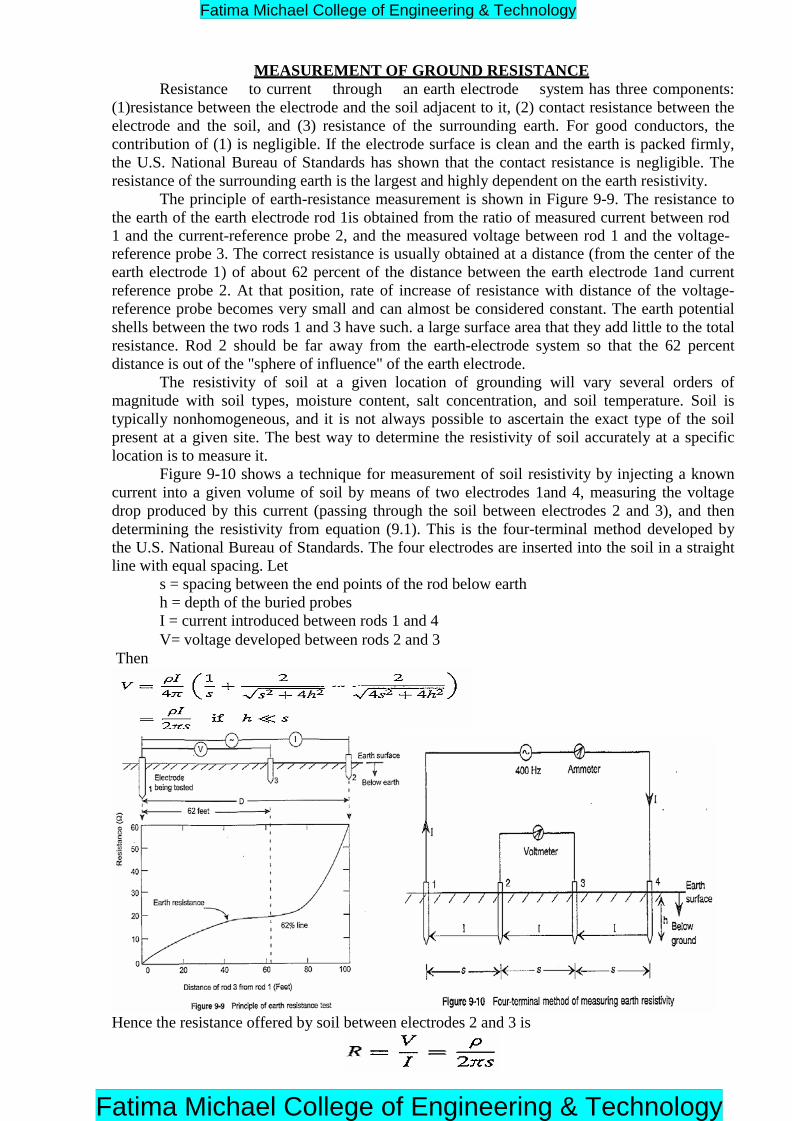
MEASUREMENT OF GROUND RESISTANCE
Resistance to current through an earth electrode system has three components:
(1)resistance between the electrode and the soil adjacent to it, (2) contact resistance between the
electrode and the soil, and (3) resistance of the surrounding earth. For good conductors, the
contribution of (1) is negligible. If the electrode surface is clean and the earth is packed firmly,
the U.S. National Bureau of Standards has shown that the contact resistance is negligible. The
resistance of the surrounding earth is the largest and highly dependent on the earth resistivity.
The principle of earth-resistance measurement is shown in Figure 9-9. The resistance to
the earth of the earth electrode rod 1is obtained from the ratio of measured current between rod
1 and the current-reference probe 2, and the measured voltage between rod 1 and the voltage- reference probe 3. The correct resistance is usually obtained at a distance (from the center of the
earth electrode 1) of about 62 percent of the distance between the earth electrode 1and current
reference probe 2. At that position, rate of increase of resistance with distance of the voltage-
reference probe becomes very small and can almost be considered constant. The earth potential
shells between the two rods 1 and 3 have such. a large surface area that they add little to the total
resistance. Rod 2 should be far away from the earth-electrode system so that the 62 percent
distance is out of the "sphere of influence" of the earth electrode.
The resistivity of soil at a given location of grounding will vary several orders of
magnitude with soil types, moisture content, salt concentration, and soil temperature. Soil is
typically nonhomogeneous, and it is not always possible to ascertain the exact type of the soil
present at a given site. The best way to determine the resistivity of soil accurately at a specific
location is to measure it.
Figure 9-10 shows a technique for measurement of soil resistivity by injecting a known
current into a given volume of soil by means of two electrodes 1and 4, measuring the voltage
drop produced by this current (passing through the soil between electrodes 2 and 3), and then
determining the resistivity from equation (9.1). This is the four-terminal method developed by
the U.S. National Bureau of Standards. The four electrodes are inserted into the soil in a straight
line with equal spacing. Let
s = spacing between the end points of the rod below earth
h = depth of the buried probes
I = current introduced between rods 1 and 4
V= voltage developed between rods 2 and 3
Then
Hence the resistance offered by soil between electrodes 2 and 3 is
Fatima Michael College of Engineering & Technology
Fatima Michael College of Engineering & Technology

To avoid polarization effects, no DC current is used in this measurement. Also to avoid
errors caused by stray power currents in the soil, 50 Hz or 60 Hz should not be used. The
measurements are done using 400Hz power supply.
SYSTEM GROUNDING FOR EMI/EMC
EMC ground is a zero impedance plane for voltage reference• of signals. In practice,
because of the finite conductivity of the ground plane, stray ground current through the common
impedance between two ground points produces conductively coupled interference between
two circuits as shown in Figure 9 11. The purposes of EMC grounding are (1) realization of
the signal, power, and electrical safety paths necessary for effective performance without
introducing excessive common-mode interference, and (2) establishment of a path to divert
interference energy existing on external conductors, or present in the environment, away from
susceptible circuits. The EMC grounding techniques are not straightforward because the
equipment and system performance is a function of large number of variables, such as type of
system, system configuration, sizes, orientation, distances, frequencies, polarization of fields,
and so on. A quantitative approach to grounding is necessary for cost-effective EMI control.
There are two levels of concern where grounding techniques are important [5]: the system
internal circuit level and the system level. At the system internal circuit level, one must resolve
internal ground loop couplings. At the system level, ambient EMI coupling into system cables
produces EMI currents through other ground loops that were not excited by any other EMI
sources.
System Grounding Network. EMC grounding networks of a system are selected based on
frequency range of intended signals and system configurations. All low frequency circuits can
be grounded using wires, whereas high-frequency circuits and high-speed logic circuits must
have low-impedance interference-free return paths in the form of conducting planes or coaxial
cables. Return of power leads should be separated from any of the above, even though they may
end up in the same terminal of the power supply regulator. The signal ground network can be a
single point ground, multipoint ground, hybrid ground, or a floating ground.
Single-Point Grounding. In single-point grounding scheme, each subsystem is grounded
to separate ground planes (structural grounds, signal grounds, shield grounds, AC primary, and
secondary power grounds). These individual ground planes from each subsystem are finally
connected by the shortest path to the system (Figure 9-12) ground point of reference potential.
Fatima Michael College of Engineering & Technology
Fatima Michael College of Engineering & Technology

A single-point grounding scheme operates better at low frequencies where the physical
length of the interconnection is small compared to wavelength at the frequency of operation.
The single-point grounding scheme avoids problems of common-mode impedance coupling of
the type shown in Figure 9-11. Problems in implementing the above single-point grounding
scheme become significant because of common-impedance coupling when:
1. Interconnecting cables are used, especially ones having cable shields with sources and
receptors operating over a length of more than A/20.
2. Parasitic capacitance exists between subsystems, or equipment housings, or between
subsystems and the grounds of other subsystems.
Multipoint Grounding. In multipoint grounding scheme, every equipment is heavily bonded
to a solid ground conducting plane which is then earthed for safety purposes (Figure 9-13).
Multipoint grounding behaves well at high frequencies where the dimension of the grounding
scheme is large compared to wavelength at the frequency of operation. At high frequencies,
there exist different potentials at different points on the interconnecting systems which need to
be grounded at multiple points to zero reference potential. At high frequencies, the parasitic
capacitive reactance represents low-impedance paths, and the bond inductance of a subsystem-
to-ground point results in higher impedances. Thus, again common-mode currents may flow, or
unequal potentials may develop, among subsystems.
Hybrid Grounding. In a hybrid grounding scheme, the ground appears as a single-point
ground at low frequencies and a multipoint ground at high frequencies. Figure 9-14 shows such
a scheme where a video circuit, in which both the sensor and driver circuit chassis must be
grounded and the coaxial cable shield needs to be grounded to the chassis at both ends. Here
low-frequency ground current loop is avoided by the capacitor at one ground. At high
frequencies, the capacitor produces low reactance and cable shield is grounded. Thus, this
circuit simultaneously behaves as a single-point ground at low frequencies and a multipoint
ground at high frequencies.
Sometimes, there is a need that all the computer and peripheral frames should be
grounded to the power system ground wire for safety purposes (shock-hazard protection). Since
the ground wire generally contains significant electrical noise, one or more inductors (Figure 9-
15) of about 1 mH are used to provide a low impedance (less than 0.4 Q) safety ground at AC
power line frequencies and RF isolation in the frequency spectrum containing the principal
energy of computer pulses [3]. The inductors attenuate induced transients and EMI noise in the
ground wire from entering into the computer voltage logic busses.
Fatima Michael College of Engineering & Technology
Fatima Michael College of Engineering & Technology
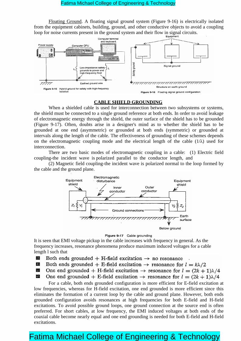
Floating Ground. A floating signal ground system (Figure 9-16) is electrically isolated
from the equipment cabinets, building, ground, and other conductive objects to avoid a coupling
loop for noise currents present in the ground system and their flow in signal circuits.
CABLE SHIELD GROUNDING
When a shielded cable is used for interconnection between two subsystems or systems,
the shield must be connected to a single ground reference at both ends. In order to avoid leakage
of electromagnetic energy through the shield, the outer surface of the shield has to be grounded
(Figure 9-17). Often, doubts arise in a designer's mind as to whether the shield has to be
grounded at one end (asymmetric) or grounded at both ends (symmetric) or grounded at
intervals along the length of the cable. The effectiveness of grounding of these schemes depends
on the electromagnetic coupling mode and the electrical length of the cable (1/λ) used for
interconnection.
There are two basic modes of electromagnetic coupling in a cable: (1) Electric field
coupling-the incident wave is polarized parallel to the conductor length, and
(2) Magnetic field coupling-the incident wave is polarized normal to the loop formed by
the cable and the ground plane.
It is seen that EMI voltage pickup in the cable increases with frequency in general. As the
frequency increases, resonance phenomena produce maximum induced voltages for a cable
length l such that
For a cable, both ends grounded configuration is more efficient for E-field excitation at
low frequencies, whereas for H-field excitation, one end grounded is more efficient since this
eliminates the formation of a current loop by the cable and ground plane. However, both ends
grounded configuration avoids resonances at high frequencies for both E-field and H-field
excitations. To avoid possible ground loops, one ground connection at the source end is often
preferred. For short cables, at low frequency, the EMI induced voltages at both ends of the
coaxial cable become nearly equal and one end grounding is needed for both E-field and H-field
excitations.
Fatima Michael College of Engineering & Technology
Fatima Michael College of Engineering & Technology

ELECTRICAL BONDING
Electrical bonding is a process in which components or modules of an assembly,
equipment or subsystems are electrically connected by means of a low impedance conductor.
Ideally, the interconnections should be made so that the mechanical and electrical properties of
the current path are determined by the connected members and not by the joints. The joint must
maintain its mechanical and electrical properties over an extended period of time. The purpose is
to make the structures homogeneous with respect to the flow of RF currents. There are several
factors that influence the EMI performances of the bonding. These are
1. Generation of intermodulation products because of nonlinear effects at contacts between
similar and dissimilar metals.
2. Development of potential differences caused by DC and AC resistances and inductance
of a given length of the bond strap.
3. Adverse impedance response because of resonance of inductance and the residual
capacitance of the bond strap.
Bonding can be made by different methods as follows:
1. A bond is achieved by joining two metallic items or surfaces through the process of welding
or brazing.
2. A bond is obtained by metallic interfaces through fasteners or by direct metal- to-metal
contact.
3. A bond is achieved by bridging two metallic surfaces with a metallic bond strap.
Shape and Material for Bond Strap
DC and AC resistances of a bond conductor are inversely proportional to the cross-
sectional area and the perimeter of the conductor. Because RF current flows through the surface
of the conductor as a result of skin effect, one way to reduce the RF impedance (resistance and
inductance) of a conductor is to increase its periphery. A cost-effective solution would be to use
conductor straps of fiat shape, for which the periphery is much larger than the rectangular bar or
circular rod for the same cross-sectional area.
The total impedance of a bond conductor whose length is small compared to the
wavelength of operation is given by
where R can be the DC or AC resistance of the conductor, Lext is the external self- inductance
and Lint is the internal inductance caused by the magnetic field penetration inside the
metal. Except at very low frequencies, Lint is generally neglected in the calculation of
impedance. The following expressions are used for the above parameters for different shapes of
the conductors.
Circular Conductor. The DC and AC resistances of circular conductors are given by
where p is the resistivity, l is the length, A is the cross-sectional area, d is the diameter and 8 is
the skin depth.
For the conductor above a height h from the ground plane or a conductor pair far from a ground
plane, and separated by a distance D
Fatima Michael College of Engineering & Technology
Fatima Michael College of Engineering & Technology

Rectangular Flat Strap. The DC and AC resistance and inductance of a flat conductor strap [19]
are given by
where t is the strap thickness, w is the strap width, l is the strap length, a is the conductivity of
the material, f is the frequency in Hz and K is a function of w/t.
Refer: General Guidelines for Good Bonds, P.No:248-250.
ISOLATION TRANSFORMERS
We introduced the concept of common-mode and differential-mode
interferences and described the application of isolation transformers to suppress these
interferences. Transformers are used to isolate ground current loops. In addition to a desired magnetic coupling between the primary and secondary windings in a transformer (see Figure 11-
13(a)), an EMI coupling between the two ports of a transformer (two circuits) takes place
through capacitance between the primary and secondary windings.
Figure 11-13 (a} Transformer coupler, {b) isolation transformer
The capacitance coupling can be reduced by providing a grounded Faraday shield
between the two windings as shown in Figure 11-13(b). High conductivity grounded shield does
not affect the desired magnetic coupling, but it reduces capacitive coupling. To avoid common-
impedance (Zg) coupling, the shield must be grounded on the load side. A single shielded
isolati6li transformer performs well to suppress common-mode interferences in the primary side
at low frequencies of up to 100 kHz by providing isolation of the order of 120-140 dB.. The DC
insulation resistance of 10-100 MQ between the primary and secondary ports of a transformer
limits this isolation at low frequencies. The common-mode rejection decreases with increasing
frequency above 100 kHz because the capacitance reactance between the primary and secondary
decreases. Isolation transformers with a single shield do not adequately suppress differential
mode coupling. In power circuits, multiple-shielded isolation transformers are used to suppress
both common mode and differential-mode interferences. In a double-shielded isolation
transformer shown in Figure 11-14(a), the shield facing the primary side is connected to the
primary neutral to suppress differential-mode interferences, and the shield facing the secondary
side is connected to the reference ground to suppress common-mode interferences. In ultra-
isolation transformers, a triple-shield arrangement is used as shown in Figure 11-14(b). The
differential mode coupling from primary and secondary ports are suppressed by using two
shields each on the corresponding side. The center shield suppresses common-mode
interferences.
The multiple shielding technique reduces the capacitance to below 0.009 pF, and
increases DC isolation to over 100 MQ. Figure 11-15 shows a typical variation .of the isolation
for common-mode and differential-mode interferences with frequency for a single-shielded
isolation transformer. For minimum capacitive coupling, one uses toroidal transformers. To
reduce magnetic coupling from or to the outside of the transformer, stress annealed mu-metal
shield cans are employed.
Fatima Michael College of Engineering & Technology
Fatima Michael College of Engineering & Technology

TRANSIENT SUPPRESSORS (TRANSIENT AND SURGE SUPPRESSION DEVICES)
IEEE standard 587 recommends that although the transient EMI voltage and current
surges can take many shapes, for all practical purposes, these can be represented either by two
unidirectional waveforms for high and low impedance circuits or by damped oscillatory
waveforms. The former waveforms carry much larger energy compared to the latter ones.Since
the rise time of these transient waves is of the order of microseconds or even nanoseconds, an
efficient surge protection requires the use of devices which can withstand this energy, and also
respond at the higher speeds needed. There are two categories of transient suppression devices;
these are the gas discharge tubes (crowbar) and semiconductor devices (variable resistor).
Since the nature and shape of transient interference signal waves change during
propagation through transmission lines, the most effective location for a surge arrestor is at the
terminals of the equipment to be protected, or sometimes at some distance away from the
equipment. There may also be a need to include them in printed circuit boards to suppress low
level residual transients resulting from transients generated outside the equipment or system, and
transients from electrostatic discharges.
Gas-Tube Surge Suppressors A gas-discharge tube can handle very large transient currents (>10 kA) when the tube is
connected between the line and the ground as shown in Figure 11-17. When transient EMI
voltage in a line exceeds the striking voltage of the gas-tube, an arc discharge occurs and the
ionized gas produces a low-impedance path from line to ground to shunt surge currents.
There are two major disadvantages of a gas-tube. First, its response time is slow and it
cannot be used for fast rise-time surges. Second, the tube remains in a conducting state even
after the surge is removed. As a consequence, a high current drain from the normal source
results. This action can be prevented by using a fast-acting circuit breaker or fuse in the line.
The gas tube is normally specified for a breakdown voltage which is higher than the circuit
operating voltage. The gas tubes have a finite life time which depends on the maximum number
of surges handled by the tube. Because of its high current handling capability, gas-tube surge
suppressors are used in AC power distribution lines and in telecommunication lines as lightning
and other high-energy surge or transient arrestors. These devices are not suitable for circuit
board operation because of their high breakdown voltages and nonrestoring characteristics under
DC conditions.
Application of Gas-Tube Surge Arrestors. Two important aspects concerning the use of gas-tube
(GT) surge arrestors in limiting transient voltages at the input terminals of electrical apparatus
are the selection of an arrestor with suitable characteristics and proper physical placement of the
arrestor in the electrical circuit. ANSI/IEEE C62.42-1987 [15] describes the circuit
Fatima Michael College of Engineering & Technology
Fatima Michael College of Engineering & Technology

configurations for several common applications of GT as shown in the matrix of Figure 11-18.
These configurations have one or more signaling terminals and usually include a ground
terminal. The one-port configuration is typically used in communication facilities. The two-port
configuration may represent a communication line repeater. The (a) arrangement in each
configuration limits common-mode surge voltages. The (b) arrangement uses multi gap surge
arrestors to limit common-mode voltages while also minimizing differential-mode voltages.
Multi gap arrestors can also afford a size reduction as compared to single-gap arrangement. The
(c) arrangement limits differential-mode surge voltages, but does not provide protection against
common-mode surge voltages. An additional arrestor (15], connected between one of the
terminals and the ground, may be added to this last arrangement, to provide protection from
common-mode interferences.
Operational Compatibility. The presence of a gas-tube surge arrestor must not interfere with
transmission of information, control, or test signals. Leakage resistance of a gas-tube surge
arrestor, measured at the voltage levels at which it is operated in the system, should be
sufficiently high to avoid significant insertion loss. The low-capacitance of gas-tube surge
arrestors generally causes insignificant insertion loss as compared to the transmission line.
However, if capacitance is of concern (such as in high-frequency applications), its maximum
permissible value will have to be specified at the frequency of the applied transmission signal.
The mounting assembly for a gas-tube surge arrestor can add significant capacitance, and may
not be overlooked.
Unwanted clipping of signals is avoided by specifying that the minimum DC breakdown
voltage must be higher than the largest signal level, including any superimposed DC bias or any
acceptable induced AC interference voltage at the terminals. Gas-tube surge arrestors do not
incorporate a current limiting element 19 extinguish follow currents after a surge has been
conducted. Conduction is, however, interrupted if the load line of the source intersects the volt-
ampere characteristic of the off-state after the surge has decayed. Extinguishing capability is
established by testing for holdover with a source having an impedance load line) equivalent to
that of the source at the protected terminals. Since reactive components (transmission line,
connected apparatus) may affect the process of extinction, these should be included in the
holdover test circuit.
Voltage Limiting. The gas-tube surge arrestor is useful in limiting unwanted AC or DC voltage
transients to levels which are below the withstand threshold of the apparatus being protected
(with a suitable margin for aging of the apparatus and the protection device). The protection of a
circuit configuration consisting of two signaling terminals and a ground terminal (Figure 11-19)
Fatima Michael College of Engineering & Technology
Fatima Michael College of Engineering & Technology

requires that all the voltages between terminals A-G, B-G, and A-B be limited. In many
applications, surges are of like polarity with respect to the ground, and the maximum voltage
between terminals A-B does not exceed the arrestor surge limiting voltage between A-G or B-G.
Accordingly, two surge arrestors, placed between A-G and B-G, are normally sufficient to
protect all three terminals. If the application is such that differential-mode transients can occur
without a common-mode component, then the two-arrestor arrangement will not bypass
differential-mode voltages up to a level equal to the sum of the two limiting voltages. A third
arrestor placed between terminals A-B will be needed to limit differential-mode transients of
lower values.
Location of Arrestors. The physical location of a gas-tube surge arrestor should minimize the
effect of grounding conductor impedance. Care must be exercised to avoid an inadvertent hazard
to the building in which the protected circuit is located. This situation illustrated in Figure 11-
20(a) arises if the protector is located beyond the point of entrance of the communication or
signaling lines to the building, and if the interior wiring connected to the protector can overheat
because of sustained conduction of power line currents. This problem is usually surmounted by
inserting a fuse or fusible element in the lines between the arrestor and the source of fault-
current. A fuse or fusible element with proper rating is used to prevent overheating of the wiring
between the building entrance and the protector.
As illustrated in Figure 11-20(b), an overheating of interior wiring can occur even when
a protector (primary) is located at the building entrance if an additional (secondary) protector
device is connected to the protected circuit. The general purpose of this secondary device is to
eliminate voltages in the grounding conductor, and surges induced directly into the interior
wiring, or to reduce surges to levels lower than those permitted by the primary protector. If the
limiting voltage of a secondary device is below that of the primary, the secondary arrestor may
only break down when a voltage surge occurs. As a result, excessive surge current can be
conducted in the interior wiring between the two devices. This condition can be avoided by
placing a current interrupter device in series with the interior wiring between the two devices, pr
by inserting sufficient impedance in the wiring to ensure an operation of the primary protector
whenever currents become excessive.
Fatima Michael College of Engineering & Technology
Fatima Michael College of Engineering & Technology
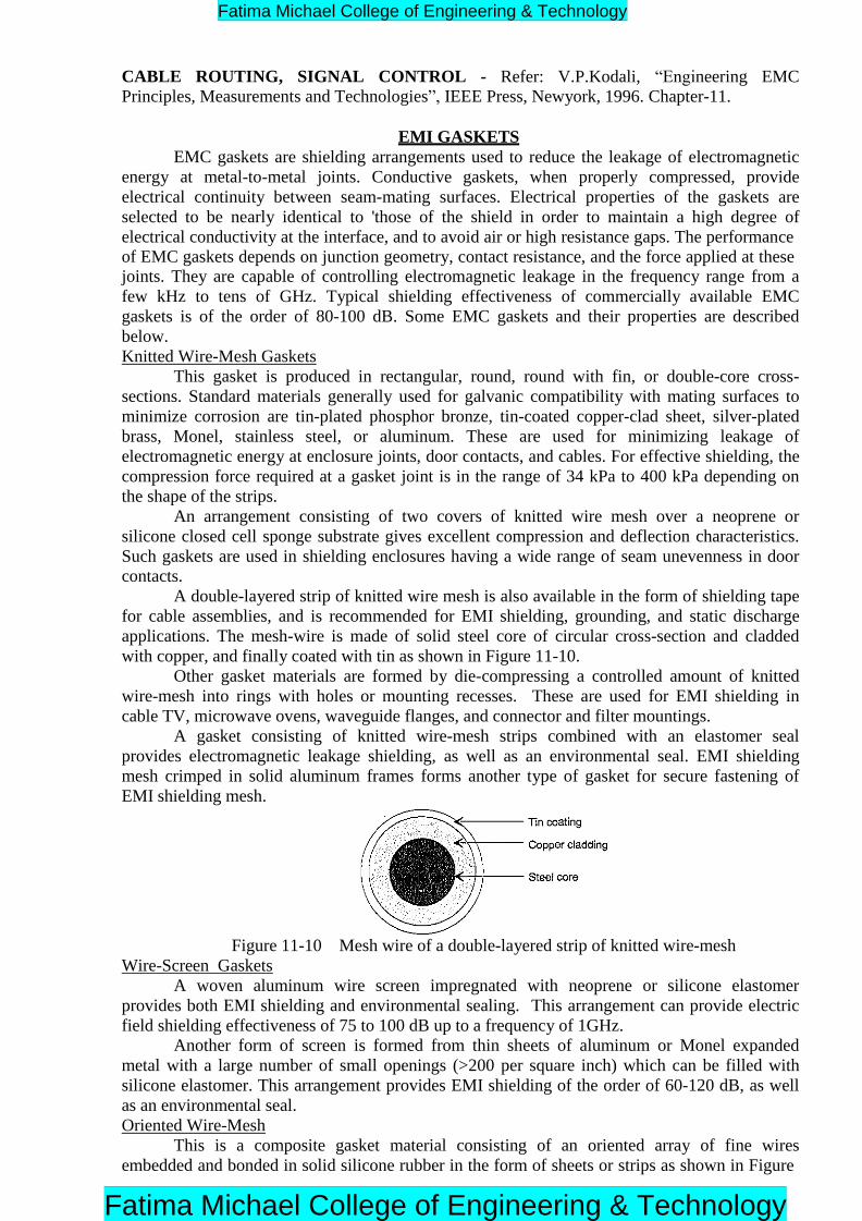
CABLE ROUTING, SIGNAL CONTROL - Refer: V.P.Kodali, ―Engineering EMC
Principles, Measurements and Technologies‖, IEEE Press, Newyork, 1996. Chapter-11.
EMI GASKETS
EMC gaskets are shielding arrangements used to reduce the leakage of electromagnetic
energy at metal-to-metal joints. Conductive gaskets, when properly compressed, provide
electrical continuity between seam-mating surfaces. Electrical properties of the gaskets are
selected to be nearly identical to 'those of the shield in order to maintain a high degree of
electrical conductivity at the interface, and to avoid air or high resistance gaps. The performance
of EMC gaskets depends on junction geometry, contact resistance, and the force applied at these joints. They are capable of controlling electromagnetic leakage in the frequency range from a
few kHz to tens of GHz. Typical shielding effectiveness of commercially available EMC
gaskets is of the order of 80-100 dB. Some EMC gaskets and their properties are described
below.
Knitted Wire-Mesh Gaskets
This gasket is produced in rectangular, round, round with fin, or double-core cross-
sections. Standard materials generally used for galvanic compatibility with mating surfaces to
minimize corrosion are tin-plated phosphor bronze, tin-coated copper-clad sheet, silver-plated
brass, Monel, stainless steel, or aluminum. These are used for minimizing leakage of
electromagnetic energy at enclosure joints, door contacts, and cables. For effective shielding, the
compression force required at a gasket joint is in the range of 34 kPa to 400 kPa depending on
the shape of the strips.
An arrangement consisting of two covers of knitted wire mesh over a neoprene or
silicone closed cell sponge substrate gives excellent compression and deflection characteristics.
Such gaskets are used in shielding enclosures having a wide range of seam unevenness in door
contacts.
A double-layered strip of knitted wire mesh is also available in the form of shielding tape
for cable assemblies, and is recommended for EMI shielding, grounding, and static discharge
applications. The mesh-wire is made of solid steel core of circular cross-section and cladded
with copper, and finally coated with tin as shown in Figure 11-10.
Other gasket materials are formed by die-compressing a controlled amount of knitted
wire-mesh into rings with holes or mounting recesses. These are used for EMI shielding in
cable TV, microwave ovens, waveguide flanges, and connector and filter mountings.
A gasket consisting of knitted wire-mesh strips combined with an elastomer seal
provides electromagnetic leakage shielding, as well as an environmental seal. EMI shielding
mesh crimped in solid aluminum frames forms another type of gasket for secure fastening of
EMI shielding mesh.
Figure 11-10 Mesh wire of a double-layered strip of knitted wire-mesh
Wire-Screen Gaskets
A woven aluminum wire screen impregnated with neoprene or silicone elastomer
provides both EMI shielding and environmental sealing. This arrangement can provide electric
field shielding effectiveness of 75 to 100 dB up to a frequency of 1GHz.
Another form of screen is formed from thin sheets of aluminum or Monel expanded
metal with a large number of small openings (>200 per square inch) which can be filled with
silicone elastomer. This arrangement provides EMI shielding of the order of 60-120 dB, as well
as an environmental seal.
Oriented Wire-Mesh
This is a composite gasket material consisting of an oriented array of fine wires
embedded and bonded in solid silicone rubber in the form of sheets or strips as shown in Figure
Fatima Michael College of Engineering & Technology
Fatima Michael College of Engineering & Technology

11-11. This is designed for use in military, industrial, and commercial applications requiring
EMI shielding and grounding in conjunction with environmental sealing when repeated opening
and closing of access doors and panels are expected. Oriented wires can also be embedded and
bonded in a soft closed-cell silicone sponge elastomer. These are used for EMI shielding and
environmental sealing when low closure forces and severe joint unevenness are expected.
Conductive Elastomer Figure 11-11 Oriented wire-mesh gasket
Conductive elastomer gaskets are formed by filling silicone elastomer with any of the
following conducting materials: silver-plated inert particles, pure silver, carbon particles, silver-
plated copper, nickel, or aluminum particles designed to achieve high shielding effectiveness
and corrosion resistance. These are available in sheets and a variety of standard cross-sections
suitable for joints.
Conductive Adhesive
Conductive adhesive is used for bonding or installing various conductive silicone
elastomer EMC gaskets. It is a thick paste of room temperature vulcanizing (RTV) silicone resin
with pure silver used as filler material to cure quickly at room temperature. It forms a flexible
resilient conductive bond or seal. A typical value of the volume resistivity of this adhesive is
0.01 Q-cm.
Both the surfaces to be bonded are roughened and cleaned with methyl alcohol
dampened cloth. After the surfaces dry, the adhesive is applied from a tube directly onto the
bond area ill spots. The adhesive is then quickly spread to form a thin film and a conductive
gasket is placed in position on top of the adhesive; the assembly is then left for curing. Many
forms of conductive adhesives are commercially available.
Conductive Grease This is a highly conductive silver-filled silicone grease without carbon or graphite. The
electrical conductivity and lubricating properties are maintained over a broad environmental
range. This material is used in power substation switches and in suspension insulators to reduce
electromagnetic interference caused by arcing and corrosion. The volume resistivity of this
grease is typically of the order of 0.02 ohm-cm.
Conductive Coatings
Conductive coatings are organic-type paints densely filled with conductive particles,
such as graphite, silver, or nickel These are used for shielding and grounding plastic enclosures,
which are susceptible to EMI, and can be applied using a conventional spray system. The
material usually contains a flammable solvent, and must be used in a well-ventilated area to
avoid fire hazard, inhalation, and direct skin contact. For best results, the application surface
must be cleaned of grease, oils, dirt, and any other foreign matter.
Figure 11-12 shows typical shielding effectiveness of compressible silver-loaded gasket
and wire-mesh gasket, respectively, measured with modified American Society for Testing and
Materials (ASTM) holder. These results vary with the compression force applied on the gaskets.
Fatima Michael College of Engineering & Technology
Fatima Michael College of Engineering & Technology

UNIT IV STANDARDS AND REGULATION
Introduction
EMC STANDARDS
A standard (generally published in the form of a document) represents a consensus of
those substantially concerned with the scope and provisions of the particular standard. It is
intended as a guide to aid the manufacturer, the user, and others who are likely to be affected.
This philosophical or mission definition of a standard is the basis for American National
Standards. Essentially similar objectives constitute the broad basis for other standards, whether
these are military or civilian standards, or national or international standards. The performance
specifications stipulated in a standard are usually the minimum considered necessary for
providing reasonable confidence to all concerned that particular equipment or subsystems
complying with these specifications will function satisfactorily within their permissible design
tolerances when operating in their intended environment.
In practice, military standards in various countries are generally mandatory for
equipment purchases and use by the military. Military standards are also generally more
elaborate, and tend to be more stringent than their nonmilitary commercial or civilian
counterparts. Similarly, standards issued by specialist agencies or regulatory agencies (such as
NASA in the United States) have varying degrees of mandatory nature associated with them. On
the other hand, civilian or nonmilitary standards are not always mandatory. For example, the
American National Standards published by the American National Standards Institution (ANSI)
are voluntary in the United States. In fact, the American National Standards do not in any
respect preclude anyone, whether he or she has approved the standard or not, from
manufacturing, marketing, purchasing, or using products, processes, or procedures not
conforming to the standard. The voluntary nature of the American National Standards is
immediately apparent. In most countries, standards, or regulations governing electromagnetic
emissions, are enforced and monitored (see Chapter 12) by national agencies, such as the
Federal Communication Commission (FCC) in the United States and Zentralamt fur
Zulassungen in Fernmeldewesen (ZZF) in Germany. In some European countries (possibly in
the whole of Europe in the near future), standards relating to both electromagnetic emissions
and immunity to electromagnetic emissions are mandatory even in nonmilitary commercial
applications.
Standards for EMI/EMC
Most electrical and electronics devices, circuits, and systems are capable of emitting
electromagnetic energy either intentionally or unintentionally. Such emissions can constitute
electromagnetic interference. At the same time, many modem electronics devices, circuits, and
equipment are capable of responding to, or being affected by, such electromagnetic interference.
We have a situation in which the culprits are also the victims and vice-versa. The problem
becomes even more serious with modern semiconductor devices and VLSI circuits, which are
easily susceptible to malfunction or even total damage as a result of electromagnetic
Fatima Michael College of Engineering & Technology
Fatima Michael College of Engineering & Technology

interference, because these devices have relatively low immunity thresholds for electromagnetic
interference. Problems relating to electromagnetic emissions (constituting electromagnetic
interference) and equipment, subsystems, and device immunity to electromagnetic interference
(electromagnetic compatibility) frequently arise in radio broadcasting, communications, control,
information technology products, instrumentation, computers, and electrical power generation
and transmission.
As a practical measure to ensure electromagnetic compatibility, a variety of
equipment design and performance standards have evolved and been published by different
agencies from time to time. These standards aim to set reasonable and rational limits for
electromagnetic emission levels by different equipment, as well as immunity levels for such
equipment. Electromagnetic interference or electromagnetic compatibility often involves weak
signal or interference levels, and the test procedures call for precision measurements at
extremely low power levels. Further, different test procedures or different instrumentation could
often lead to different results, however small the variations might be. Consequently, there is a
need to carefully define the test procedures and instrumentation. Accordingly, standards also
address the test procedures and instrumentation for measuring electromagnetic (interference)
emissions and immunity. Sufficient attention must be paid to this aspect to avoid difficulties in
the field, where the same equipment may exhibit substantial variations in measured performance
parameters when tested in different locations.
In this topic, we present an account of the EMI/EMC standards. This treatment is not an
exhaustive and complete description of any one specific standard, or of instrumentation for test
and measurement as given in a particular standard. Instead, the objective is to familiarize the
reader with several practical aspects of EMC standards, and some major published standards in
this field.
The test and evaluation for electromagnetic interference (EMI) and electromagnetic
compatibility (EMC) involves measurements and compliance relating to: Conducted emissions
(CE), Radiated emissions (RE), Susceptibility/immunity to conducted emissions (CS),
Susceptibility/immunity to radiated emissions (RS)
These tests cover both narrowband and broadband emissions. The narrowband tests deal
with continuous wave (CW) mode emissions and interferences. Broadband tests involve
transients such as electrostatic discharge or electrical surges or other similar transients
experienced in practice. We described in Chapters 5 to 8 the general layouts, test procedures,
instrumentation, and necessary precautions for conducting EMI/EMC tests.
MIL-STD-461/462
Military standards 461 and 462 [2,3] constitute a most comprehensive set of standards in
electromagnetic compatibility. MIL-STD-462 specifies test methodologies and detailed
procedures for compliance with MIL-STD-461. The parallel document MIL-STD-461 lists the
EMIJEMC related performance specifications for electrical, electronic, and electromechanical
equipment and subsystems.
MIL-STD-461 and MIL-STD-462 were first issued in 1967-68. MIL-STD-461
underwent major revisions twice during the next two decades. Both documents were
comprehensively revised and published as MIL-STD-461D and MIL-STD-462D in January
1993. The D version of these documents includes an appendix providing the rationale and
background for each specification given in the document.
MIL-STD-461/462 documents have been evolved for use by the U.S. Department of
Defense. The Armed Forces in several other countries follow these standards, either closely or
with minor variations.
Fatima Michael College of Engineering & Technology
Fatima Michael College of Engineering & Technology

Specification Frequency Range Applicability
CE101
CE102
CE106
30Hz to 10 kHz
10kHz to 10 MHz
10kHz to 40 GHz
Power leads (including returns) that obtain power from sources which are not part of
the EUT
Power leads (including returns) that obtain power from sources which are not part of
the EUT
Antenna terminals of transmitters and receivers
The EMI control levels stipulated in MIL-STD-461D apply to subsystem level hardware
for ensuring electromagnetic compatibility when various subsystems are integrated into
equipment or a system. MIL-STD-461D lays down permissible levels for conducted emissions,
susceptibility and immunity to conducted emissions, radiated emissions, and susceptibility and
immunity to radiated emissions. The frequency range and practical situations for which different
specifications are applicable are given in Tables 13-1 to 13-4.
Table 13-1 Limits for conducted emissions under MIL-STD-461D
Conducted Interference Controls
Referring to the conducted emission controls listed in Table 13-1, the basic purpose of
the lower-frequency portion of the conducted emission limit is to ensure that connection of an
equipment under test (EUT) to the mains power supply does not corrupt the power quality (or
introduce distortions in the voltage waveforms) on the power mains beyond allowable limits.
The objective of imposing limits on the conducted emission in higher frequency range is to
protect the receivers (which are connected to antenna terminals) against degradation caused by
radiated interference from power cables associated with the EUT.
The objective of the susceptibility and immunity specifications given in Table 13-2 is to
ensure that equipment performance is not degraded because of distortions present in the voltage
waveforms of the mains power supply. The objective of requirements CS103/104/105 is to
provide reasonable assurance that any variations in the response of receivers and other
subsystems (connected to the antenna) to in-band signals are within permissible limits in spite of
the presence of any:
• Within-pass-band intermodulation products, produced by nonlinearities in the subsystem
of two signals, which are themselves outside of the pass-band of the receiver (CS103)
Fatima Michael College of Engineering & Technology
Fatima Michael College of Engineering & Technology

• Signals outside of the pass-band of receivers (CS104)
• Modulation transferred from an out-of-band signal to an in-band signal (CS105)
The objective of CS109 is to ensure that equipment performance is not affected by the
magnetic fields caused by any currents flowing in the platform structure. The purpose of
CS114/116/115 is to ensure immunity of the equipment for any current and voltage waveforms
(including transients) or electromagnetic fields, which may be generated on the platform.
Measurement setup and procedures for determining susceptibility and immunity to pulsed
interferences were described in Chapter 8. These procedures can be followed for measuring the
levels of conducted emissions from a EUT, and for determining susceptibility and immunity
levels of an EUT to conducted interferences. However, when exact compliance with MIL-STD-
461D and MIL-STD-462D is required, it would be necessary to follow the detailed steps and
procedures outlined in these documents.
Radiated Interference Controls
The radiated emission limits specified in RE101/102 (see Table 13-3) are intended to
control the magnetic field and electric field emissions from an EDT .and its associated cables.
Similarly, the limits for immunity and susceptibility of an EDT in the presence of radiated
emissions, which have been specified under various requirements in Table 13-4, are intended to
ensure that the equipment will operate without degradation in the presence of various magnetic,
electric, and electromagnetic fields as specified under RS101/102/103.
For determining the radiated emissions from an EUT, or the susceptibility or
immunity of an EUT to radiated emissions, the experimental setups and procedures described in
Chapter 6 can be used. The measurement setups and procedures described in Chapter 8 are
useful for determining equipment immunity to various types of pulsed or transient interferences.
However, when exact compliance with MIL-STD-461D and MIL-S1D-462D is required, it
would be necessary to refer to these documents and follow the detailed steps and procedures
prescribed there.
Susceptibility at Intermediate Levels of Exposure
The susceptibility limits to both conducted and radiated emissions are usually the
Fatima Michael College of Engineering & Technology
Fatima Michael College of Engineering & Technology

maximum values for which compliance is required. It is also necessary to ensure that an EUT
functions satisfactorily even at stress levels below these. There have been instances where the
EUT functioned satisfactorily at maximum stress levels, but failed to function satisfactorily at
intermediate levels of conducted or radiated interferences. For this reason, the immunity and
susceptibility to conducted and radiated emissions often must be verified at several intermediate
levels, apart from the specified maximum limit.
Other Military Standards
The most important of the military standards in EMI/EMC area are the MIL-STD-461
and MIL-STD-462. As stated elsewhere, many key developments in the EMI/EMC area during
the past 50 years carne about as a result of the thrust given by the military for this subject area.
This interest of the military also resulted in the development of many other military standards in
which EMI/EMC is an important element. These include
This list is only representative of the many military standards in this area. These relate to
performance requirements at the component, circuit, or subsystem and system levels. In several
applications, EMC is important at all these levels. Further EMC specifications and requirements
vary depending on application (such as ground based, ship-borne, aircraft-based, space-borne,
etc.) and the type of equipment (such as radar, communication, control systems, power supplies,
data processing, computers, etc.). It suffices to note that a number of military specification
documents or standards exist that address these applications.
IEEE/ANSI STANDARDS
Another set of standards in the area of electromagnetic interference and electromagnetic
compatibility which have early historical beginnings are the C63 series standards, published by
the American National Standards Institution (ANSI). The Institute of Electrical and Electronics
Engineers (IEEE) is an active participant in the development and publication of these standards.
The IEEE has also published several standards in areas overlapping the C63 series. The
IEEE/ANSI standards are wholly voluntary, and represent a consensus of the broad expertise on
the subject. These documents are generally revised aperiodically. Any of these documents which
are more than five years old and have not been reaffirmed may not wholly reflect the current
state of the art, although the contents might still be of some value.
A list of selected IEEE/ANSI standards is given in Table 13-5. Various standards cover
the definitions, terminology, test beds and measurement procedures, guidelines for minimizing
EMI, and recommended limits for EMI/EMC.
Test and Evaluation Methods
One of the fundamental approaches to the measurement of radiated em1ss1ons, or
susceptibility and immunity to radiated emissions, is measurement using an open-area test site
(OATS). We have comprehensively covered the characteristics of an OATS, and measurements
using an OATS, in Chapter 5. The material presented in Chapter 5 is in conformity with the
documents forming part of the C63 standards (C63.7, C63.6, C63.4). Whenever measurements
are made using a laboratory test approach, such as those described in Chapter 6, validity of the
test bed and test results is often reaffirmed by referring these measurements to measurements
done in an OATS. This comparison and validation is usually done by comparing results obtained
from precision measurements using a laboratory test bed to similar results from open-area test
Fatima Michael College of Engineering & Technology
Fatima Michael College of Engineering & Technology

site measurements for a standard component such as a calibrating antenna.
The procedures for measuring conducted emissions or susceptibility and immunity to
conducted emissions described in Chapter 7 are in general conformity with the relevant
standards published by IEEE/ANSI (IEEE Std 213, IEEE Std 139, C63.4).
Various procedures for the evaluation of equipment, subsystem, or device immunity to
pulsed interferences described in Chapter 8 are in general conformity with the IEEE/ANSI
published standards on this subject (C62.41, C62.45, C62.47, C63.16).
As was pointed out in MIL-STD-461/462, whenever exact compliance is required with a
particular ANSI or IEEE standard, it would be necessary to follow the detailed measurement
procedures and step-by-step methodology prescribed in that standard.
CISPR / IEC STANDARDS
We noted in Section 1-2-1 that the Europe-based Comite International Special des
Perturbations Radioelectrique (CISPR) has been actively engaged since the 1930s in developing
international standards concerning EMI/EMC, and that these have been published by the
International Electrotechnical Commission (IEC). The CISPR/IEC effort is an international
effort involving not only European nations but also non-European nations such as Australia,
Canada, India, Japan, Korea, and the United States. A list of several IEC/CISPR documents
concerning EMI/EMC is given in Table 13-6.
Test and Evaluation Methods
As with ANSI/IEEE standards, the IEC/CISPR documentation and standards are
recommendations only. It is left to the participating nation and other nations to determine what
part of these recommendations will be implemented in their countries and how they will be
implemented. The test beds and the test procedures described in Chapters 6 to 8 generally
enable compliance testing with corresponding IEC/CISPR standards. Where exact compliance is
required it is necessary to refer to the corresponding standard and follow all the details and
procedures listed there.
Fatima Michael College of Engineering & Technology
Fatima Michael College of Engineering & Technology

FCC REGULATIONS
The Federal Communications Commission (FCC) in the United States is responsible for
evolving and ensuring implementation of various regulations concerning the operation of radio
broadcast and transmission facilities in the United States. The FCC also has the responsibility
for regulations to control electromagnetic emissions from various electrical and electronic
devices and equipment. These are published in the Code of Federal Regulations
Telecommunications 47 (Washington DC: US National Archives and Records Administration).
The regulations specifying limits for electromagnetic emissions for radio frequency devices and
equipment (both unintentional and intentional radiators) are covered in part 15 sub part J; arid
part 18 gives similar information for industrial, scientific, medical (ISM) equipment.
The following are among the several documents of relevance published by the FCC:
• OST bulletin No 55: Characteristics of open-area test sites
• FCC/OET MP-3: Methods of measurements of output signal level, output terminal
conducted spurious emissions, transfer switch characteristics, and radio noise emissions
from TV interference devices
• FCC/OET MP-4: Procedures for measuring RF emissions from computing devices
• FCC/OET MP-5: Methods of measurement of radio noise emissions from industrial,
scientific, and medical equipment
The test beds and procedures described in Chapters 5 to 8 generally enable compliance
testing with FCC regulations. The FCC advocates and encourages the use of procedures outlined
in ANSI C63.4-1992 for testing digital devices, intentional radiators, and other unintentional
radiators.
BRITISH STANDARDS
In the United Kingdom (England, Scotland, Wales, and Northern Ireland), several
regulations and restrictions governing electromagnetic emissions by various electrical,
electronic, and electromechanical apparatus are mandatory on the basis of Wireless Telegraph
Acts 1949 and 1967. The initial objective of these Acts and the associated Regulations was to
'preserve the quality of broadcast and communications services. With increasing awareness
about electromagnetic emissions and the interferences such emissions could cause, applicable
regulations for several other classes of electrical and electronic appliances have also evolved.
For the purpose of ensuring compliance with these requirements, several standards have evolved
and been published by the British Standards Institution (BSI). Table 13-7 gives a list of some
major British standards relating to EMI/EMC.
Apart from measurement methodologies, the British standards include product- specific
EMC specification standards Gust like several other standards), such as for household
appliances (BS 8005, BS 5404), radio and television broadcast receivers (BS 905), information
Fatima Michael College of Engineering & Technology
Fatima Michael College of Engineering & Technology

technology products (BS 6527), and industrial process measurement and control equipment (BS
6667). The United Kingdom, along with several other European nations, is actively involved in
developing unified European standards. We discuss these unified standards in Section 13-9. As a
part of this exercise, the United Kingdom also conducted an extensive and systematic study
(called Atkin's Report, 1989) of the EMC test, evaluation, and consultancy facilities. This report
covers the status as well as projected future requirements. A summary of major findings of this
report are available in Reference 6. This report is indicative of the importance and seriousness
the United Kingdom attaches for making EMC standards (both emissions and immunity)
mandatory for industrial as well as consumer products in the near future.
VDE STANDARDS
Germany is another nation that has long emphasized EMI/EMC specifications. In
Germany, the EMI/EMC standards evolve and are published by the Verband Deutscher
Elektrotechniker (VDE). Such of the VDE standards that are accepted as regulatory measures
are enforced by the Zantralamt fur Zulassungen im Fernmeldewesen (ZZF). Some relevant VDE
documents are listed in Table 13-8.
Germany has been a leader in developing and ensuring compliance with EMI/EMC
standards for consumer and industrial instrumentation and control products. In some respects,
the German standards in EMI/EMC have been more stringent than those in other countries.
These standards are applied not only for products manufactured in Germany, but also for
products imported into and sold in Germany.
EURO NORMS
Euro Norms (or European standards) constitute the first attempt at an international level
for evolving common EMI/EMC standards for immediate implementation by a group of
countries. This is a direct sequel to the emergence of European Common Market, and the
removal of trade and tariff barriers. In this situation, it is logical to harmonize technical
standards. This is necessary not only to facilitate interchangeability and flexibility, but also to
ensure safe and reliable operation of all electrical and electronic equipment, irrespective of the
country of manufacture, in all countries constituting the European Community.
The Euro Norms are discussed and evolved in CENELEC (Comite European de
Normalization Electrotechniques), where all concerned European countries are represented. The
Euro Norms harmonize and integrate the national standards of various concerned countries.
They are derived from related international standards, principally those published by the
CISPR/IEC. Once the Euro Norms are published, the agencies responsible for standardization
and regulations in different member countries produce their respective national standards, which
are harmonized with the appropriate Euro Norm. Thus identical standards are used in all EC
member countries. Tables 13-9 (a) and 13-9 (b) give a list of several Euro Norms covering
Fatima Michael College of Engineering & Technology
Fatima Michael College of Engineering & Technology

Euro Norm Subject BSI VDE CISPR/IEC
EN 55014
EN 55015
EN 55022
EN 55013
EN 500651
EN 55011
EN 50081-1
EN 60004-7
Units and methods of
measurement of radio
interference characteristics of
household electrical appliances,
portable tools and similar
electrical apparatus
Limits and methods of
measurement of radio
interference characteristics of
fluorescent lamps and
luminaires
Umits and methods of
measurement of radio
interference characteristics of
information technology
equipment
Limits and methods of
measurement of radio
interference characteristics of
broadcast receivers and
associated equipment
Signaling on low voltage
electrical installations in the
frequency range 3 to 148.5 kHz
Limits and methods of
measurement of radio
disturbance characteristics of
industrial/scientific/medical
(ISM) radio frequency
equipment
Electromagnetic compatibility
generic emission standards
(residential, commercial and light)
General guide on harmonics and
Inter harmonics measurements
and instrumentation, for power
supply systems and equipment
connected thereto
BS 800
BS 5394
BS 6527
BS 905-1
BS 6839
BSEN
55011
BSEN
50081-1
BSEN
6000-4-7
VDE
0875-1
VDE
0875-2
VDE
0878-3
VDE
0872-13
VDE
0808-1
VDE
0871-11
CISPR 14
CISPR 15
CISPR 22
CISPR 13
CISPR 11
IEC 1000-4-7
EMI/EMC, and their cross-reference to BSI and VDE specifications, as well as to the
publications of CISPR/IEC. The Euro Norms cover not only the emission limits, but also
minimum immunity levels for different equipment.
Table 13--9 (b) Euro Norms for emission limits, and relevant BSl, VDE, CISPR/IEC publications
The Euro Norms governing EMI/EMC specifications were initially planned to be
complied with, under the European Community Directive on Electromagnetic Compa1ibility
Fatima Michael College of Engineering & Technology
Fatima Michael College of Engineering & Technology

89/336/EEC, in all member countries of the European Community effective from January 1992.
The implementation date presently stands rescheduled for January 1996. The EC Directives are
binding on all member countries, taking precedence over national regulations; however, national
legislation is required in each of the member countries within a specified period for ensuring
compliance with the particular provisions. Provisions of the Electromagnetic Compatibility
document have implications for manufacturers as well as the users of electrical, electronic, and
electromechanical equipment. The provisions apply not only for products manufactured in the
EC member countries, but also to products sold in the EC member countries even if these
products are manufactured outside of the European Community.
EMI/EMC STANDARDS IN JAPAN
The EMI/EMC regulations in Japan are not mandatory at present. However, there is a
strong voluntary effort to introduce EMI/EMC standards. The Voluntary Control Council for
Interference (VCCI) for information technology equipment has issued standards (in 1986)
giving permissible limits for conducted emissions and radiated emissions for information
technology products. The VCCI is helped in this effort by Japan Electronic Industries
Development Association (JEIDA), Japan Business Machine Makers Association (JBMA),
Electronic Industries Association of Japan (EIAJ), and Communications Industries Association
of Japan (CIAJ). Although the VCCI published standards are voluntary, the VCCI makes market
sampling tests and announces the results, thus encouraging various manufacturers to promote
and observe EMI/EMC control in their products. The measurement methods and the
performance limits are based upon OSPR/IEC publication 22. The Class A specifications of the
VCCI correspond to Class A of the CISPR, and the Class 2 of VCCI correspond to Class B of
the CISPR specifications.
Apart from the VCCI effort, the JEIDA also published guidelines for equipment
immunity to EMI and limits for harmonic current injection into the public mains supply system.
These guidelines will be applied for information technology products commencing in 1996. The
JEIDA published immunity guidelines concerning electrostatic discharge; radiation
susceptibility, conducted electrical fast transients, and immunity to lightning and voltage surges
are based upon the CISPR/IEC 801 series. The guidelines for injected harmonic current limits
are based on CISPR/IEC document 77A.
PERFORMANCE STANDARDS-SOME COMPARISONS
Military Standards
Optimum performance specifications, or standards, are related to the end applications.
Table 13-10 indicates several specifications stipulated in MIL-STD-461D. Measurements for
determining compliance with MIL-STD-461D specifications are done using a peak detector (see
Chapter 7). Note that Table 13-10 is not a complete list of specifications given in MIL-STD-
461D; instead several example specifications have been listed here for illustration. The
specifications vary depending upon the agency (army, navy, air force), and the applications
(e.g., ship, submarine, aircraft, space system, etc.) within that agency. This approach permits
stringent specifications to be used where these are required, and less stringent specifications for
other applications, thus helping to reduce the costs. Various military specifications are generally
more stringent than their commercial counterparts.
IEC/CISPR Standards
For defining performance standards, the IEC/CISPR approach has been to divide the
equipment into two broad categories, Class A and Class B. Class A equipment is intended for
use in industrial, commercial, and business environments. Class B equipment is primarily
Fatima Michael College of Engineering & Technology
Fatima Michael College of Engineering & Technology

intended for operation in a residential environment, not-withstanding use in commercial,
industrial, or business environments. Examples of Class B equipment include personal
computers and calculators which are marketed for use by the general public. The European
Community has adopted the IEC/CISPR classification and specifications in evolving Euro
Norms. Table 13-11 indicates the IEC/CISPR specifications for EMI/EMC. The IEC/CISPR
emission limits are for measurements using quasi-peak detectors (see Chapter 7). Identical
performance limits are specified in Euro Norms.
ANSI Standards and FCC Specifications
The American National Standard ANSI C63.12-1987 adopts the IEC/CISPR
specifications given in Table 13-11. In addition, ANSI C.63.12-1987 also recommends the
following compliance:
• Radiated emissions below 800 kHz measured (at frequency f kHz) at a distance of
10m in any direction should not exceed {87.6- 20logf} dBµV/m.
• Radiated emissions in the frequency band 800 kHz to 230 MHz measured at a distance
of 10 m in any direction from the equipment should not exceed 30 dBµV/m.
• Common-mode conducted emission current below 800 kHz (measured at frequency f
kHz) should not exceed 2400/ f mA.
• Common-mode conducted emission current above 800 kHz should not exceed 3mA.
Fatima Michael College of Engineering & Technology
Fatima Michael College of Engineering & Technology

These two conducted emission measurements are made using a current probe (see
Chapter 7), whereas the conducted emission limits given in Table 13-11 are based on the use of
line impedance stabilization network (LISN) to measure noise voltages.
As stated earlier, although the American National Standards are evolved on the basis of a
broad consensus of the manufacturers and users, these are only recommendations. There is no
provision to enforce compliance on a mandatory basis. On the other hand, the limits for
conducted and radiated emissions specified in the Code of Federal Regulations are mandatory in
the United States. Table 13-12 gives the FCC specified limits for conducted and radiated
emissions. For this purpose, the measurements are made using a quasi-peak detector function.
The radiated emission measurements for Class A devices are done at a distance of 10 m and
those for others are taken at a distance of 3 m. The classification of equipment into Class A and
Class B is also broadly followed by the FCC, although the individual specifications differ from
the IEC/CISPR. In FCC specifications, whenever the measured level of conducted emissions
using a quasi-Peak detector are 6 dB or higher than the levels of the same emissions measured
with an average detector instrumentation having a minimum bandwidth of 9 kHz, the
emission is considered to be broadband. The readings obtained with a quasi-peak detector are
then reduced by 13dB for purpose of comparison with the limits specified in Table 13-12.
Pulsed Interference Immunity
The IEC/CISPR specifications also include immunity requirements, specifically covering
several types of pulsed interferences. These limits are summarized in Table 13-13. These
immunity requirements are also now included in the provisional Euro Norms (Pr EN 55101)
with minor variations. The test methods used for conducting immunity tests for pulsed
interferences have been described in Chapter 8. The American National Standard ANSI C
63.12-1993 includes specifications for electrostatic discharge testing. IEEE Standards C 62.36-
1991, C 62.41-1991, and C 62.45-1987 advocate immunity tests for electrical fast transients and
electrical surges. The immunity test levels specified in ANSIJIEEE Standards are included in
Table 13-13.
A comparison of the immunity levels specified in different standards is given in Table
13-13. While the Euro Norms will become mandatory, when formally adopted, for equipment
manufactured or used in the countries constituting the European Community, the ANSI/IEEE
Standards have no mandatory status in United States. There are also no FCC regulations
concerning equipment immunity to pulsed interferences.
Fatima Michael College of Engineering & Technology
Fatima Michael College of Engineering & Technology

FREQUENCY ASSIGNMENT & SPECTRUM CONVERSATION
Refer: V.P.Kodali, ―Engineering EMC Principles, Measurements and Technologies‖, IEEE Press, Newyork, 1996.
Chapter-12.
INTRODUCTION
An important objective of frequency assignment is to make it easier for various radio-
based services to function harmoniously without causing electromagnetic interference among
one another. The term radio-based denotes services that use radio waves or electromagnetic
waves of frequencies arbitrarily lower than 3000 GHz, propagated in space without artificial
guide. The radio-based services include a wide range of terrestrial and space communications,
surveillance, position determination, direction finding, and navigation (see Figure 1-1). Radio
astronomy is based on the reception of weak electromagnetic signals, which also requires proper
frequency coordination if electromagnetic interference is to be avoided.
Frequency allocation and frequency assignment (see Appendix 1 for terminology and
definitions) are technical administrative functions that ensure that permitted radio services
operate without interfering with each other. Increasing demands on a limited frequency
spectrum (see Section 1 3) necessitate the development of new techniques and technologies for
transmission of more and more information on a given frequency bandwidth. Such techniques
for improving spectrum efficiency are called spectrum conservation techniques. There are two
approaches for efficient spectrum utilization. These are the reduction of bandwidth per channel
for a particular service, or an increase in information transmitted using a given frequency
bandwidth.
This topic presents an account of the principles of frequency assignment and spectrum
conservation.
FREQUENCY ALLOCATION AND FREQUENCY ASSIGNMENT
The Discipline
Radio waves are not confined to national boundaries. It is therefore necessary that
various radio transmissions do not interfere with other services not only in their country of
origin, but also in other countries, including the neighboring countries. The International
Telecommunications Union (ITU) defines the uses of each frequency band for radio services.
Factors such as the use of frequency planning and technical characteristics of transmitters,
receivers, and antennas used in various radio services significantly contribute toward an efficient
use of the frequency spectrum usage. These factors are carefully considered in the ITU, and in
the periodic meetings of the World Administrative Radio Conference (WARC) in reaching an
international level agreement on the usage of the frequency spectrum. Frequency allocations of a
given frequency band for use by one or more terrestrial or space radio communication services
are published by the ITU from time to time as Table of Frequency Allocations. Member
countries ensure, among other steps, that:
1. Various frequency assignments are in accordance with the Table of Frequency Allocations
and other applicable regulations published by the ITU, and that the new assignments do not
cause harmful interferences especially to services in another country.
2. Minimum essential number of frequencies and spectrum space are used by applying the latest
technical advances.
The entire world has been divided into three regions, as shown in Figure 12-1, for the
purpose of frequency band allocations. The intended usage of a channel may vary from region to
region in special cases. Within this frame of allotment, frequency assignment is given by the
concerned national administration in a country for a radio station (including radio
communication and radio astronomy) to use a particular radio frequency or frequency channel
for a designated purpose. The utilization of radio frequencies and efficient planning of radio
communication services depends critically on radio propagation and radio noise data.
Fatima Michael College of Engineering & Technology
Fatima Michael College of Engineering & Technology

Spectrum Utilization
Utilization Time. Apart from other specifications or qualifications attached to a
frequency assignment, which we discuss in this chapter, the operation of a radio station can be
restricted in time. For example, some MF broadcasting stations in the United States are limited
to daytime operation.
Time-sharing of a frequency band by more than one user is an important method of
improving spectrum utilization. In many land-mobile stations, the transmissions are for a low
percentage of time only. Time-sharing of such frequencies is routinely done. Tune-division
multiple access (TDJMA) is another method for improving communication channel utilization.
This technique uses digital modulation, and leads to a three-to-one increase in the number of
communication channels in a given frequency segment.
Bandwidth. We noted in Chapter 3 that the process of modulation of a carrier frequency
with a signal results in the generation of side bands. This consideration is applicable not only to
communications, but also to other services such as radar and navigational aids. The modulated
signal occupies a bandwidth Δfm on either side of the (carrier) center frequency. Further, if Δft is
the frequency instability of the transmitter source, then the transmitter bandwidth Δft is given by
The frequency tolerance of a transmitter is therefore important for efficient use of the
frequency spectrum. Considerable improvement in spectrum utilization can be realized by
tightening the frequency tolerances of transmitters, and using state-of-the-art technologies for
this purpose. In practical radio systems, a guard band is also usually left unutilized to avoid
adjacent channel interference. If the bandwidth of this guard channel is Δfg then the spectrum
bandwidth B occupied by a communication (radio) station is
Effective Area. Normally transmitters are thought of as the spectrum users, because each
transmitter fills up a bandwidth as shown in equation (12.1) with radio power of a given
strength. A transmitter does not deny the spectrum space to other transmitters; however, there
will be interference if other transmitters operate in the same spectrum space. Receivers will find
it difficult, if not altogether impossible, to distinguish the desired signal from interfering
transmissions. Thus the spectrum space is actually utilized by the receiver(s), because they deny
it to other transmitters. The received power Pr at a distance d from a transmitter of output power
Pt is given by
Gt & Gr are the gains of transmitting & receiving antennas.
Equation (12.3) shows that the received power Pt decreases rapidly as the distance d increases.
Thus, intuitively, each transmitter bas a useful reception area, beyond which the signal strength will be
too weak to be detected, or might even be too weak to interfere with another considerably stronger
transmitter signal. We denote the effective geographical or geometrical area of a transmitter as A, which
is denied to other transmitters. Available antenna design techniques permit a realization of antennas with
lower side lobes, higher front-to-back lobe ratio, and polarization discrimination. When such antennas
are used for point-to-point communication links, frequencies which are not too far apart may be used in
adjacent areas, or even frequency reuse techniques can be implemented. Thus, with the availability of
improved antenna design techniques, the antenna becomes an important system design factor for
improving spectrum utilization and for minimizing denied geographical area. For example, the use of a
shrouded dish results in considerable improvement in spectrum utilization as compared to that for a
standard dish antenna.
Fatima Michael College of Engineering & Technology
Fatima Michael College of Engineering & Technology

Evaluation of Spectrum Utilization
Spectrum Utilization Efficiency. As a basic concept, the composite bandwidth-space
time domain is used as a measure of the spectrum utilization. The spectrum utilization factor S is
defined as S=BxAxT
Where B and A have been defined in Sections 12-2-2-2 and 12-2-2-3, and T is the
amount of time of usage as in Section 12-2-2-1. For a continuously operating radio system, the
time dimension may be ignored. In that case, above equation becomes S=BxA
Another basic concept in frequency spectrum management, spectrum utilization
efficiency E of a radio communication system, is defined as the ratio of communication
achieved (or information delivered) to the spectrum space used. Thus,
Where Ca is the useful result obtained from the radio equipment considered. The
parameter Ca may be expressed in physical terms (service area dimension, channel kilometers,
etc.), or in other equivalent indicators such as transmission capacity in binary units versus
distance. The E criterion given in above equation is used to evaluate radio systems having the
same Ca value.
Improvement in spectrum utilization is possible through higher communication capacity
(a higher value of Ca) achieved in a given channel or bandwidth by improving transmission
efficiency. A better communication is achieved if the number of voice communications
transmitted over a single channel is higher, and/or the number of users of single or several
channels is greater, and/or the distance over which the information is transmitted is larger. One
of the practical approaches to increase transmission efficiency as well as communication
capacity is to use higher order digital modulation techniques.
Optimum Communication System. In basic communication theory, the capacity Co of
a communication channel on which the wanted information is received is defined by the
equation
Where Fo is the bandwidth of the wanted message, and Po is the signal-to-noise ratio at
the receiver output. If ρs is the minimum necessary signal to-noise ratio at the receiver input to
yield a specified reception quality (which is called the protection ratio), and the bandwidth
of the communication channel on which the message is transmitted (or received) is Fm, then the
corresponding Cp is .The value of CP must be equal to or larger than Co (i.e.
CP greater than or equal to Co).
The minimum value of the protection ratio corresponds to CP = Co . For this case, from
above two equations,
An optimum or ideal communication system is characterized by the highest gain in the
signal to-noise ratio at the output and the input of the receiver by increasing Fm in comparison to
Fo. In the design of radio communication networks, the criterion shown in above equation is
used for optimally designing the communication network parameters.
Fatima Michael College of Engineering & Technology
Fatima Michael College of Engineering & Technology

123
VEC/ECE/ME/CS/AP7301-EMIC/2013-2014 Even/S.RAMESH
SPECTRUM CONVERSATION
A fundamental approach to spectrum conservation is proper frequency planning,
especially in areas where many electromagnetic emitters have to operate without causing
interference with each other. One such example is large metropolitan areas with cellular
telephone networks. Similar requirements arise in military battlefields. In such situations,
frequency planning is done using a grid approach. The complete geographic area of interest
(which may be an urban area, a country, or even a continent) is divided into grids as shown in
Figure 12-4, and a set of frequencies is used in each grid area. This set of frequencies is selected
so that the interference or potential interference between different radio services is eliminated,
or at least minimized.
Some approaches available for efficient frequency planning are:
• Minimization of the objective function Ill Graph coloring technique
• Heuristic technique
• Linear algebra-based method for grid-frequency assignment.
These are briefly described and discussed in the following.
Minimization of Objective Functions
An elimination of the electromagnetic interference between different services requires an
assignment of different noninterfering frequencies to different transmitters. A frequency
assignment plan based on a simple approach for this purpose results in considerable
consumption of the frequency spectrum. In practice, therefore, instead of aiming for a complete
elimination of interference, an acceptable upper bound is specified for the interference.
To implement the approach, an objective function of potential interference is formulated.
Constraints in the objective function include the operating bandwidths of the transmitters and
frequencies used by a group of transmitters, as well as the acceptable upper bounds on the
interference. The set of regulations, which are also broadly derived on the basis of such macro
principles, and the additional constraints for a specific situation provide the basis for frequency
assignment based on objective function. This simple approach does result in considerable
spectrum saving if the interference limiting constraints are only cochannel constraints. The
spectrum saving tends toward zero as the ratio of adjacent channel-to-cochannel constraints
increases.
Frequency-Distance and Frequency-Constrained Optimizations. Interference limiting
constraints can be broadly categorized into two types. One of these specifies that if the distance
between two transmitters is less than a certain value (in miles), an allotment of some
combinations of frequencies for such transmitters is forbidden. Constraints for combating
Fatima Michael College of Engineering & Technology
Fatima Michael College of Engineering & Technology

interference in this case are both distance and frequency. This approach is called the Frequency
Distance (F*D) constrained assignment plan. The second type employs only frequency
separation to mitigate interference. This approach is called Frequency-Constrained (F-C)
assignment approach.
If there are a number of transmitters in a set, the span of an assignment is the
difference between the highest and lowest frequencies in the set. The number of frequencies
actually used in the set is called the order of an assignment. An assignment problem in which
the objective is to minimize the span of an assignment is called minimum span assignment. If
the objective is to minimize the span of an assignment subject to the additional constraint that
its order is minimized, it is called the minimum order assignment.
P*D Constrained Channel Assignment. The constraints appearing in a frequency
assignment problem are the cochannel interference, adjacent channel interference, and
frequency-distance channel assignment limitations. If a model is developed using the set-theory
approach, these constraints appear in the form of a set of in-equations, or problem statements. A
proper algorithm, which is suitable for the "search problem," is used to find the unknowns. An
algorithm is a solution of the search problem if for a particular input to the system; it yields an
output, which is the object of the search. For the problem under investigation, search techniques
are used to find a function that relates the given set of transmitters and the given set of
frequencies satisfying a collection of interference-limiting rules for particular separations, and
also minimizes the amount of spectrum utilized.
The cochannel transmitters of a set must be separated by a distance greater than a certain
value d. The frequency distance constrained cochannel assignment problem (FDCCAP)
formulation is that
If T is a finite subset of the plane, and ‗d‘ a positive rational number, then find a
feasible assignment A (of members of T to members of positive integer z+)
for T and d, such that max A(T) is as small as possible.
The adjacent channel constraint is applied when a receiver tuned to one of the
transmitters in a set cannot tolerate the interference generated by adjacent channel transmitters.
The conditions in this case are that the cochannel transmitters be separated by a distance of at
least d(0), and the adjacent channel transmitters be separated by a distance of at least d(l).
The frequency-distance constrained adjacent channel assignment problem (F*D-ACAP)
formulation is that
The set of corresponding in-equations, representing applicable constraints, may be
developed into a computer program to handle frequency assignment problems involving very
large numbers of locations and frequencies. The object is to minimize the spectrum used.
Minimum span assignment is generally regarded as mathematically optimal from the point of
view of minimizing spectrum waste. For some situations, the minimum order approach is found
to be more convenient than the minimum span approach.
Illustrative Example. We will now illustrate the procedure by considering an example
(F'D-ACAP) [9]. Consider a set of eight transmitters located at (0,0),(0,1), (3,1), (3,2), (3,4),
(4,3), (5,5), and (6,6) in the two-dimensional Euclidean space as shown in Figure 12-5.
Fatima Michael College of Engineering & Technology
Fatima Michael College of Engineering & Technology

Transmitters separated by a distance d(1) = 1are connected by a wavy line. These cannot
be assigned the same channel (i.e., cochannel transmitters), or even adjacent channels.
Transmitters separated by d(0) = 1.415 are joined by a smooth line. Such transmitters cannot be
assigned the same channel (cochannel), but may be assigned adjacent channels. The numbers
adjacent to the transmitter locations, but not within the brackets, are based on F*D-CCAP. The
numbers inside the brackets are for F*D-ACAP. This example indicates that the minimum span
assignment may waste the spectrum. Wastage of the spectrum results from forbidding
combinations of channel assignment.
Frequency-Constrained Channel Assignment. The F*D approach described above is
based on equal geographic spacing between various transmitters. Physical distances between
location of channels is basic in that approach for mitigating interferences. However, there are
many practical situations in which the distance between different transmitter locations is
insignificant, or they are actually colocated, or the distances are varying as in the case of mobile
stations. Any approach to channel assignment problems in such a case is more complex. The
frequency-constrained (F-C) channel assignment approach, and an algorithm corresponding to
this search problem, can lead to solutions for these cases.
For the set of transmitters T={1,2, ...n), the set of forbidden channel separations are
worked out and represented as an n x n matrix.
Each f(i,j) is a set of forbidden channel separations for colocated (or mobile)
transmitters. The frequency separation matrix serves as a set of interference limiting constraints
for the F-C channel assignment to combat interference.
Additional constraints in the algorithm may arise from such considerations as minimum
span assignment or minimum order assignment, bandwidth limitations, or any other situation
specific considerations.
The frequency-constrained matrix approach is more general than the F*D approach. The
F-C matrix approach obscures the role played by distance separation. In this process, some
useful information might be overlooked. The algorithm may also be applied to consider the
distance of separation for efficient solution of some sub problems. The algorithm based
approaches for solving frequency assignment problems may appear needlessly complex when
simple situations involving a small number of transmitters and frequencies are considered. For
complex situations involving a large number of transmitters and frequencies or other associated
constraints, computer programs based on set theoretic algorithms lead to efficient frequency
planning and spectrum conservation.
General Situations. We consider a class of transmitters Ti having the same power and
bandwidth Pi and bwj and another set Tj with power and bandwidth Pj and bwj respectively.
They satisfy the condition
Fatima Michael College of Engineering & Technology
Fatima Michael College of Engineering & Technology

It has been found that the frequency spectrum is conserved if these different classes
share the same band using either variable power or unevenly spaced discrete frequencies. It was
also found that the use of evenly spaced frequencies increases the potential for intolerable
interference. On the other hand, there is considerable improvement if unevenly spaced
frequencies are used in an interwoven fashion. Forbidden frequencies for a set of transmitters
depend upon the terrain, surroundings, transmitter power and bandwidth, their separation, and
receiver rejection characteristics.
The selection of compatible frequencies for a mobile group of transmitters and receivers
requires proper planning, in view of a shortage of available frequencies in many of the bands.
One of the methods of reducing the problem is to divide a large metropolitan area into small
coverage areas and reuse each available radio channel several times. A fraction of the channels
are permanently assigned to specific zones and the remainders are placed in a common pool to
be switched automatically from one region to another as the requirements arise. A channel plan
is prepared before the communication system goes into operation. Several groups of transmitters
may operate from a common frequency in the same area. All these varied constraints can
become, in principle, a part of the algorithm and computer programs for frequency assignment.
The plan may be revised in accordance with varying requirements.
Unit-V EMI TEST METHODS AND INSTRUMENTATION
OPEN AREA TEST SITE; TEM CELL; EMI TEST SHIELDED CHAMBER AND
SHIELDED FERRITE LINED ANECHOIC CHAMBER; TX /RX ANTENNAS,
SENSORS, INJECTORS / COUPLERS, AND COUPLING FACTORS; EMI RX AND
SPECTRUM ANALYZER
INTRODUCTION OPEN AREA TEST SITE (OATS)
The measurement of radiated emissions (RE) from equipment, apparatus, or instruments
and the radiation susceptibility (RS) of such an equipment/apparatus/instrument constitute two
basic electromagnetic interference and electromagnetic compatibility (EMI/EMC)
measurements. The purpose of radiation susceptibility testing is to determine the degradation in
equipment performance caused by externally coupled electromagnetic energy. The permissible
limits to such degradation are normally specified by the user. The specification is in the form of
measurable video, audio, or other form of indication when the intensity of externally coupled
electromagnetic interference exceeds a specified threshold.
Equipment such as radio or radar transmitters is designed to deliver electromagnetic
energy at a specified frequency. However, such transmitters are also found to radiate energy at
several harmonic and subharmonic frequencies, and also at a variety of spurious frequencies.
Although such radiations tend to be at significantly lower power levels when compared to the
main frequency of operation, they still constitute a source of electromagnetic interference.
Further, electronic apparatus not designed as a radiator also tends to have unintentional leakage
sources. Such electromagnetic energy leakage sources may be considered electrically small, and
the leakage fields, which give rise to surface currents, can be modeled as equivalent electric and
magnetic short-dipole sources. Each electrically small source can be characterized, to be
perfectly general, as three orthogonal electric and magnetic dipole moments having an
amplitude and phase. All such dipole sources may then be combined as vectors to form a
composite equivalent source. An elaborate set of measurements will be required to characterize
the source of radiation. If one knows apriori that the source may be characterized by one kind of
dipole moment only (either electric or magnetic), the relative phase measurement is not needed.
Fatima Michael College of Engineering & Technology
Fatima Michael College of Engineering & Technology

Often in practical radiated emission measurements, the interest is in measuring the electrical
field strength due to radiated emissions (from the equipment under test) at a specified distance.
Several approaches are available for conducting these measurements.
In this topic we describe the method of measurement of radiated emissions and radiation
susceptibility for an equipment under test (EUT) using open area test sites (OATS).
OPEN-AREA TEST SITE MEASUREMENTS
Open site measurement is the most direct and universally accepted standard approach for
measuring radiated emissions from an equipment, or the radiation susceptibility of a component
or equipment.
Measurement of RE The basic principle of measurement for testing radiated emissions is illustrated in Figure
Fatima Michael College of Engineering & Technology
Fatima Michael College of Engineering & Technology

5-1. In this setup, with the EUT switched on, the receiver is scanned over the specified
frequency range to measure electromagnetic emissions from the EUT, and determine the
compliance of these data with the stipulated specifications.
Measurement of RS
Figure 5-2 illustrates the principle for the measurement of radiation susceptibility. In this
setup, the EUT is placed in an electromagnetic field created with the help of a suitable radiating
antenna.
The intensity of the electromagnetic field is varied by varying the power delivered to the
antenna by the transmitter amplifier (signal generator). Specific performance factors of the EUT
(or the component under test) are then observed under different levels of electromagnetic field
intensity to check for performance compliance at the designated levels.
Test Site
With the help of a proper test site and a calibrated receiving antenna, radiated emissions
from equipment under test over a specified frequency band can be measured observing various
precautions. Similarly, using a calibrated transmitting antenna, susceptibility of equipment
under test can be checked under specified field conditions. If these measurements are done in a
room, or an enclosed area, it is possible that reflections or scattered signals from walls, floor,
and ceiling will be present. The presence of such scattered signals will corrupt the
measurements. However, if these measurements are done in a proper open-area test site, the
scattered signals and reflections will not be present.
Test Antennas
A convenient approach to illuminate an equipment under test with known field strengths
is to use exact half wavelength long dipoles at fixed frequencies. These can be made and
constructed with relative ease. Further, if the cross-section of these dipoles is properly
engineered (say about 15 cm diameter), battery operated radio frequency (RF) sources can be
housed in them. Such an arrangement produces good field patterns with known antenna gain,
and can serve as a fairly accurate field strength standard. This arrangement is superior when
compared to connecting a test antenna to a signal source using coaxial cable that might
Fatima Michael College of Engineering & Technology
Fatima Michael College of Engineering & Technology

distort the field pattern. Configuration of the test antenna depends on the frequency of
operation. Table 5-1 gives a list of some commonly used test antennas, and the approximate
useful frequency range for each. Table 5 1 Commonly used test antennas
Antenna type Frequency, MHz
Rod antenna .01-30 Loop antenna .01-30 Biconical antenna 30-220 Dipole antenna 30-1000 Log periodic antenna 200-1000 Conical log spiral 200-10,000 Double ridged waveguide 1000-18,000 Waveguide horn above 1000
MEASUREMENT PRECAUTIONS While the principle of measurement is very simple and straightforward, attention to
several precautions and details of measurement would be necessary if the measurements are to
yield a true representation of the characteristic being measured, and lead to repeatable results
(particular measurement approach producing the same measured values at different test sites).
Electromagnetic Environment
First and foremost, the electromagnetic environment in the open area test site will need
to be relatively quiet and free from the presence of such strong signals as those from broadcast
radio or television transmitters and man-made electromagnetic radiations, such as those from
automobile ignition systems or arc-welding equipment. As a basic guideline, American National
Standards stipulate that it is desirable that the conducted and radiated ambient radio noise and
signal levels, measured at the test site with the EUT de-energized, be at least 6 dB below the
allowable limit of the applicable specification or standard (i.e., level of radiated emissions or
specification for radiation susceptibility).
Electromagnetic Scatterers
Another important precaution to observe is to ensure that the open test site is free from
electromagnetic scatterers. Buildings and other similar structures, electric transmission lines,
open telephone and telegraph lines, fences, and vegetation such as trees are all sources of
electromagnetic scattering. A site satisfying these conditions should be found. Underground
cables and pipelines could also lead to electromagnetic scattering if these are not buried deep
enough. One method for avoiding interferences from underground scatterers is to use a metallic
ground plane to eliminate strong reflections from underground sources such as buried metallic
objects.
Power and Cable Connections
For improving the accuracy of measurements, it is also necessary that the electrical
power connections to the EUT and the cables between the transmit/receive antenna located in
the test site and the transmitter/receiver equipment located nearby are placed in underground
trenches (see Figures 5-1 and 5-2). The power leads used to energize the EUT, receiver, and
transmitter should also pass through filters to eliminate the conducted interferences carried by
the power lines.
OPEN AREA TEST SITE
The shape and size of the open-area test site will need to be appropriate to ensure that no
scattered signals, which could affect the measurements, are present. In order to meet this
condition, American National Standards recommend that
Where Sc, and Sd are the scattered signal from obstructions located at the boundary of the open-
area test site and the direct signal between the EUT and the transmit/receive antenna,
respectively. Two commonly used configurations in the open area test site are illustrated in
Figures 5-4 and 5-5.
Stationary EUT In Figure 5-4, the EUT remains stationary, and the transmit/receive antenna is traversed on a
circular path so as to view the equipment from all directions (360° in the azimuth). For this
configuration, above equation is satisfied when
Fatima Michael College of Engineering & Technology
Fatima Michael College of Engineering & Technology

Note that for such a configuration, the path length of the scattered signal is twice
that of the direct signal, thereby ensuring that the scattered signal is at least 6 dB below the
direct signal strength.
Stationary Antenna
In Figure 5-5, the EUT is mounted on a platform which can be rotated 3600
in the
azimuth. In this case, the transmit/receive antenna can remain stationary and yet look at the EUT
from all directions (giving 3600
in azimuth). For this configuration, the boundary of the test site
is an ellipse with a major axis MD of dimension 2D and minor axis Md of dimension square root
3 D, where D is the distance between the EUT and the transmit/receive antenna. For a test site of
these dimensions, note that the path length of the scattered signal is twice that of the direct
signal, and therefore the strength of the scattered signal is at least 6 dB below that of the direct
signal.
EUT-Antenna Separation In most measurements, the distance D between the EUT and the transmit/receive antenna
is arranged to be 1, 3, or 10 m. If for some practical reasons, it becomes necessary to have D
different from one of these standard distances, the results from that measurement can be
extrapolated to one of these standard distances by using a suitable transformation.
TERRAIN ROUGHNESS
The obstruction-free areas defined in previous sections ensure that the scatterers outside
the area will not have any significant effect on the electromagnetic fields within the test site. In
order to ensure that there is no significant scattering from terrain undulations within the test
area, it becomes necessary to impose some restrictions on the roughness of the terrain.
Table 5-2 Typical limits of surface roughness as per Rayleigh criterion
Measurement Height at which Transmit/receive Maximum Distance D EUT is placed h1 antenna height h2 rms roughness
m m m bmax cm
3 1 4 4.4 10 1 4 8.4 30 2 6 14,6
Maximum allowable rms terrain roughness is usually determined using Rayleigh roughness criteria. For a situation of the type shown in Figure 5-6, the applicable limit set by Rayleigh
criteria is
Fatima Michael College of Engineering & Technology
Fatima Michael College of Engineering & Technology

Where b is the height of the rough edge of the terrain and A.
is the wavelength corresponding to the frequency of measurement. For measurements at a
frequency of 1 GHz (i.e., λ = 30 cm) as an example, the applicable limit to the rms terrain
roughness is shown in Table 5 2. Similarly for any other frequency, limits for permissible
roughness can be calculated using above equation.
ANTENNA FACTOR MEASUREMENT
Antenna factor relates the meter reading of the measuring instrument to the electric field
strength in volts per meter, or magnetic field strength in amperes per meter. This factor includes
the effects of antenna effective length, and mismatch and transmission line losses. While
antenna manufacturers and suppliers usually provide a value for the antenna factor, this
information is not always available at all frequencies of interest, and with the desired degree of
accuracy. Several practical methods are available to measure the antenna factor. One such
method, which does not in tum require the use of another standard, or precisely calibrated
antenna, is the Standard Site Method.
MEASUREMENT ERRORS
The primary sources of error, (or disagreement between the theoretical results
and practical measurements) in open test site measurements are attributable to site
imperfections, inaccuracies in the antenna characterization, direct coupling of electromagnetic
energy between the equipment under test and the transmit/receive antennas, and measurement
and calibration inaccuracies of test instruments. Theoretical results are based on infinite free
space and a perfectly conducting ground plane. These ideal conditions are almost never present
in a practical situation. Further, the usual separation distances (especially 3m and in some cases
even 10m) between the EUT and the transmit/receive antenna will result in a certain amount of
direct mutual coupling (however small it might be). Such mutual coupling effects can rarely be
fully and accurately characterized. Presence of a ground plane at some finite distance from the
antenna also affects the theoretical input impedance of the antenna and the theoretical antenna
factor. In practical measurements, measurement errors and inaccuracies in instrument
calibration, in spite of utmost care, are also important sources of error because both radiated
emission and radiated susceptibility measurements are in practice, invariably, measurements
involving weak signals at the threshold limits of most equipment. These considerations call for
extreme care and sophistication to be exercised in making RE/RS measurements using open-
area test sites.
TEM CELL (TRANSVERSE ELECTROMAGNETIC CELL)
Another commonly used laboratory approach for EMI/EMC measurements makes use of
the transverse electromagnetic (TEM) cell. The size of a TEM cell is limited by the upper
frequency, up to which it can be used. Higher order modes start appearing in the TEM cell
outside this limit. On account of this consideration, the permissible cell size becomes smaller at
higher frequencies. Further, the maximum size of a EUT inside a TEM cell is limited based on
the requirement that any change in the TEM cell characteristic impedance resulting from an
EUT placement should be minimum. These limitations are examined in Section 6-3-3.
Laboratory EMI/EMC measurement techniques using a TEM cell have both advantages and
limitations, thus making this particular approach more suitable in specific applications.
TEM Cell Constructional details of a typical TEM cell are shown in Figure 6-S(b). A TEM cell is a
rectangular coaxial transmission line, resembling a stripline, with outer conductors closed and
joined together. The rectangular section is tapered at both ends and matched to a 50-Q coaxial
transmission line. The center conductor and an outer conductor (fanned by top and bottom
plates and the two side plates, which are all joined together) facilitate the propagation of
electromagnetic energy from one end of the cell to the other end in TEM mode. The center
conductor is firmly held in position by a number of dielectric supports. The EUT is placed in the
rectangular part of the transmission line between the bottom plate and the center conductor, or
Fatima Michael College of Engineering & Technology
Fatima Michael College of Engineering & Technology

between the center conductor and the top plate. A dielectric material spacer (with dielectric
constant as close to unity as possible) is used to electrically isolate the EUT from outer and inner
conductors of the transmission line.
Note that the presence of a closed outer conductor serves as an effective shield to isolate the electromagnetic environment inside a TEM cell from the electromagnetic environment
outside of the cell. This ensures that the external electromagnetic environment will not affect the
measurements made inside the cell. Likewise any high-intensity fields generated during tests will be confined to the interior of the cell. Although Figure 6- 8 shows a rectangular cross-
section with the center conductor centrally placed (i.e., b1= b2) between the top and bottom
plates, TEM cells may also be designed with other cross-sections, such as a square cross-section (i.e.,a = b) or an asymmetric rectangular cross-section (i.e., offset center conductor with b1#b2).
For a rectangular coaxial transmission line of the type shown in Figure 6-8, with b1 = b2 = b, the characteristic impedance Zo is approximately given by the expression
For a cross-sectional geometry of the transmission line shown in Figure 6-8, an
approximate expression for Co has been derived in the literature, which is
Computed values of the characteristic impedance Zo for different values of a, b, and g using
above equation are given in Figure 6-10. From equation (6.3) it is seen that if a TEM cell is to
be designed with a characteristic impedance of 50 n, the corresponding value of Co/so= 12π/5.
Using Figure 6-9 or Figure 6-10 as a design nomogram, several combinations of a, b, and g can yield a TEM cell with a 50-Q characteristic impedance. In practice, TEM cells
designed using Figures 6-9 or 6-10 yield an approximate characteristic impedance of 50 Q, Time
domain reflectometry may be used to measure the distributed impedance and apply adjustments
to obtain a smooth 50-Q transmission line cell. TEM cells can be designed and built with
Fatima Michael College of Engineering & Technology
Fatima Michael College of Engineering & Technology

reflection coefficients of less than 0.1 over the band of frequencies.
Measurements Using TEM Cell
There are many laboratories using TEM cells for EMI/EMC measurements throughout
the world. They have developed their own variation(s) of the approach to measurements and
interpretation of results with the object of obtaining as accurate results as possible. However, the
pioneering and most intensive work in the development and application of TEM cells for
EMI/EMC measurements was done at the National Institute of Standards and Technology. The
detailed procedures they published for the measurement of radiation susceptibility and radiated
emissions are described in the following.
Radiation Susceptibility Test. A step-by-step approach for evaluating radiation
susceptibility using TEM cell is given below
Step 1: The equipment is positioned centrally in the lower half of the TEM cell as shown in
Figure 6-11.
The EUT is placed on the floor (directly on the bottom plate of the TEM cell) when a
grounding of the EUT casing is desired. When the EUT casing (cabinet) must be floated
electrically, a sheet of insulating material with dielectric constant as close to unity as possible is
placed between the EUT and the bottom plate of the TEM cell (see Figure 6-11). Further, a thin
dielectric sheet only is placed if it is desired to position the EUT close to the bottom plate of
the TEM cell so that the input/output connecting leads are not exposed to the test field. On the
other hand, dielectric foam (with dielectric constant close to unity) of appropriate thickness may
be placed if it is desired to position the EUT halfway between the bottom plate and septum of
the TEM cell.
While conducting the test, it is also necessary to precisely note the EUT orientation
relative to field polarization in the TEM cell. It is quite probable that the radiation susceptibility
of the EUT might change with different orientations. For this reason, in practice it is necessary
to conduct the test for several orientations of the EUT, and to precisely define each of these
orientations (especially when the tests must be repeated).
Fatima Michael College of Engineering & Technology
Fatima Michael College of Engineering & Technology

Step 2: Input/output connections are given to the EUT. These include power connections to energize the EUT, other input/output signal connections as exist in typical operation of the EUT,
and any additional connections required for performance monitoring.
Various connecting leads used here, including power connections, must be connected
via appropriate filters to prevent RF leakages into the TEM cell, and also to ensure that
such filters themselves do not affect the measured results. A shielded filter compartment is
usually provided for housing all the filters. Further it is also recommended that various cables
(including for power connections) should be the same, and of same length, as in intended
practical usage. Special circumstances may also call for the use of high-resistance or fiber-optic
cable to prevent perturbation of the test environment.
It is also necessary to pay attention to the manner in which various cables are laid,
especially inside the TEM cell. Care should be exercised to avoid, or at least minimize, cross
coupling of fields. Various cables may be placed on the bottom plate of the TEM cell and
covered with a conductive tape if an exposure of these to the fields existing inside the TEM cell
is to be avoided. On the other hand, if it is desired that various cables be fully and effectively
exposed to the fields inside the TEM eel the cables may be placed on dielectric stand-offs so that
these are fully exposed to the fields.
Step 3: The measuring apparatus are connected to the TEM cell and to the EUT.
As stated elsewhere, the criteria for any radiation susceptibility test, and the parameters
to be observed, are specified a priori by the user. Therefore, what is required here is for the TEM
cell to be connected to an appropriate RF power source (including amplifier) to establish
necessary field levels inside TEM cell.
An experimental setup, which enables measurements in the swept frequency mode, is
shown in Figure 6-12. Here there is provision for varying the power level, and therefore the field
strength inside the TEM cell, independent of the frequency sweep.
Figure 6 12 Block diagram for electromagnetic susceptibility testing of equipment, 10-500 MHz
At frequencies below 10 MHz, the dual directional coupler and the power meters are
replaced by a Monitoring Tee and RF voltmeter. The alternate test configuration shown in
Figure 6-13 is useful when automated discrete-frequency test and evaluation is required. The
computer can print out susceptibility test results in the desired format. The computer may also
be programmed to control power levels automatically whenever performance degradation of the
BUT due to EMI is detected.
Fatima Michael College of Engineering & Technology
Fatima Michael College of Engineering & Technology
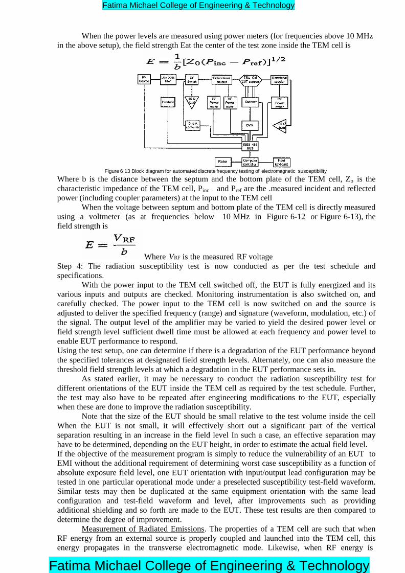
When the power levels are measured using power meters (for frequencies above 10 MHz
in the above setup), the field strength Eat the center of the test zone inside the TEM cell is
Figure 6 13 Block diagram for automated discrete frequency testing of electromagnetic susceptibility
Where b is the distance between the septum and the bottom plate of the TEM cell, Zo is the
characteristic impedance of the TEM cell, Pinc and Pref are the .measured incident and reflected
power (including coupler parameters) at the input to the TEM cell
When the voltage between septum and bottom plate of the TEM cell is directly measured
using a voltmeter (as at frequencies below 10 MHz in Figure 6-12 or Figure 6-13), the
field strength is
Where VRF is the measured RF voltage
Step 4: The radiation susceptibility test is now conducted as per the test schedule and
specifications.
With the power input to the TEM cell switched off, the EUT is fully energized and its
various inputs and outputs are checked. Monitoring instrumentation is also switched on, and
carefully checked. The power input to the TEM cell is now switched on and the source is
adjusted to deliver the specified frequency (range) and signature (waveform, modulation, etc.) of
the signal. The output level of the amplifier may be varied to yield the desired power level or
field strength level sufficient dwell time must be allowed at each frequency and power level to
enable EUT performance to respond.
Using the test setup, one can determine if there is a degradation of the EUT performance beyond
the specified tolerances at designated field strength levels. Alternately, one can also measure the
threshold field strength levels at which a degradation in the EUT performance sets in.
As stated earlier, it may be necessary to conduct the radiation susceptibility test for
different orientations of the EUT inside the TEM cell as required by the test schedule. Further,
the test may also have to be repeated after engineering modifications to the EUT, especially
when these are done to improve the radiation susceptibility.
Note that the size of the EUT should be small relative to the test volume inside the cell
When the EUT is not small, it will effectively short out a significant part of the vertical
separation resulting in an increase in the field level In such a case, an effective separation may
have to be determined, depending on the EUT height, in order to estimate the actual field level.
If the objective of the measurement program is simply to reduce the vulnerability of an EUT to
EMI without the additional requirement of determining worst case susceptibility as a function of
absolute exposure field level, one EUT orientation with input/output lead configuration may be
tested in one particular operational mode under a preselected susceptibility test-field waveform.
Similar tests may then be duplicated at the same equipment orientation with the same lead
configuration and test-field waveform and level, after improvements such as providing
additional shielding and so forth are made to the EUT. These test results are then compared to
determine the degree of improvement.
Measurement of Radiated Emissions. The properties of a TEM cell are such that when
RF energy from an external source is properly coupled and launched into the TEM cell, this
energy propagates in the transverse electromagnetic mode. Likewise, when RF energy is
Fatima Michael College of Engineering & Technology
Fatima Michael College of Engineering & Technology

somehow generated and radiated by a source located inside the TEM cell (e.g., an equipment
under test located in the TEM cell), this energy propagates in TEM mode inside the cell and
couples to the two ports of the TEM cell. Thus, by measuring such energy, one can arrive at a
quantitative estimate of the radiated emissions from the EDT. Limitations regarding size of the
EUT and useful upper frequency of the TEM cell are applicable for these measurements also. A
detailed procedure for the measurement of radiated emissions using a TEM cell is given in the
allowing:
Step 1:for positioning the EUT inside the TEM cell, and Step 2: for giving various
input/output/monitoring connections are identical to the procedures for measurement of
radiation susceptibility.
Step 3: The measuring apparatus are connected to the TEM cell.
The complexity of the measuring apparatus depends on the nature of information and
details of results required from such measurements. If the interest is in determining the
equivalent free-space radiated electric field from the EUT, the experimental setup shown in
Figure 6-14 can be used. The instrumentation for measurement consists of a precision RF
voltmeter or power meter.
If a time domain signature of the radiated emissions is required, the setup shown in
Figure 6-14 can still be used. The measuring instrumentation in this case will consist of a simple
oscilloscope or receiver/recorder.
In case a detailed pattern (including phase) of the radiations emitted by the EUT is
required, a relatively more complex measurement setup, shown in Figure 6-15, will be required.
In this setup, by connecting the two ports of the TEM cell into a loop using a hybrid coupler, it
is possible to measure the sum and difference of the powers (at the two ports of the TEM cell)
and the relative phase between the sum and difference outputs. In a perfectly general case, when
radiations from the EUT are modeled as a composite equivalent source consisting of three
orthogonal dipole moments as shown in Figure 6-16, a systematic measurement of the sum and
difference powers Ps and Pd, and relative phases Φ for six different orientations of EUT (located
inside the TEM cell) is sufficient to determine the phase and amplitude of the six components
shown in Figure 6-16.
Step 4: The radiated emissions are measured, observing the necessary precautions.
For measurements using the procedures of Figure 6-15, the six convenient orientations of
the EUT inside the TEM cell are shown in Table 6-2 and Figure 6-17.
The six different orientations selected above yield convenient mathematical equations for
computing the components shown in Figure 6-16. Various components of the power are
calculated using the expressions
Fatima Michael College of Engineering & Technology
Fatima Michael College of Engineering & Technology

Where q is the normalized amplitude of the vertical electric field which would exist in
the middle of an empty TEM cell when it is excited by an input power of 1 W at one end and
terminated in a matched load at the other end. Thus,
It is seen from the above that the amplitudes of electric dipole moments are determined
by the sum powers Psl, Psz, Ps3. Ps4. Pss, and Ps6. The amplitudes of magnetic dipole moments
are likewise determined by the measured difference powers only. Further if the radiations from
the EUT can be fully characterized by one kind of dipole moments only (electric or magnetic),
the relative phase measurement is not required.
From the above expressions, the total power radiated by the BUT in free space is
obtainable as
When phase information of the electric and magnetic dipole moments is required, as is
the case for determining the far-field radiation pattern of the EUT in free space, the relevant
parameters are computed using the equations:
Fatima Michael College of Engineering & Technology
Fatima Michael College of Engineering & Technology

EMI TEST SHIELDED CHAMBER AND SHIELDED FERRITE LINED ANECHOIC
CHAMBER
The previous topic described measurements using an open-area test site (OATS).
Although OATS is the internationally accepted facility and standard test approach for
measurement of radiated emissions and radiation susceptibility, it is not always convenient or
possible to use OATS. Consequently, a number of measurement facilities and procedures have
been developed over the years to enable such measurements to be carried out in a laboratory.
This chapter is devoted to a description, and procedures for use, of several of these laboratory
techniques. In particular, we will study Microwave anechoic chamber.
ANECHOIC CHAMBER
Anechoic Chamber A most common laboratory approach for electromagnetic interference/electromagnetic
compatibility (EMI/EMC) measurements is the use of microwave anechoic chambers. Such
chambers provide an indoor facility for measurements. They also provide high isolation, often in
excess of 100 dB, from the external electromagnetic environment. Therefore, anechoic
chambers are particularly suitable for highly sensitive measurements involving very low signal
levels. However, since the cost of a microwave anechoic chamber increases very rapidly with
its size, usually the dimensions of a microwave anechoic chamber are relatively small. A
typical installation measures 10.8 x 7.2 x 5.2 m. The size of equipment under test (EUT) that can
be measured in an anechoic chamber of this size is also small, typically less than 0.5 m.
A schematic of a microwave anechoic chamber is shown in Figure 6-1. The structure
consists of a metallic wall shielded enclosure. The enclosure is lined on the inside (walls,
ceiling, and floor) with microwave absorbing material, which is usually a carbon-impregnated
polyurethane foam in the shape of pyramids as shown in Figure 6-2.
Figure 6-1 Details of microwave anechoic chamber (1) metallic wall, Figure 6-2 Carbon impregnated foam pyramids
(2) door, (3) microwave absorbing materials,(4) turntable for azimuth rotation,
(5) wooden table (optional for height increase), (6) equipment under test, (7) antenna, (8) cable connection for instrumentation, (9) special panel for connectors
Because of the properties of this absorber lining, the chamber walls provide higher
power absorption capabilities at higher frequencies and lesser absorption at lower frequencies.
Further, at frequencies below around 200 MHz, dimensions of the available test zone become
comparable to the wavelength corresponding to the frequencies of measurement. Consequently,
use of microwave anechoic chambers for EMI/EMC measurements is limited to frequencies
above about 200MHz. Anechoic chambers usually have a door to facilitate the taking-in and
setting-up, or bringing out, the EUT and antennas and other accessories used in the
measurement. The door is a carefully designed unit with firm metallic spring contacts on all
sides for providing good isolation between the electromagnetic environments outside and inside of the chamber. Likewise any cables, connectors, or power supply lines are brought into the
anechoic chamber through special panels to provide high electromagnetic isolation. Radio
frequency (RF) signal cables and power lines are connected through separate panels. Any
relaxation of quality, standards, or precautions in the construction and assembly of the door, or
the special panels, could degrade the electromagnetic isolation between the outside and inside of
the anechoic chamber.
In sophisticated measurement setups, the floor of an anechoic chamber has rails on
which a wooden platform is mounted. The EUT can be placed on this platform. Further, the
Fatima Michael College of Engineering & Technology
Fatima Michael College of Engineering & Technology

platform can be moved on the rails and positioned with precision with the help of an electric or
mechanical arrangement.
The photograph in Figure 6-3 shows the inside of an anechoic chamber. Here the EUT is
in position on the platform, and an antenna is being positioned for measurements.
Figure 6-3 Photograph showing the arrangements inside the microwave anechoic chamber
Shielded Enclosures and Faraday Cages. Shielded enclosures and Faraday cages are the
lower-cost alternatives to microwave anechoic chambers. A shielded enclosure has walls of
metal sheet with metallic spring contacts along the panel joints to prevent radio frequency
energy leakage. The inside of a shielded enclosure is not lined with absorbing material.
Faraday cages are frequently constructed using a wire-mesh instead of a solid sheet of metal.
The electromagnetic isolation between external electromagnetic environment and inside of
the chamber is poorer for these two types of chambers when compared to anechoic
chambers. Further internal reflections , from chamber walls also tend to inhibit
measurements.
Measurements Using an Anechoic Chamber
Measurement of RE. A schematic that enables the measurement of radiated emissions
from equipment under test is shown in Figure 6-4. The measuring instruments are placed in a
shielded anteroom adjoining the anechoic chamber. Although it is not always necessary to
house the test instruments in a shielded anteroom, this approach becomes advantageous
especially when a measurement of very low signal levels is necessary. The EUT is energized via
a separate power supply cable brought in through the floor of the anechoic chamber near the
mounting of the wooden turntable. Measurement distance D is usually 1, 3, or 10m. Antenna
output is connected via a special panel, through a precisely in-situ calibrated cable, o the
receiver for measuring radiated emissions. As an example, measured radiated emissions from a
motor operating the windshield wipers of an automobile are given in Figure 6-5. The schematic
shown in Figure 6-4 can be used for measuring radiated emissions in all 360° of the azimuth by
rotating the turntable on which the EUT is located.
Figure 6-4 Schematic for measurement of radiated emissions from the equipment under test (1) shielded anechoic
chamber, (2) anteroom for test instrumentation, (3) EM Energy absorbing materials, (4) turntable for azimuth
coverage, (5) wooden table (optional), (6) equipment Under Test (EUT), (7) EMI receiving antenna, (8) calibrated
RF cable, (9) special panel for connectors, (10) amplifier for higher dynamic range, (11) EMI meter, (12)
instrument controller for EMI meter and plotter, (13) plotter
Fatima Michael College of Engineering & Technology
Fatima Michael College of Engineering & Technology

Measurement of RS. A schematic for measuring radiation susceptibility of an EDT is shown in
Figure 6-6. In this setup, it is not usually necessary to place the transmitter (i.e., signal generator
and amplifier) inside a shielded enclosure. Such an arrangement usually becomes necessary only
when the susceptibility test is being conducted at extremely low power levels for special types
of equipment. However, in most laboratories, the radiated emissions and radiation susceptibility
are tested in the same anechoic chamber, in which case an adjoining shielded room for test
equipment is part of the facility. In actual test, the power radiated by an antenna (i.e., the power
delivered to the antenna by the signal generator-amplifier combination) is increased up to
specified test levels, and the designated performance factors of a EUT are observed for
malfunction caused by radiation susceptibility. It is often necessary to repeat this test at a
number of test frequencies and power levels. Further, it may also be necessary to repeat this test
with the EUT placed in different orientations (in all the three orthogonal planes) on the turntable
inside the shielded anechoic chamber. Thus whereas the turntable in Figure 6-6 provides for
rotation in the horizontal plane, an additional attachment to this turntable may be added to
facilitate a change in the angle of elevation.
Figure 6-6 Schematic for evaluation of radiation susceptibility of an equipment under test (1) shielded anechoic chamber, (2) anteroom for test
instrumentation,(3) EM Energy absorbing materials, (4) turntable for azimuth coverage, (5) equipment under test, (6) radio frequency (RF)
transmitting antenna, (7) calibrated RF cable, (8) special panel for connectors, (9) RF power amplifier, (10) RF signal generator
Sources of Inaccuracies in Measurement Two important aspects which merit attention for the
purpose of accurate radiated emission or radiation susceptibility measurements using anechoic
chambers are the quality of the chamber (i.e., level of reflection from the walls of the
anechoic chamber) and the exactness of the relationship between the electromagnetic field
surrounding the antenna in the anechoic chamber and the voltage or power measured at the
receiver point or transmitter amplifier.
Chamber Quality. An ideal anechoic chamber provides a true free-space environment in the
region between the EUT and the receive/transmit antenna. Any reflections from the chamber
walls (side walls, ceiling, and floor) distort the field pattern created by the radiations from BUT
when it is being subjected to radiated emission testing. The field strength at any point is the
vectorial sum of all electromagnetic fields created by radiation from the EUT and all reflections
from the walls of the chamber.
Likewise, when an EUT is being tested for radiation susceptibility, the electromagnetic
field in which the EUT is immersed is the vectorial sum of all fields set up by the transmitting
antenna and all reflections from the walls of the chamber.
Fatima Michael College of Engineering & Technology
Fatima Michael College of Engineering & Technology

When the anechoic chamber is free from reflections, and therefore simulates an
ideal free space, with a transmitting antenna of gain Grx transmitting a power Prx, the
power received PRX by a receiving antenna of gain GRX is given by the equation
Where f is frequency of measurement in MHz, D is the distance between the transmit and
receive antennas.
Thus for a given pair of antennas and frequency of measurement,
The parameters PRX/Prx as a function of D can be carefully measured in the anechoic
chamber with a pair of transmit and receive antennas. A transmitter feeds the transmit antenna,
and the receive antenna is connected to a receiver. Any deviation of this characteristic from the
ideal 1/D2 relationship given in above equation is a measure of the imperfections, or reflections,
within the anechoic chamber. As an example, measurements made on an anechoic chamber at
National Institute of Standards and Technology (NIST) reproduced in Figure 6-7. Experimental
measurements and the theoretical curve as fitted at 1 m separation distance.
For this anechoic chamber, reflection error measurements were made at 20 frequencies
between 175 MHz and 18 GHz. The results are reproduced in Table 6-1. The range of error
varied between -0.6 dB and +0.5 dB at a lower frequency of 229 MHz to ±0.04 dB at a higher
frequency of 18 GHz. The reflections from the chamber walls, ceiling, and floor tend to be more
pronounced at lower frequencies. In this study, certain commercial equipment, instruments, or
materials used by the NIST are identified in Table 6-1 to adequately specify the experimental
procedure and details. Other similar equipment or instruments can be equally used.
Field Intensity. A second source of error or uncertainty in measurements using an anechoic
chamber are the inaccuracies in relating the field in which the antenna is positioned (i.e., 7 in
Figure 6-4 or 6 in Figure 6-6), and the voltage or power measured in the adjoining shielded
room where the instruments are placed. Several important parameters are:
• basic uncertainty in the measurement of power at the transmitter or receiver end
• cable losses between the transmitter/receiver and the antenna
• uncertainty in precisely estimating the antenna factor of the antenna • Inaccuracies in precisely measuring or estimating the distance D in Figure 6-4 or Figure 6-6.
For better accuracy, use of a precision power meter with a calibrated bolo meter is preferred.
Apart from using a calibrated (i.e., attenuation precisely measured) cable for connecting the
antenna to the transmitter amplifier (or receiver, as the case may be), precision measurement of
the power delivered to the antenna can be made by using a reflectometer type measurement
setup.
A Standard Laboratory Setup. When all the above precautions and steps to minimize
measurement errors were taken in a particular standard laboratory setup (2], the worst-case
overall uncertainty in the field strength generated in an anechoic chamber was estimated to be
±1.0 dB. The sources of this uncertainty are ±0.1 dB in power measurement, ±0.8 dB in
calculating antenna gain in the anechoic chamber environment and ±0.1 dB in measuring the
distance D.
Fatima Michael College of Engineering & Technology
Fatima Michael College of Engineering & Technology

Fatima Michael College of Engineering & Technology
Fatima Michael College of Engineering & Technology