Ultra-low Surface Recombination Velocity in InP Nanowires Probed by Terahertz Spectroscopy
22
Ultralow Surface Recombination Velocity in InP Nanowires Probed by Terahertz Spectroscopy Hannah J. Joyce,* ,† Jennifer Wong-Leung, ‡ Chaw-Keong Yong, † Callum J. Docherty, † Suriati Paiman, ‡,§ Qiang Gao, ‡ H. Hoe Tan, ‡ Chennupati Jagadish, ‡ James Lloyd-Hughes, † Laura M. Herz, † and Michael B. Johnston* ,† † Clarendon Laboratory, Department of Physics, University of Oxford, Oxford, OX1 3PU, United Kingdom ‡ Department of Electronic Materials Engineering, Research School of Physics and Engineering, Australian National University, Canberra, ACT 0200, Australia § Department of Physics, Faculty of Science, Universiti Putra Malaysia, 43400 Serdang, Selangor, Malaysia * S Supporting Information ABSTRACT: Using transient terahertz photoconductivity measure- ments, we have made noncontact, room temperature measurements of the ultrafast charge carrier dynamics in InP nanowires. InP nanowires exhibited a very long photoconductivity lifetime of over 1 ns, and carrier lifetimes were remarkably insensitive to surface states despite the large nanowire surface area-to-volume ratio. An exceptionally low surface recombination velocity (170 cm/s) was recorded at room temperature. These results suggest that InP nanowires are prime candidates for optoelectronic devices, particularly photovoltaic devices, without the need for surface passivation. We found that the carrier mobility is not limited by nanowire diameter but is strongly limited by the presence of planar crystallographic defects such as stacking faults in these predom- inantly wurtzite nanowires. These findings show the great potential of very narrow InP nanowires for electronic devices but indicate that improvements in the crystallographic uniformity of InP nanowires will be critical for future nanowire device engineering. KEYWORDS: InP, nanowire, terahertz, photoconductivity, surface recombination velocity, mobility S emiconductor nanowires are predicted to drive new generations of compact, ultrafast, and high efficiency electronic and optoelectronic devices. Among nanowire materials, InP is especially promising due to its direct band gap and high electron mobility. A multitude of prototype InP nanowire devices have been demonstrated including photo- detectors, 1 light-emitting diodes, 2 waveguides, 3 solar cells, 4,5 and field effect transistors. 2,6 Despite these early successes, there remain many fundamental unanswered questions concerning the dynamics of charge carriers in nanowires, and the effects of nanowire size, surfaces, and crystal structure on nanowire electronic properties. A greater understanding of these effects is essential for the future engineering of nanowire- based devices. In this Letter, we examine the ultrafast carrier dynamics within InP nanowires and assess the effects of nanowire diameter, surfaces, and crystal structure. These investigations were performed using optical pump-terahertz probe (OPTP) spectroscopy, a technique which is ideally suited for nanowire studies because it is a noncontact ultrafast probe of room temperature photoconductivity with subpicosecond resolution. 7 The contact-free nature of this technique confers a significant advantage over conventional electrical transport measurements, which are subject to artifacts associated with electrical contacts and the models used to extract data. 8,9 A further advantage is that the OPTP measurements are performed at room temperature, so its measurements of carrier mobility and lifetime are directly relevant to future InP nanowire-based devices which will be operated at room temperature. From OPTP measurements on InP nanowires of different diameters, we determine that surface recombination is negligible in InP nanowires. This result is despite the large surface area-to-volume ratio intrinsic to the nanowires and contrasts strongly with studies of GaAs nanowires for which surface recombination severely limits the carrier lifetime. 10 For InP nanowires we measured a long photoconductivity lifetime of over 1 ns. The long carrier lifetime at room temperature and insensitivity to surface states suggests that InP nanowires are excellent candidates for optoelectronic devices, especially for photovoltaic devices. Time-resolved PL spectroscopy was Received: July 19, 2012 Revised: September 6, 2012 Letter pubs.acs.org/NanoLett © XXXX American Chemical Society A dx.doi.org/10.1021/nl3026828 | Nano Lett. XXXX, XXX, XXX-XXX
Transcript of Ultra-low Surface Recombination Velocity in InP Nanowires Probed by Terahertz Spectroscopy
Ultralow Surface Recombination Velocity in InP Nanowires Probedby Terahertz SpectroscopyHannah J. Joyce,*,† Jennifer Wong-Leung,‡ Chaw-Keong Yong,† Callum J. Docherty,† Suriati Paiman,‡,§
Qiang Gao,‡ H. Hoe Tan,‡ Chennupati Jagadish,‡ James Lloyd-Hughes,† Laura M. Herz,†
and Michael B. Johnston*,†
†Clarendon Laboratory, Department of Physics, University of Oxford, Oxford, OX1 3PU, United Kingdom‡Department of Electronic Materials Engineering, Research School of Physics and Engineering, Australian National University,Canberra, ACT 0200, Australia§Department of Physics, Faculty of Science, Universiti Putra Malaysia, 43400 Serdang, Selangor, Malaysia
*S Supporting Information
ABSTRACT: Using transient terahertz photoconductivity measure-ments, we have made noncontact, room temperature measurementsof the ultrafast charge carrier dynamics in InP nanowires. InPnanowires exhibited a very long photoconductivity lifetime of over 1ns, and carrier lifetimes were remarkably insensitive to surface statesdespite the large nanowire surface area-to-volume ratio. Anexceptionally low surface recombination velocity (170 cm/s) wasrecorded at room temperature. These results suggest that InPnanowires are prime candidates for optoelectronic devices,particularly photovoltaic devices, without the need for surfacepassivation. We found that the carrier mobility is not limited bynanowire diameter but is strongly limited by the presence of planarcrystallographic defects such as stacking faults in these predom-inantly wurtzite nanowires. These findings show the great potential of very narrow InP nanowires for electronic devices butindicate that improvements in the crystallographic uniformity of InP nanowires will be critical for future nanowire deviceengineering.
KEYWORDS: InP, nanowire, terahertz, photoconductivity, surface recombination velocity, mobility
Semiconductor nanowires are predicted to drive newgenerations of compact, ultrafast, and high efficiency
electronic and optoelectronic devices. Among nanowirematerials, InP is especially promising due to its direct bandgap and high electron mobility. A multitude of prototype InPnanowire devices have been demonstrated including photo-detectors,1 light-emitting diodes,2 waveguides,3 solar cells,4,5
and field effect transistors.2,6 Despite these early successes,there remain many fundamental unanswered questionsconcerning the dynamics of charge carriers in nanowires, andthe effects of nanowire size, surfaces, and crystal structure onnanowire electronic properties. A greater understanding ofthese effects is essential for the future engineering of nanowire-based devices.In this Letter, we examine the ultrafast carrier dynamics
within InP nanowires and assess the effects of nanowirediameter, surfaces, and crystal structure. These investigationswere performed using optical pump−terahertz probe (OPTP)spectroscopy, a technique which is ideally suited for nanowirestudies because it is a noncontact ultrafast probe of roomtemperature photoconductivity with subpicosecond resolution.7
The contact-free nature of this technique confers a significant
advantage over conventional electrical transport measurements,which are subject to artifacts associated with electrical contactsand the models used to extract data.8,9 A further advantage isthat the OPTP measurements are performed at roomtemperature, so its measurements of carrier mobility andlifetime are directly relevant to future InP nanowire-baseddevices which will be operated at room temperature.From OPTP measurements on InP nanowires of different
diameters, we determine that surface recombination isnegligible in InP nanowires. This result is despite the largesurface area-to-volume ratio intrinsic to the nanowires andcontrasts strongly with studies of GaAs nanowires for whichsurface recombination severely limits the carrier lifetime.10 ForInP nanowires we measured a long photoconductivity lifetimeof over 1 ns. The long carrier lifetime at room temperature andinsensitivity to surface states suggests that InP nanowires areexcellent candidates for optoelectronic devices, especially forphotovoltaic devices. Time-resolved PL spectroscopy was
Received: July 19, 2012Revised: September 6, 2012
Letter
pubs.acs.org/NanoLett
© XXXX American Chemical Society A dx.doi.org/10.1021/nl3026828 | Nano Lett. XXXX, XXX, XXX−XXX
performed in conjunction with OPTP measurements, andprovided evidence that, after photoexcitation, electrons andholes are rapidly separated spatially into zinc-blende (ZB) andwurtzite (WZ) crystal sections, respectively, within thenanowires. This spatial separation of electrons and holes causesrapid PL quenching within 100 ps but allows a long carrierlifetime leading to long-lived photoconductivity. Additionally,we found that the carrier mobility does not show a simplesystematic relationship with nanowire diameter. Instead, thecarrier mobility is strongly influenced by the presence of planarcrystallographic defects such as stacking faults, twins, and ZB−WZ polytypism in these predominantly WZ nanowires.Nominally undoped InP nanowires were grown on InP
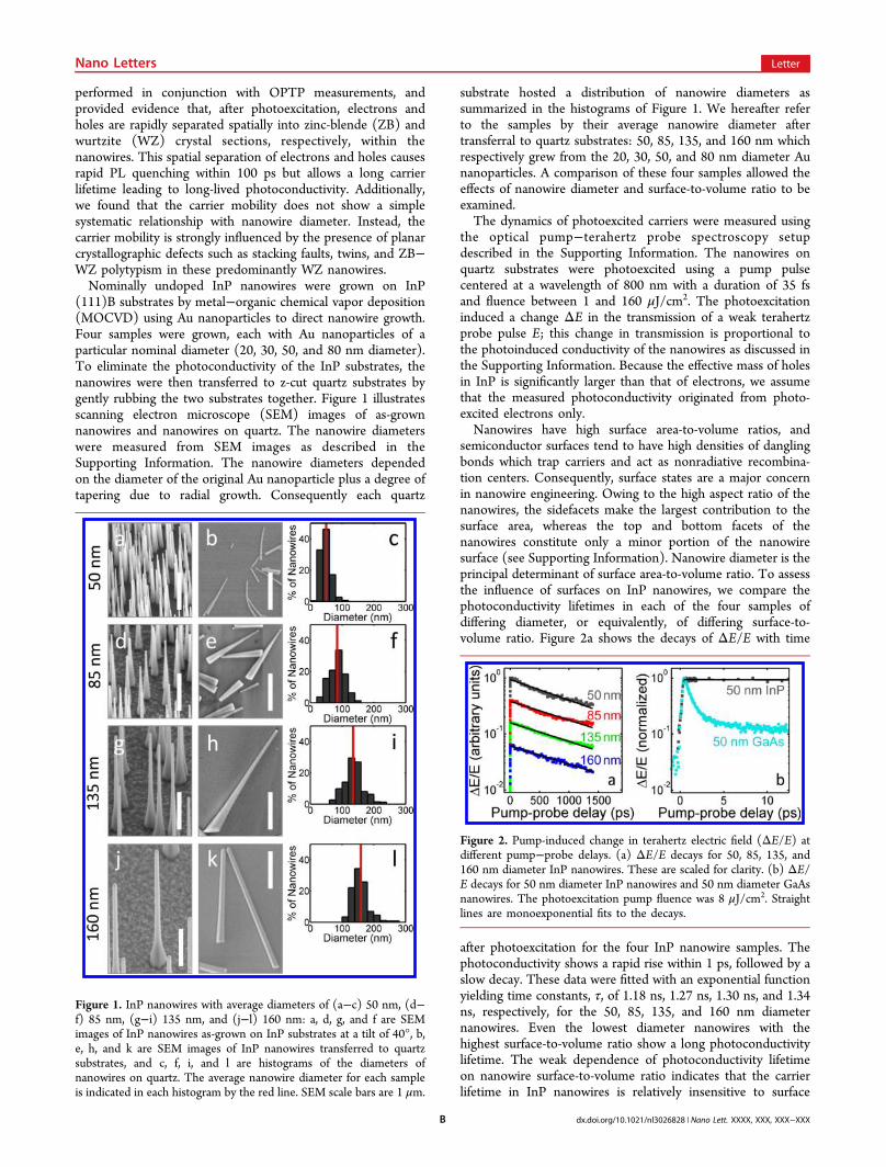
(111)B substrates by metal−organic chemical vapor deposition(MOCVD) using Au nanoparticles to direct nanowire growth.Four samples were grown, each with Au nanoparticles of aparticular nominal diameter (20, 30, 50, and 80 nm diameter).To eliminate the photoconductivity of the InP substrates, thenanowires were then transferred to z-cut quartz substrates bygently rubbing the two substrates together. Figure 1 illustratesscanning electron microscope (SEM) images of as-grownnanowires and nanowires on quartz. The nanowire diameterswere measured from SEM images as described in theSupporting Information. The nanowire diameters dependedon the diameter of the original Au nanoparticle plus a degree oftapering due to radial growth. Consequently each quartz
substrate hosted a distribution of nanowire diameters assummarized in the histograms of Figure 1. We hereafter referto the samples by their average nanowire diameter aftertransferral to quartz substrates: 50, 85, 135, and 160 nm whichrespectively grew from the 20, 30, 50, and 80 nm diameter Aunanoparticles. A comparison of these four samples allowed theeffects of nanowire diameter and surface-to-volume ratio to beexamined.The dynamics of photoexcited carriers were measured using
the optical pump−terahertz probe spectroscopy setupdescribed in the Supporting Information. The nanowires onquartz substrates were photoexcited using a pump pulsecentered at a wavelength of 800 nm with a duration of 35 fsand fluence between 1 and 160 μJ/cm2. The photoexcitationinduced a change ΔE in the transmission of a weak terahertzprobe pulse E; this change in transmission is proportional tothe photoinduced conductivity of the nanowires as discussed inthe Supporting Information. Because the effective mass of holesin InP is significantly larger than that of electrons, we assumethat the measured photoconductivity originated from photo-excited electrons only.Nanowires have high surface area-to-volume ratios, and
semiconductor surfaces tend to have high densities of danglingbonds which trap carriers and act as nonradiative recombina-tion centers. Consequently, surface states are a major concernin nanowire engineering. Owing to the high aspect ratio of thenanowires, the sidefacets make the largest contribution to thesurface area, whereas the top and bottom facets of thenanowires constitute only a minor portion of the nanowiresurface (see Supporting Information). Nanowire diameter is theprincipal determinant of surface area-to-volume ratio. To assessthe influence of surfaces on InP nanowires, we compare thephotoconductivity lifetimes in each of the four samples ofdiffering diameter, or equivalently, of differing surface-to-volume ratio. Figure 2a shows the decays of ΔE/E with time
after photoexcitation for the four InP nanowire samples. Thephotoconductivity shows a rapid rise within 1 ps, followed by aslow decay. These data were fitted with an exponential functionyielding time constants, τ, of 1.18 ns, 1.27 ns, 1.30 ns, and 1.34ns, respectively, for the 50, 85, 135, and 160 nm diameternanowires. Even the lowest diameter nanowires with thehighest surface-to-volume ratio show a long photoconductivitylifetime. The weak dependence of photoconductivity lifetimeon nanowire surface-to-volume ratio indicates that the carrierlifetime in InP nanowires is relatively insensitive to surface
Figure 1. InP nanowires with average diameters of (a−c) 50 nm, (d−f) 85 nm, (g−i) 135 nm, and (j−l) 160 nm: a, d, g, and f are SEMimages of InP nanowires as-grown on InP substrates at a tilt of 40°, b,e, h, and k are SEM images of InP nanowires transferred to quartzsubstrates, and c, f, i, and l are histograms of the diameters ofnanowires on quartz. The average nanowire diameter for each sampleis indicated in each histogram by the red line. SEM scale bars are 1 μm.
Figure 2. Pump-induced change in terahertz electric field (ΔE/E) atdifferent pump−probe delays. (a) ΔE/E decays for 50, 85, 135, and160 nm diameter InP nanowires. These are scaled for clarity. (b) ΔE/E decays for 50 nm diameter InP nanowires and 50 nm diameter GaAsnanowires. The photoexcitation pump fluence was 8 μJ/cm2. Straightlines are monoexponential fits to the decays.
Nano Letters Letter
dx.doi.org/10.1021/nl3026828 | Nano Lett. XXXX, XXX, XXX−XXXB
states. This is consistent with the low surface recombinationvelocity of the InP material system.11,12 As derivedpreviously13,14 and described in the Supporting Information,the effective recombination time is closely approximated by thefunction:
τ τ= + S
d1 1 4
volume (1)
where d is the nanowire diameter, S is the surfacerecombination velocity, and τvolume is the time constant forrecombination at volume defects. By fitting eq 1 to theexperimental τ values we extract a τvolume of 1.4 ns and a surfacerecombination velocity of only 170 cm/s. This surfacerecombination velocity is consistent with results obtained forbulk n-InP.11,15,16
This result contrasts markedly with GaAs nanowires, asdemonstrated in Figure 2b. The GaAs nanowires studied wereof similar diameter to the 50 nm diameter InP nanowires, butthe GaAs nanowires exhibit an extremely rapid initial decay inphotoconductivity due to carrier trapping at surface states.10
This is consistent with the high surface recombination velocityof GaAs.12 Generally, surface passivation is essential to improvecarrier lifetimes in GaAs nanowires.17 InP nanowires, on theother hand, exhibit prolonged photoconductivity and aremarkably low electron trapping rate at surfaces, even withoutsurface passivation. These findings are significant for manyelectronic applications which require long carrier lifetimes. Inphotovoltaic devices, for example, the long carrier lifetime andlow surface recombination velocity would minimize recombi-nation losses, to maximize the collected current and maximizeenergy conversion efficiency. We note that surface passivationof InP nanowires may yet be advantageous for light emissionapplications and photodiode devices, as demonstrated inprevious studies.5,18,19
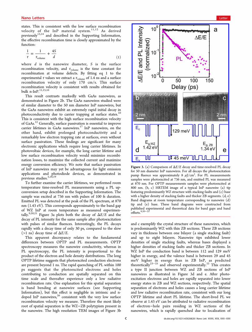
To further examine the carrier lifetimes, we performed roomtemperature time-resolved PL measurements using a PL up-conversion setup described in the Supporting Information. Thesample was excited at 736 nm with pulses of 100 fs duration.Emitted PL was detected at the peak of the PL spectrum, at 870nm (1.43 eV). This corresponds approximately to the band gapof WZ InP at room temperature as measured experimen-tally.9,20,21 Figure 3a plots both the decay of ΔE/E and thedecay of PL intensity for the same sample after photoexcitationwith pulses of similar fluences. Interestingly, the PL decaysrapidly with a decay time of only 30 ps, compared to the slow(>1 ns) decay time of ΔE/E.This apparent discrepancy relates to the fundamental
differences between OPTP and PL measurements. OPTPspectroscopy measures the nanowire conductivity, whereas inPL spectroscopy, the PL intensity is proportional to theproduct of the electron and hole density distributions. The longOPTP lifetime suggests that photoexcited conduction electronsare present beyond 1 ns. The rapid quenching of PL within 100ps suggests that the photoexcited electrons and holescontributing to conduction are spatially separated on thistime scale and thereafter experience only a low radiativerecombination rate. One explanation for this spatial separationis band bending at nanowire surfaces (see SupportingInformation), but this effect is negligible in intrinsic and n-doped InP nanowires,26 consistent with the very low surfacerecombination velocity we measure. Therefore the most likelyroot of spatial separation is the WZ−ZB polytypism present inthe nanowire. The high resolution TEM images of Figure 3b
and c exemplify the crystal structure of these nanowires, whichis predominantly WZ with thin ZB sections. These ZB sectionsvary in thickness between one bilayer (a single stacking fault)and up to eight bilayers. Nanowire tips exhibited lowerdensities of single stacking faults, whereas bases displayed ahigher densities of stacking faults and thicker ZB sections. InWZ InP the conduction band is between 112 and 129 meVhigher in energy, and the valence band is between 29 and 45meV higher in energy than in ZB InP, as predictedtheoretically23−25 and observed experimentally.22 This createsa type II junction between WZ and ZB sections of InPnanowires as illustrated in Figure 3d and e. After photo-excitation electrons and holes are rapidly separated into lowerenergy states in ZB and WZ sections, respectively. The spatialseparation of electrons and holes causes a long carrier lifetimeand low radiative recombination rate, consistent with our longOPTP lifetime and short PL lifetime. The short-lived PL weobserve at 1.43 eV can be attributed to radiative recombinationof electron−hole pairs residing in WZ sections of thenanowires, which is rapidly quenched due to localization of
Figure 3. (a) Comparison of ΔE/E decay and time-resolved PL decayfor 50 nm diameter InP nanowires. For all decays the photoexcitationpump fluence was approximately 8 μJ/cm2. For PL measurementssamples were photoexcited at 736 nm, and emitted PL was measuredat 870 nm. For OPTP measurements samples were photoexcited at800 nm. (b, c) HRTEM image of a typical InP nanowire (a) tipfeaturing predominantly WZ structure with stacking faults and (c) basewith a higher density of stacking faults and thicker ZB segments. (d, e)Band diagrams at room temperature corresponding to nanowire (d)tip and (e) base. These band diagrams were constructed frompublished experimental and theoretical data for band gaps and bandoffsets.9,20−25
Nano Letters Letter
dx.doi.org/10.1021/nl3026828 | Nano Lett. XXXX, XXX, XXX−XXXC
electrons and holes into ZB and WZ sections, respectively.More long-lived red-shifted PL is expected from spatiallyseparated electrons and holes, and this has been observed inlow temperature PL measurements.27,28
Note that electrons and holes may still contribute toconduction despite their localization in ZB and WZ nanowiresections. In these predominantly WZ nanowires, the ZBsegments are sufficiently thin, at less than 3 nm in thickness,that there is considerable leakage of the electron wave functioninto adjacent WZ segments.25 The localization of electrons andholes could, however, result in increased scattering atboundaries between ZB and WZ segments and at stackingfaults and consequently a reduced carrier mobility. To gainfurther insight into charge carrier scattering and mobility inthese nanowires, we obtained photoconductivity spectra, asdiscussed in the following.Figure 4 shows photoconductivity spectra collected for 50
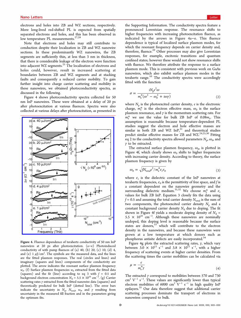
nm InP nanowires. These were obtained at a delay of 20 psafter photoexcitation at various fluences. Spectra were alsocollected at various delays after photoexcitation, as presented in
the Supporting Information. The conductivity spectra feature apronounced Lorentzian response. The resonance shifts tohigher frequencies with increasing photoexcitation fluence, asindicated by the arrows in Figure 4a−e. This fluencedependence is typical of localized surface plasmon modes, forwhich the resonant frequency depends on carrier density and,therefore, fluence.29 Other processes may also give Lorentzianresponses, for example, excitonic transitions and quantumconfined states; however these would not show resonance shiftswith fluence. We therefore attribute the response to a surfaceplasmon mode. This is consistent with previous work on GaAsnanowires, which also exhibit surface plasmon modes in theterahertz range.10 The conductivity spectra were accordinglyfitted with the function
σω
ω ω ωγ= * − +
iN e
m i( )p
2
e2
02
(2)
where Np is the photoexcited carrier density, e is the electroniccharge, me* is the electron effective mass, ω0 is the surfaceplasmon resonance, and γ is the momentum scattering rate. Forme* we use the value for bulk ZB InP of 0.08me. Thisassumption is reasonable because temperature-dependent PLstudies suggest the electron and hole effective masses aresimilar in both ZB and WZ InP,21 and theoretical studiespredict similar effective masses for ZB and WZ.24,25,30 Fittingeq 2 to the conductivity spectra allowed parameters Np, ω0, andγ to be extracted.The extracted surface plasmon frequency, ω0, is plotted in
Figure 4f, which clearly shows ω0 shifts to higher frequencieswith increasing carrier density. According to theory, the surfaceplasmon frequency is given by
ω ε ε= *fN e m/0 total2
e r 0 (3)
where εr is the dielectric constant of the InP nanowires atterahertz frequencies, ε0 is the permittivity of free space, and f isa constant dependent on the nanowire geometry and thesurrounding dielectric medium.31,32 We choose me* and εrvalues for bulk ZB InP. Equation 3 closely fits the data usingf = 0.5 and assuming the total carrier density Ntotal is the sum oftwo components, the photoexcited carrier density Np and aconstant background carrier density Nd due to doping. The fitshown in Figure 4f yields a moderate doping density of Nd =5.5 × 1016 cm−3. Although these nanowires are nominallyundoped, this doping level is reasonable because the surfacestates are donors,33 which will contribute to the electrondensity in the nanowires, and because these nanowires weregrown at a low temperature at which donors such asphosphorus antisite defects are easily incorporated.34
Figure 4g plots the extracted scattering rates, γ, which varybetween 3.0 × 10¹³ s−1 and 3.8 × 10¹³ s−1, with a higherfrequency of scattering events at higher carrier densities. Fromthe scattering times the carrier mobilities can be calculated via
μγ
= *e
me (4)
The extracted γ correspond to mobilities between 570 and 730cm2 V−1 s−1. These values are significantly lower than typicalelectron mobilities of 6000 cm2 V−1 s−1 in high quality InPepilayers.35 Our data therefore suggest that additional carrierscattering processes dominate the transport of electrons innanowires compared to bulk.
Figure 4. Fluence dependence of terahertz conductivity of 50 nm InPnanowires at 20 ps after photoexcitation. (a−e) Photoinducedconductivity of with pump fluences of (a) 40, (b) 20, (c) 10, (d) 4,and (e) 1 μJ/cm2. The symbols are the measured data, and the linesare the fitted plasmon responses. The real (circles and lines) andimaginary (squares and lines) components of the conductivity areplotted. The arrow indicates the resonant surface plasmon frequencyw0. (f) Surface plasmon frequencies w0 extracted from the fitted data(squares) and the fit (line) according to eq 3 with f = 0.5 andbackground electron concentration Nd = 5.5 × 1016 cm−3. (g) Carrierscattering rates γ extracted from the fitted nanowire data (squares) andtheoretically predicted for bulk InP (dotted line). The error barsindicate the uncertainty in Np, Ntotal, w0, and γ resulting fromuncertainty in the measured fill fraction and in the parameters givingthe optimum fits.
Nano Letters Letter
dx.doi.org/10.1021/nl3026828 | Nano Lett. XXXX, XXX, XXX−XXXD
In bulk InP at room temperature, the dominant scatteringprocesses are carrier−phonon, carrier−carrier, carrier−plas-mon, and carrier−impurity scattering. These mechanisms resultin theoretical scattering rates shown in Figure 4g, which werecalculated using models outlined in previous publications36,37
and as described in the Supporting Information. Both theexperimental γ for nanowires and the theoretical γ for bulk InPshow a similar dependence on carrier density, primarily due toincreased carrier−carrier scattering at higher carrier densities.The experimental γ are, however, higher by approximately 1.3× 10¹³ s−1. This additional scattering component is constant,that is, not dependent on carrier density.In nanowires, this additional scattering could arise from (i)
roughness at nanowire surfaces and (ii) band offsets at planarcrystallographic defects such as stacking faults, twins, andinterfaces between ZB and WZ segments. To estimate thescattering contribution from (i), we refer to the modeldeveloped by Unuma et al. for quantum wells.38 TEM imageswere analyzed from which we estimated the upper limit of theroughness height as 1 nm and estimated the lower limit ofcorrelation length as 10 nm. This modeling revealed thatsurface roughness scattering is negligible for nanowirediameters larger than 20 nm, which is valid for all nanowirediameters studied here.The modeling described above predicted that surface
roughness scattering (i) has negligible influence on carriermobility. This would imply that the nanowire surface area-to-volume ratio, and consequently diameter, should have aminimal effect on carrier mobility. To examine this predictionexperimentally, we have measured photoconductivity spectraand extracted γ for the four samples of different diameters. Thespectra are provided in the Supporting Information. For the 50,85, 135, and 160 nm samples the scattering rates wereapproximately 3.3 × 10¹³ s−1, 18 × 1013 s−1, 10 × 1013 s−1, and4.5 × 1013 s−1, respectively. These scattering rates correspondto mobilities of 660 cm2 V−1 s−1, 120 cm2 V−1 s−1, 220 cm2 V−1
s−1, and 480 cm2 V−1 s−1, respectively, for the 50, 85, 135, and160 nm diameter samples. These mobilities show no systematicdependence on nanowire diameter: the 50 and 160 nmnanowires exhibit the highest mobilities, whereas theintermediate diameters exhibit the lowest mobilities. Thenonsystematic variation in mobility suggests that other factors,for instance the density of stacking faults, plays a moredominant role in carrier dynamics than scattering at nanowiresurfaces.Assuming an electron thermal velocity of 4.1 × 107 cm/s, the
measured scattering rates correspond to average scatteringlengths, λ, between 2.3 and 12 nm (see SupportingInformation). These lengths are considerably lower than thenanowire diameters studied here, supporting our observationthat scattering at nanowire surfaces is not the major mechanismlimiting carrier mobility. These scattering lengths are, however,comparable to the distances between planar crystallographicdefects, as seen in the TEM images of Figure 3.The most likely explanation for the low mobility in these
nanowires is, therefore, the high density of stacking faults (ii).Recent publications on transport measurements of InPnanowire field effect transistors have alternately proposed thatmobility is significantly degraded by stacking faults8,39 or bysurface scattering.40 These studies, however, did not comparenanowires of different diameters. Our diameter-dependentmeasurements and theoretical calculations exclude the
possibility of significant surface scattering, providing strongevidence that stacking faults limit nanowire conductivity.The nonsystematic variation in mobility with nanowire
diameter may be ascribed to differences in the density,distribution, and thickness of ZB segments from sample tosample. Such sample-to-sample variations in crystal structureare expected because the nanowire crystal structure isinfluenced by the nanowire diameter, and by a number ofrelated parameters, such as nanowire growth rate and thedensity of Au nanoparticles on the substrate.41,42 Duringnanowire growth these parameters act in conflicting ways tostabilize either ZB or WZ layers, so that the stacking faultdensity shows a complex dependency on nanowire diameter.TEM examination of the nanowire samples revealed that thedensity of stacking faults and thickness of ZB sections indeedvaries between nanowires of different diameters but also variessubstantially within individual nanowires. Nanowire basesexhibited higher densities of stacking faults and thicker ZBsections than nanowire tips. This large variability withinindividual nanowires precluded a complete quantitative analysisof how stacking fault density and ZB section thickness vary withnanowire diameter. Future contact-free measurements on InPnanowire samples (i) without planar crystallographic defectsand (ii) with more well-defined defect densities shouldelucidate the dependence of mobility on stacking fault densityand the thickness of ZB segments.In this study, OPTP spectroscopy has revealed the effects of
nanowire diameter, surfaces, and crystal structure on carrierdynamics in InP nanowires. Our measurements indicate thatInP nanowire surfaces have only a weak influence on carrierlifetime, in marked contrast to GaAs nanowires. For InPnanowires the low surface recombination rate results in a longphotoconductivity lifetime of over 1 ns, even without surfacepassivation. This long photoconductivity lifetime points to theimmense technological potential of InP nanowires for futureoptoelectronic and photovoltaic devices. Furthermore, theoreti-cal calculations and OPTP measurements demonstrated thatInP nanowire surface roughness has a negligible effect oncarrier mobility. The mobility is, however, significantlydegraded by the presence of planar crystallographic defects.These defects are also responsible for the spatial separation ofelectrons and holes, which rapidly quenches nanowire PL.Future nanowire-based devices will therefore require very highcrystal quality of constituent InP nanowires. This study showsthe promise of even very narrow InP nanowires but emphasizesthe importance of developing growth techniques to control InPnanowire crystal structure tightly and reproducibly.
■ ASSOCIATED CONTENT*S Supporting InformationDescription of experiments (nanowire growth, electronmicroscopy, terahertz time-domain spectroscopy, photolumi-nescence up-conversion spectroscopy), calculations for deter-mining average nanowire diameter, calculations of nanowiresurface area, calculations for determining surface recombinationvelocity, calculations for converting terahertz transmission datato photoconductivity, discussion of band bending at nanowiresurfaces, discussion of ZB/WZ band offsets and thermalexcitation, discussion of the fluence dependence of photo-conductivity decay rates, calculation of theoretical carrierscattering rates, photoconductivity spectra at various timesafter photoexcitation, photoconductivity spectra for differentnanowire diameters, and a summary of nanowire transport
Nano Letters Letter
dx.doi.org/10.1021/nl3026828 | Nano Lett. XXXX, XXX, XXX−XXXE

parameters. This material is available free of charge via theInternet at http://pubs.acs.org.
■ AUTHOR INFORMATIONCorresponding Author*E-mail: [email protected]; [email protected] authors declare no competing financial interest.
■ ACKNOWLEDGMENTSThe authors thank the EPSRC (U.K.) (H.J.J., C.-K.Y, C.J.D.,J.L.-H., L.M.H., M.B.J.) and the Australian Research Council(J.W.-L., S.P., Q.G., H.H.T., C.J.) for funding. The AustralianNational Fabrication Facility, ACT Node, is acknowledged foraccess to the growth facility used is this work. The AustralianMicroscopy and Microanalysis Research Facility, ACT Node, isacknowledged for access to the TEM facilities used in this work.
■ REFERENCES(1) Wang, J. F.; Gudiksen, M. S.; Duan, X. F.; Cui, Y.; Lieber, C. M.Science 2001, 293, 1455−1457.(2) Duan, X. F.; Huang, Y.; Cui, Y.; Wang, J. F.; Lieber, C. M. Nature2001, 409, 66−69.(3) Ding, Y.; Motohisa, J.; Hua, B.; Hara, S.; Fukui, T. Nano Lett.2007, 7, 3598−3602.(4) Goto, H.; Nosaki, K.; Tomioka, K.; Hara, S.; Hiruma, K.;Motohisa, J.; Fukui, T. Appl. Phys. Express 2009, 2, 035004.(5) Novotny, C. J.; Yu, E. T.; Yu, P. K. L. Nano Lett. 2008, 8, 775−779.(6) Franceschi, S. D.; van Dam, J. A.; Bakkers, E. P. A. M.; Feiner, L.F.; Gurevich, L.; Kouwenhoven, L. P. Appl. Phys. Lett. 2003, 83, 344−346.(7) Joyce, H. J.; Gao, Q.; Tan, H. H.; Jagadish, C.; Kim, Y.; Zou, J.;Smith, L. M.; Jackson, H. E.; Yarrison-Rice, J. M.; Parkinson, P.;Johnston, M. B. Prog. Quantum Electron. 2011, 35, 23−75.(8) Wallentin, J.; Ek, M.; Wallenberg, L. R.; Samuelson, L.;Borgstrom, M. T. Nano Lett. 2012, 12, 151−155.(9) Maharjan, A.; Pemasiri, K.; Kumar, P.; Wade, A.; Smith, L. M.;Jackson, H. E.; Yarrison-Rice, J. M.; Kogan, A.; Paiman, S.; Gao, Q.;Tan, H. H.; Jagadish, C. Appl. Phys. Lett. 2009, 94, 193115.(10) Parkinson, P.; Lloyd-Hughes, J.; Gao, Q.; Tan, H. H.; Jagadish,C.; Johnston, M. B.; Herz, L. M. Nano Lett. 2007, 7, 2162−2165.(11) Casey, H. C.; Buehler, E. Appl. Phys. Lett. 1977, 30, 247−249.(12) Nolte, D. D. Solid-State Electron. 1990, 33, 295−298.(13) Leonard, F.; Talin, A. A.; Swartzentruber, B. S.; Picraux, S. T.Phys. Rev. Lett. 2009, 102, 106805.(14) Dan, Y.; Seo, K.; Takei, K.; Meza, J. H.; Javey, A.; Crozier, K. B.Nano Lett. 2011, 11, 2527−2532.(15) Diadiuk, V.; Groves, S. H.; Armiento, C. A.; Hurwitz, C. E. Appl.Phys. Lett. 1983, 42, 892−894.(16) Rosenwaks, Y.; Shapira, Y.; Huppert, D. Appl. Phys. Lett. 1990,57, 2552−2554.(17) Parkinson, P.; Joyce, H. J.; Gao, Q.; Tan, H. H.; Zhang, X.; Zou,J.; Jagadish, C.; Herz, L. M.; Johnston, M. B. Nano Lett. 2009, 9,3349−3353.(18) Mattila, M.; Hakkarainen, T.; Lipsanen, H.; Jiang, H.;Kauppinen, E. I. Appl. Phys. Lett. 2007, 90, 033101.(19) van Vugt; Veen, S. J.; Bakkers, E. P. A. M.; Roest, A. L.;Vanmaekelbergh, D. J. Am. Chem. Soc. 2005, 127, 12357−12362.(20) Mattila, M.; Hakkarainen, T.; Mulot, M.; Lipsanen, H.Nanotechnology 2006, 17, 1580−1583.(21) Mishra, A.; Titova, L. V.; Hoang, T. B.; Jackson, H. E.; Smith, L.M.; Yarrison-Rice, J. M.; Kim, Y.; Joyce, H. J.; Gao, Q.; Tan, H. H.;Jagadish, C. Appl. Phys. Lett. 2007, 91, 263104.(22) Bao, J.; Bell, D. C.; Capasso, F.; Wagner, J. B.; Martensson, T.;Tragardh, J.; Samuelson, L. Nano Lett. 2008, 8, 836−841.
(23) Murayama, M.; Nakayama, T. Phys. Rev. B 1994, 49, 4710−4724.(24) De, S.; Coleman, J. N. ACS Nano 2010, 4, 2713−2720.(25) Zhang, L.; Luo, J.; Zunger, A.; Akopian, N.; Zwiller, V.;Harmand, J. Nano Lett. 2010, 10, 4055−4060.(26) van Weert, M. H. M.; Wunnicke, O.; Roest, A. L.; Eijkemans, T.J.; Silov, A. Y.; Haverkort, J. E. M.; ‘t Hooft, G. W.; Bakkers, E. P. A. M.Appl. Phys. Lett. 2006, 88, 043109.(27) Pemasiri, K.; Montazeri, M.; Gass, R.; Smith, L. M.; Jackson, H.E.; Yarrison-Rice, J.; Paiman, S.; Gao, Q.; Tan, H. H.; Jagadish, C.;Zhang, X.; Zou, J. Nano Lett. 2009, 9, 648−654.(28) Akopian, N.; Patriarche, G.; Liu, L.; Harmand, J. C.; Zwiller, V.Nano Lett. 2010, 10, 1198−1201.(29) Nienhuys, H.-K.; Sundstrom, V. Appl. Phys. Lett. 2005, 87,012101.(30) Jancu, J. M.; Gauthron, K.; Largeau, L.; Patriarche, G.;Harmand, J. C.; Voisin, P. Appl. Phys. Lett. 2010, 97, 041910.(31) Pitarke, J. M.; Silkin, V. M.; Chulkov, E. V.; Echenique, P. M.Rep. Prog. Phys. 2007, 70, 1−87.(32) Seletskiy, D. V.; Hasselbeck, M. P.; Cederberg, J. G.;Katzenmeyer, A.; Toimil-Molares, M. E.; Leonard, F.; Talin, A. A.;Sheik-Bahae, M. Phys. Rev. B 2011, 84, 115421.(33) Newman, N.; Spicer, W. E.; Kendelewicz, T.; Lindau, I. J. Vac.Sci. Technol., B 1986, 4, 931−938.(34) Dreszer, P.; Chen, W. M.; Seendripu, K.; Wolk, J. A.;Walukiewicz, W.; Liang, B. W.; Tu, C. W.; Weber, E. R. Phys. Rev. B1993, 47, 4111−4114.(35) Razeghi, M.; Maurel, P.; Defour, M.; Omnes, F.; Neu, G.;Kozacki, A. Appl. Phys. Lett. 1988, 52, 117−119.(36) Yu, P. Y.; Cardona, M. Fundamentals of Semiconductors, 3rd ed.;Springer: Berlin, 2005.(37) Lloyd-Hughes, J. Appl. Phys. Lett. 2012, 100, 122103.(38) Unuma, T.; Yoshita, M.; Noda, T.; Sakaki, H.; Akiyama, H. J.Appl. Phys. 2003, 93, 1586−1597.(39) Storm, K.; Nylund, G.; Borgstrom, M.; Wallentin, J.; Fasth, C.;Thelander, C.; Samuelson, L. Nano Lett. 2011, 11, 1127−1130.(40) Borgstrom, M. T.; Norberg, E.; Wickert, P.; Nilsson, H. A.;Tragardh, J.; Dick, K. A.; Statkute, G.; Ramvall, P.; Deppert, K.;Samuelson, L. Nanotechnology 2008, 19, 445602.(41) Paiman, S.; Gao, Q.; Tan, H. H.; Jagadish, C.; Pemasiri, K.;Montazeri, M.; Jackson, H. E.; Smith, L. M.; Yarrison-Rice, J. M.;Zhang, X.; Zou, J. Nanotechnology 2009, 20, 225606.(42) Paiman, S.; Gao, Q.; Joyce, H. J.; Kim, Y.; Tan, H. H.; Jagadish,C.; Zhang, X.; Guo, Y.; Zou, J. J. Phys. D-Appl. Phys. 2010, 43, 445402.
Nano Letters Letter
dx.doi.org/10.1021/nl3026828 | Nano Lett. XXXX, XXX, XXX−XXXF
Supporting Information for Ultra-low Surface
Recombination Velocity in InP Nanowires Probed by
Terahertz Spectroscopy
Hannah J. Joyce,∗,† Jennifer Wong-Leung,‡ Chaw-Keong Yong,† Callum J.
Docherty,† Suriati Paiman,‡,¶ Qiang Gao,‡ H. Hoe Tan,‡ Chennupati Jagadish,‡
James Lloyd-Hughes,† Laura M. Herz,† and Michael B. Johnston∗,†
Clarendon Laboratory, Department of Physics, University of Oxford, Oxford, OX1 3PU, UK,
Department of Electronic Materials Engineering, Research School of Physics and Engineering,
Australian National University, Canberra, ACT 0200, Australia, and Department of Physics,
Faculty of Science, Universiti Putra Malaysia, 43400 Serdang, Selangor, Malaysia
E-mail: [email protected]; [email protected]
Experimental details
Growth
InP (111)B substrates were treated with poly-L-lysine. The substrate was cleaved into four portions
and to each portion colloidal Au nanoparticles of a particular diameter (20, 30, 50 or 80 nm) were
applied. Nanowires were grown at a pressure of 100 mbar and a total gas flow rate of 15 slm.∗To whom correspondence should be addressed†Clarendon Laboratory, Department of Physics, University of Oxford, Oxford, OX1 3PU, UK‡Department of Electronic Materials Engineering, Research School of Physics and Engineering, Australian Na-
tional University, Canberra, ACT 0200, Australia¶Department of Physics, Faculty of Science, Universiti Putra Malaysia, 43400 Serdang, Selangor, Malaysia
1
Growth was performed at 420◦C for 20 minutes using trimethylindium and phosphine precursors
with a V/III ratio of 700.
Electron microscopy and calculation of average nanowire diameters
Field emission scanning electron microscopy (FESEM) was carried out using a Hitachi S4300
FESEM at an accelerating voltage of 5 kV.
FESEM images of nanowires of quartz were used to quantify the nanowire diameter distribu-
tions of each of the four samples. For each sample, at least 50 individual nanowires were exam-
ined. For each individual nanowire, measurements of nanowire diameter were taken at approxi-
mately 250 nm intervals along the entire nanowire length. Using these data an average diameter
was calculated for each nanowire. Each nanowire was binned according to its average diameter.
The histograms were constructed by plotting the percentage of nanowires in each bin. The total
nanowire length was also measured for each nanowire. The average diameter, d, for each sample
(namely 50 nm, 85 nm, 135 nm and 160 nm) was then calculated using the formula:
d =∑dili∑ li
(S.1)
where di is the average diameter of nanowire i and li is its length.
For transmission electron microscopy (TEM) investigations, nanowires were first mechanically
transferred to holey carbon grids. TEM was performed using a Phillips CM300 TEM operated at
300 kV. At least 5 nanowires were examined from each sample. Nanowires were examined for
crystal structure and stacking faults over their entire length.
Terahertz time-domain spectroscopy
An amplified Ti:Sapphire laser with 4 W average power was used to generate 35 fs pulses centred at
800 nm at a 5 kHz repetition rate. Each pulse was split into three paths: approximately 590 µJ/pulse
was used as the optical pump to photoexcite the sample, 200 µJ/pulse was used to generate the THz
2
probe pulse via optical rectification in a 2 mm GaP crystal, and 1.6 µJ/pulse was used as a gate
for electro-optic detection of the transmitted THz pulse with a 200 µm GaP crystal. The optical
pump beam was attenuated using neutral density filters to produce sample photoexcitation fluences
between 1 and 160 µJ/cm2. At the sample, the optical pump beamwidth had a full width at half
maximum (FWHM) of 13 mm, whereas the THz probe FWHM was only 1.3 mm. Therefore the
terahertz probe measured an area of approximately constant photoexcited carrier density. The THz
electric field, E, was detected using a balanced photodiode circuit, and the signal was extracted
using a lock-in amplifier referenced to a 2.5 kHz chopper in the THz generation beam. A second
lock-in amplifier was used to detect the optical pump-induced change in terahertz electric field,
∆E, by referencing to a 125 Hz chopper in the optical pump beam. Varying the delay between the
optical pump, terahertz probe and optical gate pulse produced a two-dimensional map of the THz
spectral response of the material as a function of time after photoexcitation. The measurements
were performed at room temperature with the entire terahertz beam path under vacuum, to avoid
absorption of the terahertz radiation by atmospheric water vapour.
Photoluminescence up-conversion spectroscopy
The samples were excited at 736 nm using a mode-locked Ti:Sapphire laser oscillator supplying
100 fs pulses at a 82 MHz repetition rate. The spectral resolution of the time-resolved PL system
at the selected detection wavelengths was 32 meV with a time-resolution of 200 fs. The PL was
gated optically in a β -barium borate crystal using a fraction of the laser output that was subjected
to an adjustable time delay with respect to the excitation pulse. Time-resolved PL measurements
were recorded with a liquid-nitrogen cooled charge-coupled device (CCD) detector connected to a
spectrometer.
3
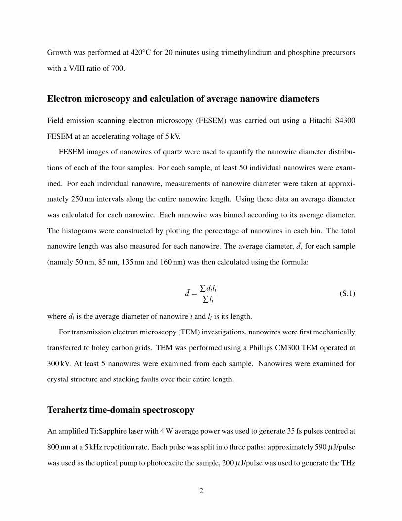
Contribution of nanowire top and base to total surface area
We approximate the nanowire shape as a truncated cone with height, h, top diameter dtop and
tapering angle, θ , as illustrated in Figure S.1a. The top surface area is given by
πr2top, (S.2)
where rtop =12dtop. The bottom surface area is given by
π(rtop +h tanθ
)2. (S.3)
The surface area made up by the lateral side surfaces is given by
πhcosθ
(2rtop +h tanθ
). (S.4)
The summation of these three terms, S.2 to S.4, gives the total surface area. The sum of terms S.2
and S.3 gives the contribution of the top and bottom faces to the total surface area. Figure S.1b
plots the proportion of the total surface area due to the sum of the top and bottom surfaces, as
a function of nanowire aspect ratio, h/dtop. The data for four different tapering angles, θ , were
plotted. The tapering angle θ = 0 corresponds to an untapered cylinder. The remaining three
tapering angles are typical of the nanowires of our study. The range of aspect ratios plotted is also
typical of the nanowires of our study. It is clear from Figure S.1b that the top and bottom surfaces
make only a small contribution to the total surface area, whereas the lateral side surfaces make the
dominant contribution to total nanowire surface area. We therefore we may neglect the top and
bottom surfaces in our analysis, and focus on the dependence of carrier lifetime as a function of
nanowire diameter.
4
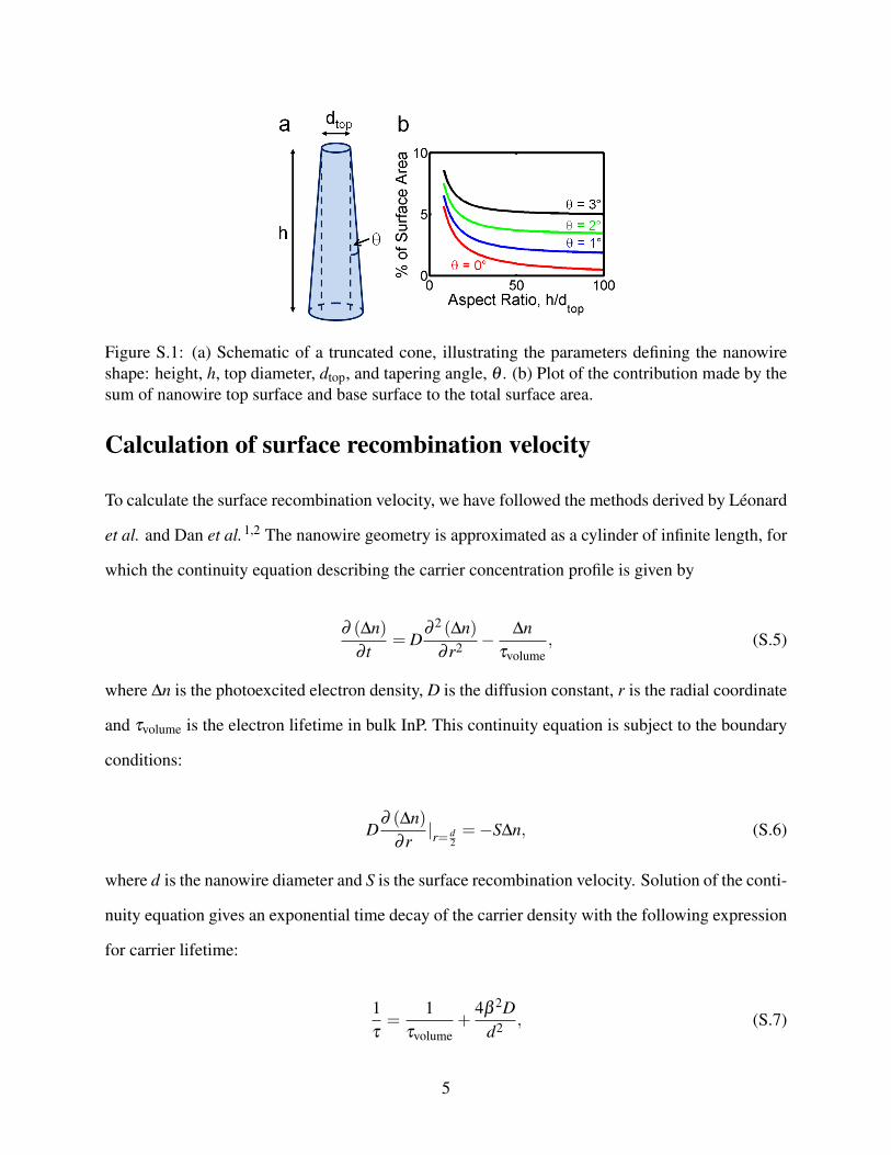
Figure S.1: (a) Schematic of a truncated cone, illustrating the parameters defining the nanowireshape: height, h, top diameter, dtop, and tapering angle, θ . (b) Plot of the contribution made by thesum of nanowire top surface and base surface to the total surface area.
Calculation of surface recombination velocity
To calculate the surface recombination velocity, we have followed the methods derived by Léonard
et al. and Dan et al.1,2 The nanowire geometry is approximated as a cylinder of infinite length, for
which the continuity equation describing the carrier concentration profile is given by
∂ (∆n)∂ t
= D∂ 2 (∆n)
∂ r2 − ∆nτvolume
, (S.5)
where ∆n is the photoexcited electron density, D is the diffusion constant, r is the radial coordinate
and τvolume is the electron lifetime in bulk InP. This continuity equation is subject to the boundary
conditions:
D∂ (∆n)
∂ r|r= d
2=−S∆n, (S.6)
where d is the nanowire diameter and S is the surface recombination velocity. Solution of the conti-
nuity equation gives an exponential time decay of the carrier density with the following expression
for carrier lifetime:
1τ=
1τvolume
+4β 2D
d2 , (S.7)
5
In the above equation, β is given by
βJ1 (β )−LJ0 (β ) = 0, (S.8)
where J0 and J1 are 0th and 1st order Bessel functions of the first kind and
L =dS2D
. (S.9)
For small β we can use the small argument behaviour of Bessel functions:
Jn (β )≈1
2nn!β
n, (S.10)
so that J0 (β ) = 1 and J1 (β ) =12β . Substituting these values into Equation (S.8) gives β =
√2L.
Using this approximation, Equation (S.7) simplifies to
1τ=
1τvolume
+4Sd. (S.11)
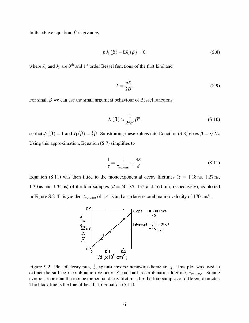
Equation (S.11) was then fitted to the monoexponential decay lifetimes (τ = 1.18 ns, 1.27 ns,
1.30 ns and 1.34 ns) of the four samples (d = 50, 85, 135 and 160 nm, respectively), as plotted
in Figure S.2. This yielded τvolume of 1.4 ns and a surface recombination velocity of 170 cm/s.
Figure S.2: Plot of decay rate, 1τ, against inverse nanowire diameter, 1
d . This plot was used toextract the surface recombination velocity, S, and bulk recombination lifetime, τvolume. Squaresymbols represent the monoexponential decay lifetimes for the four samples of different diameter.The black line is the line of best fit to Equation (S.11).
6
To confirm that the initial approximation of small β is valid, we verify that L = dS2D � 1, as
follows. The minimum diffusion constant is calculated using the Einstein relation and inserting the
lowest measured mobility of 120 cm2V−1s−1:
D =µkBT
e= 3.1cm2s−1. (S.12)
The maximum nanowire diameter is 160 nm and S = 170 cm/s. Therefore L = dS2D < 4.4×10⁻⁴, so
L� 1 and Equation (S.11) is valid.
Conversion of terahertz transmission data to photoconductivity
This section outlines how photoconductivity ∆σ is extracted from our OPTP measurement of ∆EE .
Using SEM images of nanowires on quartz, we calculated the effective areal fill factor of
nanowires, fw, for each sample. We consider the nanowires to be embedded within the surrounding
vacuum, within a layer of thickness δ . The transmitted terahertz electric fields with and without
the optical pump are defined as
Eon = fwEw∗+(1− fw)Ev (S.13)
Eoff = fwEw +(1− fw)Ev, (S.14)
where Ew and Ev are the terahertz transmission through the nanowires and the surrounding vacuum,
respectively, and * indicates a photoexcited state. Note that the pump beam does not change the
complex refractive index of the vacuum. The electric fields Ev, Ew and Ew∗ may then be written as
Ev = einvωδ/cEi (S.15)
Ew = tvwtwveinwωδ/cFPvwvEi (S.16)
Ew∗ = tvw∗tw∗veinw∗ωδ/cFPvw∗vEi, (S.17)
7
where FPi jk are the Fabry-Pérot terms, ti j are the Fresnel transmission coefficients, c is the speed
of light in vacuum, and nw∗ and nw are the refractive indices of nanowires with and without pho-
toexcitation, respectively.
Combining Equations (S.13) and (S.14) gives
Ew∗
Ew=
∆EE
[1+
(1fw−1
)Ev
Ew
]+1, (S.18)
where ∆E = Eon−Eoff. Note that the OPTP system gives direct experimental measurement of ∆EE
where ∆E is the photoinduced change in terahertz probe transmission and E = Eoff is the terahertz
probe transmission in the absence of photoexcitation.
At terahertz frequencies the thin film limit is valid because nωδ
c � 1. In the thin film limit we
can make the approximation EvEw
= 1. Using this approximation and rearranging Equation (S.18),
we define parameter A as
A =Ew
Ew∗=
11fw
∆EE +1
. (S.19)
Substituting the appropriate forms of FPi jk and ti j into Equations (S.15) to (S.17) and applying the
thin film limit einωδ/c = 1+ inωδ/c gives
Ew∗
Ew=
2− iωδ
c (1+n2w)
2− iωδ
c (1+n2w∗)
, (S.20)
The following general relations can then be substituted into Equation (S.20)
n2w = εw (S.21)
n2w∗ = εw∗ (S.22)
to give
8
εw∗ =
[− Ew
Ew∗
(2
ciωδ− (1+ εw)
)+2
ciωδ−1
], (S.23)
where εw∗ and εw are the dielectric constants of the nanowires with and without photoexcitation,
respectively. The photoinduced conductivity, ∆σ , is given by
εw∗ = εw +i∆σ
ωε0, (S.24)
where ε0 is the permittivity of free space. Substituting Equation (S.23) into Equation (S.24) gives
the following expression for ∆σ in terms of the measured signal ∆EE :
∆σ = ε0 (A−1)[
2cδ− iω (1+ εw)
], (S.25)
where A is defined in Equation (S.19). Thus, using Equations (S.25) and (S.19), the measured
signal can be converted to ∆σ using εw = 12.5 as for bulk InP and values of fw and δ as measured
from SEM images.
Spatial separation due to band-bending at nanowire surfaces
An alternative mechanism for spatial separation of electrons and holes concerns band bending
at the nanowire surface. Band bending effects have been observed in semiconductor structures
with high surface area-to-volume ratios such as p-type InP nanowires,3 Ge nanowires4 and porous
InP.5 In InP, surface states tend to pin the Fermi level within 0 to 0.34 eV of the conduction band
edge, depending on the crystallographic orientation of the surface.6,7 It is reasonable to assume
that the nanowire side facets, which are predominantly {1100} oriented, will experience surface
Fermi level pinning near the conduction band edge. Assuming the InP is doped at 5.5×1016 cm−3
(as justified in the main manuscript), the Fermi level pinning creates band bending such that the
electrons become confined to the surface and the holes to the centre of the nanowire. At early times
after photoexcitation the carrier density would screen this surface field, reducing band bending and
9
increasing the likelihood of electron–hole recombination. Consequently, PL would be observed
at early times. At later times, however, when the carrier density is lower, the surface field would
result in spatial separation of electrons and holes, which would suppress radiative recombination
and would account for the rapid quenching of PL at 1.43 eV.
A study by van Weert et al., however, demonstrated that band-bending effects are only pro-
nounced in p-InP nanowires.3 The nanowires of our study are thought to be n-type, and exhibited
a very low surface recombination velocity, indicating that band-bending effects are negligible.
Therefore presence of stacking faults and ZB/WZ polytypism is more likely to account for our
observations of a short PL lifetime coupled with a long photoconductivity lifetime.
Spatial separation due to ZB/WZ band offsets
In WZ InP, the conduction band is approximately 129 meV higher in energy, and the valence band
is approximately 45 meV higher in energy, than in ZB InP. ZB sections within a nanowire are
therefore potential wells for electrons, whereas WZ sections are potential wells for holes. Due to
quantum confinement, electrons and holes occupy discrete energy levels within these wells, with
the energy level depending on the thickness of the well. We calculated the eigenstates of finite
square wells to determine these energy levels as a function of well thickness. As the WZ sections
in these nanowires are typically thick, the hole states will lie at, or near the WZ valence band edge,
45 meV above the ZB valence band edge. This is significantly higher than the thermal energy
at room temperature, kBT = 26 meV, so there should be little thermal excitation of holes out of
the WZ potential wells. The ZB sections occur at higher densities at the nanowire bases, where
they are typically 1 nm to 3 nm in width. For ZB wells 2 nm in width, the lowest lying energy
state is 29 meV below the WZ conduction band edge. This is above the thermal energy at room
temperature, kBT = 26 meV. Therefore, for ZB potential wells greater than 2 nm in thickness, there
should be little thermal excitation of electrons at room temperature. For ZB sections less than 2 nm
in thickness, however, the electrons are only weakly localized.
10
Photoexcited carrier density
The photoexcited carrier density, Np, within a sample of thickness d is given by
Np =I
Ed
(1− e−d/α
), (S.26)
where I is the photoexcitation fluence, α is the absorption depth and E is the photon energy. At
our photoexcitation wavelength of λ = 800 nm, α = 400 nm for InP. This α is significantly larger
than all the nanowire diameters we studied, which places the nanowires in the thin film limit. This
means that for a given photoexcitation intensity, the photoexcited carrier density is approximately
constant regardless of nanowire diameter.
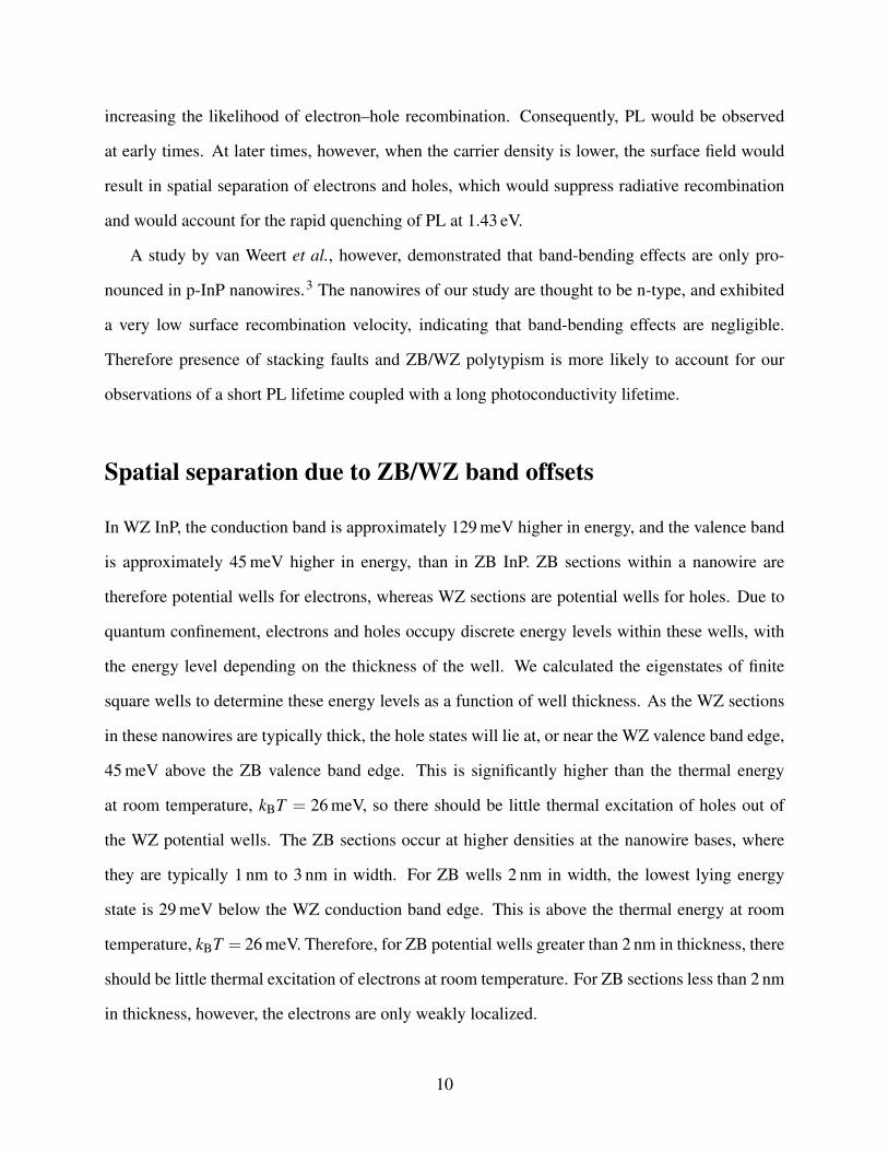
Fluence dependence of photoconductivity decay rate
Figure S.3 shows the decays of ∆E/E with time after photoexcitation for two different InP nanowire
samples: 50 nm diameter and 135 nm diameter. From Figure S.3 it is evident that the decay life-
time is approximately constant at all photoexcitation fluences. Similarly, the other two samples, of
85 nm and 160 nm diameter, showed constant decay lifetimes regardless of photoexcitation fluence.
This indicates that the carrier lifetime is minimally affected by the carrier density.
Figure S.3: Pump-induced change in terahertz electric field (∆E/E) at different pump–probe de-lays, for (a) 50 nm and (b) 135 nm diameter InP nanowires. Results for three different photoexci-tation fluences are plotted: 8, 16 and 32 µJ/cm2.
11
Calculation of theoretical scattering rates in bulk InP
Theoretical scattering rates for bulk InP are plotted in the dotted curve of Figure 4g. These scat-
tering rates were calculated assuming parameters for bulk ZB InP, such as phonon frequency and
m∗e = 0.08me. Electron–phonon, electron–electron, electron–hole and electron–plasmon mech-
anisms were included in the rates. The calculation follows published models.8,9 Carrier distri-
butions were assumed to be thermalised and at room temperature. An ionised donor density of
5.5× 1016 cm−3 was assumed for calculation of electron–impurity scattering. Electron–phonon
scattering dominates the calculated scattering rates at low carrier density and is roughly inde-
pendent of carrier density. The rates for electron–electron, electron–hole and electron–plasmon
scattering increase with carrier density.
Photoconductivity spectral evolution
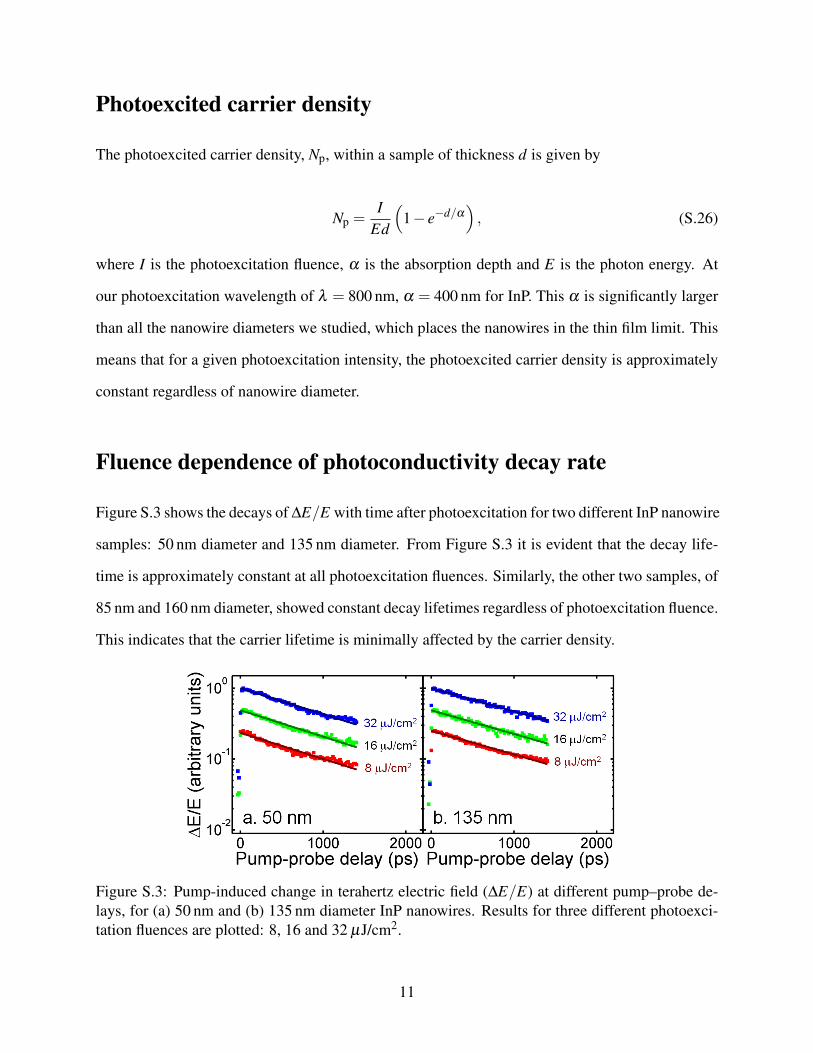
Figure S.4: Time-resolved conductivity of photoexcited carriers in 50 nm InP nanowires at times(a) 20 ps, (b) 250 ps and (c) 500 ps after the pump excitation pulse. The symbols are the measureddata and the lines are the fitted plasmon responses. The real (circles and lines) and imaginary(squares and lines) components of the conductivity are plotted. The incident pump pulse fluencewas 10 µJ/cm2. The arrow indicates the resonant surface plasmon frequency ω0.
Figure S.4 shows photoconductivity spectra of 50 nm nanowires taken various times after pho-
12
toexcitation. The surface plasmon resonance shifts to lower frequencies with time, reflecting the
decay in carrier density with time.
Photoconductivity spectra of nanowires of different diameter
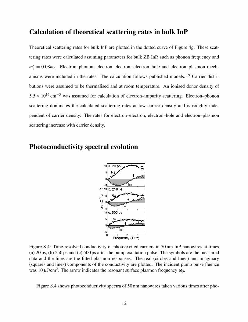
Figure S.5: Conductivity of photoexcited carriers in (a, e) 50, (b, f) 85, (c, g) 135 and (d, h) 160 nmdiameter InP nanowires at (a-d) 20 ps after photoexcitation and (e-h) 500 ps after photoexcitationwith a pump pulse of fluence 10 µJ/cm2. The symbols are the measured data and the lines are thefitted plasmon responses. The real (circles and lines) and imaginary (squares and lines) componentsof the conductivity are plotted.
Figure S.5 shows photoconductivity spectra taken for the four different nanowire samples of
50, 85, 135 and 160 nm diameter. These spectra were measured at 20 ps and 500 ps after pho-
toexcitation with a pump fluence of 10 µJ/cm2. The extracted scattering rates and mobilities are
summarized in Table S.1. After photoexcitation, the photoexcited carrier density decays. As the
photoexcited carrier density decays, the scattering rate exhibits a small decrease, because carrier–
carrier scattering decreases.
At 20 ps after photoexcitation, the extracted scattering rates were 3.3×10¹³ s−1, 18×1013 s−1,
13
10×1013 s−1 and 4.5×10¹³ s−1 respectively for the 50, 85, 135 and 160 nm diameter nanowires.
These scattering rates correspond to mobilities of 660, 120, 220 and 480 cm2V−1s−1. In the data of
Table S.1, we observe only a weak dependence of mobility on time after photoexcitation. Therefore
these mobility values are valid for a wide range of carrier densities.
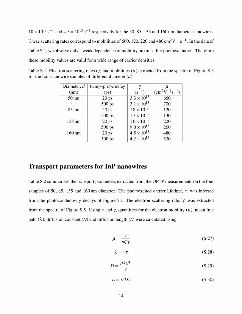
Table S.1: Electron scattering rates (γ) and mobilities (µ) extracted from the spectra of Figure S.5for the four nanowire samples of different diameter (d).
Diameter, d Pump–probe delay γ µ
(nm) (ps) (s−1) (cm2V−1s−1)50 nm 20 ps 3.3×10¹³ 660
500 ps 3.1×10¹³ 70085 nm 20 ps 18×1013 120
500 ps 17×1013 130135 nm 20 ps 10×1013 220
500 ps 9.0×10¹³ 260160 nm 20 ps 4.5×10¹³ 480
500 ps 4.2×10¹³ 530
Transport parameters for InP nanowires
Table S.2 summarises the transport parameters extracted from the OPTP measurements on the four
samples of 50, 85, 135 and 160 nm diameter. The photoexcited carrier lifetime, τ , was inferred
from the photoconductivity decays of Figure 2a. The electron scattering rate, γ , was extracted
from the spectra of Figure S.5. Using τ and γ , quantities for the electron mobility (µ), mean free
path (λ ), diffusion constant (D) and diffusion length (L) were calculated using
µ =e
m∗eγ(S.27)
λ = vτ (S.28)
D =µkBT
e(S.29)
L =√
Dτ (S.30)
14
where e is the electronic charge, m∗e is the electron effective mass, v is the electron thermal velocity
at room temperature and kB is the Boltzmann constant. We deduce v by solving the equation
E =12
m∗ev2 =32
kBT (S.31)
to give v = 4.1×10⁵ ms−1.
Table S.2: Parameters extracted for the four nanowire samples of different diameter (d), includingphotoexcited carrier lifetime (τ), electron scattering rate (γ), electron mobility (µ), mean free path(λ ), diffusion constant (D) and diffusion length (L).
d τ γ µ λ D L(nm) (ns) (s−1) (cm2V−1s−1) (nm) (cm2s−1) (nm)50 1.18 3.3×10¹³ 660 12 17 140085 1.27 18×1013 120 2.3 3.1 630
135 1.30 10×1013 220 4.1 5.7 860160 1.34 4.5×10¹³ 480 9.1 13 1300
References
(1) Léonard, F.; Talin, A. A.; Swartzentruber, B. S.; Picraux, S. T. Phys. Rev. Lett. 2009, 102,
106805.
(2) Dan, Y.; Seo, K.; Takei, K.; Meza, J. H.; Javey, A.; Crozier, K. B. Nano Lett. 2011, 11, 2527–
2532.
(3) van Weert, M. H. M.; Wunnicke, O.; Roest, A. L.; Eijkemans, T. J.; Silov, A. Y.; Haverkort, J.
E. M.; ’t Hooft, G. W.; Bakkers, E. P. A. M. Appl. Phys. Lett. 2006, 88, 043109.
(4) Prasankumar, R. P.; Choi, S.; Trugman, S. A.; Picraux, S. T.; Taylor, A. J. Nano Lett. 2008, 8,
1619–1624.
(5) Lloyd-Hughes, J.; Mueller, S.; Scalari, G.; Bishop, H.; Crossley, A.; Enachi, M.; Sirbu, L.;
Tiginyanu, I. M. Appl. Phys. Lett. 2012, 100, 132106.
15
(6) Koenders, L.; Bartels, F.; Ullrich, H.; Monch, W. J. Vac. Sci. Technol. B 1985, 3, 1107–1115.
(7) Moison, J. M.; Bensoussan, M. Surf. Sci. 1986, 168, 68–73.
(8) Yu, P. Y.; Cardona, M. Fundamentals of Semiconductors, 3rd ed.; Springer, Berlin, 2005.
(9) Lloyd-Hughes, J. Appl. Phys. Lett. 2012, 100, 122103.
16