A Way to Re-Engineer Terahertz Radar Sensors - MDPI
32
sensors Review Emerging Transistor Technologies Capable of Terahertz Amplification: A Way to Re-Engineer Terahertz Radar Sensors Mladen Božani´ c 1, * and Saurabh Sinha 2 1 Department of Electrical and Electronic Engineering Science, University of Johannesburg, Auckland Park, Johannesburg 2006, South Africa 2 Deputy Vice-Chancellor: Research and Internationalization, University of Johannesburg, Auckland Park, Johannesburg 2006, South Africa; [email protected] or [email protected] * Correspondence: [email protected] Received: 23 March 2019; Accepted: 20 May 2019; Published: 29 May 2019 Abstract: This paper reviews the state of emerging transistor technologies capable of terahertz amplification, as well as the state of transistor modeling as required in terahertz electronic circuit research. Commercial terahertz radar sensors of today are being built using bulky and expensive technologies such as Schottky diode detectors and lasers, as well as using some emerging detection methods. Meanwhile, a considerable amount of research effort has recently been invested in process development and modeling of transistor technologies capable of amplifying in the terahertz band. Indium phosphide (InP) transistors have been able to reach maximum oscillation frequency (f max ) values of over 1 THz for around a decade already, while silicon-germanium bipolar complementary metal-oxide semiconductor (BiCMOS) compatible heterojunction bipolar transistors have only recently crossed the f max = 0.7 THz mark. While it seems that the InP technology could be the ultimate terahertz technology, according to the f max and related metrics, the BiCMOS technology has the added advantage of lower cost and supporting a wider set of integrated component types. BiCMOS can thus be seen as an enabling factor for re-engineering of complete terahertz radar systems, for the first time fabricated as miniaturized monolithic integrated circuits. Rapid commercial deployment of monolithic terahertz radar chips, furthermore, depends on the accuracy of transistor modeling at these frequencies. Considerations such as fabrication and modeling of passives and antennas, as well as packaging of complete systems, are closely related to the two main contributions of this paper and are also reviewed here. Finally, this paper probes active terahertz circuits that have already been reported and that have the potential to be deployed in a re-engineered terahertz radar sensor system and attempts to predict future directions in re-engineering of monolithic radar sensors. Keywords: terahertz band; millimeter waves; InP; SiGe; BiCMOS; transistor modeling; HBT; HICUM; SoC; SoP 1. Introduction Terahertz waves (THz waves) or submillimeter waves are defined as waves with frequencies in the range between 300 GHz and 3 THz [1], lodged between millimeter waves (30 GHz to 300 GHz) and infrared radiation [2,3]. This part of the spectrum has often in the past been referred to as the “terahertz gap”, given that for a long time it escaped the interest of both electronics and photonics researchers. In certain contexts, the low-THz band is also defined as situated between 100 GHz and 1 THz [4]. The potential of the THz band is great. The THz band is an excellent part of the spectrum for spectroscopy, as different materials show different absorption spectra at THz frequencies [5–7]. When it comes to organics, many macromolecules such as protein and DNA have vibrational modes in this Sensors 2019, 19, 2454; doi:10.3390/s19112454 www.mdpi.com/journal/sensors
-
Upload
khangminh22 -
Category
Documents
-
view
1 -
download
0
Transcript of A Way to Re-Engineer Terahertz Radar Sensors - MDPI

sensors
Review
Emerging Transistor Technologies Capable ofTerahertz Amplification: A Way to Re-EngineerTerahertz Radar Sensors
Mladen Božanic 1,* and Saurabh Sinha 2
1 Department of Electrical and Electronic Engineering Science, University of Johannesburg, Auckland Park,Johannesburg 2006, South Africa
2 Deputy Vice-Chancellor: Research and Internationalization, University of Johannesburg, Auckland Park,Johannesburg 2006, South Africa; [email protected] or [email protected]
* Correspondence: [email protected]
Received: 23 March 2019; Accepted: 20 May 2019; Published: 29 May 2019
Abstract: This paper reviews the state of emerging transistor technologies capable of terahertzamplification, as well as the state of transistor modeling as required in terahertz electronic circuitresearch. Commercial terahertz radar sensors of today are being built using bulky and expensivetechnologies such as Schottky diode detectors and lasers, as well as using some emerging detectionmethods. Meanwhile, a considerable amount of research effort has recently been invested in processdevelopment and modeling of transistor technologies capable of amplifying in the terahertz band.Indium phosphide (InP) transistors have been able to reach maximum oscillation frequency (fmax)values of over 1 THz for around a decade already, while silicon-germanium bipolar complementarymetal-oxide semiconductor (BiCMOS) compatible heterojunction bipolar transistors have only recentlycrossed the fmax = 0.7 THz mark. While it seems that the InP technology could be the ultimateterahertz technology, according to the fmax and related metrics, the BiCMOS technology has the addedadvantage of lower cost and supporting a wider set of integrated component types. BiCMOS canthus be seen as an enabling factor for re-engineering of complete terahertz radar systems, for thefirst time fabricated as miniaturized monolithic integrated circuits. Rapid commercial deployment ofmonolithic terahertz radar chips, furthermore, depends on the accuracy of transistor modeling atthese frequencies. Considerations such as fabrication and modeling of passives and antennas, as wellas packaging of complete systems, are closely related to the two main contributions of this paperand are also reviewed here. Finally, this paper probes active terahertz circuits that have already beenreported and that have the potential to be deployed in a re-engineered terahertz radar sensor systemand attempts to predict future directions in re-engineering of monolithic radar sensors.
Keywords: terahertz band; millimeter waves; InP; SiGe; BiCMOS; transistor modeling; HBT; HICUM;SoC; SoP
1. Introduction
Terahertz waves (THz waves) or submillimeter waves are defined as waves with frequencies inthe range between 300 GHz and 3 THz [1], lodged between millimeter waves (30 GHz to 300 GHz)and infrared radiation [2,3]. This part of the spectrum has often in the past been referred to as the“terahertz gap”, given that for a long time it escaped the interest of both electronics and photonicsresearchers. In certain contexts, the low-THz band is also defined as situated between 100 GHz and1 THz [4]. The potential of the THz band is great. The THz band is an excellent part of the spectrum forspectroscopy, as different materials show different absorption spectra at THz frequencies [5–7]. Whenit comes to organics, many macromolecules such as protein and DNA have vibrational modes in this
Sensors 2019, 19, 2454; doi:10.3390/s19112454 www.mdpi.com/journal/sensors
Sensors 2019, 19, 2454 2 of 32
part of the spectrum [8]. Unlike X-rays, for example, THz photons are non-ionizing and hence are nothazardous to living tissues and DNA, and the amount of radiation exerted by THz imagers is severalorders of magnitude lower [3,9].
In the past two decades, a sharp rise in interest in technologies and applications operatingin the low-THz and THz bands has been evident. Emerging spectroscopy and sensing THzapplications include imaging, remote sensing, security and safety screening, process monitoring,non-contact/non-destructive materials testing, biological, medical and pharmaceutical analysis,label-free probing of genetic material, indoor mapping and navigation, target detection, as wellas many others [1,4,5,10–15]. Various technologies and combinations thereof can be deployed inapplications such as space exploration, weather studies, military and automotive applications, medicaldiagnosis research and security. In the developing world, furthermore, remote microsensing may havesustainability advantages [16]. The THz band is also suitable for ultra-fast communication; however,at present telecommunication research is still predominantly focused on the millimeter-wave band (forexample, with the world-wide deployment of 5 G cellular networks, the millimeter-wave band is onlystarting to be utilized at the time of writing this article [17]) and thus there is no immediate need forexploiting THz communication and research in this area is still in its infancy, at least for the purposesof this review article.
Radar sensing in the THz band is explored because it has numerous advantageous characteristicsover sensing in the millimeter-wave band. While in automotive applications, the millimeter-waveradar is increasingly exploited (for example, for park distance control where radars operating at 77 GHzare used), smaller wavelengths of THz waves (in the range of 1 mm) allow for higher spatial resolutionand smaller footprints [18]. As a result, THz radars could potentially be used on small drones andeven wearables. However, as more pressure is put onto increasing safety in vehicles, the numberof integrated automotive sensors and their features is ever increasing [19]. Radars operating in themillimeter-wave regime, in addition to the above-mentioned park distance control, can also be used foradaptive cruise control, blind spot and lane change assistance, among other applications, but as researchis moving towards self-driving, this is not sufficient. The current approach to self-driving assumes thatcameras and lidars can be deployed for terrain sensing. Low-THz sensing, alternatively, can providefine resolution images even in adverse conditions, such as fog, dust and snow, while also providingsensing image depth and insight into objects’ motion parameters [4]. In military environments, inaddition to navigation benefits also applicable to automotive applications (and extended into avionics),THz radars can be used for small and multiple target detection [3]. Small target detection is alsobecoming important in space technology, for example, where detection of space debris is becomingproblematic, as the amount of space junk is increasing [20]. Traditional detection of space debris isattempted with microwave radar or optical telescopes, which have a much lower resolution. What isnot intuitive is that the small target detection is also associated with gesture recognition, which hasalready been explored using millimeter-wave radar for some time [21], but wider bandwidths andbetter range and resolution can be achieved with THz radar [13]. By sensing the time delay, frequencyand phase shift and the amplitude attenuation of the radar signal (Doppler signature), real-time targetproperties, including distance, velocity, size, shape and orientation, can be attained and subsequentlyprocessed and interpreted.
THz imaging is another extremely important application of THz waves. A particularly importantarea of research is security, for example for concealed weapon detection in locations such as airportsand train terminals. The main benefit here arises once again from the wavelength of the electromagneticwaves: although radiation with a wavelength of 1 mm can easily penetrate materials of which clothesare made, it is reflected by explosives [12], weapons [22] and drugs [23]. In general, passive imagersmust be able to provide 1 cm resolution at a target distance up to 10 m, which is best achieved atfrequencies below 2 THz and even better, 1 THz. Most airports today (late 2010s) are equipped withscanners operating at frequencies close to 30 GHz and the next generation of scanners is projectedto use frequencies of close to 90 GHz [24], where a good compromise between the achievable image

Sensors 2019, 19, 2454 3 of 32
resolution and hardware costs can be found [23]. Real-time imaging, however, requires active imagers,which are suggested to be deployed in the THz range, around 300 or even 600 GHz [11]. Otherattractive imaging applications are, for example, non-destructive scanning of mail packages. In foodresearch, foreign particles, such as glass and other contaminants, can be detected by THz waves. Otherattractive applications of THz waves are medical applications, where THz waves can supplement oreven replace X-ray and ultrasound techniques [3].
Lack of efficient sources and detectors has meant that THz sensing, other than spectroscopy,has been slow to develop [25]. The main reason for this is that there are no commercially availabletransistor-based blocks, such as power amplifiers and low-noise amplifiers (LNAs). THz emitters arethus predominantly built using Schottky diode multipliers and mixers used to up-convert the signaltowards THz frequencies [11,25]. Without LNAs, on the receiver side, signals in this approach canonly be detected using mixers directly connected to the radar antenna. Another approach includesusing broadband THz pulses generated by femtosecond lasers [24], with lasers being able to reachand surpass 1.5 THz [25]. In this and related (light-based) approaches, the transmitter illuminatesthe object and the receiver collects the scattered energy. Thermal THz detectors have also beenused for detecting THz radiation, and early thermal THz detectors were predominantly based onbolometers [22]. In recent years, metamaterials with strong radiation-absorbing characteristics havealso been investigated [5]. All of the above approaches lack the ability to amplify the signals properly,which is where the contribution of electronics has long been expected [26].
A fully electronic approach to THz detection has been researched for some time. However, themain bottleneck has traditionally been the lack of transistors capable of amplification in the THz gap.With inexpensive complementary metal-oxide semiconductor (CMOS) and bipolar CMOS (BiCMOS)technologies typically having transistors with transitional frequency (fT) and maximum oscillationfrequency (fmax) between 200 GHz and 300 GHz in the past [27], the only way to extend the operationof circuits into THz applications was deploying harmonic generation techniques [28]. Fortunately, thesituation has recently started to change. Indium-phosphide (InP) transistors have been able to reachfmax values of over 1 THz for around a decade already [29], while silicon-germanium (SiGe) BiCMOSheterojunction bipolar transistors (HBTs) also crossed the fmax = 0.5 THz mark around the same time [30].The fmax = 0.7 THz mark was also crossed recently, as a result of the DOTSEVEN project funded by theEuropean Commission [31]. In all cases, the increase in the frequency of operation was achieved bydecreasing transistor feature sizes, an approach that can be taken repeatedly until the physical limitsare reached [32,33]. Technology pioneers have developed roadmaps for both InP-based and SiGe-basedtechnologies—describing the steps that should be taken to devise technologies with transistors thatachieve operation close to the physical limits. In each case, it is predicted that fT can reach 1 THzand fmax can reach or surpass 2 THz [34,35]. This means that if only transistors are considered, activecircuits can already reach low-THz frequencies now without any harmonic generation, and they haveexcellent potential to extend their regions of operation further to the complete THz band in future.This is graphically illustrated in Figure 1, where the THz research gap, in this case defined to overlapwith low-THz frequencies (0.1–1 THz), is shown in relation to the frequency spectrum and the fmax
capability of available and forecast technologies.The second bottleneck in THz research related to active devices is the fact that despite transistor
technologies becoming more readily available, for large-scale research to be feasible, these need tobe supplemented by accurate and compact models [29,36]. Given that model development requiresa combination of theoretical analysis, experimentation and circuit characterization only after thefabrication process has matured, models often lag behind the actual technology for a few generations.The third barrier is the microelectronic (or rather, nanoelectronic [37]) packaging, which also needs tocatch up with technology developments so that THz circuits can be taken from controlled laboratoryenvironments into the real world [38]. Even state-of-the art circuits perform poorly if placed into anon-optimal package. The current (estimated) state of device modeling and nanoelectronic packagingis also illustrated in Figure 1. Fourth, considerations such as fabrication (and modeling) of passives

Sensors 2019, 19, 2454 4 of 32
and antennas [14,39,40] also have to be brought in line with technology advances if these are not tohinder the re-engineering of THz sensors with THz-capable transistors. Finally, cost aspects relatedto active and passive device fabrication, as well THz-related legislation, need to be brought into thepicture as well.Sensors 2019, 19, x FOR PEER REVIEW 4 of 31
30 GHz
Frequency spectrum
Terahertz wavesLow terahertz
Millimeter wavesInfraredRF
0.1 THz 0.3 THz 3 THz
2.5 THz
1.5 THz
2 THz
SiGe HBTs (2019)
InP HEMT, HBT (2019)
SiGe (Technology roadmap)
InP (Technology roadmap)
Modeling (2019)
Packaging (2019)
0.7 THz
Terahertz circuits (2019)
Terahertz research gap
< 0.5 THz
< 0.5 THz
< 0.9 THz
0.1 – 1 THz
1 THz
< 0.4 THz> 0.4 THz
CMOS (2019)
GaN HEMT (2019)
GaAs mHEMT (2019) > 1 THz
Figure 1. The THz research gap in relation to the present [29,31,41–43] and forecast [34,35] fmax capability of transistor technologies, estimated current state of transistor modeling [44,45] and packaging [38] and reported achieved frequency operation of some THz circuits [1,42,46–52].
This paper, hence, undertakes to review the current state of transistor technologies capable of reaching THz amplification, as well as all related concepts that enable utilization of these technologies: active and passive device physics, modeling, packaging, and cost. The paper is organized as follows: In Section 2, emerging technologies capable of operating in the THz regime are described. Section 3 takes a step back and discusses the traditional and some alternative modern approaches to THz sensor implementation, at the same time highlighting where the active-device approach can introduce the cutting edge. In Section 4, other enabling factors for THz research, such as various stages of transistor modeling, are discussed. Sections 5 and 6 summarize the role of passives, interconnects, antennas and packaging, and look at emerging approaches to fabricate these. Section 7 briefly touches on commercial aspects of THz research. Section 8 reviews recently reported THz sub-systems, some almost reaching 0.9 THz (Figure 1), which have the potential to be used in the implementation of future monolithic radar sensors. A discussion of the reviewed material as well as the anticipated forward direction of the research on re-engineering of radar sensors is given in Section 9. Finally, Section 10 concludes the paper.
2. Emerging Transistor Technologies Capable of Operating in the Terahertz Regine
In the context of active circuits, the capability of a technology to operate, reaching certain frequencies, is normally associated with two metrics: fT and fmax. Although both metrics are transistor operating frequency parameters, each is a result of a different physics effects. Thus, the aim of technology researchers is to increase both parameters simultaneously. To investigate the main origin of fT in bipolar transistors, one needs to recall the well-known fT relation [53], defined as the frequency at which the transistor current gain becomes unity:
𝑓𝑓𝑇𝑇 =𝑔𝑔𝑚𝑚
2𝜋𝜋𝐶𝐶𝜋𝜋 + 𝐶𝐶𝜇𝜇 , (1)
where gm is the small-signal transconductance of the transistor and Cμ and Cπ are transistor parameters, which will not be discussed here but should be known to the reader. The transit frequency is mostly influenced by the vertical profile of the transistor [54]. It can be assumed that the sum of Cμ + Cπ is dominated by the base charging capacitance Cb = τBgm, where τB is the boron-doped base transit time in the forward direction, resulting in a simplified approximate relation
Figure 1. The THz research gap in relation to the present [29,31,41–43] and forecast [34,35] fmax capabilityof transistor technologies, estimated current state of transistor modeling [44,45] and packaging [38]and reported achieved frequency operation of some THz circuits [1,42,46–52].
This paper, hence, undertakes to review the current state of transistor technologies capable ofreaching THz amplification, as well as all related concepts that enable utilization of these technologies:active and passive device physics, modeling, packaging, and cost. The paper is organized as follows:In Section 2, emerging technologies capable of operating in the THz regime are described. Section 3takes a step back and discusses the traditional and some alternative modern approaches to THz sensorimplementation, at the same time highlighting where the active-device approach can introduce thecutting edge. In Section 4, other enabling factors for THz research, such as various stages of transistormodeling, are discussed. Sections 5 and 6 summarize the role of passives, interconnects, antennas andpackaging, and look at emerging approaches to fabricate these. Section 7 briefly touches on commercialaspects of THz research. Section 8 reviews recently reported THz sub-systems, some almost reaching0.9 THz (Figure 1), which have the potential to be used in the implementation of future monolithicradar sensors. A discussion of the reviewed material as well as the anticipated forward direction ofthe research on re-engineering of radar sensors is given in Section 9. Finally, Section 10 concludesthe paper.
2. Emerging Transistor Technologies Capable of Operating in the Terahertz Regine
In the context of active circuits, the capability of a technology to operate, reaching certainfrequencies, is normally associated with two metrics: fT and fmax. Although both metrics are transistoroperating frequency parameters, each is a result of a different physics effects. Thus, the aim oftechnology researchers is to increase both parameters simultaneously. To investigate the main origin offT in bipolar transistors, one needs to recall the well-known fT relation [53], defined as the frequency atwhich the transistor current gain becomes unity:
fT =gm
2π(Cπ + Cµ
) , (1)

Sensors 2019, 19, 2454 5 of 32
where gm is the small-signal transconductance of the transistor and Cµ and Cπ are transistor parameters,which will not be discussed here but should be known to the reader. The transit frequency is mostlyinfluenced by the vertical profile of the transistor [54]. It can be assumed that the sum of Cµ + Cπ isdominated by the base charging capacitance Cb = τBgm, where τB is the boron-doped base transit timein the forward direction, resulting in a simplified approximate relation
fT =1
2πτB. (2)
This means that the transitional frequency should increase with the decrease in the base transittime, which is, in turn, decreased by reducing the base width. Often, the total forward gate delay isused as another technology metric, which encompasses all transistor switching delays, including thebase charging time [55].
The maximum oscillation frequency, or the frequency at which the power gain is equal to unity(power gain cut-off frequency), is not only dependent on fT, but also on the physical resistance in thetransistor base, rb [56]:
fmax =
√fT
8πCµrb. (3)
Thus, to increase fmax, bipolar technology researchers are also looking to decrease the resistance inthe base, which is achieved by scaling of transistor lateral features. Naturally, there is a fundamentallimit associated with vertical and lateral scaling, and new and innovative techniques are required toget ever closer to the scaling limit, as will be seen later in this section.
If the fT parameter is considered on its own, its value is more applicable to analog and mixed modecircuits, which need to have large current gains, and thus the analog circuits are normally operated atfrequencies several times lower than fT. This is particularly true for wideband amplifiers, whereasnarrowband amplifiers can more easily be designed at frequencies close to fT. For millimeter-waveand THz circuits, the situation changes, as these circuits are reliant on power gain rather than currentgain. This is true for both power amplifiers and LNAs, as well as oscillators. Experience has shownthat fmax, which is generally higher than fT, should be between 50% and 100% higher than the designfrequency to achieve practical THz circuits [26]. This means that THz circuits can be operated abovefT. Since both fT and fmax are results of technology designs, the ratio of fmax/fT is different for eachtechnology. A technology is considered balanced when fmax is about 1.5 times larger than fT [33]. Themaximum oscillation frequency is usually worked out by extrapolation and confirmed by practicalamplifier circuits, some of which will be discussed in Section 8 of this paper. To operate circuits closeto or even above fmax, harmonic generation has to be used, but in this review, it is argued that this maynot be necessary in the near future, owing to the good properties of emerging technologies, as will beseen shortly.
Radio-frequency (RF) amplification was initially achieved with CMOS and other field-effecttransistors (FETs), because of their initial superiority over pure bipolar transistors [57,58]. After abipolar transistor with a wide-gap emitter with a pn-junction built from differing (hetero-) materials(an HBT) was introduced, HBT-based amplification gained popularity. HBTs, as opposed to gatedstructures, are able to retain higher gains and higher current densities with a frequency increase.BiCMOS, a technology with both bipolar and CMOS transistors available, was also subsequentlyintroduced, but BiCMOS technologies with fT and fmax, which truly simultaneously exceed 300 GHzand 400 GHz respectively, could not be realized until the end of the first decade of the 21st century [48].For a number of years now, the best reported metrics have come from integrated circuits (ICs) builtwith HBTs, high-electron mobility transistors (HEMTs) and metamorphic HEMTs (mHEMTs) [59].HEMTs, like HBTs, use heterojunctions, but the overall transistor structure corresponds to that of theFET. Some of the fastest HEMT transistors are built in InP technology, with fmax often exceeding 1 THz.The fastest HBTs have also been built in the same material base [29], both supported by aggressive

Sensors 2019, 19, 2454 6 of 32
technology scaling and favorable material properties. InP is an example of so-called compound III-Vmaterials (where the roman numerals III and V refer to the old numbering of the periodic systemgroups); however, active research into a compound semiconductor from group IV, viz. SiGe, hasyielded only a slightly lower fmax figure of 0.72 THz (when considered that the frequency spectrumhas logarithmic properties). Incentive-driven research into SiGe BiCMOS technologies was justifiedbecause of two main BiCMOS advantages — the ability of FETs and bipolar transistors to co-exist inthe same substrate, allowing analog, digital and RF circuits to be fabricated on the same die, and thelower cost of (Bi)CMOS.
The remainder of this section discusses the current status and the short-term predictions forseveral main technology competitors, starting with InP HEMTs and HBTs and SiGe BiCMOS. Theperformance of a technology is predominantly the consequence of the material used and its properties.The most important properties of some of the materials that will be used in the remainder of thissection are listed in Table 1.
Table 1. Properties of various semiconductors (taken from [60–63]).
Property Silicon (Si) GalliumNitride (GaN)
Silicon Germanium(SiGe)
Gallium-Arsenide(GaAs)
IndiumPhosphide (InP)
Bandgap energy (eV) 1.12 3.42 0.945 1.42 1.34Electron mobility (cm2/V-s) 1360 2000 7700 8500 5400Breakdown of electric field
(V/cm) 2 × 10⁵ 3.5 × 10⁶ 4 × 10⁵ 4 × 10⁵ 5 × 10⁵
Saturation electron driftvelocity (cm/s) 107 2.5 × 10⁷ 13.5 1.2 × 10⁷ 2 × 10⁷
Relative dielectric constant (εr) 11.7 9 - 12.9 12.5
2.1. InP HEMTs and HBTs
The main reason for the high performance of InP-based technologies is the combination of thewide gap of InP (1.34 eV) with the high electron drift velocity (more than 2 × 107 cm/s) [62]. Thekey performance parameters of HEMTs include the gate length, the gate-source capacitance and thetransconductance (which have a direct correspondence to HBT parameters in Equations (1) and (3)),as well as the FET-related parameter of the saturation velocity [2,59]. The first transistor with an fmax
of more than 1 THz was an InP HEMT transistor with a gate length of 35 nm, demonstrated in 2007.This technology also had an fT value of 400 GHz [26,51]. The fmax value was confirmed by a practicaldemonstration of amplifiers operating at frequencies up to 850 GHz. The subsequent technology nodewas 30 nm, with fmax = 1.3 THz and fT = 0.5 THz. In 2013, a 25 nm node was reported, with fmax = 1.5THz and fT = 0.61 THz, with amplification verified at 1.03 THz. To the best of the authors’ knowledge,this technology remains the technology with the highest reported fmax to date. An electron microscopeimage of the 1.3 THz InP HEMT and its gate is reproduced in Figure 2. According to Deal et al. [26],high-frequency operation of this transistor was ensured by scaling of the size of the gate to 30 nm,resulting in reduction of the gate capacitance. The gate pattern was defined using electron beamlithography. The devices were fully passivated to a thickness of 200 Angstroms with plasma-enhancedchemical vapor deposition.

Sensors 2019, 19, 2454 7 of 32
Sensors 2019, 19, x FOR PEER REVIEW 7 of 31
and only thin layers are possible without dislocations. Such transistors are called pseudomorphic HEMTs [59].
Alternative InP transistor technologies are those incorporating double-heterojunction bipolar transistors (DHBTs). DHBTs also offer a wideband collector, allowing for a higher breakdown voltage at a given fT, which increases the drive current capability [29,49,55]. InP HBTs also have good transconductance and can be densely wired, but the key challenge is establishing stable low-resistance ohmic contacts. In HBTs, the transistor dimension refers to the emitter junction width. In 2016, 130 nm HBT technology was demonstrated in [55], showing fT = 0.52 THz and fmax = 1.15 THz, and a common-emitter breakdown voltage of 3.5 V. The HBT was grown on a 100-nm InP substrate using molecular-beam epitaxy. The emitter is composed of InGaAs/InAs to minimize the contact resistance. The base is composed of carbon-doped InGaAs, while InGaAs/InAl/As is used in the base collector and base-emitter junctions. Benzocyclobutene (BCB), a dielectric, is used as a final passivation layer. The reported gate delay of this transistor is about 0.22 ps. The authors subsequently demonstrated amplification above 600 GHz. Alternative material composition can be sought from the InP/GaAsSb system [36]. GaAsSb has bandgap energy of 0.72 eV and its conduction band edge lies above that of InP, allowing for abrupt emitter-base and base-collector junctions to be implemented, which simplifies the DHBT epitaxial layer structure. This approach resulted in the state-of-the-art performance of fmax = 1.2 THz and fT = 0.5 THz [64].
Figure 2. An electron microscope image of the 30-nm Indium-phosphide (InP) high-electron mobility transistors (HEMT) gate (reproduced with permission from [26]).
In the detailed technology roadmap published in 2008 [34], it was estimated that the 128 nm InP technology node would support HBTs with fmax of 1.3 THz. This has been proven to correspond to the 130 nm technology node discussed above. In the same paper, it was extrapolated that the 64 nm node would be able to reach fmax = 2 THz, and considering that the roadmap predictions held up to 128 nm, it is probably safe to assume that the trend is going to continue and that transistors with fmax = 2 THz will become available in the near future. In fact, it was recently confirmed that no fundamental barriers exist that would prevent HBT dimensions from reaching 32 nm, which would open up the possibility for fabricating transistors with fmax even higher than 2 THz and possibly fT higher than 1 THz [29].
The biggest drawback of any III-V technology, including InP, has always been the limited variety of circuits that can be fabricated [62]. Pure HBT technologies, such as InP DHBT, would typically just be used to fabricate millimeter-wave or THz circuits, while the remaining circuits (e.g., digital circuits and the analog front end) would be fabricated in CMOS. This approach is typically costly, because multiple process technologies, packages and supporting boards would be used; furthermore, such a
Figure 2. An electron microscope image of the 30-nm Indium-phosphide (InP) high-electron mobilitytransistors (HEMT) gate (reproduced with permission from [26]).
In addition to aggressive feature scaling (for low gate resistance), the high-performance HEMTwas developed with epitaxial material enhancement for improved electron transport properties andprocess improvement. The composite channel was built with indium-arsenide (InAs) cladded betweentwo indium-gallium-arsenide (InGaAs) layers, all lattice-matched. Various techniques were used todecrease the resistance of ohmic contacts and parasitic values such as source resistance. To achievethe precise alignment of the gate required for such small features, 100 kV e-beam lithography wasused. This process includes high and low resistance thin-film resistors, metal-insulating-metal (MIM)capacitors and two metal layers for making connections. Even faster transistors should be possible ifthe indium composition inside the channel is increased, but the material becomes strained, and onlythin layers are possible without dislocations. Such transistors are called pseudomorphic HEMTs [59].
Alternative InP transistor technologies are those incorporating double-heterojunction bipolartransistors (DHBTs). DHBTs also offer a wideband collector, allowing for a higher breakdown voltageat a given fT, which increases the drive current capability [29,49,55]. InP HBTs also have goodtransconductance and can be densely wired, but the key challenge is establishing stable low-resistanceohmic contacts. In HBTs, the transistor dimension refers to the emitter junction width. In 2016,130 nm HBT technology was demonstrated in [55], showing fT = 0.52 THz and fmax = 1.15 THz, and acommon-emitter breakdown voltage of 3.5 V. The HBT was grown on a 100-nm InP substrate usingmolecular-beam epitaxy. The emitter is composed of InGaAs/InAs to minimize the contact resistance.The base is composed of carbon-doped InGaAs, while InGaAs/InAl/As is used in the base collectorand base-emitter junctions. Benzocyclobutene (BCB), a dielectric, is used as a final passivation layer.The reported gate delay of this transistor is about 0.22 ps. The authors subsequently demonstratedamplification above 600 GHz. Alternative material composition can be sought from the InP/GaAsSbsystem [36]. GaAsSb has bandgap energy of 0.72 eV and its conduction band edge lies above that ofInP, allowing for abrupt emitter-base and base-collector junctions to be implemented, which simplifiesthe DHBT epitaxial layer structure. This approach resulted in the state-of-the-art performance offmax = 1.2 THz and fT = 0.5 THz [64].
In the detailed technology roadmap published in 2008 [34], it was estimated that the 128 nm InPtechnology node would support HBTs with fmax of 1.3 THz. This has been proven to correspond to the130 nm technology node discussed above. In the same paper, it was extrapolated that the 64 nm nodewould be able to reach fmax = 2 THz, and considering that the roadmap predictions held up to 128 nm,

Sensors 2019, 19, 2454 8 of 32
it is probably safe to assume that the trend is going to continue and that transistors with fmax = 2 THzwill become available in the near future. In fact, it was recently confirmed that no fundamental barriersexist that would prevent HBT dimensions from reaching 32 nm, which would open up the possibilityfor fabricating transistors with fmax even higher than 2 THz and possibly fT higher than 1 THz [29].
The biggest drawback of any III-V technology, including InP, has always been the limited varietyof circuits that can be fabricated [62]. Pure HBT technologies, such as InP DHBT, would typicallyjust be used to fabricate millimeter-wave or THz circuits, while the remaining circuits (e.g., digitalcircuits and the analog front end) would be fabricated in CMOS. This approach is typically costly,because multiple process technologies, packages and supporting boards would be used; furthermore,such a system would often experience high losses in signals transitioning different dies. In recentyears, it was proposed that InP HBT technology could be integrated with SiGe BiCMOS technology(described in the following section), and such hybrid technology would be able to offer the benefitsof both technologies. One of the possible methods is that presented by Weimann et al. [62], whereprocessing is done in two fabrication facilities (fabs): a III-V fab and an SiGe fab. First, the BiCMOSwafer is fabricated in the SiGe fab. Then the processing continues in the III-V fab where anotherwafer, with InP DHBTs, some additional layers, including gold interconnects, low-loss dielectricsand thin-film resistors, is fabricated. The two wafers are then aligned and wafer-bonded together,face-to-face, using BCB as the adhesive, forming the bond interface, in the III-V fab. Prior to bonding,owing to differing wafer sizes, the larger 8” BiCMOS wafer has to be cut into three 3” wafers to matchthe size of the InP wafers. After bonding, the InP substrate is completely removed, leaving only InPsemiconductor islands, thus resulting in a combined SiGe/InP BiCMOS technology with eight metallayers, Si MOSFETs, SiGe HBTs and InP HBTs, as shown in the cross-section in Figure 3. Note thatin this method, deep tungsten vias, similar to through-silicon vias (TSVs), typically associated withpackaged solutions, which will be discussed later in this article, are necessary to connect aluminummetal layers from the SiGe technology with gold metal layers from the InP technology, also shown inFigure 3. A microphotograph of the 328-GHz IC test vehicle designed by Weimann et al. is reproducedin Figure 4. The figure shows a SiGe voltage-controlled oscillator (VCO) on the left and the InP balun,buffer and a quadrupler on the right, illustrating how different circuitry can be distributed to takeadvantage of both technologies simultaneously (different substrates also appear in different colors inthe figure). The approach by Weimann et al. indeed constitutes an excellent proof of concept, despitethe fact that the fT and fmax values of the InP technology are both lower than 400 GHz. However, asthe smaller-feature InP processes mature, it should be possible to reproduce the approach for trulyTHz technologies.
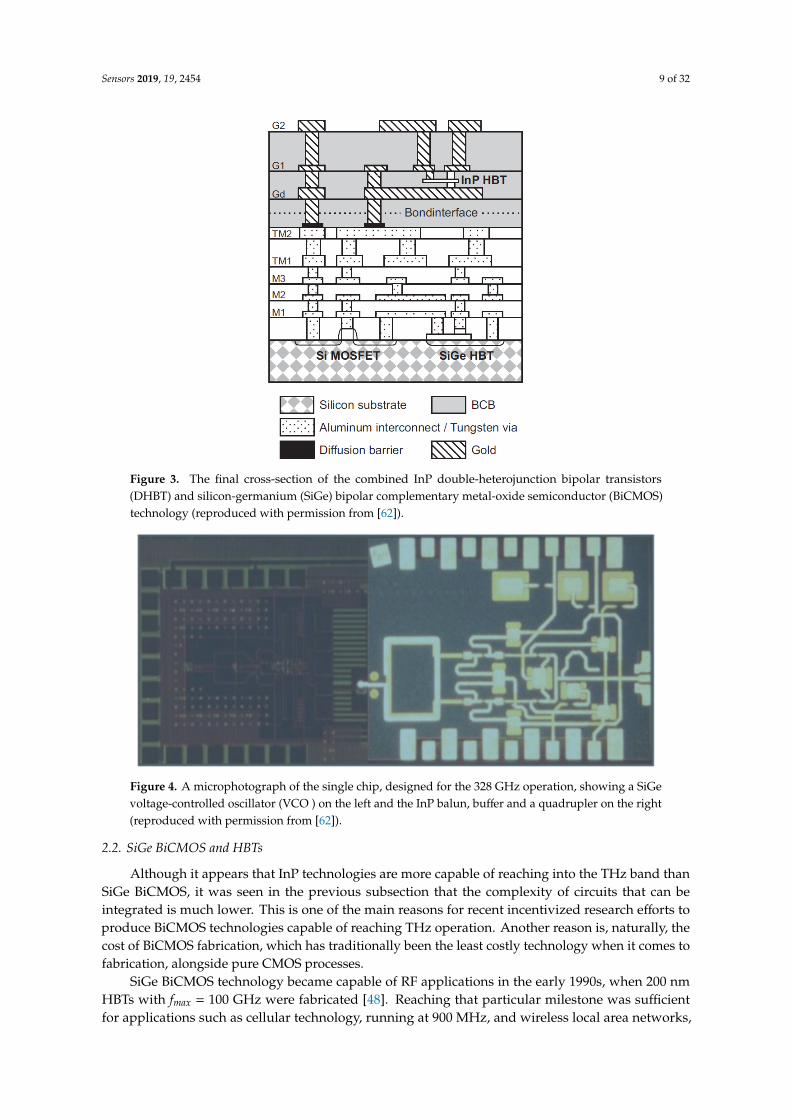
Sensors 2019, 19, 2454 9 of 32
Sensors 2019, 19, x FOR PEER REVIEW 8 of 31
system would often experience high losses in signals transitioning different dies. In recent years, it was proposed that InP HBT technology could be integrated with SiGe BiCMOS technology (described in the following section), and such hybrid technology would be able to offer the benefits of both technologies. One of the possible methods is that presented by Weimann et al. [62], where processing is done in two fabrication facilities (fabs): a III-V fab and an SiGe fab. First, the BiCMOS wafer is fabricated in the SiGe fab. Then the processing continues in the III-V fab where another wafer, with InP DHBTs, some additional layers, including gold interconnects, low-loss dielectrics and thin-film resistors, is fabricated. The two wafers are then aligned and wafer-bonded together, face-to-face, using BCB as the adhesive, forming the bond interface, in the III-V fab. Prior to bonding, owing to differing wafer sizes, the larger 8” BiCMOS wafer has to be cut into three 3” wafers to match the size of the InP wafers. After bonding, the InP substrate is completely removed, leaving only InP semiconductor islands, thus resulting in a combined SiGe/InP BiCMOS technology with eight metal layers, Si MOSFETs, SiGe HBTs and InP HBTs, as shown in the cross-section in Figure 3. Note that in this method, deep tungsten vias, similar to through-silicon vias (TSVs), typically associated with packaged solutions, which will be discussed later in this article, are necessary to connect aluminum metal layers from the SiGe technology with gold metal layers from the InP technology, also shown in Figure 3. A microphotograph of the 328-GHz IC test vehicle designed by Weimann et al. is reproduced in Figure 4. The figure shows a SiGe voltage-controlled oscillator (VCO) on the left and the InP balun, buffer and a quadrupler on the right, illustrating how different circuitry can be distributed to take advantage of both technologies simultaneously (different substrates also appear in different colors in the figure). The approach by Weimann et al. indeed constitutes an excellent proof of concept, despite the fact that the fT and fmax values of the InP technology are both lower than 400 GHz. However, as the smaller-feature InP processes mature, it should be possible to reproduce the approach for truly THz technologies.
Figure 3. The final cross-section of the combined InP double-heterojunction bipolar transistors (DHBT) and silicon-germanium (SiGe) bipolar complementary metal-oxide semiconductor (BiCMOS) technology (reproduced with permission from [62]).
Figure 3. The final cross-section of the combined InP double-heterojunction bipolar transistors(DHBT) and silicon-germanium (SiGe) bipolar complementary metal-oxide semiconductor (BiCMOS)technology (reproduced with permission from [62]).Sensors 2019, 19, x FOR PEER REVIEW 9 of 31
Figure 4. A microphotograph of the single chip, designed for the 328 GHz operation, showing a SiGe voltage-controlled oscillator (VCO ) on the left and the InP balun, buffer and a quadrupler on the right (reproduced with permission from [62]).
2.2. SiGe BiCMOS and HBTs
Although it appears that InP technologies are more capable of reaching into the THz band than SiGe BiCMOS, it was seen in the previous subsection that the complexity of circuits that can be integrated is much lower. This is one of the main reasons for recent incentivized research efforts to produce BiCMOS technologies capable of reaching THz operation. Another reason is, naturally, the cost of BiCMOS fabrication, which has traditionally been the least costly technology when it comes to fabrication, alongside pure CMOS processes.
SiGe BiCMOS technology became capable of RF applications in the early 1990s, when 200 nm HBTs with fmax = 100 GHz were fabricated [48]. Reaching that particular milestone was sufficient for applications such as cellular technology, running at 900 MHz, and wireless local area networks, running at 2.4 GHz, which required low-cost and small form factors, but not extremely fast transistors. The subsequent telecommunication boom in the early 2000s and the observed potential to explore the bottom of the millimeter-wave band triggered research of BiCMOS technologies that could reach 200 GHz and beyond. The most important commercial success of SiGe technologies at frequencies extending beyond 30 GHz was the commercialization of automotive radar operating at 77 GHz. In the 2010s technologies with fT and fmax exceeding 300 and 400 GHz respectively were developed. The performance of RF CMOS technology was being improved (by virtue of aggressive scaling beyond 100 nm) in parallel to that of BiCMOS, but BiCMOS had the advantage of increased circuit complexity, since bipolar devices could appear with RF CMOS devices in the same circuit. HBTs in BiCMOS also provided for higher transconductance values and consequently higher output power levels than RF MOSFETs at the same drive levels and frequency. However, none of these technologies (CMOS or BiCMOS) was capable of reaching into the THz part of the spectrum. At that point it was realized that feature scaling alone was not sufficient for further improvement in the existing technologies, and a different approach needed to be taken [30,32,33]. The solution was to bring together the major European semiconductor industry key players, supported by the efforts of academic researchers, in a highly funded project that would investigate the steps needed to be taken to improve the fT and fmax figures incrementally, until a technology with fmax > 0.5 THz was found, while staying ahead of non-European competition. This project was named the DOTFIVE project (for 0.5 THz); it also had the secondary objective of reaching a gate delay as low as 2.5 ps.
The DOTFIVE project ran in several stages, with initial incremental improvements on the existing self-aligned epitaxial base transistors in a SiGe technology from STMicroelectronics (fT/fmax = 230/290 GHz). In the first stage, the aim was to shrink the sizes of the base, emitter and collector, reaching the technology that had HBTs with fT = 260 GHz and fmax = 350 GHz [30]. In the second phase, silicon-germanium-carbon (SiGeC) HBTs were fabricated featuring fmax > 400 GHz and reduced
Figure 4. A microphotograph of the single chip, designed for the 328 GHz operation, showing a SiGevoltage-controlled oscillator (VCO ) on the left and the InP balun, buffer and a quadrupler on the right(reproduced with permission from [62]).
2.2. SiGe BiCMOS and HBTs
Although it appears that InP technologies are more capable of reaching into the THz band thanSiGe BiCMOS, it was seen in the previous subsection that the complexity of circuits that can beintegrated is much lower. This is one of the main reasons for recent incentivized research efforts toproduce BiCMOS technologies capable of reaching THz operation. Another reason is, naturally, thecost of BiCMOS fabrication, which has traditionally been the least costly technology when it comes tofabrication, alongside pure CMOS processes.
SiGe BiCMOS technology became capable of RF applications in the early 1990s, when 200 nmHBTs with fmax = 100 GHz were fabricated [48]. Reaching that particular milestone was sufficientfor applications such as cellular technology, running at 900 MHz, and wireless local area networks,

Sensors 2019, 19, 2454 10 of 32
running at 2.4 GHz, which required low-cost and small form factors, but not extremely fast transistors.The subsequent telecommunication boom in the early 2000s and the observed potential to explorethe bottom of the millimeter-wave band triggered research of BiCMOS technologies that could reach200 GHz and beyond. The most important commercial success of SiGe technologies at frequenciesextending beyond 30 GHz was the commercialization of automotive radar operating at 77 GHz. In the2010s technologies with fT and fmax exceeding 300 and 400 GHz respectively were developed. Theperformance of RF CMOS technology was being improved (by virtue of aggressive scaling beyond100 nm) in parallel to that of BiCMOS, but BiCMOS had the advantage of increased circuit complexity,since bipolar devices could appear with RF CMOS devices in the same circuit. HBTs in BiCMOS alsoprovided for higher transconductance values and consequently higher output power levels than RFMOSFETs at the same drive levels and frequency. However, none of these technologies (CMOS orBiCMOS) was capable of reaching into the THz part of the spectrum. At that point it was realizedthat feature scaling alone was not sufficient for further improvement in the existing technologies,and a different approach needed to be taken [30,32,33]. The solution was to bring together the majorEuropean semiconductor industry key players, supported by the efforts of academic researchers, ina highly funded project that would investigate the steps needed to be taken to improve the fT andfmax figures incrementally, until a technology with fmax > 0.5 THz was found, while staying ahead ofnon-European competition. This project was named the DOTFIVE project (for 0.5 THz); it also had thesecondary objective of reaching a gate delay as low as 2.5 ps.
The DOTFIVE project ran in several stages, with initial incremental improvements on theexisting self-aligned epitaxial base transistors in a SiGe technology from STMicroelectronics(fT/fmax = 230/290 GHz). In the first stage, the aim was to shrink the sizes of the base, emitter andcollector, reaching the technology that had HBTs with fT = 260 GHz and fmax = 350 GHz [30]. In thesecond phase, silicon-germanium-carbon (SiGeC) HBTs were fabricated featuring fmax > 400 GHzand reduced emitter and collector widths of 110 nm and 280 nm, respectively. Carbon co-dopingwas introduced to largely suppress boron diffusion, which in turn allowed a lower base width to beachieved [65]. However, any further improvements required conflicting parameter optimization, andeven further base transit time reduction, as well as the reduction of the base/collector depletion layertransit time. This could only come from device architectures with inherently lower device parasitics.The subsequent approach to the 0.5 THz transistor included device profile optimization, variouscollector isolation schemes to decrease collector capacitances, and combining the self-alignment ofemitter-base junction and base connection. The combination of approaches resulted in two HBTtechnology options from IHP: A 155-nm technology, with fT = 310 GHz, fmax = 480 GHz and gatedelay of 1.9 ps and a 120-nm technology, with a slightly lower fT (300 GHz) and slightly higher gatedelay (2 ps), but with fmax reaching the original predicted value of 500 GHz [66,67]. The integrationof the 0.5 THz HBT into a BiCMOS technology was subsequently achieved. A diagram and electronmicroscope photo of the cross-section of the 0.5 Hz SiGe HBT are shown in Figure 5, taken from [48].Figure 5a shows the primary technology features, which include the elevated SiGeC base (B), theheavily doped collector (C), selectively-implanted-collector (SIC) formation and the surrounding oxide,the narrow emitter (E) and the shallow trench isolation (STI). The widths (W) of various regions arealso shown in this figure, together with capacitive (C) and resistive (R) parasitic quantities that remaindespite the device scaling. In Figure 5b, the reference 100 nm scale can be used to get an idea of thesize of the transistor features mentioned.

Sensors 2019, 19, 2454 11 of 32
Sensors 2019, 19, x FOR PEER REVIEW 10 of 31
emitter and collector widths of 110 nm and 280 nm, respectively. Carbon co-doping was introduced to largely suppress boron diffusion, which in turn allowed a lower base width to be achieved [65]. However, any further improvements required conflicting parameter optimization, and even further base transit time reduction, as well as the reduction of the base/collector depletion layer transit time. This could only come from device architectures with inherently lower device parasitics. The subsequent approach to the 0.5 THz transistor included device profile optimization, various collector isolation schemes to decrease collector capacitances, and combining the self-alignment of emitter-base junction and base connection. The combination of approaches resulted in two HBT technology options from IHP: A 155-nm technology, with fT = 310 GHz, fmax = 480 GHz and gate delay of 1.9 ps and a 120-nm technology, with a slightly lower fT (300 GHz) and slightly higher gate delay (2 ps), but with fmax reaching the original predicted value of 500 GHz [66,67]. The integration of the 0.5 THz HBT into a BiCMOS technology was subsequently achieved. A diagram and electron microscope photo of the cross-section of the 0.5 Hz SiGe HBT are shown in Figure 5, taken from [48]. Figure 5a shows the primary technology features, which include the elevated SiGeC base (B), the heavily doped collector (C), selectively-implanted-collector (SIC) formation and the surrounding oxide, the narrow emitter (E) and the shallow trench isolation (STI). The widths (W) of various regions are also shown in this figure, together with capacitive (C) and resistive (R) parasitic quantities that remain despite the device scaling. In Figure 5b, the reference 100 nm scale can be used to get an idea of the size of the transistor features mentioned.
The DOTFIVE project was followed by the DOTSEVEN project [67], which had the main objective of extending the fmax beyond 0.7 (.7) THz. Efforts to continue HBT scaling were justified in a two-part paper by Schröter et al. [32,33] published during the time of the DOTFIVE project, which assessed ways in which transistors could be vertically and laterally scaled further, possibly even leading to technologies with fmax = 1.5 THz, while retaining a collector-emitter breakdown voltage over 1 V. Finally, a transistor with fT = 505 GHz, fmax = 720 GHz, breakdown voltage of 1.6 V and a gate delay of only 1.34 ps was reported in 2016 [31], achieving for the first time fT and fmax that were simultaneously larger than 500 GHz in a SiGe technology [68]. This performance was achieved in two iterations. In the first iteration, the non-epitaxial growth of the SiGe base layer was used to form the HBT structure, instead of the traditional double-polysilicon self-aligned structure. This was supported by the boron-doped base link module, which allowed for fmax to be improved to 550 GHz with fT = 330 GHz. To improve the fT and fmax values to the state-of-the-art values above further, several additional steps were introduced, such as an in situ doped epitaxial external base, the elimination of the base link anneal, and an ms flash anneal. The 0.7 THz HBT process retained functional metal layers, MIM capacitors, metal-oxide semiconductor varactors and polysilicon resistors and although the challenge of integrating HBTs in advanced CMOS technology remains [54] unsolved, the two technologies are deemed compatible.
(a) (b)
Figure 5. (a) Diagram and (b) electron microscope photo of the 0.5 THz heterojunction bipolar transistors (HBT) fabricated by IHP (reproduced with permission from [48]). Figure 5. (a) Diagram and (b) electron microscope photo of the 0.5 THz heterojunction bipolar transistors(HBT) fabricated by IHP (reproduced with permission from [48]).
The DOTFIVE project was followed by the DOTSEVEN project [67], which had the main objectiveof extending the fmax beyond 0.7 (.7) THz. Efforts to continue HBT scaling were justified in a two-partpaper by Schröter et al. [32,33] published during the time of the DOTFIVE project, which assessedways in which transistors could be vertically and laterally scaled further, possibly even leading totechnologies with fmax = 1.5 THz, while retaining a collector-emitter breakdown voltage over 1 V. Finally,a transistor with fT = 505 GHz, fmax = 720 GHz, breakdown voltage of 1.6 V and a gate delay of only1.34 ps was reported in 2016 [31], achieving for the first time fT and fmax that were simultaneously largerthan 500 GHz in a SiGe technology [68]. This performance was achieved in two iterations. In the firstiteration, the non-epitaxial growth of the SiGe base layer was used to form the HBT structure, instead ofthe traditional double-polysilicon self-aligned structure. This was supported by the boron-doped baselink module, which allowed for fmax to be improved to 550 GHz with fT = 330 GHz. To improve the fTand fmax values to the state-of-the-art values above further, several additional steps were introduced,such as an in situ doped epitaxial external base, the elimination of the base link anneal, and an msflash anneal. The 0.7 THz HBT process retained functional metal layers, MIM capacitors, metal-oxidesemiconductor varactors and polysilicon resistors and although the challenge of integrating HBTs inadvanced CMOS technology remains [54] unsolved, the two technologies are deemed compatible.
The 0.7 THz transistor fabrication was the culmination of the DOTFIVE and DOTSEVEN projects,and their successful outcome was heavily supported by extensive physics-based modeling andnumerical as well as electrothermal simulation tools. The only marginally better SiGe HBT wasreported by Charaborty et al. [69], having an fmax of 798 GHz, but this result was achieved only atunpractical cryogenic temperatures. However, what this shows is first, that among other implications,the HBT performance can be increased by cooling, and second, that the performance limits of SiGe-basedtechnologies have not been reached yet.
The latter of the two conclusions is further supported by the SiGe HBT technology performancescaling roadmap presented by DOTFIVE/DOTSEVEN researchers in 2016 [35], at the conclusion ofthe two projects. The roadmap was devised using the results of various 1D, 2D, 3D technologysimulators combined with compact modeling, which included all known parasitic effects and effectssuch as self-heating. Realistically achievable technology scaling nodes were proposed, based on theinformation on the currently available fabrication hardware and predictions for its future scaling,as well as the predicted physical transistor limits. According to the prediction, fmax between 2 THzand 2.5 THz could be realistically achieved with the transistor dimensions scaled to about 20% of the0.5-THz-transistor dimensions published as a result of the DOTFIVE project. However, a numberof challenges were identified for further technology scaling, of which some will be mentioned here.First, the vertical structure needs to continue to shrink, which is associated with the requirement toincrease the doping in order to keep the resistivity sufficiently low. Then, the base layer will have tobe grown with atomic-level precision, which requires further fabrication technology advancement.

Sensors 2019, 19, 2454 12 of 32
Novel epitaxy approaches will also have to be implemented to manage complex collector profiles, andco-doping by materials other than carbon would need to be suggested to suppress boron diffusionfurther. Further sheet resistance reductions would be needed as well to allow high fT and fmax atthe same time and the emitter resistance will need to be decreased further. Such tiny emitter (andtransistor) structures are furthermore expected to suffer from electromigration effects, which willneed to be alleviated. Alternative contact materials and metallization will be sought too in order toincrease the achievable current density. Finally, it must be noted that the technology modeling willhave to follow the technology scaling closely so that each new node iteration can be understood andevaluated properly.
2.3. Si CMOS
CMOS technology, traditionally used in digital and low-frequency analog circuits, has been quitecapable of competing with the BiCMOS technology, at least up to millimeter-wave frequencies [70],and may be found suitable for THz applications in the near future. CMOS is favored owing to the lowcost of fabrication and high level of achievable integration. According to Lee [71], the maximum fT of aCMOS technology can be approximated (to the first order) by the formula fT = 10 (THz·nm)/L, where Lis the gate length in nanometer, meaning that the fT of a 5 nm technology could be 2 THz, if the lengthcan be feasibly decreased to such low levels. Considering the challenges of transistor optimizationlisted in Section 2.2, reaching such frequencies even at such short lengths is unlikely. A better predictionis perhaps the one of Ellinger et al. [72], who extrapolated that fT of 500 GHz would be possible at agate length of 10 nm. Certain process modifications from standard CMOS are, however, needed toachieve good performance. A possible path forward could be sought in the tri-gate (FinFET) structuresintroduced relatively recently as part of efforts to decrease short-channel effects in FETs [73–75].
The best-performing CMOS technologies (in terms of fT and fmax) are typically based on thesilicon-on-insulator (SOI) principle [41,76]. SOI circuits are composed of single-device islands, whichare isolated from the substrate and from each other [77], which reduces transistor source/drain junctioncapacitances and substrate coupling of passives. Transistors are also less prone to short-channel effectsand can perform better at lower voltage supplies. A 45-nm IBM process is the state-of-the-art exampleof the CMOS SOI process with fT and fmax both above 250 GHz [41]. Initial results indicated that fT ofalmost 0.5 THz (485 GHz) would be possible [78], but the limitations of the body-connected SOI FETsmeant that layout optimization resulted in halving the fT value. THz applications may benefit evenmore from high-resistance SOI (HR-SOI) technologies. HR-SOI technology differs from regular SOItechnology in the sense that the substrate is modified to have resistivity of more than 1 kΩ·cm [79].This is important in the design of passives and interconnects (both discussed in more detail in separatesections later). Transmission lines, such as coplanar waveguides (CPWs) are used in integrated designsat millimeter-wave frequencies and beyond instead, and if high resistivity of the substrate is used,transmission-line losses are decreased. This effect occurs owing to the decrease in line resistance perunit length due to high substrate resistivity.
Another suggestion to improve CMOS performance is to introduce strained silicon [72]. Thisis done, for example, by placing the active silicon layer on top of another material with a largerlattice constant, such as SiGe. This results in higher carrier mobility of the transistor channel. Theperformance of CMOS can also be improved by cooling, as was shown to be the case with BiCMOS [69],or by increasing the dielectric constant of the gate oxide (e.g., replacing silicon-dioxide by high-k oxide).Silicon-nanowire FETs could also be used as an alternative to regular FETs, but many challenges intheir practical high-frequency implementations remain unsolved, although these transistors can beused for passive detection, as will be seen later.
2.4. Gallium-arsenide (GaAs) mHEMTs
GaAs HEMTs generally suffer from low integration capabilities, but GaAs substrate is morerobust and more affordable than InP substrate. Good crystal quality and good overall technology
Sensors 2019, 19, 2454 13 of 32
performance can be achieved if metamorphic transitional layers are used to connect the substrate toactive device layers built out of InP, InGaAs or InAlAs [59]. Resulting mHEMTs yield performancesimilar to that of regular HEMTs and fT values above 500 GHz as well as fmax values above 1 THz arereadily achievable [42]. In mHEMTs, each of the base, collector and emitter is composed of a differentalloy, unlike regular HEMTs. In addition to cost savings, GaAs-based technologies also have goodnoise performance [50].
2.5. GaN HEMTs
GaN technology has the advantage of supporting HEMTs that are much smaller in size thandevices fabricated in other technologies for the same output power. The wide bandgap (3.32 eV) ofGaN also enables transistors to operate at high temperatures, while yielding good noise performance.This makes GaN technology quite suitable for both high-power applications (power amplifiers), aswell as low-noise applications (LNAs), albeit at higher costs than that of other technologies [80]. This isparticularly true when comparing it to SiGe, which can also yield moderately high output power andfairly low noise performance. However, in applications such as planetary exploration, having highoutput capability is more important than the cost itself [81]. In terms of frequency performance alone,an impressive fT/fmax combination of 454/444 GHz was reported in [43], as a result of reducing fringinggate capacitances by optimizing the epitaxial layer thickness and carrier distribution. A further increasein speed should be achievable by decreasing mesa-edge capacitances that form during etching as aresult of mesa isolation and present a large portion of the total gate capacitance [82]. The possibilityof growing GaN double heterostructure high-electron mobility transistors on silicon wafers was alsoexplored for the purpose of increased integration complexity [83].
3. Traditional and Current Approaches to Terahertz Radar and Direct Terahertz Sensing
A large number of THz radar and sensing approaches that do not use solid-state amplificationhave been reported to date, with new techniques continually emerging. Some of these approaches arereviewed in this section.
3.1. Laser and Schottky-based Detectors
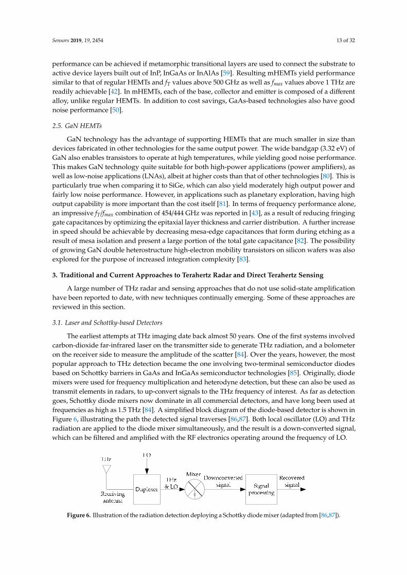
The earliest attempts at THz imaging date back almost 50 years. One of the first systems involvedcarbon-dioxide far-infrared laser on the transmitter side to generate THz radiation, and a bolometeron the receiver side to measure the amplitude of the scatter [84]. Over the years, however, the mostpopular approach to THz detection became the one involving two-terminal semiconductor diodesbased on Schottky barriers in GaAs and InGaAs semiconductor technologies [85]. Originally, diodemixers were used for frequency multiplication and heterodyne detection, but these can also be used astransmit elements in radars, to up-convert signals to the THz frequency of interest. As far as detectiongoes, Schottky diode mixers now dominate in all commercial detectors, and have long been used atfrequencies as high as 1.5 THz [84]. A simplified block diagram of the diode-based detector is shown inFigure 6, illustrating the path the detected signal traverses [86,87]. Both local oscillator (LO) and THzradiation are applied to the diode mixer simultaneously, and the result is a down-converted signal,which can be filtered and amplified with the RF electronics operating around the frequency of LO.
Sensors 2019, 19, x FOR PEER REVIEW 13 of 31
popular approach to THz detection became the one involving two-terminal semiconductor diodes based on Schottky barriers in GaAs and InGaAs semiconductor technologies [85]. Originally, diode mixers were used for frequency multiplication and heterodyne detection, but these can also be used as transmit elements in radars, to up-convert signals to the THz frequency of interest. As far as detection goes, Schottky diode mixers now dominate in all commercial detectors, and have long been used at frequencies as high as 1.5 THz [84]. A simplified block diagram of the diode-based detector is shown in Figure 6, illustrating the path the detected signal traverses [86,87]. Both local oscillator (LO) and THz radiation are applied to the diode mixer simultaneously, and the result is a down-converted signal, which can be filtered and amplified with the RF electronics operating around the frequency of LO.
Figure 6. Illustration of the radiation detection deploying a Schottky diode mixer (adapted from [86,87]).
Systems with Schottky emitters and detectors are regarded as all-electronic systems. On the other hand, photonics systems (systems based on lasers [63]) have their advantages, but still typically require passive receivers, as was the case at the very beginning of THz imaging. Typically, laser imagers can deploy the pulsed wave or continuous wave approach [88]; the pulse-wave approach has been used for many more years and is the much more widely adopted one of the two. The continuous-wave approach is the current focus of research, returning a higher level of image depth information, but requires active systems. Synthetic-aperture imaging and synthetic-aperture radar are two approaches to active imaging [11,85,89].
The simpler pulsed imaging is similar to ultrasonic imaging and involves emitting a short pulse of laser radiation at an object of imaging, and recording of the time delay of reflections to form an image [84]. An all-laser approach has, however, been explored, removing the need for an external detector [90]. It involves a laser system in which the laser radiation reflected from the target is re-injected into the laser cavity, resulting in interference between the intra-cavity field and the re-injected signal, which can be monitored. Such an approach has been termed laser-feedback interferometry.
What is common to all the above imaging approaches, in addition to the lack of solid-state amplification at the frequency of radiation, is that the systems tend to be bulky and expensive, often involving multiple technologies, techniques and discrete components combined to build the required sensing apparatus. Sensing using active components increasingly capable of THz operation, as described in Section 2, on the other hand, has the potential to overcome all of the aforementioned challenges by replacing traditional systems with custom-designed inexpensive monolithic solutions. Exceptions to the rule are modern detection approaches, discussed next.
3.2. Modern Detectors and Sources
Modern detection approaches involve metamaterials [5], microelectromechanical systems (MEMS) detectors [22], modulators based on graphene and other 2D semiconductors, as well as passive detection using traditional transistors (HBTs and HEMTs), with many new approaches demonstrated post-2010.
For the nanoelectronic community, the case of the graphene FET (GFET) is particularly interesting. Graphene has superior carrier mobility and belongs to a group of 2D semiconductors,
Figure 6. Illustration of the radiation detection deploying a Schottky diode mixer (adapted from [86,87]).

Sensors 2019, 19, 2454 14 of 32
Systems with Schottky emitters and detectors are regarded as all-electronic systems. On the otherhand, photonics systems (systems based on lasers [63]) have their advantages, but still typically requirepassive receivers, as was the case at the very beginning of THz imaging. Typically, laser imagers candeploy the pulsed wave or continuous wave approach [88]; the pulse-wave approach has been usedfor many more years and is the much more widely adopted one of the two. The continuous-waveapproach is the current focus of research, returning a higher level of image depth information, butrequires active systems. Synthetic-aperture imaging and synthetic-aperture radar are two approachesto active imaging [11,85,89].
The simpler pulsed imaging is similar to ultrasonic imaging and involves emitting a short pulseof laser radiation at an object of imaging, and recording of the time delay of reflections to form animage [84]. An all-laser approach has, however, been explored, removing the need for an externaldetector [90]. It involves a laser system in which the laser radiation reflected from the target is re-injectedinto the laser cavity, resulting in interference between the intra-cavity field and the re-injected signal,which can be monitored. Such an approach has been termed laser-feedback interferometry.
What is common to all the above imaging approaches, in addition to the lack of solid-stateamplification at the frequency of radiation, is that the systems tend to be bulky and expensive, ofteninvolving multiple technologies, techniques and discrete components combined to build the requiredsensing apparatus. Sensing using active components increasingly capable of THz operation, asdescribed in Section 2, on the other hand, has the potential to overcome all of the aforementionedchallenges by replacing traditional systems with custom-designed inexpensive monolithic solutions.Exceptions to the rule are modern detection approaches, discussed next.
3.2. Modern Detectors and Sources
Modern detection approaches involve metamaterials [5], microelectromechanical systems (MEMS)detectors [22], modulators based on graphene and other 2D semiconductors, as well as passive detectionusing traditional transistors (HBTs and HEMTs), with many new approaches demonstrated post-2010.
For the nanoelectronic community, the case of the graphene FET (GFET) is particularly interesting.Graphene has superior carrier mobility and belongs to a group of 2D semiconductors, crystallinematerials having only a single layer of atoms. GFET is a gated structure similar to regular FET,with a graphene channel laid on top of a silicon or alumina substrate. Graphene is intrinsically azero-bandgap semiconductor, and as such a GFET cannot be used as a traditional transistor [91,92].Large-area GFETs can, however, be used as wideband THz modulators, as they are highly sensitive tofree carrier concentration, while the gate allows for effective tuning. For example, plasmon-assistedresonant detection of THz radiation by antenna-coupled graphene transistors that act as both plasmonicFabry-Perot cavities and rectifying elements was demonstrated by Bandurin et al. [93] for the low-powerradiation at 2 THz. It was also shown that graphene-based ring resonators are suitable for sensing. Intheir paper, Zangeneh-Nejad and Safian demonstrate label-free probing using a silicon-nitride (Si3N4)dielectric ring resonator vertically coupled to a graphene-strip ring resonator on top in [8], as well as aslightly different resonator where Si3N4 is coupled to a thin layer of silver with a hybrid graphene-MoS2
layer on top of this structure in [94]. Finally, it should be noted that graphene also has tunable opticalproperties, which can be used to build reconfigurable devices [95]. This can be an advantage to thebandwidth limitation of THz transistors imposed by the Kramers-Kronig relation [96].
A new class of 2D elemental materials, such as silicene, germanene and phosphorene, may alsobe found suitable for THz detection [97]. Among these, black phosphorus, which is the most stableallotrope of the phosphorus element in standard conditions, has a layered graphite-like structure.Photodetection with black phosphorus was demonstrated in a wide band around 0.3 THz recentlyby Viti et al. [97]. The 1D InAs nanowire FETs are also suitable for detection, as demonstrated byVitello et al. [98], once more around 0.3 THz.
Active semiconductor devices can also be used for direct THz radiation detection, even if the radiationis above fT and fmax. Both HBTs and HEMTs on InP substrates, for example, can still rectify THz voltage

Sensors 2019, 19, 2454 15 of 32
and current up to about 3 THz despite having no available gain at these frequencies [99]. THz detectionusing traditional CMOS has also been demonstrated, utilizing the phenomenon of the Dyakonov-Shurplasma wave theory [100]. In a paper by Schuster et al. [101], 130-nm Si MOSFETs were used for detectionin the wide frequency range spanning 0.27 to 1.05 THz. In another contribution by Ikamas et al. [102],CMOS detectors are used for the detection of laser radiation at 3.1 THz. Detectors based on GaN HEMTshave also recently been demonstrated. In a paper by Cibiraite et al. [103], broadband detection between0.2 and 1.2 THz was demonstrated, with the most remarkable performance being achieved at 0.5 THz.Ikamas et al., Cibiraite et al. and Vitello et al. all argue that the use of a bow-tie type antenna increasesdetection efficiency.
Antennas are, evidently, another way to boost the efficiency of detectors and emitters. In [104],it was shown that the already mentioned hybrid graphene-MoS2 strip can be used as an antennaif deposited on GaAs substrate. Such a structure shows high values of matching efficiency andradiation efficiency.
With the conventional photo-emitters exhibiting low output powers, in the order of microwattsonly, considerable effort has been made to increase their efficiency as well. Ironside et al. [105] showthat by forming a metal-semiconductor-metal cavity through layering of an ultrafast semiconductormaterial between subwavelength metal-dielectric gratings, a photomixer can be enhanced to generatepowers in the milliwatt range for frequencies between 1.2 and 1.8 THz. The photomixer, in this design,is connected to an E-patched antenna to boost efficiency.
4. Modeling for Re-Engineered Terahertz Research
The availability of adequate transistor technologies is only the first of several enabling factorsleading to re-engineering of THz systems. When a new technology emerges, the first, usuallyextrapolated, results are usually swiftly reported to the scientific community. A second step is thefabrication of circuits that serve as the proof of concept that the claims of the technology are valid, andthe initial fabricated systems are designed and analyzed by the same research group that developedthe technology. However, before the technology can be widely adopted by other researchers andsubsequently commercialized, the physics of the technology needs to be understood, followed by thedevelopment of technology simulation models that open up the possibility of first-time prototypingsuccess. Therefore, physics and modeling of THz-capable technologies are understood to be the secondenabling factor for re-engineering THz systems and are subsequently discussed.
4.1. Physics-Driven Small-Signal Modeling of Transistors
It is common knowledge that the research and design of electronic circuits, in general, areperformed in several stages, where a first stage typically involves looking at and understanding theanalytic model that is comprehensible to designers without consulting electronic design automation(EDA) [106] tools. Transistor behavior is normally described by small-signal models, which aregenerally applicable to most signals in analog circuits and some signals in RF circuits. Specializedcircuitry, such as power amplifiers (operation at much lower frequency than fT is assumed here),requires transistors to operate in large-signal modes, and large-signal models are more applicable insuch cases.
For every transistor, irrespective of the technology node, a range of simple or complex small-signalmodels can be developed; however, simpler mathematical equations based on the device-physics alonestruggle to describe the transistor behavior accurately beyond a certain model-dependent frequency.The small-signal model of the HBT in Figure 7, for example, breaks down the transistor up to the levelwhere each pn-junction that is formed is modeled in detail by current and periphery parameters (diodesiBp, iBi, iSi and iSp) [107]. The model also includes internal and external bias-dependent capacitancesbetween different terminals (CjCXT, CJCI, CrBi, CdEi, CSUi, CSup, CCOX and CEOX), resistances of thebase (rB), collector (rC), emitter (RE) and substrate (RSui and RSUp), as well as a voltage-dependentcurrent source. This model is much more comprehensive than typical small-signal high-frequency
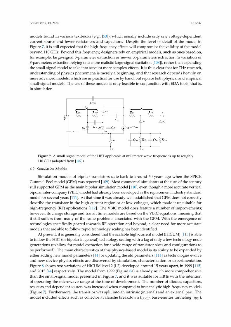
Sensors 2019, 19, 2454 16 of 32
models found in various textbooks (e.g., [53]), which usually include only one voltage-dependentcurrent source and fewer resistances and capacitors. Despite the level of detail of the model inFigure 7, it is still expected that the high-frequency effects will compromise the validity of the modelbeyond 110 GHz. Beyond this frequency, designers rely on empirical models, such as ones based on,for example, large-signal S-parameter extraction or newer X-parameters extraction (a variation ofS-parameters extraction relying on a more realistic large-signal excitation [108]), rather than expandingthe small-signal model to take into account more complex effects. It is thus clear that for THz research,understanding of physics phenomena is merely a beginning, and that research depends heavily onmore advanced models, which are unpractical for use by hand, but replace both physical and empiricalsmall-signal models. The use of these models is only feasible in conjunction with EDA tools; that is,in simulation.
Sensors 2019, 19, x FOR PEER REVIEW 15 of 31
time prototyping success. Therefore, physics and modeling of THz-capable technologies are understood to be the second enabling factor for re-engineering THz systems and are subsequently discussed.
4.1. Physics-Driven Small-Signal Modeling of Transistors
It is common knowledge that the research and design of electronic circuits, in general, are performed in several stages, where a first stage typically involves looking at and understanding the analytic model that is comprehensible to designers without consulting electronic design automation (EDA) [106] tools. Transistor behavior is normally described by small-signal models, which are generally applicable to most signals in analog circuits and some signals in RF circuits. Specialized circuitry, such as power amplifiers (operation at much lower frequency than fT is assumed here), requires transistors to operate in large-signal modes, and large-signal models are more applicable in such cases.
For every transistor, irrespective of the technology node, a range of simple or complex small-signal models can be developed; however, simpler mathematical equations based on the device-physics alone struggle to describe the transistor behavior accurately beyond a certain model-dependent frequency. The small-signal model of the HBT in Figure 7, for example, breaks down the transistor up to the level where each pn-junction that is formed is modeled in detail by current and periphery parameters (diodes iBp, iBi, iSi and iSp) [107]. The model also includes internal and external bias-dependent capacitances between different terminals (CjCXT, CJCI, CrBi, CdEi, CSUi, CSup, CCOX and CEOX), resistances of the base (rB), collector (rC), emitter (RE) and substrate (RSui and RSUp), as well as a voltage-dependent current source. This model is much more comprehensive than typical small-signal high-frequency models found in various textbooks (e.g., [53]), which usually include only one voltage-dependent current source and fewer resistances and capacitors. Despite the level of detail of the model in Figure 7, it is still expected that the high-frequency effects will compromise the validity of the model beyond 110 GHz. Beyond this frequency, designers rely on empirical models, such as ones based on, for example, large-signal S-parameter extraction or newer X-parameters extraction (a variation of S-parameters extraction relying on a more realistic large-signal excitation [108]), rather than expanding the small-signal model to take into account more complex effects. It is thus clear that for THz research, understanding of physics phenomena is merely a beginning, and that research depends heavily on more advanced models, which are unpractical for use by hand, but replace both physical and empirical small-signal models. The use of these models is only feasible in conjunction with EDA tools; that is, in simulation.
Figure 7. A small-signal model of the HBT applicable at millimeter-wave frequencies up to roughly 110 GHz (adapted from [107]).
4.2. Simulation Models
Simulation models of bipolar transistors date back to around 50 years ago when the SPICE Gummel-Pool model (GPM) was reported [109]. Most commercial simulators at the turn of the century still supported GPM as the main bipolar simulation model [110], even though a more
Figure 7. A small-signal model of the HBT applicable at millimeter-wave frequencies up to roughly110 GHz (adapted from [107]).
4.2. Simulation Models
Simulation models of bipolar transistors date back to around 50 years ago when the SPICEGummel-Pool model (GPM) was reported [109]. Most commercial simulators at the turn of the centurystill supported GPM as the main bipolar simulation model [110], even though a more accurate verticalbipolar inter-company (VBIC) model had already been developed as the replacement industry standardmodel for several years [111]. At that time it was already well established that GPM does not correctlydescribe the transistor in the high-current region or at low voltages, which made it unsuitable forhigh-frequency (RF) applications [112]. The VBIC model does feature a number of improvements;however, its charge storage and transit time models are based on the VBIC equations, meaning thatit still suffers from many of the same problems associated with the GPM. With the emergence oftechnologies specifically geared towards RF operation and beyond, a clear need for more accuratemodels that are able to follow rapid technology scaling has been identified.
At present, it is generally considered that the scalable high-current model (HICUM) [113] is ableto follow the HBT (or bipolar in general) technology scaling with a lag of only a few technology nodegenerations (to allow for model extraction for a wide range of transistor sizes and configurations tobe performed). The main characteristics of this physics-based model is its ability to be expanded byeither adding new model parameters [44] or updating the old parameters [114] as technologies evolveand new device physics effects are discovered by simulation, characterization or experimentation.Figure 8 shows two variations of HICUM level 2 (L2) developed around 15 years apart, in 1999 [115]and 2015 [44] respectively. The model from 1999 (Figure 8a) is already much more comprehensivethan the small-signal model presented in Figure 7, and it was suitable for HBTs with the intentionof operating the microwave range at the time of development. The number of diodes, capacitors,resistors and dependent sources was increased when compared to best analytic high-frequency models(Figure 7). Furthermore, the transistor was split into an intrinsic (internal) and an external part. Themodel included effects such as collector avalanche breakdown (iAVL), base-emitter tunneling (iBEt),

Sensors 2019, 19, 2454 17 of 32
self-heating (separate network as indicated in the figure), substrate coupling and the effects of theparasitic substrate transistor. The recent (2015) version of the model (Figure 8b) repeats the mainand self-heating networks of the model from 1999, and also includes non-quasi-static (NQS) effectsoccurring at high frequencies by virtue of adding another separate network. The evolved model isapplicable to transistors capable of millimeter-wave and, more recently, THz operation. This versionalso considers the effects of the correlated noise, added as a result of research reported in [116]. It isexpected that the model will continue to evolve; for instance, shortly prior to the publication ofthis article, HICUM was extended to include the avalanche multiplication in SiGe HBTs at differenttransistor injection levels [117]. A detailed description of HICUM, including the definition of allsymbols used in Figure 8, can be found in the HICUM/L2 manual by Schroter and Pawlak [113]. Thismanual is available as a direct download from the website of Dresden Technical University, where themodel originated.Sensors 2019, 19, x FOR PEER REVIEW 17 of 31
(a)
(b)
Figure 8. The evolution of high-current model (HICUM): (a) HICUM/L2 in 1999 (adapted from [115]) and (b) HICUM in 2015 (adapted from [44]).
HICUM development was extensively revised during the course of the DOTFIVE and DOTSEVEN projects and parameters were extracted for each reported technology node [36]. HICUM/L2 is now available in all commercial simulators and is at present implemented in Verilog-A. Although it was originally developed with SiGe BiCMOS technology scaling in mind, model parameters can be extracted for any HBT technology, for example for any of the contending InP HBT technology nodes [36,118]. The methodology of parameter extraction is also detailed in the HICUM/L2 manual [113].
When it comes to modeling of HEMTs, the situation differs between specific technologies. Modeling of InP HEMTs, the fastest of all HEMTs, has not been extensively reported upon in literature, unlike, for example, GaN HEMTs used in high-power amplification [119,120]. Commercial simulators still use InP HEMT models that date back to the late 20th century, while the more recent models are based on extrapolation from modeling of GaAs or GaN HEMTs [121,122]. However, some attempts at non-linear large-signal modeling of InP HEMTs have recently been made [121], but it becomes increasingly difficult to separate device behavior from the electromagnetic environment [123]. Design in this technology is then typically performed using empirical models. The situation with CMOS FETs is, fortunately, in a better state, as a range of Berkeley short-channel IGFET models (e.g., BSIM4) has been kept up to date with technology scaling [124]. However, by noting again that CMOS is currently still lagging behind HBT and HEMT technologies in terms of achievable frequencies, it would appear that HBT technologies (including SiGe BiCMOS) remain the only contenders that can currently reach into the THz domain, with supporting simulation transistor models that are able to do the same.
4.3. Summary—Terahertz Technologies, Modeling and Cost
Figure 9 shows the performance metrics of reported THz technologies, together with their estimated fabrication costs and the extent of modeling of their active devices. This figure reassures one that SiGe BiCMOS technology currently presents the best compromise when it comes to the three
Figure 8. The evolution of high-current model (HICUM): (a) HICUM/L2 in 1999 (adapted from [115])and (b) HICUM in 2015 (adapted from [44]).
HICUM development was extensively revised during the course of the DOTFIVE and DOTSEVENprojects and parameters were extracted for each reported technology node [36]. HICUM/L2 is nowavailable in all commercial simulators and is at present implemented in Verilog-A. Although it wasoriginally developed with SiGe BiCMOS technology scaling in mind, model parameters can be extractedfor any HBT technology, for example for any of the contending InP HBT technology nodes [36,118].The methodology of parameter extraction is also detailed in the HICUM/L2 manual [113].
When it comes to modeling of HEMTs, the situation differs between specific technologies.Modeling of InP HEMTs, the fastest of all HEMTs, has not been extensively reported upon in literature,unlike, for example, GaN HEMTs used in high-power amplification [119,120]. Commercial simulatorsstill use InP HEMT models that date back to the late 20th century, while the more recent models arebased on extrapolation from modeling of GaAs or GaN HEMTs [121,122]. However, some attemptsat non-linear large-signal modeling of InP HEMTs have recently been made [121], but it becomes

Sensors 2019, 19, 2454 18 of 32
increasingly difficult to separate device behavior from the electromagnetic environment [123]. Designin this technology is then typically performed using empirical models. The situation with CMOS FETsis, fortunately, in a better state, as a range of Berkeley short-channel IGFET models (e.g., BSIM4) hasbeen kept up to date with technology scaling [124]. However, by noting again that CMOS is currentlystill lagging behind HBT and HEMT technologies in terms of achievable frequencies, it would appearthat HBT technologies (including SiGe BiCMOS) remain the only contenders that can currently reachinto the THz domain, with supporting simulation transistor models that are able to do the same.
4.3. Summary—Terahertz Technologies, Modeling and Cost
Figure 9 shows the performance metrics of reported THz technologies, together with theirestimated fabrication costs and the extent of modeling of their active devices. This figure reassuresone that SiGe BiCMOS technology currently presents the best compromise when it comes to the threemetrics; furthermore, the InP HBT technology may be suitable in applications where cost is not themain concern, which is also the case with various other HEMT technologies shown in the figure.
Sensors 2019, 19, x FOR PEER REVIEW 18 of 31
metrics; furthermore, the InP HBT technology may be suitable in applications where cost is not the main concern, which is also the case with various other HEMT technologies shown in the figure.
5. Other Requirements for Re-Engineering Terahertz Radar Sensors
The third enabling factor for THz research is that THz-capable, modeled active devices must be supported by passive devices, including interconnects and antennas, which are also capable of THz operation.
Figure 9. Comparison of emerging transistor technologies capable of THz applications with respect to performance metrics, extent of modeling and cost. Linear frequency axes are used for clarity of presentation. From left to right, technology metrics have been taken from these references: [26,29,31,41–43,48,55,66].
5.1. Passives
Passive devices, specifically inductors and capacitors, tend to exhibit low-quality factors as frequency increases. Therefore, the primary challenge of passive component design in the millimeter-wave, and even more so in the THz regime, is selecting the correct topology and dimension for each component to avoid excessive losses [125]. Numerous alternatives for implementing passive components are possible, including lumped, active and distributed options [38]. In the THz regime, however, only a subset of these options are suitable. Integrated inductors start suffering from excessive losses already well below 100 GHz, while the situation with capacitors is slightly better, but still not satisfactory. Emerging technologies do provide for passive component implementation (e.g., MIM and interdigital capacitors and spiral inductors); however, these are often suitable to be used in the circuit blocks that operate well below fT. Passives can also be implemented with MEMS modifications, but the frequencies may still be inadequate at present [126]. Hence, the two main directions in THz research are research into transmission-line implementations [127], or alternatively, into implementing passives on different substrates, more suitable for high frequencies [38,128–132].
Transmission lines are suitable for THz integration owing to the small wavelength and the fact that their quality factors increase with frequency. The opposite is, regrettably, true for the insertion loss of the transmission line. Transmission lines can be configured both as inductors and capacitors. Microstrip and CPW transmission lines are two types of printed transmission lines that can be used in nanoelectronic circuits with ease. On discrete substrates, the substrate integrated waveguides
Figure 9. Comparison of emerging transistor technologies capable of THz applications withrespect to performance metrics, extent of modeling and cost. Linear frequency axes are usedfor clarity of presentation. From left to right, technology metrics have been taken from thesereferences: [26,29,31,41–43,48,55,66].
5. Other Requirements for Re-Engineering Terahertz Radar Sensors
The third enabling factor for THz research is that THz-capable, modeled active devices mustbe supported by passive devices, including interconnects and antennas, which are also capable ofTHz operation.
5.1. Passives
Passive devices, specifically inductors and capacitors, tend to exhibit low-quality factorsas frequency increases. Therefore, the primary challenge of passive component design in themillimeter-wave, and even more so in the THz regime, is selecting the correct topology and dimensionfor each component to avoid excessive losses [125]. Numerous alternatives for implementing passivecomponents are possible, including lumped, active and distributed options [38]. In the THz regime,

Sensors 2019, 19, 2454 19 of 32
however, only a subset of these options are suitable. Integrated inductors start suffering from excessivelosses already well below 100 GHz, while the situation with capacitors is slightly better, but still notsatisfactory. Emerging technologies do provide for passive component implementation (e.g., MIMand interdigital capacitors and spiral inductors); however, these are often suitable to be used in thecircuit blocks that operate well below fT. Passives can also be implemented with MEMS modifications,but the frequencies may still be inadequate at present [126]. Hence, the two main directions in THzresearch are research into transmission-line implementations [127], or alternatively, into implementingpassives on different substrates, more suitable for high frequencies [38,128–132].
Transmission lines are suitable for THz integration owing to the small wavelength and the factthat their quality factors increase with frequency. The opposite is, regrettably, true for the insertionloss of the transmission line. Transmission lines can be configured both as inductors and capacitors.Microstrip and CPW transmission lines are two types of printed transmission lines that can be used innanoelectronic circuits with ease. On discrete substrates, the substrate integrated waveguides (SIW)can also be used [133,134]. A rectangular SIW structure requires two metals and connecting vias tocreate a waveguide structure. Slow-CPW structures, utilizing various techniques that “slow down”the wave, have been reported in an attempt to increase the transmission line quality factors [135,136].Nowadays, process design kits for most recent high-speed technologies provide standard transmissionline cells for effortless design.
Using substrates geared towards passive component implementation requires the packaging ofthe designed systems to be reconsidered such that both benefits of integrated substrates and discretesubstrates can be used in conjunction with each other, which will be discussed in the next section. Bothceramic and laminate substrates are considered to be sufficiently capable of supporting fabricationof devices operating at least at the millimeter-wave regime. Laminates are fabricated from discretesubstrate layers laminated together at high pressure and temperature. Ceramic substrates can bedivided into several groups, with low-temperature co-fired ceramics (LTCC) and high-temperatureco-fired ceramics (HTCC) suitable for millimeter-wave applications. Other substrates include organics,polymers, including extremely capable liquid-crystal polymers (LCP) with hermetic properties, glassesand hybrid structures.
5.2. Interconnects
As wavelengths become ever smaller, interconnects between devices become increasingly difficultto implement. In RF electronics, it is widely considered that a connection longer than about one-tenthof the wavelength starts behaving as a transmission line, and all connections need to be treated assuch. Given that technology scaling also results in shorter connections within an IC, this may not be aproblem even in the THz regime. Attention, however, needs to be paid to how the transitions betweendifferent types of transmission lines are made to minimize the losses [137,138]. Suboptimal deviceinterconnects are known to decrease the apparent values of fT and fmax by as much as 50% in certaininstances [139].
5.3. Antennas
The size of the transmitting and receiving antenna, by definition a passive circuit, in amicroelectronic system circuit is proportional to the wavelength. Thus, THz antennas are sufficientlysmall (less than a few millimeters), for antennas and antenna arrays can easily be integrated on chip.Antennas can be placed close to the transmitter or receiver circuitry, allowing them to become anintegral part of the IC, without the need to bring the signal from the antenna from outside the packageinto the package, thus avoiding unnecessary losses [39].
Antenna integration comes with many challenges, however. For example, integrated antennasare prone to coupling to the rest of the RF circuitry, particularly to passives components. On siliconsubstrates, one of the problems is caused by the fact that a silicon substrate has low resistivity, allowingthe signal to find a low-resistivity path through the substrate and degrade the gain of the antenna.

Sensors 2019, 19, 2454 20 of 32
Another problem is due to the relatively high dielectric constant of silicon (εr = 11.9), which causessubstrate absorption [125] and degrades the antenna efficiency. Antennas on other substrates, such asthe one deployed in the SOI technology, tend to respond better. At THz frequencies, nevertheless, thebenefit of being able to remove the metal interconnects and avoid matching in integrated antennasoutweighs many of the above-mentioned drawbacks. Some examples of state-of-the-art integratedantennas can be found in references [140] and [141].
Antennas, like general passive components, can also be implemented on package. Antennas onLTCC, HTCC or LCP (LCP has εr = 3.1), for example, can have much higher gains than fully integratedantennas. Large packages also allow for multiple antennas to be readily deployed [142]. Packagedsolutions furthermore allow pure MEMS technologies to be utilized, as in the case of the THz helixantenna reported in [14].
6. Packaging of Terahertz-Wave Systems
The fourth enabling factor for any research into the THz regime beyond mere proof-of-conceptexperimentation is the emergence of adequate packaging methodologies. Packaging is necessary toprotect circuits from the influences of the environment in which they are deployed.
Throughout this article, it was generally assumed that re-engineered active THz sensors mustbe implemented in such a way that the complete system is integrated in a single THz-capabletechnology, enclosed in an appropriate package. Such an approach is known as system-on-chip (SoC)in literature [38]. It was hinted in the previous section, though, that deployment of other substratesfor a more optimal implementation of passive components or antennas, or MEMS-only technologies,can offer a multitude of benefits. In this case, multiple substrates can coexist inside the same packageenclosure, with different parts of the system implemented on each, leading to the implementationtermed system-on-package (SoP) [128]. If the discrete substrate solely serves as carrier of multiplechips (e.g., any combination SiGe BiCMOS technology, in InP technology and GaAs Schottky diodetechnology, among others [143], could be an approach to advanced THz systems), then a multi-chipmodule (MCM) is built. The relationship between SoC, MCM and SoP is illustrated in Figure 10.
Sensors 2019, 19, x FOR PEER REVIEW 20 of 31
6. Packaging of Terahertz-Wave Systems
The fourth enabling factor for any research into the THz regime beyond mere proof-of-concept experimentation is the emergence of adequate packaging methodologies. Packaging is necessary to protect circuits from the influences of the environment in which they are deployed.
Throughout this article, it was generally assumed that re-engineered active THz sensors must be implemented in such a way that the complete system is integrated in a single THz-capable technology, enclosed in an appropriate package. Such an approach is known as system-on-chip (SoC) in literature [38]. It was hinted in the previous section, though, that deployment of other substrates for a more optimal implementation of passive components or antennas, or MEMS-only technologies, can offer a multitude of benefits. In this case, multiple substrates can coexist inside the same package enclosure, with different parts of the system implemented on each, leading to the implementation termed system-on-package (SoP) [128]. If the discrete substrate solely serves as carrier of multiple chips (e.g., any combination SiGe BiCMOS technology, in InP technology and GaAs Schottky diode technology, among others [143], could be an approach to advanced THz systems), then a multi-chip module (MCM) is built. The relationship between SoC, MCM and SoP is illustrated in Figure 10.
Figure 10. Different packaging options of microelectronic circuits.
For frequencies above 100 GHz, the total cost of a microelectronic system is mostly determined by the packaging and assembly process [144]. Each packaging option comes with several other advantages and disadvantages that must be weighed against one another for a specific system to come to a decision on packaging. Some advantages and disadvantages of SoC and SoP packaging approaches are listed in Table 2. For THz applications, two main considerations are the quality and practicality issues of passive components, and the way in which connections are made between different dies and substrates. If a connection to a high-quality embedded inductor or capacitor can be made without significant losses, then SoP is probably the better option. If satisfactory system performance can be found on a single chip, the lower cost and greater reliability of the single chip solution will be the answer.
The way in which physical interconnects are made in SoC, MCM and SoP is perhaps the most important aspect of THz packaging. In SoC, connections are made from the chip enclosure to the chip substrate, and in MCMs and SoPs, the chip-to-chip interconnects in vertical and horizontal directions, with or without interposers, are also required. Typically, a mix of bonding, bumping and regular or RF TSVs is required. In SoP, most horizontal connections must be made with transmission lines or waveguides, and once again the proper transitions between transmission lines capable of traversing horizontal and vertical directions must be made to minimize losses. In all cases, traditional wire bonding can exclusively be used for direct-current and low-frequency signals; on the contrary, the flip-chip approach deploying solder microbumps, which allows the signals to traverse much shorter paths, is necessary for all RF signals. A 3D coaxial interconnect system, such as the one presented in [145], or electromagnetic transitions, such as the one described for InP HEMTs in [26], may also be
Figure 10. Different packaging options of microelectronic circuits.
For frequencies above 100 GHz, the total cost of a microelectronic system is mostly determined bythe packaging and assembly process [144]. Each packaging option comes with several other advantagesand disadvantages that must be weighed against one another for a specific system to come to a decisionon packaging. Some advantages and disadvantages of SoC and SoP packaging approaches are listedin Table 2. For THz applications, two main considerations are the quality and practicality issues ofpassive components, and the way in which connections are made between different dies and substrates.If a connection to a high-quality embedded inductor or capacitor can be made without significant

Sensors 2019, 19, 2454 21 of 32
losses, then SoP is probably the better option. If satisfactory system performance can be found on asingle chip, the lower cost and greater reliability of the single chip solution will be the answer.
Table 2. Advantages and disadvantages of system-on-chip (SoC) and system-on-package (SoP).
Type of Implementation Advantages Disadvantages
SoCHigh integration
Small sizeInexpensiveness
Low-quality passivesThermal issues
SoPFairly good integration
High densityHigher quality passives
Larger than that of the SoCLonger interconnects
Longer time to marketHigher production costs
Modeling simulation, reliability and yieldconsiderations
The way in which physical interconnects are made in SoC, MCM and SoP is perhaps the mostimportant aspect of THz packaging. In SoC, connections are made from the chip enclosure to the chipsubstrate, and in MCMs and SoPs, the chip-to-chip interconnects in vertical and horizontal directions,with or without interposers, are also required. Typically, a mix of bonding, bumping and regular orRF TSVs is required. In SoP, most horizontal connections must be made with transmission lines orwaveguides, and once again the proper transitions between transmission lines capable of traversinghorizontal and vertical directions must be made to minimize losses. In all cases, traditional wirebonding can exclusively be used for direct-current and low-frequency signals; on the contrary, theflip-chip approach deploying solder microbumps, which allows the signals to traverse much shorterpaths, is necessary for all RF signals. A 3D coaxial interconnect system, such as the one presentedin [145], or electromagnetic transitions, such as the one described for InP HEMTs in [26], may also berequired. MEMS circuits can be connected to the supporting substrates using TSVs and small solderbumps and hermetically sealed [146].
Other aspects that need to be considered in conjunction with packaging are heating, heatingeffects (such as differing thermal expansion of different materials) and associated cooling approaches(especially in high-power systems), electromigration and thermomigration (which become prominentas features decrease), reliability, as well as coupling and shielding [2,38,147]. Modeling and simulationof packaged systems are also much more challenging than those of pure integrated systems, andrequire deployment of different techniques, most notably ones based on finite-element methods [148].
7. Legislative and Commercial Factors
The fifth and last enabling factor for re-engineering THz sensors is legislative and economic factors.As technologies capable of THz applications emerge, first commercial products are typically costlyand, in many instances, it does not make sense to push for widespread deployment until the return oninvestment is deemed satisfactory. In some countries, there could also be legislation prohibiting thedeployment of systems at particular frequencies, which could limit the initial rate of acceptance as well.
It is, however, the belief of the authors of this article that these factors can be overcome if other,technical enabling factors are taken care of, and that the benefits of THz technology outweigh thepossible hindrances associated with economics and legislation. This is especially true in the case ofaffordable SiGe BiCMOS technology.
8. Review of Reported Terahertz and Low-THz Sub-Systems with the Potential to Be Used withRadar Sensors
In this section, a short review of low-THz and THz subsystems that have been demonstrated atthese frequencies is given. These proof-of-concept circuits could potentially serve as a starting pointtowards the development of re-engineered THz radar systems.

Sensors 2019, 19, 2454 22 of 32
Scheytt et al. [46], for example, presented a low-cost radar transceiver operating at 245 GHz,fabricated in IHP (DOTFIVE) technology with fmax = 0.5 THz. The transmitter consists of a 61 GHzVCO with a 122 GHz push-push output, a power amplifier and a frequency doubler to reach a powerlevel of 1 dBm at 245 GHz. On the receiver side, the input signal is passed through a 245 GHz-capableLNA and down-converted with the aid of a VCO tuned to 60 GHz. Even though up-conversion anddown-conversion are the main contributions of this paper and the output power is relatively low, thedesigned four-stage common-base LNA demonstrates the ability of amplification nearing the 300-GHzmark. The transmitter was improved, however, in the paper by Schmaltz et al. [47], showing 7 dBm ofpower delivered at the same frequency. The transmitter is actually a transmitter array for spectroscopyapplications, comprising four branches, each consisting of a power amplifier, frequency doubler andan antenna [48], as illustrated in the microphotograph shown in Figure 11. The same group alsodemonstrated a spectroscopy transmitter system at 500 GHz (close to fmax of the transistor); however,the output power reached was only −7 dBm [47].
Sensors 2019, 19, x FOR PEER REVIEW 22 of 31
doubler and an antenna [48], as illustrated in the microphotograph shown in Figure 11. The same group also demonstrated a spectroscopy transmitter system at 500 GHz (close to fmax of the transistor); however, the output power reached was only −7 dBm [47].
Figure 11. A 245 GHz transmitter array (reproduced with permission from [48]).
Deng et al. [1] demonstrated an integrated 1 × 4 phased array transmitter intended to operate at 320 GHz in a 0.18 μm SiGe BiCMOS technology. The signal is generated using a VCO at 20 GHz, which is quadrupled to reach 80 GHz. A Wilkinson power divider is then used to split the signal into four branches, and the signal in each branch is passed through two push-push frequency doublers to reach the final frequency of 320 GHz. The power achieved is 10.6 dB.
Reported SiGe transmitters use frequency multiplication to reach (sub-) THz frequencies. Oscillators in such circuits are deliberately designed to have increased power at subharmonics (typically, at double the nominal frequency). The fmax of commercially available InP HBT technologies is higher than that of commercially available BiCMOS technologies, so it comes as no surprise that it is possible to design fundamental oscillators at frequencies of several hundred gigahertz in this technology. Seo et al. [49] presented three varactor-tuned oscillators operating at 310.2, 412.9 and 573.1 GHz in a 0.25 μm InP HBT technology node.
Several demonstrations of systems in GaAs mHEMT technologies also showed quite attractive results, of which two will be mentioned here. Abbasi et al. [50] demonstrated a 220-GHz active receiver and transmitter for 220-GHz imaging and communication applications, also deploying an integrated antenna. The transmitter and the receiver functions of the chip are performed with the same set of circuits, but the direction that the signal traverses is reversed. Fabrication was completed on GaAs wafers with the metamorphic buffer with composition InxAl0.48Ga0.52-x, where x is an index that transitions from zero to 0.52, as this technology was deemed to be suitable for ultra-low-noise applications. More recently, a six-stage LNA with 150 GHz of bandwidth from 500 to 750 GHz, maximum gain of 15.4 dB and minimum measured noise figure of 15 dB was reported by Tessmann et al. [42]. The wafers had the same composition as in the previous example, as well as T-shaped 20 nm Pt-Ti-Pt-Au transistor gates encapsulated with BCB. Furthermore, the process needed to be modified to increase the quality of CPW lines, including the thinning of the substrate to only 20 μm. Capacitors based on via holes were utilized. The chip photograph of the LNA is shown in Figure 12. The figure shows that the LNA is a six-stage common-source amplifier, complete with power lines and pads. The quality improvement of CPWs results in space saving, and as a result, the whole die consumes an area of only 0.28 × 0.50 mm2.
Figure 11. A 245 GHz transmitter array (reproduced with permission from [48]).
Deng et al. [1] demonstrated an integrated 1 × 4 phased array transmitter intended to operateat 320 GHz in a 0.18 µm SiGe BiCMOS technology. The signal is generated using a VCO at 20 GHz,which is quadrupled to reach 80 GHz. A Wilkinson power divider is then used to split the signal intofour branches, and the signal in each branch is passed through two push-push frequency doublers toreach the final frequency of 320 GHz. The power achieved is 10.6 dB.
Reported SiGe transmitters use frequency multiplication to reach (sub-) THz frequencies.Oscillators in such circuits are deliberately designed to have increased power at subharmonics(typically, at double the nominal frequency). The fmax of commercially available InP HBT technologiesis higher than that of commercially available BiCMOS technologies, so it comes as no surprise thatit is possible to design fundamental oscillators at frequencies of several hundred gigahertz in thistechnology. Seo et al. [49] presented three varactor-tuned oscillators operating at 310.2, 412.9 and573.1 GHz in a 0.25 µm InP HBT technology node.
Several demonstrations of systems in GaAs mHEMT technologies also showed quite attractiveresults, of which two will be mentioned here. Abbasi et al. [50] demonstrated a 220-GHz activereceiver and transmitter for 220-GHz imaging and communication applications, also deployingan integrated antenna. The transmitter and the receiver functions of the chip are performed with

Sensors 2019, 19, 2454 23 of 32
the same set of circuits, but the direction that the signal traverses is reversed. Fabrication wascompleted on GaAs wafers with the metamorphic buffer with composition InxAl0.48Ga0.52−x, wherex is an index that transitions from zero to 0.52, as this technology was deemed to be suitable forultra-low-noise applications. More recently, a six-stage LNA with 150 GHz of bandwidth from 500to 750 GHz, maximum gain of 15.4 dB and minimum measured noise figure of 15 dB was reportedby Tessmann et al. [42]. The wafers had the same composition as in the previous example, as well asT-shaped 20 nm Pt-Ti-Pt-Au transistor gates encapsulated with BCB. Furthermore, the process neededto be modified to increase the quality of CPW lines, including the thinning of the substrate to only20 µm. Capacitors based on via holes were utilized. The chip photograph of the LNA is shown inFigure 12. The figure shows that the LNA is a six-stage common-source amplifier, complete withpower lines and pads. The quality improvement of CPWs results in space saving, and as a result, thewhole die consumes an area of only 0.28 × 0.50 mm2.
Sensors 2019, 19, x FOR PEER REVIEW 23 of 31
Finally, as expected, amplification at by far the highest frequency was achieved with InP HEMT technology. Mei et al. [51] demonstrated amplification at 1.03 THz, as has already been mentioned. The amplifier was built in the 0.25-nm technology node and consisted of 10 common-source amplifier stages and delivered 9 dB of measured gain. An LNA in the same technology node was demonstrated by Leong et al. [52], delivering 13.6 dB of gain with a noise figure as low as 11.1 dB at 850 GHz. The LNA consisted of 10 amplification stages. Furthermore, to minimize transition losses, custom waveguide transitions (WG transitions) with insertion loss of 1.8 dB were used to connect the input and output of the amplifier to an external waveguide. The complete LNA, including WG transitions and DC pads, is shown in Figure 13.
Figure 12. A 600 GHz low-noise application (LNA) in gallium-arsenide (GaAs) metamorphic HEMT (mHEMT) technology (reproduced with permission from [42]).
Figure 13. A 850 GHz LNA in InP HEMT technology (reproduced with permission from [52]).
9. Discussion
It is evident that THz-amplification-capable technologies have been available for over a decade, with III-V compound materials leading the way into applications over 1 THz, but with the disadvantage of high manufacturing costs. Less expensive SiGe BiCMOS technologies are considered to be emerging, with transistors incapable of operation above 1 THz, but with a clear roadmap towards 1 THz and above. It is also understood that adequate physics-based simulation models can be extracted for HBT-related technologies, but these usually only become commercially available several years after a technology is reported (which sometimes coincides with the availability of new technology nodes). This review also showed that currently the fastest reported technology, based on InP HEMTs, is not well supported with physics-based models (which is also true for other types of
Figure 12. A 600 GHz low-noise application (LNA) in gallium-arsenide (GaAs) metamorphic HEMT(mHEMT) technology (reproduced with permission from [42]).
Finally, as expected, amplification at by far the highest frequency was achieved with InP HEMTtechnology. Mei et al. [51] demonstrated amplification at 1.03 THz, as has already been mentioned. Theamplifier was built in the 0.25-nm technology node and consisted of 10 common-source amplifier stagesand delivered 9 dB of measured gain. An LNA in the same technology node was demonstrated byLeong et al. [52], delivering 13.6 dB of gain with a noise figure as low as 11.1 dB at 850 GHz. The LNAconsisted of 10 amplification stages. Furthermore, to minimize transition losses, custom waveguidetransitions (WG transitions) with insertion loss of 1.8 dB were used to connect the input and output ofthe amplifier to an external waveguide. The complete LNA, including WG transitions and DC pads, isshown in Figure 13.

Sensors 2019, 19, 2454 24 of 32
Sensors 2019, 19, x FOR PEER REVIEW 23 of 31
Finally, as expected, amplification at by far the highest frequency was achieved with InP HEMT technology. Mei et al. [51] demonstrated amplification at 1.03 THz, as has already been mentioned. The amplifier was built in the 0.25-nm technology node and consisted of 10 common-source amplifier stages and delivered 9 dB of measured gain. An LNA in the same technology node was demonstrated by Leong et al. [52], delivering 13.6 dB of gain with a noise figure as low as 11.1 dB at 850 GHz. The LNA consisted of 10 amplification stages. Furthermore, to minimize transition losses, custom waveguide transitions (WG transitions) with insertion loss of 1.8 dB were used to connect the input and output of the amplifier to an external waveguide. The complete LNA, including WG transitions and DC pads, is shown in Figure 13.
Figure 12. A 600 GHz low-noise application (LNA) in gallium-arsenide (GaAs) metamorphic HEMT (mHEMT) technology (reproduced with permission from [42]).
Figure 13. A 850 GHz LNA in InP HEMT technology (reproduced with permission from [52]).
9. Discussion
It is evident that THz-amplification-capable technologies have been available for over a decade, with III-V compound materials leading the way into applications over 1 THz, but with the disadvantage of high manufacturing costs. Less expensive SiGe BiCMOS technologies are considered to be emerging, with transistors incapable of operation above 1 THz, but with a clear roadmap towards 1 THz and above. It is also understood that adequate physics-based simulation models can be extracted for HBT-related technologies, but these usually only become commercially available several years after a technology is reported (which sometimes coincides with the availability of new technology nodes). This review also showed that currently the fastest reported technology, based on InP HEMTs, is not well supported with physics-based models (which is also true for other types of
Figure 13. A 850 GHz LNA in InP HEMT technology (reproduced with permission from [52]).
9. Discussion
It is evident that THz-amplification-capable technologies have been available for over a decade,with III-V compound materials leading the way into applications over 1 THz, but with the disadvantageof high manufacturing costs. Less expensive SiGe BiCMOS technologies are considered to be emerging,with transistors incapable of operation above 1 THz, but with a clear roadmap towards 1 THz and above.It is also understood that adequate physics-based simulation models can be extracted for HBT-relatedtechnologies, but these usually only become commercially available several years after a technology isreported (which sometimes coincides with the availability of new technology nodes). This review alsoshowed that currently the fastest reported technology, based on InP HEMTs, is not well supportedwith physics-based models (which is also true for other types of HEMTs), indicating that it will beunrealistic to expect its commercialization in the near future. (However, in addition to huge academicvalue, exceptions are possible.) With CMOS still barely reaching into the THz range, this leaves SiGeBiCMOS as the main contender for commercial applications of re-engineered radar sensors. Cost isalso a major factor in the wide adoption of a technology, and SiGe BiCMOS, fortunately, remains lessexpensive than the other reviewed technologies [149]. However, the feeling is that with fmax > 0.7 THz,SiGe HBTs still need some frequency-response improvement before it can be said that they can beconsidered a uniquely capable technology. Improvements are theoretically possible, as indicated in theroadmap as well, supported by the fact that emitter-junction widths can be decreased further from thecurrent size of 110–130 nm and by an introduction of the latest project (a follow-up to DOTSEVEN)aimed at further scaling of SiGe HBTs, named TARANTO [150]. Despite the fact that the silicon-basedtechnology improvements are expected to continue in small increments, many researchers argue thatthe silicon-based ICs are the best bet to push the field of THz sensing forward [151]. The continuationof this research remains in large part empowered by the cost-effectiveness of silicon-based technologies.
When it comes to passives, interconnects, antennas, and packaging; significant progress has beenmade in recent years, but it appears, at least when it comes to frequencies of 300 GHz and above, thatmore research is needed until solutions for these challenges can be standardized. At present, specificdesign factors drive the choice of passives and packaging, which needs to be supported with intenseexperimentation, partially because of the complexity of system modeling and simulation. Finally, onceall technical challenges have been overcome, commercial factors will also have to be considered.
Nevertheless, with the current approach to THz sensing predominantly relying on bulky andexpensive diode mixers or lasers with no amplification capabilities, monolithic active radar sensingsolutions, specifically based on silicon-based devices, will soon start appearing. They will, however,have to compete with passive THz detection using solid-state devices configured as detectors operatingabove fmax values, which will retain superiority above 1 THz.

Sensors 2019, 19, 2454 25 of 32
10. Conclusions
In this paper, the emerging transistor technologies capable of amplification in the THz regime wereinvestigated, with the focus on their role in re-engineering THz radar sensors as transceivers. WithIII-V compound-material technologies leading the way into applications over 1 THz, relatively closelyfollowed by the less expensive SiGe BiCMOS technology and with numerous demonstrated oscillatorand amplifier circuits in a range of technologies, it appears that future prospects are good. However,the situation is not so simple. The availability of technologies is not the only prerequisite when itcomes to commercialization. Commercialization requires stable empirical models for conceptual circuitdesigns, as well as simulation models for rapid design at particular technology nodes. Furthermore,technology researchers also tend to focus on developing models for active devices only, with lessattention being paid to passive components and packaging, despite them also being determining factorsfor commercialization of potential products. Finally, there may be other commercial factors hinderingthe widespread adoption of re-engineered THz sensors, including cost and spectrum allocation andlegislative challenges. In this paper, it was argued that as advanced technologies become more readilyavailable, the interest of the academic and subsequently the commercial community in the vast field ofTHz applications is increasing and that it can be expected that active radar sensing solutions will soonstart taking over a fair share of the commercial market.
Author Contributions: M.B. was the main contributor responsible for content collection, document drafting andcomparative methodology. S.S. contributed with technical ideas and the outline of the paper, collaborated in themain technical sections and assisted in the final preparation of the document.
Funding: This research received no external funding.
Acknowledgments: MOSIS Integrated Circuit Fabrication Service and EDA vendors, such as Keysight, havecontributed to postgraduate and research work conducted and/or supervised by the authors. MOSIS, through theMOSIS Educational Program, has supported coordination with leading foundries and thus provided studentswith the opportunity to conduct industry-relevant research. Keysight has contributed through heavily discountedsimulation software licensing and in particular usage of the Advanced Design System—ADS.
Conflicts of Interest: The authors declare no conflict of interest.
References
1. Deng, X.; Li, Y.; Li, J.; Liu, C.; Wu, W.; Xiong, Y. A 320-GHz 1x4 Fully Integrated Phased Array TransmitterUsing 0.13-µm SiGe BiCMOS Technology. IEEE Trans. Terahertz Sci. Technol. 2015, 5, 930–940. [CrossRef]
2. Božanic, M.; Sinha, S. Millimeter-Wave Low Noise Amplifiers; Springer: Cham, Switzerland, 2017.3. Ergün, S.; Sönmez, S. Terahertz Technology for Military Applications. J. Manag. Inf. Sci. 2015, 3, 13–16.
[CrossRef]4. Jasteh, D.; Hoare, E.G.; Cherniakov, M.; Gashinova, M. Experimental Low-Terahertz Radar Image Analysis
for Automotive Terrain Sensing. IEEE Geosci. Remote Sens. Lett. 2016, 13, 490–494. [CrossRef]5. Basiri, R.; Abiri, H.; Yahaghi, A. Optimization of Metamaterial Structures for Terahertz and Microwave
Sensor Applications. Microw. Opt. Technol. Lett. 2014, 56, 636–642. [CrossRef]6. Nahata, A.; Weling, A.S.; Heinz, T.F. A wideband Coherent Terahertz Spectroscopy System Using Optical
Rectification and Electro-Optic Ssampling. Appl. Phys. Lett. 1996, 69, 2321–2323. [CrossRef]7. Beard, M.C.; Turner, G.M.; Schmuttenmaer, C.A. Terahertz Spectroscopy. J. Phys. Chem. B 2002, 106,
7146–7159. [CrossRef]8. Zangeneh-Nejad, F.; Safian, R. A Graphene-Based THz Ring Resonator for Label-Free Sensing. IEEE Sens. J.
2016, 16, 4338–4344. [CrossRef]9. Radhakrishnan, S.K.; Subramaniyan, B.; Anandan, M.; Nagarajan, M. Comparative Assessment of InGaAs
Sub-Channel and InAs Composite Channel Double Gate (DG)-HEMT for Sub-Millimeter Wave Applications.AEU Int. J. Electron. Commun. 2018, 83, 462–469. [CrossRef]
10. Tajima, T.; Kosugi, T.; Song, H.J.; Hamada, H.; El Moutaouakil, A.; Sugiyama, H.; Matsuzaki, H.; Yaita, M.;Kagami, O. Terahertz MMICs and Antenna-in-Package Technology at 300 GHz for KIOSK Download System.J. Infrared Millim. Terahertz Waves 2016, 37, 1213–1224. [CrossRef]
Sensors 2019, 19, 2454 26 of 32
11. Friederich, F.; Von Spiegel, W.; Bauer, M.; Meng, F.; Thomson, M.D.; Boppel, S.; Lisauskas, A.; Hils, B.;Krozer, V.; Keil, A.; et al. THz Active Imaging Systems with Real-Time Capabilities. IEEE Trans. Terahertz Sci.Technol. 2011, 1, 183–200. [CrossRef]
12. Caris, M.; Stanko, S.; Palm, S.; Sommer, R.; Wahlen, A.; Pohl, N. 300 GHz radar for high resolution SAR andISAR applications. In Proceedings of the 16th International Radar Symposium (IRS), Dresden, Germany,24–26 June 2015; pp. 577–580.
13. Zhou, Z.; Cao, Z.; Pi, Y. Dynamic Gesture Recognition with a Terahertz Radar Based on Range ProfileSequences and Doppler Signatures. Sensors 2018, 18, 10. [CrossRef]
14. Guo, L.; Huang, F.; Tang, X. A Novel Integrated MEMS Helix Antenna for Terahertz Applications. Optik2014, 125, 101–103. [CrossRef]
15. Brucherseifer, M.; Nagel, M.; Haring Bolivar, P.; Kurz, H.; Bosserhoff, A.; Büttner, R. Label-free Probing of theBinding State of DNA by Time-Domain Terahertz Sensing. Appl. Phys. Lett. 2000, 77, 4049–4051. [CrossRef]
16. Lambrechts, J.; Sinha, S. Microsensing Networks for Sustainable Cities; Springer: Cham, Switzerland, 2016.17. Abbas, T.; Qamar, F.; Ahmed, I.; Dimyati, K.; Majed, M.B. Propagation channel characterization for 28 and 73
GHz millimeter-wave 5G frequency band. In Proceedings of the IEEE 15th Student Conference on Researchand Development (SCOReD), Putrajaya, Malaysia, 13–14 December 2017; pp. 297–302.
18. Murata, K.; Murano, K.; Watanabe, I.; Kasamatsu, A.; Tanaka, T.; Monnai, Y. See-through Detection and 3DReconstruction Using Terahertz Leaky-Wave Radar Based on Sparse Signal Processing. J. Infrared Millim.Terahertz Waves 2018, 39, 210–221. [CrossRef]
19. Choi, J.; Va, V.; Gonzalez-Prelcic, N.; Daniels, R.; Bhat, C.R.; Heath, R.W. Millimeter-Wave VehicularCommunication to Support Massive Automotive Sensing. IEEE Commun. Mag. 2016, 54, 160–167. [CrossRef]
20. Yang, X.; Pi, Y.; Liu, T.; Wang, H. Three-Dimensional Imaging of Space Debris with Space-Based TerahertzRadar. IEEE Sens. J. 2018, 18, 1063–1072. [CrossRef]
21. Lien, J.; Gillian, N.; Karagozler, M.E.; Amihood, P.; Schwesig, C.; Olson, E.; Raja, H.; Poupyrev, I. Soli:Ubiquitous Gesture Sensing with Millimeter Wave Radar. ACM Trans. Graph. 2016, 35, 142. [CrossRef]
22. Cox, J.A.; Higashi, R.; Nusseibeh, F.; Zins, C. MEMS-based uncooled THz detectors for staring imagers.In Proceedings of the Micro- and Nanotechnology Sensors, Systems, and Applications III; InternationalSociety for Optics and Photonics, Orlando, FL, USA, 13 May 2011.
23. Nuessler, D.; Schubert, M.; Kose, S.; Pohl, N. Swifter Security Scanning: Millimeter-Wave Imaging with Spin.IEEE Microw. Mag. 2017, 18, 70–78. [CrossRef]
24. Muravev, V.M.; Tsydynzhapov, G.E.; Kukushkin, I.V.; Mcnee, I.; Kozlov, V.G. Terahertz Imaging: A Technologyin Search of Applications. Laser Focus World 2017, 53, 50–53.
25. Cooper, K.B.; Chattopadhyay, G. Submillimeter-Wave Radar: Solid-State System Design and Applications.IEEE Microw. Mag. 2014, 15, 51–67. [CrossRef]
26. Deal, W.; Mei, X.B.; Leong, K.M.K.H.; Radisic, V.; Sarkozy, S.; Lai, R. THz Monolithic Integrated CircuitsUsing InP High Electron Mobility Transistors. IEEE Trans. Terahertz Sci. Technol. 2011, 1, 25–32. [CrossRef]
27. Garcia, P.; Chantre, A.; Pruvost, S.; Chevalier, P.; Nicolson, S.T.; Roy, D.; Voinigescu, S.P.; Garnier, C. WillBiCMOS stay competitive for mmW applications? In Proceedings of the IEEE Custom Integrated CircuitsConference, San Jose, CA, USA, 21–24 September 2008; pp. 387–394.
28. Mukherjee, A.; Liang, W.; Schroter, M.; Pfeiffer, U.; Jain, R.; Grzyb, J.; Hillger, P. Millimeter-wave Circuitsand Applications. In Silicon-Germanium Heterojunction Bipolar Transistors for mm-Wave Systems: Technology,Modeling and Circuit Applications; River Publishers: Alsbjergvej, Denmark, 2018; p. 235.
29. Urteaga, M.; Griffith, Z.; Seo, M.; Hacker, J.; Rodwell, M.J.W. InP HBT Technologies for THz IntegratedCircuits. Proc. IEEE 2017, 105, 1051–1067. [CrossRef]
30. Decoutere, S.; Huylenbroeck, S.V.; Heinemann, B.; Fox, A.; Chevalier, P.; Chantre, A.; Meister, T.F.; Aufinger, K.;Schroter, M. Advanced process modules and architectures for half-terahertz SiGe:C HBTs. In Proceedings ofthe 2009 IEEE Bipolar/BiCMOS Circuits and Technology Meeting, Capri, Italy, 12–14 October 2009; pp. 9–16.
31. Heinemann, B.; Rücker, H.; Barth, R.; Bärwolf, F.; Drews, J.; Fischer, G.G.; Fox, A.; Fursenko, O.; Grabolla, T.;Herzel, F.; et al. SiGe HBT with fT/fmax of 505 GHz/720 GHz. In Proceedings of the 2016 IEEE InternationalElectron Devices Meeting (IEDM), San Francisco, CA, USA, 3–7 December 2016.
32. Schroter, M.; Wedel, G.; Heinemann, B.; Jungemann, C.; Krause, J.; Chevalier, P.; Chantre, A. Physical andElectrical Performance Limits of High-Speed SiGeC HBTs—Part I: Vertical Scaling. IEEE Trans. ElectronDevices 2011, 58, 3687–3696. [CrossRef]
Sensors 2019, 19, 2454 27 of 32
33. Schroter, M.; Krause, J.; Rinaldi, N.; Wedel, G.; Heinemann, B.; Chevalier, P.; Chantre, A. Physical andElectrical Performance Limits of High-Speed Si GeC HBTs—Part II: Lateral Scaling. IEEE Trans. ElectronDevices 2011, 58, 3697–3706. [CrossRef]
34. Rodwell, M.J.W.; Le, M.; Brar, B. InP Bipolar ICs: Scaling Roadmaps, Frequency Limits, ManufacturableTechnologies. Proc. IEEE 2008, 96, 271–286. [CrossRef]
35. Schröter, M.; Rosenbaum, T.; Chevalier, P.; Heinemann, B.; Voinigescu, S.P.; Preisler, E.; Böck, J.; Mukherjee, A.SiGe HBT Technology: Future Trends and TCAD-Based Roadmap. Proc. IEEE 2017, 105, 1068–1086.[CrossRef]
36. Chevalier, P.; Schröter, M.; Bolognesi, C.R.; d’Alessandro, V.; Alexandrova, M.; Böck, J.; Flückiger, R.;Fregonese, S.; Heinemann, B.; Jungemann, C.; et al. Si/SiGe:C and InP/GaAsSb Heterojunction BipolarTransistors for THz Applications. Proc. IEEE 2017, 105, 1035–1050. [CrossRef]
37. Božanic, M.; Sinha, S. A Survey of Current Trends in Master’s Programs in Microelectronics. IEEE Trans.Educ. 2018, 61, 151–157. [CrossRef]
38. Božanic, M.; Sinha, S. Systems-Level Packaging for Millimeter-Wave Transceivers; Smart Sensors, Measurementand Instrumentation; Springer: Cham, Switzerland, 2019.
39. Cheema, H.M.; Shamim, A. The Last Barrier: On-Chip Antennas. IEEE Microw. Mag. 2013, 14, 79–91.[CrossRef]
40. Zhang, B.; Guo, Y.; Zirath, H.; Zhang, Y.P. Investigation on 3-D-Printing Technologies for Millimeter- Waveand Terahertz Applications. Proc. IEEE 2017, 105, 723–736. [CrossRef]
41. Inac, O.; Uzunkol, M.; Rebeiz, G.M. 45-nm CMOS SOI Technology Characterization for Millimeter-WaveApplications. IEEE Trans. Microw. Theory Tech. 2014, 62, 1301–1311. [CrossRef]
42. Tessmann, A.; Leuther, A.; Massler, H.; Hurm, V.; Kuri, M.; Zink, M.; Riessle, M.; Stulz, H.P.; Schlechtweg, M.;Ambacher, O. A 600 GHz low-noise amplifier module. In Proceedings of the 2014 IEEE MTT-S InternationalMicrowave Symposium (IMS2014), Tampa, FL, USA, 1–6 June 2014; pp. 1–3.
43. Tang, Y.; Shinohara, K.; Regan, D.; Corrion, A.; Brown, D.; Wong, J.; Schmitz, A.; Fung, H.; Kim, S.; Micovic, M.Ultrahigh-Speed GaN High-Electron-Mobility Transistors with fT/fmax of 454/444 GHz. IEEE ElectronDevice Lett. 2015, 36, 549–551. [CrossRef]
44. Pawlak, A.; Lehmann, S.; Sakalas, P.; Krause, J.; Aufinger, K.; Ardouin, B.; Schroter, M. SiGe HBT modelingfor mm-wave circuit design. In Proceedings of the 2015 IEEE Bipolar/BiCMOS Circuits and TechnologyMeeting, Boston, MA, USA, 26–28 October 2015; pp. 149–156.
45. Kushwaha, P.; Khandelwal, S.; Duarte, J.P.; Hu, C.; Chauhan, Y.S. RF Modeling of FDSOI Transistors UsingIndustry Standard BSIM-IMG Model. IEEE Trans. Microw. Theory Tech. 2016, 64, 1745–1751. [CrossRef]
46. Scheytt, J.C.; Sun, Y.; Schmalz, K.; Mao, Y.; Wang, R.; Debski, W.; Winkler, W. Towards mm-waveSystem-On-Chip with integrated antennas for low-cost 122 and 245 GHz radar sensors. In Proceedings ofthe 2013 IEEE 13th Topical Meeting on Silicon Monolithic Integrated Circuits in RF Systems, Austin, TX,USA, 21–23 January 2013; pp. 246–248.
47. Schmalz, K.; Borngräber, J.; Debski, W.; Neumaier, P.; Wang, R.; Hübers, H.W. Tunable 500 GHz TransmitterArray in SiGe Technology for Gas Spectroscopy. Electron. Lett. 2015, 51, 257–259. [CrossRef]
48. Mai, A.; Lopez, I.G.; Rito, P.; Nagulapalli, R.; Awny, A.; Elkhouly, M.; Eissa, M.; Ko, M.; Malignaggi, A.;Kucharski, M.; et al. High-Speed SiGe BiCMOS Technologies and Circuits. Int. J. High Speed Electron. Syst.2017, 26, 1740002. [CrossRef]
49. Seo, M.; Urteaga, M.; Hacker, J.; Young, A.; Griffith, Z.; Jain, V.; Pierson, R.; Rowell, P.; Skalare, A.; Peralta, A.;et al. InP HBT IC Technology for Terahertz Frequencies: Fundamental Oscillators Up to 0.57 THz. IEEE J.Solid-State Circuits 2011, 46, 2203–2214. [CrossRef]
50. Abbasi, M.; Gunnarsson, S.E.; Wadefalk, N.; Kozhuharov, R.; Svedin, J.; Cherednichenko, S.; Angelov, I.;Kallfass, I.; Leuther, A.; Zirath, H. Single-Chip 220-GHz Active Heterodyne Receiver and Transmitter MMICswith On-Chip Integrated Antenna. IEEE Trans. Microw. Theory Tech. 2011, 59, 466–478. [CrossRef]
51. Mei, X.; Yoshida, W.; Lange, M.; Lee, J.; Zhou, J.; Liu, P.; Leong, K.; Zamora, A.; Padilla, J.; Sarkozy, S.; et al.First Demonstration of Amplification at 1 THz Using 25-nm InP High Electron Mobility Transistor Process.IEEE Electron Device Lett. 2015, 36, 327–329. [CrossRef]
52. Leong, K.M.K.H.; Mei, X.; Yoshida, W.; Liu, P.; Zhou, Z.; Lange, M.; Lee, L.; Padilla, J.G.; Zamora, A.;Gorospe, B.S.; et al. A 0.85 THz Low Noise Amplifier Using InP HEMT Transistors. IEEE Microw. Wirel.Compon. Lett. 2015, 25, 397–399. [CrossRef]

Sensors 2019, 19, 2454 28 of 32
53. Gray, P.R.; Hurst, P.; Meyer, R.G.; Lewis, S. Analysis and Design of Analog Integrated Circuits; John Wiley &Sons: New York, NY, USA, 2009.
54. Rinaldi, N.; Schröter, M. Silicon-Germanium Heterojunction Bipolar Transistors for mm-Wave Systems: Technology,Modeling and Circuit Applications; River Publishers: Alsbjergvej, Denmark, 2018.
55. Urteaga, M.; Hacker, J.; Griffith, Z.; Young, A.; Pierson, R.; Rowell, P.; Seo, M.; Rodwell, M.J.W. A 130 nmInP HBT integrated circuit technology for THz electronics. In Proceedings of the 2016 IEEE InternationalElectron Devices Meeting (IEDM), San Francisco, CA, USA, 3–7 December 2016.
56. Lee, T.H. The Design of CMOS Radio-Frequency Integrated Circuits; Cambridge University Press: Cambridge,UK, 2003.
57. Poulin, D. Silicon Battle—Introduction to the Advantages and Disadvantages of the Various UnderlyingSemiconductor Technologies in Determining the Winner of the III-V versus Silicon Battle for Power AmplifierApplications. Microw. J. 2009, 52, 22.
58. Johnson, J.B.; Joseph, A.J.; Sheridan, D.C.; Maladi, R.M.; Brandt, P.; Persson, J.; Andersson, J.; Bjorneklett, A.;Persson, U.; Abasi, F.; et al. Silicon-Germanium BiCMOS HBT Technology for Wireless Power AmplifierApplications. IEEE J. Solid-State Circuits 2004, 39, 1605–1614. [CrossRef]
59. Samoska, L.A. An Overview of Solid-State Integrated Circuit Amplifiers in the Submillimeter-Wave andTHz Regime. IEEE Trans. Terahertz Sci. Technol. 2011, 1, 9–24. [CrossRef]
60. Kazimierczuk, M.K. RF Power Amplifiers; John Wiley & Sons: New York, NY, USA, 2014.61. Fletcher, A.S.A.; Nirmal, D. A Survey of Gallium Nitride HEMT for RF and High-Power Applications.
Superlattices Microstruct. 2017, 109, 519–537. [CrossRef]62. Weimann, N.G.; Stoppel, D.; Schukfeh, M.I.; Hossain, M.; Al-Sawaf, T.; Janke, B.; Doerner, R.; Sinha, S.;
Schmückle, F.J.; Krüger, O.; et al. SciFab—A Wafer-Level Heterointegrated InP DHBT/SiGe BiCMOS FoundryProcess for mm-Wave Applications. Phys. Status Solidi A 2016, 213, 909–916. [CrossRef]
63. Lambrechts, W.; Sinha, S. SiGe-Based Re-Engineering of Electronic Warfare Subsystems; Springer: Cham,Switzerland, 2016.
64. Bolognesi, C.R.; Flückiger, R.; Alexandrova, M.; Quan, W.; Lövblom, R.; Ostinelli, O. InP/GaAsSb DHBTsfor THz applications and improved extraction of their cutoff frequencies. In Proceedings of the 2016 IEEEInternational Electron Devices Meeting (IEDM), San Francisco, CA, USA, 3–7 December 2016.
65. Lanzerotti, L.D.; Sturm, J.C.; Stach, E.; Hull, R.; Buyuklimanli, T.; Magee, C. Suppression of boron outdiffusionin SiGe HBTs by carbon incorporation. In Proceedings of the International Electron Devices Meeting, TechnicalDigest, San Francisco, CA, USA, 8–11 December 1996; pp. 249–252.
66. Heinemann, B.; Barth, R.; Bolze, D.; Drews, J.; Fischer, G.G.; Fox, A.; Fursenko, O.; Grabolla, T.; Haak, U.;Knoll, D.; et al. SiGe HBT technology with fT/fmaxof 300GHz/500GHz and 2.0 ps CML gate delay. InProceedings of the 2010 International Electron Devices Meeting, San Francisco, CA, USA, 6–8 December 2010.
67. Lachner, R. (Invited) Towards 0.7 Terahertz Silicon Germanium Heterojunction Bipolar Technology—TheDOTSEVEN Project. ECS Trans. 2014, 64, 21–37. [CrossRef]
68. Schroter, M.; Pawlak, A. SiGe heterojunction bipolar transistor technology for sub-mm-waveelectronics—State-of-the-art and future prospects. In Proceedings of the 2018 IEEE 18th Topical Meetingon Silicon Monolithic Integrated Circuits in RF Systems (SiRF), Anaheim, CA, USA, 14–17 January 2018;pp. 60–63.
69. Chakraborty, P.S.; Cardoso, A.S.; Wier, B.R.; Omprakash, A.P.; Cressler, J.D.; Kaynak, M.; Tillack, B. A 0.8THz fMAX SiGe HBT Operating at 4.3 K. IEEE Electron Device Lett. 2014, 35, 151–153. [CrossRef]
70. Feng, G.; Boon, C.C.; Meng, F.; Yi, X.; Li, C. An 88.5–110 GHz CMOS Low-Noise Amplifier for Millimeter-WaveImaging Applications. IEEE Microw. Wirel. Compon. Lett. 2016, 26, 134–136. [CrossRef]
71. Lee, T.H. Terahertz CMOS integrated circuits. In Proceedings of the 2014 IEEE International Symposium onRadio-Frequency Integration Technology, Hefei, China, 27–30 August 2014; pp. 1–2.
72. Ellinger, F.; Claus, M.; Schröter, M.; Carta, C. Review of advanced and beyond CMOS FET technologies forradio frequency circuit design. In Proceedings of the 2011 SBMO/IEEE MTT-S International Microwave andOptoelectronics Conference (IMOC 2011), Natal, Brazil, 29 October–1 November 2011; pp. 347–351.
73. Alsharef, M.A.; Granzner, R.; Schwierz, F. Theoretical Investigation of Trigate AlGaN/GaN HEMTs. IEEE Trans.Electron Devices 2013, 60, 3335–3341. [CrossRef]

Sensors 2019, 19, 2454 29 of 32
74. Alsharef, M.; Granzner, R.; Schwierz, F.; Ture, E.; Quay, R.; Ambacher, O. Performance of tri-gate AlGaN/GaNHEMTs. In Proceedings of the 2016 46th European Solid-State Device Research Conference (ESSDERC),Lausanne, Switzerland, 12–15 September 2016; pp. 176–179.
75. Ture, E.; Brückner, P.; Godejohann, B.; Aidam, R.; Alsharef, M.; Granzner, R.; Schwierz, F.; Quay, R.;Ambacher, O. High-Current Submicrometer Tri-Gate GaN High-Electron Mobility Transistors with Binaryand Quaternary Barriers. IEEE J. Electron Devices Soc. 2016, 4, 1–6. [CrossRef]
76. Inac, O.; Cetinoneri, B.; Uzunkol, M.; Atesal, Y.A.; Rebeiz, G.M. Millimeter-wave and THz circuits in 45-nmSOI CMOS. In Proceedings of the 2011 IEEE Compound Semiconductor Integrated Circuit Symposium(CSICS), Waikoloa, HI, USA, 16–19 October 2011; pp. 1–4.
77. Cristoloveanu, S. Insulator Technologies and Devices: From Present to Future. Solid-State Electron. 2001, 45,1403–1411. [CrossRef]
78. Lee, S.; Jagannathan, B.; Narasimha, S.; Chou, A.; Zamdmer, N.; Johnson, J.; Williams, R.; Wagner, L.; Kim, J.;Plouchart, J.; et al. Record RF performance of 45-nm SOI CMOS Technology. In Proceedings of the 2007 IEEEInternational Electron Devices Meeting, Washington, DC, USA, 10–12 December 2007; pp. 255–258.
79. Gianesello, F.; Gloria, D.; Montusclat, S.; Raynaud, C.; Boret, S.; Dambrine, G.; Lepilliet, S.; Martineau, B.;Pilard, R. 1.8 dB insertion loss 200 GHz CPW band pass filter integrated in HR SOI CMOS Technology.In Proceedings of the 2007 IEEE/MTT-S International Microwave Symposium, Honolulu, HI, USA, 3–8 June2007; pp. 453–456.
80. Mishra, U.K.; Shen, L.; Kazior, T.E.; Wu, Y. GaN-Based RF Power Devices and Amplifiers. Proc. IEEE 2008, 96,287–305. [CrossRef]
81. Tang, A.; Reck, T.; Chattopadhyay, G. CMOS System-on-Chip Techniques in Millimeter-ave/THz Instrumentsand Communications for Planetary Exploration. IEEE Commun. Mag. 2016, 54, 176–182. [CrossRef]
82. Du, J.; Wang, K.; Liu, Y.; Bai, Z.; Liu, Y.; Feng, Z.; Dun, S.; Yu, Q. Influence of Mesa Edge Capacitance onFrequency Behavior of Millimeter-Wave AlGaN/GaN HEMTs. Solid-State Electron. 2017, 129, 1–5. [CrossRef]
83. Medjdoub, F. Ultrathin Barrier GaN-on-Silicon Devices for Millimeter Wave Applications. Microelectron.Reliab. 2014, 54, 1–12. [CrossRef]
84. Dickinson, J.C.; Goyette, T.M.; Waldman, J. High resolution imaging using 325GHz and 1.5 THz transceivers.In Proceedings of the Fifteenth International Symposium on Space Terahertz Technology (STT2004),Northampton, MA, USA, 27–29 April 2004; pp. 27–29.
85. Dhillon, S.S.; Vitiello, M.S.; Linfield, E.H.; Davies, A.G.; Hoffmann, M.C.; Booske, J.; Paoloni, C.; Gensch, M.;Weightman, P.; Williams, G.P. The 2017 Terahertz Science and Technology Roadmap. J. Phys. Appl. Phys.2017, 50, 043001. [CrossRef]
86. Crowe, T.W.; Mattauch, R.J.; Roser, H.P.; Bishop, W.L.; Peatman, W.C.B.; Liu, X. GaAs Schottky Diodes forTHz Mixing Applications. Proc. IEEE 1992, 80, 1827–1841. [CrossRef]
87. Mehdi, I.; Siles, J.V.; Lee, C.; Schlecht, E. THz Diode Technology: Status, Prospects, and Applications.Proc. IEEE 2017, 105, 990–1007. [CrossRef]
88. Nagatsuma, T.; Ducournau, G.; Renaud, C.C. Advances in terahertz communications accelerated by photonics.Nat. Photonics 2016, 10, 371–379. [CrossRef]
89. Ding, L.; Ye, Y.; Ye, G.; Zhu, Y. Terahertz Bistatic Synthetic Aperture Radar for 1-D Near-Field High-ResolutionImaging. J. Infrared Millim. Terahertz Waves 2018, 39, 1162–1173. [CrossRef]
90. Lui, H.S.; Taimre, T.; Bertling, K.; Lim, Y.L.; Dean, P.; Khanna, S.P.; Lachab, M.; Valavanis, A.; Indjin, D.;Linfield, E.H.; et al. Terahertz Radar Cross Section Characterization using Laser Feedback Interferometrywith a Quantum Cascade Laser. Electron. Lett. 2015, 51, 1774–1776. [CrossRef]
91. Mao, Q.; Wen, Q.Y.; Tian, W.; Wen, T.L.; Chen, Z.; Yang, Q.H.; Zhang, H.W. High-Speed and BroadbandTerahertz Wave Modulators Based on Large-Area Graphene Field-Effect Transistors. Opt. Lett. 2014, 39,5649–5652. [CrossRef]
92. Wen, Q.Y.; He, Y.L.; Liu, J.B.; Mao, Q.; Yang, Q.H.; Chen, Z.; Zhang, H.W. Graphene Field-Effect Transistor forTerahertz Modulation. In Design, Simulation and Construction of Field Effect Transistors; IntechOpen: London,UK, 2018.
93. Bandurin, D.A.; Svintsov, D.; Gayduchenko, I.; Xu, S.G.; Principi, A.; Moskotin, M.; Tretyakov, I.; Yagodkin, D.;Zhukov, S.; Taniguchi, T.; et al. Resonant Terahertz Detection using Graphene Plasmons. Nat. Commun.2018, 9, 5392. [CrossRef]

Sensors 2019, 19, 2454 30 of 32
94. Zangeneh-Nejad, F.; Safian, R. Hybrid Graphene–Molybdenum Disulphide Based Ring Resonator forLabel-Free Sensing. Opt. Commun. 2016, 371, 9–14. [CrossRef]
95. Sensale-Rodríguez, B.; Yan, R.; Liu, L.; Jena, D.; Xing, H.G. Graphene for Reconfigurable TerahertzOptoelectronics. Proc. IEEE 2013, 101, 1705–1716. [CrossRef]
96. Mobley, J.; Waters, K.R.; Hughes, M.S.; Hall, C.S.; Marsh, J.N.; Brandenburger, G.H.; Miller, J.G.Kramers–Kronig Relations Applied to Finite Bandwidth Data from Suspensions of Encapsulated Microbubbles.J. Acoust. Soc. Am. 2000, 108, 2091–2106. [CrossRef]
97. Viti, L.; Hu, J.; Coquillat, D.; Knap, W.; Tredicucci, A.; Politano, A.; Vitiello, M.S. Black Phosphorus TerahertzPhotodetectors. Adv. Mater. 2015, 27, 5567–5572. [CrossRef]
98. Vitiello, M.S.; Coquillat, D.; Viti, L.; Ercolani, D.; Teppe, F.; Pitanti, A.; Beltram, F.; Sorba, L.; Knap, W.;Tredicucci, A. Room-Temperature Terahertz Detectors Based on Semiconductor Nanowire Field-EffectTransistors. Nano Lett. 2012, 12, 96–101. [CrossRef]
99. Coquillat, D.; Nodjiadjim, V.; Blin, S.; Konczykowska, A.; Dyakonova, N.; Consejo, C.; Nouvel, P.; Pènarier, A.;Torres, J.; But, D.; et al. High-Speed Room Temperature Terahertz Detectors Based on InP DoubleHeterojunction Bipolar Transistors. Int. J. High Speed Electron. Syst. 2016, 25, 1640011. [CrossRef]
100. Dyakonov, M.; Shur, M. Detection, Mixing, and Frequency Multiplication of Terahertz Radiation byTwo-Dimensional Electronic Fluid. IEEE Trans. Electron Devices 1996, 43, 380–387. [CrossRef]
101. Schuster, F.; Coquillat, D.; Videlier, H.; Sakowicz, M.; Teppe, F.; Dussopt, L.; Giffard, B.; Skotnicki, T.;Knap, W. Broadband Terahertz Imaging with Highly Sensitive Silicon CMOS Detectors. Opt. Express 2011, 19,7827–7832. [CrossRef]
102. Ikamas, K.; Lisauskas, A.; Boppel, S.; Hu, Q.; Roskos, H.G. Efficient Detection of 3 THz Radiation fromQuantum Cascade Laser Using Silicon CMOS Detectors. J. Infrared Millim. Terahertz Waves 2017, 38, 1183–1188.[CrossRef]
103. Cibiraite, D.; Bauer, M.; Rämer, A.; Chevtchenko, S.; Lisauskas, A.; Matukas, J.; Krozer, V.; Heinrich, W.;Roskos, H.G. Enhanced performance of AlGaN/GaN HEMT-Based THz detectors at room temperature andat low temperature. In Proceedings of the 2017 42nd International Conference on Infrared, Millimeter, andTerahertz Waves (IRMMW-THz), Cancun, Mexico, 27 August–1 September 2017; pp. 1–2.
104. Zangeneh-Nejad, F.; Safian, R. Significant Enhancement in the Efficiency of Photoconductive Antennas Usinga Hybrid Graphene Molybdenum Disulphide Structure. J. Nanophotonics 2016, 10, 036005. [CrossRef]
105. Ironside, D.J.; Salas, R.; Chen, P.Y.; Le, K.Q.; Alú, A.; Bank, S.R. Enhancing THz generation in photomixersusing a metamaterial approach. Opt. Express 2019, 27, 9481–9494. [CrossRef]
106. Božanic, M.; Sinha, S. Power Amplifiers for the S-, C-, X- and Ku-bands: An EDA Perspective; Springer: Cham,Switzerland, 2015.
107. Voinigescu, S.P.; Dacquay, E.; Adinolfi, V.; Sarkas, I.; Balteanu, A.; Tomkins, A.; Celi, D.; Chevalier, P.Characterization and Modeling of an SiGe HBT Technology for Transceiver Applications in the 100–300-GHzRange. IEEE Trans. Microw. Theory Tech. 2012, 60, 4024–4034. [CrossRef]
108. Lee, C.; Lin, Y.; Lin, W. An Improved VBIC Large-Signal Equivalent-Circuit Model for SiGe HBT With anInductive Breakdown Network by X-Parameters. IEEE Trans. Microw. Theory Tech. 2015, 63, 2756–2763.[CrossRef]
109. Gummel, H.K.; Poon, H.C. An Integral Charge Control Model of Bipolar Transistors. Bell Syst. Tech. J. 1970,49, 827–852. [CrossRef]
110. Schroter, M. Staying Current with HICUM. IEEE Circuits Devices Mag. 2002, 18, 16–25. [CrossRef]111. McAndrew, C.C.; Seitchik, J.A.; Bowers, D.F.; Dunn, M.; Foisy, M.; Getreu, I.; McSwain, M.; Moinian, S.;
Parker, J.; Roulston, D.J.; et al. BIC95, the Vertical Bipolar Inter-Company Model. IEEE J. Solid-State Circuits1996, 31, 1476–1483. [CrossRef]
112. Schroter, M.; Lee, T.Y. Physics-Based Minority Charge and Transit Time Modeling for Bipolar Transistors.IEEE Trans. Electron Devices 1999, 46, 288–300. [CrossRef]
113. Schroter, M.; Pawlak, A.; Mukherjee, A. HICUM/L2: A Geometry Scalable Physics-Based Compact BipolarTransistor Model; TU Dresden: Dresden, Germany, 2017.
114. Pawlak, A.; Schroter, M. An Improved Transfer Current Model for RF and mm-Wave SiGe(C) HeterojunctionBipolar Transistors. IEEE Trans. Electron Devices 2014, 61, 2612–2618. [CrossRef]

Sensors 2019, 19, 2454 31 of 32
115. Schroter, M.; Rein, H.M.; Rabe, W.; Reimann, R.; Wassener, H.J.; Koldehoff, A. Physics- and Process-BasedBipolar Transistor Modeling for Integrated Circuit Design. IEEE J. Solid-State Circuits 1999, 34, 1136–1149.[CrossRef]
116. Herricht, J.; Sakalas, P.; Ramonas, M.; Schroter, M.; Jungemann, C.; Mukherjee, A.; Moebus, K.E. SystematicCompact Modeling of Correlated Noise in Bipolar Transistors. IEEE Trans. Microw. Theory Tech. 2012, 60,3403–3412. [CrossRef]
117. Jaoul, M.; Maneux, C.; Céli, D.; Schröter, M.; Zimmer, T. A Compact Formulation for Avalanche Multiplicationin SiGe HBTs at High Injection Levels. IEEE Trans. Electron Devices 2019, 66, 264–270. [CrossRef]
118. Nardmann, T.; Sakalas, P.; Chen, F.; Rosenbaum, T.; Schroter, M. A Geometry scalable approach to InP HBTcompact modeling for mm-wave applications. In Proceedings of the 2013 IEEE Compound SemiconductorIntegrated Circuit Symposium (CSICS), Monterey, CA, USA, 13–16 October 2013; pp. 1–4.
119. Peng, K.; Eskandari, S.; Santi, E. Characterization and Modeling of a Gallium Nitride Power HEMT. IEEETrans. Ind. Appl. 2016, 52, 4965–4975. [CrossRef]
120. Bhattacharya, M.; Jogi, J.; Gupta, R.S.; Gupta, M. Scattering Parameter Based Modeling and Simulation ofSymmetric Tied-Gate InAlAs/InGaAs DG-HEMT for Millimeter-Wave Applications. Solid-State Electron.2011, 63, 149–153. [CrossRef]
121. Li, T.; Li, W.; Liu, J. An Improved Large Signal Model of InP HEMTs. J. Semicond. 2018, 39, 054003. [CrossRef]122. Alt, A.; Marti, D.; Bolognesi, C.R. Transistor Modeling: Robust Small-Signal Equivalent Circuit Extraction in
Various HEMT Technologies. IEEE Microw. Mag. 2013, 14, 83–101. [CrossRef]123. Goodnick, S.M.; Saraniti, M. Modeling and Simulation of Terahertz Devices. IEEE Microw. Mag. 2012, 13,
36–44. [CrossRef]124. Hasani, J.Y. Three-Port Model of a Modern MOS Transistor in Millimeter Wave Band, Considering Distributed
Effects. IEEE Trans. Comput. Aided Des. Integr. Circuits Syst. 2016, 35, 1509–1518. [CrossRef]125. Rappaport, T.S.; Murdock, J.N.; Gutierrez, F. State of the Art in 60-GHz Integrated Circuits and Systems for
Wireless Communications. Proc. IEEE 2011, 99, 1390–1436. [CrossRef]126. Schirmer, N.C.; Hesselbarth, J.; Ströhle, S.; Burg, B.R.; Tiwari, M.K.; Poulikakos, D. Millimeter-Wave On-Chip
Solenoid Inductor by On-Demand Three-Dimensional Printing of Colloidal Nanoparticles. Appl. Phys. Lett.2010, 97, 243109. [CrossRef]
127. Pozar, D.M. Microwave Engineering; John Wiley & Sons: New York, NY, USA, 2012.128. Tummala, R. System on Package: Miniaturization of the Entire System; McGraw Hill Professional: New York,
NY, USA, 2007.129. Kuang, K.; Sturdivant, R. RF and Microwave Microelectronics Packaging II; Springer: Cham, Switzerland, 2017.130. Yuan, Y.; Zhang, S.R.; Zhou, X.H.; Li, E.Z. MgTiO3 Filled PTFE Composites for Microwave Substrate
Applications. Mater. Chem. Phys. 2013, 141, 175–179. [CrossRef]131. Rajab, K.Z.; Dougherty, J.P.; Lanagan, M.T. Dielectric Properties at Millimeter-Wave and THz Bands.
Adv. Millim. Wave Technol. Antennas Packag. Circuits 2009, 49–69.132. Sturdivant, R. Microwave and Millimeter-Wave Electronic Packaging; Artech House: Norwood, MA, USA, 2013.133. Parment, F.; Ghiotto, A.; Vuong, T.; Duchamp, J.; Wu, K. Air-Filled Substrate Integrated Waveguide for
Low-Loss and High Power-Handling Millimeter-Wave Substrate Integrated Circuits. IEEE Trans. Microw.Theory Tech. 2015, 63, 1228–1238. [CrossRef]
134. Mahani, M.S.; Roberts, G.W. A mmWave Folded Substrate Integrated Waveguide in a 130-nm CMOS Process.IEEE Trans. Microw. Theory Tech. 2017, 65, 2775–2788. [CrossRef]
135. Tang, X.; Franc, A.; Pistono, E.; Siligaris, A.; Vincent, P.; Ferrari, P.; Fournier, J. Performance ImprovementVersus CPW and Loss Distribution Analysis of Slow-Wave CPW in 65 nm HR-SOI CMOS Technology.IEEE Trans. Electron Devices 2012, 59, 1279–1285. [CrossRef]
136. Franc, A.; Pistono, E.; Gloria, D.; Ferrari, P. High-Performance Shielded Coplanar Waveguides for the Designof CMOS 60-GHz Bandpass Filters. IEEE Trans. Electron Devices 2012, 59, 1219–1226. [CrossRef]
137. Hu, S.; Wang, L.; Xiong, Y.; Lim, T.G.; Zhang, B.; Shi, J.; Yuan, X. TSV Technology for Millimeter-Wave andTerahertz Design and Applications. IEEE Trans. Compon. Packag. Manuf. Technol. 2011, 1, 260–267. [CrossRef]
138. Seler, E.; Wojnowski, M.; Hartner, W.; Böck, J.; Lachner, R.; Weigel, R.; Hagelauer, A. 3D rectangularwaveguide integrated in embedded Wafer Level Ball Grid Array (eWLB) package. In Proceedings of the2014 IEEE 64th Electronic Components and Technology Conference (ECTC), Orlando, FL, USA, 27–30 May2014; pp. 956–962.

Sensors 2019, 19, 2454 32 of 32
139. Ulusoy, A.Ç.; Schmid, R.L.; Zeinolabedinzadeh, S.; Khan, W.T.; Kaynak, M.; Tillack, B.; Cressler, J.D. Aninvestigation of f T and f max degradation due to device interconnects in 0.5 THz SiGe HBT technology.In Proceedings of the Bipolar/BiCMOS Circuits and Technology Meeting (BCTM), Coronado, CA, USA,28 September–1 October 2014; pp. 211–214.
140. Markish, O.; Katz, O.; Sheinman, B.; Corcos, D.; Elad, D. On-chip millimeter wave antennas and transceivers.In Proceedings of the 9th International Symposium on Networks-on-Chip, Vancouver, BC, Canada, 28–30September 2015; p. 11.
141. Sallam, M.O.; Serry, M.; Sedky, S.; Shamim, A.; De Raedt, W.; Vandenbosch, G.A.; Soliman, E.A.Micromachined On-Chip Dielectric Resonator Antenna Operating at 60 GHz. IEEE Trans. AntennasPropag. 2015, 63, 3410–3416. [CrossRef]
142. Kam, D.G.; Liu, D.; Natarajan, A.; Reynolds, S.; Chen, H.C.; Floyd, B.A. LTCC Packages with EmbeddedPhased-array Antennas for 60 GHz Communications. IEEE Microw. Wirel. Compon. Lett. 2011, 21, 142–144.[CrossRef]
143. Barker, N.S.; Bauwens, M.; erger, A.L.; Weikle, R. Silicon-on-Insulator Substrates as a MicromachiningPlatform for Advanced Terahertz Circuits. Proc. IEEE 2017, 105, 1105–1120. [CrossRef]
144. Goettel, B.; Winkler, W.; Bhutani, A.; Boes, F.; Pauli, M.; Zwick, T. Packaging Solution for a Millimeter-WaveSystem-on-Chip Radar. IEEE Trans. Compon. Packag. Manuf. Technol. 2018, 8, 73–81. [CrossRef]
145. LaMeres, B.J.; McIntosh, C.; Abusultan, M. Novel 3-D Coaxial Interconnect System for Use inSystem-in-Package Applications. IEEE Trans. Adv. Packag. 2010, 33, 37–47. [CrossRef]
146. Lau, J.H. Design and Process of 3D MEMS System-in-Package (SiP). J. Microelectron. Electron. Packag. 2010, 7,10–15. [CrossRef]
147. Hasch, J.; Topak, E.; Schnabel, R.; Zwick, T.; Weigel, R.; Waldschmidt, C. Millimeter-Wave Technology forAutomotive Radar Sensors in the 77 GHz Frequency Band. IEEE Trans. Microw. Theory Tech. 2012, 60,845–860. [CrossRef]
148. Chaskalovic, J. Finite Element Methods for Engineering Sciences: Theoretical Approach and Problem-SolvingTechniques; Springer: Cham, Switzerland, 2008.
149. Lambrechts, W.; Sinha, S.; Abdallah, J.A.; Prinsloo, J. Extending Moore’s Law through Advanced SemiconductorDesign and Processing Techniques; CRC Press: Boca Raton, FL, USA, 2018.
150. Chevalier, P.; Liebl, W.; Rucker, H.; Gauthier, A.; Manger, D.; Heinemann, B.; Avenier, G.; Bock, J. SiGeBiCMOS current status and future trends in Europe. In Proceedings of the 2018 IEEE BiCMOS and CompoundSemiconductor Integrated Circuits and Technology Symposium (BCICTS), San Diego, CA, 15–17 October2018; pp. 64–71.
151. Han, R.; Hu, Z.; Wang, C.; Holloway, J.; Yi, X.; Kim, M.; Mawdsley, J. Filling the Gap: Silicon TerahertzIntegrated Circuits Offer Our Best Bet. IEEE Microw. Mag. 2019, 20, 80–93. [CrossRef]
© 2019 by the authors. Licensee MDPI, Basel, Switzerland. This article is an open accessarticle distributed under the terms and conditions of the Creative Commons Attribution(CC BY) license (http://creativecommons.org/licenses/by/4.0/).