
Ultra Low Leakage Memory - NTNU Open
77
Ultra Low Leakage Memory Kai Robert Liknes Master of Science in Electronics Supervisor: Snorre Aunet, IET Co-supervisor: Bjornar Hernes, Disruptive Technologies Department of Electronics and Telecommunications Submission date: June 2016 Norwegian University of Science and Technology
-
Upload
khangminh22 -
Category
Documents
-
view
4 -
download
0
Transcript of Ultra Low Leakage Memory - NTNU Open

Ultra Low Leakage Memory
Kai Robert Liknes
Master of Science in Electronics
Supervisor: Snorre Aunet, IETCo-supervisor: Bjornar Hernes, Disruptive Technologies
Department of Electronics and Telecommunications
Submission date: June 2016
Norwegian University of Science and Technology


Ultra Low Leakage
Memory
Kai Liknes 10.06.2016
Abstract Three 64-byte memory systems were designed for a 0.18µm standard CMOS technology, one 6T-
SRAM system and two D-Flip-Flop systems. The leakage current, read energy and write energy of
these systems were determined by simulation. A set of extrapolation formulas for area, leakage
current, read energy and write energy were designed to determine the characteristics of the systems
as the size of the memory increases.
The simulations showed that the 64-Byte 6T-SRAM system had a 39% lower area, an 83% lower
leakage current, an 89% lower write energy and an 82% lower read energy than the reference D-Flip-
Flop memory system. The extrapolation formulas predicted that as memory sizes increases, SRAM
becomes more and more favorable in terms of area, leakage current, write energy and read energy.
2
Samandrag (Norwegian translation of abstract) Tre 64-byte minnesystem vart utvikla for ein 0.18µm standard CMOS teknologi, eit 6T-SRAM-
minnesystem og to D-Vippe-minnesystem. Lekasjestraumen, leseenergien og skriveenergien til desse
minnesystema vart simulerte. Eit sett med ekstrapolasjonsformlar vart utvikla for å avgjere korleis
desse trekka til minnesystema oppfører seg når minnestørrelsane auker.
Simuleringane viste at 64-Byte 6T-SRAM-minnesystemet hadde eit 39% mindre brikkeområde, 83%
lågare lekasjestraum, 89% lågare skriveenergi og 82% lågare leseenergi enn D-Vippe-minnesystemet.
Ekstrapoleringsformlane føresåg at dersom minnestørrelsane auker, så blir brikkeområdet,
lekasjestraumen, leseenergien og skriveenergien til SRAM-minnesystemet betre og betre i høve til D-
Vippe-minnessystemet.
Problem description The following is a problem description taken from the NTNU DAIM system. The problem description
is only partially representative of the focus of this dissertation.
Ultra low leakage memory
In ultra low power ICs, the leakage current is an important contributor to power dissipation. The
leakage can be reduced by switching off power supplies to modules that are inactive. However,
some memory is required to store the state of the system. Using non-volatile memory may in some
cases not be power efficient. Using low leakage RAM is therefore preferred in some cases.
The assignment will consist of the following tasks:
•Study literature and identify solutions for low leakage memory
•Investigate tradeoffs and compare the identified solutions
•Select best approach and design key building blocks
•Implementation of whole RAM
•Layout
3
Table of Contents Abstract ................................................................................................................................................... 1
Samandrag (Norwegian translation of abstract) .................................................................................... 2
Problem description ................................................................................................................................ 2
List of Figures .......................................................................................................................................... 5
List of tables ............................................................................................................................................ 6
List of terms, abbreviations and definitions ........................................................................................... 7
1. Preface ............................................................................................................................................ 8
2. Acknowledgement .......................................................................................................................... 8
3. Introduction .................................................................................................................................... 8
4. Theoretical background .................................................................................................................. 9
4.1 Previous work................................................................................................................................ 9
4.2 Leakage / Static energy consumption ........................................................................................... 9
4.3 Memory Cells .............................................................................................................................. 10
4.3.1 6T SRAM cell......................................................................................................................... 10
4.3.2 D-Flip-flop............................................................................................................................. 11
4.4 TSMC standard cell library naming conventions......................................................................... 11
4.5 Drive strength ............................................................................................................................. 11
4.6 Cadence Bus Notation ................................................................................................................. 12
4.7 Degraded logic / pass transistors / short circuit power .............................................................. 12
5. Implementation ............................................................................................................................ 13
5.1 Design specifications ................................................................................................................... 13
5.1.1 Process / technology ............................................................................................................ 13
5.1.2 Choice of default and minimum transistor sizes ................................................................. 14
5.2 The D-Flip-Flop memory system ................................................................................................. 15
5.2.1 Read and write operations ................................................................................................... 18
5.2.2 Sub-Cells ............................................................................................................................... 20
5.2.3 The reference D-Flip-Flop (REFDFF, DFCNQD1) ................................................................... 21
5.2.4 The C2MOS D-Flip-Flop (KHAN_DFF, D_FLIP_FLOP_KHAN_01) ........................................... 21
5.3 The 6T-SRAM memory system .................................................................................................... 22
5.3.1 Read and write operations ................................................................................................... 24
5.3.2 Sub-Cells ............................................................................................................................... 26
5.3.3 Row driver circuit ................................................................................................................. 31
5.3.4 Bit line driver circuitry .......................................................................................................... 32
5.3.5 Sense amplifier ..................................................................................................................... 33
5.3.6 6T-SRAM-Cell ....................................................................................................................... 34
4
5.3.7 Reset circuitry ...................................................................................................................... 35
5.4 Extrapolator ................................................................................................................................ 35
5.4.1 The gate count unit of measurement .................................................................................. 35
5.4.2 Predicting the gate count and leakage current of the memory systems............................. 36
5.4.3 Predicting the read and write energy of the memory systems ........................................... 36
5.4.4 Measuring average leakage current of standard cells ................................................................. 37
5.4.5 Table of the cells’ leakage current and gate count .............................................................. 38
5.4.6 Calculating the amount of multiplexers, demultiplexers and buffers ................................. 40
5.4.7 Table of cell count prediction formulas ............................................................................... 41
5.5 Miscellaneous non-standard cell schematics ............................................................................. 41
5.6 Method of simulation ................................................................................................................. 44
5.6.1 Simulator .............................................................................................................................. 44
5.6.2 Measuring read and write energy ........................................................................................ 45
5.6.3 Determining the worst case initial memory state ............................................................... 46
5.6.4 64 Byte D-Flip-Flop simulation setup ................................................................................... 47
5.6.4 64 Byte SRAM Simulation setup........................................................................................... 48
6. Results ........................................................................................................................................... 49
6.1 Simulation results ....................................................................................................................... 49
6.2 Extrapolation results ................................................................................................................... 50
7. Discussion ...................................................................................................................................... 52
7.1 D-Flip-Flop implementation ........................................................................................................ 52
7.2 6T-SRAM implementation ........................................................................................................... 53
7.2.1 Sense amplifier ..................................................................................................................... 53
7.2.2 Row/Column ratio ................................................................................................................ 54
7.2.3 Floating charge memory corruption .................................................................................... 55
7.3 Extrapolator implementation ..................................................................................................... 55
7.3.1 Address bus buffers ............................................................................................................. 55
7.3.2 Multiplexer/demultiplexer fan-outs .................................................................................... 55
7.3.3 Leakage current prediction .................................................................................................. 56
7.3.4 State machine ...................................................................................................................... 56
7.3.5 Read and Write energy prediction ....................................................................................... 57
7.4 Method of simulation ................................................................................................................. 57
7.4.1 Memory state ....................................................................................................................... 57
7.4.2 Clock Frequency: .................................................................................................................. 58
7.4.3 SRAM bit line model: ........................................................................................................... 58
7.5 Results ......................................................................................................................................... 58
5
7.6 Final system comparisons ....................................................................................................... 59
8. Conclusion ..................................................................................................................................... 59
8.1 Future work ........................................................................................................................... 59
8.1.1 Additional memory types ..................................................................................................... 59
8.1.2 Peripheral circuitry implementation .................................................................................... 60
8.1.3 SRAM sense amplifier .......................................................................................................... 60
8.1.4 Extrapolation ........................................................................................................................ 60
9. References: ................................................................................................................................... 61
Appendix A: Simulations supporting the choice of initial memory state for the D-Flip-Flop system ... 62
Appendix B: Stim and Measure cell schematics ................................................................................... 63
Appendix C: MATLAB scripts used to generate ocean and stimulus files ............................................. 66
D-Flip-Flop stim script ....................................................................................................................... 66
D-Flip-Flip flop ocean script .............................................................................................................. 68
6T-SRAM stim script .......................................................................................................................... 69
6T-SRAM ocean script ....................................................................................................................... 71
Average leak test ocean and stim script ........................................................................................... 73
Appendix D: Simulation snapshots implying the validity of the memory systems ............................... 75
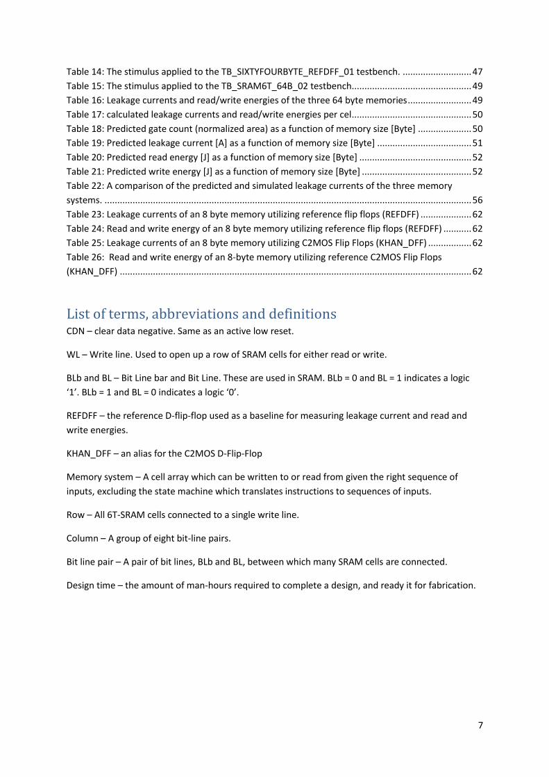
List of Figures Figure 1: A standard 6T SRAM cell. ....................................................................................................... 11
Figure 2: An example of degraded logic causing a short circuit current. ............................................. 12
Figure 3: Leakage current through an NMOS transistor (upper) and a PMOS transistor (lower) as a
function of transistor length. [2] ........................................................................................................... 14
Figure 4: Leakage current through an NMOS transistor (upper) and a PMOS transistor (lower) as a
function of transistor width. [2] ............................................................................................................ 15
Figure 5: The SIXTYFOURBYTE_DFF Cell ................................................................................................ 17
Figure 6: A waveform showing a standard read operation in the D-Flip-Flop system ......................... 18
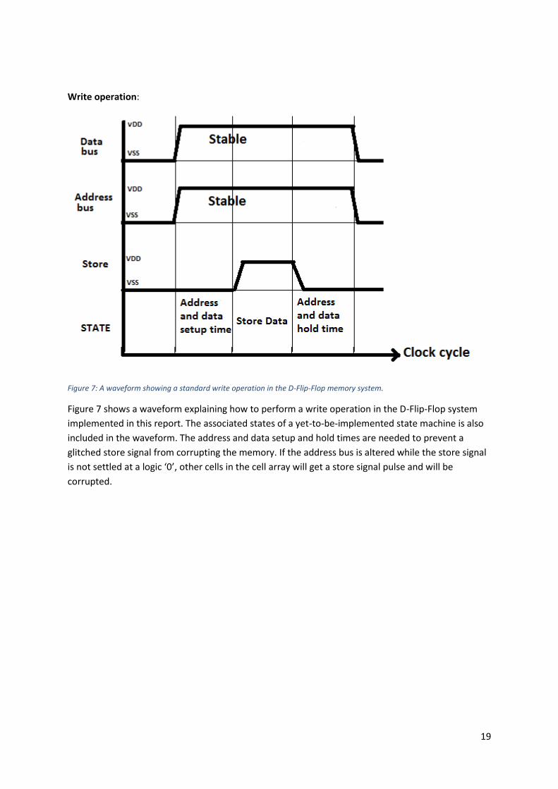
Figure 7: A waveform showing a standard write operation in the D-Flip-Flop memory system.......... 19
Figure 8: The EIGHTBYTE_DFF cell. ....................................................................................................... 20
Figure 9: The BYTE_DFF cell. ................................................................................................................. 21
Figure 10: The C2MOS Flip Flop (D_FLIP_FLOP_KHAN_01 / KHAN_DFF). ............................................ 22
Figure 11: The SRAM6T_64B_02 cell .................................................................................................... 23
Figure 12: A waveform showing a standard read operation in the 6T-SRAM memory system ........... 25
Figure 13: A waveform showing a standard write operation in the 6T-SRAM memory system. ......... 26
Figure 14: The 8x8bitBox_01 cell .......................................................................................................... 27
Figure 15: The 8x8bitBox_Left_01 cell. ................................................................................................. 28
Figure 16: The 8x8bitBox_top_02 cell. ................................................................................................. 29
Figure 17: The 8x8bitBox_topleft_02 cell. ............................................................................................ 30
Figure 18: The Row_WLDriver_01 cell used in the 6T-SRAM system ................................................... 31

6
Figure 19: The Column_Circuitry_04 cell, or bit line pair driver. .......................................................... 32
Figure 20: The sense amplifier used in the SRAM system. ................................................................... 33
Figure 21: The 6T SRAM cell. ................................................................................................................. 34
Figure 22:The testbench for measuring the average leakage current of standard cells ...................... 37
Figure 23: The testbench used to measure average leakage currents in the cells which make up the
peripheral circuitry. ............................................................................................................................... 38
Figure 24: A simplified solution of the sum of a geometric row 2N-1 .................................................... 40
Figure 25: The DEMUX-1-2_02 cell. ...................................................................................................... 41
Figure 26: The DEMUX-1-4_01 cell. ...................................................................................................... 42
Figure 27: The DEMUX-1-8_02 Cell. ...................................................................................................... 43
Figure 28: The MUX_8-1_02 cell ........................................................................................................... 44
Figure 29: An example showing the calculation of the energy spent during a D-Flip-Flop system write
operation............................................................................................................................................... 45
Figure 30: The TB_SIXTYFOURBYTE_REFDFF_01 testbench for the 64 Byte D-Flip-Flop memory
system. .................................................................................................................................................. 47
Figure 31: The TB_SRAM6T_64B_02 testbench for the SRAM system. ................................................ 48
Figure 32: Predicted gate count (normalized area) as a function of memory size [Byte] .................... 50
Figure 33: Predicted leakage current as a function of memory size [Byte] .......................................... 51
Figure 34: Predicted read energy as a function of memory size [Byte] ................................................ 51
Figure 35: Predicted write energy as a function of memory size [Byte]............................................... 52
Figure 36: An alternative sense amplifier presented in [12] ................................................................ 53
Figure 37: The TB_SIXTYFOURBYTE_REFDFF_01_STIM cell .................................................................. 63
Figure 38: The TB_SIXTYFOURBYTE_REFDFF_01_MEASURE cell .......................................................... 63
Figure 39: The TB_SRAM6T_64B_02_STIM cell. ................................................................................... 64
Figure 40: The TB_SRAM6T_64B_02_MEASURE cell ............................................................................ 65
Figure 41: A byte containing 0xFF is being read in the REFDFF system ................................................ 75
Figure 42: A byte containing 0xFF being read in the 6T-SRAM system ............................................... 75
List of tables Table 1: D-Flip-Flop truth table ............................................................................................................. 11
Table 2: Instructions decoded from the read|write codeword. ........................................................... 24
Table 3: The truth table for the Row_WLDriver_01 cell. ...................................................................... 31
Table 4:The truth table for the Column_Circuitry_04 cell. ................................................................... 33
Table 5: Transistor sizes for the 6T SRAM cell ...................................................................................... 35
Table 6: Simulated leakage currents of various TSMC standard cells and the gate counts as specified
in the TSMC standard cell datasheet .................................................................................................... 38
Table 7: A table of calculated gate counts and leakage currents of non-standard cells ...................... 39
Table 8: The formulas for calculating the number of cells contained within either a D-flip-flop
memory system or a 6T-SRAM memory system. .................................................................................. 41
Table 9: The truth table for the DEMUX-1-2_02 cell ............................................................................ 42
Table 10: The corresponding truth table for the DEMUX-1-4_01 cell. ................................................. 42
Table 11: The truth table corresponding to the DEMUX_1-8_02 cell. ................................................. 44
Table 12: The truth table corresponding to the MUX_8-1_02 cell ....................................................... 44
Table 13: The non-default simulator settings used in all simulations. ................................................. 44
7
Table 14: The stimulus applied to the TB_SIXTYFOURBYTE_REFDFF_01 testbench. ........................... 47
Table 15: The stimulus applied to the TB_SRAM6T_64B_02 testbench. .............................................. 49
Table 16: Leakage currents and read/write energies of the three 64 byte memories ......................... 49
Table 17: calculated leakage currents and read/write energies per cel ............................................... 50
Table 18: Predicted gate count (normalized area) as a function of memory size [Byte] ..................... 50
Table 19: Predicted leakage current [A] as a function of memory size [Byte] ..................................... 51
Table 20: Predicted read energy [J] as a function of memory size [Byte] ............................................ 52
Table 21: Predicted write energy [J] as a function of memory size [Byte] ........................................... 52
Table 22: A comparison of the predicted and simulated leakage currents of the three memory
systems. ................................................................................................................................................ 56
Table 23: Leakage currents of an 8 byte memory utilizing reference flip flops (REFDFF) .................... 62
Table 24: Read and write energy of an 8 byte memory utilizing reference flip flops (REFDFF) ........... 62
Table 25: Leakage currents of an 8 byte memory utilizing C2MOS Flip Flops (KHAN_DFF) ................. 62
Table 26: Read and write energy of an 8-byte memory utilizing reference C2MOS Flip Flops
(KHAN_DFF) .......................................................................................................................................... 62
List of terms, abbreviations and definitions CDN – clear data negative. Same as an active low reset.
WL – Write line. Used to open up a row of SRAM cells for either read or write.
BLb and BL – Bit Line bar and Bit Line. These are used in SRAM. BLb = 0 and BL = 1 indicates a logic
‘1’. BLb = 1 and BL = 0 indicates a logic ‘0’.
REFDFF – the reference D-flip-flop used as a baseline for measuring leakage current and read and
write energies.
KHAN_DFF – an alias for the C2MOS D-Flip-Flop
Memory system – A cell array which can be written to or read from given the right sequence of
inputs, excluding the state machine which translates instructions to sequences of inputs.
Row – All 6T-SRAM cells connected to a single write line.
Column – A group of eight bit-line pairs.
Bit line pair – A pair of bit lines, BLb and BL, between which many SRAM cells are connected.
Design time – the amount of man-hours required to complete a design, and ready it for fabrication.

8
1. Preface This master’s dissertation is written for the Norwegian University of Science and Technology
(NTNU) and Disruptive Technologies AS. Disruptive Technologies is a newly-started company that
specializes in designing microchips for use in the Internet of Things industry.
The work presented in this report was done in cooperation with Disruptive Technologies, and the
memory system designs were designed to be compatible with the company’s choice of technology
and design conventions.
The main supervisor was Snorre Aunet (NTNU) <[email protected]>, and the main company
contact was Bjørnar Hernes (Disruptive Technologies) <[email protected]>.
The following sections are adapted from [1], a work by the same author: Section 3, 4.1, 4.2 and 4.3.
The previous report might be requested by emailing the author at [email protected].
2. Acknowledgement I would like to thank Bjørnar Hernes for being of great assistance in teaching me valuable lessons
about the workings of the microchip industry, for helping me learn how to master the Cadence
analog design suite, and for helping me proofread and tailor the implementation chapter of this
dissertation.
I would further like to thank Snorre Aunet for proofreading the dissertation on such a short notice.
I would like to criticize Imran Ahmed Khan and Mirza Tariq Beg, the authors of [8], whose seemingly
erroneous schematic cost me over 4 days of design time during the development phase.
3. Introduction The Internet of Things (IoT) is a concept which is quickly gaining popularity and this causes the IC
industry to gear towards designing microchips that are compatible with this concept. According to
advocates of the Internet of Things concept [2], almost every physical object in use by people will
eventually be connected to the internet. Microchips are designed to fit into even the most trivial
applications such as clothes hangers. Sensor networks are created by spreading out a large amount
of inexpensive sensors and having them communicate over the internet. In these cases, a change of
batteries is impractical and therefore one must design to maximize the battery lifetime of the chip.
In most applications in the Internet of Things, the chip is only active and computing/transmitting
data a fraction of the time. This means the static power consumption (power leakage) will be the
deciding factor in battery lifetime.
All IoT-chips will require some form of data storage. This report assumes a distributed shared
memory (DSM), and that the memory is implemented as a single centralized memory cell array.
Memory accesses only happen when a chip is either computing or transmitting data, and because
these actions are infrequent, memory accesses are also infrequent. Combined with the fact that the
memory portion of a chip often makes up a large portion of the total chip area, this means that
minimizing the power leakage of the memory is essential to reducing the static power consumption
of the entire chip.

9
In previous works, reducing power consumption meant reducing the active power consumption.
Active power is the power required to switch transistors on and off. As stated, the leakage power of
the design is much more of a concern in IoT-chips than other chips. Instead of designing for speed,
area, or active power consumption, this report focuses primarily on the static power consumption of
memory circuits.
4. Theoretical background
4.1 Previous work Previous work in minimizing power in memory circuits focus mostly on Active power consumption,
while not considering static power consumption.
The work put into improving D-Flip-Flop systems mostly focus on the flip flop cell itself, as D-Flip-
Flops are rarely used to build memory arrays larger than 128 bytes. [3] introduces a D-Flip-Flop
design built on C2MOS (C2MOS) latch design principles, and utilizes a sense amplifier in its design to
achieve lower static and dynamic power consumption. The leakage current of the D-Flip-Flop is
inferred to be 188pA at a supply voltage of 1.8V.
Some effort has been spent on improving the energy efficiency of SRAM circuits. [4] tries to
minimize read and write power in the SRAM by splitting up bit line pairs into several sub-bit-line-
pairs, which includes a local sense amplifier. [5] Uses the same approach of splitting up the SRAM
into smaller nodes, but instead focuses on splitting up the SRAM into a binary tree structure. The
two solutions have something in common: They both trade area for lower read and write power, and
a larger area usually leads to a larger leakage current.
[1] is an unpublished work by the same author as this report. The previous report explores the
viability of several types of memory in the context of designing a low leakage, low power memory
system. The previous report also considers the limitations of designing a circuit for fabrication using
a basic CMOS technology. Parts of the work presented in this report builds on the findings of the
previous report. The previous report might be requested by emailing the author at
4.2 Leakage / Static energy consumption In CMOS technologies using a technology node of 90nm and larger, the most dominant source of
static power is the subthreshold leakage power, Psub_leak. For a single-Vdd-level circuit this is given as:
𝑃𝑠𝑢𝑏_𝑙𝑒𝑎𝑘 = 𝑉𝐷𝐷 ∗ 𝐼𝑠𝑢𝑏_𝑙𝑒𝑎𝑘 = 𝑉𝐷𝐷 2
𝑅𝑉𝑑𝑑−𝑔𝑛𝑑
Formula 1: Leakage power as a function of leakage current and supply voltage
Where Isub_leak is the current going from VDD to ground, through the drain-source subthreshold
channel of the transistors. RVdd-gnd is the equivalent resistance seen from VDD to ground.
According to [14], the subthreshold leakage current through a single transistor can be approximated
by the following function:

10
𝐼𝐷𝑆,𝑜𝑓𝑓[nA] = 100 ∗𝑊
𝐿∗ 10−
𝑉𝑡𝑆
Formula 2: A function approximating the leakage current through a transistor
Where W is the gate width, L is the gate length, Vt is the threshold voltage. S is the so-called
subthreshold swing, given by:
𝑆 = 𝜂 ∗ 60mV ∗𝑇
100
Formula 3: The formula for subthreshold swing
Where T is the temperature [K], and 𝜂 is equal to:
𝜂 = 1 +𝐶𝑑𝑒𝑝
𝐶𝑜𝑥𝑒 [4]
Formula 4: The formula for 𝜂
Where Cdep is the channel-depletion capacitance and Coxe is the channel-oxide capacitance.
4.3 Memory Cells
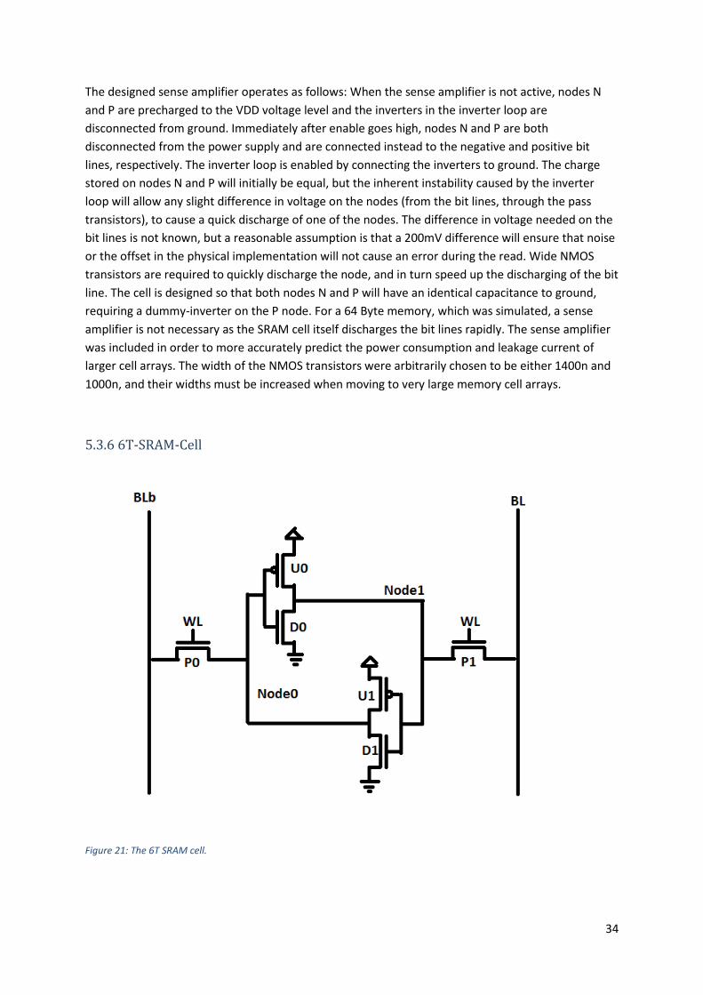
4.3.1 6T SRAM cell
A 6T-SRAM cell retains its data by having two inverters connected in a feedback loop. The first
inverter inverts the input given from the second inverter, and sends that output to the input of the
second inverter, which in turn inverts and sends back to the first inverter. This means the voltage
from either VDD or GND from the output of the first inverter reinforces the charge on the input of
the second inverter, and vice versa. This mutual reinforcement of charges on the gates of the
transistors in each inverter is what retains the data.
To write to the SRAM, the charges stored on either side of the inverter loop must be forced to the
desired value. To do this, the two bit lines are forced to the desired voltage, one will be VDD and one
will be GND. The word line transistors are then opened. This will draw the charges out of the inverter
loop and force the loop to store the new value instead.
The simplest way to read from an SRAM cell is simply to open the word line pass transistors and read
the voltages on the bit lines. The bit lines have a large parasitic capacitance and will take some time
to charge. Using a sense amplifier to quickly sense the difference in voltage on the bit lines will help
solve this problem.
11
Figure 1: A standard 6T SRAM cell.
4.3.2 D-Flip-flop
A positive-edge-triggered D flip flop stores the value D only when the signal Clk transitions from low
to high, a so called rising edge.
Clk D Qnext
Rising edge 0 0
Rising edge 1 1
Non-rising X Qprev Table 1: D-Flip-Flop truth table
4.4 TSMC standard cell library naming conventions The standard cell library provided by TSMC for the TSMC18G process contains cells which follow a
naming convention in the following format: |NAME|Y|D|x|. NAME is the abbreviated name of the
cell. Y is the amount of inputs, and is only included if the cell has multiple versions with different
amounts of inputs. D means drive strength, and x is an integer denoting the drive strength of the
cell, and ranges from 0 to 10. Drive strength is explained in section 4.5. An example of this naming
convention is the cell ND4D2, which is a 4-input NAND gate with a drive strength of 2.
4.5 Drive strength Drive strength is how easily a transistor allows current to pass through itself when switched on. A
large drive strength is required to charge nodes with a high capacitance. If an output-driving
transistor has an insufficiently large drive strength, the time required to charge the output
capacitance will increase. This will severely affect the speed of the circuit. The drive strength of a
transistor is closely related to the W/L ratio of the transistor; a higher W/L ratio produces a higher
drive strength.
12
Cells with a high drive strength often have a high input capacitance, making it necessary for the cell
driving the high-drive strength cell to have a sufficient drive strength itself. A rule of thumb used in
the design presented in this report is that a cell with a drive strength of N (see section 4.5) can drive
a load of cells totalling a drive strength of N+2. A load of 2 cells of drive strength N is assumed to
equal a load of a single cell of strength N+1. As an example, a cell with a drive strength 2 can drive
one cell with a drive strength of 4, or 2 cells of drive strength of 3.
4.6 Cadence Bus Notation For the Cadence Virtuoso software, a specific notation is used to denote either a collection of signals
or cells, and if the same notation is used for both the signals and cells, the collection of signals will
correspond to the collection of cells. The following is an example of the usage of bus notation: A
denotation of Bus<3:0> will contain the signals Bus<3>, Bus<2>, Bus<1> and Bus<0>. Connecting the
node Bus<3:0> to a single-input, single-output cell called Inverter<3:0> will cause Bus<3> to connect
to Inverter<3>, Bus<2> to Inverter<2> and so on.
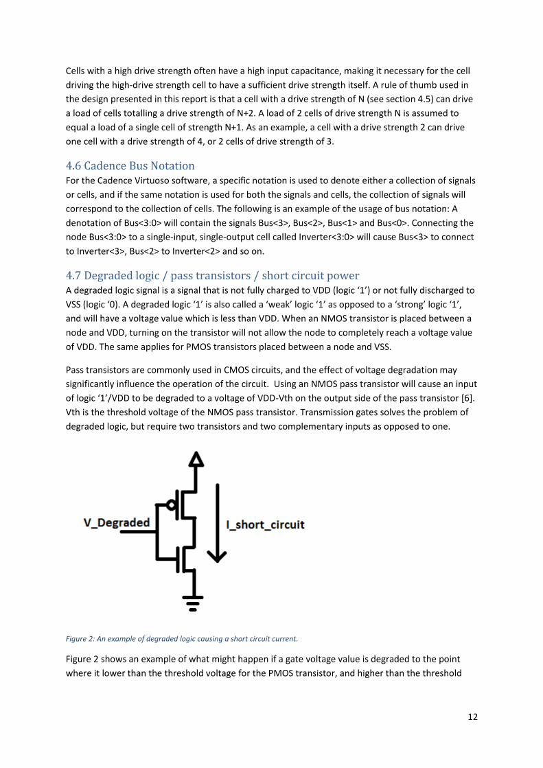
4.7 Degraded logic / pass transistors / short circuit power A degraded logic signal is a signal that is not fully charged to VDD (logic ‘1’) or not fully discharged to
VSS (logic ‘0). A degraded logic ‘1’ is also called a ‘weak’ logic ‘1’ as opposed to a ‘strong’ logic ‘1’,
and will have a voltage value which is less than VDD. When an NMOS transistor is placed between a
node and VDD, turning on the transistor will not allow the node to completely reach a voltage value
of VDD. The same applies for PMOS transistors placed between a node and VSS.
Pass transistors are commonly used in CMOS circuits, and the effect of voltage degradation may
significantly influence the operation of the circuit. Using an NMOS pass transistor will cause an input
of logic ‘1’/VDD to be degraded to a voltage of VDD-Vth on the output side of the pass transistor [6].
Vth is the threshold voltage of the NMOS pass transistor. Transmission gates solves the problem of
degraded logic, but require two transistors and two complementary inputs as opposed to one.
Figure 2: An example of degraded logic causing a short circuit current.
Figure 2 shows an example of what might happen if a gate voltage value is degraded to the point
where it lower than the threshold voltage for the PMOS transistor, and higher than the threshold

13
voltage for an NMOS transistor. The resulting current through both transistors will incur a very large
short circuit power consumption and might overheat the circuit, permanently damaging it.
5. Implementation Three different memory systems were implemented. Two versions of a D-Flip-Flop memory system
were implemented, utilizing two different D-Flip-Flops. A 6T-SRAM system was also implemented,
with the intention of comparing memory systems using D-flip-flops to systems using SRAM with
focus on leakage current, power consumption and area. The size of the designed memory systems
were 64 Bytes. The reason for this was that the simulations were done on servers owned by Cadence
Design Systems, rented by Disruptive Technologies, and simulation time was limited. To mitigate the
small size of the memory systems, a prediction formula was implemented in Microsoft Excel with the
purpose of extrapolating the leakage currents, area and read and write energies for larger memory
systems.
The cell names are sometimes misleading, as they are temporary names used in the design phase.
The reason behind this is to allow Disruptive Technologies to continue using the designs if need be.
To mitigate this, cells often go by multiple names in the report, and often both names are stated.
5.1 Design specifications A number of design goals are considered when designing the memory systems. The following list
contains design requirements by order of importance, 1 being the most important consideration:
1) Minimize leakage current
2) Minimize read energy
3) Minimize write energy
4) Minimize chip area
5) Minimize design complexity
Minimizing the leakage current is the most important consideration, as the memory most likely be
idle most of the time. Reads are assumed to be more frequent than writes, and it is therefore more
important to minimize read energy than to minimize write energy. Minimizing chip area is always an
important consideration to minimize chip costs. Lastly, because the design is handed over to another
designer, the complexity of the design should be minimized to allow a quick transfer of knowledge
from designer to designer.
5.1.1 Process / technology
The purpose of the design is to be implemented using a 0.18µm standard CMOS technology from the
Taiwan Semiconductor Manufacturing Company. The process name is TSMC18G.

14
5.1.2 Choice of default and minimum transistor sizes
Figure 3: Leakage current through an NMOS transistor (upper) and a PMOS transistor (lower) as a function of transistor length. [2]
Figure 3 shows the simulation results of leakage current through a NMOS and PMOS transistor as a
function of transistor length. The simulations were done by applying a voltage across the transistor
while the transistor was turned off (VG = VSS for the NMOS, VG = VDD for the PMOS). The following
simulation parameters were used:
- Process: TSMC018
- gmin=1e-17
- L=0.35µm - W=0.5µm - Temp=27oC - VDS=2.5V - Transistor type: 3.3V.
The results imply that a length of 550nm will minimize the leakage current through an NMOS
transistor. Using the same length for PMOS transistors will simplify the layout of the chip, saving
area. Many equations in the VLSI domain contain terms in this format:
𝑊0𝐿0
𝑊1𝐿1
. Choosing a standard
length would greatly simplify these equations, reducing design time. During the layout phase, in
CMOS structures such as the basic inverter, the PMOS transistors are usually laid out in parallel
lengthwise with the NMOS transistors [7]. Choosing different lengths would make the parallel PMOS
and NMOS transistors not align with each other, complicating the layout engineer’s job, increasing
design time. Choosing the length of the PMOS to be longer would further limit leakage current, but
would increase the area of the circuit considerably and would drastically increase design time. This
lead to 550nm being chosen as the default length for all transistors in the design.

15
Figure 4: Leakage current through an NMOS transistor (upper) and a PMOS transistor (lower) as a function of transistor width. [2]
Figure 4 shows the simulation results of leakage current through an NMOS and PMOS transistor as a
function of transistor width. The simulations were done by applying a voltage across the transistor
while the transistor was turned off (Vg = VSS for the NMOS, Vg = VDD for the PMOS). The following
simulation parameters were used:
- Process: TSMC018
- gmin=1e-17
- L=0.35µ - W=0.5µ - Temp=27oC - VDS=2.5V - Transistor type: 3.3V.
One can see that a larger width leads to a larger leakage current. Choosing a width as low as possible
would minimize leakage current. However, choosing a width that is too close to the absolute
minimum leads to greater susceptibility to fabrication errors (larger transistors leave much more
room for error). If the design is very susceptible to fabrication errors, a larger amount of the finished
microchips will not pass the physical verification process and the fabrication yield will decrease,
increasing the cost of the chip. A minimum width of 300nm was chosen.
The simulations in figure 3 and 4 were provided by Disruptive Technologies.
5.2 The D-Flip-Flop memory system The D-Flip-Flop memory system was implemented utilizing two different D-flip-flop cells. The first
was the reference D-Flip-Flop, the second was the C2MOS Flip-Flop.

16
As opposed to SRAM, a D-Flip-Flop memory has no internal multiplexing (bit lines and write lines).
This means that the fan-out of demultiplexers and multiplexers is much broader than for the SRAM
system. This also means that the peripheral circuitry of the D-Flip-Flop is simpler.

17
Figure 5: The SIXTYFOURBYTE_DFF Cell

18
Figure 5 shows a completed 64 Byte D-Flip-Flop memory system, the same as the one used in the
simulations presented in this report. The address bus is buffered as there are 8 8-1 demultiplexers
connected to each wire on the bus (see figure 8), and that presents a significant load capacitance.
The SIXTYFOURBYTE_DFF cell is made up of 8 EIGHTBYTE_DFF cells, which are explained in detail in
section 5.2.2.
In the design, each flip-flop has its own set of peripheral circuitry cells. The peripheral circuitry used
by one flip-flop cell is copied and the duplicated version is used when testing the other flip-flop cell.
The peripheral circuitry cells are named with either the keyword ‘KHAN’ for the C2MOS flip flop, or
‘REFDFF’ for the reference D-Flip-Flop. The reason for copying the peripheral circuitry is to allow two
separate testbenches for every cell, as well as to allow changes to the peripheral circuitry for each
separate flip flop. As per this report, the peripheral circuits of the two flip flops are identical.
5.2.1 Read and write operations
Input signal descriptions:
- Store: A positive flank of the store signal will perform a write of the specified value decided
by the Data bus in the flip flop decided by the address bus.
- Address: A binary number which decides which byte in the memory to read from or write to.
- Data: An 8bit/1byte binary number, which is stored in the memory if the ‘store’ signal goes
high.
- CDN: Clear Data Negative. When CDN is low, all flip flops in the memory are reset to a value
of ‘0’.
Read operation:
Figure 6: A waveform showing a standard read operation in the D-Flip-Flop system
Figure 6 shows a waveform explaining how to perform a read operation in the D-Flip-Flop system
implemented in this report. The associated states of a yet-to-be-implemented state machine is also
included in the waveform. The address setup and hold times are needed to. If the address bus is
altered while the output is being latched onto the data bus, the latched data will be corrupted.
19
Write operation:
Figure 7: A waveform showing a standard write operation in the D-Flip-Flop memory system.
Figure 7 shows a waveform explaining how to perform a write operation in the D-Flip-Flop system
implemented in this report. The associated states of a yet-to-be-implemented state machine is also
included in the waveform. The address and data setup and hold times are needed to prevent a
glitched store signal from corrupting the memory. If the address bus is altered while the store signal
is not settled at a logic ‘0’, other cells in the cell array will get a store signal pulse and will be
corrupted.

20
5.2.2 Sub-Cells
Figure 8: The EIGHTBYTE_DFF cell.
21
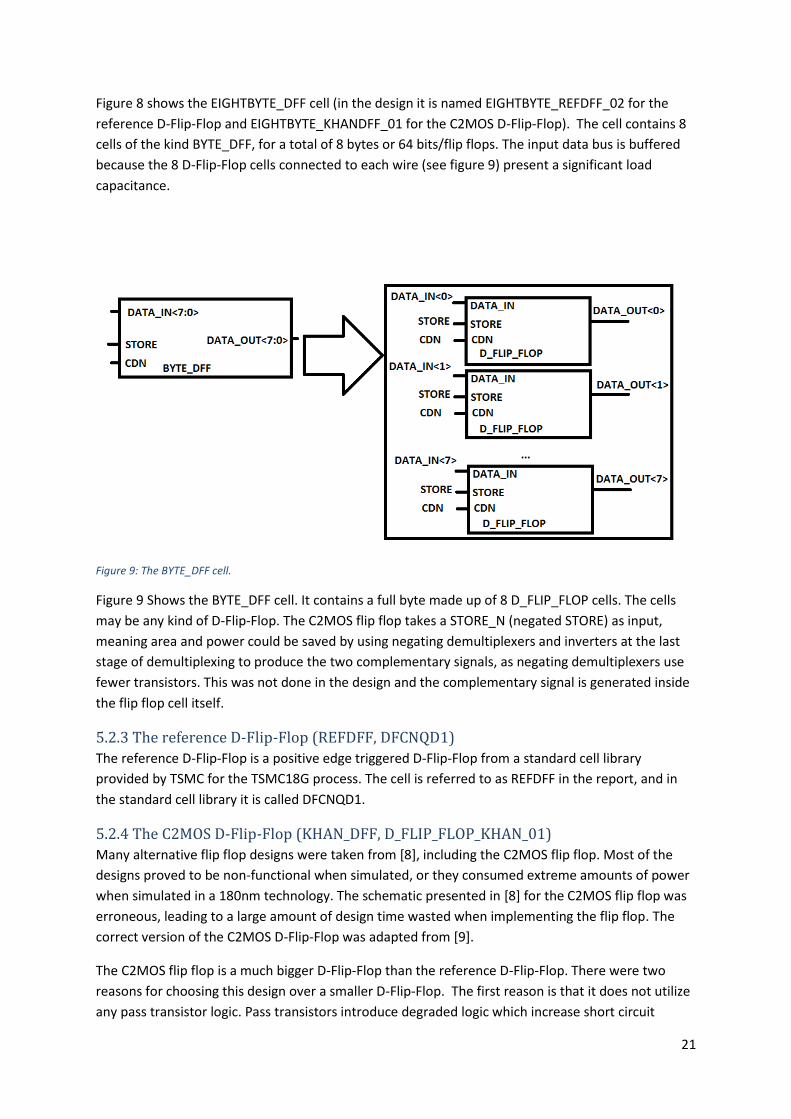
Figure 8 shows the EIGHTBYTE_DFF cell (in the design it is named EIGHTBYTE_REFDFF_02 for the
reference D-Flip-Flop and EIGHTBYTE_KHANDFF_01 for the C2MOS D-Flip-Flop). The cell contains 8
cells of the kind BYTE_DFF, for a total of 8 bytes or 64 bits/flip flops. The input data bus is buffered
because the 8 D-Flip-Flop cells connected to each wire (see figure 9) present a significant load
capacitance.
Figure 9: The BYTE_DFF cell.
Figure 9 Shows the BYTE_DFF cell. It contains a full byte made up of 8 D_FLIP_FLOP cells. The cells
may be any kind of D-Flip-Flop. The C2MOS flip flop takes a STORE_N (negated STORE) as input,
meaning area and power could be saved by using negating demultiplexers and inverters at the last
stage of demultiplexing to produce the two complementary signals, as negating demultiplexers use
fewer transistors. This was not done in the design and the complementary signal is generated inside
the flip flop cell itself.
5.2.3 The reference D-Flip-Flop (REFDFF, DFCNQD1)
The reference D-Flip-Flop is a positive edge triggered D-Flip-Flop from a standard cell library
provided by TSMC for the TSMC18G process. The cell is referred to as REFDFF in the report, and in
the standard cell library it is called DFCNQD1.
5.2.4 The C2MOS D-Flip-Flop (KHAN_DFF, D_FLIP_FLOP_KHAN_01)
Many alternative flip flop designs were taken from [8], including the C2MOS flip flop. Most of the
designs proved to be non-functional when simulated, or they consumed extreme amounts of power
when simulated in a 180nm technology. The schematic presented in [8] for the C2MOS flip flop was
erroneous, leading to a large amount of design time wasted when implementing the flip flop. The
correct version of the C2MOS D-Flip-Flop was adapted from [9].
The C2MOS flip flop is a much bigger D-Flip-Flop than the reference D-Flip-Flop. There were two
reasons for choosing this design over a smaller D-Flip-Flop. The first reason is that it does not utilize
any pass transistor logic. Pass transistors introduce degraded logic which increase short circuit

22
power (see section 4.7). The second reason is the fact that the paths from VDD to GND in the cell
often have a lot of transistors in series, increasing the effective length of transistors from VDD to
GND, reducing leakage currents. The cell is referred to as either C2MOS or KHAN_DFF in the report,
and in the design it is named D_FLIP_FLOP_KHAN_01.
Figure 10: The C2MOS Flip Flop (D_FLIP_FLOP_KHAN_01 / KHAN_DFF).
5.2.4.1 Transistor sizing
In this section, please refer to figure 10. The lengths of all the transistors are 550nm. This is chosen
because of the results presented in figure 3. The widths of all the transistors are 550nm, with the
exception of the PMOS transistors whose gate is connected to CDN. The width of all the non-reset
(CDN) transistors are set to a width of 550nm. The widths of the reset (CDN) PMOS transistors are
set to 800nm, simply to have a greater drive strength than the inverters driving the inner nodes D
and QN.
The reason behind the seemingly arbitrary choice of widths for the KHAN_DFF is the disruption of
the design phase caused by errors in [8], as explained in section 5.2.4.
5.3 The 6T-SRAM memory system The 6T-SRAM memory system requires an entirely different peripheral circuit. The functionality of
the 6T-SRAM is very different from a D-Flip-Flop, for more information, please see section 4.3.1.
23
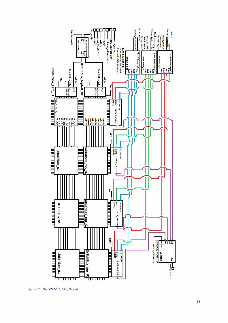
Figure 11: The SRAM6T_64B_02 cell
24
Figure 11 shows a fully built 64 Byte 6T-SRAM memory system. This 64-Byte system is the same as
the one simulated in this report. All versions of the 8x8bitBox cell contain 8 rows and 8 bit-line pairs,
for a total of 64 bits, or 8 bytes each. Scaling up further would simply mean adding more 8x8bitBox
cells (and the appropriate border versions of the 8xbitBox cell) and adding the necessary
demultiplexers, multiplexers and buffers. If one were to add two more rows of 8x8bitBox_01 (and
the appropriate border versions of the 8x8bitBox cell), a full 32x32bitBox chunk would be
completed, containing a total of 128 Bytes. The 8x8bitBox_01 cells are explained in section 5.3.2.
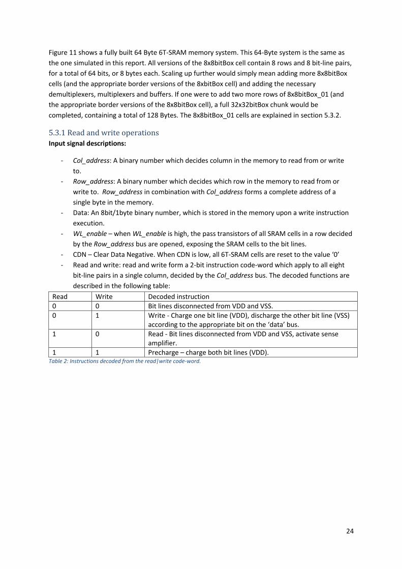
5.3.1 Read and write operations
Input signal descriptions:
- Col_address: A binary number which decides column in the memory to read from or write
to.
- Row_address: A binary number which decides which row in the memory to read from or
write to. Row_address in combination with Col_address forms a complete address of a
single byte in the memory.
- Data: An 8bit/1byte binary number, which is stored in the memory upon a write instruction
execution.
- WL_enable – when WL_enable is high, the pass transistors of all SRAM cells in a row decided
by the Row_address bus are opened, exposing the SRAM cells to the bit lines.
- CDN – Clear Data Negative. When CDN is low, all 6T-SRAM cells are reset to the value ‘0’
- Read and write: read and write form a 2-bit instruction code-word which apply to all eight
bit-line pairs in a single column, decided by the Col_address bus. The decoded functions are
described in the following table:
Read Write Decoded instruction
0 0 Bit lines disconnected from VDD and VSS.
0 1 Write - Charge one bit line (VDD), discharge the other bit line (VSS) according to the appropriate bit on the ‘data’ bus.
1 0 Read - Bit lines disconnected from VDD and VSS, activate sense amplifier.
1 1 Precharge – charge both bit lines (VDD). Table 2: Instructions decoded from the read|write code-word.

25
Read operation:
Figure 12: A waveform showing a standard read operation in the 6T-SRAM memory system
Figure 12 shows a waveform explaining how to perform a read operation in the 6T-SRAM system
implemented in this report. The associated states of a yet-to-be-implemented state machine is also
included in the waveform. The address setup time is needed to prevent non-intended bit line pairs
from being charged when the precharge happens. The address and sense hold time is needed to
prevent the data from being corrupted while it is being latched onto the output bus.
26
Write operation:
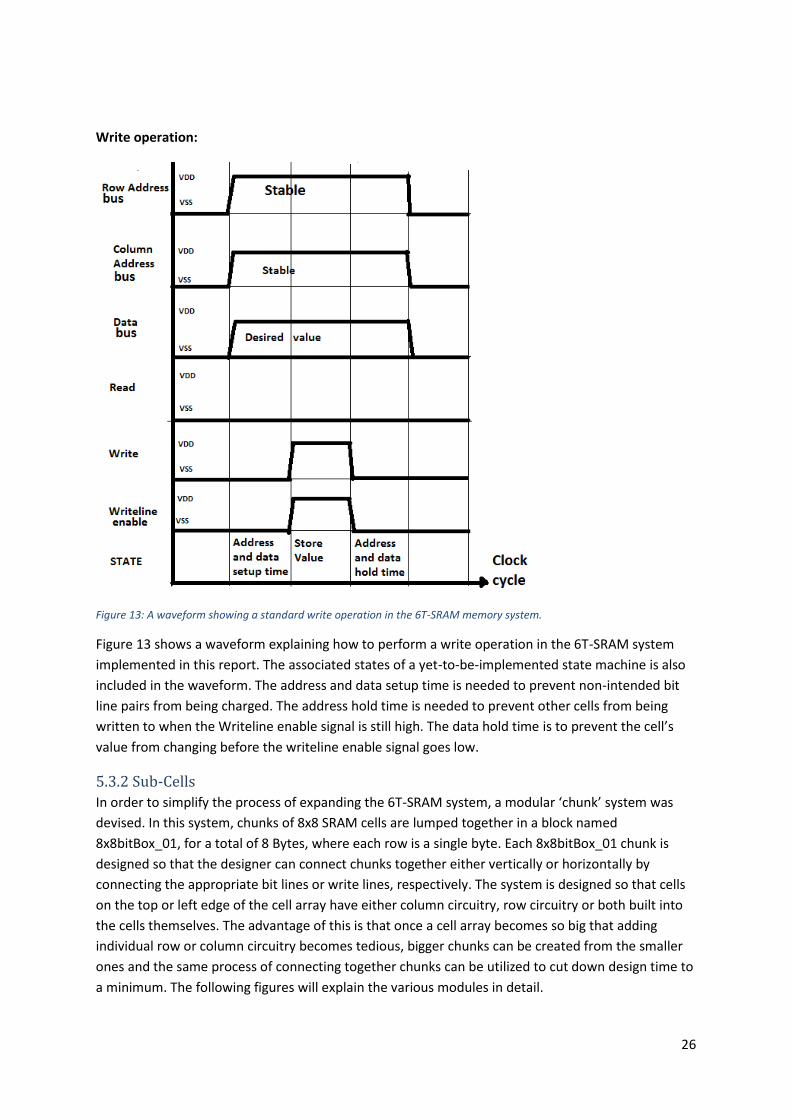
Figure 13: A waveform showing a standard write operation in the 6T-SRAM memory system.
Figure 13 shows a waveform explaining how to perform a write operation in the 6T-SRAM system
implemented in this report. The associated states of a yet-to-be-implemented state machine is also
included in the waveform. The address and data setup time is needed to prevent non-intended bit
line pairs from being charged. The address hold time is needed to prevent other cells from being
written to when the Writeline enable signal is still high. The data hold time is to prevent the cell’s
value from changing before the writeline enable signal goes low.
5.3.2 Sub-Cells
In order to simplify the process of expanding the 6T-SRAM system, a modular ‘chunk’ system was
devised. In this system, chunks of 8x8 SRAM cells are lumped together in a block named
8x8bitBox_01, for a total of 8 Bytes, where each row is a single byte. Each 8x8bitBox_01 chunk is
designed so that the designer can connect chunks together either vertically or horizontally by
connecting the appropriate bit lines or write lines, respectively. The system is designed so that cells
on the top or left edge of the cell array have either column circuitry, row circuitry or both built into
the cells themselves. The advantage of this is that once a cell array becomes so big that adding
individual row or column circuitry becomes tedious, bigger chunks can be created from the smaller
ones and the same process of connecting together chunks can be utilized to cut down design time to
a minimum. The following figures will explain the various modules in detail.
27
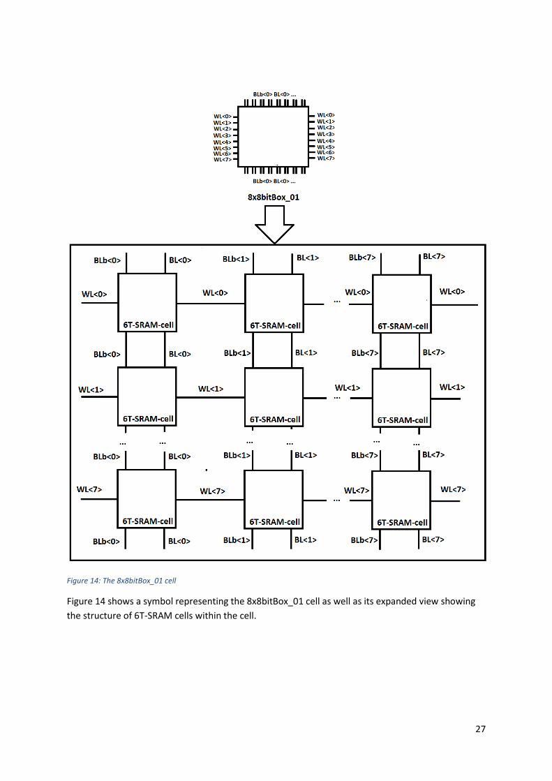
Figure 14: The 8x8bitBox_01 cell
Figure 14 shows a symbol representing the 8x8bitBox_01 cell as well as its expanded view showing
the structure of 6T-SRAM cells within the cell.
28
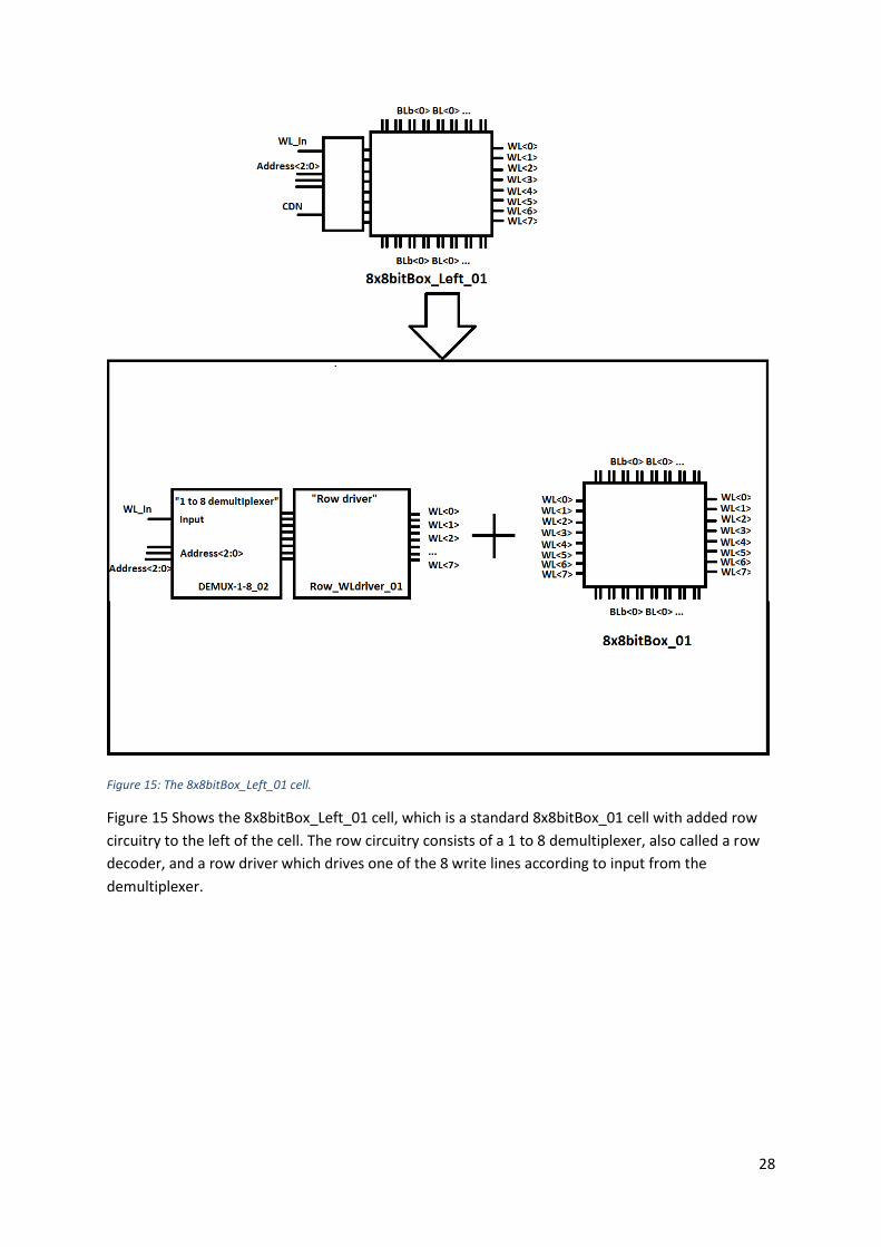
Figure 15: The 8x8bitBox_Left_01 cell.
Figure 15 Shows the 8x8bitBox_Left_01 cell, which is a standard 8x8bitBox_01 cell with added row
circuitry to the left of the cell. The row circuitry consists of a 1 to 8 demultiplexer, also called a row
decoder, and a row driver which drives one of the 8 write lines according to input from the
demultiplexer.

29
Figure 16: The 8x8bitBox_top_02 cell.
Figure 16 shows the 8x8bitBox_Top_01 cell which is a standard 8x8bitBox_Top_01 cell with added
column circuitry for each pair of bit lines. Because a whole row of 8 bits/cells, or a single byte, is
always written or read at the same time, no multiplexing is required in this cell.

30
Figure 17: The 8x8bitBox_topleft_02 cell.
Figure 17 shows the 8x8bitBox_TopLeft_01 cell which is a standard 8x8bitBox_Top_01 cell with both
column circuitry and row circuitry. The necessity of this block comes from the fact that the upper left
corner cell needs both column and row circuitry.
31
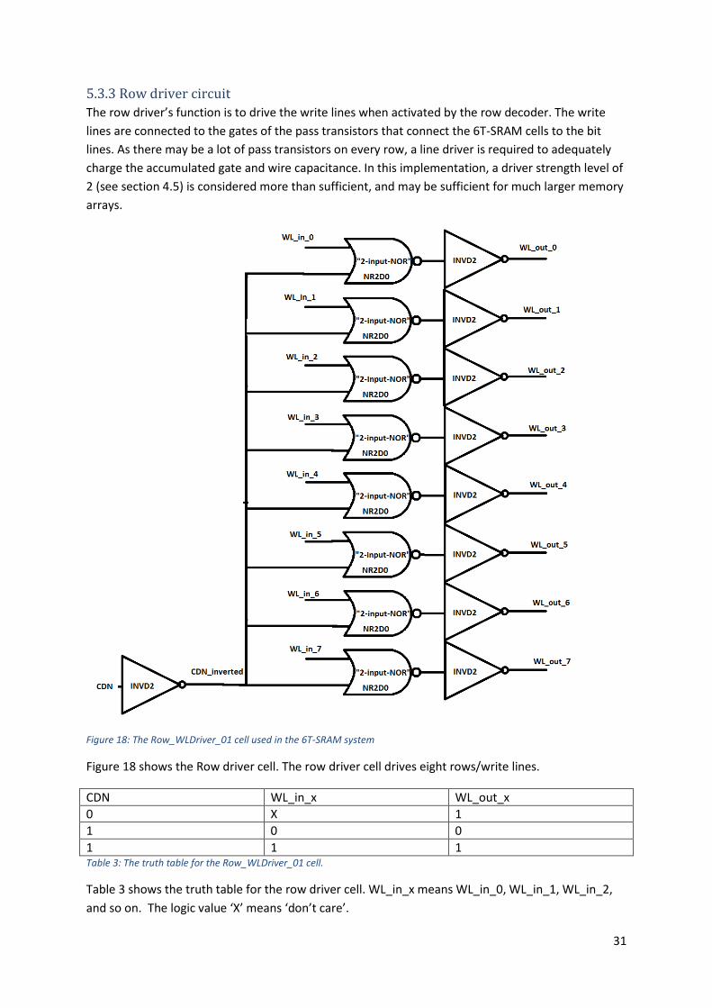
5.3.3 Row driver circuit
The row driver’s function is to drive the write lines when activated by the row decoder. The write
lines are connected to the gates of the pass transistors that connect the 6T-SRAM cells to the bit
lines. As there may be a lot of pass transistors on every row, a line driver is required to adequately
charge the accumulated gate and wire capacitance. In this implementation, a driver strength level of
2 (see section 4.5) is considered more than sufficient, and may be sufficient for much larger memory
arrays.
Figure 18: The Row_WLDriver_01 cell used in the 6T-SRAM system
Figure 18 shows the Row driver cell. The row driver cell drives eight rows/write lines.
CDN WL_in_x WL_out_x
0 X 1
1 0 0
1 1 1 Table 3: The truth table for the Row_WLDriver_01 cell.
Table 3 shows the truth table for the row driver cell. WL_in_x means WL_in_0, WL_in_1, WL_in_2,
and so on. The logic value ‘X’ means ‘don’t care’.
32
5.3.4 Bit line driver circuitry
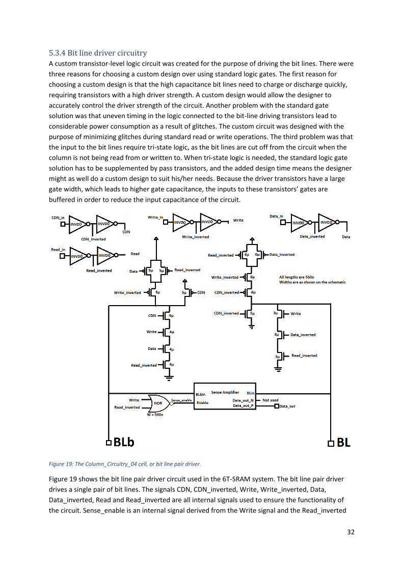
A custom transistor-level logic circuit was created for the purpose of driving the bit lines. There were
three reasons for choosing a custom design over using standard logic gates. The first reason for
choosing a custom design is that the high capacitance bit lines need to charge or discharge quickly,
requiring transistors with a high driver strength. A custom design would allow the designer to
accurately control the driver strength of the circuit. Another problem with the standard gate
solution was that uneven timing in the logic connected to the bit-line driving transistors lead to
considerable power consumption as a result of glitches. The custom circuit was designed with the
purpose of minimizing glitches during standard read or write operations. The third problem was that
the input to the bit lines require tri-state logic, as the bit lines are cut off from the circuit when the
column is not being read from or written to. When tri-state logic is needed, the standard logic gate
solution has to be supplemented by pass transistors, and the added design time means the designer
might as well do a custom design to suit his/her needs. Because the driver transistors have a large
gate width, which leads to higher gate capacitance, the inputs to these transistors’ gates are
buffered in order to reduce the input capacitance of the circuit.
Figure 19: The Column_Circuitry_04 cell, or bit line pair driver.
Figure 19 shows the bit line pair driver circuit used in the 6T-SRAM system. The bit line pair driver
drives a single pair of bit lines. The signals CDN, CDN_inverted, Write, Write_inverted, Data,
Data_inverted, Read and Read_inverted are all internal signals used to ensure the functionality of
the circuit. Sense_enable is an internal signal derived from the Write signal and the Read_inverted
33
signal, and is used to enable the sense amplifier. The Read_in, Write_in and Data_in signals are all
demultiplexed onto the appropriate column, and all bit line pair drivers in one column share the
same signals. Refer to table 4 for the functionality of the circuit.
CDN Read_in Write_in Data_in BLb BL Sense_enable
0 X X X 1 0 X
1 0 0 X Z Z 0
1 0 1 0 1 0 0
1 0 1 1 0 1 0
1 1 0 X Z Z 1
1 1 1 X 1 1 0 Table 4:The truth table for the Column_Circuitry_04 cell.
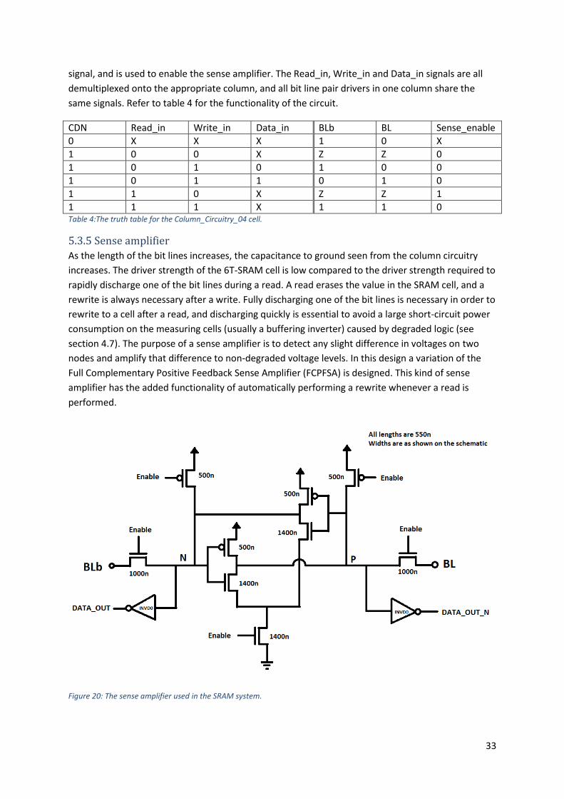
5.3.5 Sense amplifier
As the length of the bit lines increases, the capacitance to ground seen from the column circuitry
increases. The driver strength of the 6T-SRAM cell is low compared to the driver strength required to
rapidly discharge one of the bit lines during a read. A read erases the value in the SRAM cell, and a
rewrite is always necessary after a write. Fully discharging one of the bit lines is necessary in order to
rewrite to a cell after a read, and discharging quickly is essential to avoid a large short-circuit power
consumption on the measuring cells (usually a buffering inverter) caused by degraded logic (see
section 4.7). The purpose of a sense amplifier is to detect any slight difference in voltages on two
nodes and amplify that difference to non-degraded voltage levels. In this design a variation of the
Full Complementary Positive Feedback Sense Amplifier (FCPFSA) is designed. This kind of sense
amplifier has the added functionality of automatically performing a rewrite whenever a read is
performed.
Figure 20: The sense amplifier used in the SRAM system.
34
The designed sense amplifier operates as follows: When the sense amplifier is not active, nodes N
and P are precharged to the VDD voltage level and the inverters in the inverter loop are
disconnected from ground. Immediately after enable goes high, nodes N and P are both
disconnected from the power supply and are connected instead to the negative and positive bit
lines, respectively. The inverter loop is enabled by connecting the inverters to ground. The charge
stored on nodes N and P will initially be equal, but the inherent instability caused by the inverter
loop will allow any slight difference in voltage on the nodes (from the bit lines, through the pass
transistors), to cause a quick discharge of one of the nodes. The difference in voltage needed on the
bit lines is not known, but a reasonable assumption is that a 200mV difference will ensure that noise
or the offset in the physical implementation will not cause an error during the read. Wide NMOS
transistors are required to quickly discharge the node, and in turn speed up the discharging of the bit
line. The cell is designed so that both nodes N and P will have an identical capacitance to ground,
requiring a dummy-inverter on the P node. For a 64 Byte memory, which was simulated, a sense
amplifier is not necessary as the SRAM cell itself discharges the bit lines rapidly. The sense amplifier
was included in order to more accurately predict the power consumption and leakage current of
larger cell arrays. The width of the NMOS transistors were arbitrarily chosen to be either 1400n and
1000n, and their widths must be increased when moving to very large memory cell arrays.
5.3.6 6T-SRAM-Cell
Figure 21: The 6T SRAM cell.
35
5.3.6.1 Transistor sizing
For this section, please see figure 21. The transistor dimensions were chosen as follows: The length
of the NMOS transistors were designed to have a minimum leakage current as decided by the
simulations in section 5.1.2. A length of L = 550nm is chosen for all transistors. As a typical layout of
an SRAM cell is symmetrical, one can reduce the area of each cell by choosing the width and length
of the PMOS transistors to be equal to the length and width of the NMOS transistors (see section
5.1.2). A minimum length of 300nm was chosen.
Read stability: In the case of a read, both bit lines are precharged up to the VDD voltage and
subsequently the pass transistors are opened up to discharge one of the bit lines depending on the
value retained in the cell. In the case of a logic ‘0’ retained, the transistor D0 will discharge the bit
line BL down to ground. When this happens, it is important that the voltage on node1 does not
exceed Vth when current is intermittently flowing through transistors P1 and D0, which could invert
the voltage of node0. Intuitively, this means that transistor D0 should be less resistive than transistor
P1, and enough so that the node1 voltage never exceeds Vth. This means the width of D0 has to be
larger than the width of P1. According to [10], the width of D0 has to be 1.2 times as large as the
width of P1. The same goes for transistors D1 and P0.
Write stability: In the case of a write, the bit lines are forced to either BLb = 0V and BL = VDD or the
opposite, depending on value written. In the case of a logic ‘0’ being stored, BL is pulled low by
external column circuitry and the pass transistors are opened. In this case it is important that the
voltage on node1 never exceeds Vth when current is intermittently flowing through transistors U0
and P1. Intuitively, this means that P1 should be less resistive than U0, and enough so that the
node1 voltage never exceeds Vth. This means that the width of P1 should be larger than the half the
width of U0, owing to the mobility of a PMOS transistor being about half of the mobility of an NMOS
transistor. According to [10], the width of P1 has to be at least larger than 0.56 than that of U0.
Choosing U0 and U1 to be the same size as D0 and D1 meets the requirements of read and write
stability, and simplifies the layout through symmetry (see section 5.1.2).
Transistor name U0 and U1 D0 and D1 P0 and P1
Width [nm] 360 360 300
Length [nm] 550 550 550 Table 5: Transistor sizes for the 6T SRAM cell
5.3.7 Reset circuitry
The reset signal CDN needs only be considered in the peripheral circuitry. To reset the SRAM, WL is
set to 1, BL is set to 0, and BLb is set to 1. Because BL, BLb and WL are shared among a lot of SRAM
cells, the amount of transistors per cell used for resetting the memory is very low. The column reset
circuitry is implemented as a part of the column logic, specifically as part of the bit line pair driver.
The row reset circuitry was implemented as a part of the row driver circuit.
5.4 Extrapolator
5.4.1 The gate count unit of measurement
As per the TSMC datasheet, one gate is equivalent to 4 transistors with a width of 0.85µm and a
length of 300nm, for a total area of 0.68pm2 per gate count. The gate count of custom transistor

36
level designs was decided by dividing the area of the design by this value, and rounding to the
nearest half integer.
𝐺𝑎𝑡𝑒 𝐶𝑜𝑢𝑛𝑡 =𝐶𝑒𝑙𝑙 𝐴𝑟𝑒𝑎 [𝑚2]
0.68 ∗ 10−12 [𝑚2]
Formula 5: The formula for normalizing a cell’s area to the gate count unit of measurement
5.4.2 Predicting the gate count and leakage current of the memory systems
In order to predict the gate count (area) of the peripheral circuitry, various mathematical methods
were used and a few assumptions were made:
1) Beyond 64 Bytes any multiplexing or demultiplexing will be done only with 1-2
demultiplexers or 2-1 multiplexers.
2) The additional wires that are required on the address bus as the memory expands will not be
buffered. This would lead to even more complicated mathematics.
3) Because cells are separated horizontally by a large gate-source and gate-drain impedance
(almost no current passes through the gate of the transistor), total leakage current in a
bigger cell can be modelled as a sum of leakage currents through the smaller cells contained
in the bigger cell.
The leakage currents of bottom-level custom-designed cells were determined by simulating their
total leak in the 64-Byte system and then dividing by the number of custom-designed cells in the 64-
Byte design.
For the C2MOS (KHAN_DFF) D-Flip-Flop, the leakage contribution from the cells have to be
multiplied by 1.54. For details see section 5.6.3 and appendix A.
5.4.3 Predicting the read and write energy of the memory systems
In order to predict the read and write energy of the increasingly complex peripheral circuitry, a
severe simplification is made. It is assumed that the read and write energy consumed by the
peripheral circuitry is proportional to the total gate count of the peripheral circuitry. Then, the
results from the 64Byte simulations could simply be multiplied by the ratio of increase in the gate
count of the peripheral circuitry. Another assumption is that the read and write energy of the cell
array does not increase significantly when the cell array is expanded, as only a single byte of 8 cells is
written to or read from at the same time.
𝐸𝑝𝑟𝑒𝑑𝑖𝑐𝑡𝑒𝑑 = 𝐺𝑎𝑡𝑒 𝑐𝑜𝑢𝑛𝑡𝑝𝑟𝑒𝑑𝑖𝑐𝑡𝑒𝑑,𝑝𝑒𝑟𝑖𝑝ℎ𝑒𝑟𝑎𝑙
𝐺𝑎𝑡𝑒 𝑐𝑜𝑢𝑛𝑡64𝐵𝑦𝑡𝑒,𝑝𝑒𝑟𝑖𝑝ℎ𝑒𝑟𝑎𝑙∗ 𝐸64𝐵𝑦𝑡𝑒,𝑝𝑒𝑟𝑖𝑝ℎ𝑒𝑟𝑎𝑙 + 𝐸64𝐵𝑦𝑡𝑒,𝑐𝑒𝑙𝑙𝑠
Formula 6: Extrapolated read and write energies, based on the 64 Byte simulations.

37
5.4.4 Measuring average leakage current of standard cells
Figure 22:The testbench for measuring the average leakage current of standard cells
In order to measure the average leakage current of several standard cells used in the design of the
peripheral circuits, a simple testbench was designed. In figure 22, the testbench is displayed, and the
cell being measured is the AN4D2 standard cell.
A test stimulus covering all the different combinations of inputs was applied. After applying a certain
combination of inputs, the cell would be left idle for a sufficient amount of time (here: 0.5s) in order
to stabilize the internal voltages of the cell. After stabilizing the cell, the supply current going to the
cell was measured over a short period of time (200ns) and averaged. After measuring the leakage
current of every combination of inputs, the arithmetic mean of all the leakage currents was
calculated. This average leakage current was used as a representative value for the leakage of the
cell.
38
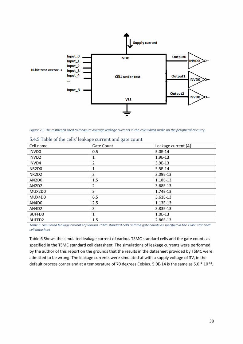
Figure 23: The testbench used to measure average leakage currents in the cells which make up the peripheral circuitry.
5.4.5 Table of the cells’ leakage current and gate count
Cell name Gate Count Leakage current [A]
INVD0 0.5 5.0E-14
INVD2 1 1.9E-13
INVD4 2 3.9E-13
NR2D0 1 5.5E-14
NR2D2 2 2.09E-13
AN2D0 1.5 1.18E-13
AN2D2 2 3.68E-13
MUX2D0 3 1.74E-13
MUX4D0 6.5 3.61E-13
AN4D0 2.5 1.13E-13
AN4D2 3 3.83E-13
BUFFD0 1 1.0E-13
BUFFD2 1.5 2.86E-13 Table 6: Simulated leakage currents of various TSMC standard cells and the gate counts as specified in the TSMC standard cell datasheet
Table 6 Shows the simulated leakage current of various TSMC standard cells and the gate counts as
specified in the TSMC standard cell datasheet. The simulations of leakage currents were performed
by the author of this report on the grounds that the results in the datasheet provided by TSMC were
admitted to be wrong. The leakage currents were simulated at with a supply voltage of 3V, in the
default process corner and at a temperature of 70 degrees Celsius. 5.0E-14 is the same as 5.0 * 10-14.
39
Cell Name Gate Count Leakage Current
DEMUX-1-2_02 4.5 6.27E-13
DEMUX-1-4_01 13.5 1.88E-12
DEMUX-1-8_02 21.5 1.05E-12
Column circuitry (including sense amplifier)
65 9.9E-13
Row_WLDriver 17 2.15E-12
MUX-8-1_02 16 8.96E-13
REFDFF (DFCNQD1) 7 7.62E-13
C2MOS DFF (KHANDFF) 12.5 1.05E-13
SRAM6T Cell 1.5 3.6E-14 Table 7: A table of calculated gate counts and leakage currents of non-standard cells
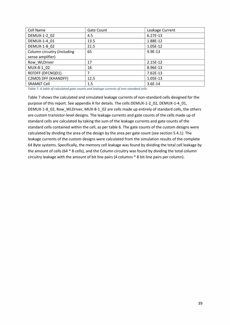
Table 7 shows the calculated and simulated leakage currents of non-standard cells designed for the
purpose of this report. See appendix A for details. The cells DEMUX-1-2_02, DEMUX-1-4_01,
DEMUX-1-8_02, Row_WLDriver, MUX-8-1_02 are cells made up entirely of standard cells, the others
are custom transistor-level designs. The leakage currents and gate counts of the cells made up of
standard cells are calculated by taking the sum of the leakage currents and gate counts of the
standard cells contained within the cell, as per table 6. The gate counts of the custom designs were
calculated by dividing the area of the design by the area per gate count (see section 5.4.1). The
leakage currents of the custom designs were calculated from the simulation results of the complete
64 Byte systems. Specifically, the memory cell leakage was found by dividing the total cell leakage by
the amount of cells (64 * 8 cells), and the Column circuitry was found by dividing the total column
circuitry leakage with the amount of bit line pairs (4 columns * 8 bit-line pairs per column).
40
5.4.6 Calculating the amount of multiplexers, demultiplexers and buffers
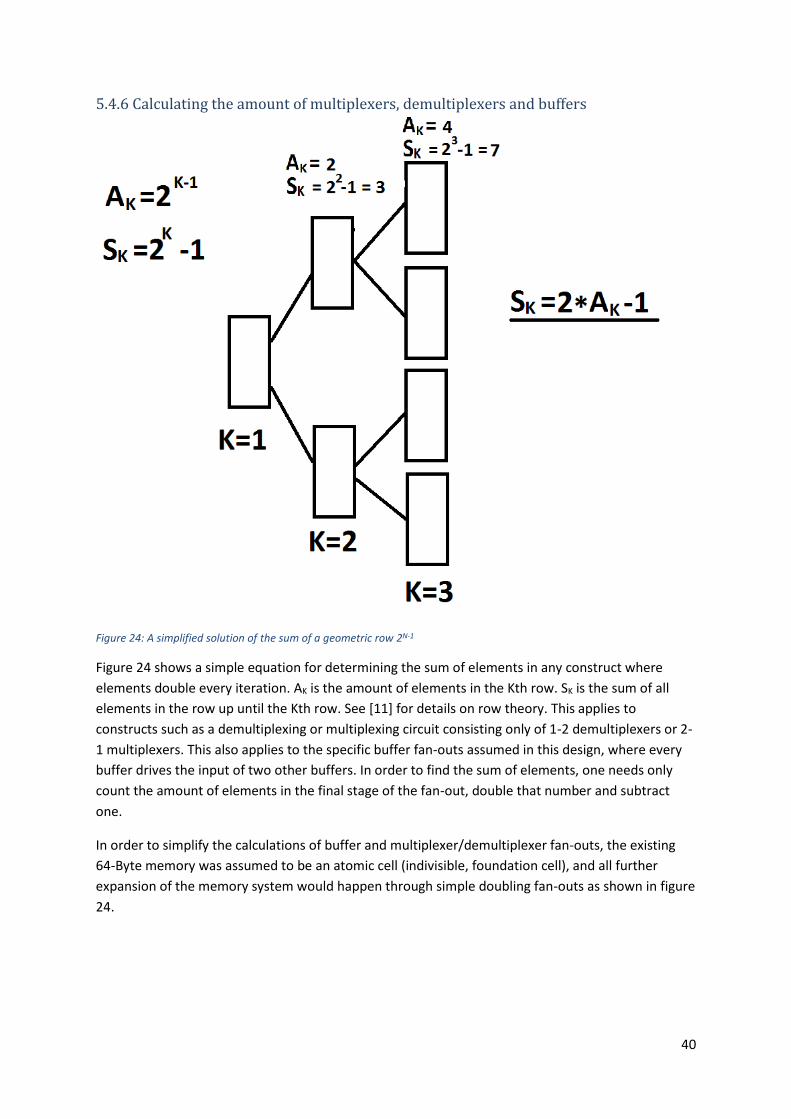
Figure 24: A simplified solution of the sum of a geometric row 2N-1
Figure 24 shows a simple equation for determining the sum of elements in any construct where
elements double every iteration. AK is the amount of elements in the Kth row. SK is the sum of all
elements in the row up until the Kth row. See [11] for details on row theory. This applies to
constructs such as a demultiplexing or multiplexing circuit consisting only of 1-2 demultiplexers or 2-
1 multiplexers. This also applies to the specific buffer fan-outs assumed in this design, where every
buffer drives the input of two other buffers. In order to find the sum of elements, one needs only
count the amount of elements in the final stage of the fan-out, double that number and subtract
one.
In order to simplify the calculations of buffer and multiplexer/demultiplexer fan-outs, the existing
64-Byte memory was assumed to be an atomic cell (indivisible, foundation cell), and all further
expansion of the memory system would happen through simple doubling fan-outs as shown in figure
24.
41
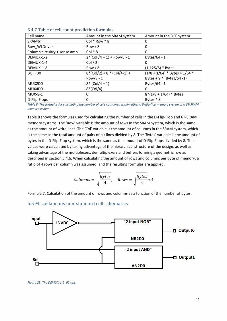
5.4.7 Table of cell count prediction formulas
Cell name Amount in the SRAM system Amount in the DFF system
SRAM6T Col * Row * 8 0
Row_WLDriver Row / 8 0
Column circuitry + sense amp Col * 8 0
DEMUX-1-2 2*(Col /4 – 1) + Row/8 - 1 Bytes/64 - 1
DEMUX-1-4 Col / 2 0
DEMUX-1-8 Row / 8 (1.125/8) * Bytes
BUFFD0 8*(Col/2) + 8 * (Col/4-1) + Row/8 - 1
(1/8 + 1/64) * Bytes + 1/64 * Bytes + 9 * (Bytes/64 -1)
MUX2D0 8* (Col/4 – 1) Bytes/64 - 1
MUX4D0 8*(Col/4) 0
MUX-8-1 0 8*(1/8 + 1/64) * Bytes
D-Flip-Flops 0 Bytes * 8 Table 8: The formulas for calculating the number of cells contained within either a D-flip-flop memory system or a 6T-SRAM memory system.
Table 8 shows the formulas used for calculating the number of cells in the D-Flip-Flop and 6T-SRAM
memory systems. The ‘Row’ variable is the amount of rows in the SRAM system, which is the same
as the amount of write lines. The ‘Col’ variable is the amount of columns in the SRAM system, which
is the same as the total amount of pairs of bit lines divided by 8. The ‘Bytes’ variable is the amount of
bytes in the D-Flip-Flop system, which is the same as the amount of D-Flip-Flops divided by 8. The
values were calculated by taking advantage of the hierarchical structure of the design, as well as
taking advantage of the multiplexers, demultiplexers and buffers forming a geometric row as
described in section 5.4.6. When calculating the amount of rows and columns per byte of memory, a
ratio of 4 rows per column was assumed, and the resulting formulas are applied:
𝐶𝑜𝑙𝑢𝑚𝑛𝑠 = √𝐵𝑦𝑡𝑒𝑠
4, 𝑅𝑜𝑤𝑠 = √
𝐵𝑦𝑡𝑒𝑠
4∗ 4
Formula 7: Calculation of the amount of rows and columns as a function of the number of bytes.
5.5 Miscellaneous non-standard cell schematics
Figure 25: The DEMUX-1-2_02 cell.
42
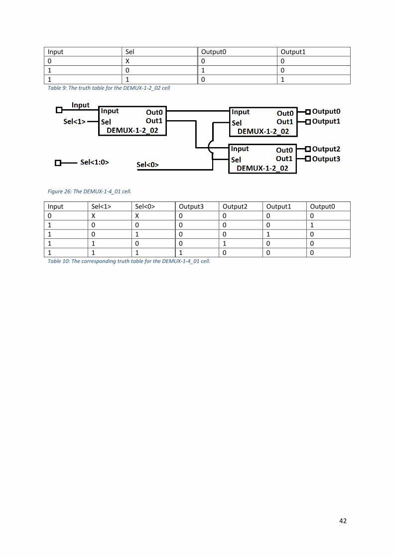
Input Sel Output0 Output1
0 X 0 0
1 0 1 0
1 1 0 1 Table 9: The truth table for the DEMUX-1-2_02 cell
Figure 26: The DEMUX-1-4_01 cell.
Input Sel<1> Sel<0> Output3 Output2 Output1 Output0
0 X X 0 0 0 0
1 0 0 0 0 0 1
1 0 1 0 0 1 0
1 1 0 0 1 0 0
1 1 1 1 0 0 0 Table 10: The corresponding truth table for the DEMUX-1-4_01 cell.
43
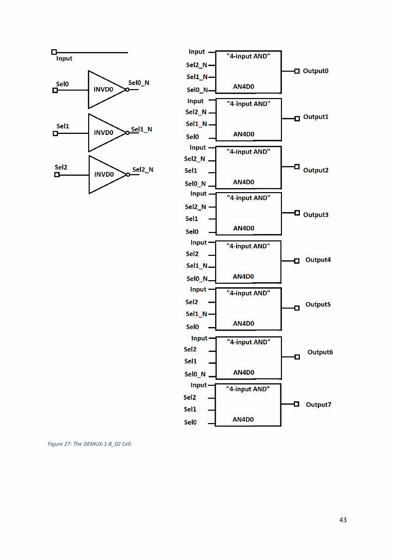
Figure 27: The DEMUX-1-8_02 Cell.
44
Input Sel2 Sel1 Sel0 Out7 Out6 Out5 Out4 Out3 Out2 Out1 Out0
0 X X X 0 0 0 0 0 0 0 0
1 0 0 0 0 0 0 0 0 0 0 1
1 0 0 1 0 0 0 0 0 0 1 0
1 0 1 0 0 0 0 0 0 1 0 0
1 0 1 1 0 0 0 0 1 0 0 0
1 1 0 0 0 0 0 1 0 0 0 0
1 1 0 1 0 0 1 0 0 0 0 0
1 1 1 0 0 1 0 0 0 0 0 0
1 1 1 1 1 0 0 0 0 0 0 0 Table 11: The truth table corresponding to the DEMUX_1-8_02 cell.
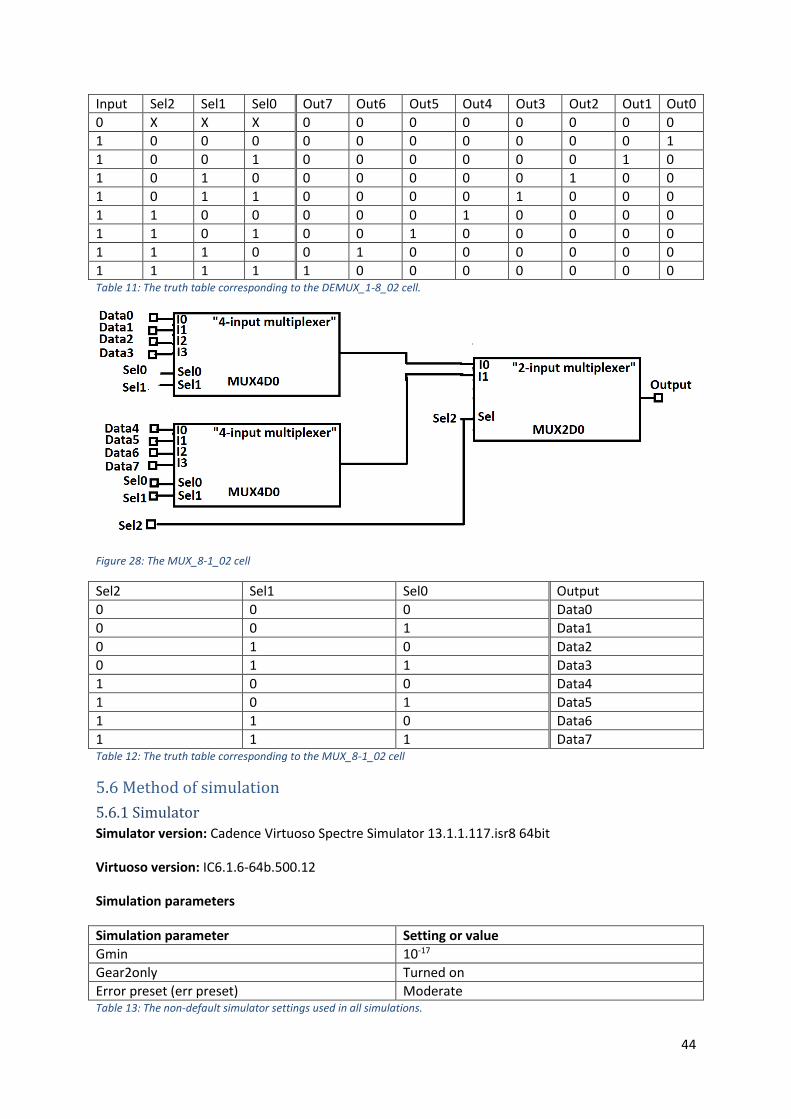
Figure 28: The MUX_8-1_02 cell
Sel2 Sel1 Sel0 Output
0 0 0 Data0
0 0 1 Data1
0 1 0 Data2
0 1 1 Data3
1 0 0 Data4
1 0 1 Data5
1 1 0 Data6
1 1 1 Data7 Table 12: The truth table corresponding to the MUX_8-1_02 cell
5.6 Method of simulation
5.6.1 Simulator
Simulator version: Cadence Virtuoso Spectre Simulator 13.1.1.117.isr8 64bit
Virtuoso version: IC6.1.6-64b.500.12
Simulation parameters
Simulation parameter Setting or value
Gmin 10-17
Gear2only Turned on
Error preset (err preset) Moderate Table 13: The non-default simulator settings used in all simulations.
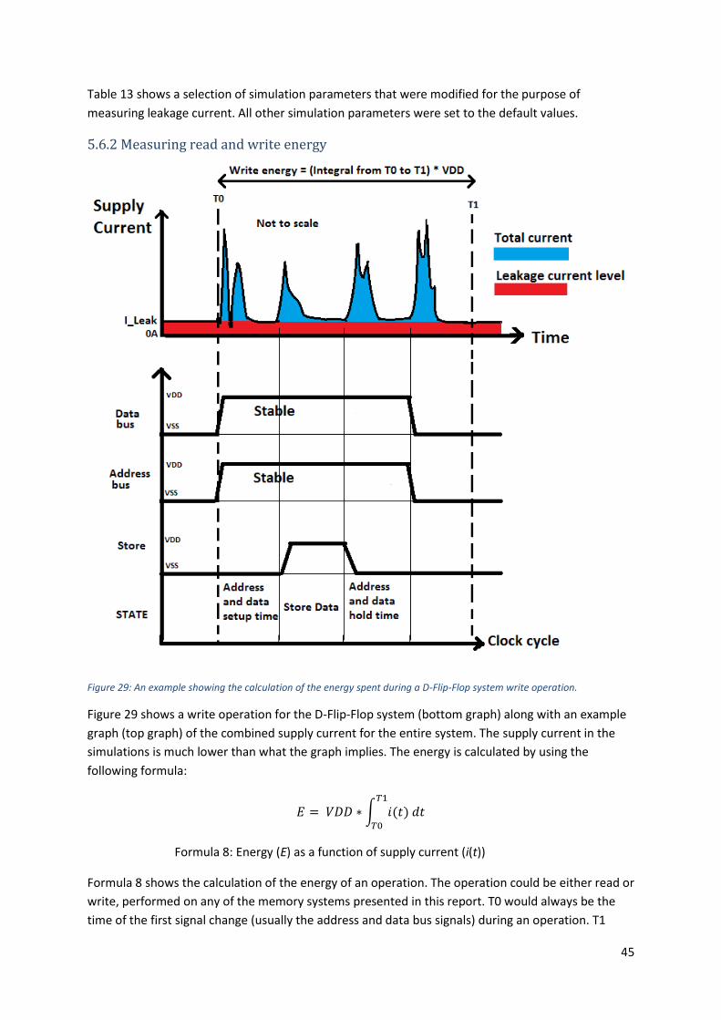
45
Table 13 shows a selection of simulation parameters that were modified for the purpose of
measuring leakage current. All other simulation parameters were set to the default values.
5.6.2 Measuring read and write energy
Figure 29: An example showing the calculation of the energy spent during a D-Flip-Flop system write operation.
Figure 29 shows a write operation for the D-Flip-Flop system (bottom graph) along with an example
graph (top graph) of the combined supply current for the entire system. The supply current in the
simulations is much lower than what the graph implies. The energy is calculated by using the
following formula:
𝐸 = 𝑉𝐷𝐷 ∗ ∫ 𝑖(𝑡) 𝑑𝑡𝑇1
𝑇0
Formula 8: Energy (E) as a function of supply current (i(t))
Formula 8 shows the calculation of the energy of an operation. The operation could be either read or
write, performed on any of the memory systems presented in this report. T0 would always be the
time of the first signal change (usually the address and data bus signals) during an operation. T1

46
would always be exactly one clock cycle after the last signal change during an operation, and the
system would be Idle during that last clock cycle. A static supply voltage is assumed.
Earlier calculations subtracted the integral of the supply current level, but the contribution of
leakage currents during a read or write was discovered to be negligible when measuring read and
write energies. In the simulations, the leakage current was in the order of magnitude less than 10-3 of
the active read and write induced currents. Another problem with subtracting the contribution of
leakage currents is that leakage current is only defined in a static system, and therefore its
contribution is unknown during a read or write.
5.6.3 Determining the worst case initial memory state
5.6.3.1 D-flip-flops
To determine the worst case state of the memory array when examining leakage currents, three
cases were simulated on an 8-byte memory circuit using the reference D-flip-flop (REFDFF).
When using the REFDFF flip-flop, having all zeros stored in the memory maximized the leakage
current.
When using the C2MOS (KHAN_DFF) flip-flop, having all ones stored in the memory meant the
leakage current from the cells was 1.54 times higher than the leakage current from the cells when
having all zeros stored in the memory. Due to the extremely long simulation time required to fill the
memory with ones, this result will not influence the simulations run and the higher leakage current
has to be considered in the prediction calculations instead.
The read and write energies were the highest when writing all ones to a byte containing all zeros, for
both flip flops.
See appendix A for details on the memory state simulations.
5.6.3.2 SRAM
As the SRAM cells are symmetrical, the effect of the memory state on leakage characteristics and
read and write energy is assumed to be negligible. A ‘11111111’ is chosen to be written to a byte
containing ‘00000000’, and the same byte is read.
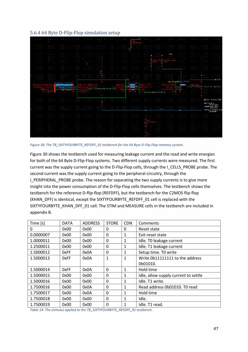
47
5.6.4 64 Byte D-Flip-Flop simulation setup
Figure 30: The TB_SIXTYFOURBYTE_REFDFF_01 testbench for the 64 Byte D-Flip-Flop memory system.
Figure 30 shows the testbench used for measuring leakage current and the read and write energies
for both of the 64 Byte D-Flip-Flop systems. Two different supply currents were measured. The first
current was the supply current going to the D-Flip-Flop cells, through the I_CELLS_PROBE probe. The
second current was the supply current going to the peripheral circuitry, through the
I_PERIPHERAL_PROBE probe. The reason for separating the two supply currents is to give more
insight into the power consumption of the D-Flip-Flop cells themselves. The testbench shows the
testbench for the reference D-flip-flop (REFDFF), but the testbench for the C2MOS flip-flop
(KHAN_DFF) is identical, except the SIXTYFOURBYTE_REFDFF_01 cell is replaced with the
SIXTYFOURBYTE_KHAN_DFF_01 cell. The STIM and MEASURE cells in the testbench are included in
appendix B.
Time [s] DATA ADDRESS STORE CDN Comments
0 0x00 0x00 0 0 Reset state
0.0000007 0x00 0x00 0 1 Exit reset state
1.0000011 0x00 0x00 0 1 Idle. T0 leakage current
1.2500011 0x00 0x00 0 1 Idle. T1 leakage current
1.5000012 0xFF 0x0A 0 1 Setup time. T0 write
1.5000013 0xFF 0x0A 1 1 Write 0b11111111 to the address 0b01010.
1.5000014 0xFF 0x0A 0 1 Hold time
1.5000015 0x00 0x00 0 1 Idle, allow supply current to settle
1.5000016 0x00 0x00 0 1 Idle. T1 write.
1.7500016 0x00 0x0A 0 1 Read address 0b01010. T0 read
1.7500017 0x00 0x0A 0 1 Hold time
1.7500018 0x00 0x00 0 1 Idle.
1.7500019 0x00 0x00 0 1 Idle. T1 read. Table 14: The stimulus applied to the TB_SIXTYFOURBYTE_REFDFF_01 testbench.
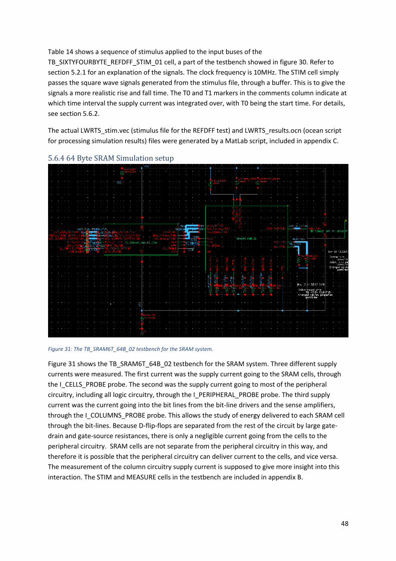
48
Table 14 shows a sequence of stimulus applied to the input buses of the
TB_SIXTYFOURBYTE_REFDFF_STIM_01 cell, a part of the testbench showed in figure 30. Refer to
section 5.2.1 for an explanation of the signals. The clock frequency is 10MHz. The STIM cell simply
passes the square wave signals generated from the stimulus file, through a buffer. This is to give the
signals a more realistic rise and fall time. The T0 and T1 markers in the comments column indicate at
which time interval the supply current was integrated over, with T0 being the start time. For details,
see section 5.6.2.
The actual LWRTS_stim.vec (stimulus file for the REFDFF test) and LWRTS_results.ocn (ocean script
for processing simulation results) files were generated by a MatLab script, included in appendix C.
5.6.4 64 Byte SRAM Simulation setup
Figure 31: The TB_SRAM6T_64B_02 testbench for the SRAM system.
Figure 31 shows the TB_SRAM6T_64B_02 testbench for the SRAM system. Three different supply
currents were measured. The first current was the supply current going to the SRAM cells, through
the I_CELLS_PROBE probe. The second was the supply current going to most of the peripheral
circuitry, including all logic circuitry, through the I_PERIPHERAL_PROBE probe. The third supply
current was the current going into the bit lines from the bit-line drivers and the sense amplifiers,
through the I_COLUMNS_PROBE probe. This allows the study of energy delivered to each SRAM cell
through the bit-lines. Because D-flip-flops are separated from the rest of the circuit by large gate-
drain and gate-source resistances, there is only a negligible current going from the cells to the
peripheral circuitry. SRAM cells are not separate from the peripheral circuitry in this way, and
therefore it is possible that the peripheral circuitry can deliver current to the cells, and vice versa.
The measurement of the column circuitry supply current is supposed to give more insight into this
interaction. The STIM and MEASURE cells in the testbench are included in appendix B.
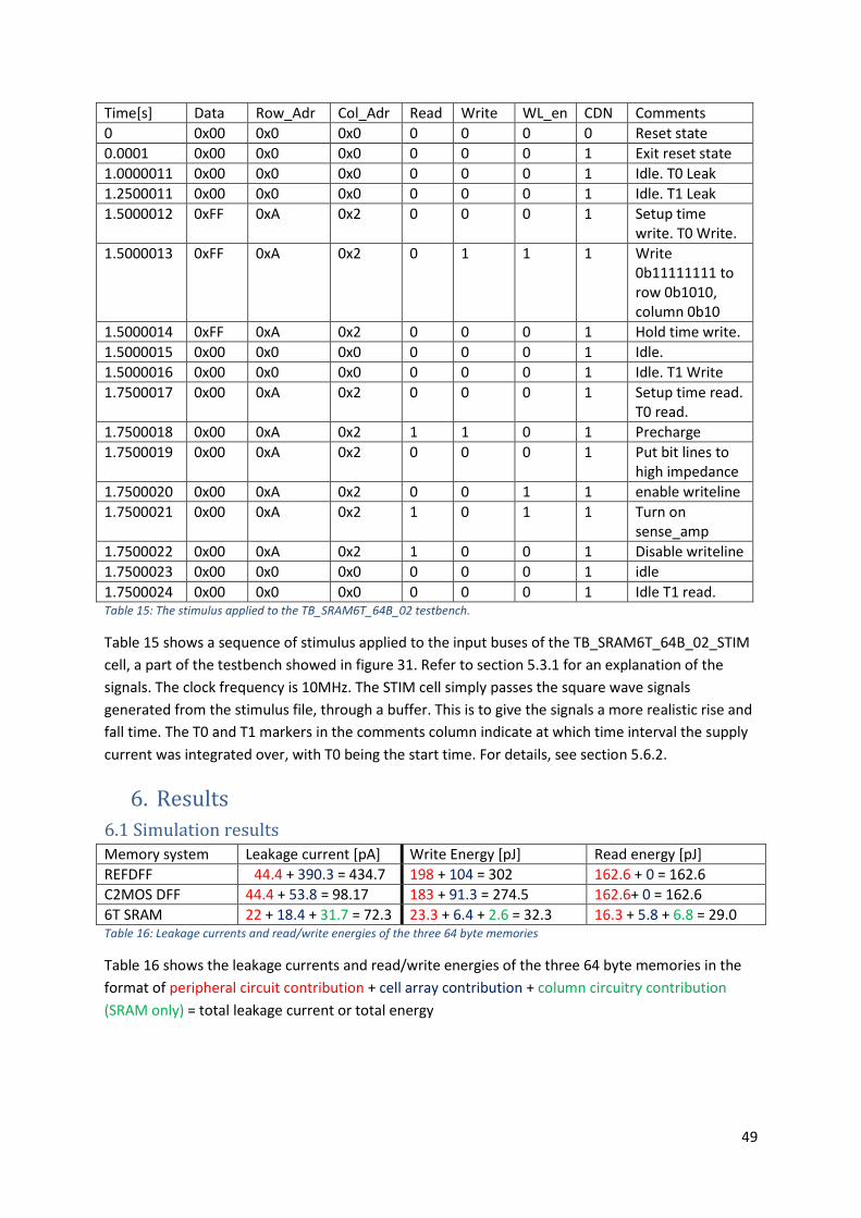
49
Time[s] Data Row_Adr Col_Adr Read Write WL_en CDN Comments
0 0x00 0x0 0x0 0 0 0 0 Reset state
0.0001 0x00 0x0 0x0 0 0 0 1 Exit reset state
1.0000011 0x00 0x0 0x0 0 0 0 1 Idle. T0 Leak
1.2500011 0x00 0x0 0x0 0 0 0 1 Idle. T1 Leak
1.5000012 0xFF 0xA 0x2 0 0 0 1 Setup time write. T0 Write.
1.5000013 0xFF 0xA 0x2 0 1 1 1 Write 0b11111111 to row 0b1010, column 0b10
1.5000014 0xFF 0xA 0x2 0 0 0 1 Hold time write.
1.5000015 0x00 0x0 0x0 0 0 0 1 Idle.
1.5000016 0x00 0x0 0x0 0 0 0 1 Idle. T1 Write
1.7500017 0x00 0xA 0x2 0 0 0 1 Setup time read. T0 read.
1.7500018 0x00 0xA 0x2 1 1 0 1 Precharge
1.7500019 0x00 0xA 0x2 0 0 0 1 Put bit lines to high impedance
1.7500020 0x00 0xA 0x2 0 0 1 1 enable writeline
1.7500021 0x00 0xA 0x2 1 0 1 1 Turn on sense_amp
1.7500022 0x00 0xA 0x2 1 0 0 1 Disable writeline
1.7500023 0x00 0x0 0x0 0 0 0 1 idle
1.7500024 0x00 0x0 0x0 0 0 0 1 Idle T1 read. Table 15: The stimulus applied to the TB_SRAM6T_64B_02 testbench.
Table 15 shows a sequence of stimulus applied to the input buses of the TB_SRAM6T_64B_02_STIM
cell, a part of the testbench showed in figure 31. Refer to section 5.3.1 for an explanation of the
signals. The clock frequency is 10MHz. The STIM cell simply passes the square wave signals
generated from the stimulus file, through a buffer. This is to give the signals a more realistic rise and
fall time. The T0 and T1 markers in the comments column indicate at which time interval the supply
current was integrated over, with T0 being the start time. For details, see section 5.6.2.
6. Results
6.1 Simulation results Memory system Leakage current [pA] Write Energy [pJ] Read energy [pJ]
REFDFF 44.4 + 390.3 = 434.7 198 + 104 = 302 162.6 + 0 = 162.6
C2MOS DFF 44.4 + 53.8 = 98.17 183 + 91.3 = 274.5 162.6+ 0 = 162.6
6T SRAM 22 + 18.4 + 31.7 = 72.3 23.3 + 6.4 + 2.6 = 32.3 16.3 + 5.8 + 6.8 = 29.0 Table 16: Leakage currents and read/write energies of the three 64 byte memories
Table 16 shows the leakage currents and read/write energies of the three 64 byte memories in the
format of peripheral circuit contribution + cell array contribution + column circuitry contribution
(SRAM only) = total leakage current or total energy
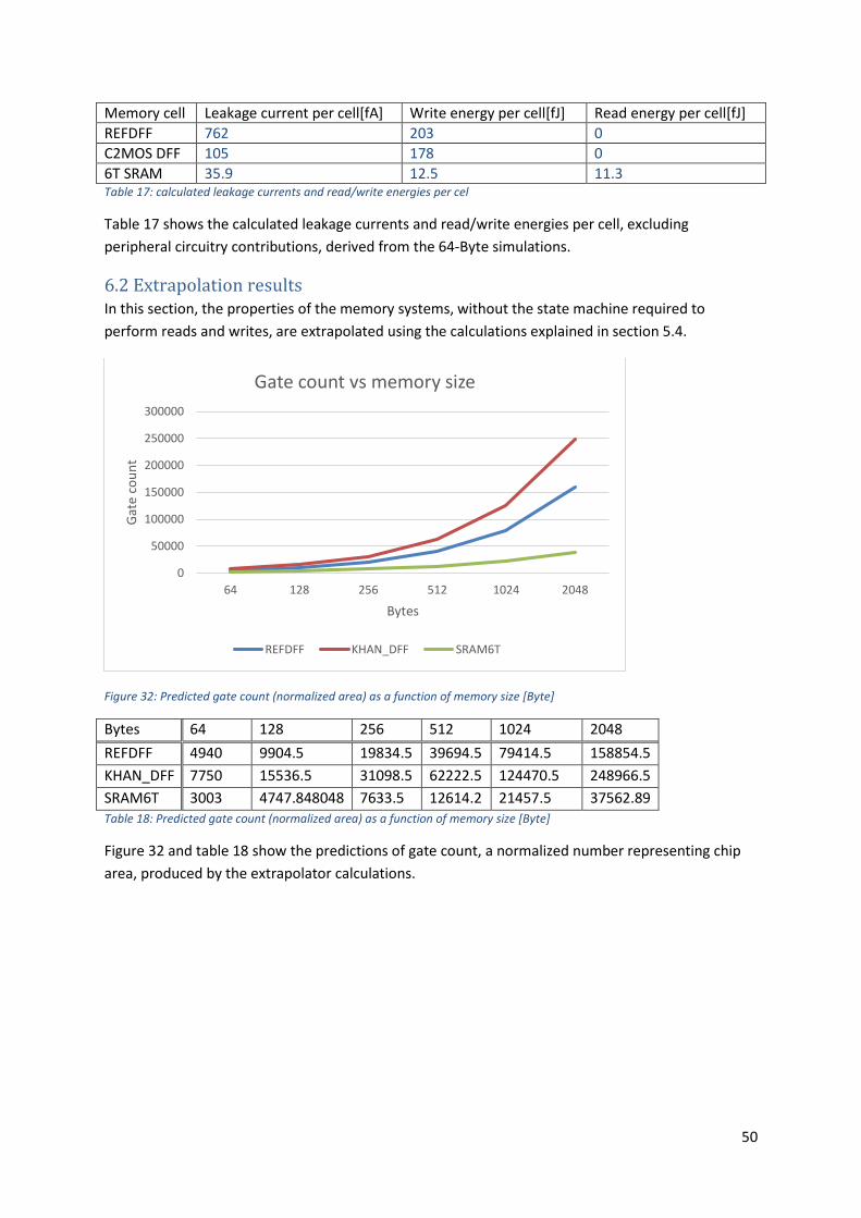
50
Memory cell Leakage current per cell[fA] Write energy per cell[fJ] Read energy per cell[fJ]
REFDFF 762 203 0
C2MOS DFF 105 178 0
6T SRAM 35.9 12.5 11.3 Table 17: calculated leakage currents and read/write energies per cel
Table 17 shows the calculated leakage currents and read/write energies per cell, excluding
peripheral circuitry contributions, derived from the 64-Byte simulations.
6.2 Extrapolation results In this section, the properties of the memory systems, without the state machine required to
perform reads and writes, are extrapolated using the calculations explained in section 5.4.
Figure 32: Predicted gate count (normalized area) as a function of memory size [Byte]
Bytes 64 128 256 512 1024 2048
REFDFF 4940 9904.5 19834.5 39694.5 79414.5 158854.5
KHAN_DFF 7750 15536.5 31098.5 62222.5 124470.5 248966.5
SRAM6T 3003 4747.848048 7633.5 12614.2 21457.5 37562.89 Table 18: Predicted gate count (normalized area) as a function of memory size [Byte]
Figure 32 and table 18 show the predictions of gate count, a normalized number representing chip
area, produced by the extrapolator calculations.
0
50000
100000
150000
200000
250000
300000
64 128 256 512 1024 2048
Gat
e co
un
t
Bytes
Gate count vs memory size
REFDFF KHAN_DFF SRAM6T
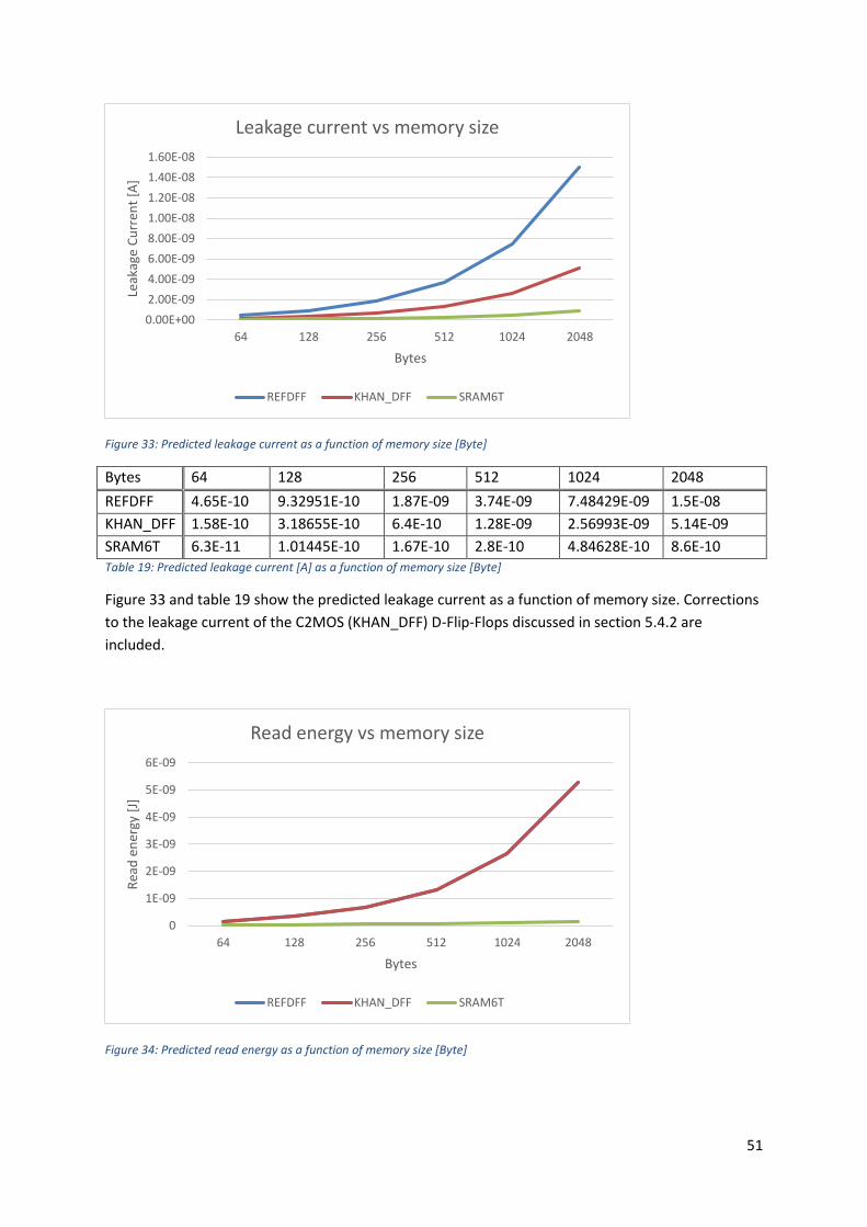
51
Figure 33: Predicted leakage current as a function of memory size [Byte]
Bytes 64 128 256 512 1024 2048
REFDFF 4.65E-10 9.32951E-10 1.87E-09 3.74E-09 7.48429E-09 1.5E-08
KHAN_DFF 1.58E-10 3.18655E-10 6.4E-10 1.28E-09 2.56993E-09 5.14E-09
SRAM6T 6.3E-11 1.01445E-10 1.67E-10 2.8E-10 4.84628E-10 8.6E-10 Table 19: Predicted leakage current [A] as a function of memory size [Byte]
Figure 33 and table 19 show the predicted leakage current as a function of memory size. Corrections
to the leakage current of the C2MOS (KHAN_DFF) D-Flip-Flops discussed in section 5.4.2 are
included.
Figure 34: Predicted read energy as a function of memory size [Byte]
0.00E+00
2.00E-09
4.00E-09
6.00E-09
8.00E-09
1.00E-08
1.20E-08
1.40E-08
1.60E-08
64 128 256 512 1024 2048
Leak
age
Cu
rren
t [A
]
Bytes
Leakage current vs memory size
REFDFF KHAN_DFF SRAM6T
0
1E-09
2E-09
3E-09
4E-09
5E-09
6E-09
64 128 256 512 1024 2048
Rea
d e
ner
gy [
J]
Bytes
Read energy vs memory size
REFDFF KHAN_DFF SRAM6T

52
Bytes 64 128 256 512 1024 2048
REFDFF 1.63E-10 3.28259E-10 6.6E-10 1.32E-09 2.64748E-09 5.3E-09
KHAN_DFF 1.63E-10 3.28259E-10 6.6E-10 1.32E-09 2.64748E-09 5.3E-09
SRAM6T 2.91E-11 3.89242E-11 5.28E-11 7.25E-11 1.00303E-10 1.4E-10 Table 20: Predicted read energy [J] as a function of memory size [Byte]
Figure 34 and table 20 show the predicted read energy as a function of memory size. The predicted
read energy is simply the simulated read energy multiplied by the increase in peripheral circuitry
area. The REFDFF and KHAN_DFF have identical results.
Figure 35: Predicted write energy as a function of memory size [Byte]
Bytes 64 128 256 512 1024 2048
REFDFF 3.02E-10 5.03625E-10 9.07E-10 1.71E-09 3.32777E-09 6.56E-09
KHAN_DFF 2.89E-10 4.91025E-10 8.94E-10 1.70E-09 3.31517E-09 6.54E-09
SRAM6T 3.19E-11 4.27298E-11 5.8E-11 7.96E-11 1.10118E-10 1.53E-10 Table 21: Predicted write energy [J] as a function of memory size [Byte]
Figure 35 and table 21 show the predicted write energy as a function of memory size. The predicted
write energy is simply the simulated write energy multiplied by the increase in peripheral circuitry
area. The REFDFF and KHAN_DFF have nearly identical results.
7. Discussion The discussion chapter of this report is divided into 5 parts. The first two sections discuss the
implementations of the D-Flip-Flop system and SRAM system. The third section discusses the
prediction/extrapolation formulas. The fourth section discusses the way the simulations were
performed. The fifth section discusses the results acquired from the simulations and extrapolation
formulas.
7.1 D-Flip-Flop implementation In this section, please refer to section 5.2.3 and 5.2.4.
0
1E-09
2E-09
3E-09
4E-09
5E-09
6E-09
7E-09
64 128 256 512 1024 2048
Wri
te e
ner
gy [
J]
Bytes
Write energy vs memory size
REFDFF KHAN_DFF SRAM6T
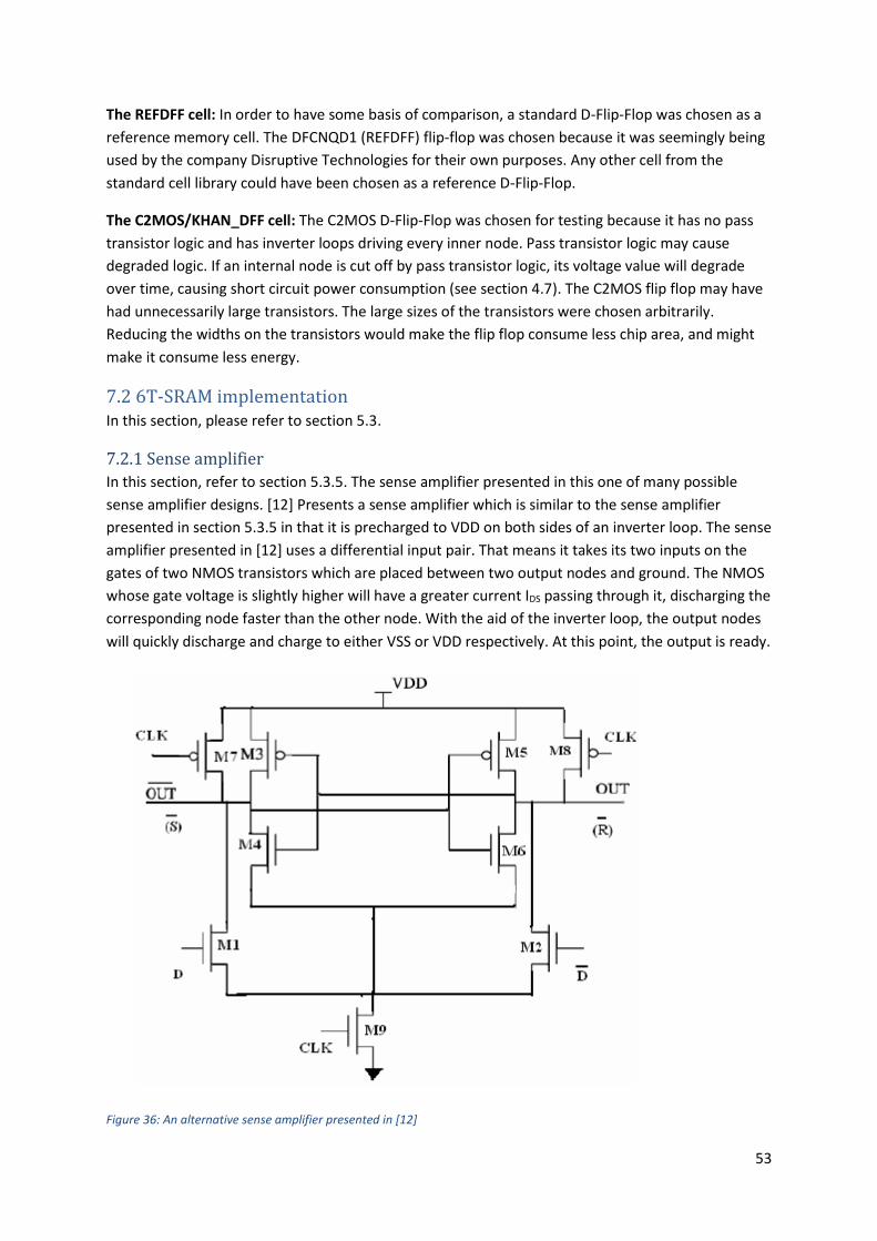
53
The REFDFF cell: In order to have some basis of comparison, a standard D-Flip-Flop was chosen as a
reference memory cell. The DFCNQD1 (REFDFF) flip-flop was chosen because it was seemingly being
used by the company Disruptive Technologies for their own purposes. Any other cell from the
standard cell library could have been chosen as a reference D-Flip-Flop.
The C2MOS/KHAN_DFF cell: The C2MOS D-Flip-Flop was chosen for testing because it has no pass
transistor logic and has inverter loops driving every inner node. Pass transistor logic may cause
degraded logic. If an internal node is cut off by pass transistor logic, its voltage value will degrade
over time, causing short circuit power consumption (see section 4.7). The C2MOS flip flop may have
had unnecessarily large transistors. The large sizes of the transistors were chosen arbitrarily.
Reducing the widths on the transistors would make the flip flop consume less chip area, and might
make it consume less energy.
7.2 6T-SRAM implementation In this section, please refer to section 5.3.
7.2.1 Sense amplifier
In this section, refer to section 5.3.5. The sense amplifier presented in this one of many possible
sense amplifier designs. [12] Presents a sense amplifier which is similar to the sense amplifier
presented in section 5.3.5 in that it is precharged to VDD on both sides of an inverter loop. The sense
amplifier presented in [12] uses a differential input pair. That means it takes its two inputs on the
gates of two NMOS transistors which are placed between two output nodes and ground. The NMOS
whose gate voltage is slightly higher will have a greater current IDS passing through it, discharging the
corresponding node faster than the other node. With the aid of the inverter loop, the output nodes
will quickly discharge and charge to either VSS or VDD respectively. At this point, the output is ready.
Figure 36: An alternative sense amplifier presented in [12]

54
In this paragraph, refer to section 5.3.5. The functionality of the sense amplifier presented in this
report is slightly different. Its output nodes are connected to the bit lines through NMOS pass
transistor. The voltage difference on the bit lines will cause one of the pass transistors to have a
greater IDS going to the bit lines, discharging one of the output nodes faster. This is inevitably slower,
as the output nodes are connected to large capacitances presented by the bit lines, and that would
drain a lot of the current that would otherwise be used to charge the output nodes. The advantage
of this design is that it greatly simplifies the process of using the output to drive the bit lines for a
rewrite, as the bit lines would be charged as soon as the pass transistors open. The minimum voltage
difference on the bit lines needed to ensure a correct read is not known, and should be examined.
Trying to measure a voltage difference which is too low would mean the output would not be
decided by the voltage difference on the bit lines, but would rather be decided by a differences in
drive strength and output node capacitances caused by fabrication errors.
A differential input pair sense amplifier (the alternative sense amplifier in figure 36 would require a
more complex timing scheme in order to rewrite to the SRAM cell. The following reason is
presented: Inverters are assumed to be the driving cells when charging the bit lines for a rewrite.
These inverters have to be disconnected from the bit lines during a measurement of voltage
difference, as leaving them to drive the bit lines would influence the measured voltage difference.
This requires an additional state, the rewrite state, which could only be entered once the sense
amplifier has made a decision on which output is the correct output. The extra state and timing
requirements for that state would increase the design complexity of the design of the state machine.
Avoiding design complexity can help reduce the area, design time, as well as the power consumption
and leakage current of a design. One problem with the sense amplifier presented in this report is
that it is slower. A slow sense amplifier will allow the output nodes to remain in an intermediate
voltage value between VDD and VSS (degraded logic) for longer. This may incur unwanted short
circuit power (See section 4.7) in either the sense amplifier or the SRAM cell, as the SRAM cell’s pass
transistors are open during a sense amplifier voltage difference measurement.
In the design presented in this report, the memory size is small enough that the bit lines present a
very low capacitance to ground. This means the SRAM cells themselves can pull the bit lines to
strong logic values (either VDD or VSS) within a read cycle, and one could use the voltage level on
the bit lines as an output. This means a sense amplifier is not needed in small memories. The sense
amplifier is included only for the purposes of studying the effect it has on chip area and leakage
current. The validity of the sense amplifier presented in this paper was not verified.
7.2.2 Row/Column ratio
In the implementation described in this report, there are 4 rows per column. This number is
arbitrary; any ratio could be chosen. The reason this number was chosen was because during the
design process, memory size expansion had to stop at 64 Bytes because of simulation time
considerations. At that point, with the given hierarchical structure, the only structures which could
be constructed without severely lengthening the design time required were either 32 rows/2
columns, 16 rows/4 columns. 4 rows per column was chosen rather than 16 rows per column.
Choosing a ratio with a higher number of rows per column decreases area overhead, as each column
needs 8 bit-line drivers and 8 sense amplifiers. If there are many rows per column, the amount of
rows will increase faster with increasing memory sizes than if there were few rows per column.
55
More rows mean longer bit lines, and longer bit lines means a greater bit line capacitance. Refer to
section 7.2.3 for an explanation why bit line capacitance might become an issue. Custom designs
with a fixed amount of rows are also possible.
7.2.3 Floating charge memory corruption
When a specific cell is accessed for a read or a write, its pass transistors are opened by enabling the
corresponding WL signal. A problem may arise as the pass transistors in all cells in the same row are
also opened at the same time. When a read or write is finished, the bit lines are disconnected
completely from either VDD or VSS. The bit lines will slowly discharge through leakage currents, but
when a writeline is enabled immediately after a read or write, the floating charge on the bit line may
be enough to flip the value in the cell. The point at which the capacitance of the bit line is big enough
for this to happen is unknown. This is not a problem for small memory sizes (assumption: 5MB and
perhaps even much more), when the bit lines have such a low capacitance to ground that the SRAM
cell will pull the charge on the bit lines to either VSS or VDD before the cells internal capacitance is
charged beyond Vth, potentially flipping the cell. The cells whose internal capacitances have not
been charged beyond Vth will eventually rewrite themselves once the writeline_enable signal goes
low, owing to the inverter loop inside the SRAM cell. Further and more precise explanations of
charge sharing is beyond the scope of this report, and a large part of the reason the system works is
because of the inherent read stability explained in section 5.3.6.
A solution that might solve this problem for much larger memories is to first precharge all bit lines in
the entire memory whenever a read or write is performed, and then activate the sense amplifiers on
every bit line pair to rewrite every bit line pair according to the value stored in the opened SRAM
cell. This would require a redesign of the column circuitry, but the amount of complexity in the
column circuitry would not increase by much, and therefore the current design is still fairly
representative of larger memory systems.
7.3 Extrapolator implementation
7.3.1 Address bus buffers
In this section, refer to sections 5.2.2 and 5.3.2 and 5.4.6. When the memory size increases, the
number of bits needed to address the memory increases. As the address bus gets wider and wider,
additional buffers will be required in order to drive the address buses on both the 6T-SRAM and the
DFF circuits. In the calculations, a static bus size was assumed, as a dynamic bus size would
complicate the mathematics of the extrapolator, and the additional buffers would not represent a
significant portion of the peripheral circuitry.
7.3.2 Multiplexer/demultiplexer fan-outs
In this section, refer to sections 5.2.2, 5.3.2 and 5.4.6. In the extrapolator calculations, it is assumed
that only 1-2 and 2-1 demultiplexers and multiplexers would be used to decode the buses and
signals outside the 64-Byte cell. Inside 64-Byte cell, 1-8 and 8-1 demultiplexers and multiplexers are
used to save area, power and leakage current, and this could also be done outside the 64-Byte cell.
This means that the extrapolator predicts a larger area, leakage current and read and write power as
a result of this.
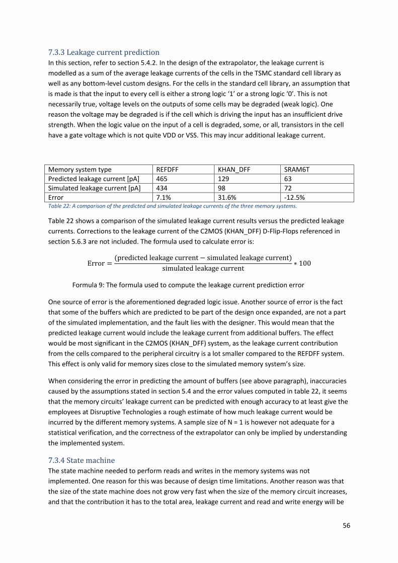
56
7.3.3 Leakage current prediction
In this section, refer to section 5.4.2. In the design of the extrapolator, the leakage current is
modelled as a sum of the average leakage currents of the cells in the TSMC standard cell library as
well as any bottom-level custom designs. For the cells in the standard cell library, an assumption that
is made is that the input to every cell is either a strong logic ‘1’ or a strong logic ‘0’. This is not
necessarily true, voltage levels on the outputs of some cells may be degraded (weak logic). One
reason the voltage may be degraded is if the cell which is driving the input has an insufficient drive
strength. When the logic value on the input of a cell is degraded, some, or all, transistors in the cell
have a gate voltage which is not quite VDD or VSS. This may incur additional leakage current.
Memory system type REFDFF KHAN_DFF SRAM6T
Predicted leakage current [pA] 465 129 63
Simulated leakage current [pA] 434 98 72
Error 7.1% 31.6% -12.5% Table 22: A comparison of the predicted and simulated leakage currents of the three memory systems.
Table 22 shows a comparison of the simulated leakage current results versus the predicted leakage
currents. Corrections to the leakage current of the C2MOS (KHAN_DFF) D-Flip-Flops referenced in
section 5.6.3 are not included. The formula used to calculate error is:
Error =(predicted leakage current − simulated leakage current)
simulated leakage current∗ 100
Formula 9: The formula used to compute the leakage current prediction error
One source of error is the aforementioned degraded logic issue. Another source of error is the fact
that some of the buffers which are predicted to be part of the design once expanded, are not a part
of the simulated implementation, and the fault lies with the designer. This would mean that the
predicted leakage current would include the leakage current from additional buffers. The effect
would be most significant in the C2MOS (KHAN_DFF) system, as the leakage current contribution
from the cells compared to the peripheral circuitry is a lot smaller compared to the REFDFF system.
This effect is only valid for memory sizes close to the simulated memory system’s size.
When considering the error in predicting the amount of buffers (see above paragraph), inaccuracies
caused by the assumptions stated in section 5.4 and the error values computed in table 22, it seems
that the memory circuits’ leakage current can be predicted with enough accuracy to at least give the
employees at Disruptive Technologies a rough estimate of how much leakage current would be
incurred by the different memory systems. A sample size of N = 1 is however not adequate for a
statistical verification, and the correctness of the extrapolator can only be implied by understanding
the implemented system.
7.3.4 State machine
The state machine needed to perform reads and writes in the memory systems was not
implemented. One reason for this was because of design time limitations. Another reason was that
the size of the state machine does not grow very fast when the size of the memory circuit increases,
and that the contribution it has to the total area, leakage current and read and write energy will be

57
negligible at large memory sizes (larger than 128 Bytes). There is however a difference in size of the
two state machines, the D-Flip-Flop state machine and the SRAM state machine. Implementing these
or predicting their sizes would allow the prediction of the ‘break-even point’, the memory size at
which a D-Flip-Flop memory system has the same area as a 6T-SRAM memory system, which is an
important metric when considering whether to use an SRAM system or a D-Flip-Flop system.
Because the speed of the circuit is of no concern in this application, the SRAM system was
implemented with an extremely simplified read and write timing sequence. This means the state
machine required to perform reads and writes on the SRAM system in this report will be far less
complex than the state machine required in high-performance systems. This leads to an educated
guess that the break-even point might be as low as 32 bytes.
7.3.5 Read and Write energy prediction
The assumption that read and write energies are proportional to chip area is wrong. There is
probably a certain correlation between area and read and write energy, because signals have to be
propagated through the multiplexer logic. A larger area of logic means the signals propagate to a
greater number of logic gates. The exact correlation between logic area and signal propagation
energy is beyond the scope of this report. The purpose predictions that were made for read and
write energy in the results section is mostly to show that for an increasing memory size, the
difference between the read and write energies of a D-Flip-Flop systems and a 6T-SRAM system
increase. This is because the D-Flip-Flop peripheral circuitry increases in size faster than the 6T-
SRAM peripheral circuitry.
Read and write energy extrapolation for the SRAM system
Extrapolation of read and write energies is likely very inaccurate at larger memory sizes. The effect
of opening the WL pass transistors of all cells connected to the same WL when reading or writing is
unknown. There will likely be an increase in the read and write energy contribution from the cell
array when increasing the cell array size, even though only one cell is ever written to or read at the
same time. An analysis of the energy consumption of the SRAM cell array as a whole is beyond the
scope of this report.
7.4 Method of simulation
7.4.1 Memory state
During the simulation, the contents of the REFDFF memory system was set to the worst case
memory state for leakage current and read and write energy. The leakage current predictions for the
KHAN_DFF/C2MOS memory system was scaled up to ensure a worst case result. The reason behind
simulating the worst case memory state is to ensure that the results show qualities as close as
possible to the qualities of the physical implementation. The physical implementation will always
have a larger leakage current than the transistor level simulations, and will most likely have a larger
read and write energy consumption.
The SRAM memory system was assumed to have approximately the same leakage current
independent of memory state. The effect the SRAM-Cells have on the voltage levels of the bit lines
was not simulated. Having every cell retain a logic value ‘0’ may cause the bit lines to have a
different voltage level than if half the cells stored a logic value ‘1’. This is because there are leakage
currents through the pass transistors which connect the SRAM cells to the bit lines. The effect this

58
has on leakage currents inside the SRAM cells is probably negligible, and the extra leakage current
through to the bit lines is accounted for in the separate measurement of column supply currents.
Measuring the worst case leakage current for flip-flops, and comparing that to a memory system
with an (assumed) unvarying leakage current might skew the data in favor of the memory system
with a stable leakage current (SRAM). To mitigate this, one could measure the average leakage
current instead.
7.4.2 Clock Frequency:
The clock frequency during simulation was set to 10MHz. This is a rather slow clock frequency, but as
energy consumption is measured as an energy per operation metric rather than power (Watt), clock
frequency does not matter much. The only situation in which the clock frequency could matter,
would be if the clock ticks were so frequent, that some internal nodes in the logic circuitry would not
settle completely within one clock period. At this point, the circuit is close to non-functional as a
result of approaching the absolute maximum clock frequency. Setting the clock frequency to this
value is not viable for the type of design presented in this report.
7.4.3 SRAM bit line model:
In the simulations presented in this report, a model of the capacitance and resistance of the bit lines
was not applied as a part of the SRAM memory system. The bit lines present a significant
capacitance beyond the drain-bulk capacitance modelled in the transistors. The bit lines also present
a resistance per length of wire, which can grow to be significant when the bit lines grow longer and
longer with increasing memory size. Increased bit line capacitance and resistance may lead to
increased read and write energy consumption by slowing down the sense amplifier (see section
7.2.1). The added capacitance and resistance of the bit lines is negligible for small memory sizes
(assumption: less than 512B).
7.5 Results Simulation results: Table 16 shows that clearly, in all cases, the 6T-SRAM system without an
implemented state machine is superior to both D-Flip-Flops. The SRAM system achieves a leakage
current that is 83% lower than that of the Reference D-Flip-Flop system, and 26% lower than that of
the C2MOS Flip-Flop system. It achieves a write energy that is 89% lower than that of the reference
D-Flip-Flop system, and 88% lower than that of the C2MOS flip-flop system. It achieves a read energy
that is 82% lower than that of the flip-flop systems.
Table 16 shows that during a read, the column circuitry draws a lot of power. This is probably
because of the sense amplifier which is enabled during a read. By choosing a different sense
amplifier design, the read energy consumption can quite possibly be reduced.
Extrapolation results: The extrapolation graphs (figure 32 through 35) show that for all the memory
systems, the gate count (area), leakage current and read and write energy grow exponentially with
an increasing memory size. The SRAM memory shows a much slower rate of growth compared to
the two D-Flip-Flop systems, and therefore the difference between the SRAM and D-Flip-Flop
systems grows exponentially in favor of the SRAM system.

59
As previously explained in section 7.3.5, the read and write energies predictions are highly
unreliable. As implied in section 7.3.1, 7.3.2 and 7.3.3, the gate count and leakage current
predictions are somewhat reliable.
7.6 Final system comparisons
In this section, the memory systems are compared to each other on the basis of the five design
considerations presented in section 5.1.
When the memory size grows to sizes greater than 64Bytes, the SRAM system is without doubt the
best design option for the purposes of minimizing leakage current, area and read and write energy.
The SRAM system fails to satisfy the fifth and least prioritized design consideration, namely design
time. An SRAM memory system requires considerably more effort to design than a D-Flip-Flop
system, as the interaction between the components of an SRAM system form a complicated system
requiring comprehensive analysis.
As stated in section 7.3.4, it is impossible to determine the exact characteristics of the memory
systems when the required state machine and I2C slave circuit has not been designed. The focus on
simplicity when designing the SRAM system helped reduce the size of the SRAM system considerably
at smaller memory sizes, and an estimate of when the areas of the SRAM system and D-Flip-Flop
systems are equal is at a memory size of 32 bytes. At a memory size of 64 Bytes, the SRAM system
without a state machine/I2C slave circuit had an area that was 39% lower than the REFDFF D-Flip
Flop system.
8. Conclusion The simulations show that the 6T-SRAM memory system, without the necessary state machine, is
clearly superior in terms of area, leakage current and read and write energy consumption. The
implementation or size prediction of the required state machines and I2C slave circuits is needed to
determine the ‘area break-even point’, but an educated guess is that the area break-even point is at
a memory size of 32 Bytes.
The extrapolations of area, leakage current and read and write energy show that when memory sizes
increase, the SRAM system becomes more and more favorable as a memory system alternative.
8.1 Future work
8.1.1 Additional memory types
Only two different types of memory were considered in this report, several others could prove to be
suitable in the given 0.18µm technology.
- RRAM could possibly be implemented on a standard CMOS technology chip [13].
Investigating the feasibility of RRAM in a low leakage low power application would be very
useful.
- Additional D-Flip-Flops could be simulated in order to select the most suitable D-Flip-Flop for
a low leakage, low power application.
- D-Latches could be investigated as a possibility in a low performance application.
- 4-transistor leaking SRAM could prove to be feasible in a low leakage application.
60
8.1.2 Peripheral circuitry implementation
The peripheral circuitries of the SRAM and DFF memory systems are far from optimal. A number of
things can be done to improve them:
- Buffer fan-outs can be replaced with inverter fan-outs, as long as an even number of
inverters are ensured.
- The demultiplexers and multiplexer fan-outs can be optimized drastically. One example
would be to use negating demultiplexers, which consume less area and leakage current.
- Synthesizing the multiplexing and demultiplexing circuits could reduce the area of the
peripheral circuitry, as well as leakage current and read and write power.
8.1.3 SRAM sense amplifier
- The validity of the sense amplifier proposed in this report needs to be ensured.
- The required voltage difference on the bit lines needed to ensure a correct read for the
proposed sense amplifier should be examined before the sense amplifier is implemented in
a physical design.
8.1.4 Extrapolation
- In order to more accurately represent the sizes and leakage currents of the memory
systems, the state machine required for reading and writing needs to be implemented. This
state machine would most likely take the form of an I2C slave circuit. Once implemented, or
its size predicted, the ‘break even’ point (the point at which the flip flop system is equal in
size to the SRAM system) can be determined.
- The mathematical models for buffer and demultiplexer/multiplexer fan-outs should be
refined to cover an increasing address bus size.
- A prediction of the read and write energy consumption of the SRAM memory cell array
would be useful. Specifically, one should look at how the read and write energy responds to
an increase in bit line capacitance when the memory size grows to 1kB and beyond.
- The energy consumption of a multiplexer/demultiplexer fan-out increases non-linearly with
the area of the fan-out. This ‘signal propagation energy’ as a function of multiplexer fan-out
area could be modelled in order to predict read and write energies more accurately.

61
9. References: [1] Liknes: Low Leakage Memory. Unpublished. Trondheim, 2015
[2] Disruptive Technologies. http://www.disruptive-technologies.com contact: Bjørnar Hernes,
[3] Jianjun, Yihe: A low clock swing, power saving and generic technology based D flip-flop with
single power supply. 7th International Conference on ASIC, 2007
[4] Yang, Kim: A Low-Power SRAM Using Hierarchical Bit Line and Local Sense Amplifiers, IEEE
JOURNAL OF SOLID-STATE CIRCUITS, VOL. 40, NO. 6, JUNE 2005
[5] Luo, Jimson, Rishad, Dhiraj: Low Power and Robust Binary Tree SRAM Design for Embedded
Systems, Electronic System Design (ISED), International Symposium on, 2013
[6] Jaeger, Blalock: Microelectronic circuit design, fourth edition, chapter 6.6. McGraw-Hill, 2011
[7] Uyemura “Introduction to VLSI Circuits and Systems”, Wiley 2001
[8] Khan, Beg: A New Area and Power Efficient Single Edge Triggered Flip-Flop Structure for Low Data
Activity and High Frequency Applications, Innovative Systems Design and Engineering, Vol.4, 2013
[9] Kumari, Anand, Bhattacharya: Comparative Study of different Flip Flop Cells for WSN
Applications, International Journal of Computer Applications, March 2014
[10] Daya, Jiang, Piotr Nowak, Sharief. Synchronous 16x8 SRAM Design. Electrical Engineering
Department, University of Florida
[11] Adams, Essex: Calculus: A Complete Course, 8th Edition, Pearson, 2013
[12] Murugeswari, Anusha, Venkateshwarlu, Bhaskar, Venkataramani: A Wide Band Voltage Mode
Sense Amplifier Receiver for High Speed Interconnects. TENCON 2008 - 2008 IEEE Region 10
Conference, 2008
[13] Sheu, Chiang, Lin, Lee, Chen, Chen, Wu, Chen, Su, Kao, Cheng, Tsai:A 5ns Fast Write Multi-Level
Non-Volatile 1 K bits RRAM Memory with Advance Write Scheme, Symposium on VLSI Circuits, 2009
[14] Amuthavalli, Gunasundari: Analysis and Design of Subthreshold Leakage Power-aware Ripple
Carry Adder at Circuit-level Using 90nm Technology, International Conference on Intelligent
Computing, Communication & Convergence, 2015

62
Appendix A: Simulations supporting the choice of initial memory
state for the D-Flip-Flop system The memory state cases were:
1) All logic zeros, that is 0x00 stored in every byte
2) All logic ones, that is 0xFF stored in every byte
3) Alternating ones and zeros: 0x55 stored in every byte
To measure the write energy, 0xFF is written to a byte containing 0x00, 0x00 is written to a byte
containing 0xFF, and 0xAA is written to a byte containing 0x55. This is based on the assumption that
flipping a bit from either 0 to 1 or from 1 to 0 requires more energy than not flipping a bit.
To measure read energy, the address which was previously written is read.
Results REFDFF:
Data stored in all bytes 0x00 0xFF 0x55
Leakage current [pA] 4.9 + 48.8 = 53.7 8.6 + 51.1 = 59.7 6.8 + 50.0 = 56.7 Table 23: Leakage currents of an 8 byte memory utilizing reference flip flops (REFDFF)
Format: peripheral circuit leakage current + cell array leakage current = total leakage current
Data stored in all bytes 0x00 0xFF 0x55
Write energy [pJ] 10.0 + 16.2 = 26.2 5.8 + 3.5 = 9.3 7.9 + 9.8 = 17.8
Read energy [pJ] 5.3 + 0 = 5.3 5.2 + 0 = 5.2 5.2 + 0 = 5.2 Table 24: Read and write energy of an 8 byte memory utilizing reference flip flops (REFDFF)
Format: peripheral circuit energy + cell array energy = total energy
Results C2MOS DFF / KHAN_DFF:
Data stored in all bytes 0x00 0xFF 0x55
Leakage current [pA] 4.9 + 6.7 = 11.62 8.6 + 10.4 = 19.0 6.8 + 8.5 = 15.3 Table 25: Leakage currents of an 8 byte memory utilizing C2MOS Flip Flops (KHAN_DFF)
Format: peripheral circuit leakage current + cell array leakage current = total leakage current
Data stored in all bytes 0x00 0xFF 0x55
Write energy [pJ] 8.2 + 12.8 = 21.2 6.3 + 1.0 = 7.3 7.3 + 6.9 = 14.24
Read energy [pJ] 5.3 + 0 = 5.3 5.2 + 0 = 5.2 5.2 + 0 = 5.2 Table 26: Read and write energy of an 8-byte memory utilizing reference C2MOS Flip Flops (KHAN_DFF)
Format: peripheral circuit energy + cell array energy = total energy

63
Appendix B: Stim and Measure cell schematics
Figure 37: The TB_SIXTYFOURBYTE_REFDFF_01_STIM cell
Figure 38: The TB_SIXTYFOURBYTE_REFDFF_01_MEASURE cell
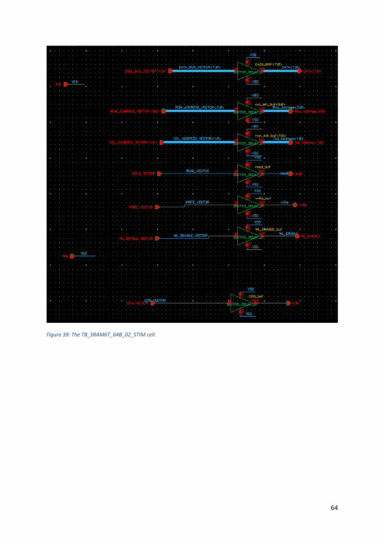
64
Figure 39: The TB_SRAM6T_64B_02_STIM cell.
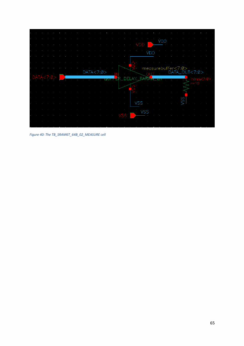
65
Figure 40: The TB_SRAM6T_64B_02_MEASURE cell

66
Appendix C: MATLAB scripts used to generate ocean and stimulus
files
D-Flip-Flop stim script function [leak_start, leak_end, write_start, write_end, read_start,
read_end] = writeStimFile_DFFRAM_64B( filename ) %generates a STIM file for use in Kai Likne's testbenches of a D-flip-flop %64 byte %% constants and initialization: hier = '0'; tunit = 'ns'; trise = '0.001' ; %100ps falltime/risetime tfall = '0.001' ; vih = '3'; vil = '0'; period = 100; %10Mhz clock freq, 100ns period wait_time = 1000000000; %1 second wait time to measure leak
radix_data = '44'; radix_address = '24'; radix_store = '1'; radix_cdn = '1';
time = '000000000000'; time_amount_of_digits = length(time); %has to be 12 maxtime = 10^(time_amount_of_digits); randomdata='00'; address_string='00';
%% start writing file fileID = fopen(filename,'w');
fprintf(fileID,'radix\n'); fprintf(fileID,'+ %s %s %s %s\n', radix_data, radix_address, radix_store,
radix_cdn); fprintf(fileID,'\nio\n'); fprintf(fileID,'+ i i i i\n\n'); fprintf(fileID,'hier %s\ntunit %s\ntrise %s\ntfall %s\nvih %s\nvil %s\n\n',
hier, tunit, trise, tfall, vih, vil); fprintf(fileID,'\nvname\n+DATA_BUS_VECTOR<[7:0]> ADDRESS_VECTOR<[5:0]>
STORE_VECTOR CDN_VECTOR\n\n');
fprintf(fileID,'\n\n\n; Initializing\n\n'); fprintf(fileID,';time\t\tdata\tad\tst\tcdn\n'); fprintf(fileID,'%s\t%s\t%s\t0\t0\t; Reset
state\n',time,randomdata,address_string); %enter reset state time = sprintf('%012d',str2num(time)+period); %timestep one clock period fprintf(fileID,'%s\t%s\t%s\t0\t1\t; deactivate reset
state\n',time,randomdata,address_string); time = sprintf('%012d',str2num(time)+period*10); %timestep 2 clock periods
%% measure leakage current time = sprintf('%012d',str2num(time)+wait_time); %timestep 1 second to
measure leak

67
leak_start = time; time = sprintf('%012d',str2num(time)+ceil(wait_time/4)); %timestep 0.25
seconds leak_end = time; time = sprintf('%012d',str2num(time)+period); %timestep one clock period
%% measure write energy
fprintf(fileID,'\n\n\n; Start measuring write energy\n\n'); fprintf(fileID,';time\t\tdata\tad\tst\tcdn\n'); time = sprintf('%012d',str2num(time)+ceil(wait_time/4)); %timestep 0.25
seconds
write_start = time;
address = '0A' ; data = 'FF'; fprintf(fileID,'%s\t%s\t%s\t0\t1\t; Setup time\n',time,data,address); time = sprintf('%012d',str2num(time)+period); %timestep one clock period fprintf(fileID,'%s\t%s\t%s\t1\t1\t; Write %s to Address
%s\n',time,data,address,data,address); time = sprintf('%012d',str2num(time)+period); %timestep one clock period fprintf(fileID,'%s\t%s\t%s\t0\t1\t; hold time\n',time,data,address); time = sprintf('%012d',str2num(time)+period); %timestep one clock period
fprintf(fileID,'%s\t00\t00\t0\t1\t; address and data are 0 when
idle\n',time); time = sprintf('%012d',str2num(time)+period); %timestep one clock period
write_end = time;
%% measure read energy fprintf(fileID,'\n\n\n; Start measuring read energy\n\n'); fprintf(fileID,';time\t\tdata\tad\tst\tcdn\n'); time = sprintf('%012d',str2num(time)+ceil(wait_time/4)); %timestep 0.25
seconds
address = '0A' ; data = '00'; %N/A
read_start = time;
fprintf(fileID,'%s\t%s\t%s\t0\t1\t; measure read energy. start read at
address %s\n',time,data,address,address); time = sprintf('%012d',str2num(time)+period); %timestep one clock period fprintf(fileID,'%s\t00\t00\t0\t1\t; read end address and data are 0 when
idle\n',time); time = sprintf('%012d',str2num(time)+period); %timestep one clock period read_end = time;
%% print out stats and close file fprintf(fileID,'\n\n\n; leak_start = %s \t leak_end = %s \n; write_start =
%s \t write_end = %s\n; read_start = %s \t read_end = %s\n',leak_start,
leak_end, write_start,write_end,read_start,read_end); fclose(fileID); end
68
D-Flip-Flip flop ocean script function writeOceanScript_64B(filename, leak_start, leak_end, write_start,
write_end, read_start, read_end) %generates an OCEAN file for use in Kai Likne's testbenches of a D-flip-
flop %REFDFF %64 byte
%% leakage currents fileID = fopen(filename,'w'); fprintf(fileID,'axlOutputResult("-----" "--- Leakage Currents ---")\n\n');
fprintf(fileID,'leak_peripheral =
average(clip(IT("/I_PERIPHERAL_PROBE/PLUS") %sn %sn
))\n',leak_start,leak_end); fprintf(fileID,'leak_cells = average(clip(IT("/I_CELLS_PROBE/PLUS") %sn %sn
))\n',leak_start,leak_end); fprintf(fileID,'leak_total = leak_peripheral + leak_cells\n');
fprintf(fileID,'\naxlOutputResult(leak_peripheral "leak_peripheral
(A)")\n'); fprintf(fileID,'axlOutputResult(leak_cells "leak_cells (A)")\n'); fprintf(fileID,'axlOutputResult(leak_total "leak_total (A)")\n');
%% write energy fprintf(fileID,'\naxlOutputResult("-----" "--- Write energy ---")\n\n');
fprintf(fileID,'write_energy_peripheral =
integ(clip(IT("/I_PERIPHERAL_PROBE/PLUS") %sn %sn )) *
VAR("VDD_VAL")\n',write_start,write_end); fprintf(fileID,'write_energy_cells = integ(clip(IT("/I_CELLS_PROBE/PLUS")
%sn %sn )) * VAR("VDD_VAL")\n',write_start,write_end); fprintf(fileID,'write_energy_total = write_energy_peripheral +
write_energy_cells\n');
fprintf(fileID,'\naxlOutputResult(write_energy_peripheral
"write_energy_peripheral (J)")\n'); fprintf(fileID,'axlOutputResult(write_energy_cells "write_energy_cells
(J)")\n'); fprintf(fileID,'axlOutputResult(write_energy_total "write_energy_total
(J)")\n');
%% read energy fprintf(fileID,'\naxlOutputResult("-----" "--- Read energy ---")\n\n');
fprintf(fileID,'read_energy_peripheral =
integ(clip(IT("/I_PERIPHERAL_PROBE/PLUS") %sn %sn )) *
VAR("VDD_VAL")\n',read_start,read_end); fprintf(fileID,'read_energy_cells = integ(clip(IT("/I_CELLS_PROBE/PLUS")
%sn %sn )) * VAR("VDD_VAL")\n',read_start,read_end); fprintf(fileID,'read_energy_total = read_energy_peripheral +
read_energy_cells\n');
fprintf(fileID,'\naxlOutputResult(read_energy_peripheral
"read_energy_peripheral (J)")\n'); fprintf(fileID,'axlOutputResult(read_energy_cells "read_energy_cells
(J)")\n');
69
fprintf(fileID,'axlOutputResult(read_energy_total "read_energy_total
(J)")\n');
fclose(fileID); end
6T-SRAM stim script function [leak_start, leak_end, write_start, write_end, read_start,
read_end] = writeStimFile_SRAM6T_64B( filename ) %generates a STIM file for use in Kai Likne's testbenches of a 6T SRAM %64 byte circuit %% constants and initialization: hier = '0'; tunit = 'ns'; trise = '0.001' ; %100ps falltime/risetime tfall = '0.001' ; vih = '3'; vil = '0'; period = 100; %10Mhz clock freq, 100ns period wait_time = 1000000000; %1 second wait time to measure leak
radix_data = '44'; radix_row_address = '4'; radix_col_address = '2'; radix_read = '1'; radix_write = '1'; radix_WL_ENABLE = '1'; radix_cdn = '1';
time = '000000000000'; time_amount_of_digits = length(time); %has to be 12 maxtime = 10^(time_amount_of_digits); data='00'; row_address='0'; col_address='0';
%% start writing file fileID = fopen(filename,'w');
fprintf(fileID,'radix\n'); fprintf(fileID,'+ %s %s %s %s %s %s %s\n', radix_data, radix_row_address,
radix_col_address, radix_read, radix_write, radix_WL_ENABLE, radix_cdn); fprintf(fileID,'\nio\n'); fprintf(fileID,'+ i i i i i i i\n\n'); fprintf(fileID,'hier %s\ntunit %s\ntrise %s\ntfall %s\nvih %s\nvil %s\n\n',
hier, tunit, trise, tfall, vih, vil); fprintf(fileID,'\nvname\n+DATA_BUS_VECTOR<[7:0]> ROW_ADDRESS_VECTOR<[3:0]>
COL_ADDRESS_VECTOR<[1:0]> READ_VECTOR WRITE_VECTOR WL_ENABLE_VECTOR
CDN_VECTOR\n\n');
fprintf(fileID,'\n\n\n; Initializing\n\n'); fprintf(fileID,';time\t\tdata\trow\tcol\trd\twrt\twl\tcdn\n'); fprintf(fileID,'%s\t%s\t%s\t%s\t%s\t%s\t%s\t%s ; Reset
state\n',time,data,row_address,col_address,'0','0','0','0'); %enter reset
state time = sprintf('%012d',str2num(time)+period); %timestep one clock period fprintf(fileID,'%s\t%s\t%s\t%s\t%s\t%s\t%s\t%s ; exit out of reset
state\n',time,data,row_address,col_address,'0','0','0','1');

70
time = sprintf('%012d',str2num(time)+period*10); %timestep 2 clock periods
%% measure leakage current time = sprintf('%012d',str2num(time)+wait_time); %timestep 1 second to
measure leak leak_start = time; time = sprintf('%012d',str2num(time)+ceil(wait_time/4)); %timestep 0.25
seconds leak_end = time; time = sprintf('%012d',str2num(time)+period); %timestep one clock period
%% measure write energy
fprintf(fileID,'\n\n\n; Start measuring write energy\n\n'); fprintf(fileID,';time\t\tdata\trow\tcol\trd\twrt\twl\tcdn\n'); time = sprintf('%012d',str2num(time)+ceil(wait_time/4)); %timestep 0.25
seconds
write_start = time;
row_address = 'A' ; col_address = '2' ; data = 'FF';
fprintf(fileID,'%s\t%s\t%s\t%s\t%s\t%s\t%s\t%s ; setup time
\n',time,data,row_address,col_address,'0','0','0','1'); time = sprintf('%012d',str2num(time)+period); %timestep one clock period fprintf(fileID,'%s\t%s\t%s\t%s\t%s\t%s\t%s\t%s ; turn on write and wl for
selected row \n',time,data,row_address,col_address,'0','1','1','1'); time = sprintf('%012d',str2num(time)+period); %timestep one clock period fprintf(fileID,'%s\t%s\t%s\t%s\t%s\t%s\t%s\t%s ; hold time
\n',time,data,row_address,col_address,'0','0','0','1'); % TODO MAY NEED TO
TURN OFF WRITELINE BEFORE turning off others, probably not time = sprintf('%012d',str2num(time)+period); %timestep one clock period row_address = '0' ; %idle col_address = '0' ; data = '00'; fprintf(fileID,'%s\t%s\t%s\t%s\t%s\t%s\t%s\t%s ; idle
\n',time,data,row_address,col_address,'0','0','0','1'); time = sprintf('%012d',str2num(time)+period); %timestep one clock period
write_end = time;
%% measure read energy fprintf(fileID,'\n\n\n; Start measuring read energy\n\n'); fprintf(fileID,';time\t\tdata\trow\tcol\trd\twrt\twl\tcdn\n'); time = sprintf('%012d',str2num(time)+ceil(wait_time/4)); %timestep 0.25
seconds
fprintf(fileID,'%s\t%s\t%s\t%s\t%s\t%s\t%s\t%s ;
\n',time,data,row_address,col_address,'0','0','0','1'); time = sprintf('%012d',str2num(time)+period); %timestep one clock period
row_address = 'A' ; col_address = '2' ; data = '00';

71
read_start = time;
fprintf(fileID,'%s\t%s\t%s\t%s\t%s\t%s\t%s\t%s ; set addressess
\n',time,data,row_address,col_address,'0','0','0','1'); time = sprintf('%012d',str2num(time)+period); %timestep one clock period fprintf(fileID,'%s\t%s\t%s\t%s\t%s\t%s\t%s\t%s ; precharge
\n',time,data,row_address,col_address,'1','1','0','1'); time = sprintf('%012d',str2num(time)+period); %timestep one clock period fprintf(fileID,'%s\t%s\t%s\t%s\t%s\t%s\t%s\t%s ; disable precharge, WAIT
WITH WRITELINES to avoid writing over
values\n',time,data,row_address,col_address,'0','0','0','1'); time = sprintf('%012d',str2num(time)+period); %timestep one clock period fprintf(fileID,'%s\t%s\t%s\t%s\t%s\t%s\t%s\t%s ;open
writeline\n',time,data,row_address,col_address,'0','0','1','1'); time = sprintf('%012d',str2num(time)+period); %timestep one clock period fprintf(fileID,'%s\t%s\t%s\t%s\t%s\t%s\t%s\t%s ; turn on read to enable
sense amp\n',time,data,row_address,col_address,'1','0','1','1'); time = sprintf('%012d',str2num(time)+period); %timestep one clock period fprintf(fileID,'%s\t%s\t%s\t%s\t%s\t%s\t%s\t%s ; turn off writeline, data
is being latched at this clock
cycle\n',time,data,row_address,col_address,'1','0','0','1'); time = sprintf('%012d',str2num(time)+period); %timestep one clock period row_address = '0' ; col_address = '0' ; data = '00'; fprintf(fileID,'%s\t%s\t%s\t%s\t%s\t%s\t%s\t%s ; return to
idle\n',time,data,row_address,col_address,'0','0','0','1'); time = sprintf('%012d',str2num(time)+period); %timestep one clock period
read_end = time;
fprintf(fileID,'%s\t%s\t%s\t%s\t%s\t%s\t%s\t%s ; idle
\n',time,data,row_address,col_address,'0','0','0','1'); time = sprintf('%012d',str2num(time)+period); %timestep one clock period %% print out stats and close file fprintf(fileID,'\n\n\n; leak_start = %s \t leak_end = %s \n; write_start =
%s \t write_end = %s\n; read_start = %s \t read_end = %s\n',leak_start,
leak_end, write_start,write_end,read_start,read_end); fclose(fileID); end
6T-SRAM ocean script function writeOceanScript_64B(filename, leak_start, leak_end, write_start,
write_end, read_start, read_end) %generates an OCEAN file for use in Kai Likne's testbenches of a SRAM 64B %circuit
%% leakage currents fileID = fopen(filename,'w'); fprintf(fileID,'axlOutputResult("-----" "--- Leakage Currents ---")\n\n');
fprintf(fileID,'leak_peripheral =
average(clip(IT("/I_PERIPHERAL_PROBE/PLUS") %sn %sn
))\n',leak_start,leak_end); fprintf(fileID,'leak_cells = average(clip(IT("/I_CELLS_PROBE/PLUS") %sn %sn
))\n',leak_start,leak_end);
72
fprintf(fileID,'leak_columns = average(clip(IT("/I_COLUMNS_PROBE/PLUS") %sn
%sn ))\n',leak_start,leak_end); fprintf(fileID,'leak_total = leak_peripheral + leak_cells +
leak_columns\n');
fprintf(fileID,'\naxlOutputResult(leak_peripheral "leak_peripheral
(A)")\n'); fprintf(fileID,'axlOutputResult(leak_cells "leak_cells (A)")\n'); fprintf(fileID,'axlOutputResult(leak_columns "leak_columns (A)")\n'); fprintf(fileID,'axlOutputResult(leak_total "leak_total (A)")\n');
%% write energy fprintf(fileID,'\naxlOutputResult("-----" "--- Write energy ---")\n\n');
fprintf(fileID,'write_energy_peripheral =
integ(clip(IT("/I_PERIPHERAL_PROBE/PLUS") %sn %sn )) *
VAR("VDD_VAL")\n',write_start,write_end); fprintf(fileID,'write_energy_cells = integ(clip(IT("/I_CELLS_PROBE/PLUS")
%sn %sn )) * VAR("VDD_VAL")\n',write_start,write_end); fprintf(fileID,'write_energy_columns =
integ(clip(IT("/I_COLUMNS_PROBE/PLUS") %sn %sn )) *
VAR("VDD_VAL")\n',write_start,write_end); fprintf(fileID,'write_energy_total = write_energy_peripheral +
write_energy_cells + write_energy_columns\n');
fprintf(fileID,'\naxlOutputResult(write_energy_peripheral
"write_energy_peripheral (J)")\n'); fprintf(fileID,'axlOutputResult(write_energy_cells "write_energy_cells
(J)")\n'); fprintf(fileID,'axlOutputResult(write_energy_columns "write_energy_columns
(J)")\n'); fprintf(fileID,'axlOutputResult(write_energy_total "write_energy_total
(J)")\n');
%% read energy fprintf(fileID,'\naxlOutputResult("-----" "--- Read energy ---")\n\n');
fprintf(fileID,'read_energy_peripheral =
integ(clip(IT("/I_PERIPHERAL_PROBE/PLUS") %sn %sn )) *
VAR("VDD_VAL")\n',read_start,read_end); fprintf(fileID,'read_energy_cells = integ(clip(IT("/I_CELLS_PROBE/PLUS")
%sn %sn )) * VAR("VDD_VAL")\n',read_start,read_end); fprintf(fileID,'read_energy_columns =
integ(clip(IT("/I_COLUMNS_PROBE/PLUS") %sn %sn )) *
VAR("VDD_VAL")\n',read_start,read_end); fprintf(fileID,'read_energy_total = read_energy_peripheral +
read_energy_cells + read_energy_columns\n');
fprintf(fileID,'\naxlOutputResult(read_energy_peripheral
"read_energy_peripheral (J)")\n'); fprintf(fileID,'axlOutputResult(read_energy_cells "read_energy_cells
(J)")\n'); fprintf(fileID,'axlOutputResult(read_energy_cells "read_energy_columns
(J)")\n'); fprintf(fileID,'axlOutputResult(read_energy_total "read_energy_total
(J)")\n');
fclose(fileID); end
73
Average leak test ocean and stim script function writeStimAndOceanFile_avgleaktest( filename ) %generates a STIM file for use in Kai Liknes' testbenches for measuring %average leakage current of standard TSMC cells
%% constants and initialization: hier = '0'; tunit = 'ns'; trise = '0.001' ; %100ps falltime/risetime tfall = '0.001' ; vih = '3'; vil = '0'; period = 100; %10Mhz clock freq, 100ns period wait_time = 500000000; %0.5 second wait time to measure leak
time = '000000000000'; time_amount_of_digits = length(time); %has to be 12 maxtime = 10^(time_amount_of_digits);
%% intialize ocean file ocean_fileID = fopen(strcat(filename,'.ocn'),'w'); fprintf(ocean_fileID,'axlOutputResult("-----" "--- Leakage Currents ---
")\n\n');
%% start writing file fileID = fopen(strcat(filename,'.vec'),'w');
fprintf(fileID,'radix\n'); fprintf(fileID,'+ 1 1 1 1\n'); fprintf(fileID,'\nio\n'); fprintf(fileID,'+ i i i i\n\n'); fprintf(fileID,'hier %s\ntunit %s\ntrise %s\ntfall %s\nvih %s\nvil %s\n\n',
hier, tunit, trise, tfall, vih, vil); fprintf(fileID,'\nvname\n+INPUT3 INPUT2 INPUT1 INPUT0\n\n');
fprintf(fileID,'\n\n\n; Initializing\n\n'); fprintf(fileID,';time\t\t\tin3\tin2\tin1\tin0\n'); fprintf(fileID,'%s\t\t%s\t%s\t%s\t%s ;\n',time,'0','0','0','0'); time = sprintf('%012d',str2num(time)+period); %timestep 1 clock period
for vector_value = 0:15 vector = dec2bin(vector_value,4);
in3 = vector(1); in2 = vector(2); in1 = vector(3); in0 = vector(4);
%write stim part fprintf(fileID,'%s\t\t%s\t%s\t%s\t%s ;\n',time,in3,in2,in1,in0);
74
time = sprintf('%012d',str2num(time)+wait_time); start = time; time = sprintf('%012d',str2num(time)+ 2* period); stop = time; time = sprintf('%012d',str2num(time)+ 2* period);
%write ocean part fprintf(ocean_fileID,'average_%s = average(clip(IT("/I_PROBE/PLUS") %sn
%sn ))\n',num2str(vector_value),start,stop); fprintf(ocean_fileID,'axlOutputResult(average_%s "average leak with
value %s (A)")\n\n', num2str(vector_value), num2str(vector_value));
end
%finish up ocean part %fourinputs fprintf(ocean_fileID,'axlOutputResult("-----" "--- Overall average leakage
currents ---")\n\n'); fprintf(ocean_fileID,'average_fourinputs = ( average_0 '); for j = 1:15 fprintf(ocean_fileID,'+ average_%s ',num2str(j)); end fprintf(ocean_fileID,')/16\n'); fprintf(ocean_fileID,'axlOutputResult(average_fourinputs "average leak with
four inputs (A)")\n\n');
%threeinputs fprintf(ocean_fileID,'average_threeinputs = ( average_0 '); for j = 1:7 fprintf(ocean_fileID,' + average_%s ',num2str(j)); end fprintf(ocean_fileID,')/8 \n'); fprintf(ocean_fileID,'axlOutputResult(average_threeinputs "average leak
with three inputs (A)")\n\n');
%twoinputs fprintf(ocean_fileID,'average_twoinputs = ( average_0 '); for j = 1:3 fprintf(ocean_fileID,'+ average_%s ',num2str(j)); end fprintf(ocean_fileID,')/4 \n'); fprintf(ocean_fileID,'axlOutputResult(average_twoinputs "average leak with
two inputs (A)")\n\n');
%oneinput fprintf(ocean_fileID,'average_oneinput = ( average_0 '); for j = 1:1 fprintf(ocean_fileID,'+ average_%s ',num2str(j)); end fprintf(ocean_fileID,')/ 2\n'); fprintf(ocean_fileID,'axlOutputResult(average_oneinput "average leak with
one input (A)")\n\n');
fclose(ocean_fileID); fclose(fileID); end
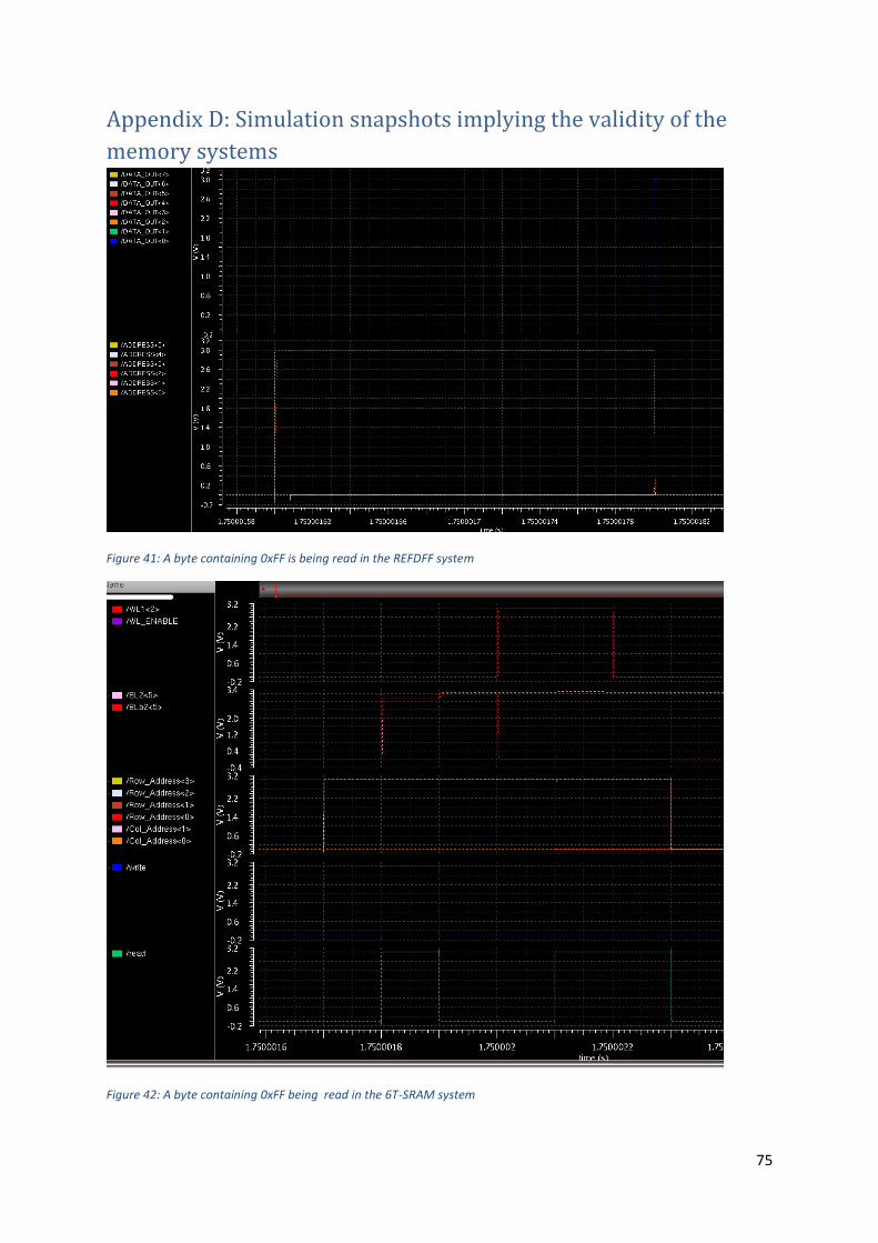
75
Appendix D: Simulation snapshots implying the validity of the
memory systems
Figure 41: A byte containing 0xFF is being read in the REFDFF system
Figure 42: A byte containing 0xFF being read in the 6T-SRAM system