
A Statistical Approach for the Characterization of Self-assembled Hexagonal Lattices
© 2013 WILEY-VCH Verlag GmbH & Co. KGaA, Weinheim 1
www.advmat.dewww.MaterialsViews.com
wileyonlinelibrary.com
CO
MM
UN
ICATIO
N
Two-Dimensional Si Nanosheets with Local Hexagonal Structure on a MoS 2 Surface
Daniele Chiappe , Emilio Scalise ,* Eugenio Cinquanta , Carlo Grazianetti , Bas van den Broek , Marco Fanciulli , Michel Houssa , and Alessandro Molle *
Although extensive knowledge has rapidly developed in the synthesis and processing of silicon quantum dots (zero-dimen-sional) and silicon nanowires (one-dimensional), the two-dimensional (2D) allotropic form of silicon has been hardly accessed and only recently few attempts have targeted 2D sil-icon nanosheets (NSs) akin to graphene. In this context, a 2D honeycomb crystalline form of silicon, the so-called “silicene”, has recently afforded great appeal as a novel graphene-like material. [ 1–11 ] Until now, free standing silicene has never been observed, because a 2D sp 2 Si crystal is chemically unstable in ambient conditions. [ 4 ] Nevertheless, quasi-2D honeycomb Si layers grown by molecular beam epitaxy (MBE) can be stabi-lized by a supporting substrate, as shown in recent pioneering experiments. [ 5 ] To date, buckled silicene structures have been experimentally reported on substrates with metallic char-acter, including Ag(111), [ 6–8 ] Ir(111), [ 9 ] and ZrB 2 . [ 10 ] However, accessing the electronic functionalities of the silicene neces-sarily demands to bypass of the metallic support.
The purpose of this paper is to look for a non-metallic substrates which can concomitantly favor a local 2D growth of Si with hexagonal crystal symmetry. To this scope, layered graphite-like materials [ 12 ] with hexagonal atomic arrangement are expected to be promising candidates. Importantly, cleavage of the layered compounds does not create dangling bonds and, therefore, these materials are ideally suited as inert sub-strates for van der Waals epitaxy of weakly interacting fi lms in the monolayer regime. [ 13–15 ] The electronic properties as well as the structural and chemical characteristics of layered materials make them appealing for a variety of applications and suitable for the synthesis of hybrid devices based on 2D materials. [ 16–18 ]
In this paper, Si epitaxy on the inorganic layered compound molybdenum disulfi de (MoS 2 ) is investigated. Bulk MoS 2 is an indirect bandgap ( E g = 1.20 eV) semiconductor similar to sil-icon. Interestingly, the vertical confi nement causes exfoliated MoS 2 single layers to be optically active with a direct bandgap ( E g = 1.83 eV), with outstanding implications for electronic and optoelectronic functionalities. [ 19–22 ] The use of MoS 2 (in its bulk form) as a substrate for deposition experiments has been put into practice by making use of molecular beam epitaxial growth of Si fi lms, whose local structural and electronic properties have been investigated by scanning tunneling microscopy/spec-troscopy (STM/STS) measurements and tentatively interpreted with the aid of density functional theory (DFT) calculations. Both experimental and theoretical results suggest the local for-mation of 2D nano-scaled Si domains with hexagonal atomic arrangement and anomalous electronic character.
It is fi rst convenient to clarify that the bulk MoS 2 crystal sketched in Figure 1 a is composed of a stack of weakly inter-acting layers (S–Mo–S units) that are linked together by van der Waals forces. Each of these stable units consists of an intermediate hexagonal plane of Mo atoms sandwiched in between two planes of S atoms. Mo atoms are bonded with the S atoms through covalent interactions, in a trigonal prismatic arrangement. The MoS 2 surface structure results in a honey-comb lattice (cell parameter a = 3.16 Å), where each site is non-equivalently occupied by Mo and S atoms. [ 23 ]
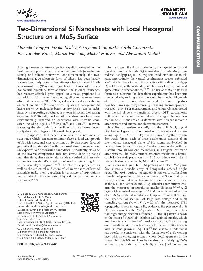
As shown in Figure 1 a, STM probing of a clean MoS 2 sur-face shows a periodic array of hexagonally ordered bright spots. The MoS 2 surface topography is known to suffer from tunneling-dependent probing conditions: the S atom lattice is usually observed at large tip-sample distances, and a mixture of the Mo (4dz 2 orbitals) and S (3p orbitals) contributions gov-erns the measured topography at smaller distances. [ 24–27 ] A Si layer with nominal coverage of 0.8 ML was deposited on the clean MoS 2 crystal at a substrate temperature of 200 °C (see the Experimental section). At large bias voltage and small tunneling current ( V B = 1 V, I S = 0.7 nA), the measured STM topography, shown in Figure 1 b, evidences the presence of a Si NS locally covering the MoS 2 surface. Accordingly, the refl ec-tion high energy electron diffraction (RHEED) pattern (shown in the inset of Figure 1 b) exhibits well-defi ned streaks, which are characteristic of the MoS 2 surface structure, [ 28 ] thus ruling out three dimensional nucleation mechanisms. Unlike the epi-taxial silicene grown on Ag(111), [ 29 ] the absence of additional sub-streaks is consistent with the formation of a Si wetting layer with no emerging reconstruction. Local apertures in the uncompleted Si NS enable us to visualize the underlying MoS 2 surface. These portions of the MoS 2 surface (dark contour in DOI: 10.1002/adma.201304783
D. Chiappe, Dr. E. Cinquanta, C. Grazianetti, Prof. M. Fanciulli, Dr. A. MolleLaboratorio MDM, IMM-CNR via C. Olivetti 2 , I-20864 , Agrate Brianza , (MB) , Italy E-mail: [email protected] E. Scalise, B. van den Broek, Dr. M. Houssa Semiconductor Physics LaboratoryDepartment of Physics and AstronomyUniversity of Leuven Celestijnenlaan 200 D , B-3001 , Leuven , Belgium E-mail: [email protected] C. Grazianetti, Prof. M. FanciulliDipartimento di Scienza dei MaterialiUniversità degli Studi di Milano Bicocca via R. Cozzi 53 , I-20126 , Milano , (MI) , Italy
Adv. Mater. 2013, DOI: 10.1002/adma.201304783
2
www.advmat.dewww.MaterialsViews.com
wileyonlinelibrary.com © 2013 WILEY-VCH Verlag GmbH & Co. KGaA, Weinheim
CO
MM
UN
ICATI
ON
Figure 1 b) clearly show the typical hexagonal pattern similar to that shown in Figure 1 a for the pristine MoS 2 surface. Other-wise, in correspondence of the Si domains, the surface appears smoother and unstructured, suggesting a different tip-to-sub-strate tunneling condition, which refl ects the locally different electronic character of the Si ad-atoms with respect to the underlying semiconductor MoS 2 . In particular, a decrease of the vertical contrast can be observed as a function of the tip-to-substrate distance, which might be indicative of reduced local-ized character of the electronic states in the Si NS, as usually experienced in metal surfaces. [ 30,31 ] An ordered surface pattern is observed from the Si covered regions when the tip bias is reduced and the tunneling current is signifi cantly increased ( V B = 0.2 V, I S = 2 nA), as shown in Figure 1 c. Here, the left side and the right side of the image correspond to a portion of bare MoS 2 and a Si covered region, respectively. A line profi le taken across the two terraces allows measuring the amplitude of the step, which amounts to 5 Å. This value roughly corre-sponds to the separation between the S atoms terminating the MoS 2 surface and the topmost atoms of the Si ad-layer. For a more accurate insight into the structural details of the Si wet-ting layer, a magnifi cation of the 2D Si domain is shown in Figure 1 d. The magnifi ed topography shows hexagonal rings with a three-fold symmetry, suggesting that Si atoms locally self-organize in honeycomb-like nano-domains. It should be noticed that the periodicity of the Si pattern replicates the lat-tice constant of the MoS 2 surface, confi rming the effective role
of the MoS 2 surface as a template in determining the atomistic arrangement of Si NS (see also Figure SI1 and Figure SI2 of the Supporting Information).
The measured topography, along with the absence of Si NS related sub-streaks in the RHEED pattern, can be tentatively rationalized by means of DFT calculations of the lowest energy Si NS/MoS 2 confi guration, in terms of a (1 × 1) honeycomb arrangement of the Si ad-layer with respect to the MoS 2 lattice.
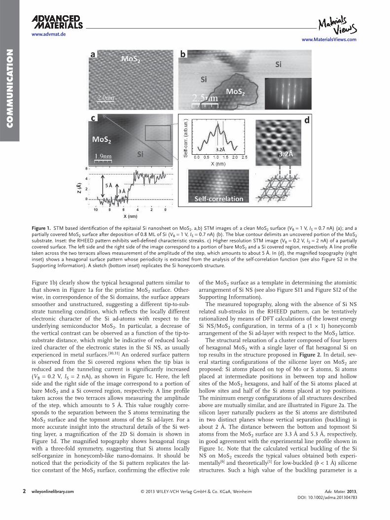
The structural relaxation of a cluster composed of four layers of hexagonal MoS 2 with a single layer of fl at hexagonal Si on top results in the structure proposed in Figure 2 . In detail, sev-eral starting confi gurations of the silicene layer on MoS 2 are proposed: Si atoms placed on top of Mo or S atoms, Si atoms placed at intermediate positions in between top and hollow sites of the MoS 2 hexagons, and half of the Si atoms placed at hollow sites and half of the Si atoms placed at top positions. The minimum energy confi gurations of all structures described above are mutually similar, and are illustrated in Figure 2 a. The silicon layer naturally puckers as the Si atoms are distributed in two distinct planes whose vertical separation (buckling) is about 2 Å. The distance between the bottom and topmost Si atoms from the MoS 2 surface are 3.3 Å and 5.3 Å, respectively, in good agreement with the experimental line profi le shown in Figure 1 c. Note that the calculated vertical buckling of the Si NS on MoS 2 exceeds the typical values obtained both experi-mentally [ 6 ] and theoretically [ 1 ] for low-buckled ( b < 1 Å) silicene structures. Such a high value of the buckling parameter is a
Figure 1. STM based identifi cation of the epitaxial Si nanosheet on MoS 2 . a,b) STM images of: a clean MoS 2 surface ( V B = 1 V, I S = 0.7 nA) (a); and a partially covered MoS 2 surface after deposition of 0.8 ML of Si ( V B = 1 V, I S = 0.7 nA) (b). The blue contour delimits an uncovered portion of the MoS 2 substrate. Inset: the RHEED pattern exhibits well-defi ned characteristic streaks. c) Higher resolution STM image ( V B = 0.2 V, I S = 2 nA) of a partially covered surface. The left side and the right side of the image correspond to a portion of bare MoS 2 and a Si covered region, respectively. A line profi le taken across the two terraces allows measurement of the amplitude of the step, which amounts to about 5 Å. In (d), the magnifi ed topography (right inset) shows a hexagonal surface pattern whose periodicity is extracted from the analysis of the self-correlation function (see also Figure S2 in the Supporting Information). A sketch (bottom inset) replicates the Si honeycomb structure.
Adv. Mater. 2013, DOI: 10.1002/adma.201304783
3
www.advmat.dewww.MaterialsViews.com
wileyonlinelibrary.com© 2013 WILEY-VCH Verlag GmbH & Co. KGaA, Weinheim
CO
MM
UN
ICATIO
N
the morphology shown in Figure 1 d. The mutual agreement between the experimental STM investigation and theoretical DFT computation confi rms the consistency of our interpreta-tive model, which describes the Si NS as a local honeycomb 2D crystal with pronounced vertical buckling between adjacent atoms.
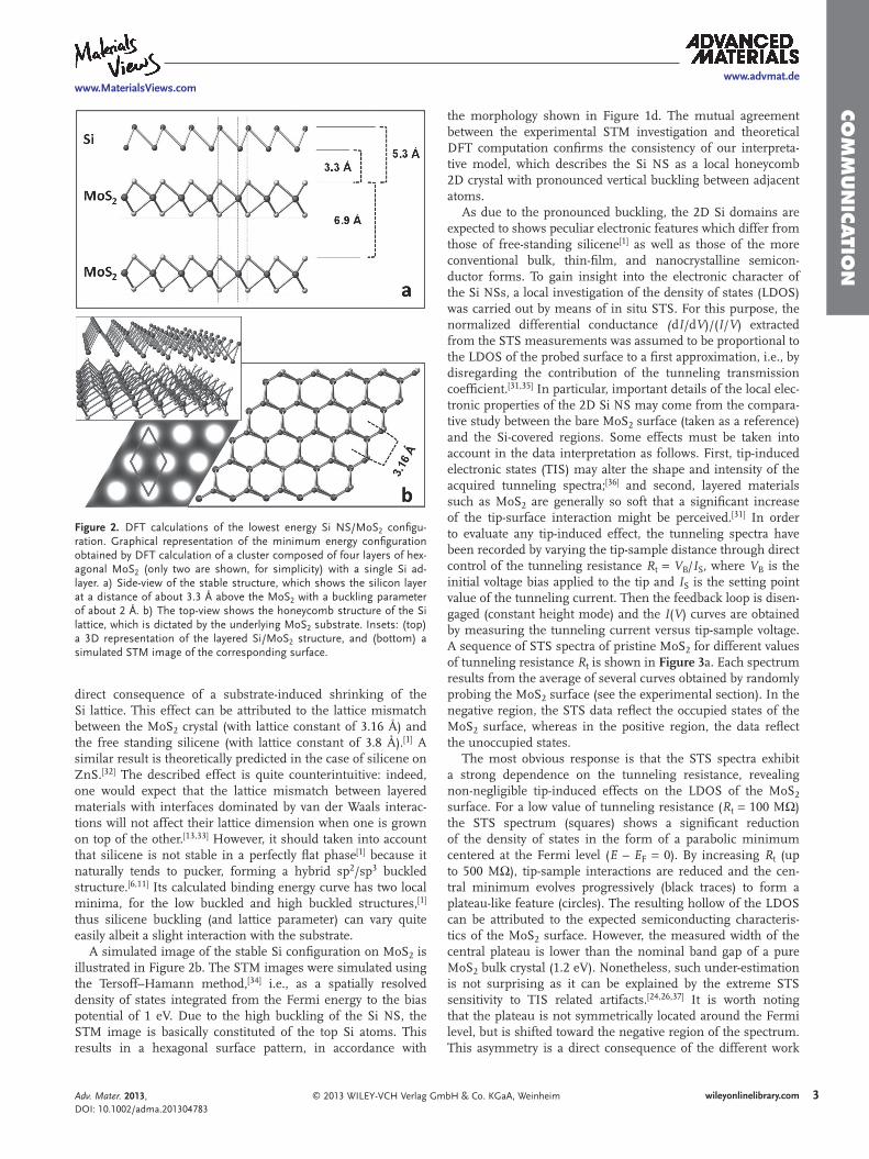
As due to the pronounced buckling, the 2D Si domains are expected to shows peculiar electronic features which differ from those of free-standing silicene [ 1 ] as well as those of the more conventional bulk, thin-fi lm, and nanocrystalline semicon-ductor forms. To gain insight into the electronic character of the Si NSs, a local investigation of the density of states (LDOS) was carried out by means of in situ STS. For this purpose, the normalized differential conductance ( d I /d V )/( I / V ) extracted from the STS measurements was assumed to be proportional to the LDOS of the probed surface to a fi rst approximation, i.e., by disregarding the contribution of the tunneling transmission coeffi cient. [ 31,35 ] In particular, important details of the local elec-tronic properties of the 2D Si NS may come from the compara-tive study between the bare MoS 2 surface (taken as a reference) and the Si-covered regions. Some effects must be taken into account in the data interpretation as follows. First, tip-induced electronic states (TIS) may alter the shape and intensity of the acquired tunneling spectra; [ 36 ] and second, layered materials such as MoS 2 are generally so soft that a signifi cant increase of the tip-surface interaction might be perceived. [ 31 ] In order to evaluate any tip-induced effect, the tunneling spectra have been recorded by varying the tip-sample distance through direct control of the tunneling resistance R t = V B / I S , where V B is the initial voltage bias applied to the tip and I S is the setting point value of the tunneling current. Then the feedback loop is disen-gaged (constant height mode) and the I ( V ) curves are obtained by measuring the tunneling current versus tip-sample voltage. A sequence of STS spectra of pristine MoS 2 for different values of tunneling resistance R t is shown in Figure 3 a. Each spectrum results from the average of several curves obtained by randomly probing the MoS 2 surface (see the experimental section). In the negative region, the STS data refl ect the occupied states of the MoS 2 surface, whereas in the positive region, the data refl ect the unoccupied states.
The most obvious response is that the STS spectra exhibit a strong dependence on the tunneling resistance, revealing non-negligible tip-induced effects on the LDOS of the MoS 2 surface. For a low value of tunneling resistance ( R t = 100 M Ω ) the STS spectrum (squares) shows a signifi cant reduction of the density of states in the form of a parabolic minimum centered at the Fermi level ( E – E F = 0). By increasing R t (up to 500 M Ω ), tip-sample interactions are reduced and the cen-tral minimum evolves progressively (black traces) to form a plateau-like feature (circles). The resulting hollow of the LDOS can be attributed to the expected semiconducting characteris-tics of the MoS 2 surface. However, the measured width of the central plateau is lower than the nominal band gap of a pure MoS 2 bulk crystal (1.2 eV). Nonetheless, such under-estimation is not surprising as it can be explained by the extreme STS sensitivity to TIS related artifacts. [ 24,26,37 ] It is worth noting that the plateau is not symmetrically located around the Fermi level, but is shifted toward the negative region of the spectrum. This asymmetry is a direct consequence of the different work
direct consequence of a substrate-induced shrinking of the Si lattice. This effect can be attributed to the lattice mismatch between the MoS 2 crystal (with lattice constant of 3.16 Å) and the free standing silicene (with lattice constant of 3.8 Å). [ 1 ] A similar result is theoretically predicted in the case of silicene on ZnS. [ 32 ] The described effect is quite counterintuitive: indeed, one would expect that the lattice mismatch between layered materials with interfaces dominated by van der Waals interac-tions will not affect their lattice dimension when one is grown on top of the other. [ 13,33 ] However, it should taken into account that silicene is not stable in a perfectly fl at phase [ 1 ] because it naturally tends to pucker, forming a hybrid sp 2 /sp 3 buckled structure. [ 6,11 ] Its calculated binding energy curve has two local minima, for the low buckled and high buckled structures, [ 1 ] thus silicene buckling (and lattice parameter) can vary quite easily albeit a slight interaction with the substrate.
A simulated image of the stable Si confi guration on MoS 2 is illustrated in Figure 2 b. The STM images were simulated using the Tersoff–Hamann method, [ 34 ] i.e., as a spatially resolved density of states integrated from the Fermi energy to the bias potential of 1 eV. Due to the high buckling of the Si NS, the STM image is basically constituted of the top Si atoms. This results in a hexagonal surface pattern, in accordance with
Figure 2. DFT calculations of the lowest energy Si NS/MoS 2 confi gu-ration. Graphical representation of the minimum energy confi guration obtained by DFT calculation of a cluster composed of four layers of hex-agonal MoS 2 (only two are shown, for simplicity) with a single Si ad-layer. a) Side-view of the stable structure, which shows the silicon layer at a distance of about 3.3 Å above the MoS 2 with a buckling parameter of about 2 Å. b) The top-view shows the honeycomb structure of the Si lattice, which is dictated by the underlying MoS 2 substrate. Insets: (top) a 3D representation of the layered Si/MoS 2 structure, and (bottom) a simulated STM image of the corresponding surface.
Adv. Mater. 2013, DOI: 10.1002/adma.201304783
4
www.advmat.dewww.MaterialsViews.com
wileyonlinelibrary.com © 2013 WILEY-VCH Verlag GmbH & Co. KGaA, Weinheim
CO
MM
UN
ICATI
ON consequence of Si NS formation consistently
with the metallic behavior that is expected from free-standing highly buckled silicene ( b > 1.9 Å). [ 1 ]
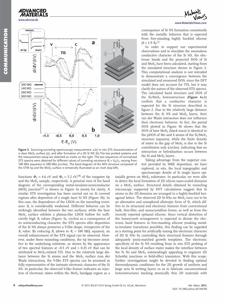
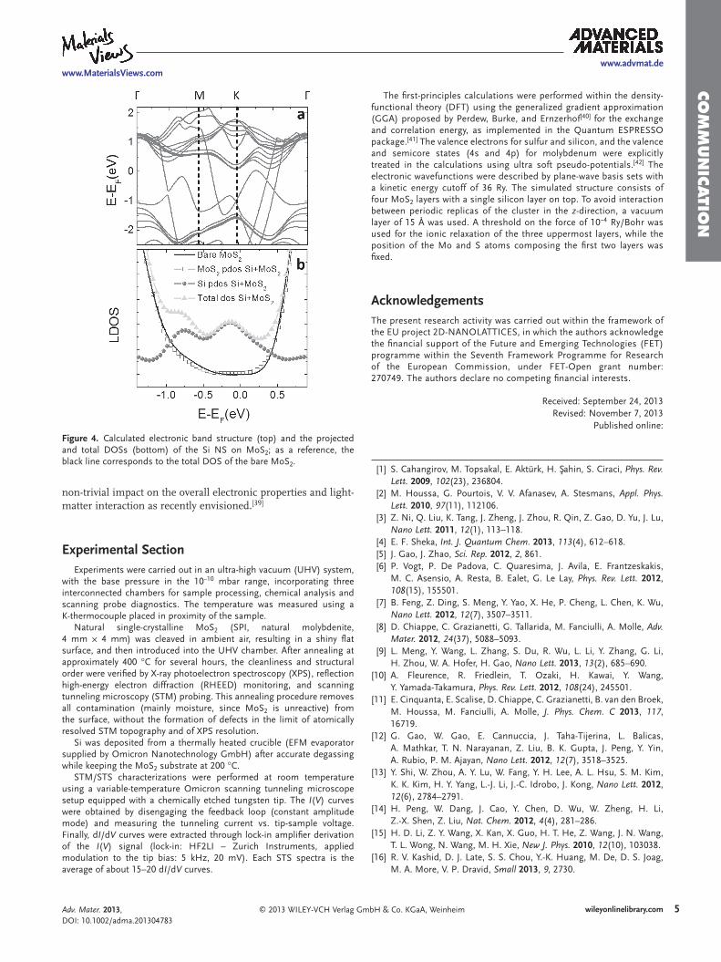
In order to support our experimental observations and to elucidate the anomalous conductive character of the Si NS, the elec-tronic bands and the projected DOS of Si and MoS 2 have been calculated, starting from the simulated structure shown in Figure 2 . This computational analysis is not intended to demonstrate a convergence between the simulated and measured DOS, since the DFT model does not account for TIS, but it may clarify the nature of the observed STS spectra. The calculated band structure and DOS of the Si/MoS 2 heterostructure ( Figure 4 a,b) confi rm that a conductive character is expected for the Si structure described in fi gure 2. Due to the relatively large distance between the Si NS and MoS 2 layers, their van der Waals interaction does not infl uence their electronic behavior. In fact, the partial DOS plotted in Figure 4 b shows that the DOS of bare MoS 2 (black trace) is identical to the pDOS of Mo and S atoms of the Si/MoS 2 structure (squares), while the fi nite density of states in the gap of MoS 2 is due to the Si contribution only (circles), indicating that no interaction or hybridization occurs between the Si and MoS 2 layers.
Taking advantage from the superior con-trol provided by MBE deposition, we have explored, in situ, the local topographic and spectroscopic details of Si single layers epi-
taxially grown on MoS 2 substrates. In particular, we were able to detect the local formation of 2D silicon nano-scaled domains on a MoS 2 surface. Structural details obtained by tunneling microscopy supported by DFT calculations suggest that Si atoms in the 2D domains are arranged in a highly-buckled hex-agonal lattice. The observed 2D Si-NSs on MoS 2 turn out to be an alternative and unexplored allotropic form of Si, which dif-fers in its structural and electronic features from conventional bulk, thin-fi lm, and nanocrystalline forms, as well as from the recently reported epitaxial silicene. Since vertical distortion of the honeycomb arrangement is expected to dictate the elec-tronic band features in free-standing silicene (making metal-to-insulator transitions possible), this fi nding can be regarded as a starting point for artifi cially tuning the electronic character of 2D Si NSs by controlling their structural features through adequately (mis)-matched growth templates. The electronic specifi city of the Si NS resulting from in situ STS probing of the local density of surface states makes the interface between the Si Ns and MoS 2 outstandingly appealing to engineer 2D Schottky junctions or fi eld-effect transistors. With this scope, further investigations might be devoted to fi nding optimal thermodynamic conditions for the 2D growth of uniform and large area Si wetting layers so as to fabricate unconventional heterostructures stacking atomically thin 2D materials with
functions Φ T = 4.6 eV and Φ S = 5.2 eV, [ 38 ] of the tungsten tip and the MoS 2 sample, respectively. A pictorial view of the band diagram of the corresponding metal-insulator-semiconductor (MIS) junction [ 31 ] is shown in Figure 3 a (inset) for clarity. A similar STS investigation has been carried out on Si covered regions after deposition of a single layer Si NS (Figure 3 b). In this case, the dependence of the LDOS on the tunneling resist-ance R t is considerably weakened. Different behavior can be strikingly identifi ed between the two surfaces; while the bare MoS 2 surface exhibits a plateau-like LDOS hollow for suffi -ciently high R t values (Figure 3 a, circles) as a consequence of its semiconducting character, the STS spectra after deposition of the Si NS always preserves a V-like shape, irrespective of the R t value. By reducing R t (down to R t = 100 M Ω , squares), an overall enhancement of the STS signal can be observed. How-ever, under these tunneling conditions, the tip becomes sensi-tive to the underlying substrate, as shown by the appearance of two spectral features at –0.5 eV and + 0.25 eV that can be attributed to MoS 2 -related TIS. Due to the relatively large dis-tance between the Si atoms and the MoS 2 surface (van der Waals interaction), the V-like STS spectra can be assumed as fully representative of the intimate electronic character of the Si NS. In particular, the observed V-like feature indicates an injec-tion of electronic states within the MoS 2 bandgap region as a
Figure 3. Scanning tunneling spectroscopy measurement. a,b) In situ STS characterization of a clean MoS 2 surface (a), and after formation of a 2D Si NS (b).The two probed systems and the measurement setup are sketched as insets on the right. The two sequences of normalized STS spectra were obtained for different values of tunneling resistance R t = V B / I S , varying from 100 M Ω (squares) to 500 M Ω (circles). The band diagram of the MIS structure composed of the STM tip and the MoS 2 surface is tentatively illustrated as an inset (top-left).
Adv. Mater. 2013, DOI: 10.1002/adma.201304783
5
www.advmat.dewww.MaterialsViews.com
wileyonlinelibrary.com© 2013 WILEY-VCH Verlag GmbH & Co. KGaA, Weinheim
CO
MM
UN
ICATIO
N
The fi rst-principles calculations were performed within the density-functional theory (DFT) using the generalized gradient approximation (GGA) proposed by Perdew, Burke, and Ernzerhof [ 40 ] for the exchange and correlation energy, as implemented in the Quantum ESPRESSO package. [ 41 ] The valence electrons for sulfur and silicon, and the valence and semicore states (4s and 4p) for molybdenum were explicitly treated in the calculations using ultra soft pseudo-potentials. [ 42 ] The electronic wavefunctions were described by plane-wave basis sets with a kinetic energy cutoff of 36 Ry. The simulated structure consists of four MoS 2 layers with a single silicon layer on top. To avoid interaction between periodic replicas of the cluster in the z -direction, a vacuum layer of 15 Å was used. A threshold on the force of 10 −4 Ry/Bohr was used for the ionic relaxation of the three uppermost layers, while the position of the Mo and S atoms composing the fi rst two layers was fi xed.
Acknowledgements The present research activity was carried out within the framework of the EU project 2D-NANOLATTICES, in which the authors acknowledge the fi nancial support of the Future and Emerging Technologies (FET) programme within the Seventh Framework Programme for Research of the European Commission, under FET-Open grant number: 270749. The authors declare no competing fi nancial interests.
Received: September 24, 2013 Revised: November 7, 2013
Published online:
[1] S. Cahangirov , M. Topsakal , E. Aktürk , H. Sahin , S. Ciraci , Phys. Rev. Lett. 2009 , 102 ( 23 ), 236804 .
[2] M. Houssa , G. Pourtois , V. V. Afanasev , A. Stesmans , Appl. Phys. Lett. 2010 , 97 ( 11 ), 112106 .
[3] Z. Ni , Q. Liu , K. Tang , J. Zheng , J. Zhou , R. Qin , Z. Gao , D. Yu , J. Lu , Nano Lett. 2011 , 12 ( 1 ), 113 – 118 .
[4] E. F. Sheka , Int. J. Quantum Chem. 2013 , 113 ( 4 ), 612 – 618 . [5] J. Gao , J. Zhao , Sci. Rep. 2012 , 2 , 861 . [6] P. Vogt , P. De Padova , C. Quaresima , J. Avila , E. Frantzeskakis ,
M. C. Asensio , A. Resta , B. Ealet , G. Le Lay , Phys. Rev. Lett. 2012 , 108 ( 15 ), 155501 .
[7] B. Feng , Z. Ding , S. Meng , Y. Yao , X. He , P. Cheng , L. Chen , K. Wu , Nano Lett. 2012 , 12 ( 7 ), 3507 – 3511 .
[8] D. Chiappe , C. Grazianetti , G. Tallarida , M. Fanciulli , A. Molle , Adv. Mater. 2012 , 24 ( 37 ), 5088 – 5093 .
[9] L. Meng , Y. Wang , L. Zhang , S. Du , R. Wu , L. Li , Y. Zhang , G. Li , H. Zhou , W. A. Hofer , H. Gao , Nano Lett. 2013 , 13 ( 2 ), 685 – 690 .
[10] A. Fleurence , R. Friedlein , T. Ozaki , H. Kawai , Y. Wang , Y. Yamada-Takamura , Phys. Rev. Lett. 2012 , 108 ( 24 ), 245501 .
[11] E. Cinquanta , E. Scalise , D. Chiappe , C. Grazianetti , B. van den Broek , M. Houssa , M. Fanciulli , A. Molle , J. Phys. Chem. C 2013 , 117 , 16719 .
[12] G. Gao , W. Gao , E. Cannuccia , J. Taha-Tijerina , L. Balicas , A. Mathkar , T. N. Narayanan , Z. Liu , B. K. Gupta , J. Peng , Y. Yin , A. Rubio , P. M. Ajayan , Nano Lett. 2012 , 12 ( 7 ), 3518 – 3525 .
[13] Y. Shi , W. Zhou , A. Y. Lu , W. Fang , Y. H. Lee , A. L. Hsu , S. M. Kim , K. K. Kim , H. Y. Yang , L.-J. Li , J.-C. Idrobo , J. Kong , Nano Lett. 2012 , 12 ( 6 ), 2784 – 2791 .
[14] H. Peng , W. Dang , J. Cao , Y. Chen , D. Wu , W. Zheng , H. Li , Z.-X. Shen , Z. Liu , Nat. Chem. 2012 , 4 ( 4 ), 281 – 286 .
[15] H. D. Li , Z. Y. Wang , X. Kan , X. Guo , H. T. He , Z. Wang , J. N. Wang , T. L. Wong , N. Wang , M. H. Xie , New J. Phys. 2010 , 12 ( 10 ), 103038 .
[16] R. V. Kashid , D. J. Late , S. S. Chou , Y.-K. Huang , M. De , D. S. Joag , M. A. More , V. P. Dravid , Small 2013 , 9 , 2730 .
non-trivial impact on the overall electronic properties and light-matter interaction as recently envisioned. [ 39 ]
Experimental Section Experiments were carried out in an ultra-high vacuum (UHV) system,
with the base pressure in the 10 −10 mbar range, incorporating three interconnected chambers for sample processing, chemical analysis and scanning probe diagnostics. The temperature was measured using a K-thermocouple placed in proximity of the sample.
Natural single-crystalline MoS 2 (SPI, natural molybdenite, 4 mm × 4 mm) was cleaved in ambient air, resulting in a shiny fl at surface, and then introduced into the UHV chamber. After annealing at approximately 400 °C for several hours, the cleanliness and structural order were verifi ed by X-ray photoelectron spectroscopy (XPS), refl ection high-energy electron diffraction (RHEED) monitoring, and scanning tunneling microscopy (STM) probing. This annealing procedure removes all contamination (mainly moisture, since MoS 2 is unreactive) from the surface, without the formation of defects in the limit of atomically resolved STM topography and of XPS resolution.
Si was deposited from a thermally heated crucible (EFM evaporator supplied by Omicron Nanotechnology GmbH) after accurate degassing while keeping the MoS 2 substrate at 200 °C.
STM/STS characterizations were performed at room temperature using a variable-temperature Omicron scanning tunneling microscope setup equipped with a chemically etched tungsten tip. The I ( V ) curves were obtained by disengaging the feedback loop (constant amplitude mode) and measuring the tunneling current vs. tip-sample voltage. Finally, d I /d V curves were extracted through lock-in amplifi er derivation of the I ( V ) signal (lock-in: HF2LI – Zurich Instruments, applied modulation to the tip bias: 5 kHz, 20 mV). Each STS spectra is the average of about 15–20 d I /d V curves.
Figure 4. Calculated electronic band structure (top) and the projected and total DOSs (bottom) of the Si NS on MoS 2 ; as a reference, the black line corresponds to the total DOS of the bare MoS 2 .
Adv. Mater. 2013, DOI: 10.1002/adma.201304783
6
www.advmat.dewww.MaterialsViews.com
wileyonlinelibrary.com © 2013 WILEY-VCH Verlag GmbH & Co. KGaA, Weinheim
CO
MM
UN
ICATI
ON [31] R. Wiesendanger , Scanning Probe Microscopy and Spectroscopy:
Methods and Applications , Cambridge University Press , Cambridge, UK , 1994 .
[32] M. Houssa , B. van den Broek , E. Scalise , G. Pourtois , V. V. Afanas’ev , A. Stesmans , Phys. Chem. Chem. Phys. 2013 , 15 ( 11 ), 3702 – 3705 .
[33] A. J. Koma , Cryst. Growth 1999 , 201 , 236 – 241 . [34] J. Tersoff , D. R. Hamann , Phys. Rev. B 1985 , 31 , 805 – 813 . [35] J. A. Stroscio , R. M. Feenstra , A. P. Fein , Phys. Rev. Lett. 1986 ,
57 ( 20 ), 2579 – 2582 . [36] E. Tekman , S. Ciraci , Phys. Rev. B 1989 , 40 ( 15 ), 10286 . [37] E. Tekman , S. Ciraci , Phys. Scr. 1988 , 38 ( 3 ), 486 . [38] S. Fiechter , Sol. Energ. Mater. Sol. Cells 2004 , 83 ( 4 ), 459 – 477 . [39] L. Britnell , R. M. Ribeiro , A. Eckmann , R. Jalil , B. D. Belle , A. Mishchenko ,
Y.-J. Kim , R. V. Gorbachev , T. Georgiou , S. V. Morozov , A. N. Grigorenko , A. K. Geim , C. Casiraghi , A. H. Castro Neto , K. S. Novoselov , Science 2009 , 340 ( 6138 ), 1311 – 1314 .
[40] J. P. Perdew , K. Burke , M. Ernzerhof , Phys. Rev. Lett. 1996 , 77 ( 18 ), 3865 – 3868 .
[41] P. Giannozzi , S. Baroni , N. Bonini , M. Calandra , R. Car , C. Cavazzoni , D. Ceresoli , G. L. Chiarotti , M. Cococcioni , I. Dabo , A. Dal Corso , S. de Gironcoli , S. Fabris , G. Fratesi , R. Gebauer , U. Gerstmann , C. Gougoussis , A. Kokalj , M. Lazzeri , L. Martin-Samos , N. Marzari , F. Mauri , R. Mazzarello , S. Paolini , A. Pasquarello , L. Paulatto , C. Sbraccia , S. Scandolo , G. Sclauzero , A. P. Seitsonen , A. Smogunov , P. Umari , R. M. Wentzcovitch , J. Phys.-Condens. Matter 2009 , 21 ( 39 ), 395502 .
[42] D. Vanderbilt , Phys. Rev. B 1990 , 41 ( 11 ), 7892 .
[17] D. J. Late , B. Liu , H. S. S. R. Matte , C. N. R. Rao , V. P. Dravid , Adv. Funct. Mater. 2012 , 22 , 1894 .
[18] D. J. Late , B. Liu , J. Luo , A. Yan , H. S. S. R. Matte , M. Grayson , C. N. R. Rao , V. P. Dravid , Adv. Mater. 2012 , 24 , 3549 .
[19] B. Radisavljevic , A. Radenovic , J. Brivio , V. Giacometti , A. Kis , Nat. Nanotechnol. 2011 , 6 ( 3 ), 147 – 150 .
[20] Z. Yin , H. Li , H. Li , L. Jiang , Y. Shi , Y. Sun , G. Lu , Q. Zhang , X. Chen , H. Zhang , ACS Nano 2011 , 6 ( 1 ), 74 – 80 .
[21] H. S. Lee , S. W. Min , Y. G. Chang , M. K. Park , T. Nam , H. Kim , J. H. Kim , S. Ryu , S. Im , Nano Lett. 2012 , 12 ( 7 ), 3695 – 3700 .
[22] M. Chhowalla , H. S. Shin , G. Eda , L. J. Li , K. P. Loh , H. Zhang , Nat. Chem. 2013 , 5 ( 4 ), 263 – 275 .
[23] S. W. Han , G. B. Cha , E. Frantzeskakis , I. Razado-Colambo , J. Avila , Y. S. Park , D. Kim , J. Hwang , J. S. Kang , S. Ryu , W. S. Yun , S. C. Hong , M. C. Asensio , Phys. Rev. B 2012 , 86 ( 11 ), 115105 .
[24] U. Becker , K. M. Rosso , R. Weaver , M. Warren , M. F. Hochella Jr ., Geochim. Cosmochim. Acta 2003 , 67 ( 5 ), 923 – 934 .
[25] C. Joachim , A. Altibelli , P. Sautet , Surf. Sci. 1996 , 367 ( 2 ), 209 – 220 . [26] H. Murata , A. Koma , Phys. Rev. B 1999 , 59 ( 15 ), 10327 – 10334 . [27] S. Helveg , J. V. Lauritsen , E. Lægsgaard , I. Stensgaard , J. K. Nørskov ,
B. S. Clausen , H. Topsøe , F. Besenbacher , Phys. Rev. Lett. 2000 , 84 ( 5 ), 951 – 954 .
[28] T. Hayashi , K. Ueno , K. Saiki , A. Koma , J. Cryst. Growth 2000 , 219 ( 1 ), 115 – 122 .
[29] A. Molle , C. Grazianetti , D. Chiappe , E. Cinquanta , E. Cianci , G. Tallarida , M. Fanciulli , Adv. Funct. Mater. 2013 , 23 , 4340 – 4344.
[30] C. J. Chen , Phys. Rev. Lett. 1990 , 65 ( 4 ), 448 – 451 .
Adv. Mater. 2013, DOI: 10.1002/adma.201304783
Copyright © 2022 FDOKUMEN