
Two-Dimensional Halide Perovskites - arXiv
83
1 Two-Dimensional Halide Perovskites: Synthesis, Optoelectronic Properties, Stability, and Applications Sushant Ghimire a and Christian Klinke* a,b,c * Corresponding author a Institute of Physics, University of Rostock, 18059 Rostock, Germany b Department of Chemistry, Swansea University, Swansea SA2 8PP, U.K. c Department "Life, Light & Matter", University of Rostock, Albert-Einstein-Strasse 25, 18059 Rostock, Germany Corresponding author: [email protected] Halide perovskites are promising materials for light-emitting and light-harvesting applications. In this context, two-dimensional perovskites such as nanoplatelets or Ruddlesden-Popper and Dion-Jacobson layered structures are important because of their structural flexibility, electronic confinement, and better stability. This review article brings forth an extensive overview of the recent developments of two-dimensional halide perovskites both in the colloidal and non- colloidal forms. We outline the strategy to synthesize and control the shape and discuss different crystalline phases and optoelectronic properties. We review the applications of two- dimensional perovskites in solar cells, light-emitting diodes, lasers, photodetectors, and photocatalysis. Besides, we also emphasize the moisture, thermal, and photostability of these materials in comparison to their three-dimensional analogs.
-
Upload
khangminh22 -
Category
Documents
-
view
0 -
download
0
Transcript of Two-Dimensional Halide Perovskites - arXiv

1
Two-Dimensional Halide Perovskites: Synthesis, Optoelectronic Properties,
Stability, and Applications
Sushant Ghimirea and Christian Klinke*a,b,c
* Corresponding author
a Institute of Physics, University of Rostock, 18059 Rostock, Germany
b Department of Chemistry, Swansea University, Swansea SA2 8PP, U.K.
c Department "Life, Light & Matter", University of Rostock, Albert-Einstein-Strasse 25,
18059 Rostock, Germany
Corresponding author: [email protected]
Halide perovskites are promising materials for light-emitting and light-harvesting applications.
In this context, two-dimensional perovskites such as nanoplatelets or Ruddlesden-Popper and
Dion-Jacobson layered structures are important because of their structural flexibility, electronic
confinement, and better stability. This review article brings forth an extensive overview of the
recent developments of two-dimensional halide perovskites both in the colloidal and non-
colloidal forms. We outline the strategy to synthesize and control the shape and discuss
different crystalline phases and optoelectronic properties. We review the applications of two-
dimensional perovskites in solar cells, light-emitting diodes, lasers, photodetectors, and
photocatalysis. Besides, we also emphasize the moisture, thermal, and photostability of these
materials in comparison to their three-dimensional analogs.

2
TOC graphic
2D halide perovskites show stable layered structures with interesting properties such as
electronic confinement, energy funneling, exciton dissociation at crystal edges, and broad
emission due to self-trapped excitons (STEs). These properties make 2D halide perovskites
promising for solar cells, LEDs, lasers, photodetectors, and photocatalysis.
2D
Halide Perovskites
Oriented Layered
StructureM
ois
ture
, H
ea
t, &
Lig
ht
Sta
bil
ity D
ime
ns
ion
al &
Die
lectric
Co
nfin
em
en
ts
STEs, Energy Funneling, Exciton
Dissociation
3
Biography of Authors
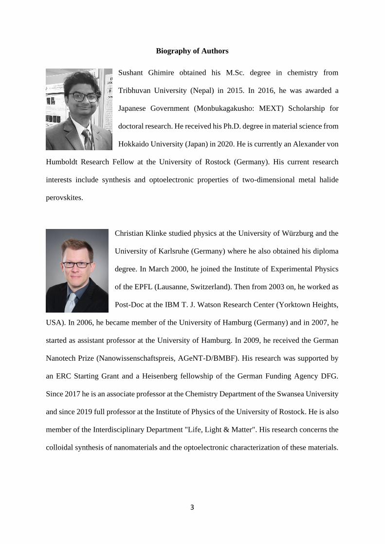
Sushant Ghimire obtained his M.Sc. degree in chemistry from
Tribhuvan University (Nepal) in 2015. In 2016, he was awarded a
Japanese Government (Monbukagakusho: MEXT) Scholarship for
doctoral research. He received his Ph.D. degree in material science from
Hokkaido University (Japan) in 2020. He is currently an Alexander von
Humboldt Research Fellow at the University of Rostock (Germany). His current research
interests include synthesis and optoelectronic properties of two-dimensional metal halide
perovskites.
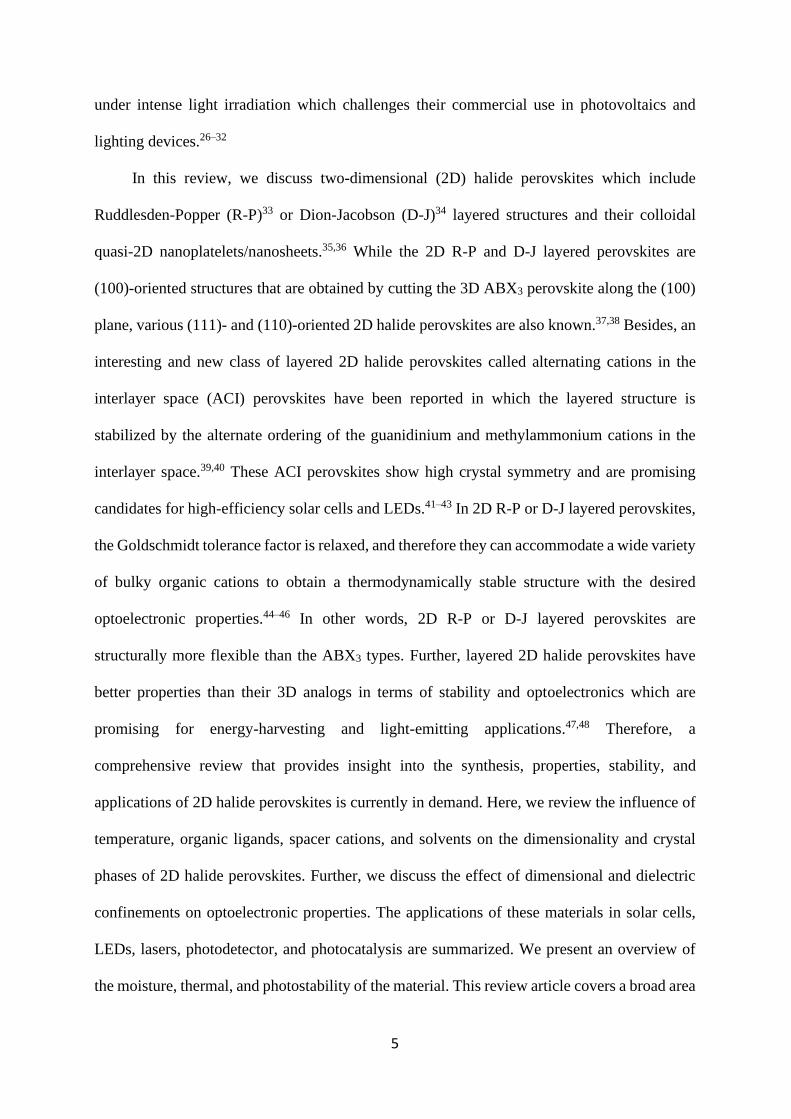
Christian Klinke studied physics at the University of Würzburg and the
University of Karlsruhe (Germany) where he also obtained his diploma
degree. In March 2000, he joined the Institute of Experimental Physics
of the EPFL (Lausanne, Switzerland). Then from 2003 on, he worked as
Post-Doc at the IBM T. J. Watson Research Center (Yorktown Heights,
USA). In 2006, he became member of the University of Hamburg (Germany) and in 2007, he
started as assistant professor at the University of Hamburg. In 2009, he received the German
Nanotech Prize (Nanowissenschaftspreis, AGeNT-D/BMBF). His research was supported by
an ERC Starting Grant and a Heisenberg fellowship of the German Funding Agency DFG.
Since 2017 he is an associate professor at the Chemistry Department of the Swansea University
and since 2019 full professor at the Institute of Physics of the University of Rostock. He is also
member of the Interdisciplinary Department "Life, Light & Matter". His research concerns the
colloidal synthesis of nanomaterials and the optoelectronic characterization of these materials.

4
1. Introduction
Halide perovskites have shown significant efficiencies in solar cells1,2 and LEDs.3,4
Photodetection,5,6 X-ray scintillation,7,8 lasing,9,10 and photocatalysis11,12 are other areas where
these materials are flourishing. Halide perovskites are referred to as defect tolerant13–15 which,
along with the low exciton binding energy in their bulk, show long-range carrier diffusion and
high carrier mobility.16–18 A record-breaking diffusion length of 175 µm is already
demonstrated in bulk methylammonium lead iodide (MAPbI3) single crystal.17 An unusually
long photoluminescence (PL) lifetime has also been reported in the close-packed assembly of
perovskite nanocrystals.19,20 Further, these materials show high photoluminescence (PL)
quantum yield (QY) and halide composition-dependent bandgap energy which is tunable in the
entire visible spectrum.9,21–23 Such unique optoelectronic properties make halide perovskites
highly promising for light-harvesting and light-emitting applications.
Three-dimensional (3D) perovskites have ABX3 structures with corner-sharing inorganic
[BX6]4- octahedra, where the B-site cation is Pb2+, Sn2+, or Ge2+ and X- ions are halides (Cl-,
Br-, or I-). The A-site cation occupies the space formed by the corner-sharing inorganic
octahedra to form the crystal lattice. The formation of a thermodynamically stable 3D
perovskite lattice is guided by the Goldschmidt tolerance factor (𝑡 =𝑟A+𝑟X
√2(𝑟B+𝑟X)) and the
octahedral factor (𝜇 =𝑟B
𝑟X), which correlate the ionic radii of A-site (rA), B-site (rB), and X- (rX)
ions. A stable ABX3 perovskite structure is formed with Cs+, MA+ (methylammonium), or FA+
(formamidinium) as A-site cations which result in the Goldschmidt tolerance factor in a narrow
range of 0.81 to 1.18,24 This limits the structural flexibility in 3D perovskites. The tunable optical
properties in ABX3 perovskites are governed by the band-edge electronic structure formed by
the mixing of s- and p-orbitals of B-site cations and halides.25 Despite having exceptional
optoelectronic properties, 3D halide perovskites are less stable in a moist environment and
5
under intense light irradiation which challenges their commercial use in photovoltaics and
lighting devices.26–32
In this review, we discuss two-dimensional (2D) halide perovskites which include
Ruddlesden-Popper (R-P)33 or Dion-Jacobson (D-J)34 layered structures and their colloidal
quasi-2D nanoplatelets/nanosheets.35,36 While the 2D R-P and D-J layered perovskites are
(100)-oriented structures that are obtained by cutting the 3D ABX3 perovskite along the (100)
plane, various (111)- and (110)-oriented 2D halide perovskites are also known.37,38 Besides, an
interesting and new class of layered 2D halide perovskites called alternating cations in the
interlayer space (ACI) perovskites have been reported in which the layered structure is
stabilized by the alternate ordering of the guanidinium and methylammonium cations in the
interlayer space.39,40 These ACI perovskites show high crystal symmetry and are promising
candidates for high-efficiency solar cells and LEDs.41–43 In 2D R-P or D-J layered perovskites,
the Goldschmidt tolerance factor is relaxed, and therefore they can accommodate a wide variety
of bulky organic cations to obtain a thermodynamically stable structure with the desired
optoelectronic properties.44–46 In other words, 2D R-P or D-J layered perovskites are
structurally more flexible than the ABX3 types. Further, layered 2D halide perovskites have
better properties than their 3D analogs in terms of stability and optoelectronics which are
promising for energy-harvesting and light-emitting applications.47,48 Therefore, a
comprehensive review that provides insight into the synthesis, properties, stability, and
applications of 2D halide perovskites is currently in demand. Here, we review the influence of
temperature, organic ligands, spacer cations, and solvents on the dimensionality and crystal
phases of 2D halide perovskites. Further, we discuss the effect of dimensional and dielectric
confinements on optoelectronic properties. The applications of these materials in solar cells,
LEDs, lasers, photodetector, and photocatalysis are summarized. We present an overview of
the moisture, thermal, and photostability of the material. This review article covers a broad area
6
of 2D halide perovskites. We believe it provides a good reference for students and researchers
in understanding the fundamental properties of these classes of materials and advance further.
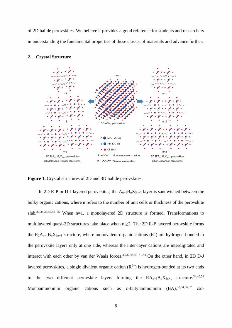
2. Crystal Structure
Figure 1. Crystal structures of 2D and 3D halide perovskites.
In 2D R-P or D-J layered perovskites, the An−1BnX3n+1 layer is sandwiched between the
bulky organic cations, where n refers to the number of unit cells or thickness of the perovskite
slab.33,34,37,45,49–55 When n=1, a monolayered 2D structure is formed. Transformations to
multilayered quasi-2D structures take place when n ≥2. The 2D R-P layered perovskite forms
the R2An−1BnX3n+1 structure, where monovalent organic cations (R+) are hydrogen-bonded to
the perovskite layers only at one side, whereas the inter-layer cations are interdigitated and
interact with each other by van der Waals forces.33,37,45,49–51,54 On the other hand, in 2D D-J
layered perovskites, a single divalent organic cation (R2+) is hydrogen-bonded at its two ends
to the two different perovskite layers forming the RAn−1BnX3n+1 structure.34,45,52
Monoammonium organic cations such as n-butylammonium (BA),33,54,56,57 iso-
2D R2An−1BnX3n+1 perovskites
(Ruddlesden-Popper structures)
2D R’An−1BnX3n+1 perovskites
(Dion-Jacobson structures)
3D ABX3 perovskites
n=1
n=2
n=3
n=1
n=2
n=3
A MA, FA, Cs
B Pb, Sn, Sb
X Cl, Br, I
R Monoammonium cation
R’ Diammonium cation
n=∞

7
butylammonium (iso-BA),56,57 n-pentylammonium (PA),50,54 n-hexylammonium (HA),50,54 n-
octylammonium (OA),58 phenylethylammonium (PEA),46,59–61 and phenylmethylammonium
(PMA) or benzylammonium62,63 are used as organic spacers in 2D R-P layered perovskites.
Similarly, (aminomethyl)piperidinium (AMP),34,64–67 (aminomethyl)pyridinium (AMPY),52
1,4‐phenylenedimethanammonium (PDMA),68–70 and short-chain alkyldiammonium cations71–
73 are some examples of organic spacers in 2D D-J layered perovskites. Figure 1 distinguishes
between the layered 2D and 3D halide perovskite structures. The flexibility, arrangement, and
separation of inorganic stacking in layered 2D halide perovskites are controlled by the choice
of organic spacer cations. The monoammonium spacer cations in 2D R-P layered perovskites
allow the stacking layers to slide over each other, resulting in a staggered arrangement due to
half a unit cell interlayer shift. On the other hand, the divalent organic cations increase the
rigidity of the 2D D-J layered structure giving rise to an eclipsed arrangement of the stacking
layers with smaller interlayer spacing.45,52,54 Nevertheless, a 2D R-P layered structure is formed
if such divalent organic cations are sufficiently long to tilt and allow the inorganic layers to
slide in a staggered configuration.53
2.1 Characterization
In (100)-oriented 2D halide perovskites, the A-site cations are fully or partly replaced by
the monodentate or bidentate organic ammonium cations to form R-P or D-J layered structures
with different thicknesses of the inorganic layer (n=1, 2, 3, and so on). Unlike ABX3
perovskites, the layered 2D halide perovskites have the inorganic BX6 octahedra in two
different environments, those which are on the surface next to the organic spacer layer, and the
next ones which are at the middle surrounded by other BX6 octahedra. Therefore, the crystal
structure of a layered 2D halide perovskite is influenced on the one hand in a similar way to
that of ABX3 perovskites, and on the other hand in a unique way due to the presence of organic
8
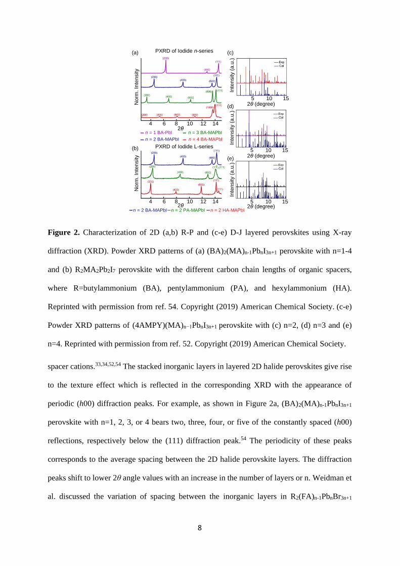
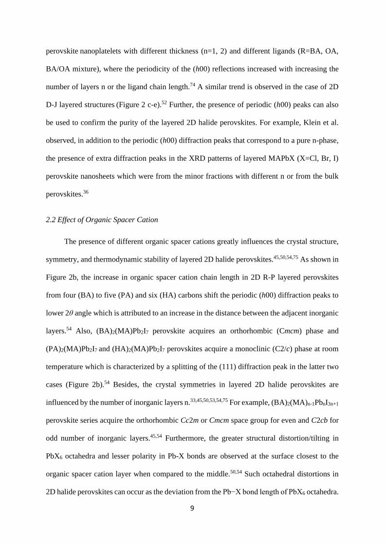
Figure 2. Characterization of 2D (a,b) R-P and (c-e) D-J layered perovskites using X-ray
diffraction (XRD). Powder XRD patterns of (a) (BA)2(MA)n-1PbnI3n+1 perovskite with n=1-4
and (b) R2MA2Pb2I7 perovskite with the different carbon chain lengths of organic spacers,
where R=butylammonium (BA), pentylammonium (PA), and hexylammonium (HA).
Reprinted with permission from ref. 54. Copyright (2019) American Chemical Society. (c-e)
Powder XRD patterns of (4AMPY)(MA)n−1PbnI3n+1 perovskite with (c) n=2, (d) n=3 and (e)
n=4. Reprinted with permission from ref. 52. Copyright (2019) American Chemical Society.
spacer cations.33,34,52,54 The stacked inorganic layers in layered 2D halide perovskites give rise
to the texture effect which is reflected in the corresponding XRD with the appearance of
periodic (h00) diffraction peaks. For example, as shown in Figure 2a, (BA)2(MA)n-1PbnI3n+1
perovskite with n=1, 2, 3, or 4 bears two, three, four, or five of the constantly spaced (h00)
reflections, respectively below the (111) diffraction peak.54 The periodicity of these peaks
corresponds to the average spacing between the 2D halide perovskite layers. The diffraction
peaks shift to lower 2θ angle values with an increase in the number of layers or n. Weidman et
al. discussed the variation of spacing between the inorganic layers in R2(FA)n-1PbnBr3n+1
Norm
. In
tensity
Norm
. In
tensity
Inte
nsity (
a.u
.)In
tensity (
a.u
.)In
tensity (
a.u
.)
n = 1 BA-PbI n = 3 BA-MAPbI
n = 2 BA-MAPbI n = 4 BA-MAPbI
n = 2 BA-MAPbI n = 2 PA-MAPbI n = 2 HA-MAPbI
PXRD of Iodide n-series
PXRD of Iodide L-series
4 6 8 10 12 14
4 6 8 10 12 14
2θ
2θ
5 10 152θ (degree)
5 10 152θ (degree)
5 10 152θ (degree)
(a)
(b)
(c)
(d)
(e)
9
perovskite nanoplatelets with different thickness (n=1, 2) and different ligands (R=BA, OA,
BA/OA mixture), where the periodicity of the (h00) reflections increased with increasing the
number of layers n or the ligand chain length.74 A similar trend is observed in the case of 2D
D-J layered structures (Figure 2 c-e).52 Further, the presence of periodic (h00) peaks can also
be used to confirm the purity of the layered 2D halide perovskites. For example, Klein et al.
observed, in addition to the periodic (h00) diffraction peaks that correspond to a pure n-phase,
the presence of extra diffraction peaks in the XRD patterns of layered MAPbX (X=Cl, Br, I)
perovskite nanosheets which were from the minor fractions with different n or from the bulk
perovskites.36
2.2 Effect of Organic Spacer Cation
The presence of different organic spacer cations greatly influences the crystal structure,
symmetry, and thermodynamic stability of layered 2D halide perovskites.45,50,54,75 As shown in
Figure 2b, the increase in organic spacer cation chain length in 2D R-P layered perovskites
from four (BA) to five (PA) and six (HA) carbons shift the periodic (h00) diffraction peaks to
lower 2θ angle which is attributed to an increase in the distance between the adjacent inorganic
layers.54 Also, (BA)2(MA)Pb2I7 perovskite acquires an orthorhombic (Cmcm) phase and
(PA)2(MA)Pb2I7 and (HA)2(MA)Pb2I7 perovskites acquire a monoclinic (C2/c) phase at room
temperature which is characterized by a splitting of the (111) diffraction peak in the latter two
cases (Figure 2b).54 Besides, the crystal symmetries in layered 2D halide perovskites are
influenced by the number of inorganic layers n.33,45,50,53,54,75 For example, (BA)2(MA)n-1PbnI3n+1
perovskite series acquire the orthorhombic Cc2m or Cmcm space group for even and C2cb for
odd number of inorganic layers.45,54 Furthermore, the greater structural distortion/tilting in
PbX6 octahedra and lesser polarity in Pb-X bonds are observed at the surface closest to the
organic spacer cation layer when compared to the middle.50,54 Such octahedral distortions in
2D halide perovskites can occur as the deviation from the Pb−X bond length of PbX6 octahedra.

10
Also, the out-of-plane tilting of the X-Pb-X bond angle and the in-plane tilting of the Pb-X-Pb
bond angle from the ideal values of 90° and 180°, respectively contributes to the octahedral
distortion. The Pb-X bond length deviation and the out-of-plane tilting are quantified in terms
of bond length distortion (∆d) and bond angle variance (σ) of the of the PbX6 octahedra, which
are defined by the equations 1 and 2, respectively.75
∆d= (1
6) ∑ [
𝑑𝑛2 − 𝑑
𝑑] 1
6
𝑖=6
,
where d is the average Pb−X bond length and dn are the individual Pb−X bond lengths and
σ2= ∑(θi-90)2
11 2
12
i=1
,
where θi is the individual deviated X−Pb−X bond angle from the non-distorted 90°. In 2D
halide perovskites, ∆d and σ are larger for the R-P layered structures when compared to the D-
J layered structures, indicating a larger octahedral distortion in the case of monoammonium
organic cation-based 2D structures.75 On the other hand, the organic spacer cation penetration
depth into the plane of the axial halogens of the inorganic slab has a significant influence on
the in-plane tilting of the PbX6 octahedra.45,73,76,77 This is accredited to the stress exerted on the
inorganic layers by the different extent of electrostatic and hydrogen-bonding interactions
among PbX6 octahedra, A-site, and organic spacer cations. The octahedral distortion in the
inorganic slab decreases by increasing the length of the organic spacer cations in layered 2D
halide perovskites which is due to the minimization of the stress transmitted to the PbX6
octahedra due to the presence of the long carbon chains.54
The position of the -NH3+ group and the presence of an aromatic ring in the organic spacer
cation also influence the crystal structure of layered 2D halide perovskites through different
distortions of the adjacent inorganic layers (Figure 3).34,45,52,75 For example, in AMP-based 2D

11
D-J layered perovskites (Figure 3 a and c),34,45 the presence of the CH3NH3+ group at the 3rd
position to nitrogen on the piperidine heterocyclic ring (3AMP) weakly hydrogen bonds the
organic spacer cations to the terminal iodides on the surface. This has a small effect on the in-
Figure 3. Octahedral distortion and thermodynamic stability of layered 2D halide perovskites.
(a,b) Crystal structures of (a) AMP- and (b) AMPY-based 2D D-J layered perovskites.
Reprinted with permission from ref. 45. Copyright (2021) American Chemical Society. (c,d)
Equatorial Pb−I−Pb angles for (c) (xAMP)(MA)n−1PbnI3n+1 and (d) (xAMPY)(MA)n−1PbnI3n+1
(x=3, 4) perovskites at different inorganic layer thickness (n). Reprinted with permission from
(c) ref. 34, copyright (2018) American Chemical Society and from (d) ref. 52, copyright (2019)
American Chemical Society. (e) Enthalpy of formation of 2D R-P and D-J layered perovskites
at different inorganic layer thickness (n). Reprinted with permission from ref. 75. Copyright
(2021) American Chemical Society.
plane (equatorial) Pb-I-Pb angle distortion. On the other hand, 4AMP (CH3NH3+ group at the
4th position to nitrogen on the piperidine heterocyclic ring) is hydrogen-bonded to the
60
40
20
0
-20
-40En
thalp
y o
f fo
rmation
∆H
f(k
J/m
ol)
2 3 4 5 6n layer member
Equato
ria
l P
b-I
-Pb ( ) 175
170
165
160
155
150
145n=1 n=2 n=3 n=4
Layer-number
Pb-I
-Pb ( )
1 2 3 4
175
170
165
160
155
150
PbnI3n+1
(c)
(d)
(e)
(a)
(b)
3AMP 4AMP
3AMPY 4AMPY

12
equatorial bridging iodide that is shared between the adjacent corner-sharing octahedra. This
does not affect the out-of-plane (axial) tilting but increases the in-plane distortion. As the
inorganic layer becomes thicker than n=2, the influence of organic spacer cation on the crystal
structure decreases. A similar trend is observed in the case of AMPY-based 2D D-J layered
perovskites (Figure 3 b and d).45,52 However, the difference lies in the presence of the aromatic
ring which decreases the interlayer spacing in AMPY-based layered 2D halide perovskites
more than AMP-based analogs due to the aromaticity. Additionally, the 4AMPY-based 2D
layered structure is more distorted compared to the 3AMPY-based structures. The strong
hydrogen bonding of 4AMPY to the equatorial bridging iodide due to the ortho-para activation
of the ring increases the in- plane distortion of stacking layers. On the other hand, the rigidity
of the aromatic ring makes the 3AMPY cation slightly tilted when it is hydrogen-bonded to the
stacking layers. Therefore, to accommodate a tilted 3AMPY cation, the stacking inorganic
layers are slightly staggered which is in contrast to the 4AMPY-based 2D D-J layered
perovskites that are perfectly eclipsed (Figure 3b).52 Although the 2D D-J layered perovskites
show smaller octahedral distortion when compared to the R-P layered structures, the former
ones are thermodynamically less stable than the later ones, as shown in Figure 3e.75 Also, the
thermodynamic stability of layered 2D halide perovskites decreases as the thickness of the
inorganic layer increases. It has been shown that the enthalpy of formation in the case of
(BA)2(MA)n-1PbnI3n+1 perovskite series becomes positive when n>5.51
2.3 Effect of Temperature
Crystal phase transitions in halide perovskites are ubiquitous at different
temperatures.51,54,78–84 For example, bulk MAPbI3 assumes a tetragonal (β) phase at room
temperature which changes to a cubic (α) phase at the temperatures >310 K and an
orthorhombic (γ) phase at temperatures <160 K.78 Differential scanning calorimetry (DSC) and
powder or single-crystal XRD techniques are used to quantify the phase transition temperature

13
in perovskites (Figure 4 a and b).81 In layered 2D halide perovskites, the phase transition
temperature depends on the number of inorganic layers n and the carbon chain length/structure
of the organic spacer cations.50,51,54,82–84 Table 1 summarizes the temperature-dependent crystal
phases and space groups of 4, 5, and 6 carbon chain alkylammonium-based layered 2D halide
Figure 4. Crystal phase transition in layered 2D halide perovskites. (a) DSC heating−cooling
curve revealing reversible first-order phase transition in (BA)2(MA)Pb2I7 perovskite crystal.
(b) Corresponding powder XRD above (red) and below (blue) the phase transition temperature,
Tm, and inset showing the contraction of (600) intersheet spacing and broadening of (111) quasi-
vertical plane. (c) Crystal structure of (BA)2(MA)Pb2I7 perovskite below (left) and above (right)
Tm. (d) Schematic representation of the observed phase transition. The corrugation tilt angle is
shown schematically (red) as the angle between the organic chains and the normal vector of the
inorganic sheet. Reprinted with permission from ref. 81. Copyright (2019) American Chemical
Society.
perovskites with different numbers of inorganic layers. All (BA)2(MA)n-1PbnI3n+1 perovskites
crystallize in the orthorhombic phase at room temperature, while (PA)2(MA)n-1PbnI3n+1 and
(HA)2(MA)n- 1PbnI3n+1 adopt the monoclinic phase at room temperature and the orthorhombic
phase only at higher temperatures. An exception is (HA)2PbI4 perovskite which is orthorhombic
at room temperature.54 Interestingly, the phase transition temperature for an orthorhombic
(a)
(c)
(b)
(d)
Heat
Flo
w (
W/g
)1.00.80.60.40.20.0
-0.2-0.4-0.6-0.8-1.0
-∆H
-60 -40 -20 0 20 40 60 80
Norm
aliz
ed I
nte
nsity
Temperature ( C)10 20 30 40
2-Theta (deg)
θtilt
Low Temperature
“Ordered”
High Temperature
“Disordered”

14
phase in BA-based 2D R-P layered perovskites is independent of n, whereas thickness-
dependent phase transition temperatures are reported for the low-temperature triclinic phase of
this material.51,54 Also, in the case of PA- and HA-based 2D R-P layered perovskites, the phase
transition temperature increases with an increase in the thickness of the inorganic layer. The
transition from room temperature to the high or low-temperature phase is considered as a first-
order (melting/freezing) transition of the
Table 1. Crystal structure and symmetry of R2MAn-1PbnI3n+1 (R=BA, PA, and HA; n=1 to 4)
perovskites at different temperatures (T). RT refers to room temperature. This table is based on
the references 33, 50, 54, and 82
alkylammonium chains separating the inorganic layers (Figure 4).54,81 Such phase transitions
in 2D halide perovskites above (or below) the room temperature is accompanied by an increase

15
(or decrease) in the unit cell volume which is caused by the thermal expansion (or contraction)
of the lattice. This shifts the adjacent inorganic layer relative to each other, changes the
orientation (corrugation angle) of the organic spacer cations with respect to each other and the
surface plane, and distorts the inorganic octahedra (Figure 4 c and d).50,81 Mitzi and coworkers
have shown that the branching of the alkyl chain near the ammonium group remarkably
decreases the melting transition temperature in layered 2D halide perovskites.85,86 This is
attributed to the steric effect of the branched organic spacer cation on the electrostatic
interaction with the inorganic layers. They also showed that the branched organic spacer with
a long alkyl chain length additionally influences the van der Waals interaction between adjacent
stacked layers.86 Such temperature-dependent variation of crystal structures and lattice size in
2D halide perovskites can influence their optoelectronic properties and applications.87–89
3. Crystal Growth
Crystallization of halide perovskites involves the mechanism of nucleation and growth.90
In wet chemical synthesis, supersaturation of precursors in a solution starts the nucleation of
perovskite crystals. The rate of nucleation depends on the degree of supersaturation,
temperature, and surface free energy. The nucleation stops below a certain critical
supersaturation concentration of the reacting precursors. The resulting perovskite nuclei then
grow by the diffusion of precursors from the solution to the nuclei surface and reaction therein.
The final shape/dimensionality of the halide perovskites is determined by the
symmetry/structure of the nuclei. The symmetry of the nuclei can be preserved or
systematically broken to obtain the material of the desired shape.36,91–94 The interplay between
different factors such as temperature, reaction time, precursors, ligands, solvents, and so forth
influences the symmetry and growth of the perovskite nuclei where the size of the thus grown
crystals is either bulk or confined to the nanoscale.33,91,95–97 Figure 5 shows the microscopic

16
images of 2D halide perovskites of different sizes and types. The influence of these parameters
on the size and shape of halide perovskites are discussed below.
3.1 Bulk crystal growth
Figure 5. Microscopic characterization of 2D halide perovskites. (a) High-angle annular dark-
field scanning transmission electron microscopic image of CsPbBr3 perovskite nanoplatelets.
Reprinted with permission from ref. 94. Copyright (2019) Wiley-VCH. (b,c) Transmission
electron microscopic images of (b) MAPbI perovskite nanosheets with n≤4, and (c) MAPbI
nanosheets with n>4. Insets show the corresponding selected area electron diffraction patterns.
Reprinted with permission from ref. 36. Copyright (2019) American Chemical Society. (d-f)
Scanning electron microscopic images of BA2MAn-1PbnI3n+1 2D R-P layered perovskite with
(d) n=1, (e) n=2, and (f) n=3 (scale bar is 200 µm). Reprinted with permission from ref. 33.
Copyright (2016) American Chemical Society. (g-i) Optical microscopic images of
(4AMP)MAn-1PbnI3n+1 2D D-J layered perovskite with (g) n=2, (h) n=3, and (i) n=4. Reprinted
with permission from ref. 34. Copyright (2018) American Chemical Society.
(a)
(b)
(c)
(d)
(e)
(f)
(g)
(h)
(i)
17
Following the first report on the solution-phase crystallization of (BA)2(MA)n-1Sn3n+1
perovskites by Mitzi et al.,55 bulk crystals of homologous series of 2D halide perovskites with
R-P or D-J layered structures are prepared by the slow cooling of their precursors in hydrohalic
acid (Figure 5 d-i).33,34,50–54,77,82–84 The thickness of perovskite layers is tuned systematically by
adjusting the ratio between the bulky organic spacer cation and small A-site cation where the
spacer cation acts as a limiting reagent. The use of spacer cations as limiting reagents is
particularly important to obtain layered 2D halide perovskites of desired thickness.33 In a
typical synthesis of (BA)2(MA)n−1PbnI3n+1 perovskites, the stoichiometric amounts of PbI2 and
MAI are dissolved in HI solvent and refluxed with half the stoichiometric amount of BAI. Upon
cooling to ambient conditions, 2D R-P layered perovskites with the desired thickness or n
crystallize (Figure 5 d-f). However, it is more challenging to synthesize the layered 2D halide
perovskites of n>1 with diammonium spacer cations, where the crystallization of the thicker
layers was prevented by the precipitation of monolayered 2D perovskites with n=1.53 The low
solubility of n=1 2D halide perovskites in HI is caused by the strong hydrogen bonding ability
of the diammonium cations when compared to the monoammonium cations. The strong
electrostatic interaction between the -NH3+ group of the organic spacer cations and H2O also
results in the precipitation of undesirable hydrate (light-yellow) phases when the solution is
very dilute or quickly cooled down.45,52 Kanatzidis and coworkers successfully synthesized 2D
D-J layered perovskites with n>1 using a nearly saturated solution of Pb2+ and MA+ in HI at its
boiling point following a step-cooling.52 At first, the precursor solution with organic spacer
cations was cooled to a temperature just below the boiling point of HI (125 °C) and kept there
for several hours under reflux to prevent the precipitation of an undesirable light-yellow phase.
It was then slowly cooled to room temperature which yielded the 2D D-J layered perovskites
of desired thickness.

18
Antisolvent vapor-assisted crystallization (AVC) can also be used for the synthesis of
monolayer thick 2D halide perovskite bulk crystals.45,88,98,99 This method is more common in
the synthesis of 3D halide perovskites, where the micro to millimeter size crystals are formed
by the slow vapor diffusion of a highly volatile antisolvent such as chlorobenzene or
dichloromethane (DCM) into the precursors dissolved in dimethyl formamide (DMF), γ-
butyrolactone, or dimethylsulfoxide (DMSO).18 The antisolvents induce supersaturation by
reducing the solubility of the perovskite phase in the solution which results in crystallization.
In a typical synthesis, the stoichiometric amounts of the precursors RNH3X and PbX2 (where
RNH3 is organic spacer cation and X is Br or I) are dissolved in the solvents such as DMF or
γ-butyrolactone. This precursor solution is poured into a small container which is placed inside
a larger container filled with DCM or chlorobenzene as the antisolvent. The whole system is
covered and allowed to stand undisturbed for many hours to a few days which results in the
crystallization of the layered 2D halide perovskites.88,98,99 The AVC method can be further
modified as the antisolvent vapor-assisted capping crystallization (AVCC) for the fast
crystallization, typically within a few tens of minutes, of the layered 2D halide perovskites.98
Here, the precursor solution is sandwiched between the two glass slides which are kept inside
a larger container, and on the top of it, a small container filled with the antisolvent is placed.
The AVCC method is beneficial over the AVC since it can result not only in the fast
crystallization but also forms the multilayered 2D halide perovskites with n>1,100 which is
unlikely by the AVC. Nevertheless, the strong coordinating solvents can prevent the
crystallization of the layered 2D halide perovskites which is due to the formation of the highly
solvated precursor ions.45
3.2 Growth on a substrate
Halide perovskites can be grown as atomically flat 2D sheets directly from the
evaporation of their precursor solution on a substrate such as silicon or glass.59,101–106 The rate

19
of solvent evaporation greatly influences the kinetics of crystal growth on the substrate. In turn,
the polarity of solvents in which precursors are dissolved, the solvent volume ratio, the
crystallization temperature, and the nature of the substrate surface affect the overall quality and
thickness of the 2D halide perovskite structures. The deposition of the precursor solution on
the substrate is carried out by drop-casting, spin-coating, chemical vapor deposition (CVD), or
spray coating.18 Our discussion here on the growth of 2D halide perovskites on a substrate is
focused on drop-casting and spin-coating.
Yang and co-workers demonstrated the growth of single-crystalline (BA)2PbBr4
perovskite with single to few unit-cell thicknesses by drop-casting the precursor solution on a
Si/SiO2 substrate at a moderate temperature.101 The thickness of the 2D perovskite sheets was
controlled by using DMF-chlorobenzene-acetonitrile as a ternary co-solvent to dissolve the
precursors. While chlorobenzene reduces the solubility of halide perovskites in DMF and
promotes crystallization, fast evaporation of acetonitrile induces the formation and growth of
ultrathin 2D perovskite sheets. Following this method, Chen et al. synthesized ultrathin
(BA)2(MA)n-1PbnBr3n+1 perovskite layers by doping the (BA)2PbBr4 sheets with MABr.102 The
thickness was tuned from n=2 to n=∞ by increasing the reaction time from 2 to 60 min. The
mechanism of such structural transformation involves the intercalation of MA+ cations between
the (BA)2PbBr4 perovskite layers, followed by the release of C4H9NH3Br and simultaneous
merging of [PbBr6]4- octahedra. Spin-coating is another efficient technique to produce uniform
and high-quality films of 2D halide perovskites.59,105,107 This method is mostly used for
depositing perovskite layers for device fabrication such as solar cells and LEDs. Here, the
precursors dissolved in DMF or DMSO are spin-coated on glass/ITO substrates in a single step
or multiple steps followed by ambient drying or annealing to obtain layered 2D halide
perovskites. Karunadasa and coworkers showed the one-step spin coating of high-quality films
of (PEA)2(MA)2Pb3I10 perovskite which acted as an excellent light-absorbing layer in the thus

20
fabricated perovskite solar cells.59 In addition to the stoichiometric ratio of precursors and size
of organic cations, crystallization dynamics during the film growth largely determine the
selective thickness of these 2D materials.105,106 For example, the 2D halide perovskites obtained
by the fast-crystallization of stoichiometric precursors in DMF through spin coating followed
by the immediate high-temperature annealing do not always contain the stacking layers with
purely one value of n.105 They may contain a mixture of 2D layers with different n. On the other
hand, a slow crystallization process rendered by the complexation of Pb2+ with additives and
low initial annealing temperatures can lead to the growth of 2D perovskite layers with purely
one value of n.
3.3 Hot-injection method
The hot-injection method is a particular type of colloidal synthesis of monodispersed
semiconductor nanostructures.108 The burst nucleation of nanocrystals takes place when a
precursor solution is injected into the hot solution of another precursor in the presence of
ligands. The reaction is stopped after a certain time by sudden cooling of the reaction mixture
to obtain quantum dots (QDs) or nanocrystals. Protesescu et al. demonstrated the hot-injection
synthesis (here onwards standard hot-injection method) of CsPbX3 (X=Cl, Br, I) perovskite
nanocrystals at high temperatures (150 to 200 °C).109 They employed cesium oleate and lead
(II) halide as precursors, oleic acid and oleylamine as ligands, and octadecene as a high boiling
solvent for the synthesis of 4-15 nm-sized CsPbX3 perovskite nanocrystals. A very short
reaction time of 30 s selectively resulted in the crystallization of cube-shaped nanocrystals
under given conditions. Following these early reports, different modifications were made to the
hot-injection method to obtain 2D or quasi-2D structures.36,95–97,110–112 For example, Bekenstein
et al. successfully showed the synthesis of quasi-2D CsPbX3 perovskite nanoplatelets with the
thickness varying from 1 to 5 unit cells.110 Here, a lower reaction temperature (90-130 °C) than
the standard hot-injection method resulted in the crystallization of nanoplatelets. The lower

21
temperature (90 °C) slowed down the reaction kinetics and allowed the organic ligands to
assemble into mesostructures inside which thin nanoplatelets were grown by the breaking of
the crystals' inherent cubic symmetry. Shamsi et al. reported the formation of CsPbBr3
perovskite nanosheets over a wide range of temperatures (50 to 150 °C) by using short-chain
(octanoic acid and octylamine) and long-chain (oleic acid and oleylamine) ligands.111 By
increasing the ratio of short to long-chain ligands, they obtained larger and thinner nanosheets,
while a longer reaction time (> 5 min) resulted in the aggregation of the products. The
composition tuning of these nanosheets was possible through the post-synthesis halogen
exchange. Klein et al. utilized pre-synthesized nanosheets of PbX2 (X=Cl, Br, I) as templates
in a hot-injection synthesis to obtain 2D MAPbX perovskite nanosheets (Figure 5 b and c).36
The obtained nanosheets were ranging from 50 nm to 8 μm in their lateral size, and the
thickness was varying from bulk (n≥4) to monolayer (n=1).
Figure 6. Effect of ligand chain length and temperature on the shape and size of halide
perovskite nanocrystals synthesized using the hot-injection method. Reprinted with permission
from ref. 96. Copyright (2016) American Chemical Society.
Hot-injection synthesis of halide perovskites can involve binary ligands, which are
composed of aliphatic carboxylic acids and primary aliphatic amines. The precise regulation of
chain length or concentration of these ligands can induce symmetry breaking, resulting in the

22
growth of 2D or quasi-2D perovskite nanoplatelets. Pan et al. studied the effect of ligand chain
length and temperature on the morphology of CsPbBr3 perovskite nanocrystals (Figure 6).96
While the hot-injection at higher temperature (170 °C) using shorter-chain carboxylic acids
(dodecanoic, octanoic, or hexanoic acids) and a longer chain aliphatic amine (oleylamine)
resulted in the crystallization of perovskite nanocubes, the use of a longer-chain carboxylic acid
(oleic acid) and shorter chain amines (dodecyl-, octyl-, or hexylamine) at higher or lower
temperatures resulted in the formation of nanoplatelets. Moreover, the thickness of the
nanoplatelets was precisely controlled by decreasing the temperature to 140 °C and using the
aliphatic amines with 6 or 8 carbon chain lengths. Manna and coworkers discussed the role of
acid-base equilibria in directing the growth of perovskite nanoplatelets during the hot-injection
synthesis.95 The equimolar oleic acid and oleylamine ligands in a nonpolar solvent remain in
equilibrium with the oleylammonium cation and oleate anion, which is exothermic. At higher
concentrations of oleic acid or lower temperatures, the acid-base equilibrium shifts forward,
increasing the concentration of oleylammonium ions. Such oleylammonium-rich conditions
resulted in the growth of quasi-2D [RNH3]2[CsPbBr3]n−1PbBr4 perovskite nanoplatelets. By
using strong acids such as benzylsulfonic acid or hexanoic acid, they obtained perovskite
nanoplatelets even at a lower concentration of acid. Moreover, by increasing the ratio of
(oleylammonium ion)/Cs+, which is by decreasing the concentration of Cs+, they successfully
synthesized the thickness-controlled perovskite nanoplatelets even at a higher temperature of
190 °C, which otherwise gives only the cube-shaped nanocrystals in the standard hot-injection
synthesis.95
3.4 Precipitation Method
Colloidal 2D halide perovskites have also been conveniently prepared by precipitation,
which is either by adapting the method reported by Schmidt et al.113 or by using the ligand-
assisted reprecipitation (LARP) technique first demonstrated by Zhang et al.21 In the Schmidt

23
method, precursor solutions of MAX and PbX2 in DMF are added to a ligand mixture of oleic
acid and the medium to long-chain alkyl ammonium halide in octadecene at 80 °C. Precipitation
of nanocrystals is rendered by the subsequent addition of acetone. On the other hand, LARP
involves the precipitation of perovskite nanocrystals at room temperature directly from the
addition of precursors and ligands dissolved in polar solvents such as DMF, DMSO, or γ-
butyrolactone into a non-polar solvent such as toluene. Following the Schmidt method, Tyagi
et al. synthesized MAPbBr3 perovskite nanocrystals at 80 °C by employing OABr as ligand.114
2D halide perovskites were isolated by purification of the reaction mixture through dilution,
sonication, and filtration to remove large particles and selective precipitation of nanoplatelets
using acetone. However, for the systematic control over the thickness of the nanoplatelets,
stoichiometric variation of the ligand to precursor ratio is necessary. Sichert et al.
systematically varied the ratio of OABr to MABr and obtained 2D halide perovskite
nanoplatelets with thickness n=1 to n=∞.35 Similarly, Akkerman et al. employed the Schmidt
method to obtain CsPbBr3 perovskite nanoplatelets with thicknesses ranging from 3 to 5 unit
cells.115 They used different polar solvents such as isopropyl alcohol, ethanol, and acetone to
precipitate the nanocrystals. While isopropyl alcohol and ethanol resulted in large-sized
particles due to the fast crystallization, the shape-controlled perovskite nanoplatelets were
selectively precipitated by acetone.
The ligand-assisted reprecipitation (LARP) method is considered as one of the most
versatile methods for the synthesis of 2D halide perovskites where the room temperature
condition is ideal for the slow growth kinetics.22,74,94,116–124 The crystallization process in LARP
is caused by the supersaturation induced by the solubility change with solvent mixing. Tisdale
and coworkers demonstrated the synthesis of colloidal lead and tin halide perovskite
nanoplatelets, R2A n-1BnX 3n+1 (A=Cs, MA, or FA, B=Pb or Sn, R=BA or OA, and X=Cl, Br, or
I), with lateral sizes up to 1 µm and thicknesses down to one to two monolayers by the
24
reprecipitation method.74,123 The thickness of perovskite nanoplatelets was controlled by tuning
the stoichiometric ratio of precursors RX, AX, and BX2 in DMF. When the precursor stock
solution was added to toluene at room temperature, layered 2D halide perovskite nanoplatelets
of desired thickness were obtained. Nevertheless, the tin-based perovskite nanoplatelets were
stable only under an inert atmosphere.74 The thickness of the perovskite nanoplatelets
synthesized via the LARP method can be controlled by the choice of the ligands or their
concentrations, precursor ratio, and antisolvents. For example, Levchuk et al. varied the ratio
of oleic acid and oleylamine ligands to obtain quantum-confined MAPbX3 (X=Cl, Br, I)
perovskite nanoplatelets with 2 to 5 monolayers.117 While the use of chloroform as antisolvent
resulted in thicker nanoplatelets, thinner ones were precipitated with toluene or a
toluene/chloroform mixture. This is attributed to the different dielectric constants of the solvent
and the antisolvent which allows chloroform instead of toluene to mix properly with DMF. As
a result, nucleation kinetics in the case of chloroform become faster, and thicker perovskite
nanoplatelets are formed. Nonetheless, either no precipitation of FAPbX3 perovskite
nanoplatelets or the formation of large particles and aggregates resulted when toluene was used
as the antisolvent by the same group in their other work.22 In this case, only pure chloroform
worked well. Cho and Banerjee et al. carried out an extensive study on the dimensional control
of CsPbBr3 perovskite nanocrystals prepared from the ligand-mediated reprecipitation at room
temperature.118 A change in the shape of CsPbBr3 perovskite nanocrystals from 3D to quasi-
2D, 2D monolayer, and 0D structures was observed by increasing the molar ratio of the Pb
precursor to different monodentate and bidentate amine ligands. Typically, ultrathin perovskite
nanoplatelets were obtained at a Pb/n-octylamine ratio of 1:2, and the nanoplatelets with 3 to 4
monolayer thickness and large lateral dimensions were formed at the molar ratio of 1:4. High
concentrations of coordinating amine ligands change the monomer supersaturation by binding
with more Pb2+ precursor ions. This resulted in the anisotropic growth of perovskite
25
nanocrystals into 2D structures. On the other hand, at a very high concentration of amine
ligands, these 2D halide perovskites were transformed into 0D Cs4PbBr6 perovskite
nanocrystals which was caused by the leaching of PbBr2 from the nanoplatelets. Recently,
Polavarapu and co-workers demonstrated a modified LARP synthesis of formamidinium- or
cesium-based halide perovskite nanoplatelets by tuning the molar ratio of monovalent (FA+ or
Cs+) to divalent (Pb2+) cations (Figure 5a).94 While a decrease in the monovalent to divalent
cation ratio resulted in the crystallization of 2D nanoplatelets, an increase in this ratio formed
3D nanocubes.
3.5 Exfoliation
Exfoliation is a top-down technique for synthesizing the 2D halide perovskites.101,125–132
Scotch tape is used to obtain atomically thin 2D structures through repeated peeling of a bulk
perovskite crystal by adhering it between the adhesive sides of two scotch tapes.101,126,127 The
thus obtained 2D halide perovskite layers are transferred onto a substrate by pressing the scotch
tape against it. Although this method for obtaining 2D halide perovskites is straightforward,
precise control over the thickness of inorganic layers is often difficult. 2D halide perovskites
obtained from the scotch tape method are mechanically brittle,101 and their stability and PL QY
can be compromised due to the fractured surface caused by the mechanical force with large
number of dangling bonds and surface defects. Recently, ligand-assisted ball milling is
demonstrated by Yun et al. for the mechanical exfoliation of perovskite crystals to obtain quasi-
2D structures with improved PL QY and stability.132
Colloidally stable ultrathin 2D halide perovskites are obtained by the solvent-assisted or
sonication-assisted exfoliation of perovskite nanocrystals in the presence of excess surface
ligands.129–131 In solvent-assisted exfoliation, nanoplatelets of halide perovskites are formed by
increasing the dilution of the colloidal nanocrystal solution. The increase in the osmotic
swelling of nanocrystals caused by the solvent molecules at higher dilutions results in their
26
fragmentation into nanoplatelets, and the excess ligand molecules which are already present in
or subsequently added penetrate the interlayer region and stabilize the newly formed surface.
Urban and co-workers demonstrated the solvent-assisted fragmentation of MAPbX3 (X=Br, I)
perovskite nanocrystals into stable nanoplatelets of different thicknesses by varying the degree
of dilution or ligand concentration.129 Such fragmentation of larger nanocrystals into quasi-2D
structures is also induced by external stimuli such as sonication. Here, instead of dilution,
sonication fragments the nanocrystals into thin perovskite layers, and the organic ligands
penetrate these layers to bind with the newly formed facets.130 The 2D perovskite nanoplatelets
with different thicknesses are then separated by centrifugation at different speeds.
4. Optoelectronic Properties
In 2D halide perovskites, an interplay between defect passivation, charge-carrier
confinement, and crystal structure and alignment leads to unique carrier dynamics and
optoelectronic properties when compared to the 3D ABX3 perovskites.133,134 Photoexcitation
of bulk crystals and films of 3D halide perovskites mainly generates free charge carriers by the
thermal dissociation of excitons, and the carrier dynamics are dominated by the bimolecular
electron-hole recombination.16–18 This happens because the low exciton binding energy in these
materials varies in a wide range (~2 to 60 meV)24 which is comparable to or even below the
thermal energy (~kBT, where kB is Boltzmann constant) at room temperature. On the other hand,
in layered 2D halide perovskites, the photogenerated charge carriers are strongly electronically
confined along with the thickness of the inorganic layer. While the organic spacer cations
passivate and reduce the contribution of defects towards the non-radiative monomolecular
carrier recombination, contribution from excitonic radiative recombination dominates in the
ultrathin 2D halide perovskites with high exciton binding energy,133 which is irrespective of
their lateral size. Further, in layered 2D halide perovskites, the increased Coulombic
interactions due to the strong electronic confinement may enhance the Auger recombination

27
which influences the bi-exciton and hot-carrier dynamics.134 Nevertheless, in 3D ABX3
perovskites, the excitonic monomolecular recombination dominates only in nanocrystals or
quantum dots with high exciton binding energy when their size becomes comparable to or
smaller than the corresponding exciton Bohr radius.109,135–137
4.1 Dimensional and dielectric confinements
Figure 7. Dimensional confinement in colloidal perovskite nanoplatelets. (a) Photographs of
CsPbBr3 perovskite nanoplatelet solutions under UV light showing the thickness/shape-
dependent color. (b) Absorption (dashed lines) and PL (solid lines) spectra of CsPbBr3
nanoplatelets with different thicknesses. (c) The plots of exciton binding energy (EB, red
crosses) as the function of nanoplatelet thickness. EB is calculated as the difference between
the continuum absorption onset energy EC (black squares) and the 1s exciton transition energy
E1s (green circles) obtained from the corresponding absorption spectra. The dashed lines are
for eye guidance. Reproduced with permission from ref. 116. Copyright (2018) American
Chemical Society.
Cs/Pb ratio
2ML 3ML 4 ML 5 ML 6 ML cubes
(a)
1
01
01
01
01
01
0
PL a
nd O
D in
a.u
.
350 400 450 500 550 600Wavelength in nm
(b)
3.2
2.8
2.4
energ
y in e
V
1 3 5 7 9platelet thickness in nm
0.4
0.2
0
EB
in e
V
(c)

28
In bulk crystals and films of 3D ABX3 perovskites, the optical bandgap and emission color can
be tuned by changing the halide ion composition.138–141 On the other hand, in dimensionally-
confined halide perovskites, the change in shape from 3D nanocubes to 2D nanoplatelets and a
decrease in the corresponding thickness blue shifts the bandgap and changes the emission color,
as shown in Figure 7 a-c.22,110,116 The excitons are dimensionally confined to the thickness of
the perovskite nanoplatelets, and the exciton binding energy increases when the nanoplatelets
become thinner. The excitonic confinement is characterized by a sharp excitonic peak and
narrow-band emission (Figure 7b). In CsPbBr3 perovskite nanoplatelets, the 1s exciton binding
energy increases significantly up to 280 meV when the thickness is decreased to 2 monolayers
(Figure 7c).116
The dimensional and dielectric confinements of excitons in 2D halide perovskites are
greatly enhanced when a dielectric mismatch between the perovskite layer and the surrounding
organic cation spacer is involved.45,60,61,123,142–145 As shown in Figure 8a, the inorganic BX6
octahedral layers in layered 2D halide perovskites act as natural multi-quantum wells which
are sandwiched between the barrier of adjacent organic spacer layers. Any photogenerated
excitons are confined within the inorganic well, resulting in sharp excitonic absorption and
narrow-band emission. Figure 8 e and f show the n-dependent variation of bandgaps in Pb- and
Sn-based 2D R-P layered perovskites. The optical bandgap energy decreases as the number of
inorganic layers increases in (BA)2An-1BnI3n+1 [B=Sn, Pb] perovskites.142 Interestingly, layered
2D halide perovskites containing MA cation in A-site showed larger bandgaps when compared
to those with FA cation. This can be attributed to the octahedral tilt observed in MA-based
halide perovskites due to its smaller size compared to the FA cation.18,24 Nevertheless, such
octahedral tilt is more prominent in layered 2D halide perovskites when the composition of the
organic spacer cations is changed (Figure 3),33,34,50,52,54 whose influence on the optoelectronic
properties is discussed later. The exciton binding energy shows inverse scaling with the exciton

29
Figure 8. Optoelectronic properties of 2D R-P or D-J layered perovskites. (a) Scheme showing
multi-quantum well structure of 2D layered perovskites. (b) Fraction of free charge carriers in
(BA)2MAn-1PbnI3n+1 as the function of temperature. The lines show simulated values using the
Saha equation (at excitation density=5×1014 cm−3), and the symbols indicate the experimental
values. Reproduced with permission from ref. 145. Copyright (2017) American Chemical
Society. (c) Absorption and (d) PL spectra of different 2D R-P and D-J perovskites of the same
thickness (n=3) showing the effect of organic cation spacers on the optical properties.
Reproduced with permission from ref. 53. Copyright (2018) American Chemical Society. (e,f)
Bandgap energies of (BA)2An-1BnX3n+1 perovskites with different compositions and
thicknesses. Reproduced with permission from ref. 142. Copyright (2020) American Chemical
Society.
reduced mass (1/µ=1/me+1/mh, where me and mh are electron and hole masses, respectively)
and the perovskite layer thickness more strongly in the dielectrically-confined 2D halide
perovskites.144 Table 2 lists the binding energy and reduced mass of excitons in some 3D and
2D halide perovskites at different temperatures. The optical transitions at room temperature
+
─
Barrier
(ᵋb)Barrier
(ᵋb)
EB>>(kBT)RT
(a)1.0
0.8
0.6
0.4
0.2
0.0
X (
nfc/n
)
-200 -100 0 100 200Temperature ( C)
(b)
1.4 1.6 1.8 2.0 2.2 2.4
α/S
(a.u
.)
Energy (eV)
(c)
PL I
nte
nsity (
a.u
.)
550 600 650 700Wavelength (nm)
(d)
-1.0
-2.0
-3.0
-4.0
-5.0
-6.0
-7.0
-1.0
-2.0
-3.0
-4.0
-5.0
-6.0
-7.0
(e) (f)
ᵋw>ᵋb
Quantum well(ᵋw)

30
Table 2 Exciton binding energy (EB) and exciton reduced mass (µ) of 2D and 3D halide
perovskites at different temperatures (T). Here, m0 is the free electron mass, BDA is butane‐
1,4‐diammonium, and DMPD is N,N‐dimethylpropane‐1,3‐diammonium.
Dimensionality
(D)/size
n EB (meV) µ T (K) Ref.
MAPbI3 3D/bulk ∞ ≤12 0.104m0 155─190, ~290, ~RT 146–151
16 0.104m0 2 146–148
MAPbBr3 3D/bulk ∞ 14 ─ RT 149
25 0.117m0 2 147
CsPbBr3 3D/bulk ∞ 33 0.126m0 RT 152
CsPbBr3 2D/nanoplatelet 2 280 ─ RT 116
(BA)2MAn-1PbnI3n+1 2D/layered R-P 1 467 0.221m0 4 144
2 251 0.217m0 4─290 144
3 177 0.201m0 4─290 144
4 157 0.196m0 4─290 144
5 125 0.186m0 4─290 144
(HA)2MAn-1PbnI3n+1 2D/layered R-P 1 361 0.18m0 5 153,154
2 260 ─ 5 154
3 150 ─ 5 154
4 100 ─ 5 154
(PEA)2MAn-1PbnI3n+1 2D/layered R-P 1 220 ─ 10 155
2 170 ─ 10 155
3 125 ─ 290 156
4 100 ─ 290 156
BDAPbI4 2D/layered D-J 1 390 ─ RT 157
DMPDPbI4 2D/layered D-J 1 270 ─ RT 157
can change from excitonic to free carriers when the thickness of the perovskite layer is too large
such that n~∞.158 Figure 8b shows the temperature dependence of exciton dissociation in
31
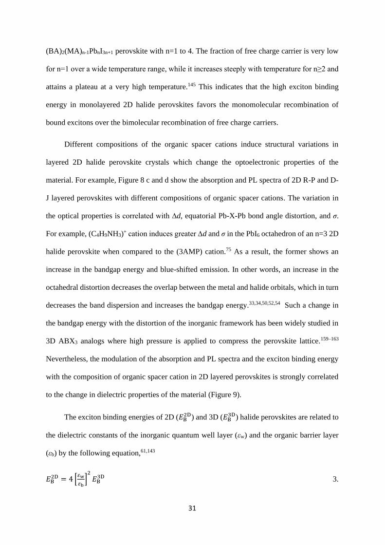
(BA)2(MA)n-1PbnI3n+1 perovskite with n=1 to 4. The fraction of free charge carrier is very low
for n=1 over a wide temperature range, while it increases steeply with temperature for n≥2 and
attains a plateau at a very high temperature.145 This indicates that the high exciton binding
energy in monolayered 2D halide perovskites favors the monomolecular recombination of
bound excitons over the bimolecular recombination of free charge carriers.
Different compositions of the organic spacer cations induce structural variations in
layered 2D halide perovskite crystals which change the optoelectronic properties of the
material. For example, Figure 8 c and d show the absorption and PL spectra of 2D R-P and D-
J layered perovskites with different compositions of organic spacer cations. The variation in
the optical properties is correlated with ∆d, equatorial Pb-X-Pb bond angle distortion, and σ.
For example, (C4H9NH3)+ cation induces greater ∆d and σ in the PbI6 octahedron of an n=3 2D
halide perovskite when compared to the (3AMP) cation.75 As a result, the former shows an
increase in the bandgap energy and blue-shifted emission. In other words, an increase in the
octahedral distortion decreases the overlap between the metal and halide orbitals, which in turn
decreases the band dispersion and increases the bandgap energy.33,34,50,52,54 Such a change in
the bandgap energy with the distortion of the inorganic framework has been widely studied in
3D ABX3 analogs where high pressure is applied to compress the perovskite lattice.159–163
Nevertheless, the modulation of the absorption and PL spectra and the exciton binding energy
with the composition of organic spacer cation in 2D layered perovskites is strongly correlated
to the change in dielectric properties of the material (Figure 9).
The exciton binding energies of 2D (𝐸B2D) and 3D (𝐸B
3D) halide perovskites are related to
the dielectric constants of the inorganic quantum well layer (εw) and the organic barrier layer
(εb) by the following equation,61,143
𝐸B2D = 4 [
𝜀w
𝜀b]
2
𝐸B3D 3.

32
Figure 9. Dielectric confinement in layered 2D halide perovskites. (a) The binding energy and
the Bohr radius of excitons as a function of organic barrier dielectric constant in (PEA)2PbI4
[square] and (EA)2PbI4 [diamond] perovskites. The inset shows the crystal structures of the 2D
layered perovskites. Reproduced with permission from ref. 60. Copyright (2018) Nature
Publishing Group. (b) PL decay profiles of (PEA)2PbX4 [X=Cl, Br, I] perovskite films. The
arrow shows a faster PL decay from Cl/Br to Br and Br to I. The inset shows the PL decay
profile of a (PEA)2PbI4 perovskite and the instrument response at a shorter time window.
Reproduced with permission from ref. 61. Copyright (2020) American Chemical Society. (c)
Carrier relaxation processes in layered 2D halide perovskites upon (i) band-edge excitation, (ii)
hot-carrier generation, and (iii) phonon-assisted hot-carrier cooling. Reproduced with
permission from ref. 164. Copyright (2019) American Chemical Society.
Thus, for a 2D halide perovskite with εw˃εb, the Coulomb screening between the electrons and
holes is less and the exciton binding energy is high. Figure 9a compares the calculated binding
energy and Bohr radius of excitons in (PEA)2PbI4 and (EA)2PbI4 [EA=ethylammonium]
perovskites with different dielectric constants of the organic spacer cation. In (PEA)2PbI4
perovskite the organic spacer PEA has a dielectric constant (εb~3.3) smaller than that of the
(c)
(ii) (iii)
Bin
din
g E
nerg
y (
meV
)
400
300
200
100
00 10 20 30 40 50 60
Organic ε
6
5
4
3
2
1
0
Bohr
radiu
s(n
m)
Low ε organic layer
High ε
organic layer
(PEA)2PbI4 (EA)2PbI4
(II)
(I)
(a) (b)
104
103
102
101
Counts
0 20 40 60Time (ns)
(i)

33
inorganic well (εw~6.1).60 Therefore, the exciton Bohr radius decreases (~1 nm), and the exciton
binding energy increases (˃300 meV), showing strong dielectric confinement. Also, the
strongly bound exciton undergoes fast radiative recombination which increases the PL QY of
the dielectrically-confined 2D halide perovskites.143 On the other hand, in (EA)2PbI4 perovskite
the dielectric constant of EA (εb~37) is more than 10 times greater than that of PEA, which is
in turn much greater than εw. This weakens the dielectric confinement and enhances the
Coulomb screening between the electron and the hole. As a result, the exciton Bohr radius
increases (~4 nm), and the exciton binding energy decreases (<15 meV).60 In addition to the
highly polarizable organic spacer cations, the electronic confinement in 2D halide perovskite
nanoplatelets and R-P layered structures is weakened by replacing or combining the organic
spacer cations with the electron-accepting organic chromophores such as perylene diimide and
the organic charge-transfer complexes such as pyrene alkylammonium-
tetracyanoquinodimethane (pyrene-C4:TCNQ) donor-acceptor system.165,166 For example,
photoexcitation of a 2D (pyrene-C4:TCNQ)2PbI4 perovskite resulted in the long-lived (1-4 µs)
free charge carriers in the inorganic layers which was accredited to charge-separated holes
transferred from the (pyrene-C4:TCNQ) charge-transfer complex into the inorganic perovskite
layers. On the other hand, the electrons were confined in the TCNQ molecules. Such strategies
are useful in achieving the charge-separated states in electronically-confined 2D halide
perovskites for their applications to solar cells, photodetectors, and photocatalysis. Further, Nag
and coworkers have shown that the dielectric confinement in layered 2D halide perovskites can
also be tuned by changing the composition of halide ions.61 Change in the halide composition
from Cl to Br and Br to I increases εw of the inorganic (quantum well) layer in (PEA)2PbX4
perovskites which increases the dielectric confinement of excitons. As a result, the fast
excitonic recombination decreases the PL lifetime of (PEA)2PbX4 perovskite while changing

34
the composition from Cl to Br and Br to I (Figure 9b). This is a trend observed opposite to the
3D ABX3 perovskites where the PL lifetime increases from Cl to Br and Br to I.22,109
Organic spacer cation also influences the hot-carrier dynamics in layered 2D halide
perovskites.134,164,167–170 Photoexcitation of 2D halide perovskites at band edge generates
strongly bound excitons which can undergo monomolecular recombination to produce photons
[Figure 9c (i)]. Photoexcitation above bandgap generates hot electrons and hot holes which
occupy the higher electronic states. These hot carriers must thermalize non-radiatively to the
band edge by emitting phonons before they undergo radiative recombination [Figure 9c (ii)].
The released phonons can interact with the hot-carrier relaxation [Figure 9c (iii)] and affect the
fast-carrier dynamics. An increase in the dielectric constant of the organic spacer cation in
layered 2D halide perovskites increases the hot-carrier relaxation time from hundreds of
femtoseconds to picoseconds.164,167,170 Further, the slow propagation of acoustic phonons and
their upconversion to optical phonons in 2D halide perovskites by varying the composition of
organic spacer cation and increasing the number of inorganic layers (n) can heat the cold
carriers and further delay the hot-carrier cooling to thousands of picoseconds.171 Hot-carrier
cooling in such 2D halide perovskites is much longer than in the case of 3D ABX3
perovskites.168 The prolonged hot-carrier relaxation in 2D layered perovskites provides means
to harvest hot electrons and holes for optoelectronic and photocatalytic applications.
4.2 Self-trapped excitons and broad photoluminescence
The optoelectronic properties of halide perovskites are greatly influenced by temperature.
At higher temperatures, the electron-phonon interaction broadens the absorption and PL bands
inhomogeneously in 3D ABX3 perovskites.172–174 On the other hand, the sharpening of
absorption and PL peaks is observed at cryogenic temperature, most likely due to the low
electron-phonon interaction. In addition to the spectral shape, the position of the absorption and

35
emission peak also shifts with temperature which is attributed to the change in octahedral
distortion, tilt angles, or crystal phase.78,175 In layered 2D halide perovskites, the influence of
temperature on the optoelectronic properties is rather unique. These layered 2D structures show
largely Stokes-shifted and intense broadband emission at lower temperatures, depending on the
type of organic spacer cations.176–178 In some of the layered 2D halide perovskites and low-
dimensional post-perovskite chains, broad emission (BE) covering most of the visible spectrum
has been observed even at room temperature, which makes them promising white light-emitting
fluorophores.176,179–181 The broadband emission from layered 2D halide perovskites is known
to originate from the self-trapped excitons (STEs).
Figure 10. Exciton self-trapping in layered 2D halide perovskites. (a) Scheme showing the
exciton self-trapping (red arrow) and detrapping (blue arrow) with free exciton (FE) emission
in pink and STE emission in orange (Ea,trap=activation energy for self-trapping and
Ea,detrap=activation energy for detrapping). (b) PL spectra of (HIS)PbBr4 (HIS=histammonium)
perovskite single crystal at different temperatures showing the narrow emission (NE) at ca. 3
eV and the broad emission (BE) at ca. 2 eV. Reproduced with permission from ref. 176.
Copyright (2017) Royal Society of Chemistry.
STEs are the photoexcited bound electron-hole pairs that are trapped and stabilized into
a self-created potential well.177 The electron (hole) forms a small localized polaron by the virtue
(a) (b)

36
of a deformable lattice which then attracts the hole (electron). The BE from layered 2D halide
perovskites is observed at low temperatures at which the formation of STEs is favored. At room
temperature, on the other hand, detrapping of STEs results in the narrow emission (NE) with a
small Stokes shift from the radiative recombination of the free exciton (FE).182 Here, FEs are
those which are not self-trapped, and they should not be confused with the unbound excitons
or free charge carriers. Figure 10a shows the exciton self-trapping and detrapping in a layered
2D halide perovskite. Karunadasa and coworkers have shown the formation of STEs and
broadband emission from a variety of layered 2D halide perovskites and similar
materials.176,180,183,184 Figure 10b shows the temperature-dependent PL spectra of (HIS)PbBr4
perovskites which show NE at 202 K and BE at or below 77 K. The NE band can be observed
even at cryogenic temperature along with the BE band which is due to the thermal equilibrium
between the FEs and STEs. The BE in layered 2D halide perovskites is correlated to the
structural distortions induced by different organic spacer cations.177,182 Unlike the NE from FEs
at room temperature which is influenced by the in-plane Pb-X-Pb distortion (Figure 8 c and d),
the BE in layered 2D halide perovskites from STEs is affected by the out-of-plane distortion.
For example, (BA)2PbBr4 perovskite with least out-of-plane distortion (θout=177°) shows only
NE at the wide temperature range from 200 to 20 K, while (HIS)PbBr4 with relatively higher
out-of-plane distortion (θout~157°) shows BE at lower temperatures (<200 K).176 Another
example is highly distorted (AEA)PbBr4 perovskite (θout~22°) which shows dominant BE at
room temperature.176 Apart from the organic spacer cation-induced structural distortion,
halogens also influence the self-trapping of excitons and BE in layered 2D halide
perovskites.178,181 Gautier et al. showed that STEs are more favored than FEs for Cl-based
layered 2D halide perovskites than for Br- or I-based ones.181 This is attributed to the lower
self-trapping depth in the case of Br and I when compared to Cl. In other words, the detrapping
barrier is high for lighter halides. Halogen composition influences lattice deformation through

37
different metal-halide bonding, which in turn influences the trapping/detrapping of excitons in
layered 2D halide perovskites.
STEs are considered as intrinsic as the trapping potential is originated from the excitons
themselves. However, there exists a debate among perovskite researchers that whether the
origin of broadband emission is intrinsic, or is caused by the factors such as dopants and
defects.185–187 Recently, Kahmann et al. showed the extrinsic nature of BE in PEA- and its
fluorinated derivative (FPEA)-based 2D R-P layered perovskites.185 While the STEs cannot be
accessed directly from the ground state, their work showed the existence of in-gap (defect)
states accessed by the below bandgap excitation which contributes to the broadband emission.
Further, the sample-to-sample variation in the intensity of NE and BE substantiated the
presence of emissive in-gap states with different densities in different samples. Also, Yin et al.
showed that the Stokes-shifted and broadband emission from (PEA)2PbI4 perovskites is
originated from the defect states.186 These radiative defect states are contributed by the surface
or bulk iodine vacancies, and Yin et al. demonstrated the suppression of such broadband
emission by passivating the defects using excess PEAI.
5. Environmental Stability
Despite the outstanding optoelectronic and charge carrier properties of 3D ABX3
perovskites that are promising for high-efficiency light-emitting and light-harvesting devices,
these materials often suffer from poor stability against moisture and light.18 Various studies
have revealed the formation of mono- or dihydrate species as the first step towards the
degradation of halide perovskites when they are exposed to moisture or water vapor (Figure 11
a).28,188–197 The hydrated 3D ABX3 perovskite decomposes irreversibly in the presence of
excess water into aqueous HX and solid BX2, and the organic A-site cation is either released
as gas or dissolved in water. The presence of halide vacancies, surface defects, and surface

38
reactivity in halide perovskites accelerate the decomposition process by acting as active sites
for adsorbing water and oxygen molecules.28,29,191,198,199
Figure 11. Environmental stability of halide perovskites. (a) Scheme showing the hydration
and decomposition cycle of MAPbI3 perovskite in the presence of water/moisture. Reproduced
with permission from ref. 188. Copyright (2014) American Chemical Society. (b) Contact
angles between a water droplet and the perovskite films (i) MAPbI3, (ii) (BA)2MA2Pb3I10, (iii)
(PA)2MA2Pb3I10, and (iv) (HA)2MA2Pb3I10. Reproduced with permission from ref. 50.
Copyright (2019) American Chemical Society. (c) Photographs and XRD of films of halide
perovskites with 3D and layered 2D structures that are exposed to humidity for over 2 months.
Reproduced with permission from ref. 77. Copyright (2015) American Chemical Society.
Comparison of (d) heat-, (e) moisture-, and (f) photostability of solar cells constructed from 3D
and layered 2D halide perovskites. The labels of the y-axis in (e) and (f) correspond to that of
(d). Reproduced with permission from ref. 72. Copyright (2018) Elsevier Inc. (g) The plot of
activation energy (Ea) of halide exchange as the function of inorganic layer thickness (n) of a
layered 2D halide perovskite. Reproduced with permission from ref. 48. Copyright (2020)
American Chemical Society.
0 20 40 60 80 ≥100
Number of layers (n)
1.00
0.75
0.50
0.25
0.00
70
60
50
Ea
(kJ/m
ol)
Norm
aliz
ed P
CE
0 1000 2000 3000 4000 0 1000 2000 30000 48 96 144
Aging time (hr) Aging time (hr) Aging time (hr)
Heat stability @85 C and 40-70% RH Humidity stability under 40-70% RH Light stability under 1-Sun illumination
(g)(e) (f)(d)
0 10 20 30 402θ (degree)
Inte
nsity (
a.u
.)
2 m
onth
s
40%
hum
idity
(a) (b) (c)
(i) (ii)
(iii) (iv)

39
Halide vacancies in 3D ABX3 perovskites are very common due to their low energy of
formation.28,198,200,201 Furthermore, these perovskites exposed to ambient air generate
superoxide under photoirradiation which induces oxidative degradation of the material.27,29,198
For example, photogenerated electrons in MAPbI3 perovskite nanocrystals or films reduce the
oxygen molecules adsorbed on the vacant iodide sites to superoxide.27,29 The thus generated
superoxide degrades the material by reacting with the photo-oxidized perovskite structure to
form methylamine, PbI2, iodine, and water. In addition to the moisture- and superoxide-induced
degradation, migration of halide ions under prolonged photoirradiation or electrical bias is
another detrimental effect that limits the operational stabilities and efficiencies of 3D ABX3
perovskite-based devices.26,202–208 The migration of halide ions in the perovskite lattice is a
thermally activated process that is assisted through the halide vacancy defects. It has the lowest
activation energy (~0.58 eV for iodide ion migration) when compared to the migration of other
ions in the perovskite lattice.202 Such easy movement of halide ions under light irradiation or
the influence of an electric field during device operation results in defect migration, phase
segregation, or lattice distortion inside the perovskite layers which ultimately destabilizes the
material if such processes are prolonged and irreversible. Further, the halide ion migration
across the halide perovskite-electrode interface leads to the degradation of the perovskite
structure and electrodes through the extraction of ions from the perovskite layer.26,209,210 2D R-
P or D-J layered perovskites, on the other hand, demonstrate improved stability against
moisture and light (Figure 11 b-g).48,50,59,72,77,211 Nevertheless, long-term stability of colloidal
2D perovskite nanoplatelets/nanosheets is still a challenge.123,212 In this section, we discuss the
stability of 2D halide perovskites concerning moisture, heat, and light.
5.1 Moisture and thermal stability
In layered 2D halide perovskites, the moisture stability is rendered by the hydrophobic
nature of aliphatic or aromatic organic ammonium spacer cations.48,50,53,59,72,77,211,213–215 Such
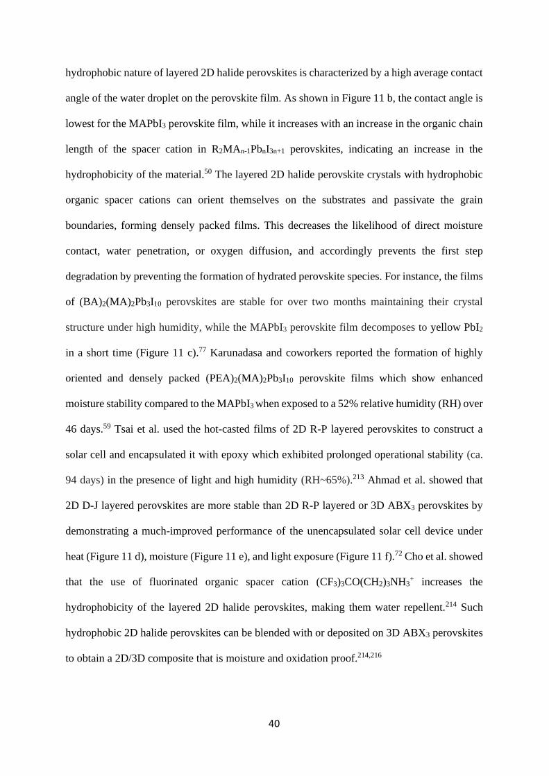
40
hydrophobic nature of layered 2D halide perovskites is characterized by a high average contact
angle of the water droplet on the perovskite film. As shown in Figure 11 b, the contact angle is
lowest for the MAPbI3 perovskite film, while it increases with an increase in the organic chain
length of the spacer cation in R2MAn-1PbnI3n+1 perovskites, indicating an increase in the
hydrophobicity of the material.50 The layered 2D halide perovskite crystals with hydrophobic
organic spacer cations can orient themselves on the substrates and passivate the grain
boundaries, forming densely packed films. This decreases the likelihood of direct moisture
contact, water penetration, or oxygen diffusion, and accordingly prevents the first step
degradation by preventing the formation of hydrated perovskite species. For instance, the films
of (BA)2(MA)2Pb3I10 perovskites are stable for over two months maintaining their crystal
structure under high humidity, while the MAPbI3 perovskite film decomposes to yellow PbI2
in a short time (Figure 11 c).77 Karunadasa and coworkers reported the formation of highly
oriented and densely packed (PEA)2(MA)2Pb3I10 perovskite films which show enhanced
moisture stability compared to the MAPbI3 when exposed to a 52% relative humidity (RH) over
46 days.59 Tsai et al. used the hot-casted films of 2D R-P layered perovskites to construct a
solar cell and encapsulated it with epoxy which exhibited prolonged operational stability (ca.
94 days) in the presence of light and high humidity (RH~65%).213 Ahmad et al. showed that
2D D-J layered perovskites are more stable than 2D R-P layered or 3D ABX3 perovskites by
demonstrating a much-improved performance of the unencapsulated solar cell device under
heat (Figure 11 d), moisture (Figure 11 e), and light exposure (Figure 11 f).72 Cho et al. showed
that the use of fluorinated organic spacer cation (CF3)3CO(CH2)3NH3+ increases the
hydrophobicity of the layered 2D halide perovskites, making them water repellent.214 Such
hydrophobic 2D halide perovskites can be blended with or deposited on 3D ABX3 perovskites
to obtain a 2D/3D composite that is moisture and oxidation proof.214,216
41
Better thermal stability in layered 2D halide perovskites when compared to 3D ones is
attributed to the stronger electrostatic interaction between the organic spacer cation and the
BX6 octahedra and the van der Waals interaction among the stacked inorganic layers. In 2D R-
P layered perovskites, the monoammonium organic spacer cations create the van der Waals gap
between the adjacent stacking layers. On the other hand, the gap is completely removed in the
case of 2D D-J layered perovskites where the diammonium organic spacers link the adjacent
layers electrostatically. Hence, the 2D D-J layered perovskites become more stable towards
heat than their R-P counterparts.72 The thermal stability of the layered 2D halide perovskites
also is affected by the orientation of crystals on the substrate. The vertically oriented 2D halide
perovskites are thermally more stable than the parallelly or randomly oriented ones which are
attributed to the better heat distribution among the vertically oriented crystallites in the film.50,53
Nevertheless, the thermal and the air stability of the layered 2D halide perovskite films also
depends on the deposition method, the film thickness, and the substrate crystallinity.50
5.2 Photostability
The bulky organic spacer cations enhance the photostability of layered 2D halide
perovskites (Figure 11 f).50,72,213 The efficient passivation of perovskite lattice against moisture
and oxygen by the hydrophobic organic spacers reduces the formation of reactive oxygen
species in the presence of light which improves the photostability.217 More importantly, the
photostability is improved by the suppression of the halide ion migration in layered 2D halide
perovskites.48,211,218,219 The out-of-plane migration of halide ions in 2D halide perovskites,
which is from one inorganic slab to another stacking together, is prevented by the bulky organic
spacer cations that act as the barrier layer in between. On the other hand, the in-plane movement
of halide ions within the perovskite layer is suppressed by the low probability of point defect
formation due to the large formation energy of these point defects. For example,
(BA)2(MA)2Pb3I10 perovskite has a halide vacancy formation energy of ~5.46 eV, which is

42
higher than that of MAPbI3 perovskite (3.44 eV).211 Therefore, the vacancy-mediated diffusion
of halide ions in layered 2D halide perovskites is suppressed. Further, the activation energy for
the halide exchange increases with decreasing the number of inorganic layers n<10 in layered
2D halide perovskites (Figure 11 g).48 This indicates the increased thermal barrier for the halide
ion migration in layered 2D perovskite structures when compared to their 3D analogs.
While layered 2D halide perovskites are relatively more stable than the 3D ABX3, the
stability of these low dimensional structures in their colloidal states is still a question, especially
during long-time room temperature storage and after post-synthetic purification.36,74,123,212,220
Multiple washing steps after synthesis can strip off the ligands from the surface of the
perovskite nanoplatelets or nanosheets and thus destroy the colloidal stability.36 Removal of a
large number of ligands can also lead to low PL QY and material degradation, owing to the
formation of defects.116 Moreover, the use of too polar antisolvent during the purification step
can dissolve the perovskite nanoplatelets.212 Therefore, it is plausible to implement efficient
strategies to stabilize colloidal 2D halide perovskites. The addition of surface ligands and
halides to the washing solvent during the purification steps or to the colloidal solution after
purification is one way to preserve the ligand density on the surface of perovskite nanoplatelets
or nanosheets. This also helps to minimize the surface defects and improve the PL QY. Also,
washing with solvents that have low dielectric constants such as diethylene glycol dimethyl
ether (diglyme) has shown to be efficient for maintaining stable and highly luminescent
colloidal halide perovskites.221
6. Applications
6.1 Solar cells
Since Miyasaka and co-workers first demonstrated the 3D ABX3 perovskite solar cell in
2009 with an efficiency of 3.8%,222 extensive study has been performed in the last decade to

43
improve the open circuit potential (Voc) and achieve high photon conversion efficiency
(PCE).1,223–225 According to the National Renewable Energy Lab (NREL) best research cell
efficiency chart 2021, the current record-breaking PCE of halide perovskite solar cell is
25.5%,226 which can be attributed not only to their intrinsic excellent optoelectronic properties
but also to better material deposition strategies,227 defect passivation,228,229 and exploration of
better electron or hole transport layers.2 Despite a great potential for solar energy harvesting,
3D ABX3 perovskites are not yet commercially viable due to their poor stability.230 2D halide
perovskites such as R-P or D-J layered structures, on the other hand, are more stable alternatives
to ABX3 in solar cells. In this section, we discuss the developments in 2D halide perovskite-
based solar cells.
In 2014, the 2D (PEA)2(MA)2Pb3I10 perovskite was used as the light-absorbing layer for
the first time in a planer solar cell device which showed a PCE of 4.74 %.59 Later, various 2D
R-P and D-J layered perovskite-based solar cells were constructed with significant
improvement in their efficiency.34,56,64,69,70,72,73,77,126,213,215,219,231 Tsai et al. demonstrated a PCE
of 12.51% with Voc of 1.01 V in (BA)2(MA)3Pb4I13-based solar cell.213 The device was
hysteresis-free in the current (J)-voltage (V) curve, which is essential for reproducible higher
efficiencies. Such hysteresis in the J-V curve is reported in the case of 3D ABX3 perovskite
solar cells, which is mainly attributed to the ionic conductivity and poor photostability of the
material.202,232,233 The quality and packing of layered 2D halide perovskite crystals in a film are
influenced by the choice of organic spacer cations. This in turn affects the stability and
efficiency of perovskite solar cells. Ahmad et al. reported a D-J layered structure-based
perovskite solar cell with a PCE of 13.3%, which was higher than for R-P layered structure-
based devices.72 The improved performance of D-J layered structure-based perovskite solar
cells was attributed to the formation of high-quality crystals with less octahedral distortion and
dense packing which lead to better carrier mobility. Zheng et al. used benzylammonium, N,N-

44
dimethylammonium, propyl-1,3-diammonium, and butyl-1,4-diammonium cations in layered
2D halide perovskites and constructed solar cells.215 Among these, 2D halide perovskite films
with benzylammonium as cations provided a high PCE (17.4%) and excellent operational
stability (>500 h) under humid conditions (80% relative humidity). Also, an increase in the
number of inorganic layers or thickness of the 2D halide perovskite increases the PCE in solar
cells, which is possibly due to the small lattice distortion, low exciton binding energy, and long
carrier diffusion in thick quasi-2D halide perovskite layers.73 Nevertheless, the organic spacer
cations act as an insulating layer which reduces the carrier diffusion between the stacked
inorganic layers and suppresses the carrier extraction to the charge transport layers. Therefore,
the orientation of layered 2D halide perovskite crystals on a substrate greatly determines the
efficiency of solar cells.77,107,213,234–236 The 2D halide perovskites can align in-plane
(parallel/horizontal) or out-of-plane (perpendicular/vertical) to the substrate during their
growth or deposition. Consequently, solar cells with vertically oriented layered 2D halide
perovskites show better charge mobility and extraction and therefore high PCE (Figure 12).
Hot-casting of precursors on the substrate results in the vertical growth of 2D halide perovskites
(Figure 12 a) and better solar cell performance (Figure 12e) when compared to the room
temperature or moderate temperature deposition, which forms parallelly or randomly oriented
crystals (Figure 12 b).107,213 Such preferred vertical orientation of perovskite crystals can be
characterized by the concentrated spots in Grazing incidence wide-angle X-ray scattering
(GIWAXS) patterns which smear out into rings for the randomly oriented ones (Figure 12 c
and d). The efficient charge extraction from the strongly quantum confined 2D halide
perovskite layers can also be achieved by attaching electron-accepting molecules such as
fullerenes and organic chromophores on the perovskite surface.165,237 Intercalation of inorganic
moieties such as halogens within the van der Waals gap of organic spacer cation layers can also

45
reduce the dielectric confinement in 2D halide perovskite layers.238 This makes the excitons
more viable for the dissociation and extraction to the charge transport layers in the solar cells.
Figure 12. Performance of a layered 2D halide perovskite-based solar cell. (a,b) Scheme
showing the (a) vertical and (b) random orientation of layered 2D halide perovskite crystals
and the corresponding influence on the charge carrier extraction in a solar cell. (c,d) GIWAXS
patterns of layered 2D halide perovskite films showing (c) vertical and (d) random orientation.
(e) Current density versus voltage curves of layered 2D halide perovskite-based solar cells with
vertical and random orientation of crystals. Reprinted with permission from ref. 107. Copyright
(2018) Nature Publishing Group.
Besides, solar cells with 2D/3D perovskite heterostructures as light absorbers are gaining
recent attention due to their extreme stability and high efficiency (PCE>20%).214,239–243 In such
perovskite solar cells, higher stability against moisture is due to the hydrophobicity of layered
2D halide perovskites, and high efficiency is achieved by the combined 2D/3D perovskite layer.
The hydrophobic 2D perovskite layers also passivate the surface defects, reduce the ion
migration, and suppress the nonradiative recombination in 3D ABX3 perovskites. Zhu et al.
demonstrated the PCE of 20% for the 2D/3D perovskite solar cells by incorporating 2D
(PEA)2PbI4 perovskite nanosheets between 3D MAPbI3 perovskite and hole-transporting
layer.243 The favorable band alignment between the graded 2D/3D perovskite structure and the
hole-transport layer at the interface increased the hole transfer efficiency and reduced the
(a)
(b)
(c)
(e)
(d)

46
interface charge recombination, which resulted in high PCE. Liu et al. reported a 2D/3D
perovskite solar cell with excellent operational stability under ambient atmosphere and PCE
>22% by depositing an (FEA)2PbI4 [FEA= pentafluorophenylethylammonium] layer on top of
a 3D halide perovskite.239 They demonstrated the enhancement of interfacial hole extraction in
the device by the 2D perovskite layers. Bouduban et al. showed PCE >23% and very high Voc
(>1.0 V) in solar cells with 2D/3D perovskite heterostructures which contain PEA or
fluorinated derivatives of PEA as spacer cations.242 They attributed the excellent solar cell
performance to the planar orientation of layered 2D halide perovskites on top of 3D ones which
not only passivate the defects but also prevent the back-electron transfer without affecting the
charge extraction from the perovskite layer.
6.2 LEDs and lasers
Figure 13. Scheme showing efficient energy transfer in quasi-2D halide perovskites. CB and
VB are conduction and valence bands, respectively.
Strong electronic confinement in layered 2D halide perovskites leads to high PL QY and
narrow-band emission which are promising for LED and lasing applications.244–246 While LEDs
based on 3D ABX3 perovskites have already achieved an external quantum efficiency (EQE)
n=1 n=2 n=3 n≥4
──
+
─
+
─
+
─
+
─
+
─
+
+
Hig
h P
L Q
Y
Energy funneling
Energy funneling
Increase in carrier
concentrationVB
CB
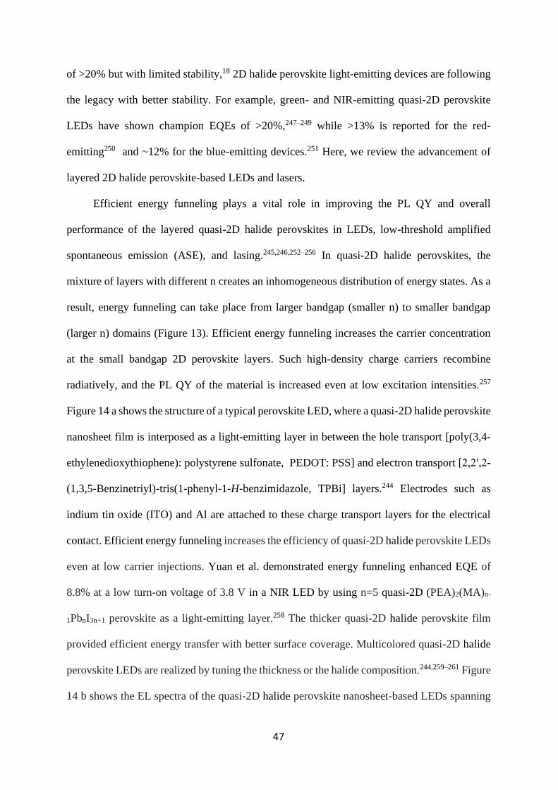
47
of >20% but with limited stability,18 2D halide perovskite light-emitting devices are following
the legacy with better stability. For example, green- and NIR-emitting quasi-2D perovskite
LEDs have shown champion EQEs of >20%,247–249 while >13% is reported for the red-
emitting250 and ~12% for the blue-emitting devices.251 Here, we review the advancement of
layered 2D halide perovskite-based LEDs and lasers.
Efficient energy funneling plays a vital role in improving the PL QY and overall
performance of the layered quasi-2D halide perovskites in LEDs, low-threshold amplified
spontaneous emission (ASE), and lasing.245,246,252–256 In quasi-2D halide perovskites, the
mixture of layers with different n creates an inhomogeneous distribution of energy states. As a
result, energy funneling can take place from larger bandgap (smaller n) to smaller bandgap
(larger n) domains (Figure 13). Efficient energy funneling increases the carrier concentration
at the small bandgap 2D perovskite layers. Such high-density charge carriers recombine
radiatively, and the PL QY of the material is increased even at low excitation intensities.257
Figure 14 a shows the structure of a typical perovskite LED, where a quasi-2D halide perovskite
nanosheet film is interposed as a light-emitting layer in between the hole transport [poly(3,4-
ethylenedioxythiophene): polystyrene sulfonate, PEDOT: PSS] and electron transport [2,2′,2-
(1,3,5-Benzinetriyl)-tris(1-phenyl-1-H-benzimidazole, TPBi] layers.244 Electrodes such as
indium tin oxide (ITO) and Al are attached to these charge transport layers for the electrical
contact. Efficient energy funneling increases the efficiency of quasi-2D halide perovskite LEDs
even at low carrier injections. Yuan et al. demonstrated energy funneling enhanced EQE of
8.8% at a low turn-on voltage of 3.8 V in a NIR LED by using n=5 quasi-2D (PEA)2(MA)n-
1PbnI3n+1 perovskite as a light-emitting layer.258 The thicker quasi-2D halide perovskite film
provided efficient energy transfer with better surface coverage. Multicolored quasi-2D halide
perovskite LEDs are realized by tuning the thickness or the halide composition.244,259–261 Figure
14 b shows the EL spectra of the quasi-2D halide perovskite nanosheet-based LEDs spanning
48
a large visible spectrum from blue to red, and Figure 14 c shows the real multicolored quasi-
2D halide perovskite nanosheet-based LED devices.
Figure 14. Light-emitting applications of layered 2D halide perovskites. (a-c) Multicolor LEDs
based on quasi-2D (BA)2(Cs)n−1Pbn(Br/X)3n+1 [X = Cl, I] perovskite nanosheets: (a) LED
device architecture, (b) electroluminescence spectra, and (c) real LED devices showing blue,
green and red electroluminescence. Reprinted with permission from ref. 244. Copyright (2019)
American Chemical Society. (d) ASE spectra and (e) ASE threshold as the function of pump
fluence in quasi-2D (PEA)2(FA)3Pb4Br13 perovskite films. Reprinted with permission from ref.
245. Copyright (2020) Wiley-VCH. (f,g) Lasing from mechanically exfoliated
(BA)2(MA)n−1PbnI3n+1 perovskite microflakes: (f) Multimode lasing spectra as the function of
pump fluence for n=3 2D layered perovskites and (g) multicolor lasing from the layered 2D
halide perovskites with different n values. Reprinted with permission from ref. 246. Copyright
(2019) Wiley-VCH.
The EQE of a quasi-2D halide perovskite LED is affected by the nonradiative
recombination centers or defects, which are originated from the uncoordinated Pb2+ ions in the
lead-based perovskites,247 oxidation of Sn2+ to Sn4+ in the tin-based perovskites,262 grain
boundaries, and ion vacancies.263 Kong et al. showed a champion EQE of 20.5% and a
luminance of 13,400 cd m-2 in a green-emitting LED by passivating the defects in quasi-2D
400 500 600 700 800 900Wavelength (nm)
EL I
nte
nsity (
a.u
.)
Wavelength (nm)
0.9
0.6
0.3
Norm
aliz
ed Inte
nsity (
a.u
.)
n=2 n=3 n=4 n=5
610 620 630 640Wavelength (nm)
1
0
480 520 560 600
10000
8000
6000
4000
2000
0
Wavelength (nm)
Inte
nsity (
a.u
.)Energy Fluence (µJ/cm2)
Inte
nsity (
a.u
.) 2000015000
10000
5000
0 1 2 3 4 5 6 560 600 640 680
(a)
(b)
(c) (d)
(e)
(f)
(g)
49
(BA)2Csn−1PbnBr3n+1 [n≥4] perovskite film using methylsulfonate.247 Methylsulfonate also
enhanced the energy funneling by increasing the donor-to-acceptor ratio through the
redistribution of inorganic layer thickness. The strong exciton binding energy in the quasi-2D
halide perovskites can induce non-radiative Auger processes which decrease the EQE of LED
devices.248,264 Recently, Jiang et al. reported a very high EQE of 20.36% and a champion
luminance of 82,480 cd m-2 in a quasi-2D halide perovskite LED by employing p-fluoro-PEA
as the spacer cation, which was attributed to the lowing of the Auger recombination rate due to
the reduced exciton binding energy.248 While the decreased exciton binding energy lowers the
PL QY by increasing the trap-assisted nonradiative recombination, compensation was made by
passivating such defects using potassium trifluoromethanesulfonate. Nonetheless, the
nonradiative recombination is also induced by the higher concentration of n=1 layers in the
quasi-2D halide perovskites, which is due to either the presence of deep defect states in such
wide-bandgap domains or the strong exciton-phonon coupling.265–267 Therefore, it is essential
to control the concentration and distribution of layers with different thickness in quasi-2D
halide perovskites for high-efficiency LEDs. The formation of the n=1 layers can be controlled
by modulating the interaction between the organic spacer cations and the inorganic layers and
altering the crystallization process.266–268 Alongside, optimally oriented and well-connected 2D
perovskite domains render efficient charge transport.265 Organic spacer cations can affect the
performance of quasi-2D halide perovskite LEDs by tuning the organic barrier and quantum
well width, modifying the carrier recombination pathways, influencing the energy funneling
process, and affecting the film quality.250,269,270 In fact, the efficiency of energy funneling in the
quasi-2D halide perovskites depends upon the size/length of the organic spacer cations where
the shorter chain spacer results in more efficient energy transfer.36,58 Klein et al. showed
efficient energy funneling in 2D MAPbBr perovskite nanosheets which were prepared by using
short-chain dodecylamine ligands.36 This resulted in red-shifted emission with an increase in

50
the PLQY up to 49% for the sample with n=4. On the other hand, 2D halide perovskite
nanosheets synthesized using relatively long-chain ligands such as tetradecylamine and
hexadecylamine showed weaker energy funneling characterized by the emission at higher
energy and with lower quantum yield.
An increase in the local exciton density through efficient energy funneling in the quasi-
2D halide perovskites can result in population inversion, which is a prerequisite for ASE or
lasing. Lei et al. demonstrated that efficient energy funneling leads to ASE from films of quasi-
2D (PEA)2(FA)3Pb4Br13 perovskite at a low threshold of 4.16 µJ cm-2 (Figure 14 d and e).245
They also demonstrated distributed feedback lasing by optically pumping the quasi-2D halide
perovskite film at room temperature using a pulsed laser. The distributed feedback cavity was
constructed by nanoimprinting the 1D grating with a period of 350 nm on a substrate and spin
coating the 2D halide perovskites on the top of it. The lasing threshold was 10 µJ cm-2, above
which a significantly narrowed (FWHM=1.7 nm) lasing emission was observed. Liang et al.
showed multimode microcavity lasing at 78 K from mechanically exfoliated quasi-2D
(BA)2(MA)n −1PbnI3n+1 perovskites with a low lasing threshold of 2.6 µJ cm-2 (Figure 14 f).246
The lasing color was tuned by modulating the thickness of the quasi-2D halide perovskite, as
shown in Figure 14 g. Recently, Qin et al. demonstrated continuous wave (CW) pumped lasing
at room temperature from quasi-2D halide perovskites with a threshold of 4.7 µJ cm-2.256 CW
lasing in layered 2D halide perovskites is difficult to achieve at room temperature, which is due
to singlet-triplet exciton annihilation. However, they employed 1-naphthylmethylamine as a
triplet quencher to suppress the exciton annihilation and to achieve low-threshold CW lasing
from a quasi-2D halide perovskite distributed feedback cavity. In addition to the cavity lasing,
random lasing from layered 2D halide perovskites have also been observed.271 Nevertheless,
defects and Auger processes that affected the efficiency of LEDs can impede the performance
of quasi-2D halide perovskite lasers as well. Therefore, strategies for defect passivation and

51
suppression of Auger recombination should be employed for utilizing layered 2D halide
perovskites as efficient gain media in lasers.253
6.3 Photodetectors
Anisotropic charge carrier properties along the stacking and crystal growth directions
make layered 2D halide perovskites an interesting class of photodetectors.272–277 Anisotropy in
the charge carrier properties of layered 2D halide perovskites is caused by the natural multi-
quantum well structure. Therefore, the exciton diffusion occurs more efficiently towards the
edges from the bulk than towards the stacking plane due to the organic barrier. In layered 2D
halide perovskites, the edges of the inorganic layer contribute lower energy states.126,278
Excitons get trapped by these states and dissociated into slowly recombining free carriers.
Therefore, a large photocurrent from the edge-dissociated excitons can be detected under
photoirradiation. The room-temperature carrier mobility of 5.4−7.0 cm2 V−1 s−1 is reported at
the edges of (BA)2(FA)n-1PbnI3n+1 perovskites, showing that the edges are conducting.127
However, the exact origin of such edge states in the 2D perovskite layers is not clear. While
Shi et al. discussed the moisture-induced atomic rearrangement and formation of the emissive
edge states in layered 2D halide perovskites,127 Zho et al. showed that such low energy edge
states are formed due to the loss of organic cation spacers at the crystal edge.279 Although the
dissociation of excitons at the edges of 2D halide perovskites were employed initially to
improve the PCE solar cells,126 it was later used to enhance the performance of
photodetectors.273,274
The performance of a 2D halide perovskite photodetector is evaluated using various
parameters such as responsivity, detectivity, and response speed.280 Responsivity is defined as
the ratio of photocurrent density to the incident light intensity. Detectivity measures the
sensitivity of a photodetector above the noise/dark current. Similarly, response speed indicates
how fast a photodetector reaches 90% of the maximum photocurrent after the light exposure

52
(τrise) and how fast the photocurrent decays to 10% of its maximum in dark (τfall). The
performance of a perovskite photodetector is affected by the bargain between the high
photocurrent which requires high-quality crystals without defects and grain boundaries and a
very low dark current which requires a barricade for the thermally activated charge carriers.
Therefore, layered 2D halide perovskites are good candidates for photodetection due to their
anisotropic charge carrier properties. Tan et al. reported (BA)2PbBr4 perovskite single crystal
planar photodetector in 2016, which showed an encouraging responsivity of 2100 A W-1 with
a low dark current of 10-10 A.281 Following this, the photodetectors based on layered 2D halide
perovskites and 2D perovskite heterostructures with different compositions are known.282–286
In later years, the performance of these photodetectors fabricated on single crystals and films
was considerably improved through the modulation of quality, thickness, and orientation of the
2D crystal, interface engineering, and understanding the anisotropic charge carrier
dynamics.272–277,285,287–293 Feng et al. reported a high-performance photodetector based on
nanowire-like arrays of quasi-2D (BA)2(MA)n−1PbnI3n+1 [n=4] perovskites with average
responsivities >1.5 × 10⁴ A W−1 and detectivities >7 × 10¹⁵ Jones.274 The organic barriers along
the length of the nanowire-like array extremely suppressed the dark current to the order of ~10-
15 A, whereas the excitons diffused to the exposed edges and dissociated into the long-lived
free carriers, amplifying the photocurrent. The anisotropic charge carrier properties and
efficient exciton dissociation at the edges resulted in a fast response time of <30 µs, which was
in the millisecond time-scale for those which did not involve the edge dissociation of excitons.
Similarly, Liu et al. demonstrated a responsivity >139 A W−1, high detectivity in the order of
~1015 Jones, and a fast response time of <40 μs from a photodetector constructed on the (001)
plane of a millimeter-sized (PEA)2PbI4 perovskite single crystal.273 The photodetector
performance based on the (001) plane was superior to (010) plane due to the high electronic
conductivity along the (001) plane and the dissociation of excitons at the exposed edges which
53
is hindered along the (010) plane due to the organic barrier. Huan et al. fabricated a
photodetector on the highly oriented layered 2D halide perovskite film which showed a record
fast response time of ~2.54 ns, a low dark current of 10-11 A, and very high detectivity in the
order of 1014 Jones.277 In their device, the high conductivity of excitons along the in-plane
direction resulted in ultrafast response speed. Fu et al. fabricated high-performance
photodetectors from the nanosheets of C6H5(CH2)3NH3)3Pb2I7 perovskites which show
significantly low dark current (1.5 pA), fast response speed ( τrise=850 μs and τfall=780 μs), and
high detectivity (∼1.2×10¹⁰ Jones).294 They attributed the low dark current, fast response speed,
and high detectivity to the high crystallinity and low defect density of the perovskite
nanosheets. Nevertheless, the performance of photodetectors based on the layered 2D halide
perovskite film is affected by the traps at the grain boundaries, which can be mitigated by
preparing the highly crystalline films with large grains.289 Also, in the case of tin-based layered
2D halide perovskite devices, self-doping due to the oxidation of Sn2+ to Sn4+ can increase the
overall carrier conductivity and the dark current.286 Treatment of tin-based 2D halide perovskite
crystals with SnF2 can improve the performance of photodetector by minimizing the self-
doping through Sn2+ vacancy passivation.283
6.4 Photocatalysis
Recently, the photocatalytic activities of 3D ABX3 perovskites in water splitting and
hydrogen production, CO2 reduction, organic reactions, and dye degradation are
explored.11,12,295–298 Large absorption coefficient for visible light, photogeneration of free
charge carriers, selective redox reaction, low cost, and facile synthesis make halide perovskites
promising photocatalysts. Halide perovskite photocatalysis is demonstrated with either the pure
3D ABX3 as catalyst296 or its composite with other materials such as Pt,297 TiO2,299 tungsten
oxide,300 reduced graphene oxide,301 Bi2WO6,302 and graphitic carbon nitride.298 These
composite structures help to accelerate charge separation and transport for efficient

54
photocatalysis. Despite fulfilling most of the criteria to become an efficient photocatalyst, 3D
ABX3 perovskites do not survive for a long time under the conditions required for
photocatalytic reactions, such as highly polar/aqueous and oxygen-rich environments and
prolonged irradiation.12 On the other hand, layered 2D halide perovskites can be used as
photocatalysts with better durability.
Figure 15. Scheme showing charge separation and photocatalytic activity of the layered 2D
halide perovskites. HOMO and LUMO refer to the highest occupied molecular orbital of a hole
acceptor and the lowest unoccupied molecular orbital of an electron acceptor, respectively. HT
and ET are defined as the hole transfer and electron transfer processes, respectively.
The high-energy excitons generated at the wide bandgap 2D perovskite layer can easily
overcome the potential energy for driving the photocatalytic reactions. Hong et al. used
(HDA)2BI4 [HDA=hexadecylammonium, B=Pb or Sn] perovskite to catalyze a photo-redox
organic synthesis involving decarboxylation and dehydrogenation reactions.303 It involved the
conversion of an indoline-2-carboxylic acid to indoline (decarboxylation) and indole
(decarboxylation and dehydrogenation) in the presence of layered 2D halide perovskite as
catalyst under white light illumination. They obtained a maximum yield of 98% for indoline
and 84% for indole. Interestingly, there was no product formation in the absence of 2D halide
perovskite photocatalyst; and even if other catalysts were used, the yield was very low, which
confirmed the superior photocatalytic activity of the (HDA)2BI4 perovskites. Recently, Wang
+
─
+
─
HT
ET
HOMO
LUMO
55
et al. demonstrated photocatalytic splitting of HI to generate H2 by using layered 2D halide
perovskites as photocatalysts.304 They showed the dependency of H2 evolution on the organic
spacer cations, whereby the shortest chain length cation PMA exhibited the highest
photocatalytic activity in the presence of cocatalyst Pt. This was attributed to the efficient
charge transfer among the stacked 2D perovskite layers and at the perovskite-cocatalyst
interface. They also claim that the conversion efficiency of ~1.57% for this reaction is the
champion value among all the halide perovskite photocatalysts for H2 production reported to
date. Recently, Wu et al. demonstrated the photocatalytic reduction of CO2 to CO with a
generation rate of 21.6 μmol g−1 h−1 by CsPbBr3 perovskite nanosheets.305 This generation rate
was 3.8 times higher than the 3D CsPbBr3 perovskite nanocrystals which further improved
(~43.9 μmol g−1 h−1) and became >7 times than the 3D ABX3 halide perovskites when the
bromide ions in the nanosheets were replaced with the mixed Br/I through the anion exchange.
The excellent photocatalytic performance of these 2D halide perovskite nanosheets was
attributed to the largely exposed/less-coordinated metal atoms as active sites, short charge
carrier diffusion along the thickness and easy extraction of charges to CO2 and H2O reactants,
and enhanced visible light absorption. Nevertheless, one can argue that the strong dimensional
and dielectric confinement of charge carriers imposes poor charge separation and transport in
the case of layered 2D halide perovskites, which makes them poor photocatalysts. Exciton
dissociation and effective charge separation in layered 2D halide perovskites can be realized
by employing efficient electron/hole acceptors, and the separated charges can be utilized for
photo-redox reactions, as shown schematically in Figure 15. Li et al. showed effective charge
separation in strongly quantum confined CsPbBr3 perovskite nanoplatelets (exciton binding
energy=260 meV) by using organic molecules benzoquinone and phenothiazine as electron and
hole acceptors, respectively.306 The charge-separated states existed for >100 ns, which makes
such 2D halide perovskite-organic molecule composites good photocatalyst candidates. A long-

56
lived charge-separated state in the strongly quantum confined halide perovskites is also
reported for the case of methyl viologen as an electron acceptor.307
7. Summary and Outlook
Layered 2D halide perovskites are an interesting class of semiconductor materials in which the
optoelectronic properties are tuned by the dimensional and dielectric confinements. They show
better environmental stability compared to the 3D ABX3 analogs, owing to their unique
structure which comprises bulky hydrophobic organic ligands to become a part of the crystal
structure. High PL QY in 2D or quasi-2D halide perovskites along with the processes such as
efficient energy transfer between the inorganic layers with different thickness, exciton
dissociation at the edges, and charge separation can be utilized for efficient solar to electrical
energy conversion, solar to chemical energy conversion, light-emitting applications, and
photodetectors. The inclusion of charge-transfer complexes between the stacked perovskite
layers could be an efficient strategy to separate strongly bound excitons in layered 2D halide
perovskites. Nevertheless, challenges remain in stabilizing the colloidal 2D halide perovskite
nanoplatelets and nanosheets during the synthesis, purification, and long-term storage. Polymer
or inorganic coatings can improve the moisture- and photostability of colloidal 2D perovskite
nanoplatelets and nanosheets. The selective crystallization of layered 2D halide perovskites
with higher n is often limited by the precipitation of monolayered structures due to their low
enthalpy of formation.51 Such large bandgap 2D halide perovskite monolayers show enhanced
nonradiative recombination due to the efficient exciton-phonon coupling, Auger processes, and
defects. The nonradiative recombination in these materials can be suppressed through the
passivation of defects and Auger recombination centers by solvent engineering and inorganic
salt treatment. Further, the anisotropic charge carrier properties require specific orientation and
interfacial engineering of the 2D perovskite crystals for efficient carrier transport and extraction
57
in different optoelectronic applications. 2D/3D perovskite heterostructures, on the other hand,
can show better carrier mobility due to their suitable band alignment. Although the broadband
emission observed in some layered 2D halide perovskites has shown promise towards the
white-emitting LEDs, insufficient understanding of the exact origin of such phenomenon has
limited further development. Therefore, full-fledged utilization of layered 2D halide
perovskites for diverse optoelectronic applications requires better strategies to control the
growth and stability of the crystals in colloidal and noncolloidal states and an advanced
understanding of the various photophysical and chemical processes therein.
Conflicts of Interest
The authors declare no conflicts of interest.
Acknowledgments
SG acknowledges Alexander von Humboldt (AvH) Foundation for the postdoctoral research
fellowship.

58
References
1 J. Y. Kim, J.-W. Lee, H. S. Jung, H. Shin and N.-G. Park, Chem. Rev., 2020, 120, 7867–
7918.
2 M. Jeong, I. W. Choi, E. M. Go, Y. Cho, M. Kim, B. Lee, S. Jeong, Y. Jo, H. W. Choi,
J. Lee, J.-H. Bae, S. K. Kwak, D. S. Kim and C. Yang, Science, 2020, 369, 1615–1620.
3 D. Han, M. Imran, M. Zhang, S. Chang, X. Wu, X. Zhang, J. Tang, M. Wang, S. Ali, X.
Li, G. Yu, J. Han, L. Wang, B. Zou and H. Zhong, ACS Nano, 2018, 12, 8808–8816.
4 H. Chen, L. Fan, R. Zhang, C. Bao, H. Zhao, W. Xiang, W. Liu, G. Niu, R. Guo, L. Zhang
and L. Wang, Adv. Opt. Mater., 2020, 8, 1901390.
5 X. Geng, F. Wang, H. Tian, Q. Feng, H. Zhang, R. Liang, Y. Shen, Z. Ju, G.-Y. Gou, N.
Deng, Y. Li, J. Ren, D. Xie, Y. Yang and T.-L. Ren, ACS Nano, 2020, 14, 2860–2868.
6 L. Dou, Y. (Micheal) Yang, J. You, Z. Hong, W.-H. Chang, G. Li and Y. Yang, Nat.
Commun., 2014, 5, 5404.
7 J. Cao, Z. Guo, S. Zhu, Y. Fu, H. Zhang, Q. Wang and Z. Gu, ACS Appl. Mater.
Interfaces, 2020, 12, 19797–19804.
8 Q. Chen, J. Wu, X. Ou, B. Huang, J. Almutlaq, A. A. Zhumekenov, X. Guan, S. Han, L.
Liang, Z. Yi, J. Li, X. Xie, Y. Wang, Y. Li, D. Fan, D. B. L. Teh, A. H. All, O. F.
Mohammed, O. M. Bakr, T. Wu, M. Bettinelli, H. Yang, W. Huang and X. Liu, Nature,
2018, 561, 88–93.
9 S. Yakunin, L. Protesescu, F. Krieg, M. I. Bodnarchuk, G. Nedelcu, M. Humer, G. De
Luca, M. Fiebig, W. Heiss and M. V. Kovalenko, Nat. Commun., 2015, 6, 8056.
10 W. Sun, Y. Liu, G. Qu, Y. Fan, W. Dai, Y. Wang, Q. Song, J. Han and S. Xiao, Nat.
Commun., 2020, 11, 4862.
11 J.-H. Kim, S. Seo, J.-H. Lee, H. Choi, S. Kim, G. Piao, Y. R. Kim, B. Park, J. Lee, Y.
Jung, H. Park, S. Lee and K. Lee, Adv. Funct. Mater., 2021, 2008277.

59
12 H. Huang, B. Pradhan, J. Hofkens, M. B. J. Roeffaers and J. A. Steele, ACS Energy Lett.,
2020, 5, 1107–1123.
13 K. X. Steirer, P. Schulz, G. Teeter, V. Stevanovic, M. Yang, K. Zhu and J. J. Berry, ACS
Energy Lett., 2016, 1, 360–366.
14 J. Kang and L.-W. Wang, J. Phys. Chem. Lett., 2017, 8, 489–493.
15 W. Chu, Q. Zheng, O. V. Prezhdo, J. Zhao and W. A. Saidi, Sci. Adv., 2020, 6, eaaw7453.
16 M. Saba, M. Cadelano, D. Marongiu, F. Chen, V. Sarritzu, N. Sestu, C. Figus, M. Aresti,
R. Piras, A. Geddo Lehmann, C. Cannas, A. Musinu, F. Quochi, A. Mura and G.
Bongiovanni, Nat. Commun., 2014, 5, 5049.
17 Q. Dong, Y. Fang, Y. Shao, P. Mulligan, J. Qiu, L. Cao and J. Huang, Science, 2015,
347, 967–970.
18 L. Chouhan, S. Ghimire, C. Subrahmanyam, T. Miyasaka and V. Biju, Chem. Soc. Rev.,
2020, 49, 2869–2885.
19 S. Ghimire, L. Chouhan, Y. Takano, K. Takahashi, T. Nakamura, K. Yuyama and V.
Biju, ACS Energy Lett., 2019, 4, 133–141.
20 S. Ghimire, V. C. Nair, C. Muthu, K. Yuyama, M. Vacha and V. Biju, Nanoscale, 2019,
11, 9335–9340.
21 F. Zhang, H. Zhong, C. Chen, X. Wu, X. Hu, H. Huang, J. Han, B. Zou and Y. Dong,
ACS Nano, 2015, 9, 4533–4542.
22 I. Levchuk, A. Osvet, X. Tang, M. Brandl, J. D. Perea, F. Hoegl, G. J. Matt, R. Hock, M.
Batentschuk and C. J. Brabec, Nano Lett., 2017, 17, 2765–2770.
23 G. Nedelcu, L. Protesescu, S. Yakunin, M. I. Bodnarchuk, M. J. Grotevent and M. V.
Kovalenko, Nano Lett., 2015, 15, 5635–5640.
24 J. S. Manser, J. A. Christians and P. V. Kamat, Chem. Rev., 2016, 116, 12956–13008.
25 T. Umebayashi, K. Asai, T. Kondo and A. Nakao, Phys. Rev. B, 2003, 67, 155405.
60
26 B. Rivkin, P. Fassl, Q. Sun, A. D. Taylor, Z. Chen and Y. Vaynzof, ACS Omega, 2018,
3, 10042–10047.
27 L. Chouhan, S. Ghimire and V. Biju, Angew. Chem. Int. Ed., 2019, 58, 4875–4879.
28 Y.-H. Kye, C.-J. Yu, U.-G. Jong, Y. Chen and A. Walsh, J. Phys. Chem. Lett., 2018, 9,
2196–2201.
29 N. Aristidou, C. Eames, I. Sanchez-Molina, X. Bu, J. Kosco, M. S. Islam and S. A. Haque,
Nat. Commun., 2017, 8, 15218.
30 J. H. Warby, B. Wenger, A. J. Ramadan, R. D. J. Oliver, H. C. Sansom, A. R. Marshall
and H. J. Snaith, ACS Nano, 2020, 14, 8855–8865.
31 L. Veeramuthu, F.-C. Liang, Z.-X. Zhang, C.-J. Cho, E. Ercan, C.-C. Chueh, W.-C. Chen,
R. Borsali and C.-C. Kuo, ACS Omega, 2020, 5, 8972–8981.
32 Y. Miao, Y. Ke, N. Wang, W. Zou, M. Xu, Y. Cao, Y. Sun, R. Yang, Y. Wang, Y. Tong,
W. Xu, L. Zhang, R. Li, J. Li, H. He, Y. Jin, F. Gao, W. Huang and J. Wang, Nat.
Commun., 2019, 10, 3624.
33 C. C. Stoumpos, D. H. Cao, D. J. Clark, J. Young, J. M. Rondinelli, J. I. Jang, J. T. Hupp
and M. G. Kanatzidis, Chem. Mater., 2016, 28, 2852–2867.
34 L. Mao, W. Ke, L. Pedesseau, Y. Wu, C. Katan, J. Even, M. R. Wasielewski, C. C.
Stoumpos and M. G. Kanatzidis, J. Am. Chem. Soc., 2018, 140, 3775–3783.
35 J. A. Sichert, Y. Tong, N. Mutz, M. Vollmer, S. Fischer, K. Z. Milowska, R. García
Cortadella, B. Nickel, C. Cardenas-Daw, J. K. Stolarczyk, A. S. Urban and J. Feldmann,
Nano Lett., 2015, 15, 6521–6527.
36 E. Klein, A. Black, Ö. Tokmak, C. Strelow, R. Lesyuk and C. Klinke, ACS Nano, 2019,
13, 6955–6962.
37 D. B. Mitzi, J. Chem. Soc., Dalton Trans., 2001, 1–12.
38 P. Acharyya, K. Kundu and K. Biswas, Nanoscale, 2020, 12, 21094–21117.
61
39 C. M. M. Soe, C. C. Stoumpos, M. Kepenekian, B. Traoré, H. Tsai, W. Nie, B. Wang, C.
Katan, R. Seshadri, A. D. Mohite, J. Even, T. J. Marks and M. G. Kanatzidis, J. Am.
Chem. Soc., 2017, 139, 16297–16309.
40 Y. Zhang, P. Wang, M.-C. Tang, D. Barrit, W. Ke, J. Liu, T. Luo, Y. Liu, T. Niu, D.-M.
Smilgies, Z. Yang, Z. Liu, S. Jin, M. G. Kanatzidis, A. Amassian, S. F. Liu and K. Zhao,
J. Am. Chem. Soc., 2019, 141, 2684–2694.
41 T. Luo, Y. Zhang, Z. Xu, T. Niu, J. Wen, J. Lu, S. Jin, S. (Frank) Liu and K. Zhao, Adv.
Mater., 2019, 31, 1903848.
42 S. Ghosh, B. Pradhan, Y. Zhang, D. Rana, D. Naumenko, H. Amenitsch, J. Hofkens and
A. Materny, J. Phys. Chem. C, 2021, 125, 7799–7807.
43 Y. Zhang, M. Keshavarz, E. Debroye, E. Fron, M. C. R. González, D. Naumenko, H.
Amenitsch, J. V. de Vondel, S. D. Feyter, P. Heremans, M. B. J. Roeffaers, W. Qiu, B.
Pradhan and J. Hofkens, Nanophotonics, 2021, DOI:10.1515/nanoph-2021-0037.
44 M. P. Hautzinger, D. Pan, A. K. Pigg, Y. Fu, D. J. Morrow, M. Leng, M.-Y. Kuo, N.
Spitha, D. P. Lafayette, D. D. Kohler, J. C. Wright and S. Jin, ACS Energy Lett., 2020, 5,
1430–1437.
45 X. Li, J. M. Hoffman and M. G. Kanatzidis, Chem. Rev., 2021, 121, 2230–2291.
46 S. Ramos-Terrón, A. D. Jodlowski, C. Verdugo-Escamilla, L. Camacho and G. de
Miguel, Chem. Mater., 2020, 32, 4024–4037.
47 D. T. Gangadharan and D. Ma, Energy Environ. Sci., 2019, 12, 2860–2889.
48 J. Cho, J. T. DuBose, A. N. T. Le and P. V. Kamat, ACS Materials Lett., 2020, 2, 565–
570.
49 G. Grancini and M. K. Nazeeruddin, Nat. Rev. Mater., 2019, 4, 4–22.

62
50 I. Spanopoulos, I. Hadar, W. Ke, Q. Tu, M. Chen, H. Tsai, Y. He, G. Shekhawat, V. P.
Dravid, M. R. Wasielewski, A. D. Mohite, C. C. Stoumpos and M. G. Kanatzidis, J. Am.
Chem. Soc., 2019, 141, 5518–5534.
51 C. M. M. Soe, G. P. Nagabhushana, R. Shivaramaiah, H. Tsai, W. Nie, J.-C. Blancon, F.
Melkonyan, D. H. Cao, B. Traoré, L. Pedesseau, M. Kepenekian, C. Katan, J. Even, T. J.
Marks, A. Navrotsky, A. D. Mohite, C. C. Stoumpos and M. G. Kanatzidis, Proc. Natl.
Acad. Sci. U. S. A., 2019, 116, 58–66.
52 X. Li, W. Ke, B. Traoré, P. Guo, I. Hadar, M. Kepenekian, J. Even, C. Katan, C. C.
Stoumpos, R. D. Schaller and M. G. Kanatzidis, J. Am. Chem. Soc., 2019, 141, 12880–
12890.
53 X. Li, J. Hoffman, W. Ke, M. Chen, H. Tsai, W. Nie, A. D. Mohite, M. Kepenekian, C.
Katan, J. Even, M. R. Wasielewski, C. C. Stoumpos and M. G. Kanatzidis, J. Am. Chem.
Soc., 2018, 140, 12226–12238.
54 W. Paritmongkol, N. S. Dahod, A. Stollmann, N. Mao, C. Settens, S.-L. Zheng and W.
A. Tisdale, Chem. Mater., 2019, 31, 5592–5607.
55 D. B. Mitzi, C. A. Feild, W. T. A. Harrison and A. M. Guloy, Nature, 1994, 369, 467–
469.
56 Y. Chen, Y. Sun, J. Peng, W. Zhang, X. Su, K. Zheng, T. Pullerits and Z. Liang, Adv.
Energy Mater., 2017, 7, 1700162.
57 K. Zheng, Y. Chen, Y. Sun, J. Chen, P. Chábera, R. Schaller, M. J. Al-Marri, S.
E. Canton, Z. Liang and T. Pullerits, J. Mater. Chem. A, 2018, 6, 6244–6250.
58 S. Panuganti, L. V. Besteiro, E. S. Vasileiadou, J. M. Hoffman, A. O. Govorov, S. K.
Gray, M. G. Kanatzidis and R. D. Schaller, J. Am. Chem. Soc., 2021, 143, 4244–4252.
59 I. C. Smith, E. T. Hoke, D. Solis-Ibarra, M. D. McGehee and H. I. Karunadasa, Angew.
Chem. Int. Ed., 2014, 53, 11232–11235.
63
60 B. Cheng, T.-Y. Li, P. Maity, P.-C. Wei, D. Nordlund, K.-T. Ho, D.-H. Lien, C.-H. Lin,
R.-Z. Liang, X. Miao, I. A. Ajia, J. Yin, D. Sokaras, A. Javey, I. S. Roqan, O. F.
Mohammed and J.-H. He, Commun. Phys., 2018, 1, 1–8.
61 R. Chakraborty and A. Nag, J. Phys. Chem. C, 2020, 124, 16177–16185.
62 Y. Gao, G. Walters, Y. Qin, B. Chen, Y. Min, A. Seifitokaldani, B. Sun, P. Todorovic,
M. I. Saidaminov, A. Lough, S. Tongay, S. Hoogland and E. H. Sargent, Adv. Mater.,
2019, 31, 1808336.
63 T. Schmitt, S. Bourelle, N. Tye, G. Soavi, A. D. Bond, S. Feldmann, B. Traore, C. Katan,
J. Even, S. E. Dutton and F. Deschler, J. Am. Chem. Soc., 2020, 142, 5060–5067.
64 W. Ke, L. Mao, C. C. Stoumpos, J. Hoffman, I. Spanopoulos, A. D. Mohite and M. G.
Kanatzidis, Adv. Energy Mater., 2019, 9, 1803384.
65 H. Wu, X. Lian, S. Tian, Y. Zhang, M. Qin, Y. Zhang, F. Wang, X. Lu, G. Wu and H.
Chen, Solar RRL, 2020, 4, 2000087.
66 L. Kong, G. Liu, J. Gong, L. Mao, M. Chen, Q. Hu, X. Lü, W. Yang, M. G. Kanatzidis
and H. Mao, Proc. Natl. Acad. Sci. U. S. A., 2020, 117, 16121–16126.
67 W. Ke, C. Chen, I. Spanopoulos, L. Mao, I. Hadar, X. Li, J. M. Hoffman, Z. Song, Y.
Yan and M. G. Kanatzidis, J. Am. Chem. Soc., 2020, 142, 15049–15057.
68 M. C. Gélvez‐Rueda, P. Ahlawat, L. Merten, F. Jahanbakhshi, M. Mladenović, A.
Hinderhofer, M. I. Dar, Y. Li, A. Dučinskas, B. Carlsen, W. Tress, A. Ummadisingu, S.
M. Zakeeruddin, F. Schreiber, A. Hagfeldt, U. Rothlisberger, F. C. Grozema, J. V. Milić
and M. Graetzel, Adv. Funct. Mater., 2020, 30, 2003428.
69 S. Yu, Y. Yan, M. Abdellah, T. Pullerits, K. Zheng and Z. Liang, Small, 2019, 15,
1905081.
70 J. Wang, D. Lin, Y. Chen, S. Luo, L. Ke, X. Ren, S. Cui, L. Zhang, Z. Li, K. Meng, Y.
Lin, L. Ding and Y. Yuan, Solar RRL, 2020, 4, 2000371.

64
71 P. Li, X. Liu, Y. Zhang, C. Liang, G. Chen, F. Li, M. Su, G. Xing, X. Tao and Y. Song,
Angew. Chem., Int. Ed., 2020, 59, 6909–6914.
72 S. Ahmad, P. Fu, S. Yu, Q. Yang, X. Liu, X. Wang, X. Wang, X. Guo and C. Li, Joule,
2019, 3, 794–806.
73 Z. Fang, M. Shang, Y. Zheng, T. Zhang, Z. Du, G. Wang, X. Duan, K.-C. Chou, C.-H.
Lin, W. Yang, X. Hou and T. Wu, Mater. Horiz., 2020, 7, 1042–1050.
74 M. C. Weidman, M. Seitz, S. D. Stranks and W. A. Tisdale, ACS Nano, 2016, 10, 7830–
7839.
75 E. S. Vasileiadou, B. Wang, I. Spanopoulos, I. Hadar, A. Navrotsky and M. G.
Kanatzidis, J. Am. Chem. Soc., 2021, 143, 2523–2536.
76 K. Du, Q. Tu, X. Zhang, Q. Han, J. Liu, S. Zauscher and D. B. Mitzi, Inorg. Chem., 2017,
56, 9291–9302.
77 D. H. Cao, C. C. Stoumpos, O. K. Farha, J. T. Hupp and M. G. Kanatzidis, J. Am. Chem.
Soc., 2015, 137, 7843–7850.
78 R. L. Milot, G. E. Eperon, H. J. Snaith, M. B. Johnston and L. M. Herz, Adv. Funct.
Mater., 2015, 25, 6218–6227.
79 E. S. Parrott, R. L. Milot, T. Stergiopoulos, H. J. Snaith, M. B. Johnston and L. M. Herz,
J. Phys. Chem. Lett., 2016, 7, 1321–1326.
80 J. A. Steele, M. Lai, Y. Zhang, Z. Lin, J. Hofkens, M. B. J. Roeffaers and P. Yang, Acc.
Mater. Res., 2020, 1, 3–15.
81 N. S. Dahod, W. Paritmongkol, A. Stollmann, C. Settens, S.-L. Zheng and W. A. Tisdale,
J. Phys. Chem. Lett., 2019, 10, 2924–2930.
82 D. G. Billing and A. Lemmerer, Acta Crystallogr., Sect. B: Struct. Sci., 2007, 63, 735–
747.
83 D. G. Billing and A. Lemmerer, New J. Chem., 2008, 32, 1736.

65
84 A. Lemmerer and D. G. Billing, Dalton Trans., 2012, 41, 1146–1157.
85 T. Li, W. A. Dunlap-Shohl, Q. Han and D. B. Mitzi, Chem. Mater., 2017, 29, 6200–6204.
86 T. Li, W. A. Dunlap-Shohl, E. W. Reinheimer, P. Le Magueres and D. B. Mitzi, Chem.
Sci., 2019, 10, 1168–1175.
87 C. M. Mauck, A. France-Lanord, A. C. Hernandez Oendra, N. S. Dahod, J. C. Grossman
and W. A. Tisdale, J. Phys. Chem. C, 2019, 123, 27904–27916.
88 X. Gong, O. Voznyy, A. Jain, W. Liu, R. Sabatini, Z. Piontkowski, G. Walters, G. Bappi,
S. Nokhrin, O. Bushuyev, M. Yuan, R. Comin, D. McCamant, S. O. Kelley and E. H.
Sargent, Nat. Mater., 2018, 17, 550–556.
89 Y. Zhang, R. Wang, Y. Li, Z. Wang, S. Hu, X. Yan, Y. Zhai, C. Zhang and C. Sheng, J.
Phys. Chem. Lett., 2019, 10, 13–19.
90 C. Liu, Y.-B. Cheng and Z. Ge, Chem. Soc. Rev., 2020, 49, 1653–1687.
91 N. Pradhan, Acc. Chem. Res., 2021, 54, 1200–1208.
92 K. D. Gilroy, H.-C. Peng, X. Yang, A. Ruditskiy and Y. Xia, Chem. Commun., 2017, 53,
4530–4541.
93 T. Udayabhaskararao, M. Kazes, L. Houben, H. Lin and D. Oron, Chem. Mater., 2017,
29, 1302–1308.
94 H. Huang, Y. Li, Y. Tong, E. Yao, M. W. Feil, A. F. Richter, M. Döblinger, A. L. Rogach,
J. Feldmann and L. Polavarapu, Angew. Chem. Int. Ed., 2019, 58, 16558–16562.
95 G. Almeida, L. Goldoni, Q. Akkerman, Z. Dang, A. H. Khan, S. Marras, I. Moreels and
L. Manna, ACS Nano, 2018, 12, 1704–1711.
96 A. Pan, B. He, X. Fan, Z. Liu, J. J. Urban, A. P. Alivisatos, L. He and Y. Liu, ACS Nano,
2016, 10, 7943–7954.
97 Q. A. Akkerman, E. Bladt, U. Petralanda, Z. Dang, E. Sartori, D. Baranov, A. L.
Abdelhady, I. Infante, S. Bals and L. Manna, Chem. Mater., 2019, 31, 2182–2190.

66
98 F. Lédée, G. Trippé-Allard, H. Diab, P. Audebert, D. Garrot, J.-S. Lauret and E.
Deleporte, CrystEngComm, 2017, 19, 2598–2602.
99 H. Tian, L. Zhao, X. Wang, Y.-W. Yeh, N. Yao, B. P. Rand and T.-L. Ren, ACS Nano,
2017, 11, 12247–12256.
100 M. Cinquino, L. Polimeno, G. Lerario, M. De Giorgi, A. Moliterni, V. Olieric, A.
Fieramosca, S. Carallo, R. Mastria, V. Ardizzone, L. Dominici, D. Ballarini, C. Giannini,
D. Sanvitto, A. Rizzo, and L. De Marco, J. Lumin., 2020, 221, 117079.
101 L. Dou, A. B. Wong, Y. Yu, M. Lai, N. Kornienko, S. W. Eaton, A. Fu, C. G. Bischak,
J. Ma, T. Ding, N. S. Ginsberg, L.-W. Wang, A. P. Alivisatos and P. Yang, Science, 2015,
349, 1518–1521.
102 J. Chen, L. Gan, F. Zhuge, H. Li, J. Song, H. Zeng and T. Zhai, Angew. Chem. Int. Ed.,
2017, 56, 2390–2394.
103 J. Chen, Y. Wang, L. Gan, Y. He, H. Li and T. Zhai, Angew. Chem. Int. Ed., 2017, 56,
14893–14897.
104 Y. Liu, Y. Zhang, Z. Yang, H. Ye, J. Feng, Z. Xu, X. Zhang, R. Munir, J. Liu, P. Zuo, Q.
Li, M. Hu, L. Meng, K. Wang, D.-M. Smilgies, G. Zhao, H. Xu, Z. Yang, A. Amassian,
J. Li, K. Zhao and S. Liu, Nat. Commun., 2018, 9, 5302.
105 Y. Hu, L. M. Spies, D. Alonso-Álvarez, P. Mocherla, H. Jones, J. Hanisch, T. Bein, P. R.
F. Barnes and P. Docampo, J. Mater. Chem. A, 2018, 6, 22215–22225.
106 C. Zuo, A. D. Scully, W. L. Tan, F. Zheng, K. P. Ghiggino, D. Vak, H. Weerasinghe, C.
R. McNeill, D. Angmo, A. S. R. Chesman and M. Gao, Commun. Mater., 2020, 1, 33.
107 A. Z. Chen, M. Shiu, J. H. Ma, M. R. Alpert, D. Zhang, B. J. Foley, D.-M. Smilgies, S.-
H. Lee and J. J. Choi, Nat. Commun., 2018, 9, 1336.
108 C. B. Murray, D. J. Norris and M. G. Bawendi, J. Am. Chem. Soc., 1993, 115, 8706–
8715.

67
109 L. Protesescu, S. Yakunin, M. I. Bodnarchuk, F. Krieg, R. Caputo, C. H. Hendon, R. X.
Yang, A. Walsh and M. V. Kovalenko, Nano Lett., 2015, 15, 3692–3696.
110 Y. Bekenstein, B. A. Koscher, S. W. Eaton, P. Yang and A. P. Alivisatos, J. Am. Chem.
Soc., 2015, 137, 16008–16011.
111 J. Shamsi, Z. Dang, P. Bianchini, C. Canale, F. Di Stasio, R. Brescia, M. Prato and L.
Manna, J. Am. Chem. Soc., 2016, 138, 7240–7243.
112 A. Wang, X. Yan, M. Zhang, S. Sun, M. Yang, W. Shen, X. Pan, P. Wang and Z. Deng,
Chem. Mater., 2016, 28, 8132–8140.
113 L. C. Schmidt, A. Pertegás, S. González-Carrero, O. Malinkiewicz, S. Agouram, G.
Mínguez Espallargas, H. J. Bolink, R. E. Galian and J. Pérez-Prieto, J. Am. Chem. Soc.,
2014, 136, 850–853.
114 P. Tyagi, S. M. Arveson and W. A. Tisdale, J. Phys. Chem. Lett., 2015, 6, 1911–1916.
115 Q. A. Akkerman, S. G. Motti, A. R. Srimath Kandada, E. Mosconi, V. D’Innocenzo, G.
Bertoni, S. Marras, B. A. Kamino, L. Miranda, F. De Angelis, A. Petrozza, M. Prato and
L. Manna, J. Am. Chem. Soc., 2016, 138, 1010–1016.
116 B. J. Bohn, Y. Tong, M. Gramlich, M. L. Lai, M. Döblinger, K. Wang, R. L. Z. Hoye, P.
Müller-Buschbaum, S. D. Stranks, A. S. Urban, L. Polavarapu and J. Feldmann, Nano
Lett., 2018, 18, 5231–5238.
117 I. Levchuk, P. Herre, M. Brandl, A. Osvet, R. Hock, W. Peukert, P. Schweizer, E.
Spiecker, M. Batentschuk and C. J. Brabec, Chem. Commun., 2017, 53, 244–247.
118 J. Cho and S. Banerjee, Chem. Mater., 2018, 30, 6144–6155.
119 S. Sun, D. Yuan, Y. Xu, A. Wang and Z. Deng, ACS Nano, 2016, 10, 3648–3657.
120 L. Martínez-Sarti, S. H. Jo, Y.-H. Kim, M. Sessolo, F. Palazon, T.-W. Lee and H. J.
Bolink, Nanoscale, 2019, 11, 12793–12797.
121 D. Yu, F. Cao, Y. Gao, Y. Xiong and H. Zeng, Adv. Funct. Mater., 2018, 28, 1800248.

68
122 D. N. Minh, J. Kim, J. Hyon, J. H. Sim, H. H. Sowlih, C. Seo, J. Nam, S. Eom, S. Suk,
S. Lee, E. Kim and Y. Kang, Chem. Mater., 2017, 29, 5713–5719.
123 S. K. Ha, C. M. Mauck and W. A. Tisdale, Chem. Mater., 2019, 31, 2486–2496.
124 S. Yang, W. Niu, A.-L. Wang, Z. Fan, B. Chen, C. Tan, Q. Lu and H. Zhang, Angew.
Chem., Int. Ed., 2017, 56, 4252–4255.
125 W. Niu, A. Eiden, G. Vijaya Prakash and J. J. Baumberg, Appl. Phys. Lett., 2014, 104,
171111.
126 J.-C. Blancon, H. Tsai, W. Nie, C. C. Stoumpos, L. Pedesseau, C. Katan, M. Kepenekian,
C. M. M. Soe, K. Appavoo, M. Y. Sfeir, S. Tretiak, P. M. Ajayan, M. G. Kanatzidis, J.
Even, J. J. Crochet and A. D. Mohite, Science, 2017, 355, 1288–1292.
127 E. Shi, S. Deng, B. Yuan, Y. Gao, Akriti, L. Yuan, C. S. Davis, D. Zemlyanov, Y. Yu, L.
Huang and L. Dou, ACS Nano, 2019, 13, 1635–1644.
128 O. Yaffe, A. Chernikov, Z. M. Norman, Y. Zhong, A. Velauthapillai, A. van der Zande,
J. S. Owen and T. F. Heinz, Phys. Rev. B, 2015, 92, 045414.
129 Y. Tong, F. Ehrat, W. Vanderlinden, C. Cardenas-Daw, J. K. Stolarczyk, L. Polavarapu
and A. S. Urban, ACS Nano, 2016, 10, 10936–10944.
130 V. A. Hintermayr, A. F. Richter, F. Ehrat, M. Döblinger, W. Vanderlinden, J. A. Sichert,
Y. Tong, L. Polavarapu, J. Feldmann and A. S. Urban, Adv. Mater., 2016, 28, 9478–9485.
131 B. J. Bohn, T. Simon, M. Gramlich, A. F. Richter, L. Polavarapu, A. S. Urban and J.
Feldmann, ACS Photonics, 2018, 5, 648–654.
132 S. Yun, A. Kirakosyan, S.-G. Yoon and J. Choi, ACS Sustainable Chem. Eng., 2018, 6,
3733–3738.
133 R. L. Milot, R. J. Sutton, G. E. Eperon, A. A. Haghighirad, J. Martinez Hardigree, L.
Miranda, H. J. Snaith, M. B. Johnston and L. M. Herz, Nano Lett., 2016, 16, 7001–7007.

69
134 A. Burgos-Caminal, E. Socie, M. E. F. Bouduban and J.-E. Moser, J. Phys. Chem. Lett.,
2020, 11, 7692–7701.
135 K. Tanaka, T. Takahashi, T. Ban, T. Kondo, K. Uchida and N. Miura, Solid State
Commun., 2003, 127, 619–623.
136 K. Zheng, Q. Zhu, M. Abdellah, M. E. Messing, W. Zhang, A. Generalov, Y. Niu, L.
Ribaud, S. E. Canton and T. Pullerits, J. Phys. Chem. Lett., 2015, 6, 2969–2975.
137 S. Parveen, K. K. Paul, R. Das and P. K. Giri, J. Colloid Interface Sci., 2019, 539, 619–
633.
138 R. J. Sutton, G. E. Eperon, L. Miranda, E. S. Parrott, B. A. Kamino, J. B. Patel, M. T.
Hörantner, M. B. Johnston, A. A. Haghighirad, D. T. Moore and H. J. Snaith, Adv. Energy
Mater., 2016, 6, 1502458.
139 J. H. Noh, S. H. Im, J. H. Heo, T. N. Mandal and S. I. Seok, Nano Lett., 2013, 13, 1764–
1769.
140 L. Wang, G. D. Yuan, R. F. Duan, F. Huang, T. B. Wei, Z. Q. Liu, J. X. Wang and J. M.
Li, AIP Adv., 2016, 6, 045115.
141 M. J. Islam, K. Yuyama, K. Takahashi, T. Nakamura, K. Konishi and V. Biju, NPG Asia
Mater., 2019, 11, 1–7.
142 N. Zibouche and M. S. Islam, ACS Appl. Mater. Interfaces, 2020, 12, 15328–15337.
143 J.-T. Lin, C.-C. Liao, C.-S. Hsu, D.-G. Chen, H.-M. Chen, M.-K. Tsai, P.-T. Chou and
C.-W. Chiu, J. Am. Chem. Soc., 2019, 141, 10324–10330.
144 J.-C. Blancon, A. V. Stier, H. Tsai, W. Nie, C. C. Stoumpos, B. Traoré, L. Pedesseau, M.
Kepenekian, F. Katsutani, G. T. Noe, J. Kono, S. Tretiak, S. A. Crooker, C. Katan, M. G.
Kanatzidis, J. J. Crochet, J. Even and A. D. Mohite, Nat. Commun., 2018, 9, 2254.
70
145 M. C. Gélvez-Rueda, E. M. Hutter, D. H. Cao, N. Renaud, C. C. Stoumpos, J. T. Hupp,
T. J. Savenije, M. G. Kanatzidis and F. C. Grozema, J. Phys. Chem. C, 2017, 121, 26566–
26574.
146 A. Miyata, A. Mitioglu, P. Plochocka, O. Portugall, J. T.-W. Wang, S. D. Stranks, H. J.
Snaith and R. J. Nicholas, Nat. Phys., 2015, 11, 582–587.
147 K. Galkowski, A. Mitioglu, A. Miyata, P. Plochocka, O. Portugall, G. E. Eperon, J. T.-
W. Wang, T. Stergiopoulos, S. D. Stranks, H. J. Snaith and R. J. Nicholas, Energy
Environ. Sci., 2016, 9, 962–970.
148 Z. Yang, A. Surrente, K. Galkowski, N. Bruyant, D. K. Maude, A. A. Haghighirad, H. J.
Snaith, P. Plochocka and R. J. Nicholas, J. Phys. Chem. Lett., 2017, 8, 1851–1855.
149 K. Awasthi, K.-B. Du, C.-Y. Wang, C.-L. Tsai, M. Hamada, S. Narra, E. W.-G. Diau and
N. Ohta, ACS Photonics, 2018, 5, 2408–2417.
150 Y. Liu, J. Wang, N. Zhu, W. Liu, C. Wu, C. Liu, L. Xiao, Z. Chen and S. Wang, Opt.
Lett., 2019, 44, 3474.
151 M. Hamada, S. Rana, E. Jokar, K. Awasthi, E. W.-G. Diau and N. Ohta, ACS Appl.
Energy Mater., 2020, 3, 11830–11840.
152 Z. Yang, A. Surrente, K. Galkowski, A. Miyata, O. Portugall, R. J. Sutton, A. A.
Haghighirad, H. J. Snaith, D. K. Maude, P. Plochocka and R. J. Nicholas, ACS Energy
Lett., 2017, 2, 1621–1627.
153 K. Tanaka and T. Kondo, Sci. Technol. Adv. Mater., 2003, 4, 599–604.
154 K. Tanaka, T. Takahashi, T. Kondo, T. Umebayashi, K. Asai and K. Ema, Phys. Rev. B,
2005, 71, 045312.
155 X. Hong, T. Ishihara and A. V. Nurmikko, Phys. Rev. B, 1992, 45, 6961–6964.
156 G. Delport, G. Chehade, F. Lédée, H. Diab, C. Milesi-Brault, G. Trippé-Allard, J. Even,
J.-S. Lauret, E. Deleporte and D. Garrot, J. Phys. Chem. Lett., 2019, 10, 5153–5159.
71
157 S. Silver, S. Xun, H. Li, J.-L. Brédas and A. Kahn, Adv. Energy Mater., 2020, 10,
1903900.
158 N. Spitha, D. D. Kohler, M. P. Hautzinger, J. Li, S. Jin and J. C. Wright, J. Phys. Chem.
C, 2020, 124, 17430–17439.
159 Y. Wang, X. Lü, W. Yang, T. Wen, L. Yang, X. Ren, L. Wang, Z. Lin and Y. Zhao, J.
Am. Chem. Soc., 2015, 137, 11144–11149.
160 A. Jaffe, Y. Lin, C. M. Beavers, J. Voss, W. L. Mao and H. I. Karunadasa, ACS Cent.
Sci., 2016, 2, 201–209.
161 Y. Cao, G. Qi, C. Liu, L. Wang, Z. Ma, K. Wang, F. Du, G. Xiao and B. Zou, J. Phys.
Chem. C, 2018, 122, 9332–9338.
162 S. Ghimire, K. Takahashi, Y. Takano, T. Nakamura and V. Biju, J. Phys. Chem. C, 2019,
123, 27752–27758.
163 S. B. Bhagyalakshmi, S. Ghimire, K. Takahashi, K. Yuyama, Y. Takano, T. Nakamura
and V. Biju, Chem. - Eur. J., 2020, 26, 2133–2137.
164 P. Maity, J. Yin, B. Cheng, J.-H. He, O. M. Bakr and O. F. Mohammed, J. Phys. Chem.
Lett., 2019, 10, 5259–5264.
165 M. C. Gélvez-Rueda, M. B. Fridriksson, R. K. Dubey, W. F. Jager, W. van der Stam and
F. C. Grozema, Nat. Commun., 2020, 11, 1901.
166 M. C. Gélvez-Rueda, W. T. M. Van Gompel, R. Herckens, L. Lutsen, D. Vanderzande
and F. C. Grozema, J. Phys. Chem. Lett., 2020, 11, 824–830.
167 J. Yin, P. Maity, R. Naphade, B. Cheng, J.-H. He, O. M. Bakr, J.-L. Brédas and O. F.
Mohammed, ACS Nano, 2019, 13, 12621–12629.
168 A. O. El-Ballouli, O. M. Bakr and O. F. Mohammed, J. Phys. Chem. Lett., 2020, 11,
5705–5718.
169 Z. Gan, Y. Cheng, W. Chen, K. P. Loh, B. Jia and X. Wen, Adv. Sci., 2021, 8, 2001843.
72
170 D. Lin, L. Ma, W. Ni, C. Wang, F. Zhang, H. Dong, G. G. Gurzadyan and Z. Nie, J.
Mater. Chem. A, 2020, 8, 25402–25410.
171 X. Jia, J. Jiang, Y. Zhang, J. Qiu, S. Wang, Z. Chen, N. Yuan and J. Ding, Appl. Phys.
Lett., 2018, 112, 143903.
172 Y. Liu, H. Lu, J. Niu, H. Zhang, S. Lou, C. Gao, Y. Zhan, X. Zhang, Q. Jin and L. Zheng,
AIP Adv., 2018, 8, 095108.
173 Y. Gao, L. Zhao, Q. Shang, Y. Zhong, Z. Liu, J. Chen, Z. Zhang, J. Shi, W. Du, Y. Zhang,
S. Chen, P. Gao, X. Liu, X. Wang and Q. Zhang, Adv. Mater., 2018, 30, 1801805.
174 D. Niesner, O. Schuster, M. Wilhelm, I. Levchuk, A. Osvet, S. Shrestha, M. Batentschuk,
C. Brabec and T. Fauster, Phys. Rev. B, 2017, 95, 075207.
175 G. Mannino, I. Deretzis, E. Smecca, A. La Magna, A. Alberti, D. Ceratti and D. Cahen,
J. Phys. Chem. Lett., 2020, 11, 2490–2496.
176 M. D. Smith, A. Jaffe, E. R. Dohner, A. M. Lindenberg and H. I. Karunadasa, Chem. Sci.,
2017, 8, 4497–4504.
177 M. D. Smith and H. I. Karunadasa, Acc. Chem. Res., 2018, 51, 619–627.
178 X. Liu, Z. Yang, C. Ge, H. Li, M. Hao, C. Wan, Y. Song, B. Li and Q. Dong, CCS Chem.,
2020, 2, 2576–2583.
179 A. Wang, Y. Guo, Z. Zhou, X. Niu, Y. Wang, F. Muhammad, H. Li, T. Zhang, J. Wang,
S. Nie and Z. Deng, Chem. Sci., 2019, 10, 4573–4579.
180 E. R. Dohner, E. T. Hoke and H. I. Karunadasa, J. Am. Chem. Soc., 2014, 136, 1718–
1721.
181 R. Gautier, M. Paris and F. Massuyeau, J. Am. Chem. Soc., 2019, 141, 12619–12623.
182 J. Li, H. Wang and D. Li, Front. Optoelectron., 2020, 13, 225–234.
183 E. R. Dohner, A. Jaffe, L. R. Bradshaw and H. I. Karunadasa, J. Am. Chem. Soc., 2014,
136, 13154–13157.

73
184 M. D. Smith, B. L. Watson, R. H. Dauskardt and H. I. Karunadasa, Chem. Mater., 2017,
29, 7083–7087.
185 S. Kahmann, E. K. Tekelenburg, H. Duim, M. E. Kamminga and M. A. Loi, Nat.
Commun., 2020, 11, 2344.
186 J. Yin, R. Naphade, L. Gutiérrez Arzaluz, J.-L. Brédas, O. M. Bakr and O. F. Mohammed,
ACS Energy Lett., 2020, 5, 2149–2155.
187 X. Li, X. Lian, J. Pang, B. Luo, Y. Xiao, M.-D. Li, X.-C. Huang and J. Z. Zhang, J. Phys.
Chem. Lett., 2020, 11, 8157–8163.
188 J. M. Frost, K. T. Butler, F. Brivio, C. H. Hendon, M. van Schilfgaarde and A. Walsh,
Nano Lett., 2014, 14, 2584–2590.
189 A. M. A. Leguy, Y. Hu, M. Campoy-Quiles, M. I. Alonso, O. J. Weber, P. Azarhoosh,
M. van Schilfgaarde, M. T. Weller, T. Bein, J. Nelson, P. Docampo and P. R. F. Barnes,
Chem. Mater., 2015, 27, 3397–3407.
190 J. A. Christians, P. A. Miranda Herrera and P. V. Kamat, J. Am. Chem. Soc., 2015, 137,
1530–1538.
191 E. Mosconi, J. M. Azpiroz and F. De Angelis, Chem. Mater., 2015, 27, 4885–4892.
192 J. Yang, B. D. Siempelkamp, D. Liu and T. L. Kelly, ACS Nano, 2015, 9, 1955–1963.
193 C. C. Boyd, R. Cheacharoen, T. Leijtens and M. D. McGehee, Chem. Rev., 2019, 119,
3418–3451.
194 E. J. Juarez-Perez, L. K. Ono, I. Uriarte, E. J. Cocinero and Y. Qi, ACS Appl. Mater.
Interfaces, 2019, 11, 12586–12593.
195 K. J. Xu, R. T. Wang, A. F. Xu, J. Y. Chen and G. Xu, ACS Appl. Mater. Interfaces,
2020, 12, 48882–48889.
196 P. Toloueinia, H. Khassaf, A. Shirazi Amin, Z. M. Tobin, S. P. Alpay and S. L. Suib,
ACS Appl. Energy Mater., 2020, 3, 8240–8248.

74
197 E. Radicchi, F. Ambrosio, E. Mosconi, A. A. Alasmari, F. A. S. Alasmary and F. De
Angelis, J. Phys. Chem. B, 2020, 124, 11481–11490.
198 M. I. Saidaminov, J. Kim, A. Jain, R. Quintero-Bermudez, H. Tan, G. Long, F. Tan, A.
Johnston, Y. Zhao, O. Voznyy and E. H. Sargent, Nat. Energy, 2018, 3, 648–654.
199 L. E. Mundt, J. Tong, A. F. Palmstrom, S. P. Dunfield, K. Zhu, J. J. Berry, L. T. Schelhas
and E. L. Ratcliff, ACS Energy Lett., 2020, 5, 3344–3351.
200 A. Walsh, D. O. Scanlon, S. Chen, X. G. Gong and S.-H. Wei, Angew. Chem., Int. Ed.,
2015, 54, 1791–1794.
201 Y. Liu, K. Palotas, X. Yuan, T. Hou, H. Lin, Y. Li and S.-T. Lee, ACS Nano, 2017, 11,
2060–2065.
202 C. Eames, J. M. Frost, P. R. F. Barnes, B. C. O’Regan, A. Walsh and M. S. Islam, Nat.
Commun., 2015, 6, 7497.
203 A. J. Barker, A. Sadhanala, F. Deschler, M. Gandini, S. P. Senanayak, P. M. Pearce, E.
Mosconi, A. J. Pearson, Y. Wu, A. R. Srimath Kandada, T. Leijtens, F. De Angelis, S. E.
Dutton, A. Petrozza and R. H. Friend, ACS Energy Lett., 2017, 2, 1416–1424.
204 H. Lee, D. Ko and C. Lee, ACS Appl. Mater. Interfaces, 2019, 11, 11667–11673.
205 D. Meggiolaro, E. Mosconi and F. De Angelis, ACS Energy Lett., 2019, 4, 779–785.
206 D. D. Girolamo, N. Phung, F. U. Kosasih, F. D. Giacomo, F. Matteocci, J. A. Smith, M.
A. Flatken, H. Köbler, S. H. T. Cruz, A. Mattoni, L. Cinà, B. Rech, A. Latini, G. Divitini,
C. Ducati, A. D. Carlo, D. Dini and A. Abate, Adv. Energy Mater., 2020, 10, 2000310.
207 H. Zhang, X. Fu, Y. Tang, H. Wang, C. Zhang, W. W. Yu, X. Wang, Y. Zhang and M.
Xiao, Nat. Commun., 2019, 10, 1088.
208 V. Nandal and P. R. Nair, ACS Nano, 2017, 11, 11505–11512.
209 A. Guerrero, J. You, C. Aranda, Y. S. Kang, G. Garcia-Belmonte, H. Zhou, J. Bisquert
and Y. Yang, ACS Nano, 2016, 10, 218–224.

75
210 H. Lee and C. Lee, Adv. Energy Mater., 2018, 8, 1702197.
211 X. Xiao, J. Dai, Y. Fang, J. Zhao, X. Zheng, S. Tang, P. N. Rudd, X. C. Zeng and J.
Huang, ACS Energy Lett., 2018, 3, 684–688.
212 M. C. Weidman, A. J. Goodman and W. A. Tisdale, Chem. Mater., 2017, 29, 5019–5030.
213 H. Tsai, W. Nie, J.-C. Blancon, C. C. Stoumpos, R. Asadpour, B. Harutyunyan, A. J.
Neukirch, R. Verduzco, J. J. Crochet, S. Tretiak, L. Pedesseau, J. Even, M. A. Alam, G.
Gupta, J. Lou, P. M. Ajayan, M. J. Bedzyk, M. G. Kanatzidis and A. D. Mohite, Nature,
2016, 536, 312–316.
214 K. T. Cho, Y. Zhang, S. Orlandi, M. Cavazzini, I. Zimmermann, A. Lesch, N. Tabet, G.
Pozzi, G. Grancini and M. K. Nazeeruddin, Nano Lett., 2018, 18, 5467–5474.
215 H. Zheng, G. Liu, L. Zhu, J. Ye, X. Zhang, A. Alsaedi, T. Hayat, X. Pan and S. Dai, Adv.
Energy Mater., 2018, 8, 1800051.
216 E. Jokar, P.-Y. Cheng, C.-Y. Lin, S. Narra, S. Shahbazi and E. Wei-Guang Diau, ACS
Energy Lett., 2021, 6, 485–492.
217 Q. Zhou, Y. Gao, C. Cai, Z. Zhang, J. Xu, Z. Yuan and P. Gao, Angew. Chem., Int. Ed.,
2021, 60, 8303–8312.
218 Y. Lin, Y. Bai, Y. Fang, Q. Wang, Y. Deng and J. Huang, ACS Energy Lett., 2017, 2,
1571–1572.
219 Z. Huang, A. H. Proppe, H. Tan, M. I. Saidaminov, F. Tan, A. Mei, C.-S. Tan, M. Wei,
Y. Hou, H. Han, S. O. Kelley and E. H. Sargent, ACS Energy Lett., 2019, 4, 1521–1527.
220 C. J. Dahlman, N. R. Venkatesan, P. T. Corona, R. M. Kennard, L. Mao, N. C. Smith, J.
Zhang, R. Seshadri, M. E. Helgeson and M. L. Chabinyc, ACS Nano, 2020, 14, 11294–
11308.
221 K. Hoshi, T. Chiba, J. Sato, Y. Hayashi, Y. Takahashi, H. Ebe, S. Ohisa and J. Kido, ACS
Appl. Mater. Interfaces, 2018, 10, 24607–24612.
76
222 A. Kojima, K. Teshima, Y. Shirai and T. Miyasaka, J. Am. Chem. Soc., 2009, 131, 6050–
6051.
223 M. A. Green, A. Ho-Baillie and H. J. Snaith, Nat. Photonics, 2014, 8, 506–514.
224 J.-P. Correa-Baena, M. Saliba, T. Buonassisi, M. Grätzel, A. Abate, W. Tress and A.
Hagfeldt, Science, 2017, 358, 739–744.
225 A. K. Jena, A. Kulkarni and T. Miyasaka, Chem. Rev., 2019, 119, 3036–3103.
226 Best Research-Cell Efficiency Chart, https://www.nrel.gov/pv/cell-efficiency.html,
(accessed March 31, 2021).
227 A. D. Taylor, Q. Sun, K. P. Goetz, Q. An, T. Schramm, Y. Hofstetter, M. Litterst, F.
Paulus and Y. Vaynzof, Nat. Commun., 2021, 12, 1878.
228 H. Zhu, Y. Liu, F. T. Eickemeyer, L. Pan, D. Ren, M. A. Ruiz‐Preciado, B. Carlsen, B.
Yang, X. Dong, Z. Wang, H. Liu, S. Wang, S. M. Zakeeruddin, A. Hagfeldt, M. I. Dar,
X. Li and M. Grätzel, Adv. Mater., 2020, 32, 1907757.
229 G. Kim, H. Min, K. S. Lee, D. Y. Lee, S. M. Yoon and S. I. Seok, Science, 2020, 370,
108–112.
230 Y. Rong, Y. Hu, A. Mei, H. Tan, M. I. Saidaminov, S. I. Seok, M. D. McGehee, E. H.
Sargent and H. Han, Science, 2018, 361, eaat8235.
231 Y. Dang, J. Wei, X. Liu, X. Wang, K. Xu, M. Lei, W. Hu and X. Tao, Sustainable Energy
Fuels, 2018, 2, 2237–2243.
232 H. J. Snaith, A. Abate, J. M. Ball, G. E. Eperon, T. Leijtens, N. K. Noel, S. D. Stranks, J.
T.-W. Wang, K. Wojciechowski and W. Zhang, J. Phys. Chem. Lett., 2014, 5, 1511–
1515.
233 C. Caddeo, A. Filippetti and A. Mattoni, Nano Energy, 2020, 67, 104162.
234 C. M. M. Soe, W. Nie, C. C. Stoumpos, H. Tsai, J.-C. Blancon, F. Liu, J. Even, T. J.
Marks, A. D. Mohite and M. G. Kanatzidis, Adv. Energy Mater., 2018, 8, 1700979.
77
235 J. Wang, S. Luo, Y. Lin, Y. Chen, Y. Deng, Z. Li, K. Meng, G. Chen, T. Huang, S. Xiao,
H. Huang, C. Zhou, L. Ding, J. He, J. Huang and Y. Yuan, Nat. Commun., 2020, 11, 582.
236 X. Zhang, G. Wu, W. Fu, M. Qin, W. Yang, J. Yan, Z. Zhang, X. Lu and H. Chen, Adv.
Energy Mater., 2018, 8, 1702498.
237 K. Kikuchi, Y. Takeoka, M. Rikukawa and K. Sanui, Colloids Surf., A, 2005, 257–258,
199–202.
238 M. D. Smith, L. Pedesseau, M. Kepenekian, I. C. Smith, C. Katan, J. Even and H. I.
Karunadasa, Chem. Sci., 2017, 8, 1960–1968.
239 Y. Liu, S. Akin, L. Pan, R. Uchida, N. Arora, J. V. Milić, A. Hinderhofer, F. Schreiber,
A. R. Uhl, S. M. Zakeeruddin, A. Hagfeldt, M. I. Dar and M. Grätzel, Sci. Adv., 2019, 5,
eaaw2543.
240 J. Hu, C. Wang, S. Qiu, Y. Zhao, E. Gu, L. Zeng, Y. Yang, C. Li, X. Liu, K. Forberich,
C. J. Brabec, M. K. Nazeeruddin, Y. Mai and F. Guo, Adv. Energy Mater., 2020, 10,
2000173.
241 T. Niu, J. Lu, X. Jia, Z. Xu, M.-C. Tang, D. Barrit, N. Yuan, J. Ding, X. Zhang, Y. Fan,
T. Luo, Y. Zhang, D.-M. Smilgies, Z. Liu, A. Amassian, S. Jin, K. Zhao and S. Liu, Nano
Lett., 2019, 19, 7181–7190.
242 M. E. F. Bouduban, V. I. E. Queloz, V. M. Caselli, K. T. Cho, A. R. Kirmani, S. Paek,
C. Roldan-Carmona, L. J. Richter, J. E. Moser, T. J. Savenije, M. K. Nazeeruddin and G.
Grancini, J. Phys. Chem. Lett., 2019, 10, 5713–5720.
243 L. Zhu, Q. Lu, C. Li, Y. Wang and Z. Deng, Chin. Chem. Lett., 2021,
DOI:10.1016/j.cclet.2020.12.052.
244 P. Vashishtha, M. Ng, S. B. Shivarudraiah and J. E. Halpert, Chem. Mater., 2019, 31, 83–
89.

78
245 L. Lei, D. Seyitliyev, S. Stuard, J. Mendes, Q. Dong, X. Fu, Y.-A. Chen, S. He, X. Yi, L.
Zhu, C.-H. Chang, H. Ade, K. Gundogdu and F. So, Adv. Mater., 2020, 32, 1906571.
246 Y. Liang, Q. Shang, Q. Wei, L. Zhao, Z. Liu, J. Shi, Y. Zhong, J. Chen, Y. Gao, M. Li,
X. Liu, G. Xing and Q. Zhang, Adv. Mater., 2019, 31, 1903030.
247 L. Kong, X. Zhang, Y. Li, H. Wang, Y. Jiang, S. Wang, M. You, C. Zhang, T. Zhang, S.
V. Kershaw, W. Zheng, Y. Yang, Q. Lin, M. Yuan, A. L. Rogach and X. Yang, Nat.
Commun., 2021, 12, 1246.
248 Y. Jiang, M. Cui, S. Li, C. Sun, Y. Huang, J. Wei, L. Zhang, M. Lv, C. Qin, Y. Liu and
M. Yuan, Nat. Commun., 2021, 12, 336.
249 B. Zhao, S. Bai, V. Kim, R. Lamboll, R. Shivanna, F. Auras, J. M. Richter, L. Yang, L.
Dai, M. Alsari, X.-J. She, L. Liang, J. Zhang, S. Lilliu, P. Gao, H. J. Snaith, J. Wang, N.
C. Greenham, R. H. Friend and D. Di, Nat. Photonics, 2018, 12, 783–789.
250 Z. He, Y. Liu, Z. Yang, J. Li, J. Cui, D. Chen, Z. Fang, H. He, Z. Ye, H. Zhu, N. Wang,
J. Wang and Y. Jin, ACS Photonics, 2019, 6, 587–594.
251 Z. Chu, Y. Zhao, F. Ma, C.-X. Zhang, H. Deng, F. Gao, Q. Ye, J. Meng, Z. Yin, X. Zhang
and J. You, Nat. Commun., 2020, 11, 4165.
252 H. Zhang, Q. Liao, Y. Wu, Z. Zhang, Q. Gao, P. Liu, M. Li, J. Yao and H. Fu, Adv.
Mater., 2018, 30, 1706186.
253 M. Cui, C. Qin, Y. Jiang, M. Yuan, L. Xu, D. Song, Y. Jiang and Y. Liu, J. Phys. Chem.
Lett., 2020, 11, 5734–5740.
254 M. R. Leyden, T. Matsushima, C. Qin, S. Ruan, H. Ye and C. Adachi, Phys. Chem. Chem.
Phys., 2018, 20, 15030–15036.
255 C. M. Raghavan, T.-P. Chen, S.-S. Li, W.-L. Chen, C.-Y. Lo, Y.-M. Liao, G. Haider, C.-
C. Lin, C.-C. Chen, R. Sankar, Y.-M. Chang, F.-C. Chou and C.-W. Chen, Nano Lett.,
2018, 18, 3221–3228.
79
256 C. Qin, A. S. D. Sandanayaka, C. Zhao, T. Matsushima, D. Zhang, T. Fujihara and C.
Adachi, Nature, 2020, 585, 53–57.
257 Y. Jiang, J. Wei and M. Yuan, J. Phys. Chem. Lett., 2021, 14.
258 M. Yuan, L. N. Quan, R. Comin, G. Walters, R. Sabatini, O. Voznyy, S. Hoogland, Y.
Zhao, E. M. Beauregard, P. Kanjanaboos, Z. Lu, D. H. Kim and E. H. Sargent, Nat.
Nanotechnol., 2016, 11, 872–877.
259 N. Wang, L. Cheng, R. Ge, S. Zhang, Y. Miao, W. Zou, C. Yi, Y. Sun, Y. Cao, R. Yang,
Y. Wei, Q. Guo, Y. Ke, M. Yu, Y. Jin, Y. Liu, Q. Ding, D. Di, L. Yang, G. Xing, H. Tian,
C. Jin, F. Gao, R. H. Friend, J. Wang and W. Huang, Nat. Photonics, 2016, 10, 699–704.
260 Y. Liu, J. Cui, K. Du, H. Tian, Z. He, Q. Zhou, Z. Yang, Y. Deng, D. Chen, X. Zuo, Y.
Ren, L. Wang, H. Zhu, B. Zhao, D. Di, J. Wang, R. H. Friend and Y. Jin, Nat. Photonics,
2019, 13, 760–764.
261 Z. Chen, C. Zhang, X.-F. Jiang, M. Liu, R. Xia, T. Shi, D. Chen, Q. Xue, Y.-J. Zhao, S.
Su, H.-L. Yip and Y. Cao, Adv. Mater., 2017, 29, 1603157.
262 F. Yuan, X. Zheng, A. Johnston, Y.-K. Wang, C. Zhou, Y. Dong, B. Chen, H. Chen, J.
Z. Fan, G. Sharma, P. Li, Y. Gao, O. Voznyy, H.-T. Kung, Z.-H. Lu, O. M. Bakr and E.
H. Sargent, Sci. Adv., 2020, 6, eabb0253.
263 X. Yang, X. Zhang, J. Deng, Z. Chu, Q. Jiang, J. Meng, P. Wang, L. Zhang, Z. Yin and
J. You, Nat. Commun., 2018, 9, 570.
264 W. Zou, R. Li, S. Zhang, Y. Liu, N. Wang, Y. Cao, Y. Miao, M. Xu, Q. Guo, D. Di, L.
Zhang, C. Yi, F. Gao, R. H. Friend, J. Wang and W. Huang, Nat. Commun., 2018, 9, 608.
265 H.-D. Lee, H. Kim, H. Cho, W. Cha, Y. Hong, Y.-H. Kim, A. Sadhanala, V.
Venugopalan, J. S. Kim, J. W. Choi, C.-L. Lee, D. Kim, H. Yang, R. H. Friend and T.-
W. Lee, Adv. Funct. Mater., 2019, 29, 1901225.

80
266 S. Yuan, Z.-K. Wang, L.-X. Xiao, C.-F. Zhang, S.-Y. Yang, B.-B. Chen, H.-T. Ge, Q.-S.
Tian, Y. Jin and L.-S. Liao, Adv. Mater., 2019, 31, 1904319.
267 P. Pang, G. Jin, C. Liang, B. Wang, W. Xiang, D. Zhang, J. Xu, W. Hong, Z. Xiao, L.
Wang, G. Xing, J. Chen and D. Ma, ACS Nano, 2020, 14, 11420–11430.
268 J. Xing, Y. Zhao, M. Askerka, L. N. Quan, X. Gong, W. Zhao, J. Zhao, H. Tan, G. Long,
L. Gao, Z. Yang, O. Voznyy, J. Tang, Z.-H. Lu, Q. Xiong and E. H. Sargent, Nat.
Commun., 2018, 9, 3541.
269 M. Yu, C. Yi, N. Wang, L. Zhang, R. Zou, Y. Tong, H. Chen, Y. Cao, Y. He, Y. Wang,
M. Xu, Y. Liu, Y. Jin, W. Huang and J. Wang, Adv. Opt. Mater., 2019, 7, 1801575.
270 H. Tsai, C. Liu, E. Kinigstein, M. Li, S. Tretiak, M. Cotlet, X. Ma, X. Zhang and W. Nie,
Adv. Sci., 2020, 7, 1903202.
271 P. Kumar Roy, R. Kumar Ulaganathan, C. Murugesan Raghavan, S. Milind Mhatre, H.-
I. Lin, W.-L. Chen, Y.-M. Chang, A. Rozhin, Y.-T. Hsu, Y.-F. Chen, R. Sankar, F.-C.
Chou and C.-T. Liang, Nanoscale, 2020, 12, 18269–18277.
272 X. He, Y. Wang, K. Li, X. Wang, P. Liu, Y. Yang, Q. Liao, T. Zhai, J. Yao and H. Fu,
ACS Appl. Mater. Interfaces, 2019, 11, 15905–15912.
273 Y. Liu, H. Ye, Y. Zhang, K. Zhao, Z. Yang, Y. Yuan, H. Wu, G. Zhao, Z. Yang, J. Tang,
Z. Xu and S. (Frank) Liu, Matter, 2019, 1, 465–480.
274 J. Feng, C. Gong, H. Gao, W. Wen, Y. Gong, X. Jiang, B. Zhang, Y. Wu, Y. Wu, H. Fu,
L. Jiang and X. Zhang, Nat. Electron. , 2018, 1, 404–410.
275 K. Wang, C. Wu, D. Yang, Y. Jiang and S. Priya, ACS Nano, 2018, 12, 4919–4929.
276 D. Yu, F. Cao, Y. Shen, X. Liu, Y. Zhu and H. Zeng, J. Phys. Chem. Lett., 2017, 8, 2565–
2572.
277 S. Han, Y. Yao, X. Liu, B. Li, C. Ji, Z. Sun, M. Hong and J. Luo, Small, 2019, 15,
1901194.

81
278 K. Wang, C. Wu, Y. Jiang, D. Yang, K. Wang and S. Priya, Sci. Adv., 2019, 5, eaau3241.
279 C. Zhao, W. Tian, J. Leng, Y. Zhao and S. Jin, J. Phys. Chem. Lett., 2019, 10, 3950–
3954.
280 H.-P. Wang, S. Li, X. Liu, Z. Shi, X. Fang and J.-H. He, Adv. Mater., 2021, 33, 2003309.
281 Z. Tan, Y. Wu, H. Hong, J. Yin, J. Zhang, L. Lin, M. Wang, X. Sun, L. Sun, Y. Huang,
K. Liu, Z. Liu and H. Peng, J. Am. Chem. Soc., 2016, 138, 16612–16615.
282 L. Qian, Y. Sun, M. Sun, Z. Fang, L. Li, D. Xie, C. Li and L. Ding, J. Mater. Chem. C,
2019, 7, 5353–5358.
283 L. Qian, Y. Sun, M. Wu, C. Li, D. Xie, L. Ding and G. Shi, Nanoscale, 2018, 10, 6837–
6843.
284 C. Fang, H. Wang, Z. Shen, H. Shen, S. Wang, J. Ma, J. Wang, H. Luo and D. Li, ACS
Appl. Mater. Interfaces, 2019, 11, 8419–8427.
285 Q. Fu, X. Wang, F. Liu, Y. Dong, Z. Liu, S. Zheng, A. Chaturvedi, J. Zhou, P. Hu, Z.
Zhu, F. Bo, Y. Long and Z. Liu, Small, 2019, 15, 1902890.
286 C. Chen, X. Zhang, G. Wu, H. Li and H. Chen, Adv. Opt. Mater., 2017, 5, 1600539.
287 Y. Zhang, Y. Liu, Z. Xu, Z. Yang and S. (Frank) Liu, Small, 2020, 16, 2003145.
288 W. Peng, J. Yin, K.-T. Ho, O. Ouellette, M. De Bastiani, B. Murali, O. El Tall, C. Shen,
X. Miao, J. Pan, E. Alarousu, J.-H. He, B. S. Ooi, O. F. Mohammed, E. Sargent and O.
M. Bakr, Nano Lett., 2017, 17, 4759–4767.
289 B. Hwang, Y. Park and J.-S. Lee, J. Mater. Chem. C, 2021, 9, 110–116.
290 S. Parveen, K. K. Paul and P. K. Giri, ACS Appl. Mater. Interfaces, 2020, 12, 6283–6297.
291 F. Zhou, I. Abdelwahab, K. Leng, K. P. Loh and W. Ji, Adv. Mater., 2019, 31, 1904155.
292 J. Wang, J. Li, S. Lan, C. Fang, H. Shen, Q. Xiong and D. Li, ACS Nano, 2019, 13, 5473–
5484.
293 J. Zhou, Y. Chu and J. Huang, ACS Appl. Mater. Interfaces, 2016, 8, 25660–25666.
82
294 X. Fu, S. Jiao, Y. Jiang, L. Li, X. Wang, C. Zhu, C. Ma, H. Zhao, Z. Xu, Y. Liu, W.
Huang, W. Zheng, P. Fan, F. Jiang, D. Zhang, X. Zhu, X. Wang and A. Pan, ACS Appl.
Mater. Interfaces, 2020, 12, 2884–2891.
295 X. Zhu, Y. Lin, Y. Sun, M. C. Beard and Y. Yan, J. Am. Chem. Soc., 2019, 141, 733–
738.
296 X. Zhu, Y. Lin, J. San Martin, Y. Sun, D. Zhu and Y. Yan, Nat. Commun., 2019, 10,
2843.
297 S. Park, W. J. Chang, C. W. Lee, S. Park, H.-Y. Ahn and K. T. Nam, Nat. Energy, 2016,
2, 1–8.
298 R. Cheng, H. Jin, M. B. J. Roeffaers, J. Hofkens and E. Debroye, ACS Omega, 2020, 5,
24495–24503.
299 X. Wang, H. Wang, H. Zhang, W. Yu, X. Wang, Y. Zhao, X. Zong and C. Li, ACS Energy
Lett., 2018, 3, 1159–1164.
300 R. Cheng, J. A. Steele, M. B. J. Roeffaers, J. Hofkens and E. Debroye, ACS Appl. Energy
Mater., 2021, 4, 3460–3468.
301 Y. Wu, P. Wang, X. Zhu, Q. Zhang, Z. Wang, Y. Liu, G. Zou, Y. Dai, M.-H. Whangbo
and B. Huang, Adv. Mater., 2018, 30, 1704342.
302 H. Huang, J. Zhao, Y. Du, C. Zhou, M. Zhang, Z. Wang, Y. Weng, J. Long, J. Hofkens,
J. A. Steele and M. B. J. Roeffaers, ACS Nano, 2020, 14, 16689–16697.
303 Z. Hong, W. K. Chong, A. Y. R. Ng, M. Li, R. Ganguly, T. C. Sum and H. S. Soo, Angew.
Chem., Int. Ed., 2019, 58, 3456–3460.
304 H. Wang, H. Zhang, J. Wang, Y. Gao, F. Fan, K. Wu, X. Zong and C. Li, Angew. Chem.,
Int. Ed., 2021, 60, 7376–7381.
305 L.-Y. Wu, M.-R. Zhang, Y.-X. Feng, W. Zhang, M. Zhang and T.-B. Lu, Solar RRL,
2021, DOI: 10.1002/solr.202100263.

83
306 Q. Li and T. Lian, J. Phys. Chem. Lett., 2019, 10, 566–573.
307 S. M. Kobosko, J. T. DuBose and P. V. Kamat, ACS Energy Lett., 2020, 5, 221–223.