
Transport de charge dans le photovoltaïque par imagerie ...
156
HAL Id: tel-02879907 https://pastel.archives-ouvertes.fr/tel-02879907 Submitted on 24 Jun 2020 HAL is a multi-disciplinary open access archive for the deposit and dissemination of sci- entific research documents, whether they are pub- lished or not. The documents may come from teaching and research institutions in France or abroad, or from public or private research centers. L’archive ouverte pluridisciplinaire HAL, est destinée au dépôt et à la diffusion de documents scientifiques de niveau recherche, publiés ou non, émanant des établissements d’enseignement et de recherche français ou étrangers, des laboratoires publics ou privés. Transport de charge dans le photovoltaïque par imagerie multidimensionnelle de luminescence Adrien Bercegol To cite this version: Adrien Bercegol. Transport de charge dans le photovoltaïque par imagerie multidimensionnelle de luminescence. Autre. Université Paris sciences et lettres, 2019. Français. NNT : 2019PSLEC021. tel-02879907
-
Upload
khangminh22 -
Category
Documents
-
view
1 -
download
0
Transcript of Transport de charge dans le photovoltaïque par imagerie ...

HAL Id: tel-02879907https://pastel.archives-ouvertes.fr/tel-02879907
Submitted on 24 Jun 2020
HAL is a multi-disciplinary open accessarchive for the deposit and dissemination of sci-entific research documents, whether they are pub-lished or not. The documents may come fromteaching and research institutions in France orabroad, or from public or private research centers.
L’archive ouverte pluridisciplinaire HAL, estdestinée au dépôt et à la diffusion de documentsscientifiques de niveau recherche, publiés ou non,émanant des établissements d’enseignement et derecherche français ou étrangers, des laboratoirespublics ou privés.
Transport de charge dans le photovoltaïque par imageriemultidimensionnelle de luminescence
Adrien Bercegol
To cite this version:Adrien Bercegol. Transport de charge dans le photovoltaïque par imagerie multidimensionnelle deluminescence. Autre. Université Paris sciences et lettres, 2019. Français. �NNT : 2019PSLEC021�.�tel-02879907�

Préparée à l’École Nationale Supérieure de Chimie de Paris
Transport de charge dans le photovoltaïque par imagerie
multidimensionnelle de luminescence
Charge transport in photovoltaics via multidimensional luminescence imaging
Soutenue par
Adrien BERCEGOL Le 1 .7 1 .2 2019
Ecole doctorale n° 397
Physico-Chimie des
matériaux
Spécialité
Physico-chimie
Composition du jury :
Emmanuelle, DELEPORTE
Professeur, ENS Paris Saclay Rapporteur
Xavier, MARIE
Professeur, INSA Toulouse Rapporteur
Zhuoying, CHEN
Chargée de recherche, ESPCI Présidente du jury
Sam D. STRANKS
Lecturer, Cambridge University Examinateur
Bernard, GEFFROY
Ingénieur-chercheur, CEA Examinateur
Daniel, ORY
Ingénieur-chercheur, EDF R&D Examinateur
Laurent, LOMBEZ
Chargé de recherche, IPVF Directeur de thèse

ACKNOWLEDGEMENTS
Cette thèse synthétise les résultats majeurs obtenus pendant trois années de recherche,
mais elle n’est pas complète sans sa partie humaine. Mes premiers remerciements vont à
mes encadrants, Laurent Lombez & Daniel Ory. Ils m’ont fait confiance et m’ont formé
aux rudiments puis aux finesses de l’optique. Ils m’ont transmis leur passion pour la
luminescence. Je dois beaucoup à leur disponibilité permanente, à leurs encouragements,
et je veux les remercier du fond du cœur.
Ces travaux s’inscrivent dans le projet de caractérisation de l’IPVF et je veux
également souligner l’importance de cette équipe. Je me souviendrai des discussions au
bâtiment F comme à l’IPVF, en salle café ou en salle laser. Là, nous avons pu évoquer
nos problèmes expérimentaux et théoriques dans une atmosphère décontractée, et pour
cela je veux remercier Stefania, Baptiste, Olivier, Trung, Wei, Mahyar, Daniel S, Jean-
Baptiste, Guillaume, Jean-François... Je tenais également à remercier tout
particulièrement Marie, que j’ai eu le plaisir d’encadrer en stage et qui reprend
maintenant le flambeau de la thèse de caractérisation par luminescence. Je n’oublie bien
évidemment pas les membres du projet pérovskite, qui ont su me convaincre du potentiel
formidable de leurs matériaux. Je me souviendrai des longues discussions avec Jean,
Javier, Sébastien, Amelle, Aurélien, Armelle, Salim, Philip… mais aussi avec les
concurrents du projet III-V : Amadeo, Ahmed, Stéphane. Je les remercie pour la qualité
et la quantité des échantillons qu’ils m’ont confiés, ainsi que pour leur curiosité
scientifique qui nourrit une riche et prometteuse collaboration synthèse/caractérisation.
Mes expériences de luminescence étaient complétées par un traitement de données
chronophage. Je veux remercier mes co-bureaux d’avoir accompagné ces longues journées
de labeur sur Matlab, Word ou PowerPoint, de les avoir agrémenté de pauses café et de
discussions à la volée. De manière générale, c’est l’ensemble des chercheurs travaillant à
l’IPVF que je remercie pour l’ambiance de travail propice à la création scientifique et au
bien-être professionnel. Qu’il s’agisse de jouer au baby-foot à la pause méridienne ou
d’aller boire une bière, j’ai toujours trouvé des collègues motivés. Je les remercie tous
pour cela et souhaite le meilleur à tous, professionnellement comme personnellement.
Bien évidemment, je pense également à l’équipe de foot, que j’ai eu l’honneur de manager.
Je remercie tous les joueurs qui ont participé à cette aventure qui a rythmé ma thèse.
Que les victoires continuent à s’enchainer !
Enfin, je remercie tous ceux qui m’ont soutenu personnellement au cours de ce périple,
de ma famille à Toulouse, à Lyon et dans l’Aveyron, à ma copine et mes amis à Paris,
ils ont tous contribué à cette réussite en me donnant la force d’avancer.

TABLE OF CONTENTS
FIGURE LIST ............................................................................................................. 5
TABLE LIST ............................................................................................................... 7
INDEX OF SYM BOLS ............................................................................................... 8
INDEX OF ABBREVIATIONS ................................................................................ 12
INTRODUCTION ..................................................................................................... 14
1. THEORETICAL BACKGROUND .................................................................... 17
1.1. LUMINESCENCE ANALYSIS .............................................................................................. 17
1.1.1. Detailed balance ................................................................................................... 17
1.1.2. Radiometric concerns ............................................................................................ 18
1.1.3. Modeling absorption properties ............................................................................ 20
1.1.4. Six parameters for one photoluminescence spectrum ........................................... 20
1.2. TRANSPORT IN A SOLAR CELL ........................................................................................ 22
1.2.1. Electron & hole current ........................................................................................ 23
1.2.2. Continuity equation .............................................................................................. 24
1.2.3. Generation and recombination ............................................................................. 25
1.2.4. Influence on photovoltaic performance ................................................................. 26
1.3. PEROVSKITE, AN EMERGING CLASS OF MATERIAL .......................................................... 28
1.3.1. Chemistry & tunable bandgap .............................................................................. 28
1.3.2. Transport properties ............................................................................................. 30
1.3.3. Integration into photovoltaic device ..................................................................... 31
2. EXPERIM ENTAL M ETHODS ......................................................................... 33
2.1. HYPERSPECTRAL IMAGER ............................................................................................. 33
2.1.1. Acquiring and rectifying images ........................................................................... 33
2.1.2. Calibrating the transmission of the system .......................................................... 35
2.1.3. Getting to absolute units ...................................................................................... 36
2.1.4. Degrees of freedom ................................................................................................ 37
2.2. TIME-RESOLVED FLUORESCENCE IMAGING ................................................................... 37
2.2.1. Time-resolved em-iccd camera .............................................................................. 38
2.2.2. Complete time-resolved imaging set-up ................................................................ 39
2.2.3. Acquiring time-resolved images ............................................................................ 40
2.2.4. Degrees of freedom ................................................................................................ 41
2.3. 4-D PHOTOLUMINESCENCE IMAGING .............................................................................. 41
2.3.1. Single Pixel Imaging (SPI) ................................................................................... 42
2.3.2. 2D imaging set-up based on SPI ........................................................................... 42
2.3.3. 4D imaging set-up based on SPI ........................................................................... 44
2.4. FITTING METHODS ........................................................................................................ 47
2.4.1. Binning, clustering, smoothing ............................................................................. 47
2.4.2. Modeling & fitting ................................................................................................ 48
3. LATERAL TRANSPORT & RECOM BINATION IN A PHOTOVOLTAIC
CELL .......................................................................................................................... 50

3.1. EXPERIMENTAL DETAILS ............................................................................................... 50
3.1.1. Sample structure ................................................................................................... 50
3.1.2. Imaging specifics ................................................................................................... 51
3.2. PROJECTIONS OF THE DATA SET .................................................................................... 51
3.2.1. Temporal aspect ................................................................................................... 51
3.2.2. Spatial aspect ........................................................................................................ 52
3.2.3. Summary ............................................................................................................... 53
3.3. MODELING TRANSPORT ................................................................................................. 54
3.3.1. About neglecting in-depth diffusion ...................................................................... 54
3.3.2. About neglecting the electric field ........................................................................ 55
3.3.3. Continuity equation .............................................................................................. 56
3.3.4. Solving the continuity equation ............................................................................ 56
3.3.5. Fitting procedure .................................................................................................. 57
3.4. DETERMINATION OF TRANSPORT PROPERTIES .............................................................. 58
3.4.1. Sensitivity to fitting parameter ............................................................................ 58
3.4.2. About our III-V solar cell ..................................................................................... 60
3.5. DISCUSSION ................................................................................................................... 61
3.6. CONCLUSION .................................................................................................................. 63
4. IN -DEPTH TRANSPORT IN A PEROVSKITE THIN FILM ........................ 64
4.1. EXPERIMENTAL DETAILS ............................................................................................... 65
4.1.1. Sample structure ................................................................................................... 65
4.1.2. PV characterization .............................................................................................. 65
4.1.3. Imaging specifics ................................................................................................... 66
4.2. PROJECTIONS OF THE DATASET ..................................................................................... 66
4.2.1. Spectral aspect ...................................................................................................... 66
4.2.2. Spatial aspect ........................................................................................................ 67
4.2.3. Temporal aspect ................................................................................................... 68
4.3. MODELING TIME-RESOLVED PHOTO-LUMINESCENCE ...................................................... 68
4.3.1. Modeling traps ...................................................................................................... 69
4.3.2. Modeling in-depth transport ................................................................................. 69
4.3.3. Trap-diffusion model ............................................................................................. 70
4.3.4. Calculating IPL ...................................................................................................... 71
4.3.5. Trapfree-diffusion model ....................................................................................... 72
4.4. RESULTS ........................................................................................................................ 72
4.4.1. Fitting to trap-diffusion ........................................................................................ 72
4.4.2. Extracting 1-sun properties from pulsed experiments .......................................... 74
4.4.3. Fitting to trapfree-diffusion .................................................................................. 75
4.4.4. Individual access to back & front surface recombination velocities...................... 76
4.5. DISCUSSION ................................................................................................................... 77
4.5.1. Main recombination pathway ............................................................................... 77
4.5.2. About interface recombination ............................................................................. 78
4.5.3. About slow diffusion ............................................................................................. 79
4.5.4. About trap relevance ............................................................................................ 79
4.6. CONCLUSION .................................................................................................................. 80
5. LATERAL TRANSPORT IN A PEROVSKITE THIN FILM ......................... 81

5.1. EXPERIMENTAL DETAILS ............................................................................................... 82
5.1.1. Sample description ................................................................................................ 82
5.1.2. Imaging specifics ................................................................................................... 82
5.2. PROJECTIONS OF THE DATASET ..................................................................................... 83
5.2.1. Spatial aspect ........................................................................................................ 83
5.2.2. Temporal aspect ................................................................................................... 83
5.2.3. Spectral aspect ...................................................................................................... 84
5.3. MODELING PHOTONIC .................................................................................................... 85
5.3.1. Evidencing the photonic regime ............................................................................ 85
5.3.2. Long-range photonic propagation ......................................................................... 86
5.3.3. Short-range photonic propagation ........................................................................ 89
5.3.4. Taking into account photon recycling .................................................................. 90
5.3.5. Mono-chromatic equivalent flux ........................................................................... 91
5.3.6. About our model for photonic transport .............................................................. 92
5.4. DETERMINATION OF TRANSPORT PROPERTIES .............................................................. 93
5.4.1. Model assumptions ............................................................................................... 93
5.4.2. Perovskite thin film .............................................................................................. 94
5.4.3. Discussing thereof ................................................................................................. 97
5.4.4. InGaP thin film .................................................................................................... 99
5.5. APPLYING MULTIDIMENSIONAL IMAGING TO HETEROGENEOUS MATERIALS ................. 100
5.5.1. Wrinkles in triple cation perovskite .................................................................... 100
5.5.2. Hyperspectral imaging ........................................................................................ 101
5.5.3. Time-resolved imaging ........................................................................................ 101
5.5.4. Photon propagation in wrinkled samples ............................................................ 103
5.6. CONCLUSION ................................................................................................................ 104
6. ELECTRON , HOLE AND ION TRANSPORT .............................................. 105
6.1. EXPERIMENTAL DETAILS ............................................................................................. 106
6.1.1. Sample description .............................................................................................. 106
6.1.2. Imaging specifics ................................................................................................. 106
6.2. ELECTRON/HOLE TRANSPORT ..................................................................................... 107
6.2.1. Fast-bias time-resolved imaging ......................................................................... 107
6.2.2. IPL quenching at the positive electrode ............................................................... 108
6.2.3. Fitting electron/hole mobility ............................................................................. 109
6.2.4. Discussion & relevance ....................................................................................... 111
6.3. ION MIGRATION AND DEFECT TRANSPORT ................................................................... 111
6.3.1. Slow-bias hyperspectral imaging ......................................................................... 111
6.3.2. Evidence of ion migration ................................................................................... 112
6.3.3. Correlation to defect creation ............................................................................. 114
6.3.4. Slow-bias time-resolved imaging ......................................................................... 114
6.4. CONCLUSION ................................................................................................................ 116
GENERAL CONCLUSION ..................................................................................... 119
REFERENCES ........................................................................................................ 123
RESUM E EN LANGUE FRANÇAISE .................................................................. 138
COM M UNICATION & RECOGNITION .............................................................. 152

FIGURE LIST
Figure 1-1 Gray-body radiation decomposed ................................................................................ 18
Figure 1-2 Volume of semi-conductor material and photons in equilibrium ................................ 19
Figure 1-3 Photoluminescence emission and absorptivity ............................................................ 22
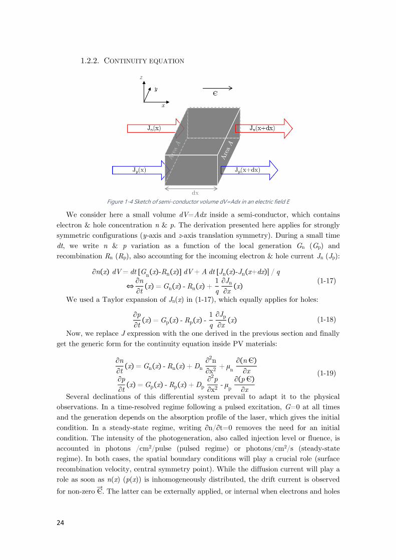
Figure 1-4 Sketch of semi-conductor volume dV=Adx in an electric field E ............................... 24
Figure 1-5 Band diagram and recombination type ....................................................................... 25
Figure 1-6 Generic perovskite crystal structure (ABX3). ............................................................. 28
Figure 1-7 Absorption spectra of CH3NH3PbI3 ............................................................................. 30
Figure 1-8 Cross-sectional view of a perovskite solar cell ............................................................. 32
Figure 2-1 Sketch of the hyperspectral imager (also HI) .............................................................. 34
Figure 2-2 Raw acquisitions at 6 increasing wavelengths on the CCD sensor of the HI. ............. 35
Figure 2-3 Reference spectrum of the calibration lamp, and measured spectrum Itrans ................ 35
Figure 2-4 Rectified images from a lambertian source with known spectrum. ............................. 36
Figure 2-5 Sketch of the em-ICCD camera under operation ........................................................ 38
Figure 2-6 Sketch of the time-resolved fluorescence imaging (TR-FLIM) set-up. ........................ 39
Figure 2-7 Digital Mirror Device and its use in Single pixel imaging (a) visual of the DMD
projecting a pattern (b) sketch of the SPI experiment ................................................................. 42
Figure 2-8 Proof of concept of image reconstruction from SPI .................................................... 44
Figure 2-9 Spectrometer and streak camera (a) The spectrometer is represented with light input
on top of the image and output on the right. Light is dispersed by a grating on the triangular
compound 155. (b) Streak camera with light path from the left to the right. (A: window; B:
photocathode; C: deflecting electring field; D: phosphor screen; E: CCD sensor) 156 ................... 45
Figure 2-10 4D PL imaging set-up................................................................................................ 45
Figure 2-11 Output from the 4D IPL imaging set-up after reconstruction .................................... 46
Figure 2-12 Space- & time-resolved IPL spectra ............................................................................ 47
Figure 3-1 Structure of the investigated III-V solar cell ............................................................... 50
Figure 3-2 Photoluminescence image of a GaAs solar cell ............................................................ 52
Figure 3-3 Experimental IPL profile at t = 1, 50, 100, 200 ns after the laser pulse ...................... 53
Figure 3-4 Photoluminescence images (a-c) and spatially integrated intensity profiles (d-f) ....... 54
Figure 3-5 Vertical concentration profile for photo-generated electrons....................................... 55
Figure 3-6 Simulations of IPL transients/profiles according to eq. (3-8) ....................................... 59
Figure 3-7 Fitting results vs experimental IPL transients/profiles ................................................ 60
Figure 3-8 Reconstruction error between the experimental transient and the theoretical model . 61
Figure 3-9 IPL transient for a wide-field illumination and a local excitation ................................ 62
Figure 4-1 J-V; EQE and cross section SEM image of the investigated sample........................... 65
Figure 4-2 Absolute PL spectrum for the considered perovskite samples, optically excited at =
532 nm at 0 = 5.5 x10³ W·m-2. ................................................................................................... 67
Figure 4-3 Photoluminescence images taken 10 ns after the laser pulse ...................................... 67
Figure 4-4 Photoluminescence decays for perovskite deposited at increasing injection levels ...... 68
Figure 4-5 Sketch showing the allowed energetic transitions in perovskite .................................. 70
Figure 4-6 In-depth concentration profile for electrons (or holes) inside a perovskite layer ........ 70
Figure 4-7 (a)-Experimental (dotted lines) and numerically fitted (plain lines) IPL decays for a
mixed cation perovskite ................................................................................................................ 73

Figure 4-8 (a) Scatter plot of values determines for τ1sun & L1sun from eq. (4-14) & (4-15) ......... 75
Figure 4-9 Fitted IPL transients acquired at increasing photon flux 0,1,0,2&0,3,..................... 76
Figure 4-10 Temporal evolution of recombination terms simulated for perovskite P2 ................. 78
Figure 5-1 Sketch of the experimental observations and of the physical mechanisms taking place
...................................................................................................................................................... 82
Figure 5-2 IPL maps of a perovskite sample after point pulsed illumination ................................ 83
Figure 5-3 IPL profiles of a perovskite sample after point pulsed illumination ............................. 83
Figure 5-4 IPL decays of a perovskite sample after point pulsed illumination at incremental
distances from the illumination point ........................................................................................... 84
Figure 5-5 PL spectral images at distinct photon energies ........................................................... 84
Figure 5-6 IPL spectra at increasing distances from the laser spot ............................................... 85
Figure 5-7 Geometrical sketch of the elementary volume dV in the long-range scenario ............. 86
Figure 5-8 Optimal reconstruction of IPL for increasing distances to the excitation point ........... 88
Figure 5-9 Sketch of the elementary volume 𝑑𝑉 in the short-range scenario ............................... 89
Figure 5-10 Contributions to rate equation (5-19) for a gaussian charge carrier distribution...... 91
Figure 5-11 Contribution of each PL wavelength to the recycling ............................................... 92
Figure 5-12 Determination of the pure electronic diffusion properties ......................................... 94
Figure 5-13 Sensitivity to space-domain restriction ...................................................................... 95
Figure 5-14 Fitting results for the optimization approach applied on IPL profiles with varying
space-domain restrictions. Best-fit appear in color surface and experimental in transparent
surface. Displayed rmax values were selected as the optimal ones as from Figure 5-13. (rmax=
1.7µm (a)-(b) // rmax = 2.1 µm (c)-(d) // rmax= 2.5µm (e)-(f) // rmax = 2.9µm (g)-(h)). A
textbox displays the fitted values for τn Dn & Reh* for each rmax value. ...................................... 97
Figure 5-15 Fitting IPL profiles acquired on InGaP sample .......................................................... 99
Figure 5-16 Morphological properties of a wrinkle-containing perovskite sample ...................... 100
Figure 5-17 Spectral aspect of multi-dimensional IPL imaging of a wrinkle-containing perovskite
sample ......................................................................................................................................... 101
Figure 5-18 Temporal aspect of multi-dimensional PL imaging of a wrinkle-containing perovskite
sample ......................................................................................................................................... 102
Figure 5-19 Cross-sections profiles drawn in IPL(500ns<t<1µs) map ......................................... 103
Figure 5-20 PL spectral images at distinct photon energies of a wrinkled sample ..................... 103
Figure 6-1 Structure of the perovskite channels ......................................................................... 106
Figure 6-2 Sketch of the modified version of TR-FLIM ............................................................. 107
Figure 6-3 Summary of fast-bias experimental results ............................................................... 108
Figure 6-4 Summary of simulation results and fitting of electron/hole mobility ....................... 109
Figure 6-5 Variations of the PL ratio and reconstruction error for different couples (µn,µp). .... 111
Figure 6-6 Temporal sketch of the slow bias experiment. .......................................................... 112
Figure 6-7 Summary of slow-bias experimental results on the HI .............................................. 113
Figure 6-8 Summary of slow-bias experimental results on the TR-FLIM .................................. 116
Figure 6-9 Optoelectronic parameters mapped for slow bias experiment (positive) ................... 117
Figure 6-10 Optoelectronic parameters mapped for slow bias experiment (negative) ................ 118

TABLE LIST
Table 2-1 Example of sequential acquisition on the TR-FLIM, during which the gain parameters
are fixed while tdel changes. .......................................................................................................... 40
Table 2-2 Example of snapshot acquisition on the TR-FLIM, during which the gain parameters
can be varied at each delay. ......................................................................................................... 41
Table 3-1 Fitted physical parameters for each injection level ...................................................... 61
Table 4-1 Physical parameters for each sample probed. Reh, Dn NT and Sair ............................... 74
Table 4-2 Physical parameters for each sample probed. τn, Dn NT and Sair ................................. 76
Table 4-3 Physical parameters for the semi-transparent device probed with double side
illumination ................................................................................................................................... 77
Table 4-4 Major recombination pathways at short times (t = 0.. 20 ns) and long times (t>100
ns) ................................................................................................................................................. 78
Table 5-1 Summary of values used for photon propagation calculation in the long-range scenario
...................................................................................................................................................... 87
Table 5-2 Summary of values used for photon propagation calculation in the short-range
scenario ......................................................................................................................................... 89
Table 5-3 Summary of the main physical contributions in the luminescence spatial variation ... 93
Table 5-4 Transport and recombination parameters determined by fitting IPL profiles. .............. 95
Table 5-5 Transport and recombination parameters determined by fitting IPL profiles on InGaP
thin films....................................................................................................................................... 99

Index of symbols
Mathematical
notation
Unit Signification
a(E) [ ] Absorptivity
Acell ; Afield cm2 Area of the cell, the field
A21 cm3/s Einstein spontaneous emission coefficient
Ak [ ] Coefficient for each contribution Uk (section
3.3.4)
α /cm Absorption coefficient
α1sun /cm Equivalent absorption coefficient at 1 sun
αλ /cm Absorption coefficient at wavelength lambda
αPL /cm Mean absorption coefficient on PL spectrum
α0d [ ] Generic absorption parameter in sub-bandgap
absorption model
(bi)i∈[1,m] counts Measurement on the photodetector (m
measurement)
B12 cm6/s Einstein absorption coefficient
B21 cm6/s Einstein stimulated emission coefficient
βk /cm Spatial pulsation of each contribution Uk
(section 3.3.4)
c0 m/s Light speed (celerity)
Deff cm2/s Effective diffusion coefficient
Dn ; Dp cm2/s Diffusion coefficient for electron / hole
Δµ eV Quasi-Fermi level splitting (also QFLS)
Δn ; Δp /cm3 Photogenerated electron/hole
δλ nm Grating bandwidth of the VBG
Є V/cm Electric field
Ei eV Intrinsic energy level
Epeak eV IPL peak energy
Eph eV Photon energy
Ef,n ; Ef,p eV Fermi level for electron, hole
Eg eV Bandgap
ε0 F/m Vacuum permittivity
EQEPV (EQELED) [ ] External quantum efficiency of a PV (or LED)
device
η % PCE
Eu eV Characteristic energy for sub-bandgap
absorption
fmodel [ ] Generic model function for fitting purpose
fsystem [ ] Spectral sensitivity of an optical system
flas Hz Laser frequency
fvb ; fcb [ ] Saturation factor for Vb (Cb)

fwr [ ] Wrinkle correction factor for IPL profile
FWHM cm FWHM of the gaussian distribution
G1sun /cm2/s Generation at 1 sun (AM1.5G)
gcorr [ ] PR correction factor (section 5.3.4)
Gem [ ] Electron multiplying gain on the em-ICCD
GI [ ] Intensifier gain on the em-ICCD
Gn ; Gp /cm3/s Generation rate (electron/hole)
grec ; grec /cm3/s Recycling term (w/ monochromatic PL
assumption)
Hk [ ] Hadamard matrix
h eV s Reduced Planck constant
ICCD counts Rectified images on the HI CCD
ICCD* counts Raw images on the HI CCD
ICCD,d (*) counts Dark rectified (raw) images on the HI CCD
IIx [ ] Neutral iodide in perovskite crystal
Iix [ ] Interstitial iodide in perovskite crystal
Ilas ; Ilas,d counts (dark) Rectified images from the laser
Iref counts Reference spectrum for HI calibration
Itrans counts Transmitted spectrum on the HI set*up
Jn,diff ; Jp,diff C/cm2/s Diffusion current (electron/hole)
Jn,drift ; Jp,drift C/cm2/s Drift current (electron/hole)
Jn ; Jp C/cm2/s Total current
jγ ph/s/eV Photon flux at energy E (emitted by dSem in
solid angle dΩem)
kB m2 kg s-2 K-1 Boltzmann constant
Kp ph.eV/cm3/s Simplification parameter introduced in eq.(1-7)
KA1 ; KA2 cm6/s Auger recombination coefficients
L1sun cm Equivalent diffusion length at 1 sun
Leff cm Effective diffusion length
Ln ; Lp cm (Electron/hole) diffusion length
LPR cm Photon recycling length
λlas nm Wavelength (of the laser)
µn ; µp cm2/V/s Mobility (electron/hole)
n /cm3 Electron concentration
n0 ; p0 /cm3 Intrinsic electron / hole concentration
n1sun /cm3 Charge carrier concentration at 1 sun
(AM1.5G)
Nacc [ ] Number of accumulations on the CCD
ncts/nph [ ] Absolute calibration factor for HI set-up
nT /cm3 Trapped electron concentration
NT /cm3 Trap site concentrations
nγ(E) ; dnγ ph/cm3 (contribution to) density of photon gas at
energy E
nopt [ ] Optical index
Ω sr Solid angle
Ωeff sr Collection solid angle

Ωem ; dΩem sr (Elementary) Emission solid angle
p /cm3 Hole concentration
pescape [ ] Escape probability for photon
prm [ ] Generic parameter vector for fitting purpose
Ф0 ph/cm2/s Fluence
ФBB ph/s/eV/cm3 Black-body radiation
φc rad Critical (total reflexion) angle
Фprop ph/cm3/s/eV Propagated flux
(Πi,k)
i∈[1,m];k∈[1,n] [ ] Pattern matrix (m patterns of n pixel)
Ψ rad Angle between normal to dSem and dΩem
q eV Electron charge
Raug /cm3/s Auger recombination rate
Rem /s Emission rate of a defect
R∞ [ ] Residual from convergence of spatial profile
Rint /cm2/s Interface recombination rate
rmax cm Maximum radius considered on the fitting
window
Rn ; Rp /cm3/s Recombination rate (electron/hole)
Rnrad /cm2/s Non-radiative recombination rate
Rpop cm3/s Capture rate of a defect
Rrad /cm3/s Radiative recombination rate
Rt [ ] Local spectral ratio on HI set-up
RX(E) [ ] Reflection coefficient at energy E
R1→2 /s Transition rate from state 1 to 2
R2→1 /s Transition rate from state 2 to 1
Reh cm3/s Internal radiative recombination coefficient
Reh* cm3/s External radiative coefficient (corrected from
reabsorption)
Rsp ph/cm3/s/eV Spontaneous emission rate
Sc cm/s Contact recombination velocity
Sfront ; Sback cm/s (front / back) Surface recombination velocity
Spix cm2 Surface imaged by a pixel
Sem ; dSem cm2 (Elementary) Emission surface
σcv cm Kernel of convolution
σn ; σp cm2 Capture cross-section of a defect
T K Temperature
tdel ns Gating delay on the em-ICCD
texp s Exposure time
t∞ ns Convergence time of spatial profile
tlas ns Detection time of the laser
twidth ns Gating width on the em-ICCD
τ1sun ns Equivalent lifetime at 1 sun
τn ; τp ns (Electron/hole) lifetime
Θ [ ] Coefficient for sub-bandgap absorption model
Uk [ ] Sinusoidal contribution in chapter 3

V V Voltage (chapter 6)
V ; dV cm3 (Elementary) Volume
Vbi V Built-in voltage
VI+ [ ] Iodide vacancy in perovskite crystal
<vn > ; <vp > cm/s Average velocity of electron/hole
Voc V Open circuit voltage
Vocrad V Open-circuit voltage at the radiative limit
Vabs cm3 Absorber volume
wSCR cm Width of the SCR
X [ ] Generic signal (space-, time- and/or spectrally-
resolved)
X* [ ] Reconstructed sisgnal
(Xk) k ∈ [1,n] [ ] Spatially resolved signal (n pixel)
z0 cm Absorber thickness

Index of abbreviations
Abbreviation Meaning
ABX3 Perovskite crystalline structure
AM1.5G Reference solar spectrum
Cb Conduction band
CCD Charge coupled device
CIGS Cu(In,Ga)Se : Copper, Indium, Gallium diselenide
CMOS Complementary Metal Oxide Semiconductor
DFT Density functional theory
DMD Digital Mirror Device
DSSC Dye-sensitized solar cell
EDS Electron dispersive spectroscopy
em-ICCD Electron-multiplied intensified CCD
EQE External quantum efficiency
ETL Electron transport layer
FA Formamidinium (CH3NH2)
FTO Fluoride-doped tin oxide
HI Hyperspectral imager
HTL Hole transport layer
IEL Electroluminescence intensity
IL Luminescence intensity
IPL Photoluminescence intensity
III-V Semi-conductor with atom from group 3 & 5
IPVF Institut du photovoltaïque d'Ile-de-France
ITO Indium tin oxide
I-V Intensity-voltage characteristics
KPFM Kelvin probe force microscopy
LED Light-emitting device
MA Methylammonium (CH3NH3)
MAPI Methylammonium lead iodide (CH3NH3PbI3)
MBE Molecular beam epitaxy
MCP Multi-channel plate
MEMS Micro-electromechanical system
MOCVD Metalorganic chemical vapor deposition
NA Numerical aperture
PCE Power conversion efficiency
PR Photon recycling
PSC Perovskite solar cells
PV Photovoltaic
QFL Quasi-Fermi level
QFLS Quasi-Fermi level splitting (also Δµ)
SCR Space charge region

SEM Scanning electron microscope
SLM Spatial light modulator
SPI Single pixel imaging
SRH Shockley-Read-Hall
TCO Transparent conductive oxide
THz TeraHertz
TR-FLIM Time-resolved fluorescence imaging
TRMC Time-resolved microwave conductivity
TRPL Time-resolved PL
UV Ultraviolet
Vb Valence band
Voc Open-circuit voltage
VBG Volume Bragg grating
WF Wide-field
Z1, Z2 Zones for TRPL analysis

14
Introduction
Photovoltaic (PV) devices offer a direct conversion of light source into electricity,
providing a much-needed solution to meet climate targets and move towards a low-carbon
economy. Indeed, the electricity consumption of mankind in 2018 could be matched by
the production of 100 000 km2 of photovoltaic panels (0.07% of Earth surface)1. The
international energy agency (IEA) forecasts that PV energy will overcome wind energy
in 2025, as well as hydro in 2030 and coal in 2040 (in terms of installed capacity)1. This
is not only due to its ever-decreasing cost of production but also to its continuous increase
of power conversion efficiency (PCE) over the last decades. The influence of both factors
is explicit in Figure 0(a), which displays the average module price (in USD/Watt peak)
as a function of cumulative module shipments. In order to approach the theoretical limit
for power conversion efficiency, which is about 31% in classical devices and about 47%
in tandem devices combining two absorber materials2,3, it is crucial to work on both the
electronic and optical performances, both affecting the output power.
In this thesis, we focus on PV materials and devices produced at IPVF (Institut du
Photovoltaïque d’Ile-de-France). This research institute notably aims at developing
tandem solar cells. They consist in the superposition of an already industrially mature
Silicon solar cell, which efficiently collects the near-infrared photons (NIR) and of another
solar cell with an absorber having a wider bandgap. Several materials and device
architectures are currently investigated, but they should convert more efficiently the
energetic photons (blue, UV) and transmits the red/NIR photons to the bottom cell (Si).
This is sketched in Figure 0(b), in which the power spectrum for each cell is represented,
along with the power spectrum available in the solar radiation incident on Earth surface.
Figure 0 (a) The green line, which shows that module price decays by 20% for each doubling of the cumulative
shipment (also Swanson's law4) is a fit to the blue experimental line. (b) Power conversion sketched for a tandem
solar cell under solar spectrum. The top cell absorbs the more energetic photons and transmits the remaining to
the bottom cell. Thermalization and transmission losses are accounted.

15
In optoelectronics, and in the field of photovoltaics in particular, photoluminescence
(IPL) analysis methods are used to optimize devices. Being contactless and non-
destructive, they can be used at different steps of the life cycle of a solar cell, from the
growth (in-situ) to the use (in-operando). For instance, their use for in-line quality checks
during production, or for fault detection on photovoltaic fields is already reported5,6. IPL
analysis methods are based on the fact that the luminescence intensity is directly related
to the product of charge carrier concentrations (electron / hole). They therefore
constitute a powerful tool for characterizing charge transport mechanisms (see chapter 1).
In this thesis, we focus on describing methods based on multidimensional luminescence
imaging. This technique includes spatial, spectral and temporal analysis of the light flux
emitted by photovoltaic materials under excitation. Its implementation requires the
development of optical assemblies as well as digital methods of data processing.
Two set-ups have been mostly used throughout this doctoral work: (i) the
hyperspectral imager (HI, section 2.1), which provides access to spectrally-resolved
images (one image per wavelength) and (ii) the time-resolved fluorescence imager (TR-
FLIM, section 2.2) which outputs time-resolved images (one image per unit of time).
While the HI was already fully assembled when this work began, the TR-FLIM set-up
was barely assembled and its development was finished during the thesis. Its two main
components are a pulsed laser and a fast camera. Its operating principles will be
thoroughly described, and its proof of concept on a reference photovoltaic material
(GaAs) will also be presented (chapter 3). It demonstrates that TR-FLIM allows the
assessment of transport and recombination properties with a single experiment. We will
show how the use of wide-field (WF) illumination and collection allows to get rid of
artefacts linked to classical optical microscopy (e.g. confocal microscopy), induced by
charge transport away from the illumination zone. Furthermore, this WF illumination
constitutes a realistic excitation scenario for PV materials and devices, due to its large
area and relatively low power. To go deeper than these already refined study of charge
transport in halide perovskites, a new set-up dedicated to 4D IPL imaging was designed
and is under development (section 2.3). It allows to acquired 4D IPL data sets (2D spatial
+ spectral + temporal) by combining the concept of single pixel imaging to a streak
camera. In this manuscript, we will describe its operating principles, which are protected
by a filed patent, as well as its initial development realized with the help of a master
student. A first proof of concept obtained on a perovskite layer will be presented.
These advanced characterization techniques notably enable the study of charge
transport in an emerging class of materials with very promising photovoltaic properties:
halide perovskites. Solar cells with perovskite absorbers have indeed exhibited a
tremendous increase in terms of PCE over the last decade7,8, while being crafted with
abundant and cheap raw materials and using a low thermal budget. Nonetheless, the
limiting factors preventing their commercialization are the up-scalability of fabrication
techniques, and their long-term stability9. Indeed, the fundamental physics and different
transport properties of halide perovskites have still not been fully understood and
described10 (section 1.3). Throughout this manuscript, charge carrier diffusion in mixed

16
cation halide perovskites will be brought to light thanks to several transport experiments.
It will also be distinguished from photon recycling, which constitutes a complementary
transport mechanism whereby a luminescence photon is reabsorbed and regenerates a
charge. The first experiment is based on a surface excitation, after which the charge
carriers diffuse in-depth into the perovskite thin film (chapter 4). The second experiment
is based on a point excitation, following which the charge transport is essentially radial
(chapter 5). In both cases, the diffusion and recombination of charge carriers will be
imaged with a high temporal and spectral resolution. This should allow to quantify their
impact by means of optimization algorithms that fit the experimental results to physical
models (continuity equation).
Imaging methods are also adapted to the investigation of the impact of chemical and
morphological inhomogeneities on local optoelectronic properties. This will be illustrated
by the study of the influence of wrinkles appearing at the surface of Cs-rich perovskite
(section 5.5).
Eventually, we will make use of multidimensional imaging techniques to probe lateral
structures featuring a 20μm wide perovskite channel in-between two electrodes
(chapter 6). By applying a fast electric bias across the channel (<1μs), we isolate the
drift of charge carriers from that of the ions composing perovskite. Experiments at larger
time scale (electric field applied 10 minutes) will also allow us to image the movement of
halide ions. This multi-dimensional experiment should bring us as close as ever to the
operating principles of a PV device, which operate with light and bias.

17
1. Theoretical background
1.1. LUMINESCENCE ANALYSIS
1.1.1. DETAILED BALANCE
Photovoltaic (PV) devices directly convert energy from light into electricity. In this
thesis, we focus mainly on the absorbing material inside PV device. One of its main
physical propertie is the bandgap Eg, which is defined as the energy difference between
the conduction band (Cb) and the valence band (Vb). It can be seen as an optical
absorption threshold as the incident photons with energy Eph > Eg are converted into
excited charge carriers: electrons and holes. Each of these two populations can be
described by an (electro)chemical potential where their energy difference leads to the
appearance of an internal voltage; it is the photovoltaic effect11.
Absorption and emission compensate each other at thermal equilibrium due to detailed
balance considerations, as was first discovered by Kirchoff12 in 1860. This can be
expressed using Einstein coefficients from the quantum theory of radiation inside a two-
state system13 (B12 for absorption, B21 for stimulated emission and A21 for spontaneous
emission). Please note that we derive here an internal equilibrium between photon gas
and matter, which does not include external illumination such as sunlight. In this
formalism, the transitions rates R1→2 & R2→1 at thermal equilibrium write:
R1→2=R2→1 ⇔ n1B12nγ(E)=n2A21+n2B21nγ(E) (1-1)
In eq. (1-1), n1 & n2 are the carrier population in state 1 & 2, which would correspond
to the ground (e.g. Vb) and excited (e.g. Cb) state in a PV absorber. nγ corresponds to
the density of the photon gas inside the material. The n2A21 term represents the
spontaneous emission rate Rsp of a semi-conductor, which was derived in 1954 by van
Roosbroeck & Schockley14. This rate can be written at a given energy E inside a semi-
conductor of optical index nopt:
Rsp(E)=
nopt3
π2h3c03
a(E)E 2
exp (E
kBT) -1
(1-2)
In eq.(1-2), the absorptivity a(E) of the semi-conductor appears (first predicted by
Kennard15). While it would be 1 in a blackbody, its value varies with E in semi-conductors
from ≈ 1 above Eg to ≈ 0 below Eg. Semi-conductors are thus called ‘gray-bodies’. As an
example, the absorptivity of a perovskite layer (Eg=1.55eV) is shown in Figure 1-1, along
with the spontaneous emission of this semi-conductor as described in eq. (1-2). It notably
differs from the black-body radiation (thermal radiation at 300K). The luminescence IL
is defined as the portion from this photon gas they emit as radiation. For a semi-
conductor with Eg around 1 eV at 300K, it is essentially formed by infrared photons.

18
Figure 1-1 Gray-body radiation decomposedas the product of absorptivity a(E) and black-body radiation.
Calculation is done for Eg= 1.55eV, Eu=15meV, Θ=1.5, α0d=10 (see section 1.1.4 for more details on spectrum)
Now, if an external source (light, chemical reaction, electricity) provides energy to the
material, the luminescence signal is enhanced by orders of magnitude (1020 more intense
for a typical perovskite layer under AM1.5G solar spectrum). In the case of light
excitation, the radiation is called photoluminescence (IPL), while it is called
electroluminescence (IEL) in the case of electric stimulation. Provided that each
population (electron, hole) can still be described by a Fermi-Dirac distribution, quasi-
Fermi level for electrons (EF,n) and holes (EF,o) can be defined and used in Lasher-Stern
equation16 (eq. (1-3)). It notably contains the quasi-Fermi level splitting (QFLS, or
Δµ=EF,n-EF,p) which quantifies the (electro)chemical potential of charge carriers inside
the PV absorber (i.e. the aforementioned internal voltage)17.
Rsp(E)=
nopt3
π2h3c03
a(E)E 2
exp (E-ΔµkBT ) -1
(1-3)
1.1.2. RADIOMETRIC CONCERNS
Knowing the internal spontaneous emission rate is a first step towards characterization
by luminescence imaging, but the formula giving the radiated flux is still missing. We
now consider a volume V with homogeneous concentration of excited charge carriers n &
p. We express in (1-4) its spontaneous emission as a photon density per energy per solid
angle, where the isotropicity of Rsp explains the 1/4π factor:
Rsp(E,Ω)=
nopt3
4πh3π2c3
a(E)E2
exp (E-ΔµkBT ) -1
(1-4)
The flux jγ going out of V by a small surface dSem (drawn on V), in a direction defined
by the solid angle dΩem making an angle Ψ with the normal to dSem would then be
expressed as:

19
jγ=Rsp(E,Ω)dΩemcos(Ψ)dSem
c0
nopt (1-5)
Figure 1-2 Volume of semi-conductor material and photons in equilibrium, in which the spontaneous emission
Rsp and from which a photon flux jγ is emitted through dSem in the direction dΩem.
This equation notably tells us that the intensity incident on a surface at distance r
from the emission point decays quadratically as r increases (i.e. as 1/r2). Based on the
cos(Ψ) factor appearing in eq. (1-5), the angular repartition of jγ follows Lambert’s cosine
law18. In the case when V is the absorber in homogeneous excitation conditions, jγ gives
a physical definition of the monitored photoluminescence signal IPL. In this scenario, dSem
would correspond to the region of interest at the sample surface, while dΩem would
correspond to the collection solid angle from the imaging set-up (see section 2.1.3). But
eq. (1-5) also applies for small volumes dV smaller than the absorber itself (dV<Vabs).
Photon recycling, which consists in charge transport mediated by photons, will be studied
in the presented formalism (see section 5.3.4).
A more convenient expression of Rsp can be obtained when E-Δµ>>kBT, which is
typically the case for any IPL spectrum considered in this thesis. We approximate the
Fermi-Dirac statistics by an exponential term (Boltzmann distribution) exp(-E/kBT) and
convert19 the exp(-Δµ/kBT) term into np/n0p0. Also, we abbreviate all the physical
constants into a single parameter Kp, which reduces eq. (1-4) to:
Rsp(E,Ω)≈
Kpnp
n0p0
a(E)E2 exp (-E
kBT)
(1-6)
An interesting application consists in integrating the previous formula at thermal
equilibrium, when only intrinsic charge carriers are present. In this case (np=n0p0), the
radiative recombination writes Rehn0p0 and can be determined with eq. (1-7)20. This will
be used to determined n0p0 from Reh values in section 5.4.3.
4π∫ Kpα(E)E2 exp (
-E
kBT)
E
dE=Rehn0p0 (1-7)

20
1.1.3. MODELING ABSORPTION PROPERTIES
Having a proper expression for the absorptivity a(E) of the considered volume is now
required to extract optoelectronic properties from IPL measurements. In this section, we
rely on Katahara et al.21 who allowed a treatment of IPL spectra taking into account sub-
bandgap absorption. We first express a(E) as a function of the absorption coefficient α(E)
and the thickness of the slab z0 in eq.(1-8). In a general case, this absorptivity depends
on the occupation probabilities of Cb and Vb (fvb - fcb), which strongly depend on Δµ.
Yet, we place ourselves in the non-degenerate case where Eg-Δµ > 6kBT, in which Cb &
Vb are not saturated (i.e. fvb-fcb=1). a(E) consequently remains independent from Δµ.
a(E) = 1 - exp(- α(E) [fvb - fcb] z0) (1-8)
A slightly enhanced version of this expression includes the multiple reflection in the
semi-conductor slab, with reflexion coefficient RX(E) identical at both front and rear
interfaces:
aRX(E) =
(1 - RX(E))(1 - exp(- α(E) [fvb - fcb] z0))
1 - RX(E) exp(α(E) [fvb - fcb] z0)
(1-9)
The previous equations are valid for a spatially homogeneous semi-conductor layer
with homogeneous Δµ (in particular in-depth), as it cannot be treated as a unique volume
with photon gas at equilibrium otherwise. To deal with inhomogeneities, one should
divide the slab into infinitesimal volumes coupled to each other via photonic and
electronic fluxes22–24. In any case, the absorption coefficient remains to be calculated. It
is here described by an ideal band-band term convoluted with a sub-bandgap absorption,
in which the tail states decay at a pseudo-exponential rate inside the bandgap (coefficient
0.5 < Θ < 2 and characteristic energy Eu).
α(E)=
α0
2EuΓ (1+1Θ)
∫ exp(- |u
Eu|Θ
)√E-Eg-u du∞
-∞
(1-10)
1.1.4. SIX PARAMETERS FOR ONE PHOTOLUMINESCENCE SPECTRUM
Previous considerations leave us with 6 free parameters to describe an IPL spectrum
and we will next give a brief overview of their influence. For this purpose, we calculate
IPL spectrum emitted by a semi-conductor layer using eqs. (1-5), (1-8) and (1-10). More
precisely, we conducted a parameter variation around the expected values for perovskite
which is the most studied material in this thesis. Even if these parameters can sometimes
be correlated, we vary one parameter at a time for the sake of simplicity.
At first, the temperature of the charge carriers T is investigated in Figure 1-3(a-b). It
solely impacts the high-energy section of IPL, in which a(E>>Eg)≈1. Indeed, T does not
impact the absorptivity in our non-degenerate model (Eg-Δµ < 6kBT and so fvb-fcb=1),
as displayed in eq. (1-10). Then, the QFLS influence is seen in Figure 1-3(c-d) and it
mainly dictates the total intensity of the signal without changing its shape. This
observation is relevant for any spectrally-integrated technique for which IPL intensities
are compared. For example, if we use a time-resolved sensor with spectral sensitivity

21
fsystem(E), one detects ∫ fsystem(E)IPL(E,t)dEE
. Now, as IPL spectrum is not changed over
the decay (constant Eg, T, α0z0,, Θ, Eu), the temporal signal is proportional to the
evolution of exp(Δµ(t)/kBT) and hence to the product of charge carrier concentration
(np).
The four last parameters all appear in the sub-bandgap absorption derivation. Their
influence will be notably seen in the low-energy part of IPL spectrum, in which a(E)
decays faster than E2exp(-E/kBT) increases. We start with the bandgap Eg in Figure
1-3(e-f), which has a direct influence on the energetic position of the absorption on-set,
as well as of the IPL peak. The enhanced intensity at lower bandgap lacks physical
meaning, it could find its origin in the absorption parameter α0 in the next parameter
α0z0. (z0 being the thickness of the layer). The latter tends to soften the absorption on-
set without shifting its energetic position. It remains hardly measured and will generally
be fixed to 10 in this thesis, as it is strongly correlated to Eg. The last parameters are
dedicated to the tail states in the bandgap. As explicated in the last section, they describe
a stretched exponential decay with rate Θ and characteristic energy Eu. As an example,
we would have Θ=1 for a mono-exponential decay and Eu would correspond the Urbach
energy25. The simulations presented in Figure 1-3(i-l) give more insight into their
influence on IPL spectra and absorptivity. At fixed Θ value, a smaller Eu describes a
“cleaner” bandgap with less tail states. It notably goes with a sharper slope on the IPL
spectrum for the lowest Eu. The influence of Θ is less evident and cannot be captured
easily with a single parameter variation. It remains noteworthy that Figure 1-3(k)
underlines the lack of direct relation between Eg and IPL peak position. Indeed, when sub-
bandgap absorption is high (‘dirty’ bandgap), IPL spectrum has a peak shifted inside the
bandgap. The reader is referred to Katahara et al. for further insight into sub-bandgap
absorption, which is a complex function of Θ & Eu.
A numerical model to extract material properties from IPL measurements was
designed26. It minimizes the distance between experimental IPL and theoretical ones, by
variating the fitting parameters (bandgap, QFLS, sub-bandgap absorption). An
optimization approach is conducted.

22
Figure 1-3 Photoluminescence emission and absorptivity calculated from the generalized Planck lawin eq.
(1-5). (a) (b) represents T variation, (c) (d) Δµ variation, (e) (f) Eu variation, (g) (h) Θ variation, (i) (j) Eg variation,
(k) (l) α0z0 variation, while other factors are left constant at values from (T=300K, Δµ=1.2V; Eu=35meV; Θ=1.5;
Eg=1.55eV; α0d=10)
1.2. TRANSPORT IN A SOLAR CELL
In this section we study charge carrier transport (diffusion & recombination) in PV
materials. The model applies for steady-state but also for time-resolved measurements
having a time step above 40ps (streak camera time resolution). This time scale is
significantly longer than carrier-carrier interaction in the considered materials27,28, which
allows us to define each carrier population (n & p) with eq. (1-11) even if the system is
out of thermal equilibrium. In the following, intrinsic Fermi level Ei, intrinsic
concentrations n0 & p0 and photo-generated concentrations Δn & Δp are used:
n=n0+Δn=n0 exp (
EF,n-Ei
kBT)
p=p0+Δp=p0 exp (-EF,p-Ei
kBT)
(1-11)

23
1.2.1. ELECTRON & HOLE CURRENT
Charge carrier in a non-degenerate and non-relativistic gas have a thermal energy of
kBT/2 per particle per degree of freedom. Their individual motion has random direction
and is frequently interrupted by scattering. In the presence of electric field Є , an average
velocity <vn > (<vp >) describes a net motion of the electron population along Є direction
(Drude model29). After solving Newton’s law on this population, a steady-state velocity
is derived as a function of electron mobility µn (μp):
<vn > = - μn Є
<vp > = μp Є
(1-12)
This allows us to provide the following expression for drift currents Jn,drift (Jp,drift
):
Jn,drift = - q n <vn > = q n μ
n Є
Jp,drift = q p <vp > = q p μ
p Є
(1-13)
The previously introduced mobility depends on the carrier effective mass, which
accounts for its interaction with impurity (i.e. dopants30 or defects) as well as with the
lattice (phonons). These interactions lead to scattering, which eventually slow down the
field-accelerated particles. We have thus eq. (1-12) which remains for drift velocities
below saturation velocities, which is not reached for the moderate electric fields at stake
in a solar cell (Є≈104 V/cm & µ≈1 cm2/V/s). In addition to Jdrift , another current must
be defined when the charge carrier distribution is inhomogeneous. It is induced by the
random thermal motion and cancels itself when carrier distribution homogenize. It
includes the diffusion coefficient Dn (Dp), which is directly linked to µn (µp) by Einstein
relations31 (D=µkBT/q):
Jn,diff = q Dn ∇n
Jp,diff = - q Dp ∇p
(1-14)
The total electron/hole current is J =Jdrift +Jdiff
and can sometimes be zero with two
non-zeros drift and diffusion currents. We here give its expression as a function of the
quasi-Fermi level for electrons and holes (deriving n expression from (1-11)):
Jn = q n μ
n Є + n μ
n (∇EF,n - ∇Ei)
Jp = q p μ
p Є + p μ
p (∇EF,p - ∇Ei)
(1-15)
Knowing that the electric field directly relates to the gradient of intrinsic level
via q Є =∇Ei, we eventually reach a meaningful expression of J as a function of the
gradient of QFL only:
Jn = n μ
n ∇EF,n ; Jp = p μ
p ∇EF,p (1-16)
24
1.2.2. CONTINUITY EQUATION
Figure 1-4 Sketch of semi-conductor volume dV=Adx in an electric field E
We consider here a small volume dV=Adx inside a semi-conductor, which contains
electron & hole concentration n & p. The derivation presented here applies for strongly
symmetric configurations (y-axis and z-axis translation symmetry). During a small time
dt, we write n & p variation as a function of the local generation Gn (Gp) and
recombination Rn (Rp), also accounting for the incoming electron & hole current Jn (Jp):
∂n(x) dV = dt [Gn(x)-Rn(x)] dV + A dt [Jn(x)-Jn(x+dx)] / q
⇔∂n
∂t(x) = Gn(x) - Rn(x) +
1
q ∂Jn
∂x(x)
(1-17)
We used a Taylor expansion of Jn(x) in (1-17), which equally applies for holes:
∂p
∂t(x) = Gp(x) - Rp(x) -
1
q ∂Jp
∂x(x) (1-18)
Now, we replace J expression with the one derived in the previous section and finally
get the generic form for the continuity equation inside PV materials:
∂n
∂t(x) = Gn(x) - Rn(x) + Dn
∂2n
∂x2 + μ
n ∂(n Є)
∂x
∂p
∂t(x) = Gp(x) - Rp(x) + Dp
∂2p
∂x2 - μ
p ∂(p Є)
∂x
(1-19)
Several declinations of this differential system prevail to adapt it to the physical
observations. In a time-resolved regime following a pulsed excitation, G=0 at all times
and the generation depends on the absorption profile of the laser, which gives the initial
condition. In a steady-state regime, writing ∂n/∂t=0 removes the need for an initial
condition. The intensity of the photogeneration, also called injection level or fluence, is
accounted in photons /cm2/pulse (pulsed regime) or photons/cm2/s (steady-state
regime). In both cases, the spatial boundary conditions will play a crucial role (surface
recombination velocity, central symmetry point). While the diffusion current will play a
role as soon as n(x) (p(x)) is inhomogeneously distributed, the drift current is observed
for non-zero Є . The latter can be externally applied, or internal when electrons and holes

25
have different distributions (n≠p), which leads to ambipolar diffusion32. For what
concerns Rn (Rp), their various expressions are treated in the next section.
1.2.3. GENERATION AND RECOMBINATION
We here start with radiative recombinations, as they were already described in section
1.1. At thermal equilibrium, they are compensated with radiative generations. For an
excited semi-conductor, their rate Rrad is amplified by orders of magnitude in comparison
to thermal recombination & generation. They are described by a volumic rate Reh (defined
in (1-7)) and their net contribution to Rn or Rp is:
Rrad = Reh (np - n02) (1-20)
In addition to radiative recombinations, Auger recombinations, interface
recombination and trap-assisted recombinations contribute to the global decay of charge
carrier population. While interface recombinations have a spatial dependence in the semi-
conductor and will be treated separately, the other types can be represented on a sole
energetic scale, as in Figure 1-5.
Figure 1-5 Band diagram and recombination type (Auger : green, radiative : red & trap-assisted blue). The
various recombination rates are defined in the equations of this section.
The first one relies on the Auger effect33,34: as an example, an electron falls back from
a certain energetic level (here Cb) to a vacancy in a lower one (here Vb), thereby exciting
another charge carrier to an even higher level (here above Cb) This three-particle process
has a volumic rate depending strongly on the charge carrier concentration:
Raug = KA1 n (np - ni2) + KA2 p (np - ni
2) (1-21)
Now remain the trap-assisted non-radiative recombinations. They do not only depend
on the pure material band structure (as Reh, KA1 or KA2), but also on the presence of
impurities and crystallographic defects, which generate trap for carriers. In the Shockley-
Read-Hall (SRH) formalism35,36, each trap has an energetic level Et and a capture cross-

26
section for each carrier type σn (σp). In a toy model including a single kind of trap, it
yields a capture (Rpop)/emission (Rem) rate for each carrier type:
Electron : Rpop,n = σn vth ; Rem,n= σn vth NC exp(- (Ec-Et) / kBT))
Hole : Rpop,p = σp vth ; Rem,p= σp vth NV exp(- (Et-Ev) / kBT)) (1-22)
At this point, it is very noteworthy that emission rates are thermally activated,
whereas capture rates are constant. On the one hand, these traps might appear in the
bulk semi-conductor and lead to the differential system presented in (1-23). It is made of
rate equations rule the populations in the trap level depending on the trap center
concentrations NT and on the filled trap concentrations nT:
∂n
∂t= Raug - Rrad - Rpop,n n (NT - nT) + Rem,n nT
∂nT
∂t = Rpop,n n (NT - nT) - Rem,n nT - Rpop,p nT p + Rem,p (NT - nT)
∂p
∂t = Raug - Rrad - Rpop,p nT p + Rem,p (NT-nT)
(1-23)
Despite not accounting for drift/diffusion currents, this system does not have an
analytical solution, and describes processes happening at various time scales. For a
shallow trap (i.e. activation energy around kBT), emission rates for electron and hole
diverge by orders of magnitude, which makes the numerical solving complex. There are
fortunately multiple possibilities to simplify Eq. (1-23), as for example one can neglect
the slowest capture/emission rates37, or forget about Auger recombinations when the
injection is low (n<1018 /cm3 in perovskite38). We will not enumerate them here but the
relevant assumptions will be declined in the model section of each experimental chapter
(sections 3.3, 4.3, 5.4.1, 6.2.3).
On the other hand, traps might appear at any interface in the system and especially
at the boundaries of the absorber. For a 1D model with boundaries at x=0 & x=x0, we
would model interface recombination of electrons with a surface recombination velocity
S:
Dn
∂n
∂x(x = x0) = Sright n(x = x0)
Dn ∂n
∂x(x = 0) = Sleft n(x = 0)
(1-24)
As a partial conclusion, we briefly described and expressed the various recombination
currents in a PV material. They are all included in the recombination term R in eq.
(1-19), except for the interface recombination which will appear in the boundary
conditions of the differential system.
1.2.4. INFLUENCE ON PHOTOVOLTAIC PERFORMANCE
We will now focus on the effective consequences of transport properties on
photovoltaic operation, during which a current transports the charge carriers from their
generation point inside the absorber to the transport layers/contacts. The extraction is
efficient if and only if they do not recombine through Auger or trap assisted phenomenon
before reaching the external circuit. For thin film solar cells (CIGS, perovskite)39, as well

27
as for modern architectures of Silicon solar cells with passivated contacts40, this transport
is essentially diffusive. The diffusion properties have two complementary aspects: the
sensitivity to a carrier concentration gradient (diffusion coefficient D), and the average
time available for the diffusion process (lifetime τ). Optimizing the solar cell efficiency
thus requires to maximize the average diffusion length (Ln=√Dnτn), such as it is at least
superior to the cell thickness. However, this might not be a sufficient as illustrated by
Rau’s reciprocity relations41, which we detail here under.
The first reciprocity relation between photovoltaic quantum efficiency EQEPV
(electrons out / photons in) and electroluminescent emission IEL at the applied potential
V writes:
IEL(E) = EQEPV(E) ϕ
BB(E) [ exp (
qV
kBT) - 1 ] (1-25)
The second one relates the light emission quantum efficiency of a light-emitting device
(LED) EQELED (photons out / electrons in) to the Voc deficit of the solar cell. This deficit
is deduced from the radiative open-circuit voltage Voc rad that would be obtained in a device
without non-radiative recombination, neither in the bulk nor at the interfaces:
ΔVoc = Voc
rad - Voc = - kBT
q ln(EQELED) (1-26)
They are valid for any device where the main recombination channel is linear to charge
carrier concentration41,42, and were recently extended to p-i-n solar cell structure43. They
translate analytically the common saying: “a good solar cell is also a good LED”. For a
variety of solar cell devices, they show that the combination of IPL and IEL measurements
allows for a detailed loss analysis44. They allow us to easily illustrate the relevance of
mobility and lifetime together by considering two extreme cases. One the one hand, a
low-mobility cell at the radiative limit (no non-radiative recombination) would have an
excellent Voc as EQELED=1 (eq. (1-26)). It would however have a low EQEPV as carriers
would not be collected and hence a low Jsc. It would notably emit photoluminescence
both at open-circuit and short-circuit conditions. On the other hand, a high-mobility cell
with a short lifetime would have an excellent EQEPV (perfect carrier collection), but a
non-optimal EQELED due to the partial non-radiative recombination of the injected
carriers, leading to a Voc deficit (eq. (1-26)). This deficit scales logarithmically and can
remain acceptable for relatively high loss in EQELED, making this type of high-mobility
cell preferred for PV applications.
We comment now shortly on perovskite absorbers, which will be the main focus on
this dissertation. As we will see, they are limited by trap-assisted and bimolecular
recombination (next section and Chapter 4), which constitute a non-linear charge
recombination pathway. This hinders the application of reciprocity relations, even in
their generalized derivation in a p-i-n configuration43, which would also require doping.
Still, these relations allowed to illustrate how crucial is the distinction between mobility
and lifetime.

28
1.3.PEROVSKITE, AN EMERGING CLASS OF MATERIAL
1.3.1. CHEMISTRY & TUNABLE BANDGAP
Perovskite crystal structure ABX3 was
initially discovered in 1839 by mining in the
Ural Mountains. This structure has been used
to fabricate materials since. Interesting semi-
conducting properties in halide perovskites had
been spotted in the 90s45,46, and their most
famous representative has been CH3NH3PbI3
(MAPI) for 10 years. It was first used47 as a
sensitizer in a dye-sensitized solar cell (DSSC).
A wide research field has then developed and
several atoms/molecules have been included in
the ABX3 structure to reach higher power
conversion efficiency (PCE) and stability.
Starting with the B site, it is mostly occupied by Pb for PV applications despite intense
research to replace it with the less toxic Sn48,49. As displayed in Figure 1-6, the central
metallic cation forms an octahedron with halide X- anions50–52, which can be either iodide
I-, bromide Br- or chloride Cl-. Eventually, various organic & inorganic cations (MA,
CH3NH2 or FA50,53,54, Cs55, Rb56,57) can be employed on the A-site. Their screening is
done so as to match the remaining size between each lead halide octahedron, according
to Goldschmidt tolerance factor58 and octahedral factor59. If a too large cation is used,
the 3D-structure collapses and lower-dimensional structures (quasi-2D or 2D60,61, or even
quantum dots62–64) are formed. If a too small cation like K is used, it segregates at the
grain boundaries/interfaces of the material65,66. Cubic phase of the perovskite structure
is most studied for PV applications, but halide perovskites transition to tetragonal phase
at low temperature (around 150K), as will be discussed in the next section. The polarity
of MA / FA molecules leads to ferroelectric peculiarities, which play yet a negligible role
in the photovoltaic devices built with halide perovskite67.
Metal halide perovskite are semi-conductors. Their bandgap is strongly impacted by
the chemical composition and especially by the halide. For example, the original MAPI
perovskite has its bandgap around 1.55eV, whereas the pure bromide (MAPbBr3) one is
2.3eV and the pure chloride (MAPbCl3) one is above 3eV. On the contrary, changing the
A-site cation leads to less significant change, as FAPbI3 (CsPbI3) perovskite has a 1.48eV
(1.72eV) bandgap54. As the previously listed compounds share a similar crystal structure,
their mixing is possible and a full-range covering of the visible spectrum can be realized
with this material family. The (in)direct character of the bandgap has been heavily
debated recently. The presence of a Rashba splitting, creating an indirect bandgap below
the direct one68–70 was investigated. The rapid radiative recombination observed by
ultrafast luminescence analysis allowed to discard this assumption, and the community
now agrees on the direct character of the bandgap71,72. Charge carrier recombination
Figure 1-6 Generic perovskite crystal structure
(ABX3).

29
phenomena in halide perovskite are discussed further in the next sub-section. Mixed
cation, iodide-rich or pure iodide compound are considered throughout this manuscript.
Most represented are (MA0.16FA0.84) Pb (I0.83Br0.17)3 and Cs0.05(MA0.16FA0.84)0.95 Pb
(I0.83Br0.17)3. They have been chosen for their high potential as top-cell of Si-based
tandem73,74, as well as for their relative stability.
Lead halide perovskite know several fabrication techniques (sequential deposition75,
solvent engineering76, spin-coating77, vapor-assisted solution process78 or iodide
management79). Samples considered in this manuscript were produced via spin-coating77,
which consists in depositing drops of a solution containing the species in the desired
stoichiometry on a substrate that is then rotated at high speed (several krpm). During
this rotation, an anti-solvent is dropped to rinse the perovskite layer. The final annealing
step happens at T<150°C. This process, as well as many others considered for perovskite
production75,76,79–81, requires low thermal budget and rather abundant materials. This
constitutes one of the reasons for their great potential for producing low-cost electricity.
The film composition given in this manuscript corresponds to the composition of the
solution deposited, but could differ from the dry composition. Precise quantitative
techniques exist to get the dry stoichiometry exist82 but were not easily accessed at IPVF.
This material family is highly sensitive to environmental stresses such as humidity,
oxygen, light83,84. The most visual degradation pathway leads to the irreversible
breakdown of perovskite crystal structure into the PbI2 salt (yellowish compound at room
temperature), while others lead for example to oxide formation at the exposed interface85.
We mention here the so-called Hoke effect as an example. It describes the reversible phase
segregation of mixed halide perovskite under illumination. It sets an upper limit to
bromide integration at approx. 20% on the X-site for (MA,FA)-based perovskite86,87
(resp. 40% on the X-site for (FA,Cs)-based perovskite88). This condition is respected for
the samples considered here after. Stability issues are out of the scope of this manuscript,
and were mitigated by storing samples in dark vacuum box, and realizing experiments at
most after 1 hour of air exposure at room temperature, 50% humidity.
As seen previously, several ions constitute the perovskite crystal structure, which
constitutes a soft lattice in which ions move rather easily89–91. Diffusion coefficients for
halide ions are in the order of magnitude expected for an ionic semi-conductor91,92. Any
vacancy in this structure (missing atom) creates a defect able to capture a charge carrier.
As an example, a positively charged iodide vacancy VI+ constitutes a potential electron
trap, whereas a neutral iodide (IIx) could trap a hole and create a vacancy VI
+ and an
interstitial iodide Iix 93. (IIx+h+ = Iix+VI+). Furthermore, electron, hole and ion contribute
to the definition of the internal electric field, and ion accumulation at interfaces can
endanger charge collection. Continuity equation applies to electron/hole, but also to ion.
This will be studied in details in Chapter 6.

30
1.3.2. TRANSPORT PROPERTIES
Studying transport in perovskite materials consist in determining the generation,
recombination and diffusion characteristics, so that the continuity equation (eq. (1-19))
can be solved in any excitation & geometrical configuration. For what concerns
generation, photon absorption with Beer-Lambert law applies for external illumination
(sun, laser) as well as for radiative recycling. Absorption coefficients used in this law have
been studied thoroughly in perovskite absorbers. They are displayed for a MAPI crystal
in Figure 1-7, in which the phase transition around T=180 K is visible thanks to an
abrupt change of bandgap. These absorption spectra also present excitonic features
enhancing the absorption at E=Eg at low temperature94, which vanish at room
temperature due to the weak exciton binding energy95–97.
Figure 1-7 Absorption spectra of CH3NH3PbI3for the full temperature range from 4 K to 295 K as a function of
energy (eV) on the bottom axis and wavelength (nm) on the top axis. Reproduced from Davies et al.94under
Creative Commons
Exciton dissociation generates free charges. Before describing their recombination, it
is very noteworthy to point out the intrinsic character of halide perovskite, in which
extrinsic doping has never been achieved. Now, electron/hole recombination described by
the differential system (1-23) can be reduced under certain assumptions to simpler rate
equations that can be solved analytically. A simplistic recombination term was first used
by Xing et al. in 2013, who first measured an IPL lifetime τn around 10 ns on a MAPI
layer98. The model quality was soon enhanced with the inclusion of trap levels as in
(1-23), in order to reproduce the increasing IPL decay rate at increasing excitation
level37,99–101. Quantifications for the trap concentrations were derived thanks to several
transient measurement techniques (transient absorption99,102,103, transient THz
conductivity104,105, TRPL37,106,107, time-resolved microwave conductivity TRMC101).
Temperature-dependent studies were even realized in order to locate more precisely the

31
trap energetic level within the bandgap108. Despite a strong discrepancy regarding this
level inside the bandgap10,109, a strong consensus still exists on the relatively small
concentration in non-radiative recombination centers. Physical reasons for this very long
lifetime of charge carriers (sometimes up to several µs85) are still an open question110.
One of the explanation relies in the high energy formation of deep traps, in comparison
to shallow levels. Indeed, density functional theory (DFT) calculations predicted the
favored formation of benign point defects111, especially when MAPI (or FAPI) is
deposited in I-rich conditions112. Another explanation presents the low phonon energy as
responsible of the long lifetime, as several phonons would have to be emitted so that the
energetic gap between Cb and trap (or trap & Vb) is crossed113.
Last but not least, the diffusion properties of halide perovskite remain to be discussed
in this section. The knowledge of D (or equally of µ) allows to derive Jdiff & Jdrift
in any
situation. A wide range of mobility values has been reported in the literature, going from
0.05 to 100 cm2/Vs 54,103,114–116. These huge variations in term of transport properties can
be ascribed to the quality of perovskites absorbers, to their chemical composition and to
the grade of crystallinity of the thin films117. Yet, the great variety of measurement
techniques applied to determine diffusion properties could also explain this discrepancy.
Electric ones based on the principle of time-of-flight have been used99,118 but are probably
biased by ion migration (see section 6.2.4). The initial conductivity of the sample in a
TRMC experiment also yields an approximate quantification of the mobility62,85,101.
Optical techniques are also widely used: one can here cite reports from transient
absorption imaging119–121, THz probe122, IPL spectroscopy24,123 or imaging124,125. The results
associated to these techniques are further discussed in section 4.5 & 5.4.3, with particular
interest given to the photon recycling phenomenon23 that also influences the charge
transport.
1.3.3. INTEGRATION INTO PHOTOVOLTAIC DEVICE
Perovskite layers owe their ever-increasing popularity in the energy materials
community to their use as absorber layer in PV devices. Indeed, perovskite solar cells
(PSC) have shown an unprecedented rapid increase of the conversion efficiency126,127. If
the first perovskite solar cell had a DSSC architecture47 with a perovskite thickness
inferior to 100 nm, other structures with thicker layers were employed then. In 2012,
perovskite layers were still deposited on top of a meso-porous TiO2 bead, which yielded
higher efficiency solar cell128. This TiO2 interface acted as electron transport layer (ETL),
while a Spiro-OMeTAD layer at the other interface acted as hole transport layer (HTL).
The structure was completed by a transparent conductive oxides (TCO) as FTO at the
front contact, and by an Au metal electrode at the back contact. The full stack represents
the devices used throughout this manuscript, and is seen on a cross-sectional view under
a scanning electron microscope (SEM) in Figure 1-8. Even if a general overview of the
PSC structure is outside the scope of this literature review, we recall here some concurrent
PSC architectures with the planar one (without the meso-porous interface) deposited on
textured Silicon126, or the back-contact one129.

32
Figure 1-8 Cross-sectional view of a perovskite solar cell Hole transporter refers to the HTL which is Spiro-
OMeTAD 74.
Several other layers can be employed as transport layers inside perovskite solar cells.
Replacing the TiO2 has early been a concern due to its prone degradation when exposed
to UV light130,131. Inorganic SnO2 and ZnO are developed to do so132. For what concerns
Spiro-OMeTAD, its cost and sensitivity explain the extensive research for alternative
HTL (like polymers P3HT & PTAA133 or inorganic Cu-SCN115 for example). The non-
radiative recombination happening at the perovskite/ETL (-/HTL) interfaces generally
constitute the main recombination pathway134,135, which also drives the research towards
their optimization and/or replacement. For this purpose, alternative improvements rely
on interface passivation using mixed 2D/3D perovskite60 or ultra-thin PMMA
barrier136,137. The considered PSC (similar as represented in Figure 1-8) operate as pin
solar cell39,138. Under illumination, an intrinsic zone without electric field is present in the
absorber. Henceforth, charge collection works out of diffusion and it is most relevant to
characterize Ln & Lp.
PSC are instable. Not only because perovskite and TL layers are sensitive83, but also
because the perovskite/TL interface are complex chemical environments where
degradation pathways are nested139. Irreversible changes are detrimental to the
sustainability of an eventual commercial product, but even reversible transformations
matter as they hinder characterization approaches. A very frequent instability consists
in the hysteretic behavior in the I-V curves under illumination. This generates
uncertainty concerning the effective maximum power point of the solar cell. Probable
causes for this hysteresis are interface trapping140,141 or ion migration142. In addition to
this hysteresis between forward and reverse scan, several kinds of light-soaking effects143–
145 have been observed.

33
2. Experimental methods
In this section, we give the operating principles of the luminescence imaging set-ups
used in this dissertation. The hyperspectral imager (HI) yields spectrally-resolved IPL
images in absolute units and will be described first (section 2.1). Then will come the time-
resolved fluorescence imaging (TR-FLIM) set-up, which gives time-resolved IPL images
(section 2.2). Eventually, a new set-up adapted to get 4D IPL images (2D spatial, spectral,
temporal) will be presented (section 2.3).
2.1. HYPERSPECTRAL IMAGER
In this section, we describe the operating principles of the HI. The acquisition of raw
ICCD* images, their rectificationa, and calibration is described. We explain how the signal
is corrected for each pixel of the sensor from the read noise, the dark current noise of the
camera as well as from the spectral transmissions along all the optical path, and the
spatial inhomogeneity of the optical system (flat-field). After calibration of the rectified
images, a datacube IPL(x,y,λ) is obtained. It can be equally seen as a collection of spectral
images (one image per λ) or as a collection of IPL spectra (one for each pixel). These
spectra are expressed in absolute units (photons/eV/s/m2/sr) of luminance, and can thus
be fitted with the generalized Planck law (see section 1.1.3). The spatial resolution is
1µm for the highest magnification objective and for visible/NIR wavelength range. The
spectral resolution is 2nm.
2.1.1. ACQUIRING AND RECTIFYING IMAGES
The HI, sketched in Figure 2-1, is based on classical optical microscope. The studied
sample is illuminated by a light source (i.e. WF illumination), which consists for example
in spread laser beam. This illumination light is reflected by a beam splitter and shined
on the sample through a microscope objective. The sample absorbs the excitation light
and emits a photoluminescence signal, which is collected by the same microscope
objective. This PL beam is then transmitted by the beam splitter, which sorts out any
laser light reflection on the sample surface.
a As it will be explained soon, the raw data are not usable as such and must be “rectified”. This pre-
treatement is called “rectification”.

34
Figure 2-1 Sketch of the hyperspectral imager (also HI) in a configuration with wide-field illumination of a
sample emitting red luminescence. The computer collects the images from the CCD, and controls the central
wavelength of the HI as well as the exposure time of the CCD.
At this point, luminescence images could be formed by the first lens but they would
be panchromatic (spectrally integrated). In order to collect spectrally-resolved images,
we use a 2D spectral filter developed by Photon Etc based on volume Bragg gratings
(VBG). This crucial optical component analyzes an image (input beam at the bottom of
the cube in Figure 2-1) and outputs a shifted image that contains a combination of
spectral and spatial information. To be more specific, the spatial y-axis on ICCD* images
is not impacted, while the x-axis contains mixed spatial and spectral information centered
at a precise wavelength λ. Focusing this output beam on the CCD sensor for an exposure
time texp results in ICCD* image. As the central wavelength can be tuned, it is possible to
acquire a set of n distorted images ICCD* at increasing λ1… λn, which corresponds to the
raw cube of data. As an example, a set of ICCD* images acquired on a perovskite sample
is shown in Figure 2-2(a). The ICCD* signal is more intense to the right of the image at
λ1, and to the left of the image at λ6. This is a signature of the spatial/spectral shift in
the output beam of the VBG. It can be corrected by a linear operation (so-called
rectification) applied on them. As displayed in Figure 2-2(b), it yields a set of n spectral
ICCD(x,y,λ) images, also called rectified cube. The ICCD signal is correctly localized on the
image, i.e. every pixel contains solely information on its conjugated point in the sample
plane. The rectified cube indicates that the most intense emission wavelength is λ3 or λ4
for all pixel, which was not easily inferred by the raw images.

35
Figure 2-2 Raw acquisitions at 6 increasing wavelengths on the CCD sensor of the HI. It is imaging the output
beam from the volume Braggs gratings. After rectification, the spatial component is correct on each of the 6
spectral images.
2.1.2. CALIBRATING THE TRANSMISSION OF THE SYSTEM
The spectral images from the rectified cube remain to be calibrated to get quantitative
information regarding the emitted photon flux. This procedure is thoroughly described in
A. Delamarre thesis146. The first step consists in acquiring a “dark” image ICCD,d without
illuminating the sample, at the same exposure time texp. It allows to correct the read noise
and dark current noise of the camera. We here also normalize with the exposure time to
get to the detected intensity per unit of time (ICCD – ICCD,d)/texp.
Figure 2-3 Reference spectrum of the calibration lamp, and measured spectrum Itrans (spatially averaged). 12
characteristic wavelengths used also used in Figure 2-4 are indicated by straight colored lines.
Then, the transmission along the optical path is calibrated by imaging an
homogeneous light source with a known spectrum Iref(λ), which is represented in Figure
2-3. In practical, we shine a calibrated lamp (Spectral Products) into an integrating
sphere located at the sample position. A small aperture in this sphere allows the light
with Iref spectrum to go out with a spatially homogenous output, which angular
repartition follows the Lambert’s cosine law. This leads us to a proper calibration of the
transmission of the optical system for each spatial location, each wavelength and each
angular emission. In order to illustrate the relevance of this calibration step, we first
consider the spatially integrated Itrans(λ) spectrum. It differs greatly from Iref(λ), which is

36
explained by the weak response of the Silicon CCD sensor in the infrared and by spectral
filters on the optical path. Now, the factors affecting the transmission are spatially
heterogeneous. This is evident by looking at rectified images Itrans(x,y,λ) displayed in
Figure 2-4. We use these images to correct the spatial inhomogeneity of the optical system
(flat-field), by using a local spectral ratio Rt(x,y,λ):
Rt(x,y,λ)=
Iref(λ)
[Itrans(x,y,λ)-Itrans,d(x,y,λ)]/δt
(2-1)
Figure 2-4 Rectified images from a lambertian source with known spectrum. The spatial inhomogeneity is due
to optical aberrations associated to the wide-field collection. The dark dots in the image are dead pixel of the
CCD sensor.
2.1.3. GETTING TO ABSOLUTE UNITS
After the previous step, one obtains the spatially and spectrally-resolved calibrated
intensity in counts. Here we will explain how to convert counts into physical units
(luminance).
Counts to number of photons: At this step, we image the output of a fiber in which a
laser is coupled in. The output of power is known and converted to a photon number per
unit of time nph. A perfect collection of all photons out of the fiber is ensured by the use
of a fiber having a smaller numerical aperture (NA) than the one of the collection
microscope objective. As previously explained, the images of the laser formed on the CCD
(Ilas) are corrected from the background noise using a “dark” acquisition Ilas,d. Next, Ilas
are converted into count numbers ncts in eq. (2-2) by using the correcting factor Rt derived
in eq. (2-1).
ncts=∬ ∫(Ilas(x,y,λ)-Ilas,d(x,y,λ))
δtlasRt(x,y,λ)dx dy dλ
λx,y
(2-2)
In order to get from counts on the CCD to number of photons, the correction factor
ncts/nph can be used. The derived factor is not wavelength-dependent, as the spectral
sensitivity is already accounted for by Rt.
Grating bandwidth normalization: This is analogous to the normalization with the
exposure time. Indeed, set to λ, the VBG lets through light of wavelength in the range
from λ – δλ/2 to λ + δλ/2. Hence, the registered intensity is integrated over a wavelength

37
bandwidth of δλ. To normalize to physical units, one has to divide the intensity obtained
previously by δλ.
Spatial normalization: The intensity is detected pixel-by-pixel, each pixel representing
a surface Spix of the sample, which is determined by imaging a target with known
dimensions. To get the number of photons by unit sample surface, one has to divide the
previous result by Spix.
Solid angle normalization: The imaging system collects light in a solid angle which is
defined by the microscope objective. With an objective of numerical aperture NA, this
angle is calculated to be Ωeff=π(NA)2. To get photon flux per unit solid angle, one has to
divide the previous result by this effective collection angle. Here, a lambertian emission
from the sample is assumed.
Eventually, we have the following formulas allowing to convert the rectified datacube
ICCD(x,y,λ) into a calibrated datacube IPL(x,y,λ) representing the photoluminescence
emission in physical units. For (Spix,δλ,Ωeff,texp) inputs in SI units, IPL is expressed in
photons /sr /s /m2 /m in eq. (2-3) or in photons /sr /s /m2 /eV in eq. (2-4).
IPL(x,y,λ)=
ICCD(x,y,λ)-ICCD,d
(x,y,λ)
texpRt(x,y,λ)
nph
ncts
1
δλ
1
Spix
1
Ωeff (2-3)
IPL(x,y,E)=
ICCD(x,y,λ)-ICCD,d
(x,y,λ)
texpRt(x,y,λ)
nph
ncts
1
δλ
1
Spix
1
Ωeff
hc
qλ2 (2-4)
2.1.4. DEGREES OF FREEDOM
Despite a quite tedious calibration procedure, the HI constitutes a powerful tool for
characterizing photovoltaic materials and devices. It allows to characterize the QFLS of
any material with 0.01 eV uncertainty provided that whole spectrum is fitted147,148. Its
high flexibility shall also be underlined. At first, various illumination sources can replace
the standard wide-spread green laser. A local illumination can be obtained by removing
the wide-field illumination set-up (chapter 5). Also, LED can be used to have illumination
with broader spectrum, or better homogeneity. Electroluminescence signals are monitored
without any external illumination, and the HI is perfectly suited to study their spatial
dependency149. On the collection side, several optical systems with magnification going
from x1/10 to x100 can be used to access information from the macro-scale to the micro-
scale.
2.2. TIME-RESOLVED FLUORESCENCE IMAGING
We will focus more on this set-up that has been developed during my PhD, even if
some preliminary results had already been acquired. As explained in section 1.1.4, a time-
resolved sensor with spectral sensitivity fsystem measures a signal proportional to exp(-
Δµ/kBT) when the signal spectral shape is unchanged. This assumption is verified for the
sample measured with the TR-FLIM throughout the manuscript. Henceforth, IPL will
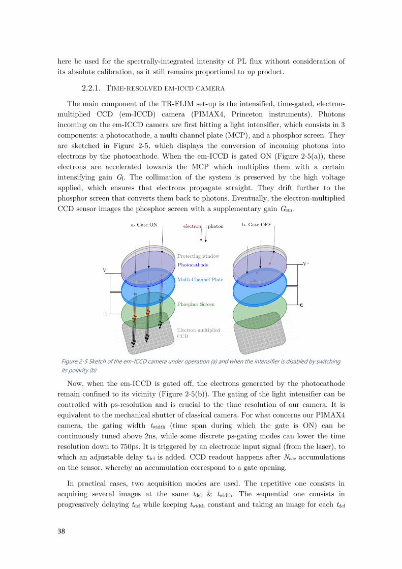
38
here be used for the spectrally-integrated intensity of PL flux without consideration of
its absolute calibration, as it still remains proportional to np product.
2.2.1. TIME-RESOLVED EM-ICCD CAMERA
The main component of the TR-FLIM set-up is the intensified, time-gated, electron-
multiplied CCD (em-ICCD) camera (PIMAX4, Princeton instruments). Photons
incoming on the em-ICCD camera are first hitting a light intensifier, which consists in 3
components: a photocathode, a multi-channel plate (MCP), and a phosphor screen. They
are sketched in Figure 2-5, which displays the conversion of incoming photons into
electrons by the photocathode. When the em-ICCD is gated ON (Figure 2-5(a)), these
electrons are accelerated towards the MCP which multiplies them with a certain
intensifying gain GI. The collimation of the system is preserved by the high voltage
applied, which ensures that electrons propagate straight. They drift further to the
phosphor screen that converts them back to photons. Eventually, the electron-multiplied
CCD sensor images the phosphor screen with a supplementary gain Gem.
Figure 2-5 Sketch of the em-ICCD camera under operation (a) and when the intensifier is disabled by switching
its polarity (b)
Now, when the em-ICCD is gated off, the electrons generated by the photocathode
remain confined to its vicinity (Figure 2-5(b)). The gating of the light intensifier can be
controlled with ps-resolution and is crucial to the time resolution of our camera. It is
equivalent to the mechanical shutter of classical camera. For what concerns our PIMAX4
camera, the gating width twidth (time span during which the gate is ON) can be
continuously tuned above 2ns, while some discrete ps-gating modes can lower the time
resolution down to 750ps. It is triggered by an electronic input signal (from the laser), to
which an adjustable delay tdel is added. CCD readout happens after Nacc accumulations
on the sensor, whereby an accumulation correspond to a gate opening.
In practical cases, two acquisition modes are used. The repetitive one consists in
acquiring several images at the same tdel & twidth. The sequential one consists in
progressively delaying tdel while keeping twidth constant and taking an image for each tdel

39
value. This is typically realized with tdel values going from the beginning (tlas) until the
end of the luminescence decay. The precise values used are recalled in “Imaging Specifics”
section of each chapter (3.1.2, 4.1.3, 5.1.2 & 6.1.2).
2.2.2. COMPLETE TIME-RESOLVED IMAGING SET-UP
In addition to the aforementioned em-ICCD camera, we mainly use a pulsed laser
(TALISKER, Coherent) as illumination source. It delivers 15 ps-wide light pulses
(=532 nm) at a tunable repetition rate (from 200 kHz to 1 MHz), as well as a
synchronized electric output that is used as a trigger for the camera. This is sketched in
Figure 2-6, which displays the electric and optical connections between each component
of the TR-FLIM set-up. For what concerns the optical part, the laser is focused in a
speckle removal filter based on a 50 µm pinhole, and goes through a wide-field
illumination optical system. The TR-FLIM set-up has the same microscope architecture
as the previously introduced HI. Hence, a microscope objective and beam splitter are
again used to illuminate the sample and to collect the PL flux emitted, which is
transmitted to the em-ICCD camera. On the electronic part, the computer controls the
laser frequency flas and fluence ϕ0, as well as the different gating (tdel, twidth) and gain
(Nacc, GI, Gem) parameters of the camera.
Figure 2-6 Sketch of the time-resolved fluorescence imaging (TR-FLIM) set-up.
Here, it is very noteworthy that supplementary synchronizations to the system are
available. In chapter 6, we use a modified version of the TR-FLIM set-up, in which the
em-ICCD camera is still triggered by the laser and operated as a time-gated camera with
gating delay tdel & width twidth, but also sends another trigger signal with another delay
tdel2 to a function generator (AFG 3000 Tektronix). The latter will then generate a pulsed
electric bias synchronous to the optical excitation, so that the photoluminescence signal
of the sample/device can be observed as a function of a pulsed electric field.

40
2.2.3. ACQUIRING TIME-RESOLVED IMAGES
Each experiment requires a careful setting of the gating and gain values. At first, it is
required to measure the delay value at which the laser is hitting the sample. This is a
critical step that should be realized with caution as the laser might damage the intensifier.
Hence, it is recommended to realize it at rather high gain and low laser power. Practically,
one should gradually increase laser power thanks to a tunable neutral density filter, until
the signal is higher than the background.
The relative intensity of the signal is measured by using a twidth value larger than the
laser period 1/flas, so that at least one laser pulse is incoming on the sample whatever tdel
value. At this point, the intensity of the laser can be tuned cautiously as explained at
the beginning of the sub-section. Then, a dichotomy approach based on a progressive
reduction of twidth to 1/2flas 1/4flas… is followed. The delay time tdel is changed until the
temporal position of the laser pulse is known for the targeted width twidth. Here, it shall
be noted that the measured value for tlas slightly evolves with twidth (around 2ns difference
when switching from twidth<1ns to twidth>5ns). This may be due to electronic bugs but
can be compensated by measuring tlas for each twidth used in the measurement campaign.
The gain parameters (the number of accumulations on the CCD Nacc, the intensifier
gain GI and the electronic gain Gem) are optimized for each experiment. They are kept
constant during a sequential acquisition of time-resolved IPL images. Henceforth, they
should be determined so as to avoid any saturation when the signal is maximal (i.e. at
tdel=tlas). An example of sequential acquisition with variable tdel and fixed twidth & gain
parameters is given in Table 2-1. For a power study such as presented in chapter 3, 4 &
5, the gain parameters should be adjusted for each fluence so that the signal to noise
ratio remains high. To compare relative IPL intensity from sample to sample at a given
laser power, these gain parameters should be kept constant as their impact has not been
calibrated.
Gate delay tdel
(past tlas)
Gate width
twidth (ns)
On-CCD
accumulat°Nacc Gain GI [a.u.] Gain Gem [a.u.]
0, 2, 4 …98,
100 2 1000 10 20
Table 2-1 Example of sequential acquisition on the TR-FLIM, during which the gain parameters are fixed while tdel
changes.
In chapter 6, we do not use sequential acquisition to reconstruct IPL(x,y,t) but snapshot
acquisition. This consists in taking several repetitive acquisitions at incremental time
delays while adjusting gate width and gain parameters for each delay value. The example
of snapshot given in Table 2-2 shows that gain parameters can be increased at long times,
when IPL is naturally weaker. This enhances image quality but hampers any comparison
between IPL intensity at different tdel values.
Gate delay tdel
(past tlas)
Gate width
twidth (ns)
On-CCD
accumulat°Nacc Gain GI [a.u.] Gain Gem [a.u.]

41
0 2 1000 10 20
10 5 10000 10 20
100 50 10000 100 100
Table 2-2 Example of snapshot acquisition on the TR-FLIM, during which the gain parameters can be varied at
each delay.
2.2.4. DEGREES OF FREEDOM
In the previous subsections, we already introduced the degrees of freedom linked to
the acquisition modes of the camera, as well as those offered for the synchronization of
external devices (e.g. electric pulse synchronized to the laser pulse). Here, we could also
add the relative variety regarding the illumination sources and collection. As an example,
we make use of another laser than the TALISKER for the experiments presented in
chapter 5. We used a tunable laser (Fianium) mainly because of unavailability of the
TALIKSER, but it could also allow to vary the excitation wavelength. In addition to the
pulsed excitation necessary to a time-resolved acquisition, a continuous wave source could
added to the illumination path, so that samples are observed while being light soaked.
As for the hyperspectral imager, collection objectives can be varied from *1/10 to *100
magnification, allowing to get IPL intensities from the macro-scale to the micro-scale.
2.3.4-D PHOTOLUMINESCENCE IMAGING
This set-up has been designed by the PhD candidate and developed by a master
student under his supervision. A patent protecting its operating principles has been filed
(Deposit number 19315037.2). It relies on principles related to single pixel imaging (SPI)
which are recalled first, before the set-up is described in details. A proof of concept is
realized in two steps. The first step consists in acquiring a “single-pixel image” of a
monochromatic pattern with a photodetector (subsection 2.3.2). The second step
showcases the first 4D IPL acquisition, which was here realized on a perovskite layer and
demonstrates the feasibility of simultaneous spatial, spectral and temporal resolution
(subsection 2.3.3). For more details concerning the optical design, the electronic control
and the synchronization of the set-up, the reader is referred to Marie Legrand’s master
thesis150.

42
2.3.1. SINGLE PIXEL IMAGING (SPI)
Figure 2-7 Digital Mirror Device and its use in Single pixel imaging (a) visual of the DMD projecting a pattern
(b) sketch of the SPI experiment
The developed system is based on the principles of Single Pixel Imaging (SPI)151,152,
which allows us to realize 2D spatial imaging with a single element photodetector,
whereas classical imaging systems (CCD, CMOS) use 2D sensors to capture 2D images.
The key component of this technology is a spatial light modulator (SLM) reflecting light
to the photodetector following a geometrical pattern Π (displayed in Figure 2-7(a)).
Analysing the output signal (total intensity detected) and demodulating it with the
projected patterns allow the image reconstruction. This micro-electro mechanical system
(MEMS) is made of 1024x728 micro-mirrors having 13µm pitch that can be controlled
independently. It allows to perform acquisitions of selected parts of the sample and
combine them to reconstruct the whole picture. This operating principle is sketched in
Figure 2-7(b). By using this SLM, we are restricted to binary patterns Π as each mirror
reflects 100% or 0%, on the contrary to liquid crystal devices allowing gray-scale
modulation153. The output signal from the detector can be computed an intensity
measurement for each pattern b(Π). Image reconstruction algorithms are then applied to
associate each location of the sample with an IPL intensity. In the next sub-section, we
will present a rather basic SPI set-up that will be used in order to validate the operating
principles of SPI. It will also allow us to validate our spatial reconstruction algorithm.
Thereafter, we will present the 4D IPL imaging set-up employing a streak camera as
detector.
2.3.2. 2D IMAGING SET-UP BASED ON SPI
Before describing the optical set-up, we focus on the mathematical background. Let
us consider a sample emitting a spatially-resolved signal (Xk)k∈[1,n], where the whole
spatial variation is modeled by a single parameter (1D). Let us also consider a SLM
displaying a series of binary patterns (Πi)i∈[1,m]. For each acquisition bi of the
photodetector, light from xk is reflected to the photodetector if and only if Πi,k=1.
Henceforth, the photodetector collects an information (bi)i∈[1,m], which is described by:
bi=∑Πi,k Xk
n
k=1
(2-1)

43
Following this approach, the problem of interest can be described mathematically by
finding the target image X from the pattern matrix Π and the measurement vector b:
Π X=b (2-2)
In the case where Π is a square matrix (e.g. m=n with as many measurements per
pixel), the previous linear system has an exact solution if and only if the patterns form
a spatial basis. That’s why we will next make use of a specific class of binary matrix
forming an orthogonal basis154: Hadamard matrix Hk. The case where m<n is called
“compressive sensing” as it makes use of less measurements than the targeted spatial
resolution. It is frequently encountered in SPI applications as it allows to significantly
reduce the acquisition time151. Yet, compressive sensing requires assumptions on the
image sparsity or on their gradient, and greatly increases the post-treatment time of the
images, in particular for the targeted application of 4D IPL imaging. Therefore, we decided
to stick to the Hadamard basis (with m=n) for our first developments. More details about
image reconstruction are available in Marie Legrand’s master thesis150.
The experimental set-up for our proof of concept of SPI includes an illuminated sun-
shaped object (displayed in Figure 2-8(b)- its shape represents a “sun”), which image is
formed on the DMD. The latter displays patterns from Hadamard basis with 24x32
spatial resolution (m=768), and reflects light into a powermeter (Thorlabs S130C), which
output power b(t) is displayed for the first 70 patterns in Figure 2-8(a). Patterns are
changed with a 5Hz frequency, whereas the power intensity is read with a much higher
frequency (around 300Hz) in order to increase the signal to noise ratio. We then sampled
b(t) to obtain a unique bi value for each pattern Πi, represented with green crosses in
Figure 2-8(a). As the pattern matrix is easily inverted, we used eq.(2-2) to obtain a
reconstructed image X*=Π-1b, which is displayed in Figure 2-8(c). The shape of the “sun”
and its surrounding rays appear clearly on X*. The intensity is higher at the center of
the image, which could be explained by optical losses far from the optical axis (non-
gaussian conditions). Still, the black round frame of the object is also imaged by our SPI
set-up, as we could check by plotting X* in logarithmical scale in Figure 2-8(d).

44
Figure 2-8 Proof of concept of image reconstruction from SPI (a) Output signal from photodetector on the
first 70 patterns, sampled with one measurement per pattern (green cross) (b) Original image pictured with a
phone camera (c) reconstructed image X* as determined by solving X*=Π -1b. d) logarithm of X*
2.3.3. 4D IMAGING SET-UP BASED ON SPI
In the 4D IPL imaging set-up, the single element photodetector is more complex than
a photodiode. Indeed it will return the spectral and temporal information contained in
the beam spatially hashed by the DMD. This photodetector is composed of a
spectrometer (Figure 2-9(a)) and a streak camera (Figure 2-9(b)). The first one splits the
input beam according to the photon wavelength and outputs a dispersed line signal. The
horizontal line determines a spectral axis (displayed in Figure 2-9(b)). It enters into the
streak camera and gets converted to “photo-electrons” by the photocathode (AB in Figure
2-9(b)). As in the light intensifier presented in section 2.2.1, they propagate straight due
to a reverse bias applied on the spectral axis. Now, a second orthogonal bias is sweeped
(C in Figure 2-9(b)). It is synchronized with the laser frequency and deflects the photo-
electrons as a function of time. The first incoming electrons go to the top of the phosphor
screen (D in Figure 2-9(b)), whereas the last ones are deflected to the bottom of this
compound. A CCD sensor images the phosphor screen and transmits the acquired
spectral-temporal characteristic to the computer.
The complete 4D PL imaging set-up is sketched in Figure 2-10. Same illumination
path as for the TR-FLIM is used. Yet, IPL signal emitted by the sample is imaged on the
DMD and not on the em-ICCD camera. The DMD displays consecutively the patterns
(Πi)i∈[1,m] that spatially hashes the IPL image, as in the experiment presented in sub-
section 2.3.2. This hashed flux is then focused on the entrance of the spectrometer. For
each pattern, a temporal spectral output bi(λ,t) is obtained by the spectro/streak camera,
with λ varying between λi & λf and t varying between ti & tf. The reference time (t=0) is
triggered by the laser, as for TR-FLIM set-up. Details regarding the DMD control, its
synchronization with the streak camera are available in Marie Legrand’s report150.

45
Figure 2-9 Spectrometer and streak camera (a) The spectrometer is represented with light input on top of the
image and output on the right. Light is dispersed by a grating on the triangular compound 155. (b) Streak
camera with light path from the left to the right. (A: window; B: photocathode; C: deflecting electring field; D:
phosphor screen; E: CCD sensor) 156
The reconstruction phase is operated by the computer, using again the inverse pattern
matrix. For each wavelength and time, the linear operation described in eq. (2-3) applies
and an IPL signal resolved in time, spectrum and space is eventually obtained.
∀(λ,t) IPL(pixel k,λ,t)=∑(Π -1)
i,k bi(λ,t)
m
i=1
(2-3)
Figure 2-10 4D PL imaging set-up as developed for the proof of concept. The sample under illumination (WF
spread laser) emits photoluminescence. It is imaged on the DMD, which displays a pattern Πi that spatially
hashes the PL image. This hashed flux is then focused on the entrance of the spectrometer.
An experimental proof of concept has been performed on a perovskite sample under
local illumination, which is obtained by removing the wide-field illumination set-up. A
similar experiment is studied with TR-FLIM and HI in chapter 5. A Nikon objective with
numerical aperture 0.6 and magnification 50 was used The region of interest on the
sample is restricted to some µm around the point illumination. Henceforth, the Hadamard
set of pattern was displayed on a limited area of the DMD, around the conjugate point

46
of the illumination center. This was located using a dichotomy approach on the set of
active mirrors, until the mirror reflecting the most light was found. Then we defined a
set of Hadamard patterns distributed around this mirror with 6x8 resolution (m=48) and
converted the acquired bi(λ,t) images into an hypercube IPL(x,y,λ,t). Spectral-temporal
images on a 3x3 group around the illumination center are represented in Figure 2-11.
This group of 3x3 pixels is a spatial extract of the full 6x8 resolution, which representation
on a single figure is not feasible. The significant variations in signal intensity between
the central pixel and surrounding ones are evident. The wealth of the acquired data is
further represented in Figure 2-12, which displays IPL spectra at short times (t<1ns) and
long times (4ns<t<10ns) for each pixel. When the signal to noise ratio is high enough,
an IPL peak value λmax is calculated and indicated in the subplot. It is determined at 762
nm for the central point and increases up to 780 nm for the surrounding pixel, which is
in accordance with the photon propagation phenomenon observed in chapter 5. More
visibly maybe, the high-energy tail of the spectrum is cut in the surrounding pixels, which
shape resemble ϕprop
derived in section 5.3.2. This experiment deals as proof of concept
for the 4D IPL imaging set-up.
Figure 2-11 Output from the 4D IPL imaging set-up after reconstruction conducted by solving eq. (2-3), and
represented on 3x3 pixel around the one conjugated to the illumination center.

47
Figure 2-12 Space- & time-resolved IPL spectra (green : IPL(λ,t<1ns) ; blue ; IPL(λ,t>4ns)) extracted on 5x3 pixel
around the one conjugated to the illumination center. When the signal to noise ratio is high enough, a PL peak
value λmax is calculated and indicated in each subplot
2.4. FITTING METHODS
Following concerns globally apply for the multi-dimensional data-sets (also called data
cubes) acquired with the previously introduced imaging techniques. Their post-processing
shares a similar architecture throughout the manuscript. This section is not dedicated to
the construction of physical models, but to the mathematical background necessary to
check their validity, correspondence to the measurement.
2.4.1. BINNING, CLUSTERING, SMOOTHING
The spatial dimension of these data cubes is the main reason for the gigantic memory
size they occupy. For example, a TR-FLIM acquisition with twidth varying between 0 and
1 µs with 1ns step occupies up to 1 Go, as the CCD sensor has 1024x1024 pixels. A first
step to reduce the size of the acquisition consists in binning the CCD sensor, whereby
groups of nB×nB pixel are constituted and read together by the CCD sensor (generally
nB=2 or 4). The knowledge of the spatial resolution of the system allows to select the
appropriate binning factor nB, which is generally chosen to avoid over-resolution. A
second step to reduce the size of the data cubes consists in clustering. It is often realized
according to prior knowledge of the sample geometry. A symmetry of the device (axial

48
in chapter 3 & 6, radial in chapter 5) allows to consider mean IPL intensities along one
spatial dimension. Also, different behaviors observed during the acquisition (Z1 & Z2 in
chapter 4, or wrinkles in section 5.5) can lead to the definition of region of interests with
more complex geometries, on which IPL is as well averaged. This whole clustering process
results in time- (or spectrally-) resolved data set which will be easier to fit to physical
models.
Smoothing experimental results is realized with Savitzky-Golay filter or moving
averages for the time-resolved acquisitions, which signal to noise ratios decreases sharply
for long times past the laser pulse. For what concerned the hyperspectral maps, advanced
convolution techniques have been developed together with signal post-processing experts
from EDF R&D26,157. They rely on a spectral and spatial deconvolution, in which the
kernels are fixed by the resolutions of the system. This deconvolution is combined to
Anscombe transformation, which acts on the Poisson noise by giving it a Gaussian
distribution.
2.4.2. MODELING & FITTING
Let us now consider a model fmodel taking a parameter vector prm as input and
X*=fmodel(prm). An example of such model is the function that outputs the IPL decay for
a theoretical perovskite at known fluence Ф0 (constant parameter) with transport (Dn)
& recombination (Reh,τn,S) parameters as input (fitting parameters). In this case, fmodel
first derives the solution of a partial derivative equation (continuity equation) using pdepe
function from Matlab158, and then calculates the resulting IPL by integrating the np
product in-depth.
Fitting the acquired datacube X to the model fmodel consists in determining the optimal
prm vector minimizing the reconstruction error:
minprm
|X*-X|norm (2-4)
Several norms (or distances) can be used but we often rely on | |log1 which calculates
the difference between log(X) and log (X*). This allows to better reproduce the signal on
its whole decay (or spectrum), including when it becomes lower at long times after the
laser (t >> tlas), or at energies lower or higher than the bandgap. If one would apply | |1
or | |2 while fitting a time-resolved IPL decay, the beginning of the decay would be over-
fitted and the decay tail would be poorly reproduced.
The optimization problem summarized in eq. (2-4) is solved using Matlab, using either
the Curve Fitting package (fit function), or the Optimization package (fminsearch
function). In any case, the multi-parameter model fmodel is defined with parameter values
normalized around their expected value, so that convergence issues due to low or high
numeric values are avoided. In our example, one would replaces Reh, which value is
expected to be between 10-12 and 10-8, by Reh/10-10 and indicate the normalizing factor
as constant parameter.

49
The ‘trust-region’ algorithm was mostly used to solve optimization problems159. It was
launched several times with random values for the initial parameter vector. Out of all
the local minima determined, the best parameter vector (lowest minimum for |X*-X|)
was kept and used to determine the fitted values. The reliability of the fitting method is
first verified qualitatively by comparing the reconstructed X*=fmodel(prm) to the original
measurement X, and verifying that the “physical” features of the decay (spectrum) are
preserved. A second (quantitative) step consists in calculating the variation of the
reconstruction error (|X*-X|) for small variation of prm around the optimal values.
Example of such verification are displayed in Figure 4-7(c), or Figure 6-5.

50
3. Lateral transport & recombination in a
photovoltaic cell
In this first experimental chapter, we introduce time-resolved fluorescence imaging as
an optical characterization method for optoelectronic devices. Under wide-field
illumination, we will probe the lateral diffusion and recombination of minority charge
carriers inside a Gallium Arsenide (GaAs)-based solar cell. This cell acts as a proof of
concept device. By conducting the analysis of its IPL signal, we intend to demonstrate
the relevance of optoelectronic characterization by TR-FLIM. In a first time, we
introduce the reader to the experimental details specific to this chapter (section 3.1).
Then, we conduct a thorough exploration of the acquisitions by plotting the data along
its spatial and temporal dimensions (section 3.2). Thanks to this data analytics, we are
able to design a model matched to the physical phenomena at stake, i.e. transport, bulk
and contact recombination (section 3.3). The model is derived from the continuity
equation, and subsequently solved analytically. A fitting procedure adapted to the TR-
FLIM output is developed and applied to reconstruct the experimental IPL transients
(section 3.4). Key optoelectronic properties for the considered device will then be
extracted from these fits. Finally, we will comment on the particular advantage of using
wide-field illumination (section 3.5).
3.1.EXPERIMENTAL DETAILS
3.1.1. SAMPLE STRUCTURE
Figure 3-1 Structure of the investigated III-V solar cell(a) 3D sketch (not to scale) of the illuminated solar cell,
where the fork-shaped contact (black lines) and the light collection zone (dotted orange square) are
represented (b) (a). Layer structure of the illuminated solar cell

51
The investigated sample consists in a standard GaAs (gallium-arsenide) solar cell. Its
layer structure is displayed in Figure 3-1(b). Figure 3-1(a) displays its 3D structure and
notably shows the contact geometry, as well as the light collection area (Af = 1mm2).
The cell power conversion efficiency is 18.8%, and its VOC is 0.983 V. The investigated
photoluminescence signal peaks at 1.44 eV, which designates the GaAs absorber layer as
the emitting layer149. As the considered sample shows a lateral symmetry (parallel to the
contact direction in the collection zone), we will often focus on the intensity integrated
along the y-axis (contact axis). Note that the simple cell geometry was here chosen for
the sake of clarity and that the presented experiment would also apply for more complex
device configurations.
3.1.2. IMAGING SPECIFICS
The experimental set-up for TR-FLIM was presented in section 2.2. For our study,
sequential acquisitions were realized. The gating time was varied stepwise between t=tlas
(taken as reference) and t=300 ns, whereas the gate width remained constant at 1 ns. A
wide-field illumination was obtained with a home-built opto-mechanical set-up, which
was not yet including a rotating diffuser (hence the speckle appearing in Figure 3-4(a)).
With the considered configuration, the geometrical resolution is 1 μm. The illuminated
area A0 is larger than the active area of the solar cell (Acell = 5.2mm2). The photon flux
incident on the sample was varied between 0=3x10¹¹/pulse/cm2 and 80.
3.2.PROJECTIONS OF THE DATA SET
3.2.1. TEMPORAL ASPECT
Any TR-FLIM experiment is followed by an exploratory phase, during which the
acquired IPL(x,y,t) cube gets plotted along its temporal and spatial dimensions. We will
here show the complementarity of these two exploration directions. At first, Figure 3-2
displays an IPL image taken 10 ns after the laser pulse. The two blue stripes (lowest IPL)
on the image represent the metallic contacts (also on Figure 3-(c)), which are separated
by a 900µm distance. Different cross-sections (b to e) parallel to the contacts are
distributed equally between left and right contact. We calculated the mean time-resolved
IPL decays on these lines, and show them in Figure 3-3(b)-(f) for increasing incident
powers.
At short times after the pulse, IPL decays faster close to the contact than in the center
of the cell. Despite being in open-circuit condition, the contacts seem to induce a locally
higher recombination rate, which results in a IPL intensity drop. On the contrary, a mono-
exponential decay (straight line in semi-log scale) is apparent at the center of the cell,
which hints that a unique recombination process dominate the charge carrier dynamics
there.

52
Figure 3-2 Photoluminescence image of a GaAs solar cell at open-circuit conditions (a). It is taken at t=10ns after
the laser pulse. The scaling bar is 100 µm. Each black line corresponds to an extraction zone for the normalized
TRPL decays shown in b-e. Several decays are represented with a color for each power 0 (see caption on the top
right corner)
At long times after the pulse, the decay speed seems homogeneous for each zone, even
if it still depends on the injection level 0. Similar observations are done at for left &
right contact (Figure 3-3(b)&(f)), as well as for center left & center right (Figure
3-3(c)&(e)), pointing out the influence of the cell geometry on the probed IPL signal.
3.2.2. SPATIAL ASPECT
After having considered temporal extractions of the dataset, we look at spatial
extractions in Figure 3-3. For increasing time after the laser pulse, IPL profiles orthogonal
to contact direction are displayed. The contact zone appear as deeps at x=±450µm and
the profiles are normalized to their maximum for each time and injection level. Their
shape change from a flat and almost uniform profile after the pulse to a steeper profile
after a hundred of nanoseconds. One can note that the lower injection level is more
rapidly quenched next to the contact, whereas the higher injection level remains rather
flat at t=50ns. This constitutes another justification for the power study. Here again, the
IPL decay seems to be dominated by the recombination at the contacts, as IPL is
progressively quenched from this zone to the cell center. This calls for the development
of a model for minority carriers including contact recombination and diffusion.

53
Figure 3-3 Experimental IPL profile at t = 1, 50, 100, 200 ns after the laser pulse, for the same power study as in
Figure 3-2.
3.2.3. SUMMARY
Now that we explored the spatial and temporal dimensions of the data cube, we can
propose a graph summarizing the rich information it contains. Indeed, Figure 3-4(a)-(c)
consists in a series of time frames revealing the time-resolved IPL images at t=0, 10 and
100ns, while the global decay and deformation of IPL profiles appear in Figure 3-4(d)-(f).
Yet, visually taking into consideration the whole power study requires the previously
introduced spatial and temporal extractions.
Thanks to the previous remarks, we can assess the phenomena most likely to influence
the evolution of IPL in such a solar cell. In addition to the obvious SRH recombination
happening homogeneously in the bulk, non-radiative recombination at the contact seem
to play a predominant role, as well as diffusion of charge carriers from the center of the
cell to the recombining contact. Therefore, the next section is dedicated to the
development of a physical model able to reproduce the whole IPL evolution.

54
Figure 3-4 Photoluminescence images (a-c) and spatially integrated intensity profiles (d-f) for a complete GaAs
solar cell in open-circuit condition, at incremental time steps following the laser pulse. (d-f) share the same vertical
scale. Scaling bar is 100 μm long.
3.3. MODELING TRANSPORT
3.3.1. ABOUT NEGLECTING IN-DEPTH DIFFUSION
To develop the following model, a homogeneous charge carrier concentration
throughout the thickness of the absorber layer is assumed. Even if absorbing the laser
pulse generates an exponentially decaying concentration profile (as of Beer-Lambert
absorption), it is totally homogenized in less than 1ns. This is due to the high mobility
of charge carriers in a III-V material such as GaAs160; this condition might not be satisfied
in all PV absorbers. We provide further justification by solving the continuity equation
(introduced in section 1.2.2) and displaying the vertical concentration profiles for photo-
generated carriers Δn(z).

55
Figure 3-5 Vertical concentration profile for photo-generated electrons, at various time after the laser pulse (a),
which are also shown normalized to their maximum (b). Simulation realized assuming standard diffusion
properties for the GaAs layer : Dn = 75cm2/s, Sf = 102cm/s, τn = 75ns160
Therefore, in-depth diffusion of minority carriers does not play a significant role in the
present which focuses on a longer time scale (ns scale mostly). Once again if we consider
other materials with lower mobility, this consideration needs to be revisited or we need
to look at longer time scale as we will demonstrate in section 4.3.2.
Furthermore, we optically determined that the quasi-Fermi level splitting equals the
open-circuit voltage in a similar device, which validates the assumption that there is no
in-plane potential gradient inside our sample (i.e. homogeneous concentration of carrier
in the sample depth).149
3.3.2. ABOUT NEGLECTING THE ELECTRIC FIELD
The electric field inside the solar cell, as well as the drift current it induces, will be
neglected throughout this study. Our justification mainly relies on the negligible width
of the depletion region wSCR as compared to the absorber thickness. Indeed, if we consider
a classic homojunction architecture, the electric field will be confined in the depletion
region, where free charge carriers are absent and all dopants are ionized. This depletion
region is located around the p-n junction and its width is defined by161 :
wSCR=√2×
ϵ0q×Vbi×(
1
n0,GaAs+
1
p0,GaAs
) = 48 nm (3-1)
where the doping levels (n0,GaAs and p0,GaAs) of the n- and the p-type parts of the
absorber layer can be read in Figure 3-4(c), and Vbi is the built-in voltage defined by :
Vbi=
kT
qln (
n0,GaAsp0,GaAs
ni2
)= 1.3 V (3-2)
Now, we made the point that wSCR is 2 orders of magnitude lower than the cell
thickness. Henceforth, taking the drift zone into account would slightly modify our
assumption of a vertically uniform concentration profile. Still, it corresponds to a second-
order correction to our model. One could also show interest for the transitory drift regime.
Following Maiberg’s calculations, the depletion region appears on the ps time scale, like

56
the homogenization of the vertical concentration profile162, which further confirms the
negligible aspect of the drift in our study.
3.3.3. CONTINUITY EQUATION
In section 3.2, we introduced the 3 main phenomena governing the charge transport
in the considered device: bulk recombination, contact recombination and diffusion. In
section 3.3.1 & 3.3.2, justifications were presented for taking only them into account and
for excluding in-depth diffusion and the drift current. A final assumption relies in the
fact that no trap centers are active in our high quality GaAs, which finally results in the
electro-neutrality rule Δp(x,t)=Δn(x,t), where Δn and Δp are the concentration of
photo-generated electrons and holes.
Now, the incoming photon flux 0 being low, Δn remains lower than the doping level
p0 and hence we can assume a monomolecular recombination regime19. Indeed, in p-doped
semi-conductor such as GaAs, the radiative recombination rate Rrad yields (3-3), where
Reh is the radiative constant.
Rrad=RehΔn(Δp+p0)=RehΔnp0∝Δn (3-3)
Here, we also used the weak injection regime assumption (i.e. Δn<< p0) to describe the
radiative recombination rate as solely depending on the minority carrier population19.
Observing IPL in our TR-FLIM set-up is equivalent to having access to the in-depth
integration of Δn. As we assume a homogeneous in-depth charge carrier concentration,
we can write:
IPL(x,t)∝Δn(x,t) (3-4)
This assumption allows us to explain the temporal and spatial variations of IPL with
the transport of minority charge carriers19, which is ruled by equation (3-5) in the bulk
and by equation (3-6) at the contacts (localized at x=±450µm):
Deff
∂2Δn
∂x2 -∂Δn
∂t+
Δn
τn=0
(3-5)
Scn=Deff
∂Δn
∂x
(3-6)
In this model, 𝜏𝑛 is the minority carrier lifetime, Deff is the minority carrier effective
diffusion coefficient in the solar cell, and Sc is the recombination velocity at the contact.
An effective diffusion length can be defined by LeffSc = Deff 163. The wide-field uniform
illumination 0 and the thickness of the absorber z0 dictate the initial condition:
Δn(t=0,x)=
Φ0
z0
(3-7)
3.3.4. SOLVING THE CONTINUITY EQUATION
An analytical solution to this model can be determined164, and can be written as a
sum of sinusoidal contributions Uk(x), with spatial pulsation k:
Δn(x,t)=(∑Ak
k
Uk(x) exp(-Deffβk2t)) exp (-
t
τn)
(3-8)
57
Uk(x)= cos(β
kx)+
Sc
Deffβk
sin(βkx)
(3-9)
Ak∈ ℝ ; tan(β
kx0)=
2Deffβk/Sc
Deff2 β
k2/Sc
2-1
(3-10)
Ak coefficients are determined by projecting the spatial initial condition on the basis
formed by Uk(x) contributions. On the temporal scale, the TRPL decay is locally multi-
exponential, and τn has a global influence. On the spatial scale, the IPL profile is
equivalent to A1U1(x) after a certain time t∞. This can be evidenced by dividing the
general solution in eq. (3-8) by A1U1(x)exp(-t/τn), to which it will be equivalent at long
times:
Δn(x,t)
A1U1(x)e
-tτn
=1+(∑Ak
A1k>1
Uk(x)
U1(x)exp(-Deff(βk
2-β12)t))=1+R∞(x,t)
(3-11)
Now, it is obvious that the second term of this sum R∞(x,t) tends to 0 at exponential
speed at long times. What’s more, it is dominated by its first term:
R∞(x,t) ~
A2
A1
U2(x)
U1(x)exp(-Deff(βk
2-β12)t)
(3-12)
Thanks to eq. (3-12), one can estimate the time t∞ after which the IPL spatial profile
is equivalent to A1U1(x), which would be:
R∞(x,t)<e-3 ⇔ t>t∞=
3
Deff(β2
2-β
12)
(3-13)
Here, one can note that a greater value for Deff induces a smaller value of t∞ which is
consistent with the physical intuition. Indeed, a faster diffusion will accelerate the
convergence to stable IPL profile.
3.3.5. FITTING PROCEDURE
This mathematical analysis finds an application with the following fitting method. At
first, n is determined by fitting a single TRPL decay far from the contact. Indeed, one
can consider the differential equation (3-5) at short times, in which the homogeneous
illumination is zero (homogeneous generation). Then the decay rate appears as the
derivative of log(Δn):
∂ logΔn
∂t(x,t=0)=-
1
τn
(3-14)
Our fitting procedure will then determine optimal values for (Sc,Deff), by fitting the
experimental decays IPL to the theoretical profiles from eq. (3-8). It is equivalent to
solving the optimization problem presented in eq. (3-15), where the analytical solution is
compared point by point to the spatially normalized intensity profiles IPL / maxx (IPL).
On the contrary to n, the precise determination of Deff and Sc requires the combination
of temporal and spatial data, which underlines the utility of the TR-FLIM set-up.

58
min
Deff,Sn
∑(IPL(x,t)
maxx
(IPL(x,t))-
n(x,t)
maxx
n(x,t))
2
(3-15)
3.4.DETERMINATION OF TRANSPORT PROPERTIES
3.4.1. SENSITIVITY TO FITTING PARAMETER
Figure 3-6(a) confirms that τn has a global influence throughout the cell. On the same
figure, (d) & (f) allow to underline the great influence of Leff & Sc at the contact, while
(c) & (e) demonstrate their negligible impact at the center. The quick reading procedure
at the center of the cell is recommended. On the spatial scale, Leff has a great influence
on the final (long-time) PL profile (see (g)) while Sc has an non-existent impact (h). This
sensitivity analysis justifies the choice of (Leff , Sc, τn) as fitting parameters, by attributing
each of them a specific area of the dataset where their influence will be probed solely.
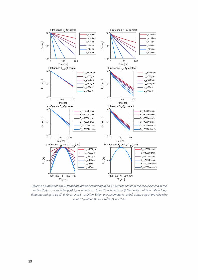
59
Figure 3-6 Simulations of IPL transients/profiles according to eq. (3-8)at the center of the cell (a,c,e) and at the
contact (b,d,f). τn is varied in (a,b). Leff is varied in (c,d), and Sc is varied in (e,f). Simulations of PL profile at long
times according to eq. (3-9) for Leff and Sc variation. When one parameter is varied, others stay at the following
values :Leff=200µm, Sc=5 104cm/s, τn=75ns.

60
3.4.2. ABOUT OUR III-V SOLAR CELL
Figure 3-7 Fitting results vs experimental IPL transients/profiles(a) PL experimental (dotted lines) and fitted
(plain lines) decay at |x|=0, 324, 405 μm. (b) PL experimental (dotted lines) and fitted (plain lines) profile at
t = 20; 60; 100; 140; 180 ns. Fluence level for both figure is Φ0=1.2 x 10¹² /cm2/pulse.
In Figure 3-7, dotted lines show IPL decays and profiles acquired on a GaAs solar cell
at a moderate fluence level Φ0=1.2x10¹² /pulse/cm2. Similarly to Figure 3-2, normalized
temporal intensity profiles at various locations in the solar cell (from contact to center)
are displayed in Figure 3-7 (a). Normalized spatial intensity profiles at various time
delays after the pulse are displayed in Figure 3-7 (b). As explained in eq. (3-14), we first
determine the bulk lifetime n by fitting the IPL decay far from the contact (x=0µm) as
a mono-exponential decay. It yields n = 75 ns.
In the same figure, plain lines show the numerical solution for the fitted parameters
n=75 ns, Deff=2160 cm2/V/s, and Sc=1.2x105 cm/s. With this small amount of
parameters, both spatial and temporal evolution of the IPL intensity are reproduced with
a good accuracy, except in the vicinity of the contact. Furthermore, the observed
convergence of the PL profile after 100ns is consistent with the proposed calculation of
t∞ in eq. (3-13) as well as with the value of Leff=190 m.
In order to validate this fitting approach, we studied the evolution of the
reconstruction error induced by little changes in the fitting parameters. This error is
displayed by the contour lines in Figure 3-8 and its steep rise demonstrates the robustness
of our method. Its isotropic rise (concentric circles) indicate the weak correlation between
fitting parameters. The physical constants determined for various fluence levels are
displayed in Table 3-1. Deff confidence intervals are calculated according with error
propagation. The effective diffusion length remains constant, whereas the drop in contact
recombination velocity indicates a saturation. It also induces a drop of Deff, as the loss
at the contacts is reduced while Leff remains constant. Eventually, the very slow reduction
of 𝜏𝑛 validates again the assumed monomolecular recombination regime162.

61
Φ0 [/pulse/cm2]
Δnt=0
p0
𝜏𝑛
[ns] Leff
[μm] Sn
[x 105 cm/s] Deff
[cm2/s]
3 x 10¹¹ 1% 75 ± 1 180 ± 20 3.2 ± 0.4 5760 ± 900
6 x 10¹¹ 2% 75 ± 1 190 ± 20 2.0 ± 0.2 3800 ± 550
1.2 x 10¹² 4% 75 ± 1 180 ± 20 1.2 ± 0.1 2160 ± 390
2.4 x 10¹² 8% 72 ± 1 180 ± 20 0.7 ± 0.1 1440 ± 260
Table 3-1 Fitted physical parameters for each injection level. p0 is the doping concentration of the absorber. For
the whole range of fitting parameters indicated, the reconstruction error rises by less than 10%.
Figure 3-8 Reconstruction error between the experimental transient and the theoretical modelcalculated with
the least square method. This corresponds to n0=1.2x10¹²/cm2/pulse and τn=75ns. Contour lines limit an area
where the reconstruction error does not rise by more than 10 %, 25 %; 50 % ; 100 % ; 200 %
3.5.DISCUSSION
In the previous sections, we demonstrated that a single contactless experiment was
enough to characterize the lateral transport of minority carriers in a fully assembled solar
cell. By measuring and modeling the temporal and spatial evolution of the PL intensity,
we could determine τn, Leff and Sc, unlike many other characterization methods which
necessitate a supplementary input parameter32,165–167.
The model we propose to reconstruct the data cube is simple yet trustable. It was
already used in a vertical direction (from the front contact to the back contact) to fit
results from TRPL or Time of flight experiments in bulk GaAs164,165, or more recently to
model the lateral transport in the same material32,168. Nonetheless, we implement it in a
novel approach, i.e. for the lateral transport inside a solar cell. Again, its robustness is
proved by the simultaneous reconstruction of both temporal and spatial evolution of the
PL intensity. Note that a symmetrical situation (Sc,left=Sc,right) was considered here for
the sake of clarity, but that this model is extensible to more complex geometrical
configurations.

62
In particular, this model highlights an effective diffusion length Leff, which assesses the
geometrical extent of the contact. Such an effective diffusion length was already observed
for an in-depth application of the model, with a front and a back surface recombination
velocity153,169. In our case, it characterizes the mean path length laterally travelled by
charge carriers in the fully assembled solar cell. Considering its value significantly larger
than commonly measured diffusion length inside low-doped GaAs32,167, it seems clear that
the lateral transport to the contact happens (at least partially) in another layer, which
could be the AlGaInP top layer. It so happens in other optoelectronic devices, such as
the AlGaInP LEDS containing a current spreading layer170. In any case, Leff reflects the
charge extraction efficiency under realistic excitation conditions and could be used to
optimize the design of the contact and front sheet, as done with the measurements of R□
by electroluminescence171,172.
Also, our fitting procedure gives access to the lifetime associated to the main
recombination channel, i.e. the bulk lifetime τn of the absorber. Its value being
independent of the injection level, it corresponds to the monomolecular rate. It is
comparable to that found by Nelson and Sobers for a similar p-doping level173. On the
contrary, the last fitting parameter, Sc, shows a strong injection dependence. The
saturation of the surface states inducing the high recombination rate could explain the
Sc drop. This is suggested by Cadiz et al. who assessed the injection dependence in the
surface recombination model, by studying a bare GaAs/GaInP interface. They stated
that Sc-1 depends logarithmically on n0
174, which is reproduced by our power study with
a good agreement. A higher 0 could induce a lower Sc at the contact, and a variable
Sc(Δn) could be introduced in the model. This would correspond to a good quality second-
order correction. However, it implies to develop a more complex numeric model, as no
exact solution to the differential system can then be determined.
Figure 3-9 IPL transient for a wide-field illumination and a local excitation taken in between fingers,, integrated
on a 10 μm ×10 μm square (Φ0=3x10¹²/pulse/cm2 in WF & Φ0=2x10¹⁴ /pulse/cm2 in point illumination).
The advantage taken from using wide-field illumination is eventually discussed here.
Our TR-FLIM technique could be compared to micro-photoluminescence mapping as it
has been used to measure carrier transport with a contactless method. It probes the
lateral diffusion by changing the collection area (i.e by changing the pinhole size in

63
confocal system). Nevertheless, it usually works at relatively high fluence and requires a
tabulated information as input such as the radiative coefficient.175
Furthermore, we can compare our wide field excitation to a punctual one and observe
the effect on the carrier dynamics. Resulting IPL transients are shown in Figure 3-9. With
the local illumination, the dark surrounding acts as a low biased diode attracting the
minority carrier. Due to this lateral diffusion of photoelectrons far from the excitation
region, a quick drop in the local PL intensity is observed. On the contrary, the PL decays
at a constant rate corresponding to the bulk lifetime for a wide-field illumination. This
notably illustrates the importance of properly scaling the excitation and photon collection
conditions to the raw absorber diffusion length and to the effective diffusion length in the
finished optoelectronic device21,176,177. Yet, it remains possible to probe transport
properties by using a point illumination on the TR-FLIM set-up, as we will prove in
Chapter 5.
3.6. CONCLUSION
In this chapter178, we introduced an optical contactless characterization method: TR-
FLIM, which consists in acquiring time-resolved PL images of an optoelectronic device
in order to determine transport properties. A first successful application on a GaAs-based
solar cell leads to the simultaneous determination of τn, Leff and Sc, without any prior
knowledge about its physical properties. This chapter opens the gate to further studies
of other optoelectronic devices with TR-FLIM, especially in Si solar cells where the
development of passivating contacts call for precise measurement of Sc179.

64
4. In-depth transport in a perovskite thin film
In this chapter, we focus on diffusion properties in perovskite materials, as they play
a crucial role in solar cell operation, during which charge carriers diffuse to the transport
layers39. These diffusion properties have two complementary aspects: the sensitivity to a
carrier concentration gradient (diffusion coefficient D), and the average time available
for the diffusion process (lifetime τ). A wide range of D values have been reported in the
literature54,103,114,115. Here we propose to evaluate D and τ by measuring TRPL decays in
perovskite layers.
Time resolved optoelectronic characterization techniques have thoroughly been used
to investigate the transport properties inside perovskite solar cells. At the picosecond
scale109, transient optical transmission spectroscopy allowed determining the best
electron/hole transport layers (E/HTL), by studying the charge carrier extraction speed
at interfaces80,180. At the ns scale, bulk transport and recombination become dominant109.
TRPL decays are well adapted to this time scale, and their analysis paved the way
towards a deeper understanding of charge carrier transport inside perovskite
absorbers181,182. At first, the low binding energy of the exciton95,123 explained their
negligible concentration under realistic excitation conditions (1 sun illumination, room
temperature). This initiated the switch from an organic point of view (exciton quenched
at the contact) to an inorganic one (free charges diffusing to the contacts)109,115. In a
second phase, this technique also allowed to underline the predominant role of trap states
in recombination kinetics, for various chemical compositions of perovskite37,101,104,183.
Considering the multiple time-dependent phenomena in bulk perovskite, a unique PL
lifetime is not sufficient to assess its quality10, on the contrary to physical parameters
extracted thanks to more detailed models.
In this chapter, we describe briefly the sample matrix considered, which includes
several chemical compositions and interface conditions (section 4.1.1) and leads to various
PV performance (section 4.1.2). After presenting an overlook of the dataset (spatial and
temporal aspects) in section 4.1, we develop a charge carrier transport model able to
reconstruct IPL transients in section 4.3. Fitting the model to the acquired IPL transients
allows us to fully characterize in-depth transport and recombination. We do so in various
perovskite absorbers and compare them to emerge common properties (section 4.4).
Finally, we discuss the validity of different models and the physical signification of the
fitting parameters in section 4.5.

65
4.1. EXPERIMENTAL DETAILS
4.1.1. SAMPLE STRUCTURE
While the general formula for hybrid organic-inorganic halide perovskites is fixed by
the crystalline structure they share (ABX3), numerous possibilities in the chemical
composition arise for the choice of the cation A+ (methylammonium cation MA+,
formamidinium cation FA+, Cs+, Rb+)54–56,184, the halide X- (I-; Br-; Cl) 54,80,185, and the
central metal cation B2+ (Pb2+ or Sn2+)186. For our study, we selected various absorber
layers for their bandgap adapted to PV applications, and for their relative stability to
phase segregation87,125. The number of monovalent cations A+ varies from one to three.
The simplest hybrid perovskite compound is MAPbI3 (noted P1), to which FA+ or {FA+
and Cs+} or {FA+ and Rb+} are added, giving the following different compositions
MA0.17FA0.83 Pb (I0.83Br0.17)3 (noted P2), (MA0.17FA0.83)0.95 Cs0.05 Pb(I0.83Br0.17)3 (noted P3)
and (MA0.17FA0.83)0.95 Rb0.05 (I0.83Br0.17)3 (noted P4).
For TRPL characterization, samples were prepared with an architecture both
perovskite/fluorine-doped tin oxide (FTO) and perovskite/ mesoporous(mp)-TiO2/
blocking(bl)-TiO2/ FTO. The latter is represented in cross-sectional view in Figure 4-1(c).
FTO was commercially available while bl-TiO2 was synthetized by spray pyrolysis and
mp-TiO2 was spun coated and subsequently sintered. Perovskite absorbers were prepared
with minor modifications regarding previously reported procedures (Ahn et al.77 for P1,
and Saliba et al. 55,56 for P2, P3, and P4). The thickness of perovskite layer z0 is around
500 nm, as seen in the cross section image in Figure 4-1(c). Concerning the devices used
for PV characterization, the Spiro-OMeTAD later was deposited by spin coating, and
the Au layer was deposited by thermal evaporation over TiO2 containing devices to
complete the solar cell. More details concerning the sample preparation is available in
the Supplementary Information of the article, online187.
4.1.2. PV CHARACTERIZATION
Figure 4-1 J-V; EQE and cross section SEM image of the investigated sample: (a) J-V characteristics recorded in
reverse conditions (80mV/s, full line) and forward conditions (80 mV/s, dotted line) of the devices based on
perovskite absorber with various chemical composition. Extracted electrical parameters are indicated in the
caption. (b) External Quantum Efficiency measurements on the same devices. (c) Focused Ion Beam (FIB)
image, highlighting the layer structure of the sample probed by TRPL, when mp/bl-TiO2 is the back interface.
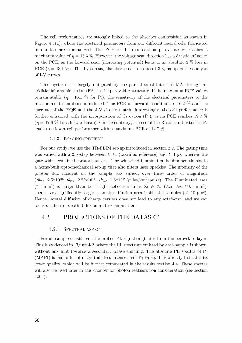
66
The cell performances are strongly linked to the absorber composition as shown in
Figure 4-1(a), where the electrical parameters from our different record cells fabricated
in our lab are summarized. The PCE of the mono-cation perovskite P1 reaches a
maximum value of η = 16.3 %. However, the voltage scan direction has a drastic influence
on the PCE, as the forward scan (increasing potential) leads to an absolute 3 % loss in
PCE (η = 13.1 %). This hysteresis, also discussed in section 1.3.3, hampers the analysis
of I-V curves.
This hysteresis is largely mitigated by the partial substitution of MA through an
additionial organic cation (FA) in the perovskite structure. If the maximum PCE values
remain stable (η = 16.1 % for P2), the sensitivity of the electrical parameters to the
measurement conditions is reduced. The PCE in forward conditions is 16.2 % and the
currents of the EQE and the J-V closely match. Interestingly, the cell performance is
further enhanced with the incorporation of Cs cation (P3), as its PCE reaches 19.7 %
(η = 17.6 % for a forward scan). On the contrary, the use of the Rb as third cation in P4
leads to a lower cell performance with a maximum PCE of 14.7 %.
4.1.3. IMAGING SPECIFICS
For our study, we use the TR-FLIM set-up introduced in section 2.2. The gating time
was varied with a 2ns-step between t=tlas (taken as reference) and t=1 μs, whereas the
gate width remained constant at 2 ns. The wide-field illumination is obtained thanks to
a home-built opto-mechanical set-up that also filters laser speckles. The intensity of the
photon flux incident on the sample was varied, over three order of magnitude
(0,1=2.5x10¹⁰; 0,2=2.25x10¹¹; 0,3=1.6x10¹²/pulse/cm2/pulse). The illuminated area
(≈1 mm2) is larger than both light collection areas Z1 & Z2 (AZ1=AZ2 ≈0.1 mm2),
themselves significantly larger than the diffusion area inside the samples (≈1-10 μm2).
Hence, lateral diffusion of charge carriers does not lead to any artefacts21 and we can
focus on their in-depth diffusion and recombination.
4.2. PROJECTIONS OF THE DATASET
4.2.1. SPECTRAL ASPECT
For all sample considered, the probed PL signal originates from the perovskite layer.
This is evidenced in Figure 4-2, where the PL spectrum emitted by each sample is shown,
without any hint towards a secondary phase emitting. The absolute PL spectra of P1
(MAPI) is one order of magnitude less intense than P2-P3-P4. This already indicates its
lower quality, which will be further commented in the results section 4.4. These spectra
will also be used later in this chapter for photon reabsorption consideration (see section
4.3.4).
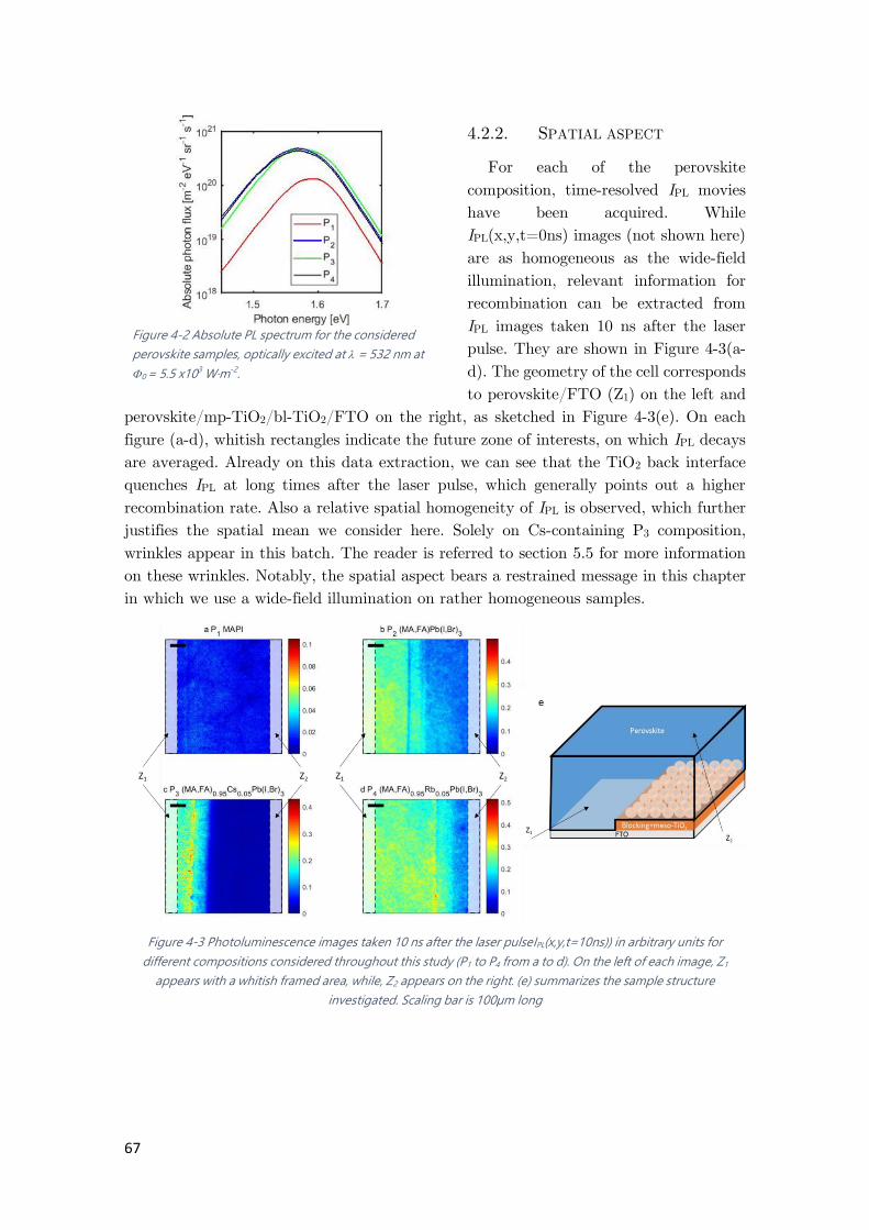
67
4.2.2. SPATIAL ASPECT
For each of the perovskite
composition, time-resolved IPL movies
have been acquired. While
IPL(x,y,t=0ns) images (not shown here)
are as homogeneous as the wide-field
illumination, relevant information for
recombination can be extracted from
IPL images taken 10 ns after the laser
pulse. They are shown in Figure 4-3(a-
d). The geometry of the cell corresponds
to perovskite/FTO (Z1) on the left and
perovskite/mp-TiO2/bl-TiO2/FTO on the right, as sketched in Figure 4-3(e). On each
figure (a-d), whitish rectangles indicate the future zone of interests, on which IPL decays
are averaged. Already on this data extraction, we can see that the TiO2 back interface
quenches IPL at long times after the laser pulse, which generally points out a higher
recombination rate. Also a relative spatial homogeneity of IPL is observed, which further
justifies the spatial mean we consider here. Solely on Cs-containing P3 composition,
wrinkles appear in this batch. The reader is referred to section 5.5 for more information
on these wrinkles. Notably, the spatial aspect bears a restrained message in this chapter
in which we use a wide-field illumination on rather homogeneous samples.
Figure 4-3 Photoluminescence images taken 10 ns after the laser pulseIPL(x,y,t=10ns)) in arbitrary units for
different compositions considered throughout this study (P1 to P4 from a to d). On the left of each image, Z1
appears with a whitish framed area, while, Z2 appears on the right. (e) summarizes the sample structure
investigated. Scaling bar is 100µm long
Figure 4-2 Absolute PL spectrum for the considered
perovskite samples, optically excited at = 532 nm at
0 = 5.5 x10³ W·m-2.

68
4.2.3. TEMPORAL ASPECT
The temporal extraction on a zone corresponds to the frequently used TRPL decay.
For the zone Z1, IPL decays appear in Figure 4-4(a-c). While P2 to P4 feature similar
behaviors with a fast IPL drop at short times and a slower decay up to the end of the
acquisition (t=1.5µs), the P1 composition decays drastically faster. When deposited on
bilayer-TiO2 interface (zone Z2), this fast decay for P1 is also observed (see Figure 4-4(d-
f)). The Cs-rich composition (P3) also displays a faster decay.
Figure 4-4 Photoluminescence decays for perovskite deposited at increasing injection levels, on FTO (a-c), and
on bilayer-TiO2 (d-f)
The phenomenological analysis of this group of IPL decays will here remain limited.
Recently, empirical models have been developed to explain non-exponential decays in
perovskite thin films, like the stretched exponential model186,188 or the bi-exponential
model50,131. However, they fail to reproduce transients from a power study, and can only
yield relative quantification of recombination and transport processes. As an illustration,
the bi-exponential model would yield injection-dependent “lifetimes”, which would be
hard to convert into a clear diagnostic. In the next section, we will develop a physical
model that is consistent at any injection level.
4.3.MODELING TIME-RESOLVED PHOTO-LUMINESCENCE
In this section, we start from a well-established model including traps37,85 (section
4.3.1), which we complete by considering the in-depth diffusion of charge carriers (section
4.3.2) and by deriving IPL from charge carrier concentration (4.3.4). Another model
summarizing the trap-induced recombination by a non-radiative lifetime will also be
introduced (section).

69
4.3.1. MODELING TRAPS
We model the perovskite layer as a semi-conductor with low intrinsic concentrations
(n0 ≈107/cm3, see section 5.4.3) and no doping (see section 1.3.2), in which we will write
Δn=n and Δp=p. In addition to electron and hole population, we consider a third
population called “trapped electrons” nT, which concentration has to remain lower than
the total traps concentration NT. These 3 populations are represented on an energetic
diagram in Figure 4-5(a), where arrows indicate the recombination pathways along with
their associated rates Rpop (electron capture, similar to Rpop,n in section 1.2.3), Rdep (hole
capture, similar to Rpop,p in section 1.2.3) and Reh* (net band-to-band recombination,
including generation due to photon recycling). The following rate equations (4-1), (4-2)
& (4-3) allow to follow their concentration in time. They include the assumption that
Rem,n=Rem,p=0, which is equivalent to say that the trap level is rather deep in the gap,
so that any emission is forbidden.
∂n
∂t= - Reh n p - Rpop n (NT-nT)
(4-1)
∂nT
∂t = Rpop n (NT-nT) - Rdep nT p
(4-2)
∂p
∂t = - Reh n p - Rdep nT p
(4-3)
One can then focus on the evolution of the trapped population nT in a pulsed excitation
regime. Its time average value stabilizes at nT,0189, as the relaxation lifetime have typical
values within the μs to ms range37,125. Henceforth, it can be assumed constant during a
TRPL decay, which lasts at most few μs. As the typical evolution time for the trapped
population is slower than the TRPL decay, it can be interesting to express the mean
trapped electron concentration between two pulses:
nT =f0 ∫ nT(t) dt
t=1/f0
t=0
(4-4)
Considering that the traps are empty when the laser is turned on, nT is growing after
each pulse and always lower than NT. Hence, it converges to a value we call nT,0. Here,
it should be noted that we model the trapped electron population as homogeneous in the
depth of the absorber. This corresponds to a fair assumption, as the inhomogeneous
regime lasts approx. 100ns, whereas the laser pulses hit the sample every 25 s. In a
practical way, we numerically determine nT,0 by running (4-1), (4-2) & (4-3) for each set
of fitting parameters, before solving the differential system including one carrier
population only and in-depth diffusion which we will define in the next sections.
4.3.2. MODELING IN-DEPTH TRANSPORT
In addition to the charge carrier recombination kinetics, one should also consider the
in-depth transport thanks to a diffusion term in the continuity equation. In fact, the
absorption length of the perovskite layer (1/532 = 100 nm)98 is significantly lower than
its thickness (z0 = 500 nm), and its value at the excitation wavelength is not significantly
affected by chemical compositional tailoring57,190–192. As a consequence, the photo-

70
generated carriers are concentrated close to the front interface at short times after the
laser pulse, as illustrated by the sketch in Figure 4-5(b) and by numerical simulations
displayed in Figure 4-6. In-depth concentration of the electrons (and holes) inside a
perovskite layer evolve to a flat distribution after 100ns. The time required for the in-
depth homogenization mainly depends on the diffusion coefficient D. In fast diffusion
materials such as III-V semi-conductors, this effect has no influence on TRPL decay as
the carriers homogenization in-depth occurs in a few ps193 (see sub-section 3.3.1). It
becomes visible in some photovoltaic absorbers such as CIGS162 and as we will see, it has
a significant effect on IPL decays in perovskite materials.
Figure 4-5 Sketch showing the allowed energetic transitions in perovskite(a). Cb and Vb stand for conduction
and valence band. Reh* is the net band-to-band recombination rate, Rpop is the trap capture rate, Rdep is the
trap-assisted recombination rate. nT is the trapped electron concentration, which has to remain lower than the
total trap concentration NT. (b)- Sketch showing the slow in-depth diffusion of charge carriers, following an
incoming photon flux 0 at t=0ns. Full (empty) circles stand for electrons (holes). Blue symbols stand for
photo-generated charge carriers, while red ones stand for trapped electrons and photo-doped holes.
Figure 4-6 In-depth concentration profile for electrons (or holes) inside a perovskite layer, following an optical
pulsed excitation at = 532 nm. This calculation is realized by solving the continuity equation with Dn=5x10-
3cm2/s; Reh=1.3x10⁻¹⁰cm3/s; τn=1370ns, Sf=40cm/s, as determined in section 4.4
4.3.3. TRAP-DIFFUSION MODEL
Now, we assume that the two physical phenomena sketched in Figure 4-5(b), in-depth
diffusion and trap-assisted recombination, dominate the charge carriers kinetics in a
pulsed excitation regime. We also assume a local electro-neutrality:

71
p(z,t)=nT,0+n(z,t) (4-5)
This implicitly induces that the diffusion coefficients for electrons and holes are
similar, which is consistent with previous observations in intrinsic perovskite material39
and will be confirmed by experiments presented in section 6.2.3. This also allows us to
reproduce the whole transport of charge carriers by writing a simple rate equation for a
single population (4-6), with spatial Von Neumann boundary conditions (4-7) and (4-8):
∂n
∂t=-Reh
* n(nT,0+n)-Rpopn(NT-nT,0)+Dn
∂2n
∂z2
(4-6)
∀t,z=0→Dn
∂n
∂z=Sfn
(4-7)
∀t,z=z0→Dn
∂n
∂z=-Sbn
(4-8)
The temporal initial condition is determined by the absorption properties of the
sample, before any in-depth diffusion or front surface recombination can happen:
t=0→n=Φ0α532 exp(-α532z) (4-9)
4.3.4. CALCULATING IPL
Once this differential system solved, the PL intensity IPL remains to be calculated.
For the considered intrinsic semi-conductor, it can be expressed as:
IPL∝∫ Reh
* n(nT,0+n)exp(-αPLz)dzz0
0
(4-10)
In this formula, partial reabsorption of the PL signal is considered as radiative
recombination happening close to the front interface contribute more to IPL than others.
Indeed, the reabsorption probability of these photons is lower. We model it thanks to the
coefficient αPL, which corresponds to the average absorption coefficient for the
photoluminescence signal. It can be determined from the α(E) extracted from external
quantum efficiency measurement displayed in Figure 4-1(b). For this purpose, we assume
first that the normalized EQE reflects the internal quantum efficiency (IQE) of the device
and then that IQE(E) can be approximated by the internal absorbance of the device
A(E) (i.e. perfect collection of photo-carriers). As A(E) = (1-exp(-α(E)*z0), it follows
that the absorption coefficient is : α(E)~-1/z0*ln(1-IQE(E)). This estimation is limited
around the bandgap of the absorber. Then, α(E) can be convolved with the PL spectrum
IPL(E) displayed in Figure 4-2, with the following formula:
αPL=
∫ α (E) IPL(E) dEE=∞
E=0
∫ IPL(E) dEE=∞
E=0
(4-11)
Calculations lead to 2.5±1 x 10³ /cm for P1 P2 and P4 and to 5±1 x 10³ /cm for P3.
The PL reabsorption described in eq. (4-10) notably induces a photon recycling
phenomenon inside the absorber, which we take into account with a relative correction
of the fitted external radiative coefficient Reh*, in order to determine the internal
radiative coefficient Reh=Reh*/(pescape), with pescape=12.5% 85,94,135,194. Even if taking a

72
constant pescape for different back interfaces is a gross assumption, we keep the advanced
photon propagation & recycling concerns for the next chapter (see section 5.3).
4.3.5. TRAPFREE-DIFFUSION MODEL
The amount of free parameters in the aforementioned trap model is high (Reh, Rpop,
Rdep, Dn, NT, Sair, STiO2). This would call for a high number of experiments to control
them. In the published version of this chapter187, we could not fit Rpop and Rdep values
and thus extracted them from the literature. They were assumed constant for all
compositions. It would be possible to study their value by using a temperature-dependent
study195, but we did not have the facility to do so during this doctoral work. However,
we suggest here a model94,122 that is not impacted by this uncertainty. It is based on the
same assumption of electro-neutrality (4-5), and make use of the same boundary
conditions (4-7)(4-8), initial condition (4-9) and IPL integration using (4-10). It simply
replaces (4-6) with (4-12), where a mono-molecular lifetime τn appears.
∂n
∂t=-Reh
* n2-n
τn+Dn
∂2n
∂z2
(4-12)
In section 4.4.3, we will show that both approaches tend to similar conclusions.
4.4. RESULTS
In this section, we fit IPL transients to the aforementioned trap-diffusion model. This
process allows us to quantify bulk non-radiative & radiative, as well as interface
recombination pathways, along with diffusion properties (section 4.4.1), which ultimately
allows to calculate equivalent Ln and τn at 1 sun excitation (section 4.4.2). The concurrent
trapfree-diffusion model introduced in section 4.3.5 is also investigated in section 4.4.3.
4.4.1. FITTING TO TRAP-DIFFUSION
Our trap-diffusion model was first tested on mixed cation perovskite layers directly
deposited on FTO. An optimization algorithm is employed to minimize the logarithmical
difference from experimental to numerical transients. Experimental IPL transients
obtained at increasing fluence levels are displayed in Figure 4-7(a), along with the
optimized numerical ones. In the fitting process, the trap-related recombination rates
were fixed to literature values (Rpop = 2x10⁻¹⁰ cm-3s-1, Rdep = 8x10-12 cm-3s-1)37, while the
main optoelectronic parameters related to the perovskite layer were fitted, yielding an
external radiative recombination coefficient Reh* = 1.3x10⁻¹⁰ cm-3s-1, a trap concentration
NT = 6.5x1014 cm-3, a diffusion coefficient Dn = 4.7x10⁻³ cm2s-1, and a front interface
recombination velocity Sair, with values ranging between 140 cm/s at high fluence and
100 cm/s at low fluence. A complementary experiment was then realized for the same
perovskite deposited on mesoporous TiO2. Resulting IPL transients are shown in Figure
4-7(b). Even though the decays do not look like those acquired on FTO, they can still be
numerically reproduced by our model. More specifically, they are fitted thanks to a single
parameter variation: the back surface recombination velocity Sb. Indeed, this parameter
was taken as a reference on Z1 (SFTO), while it is fitted to STiO2 = 40 cm/s on Z2.

73
Now, several parameters were fitted and their eventual correlation is therefore
investigated. We calculate the set of parameter values for which the reconstruction error
rises by less than 10% and represent it on a 3D view in Figure 4-7(c). Their concentric
aspect translates the non-correlation of parameters. We deduced from these volumes the
confidence intervals for each parameter, and included them in Table 4-1. They witness
for the precision of the fit.
Figure 4-7 (a)-Experimental (dotted lines) and numerically fitted (plain lines) IPL decays for a mixed cation
perovskite MA0.17FA0.83 Pb (I0.83Br0.17)3 (also P2) layer deposited on FTO (A) or on mesoporous-TiO2 (b).Various
orders of magnitude of the fluence level 0 have been tested.(c) Iso-surfaces showing a set of parameters (Reh*
Dn NT) leading to a reconstruction error not higher than 10 % (red), 20% (green), 50% (blue) of the optimal
reconstruction error. The green one is used for confidence intervals indicated in Table 4-.
We repeated this same experiment for samples P1, P3 and P4, having a similar
architecture but different absorbers. Experimental and numerical transients are available
in the published version of this chapter187. Again, our model allows a fair reproduction of
TRPL transients in the FTO/Pn architecture for all samples considered, and allows to
extract key optoelectronic properties for bulk and perovskite/air interface. Once again,
the confidence intervals indicated in Table 4-1 are narrow, except for the diffusion
coefficient/length in MAPbI3 (which could be attributed to the quick degradation of this
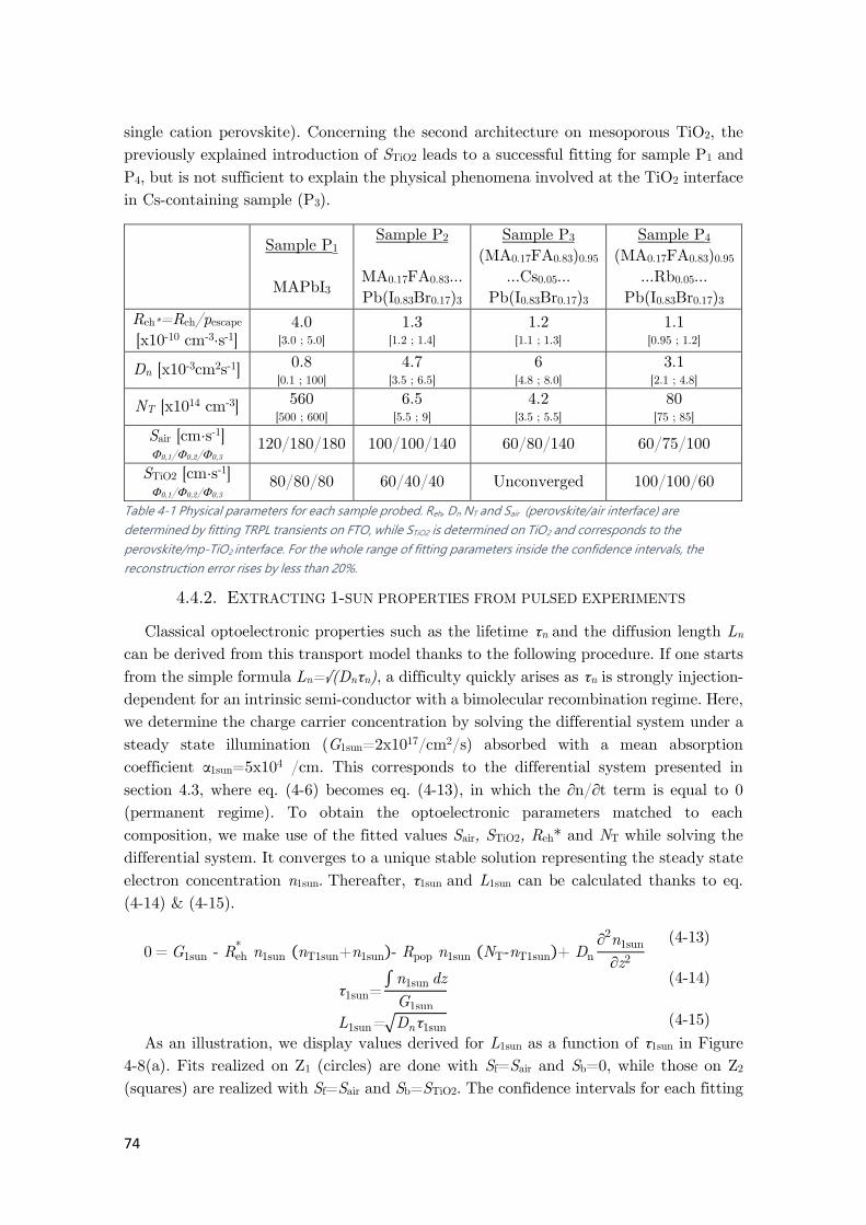
74
single cation perovskite). Concerning the second architecture on mesoporous TiO2, the
previously explained introduction of STiO2 leads to a successful fitting for sample P1 and
P4, but is not sufficient to explain the physical phenomena involved at the TiO2 interface
in Cs-containing sample (P3).
Sample P1
MAPbI3
Sample P2
MA0.17FA0.83…
Pb(I0.83Br0.17)3
Sample P3
(MA0.17FA0.83)0.95
…Cs0.05…
Pb(I0.83Br0.17)3
Sample P4
(MA0.17FA0.83)0.95
…Rb0.05…
Pb(I0.83Br0.17)3
Reh*=Reh/pescape
[x10-10 cm-3·s-1] 4.0
[3.0 ; 5.0] 1.3
[1.2 ; 1.4] 1.2
[1.1 ; 1.3] 1.1
[0.95 ; 1.2]
Dn [x10-3cm2s-1] 0.8 [0.1 ; 100]
4.7 [3.5 ; 6.5]
6 [4.8 ; 8.0]
3.1 [2.1 ; 4.8]
NT [x1014 cm-3] 560 [500 ; 600]
6.5 [5.5 ; 9]
4.2 [3.5 ; 5.5]
80 [75 ; 85]
Sair [cm·s-1] 0,1/0,2/0,3
120/180/180 100/100/140 60/80/140 60/75/100
STiO2 [cm·s-1] 0,1/0,2/0,3
80/80/80 60/40/40 Unconverged 100/100/60
Table 4-1 Physical parameters for each sample probed. Reh, Dn NT and Sair (perovskite/air interface) are
determined by fitting TRPL transients on FTO, while STiO2 is determined on TiO2 and corresponds to the
perovskite/mp-TiO2 interface. For the whole range of fitting parameters inside the confidence intervals, the
reconstruction error rises by less than 20%.
4.4.2. EXTRACTING 1-SUN PROPERTIES FROM PULSED EXPERIMENTS
Classical optoelectronic properties such as the lifetime τn and the diffusion length Ln
can be derived from this transport model thanks to the following procedure. If one starts
from the simple formula Ln=√(Dnτn), a difficulty quickly arises as τn is strongly injection-
dependent for an intrinsic semi-conductor with a bimolecular recombination regime. Here,
we determine the charge carrier concentration by solving the differential system under a
steady state illumination (G1sun=2x10¹⁷/cm2/s) absorbed with a mean absorption
coefficient α1sun=5x10⁴ /cm. This corresponds to the differential system presented in
section 4.3, where eq. (4-6) becomes eq. (4-13), in which the ∂n/∂t term is equal to 0
(permanent regime). To obtain the optoelectronic parameters matched to each
composition, we make use of the fitted values Sair, STiO2, Reh* and NT while solving the
differential system. It converges to a unique stable solution representing the steady state
electron concentration n1sun. Thereafter, τ1sun and L1sun can be calculated thanks to eq.
(4-14) & (4-15).
0 = G1sun - Reh* n1sun (nT1sun+n1sun)- Rpop n1sun (NT-nT1sun)+ Dn
∂2n1sun
∂z2
(4-13)
τ1sun=∫n1sun dz
G1sun
(4-14)
L1sun=√Dnτ1sun (4-15)
As an illustration, we display values derived for L1sun as a function of τ1sun in Figure
4-8(a). Fits realized on Z1 (circles) are done with Sf=Sair and Sb=0, while those on Z2
(squares) are realized with Sf=Sair and Sb=STiO2. The confidence intervals for each fitting

75
parameter, as displayed in Table 4-, are taken into consideration as several points are
drawn on the scatter plot for each zone.
Figure 4-8 (a) Scatter plot of values determines for τ1sun & L1sun from eq. (4-14) & (4-15), accounting for the
confidence intervals of each fitting parameter (NT, Sair, Reh, Dn) with Sb=0 for Z1 and Sb=STiO2 for Z2. (b) Same for
the trap-free model with (τn, Sair, Reh, Dn) with Sb=0 for Z1 and Sb=STiO2 for Z2.
4.4.3. FITTING TO TRAPFREE-DIFFUSION
Less parameters in a model can yield a lower fitting quality, but it also participates
in its self-consistency and reliability. In this sub-section, we present another round of fit
realized on the same experimental data with the trapfree-diffusion model. While the
values for Dn and Reh* are similar to the previous section 4.4.1, τn is a new parameter
that would be fitted to a higher value for a sample with less traps. It represents a
straightforward indicator of non-radiative recombination in the bulk: the SRH lifetime.
For what concerns interface S values, they are similar for STiO2 and tend to be lower for
Sair. Noteworthy, the fitting procedure is still yielding good reproduction of the dataset
at any fluence 0. Moreover, the same conversion from pulsed illumination into
continuous 1 sun illumination applies, and one can derive values for τ1sun and L1sun by
solving the differential system in permanent regime. This is shown in Figure 4-8(b), in
which we can see that the kinetic/diffusion model and traps/diffusion model lead to
similar values for those parameters – around 500 ns for τ1sun and around 500 nm for L1sun.
As our primary objective is to assess the relevance of these materials for PV operation,
both model seem to be both as valid.
Sample P1
MAPbI3
Sample P2
MA0.17FA0.83…
Pb(I0.83Br0.17)3
Sample P3
(MA0.17FA0.83)0.95
…Cs0.05…
Pb(I0.83Br0.17)3
Sample P4
(MA0.17FA0.83)0.95
…Rb0.05…
Pb(I0.83Br0.17)3
Reh*=Reh/pescape
[x10-10 cm-3·s-1] 3.3
[2.5 ; 4] 1.3
[1.2 ; 1.4] 1.3
[1.2 ; 1.4] 1.05
[0.95 ; 1.15]
Dn [x10-3cm2s-1] 1.4 [1 ; 1.8]
3.4 [2.8 ; 4]
7.5 [6.5 ; 9]
2.9 [2.4 ; 3.5]
τn [ns] 190
[160 ; 210] 1370
[1200 ; 1500] 1154
[1000 ; 1300] 1000
[900 ; 1100]

76
Sair [cm·s-1] 0,1/0,2/0,3
150/200/60 40/40/10 40/30/0 40/20/0
STiO2 [cm·s-1] 0,1/0,2/0,3
80/80/80 60/40/40 Unconverged 100/100/60
Table 4-2 Physical parameters for each sample probed. τn, Dn NT and Sair(perovskite/air interface) are determined
by fitting TRPL transients on FTO, while STiO2 is determined on TiO2 and corresponds to the perovskite/mp-TiO2
interface. Diffusion length L1sun , lifetime τ1sun and associated tolerance intervals are calculated using eq.
(4-14)&(4-15)
4.4.4. INDIVIDUAL ACCESS TO BACK & FRONT SURFACE RECOMBINATION
VELOCITIES
Here, we will introduce an experiment realized to decorrelate front and back surface
recombination velocities, for which a device with transparent interfaces is required. It is
thus applied on a full device adapted to tandem integration, in which the perovskite
(composition P3) is sandwiched into transparent layers. We acquired IPL decays with 3
increasing flux and 2 illumination directions. This allowed us to study the interfaces it
forms with the transport layers, as sketched in Figure 4-9. We fitted the 6 transients
together with the trap-diffusion model. The diffusion coefficient was evaluated at
Dn=8.8x10⁻³cm2/s, the bimolecular recombination Reh*=1.3x10⁻¹⁰cm3/s and the trap
concentration NT=1.1x10¹⁶/cm3. Both surface recombination velocities SSpiro & STiO2 were
determined as highly injection-dependent. Results are summarized in Table 4-3 below.
Figure 4-9 Fitted IPL transients acquired at increasing photon flux 0,1,0,2&0,3,illuminating on TiO2 side (a) as
well as on Spiro Side (b) on a semi-transparent device. In-between (a) & (b) is represented a sketch showing
the double side illumination on the semi-transparent device.
This fit with double illumination was used for a quick ageing study of a semi-
transparent device adapted to tandem integration74. The comparison of fitted values for
fresh and aged (1 month in dark) revealed similar values for NT & Reh. On the contrary,
Dn was smaller after ageing (down to 2.8x10⁻³ cm2/s), slowing down charge transport and
contributing to a more difficult extraction, as the equivalent diffusion length L1sun was
lowered from 550 nm to 290 nm.
For what concerns the interfaces, S values notably take higher values at low injection
(0,1), which is consistent with the quicker decay observed at this fluence. In this case,

77
it could correspond to a carrier extraction at the front interface (in reference to laser), as
we work in a full device where internal electric field might help the collection. More work
on this injection dependence of S could bring precious hints on the interfacial charge
carrier processes139. In any case, STiO2 was measured at higher values after ageing, which
points out the degradation of the TiO2 interface, generally attributed to the UV effect131.
Device
(fresh)
Device (aged,
20 days
dark)
Reh*=Reh/pescape
[x10-10 cm-3·s-1] 1.3
[1.1 ; 1.5] 1.6
[1.4 ; 1.8]
Dn [x10-3cm2s-1] 8.8 [7.4 ; 9.7]
2.8 [2.5 ; 3.1]
NT [/cm3] 110 [100 ; 130]
100 [80 ; 115]
SSpiro [cm·s-1] 0,1/0,2/0,3
660/40/1 370/32/1
STiO2 [cm·s-1] 0,1/0,2/0,3
1300/210/180 1000/300/225
Table 4-3 Physical parameters for the semi-transparent
device probed with double side illumination
4.5. DISCUSSION
Thanks to a complete model for TRPL decays, we could highlight the main phenomena
governing the charge carriers transport and recombination in perovskite, leading to a
versatile description of their kinetics for a wide range of fluence level. In this section, we
first show the relative weight of each of the considered recombination pathway in IPL
decays (4.5.1), before focusing on the main ones successively: at the interface (4.5.2), slow
carrier diffusion in-depth (4.5.3), non-radiative carrier recombination (4.5.4).
4.5.1. MAIN RECOMBINATION PATHWAY
The main recombination channel for charge carriers dictates their global decay rate.
It changes during the TRPL decay, and also as the excitation fluence is varied. We here
present a method able to analyze the influence of radiative recombination Rrad, non-
radiative recombination Rnrad and interface recombination Rint. It requires to integrate
each recombination current over the depth with the following formulas:
Rrad(t) = ∫ Reh
* n(t,z) [nT0+n(t,z)] dzz0
0
(4-16)
Rnrad(t) = ∫ Rpop n(t,z) [NT-nT0] dz
z0
0
(4-17)
Rint(t) = Sf n(t,z=0) (4-18)
As a result, it is possible to attribute early and later time PL kinetics to different
terms in the rate equation by analyzing the decays of each recombination current Rs. In
Figure 4-10, the main recombination pathway appears as the highest recombination

78
current at each time and each fluence. The result of this analysis for each composition is
displayed in Table 4-4, where we can see that trap-assisted (also non-radiative)
recombination globally dominate the second part of the decay, while other two
phenomena must be considered to explain the faster PL decay at short times. On the one
hand, charge carriers are concentrated in a smaller volume at short times, which favors
the radiative recombination process, as electrons and hole “meet” more often162. On the
other hand, they diffuse away from the defects located at the front interface, which
eventually slows down the early decay. Both are especially relevant in low-mobility
perovskite absorbers.
Figure 4-10 Temporal evolution of recombination terms simulated for perovskite P2, at the same excitations
powers employed during TRPL decay (a: 0,1 b: 0,2 c: 0,3) These terms are defined in eq. (4-16), (4-17) & (4-18)
MAPbI3 (P1) Perovskite P2 Perovskite P3 Perovskite P4
Short
times
Long
times
Short
times
Long
times
Short
times
Long
times
Short
times
Long
times
0,1 Interface
Trap/
Non-
rad.
Interface
Trap/
Non-rad.
Interface
Trap/
Non-rad.
Interface
Trap/
Non-
rad.
0,2 Interface
Trap/
Non-
rad.
Interface
Trap/
Non-rad.
Interface
Trap/
Non-rad.
Interface
Trap/
Non-
rad.
0,3 Radiative Trap/
Non-
rad.
Radiative Radiative Radiative Radiative Radiative Trap/
Non-
rad.
Table 4-4 Major recombination pathways at short times (t = 0.. 20 ns) and long times (t>100 ns), calculated for
each perovskite composition studied here.
4.5.2. ABOUT INTERFACE RECOMBINATION
Moreover, our model allows us to quantify the recombination rate attributed to the
interfaces, generally guilty of the most radiative losses in solar cells134,196,197. While Sair
refers to the perovskite/air interface, STiO2 refers to the one located at mp-
TiO2/perovskite. All samples considered in this study were half-cells and hence these
velocities correspond to recombination at interfacial defects rather than electrical
injection, which is often observed in full devices at short-circuit54. In section 4.4.1, the
interface formed at FTO/perovskite was taken as reference for Sb, as our experiment

79
cannot effectively distinguish between bulk and back surface recombination162, and we
only illuminated from the air/perovskite side. In section 4.4.4, we presented further
developments around this model. Indeed, we realized an experiment where we acquired
two set of TRPL decays by illuminating one side after another, which is a more
appropriate method distinguish the influence of both interfaces74.
Still, the successful fitting of the data of the zone Z2 of the samples allows us to assess
that the mp-TiO2/perovskite induces a higher recombination current than the
FTO/perovskite one. This can be explained by the larger contact surface at such a meso-
structured interface. Now, STiO2 remains lower than Sair, showing a preserved interface
crystalline quality, in comparison to the one obtained after exposure to the ambient
atmosphere. Eventually, it can be noted that both Sair and STiO2 demonstrate a slight
injection-dependence. Even if a fine modeling of interface recombination was out of the
scope of the study realized on perovskite half-cells, it can be noted that these
recombination velocities quantify the interface recombination current. They are not a
fixed material property as they depend on the interfacial trap density – where the traps
might saturate as the fluence increases – and on the Fermi level position at the
interface174,198.
4.5.3. ABOUT SLOW DIFFUSION
Concerning the diffusion coefficient, we found low values of Dn being in the same order
of magnitude for every sample. It implies a relative long time to obtain a homogeneous
in-depth carrier distribution. A direct application of the Einstein law (Dn=μnkT/q) leads
to μn values comprised between 0.1 and 0.3 cm2/(V.s), which locates our batch in the
lower values for polycrystalline solution processed perovskites103,114,115. This might seem
contradictory with the value of PCE as high as 19% obtained with such an absorber.
However, these low Dn values are compensated with the very long lifetime τ1sun of charge
carriers, which we display in Figure 4-8. Their high values ensure that the diffusion length
L1sun remains larger than z0, thus preserving an efficient charge carrier collection.
This experimental insight into slow diffusion could bring crucial information regarding
the recent discovery of a Rashba splitting in MAPbI3 69,70,199, as well as in CsPbI3 200.
This effect linked to spin-orbit coupling leads to the coexistence of a direct and an indirect
bandgap, the first one being beneficial to absorption, and the latter drastically enhancing
the lifetime of the carriers. The main recombination pathway for photo-generated carriers
relies on a phonon coupling, or on the overcoming of an activation barrier68,201. Regarding
a recent study from Kirchartz et al., a slow diffusion together with high PCE is possible
thanks to this particular band structure202. However, it should be noted that the
significance of this spin-orbit coupling is still under debate in the perovskite community94.
4.5.4. ABOUT TRAP RELEVANCE
On the contrary to the previously discussed topics (interface recombination & slow
diffusion), non-radiative recombination are modeled differently in trap-diffusion and
trapfree model. We start by commenting the values obtained with the trap-diffusion
80
model, in which the fitted trap concentration is highly dependent on the chemical
composition of the considered sample, with values varying between 4.2 x1014 cm-3 for
sample P3 and 5x1016 cm-3 for sample P1. The latter is consistent with NT values
previously reported in MAPbI3 absorbers, for various energetic positions37,188,203. The
influence of traps on the charge carrier kinetics in a pulsed excitation regime mainly
happens through the photo-doped charges they fix in the valence band by trapping
electrons on the long term37,85,101. This is mainly described by their concentration NT,
which lower value in P2 and P3 confirm the effective trap passivation through cation
substitution previously observed52,204. What’s more, the good correlation between the
effect of chemical composition on NT and Voc values underlines the significant role of
these traps in solar cell operation. The trapfree-diffusion model gives higher lifetime
values when NT is lower, and hence the link between non-radiative recombination and
Voc loss is maintained. To the best of our knowledge, physical models including diffusion
and recombination had not been applied to IPL decays before. Furthermore, previous
physical models for perovskites predicted mono-exponential decays at low fluence37,135,
which were not observed in any half-cells. This confirms the relevance of models presented
here above. Eventually, we stress here some recent reports (posterior to this study) using
diffusion/recombination models on IPL transients205–207.
4.6. CONCLUSION
In this chapter, we developed charge carrier transport models incorporating for the
first time a combination of the recombination dynamics and the slow in-depth diffusion
after a pulsed excitation. We applied them to the simultaneous fitting of IPL decays at
various fluence levels, for different PV-compatible perovskite compositions. For each of
them, we quantified non-radiative & radiative recombination, as well as diffusion
properties. We showed the path to translate this thorough representation of charge carrier
transport into 1 sun equivalent lifetime and diffusion length. In addition, our models have
a vertical component, which opens the way for independent characterization of ETL/-
and HTL/perovskite interfaces.
The variation in chemical composition of perovskite absorbers mainly impacts the trap
concentration (or bulk non-radiative recombination), while the slow diffusion remains
characteristic for any batch. The best PCE (19.7%) obtained after Cs incorporation could
be explained by a reduction in trap state density (NT = 4.2x10¹⁴/cm3 or τn = 1370 ns).
It is notably high despite the underlined slow diffusion, as it gets compensated by a high
τ1sun. Henceforth, L1sun remains above the absorber thickness and charge collection is
ensured.

81
5. Lateral transport in a perovskite thin film
The development of high efficiency solar cells relies on the management of electronic
and optical properties that need to be accurately measured. As the conversion efficiencies
increase, there is a concomitant electronic and photonic contribution that affect the
overall performances of the photovoltaic devices. Here we show an optical method based
on the use of complementary multi-dimensional imaging techniques. It allows us to collect
and analyze the luminescence signal with high spatial, spectral and temporal resolution.
We apply it to probe several transport properties of semiconducting materials, thereby
decoupling and quantifying the electronic and photonic contributions. Example of
application is shown on halide perovskite thin film for which a large range of transport
properties is given in the literature, depending on the film fabrication route but also on
the measurement technique (see section 1.3).
We focus here more precisely on previous uses of local illumination on perovskite.
Looking at steady-state IPL images allows to assess the lateral diffusion length of charge
carriers32,168,188 and underline the transport anisotropy in unpassivated polycrystalline
CH3NH3PbI3 (MAPI) films208. Time-resolved diffusion profiles have also been
observed120,209–212 and the widening of the IPL profiles give insight into the carrier mobility.
Nonetheless, multi-dimensional approaches were still missing. Regarding the PR, several
studies have underlined this optical process in perovskite absorber, either by focusing on
the slow radiative recombination process122,213,214, or by highlighting the long-range charge
carrier regeneration24,194,215. However, a model able to decorrelate electronic and photonic
contributions to transport is still missing.
In this chapter, we make use of the developed IPL imaging platform on perovskite thin
films, which first leads to a quantitative optical experiment based on point pulsed
illumination. Experimental details specific to this chapter are presented in section 5.1,
before section 5.2 gives a quick overlook on the data set. By its analysis, we evidence the
contribution of optical effects such as the photon recycling as a well as the photon
propagation where emitted light is laterally transported without being reabsorbed
(section 5.3). This latter effect has to be considered to avoid overestimated transport
properties. In section 5.4, we quantify these transport properties by rigorously solving
the complete time dependent continuity equation, yielding a method valid for several
semiconductor materials. Further application of multi-dimensional imaging platform on
a sample presenting heterogeneities is presented in section 5.5.

82
5.1. EXPERIMENTAL DETAILS
5.1.1. SAMPLE DESCRIPTION
In this chapter we investigate from section 5.1 to 5.4 a triple cation mixed halide
perovskite thin film ((MA0.14,FA0.86)0.95Cs0.05Pb(I0.84,Br0.16)3) [P3] spin coated on glass.
The absorption coefficient of perovskite was determined using a combination of
transmission/reflexion measurements at photon energies above the bandgap and Fourier
transform photocurrent spectroscopy at all energies, which are absolutely calibrated
thank to the first ones. The resulting absorption coefficient measurement is displayed in
the published version of this chapter216, and accompanied by further details on the
material fabrication process. The local illumination is applied on homogeneous regions,
whereas inhomogeneities are the focus of section 5.5. In this section, we use samples
having the same chemical composition [P3] but a slightly different production process
leading to wrinkle formation, but also a slightly modified one without Cs [P2] having no
wrinkle.
Figure 5-1 Sketch of the experimental observations and of the physical mechanisms taking place(a) Sample
structure and sketch showing the triple mechanism (carrier diffusion, photon propagation and photon
recycling) studied here (b) sketch showing the acquisition in 3 dimensions with time-resolved fluorescence
imaging (TR-FLIM) or hyperspectral imaging (HI), for a point illumination sketched in the left face.
5.1.2. IMAGING SPECIFICS
Multi-dimensional luminescence analysis requires the use of the hyperspectral imager
and of the TR-FLIM set-ups. This experimental approach is summarized in Figure 5-1.
In both cases, the sample is illuminated through an infinity-corrected X100 Nikon
objective with numerical aperture 0.95 and the luminescence is collected through the
same objective. For both setup, the optical excitation is made with a supercontinuum
Fianium Laser set at 550nm with pulse width 6ps, and repetition rate of 1MHz. The
diffraction limit in these conditions is 350nm. We have evaluated by measurement of the

83
optical transfert function that the spot has a diameter of 950+/-50 nm. The minimum
gate width of the camera is 480 ps which allows a temporal resolution of the system about
750 ps. It is used in the point illumination experiment, for the high flux (Φ0=5x10⁶
/pulse), while a longer gate width (5ns) is used for the low flux (Φ0=105/pulse).
5.2. PROJECTIONS OF THE DATASET
5.2.1. SPATIAL ASPECT
As the diffusion is theoretically isotropic from the local excitation spot, we mostly
averaged the recorded luminescence signal IPL in radial coordinates r in order to
significantly enhance our sensitivity with a higher signal to noise ratio. The spatial
analysis of the signal is hence a radial mean. It corresponds to a fair analysis if one looks
at the symmetry in spectral or time images.
5.2.2. TEMPORAL ASPECT
Figure 5-2 IPL maps of a perovskite sample after point pulsed illumination(a) at t=0ns and then integrated
between larger time steps, which are indicated in the title of each sub-figure (b) to (f). Scaling bar is 5µm long
Figure 5-3 IPL profiles of a perovskite sample after point pulsed illumination(a) their progressive decay is shown
in the same scale for each profile, with the same time steps as in Figure 5-2, (b) same IPL profiles normalized to
their maximum (at r=0µm), where the lateral broadening is underlined
The time-resolved images give a first hint towards diffusion away from the excitation
spot. In Figure 5-2, IPL images acquired after the pulsed point illumination are shown.
Each colorbar being scaled to the maximum, the radial broadening of IPL flare is evident.
The global decay of the maximum value of the radially averaged profiles is illustrated in
Figure 5-3(a). An inflexion point (circled in black on the graph) is unexpected in the
t=0ns profile, as the excitation beam is Gaussian and should appear as straight line in
logarithmical scale. It will be explained in section 5.3. In Figure 5-3(b), a normalized view
allows us to underline the broadening of the radial IPL profiles, which full-width at half
maximum (FWHM) is enhanced two-fold in 100ns. Quantitative analysis of these
transients is presented in section 5.4.
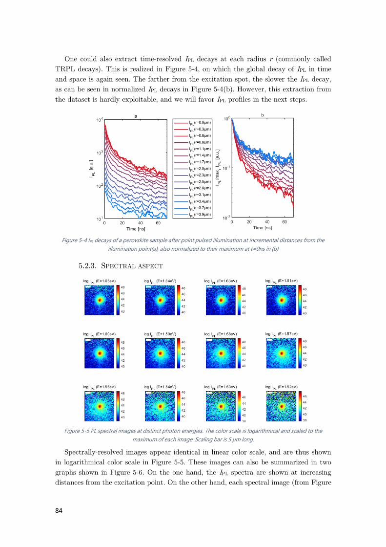
84
One could also extract time-resolved IPL decays at each radius r (commonly called
TRPL decays). This is realized in Figure 5-4, on which the global decay of IPL in time
and space is again seen. The farther from the excitation spot, the slower the IPL decay,
as can be seen in normalized IPL decays in Figure 5-4(b). However, this extraction from
the dataset is hardly exploitable, and we will favor IPL profiles in the next steps.
Figure 5-4 IPL decays of a perovskite sample after point pulsed illumination at incremental distances from the
illumination point(a), also normalized to their maximum at t=0ns in (b)
5.2.3. SPECTRAL ASPECT
Figure 5-5 PL spectral images at distinct photon energies. The color scale is logarithmical and scaled to the
maximum of each image. Scaling bar is 5 µm long.
Spectrally-resolved images appear identical in linear color scale, and are thus shown
in logarithmical color scale in Figure 5-5. These images can also be summarized in two
graphs shown in Figure 5-6. On the one hand, the IPL spectra are shown at increasing
distances from the excitation point. On the other hand, each spectral image (from Figure

85
5-5) can be represented by a radially averaged profile, as done in Figure 5-6(b). One can
notice than starting from E<Epeak=1.6eV on the spectral images, the central IPL flare is
progressively enlarged. As E decreases, the signal to noise ratio becomes progressively too
low for a clear image, whereas the IPL profile at E=1.52eV remains easily read. Further
analysis will unveil the predominant role of photonic propagation and photon recycling
in the next section.
Figure 5-6 IPL spectra at increasing distances from the laser spot(a) PL profiles for each emitted photon energy
from 1.52 eV to 1.68 eV. (b)
5.3.MODELING PHOTONIC
5.3.1. EVIDENCING THE PHOTONIC REGIME
The IPL profiles at fixed E values (Figure 5-6(b)) reveal the presence of two different
regimes. At a shorter distance, the PL spectra is independent from the photon energies
Eph. At a longer distance, it appears that IPL for the less energetic photons Eph < Epeak is
maintained over a longer distance as compared to Eph > Epeak ; Epeak being the emission
energy at which the maximum PL intensity is reached. Indeed, the ratio between
IPL(1.52eV) and IPL(1.65eV) increases (i.e. the red wavelengths of the PL signal propagate
farther).
These long-range photons end up either by getting partially reabsorbed to excite
charge carrier, which ultimately recombine (PR), or by being coupled out of the thin
film. If all of them were reabsorbed, we would observe a local IPL emission and expect no
IPL spectra variation. However, the IPL spectra at different distance from the excitation
spot are presented in Figure 5-6(a) and a spectral change for r > 3 µm is apparent. It
indicates a strong contribution of a simple photon propagation at longer distance without
contribution to the PR. The following expression of IPL summarizes the previous
considerations and splits the monitored signal IPL between a propagated flux Φprop which
progressively red-shifts as r increases, and a local IPL emission with a constant spectrum:
IPL = 𝛷prop + Reh* n2 (5-1)

86
This interpretation was first introduced by Pazos-Outon et al.194, and we confirm it
by analytical calculations accounting for total internal reflexions of the isotropically
emitted PL photons. The contribution of propagated PL photons is described analytically
by Φprop derived the next sub-section.
5.3.2. LONG-RANGE PHOTONIC PROPAGATION
Figure 5-7 Geometrical sketch of the elementary volume dV in the long-range scenario, showing the photons
(green rays) emitted in dV (orange), towards the origin of a secondary frame, where the recycling term grec is
calculated. Various solid angles of emission ultimately propagate towards the origin thanks to total internal
reflection at front and back interfaces for 𝜑𝑐 < 𝜑 < 𝜋 − 𝜑𝑐 .
To analyse the propagation of photons, we start from the radiometric formalism
described in section 1.1.2. We adapt it to derive the photonic density nγ2 propagated
towards the origin of a secondary frame (r’,θ’,z). This origin might be distinct from the
center of charge carrier distribution. We consider the flux jγ2 emitted from dV depicted
in orange in Figure 5-7 towards an elementary surface dSO placed at O (r’=0). It depends
on the photon density in dV, and on the emission surface dSem and solid angle dΩem,
which values are given in Table 5-1.
Total internal reflexions of the PL have to be considered and several photon
trajectories link two points, as indicated with green rays in Figure 5-7. We consider them
by varying the angle φ between the PL ray and (Oz). The critical angle can be defined
using Snell-Descartes law : φc=asin(1/nopt). For φ < φc and for φ < π - φc, photons are
emitted out of the thin film. For π - φc > φ > φc, they eventually reach the origin. To
account for the Lambertian emission through the elementary surface dSem, a solid angle
of emission dΩem(φ) has to be defined. It reads:
dΩem(φ)=
dSO
r'2
sin2 φ
=dSO sin2 φ
r'2
(5-2)

87
Paramete
r Description Value [long-distance]
dV Emission volume dr’ r’ dθ’ z0
a(E) Absorptivity of dV α(E) dr
dSem Emission surface r’ dθ’ z0
dΩem Emission solid
angle dSO sin2 φ
r'2
Table 5-1 Summary of values used for photon propagation calculation in the long-range scenario
The flux jγ2 propagates from (r’,θ’,z) towards O and gets attenuated, which we
account of by adding a Beer-Lambert term exp(-𝛼(E)sin(φ)/r). Henceforth, the
contribution of dV to nγ2 writes:
dSOdnγ2(E)=nγ(X,E,Ω)∫ dΩem sin(φ) dSem exp(-
α(E)sin(φ)
r') dφ
(5-3)
Next, we develop eq. (5-3) by expressing nγ(X,E,Ω) using van-Roosbroeck-Schockley
formalism (also eq. (1-2)), and reach another expression for dnγ,2:
dSOdnγ,2(E)=
Kpn2(r',θ')
n0p0
E2α(E) exp (-E
kBT) dr'…
…∫ dSem sin φ dΩem(φ) exp(-α(E)r
sin(φ))
π-φc
φc
dφ
(5-4)
Then, one can integrate dnγ,2 over the semi-conductor slab, making use of the known
expressions of dΩem, dSem from Table 5-1. We obtain the long-range propagated photon
density per energy:
dSOn
γ,2(E)=
Kp
n0p0
E2α(E) exp (-E
kBT)…
…∫ ∫ ∫n2(r',θ')dSO z0 sin
3 φ
r'exp(-
α(E)r'
sin(φ))
π-φc
φc
dr'dθ'dφ 2π
θ'=0
∞
r'=0
(5-5)
Where the surface on which we integrate the propagating flux (dSO) can now be
simplified:
nγ,2(E)=
Kp
n0p0
E2α(E) exp (-E
kBT)…
…∫ ∫ ∫n2(r',θ')z0 sin3 φ
r'exp(-
α(E)r'
sin(φ))
π-φc
φc
dr'dθ'dφ 2π
θ'=0
∞
r'=0
(5-6)
To determine the propagated flux at a certain distance r from the symmetry center of
the charge carrier concentration, one needs to define a secondary frame with polar
coordinates centered at the point (r,0), and then it is possible to calculate Φprop(r,E)
within this secondary frame by rewriting (5-6): (N.B. Φprop(r,E)= nγ,2(E))

88
Φprop(r,E)=KpE
2α(E) exp (-E
kBT)
n0p0
…
…∬ dr'dθ'
(r',θ') frame centered in (r,0)
z0
n2(r',θ')
r'∫ dφ sin3 φ exp(-
α(E)r'
sin φ)
π-φc
φc
(5-7)
We changed r (from the primary frame) from 3 to 20 µm and simulated the evolution
of the spectrum and the intensity of the propagated PL, thereby generating a family of
propagated spectra Φprop(r). This model was verified by fitting the PL spectra extracted
from hyperspectral maps acquired around a point pulsed illumination. They were
reproduced as the linear combination of the calculated propagated flux to a direct PL
emission, taken as proportional to IPL(r=0), described by:
IPL(r)
maxE
(IPL(r))=β
Φprop(r)
maxE
Φprop(r)+(1-β)
IPL(r=0)
maxE
IPL(r=0)
(5-8)
Normalizations are employed so that the sum of coefficients for both contributions is
1. Results are displayed in Figure 5-8, and showcase an excellent reproduction quality.
The relative weight of direct and waveguided contribution is indicated in the legend of
each subplot. The weight of direct emission is 100% at 3 µm and decreases to 40% at
r=9 µm. The weight of propagated spectrum follows an opposite trend.
Figure 5-8 Optimal reconstruction of IPL for increasing distances to the excitation point. Fit is based on a linear
combination of direct contribution (green crosses) and propagated one (red circles), as explicated in eq. (5-8).
This assesses the photon propagation regime and confirms the trapping of
photoluminescence signal inside the thin film leading to photonic propagation and
recycling over longer distance than what could be inferred from experiments realized on
single crystals215,217. At long range, the photon recycling phenomenon is not quantified
here, but it will be studied at short range, where it plays a dominant role in transport.

89
5.3.3. SHORT-RANGE PHOTONIC PROPAGATION
Figure 5-9 Sketch of the elementary volume 𝑑𝑉 in the short-range scenario(orange box here above) inside a
semi-conductor slab with thickness z0
Here again, we start back from eq. (1-2) that we adapt to derive the photon flux jγ1
emitted from dV towards the origin of a secondary frame. Figure 5-9 displays a 3D view
of the elementary volume, along with geometrical parameters allowing us to write dSem
and dΩem in Table 5-2. The role of the angle φ in eq. (5-4) is taken over by an in-depth
integration from 0 to z0, as no guided modes are considered for this short-range
calculation. We derive dnγ1 by integrating the incoming flux through an elementary
surface dSO placed at O (r’=0). An attenuation term is added and corresponds to Beer-
Lambert theory. This yields:
dSOdnγ1(E)=nγ(X,E,Ω)dΩemdSem exp(-
α(E)
r')
(5-9)
Paramete
r Description Value
dV Emission volume dr’ r’ dθ’ dz
a(E) Absorptivity of dV α(E) dr
dSem Emission surface r’ dθ’ dz
dΩem Emission solid
angle
dSO
r'2
Table 5-2 Summary of values used for photon propagation calculation in the short-range scenario
Eventually, the photon density at the origin propagated from d𝑉 towards O, can be
written as in eq. (5-10):
dSOdnγ,1(E)=
dSOnγ(r',θ',E,Ω)
r'2exp(-α(E)r') r' dθ' dz
(5-10)
In the next step, we replace nγ(r',θ',E,Ω), knowing that the absorptivity (and hence
emissivity) of dV is α(E)dr’.
dnγ,1(E)=
Kp∙n2(r',θ')
n0p0
α(E)E 2 exp (-E
kBT)
exp(-α(E)r')
r' dr' dθ' dz
(5-11)

90
The integration over the whole volume remains. It yields the formula of nγ,1, which
we also call Φprop(r,E) as in eq. (5-7) in the long-range scenario:
Φprop(r,E)=∭
Kpn2(r',θ')
n0p0(r',θ',z') frame centered in (r,0,0)
…
…𝛼(E)E2 exp (-E
kBT)exp(-𝛼(E)r')
r'dr'dθ'dz
(5-12)
This formula remains valid if the charge carrier concentration is near the origin. Hence,
the whole volume refers to r’ values comprised between 0 and some multiples of z0 at
most. Otherwise one should consider the other scenario from the previous section 5.3.2.
Eq. (5-12) notably applies to derive the panchromatic reabsorbed density at (r,0,0),
which we call grec:
grec
(r)=∭Kpn
2(r',θ')
n0p0(r',θ',z') frame centered in (r,0,0)
…
…∫𝛼2(E)E2 exp (-E
kBT)exp(-𝛼(E)r')
r'dEdr'dθ'dz
(5-13)
5.3.4. TAKING INTO ACCOUNT PHOTON RECYCLING
Under steady-state homogeneous illumination, the recycling is proportional to the PL
emission and a single correction factor gcorr can be applied on the measured external
radiative coefficient value Reh*, to obtain the internal radiative coefficient Reh122,181,214. It
is defined as gcorr=Reh/Reh* and was used in section 4.3.4. However, this assumption does
not hold in a more general case218, in particular for transient experiments or for
inhomogeneous illumination conditions. For this reason, we investigated the behavior of
grec depending on the charge carrier concentration profile.
We applied this calculation on Gaussian charge carrier distribution with FWHM
comprised between 1 and 3 µm, representative of the temporal evolution of the charge
carrier distribution between t = 0 ns and t = 100 ns. Notably, FWHM value is 1.5 µm
at t = 10ns. The recycling term is represented in Figure 5-10(a) as a function of the
radius r, along with the local PL emission intensity. Electronic transport happens at the
nanosecond scale and immediate photon propagation is assumed, which allows to
associate the same time coordinate to a PL emission profile and a PL recycling profile.
At first sight, they behave similarly at short distances, but can strongly differ for large
values of r.
Figure 5-10(b) shows the local correction factor gcorr introduced as Reh/Reh* here
above, which is written in different terms in the following equation:
gcorr
(r)=1-grec
(r)
∬nγ(r,E,Ω)dEdΩ=1-
recycling
emission (5-14)
For each value of FWHM, a threshold appears where the PL emission drops, whereas
the PL recycling maintains its intensity, as the PL signal emitted at the center propagates
and gets reabsorbed farther inside the material. For example, grec and Rehn2 trends split
before r = 3µm FWHM = 1µm. As a consequence, the ratio IPL/grec drops drastically and

91
gcorr values become negative (the recycling contribution becoming higher than the
emission contribution). Past this threshold, the recycling is not proportional to the local
emission anymore. Henceforth, thanks to the analytic expression of grec in eq. (5-13), we
determine a constant value for gcorr=0.43±0.05 over the first microns of the distribution,
on which the recycling is proportional to the local PL emission.
Figure 5-10 Contributions to rate equation (5-19) for a gaussian charge carrier distributionwith
FWHM=1..3µm, and 𝛷0 = 5 × 10⁶photons per pulse.(a) The PL emission (Rehn2) is displayed in dotted lines,
while the recycling is in plain lines. Vertical scale is in arbitrary units. (b) The local Reh correction factor, as
defined in the equation above, is displayed for gaussian charge carrier distributions with FWHM=1..3𝜇𝑚.
5.3.5. MONO-CHROMATIC EQUIVALENT FLUX
The approximation of considering the PL as monochromatic with a single absorption
coefficient αPR can be useful to gain some physical intuition. It was notably used in section
4.3.4 to calculate IPL while knowing the in-depth concentrations of n & p. We investigate
here its validity for photon recycling calculation.
αPR=∫ αPR(E)E2 exp (-
EkBT
)dE
∫E2 exp (-E
kBT)dE
(5-15)
It allows to separate spatial and energetic integrals as in the equation below, and we
will comment on its validity.
grec
(r) =∭Kpn
2(r',θ')
n0p0(r',θ',z') frame centered in (r,0,0)
αPRexp(-αPRr')
r'dr'dθ'dz'…
…∫ E2 exp (-E
kBT)dE
E
(5-16)
This is equivalent to:

92
grec
(r) =∭Reh
4π(r',θ',z') frame centered in (r,0,0)
n2(r',θ')αPR
exp(-αPRr')
r'dr'dθ'dz' (5-17)
In Figure 5-11, the individual contributions of each wavelength to the recycling term
are displayed for a Gaussian distribution with FWHM = 1.5µm. The plain line and the
squared line remain close at short distance, which shows that eq. (5-16) (average
absorption coefficient) is valid at short distances. This approximation might
underestimate the long-range photonic transport, as both trends diverge for r > 5µm, but
this is outside of the scope of the short-range calculation derived in section 5.3.3.
Figure 5-11 Contribution of each PL wavelength to the recycling. The black plain line giving the sum of all
contributions was also displayed in Figure 5-10(a). The squared curve was derived under the assumption of a
fixed absorption coefficient for the whole PL emission, also named αPR.
5.3.6. ABOUT OUR MODEL FOR PHOTONIC TRANSPORT
This study addressed the measurement of optical properties related to photon
propagation inside a thin film. Previous models based on ray optics122,213 or detailed
balance considerations214,219 had allowed to quantify the recycling process at the device
scale for a homogeneous illumination. They assumed either an angular randomization at
each reflection, which leads to the famous “4n2 limit” derived by Yablonovich220, or a
reflection as of Snell-Descartes law. We employed inhomogeneous illumination to monitor
transport and hence we needed a more precise model. The developed one places itself in
the black-body formalism and assumes an isotropic emission which directly depends on
the local quasi-Fermi level splitting. Since the emissivity is linked to the absorptivity, it
also allows us to derive the reabsorption of the emitted flux (PR), notably accounting for
possible total internal reflexions. It reproduces very well the deformation of PL spectra
at long range. However, a small amount of outcoupling of these guided modes is necessary
for us to observe the photon propagation flux.

93
A similar model was employed to assess the trapping of PL photons inside CsPbBr3
micro-wires221. We complete their analysis by separating the monitored IPL signal into a
propagated and a locally emitted component, which allows us to characterize short-range
and long-range transport properties. Another technique to account for this photon flux
consists in transforming the continuity equation for electrons and holes into a coupled
differential system with various photon fluxes194,218. This was mainly used to predict long-
range photon recycling but not to separate short-range electronic and photonic transport.
In the present study, we do so by using a single differential equation summarizing the
photon diffusion in a unique regeneration term, which results in a simple model adapted
to fitting multiple parameters at once.
5.4. DETERMINATION OF TRANSPORT PROPERTIES
Table 4-3 summarized previous considerations for the interpretation of spectrally-
resolved measurements. In a nutshell, we can relate the IPL(r<3µm) to the local charge
carrier concentration, while further spectral analysis is required to investigate transport
properties using IPL(r>3µm). This spectral analysis indicates that IPL(E>Epeak) can be
ascribed to locally induced PL emission, as Φprop(E>Epeak) ≈ 0 for large values of r. This
long-range charge carrier concentration is assumed to represent photon recycling, which
will be justified with the next derived electronic diffusion length (450nm). Hence, a
characteristic length LPR for the photon recycling can be extracted by fitting the decay
of IPL(r) for E > Epeak with an exponential attenuation length. It decays with
characteristic length of 2.5µm. Knowing that the PL decreases quadratically with the
carrier concentration n, LPR is measured around 5µm. This length applies for photon
recycling after a point pulsed illumination. This photonic transport is essentially lateral
and probably affected by the film thickness.
r [µm] Spectrally-resolved IPL
IPL(E<Epeak)
Spectrally-resolved IPL
IPL(E>Epeak)
Time-resolved IPL
IPL(t)
r >3µm IPL=Reh*n2 IPL=Reh
*n2 IPL=Reh*n2
r >3µm IPL=Φprop+Reh*n2 IPL=Reh
*n2 IPL=Φprop+Reh*n2
Table 5-3 Summary of the main physical contributions in the luminescence spatial variation. Physical
interpretation of the monitored signal IPL (r) using HI (column 2 & 3) or TR-FLIM (column 4). Two distinct zones
appear, limited by r = 3µm. The photon propagation regime corresponds to Φprop and local PL emission to Reh*n2.
The 3 µm value is defined empirically from the change in the PL profile in Figure 2 and matches with the value of
1/𝛼 at E = 1.57 eV
5.4.1. MODEL ASSUMPTIONS
We model perovskite thin films as intrinsic semi-conductors, where we can write as in
Table 4-3:
∀ (for all) t, r<3 μm : IPL(r,t) ∝ n2(r,t) (5-18)
Non-radiative recombinations are considered monomolecular, and are described thanks
to a Shockley-Read-Hall lifetime τn, while radiative recombinations are modeled via the
internal radiative coefficient Reh94. Auger recombination are neglected as they take a

94
significant share in the recombination process only for n > 1018cm-3 218,222. Ambipolar
effects are not considered, as electron and hole have similar mobilities in metal halide
perovskite98,121, which we also investigate in chapter 6. The local excitation creates a
charge carrier gradient, which homogenizes through charge carrier diffusion19 (diffusion
coefficient Dn) as well as through photon diffusion218. The local reabsorption of this
photon flux leads to the emergence of an additional generation term grec in the continuity
equation122. In the following, we will neglect the in-depth dimension to focus on the lateral
transport. For this purpose, we will restrain our dataset to the long times, when in-depth
diffusion has already happened (typically t>10ns for 600nm-thick perovskite layers187, as
established in Table 4-4). Finally, the diffusion equation writes in polar coordinates:
∂n
∂t(r,t)=Dn∇n(r,t)-
n(r,t)
τn-Rehn
2(r,t)+grec(r,t)
⇔∂n
∂t(r,t)=Dn∇n(r,t)-
n(r,t)
τn-Reh
* n2(r,t)
(5-19)
The equivalence sign in (5-19) refers to the definition of an external radiative
coefficient Reh* accounting for local PL emission corrected by photon recycling. We
demonstrated in section 5.3.4 that is valid for r < 4µm provided that the charge carrier
distribution verifies FWHM > 1.5µm. Henceforth, our fitting approach is valid for t >
10ns, when this charge carrier concentration is not too peaked.
5.4.2. PEROVSKITE THIN FILM
Figure 5-12 Determination of the pure electronic diffusion properties(a) Surface showing the best fit between
IPL(r,t) calculated with the diffusion-recombination model in eq. (5-19) and experimental data (black circles)
acquired on a mixed halide perovskite thin film (ϕ0=5x10⁶ photons per pulse). Fake colors indicate the PL
intensity (b) is a 2D map of the experimental data whereas (c) is a 2D map of the modeling results. (d)
Logarithmic residuals map from the modeling.
In the published version of this chapter, time-resolved IPL profiles from the power
study are fitted separately, yielding concordant values for Dn, Reh*, and τn that are
displayed in Table 5-4. The fit realized at high fluence is shown in details in 3D and plan
views in Figure 5-12(a-c). The logarithmic difference between experimental and numerical
values was miniminzed, and Figure 5-12(d) shows that it remains negligible at any fitting
point. The fit realized at low fluence is not sensitive to Reh*, which is consistent with the

95
decreased weight of bimolecular recombination as n decays. Thanks to gcorr, we can also
derive the internal radiative coefficient Reh = 1.0 x10⁻¹⁰ ± .4 x10-10 cm3s-1. An equivalent
electronic diffusion length can be determined around 450 nm. It is derived at n = 1016/cm3
– a relevant value for PV operation at 1 sun excitation38,223 – and take into account SRH
and radiative recombinations for the definition of the lifetime. At such a fluence, the
radiative lifetime is 660ns, while the non-radiative one remains at 110ns.
Parameter
Fitting
ϕ0=5x10⁶/pulse
Fitting
ϕ0=105/pulse
Fitting both
power together
Dn [cm2/s] 0.027 ± 0.007 0.035 ± 0.02 [0.012 – 0.045]
τn [ns] 110 ± 30 94 ± 30 [76 – 96]
Reh* [x10-10 cm3/s] 0.44 ± 0.2 ? [0.2 – 0.3]
FWHM [µm] 1.15 ± 0.05 1.15 ± 0.05 [0.97 – 1.17]
Table 5-4 Transport and recombination parameters determined by fitting IPL profiles.
Figure 5-13 Sensitivity to space-domain restriction. Values for the parameters Dn (a) τn (b) Reh* (c) and FWHM
(d), determined by our optimization algorithm fitting IPL profiles for both power at the same time, while varying
rmax in the space-domain restriction. The adjusted error indicating the reproduction quality is displayed in (e).
In the actual version of this chapter, we update the results by fitting
IPL(0<r<rmax,t>10ns) profiles for both fluence at the same time. In order to fit several
curves with a single set of parameters, an optimization approach is used with Matlab
function “fminsearch”, whereas the “Curve Fitting” toolbox was used up to now. This
approach enhances the precision of the results and was preferred for further application
of the model. We subsequently adjust the control experiments realized while varying the
space-domain restriction. This consists in fitting IPL(0<r<rmax,t>10ns) profiles for
various values of rmax. This investigation results in the variation of each fitting parameter

96
as a function of rmax, which is plotted in Figure 5-13. While τn & Reh* are stable
throughout the variation of rmax, FWHM and Dn show significant variation as rmax
increases. In order to discriminate the various fitted values, we rely not only on the
previous section about photonic propagation but also on to the reconstruction error in
Figure 5-13(e). We thus exclude rmax values exceeding 3µm, for which Dn would be
strongly overestimated as photonic transport would also be fitted with electronic diffusion
(fitted Dn values get even above 0.1 cm2/s for rmax>4µm). Too low values for rmax are
also avoided, as the adjusted error in Figure 5-13(e) increases.

97
Figure 5-14 Fitting results for the optimization approach applied on IPL profiles with varying space-domain
restrictions. Best-fit appear in color surface and experimental in transparent surface. Displayed rmax values were
selected as the optimal ones as from Figure 5-13. (rmax= 1.7µm (a)-(b) // rmax = 2.1 µm (c)-(d) // rmax= 2.5µm
(e)-(f) // rmax = 2.9µm (g)-(h)). A textbox displays the fitted values for τn Dn & Reh* for each rmax value.
The 4 remaining scenario with lowest reproduction error are displayed in Figure 5-14.
For each of them, it provides a 3D view of low power and high power experimental
profiles and optimal reconstruction. It leads to the confidence intervals for each
parameter, which is given in the last column of Table 5-4. The apparent quality of the
fit is equally good on both power for a single set of power-independent parameters.
5.4.3. DISCUSSING THEREOF
The obtained electronic and photonic parameters are in line with the values one can
find separately in the literature. In our work, the monomolecular lifetime τn values are
effective lifetimes and take into account the non-radiative recombination phenomena
occurring at the bulk and at the interfaces. This could explain their low values, in
comparison to studies where they refer only to the bulk85,214. Also, trapping and
detrapping events from shallow traps are neglected in our first order approach. These
might induce a quicker PL quenching far from the excitation spot, where empty traps
could remain. This could as well explain the low value derived for τn, in comparison with
previous studies accounting for traps37,85,187. Hopping mechanism from trap to trap might
also contribute to the transport and explain the low values determined for Dn, which we
discuss next.
For what concerns Reh*, its value is not only dependent on the material quality, but
also on the geometry of the excitation profile and of the thin film itself. Once corrected
with gcorr=0.43, it leads to the internal radiative coefficient Reh, which closely matches
calculated ones218, and measured ones94,102. Being an intrinsic material property, it also
allows to determine the charge carrier intrinsic concentration n0² (4.4x1014cm-3 according
to eq. (1-7)).
Finally, charge carrier extraction in photovoltaic devices based on perovskite layers
works out of diffusion39 and hence internal electric fields play a negligible role. We also
recall that our measurement was applied on neat films, in which no built-in electric field
due to heterointerfaces with transport layers is likely to happen. Our experiment is thus

98
well suited to probe the diffusion properties relevant for PV operation. As previously
mentioned in the introduction a large range of transport parameters might be found for
perovskite absorbers. Besides the different sample qualities and compositions, one origin
might be found in the concomitant electronic and photonic contribution investigated in
this chapter.
On the one hand, previous works have underlined the photon propagation as well as
the PR and we here confirm these results24,194,215,221. However, so far no complete model
was developed in order to determine the transport properties. On the other hand, several
experiments based on luminescence analysis (especially time-dependent experiments)
measure the carrier lifetime and transport properties. Nevertheless, they do not take into
account the two photonic contributions24,99,123,188,208,224. This fact goes along with pump-
probe experiments where the spatial contribution probes the solely carrier diffusion119–
121. Although the photon propagation can be ignored in the latter experiment, the PR
affects the carrier concentration and should be considered. Those experiments derived
fairly high values for Dn119,121
, which are an order of magnitude higher than observed in
this study. In a general way, luminescence experiments based on point pulsed illumination
in perovskite might deliver lifetime values not so much impacted by PR224, but the
diffusion away from the excitation spot remains influenced by PR and it is not
straightforward to characterize carrier transport with it. A recent study illustrates this
artifact where the authors determined Dn by fitting the time-resolved PL signal away
from the excitation and attributed the whole dynamics to the electronic diffusion, which
could yield an over-estimated determination of Dn > 1cm2s-1 124. Also, we want to
highlight here a simple idea to monitor solely the direct emission and not the propagated
one. This consists in adding a color filter at Epeak in the collection branch to get rid of
long-range photons, which allows then to distinguish electronic and photonic diffusion.
We have shown that both charge carrier diffusion (led by mobility and lifetime) and
photon diffusion (led by absorption properties) contribute to the transport. It is
important to know the weight of PR in the transport as it has a beneficial effect on Voc225.
Nevertheless, it gets mitigated if light management happens, as it leads to a better light
in- and out-coupling. Indeed, the escape probability of PL photons is directly included in
the formula giving the Voc boost induced by PR226.
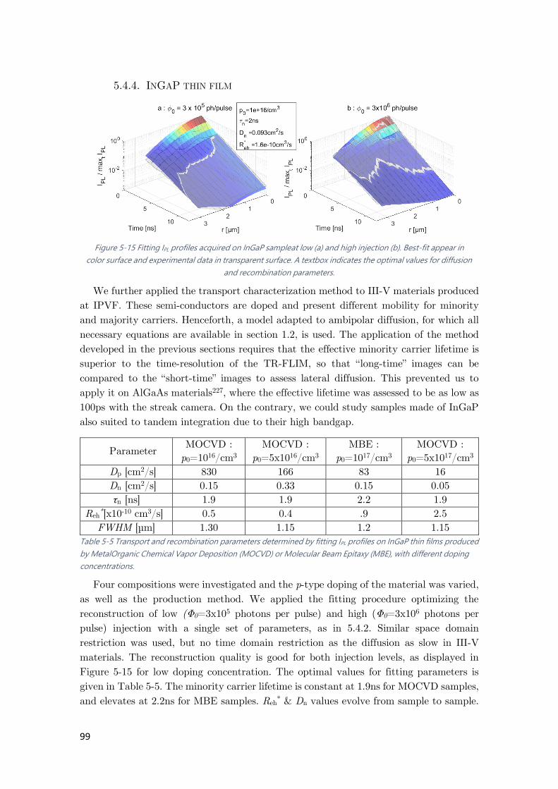
99
5.4.4. INGAP THIN FILM
Figure 5-15 Fitting IPL profiles acquired on InGaP sampleat low (a) and high injection (b). Best-fit appear in
color surface and experimental data in transparent surface. A textbox indicates the optimal values for diffusion
and recombination parameters.
We further applied the transport characterization method to III-V materials produced
at IPVF. These semi-conductors are doped and present different mobility for minority
and majority carriers. Henceforth, a model adapted to ambipolar diffusion, for which all
necessary equations are available in section 1.2, is used. The application of the method
developed in the previous sections requires that the effective minority carrier lifetime is
superior to the time-resolution of the TR-FLIM, so that “long-time” images can be
compared to the “short-time” images to assess lateral diffusion. This prevented us to
apply it on AlGaAs materials227, where the effective lifetime was assessed to be as low as
100ps with the streak camera. On the contrary, we could study samples made of InGaP
also suited to tandem integration due to their high bandgap.
Parameter MOCVD :
p0=1016/cm3
MOCVD :
p0=5x10¹⁶/cm3
MBE :
p0=1017/cm3
MOCVD :
p0=5x10¹⁷/cm3
Dp [cm2/s] 830 166 83 16
Dn [cm2/s] 0.15 0.33 0.15 0.05
τn [ns] 1.9 1.9 2.2 1.9
Reh*[x10-10 cm3/s] 0.5 0.4 .9 2.5
FWHM [µm] 1.30 1.15 1.2 1.15
Table 5-5 Transport and recombination parameters determined by fitting IPL profiles on InGaP thin films produced
by MetalOrganic Chemical Vapor Deposition (MOCVD) or Molecular Beam Epitaxy (MBE), with different doping
concentrations.
Four compositions were investigated and the p-type doping of the material was varied,
as well as the production method. We applied the fitting procedure optimizing the
reconstruction of low (Φ0=3x10⁵ photons per pulse) and high (Φ0=3x10⁶ photons per
pulse) injection with a single set of parameters, as in 5.4.2. Similar space domain
restriction was used, but no time domain restriction as the diffusion as slow in III-V
materials. The reconstruction quality is good for both injection levels, as displayed in
Figure 5-15 for low doping concentration. The optimal values for fitting parameters is
given in Table 5-5. The minority carrier lifetime is constant at 1.9ns for MOCVD samples,
and elevates at 2.2ns for MBE samples. Reh* & Dn values evolve from sample to sample.

100
The diffusion of minority carriers is slower in heavily doped samples (Dn=0.05cm2/s for
p0=5x10¹⁷/cm3), which is expected. The external radiative coefficient value is also
increased when doping is stronger, but it remains close to the literature value of 5x10-11
cm3/s 228. Here, it shall be noted that only the temporal part of multi-dimensional imaging
was applied on the samples. It is assumed that photon propagation and recycling are not
too different when a 500nm thick perovskite sample deposited on glass is changed with a
200nm thick one of InGaP deposited on GaAs.
5.5. APPLYING MULTIDIMENSIONAL IMAGING TO
HETEROGENEOUS MATERIALS
This section is extracted from “Spatial inhomogeneity analysis of Cesium-rich wrinkles
in triple cation perovskite”, except for the sub-section 5.5.4 which deals with photon
propagation concerns applied to wrinkled samples, and brings a new proof for the
separation of electronic and photonic diffusion.
5.5.1. WRINKLES IN TRIPLE CATION PEROVSKITE
Figure 5-16 Morphological properties of a wrinkle-containing perovskite sample. Focused Ion Beam was used
to observe a cross-section SEM of a perovskite PV device (B) SEM image (top-view) of a similar perovskite layer
deposited on FTO/bl-TiO2/mp-TiO2
The addition of cesium in the perovskite film can lead to the formation of veins-shaped
roughness, which are represented in Figure 5-16 and will here be called wrinkles. In a
triple cation perovskite containing 5% Cs in the A-site (P3), the inter-wrinkle distance is
12±1.5 µm, whereas their average width is around 3 µm. EDS mapping indicated a local
cesium excess in the wrinkles, as well as depletion in nitrogen. This EDS analysis is
presented in the published version of this section229.
Wrinkling had already been observed during this phase for mixed organic cations (as
P2 composition)230, and also P3 composition231. As an example, Bush et al. modified the
in-plane compressive stress during film formation and could then inhibit wrinkle
formation231. More recently, Braunger et al. also studied their appearance in
(FA,Cs)Pb(I,Br)3 perovskite232, pointing out a 12.8% to 15.3% rise in average power
conversion efficiency. Here, we mainly study the optoelectronic inhomogeneities in
wrinkled sample.

101
5.5.2. HYPERSPECTRAL IMAGING
Advanced photoluminescence (PL) imaging tools lead us to a deeper understanding of
the impact of this morphological features on PV operation134,233,234. At first, we apply
hyperspectral imaging to unravel the bandgap inhomogeneities induced by the Cs spatial
distribution. Advanced IPL imaging methods allow us to analysis the optoelectronic
properties of the wrinkles. At first, we used the HI to record spectrally resolved IPL images
with a micrometric resolution. Figure 5-17(a) displays the IPL peak position as well as
the optical microscopy images for the P2 and P3 samples. For the latter, blue IPL spectral
shifts are observed at the very same location as the wrinkles (see Figure 5-17(b)). This
spectral shift goes to ΔE=10±2 meV (from 1.57 eV to 1.58 eV). This could be explained
by a smaller grain size in the wrinkle51,235, which we did not observe in SEM analysis,
and which is in contradiction with the bigger grain size on wrinkles observed by Braunger
et al232. On the contrary, it is consistent55 with the enhanced concentration in Cesium,
previously observed by EDS.
Figure 5-17 Spectral aspect of multi-dimensional IPL imaging of a wrinkle-containing perovskite sample,
showing the peak position of the local IPL spectrum, measured on a P2 perovskite (a-b) or on a P3 perovskite (c-
d). At the bottom, photographies are taken with uniform illumination, allowing to correlate blue shift of the PL
peak to the wrinkles
5.5.3. TIME-RESOLVED IMAGING
We then look at time-resolved IPL maps recorded a triple cation perovskite thin film.
Figure 5-18 summarizes the recorded data where we display IPL images integrated
between 0ns and 100ns after the excitation (Figure 5-18(a)) but also later (Figure 5-18(b-
c)). At short times, the IPL maps show features uncorrelated to the wrinkles. At long
times (typically t > 100ns), their geometrical aspect constitutes a pattern having similar
dimensions than the wrinkles observed on the SEM pictures and HI data. As a qualitative
summary, the temporal evolution of the IPL profiles shows a global decay, as well as a
convergence from a rather flat to a profile shaped by the wrinkles.

102
Figure 5-18 Temporal aspect of multi-dimensional PL imaging of a wrinkle-containing perovskite sample,
showing the temporal evolution of PL signal after the laser pulse (at t=0ns).
As demonstrated in section 4.5.1, in-depth diffusion of photo-generated carriers and
trapping37,104 govern the global kinetics187 at short times, whereas the variations at longer
times (typically t > 100ns) are dominated by bimolecular radiative recombination94. At
that time, n & p are homogeneous in-depth, which allows us to write IPL as a function of
the local thickness z0(x,y) in eq. (5-20), in which an average absorption coefficient for PL
emission (αPL) is used:
IPL(x,y)∝∫ Reh
* (x,y)n(x,y)p(x,y)exp(-αPLz)dzz0(x,y)
0
⇒ t>100ns : IPL(x,y) ∝ [Reh
*np](x,y)×fwr
(z0)
(5-20)
This equation tells us that IPL depends solely on the electron and hole concentrations
(n and p) and on a correction factor fwr directly linked to the thin film thickness, as a
thicker perovskite layer (e.g. wrinkle) emits more luminescence. With this deeper
knowledge, we investigate further the long-time profile by looking at IPL(t>500ns) image
in Figure 5-19(a). Cross-sections profiles were taken orthogonally to the wrinkle directions
and are represented separately in Figure 5-19(b-d). If wrinkles and inter-wrinkles zones
had similar optoelectronic properties, n and p would be equal at any point (x,y) in eq.
(5-20). Under this assumption, the PL profiles would exactly represent the morphological
profile fwr, which is not the case as the wrinkle lateral width is at most 2 µm, whereas
the more emissive zones in the PL profile is 5 to 8 µm wide. Henceforth, we rule out the
hypothesis that long-time PL maps are explained by the perovskite local thickness only,
and suggest that τn inhomogeneities mainly explain them.
To demonstrate the previous suggestion, we designed a drift diffusion modeling with
Silvaco Atlas, where a simple wrinkle morphology was investigated. Two scenarios are
considered. The former includes similar trap density in and out the wrinkle, while the
latter includes a lower trap density in the wrinkle. More details on these models are
available in the published version of this section229. In the first case, the long-time IPL
profiles mimic the wrinkle shape, while in the second case, the lower local trap density
in the wrinkle widens the long-time IPL profile. This is explained through the lateral
diffusion of carriers from the trap-limited zones to the inter-wrinkle zone. This global
trend confirms that Cs content in the vein locally decreases the non-radiative
recombination rate and induces this wide profile, which is consistent with previously
observed Cs-induced trap passivation in triple cation perovskite55,184,204.

103
Figure 5-19 Cross-sections profiles drawn in IPL(500ns<t<1µs) map(a) displaying the wrinkle-shaped profile in
arbitrary units (b-d)
5.5.4. PHOTON PROPAGATION IN WRINKLED SAMPLES
Figure 5-20 PL spectral images at distinct photon energies of a wrinkled sample. Similarly to Figure 5-5, the
color scale is logarithmical and scaled to the maximum of each image. Scaling bar is 5 µm
We finally applied a local illumination on a wrinkled sample, in order to provide
further proof for the photon propagation regime. As wrinkles constitutes local roughness,
they are able to couple out a propagated flux by breaking the planarity of the waveguide.
We observe this in Figure 5-20 on IPL images at E < Epeak, for which the propagated
contribution is seen at r > 3 µm (as demonstrated in section 5.3). In these images, the
radial symmetry of IPL (which was observed for a flat sample in Figure 5-5) is broken
and two arch shapes appear. They remain visible for each E < Epeak and correspond to
two wrinkles able to couple out Φprop. In other words, the waveguided PL flux is expelled
out of the thin film when it would encounter the wrinkle. It is very noteworthy that
previous conclusions based on hyperspectral imaging (section 5.5.2) are not impacted by
photon propagation. Indeed, the out-coupling of a propagated component tends to shift

104
the local IPL to the ‘red’ (i.e. low E), whereas we observed a ‘blue’ shift on the wrinkle.
Concerning section 5.5.3, photon propagation concerns could not be considered in the
modeling (neither eq. (5-20) nor Silvaco modeling). Including them could allow the
quantification of lifetime in inhomogeneous samples.
As a partial conclusion, multi-dimensional PL imaging was carried out on a sample
containing wrinkles, in order to assess the impact of this chemical heterogeneity. The
hyperspectral map indicates a blue shift in the PL spectrum on the wrinkles, which is
consistent with the Cs enrichment184. Time-resolved IPL images pointed out a slower IPL
decay on the wrinkle, possibly indicating a shallow trap passivation by the richer Cs.
Multi-dimensional imaging also applies for the optoelectronic characterization of
heterogeneous materials, as triple cation perovskite can sometimes be.
5.6. CONCLUSION
In conclusion, transport in a semi-conductor thin film happens via 2 channels. The
first one consists in electron and hole diffusion through scattering and it can be described
by a diffusion coefficient, which takes low values in metal halide perovskite. Henceforth,
this transport is essentially short-range. The photon recycling constitutes the second one
and can be observed at any range. Indeed, it does not only induce long-range transport,
but also significantly influences short-range transport. Thanks to time-resolved PL
profiles acquired after a pulsed point illumination, we have been able to decorrelate both
electronic and photonic regimes and to quantify their impact on charge carrier transport.
Additionally, a photon propagation regime was observed, confirming the guided
propagation of PL photons inside the thin film. In a nutshell, we determine precise values
for bulk-related parameters, namely the charge carrier mobility and monomolecular
lifetime, the external radiative coefficient, as well as for device-related light management
parameters, namely the photon escape probability and the long-range photon recycling
length. The introduced contactless experiment is based on multi-dimensional PL imaging
and can find interest in any semi-conducting materials where both electronic and photonic
contribution happen, especially on high quality materials.

105
6. Electron, hole and ion transport
Fundamental physics and different transport properties of halide perovskites have still
not been fully understood and described10 (see also section 1.3). In particular, a deep
comprehension of the interplay between electronic and ionic transport phenomena is
crucial for the optimization of the energy harvesting after light absorption. This is also a
fundamental question91,92,236 as ionic motion is usually associated with defect creation,
difficulties in doping control and low carrier lifetimes, one does not expect a semi-ionic
conductor to be also an excellent photovoltaic converter.
On the one hand, electronic charge transport in halide perovskites has been well
investigated using advanced optical methods, which allowed to observe and disentangle
the two main phenomena: charge diffusion and photon recycling23,216 (also described in
chapter 5). Due to the low exciton binding energy, electron and hole behave as free
carriers at room temperature95. In most studies, an ambipolar charge transport is assumed
as the doping concentration is known to be small110. Only a few pieces of evidence of a
balanced electron/hole transport (i.e. electron mobility µn = hole mobility µp) have been
provided so far116,117,204.
On the other hand, ion migration has been studied early in halide perovskites. In 2014,
Xiao et al. applied an electric field on a CH3NH3PbI3 (MAPI) lateral structure reporting
a switchable photovoltaic effect237, later explained by ion migration238,239. Ion migration
is also considered as the main culprit for the hysteretic behavior of PSC’s 239–242. Despite
a great number of experimental observations, the physics behind such an ionic migration
remains unclear243. Indeed, their activation energy is still debated, as well as the influence
of grain boundaries and the impact of temperature and light91,92,236. The halide ions (I-
/Br-) are mostly concerned, as organic MA+ / FA+ and inorganic Pb2+ are expected to
drift on much longer time scales91,92,243
Overall, the complex interactions between ions, electrons and holes has been recently
underlined, as excess charge-carrier have been shown to accelerate ion migration244 and
as iodide-induced defect creation has been theoretically derived245. Numerical drift-
diffusion models taking into account both the motion of ionic species and electronic charge
carriers have been proposed246. Recently, Snaith’ research group showcased the
incorporation of additive ionic salt BMIBF4 as an efficient way to prevent ion migration,
paving the way towards stable PSC247.
In this chapter, we present a set of experiments under electric bias based on multi-
dimensional luminescence imaging to probe the individual electronic transport as well the
ionic one. Thanks to multi-dimensional imaging coupled with a proper sample design, we
have been able to study lateral transport of charge carriers in hybrid mixed halide
perovskites (chapters 4, 5). Besides, measuring the local variations of the luminescence
signal under electric bias allows a direct access to charge carrier collection and transport
properties for each kind of charge carrier. In a first set of experiments, we inhibit ion

106
migration by applying a pulsed electric bias and only observe the electronic transport
(section 6.2). The ionic migration was activated in a second set of experiments where the
bias was applied for a longer period of time (10 min). The use of a spectrally and spatially
resolved systems allows us to acquire absolute IPL images, and to image the quasi-Fermi
level splitting Δµ as well as the bandgap Eg evolution during the bias exposure (section
6.3). We discuss the correlation between all these parameters and the link between non-
radiative recombination pathways and ionic migration.
6.1. EXPERIMENTAL DETAILS
6.1.1. SAMPLE DESCRIPTION
The samples architecture is depicted in Figure 6-1(a-b). Firstly, a coplanar Au electric
contacts was evaporated on a specific mask design made by UV lithography on a glass
substrate, leaving a 20 µm channel between the gold electrodes. To prevent gold in-
diffusion inside the perovskite layer83, 50 nm of ITO were sputtered on top of the Au
layer. Finally a double cation perovskite thin film (FA0.83MA0.17 Pb (Br0.16I0.84)3) was
deposited. Cross-section images displayed in Figure 6-1(c) confirm the conformal
deposition on the lateral structure, and indicate a 800nm perovskite thickness.
Figure 6-1 Structure of the perovskite channels (a) sample image through glass. Top channel width is 1 mm
and serves as scale. (b) sketch of lateral structure inside the white circle in (a). (c) Cross-section image of the
perovskite channel at the vicinity of the contact, where a double layer Au(shiny)/ITO is seen. The thickness of
the perovskite layer is approx. 800nm, while the distance between electrical pads is 20µm. A double layer is
deposited on top of perovskite for protection (Ti).
6.1.2. IMAGING SPECIFICS
For the time-resolved images, wide-field illumination was realized with pulsed laser
Talisker with rather low frequency flas=200kHz, and rather high fluence ϕ0=5 1011
ph/cm2/pulse. It is homogeneous on the surface imaged by the CCD sensor of the TR-
FLIM. The photoluminescence is collected through a Nikon 100x objective. The PL is
filtered through short-pass and long-pass filters (DMLP650R and FES750, Thorlabs). A
pulsed electric field generated by a function generator AFG 3000 (Tektronix) is
synchronized with laser illumination. The TR-FLIM is described in details in section 2.2.
Snapshot acquisitions at t=0, 10 & 100 ns with different gain parameters at each time
step, in order to get optimal image quality also at long times.
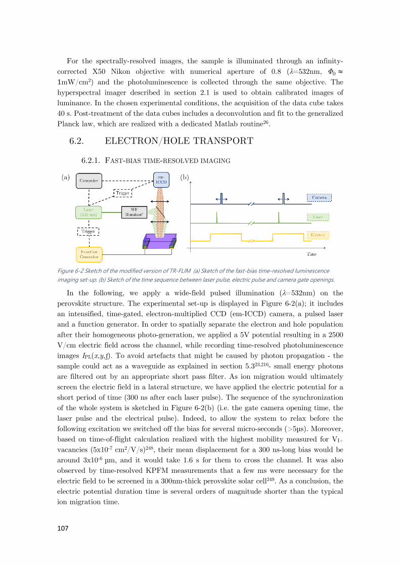
107
For the spectrally-resolved images, the sample is illuminated through an infinity-
corrected X50 Nikon objective with numerical aperture of 0.8 (λ=532nm, Φ0 ≈
1mW/cm2) and the photoluminescence is collected through the same objective. The
hyperspectral imager described in section 2.1 is used to obtain calibrated images of
luminance. In the chosen experimental conditions, the acquisition of the data cube takes
40 s. Post-treatment of the data cubes includes a deconvolution and fit to the generalized
Planck law, which are realized with a dedicated Matlab routine26.
6.2. ELECTRON/HOLE TRANSPORT
6.2.1. FAST-BIAS TIME-RESOLVED IMAGING
Figure 6-2 Sketch of the modified version of TR-FLIM (a) Sketch of the fast-bias time-resolved luminescence
imaging set-up. (b) Sketch of the time sequence between laser pulse, electric pulse and camera gate openings.
In the following, we apply a wide-field pulsed illumination (λ=532nm) on the
perovskite structure. The experimental set-up is displayed in Figure 6-2(a); it includes
an intensified, time-gated, electron-multiplied CCD (em-ICCD) camera, a pulsed laser
and a function generator. In order to spatially separate the electron and hole population
after their homogeneous photo-generation, we applied a 5V potential resulting in a 2500
V/cm electric field across the channel, while recording time-resolved photoluminescence
images IPL(x,y,t). To avoid artefacts that might be caused by photon propagation - the
sample could act as a waveguide as explained in section 5.323,216- small energy photons
are filtered out by an appropriate short pass filter. As ion migration would ultimately
screen the electric field in a lateral structure, we have applied the electric potential for a
short period of time (300 ns after each laser pulse). The sequence of the synchronization
of the whole system is sketched in Figure 6-2(b) (i.e. the gate camera opening time, the
laser pulse and the electrical pulse). Indeed, to allow the system to relax before the
following excitation we switched off the bias for several micro-seconds (>5µs). Moreover,
based on time-of-flight calculation realized with the highest mobility measured for VI+
vacancies (5x10⁻⁷ cm2/V/s)248, their mean displacement for a 300 ns-long bias would be
around 3x10⁻⁶ µm, and it would take 1.6 s for them to cross the channel. It was also
observed by time-resolved KPFM measurements that a few ms were necessary for the
electric field to be screened in a 300nm-thick perovskite solar cell249. As a conclusion, the
electric potential duration time is several orders of magnitude shorter than the typical
ion migration time.

108
6.2.2. IPL QUENCHING AT THE POSITIVE ELECTRODE
Figure 6-3 Summary of fast-bias experimental results (a)-(c) PL images at incremental time steps after the laser
pulse (scaling bar 10µm). (d)-(f) Integration of the PL intensity along the y axis (parallel to the electrodes). Bias is
applied on the left. A positive electric field is present for |x|<10µm for V=5V, and a negative electric field for V=-
5V.
The luminescence signal is representative of the electronic carrier transport that we
aim at investigating. We can interpret the intensity of the local PL signal IPL(x,y,t) as
the in-depth integrated local product of electron and hole concentrations216 (similarly to
section 4.3.4):
IPL(x,y,t) ∝ ∫ n(x,y,z,t) p(x,y,z,t) exp(-αPLz) dz
z
(6-1)
In Figure 6-3(a)-(c) three time resolved PL image are shown, respectively at 0 ns, 10
ns and 100 ns after the laser excitation, while a 5V potential is applied on the left
electrode. The PL signal appears globally more intense for the perovskite deposited on
top of Au/ITO, probably due to the back-reflection of PL photons. The corresponding
time-resolved profiles IPL(x,t) are displayed in Figure 6-3(d)-(f) at 5V, -5V and 0V
(integration over the y-axis). The 0 V profile, in which no electric field is applied across
the channel, is used as reference. Noteworthy, also on 0 V profile, a PL drop at the edge
of both contacts can be observed. We ascribe this behavior to a large trap density in this
region composed by smaller grains, sometimes poorly interconnected. The PL profile
inhomogeneities could be explained by a fast current extraction in this zone. We exclude
this possibility by realizing a control experiment without connecting the contacts,
similarly to an open-circuit condition. In both cases, 0 V and disconnected contacts, a
similar drop at the edge was observed. A further proof is provided by the analysis of the
IPL over the whole sample, by comparing the IPL on the zone of the stack Au/ITO/Pvk
and on the zone of the bare perovksite thin film. We can notice that the signal appears
more intense in the region Au/ITO/Pvk, in contrast with an efficient charge extraction
which would lead to a dramatic quenching of the IPL.

109
When a bias is applied, a progressive IPL drop clearly appears, both at t=10ns and
t=100ns, close to the positively biased edge of the channel (at x=-10 µm for V=5V). The
reversibility of this effect was investigated by flipping the direction of the electric field: a
symmetric trend is observed for the opposite bias (-5V). In addition, we have tested the
system for an applied bias of ±2 V, for which a less evident IPL drop appears at the
positive electrode. We can thus conclude that there is a direct relation between IPL drop
and applied electric field intensity. Qualitatively, the electric field allows to dissociate
charge carrier type (i.e. electron/hole). At the positively biased interface, holes are
depleted while electrons accumulate, and vice-versa at the opposite electrode. For a
purely ambipolar material with µp=µn, a symmetric IPL profile across the channel would
be expected, featuring a symmetric quenching for any bias. On the contrary, assuming
µp>µn, an asymmetric signature on the IPL profile appears as their accumulation and
depletion are enhanced. We further evidence these behaviours by introducing 2D
simulations realized by a master student (G. Vidon) with Silvaco Atlas in the next sub-
section.
6.2.3. FITTING ELECTRON/HOLE MOBILITY
We have simulated and reported the two cases (µp>µn & µp=µn) with IPL ratios in
Figure 6-5(a), and the electron/hole concentration (for µp>µn) are mapped in cross-
sectional view in Figure 6-4(b)-(c) at t=100ns. They illustrate the effect of the difference
between electron and hole mobilities, which eventually impacts the radiative
recombination, also shown in Figure 6-4-(d). It is remarkable that this impact on the IPL
intensity is sensitive to relatively small asymmetries in mobilities.
Figure 6-4 Summary of simulation results and fitting of electron/hole mobility (a) Ratio between IPL profiles at
t=100ns and t=10ns (dark line), displayed with the fitted curves (red line) for 5V application. (b) Electron
concentration at t=100ns for the optimal set of parameters (c) hole concentration at t=100ns, (d) local PL
emission at t=100ns. (b)-(d) are modeled with Silvaco Atlas.
In order to quantify the mobilities of electron and hole, a 2D drift-diffusion model is
used (Silvaco Atlas). A Matlab routine allows the fitting of experimental data to the
numerical outputs of the Silvaco simulation. The model reproduces the experimental

110
device in which IPL(x,y,t) is probed after a wide field pulsed illumination. The simulation
takes into account lateral & in-depth diffusion, radiative and trap-assisted recombination
as well as the influence of the applied bias (i.e. external electric field in the channel).
Time-resolved radiative recombination maps were derived, and in-depth integrated
profiles Rrad emitted by the perovskite layer are derived.
Rrad(x)=∫ [R
ehnp](x,z) exp(-αPLz)dz
z0
z=0
(6-2)
In addition to this in-depth integration, a spatial convolution is applied according to
eq. (6-3) with convolution radius σcv=1µm, to account for the spatial resolution of the
imaging system. This corresponds to the fact that too sharp IPL spikes or cliffs would not
be resolved by the system.
IPL(x)=
∫ dx' exp(-(x-x')
2
2σcv2 )∫ [R
ehnp](x',z) exp(-αPLz) dz
z0
z=0
x'=l
x'=0
∫ dx'x'=l
x'=0exp (-
(x-x')2
2σcv2 )
(6-3)
In order not to be affected by optical artifacts (i.e. flatfield and light outcoupling), the
fitting is considered for IPL ratio at long and short time scale: IPL(x,t=100ns,V=5V) /
IPL(x,t=10ns,V=5V) and IPL(x,t=100ns,V=-5V) / IPL(x,t=10ns,V=-5V). The only
varying parameters for the fit are the electron and hole mobilities µn and µp, the other
parameters were chosen according to previous work187,216 in order to be close to the
perovskite layers produced in our laboratory (Reh* and τn from section 5.4.2). The curves
are fitted simultaneously, and the results are displayed as a superposition of experimental
and best-fitted data in Figure 6-4(a) for V=5V. The reconstruction quality is as good for
the control experiment realized at for V=-5V. We obtain an electron mobility of
µn=0.22±0.01 cm2/Vs and µp=0.47±0.02 cm2/Vs, their ratio being µp/µn = 2.25±0.23.
The model reproduces well the interesting features of the experimental curves, namely
the deeps position and amplitude. However, our simulation does not take into account
local lifetime inhomogeneities which are the main cause of the rapid variations observed
on the experimental curve. A map of the evolution of the error as a function of the
mobilities is given in Figure 6-5(c-d), attesting from the precision of the fitting procedure.
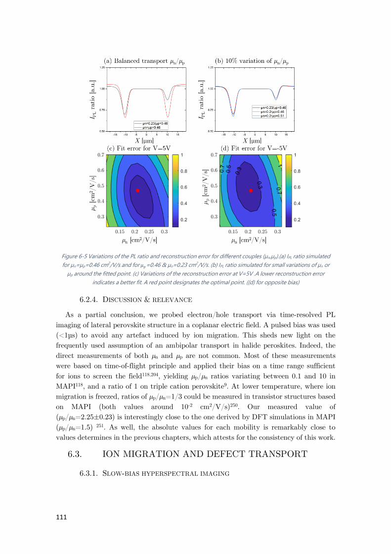
111
Figure 6-5 Variations of the PL ratio and reconstruction error for different couples (µn,µp).(a) IPL ratio simulated
for µn=µp=0.46 cm2/V/s and for 𝜇𝑝=0.46 & µn=0.23 cm2/V/s. (b) IPL ratio simulated for small variations of µn or
µp around the fitted point. (c) Variations of the reconstruction error at V=5V .A lower reconstruction error
indicates a better fit. A red point designates the optimal point. ((d) for opposite bias)
6.2.4. DISCUSSION & RELEVANCE
As a partial conclusion, we probed electron/hole transport via time-resolved PL
imaging of lateral perovskite structure in a coplanar electric field. A pulsed bias was used
(<1µs) to avoid any artefact induced by ion migration. This sheds new light on the
frequently used assumption of an ambipolar transport in halide peroskites. Indeed, the
direct measurements of both µn and µp are not common. Most of these measurements
were based on time-of-flight principle and applied their bias on a time range sufficient
for ions to screen the field118,204, yielding µp/µn ratios variating between 0.1 and 10 in
MAPI118, and a ratio of 1 on triple cation perovskite9. At lower temperature, where ion
migration is freezed, ratios of µp/µn=1/3 could be measured in transistor structures based
on MAPI (both values around 10-2 cm2/V/s)250. Our measured value of
(µp/µn=2.25±0.23) is interestingly close to the one derived by DFT simulations in MAPI
(µp/µn=1.5) 251. As well, the absolute values for each mobility is remarkably close to
values determines in the previous chapters, which attests for the consistency of this work.
6.3. ION MIGRATION AND DEFECT TRANSPORT
6.3.1. SLOW-BIAS HYPERSPECTRAL IMAGING

112
In order to observe the transport of ionic species which are slower than electrons and
holes, we have performed a second experiment where we applied a 5 V bias for several
minutes on the same sample architecture (see Figure 6-1(a)). The timing of the
experiment is sketched in Figure 6-6. The bias time was chosen because halide ions and
vacancies have been reported to drift on similar time scales. In MAPI, several reports
give mobility values in the range of 10-10 to 10-7 cm2/V/s for I- ions or VI+ vacancies 243,248,252,253 (yielding 20s to 300 minutes for them to cross a 20µm channel). However, I-
is not the only ion concerned as in MAPbBr3 single crystal, Br-/VBr+ migration over 10
µm was observed after 20 minutes exposure to a similar electric field254. On the contrary,
organic MA+ / FA+ / Pb2+ ions are expected to drift more slowly91,92,243.
Figure 6-6 Temporal sketch of the slow bias experiment. A blue square indicates each HI acquistion
In this section, we use a hyperspectral imager leading to spectrally-resolved and
absolute PL images (i.e. luminance images) of the channel. We then fit the full PL
absolute emission spectrum at each spatial location using the generalized Planck law,
according to the procedure described by Katahara et al.21. A typical experimental
spectrum and its corresponding fit are displayed in Figure 6-7(b). The fitting procedure
allows us to derive the local bandgap Eg and the quasi-Fermi level splitting Δµ. While
the former is mainly defined by I/Br ratio in mixed halide perovskite54, the latter
corresponds to the electrochemical potential difference of the charge carriers inside the
absorber material (i.e. internal voltage). The difference between Δµ and Eg – in equation
(6-4) and sketched in Figure 6-7(c) – gives an estimation of the non-radiative
recombination current in the solar cell255 and will be considered to highlight bias-induced
defect formation.
Δ(Δμ - Eg) = ΔΔμ - ΔEg (6-4)
6.3.2. EVIDENCE OF ION MIGRATION
Three acquisitions are made: one just before the electric bias application (+5V) and
two after 1 min and 5 min. More information about the timing of the experiment is
displayed in Figure 6-6. On each of the three data, maps of the bandgap, of the quasi-
Fermi level splitting Δµ and of the sub-bandgap absorption parameter Eu are
determined26. Variations of the sub-bandgap absorption are not significant, also with
exposition to light and bias. On the contrary, Eg and Δµ evolve significantly. To properly
identify the effect of the electric bias we analyze differential maps for the bandgap (ΔEg),

113
and for the quasi-Fermi level splitting (ΔΔµ). In this normalization process, the first
acquisition just before bias exposure is taken as a reference and the derived parameters
map (Eg(0V, 0min) or Δµ(0V, 0min)) are subtracted from maps extracted from t=1min
or t=5min acquisitions..
Figure 6-7 Summary of slow-bias experimental results on the HI(a) Sketch of the lateral structure investigated as
a 5V bias is applied on the left electrode for 10 minutes. (b) PL spectrum taken at one pixel of the image,
displayed with its fit to generalized Planck law. (c) Sketch of the band structure with bandgap Eg and quasi-Fermi
level splitting Δµ. After 1 minute of bias, we display the variation of quasi-Fermi level splitting ΔΔµ in (d) (and
after 5 min in (g)). The bandgap change ΔEg image is also displayed in (e) after 1 min and after 5 min in (h). Finally,
the bandgap ΔEg change and quasi-Fermi level change are spatially averaged across the channel in (f) & (i). The
defect creation can be assessed in (f) ((i) for t=5min), where negative values of Δ(Δµ-Eg) appear red. (For details
see text). Scale bar is 10 µm on the images.
We first look at the spatial variations of the bandgap. For instance to probe the change
in the bandgap after 1min, we look at ΔEg(5V,1min) = Eg(5V,1min) - Eg(0V,0min) as it
is displayed in Figure 6-7(e). The situation after 5 minutes ΔEg(5V,5min) is seen in
Figure 6-7(h). After 1 minute of electric bias exposure under continuous illumination, the
bandgap is slightly narrowed at the negative electrode, and strongly narrowed on the
positive electrode. After 5 minutes the trend is enhanced: the red-shifted zone close to
the positive electrode becomes wider. The bandgap modification is a clear indication that
the electric bias induced a chemical change of the materials probably associated with the
ionic migration. At the positive electrode, halide ions accumulate, while halide vacancies
drift to the negative one. We suggest that the red shift is related to the local enrichment
in iodine I-, which is known to diminish Eg in mixed halide perovskite54. As a direct
consequence, we suggest that I- drifts faster than Br- in the considered mixed halide

114
perovskite. If I- were less mobile than Br-, an alternative scenario leading to an apparent
bandgap narrowing remains possible. Indeed, Br- could be accumulated at the positive
electrode. The formed perovskite could segregate under illumination, whereby only the I-
rich phase would be luminescing87,256. However, we tend to exclude this scenario as halide
vacancies, which play a crucial role in this phase segregation257, are repelled from the
positive electrode.
6.3.3. CORRELATION TO DEFECT CREATION
We now correlate the bandgap variations to the electrochemical potential variations.
In Figure 6-7(e)-(h), ΔΔµ and ΔEg profiles are extracted along the channel direction (x-
axis). Both profiles show similar behaviors and are reduced in the vicinity of the positive
electrode. Specifically, after one minute we noticed a drop of Δµ of 25 meV across 4 µm
from the positive electrode (Figure 6-7(d)), and of 35 meV across 6 µm after 5 min of
bias exposure (Figure 6-7(g)). Simultaneously, we have underlined a drop of 𝐸𝑔 in the
same area. As we mention previously a good indicator to quantify the defects creation255
is the evolution of the difference between the quasi-Fermi level splitting and the bandgap
: Δ(Δµ-Eg). In the vicinity of the contact, the bandgap decreases (ΔEg<0) and still we
have negative values of Δ(Δµ-Eg), which means that Δµ is not only affected by Eg but
also by the creation of defects. This is highlighted in Figure 6-7(f)&(i) by the red zone.
Therefore, there is a significant increase of non-radiative recombination at the positive
electrode appearing within 5 min. Notably, no significant change appears around the
positive electrode between 5 min and 10 min, as shown in Figure 6-9 (p.117). This
indicates that the electric field is then screened by the charged species accumulated next
to the positive electrode, and further strengthen the scenario in which charged species
(halide ions) accumulate.
Outside of the defect creation zone, we observe a zone where the difference Δ(Δµ-Eg)
is positive and highlighted in blue in Figure 6-7(f)&(i). The lower non-radiative
recombination current is not related to the electric field, as the same defect passivation
is observed for the perovskite deposited on top of the electrodes, far away from any inter-
electrode electric field. As well after 5 minutes, we can observe a global narrowing of the
bandgap in Figure 6-7(h) (approx. 5 meV decrease), also coincident with a rise in Δµ
(approx. 5meV). These values are consistent to what was observed under continuous
light and ambient atmosphere elsewhere.258
An important control experiment consisted in applying an opposite bias on the same
channel. The results are displayed in Figure 6-10: defects are created at the other
electrode of the channel, which is then positively biased, and bandgap shifts are also
observed. The reversibility of the ion migration is not complete and bandgap variations
trends are not so pronounced.
6.3.4. SLOW-BIAS TIME-RESOLVED IMAGING
Also, the same long-time bias exposure has been realized under the TR-FLIM set-up.
IPL ratio profiles (similar as those used in Figure 6-4) are displayed in Figure 6-8. We

115
underline here that the spectral shifts due to bandgap change during the bias exposure
are corrected by considering IPL ratio. As displayed in the equations below, the E-
dependence disappears as we have observed on a streak camera that IPL(E) spectrum was
unchanged between t=10ns & t=100ns. (section 2.3) The spectral sensitivity of the TR-
FLIM set-up is called fsystem(E) here under.
IPL(t=100ns)
IPL(t=10ns)=
∫ fsystem(E ) IPL(E , t=100ns, tbias=1min) dE
E
∫ fsystem(E ) IPL(E , t=10ns, tbias=1min) dE
E
(6-5)
IPL(t=100ns)
IPL(t=10ns)=
[Reh
*np](t =100ns, tbias=1min)
[Reh
*np](t =10ns, tbias=1min)
(6-6)
Now, for each bias direction, a drop appears near the positive electric contact after 1
minute of biasing. This drop is about 5 µm large, which is significantly higher than the
1µm-wide drop observed after fast-bias exposure. For the fast-bias experiment, this drop
was due to electron/hole motion and was recovered as soon as the bias was turned off.
In this slow-bias experiment, the decay at the positive electrode can be correlated to the
defect creation created by halide ion motion. Due to these defects, the PL lifetime is
locally lower, which ultimately results in a lower IPL(t=100ns)/IPL(t=10ns) ratio.
As seen previously with the evolution of Δ(Δµ-Eg), a few defect are created between
tbias=1 and tbias=10min. Consistently, the IPL ratio is almost unchanged between 1 and
10 min. This is explained by the progressive accumulation of charged species at the
positive electrode, which tends to screen the electric field. Furthermore, the IPL ratio
profile remains almost constant at the positive edge some seconds after disconnecting the
electric bias (Bias Off curve), while a drop appears on the other edge. This points out
ionic effects, as accumulated electronic charges would migrate back immediately. The
presence of the induced opposite electric field (the screening field), is thus also evidenced
by the quenching at opposite edge. Eventually, recovery of the IPL ratio profile after 10
min without electric field (in dark) proves the back migration of ions, or at least the
passivation of the field-activated traps.
Similar field screening effects were observed previously in a MAPbI3 channel238, as
well as on a hybrid mixed halide perovskite channel, in which it was attributed to the
appearance of surface charge and to ionic migration249. Our observations are also
consistent with previous reports from a progressive PL quenching at the positive electrode
of a lateral contact structure236,248,252,254. This PL quenching could be suppressed by
insulating the channel from the contact with a thin PMMA layer259. Henceforth,
electrochemical reactions at the perovskite interface might induce the generation of non-
radiative pathways at the vicinity of the electrode.
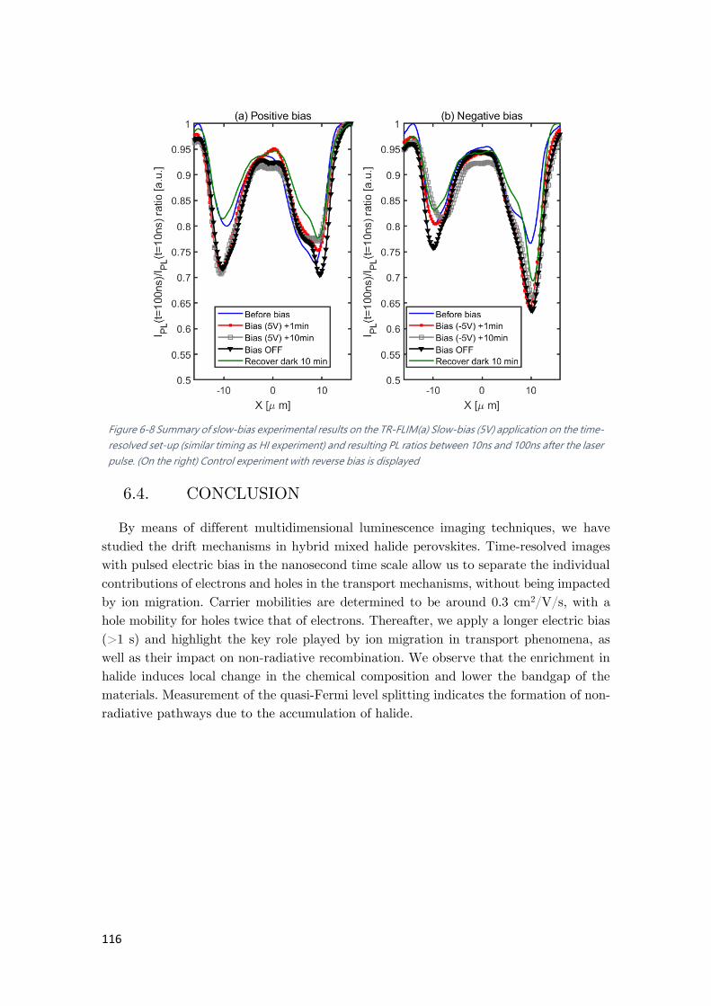
116
Figure 6-8 Summary of slow-bias experimental results on the TR-FLIM(a) Slow-bias (5V) application on the time-
resolved set-up (similar timing as HI experiment) and resulting PL ratios between 10ns and 100ns after the laser
pulse. (On the right) Control experiment with reverse bias is displayed
6.4. CONCLUSION
By means of different multidimensional luminescence imaging techniques, we have
studied the drift mechanisms in hybrid mixed halide perovskites. Time-resolved images
with pulsed electric bias in the nanosecond time scale allow us to separate the individual
contributions of electrons and holes in the transport mechanisms, without being impacted
by ion migration. Carrier mobilities are determined to be around 0.3 cm2/V/s, with a
hole mobility for holes twice that of electrons. Thereafter, we apply a longer electric bias
(>1 s) and highlight the key role played by ion migration in transport phenomena, as
well as their impact on non-radiative recombination. We observe that the enrichment in
halide induces local change in the chemical composition and lower the bandgap of the
materials. Measurement of the quasi-Fermi level splitting indicates the formation of non-
radiative pathways due to the accumulation of halide.

117
Figure 6-9 Optoelectronic parameters mapped for slow bias experiment (positive)Δµ evolution (first column),
Bandgap evolution (second column), quasi-Fermi level splitting evolution corrected from bandgap variations
Δ(Δµ-Eg) (third column). For 5V exposure, differential maps between 1 minute and pre-bias exposure (top row),
between 5 min and pre-bias (second row), between 10 min and pre-bias (second row), between 5 minutes and
1 minute bias exposure (fourth row). Bias is applied on the left electrode for each image. Scaling bar is 10µm.

118
Figure 6-10 Optoelectronic parameters mapped for slow bias experiment (negative) Δµ evolution (first column),
Bandgap evolution (second column), quasi-Fermi level splitting evolution corrected from bandgap variations
Δ(Δµ-Eg) (third column). For -5V exposure, differential maps between 1 minute and pre-bias exposure (top row),
between 5 min and pre-bias (second row), between 10 min and pre-bias (second row), between 5 minutes and
1 minute bias exposure (fourth row). Bias is applied on the left electrode for each image. Scaling bar is 10µm.

119
General conclusion
In this thesis, we have focused on describing optical methods to quantitatively assess
charge carrier transport properties in photovoltaic absorbers and devices. The
experimental investigation was based on multidimensional luminescence imaging
techniques. They include spatial, spectral and temporal analysis of the light flux emitted
by photovoltaic materials under excitation. Its implementation required the development
of optical assemblies as well as digital methods of data processing. Two set-ups have been
mostly used throughout this doctoral work: (i) the hyperspectral imager (HI), which
provides access to spectrally-resolved images (one image per wavelength) and (ii) the
time-resolved fluorescence imager (TR-FLIM) which outputs time-resolved images (one
image per unit of time). While the HI was already fully assembled when this work began,
the TR-FLIM set-up was at preliminary stage and its development was finished during
the thesis. Its two main components are a pulsed laser and a fast camera. Its operating
principles were thoroughly described, and its proof of concept on a reference photovoltaic
cell (GaAs-based) was also presented. It demonstrated that TR-FLIM allows the
assessment of charge transport and recombination properties with a single experiment.
In particular, we could quantify the lateral charge transport in the device. We have
shown how the use of wide-field illumination and collection allows to get rid of artefacts
linked to local illumination. Furthermore, this wide-field illumination constitutes a
realistic excitation scenario for photovoltaic materials and devices, due to its large area
and relatively low power.
We then used these advanced characterization techniques to study charge transport
in an emerging class of materials with very promising photovoltaic properties: halide
perovskites. Throughout this manuscript, charge carrier diffusion in mixed cation halide
perovskites have been brought to light thanks to several transport experiments. The first
experiment was based on a large surface excitation, after which the charge carriers diffuse
in-depth into the perovskite thin film. Therefore, we can probe the transport properties
within the thickness of this layer. Remarkably it is possible to quantify the recombination
at both the front and back surfaces as well as the recombination mechanisms within the
bulk. The second experiment was based on a point excitation, following which the charge
transport is essentially radial, at least after a certain time when we can neglect the in-
depth diffusion. The carrier diffusion was distinguished from photon recycling, which
constitutes a complementary transport mechanism whereby a luminescence photon is
reabsorbed and regenerates a charge. Here again, the diffusion and recombination of
charge carriers have been imaged with a high temporal and spectral resolution. This
allowed to quantify them by means of optimization algorithms that fit the experimental
results to the developed physical models (time-resolved diffusion equation).
Imaging methods are also adapted to the investigation of the impact of chemical and
morphological inhomogeneities on local optoelectronic properties. This was illustrated by

120
the study of the influence of wrinkles appearing at the surface of Cs-rich perovskite. We
noticed that morphological features change the light out-coupling properties, thereby
hampering straightforward analysis of IPL signal. We could still correlate chemical
heterogeneities to bandgap and lifetime ones, which underlined the beneficial role of Cs-
rich wrinkles in transport properties. Nonetheless, further development on the coupling
between 2D-3D modeling and IPL imaging should be conducted to obtain a proper
quantification of transport in inhomogeneous materials.
Eventually, we have applied multidimensional IPL imaging techniques to probe lateral
structures featuring a 20μm wide perovskite channel in-between two electrodes. The main
goal was to go further than our previous studies and separate the electron and hole
transport properties which is difficult in such an intrinsic layer as perovskite. The
stability of the material linked to ion migration had also to be considered. By applying a
fast electric bias across the channel (<1μs), we first isolated the drift of charge carriers
from that of the ions composing perovskite. Electron and hole mobilities were quantified
separately (µp/µn=2.25±0.23). Their almost equal value justified their previous
symmetrical (ambipolar) treatment. Then, experiments at longer time scale (electric field
applied for 10 minutes) also allowed us to image the transport of halide ions. This multi-
dimensional experiment brought us as close as ever to the operating principles of a PV
device, which operates with light and bias. The accumulation of ions at the positive
electrode leads to a local reduction in the lifetime of the charge carriers.
As a summary concerning transport in halide perovskite, we can state that interface
recombination surely is the main loss channel in perovskite solar cells. This assertion
gives precious orientations for the next synthetic approaches focusing on interface design.
For what concerns charge transport in bulk perovskite, we systematically quantified
relatively low values of charge carrier mobilities (between 0.2 and 1 cm2/V/s), whereby
the fundamental reason for this value remains unclear. In any case, this slow diffusion
remains compensated by the long lifetime of charge carriers (≈1μs), which guarantees
their collection in a PV device. Two main pitfalls on the way to industrialization of
perovskite solar cells remain - the stability of the devices and the up-scalability of
fabrication techniques. The set of characterization techniques introduced in this
manuscript would apply for a study tackling these issues. On the stability side, next
measurement campaigns could focus on the evolution of optoelectronic properties as the
material is exposed to environmental stresses (moisture, light, oxygen). On the upscaling
side, the high versatility from the micro scale to the macro scale could allow to identify
localize and circumvent the defects related to large scale production. Moreover, having
spectrally and time-resolved images available at each step of the production/ageing
triggers the need for efficient post-treatment algorithms, in which machine learning
approaches could play a role.
To go deeper than these already refined study of charge transport in halide perovskites,
a new set-up dedicated to 4D IPL imaging was designed. It allows to acquire 4D IPL data
sets (2D spatial + spectral + temporal in a single experiment) by combining the concept

121
of single pixel imaging to a streak camera. As compared to a simple combination of HI
and TR-FLIM setups, it allows having a better optical sensitivity (we here do not select
both the energy and decay time of the signal) as well as a better time and spectral
resolution. In this manuscript, we described its operating principles, which are protected
by a filed patent, as well as its initial development realized with the help of a master
student. A first proof of concept obtained on a perovskite layer was presented. It paved
the way towards further advanced characterization of PV materials. Next developments
of this set-up notably includes its calibration, thanks to which one could fit the acquired
hypercube to the generalized Planck law, in order to map the QFLS with a picosecond
resolution. This should unveil fundamental mechanisms of charge separation, transport,
collection and recombination in the presence of electric field, or at hetero-interfaces,
which is of high interest at the moment.

122

123
References
1 IEA (International Energy Agency), World Energy Lookout, 2018.
2 W. Shockley and H. J. Queisser, J. Appl. Phys., 1961, 32, 510–519.
3 J.-F. Guillemoles, T. Kirchartz, D. Cahen and U. Rau, Nat. Photonics, 2019, 13,
501–505.
4 G. Carr, Econ., 2012.
5 F. Oliva, S. Kretzschmar, D. Colombara, S. Tombolato, C. M. Ruiz, A.
Redinger, E. Saucedo, C. Broussillou, T. G. de Monsabert, T. Unold, P. J. Dale,
V. Izquierdo-Roca and A. Perez-Rodriguez, Sol. Energy Mater. Sol. Cells, 2016,
158, 168–183.
6 T. Trupke and R. A. Bardos, Appl. Phys. Lett., 2006, 89, 044107.
7 NREL, Best Research-Cell Efficiencies,
https://www.nrel.gov/pv/assets/images/efficiency-chart.png.
8 H. J. Snaith, Nat. Mater., 2018, 17, 372–376.
9 Y. Rong, Y. Hu, A. Mei, H. Tan, M. I. Saidaminov, S. Il Seok, M. D. McGehee,
E. H. Sargent and H. Han, Science (80-. )., 2018, 361, eaat8235.
10 J. Huang, Y. Yuan, Y. Shao and Y. Yan, Nat. Rev. Mater., 2017, 2, 17042.
11 E. Becquerel, Compte-rendus l’académie des Sci., 1839, 9, 561.
12 G. Kirchoff, Ann. Phys.
13 A. Einstein, in The old quantum theory, 1917, pp. 167–183.
14 W. van Roosbroeck and W. Shockley, Phys. Rev., 1954, 94, 1558–1560.
15 E. H. Kennard, Phys. Rev., 1918, 11, 29–38.
16 G. Lasher and F. Stern, Phys. Rev.
17 P. Würfel, J. Phys. C Solid State Phys., 1982, 15, 3967–3985.
18 J. H. Lambert, Photometria, sive de Mensura et gradibus luminis, colorum et
umbrae, 1760.
19 S. M. Sze and K. K. Ng, Physics of semi-conductor devices, John Wiley & Sons,
2006.
20 R. K. Ahrenkiel, D. J. Dunlavy, B. Keyes, S. M. Vernon, T. M. Dixon, S. P.
Tobin, K. L. Miller and R. E. Hayes, Appl. Phys. Lett., 1989, 55, 1088–1090.
21 J. K. Katahara and H. W. Hillhouse, J. Appl. Phys., 2014, 116, 173504.

124
22 M. Maiberg, F. Bertram, M. Muller and R. Scheer, J. Appl. Phys., 2017, 121,
085703.
23 L. M. Pazos-Outón, M. Szumilo, R. Lamboll, J. M. Richter, M. Crespo-Quesada,
M. Abdi-Jalebi, H. J. Beeson, M. Vrućinić, M. Alsari, H. J. Snaith, B. Ehrler, R.
H. Friend and F. Deschler, Science (80-. )., 2016, 351, 1430–1433.
24 T. Yamada, Y. Yamada, Y. Nakaike, A. Wakamiya and Y. Kanemitsu, Phys.
Rev. Appl., 2017, 7, 1–8.
25 F. Urbach, Phys. Rev., 1953, 92, 1324.
26 N. Paul, V. Le Guen, D. Ory and L. Lombez, in 2017 IEEE 44th Photovoltaic
Specialist Conference (PVSC), 2017, pp. 1–4.
27 D. König, K. Casalenuovo, Y. Takeda, G. Conibeer, J.-F. Guillemoles, R.
Patterson, L. M. Huang and M. A. Green, Phys. E, 2010, 42, 2862–2866.
28 M. Li, J. Fu, Q. Xu and T. C. Sum, Adv. Mater., 2018, 1802486, 1–17.
29 P. Drude, Ann. Phys., 1900, 306, 566–613.
30 H. C. Casey and F. Stern, J. Appl. Phys., 1976, 47, 631–643.
31 A. Einstein, Ann. Phys., 1905, 322, 549–560.
32 D. Paget, F. Cadiz, A. C. H. Rowe, F. Moreau, S. Arscott and E. Peytavit, J.
Appl. Phys., 2012, 111, 123720.
33 P. Auger, Compte-rendus l’académie des Sci., 1923, 177, 169–171.
34 L. Meitner, Phys Z., 1922, 9, 131–144.
35 W. Shockley and W. T. Read, Phys. Rev., 1952, 87, 835.
36 R. N. Hall, Phys. Rev., 1952, 87, 387.
37 S. D. Stranks, V. M. Burlakov, T. Leijtens, J. M. Ball, A. Goriely and H. J.
Snaith, Phys. Rev. Appl., 2014, 2, 034007.
38 Q. Lin, Z. Wang, H. J. Snaith, M. B. Johnston and L. M. Herz, Adv. Sci., 2018,
1700792, 1–8.
39 E. Edri, S. Kirmayer, S. Mukhopadhyay, K. Gartsman, G. Hodes and D. Cahen,
Nat. Commun., 2014, 5, 1–8.
40 P. J. Verlinden, M. Aleman, N. Posthuma, J. Fernandez, B. Pawlak, J.
Robbelein, M. Debucquoy, K. Van Wichelen and J. Poortmans, Sol. Energy
Mater. Sol. Cells, 2012, 106, 37–41.
41 U. Rau, Phys. Rev. B, 2007, 76, 085303.
42 C. Donolato, Appl. Phys. Lett., 1985, 46, 270.
43 K. Toprasertpong, A. Delamarre, Y. Nakano, J. F. Guillemoles and M.

125
Sugiyama, Phys. Rev. Appl., 2019, 11, 1.
44 U. Rau, B. Blank, T. C. M. Müller and T. Kirchartz, Phys. Rev. Appl., 2017, 7,
44016.
45 D. B. Mitzi, C. A. Feild, W. T. A. Harrison and A. M. Guloy, Nature, 1994,
369, 467–469.
46 C. R. Kagan, D. B. Mitzi and C. D. Dimitrakopoulos, Science (80-. )., 1999,
286, 945–947.
47 A. Kojima, K. Teshima, Y. Shirai and T. Miyasaka, J. Am. Chem. Soc., 2009,
131, 6050–6051.
48 N. K. Noel, S. D. Stranks, A. Abate, C. Wehrenfennig, S. Guarnera, A.-A.
Haghighirad, A. Sadhanala, G. E. Eperon, S. K. Pathak, M. B. Johnston, A.
Petrozza, L. M. Herz and H. J. Snaith, Energy Environ. Sci., 2014, 7, 3061.
49 F. Hao, C. C. Stoumpos, D. H. Cao, R. P. H. Chang and M. G. Kanatzidis, Nat.
Photonics, 2014, 8, 489–494.
50 N. Pellet, P. Gao, G. Gregori, T. Y. Yang, M. K. Nazeeruddin, J. Maier and M.
Grätzel, Angew. Chemie - Int. Ed., 2014, 53, 3151–3157.
51 V. D’innocenzo, A. R. S. Kandada, M. De Bastiani, M. Gandini and A.
Petrozza, J. Am. Chem. Soc., 2014, 136, 17730–17733.
52 Z. Yang, C. C. Chueh, P. W. Liang, M. Crump, F. Lin, Z. Zhu and A. K. Y.
Jen, Nano Energy, 2016, 22, 328–337.
53 N. J. Jeon, J. H. Noh, W. S. Yang, Y. C. Kim, S. Ryu, J. Seo and S. Il Seok,
Nature, 2015, 517, 476–480.
54 G. E. Eperon, S. D. Stranks, C. Menelaou, M. B. Johnston, L. M. Herz and H. J.
Snaith, Energy Environ. Sci., 2014, 7, 982.
55 M. Saliba, T. Matsui, J.-Y. Seo, K. Domanski, J.-P. Correa-Baena, M. K.
Nazeeruddin, S. M. Zakeeruddin, W. Tress, A. Abate, A. Hagfeldt and M.
Grätzel, Energy Environ. Sci., 2016, 9, 1989–1997.
56 M. Saliba, T. Matsui, K. Domanski, J.-Y. Seo, A. Ummadisingu, S. M.
Zakeeruddin, J.-P. Correa-Baena, W. Tress, A. Abate, A. Hagfeldt and M.
Grätzel, Science (80-. )., 2016, 354, 206–209.
57 T. Duong, Y. L. Wu, H. Shen, J. Peng, X. Fu, D. Jacobs, E. C. Wang, T. C.
Kho, K. C. Fong, M. Stocks, E. Franklin, A. Blakers, N. Zin, K. McIntosh, W.
Li, Y. B. Cheng, T. P. White, K. Weber and K. Catchpole, Adv. Energy Mater.,
2017, 7, 1–11.
58 Z. Li, M. Yang, J.-S. Park, S.-H. Wei, J. J. Berry and K. Zhu, Chem. Mater.,
2016, 28, 284–292.
59 M. A. Green, A. Ho-Baillie and H. J. Snaith, Nat. Photonics, 2014, 8, 506–514.

126
60 S. Motti, T. Crothers, R. Yang, Y. Cao, R. Li, M. B. Johnston, J. Wang and L.
M. Herz, Nano Lett., 2019, 19, 3953–3960.
61 J. Byun, H. Cho, C. M. Wolff, A. Sadhanala, R. H. Friend, H. Yang and T. Lee,
Adv. Mater., 2016, 28, 7515–7520.
62 E. M. Sanehira, A. R. Marshall, J. A. Christians, S. P. Harvey, P. N. Ciesielski,
L. M. Wheeler, P. Schulz, L. Y. Lin, M. C. Beard and J. M. Luther, Sci. Adv.,
2017, 3, eaao4204.
63 A. Swarnkar, A. R. Marshall, E. M. Sanehira, B. D. Chernomordik, D. T. Moore,
J. A. Christians, T. Chakrabarti and J. M. Luther, Science (80-. )., 2016, 354,
92–95.
64 Q. A. Akkerman, G. Rainò, M. V. Kovalenko and L. Manna, Nat. Mater., 2018,
1–12.
65 M. Abdi-Jalebi, Z. Andaji-Garmaroudi, S. Cacovich, C. Stavrakas, B. Philippe,
J. M. Richter, M. Alsari, E. P. Booker, E. M. Hutter, A. J. Pearson, S. Lilliu, T.
J. Savenije, H. Rensmo, G. Divitini, C. Ducati, R. H. Friend and S. D. Stranks,
Nature, 2018, 555, 497–501.
66 D. J. Kubicki, D. Prochowicz, A. Hofstetter, S. M. Zakeeruddin, M. Grätzel and
L. Emsley, J. Am. Chem. Soc., 2017, 139, 14173–14180.
67 J. Beilsten-Edmands, G. E. Eperon, R. D. Johnson, H. J. Snaith and P. G.
Radaelli, Appl. Phys. Lett., 2015, 106, 173502.
68 J. E. Moser, Nat. Mater., 2016, 16, 4–6.
69 T. Wang, B. Daiber, J. M. Frost, S. A. Mann, E. C. Garnett, A. Walsh and B.
Ehrler, Energy Environ. Sci., 2017, 10, 509–515.
70 F. Zheng, L. Z. Tan, S. Liu and A. M. Rappe, Nano Lett., 2015, 15, 7794–7800.
71 J. M. Richter, K. Chen, A. Sadhanala, J. Butkus, J. P. H. Rivett, R. H. Friend,
B. Monserrat, J. M. Hodgkiss and F. Deschler, Adv. Mater., 2018, 1803379,
1803379.
72 D. W. deQuilettes, K. Frohna, D. Emin, T. Kirchartz, V. Bulovic, D. S. Ginger
and S. D. Stranks, Chem. Rev., , DOI:10.1021/acs.chemrev.9b00169.
73 G. E. Eperon, M. T. Hörantner and H. J. Snaith, Nat. Rev. Chem., 2017, 1,
0095.
74 F. J. Ramos, S. Jutteau, J. Posada, A. Bercegol, A. Rebai, T. Guillemot, R.
Bodeux, N. Schneider, N. Loones, D. Ory, C. Broussillou, G. Goaer, L. Lombez
and J. Rousset, Sci. Rep., 2018, 8, 16139.
75 J. Burschka, N. Pellet, S.-J. Moon, R. Humphry-Baker, P. Gao, M. K.
Nazeeruddin and M. Grätzel, Nature, 2013, 499, 316–319.
76 N. J. Jeon, J. H. Noh, Y. C. Kim, W. S. Yang, S. Ryu and S. Il Seok, Nat.

127
Mater., 2014, 13, 897–903.
77 N. Ahn, D. Y. Son, I. H. Jang, S. M. Kang, M. Choi and N. G. Park, J. Am.
Chem. Soc., 2015, 137, 8696–8699.
78 Q. Chen, H. Zhou, Z. Hong, S. Luo, H.-S. Duan, H.-H. Wang, Y. Liu, G. Li and
Y. Yang, J. Am. Chem. Soc., 2014, 136, 622–625.
79 W. S. Yang, B.-W. Park, E. H. Jung, N. J. Jeon, Y. C. Kim, D. U. Lee, S. S.
Shin, J. Seo, E. K. Kim, J. H. Noh and S. Il Seok, Science (80-. )., 2017, 356,
1376–1379.
80 Q. Chen, H. Zhou, Y. Fang, A. Z. Stieg, T.-B. Song, H.-H. Wang, X. Xu, Y. Liu,
S. Lu, J. You, P. Sun, J. McKay, M. S. Goorsky and Y. Yang, Nat. Commun.,
2015, 6, 7269.
81 M. R. Leyden, Y.Jiang and Y. Qi, J. Mater. Chem. A, 2016, 4, 13125–13132.
82 C. Pareja-Rivera, A. L. Solís-Cambero, M. Sánchez-Torres, E. Lima and D.
Solis-Ibarra, ACS Energy Lett., 2018, 2366–2367.
83 C. C. Boyd, R. Cheacharoen, T. Leijtens and M. D. McGehee, Chem. Rev., 2019,
119, 3418–3451.
84 G. Divitini, S. Cacovich, F. Matteocci, L. Cinà, A. Di Carlo and C. Ducati, Nat.
Energy, 2016, 1, 15012.
85 R. Brenes, D. Guo, A. Osherov, N. K. Noel, C. Eames, E. M. Hutter, S. K.
Pathak, F. Niroui, R. H. Friend, M. S. Islam, H. J. Snaith, V. Bulović, T. J.
Savenije and S. D. Stranks, Joule, 2017, 1, 155–167.
86 R. E. Beal, D. J. Slotcavage, T. Leijtens, A. R. Bowring, R. A. Belisle, W. H.
Nguyen, G. F. Burkhard, E. T. Hoke and M. D. McGehee, J. Phys. Chem. Lett.,
2016, 7, 746–751.
87 D. J. Slotcavage, H. I. Karunadasa and M. D. McGehee, ACS Energy Lett.,
2016, 1, 1199–1205.
88 C. G. Bischak, A. B. Wong, E. Lin, D. T. Limmer, P. Yang and N. S. Ginsberg,
J. Phys. Chem. Lett., 2018, 9, 3998–4005.
89 O. Almora, A. Guerrero and G. Garcia-Belmonte, Appl. Phys. Lett., 2016, 108,
043903.
90 J. M. Frost and A. Walsh, Acc. Chem. Res., 2016, 49, 528–535.
91 A. Senocrate and J. Maier, J. Am. Chem. Soc., 2019, 141, 8382–8396.
92 A. Walsh and S. D. Stranks, ACS Energy Lett., 2018, 3, 1983–1990.
93 G. Y. Kim, A. Senocrate, T. Y. Yang, G. Gregori, M. Grätzel and J. Maier, Nat.
Mater., 2018, 17, 445–449.
94 C. L. Davies, M. R. Filip, J. B. Patel, T. W. Crothers, C. Verdi, A. D. Wright,

128
R. L. Milot, F. Giustino, M. B. Johnston and L. M. Herz, Nat. Commun., 2018,
9, 1–9.
95 A. Miyata, A. Mitioglu, P. Plochocka, O. Portugall, J. T.-W. Wang, S. D.
Stranks, H. J. Snaith and R. J. Nicholas, Nat. Phys., 2015, 11, 582–588.
96 K. Galkowski, A. Mitioglu, A. Miyata, P. Plochocka, O. Portugall, G. E. Eperon,
J. T.-W. Wang, T. Stergiopoulos, S. D. Stranks, H. J. Snaith and R. J. Nicholas,
Energy Environ. Sci., 2016, 9, 962–970.
97 A. Mahboubi Soufiani, Z. Yang, T. Young, A. Miyata, A. Surrente, A. Pascoe,
K. Galkowski, M. Abdi-Jalebi, R. Brenes, J. Urban, N. Zhang, V. Bulović, O.
Portugall, Y.-B. Cheng, R. J. Nicholas, A. Ho-Baillie, M. A. Green, P. Plochocka
and S. D. Stranks, Energy Environ. Sci., 2017, 10, 1358–1366.
98 G. Xing, N. Mathews, S. Sun, S. S. Lim, Y. M. Lam, M. Gratzel, S. Mhaisalkar
and T. C. Sum, Science (80-. )., 2013, 342, 344–347.
99 D. Shi, V. Adinolfi, R. Comin, M. Yuan, E. Alarousu, A. Buin, Y. Chen, S.
Hoogland, A. Rothenberger, K. Katsiev, Y. Losovyj, X. Zhang, P. A. Dowben,
O. F. Mohammed, E. H. Sargent and O. M. Bakr, Science (80-. )., 2015, 347,
519–522.
100 Y. Yamada, T. Yamada, L. Q. Phuong, N. Maruyama, H. Nishimura, A.
Wakamiya, Y. Murata and Y. Kanemitsu, J. Am. Chem. Soc., 2015, 137,
10456–10459.
101 E. M. Hutter, G. E. Eperon, S. D. Stranks and T. J. Savenije, J. Phys. Chem.
Lett., 2015, 6, 3082–3090.
102 J. M. Richter, M. Abdi-Jalebi, A. Sadhanala, M. Tabachnyk, J. P. H. Rivett, L.
M. Pazos-Outón, K. C. Gödel, M. Price, F. Deschler and R. H. Friend, Nat.
Commun., 2016, 7, 13941.
103 C. Wehrenfennig, G. E. Eperon, M. B. Johnston, H. J. Snaith and L. M. Herz,
Adv. Mater., 2014, 26, 1584–1589.
104 M. B. Johnston and L. M. Herz, Acc. Chem. Res., 2016, 49, 146–154.
105 W. Rehman, D. P. McMeekin, J. B. Patel, R. L. Milot, M. B. Johnston, H. J.
Snaith and L. M. Herz, Energy Environ. Sci., 2017, 10, 361–369.
106 X. Fu, K. J. Weber and T. P. White, J. Appl. Phys., 2018, 124, 073102.
107 H. Do Kim and H. Ohkita, Jpn. J. Appl. Phys., 2018, 57, 08RE03.
108 I. Levine, O. G. Vera, M. Kulbak, D.-R. Ceratti, C. Rehermann, J. A. Márquez,
S. Levcenko, T. Unold, G. Hodes, I. Balberg, D. Cahen and T. Dittrich, ACS
Energy Lett., 2019, 1150–1157.
109 W. Tress, Adv. Energy Mater., 2017, 7, 1602358.
110 D. A. Egger, A. Bera, D. Cahen, G. Hodes, T. Kirchartz, L. Kronik, R.

129
Lovrincic, A. M. Rappe, D. R. Reichman and O. Yaffe, Adv. Mater., 2018,
1800691, 1–11.
111 W. J. Yin, T. Shi and Y. Yan, Appl. Phys. Lett., 2014, 104, 063903.
112 N. Liu and C. Y. Yam, Phys. Chem. Chem. Phys., 2018, 20, 6800–6804.
113 T. Kirchartz, T. Markvart, U. Rau and D. A. Egger, J. Phys. Chem. Lett., 2018,
9, 939–946.
114 Y. Chen, H. T. Yi, X. Wu, R. Haroldson, Y. N. Gartstein, Y. I. Rodionov, K. S.
Tikhonov, A. Zakhidov, X.-Y. Zhu and V. Podzorov, Nat. Commun., 2016, 7,
12253.
115 R. Fan, Y. Huang, L. Wang, L. Li, G. Zheng and H. Zhou, Adv. Energy Mater.,
2016, 6, 1–32.
116 L. M. Herz, ACS Energy Lett., 2017, 2, 1539–1548.
117 J. Peng, Y. Chen, K. Zheng and Z. Liang, Chem. Soc. Rev., 2017, 46, 5714–
5729.
118 B. Maynard, Q. Long, E. A. Schiff, M. Yang, K. Zhu, R. Kottokkaran, H. Abbas
and V. L. Dalal, Appl. Phys. Lett., 2016, 108, 173505.
119 Z. Guo, N. Zhou, O. F. Williams, J. Hu, W. You and A. M. Moran, J. Phys.
Chem. C, 2018, 122, 10650–10656.
120 Z. Guo, J. S. Manser, Y. Wan, P. V. Kamat and L. Huang, Nat. Commun.,
2015, 6, 1–8.
121 J. M. Snaider, Z. Guo, T. Wang, M. Yang, L. Yuan, K. Zhu and L. Huang, ACS
Energy Lett., 2018, 1402–1408.
122 T. W. Crothers, R. L. Milot, J. B. Patel, E. S. Parrott, J. Schlipf, P. Muller-
Buschbaum, M. B. Johnston and L. M. Herz, Nano Lett., 2017, 17, 5782–5789.
123 S. D. Stranks, G. E. Eperon, G. Grancini, C. Menelaou, M. J. P. Alcocer, T.
Leijtens, L. M. Herz, A. Petrozza and H. J. Snaith, Science (80-. )., 2013, 432,
341–344.
124 W. Tian, R. Cui, J. Leng, J. Liu, Y. Li, C. Zhao, J. Zhang, W. Deng, T. Lian
and S. Jin, Angew. Chemie - Int. Ed., 2016, 128, 13261–13265.
125 D. W. de Quilettes, W. Zhang, V. M. Burlakov, D. J. Graham, T. Leijtens, A.
Osherov, V. Bulovic, H. J. Snaith, D. S. Ginger and S. D. Stranks, Nat.
Commun., 2016, 7, 11683.
126 F. Sahli, J. Werner, B. A. Kamino, M. Bräuninger, R. Monnard, B. Paviet-
salomon, L. Barraud, L. Ding, J. J. D. Leon, D. Sacchetto, G. Cattaneo, M.
Boccard, M. Despeisse, S. Nicolay, Q. Jeangros, B. Niesen and C. Ballif, Nat.
Mater., 2018, 17, 820–826.

130
127 H. J. Snaith, Nat. Mater., 2018, 17, 372–376.
128 M. M. Lee, J. Teuscher, T. Miyasaka, T. N. Murakami and H. J. Snaith, Science
(80-. )., 2012, 338, 643–647.
129 X. Lin, A. N. Jumabekov, N. N. Lal, A. R. Pascoe, D. E. Gómez, N. W. Duffy,
A. S. R. Chesman, K. Sears, M. Fournier, Y. Zhang, Q. Bao, Y. B. Cheng, L.
Spiccia and U. Bach, Nat. Commun., , DOI:10.1038/s41467-017-00588-3.
130 T. Leijtens, G. E. Eperon, S. K. Pathak, A. Abate, M. M. Lee and H. J. Snaith,
Nat. Commun.
131 G. Liu, B. Yang, B. Liu, C. Zhang, S. Xiao, Y. Yuan, H. Xie, D. Niu, J. Yang,
Y. Gao and C. Zhou, Appl. Phys. Lett., 2017, 111, 153501.
132 J. Cao, B. Wu, R. Chen, Y. Wu, Y. Hui, B. W. Mao and N. Zheng, Adv. Mater.,
2018, 30, 1–9.
133 P. Caprioglio, M. Stolterfoht, C. M. Wolff, T. Unold, B. Rech, S. Albrecht and
D. Neher, Adv. Energy Mater., 2019, 1901631.
134 G. El-Hajje, C. Momblona, L. Gil-Escrig, J. Ávila, T. Guillemot, J.-F.
Guillemoles, M. Sessolo, H. J. Bolink and L. Lombez, Energy Environ. Sci.,
2016, 9, 2286–2294.
135 F. Staub, H. Hempel, J. C. Hebig, J. Mock, U. W. Paetzold, U. Rau, T. Unold
and T. Kirchartz, Phys. Rev. Appl., 2016, 6, 1–13.
136 J. Peng, Y. Wu, W. Ye, D. A. Jacobs, H. Shen, X. Fu, Y. Wan, T. Duong, N.
Wu, C. Barugkin, H. T. Nguyen, D. Zhong, J. Li, T. Lu, Y. Liu, M. N. Lockrey,
K. J. Weber, K. R. Catchpole and T. P. White, Energy Environ. Sci., 2017, 10,
1792–1800.
137 F. Yang, H. E. Lim, F. Wang, M. Ozaki, A. Shimazaki, J. Liu, N. B. Mohamed,
K. Shinokita, Y. Miyauchi, A. Wakamiya, Y. Murata and K. Matsuda, Adv.
Mater. Interfaces, 2018, 5, 1–10.
138 C. S. Jiang, M. Yang, Y. Zhou, B. To, S. U. Nanayakkara, J. M. Luther, W.
Zhou, J. J. Berry, J. Van De Lagemaat, N. P. Padture, K. Zhu and M. M. Al-
Jassim, Nat. Commun., 2015, 6, 1–10.
139 P. Schulz, ACS Energy Lett., 2018, 3, 1287–1293.
140 S. Van Reenen, M. Kemerink and H. J. Snaith, J. Phys. Chem. Lett., 2015, 6,
3808–3814.
141 S. A. L. Weber, I. M. Hermes, S. H. Turren-Cruz, C. Gort, V. W. Bergmann, L.
Gilson, A. Hagfeldt, M. Graetzel, W. Tress and R. Berger, Energy Environ. Sci.,
2018, 11, 2404.
142 P. Lopez-Varo, J. A. Jiménez-Tejada, M. García-Rosell, S. Ravishankar, G.
Garcia-Belmonte, J. Bisquert and O. Almora, Adv. Energy Mater., 2018,
1702772, 1–36.

131
143 H. Tsai, R. Asadpour, J. C. Blancon, C. C. Stoumpos, O. Durand, J. W.
Strzalka, B. Chen, R. Verduzco, P. M. Ajayan, S. Tretiak, J. Even, M. A. Alam,
M. G. Kanatzidis, W. Nie and A. D. Mohite, Science (80-. )., 2018, 360, 67–70.
144 R. Brenes, C. Eames, V. Bulović, M. S. Islam and S. D. Stranks, Adv. Mater.,
2018, 30, 1–8.
145 R. J. Stoddard, F. T. Eickemeyer, J. K. Katahara and H. W. Hillhouse, J. Phys.
Chem. Lett., 2017, 8, 3289–3298.
146 A. Delamarre, UPMC Sorbonne Universités, 2013.
147 F. Gibelli, L. Lombez and J. Guillemoles, J. Phys. Condens. Matter.
148 A. Delamarre, M. Paire, J.-F. Guillemoles and L. Lombez, Prog. Photovoltaics,
2015, 23, 1305–1312.
149 A. Delamarre, L. Lombez and J. Guillemoles, J. Photonics Energy2, 2012, 2,
027004.
150 M. Legrand, Ecole Centrale de Lyon, 2019.
151 M. P. Edgar, G. M. Gibson and M. J. Padgett, Nat. Photonics, 2019, 13, 13–20.
152 M. F. Duarte, M. A. Davenport, D. Takbar, J. N. Laska, T. Sun, K. F. Kelly
and R. G. Baraniuk, IEEE Signal Process. Mag., 2008, 25, 83–91.
153 Y. Zhu, M. K. Juhl, T. Trupke and Z. Hameiri, IEEE J. Photovoltaics, 2017, 7,
1087–1091.
154 Z. Zhang, X. Wang, G. Zheng and J. Zhong, Opt. Express, 2017, 25, 19619–
19639.
155 Princeton Instruments, SpectraPro HRS Datasheet, .
156 Hamamatsu, C10910_InstructionManual(English)_118E, .
157 V. Le Guen, N. Paul, D. Ory and L. Lombez, 1–4.
158 MATLAB, Solve 1-D parabolic and elliptic PDEs,
https://fr.mathworks.com/help/matlab/ref/pdepe.html?, (accessed 18 October
2019).
159 MATLAB, Unconstrained nonlinear optimization algorithms,
https://fr.mathworks.com/help/optim/ug/unconstrained-nonlinear-optimization-
algorithms.html, (accessed 18 October 2019).
160 I. Ioffe, Gallium Arsenide Electronic and electrical Properties,
http://www.ioffe.ru/SVA/NSM/Semicond/GaAs/electric.html#Recombination.
161 C. Honsberg and S. Bowden, Solving for Depletion Region,
http://www.pveducation.org/pvcdrom/solving-for-depletion-region.
162 M. Maiberg and R. Scheer, J. Appl. Phys., 2014, 116, 123711.

132
163 D. Hinken, K. Bothe, K. Ramspeck, S. Herlufsen and R. Brendel, J. Appl. Phys.,
2009, 105, 104516.
164 R. K. Ahrenkiel, Solid State Electron., 1992, 35, 239–250.
165 B. M. Keyes, D. J. Dunlavy, R. K. Ahrenkiel, S. E. Asher, L. D. Partain, D. D.
Liu and M. S. Kuryla, J. Vac. Sci. Technol. A Vacuum, Surfaces, Film., 1990,
8, 2004–2008.
166 R. Brüggemann, J. Phys. Conf. Ser., 2010, 253, 012081.
167 K. Chen, N. Sheehan, F. He, X. Meng, S. C. Mason, S. R. Bank and Y. Wang,
ACS Photonics, 2017, 4, 1440–1446.
168 F. Cadiz, D. Paget, A. C. H. Rowe, T. Amand, P. Barate and S. Arscott, Phys.
Rev. B, 2015, 91, 165203.
169 T. Dullweber, O. Lundberg, J. Malmström, M. Bodegard, L. Stolt, U. Rau, H.
W. Schock and J. H. Werner, Thin Solid Films, 2001, 387, 11–13.
170 T. Gessmann and E. F. Schubert, J. Appl. Phys., 2004, 95, 2203–2216.
171 D. Hinken, K. Ramspeck, K. Bothe, B. Fischer and R. Brendel, Appl. Phys.
Lett., 2007, 91, 89–92.
172 M. Paire, L. Lombez, J. F. Guillemoles and D. Lincot, Thin Solid Films, 2011,
519, 7493–7496.
173 R. J. Nelson and R. G. Sobers, J. Appl. Phys., 1979, 49, 6103.
174 F. Cadiz, D. Paget, A. C. H. Rowe, V. L. Berkovits, V. P. Ulin, S. Arscott and
E. Peytavit, J. Appl. Phys., 2013, 114, 103711.
175 P. Gundel, F. D. Heinz, M. C. Schubert, J. A. Giesecke and W. Warta, J. Appl.
Phys., 2010, 108, 033705.
176 D. Kuciauskas, T. H. Myers, T. M. Barnes, S. A. Jensen and A. M. Allende
Motz, Appl. Phys. Lett., 2017, 110, 083905.
177 F. D. Heinz, J. A. Giesecke, L. E. Mundt, M. Kasemann and W. Warta, J. Appl.
Phys., 2015, 118, 5706.
178 A. Bercegol, G. El-Hajje, D. Ory and L. Lombez, J. Appl. Phys., 2017, 122,
203102.
179 A. Edler, V. D. Mihailetchi, L. J. Koduvelikulathu, R. Kopecek and R. Harney,
2015, 620–627.
180 A. Marchioro, J. Teuscher, D. Friedrich, M. Kunst, R. van de Krol, T. Moehl,
M. Grätzel and J.-E. Moser, Nat. Photonics, 2014, 8, 250–255.
181 B. Krogmeier, F. Staub, D. Grabowski, U. Rau and T. Kirchartz, Sustain.
Energy Fuels, 2018, 2, 1027–1034.

133
182 Y. Yang, M. Yang, D. T. Moore, Y. Yan, E. M. Miller, K. Zhu and M. C. Beard,
Nat. Energy, 2017, 2, 1–7.
183 T. Leijtens, S. D. Stranks, G. E. Eperon, R. Lindblad, E. M. J. Johansson, J. M.
Ball, M. M. Lee, H. J. Snaith and I. J. Mcpherson, ACS Nano, 2014, 7147–7155.
184 M. Deepa, M. Salado, L. Calio, S. Kazim, S. M. Shivaprasad and S. Ahmad,
Phys. Chem. Chem. Phys., 2017, 19, 4069–4077.
185 S. Colella, E. Mosconi, P. Fedeli, A. Listorti, F. Gazza, F. Orlandi, P. Ferro, T.
Besagni, A. Rizzo, G. Calestani, G. Gigli, F. De Angelis and R. Mosca, Chem.
Mater., 2013, 25, 4613–4618.
186 J. T.-W. Wang, Z. Wang, S. Pathak, W. Zhang, D. W. deQuilettes, F.
Wisnivesky-Rocca-Rivarola, J. Huang, P. K. Nayak, J. B. Patel, H. A. Mohd
Yusof, Y. Vaynzof, R. Zhu, I. Ramirez, J. Zhang, C. Ducati, C. Grovenor, M. B.
Johnston, D. S. Ginger, R. J. Nicholas and H. J. Snaith, Energy Environ. Sci.,
2016, 9, 2892–2901.
187 A. Bercegol, F. J. Ramos, A. Rebai, T. Guillemot, D. Ory, J. Rousset and L.
Lombez, J. Phys. Chem. C, 2018, 122, 24570–24577.
188 D. W. de Quilettes, S. M. Vorpahl, S. D. Stranks, H. Nagaoka, G. E. Eperon, M.
E. Ziffer, H. J. Snaith and D. S. Ginger, Science (80-. )., 2015, 348, 683–686.
189 M. Maiberg, T. Hölscher, S. Zahedi-Azad and R. Scheer, J. Appl. Phys., 2015,
118, 105701.
190 T. Duong, H. K. Mulmudi, H. Shen, Y. L. Wu, C. Barugkin, Y. O. Mayon, H. T.
Nguyen, D. Macdonald, J. Peng, M. Lockrey, W. Li, Y. B. Cheng, T. P. White,
K. Weber and K. Catchpole, Nano Energy, 2016, 30, 330–340.
191 J. W. Lee, D. H. Kim, H. S. Kim, S. W. Seo, S. M. Cho and N. G. Park, Adv.
Energy Mater., 2015, 5, 1501310.
192 Y. Sun, J. Peng, Y. Chen, Y. Yao and Z. Liang, Sci. Rep., 2017, 7, 1–7.
193 W. K. Metzger, R. K. Ahrenkiel, J. Dashdorj and D. J. Friedman, Phys. Rev. B
- Condens. Matter Mater. Phys., 2005, 71, 1–9.
194 L. M. Pazos-Outon, M. Szumilo, R. Lamboll, J. M. Richter, M. Crespo-quesada,
M. Abdi-jalebi, H. J. Beeson, M. Vrucinic, M. Alsari, H. J. Snaith, B. Ehrler, R.
H. Friend and F. Deschler, Science (80-. )., 2016, 351, 1430–1434.
195 A. Redinger, S. Levcenko, C. J. Hages, D. Greiner, C. A. Kaufmann and T.
Unold, Appl. Phys. Lett., 2017, 110, 122104.
196 S. Garud, N. Gampa, T. G. Allen, R. Kotipalli, D. Flandre, M. Batuk, J.
Hadermann, M. Meuris, J. Poortmans, A. Smets and B. Vermang, Phys. Status
Solidi a-Applications Mater. Sci., 2018, 1700826, 1–6.
197 A. Bercegol, B. Chacko, R. Klenk, I. Lauermann, M. C. Lux-Steiner and M.
Liero, J. Appl. Phys., 2016, 119, 155304.

134
198 A. G. Aberle, S. Glunz and W. Warta, J. Appl. Phys., 1992, 71, 4422.
199 M. Kepenekian, R. Robles, C. Katan, D. Sapori, L. Pedesseau and J. Even, ACS
Nano, 2015, 9, 11557–11567.
200 A. Marronnier, H. Lee, B. Geffroy, J. Even, Y. Bonnassieux and G. Roma, J.
Phys. Chem. Lett., 2017, 8, 2659–2665.
201 E. M. Hutter, M. C. Gélvez-Rueda, A. Osherov, V. Bulović, F. C. Grozema, S.
D. Stranks and T. J. Savenije, Nat. Mater., 2017, 16, 115–120.
202 T. Kirchartz and U. Rau, J. Phys. Chem. Lett., 2017, 8, 1265–1271.
203 H.-S. Duan, H. Zhou, Q. Chen, P. Sun, S. Luo, T.-B. Song, B. Bob and Y. Yang,
Phys. Chem. Chem. Phys., 2015, 17, 112–116.
204 Y. Hu, E. M. Hutter, P. Rieder, I. Grill, J. Hanisch, M. F. Aygüler, A. G.
Hufnagel, M. Handloser, T. Bein, A. Hartschuh, K. Tvingstedt, V. Dyakonov, A.
Baumann, T. J. Savenije, M. L. Petrus and P. Docampo, Adv. Energy Mater.,
2018, 1703057, 1–11.
205 T. P. Weiss, B. Bissig, T. Feurer, R. Carron, S. Buecheler and A. N. Tiwari, Sci.
Rep., 2019, 9, 1–13.
206 V. S. Chirvony, K. S. Sekerbayev, D. Pérez-del-Rey, J. P. Martínez-Pastor, F.
Palazon, P. P. Boix, T. I. Taurbayev, M. Sessolo and H. J. Bolink, J. Phys.
Chem. Lett., 2019, 5167–5172.
207 A. A. B. Baloch, F. H. Alharbi, G. Grancini, M. I. Hossain, M. K. Nazeeruddin
and N. Tabet, J. Phys. Chem. C, 2018, 122, 26805–26815.
208 D. W. DeQuilettes, S. Jariwala, S. Burke, M. E. Ziffer, J. T. W. Wang, H. J.
Snaith and D. S. Ginger, ACS Nano, 2017, 11, 11488–11496.
209 A. Olsson, D. J. Erskine, Z. Y. Xu, A. Schremer and C. L. Tang, Appl. Phys.
Lett., 1982, 41, 659–661.
210 A. Richter, M. Süptitz, D. Heinrich, C. Lienau, T. Elsaesser, M. Ramsteiner, R.
Nötzel, K. H. Ploog, D. Heinrich, C. Lienau and T. Elsaesser, 1998, 2176, 10–13.
211 L. M. Smith, D. R. Wake, J. P. Wolfe, D. Levi, M. V Klein, J. Klem, T.
Henderson and H. Morkoc, Phys. Rev. B, 1988, 38, 5788–5791.
212 M. Kulig, J. Zipfel, P. Nagler, S. Blanter, C. Schüller, T. Korn, N. Paradiso, M.
M. Glazov and A. Chernikov, Phys. Rev. Lett., 2018, 120, 207401.
213 M. A. Steiner, J. F. Geisz, I. García, D. J. Friedman, A. Duda and S. R. Kurtz,
J. Appl. Phys., 2013, 113, 0–11.
214 F. Staub, T. Kirchartz, K. Bittkau and U. Rau, J. Phys. Chem. Lett., 2017, 8,
5084–5090.
215 Y. Fang, H. Wei, Q. Dong and J. Huang, Nat. Commun., 2017, 8, 1–9.

135
216 A. Bercegol, D. Ory, D. Suchet, S. Cacovich, O. Fournier, J. Rousset and L.
Lombez, Nat. Commun., 2019, 10:1586.
217 H. Diab, C. Arnold, F. Lédée, G. Trippé-Allard, G. Delport, C. Vilar, F.
Bretenaker, J. Barjon, J.-S. Lauret, E. Deleporte and D. Garrot, J. Phys. Chem.
Lett., 2017, 8, 2977–2983.
218 M. Ansari-Rad and J. Bisquert, Phys. Rev. Appl., 2018, 10, 034062.
219 T. Yamada, T. Aharen and Y. Kanemitsu, Phys. Rev. Lett., 2018, 120, 57404.
220 E. Yablonovitch, J. Opt. Soc. Am., 1982, 72, 899–907.
221 I. Dursun, Y. Zheng, T. Guo, M. De Bastiani, B. Turedi, L. Sinatra, M. A.
Haque, B. Sun, A. A. Zhumekenov, M. I. Saidaminov, F. P. García De Arquer,
E. H. Sargent, T. Wu, Y. N. Gartstein, O. M. Bakr, O. F. Mohammed and A. V.
Malko, ACS Energy Lett., 2018, 3, 1492–1498.
222 I. L. Braly, W. Dane, L. M. Pazos-outón, S. Burke, M. E. Ziffer, D. S. Ginger
and H. W. Hillhouse, Nat. Photonics.
223 S. D. Stranks, R. L. Z. Hoye, D. Di, R. H. Friend* and F. Deschler*, Adv.
Mater., 2018, 1803336.
224 M. Yang, Y. Zeng, Z. Li, D. H. Kim, C. Jiang, J. Van De Lagemaat and K. Zhu,
Phys. Chem. Chem. Phys., 2017, 19, 5043–5050.
225 T. Kirchartz, F. Staub and U. Rau, ACS Energy Lett., 2016, 1, 731–739.
226 M. G. Abebe, A. Abass, G. Gomard, L. Zschiedrich, U. Lemmer, B. S. Richards,
C. Rockstuhl and U. W. Paetzold, Phys. Rev. B, 2018, 98, 1–12.
227 D. Ory, A. Bercegol, D. Suchet, M. Legrand, J.-B. Puel, A. Michaud, A. Ben
Slimane, S. Collin, S. Cacovich, O. Fournier, A. Rebai, J. Rousset, J.-F.
Guillemoles and L. Lombez, in 46th IEEE Photovoltaics Specialists Conference,
2019.
228 K. Lee, K. W. J. Barnham, J. S. Roberts, D. Alonso-Alvarez, N. P. Hylton, M.
FAhrer and N. J. Ekins-Daukes, IEEE J. Photovoltaics, 2017, 7, 817–821.
229 A. Bercegol, F. J. Ramos, A. Rebai, T. Guillemot, J.-B. Puel, J.-F. Guillemoles,
D. Ory, J. Rousset and L. Lombez, J. Phys. Chem. C, 2018, 122, 23345–23351.
230 K. Sveinbjörnsson, K. Aitola, J. Zhang, M. B. Johansson, X. Zhang, J. P.
Correa-Baena, A. Hagfeldt, G. Boschloo and E. M. J. Johansson, J. Mater.
Chem. A, 2016, 4, 16536–16545.
231 K. A. Bush, N. Rolston, A. Gold-Parker, S. Manzoor, J. Hausele, Z. Yu, J. A.
Raiford, R. Cheacharoen, Z. C. Holman, M. F. Toney, R. H. Dauskardt and M.
D. McGehee, ACS Energy Lett., 2018, 3, 1225–1232.
232 S. Braunger, L. E. Mundt, C. M. Wolff, M. Mews, C. Rehermann, M. Jost, A. T.
ESTEVES, D. Eisenhauer, C. Becker, J. A. G. Torres, E. Unger, L. Korte, D.

136
Neher, M. C. Schubert, B. Rech and S. Albrecht, J. Phys. Chem. C, 2018, 122,
17123–17135.
233 A. Delamarre, L. Lombez and J. F. Guillemoles, Appl. Phys. Lett., 2012, 100,
131108.
234 E. M. Tennyson, J. M. Howard and M. S. Leite, ACS Energy Lett., 2017, 2,
1825–1834.
235 G. Grancini, A. R. Srimath Kandada, J. M. Frost, A. J. Barker, M. De Bastiani,
M. Gandini, S. Marras, G. Lanzani, A. Walsh and A. Petrozza, Nat. Photonics,
2015, 9, 695.
236 Y. C. Zhao, W. K. Zhou, X. Zhou, K. H. Liu, D. P. Yu and Q. Zhao, Light Sci.
Appl., 2017, 6, e16243-8.
237 Z. Xiao, Y. Yuan, Y. Shao, Q. Wang, Q. Dong, C. Bi, P. Sharma, A. Gruverman
and J. Huang, Nat. Mater., 2015, 14, 193–197.
238 D. Li, H. Wu, H. Cheng, G. Wang, Y. Huang and X. Duan, ACS Nano, 2016,
10, 6933–6941.
239 C. Li, S. Tscheuschner, F. Paulus, P. E. Hopkinson, J. Kießling, A. Köhler, Y.
Vaynzof and S. Huettner, Adv. Mater., 2016, 28, 2446–2454.
240 N. E. Courtier, J. M. Cave, J. M. Foster, A. B. Walker and G. Richardson,
Energy Environ. Sci., 2019, 12, 396–409.
241 G. Richardson, S. E. J. O. Kane, R. G. Niemann, T. A. Peltola, J. M. Foster, J.
Cameron and A. B. Walker, Energy Environ. Sci., 2016, 9, 1476–1485.
242 D. Moia, I. Gelmetti, P. Calado, W. Fisher, M. Stringer, O. Game, Y. Hu, P.
Docampo, D. Lidzey, E. Palomares, J. Nelson and P. R. F. Barnes, Energy
Environ. Sci., 2019, 12, 1296–1308.
243 W. Tress, J. Phys. Chem. Lett., 2017, 8, 3106–3114.
244 Y. Lin, B. Chen, Y. Fang, J. Zhao, C. Bao, Z. Yu, Y. Deng, P. N. Rudd, Y.
Yan, Y. Yuan and J. Huang, Nat. Commun., 2018, 9:4981.
245 F. De Angelis, Nat. Mater., 2018, 17, 383–384.
246 N. E. Courtier, G. Richardson and J. M. Foster, Appl. Math. Model., 2018, 63,
329–348.
247 S. Bai, P. Da, C. Li, Z. Wang, Z. Yuan, F. Fu, M. Kawecki, X. Liu, N. Sakai, J.
T. W. Wang, S. Huettner, S. Buecheler, M. Fahlman, F. Gao and H. J. Snaith,
Nature, 2019, 571, 245–250.
248 C. Li, A. Guerrero, S. Huettner and J. Bisquert, Nat. Commun., 2018, 9, 5113.
249 S. A. L. Weber, I. M. Hermes, S. H. Turren-Cruz, C. Gort, V. W. Bergmann, L.
Gilson, A. Hagfeldt, M. Graetzel, W. Tress and R. Berger, Energy Environ. Sci.,

137
2018, 11, 2404–2413.
250 X. Y. Chin, D. Cortecchia, J. Yin, A. Bruno and C. Soci, Nat. Commun., 2015,
6, 1–9.
251 C. Motta, F. El-Mellouhi and S. Sanvito, Sci. Rep., 2015, 5, 1–8.
252 C. Li, A. Guerrero, Y. Zhong, A. Gräser, C. A. M. Luna, J. Köhler, J. Bisquert,
R. Hildner and S. Huettner, Small, 2017, 13, 1–10.
253 Y. Yuan, J. Chae, Y. Shao, Q. Wang, Z. Xiao, A. Centrone and J. Huang, Adv.
Energy Mater., 2015, 5, 1–7.
254 Y. Luo, P. Khoram, S. Brittman, Z. Zhu, B. Lai, S. P. Ong, E. C. Garnett and
D. P. Fenning, Adv. Mater., 2017, 29, 1–7.
255 R. King, D. Bhusari, A. Boca, D. Larrabee, X. Q. Liu, W. Hong, C. M. Fetzer,
D. C. Law and N. H. Karam, Prog. Photovoltaics Res. Appl., 2011, 19, 797–812.
256 S. J. Yoon, S. Draguta, J. S. Manser, O. Sharia, W. F. Schneider, M. Kuno and
P. V Kamat, ACS Energy Lett., 2016, 1, 290–296.
257 S. J. Yoon, M. Kuno and P. V Kamat, ACS Energy Lett., 2017, 2, 1507–1514.
258 C. Stavrakas, A. A. Zhemekenov, R. Brenes, M. Abdi-Jelabi, V. Bulovic, O. M.
Bakr, E. S. Barnard and S. D. Stranks, Energy Environ. Sci., 2018, 11, 2846–
2852.
259 S. T. Birkhold, J. T. Precht, H. Liu, R. Giridharagopal, G. E. Eperon, L.
Schmidt-Mende, X. Li and D. S. Ginger, ACS Energy Lett., 2018, 3, 1279–1286.

138
Résumé en langue française
Chapitre 0 : Introduction
Les dispositifs photovoltaïques (PV) convertissent directement la lumière en électricité,
offrant une solution indispensable pour atteindre les objectifs climatiques et progresser vers une
économie sobre en carbone. En effet, la consommation d'électricité de l'humanité en 2018 pourrait
être compensée par la production de 100 000 km2 de panneaux photovoltaïques (0,07% de la
surface de la Terre). L'Agence Internationale de l'Énergie (IEA) prévoit que l'énergie
photovoltaïque dépassera l'énergie éolienne en 2025, l'hydroélectricité en 2030 et le charbon en
2040 (en termes de capacité installée). Ceci est dû non seulement à son coût de production en
diminution constante, mais également à l’augmentation continue du rendement de conversion
d'énergie (PCE) au cours des dernières décennies. L'influence des deux facteurs est explicite dans
la Figure R1 (a), qui affiche le prix moyen du module (en USD / Watt de pointe) en fonction des
expéditions cumulées. Pour approcher la limite théorique du rendement de conversion d'énergie,
qui est d'environ 31% dans les dispositifs classiques et d'environ 47% dans les dispositifs tandem
combinant deux matériaux absorbants, il est crucial de travailler à la fois sur les performances
électroniques et optiques, affectant à la fois puissance de sortie.
Dans cette thèse, nous nous concentrons sur les matériaux et les dispositifs
photovoltaïques produits à l’Institut du Photovoltaïque d’Ile-de-France (IPVF). Cet institut de
recherche vise notamment à développer des cellules solaires tandem. Elles consistent en la
superposition d'une cellule solaire en silicium, déjà mature sur le plan industriel, qui collecte
efficacement les photons dans le proche infrarouge (NIR) et d'une autre cellule solaire avec un
absorbeur à bande interdite plus large. Plusieurs matériaux et architectures de dispositifs sont
actuellement à l'étude, mais ils devraient convertir plus efficacement les photons énergétiques
(bleu, UV) et transmettre les photons rouges / NIR à la cellule inférieure (Si). Ceci est esquissé à
la Figure R1(b), dans laquelle le spectre de puissance de chaque cellule est représenté, ainsi que
le spectre de puissance disponible dans le rayonnement solaire incident à la surface de la Terre.
Figure R1 (a) La production de modules (ligne bleue) est fittée par la ligne verte qui montre que le prix du module diminue de 20% pour chaque doublement des expéditions cumulées (également appelée la loi de Swanson). (b)
139
Conversion de puissance schématisée pour une cellule solaire tandem sous spectre solaire. La cellule supérieure absorbe les photons les plus énergétiques et transmet le reste à la cellule inférieure. La thermalisation et les pertes de transmission sont comptabilisées.
En optoélectronique, et en particulier dans le domaine de la photovoltaïque, des
méthodes d'analyse par photoluminescence (IPL) sont utilisées pour optimiser les
dispositifs. Sans contact et non destructifs, ils peuvent être utilisés à différentes étapes
du cycle de vie d'une cellule solaire, de la croissance (in situ) à l'utilisation (in-operando).
Par exemple, leur utilisation pour des contrôles de qualité en ligne pendant la production
ou pour la détection de défauts sur des champs photovoltaïques est déjà rapportée. Les
méthodes d'analyse IPL sont basées sur le fait que l'intensité de la luminescence est
directement liée au produit des concentrations de porteurs de charge (électron / trou).
Ils constituent donc un puissant outil de caractérisation des mécanismes de transport de
charges (voir chapitre 1). Dans cette thèse, nous nous concentrons sur la description de
méthodes basées sur l’imagerie multidimensionnelle par luminescence. Cette technique
comprend l'analyse spatiale, spectrale et temporelle du flux lumineux émis par des
matériaux photovoltaïques sous excitation. Sa mise en œuvre nécessite le développement
d'assemblages optiques ainsi que de méthodes numériques de traitement de données.
Deux configurations ont été principalement utilisées tout au long de cette thèse:
(i) l'imageur hyperspectral (HI, section 2.1), qui donne accès à des images résolues
spectralement (une image par longueur d'onde) et (ii) la TR-FLIM (section 2.2) qui
produit des images résolues en temps (une image par unité de temps). Alors que le HI
était déjà complètement assemblé au début de ces travaux, le montage de TR-FLIM était
à peine assemblé et son développement s’est achevé au cours de la thèse. Ses deux
composants principaux sont un laser pulsé et une caméra rapide. Ses principes de
fonctionnement sont décrits en détail et sa preuve de concept sur un matériau
photovoltaïque de référence (GaAs) est également présentée (chapitre 3). Il démontre que
la TR-FLIM permet l'évaluation des propriétés de transport et de recombinaison avec
une seule expérience. Nous montrerons comment l'utilisation de l'éclairage et de la
collecte à grand champ (WF) permet de supprimer les artefacts liés à la microscopie
optique classique (par exemple, la microscopie confocale). Ces artefacts sont induits par
le transport de charges en dehors de la zone d'éclairage. En outre, cet éclairage WF
constitue un scénario d'excitation réaliste pour les matériaux et les dispositifs PV, en
raison de sa grande surface et de sa puissance relativement faible. Pour aller plus loin
que ces études déjà poussées du transport de charges dans les pérovskites aux halogénures,
une nouvelle configuration dédiée à l’imagerie IPL 4D a été conçue et est en cours de
développement (section 2.3). Il permet d’acquérir des ensembles de données IPL 4D (2D
spatiales + spectrale + temporelle) en combinant le concept d’imagerie à pixel unique à
une caméra à balayage de fente. Dans ce manuscrit, nous décrirons ses principes de
fonctionnement, protégés par un brevet déposé, ainsi que son développement initial réalisé
avec l'aide d’une stagiaire de master. Une première preuve de concept obtenue sur une
couche de pérovskite sera présentée.

140
Ces techniques de caractérisation avancées permettent notamment d’étudier le
transport de charges dans une classe émergente de matériaux aux propriétés
photovoltaïques très prometteuses: les pérovskites aux halogénures. Les cellules solaires
dotées d'absorbeurs de pérovskite ont en effet connu une augmentation considérable en
termes de PCE au cours de la dernière décennie, alors qu'elles étaient fabriquées avec des
matières premières abondantes et bon marché et utilisaient un faible budget thermique
lors de leur production. Néanmoins, les facteurs limitants empêchant leur
commercialisation sont l’ « upscale » des techniques de fabrication et la stabilité à long
terme des dispositifs. En effet, la physique fondamentale et les différentes propriétés de
transport des pérovskites aux halogénures n’ont toujours pas été pleinement comprises
et décrites (section 1.3). Tout au long de ce manuscrit, plusieurs expériences de transport
permettent de mettre en lumière la diffusion de porteurs de charge dans des pérovskites
à halogénures de cations mixtes. Cette diffusion sera également distinguée du recyclage
des photons, qui constitue un mécanisme de transport complémentaire par lequel un
photon de luminescence est réabsorbé et régénère une charge. La première expérience est
basée sur une excitation de surface, après laquelle les porteurs de charge diffusent en
profondeur dans le film mince de pérovskite (chapitre 4). La deuxième expérience est
basée sur une excitation ponctuelle, à la suite de laquelle le transport de charge est
essentiellement radial (chapitre 5). Dans les deux cas, la diffusion et la recombinaison des
porteurs de charge sont imagées avec une résolution temporelle et spectrale élevée. Cela
devrait permettre de quantifier leur impact au moyen d'algorithmes d'optimisation en
fittant les résultats expérimentaux aux modèles physiques (équation de continuité).
Les méthodes d'imagerie sont également adaptées à l'étude de l'impact des
inhomogénéités chimiques et morphologiques sur les propriétés optoélectroniques locales.
Ceci sera illustré par l'étude de l'influence des rides apparaissant à la surface de la
pérovskite riche en Cs (section 5.5).
Enfin, nous utiliserons des techniques d’imagerie multidimensionnelles pour
sonder les structures latérales comportant un canal de pérovskite de 20 µm de large entre
deux électrodes (chapitre 6). En appliquant une polarisation électrique rapide sur le canal
(<1 μs), nous isolons la dérive des porteurs de charge de celle des ions composant la
pérovskite. Des expériences à plus grande échelle de temps (champ électrique appliqué
pendant 10 minutes) nous permettront également de visualiser le mouvement des ions
halogénures. Cette expérience multidimensionnelle devrait nous amener au plus près des
principes de fonctionnement d'un dispositif PV, qui fonctionne avec lumière et champ
électrique.
Chapitre 1 : Contexte scientifique
L’analyse des signaux de luminescence émis par les matériaux photovoltaïques est
au cœur de la thèse présentée. Si on considère un volume V (d’indice optique nopt) avec
une concentration homogène de porteurs de charge excités n (potentiel Ef,n) & p (potentiel
Ef,p) à la température T, on peut exprimer l’émission spontanée Rsp sous forme de densité
de photons par énergie par angle solide Ω, où l’isotropicité de Rsp explique le facteur

141
1/4π. L’écart entre les quasi-niveaux de Fermi (Δµ=Ef,n-Ef,p) apparait dans la formule.
Il représente le potentiel chimique emmagasiné dans le matériau sous éclairement. Sa
valeur sous un éclairement de 1 soleil borne la tension de court-circuit Voc de la cellule
photovoltaïque éventuellement construite avec ce matériau.
Rsp(E,Ω)=
nopt3
4πh3π2c3
a(E)E2
exp (E-ΔµkBT
) -1
(R-1)
Avoir une expression appropriée pour l’absorptivité a(E) du volume considéré est
maintenant nécessaire pour extraire les propriétés optoélectroniques des mesures IPL.
Dans cette thèse, nous nous appuyons sur Katahara et al. qui ont permis un traitement
des spectres prenant en compte l’absorption sous-bande interdite. Dans la section 1.1.3,
les formules décrivant a(E) en fonction du gap Eg, et de la décroissance des états sous le
gap sont données. Ces considérations nous laissent avec 6 paramètres libres pour décrire
un spectre IPL(E) et nous donnons ici un bref aperçu de leur influence. Pour ce faire, nous
calculons le spectre IPL émis par une couche semi-conductrice à l'aide des équations (1-
5), (1-8) et (1-10). Plus précisément, nous effectuons une variation de paramètre autour
des valeurs attendues pour la pérovskite, qui est le matériau le plus étudié dans cette
thèse. Même si ces paramètres peuvent parfois être corrélés, nous modifions un paramètre
à la fois dans un souci de simplicité. Le résultat est présenté dans la figure R2 et
commenté en anglais dans la section 1.1.4.
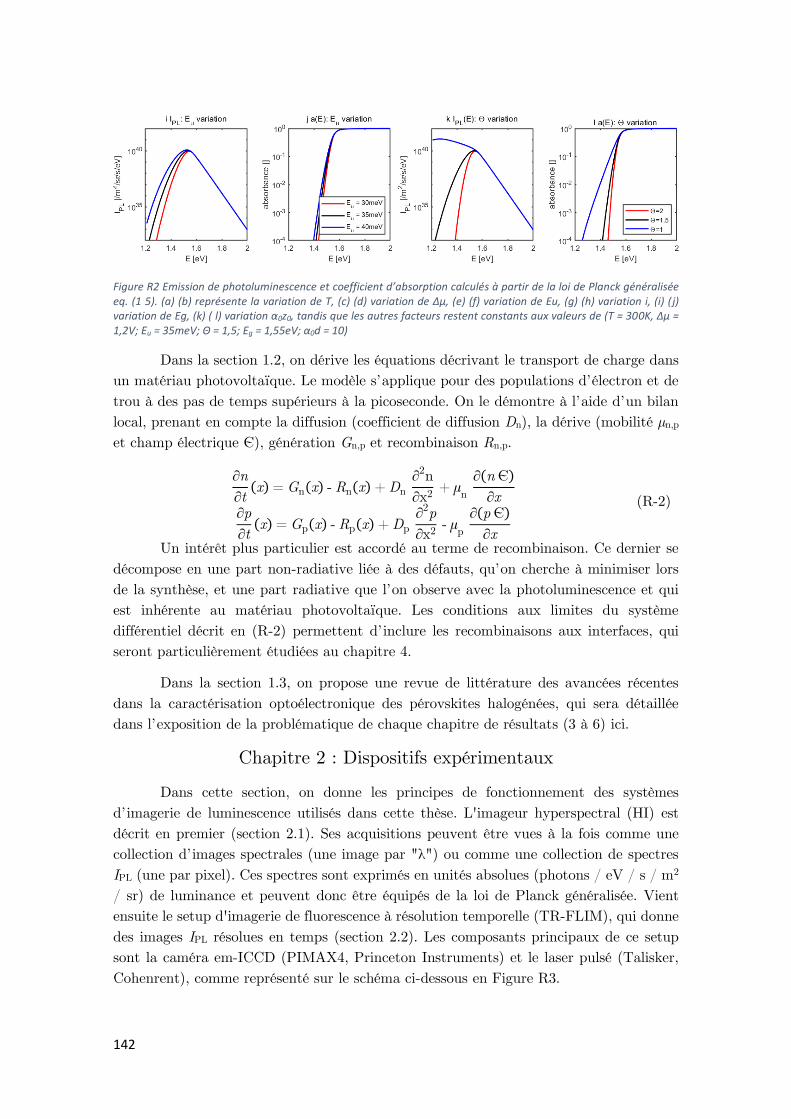
142
Figure R2 Emission de photoluminescence et coefficient d’absorption calculés à partir de la loi de Planck généralisée eq. (1 5). (a) (b) représente la variation de T, (c) (d) variation de Δµ, (e) (f) variation de Eu, (g) (h) variation i, (i) ( j) variation de Eg, (k) ( l) variation α0z0, tandis que les autres facteurs restent constants aux valeurs de (T = 300K, Δµ = 1,2V; Eu = 35meV; Θ = 1,5; Eg = 1,55eV; α0d = 10)
Dans la section 1.2, on dérive les équations décrivant le transport de charge dans
un matériau photovoltaïque. Le modèle s’applique pour des populations d’électron et de
trou à des pas de temps supérieurs à la picoseconde. On le démontre à l’aide d’un bilan
local, prenant en compte la diffusion (coefficient de diffusion Dn), la dérive (mobilité µn,p
et champ électrique Є), génération Gn,p et recombinaison Rn,p.
∂n
∂t(x) = Gn(x) - Rn(x) + Dn
∂2n
∂x2 + μ
n ∂(n Є)
∂x
∂p
∂t(x) = Gp(x) - Rp(x) + Dp
∂2p
∂x2 - μ
p ∂(p Є)
∂x
(R-2)
Un intérêt plus particulier est accordé au terme de recombinaison. Ce dernier se
décompose en une part non-radiative liée à des défauts, qu’on cherche à minimiser lors
de la synthèse, et une part radiative que l’on observe avec la photoluminescence et qui
est inhérente au matériau photovoltaïque. Les conditions aux limites du système
différentiel décrit en (R-2) permettent d’inclure les recombinaisons aux interfaces, qui
seront particulièrement étudiées au chapitre 4.
Dans la section 1.3, on propose une revue de littérature des avancées récentes
dans la caractérisation optoélectronique des pérovskites halogénées, qui sera détaillée
dans l’exposition de la problématique de chaque chapitre de résultats (3 à 6) ici.
Chapitre 2 : Dispositifs expérimentaux
Dans cette section, on donne les principes de fonctionnement des systèmes
d’imagerie de luminescence utilisés dans cette thèse. L'imageur hyperspectral (HI) est
décrit en premier (section 2.1). Ses acquisitions peuvent être vues à la fois comme une
collection d’images spectrales (une image par "λ") ou comme une collection de spectres
IPL (une par pixel). Ces spectres sont exprimés en unités absolues (photons / eV / s / m2
/ sr) de luminance et peuvent donc être équipés de la loi de Planck généralisée. Vient
ensuite le setup d'imagerie de fluorescence à résolution temporelle (TR-FLIM), qui donne
des images IPL résolues en temps (section 2.2). Les composants principaux de ce setup
sont la caméra em-ICCD (PIMAX4, Princeton Instruments) et le laser pulsé (Talisker,
Cohenrent), comme représenté sur le schéma ci-dessous en Figure R3.

143
Figure R3 Schéma du set-up TR-FLIM (Computer : ordinateur / Time-resolved images : images résolues en temps / Speckle removal : filtre anti-speckle / Wide-field illumination : illumination grand champ / Lens : objectif / Beam Splitter : lame séparatrice / Objective : objectif / Sample : échantillon)
Finalement, une nouvelle configuration adaptée pour obtenir des images 4D IPL
(2D spatiale, spectrale, temporelle) est présentée (section 2.3). Cette configuration a été
conçue par le candidat au doctorat et développée par un stagiaire de master sous sa
supervision. Un brevet protégeant ses principes de fonctionnement a été déposé (numéro
de dépôt 19315037.2). Il repose sur des principes liés à l’imagerie à pixel unique (SPI)
ainsi que sur l’utilisation d’une caméra à balayage de fente.
Chapitre 3 : Transport de charge latéral dans une cellule PV
Dans ce premier chapitre expérimental, on introduit la TR-FLIM comme méthode
de caractérisation optique des dispositifs optoélectroniques. Sous illumination à champ
large, nous étudierons la diffusion latérale et la recombinaison des porteurs de charge
minoritaires dans une cellule solaire à base d’arséniure de gallium (GaAs). Cette cellule
sert de dispositif de validation de principe. En effectuant l'analyse de son signal IPL, on
entend démontrer la pertinence de la caractérisation optoélectronique par TR-FLIM.
Dans un premier temps, les détails expérimentaux spécifiques à ce chapitre sont présentés
(section 3.1). Ensuite, on mène une exploration approfondie des acquisitions en traçant
les données le long de leurs dimensions spatiale et temporelle (section 3.2). Grâce à cette
analyse de données, on arrive à concevoir un modèle adapté aux phénomènes physiques
en jeu, à savoir le transport et la recombinaison dans le volume ou à proximité du contact
(section 3.3). Le modèle est dérivé de l'équation de continuité et est ensuite résolu
analytiquement. Une procédure de fit adapté aux données acquises par la TR-FLIM est
développée et appliquée pour reconstruire les déclins IPL expérimentaux (section 3.4). Les
propriétés optoélectroniques clés du dispositif considéré seront ensuite extraites de ces
ajustements. Enfin, on commente l’avantage particulier de l’éclairage à champ large
(section 3.5).

144
Chapitre 4 : Transport de charge dans l’épaisseur d’une pérovskite
Dans ce chapitre, on se concentre sur les propriétés de diffusion dans les matériaux
à base de pérovskite, car ils jouent un rôle crucial dans le fonctionnement des cellules
solaires, au cours desquels les porteurs de charge se diffusent vers les couches de transport.
Ces propriétés de diffusion ont deux aspects complémentaires: la sensibilité à un gradient
de concentration de porteurs (coefficient de diffusion D) et le temps moyen disponible
pour le processus de diffusion (durée de vie τ). Une large gamme de valeurs de D ont été
rapportées dans la littérature. On propose ici d’évaluer D et τ en mesurant les déclins
IPL dans les couches de pérovskite.
On décrit d’abord brièvement le jeu d’échantillons considéré, qui inclut plusieurs
compositions chimiques et conditions d’interface (section 4.1.1) et conduit à diverses
performances PV (section 4.1.2). Après avoir présenté un aperçu du jeu de données
(aspects spatiaux et temporels) dans la section 4.2, nous développons un modèle de
transport de porteurs de charge capable de reconstruire les déclins IPL dans la section 4.3.
On ajuste les coefficients du modèle différentiel de transport pour qu’il reproduise les
déclins IPL acquis, ce qui permet de caractériser complètement le transport en profondeur
et la recombinaison. Un exemple de reconstruction de déclins expérimentaux se trouve
en Figure R4 (a-b) pour deux interfaces arrières différentes et 3 niveaux d’illumination
croissants (Ф0). La figure R4(c) représente l’évolution de l’erreur de reconstruction à
proximité de la solution retenue, qui s’accroit rapidement pour des petits écarts de
paramètres et témoigne de la précision du fit. Comme ces coefficients de diffusion et
recombinaison ont été ajustés sur un jeu de conditions expérimentales assez large, ils
s’appliquent en particulier pour décrire le comportement du matériau sous un éclairement
constant de 1 soleil.

145
Figure R4 Déclins de IPL expérimentaux (lignes en pointillés) et ajustés numériquement (lignes simples) pour une perovskite à cations mixtes b). Différents ordres de grandeur du niveau d’illumination ont été testés. (c) Les iso-surfaces montrant un ensemble de paramètres (Reh * Dn NT) conduisant à une erreur de reconstruction ne dépassant pas 10% (rouge), 20% (vert), 50% (bleu) de l'erreur de reconstruction optimale.
Cette expérience est réalisée dans différents absorbeurs de pérovskite. On en
compare les résultats pour dégager des propriétés communes (section 4.4). Enfin, on
discute de la validité de différents modèles et de la signification physique des paramètres
d’ajustement dans la section 4.5.
Chapitre 5 : Transport de charge latéral dans une pérovskite
Le développement de cellules solaires à haute efficacité repose sur la gestion des
propriétés électroniques et optiques qui doivent être mesurées avec précision. Au fur et à
mesure que les rendements de conversion augmentent, un apport électronique et
photonique concomitant affecte les performances globales des dispositifs photovoltaïques.
On montre ici une méthode optique basée sur l’utilisation de techniques d’imagerie
multidimensionnelles complémentaires (voir Figure R5-(b)). Elle nous permet de collecter
et d’analyser le signal de luminescence avec une résolution spatiale, spectrale et
temporelle élevée. On l'applique pour sonder plusieurs propriétés de transport de
matériaux semi-conducteurs, permettant ainsi de découpler et de quantifier les

146
contributions électroniques et photoniques. Un exemple d'application est présenté sur une
couche mince de pérovskite halogénée pour laquelle une large gamme de propriétés de
transport est donnée dans la littérature, en fonction du procédé de fabrication du film
mais également de la technique de mesure (voir section 1.3).
Nous nous concentrons ici plus précisément sur les utilisations antérieures de
l'éclairage local sur une pérovskite. L'examen des images IPL a permis d'évaluer la
longueur de diffusion latérale des porteurs de charge et de souligner l'anisotropie du
transport dans des films CH3NH3PbI3 polycristallins non passivés. Des profils de diffusion
résolus dans le temps ont également été observés et l'élargissement des profils IPL permet
de mieux comprendre la mobilité des porteurs. Néanmoins, les approches
multidimensionnelles étaient toujours manquantes. En ce qui concerne le recyclage de
photons, plusieurs études ont souligné ce processus optique dans l’absorbeur de
pérovskite, soit en mettant l’accent sur le processus de recombinaison radiative lente,
soit en soulignant la régénération des porteurs de charge à longue distance. Cependant,
un modèle capable de décorréler les contributions électroniques et photoniques au
transport fait toujours défaut.
Dans ce chapitre, on utilise la plate-forme d'imagerie IPL développée sur des
couches minces en pérovskite, grâce à laquelle on réalise une expérience optique
quantitative basée sur un éclairage ponctuelle pulsé. Les détails expérimentaux
spécifiques à ce chapitre sont présentés dans la section 5.1, avant que la section 5.2 ne
donne un aperçu rapide de l'ensemble de données. Par son analyse, nous mettons en
évidence la contribution d'effets optiques tels que le recyclage de photons ainsi que la
propagation de photons lorsque la lumière émise est transportée latéralement sans être
résorbée (section 5.3, également Figure R5(a)). Ce dernier effet doit être pris en compte
pour éviter des propriétés de transport surestimées.
Figure R5 Schéma des observations expérimentales et des mécanismes physiques en jeu (a) Structure de l’échantillon et schéma montrant le mécanisme triple (diffusion des porteurs, propagation des photons et recyclage des photons) étudié ici (b) Schéma illustrant l’acquisition en 3 dimensions avec la fluorescence résolue en temps imagerie (TR-FLIM) ou hyperspectrale (HI), pour un éclairage ponctuel esquissé sur la face gauche.

147
Dans la section 5.4, nous quantifions ces propriétés de transport en résolvant de
manière rigoureuse l’équation de continuité dépendante du temps, donnant une méthode
valable pour plusieurs matériaux semi-conducteurs (validation sur échantillons III-V
InGaP produits à l’IPVF). La section 5.5 présente d'autres applications de la plateforme
d'imagerie multidimensionnelle sur un échantillon présentant des hétérogénéités.
(veinules à la surface de pérovskite riches en Cs).
Chapitre 6 : Transport de charge ambipolaire et migration
ionique dans une pérovskite
La physique fondamentale et les différentes propriétés de transport des pérovskites
aux halogénures n'ont pas encore été entièrement comprises et décrites En particulier,
une compréhension profonde de l'interaction entre les phénomènes de transport
électronique et ionique est cruciale pour l'optimisation de la collecte d'énergie après
absorption de la lumière. C’est également une question fondamentale, car le mouvement
ionique est généralement associé à la création de défauts, à des difficultés de contrôle du
dopage et à la faible durée de vie des porteurs. On ne s’attend pas à ce qu’un conducteur
semi-ionique soit aussi un excellent convertisseur photovoltaïque.
D'une part, le transport de charges électroniques dans les pérovskites aux
halogénures a été étudié de manière approfondie à l'aide de méthodes optiques avancées,
qui ont permis d'observer et de démêler les deux phénomènes principaux: la diffusion de
charges et le recyclage de photons (également décrit au chapitre précédent). En raison de
la faible énergie de liaison des excitons, les électrons et les trous se comportent comme
des porteurs libres à la température ambiante. Dans la plupart des études, on suppose
un transport de charge ambipolaire, la concentration de dopage étant connue pour être
faible. Jusqu'à présent, seuls quelques éléments de preuve d'un transport équilibré
électron / trou (à savoir, la mobilité électronique µn = la mobilité des trous µp) ont été
fournis jusqu'à présent.
D'autre part, la migration des ions a été étudiée tôt dans les pérovskites aux
halogénures. En 2014, Xiao et al. appliqué un champ électrique sur une structure latérale
CH3NH3PbI3 (MAPI) signalant un effet photovoltaïque commutable, expliqué
ultérieurement par la migration des ions. La migration des ions est également considérée
comme le principal responsable du comportement hystérétique des cellules PV. Malgré
un grand nombre d'observations expérimentales, la physique derrière une telle migration
ionique reste incertaine. En effet, leur énergie d'activation est toujours débattue, de même
que l'influence des joints de grains et l'impact de la température et de la lumière. Les
ions halogénures (I- / Br-) sont principalement concernés, étant donné que les MA+
organiques / FA+ et les Pb2+ inorganiques devraient dériver sur des échelles de temps
beaucoup plus longues.
Dans l'ensemble, les interactions complexes entre les ions, les électrons et les trous
ont récemment été soulignées, car il a été démontré que l'excès de porteurs de charge
accélère la migration des ions et que la création de défauts induite par l'iodure a été

148
dérivée en théorie. Des modèles numériques de diffusion de la dérive tenant compte à la
fois du mouvement des espèces ioniques et des porteurs de charge électroniques ont été
proposés. Le groupe de recherche de H. Snaith a récemment présenté l’incorporation du
BMIBF4, un sel ionique additif, comme moyen efficace de prévenir la migration des ions,
ouvrant ainsi la voie à la stabilité du PSC.
Dans ce chapitre, nous présentons un ensemble d'expériences sous polarisation
électrique basées sur une imagerie multidimensionnelle par luminescence afin de sonder
le transport électronique individuel ainsi que le transport ionique. Grâce à l'imagerie
multidimensionnelle, nous avons déjà pu étudier le transport latéral des porteurs de
charge dans des pérovskites mixtes à base d'halogénures (chapitres 4, 5). Ici, la mesure
des variations locales du signal de luminescence sous polarisation électrique permet un
accès direct aux propriétés de collecte et de transport des porteurs de charge pour chaque
type de porteur de charge. Dans une première série d'expériences, nous inhibons la
migration des ions en appliquant une polarisation électrique pulsée et observons
uniquement le transport électronique (section 6.2). Les images résolues dans le temps à
l'échelle nanoseconde nous permettent de séparer les contributions individuelles
d'électrons et de trous dans les mécanismes de transport. Les mobilités des porteurs sont
déterminées à environ 0.3 cm2 / V / s, avec une mobilité pour les trous deux fois
supérieure à celle des électrons. Ensuite, nous appliquons un biais électrique plus long (>
1 s) et mettons en évidence le rôle clé joué par la migration des ions dans les phénomènes
de transport (section 6.3), ainsi que leur impact sur la recombinaison non radiative. Nous
observons que l'enrichissement en halogénure induit un changement local de la
composition chimique et diminue la bande interdite des matériaux. La mesure de la
division du niveau de quasi-Fermi indique la formation de voies non radiatives dues à
l'accumulation d'halogénures. Les conclusions de ce chapitre sont résumées dans la Figure
R6.
Figure R6 Résumé des 2 expériences à l’étude dans le chapitre 6. La couche minche de pérovskite (violet) est contacté latéralement par des couches d’ITO (vert) et or (jaune). Un biais électrique rapide (<1µs) ou plus long est appliqué. Le champ résiduel est de 2500V/cm, car on considère un canal de 20µm avec un potentiel électrique de 5V.
149
Conclusion
Cette thèse se concentre sur la description de méthodes optiques permettant
d'évaluer quantitativement les propriétés de transport de porteurs de charge dans des
absorbeurs et des dispositifs photovoltaïques. Les expériences consistent en l’application
de techniques d'imagerie multidimensionnelle de luminescence. Elles incluent l'analyse
spatiale, spectrale et temporelle du flux lumineux émis par des matériaux photovoltaïques
sous excitation. Leur mise en œuvre a nécessité le développement d'assemblages optiques
ainsi que de méthodes numériques de traitement de données. Deux configurations ont été
principalement utilisées tout au long de cette thèse: (i) l’imageur hyperspectral (HI), qui
permet d’accéder aux images à résolution spectrale (une image par longueur d’onde) et
(ii) l’imageur à fluorescence à résolution temporelle (TR-FLIM) qui produit des images
à résolution temporelle (une image par unité de temps). Alors que le HI était déjà
complètement assemblé au début de ce travail, la configuration du TR-FLIM en était à
un stade préliminaire et son développement s’était terminé au cours de la thèse. Ses deux
composants principaux sont un laser pulsé et une caméra rapide. Ses principes de
fonctionnement ont été décrits en détail et sa preuve de concept sur une cellule
photovoltaïque de référence (à base de GaAs) a également été présentée. Il a démontré
que TR-FLIM permet l'évaluation du transport de charge et des propriétés de
recombinaison avec une seule expérience. En particulier, nous pourrions quantifier le
transport de charge latérale dans l'appareil. Nous avons montré comment l’utilisation de
l’éclairage et de la collecte à grand champ permettait de supprimer les artefacts liés à
l’éclairage local. En outre, cet éclairage à large champ constitue un scénario d'excitation
réaliste pour les matériaux et les dispositifs photovoltaïques, en raison de sa grande
surface et de sa puissance relativement faible.
Nous avons ensuite utilisé ces techniques de caractérisation avancées pour étudier
le transport de charges dans une classe émergente de matériaux aux propriétés
photovoltaïques très prometteuses: les pérovskites aux halogénures. Tout au long de ce
manuscrit, plusieurs expériences de transport ont permis de mettre en évidence la
diffusion de porteurs de charge dans des pérovskites à halogénures mixtes. La première
expérience était basée sur une excitation de surface importante, à la suite de laquelle les
porteurs de charge diffusent en profondeur dans la couche mince de pérovskite. Par
conséquent, nous pouvons sonder les propriétés de transport dans l'épaisseur de cette
couche. De manière remarquable, il est possible de quantifier la recombinaison sur les
surfaces avant et arrière ainsi que les mécanismes de recombinaison dans la masse. La
deuxième expérience était basée sur une excitation ponctuelle, à la suite de laquelle le
transport de charge est essentiellement radial, au moins après un certain temps où nous
pouvons négliger la diffusion en profondeur. La diffusion des porteurs s'est distinguée du
recyclage des photons, qui constitue un mécanisme de transport complémentaire par
lequel un photon de luminescence est réabsorbé et régénère une charge. Là encore, la
diffusion et la recombinaison des porteurs de charge ont été imagées avec une résolution
temporelle et spectrale élevée. Cela a permis de les quantifier au moyen d'algorithmes

150
d'optimisation qui adaptent les résultats expérimentaux aux modèles physiques
développés (équation de diffusion résolue dans le temps).
Les méthodes d'imagerie sont également adaptées à l'étude de l'impact des
inhomogénéités chimique et morphologique sur les propriétés optoélectroniques locales.
Ceci a été illustré par l'étude de l'influence des veinules apparaissant à la surface de la
pérovskite riche en Cs. Nous avons remarqué que les caractéristiques morphologiques
modifient les propriétés de découplage de la lumière, ce qui entrave l'analyse directe du
signal IPL. Nous avons également pu établir une corrélation entre les hétérogénéités
chimiques, les variations de bandes interdites et celles de durées de vie. Ces corrélations
soulignent le rôle bénéfique des rides riches en Cs dans les propriétés de transport.
Néanmoins, il conviendrait de poursuivre le développement du couplage entre la
modélisation 2D-3D et l'imagerie IPL afin d'obtenir une quantification appropriée du
transport dans des matériaux non homogènes.
Finalement, nous avons appliqué des techniques d’imagerie IPL
multidimensionnelles pour sonder des structures latérales dotées d’un canal pérovskite de
20 µm de large entre deux électrodes. L'objectif principal était d'aller plus loin que nos
études précédentes et de séparer les propriétés de transport d'électrons et de trous, ce qui
est difficile dans une couche intrinsèque telle que la pérovskite. La stabilité du matériau
liée à la migration des ions devait également être prise en compte. En appliquant une
polarisation électrique rapide sur le canal (<1 µs), nous avons d’abord isolé la dérive des
porteurs de charge de celle des ions composant la pérovskite. Les mobilités des électrons
et des trous ont été quantifiées séparément (µp/µn = 2.25 ± 0.23). Leur valeur presque
égale justifie leur traitement symétrique précédent (ambipolaire). Ensuite, des
expériences à plus longue échelle (champ électrique appliqué pendant 10 minutes) nous
ont également permis d'imager le transport des ions halogénures. Cette expérience
multidimensionnelle nous a rapprochés plus que jamais des principes de fonctionnement
d'un appareil PV, qui fonctionne avec lumière et biais. L’accumulation d’ions au niveau
de l’électrode positive entraîne une réduction locale de la durée de vie des porteurs de
charge.
En résumé, concernant le transport dans les pérovskites halogénées, nous pouvons
affirmer que les recombinaisons aux interfaces constituent certainement le principal canal
de perte dans les cellules solaires à pérovskite. Cette affirmation donne de précieuses
orientations pour les prochaines approches synthétiques qui devraient se concentrer sur
le design d'interfaces passivées. En ce qui concerne le transport de charges dans le volume
de la pérovskite, nous avons systématiquement quantifié des valeurs relativement faibles
de la mobilité des porteurs de charges (entre 0.2 et 1 cm2 / V / s). Dans tous les cas,
cette diffusion lente reste compensée par la longue durée de vie des porteurs de charge
(1μs), ce qui garantit leur collecte dans un appareil PV. L’industrialisation des cellules
solaires en pérovskite devra être précédée de réels progrès sur deux points majeurs : la
stabilité des dispositifs et l’ « upscale » des techniques de fabrication. L'ensemble des
techniques de caractérisation introduites dans ce manuscrit s'appliquerait à une étude

151
traitant de ces questions. Du côté de la stabilité, les prochaines campagnes de mesure
pourraient porter sur l’évolution des propriétés optoélectroniques du fait que le matériau
est soumis à des contraintes environnementales (humidité, lumière, oxygène). Du côté de
l’« upscale », la grande polyvalence de l’échelle micro à la macro pourrait permettre de
localiser et d’identifier les défauts liés à la production à grande échelle. De plus, le fait
de disposer d'images à résolution spectrale et temporelle disponibles à chaque étape de la
production / du vieillissement met en évidence le besoin d'algorithmes de post-traitement
efficaces, dans lesquels les approches d'apprentissage automatique pourraient jouer un
rôle.
Pour approfondir encore ces études du transport de charges dans les pérovskites
halogénées, une nouvelle configuration dédiée à l’imagerie IPL 4D a été conçue. Il permet
d’acquérir des ensembles de données IPL 4D (2D spatiales + spectrales + temporelles en
une seule expérience) en combinant le concept d’imagerie à pixel unique à une caméra à
balayage. Comparé à une simple combinaison de configurations HI et TR-FLIM, il permet
d’avoir une meilleure sensibilité optique (nous ne sélectionnons pas à la fois l’énergie et
le temps de décroissance du signal), ainsi qu’une meilleure résolution temporelle et
spectrale. Dans ce manuscrit, nous avons décrit ses principes de fonctionnement, protégés
par un brevet déposé, ainsi que son développement initial réalisé avec l'aide d'un étudiant
à la maîtrise. Une première preuve de concept obtenue sur une couche de pérovskite a
été présentée. Cela a ouvert la voie à une caractérisation plus avancée des matériaux PV.
Les prochains développements de cette configuration incluent notamment la calibration,
grâce auquel on pourrait fitter l'hypercube acquis à la loi de Planck généralisée, afin de
cartographier les QFLS avec une résolution de l'ordre de la picoseconde. Cela devrait
révéler les mécanismes fondamentaux de séparation, de transport, de collecte et de
recombinaison de charge en présence de champ électrique ou d'hétéro-interfaces qui
présentent un grand intérêt pour le moment.

152
Communication & Recognition
Peer-reviewed publications:
1. A. Bercegol, G. El-Hajje, D. Ory, and L. Lombez, « Determination of transport
properties in optoelectronic devices by time-resolved fluorescence imaging » J. Appl.
Phys., 2017, 122 (20), p. 203102
2. A. Bercegol, J.F. Ramos, A. Rebai, T. Guillemot, D. Ory, J. Rousset, L.Lombez,
« Slow diffusion and long lifetime in metal halide perovskite for photovoltaics », J. Phys.
Chem. C, 2018, 122 (43), pp 24570–24577
3. A. Bercegol, J.F. Ramos, D. Ory, A. Rebai, J-F. Guillemoles , J. Rousset, L.
Lombez, « Spatial inhomogeneity analysis of Cs-rich wrinkles in triple cation
perovskite », J. Phys. Chem. C, 2018 122 (41), pp 23345–23351
4. J. F. Ramos, S. Jutteau, J. Posada, A. Bercegol, A. Rebai, T. Guillemot, R.
Bodeux, N. Schneider, N. Loones, D. Ory, C. Broussillou, G. Goaer, L. Lombez, J.
Rousset « Highly efficient MoOx-free semitransparent perovskite solar cell for 4T tandem
application improving the efficiency of commercially-available Al-BSF silicon » Scientific
Reports 2018 8:16139
5. A. Bercegol, D. Ory, D. Suchet, S. Cacovich, O. Fournier, J. Rousset, L.
Lombez, « Quantitative optical assessment of electronic and photonic properties in halide
perovskite », Nature Communications 2019, 10:1586
6. A. Bercegol, S. Cacovich, S. Mejaouri, A. Yaïche, G. Vidon, J-B. Puel, C.
Longeaud, J-F. Guillemoles, S. Jutteau, J. Rousset, D. Ory, L. Lombez, « Imaging
electron, hole and ion transport in halide perovskite », submitted 2019
7. Ben Slimane, A. Michaud, O. Mauguin, X. Lafosse, A. Bercegol, L. Lombez, J-
C. Harmand, S. Collin, « 1.73 eV AlGaAs/InGaP heterojunction solar cell grown by
MBE with 18.7% efficiency », Progress in Photovoltaics, under revision 2019
8. S. Cacovich, D. Messou, A. Bercegol, S Bechu, A. Yaïche, H. Shafique, J.
Rousset, P. Schulz, M. Bouttemy, L. Lombez, « Light-induced passivation in triple cation
halide perovskites: interplay between surface chemistry and transport properties », in
preparation 2019
Patent
1. A. Bercegol, D. Ory, and L. Lombez, « Time-resolved hyperspectral single pixel
imaging (THYSPI) of low-emissive objects » deposit number 19315037.2 2019
153
Conference proceedings:
1. A. Bercegol, D. Ory, J. F. Ramos, A. Rebai, J. Rousset, L. Lombez,
« Determination of transport properties in optoelectronic devices by time-resolved
fluorescence imaging », SPIE Photonics West Proceedings 2018
2. A. Bercegol, G. El-Hajje, D. Ory, L. Lombez, « Time-resolved fluorescence
imaging as a self-consistent characterization method for photovoltaic materials », 7th
WCPEC Proceedings 2018
3. A. Bercegol, J.F. Ramos, A. Rebai, D. Ory, J. Rousset, L. Lombez
« Investigation of in-depth transport and absorption properties of various perovskite
materials using luminescence imaging », 7th WCPEC Proceedings 2018
4. A. Bercegol, D. Ory, L. Lombez, « Time-resolved imaging of lateral charge
carrier transport in photovoltaic absorbers » SPIE Photonics West Proceedings 2019
5. A. Bercegol, D. Ory, D. Suchet, S. Cacovich, O. Fournier, J. Rousset, L.
Lombez, « Quantitative optical assessment of electronic and photonic properties », 46th
IEEE PVSC Proceedings 2019
6. D. Ory, A. Bercegol, D. Suchet, M. Legrand, J-B. Puel, A. Michaud, A. Ben
Slimane, S. Collin, S. Cacovich, O. Fournier, A. Rebai, J. Rousset, J-F. Guillemoles, L.
Lombez, « Multi-dimensional luminescence imaging: accessing to transport properties »,
46th IEEE PVSC Proceedings 2019
7. A. Michaud, A. Ben Slimane, A. Bercegol, R. Lachaume, J-C. Harmand, J.F.
Martin, S. Collin, « Elaboration of III-V top cell for tandem with Silicon », 46th IEEE
PVSC Proceedings 2019
Awards
45th IEEE PVSC: Graduate student assistant
46th IEEE PVSC: Finalist for best student award (presentation: « Quantitative optical
assessment of electronic and photonic properties »)
36th EU-PVSEC: Student award (presentation: « Multi-dimensional imaging of
electron/hole transport in triple cation perovskites »)

ABSTRACT
In optoelectronics, and in the field of photovoltaics in particular, luminescence analysis
methods are used to optimize devices. Being contactless and non-destructive, they can be used at
different stages in the manufacture of a solar cell. They are based on the fact that the luminescence
intensity is directly related to the product of charge carrier concentrations. In this thesis, we focus
on describing methods based on multidimensional luminescence imaging. This technique includes
the spatial, spectral and temporal analysis of light flux emitted by photovoltaic materials. Its
implementation requires the development of optical assemblies as well as digital methods of data
processing. We rely on hyperspectral imaging (spatial-spectral) and TR-FLIM (spatial-temporal)
techniques. Correlative analyzes of the acquired luminescence cubes enables the study of an
emerging class of materials with very promising photovoltaic properties: halide perovskites. Their
electronic (diffusion/recombination), photonic and ionic transport properties are characterized
thanks to multi-dimensional luminescence imaging.
MOTS CLÉS
Transport de charge / Caractérisation optique / Photoluminescence / Pérovskite /
Photovoltaïque
RÉSUMÉ
En optoélectronique, et dans le domaine du photovoltaïque en particulier, les méthodes
d'analyse de luminescence servent à optimiser les dispositifs. Étant sans contact et non destructives,
elles peuvent être utilisées à différentes étapes de la fabrication d’une cellule solaire. Elles s’appuient
sur le fait que l’intensité de luminescence est directement liée au produit des concentrations de
porteur de charges. Dans cette thèse, on s’intéresse plus particulièrement à l’imagerie
multidimensionnelle de luminescence, qui inclut l’analyse spatiale, spectrale et temporelle de la
luminescence des matériaux photovoltaïques. Sa mise en œuvre requiert le développement de
montages optiques ainsi que de méthodes numériques de traitement des données. On s’appuie sur
un imageur hyperspectral (spatial-spectral) et sur la TR-FLIM (spatial-temporel). La corrélation
des résultats acquis permet l’étude d’une famille émergente de matériaux aux propriétés
photovoltaïques prometteuses : les pérovskites halogénées. Leurs propriétés de transport
électronique (diffusion/recombinaison), photonique et ionique sont caractérisées.
KEYWORDS
Charge transport / Optical chatacterization / Photoluminescence / Pérovskite / Photovoltaics