TPS53128 Dual Synchronous Step-Down Controller With Auto ...
38
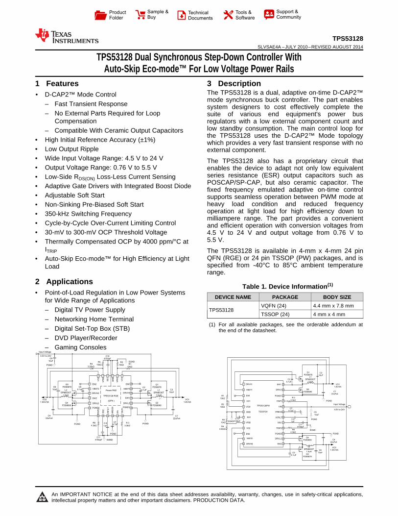
TPS53128PW TSSOP24 SW1 DRVL1 DRVH1 VBST1 EN1 VFB2 VO2 VO1 VFB1 GND TRIP2 VREG5 TRIP1 PGND1 3 24 8 21 22 23 15 9 16 18 19 20 5 7 1 10 11 VIN SS2 DRVH2 VBST2 EN2 PGND2 DRVL2 SW2 13 14 12 V5FILT 17 SS1 6 2 4 PGND PGND SGND PGND SGND Input Voltage 4.5V to 24V C9 10uF VO1 1.8V/4A C1 22uFx4 C3 10uF Q1 FDS8878 L1 SPM6530T 1.5uH Q2 FDS8690 C2 0.1uF R3 3.3kΩ R6 4.3kΩ C8 1uF C7 4.7uF L2 SPM6530T 1.5uH VO2 1.05V/4A C6 10uF Q3 FDS8878 Q4 FDS8690 C5 0.1uF R2 10kΩ R1 13kΩ R5 10kΩ R4 3.52kΩ C11 4700pF C10 4700pF C4 22uFx4 TPS53128 RGE (QFN ) DRVH2 VBST2 EN2 SW1 DRVL1 DRVH1 VBST1 EN1 VFB2 VO2 VO1 VFB1 GND PGND2 PGND1 DRVL2 SW2 C3 10uF VO2 1.05V/4A C5 0.1uF Input Voltage PGND C4 22uFx4 10uF C6 10uF L1 PGND Q3 FDS8878 R4 3.52kΩ R5 10kΩ PGND SGND R6 4.3kΩ 24 22 23 19 20 21 13 14 15 16 17 18 8 9 10 11 12 7 1 2 3 4 5 6 Power PAD PGND SGND SS1 SS2 TRIP2 V5FILT VREG5 VIN TRIP1 4.5V to 24V VO1 1.8V/4A Q4 FDS8690 Q1 FDS8878 C9 Q2 FDS8690 L2 SPM6530T 1.5uH L1 SPM6530T 1.5uH C2 0.1uF R3 3.3kΩ R2 10kΩ C8 1uF C7 4.7uF R1 13kΩ C1 22uFx4 C11 4700pF C10 4700pF Product Folder Sample & Buy Technical Documents Tools & Software Support & Community An IMPORTANT NOTICE at the end of this data sheet addresses availability, warranty, changes, use in safety-critical applications, intellectual property matters and other important disclaimers. PRODUCTION DATA. TPS53128 SLVSAE4A – JULY 2010 – REVISED AUGUST 2014 TPS53128 Dual Synchronous Step-Down Controller With Auto-Skip Eco-mode™ For Low Voltage Power Rails 1 1 Features 1• D-CAP2™ Mode Control – Fast Transient Response – No External Parts Required for Loop Compensation – Compatible With Ceramic Output Capacitors • High Initial Reference Accuracy (±1%) • Low Output Ripple • Wide Input Voltage Range: 4.5 V to 24 V • Output Voltage Range: 0.76 V to 5.5 V • Low-Side R DS(ON) Loss-Less Current Sensing • Adaptive Gate Drivers with Integrated Boost Diode • Adjustable Soft Start • Non-Sinking Pre-Biased Soft Start • 350-kHz Switching Frequency • Cycle-by-Cycle Over-Current Limiting Control • 30-mV to 300-mV OCP Threshold Voltage • Thermally Compensated OCP by 4000 ppm/°C at I TRIP • Auto-Skip Eco-mode™ for High Efficiency at Light Load 2 Applications • Point-of-Load Regulation in Low Power Systems for Wide Range of Applications – Digital TV Power Supply – Networking Home Terminal – Digital Set-Top Box (STB) – DVD Player/Recorder – Gaming Consoles 3 Description The TPS53128 is a dual, adaptive on-time D-CAP2™ mode synchronous buck controller. The part enables system designers to cost effectively complete the suite of various end equipment's power bus regulators with a low external component count and low standby consumption. The main control loop for the TPS53128 uses the D-CAP2™ Mode topology which provides a very fast transient response with no external component. The TPS53128 also has a proprietary circuit that enables the device to adapt not only low equivalent series resistance (ESR) output capacitors such as POSCAP/SP-CAP, but also ceramic capacitor. The fixed frequency emulated adaptive on-time control supports seamless operation between PWM mode at heavy load condition and reduced frequency operation at light load for high efficiency down to milliampere range. The part provides a convenient and efficient operation with conversion voltages from 4.5 V to 24 V and output voltage from 0.76 V to 5.5 V. The TPS53128 is available in 4-mm x 4-mm 24 pin QFN (RGE) or 24 pin TSSOP (PW) packages, and is specified from -40°C to 85°C ambient temperature range. Table 1. Device Information (1) DEVICE NAME PACKAGE BODY SIZE TPS53128 VQFN (24) 4.4 mm x 7.8 mm TSSOP (24) 4 mm x 4 mm (1) For all available packages, see the orderable addendum at the end of the datasheet.
-
Upload
khangminh22 -
Category
Documents
-
view
6 -
download
0
Transcript of TPS53128 Dual Synchronous Step-Down Controller With Auto ...
TPS53128PW
TSSOP24
SW1
DRVL1
DRVH1
VBST1
EN1
VFB2
VO2
VO1
VFB1
GND
TRIP2
VREG5
TRIP1
PGND13
24
8
21
22
23
15
9 16
18
19
205
7
1
10
11
VIN
SS2
DRVH2
VBST2
EN2 PGND2
DRVL2
SW2 13
14
12
V5FILT
17
SS1
6
2
4 PGND
PGND
SGND
PGNDSGND
Input Voltage
4.5V to 24V
C9
10uF
VO1
1.8V/4A
C1
22uFx4
C3
10uF
Q1
FDS8878L1
SPM6530T
1.5uH
Q2
FDS8690
C2
0.1uF
R3
3.3kΩ
R6
4.3kΩ
C8
1uF
C7
4.7uF
L2
SPM6530T
1.5uH
VO2
1.05V/4AC6
10uFQ3
FDS8878
Q4
FDS8690
C5
0.1uF
R2
10kΩ
R1
13kΩ
R5
10kΩ
R4
3.52kΩ
C11
4700pF
C10
4700pF
C4
22uFx4
TPS53128 RGE
(QFN )
DRVH2
VBST2
EN2
SW1
DRVL1
DRVH1
VBST1
EN1
VF
B2
VO
2
VO
1
VF
B1
GN
D
PGND2 PGND1
DRVL2
SW2
C3
10uF
VO2
1.05V/4A
C5
0.1uF
Input Voltage
PGND
C4
22uFx4
10uF
C6
10uF
L1
PGND
Q3
FDS8878
R4
3.52kΩ
R5
10kΩ
PGND
SGND
R6
4.3kΩ
24
22
23
19
20
21
13 14 15 16 17 18
8
9
10
11
12
7
123456
Power PAD
PGND
SGND
SS
1
SS
2
TR
IP2
V5
FIL
T
VR
EG
5
VIN
TR
IP1
4.5V to 24V
VO1
1.8V/4AQ4
FDS8690
Q1
FDS8878
C9
Q2
FDS8690
L2
SPM6530T
1.5uH
L1
SPM6530T
1.5uH
C2
0.1uF
R3
3.3kΩ
R2
10kΩ
C8
1uF
C74.7uF
R1
13kΩ
C1
22uFx4
C11
4700pF
C10
4700pF
Product
Folder
Sample &Buy
Technical
Documents
Tools &
Software
Support &Community
An IMPORTANT NOTICE at the end of this data sheet addresses availability, warranty, changes, use in safety-critical applications,intellectual property matters and other important disclaimers. PRODUCTION DATA.
TPS53128SLVSAE4A –JULY 2010–REVISED AUGUST 2014
TPS53128 Dual Synchronous Step-Down Controller WithAuto-Skip Eco-mode™ For Low Voltage Power Rails
1
1 Features1• D-CAP2™ Mode Control
– Fast Transient Response– No External Parts Required for Loop
Compensation– Compatible With Ceramic Output Capacitors
• High Initial Reference Accuracy (±1%)• Low Output Ripple• Wide Input Voltage Range: 4.5 V to 24 V• Output Voltage Range: 0.76 V to 5.5 V• Low-Side RDS(ON) Loss-Less Current Sensing• Adaptive Gate Drivers with Integrated Boost Diode• Adjustable Soft Start• Non-Sinking Pre-Biased Soft Start• 350-kHz Switching Frequency• Cycle-by-Cycle Over-Current Limiting Control• 30-mV to 300-mV OCP Threshold Voltage• Thermally Compensated OCP by 4000 ppm/°C at
ITRIP
• Auto-Skip Eco-mode™ for High Efficiency at LightLoad
2 Applications• Point-of-Load Regulation in Low Power Systems
for Wide Range of Applications– Digital TV Power Supply– Networking Home Terminal– Digital Set-Top Box (STB)– DVD Player/Recorder– Gaming Consoles
3 DescriptionThe TPS53128 is a dual, adaptive on-time D-CAP2™mode synchronous buck controller. The part enablessystem designers to cost effectively complete thesuite of various end equipment's power busregulators with a low external component count andlow standby consumption. The main control loop forthe TPS53128 uses the D-CAP2™ Mode topologywhich provides a very fast transient response with noexternal component.
The TPS53128 also has a proprietary circuit thatenables the device to adapt not only low equivalentseries resistance (ESR) output capacitors such asPOSCAP/SP-CAP, but also ceramic capacitor. Thefixed frequency emulated adaptive on-time controlsupports seamless operation between PWM mode atheavy load condition and reduced frequencyoperation at light load for high efficiency down tomilliampere range. The part provides a convenientand efficient operation with conversion voltages from4.5 V to 24 V and output voltage from 0.76 V to5.5 V.
The TPS53128 is available in 4-mm x 4-mm 24 pinQFN (RGE) or 24 pin TSSOP (PW) packages, and isspecified from -40°C to 85°C ambient temperaturerange.
Table 1. Device Information(1)
DEVICE NAME PACKAGE BODY SIZE
TPS53128VQFN (24) 4.4 mm x 7.8 mmTSSOP (24) 4 mm x 4 mm
(1) For all available packages, see the orderable addendum atthe end of the datasheet.

2
TPS53128SLVSAE4A –JULY 2010–REVISED AUGUST 2014 www.ti.com
Submit Documentation Feedback Copyright © 2010–2014, Texas Instruments Incorporated
Table of Contents1 Features .................................................................. 12 Applications ........................................................... 13 Description ............................................................. 14 Revision History..................................................... 25 Pin Configuration and Functions ......................... 36 Specifications......................................................... 4
6.1 Absolute Maximum Ratings ...................................... 46.2 Handling Ratings ...................................................... 46.3 Recommended Operating Conditions....................... 46.4 Thermal Information .................................................. 56.5 Electrical Characteristics........................................... 56.6 Typical Characteristics .............................................. 7
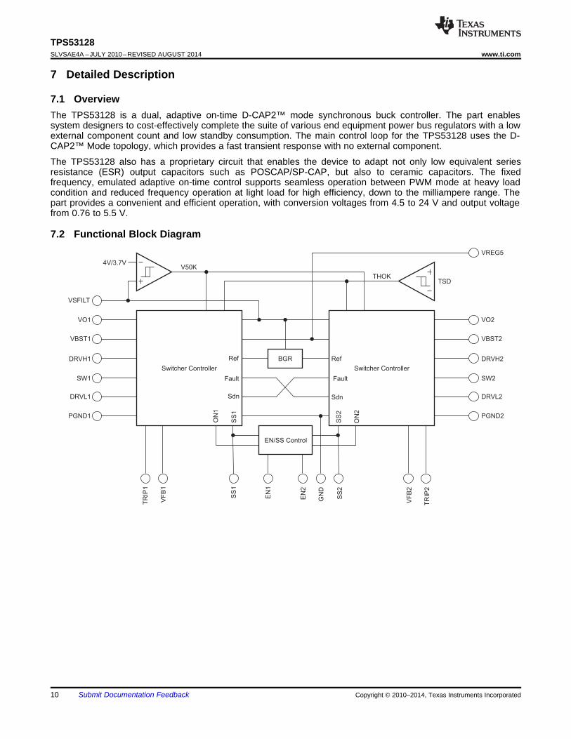
7 Detailed Description ............................................ 107.1 Overview ................................................................. 107.2 Functional Block Diagram ....................................... 10
7.3 Feature Description................................................. 117.4 Device Functional Modes........................................ 14
8 Application and Implementation ........................ 158.1 Application Information............................................ 158.2 Typical Application ................................................. 15
9 Power Supply Recommendations ...................... 2310 Layout................................................................... 24
10.1 Layout Guidelines ................................................. 2410.2 Layout Example .................................................... 24
11 Device and Documentation Support ................. 2511.1 Trademarks ........................................................... 2511.2 Electrostatic Discharge Caution............................ 2511.3 Glossary ................................................................ 25
12 Mechanical, Packaging, and OrderableInformation ........................................................... 25
4 Revision HistoryNOTE: Page numbers for previous revisions may differ from page numbers in the current version.
Changes from Original (July 2010) to Revision A Page
• Changed format to meet latest data sheet standards; added new sections and moved existing sections............................ 1• Added Eco-mode bullet to Features....................................................................................................................................... 1• Added QFN and TSSOP schematics .................................................................................................................................... 1• Added V(ESD) value ................................................................................................................................................................. 4• Added thermal information .................................................................................................................................................... 5• Changed min for VVREG5 ........................................................................................................................................................ 5• Changed max for RDRVL at -100 mA ...................................................................................................................................... 5• Changed the I(SSC) Min value From: -1.5 to -2.5 μA and the Max value From: -2.5 To: -1.5 μA ....................................... 6• Added Overview section. ..................................................................................................................................................... 10• Added Device Functional Modes ......................................................................................................................................... 14• Added Design Parameter values ......................................................................................................................................... 16• Added Power Supply Recommendations ............................................................................................................................ 23• Added Layout Example image.............................................................................................................................................. 24

TRIP1
VIN
VO1
VFB1
GND
SS1
VREG5
V5FILT
SS 2
TRIP2
VFB2
VO2
EN
2E
N1
VB
ST
1
DR
VH
1
SW
1
DR
VL1
PG
ND
1
VB
ST
2
DR
VH
2
SW
2
DR
VL2
PG
ND
216
15
14
13
18
17
1
2
3
4
5
6
9 10
11
127 8
23
2024
22
21
19
QFN PACKAGE
(TOP VIEW)
VBST1
EN1
VO1
VFB1
GND
SS1
VFB2
VO2
EN2
VBST2
DRVH1 SW1
DRVL1
PGND1
TRIP1
VIN
VREG5
V5FILT
SS2
TRIP2
PGND2
DRVL2
SW2DRVH2
24
23
22
21
20
19
18
17
1
2
3
4
5
6
7
8
9
10
11
12
16
15
14
13
TSSOP PACKAGE(TOP VIEW)
3
TPS53128www.ti.com SLVSAE4A –JULY 2010–REVISED AUGUST 2014
Submit Documentation FeedbackCopyright © 2010–2014, Texas Instruments Incorporated
5 Pin Configuration and Functions
Table 2. Pin FunctionsPIN
I/O DESCRIPTIONNAME RGE PW
VBST1,VBST2 23, 8 2, 11 I
Supply input for high-side NFET driver. Bypass to SWx with a high-quality 0.1-μF ceramiccapacitor. An external schottky diode can be added from VREG5 if forward drop is critical todrive the high-side FET.
EN1, EN2 24, 7 3, 10 I Enable. Pull High to enable SMPS.
VO1, VO2 1, 6 4, 9 I Output voltage inputs for on-time adjustment and output discharge. Connect directly to theoutput voltage.
VFB1,VFB2 2, 5 5, 8 I D-CAP2 feedback inputs. Connect to output voltage with resistor divider.
GND 3 6 I Signal ground pin. Connect to PGND1, PGND2 and system ground at a single point.DRVH1,DRVH2 22, 9 1, 12 O High-side N-Channel MOSFET gate driver outputs. SWx referenced drivers switch between
SWx (OFF) and VBSTx (ON).SW1, SW2 21, 10 24, 13 I/O Switch node connections for both the high-side drivers and the over current comparators.DRVL1,DRVL2 20, 11 23, 14 O Low-side N-Channel MOSFET gate driver outputs. PGND referenced drivers switch between
PGNDx (OFF) and VREG5 (ON).PGND1,PGND2 19, 12 22, 15 I/O Power ground connections for both the low-side drivers and the over current comparators.
Connect PGND1, PGND2 and GND strongly together near the IC.TRIP1,TRIP2 18, 13 21, 16 I Over current threshold programming pin. Connect to GND with a resistor to GND to set
threshold for low-side RDS(ON) current limit.
VIN 17 20 I Supply Input for 5-V linear regulator. Bypass to GND with a minimum high-quality 0.1-μFceramic capacitor.
V5FILT 15 18 I5-V supply input for the entire control circuitry except the MOSFET drivers. Bypass to GNDwith a minimum high-quality 1.0-μF ceramic capacitor. V5FILT is connected to VREG5 viaan internal 10-Ω resistor.
VREG5 16 19 OOutput of 5-V linear regulator and supply for MOSFET drivers. Bypass to GND with aminimum high-quality 4.7-μF ceramic capacitor. VREG5 is connected to V5FILT via aninternal 10-Ω resistor.
SS1, SS2 4,14 7, 17 O Soft-start programming pin. Connect capacitor from SSx pin to GND to program soft-starttime.
4
TPS53128SLVSAE4A –JULY 2010–REVISED AUGUST 2014 www.ti.com
Submit Documentation Feedback Copyright © 2010–2014, Texas Instruments Incorporated
(1) Stresses beyond those listed under "absolute maximum ratings" may cause permanent damage to the device. These are stress ratingsonly and functional operation of the device at these or any other conditions beyond those indicated under "recommended operatingconditions" are not implied. Exposure to absolute-maximum-rated conditions for extended periods may affect device reliability.
6 Specifications
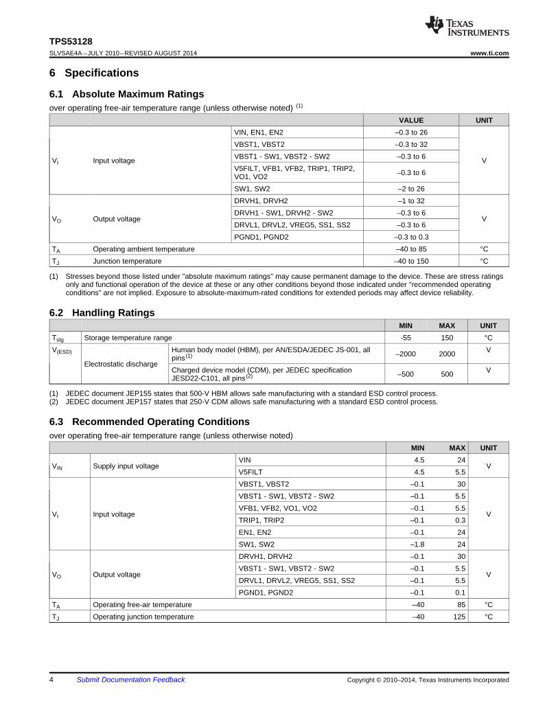
6.1 Absolute Maximum Ratingsover operating free-air temperature range (unless otherwise noted) (1)
VALUE UNIT
VI Input voltage
VIN, EN1, EN2 –0.3 to 26
V
VBST1, VBST2 –0.3 to 32VBST1 - SW1, VBST2 - SW2 –0.3 to 6V5FILT, VFB1, VFB2, TRIP1, TRIP2,VO1, VO2 –0.3 to 6
SW1, SW2 –2 to 26
VO Output voltage
DRVH1, DRVH2 –1 to 32
VDRVH1 - SW1, DRVH2 - SW2 –0.3 to 6DRVL1, DRVL2, VREG5, SS1, SS2 –0.3 to 6PGND1, PGND2 –0.3 to 0.3
TA Operating ambient temperature –40 to 85 °CTJ Junction temperature –40 to 150 °C
(1) JEDEC document JEP155 states that 500-V HBM allows safe manufacturing with a standard ESD control process.(2) JEDEC document JEP157 states that 250-V CDM allows safe manufacturing with a standard ESD control process.
6.2 Handling RatingsMIN MAX UNIT
Tstg Storage temperature range -55 150 °CV(ESD)
Electrostatic discharge
Human body model (HBM), per AN/ESDA/JEDEC JS-001, allpins (1) –2000 2000 V
Charged device model (CDM), per JEDEC specificationJESD22-C101, all pins (2) –500 500 V
6.3 Recommended Operating Conditionsover operating free-air temperature range (unless otherwise noted)
MIN MAX UNIT
VIN Supply input voltageVIN 4.5 24
VV5FILT 4.5 5.5
VI Input voltage
VBST1, VBST2 –0.1 30
V
VBST1 - SW1, VBST2 - SW2 –0.1 5.5VFB1, VFB2, VO1, VO2 –0.1 5.5TRIP1, TRIP2 –0.1 0.3EN1, EN2 –0.1 24SW1, SW2 –1.8 24
VO Output voltage
DRVH1, DRVH2 –0.1 30
VVBST1 - SW1, VBST2 - SW2 –0.1 5.5DRVL1, DRVL2, VREG5, SS1, SS2 –0.1 5.5PGND1, PGND2 –0.1 0.1
TA Operating free-air temperature –40 85 °CTJ Operating junction temperature –40 125 °C
5
TPS53128www.ti.com SLVSAE4A –JULY 2010–REVISED AUGUST 2014
Submit Documentation FeedbackCopyright © 2010–2014, Texas Instruments Incorporated
(1) For more information about traditional and new thermal metrics, see the IC Package Thermal Metrics application report, SPRA953.
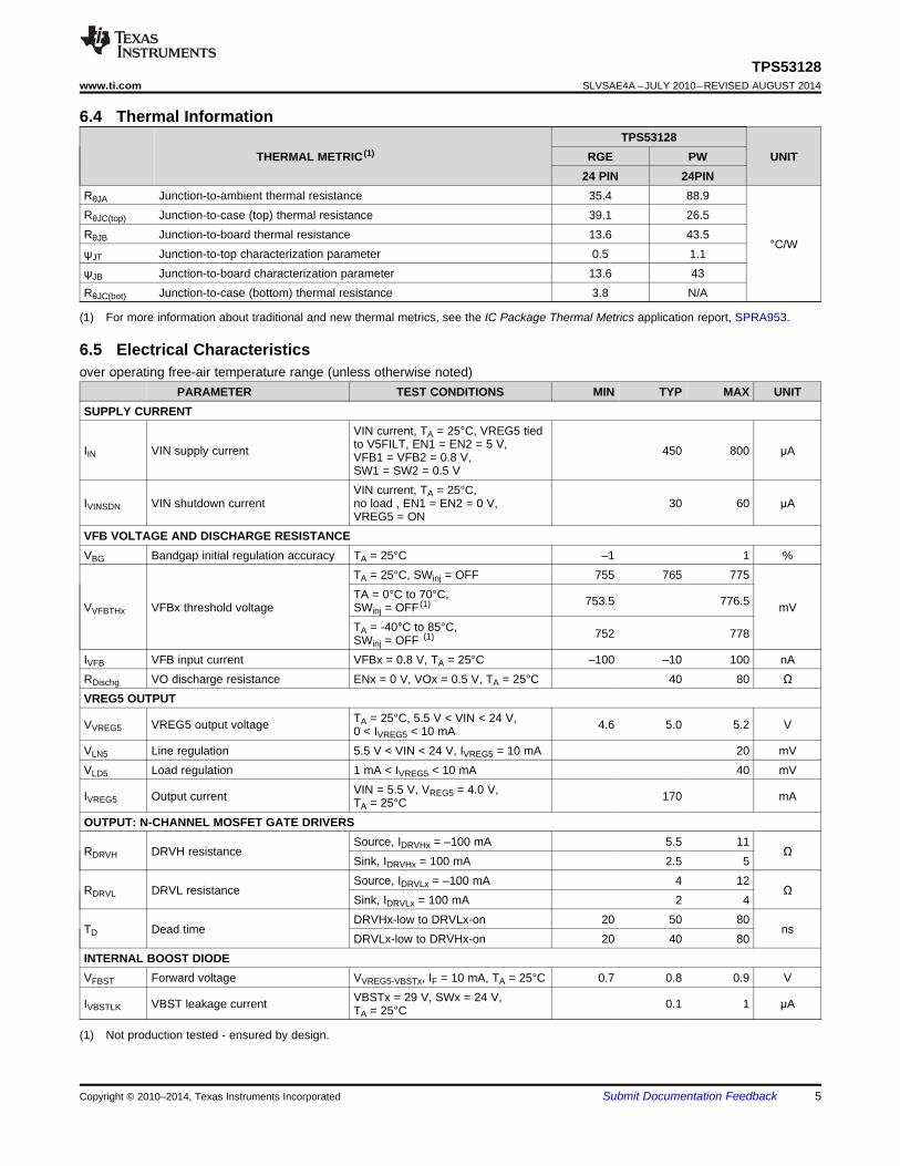
6.4 Thermal Information
THERMAL METRIC (1)TPS53128
UNITRGE PW24 PIN 24PIN
RθJA Junction-to-ambient thermal resistance 35.4 88.9
°C/W
RθJC(top) Junction-to-case (top) thermal resistance 39.1 26.5RθJB Junction-to-board thermal resistance 13.6 43.5ψJT Junction-to-top characterization parameter 0.5 1.1ψJB Junction-to-board characterization parameter 13.6 43RθJC(bot) Junction-to-case (bottom) thermal resistance 3.8 N/A
(1) Not production tested - ensured by design.
6.5 Electrical Characteristicsover operating free-air temperature range (unless otherwise noted)
PARAMETER TEST CONDITIONS MIN TYP MAX UNITSUPPLY CURRENT
IIN VIN supply current
VIN current, TA = 25°C, VREG5 tiedto V5FILT, EN1 = EN2 = 5 V,VFB1 = VFB2 = 0.8 V,SW1 = SW2 = 0.5 V
450 800 μA
IVINSDN VIN shutdown currentVIN current, TA = 25°C,no load , EN1 = EN2 = 0 V,VREG5 = ON
30 60 μA
VFB VOLTAGE AND DISCHARGE RESISTANCEVBG Bandgap initial regulation accuracy TA = 25°C –1 1 %
VVFBTHx VFBx threshold voltage
TA = 25°C, SWinj = OFF 755 765 775
mVTA = 0°C to 70°C,SWinj = OFF (1) 753.5 776.5
TA = -40°C to 85°C,SWinj = OFF (1) 752 778
IVFB VFB input current VFBx = 0.8 V, TA = 25°C –100 –10 100 nARDischg VO discharge resistance ENx = 0 V, VOx = 0.5 V, TA = 25°C 40 80 ΩVREG5 OUTPUT
VVREG5 VREG5 output voltage TA = 25°C, 5.5 V < VIN < 24 V,0 < IVREG5 < 10 mA 4.6 5.0 5.2 V
VLN5 Line regulation 5.5 V < VIN < 24 V, IVREG5 = 10 mA 20 mVVLD5 Load regulation 1 mA < IVREG5 < 10 mA 40 mV
IVREG5 Output current VIN = 5.5 V, VREG5 = 4.0 V,TA = 25°C 170 mA
OUTPUT: N-CHANNEL MOSFET GATE DRIVERS
RDRVH DRVH resistanceSource, IDRVHx = –100 mA 5.5 11
ΩSink, IDRVHx = 100 mA 2.5 5
RDRVL DRVL resistanceSource, IDRVLx = –100 mA 4 12
ΩSink, IDRVLx = 100 mA 2 4
TD Dead timeDRVHx-low to DRVLx-on 20 50 80
nsDRVLx-low to DRVHx-on 20 40 80
INTERNAL BOOST DIODEVFBST Forward voltage VVREG5-VBSTx, IF = 10 mA, TA = 25°C 0.7 0.8 0.9 V
IVBSTLK VBST leakage current VBSTx = 29 V, SWx = 24 V,TA = 25°C 0.1 1 μA
6
TPS53128SLVSAE4A –JULY 2010–REVISED AUGUST 2014 www.ti.com
Submit Documentation Feedback Copyright © 2010–2014, Texas Instruments Incorporated
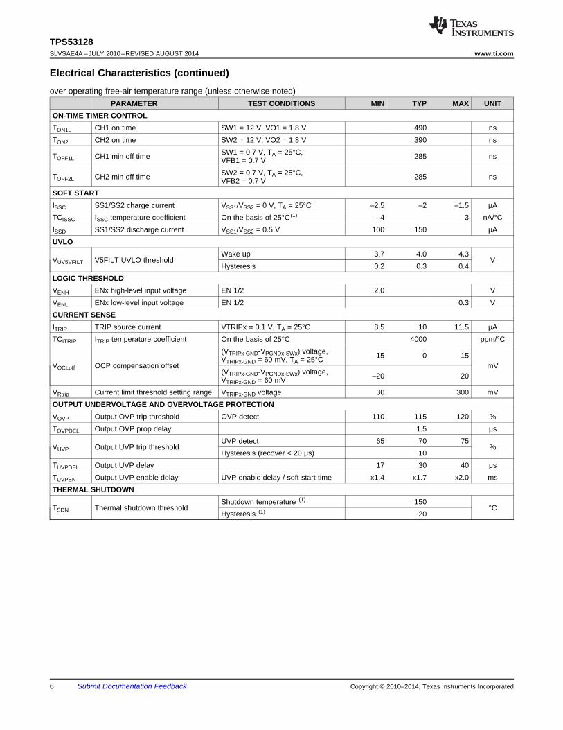
Electrical Characteristics (continued)over operating free-air temperature range (unless otherwise noted)
PARAMETER TEST CONDITIONS MIN TYP MAX UNITON-TIME TIMER CONTROLTON1L CH1 on time SW1 = 12 V, VO1 = 1.8 V 490 nsTON2L CH2 on time SW2 = 12 V, VO2 = 1.8 V 390 ns
TOFF1L CH1 min off time SW1 = 0.7 V, TA = 25°C,VFB1 = 0.7 V 285 ns
TOFF2L CH2 min off time SW2 = 0.7 V, TA = 25°C,VFB2 = 0.7 V 285 ns
SOFT STARTISSC SS1/SS2 charge current VSS1/VSS2 = 0 V, TA = 25°C –2.5 –2 –1.5 μATCISSC ISSC temperature coefficient On the basis of 25°C (1) –4 3 nA/°CISSD SS1/SS2 discharge current VSS1/VSS2 = 0.5 V 100 150 μAUVLO
VUV5VFILT V5FILT UVLO thresholdWake up 3.7 4.0 4.3
VHysteresis 0.2 0.3 0.4
LOGIC THRESHOLDVENH ENx high-level input voltage EN 1/2 2.0 VVENL ENx low-level input voltage EN 1/2 0.3 VCURRENT SENSEITRIP TRIP source current VTRIPx = 0.1 V, TA = 25°C 8.5 10 11.5 μATCITRIP ITRIP temperature coefficient On the basis of 25°C 4000 ppm/°C
VOCLoff OCP compensation offset
(VTRIPx-GND-VPGNDx-SWx) voltage,VTRIPx-GND = 60 mV, TA = 25°C –15 0 15
mV(VTRIPx-GND-VPGNDx-SWx) voltage,VTRIPx-GND = 60 mV –20 20
VRtrip Current limit threshold setting range VTRIPx-GND voltage 30 300 mVOUTPUT UNDERVOLTAGE AND OVERVOLTAGE PROTECTIONVOVP Output OVP trip threshold OVP detect 110 115 120 %TOVPDEL Output OVP prop delay 1.5 μs
VUVP Output UVP trip thresholdUVP detect 65 70 75
%Hysteresis (recover < 20 μs) 10
TUVPDEL Output UVP delay 17 30 40 μsTUVPEN Output UVP enable delay UVP enable delay / soft-start time x1.4 x1.7 x2.0 msTHERMAL SHUTDOWN
TSDN Thermal shutdown thresholdShutdown temperature (1) 150
°CHysteresis (1) 20
5.000
5.010
5.020
5.030
5.040
5.050
5.060
5.070
-50 0 50 100 150
T - Junction Temperature - °CJ
VF
B V
olt
ag
e -
V
20
15
10
5
0–50 0 50 100 150
Junction Temperature (°C)
So
urc
e C
urr
en
t (µ
A)
0
100
200
300
400
500
600
700
-50 0 50 100 150
T - Junction Temperature - °CJ
I-
Su
pp
ly C
urr
en
t -
AIN
m
10
20
30
40
50
60
-50 0 50 100 150
Junction Temperature (°C)
Sh
utd
ow
n C
urr
en
t (µ
A)
0
7
TPS53128www.ti.com SLVSAE4A –JULY 2010–REVISED AUGUST 2014
Submit Documentation FeedbackCopyright © 2010–2014, Texas Instruments Incorporated
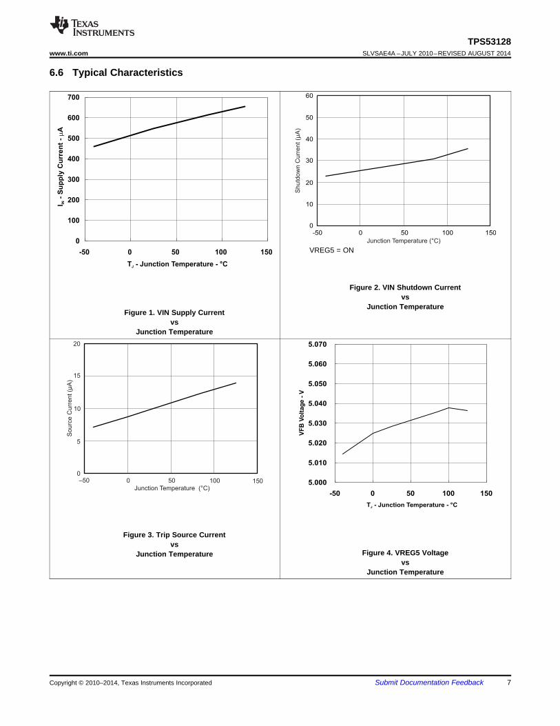
6.6 Typical Characteristics
Figure 1. VIN Supply Currentvs
Junction Temperature
VREG5 = ON
Figure 2. VIN Shutdown Currentvs
Junction Temperature
Figure 3. Trip Source Currentvs
Junction Temperature Figure 4. VREG5 Voltagevs
Junction Temperature
0.750
0.755
0.760
0.765
0.770
0.775
0.780
0.785
0.790
0.795
0.800
-50 0 50 100 150T - Junction Temperature - °CJ
VF
B1
Vo
lta
ge
- V
0.750
0.755
0.760
0.765
0.770
0.775
0.780
0.785
0.790
0.795
0.800
0 5 10 15 20 25
VIN - Input Voltage - V
VF
B1 V
olt
ag
e -
V
0.750
0.755
0.760
0.765
0.770
0.775
0.780
0.785
0.790
0.795
0.800
0 5 10 15 20 25
VIN - Input Voltage - V
VF
B1 V
olt
ag
e -
V
4.5
4.7
4.9
5.1
5.3
5.5
0 5 10 15 20 25
VR
EG
5 V
oltage (
V)
Input Voltage (V)
8
TPS53128SLVSAE4A –JULY 2010–REVISED AUGUST 2014 www.ti.com
Submit Documentation Feedback Copyright © 2010–2014, Texas Instruments Incorporated
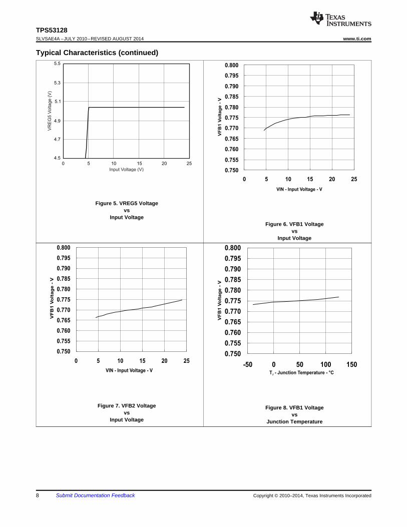
Typical Characteristics (continued)
Figure 5. VREG5 Voltagevs
Input VoltageFigure 6. VFB1 Voltage
vsInput Voltage
Figure 7. VFB2 Voltagevs
Input Voltage
Figure 8. VFB1 Voltagevs
Junction Temperature

0.750
0.755
0.760
0.765
0.770
0.775
0.780
0.785
0.790
0.795
0.800
-50 0 50 100 150
T - Junction Temperature - °CJ
VF
B2 V
olt
ag
e -
V
9
TPS53128www.ti.com SLVSAE4A –JULY 2010–REVISED AUGUST 2014
Submit Documentation FeedbackCopyright © 2010–2014, Texas Instruments Incorporated
Typical Characteristics (continued)
Figure 9. VFB2 Voltagevs
Junction Temperature
Switcher Controller
Ref
Fault
Sdn
SS
2
ON
2
VO2
VBST2
DRVH2
SW2
DRVL2
PGND2
VREG5
TSDTHOK
Switcher Controller
Ref
Sdn
ON
1
SS
1
BGR
EN/SS Control
VO1
VBST1
DRVH1
SW1
DRVL1
PGND1
VSFILT
Fault
4V/3.7VV50K
TR
IP1
VF
B1
SS
1
EN
1
EN
2
GN
D
SS
2
VF
B2
TR
IP2
10
TPS53128SLVSAE4A –JULY 2010–REVISED AUGUST 2014 www.ti.com
Submit Documentation Feedback Copyright © 2010–2014, Texas Instruments Incorporated
7 Detailed Description
7.1 OverviewThe TPS53128 is a dual, adaptive on-time D-CAP2™ mode synchronous buck controller. The part enablessystem designers to cost-effectively complete the suite of various end equipment power bus regulators with a lowexternal component count and low standby consumption. The main control loop for the TPS53128 uses the D-CAP2™ Mode topology, which provides a fast transient response with no external component.
The TPS53128 also has a proprietary circuit that enables the device to adapt not only low equivalent seriesresistance (ESR) output capacitors such as POSCAP/SP-CAP, but also to ceramic capacitors. The fixedfrequency, emulated adaptive on-time control supports seamless operation between PWM mode at heavy loadcondition and reduced frequency operation at light load for high efficiency, down to the milliampere range. Thepart provides a convenient and efficient operation, with conversion voltages from 4.5 to 24 V and output voltagefrom 0.76 to 5.5 V.
7.2 Functional Block Diagram
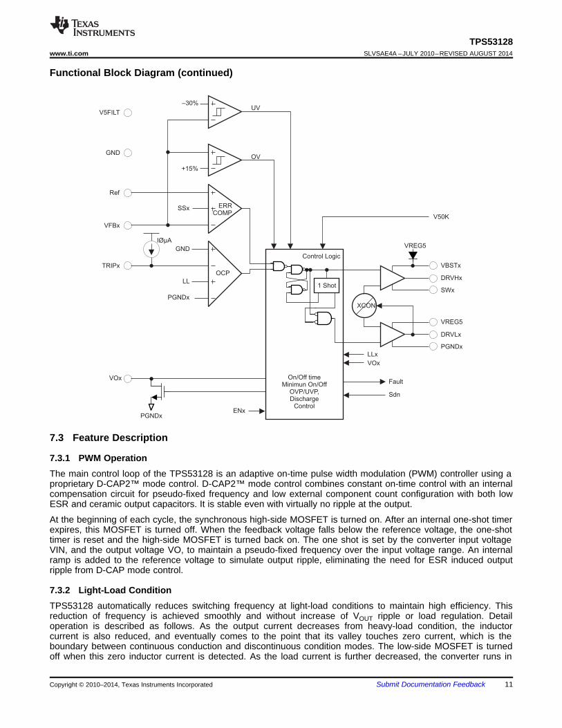
Control Logic
On/Off timeMinimun On/Off
OVP/UVP,Discharge
Control
XCON
OCP
ERRCOMP
OV
UV
ENx
VOx
PGNDx
LLx
VOx
Fault
Sdn
V50K
VBSTx
DRVHx
SWx
VREG5
VREG5
DRVLx
PGNDx
V5FILT
GND
Ref
VFBx
TRIPx
–30%
+15%
SSx
GND
IصA
LL
PGNDx
1 Shot
11
TPS53128www.ti.com SLVSAE4A –JULY 2010–REVISED AUGUST 2014
Submit Documentation FeedbackCopyright © 2010–2014, Texas Instruments Incorporated
Functional Block Diagram (continued)
7.3 Feature Description
7.3.1 PWM OperationThe main control loop of the TPS53128 is an adaptive on-time pulse width modulation (PWM) controller using aproprietary D-CAP2™ mode control. D-CAP2™ mode control combines constant on-time control with an internalcompensation circuit for pseudo-fixed frequency and low external component count configuration with both lowESR and ceramic output capacitors. It is stable even with virtually no ripple at the output.
At the beginning of each cycle, the synchronous high-side MOSFET is turned on. After an internal one-shot timerexpires, this MOSFET is turned off. When the feedback voltage falls below the reference voltage, the one-shottimer is reset and the high-side MOSFET is turned back on. The one shot is set by the converter input voltageVIN, and the output voltage VO, to maintain a pseudo-fixed frequency over the input voltage range. An internalramp is added to the reference voltage to simulate output ripple, eliminating the need for ESR induced outputripple from D-CAP mode control.
7.3.2 Light-Load ConditionTPS53128 automatically reduces switching frequency at light-load conditions to maintain high efficiency. Thisreduction of frequency is achieved smoothly and without increase of VOUT ripple or load regulation. Detailoperation is described as follows. As the output current decreases from heavy-load condition, the inductorcurrent is also reduced, and eventually comes to the point that its valley touches zero current, which is theboundary between continuous conduction and discontinuous condition modes. The low-side MOSFET is turnedoff when this zero inductor current is detected. As the load current is further decreased, the converter runs in

( )
1
2
INOUT LL
IN
V VoxVox
L fsw VI
-
= ´
´ ´
12
TPS53128SLVSAE4A –JULY 2010–REVISED AUGUST 2014 www.ti.com
Submit Documentation Feedback Copyright © 2010–2014, Texas Instruments Incorporated
Feature Description (continued)discontinuous conduction mode and it takes longer and longer to discharge the output capacitor to the level thatrequires the next ON cycle. The ON time is kept the same as that in the heavy-load condition. In reverse, whenthe output current increases from light load to heavy load, the switching frequency increases to the preset valueas the inductor current reaches the continuous conduction. The transition load point to the light load operation,IOUT(LL) (i.e., threshold between continuous and discontinuous condition mode) can be calculated as follows.
(1)
Where fSW is the PWM switching frequency.
Switching frequency versus output current in the light-load condition is a function of L, fSW, VIN and VOUT, but itdecreases almost proportional to the output current from the IOUT(LL) given in Equation 1.
7.3.3 DriversEach channel of the TPS53128 contains two high-current resistive MOSFET gate drivers. The low-side driver is aPGND referenced, VREG5 powered driver designed to drive the gate of a high-current, low RDS(ON) N-channelMOSFET whose source is connected to PGND. The high-side driver is a floating SWx referenced VBST powereddriver designed to drive the gate of a high-current, low RDS(ON) N-channel MOSFET. To maintain the VBSTvoltage during the high-side driver ON time, a capacitor is placed from SWx to VBSTx. Each driver drawsaverage current equal to gate charge (Qg at Vgs = 5 V) times switching frequency (fSW).
To prevent cross-conduction, there is a narrow dead-time when both high-side and low-side drivers are OFFbetween each driver transition. During this time the inductor current is carried by one of the MOSFETs bodydiodes.
7.3.4 PWM Frequency And Adaptive On-Time ControlTPS53128 employs adaptive on-time control scheme and does not have a dedicated on board oscillator.
TPS53128 runs with pseudo-constant frequency by using the input voltage and output voltage to set the on-timeone-shot timer. The on-time is inversely proportional to the input voltage and proportional to the output voltage.Therefore, when the duty ratio is VOUT/VIN, the frequency is constant.
7.3.5 5-Volt RegulatorThe TPS53128 has an internal 5-V low-dropout (LDO) regulator to provide a regulated voltage for all both driversand the IC's internal logic. A high-quality 4.7-μF or greater ceramic capacitor from VREG5 to GND is required tostabilize the internal regulator. An internal 10-Ω resistor from VREG5 filters the regulator output to the IC'sanalog and logic input voltage, V5FILT. An additional high-quality 1.0-μF ceramic capacitor is required fromV5FILT to GND to filter switching noise from VREG5.
7.3.6 Soft StartThe TPS53128 has a programmable soft-start . When the ENx pin becomes high, 2.0-μA current begins chargingthe capacitor connected from the SS pin to GND. The internal reference for the D-CAP2™ mode controlcomparator is overridden by the soft-start voltage until the soft-start voltage is greater than the internal referencefor smooth control of the output voltage during start up.
7.3.7 Pre-Bias SupportThe TPS53128 supports pre-bias start-up without sinking current from the output capacitor. When enabled, thelow-side driver is held off until the soft-start commands a voltage higher than the pre-bias level (internal soft-startbecomes greater than feedback voltage (VFB)), then the TPS53128 slowly activates synchronous rectification bylimiting the first DRVL pulses with a narrow on-time. This limited on-time is then incremented on a cycle-by-cyclebasis until it coincides with the full 1-D off-time. This scheme prevents the initial sinking of current from the pre-bias output, and ensure that the output voltage (VOUT) starts and ramps up smoothly into regulation and thecontrol loop is given time to transition from pre-biased start-up to normal mode operation.
R (k ) =TRIP WV (mV)TRIP
I ( A)TRIP m¾
V =TRIP
(V - V )IN O
2 1· ·L fSW
¾ ·
VO¾VIN
· RDS(ON)I -OCL( )
13
TPS53128www.ti.com SLVSAE4A –JULY 2010–REVISED AUGUST 2014
Submit Documentation FeedbackCopyright © 2010–2014, Texas Instruments Incorporated
Feature Description (continued)7.3.8 Output Discharge ControlTPS53128 discharges the outputs when ENx is low, or the controller is turned off by the protection functions(OVP, UVP, UVLO, and thermal shutdown). The device discharges output using an internal 40-Ω MOSFET whichis connected to VOx and PGNDx. The external low-side MOSFET is not turned on during the output dischargeoperation to avoid the possibility of causing negative voltage at the output. This discharge ensures that on startthe regulated voltage always initializes from 0 V.
7.3.9 Over Current LimitTPS53128 has cycle-by-cycle over current limit feature. The over current limits the inductor valley current bymonitoring the voltage drop across the low-side MOSFET RDS(ON) during the low-side driver on-time. If theinductor current is larger than the over current limit (OCL), the TPS53128 delays the start of the next switchingcycle until the sensed inductor current falls below the OCL current. MOSFET RDS(ON) current sensing is used toprovide an accuracy and cost effective solution without external devices. To program the OCL, the TRIP pinshould be connected to GND through a trip voltage setting resistor, according to the following equations.
(2)
(3)
The trip voltage should be between 30 mV to 300 mV over all operational temperature, including the 4000-ppm/°C temperature slope compensation for the temperature dependency of the RDS(ON).
If the load current exceeds the over current limit, the voltage will begin to drop. If the over current conditionscontinues the output voltage will fall below the under voltage protection threshold and the TPS53128 will shutdown.
In an over current condition, the current to the load exceeds the current to the output capacitor; thus the outputvoltage tends to fall off. Eventually, it will end up with crossing the under voltage protection threshold andshutdown.
7.3.10 Over/Under Voltage ProtectionTPS53128 monitors a resistor divided feedback voltage to detect over and under voltage. If the feedback voltageis higher than 115% of the reference voltage, the OVP comparator output goes high and the circuit latches thehigh-side MOSFET driver OFF and the low-side MOSFET driver ON.
When the feedback voltage is lower than 70% of the reference voltage, the UVP comparator output goes highand an internal UVP delay counter begins counting. After 30 μs, TPS53128 latches OFF both top and bottomMOSFET drivers. This function is enabled approximately 1.7 x TSS after power-on. The OVP and UVP latch off isreset when EN goes low level.
7.3.11 UVLO ProtectionTPS53128 has V5FILT under voltage lock out protection (UVLO) that monitors the voltage of V5FILT pin.
When the V5FILT voltage is lower than UVLO threshold voltage, the device is shut off. All output drivers are OFFand output discharge is ON. The UVLO is non-latch protection.
7.3.12 Thermal ShutdownThe TPS53128 includes an over temperature protection shut-down feature. If the TPS53128 die temperatureexceeds the OTP threshold (typically 150°C), both the high-side and low-side drivers are shut off, the outputvoltage discharge function is enabled and then the device is shut off until the die temperature drops. Thermalshutdown is a non-latch protection.
14
TPS53128SLVSAE4A –JULY 2010–REVISED AUGUST 2014 www.ti.com
Submit Documentation Feedback Copyright © 2010–2014, Texas Instruments Incorporated
7.4 Device Functional ModesThe TPS53128 has two operating modes. The TPS53128 is in shut down mode when the EN1 and EN2 pins arelow. When the EN1 and EN2 pins are pulled high, the TPS53128 enters the normal operating mode.
TPS53128 RGE
(QFN )
DRVH2
VBST2
EN2
SW1
DRVL1
DRVH1
VBST1
EN1
VF
B2
VO
2
VO
1
VF
B1
GN
DPGND2 PGND1
DRVL2
SW2
C3
10uF
VO2
1.05V/4A
C5
0.1uF
Input Voltage
PGND
C4
22uFx4
10uF
C6
10uF
L1
PGND
Q3
FDS8878
R4
3.52kΩ
R5
10kΩ
PGND
SGND
R6
4.3kΩ
24
22
23
19
20
21
13 14 15 16 17 18
8
9
10
11
12
7
123456
Power PAD
PGND
SGND
SS
1
SS
2
TR
IP2
V5
FIL
T
VR
EG
5
VIN
TR
IP1
4.5V to 24V
VO1
1.8V/4AQ4
FDS8690
Q1
FDS8878
C9
Q2
FDS8690
L2
SPM6530T
1.5uH
L1
SPM6530T
1.5uH
C2
0.1uF
R3
3.3kΩ
R2
10kΩ
C8
1uF
C74.7uF
R1
13kΩ
C1
22uFx4
C11
4700pF
C10
4700pF
15
TPS53128www.ti.com SLVSAE4A –JULY 2010–REVISED AUGUST 2014
Submit Documentation FeedbackCopyright © 2010–2014, Texas Instruments Incorporated
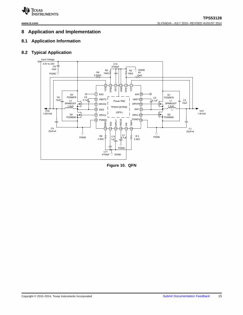
8 Application and Implementation
8.1 Application Information
8.2 Typical Application
Figure 10. QFN

I =L (RIPPLE)1
V - VIN(MAX) O1¾
L f1 · SW
·
Vo1¾VIN(MAX)
( ) ( )(max) (max)
1( ) (max) (max)
1 3 11 11
1
IN IN
L ripple IN IN
Vo VoVo VoL
fsw Io fsw
V V
V VI
- ´ -= ´ = ´
´ ´
TPS53128PW
TSSOP24
SW1
DRVL1
DRVH1
VBST1
EN1
VFB2
VO2
VO1
VFB1
GND
TRIP2
VREG5
TRIP1
PGND13
24
8
21
22
23
15
9 16
18
19
205
7
1
10
11
VIN
SS2
DRVH2
VBST2
EN2 PGND2
DRVL2
SW2 13
14
12
V5FILT
17
SS1
6
2
4 PGND
PGND
SGND
PGNDSGND
Input Voltage
4.5V to 24V
C9
10uF
VO1
1.8V/4A
C1
22uFx4
C3
10uF
Q1
FDS8878L1
SPM6530T
1.5uH
Q2
FDS8690
C2
0.1uF
R3
3.3kΩ
R6
4.3kΩ
C8
1uF
C7
4.7uF
L2
SPM6530T
1.5uH
VO2
1.05V/4AC6
10uFQ3
FDS8878
Q4
FDS8690
C5
0.1uF
R2
10kΩ
R1
13kΩ
R5
10kΩ
R4
3.52kΩ
C11
4700pF
C10
4700pF
C4
22uFx4
16
TPS53128SLVSAE4A –JULY 2010–REVISED AUGUST 2014 www.ti.com
Submit Documentation Feedback Copyright © 2010–2014, Texas Instruments Incorporated
Typical Application (continued)
Figure 11. TSSOP
8.2.1 Design Requirements
Table 3. Design ParametersDESIGN PARAMETER EXAMPLE VALUE
Input Voltage 12 V
Output Voltage Vo1 = 1.8 VVo2 = 1.05 V
8.2.2 Detailed Design Procedure
1. Choose inductor.
The inductance value is selected to provide approximately 30% peak to peak ripple current at maximum load.Larger ripple current increases output ripple voltage, improve S/N ratio and contribute to stable operation.
Equation 4 can be used to calculate L1.
(4)
The inductors current ratings needs to support both the RMS (thermal) current and the Peak (saturation)current. The RMS and peak inductor current can be estimated as follows.
(5)
V = (V - V )swinj IN O1 0.5875· ·1¾
fSW
VO1¾
VIN
4975· ·( ) ( )
K = (V - VIN O1) ·
Ton1¾
T Ton min(off)1 +
C1 =D I L
load
2
· 1¾2 · ·K DV
US
C1 =D I L
load
2
· 1¾2 1· ·V
ODV
OS
C =1IL (RIPPLE)1
¾8 1· VO (RIPPLE)
·1
¾fSW
I =L (RMS)1 Ö IO12
+1¾12
(I )L (RIPPLE)1
2
¾
I =L (PEAK)1
VTRIP¾
RDS(ON)
+ IL (RIPPLE)1
17
TPS53128www.ti.com SLVSAE4A –JULY 2010–REVISED AUGUST 2014
Submit Documentation FeedbackCopyright © 2010–2014, Texas Instruments Incorporated
(6)
(7)
Note: The calculation above shall serve as a general reference. To further improve transient response, theoutput inductance could be reduced further. This needs to be considered along with the selection of theoutput capacitor.
2. Choose output capacitor.
The capacitor value and ESR determines the amount of output voltage ripple and load transient response. itis recommended to use a ceramic output capacitor.
(8)
(9)
(10)
Where
(11)
Select the capacitance value greater than the largest value calculated from Equation 8, Equation 9 andEquation 10. The capacitance for C1 should be greater than 66 μF.
WhereΔVOS = The allowable amount of overshoot voltage in load transitionΔVUS = The allowable amount of undershoot voltage in load transitionTmin(off) = Minimum off time
3. Choose input capacitor.
The TPS53128 requires an input decoupling capacitor and a bulk capacitor is needed depending on theapplication. A minimum 10-μF high-quality ceramic capacitor is recommended for the input capacitor. Thecapacitor voltage rating needs to be greater than the maximum input voltage.
4. Choose bootstrap capacitor.
The TPS53128 requires a bootstrap capacitor from SW to VBST to provide the floating supply for the high-side drivers. A minimum 0.1-μF high-quality ceramic capacitor is recommended. The voltage rating should begreater than 10 V.
5. Choose VREG5 and V5FILT capacitor.
The TPS53128 requires both the VREG5 regulator and V5FILT input are bypassed. A minimum 4.7-μF high-quality ceramic capacitor must be connected between the VREG5 and GND for proper operation. A minimum1-μF high-quality ceramic capacitor must be connected between the V5FILT and GND for proper operation.Both of these capacitors’ voltage ratings should be greater than 10 V.
6. Choose output voltage divider resistors.
The output voltage is set with a resistor divider from the output voltage node to the VFBx pin. It isrecommended to use 1% tolerance or better resisters. Select R2 between 10 kΩ and 100 kΩ and useEquation 12 or Equation 13 to calculate R1.
(12)

C =SS
T ISS SSC
·
¾V
FB
R (k ) =TRIP WV (mV) - VTRIP OCLoff¾
I ( A)TRIP(min) m
V =TRIP
(V - V )IN O¾
2 1· ·L fSW
·
VO¾VIN
R· DS(ON)(I -OCL )
R1 =( VO¾
VFB +VFB(RIPPLE)¾
2
- 1) · R21
+ Vswinj
18
TPS53128SLVSAE4A –JULY 2010–REVISED AUGUST 2014 www.ti.com
Submit Documentation Feedback Copyright © 2010–2014, Texas Instruments Incorporated
(13)
WhereVFB(RIPPLE) = Ripple voltage at VFBVswinj = Ripple voltage at error comparator
7. Choose register setting for over current limit.
(14)
(15)
WhereRDS(ON) = Low side FET on-resistanceITRIP(min) = TRIP pin source current (8.5 μA)VOCL0ff = Minimum over current limit offset voltage (–20 mV)IOCL = Over current limit
8. Choose soft start capacitor.
Soft start time equation is as follows.
(16)

0
50
100
150
200
250
300
350
400
0.01 0.1 1 10
f- S
wit
ch
ing
Freq
uen
cy -
kH
zS
W
I - Output Current - AO
VO2=1.05V
0
50
100
150
200
250
300
350
400
0.01 0.1 1 10I - Output Current - AO
f-
Sw
itch
ing
Fre
qu
en
cy -
kH
zS
W
VO1=1.8V
0
100
200
300
400
500
0 5 10 15 20 25
f-
Sw
itc
hin
g F
re
qu
en
cy
- k
Hz
SW
VIN - Input Voltage - V
V 1=1.8VO
0
100
200
300
400
500
0 5 10 15 20 25
Sw
itch
ing
Fre
qu
en
cy (
kH
z)
Input Voltage (V)
19
TPS53128www.ti.com SLVSAE4A –JULY 2010–REVISED AUGUST 2014
Submit Documentation FeedbackCopyright © 2010–2014, Texas Instruments Incorporated
8.2.3 Application Curves
IO1 = 3 A VO1 = 1.8 V
Figure 12. Switching Frequencyvs
Input Voltage (Ch1)
IO2 = 3 A VO2 = 1.05 V
Figure 13. Switching Frequencyvs
Input Voltage (Ch2)
VO1 = 1.8 V
Figure 14. Switching Frequencyvs
Output Current (Ch1)
VO2 = 1.05 V
Figure 15. Switching Frequencyvs
Output Current (Ch2)
1.000
1.010
1.020
1.030
1.040
1.050
1.060
1.070
1.080
1.090
1.100
0 5 10 15 20 25V - Input Voltage - VI
V-
Ou
tpu
t V
olt
ag
e -
VO
UT
2
VO2=1.05V
1.760
1.770
1.780
1.790
1.800
1.810
1.820
1.830
1.840
1.850
1.860
1.870
1.880
0 5 10 15 20 25V - Input Voltage - VI
V-
Ou
tpu
t V
olt
ag
e -
VO
UT
1
VO1=1.8V
1.760
1.770
1.780
1.790
1.800
1.810
1.820
1.830
1.840
1.850
1.860
1.870
1.880
0.001 0.01 0.1 1 10
I - Output Current - AOUT
V-
Ou
tpu
t V
olt
ag
e -
VO
UT
VO1=1.8V
1.000
1.010
1.020
1.030
1.040
1.050
1.060
1.070
1.080
1.090
1.100
0.001 0.01 0.1 1 10
I - Output Current - AOUT
V-
Ou
tpu
t V
olt
ag
e -
VO
UT
VO2=1.05V
20
TPS53128SLVSAE4A –JULY 2010–REVISED AUGUST 2014 www.ti.com
Submit Documentation Feedback Copyright © 2010–2014, Texas Instruments Incorporated
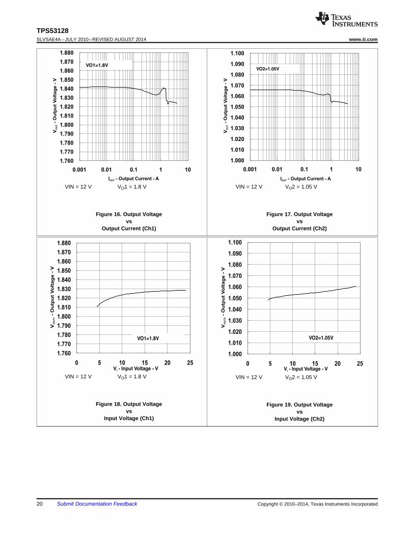
VIN = 12 V VO1 = 1.8 V
Figure 16. Output Voltagevs
Output Current (Ch1)
VIN = 12 V VO2 = 1.05 V
Figure 17. Output Voltagevs
Output Current (Ch2)
VIN = 12 V VO1 = 1.8 V
Figure 18. Output Voltagevs
Input Voltage (Ch1)
VIN = 12 V VO2 = 1.05 V
Figure 19. Output Voltagevs
Input Voltage (Ch2)
VO1=1.8V (50mV/div)
IOUT1 (2A/div)
VO2=1.05V (50mV/div)
IOUT2 (2A/div)
21
TPS53128www.ti.com SLVSAE4A –JULY 2010–REVISED AUGUST 2014
Submit Documentation FeedbackCopyright © 2010–2014, Texas Instruments Incorporated
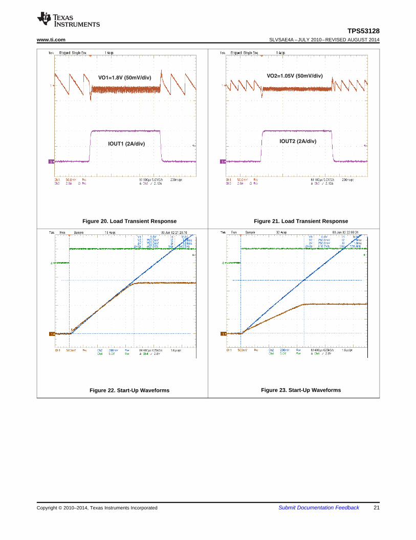
Figure 20. Load Transient Response Figure 21. Load Transient Response
Figure 22. Start-Up Waveforms Figure 23. Start-Up Waveforms
VO1 (20mV/div)
VO1=1.8V
VO2 (20mV/div)
VO2=1.05V
0
10
20
30
40
50
60
70
80
90
100
0.001 0.01 0.1 1 10
I - Output Current - AOUT
Eff
icie
ncy
- %
VO1=1.8V
0
10
20
30
40
50
60
70
80
90
100
0.001 0.01 0.1 1 10
I - Output Current - AOUT
Eff
icie
nc
y -
%
VO2=1.05V
22
TPS53128SLVSAE4A –JULY 2010–REVISED AUGUST 2014 www.ti.com
Submit Documentation Feedback Copyright © 2010–2014, Texas Instruments Incorporated
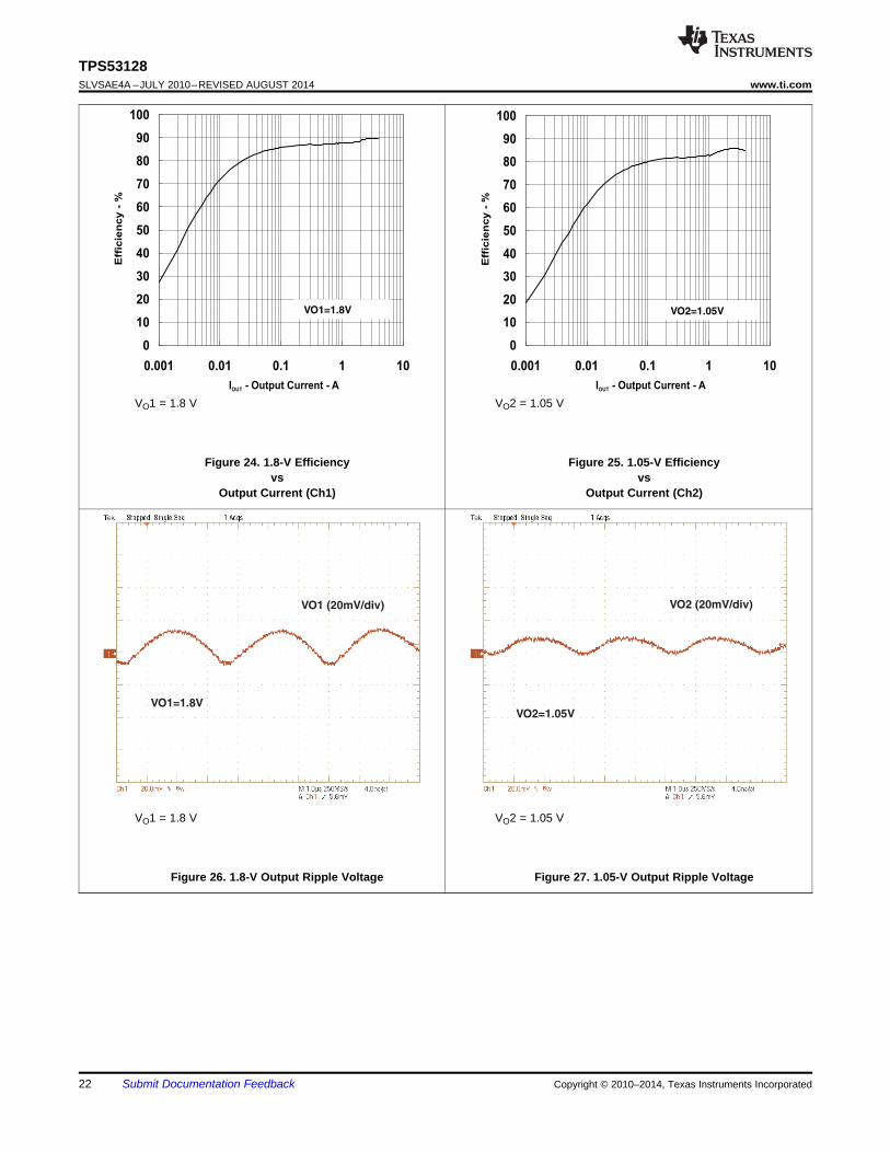
VO1 = 1.8 V
Figure 24. 1.8-V Efficiencyvs
Output Current (Ch1)
VO2 = 1.05 V
Figure 25. 1.05-V Efficiencyvs
Output Current (Ch2)
VO1 = 1.8 V
Figure 26. 1.8-V Output Ripple Voltage
VO2 = 1.05 V
Figure 27. 1.05-V Output Ripple Voltage

23
TPS53128www.ti.com SLVSAE4A –JULY 2010–REVISED AUGUST 2014
Submit Documentation FeedbackCopyright © 2010–2014, Texas Instruments Incorporated
9 Power Supply RecommendationsThe devices are designed to operate from an input voltage supply range between 4.5 and 24 V. This input supplymust be well regulated. If the input supply is located more than a few inches from the TPS53128 device, anadditional 0.1 μF ceramic capacitance may be required in addition to the 10 μF of the ceramic bypass capacitors.

SW1
DRVL1
DRVH1
VBST1
EN1
PGND1
TR
IP1
VIN
VR
EG
5
V5
FIL
T
TE
ST
2
TR
IP2
PGND2
DRVL2
SW2
DRVH2
VBST2
EN2
VO
1
VF
B1
GN
D
TE
ST
1
VF
B2
VO
2
123456
7
8
9
11
12
10
13 15 16 17 18
19
20
21
22
23
24
14
TPS53128
RGE
(QFN )
Thermal PAD
R1
R2
R4
R5
C2
R3
C7
C9
C8R6
C5
Q2
Q1Q3
Q4
L2
C4, 1
C4, 2
C1, 1
C1, 2
L1
C6 C3
TO EN 2 TO EN 1
(3)
(3) (3)
(1)
(4)
(5)(5)
VIN
S 1WS 2W
VOUT2 VOUT1PGND
SGNDTop Side Component or Via
Bottom Side Component
Top Side Etch
Bottom Side EtchComponent Pads Shown in White
C4, 3
C4, 4
C1, 3
C1, 4
24
TPS53128SLVSAE4A –JULY 2010–REVISED AUGUST 2014 www.ti.com
Submit Documentation Feedback Copyright © 2010–2014, Texas Instruments Incorporated
10 Layout
10.1 Layout Guidelines• Keep the input switching current loop as small as possible.• Place the input capacitor (C3,C6) close to the top switching FET. The output current loop should also be kept
as small as possible.• Keep the SW node as physically small and short as possible as to minimize parasitic capacitance and
inductance and to minimize radiated emissions. Kelvin connections should be brought from the output to thefeedback pin (FBx) of the device.
• Keep analog and non-switching components away from switching components.• Make a single point connection from the signal ground to power ground.• Do not allow switching current to flow under the device.
10.2 Layout Example
Figure 28.

25
TPS53128www.ti.com SLVSAE4A –JULY 2010–REVISED AUGUST 2014
Submit Documentation FeedbackCopyright © 2010–2014, Texas Instruments Incorporated
11 Device and Documentation Support
11.1 TrademarksD-CAP2, Eco-mode are trademarks of Texas Instruments.All other trademarks are the property of their respective owners.
11.2 Electrostatic Discharge CautionThese devices have limited built-in ESD protection. The leads should be shorted together or the device placed in conductive foamduring storage or handling to prevent electrostatic damage to the MOS gates.
11.3 GlossarySLYZ022 — TI Glossary.
This glossary lists and explains terms, acronyms, and definitions.
12 Mechanical, Packaging, and Orderable InformationThe following pages include mechanical, packaging, and orderable information. This information is the mostcurrent data available for the designated devices. This data is subject to change without notice and revision ofthis document. For browser-based versions of this data sheet, refer to the left-hand navigation.

PACKAGE OPTION ADDENDUM
www.ti.com 10-Dec-2020
Addendum-Page 1
PACKAGING INFORMATION
Orderable Device Status(1)
Package Type PackageDrawing
Pins PackageQty
Eco Plan(2)
Lead finish/Ball material
(6)
MSL Peak Temp(3)
Op Temp (°C) Device Marking(4/5)
Samples
TPS53128PW ACTIVE TSSOP PW 24 60 RoHS & Green NIPDAU Level-1-260C-UNLIM -40 to 85 TPS53128
TPS53128PWR ACTIVE TSSOP PW 24 2000 RoHS & Green NIPDAU Level-1-260C-UNLIM -40 to 85 TPS53128
TPS53128RGER ACTIVE VQFN RGE 24 3000 RoHS & Green NIPDAU Level-2-260C-1 YEAR -40 to 85 TPS53128
TPS53128RGET ACTIVE VQFN RGE 24 250 RoHS & Green NIPDAU Level-2-260C-1 YEAR -40 to 85 TPS53128
(1) The marketing status values are defined as follows:ACTIVE: Product device recommended for new designs.LIFEBUY: TI has announced that the device will be discontinued, and a lifetime-buy period is in effect.NRND: Not recommended for new designs. Device is in production to support existing customers, but TI does not recommend using this part in a new design.PREVIEW: Device has been announced but is not in production. Samples may or may not be available.OBSOLETE: TI has discontinued the production of the device.
(2) RoHS: TI defines "RoHS" to mean semiconductor products that are compliant with the current EU RoHS requirements for all 10 RoHS substances, including the requirement that RoHS substancedo not exceed 0.1% by weight in homogeneous materials. Where designed to be soldered at high temperatures, "RoHS" products are suitable for use in specified lead-free processes. TI mayreference these types of products as "Pb-Free".RoHS Exempt: TI defines "RoHS Exempt" to mean products that contain lead but are compliant with EU RoHS pursuant to a specific EU RoHS exemption.Green: TI defines "Green" to mean the content of Chlorine (Cl) and Bromine (Br) based flame retardants meet JS709B low halogen requirements of <=1000ppm threshold. Antimony trioxide basedflame retardants must also meet the <=1000ppm threshold requirement.
(3) MSL, Peak Temp. - The Moisture Sensitivity Level rating according to the JEDEC industry standard classifications, and peak solder temperature.
(4) There may be additional marking, which relates to the logo, the lot trace code information, or the environmental category on the device.
(5) Multiple Device Markings will be inside parentheses. Only one Device Marking contained in parentheses and separated by a "~" will appear on a device. If a line is indented then it is a continuationof the previous line and the two combined represent the entire Device Marking for that device.
(6) Lead finish/Ball material - Orderable Devices may have multiple material finish options. Finish options are separated by a vertical ruled line. Lead finish/Ball material values may wrap to twolines if the finish value exceeds the maximum column width.
Important Information and Disclaimer:The information provided on this page represents TI's knowledge and belief as of the date that it is provided. TI bases its knowledge and belief on informationprovided by third parties, and makes no representation or warranty as to the accuracy of such information. Efforts are underway to better integrate information from third parties. TI has taken and
PACKAGE OPTION ADDENDUM
www.ti.com 10-Dec-2020
Addendum-Page 2
continues to take reasonable steps to provide representative and accurate information but may not have conducted destructive testing or chemical analysis on incoming materials and chemicals.TI and TI suppliers consider certain information to be proprietary, and thus CAS numbers and other limited information may not be available for release.
In no event shall TI's liability arising out of such information exceed the total purchase price of the TI part(s) at issue in this document sold by TI to Customer on an annual basis.

TAPE AND REEL INFORMATION
*All dimensions are nominal
Device PackageType
PackageDrawing
Pins SPQ ReelDiameter
(mm)
ReelWidth
W1 (mm)
A0(mm)
B0(mm)
K0(mm)
P1(mm)
W(mm)
Pin1Quadrant
TPS53128PWR TSSOP PW 24 2000 330.0 16.4 6.95 8.3 1.6 8.0 16.0 Q1
TPS53128RGER VQFN RGE 24 3000 330.0 12.4 4.25 4.25 1.15 8.0 12.0 Q2
TPS53128RGET VQFN RGE 24 250 180.0 12.4 4.25 4.25 1.15 8.0 12.0 Q2
PACKAGE MATERIALS INFORMATION
www.ti.com 5-Jan-2022
Pack Materials-Page 1
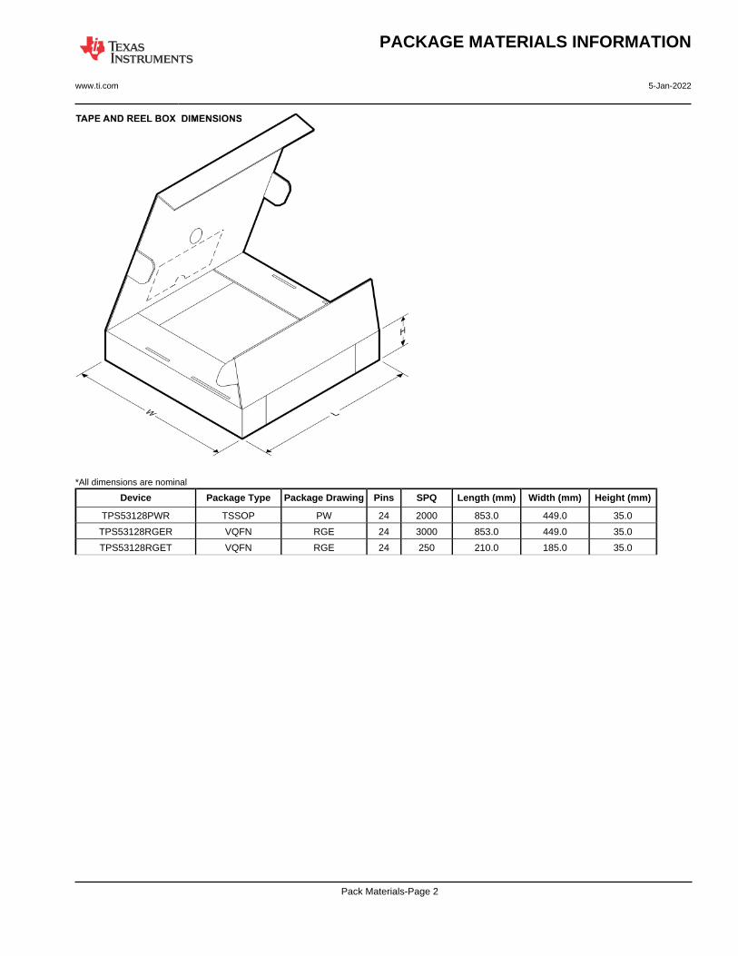
*All dimensions are nominal
Device Package Type Package Drawing Pins SPQ Length (mm) Width (mm) Height (mm)
TPS53128PWR TSSOP PW 24 2000 853.0 449.0 35.0
TPS53128RGER VQFN RGE 24 3000 853.0 449.0 35.0
TPS53128RGET VQFN RGE 24 250 210.0 185.0 35.0
PACKAGE MATERIALS INFORMATION
www.ti.com 5-Jan-2022
Pack Materials-Page 2
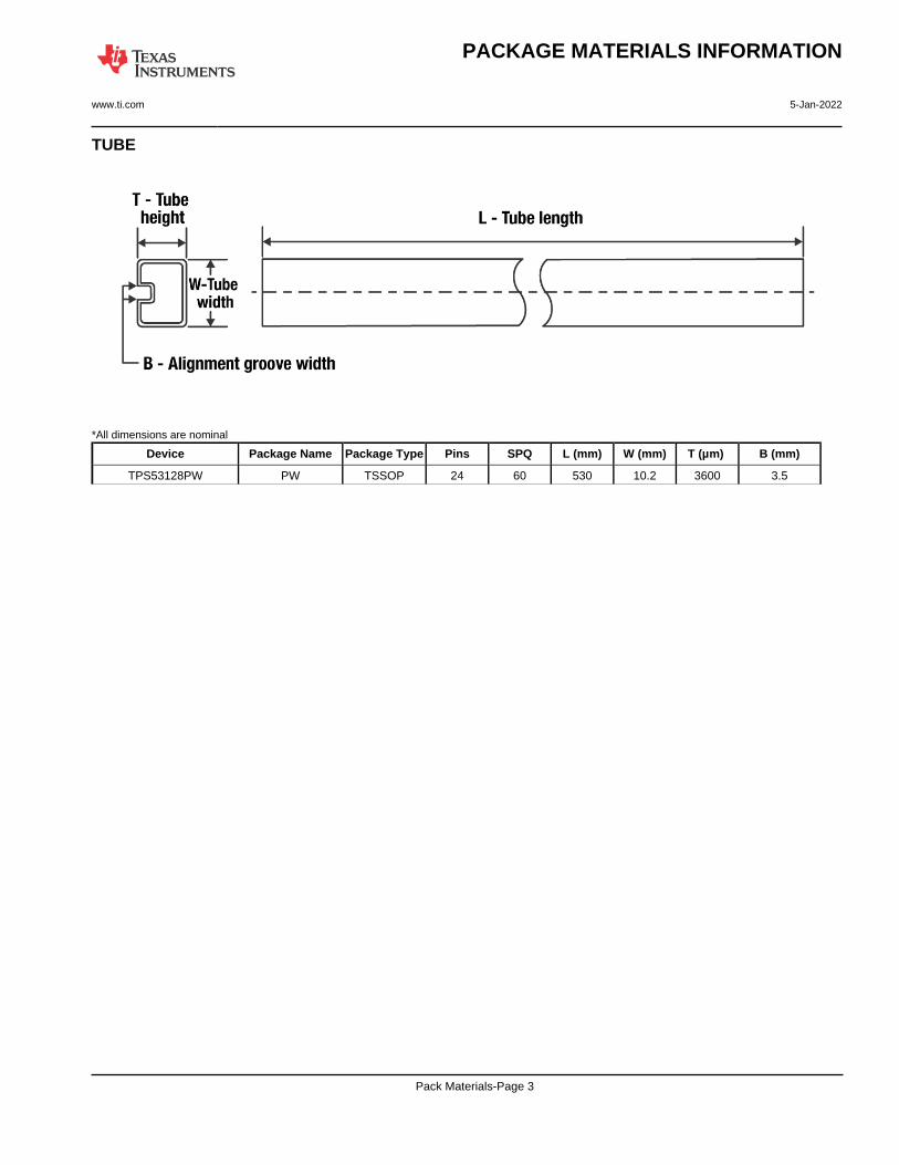
TUBE
*All dimensions are nominal
Device Package Name Package Type Pins SPQ L (mm) W (mm) T (µm) B (mm)
TPS53128PW PW TSSOP 24 60 530 10.2 3600 3.5
PACKAGE MATERIALS INFORMATION
www.ti.com 5-Jan-2022
Pack Materials-Page 3
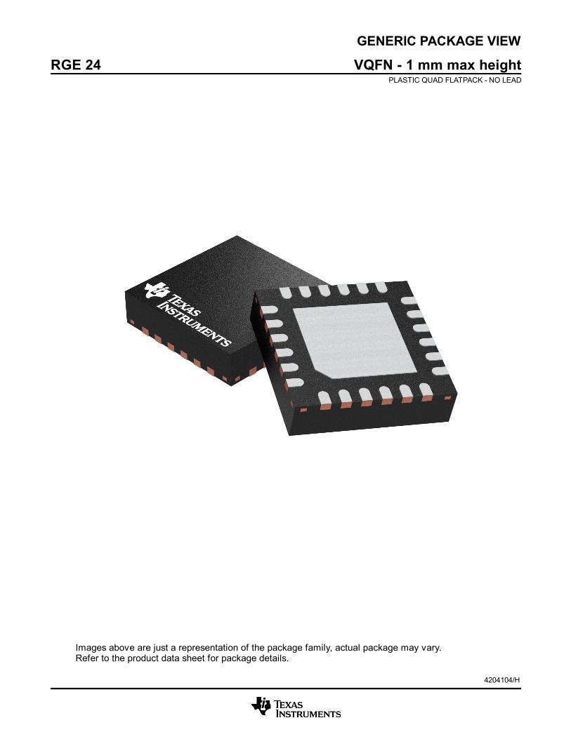
GENERIC PACKAGE VIEW
Images above are just a representation of the package family, actual package may vary.Refer to the product data sheet for package details.
RGE 24 VQFN - 1 mm max heightPLASTIC QUAD FLATPACK - NO LEAD
4204104/H

www.ti.com
PACKAGE OUTLINE
C
SEE TERMINALDETAIL
24X 0.30.2
2.45 0.1
24X 0.50.3
1 MAX
(0.2) TYP
0.050.00
20X 0.5
2X2.5
2X 2.5
A 4.13.9
B
4.13.9
0.30.2
0.50.3
VQFN - 1 mm max heightRGE0024BPLASTIC QUAD FLATPACK - NO LEAD
4219013/A 05/2017
PIN 1 INDEX AREA
0.08 C
SEATING PLANE
1
6 13
18
7 12
24 19
(OPTIONAL)PIN 1 ID
0.1 C A B0.05
EXPOSEDTHERMAL PAD
25 SYMM
SYMM
NOTES: 1. All linear dimensions are in millimeters. Any dimensions in parenthesis are for reference only. Dimensioning and tolerancing per ASME Y14.5M. 2. This drawing is subject to change without notice. 3. The package thermal pad must be soldered to the printed circuit board for thermal and mechanical performance.
SCALE 3.000
DETAILOPTIONAL TERMINAL
TYPICAL

www.ti.com
EXAMPLE BOARD LAYOUT
0.07 MINALL AROUND
0.07 MAXALL AROUND
24X (0.25)
24X (0.6)
( 0.2) TYPVIA
20X (0.5)
(3.8)
(3.8)
( 2.45)
(R0.05)TYP
(0.975) TYP
VQFN - 1 mm max heightRGE0024BPLASTIC QUAD FLATPACK - NO LEAD
4219013/A 05/2017
SYMM
1
6
7 12
13
18
1924
SYMM
LAND PATTERN EXAMPLEEXPOSED METAL SHOWN
SCALE:15X
NOTES: (continued) 4. This package is designed to be soldered to a thermal pad on the board. For more information, see Texas Instruments literature number SLUA271 (www.ti.com/lit/slua271).5. Vias are optional depending on application, refer to device data sheet. If any vias are implemented, refer to their locations shown on this view. It is recommended that vias under paste be filled, plugged or tented.
25
SOLDER MASKOPENING
METAL UNDERSOLDER MASK
SOLDER MASKDEFINED
EXPOSEDMETAL
METAL
SOLDER MASKOPENING
SOLDER MASK DETAILS
NON SOLDER MASKDEFINED
(PREFERRED)
EXPOSEDMETAL
www.ti.com
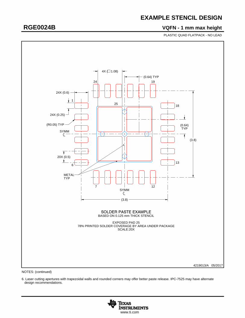
EXAMPLE STENCIL DESIGN
24X (0.6)
24X (0.25)
20X (0.5)
(3.8)
(3.8)
4X ( 1.08)
(0.64)TYP
(0.64) TYP
(R0.05) TYP
VQFN - 1 mm max heightRGE0024BPLASTIC QUAD FLATPACK - NO LEAD
4219013/A 05/2017
NOTES: (continued) 6. Laser cutting apertures with trapezoidal walls and rounded corners may offer better paste release. IPC-7525 may have alternate design recommendations.
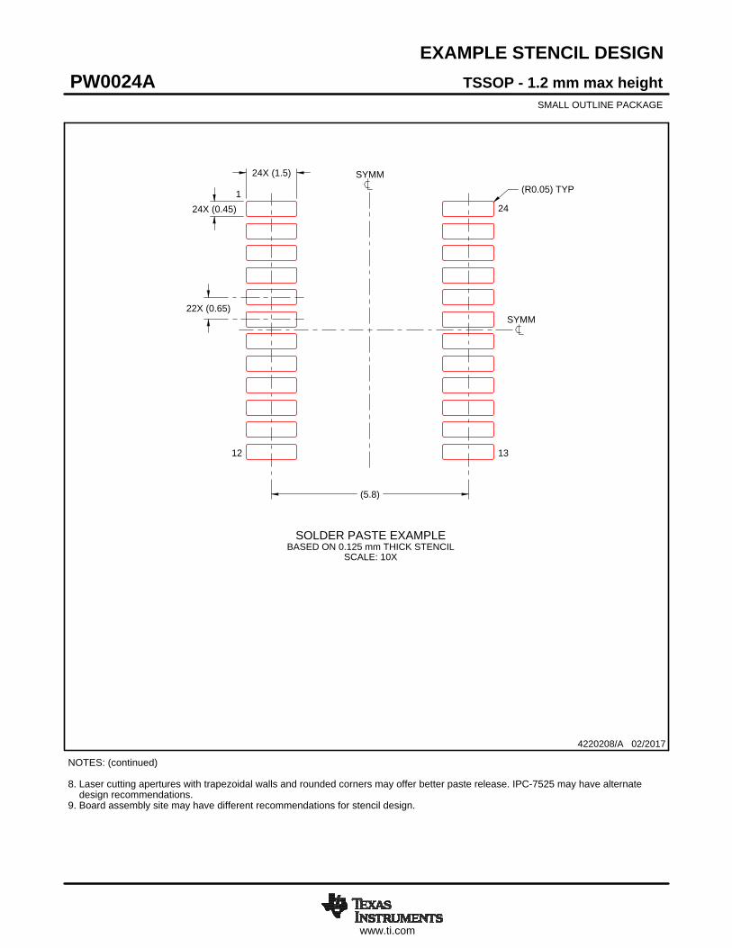
25
SYMM
METALTYP
SOLDER PASTE EXAMPLEBASED ON 0.125 mm THICK STENCIL
EXPOSED PAD 25
78% PRINTED SOLDER COVERAGE BY AREA UNDER PACKAGESCALE:20X
SYMM
1
6
7 12
13
18
1924
www.ti.com
PACKAGE OUTLINE
C
22X 0.65
2X7.15
24X 0.300.19
TYP6.66.2
1.2 MAX
0.150.05
0.25GAGE PLANE
-80
BNOTE 4
4.54.3
A
NOTE 3
7.97.7
0.750.50
(0.15) TYP
TSSOP - 1.2 mm max heightPW0024ASMALL OUTLINE PACKAGE
4220208/A 02/2017
1
1213
24
0.1 C A B
PIN 1 INDEX AREA
SEE DETAIL A
0.1 C
NOTES: 1. All linear dimensions are in millimeters. Any dimensions in parenthesis are for reference only. Dimensioning and tolerancing per ASME Y14.5M. 2. This drawing is subject to change without notice. 3. This dimension does not include mold flash, protrusions, or gate burrs. Mold flash, protrusions, or gate burrs shall not exceed 0.15 mm per side. 4. This dimension does not include interlead flash. Interlead flash shall not exceed 0.25 mm per side.5. Reference JEDEC registration MO-153.
SEATINGPLANE
A 20DETAIL ATYPICAL
SCALE 2.000
www.ti.com
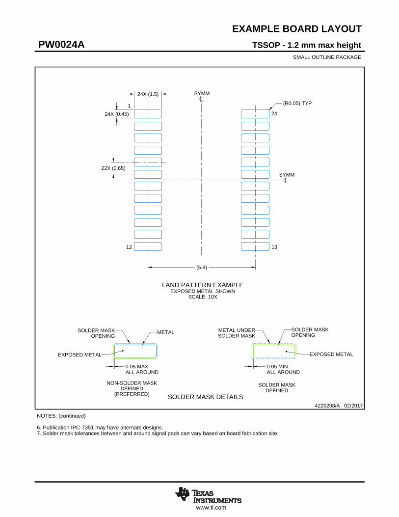
EXAMPLE BOARD LAYOUT
0.05 MAXALL AROUND
0.05 MINALL AROUND
24X (1.5)
24X (0.45)
22X (0.65)
(5.8)
(R0.05) TYP
TSSOP - 1.2 mm max heightPW0024ASMALL OUTLINE PACKAGE
4220208/A 02/2017
NOTES: (continued) 6. Publication IPC-7351 may have alternate designs. 7. Solder mask tolerances between and around signal pads can vary based on board fabrication site.
LAND PATTERN EXAMPLEEXPOSED METAL SHOWN
SCALE: 10X
SYMM
SYMM
1
12 13
24
15.000
METALSOLDER MASKOPENING
METAL UNDERSOLDER MASK
SOLDER MASKOPENING
EXPOSED METALEXPOSED METAL
SOLDER MASK DETAILS
NON-SOLDER MASKDEFINED
(PREFERRED)
SOLDER MASKDEFINED
www.ti.com
EXAMPLE STENCIL DESIGN
24X (1.5)
24X (0.45)
22X (0.65)
(5.8)
(R0.05) TYP
TSSOP - 1.2 mm max heightPW0024ASMALL OUTLINE PACKAGE
4220208/A 02/2017
NOTES: (continued) 8. Laser cutting apertures with trapezoidal walls and rounded corners may offer better paste release. IPC-7525 may have alternate design recommendations. 9. Board assembly site may have different recommendations for stencil design.
SOLDER PASTE EXAMPLEBASED ON 0.125 mm THICK STENCIL
SCALE: 10X
SYMM
SYMM
1
12 13
24
IMPORTANT NOTICE AND DISCLAIMERTI PROVIDES TECHNICAL AND RELIABILITY DATA (INCLUDING DATA SHEETS), DESIGN RESOURCES (INCLUDING REFERENCE DESIGNS), APPLICATION OR OTHER DESIGN ADVICE, WEB TOOLS, SAFETY INFORMATION, AND OTHER RESOURCES “AS IS” AND WITH ALL FAULTS, AND DISCLAIMS ALL WARRANTIES, EXPRESS AND IMPLIED, INCLUDING WITHOUT LIMITATION ANY IMPLIED WARRANTIES OF MERCHANTABILITY, FITNESS FOR A PARTICULAR PURPOSE OR NON-INFRINGEMENT OF THIRD PARTY INTELLECTUAL PROPERTY RIGHTS.These resources are intended for skilled developers designing with TI products. You are solely responsible for (1) selecting the appropriate TI products for your application, (2) designing, validating and testing your application, and (3) ensuring your application meets applicable standards, and any other safety, security, regulatory or other requirements.These resources are subject to change without notice. TI grants you permission to use these resources only for development of an application that uses the TI products described in the resource. Other reproduction and display of these resources is prohibited. No license is granted to any other TI intellectual property right or to any third party intellectual property right. TI disclaims responsibility for, and you will fully indemnify TI and its representatives against, any claims, damages, costs, losses, and liabilities arising out of your use of these resources.TI’s products are provided subject to TI’s Terms of Sale or other applicable terms available either on ti.com or provided in conjunction with such TI products. TI’s provision of these resources does not expand or otherwise alter TI’s applicable warranties or warranty disclaimers for TI products.TI objects to and rejects any additional or different terms you may have proposed. IMPORTANT NOTICE
Mailing Address: Texas Instruments, Post Office Box 655303, Dallas, Texas 75265Copyright © 2022, Texas Instruments Incorporated