
TMS320x2806x Piccolo Technical Reference Manual (Rev. H)
1126
TMS320x2806x Technical Reference Manual Literature Number: SPRUH18H January 2011 – Revised November 2019
-
Upload
khangminh22 -
Category
Documents
-
view
0 -
download
0
Transcript of TMS320x2806x Piccolo Technical Reference Manual (Rev. H)

TMS320x2806x
Technical Reference Manual
Literature Number: SPRUH18HJanuary 2011–Revised November 2019

2 SPRUH18H–January 2011–Revised November 2019Submit Documentation Feedback
Copyright © 2011–2019, Texas Instruments Incorporated
Contents
Contents
Preface....................................................................................................................................... 431 System Control and Interrupts ............................................................................................. 45
1.2 Flash and OTP Memory Blocks .......................................................................................... 461.2.1 Flash Memory...................................................................................................... 461.2.2 OTP Memory....................................................................................................... 461.2.3 Flash and OTP Power Modes ................................................................................... 471.2.4 Flash and OTP Registers ........................................................................................ 52
1.3 Code Security Module (CSM)............................................................................................. 581.3.1 Functional Description ............................................................................................ 581.3.2 CSM Impact on Other On-Chip Resources .................................................................... 601.3.3 Incorporating Code Security in User Applications ............................................................ 601.3.4 Do's and Don'ts to Protect Security Logic...................................................................... 661.3.5 CSM Features - Summary ....................................................................................... 66
1.4 Clocking ..................................................................................................................... 671.4.1 Clocking and System Control .................................................................................... 671.4.2 OSC and PLL Block............................................................................................... 741.4.3 Low-Power Modes Block ......................................................................................... 991.4.4 CPU Watchdog Block ........................................................................................... 1011.4.5 32-Bit CPU Timers 0/1/2 ........................................................................................ 107
1.5 General-Purpose Input/Output (GPIO)................................................................................. 1121.5.1 GPIO Module Overview......................................................................................... 1121.5.2 Configuration Overview ......................................................................................... 1181.5.3 Digital General Purpose I/O Control........................................................................... 1201.5.4 Input Qualification................................................................................................ 1211.5.5 GPIO and Peripheral Multiplexing (MUX) .................................................................... 1261.5.6 Register Bit Definitions .......................................................................................... 130
1.6 Peripheral Frames ........................................................................................................ 1561.6.1 Peripheral Frame Registers .................................................................................... 1561.6.2 EALLOW-Protected Registers ................................................................................. 1581.6.3 Device Emulation Registers .................................................................................... 1621.6.4 Write-Followed-by-Read Protection ........................................................................... 165
1.7 Peripheral Interrupt Expansion (PIE)................................................................................... 1661.7.1 Overview of the PIE Controller................................................................................. 1661.7.2 Vector Table Mapping........................................................................................... 1691.7.3 Interrupt Sources................................................................................................. 1711.7.4 PIE Configuration Registers .................................................................................... 1801.7.5 PIE Interrupt Registers .......................................................................................... 1811.7.6 External Interrupt Control Registers .......................................................................... 189
1.8 VREG/BOR/POR ......................................................................................................... 1911.8.1 On-chip Voltage Regulator (VREG) ........................................................................... 1911.8.2 On-chip Power-On Reset (POR) and Brown-Out Reset (BOR) Circuit................................... 192
2 Boot ROM ........................................................................................................................ 1932.1 Boot ROM Memory Map ................................................................................................. 194
2.1.1 On-Chip Boot ROM Math Tables .............................................................................. 1962.1.2 On-Chip Boot ROM IQmath Functions........................................................................ 198

www.ti.com
3SPRUH18H–January 2011–Revised November 2019Submit Documentation Feedback
Copyright © 2011–2019, Texas Instruments Incorporated
Contents
2.1.3 On-Chip Flash API............................................................................................... 1982.1.4 CPU Vector Table ............................................................................................... 198
2.2 Bootloader Features...................................................................................................... 2012.2.1 Bootloader Functional Operation .............................................................................. 2012.2.2 Bootloader Device Configuration .............................................................................. 2022.2.3 PLL Multiplier and DIVSEL Selection ......................................................................... 2022.2.4 Watchdog Module ............................................................................................... 2032.2.5 Taking an ITRAP Interrupt...................................................................................... 2032.2.6 Internal Pullup Resisters ........................................................................................ 2032.2.7 PIE Configuration ................................................................................................ 2032.2.8 Reserved Memory ............................................................................................... 2032.2.9 Bootloader Modes ............................................................................................... 2052.2.10 Device_Cal ...................................................................................................... 2112.2.11 Bootloader Data Stream Structure........................................................................... 2112.2.12 Basic Transfer Procedure ..................................................................................... 2162.2.13 InitBoot Assembly Routine .................................................................................... 2172.2.14 SelectBootMode Function .................................................................................... 2182.2.15 CopyData Function ............................................................................................. 2212.2.16 SCI_Boot Function ............................................................................................. 2212.2.17 Parallel_Boot Function (GPIO)................................................................................ 2232.2.18 SPI_Boot Function.............................................................................................. 2282.2.19 I2C Boot Function .............................................................................................. 2312.2.20 eCAN Boot Function ........................................................................................... 2342.2.21 ExitBoot Assembly Routine................................................................................... 236
2.3 Building the Boot Table .................................................................................................. 2372.3.1 The C2000 Hex Utility ........................................................................................... 2372.3.2 Example: Preparing a COFF File For eCAN Bootloading .................................................. 238
2.4 Bootloader Code Overview .............................................................................................. 2422.4.1 Boot ROM Version and Checksum Information ............................................................. 242
3 Enhanced Pulse Width Modulator (ePWM) Module................................................................ 2433.1 Introduction ................................................................................................................ 244
3.1.1 Submodule Overview............................................................................................ 2443.1.2 Register Mapping ................................................................................................ 247
3.2 ePWM Submodules ...................................................................................................... 2503.2.1 Overview .......................................................................................................... 2503.2.2 Time-Base (TB) Submodule.................................................................................... 2523.2.3 Counter-Compare (CC) Submodule........................................................................... 2613.2.4 Action-Qualifier (AQ) Submodule .............................................................................. 2673.2.5 Dead-Band Generator (DB) Submodule ...................................................................... 2823.2.6 PWM-Chopper (PC) Submodule............................................................................... 2873.2.7 Trip-Zone (TZ) Submodule ..................................................................................... 2913.2.8 Event-Trigger (ET) Submodule ................................................................................ 2963.2.9 Digital Compare (DC) Submodule ............................................................................. 301
3.3 Applications to Power Topologies ...................................................................................... 3073.3.1 Overview of Multiple Modules ................................................................................. 3073.3.2 Key Configuration Capabilities ................................................................................. 3073.3.3 Controlling Multiple Buck Converters With Independent Frequencies .................................... 3083.3.4 Controlling Multiple Buck Converters With Same Frequencies............................................ 3123.3.5 Controlling Multiple Half H-Bridge (HHB) Converters ....................................................... 3153.3.6 Controlling Dual 3-Phase Inverters for Motors (ACI and PMSM).......................................... 3173.3.7 Practical Applications Using Phase Control Between PWM Modules .................................... 3213.3.8 Controlling a 3-Phase Interleaved DC/DC Converter ....................................................... 3223.3.9 Controlling Zero Voltage Switched Full Bridge (ZVSFB) Converter....................................... 327

www.ti.com
4 SPRUH18H–January 2011–Revised November 2019Submit Documentation Feedback
Copyright © 2011–2019, Texas Instruments Incorporated
Contents
3.3.10 Controlling a Peak Current Mode Controlled Buck Module ............................................... 3293.3.11 Controlling H-Bridge LLC Resonant Converter ............................................................. 331
3.4 Registers ................................................................................................................... 3343.4.1 Time-Base Submodule Registers.............................................................................. 3343.4.2 Counter-Compare Submodule Registers ..................................................................... 3413.4.3 Action-Qualifier Submodule Registers ........................................................................ 3453.4.4 Dead-Band Submodule Registers ............................................................................. 3483.4.5 PWM-Chopper Submodule Control Register................................................................. 3513.4.6 Trip-Zone Submodule Control and Status Registers........................................................ 3533.4.7 Digital Compare Submodule Registers ....................................................................... 3603.4.8 Event-Trigger Submodule Registers .......................................................................... 3653.4.9 Proper Interrupt Initialization Procedure ...................................................................... 371
4 High-Resolution Pulse Width Modulator (HRPWM)................................................................ 3724.1 Introduction ................................................................................................................ 3734.2 Operational Description of HRPWM.................................................................................... 375
4.2.1 Controlling the HRPWM Capabilities.......................................................................... 3764.2.2 Configuring the HRPWM........................................................................................ 3784.2.3 Principle of Operation ........................................................................................... 3794.2.4 Scale Factor Optimizing Software (SFO) ..................................................................... 3894.2.5 HRPWM Examples Using Optimized Assembly Code. ..................................................... 389
4.3 HRPWM Register Descriptions ......................................................................................... 3954.3.1 Register Summary ............................................................................................... 3954.3.2 Registers and Field Descriptions .............................................................................. 396
4.4 Appendix A: SFO Library Software - SFO_TI_Build_V6.lib ......................................................... 4004.5 Scale Factor Optimizer Function - int SFO() .......................................................................... 4004.6 Software Usage ........................................................................................................... 4014.7 SFO Library Version Software Differences ............................................................................ 402
5 High Resolution Capture (HRCAP) ...................................................................................... 4045.1 Introduction ................................................................................................................ 4055.2 Description................................................................................................................. 4055.3 Operational Details ....................................................................................................... 406
5.3.1 HRCAP Clocking................................................................................................. 4065.3.2 HRCAP Modes of Operation ................................................................................... 4075.3.3 HRCAP Interrupts................................................................................................ 410
5.4 Register Descriptions..................................................................................................... 4115.4.1 HRCAP Control Register (HCCTL) – EALLOW protected ................................................. 4115.4.2 HRCAP Interrupt Flag Register (HCIFR) – EALLOW protected........................................... 4125.4.3 HRCAP Interrupt Clear Register (HCICLR) – EALLOW protected........................................ 4145.4.4 HRCAP Interrupt Force Register (HCIFRC)– EALLOW protected ........................................ 4155.4.5 HRCAP Counter Register (HCCOUNTER)................................................................... 4155.4.6 HRCAP Capture Counter On Rising Edge 0 Register (HCCAPCNTRISE0)............................. 4165.4.7 HRCAP Capture Counter On Rising Edge 1 Register (HCCAPCNTRISE1)............................. 4165.4.8 HRCAP Capture Counter On Falling Edge 0 Register (HCCAPCNTFALL0) ............................ 4165.4.9 HRCAP Capture Counter On Falling Edge 1 Register (HCCAPCNTFALL1) ............................ 417
5.5 HRCAP Calibration Library ............................................................................................. 4175.5.1 HRCAP Calibration Library Functions ........................................................................ 4185.5.2 HRCAP Calibration Library Software Usage ................................................................. 422
6 Enhanced Capture (eCAP) ................................................................................................. 4256.1 Introduction ................................................................................................................ 4266.2 Features.................................................................................................................... 4266.3 Description................................................................................................................. 4266.4 Capture and APWM Operating Mode .................................................................................. 4286.5 Capture Mode Description ............................................................................................... 429

www.ti.com
5SPRUH18H–January 2011–Revised November 2019Submit Documentation Feedback
Copyright © 2011–2019, Texas Instruments Incorporated
Contents
6.5.1 Event Prescaler .................................................................................................. 4306.5.2 Edge Polarity Select and Qualifier............................................................................. 4316.5.3 Continuous/One-Shot Control .................................................................................. 4316.5.4 32-Bit Counter and Phase Control............................................................................. 4326.5.5 CAP1-CAP4 Registers .......................................................................................... 4336.5.6 eCAP Synchronization .......................................................................................... 4336.5.7 Interrupt Control.................................................................................................. 4336.5.8 Shadow Load and Lockout Control............................................................................ 4356.5.9 APWM Mode Operation......................................................................................... 435
6.6 Application of the eCAP Module ....................................................................................... 4376.6.1 Example 1 - Absolute Time-Stamp Operation Rising Edge Trigger....................................... 4376.6.2 Example 2 - Absolute Time-Stamp Operation Rising and Falling Edge Trigger ........................ 4386.6.3 Example 3 - Time Difference (Delta) Operation Rising Edge Trigger..................................... 4396.6.4 Example 4 - Time Difference (Delta) Operation Rising and Falling Edge Trigger ...................... 440
6.7 Application of the APWM Mode......................................................................................... 4416.7.1 Example 1 - Simple PWM Generation (Independent Channel/s).......................................... 441
6.8 eCAP Registers ........................................................................................................... 4426.8.1 eCAP Base Addresses.......................................................................................... 4426.8.2 ECAP_REGS Registers......................................................................................... 443
7 Enhanced Quadrature Encoder Pulse (eQEP)....................................................................... 4607.1 Introduction ................................................................................................................ 4617.2 Configuring Device Pins ................................................................................................. 4637.3 Description................................................................................................................. 463
7.3.1 EQEP Inputs...................................................................................................... 4637.3.2 Functional Description........................................................................................... 4647.3.3 eQEP Memory Map ............................................................................................. 465
7.4 Quadrature Decoder Unit (QDU) ....................................................................................... 4667.4.1 Position Counter Input Modes.................................................................................. 4667.4.2 eQEP Input Polarity Selection.................................................................................. 4697.4.3 Position-Compare Sync Output ................................................................................ 469
7.5 Position Counter and Control Unit (PCCU)............................................................................ 4697.5.1 Position Counter Operating Modes............................................................................ 4697.5.2 Position Counter Latch .......................................................................................... 4717.5.3 Position Counter Initialization .................................................................................. 4737.5.4 eQEP Position-compare Unit................................................................................... 474
7.6 eQEP Edge Capture Unit ................................................................................................ 4757.7 eQEP Watchdog .......................................................................................................... 4797.8 Unit Timer Base ........................................................................................................... 4797.9 eQEP Interrupt Structure ................................................................................................ 4807.10 eQEP Registers ........................................................................................................... 481
7.10.1 eQEP Base Addresses ........................................................................................ 4817.10.2 EQEP_REGS Registers ....................................................................................... 482
8 Analog-to-Digital Converter (ADC) ...................................................................................... 5168.1 ADC Overview............................................................................................................. 5178.2 Features.................................................................................................................... 5178.3 Block Diagram............................................................................................................. 5178.4 SOC Principle of Operation.............................................................................................. 518
8.4.1 ADC Acquisition (Sample and Hold) Window ................................................................ 5208.4.2 Trigger Operation ................................................................................................ 5248.4.3 Channel Selection ............................................................................................... 525
8.5 ONESHOT Single Conversion Support ................................................................................ 5258.6 ADC Conversion Priority ................................................................................................. 5268.7 Sequential Sampling Mode .............................................................................................. 529

www.ti.com
6 SPRUH18H–January 2011–Revised November 2019Submit Documentation Feedback
Copyright © 2011–2019, Texas Instruments Incorporated
Contents
8.8 Simultaneous Sampling Mode .......................................................................................... 5298.9 EOC and Interrupt Operation............................................................................................ 5308.10 Power-Up Sequence ..................................................................................................... 5308.11 ADC Calibration ........................................................................................................... 531
8.11.1 Factory Settings and Calibration Function .................................................................. 5318.11.2 ADC Zero Offset Calibration .................................................................................. 5318.11.3 ADC Full Scale Gain Calibration.............................................................................. 5328.11.4 ADC Bias Current Calibration ................................................................................. 532
8.12 Internal/External Reference Voltage Selection........................................................................ 5328.12.1 Internal Reference Voltage .................................................................................... 5328.12.2 External Reference Voltage ................................................................................... 532
8.13 ADC Registers ............................................................................................................ 5348.13.1 ADC Control Register 1 (ADCCTL1) ........................................................................ 5348.13.2 ADC Control Register 2 (ADCCTL2) ......................................................................... 5368.13.3 ADC Interrupt Registers ....................................................................................... 5378.13.4 ADC Priority Register .......................................................................................... 5418.13.5 ADC SOC Registers............................................................................................ 5438.13.6 ADC Calibration Registers..................................................................................... 5498.13.7 Comparator Hysteresis Control Register .................................................................... 5508.13.8 ADC Revision Register ........................................................................................ 5508.13.9 ADC Result Registers .......................................................................................... 550
8.14 ADC Timings .............................................................................................................. 5518.15 Internal Temperature Sensor............................................................................................ 555
8.15.1 Transfer Function ............................................................................................... 555
9 Comparator...................................................................................................................... 5579.1 Introduction ................................................................................................................ 5589.2 Features.................................................................................................................... 5589.3 Block Diagram............................................................................................................. 5589.4 Comparator Function ..................................................................................................... 5589.5 DAC Reference ........................................................................................................... 5599.6 Ramp Generator Input ................................................................................................... 5599.7 Initialization ................................................................................................................ 5619.8 Digital Domain Manipulation............................................................................................. 5619.9 Comparator Registers .................................................................................................... 562
9.9.1 Comparator Control (COMPCTL) Register .................................................................. 5629.9.2 Compare Output Status (COMPSTS) Register .............................................................. 5639.9.3 DAC Control (DACCTL) Register ............................................................................. 5639.9.4 DAC Value (DACVAL) Register................................................................................ 5649.9.5 Ramp Generator Maximum Reference Active (RAMPMAXREF_ACTIVE) Register ................... 5649.9.6 Ramp Generator Maximum Reference Shadow (RAMPMAXREF_SHDW) Register................... 5659.9.7 Ramp Generator Decrement Value Active (RAMPDECVAL_ACTIVE) Register ........................ 5659.9.8 Ramp Generator Decrement Value Shadow (RAMPDECVAL_SHDW) Register ....................... 5659.9.9 Ramp Generator Status (RAMPSTS) Register .............................................................. 565
10 Control Law Accelerator (CLA) ........................................................................................... 56710.1 Introduction ................................................................................................................ 56810.2 Features.................................................................................................................... 56810.3 CLA Interface.............................................................................................................. 570
10.3.1 CLA Memory .................................................................................................... 57010.3.2 CLA Memory Bus ............................................................................................... 57010.3.3 Shared Peripherals and EALLOW Protection............................................................... 57110.3.4 CLA Tasks and Interrupt Vectors ............................................................................. 572
10.4 CLA and CPU Arbitration ................................................................................................ 57310.4.1 CLA and CPU Arbitration ...................................................................................... 573

www.ti.com
7SPRUH18H–January 2011–Revised November 2019Submit Documentation Feedback
Copyright © 2011–2019, Texas Instruments Incorporated
Contents
10.5 CLA Configuration and Debug .......................................................................................... 57810.5.1 Building a CLA Application .................................................................................... 57810.5.2 Typical CLA Initialization Sequence.......................................................................... 57810.5.3 Debugging CLA Code .......................................................................................... 57910.5.4 CLA Illegal Opcode Behavior ................................................................................. 58010.5.5 Resetting the CLA .............................................................................................. 580
10.6 Pipeline..................................................................................................................... 58210.6.1 Pipeline Overview............................................................................................... 58210.6.2 CLA Pipeline Alignment........................................................................................ 58210.6.3 Parallel Instructions............................................................................................. 586
10.7 Instruction Set ............................................................................................................. 58710.7.1 Instruction Descriptions ........................................................................................ 58710.7.2 Addressing Modes and Encoding ............................................................................ 58910.7.3 Instructions ...................................................................................................... 591
10.8 Register Set ............................................................................................................... 70210.8.1 Register Memory Mapping .................................................................................... 70210.8.2 Task Interrupt Vector Registers............................................................................... 70310.8.3 Configuration Registers ........................................................................................ 70410.8.4 Execution Registers ............................................................................................ 716
11 Direct Memory Access (DMA) Module ................................................................................ 71911.1 Introduction ............................................................................................................... 72011.2 DMA Overview ............................................................................................................ 72011.3 Architecture ................................................................................................................ 720
11.3.1 Block Diagram................................................................................................... 72011.3.2 Peripheral Interrupt Event Trigger Sources ................................................................. 72111.3.3 DMA Bus......................................................................................................... 723
11.4 Pipeline Timing and Throughput ........................................................................................ 72411.5 CPU Arbitration ........................................................................................................... 72511.6 Channel Priority ........................................................................................................... 725
11.6.1 Round-Robin Mode............................................................................................. 72511.6.2 Channel 1 High Priority Mode................................................................................. 726
11.7 Address Pointer and Transfer Control ................................................................................. 72611.8 Overrun Detection Feature .............................................................................................. 73111.9 Register Descriptions..................................................................................................... 733
11.9.1 DMA Control Register (DMACTRL) — EALLOW Protected .............................................. 73411.9.2 Debug Control Register (DEBUGCTRL) — EALLOW Protected......................................... 73611.9.3 Revision Register (REVISION) ............................................................................... 73611.9.4 Priority Control Register 1 (PRIORITYCTRL1) — EALLOW Protected ................................. 73711.9.5 Priority Status Register (PRIORITYSTAT) .................................................................. 73811.9.6 Mode Register (MODE) — EALLOW Protected ............................................................ 73911.9.7 Control Register (CONTROL) — EALLOW Protected ..................................................... 74111.9.8 Burst Size Register (BURST_SIZE) — EALLOW Protected.............................................. 74311.9.9 BURST_COUNT Register ..................................................................................... 74311.9.10 Source Burst Step Register Size (SRC_BURST_STEP) — EALLOW Protected .................... 74411.9.11 Destination Burst Step Register Size (DST_BURST_STEP) — EALLOW Protected................ 74511.9.12 Transfer Size Register (TRANSFER_SIZE) — EALLOW Protected ................................... 74511.9.13 Transfer Count Register (TRANSFER_COUNT) ......................................................... 74611.9.14 Source Transfer Step Size Register (SRC_TRANSFER_STEP) — EALLOW Protected ........... 74611.9.15 Destination Transfer Step Size Register (DST_TRANSFER_STEP) — EALLOW Protected....... 74711.9.16 Source/Destination Wrap Size Register (SRC/DST_WRAP_SIZE) — EALLOW protected)........ 74711.9.17 Source/Destination Wrap Count Register (SCR/DST_WRAP_COUNT) .............................. 74811.9.18 Source/Destination Wrap Step Size Registers (SRC/DST_WRAP_STEP) — EALLOW Protected 74811.9.19 Shadow Source Begin and Current Address Pointer Registers

www.ti.com
8 SPRUH18H–January 2011–Revised November 2019Submit Documentation Feedback
Copyright © 2011–2019, Texas Instruments Incorporated
Contents
(SRC_BEG_ADDR_SHADOW/DST_BEG_ADDR_SHADOW) — All EALLOW Protected ............ 74911.9.20 Active Source Begin and Current Address Pointer Registers
(SRC_BEG_ADDR/DST_BEG_ADDR) ....................................................................... 74911.9.21 Shadow Destination Begin and Current Address Pointer Registers
(SRC_ADDR_SHADOW/DST_ADDR_SHADOW) — All EALLOW Protected .......................... 75011.9.22 Active Destination Begin and Current Address Pointer Registers (SRC_ADDR/DST_ADDR) ..... 750
12 Serial Peripheral Interface (SPI) .......................................................................................... 75112.1 Introduction ................................................................................................................ 752
12.1.1 Features.......................................................................................................... 75212.1.2 Block Diagram.................................................................................................. 752
12.2 System-Level Integration ................................................................................................ 75312.2.1 SPI Module Signals............................................................................................. 75312.2.2 Configuring Device Pins ....................................................................................... 75412.2.3 SPI Interrupts.................................................................................................... 754
12.3 SPI Operation ............................................................................................................. 75612.3.1 Introduction to Operation ...................................................................................... 75612.3.2 Master Mode .................................................................................................... 75712.3.3 Slave Mode ...................................................................................................... 75812.3.4 Data Format ..................................................................................................... 75812.3.5 Baud Rate Selection ........................................................................................... 75912.3.6 SPI Clocking Schemes......................................................................................... 76012.3.7 SPI FIFO Description........................................................................................... 76112.3.8 SPI 3-Wire Mode Description ................................................................................. 762
12.4 Programming Procedure ................................................................................................. 76412.4.1 Initialization Upon Reset ....................................................................................... 76412.4.2 Configuring the SPI............................................................................................. 76412.4.3 Data Transfer Example ........................................................................................ 76412.4.4 SPI 3-Wire Mode Code Examples............................................................................ 76612.4.5 SPI STEINV Bit in Digital Audio Transfers .................................................................. 767
12.5 SPI Registers.............................................................................................................. 76912.5.1 SPI Base Addresses ........................................................................................... 76912.5.2 SPI_REGS Registers .......................................................................................... 770
13 Serial Communications Interface (SCI) ................................................................................ 78913.1 Introduction ................................................................................................................ 79013.2 Architecture ................................................................................................................ 79213.3 SCI Module Signal Summary ........................................................................................... 79213.4 Configuring Device Pins ................................................................................................. 79213.5 Multiprocessor and Asynchronous Communication Modes ......................................................... 79213.6 SCI Programmable Data Format ....................................................................................... 79313.7 SCI Multiprocessor Communication .................................................................................... 793
13.7.1 Recognizing the Address Byte ................................................................................ 79413.7.2 Controlling the SCI TX and RX Features .................................................................... 79413.7.3 Receipt Sequence .............................................................................................. 794
13.8 Idle-Line Multiprocessor Mode .......................................................................................... 79413.8.1 Idle-Line Mode Steps........................................................................................... 79513.8.2 Block Start Signal............................................................................................... 79613.8.3 Wake-UP Temporary (WUT) Flag ............................................................................ 79613.8.4 Receiver Operation ............................................................................................. 796
13.9 Address-Bit Multiprocessor Mode ...................................................................................... 79613.9.1 Sending an Address............................................................................................ 796
13.10 SCI Communication Format............................................................................................. 79713.10.1 Receiver Signals in Communication Modes ............................................................... 79813.10.2 Transmitter Signals in Communication Modes ............................................................ 798

www.ti.com
9SPRUH18H–January 2011–Revised November 2019Submit Documentation Feedback
Copyright © 2011–2019, Texas Instruments Incorporated
Contents
13.11 SCI Port Interrupts ....................................................................................................... 79913.12 SCI Baud Rate Calculations ............................................................................................ 80013.13 SCI Enhanced Features ................................................................................................. 800
13.13.1 SCI FIFO Description ......................................................................................... 80013.13.2 SCI Auto-Baud................................................................................................. 80213.13.3 Autobaud-Detect Sequence ................................................................................. 802
13.14 SCI Registers ............................................................................................................. 80313.14.1 SCI Base Addresses.......................................................................................... 80313.14.2 SCI_REGS Registers ......................................................................................... 804
14 Inter-Integrated Circuit Module (I2C) ................................................................................... 82414.1 Introduction ................................................................................................................ 825
14.1.1 Features.......................................................................................................... 82514.1.2 Features Not Supported ....................................................................................... 82614.1.3 Functional Overview............................................................................................ 82614.1.4 Clock Generation ............................................................................................... 82714.1.5 I2C Clock Divider Registers (I2CCLKL and I2CCLKH) .................................................... 828
14.2 Configuring Device Pins ................................................................................................. 82814.3 I2C Module Operational Details......................................................................................... 829
14.3.1 Input and Output Voltage Levels ............................................................................. 82914.3.2 Data Validity ..................................................................................................... 82914.3.3 Operating Modes ............................................................................................... 82914.3.4 I2C Module START and STOP Conditions.................................................................. 83014.3.5 Serial Data Formats ............................................................................................ 83114.3.6 NACK Bit Generation........................................................................................... 83314.3.7 Clock Synchronization ......................................................................................... 83414.3.8 Arbitration ........................................................................................................ 83414.3.9 Digital Loopback Mode......................................................................................... 835
14.4 Interrupt Requests Generated by the I2C Module.................................................................... 83614.4.1 Basic I2C Interrupt Requests.................................................................................. 83614.4.2 I2C FIFO Interrupts ............................................................................................. 838
14.5 Resetting or Disabling the I2C Module................................................................................. 83914.6 I2C Registers .............................................................................................................. 840
14.6.1 I2C Base Addresses ........................................................................................... 84014.6.2 I2C_REGS Registers........................................................................................... 841
15 Multichannel Buffered Serial Port (McBSP) .......................................................................... 86515.1 Overview ................................................................................................................... 866
15.1.1 Features of the McBSP ........................................................................................ 86615.1.2 McBSP Pins/Signals............................................................................................ 86715.1.3 McBSP Operation............................................................................................... 86815.1.4 Data Transfer Process of McBSP ............................................................................ 86915.1.5 Companding (Compressing and Expanding) Data ......................................................... 869
15.2 Clocking and Framing Data ............................................................................................. 87115.2.1 Clocking .......................................................................................................... 87115.2.2 Serial Words..................................................................................................... 87115.2.3 Frames and Frame Synchronization ......................................................................... 87215.2.4 Generating Transmit and Receive Interrupts ............................................................... 87215.2.5 Ignoring Frame-Synchronization Pulses ..................................................................... 87215.2.6 Frame Frequency ............................................................................................... 87315.2.7 Maximum Frame Frequency .................................................................................. 873
15.3 Frame Phases............................................................................................................. 87315.3.1 Number of Phases, Words, and Bits Per Frame ........................................................... 87415.3.2 Single-Phase Frame Example ................................................................................ 87415.3.3 Dual-Phase Frame Example .................................................................................. 874

www.ti.com
10 SPRUH18H–January 2011–Revised November 2019Submit Documentation Feedback
Copyright © 2011–2019, Texas Instruments Incorporated
Contents
15.3.4 Implementing the AC97 Standard With a Dual-Phase Frame ............................................ 87515.3.5 McBSP Reception .............................................................................................. 87515.3.6 McBSP Transmission .......................................................................................... 87715.3.7 Interrupts and DMA Events Generated by a McBSP ...................................................... 878
15.4 McBSP Sample Rate Generator ........................................................................................ 87815.4.1 Block Diagram................................................................................................... 87915.4.2 Frame Synchronization Generation in the Sample Rate Generator ..................................... 88215.4.3 Synchronizing Sample Rate Generator Outputs to an External Clock .................................. 88215.4.4 Reset and Initialization Procedure for the Sample Rate Generator...................................... 884
15.5 McBSP Exception/Error Conditions .................................................................................... 88515.5.1 Types of Errors.................................................................................................. 88515.5.2 Overrun in the Receiver........................................................................................ 88515.5.3 Unexpected Receive Frame-Synchronization Pulse ....................................................... 88715.5.4 Overwrite in the Transmitter................................................................................... 88915.5.5 Unexpected Transmit Frame-Synchronization Pulse ...................................................... 891
15.6 Multichannel Selection Modes .......................................................................................... 89315.6.1 Channels, Blocks, and Partitions ............................................................................. 89315.6.2 Multichannel Selection ......................................................................................... 89415.6.3 Configuring a Frame for Multichannel Selection............................................................ 89415.6.4 Using Two Partitions ........................................................................................... 89415.6.5 Using Eight Partitions .......................................................................................... 89615.6.6 Receive Multichannel Selection Mode ....................................................................... 89715.6.7 Transmit Multichannel Selection Modes ..................................................................... 897
15.7 SPI Operation Using the Clock Stop Mode............................................................................ 90015.7.1 SPI Protocol ..................................................................................................... 90015.7.2 Clock Stop Mode................................................................................................ 90115.7.3 Bits Used to Enable and Configure the Clock Stop Mode ................................................ 90115.7.4 Clock Stop Mode Timing Diagrams .......................................................................... 90215.7.5 Procedure for Configuring a McBSP for SPI Operation ................................................... 90415.7.6 McBSP as the SPI Master..................................................................................... 90415.7.7 McBSP as an SPI Slave ....................................................................................... 906
15.8 Receiver Configuration................................................................................................... 90715.8.1 Programming the McBSP Registers for the Desired Receiver Operation............................... 90715.8.2 Resetting and Enabling the Receiver ........................................................................ 90815.8.3 Set the Receiver Pins to Operate as McBSP Pins ......................................................... 90815.8.4 Enable/Disable the Digital Loopback Mode ................................................................. 90915.8.5 Enable/Disable the Clock Stop Mode ........................................................................ 90915.8.6 Enable/Disable the Receive Multichannel Selection Mode................................................ 91015.8.7 Choose One or Two Phases for the Receive Frame ...................................................... 91015.8.8 Set the Receive Word Length(s).............................................................................. 91115.8.9 Set the Receive Frame Length ............................................................................... 91115.8.10 Enable/Disable the Receive Frame-Synchronization Ignore Function ................................. 91215.8.11 Set the Receive Companding Mode ........................................................................ 91315.8.12 Set the Receive Data Delay ................................................................................. 91415.8.13 Set the Receive Sign-Extension and Justification Mode ................................................. 91615.8.14 Set the Receive Interrupt Mode ............................................................................. 91715.8.15 Set the Receive Frame-Synchronization Mode ........................................................... 91715.8.16 Set the Receive Frame-Synchronization Polarity ......................................................... 91915.8.17 Set the Receive Clock Mode ................................................................................ 92115.8.18 Set the Receive Clock Polarity .............................................................................. 92215.8.19 Set the SRG Clock Divide-Down Value .................................................................... 92415.8.20 Set the SRG Clock Synchronization Mode ................................................................ 92415.8.21 Set the SRG Clock Mode (Choose an Input Clock) ...................................................... 924
www.ti.com
11SPRUH18H–January 2011–Revised November 2019Submit Documentation Feedback
Copyright © 2011–2019, Texas Instruments Incorporated
Contents
15.8.22 Set the SRG Input Clock Polarity ........................................................................... 92615.9 Transmitter Configuration................................................................................................ 926
15.9.1 Programming the McBSP Registers for the Desired Transmitter Operation............................ 92615.9.2 Resetting and Enabling the Transmitter ..................................................................... 92715.9.3 Set the Transmitter Pins to Operate as McBSP Pins ...................................................... 92815.9.4 Enable/Disable the Digital Loopback Mode ................................................................. 92815.9.5 Enable/Disable the Clock Stop Mode ........................................................................ 92815.9.6 Enable/Disable Transmit Multichannel Selection ........................................................... 92915.9.7 Choose One or Two Phases for the Transmit Frame...................................................... 93115.9.8 Set the Transmit Word Length(s) ............................................................................. 93115.9.9 Set the Transmit Frame Length............................................................................... 93215.9.10 Enable/Disable the Transmit Frame-Synchronization Ignore Function ................................ 93315.9.11 Set the Transmit Companding Mode ....................................................................... 93415.9.12 Set the Transmit Data Delay................................................................................. 93515.9.13 Set the Transmit DXENA Mode ............................................................................. 93715.9.14 Set the Transmit Interrupt Mode ............................................................................ 93715.9.15 Set the Transmit Frame-Synchronization Mode........................................................... 93815.9.16 Set the Transmit Frame-Synchronization Polarity ........................................................ 93915.9.17 Set the SRG Frame-Synchronization Period and Pulse Width.......................................... 94015.9.18 Set the Transmit Clock Mode................................................................................ 94115.9.19 Set the Transmit Clock Polarity ............................................................................. 941
15.10 Emulation and Reset Considerations .................................................................................. 94315.10.1 McBSP Emulation Mode ..................................................................................... 94315.10.2 Resetting and Initializing McBSP............................................................................ 943
15.11 Data Packing Examples ................................................................................................. 94515.11.1 Data Packing Using Frame Length and Word Length.................................................... 94515.11.2 Data Packing Using Word Length and the Frame-Synchronization Ignore Function ................ 947
15.12 McBSP Registers......................................................................................................... 94715.12.1 Register Summary ............................................................................................ 94715.12.2 Data Receive Registers (DRR[1,2])......................................................................... 94815.12.3 Data Transmit Registers (DXR[1,2]) ........................................................................ 94915.12.4 Serial Port Control Registers (SPCR[1,2]) ................................................................. 95015.12.5 Receive Control Registers (RCR[1, 2]) .................................................................... 95515.12.6 Transmit Control Registers (XCR1 and XCR2) ........................................................... 95715.12.7 Sample Rate Generator Registers (SRGR1 and SRGR2)............................................... 96015.12.8 Multichannel Control Registers (MCR[1,2]) ................................................................ 96215.12.9 Pin Control Register (PCR) .................................................................................. 96715.12.10 Receive Channel Enable Registers (RCERA, RCERB, RCERC, RCERD, RCERE, RCERF,
RCERG, RCERH) ............................................................................................... 96915.12.11 Transmit Channel Enable Registers (XCERA, XCERB, XCERC, XCERD, XCERE, XCERF,
XCERG, XCERH)................................................................................................ 97115.12.12 Interrupt Generation ......................................................................................... 973
16 Controller Area Network (CAN)........................................................................................... 97716.1 CAN Overview............................................................................................................. 978
16.1.1 Features.......................................................................................................... 97816.1.2 Block Diagram................................................................................................... 978
16.2 eCAN Compatibility With Other TI CAN Modules .................................................................... 97916.3 The CAN Network and Module ......................................................................................... 979
16.3.1 CAN Protocol Overview........................................................................................ 98016.4 eCAN Controller Overview............................................................................................... 981
16.4.1 Standard CAN Controller (SCC) Mode ...................................................................... 98216.4.2 Memory Map .................................................................................................... 983
16.5 Message Objects ......................................................................................................... 98516.6 Message Mailbox ......................................................................................................... 985

www.ti.com
12 SPRUH18H–January 2011–Revised November 2019Submit Documentation Feedback
Copyright © 2011–2019, Texas Instruments Incorporated
Contents
16.6.1 Transmit Mailbox................................................................................................ 98716.6.2 Receive Mailbox ................................................................................................ 98816.6.3 CAN Module Operation in Normal Configuration ........................................................... 988
16.7 eCAN Configuration ...................................................................................................... 98916.7.1 CAN Module Initialization ...................................................................................... 98916.7.2 Steps to Configure eCAN...................................................................................... 99216.7.3 Handling of Remote Frame Mailboxes....................................................................... 99416.7.4 Interrupts......................................................................................................... 99516.7.5 CAN Power-Down Mode ..................................................................................... 1000
16.8 eCAN Registers ......................................................................................................... 100116.8.1 Mailbox Enable Register (CANME) ......................................................................... 100116.8.2 Mailbox-Direction Register (CANMD)....................................................................... 100216.8.3 Transmission-Request Set Register (CANTRS) .......................................................... 100316.8.4 Transmission-Request-Reset Register (CANTRR) ....................................................... 100416.8.5 Transmission-Acknowledge Register (CANTA) ........................................................... 100516.8.6 Abort-Acknowledge Register (CANAA)..................................................................... 100616.8.7 Received-Message-Pending Register (CANRMP)........................................................ 100716.8.8 Received-Message-Lost Register (CANRML)............................................................. 100816.8.9 Remote-Frame-Pending Register (CANRFP) ............................................................. 100916.8.10 Global Acceptance Mask Register (CANGAM) .......................................................... 101116.8.11 Master Control Register (CANMC) ........................................................................ 101216.8.12 Bit-Timing Configuration Register (CANBTC)............................................................ 101516.8.13 Error and Status Register (CANES)....................................................................... 101716.8.14 CAN Error Counter Registers (CANTEC/CANREC) .................................................... 101916.8.15 Interrupt Registers ........................................................................................... 102016.8.16 Overwrite Protection Control Register (CANOPC) ...................................................... 102716.8.17 eCAN I/O Control Registers (CANTIOC, CANRIOC) ................................................... 102816.8.18 Timer Management Unit .................................................................................... 103016.8.19 Mailbox Layout ............................................................................................... 1036
16.9 Message Data Registers (CANMDL, CANMDH).................................................................... 103916.10 Acceptance Filter........................................................................................................ 1040
16.10.1 Local-Acceptance Masks (CANLAM) ..................................................................... 1040
17 Universal Serial Bus (USB) Controller................................................................................ 104217.1 Introduction............................................................................................................... 104317.2 Features .................................................................................................................. 1043
17.2.1 Block Diagram ................................................................................................. 104317.2.2 Signal Description ............................................................................................. 104417.2.3 Signal Pinout Tables ......................................................................................... 104417.2.4 VBus Recommendations ..................................................................................... 1044
17.3 Functional Description .................................................................................................. 104517.3.1 Operation as a Device........................................................................................ 104517.3.2 Operation as a Host........................................................................................... 104917.3.3 DMA Operation ................................................................................................ 105217.3.4 Address/Data Bus Bridge .................................................................................... 1053
17.4 Initialization and Configuration......................................................................................... 105417.4.1 Pin Configuration .............................................................................................. 105417.4.2 Endpoint Configuration ....................................................................................... 1055
17.5 USB Registers ........................................................................................................... 105617.5.1 Register Map................................................................................................... 105617.5.2 Register Descriptions ......................................................................................... 1061
Revision History ...................................................................................................................... 1125

www.ti.com
13SPRUH18H–January 2011–Revised November 2019Submit Documentation Feedback
Copyright © 2011–2019, Texas Instruments Incorporated
List of Figures
List of Figures1-1. Flash Power Mode State Diagram ....................................................................................... 481-2. Flash Pipeline............................................................................................................... 501-3. Flash Configuration Access Flow Diagram ............................................................................. 511-4. Flash Options Register (FOPT) .......................................................................................... 531-5. Flash Power Register (FPWR) ........................................................................................... 531-6. Flash Status Register (FSTATUS) ....................................................................................... 541-7. Flash Standby Wait Register (FSTDBYWAIT) ......................................................................... 551-8. Flash Standby to Active Wait Counter Register (FACTIVEWAIT) .................................................. 551-9. Flash Wait-State Register (FBANKWAIT) .............................................................................. 561-10. OTP Wait-State Register (FOTPWAIT) ................................................................................. 571-11. CSM Status and Control Register (CSMSCR) ......................................................................... 621-12. Password Match Flow (PMF) ............................................................................................ 631-13. Clock and Reset Domains ................................................................................................ 681-14. Peripheral Clock Control 0 Register (PCLKCR0) ...................................................................... 691-15. Peripheral Clock Control 1 Register (PCLKCR1) ...................................................................... 711-16. Peripheral Clock Control 2 Register (PCLKCR2) ..................................................................... 721-17. Peripheral Clock Control 3 Register (PCLKCR3) ...................................................................... 731-18. Low-Speed Peripheral Clock Prescaler Register (LOSPCP) ......................................................... 741-19. Clocking Options ........................................................................................................... 751-20. Internal Oscillator Trim (INTOSCnTRIM) Register .................................................................... 761-21. Clocking (XCLK) Register ................................................................................................. 771-22. Clock Control (CLKCTL) Register ....................................................................................... 771-23. OSC and PLL Block........................................................................................................ 801-24. PLLCR Change Procedure Flow Chart.................................................................................. 821-25. PLLCR Register Layout ................................................................................................... 831-26. PLL Status Register (PLLSTS) ........................................................................................... 831-27. PLL Lock Period (PLLLOCKPRD) Register............................................................................. 851-28. PLL2 Input and Output Configurations .................................................................................. 861-29. PLL2 Configuration (PLL2CTL) Register (EALLOW protected) ...................................................... 861-30. PLL2 Multiplier (PLL2MULT) Register (EALLOW protected) ......................................................... 861-31. PLL2 Lock Status (PLL2STS) Register ................................................................................. 871-32. SYSCLK2 Clock Counter (SYSCLK2CNTR) Register................................................................. 871-33. EPWM DMA/CLA Configuration (EPWMCFG) Register .............................................................. 881-34. Clocking and Reset Logic ................................................................................................. 891-35. Clock Fail Interrupt ......................................................................................................... 931-36. NMI Configuration (NMICFG) Register .................................................................................. 941-37. NMI Flag (NMIFLG) Register Register ................................................................................. 941-38. NMI Flag (NMIFLGCLR) Register Register ............................................................................ 951-39. NMI Flag (NMIFLGFRC) Register Register ............................................................................ 961-40. NMI Watchdog Counter (NMIWDCNT) Register ....................................................................... 961-41. NMI Watchdog Period (NMIWDPRD) Register......................................................................... 961-42. XCLKOUT Generation ..................................................................................................... 981-43. Low-Power Mode Control 0 Register (LPMCR0) ..................................................................... 1001-44. CPU Watchdog Module .................................................................................................. 1011-45. System Control and Status Register (SCSR) ........................................................................ 1041-46. Watchdog Counter Register (WDCNTR) .............................................................................. 1051-47. Watchdog Reset Key Register (WDKEY) ............................................................................. 105
www.ti.com
14 SPRUH18H–January 2011–Revised November 2019Submit Documentation Feedback
Copyright © 2011–2019, Texas Instruments Incorporated
List of Figures
1-48. Watchdog Control Register (WDCR)................................................................................... 1051-49. CPU-Timers ............................................................................................................... 1071-50. CPU-Timer Interrupts Signals and Output Signal .................................................................... 1071-51. TIMERxTIM Register (x = 0, 1, 2) ...................................................................................... 1081-52. TIMERxTIMH Register (x = 0, 1, 2) .................................................................................... 1081-53. TIMERxPRD Register (x = 0, 1, 2) ..................................................................................... 1091-54. TIMERxPRDH Register (x = 0, 1, 2) ................................................................................... 1091-55. TIMERxTCR Register (x = 0, 1, 2) ..................................................................................... 1091-56. TIMERxTPR Register (x = 0, 1, 2)...................................................................................... 1101-57. TIMERxTPRH Register (x = 0, 1, 2) ................................................................................... 1111-58. General GPIO Multiplexing Diagram ................................................................................... 1131-59. GPIO32, GPIO33 Multiplexing Diagram ............................................................................... 1141-60. JTAG Port/GPIO Multiplexing ........................................................................................... 1151-61. JTAGDEBUG Register (Addfress 0x702A, EALLOW protected) ................................................... 1151-62. Analog/GPIO Multiplexing ............................................................................................... 1171-63. Input Qualification Using a Sampling Window ........................................................................ 1221-64. Input Qualifier Clock Cycles ............................................................................................. 1251-65. GPIO Port A MUX 1 (GPAMUX1) Register ........................................................................... 1301-66. GPIO Port A MUX 2 (GPAMUX2) Register ........................................................................... 1321-67. GPIO Port B MUX 1 (GPBMUX1) Register ........................................................................... 1341-68. GPIO Port B MUX 2 (GPBMUX2) Register ........................................................................... 1361-69. Analog I/O MUX (AIOMUX1) Register ................................................................................. 1371-70. GPIO Port A Qualification Control (GPACTRL) Register ........................................................... 1381-71. GPIO Port B Qualification Control (GPBCTRL) Register ........................................................... 1401-72. GPIO A Control Register 2 Register (GPACTRL2) Register........................................................ 1401-73. GPIO Port A Qualification Select 1 (GPAQSEL1) Register ......................................................... 1421-74. GPIO Port A Qualification Select 2 (GPAQSEL2) Register ......................................................... 1431-75. GPIO Port B Qualification Select 1 (GPBQSEL1) Register ......................................................... 1441-76. GPIO Port B Qualification Select 2 (GPBQSEL2) Register ......................................................... 1451-77. GPIO Port A Direction (GPADIR) Register ........................................................................... 1451-78. GPIO Port B Direction (GPBDIR) Register ........................................................................... 1461-79. Analog I/O DIR (AIODIR) Register ..................................................................................... 1471-80. GPIO Port A Pullup Disable (GPAPUD) Registers .................................................................. 1471-81. GPIO Port B Pullup Disable (GPBPUD) Registers .................................................................. 1481-82. GPIO Port A Data (GPADAT) Register ............................................................................... 1491-83. GPIO Port B Data (GPBDAT) Register ............................................................................... 1501-84. Analog I/O DAT (AIODAT) Register.................................................................................... 1501-85. GPIO Port A Set, Clear and Toggle (GPASET, GPACLEAR, GPATOGGLE) Registers ....................... 1511-86. GPIO Port B Set, Clear and Toggle (GPBSET, GPBCLEAR, GPBTOGGLE) Registers ....................... 1521-87. Analog I/O Toggle (AIOSET, AIOCLEAR, AIOTOGGLE) Register ................................................ 1531-88. GPIO XINTn Interrupt Select (GPIOXINTnSEL) Registers.......................................................... 1541-89. GPIO Low Power Mode Wakeup Select (GPIOLPMSEL) Register ................................................ 1551-90. Device Configuration (DEVICECNF) Register ........................................................................ 1621-91. Part ID Register ........................................................................................................... 1631-92. REVID Register ........................................................................................................... 1641-93. Overview: Multiplexing of Interrupts Using the PIE Block ........................................................... 1661-94. Typical PIE/CPU Interrupt Response - INTx.y ........................................................................ 1681-95. Reset Flow Diagram...................................................................................................... 1701-96. PIE Interrupt Sources and External Interrupts XINT1/XINT2/XINT3 ............................................... 171

www.ti.com
15SPRUH18H–January 2011–Revised November 2019Submit Documentation Feedback
Copyright © 2011–2019, Texas Instruments Incorporated
List of Figures
1-97. Multiplexed Interrupt Request Flow Diagram ......................................................................... 1741-98. PIECTRL Register (Address 0xCE0)................................................................................... 1811-99. PIE Interrupt Acknowledge Register (PIEACK) Register (Address 0xCE1)....................................... 1811-100. PIEIFRx Register (x = 1 to 12) .......................................................................................... 1821-101. PIEIERx Register (x = 1 to 12).......................................................................................... 1821-102. Interrupt Flag Register (IFR) — CPU Register ....................................................................... 1841-103. Interrupt Enable Register (IER) — CPU Register .................................................................... 1861-104. Debug Interrupt Enable Register (DBGIER) — CPU Register ..................................................... 1871-105. External Interrupt n Control Register (XINTnCR) .................................................................... 1891-106. External Interrupt n Counter (XINTnCTR) (Address 7078h) ........................................................ 1901-107. BOR Configuration (BORCFG) Register .............................................................................. 1922-1. F2806x Memory Map of On-Chip ROM ............................................................................... 1942-2. F2806xM/2806xF Memory Map of On-Chip ROM.................................................................... 1952-3. Vector Table Map ......................................................................................................... 1992-4. Bootloader Flow Diagram................................................................................................ 2012-5. Boot ROM Stack .......................................................................................................... 2032-6. Boot ROM Function Overview .......................................................................................... 2062-7. Bootloader Basic Transfer Procedure ................................................................................. 2172-8. Overview of InitBoot Assembly Function .............................................................................. 2182-9. Overview of the SelectBootMode Function ........................................................................... 2192-10. Overview of Get_mode() Function ..................................................................................... 2202-11. Overview of CopyData Function ....................................................................................... 2212-12. Overview of SCI Bootloader Operation ................................................................................ 2212-13. Overview of SCI_Boot Function ........................................................................................ 2222-14. Overview of SCI_GetWordData Function ............................................................................. 2232-15. Overview of Parallel GPIO bootloader Operation .................................................................... 2232-16. Parallel GPIO Boot Loader Handshake Protocol ..................................................................... 2242-17. Parallel GPIO Mode Overview .......................................................................................... 2252-18. Parallel GPIO Mode - Host Transfer Flow............................................................................. 2262-19. 8-Bit Parallel GetWord Function ........................................................................................ 2272-20. SPI Loader................................................................................................................. 2282-21. Data Transfer From EEPROM Flow.................................................................................... 2302-22. Overview of SPIA_GetWordData Function ........................................................................... 2302-23. EEPROM Device at Address 0x50 ..................................................................................... 2312-24. Overview of I2C_Boot Function ........................................................................................ 2322-25. Random Read ............................................................................................................. 2332-26. Sequential Read .......................................................................................................... 2332-27. Overview of eCAN-A bootloader Operation ........................................................................... 2342-28. ExitBoot Procedure Flow ................................................................................................ 2363-1. Multiple ePWM Modules ................................................................................................. 2453-2. Submodules and Signal Connections for an ePWM Module........................................................ 2463-3. ePWM Submodules and Critical Internal Signal Interconnects ..................................................... 2473-4. Time-Base Submodule Block Diagram ................................................................................ 2523-5. Time-Base Submodule Signals and Registers........................................................................ 2533-6. Time-Base Frequency and Period...................................................................................... 2553-7. Time-Base Counter Synchronization Scheme 1...................................................................... 2573-8. Time-Base Up-Count Mode Waveforms ............................................................................... 2593-9. Time-Base Down-Count Mode Waveforms ........................................................................... 2603-10. Time-Base Up-Down-Count Waveforms, TBCTL[PHSDIR = 0] Count Down On Synchronization Event .... 260

www.ti.com
16 SPRUH18H–January 2011–Revised November 2019Submit Documentation Feedback
Copyright © 2011–2019, Texas Instruments Incorporated
List of Figures
3-11. Time-Base Up-Down Count Waveforms, TBCTL[PHSDIR = 1] Count Up On Synchronization Event ........ 2613-12. Counter-Compare Submodule .......................................................................................... 2613-13. Detailed View of the Counter-Compare Submodule ................................................................. 2633-14. Counter-Compare Event Waveforms in Up-Count Mode............................................................ 2653-15. Counter-Compare Events in Down-Count Mode ..................................................................... 2663-16. Counter-Compare Events In Up-Down-Count Mode, TBCTL[PHSDIR = 0] Count Down On
Synchronization Event ................................................................................................... 2673-17. Counter-Compare Events In Up-Down-Count Mode, TBCTL[PHSDIR = 1] Count Up On Synchronization
Event ....................................................................................................................... 2673-18. Action-Qualifier Submodule ............................................................................................. 2683-19. Action-Qualifier Submodule Inputs and Outputs...................................................................... 2693-20. Possible Action-Qualifier Actions for EPWMxA and EPWMxB Outputs ........................................... 2703-21. Up-Down-Count Mode Symmetrical Waveform....................................................................... 2733-22. Up, Single Edge Asymmetric Waveform, With Independent Modulation on EPWMxA and
EPWMxB—Active High .................................................................................................. 2743-23. Up, Single Edge Asymmetric Waveform With Independent Modulation on EPWMxA and
EPWMxB—Active Low ................................................................................................... 2763-24. Up-Count, Pulse Placement Asymmetric Waveform With Independent Modulation on EPWMxA............. 2773-25. Up-Down-Count, Dual Edge Symmetric Waveform, With Independent Modulation on EPWMxA and
EPWMxB — Active Low ................................................................................................. 2793-26. Up-Down-Count, Dual Edge Symmetric Waveform, With Independent Modulation on EPWMxA and
EPWMxB — Complementary ........................................................................................... 2803-27. Up-Down-Count, Dual Edge Asymmetric Waveform, With Independent Modulation on EPWMxA—Active
Low ......................................................................................................................... 2813-28. Dead-Band Submodule .................................................................................................. 2823-29. Configuration Options for the Dead-Band Submodule............................................................... 2833-30. Dead-Band Waveforms for Typical Cases (0% < Duty < 100%) ................................................... 2853-31. PWM-Chopper Submodule .............................................................................................. 2873-32. PWM-Chopper Submodule Operational Details ...................................................................... 2883-33. Simple PWM-Chopper Submodule Waveforms Showing Chopping Action Only ................................ 2883-34. PWM-Chopper Submodule Waveforms Showing the First Pulse and Subsequent Sustaining Pulses ....... 2893-35. PWM-Chopper Submodule Waveforms Showing the Pulse Width (Duty Cycle) Control of Sustaining
Pulses ...................................................................................................................... 2903-36. Trip-Zone Submodule .................................................................................................... 2913-37. Trip-Zone Submodule Mode Control Logic............................................................................ 2953-38. Trip-Zone Submodule Interrupt Logic .................................................................................. 2963-39. Event-Trigger Submodule ............................................................................................... 2973-40. Event-Trigger Submodule Inter-Connectivity of ADC Start of Conversion ........................................ 2973-41. Event-Trigger Submodule Showing Event Inputs and Prescaled Outputs ........................................ 2983-42. Event-Trigger Interrupt Generator ...................................................................................... 2993-43. Event-Trigger SOCA Pulse Generator ................................................................................. 3003-44. Event-Trigger SOCB Pulse Generator ................................................................................. 3003-45. Digital-Compare Submodule High-Level Block Diagram ............................................................ 3013-46. DCAEVT1 Event Triggering ............................................................................................. 3033-47. DCAEVT2 Event Triggering ............................................................................................. 3033-48. DCBEVT1 Event Triggering ............................................................................................. 3043-49. DCBEVT2 Event Triggering ............................................................................................. 3043-50. Event Filtering ............................................................................................................. 3053-51. Blanking Window Timing Diagram...................................................................................... 3063-52. Simplified ePWM Module ................................................................................................ 3073-53. EPWM1 Configured as a Typical Master, EPWM2 Configured as a Slave ...................................... 308

www.ti.com
17SPRUH18H–January 2011–Revised November 2019Submit Documentation Feedback
Copyright © 2011–2019, Texas Instruments Incorporated
List of Figures
3-54. Control of Four Buck Stages. Here FPWM1≠ FPWM2≠ FPWM3≠ FPWM4 .................................................... 3093-55. Buck Waveforms for (Note: Only three bucks shown here) ......................................................... 3103-56. Control of Four Buck Stages. (Note: FPWM2 = N x FPWM1) ............................................................. 3123-57. Buck Waveforms for (Note: FPWM2 = FPWM1)) ............................................................................ 3133-58. Control of Two Half-H Bridge Stages (FPWM2 = N x FPWM1) ........................................................... 3153-59. Half-H Bridge Waveforms for (Note: Here FPWM2 = FPWM1 ) ........................................................... 3163-60. Control of Dual 3-Phase Inverter Stages as Is Commonly Used in Motor Control............................... 3183-61. 3-Phase Inverter Waveforms for (Only One Inverter Shown)....................................................... 3193-62. Configuring Two PWM Modules for Phase Control .................................................................. 3213-63. Timing Waveforms Associated With Phase Control Between 2 Modules ......................................... 3223-64. Control of a 3-Phase Interleaved DC/DC Converter ................................................................. 3233-65. 3-Phase Interleaved DC/DC Converter Waveforms for ............................................................. 3243-66. Controlling a Full-H Bridge Stage (FPWM2 = FPWM1) .................................................................... 3273-67. ZVS Full-H Bridge Waveforms .......................................................................................... 3283-68. Peak Current Mode Control of a Buck Converter .................................................................... 3303-69. Peak Current Mode Control Waveforms for .......................................................................... 3303-70. Control of Two Resonant Converter Stages .......................................................................... 3323-71. H-Bridge LLC Resonant Converter PWM Waveforms ............................................................... 3323-72. Time-Base Period Register (TBPRD) .................................................................................. 3343-73. Time Base Period High Resolution Register (TBPRDHR) .......................................................... 3343-74. Time Base Period Mirror Register (TBPRDM) ........................................................................ 3343-75. Time-Base Period High Resolution Mirror Register (TBPRDHRM) ............................................... 3353-76. Time-Base Phase Register (TBPHS) .................................................................................. 3353-77. Time-Base Phase High Resolution Register (TBPHSHR)........................................................... 3363-78. Time-Base Counter Register (TBCTR) ................................................................................ 3363-79. Time-Base Control Register (TBCTL).................................................................................. 3363-80. Time-Base Status Register (TBSTS)................................................................................... 3393-81. EPWM DMA/CLA Configuration (EPWMCFG) Register............................................................. 3393-82. High Resolution Period Control Register (HRPCTL) ................................................................. 3393-83. Counter-Compare A Register (CMPA) ................................................................................ 3413-84. Counter-Compare B Register (CMPB) ................................................................................. 3413-85. Counter-Compare Control Register (CMPCTL)....................................................................... 3433-86. Compare A High Resolution Register (CMPAHR) ................................................................... 3443-87. Counter-Compare A Mirror Register (CMPAM) ...................................................................... 3443-88. Compare A High Resolution Mirror Register .......................................................................... 3443-89. Action-Qualifier Output A Control Register (AQCTLA)............................................................... 3453-90. Action-Qualifier Output B Control Register (AQCTLB)............................................................... 3463-91. Action-Qualifier Software Force Register (AQSFRC) ................................................................ 3473-92. Action-Qualifier Continuous Software Force Register (AQCSFRC)................................................ 3483-93. Dead-Band Generator Control Register (DBCTL) .................................................................... 3493-94. Dead-Band Generator Rising Edge Delay Register (DBRED)...................................................... 3503-95. Dead-Band Generator Falling Edge Delay Register (DBFED) ..................................................... 3503-96. PWM-Chopper Control Register (PCCTL)............................................................................. 3513-97. Trip-Zone Select Register (TZSEL) .................................................................................... 3533-98. Trip-Zone Control Register (TZCTL) ................................................................................... 3543-99. Trip-Zone Enable Interrupt Register (TZEINT)........................................................................ 3553-100. Trip-Zone Flag Register (TZFLG)....................................................................................... 3563-101. Trip-Zone Clear Register (TZCLR) ..................................................................................... 3573-102. Trip-Zone Force Register (TZFRC)..................................................................................... 357

www.ti.com
18 SPRUH18H–January 2011–Revised November 2019Submit Documentation Feedback
Copyright © 2011–2019, Texas Instruments Incorporated
List of Figures
3-103. Trip Zone Digital Compare Event Select Register (TZDCSEL)..................................................... 3583-104. Digital Compare Trip Select (DCTRIPSEL) ........................................................................... 3603-105. Digital Compare A Control Register (DCACTL) ...................................................................... 3613-106. Digital Compare B Control Register (DCBCTL)....................................................................... 3623-107. Digital Compare Filter Control Register (DCFCTL) .................................................................. 3623-108. Digital Compare Capture Control Register (DCCAPCTL) ........................................................... 3633-109. Digital Compare Counter Capture Register (DCCAP) ............................................................... 3633-110. Digital Compare Filter Offset Register (DCFOFFSET) .............................................................. 3643-111. Digital Compare Filter Offset Counter Register (DCFOFFSETCNT) .............................................. 3643-112. Digital Compare Filter Window Register (DCFWINDOW) ........................................................... 3653-113. Digital Compare Filter Window Counter Register (DCFWINDOWCNT) ........................................... 3653-114. Event-Trigger Selection Register (ETSEL) ............................................................................ 3653-115. Event-Trigger Prescale Register (ETPS) .............................................................................. 3673-116. Event-Trigger Flag Register (ETFLG).................................................................................. 3683-117. Event-Trigger Clear Register (ETCLR) ................................................................................ 3693-118. Event-Trigger Force Register (ETFRC)................................................................................ 3694-1. Resolution Calculations for Conventionally Generated PWM....................................................... 3734-2. Operating Logic Using MEP ............................................................................................. 3754-3. HRPWM Extension Registers and Memory Configuration .......................................................... 3764-4. HRPWM System Interface............................................................................................... 3774-5. HRPWM Block Diagram ................................................................................................. 3784-6. Required PWM Waveform for a Requested Duty = 30.0% ......................................................... 3804-7. Low % Duty Cycle Range Limitation Example (HRPCTL[HRPE] = 0)............................................. 3834-8. High % Duty Cycle Range Limitation Example (HRPCTL[HRPE] = 0) ........................................... 3854-9. Up-Count Duty Cycle Range Limitation Example (HRPCTL[HRPE]=1) ........................................... 3854-10. Up-Down Count Duty Cycle Range Limitation Example (HRPCTL[HRPE]=1) ................................... 3864-11. Simple Buck Controlled Converter Using a Single PWM............................................................ 3904-12. PWM Waveform Generated for Simple Buck Controlled Converter ............................................... 3904-13. Simple Reconstruction Filter for a PWM Based DAC................................................................ 3924-14. PWM Waveform Generated for the PWM DAC Function ........................................................... 3924-15. HRPWM Configuration Register (HRCNFG) .......................................................................... 3964-16. Counter Compare A High Resolution Register (CMPAHR) ......................................................... 3974-17. TB Phase High Resolution Register (TBPHSHR) .................................................................... 3974-18. Time Base Period High Resolution Register .......................................................................... 3974-19. Compare A High Resolution Mirror Register .......................................................................... 3984-20. Time-Base Period High Resolution Mirror Register .................................................................. 3984-21. High Resolution Period Control Register (HRPCTL) ................................................................. 3984-22. High Resolution Micro Step Register (HRMSTEP) (EALLOW protected): ........................................ 3995-1. HRCAP Module System Block Diagram ............................................................................... 4055-2. HRCAP Block Diagram .................................................................................................. 4065-3. HCCAPCLK Generation ................................................................................................. 4075-4. HCCOUNTER Behavior During High Pulse Width Capture......................................................... 4075-5. Rise vs. Fall Capture Events ............................................................................................ 4085-6. High Pulse Width Normal Mode Capture .............................................................................. 4095-7. Low Pulse Width Normal Mode Capture............................................................................... 4095-8. HRCAP High-Resolution Mode Operating Logic ..................................................................... 4105-9. Interrupts in HRCAP Module ............................................................................................ 4115-10. HRCAP Control Register (HCCTL) .................................................................................... 4125-11. HRCAP Interrupt Flag Register (HCIFR) .............................................................................. 412

www.ti.com
19SPRUH18H–January 2011–Revised November 2019Submit Documentation Feedback
Copyright © 2011–2019, Texas Instruments Incorporated
List of Figures
5-12. HRCAP Interrupt Clear Register (HCICLR) ........................................................................... 4145-13. HRCAP Interrupt Force Register (HCIFRC) .......................................................................... 4155-14. HRCAP Counter Register (HCCOUNTER)............................................................................ 4155-15. HRCAP Capture Counter On Rising Edge 0 Register (HCCAPCNTRISE0)...................................... 4165-16. HRCAP Capture Counter On Rising Edge 1 Register (HCCAPCNTRISE1)...................................... 4165-17. HRCAP Capture Counter On Falling Edge 0 Register (HCCAPCNTFALL0) ..................................... 4165-18. HRCAP Capture Counter On Falling Edge 1 Register (HCCAPCNTFALL1) ..................................... 4175-19. LowPulseWidth0 Capture on RISE and FALL Events ............................................................... 4195-20. HighPulseWidth0/1 Capture on RISE and FALL Events ............................................................ 4205-21. PeriodWidthRise0 and PeriodWidthFall0 Capture on RISE and FALL Events ................................... 4216-1. Multiple eCAP Modules In A C28x System............................................................................ 4276-2. Capture and APWM Modes of Operation.............................................................................. 4286-3. Counter Compare and PRD Effects on the eCAP Output in APWM Mode ....................................... 4296-4. eCAP Block Diagram ..................................................................................................... 4306-5. Event Prescale Control................................................................................................... 4316-6. Prescale Function Waveforms .......................................................................................... 4316-7. Details of the Continuous/One-shot Block............................................................................. 4326-8. Details of the Counter and Synchronization Block ................................................................... 4336-9. Interrupts in eCAP Module .............................................................................................. 4356-10. PWM Waveform Details Of APWM Mode Operation ................................................................ 4366-11. Time-Base Frequency and Period Calculation........................................................................ 4376-12. Capture Sequence for Absolute Time-stamp and Rising Edge Detect ............................................ 4376-13. Capture Sequence for Absolute Time-stamp With Rising and Falling Edge Detect ............................. 4386-14. Capture Sequence for Delta Mode Time-stamp and Rising Edge Detect......................................... 4396-15. Capture Sequence for Delta Mode Time-stamp With Rising and Falling Edge Detect.......................... 4406-16. PWM Waveform Details of APWM Mode Operation ................................................................. 4416-17. TSCTR Register .......................................................................................................... 4446-18. CTRPHS Register ........................................................................................................ 4456-19. CAP1 Register ............................................................................................................ 4466-20. CAP2 Register ............................................................................................................ 4476-21. CAP3 Register ............................................................................................................ 4486-22. CAP4 Register ............................................................................................................ 4496-23. ECCTL1 Register ......................................................................................................... 4506-24. ECCTL2 Register ......................................................................................................... 4526-25. ECEINT Register.......................................................................................................... 4546-26. ECFLG Register .......................................................................................................... 4566-27. ECCLR Register .......................................................................................................... 4586-28. ECFRC Register .......................................................................................................... 4597-1. Optical Encoder Disk ..................................................................................................... 4617-2. QEP Encoder Output Signal for Forward/Reverse Movement...................................................... 4617-3. Index Pulse Example ..................................................................................................... 4627-4. Functional Block Diagram of the eQEP Peripheral................................................................... 4647-5. Functional Block Diagram of Decoder Unit............................................................................ 4667-6. Quadrature Decoder State Machine.................................................................................... 4677-7. Quadrature-clock and Direction Decoding............................................................................. 4687-8. Position Counter Reset by Index Pulse for 1000 Line Encoder (QPOSMAX = 3999 or 0xF9F) ............... 4707-9. Position Counter Underflow/Overflow (QPOSMAX = 4) ............................................................ 4717-10. Software Index Marker for 1000-line Encoder (QEPCTL[IEL] = 1)................................................. 4727-11. Strobe Event Latch (QEPCTL[SEL] = 1)............................................................................... 473

www.ti.com
20 SPRUH18H–January 2011–Revised November 2019Submit Documentation Feedback
Copyright © 2011–2019, Texas Instruments Incorporated
List of Figures
7-12. eQEP Position-compare Unit............................................................................................ 4747-13. eQEP Position-compare Event Generation Points ................................................................... 4757-14. eQEP Position-compare Sync Output Pulse Stretcher .............................................................. 4757-15. eQEP Edge Capture Unit ................................................................................................ 4777-16. Unit Position Event for Low Speed Measurement (QCAPCTL[UPPS] = 0010) .................................. 4777-17. eQEP Edge Capture Unit - Timing Details ............................................................................ 4787-18. eQEP Watchdog Timer .................................................................................................. 4797-19. eQEP Unit Time Base.................................................................................................... 4807-20. EQEP Interrupt Generation.............................................................................................. 4807-21. QPOSCNT Register ...................................................................................................... 4847-22. QPOSINIT Register....................................................................................................... 4857-23. QPOSMAX Register...................................................................................................... 4867-24. QPOSCMP Register...................................................................................................... 4877-25. QPOSILAT Register ...................................................................................................... 4887-26. QPOSSLAT Register ..................................................................................................... 4897-27. QPOSLAT Register....................................................................................................... 4907-28. QUTMR Register.......................................................................................................... 4917-29. QUPRD Register.......................................................................................................... 4927-30. QWDTMR Register ....................................................................................................... 4937-31. QWDPRD Register ....................................................................................................... 4947-32. QDECCTL Register....................................................................................................... 4957-33. QEPCTL Register......................................................................................................... 4977-34. QCAPCTL Register....................................................................................................... 5007-35. QPOSCTL Register....................................................................................................... 5017-36. QEINT Register ........................................................................................................... 5027-37. QFLG Register ............................................................................................................ 5047-38. QCLR Register ............................................................................................................ 5067-39. QFRC Register............................................................................................................ 5087-40. QEPSTS Register ........................................................................................................ 5107-41. QCTMR Register.......................................................................................................... 5127-42. QCPRD Register.......................................................................................................... 5137-43. QCTMRLAT Register..................................................................................................... 5147-44. QCPRDLAT Register..................................................................................................... 5158-1. ADC Block Diagram ...................................................................................................... 5188-2. SOC Block Diagram ...................................................................................................... 5198-3. ADCINx Input Model...................................................................................................... 5208-4. ONESHOT Single Conversion .......................................................................................... 5258-5. Round Robin Priority Example .......................................................................................... 5278-6. High Priority Example .................................................................................................... 5288-7. Interrupt Structure ........................................................................................................ 5308-8. ADC Control Register 1 (ADCCTL1) (Address Offset 00h) ......................................................... 5348-9. ADC Control Register 2 (ADCCTL2) (Address Offset 01h) ........................................................ 5368-10. ADC Interrupt Flag Register (ADCINTFLG) (Address Offset 04h) ................................................. 5378-11. ADC Interrupt Flag Clear Register (ADCINTFLGCLR) (Address Offset 05h) .................................... 5388-12. ADC Interrupt Overflow Register (ADCINTOVF) (Address Offset 06h) ........................................... 5388-13. ADC Interrupt Overflow Clear Register (ADCINTOVFCLR) (Address Offset 07h)............................... 5388-14. Interrupt Select 1 And 2 Register (INTSEL1N2) (Address Offset 08h) ............................................ 5398-15. Interrupt Select 3 And 4 Register (INTSEL3N4) (Address Offset 09h) ............................................ 5398-16. Interrupt Select 5 And 6 Register (INTSEL5N6) (Address Offset 0Ah)............................................ 539

www.ti.com
21SPRUH18H–January 2011–Revised November 2019Submit Documentation Feedback
Copyright © 2011–2019, Texas Instruments Incorporated
List of Figures
8-17. Interrupt Select 7 And 8 Register (INTSEL7N8) (Address Offset 0Bh)............................................ 5398-18. Interrupt Select 9 And 10 Register (INTSEL9N10) (Address Offset 0Ch)......................................... 5408-19. ADC Start of Conversion Priority Control Register (SOCPRICTL) ................................................. 5418-20. ADC Sample Mode Register (ADCSAMPLEMODE) (Address Offset 12h) ....................................... 5438-21. ADC Interrupt Trigger SOC Select 1 Register (ADCINTSOCSEL1) (Address Offset 14h) ..................... 5448-22. ADC Interrupt Trigger SOC Select 2 Register (ADCINTSOCSEL2) (Address Offset 15h) ..................... 5458-23. ADC SOC Flag 1 Register (ADCSOCFLG1) (Address Offset 18h) ................................................ 5458-24. ADC SOC Force 1 Register (ADCSOCFRC1) (Address Offset 1Ah).............................................. 5458-25. ADC SOC Overflow 1 Register (ADCSOCOVF1) (Address Offset 1Ch) .......................................... 5468-26. ADC SOC Overflow Clear 1 Register (ADCSOCOVFCLR1) (Address Offset 1Eh) ............................. 5468-27. ADC SOC0 - SOC15 Control Registers (ADCSOCxCTL) (Address Offset 20h - 2Fh).......................... 5478-28. ADC Reference/Gain Trim Register (ADCREFTRIM) (Address Offset 40h)...................................... 5498-29. ADC Offset Trim Register (ADCOFFTRIM) (Address Offset 41h) ................................................. 5498-30. Comparator Hysteresis Control Register (COMPHYSTCTL) (Address Offset 4Ch) ............................. 5508-31. ADC Revision Register (ADCREV) (Address Offset 4Fh)........................................................... 5508-32. ADC RESULT0 - RESULT15 Registers (ADCRESULTx) (PF1 Block Address Offset 00h - 0Fh)............. 5518-33. Timing Example For Sequential Mode / Late Interrupt Pulse ....................................................... 5518-34. Timing Example For Sequential Mode / Early Interrupt Pulse ...................................................... 5528-35. Timing Example For Simultaneous Mode / Late Interrupt Pulse ................................................... 5538-36. Timing Example For Simultaneous Mode / Early Interrupt Pulse .................................................. 5548-37. Timing Example for NONOVERLAP Mode ............................................................................ 5548-38. Temperature Sensor Transfer Function ............................................................................... 5559-1. Comparator Block Diagram.............................................................................................. 5589-2. Comparator ................................................................................................................ 5599-3. Ramp Generator Block Diagram........................................................................................ 5609-4. Ramp Generator Behavior............................................................................................... 5619-5. Comparator Control (COMPCTL) Register ........................................................................... 5629-6. Compare Output Status (COMPSTS) Register ....................................................................... 5639-7. DAC Control (DACCTL) Register ...................................................................................... 5639-8. DAC Value (DACVAL) Register......................................................................................... 5649-9. Ramp Generator Maximum Reference Active (RAMPMAXREF_ACTIVE) Register ............................ 5649-10. Ramp Generator Maximum Reference Shadow (RAMPMAXREF_SHDW) Register............................ 5659-11. Ramp Generator Decrement Value Active (RAMPDECVAL_ACTIVE) Register ................................. 5659-12. Ramp Generator Decrement Value Shadow (RAMPDECVAL_SHDW) Register ................................ 5659-13. Ramp Generator Status (RAMPSTS) Register ....................................................................... 56510-1. CLA (Type 0) Block Diagram............................................................................................ 56910-2. Task Interrupt Vector (MVECT1/2/3/4/5/6/7/8) Register ............................................................. 70310-3. Control Register (MCTL)................................................................................................. 70410-4. Memory Configuration Register (MMEMCFG) ........................................................................ 70510-5. CLA Peripheral Interrupt Source Select 1 Register (MPISRCSEL1)............................................... 70610-6. Interrupt Enable Register (MIER) ....................................................................................... 70810-7. Interrupt Flag Register (MIFR) .......................................................................................... 70910-8. Interrupt Overflow Flag Register (MIOVF)............................................................................. 71010-9. Interrupt Run Status Register (MIRUN)................................................................................ 71110-10. Interrupt Force Register (MIFRC)....................................................................................... 71310-11. Interrupt Flag Clear Register (MICLR) ................................................................................. 71410-12. Interrupt Overflow Flag Clear Register (MICLROVF) ................................................................ 71510-13. Program Counter (MPC) ................................................................................................. 71610-14. CLA Status Register (MSTF)............................................................................................ 716

www.ti.com
22 SPRUH18H–January 2011–Revised November 2019Submit Documentation Feedback
Copyright © 2011–2019, Texas Instruments Incorporated
List of Figures
11-1. DMA Block Diagram ...................................................................................................... 72111-2. Peripheral Interrupt Trigger Input Diagram ............................................................................ 72211-3. 4-Stage Pipeline DMA Transfer......................................................................................... 72411-4. 4-Stage Pipeline With One Read Stall (McBSP as source) ......................................................... 72411-5. DMA State Diagram ...................................................................................................... 73011-6. Overrun Detection Logic ................................................................................................. 73211-7. DMA Control Register (DMACTRL) .................................................................................... 73411-8. Debug Control Register (DEBUGCTRL) .............................................................................. 73611-9. Revision Register (REVISION).......................................................................................... 73611-10. Priority Control Register 1 (PRIORITYCTRL1) ....................................................................... 73711-11. Priority Status Register (PRIORITYSTAT) ............................................................................ 73811-12. Mode Register (MODE) ................................................................................................. 73911-13. Control Register (CONTROL) .......................................................................................... 74111-14. Burst Size Register (BURST_SIZE) ................................................................................... 74311-15. Burst Count Register (BURST_COUNT) ............................................................................. 74311-16. Source Burst Step Size Register (SRC_BURST_STEP) ........................................................... 74411-17. Destination Burst Step Register Size (DST_BURST_STEP) ...................................................... 74511-18. Transfer Size Register (TRANSFER_SIZE) .......................................................................... 74511-19. Transfer Count Register (TRANSFER_COUNT) .................................................................... 74611-20. Source Transfer Step Size Register (SRC_TRANSFER_STEP) .................................................. 74611-21. Destination Transfer Step Size Register (DST_TRANSFER_STEP) ............................................. 74711-22. Source/Destination Wrap Size Register (SRC/DST_WRAP_SIZE) ............................................... 74711-23. Source/Destination Wrap Count Register (SCR/DST_WRAP_COUNT) ......................................... 74811-24. Source/Destination Wrap Step Size Registers (SRC/DST_WRAP_STEP) ...................................... 74811-25. Shadow Source Begin and Current Address Pointer Registers
(SRC_BEG_ADDR_SHADOW/DST_BEG_ADDR_SHADOW)..................................................... 74911-26. Active Source Begin and Current Address Pointer Registers (SRC_BEG_ADDR/DST_BEG_ADDR) ....... 74911-27. Shadow Destination Begin and Current Address Pointer Registers
(SRC_ADDR_SHADOW/DST_ADDR_SHADOW) ................................................................... 75011-28. Active Destination Begin and Current Address Pointer Registers (SRC_ADDR/DST_ADDR)................. 75012-1. SPI CPU Interface ........................................................................................................ 75312-2. SPI Interrupt Flags and Enable Logic Generation.................................................................... 75512-3. SPI Master/Slave Connection ........................................................................................... 75612-4. Serial Peripheral Interface Block Diagram............................................................................. 75712-5. SPICLK Signal Options .................................................................................................. 76012-6. SPI: SPICLK-LSPCLK Characteristic When (BRR + 1) is Odd, BRR > 3, and CLKPOLARITY = 1........... 76112-7. SPI 3-wire Master Mode ................................................................................................. 76212-8. SPI 3-wire Slave Mode................................................................................................... 76312-9. Five Bits per Character................................................................................................... 76612-10. SPI Digital Audio Receiver Configuration Using Two SPIs ......................................................... 76812-11. Standard Right-Justified Digital Audio Data Format.................................................................. 76812-12. SPICCR Register ......................................................................................................... 77112-13. SPICTL Register .......................................................................................................... 77312-14. SPISTS Register .......................................................................................................... 77512-15. SPIBRR Register ......................................................................................................... 77712-16. SPIRXEMU Register ..................................................................................................... 77812-17. SPIRXBUF Register ...................................................................................................... 77912-18. SPITXBUF Register ...................................................................................................... 78012-19. SPIDAT Register.......................................................................................................... 781

www.ti.com
23SPRUH18H–January 2011–Revised November 2019Submit Documentation Feedback
Copyright © 2011–2019, Texas Instruments Incorporated
List of Figures
12-20. SPIFFTX Register ........................................................................................................ 78212-21. SPIFFRX Register ........................................................................................................ 78412-22. SPIFFCT Register ........................................................................................................ 78612-23. SPIPRI Register........................................................................................................... 78713-1. SCI CPU Interface ........................................................................................................ 79013-2. Serial Communications Interface (SCI) Module Block Diagram .................................................... 79113-3. Typical SCI Data Frame Formats....................................................................................... 79313-4. Idle-Line Multiprocessor Communication Format..................................................................... 79513-5. Double-Buffered WUT and TXSHF..................................................................................... 79613-6. Address-Bit Multiprocessor Communication Format ................................................................. 79713-7. SCI Asynchronous Communications Format.......................................................................... 79813-8. SCI RX Signals in Communication Modes ............................................................................ 79813-9. SCI TX Signals in Communications Mode ............................................................................ 79913-10. SCI FIFO Interrupt Flags and Enable Logic........................................................................... 80113-11. SCICCR Register ......................................................................................................... 80513-12. SCICTL1 Register ........................................................................................................ 80713-13. SCIHBAUD Register ..................................................................................................... 80913-14. SCILBAUD Register ...................................................................................................... 81013-15. SCICTL2 Register ........................................................................................................ 81113-16. SCIRXST Register........................................................................................................ 81313-17. SCIRXEMU Register ..................................................................................................... 81513-18. SCIRXBUF Register...................................................................................................... 81613-19. SCITXBUF Register ...................................................................................................... 81713-20. SCIFFTX Register ........................................................................................................ 81813-21. SCIFFRX Register ........................................................................................................ 82013-22. SCIFFCT Register ........................................................................................................ 82213-23. SCIPRI Register .......................................................................................................... 82314-1. Multiple I2C Modules Connected ....................................................................................... 82514-2. I2C Module Conceptual Block Diagram................................................................................ 82714-3. Clocking Diagram for the I2C Module.................................................................................. 82714-4. The Roles of the Clock Divide-Down Values (ICCL and ICCH) .................................................... 82814-5. Bit Transfer on the I2C bus.............................................................................................. 82914-6. I2C Module START and STOP Conditions............................................................................ 83114-7. I2C Module Data Transfer (7-Bit Addressing with 8-bit Data Configuration Shown)............................. 83214-8. I2C Module 7-Bit Addressing Format (FDF = 0, XA = 0 in I2CMDR) .............................................. 83214-9. I2C Module 10-Bit Addressing Format (FDF = 0, XA = 1 in I2CMDR) ............................................ 83214-10. I2C Module Free Data Format (FDF = 1 in I2CMDR)................................................................ 83314-11. Repeated START Condition (in This Case, 7-Bit Addressing Format) ............................................ 83314-12. Synchronization of Two I2C Clock Generators During Arbitration ................................................. 83414-13. Arbitration Procedure Between Two Master-Transmitters........................................................... 83514-14. Pin Diagram Showing the Effects of the Digital Loopback Mode (DLB) Bit....................................... 83614-15. Enable Paths of the I2C Interrupt Requests .......................................................................... 83714-16. Backwards Compatibility Mode Bit, Slave Transmitter............................................................... 83814-17. I2C FIFO Interrupt ........................................................................................................ 83914-18. I2COAR Register ......................................................................................................... 84214-19. I2CIER Register........................................................................................................... 84314-20. I2CSTR Register .......................................................................................................... 84414-21. I2CCLKL Register ........................................................................................................ 84814-22. I2CCLKH Register ........................................................................................................ 849

www.ti.com
24 SPRUH18H–January 2011–Revised November 2019Submit Documentation Feedback
Copyright © 2011–2019, Texas Instruments Incorporated
List of Figures
14-23. I2CCNT Register.......................................................................................................... 85014-24. I2CDRR Register ......................................................................................................... 85114-25. I2CSAR Register.......................................................................................................... 85214-26. I2CDXR Register.......................................................................................................... 85314-27. I2CMDR Register ......................................................................................................... 85414-28. I2CISRC Register......................................................................................................... 85814-29. I2CEMDR Register ....................................................................................................... 85914-30. I2CPSC Register.......................................................................................................... 86014-31. I2CFFTX Register ........................................................................................................ 86114-32. I2CFFRX Register ........................................................................................................ 86315-1. Conceptual Block Diagram of the McBSP............................................................................. 86815-2. McBSP Data Transfer Paths ............................................................................................ 86915-3. Companding Processes.................................................................................................. 87015-4. μ-Law Transmit Data Companding Format............................................................................ 87015-5. A-Law Transmit Data Companding Format ........................................................................... 87015-6. Two Methods by Which the McBSP Can Compand Internal Data ................................................. 87115-7. Example - Clock Signal Control of Bit Transfer Timing .............................................................. 87115-8. McBSP Operating at Maximum Packet Frequency .................................................................. 87315-9. Single-Phase Frame for a McBSP Data Transfer .................................................................... 87415-10. Dual-Phase Frame for a McBSP Data Transfer ...................................................................... 87415-11. Implementing the AC97 Standard With a Dual-Phase Frame ...................................................... 87515-12. Timing of an AC97-Standard Data Transfer Near Frame Synchronization ....................................... 87515-13. McBSP Reception Physical Data Path................................................................................. 87615-14. McBSP Reception Signal Activity....................................................................................... 87615-15. McBSP Transmission Physical Data Path............................................................................. 87715-16. McBSP Transmission Signal Activity................................................................................... 87715-17. Conceptual Block Diagram of the Sample Rate Generator ......................................................... 87915-18. Possible Inputs to the Sample Rate Generator and the Polarity Bits .............................................. 88115-19. CLKG Synchronization and FSG Generation When GSYNC = 1 and CLKGDV = 1 ............................ 88315-20. CLKG Synchronization and FSG Generation When GSYNC = 1 and CLKGDV = 3 ............................ 88415-21. Overrun in the McBSP Receiver........................................................................................ 88615-22. Overrun Prevented in the McBSP Receiver........................................................................... 88715-23. Possible Responses to Receive Frame-Synchronization Pulses................................................... 88715-24. An Unexpected Frame-Synchronization Pulse During a McBSP Reception...................................... 88815-25. Proper Positioning of Frame-Synchronization Pulses................................................................ 88915-26. Data in the McBSP Transmitter Overwritten and Thus Not Transmitted .......................................... 88915-27. Underflow During McBSP Transmission............................................................................... 89015-28. Underflow Prevented in the McBSP Transmitter ..................................................................... 89115-29. Possible Responses to Transmit Frame-Synchronization Pulses .................................................. 89115-30. An Unexpected Frame-Synchronization Pulse During a McBSP Transmission.................................. 89215-31. Proper Positioning of Frame-Synchronization Pulses................................................................ 89315-32. Alternating Between the Channels of Partition A and the Channels of Partition B .............................. 89515-33. Reassigning Channel Blocks Throughout a McBSP Data Transfer................................................ 89615-34. McBSP Data Transfer in the 8-Partition Mode........................................................................ 89715-35. Activity on McBSP Pins for the Possible Values of XMCM ......................................................... 90015-36. Typical SPI Interface ..................................................................................................... 90115-37. SPI Transfer With CLKSTP = 10b (No Clock Delay), CLKXP = 0, and CLKRP = 0 ............................. 90315-38. SPI Transfer With CLKSTP = 11b (Clock Delay), CLKXP = 0, CLKRP = 1 ...................................... 90315-39. SPI Transfer With CLKSTP = 10b (No Clock Delay), CLKXP = 1, and CLKRP = 0 ............................. 903

www.ti.com
25SPRUH18H–January 2011–Revised November 2019Submit Documentation Feedback
Copyright © 2011–2019, Texas Instruments Incorporated
List of Figures
15-40. SPI Transfer With CLKSTP = 11b (Clock Delay), CLKXP = 1, CLKRP = 1 ...................................... 90315-41. SPI Interface with McBSP Used as Master ........................................................................... 90515-42. SPI Interface With McBSP Used as Slave ............................................................................ 90615-43. Unexpected Frame-Synchronization Pulse With (R/X)FIG = 0 ..................................................... 91315-44. Unexpected Frame-Synchronization Pulse With (R/X)FIG = 1 ..................................................... 91315-45. Companding Processes for Reception and for Transmission ...................................................... 91415-46. Range of Programmable Data Delay................................................................................... 91515-47. 2-Bit Data Delay Used to Skip a Framing Bit ......................................................................... 91615-48. Data Clocked Externally Using a Rising Edge and Sampled by the McBSP Receiver on a Falling Edge.... 92015-49. Frame of Period 16 CLKG Periods and Active Width of 2 CLKG Periods ........................................ 92115-50. Data Clocked Externally Using a Rising Edge and Sampled by the McBSP Receiver on a Falling Edge.... 92315-51. Unexpected Frame-Synchronization Pulse With (R/X) FIG = 0 .................................................... 93315-52. Unexpected Frame-Synchronization Pulse With (R/X) FIG = 1 .................................................... 93415-53. Companding Processes for Reception and for Transmission....................................................... 93415-54. μ-Law Transmit Data Companding Format............................................................................ 93515-55. A-Law Transmit Data Companding Format ........................................................................... 93515-56. Range of Programmable Data Delay................................................................................... 93615-57. 2-Bit Data Delay Used to Skip a Framing Bit ......................................................................... 93615-58. Data Clocked Externally Using a Rising Edge and Sampled by the McBSP Receiver on a Falling Edge.... 94015-59. Frame of Period 16 CLKG Periods and Active Width of 2 CLKG Periods ........................................ 94015-60. Data Clocked Externally Using a Rising Edge and Sampled by the McBSP Receiver on a Falling Edge.... 94215-61. Four 8-Bit Data Words Transferred To/From the McBSP ........................................................... 94615-62. One 32-Bit Data Word Transferred To/From the McBSP ........................................................... 94615-63. 8-Bit Data Words Transferred at Maximum Packet Frequency..................................................... 94715-64. Configuring the Data Stream of as a Continuous 32-Bit Word ..................................................... 94715-65. Data Receive Registers (DRR2 and DRR1) .......................................................................... 94915-66. Data Transmit Registers (DXR2 and DXR1) .......................................................................... 94915-67. Serial Port Control 1 Register (SPCR1) ............................................................................... 95015-68. Serial Port Control 2 Register (SPCR2) ............................................................................... 95315-69. Receive Control Register 1 (RCR1) .................................................................................... 95515-70. Receive Control Register 2 (RCR2) .................................................................................... 95615-71. Transmit Control 1 Register (XCR1) ................................................................................... 95815-72. Transmit Control 2 Register (XCR2) .................................................................................. 95915-73. Sample Rate Generator 1 Register (SRGR1)......................................................................... 96115-74. Sample Rate Generator 2 Register (SRGR2)......................................................................... 96115-75. Multichannel Control 1 Register (MCR1) ............................................................................. 96315-76. Multichannel Control 2 Register (MCR2) .............................................................................. 96515-77. Pin Control Register (PCR) ............................................................................................. 96715-78. Receive Channel Enable Registers (RCERA...RCERH) ............................................................ 96915-79. Transmit Channel Enable Registers (XCERA...XCERH) ............................................................ 97115-80. Receive Interrupt Generation............................................................................................ 97315-81. Transmit Interrupt Generation........................................................................................... 97415-82. McBSP Interrupt Enable Register (MFFINT) .......................................................................... 97516-1. eCAN Block Diagram and Interface Circuit............................................................................ 97916-2. CAN Data Frame ......................................................................................................... 98016-3. Architecture of the eCAN Module....................................................................................... 98116-4. eCAN-A Memory Map.................................................................................................... 98416-5. Initialization Sequence ................................................................................................... 98916-6. CAN Bit Timing............................................................................................................ 990

www.ti.com
26 SPRUH18H–January 2011–Revised November 2019Submit Documentation Feedback
Copyright © 2011–2019, Texas Instruments Incorporated
List of Figures
16-7. Interrupts Scheme ........................................................................................................ 99616-8. Mailbox-Enable Register (CANME) ................................................................................... 100116-9. Mailbox-Enable Register (CANME) ................................................................................... 100116-10. Mailbox-Direction Register (CANMD)................................................................................. 100216-11. Transmission-Request Set Register (CANTRS) .................................................................... 100316-12. Transmission-Request-Reset Register (CANTRR) ................................................................. 100416-13. Transmission-Acknowledge Register (CANTA) ..................................................................... 100516-14. Abort-Acknowledge Register (CANAA)............................................................................... 100616-15. Received-Message-Pending Register (CANRMP).................................................................. 100716-16. Received-Message-Lost Register (CANRML) ....................................................................... 100816-17. Remote-Frame-Pending Register (CANRFP) ....................................................................... 100916-18. Global Acceptance Mask Register (CANGAM)...................................................................... 101116-19. Master Control Register (CANMC).................................................................................... 101216-20. Bit-Timing Configuration Register (CANBTC) ....................................................................... 101516-21. Error and Status Register (CANES) .................................................................................. 101716-22. Transmit-Error-Counter Register (CANTEC) ........................................................................ 101916-23. Receive-Error-Counter Register (CANREC)......................................................................... 101916-24. Global Interrupt Flag 0 Register (CANGIF0)......................................................................... 102116-25. Global Interrupt Flag 1 Register (CANGIF1)......................................................................... 102116-26. Global Interrupt Mask Register (CANGIM)........................................................................... 102316-27. Mailbox Interrupt Mask Register (CANMIM) ......................................................................... 102516-28. Mailbox Interrupt Level Register (CANMIL).......................................................................... 102616-29. Overwrite Protection Control Register (CANOPC).................................................................. 102716-30. TX I/O Control Register (CANTIOC) .................................................................................. 102816-31. RX I/O Control Register (CANRIOC) ................................................................................. 102916-32. Time-Stamp Counter Register (CANTSC) ........................................................................... 103116-33. Message-Object Time-Out Registers (MOTO) ...................................................................... 103216-34. Message Object Time Stamp Registers (MOTS) ................................................................... 103316-35. Time-Out Control Register (CANTOC) ............................................................................... 103416-36. Time-Out Status Register (CANTOS) ................................................................................ 103516-37. Message Identifier Register (MSGID) Register...................................................................... 103616-38. Message-Control Register (MSGCTRL).............................................................................. 103816-39. Message-Data-Low Register With DBO = 0 (CANMDL) ........................................................... 103916-40. Message-Data-High Register With DBO = 0 (CANMDH) .......................................................... 103916-41. Message-Data-Low Register With DBO = 1 (CANMDL) ........................................................... 103916-42. Message-Data-High Register With DBO = 1 (CANMDH) .......................................................... 103916-43. Local-Acceptance-Mask Register (LAMn) ........................................................................... 104117-1. USB Block Diagram ..................................................................................................... 104317-2. USB Scheme............................................................................................................. 104517-3. Function Address Register (USBFADDR) ........................................................................... 106117-4. Power Management Register (USBPOWER) in Host Mode....................................................... 106217-5. Power Management Register (USBPOWER) in Device Mode .................................................... 106217-6. USB Transmit Interrupt Status Register (USBTXIS)................................................................ 106417-7. USB Receive Interrupt Status Register (USBRXIS) ................................................................ 106517-8. USB Transmit Interrupt Status Enable Register (USBTXIE) ...................................................... 106617-9. USB Receive Interrupt Enable Register (USBRXIE) ............................................................... 106717-10. USB General Interrupt Status Register (USBIS) in Host Mode ................................................... 106817-11. USB General Interrupt Status Register (USBIS) in Device Mode ................................................ 106917-12. USB Interrupt Enable Register (USBIE) in Host Mode............................................................. 1070

www.ti.com
27SPRUH18H–January 2011–Revised November 2019Submit Documentation Feedback
Copyright © 2011–2019, Texas Instruments Incorporated
List of Figures
17-13. USB Interrupt Enable Register (USBIE) in Device Mode .......................................................... 107117-14. Frame Number Register (FRAME).................................................................................... 107217-15. USB Endpoint Index Register (USBEPIDX) ......................................................................... 107217-16. USB Test Mode Register (USBTEST) in Host Mode ............................................................... 107317-17. USB Test Mode Register (USBTEST) in Device Mode ............................................................ 107317-18. USB FIFO Endpoint n Register (USBFIFO[n]) ...................................................................... 107517-19. USB Device Control Register (USBDEVCTL) ....................................................................... 107617-20. USB Transmit Dynamic FIFO Sizing Register (USBTXFIFOSZ) ................................................. 107817-21. USB Receive Dynamic FIFO Sizing Register (USBRXFIFOSZ) .................................................. 107917-22. USB Transmit FIFO Start Address Register (USBTXFIFOADDR])............................................... 108017-23. USB Receive FIFO Start Address Register (USBRXFIFOADDR) ................................................ 108117-24. USB Connect Timing Register (USBCONTIM) ...................................................................... 108217-25. USB Full-Speed Last Transaction to End of Frame Timing Register (USBFSEOF) ........................... 108317-26. USB Low-Speed Last Transaction to End of Frame Timing Register (USBLSEOF) ........................... 108317-27. USB Transmit Functional Address Endpoint n Registers (USBTXFUNCADDR[n]) ............................ 108417-28. USB Transmit Hub Address Endpoint n Registers (USBTXHUBADDR[n])...................................... 108517-29. USB Transmit Hub Port Endpoint n Registers (USBTXHUBPORT[n])........................................... 108617-30. USB Receive Functional Address Endpoint n Registers (USBFIFO[n]) ......................................... 108717-31. USB Receive Hub Address Endpoint n Registers (USBRXHUBADDR[n]) ...................................... 108817-32. USB Transmit Hub Port Endpoint n Registers (USBRXHUBPORT[n]) .......................................... 108917-33. USB Maximum Transmit Data Endpoint n Registers (USBTXMAXP[n])......................................... 109017-34. USB Control and Status Endpoint 0 Low Register (USBCSRL0) in Host Mode ................................ 109117-35. USB Control and Status Endpoint 0 Low Register (USBCSRL0) in Device Mode ............................. 109217-36. USB Control and Status Endpoint 0 High Register (USBCSRH0) in Host Mode ............................... 109317-37. USB Control and Status Endpoint 0 High Register (USBCSRH0) in Device Mode ............................ 109317-38. USB Receive Byte Count Endpoint 0 Register (USBCOUNT0)................................................... 109417-39. USB Type Endpoint 0 Register (USBTYPE0) ....................................................................... 109417-40. USB NAK Limit Register (USBNAKLMT) ............................................................................ 109517-41. USB Transmit Control and Status Endpoint n Low Register (USBTXCSRL[n]) in Host Mode................ 109617-42. USB Transmit Control and Status Endpoint n Low Register (USBTXCSRL[n]) in Device Mode ............. 109717-43. USB Transmit Control and Status Endpoint n High Register (USBTXCSRH[n]) in Host Mode............... 109917-44. USB Transmit Control and Status Endpoint n High Register (USBTXCSRH[n]) in Device Mode ............ 110017-45. USB Maximum Receive Data Endpoint n Registers (USBRXMAXP[n]) ......................................... 110117-46. USB Receive Control and Status Endpoint n Low Register (USBCSRL[n]) in Host Mode .................... 110217-47. USB Control and Status Endpoint n Low Register (USBCSRL[n]) in Device Mode............................ 110317-48. USB Receive Control and Status Endpoint n High Register (USBCSRH[n]) in Host Mode................... 110417-49. USB Control and Status Endpoint n High Register (USBCSRH[n]) in Device Mode........................... 110517-50. USB Maximum Receive Data Endpoint n Registers (USBRXCOUNT[n]) ....................................... 110617-51. USB Host Transmit Configure Type Endpoint n Register (USBTXTYPE[n]) .................................... 110717-52. USB Host Transmit Interval Endpoint n Register (USBTXINTERVAL[n]) ....................................... 110817-53. USB Host Configure Receive Type Endpoint n Register (USBRXTYPE[n]) .................................... 110917-54. USB Host Receive Polling Interval Endpoint n Register (USBRXINTERVAL[n]) ............................... 111017-55. USB Request Packet Count in Block Transfer Endpoint n Registers (USBRQPKTCOUNT[n]) .............. 111117-56. USB Receive Double Packet Buffer Disable Register (USBRXDPKTBUFDIS)................................. 111217-57. USB Transmit Double Packet Buffer Disable Register (USBTXDPKTBUFDIS) ................................ 111317-58. USB External Power Control Register (USBEPC) .................................................................. 111417-59. USB External Power Control Raw Interrupt Status Register (USBEPCRIS) .................................... 111617-60. USB External Power Control Interrupt Mask Register (USBEPCIM) ............................................. 111717-61. USB External Power Control Interrupt Status and Clear Register (USBEPCISC).............................. 1118

www.ti.com
28 SPRUH18H–January 2011–Revised November 2019Submit Documentation Feedback
Copyright © 2011–2019, Texas Instruments Incorporated
List of Figures
17-62. USB Device RESUME Raw Interrupt Status Register (USBDRRIS) ............................................. 111917-63. USB Device RESUME Raw Interrupt Status Register (USBDRRIS) ............................................. 112017-64. USB Device RESUME Interrupt Status and Clear Register (USBDRISC)....................................... 112117-65. USB General-Purpose Control and Status Register (USBGPCS) ................................................ 112217-66. USB DMA Select Register (USBDMASEL) .......................................................................... 1123

www.ti.com
29SPRUH18H–January 2011–Revised November 2019Submit Documentation Feedback
Copyright © 2011–2019, Texas Instruments Incorporated
List of Tables
List of Tables1-1. Flash/OTP Configuration Registers ...................................................................................... 521-2. Flash Options Register (FOPT) Field Descriptions .................................................................... 531-3. Flash Power Register (FPWR) Field Descriptions ..................................................................... 531-4. Flash Status Register (FSTATUS) Field Descriptions................................................................. 541-5. Flash Standby Wait Register (FSTDBYWAIT) Field Descriptions ................................................... 551-6. Flash Standby to Active Wait Counter Register (FACTIVEWAIT) Field Descriptions............................. 551-7. Flash Wait-State Register (FBANKWAIT) Field Descriptions ........................................................ 561-8. OTP Wait-State Register (FOTPWAIT) Field Descriptions ........................................................... 571-9. Security Levels ............................................................................................................. 581-10. Resources Affected by the CSM ......................................................................................... 601-11. Resources Not Affected by the CSM .................................................................................... 601-12. Code Security Module (CSM) Registers ................................................................................ 611-13. CSM Status and Control Register (CSMSCR) Field Descriptions ................................................... 621-14. PLL, Clocking, Watchdog, and Low-Power Mode Registers ......................................................... 691-15. Peripheral Clock Control 0 Register (PCLKCR0) Field Descriptions ................................................ 701-16. Peripheral Clock Control 1 Register (PCLKCR1) Field Descriptions ............................................... 711-17. Peripheral Clock Control 2 Register (PCLKCR2) Field Descriptions ................................................ 721-18. Peripheral Clock Control 3 Register (PCLKCR3) Field Descriptions ................................................ 731-19. Low-Speed Peripheral Clock Prescaler Register (LOSPCP) Field Descriptions................................... 741-20. Internal Oscillator Trim (INTOSCnTRIM) Register Field Descriptions .............................................. 761-21. Clocking (XCLK) Field Descriptions ..................................................................................... 771-22. Clock Control (CLKCTL) Register Field Descriptions ................................................................. 771-23. Possible PLL Configuration Modes ...................................................................................... 801-24. PLL Settings ................................................................................................................ 831-25. PLL Status Register (PLLSTS) Field Descriptions..................................................................... 841-26. PLL Lock Period (PLLLOCKPRD) Register Field Descriptions ...................................................... 851-27. PLL2 Configuration (PLL2CTL) Register Field Descriptions ......................................................... 861-28. PLL2 Multiplier (PLL2MULT) Register Field Descriptions ............................................................ 871-29. PLL2 Lock Status (PLL2STS) Register Field Descriptions ........................................................... 871-30. SYSCLK2 Clock Counter (SYSCLK2CNTR) Register Field Descriptions .......................................... 871-31. EPWM DMA/CLA Configuration (EPWMCFG) Register Field Descriptions ........................................ 881-32. NMI Interrupt Registers.................................................................................................... 931-33. NMI Configuration (NMICFG) Register Bit Definitions (EALLOW)................................................... 941-34. NMI Flag (NMIFLG) Register Bit Definitions (EALLOW Protected).................................................. 941-35. NMI Flag Clear (NMIFLGCLR) Register Bit Definitions (EALLOW Protected) ..................................... 951-36. NMI Flag Force (NMIFLGFRC) Register Bit Definitions (EALLOW Protected) .................................... 961-37. NMI Watchdog Counter (NMIWDCNT) Register Bit Definitions...................................................... 961-38. NMI Watchdog Period (NMIWDPRD) Register Bit Definitions (EALLOW Protected) ............................. 961-39. Low-Power Mode Summary .............................................................................................. 991-40. Low Power Modes ......................................................................................................... 991-41. Low-Power Mode Control 0 Register (LPMCR0) Field Descriptions............................................... 1001-42. Example Watchdog Key Sequences ................................................................................... 1021-43. System Control and Status Register (SCSR) Field Descriptions................................................... 1041-44. Watchdog Counter Register (WDCNTR) Field Descriptions ........................................................ 1051-45. Watchdog Reset Key Register (WDKEY) Field Descriptions ....................................................... 1051-46. Watchdog Control Register (WDCR) Field Descriptions ............................................................ 1051-47. CPU-Timers 0, 1, 2 Configuration and Control Registers ........................................................... 108

www.ti.com
30 SPRUH18H–January 2011–Revised November 2019Submit Documentation Feedback
Copyright © 2011–2019, Texas Instruments Incorporated
List of Tables
1-48. TIMERxTIM Register Field Descriptions............................................................................... 1081-49. TIMERxTIMH Register Field Descriptions............................................................................. 1091-50. TIMERxPRD Register Field Descriptions.............................................................................. 1091-51. TIMERxPRDH Register Field Descriptions............................................................................ 1091-52. TIMERxTCR Register Field Descriptions .............................................................................. 1091-53. TIMERxTPR Register Field Descriptions .............................................................................. 1101-54. TIMERxTPRH Register Field Descriptions ............................................................................ 1111-55. JTAGDEBUG Register Field Descriptions............................................................................. 1161-56. GPIO Control Registers .................................................................................................. 1181-57. GPIO Interrupt and Low Power Mode Select Registers ............................................................. 1181-58. GPIO Data Registers ..................................................................................................... 1201-59. Sampling Period .......................................................................................................... 1231-60. Sampling Frequency ..................................................................................................... 1231-61. Case 1: Three-Sample Sampling Window Width ..................................................................... 1231-62. Case 2: Six-Sample Sampling Window Width ........................................................................ 1241-63. Default State of Peripheral Input........................................................................................ 1271-64. GPIOA MUX .............................................................................................................. 1281-65. GPIOB MUX .............................................................................................................. 1291-66. Analog MUX ............................................................................................................... 1301-67. GPIO Port A Multiplexing 1 (GPAMUX1) Register Field Descriptions ............................................. 1301-68. GPIO Port A MUX 2 (GPAMUX2) Register Field Descriptions ..................................................... 1321-69. GPIO Port B MUX 1 (GPBMUX1) Register Field Descriptions ..................................................... 1351-70. GPIO Port B MUX 2 (GPBMUX2) Register Field Descriptions ..................................................... 1361-71. Analog I/O MUX (AIOMUX1) Register Field Descriptions........................................................... 1381-72. GPIO Port A Qualification Control (GPACTRL) Register Field Descriptions ..................................... 1381-73. GPIO Port B Qualification Control (GPBCTRL) Register Field Descriptions ..................................... 1401-74. (GPACTRL2) Register Field Descriptions ............................................................................. 1411-75. GPIO Port A Qualification Select 1 (GPAQSEL1) Register Field Descriptions................................... 1421-76. GPIO Port A Qualification Select 2 (GPAQSEL2) Register Field Descriptions................................... 1431-77. GPIO Port B Qualification Select 1 (GPBQSEL1) Register Field Descriptions................................... 1441-78. GPIO Port B Qualification Select 2 (GPBQSEL2) Register Field Descriptions................................... 1451-79. GPIO Port A Direction (GPADIR) Register Field Descriptions...................................................... 1451-80. GPIO Port B Direction (GPBDIR) Register Field Descriptions...................................................... 1461-81. Analog I/O DIR (AIODIR) Register Field Descriptions ............................................................... 1471-82. GPIO Port A Internal Pullup Disable (GPAPUD) Register Field Descriptions .................................... 1471-83. GPIO Port B Internal Pullup Disable (GPBPUD) Register Field Descriptions .................................... 1481-84. GPIO Port A Data (GPADAT) Register Field Descriptions.......................................................... 1491-85. GPIO Port B Data (GPBDAT) Register Field Descriptions.......................................................... 1501-86. Analog I/O DAT (AIODAT) Register Field Descriptions ............................................................. 1511-87. GPIO Port A Set (GPASET) Register Field Descriptions............................................................ 1511-88. GPIO Port A Clear (GPACLEAR) Register Field Descriptions ..................................................... 1511-89. GPIO Port A Toggle (GPATOGGLE) Register Field Descriptions ................................................. 1521-90. GPIO Port B Set (GPBSET) Register Field Descriptions............................................................ 1521-91. GPIO Port B Clear (GPBCLEAR) Register Field Descriptions ..................................................... 1521-92. GPIO Port B Toggle (GPBTOGGLE) Register Field Descriptions ................................................. 1531-93. Analog I/O Set (AIOSET) Register Field Descriptions ............................................................... 1531-94. Analog I/O Clear (AIOCLEAR) Register Field Descriptions......................................................... 1541-95. Analog I/O Toggle (AIOTOGGLE) Register Field Descriptions..................................................... 1541-96. GPIO XINTn Interrupt Select (GPIOXINTnSEL) Register Field Descriptions..................................... 154

www.ti.com
31SPRUH18H–January 2011–Revised November 2019Submit Documentation Feedback
Copyright © 2011–2019, Texas Instruments Incorporated
List of Tables
1-97. XINT1/XINT2/XINT3 Interrupt Select and Configuration Registers ................................................ 1541-98. GPIO Low Power Mode Wakeup Select (GPIOLPMSEL) Register Field Descriptions.......................... 1551-99. Peripheral Frame 0 Registers ........................................................................................... 1561-100. Peripheral Frame 1 Registers ........................................................................................... 1571-101. Peripheral Frame 2 Registers ........................................................................................... 1571-102. Peripheral Frame 3 Registers ........................................................................................... 1571-103. Access to EALLOW-Protected Registers .............................................................................. 1581-104. EALLOW-Protected Device Emulation Registers..................................................................... 1581-105. EALLOW-Protected Flash/OTP Configuration Registers ............................................................ 1581-106. EALLOW-Protected Code Security Module (CSM) Registers ...................................................... 1591-107. EALLOW-Protected PLL, Clocking, Watchdog, and Low-Power Mode Registers ............................... 1591-108. EALLOW-Protected GPIO Registers ................................................................................... 1601-109. EALLOW-Protected PIE Vector Table ................................................................................. 1611-110. EALLOW-Protected ePWM1 - ePWM 7 Registers ................................................................... 1611-111. Device Emulation Registers ............................................................................................. 1621-112. DEVICECNF Register Field Descriptions.............................................................................. 1621-113. PARTID Register Field Descriptions ................................................................................... 1631-114. CLASSID Register Field Descriptions.................................................................................. 1641-115. REVID Register Field Descriptions ..................................................................................... 1641-116. Enabling Interrupt ......................................................................................................... 1681-117. Interrupt Vector Table Mapping ........................................................................................ 1691-118. Vector Table Mapping After Reset Operation ........................................................................ 1691-119. PIE MUXed Peripheral Interrupt Vector Table ........................................................................ 1751-120. PIE Vector Table.......................................................................................................... 1761-121. PIE Configuration and Control Registers .............................................................................. 1801-122. PIECTRL Register Address Field Descriptions ....................................................................... 1811-123. PIE Interrupt Acknowledge Register (PIEACK) Field Descriptions................................................. 1811-124. PIEIFRx Register Field Descriptions ................................................................................... 1821-125. PIEIERx Register (x = 1 to 12) Field Descriptions ................................................................... 1831-126. Interrupt Flag Register (IFR) — CPU Register Field Descriptions ................................................. 1841-127. Interrupt Enable Register (IER) — CPU Register Field Descriptions .............................................. 1861-128. Debug Interrupt Enable Register (DBGIER) — CPU Register Field Descriptions ............................... 1871-129. Interrupt Control and Counter Registers (not EALLOW Protected) ................................................ 1891-130. External Interrupt n Control Register (XINTnCR) Field Descriptions .............................................. 1891-131. External Interrupt n Counter (XINTnCTR) Field Descriptions....................................................... 1901-132. BOR Configuration (BORCFG) Field Descriptions ................................................................... 1922-1. Vector Locations .......................................................................................................... 2002-2. Configuration for Device Modes ........................................................................................ 2022-3. PIE Vector SARAM Locations Used by the Boot ROM.............................................................. 2052-4. Boot Mode Selection ..................................................................................................... 2052-5. Valid EMU_KEY and EMU_BMODE Values .......................................................................... 2072-6. OTP Values for GetMode................................................................................................ 2092-7. Emulation Boot modes (TRST = 1)..................................................................................... 2102-8. Stand-Alone Boot Modes with (TRST = 0) ............................................................................ 2102-9. General Structure Of Source Program Data Stream In 16-Bit Mode ............................................. 2132-10. LSB/MSB Loading Sequence in 8-Bit Data Stream .................................................................. 2152-11. Parallel GPIO Boot 8-Bit Data Stream ................................................................................. 2242-12. SPI 8-Bit Data Stream ................................................................................................... 2282-13. I2C 8-Bit Data Stream ................................................................................................... 233

www.ti.com
32 SPRUH18H–January 2011–Revised November 2019Submit Documentation Feedback
Copyright © 2011–2019, Texas Instruments Incorporated
List of Tables
2-14. Bit-Rate Value for Internal Oscillators.................................................................................. 2342-15. eCAN 8-Bit Data Stream................................................................................................. 2352-16. CPU Register Restored Values ......................................................................................... 2372-17. Boot Loader Options ..................................................................................................... 2382-18. Bootloader Revision and Checksum Information ..................................................................... 2423-1. ePWM Module Control and Status Register Set Grouped by Submodule ........................................ 2483-2. Submodule Configuration Parameters ................................................................................. 2503-3. Time-Base Submodule Registers....................................................................................... 2533-4. Key Time-Base Signals .................................................................................................. 2543-5. Counter-Compare Submodule Registers ............................................................................. 2623-6. Counter-Compare Submodule Key Signals ........................................................................... 2633-7. Action-Qualifier Submodule Registers ................................................................................. 2683-8. Action-Qualifier Submodule Possible Input Events .................................................................. 2693-9. Action-Qualifier Event Priority for Up-Down-Count Mode ........................................................... 2713-10. Action-Qualifier Event Priority for Up-Count Mode ................................................................... 2713-11. Action-Qualifier Event Priority for Down-Count Mode................................................................ 2713-12. Behavior if CMPA/CMPB is Greater than the Period ................................................................ 2713-13. Dead-Band Generator Submodule Registers ......................................................................... 2823-14. Classical Dead-Band Operating Modes ............................................................................... 2843-15. PWM-Chopper Submodule Registers.................................................................................. 2873-16. Possible Pulse Width Values for SYSCLKOUT = 90 MHz .......................................................... 2893-17. Trip-Zone Submodule Registers ........................................................................................ 2923-18. Possible Actions On a Trip Event....................................................................................... 2943-19. Event-Trigger Submodule Registers .................................................................................. 2983-20. Digital Compare Submodule Registers ................................................................................ 3013-21. Time-Base Period Register (TBPRD) Field Descriptions............................................................ 3343-22. Time Base Period High Resolution Register (TBPRDHR) Field Descriptions .................................... 3343-23. Time Base Period Mirror Register (TBPRDM) Field Descriptions.................................................. 3353-24. Time-Base Period High Resolution Mirror Register (TBPRDHRM) Field Descriptions .......................... 3353-25. Time-Base Phase Register (TBPHS) Field Descriptions ............................................................ 3353-26. Time-Base Phase High Resolution Register (TBPHSHR) Field Descriptions .................................... 3363-27. Time-Base Counter Register (TBCTR) Field Descriptions .......................................................... 3363-28. Time-Base Control Register (TBCTL) Field Descriptions ........................................................... 3363-29. Time-Base Status Register (TBSTS) Field Descriptions ............................................................ 3393-30. EPWM DMA/CLA Configuration (EPWMCFG) Register Field Descriptions ...................................... 3393-31. High Resolution Period Control Register (HRPCTL) Field Descriptions .......................................... 3403-32. Counter-Compare A Register (CMPA) Field Descriptions........................................................... 3413-33. Counter-Compare B Register (CMPB) Field Descriptions........................................................... 3423-34. Counter-Compare Control Register (CMPCTL) Field Descriptions ................................................ 3433-35. Compare A High Resolution Register (CMPAHR) Field Descriptions ............................................. 3443-36. Counter-Compare A Mirror Register (CMPAM) Field Descriptions ................................................ 3443-37. Compare A High-Resolution Mirror Register (CMPAHRM) Field Descriptions ................................... 3453-38. Action-Qualifier Output A Control Register (AQCTLA) Field Descriptions ....................................... 3453-39. Action-Qualifier Output B Control Register (AQCTLB) Field Descriptions ....................................... 3463-40. Action-Qualifier Software Force Register (AQSFRC) Field Descriptions.......................................... 3473-41. Action-qualifier Continuous Software Force Register (AQCSFRC) Field Descriptions .......................... 3483-42. Dead-Band Generator Control Register (DBCTL) Field Descriptions.............................................. 3493-43. Dead-Band Generator Rising Edge Delay Register (DBRED) Field Descriptions ............................... 3503-44. Dead-Band Generator Falling Edge Delay Register (DBFED) Field Descriptions ............................... 350

www.ti.com
33SPRUH18H–January 2011–Revised November 2019Submit Documentation Feedback
Copyright © 2011–2019, Texas Instruments Incorporated
List of Tables
3-45. PWM-Chopper Control Register (PCCTL) Bit Descriptions ........................................................ 3513-46. Trip-Zone Submodule Select Register (TZSEL) Field Descriptions ............................................... 3533-47. Trip-Zone Control Register Field Descriptions ........................................................................ 3543-48. Trip-Zone Enable Interrupt Register (TZEINT) Field Descriptions ................................................. 3553-49. Trip-Zone Flag Register Field Descriptions ........................................................................... 3563-50. Trip-Zone Clear Register (TZCLR) Field Descriptions ............................................................... 3573-51. Trip-Zone Force Register (TZFRC) Field Descriptions .............................................................. 3573-52. Trip Zone Digital Compare Event Select Register (TZDCSEL) Field Descriptions .............................. 3583-53. Digital Compare Trip Select (DCTRIPSEL) Field Descriptions ..................................................... 3603-54. Digital Compare A Control Register (DCACTL) Field Descriptions ................................................ 3613-55. Digital Compare B Control Register (DCBCTL) Field Descriptions ................................................ 3623-56. Digital Compare Filter Control Register (DCFCTL) Field Descriptions ............................................ 3623-57. Digital Compare Capture Control Register (DCCAPCTL) Field Descriptions..................................... 3633-58. Digital Compare Counter Capture Register (DCCAP) Field Descriptions ......................................... 3643-59. Digital Compare Filter Offset Register (DCFOFFSET) Field Descriptions ........................................ 3643-60. Digital Compare Filter Offset Counter Register (DCFOFFSETCNT) Field Descriptions ........................ 3643-61. Digital Compare Filter Window Register (DCFWINDOW) Field Descriptions..................................... 3653-62. Digital Compare Filter Window Counter Register (DCFWINDOWCNT) Field Descriptions..................... 3653-63. Event-Trigger Selection Register (ETSEL) Field Descriptions ..................................................... 3663-64. Event-Trigger Prescale Register (ETPS) Field Descriptions ....................................................... 3673-65. Event-Trigger Flag Register (ETFLG) Field Descriptions ........................................................... 3683-66. Event-Trigger Clear Register (ETCLR) Field Descriptions .......................................................... 3693-67. Event-Trigger Force Register (ETFRC) Field Descriptions ......................................................... 3694-1. Resolution for PWM and HRPWM...................................................................................... 3744-2. HRPWM Registers........................................................................................................ 3754-3. Relationship Between MEP Steps, PWM Frequency and Resolution ............................................. 3794-4. CMPA vs Duty (left), and [CMPA:CMPAHR] vs Duty (right) ........................................................ 3814-5. Duty Cycle Range Limitation for 3 SYSCLK/TBCLK Cycles ........................................................ 3844-6. Register Descriptions..................................................................................................... 3954-7. HRPWM Configuration Register (HRCNFG) Field Descriptions.................................................... 3964-8. Counter Compare A High Resolution Register (CMPAHR) Field Descriptions................................... 3974-9. TB Phase High Resolution Register (TBPHSHR) Field Descriptions.............................................. 3974-10. Time Base Period High-Resolution Register (TBPRDHR) Field Descriptions .................................... 3974-11. Compare A High-Resolution Mirror Register (CMPAHRM) Field Descriptions ................................... 3984-12. Time-Base Period High-Resolution Mirror Register (TBPRDHRM) Field Descriptions.......................... 3984-13. High Resolution Period Control Register (HRPCTL) Field Descriptions .......................................... 3994-14. High Resolution Micro Step Register (HRMSTEP) Field Descriptions ............................................ 3994-15. SFO Library Features .................................................................................................... 4004-16. Factor Values.............................................................................................................. 4015-1. HRCAP Register Summary.............................................................................................. 4115-2. HRCAP Control Register (HCCTL) Field Descriptions............................................................... 4125-3. HRCAP Interrupt Flag Register (HCIFR) Field Descriptions ........................................................ 4125-4. HRCAP Interrupt Clear Register (HCICLR) Field Descriptions ..................................................... 4145-5. HRCAP Interrupt Force Register (HCIFRC) Field Descriptions .................................................... 4155-6. HRCAP Counter Register (HCCOUNTER) Field Descriptions ..................................................... 4155-7. HRCAP Capture Counter On Rising Edge 0 Register (HCCAPCNTRISE0) Field Descriptions ............... 4165-8. HRCAP Capture Counter On Rising Edge 1 Register (HCCAPCNTRISE1) Field Descriptions ............... 4165-9. HRCAP Capture Counter On Falling Edge 0 Register (HCCAPCNTFALL0) Field Descriptions............... 4165-10. HRCAP Capture Counter On Falling Edge 1 Register (HCCAPCNTFALL1) Field Descriptions............... 417

www.ti.com
34 SPRUH18H–January 2011–Revised November 2019Submit Documentation Feedback
Copyright © 2011–2019, Texas Instruments Incorporated
List of Tables
6-1. ECAP Base Address Table.............................................................................................. 4426-2. ECAP_REGS Registers.................................................................................................. 4436-3. ECAP_REGS Access Type Codes ..................................................................................... 4436-4. TSCTR Register Field Descriptions .................................................................................... 4446-5. CTRPHS Register Field Descriptions .................................................................................. 4456-6. CAP1 Register Field Descriptions ...................................................................................... 4466-7. CAP2 Register Field Descriptions ...................................................................................... 4476-8. CAP3 Register Field Descriptions ...................................................................................... 4486-9. CAP4 Register Field Descriptions ...................................................................................... 4496-10. ECCTL1 Register Field Descriptions................................................................................... 4506-11. ECCTL2 Register Field Descriptions................................................................................... 4526-12. ECEINT Register Field Descriptions ................................................................................... 4546-13. ECFLG Register Field Descriptions .................................................................................... 4566-14. ECCLR Register Field Descriptions .................................................................................... 4586-15. ECFRC Register Field Descriptions .................................................................................... 4597-1. EQEP Memory Map ..................................................................................................... 4657-2. Quadrature Decoder Truth Table ...................................................................................... 4677-3. EQEP Base Address Table.............................................................................................. 4817-4. EQEP_REGS Registers ................................................................................................. 4827-5. EQEP_REGS Access Type Codes..................................................................................... 4827-6. QPOSCNT Register Field Descriptions................................................................................ 4847-7. QPOSINIT Register Field Descriptions ................................................................................ 4857-8. QPOSMAX Register Field Descriptions ............................................................................... 4867-9. QPOSCMP Register Field Descriptions ............................................................................... 4877-10. QPOSILAT Register Field Descriptions................................................................................ 4887-11. QPOSSLAT Register Field Descriptions............................................................................... 4897-12. QPOSLAT Register Field Descriptions ................................................................................ 4907-13. QUTMR Register Field Descriptions ................................................................................... 4917-14. QUPRD Register Field Descriptions ................................................................................... 4927-15. QWDTMR Register Field Descriptions................................................................................. 4937-16. QWDPRD Register Field Descriptions ................................................................................. 4947-17. QDECCTL Register Field Descriptions ................................................................................ 4957-18. QEPCTL Register Field Descriptions .................................................................................. 4977-19. QCAPCTL Register Field Descriptions ................................................................................ 5007-20. QPOSCTL Register Field Descriptions ................................................................................ 5017-21. QEINT Register Field Descriptions ..................................................................................... 5027-22. QFLG Register Field Descriptions...................................................................................... 5047-23. QCLR Register Field Descriptions...................................................................................... 5067-24. QFRC Register Field Descriptions ..................................................................................... 5087-25. QEPSTS Register Field Descriptions .................................................................................. 5107-26. QCTMR Register Field Descriptions ................................................................................... 5127-27. QCPRD Register Field Descriptions ................................................................................... 5137-28. QCTMRLAT Register Field Descriptions .............................................................................. 5147-29. QCPRDLAT Register Field Descriptions .............................................................................. 5158-1. Sample Timings with Different Values of ACQPS .................................................................... 5208-2. Estimated Droop Error from nτ Value .................................................................................. 5238-3. ADC Configuration and Control Registers (AdcRegs and AdcResult): ............................................ 5348-4. ADC Control Register 1 (ADCCTL1) Field Descriptions............................................................. 5358-5. ADC Control Register 2 (ADCCTL2) Field Descriptions............................................................. 537

www.ti.com
35SPRUH18H–January 2011–Revised November 2019Submit Documentation Feedback
Copyright © 2011–2019, Texas Instruments Incorporated
List of Tables
8-6. ADC Interrupt Flag Register (ADCINTFLG) Field Descriptions..................................................... 5378-7. ADC Interrupt Flag Clear Register (ADCINTFLGCLR) Field Descriptions ........................................ 5388-8. ADC Interrupt Overflow Register (ADCINTOVF) Field Descriptions ............................................... 5388-9. ADC Interrupt Overflow Clear Register (ADCINTOVFCLR) Field Descriptions .................................. 5398-10. INTSELxNy Register Field Descriptions ............................................................................... 5408-11. SOCPRICTL Register Field Descriptions.............................................................................. 5418-12. ADC Sample Mode Register (ADCSAMPLEMODE) Field Descriptions........................................... 5438-13. ADC Interrupt Trigger SOC Select 1 Register (ADCINTSOCSEL1) Register Field Descriptions .............. 5448-14. ADC Interrupt Trigger SOC Select 2 Register (ADCINTSOCSEL2) Field Descriptions ......................... 5458-15. ADC SOC Flag 1 Register (ADCSOCFLG1) Field Descriptions ................................................... 5458-16. ADC SOC Force 1 Register (ADCSOCFRC1) Field Descriptions.................................................. 5468-17. ADC SOC Overflow 1 Register (ADCSOCOVF1) Field Descriptions.............................................. 5468-18. ADC SOC Overflow Clear 1 Register (ADCSOCOVFCLR1) Field Descriptions ................................. 5468-19. ADC SOC0 - SOC15 Control Registers (ADCSOCxCTL) Register Field Descriptions.......................... 5478-20. ADC Reference/Gain Trim Register (ADCREFTRIM) Field Descriptions ......................................... 5498-21. ADC Offset Trim Register (ADCOFFTRIM) Field Descriptions ..................................................... 5498-22. Comparator Hysteresis Control Register (COMPHYSTCTL) Field Descriptions ................................. 5508-23. ADC Revision Register (ADCREV) Field Descriptions .............................................................. 5508-24. ADC RESULT0 - ADCRESULT15 Registers (ADCRESULTx) Field Descriptions ............................... 5519-1. Comparator Truth Table ................................................................................................. 5599-2. Comparator Module Registers ......................................................................................... 5629-3. COMPCTL Register Field Descriptions ................................................................................ 5639-4. Compare Output Status (COMPSTS) Register Field Descriptions................................................. 5639-5. DACCTL Register Field Descriptions .................................................................................. 5649-6. DAC Value (DACVAL) Register Field Descriptions .................................................................. 5649-7. Ramp Generator Maximum Reference Active (RAMPMAXREF_ACTIVE) Register Field Descriptions ...... 5649-8. Ramp Generator Maximum Reference Shadow (RAMPMAXREF_SHDW) Register Field Descriptions ..... 5659-9. Ramp Generator Decrement Value Active (RAMPDECVAL_ACTIVE) Register Field Descriptions........... 5659-10. Ramp Generator Decrement Value Shadow (RAMPDECVAL_SHDW) Register Field Descriptions.......... 5659-11. Ramp Generator Status (RAMPSTS) Register Field Descriptions ................................................. 56610-1. Write Followed by Read - Read Occurs First ........................................................................ 58310-2. Write Followed by Read - Write Occurs First ........................................................................ 58310-3. ADC to CLA Early Interrupt Response ................................................................................ 58510-4. Operand Nomenclature .................................................................................................. 58710-5. INSTRUCTION dest, source1, source2 Short Description .......................................................... 58810-6. Addressing Modes ........................................................................................................ 58910-7. Shift Field Encoding ...................................................................................................... 58910-8. Operand Encoding........................................................................................................ 59010-9. Condition Field Encoding ................................................................................................ 59010-10. General Instructions ...................................................................................................... 59110-11. Pipeline Activity For MBCNDD, Branch Not Taken .................................................................. 60610-12. Pipeline Activity For MBCNDD, Branch Taken ....................................................................... 60610-13. Pipeline Activity For MCCNDD, Call Not Taken ..................................................................... 61210-14. Pipeline Activity For MCCNDD, Call Taken .......................................................................... 61210-15. Pipeline Activity For MMOV16 MARx, MRa , #16I ................................................................... 64410-16. Pipeline Activity For MMOV16 MAR0/MAR1, mem16 ............................................................... 64710-17. Pipeline Activity For MMOVI16 MAR0/MAR1, #16I .................................................................. 66110-18. Pipeline Activity For MRCNDD, Return Not Taken .................................................................. 68310-19. Pipeline Activity For MRCNDD, Return Taken ....................................................................... 683

www.ti.com
36 SPRUH18H–January 2011–Revised November 2019Submit Documentation Feedback
Copyright © 2011–2019, Texas Instruments Incorporated
List of Tables
10-20. Pipeline Activity For MSTOP ............................................................................................ 68710-21. CLA Module Control and Status Register Set ........................................................................ 70210-22. Task Interrupt Vector (MVECT1/2/3/4/5/6/7/8) Field Descriptions ................................................. 70310-23. Control Register (MCTL) Field Descriptions .......................................................................... 70410-24. Memory Configuration Register (MMEMCFG) Field Descriptions.................................................. 70510-25. Peripheral Interrupt Source Select 1 (MPISRCSEL1) Register Field Descriptions .............................. 70710-26. Interrupt Enable Register (MIER) Field Descriptions................................................................. 70810-27. Interrupt Flag Register (MIFR) Field Descriptions .................................................................... 70910-28. Interrupt Overflow Flag Register (MIOVF) Field Descriptions ...................................................... 71010-29. Interrupt Run Status Register (MIRUN) Field Descriptions ......................................................... 71110-30. Interrupt Force Register (MIFRC) Field Descriptions ................................................................ 71310-31. Interrupt Flag Clear Register (MICLR) Field Descriptions........................................................... 71410-32. Interrupt Overflow Flag Clear Register (MICLROVF) Field Descriptions.......................................... 71510-33. Program Counter (MPC) Field Descriptions........................................................................... 71610-34. CLA Status (MSTF) Register Field Descriptions ..................................................................... 71711-1. Peripheral Interrupt Trigger Source Options .......................................................................... 72311-2. DMA Register Summary ................................................................................................ 73311-3. DMA Control Register (DMACTRL) Field Descriptions .............................................................. 73411-4. Debug Control Register (DEBUGCTRL) Field Descriptions ........................................................ 73611-5. Revision Register (REVISION) Field Descriptions ................................................................... 73611-6. Priority Control Register 1 (PRIORITYCTRL1) Field Descriptions ................................................. 73711-7. Priority Status Register (PRIORITYSTAT) Field Descriptions ...................................................... 73811-8. Mode Register (MODE) Field Descriptions............................................................................ 73911-9. Control Register (CONTROL) Field Descriptions..................................................................... 74111-10. Burst Size Register (BURST_SIZE) Field Descriptions.............................................................. 74311-11. Burst Count Register (BURST_COUNT) Field Descriptions ........................................................ 74311-12. Source Burst Step Size Register (SRC_BURST_STEP) Field Descriptions...................................... 74411-13. Destination Burst Step Register Size (DST_BURST_STEP) Field Descriptions ................................. 74511-14. Transfer Size Register (TRANSFER_SIZE) Field Descriptions .................................................... 74511-15. Transfer Count Register (TRANSFER_COUNT) Field Descriptions ............................................... 74611-16. Source Transfer Step Size Register (SRC_TRANSFER_STEP) Field Descriptions ............................ 74611-17. Destination Transfer Step Size Register (DST_TRANSFER_STEP) Field Descriptions........................ 74711-18. Source/Destination Wrap Size Register (SRC/DST_WRAP_SIZE) Field Descriptions ......................... 74711-19. Source/Destination Wrap Count Register (SCR/DST_WRAP_COUNT) Field Descriptions .................... 74811-20. Source/Destination Wrap Step Size Registers (SRC/DST_WRAP_STEP) Field Descriptions................. 74811-21. Shadow Source Begin and Current Address Pointer Registers
(SRC_BEG_ADDR_SHADOW/DST_BEG_ADDR_SHADOW) Field Descriptions .............................. 74911-22. Active Source Begin and Current Address Pointer Registers (SRC_BEG_ADDR/DST_BEG_ADDR) Field
Descriptions ............................................................................................................... 74911-23. Shadow Destination Begin and Current Address Pointer Registers
(SRC_ADDR_SHADOW/DST_ADDR_SHADOW) Field Descriptions............................................. 75011-24. Active Destination Begin and Current Address Pointer Registers (SRC_ADDR/DST_ADDR) Field
Descriptions ............................................................................................................... 75012-1. SPI Module Signal Summary............................................................................................ 75312-2. SPI Interrupt Flag Modes ................................................................................................ 75612-3. SPI Clocking Scheme Selection Guide ................................................................................ 76012-4. 4-wire vs. 3-wire SPI Pin Functions .................................................................................... 76212-5. 3-Wire SPI Pin Configuration............................................................................................ 76312-6. SPI Base Address Table................................................................................................. 76912-7. SPI_REGS Registers..................................................................................................... 770

www.ti.com
37SPRUH18H–January 2011–Revised November 2019Submit Documentation Feedback
Copyright © 2011–2019, Texas Instruments Incorporated
List of Tables
12-8. SPI_REGS Access Type Codes ........................................................................................ 77012-9. SPICCR Register Field Descriptions ................................................................................... 77112-10. SPICTL Register Field Descriptions.................................................................................... 77312-11. SPISTS Register Field Descriptions.................................................................................... 77512-12. SPIBRR Register Field Descriptions ................................................................................... 77712-13. SPIRXEMU Register Field Descriptions ............................................................................... 77812-14. SPIRXBUF Register Field Descriptions................................................................................ 77912-15. SPITXBUF Register Field Descriptions ................................................................................ 78012-16. SPIDAT Register Field Descriptions ................................................................................... 78112-17. SPIFFTX Register Field Descriptions .................................................................................. 78212-18. SPIFFRX Register Field Descriptions.................................................................................. 78412-19. SPIFFCT Register Field Descriptions .................................................................................. 78612-20. SPIPRI Register Field Descriptions .................................................................................... 78713-1. SCI Module Signal Summary ........................................................................................... 79213-2. Programming the Data Format Using SCICCR ....................................................................... 79313-3. Asynchronous Baud Register Values for Common SCI Bit Rates ................................................. 80013-4. SCI Interrupt Flags........................................................................................................ 80213-5. SCI Base Address Table................................................................................................. 80313-6. SCI_REGS Registers .................................................................................................... 80413-7. SCI_REGS Access Type Codes........................................................................................ 80413-8. SCICCR Register Field Descriptions................................................................................... 80513-9. SCICTL1 Register Field Descriptions .................................................................................. 80713-10. SCIHBAUD Register Field Descriptions ............................................................................... 80913-11. SCILBAUD Register Field Descriptions................................................................................ 81013-12. SCICTL2 Register Field Descriptions .................................................................................. 81113-13. SCIRXST Register Field Descriptions ................................................................................. 81313-14. SCIRXEMU Register Field Descriptions ............................................................................... 81513-15. SCIRXBUF Register Field Descriptions ............................................................................... 81613-16. SCITXBUF Register Field Descriptions................................................................................ 81713-17. SCIFFTX Register Field Descriptions .................................................................................. 81813-18. SCIFFRX Register Field Descriptions.................................................................................. 82013-19. SCIFFCT Register Field Descriptions.................................................................................. 82213-20. SCIPRI Register Field Descriptions .................................................................................... 82314-1. Dependency of Delay d on the Divide-Down Value IPSC........................................................... 82814-2. Operating Modes of the I2C Module ................................................................................... 82914-3. Master-Transmitter/Receiver Bus Activity Defined by the RM, STT, and STP Bits of I2CMDR................ 83014-4. How the MST and FDF Bits of I2CMDR Affect the Role of the TRX Bit of I2CMDR ............................ 83314-5. Ways to Generate a NACK Bit .......................................................................................... 83414-6. Descriptions of the Basic I2C Interrupt Requests .................................................................... 83714-7. I2C Base Address Table ................................................................................................. 84014-8. I2C_REGS Registers..................................................................................................... 84114-9. I2C_REGS Access Type Codes ........................................................................................ 84114-10. I2COAR Register Field Descriptions ................................................................................... 84214-11. I2CIER Register Field Descriptions .................................................................................... 84314-12. I2CSTR Register Field Descriptions.................................................................................... 84414-13. I2CCLKL Register Field Descriptions .................................................................................. 84814-14. I2CCLKH Register Field Descriptions.................................................................................. 84914-15. I2CCNT Register Field Descriptions ................................................................................... 85014-16. I2CDRR Register Field Descriptions ................................................................................... 851

www.ti.com
38 SPRUH18H–January 2011–Revised November 2019Submit Documentation Feedback
Copyright © 2011–2019, Texas Instruments Incorporated
List of Tables
14-17. I2CSAR Register Field Descriptions ................................................................................... 85214-18. I2CDXR Register Field Descriptions ................................................................................... 85314-19. I2CMDR Register Field Descriptions................................................................................... 85414-20. I2CISRC Register Field Descriptions .................................................................................. 85814-21. I2CEMDR Register Field Descriptions ................................................................................. 85914-22. I2CPSC Register Field Descriptions ................................................................................... 86014-23. I2CFFTX Register Field Descriptions .................................................................................. 86114-24. I2CFFRX Register Field Descriptions .................................................................................. 86315-1. McBSP Interface Pins/Signals .......................................................................................... 86715-2. Register Bits That Determine the Number of Phases, Words, and Bits ........................................... 87415-3. Interrupts and DMA Events Generated by a McBSP ................................................................ 87815-4. Effects of DLB and CLKSTP on Clock Modes ........................................................................ 88015-5. Choosing an Input Clock for the Sample Rate Generator with the SCLKME and CLKSM Bits ................ 88015-6. Polarity Options for the Input to the Sample Rate Generator ...................................................... 88115-7. Input Clock Selection for Sample Rate Generator ................................................................... 88415-8. Block - Channel Assignment ............................................................................................ 89315-9. 2-Partition Mode .......................................................................................................... 89415-10. 8-Partition mode .......................................................................................................... 89415-11. Receive Channel Assignment and Control With Eight Receive Partitions ........................................ 89615-12. Transmit Channel Assignment and Control When Eight Transmit Partitions Are Used ......................... 89715-13. Selecting a Transmit Multichannel Selection Mode With the XMCM Bits ......................................... 89815-14. Bits Used to Enable and Configure the Clock Stop Mode........................................................... 90115-15. Effects of CLKSTP, CLKXP, and CLKRP on the Clock Scheme................................................... 90215-16. Bit Values Required to Configure the McBSP as an SPI Master .................................................. 90515-17. Bit Values Required to Configure the McBSP as an SPI Slave .................................................... 90615-18. Register Bits Used to Reset or Enable the McBSP Receiver Field Descriptions ................................ 90815-19. Reset State of Each McBSP Pin........................................................................................ 90815-20. Register Bit Used to Enable/Disable the Digital Loopback Mode .................................................. 90915-21. Receive Signals Connected to Transmit Signals in Digital Loopback Mode...................................... 90915-22. Register Bits Used to Enable/Disable the Clock Stop Mode........................................................ 90915-23. Effects of CLKSTP, CLKXP, and CLKRP on the Clock Scheme................................................... 91015-24. Register Bit Used to Enable/Disable the Receive Multichannel Selection Mode................................. 91015-25. Register Bit Used to Choose One or Two Phases for the Receive Frame ....................................... 91015-26. Register Bits Used to Set the Receive Word Length(s) ............................................................. 91115-27. Register Bits Used to Set the Receive Frame Length ............................................................... 91115-28. How to Calculate the Length of the Receive Frame ................................................................. 91215-29. Register Bit Used to Enable/Disable the Receive Frame-Synchronization Ignore Function.................... 91215-30. Register Bits Used to Set the Receive Companding Mode ......................................................... 91315-31. Register Bits Used to Set the Receive Data Delay................................................................... 91415-32. Register Bits Used to Set the Receive Sign-Extension and Justification Mode .................................. 91615-33. Example: Use of RJUST Field With 12-Bit Data Value ABCh ...................................................... 91615-34. Example: Use of RJUST Field With 20-Bit Data Value ABCDEh .................................................. 91615-35. Register Bits Used to Set the Receive Interrupt Mode .............................................................. 91715-36. Register Bits Used to Set the Receive Frame Synchronization Mode ............................................ 91715-37. Select Sources to Provide the Receive Frame-Synchronization Signal and the Effect on the FSR Pin ...... 91815-38. Register Bit Used to Set Receive Frame-Synchronization Polarity ................................................ 91915-39. Register Bits Used to Set the SRG Frame-Synchronization Period and Pulse Width ........................... 92015-40. Register Bits Used to Set the Receive Clock Mode ................................................................. 92115-41. Receive Clock Signal Source Selection ............................................................................... 922

www.ti.com
39SPRUH18H–January 2011–Revised November 2019Submit Documentation Feedback
Copyright © 2011–2019, Texas Instruments Incorporated
List of Tables
15-42. Register Bit Used to Set Receive Clock Polarity ..................................................................... 92215-43. Register Bits Used to Set the Sample Rate Generator (SRG) Clock Divide-Down Value ...................... 92415-44. Register Bit Used to Set the SRG Clock Synchronization Mode ................................................... 92415-45. Register Bits Used to Set the SRG Clock Mode (Choose an Input Clock) ....................................... 92415-46. Register Bits Used to Set the SRG Input Clock Polarity............................................................. 92615-47. Register Bits Used to Place Transmitter in Reset Field Descriptions.............................................. 92715-48. Register Bit Used to Enable/Disable the Digital Loopback Mode .................................................. 92815-49. Receive Signals Connected to Transmit Signals in Digital Loopback Mode...................................... 92815-50. Register Bits Used to Enable/Disable the Clock Stop Mode........................................................ 92815-51. Effects of CLKSTP, CLKXP, and CLKRP on the Clock Scheme................................................... 92915-52. Register Bits Used to Enable/Disable Transmit Multichannel Selection........................................... 93015-53. Register Bit Used to Choose 1 or 2 Phases for the Transmit Frame .............................................. 93115-54. Register Bits Used to Set the Transmit Word Length(s)............................................................. 93115-55. Register Bits Used to Set the Transmit Frame Length .............................................................. 93215-56. How to Calculate Frame Length ........................................................................................ 93215-57. Register Bit Used to Enable/Disable the Transmit Frame-Synchronization Ignore Function ................... 93315-58. Register Bits Used to Set the Transmit Companding Mode ........................................................ 93415-59. Register Bits Used to Set the Transmit Data Delay.................................................................. 93515-60. Register Bit Used to Set the Transmit DXENA (DX Delay Enabler) Mode........................................ 93715-61. Register Bits Used to Set the Transmit Interrupt Mode.............................................................. 93715-62. Register Bits Used to Set the Transmit Frame-Synchronization Mode............................................ 93815-63. How FSXM and FSGM Select the Source of Transmit Frame-Synchronization Pulses ........................ 93815-64. Register Bit Used to Set Transmit Frame-Synchronization Polarity ............................................... 93915-65. Register Bits Used to Set SRG Frame-Synchronization Period and Pulse Width ............................... 94015-66. Register Bit Used to Set the Transmit Clock Mode .................................................................. 94115-67. How the CLKXM Bit Selects the Transmit Clock and the Corresponding Status of the MCLKX pin .......... 94115-68. Register Bit Used to Set Transmit Clock Polarity..................................................................... 94115-69. McBSP Emulation Modes Selectable with FREE and SOFT Bits of SPCR2 ..................................... 94315-70. Reset State of Each McBSP Pin........................................................................................ 94315-71. McBSP Register Summary .............................................................................................. 94715-72. Serial Port Control 1 Register (SPCR1) Field Descriptions ........................................................ 95015-73. Serial Port Control 2 Register (SPCR2) Field Descriptions ......................................................... 95315-74. Receive Control Register 1 (RCR1) Field Descriptions.............................................................. 95515-75. Frame Length Formula for Receive Control 1 Register (RCR1).................................................... 95615-76. Receive Control Register 2 (RCR2) Field Descriptions.............................................................. 95615-77. Frame Length Formula for Receive Control 2 Register (RCR2).................................................... 95715-78. Transmit Control 1 Register (XCR1) Field Descriptions ............................................................ 95815-79. Frame Length Formula for Transmit Control 1 Register (XCR1) ................................................... 95815-80. Transmit Control 2 Register (XCR2) Field Descriptions ............................................................. 95915-81. Frame Length Formula for Transmit Control 2 Register (XCR2) ................................................... 96015-82. Sample Rate Generator 1 Register (SRGR1) Field Descriptions .................................................. 96115-83. Sample Rate Generator 2 Register (SRGR2) Field Descriptions .................................................. 96215-84. Multichannel Control 1 Register (MCR1) Field Descriptions ........................................................ 96315-85. Multichannel Control 2 Register (MCR2) Field Descriptions ........................................................ 96515-86. Pin Control Register (PCR) Field Descriptions ....................................................................... 96715-87. Pin Configuration ......................................................................................................... 96915-88. Receive Channel Enable Registers (RCERA...RCERH) Field Descriptions ...................................... 96915-89. Use of the Receive Channel Enable Registers ...................................................................... 97015-90. Transmit Channel Enable Registers (XCERA...XCERH) Field Descriptions...................................... 971

www.ti.com
40 SPRUH18H–January 2011–Revised November 2019Submit Documentation Feedback
Copyright © 2011–2019, Texas Instruments Incorporated
List of Tables
15-91. Use of the Transmit Channel Enable Registers ..................................................................... 97215-92. Receive Interrupt Sources and Signals ................................................................................ 97315-93. Transmit Interrupt Sources and Signals ............................................................................... 97415-94. Error Flags ................................................................................................................ 97415-95. McBSP Interrupt Enable Register (MFFINT) Field Descriptions.................................................... 97515-96. McBSP Mode Selection .................................................................................................. 97516-1. eCAN-A Mailbox RAM Layout........................................................................................... 98616-2. Addresses of LAM, MOTS and MOTO registers for mailboxes (eCAN-A) ........................................ 98716-3. Message Object Behavior Configuration .............................................................................. 98716-4. BRP Field for Bit Rates (BT = 15, TSEG1reg = 10, TSEG2reg = 2, Sampling Point = 80%)...................... 99116-5. Achieving Different Sampling Points With a BT of 15................................................................ 99116-6. eCAN Interrupt Assertion/Clearing ..................................................................................... 99816-7. Mailbox-Enable Register (CANME) Field Descriptions............................................................. 100116-8. Mailbox-Direction Register (CANMD) Field Descriptions .......................................................... 100216-9. Transmission-Request Set Register (CANTRS) Field Descriptions .............................................. 100316-10. Transmission-Request-Reset Register (CANTRR) Field Descriptions ........................................... 100416-11. Transmission-Acknowledge Register (CANTA) Field Descriptions ............................................... 100516-12. Abort-Acknowledge Register (CANAA) Field Descriptions ........................................................ 100616-13. Received-Message-Pending Register (CANRMP) Field Descriptions ........................................... 100716-14. Received-Message-Lost Register (CANRML) Field Descriptions................................................. 100816-15. Remote-Frame-Pending Register (CANRFP) Field Descriptions ................................................. 100916-16. Global Acceptance Mask Register (CANGAM) Field Descriptions ............................................... 101116-17. Master Control Register (CANMC) Field Descriptions ............................................................. 101216-18. Bit-Timing Configuration Register (CANBTC) Field Descriptions ................................................. 101516-19. Error and Status Register (CANES) Field Descriptions ............................................................ 101716-20. Global Interrupt Flag Registers (CANGIF0/CANGIF1) Field Descriptions ....................................... 102116-21. Global Interrupt Mask Register (CANGIM) Field Descriptions .................................................... 102316-22. Mailbox Interrupt Mask Register (CANMIM) Field Descriptions................................................... 102516-23. Mailbox Interrupt Level Register (CANMIL) Field Descriptions ................................................... 102616-24. Overwrite Protection Control Register (CANOPC) Field Descriptions ........................................... 102716-25. TX I/O Control Register (CANTIOC) Field Descriptions ........................................................... 102816-26. RX I/O Control Register (CANRIOC) Field Descriptions ........................................................... 102916-27. Time-Stamp Counter Register (CANTSC) Field Descriptions ..................................................... 103116-28. Message-Object Time-Out Registers (MOTO) Field Descriptions ................................................ 103216-29. Message Object Time Stamp Registers (MOTS) Field Descriptions ............................................. 103316-30. Time-Out Control Register (CANTOC) Field Descriptions ......................................................... 103416-31. Time-Out Status Register (CANTOS) Field Descriptions .......................................................... 103516-32. Message Identifier Register (MSGID) Field Descriptions .......................................................... 103616-33. Message-Control Register (MSGCTRL) Field Descriptions ....................................................... 103816-34. Local-Acceptance-Mask Register (LAMn) Field Descriptions ..................................................... 104117-1. Signal Pinouts ........................................................................................................... 104417-2. USB Memory Access From Software................................................................................. 105317-3. USB Memory Access From CCS...................................................................................... 105417-4. Universal Serial Bus (USB) Controller Register Map .............................................................. 105617-5. Function Address Register (USBFADDR) Field Descriptions ..................................................... 106117-6. Power Management Register (USBPOWER) in Host Mode Field Descriptions ................................ 106217-7. Power Management Register (USBPOWER) in Device Mode Field Descriptions.............................. 106217-8. USB Transmit Interrupt Status Register (USBTXIS) Field Descriptions ......................................... 106417-9. USB Receive Interrupt Status Register (USBRXIS) Field Descriptions.......................................... 1065

www.ti.com
41SPRUH18H–January 2011–Revised November 2019Submit Documentation Feedback
Copyright © 2011–2019, Texas Instruments Incorporated
List of Tables
17-10. USB Transmit Interrupt Status Register (USBTXIE) Field Descriptions ......................................... 106617-11. USB Receive Interrupt Register (USBRXIE) Field Descriptions .................................................. 106717-12. USB General Interrupt Status Register (USBIS) in Host Mode Field Descriptions ............................. 106817-13. USB General Interrupt Status Register (USBIS) in Device Mode Field Descriptions .......................... 106917-14. USB Interrupt Enable Register (USBIE) in Host Mode Field Descriptions ...................................... 107017-15. USB Interrupt Enable Register (USBIE) in Device Mode Field Descriptions.................................... 107117-16. Frame Number Register (FRAME) Field Descriptions ............................................................. 107217-17. USB Endpoint Index Register (USBEPIDX) Field Descriptions ................................................... 107217-18. USB Test Mode Register (USBTEST) in Host Mode Field Descriptions......................................... 107317-19. USB Test Mode Register (USBTEST) in Device Mode Field Descriptions ...................................... 107317-20. USB FIFO Endpoint n Register (USBFIFO[n]) Field Descriptions ................................................ 107517-21. USB Device Control Register (USBDEVCTL) Field Descriptions................................................. 107617-22. USB Transmit Dynamic FIFO Sizing Register (USBTXFIFOSZ) Field Descriptions ........................... 107817-23. USB Receive Dynamic FIFO Sizing Register (USBRXFIFOSZ) Field Descriptions............................ 107917-24. USB Transmit FIFO Start Address Register (USBTXFIFOADDR) Field Descriptions ......................... 108017-25. USB Receive FIFO Start Address Register (USBRXFIFOADDR) Field Descriptions.......................... 108117-26. USB Connect Timing Register (USBCONTIM) Field Descriptions................................................ 108217-27. USB Full-Speed Last Transaction to End of Frame Timing Register (USBFSEOF) Field Descriptions ..... 108317-28. USB Low-Speed Last Transaction to End of Frame Timing Register (USBLSEOF) Field Descriptions..... 108317-29. USB Transmit Functional Address Endpoint n Registers (USBTXFUNCADDR[n]) Field Descriptions ...... 108417-30. USB Transmit Hub Address Endpoint n Registers(USBTXHUBADDR[n]) Field Descriptions ................ 108517-31. USB Transmit Hub Port Endpoint n Registers(USBTXHUBPORT[n]) Field Descriptions ..................... 108617-32. USB Recieve Functional Address Endpoint n Registers(USBFIFO[n]) Field Descriptions .................... 108717-33. USB Receive Hub Address Endpoint n Registers(USBRXHUBADDR[n]) Field Descriptions ................ 108817-34. USB Transmit Hub Port Endpoint n Registers(USBRXHUBPORT[n]) Field Descriptions ..................... 108917-35. USB Maximum Transmit Data Endpoint n Registers(USBTXMAXP[n]) Field Descriptions ................... 109017-36. USB Control and Status Endpoint 0 Low Register(USBCSRL0) in Host Mode Field Descriptions .......... 109117-37. USB Control and Status Endpoint 0 Low Register (USBCSRL0) in Device Mode Field Descriptions ....... 109217-38. USB Control and Status Endpoint 0 High Register (USBCSRH0) in Host Mode Field Descriptions......... 109317-39. USB Control and Status Endpoint 0 High Register (USBCSRH0) in Device Mode Field Descriptions ...... 109317-40. USB Receive Byte Count Endpoint 0 Register (USBCOUNT0) Field Descriptions ............................ 109417-41. USB Type Endpoint 0 Register (USBTYPE0) Field Descriptions................................................. 109417-42. USB NAK Limit Register (USBNAKLMT) Field Descriptions ...................................................... 109517-43. USB Transmit Control and Status Endpoint n Low Register (USBTXCSRL[n]) in Host Mode Field
Descriptions .............................................................................................................. 109617-44. USB Transmit Control and Status Endpoint n Low Register (USBTXCSRL[n]) in Device Mode Field
Descriptions .............................................................................................................. 109717-45. USB Transmit Control and Status Endpoint n High Register (USBTXCSRH[n]) in Host Mode Field
Descriptions .............................................................................................................. 109917-46. USB Transmit Control and Status Endpoint n High Register (USBTXCSRH[n]) in Device Mode Field
Descriptions .............................................................................................................. 110017-47. USB Maximum Receive Data Endpoint n Registers (USBTXMAXP[n]) Field Descriptions ................... 110117-48. USB Control and Status Endpoint n Low Register(USBCSRL[n]) in Host Mode Field Descriptions ......... 110217-49. USB Control and Status Endpoint 0 Low Register(USBCSRL[n]) in Device Mode Field Descriptions ...... 110317-50. USB Control and Status Endpoint n High Register (USBCSRH[n]) in Host Mode Field Descriptions ....... 110417-51. USB Control and Status Endpoint 0 High Register(USBCSRH[n]) in Device Mode Field Descriptions ..... 110517-52. USB Maximum Receive Data Endpoint n Registers (USBRXCOUNT[n]) Field Descriptions ................. 110617-53. USB Host Transmit Configure Type Endpoint n Register(USBTXTYPE[n]) Field Descriptions .............. 110717-54. USBTXINTERVAL[n] Frame Numbers ............................................................................... 110817-55. USB Host Transmit Interval Endpoint n Register(USBTXINTERVAL[n]) Field Descriptions .................. 1108

www.ti.com
42 SPRUH18H–January 2011–Revised November 2019Submit Documentation Feedback
Copyright © 2011–2019, Texas Instruments Incorporated
List of Tables
17-56. USB Host Configure Receive Type Endpoint n Register(USBRXTYPE[n]) Field Descriptions ............... 110917-57. USBRXINTERVAL[n] Frame Numbers ............................................................................... 111017-58. USB Host Receive Polling Interval Endpoint n Register(USBRXINTERVAL[n]) Field Descriptions.......... 111017-59. USB Request Packet Count in Block Transfer Endpoint n Registers (USBRQPKTCOUNT[n]) Field
Descriptions .............................................................................................................. 111117-60. USB Receive Double Packet Buffer Disable Register (USBRXDPKTBUFDIS) Field Descriptions .......... 111217-61. USB Transmit Double Packet Buffer Disable Register (USBTXDPKTBUFDIS) Field Descriptions .......... 111317-62. USB External Power Control Register (USBEPC) Field Descriptions............................................ 111417-63. USB External Power Control Raw Interrupt Status Register (USBEPCRIS) Field Descriptions.............. 111617-64. USB External Power Control Interrupt Mask Register (USBEPCIM) Field Descriptions....................... 111717-65. USB External Power Control Interrupt Status and Clear Register (USBEPCISC) Field Descriptions ....... 111817-66. USB Device RESUME Raw Interrupt Status Register (USBDRRIS) Field Descriptions....................... 111917-67. USB Device RESUME Raw Interrupt Status Register (USBDRRIS) Field Descriptions....................... 112017-68. USB Device RESUME Interrupt Status and Clear Register (USBDRISC) Field Descriptions ................ 112117-69. USB General-Purpose Control and Status Register (USBGPCS) Field Descriptions.......................... 112217-70. USB DMA Select Register (USBDMASEL) Field Descriptions.................................................... 1123

43SPRUH18H–January 2011–Revised November 2019Submit Documentation Feedback
Copyright © 2011–2019, Texas Instruments Incorporated
Read This First
PrefaceSPRUH18H–January 2011–Revised November 2019
Read This First
About This ManualThis Technical Reference Manual (TRM) details the integration, the environment, the functionaldescription, and the programming models for each peripheral and subsystem in the device.
Notational ConventionsThis document uses the following conventions.• Hexadecimal numbers may be shown with the suffix h or the prefix 0x. For example, the following
number is 40 hexadecimal (decimal 64): 40h or 0x40.• Registers in this document are shown in figures and described in tables.
– Each register figure shows a rectangle divided into fields that represent the fields of the register.Each field is labeled with its bit name, its beginning and ending bit numbers above, and itsread/write properties with default reset value below. A legend explains the notation used for theproperties.
– Reserved bits in a register figure can have one of multiple meanings:• Not implemented on the device• Reserved for future device expansion• Reserved for TI testing• Reserved configurations of the device that are not supported
– Writing nondefault values to the Reserved bits could cause unexpected behavior and should beavoided.
GlossaryTI Glossary —This glossary lists and explains terms, acronyms, and definitions.
Related Documentation From Texas InstrumentsFor product information, visit the Texas Instruments website at http://www.ti.com.
SPRU430 — TMS320C28x CPU and Instruction Set Reference Guide. Describes the central processingunit (CPU) and the assembly language instructions of the TMS320C28x 32-bit fixed-point CPU. It alsodescribes emulation features available on these devices.
SPRUE02 — TMS320C28x Floating Point Unit and Instruction Set Reference Guide. Describes the CPUarchitecture, pipeline, instruction set, and interrupts of the C28x floating-point DSP.
Documentation FeedbackUse the link at the bottom of the page to submit documentation feedback.
Support ResourcesTI E2E™ support forums are an engineer's go-to source for fast, verified answers and design help —straight from the experts. Search existing answers or ask your own question to get the quick design helpyou need.
Linked content is provided "AS IS" by the respective contributors. They do not constitute TI specificationsand do not necessarily reflect TI's views; see TI's Terms of Use.

Export Control Notice www.ti.com
44 SPRUH18H–January 2011–Revised November 2019Submit Documentation Feedback
Copyright © 2011–2019, Texas Instruments Incorporated
Read This First
Export Control NoticeRecipient agrees to not knowingly export or re-export, directly or indirectly, any product or technical data(as defined by the U.S., EU, and other Export Administration Regulations) including software, or anycontrolled product restricted by other applicable national regulations, received from disclosing party undernondisclosure obligations (if any), or any direct product of such technology, to any destination to whichsuch export or re-export is restricted or prohibited by U.S. or other applicable laws, without obtaining priorauthorization from U.S. Department of Commerce and other competent Government authorities to theextent required by those laws.
TrademarksE2E, Code Composer Studio, Piccolo, TMS470, LF240xA are trademarks of Texas Instruments.USB Specification Revision 2.0 is a trademark of Compaq Computer Corp.E2E, Code Composer Studio, are trademarks of ~ Texas Instruments.
TrademarksE2E, Code Composer Studio, Piccolo, TMS470, LF240xA are trademarks of Texas Instruments.USB Specification Revision 2.0 is a trademark of Compaq Computer Corp.E2E, Code Composer Studio, are trademarks of ~ Texas Instruments.

45SPRUH18H–January 2011–Revised November 2019Submit Documentation Feedback
Copyright © 2011–2019, Texas Instruments Incorporated
System Control and Interrupts
Chapter 1SPRUH18H–January 2011–Revised November 2019
System Control and Interrupts
This chapter describes how various system controls and interrupts work and provides information on the:• Flash and one-time programmable (OTP) memories• Code security module (CSM), which is a security feature.• Clocking mechanisms including the oscillator, PLL, XCLKOUT, watchdog module, and the low-power
modes. In addition, the 32-bit CPU-Timers are also described.• GPIO multiplexing (MUX) registers used to select the operation of shared pins on the device.• Accessing the peripheral frames to write to and read from various peripheral registers on the device.• Interrupt sources both external and the peripheral interrupt expansion (PIE) block that multiplexes
numerous interrupt sources into a smaller set of interrupt inputs.
For more information on the Viterbi, Complex Math, CRC Unit (VCU), please refer to TMS320C28xExtended Instruction Sets Technical Reference Manual, https://www.ti.com/lit/ug/spruhs1b/spruhs1.
Topic ........................................................................................................................... Page
1.2 Flash and OTP Memory Blocks ............................................................................ 461.3 Code Security Module (CSM) ............................................................................... 581.4 Clocking............................................................................................................ 671.5 General-Purpose Input/Output (GPIO) ................................................................. 1121.6 Peripheral Frames ............................................................................................ 1561.7 Peripheral Interrupt Expansion (PIE) ................................................................... 1661.8 VREG/BOR/POR ............................................................................................... 191

Flash and OTP Memory Blocks www.ti.com
46 SPRUH18H–January 2011–Revised November 2019Submit Documentation Feedback
Copyright © 2011–2019, Texas Instruments Incorporated
System Control and Interrupts
1.2 Flash and OTP Memory BlocksThis section describes the proper sequence to configure the wait states and operating mode of flash andone-time programmable (OTP) memories. It also includes information on flash and OTP power modes andhow to improve flash performance by enabling the flash pipeline mode.
1.2.1 Flash MemoryThe on-chip flash is uniformly mapped in both program and data memory space. This flash memory isalways enabled and features:• Multiple sectors
The minimum amount of flash memory that can be erased is a sector. Having multiple sectors providesthe option of leaving some sectors programmed and only erasing specific sectors.
• Code securityThe flash is protected by the Code Security Module (CSM). By programming a password into the flash,the user can prevent access to the flash by unauthorized persons. See Section 1.3 for information onusing the Code Security Module.
• Low power modesTo save power when the flash is not in use, two levels of low power modes are available. SeeSection 1.2.3 for more information on the available flash power modes.
• Configurable wait statesConfigurable wait states can be adjusted based on CPU frequency to give the best performance for agiven execution speed.
• Enhanced performanceA flash pipeline mode is provided to improve performance of linear code execution.
1.2.2 OTP MemoryThe 1K x 16 block of one-time programmable (OTP) memory is uniformly mapped in both program anddata memory space. Thus, the OTP can be used to program data or code. This block, unlike flash, can beprogrammed only one time and cannot be erased.

www.ti.com Flash and OTP Memory Blocks
47SPRUH18H–January 2011–Revised November 2019Submit Documentation Feedback
Copyright © 2011–2019, Texas Instruments Incorporated
System Control and Interrupts
1.2.3 Flash and OTP Power ModesThe following operating states apply to the flash and OTP memory:• Reset or Sleep State
This is the state after a device reset. In this state, the bank and pump are in a sleep state (lowestpower). When the flash is in the sleep state, a CPU data read or opcode fetch to the flash or OTPmemory map area will automatically initiate a change in power modes to the standby state and then tothe active state. During this transition time to the active state, the CPU will automatically be stalled.Once the transition to the active state is completed, the CPU access will complete as normal.
• Standby StateIn this state, the bank and pump are in standby power mode state. This state uses more power thenthe sleep state, but takes a shorter time to transition to the active or read state. When the flash is inthe standby state, a CPU data read or opcode fetch to the flash or OTP memory map area willautomatically initiate a change in power modes to the active state. During this transition time to theactive state, the CPU will automatically be stalled. Once the flash/OTP has reached the active state,the CPU access will complete as normal.
• Active or Read StateIn this state, the bank and pump are in active power mode state (highest power). The CPU read orfetch access wait states to the flash/OTP memory map area is controlled by the FBANKWAIT andFOTPWAIT registers. A prefetch mechanism called flash pipeline can also be enabled to improve fetchperformance for linear code execution.
NOTE: During the boot process, the Boot ROM performs a dummy read of the Code SecurityModule (CSM) password locations located in the flash. This read is performed to unlock anew or erased device that has no password stored in it so that flash programming or loadingof code into CSM protected SARAM can be performed. On devices with a password stored,this read has no effect and the CSM remains locked (see Section 1.3 for information on theCSM). One effect of this read is that the flash will transition from the sleep (reset) state to theactive state.
The flash/OTP bank and pump are always in the same power mode. See Figure 1-1 for a graphicdepiction of the available power states. You can change the current flash/OTP memory power state asfollows:• To move to a lower power state
Change the PWR mode bits from a higher power mode to a lower power mode. This changeinstantaneously moves the flash/OTP bank to the lower power state. This register should be accessedonly by code running outside the flash/OTP memory.
• To move to a higher power stateTo move from a lower power state to a higher power state, there are two options.1. Change the FPWR register from a lower state to a higher state. This access brings the flash/OTP
memory to the higher state.2. Access the flash or OTP memory by a read access or program opcode fetch access. This access
automatically brings the flash/OTP memory to the active state.
There is a delay when moving from a lower power state to a higher one. See Figure 1-1. This delay isrequired to allow the flash to stabilize at the higher power mode. If any access to the flash/OTP memoryoccurs during this delay the CPU automatically stalls until the delay is complete.

Activestate
stateStandby
stateSleep
DelayFACTIVEWAIT
cycles
DelayFSTDBYWAIT
cyclesFSTDBYWAIT
cycles
FACTIVEWAIT
Delay
cycles
Delay
Highest
power
Lowest powerLongest
Wake up time
PWR=0,1
PWR=0,0
PWR=0,0
PWR=1,1or access to
the Flash/OTP
PWR=0,1
PWR=1,1or access to
the Flash/OTP
Reset
Flash and OTP Memory Blocks www.ti.com
48 SPRUH18H–January 2011–Revised November 2019Submit Documentation Feedback
Copyright © 2011–2019, Texas Instruments Incorporated
System Control and Interrupts
Figure 1-1. Flash Power Mode State Diagram
The duration of the delay is determined by the FSTDBYWAIT and FACTIVEWAIT registers. Moving fromthe sleep state to a standby state is delayed by a count determined by the FSTDBYWAIT register. Movingfrom the standby state to the active state is delayed by a count determined by the FACTIVEWAIT register.Moving from the sleep mode (lowest power) to the active mode (highest power) is delayed byFSTDBYWAIT + FACTIVEWAIT. These registers should be left in their default state.
1.2.3.1 Flash and OTP PerformanceCPU read or data fetch operations to the flash/OTP can take one of the following forms:• 32-bit instruction fetch• 16-bit or 32-bit data space read• 16-bit program space read
Once flash is in the active power state, then a read or fetch access to the bank memory map area can beclassified as a flash access or an OTP access.
The main flash array is organized into rows and columns. The rows contain 2048 bits of information.Accesses to flash and OTP are one of three types:1. Flash Memory Random Access
The first access to a 2048 bit row is considered a random access.2. Flash Memory Paged Access
While the first access to a row is considered a random access, subsequent accesses within the samerow are termed paged accesses.The number of wait states for both a random and a paged access can be configured by programmingthe FBANKWAIT register. The number of wait states used by a random access is controlled by theRANDWAIT bits and the number of wait states used by a paged access is controlled by thePAGEWAIT bits. The FBANKWAIT register defaults to a worst-case wait state count and, thus, needs

www.ti.com Flash and OTP Memory Blocks
49SPRUH18H–January 2011–Revised November 2019Submit Documentation Feedback
Copyright © 2011–2019, Texas Instruments Incorporated
System Control and Interrupts
to be initialized for the appropriate number of wait states to improve performance based on the CPUclock rate and the access time of the flash. The flash supports 0-wait accesses when the PAGEWAITbits are set to zero. This assumes that the CPU speed is low enough to accommodate the accesstime. To determine the random and paged access time requirements, refer to the datasheet for yourparticular device.
3. OTP AccessRead or fetch accesses to the OTP are controlled by the OTPWAIT bits in the FOTPWAIT register.Accesses to the OTP take longer than the flash and there is no paged mode. To determine OTPaccess time requirements, see the datasheet for your particular device.
Some other points to keep in mind when working with flash:• CPU writes to the flash or OTP memory map area are ignored. They complete in a single cycle.• When the Code Security Module (CSM) is secured, reads to the flash/OTP memory map area from
outside the secure zone take the same number of cycles as a normal access. However, the readoperation returns a zero.
• Reads of the CSM password locations are hardwired for 16 wait-states. The PAGEWAIT andRANDOMWAIT bits have no effect on these locations. See Section 1.3 for more information on theCSM.
1.2.3.2 Flash Pipeline ModeFlash memory is typically used to store application code. During code execution, instructions are fetchedfrom sequential memory addresses, except when a discontinuity occurs. Usually the portion of the codethat resides in sequential addresses makes up the majority of the application code and is referred to aslinear code. To improve the performance of linear code execution, a flash pipeline mode has beenimplemented. The flash pipeline feature is disabled by default. Setting the ENPIPE bit in the FOPT registerenables this mode. The flash pipeline mode is independent of the CPU pipeline.
An instruction fetch from the flash or OTP reads out 64 bits per access. The starting address of the accessfrom flash is automatically aligned to a 64-bit boundary such that the instruction location is within the 64bits to be fetched. With flash pipeline mode enabled (see Figure 1-2), the 64 bits read from the instructionfetch are stored in a 64-bit wide by 2-level deep instruction pre-fetch buffer. The contents of this pre-fetchbuffer are then sent to the CPU for processing as required.
Up to two 32-bit instructions or up to four 16-bit instructions can reside within a single 64-bit access. Themajority of C28x instructions are 16 bits, so for every 64-bit instruction fetch from the flash bank it is likelythat there are up to four instructions in the pre-fetch buffer ready to process through the CPU. During thetime it takes to process these instructions, the flash pipeline automatically initiates another access to theflash bank to pre-fetch the next 64 bits. In this manner, the flash pipeline mode works in the background tokeep the instruction pre-fetch buffers as full as possible. Using this technique, the overall efficiency ofsequential code execution from flash or OTP is improved significantly.

Flash Pipeline
CPU 32 bitsM
U
X
Data read from either program or data memory
Instruction Fetch (64 bits)
Flash or OTP
Read
16 bits
Flash and OTP
Instruction buffer
64-bit
Buffer
64-bit
Buffer
Flash and OTP Memory Blocks www.ti.com
50 SPRUH18H–January 2011–Revised November 2019Submit Documentation Feedback
Copyright © 2011–2019, Texas Instruments Incorporated
System Control and Interrupts
Figure 1-2. Flash Pipeline
The flash pipeline pre-fetch is aborted only on a PC discontinuity caused by executing an instruction suchas a branch, BANZ, call, or loop. When this occurs, the pre-fetch is aborted and the contents of the pre-fetch buffer are flushed. There are two possible scenarios when this occurs:1. If the destination address is within the flash or OTP, the pre-fetch aborts and then resumes at the
destination address.2. If the destination address is outside of the flash and OTP, the pre-fetch is aborted and begins again
only when a branch is made back into the flash or OTP. The flash pipeline pre-fetch mechanism onlyapplies to instruction fetches from program space. Data reads from data memory and from programmemory do not utilize the pre-fetch buffer capability and thus bypass the pre-fetch buffer. For example,instructions such as MAC, DMAC, and PREAD read a data value from program memory. When thisread happens, the pre-fetch buffer is bypassed but the buffer is not flushed. If an instruction pre-fetchis already in progress when a data read operation is initiated, then the data read will be stalled until thepre-fetch completes.
1.2.3.3 Reserved Locations Within Flash and OTPWhen allocating code and data to flash and OTP memory, keep the following in mind:1. Address locations 0x3F 7FF6 and 0x3F 7FF7 are reserved for an entry into flash branch instruction.
When the boot to flash boot option is used, the boot ROM will jump to address 0x3F 7FF6. If youprogram a branch instruction here that will then re-direct code execution to the entry point of theapplication.
2. Addresses from 0x3F 7FF0 to 0x3F 7FF5 are reserved for data variables and should not containprogram code.

Wait eight cycles to let the write instructions
propagate through the CPU pipeline. This
must be done before the return-from-function
call is made.
Write instructions to FOPT, FBANKWAIT,
etc.
The function that changes the configuration
cannot execute from the Flash or OTP.
Branch or call is required to properly flush the
CPU pipeline before the configuration
change.
Wait 8 cycles (8 NOPs)
Return to calling function
Continue executionSARAM, Flash,
or OTP
Flash configuration
change
Do not execute from
Flash/OTP
SARAM
Begin Flash configuration
change
SARAM, Flash, OTPBranch or call to
configuration code
www.ti.com Flash and OTP Memory Blocks
51SPRUH18H–January 2011–Revised November 2019Submit Documentation Feedback
Copyright © 2011–2019, Texas Instruments Incorporated
System Control and Interrupts
1.2.3.4 Procedure to Change the Flash Configuration RegistersDuring flash configuration, no accesses to the flash or OTP can be in progress. This includes instructionsstill in the CPU pipeline, data reads, and instruction pre-fetch operations. To be sure that no access takesplace during the configuration change, you should follow the procedure shown in Figure 1-3 for any codethat modifies the FOPT, FPWR, FBANKWAIT, or FOTPWAIT registers.
Figure 1-3. Flash Configuration Access Flow Diagram
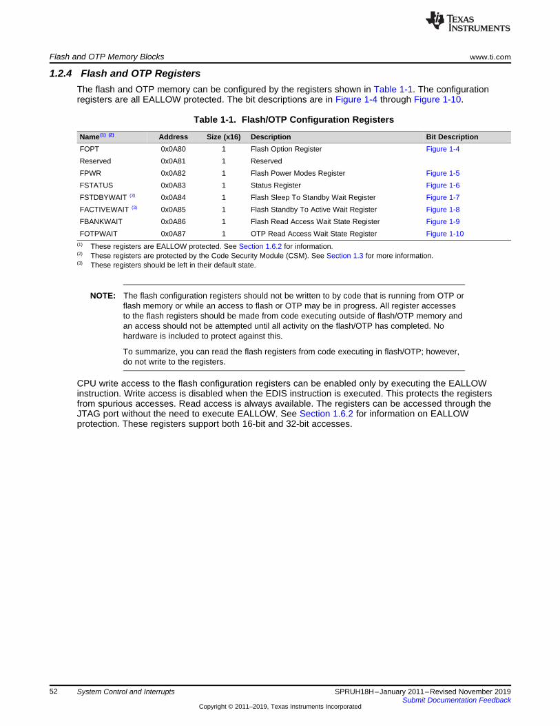
Flash and OTP Memory Blocks www.ti.com
52 SPRUH18H–January 2011–Revised November 2019Submit Documentation Feedback
Copyright © 2011–2019, Texas Instruments Incorporated
System Control and Interrupts
1.2.4 Flash and OTP RegistersThe flash and OTP memory can be configured by the registers shown in Table 1-1. The configurationregisters are all EALLOW protected. The bit descriptions are in Figure 1-4 through Figure 1-10.
(1) These registers are EALLOW protected. See Section 1.6.2 for information.(2) These registers are protected by the Code Security Module (CSM). See Section 1.3 for more information.(3) These registers should be left in their default state.
Table 1-1. Flash/OTP Configuration Registers
Name (1) (2) Address Size (x16) Description Bit DescriptionFOPT 0x0A80 1 Flash Option Register Figure 1-4Reserved 0x0A81 1 ReservedFPWR 0x0A82 1 Flash Power Modes Register Figure 1-5FSTATUS 0x0A83 1 Status Register Figure 1-6FSTDBYWAIT (3) 0x0A84 1 Flash Sleep To Standby Wait Register Figure 1-7FACTIVEWAIT (3) 0x0A85 1 Flash Standby To Active Wait Register Figure 1-8FBANKWAIT 0x0A86 1 Flash Read Access Wait State Register Figure 1-9FOTPWAIT 0x0A87 1 OTP Read Access Wait State Register Figure 1-10
NOTE: The flash configuration registers should not be written to by code that is running from OTP orflash memory or while an access to flash or OTP may be in progress. All register accessesto the flash registers should be made from code executing outside of flash/OTP memory andan access should not be attempted until all activity on the flash/OTP has completed. Nohardware is included to protect against this.
To summarize, you can read the flash registers from code executing in flash/OTP; however,do not write to the registers.
CPU write access to the flash configuration registers can be enabled only by executing the EALLOWinstruction. Write access is disabled when the EDIS instruction is executed. This protects the registersfrom spurious accesses. Read access is always available. The registers can be accessed through theJTAG port without the need to execute EALLOW. See Section 1.6.2 for information on EALLOWprotection. These registers support both 16-bit and 32-bit accesses.

www.ti.com Flash and OTP Memory Blocks
53SPRUH18H–January 2011–Revised November 2019Submit Documentation Feedback
Copyright © 2011–2019, Texas Instruments Incorporated
System Control and Interrupts
Figure 1-4. Flash Options Register (FOPT)15 1 0
Reserved ENPIPER-0 R/W-0
LEGEND: R/W = Read/Write; R = Read only; -n = value after reset
(1) This register is EALLOW protected. See Section 1.6.2 for more information.(2) This register is protected by the Code Security Module (CSM). See Section 1.3 for more information.(3) When writing to this register, follow the procedure described in Section 1.2.3.4.
Table 1-2. Flash Options Register (FOPT) Field Descriptions
Bit Field Value Description (1) (2) (3)
15-1 Reserved Any writes to these bits must always have a value of 0.0 ENPIPE Enable Flash Pipeline Mode Bit. Flash pipeline mode is active when this bit is set. The pipeline
mode improves performance of instruction fetches by pre-fetching instructions. See Section 1.2.3.2for more information.When pipeline mode is enabled, the flash wait states (paged and random) must be greater thanzero.On flash devices, ENPIPE affects fetches from flash and OTP.
0 Flash Pipeline mode is not active. (default)1 Flash Pipeline mode is active.
Figure 1-5. Flash Power Register (FPWR)15 2 1 0
Reserved PWRR-0 R/W-0
LEGEND: R/W = Read/Write; R = Read only; -n = value after reset
(1) This register is EALLOW protected. See Section 1.6.2 for more information.(2) This register is protected by the Code Security Module (CSM). See Section 1.3 for more information.
Table 1-3. Flash Power Register (FPWR) Field Descriptions
Bit Field Value Description (1) (2)
15-2 Reserved Any writes to these bits must always have a value of 0.1-0 PWR Flash Power Mode Bits. Writing to these bits changes the current power mode of the flash bank
and pump. See section Section 1.2.3 for more information on changing the flash bank power mode.00 Pump and bank sleep (lowest power)01 Pump and bank standby10 Reserved (no effect)11 Pump and bank active (highest power)

Flash and OTP Memory Blocks www.ti.com
54 SPRUH18H–January 2011–Revised November 2019Submit Documentation Feedback
Copyright © 2011–2019, Texas Instruments Incorporated
System Control and Interrupts
Figure 1-6. Flash Status Register (FSTATUS)15 9 8
Reserved 3VSTATR-0 R/W1C-0
7 4 3 2 1 0Reserved ACTIVEWAITS STDBYWAITS PWRS
R-0 R-0 R-0 R-0LEGEND: R/W = Read/Write; R = Read only; W1C = Write 1 to clear; -n = value after reset
(1) This register is EALLOW protected. See Section 1.6.2 for more information.(2) This register is protected by the Code Security Module (CSM). See Section 1.3 for more information.
Table 1-4. Flash Status Register (FSTATUS) Field Descriptions
Bit Field Value Description (1) (2)
15-9 Reserved Any writes to these bits must always have a value of 0.8 3VSTAT Flash Voltage (VDD3VFL) Status Latch Bit. When set, this bit indicates that the 3VSTAT signal from
the pump module went to a high level. This signal indicates that the flash 3.3-V supply went out ofthe allowable range.
0 Writes of 0 are ignored.1 When this bit reads 1, it indicates that the flash 3.3-V supply went out of the allowable range.
Clear this bit by writing a 1.7-4 Reserved Any writes to these bits must always have a value of 0.3 ACTIVEWAITS Bank and Pump Standby To Active Wait Counter Status Bit. This bit indicates whether the
respective wait counter is timing out an access.0 The counter is not counting.1 The counter is counting.
2 STDBYWAITS Bank and Pump Sleep To Standby Wait Counter Status Bit. This bit indicates whether therespective wait counter is timing out an access.
0 The counter is not counting.1 The counter is counting.
1-0 PWRS Power Modes Status Bits. These bits indicate which power mode the flash/OTP is currently in.The PWRS bits are set to the new power mode only after the appropriate timing delays haveexpired.
00 Pump and bank in sleep mode (lowest power)01 Pump and bank in standby mode10 Reserved11 Pump and bank active and in read mode (highest power)
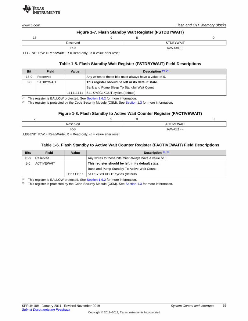
www.ti.com Flash and OTP Memory Blocks
55SPRUH18H–January 2011–Revised November 2019Submit Documentation Feedback
Copyright © 2011–2019, Texas Instruments Incorporated
System Control and Interrupts
Figure 1-7. Flash Standby Wait Register (FSTDBYWAIT)15 9 8 0
Reserved STDBYWAITR-0 R/W-0x1FF
LEGEND: R/W = Read/Write; R = Read only; -n = value after reset
(1) This register is EALLOW protected. See Section 1.6.2 for more information.(2) This register is protected by the Code Security Module (CSM). See Section 1.3 for more information.
Table 1-5. Flash Standby Wait Register (FSTDBYWAIT) Field Descriptions
Bit Field Value Description (1) (2)
15-9 Reserved Any writes to these bits must always have a value of 0.8-0 STDBYWAIT This register should be left in its default state.
Bank and Pump Sleep To Standby Wait Count.111111111 511 SYSCLKOUT cycles (default)
Figure 1-8. Flash Standby to Active Wait Counter Register (FACTIVEWAIT)7 9 8 0
Reserved ACTIVEWAITR-0 R/W-0x1FF
LEGEND: R/W = Read/Write; R = Read only; -n = value after reset
(1) This register is EALLOW protected. See Section 1.6.2 for more information.(2) This register is protected by the Code Security Module (CSM). See Section 1.3 for more information.
Table 1-6. Flash Standby to Active Wait Counter Register (FACTIVEWAIT) Field Descriptions
Bits Field Value Description (1) (2)
15-9 Reserved Any writes to these bits must always have a value of 0.8-0 ACTIVEWAIT This register should be left in its default state.
Bank and Pump Standby To Active Wait Count:111111111 511 SYSCLKOUT cycles (default)

Flash and OTP Memory Blocks www.ti.com
56 SPRUH18H–January 2011–Revised November 2019Submit Documentation Feedback
Copyright © 2011–2019, Texas Instruments Incorporated
System Control and Interrupts
Figure 1-9. Flash Wait-State Register (FBANKWAIT)15 12 11 8 7 4 3 0
Reserved PAGEWAIT Reserved RANDWAITR-0 R/W-0xF R-0 R/W-0xF
LEGEND: R/W = Read/Write; R = Read only; -n = value after reset
(1) This register is EALLOW protected. See Section 1.6.2 for more information.(2) This register is protected by the Code Security Module (CSM). See Section 1.3 for more information.(3) When writing to this register, follow the procedure described in Section 1.2.3.4.
Table 1-7. Flash Wait-State Register (FBANKWAIT) Field Descriptions
Bits Field Value Description (1) (2) (3)
15-12 Reserved Any writes to these bits must always have a value of 0.11-8 PAGEWAIT Flash Paged Read Wait States. These register bits specify the number of wait states for a paged
read operation in CPU clock cycles (0..15 SYSCLKOUT cycles) to the flash bank. SeeSection 1.2.3.1 for more information.See the device-specific datasheet for the minimum time required for a PAGED flash access.You must set RANDWAIT to a value greater than or equal to the PAGEWAIT setting. No hardware isprovided to detect a PAGEWAIT value that is greater then RANDWAIT.
0000 Zero wait-state per paged flash access or one SYSCLKOUT cycle per access0001 One wait state per paged flash access or a total of two SYSCLKOUT cycles per access0010 Two wait states per paged flash access or a total of three SYSCLKOUT cycles per access0011 Three wait states per paged flash access or a total of four SYSCLKOUT cycles per access. . . . . .
1111 15 wait states per paged flash access or a total of 16 SYSCLKOUT cycles per access. (default)7-4 Reserved Any writes to these bits must always have a value of 0.3-0 RANDWAIT Flash Random Read Wait States. These register bits specify the number of wait states for a random
read operation in CPU clock cycles (1..15 SYSCLKOUT cycles) to the flash bank. SeeSection 1.2.3.1 for more information.See the device-specific datasheet for the minimum time required for a RANDOM flash access.RANDWAIT must be set greater than 0. That is, at least 1 random wait state must be used. Inaddition, you must set RANDWAIT to a value greater than or equal to the PAGEWAIT setting. Thedevice will not detect and correct a PAGEWAIT value that is greater then RANDWAIT.
0000 Illegal value. RANDWAIT must be set greater then 0.0001 One wait state per random flash access or a total of two SYSCLKOUT cycles per access.0010 Two wait states per random flash access or a total of three SYSCLKOUT cycles per access.0011 Three wait states per random flash access or a total of four SYSCLKOUT cycles per access.. . . . . .
1111 15 wait states per random flash access or a total of 16 SYSCLKOUT cycles per access. (default)

www.ti.com Flash and OTP Memory Blocks
57SPRUH18H–January 2011–Revised November 2019Submit Documentation Feedback
Copyright © 2011–2019, Texas Instruments Incorporated
System Control and Interrupts
Figure 1-10. OTP Wait-State Register (FOTPWAIT)15 5 4 0
Reserved OTPWAITR-0 R/W-0x1F
LEGEND: R/W = Read/Write; R = Read only; -n = value after reset
(1) This register is EALLOW protected. See Section 1.6.2 for more information.(2) This register is protected by the Code Security Module (CSM). See Section 1.3 for more information.(3) When writing to this register, follow the procedure described in Section 1.2.3.4.
Table 1-8. OTP Wait-State Register (FOTPWAIT) Field Descriptions
Bits Field Value Description (1) (2) (3)
15-5 Reserved Any writes to these bits must always have a value of 0.4-0 OTPWAIT OTP Read Wait States. These register bits specify the number of wait states for a read operation in
CPU clock cycles (1..31 SYSCLKOUT cycles) to the OTP. See CPU Read Or Fetch Access Fromflash/OTP section for details. There is no PAGE mode in the OTP.OTPWAIT must be set greater than 0. That is, a minimum of 1 wait state must be used. See thedevice-specific datasheet for the minimum time required for an OTP access.
00000 Illegal value. OTPWAIT must be set to 1 or greater.00001 One wait state will be used each OTP access for a total of two SYSCLKOUT cycles per access.00010 Two wait states will be used for each OTP access for a total of three SYSCLKOUT cycles per access.00011 Three wait states will be used for each OTP access for a total of four SYSCLKOUT cycles per access.
. . . . . .11111 31 wait states will be used for an OTP access for a total of 32 SYSCLKOUT cycles per access.

Code Security Module (CSM) www.ti.com
58 SPRUH18H–January 2011–Revised November 2019Submit Documentation Feedback
Copyright © 2011–2019, Texas Instruments Incorporated
System Control and Interrupts
1.3 Code Security Module (CSM)The code security module (CSM) is a security feature incorporated in 28x devices. It preventsaccess/visibility to on-chip memory to unauthorized persons — that is, it prevents duplication/reverseengineering of proprietary code.
The word "secure" means access to on-chip secure memory is protected. The word "unsecure" meansaccess to on-chip secure memory is not protected — that is, the contents of the memory could be read byany means (through a debugging tool such as Code Composer Studio™, for example).
1.3.1 Functional DescriptionThe security module restricts the CPU access to certain on-chip memory without interrupting or stallingCPU execution. When a read occurs to a protected memory location, the read returns a zero value andCPU execution continues with the next instruction. This, in effect, blocks read and write access to variousmemories through the JTAG port or external peripherals. Security is defined with respect to the access ofon-chip memory and prevents unauthorized copying of proprietary code or data.
The device is secure when CPU access to the on-chip secure memory locations is restricted. Whensecure, two levels of protection are possible, depending on where the program counter is currentlypointing. If code is currently running from inside secure memory, only an access through JTAG is blocked(that is, through the debug probe). This allows secure code to access secure data. Conversely, if code isrunning from nonsecure memory, all accesses to secure memories are blocked. User code candynamically jump in and out of secure memory, thereby allowing secure function calls from nonsecurememory. Similarly, interrupt service routines can be placed in secure memory, even if the main programloop is run from nonsecure memory.
Security is protected by a password of 128-bits of data (eight 16-bit words) that is used to secure orunsecure the device. This password is stored at the end of flash in 8 words referred to as the passwordlocations.
The device is unsecured by executing the password match flow (PMF), described in Section 1.3.3.2.Table 1-9 shows the levels of security.
Table 1-9. Security Levels
PMF ExecutedWith CorrectPassword?
Operating Mode Program FetchLocation
Security Description
No Secure Outside secure memory Only instruction fetches by the CPU are allowed to securememory. In other words, code can still be executed, but notread
No Secure Inside secure memory CPU has full access.JTAG port cannot read the secured memory contents.
Yes Not Secure Anywhere Full access for CPU and JTAG port to secure memory
The password is stored in code security password locations (PWL) in flash memory (0x3F 7FF8 -0x3F 7FFF). These locations store the password predetermined by the system designer.
If the password locations have all 128 bits as ones, the device is labeled unsecure. Since new flashdevices have erased flash (all ones), only a read of the password locations is required to bring the deviceinto unsecure mode. If the password locations have all 128 bits as zeros, the device is secure, regardlessof the contents of the KEY registers. Do not use all zeros as a password or reset the device during anerase of the flash. Resetting the device during an erase routine can result in either an all zero or unknownpassword. If a device is reset when the password locations are all zeros, the device cannot be unlockedby the password match flow described in Section 1.3.3.2. Using a password of all zeros will seriously limityour ability to debug secure code or reprogram the flash.
NOTE: If a device is reset while the password locations are all zero or an unknown value, the devicewill be permanently locked unless a method to run the flash erase routine from secureSARAM is embedded into the flash or OTP. Care must be taken when implementing thisprocedure to avoid introducing a security hole.
www.ti.com Code Security Module (CSM)
59SPRUH18H–January 2011–Revised November 2019Submit Documentation Feedback
Copyright © 2011–2019, Texas Instruments Incorporated
System Control and Interrupts
User accessible registers (eight 16-bit words) that are used to unsecure the device are referred to as KEYregisters. These registers are mapped in the memory space at addresses 0x00 0AE0 - 0x00 0AE7 andare EALLOW protected.
In addition to the CSM, the emulation code security logic (ECSL) has been implemented to preventunauthorized users from stepping through secure code. Any code or data access to flash, user OTP, L0memory while the emulator is connected will trip the ECSL and break the emulation connection. To allowemulation of secure code, while maintaining the CSM protection against secure memory reads, you mustwrite the correct value into the lower 64 bits of the KEY register, which matches the value stored in thelower 64 bits of the password locations within the flash. Note that dummy reads of all 128 bits of thepassword in the flash must still be performed. If the lower 64 bits of the password locations are all ones(unprogrammed), then the KEY value does not need to match.
When initially debugging a device with the password locations in flash programmed (that is, secured), theemulator takes some time to take control of the CPU. During this time, the CPU will start running and mayexecute an instruction that performs an access to a protected ECSL area. If this happens, the ECSL willtrip and cause the emulator connection to be cut. Two solutions to this problem exist:1. The first is to use the Wait-In-Reset emulation mode, which will hold the device in reset until the
emulator takes control. The emulator must support this mode for this option.2. The second option is to use the “Branch to check boot mode” boot option. This will sit in a loop and
continuously poll the boot mode select pins. You can select this boot mode and then exit this modeonce the emulator is connected by re-mapping the PC to another address or by changing the bootmode selection pin to the desired boot mode.
NOTE: The 128-bit password (at 0x3F 7FF8 - 0x3F 7FFF) must not be programmed to zeros. Doingso would permanently lock the device.
Addresses 0x3F 7FF0 through 0x3F 7FF5 are reserved for data variables and should notcontain program code.
Disclaimer: Code Security Module Disclaimer
The Code Security Module ( CSM ) included on this device was designed to passwordprotect the data stored in the associated memory and is warranted by Texas Instruments(TI), in accordance with its standard terms and conditions, to conform to TI's publishedspecifications for the warranty period applicable for this device.
TI DOES NOT, HOWEVER, WARRANT OR REPRESENT THAT THE CSM CANNOT BECOMPROMISED OR BREACHED OR THAT THE DATA STORED IN THE ASSOCIATEDMEMORY CANNOT BE ACCESSED THROUGH OTHER MEANS. MOREOVER, EXCEPTAS SET FORTH ABOVE, TI MAKES NO WARRANTIES OR REPRESENTATIONSCONCERNING THE CSM OR OPERATION OF THIS DEVICE, INCLUDING ANY IMPLIEDWARRANTIES OF MERCHANTABILITY OR FITNESS FOR A PARTICULAR PURPOSE.
IN NO EVENT SHALL TI BE LIABLE FOR ANY CONSEQUENTIAL, SPECIAL, INDIRECT,INCIDENTAL, OR PUNITIVE DAMAGES, HOWEVER CAUSED, ARISING IN ANY WAYOUT OF YOUR USE OF THE CSM OR THIS DEVICE, WHETHER OR NOT TI HAS BEENADVISED OF THE POSSIBILITY OF SUCH DAMAGES. EXCLUDED DAMAGES INCLUDE,BUT ARE NOT LIMITED TO LOSS OF DATA, LOSS OF GOODWILL, LOSS OF USE ORINTERRUPTION OF BUSINESS OR OTHER ECONOMIC LOSS.

Code Security Module (CSM) www.ti.com
60 SPRUH18H–January 2011–Revised November 2019Submit Documentation Feedback
Copyright © 2011–2019, Texas Instruments Incorporated
System Control and Interrupts
1.3.2 CSM Impact on Other On-Chip ResourcesThe CSM affects access to the on-chip resources listed in Table 1-10.
(1) Not affected by ECSL
Table 1-10. Resources Affected by the CSM
Address Block0x00 0A80 - 0x00 0A87 Flash Configuration Registers0x00 8000 - 0x00 87FF L0 SARAM (2K x 16)0x00 8800 - 0x00 8BFF L1 DPSARAM - CLA Data RAM 0 (1K x 16)0x00 8C00 - 0x00 8FFF L2 DPSARAM - CLA Data RAM 1 (1K x 16)0x00 9000 - 0x00 9FFF L3 DPSARAM - CLA Program RAM (4K x 16)0x3D 8000 - 0x3F 7FFF or0x3E 8000 - 0x3F 7FFF
Flash (128K x 16)Flash (64K x 16)
0x3D 7800 - 0x3D 7BFF User One-Time Programmable (OTP) (1K x 16)0x3D 7C00 - 0x3D 7FFF TI One-Time Programmable (OTP) (1)(1K x 16)0x00 A000 - 0x00 BFFF L4 SARAM
The Code Security Module has no impact whatsoever on the following on-chip resources:• Single-access RAM (SARAM) blocks not designated as secure - These memory blocks can be freely
accessed and code run from them, whether the device is in secure or unsecure mode.• Boot ROM contents - Visibility to the boot ROM contents is not impacted by the CSM.• On-chip peripheral registers - The peripheral registers can be initialized by code running from on-chip
or off-chip memory, whether the device is in secure or unsecure mode.• PIE Vector Table - Vector tables can be read and written regardless of whether the device is in secure
or unsecure mode. Table 1-10 and Table 1-11 show which on-chip resources are affected (or are notaffected) by the CSM.
Table 1-11. Resources Not Affected by the CSM
Address Block0x00 0000 - 0x00 03FF M0 SARAM (1K x 16)0x00 0400 - 0x00 07FF M1 SARAM (1K x16)0x00 0800 - 0x00 0CFF Peripheral Frame 0 (2K x 16)0x00 0D00 - 0x00 0FFF PIE Vector RAM (256 x 16)0x00 6000 - 0x00 6FFF Peripheral Frame 1 (4K x 16)0x00 7000 - 0x00 7FFF Peripheral Frame 2 (4K x 16)
To summarize, it is possible to load code onto the unprotected on-chip program SARAM via the JTAGconnector without any impact from the Code Security Module. The code can be debugged and theperipheral registers initialized, independent of whether the device is in secure or unsecure mode.
1.3.3 Incorporating Code Security in User ApplicationsCode security is typically not employed in the development phase of a project; however, security may bedesired once the application code is finalized. Before such a code is programmed in the flash memory, apassword should be chosen to secure the device. Once a password is in place, the device is secured (thatis, programming a password at the appropriate locations and either performing a device reset or settingthe FORCESEC bit (CSMSCR.15) is the action that secures the device). From that time on, access todebug the contents of secure memory by any means (via JTAG, code running off external/on-chipmemory, and so on) requires the supply of a valid password. A password is not needed to run the codeout of secure memory (such as in end-customer usage); however, access to secure memory contents fordebug purpose requires a password.

www.ti.com Code Security Module (CSM)
61SPRUH18H–January 2011–Revised November 2019Submit Documentation Feedback
Copyright © 2011–2019, Texas Instruments Incorporated
System Control and Interrupts
If the code-security feature is used, any one of the following directives must be used when a functionresiding in secure memory calls another function which belongs to a different secure zone or to unsecurememory:• Use unsecure memory as stack• Switch stack to unsecure memory before calling the function• Unlock security before calling the function
Note that the above directives apply for any address-based-parameters passed on to the called function,basically making sure that the called function can read/write to these address-based parameters.
(1) These registers are EALLOW protected. Refer to Section 1.6.2 for more information.
Table 1-12. Code Security Module (CSM) Registers
MemoryAddress Register Name Reset Values Register DescriptionKEY Registers0x00 - 0AE0 KEY0 (1) 0xFFFF Low word of the 128-bit KEY register0x00 - 0AE1 KEY1 (1) 0xFFFF Second word of the 128-bit KEY register0x00 - 0AE2 KEY2 (1) 0xFFFF Third word of the 128-bit KEY register0x00 - 0AE3 KEY3 (1) 0xFFFF Fourth word of the 128-bit key0x00 - 0AE4 KEY4 (1) 0xFFFF Fifth word of the 128-bit key0x00 - 0AE5 KEY5 (1) 0xFFFF Sixth word of the 128-bit key0x00 - 0AE6 KEY6 (1) 0xFFFF Seventh word of the 128-bit key0x00 - 0AE7 KEY7 (1) 0xFFFF High word of the 128-bit KEY register0x00 - 0AEF CSMSCR (1) 0x002F CSM status and control registerPassword Locations (PWL) in Flash Memory - Reserved for the CSM password only0x3F - 7FF8 PWL0 User defined Low word of the 128-bit password0x3F - 7FF9 PWL1 User defined Second word of the 128-bit password0x3F - 7FFA PWL2 User defined Third word of the 128-bit password0x3F - 7FFB PWL3 User defined Fourth word of the 128-bit password0x3F - 7FFC PWL4 User defined Fifth word of the 128-bit password0x3F - 7FFD PWL5 User defined Sixth word of the 128-bit password0x3F - 7FFE PWL6 User defined Seventh word of the 128-bit password0x3F - 7FFF PWL7 User defined High word of the 128-bit password

Code Security Module (CSM) www.ti.com
62 SPRUH18H–January 2011–Revised November 2019Submit Documentation Feedback
Copyright © 2011–2019, Texas Instruments Incorporated
System Control and Interrupts
Figure 1-11. CSM Status and Control Register (CSMSCR)15 14 1 0
FORCESEC Reserved SECUREW-0 R-0x002E R-1
LEGEND: R/W = Read/Write; R = Read only; -n = value after reset
(1) This register is EALLOW protected. Refer to Section 1.6.2 for more information.
Table 1-13. CSM Status and Control Register (CSMSCR) Field Descriptions
Bits Field Value Description (1)
15 FORCESEC Writing a 1 clears the KEY registers and secures the device.0 A read always returns a zero.1 Clears the KEY registers and secures the device. The password match flow described in
Section 1.3.3.2 must be followed to unsecure the device again.14-1 Reserved Reserved
0 SECURE Read-only bit that reflects the security state of the device.0 Device is unsecure (CSM unlocked).1 Device is secure (CSM locked).
1.3.3.1 Environments That Require Security UnlockingFollowing are the typical situations under which unsecuring may be required:• Code development using debuggers (such as Code Composer Studio™).
This is the most common environment during the design phase of a product.• Flash programming using TI's flash utilities such as Code Composer Studio™ Flash Programmer plug-
in or Uniflash.Flash programming is common during code development and testing. Once the user supplies thenecessary password, the flash utilities disable the security logic before attempting to program the flash.The flash utilities can disable the code security logic in new devices without any authorization, sincenew devices come with an erased flash. However, reprogramming devices (that already contain acustom password) require the password to be supplied to the flash utilities in order to unlock the deviceto enable programming. In custom programming solutions that use the flash API supplied by TIunlocking the CSM can be avoided by executing the flash programming algorithms from securememory.
• Custom environment defined by the application
In addition to the above, access to secure memory contents can be required in situations such as:• Using the on-chip bootloader to load code or data into secure SARAM or to erase/program the flash.• Executing code from on-chip unsecure memory and requiring access to secure memory for lookup
table. This is not a suggested operating condition as supplying the password from external code couldcompromise code security.
The unsecuring sequence is identical in all the above situations. This sequence is referred to as thepassword match flow (PMF) for simplicity. Figure 1-12 explains the sequence of operation that is requiredevery time the user attempts to unsecure a device. A code example is listed for clarity.

Start
Yes
No
Yes
No
Device unsecure
User can access
on-chip secure
memory
Device permanently secured
CPU access is limited.
Device cannot be debugged
or reprogrammed.
Do dummy read of PWL
0x3F 7FF8 − 0x3F 7FFF
KEY registers = all ones
Correctpassword?
Are PWL =all Fs?
Are PWL =all zeros?
Device secure after
reset or runtime
No
Yes
Write the password to
KEY registers
0x00 0AE0 0x00 0AE7−(A)
www.ti.com Code Security Module (CSM)
63SPRUH18H–January 2011–Revised November 2019Submit Documentation Feedback
Copyright © 2011–2019, Texas Instruments Incorporated
System Control and Interrupts
1.3.3.2 Password Match FlowPassword match flow (PMF) is essentially a sequence of eight dummy reads from password locations(PWL) followed by eight writes to KEY registers.
Figure 1-12 shows how the PMF helps to initialize the security logic registers and disable security logic.
Figure 1-12. Password Match Flow (PMF)
A The KEY registers are EALLOW protected.
NOTE: Any read of the CSM password would yield 0x0000 until the device is unlocked. These reads arelabeled "dummy read" or a "fake read." The application reads the password locations, but will always get0's no matter what the actual value is. What is important is the actual value of the password. If the actualvalue is all 0xFFFF, then doing this "dummy read" will unlock the device. If the actual value is all 0x0000,then no matter what the application code does, one will never be able to unlock the device. If the actualvalue is something other than all 0xFFFF or 0x0000, then when the dummy read is performed, the actualvalue must match the password the user provided.

Code Security Module (CSM) www.ti.com
64 SPRUH18H–January 2011–Revised November 2019Submit Documentation Feedback
Copyright © 2011–2019, Texas Instruments Incorporated
System Control and Interrupts
1.3.3.3 Unsecuring Considerations for Devices With/Without Code SecurityCase 1 and Case 2 provide unsecuring considerations for devices with and without code security.
Case 1: Device With Code SecurityA device with code security should have a predetermined password stored in the password locations(0x3F 7FF8 - 0x3F 7FFF in memory). In addition, locations 0x3F 7F80 - 0x3F 7FF5 should beprogrammed with all 0x0000 and not used for program and/or data storage. The following are steps tounsecure this device:1. Perform a dummy read of the password locations. The CSM blocks the OTP reads to password
location. Hence the dummy reads to password location can be done only from RAM (secure/unsecure)or Flash.
2. Write the password into the KEY registers (locations 0x00 0AE0 - 0x00 0AE7 in memory).3. If the password is correct, the device becomes unsecure; otherwise, it stays secure.Case 2: Device Without Code Security
A device without code security should have 0x FFFF FFFF FFFF FFFF FFFF FFFF FFFF FFFF (128 bitsof all ones) stored in the password locations. The following are steps to use this device:1. At reset, the CSM will lock memory regions protected by the CSM.2. Perform a dummy read of the password locations. The CSM blocks the OTP reads to password
location. Hence the dummy reads to password location can be done only from RAM (secure/unsecure)or Flash.
3. Since the password is all ones, this alone will unlock all memory regions. Secure memory is fullyaccessible immediately after this operation is completed.
NOTE: Even if a device is not protected with a password (all password locations all ones), the CSMwill lock at reset. Thus, a dummy read operation must still be performed on these devicesprior to reading, writing, or programming secure memory if the code performing the access isexecuting from outside of the CSM protected memory region. The Boot ROM code does thisdummy read for convenience.

www.ti.com Code Security Module (CSM)
65SPRUH18H–January 2011–Revised November 2019Submit Documentation Feedback
Copyright © 2011–2019, Texas Instruments Incorporated
System Control and Interrupts
1.3.3.3.1 C Code Example to Unsecure
volatile int *CSM = (volatile int *)0x000AE0; //CSM register filevolatile int *PWL = (volatile int *)0x003F7FF8; //Password locationvolatile int tmp;int I;
// Read the 128-bits of the password locations (PWL)// in flash at address 0x3F 7FF8 - 0x3F 7FFF// If the device is secure, then the values read will// not actually be loaded into the temp variable, so// this is called a dummy read.
for (I=0; i<8; I++) tmp = *PWL++;// If the password locations (PWL) are all = ones (0xFFFF),// then the device will now be unsecure. If the password// is not all ones (0xFFFF), then the code below is required// to unsecure the CSM.// Write the 128-bit password to the KEY registers// If this password matches that stored in the// PWL then the CSM will become unsecure. If it does not// match, then the device will remain secure.// An example password of:// 0x11112222333344445555666677778888 is used.
asm(" EALLOW"); // Key registers are EALLOW protected*CSM++ = 0x1111; // Register KEY0 at 0xAE0*CSM++ = 0x2222; // Register KEY1 at 0xAE1*CSM++ = 0x3333; // Register KEY2 at 0xAE2*CSM++ = 0x4444; // Register KEY3 at 0xAE3*CSM++ = 0x5555; // Register KEY4 at 0xAE4*CSM++ = 0x6666; // Register KEY5 at 0xAE5*CSM++ = 0x7777; // Register KEY6 at 0xAE6*CSM++ = 0x8888; // Register KEY7 at 0xAE7asm(" EDIS");
1.3.3.3.2 C Code Example to Resecure
volatile int *CSMSCR = 0x00AEF; //CSMSCR register//Set FORCESEC bit
asm(" EALLOW"); //CSMSCR register is EALLOW protected.
*CSMSCR = 0x8000;
asm("EDIS");

Code Security Module (CSM) www.ti.com
66 SPRUH18H–January 2011–Revised November 2019Submit Documentation Feedback
Copyright © 2011–2019, Texas Instruments Incorporated
System Control and Interrupts
1.3.4 Do's and Don'ts to Protect Security Logic
1.3.4.1 Do's• To keep the debug and code development phase simple, use the device in the unsecure mode; that is,
use all 128 bits as ones in the password locations (or use a password that is easy to remember). Usea password after the development phase when the code is frozen.
• Recheck the password stored in the password locations before programming the COFF file using flashutilities.
• The flow of code execution can freely toggle back and forth between secure memory and unsecurememory without compromising security. To access data variables located in secure memory when thedevice is secured, code execution must currently be running from secure memory.
• Program locations 0x3F 7F80 - 0x3F 7FF5 with 0x0000 when using the CSM.
1.3.4.2 Don'ts• If code security is desired, do not embed the password in your application anywhere other than in the
password locations or security can be compromised.• Do not use 128 bits of all zeros as the password. This automatically secures the device, regardless of
the contents of the KEY register. The device is not debuggable nor reprogrammable.• Do not pull a reset during an erase operation on the flash array. This can leave either zeros or an
unknown value in the password locations. If the password locations are all zero during a reset, thedevice will always be secure, regardless of the contents of the KEY register.
• Do not use locations 0x3F 7F80 - 0x3F 7FF5 to store program and/or data. These locations should beprogrammed to 0x0000 when using the CSM.
1.3.5 CSM Features - Summary1. The flash is secured after a reset until the password match flow described in Section 1.3.3.2 is
executed.2. The standard way of running code out of the flash is to program the flash with the code and power up
the device. Since instruction fetches are always allowed from secure memory, regardless of the stateof the CSM, the code functions correctly even without executing the password match flow.
3. Secure memory cannot be modified by code executing from unsecure memory while the device issecured.
4. Secure memory cannot be read from any code running from unsecure memory while the device issecured.
5. Secure memory cannot be read or written to by the debugger (Code Composer Studio™) at any timethat the device is secured.
6. Complete access to secure memory from both the CPU code and the debugger is granted while thedevice is unsecured.

www.ti.com Clocking
67SPRUH18H–January 2011–Revised November 2019Submit Documentation Feedback
Copyright © 2011–2019, Texas Instruments Incorporated
System Control and Interrupts
1.4 ClockingThis section describes the oscillator, PLL and clocking mechanisms, the watchdog function, and the low-power modes.
1.4.1 Clocking and System ControlThe figure below shows the various clock and reset domains.

LOSPCP(System Ctrl Regs)
PeripheralRegistersSPI-A, SPI-B, SCI-A, SCI-B
PF2
LSPCLK
SYSCLKOUTC28x Core CLKIN
PeripheralRegisters
USBPF3
GPIOMux
LOSPCP(System Ctrl Regs)
PeripheralRegistersMcBSP
PF3
LSPCLK
PeripheralRegisterseCAN-A
PF1
PeripheralRegisters
eCAP1, eCAP2, eCAP3eQEP1, eQEP2 PF3
PeripheralRegisters
ePWM1, ePWM2,ePWM3, ePWM4, ePWM5,ePWM6, ePWM7, ePWM8 PF3
PeripheralRegisters
I2C-APF2
PeripheralRegisters
HRCAP1, HRCAP2,HRCAP3, HRCAP4 PF1
ADCRegisters12-Bit ADC16 Ch
PF2
PF0
COMPRegistersCOMP1/2/3
PF36
AnalogGPIOMux
/2
PCLKCR0/1/2/3(System Ctrl Regs)
Clock Enables
Clock Enables
Clock Enables
Clock Enables
Clock Enables
Clock Enables
Clock Enables
Clock Enables
Clock Enables
Clock Enables
PLL2
I/O
I/O
I/O
I/O
I/O
I/O
I/O
I/O
Clocking www.ti.com
68 SPRUH18H–January 2011–Revised November 2019Submit Documentation Feedback
Copyright © 2011–2019, Texas Instruments Incorporated
System Control and Interrupts
Figure 1-13. Clock and Reset Domains
The PLL, clocking, watchdog and low-power modes, are controlled by the registers listed in Table 1-14.

www.ti.com Clocking
69SPRUH18H–January 2011–Revised November 2019Submit Documentation Feedback
Copyright © 2011–2019, Texas Instruments Incorporated
System Control and Interrupts
Table 1-14. PLL, Clocking, Watchdog, and Low-Power Mode Registers
NAME ADDRESS SIZE (x16) DESCRIPTIONBORCFG 0x00 0985 1 BOR Configuration RegisterXCLK 0x00 7010 1 XCLKOUT ControlPLLSTS 0x00 7011 1 PLL Status RegisterCLKCTL 0x00 7012 1 Clock Control RegisterPLLLOCKPRD 0x00 7013 1 PLL Lock PeriodINTOSC1TRIM 0x00 7014 1 Internal Oscillator 1 Trim RegisterINTOSC2TRIM 0x00 7016 1 Internal Oscillator 2 Trim RegisterPCLKCR2 0x00 7019 1 Peripheral Clock Control Register 2LOSPCP 0x00 701B 1 Low-Speed Peripheral Clock Prescaler RegisterPCLKCR0 0x00 701C 1 Peripheral Clock Control Register 0PCLKCR1 0x00 701D 1 Peripheral Clock Control Register 1LPMCR0 0x00 701E 1 Low Power Mode Control Register 0PCLKCR3 0x00 7020 1 Peripheral Clock Control Register 3PLLCR 0x00 7021 1 PLL Control RegisterSCSR 0x00 7022 1 System Control and Status RegisterWDCNTR 0x00 7023 1 Watchdog Counter RegisterWDKEY 0x00 7025 1 Watchdog Reset Key RegisterWDCR 0x00 7029 1 Watchdog Control RegisterPLL2CTL 0x00 7030 1 PLL2 Configuration RegisterPLL2MULT 0x00 7032 1 PLL2 Multiplier RegisterPLL2STS 0x00 7034 1 PLL2 Lock Status RegisterSYSCLK2CNTR 0x00 7036 1 SYSCLK2 Clock Counter RegisterEPWMCFG 0x00 703A 1 ePWM DMA/CLA Configuration Register
1.4.1.1 Enabling/Disabling Clocks to the Peripheral ModulesThe PCLKCR0/1/2/3 registers enable/disable clocks to the various peripheral modules. There is a 2-SYSCLKOUT cycle delay from when a write to the PCLKCR0/1/2/3 registers occurs to when the action isvalid. This delay must be taken into account before attempting to access the peripheral configurationregisters. Due to the peripheral-GPIO multiplexing at the pin level, all peripherals cannot be used at thesame time. While it is possible to turn on the clocks to all the peripherals at the same time, such aconfiguration may not be useful. If this is done, the current drawn will be more than required. To avoid this,only enable the clocks required by the application.
Figure 1-14. Peripheral Clock Control 0 Register (PCLKCR0)15 14 13 12 11 10 9 8
Reserved ECANAENCLK Reserved MCBSPAENCLK
SCIBENCLK SCIAENCLK SPIBENCLK SPIAENCLK
R-0 R/W-0 R-0 R/W-0 R/W-0 R/W-0 R/W-0 R/W-0
7 5 4 3 2 1 0Reserved I2CAENCLK ADCENCLK TBCLKSYNC Reserved HRPWMENCLK
R-0 R/W-0 R/W-0 R/W-0 R-0 R/W-0LEGEND: R/W = Read/Write; R = Read only; -n = value after reset

Clocking www.ti.com
70 SPRUH18H–January 2011–Revised November 2019Submit Documentation Feedback
Copyright © 2011–2019, Texas Instruments Incorporated
System Control and Interrupts
(1) If a peripheral block is not used, the clock to that peripheral can be turned off to minimize power consumption.
Table 1-15. Peripheral Clock Control 0 Register (PCLKCR0) Field Descriptions
Bit Field Value Description15 Reserved Any writes to these bits must always have a value of 0.14 ECANAENCLK ECAN-A clock enable
0 The eCAN-A module is not clocked. (default) (1)
1 The eCAN-A module is clocked (SYSCLKOUT/2).13 Reserved Any writes to these bits must always have a value of 0.12 MCBSPAENCLK MCBSP clock enable
0 The McBSP module is not clocked.1 The McBSP module is clocked.
11 SCIBENCLK SCI-B clock enable0 The SCI-B module is not clocked.1 The SCI-B module is clocked.
10 SCIAENCLK SCI-A clock enable0 The SCI-A module is not clocked. (default) (1)
1 The SCI-A module is clocked by the low-speed clock (LSPCLK).9 SPIBENCLK SPI-B clock enable
0 The SPI-B module is not clocked. (default) (1)
1 The SPI-B module is clocked by the low-speed clock (LSPCLK).8 SPIAENCLK SPI-A clock enable
0 The SPI-A module is not clocked. (default) (1)
1 The SPI-A module is clocked by the low-speed clock (LSPCLK).7-5 Reserved Any writes to these bits must always have a value of 0.4 I2CAENCLK I2C clock enable
0 The I2C module is not clocked. (default) (1)
1 The I2C module is clocked.3 ADCENCLK ADC clock enable
0 The ADC is not clocked. (default) (1)
1 The ADC module is clocked2 TBCLKSYNC ePWM Module Time Base Clock (TBCLK) Sync: Allows the user to globally synchronize all enabled
ePWM modules to the time base clock (TBCLK):0 The TBCLK (Time Base Clock) within each enabled ePWM module is stopped. (default). If,
however, the ePWM clock enable bit is set in the PCLKCR1 register, then the ePWM module willstill be clocked by SYSCLKOUT even if TBCLKSYNC is 0.
1 All enabled ePWM module clocks are started with the first rising edge of TBCLK aligned. Forperfectly synchronized TBCLKs, the prescaler bits in the TBCTL register of each ePWM modulemust be set identically. The proper procedure for enabling ePWM clocks is as follows:• Enable ePWM module clocks in the PCLKCR1 register.• Set TBCLKSYNC to 0.• Configure prescaler values and ePWM modes.• Set TBCLKSYNC to 1.
1 Reserved Any writes to these bits must always have a value of 0.0 HRPWMENCLK HRPWM clock enable
0 HRPWM is not enabled.1 HRPWM is enabled.

www.ti.com Clocking
71SPRUH18H–January 2011–Revised November 2019Submit Documentation Feedback
Copyright © 2011–2019, Texas Instruments Incorporated
System Control and Interrupts
Figure 1-15. Peripheral Clock Control 1 Register (PCLKCR1)15 14 13 11 10 9 8
EQEP2ENCLK EQEP1ENCLK Reserved ECAP3ENCLK ECAP2ENCLK ECAP1ENCLKR/W-0 R/W-0 R-0 R/W-0 R/W-0 R/W-0
7 5 4 3 2 1 0EPWM8ENCLK EPWM7ENCLK EPWM6ENCLK EPWM5ENCLK EPWM4ENCLK EPWM3ENCLK EPWM2ENCLK EPWM1ENCLK
R/W-0 R/W-0 R/W-0 R/W-0 R/W-0 R/W-0 R/W-0 R/W-0LEGEND: R/W = Read/Write; R = Read only; -n = value after reset
(1) This register is EALLOW protected. See Section 1.6.2 for more information.(2) If a peripheral block is not used, the clock to that peripheral can be turned off to minimize power consumption.(3) To start the ePWM Time-base clock (TBCLK) within the ePWM modules, the TBCLKSYNC bit in PCLKCR0 must also be set.
Table 1-16. Peripheral Clock Control 1 Register (PCLKCR1) Field Descriptions
Bits Field Value Description (1)
15 EQEP2ENCLK eQEP2 clock enable0 The eQEP2 module is not clocked. (default) (2)
1 The eQEP2 module is clocked by the system clock (SYSCLKOUT).14 EQEP1ENCLK eQEP1 clock enable
0 The eQEP1 module is not clocked. (default) (2)
1 The eQEP1 module is clocked by the system clock (SYSCLKOUT).13-11 Reserved Any writes to these bits must always have a value of 0.
10 ECAP3ENCLK eCAP3 clock enable0 The eCAP3 module is not clocked. (default) (2)
1 The eCAP3 module is clocked by the system clock (SYSCLKOUT).9 ECAP2ENCLK eCAP2 clock enable
0 The eCAP2 module is not clocked. (default) (2)
1 The eCAP2 module is clocked by the system clock (SYSCLKOUT).8 ECAP1ENCLK eCAP1 clock enable
0 The eCAP1 module is not clocked. (default) (2)
1 The eCAP1 module is clocked by the system clock (SYSCLKOUT).7 EPWM8ENCLK ePWM8 clock enable. (3)
0 The ePWM8 module is not clocked. (default) (2)
1 The ePWM8 module is clocked by the system clock (SYSCLKOUT).6 EPWM7ENCLK ePWM7 clock enable. (3)
0 The ePWM7 module is not clocked. (default) (2)
1 The ePWM7 module is clocked by the system clock (SYSCLKOUT).5 EPWM6ENCLK ePWM6 clock enable. (3)
0 The ePWM6 module is not clocked. (default) (2)
1 The ePWM6 module is clocked by the system clock (SYSCLKOUT).4 EPWM5ENCLK ePWM5 clock enable (3)
0 The ePWM5 module is not clocked. (default) (2)
1 The ePWM5 module is clocked by the system clock (SYSCLKOUT).3 EPWM4ENCLK ePWM4 clock enable. (3)
0 The ePWM4 module is not clocked. (default) (2)
1 The ePWM4 module is clocked by the system clock (SYSCLKOUT).2 EPWM3ENCLK ePWM3 clock enable. (3)
0 The ePWM3 module is not clocked. (default) (2)
1 The ePWM3 module is clocked by the system clock (SYSCLKOUT).

Clocking www.ti.com
72 SPRUH18H–January 2011–Revised November 2019Submit Documentation Feedback
Copyright © 2011–2019, Texas Instruments Incorporated
System Control and Interrupts
Table 1-16. Peripheral Clock Control 1 Register (PCLKCR1) Field Descriptions (continued)Bits Field Value Description (1)
1 EPWM2ENCLK ePWM2 clock enable. (3)
0 The ePWM2 module is not clocked. (default) (2)
1 The ePWM2 module is clocked by the system clock (SYSCLKOUT).0 EPWM1ENCLK ePWM1 clock enable. (3)
0 The ePWM1 module is not clocked. (default) (2)
1 The ePWM1 module is clocked by the system clock (SYSCLKOUT).
Figure 1-16. Peripheral Clock Control 2 Register (PCLKCR2)15 12 11 10 9 8
Reserved HRCAP4ENCLK HRCAP3ENCLK HRCAP2ENCLK HRCAP1ENCLKR-0 R/W-0 R/W-0 R/W-0 R/W-0
7 0Reserved
R-0LEGEND: R/W = Read/Write; R = Read only; -n = value after reset
(1) If a peripheral block is not used, the clock to that peripheral can be turned off to minimize power consumption.
Table 1-17. Peripheral Clock Control 2 Register (PCLKCR2) Field Descriptions
Bit Field Value Description15-12 Reserved 0 Any writes to these bits must always have a value of 0.
11 HRCAP4ENCLK 0 The HRCAP4 module is not clocked. (default) (1)
1 The HRCAP4 module is clocked.10 HRCAP3ENCLK 0 The HRCAP3 module is not clocked. (default) (1)
1 The HRCAP3 module is clocked.9 HRCAP2ENCLK 0 The HRCAP2 module is not clocked. (default) (1)
1 The HRCAP2 module is clocked.8 HRCAP1ENCLK 0 The HRCAP1 module is not clocked. (default) (1)
1 The HRCAP1 module is clocked.0-7 Reserved Any writes to these bits must always have a value of 0.

www.ti.com Clocking
73SPRUH18H–January 2011–Revised November 2019Submit Documentation Feedback
Copyright © 2011–2019, Texas Instruments Incorporated
System Control and Interrupts
Figure 1-17. Peripheral Clock Control 3 Register (PCLKCR3)15 14 13 12 11 10 9 8
USB0ENCLK CLA1ENCLK Reserved Reserved DMAENCLK CPUTIMER2ENCLK CPUTIMER1ENCLK CPUTIMER0ENCLK
R-0 R/W-0 R-1 R-0 R/W-0 R/W-1 R/W-1 R/W-1
7 3 2 1 0Reserved COMP3ENCLK COMP2ENCLK COMP1ENCLK
R-0 R/W-0 R/W-0 R/W-0LEGEND: R/W = Read/Write; R = Read only; -n = value after reset
Table 1-18. Peripheral Clock Control 3 Register (PCLKCR3) Field Descriptions
Bit Field Value Description15 USB0ENCLK USB module clock enable
0 Clock is disabled1 Clock is enabled
14 CLA1ENCLK CLA module clock enable0 CLA is not clocked1 CLA is clocked
13 Reserved Reserved12 Reserved Any writes to these bits must always have a value of 0.11 DMAENCLK DMA module clock enable
0 DMA is not clocked1 DMA is clocked
10 CPUTIMER2ENCLK CPU Timer 2 Clock Enable0 The CPU Timer 2 is not clocked.1 The CPU Timer 2 is clocked.
9 CPUTIMER1ENCLK CPU Timer 1 Clock Enable0 The CPU Timer 1 is not clocked.1 The CPU Timer 1 is clocked.
8 CPUTIMER0ENCLK CPU Timer 0 Clock Enable0 The CPU Timer 0 is not clocked.1 The CPU Timer 0 is clocked.
7:3 Reserved Any writes to these bits must always have a value of 0.2 COMP3ENCLK Comparator3 clock enable
0 Comparator3 is not clocked1 Comparator3 is clocked
1 COMP2ENCLK Comparator2 clock enable0 Comparator2 is not clocked1 Comparator2 is clocked
0 COMP1ENCLK Comparator1 clock enable0 Comparator1 is not clocked1 Comparator1 is clocked

Clocking www.ti.com
74 SPRUH18H–January 2011–Revised November 2019Submit Documentation Feedback
Copyright © 2011–2019, Texas Instruments Incorporated
System Control and Interrupts
1.4.1.2 Configuring the Low-Speed Peripheral Clock PrescalerThe low-speed peripheral clock prescale (LOSPCP) registers are used to configure the low-speedperipheral clocks. See Figure 1-18 for the LOSPCP layout.
Figure 1-18. Low-Speed Peripheral Clock Prescaler Register (LOSPCP)15 3 2 0
Reserved LSPCLKR-0 R/W-010
LEGEND: R/W = Read/Write; R = Read only; -n = value after reset
(1) This register is EALLOW protected. See Section 1.6.2 for more information.(2) LOSPCP in this equation denotes the value of bits 2:0 in the LOSPCP register.
Table 1-19. Low-Speed Peripheral Clock Prescaler Register (LOSPCP) Field Descriptions
Bits Field Value Description (1)
15-3 Reserved Reserved2-0 LSPCLK These bits configure the low-speed peripheral clock (LSPCLK) rate relative to SYSCLKOUT:
If LOSPCP (2) ≠ 0, then LSPCLK = SYSCLKOUT/(LOSPCP X 2)If LOSPCP = 0, then LSPCLK = SYSCLKOUT
000 Low speed clock = SYSCLKOUT/1001 Low speed clock= SYSCLKOUT/2010 Low speed clock= SYSCLKOUT/4 (reset default)011 Low speed clock= SYSCLKOUT/6100 Low speed clock= SYSCLKOUT/8101 Low speed clock= SYSCLKOUT/10110 Low speed clock= SYSCLKOUT/12111 Low speed clock= SYSCLKOUT/14
1.4.2 OSC and PLL BlockThe on-chip oscillators and phase-locked loop (PLL) block provide the clocking signals for the device, aswell as control for low-power mode (LPM) entry or exit.
1.4.2.1 Input Clock OptionsThe device has two internal oscillators (INTOSC1 and INTOSC2) that need no external components. Italso has an on-chip, PLL-based clock module. Figure 1-19 shows the different options that are available toclock the device. Following are the input clock options available:• INTOSC1 (Internal zero-pin Oscillator 1): This is the on-chip internal oscillator 1. It can provide the
clock for the Watchdog block, CPU-core and CPU-Timer 2. This is the default clock source upon reset.• INTOSC2 (Internal zero-pin Oscillator 2): This is the on-chip internal oscillator 2. It can provide the
clock for the Watchdog block, CPU-core and CPU-Timer 2. Both INTOSC1 and INTOSC2 can beindependently chosen for the Watchdog block, CPU-core, and CPU-Timer 2. If using INTOSC2 as aclock source, please refer to the Advisory Oscillator: CPU clock switching to INTOSC2 may result inmissing clock condition after reset in the device errata.
• XTAL OSC (Crystal or Resonator): The on-chip crystal oscillator enables the use of an externalquartz crystal or ceramic resonator. The crystal or resonator is connected to the X1/X2 pins.
• XCLKIN (External clock source): If the on-chip crystal oscillator is not used, this mode allows it to bebypassed. The device clock is generated from an external clock source input on the XCLKIN pin. Notethat the XCLKIN is multiplexed with GPIO19 or GPIO38 pin. The XCLKIN input can be selected asGPIO19 or GPIO38 via the XCLKINSEL bit in XCLK register. The CLKCTL[XCLKINOFF] bit disablesthis clock input (forced low). If the clock source is not used or the respective pins are used as GPIOs,the user should disable it at boot time.

INTOSC1TRIM Reg(A)
InternalOSC 1
(10 MHz)
OSCE
CLKCTL[INTOSC1OFF]
WAKEOSCCLKCTL[INTOSC1HALT]
INTOSC2TRIM Reg(A)
InternalOSC 2
(10 MHz)
OSCE
CLKCTL[INTOSC2OFF]
CLKCTL[INTOSC2HALT]
1 = Turn OSC Off
1 = Ignore HALT
1 = Turn OSC Off
1 = Ignore HALT
XCLK[XCLKINSEL]0 = GPIO381 = GPIO19
GPIO19or
GPIO38
CLKCTL[XCLKINOFF]
0
0
1
(Crystal)OSC
XCLKIN
X1
X2
CLKCTL[XTALOSCOFF]0 = OSC on (default on reset)1 = Turn OSC off
0
1
0
0
1
1
OSC1CLK
OSCCLKSRC1 WDCLK
OSC2CLK0
1
CLKCTL[WDCLKSRCSEL]
(OSC1CLK on reset)XRS
CLKCTL[OSCCLKSRCSEL]
SYSCLKOUT
CLKCTL[TMR2CLKSRCSEL]
OSCCLKSRC2
11Prescale/1, /2, /4,/8, /16
CLKCTL[TRM2CLKPRESCALE]
DEVICECNF[SYSCLK2DIV2DIS]
00
01, 10, 11
CPUTMR2CLK
SYNCEdge
Detect
10
01
CLKCTL[OSCCLKSRC2SEL]
SYSCLKOUT
WAKEOSC(Oscillators enabled when this signal is high)
EXTCLK
XTAL
XCLKIN
(OSC1CLK on reset)XRS
OSCCLK PLL
Missing-Clock-Detect Circuit(B)
CPU-Watchdog
PLL2CTL.PLL2CLKSRCSEL
PLL2CTL.PLL2EN
SYSCLK2 to USB
PLL2CLKHRCAP
PLL2
/2
www.ti.com Clocking
75SPRUH18H–January 2011–Revised November 2019Submit Documentation Feedback
Copyright © 2011–2019, Texas Instruments Incorporated
System Control and Interrupts
Figure 1-19. Clocking Options
A Register loaded from TI OTP-based calibration function.
1.4.2.1.1 Trimming INTOSCnThe nominal frequency of both INTOSC1 and INTOSC2 is 10 MHz. Two 16-bit registers are provided fortrimming each oscillator at manufacturing time (called coarse trim) and also provide a way to trim theoscillator using software (called fine trim). The bit layout for both registers is the same, so only one isshown with "n" in place of the numbers 1 or 2.

Clocking www.ti.com
76 SPRUH18H–January 2011–Revised November 2019Submit Documentation Feedback
Copyright © 2011–2019, Texas Instruments Incorporated
System Control and Interrupts
Figure 1-20. Internal Oscillator Trim (INTOSCnTRIM) Register15 14 9 8 7 0
Reserved FINETRIM Reserved COARSETRIMR-0 R/W-0 R-0 R/W-0
LEGEND: R/W = Read/Write; R = Read only; -n = value after reset
(1) The internal oscillators are software trimmed with parameters stored in OTP. During boot time, the boot-ROM copies this value to theabove registers.
Table 1-20. Internal Oscillator Trim (INTOSCnTRIM) Register Field Descriptions
Bit Field Value Description (1)
15 Reserved Any writes to these bits must always have a value of 0.14-9 FINETRIM 6-bit Fine Trim Value: Signed magnitude value (- 31 to + 31)
8 Reserved Any writes to these bits must always have a value of 0.7-0 COARSETRIM 8-bit Coarse Trim Value: Signed magnitude value (- 127 to + 127)
1.4.2.1.2 Device_CalThe device calibration routine, Device_cal(), is programmed into TI reserved memory by the factory. Theboot ROM automatically calls the Device_cal() routine to calibrate the internal oscillators and ADC withdevice-specific calibration data. During normal operation, this process occurs automatically and no actionis required by the user.
If the boot ROM is bypassed by Code Composer Studio during the development process, then thecalibration process must be initiated by the application. For working examples, see the system initializationroutines in C2000Ware.
NOTE: Failure to initialize these registers will cause the oscillators and ADC to function out ofspecification. The following three steps describe how to call the Device_cal routine from anapplication.
Step 1: Create a pointer to the Device_cal function as shown in Example 2-5. This #define is included inC2000Ware.
Step 2: Call the function pointed to by Device_cal() as shown in Example 2-5. The ADC clocks must beenabled before making this call.
Example 1-1. Calling the Device_cal() function
//Device_cal is a pointer to a function//that begins at the address shown# define Device_cal (void(*)(void))0x3D7C80... ...
EALLOW;SysCtrlRegs.PCLKCR0.bit.ADCENCLK = 1;(*Device_cal)();SysCtrlRegs.PCLKCR0.bit.ADCENCLK = 0;EDIS;
...
1.4.2.2 Configuring XCLKIN Source and XCLKOUT OptionsThe XCLK register is used to choose the GPIO pin for XCLKIN input and to configure the XCLKOUT pinfrequency.

www.ti.com Clocking
77SPRUH18H–January 2011–Revised November 2019Submit Documentation Feedback
Copyright © 2011–2019, Texas Instruments Incorporated
System Control and Interrupts
Figure 1-21. Clocking (XCLK) Register15 8
ReservedR-0
7 6 5 2 1 0Reserved XCLKINSEL Reserved XCLKOUTDIV
R-0 R/W-0 R-0 R/W-0LEGEND: R/W = Read/Write; R = Read only; -n = value after reset
(1) The XCLKINSEL bit in the XCLK register is reset by XRS input signal.(2) Refer to the device datasheet for the maximum permissible XCLKOUT frequency.
Table 1-21. Clocking (XCLK) Field Descriptions
Bit Field Value Description (1)
15-7 Reserved Any writes to these bits must always have a value of 0.6 XCLKINSEL XCLKIN Source Select Bit: This bit selects the source
0 GPIO38 is XCLKIN input source (this is also the JTAG port TCK source)1 GPIO19 is XCLKIN input source
5-2 Reserved Any writes to these bits must always have a value of 0.1-0 XCLKOUTDIV (2) XCLKOUT Divide Ratio: These two bits select the XCLKOUT frequency ratio relative to
SYSCLKOUT. The ratios are:00 XCLKOUT = SYSCLKOUT/401 XCLKOUT = SYSCLKOUT/210 XCLKOUT = SYSCLKOUT11 XCLKOUT = Off
1.4.2.3 Configuring Device Clock DomainsThe CLKCTL register is used to choose between the avaliable clock sources and also configure devicebehavior during clock failure.
Figure 1-22. Clock Control (CLKCTL) Register15 14 13 12 11 10 9 8
NMIRESETSEL XTALOSCOFF XCLKINOFF WDHALTI INTOSC2HALTI INTOSC2OFF INTOSC1HALTI INTOSC1OFF
R/W-0 R/W-0 R/W-0 R/W-0 R/W-0 R/W-0 R/W-0 R/W-0
7 5 4 3 2 1 0TMR2CLKPRESCALE TMR2CLKSRCSEL WDCLKSRCSEL OSCCLKSRC2SEL OSCCLKSRCSEL
R/W-0 R/W-0 R/W-0 R/W-0 R/W-0LEGEND: R/W = Read/Write; R = Read only; -n = value after reset
Table 1-22. Clock Control (CLKCTL) Register Field Descriptions
Bit Field Value Description15 NMIRESETSEL NMI Reset Select bit. This bit selects the action when the VCOCLK counter overflows due
to a missing clock condition.0 MCLKRS is driven without any delay (default on reset)1 NMI Watcdog Reset (NMIRS) initiates MCLKRS
Note: The CLOCKFAIL signal is generated regardless of this mode selection.14 XTALOSCOFF Crystal Oscillator Off bit. This bit could be used to turn off the crystal oscillator if it is not
used.0 Crystal oscillator on (default on reset)1 Crystal oscillator off
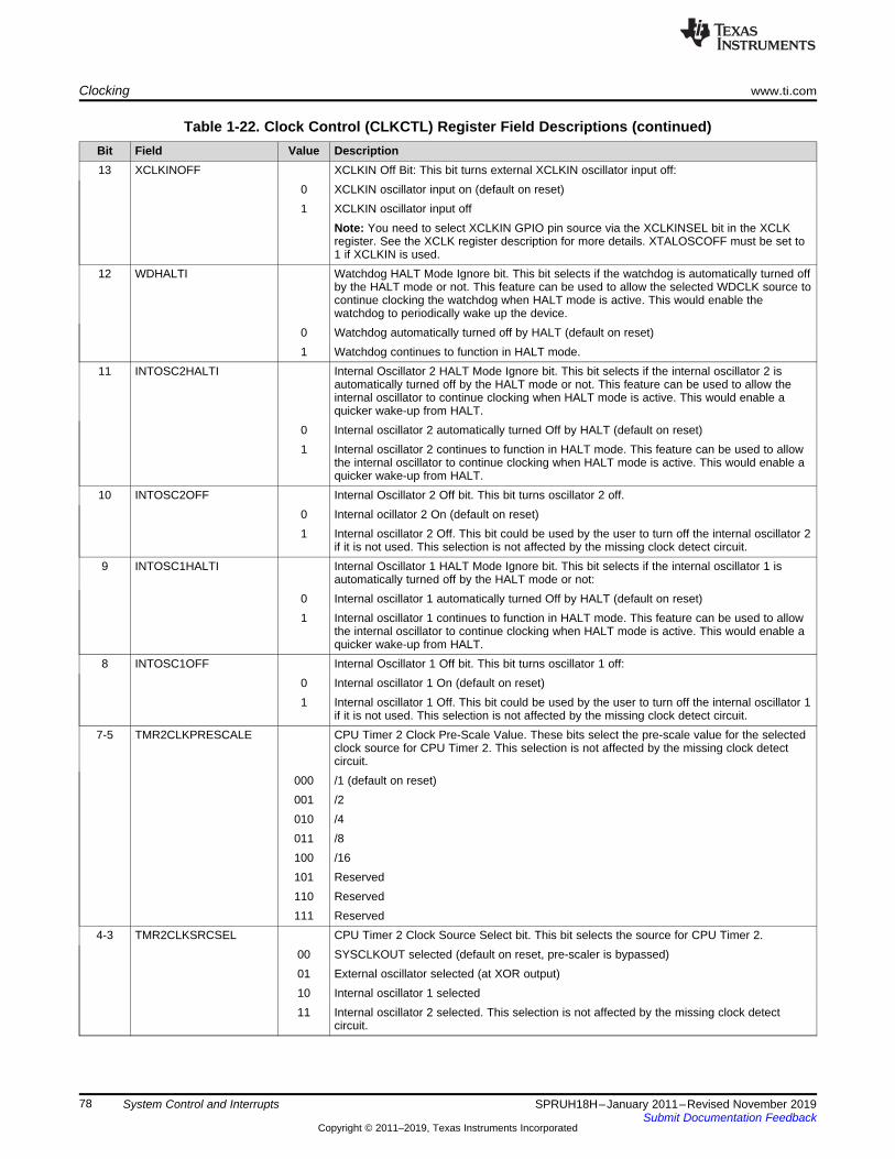
Clocking www.ti.com
78 SPRUH18H–January 2011–Revised November 2019Submit Documentation Feedback
Copyright © 2011–2019, Texas Instruments Incorporated
System Control and Interrupts
Table 1-22. Clock Control (CLKCTL) Register Field Descriptions (continued)Bit Field Value Description13 XCLKINOFF XCLKIN Off Bit: This bit turns external XCLKIN oscillator input off:
0 XCLKIN oscillator input on (default on reset)1 XCLKIN oscillator input off
Note: You need to select XCLKIN GPIO pin source via the XCLKINSEL bit in the XCLKregister. See the XCLK register description for more details. XTALOSCOFF must be set to1 if XCLKIN is used.
12 WDHALTI Watchdog HALT Mode Ignore bit. This bit selects if the watchdog is automatically turned offby the HALT mode or not. This feature can be used to allow the selected WDCLK source tocontinue clocking the watchdog when HALT mode is active. This would enable thewatchdog to periodically wake up the device.
0 Watchdog automatically turned off by HALT (default on reset)1 Watchdog continues to function in HALT mode.
11 INTOSC2HALTI Internal Oscillator 2 HALT Mode Ignore bit. This bit selects if the internal oscillator 2 isautomatically turned off by the HALT mode or not. This feature can be used to allow theinternal oscillator to continue clocking when HALT mode is active. This would enable aquicker wake-up from HALT.
0 Internal oscillator 2 automatically turned Off by HALT (default on reset)1 Internal oscillator 2 continues to function in HALT mode. This feature can be used to allow
the internal oscillator to continue clocking when HALT mode is active. This would enable aquicker wake-up from HALT.
10 INTOSC2OFF Internal Oscillator 2 Off bit. This bit turns oscillator 2 off.0 Internal ocillator 2 On (default on reset)1 Internal oscillator 2 Off. This bit could be used by the user to turn off the internal oscillator 2
if it is not used. This selection is not affected by the missing clock detect circuit.9 INTOSC1HALTI Internal Oscillator 1 HALT Mode Ignore bit. This bit selects if the internal oscillator 1 is
automatically turned off by the HALT mode or not:0 Internal oscillator 1 automatically turned Off by HALT (default on reset)1 Internal oscillator 1 continues to function in HALT mode. This feature can be used to allow
the internal oscillator to continue clocking when HALT mode is active. This would enable aquicker wake-up from HALT.
8 INTOSC1OFF Internal Oscillator 1 Off bit. This bit turns oscillator 1 off:0 Internal oscillator 1 On (default on reset)1 Internal oscillator 1 Off. This bit could be used by the user to turn off the internal oscillator 1
if it is not used. This selection is not affected by the missing clock detect circuit.7-5 TMR2CLKPRESCALE CPU Timer 2 Clock Pre-Scale Value. These bits select the pre-scale value for the selected
clock source for CPU Timer 2. This selection is not affected by the missing clock detectcircuit.
000 /1 (default on reset)001 /2010 /4011 /8100 /16101 Reserved110 Reserved111 Reserved
4-3 TMR2CLKSRCSEL CPU Timer 2 Clock Source Select bit. This bit selects the source for CPU Timer 2.00 SYSCLKOUT selected (default on reset, pre-scaler is bypassed)01 External oscillator selected (at XOR output)10 Internal oscillator 1 selected11 Internal oscillator 2 selected. This selection is not affected by the missing clock detect
circuit.

www.ti.com Clocking
79SPRUH18H–January 2011–Revised November 2019Submit Documentation Feedback
Copyright © 2011–2019, Texas Instruments Incorporated
System Control and Interrupts
Table 1-22. Clock Control (CLKCTL) Register Field Descriptions (continued)Bit Field Value Description2 WDCLKSRCSEL Watchdog Clock Source Select bit. This bit selects the source for WDCLK. On XRS low
and after XRS goes high, internal oscillator 1 is selected by default. User would need toselect external oscillator or internal oscillator 2 during their initialization process. If missingclock detect circuit detects a missing clock, then this bit is forced to 0 and internal oscillator1 is selected. The user changing this bit does not affect the PLLCR value.
0 Internal oscillator 1 selected (default on reset)1 External oscillator or Internal oscillator 2 selected
1 OSCCLKSRC2SEL Oscillator 2 Clock Source Select bit. This bit selects between internal oscillator 2 or externaloscillator. This selection is not affected by the missing clock detect circuit.
0 External oscillator selected (default on reset)1 Internal oscillator 2 selected
0 OSCCLKSRCSEL Oscillator Clock Source Select bit. This bit selects the source for OSCCLK. On XRS lowand after XRS goes high, internal oscillator 1 is selected by default. The user would need toselect external oscillator or internal oscillator 2 during their initialization process. Wheneverthe user changes the clock source using these bits, the PLLCR register will beautomatically forced to zero. This prevents potential PLL overshoot. The user will then haveto write to the PLLCR register to configure the appropriate PLL multiplier value. The usercan also configure the PLL lock period using the PLLLOCKPRD register to reduce the locktime if necessary. If the missing clock detect circuit detects a missing clock, then this bit isautomatically forced to 0 and internal oscillator 1 is selected. The PLLCR register will alsobe automatically forced to zero to prevent any potential overshoot.
0 Internal oscillator 1 selected (default on reset)1 External oscillator or Internal oscillator 2 selected. Note: If users wish to use oscillator 2 or
external oscillator to clock the CPU, they should configure the OSCCLKSRC2SEL bit first,and then write to the OSCCLKSRCSEL bit next.
1.4.2.3.1 Switching the Input Clock SourceThe following procedure may be used to switch clock sources:1. Use CPU Timer 2 to detect if clock sources are functional.2. If any of the clock sources is not functional, turn off the respective clock source (using the respective
CLKCTL bit).3. Switch over to a new clock source.4. If clock source switching occurred while in Limp Mode, then write a 1 to MCLKCLR will be issued to
exit Limp Mode.
If OSCCLKSRC2 (an external Crystal [XTAL] or oscillator [XCLKIN input] or Internal Oscillator 2[INTOSC2]) is selected as the clock source and a missing clock is detected, the missing clock detectcircuit will automatically switch to Internal Oscillator 1 (OSCCLKSRC1) and generate a CLOCKFAILsignal. In addition, the PLLCR register is forced to zero (PLL is bypassed) to prevent any potentialovershoot. The user can then write to the PLLCR register to re-lock the PLL. Under this situation, themissing clock detect circuit will be automatically re-enabled (PLLSTS[MCLKSTS] bit will be automaticallycleared). If Internal Oscillator 1 (OSCCLKSRC1) should also fail, then under this situation, the missingclock detect circuit will remain in limp mode. The user will have to re-enable the logic via thePLLSTS[MCLKCLR] bit.
1.4.2.3.2 Switching to INTOSC2 in the Absence of External ClocksFor the device to work properly upon a switch from INTOSC1 to INTOSC2 in the absence of any externalclock, the application code needs to write a 1 to the CLKCTL.XTALOSCOFF and CLKCTL.XCLKINOFFbits first. This is to indicate to the clock switching circuitry that external clocks are not present. Only afterthis should the OSCCLKSRCSEL and OSCCLKSRC2SEL bits be written to. Note that this sequenceshould be separated into two writes as follows:
First write → CLKCTL.XTALOSCOFF=1 and CLKCTL.XCLKINOFF=1
Second write → CLKCTL.OSCCLKLSRCSEL=1 and CLKCTL.OSCCLKSRC2SEL=1

PLLSTS[OSCOFF]
OSCCLK
PLLVCOCLK
4-bit Multiplier PLLCR[DIV]
OSCCLK orVCOCLK CLKIN
OSCCLK0
PLLSTS[PLLOFF]
n n ≠ 0
PLLSTS[DIVSEL]
/1
/2
/4
ToCPU
Clocking www.ti.com
80 SPRUH18H–January 2011–Revised November 2019Submit Documentation Feedback
Copyright © 2011–2019, Texas Instruments Incorporated
System Control and Interrupts
The second write should not alter the values of XTALOSCOFF and XCLKINOFF bits. If C2000Ware,supplied by Texas Instruments is used, clock switching can be achieved with the following code snip:
SysCtrlRegs.CLKCTL.all = 0x6000; // Set XTALOSCOFF=1 & XCLKINOFF=1SysCtrlRegs.CLKCTL.all = 0x6003; // Set OSCCLKLSRCSEL=1 & OSCCLKSRC2SEL=1
The system initialization file DSP2806x_SysCtrl.c, provided as part of C2000Ware also contain functionsto switch to different clock sources. If an attempt is made to switch from INTOSC1 to INTOSC2 withoutthe write to the XTALOSCOFF and XCLKINOFF bits, a missing clock will be detected due to the absenceof external clock source (even after the proper source selection). The PLLCR will be zeroed out and thedevice will automatically clear the MCLKSTS bit and switch back INTOSC1.
1.4.2.4 PLL-based Clock ModuleThis device has two PLL modules. “PLL” refers to the main PLL that generats the clock for the core and allperipherals. PLL2 refers to the PLL that generates the clock for the USB and HRCAP modules. Figure 1-23 shows the OSC and PLL block diagram.
Figure 1-23. OSC and PLL Block
The following is applicable for devices that have X1/X2 pins:
When using XCLKIN as the external clock source, you must tie X1 low and leave X2 disconnected.
(1) PLLSTS[DIVSEL] must be 0 before writing to the PLLCR and should be changed only after PLLSTS[PLLLOCKS] = 1. SeeFigure 1-24.
(2) The input clock and PLLCR[DIV] bits should be chosen in such a way that the output frequency of the PLL (VCOCLK) is aminimum of 50 MHz.
Table 1-23. Possible PLL Configuration Modes
PLL Mode Remarks PLLSTS[DIVSEL] (1)CLKIN and
SYSCLKOUT (2)
PLL Off Invoked by the user setting the PLLOFF bit in the PLLSTS register. ThePLL block is disabled in this mode. The CPU clock (CLKIN) can then bederived directly from any one of the following sources: INTOSC1,INTOSC2, XCLKIN pin, or X1/X2 pins. This can be useful to reducesystem noise and for low power operation. The PLLCR register must firstbe set to 0x0000 (PLL Bypass) before entering this mode.
0, 123
OSCCLK/4OSCCLK/2OSCCLK/1
PLL Bypass PLL Bypass is the default PLL configuration upon power-up or after anexternal reset (XRS). This mode is selected when the PLLCR register isset to 0x0000 or while the PLL locks to a new frequency after thePLLCR register has been modified. In this mode, the PLL itself isbypassed but the PLL is not turned off.
0, 123
OSCCLK/4OSCCLK/2OSCCLK/1
PLL Enabled Achieved by writing a non-zero value n into the PLLCR register. Uponwriting to the PLLCR, the device will switch to PLL Bypass mode untilthe PLL locks.
0, 123
OSCCLK*n/4OSCCLK*n/2OSCCLK*n/1
1.4.2.5 PLL Control (PLLCR) RegisterThe PLLCR register is used to change the PLL multiplier of the device. Before writing to the PLLCRregister, the following requirements must be met:

www.ti.com Clocking
81SPRUH18H–January 2011–Revised November 2019Submit Documentation Feedback
Copyright © 2011–2019, Texas Instruments Incorporated
System Control and Interrupts
• The PLLSTS[DIVSEL] bit must be 0 (CLKIN divide by 4 enabled). Change PLLSTS[DIVSEL] only afterthe PLL has completed locking, that is, after PLLSTS[PLLLOCKS] = 1.
Once the PLL is stable and has locked at the new specified frequency, the PLL switches CLKIN to thenew value as shown in Table 1-24. When this happens, the PLLLOCKS bit in the PLLSTS register is set,indicating that the PLL has finished locking and the device is now running at the new frequency. Usersoftware can monitor the PLLLOCKS bit to determine when the PLL has completed locking. OncePLLSTS[PLLLOCKS] = 1, DIVSEL can be changed.
Follow the procedure in Figure 1-24 any time you are writing to the PLLCR register.

Start
PLLSTS[MCLKSTS]= 1?
Yes
No
Device is operating in limp
mode. Take appropriate
action for your system.
Do not write to PLLCR.
Set PLL[MCLKOFF] = 0to enable failed oscillator
detect logic.
If required,PLLSTS [DIVSEL]
can now be changed.
Set new PLLCR value
Is
PLLSTS[PLLLOCKS]= 1?
Continue to wait for PLLto lock. This is importantfor time-critical software.
Set PLLSTS[MCLKOFF] = 1to disable failed oscillator
detect logic
No
Yes
PLLSTS[DIVSEL]
= 2 or 3?
No
Set PLLSTS[DIVSEL] = 0Yes
Clocking www.ti.com
82 SPRUH18H–January 2011–Revised November 2019Submit Documentation Feedback
Copyright © 2011–2019, Texas Instruments Incorporated
System Control and Interrupts
Figure 1-24. PLLCR Change Procedure Flow Chart

www.ti.com Clocking
83SPRUH18H–January 2011–Revised November 2019Submit Documentation Feedback
Copyright © 2011–2019, Texas Instruments Incorporated
System Control and Interrupts
1.4.2.6 PLL Control, Status and XCLKOUT Register DescriptionsThe DIV field in the PLLCR register controls whether the PLL is bypassed or not and sets the PLLclocking ratio when it is not bypassed. PLL bypass is the default mode after reset. Do not write to the DIVfield if the PLLSTS[DIVSEL] bit is 10 or 11, or if the PLL is operating in limp mode as indicated by thePLLSTS[MCLKSTS] bit being set. See the procedure for changing the PLLCR described in Figure 1-24.
Figure 1-25. PLLCR Register Layout15 5 4 0
Reserved DIVR-0 R/W-0
LEGEND: R/W = Read/Write; R = Read only; -n = value after reset
(1) This register is EALLOW protected. See Section 1.6.2 for more information.(2) PLLSTS[DIVSEL] must be 0 or 1 before writing to the PLLCR and should be changed only after PLLSTS[PLLLOCKS] = 1. See
Figure 1-24.(3) The PLL control register (PLLCR) and PLL Status Register (PLLSTS) are reset to their default state by the XRS signal or a
watchdog reset only. A reset issued by the debugger or the missing clock detect logic have no effect.
Table 1-24. PLL Settings (1)
SYSCLKOUT (CLKIN) (2)
PLLCR[DIV] Value (3) PLLSTS[DIVSEL] = 0 or 1 PLLSTS[DIVSEL] = 2 PLLSTS[DIVSEL] = 30000 (PLL bypass) OSCCLK/4 (Default) OSCCLK/2 OSCCLK/1
00001 (OSCCLK * 1)/4 (OSCCLK * 1)/2 (OSCCLK * 1)/100010 (OSCCLK * 2)/4 (OSCCLK * 2)/2 (OSCCLK * 2)/100011 (OSCCLK * 3)/4 (OSCCLK * 3)/2 (OSCCLK * 3)/100100 (OSCCLK * 4)/4 (OSCCLK * 4)/2 (OSCCLK * 4)/100101 (OSCCLK * 5)/4 (OSCCLK * 5)/2 (OSCCLK * 5)/100110 (OSCCLK * 6)/4 (OSCCLK * 6)/2 (OSCCLK * 6)/100111 (OSCCLK * 7)/4 (OSCCLK * 7)/2 (OSCCLK * 7)/101000 (OSCCLK * 8)/4 (OSCCLK * 8)/2 (OSCCLK * 8)/101001 (OSCCLK * 9)/4 (OSCCLK * 9)/2 (OSCCLK * 9)/101010 (OSCCLK * 10)/4 (OSCCLK * 10)/2 (OSCCLK * 10)/101011 (OSCCLK * 11)/4 (OSCCLK * 11)/2 (OSCCLK * 11)/101100 (OSCCLK * 12)/4 (OSCCLK * 12)/2 (OSCCLK * 12)/101101 (OSCCLK * 13)/4 (OSCCLK * 13)/2 (OSCCLK * 13)/101110 (OSCCLK * 14)/4 (OSCCLK * 14)/2 (OSCCLK * 14)/101111 (OSCCLK * 15)/4 (OSCCLK * 15)/2 (OSCCLK * 15)/110000 (OSCCLK * 16)/4 (OSCCLK * 16)/2 (OSCCLK * 16)/110001 (OSCCLK * 17)/4 (OSCCLK * 17)/2 (OSCCLK * 17)/110010 (OSCCLK * 18)/4 (OSCCLK * 18)/2 (OSCCLK * 18)/1
10011-11111 Reserved Reserved Reserved
Figure 1-26. PLL Status Register (PLLSTS)15 14 9 8
NORMRDYE Reserved DIVSELR/W-0 R-0 R/W-0
7 6 5 4 3 2 1 0DIVSEL MCLKOFF OSCOFF MCLKCLR MCLKSTS PLLOFF Reserved PLLLOCKSR/W-0 R/W-0 R/W-0 W-0 R-0 R/W-0 R-0 R-1
LEGEND: R/W = Read/Write; R = Read only; -n = value after reset

Clocking www.ti.com
84 SPRUH18H–January 2011–Revised November 2019Submit Documentation Feedback
Copyright © 2011–2019, Texas Instruments Incorporated
System Control and Interrupts
(1) This register is reset to its default state only by the XRS signal or a watchdog reset. It is not reset by a missing clock or debugger reset.(2) This register is EALLOW protected. See Section 1.6.2 for more information.
Table 1-25. PLL Status Register (PLLSTS) Field Descriptions
Bits Field Value Description (1) (2)
15 NORMRDYE NORMRDY Enable Bit: This bit selects if NORMRDY signal from VREG gates the PLL from turningon when the VREG is out of regulation. It may be required to keep the PLL off while coming in andout of HALT mode and this signal can be used for that purpose:
0 NORMRDY signal from VREG does not gate PLL (PLL ignores NORMRDY)1 NORMRDY signal from VREG will gate PLL (PLL off when NORMRDY low)
The NORMRDY signal from the VREG is low when the VREG is out of regulation and this signalwill go high if the VREG is within regulation.
14-9 Reserved Any writes to these bits must always have a value of 0.8:7 DIVSEL Divide Select: This bit selects between /4, /2, and /1 for CLKIN to the CPU.
The configuration of the DIVSEL bit is as follows:00, 01 Select Divide By 4 for CLKIN
10 Select Divide By 2 for CLKIN11 Select Divide By 1 for CLKIN
6 MCLKOFF Missing clock-detect off bit0 Main oscillator fail-detect logic is enabled. (default)1 Main oscillator fail-detect logic is disabled and the PLL will not issue a limp-mode clock. Use this
mode when code must not be affected by the detection circuit. For example, if external clocks areturned off.
5 OSCOFF Oscillator Clock Off Bit0 The OSCCLK signal from X1/X2 or XCLKIN is fed to the PLL block. (default)1 The OSCCLK signal from X1/X2 or XCLKIN is not fed to the PLL block. This does not shut down
the internal oscillator. The OSCOFF bit is used for testing the missing clock detection logic.When the OSCOFF bit is set, do not enter HALT or STANDBY modes or write to PLLCR as theseoperations can result in unpredictable behavior.When the OSCOFF bit is set, the behavior of the watchdog is different depending on which inputclock source (X1, X1/X2 or XCLKIN) is being used:• X1/X2: The watchdog is not functional.• XCLKIN: The watchdog is functional and should be disabled before setting OSCOFF.
4 MCLKCLR Missing Clock Clear Bit.0 Writing a 0 has no effect. This bit always reads 0.1 Forces the missing clock detection circuits to be cleared and reset. If OSCCLK is still missing, the
detection circuit will again generate a reset to the system, set the missing clock status bit(MCLKSTS), and the CPU will be clocked by the PLL operating at a limp mode frequency.
3 MCLKSTS Missing Clock Status Bit. Check the status of this bit after a reset to determine whether a missingoscillator condition was detected. Under normal conditions, this bit should be 0. Writes to this bitare ignored. This bit will be cleared by writing to the MCLKCLR bit or by forcing an external reset.
0 Indicates normal operation. A missing clock condition has not been detected.1 Indicates that OSCCLK was detected as missing. The main oscillator fail detect logic has reset the
device and the CPU is now clocked by the PLL operating at the limp mode frequency.When the missing clock detection circuit automatically switches between OSCCLKSRC2 toOSCCLKSRC1 (upon detecting OSCCLKSRC2 failure), this bit will be automatically cleared andthe missing clock detection circuit will be re-enabled. For all other cases, the user needs to re-enable this mode by writing a 1 to the MCLKCLR bit.
2 PLLOFF PLL Off Bit. This bit turns off the PLL. This is useful for system noise testing. This mode must onlybe used when the PLLCR register is set to 0x0000.
0 PLL On (default)1 PLL Off. While the PLLOFF bit is set the PLL module will be kept powered down.
The device must be in PLL bypass mode (PLLCR = 0x0000) before writing a 1 to PLLOFF. Whilethe PLL is turned off (PLLOFF = 1), do not write a non-zero value to the PLLCR.The STANDBY and HALT low power modes will work as expected when PLLOFF = 1. After wakingup from HALT or STANDBY the PLL module will remain powered down.
1 Reserved Any writes to these bits must always have a value of 0.

www.ti.com Clocking
85SPRUH18H–January 2011–Revised November 2019Submit Documentation Feedback
Copyright © 2011–2019, Texas Instruments Incorporated
System Control and Interrupts
Table 1-25. PLL Status Register (PLLSTS) Field Descriptions (continued)Bits Field Value Description (1) (2)
0 PLLLOCKS PLL Lock Status Bit.0 Indicates that the PLLCR register has been written to and the PLL is currently locking. The CPU is
clocked by OSCCLK/2 until the PLL locks.1 Indicates that the PLL has finished locking and is now stable.
Figure 1-27. PLL Lock Period (PLLLOCKPRD) Register15 0
PLLLOCKPRDR/W-FFFFh
LEGEND: R/W = Read/Write; R = Read only; -n = value after reset
(1) PLLLOCKPRD is affected by the XRSn signal only.(2) This register is EALLOW protected. See Section 1.6.2 for more information.
Table 1-26. PLL Lock Period (PLLLOCKPRD) Register Field Descriptions
Bit Field Value Description (1) (2)
15:0 PLLLOCKPRD PLL Lock Period Counter ValueThese 16 bits configure the PLL lock period. This value is programmable, so shorter PLL lock-timecan be programmed by user. The user needs to compute the number of OSCCLK cycles (based onthe OSCCLK value used in the design) and update this register.PLL Lock Period
FFFFh 65535 OSCLK Cycles (default on reset)FFFEh 65534 OSCLK Cycles
... ...0001h 1 OSCCLK Cycle0000h 0 OSCCLK Cycles (no PLL lock period)

DEVICECNF.SYSCLK2DIV2DIS
PLL2CTL.PLL2EN
PLL2CTL.PLL2CLKSRCSEL
INTOSC1
X1
XCLKIN
PLL2
PLL2CLKHRCAP
/2 SYSCLK2 to
USB
0
1
Clocking www.ti.com
86 SPRUH18H–January 2011–Revised November 2019Submit Documentation Feedback
Copyright © 2011–2019, Texas Instruments Incorporated
System Control and Interrupts
1.4.2.7 PLL2 RegistersIn addition to the main PLL that clocks the CPU, a second PLL (PLL2) exists for clocking the USB andHRCAP modules. Figure 1-28 shows the possible input and output configurations for PLL2.
Figure 1-28. PLL2 Input and Output Configurations
Figure 1-29. PLL2 Configuration (PLL2CTL) Register (EALLOW protected)15 3 2 1 0
Reserved PLL2EN PLL2CLKSRCSELR-0 R/W-1 R/W-00
LEGEND: R/W = Read/Write; R = Read only; -n = value after reset
Table 1-27. PLL2 Configuration (PLL2CTL) Register Field Descriptions
Bit Field Value Description15-3 Reserved Any writes to these bits must always have a value of 0.
2 PLL2EN PLL enabled or disabled: This bit decides if PLL2 is enabled or not0 PLL2 is powered off – clock to SYSCLK2 is a direct feed from input clock source as decided by the
PLL2CLKSRCSEL bit1 PLL2 is enabled and clock to SYSCLK2 will depend on the DEVICECNF[SYSCLK2DIV2DIS] bit.
1-0 PLL2CLKSRCSEL
PLL2 Clock Source Select Bits: These bit select the source for the PLL2 input clock:00 Internal oscillator 1 is selected as clock to PLL201 Internal oscillator 1 is selected as clock to PLL210 X1 clock source is selected as clock to PLL211 GPIO_XCLKIN is selected as clock to PLL2
On XRS low and after XRS goes high, X1 is selected as clock source to the USB PLL by default.The user would need to select X1 or GPIO_XCLKIN as clock source during their initializationprocess.Whenever the user changes the clock source using these bits, the DEVICECNF[SYSCLK2DIV2DIS]bit will be automatically forced to zero. This prevents potential PLL overshoot. The user will thenhave to write to the DEVICECNF[SYSCLK2DIV2DIS] bit to configure the appropriate divisor ratio.
Note: PLL2CTL is affected by the XRS signal only.
Figure 1-30. PLL2 Multiplier (PLL2MULT) Register (EALLOW protected)15 4 3 0
Reserved PLL2MULTR-0 R/W-0x0
LEGEND: R/W = Read/Write; R = Read only; -n = value after reset

www.ti.com Clocking
87SPRUH18H–January 2011–Revised November 2019Submit Documentation Feedback
Copyright © 2011–2019, Texas Instruments Incorporated
System Control and Interrupts
Table 1-28. PLL2 Multiplier (PLL2MULT) Register Field Descriptions
Bit Field Value Description15-4 Reserved Any writes to these bits must always have a value of 0.3-0 PLL2MULT PLL2 Multiplier. This bit field determines the output frequency of PLL2
(PLL2Fout) for a given input (PLL2Fin)0000 PLL2Fout = PLL2Fin (PLLBYPASS)0001 PLL2Fout = PLL2Fin * 10010 PLL2Fout = PLL2Fin * 20011 PLL2Fout = PLL2Fin * 3......1111 PLL2Fout = PLL2Fin * 15PLL2 should be enabled (PLL2EN = 1) prior to setting these bits.
Note: PLL2MULT is affected by XRSn signal only.
Figure 1-31. PLL2 Lock Status (PLL2STS) Register15 1 0
Reserved PLL2LOCKSR-0 R-0x0
LEGEND: R/W = Read/Write; R = Read only; -n = value after reset Note: PLL2STS is affected by XRnS signal only.
Table 1-29. PLL2 Lock Status (PLL2STS) Register Field Descriptions
Bit Field Value Description15-4 Reserved Any writes to these bits must always have a value of 0.3-0 PLL2MULT PLL2 Lock Status Bit: This bit indicates whether PLL2 is locked or not. When the PLL2MULT
setting is modified, a counter is loaded with the value from the main PLL PLLLOCKPRD bit fieldand the PLL2LOCKS bit is cleared. Once set to a non-zero value, the counter begins down-counting. Upon reaching zero, the counter stops and the PLL2LOCKS bit is set.
0 PLL2 is not yet locked1 PLL2 is locked
Note: PLL2STS is affected by XRSn signal only.
Figure 1-32. SYSCLK2 Clock Counter (SYSCLK2CNTR) Register15 0
COUNTR/C-0x0
LEGEND: R/W = Read/Write; R = Read only; -n = value after reset
Table 1-30. SYSCLK2 Clock Counter (SYSCLK2CNTR) Register Field Descriptions
Bit Field Value Description15-0 COUNT SYSCLK2 Counter Bit Field: This bit field is a free-running counter based off the SYSCLK2 clock.
Software can compare the rate of update of this bit field against the rate of update of a CPU Timerto determine at what approximate frequency the SYSCLK2 clock is running.
Note 1: Since COUNT will begin updating as soon as reset is released, the value of this register after reset will be non-zero before softwarecan read it.Note 2: SYSCLK2CNTR will tap off the clock after the /2 from PLL2OUT if it is enabled. If not enabled it will tap off PLL2OUT.

Clocking www.ti.com
88 SPRUH18H–January 2011–Revised November 2019Submit Documentation Feedback
Copyright © 2011–2019, Texas Instruments Incorporated
System Control and Interrupts
Figure 1-33. EPWM DMA/CLA Configuration (EPWMCFG) Register15 1 0
Reserved CONFIGR-0 R/W-0X0
LEGEND: R/W = Read/Write; R = Read only; -n = value after reset
Table 1-31. EPWM DMA/CLA Configuration (EPWMCFG) Register Field Descriptions
Bit Field Value Description15-1 Reserved Any writes to these bits must always have a value of 0.
0 CONFIG EPWM DMA Enable Bit:0 The EPWM blocks are connected to the CLA bus and are inaccessible to the DMA bus1 The EPWM blocks are connected to the DMA bus and are inaccessible to the CLA bus
1.4.2.8 Input Clock Fail DetectionIt is possible for the clock source of the device to fail. When the PLL is not disabled, the main oscillator faillogic allows the device to detect this condition and handle it as described in this section.
Two counters are used to monitor the presence of the OSCCLK signal as shown in Figure 1-34. The firstcounter is incremented by the OSCCLK signal itself. When the PLL is not turned off, the second counter isincremented by the VCOCLK coming out of the PLL block. These counters are configured such that whenthe 7-bit OSCCLK counter overflows, it clears the 13-bit VCOCLK counter. In normal operating mode, aslong as OSCCLK is present, the VCOCLK counter will never overflow.

OSCCLK
VCOCLKCounter(13 bits)
OSCCLKCounter(7 bits)
ClockSwitchLogic
MCLKSTS
PLLSTSReg
clear
res
clk
clk
ovf
ovf
res
clear
XRS
MCLKCLR
Sync
SYSCLKOUT
MC
LK
RS
VCOCLK(OSCCLK * PLLCR ratio)
PLLCLK
PLL
PLL
PLLCR Reg
clear
clear
clear
Internal&
ExternalOscillators
X2 (Vcore)
X1 (Vcore)
/1,/2,/4
PLLDIS (turn off when 0, used in device test mode)
PLL LockCounter(16 bits)
clear
clk ovf
resoff
PLLLOCKS
(turn off when 1)
C28Core
PLLDIS(used in device test mode)
CLKIN
DIVSEL
(/4 on reset)
MCLKOFF(turn off when 1)
Low PowerModes Block
WA
KE
OS
CH
AL
TS
TA
ND
BY
WAKEINT
LPMINT
WDBlock
WDINT
WDRSTWDHALT
OSCCLK
0
1
PIE
VREG
VREGHALT
NMIWDNMIRS
NMI
CLOCKFAIL
WAKEOSC
CLKCTL RegXRS CLOCKFAIL
PLLSTS[OSCOFF]
01
PLLSTS[PLLOFF]
GPIOMux
/1, /2,/4, off
XCLK Reg
PLLLOCKPRD Reg
CPU Timer2CPUTMR2CLK
WDCLK
SYSCLKOUT
ePWM1.../ePWMxTZ5
GPIOMux
XCLKIN
WDHALTI
(ignore HALT)
NORMRDY
NORMRDYE
XCLKOUT
www.ti.com Clocking
89SPRUH18H–January 2011–Revised November 2019Submit Documentation Feedback
Copyright © 2011–2019, Texas Instruments Incorporated
System Control and Interrupts
Figure 1-34. Clocking and Reset Logic
If the OSCCLK input signal is missing, then the PLL will output a default limp mode frequency and theVCOCLK counter will continue to increment. Since the OSCCLK signal is missing, the OSCCLK counterwill not increment, and therefore, the VCOCLK counter is not periodically cleared. Eventually, theVCOCLK counter overflows. This signals a missing clock condition to the missing-clock-detection logic.What happens next is based on which clock source has been chosen for the PLL and the value ofNMIRESETSEL.

Clocking www.ti.com
90 SPRUH18H–January 2011–Revised November 2019Submit Documentation Feedback
Copyright © 2011–2019, Texas Instruments Incorporated
System Control and Interrupts
Case A:INTOSC1 is used as the clock source. NMIWD is disabled (NMIRESETSEL = 0)Failure of INTOSC1 causes PLL to issue a limp mode clock. The system continues to function with thelimp clock and so does the VCOCLK counter. Eventually, VCOCLK counter overflows and issues aCLOCKFAIL signal (MCLKSTS bit is set) and the missing clock detection logic resets the CPU,peripherals, and other device logic by way of MCLKRS. The exact delay (from the time the clock wasstopped to the time a reset is asserted) depends on the VCOCLK counter value when the INTOSC1 clockvanished. The MCLKSTS bit is only affected by XRS, not by a missing clock reset. So, after a reset, codecan examine this bit to determine if the reset was due to a missing clock and take appropriate action. Notethat even though the CLOCKFAIL signal is generated, the NMIWDCNTR will not count.
Case B:INTOSC1 is used as the clock source. NMIWD is enabled (NMIRESETSEL = 1)Failure of INTOSC1 causes PLL to issue a limp mode clock. The system continues to function with thelimp clock and so does the VCOCLK counter. Eventually, the VCOCLK counter overflows and issuesCLOCKFAIL (MCLKSTS bit is set), which asserts the NMI and starts the NMIWDCNTR. If NMIWDCNTRis allowed to reach the NMIWDPRD value, a reset (MCLKRS) is asserted. In the interim period, theapplication could choose to gracefully shut down the system before a reset is generated. Inside theNMI_ISR, the flags in NMIFLG register may be cleared, which prevents a reset.
In case A, reset is inevitable and cannot be delayed. In case B, the software can• Choose to clear the flags to prevent a reset.• Perform a graceful shutdown of the system.• Switch to OSCCLKSRC2, if need be.
Case C:OSCCLKSRC2 (INTOSC2 or X1/X2 or XCLKIN) is used as the clock source. NMIWD is disabled(NMIRESETSEL = 0)When the VCOCLK counter overflows (due to loss of OSCCLKSRC2), the Missing-Clock-Detect circuitrecognizes the missing clock condition. CLOCKFAIL will be generated (but it is of no consequence). SinceNMIRESETSEL=0, the device will be reset. No switching of clock source happens, since the device isreset. This is similar to Case A.
Case D:OSCCLKSRC2 (INTOSC2 or X1/X2 or XCLKIN) is used as the clock source. NMIWD is enabled(NMIRESETSEL = 1)When the VCOCLK counter overflows (due to loss of OSCCLKSRC2), the Missing-Clock-Detect circuitrecognizes the missing clock condition. CLOCKFAIL is generated and OSCCLK is switched to INTOSC1.For this reason, INTOSC1 should not be disabled in user code. The MCLKSTS bit is set, but clearedautomatically after the clock switch. PLLCR is zeroed. The user must reconfigure PLLCR. SinceNMIRESETSEL=1, NMI interrupt will be triggered and PLL could be reconfigured there. Inside theNMI_ISR, the flags in the NMIFLG register may be cleared, which prevents a reset. If INTOSC1 also fails,this becomes similar to Case B. The advantage of using OSCCLKSRC2 as the source for the PLL is thatthe clock source is automatically switched to INTOSC1 upon loss of OSCCLKSRC2.
1.4.2.9 Missing Clock Reset and Missing Clock StatusThe MCLKRS is an internal reset only. The external XRS pin of the device is not pulled low by MCLKRS ,and the PLLCR and PLLSTS registers are not reset. In addition to resetting the device, the missing clockdetect logic sets the PLLSTS[MCLKSTS] register bit. When the MCLKSTS bit is 1, this indicates that themissing oscillator detect logic has reset the part and that the CPU is now running at the limp modefrequency.

www.ti.com Clocking
91SPRUH18H–January 2011–Revised November 2019Submit Documentation Feedback
Copyright © 2011–2019, Texas Instruments Incorporated
System Control and Interrupts
Software should check the PLLSTS[MCLKSTS] bit after a reset to determine if the device was reset byMCLKRS due to a missing clock condition. If MCLKSTS is set, then the firmware should take the actionappropriate for the system such as a system shutdown. The missing clock status can be cleared by writinga 1 to the PLLSTS[MCLKCLR] bit. This will reset the missing clock detection circuits and counters. IfOSCCLK is still missing after writing to the MCLKCLR bit, then the VCOCLK counter again overflows andthe process will repeat.
NOTE: Applications in which the correct CPU operating frequency is absolutely critical shouldimplement a mechanism by which the DSP will be held in reset should the input clocks everfail. For example, an R-C circuit may be used to trigger the XRS pin of the DSP should thecapacitor ever get fully charged. An I/O pin may be used to discharge the capacitor on aperiodic basis to prevent it from getting fully charged. Such a circuit would also help indetecting failure of the flash memory.
The following precautions and limitations should be kept in mind:• Use the proper procedure when changing the PLL Control Register. Always follow the procedure
outlined in Figure 1-24 when modifying the PLLCR register.• Do not write to the PLLCR register when the device is operating in limp mode. When writing to
the PLLCR register, the device switches to the CPU's CLKIN input to OSCCLK/2. When operating afterlimp mode has been detected, OSCCLK may not be present and the clocks to the system will stop.Always check that the PLLSTS[MCLKSTS] bit = 0 before writing to the PLLCR register as described inFigure 1-24.
• Do not enter HALT low power mode when the device is operating in limp mode. If you try to enterHALT mode when the device is already operating in limp mode then the device may not properly enterHALT. The device may instead enter STANDBY mode or may hang and you may not be able to exitHALT mode. For this reason, always check that the PLLSTS[MCLKSTS] bit = 0 before entering HALTmode.
The following list describes the behavior of the missing clock detect logic in various operating modes:• PLL by-pass mode
When the PLL control register is set to 0x0000, the PLL is bypassed. Depending on the state of thePLLSTS[DIVSEL] bit, OSCCLK, OSCCLK/2, or OSCCLK/4 is connected directly to the CPU's inputclock, CLKIN. If the OSCCLK is detected as missing, the device will automatically switch to the PLL’slimp mode clock. Further behavior is determined by the clock source used for OSCCLK and the valueof NMIRESETSEL bit as explained before.
• STANDBY low power modeIn this mode, the CLKIN to the CPU is stopped. If a missing input clock is detected, the missing clockstatus bit will be set and the device will generate a missing clock reset. If the PLL is in by-pass modewhen this occurs, then one-half of the PLL limp frequency will automatically be routed to the CPU. Thedevice will now run at the PLL limp mode frequency or at one-half or one-fourth of the PLL limp modefrequency, depending on the state of the PLLSTS[DIVSEL] bit.
• HALT low power modeIn HALT low power mode, all of the clocks to the device are turned off. When the device comes out ofHALT mode, the oscillator and PLL will power up. The counters that are used to detect a missing inputclock (VCOCLK and OSCCLK) will be enabled only after this power-up has completed. If VCOCLKcounter overflows, the missing clock detect status bit will be set and the device will generate a missingclock reset. If the PLL is in by-pass mode when the overflow occurs, then one-half of the PLL limpfrequency will automatically be routed to the CPU. The device will now run at the PLL limp modefrequency or at one-half or one-fourth of the PLL limp mode frequency depending on the state of thePLLSTS[DIVSEL] bit.

Clocking www.ti.com
92 SPRUH18H–January 2011–Revised November 2019Submit Documentation Feedback
Copyright © 2011–2019, Texas Instruments Incorporated
System Control and Interrupts
1.4.2.10 NMI Interrupt and WatchdogThe NMI watchdog (NMIWD) is used to detect and aid in handling a clock failure condition. The NMIinterrupt enables the monitoring of clock failure. In 280x/2833x/2823x devices, when the VCOCLK counteroverflows (due to loss of input clock), a missing clock condition is detected and a missing-clock-reset(MCLKRS) is generated immediately. In this device, a CLOCKFAIL signal can be generated first, which isthen fed to the NMI Watchdog circuit and a reset can be generated after a preprogrammed delay. Thisfeature is not enabled upon power-up, however. That is, when this device first powers up, the MCLKRSsignal is generated immediately upon clock failure like 280x/2833x/2823x devices. The user must enablethe generation of the NMI signal via the CLKCTL[NMIRESETSEL] bit. Note that the NMI watchdog isdifferent from the watchdog described in Section 1.4.4.
When the OSCCLK goes missing, the CLOCKFAIL signal triggers the NMI and gets the NMIWD counterrunning. In the NMI ISR, the application is expected to take corrective action (such as gracefully shutdown the system before a reset is generated or clear the CLOCKFAIL and NMIINT flags and switch to analternate clock source, if applicable). If this is not done, the NMIWDCTR overflows and generates an NMIreset (NMIRS) after a preprogrammed number of SYSCLKOUT cycles. NMIRS is fed to MCLKRS togenerate a system reset back into the core. Note that NMI reset is internal to the device and will not bereflected on the XRS pin.
The CLOCKFAIL signal could also be used to activate the TZ5 signal to drive the PWM pins into a highimpedance state. This allows the PWM outputs to b tripped in case of clock failure. Figure 1-35 shows theCLOCKFAIL interrupt mechanism. Likewise, TZ6 is connected to EMUSTOP output from the CPU. Thisallows the user to configure trip action during a CPU halt, such as during emulation or debug sessions.

NMIFLG[NMINT]
1
0
GenerateInterrupt
PulseWhen
Input = 1
NMINT
Latch
Clear
Set Clear
NMIFLGCLR[NMINT]
XRS
0
NMICFG[CLOCKFAIL]
Latch
Clear
SetClear
XRS
NMIFLG[CLOCKFAIL]
NMI Watchdog
SYSCLKOUT
SYSRS
NMIRSNMIWDPRD[15:0]
NMIWDCNT[15:0]
NMIFLGCLR[CLOCKFAIL]
SYNC?
NMIFLGFRC[CLOCKFAIL]
SYSCLKOUT
See SystemControl Section
CLOCKFAIL
www.ti.com Clocking
93SPRUH18H–January 2011–Revised November 2019Submit Documentation Feedback
Copyright © 2011–2019, Texas Instruments Incorporated
System Control and Interrupts
Figure 1-35. Clock Fail Interrupt
A The NMI watchdog module is clocked by SYSCLKOUT. Due to the limp mode function of the PLL, SYSCLKOUT ispresent even if the source clock for OSCCLK fails.
The NMI Interrupt support registers are listed in Table 1-32.
Table 1-32. NMI Interrupt Registers
Name Address Range Size (x16) EALLOW DescriptionNMICFG 0x7060 1 yes NMI Configuration RegisterNMIFLG 0x7061 1 yes NMI Flag RegisterNMIFLGCLR 0x7062 1 yes NMI Flag Clear RegisterNMIFLGFRC 0x7063 1 yes NMI Flag Force RegisterNMIWDCNT 0x7064 1 - NMI Watchdog Counter RegisterNMIWDPRD 0x7065 1 yes NMI Watchdog Period Register

Clocking www.ti.com
94 SPRUH18H–January 2011–Revised November 2019Submit Documentation Feedback
Copyright © 2011–2019, Texas Instruments Incorporated
System Control and Interrupts
Figure 1-36. NMI Configuration (NMICFG) Register15 2 1 0
Reserved CLOCKFAIL ReservedR-0 R/W-0 R-0
LEGEND: R/W = Read/Write; R = Read only; -n = value after reset
Table 1-33. NMI Configuration (NMICFG) Register Bit Definitions (EALLOW)
Bits Name Type Description15:2 Reserved Any writes to these bits must always have a value of 0.
1 CLOCKFAIL CLOCKFAIL-interrupt Enable Bit: This bit, when set to 1 enables the CLOCKFAIL condition togenerate an NMI interrupt. Once enabled, the flag cannot be cleared by the user. Only a devicereset clears the flag. Writes of 0 are ignored. Reading the bit will indicate if the flag is enabled ordisabled:
0 CLOCKFAIL Interrupt Disabled1 CLOCKFAIL Interrupt Enabled
0 Reserved Any writes to these bits must always have a value of 0.
Figure 1-37. NMI Flag (NMIFLG) Register Register15 2 1 0
Reserved CLOCKFAIL NMIINTR-0 R-0 R-0
LEGEND: R/W = Read/Write; R = Read only; -n = value after reset
Table 1-34. NMI Flag (NMIFLG) Register Bit Definitions (EALLOW Protected)
Bits Name Type Description15:2 Reserved Any writes to these bits must always have a value of 0.
1 CLOCKFAIL CLOCKFAIL Interrupt Flag: This bit indicates if the CLOCKFAIL condition is latched. This bit canbe cleared only by writing to the respective bit in the NMIFLGCLR register or by a device reset(XRS):
0 No CLOCKFAIL condition pending1 CLOCKFAIL condition detected. This bit will be set in the event of any clock failure.
0 NMIINT NMI Interrupt Flag: This bit indicates if an NMI interrupt was generated. This bit can only becleared by writing to the respective bit in the NMIFLGCLR register or by an XRS reset:
0 No NMI interrupt generated1 NMI interrupt generated
No further NMI interrupts are generated until you clear this flag.

www.ti.com Clocking
95SPRUH18H–January 2011–Revised November 2019Submit Documentation Feedback
Copyright © 2011–2019, Texas Instruments Incorporated
System Control and Interrupts
Figure 1-38. NMI Flag (NMIFLGCLR) Register Register15 2 1 0
Reserved CLOCKFAIL NMIINTR-0 W-0 W-0
LEGEND: R/W = Read/Write; R = Read only; -n = value after reset
(1) If hardware is trying to set a bit to 1 while software is trying to clear a bit to 0 on the same cycle, hardware has priority. Youshould clear the pending CLOCKFAIL flag first and then clear the NMIINT flag.
Table 1-35. NMI Flag Clear (NMIFLGCLR) Register Bit Definitions (EALLOW Protected)
Bits Name Type Description15:2 Reserved Any writes to these bits must always have a value of 0.
1 CLOCKFAIL (1) CLOCKFAIL Flag Clear0 Writes of 0 are ignored. Always reads back 0.1 Writing a 1 to the respective bit clears the corresponding flag bit in the NMIFLG register.
0 NMIINT (1) NMI Flag Clear0 Writes of 0 are ignored. Always reads back 0.1 Writing a 1 to the respective bit clears the corresponding flag bit in the NMIFLG register.

Clocking www.ti.com
96 SPRUH18H–January 2011–Revised November 2019Submit Documentation Feedback
Copyright © 2011–2019, Texas Instruments Incorporated
System Control and Interrupts
Figure 1-39. NMI Flag (NMIFLGFRC) Register Register15 2 1 0
Reserved CLOCKFAIL ReservedR-0 W-0 R-0
LEGEND: R/W = Read/Write; R = Read only; -n = value after reset
Table 1-36. NMI Flag Force (NMIFLGFRC) Register Bit Definitions (EALLOW Protected)
Bits Name Value Description15:2 Reserved Any writes to these bits must always have a value of 0.
1 CLOCKFAIL CLOCKFAIL flag force. This can be used as a means to test the NMI mechanisms.0 Writes of 0 are ignored. Always reads back 0.1 Writing a 1 sets the CLOCKFAIL flag.
0 Reserved Any writes to these bits must always have a value of 0.
Figure 1-40. NMI Watchdog Counter (NMIWDCNT) Register15 0
NMIWDCNTR-0
LEGEND: R/W = Read/Write; R = Read only; -n = value after reset
Table 1-37. NMI Watchdog Counter (NMIWDCNT) Register Bit Definitions
Bits Name Type Description15:0 NMIWDCNT NMI Watchdog Counter: This 16-bit incremental counter will start incrementing whenever any
one of the enabled FAIL flags are set. If the counter reaches the period value, an NMIRSsignal is fired, which then resets the system. The counter resets to zero when it reaches theperiod value and then restarts counting if any of the enabled FAIL flags are set.
0 If no enabled FAIL flag is set, then the counter resets to zero and remains at zero until anenabled FAIL flag is set.
1 Normally, the software would respond to the NMI interrupt generated and clear the offendingFLAGs before the NMI watchdog triggers a reset. In some situations, the software may decideto allow the watchdog to reset the device anyway.The counter is clocked at the SYSCLKOUT rate. Reset value of this counter is zero.
Figure 1-41. NMI Watchdog Period (NMIWDPRD) Register15 0
NMIWDPRDR/W-0xFFFF
LEGEND: R/W = Read/Write; R = Read only; -n = value after reset
Table 1-38. NMI Watchdog Period (NMIWDPRD) Register Bit Definitions (EALLOW Protected)
Bits Name Type Description15:0 NMIWDPRD R/W NMI Watchdog Period: This 16-bit value contains the period value at which a reset is
generated when the watchdog counter matches. At reset this value is set at the maximum.The software can decrease the period value at initialization time.Writing a PERIOD value that is equal to the current counter value automatically forces anNMIRS and resets the watchdog counter. If a PERIOD value is written that is smaller than thecurrent counter value, the counter will continue counting until it overflows and starts countingup again from 0. After the overflow, once the COUNTER value equals the new PERIODvalue, an NMIRS is forced which resets the watchdog counter .

www.ti.com Clocking
97SPRUH18H–January 2011–Revised November 2019Submit Documentation Feedback
Copyright © 2011–2019, Texas Instruments Incorporated
System Control and Interrupts
1.4.2.10.1 NMI Watchdog Emulation ConsiderationsThe NMI watchdog module does not operate when trying to debug the target device (emulation suspendsuch as breakpoint). The NMI watchdog module behaves as follows under various debug conditions:
CPU Suspended: When the CPU is suspended, the NMI watchdog counter is suspended.Run-Free Mode: When the CPU is placed in run-free mode, the NMI watchdog counter
resumes operation as normal.Real-Time Single-StepMode:
When the CPU is in real-time single-step mode, the NMI watchdog counteris suspended. The counter remains suspended even within real-timeinterrupts.
Real-Time Run-FreeMode:
When the CPU is in real-time run-free mode, the NMI watchdog counteroperates as normal.

CLKIN
28x CPU
SYSCLKOUT
0,0
0,1
1,0
XCLKOUT
Pin
XCLK[XCLKOUTDIV]
PLL
PLL Bypass
OSCCLK
Default at reset
PLLCR
0
n
n ≠ 0
0
or
1
3
/2
PLLSTS[DIVSEL]
2
/4/4
/2
Clocking www.ti.com
98 SPRUH18H–January 2011–Revised November 2019Submit Documentation Feedback
Copyright © 2011–2019, Texas Instruments Incorporated
System Control and Interrupts
1.4.2.11 XCLKOUT GenerationThe XCLKOUT signal is directly derived from the system clock SYSCLKOUT as shown in Figure 1-42.XCLKOUT can be either equal to, one-half, or one-fourth of SYSCLKOUT. By default, at power-up,XCLKOUT = SYSCLKOUT/4 or XCLKOUT = OSCCLK/16.
Figure 1-42. XCLKOUT Generation
If XCLKOUT is not being used, it can be turned off by setting the XCLKOUTDIV bit to 3 in the XCLKregister.
1.4.2.12 External Reference Oscillator Clock OptionTI recommends that customers have the resonator/crystal vendor characterize the operation of theirdevice with the DSP chip. The resonator/crystal vendor has the equipment and expertise to tune the tankcircuit. The vendor can also advise the customer regarding the proper tank component values to provideproper start-up and stability over the entire operating range.

www.ti.com Clocking
99SPRUH18H–January 2011–Revised November 2019Submit Documentation Feedback
Copyright © 2011–2019, Texas Instruments Incorporated
System Control and Interrupts
1.4.3 Low-Power Modes BlockTable 1-39 summarizes the various modes.
The various low-power modes operate as shown in Table 1-40.
Refer to the device datasheet for exact timing for entering and exiting the low power modes.
(1) The Exit column lists which signals or under what conditions the low power mode is exited. This signal must be kept low long enough foran interrupt to be recognized by the device. Otherwise the IDLE mode is not exited and the device goes back into the indicated lowpower mode.
(2) On the 28x, the JTAG port can still function even if the clock to the CPU (CLKIN) is turned off.
Table 1-39. Low-Power Mode Summary
Mode LPMCR0[1:0] OSCCLK CLKIN SYSCLKOUT Exit (1)
IDLE 00 On On On XRS,Watchdog interrupt,Any enabled interrupt
STANDBY 01 On(watchdog still running)
Off Off XRS,Watchdog interrupt,GPIO Port A signal,Debugger (2)
HALT 1X Off(oscillator and PLL turned off,
watchdog not functional)
Off Off XRS,GPIO Port A Signal,Debugger (2)
Table 1-40. Low Power Modes
Mode DescriptionIDLEMode:
This mode is exited by any enabled interrupt. The LPM block itself performs no tasks during this mode.
STANDBYMode:
If the LPM bits in the LPMCR0 register are set to 01, the device enters STANDBY mode when the IDLE instruction isexecuted. In STANDBY mode the clock input to the CPU (CLKIN) is disabled, which disables all clocks derived fromSYSCLKOUT. The oscillator and PLL and watchdog will still function. Before entering the STANDBY mode, you shouldperform the following tasks:
• Enable the WAKEINT interrupt in the PIE module. This interrupt is connected to both the watchdog and the lowpower mode module interrupt.
• If desired, specify one of the GPIO port A signals to wake the device in the GPIOLPMSEL register. TheGPIOLPMSEL register is part of the GPIO module. In addition to the selected GPIO signal, the XRS input and thewatchdog interrupt, if enabled in the LPMCR0 register, can wake the device from the STANDBY mode.
• Select the input qualification in the LPMCR0 register for the signal that will wake the device.When the selected external signal goes low, it must remain low a number of OSCCLK cycles as specified by thequalification period in the LPMCR0 register. If the signal should be sampled high during this time, the qualification willrestart. At the end of the qualification period, the PLL enables the CLKIN to the CPU and the WAKEINT interrupt islatched in the PIE block. The CPU then responds to the WAKEINT interrupt if it is enabled.
HALTMode:
If the LPM bits in the LPMCR0 register are set to 1x, the device enters the HALT mode when the IDLE instruction isexecuted. In HALT mode all of the device clocks, including the PLL and oscillator, are shut down. Before entering theHALT mode, you should perform the following tasks:
• Enable the WAKEINT interrupt in the PIE module (PIEIER1.8 = 1). This interrupt is connected to both thewatchdog and the Low-Power-Mode module interrupt.
• Specify one of the GPIO port A signals to wake the device in the GPIOLPMSEL register. The GPIOLPMSELregister is part of the GPIO module. In addition to the selected GPIO signal, the XRS input can also wake thedevice from the HALT mode.
• Disable all interrupts with the possible exception of the HALT mode wakeup interrupt. The interrupts can be re-enabled after the device is brought out of HALT mode.
1. For device to exit HALT mode properly, the following conditions must be met:
Bit 7 (INT1.8) of PIEIER1 register should be 1.Bit 0 (INT1) of IER register must be 1.
2. If the above conditions are met,(a) WAKE_INT ISR will be executed first, followed by the instructions after IDLE, if INTM = 0.(b) WAKE_INT ISR will not be executed and instructions after IDLE will be executed, if INTM = 1.

Clocking www.ti.com
100 SPRUH18H–January 2011–Revised November 2019Submit Documentation Feedback
Copyright © 2011–2019, Texas Instruments Incorporated
System Control and Interrupts
Table 1-40. Low Power Modes (continued)Mode Description
Do not enter HALT low power mode when the device is operating in limp mode (PLLSTS[MCLKSTS] = 1).If you try to enter HALT mode when the device is already operating in limp mode then the device may not properly enterHALT. The device may instead enter STANDBY mode or may hang and you may not be able to exit HALT mode. Forthis reason, always check that the PLLSTS[MCLKSTS] bit = 0 before entering HALT mode.When the selected external signal goes low, it is fed asynchronously to the LPM block. The oscillator is turned on andbegins to power up. You must hold the signal low long enough for the oscillator to complete power up. When the signalis held low for enough time and driven high, this will asynchronously release the PLL and it will begin to lock. Once thePLL has locked, it feeds the CLKIN to the CPU at which time the CPU responds to the WAKEINT interrupt if enabled.
The low-power modes are controlled by the LPMCR0 register (Figure 1-43).
Figure 1-43. Low-Power Mode Control 0 Register (LPMCR0)15 14 8 7 2 1 0
WDINTE Reserved QUALSTDBY LPMR/W-0 R-0 R/W-0x3F R/W-0
LEGEND: R/W = Read/Write; R = Read only; -n = value after reset
(1) This register is EALLOW protected. See Section 1.6.2 for more information.(2) The low power mode bits (LPM) only take effect when the IDLE instruction is executed. Therefore, you must set the LPM bits to the
appropriate mode before executing the IDLE instruction.
Table 1-41. Low-Power Mode Control 0 Register (LPMCR0) Field Descriptions
Bits Field Value Description (1)
15 WDINTE Watchdog interrupt enable0 The watchdog interrupt is not allowed to wake the device from STANDBY. (default)
1 The watchdog is allowed to wake the device from STANDBY. The watchdog interrupt must alsobe enabled in the SCSR register.
14-8 Reserved Any writes to these bits must always have a value of 0.7-2 QUALSTDBY Select number of OSCCLK clock cycles to qualify the selected GPIO inputs that wake the device
from STANDBY mode. This qualification is only used when in STANDBY mode. The GPIOsignals that can wake the device from STANDBY are specified in the GPIOLPMSEL register.
000000 2 OSCCLKs000001 3 OSCCLKs
. . . . . .111111 65 OSCCLKs (default)
1-0 LPM (2) These bits set the low power mode for the device.00 Set the low power mode to IDLE (default)01 Set the low power mode to STANDBY10 Set the low power mode to HALT11 Set the low power mode to HALT
1.4.3.1 Options for Automatic Wakeup in Low-power ModesThe device provides two options to automatically wake up from HALT and STANDBY modes, without theneed for an external stimulus:
Wakeup from HALT: Set WDHALTI bit in CLKCTL register to 1. When the device wakes up from HALT, itwill be through a CPU-watchdog reset. The WDFLAG bit in the WDCR register can be used to differentiatebetween a CPU-watchdog-reset and a device reset.
Wakeup from STANDBY: Set WDINTE bit in LPMCR0 register to 1. When the device wakes up fromSTANDBY, it will be through the WAKEINT interrupt (Interrupt 1.8 in the PIE).

/512WDCLK
WDCR (WDPS[2:0])
WDCLK
SCSR(WDOVERRIDE)
WDCNTR(7:0)
WDKEY(7:0)
Good K ey
1 0 1
WDCR (WDCHK[2:0])
Bad
WDCHK
Key
WDCR (WDDIS)
Clear Counter
SCSR (WDENINT)
Watchdog
Prescaler
Generate
Output Pulse
(512 OSCCLKs)
8-Bit
Watchdog
Counter
CLR
WDRST
WDINTWatchdog
55 + AA
Key Detector
Core-reset
XRS
WDRST(A)
Internal
Pullup
www.ti.com Clocking
101SPRUH18H–January 2011–Revised November 2019Submit Documentation Feedback
Copyright © 2011–2019, Texas Instruments Incorporated
System Control and Interrupts
1.4.4 CPU Watchdog BlockThe watchdog module generates an output pulse, 512 oscillator-clocks (OSCCLK) wide whenever the 8-bit watchdog up counter has reached its maximum value. To prevent this, the user can either disable thecounter or the software must periodically write a 0x55 + 0xAA sequence into the watchdog key registerwhich resets the watchdog counter. Figure 1-44 shows the various functional blocks within the watchdogmodule.
Figure 1-44. CPU Watchdog Module
A The WDRST and XRS signals are driven low for 512 OSCCLK cycles when a watchdog reset occurs. Likewise, if thewatchdog interrupt is enabled, the WDINT signal will be driven low for 512 OSCCLK cycles when an interrupt occurs.

Clocking www.ti.com
102 SPRUH18H–January 2011–Revised November 2019Submit Documentation Feedback
Copyright © 2011–2019, Texas Instruments Incorporated
System Control and Interrupts
1.4.4.1 Servicing the Watchdog TimerThe WDCNTR is reset when the proper sequence is written to the WDKEY register before the 8-bitwatchdog counter (WDCNTR) overflows. The WDCNTR is reset-enabled when a value of 0x55 is writtento the WDKEY. When the next value written to the WDKEY register is 0xAA then the WDCNTR is reset.Any value written to the WDKEY other than 0x55 or 0xAA causes no action. Any sequence of 0x55 and0xAA values can be written to the WDKEY without causing a system reset; only a write of 0x55 followedby a write of 0xAA to the WDKEY resets the WDCNTR.
Table 1-42. Example Watchdog Key Sequences
Step Value Written to WDKEY Result1 0xAA No action2 0xAA No action3 0x55 WDCNTR is enabled to be reset if next value is 0xAA.4 0x55 WDCNTR is enabled to be reset if next value is 0xAA.5 0x55 WDCNTR is enabled to be reset if next value is 0xAA.6 0xAA WDCNTR is reset.7 0xAA No action8 0x55 WDCNTR is enabled to be reset if next value is 0xAA.9 0xAA WDCNTR is reset.
10 0x55 WDCNTR is enabled to be reset if next value is 0xAA.11 0x32 Improper value written to WDKEY.
No action, WDCNTR no longer enabled to be reset by next 0xAA.12 0xAA No action due to previous invalid value.13 0x55 WDCNTR is enabled to be reset if next value is 0xAA.14 0xAA WDCNTR is reset.
Step 3 in Table 1-42 is the first action that enables the WDCNTR to be reset. The WDCNTR is notactually reset until step 6. Step 8 again re-enables the WDCNTR to be reset and step 9 resets theWDCNTR. Step 10 again re-enables the WDCNTR ro be reset. Writing the wrong key value to theWDKEY in step 11 causes no action, however the WDCNTR is no longer enabled to be reset and the0xAA in step 12 now has no effect.
If the watchdog is configured to reset the device, then a WDCR overflow or writing the incorrect value tothe WDCR[WDCHK] bits will reset the device and set the watchdog flag (WDFLAG) in the WDCR register.After a reset, the program can read the state of this flag to determine the source of the reset. After reset,the WDFLAG should be cleared by software to allow the source of subsequent resets to be determined.Watchdog resets are not prevented when the flag is set.
1.4.4.2 Watchdog Reset or Watchdog Interrupt ModeThe watchdog can be configured in the SCSR register to either reset the device (WDRST) or assert aninterrupt (WDINT) if the watchdog counter reaches its maximum value. The behavior of each condition isdescribed below:• Reset mode:
If the watchdog is configured to reset the device, then the WDRST signal will pull the device reset(XRS) pin low for 512 OSCCLK cycles when the watchdog counter reaches its maximum value.
• Interrupt mode:If the watchdog is configured to assert an interrupt, then the WDINT signal will be driven low for 512OSCCLK cycles, causing the WAKEINT interrupt in the PIE to be taken if it is enabled in the PIEmodule. The watchdog interrupt is edge triggered on the falling edge of WDINT. Thus, if the WAKEINTinterrupt is re-enabled before WDINT goes inactive, you will not immediately get another interrupt. Thenext WAKEINT interrupt will occur at the next watchdog timeout. If the watchdog is disabled beforeWDINT goes inactive, the 512-cycle count will halt and WDINT will remain active. The count willresume when the watchdog is enabled again.If the watchdog is reconfigured from interrupt mode to reset mode while WDINT is still active low, then

www.ti.com Clocking
103SPRUH18H–January 2011–Revised November 2019Submit Documentation Feedback
Copyright © 2011–2019, Texas Instruments Incorporated
System Control and Interrupts
the device will reset immediately. The WDINTS bit in the SCSR register can be read to determine thecurrent state of the WDINT signal before reconfiguring the watchdog to reset mode.
1.4.4.3 Watchdog Operation in Low-power ModesIn STANDBY mode, all of the clocks to the peripherals are turned off on the device. The only peripheralthat remains functional is the watchdog since the watchdog module runs off the oscillator clock(OSCCLK). The WDINT signal is fed to the Low Power Modes (LPM) block so that it can be used to wakethe device from STANDBY low power mode (if enabled). See the Low Power Modes Block section of thedevice datasheet for details.
In IDLE mode, the watchdog interrupt (WDINT) signal can generate an interrupt to the CPU to take theCPU out of IDLE mode. The watchdog is connected to the WAKEINT interrupt in the PIE.
NOTE: If the watchdog interrupt is used to wake-up from an IDLE or STANDBY low power modecondition, then make sure that the WDINT signal goes back high again before attempting togo back into the IDLE or STANDBY mode. The WDINT signal will be held low for 512OSCCLK cycles when the watchdog interrupt is generated. You can determine the currentstate of WDINT by reading the watchdog interrupt status bit (WDINTS) bit in the SCSRregister. WDINTS follows the state of WDINT by two SYSCLKOUT cycles.
By using WDHALTI and INTOSC1HALTI bits, INTOSC1 and the watchdog module could be kept alive inHALT mode. The device can then wake-up from HALT mode through the watchdog, but it is through thewatchdog reset, not the interrupt. When this happens, the RAM contents are not disturbed, but theperipherals will have to be re-initialized.
1.4.4.4 Emulation ConsiderationsThe watchdog module behaves as follows under various debug conditions:
CPU Suspended: When the CPU is suspended, the watchdog clock (WDCLK) is suspendedRun-Free Mode: When the CPU is placed in run-free mode, then the watchdog module
resumes operation as normal.Real-Time Single-StepMode:
When the CPU is in real-time single-step mode, the watchdog clock(WDCLK) is suspended. The watchdog remains suspended even within real-time interrupts.
Real-Time Run-FreeMode:
When the CPU is in real-time run-free mode, the watchdog operates asnormal.

Clocking www.ti.com
104 SPRUH18H–January 2011–Revised November 2019Submit Documentation Feedback
Copyright © 2011–2019, Texas Instruments Incorporated
System Control and Interrupts
1.4.4.5 Watchdog RegistersThe system control and status register (SCSR) contains the watchdog override bit and the watchdoginterrupt enable/disable bit. Figure 1-45 describes the bit functions of the SCSR register.
Figure 1-45. System Control and Status Register (SCSR)15 8
ReservedR-0
7 3 2 1 0Reserved WDINTS WDENINT WDOVERRIDE
R-0 R-1 R/W-0 R/W1C-1LEGEND: R/W = Read/Write; R = Read only; -n = value after reset
(1) This register is EALLOW protected. See Section 1.6.2 for more information.
Table 1-43. System Control and Status Register (SCSR) Field Descriptions
Bit Field Value Description (1)
15-3 Reserved Any writes to these bits must always have a value of 0.2 WDINTS Watchdog interrupt status bit. WDINTS reflects the current state of the WDINT signal from the
watchdog block. WDINTS follows the state of WDINT by two SYSCLKOUT cycles.If the watchdog interrupt is used to wake the device from IDLE or STANDBY low power mode, usethis bit to make sure WDINT is not active before attempting to go back into IDLE or STANDBYmode.
0 Watchdog interrupt signal (WDINT) is active.1 Watchdog interrupt signal (WDINT) is not active.
1 WDENINT Watchdog interrupt enable.0 The watchdog reset (WDRST) output signal is enabled and the watchdog interrupt (WDINT) output
signal is disabled. This is the default state on reset (XRS). When the watchdog interrupt occurs theWDRST signal will stay low for 512 OSCCLK cycles.If the WDENINT bit is cleared while WDINT is low, a reset will immediately occur. The WDINTS bitcan be read to determine the state of the WDINT signal.
1 The WDRST output signal is disabled and the WDINT output signal is enabled. When the watchdoginterrupt occurs, the WDINTsignal will stay low for 512 OSCCLK cycles.If the watchdog interrupt is used to wake the device from IDLE or STANDBY low power mode, usethe WDINTS bit to make sure WDINT is not active before attempting to go back into IDLE orSTANDBY mode.
0 WDOVERRIDE Watchdog override - Protects the watchdog from being disabled by the watchdog disable (WDDIS)bit in the watchdog control (WDCR) register.
0 WDDIS in WDCR has no effect and WD cannot be disabled. If this bit is cleared, it remains in thisstate until a reset occurs.
1 WDDIS bit in WDCR can disable the watchdog. This bit is a clear-only bit (write 1 to clear). Thereset default of this bit is a 1, and writing a 1 clears this bit (bit becomes 0) and the WD cannot bedisabled. Writing a 0 has no effect.

www.ti.com Clocking
105SPRUH18H–January 2011–Revised November 2019Submit Documentation Feedback
Copyright © 2011–2019, Texas Instruments Incorporated
System Control and Interrupts
Figure 1-46. Watchdog Counter Register (WDCNTR)15 8 7 0
Reserved WDCNTRR-0 R-0
LEGEND: R/W = Read/Write; R = Read only; -n = value after reset
Table 1-44. Watchdog Counter Register (WDCNTR) Field Descriptions
Bits Field Description15-8 Reserved Any writes to these bits must always have a value of 0.7-0 WDCNTR These bits contain the current value of the WD counter. The 8-bit counter continually increments at the
watchdog clock (WDCLK), rate. If the counter overflows, then the watchdog initiates a reset. If the WDKEYregister is written with a valid combination, then the counter is reset to zero. The watchdog clock rate isconfigured in the WDCR register.
Figure 1-47. Watchdog Reset Key Register (WDKEY)15 8 7 0
Reserved WDKEYR-0 R/W-0
LEGEND: R/W = Read/Write; R = Read only; -n = value after reset
(1) This register is EALLOW protected. See Section 1.6.2 for more information.
Table 1-45. Watchdog Reset Key Register (WDKEY) Field Descriptions
Bits Field Value Description (1)
15-8 Reserved Any writes to these bits must always have a value of 0.7-0 WDKEY Refer to Table 1-42 for examples of different WDKEY write sequences.
0x55 + 0xAA Writing 0x55 followed by 0xAA to WDKEY causes the WDCNTR bits to be cleared.Other value Writing any value other than 0x55 or 0xAA causes no action to be generated. If any value other than
0xAA is written after 0x55, then the sequence must restart with 0x55.Reads from WDKEY return the value of the WDCR register.
Figure 1-48. Watchdog Control Register (WDCR)15 8
ReservedR-0
7 6 5 3 2 0WDFLAG WDDIS WDCHK WDPSR/W1C-0 R/W-0 R/W-0 R/W-0
LEGEND: R/W = Read/Write; R = Read only; -n = value after reset
(1) This register is EALLOW protected. See Section 1.6.2 for more information.
Table 1-46. Watchdog Control Register (WDCR) Field Descriptions
Bits Field Value Description (1)
15-8 Reserved Any writes to these bits must always have a value of 0.7 WDFLAG Watchdog reset status flag bit
0 The reset was caused either by the XRS pin or because of power-up. The bit remains latcheduntil you write a 1 to clear the condition. Writes of 0 are ignored.
1 Indicates a watchdog reset (WDRST) generated the reset condition. .6 WDDIS Watchdog disable bit. This bit can be modified only if the WDOVERRIDE bit in the SCSR
register is set to 1 (default behavior upon reset).0 Enables the watchdog module. Upon reset, the watchdog module is enabled.1 Disables the watchdog module.
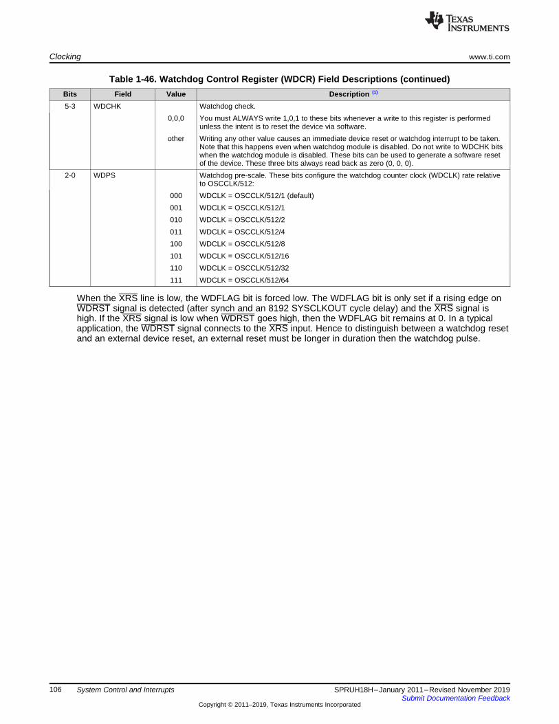
Clocking www.ti.com
106 SPRUH18H–January 2011–Revised November 2019Submit Documentation Feedback
Copyright © 2011–2019, Texas Instruments Incorporated
System Control and Interrupts
Table 1-46. Watchdog Control Register (WDCR) Field Descriptions (continued)Bits Field Value Description (1)
5-3 WDCHK Watchdog check.0,0,0 You must ALWAYS write 1,0,1 to these bits whenever a write to this register is performed
unless the intent is to reset the device via software.other Writing any other value causes an immediate device reset or watchdog interrupt to be taken.
Note that this happens even when watchdog module is disabled. Do not write to WDCHK bitswhen the watchdog module is disabled. These bits can be used to generate a software resetof the device. These three bits always read back as zero (0, 0, 0).
2-0 WDPS Watchdog pre-scale. These bits configure the watchdog counter clock (WDCLK) rate relativeto OSCCLK/512:
000 WDCLK = OSCCLK/512/1 (default)001 WDCLK = OSCCLK/512/1010 WDCLK = OSCCLK/512/2011 WDCLK = OSCCLK/512/4100 WDCLK = OSCCLK/512/8101 WDCLK = OSCCLK/512/16110 WDCLK = OSCCLK/512/32111 WDCLK = OSCCLK/512/64
When the XRS line is low, the WDFLAG bit is forced low. The WDFLAG bit is only set if a rising edge onWDRST signal is detected (after synch and an 8192 SYSCLKOUT cycle delay) and the XRS signal ishigh. If the XRS signal is low when WDRST goes high, then the WDFLAG bit remains at 0. In a typicalapplication, the WDRST signal connects to the XRS input. Hence to distinguish between a watchdog resetand an external device reset, an external reset must be longer in duration then the watchdog pulse.

INT1
to
INT12
INT14
28x
CPU
TINT2
TINT0PIE CPU-TIMER 0
CPU-TIMER 2
INT13
TINT1CPU-TIMER 1
Borrow
Reset
Timer reload
SYSCLKOUT
TCR.4
(Timer start status)
TINT
16-bit timer divide-down
TDDRH:TDDR32-bit timer period
PRDH:PRD
32-bit counter
TIMH:TIM
16-bit prescale counter
PSCH:PSC
Borrow
www.ti.com Clocking
107SPRUH18H–January 2011–Revised November 2019Submit Documentation Feedback
Copyright © 2011–2019, Texas Instruments Incorporated
System Control and Interrupts
1.4.5 32-Bit CPU Timers 0/1/2This section describes the three 32-bit CPU-timers (TIMER0/1/2) shown in (Figure 1-49).
The CPU Timer-0 and CPU-Timer 1 can be used in user applications. Timer 2 is reserved for DSP/BIOS.If the application is not using DSP/BIOS, then Timer 2 can be used in the application. The CPU-timerinterrupt signals (TINT0, TINT1, TINT2) are connected as shown in Figure 1-50.
Figure 1-49. CPU-Timers
Figure 1-50. CPU-Timer Interrupts Signals and Output Signal
A The timer registers are connected to the Memory Bus of the 28x processor.B The timing of the timers is synchronized to SYSCLKOUT of the processor clock.

Clocking www.ti.com
108 SPRUH18H–January 2011–Revised November 2019Submit Documentation Feedback
Copyright © 2011–2019, Texas Instruments Incorporated
System Control and Interrupts
The general operation of the CPU-timer is as follows: The 32-bit counter register TIMH:TIM is loaded withthe value in the period register PRDH:PRD. The counter decrements once every (TPR[TDDRH:TDDR]+1)SYSCLKOUT cycles, where TDDRH:TDDR is the timer divider. When the counter reaches 0, a timerinterrupt output signal generates an interrupt pulse. The registers listed in Table 1-47 are used toconfigure the timers.
Table 1-47. CPU-Timers 0, 1, 2 Configuration and Control Registers
Name Address Size (x16) Description Bit DescriptionTIMER0TIM 0x0C00 1 CPU-Timer 0, Counter Register Figure 1-51TIMER0TIMH 0x0C01 1 CPU-Timer 0, Counter Register High Figure 1-52TIMER0PRD 0x0C02 1 CPU-Timer 0, Period Register Figure 1-53TIMER0PRDH 0x0C03 1 CPU-Timer 0, Period Register High Figure 1-54TIMER0TCR 0x0C04 1 CPU-Timer 0, Control Register Figure 1-55TIMER0TPR 0x0C06 1 CPU-Timer 0, Prescale Register Figure 1-56TIMER0TPRH 0x0C07 1 CPU-Timer 0, Prescale Register High Figure 1-57TIMER1TIM 0x0C08 1 CPU-Timer 1, Counter Register Figure 1-51TIMER1TIMH 0x0C09 1 CPU-Timer 1, Counter Register High Figure 1-52TIMER1PRD 0x0C0A 1 CPU-Timer 1, Period Register Figure 1-53TIMER1PRDH 0x0C0B 1 CPU-Timer 1, Period Register High Figure 1-54TIMER1TCR 0x0C0C 1 CPU-Timer 1, Control Register Figure 1-55TIMER1TPR 0x0C0E 1 CPU-Timer 1, Prescale Register Figure 1-56TIMER1TPRH 0x0C0F 1 CPU-Timer 1, Prescale Register High Figure 1-57TIMER2TIM 0x0C10 1 CPU-Timer 2, Counter Register Figure 1-51TIMER2TIMH 0x0C11 1 CPU-Timer 2, Counter Register High Figure 1-52TIMER2PRD 0x0C12 1 CPU-Timer 2, Period Register Figure 1-53TIMER2PRDH 0x0C13 1 CPU-Timer 2, Period Register High Figure 1-54TIMER2TCR 0x0C14 1 CPU-Timer 2, Control Register Figure 1-55TIMER2TPR 0x0C16 1 CPU-Timer 2, Prescale Register Figure 1-56TIMER2TPRH 0x0C17 1 CPU-Timer 2, Prescale Register High Figure 1-57
Figure 1-51. TIMERxTIM Register (x = 0, 1, 2)15 0
TIMR/W-0
LEGEND: R/W = Read/Write; R = Read only; -n = value after reset
Table 1-48. TIMERxTIM Register Field Descriptions
Bits Field Description15-0 TIM CPU-Timer Counter Registers (TIMH:TIM): The TIM register holds the low 16 bits of the current 32-bit count
of the timer. The TIMH register holds the high 16 bits of the current 32-bit count of the timer. The TIMH:TIMdecrements by one every (TDDRH:TDDR+1) clock cycles, where TDDRH:TDDR is the timer prescale divide-down value. When the TIMH:TIM decrements to zero, the TIMH:TIM register is reloaded with the periodvalue contained in the PRDH:PRD registers. The timer interrupt (TINT) signal is generated.
Figure 1-52. TIMERxTIMH Register (x = 0, 1, 2)15 0
TIMHR/W-0
LEGEND: R/W = Read/Write; R = Read only; -n = value after reset

www.ti.com Clocking
109SPRUH18H–January 2011–Revised November 2019Submit Documentation Feedback
Copyright © 2011–2019, Texas Instruments Incorporated
System Control and Interrupts
Table 1-49. TIMERxTIMH Register Field Descriptions
Bits Field Description15-0 TIMH See description for TIMERxTIM.
Figure 1-53. TIMERxPRD Register (x = 0, 1, 2)15 0
PRDR/W-1
LEGEND: R/W = Read/Write; R = Read only; -n = value after reset
Table 1-50. TIMERxPRD Register Field Descriptions
Bits Field Description15-0 PRD CPU-Timer Period Registers (PRDH:PRD): The PRD register holds the low 16 bits of the 32-bit period. The
PRDH register holds the high 16 bits of the 32-bit period. When the TIMH:TIM decrements to zero, theTIMH:TIM register is reloaded with the period value contained in the PRDH:PRD registers, at the start ofthe next timer input clock cycle (the output of the prescaler). The PRDH:PRD contents are also loaded intothe TIMH:TIM when you set the timer reload bit (TRB) in the Timer Control Register (TCR).
Figure 1-54. TIMERxPRDH Register (x = 0, 1, 2)15 0
PRDHR/W-0
LEGEND: R/W = Read/Write; R = Read only; -n = value after reset
Table 1-51. TIMERxPRDH Register Field Descriptions
Bits Field Description15-0 PRDH See description for TIMERxPRD
Figure 1-55. TIMERxTCR Register (x = 0, 1, 2)15 14 13 12 11 10 9 8TIF TIE Reserved FREE SOFT Reserved
R/W-0 R/W-0 R-0 R/W-0 R/W-0 R-0
7 6 5 4 3 0Reserved TRB TSS Reserved
R-0 R/W-0 R/W-0 R-0LEGEND: R/W = Read/Write; R = Read only; -n = value after reset
Table 1-52. TIMERxTCR Register Field Descriptions
Bits Field Value Description15 TIF CPU-Timer Interrupt Flag.
0 The CPU-Timer has not decremented to zero.Writes of 0 are ignored.
1 This flag gets set when the CPU-timer decrements to zero.Writing a 1 to this bit clears the flag.
14 TIE CPU-Timer Interrupt Enable.0 The CPU-Timer interrupt is disabled.1 The CPU-Timer interrupt is enabled. If the timer decrements to zero, and TIE is set, the
timer asserts its interrupt request.13-12 Reserved Any writes to these bits must always have a value of 0.

Clocking www.ti.com
110 SPRUH18H–January 2011–Revised November 2019Submit Documentation Feedback
Copyright © 2011–2019, Texas Instruments Incorporated
System Control and Interrupts
Table 1-52. TIMERxTCR Register Field Descriptions (continued)Bits Field Value Description
11-10 FREESOFT
CPU-Timer Emulation Modes: These bits are special emulation bits that determine thestate of the timer when a breakpoint is encountered in the high-level languagedebugger. If the FREE bit is set to 1, then, upon a software breakpoint, the timercontinues to run (that is, free runs). In this case, SOFT is a don't care. But if FREE is 0,then SOFT takes effect. In this case, if SOFT = 0, the timer halts the next time theTIMH:TIM decrements. If the SOFT bit is 1, then the timer halts when the TIMH:TIMhas decremented to zero.
FREE SOFT CPU-Timer Emulation Mode0 0 Stop after the next decrement of the TIMH:TIM (hard stop)0 1 Stop after the TIMH:TIM decrements to 0 (soft stop)1 0 Free run1 1 Free run
In the SOFT STOP mode, the timer generates an interrupt before shutting down (sincereaching 0 is the interrupt causing condition).
9-6 Reserved Any writes to these bits must always have a value of 0.5 TRB CPU-Timer Reload bit.
0 The TRB bit is always read as zero. Writes of 0 are ignored.1 When you write a 1 to TRB, the TIMH:TIM is loaded with the value in the PRDH:PRD,
and the prescaler counter (PSCH:PSC) is loaded with the value in the timer divide-down register (TDDRH:TDDR).
4 TSS CPU-Timer stop status bit. TSS is a 1-bit flag that stops or starts the CPU-timer.0 Reads of 0 indicate the CPU-timer is running.
To start or restart the CPU-timer, set TSS to 0. At reset, TSS is cleared to 0 and theCPU-timer immediately starts.
1 Reads of 1 indicate that the CPU-timer is stopped.To stop the CPU-timer, set TSS to 1.
3-0 Reserved Any writes to these bits must always have a value of 0.
Figure 1-56. TIMERxTPR Register (x = 0, 1, 2)15 8 7 0
PSC TDDRR-0 R/W-0
LEGEND: R/W = Read/Write; R = Read only; -n = value after reset
Table 1-53. TIMERxTPR Register Field Descriptions
Bits Field Description15-8 PSC CPU-Timer Prescale Counter. These bits hold the current prescale count for the timer. For every timer clock
source cycle that the PSCH:PSC value is greater than 0, the PSCH:PSC decrements by one. One timer clock(output of the timer prescaler) cycle after the PSCH:PSC reaches 0, the PSCH:PSC is loaded with the contentsof the TDDRH:TDDR, and the timer counter register (TIMH:TIM) decrements by one. The PSCH:PSC is alsoreloaded whenever the timer reload bit (TRB) is set by software. The PSCH:PSC can be checked by readingthe register, but it cannot be set directly. It must get its value from the timer divide-down register(TDDRH:TDDR). At reset, the PSCH:PSC is set to 0.
7-0 TDDR CPU-Timer Divide-Down. Every (TDDRH:TDDR + 1) timer clock source cycles, the timer counter register(TIMH:TIM) decrements by one. At reset, the TDDRH:TDDR bits are cleared to 0. To increase the overall timercount by an integer factor, write this factor minus one to the TDDRH:TDDR bits. When the prescaler counter(PSCH:PSC) value is 0, one timer clock source cycle later, the contents of the TDDRH:TDDR reload thePSCH:PSC, and the TIMH:TIM decrements by one. TDDRH:TDDR also reloads the PSCH:PSC whenever thetimer reload bit (TRB) is set by software.

www.ti.com Clocking
111SPRUH18H–January 2011–Revised November 2019Submit Documentation Feedback
Copyright © 2011–2019, Texas Instruments Incorporated
System Control and Interrupts
Figure 1-57. TIMERxTPRH Register (x = 0, 1, 2)15 8 7 0
PSCH TDDRHR-0 R/W-0
LEGEND: R/W = Read/Write; R = Read only; -n = value after reset
Table 1-54. TIMERxTPRH Register Field Descriptions
Bits Field Description15-8 PSCH See description of TIMERxTPR.7-0 TDDRH See description of TIMERxTPR.

General-Purpose Input/Output (GPIO) www.ti.com
112 SPRUH18H–January 2011–Revised November 2019Submit Documentation Feedback
Copyright © 2011–2019, Texas Instruments Incorporated
System Control and Interrupts
1.5 General-Purpose Input/Output (GPIO)The GPIO multiplexing (MUX) registers are used to select the operation of shared pins. The pins arenamed by their general purpose I/O name (GPIO0 - GPIO58). These pins can be individually selected tooperate as digital I/O, referred to as GPIO, or connected to one of up to three peripheral I/O signals (viathe GPxMUXn registers). If selected for digital I/O mode, registers are provided to configure the pindirection (via the GPxDIR registers). You can also qualify the input signals to remove unwanted noise (viathe GPxQSELn, GPACTRL, and GPBCTRL registers).
1.5.1 GPIO Module OverviewUp to three independent peripheral signals are multiplexed on a single GPIO-enabled pin in addition toindividual pin bit-I/O capability. There are three I/O ports. Port A consists of GPIO0 - GPIO31, port Bconsists of GPIO32 - GPIO58. The analog port consists of AIO0-AIO15. Figure 1-58 shows the basicmodes of operation for the GPIO module. Note that GPIO functionality is provided on JTAG pins as well.

GPADAT(latch)
GPACLEAR,
GPATOGGLEGPAQSEL 1/2
Qual
GPAMUX1/2
SYSCLKOUT
Highimpedance
outputcontrol
GPIOPins
PU
XRS
Sync
Low powermodes block
GPIOx.async
GPADIR(latch)
01
11
01
GPACTRL
2
2
10
Peripheral 1 input
N/C
(default on reset)
(default on reset)
GPIOx_OUT
GPIOx_DIR
GPAPUD
0 = enable PU
1 = disable PU
(disabled after reset)
async
(async disablewhen low)
11
10 Peripheral 2 input
Peripheral 3 input
Peripheral 1 output
GPASET,
(defaulton reset)
3 samples
6 samples
00 00XRS (default on reset)
01
11
10
00
01
11
10
00
0 = input, 1 = output
GPIO XINT1SEL
GPIO XINT2SEL
GPIO XINT3SEL
Externalinterrupt
MUXPIE
GPADAT (read)
GPIOLPMSEL
LPMCR0
Peripheral 2 output
Peripheral 3 output
Peripheral 1 output enable
Peripheral 2 output enable
Peripheral 3 output enable
www.ti.com General-Purpose Input/Output (GPIO)
113SPRUH18H–January 2011–Revised November 2019Submit Documentation Feedback
Copyright © 2011–2019, Texas Instruments Incorporated
System Control and Interrupts
Figure 1-58. General GPIO Multiplexing Diagram
A GPxDAT latch/read are accessed at the same memory location.
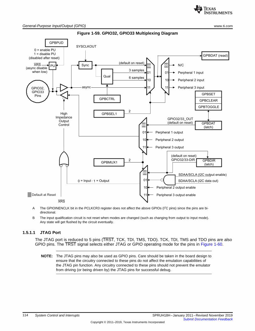
GPBDAT(latch)
GPBCLEAR
GPBTOGGLE
GPBSEL1
Qual
GPBMUX1
SYSCLKOUT
HighImpedance
OutputControl
GPIO32,GPIO33
Pins
PU
XRS
0 = Input , 1 = Output
Sync
GPBDIR(latch)
01
11
01
GPBCTRL
2
2
10
Perpheral 1 input
N/C
(default on reset)
GPIO32/33_OUT(default on reset)
GPBPUD
0 = enable PU
1 = disable PU
(disabled after reset)
async
(async disablewhen low)
0x
1x
11
10 Peripheral 2 input
Peripheral 3 input
GPBSET
(default on reset)
3 samples
6 samples
00 00XRS
Default at Reset
GPBDAT (read)
01 Perpheral 1 output
11
10 Peripheral 2 output
Peripheral 3 output
00
01
11
10 Peripheral 2 output enable
Peripheral 3 output enable
00SDAA/SCLA (I2C output enable)
SDAA/SCLA (I2C data out)
GPIO32/33-DIR
General-Purpose Input/Output (GPIO) www.ti.com
114 SPRUH18H–January 2011–Revised November 2019Submit Documentation Feedback
Copyright © 2011–2019, Texas Instruments Incorporated
System Control and Interrupts
Figure 1-59. GPIO32, GPIO33 Multiplexing Diagram
A The GPIOINENCLK bit in the PCLKCR3 register does not affect the above GPIOs (I2C pins) since the pins are bi-directional.
B The input qualification circuit is not reset when modes are changed (such as changing from output to input mode).Any state will get flushed by the circuit eventually.
1.5.1.1 JTAG PortThe JTAG port is reduced to 5 pins (TRST, TCK, TDI, TMS, TDO). TCK, TDI, TMS and TDO pins are alsoGPIO pins. The TRST signal selects either JTAG or GPIO operating mode for the pins in Figure 1-60.
NOTE: The JTAG pins may also be used as GPIO pins. Care should be taken in the board design toensure that the circuitry connected to these pins do not affect the emulation capabilities ofthe JTAG pin function. Any circuitry connected to these pins should not prevent the emulatorfrom driving (or being driven by) the JTAG pins for successful debug.

TRST
1
0
C28xCore
TCK/GPIO38
TCK
XCLKIN
GPIO38_in
GPIO38_out
TDO
GPIO37_out
TDO/GPIO37
GPIO37_in
1
0
TMSTMS/GPIO36
GPIO36_out
GPIO36_in
1
1
0
TDITDI/GPIO35
GPIO35_out
GPIO35_in
1
TRSTTRST
= 0: JTAG Disabled (GPIO Mode)= 1: JTAG Mode
TRST
www.ti.com General-Purpose Input/Output (GPIO)
115SPRUH18H–January 2011–Revised November 2019Submit Documentation Feedback
Copyright © 2011–2019, Texas Instruments Incorporated
System Control and Interrupts
Figure 1-60. JTAG Port/GPIO Multiplexing
1.5.1.2 Choosing JTAG or GPIO FunctionalityThe TRST signal selects the functionality of the JTAG signals, in combination with the JTAGDIS bit in theJTAGDEBUG register as follows.
TRST JTAGDIS bit JTAG Port Mode
0 X GPIO mode enabled, JTAGport disabled
1 0 JTAG port enabled (GPIOsshould be configured as inputs)
1 1 GPIO mode enabled, JTAGport disabled
The JTAGDEBUG register is shown and described below.
Figure 1-61. JTAGDEBUG Register (Addfress 0x702A, EALLOW protected)15 1 0
Reserved JTAGDISR-0 R/W-0
LEGEND: R/W = Read/Write; R = Read only; -n = value after reset

General-Purpose Input/Output (GPIO) www.ti.com
116 SPRUH18H–January 2011–Revised November 2019Submit Documentation Feedback
Copyright © 2011–2019, Texas Instruments Incorporated
System Control and Interrupts
Table 1-55. JTAGDEBUG Register Field Descriptions
Bits Field Value Description15-1 Reserved Any writes to these bits must always have a value of 0.
0 JTAGDIS JTAG Port Disable Bit: This bit enables/disables the JTAG port. When disabled, the JTAGpins can be used as GPIOs:
0 JTAG Port Enabled1 JTAG Port Disabled (GPIO Mode)
This bit is reset by TRST. The bit is forced to "0" when TRST is "0". When TRST is "1", thenJTAGDIS bit can be modified by CPU.
Note: Ensure no contention with the emulator signals when JTAGDIS=1

To COMPy A or B input
To ADC Channel X
1
0
AIOx Pin
AIOxIN
AIOxINESYNC
SYSCLKOUT
Logic implemented in GPIO MUX block
AIODAT Reg(Read)
AIODAT Reg(Latch)
AIOSET,AIOCLEAR,AIOTOGGLE
Regs
AIOMUX1 Reg
1
0
AIO
xD
IR(1
= In
pu
t,0 =
Ou
tpu
t)
(0 = Input, 1 = Output)
AIODIR Reg(Latch)
0
www.ti.com General-Purpose Input/Output (GPIO)
117SPRUH18H–January 2011–Revised November 2019Submit Documentation Feedback
Copyright © 2011–2019, Texas Instruments Incorporated
System Control and Interrupts
Figure 1-62. Analog/GPIO Multiplexing
A The ADC/Comparator path is always enabled, irrespective of the AIOMUX1 value.B The AIO section is blocked off when the corresponding AIOMUX1 bit is 1.

General-Purpose Input/Output (GPIO) www.ti.com
118 SPRUH18H–January 2011–Revised November 2019Submit Documentation Feedback
Copyright © 2011–2019, Texas Instruments Incorporated
System Control and Interrupts
1.5.2 Configuration OverviewThe pin function assignments, input qualification, and the external interrupt sources are all controlled bythe GPIO configuration control registers. In addition, you can assign pins to wake the device from theHALT and STANDBY low power modes and enable/disable internal pullup resistors. and Table 1-57 listthe registers that are used to configure the GPIO pins to match the system requirements.
(1) The registers in this table are EALLOW protected. See Section 1.6.2 for more information.
Table 1-56. GPIO Control Registers
Name (1) Address Size (x16) Register Description Bit DescriptionGPACTRL 0x6F80 2 GPIO A Control Register (GPIO0-GPIO31) Figure 1-70GPAQSEL1 0x6F82 2 GPIO A Qualifier Select 1 Register (GPIO0-GPIO15) Figure 1-73GPAQSEL2 0x6F84 2 GPIO A Qualifier Select 2 Register (GPIO16-GPIO31) Figure 1-74GPAMUX1 0x6F86 2 GPIO A MUX 1 Register (GPIO0-GPIO15) Figure 1-65GPAMUX2 0x6F88 2 GPIO A MUX 2 Register (GPIO16-GPIO31) Figure 1-66GPADIR 0x6F8A 2 GPIO A Direction Register (GPIO0-GPIO31) Figure 1-77GPAPUD 0x6F8C 2 GPIO A Pull Up Disable Register (GPIO0-GPIO31) Figure 1-80GPACTRL2 0x6F8E 2 USB I/O Control Figure 1-72GPBCTRL 0x6F90 2 GPIO B Control Register (GPIO32-GPIO58) Figure 1-71GPBQSEL1 0x6F92 2 GPIO B Qualifier Select 1 Register (GPIO32-GPIO44) Figure 1-75GPBQSEL2 0x6F94 2 GPIO B Qualifier Select 2 Register (GPIO50-GPIO58) Figure 1-76GPBMUX1 0x6F96 2 GPIO B MUX 1 Register (GPIO32-GPIO44) Figure 1-67GPBMUX2 0x6F98 2 GPIO B MUX2 Register (GPIO50-GPIO58) Figure 1-68GPBDIR 0x6F9A 2 GPIO B Direction Register (GPIO32-GPIO58) Figure 1-78GPBPUD 0x6F9C 2 GPIO B Pull Up Disable Register (GPIO32-GPIO58) Figure 1-81AIOMUX1 0x6FB6 2 Analog, I/O MUX 1 register (AIO0 - AIO15) Figure 1-69AIODIR 0x6FBA 2 Analog, I/O Direction Register (AIO0 - AIO15)
(1) The registers in this table are EALLOW protected. See Section 1.6.2 for more information.
Table 1-57. GPIO Interrupt and Low Power Mode Select Registers
Name (1) Address Size(x16) Register Description Bit Description
GPIOXINT1SEL 0x6FE0 1 XINT1 Source Select Register (GPIO0-GPIO31) Figure 1-88GPIOXINT2SEL 0x6FE1 1 XINT2 Source Select Register (GPIO0-GPIO31) Figure 1-88GPIOXINT3SEL 0x6FE2 1 XINT3 Source Select Register (GPIO0 - GPIO31) Figure 1-88GPIOLPMSEL 0x6FE8 1 LPM wakeup Source Select Register (GPIO0-GPIO31) Figure 10-14

www.ti.com General-Purpose Input/Output (GPIO)
119SPRUH18H–January 2011–Revised November 2019Submit Documentation Feedback
Copyright © 2011–2019, Texas Instruments Incorporated
System Control and Interrupts
To plan configuration of the GPIO module, consider the following steps:Step 1. Plan the device pin-out:Through a pin multiplexing scheme, a lot of flexibility is provided for assigning functionality to theGPIO-capable pins. Before getting started, look at the peripheral options available for each pin, andplan pin-out for your specific system. Will the pin be used as a general purpose input or output (GPIO)or as one of up to three available peripheral functions? Knowing this information will help determinehow to further configure the pin.Step 2. Enable or disable internal pull-up resistors:To enable or disable the internal pullup resistors, write to the respective bits in the GPIO pullup disable(GPAPUD and GPBPUD) registers. For pins that can function as ePWM output pins, the internal pullupresistors are disabled by default. All other GPIO-capable pins have the pullup enabled by default. TheAIOx pins do not have internal pull-up resistors.Step 3. Select input qualification:If the pin will be used as an input, specify the required input qualification, if any. The input qualificationis specified in the GPACTRL, GPBCTRL, GPAQSEL1, GPAQSEL2, GPBQSEL1, and GPBQSEL2registers. By default, all of the input signals are synchronized to SYSCLKOUT only.Step 4. Select the pin function:Configure the GPxMUXn or AIOMUXn registers such that the pin is a GPIO or one of three availableperipheral functions. By default, all GPIO-capable pins are configured at reset as general purpose inputpins.Step 5. For digital general purpose I/O, select the direction of the pin:If the pin is configured as an GPIO, specify the direction of the pin as either input or output in theGPADIR, GPBDIR, or AIODIR registers. By default, all GPIO pins are inputs. To change the pin frominput to output, first load the output latch with the value to be driven by writing the appropriate value tothe GPxCLEAR, GPxSET, or GPxTOGGLE (or AIOCLEAR, AIOSET, or AIOTOGGLE) registers. Oncethe output latch is loaded, change the pin direction from input to output via the GPxDIR registers. Theoutput latch for all pins is cleared at reset.Step 6. Select low power mode wake-up sources:Specify which pins, if any, will be able to wake the device from HALT and STANDBY low powermodes. The pins are specified in the GPIOLPMSEL register.Step 7. Select external interrupt sources:Specify the source for the XINT1 - XINT3 interrupts. For each interrupt you can specify one of the portA signals as the source. This is done by specifying the source in the GPIOXINTnSEL register. Thepolarity of the interrupts can be configured in the XINTnCR register as described in Section 1.7.6.
NOTE: There is a 2-SYSCLKOUT cycle delay from when a write to configuration registers such asGPxMUXn and GPxQSELn occurs to when the action is valid

General-Purpose Input/Output (GPIO) www.ti.com
120 SPRUH18H–January 2011–Revised November 2019Submit Documentation Feedback
Copyright © 2011–2019, Texas Instruments Incorporated
System Control and Interrupts
1.5.3 Digital General Purpose I/O ControlFor pins that are configured as GPIO you can change the values on the pins by using the registers inTable 1-58.
Table 1-58. GPIO Data Registers
Name Address Size (x16) Register Description Bit DescriptionGPADAT 0x6FC0 2 GPIO A Data Register (GPIO0-GPIO31) Figure 1-82GPASET 0x6FC2 2 GPIO A Set Register (GPIO0-GPIO31) Figure 1-85GPACLEAR 0x6FC4 2 GPIO A Clear Register (GPIO0-GPIO31) Figure 1-85GPATOGGLE 0x6FC6 2 GPIO A Toggle Register (GPIO0-GPIO31) Figure 1-85GPBDAT 0x6FC8 2 GPIO B Data Register (GPIO32-GPIO58) Figure 1-83GPBSET 0x6FCA 2 GPIO B Set Register (GPIO32-GPIO58) Figure 1-86GPBCLEAR 0x6FCC 2 GPIO B Clear Register (GPIO32-GPIO58) Figure 1-86GPBTOGGLE 0x6FCE 2 GPIO B Toggle Register (GPIO32-GPIO58) Figure 1-86AIODAT 0x6FD8 2 Analog I/O Data Register (AIO0 - AIO15) Figure 1-84AIOSET 0x6FDA 2 Analog I/O Data Set Register (AIO0 - AIO15)
Figure 1-87AIOCLEAR 0x6FDC 2 Analog I/O Clear Register (AIO0 - AIO15)AIOTOGGLE 0x6FDE 2 Analog I/O Toggle Register (AIO0 - AIO15)
• GPxDAT/AIODAT RegistersEach I/O port has one data register. Each bit in the data register corresponds to one GPIO pin. Nomatter how the pin is configured (GPIO or peripheral function), the corresponding bit in the dataregister reflects the current state of the pin after qualification (This does not apply to AIOx pins).Writing to the GPxDAT/AIODAT register clears or sets the corresponding output latch and if the pin isenabled as a general purpose output (GPIO output) the pin will also be driven either low or high. If thepin is not configured as a GPIO output then the value will be latched, but the pin will not be driven.Only if the pin is later configured as a GPIO output, will the latched value be driven onto the pin.
When using the GPxDAT register to change the level of an output pin, you should be cautious not toaccidentally change the level of another pin. For example, if you mean to change the output latch levelof GPIOA1 by writing to the GPADAT register bit 0 using a read-modify-write instruction, a problem canoccur if another I/O port A signal changes level between the read and the write stage of the instruction.Following is an analysis of why this happens:
The GPxDAT registers reflect the state of the pin, not the latch. This means the register reflects theactual pin value. However, there is a lag between when the register is written to when the new pinvalue is reflected back in the register. This may pose a problem when this register is used insubsequent program statements to alter the state of GPIO pins. An example is shown below where twoprogram statements attempt to drive two different GPIO pins that are currently low to a high state.
If Read-Modify-Write operations are used on the GPxDAT registers, because of the delay between theoutput and the input of the first instruction (I1), the second instruction (I2) will read the old value andwrite it back.
GpioDataRegs.GPADAT.bit.GPIO1 = 1 ; I1 performs read-modify-write of GPADATGpioDataRegs.GPADAT.bit.GPIO2 = 1 ; I2 also a read-modify-write of GPADAT.
; It gets the old value of GPIO1 due to the delay
The second instruction will wait for the first to finish its write due to the write-followed-by-readprotection on this peripheral frame. There will be some lag, however, between the write of (I1) and theGPxDAT bit reflecting the new value (1) on the pin. During this lag, the second instruction will read theold value of GPIO1 (0) and write it back along with the new value of GPIO2 (1). Therefore, GPIO1 pinstays low.
One solution is to put some NOP’s between instructions. A better solution is to use the

www.ti.com General-Purpose Input/Output (GPIO)
121SPRUH18H–January 2011–Revised November 2019Submit Documentation Feedback
Copyright © 2011–2019, Texas Instruments Incorporated
System Control and Interrupts
GPxSET/GPxCLEAR/GPxTOGGLE registers instead of the GPxDAT registers. These registers alwaysread back a 0 and writes of 0 have no effect. Only bits that need to be changed can be specifiedwithout disturbing any other bits that are currently in the process of changing.
• GPxSET/AIOSET RegistersThe set registers are used to drive specified GPIO pins high without disturbing other pins. Each I/Oport has one set register and each bit corresponds to one GPIO pin. The set registers always readback 0. If the corresponding pin is configured as an output, then writing a 1 to that bit in the set registerwill set the output latch high and the corresponding pin will be driven high. If the pin is not configuredas a GPIO output, then the value will be latched but the pin will not be driven. Only if the pin is laterconfigured as a GPIO output will the latched value will be driven onto the pin. Writing a 0 to any bit inthe set registers has no effect.
• GPxCLEAR/AIOCLEAR RegistersThe clear registers are used to drive specified GPIO pins low without disturbing other pins. Each I/Oport has one clear register. The clear registers always read back 0. If the corresponding pin isconfigured as a general purpose output, then writing a 1 to the corresponding bit in the clear registerwill clear the output latch and the pin will be driven low. If the pin is not configured as a GPIO output,then the value will be latched but the pin will not be driven. Only if the pin is later configured as a GPIOoutput will the latched value will be driven onto the pin. Writing a 0 to any bit in the clear registers hasno effect.
• GPxTOGGLE/AIOTOGGLE RegistersThe toggle registers are used to drive specified GPIO pins to the opposite level without disturbing otherpins. Each I/O port has one toggle register. The toggle registers always read back 0. If thecorresponding pin is configured as an output, then writing a 1 to that bit in the toggle register flips theoutput latch and pulls the corresponding pin in the opposite direction. That is, if the output pin is drivenlow, then writing a 1 to the corresponding bit in the toggle register will pull the pin high. Likewise, if theoutput pin is high, then writing a 1 to the corresponding bit in the toggle register will pull the pin low. Ifthe pin is not configured as a GPIO output, then the value will be latched but the pin will not be driven.Only if the pin is later configured as a GPIO output will the latched value will be driven onto the pin.Writing a 0 to any bit in the toggle registers has no effect.
1.5.4 Input QualificationThe input qualification scheme has been designed to be very flexible. You can select the type of inputqualification for each GPIO pin by configuring the GPAQSEL1, GPAQSEL2, GPBQSEL1 and GPBQSEL2registers. In the case of a GPIO input pin, the qualification can be specified as only synchronize toSYSCLKOUT or qualification by a sampling window. For pins that are configured as peripheral inputs, theinput can also be asynchronous in addition to synchronized to SYSCLKOUT or qualified by a samplingwindow. The remainder of this section describes the options available.
1.5.4.1 No Synchronization (asynchronous input)This mode is used for peripherals where input synchronization is not required or the peripheral itselfperforms the synchronization. Examples include communication ports SCI, SPI, eCAN and I2C. In addition,it may be desirable to have the ePWM trip zone (TZn) signals function independent of the presence ofSYSCLKOUT.
The asynchronous option is not valid if the pin is used as a general purpose digital input pin (GPIO). If thepin is configured as a GPIO input and the asynchronous option is selected then the qualification defaultsto synchronization to SYSCLKOUT as described in Section 1.5.4.2.
1.5.4.2 Synchronization to SYSCLKOUT OnlyThis is the default qualification mode of all the pins at reset. In this mode, the input signal is onlysynchronized to the system clock (SYSCLKOUT). Because the incoming signal is asynchronous, it cantake up to a SYSCLKOUT period of delay in order for the input to the device to be changed. No furtherqualification is performed on the signal.

GPxCTRL Reg
SYNC
SYSCLKOUT
Qualification Input Signal
Qualified By 3
or 6 Samples
GPIOx
Time between samples
GPxQSEL1/2
Number of Samples
General-Purpose Input/Output (GPIO) www.ti.com
122 SPRUH18H–January 2011–Revised November 2019Submit Documentation Feedback
Copyright © 2011–2019, Texas Instruments Incorporated
System Control and Interrupts
1.5.4.3 Qualification Using a Sampling WindowIn this mode, the signal is first synchronized to the system clock (SYSCLKOUT) and then qualified by aspecified number of cycles before the input is allowed to change. Figure 1-63 and Figure 1-64 show howthe input qualification is performed to eliminate unwanted noise. Two parameters are specified by the userfor this type of qualification: 1) the sampling period, or how often the signal is sampled, and 2) the numberof samples to be taken.
Figure 1-63. Input Qualification Using a Sampling Window
Time between samples (sampling period):To qualify the signal, the input signal is sampled at a regular period. The sampling period is specified bythe user and determines the time duration between samples, or how often the signal will be sampled,relative to the CPU clock (SYSCLKOUT).
The sampling period is specified by the qualification period (QUALPRDn) bits in the GPxCTRL register.The sampling period is configurable in groups of 8 input signals. For example, GPIO0 to GPIO7 useGPACTRL[QUALPRD0] setting and GPIO8 to GPIO15 use GPACTRL[QUALPRD1]. Table 1-59 andTable 1-60 show the relationship between the sampling period or sampling frequency and theGPxCTRL[QUALPRDn] setting.

www.ti.com General-Purpose Input/Output (GPIO)
123SPRUH18H–January 2011–Revised November 2019Submit Documentation Feedback
Copyright © 2011–2019, Texas Instruments Incorporated
System Control and Interrupts
Table 1-59. Sampling Period
Sampling PeriodIf GPxCTRL[QUALPRDn] = 0 1 × TSYSCLKOUT
If GPxCTRL[QUALPRDn] ≠ 0 2 × GPxCTRL[QUALPRDn] × TSYSCLKOUT
Where TSYSCLKOUT is the period in time of SYSCLKOUT
Table 1-60. Sampling Frequency
Sampling FrequencyIf GPxCTRL[QUALPRDn] = 0 fSYSCLKOUT
If GPxCTRL[QUALPRDn] ≠ 0 fSYSCLKOUT × 1 ÷ (2 × GPxCTRL[QUALPRDn])Where fSYSCLKOUT is the frequency of SYSCLKOUT
From these equations, the minimum and maximum time between samples can be calculated for a givenSYSCLKOUT frequency:
Example: Maximum Sampling Frequency:If GPxCTRL[QUALPRDn] = 0then the sampling frequency is fSYSCLKOUT
If, for example, fSYSCLKOUT = 60 MHzthen the signal will be sampled at 60 MHz or one sample every 16.67 ns.
Example: Minimum Sampling Frequency:If GPxCTRL[QUALPRDn] = 0xFF (255)then the sampling frequency is fSYSCLKOUT × 1 ÷ (2 × GPxCTRL[QUALPRDn])If, for example, fSYSCLKOUT = 60 MHzthen the signal will be sampled at 60 MHz × 1 ÷ (2 × 255) or one sample every 8.5 μs.
Number of samples:The number of times the signal is sampled is either 3 samples or 6 samples as specified in thequalification selection (GPAQSEL1, GPAQSEL2, GPBQSEL1, and GPBQSEL2) registers. When 3 or 6consecutive cycles are the same, then the input change will be passed through to the DSP.
Total Sampling Window Width:The sampling window is the time during which the input signal will be sampled as shown in Figure 1-64.By using the equation for the sampling period along with the number of samples to be taken, the totalwidth of the window can be determined.
For the input qualifier to detect a change in the input, the level of the signal must be stable for the durationof the sampling window width or longer.
The number of sampling periods within the window is always one less then the number of samples taken.For a thee-sample window, the sampling window width is 2 sampling periods wide where the samplingperiod is defined in Table 1-59. Likewise, for a six-sample window, the sampling window width is 5sampling periods wide. Table 1-61 and Table 1-62 show the calculations that can be used to determinethe total sampling window width based on GPxCTRL[QUALPRDn] and the number of samples taken.
Table 1-61. Case 1: Three-Sample Sampling Window Width
Total Sampling Window WidthIf GPxCTRL[QUALPRDn] = 0 2 × TSYSCLKOUT
If GPxCTRL[QUALPRDn] ≠ 0 2 × 2 × GPxCTRL[QUALPRDn] × TSYSCLKOUT
Where TSYSCLKOUT is the period in time of SYSCLKOUT

General-Purpose Input/Output (GPIO) www.ti.com
124 SPRUH18H–January 2011–Revised November 2019Submit Documentation Feedback
Copyright © 2011–2019, Texas Instruments Incorporated
System Control and Interrupts
Table 1-62. Case 2: Six-Sample Sampling Window Width
Total Sampling Window WidthIf GPxCTRL[QUALPRDn] = 0 5 × TSYSCLKOUT
If GPxCTRL[QUALPRDn] ≠ 0 5 × 2 × GPxCTRL[QUALPRDn] × TSYSCLKOUT
Where TSYSCLKOUT is the period in time of SYSCLKOUT
NOTE: The external signal change is asynchronous with respect to both the sampling period andSYSCLKOUT. Due to the asynchronous nature of the external signal, the input should beheld stable for a time greater than the sampling window width to make sure the logic detectsa change in the signal. The extra time required can be up to an additional sampling period +TSYSCLKOUT.
The required duration for an input signal to be stable for the qualification logic to detect achange is described in the device specific datasheet.

GPIO Signal
1
Sampling Window
Output FromQualifier
1 1 1 1 1 1 1 1 1 1 10 0 0 0 0 0 0 0 0 0
SYSCLKOUT
QUALPRD = 1(SYSCLKOUT/2)
(SYSCLKOUT cycle * 2 * QUALPRD) * 5(C))
(A)
GPxQSELn = 1,0 (6 samples)
Sampling Period determined
by GPxCTRL[QUALPRD](B)
A. This glitch will be ignored by the input qualifier. The QUALPRD bit field specifies the qualification sampling period. It can vary from 00 to
0xFF. If QUALPRD = 00, then the sampling period is 1 SYSCLKOUT cycle. For any other value “n”, the qualification sampling period in 2n
SYSCLKOUT cycles (i.e., at every 2n SYSCLKOUT cycles, the GPIO pin will be sampled).
B. The qualification period selected via the GPxCTRL register applies to groups of 8 GPIO pins.
C. The qualification block can take either three or six samples. The GPxQSELn Register selects which sample mode is used.
D. In the example shown, for the qualifier to detect the change, the input should be stable for 10 SYSCLKOUT cycles or greater. In other words,
the inputs should be stable for (5 x QUALPRD x 2) SYSCLKOUT cycles. That would ensure 5 sampling periods for detection to occur. Since
external signals are driven asynchronously, an 13-SYSCLKOUT-wide pulse ensures reliable recognition.
(D)
tw(SP)
tw(IQSW)
www.ti.com General-Purpose Input/Output (GPIO)
125SPRUH18H–January 2011–Revised November 2019Submit Documentation Feedback
Copyright © 2011–2019, Texas Instruments Incorporated
System Control and Interrupts
Example Qualification Window:For the example shown in Figure 1-64, the input qualification has been configured as follows:• GPxQSEL1/2 = 1,0. This indicates a six-sample qualification.• GPxCTRL[QUALPRDn] = 1. The sampling period is tw(SP) = 2 × GPxCTRL[QUALPRDn] × TSYSCLKOUT .
This configuration results in the following:• The width of the sampling window is: .
tw(IQSW) = 5 × tw(SP) = 5 × 2 × GPxCTRL[QUALPRDn] × TSYSCLKOUT or 5 × 2 × TSYSCLKOUT
• If, for example, TSYSCLKOUT = 16.67 ns, then the duration of the sampling window is:tw(IQSW) = 5 × 2 × 16.67 ns =166.7 ns.
• To account for the asynchronous nature of the input relative to the sampling period and SYSCLKOUT,up to an additional sampling period, tw(SP), + TSYSCLKOUT may be required to detect a change in theinput signal. For this example:tw(SP) + TSYSCLKOUT = 333.4 ns + 166.67 ns = 500.1 ns
• In Figure 1-64, the glitch (A) is shorter then the qualification window and will be ignored by the inputqualifier.
Figure 1-64. Input Qualifier Clock Cycles

General-Purpose Input/Output (GPIO) www.ti.com
126 SPRUH18H–January 2011–Revised November 2019Submit Documentation Feedback
Copyright © 2011–2019, Texas Instruments Incorporated
System Control and Interrupts
1.5.5 GPIO and Peripheral Multiplexing (MUX)Up to three different peripheral functions are multiplexed along with a general input/output (GPIO) functionper pin. This allows you to pick and choose a peripheral mix that will work best for the particularapplication.
and Table 1-65 show an overview of the possible multiplexing combinations sorted by GPIO pin. Thesecond column indicates the I/O name of the pin on the device. Since the I/O name is unique, it is the bestway to identify a particular pin. Therefore, the register descriptions in this section only refer to the GPIOname of a particular pin. The MUX register and particular bits that control the selection for each pin areindicated in the first column.
For example, the multiplexing for the GPIO6 pin is controlled by writing to GPAMUX[13:12]. By writing tothese bits, the pin is configured as either GPIO6, or one of up to three peripheral functions. The GPIO6pin can be configured as follows:
GPAMUX1[13:12] Bit Setting Pin Functionality SelectedIf GPAMUX1[13:12] = 0,0 Pin configured as GPIO6If GPAMUX1[13:12] = 0,1 Pin configured as EPWM4A (O)If GPAMUX1[13:12] = 1,0 Pin configured as EPWMSYNCI (I)If GPAMUX1[13:12] = 1,1 Pin configured as EPWMSYNCO (O)
The devices have different multiplexing schemes. If a peripheral is not available on a particular device,that MUX selection is reserved on that device and should not be used.
NOTE: If you should select a reserved GPIO MUX configuration that is not mapped to a peripheral,the state of the pin will be undefined and the pin may be driven. Reserved configurations arefor future expansion and should not be selected. In the device MUX tables (Table 1-64 andTable 1-65) these options are indicated as Reserved .
Some peripherals can be assigned to more than one pin via the MUX registers. For example, theSPISIMOB can be assigned to either the GPIO12 or GPIO24 pin, depending on individual systemrequirements as shown below:
Pin Assigned to SPISIMOB MUX ConfigurationChoice 1 GPIO12 GPAMUX1[25:24] = 11
or Choice 2 GPIO24 GPAMUX2[17:16] = 11
If no pin is configured as an input to a peripheral, or if more than one pin is configured as an input for thesame peripheral, then the input to the peripheral will either default to a 0 or a 1 as shown in Table 1-63.For example, if SPISIMOB were assigned to both GPIO12 and GPIO24, the input to the SPI peripheralwould default to a high state as shown in Table 1-63 and the input would not be connected to GPIO12 orGPIO24.

www.ti.com General-Purpose Input/Output (GPIO)
127SPRUH18H–January 2011–Revised November 2019Submit Documentation Feedback
Copyright © 2011–2019, Texas Instruments Incorporated
System Control and Interrupts
(1) This value will be assigned to the peripheral input if more then one pin has been assigned to the peripheral function in the GPxMUX1/2registers or if no pin has been assigned.
Table 1-63. Default State of Peripheral Input
Peripheral Input Description Default Input (1)
TZ1-TZ3 Trip zone 1-3 1EPWMSYNCI ePWM Synch Input 0ECAP1 eCAP1 input 1EQEP1A eQEP input 1EQEP1I eQEP index 1EQEP1S eQEP strobe 1SPICLKA/SPICLKB SPI-A clock 1SPISTEA /SPISTEB SPI-A transmit enable 0SPISIMOA/SPISIMOB SPI-A Slave-in, master-out 1SPISOMIA/SPISOMIB SPI-A Slave-out, master-in 1SCIRXDA - SCIRXDB SCI-A - SCI-B receive 1CANRXA eCAN-A receive 1SDAA I2C data 1SCLA1 I2C clock 1

General-Purpose Input/Output (GPIO) www.ti.com
128 SPRUH18H–January 2011–Revised November 2019Submit Documentation Feedback
Copyright © 2011–2019, Texas Instruments Incorporated
System Control and Interrupts
(1) The word "Reserved" means that there is no peripheral assigned to this GPxMUX1/2 register setting. Should it be selected, the state ofthe pin will be undefined and the pin may be driven. This selection is a reserved configuration for future expansion.
(2) I = Input, O = Output, OD = Open Drain(3) eQEP2 is not available on the 80-pin PN/PFP package.
Table 1-64. GPIOA MUX (1) (2)
DEFAULT AT RESETPRIMARY I/OFUNCTION
PERIPHERALSELECTION 1
PERIPHERALSELECTION 2
PERIPHERALSELECTION 3
GPAMUX1 REGISTERBITS (GPAMUX1 BITS = 00) (GPAMUX1 BITS = 01) (GPAMUX1 BITS = 10) (GPAMUX1 BITS = 11)
1-0 GPIO0 EPWM1A (O) Reserved Reserved3-2 GPIO1 EPWM1B (O) Reserved COMP1OUT (O)5-4 GPIO2 EPWM2A (O) Reserved Reserved7-6 GPIO3 EPWM2B (O) SPISOMIA (I/O) COMP2OUT (O)9-8 GPIO4 EPWM3A (O) Reserved Reserved
11-10 GPIO5 EPWM3B (O) SPISIMOA (I/O) ECAP1 (I/O)13-12 GPIO6 EPWM4A (O) EPWMSYNCI (I) EPWMSYNCO (O)15-14 GPIO7 EPWM4B (O) SCIRXDA (I) ECAP2 (I/O)17-16 GPIO8 EPWM5A (O) Reserved ADCSOCAO (O)19-18 GPIO9 EPWM5B (O) SCITXDB (3) (O) ECAP3 (I/O)21-20 GPIO10 EPWM6A (O) Reserved ADCSOCBO (O)23-22 GPIO11 EPWM6B (O) SCIRXDB (3) (I) ECAP1 (I/O)25-24 GPIO12 TZ1 (I) SCITXDA (O) SPISIMOB (I/O)27-26 GPIO13 TZ2 (I) Reserved SPISOMIB (I/O)29-28 GPIO14 TZ3 (I) SCITXDB (3) (O) SPICLKB (I/O)31-30 GPIO15 ECAP2 (I/O) SCIRXDB (3) (I) SPISTEB (I/O)
GPAMUX2 REGISTERBITS (GPAMUX2 BITS = 00) (GPAMUX2 BITS = 01) (GPAMUX2 BITS = 10) (GPAMUX2 BITS = 11)
1-0 GPIO16 SPISIMOA (I/O) Reserved TZ2 (I)3-2 GPIO17 SPISOMIA (I/O) Reserved TZ3 (I)5-4 GPIO18 SPICLKA (I/O) SCITXDB (3) (O) XCLKOUT (O)7-6 GPIO19/XCLKIN SPISTEA (I/O) SCIRXDB (3) (I) ECAP1 (I/O)9-8 GPIO20 EQEP1A (I) MDXA (O) COMP1OUT (O)
11-10 GPIO21 EQEP1B (I) MDRA (I) COMP2OUT (O)13-12 GPIO22 EQEP1S (I/O) MCLKXA (I/O) SCITXDB (3) (O)15-14 GPIO23 EQEP1I (I/O) MFSXA (I/O) SCIRXDB (3) (I)17-16 GPIO24 ECAP1 (I/O) EQEP2A (3) (I) SPISIMOB (I/O)19-18 GPIO25 ECAP2 (I/O) EQEP2B (3) (I) SPISOMIB (I/O)21-20 GPIO26 ECAP3 (I/O) EQEP2I (3) (I/O) SPICLKB (I/O)23-22 GPIO27 HRCAP2 (I) EQEP2S (3) (I/O) SPISTEB (I/O)25-24 GPIO28 SCIRXDA (I) SDAA (I/OD) TZ2 (I)27-26 GPIO29 SCITXDA (O) SCLA (I/OD) TZ3 (I)29-28 GPIO30 CANRXA (I) EQEP2I (3) (I/O) EPWM7A (O)31-30 GPIO31 CANTXA (O) EQEP2S (3) (I/O) EPWM8A (O)

www.ti.com General-Purpose Input/Output (GPIO)
129SPRUH18H–January 2011–Revised November 2019Submit Documentation Feedback
Copyright © 2011–2019, Texas Instruments Incorporated
System Control and Interrupts
(1) The word "Reserved" means that there is no peripheral assigned to this GPxMUX1/2 register setting. Should it be selected, the state ofthe pin will be undefined and the pin may be driven. This selection is a reserved configuration for future expansion.
(2) I = Input, O = Output, OD = Open Drain(3) This pin is not available in the 80-pin PN/PFP package.
Table 1-65. GPIOB MUX (1) (2)
DEFAULT AT RESETPRIMARY I/O FUNCTION
PERIPHERALSELECTION 1
PERIPHERALSELECTION 2
PERIPHERALSELECTION 3
GPBMUX1 REGISTERBITS (GPBMUX1 BITS = 00) (GPBMUX1 BITS = 01) (GPBMUX1 BITS = 10) (GPBMUX1 BITS = 11)
1-0 GPIO32 SDAA (I/OD) EPWMSYNCI (I) ADCSOCAO (O)3-2 GPIO33 SCLA (I/OD) EPWMSYNCO (O) ADCSOCBO (O)5-4 GPIO34 COMP2OUT (O) Reserved COMP3OUT (O)7-6 GPIO35 (TDI) Reserved Reserved Reserved9-8 GPIO36 (TMS) Reserved Reserved Reserved
11-10 GPIO37 (TDO) Reserved Reserved Reserved13-12 GPIO38/XCLKIN (TCK) Reserved Reserved Reserved15-14 GPIO39 Reserved Reserved Reserved17-16 GPIO40 (3) EPWM7A (O) SCITXDB (O) Reserved19-18 GPIO41 (3) EPWM7B (O) SCIRXDB (I) Reserved21-20 GPIO42 (3) EPWM8A (O) TZ1 (I) COMP1OUT (O)23-22 GPIO43 (3) EPWM8B (O) TZ2 (I) COMP2OUT (O)25-24 GPIO44 (3) MFSRA (I/O) SCIRXDB (I) EPWM7B (O)27-26 Reserved Reserved Reserved Reserved29-28 Reserved Reserved Reserved Reserved31-30 Reserved Reserved Reserved Reserved
GPBMUX2 REGISTERBITS (GPBMUX2 BITS = 00) (GPBMUX2 BITS = 01) (GPBMUX2 BITS = 10) (GPBMUX2 BITS = 11)
1-0 Reserved Reserved Reserved Reserved3-2 Reserved Reserved Reserved Reserved5-4 GPIO50 (3) EQEP1A (I) MDXA (O) TZ1 (I)7-6 GPIO51 (3) EQEP1B (I) MDRA (I) TZ2 (I)9-8 GPIO52 (3) EQEP1S (I/O) MCLKXA (I/O) TZ3 (I)
11-10 GPIO53 (3) EQEP1I (I/O) MFSXA (I/O) Reserved13-12 GPIO54 (3) SPISIMOA (I/O) EQEP2A (I) HRCAP1 (I)15-14 GPIO55 (3) SPISOMIA (I/O) EQEP2B (I) HRCAP2 (I)17-16 GPIO56 (3) SPICLKA (I/O) EQEP2I (I/O) HRCAP3 (I)19-18 GPIO57 (3) SPISTEA (I/O) EQEP2S (I/O) HRCAP4 (I)21-20 GPIO58 (3) MCLKRA (I/O) SCITXDB (O) EPWM7A (O)23-22 Reserved Reserved Reserved Reserved25-24 Reserved Reserved Reserved Reserved27-26 Reserved Reserved Reserved Reserved29-28 Reserved Reserved Reserved Reserved31-30 Reserved Reserved Reserved Reserved

General-Purpose Input/Output (GPIO) www.ti.com
130 SPRUH18H–January 2011–Revised November 2019Submit Documentation Feedback
Copyright © 2011–2019, Texas Instruments Incorporated
System Control and Interrupts
Table 1-66. Analog MUX
Default at ResetAIOx and Peripheral Selection1 Peripheral Selection 2 and Peripheral
Selection 3AIOMUX1 Register bits AIOMUX1 bits = 0,x AIOMUX1 bits = 1,x
1-0 ADCINA0 (I) ADCINA0 (I)3-2 ADCINA1 (I) ADCINA1 (I)5-4 AIO2 (I/O) ADCINA2 (I), COMP1A (I)7-6 ADCINA3 (I) ADCINA3 (I)9-8 AIO4 (I/O) ADCINA4 (I), COMP2A (I)
11-10 ADCINA5 (I) ADCINA5 (I)13-12 AIO6 (I/O) ADCINA6 (I), COMP3A (1)15-14 ADCINA7 (I) ADCINA7 (I)17-16 ADCINB0 (I) ADCINB0 (I)19-18 ADCINB1 (I) ADCINB1 (I)21-20 AIO10 (I/O) ADCINB2 (I), COMP1B (I)23-22 ADCINB3 (I) ADCINB3 (I)25-24 AIO12 (I/O) ADCINB4 (I), COMP2B (I)27-26 ADCINB5 (I) ADCINB5 (I)29-28 AIO14 (I/O) ADCINB6 (I), COMP3B (1)31-30 ADCINB7 (I) ADCINB7 (I)
1.5.6 Register Bit Definitions
Figure 1-65. GPIO Port A MUX 1 (GPAMUX1) Register31 30 29 28 27 26 25 24 23 22 21 20 19 18 17 16
GPIO15 GPIO14 GPIO13 GPIO12 GPIO11 GPIO10 GPIO9 GPIO8R/W-0 R/W-0 R/W-0 R/W-0 R/W-0 R/W-0 R/W-0 R/W-0
15 14 13 12 11 10 9 8 7 6 5 4 3 2 1 0GPIO7 GPIO6 GPIO5 GPIO4 GPIO3 GPIO2 GPIO1 GPIO0R/W-0 R/W-0 R/W-0 R/W-0 R/W-0 R/W-0 R/W-0 R/W-0
LEGEND- R/W = Read/Write; R = Read only; -n = value after reset
(1) This register is EALLOW protected. See Section 1.6.2 for more information.
Table 1-67. GPIO Port A Multiplexing 1 (GPAMUX1) Register Field Descriptions
Bits Field Value Description (1)
31-30 GPIO15 Configure the GPIO15 pin as:00 GPIO15 - General purpose input/output 15 (default) (I/O)01 ECAP2 (I/O)10 SCIRXDB (I)11 SPISTEB (I/O)
29-28 GPIO14 Configure the GPIO14 pin as:00 GPIO14 - General purpose I/O 14 (default) (I/O)01 TZ3 - Trip zone 3 (I)10 SCITXDB (O)11 SPICLKB (IO) - SPI-B clock
This option is reserved on devices that do not have an SPI-B port.

www.ti.com General-Purpose Input/Output (GPIO)
131SPRUH18H–January 2011–Revised November 2019Submit Documentation Feedback
Copyright © 2011–2019, Texas Instruments Incorporated
System Control and Interrupts
Table 1-67. GPIO Port A Multiplexing 1 (GPAMUX1) Register Field Descriptions (continued)Bits Field Value Description (1)
27-26 GPIO13 Configure the GPIO13 pin as:00 GPIO13 - General purpose I/O 13 (default) (I/O)01 TZ2 - Trip zone 2 (I)10 Reserved11 SPISOMIB (I/O) - SPI-B Slave Output/Master input
This option is reserved on devices that do not have an SPI-B port.25-24 GPIO12 Configure the GPIO12 pin as:
00 GPIO12 - General purpose I/O 12 (default) (I/O)01 TZ1 - Trip zone 1 (I)10 SCITXDA - SCI-A Transmit (O)11 SPISIMOB (I/O) - SPI-B Slave input/Master output
This option is reserved on devices that do not have an SPI-B port.23-22 GPIO11 Configure the GPIO11 pin as:
00 GPIO11 - General purpose I/O 11 (default) (I/O)01 EPWM6B - ePWM 6 output B (O)10 SCIRXDB (I)11 ECAP1 (I/O)
21-20 GPIO10 Configure the GPIO10 pin as:00 GPIO10 - General purpose I/O 10 (default) (I/O)01 EPWM6A - ePWM6 output A (O)10 Reserved11 ADCSOCBO - ADC Start of conversion B (O)
19-18 GPIO9 Configure the GPIO9 pin as:00 GPIO9 - General purpose I/O 9 (default) (I/O)01 EPWM5B - ePWM5 output B10 SCITXDB (O)11 ECAP3 (I/O)
17-16 GPIO8 Configure the GPIO8 pin as:00 GPIO8 - General purpose I/O 8 (default) (I/O)01 EPWM5A - ePWM5 output A (O)10 Reserved11 ADCSOCAO - ADC Start of conversion A
15-14 GPIO7 Configure the GPIO7 pin as:00 GPIO7 - General purpose I/O 7 (default) (I/O)01 EPWM4B - ePWM4 output B (O)10 SCIRXDA (I) - SCI-A receive (I)11 ECAP2 (I/O)
13-12 GPIO6 Configure the GPIO6 pin as:00 GPIO6 - General purpose I/O 6 (default)01 EPWM4A - ePWM4 output A (O)10 EPWMSYNCI - ePWM Synch-in (I)11 EPWMSYNCO - ePWM Synch-out (O)
11-10 GPIO5 Configure the GPIO5 pin as:00 GPIO5 - General purpose I/O 5 (default) (I/O)01 EPWM3B - ePWM3 output B10 SPISIMOA (I/O) - SPI-A Slave input/Master output11 ECAP1 - eCAP1 (I/O)

General-Purpose Input/Output (GPIO) www.ti.com
132 SPRUH18H–January 2011–Revised November 2019Submit Documentation Feedback
Copyright © 2011–2019, Texas Instruments Incorporated
System Control and Interrupts
Table 1-67. GPIO Port A Multiplexing 1 (GPAMUX1) Register Field Descriptions (continued)Bits Field Value Description (1)
9-8 GPIO4 Configure the GPIO4 pin as:00 GPIO4 - General purpose I/O 4 (default) (I/O)01 EPWM3A - ePWM3 output A (O)10 Reserved11 Reserved
7-6 GPIO3 Configure the GPIO3 pin as:00 GPIO3 - General purpose I/O 3 (default) (I/O)01 EPWM2B - ePWM2 output B (O)10 SPISOMIA (I/O) - SPI-A Slave output/Master input11 COMP2OUT (O) - Comparator 2 output
5-4 GPIO2 Configure the GPIO2 pin as:00 GPIO2 (I/O) General purpose I/O 2 (default) (I/O)01 EPWM2A - ePWM2 output A (O)10 Reserved11 Reserved
3-2 GPIO1 Configure the GPIO1 pin as:00 GPIO1 - General purpose I/O 1 (default) (I/O)01 EPWM1B - ePWM1 output B (O)10 Reserved11 COMP1OUT (O) - Comparator 1 output
1-0 GPIO0 Configure the GPIO0 pin as:00 GPIO0 - General purpose I/O 0 (default) (I/O)01 EPWM1A - ePWM1 output A (O)10 Reserved11 Reserved
Figure 1-66. GPIO Port A MUX 2 (GPAMUX2) Register31 30 29 28 27 26 25 24 23 22 21 20 19 18 17 16
GPIO31 GPIO30 GPIO29 GPIO28 GPIO27 GPIO26 GPIO25 GPIO24R/W-0 R/W-0 R/W-0 R/W-0 R/W-0 R/W-0 R/W-0 R/W-0
15 14 13 12 11 10 9 8 7 6 5 4 3 2 1 0GPIO23 GPIO22 GPIO21 GPIO20 GPIO19/XCLKI
NGPIO18 GPIO17 GPIO16
R/W-0 R/W-0 R/W-0 R/W-0 R/W-0 R/W-0 R/W-0 R/W-0LEGEND: R/W = Read/Write; R = Read only; -n = value after reset
(1) If reserved configurations are selected, then the state of the pin will be undefined and the pin may be driven. These selectionsare reserved for future expansion and should not be used.
Table 1-68. GPIO Port A MUX 2 (GPAMUX2) Register Field Descriptions
Bits Field Value Description (1)
31-30 GPIO31 Configure the GPIO31 pin as:00 GPIO31 - General purpose I/O 31 (default) (I/O)01 CANTXA - eCAN-A transmit (O)10 EQEP2S (I/O)11 EPWM8A (O)
29-28 GPIO30 Configure the GPIO30 pin as:00 GPIO30 (I/O) General purpose I/O 30 (default) (I/O)

www.ti.com General-Purpose Input/Output (GPIO)
133SPRUH18H–January 2011–Revised November 2019Submit Documentation Feedback
Copyright © 2011–2019, Texas Instruments Incorporated
System Control and Interrupts
Table 1-68. GPIO Port A MUX 2 (GPAMUX2) Register Field Descriptions (continued)Bits Field Value Description (1)
01 CANRXA - eCAN-A receive (I)10 EQEP2I (I/O)11 EPWM7A (O)
27-26 GPIO29 Configure the GPIO29 pin as:00 GPIO29 (I/O) General purpose I/O 29 (default) (I/O)01 SCITXDA - SCI-A transmit. (O)10 SCLA - I2C clock open drain bidirectional port (I/O)11 TZ3 - Trip zone 3(I)
25-24 GPIO28 Configure the GPIO28 pin as:00 GPIO28 (I/O) General purpose I/O 28 (default) (I/O)01 SCIRXDA - SCI-A receive (I)10 SDAA - I2C data open drain bidirectional port (I/O)11 TZ2 - Trip zone 2 (I)
23-22 GPIO27 Configure the GPIO27 pin as:00 GPIO27 - General purpose I/O 27 (default) (I/O)01 HRCAP2 (I)10 EQEP2S (I/O)11 SPISTEB (I/O) - SPI-B Slave transmit enable
21-20 GPIO26 Configure the GPIO26 pin as:00 GPIO26 - General purpose I/O 26 (default) (I/O)01 ECAP3 (I/O)10 EQEP2I (I/O)11 SPICLKB (I/O) - SPI-B clock
19-18 GPIO25 Configure the GPIO25 pin as:00 GPIO25 - General purpose I/O 25 (default) (I/O)01 ECAP2 (I/O)10 EQEP2B (I)11 SPISOMIB (I/O) - SPI-B Slave Output/Master input
17-16 GPIO24 Configure the GPIO24 pin as:00 GPIO24 - General purpose I/O 24 (default) (I/O)01 ECAP1 - eCAP1 (I/O)10 EQEP2A (I)11 SPISIMOB (I/O) - SPI-B Slave input/Master output
15-14 GPIO23 Configure the GPIO23 pin as:00 GPIO23 - General purpose I/O 23 (default) (I/O)01 EQEP1I - eQEP1 index (I/O)10 MFSXA (I/O)11 SCIRXDB (I)
13-12 GPIO22 Configure the GPIO22 pin as:00 GPIO22 - General purpose I/O 22 (default) (I/O)01 EQEP1S - eQEP1 strobe (I/O)10 MCLKXA (I/O)11 SCITXDB (O)

General-Purpose Input/Output (GPIO) www.ti.com
134 SPRUH18H–January 2011–Revised November 2019Submit Documentation Feedback
Copyright © 2011–2019, Texas Instruments Incorporated
System Control and Interrupts
Table 1-68. GPIO Port A MUX 2 (GPAMUX2) Register Field Descriptions (continued)Bits Field Value Description (1)
11-10 GPIO21 Configure the GPIO21 pin as:00 GPIO21 - General purpose I/O 21 (default) (I/O)01 EQEP1B - eQEP1 input B (I)10 MDRA (I)11 COMP2OUT (O) - Comparator 2 output
9-8 GPIO20 Configure the GPIO20 pin as:00 GPIO20 - General purpose I/O 20 (default) (I/O)01 EQEP1A - eQEP1 input A (I)10 MDXA (O)11 COMP1OUT (O) - Comparator 1 output
7-6 GPIO19/XCLKIN Configure the GPIO19 pin as:00 GPIO19 - General purpose I/O 19 (default) (I/O) or XCLKIN01 SPISTEA - SPI-A slave transmit enable (I/O)10 SCIRXDB (I)11 ECAP1 - eCAP1 (I/O)
5-4 GPIO18 Configure the GPIO18 pin as:00 GPIO18 - General purpose I/O 18 (default) (I/O)01 SPICLKA - SPI-A clock (I/O)10 SCITXDB (O)11 XCLKOUT (O) - External clock output
3-2 GPIO17 Configure the GPIO17 pin as:00 GPIO17 - General purpose I/O 17 (default) (I/O)01 SPISOMIA - SPI-A Slave output/Master input (I/O)10 Reserved11 TZ3 - Trip zone 3 (I)
1-0 GPIO16 Configure the GPIO16 pin as:00 GPIO16 - General purpose I/O 16 (default) (I/O)01 SPISIMOA - SPI-A slave-in, master-out (I/O),10 Reserved11 TZ2 - Trip zone 2 (I)
Figure 1-67. GPIO Port B MUX 1 (GPBMUX1) Register31 26 25 24 23 22 21 20 19 18 17 16
Reserved GPIO44 GPIO43 GPIO42 GPIO41 GPIO40R-0 R/W-0 R/W-0 R/W-0 R/W-0 R/W-0
15 14 13 12 11 10 9 8 7 6 5 4 3 2 1 0GPIO39 GPIO38/XCLKI
N (TCK)GPIO37(TDO) GPIO36(TMS) GPIO35(TDI) GPIO34 GPIO33 GPIO32
R/W-0 R/W-0 R/W-0 R/W-0 R/W-0 R/W-0 R/W-0 R/W-0LEGEND: R/W = Read/Write; R = Read only; -n = value after reset

www.ti.com General-Purpose Input/Output (GPIO)
135SPRUH18H–January 2011–Revised November 2019Submit Documentation Feedback
Copyright © 2011–2019, Texas Instruments Incorporated
System Control and Interrupts
Table 1-69. GPIO Port B MUX 1 (GPBMUX1) Register Field Descriptions
Bit Field Value Description31:26 Reserved Reserved Reserved25:24 GPIO44 Configure this pin as:
00 GPIO44 - general purpose I/O 44 (default)01 MFSRA (I/O)10 SCIRXDB (I)11 EPWM7B (O)
23:22 GPIO43 Configure this pin as:00 GPIO43 - general purpose I/O 43 (default)01 EPWM8B (O)10 TZ2 (I)11 COMP2OUT (O) - Comparator 2 output
21:20 GPIO42 Configure this pin as:00 GPIO42 - general purpose I/O 42 (default)01 EPWM8A (O)10 TZ1 (I)11 COMP1OUT (O) - Comparator 1 output
19:18 GPIO41 Configure this pin as:00 GPIO41 - general purpose I/O 41 (default)01 EPWM7B (O) ePWM7 output B (O)10 SCIRXDB (I)11 Reserved
17:16 GPIO40 Configure this pin as:00 GPIO40 - general purpose I/O 40 (default)01 EPWM7A (O) - ePWM7 output A (O)10 SCITXDB (O)11 Reserved
15:14 GPIO39 Configure this pin as:00 GPIO39 - general purpose I/O 39 (default)01 Reserved
10 or 11 Reserved13:12 GPIO38/XCLKI
N (TCK)Configure this pin as:
00 GPIO38 - general purpose I/O 38 (default). If TRST = 1, JTAG TCK function is chosen forthis pin. This pin can also be used to provide a clock from an external oscillator to the core.
01 Reserved10 or 11 Reserved
11:10 GPIO37(TDO) Configure this pin as:00 GPIO37 - general purpose I/O 37 (default). If TRST = 1, JTAG TDO function is chosen for
this pin.01 Reserved
10 or 11 Reserved9:8 GPIO36(TMS) Configure this pin as:
00 GPIO36 - general purpose I/O 36 (default). If TRST = 1, JTAG TMS function is chosen forthis pin.
01 Reserved10 or 11 Reserved

General-Purpose Input/Output (GPIO) www.ti.com
136 SPRUH18H–January 2011–Revised November 2019Submit Documentation Feedback
Copyright © 2011–2019, Texas Instruments Incorporated
System Control and Interrupts
Table 1-69. GPIO Port B MUX 1 (GPBMUX1) Register Field Descriptions (continued)Bit Field Value Description7:6 GPIO35(TDI) Configure this pin as:
00 GPIO35 - general purpose I/O 35 (default). If TRST = 1, JTAG TDI function is chosen for thispin.
01 Reserved10 or 11 Reserved
5:4 GPIO34 Configure this pin as:00 GPIO34 - general purpose I/O 34 (default)01 COMP2OUT (O) - Comparator 2 output10 Reserved11 COMP3OUT (O) - Comparator 3 output
3:2 GPIO33 Configure this pin as:00 GPIO33 - general purpose I/O 33 (default)01 SCLA - I2C clock open drain bidirectional port (I/O)10 EPWMSYNCO - External ePWM sync pulse output (O)11 ADCSOCBO - ADC start-of-conversion B (O)
1:0 GPIO32 Configure this pin as:00 GPIO32 - general purpose I/O 32 (default)01 SDAA - I2C data open drain bidirectional port (I/O)10 EPWMSYNCI - External ePWM sync pulse input (I)11 ADCSOCAO - ADC start-of-conversion A (O)
Figure 1-68. GPIO Port B MUX 2 (GPBMUX2) Register31 22 21 20 19 18 17 16
Reserved GPIO58 GPIO57 GPIO56R-0 R/W-0 R/W-0 R/W-0
15 14 13 12 11 10 9 8 7 6 5 4 3 0GPIO55 GPIO54 GPIO53 GPIO52 GPIO51 GPIO50 ReservedR/W-0 R/W-0 R/W-0 R/W-0 R/W-0 R/W-0 R-0
LEGEND: R/W = Read/Write; R = Read only; -n = value after reset
Table 1-70. GPIO Port B MUX 2 (GPBMUX2) Register Field Descriptions
Bit Field Value Description31:22 Reserved Any writes to these bits must always have a value of 0.21:20 GPIO58 Configure this pin as:
00 GPIO58 - general purpose I/O 42 (default)01 MCLKRA (I/O)10 SCITXDB (O)11 EPWM7A (O)
19:18 GPIO57 Configure this pin as:00 GPIO57 - general purpose I/O 57 (default)01 SPISTEA (I/O)10 EQEP2S (I/O)11 HRCAP4 (I)

www.ti.com General-Purpose Input/Output (GPIO)
137SPRUH18H–January 2011–Revised November 2019Submit Documentation Feedback
Copyright © 2011–2019, Texas Instruments Incorporated
System Control and Interrupts
Table 1-70. GPIO Port B MUX 2 (GPBMUX2) Register Field Descriptions (continued)Bit Field Value Description
17:16 GPIO56 Configure this pin as:00 GPIO56 - general purpose I/O 56(default)01 SPICLKA (I/O)10 EQEP2I (I/O)11 HRCAP3 (I)
15:14 GPIO55 Configure this pin as:00 GPIO55 - general purpose I/O 55 (default)01 SPISOMIA (I/O)10 EQEP2B (I)11 HRCAP2 (I)
13:12 GPIO54 Configure this pin as:00 GPIO54 - general purpose I/O 54 (default).01 SPISIMOA (I/O)10 EQEP2A (I)11 HRCAP1 (I)
11:10 GPIO53 Configure this pin as:00 GPIO53 - general purpose I/O 53 (default).01 EQEP1I (I/O)10 MFSXA (I/O)11 Reserved
9:8 GPIO52 Configure this pin as:00 GPIO52 - general purpose I/O 52 (default).01 EQEP1S (I/O)10 MCLKXA (I/O)11 TZ3 (I)
7:6 GPIO51 Configure this pin as:00 GPIO51 - general purpose I/O 51 (default).01 EQEP1B (I)10 MDRA (I)11 TZ2 (I)
5:4 GPIO50 Configure this pin as:00 GPIO50 - general purpose I/O 50 (default)01 EQEP1A (I)10 MDXA (O)11 TZ1 (I)
3:0 Reserved Any writes to these bits must always have a value of 0.
Figure 1-69. Analog I/O MUX (AIOMUX1) Register31 30 29 28 27 26 25 24 23 22 21 20 19 16Reserved AIO14 Reserved AIO12 Reserved AIO10 Reserved
R-0 R/W-1,x R-0 R/W-1,x R-0 R/W-1,x R-0
15 14 13 12 11 10 9 8 7 6 5 4 3 0Reserved AIO6 Reserved AIO4 Reserved AIO2 Reserved
R-0 R/W-1,x R-0 R/W-1,x R-0 R/W-1,x R-0LEGEND: R/W = Read/Write; R = Read only; -n = value after reset

General-Purpose Input/Output (GPIO) www.ti.com
138 SPRUH18H–January 2011–Revised November 2019Submit Documentation Feedback
Copyright © 2011–2019, Texas Instruments Incorporated
System Control and Interrupts
Table 1-71. Analog I/O MUX (AIOMUX1) Register Field Descriptions
Bit Field Value Description31:30 Reserved Any writes to these bits must always have a value of 0.29:28 AIO14 00 or 01 AIO14 enabled
10 or 11 AIO14 disabled (default)27:26 Reserved Any writes to these bits must always have a value of 0.25:24 AIO12 00 or 01 AIO12 enabled
10 or 11 AIO12 disabled (default)23:22 Reserved Any writes to these bits must always have a value of 0.21:20 AIO10 00 or 01 AIO10 enabled
10 or 11 AIO10 disabled (default)19:14 Reserved Any writes to these bits must always have a value of 0.13:12 AIO6 00 or 01 AIO6 enabled
10 or 11 AIO6 disabled (default)11:10 Reserved Any writes to these bits must always have a value of 0.9:8 AIO4 00 or 01 AIO4 enabled
10 or 11 AIO4 disabled (default)7:6 Reserved Any writes to these bits must always have a value of 0.5:4 AIO2 00 or 01 AIO2 enabled
10 or 11 AIO2 disabled (default)3:0 Reserved Any writes to these bits must always have a value of 0.
Figure 1-70. GPIO Port A Qualification Control (GPACTRL) Register31 24 23 16
QUALPRD3 QUALPRD2R/W-0 R/W-0
15 8 7 0QUALPRD1 QUALPRD0
R/W-0 R/W-0LEGEND: R/W = Read/Write; R = Read only; -n = value after reset
(1) This register is EALLOW protected. See Section 1.6.2 for more information.(2) TSYSCLKOUT indicates the period of SYSCLKOUT.
The GPxCTRL registers specify the sampling period for input pins when configured for input qualificationusing a window of three or six samples. The sampling period is the amount of time between qualificationsamples relative to the period of SYSCLKOUT. The number of samples is specified in the GPxQSELnregisters.
Table 1-72. GPIO Port A Qualification Control (GPACTRL) Register Field Descriptions
Bits Field Value Description (1)
31-24 QUALPRD3 Specifies the sampling period for pins GPIO24 to GPIO31.0x00 Sampling Period = TSYSCLKOUT
(2)
0x01 Sampling Period = 2 × TSYSCLKOUT
0x02 Sampling Period = 4 × TSYSCLKOUT
. . . . . .0xFF Sampling Period = 510 × TSYSCLKOUT

www.ti.com General-Purpose Input/Output (GPIO)
139SPRUH18H–January 2011–Revised November 2019Submit Documentation Feedback
Copyright © 2011–2019, Texas Instruments Incorporated
System Control and Interrupts
Table 1-72. GPIO Port A Qualification Control (GPACTRL) Register Field Descriptions (continued)Bits Field Value Description (1)
23-16 QUALPRD2 Specifies the sampling period for pins GPIO16 to GPIO23.0x00 Sampling Period = TSYSCLKOUT
(2)
0x01 Sampling Period = 2 × TSYSCLKOUT
0x02 Sampling Period = 4 × TSYSCLKOUT
. . . . . .0xFF Sampling Period = 510 × TSYSCLKOUT
15-8 QUALPRD1 Specifies the sampling period for pins GPIO8 to GPIO15.0x00 Sampling Period = TSYSCLKOUT
(2)
0x01 Sampling Period = 2 × TSYSCLKOUT
0x02 Sampling Period = 4 × TSYSCLKOUT
. . . . . .0xFF Sampling Period = 510 × TSYSCLKOUT
7-0 QUALPRD0 Specifies the sampling period for pins GPIO0 to GPIO7.0x00 Sampling Period = TSYSCLKOUT
(2)
0x01 Sampling Period = 2 × TSYSCLKOUT
0x02 Sampling Period = 4 × TSYSCLKOUT
. . . . . .0xFF Sampling Period = 510 × TSYSCLKOUT

General-Purpose Input/Output (GPIO) www.ti.com
140 SPRUH18H–January 2011–Revised November 2019Submit Documentation Feedback
Copyright © 2011–2019, Texas Instruments Incorporated
System Control and Interrupts
Figure 1-71. GPIO Port B Qualification Control (GPBCTRL) Register31 24 23 16
QUALPRD3 QUALPRD2R/W-0 R/W-0
15 8 7 0QUALPRD1 QUALPRD0
R/W-0 R/W-0LEGEND: R/W = Read/Write; R = Read only; -n = value after reset
(1) This register is EALLOW protected. See Section 1.6.2 for more information.(2) TSYSCLKOUT indicates the period of SYSCLKOUT.
Table 1-73. GPIO Port B Qualification Control (GPBCTRL) Register Field Descriptions
Bits Field Value Description (1)
31-24 QUALPRD3 Specifies the sampling period for pins GPIO56 to GPIO580x00 Sampling Period = TSYSCLKOUT
(2)
0x01 Sampling Period = 2 × TSYSCLKOUT
0x02 Sampling Period = 4 × TSYSCLKOUT
. . . . . .0xFF Sampling Period = 510 × TSYSCLKOUT
23-16 QUALPRD2 Specifies the sampling period for pins GPIO50 to GPIO550xFF Sampling Period = 510 × TSYSCLKOUT
0x00 Sampling Period = TSYSCLKOUT(2)
0x01 Sampling Period = 2 × TSYSCLKOUT
0x02 Sampling Period = 4 × TSYSCLKOUT
. . . . . .0xFF Sampling Period = 510 × TSYSCLKOUT
15-8 QUALPRD1 Specifies the sampling period for pins GPIO40 to GPIO440xFF Sampling Period = 510 × TSYSCLKOUT
0x00 Sampling Period = TSYSCLKOUT(2)
0x01 Sampling Period = 2 × TSYSCLKOUT
0x02 Sampling Period = 4 × TSYSCLKOUT
. . . . . .0xFF Sampling Period = 510 × TSYSCLKOUT
7-0 QUALPRD0 Specifies the sampling period for pins GPIO32 to GPIO390xFF Sampling Period = 510 × TSYSCLKOUT
0x00 Sampling Period = TSYSCLKOUT(2)
0x01 Sampling Period = 2 × TSYSCLKOUT
0x02 Sampling Period = 4 × TSYSCLKOUT
. . . . . .0xFF Sampling Period = 510 × TSYSCLKOUT
Figure 1-72. GPIO A Control Register 2 Register (GPACTRL2) Register31 16
ReservedR-0
15 1 0Reserved USBIOEN
R-0 R/W-0LEGEND: R/W = Read/Write; R = Read only; -n = value after reset

www.ti.com General-Purpose Input/Output (GPIO)
141SPRUH18H–January 2011–Revised November 2019Submit Documentation Feedback
Copyright © 2011–2019, Texas Instruments Incorporated
System Control and Interrupts
Table 1-74. (GPACTRL2) Register Field Descriptions
Bits Field Value Description31-1 Reserved Any writes to these bits must always have a value of 0.
0 USBIOEN USB I/O Enable Bit0 USB0DP and USB0DM pins are controlled by GPIO Mux register settings. USBPHY is
powered down.1 USB0DP and USB0DM pins configured as USB function. GPIO function is disabled.

General-Purpose Input/Output (GPIO) www.ti.com
142 SPRUH18H–January 2011–Revised November 2019Submit Documentation Feedback
Copyright © 2011–2019, Texas Instruments Incorporated
System Control and Interrupts
Figure 1-73. GPIO Port A Qualification Select 1 (GPAQSEL1) Register31 30 29 28 27 26 25 24 23 22 21 20 19 18 17 16
GPIO15 GPIO14 GPIO13 GPIO12 GPIO11 GPIO10 GPIO9 GPIO8R/W-0 R/W-0 R/W-0 R/W-0 R/W-0 R/W-0 R/W-0 R/W-0
15 14 13 12 11 10 9 8 7 6 5 4 3 2 1 0GPIO7 GPIO6 GPIO5 GPIO4 GPIO3 GPIO2 GPIO1 GPIO0R/W-0 R/W-0 R/W-0 R/W-0 R/W-0 R/W-0 R/W-0 R/W-0
LEGEND: R/W = Read/Write; R = Read only; -n = value after reset
(1) This register is EALLOW protected. See Section 1.6.2 for more information.
Table 1-75. GPIO Port A Qualification Select 1 (GPAQSEL1) Register Field Descriptions
Bits Field Value Description (1)
31-0 GPIO15-GPIO0 Select input qualification type for GPIO0 to GPIO15. The input qualification of each GPIOinput is controlled by two bits as shown in Figure 1-73.
00 Synchronize to SYSCLKOUT only. Valid for both peripheral and GPIO pins.01 Qualification using 3 samples. Valid for pins configured as GPIO or a peripheral function.
The time between samples is specified in the GPACTRL register.10 Qualification using 6 samples. Valid for pins configured as GPIO or a peripheral function.
The time between samples is specified in the GPACTRL register.11 Asynchronous. (no synchronization or qualification). This option applies to pins configured
as peripherals only. If the pin is configured as a GPIO input, then this option is the same as0,0 or synchronize to SYSCLKOUT.

www.ti.com General-Purpose Input/Output (GPIO)
143SPRUH18H–January 2011–Revised November 2019Submit Documentation Feedback
Copyright © 2011–2019, Texas Instruments Incorporated
System Control and Interrupts
Figure 1-74. GPIO Port A Qualification Select 2 (GPAQSEL2) Register31 30 29 28 27 26 25 24 23 22 21 20 19 18 17 16
GPIO31 GPIO30 GPIO29 GPIO28 GPIO27 GPIO26 GPIO25 GPIO24R/W-0 R/W-0 R/W-0 R/W-0 R/W-0 R/W-0 R/W-0 R/W-0
15 14 13 12 11 10 9 8 7 6 5 4 3 2 1 0GPIO23 GPIO22 GPIO21 GPIO20 GPIO19 GPIO18 GPIO17 GPIO16R/W-0 R/W-0 R/W-0 R/W-0 R/W-0 R/W-0 R/W-0 R/W-0
LEGEND: R/W = Read/Write; R = Read only; -n = value after reset
(1) This register is EALLOW protected. See Section 1.6.2 for more information.
Table 1-76. GPIO Port A Qualification Select 2 (GPAQSEL2) Register Field Descriptions
Bits Field Value Description (1)
31-0 GPIO31-GPIO16 Select input qualification type for GPIO16 to GPIO31. The input qualification of each GPIOinput is controlled by two bits as shown in Figure 1-74.
00 Synchronize to SYSCLKOUT only. Valid for both peripheral and GPIO pins.01 Qualification using 3 samples. Valid for pins configured as GPIO or a peripheral function. The
time between samples is specified in the GPACTRL register.10 Qualification using 6 samples. Valid for pins configured as GPIO or a peripheral function. The
time between samples is specified in the GPACTRL register.11 Asynchronous. (no synchronization or qualification). This option applies to pins configured as
peripherals only. If the pin is configured as a GPIO input, then this option is the same as 0,0or synchronize to SYSCLKOUT.

General-Purpose Input/Output (GPIO) www.ti.com
144 SPRUH18H–January 2011–Revised November 2019Submit Documentation Feedback
Copyright © 2011–2019, Texas Instruments Incorporated
System Control and Interrupts
Figure 1-75. GPIO Port B Qualification Select 1 (GPBQSEL1) Register31 26 25 24 23 22 21 20 19 18 17 16
Reserved GPIO44 GPIO43 GPIO42 GPIO41 GPIO40R/W-0 R/W-0 R/W-0 R/W-0 R/W-0 R/W-0
15 14 13 12 11 10 9 8 7 6 5 4 3 2 1 0GPIO39 GPIO38 GPIO37 GPIO36 GPIO35 GPIO34 GPIO33 GPIO32R/W-0 R/W-0 R/W-0 R/W-0 R/W-0 R/W-0 R/W-0 R/W-0
LEGEND: R/W = Read/Write; R = Read only; -n = value after reset
(1) This register is EALLOW protected. See Section 1.6.2 for more information.
Table 1-77. GPIO Port B Qualification Select 1 (GPBQSEL1) Register Field Descriptions
Bits Field Value Description (1)
31- 26 Reserved Any writes to these bits must always have a value of 0.25-0 GPIO 44-GPIO32 Select input qualification type for GPIO32 to GPIO44. The input qualification of each GPIO
input is controlled by two bits as shown in Figure 1-75 .00 Synchronize to SYSCLKOUT only. Valid for both peripheral and GPIO pins.01 Qualification using 3 samples. Valid for pins configured as GPIO or a peripheral function.
The time between samples is specified in the GPACTRL register.10 Qualification using 6 samples. Valid for pins configured as GPIO or a peripheral function.
The time between samples is specified in the GPACTRL register.11 Asynchronous. (no synchronization or qualification). This option applies to pins configured
as peripherals only. If the pin is configured as a GPIO input, then this option is the same as0,0 or synchronize to SYSCLKOUT.

www.ti.com General-Purpose Input/Output (GPIO)
145SPRUH18H–January 2011–Revised November 2019Submit Documentation Feedback
Copyright © 2011–2019, Texas Instruments Incorporated
System Control and Interrupts
Figure 1-76. GPIO Port B Qualification Select 2 (GPBQSEL2) Register31 22 21 20 19 18 17 16
Reserved GPIO58 GPIO57 GPIO56R/W-0 R/W-0 R/W-0 R/W-0
15 14 13 12 11 10 9 8 7 6 5 4 3 0GPIO55 GPIO54 GPIO53 GPIO52 GPIO51 GPIO50 ReservedR/W-0 R/W-0 R/W-0 R/W-0 R/W-0 R/W-0 R/W-0
LEGEND: R/W = Read/Write; R = Read only; -n = value after reset
(1) This register is EALLOW protected. See Section 1.6.2 for more information.
Table 1-78. GPIO Port B Qualification Select 2 (GPBQSEL2) Register Field Descriptions
Bits Field Value Description (1)
31- 22 Reserved Any writes to these bits must always have a value of 0.21-0 GPIO58-GPIO50 Select input qualification type for GPIO58 to GPIO50. The input qualification of each GPIO
input is controlled by two bits as shown in Figure 1-76 .00 Synchronize to SYSCLKOUT only. Valid for both peripheral and GPIO pins.01 Qualification using 3 samples. Valid for pins configured as GPIO or a peripheral function.
The time between samples is specified in the GPACTRL register.10 Qualification using 6 samples. Valid for pins configured as GPIO or a peripheral function.
The time between samples is specified in the GPACTRL register.11 Asynchronous. (no synchronization or qualification). This option applies to pins configured
as peripherals only. If the pin is configured as a GPIO input, then this option is the same as0,0 or synchronize to SYSCLKOUT.
The GPADIR and GPBDIR registers control the direction of the pins when they are configured as a GPIOin the appropriate MUX register. The direction register has no effect on pins configured as peripheralfunctions.
Figure 1-77. GPIO Port A Direction (GPADIR) Register31 30 29 28 27 26 25 24
GPIO31 GPIO30 GPIO29 GPIO28 GPIO27 GPIO26 GPIO25 GPIO24R/W-0 R/W-0 R/W-0 R/W-0 R/W-0 R/W-0 R/W-0 R/W-0
23 22 21 20 19 18 17 16GPIO23 GPIO22 GPIO21 GPIO20 GPIO19 GPIO18 GPIO17 GPIO16R/W-0 R/W-0 R/W-0 R/W-0 R/W-0 R/W-0 R/W-0 R/W-0
15 14 13 12 11 10 9 8GPIO15 GPIO14 GPIO13 GPIO12 GPIO11 GPIO10 GPIO9 GPIO8R/W-0 R/W-0 R/W-0 R/W-0 R/W-0 R/W-0 R/W-0 R/W-0
7 6 5 4 3 2 1 0GPIO7 GPIO6 GPIO5 GPIO4 GPIO3 GPIO2 GPIO1 GPIO0R/W-0 R/W-0 R/W-0 R/W-0 R/W-0 R/W-0 R/W-0 R/W-0
LEGEND: R/W = Read/Write; R = Read only; -n = value after reset
(1) This register is EALLOW protected. See Section 1.6.2 for more information.
Table 1-79. GPIO Port A Direction (GPADIR) Register Field Descriptions
Bits Field Value Description (1)
31-0 GPIO31-GPIO0 Controls direction of GPIO Port A pins when the specified pin is configured as a GPIO in theappropriate GPAMUX1 or GPAMUX2 register.
0 Configures the GPIO pin as an input. (default)1 Configures the GPIO pin as an output
The value currently in the GPADAT output latch is driven on the pin. To initialize the GPADATlatch prior to changing the pin from an input to an output, use the GPASET, GPACLEAR, andGPATOGGLE registers.

General-Purpose Input/Output (GPIO) www.ti.com
146 SPRUH18H–January 2011–Revised November 2019Submit Documentation Feedback
Copyright © 2011–2019, Texas Instruments Incorporated
System Control and Interrupts
Figure 1-78. GPIO Port B Direction (GPBDIR) Register31 27 26 25 24
Reserved GPIO58 GPIO57 GPIO56R-0 R/W-0 R/W-0 R/W-0
23 22 21 20 19 18 17 16GPIO55 GPIO54 GPIO53 GPIO52 GPIO51 GPIO50 ReservedR/W-0 R/W-0 R/W-0 R/W-0 R/W-0 R/W-0 R-0
15 13 12 11 10 9 8Reserved GPIO44 GPIO43 GPIO42 GPIO41 GPIO40
R-0 R/W-0 R/W-0 R/W-0 R/W-0 R/W-0
7 6 5 4 3 2 1 0GPIO39 GPIO38 GPIO37 GPIO36 GPIO35 GPIO34 GPIO33 GPIO32R/W-0 R/W-0 R/W-0 R/W-0 R/W-0 R/W-0 R/W-0 R/W-0
LEGEND: R/W = Read/Write; R = Read only; -n = value after reset
(1) This register is EALLOW protected. See Section 1.6.2 for more information.
Table 1-80. GPIO Port B Direction (GPBDIR) Register Field Descriptions
Bits Field Value Description (1)
31-27 Reserved Any writes to these bits must always have a value of 0.26-18 GPIO58-GPIO50 Controls direction of GPIO pin when GPIO mode is selected. Reading the register returns the
current value of the register setting.0 Configures the GPIO pin as an input. (default)1 Configures the GPIO pin as an output
17-13 Reserved Any writes to these bits must always have a value of 0.12-0 GPIO44-GPIO32 Controls direction of GPIO pin when GPIO mode is selected. Reading the register returns the
current value of the register setting.0 Configures the GPIO pin as an input. (default)1 Configures the GPIO pin as an output

www.ti.com General-Purpose Input/Output (GPIO)
147SPRUH18H–January 2011–Revised November 2019Submit Documentation Feedback
Copyright © 2011–2019, Texas Instruments Incorporated
System Control and Interrupts
Figure 1-79. Analog I/O DIR (AIODIR) Register31 16
ReservedR-0
15 14 13 12 11 10 9 8Reserved AIO14 Reserved AIO12 Reserved AIO10 Reserved
R-0 R/W-x R-0 R/W-x R-0 R/W-x R-0
7 6 5 4 3 2 1 0Reserved AIO6 Reserved AIO4 Reserved AIO2 Reserved
R-0 R/W-x R-0 R/W-x R-0 R/W-x R-0LEGEND: R/W = Read/Write; R = Read only; -n = value after reset
Table 1-81. Analog I/O DIR (AIODIR) Register Field Descriptions
Bit Field Value Description31:15 Reserved Any writes to these bits must always have a value of 0.14:0 AIOn Controls direction of the available AIO pin when AIO mode is selected. Reading the register returns
the current value of the register setting0 Configures the AIO pin as an input. (default)1 Configures the AIO pin as an output
The pullup disable (GPxPUD) registers allow you to specify which pins should have an internal pullupresister enabled. The internal pullups on the pins that can be configured as ePWM outputs(GPIO0-GPIO11) are all disabled asynchronously when the external reset signal (XRS) is low. The internal pullupson all other pins are enabled on reset. When coming out of reset, the pullups remain in their default stateuntil you enable or disable them selectively in software by writing to this register. The pullup configurationapplies both to pins configured as I/O and those configured as peripheral functions.
Figure 1-80. GPIO Port A Pullup Disable (GPAPUD) Registers31 30 29 28 27 26 25 24
GPIO31 GPIO30 GPIO29 GPIO28 GPIO27 GPIO26 GPIO25 GPIO24R/W-0 R/W-0 R/W-0 R/W-0 R/W-0 R/W-0 R/W-0 R/W-0
23 22 21 20 19 18 17 16GPIO23 GPIO22 GPIO21 GPIO20 GPIO19 GPIO18 GPIO17 GPIO16R/W-0 R/W-0 R/W-0 R/W-0 R/W-0 R/W-0 R/W-0 R/W-0
15 14 13 12 11 10 9 8GPIO15 GPIO14 GPIO13 GPIO12 GPIO11 GPIO10 GPIO9 GPIO8R/W-0 R/W-0 R/W-0 R/W-0 R/W-1 R/W-1 R/W-1 R/W-1
7 6 5 4 3 2 1 0GPIO7 GPIO6 GPIO5 GPIO4 GPIO3 GPIO2 GPIO1 GPIO0R/W-1 R/W-1 R/W-1 R/W-1 R/W-1 R/W-1 R/W-1 R/W-1
LEGEND: R/W = Read/Write; R = Read only; -n = value after reset
(1) This register is EALLOW protected. See Section 1.6.2 for more information.
Table 1-82. GPIO Port A Internal Pullup Disable (GPAPUD) Register Field Descriptions
Bits Field Value Description (1)
31-0 GPIO31-GPIO0 Configure the internal pullup resister on the selected GPIO Port A pin. Each GPIO pincorresponds to one bit in this register.
0 Enable the internal pullup on the specified pin. (default for GPIO12-GPIO31)1 Disable the internal pullup on the specified pin. (default for GPIO0-GPIO11)

General-Purpose Input/Output (GPIO) www.ti.com
148 SPRUH18H–January 2011–Revised November 2019Submit Documentation Feedback
Copyright © 2011–2019, Texas Instruments Incorporated
System Control and Interrupts
Figure 1-81. GPIO Port B Pullup Disable (GPBPUD) Registers31 27 26 25 24
Reserved GPIO58 GPIO57 GPIO56R-0 R/W-0 R/W-0 R/W-0
23 22 21 20 19 18 17 16GPIO55 GPIO54 GPIO53 GPIO52 GPIO51 GPIO50 ReservedR/W-0 R/W-0 R/W-0 R/W-0 R/W-0 R/W-0 R-0
15 13 12 11 10 9 8Reserved GPIO44 GPIO43 GPIO42 GPIO41 GPIO40
R-0 R/W-0 R/W-1 R/W-1 R/W-1 R/W-1
7 6 5 4 3 2 1 0GPIO39 GPIO38 GPIO37 GPIO36 GPIO35 GPIO34 GPIO33 GPIO32R/W-0 R/W-0 R/W-0 R/W-0 R/W-0 R/W-0 R/W-0 R/W-0
LEGEND: R/W = Read/Write; R = Read only; -n = value after reset
(1) This register is EALLOW protected. See Section 1.6.2 for more information.
Table 1-83. GPIO Port B Internal Pullup Disable (GPBPUD) Register Field Descriptions
Bits Field Value Description (1)
31- 27 Reserved Any writes to these bits must always have a value of 0.26-18 GPIO58-
GPIO50Configure the internal pullup resister on the selected GPIO Port B pin. Each GPIO pincorresponds to one bit in this register.
0 Enable the internal pullup on the specified pin. (default for GPIO58-GPIO50))1 Disable the internal pullup on the specified pin.
17-13 Reserved Any writes to these bits must always have a value of 0.12-8 GPIO44-
GPIO40Configure the internal pullup resister on the selected GPIO Port B pin. Each GPIO pincorresponds to one bit in this register.
0 Enable the internal pullup on the specified pin. (default for GPIO44)1 Disable the internal pullup on the specified pin. (default for GPIO43-GPIO40)
7-0 GPIO39-GPIO32
Configure the internal pullup resister on the selected GPIO Port B pin. Each GPIO pincorresponds to one bit in this register.
0 Enable the internal pullup on the specified pin. (default for GPIO39-GPIO32)1 Disable the internal pullup on the specified pin
The GPIO data registers indicate the current status of the GPIO pin, irrespective of which mode the pin isin. Writing to this register will set the respective GPIO pin high or low if the pin is enabled as a GPIOoutput, otherwise the value written is latched but ignored. The state of the output register latch will remainin its current state until the next write operation. A reset will clear all bits and latched values to zero. Thevalue read from the GPxDAT registers reflect the state of the pin (after qualification), not the state of theoutput latch of the GPxDAT register.
Typically the DAT registers are used for reading the current state of the pins. To easily modify the outputlevel of the pin refer to the SET, CLEAR and TOGGLE registers.

www.ti.com General-Purpose Input/Output (GPIO)
149SPRUH18H–January 2011–Revised November 2019Submit Documentation Feedback
Copyright © 2011–2019, Texas Instruments Incorporated
System Control and Interrupts
(1) x = The state of the GPADAT register is unknown after reset. It depends on the level of the pin after reset.
Figure 1-82. GPIO Port A Data (GPADAT) Register31 30 29 28 27 26 25 24
GPIO31 GPIO30 GPIO29 GPIO28 GPIO27 GPIO26 GPIO25 GPIO24R/W-x R/W-x R/W-x R/W-x R/W-x R/W-x R/W-x R/W-x
23 22 21 20 19 18 17 16GPIO23 GPIO22 GPIO21 GPIO20 GPIO19 GPIO18 GPIO17 GPIO16R/W-x R/W-x R/W-x R/W-x R/W-x R/W-x R/W-x R/W-x
15 14 13 12 11 10 9 8GPIO15 GPIO14 GPIO13 GPIO12 GPIO11 GPIO10 GPIO9 GPIO8R/W-x R/W-x R/W-x R/W-x R/W-x R/W-x R/W-x R/W-x
7 6 5 4 3 2 1 0GPIO7 GPIO6 GPIO5 GPIO4 GPIO3 GPIO2 GPIO1 GPIO0R/W-x R/W-x R/W-x R/W-x R/W-x R/W-x R/W-x R/W-x
LEGEND: R/W = Read/Write; R = Read only; -n = value after reset (1)
Table 1-84. GPIO Port A Data (GPADAT) Register Field Descriptions
Bits Field Value Description31-0 GPIO31-GPIO0 Each bit corresponds to one GPIO port A pin (GPIO0-GPIO31) as shown in Figure 1-82.
0 Reading a 0 indicates that the state of the pin is currently low, irrespective of the mode the pin isconfigured for.Writing a 0 will force an output of 0 if the pin is configured as a GPIO output in the appropriateGPAMUX1/2 and GPADIR registers; otherwise, the value is latched but not used to drive thepin.
1 Reading a 1 indicates that the state of the pin is currently high irrespective of the mode the pinis configured for.Writing a 1will force an output of 1if the pin is configured as a GPIO output in the appropriateGPAMUX1/2 and GPADIR registers; otherwise, the value is latched but not used to drive thepin.

General-Purpose Input/Output (GPIO) www.ti.com
150 SPRUH18H–January 2011–Revised November 2019Submit Documentation Feedback
Copyright © 2011–2019, Texas Instruments Incorporated
System Control and Interrupts
Figure 1-83. GPIO Port B Data (GPBDAT) Register31 27 26 25 24
Reserved GPIO58 GPIO57 GPIO56R-0 R/W-0 R/W-0 R/W-0
23 22 21 20 19 18 17 16GPIO55 GPIO54 GPIO53 GPIO52 GPIO51 GPIO50 ReservedR/W-0 R/W-0 R/W-0 R/W-0 R/W-0 R/W-0 R-0
15 13 12 11 10 9 8Reserved GPIO44 GPIO43 GPIO42 GPIO41 GPIO40
R-0 R/W-0 R/W-0 R/W-0 R/W-0 R/W-0
7 6 5 4 3 2 1 0GPIO39 GPIO38 GPIO37 GPIO36 GPIO35 GPIO34 GPIO33 GPIO32R/W-0 R/W-0 R/W-0 R/W-0 R/W-0 R/W-0 R/W-0 R/W-0
LEGEND: R/W = Read/Write; R = Read only; -n = value after reset
Table 1-85. GPIO Port B Data (GPBDAT) Register Field Descriptions
Bit Field Value Description31-27 Reserved Any writes to these bits must always have a value of 0.26-18 GPIO 58-GPIO50 Each bit corresponds to one GPIO port B pin (GPIO58-GPIO50) as shown in Figure 1-83.
0 Reading a 0 indicates that the state of the pin is currently low, irrespective of the mode the pin isconfigured for.Writing a 0 will force an output of 0 if the pin is configured as a GPIO output in the appropriateGPBMUX1 and GPBDIR registers; otherwise, the value is latched but not used to drive the pin.
1 Reading a 1 indicates that the state of the pin is currently high irrespective of the mode the pin isconfigured for.Writing a 1 will force an output of 1 if the pin is configured as a GPIO output in the GPBMUX1and GPBDIR registers; otherwise, the value is latched but not used to drive the pin.
17-13 Reserved Any writes to these bits must always have a value of 0.12-0 GPIO44-GPIO32 Each bit corresponds to one GPIO port B pin (GPIO44-GPIO32) as shown in Figure 1-83.
0 Reading a 0 indicates that the state of the pin is currently low, irrespective of the mode the pin isconfigured for.Writing a 0 will force an output of 0 if the pin is configured as a GPIO output in the appropriateGPBMUX1 and GPBDIR registers; otherwise, the value is latched but not used to drive the pin.
1 Reading a 1 indicates that the state of the pin is currently high irrespective of the mode the pin isconfigured for.Writing a 1 will force an output of 1 if the pin is configured as a GPIO output in the GPBMUX1and GPBDIR registers; otherwise, the value is latched but not used to drive the pin.
Figure 1-84. Analog I/O DAT (AIODAT) Register31 16
ReservedR-0
15 14 13 12 11 10 9 8Reserved AIO14 Reserved AIO12 Reserved AIO10 Reserved
R-0 R/W-x R-0 R/W-x R-0 R/W-x R-0
7 6 5 4 3 2 1 0Reserved AIO6 Reserved AIO4 Reserved AIO2 Reserved
R-0 R/W-x R-0 R/W-x R-0 R/W-x R-0LEGEND: R/W = Read/Write; R = Read only; -n = value after reset

www.ti.com General-Purpose Input/Output (GPIO)
151SPRUH18H–January 2011–Revised November 2019Submit Documentation Feedback
Copyright © 2011–2019, Texas Instruments Incorporated
System Control and Interrupts
Table 1-86. Analog I/O DAT (AIODAT) Register Field Descriptions
Bit Field Value Description31:15 Reserved Any writes to these bits must always have a value of 0.14-0 AIOn Each bit corresponds to one AIO port pin
0 Reading a 0 indicates that the state of the pin is currently low, irrespective of the mode the pin isconfigured for.Writing a 0 will force an output of 0 if the pin is configured as a AIO output in the appropriateregisters; otherwise, the value is latched but not used to drive the pin.
1 Reading a 1 indicates that the state of the pin is currently high irrespective of the mode the pin isconfigured for.Writing a 1will force an output of 1if the pin is configured as a AIO output in the appropriateregisters; otherwise, the value is latched but not used to drive the pin.
Figure 1-85. GPIO Port A Set, Clear and Toggle (GPASET, GPACLEAR, GPATOGGLE) Registers31 30 29 28 27 26 25 24
GPIO31 GPIO30 GPIO29 GPIO28 GPIO27 GPIO26 GPIO25 GPIO24R/W-0 R/W-0 R/W-0 R/W-0 R/W-0 R/W-0 R/W-0 R/W-0
23 22 21 20 19 18 17 16GPIO23 GPIO22 GPIO21 GPIO20 GPIO19 GPIO18 GPIO17 GPIO16R/W-0 R/W-0 R/W-0 R/W-0 R/W-0 R/W-0 R/W-0 R/W-0
15 14 13 12 11 10 9 8GPIO15 GPIO14 GPIO13 GPIO12 GPIO11 GPIO10 GPIO9 GPIO8R/W-0 R/W-0 R/W-0 R/W-0 R/W-0 R/W-0 R/W-0 R/W-0
7 6 5 4 3 2 1 0GPIO7 GPIO6 GPIO5 GPIO4 GPIO3 GPIO2 GPIO1 GPIO0R/W-0 R/W-0 R/W-0 R/W-0 R/W-0 R/W-0 R/W-0 R/W-0
LEGEND: R/W = Read/Write; R = Read only; -n = value after reset
Table 1-87. GPIO Port A Set (GPASET) Register Field Descriptions
Bits Field Value Description31-0 GPIO31-GPIO0 Each GPIO port A pin (GPIO0-GPIO31) corresponds to one bit in this register as shown in
Figure 1-85.0 Writes of 0 are ignored. This register always reads back a 0.1 Writing a 1 forces the respective output data latch to high. If the pin is configured as a GPIO
output then it will be driven high. If the pin is not configured as a GPIO output then the latch is sethigh but the pin is not driven.
Table 1-88. GPIO Port A Clear (GPACLEAR) Register Field Descriptions
Bits Field Value Description31-0 GPIO31 - GPIO0 Each GPIO port A pin (GPIO0-GPIO31) corresponds to one bit in this register as shown in
Figure 1-85.0 Writes of 0 are ignored. This register always reads back a 0.1 Writing a 1 forces the respective output data latch to low. If the pin is configured as a GPIO output
then it will be driven low. If the pin is not configured as a GPIO output then the latch is cleared butthe pin is not driven.
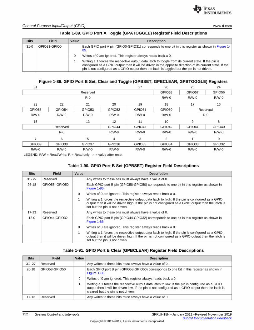
General-Purpose Input/Output (GPIO) www.ti.com
152 SPRUH18H–January 2011–Revised November 2019Submit Documentation Feedback
Copyright © 2011–2019, Texas Instruments Incorporated
System Control and Interrupts
Table 1-89. GPIO Port A Toggle (GPATOGGLE) Register Field Descriptions
Bits Field Value Description31-0 GPIO31-GPIO0 Each GPIO port A pin (GPIO0-GPIO31) corresponds to one bit in this register as shown in Figure 1-
85.0 Writes of 0 are ignored. This register always reads back a 0.1 Writing a 1 forces the respective output data latch to toggle from its current state. If the pin is
configured as a GPIO output then it will be driven in the opposite direction of its current state. If thepin is not configured as a GPIO output then the latch is toggled but the pin is not driven.
Figure 1-86. GPIO Port B Set, Clear and Toggle (GPBSET, GPBCLEAR, GPBTOGGLE) Registers31 27 26 25 24
Reserved GPIO58 GPIO57 GPIO56R-0 R/W-0 R/W-0 R/W-0
23 22 21 20 19 18 17 16GPIO55 GPIO54 GPIO53 GPIO52 GPIO51 GPIO50 ReservedR/W-0 R/W-0 R/W-0 R/W-0 R/W-0 R/W-0 R-0
15 13 12 11 10 9 8Reserved GPIO44 GPIO43 GPIO42 GPIO41 GPIO40
R-0 R/W-0 R/W-0 R/W-0 R/W-0 R/W-0
7 6 5 4 3 2 1 0GPIO39 GPIO38 GPIO37 GPIO36 GPIO35 GPIO34 GPIO33 GPIO32R/W-0 R/W-0 R/W-0 R/W-0 R/W-0 R/W-0 R/W-0 R/W-0
LEGEND: R/W = Read/Write; R = Read only; -n = value after reset
Table 1-90. GPIO Port B Set (GPBSET) Register Field Descriptions
Bits Field Value Description31- 27 Reserved Any writes to these bits must always have a value of 0.26-18 GPIO58 -GPIO50 Each GPIO port B pin (GPIO58-GPIO50) corresponds to one bit in this register as shown in
Figure 1-86.0 Writes of 0 are ignored. This register always reads back a 0.1 Writing a 1 forces the respective output data latch to high. If the pin is configured as a GPIO
output then it will be driven high. If the pin is not configured as a GPIO output then the latch isset but the pin is not driven.
17-13 Reserved Any writes to these bits must always have a value of 0.12-0 GPIO44-GPIO32 Each GPIO port B pin (GPIO44-GPIO32) corresponds to one bit in this register as shown in
Figure 1-86.0 Writes of 0 are ignored. This register always reads back a 0.1 Writing a 1 forces the respective output data latch to high. If the pin is configured as a GPIO
output then it will be driven high. If the pin is not configured as a GPIO output then the latch isset but the pin is not driven.
Table 1-91. GPIO Port B Clear (GPBCLEAR) Register Field Descriptions
Bits Field Value Description31- 27 Reserved Any writes to these bits must always have a value of 0.26-18 GPIO58-GPIO50 Each GPIO port B pin (GPIO58-GPIO50) corresponds to one bit in this register as shown in
Figure 1-86.0 Writes of 0 are ignored. This register always reads back a 0.1 Writing a 1 forces the respective output data latch to low. If the pin is configured as a GPIO
output then it will be driven low. If the pin is not configured as a GPIO output then the latch iscleared but the pin is not driven.
17-13 Reserved Any writes to these bits must always have a value of 0.

www.ti.com General-Purpose Input/Output (GPIO)
153SPRUH18H–January 2011–Revised November 2019Submit Documentation Feedback
Copyright © 2011–2019, Texas Instruments Incorporated
System Control and Interrupts
Table 1-91. GPIO Port B Clear (GPBCLEAR) Register Field Descriptions (continued)Bits Field Value Description12-0 GPIO44-GPIO32 Each GPIO port B pin (GPIO32-GPIO 44) corresponds to one bit in this register as shown in
Figure 1-86.0 Writes of 0 are ignored. This register always reads back a 0.1 Writing a 1 forces the respective output data latch to low. If the pin is configured as a GPIO
output then it will be driven low. If the pin is not configured as a GPIO output then the latch iscleared but the pin is not driven.
Table 1-92. GPIO Port B Toggle (GPBTOGGLE) Register Field Descriptions
Bits Field Value Description31- 27 Reserved Any writes to these bits must always have a value of 0.26-18 GPIO58 -GPIO50 Each GPIO port B pin (GPIO58-GPIO50) corresponds to one bit in this register as shown in
Figure 1-86.0 Writes of 0 are ignored. This register always reads back a 0.1 Writing a 1 forces the respective output data latch to toggle from its current state. If the pin is
configured as a GPIO output then it will be driven in the opposite direction of its current state. Ifthe pin is not configured as a GPIO output then the latch is cleared but the pin is not driven.
17-13 Reserved Any writes to these bits must always have a value of 0.12-0 GPIO44-GPIO32 Each GPIO port B pin (GPIO44-GPIO32) corresponds to one bit in this register as shown in
Figure 1-86.0 Writes of 0 are ignored. This register always reads back a 0.1 Writing a 1 forces the respective output data latch to toggle from its current state. If the pin is
configured as a GPIO output then it will be driven in the opposite direction of its current state. Ifthe pin is not configured as a GPIO output then the latch is cleared but the pin is not driven.
Figure 1-87. Analog I/O Toggle (AIOSET, AIOCLEAR, AIOTOGGLE) Register31 16
ReservedR-0
15 14 13 12 11 10 9 8Reserved AIO14 Reserved AIO12 Reserved AIO10 Reserved
R-0 R/W-x R-0 R/W-x R-0 R/W-x R-0
7 6 5 4 3 2 1 0Reserved AIO6 Reserved AIO4 Reserved AIO2 Reserved
R-0 R/W-x R-0 R/W-x R-0 R/W-x R-0LEGEND: R/W = Read/Write; R = Read only; -n = value after reset
Table 1-93. Analog I/O Set (AIOSET) Register Field Descriptions
Bits Field Value Description31-15 Reserved Any writes to these bits must always have a value of 0.14-0 AIOn Each AIO pin corresponds to one bit in this register.
0 Writes of 0 are ignored. This register always reads back a 0.1 Writing a 1 forces the respective output data latch to high. If the pin is configured as a AIO output
then it will be driven high. If the pin is not configured as a AIO output then the latch is set but thepin is not driven.
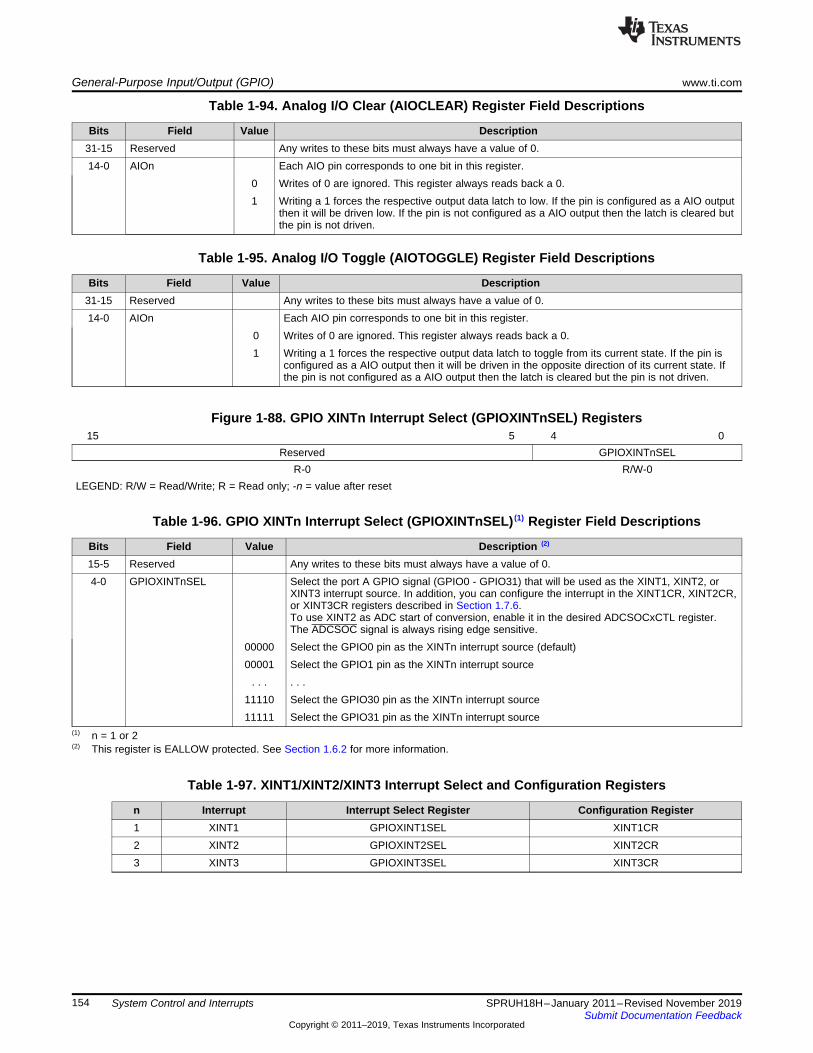
General-Purpose Input/Output (GPIO) www.ti.com
154 SPRUH18H–January 2011–Revised November 2019Submit Documentation Feedback
Copyright © 2011–2019, Texas Instruments Incorporated
System Control and Interrupts
Table 1-94. Analog I/O Clear (AIOCLEAR) Register Field Descriptions
Bits Field Value Description31-15 Reserved Any writes to these bits must always have a value of 0.14-0 AIOn Each AIO pin corresponds to one bit in this register.
0 Writes of 0 are ignored. This register always reads back a 0.1 Writing a 1 forces the respective output data latch to low. If the pin is configured as a AIO output
then it will be driven low. If the pin is not configured as a AIO output then the latch is cleared butthe pin is not driven.
Table 1-95. Analog I/O Toggle (AIOTOGGLE) Register Field Descriptions
Bits Field Value Description31-15 Reserved Any writes to these bits must always have a value of 0.14-0 AIOn Each AIO pin corresponds to one bit in this register.
0 Writes of 0 are ignored. This register always reads back a 0.1 Writing a 1 forces the respective output data latch to toggle from its current state. If the pin is
configured as a AIO output then it will be driven in the opposite direction of its current state. Ifthe pin is not configured as a AIO output then the latch is cleared but the pin is not driven.
Figure 1-88. GPIO XINTn Interrupt Select (GPIOXINTnSEL) Registers15 5 4 0
Reserved GPIOXINTnSELR-0 R/W-0
LEGEND: R/W = Read/Write; R = Read only; -n = value after reset
(1) n = 1 or 2(2) This register is EALLOW protected. See Section 1.6.2 for more information.
Table 1-96. GPIO XINTn Interrupt Select (GPIOXINTnSEL) (1) Register Field Descriptions
Bits Field Value Description (2)
15-5 Reserved Any writes to these bits must always have a value of 0.4-0 GPIOXINTnSEL Select the port A GPIO signal (GPIO0 - GPIO31) that will be used as the XINT1, XINT2, or
XINT3 interrupt source. In addition, you can configure the interrupt in the XINT1CR, XINT2CR,or XINT3CR registers described in Section 1.7.6.To use XINT2 as ADC start of conversion, enable it in the desired ADCSOCxCTL register.The ADCSOC signal is always rising edge sensitive.
00000 Select the GPIO0 pin as the XINTn interrupt source (default)00001 Select the GPIO1 pin as the XINTn interrupt source
. . . . . .11110 Select the GPIO30 pin as the XINTn interrupt source11111 Select the GPIO31 pin as the XINTn interrupt source
Table 1-97. XINT1/XINT2/XINT3 Interrupt Select and Configuration Registers
n Interrupt Interrupt Select Register Configuration Register1 XINT1 GPIOXINT1SEL XINT1CR2 XINT2 GPIOXINT2SEL XINT2CR3 XINT3 GPIOXINT3SEL XINT3CR
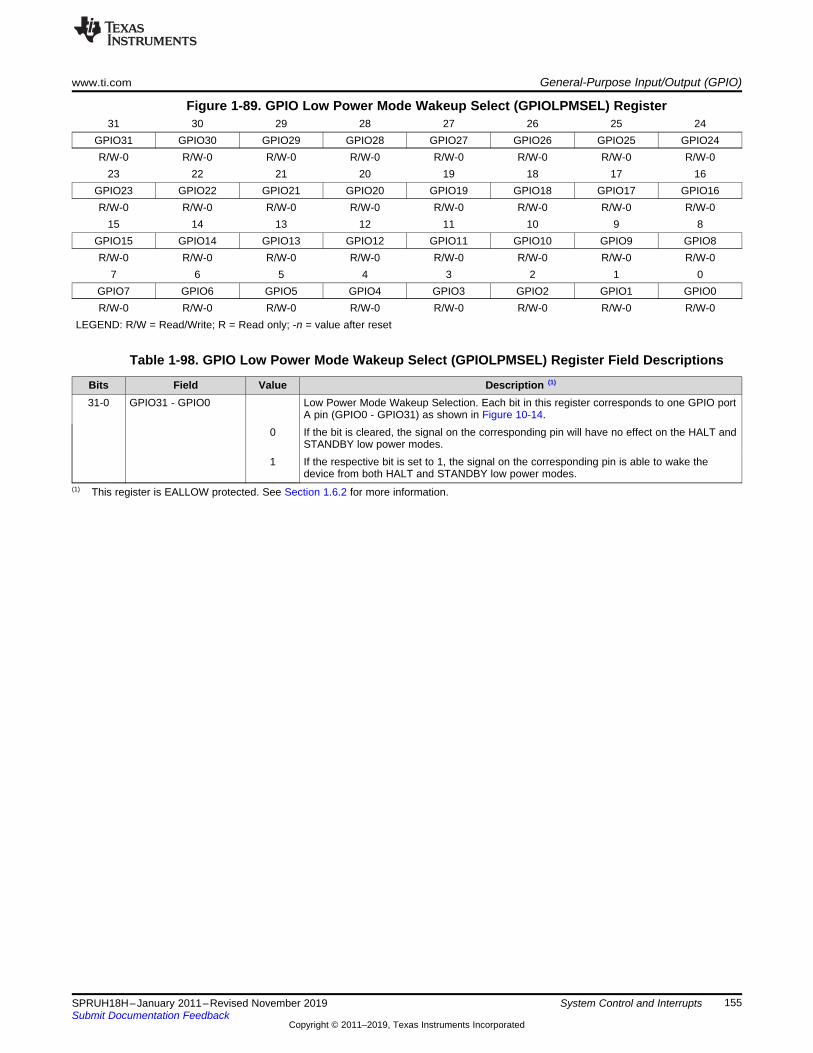
www.ti.com General-Purpose Input/Output (GPIO)
155SPRUH18H–January 2011–Revised November 2019Submit Documentation Feedback
Copyright © 2011–2019, Texas Instruments Incorporated
System Control and Interrupts
Figure 1-89. GPIO Low Power Mode Wakeup Select (GPIOLPMSEL) Register31 30 29 28 27 26 25 24
GPIO31 GPIO30 GPIO29 GPIO28 GPIO27 GPIO26 GPIO25 GPIO24R/W-0 R/W-0 R/W-0 R/W-0 R/W-0 R/W-0 R/W-0 R/W-0
23 22 21 20 19 18 17 16GPIO23 GPIO22 GPIO21 GPIO20 GPIO19 GPIO18 GPIO17 GPIO16R/W-0 R/W-0 R/W-0 R/W-0 R/W-0 R/W-0 R/W-0 R/W-0
15 14 13 12 11 10 9 8GPIO15 GPIO14 GPIO13 GPIO12 GPIO11 GPIO10 GPIO9 GPIO8R/W-0 R/W-0 R/W-0 R/W-0 R/W-0 R/W-0 R/W-0 R/W-0
7 6 5 4 3 2 1 0GPIO7 GPIO6 GPIO5 GPIO4 GPIO3 GPIO2 GPIO1 GPIO0R/W-0 R/W-0 R/W-0 R/W-0 R/W-0 R/W-0 R/W-0 R/W-0
LEGEND: R/W = Read/Write; R = Read only; -n = value after reset
(1) This register is EALLOW protected. See Section 1.6.2 for more information.
Table 1-98. GPIO Low Power Mode Wakeup Select (GPIOLPMSEL) Register Field Descriptions
Bits Field Value Description (1)
31-0 GPIO31 - GPIO0 Low Power Mode Wakeup Selection. Each bit in this register corresponds to one GPIO portA pin (GPIO0 - GPIO31) as shown in Figure 10-14.
0 If the bit is cleared, the signal on the corresponding pin will have no effect on the HALT andSTANDBY low power modes.
1 If the respective bit is set to 1, the signal on the corresponding pin is able to wake thedevice from both HALT and STANDBY low power modes.

Peripheral Frames www.ti.com
156 SPRUH18H–January 2011–Revised November 2019Submit Documentation Feedback
Copyright © 2011–2019, Texas Instruments Incorporated
System Control and Interrupts
1.6 Peripheral FramesThis chapter describes the peripheral frames and device emulation registers.
1.6.1 Peripheral Frame RegistersThis device contains four peripheral register spaces. The spaces are categorized as follows:• Peripheral Frame 0: These are peripherals that are mapped directly to the CPU memory bus. See
Table 1-99.• Peripheral Frame 1: These are peripherals that are mapped to the 32-bit peripheral bus. See Table 1-
100.• Peripheral Frame 2: These are peripherals that are mapped to the 16-bit peripheral bus. See Table 1-
101.• Peripheral Frame 3: These are peripherals that are mapped to the 16-bit peripheral bus. See Table 1-
102.
(1) Registers in Frame 0 support 16-bit and 32-bit accesses.(2) If registers are EALLOW protected, then writes cannot be performed until the EALLOW instruction is executed. The EDIS
instruction disables writes to prevent stray code or pointers from corrupting register contents.(3) The Flash Registers are also protected by the Code Security Module (CSM).
Table 1-99. Peripheral Frame 0 Registers (1)
NAME ADDRESS RANGE SIZE (×16) EALLOW PROTECTED (2)
Device Emulation Registers 0x00 0880 – 0x00 0984 261 YesSystem Power Control Registers 0x00 0985 – 0x00 0987 3 YesFLASH Registers (3) 0x00 0A80 – 0x00 0ADF 96 YesCode Security Module Registers 0x00 0AE0 – 0x00 0AEF 16 YesADC registers(0 wait read only)
0x00 0B00 – 0x00 0B0F 16 No
CPU–TIMER0/1/2 Registers 0x00 0C00 – 0x00 0C3F 64 NoPIE Registers 0x00 0CE0 – 0x00 0CFF 32 NoPIE Vector Table 0x00 0D00 – 0x00 0DFF 256 NoDMA Registers 0x00 1000 – 0x00 11FF 512 YesCLA Registers 0x00 1400 – 0x00 147F 128 YesCLA to CPU Message RAM (CPU writesignored)
0x00 1480 – 0x00 14FF 128 NA
CPU to CLA Message RAM (CLA writesignored)
0x00 1500 – 0x00 157F 128 NA

www.ti.com Peripheral Frames
157SPRUH18H–January 2011–Revised November 2019Submit Documentation Feedback
Copyright © 2011–2019, Texas Instruments Incorporated
System Control and Interrupts
(1) Back-to-back write operations to Peripheral Frame 1 registers will incur a 1-cycle stall (1 cycle delay).(2) Peripheral Frame 1 allows 16-bit and 32-bit accesses. All 32-bit accesses are aligned to even address boundaries.(3) Some registers are EALLOW protected. See the module reference guide for more information.
Table 1-100. Peripheral Frame 1 Registers (1)
NAME ADDRESS RANGE SIZE (×16) EALLOW PROTECTED (2)
eCAN-A registers 0x00 6000 – 0x00 61FF 512 (3)
Comparator 1 registers 0x00 6400 – 0x00 641F 32 (3)
Comparator 2 registers 0x00 6420 – 0x00 643F 32 (3)
Comparator 3 registers 0x00 6440 – 0x00 645F 32 (3)
ePWM1 + HRPWM1 registers 0x00 6800 – 0x00 683F 64 (3)
ePWM2 + HRPWM2 registers 0x00 6840 – 0x00 687F 64 (3)
ePWM3 + HRPWM3 registers 0x00 6880 – 0x00 68BF 64 (3)
ePWM4 + HRPWM4 registers 0x00 68C0 – 0x00 68FF 64 (3)
ePWM5 + HRPWM5 registers 0x00 6900 – 0x00 693F 64 (3)
ePWM6 + HRPWM6 registers 0x00 6940 – 0x00 697F 64 (3)
ePWM7 + HRPWM7 registers 0x00 6980 – 0x00 69BF 64 (3)
ePWM8 + HRPWM8 registers 0x00 69C0 – 0x00 69FF 64 (3)
eCAP1 registers 0x00 6A00 – 0x00 6A1F 32 NoeCAP2 registers 0x00 6A20 – 0x00 6A3F 32 NoeCAP3 registers 0x00 6A40 – 0x00 6A57 32 NoHRCAP1 registers 0x00 6AC0 – 0x00 6ADF 32 (3)
HRCAP2 registers 0x00 6AE0 – 0x00 6AFF 32 (3)
eQEP1 registers 0x00 6B00 – 0x00 6B3F 64 (3)
eQEP2 registers 0x00 6B40 – 0x00 6B7F 64 (3)
HRCAP3 registers 0x00 6C80 – 0x00 6C9F 32 (3)
HRCAP4 registers 0x00 6CA0 – 0x00 6CBF 32 (3)
GPIO registers 0x00 6F80 – 0x00 6FFF 128 (3)
(1) Some registers are EALLOW protected. See the module reference guide for more information.
Table 1-101. Peripheral Frame 2 Registers
NAME ADDRESS RANGE SIZE (×16) EALLOW PROTECTEDSystem Control Registers 0x00 7010 – 0x00 702F 32 YesSPI-A Registers 0x00 7040 – 0x00 704F 16 NoSCI-A Registers 0x00 7050 – 0x00 705F 16 NoNMI Watchdog Interrupt Registers 0x00 7060 – 0x00 706F 16 YesExternal Interrupt Registers 0x00 7070 – 0x00 707F 16 YesADC Registers 0x00 7100 – 0x00 717F 128 (1)
SPI-B Registers 0x00 7740 – 0x00 774F 16 NoSCI-B Registers 0x00 7750 – 0x00 775F 16 NoI2C-A Registers 0x00 7900 – 0x00 793F 64 (1)
Table 1-102. Peripheral Frame 3 Registers
NAME ADDRESS RANGE SIZE (×16) EALLOW PROTECTEDUSB0 Registers 0x00 4000 – 0x4FFF 4096 NoMcBSP-A Registers 0x00 5000 – 0x00 503F 64 No

Peripheral Frames www.ti.com
158 SPRUH18H–January 2011–Revised November 2019Submit Documentation Feedback
Copyright © 2011–2019, Texas Instruments Incorporated
System Control and Interrupts
1.6.2 EALLOW-Protected RegistersSeveral control registers are protected from spurious CPU writes by the EALLOW protection mechanism.The EALLOW bit in status register 1 (ST1) indicates if the state of protection as shown in Table 1-103.
(1) The EALLOW bit is overridden via the JTAG port, allowing full access of protected registers during debug from the CodeComposer Studio interface.
Table 1-103. Access to EALLOW-Protected Registers
EALLOW Bit CPU Writes CPU Reads JTAG Writes JTAG Reads0 Ignored Allowed Allowed (1) Allowed1 Allowed Allowed Allowed Allowed
At reset the EALLOW bit is cleared enabling EALLOW protection. While protected, all writes to protectedregisters by the CPU are ignored and only CPU reads, JTAG reads, and JTAG writes are allowed. If thisbit is set, by executing the EALLOW instruction, then the CPU is allowed to write freely to protectedregisters. After modifying registers, they can once again be protected by executing the EDI instruction toclear the EALLOW bit.
The following registers are EALLOW-protected:• Device Emulation Registers• Flash Registers• CSM Registers• PIE Vector Table• System Control Registers• GPIO MUX Registers
Table 1-104. EALLOW-Protected Device Emulation Registers
Name Address Size(x16)
Description
DEVICECNF 0x08800x0881
2 Device Configuration Register
Table 1-105. EALLOW-Protected Flash/OTP Configuration Registers
Name AddressSize(x16) Description
FOPT 0x0A80 1 Flash Option RegisterFPWR 0x0A82 1 Flash Power Modes RegisterFSTATUS 0x0A83 1 Status RegisterFSTDBYWAIT 0x0A84 1 Flash Sleep To Standby Wait State RegisterFACTIVEWAIT 0x0A85 1 Flash Standby To Active Wait State RegisterFBANKWAIT 0x0A86 1 Flash Read Access Wait State RegisterFOTPWAIT 0x0A87 1 OTP Read Access Wait State Register

www.ti.com Peripheral Frames
159SPRUH18H–January 2011–Revised November 2019Submit Documentation Feedback
Copyright © 2011–2019, Texas Instruments Incorporated
System Control and Interrupts
Table 1-106. EALLOW-Protected Code Security Module (CSM) Registers
Register Name Address Size(x16) Register Description
KEY0 0x0AE0 1 Low word of the 128-bit KEY registerKEY1 0x0AE1 1 Second word of the 128-bit KEY registerKEY2 0x0AE2 1 Third word of the 128-bit KEY registerKEY3 0x0AE3 1 Fourth word of the 128-bit KEY registerKEY4 0x0AE4 1 Fifth word of the 128-bit KEY registerKEY5 0x0AE5 1 Sixth word of the 128-bit KEY registerKEY6 0x0AE6 1 Seventh word of the 128-bit KEY registerKEY7 0x0AE7 1 High word of the 128-bit KEY registerCSMSCR 0x0AEF 1 CSM status and control register
Table 1-107. EALLOW-Protected PLL, Clocking, Watchdog, and Low-Power Mode Registers
NAME ADDRESS SIZE (x16) DESCRIPTIONBORCFG 0x00 0985 1 BOR Configuration RegisterXCLK 0x00 7010 1 XCLKOUT and XCLKIN Control RegisterPLLSTS 0x00 7011 1 PLL Status RegisterCLKCTL 0x00 7012 1 Clock Control RegisterPLLLOCKPRD 0x00 7013 1 PLL Lock Period RegisterINTOSC1TRIM 0x00 7014 1 Internal Oscillator 1 Trim RegisterINTOSC2TRIM 0x00 7016 1 Internal Oscillator 2 Trim RegisterPCLKCR2 0x00 7019 1 Peripheral Clock Control Register 2LOSPCP 0x00 701B 1 Low-Speed Peripheral Clock Prescaler RegisterPCLKCR0 0x00 701C 1 Peripheral Clock Control Register 0PCLKCR1 0x00 701D 1 Peripheral Clock Control Register 1LPMCR0 0x00 701E 1 Low Power Mode Control Register 0PCLKCR3 0x00 7020 1 Peripheral Clock Control Register 3PLLCR 0x00 7021 1 PLL Control RegisterSCSR 0x00 7022 1 System Control and Status RegisterWDCNTR 0x00 7023 1 Watchdog Counter RegisterWDKEY 0x00 7025 1 Watchdog Reset Key RegisterWDCR 0x00 7029 1 Watchdog Control RegisterPLL2CTL 0x00 7030 1 PLL2 Configuration RegisterPLL2MULT 0x00 7032 1 PLL2 Multiplier RegisterPLL2STS 0x00 7034 1 PLL2 Lock Status RegisterSYSCLK2CNTR 0x00 7036 1 SYSCLK2 Clock Counter RegisterEPWMCFG 0x00 703A 1 ePWM DMA/CLA Configuration Register

Peripheral Frames www.ti.com
160 SPRUH18H–January 2011–Revised November 2019Submit Documentation Feedback
Copyright © 2011–2019, Texas Instruments Incorporated
System Control and Interrupts
(1) The registers in this table are EALLOW protected. See Section 1.6.2 for more information.
Table 1-108. EALLOW-Protected GPIO Registers
Name (1) Address Size (x16) Register DescriptionGPACTRL 0x6F80 2 GPIO A Control RegisterGPAQSEL1 0x6F82 2 GPIO A Qualifier Select 1 RegisterGPAQSEL2 0x6F84 2 GPIO A Qualifier Select 2 RegisterGPAMUX1 0x6F86 2 GPIO A MUX 1 RegisterGPAMUX2 0x6F88 2 GPIO A MUX 2 RegisterGPADIR 0x6F8A 2 GPIO A Direction RegisterGPAPUD 0x6F8C 2 GPIO A Pull Up Disable RegisterGPBCTRL 0x6F90 2 GPIO B Control RegisterGPBQSEL1 0x6F92 2 GPIO B Qualifier Select 1 RegisterGPBQSEL2 0x6F94 2 GPIO B Qualifier Select 2 RegisterGPBMUX1 0x6F96 2 GPIO B MUX 1 RegisterGPBMUX2 0x6F98 2 GPIO B MUX 2 RegisterGPBDIR 0x6F9A 2 GPIO B Direction RegisterGPBPUD 0x6F9C 2 GPIO B Pull Up Disable RegisterAIOMUX1 0x6FB6 2 Analog, I/O MUX 1 registerAIODIR 0x6FBA 2 Analog, IO Direction RegisterGPIOXINT1SEL 0x6FE0 1 XINT1 Source Select Register (GPIO0-GPIO31)GPIOXINT2SEL 0x6FE1 1 XINT2 Source Select Register (GPIO0-GPIO31)GPIOXINT3SEL 0x6FE2 1 XINT3 Source Select Register (GPIO0 - GPIO31)GPIOLPMSEL 0x6FE8 1 LPM wakeup Source Select Register (GPIO0-GPIO31)
Table 1-110 shows addresses for the following ePWM EALLOW-protected registers:• Trip Zone Select Register (TZSEL)• Trip Zone Control Register (TZCTL)• Trip Zone Enable Interrupt Register (TZEINT)• Trip Zone Clear Register (TZCLR)• Trip Zone Force Register (TZFRC)• HRPWM Configuration Register (HRCNFG)

www.ti.com Peripheral Frames
161SPRUH18H–January 2011–Revised November 2019Submit Documentation Feedback
Copyright © 2011–2019, Texas Instruments Incorporated
System Control and Interrupts
Table 1-109. EALLOW-Protected PIE Vector Table
Name Address Size (x16) DescriptionNot used 0x0D00 2 Reserved
0x0D020x0D040x0D060x0D080x0D0A0x0D0C0x0D0E0x0D100x0D120x0D140x0D160x0D18
INT13 0x0D1A 2 CPU-Timer 1INT14 0x0D1C 2 CPU-Timer 2DATALOG 0x0D1E 2 CPU Data Logging InterruptRTOSINT 0x0D20 2 CPU Real-Time OS InterruptEMUINT 0x0D22 2 CPU Emulation InterruptNMI 0x0D24 2 External Non-Maskable InterruptILLEGAL 0x0D26 2 Illegal OperationUSER1 0x0D28 2 User-Defined Trap. . . .USER12 0x0D3E 2 User-Defined TrapINT1.1.INT1.8
0x0D40.
0x0D4E
2.2
Group 1 Interrupt Vectors
.
.
.
.
.
.
.
.
.
Group 2 Interrupt Vectorsto Group 11 Interrupt Vectors
INT12.1.INT12.8
0x0DF0.
0x0DFE
2.2
Group 12 Interrupt Vectors
Table 1-110. EALLOW-Protected ePWM1 - ePWM 7 Registers
TZSEL TZCTL TZEINT TZCLR TZFRC HRCNFG Size x16ePWM1 0x6812 0x6814 0x6815 0x6817 0x6818 0x6820 1ePWM2 0x6852 0x6854 0x6855 0x6857 0x6858 0x6860 1ePWM3 0x6892 0x6894 0x6895 0x6897 0x6898 0x68A0 1ePWM4 0x68D2 0x68D4 0x68D5 0x68D7 0x68D8 0x68E0 1ePWM5 0x6912 0x6914 0x6915 0x6917 0x6918 0x6920 1ePWM6 0x6952 0x6954 0x6955 0x6957 0x6958 0x6960 1ePWM7 0x6992 0x6994 0x6995 0x6997 0x6998 0x69A0 1

Peripheral Frames www.ti.com
162 SPRUH18H–January 2011–Revised November 2019Submit Documentation Feedback
Copyright © 2011–2019, Texas Instruments Incorporated
System Control and Interrupts
1.6.3 Device Emulation RegistersThese registers are used to control the protection mode of the C28x CPU and to monitor some criticaldevice signals. The registers are defined in Table 1-111.
Table 1-111. Device Emulation Registers
Name Address Size (x16) DescriptionDEVICECNF 0x0880
0x08812 Device Configuration Register
PARTID 0x3D 7E80 1 Part ID RegisterCLASSID 0x0882 1 Class ID RegisterREVID 0x0883 1 Revision ID Register
Figure 1-90. Device Configuration (DEVICECNF) Register31 30 29 28 27 26 20 19 18 16
Rsvd SYSCLK2DIV2DIS Reserved TRST Reserved ENPROT Reserved
R-0 R/W-0 R-0 R-0 R-0 R/W-1 R-111
15 5 4 3 2 0Reserved XRS Res VMAPS Reserved
R-0 R-P R-0 R-1 R-011LEGEND: R/W = Read/Write; R = Read only; -n = value after reset
Table 1-112. DEVICECNF Register Field Descriptions
Bits Field Value Description31 Reserved Any writes to these bits must always have a value of 0.30 SYSCLK2DIV2DIS SYSCLK2 Clock Divide by 2 Disable Bit
0 PLL2 Output/21 PLL2 Output/1
29-28 Reserved27 TRST Read status of TRST signal. Reading this bit gives the current status of the TRST signal.
0 No emulator is connected.1 An emulator is connected.
26:20 Reserved Any writes to these bits must always have a value of 0.19 ENPROT Enable Write-Read Protection Mode Bit.
0 Disables write-read protection mode1 Enables write-read protection for the address range 0x4000-0x7FFF
18-6 Reserved Any writes to these bits must always have a value of 0.5 XRS Reset Input Signal Status. This is connected directly to the XRS input pin.4 Reserved Reserved3 VMAPS VMAP Configure Status. This indicates the status of VMAP.
2-0 Reserved Any writes to these bits must always have a value of 0.

www.ti.com Peripheral Frames
163SPRUH18H–January 2011–Revised November 2019Submit Documentation Feedback
Copyright © 2011–2019, Texas Instruments Incorporated
System Control and Interrupts
Figure 1-91. Part ID Register15 8 7 0
PARTTYPE PARTIDR R
LEGEND: R/W = Read/Write; R = Read only; -n = value after reset
(1) The reset value depends on the device as indicated in the register description.(2) For TMS320F28069U devices, the PARTID/CLASSID numbers are also used for TMX devices. In the case of TMX320F28069UPFPA
and TMX320F28069UPZPA devices, the temperature rating is "A" instead of "T".
Table 1-113. PARTID Register Field Descriptions
Bit Field Value (1) Description15:8 PARTTYPE Part type ID register. Specifies the type of device such as
flash-based.0x00 Flash-based device
All other values are reserved.7:0 PARTID (2) 0x3D 7E80 Part ID Register. These 8 bits specify the feature set of
this device:TMS320F28069PZP/PZ 0x9ETMS320F28069UPZP/ PZ 0x9FTMS320F28069PFP/PN 0x9CTMS320F28069UPFP/PN 0x9DTMS320F28068PZP/PZ 0x8ETMS320F28068UPZP/PZ 0x8FTMS320F28068PFP/PN 0x8CTMS320F28068UPFP/PN 0x8DTMS320F28067PZP/PZ 0x8ATMS320F28067UPZP/PZ 0x8BTMS320F28067PFP/PN 0x88TMS320F28067UPFP/PN 0x89TMS320F28066PZP/PZ 0x86TMS320F28066UPZP/PZ 0x87TMS320F28066PFP/PN 0x84TMS320F28066UPFP/PN 0x85TMS320F28065PZP/PZ 0x7ETMS320F28065UPZP/PZ 0x7FTMS320F28065PFP/PN 0x7CTMS320F28065UPFP/PN 0x7DTMS320F28064PZP/PZ 0x6ETMS320F28064UPZP/PZ 0x6FTMS320F28064PFP/PN 0x6CTMS320F28064UPFP/PN 0x6DTMS320F28063PZP/PZ 0x6ATMS320F28063UPZP/PZ 0x6BTMS320F28063PFP/PN 0x68TMS320F28063UPFP/PN 0x69TMS320F28062PZP/PZ 0x66TMS320F28062UPZP/PZ 0x67TMS320F28062PFP/PN 0x65TMS320F28062UPFP/PN 0x64

Peripheral Frames www.ti.com
164 SPRUH18H–January 2011–Revised November 2019Submit Documentation Feedback
Copyright © 2011–2019, Texas Instruments Incorporated
System Control and Interrupts
(1) The reset value depends on the device as indicated in the register description.
Table 1-114. CLASSID Register Field Descriptions
Bit Field Value (1) Description7:0 CLASSID 0x0882 Class ID register. These 8 bits specify the feature set of
this device:TMS320F28069 0x009FTMS320F28068 0x008FTMS320F28067 0x008FTMS320F28066 0x008FTMS320F28065 0x007FTMS320F28064 0x006FTMS320F28063 0x006FTMS320F28062 0x006F
(1) The reset value depends on the silicon revision as described in the register field description.
Figure 1-92. REVID Register15 0
REVIDR- (1)
LEGEND: R/W = Read/Write; R = Read only; -n = value after reset
(1) The reset value depends on the silicon revision as described in the register field description.
Table 1-115. REVID Register Field Descriptions
Bits Field Value Description15-0 REVID (1)These 16 bits specify the silicon revision number for the particular part. This number always
starts with 0x0000. It is typically incremented when major changes are made to the silicon. Thesilicon revision information is also part of the package symbolization. It may be used to discernthe revision information in cases where the REVID is not incremented from one silicon revisionto another.
0x0000 Silicon Revision 0 - TMX0x0001 Silicon Revision A - TMS

www.ti.com Peripheral Frames
165SPRUH18H–January 2011–Revised November 2019Submit Documentation Feedback
Copyright © 2011–2019, Texas Instruments Incorporated
System Control and Interrupts
1.6.4 Write-Followed-by-Read ProtectionThe memory address range for which CPU write followed by read operations are protected is 0x4000 -0x7FFF (operations occur in sequence rather then in their natural pipeline order). This is necessaryprotection for certain peripheral operations.
Example: The following lines of code perform a write to register 1 (REG1) location and then the nextinstruction performs a read from Register 2 (REG2) location. On the processor memory bus, with blockprotection disabled, the read operation is issued before the write as shown.
MOV @REG1,AL ---------+TBIT @REG2,#BIT_X ---------|-------> Read
+-------> Write
If block protection is enabled, then the read is stalled until the write occurs as shown:
MOV @REG1,AL ---------+TBIT @REG2,#BIT_X ---------|-----+
+-----|---> Write+---> Read

INT12
MUX
INT11
INT2
INT1
CPU
(Enable)(Flag)
INTx
INTx.8
PIEIERx(8:1) PIEIFRx(8:1)
MUX
INTx.7
INTx.6
INTx.5
INTx.4
INTx.3
INTx.2
INTx.1
From
Peripherals or
External
Interrupts
(Enable) (Flag)
IER(12:1)IFR(12:1)
GlobalEnable
INTM
1
0
PIEACKx
(Enable/Flag)
Peripheral Interrupt Expansion (PIE) www.ti.com
166 SPRUH18H–January 2011–Revised November 2019Submit Documentation Feedback
Copyright © 2011–2019, Texas Instruments Incorporated
System Control and Interrupts
1.7 Peripheral Interrupt Expansion (PIE)The peripheral interrupt expansion (PIE) block multiplexes numerous interrupt sources into a smaller set ofinterrupt inputs. The PIE block can support 96 individual interrupts that are grouped into blocks of eight.Each group is fed into one of 12 core interrupt lines (INT1 to INT12). Each of the 96 interrupts issupported by its own vector stored in a dedicated RAM block that you can modify. The CPU, uponservicing the interrupt, automatically fetches the appropriate interrupt vector. It takes nine CPU clockcycles to fetch the vector and save critical CPU registers. Therefore, the CPU can respond quickly tointerrupt events. Prioritization of interrupts is controlled in hardware and software. Each individual interruptcan be enabled/disabled within the PIE block.
1.7.1 Overview of the PIE ControllerThe 28x CPU supports one nonmaskable interrupt (NMI) and 16 maskable prioritized interrupt requests(INT1-INT14, RTOSINT, and DLOGINT) at the CPU level. The 28x devices have many peripherals andeach peripheral is capable of generating one or more interrupts in response to many events at theperipheral level. Because the CPU does not have sufficient capacity to handle all peripheral interruptrequests at the CPU level, a centralized peripheral interrupt expansion (PIE) controller is required toarbitrate the interrupt requests from various sources such as peripherals and other external pins.
The PIE vector table is used to store the address (vector) of each interrupt service routine (ISR) within thesystem. There is one vector per interrupt source including all MUXed and nonMUXed interrupts. Youpopulate the vector table during device initialization and you can update it during operation.
1.7.1.1 Interrupt Operation SequenceFigure 1-93 shows an overview of the interrupt operation sequence for all multiplexed PIE interrupts.Interrupt sources that are not multiplexed are fed directly to the CPU.
Figure 1-93. Overview: Multiplexing of Interrupts Using the PIE Block
• Peripheral LevelAn interrupt-generating event occurs in a peripheral. The interrupt flag (IF) bit corresponding to thatevent is set in a register for that particular peripheral.If the corresponding interrupt enable (IE) bit is set, the peripheral generates an interrupt request to thePIE controller. If the interrupt is not enabled at the peripheral level, then the IF remains set untilcleared by software. If the interrupt is enabled at a later time, and the interrupt flag is still set, theinterrupt request is asserted to the PIE.

www.ti.com Peripheral Interrupt Expansion (PIE)
167SPRUH18H–January 2011–Revised November 2019Submit Documentation Feedback
Copyright © 2011–2019, Texas Instruments Incorporated
System Control and Interrupts
Interrupt flags within the peripheral registers must be manually cleared. See the peripheral referenceguide for a specific peripheral for more information.
• PIE LevelThe PIE block multiplexes eight peripheral and external pin interrupts into one CPU interrupt. Theseinterrupts are divided into 12 groups: PIE group 1 - PIE group 12. The interrupts within a group aremultiplexed into one CPU interrupt. For example, PIE group 1 is multiplexed into CPU interrupt 1(INT1) while PIE group 12 is multiplexed into CPU interrupt 12 (INT12). Interrupt sources connected tothe remaining CPU interrupts are not multiplexed. For the nonmultiplexed interrupts, the PIE passesthe request directly to the CPU.For multiplexed interrupt sources, each interrupt group in the PIE block has an associated flag register(PIEIFRx) and enable (PIEIERx) register (x = PIE group 1 - PIE group 12). Each bit, referred to as y,corresponds to one of the 8 MUXed interrupts within the group. Thus PIEIFRx.y and PIEIERx.ycorrespond to interrupt y (y = 1-8) in PIE group x (x = 1-12). In addition, there is one acknowledge bit(PIEACK) for every PIE interrupt group referred to as PIEACKx (x = 1-12). Figure 1-94 illustrates thebehavior of the PIE hardware under various PIEIFR and PIEIER register conditions.Once the request is made to the PIE controller, the corresponding PIE interrupt flag (PIEIFRx.y) bit isset. If the PIE interrupt enable (PIEIERx.y) bit is also set for the given interrupt then the PIE checks thecorresponding PIEACKx bit to determine if the CPU is ready for an interrupt from that group. If thePIEACKx bit is clear for that group, then the PIE sends the interrupt request to the CPU. If PIEACKx isset, then the PIE waits until it is cleared to send the request for INTx. See Section 6.3 for details.
• CPU LevelOnce the request is sent to the CPU, the CPU level interrupt flag (IFR) bit corresponding to INTx is set.After a flag has been latched in the IFR, the corresponding interrupt is not serviced until it isappropriately enabled in the CPU interrupt enable (IER) register or the debug interrupt enable register(DBGIER) and the global interrupt mask (INTM) bit.

Start
Stage A
PIEIFRx.y=1
?
Wait for anyPIEIFRx.y=1
No
Wait forPIEIERx.y=1
Stage B
PIEIERx.y=1?
No
PIEACKx=0
Stage C
?
NoWait forS/W to clear
PIEACKx bit=0
Yes
Yes
Yes
Hardware setsPIEACKx=1
Stage DInterrupt requestsent to 28x CPU
on INTx
Interruptsto CPU
Stage EIFRx bit set 1
Yes
Stage GINTM bit=0
?
No
Yes
IERx bit=1Stage F
?
No
Stage HCPU responds
IFRx=0, IERx=0INTM=1, EALLOW=0
Context Save performed
Stage IVector fetched from the PIE
PIEIFRx.y is clearedCPU branches to ISR
Stage JInterrupt service routine responds
Write 1 to PIEACKx bit to clearto enable other interrupts in
PIEIFRx groupRe-enable interrupts, INTM=0
Return
End
CPU interrupt controlPIE interrupt control
Peripheral Interrupt Expansion (PIE) www.ti.com
168 SPRUH18H–January 2011–Revised November 2019Submit Documentation Feedback
Copyright © 2011–2019, Texas Instruments Incorporated
System Control and Interrupts
Figure 1-94. Typical PIE/CPU Interrupt Response - INTx.y
A For multiplexed interrupts, the PIE responds with the highest priority interrupt that is both flagged and enabled. Ifthere is no interrupt both flagged and enabled, then the highest priority interrupt within the group (INTx.1 where x isthe PIE group) is used. See Section Section 1.7.3.3 for details.
As shown in Table 1-116, the requirements for enabling the maskable interrupt at the CPU level dependson the interrupt handling process being used. In the standard process, which happens most of the time,the DBGIER register is not used. When the 28x is in real-time emulation mode and the CPU is halted, adifferent process is used. In this special case, the DBGIER is used and the INTM bit is ignored. If the DSPis in real-time mode and the CPU is running, the standard interrupt-handling process applies.
Table 1-116. Enabling Interrupt
Interrupt Handling Process Interrupt Enabled If…Standard INTM = 0 and bit in IER is 1DSP in real-time mode and halted Bit in IER is 1 and DBGIER is 1

www.ti.com Peripheral Interrupt Expansion (PIE)
169SPRUH18H–January 2011–Revised November 2019Submit Documentation Feedback
Copyright © 2011–2019, Texas Instruments Incorporated
System Control and Interrupts
The CPU then prepares to service the interrupt. This preparation process is described in detail inTMS320x28x DSP CPU and Instruction Set Reference Guide (literature number SPRU430). Inpreparation, the corresponding CPU IFR and IER bits are cleared, EALLOW and LOOP are cleared, INTMand DBGM are set, the pipeline is flushed and the return address is stored, and the automatic contextsave is performed. The vector of the ISR is then fetched from the PIE module. If the interrupt requestcomes from a multiplexed interrupt, the PIE module uses the group PIEIERx and PIEIFRx registers todecode which interrupt needs to be serviced. This decode process is described in detail in SectionSection 1.7.3.3.
The address for the interrupt service routine that is executed is fetched directly from the PIE interruptvector table. There is one 32-bit vector for each of the possible 96 interrupts within the PIE. Interrupt flagswithin the PIE module (PIEIFRx.y) are automatically cleared when the interrupt vector is fetched. The PIEacknowledge bit for a given interrupt group, however, must be cleared manually when ready to receivemore interrupts from the PIE group.
1.7.2 Vector Table MappingOn 28xx devices, the interrupt vector table can be mapped to four distinct locations in memory. In practiceonly the PIE vector table mapping is used.
This vector mapping is controlled by the following mode bits/signals:
VMAP: VMAP is found in the Status Register 1 ST1 (bit 3). A device reset sets this bit to 1. The state of this bit can bemodified by writing to ST1 or by SETC/CLRC VMAP instructions. For normal operation leave this bit set.
M0M1MAP: M0M1MAP is found in the Status Register 1 ST1 (bit 11). A device reset sets this bit to 1. The state of this bitcan be modified by writing to ST1 or by SETC/CLRC M0M1MAP instructions. For normal 28xx device operation,this bit should remain set. M0M1MAP = 0 is reserved for TI testing only.
ENPIE: ENPIE is found in the PIECTRL Register (bit 0). The default value of this bit, on reset, is set to 0 (PIE disabled).The state of this bit can be modified after reset by writing to the PIECTRL register (address 0x0000 0CE0).
Using these bits and signals the possible vector table mappings are shown in Table 1-117.
(1) Vector map M0 and M1 Vector is a reserved mode only. On the 28x devices these are used as SARAM.
Table 1-117. Interrupt Vector Table Mapping
Vector MAPS Vectors Fetched From Address Range VMAP M0M1MAP ENPIEM1 Vector (1) M1 SARAM Block 0x000000 - 0x00003F 0 0 XM0 Vector (1) M0 SARAM Block 0x000000 - 0x00003F 0 1 X
BROM Vector Boot ROM Block 0x3FFFC0 - 0x3FFFFF 1 X 0PIE Vector PIE Block 0x000D00 - 0x000DFF 1 X 1
The M1 and M0 vector table mapping are reserved for TI testing only. When using other vector mappings,the M0 and M1 memory blocks are treated as SARAM blocks and can be used freely without anyrestrictions.
After a device reset operation, the vector table is mapped as shown in Table 1-118.
(1) On the 28x devices, the VMAP and M0M1MAP modes are set to 1 on reset. The ENPIE mode is forced to 0 on reset.(2) The reset vector is always fetched from the boot ROM.
Table 1-118. Vector Table Mapping After Reset Operation
Vector MAPS Reset Fetched From Address Range VMAP (1) M0M1MAP (1)ENPIE
(1)
BROM Vector (2) Boot ROM Block 0x3FFFC0 - 0x3FFFFF 1 1 0
After the reset and boot is complete, the PIE vector table should be initialized by the user's code. Then theapplication enables the PIE vector table. From that point on the interrupt vectors are fetched from the PIEvector table. Note: when a reset occurs, the reset vector is always fetched from the vector table as shownin Table 1-118. After a reset the PIE vector table is always disabled.
Figure 1-95 illustrates the process by which the vector table mapping is selected.

Reset(power-on reset or warm reset)
Reset vector fetched from
boot ROM
Branch into bootloader
routines, depending on the
state of GPIO pins
Yes
Usingperipheralinterrupts
?
PIE disabled (ENPIE=0)
OBJMODE = 0AMODE = 0
Yes
User code initializes:
OBJMODE and AMODE state†
PIE enable (ENPIE = 1)
CPU IER register and INTM
Vectors (except for reset)are fetched from PIE vector map‡
Recommended flow for 280x applications
No
User code initializes:
OBJMODE and AMODE state1CPU IER register and INTMVMAP state
VMAP = 1?
Vectors
(except for reset)
are fetched
from M0 vector
map‡
Vectors
Used for test purposes only
No
PIE vector tablePIEIERx registers
VMAP = 1
MOM1MAP = 1
(except for reset) are
fetched from BROM
vector map‡
Peripheral Interrupt Expansion (PIE) www.ti.com
170 SPRUH18H–January 2011–Revised November 2019Submit Documentation Feedback
Copyright © 2011–2019, Texas Instruments Incorporated
System Control and Interrupts
Figure 1-95. Reset Flow Diagram
A The compatibility operating mode of the 28x CPU is determined by a combination of the OBJMODE and AMODE bitsin Status Register 1 (ST1):
Operating Mode OBJMODE AMODEC28x Mode 1 024x/240xA Source-Compatible 1 1C27x Object-Compatible 0 0 (Default at reset)
B The reset vector is always fetched from the boot ROM.

Watchdog
XINT1Interrupt Control
XINT1
XINT1CR[15:0]
Interrupt ControlXINT2
XINT2CR[15:0]
GPIOMUX
WDINT
INT1to
INT12
NMI
XINT1CTR[15:0]
XINT2CTR[15:0]
XINT3CTR[15:0]
Low-Power ModesLPMINT
WAKEINTSync
SYSCLKOUT
MUX
XINT2MUX
XINT3
ADCXINT2SOC
GPIOXINT1SEL[4:0]
GPIOXINT2SEL[4:0]
MUX
Interrupt ControlXINT3
XINT3CR[15:0]
System Control(See the System Control section.)
INT14
INT13
GPIO0.int
GPIO31.int
DMA clear
DMA
PIE
Up
to
96 I
nte
rru
pts
DMA
DMA
TOUT1
CPU TIMER 2
CPU TIMER 0TINT0
CPU TIMER 1
TINT2
TINT1 Flash Wrapper
GPIOXINT3SEL[4:0]
MUX
NMI Interrupt With Watchdog Function(See the NMI Watchdog section.) NMIRS
GPIO0.int
GPIO31.int
CLOCKFAIL
CPUTMR2CLK
DMA
C28xCore
Peripherals
(USB, McBSP, ePWM, ADC)
Peripherals
(SPI, SCI, I2C, eCAN, eCAP, eQEP,HRCAP, CLA)
www.ti.com Peripheral Interrupt Expansion (PIE)
171SPRUH18H–January 2011–Revised November 2019Submit Documentation Feedback
Copyright © 2011–2019, Texas Instruments Incorporated
System Control and Interrupts
1.7.3 Interrupt SourcesFigure 1-96 shows how the various interrupt sources are multiplexed within the devices. This multiplexing(MUX) scheme may not be exactly the same on all 28x devices. See the device datasheet for details.
Figure 1-96. PIE Interrupt Sources and External Interrupts XINT1/XINT2/XINT3

Peripheral Interrupt Expansion (PIE) www.ti.com
172 SPRUH18H–January 2011–Revised November 2019Submit Documentation Feedback
Copyright © 2011–2019, Texas Instruments Incorporated
System Control and Interrupts
1.7.3.1 Procedure for Handling Multiplexed InterruptsThe PIE module multiplexes eight peripheral and external pin interrupts into one CPU interrupt. Theseinterrupts are divided into 12 groups: PIE group 1 - PIE group 12. Each group has an associated enablePIEIER and flag PIEIFR register. These registers are used to control the flow of interrupts to the CPU. ThePIE module also uses the PIEIER and PIEIFR registers to decode to which interrupt service routine theCPU should branch.
There are three main rules that should be followed when clearing bits within the PIEIFR and the PIEIERregisters:
Rule 1: Never clear a PIEIFR bit by softwareAn incoming interrupt may be lost while a write or a read-modify-write operation to the PIEIFR registertakes place. To clear a PIEIFR bit, the pending interrupt must be serviced. If you want to clear the PIEIFRbit without executing the normal service routine, then use the following procedure:
1. Set the EALLOW bit to allow modification to the PIE vector table.2. Modify the PIE vector table so that the vector for the peripheral's service routine points to a temporary
ISR. This temporary ISR will only perform a return from interrupt (IRET) operation.3. Enable the interrupt so that the interrupt will be serviced by the temporary ISR.4. After the temporary interrupt routine is serviced, the PIEIFR bit will be clear5. Modify the PIE vector table to re-map the peripheral's service routine to the proper service routine.6. Clear the EALLOW bit.
Rule 2: Procedure for software-prioritizing interruptsRefer to the method shown in the C2000Ware example for software prioritization of interrupts.
a. Use the CPU IER register as a global priority and the individual PIEIER registers for group priorities. Inthis case the PIEIER register is only modified within an interrupt. In addition, only the PIEIER for thesame group as the interrupt being serviced is modified. This modification is done while the PIEACK bitholds additional interrupts back from the CPU.
b. Never disable a PIEIER bit for a group when servicing an interrupt from an unrelated group.
Rule 3: Disabling interrupts using PIEIERIf the PIEIER registers are used to enable and then later disable an interrupt then the procedure describedin Section 1.7.3.2 must be followed.

www.ti.com Peripheral Interrupt Expansion (PIE)
173SPRUH18H–January 2011–Revised November 2019Submit Documentation Feedback
Copyright © 2011–2019, Texas Instruments Incorporated
System Control and Interrupts
1.7.3.2 Procedures for Enabling And Disabling Multiplexed Peripheral InterruptsThe proper procedure for enabling or disabling an interrupt is by using the peripheral interruptenable/disable flags. The primary purpose of the PIEIER and CPU IER registers is for softwareprioritization of interrupts within the same PIE interrupt group. Refer to the method shown in theC2000Ware example for software prioritization of interrupts.
Should bits within the PIEIER registers need to be cleared outside of this context, one of the following twoprocedures should be followed. The first method preserves the associated PIE flag register so thatinterrupts are not lost. The second method clears the associated PIE flag register.
Method 1: Use the PIEIERx register to disable the interrupt and preserve the associated PIEIFRxflags.To clear bits within a PIEIERx register while preserving the associated flags in the PIEIFRx register, thefollowing procedure should be followed:
Step a. Disable global interrupts (INTM = 1).Step b. Clear the PIEIERx.y bit to disable the interrupt for a given peripheral. This can be done for
one or more peripherals within the same group.Step c. Wait 5 cycles. This delay is required to be sure that any interrupt that was incoming to the
CPU has been flagged within the CPU IFR register.Step d. Clear the CPU IFRx bit for the peripheral group. This is a safe operation on the CPU IFR
register.Step e. Clear the PIEACKx bit for the peripheral group.Step f. Enable global interrupts (INTM = 0).
Method 2: Use the PIEIERx register to disable the interrupt and clear the associated PIEIFRx flags.To perform a software reset of a peripheral interrupt and clear the associated flag in the PIEIFRx registerand CPU IFR register, the following procedure should be followed:
Step 1. Disable global interrupts (INTM = 1).Step 2. Set the EALLOW bit.Step 3. Modify the PIE vector table to temporarily map the vector of the specific peripheral interrupt to
a empty interrupt service routine (ISR). This empty ISR will only perform a return frominterrupt (IRET) instruction. This is the safe way to clear a single PIEIFRx.y bit without losingany interrupts from other peripherals within the group.
Step 4. Disable the peripheral interrupt at the peripheral register.Step 5. Enable global interrupts (INTM = 0).Step 6. Wait for any pending interrupt from the peripheral to be serviced by the empty ISR routine.Step 7. Disable global interrupts (INTM = 1).Step 8. Modify the PIE vector table to map the peripheral vector back to its original ISR.Step 9. Clear the EALLOW bit.Step 10. Disable the PIEIER bit for given peripheral.Step 11. Clear the IFR bit for given peripheral group (this is safe operation on CPU IFR register).Step 12. Clear the PIEACK bit for the PIE group.Step 13. Enable global interrupts.

PeripheralIE/IF
PIEIFRx.1latch
PIEinterrupt
flag
PIEIERx.1
Highest
Vector
01
01
PIEIFRx.8
Vector
latch
PeripheralIE/IF
10
10
Lowest
PIEIERx.8
8 interruptsper group
Search orderhighest to
lowest
Pulsegen
PIEACKx
0
1
1
2
3a
interruptenable
PIE
3b
4
Vector is fetchedonly after CPUinterrupt logic
has recognizedthe interrupt
9
IFRxlatch
1=valid Int
IERx
10
5
6
01
INTM
7
CPUinterrupt
logic
8
CPU
PIE group
acknowledge
Peripheral Interrupt Expansion (PIE) www.ti.com
174 SPRUH18H–January 2011–Revised November 2019Submit Documentation Feedback
Copyright © 2011–2019, Texas Instruments Incorporated
System Control and Interrupts
1.7.3.3 Flow of a Multiplexed Interrupt Request From a Peripheral to the CPUFigure 1-97 shows the flow with the steps shown in circled numbers. Following the diagram, the steps aredescribed.
Figure 1-97. Multiplexed Interrupt Request Flow Diagram
Step 1. Any peripheral or external interrupt within the PIE group generates an interrupt. If interruptsare enabled within the peripheral module then the interrupt request is sent to the PIE module.
Step 2. The PIE module recognizes that interrupt y within PIE group x (INTx.y) has asserted aninterrupt and the appropriate PIE interrupt flag bit is latched: PIEIFRx.y = 1.
Step 3. For the interrupt request to be sent from the PIE to the CPU, both of the following conditionsmust be true:1. The proper enable bit must be set (PIEIERx.y = 1) and2. The PIEACKx bit for the group must be clear.
Step 4. If both conditions in 3a and 3b are true, then an interrupt request is sent to the CPU and theacknowledge bit is again set (PIEACKx = 1). The PIEACKx bit will remain set until you clear itto indicate that additional interrupts from the group can be sent from the PIE to the CPU.
Step 5. The CPU interrupt flag bit is set (CPU IFRx = 1) to indicate a pending interrupt x at the CPUlevel.
Step 6. If the CPU interrupt is enabled (CPU IER bit x = 1, or DBGIER bit x = 1) AND the globalinterrupt mask is clear (INTM = 0) then the CPU will service the INTx.
Step 7. The CPU recognizes the interrupt and performs the automatic context save, clears the IERbit, sets INTM, and clears EALLOW. All of the steps that the CPU takes in order to prepare toservice the interrupt are documented in the TM S320C28x DSP CPU and Instruction SetReference Guide (literature number SPRU430).
Step 8. The CPU will then request the appropriate vector from the PIE.Step 9. For multiplexed interrupts, the PIE module uses the current value in the PIEIERx and
PIEIFRx registers to decode which vector address should be used. There are two possiblecases:a. The vector for the highest priority interrupt within the group that is both enabled in the

www.ti.com Peripheral Interrupt Expansion (PIE)
175SPRUH18H–January 2011–Revised November 2019Submit Documentation Feedback
Copyright © 2011–2019, Texas Instruments Incorporated
System Control and Interrupts
PIEIERx register, and flagged as pending in the PIEIFRx is fetched and used as thebranch address. In this manner if an even higher priority enabled interrupt was flaggedafter Step 7, it will be serviced first.
b. If no flagged interrupts within the group are enabled, then the PIE will respond with thevector for the highest priority interrupt within that group. That is the branch address usedfor INTx.1. This behavior corresponds to the 28x TRAP or INT instructions.
NOTE: Because the PIEIERx register is used to determine which vector will be used for the branch,you must take care when clearing bits within the PIEIERx register. The proper procedure forclearing bits within a PIEIERx register is described in Section 1.7.3.2. Failure to follow thesesteps can result in changes occurring to the PIEIERx register after an interrupt has beenpassed to the CPU at Step 5 in Figure 6-5. In this case, the PIE will respond as if a TRAP orINT instruction was executed unless there are other interrupts both pending and enabled.
At this point, the PIEIFRx.y bit is cleared and the CPU branches to the vector of the interrupt fetchedfrom the PIE.
1.7.3.4 The PIE Vector TableThe PIE vector table (see Table 1-120) consists of a 256 x 16 SARAM block that can also be used asRAM (in data space only) if the PIE block is not in use. The PIE vector table contents are undefined onreset. The CPU fixes interrupt priority for INT1 to INT12. The PIE controls priority for each group of eightinterrupts. For example, if INT1.1 should occur simultaneously with INT8.1, both interrupts are presentedto the CPU simultaneously by the PIE block, and the CPU services INT1.1 first. If INT1.1 should occursimultaneously with INT1.8, then INT1.1 is sent to the CPU first and then INT1.8 follows. Interruptprioritization is performed during the vector fetch portion of the interrupt processing.
When the PIE is enabled, a TRAP #1 through TRAP #12 or an INTR INT1 to INTR INT12 instructiontransfers program control to the interrupt service routine corresponding to the first vector within the PIEgroup. For example: TRAP #1 fetches the vector from INT1.1, TRAP #2 fetches the vector from INT2.1and so forth. Similarly an OR IFR, #16-bit operation causes the vector to be fetched from INTR1.1 toINTR12.1 locations, if the respective interrupt flag is set. All other TRAP, INTR, OR IFR,#16-bit operationsfetch the vector from the respective table location. The vector table is EALLOW protected.
Out of the 96 possible MUXed interrupts in Table 1-119, 43 interrupts are currently used. The remaininginterrupts are reserved for future devices. These reserved interrupts can be used as software interrupts ifthey are enabled at the PIEIFRx level, provided none of the interrupts within the group is being used by aperipheral. Otherwise, interrupts coming from peripherals may be lost by accidentally clearing their flagswhen modifying the PIEIFR.
To summarize, there are two safe cases when the reserved interrupts can be used as software interrupts:1. No peripheral within the group is asserting interrupts.2. No peripheral interrupts are assigned to the group. For example, PIE group 11 and 12 do not have any
peripherals attached to them.
The interrupt grouping for peripherals and external interrupts connected to the PIE module is shown inTable 1-119. Each row in the table shows the 8 interrupts multiplexed into a particular CPU interrupt. Theentire PIE vector table, including both MUXed and non-MUXed interrupts, is shown in Table 1-120.
Table 1-119. PIE MUXed Peripheral Interrupt Vector TableINTx.8 INTx.7 INTx.6 INTx.5 INTx.4 INTx.3 INTx.2 INTx.1
INT1.y WAKEINT TINT0 ADCINT9 XINT2 XINT1 Reserved ADCINT2 ADCINT1
(LPM/WD) (TIMER 0) (ADC) Ext. int. 2 Ext. int. 1 – (ADC) (ADC)
0xD4E 0xD4C 0xD4A 0xD48 0xD46 0xD44 0xD42 0xD40
INT2.y EPWM8_TZINT EPWM7_TZINT EPWM6_TZINT EPWM5_TZINT EPWM4_TZINT EPWM3_TZINT EPWM2_TZINT EPWM1_TZINT
(ePWM8) (ePWM7) (ePWM6) (ePWM5) (ePWM4) (ePWM3) (ePWM2) (ePWM1)
0xD5E 0xD5C 0xD5A 0xD58 0xD56 0xD54 0xD52 0xD50
INT3.y EPWM8_INT EPWM7_INT EPWM6_INT EPWM5_INT EPWM4_INT EPWM3_INT EPWM2_INT EPWM1_INT
(ePWM8) (ePWM7) (ePWM6) (ePWM5) (ePWM4) (ePWM3) (ePWM2) (ePWM1)
0xD6E 0xD6C 0xD6A 0xD68 0xD66 0xD64 0xD62 0xD60

Peripheral Interrupt Expansion (PIE) www.ti.com
176 SPRUH18H–January 2011–Revised November 2019Submit Documentation Feedback
Copyright © 2011–2019, Texas Instruments Incorporated
System Control and Interrupts
Table 1-119. PIE MUXed Peripheral Interrupt Vector Table (continued)INTx.8 INTx.7 INTx.6 INTx.5 INTx.4 INTx.3 INTx.2 INTx.1
INT4.y HRCAP2_INT HRCAP1_INT Reserved Reserved Reserved ECAP3_INT ECAP2_INT ECAP1_INT
(HRCAP2) (HRCAP1) – – – (eCAP3) (eCAP2) (eCAP1)
0xD7E 0xD7C 0xD7A 0xD78 0xD76 0xD74 0xD72 0xD70
INT5.y Reserved Reserved Reserved HRCAP4_INT HRCAP3_INT Reserved EQEP2_INT EQEP1_INT
USB0_INT (USB0) – – (HRCAP4) (HRCAP3) – (eQEP2) (eQEP1)
0xD8E 0xD8C 0xD8A 0xD88 0xD86 0xD84 0xD82 0xD80
INT6.y Reserved Reserved MXINTA MRINTA SPITXINTB SPIRXINTB SPITXINTA SPIRXINTA
– – (McBSP-A) (McBSP-A) (SPI-B) (SPI-B) (SPI-A) (SPI-A)
0xD9E 0xD9C 0xD9A 0xD98 0xD96 0xD94 0xD92 0xD90
INT7.y Reserved Reserved DINTCH6 DINTCH5 DINTCH4 DINTCH3 DINTCH2 DINTCH1
– – (DMA) (DMA) (DMA) (DMA) (DMA) (DMA)
0xDAE 0xDAC 0xDAA 0xDA8 0xDA6 0xDA4 0xDA2 0xDA0
INT8.y Reserved Reserved Reserved Reserved Reserved Reserved I2CINT2A I2CINT1A
– – – – – – (I2C-A) (I2C-A)
0xDBE 0xDBC 0xDBA 0xDB8 0xDB6 0xDB4 0xDB2 0xDB0
INT9.y Reserved Reserved ECAN1_INT1 ECAN0_INT0 SCITXINTB SCIRXINTB SCITXINTA SCIRXINTA
– – (CAN-A) (CAN-A) (SCI-B) (SCI-B) (SCI-A) (SCI-A)
0xDCE 0xDCC 0xDCA 0xDC8 0xDC6 0xDC4 0xDC2 0xDC0
INT10.y ADCINT8 ADCINT7 ADCINT6 ADCINT5 ADCINT4 ADCINT3 ADCINT2 ADCINT1
(ADC) (ADC) (ADC) (ADC) (ADC) (ADC) (ADC) (ADC)
0xDDE 0xDDC 0xDDA 0xDD8 0xDD6 0xDD4 0xDD2 0xDD0
INT11.y CLA1_INT8 CLA1_INT7 CLA1_INT6 CLA1_INT5 CLA1_INT4 CLA1_INT3 CLA1_INT2 CLA1_INT1
(CLA) (CLA) (CLA) (CLA) (CLA) (CLA) (CLA) (CLA)
0xDEE 0xDEC 0xDEA 0xDE8 0xDE6 0xDE4 0xDE2 0xDE0
INT12.y LUF LVF Reserved Reserved Reserved Reserved Reserved XINT3
(CLA, FPU32) (CLA, FPU32) – – – – – Ext. Int. 3
0xDFE 0xDFC 0xDFA 0xDF8 0xDF6 0xDF4 0xDF2 0xDF0
(1) Reset is always fetched from location 0x003F FFC0 in Boot ROM.(2) All the locations within the PIE vector table are EALLOW protected.
Table 1-120. PIE Vector Table
NameVECTOR
ID Address (1) Size (x16) Description (2)CPU
PriorityPIE Group
PriorityReset 0 0x0000 0D00 2 Reset is always fetched from location
0x003F FFC0 in Boot ROM.1
(highest)-
INT1 1 0x0000 0D02 2 Not used. See PIE Group 1 5 -INT2 2 0x0000 0D04 2 Not used. See PIE Group 2 6 -INT3 3 0x0000 0D06 2 Not used. See PIE Group 3 7 -INT4 4 0x0000 0D08 2 Not used. See PIE Group 4 8 -INT5 5 0x0000 0D0A 2 Not used. See PIE Group 5 9 -INT6 6 0x0000 0D0C 2 Not used. See PIE Group 6 10 -INT7 7 0x0000 0D0E 2 Not used. See PIE Group 7 11 -INT8 8 0x0000 0D10 2 Not used. See PIE Group 8 12 -INT9 9 0x0000 0D12 2 Not used. See PIE Group 9 13 -INT10 10 0x0000 0D14 2 Not used. See PIE Group 10 14 -INT11 11 0x0000 0D16 2 Not used. See PIE Group 11 15 -INT12 12 0x0000 0D18 2 Not used. See PIE Group 12 16 -INT13 13 0x0000 0D1A 2 External Interrupt 13 (XINT13) or
CPU-Timer117 -
INT14 14 0x0000 0D1C 2 CPU-Timer2(for TI/RTOS use)
18 -
DATALOG 15 0x0000 0D1E 2 CPU Data Logging Interrupt 19 (lowest) -

www.ti.com Peripheral Interrupt Expansion (PIE)
177SPRUH18H–January 2011–Revised November 2019Submit Documentation Feedback
Copyright © 2011–2019, Texas Instruments Incorporated
System Control and Interrupts
Table 1-120. PIE Vector Table (continued)
NameVECTOR
ID Address (1) Size (x16) Description (2)CPU
PriorityPIE Group
PriorityRTOSINT 16 0x0000 0D20 2 CPU Real-Time OS Interrupt 4 -EMUINT 17 0x0000 0D22 2 CPU Emulation Interrupt 2 -NMI 18 0x0000 0D24 2 External Non-Maskable Interrupt 3 -ILLEGAL 19 0x0000 0D26 2 Illegal Operation - -USER1 20 0x0000 0D28 2 User-Defined Trap - -USER2 21 0x0000 0D2A 2 User Defined Trap - -USER3 22 0x0000 0D2C 2 User Defined Trap - -USER4 23 0x0000 0D2E 2 User Defined Trap - -USER5 24 0x0000 0D30 2 User Defined Trap - -USER6 25 0x0000 0D32 2 User Defined Trap - -USER7 26 0x0000 0D34 2 User Defined Trap - -USER8 27 0x0000 0D36 2 User Defined Trap - -USER9 28 0x0000 0D38 2 User Defined Trap - -USER10 29 0x0000 0D3A 2 User Defined Trap - -USER11 30 0x0000 0D3C 2 User Defined Trap - -USER12 31 0x0000 0D3E 2 User Defined Trap - -PIE Group 1 Vectors - MUXed into CPU INT1INT1.1 32 0x0000 0D40 2 ADCINT1 (ADC) 5 1 (highest)INT1.2 33 0x0000 0D42 2 ADCINT2 (ADC) 5 2INT1.3 34 0x0000 0D44 2 Reserved 5 3INT1.4 35 0x0000 0D46 2 XINT1 5 4INT1.5 36 0x0000 0D48 2 XINT2 5 5INT1.6 37 0x0000 0D4A 2 ADCINT9 (ADC) 5 6INT1.7 38 0x0000 0D4C 2 TINT0 (CPU-
Timer0)5 7
INT1.8 39 0x0000 0D4E 2 WAKEINT (LPM/WD) 5 8 (lowest)PIE Group 2 Vectors - MUXed into CPU INT2INT2.1 40 0x0000 0D50 2 EPWM1_TZINT (EPWM1) 6 1 (highest)INT2.2 41 0x0000 0D52 2 EPWM2_TZINT (EPWM2) 6 2INT2.3 42 0x0000 0D54 2 EPWM3_TZINT (EPWM3) 6 3INT2.4 43 0x0000 0D56 2 EPWM4_TZINT (EPWM4) 6 4INT2.5 44 0x0000 0D58 2 EPWM5_TZINT (EPWM5) 6 5INT2.6 45 0x0000 0D5A 2 EPWM6_TZINT (EPWM6) 6 6INT2.7 46 0x0000 0D5C 2 EPWM7_TZINT (EPWM7) 6 7INT2.8 47 0x0000 0D5E 2 Reserved 6 8 (lowest)PIE Group 3 Vectors - MUXed into CPU INT3INT3.1 48 0x0000 0D60 2 EPWM1_INT (EPWM1) 7 1 (highest)INT3.2 49 0x0000 0D62 2 EPWM2_INT (EPWM2) 7 2INT3.3 50 0x0000 0D64 2 EPWM3_INT (EPWM3) 7 3INT3.4 51 0x0000 0D66 2 EPWM4_INT (EPWM4) 7 4INT3.5 52 0x0000 0D68 2 EPWM5_INT (EPWM5) 7 5INT3.6 53 0x0000 0D6A 2 EPWM6_INT (EPWM6) 7 6INT3.7 54 0x0000 0D6C 2 EPWM7_INT (EPWM7) 7 7INT3.8 55 0x0000 0D6E 2 EPWM8_INT (EPWM8) 7 8 (lowest)PIE Group 4 Vectors - MUXed into CPU INT4INT4.1 56 0x0000 0D70 2 ECAP1_INT (ECAP1) 8 1 (highest)INT4.2 57 0x0000 0D72 2 ECAP2_INT (ECAP2) 8 2

Peripheral Interrupt Expansion (PIE) www.ti.com
178 SPRUH18H–January 2011–Revised November 2019Submit Documentation Feedback
Copyright © 2011–2019, Texas Instruments Incorporated
System Control and Interrupts
Table 1-120. PIE Vector Table (continued)
NameVECTOR
ID Address (1) Size (x16) Description (2)CPU
PriorityPIE Group
PriorityINT4.3 58 0x0000 0D74 2 ECAP3_INT (ECAP3) 8 3INT4.4 59 0x0000 0D76 2 Reserved - 8 4INT4.5 60 0x0000 0D78 2 Reserved - 8 5INT4.6 61 0x0000 0D7A 2 Reserved - 8 6INT4.7 62 0x0000 0D7C 2 Reserved - 8 7INT4.8 63 0x0000 0D7E 2 Reserved - 8 8 (lowest)PIE Group 5 Vectors - MUXed into CPU INT5INT5.1 64 0x0000 0D80 2 EQEP1_INT (EQEP1) 9 1 (highest)INT5.2 65 0x0000 0D82 2 EQEP2_INT (EQEP2) 9 2INT5.3 66 0x0000 0D84 2 Reserved 9 3INT5.4 67 0x0000 0D86 2 HRCAP3INT HRCAP3 9 4INT5.5 68 0x0000 0D88 2 HRCAP4INT HRCAP4 9 5INT5.6 69 0x0000 0D8A 2 Reserved - 9 6INT5.7 70 0x0000 0D8C 2 Reserved - 9 7INT5.8 71 0x0000 0D8E 2 USB0_INT (USB0) - 9 8 (lowest)PIE Group 6 Vectors - MUXed into CPU INT6INT6.1 72 0x0000 0D90 2 SPIRXINTA (SPI-A) 10 1 (highest)INT6.2 73 0x0000 0D92 2 SPITXINTA (SPI-A) 10 2INT6.3 74 0x0000 0D94 2 SPIRXINTB (SPI-B) 10 3INT6.4 75 0x0000 0D96 2 SPITXINTB (SPI-B) 10 4INT6.5 76 0x0000 0D98 2 MRINTA (McBSP-A) 10 5INT6.6 77 0x0000 0D9A 2 MXINTA (McBSP-A) 10 6INT6.7 78 0x0000 0D9C 2 Reserved - 10 7INT6.8 79 0x0000 0D9E 2 Reserved - 10 8 (lowest)PIE Group 7 Vectors - MUXed into CPU INT7INT7.1 80 0x0000 0DA0 2 DINTCH1 (DMA) 11 1 (highest)INT7.2 81 0x0000 0DA2 2 DINTCH2 (DMA) 11 2INT7.3 82 0x0000 0DA4 2 DINTCH3 (DMA) 11 3INT7.4 83 0x0000 0DA6 2 DINTCH4 (DMA) 11 4INT7.5 84 0x0000 0DA8 2 DINTCH5 (DMA) 11 5INT7.6 85 0x0000 0DAA 2 DINTCH6 (DMA) 11 6INT7.7 86 0x0000 0DAC 2 Reserved - 11 7INT7.8 87 0x0000 0DAE 2 Reserved - 11 8 (lowest)PIE Group 8 Vectors - MUXed into CPU INT8INT8.1 88 0x0000 0DB0 2 I2CINT1A (I2C-A) 12 1 (highest)INT8.2 89 0x0000 0DB2 2 I2CINT2A (I2C-A) 12 2INT8.3 90 0x0000 0DB4 2 Reserved - 12 3INT8.4 91 0x0000 0DB6 2 Reserved - 12 4INT8.5 92 0x0000 0DB8 2 Reserved - 12 5INT8.6 93 0x0000 0DBA 2 Reserved - 12 6INT8.7 94 0x0000 0DBC 2 Reserved - 12 7INT8.8 95 0x0000 0DBE 2 Reserved - 12 8 (lowest)PIE Group 9 Vectors - MUXed into CPU INT9INT9.1 96 0x0000 0DC0 2 SCIRXINTA (SCI-A) 13 1 (highest)INT9.2 97 0x0000 0DC2 2 SCITXINTA (SCI-A) 13 2INT9.3 98 0x0000 0DC4 2 SCIRXINTB (SCI-B) 13 3INT9.4 99 0x0000 0DC6 2 SCITXINTB (SCI-B) 13 4

www.ti.com Peripheral Interrupt Expansion (PIE)
179SPRUH18H–January 2011–Revised November 2019Submit Documentation Feedback
Copyright © 2011–2019, Texas Instruments Incorporated
System Control and Interrupts
Table 1-120. PIE Vector Table (continued)
NameVECTOR
ID Address (1) Size (x16) Description (2)CPU
PriorityPIE Group
PriorityINT9.5 100 0x0000 0DC8 2 ECANAINT0 (CAN-A) 13 5INT9.6 101 0x0000 0DCA 2 ECANAINT1 (CAN-A) 13 6INT9.7 102 0x0000 0DCC 2 Reserved - 13 7INT9.8 103 0x0000 0DCE 2 Reserved - 13 8 (lowest)PIE Group 10 Vectors - MUXed into CPU INT10INT10.1 104 0x0000 0DD0 2 ADCINT1 (ADC) 14 1 (highest)INT10.2 105 0x0000 0DD2 2 ADCINT2 (ADC) 14 2INT10.3 106 0x0000 0DD4 2 ADCINT3 (ADC) 14 3INT10.4 107 0x0000 0DD6 2 ADCINT4 (ADC) 14 4INT10.5 108 0x0000 0DD8 2 ADCINT5 (ADC) 14 5INT10.6 109 0x0000 0DDA 2 ADCINT6 (ADC) 14 6INT10.7 110 0x0000 0DDC 2 ADCINT7 (ADC) 14 7INT10.8 111 0x0000 0DDE 2 ADCINT8 (ADC) 14 8 (lowest)PIE Group 11 Vectors - MUXed into CPU INT11INT11.1 112 0x0000 0DE0 2 CLA1_INT1 (CLA) 15 1 (highest)INT11.2 113 0x0000 0DE2 2 CLA1_INT2 (CLA) 15 2INT11.3 114 0x0000 0DE4 2 CLA1_INT3 (CLA) 15 3INT11.4 115 0x0000 0DE6 2 CLA1_INT4 (CLA) 15 4INT11.5 116 0x0000 0DE8 2 CLA1_INT5 (CLA) 15 5INT11.6 117 0x0000 0DEA 2 CLA1_INT6 (CLA) 15 6INT11.7 118 0x0000 0DEC 2 CLA1_INT7 (CLA) 15 7INT11.8 119 0x0000 0DEE 2 CLA1_INT8 (CLA) 15 8 (lowest)PIE Group 12 Vectors - Muxed into CPU INT12INT12.1 120 0x0000 0DF0 2 XINT3 - 16 1 (highest)INT12.2 121 0x0000 0DF2 2 Reserved - 16 2INT12.3 122 0x0000 0DF4 2 Reserved - 16 3INT12.4 123 0x0000 0DF6 2 Reserved - 16 4INT12.5 124 0x0000 0DF8 2 Reserved - 16 5INT12.6 125 0x0000 0DFA 2 Reserved - 16 6INT12.7 126 0x0000 0DFC 2 LVF (CLA) 16 7INT12.8 127 0x0000 0DFE 2 LUF (CLA) 16 8 (lowest)

Peripheral Interrupt Expansion (PIE) www.ti.com
180 SPRUH18H–January 2011–Revised November 2019Submit Documentation Feedback
Copyright © 2011–2019, Texas Instruments Incorporated
System Control and Interrupts
1.7.4 PIE Configuration RegistersThe registers controlling the functionality of the PIE block are shown in Table 1-121.
Table 1-121. PIE Configuration and Control Registers
Name Address Size (x16) DescriptionPIECTRL 0x0000 - 0CE0 1 PIE, Control RegisterPIEACK 0x0000 - 0CE1 1 PIE, Acknowledge RegisterPIEIER1 0x0000 - 0CE2 1 PIE, INT1 Group Enable RegisterPIEIFR1 0x0000 - 0CE3 1 PIE, INT1 Group Flag RegisterPIEIER2 0x0000 - 0CE4 1 PIE, INT2 Group Enable RegisterPIEIFR2 0x0000 - 0CE5 1 PIE, INT2 Group Flag RegisterPIEIER3 0x0000 - 0CE6 1 PIE, INT3 Group Enable RegisterPIEIFR3 0x0000 - 0CE7 1 PIE, INT3 Group Flag RegisterPIEIER4 0x0000 - 0CE8 1 PIE, INT4 Group Enable RegisterPIEIFR4 0x0000 - 0CE9 1 PIE, INT4 Group Flag RegisterPIEIER5 0x0000 - 0CEA 1 PIE, INT5 Group Enable RegisterPIEIFR5 0x0000 - 0CEB 1 PIE, INT5 Group Flag RegisterPIEIER6 0x0000 - 0CEC 1 PIE, INT6 Group Enable RegisterPIEIFR6 0x0000 - 0CED 1 PIE, INT6 Group Flag RegisterPIEIER7 0x0000 - 0CEE 1 PIE, INT7 Group Enable RegisterPIEIFR7 0x0000 - 0CEF 1 PIE, INT7 Group Flag RegisterPIEIER8 0x0000 - 0CF0 1 PIE, INT8 Group Enable RegisterPIEIFR8 0x0000 - 0CF1 1 PIE, INT8 Group Flag RegisterPIEIER9 0x0000 - 0CF2 1 PIE, INT9 Group Enable RegisterPIEIFR9 0x0000 - 0CF3 1 PIE, INT9 Group Flag RegisterPIEIER10 0x0000 - 0CF4 1 PIE, INT10 Group Enable RegisterPIEIFR10 0x0000 - 0CF5 1 PIE, INT10 Group Flag RegisterPIEIER11 0x0000 - 0CF6 1 PIE, INT11 Group Enable RegisterPIEIFR11 0x0000 - 0CF7 1 PIE, INT11 Group Flag RegisterPIEIER12 0x0000 - 0CF8 1 PIE, INT12 Group Enable RegisterPIEIFR12 0x0000 - 0CF9 1 PIE, INT12 Group Flag Register

www.ti.com Peripheral Interrupt Expansion (PIE)
181SPRUH18H–January 2011–Revised November 2019Submit Documentation Feedback
Copyright © 2011–2019, Texas Instruments Incorporated
System Control and Interrupts
1.7.5 PIE Interrupt Registers
Figure 1-98. PIECTRL Register (Address 0xCE0)15 1 0
PIEVECT ENPIER-0 R/W-0
LEGEND: R/W = Read/Write; R = Read only; -n = value after reset
Table 1-122. PIECTRL Register Address Field Descriptions
Bits Field Value Description15-1 PIEVECT These bits indicate the address within the PIE vector table from which the vector was fetched. The
least significant bit of the address is ignored and only bits 1 to 15 of the address is shown. You canread the vector value to determine which interrupt generated the vector fetch.For Example: If PIECTRL = 0x0D27 then the vector from address 0x0D26 (illegal operation) wasfetched.Note: When a NMI is serviced, the PIEVECT bit-field does not reflect the vector as it does for otherinterrupts.
0 ENPIE Enable vector fetching from PIE vector table.Note: The reset vector is never fetched from the PIE, even when it is enabled. This vector is alwaysfetched from boot ROM.
0 If this bit is set to 0, the PIE block is disabled and vectors are fetched from the CPU vector table inboot ROM. All PIE block registers (PIEACK, PIEIFR, PIEIER) can be accessed even when the PIEblock is disabled.
1 When ENPIE is set to 1, all vectors, except for reset, are fetched from the PIE vector table. The resetvector is always fetched from the boot ROM.
Figure 1-99. PIE Interrupt Acknowledge Register (PIEACK) Register (Address 0xCE1)15 12 11 0
Reserved PIEACKR-0 R/W1C-0
LEGEND: R/W1C = Read/Write 1 to clear; R = Read only; -n = value after reset
(1) bit x = PIEACK bit 0 - PIEACK bit 11. Bit 0 refers to CPU INT1 up to Bit 11, which refers to CPU INT12
Table 1-123. PIE Interrupt Acknowledge Register (PIEACK) Field Descriptions
Bits Field Value Description15-12 Reserved Reserved11-0 PIEACK Each bit in PIEACK refers to a specific PIE group. Bit 0 refers to interrupts in PIE group 1 that are
MUXed into INT1 up to Bit 11, which refers to PIE group 12 which is MUXed into CPU IN T12bit x = 0 (1) If a bit reads as a 0, it indicates that the PIE can send an interrupt from the respective group to the
CPU.Writes of 0 are ignored.
bit x = 1 Reading a 1 indicates if an interrupt from the respective group has been sent to the CPU and allother interrupts from the group are currently blocked.Writing a 1 to the respective interrupt bit clears the bit and enables the PIE block to drive a pulse intothe CPU interrupt input if an interrupt is pending for that group.

Peripheral Interrupt Expansion (PIE) www.ti.com
182 SPRUH18H–January 2011–Revised November 2019Submit Documentation Feedback
Copyright © 2011–2019, Texas Instruments Incorporated
System Control and Interrupts
1.7.5.1 PIE Interrupt Flag RegistersThere are twelve PIEIFR registers, one for each CPU interrupt used by the PIE module (INT1-INT12).
Figure 1-100. PIEIFRx Register (x = 1 to 12)15 8
ReservedR-0
7 6 5 4 3 2 1 0INTx.8 INTx.7 INTx.6 INTx.5 INTx.4 INTx.3 INTx.2 INTx.1R/W-0 R/W-0 R/W-0 R/W-0 R/W-0 R/W-0 R/W-0 R/W-0
LEGEND: R/W = Read/Write; R = Read only; -n = value after reset
Table 1-124. PIEIFRx Register Field Descriptions
Bits Field Description15-8 Reserved Reserved
7 INTx.8 These register bits indicate whether an interrupt is currently active. They behave very much like the CPUinterrupt flag register. When an interrupt is active, the respective register bit is set. The bit is cleared when theinterrupt is serviced or by writing a 0 to the register bit. This register can also be read to determine whichinterrupts are active or pending. x = 1 to 12. INTx means CPU INT1 to INT12
6 INTx.75 INTx.6
4 INTx.5 The PIEIFR register bit is cleared during the interrupt vector fetch portion of the interrupt processing.3 INTx.4 Hardware has priority over CPU accesses to the PIEIFR registers.2 INTx.31 INTx.20 INTx.1
NOTE: Never clear a PIEIFR bit. An interrupt may be lost during the read-modify-write operation.See Section Section 1.7.3.1 for a method to clear flagged interrupts.
1.7.5.2 PIE Interrupt Enable RegistersThere are twelve PIEIER registers, one for each CPU interrupt used by the PIE module (INT1-INT12).
Figure 1-101. PIEIERx Register (x = 1 to 12)15 8
ReservedR-0
7 6 5 4 3 2 1 0INTx.8 INTx.7 INTx.6 INTx.5 INTx.4 INTx.3 INTx.2 INTx.1R/W-0 R/W-0 R/W-0 R/W-0 R/W-0 R/W-0 R/W-0 R/W-0
LEGEND: R/W = Read/Write; R = Read only; -n = value after reset

www.ti.com Peripheral Interrupt Expansion (PIE)
183SPRUH18H–January 2011–Revised November 2019Submit Documentation Feedback
Copyright © 2011–2019, Texas Instruments Incorporated
System Control and Interrupts
Table 1-125. PIEIERx Register (x = 1 to 12) Field Descriptions
Bits Field Description15-8 Reserved Reserved
7 INTx.8 These register bits individually enable an interrupt within a group and behave very much like the core interruptenable register. Setting a bit to 1 enables the servicing of the respective interrupt. Setting a bit to 0 disablesthe servicing of the interrupt. x = 1 to 12. INTx means CPU INT1 to INT126 INTx.7
5 INTx.64 INTx.53 INTx.42 INTx.31 INTx.20 INTx.1
NOTE: Care must be taken when clearing PIEIER bits during normal operation. See SectionSection 1.7.3.2 for the proper procedure for handling these bits.
1.7.5.3 CPU Interrupt Flag Register (IFR)The CPU interrupt flag register (IFR), is a 16-bit, CPU register and is used to identify and clear pendinginterrupts. The IFR contains flag bits for all the maskable interrupts at the CPU level (INT1-INT14,DLOGINT and RTOSINT). When the PIE is enabled, the PIE module multiplexes interrupt sources forINT1-INT12.
When a maskable interrupt is requested, the flag bit in the corresponding peripheral control register is setto 1. If the corresponding mask bit is also 1, the interrupt request is sent to the CPU, setting thecorresponding flag in the IFR. This indicates that the interrupt is pending or waiting for acknowledgment.
To identify pending interrupts, use the PUSH IFR instruction and then test the value on the stack. Use theOR IFR instruction to set IFR bits and use the AND IFR instruction to manually clear pending interrupts.All pending interrupts are cleared with the AND IFR #0 instruction or by a hardware reset.
The following events also clear an IFR flag:• The CPU acknowledges the interrupt.• The 28x device is reset.
NOTE:1. To clear a CPU IFR bit, you must write a zero to it, not a one.2. When a maskable interrupt is acknowledged, only the IFR bit is cleared automatically.
The flag bit in the corresponding peripheral control register is not cleared. If anapplication requires that the control register flag be cleared, the bit must be cleared bysoftware.
3. When an interrupt is requested by an INTR instruction and the corresponding IFR bit isset, the CPU does not clear the bit automatically. If an application requires that the IFRbit be cleared, the bit must be cleared by software.
4. IMR and IFR registers pertain to core-level interrupts. All peripherals have their owninterrupt mask and flag bits in their respective control/configuration registers. Note thatseveral peripheral interrupts are grouped under one core-level interrupt.

Peripheral Interrupt Expansion (PIE) www.ti.com
184 SPRUH18H–January 2011–Revised November 2019Submit Documentation Feedback
Copyright © 2011–2019, Texas Instruments Incorporated
System Control and Interrupts
Figure 1-102. Interrupt Flag Register (IFR) — CPU Register15 14 13 12 11 10 9 8
RTOSINT DLOGINT INT14 INT13 INT12 INT11 INT10 INT9R/W-0 R/W-0 R/W-0 R/W-0 R/W-0 R/W-0 R/W-0 R/W-0
7 6 5 4 3 2 1 0INT8 INT7 INT6 INT5 INT4 INT3 INT2 INT1
R/W-0 R/W-0 R/W-0 R/W-0 R/W-0 R/W-0 R/W-0 R/W-0LEGEND: R/W = Read/Write; R = Read only; -n = value after reset
Table 1-126. Interrupt Flag Register (IFR) — CPU Register Field Descriptions
Bits Field Value Description15 RTOSINT Real-time operating system flag. RTOSINT is the flag for RTOS interrupts.
0 No RTOS interrupt is pending1 At least one RTOS interrupt is pending. Write a 0 to this bit to clear it to 0 and clear the interrupt
request14 DLOGINT Data logging interrupt fag. DLOGINT is the flag for data logging interrupts.
0 No DLOGINT is pending1 At least one DLOGINT interrupt is pending. Write a 0 to this bit to clear it to 0 and clear the interrupt
request13 INT14 Interrupt 14 flag. INT14 is the flag for interrupts connected to CPU interrupt level INT14.
0 No INT14 interrupt is pending1 At least one INT14 interrupt is pending. Write a 0 to this bit to clear it to 0 and clear the interrupt
request12 INT13 Interrupt 13 flag. INT13 is the flag for interrupts connected to CPU interrupt level INT13I.
0 No INT13 interrupt is pending1 At least one INT13 interrupt is pending. Write a 0 to this bit to clear it to 0 and clear the interrupt
request11 INT12 Interrupt 12 flag. INT12 is the flag for interrupts connected to CPU interrupt level INT12.
0 No INT12 interrupt is pending1 At least one INT12 interrupt is pending. Write a 0 to this bit to clear it to 0 and clear the interrupt
request10 INT11 Interrupt 11 flag. INT11 is the flag for interrupts connected to CPU interrupt level INT11.
0 No INT11 interrupt is pending1 At least one INT11 interrupt is pending. Write a 0 to this bit to clear it to 0 and clear the interrupt
request9 INT10 Interrupt 10 flag. INT10 is the flag for interrupts connected to CPU interrupt level INT10.
0 No INT10 interrupt is pending1 At least one INT6 interrupt is pending. Write a 0 to this bit to clear it to 0 and clear the interrupt
request8 INT9 Interrupt 9 flag. INT9 is the flag for interrupts connected to CPU interrupt level INT6.
0 No INT9 interrupt is pending1 At least one INT9 interrupt is pending. Write a 0 to this bit to clear it to 0 and clear the interrupt
request7 INT8 Interrupt 8 flag. INT8 is the flag for interrupts connected to CPU interrupt level INT6.
0 No INT8 interrupt is pending1 At least one INT8 interrupt is pending. Write a 0 to this bit to clear it to 0 and clear the interrupt
request6 INT7 Interrupt 7 flag. INT7 is the flag for interrupts connected to CPU interrupt level INT7.
0 No INT7 interrupt is pending1 At least one INT7 interrupt is pending. Write a 0 to this bit to clear it to 0 and clear the interrupt
request

www.ti.com Peripheral Interrupt Expansion (PIE)
185SPRUH18H–January 2011–Revised November 2019Submit Documentation Feedback
Copyright © 2011–2019, Texas Instruments Incorporated
System Control and Interrupts
Table 1-126. Interrupt Flag Register (IFR) — CPU Register Field Descriptions (continued)Bits Field Value Description
5 INT6 Interrupt 6 flag. INT6 is the flag for interrupts connected to CPU interrupt level INT6.0 No INT6 interrupt is pending1 At least one INT6 interrupt is pending. Write a 0 to this bit to clear it to 0 and clear the interrupt
request4 INT5 Interrupt 5 flag. INT5 is the flag for interrupts connected to CPU interrupt level INT5.
0 No INT5 interrupt is pending1 At least one INT5 interrupt is pending. Write a 0 to this bit to clear it to 0 and clear the interrupt
request3 INT4 Interrupt 4 flag. INT4 is the flag for interrupts connected to CPU interrupt level INT4.
0 No INT4 interrupt is pending1 At least one INT4 interrupt is pending. Write a 0 to this bit to clear it to 0 and clear the interrupt
request2 INT3 Interrupt 3 flag. INT3 is the flag for interrupts connected to CPU interrupt level INT3.
0 No INT3 interrupt is pending1 At least one INT3 interrupt is pending. Write a 0 to this bit to clear it to 0 and clear the interrupt
request1 INT2 Interrupt 2 flag. INT2 is the flag for interrupts connected to CPU interrupt level INT2.
0 No INT2 interrupt is pending1 At least one INT2 interrupt is pending. Write a 0 to this bit to clear it to 0 and clear the interrupt
request0 INT1 Interrupt 1 flag. INT1 is the flag for interrupts connected to CPU interrupt level INT1.
0 No INT1 interrupt is pending1 At least one INT1 interrupt is pending. Write a 0 to this bit to clear it to 0 and clear the interrupt
request
1.7.5.4 Interrupt Enable Register (IER) and Debug Interrupt Enable Register (DBGIER)The IER is a 16-bit CPU register. The IER contains enable bits for all the maskable CPU interrupt levels(INT1-INT14, RTOSINT and DLOGINT). Neither NMI nor XRS is included in the IER; thus, IER has noeffect on these interrupts.
You can read the IER to identify enabled or disabled interrupt levels, and you can write to the IER toenable or disable interrupt levels. To enable an interrupt level, set its corresponding IER bit to one usingthe OR IER instruction. To disable an interrupt level, set its corresponding IER bit to zero using the ANDIER instruction. When an interrupt is disabled, it is not acknowledged, regardless of the value of the INTMbit. When an interrupt is enabled, it is acknowledged if the corresponding IFR bit is one and the INTM bitis zero.
When using the OR IER and AND IER instructions to modify IER bits make sure they do not modify thestate of bit 15 (RTOSINT) unless a real-time operating system is present.
When a hardware interrupt is serviced or an INTR instruction is executed, the corresponding IER bit iscleared automatically. When an interrupt is requested by the TRAP instruction the IER bit is not clearedautomatically. In the case of the TRAP instruction if the bit needs to be cleared it must be done by theinterrupt service routine.
At reset, all the IER bits are cleared to 0, disabling all maskable CPU level interrupts.
The IER register is shown in Figure 1-103, and descriptions of the bits follow the figure.

Peripheral Interrupt Expansion (PIE) www.ti.com
186 SPRUH18H–January 2011–Revised November 2019Submit Documentation Feedback
Copyright © 2011–2019, Texas Instruments Incorporated
System Control and Interrupts
Figure 1-103. Interrupt Enable Register (IER) — CPU Register15 14 13 12 11 10 9 8
RTOSINT DLOGINT INT14 INT13 INT12 INT11 INT10 INT9R/W-0 R/W-0 R/W-0 R/W-0 R/W-0 R/W-0 R/W-0 R/W-0
7 6 5 4 3 2 1 0INT8 INT7 INT6 INT5 INT4 INT3 INT2 INT1
R/W-0 R/W-0 R/W-0 R/W-0 R/W-0 R/W-0 R/W-0 R/W-0LEGEND: R/W = Read/Write; R = Read only; -n = value after reset
Table 1-127. Interrupt Enable Register (IER) — CPU Register Field Descriptions
Bits Field Value Description15 RTOSINT Real-time operating system interrupt enable. RTOSINT enables or disables the CPU RTOS
interrupt.0 RTOSINT is disabled1 RTOSINT is enabled
14 DLOGINT Data logging interrupt enable. DLOGINT enables or disables the CPU data logging interrupt.0 DLOGINT is disabled1 DLOGINT is enabled
13 INT14 Interrupt 14 enable. INT14 enables or disables CPU interrupt level INT14.0 Level INT14 is disabled1 Level INT14 is enabled
12 INT13 Interrupt 13 enable. INT13 enables or disables CPU interrupt level INT13.0 Level INT13 is disabled1 Level INT13 is enabled
11 INT12 Interrupt 12 enable. INT12 enables or disables CPU interrupt level INT12.0 Level INT12 is disabled1 Level INT12 is enabled
10 INT11 Interrupt 11 enable. INT11 enables or disables CPU interrupt level INT11.0 Level INT11 is disabled1 Level INT11 is enabled
9 INT10 Interrupt 10 enable. INT10 enables or disables CPU interrupt level INT10.0 Level INT10 is disabled1 Level INT10 is enabled
8 INT9 Interrupt 9 enable. INT9 enables or disables CPU interrupt level INT9.0 Level INT9 is disabled1 Level INT9 is enabled
7 INT8 Interrupt 8 enable. INT8 enables or disables CPU interrupt level INT8.0 Level INT8 is disabled1 Level INT8 is enabled
6 INT7 Interrupt 7 enable. INT7 enables or disables CPU interrupt level INT7.0 Level INT7 is disabled1 Level INT7 is enabled
5 INT6 Interrupt 6 enable. INT6 enables or disables CPU interrupt level INT6.0 Level INT6 is disabled1 Level INT6 is enabled
4 INT5 Interrupt 5 enable.INT5 enables or disables CPU interrupt level INT5.0 Level INT5 is disabled1 Level INT5 is enabled

www.ti.com Peripheral Interrupt Expansion (PIE)
187SPRUH18H–January 2011–Revised November 2019Submit Documentation Feedback
Copyright © 2011–2019, Texas Instruments Incorporated
System Control and Interrupts
Table 1-127. Interrupt Enable Register (IER) — CPU Register Field Descriptions (continued)Bits Field Value Description
3 INT4 Interrupt 4 enable.INT4 enables or disables CPU interrupt level INT4.0 Level INT4 is disabled1 Level INT4 is enabled
2 INT3 Interrupt 3 enable.INT3 enables or disables CPU interrupt level INT3.0 Level INT3 is disabled1 Level INT3 is enabled
1 INT2 Interrupt 2 enable.INT2 enables or disables CPU interrupt level INT2.0 Level INT2 is disabled1 Level INT2 is enabled
0 INT1 Interrupt 1 enable.INT1 enables or disables CPU interrupt level INT1.0 Level INT1 is disabled1 Level INT1 is enabled
The Debug Interrupt Enable Register (DBGIER) is used only when the CPU is halted in real-timeemulation mode. An interrupt enabled in the DBGIER is defined as a time-critical interrupt. When the CPUis halted in real-time mode, the only interrupts that are serviced are time-critical interrupts that are alsoenabled in the IER. If the CPU is running in real-time emulation mode, the standard interrupt-handlingprocess is used and the DBGIER is ignored.
As with the IER, you can read the DBGIER to identify enabled or disabled interrupts and write to theDBGIER to enable or disable interrupts. To enable an interrupt, set its corresponding bit to 1. To disablean interrupt, set its corresponding bit to 0. Use the PUSH DBGIER instruction to read from the DBGIERand POP DBGIER to write to the DBGIER register. At reset, all the DBGIER bits are set to 0.
Figure 1-104. Debug Interrupt Enable Register (DBGIER) — CPU Register15 14 13 12 11 10 9 8
RTOSINT DLOGINT INT14 INT13 INT12 INT11 INT10 INT9R/W-0 R/W-0 R/W-0 R/W-0 R/W-0 R/W-0 R/W-0 R/W-0
7 6 5 4 3 2 1 0INT8 INT7 INT6 INT5 INT4 INT3 INT2 INT1
R/W-0 R/W-0 R/W-0 R/W-0 R/W-0 R/W-0 R/W-0 R/W-0LEGEND: R/W = Read/Write; R = Read only; -n = value after reset
Table 1-128. Debug Interrupt Enable Register (DBGIER) — CPU Register Field Descriptions
Bits Field Value Description15 RTOSINT Real-time operating system interrupt enable. RTOSINT enables or disables the CPU RTOS
interrupt.0 RTOSINT is disabled1 RTOSINT is enabled
14 DLOGINT . Data logging interrupt enable. DLOGINT enables or disables the CPU data logging interrupt0 DLOGINT is disabled1 DLOGINT is enabled
13 INT14 . Interrupt 14 enable. INT14 enables or disables CPU interrupt level INT140 Level INT14 is disabled1 Level INT14 is enabled
12 INT13 Interrupt 13 enable. INT13 enables or disables CPU interrupt level INT13.0 Level INT13 is disabled1 Level INT13 is enabled

Peripheral Interrupt Expansion (PIE) www.ti.com
188 SPRUH18H–January 2011–Revised November 2019Submit Documentation Feedback
Copyright © 2011–2019, Texas Instruments Incorporated
System Control and Interrupts
Table 1-128. Debug Interrupt Enable Register (DBGIER) — CPU Register Field Descriptions (continued)Bits Field Value Description11 INT12 Interrupt 12 enable. INT12 enables or disables CPU interrupt level INT12.
0 Level INT12 is disabled1 Level INT12 is enabled
10 INT11 Interrupt 11 enable. INT11 enables or disables CPU interrupt level INT11.0 Level INT11 is disabled1 Level INT11 is enabled
9 INT10 Interrupt 10 enable. INT10 enables or disables CPU interrupt level INT10.0 Level INT10 is disabled1 Level INT10 is enabled
8 INT9 Interrupt 9 enable. INT9 enables or disables CPU interrupt level INT9.0 Level INT9 is disabled1 Level INT9 is enabled
7 INT8 Interrupt 8 enable. INT8 enables or disables CPU interrupt level INT8.0 Level INT8 is disabled1 Level INT8 is enabled
6 INT7 Interrupt 7 enable. INT7 enables or disables CPU interrupt level INT77.0 Level INT7 is disabled1 Level INT7 is enabled
5 INT6 Interrupt 6 enable. INT6 enables or disables CPU interrupt level INT6.0 Level INT6 is disabled1 Level INT6 is enabled
4 INT5 Interrupt 5 enable.INT5 enables or disables CPU interrupt level INT5.0 Level INT5 is disabled1 Level INT5 is enabled
3 INT4 Interrupt 4 enable.INT4 enables or disables CPU interrupt level INT4.0 Level INT4 is disabled1 Level INT4 is enabled
2 INT3 Interrupt 3 enable.INT3 enables or disables CPU interrupt level INT3.0 Level INT3 is disabled1 Level INT3 is enabled
1 INT2 Interrupt 2 enable.INT2 enables or disables CPU interrupt level INT2.0 Level INT2 is disabled1 Level INT2 is enabled
0 INT1 Interrupt 1 enable.INT1 enables or disables CPU interrupt level INT1.0 Level INT1 is disabled1 Level INT1 is enabled

www.ti.com Peripheral Interrupt Expansion (PIE)
189SPRUH18H–January 2011–Revised November 2019Submit Documentation Feedback
Copyright © 2011–2019, Texas Instruments Incorporated
System Control and Interrupts
1.7.6 External Interrupt Control RegistersThree external interrupts, XINT1 –XINT3 are supported. Each of these external interrupts can be selectedfor negative or positive edge triggered and can also be enabled or disabled. The masked interrupts alsocontain a 16-bit free running up counter that is reset to zero when a valid interrupt edge is detected. Thiscounter can be used to accurately time stamp the interrupt.
Table 1-129. Interrupt Control and Counter Registers (not EALLOW Protected)
Name Address Range Size (x16) DescriptionXINT1CR 0x0000 7070 1 XINT1 configuration registerXINT2CR 0x0000 7071 1 XINT2 configuration registerXINT3CR 0x0000 7072 1 XINT3 configuration registerreserved 0x0000 7073 - 0x0000 7077 5XINT1CTR 0x0000 7078 1 XINT1 counter registerXINT2CTR 0x0000 7079 1 XINT2 counter registerXINT3CTR 0x0000 707A 1 XINT3 counter registerreserved 0x0000 707B - 0x0000 707E 5
XINT1CR through XINT3CR are identical except for the interrupt number; therefore, Figure 1-105 andTable 1-130 represent registers for external interrupts 1 through 3 as XINTnCR where n = the interruptnumber.
Figure 1-105. External Interrupt n Control Register (XINTnCR)15 4 3 2 1 0
Reserved Polarity Reserved EnableR-0 R/W-0 R-0 R/W-0
LEGEND: R/W = Read/Write; R = Read only; -n = value after reset
Table 1-130. External Interrupt n Control Register (XINTnCR) Field Descriptions
Bits Field Value Description15-4 Reserved Reads return zero; writes have no effect.3-2 Polarity This read/write bit determines whether interrupts are generated on the rising edge or the
falling edge of a signal on the pin.00 Interrupt generated on a falling edge (high-to-low transition)01 Interrupt generated on a rising edge (low-to-high transition)10 Interrupt generated on a falling edge (high-to-low transition)11 Interrupt generated on both a falling edge and a rising edge (high-to-low and low-to-high
transition)1 Reserved Reads return zero; writes have no effect0 Enable This read/write bit enables or disables external interrupt XINTn.
0 Disable interrupt1 Enable interrupt
For XINT1/XINT2/XINT3, there is also a 16-bit counter that is reset to 0x000 whenever an interrupt edge isdetected. These counters can be used to accurately time stamp an occurrence of the interrupt. XINT1CTRthrough XINT3CTR are identical except for the interrupt number; therefore, Figure 1-106 and Table 1-131represent registers for the external interrupts as XINTnCTR, where n = the interrupt number.

Peripheral Interrupt Expansion (PIE) www.ti.com
190 SPRUH18H–January 2011–Revised November 2019Submit Documentation Feedback
Copyright © 2011–2019, Texas Instruments Incorporated
System Control and Interrupts
Figure 1-106. External Interrupt n Counter (XINTnCTR) (Address 7078h)15 0
INTCTR[15-8]R-0
LEGEND: R/W = Read/Write; R = Read only; -n = value after reset
Table 1-131. External Interrupt n Counter (XINTnCTR) Field Descriptions
Bits Field Description15-0 INTCTR This is a free running 16-bit up-counter that is clocked at the SYSCLKOUT rate. The counter value is
reset to 0x0000 when a valid interrupt edge is detected and then continues counting until the next validinterrupt edge is detected. When the interrupt is disabled, the counter stops. The counter is a free-runningcounter and wraps around to zero when the max value is reached. The counter is a read only register andcan only be reset to zero by a valid interrupt edge or by reset.

www.ti.com VREG/BOR/POR
191SPRUH18H–January 2011–Revised November 2019Submit Documentation Feedback
Copyright © 2011–2019, Texas Instruments Incorporated
System Control and Interrupts
1.8 VREG/BOR/PORAlthough the core and I/O circuitry operate on two different voltages, these devices have an on-chipvoltage regulator (VREG) to generate the VDD voltage from the VDDIO supply. This eliminates the cost andarea of a second external regulator on an application board. Additionally, internal power-on reset (POR)and brown-out reset (BOR) circuits monitor both the VDD and VDDIO rails during power-up and run mode,eliminating a need for any external voltage supervisory circuits.
The VDD BOR is only valid when the VREG is enabled. If VREG is disabled, and external LDO is used for1.8V, then there is no BOR functIon on VDD.
1.8.1 On-chip Voltage Regulator (VREG)An on-chip voltage regulator facilitates the powering of the device without adding the cost or board spaceof a second external regulator. This linear regulator generates the core VDD voltage from the VDDIO supply.Therefore, although capacitors are required on each VDD pin to stabilize the generated voltage, powerneed not be supplied to these pins to operate the device. Conversely, the VREG can be bypassed oroverdriven, should power or redundancy be the primary concern of the application.
1.8.1.1 Using the on-chip VREGTo utilize the on-chip VREG, the VREGENZ pin should be pulled low and the appropriate recommendedoperating voltage should be supplied to the VDDIO and VDDA pins. In this case, the VDD voltage needed bythe core logic will be generated by the VREG. Each VDD pin requires on the order of 1.2 μF capacitancefor proper regulation of the VREG. These capacitors should be located as close as possible to the devicepins. Refer to the device datasheet for the acceptable range of capacitance.
1.8.1.2 Bypassing the on-chip VREGTo conserve power, it is also possible to bypass the on-chip VREG and supply the core logic voltage tothe VDD pins with a more efficient external regulator. To enable this option, the VREGENZ pin must bepulled high. Refer to the device datasheet for the acceptable range of voltage that must be supplied to theVDD pins.

VREG/BOR/POR www.ti.com
192 SPRUH18H–January 2011–Revised November 2019Submit Documentation Feedback
Copyright © 2011–2019, Texas Instruments Incorporated
System Control and Interrupts
1.8.2 On-chip Power-On Reset (POR) and Brown-Out Reset (BOR) CircuitTwo on-chip supervisory circuits, the power-on reset (POR) and the brown-out reset (BOR) remove theburden of monitoring the VDD and VDDIO supply rails from the application board. The purpose of the POR isto create a clean reset throughout the device during the entire power-up procedure. The trip point is alooser, lower trip point than the BOR, which watches for dips in the VDD or VDDIO rail during deviceoperation. The POR function is present on both VDD and VDDIO rails at all times. After initial device power-up, the BOR function is present on VDDIO at all times, and on VDD when the internal VREG is enabled(VREGENZ pin is pulled low). Both functions pull the XRS pin low when one of the voltages is below theirrespective trip point. Additionally, when monitoring the VDD rail, the BOR pulls XRS low when VDD is aboveits overvoltage trip point. See the device datasheet for the various trip points as well as the delay timefrom the removal of the fault condition to enable the BOR function, to the release of the XRS pin.
A bit is provided in the BORCFG register (address 0x985) to disable both the VDD and VDDIO BORfunctions. The default state of this bit is to enable the BOR function. When the BOR functions aredisabled, the POR functions will remain enabled. See Table 1-132 for a description of the BORCFGregister. The BORCFG register state can only be modified by software and the XRS pin signal. A CPUreset from the debugger will not modify this register.
Figure 1-107. BOR Configuration (BORCFG) Register15 3 2 1 0
Reserved Reserved Reserved BORENZR-0 R-1 R/W-0 R/W-0
LEGEND: R/W = Read/Write; R = Read only; -n = value after reset
Table 1-132. BOR Configuration (BORCFG) Field Descriptions
Bits Field Value Description15-1 Reserved Reserved
0 BORENZ BOR enable active low bit.0 BOR functions are enabled.1 BOR functions are disabled.

193SPRUH18H–January 2011–Revised November 2019Submit Documentation Feedback
Copyright © 2011–2019, Texas Instruments Incorporated
Boot ROM
Chapter 2SPRUH18H–January 2011–Revised November 2019
Boot ROM
This chapter is applicable for the code and data stored in the on-chip boot ROM. The boot ROM is factory-programmed with bootloading software. Bootmode signals (-TRST and select general purpose I/Os)indicate to the bootloader which mode to use on power-up. The boot ROM also contains standard mathtables, such as SIN/COS waveforms, for use in IQ math related algorithms found in the C28x IQMathLibrary - A Virtual Floating Point Engine (literature number SPRC087). Described here are the purposeand features of the bootloader, as well as other contents of the device on-chip boot ROM, and identifieswhere all of the information is located within that memory. This chapter also refers to associated code thatcan be downloaded via the latest version of C2000ware from the TI website.
Topic ........................................................................................................................... Page
2.1 Boot ROM Memory Map..................................................................................... 1942.2 Bootloader Features ......................................................................................... 2012.3 Building the Boot Table..................................................................................... 2372.4 Bootloader Code Overview ................................................................................ 242

On Chip Boot ROM
Data Space Prog Space
Reserved
FPU Math Tables
IQTABLES
IQTABLES2
IQTABLES3
IQ Math Functions
Bootloader Functions
Flash API
ROM API Table
ROM VersionROM Checksum
Reset VectorCPU Vector Table
0x3F FFFF
0x3F FFC0
0x3FFFBA
0x3FFEB9
0x3F F7D2
0x3F EA50
0x3F EADC
0x3F F3B0
0x3F DF00
0x3F D860
0x3F 8000
Section StartAddress
0x3F EB86
Boot ROM Memory Map www.ti.com
194 SPRUH18H–January 2011–Revised November 2019Submit Documentation Feedback
Copyright © 2011–2019, Texas Instruments Incorporated
Boot ROM
2.1 Boot ROM Memory MapThe boot ROM is an 32K x 16 block of read-only memory located at addresses 0x3F 8000 - 0x3F FFFF.
The on-chip boot ROM is factory programmed with boot-load routines and both fixed-point and floating-point math tables. These are for use with the C28x IQMath Library - A Virtual Floating Point Engine(SPRC087) and the C28x FPU Fast RTS Library (SPRC664). This document describes the followingitems:• Bootloader functions• Version number, release date and checksum• Reset vector• Illegal trap vector (ITRAP)• CPU vector table (used for test purposes only)• IQmath Tables• Selected IQmath functions• Floating Point unit (FPU) math tables• Flash API library
Figure 2-1 and Figure 2-2 show the memory map of the on-chip boot ROM. This will vary between F2806xparts and F2806xF and F2806M parts. The memory block is 32Kx16 in size and is located at 0x3F 8000 -0x3F FFFF in both program and data space.
Figure 2-1. F2806x Memory Map of On-Chip ROM

On Chip Boot ROM
Data Space Prog Space
FPU Math Tables
IQTABLES
IQTABLES2
IQTABLES3
IQ Math Functions
Bootloader Functions
Flash API
ROM API Table
ROM VersionROM Checksum
Reset VectorCPU Vector Table
0x3F FFFF
0x3F FFC0
0x3FFFBA
0x3FFEB9
0x3F F7D2
0x3F E780
0x3F E80C
0x3F F3B0
0x3F DC30
0x3F D590
0x3F 8000
Section StartAddress
FAST + SPIN libraries
0x3F E8B6
www.ti.com Boot ROM Memory Map
195SPRUH18H–January 2011–Revised November 2019Submit Documentation Feedback
Copyright © 2011–2019, Texas Instruments Incorporated
Boot ROM
Figure 2-2. F2806xM/2806xF Memory Map of On-Chip ROM

Boot ROM Memory Map www.ti.com
196 SPRUH18H–January 2011–Revised November 2019Submit Documentation Feedback
Copyright © 2011–2019, Texas Instruments Incorporated
Boot ROM
2.1.1 On-Chip Boot ROM Math TablesApproximately 4K of the boot ROM is reserved for floating-point and IQ math tables. These tables areprovided to help improve performance and save SARAM space.
The floating-point math tables included in the boot ROM are used by the Texas Instruments™ C28x FPUFast RTS Library (SPRC664). The C28x Fast RTS Library is a collection of optimized floating-point mathfunctions for C programmers of the C28x with floating-point unit. Designers of computationally intensivereal-time applications can achieve execution speeds considerably faster than what are currently availablewithout having to rewrite existing code. The functions listed in the features section are specificallyoptimized for the C28x + FPU controllers. The Fast RTS library accesses the floating-point tables throughthe FPUmathTables memory section. If you do not wish to load a copy of these tables into the device, usethe boot ROM memory addresses and label the section as “NOLOAD” as shown in Example 2-1. Thisfacilitates referencing the look-up tables without actually loading the section to the target.
The following math tables are included in the Boot ROM:• Sine/Cosine Table, Single-precision Floating point
– Table size: 1282 words– Contents: 32-bit floating-point samples for one and a quarter period sine wave
• Normalized Arctan Table, Single-precision Floating point– Table size: 388 words– Contents 32-bit second order coefficients for line of best fit
• Exp Coefficient Table, Single-precision Floating point– Table size: 20 words– Contents: 32-bit coefficients for calculating exp (X) using a Taylor series
Example 2-1. Linker Command File to Access FPU Tables
MEMORY{
PAGE 0 :...FPUTABLES : origin = 0x3FD860, length = 0x0006A0...
}SECTIONS{
...FPUmathTables : > FPUTABLES, PAGE = 0, TYPE = NOLOAD,...
}
The fixed-point math tables included in the boot ROM are used by the Texas Instruments™ C28x IQMathLibrary - A Virtual Floating Point Engine (SPRC087). The 28x IQmath Library is a collection of highly optimizedand high precision mathematical functions for C/C++ programmers to seamlessly port a floating-pointalgorithm into fixed-point code on TMS320C28x devices.
These routines are typically used in computational-intensive real-time applications where optimal executionspeed and high accuracy is critical. By using these routines, you can achieve execution speeds that areconsiderably faster than equivalent code written in standard ANSI C language. In addition, by providing ready-to-use high precision functions, the TI IQmath Library can shorten significantly your DSP applicationdevelopment time.
The IQmath library accesses the tables through the IQmathTables and the IQmathTablesRam linker sections.The IQmathTables section is completely included in the boot ROM. From the IQmathTablesRam section, onlythe IQexp table is included and the remainder must be loaded into the device if used. If you do not wish toload a copy of these tables already included in the ROM into the device, use the boot ROM memoryaddresses and label the sections as “NOLOAD” as shown in Example 2-2. This facilitates referencing the look-up tables without actually loading the section to the target. Refer to the IQMath Library documentation formore information.

www.ti.com Boot ROM Memory Map
197SPRUH18H–January 2011–Revised November 2019Submit Documentation Feedback
Copyright © 2011–2019, Texas Instruments Incorporated
Boot ROM
Example 2‑‑2. Linker Command File to Access IQ Tables
MEMORY{
PAGE 0 :...IQTABLES : origin = 0x3FDB52, length = 0x000b50IQTABLES2 : origin = 0x3FE6A2, length = 0x00008CIQTABLES3 : origin = 0x3FE72E, length = 0x0000AA
...}SECTIONS{
...IQmathTables : load = IQTABLES, type = NOLOAD, PAGE = 0IQmathTables2 > IQTABLES2, type = NOLOAD, PAGE = 0
{IQmath.lib<IQNexpTable.obj> (IQmathTablesRam)
}IQmathTables3 : load = IQTABLES3, PAGE = 0
{IQNasinTable.obj (IQmathTablesRam)
}
IQmathTablesRam : load = DRAML1, PAGE = 1...
}
The following math tables are included in the Boot ROM:• Sine/Cosine Table, IQ Math Table
– Table size: 1282 words– Q format: Q30– Contents: 32-bit samples for one and a quarter period sine waveThis is useful for accurate sine wave generation and 32-bit FFTs. This can also be used for 16-bit math,just skip over every second value.
• Normalized Inverse Table, IQ Math Table– Table size: 528 words– Q format: Q29– Contents: 32-bit normalized inverse samples plus saturation limitsThis table is used as an initial estimate in the Newton-Raphson inverse algorithm. By using a moreaccurate estimate the convergence is quicker and hence cycle time is faster.
• Normalized Square Root Table, IQ Math Table– Table size: 274 words– Q format: Q30– Contents: 32-bit normalized inverse square root samples plus saturationThis table is used as an initial estimate in the Newton-Raphson square-root algorithm. By using a moreaccurate estimate the convergence is quicker and hence cycle time is faster.
• Normalized Arctan Table, IQ Math Table– Table size: 452 words– Q format: Q30– Contents 32-bit second order coefficients for line of best fit plus normalization tableThis table is used as an initial estimate in the Arctan iterative algorithm. By using a more accurate estimatethe convergence is quicker and hence cycle time is faster.
• Rounding and Saturation Table, IQ Math Table

Boot ROM Memory Map www.ti.com
198 SPRUH18H–January 2011–Revised November 2019Submit Documentation Feedback
Copyright © 2011–2019, Texas Instruments Incorporated
Boot ROM
Example 2‑‑2. Linker Command File to Access IQ Tables (continued)– Table size: 360 words– Q format: Q30– Contents: 32-bit rounding and saturation limits for various Q values
• Exp Min/Max Table, IQMath Table– Table size: 120 words– Q format: Q1 - Q30– Contents: 32-bit Min and Max values for each Q value
• Exp Coefficient Table, IQMath Table– Table size: 20 words– Q format: Q31– Contents: 32-bit coefficients for calculating exp (X) using a taylor series
• Inverse Sin/Cos Table, IQ Math Table– Table size: 85 x 16– Q format: Q29– Contents: Coefficient table to calculate the formula f(x) = c4*x^4 + c3*x^3 + c2*x^2 + c1*x + c0.
2.1.2 On-Chip Boot ROM IQmath FunctionsThe following IQmath functions are included in the Boot ROM:• IQNatan2 N= 15, 20, 24, 29• IQNcos N= 15, 20, 24, 29• IQNdiv N= 15, 20, 24, 29• IQisqrt N= 15, 20, 24, 29• IQNmag N= 15, 20, 24, 29• IQNsin N= 15, 20, 24, 29• IQNsqrt N= 15, 20, 24, 29
These functions can be accessed using the IQmath boot ROM symbol library included with the boot ROMsource. If this library is linked in the project before the IQmath library, and the linker-priority option is used,then any math tables and IQmath functions within the boot ROM will be used first. Refer to the IQMathLibrary documentation for more information.
2.1.3 On-Chip Flash APIThe boot ROM contains the API to program and erase the flash. This flash API can be accessed using theboot ROM flash API symbol library released with the boot ROM source. Refer to the 2806x Flash APILibrary documentation for information on how to use the symbol library.
2.1.4 CPU Vector TableA CPU vector table resides in boot ROM memory from address 0x3F 8000 - 0x3F FFFF. This vector tableis active after reset when VMAP = 1, ENPIE = 0 (PIE vector table disabled).

Reserved section
Bootloaderfunctions
Reset vectorCPU vector table64 x 16
0x3F 8000
0x3F FFFF
0x3F FFC0Reset fetched from here whenVMAP=1Other vectors fetched from here whenVMAP=1, ENPIE=0
Math tables+
www.ti.com Boot ROM Memory Map
199SPRUH18H–January 2011–Revised November 2019Submit Documentation Feedback
Copyright © 2011–2019, Texas Instruments Incorporated
Boot ROM
Figure 2-3. Vector Table Map
A The VMAP bit is located in Status Register 1 (ST1). VMAP is always 1 on reset. It can be changed after reset bysoftware, however, the normal operating mode will be to leave VMAP=1.
B The ENPIE bit is located in the PIECTRL register. The default state of this bit at reset is 0, which disables thePeripheral Interrupt Expansion block (PIE).
The only vector that will normally be handled from the internal boot ROM memory is the reset vectorlocated at 0x3F FFC0. The reset vector is factory programmed to point to the InitBoot function stored inthe boot ROM. This function starts the boot load process. A series of checking operations is performed onTRST and General-Purpose I/O (GPIO I/O) pins to determine which boot mode to use. This boot modeselection is described in Section 2.2.9 of this document.
The remaining vectors in the boot ROM are not used during normal operation. After the boot process iscomplete, you should initialize the Peripheral Interrupt Expansion (PIE) vector table and enable the PIEblock. From that point on, all vectors, except reset, will be fetched from the PIE module and not the CPUvector table shown in Table 2-1.
For TI silicon debug and test purposes the vectors located in the boot ROM memory point to locations inthe M0 SARAM block as described in Table 2-1. During silicon debug, you can program the specifiedlocations in M0 with branch instructions to catch any vectors fetched from boot ROM. This is not requiredfor normal device operation.
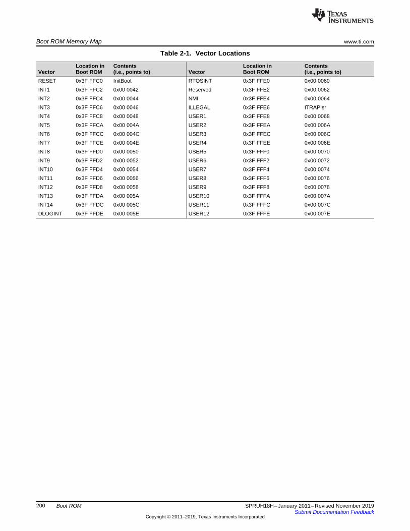
Boot ROM Memory Map www.ti.com
200 SPRUH18H–January 2011–Revised November 2019Submit Documentation Feedback
Copyright © 2011–2019, Texas Instruments Incorporated
Boot ROM
Table 2-1. Vector Locations
VectorLocation inBoot ROM
Contents(i.e., points to) Vector
Location inBoot ROM
Contents(i.e., points to)
RESET 0x3F FFC0 InitBoot RTOSINT 0x3F FFE0 0x00 0060INT1 0x3F FFC2 0x00 0042 Reserved 0x3F FFE2 0x00 0062INT2 0x3F FFC4 0x00 0044 NMI 0x3F FFE4 0x00 0064INT3 0x3F FFC6 0x00 0046 ILLEGAL 0x3F FFE6 ITRAPIsrINT4 0x3F FFC8 0x00 0048 USER1 0x3F FFE8 0x00 0068INT5 0x3F FFCA 0x00 004A USER2 0x3F FFEA 0x00 006AINT6 0x3F FFCC 0x00 004C USER3 0x3F FFEC 0x00 006CINT7 0x3F FFCE 0x00 004E USER4 0x3F FFEE 0x00 006EINT8 0x3F FFD0 0x00 0050 USER5 0x3F FFF0 0x00 0070INT9 0x3F FFD2 0x00 0052 USER6 0x3F FFF2 0x00 0072INT10 0x3F FFD4 0x00 0054 USER7 0x3F FFF4 0x00 0074INT11 0x3F FFD6 0x00 0056 USER8 0x3F FFF6 0x00 0076INT12 0x3F FFD8 0x00 0058 USER9 0x3F FFF8 0x00 0078INT13 0x3F FFDA 0x00 005A USER10 0x3F FFFA 0x00 007AINT14 0x3F FFDC 0x00 005C USER11 0x3F FFFC 0x00 007CDLOGINT 0x3F FFDE 0x00 005E USER12 0x3F FFFE 0x00 007E

Reset(Power-On Reset or
Warm Reset)
Silicon Sets the Following:PIE Disabled (ENPIE=0)
VMAP=1OBJMODE=0
AMODE=0M0M1MAP=1
Boot ROM
Reset Vector Fetchedfrom Boot ROM Address
0x3F FFC0
Jump to InitBoot Functionto Start Boot Process
Call Device_cal()
PLLSTS[DIVSEL]=3
Dummy Read of CSMPassword Locations
TRST=1?
Yes
No
Emulator Not Connected
Determine Boot ModeBased on 2 GPIO Pinsand 2 OTP Locations
(OTP_KEY andOTP_BMODE)
Emulator Connected
Determine Boot ModeBased on 2 RAM
Locations(EMU_KEY andEMU_BMODE)
Begin Execution at EntryPoint as Determined bySelected Boot Modes
www.ti.com Bootloader Features
201SPRUH18H–January 2011–Revised November 2019Submit Documentation Feedback
Copyright © 2011–2019, Texas Instruments Incorporated
Boot ROM
2.2 Bootloader FeaturesThis section describes in detail the boot mode selection process, as well as the specifics of the bootloaderoperation.
2.2.1 Bootloader Functional OperationThe bootloader uses the state of TRST and two GPIO signals to determine which boot mode to use. Theboot mode selection process and the specifics of each bootloader are described in the remainder of thisdocument. Figure 2-4 shows the basic bootloader flow:
Figure 2-4. Bootloader Flow Diagram
The reset vector in boot ROM redirects program execution to the InitBoot function. After performing deviceinitialization the bootloader will check the state of the TRST pin to determine if an emulation pod isconnected.• Emulation Boot (Emulation Pod is connected and TRST = 1)In emulation boot, the boot ROM will check two SARAM locations called EMU_KEY and EMU_BMODE fora boot mode. If the contents of either location are invalid, then the "wait" boot mode is used. All boot modeoptions can be accessed by modifying the value of EMU_BMODE through the debugger when performingan emulation boot.
Stand-alone Boot (TRST = 0)If the device is in stand-alone boot mode, then the state of two GPIO pins are used to determine whichboot mode execute. Options include: GetMode, wait, SCI, and parallel I/O. Each of the modes is describedin detail in Table 2-4. The GetMode option by default boots to flash but can be customized byprogramming two values into OTP to select another boot loader.
These boot modes mentioned here are discussed in detail in Section 2.2.9.
After the selection process and if the required boot loading is complete, the processor will continueexecution at an entry point determined by the boot mode selected. If a bootloader was called, then theinput stream loaded by the peripheral determines this entry address. This data stream is described inSection 2.2.11. If, instead, you choose to boot directly to Flash, OTP, or SARAM, the entry address ispredefined for each of these memory blocks.

Bootloader Features www.ti.com
202 SPRUH18H–January 2011–Revised November 2019Submit Documentation Feedback
Copyright © 2011–2019, Texas Instruments Incorporated
Boot ROM
The following sections discuss in detail the different boot modes available and the process used forloading data code into the device.
2.2.2 Bootloader Device ConfigurationAt reset, any 28x CPU-based device is in 27x object-compatible mode. It is up to the application to placethe device in the proper operating mode before execution proceeds.
On the 28x devices, when booting from the internal boot ROM, the device is configured for 28x operatingmode by the boot ROM software. You are responsible for any additional configuration required.
For example, if your application includes C2xLP source, then you are responsible for configuring thedevice for C2xLP source compatibility prior to execution of code generated from C2xLP source.
The configuration required for each operating mode is summarized in Table 2-2.
(1) C27x refers to the TMS320C27x family of processors. C2xLP refers to theTMS320F24x/TMS320LF240xA family of devices that incorporate the C2xLP core. The information inthe table above is for reference only and is not applicable for the typical user development. For moreinformation on the C2xLP core, refer to SPRU430.
(2) Normally for C27x compatibility, the M0M1MAP would be 0. On these devices, however, it is tied offhigh internally; therefore, at reset, M0M1MAP is always configured for 28x mode.
Table 2-2. Configuration for Device Modes (1)
C27x Mode (Reset) 28x ModeC2xLP Source
Compatible ModeOBJMODE 0 1 1AMODE 0 0 1PAGE0 0 0 0M0M1MAP (2) 1 1 1Other Settings SXM = 1, C = 1, SPM = 0
2.2.3 PLL Multiplier and DIVSEL SelectionThe Boot ROM changes the PLL multiplier (PLLCR) and divider (PLLSTS[DIVSEL]) bits as follows:• All boot modes:
PLLCR is not modified. PLLSTS[DIVSEL] is set to 3 for SYSCLKOUT = CLKIN/1. This increases thespeed of the loaders.
NOTE: The PLL multiplier (PLLSTS) and divider (PLLSTS[DIVSEL]) are not affected by a reset fromthe debugger. Therefore, a boot that is initialized from a reset from Code Composer Studio™may be at a different speed than booting by pulling the external reset line (XRS) low.
NOTE: The reset value of PLLSTS[DIVSEL] is 0. This configures the device for SYSCLKOUT =CLKIN/4 . The boot ROM will change this to SYSCLKOUT = CLKIN/1 to improveperformance of the loaders. PLLSTS[DIVSEL] is left in this state when the boot ROM exitsand it is up to the application to change it before configuring the PLLCR register.
NOTE: The boot ROM leaves PLLSTS[DIVSEL] in the CLKIN/1 state when the boot ROM exits. Thisis not a valid configuration if the PLL is used. Thus the application must change it beforeconfiguring the PLLCR register.
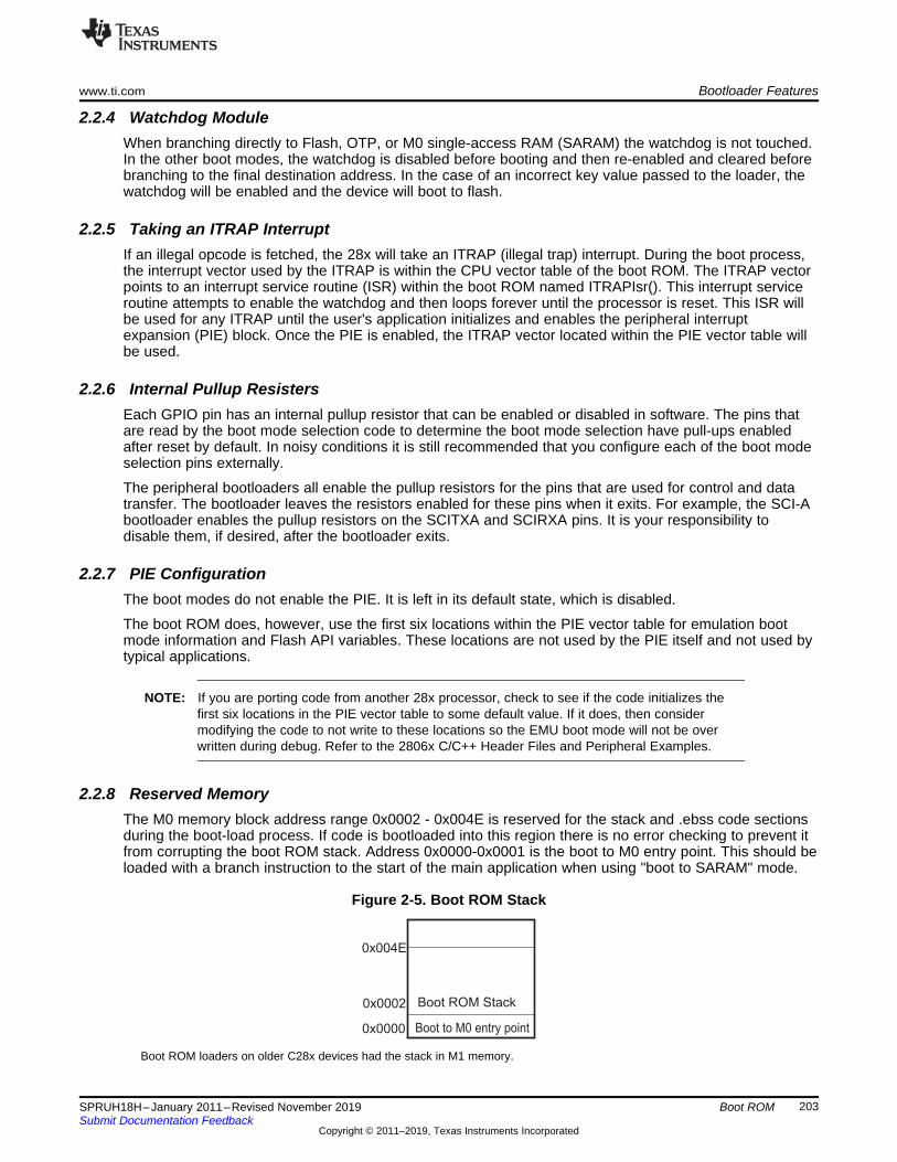
Boot ROM Stack
Boot to M0 entry point0x0000
0x0002
0x004E
www.ti.com Bootloader Features
203SPRUH18H–January 2011–Revised November 2019Submit Documentation Feedback
Copyright © 2011–2019, Texas Instruments Incorporated
Boot ROM
2.2.4 Watchdog ModuleWhen branching directly to Flash, OTP, or M0 single-access RAM (SARAM) the watchdog is not touched.In the other boot modes, the watchdog is disabled before booting and then re-enabled and cleared beforebranching to the final destination address. In the case of an incorrect key value passed to the loader, thewatchdog will be enabled and the device will boot to flash.
2.2.5 Taking an ITRAP InterruptIf an illegal opcode is fetched, the 28x will take an ITRAP (illegal trap) interrupt. During the boot process,the interrupt vector used by the ITRAP is within the CPU vector table of the boot ROM. The ITRAP vectorpoints to an interrupt service routine (ISR) within the boot ROM named ITRAPIsr(). This interrupt serviceroutine attempts to enable the watchdog and then loops forever until the processor is reset. This ISR willbe used for any ITRAP until the user's application initializes and enables the peripheral interruptexpansion (PIE) block. Once the PIE is enabled, the ITRAP vector located within the PIE vector table willbe used.
2.2.6 Internal Pullup ResistersEach GPIO pin has an internal pullup resistor that can be enabled or disabled in software. The pins thatare read by the boot mode selection code to determine the boot mode selection have pull-ups enabledafter reset by default. In noisy conditions it is still recommended that you configure each of the boot modeselection pins externally.
The peripheral bootloaders all enable the pullup resistors for the pins that are used for control and datatransfer. The bootloader leaves the resistors enabled for these pins when it exits. For example, the SCI-Abootloader enables the pullup resistors on the SCITXA and SCIRXA pins. It is your responsibility todisable them, if desired, after the bootloader exits.
2.2.7 PIE ConfigurationThe boot modes do not enable the PIE. It is left in its default state, which is disabled.
The boot ROM does, however, use the first six locations within the PIE vector table for emulation bootmode information and Flash API variables. These locations are not used by the PIE itself and not used bytypical applications.
NOTE: If you are porting code from another 28x processor, check to see if the code initializes thefirst six locations in the PIE vector table to some default value. If it does, then considermodifying the code to not write to these locations so the EMU boot mode will not be overwritten during debug. Refer to the 2806x C/C++ Header Files and Peripheral Examples.
2.2.8 Reserved MemoryThe M0 memory block address range 0x0002 - 0x004E is reserved for the stack and .ebss code sectionsduring the boot-load process. If code is bootloaded into this region there is no error checking to prevent itfrom corrupting the boot ROM stack. Address 0x0000-0x0001 is the boot to M0 entry point. This should beloaded with a branch instruction to the start of the main application when using "boot to SARAM" mode.
Figure 2-5. Boot ROM Stack
Boot ROM loaders on older C28x devices had the stack in M1 memory.

Bootloader Features www.ti.com
204 SPRUH18H–January 2011–Revised November 2019Submit Documentation Feedback
Copyright © 2011–2019, Texas Instruments Incorporated
Boot ROM
NOTE: If code or data is bootloaded into the address range address range 0x0002 - 0x004E there isno error checking to prevent it from corrupting the boot ROM stack.

www.ti.com Bootloader Features
205SPRUH18H–January 2011–Revised November 2019Submit Documentation Feedback
Copyright © 2011–2019, Texas Instruments Incorporated
Boot ROM
In addition, the first 6 locations of the PIE vector table are used by the boot ROM. These locations are notused by the PIE itself and not used by typical applications. These locations are used as SARAM by theboot ROM and will not effect the behavior of the PIE. Note: Some example code from previous devicesmay initialize these locations. This will overwrite any boot mode you have populated. These locations are:
Table 2-3. PIE Vector SARAM Locations Used by the Boot ROM
Location Name Note0x0D00 x 16 EMU_KEY Used for emulation boot0x0D01 x 16 EMU_BMODE Used for emulation boot0x0D02 x 32 Flash_CallbackPtr Used by the flash API0x0D04 x 32 Flash_CPUScaleFactor Used by the flash API
2.2.9 Bootloader ModesTo accommodate different system requirements, the boot ROM offers a variety of boot modes. Thissection describes the different boot modes and gives brief summary of their functional operation. Thestates of TRST and two GPIO pins are used to determine the desired boot mode as shown in Table 2-4.
Table 2-4. Boot Mode Selection
GPIO37 TDO GPIO34CMP2OUT TRST
Mode EMU x x 1 Emulation BootMode 0 0 0 0 Parallel I/OMode 1 0 1 0 SCIMode 2 1 0 0 WaitMode 3 1 1 0 GetMode
NOTE: The default behavior of the GetMode option on unprogrammed devices is to boot to flash.This behavior can be changed by programming two locations in the OTP as shown inTable 2-6. In addition, if these locations are used by an application, then GetMode will jumpto flash as long as OTP_KEY !=0x005A and/or OTP_BMODE is not a valid value.
NOTE: This device does not support the hardware wait-in-reset mode that is available on otherC2000 parts. The "wait" boot mode can be used to emulate a wait-in-reset mode. The "wait"mode is very important for debugging devices with the CSM password programmed (i.e.,secured). When the device is powered up, the CPU will start running and may execute aninstruction that performs an access to a protected emulation code security logic (ECSL) area.If this happens, the ECSL will trip and cause the emulator connection to be cut. The "wait"mode keeps this from happening by looping within the boot ROM until an emulator isconnected.
Figure 2-6 shows an overview of the boot process. Each step is described in greater detail in followingsections.
While each sub-section gives details regarding the implementation of the native boot modes on thedevice, they do not address utilizing each boot mode for common system operations such as:• Device Firmware Upgrade (DFU)• Erasing the flash memory• Verifying the flash memory• Unlocking the security zones• Running the embedded code from "main"• Resetting the MCU
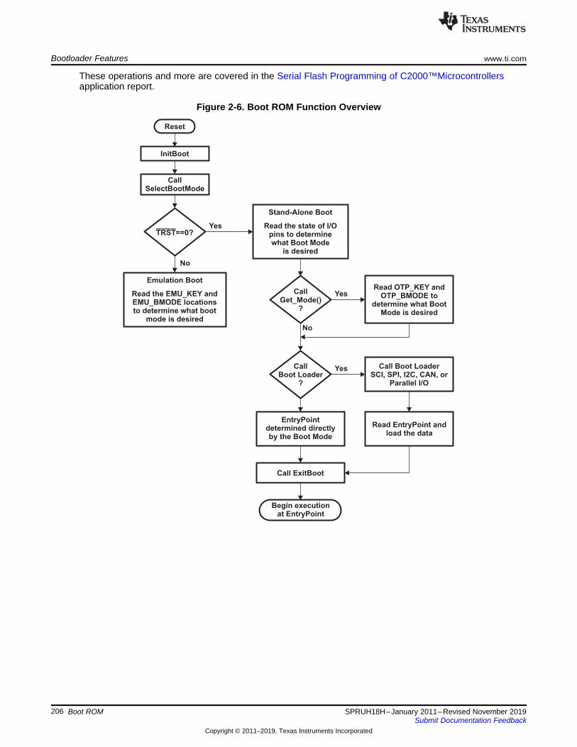
Reset
InitBoot
CallSelectBootMode
TRST==0?Yes
No
Emulation Boot
Read the EMU_KEY andEMU_BMODE locationsto determine what boot
mode is desired
Stand-Alone Boot
Read the state of I/Opins to determinewhat Boot Mode
is desired
CallGet_Mode()
?
YesRead OTP_KEY and
OTP_BMODE todetermine what Boot
Mode is desired
No
CallBoot Loader
?
Yes Call Boot LoaderSCI, SPI, I2C, CAN, or
Parallel I/O
Read EntryPoint andload the data
EntryPointdetermined directlyby the Boot Mode
Call ExitBoot
Begin executionat EntryPoint
Bootloader Features www.ti.com
206 SPRUH18H–January 2011–Revised November 2019Submit Documentation Feedback
Copyright © 2011–2019, Texas Instruments Incorporated
Boot ROM
These operations and more are covered in the Serial Flash Programming of C2000™Microcontrollersapplication report.
Figure 2-6. Boot ROM Function Overview

www.ti.com Bootloader Features
207SPRUH18H–January 2011–Revised November 2019Submit Documentation Feedback
Copyright © 2011–2019, Texas Instruments Incorporated
Boot ROM
Table 2-5. Valid EMU_KEY and EMU_BMODE Values
Address Name Value
0x0D00 EMU_KEY
if TRST == 1 and EMU_KEY == 0x55AA,then check EMU_BMODE for the boot mode,
else { Invalid EMU_KEYBoot mode = WAIT_BOOT }
0x0D01 EMU_BMODE
0x0000 Boot mode = PARALLEL_BOOT0x0001 Boot mode = SCI_BOOT0x0002 Boot mode = WAIT_BOOT
0x0003 Boot mode = GET_BOOT(GetMode from OTP_KEY/OTP_BMODE)
0x0004 Boot mode = SPI_BOOT0x0005 Boot mode = I2C_BOOT0x0006 Boot mode = OTP_BOOT0x0007 Boot mode = CAN_BOOT0x000A Boot mode = RAM_BOOT0x000B Boot mode = FLASH_BOOTOther Boot mode = WAIT_BOOT
Table 2-7 shows the expanded emulation boot mode table.
Here are two examples of an emulation boot:
Example 2-3. Debug an application that loads through the SCI at boot.
To debug an application that loads through the SCI at boot, follow these steps:• Configure the pins for mode 1, SCI, and initiate a power-on-reset.• The boot ROM will detect TRST = 0 and will use the two pins to determine SCI boot.• The boot ROM populates EMU_KEY with 0x55AA and EMU_BMODE with SCI_BOOT.• The boot ROM sits in the SCI loader waiting for data.• Connect the debugger. TRST will go high.• Perform a debugger reset and run. The boot loader will use the EMU_BMODE and boot to SCI.

Bootloader Features www.ti.com
208 SPRUH18H–January 2011–Revised November 2019Submit Documentation Feedback
Copyright © 2011–2019, Texas Instruments Incorporated
Boot ROM
Example 2-4. You want to connect your emulator, but do not want application code to start executingbefore the emulator connects.
To connect your emulator, but keep application code from executing before the emulator connects:• Configure GPIO37 and GPIO34 pins for mode 2, WAIT, and initiate a power-on-reset.• The boot ROM will detect TRST = 0 and will use the two pins to determine wait boot.• The boot ROM populates EMU_KEY with 0x55AA and EMU_BMODE with WAIT_BOOT.• The boot ROM sits in the wait routine.• Connect the debugger; TRST will go high.• Modify the EMU_BMODE via the debugger to boot to FLASH or other desired boot mode.• Perform a debugger reset and run. The boot loader will use the EMU_BMODE and boot to the desired
loader or location.
NOTE: The behavior of emulators with regards to TRST differs. Some emulators pull TRSThigh only when Code Composer Studio is in a connected state. For these emulators, if CCSis disconnected TRST will return to a low state. With CCS disconnected, GPIO34 andGPIO37 will be used to determine the boot mode. For these emulators, this is true even if theemulator pod is physically connected.
Some emulators pull TRST high when CCS connects and leave it high as long as the powersense pin is active. TRST will remain high even after CCS disconnects. For these emulators,the EMU mode stored in RAM will be used unless the target is power cycled, causing thestate of TRST to reset back to a low state.
The following boot modes are invoked by the state of the boot mode pins if an emulator is not connected:• Wait
This devices does not support the hardware wait-in-reset mode that is available on other C2000 parts.The "wait" boot mode can be used to emulate a wait-in-reset mode. The "wait" mode is very importantfor debugging devices with the CSM password programmed (i.e., secured). When the device ispowered up, the CPU will start running and may execute an instruction that performs an access to aemulation code security logic (ECSL) protected area. If this happens, the ECSL will trip and cause theemulator connection to be cut. The "wait" mode keeps this from happening by looping within the bootROM until an emulator is connectedThis mode writes WAIT_BOOT to EMU_BMODE. Once the emulator is connected you can thenmanually populate the EMU_BMODE with the appropriate boot mode for the debug session.
• SCIIn this mode, the boot ROM will load code to be executed into on-chip memory via the SCI-A port.When invoked as a stand-alone mode, the boot ROM writes SCI_BOOT to EMU_BMODE.
• Parallel I/O 8-bitThe parallel I/O boot mode is typically used only by production flash programmers.
• GetModeThe GetMode option uses two locations within the USER OTP to determine the boot mode. On an un-programmed device, this mode will always boot to flash. On a programmed device, you can choose toprogram these locations to change the behavior. If either of these locations is not an expected value,then boot to flash will be used.The last six words of user OTP region (0x3D7BFA to 0x3D7BFF) are reserved for the GetModefunction usage.The values used by the Get_Mode() function are shown in Table 2-6.

www.ti.com Bootloader Features
209SPRUH18H–January 2011–Revised November 2019Submit Documentation Feedback
Copyright © 2011–2019, Texas Instruments Incorporated
Boot ROM
Table 2-6. OTP Values for GetMode
Address Name Value
0x3D7BFB OTP_KEY
GetMode will be entered if one of the two conditions is true:Case 1: TRST == 0, GPIO34 == 1 and GPIO37 == 1Case 2: TRST == 1, EMU_KEY == 0x55AA and EMU_BMODE == GET_BOOTGetMode first checks the value of OTP_KEY:if OTP_KEY == 0x005A, then check OTP_BMODE for the boot modeelse { Invalid key: Boot mode = FLASH_BOOT }
0x3D7BFE OTP_BMODE
0x0001 Boot mode = SCI_BOOT0x0004 Boot mode = SPI_BOOT0x0005 Boot mode = I2C_BOOT0x0006 Boot mode = OTP_BOOT0x0007 Boot mode = CAN_BOOTOther Boot mode = FLASH_BOOT
The following boot modes are available through the emulation boot option. Some are alsoavailable as a programmed get mode option.• Jump to M0 SARAM
This mode is only available in emulation boot. The boot ROM software configures the device for 28xoperation and branches directly to address 0X000000. This is the first address in the M0 memoryblock.
• Jump to branch instruction in flash memory.Jump to flash is the default behavior of the Get Mode boot option. Jump to flash is also available as anemulation boot option.In this mode, the boot ROM software configures the device for 28x operation and branches directly tolocation 0x3F 7FF6. This location is just before the 128-bit code security module (CSM) passwordlocations. You are required to have previously programmed a branch instruction at location 0x3F 7FF6that will redirect code execution to either a custom boot-loader or the application code.
• Jump to OTP MemoryJump to OTP is available only as an option programmed into OTP_BMODE via the get mode function.With the emulator connected, jump to OTP can also be achieved by manually writing the OTP_BOOTvalue to EMU_BMODE. The entry point location is 0x3D 7800.
• SPI EEPROM or Flash boot mode (SPI-A)Jump to SPI is available in stand-alone mode as a programmed Get Mode option. That is, to configurea device for SPI boot in stand-alone mode, the OTP_KEY and OTP_BMODE locations must beprogrammed for SPI_BOOT and the boot mode pins configured for the Get Mode boot option.SCI boot is also available as an emulation boot option.In this mode, the boot ROM will load code and data into on-chip memory from an external SPIEEPROM or SPI flash via the SPI-A port.
• I2C-A boot mode (I2C-A)Jump to I2C is available in stand-alone mode as a programmed Get mode option. That is, to configurea device for I2C boot in stand-alone mode, the OTP_KEY and OTP_BMODE locations must beprogrammed for I2C_BOOT and the boot mode pins configured for the Get Mode boot option.I2C boot is also available as an emulation boot option.In this mode, the boot ROM will load code and data into on-chip memory from an external serialEEPROM or flash at address 0x50 on the I2C-A bus.
• eCAN-A boot mode (eCAN-A)Jump to eCAN is available in stand-alone mode as a programmed Get mode option. That is, toconfigure a device for eCAN boot in stand-alone mode, the OTP_KEY and OTP_BMODE locationsmust be programmed for CAN_BOOT and the boot mode pins configured for the Get Mode bootoption. eCAN boot is also available as an emulation boot option. In this mode, the eCAN-A peripheral

Bootloader Features www.ti.com
210 SPRUH18H–January 2011–Revised November 2019Submit Documentation Feedback
Copyright © 2011–2019, Texas Instruments Incorporated
Boot ROM
is used to transfer data and code into the on-chip memory using eCAN-A mailbox 1. The transfer is an8-bit data stream with two 8-bit values being transferred during each communication.
(1) Get Mode indicated the boot mode was derived from the values programmed in the OTP_KEY and OTP_BMODE locations.(2) x = don't care.
Table 2-7. Emulation Boot modes (TRST = 1)
TRST GPIO37TDO GPIO34
EMUKEY
EMUBMODE
OTPKEY
OTPBMODE
Boot ModeSelected (1)
EMUKEY
EMUBMODE
Readfrom
0x0D00
Readfrom
0x0D01
Readfrom
0x3D7BFB
Readfrom
0x3D7BFE
Writtento
0x0D00
Writtento
0x0D011 x (2) x !=0x55AA x x x Wait - -
0x55AA 0x0000 x x Parallel I/O - -0x0001 x x SCI - -0x0002 x x Wait - -0x0003 != 0x005A x GetMode: Flash - -
0x005A 0x0001 GetMode: SCI - -0x000B GetMode: Flash - -0x0004 GetMode: SPI - -0x0005 GetMode: I2C - -0x0006 GetMode: OTP - -0x0007 GetMode: CAN - -Other GetMode: Flash - -
0x0004 x x SPI - -0x0005 x x I2C - -0x0006 x x OTP - -0x0007 x x CAN - -0x000A x x Boot to RAM - -0x000B x x Boot to FLASH - -Other x x Wait - -
(1) Get Mode indicates the boot mode was derived from the values programmed in the OTP_KEY and OTP_BMODE locations.(2) The boot ROM will write this value to EMU_KEY and EMU_BMODE. This value can be used or overwritten by the user if a
debugger is connected.(3) x = don't care.
Table 2-8. Stand-Alone Boot Modes with (TRST = 0)
TRST GPIO37TDO GPIO34
EMUKEY
EMUBMODE
OTPKEY
OTPBMODE
Boot ModeSelected (1)
(2)
EMUKEY
(2)
EMUBMODE
Readfrom
0x0D00
Readfrom
0x0D01
Readfrom
0x3D7BFB
Readfrom
0x3D7BFE
Writtento
0x0D00
Writtento
0x0D010 0 0 x (3) x x x Parallel I/O 0x55AA 0x00000 0 1 x x x x SCI 0x55AA 0x00010 1 0 x x x x Wait 0x55AA 0x0002
0 1 1 x x
!=0x005A x GetMode: Flash
0x55AA 0x00030x005A
0x0001 GetMode: SCI0x000B GetMode: Flash0x0004 GetMode: SPI0x0005 GetMode: I2C0x0006 GetMode: OTP0x0007 GetMode: CANOther GetMode: Flash

www.ti.com Bootloader Features
211SPRUH18H–January 2011–Revised November 2019Submit Documentation Feedback
Copyright © 2011–2019, Texas Instruments Incorporated
Boot ROM
2.2.10 Device_CalThe Device_cal() routine is programmed into TI reserved memory by the factory. The boot ROMautomatically calls the Device_cal() routine to calibrate the internal oscillators and ADC with devicespecific calibration data. During normal operation, this process occurs automatically and no action isrequired by the user.
If the boot ROM is bypassed by Code Composer Studio during the development process, then thecalibration must be initialized by application. For working examples, see the system initialization in theC280 3x C/C++ Header Files and Peripheral Examples.
NOTE: Failure to initialize these registers will cause the oscillators and ADC to function out ofspecification. The following three steps describe how to call the Device_cal routine from anapplication.
Step 1: Create a pointer to the Device_cal function as shown in Example 2-5. This #define is included inthe Header Files and Peripheral Examples.
Step 2: Call the function pointed to by Device_cal() as shown in Example 2-5. The ADC clocks must beenabled before making this call.
Example 2-5. Calling the Device_cal() function
//Device call is a pointer to a function//that begins at the address shown# define Device_cal (void(*)(void))0x3D7C80... ...
EALLOW;SysCtrlRegs.PCLKCR0.bit.ADCENCLK = 1;(*Device_cal)();SysCtrlRegs.PCLKCR0.bit.ADCENCLK = 0;EDIS;
...
2.2.11 Bootloader Data Stream StructureThe following two tables and associated examples show the structure of the data stream incoming to thebootloader. The basic structure is the same for all the bootloaders and is based on the C54x source datastream generated by the C54x hex utility. The C28x hex utility (hex2000.exe) has been updated to supportthis structure. The hex2000.exe utility is included with the C2000 code generation tools. All values in thedata stream structure are in hex.
The first 16-bit word in the data stream is known as the key value. The key value indicates to thebootloader the width of the incoming stream: 8 or 16 bits. Note that not all bootloaders will accept both 8and 16-bit streams. Please refer to the detailed information on each loader for the valid data stream width.For an 8-bit data stream, the key value is 0x08AA and for a 16-bit stream it is 0x10AA. If a bootloaderreceives an invalid key value, then the load is aborted.
The next eight words are used to initialize register values or otherwise enhance the bootloader by passingvalues to it. If a bootloader does not use these values then they are reserved for future use and thebootloader simply reads the value and then discards it. Currently only the SPI and I2C and parallelbootloaders use these words to initialize registers.
The tenth and eleventh words comprise the 22-bit entry point address. This address is used to initializethe PC after the boot load is complete. This address is most likely the entry point of the programdownloaded by the bootloader.

Bootloader Features www.ti.com
212 SPRUH18H–January 2011–Revised November 2019Submit Documentation Feedback
Copyright © 2011–2019, Texas Instruments Incorporated
Boot ROM
The twelfth word in the data stream is the size of the first data block to be transferred. The size of theblock is defined for both 8-bit and 16-bit data stream formats as the number of 16-bit words in the block.For example, to transfer a block of 20 8-bit data values from an 8-bit data stream, the block size would be0x000A to indicate 10 16-bit words.
The next two words indicate to the loader the destination address of the block of data. Following the sizeand address will be the 16-bit words that makeup that block of data.
This pattern of block size/destination address repeats for each block of data to be transferred. Once all theblocks have been transferred, a block size of 0x0000 signals to the loader that the transfer is complete. Atthis point the loader will return the entry point address to the calling routine which in turn will cleanup andexit. Execution will then continue at the entry point address as determined by the input data streamcontents.

www.ti.com Bootloader Features
213SPRUH18H–January 2011–Revised November 2019Submit Documentation Feedback
Copyright © 2011–2019, Texas Instruments Incorporated
Boot ROM
Table 2-9. General Structure Of Source Program Data Stream In 16-Bit Mode
Word Contents1 10AA (KeyValue for memory width = 16bits)2 Register initialization value or reserved for future use3 Register initialization value or reserved for future use4 Register initialization value or reserved for future use5 Register initialization value or reserved for future use6 Register initialization value or reserved for future use7 Register initialization value or reserved for future use8 Register initialization value or reserved for future use9 Register initialization value or reserved for future use10 Entry point PC[22:16]11 Entry point PC[15:0]12 Block size (number of words) of the first block of data to load. If the block size is 0, this indicates the end of the
source program. Otherwise another section follows.13 Destination address of first block Addr[31:16]14 Destination address of first block Addr[15:0]15 First word of the first block in the source being loaded......
...
.... Last word of the first block of the source being loaded. Block size of the 2nd block to load.. Destination address of second block Addr[31:16]. Destination address of second block Addr[15:0]. First word of the second block in the source being loaded. …. Last word of the second block of the source being loaded. Block size of the last block to load. Destination address of last block Addr[31:16]. Destination address of last block Addr[15:0]. First word of the last block in the source being loaded......
...
...n Last word of the last block of the source being loaded
n+1 Block size of 0000h - indicates end of the source program

Bootloader Features www.ti.com
214 SPRUH18H–January 2011–Revised November 2019Submit Documentation Feedback
Copyright © 2011–2019, Texas Instruments Incorporated
Boot ROM
Example 2-6. Data Stream Structure 16-bit
10AA ; 0x10AA 16-bit key value0000 0000 0000 0000 ; 8 reserved words0000 0000 0000 0000003F 8000 ; 0x003F8000 EntryAddr, starting point after boot load completes0005 ; 0x0005 - First block consists of 5 16-bit words003F 9010 ; 0x003F9010 - First block will be loaded starting at 0x3F90100001 0002 0003 0004 ; Data loaded = 0x0001 0x0002 0x0003 0x0004 0x000500050002 ; 0x0002 - 2nd block consists of 2 16-bit words003F 8000 ; 0x003F8000 - 2nd block will be loaded starting at 0x3F80007700 7625 ; Data loaded = 0x7700 0x76250000 ; 0x0000 - Size of 0 indicates end of data streamAfter load has completed the following memory values will have been initialized as follows:Location Value0x3F9010 0x00010x3F9011 0x00020x3F9012 0x00030x3F9013 0x00040x3F9014 0x00050x3F8000 0x77000x3F8001 0x7625PC Begins execution at 0x3F8000
In 8-bit mode, the least significant byte (LSB) of the word is sent first followed by the most significant byte(MSB). For 32-bit values, such as a destination address, the most significant word (MSW) is loaded first,followed by the least significant word (LSW). The bootloaders take this into account when loading an 8-bitdata stream.

www.ti.com Bootloader Features
215SPRUH18H–January 2011–Revised November 2019Submit Documentation Feedback
Copyright © 2011–2019, Texas Instruments Incorporated
Boot ROM
Table 2-10. LSB/MSB Loading Sequence in 8-Bit Data Stream
Byte ContentsLSB (First Byte of 2) MSB (Second Byte of 2)
1 2 LSB: AA (KeyValue for memory width = 8 bits) MSB: 08h (KeyValue for memory width = 8 bits)3 4 LSB: Register initialization value or reserved MSB: Register initialization value or reserved5 6 LSB: Register initialization value or reserved MSB: Register initialization value or reserved7 8 LSB: Register initialization value or reserved MSB: Register initialization value or reserved......
...
.........
...
...17 18 LSB: Register initialization value or reserved MSB: Register initialization value or reserved19 20 LSB: Upper half of Entry point PC[23:16] MSB: Upper half of entry point PC[31:24] (Always 0x00)21 22 LSB: Lower half of Entry point PC[7:0] MSB: Lower half of Entry point PC[15:8]23 24 LSB: Block size in words of the first block to load. If the block
size is 0, this indicates the end of the source program.Otherwise another block follows. For example, a block size of0x000A would indicate 10 words or 20 bytes in the block.
MSB: block size
25 26 LSB: MSW destination address, first block Addr[23:16] MSB: MSW destination address, first block Addr[31:24]27 28 LSB: LSW destination address, first block Addr[7:0] MSB: LSW destination address, first block Addr[15:8]29 30 LSB: First word of the first block being loaded MSB: First word of the first block being loaded......
...
.........
...
.... . LSB: Last word of the first block to load MSB: Last word of the first block to load. . LSB: Block size of the second block MSB: Block size of the second block. . LSB: MSW destination address, second block Addr[23:16] MSB: MSW destination address, second block Addr[31:24]. . LSB: LSW destination address, second block Addr[7:0] MSB: LSW destination address, second block Addr[15:8]. . LSB: First word of the second block being loaded MSB: First word of the second block being loaded
...
.........
...
.........
. . LSB: Last word of the second block MSB: Last word of the second block
. . LSB: Block size of the last block MSB: Block size of the last block
. . LSB: MSW of destination address of last block Addr[23:16] MSB: MSW destination address, last block Addr[31:24]
. . LSB: LSW destination address, last block Addr[7:0] MSB: LSW destination address, last block Addr[15:8]
. . LSB: First word of the last block being loaded MSB: First word of the last block being loaded......
...
.........
...
.... . LSB: Last word of the last block MSB: Last word of the last blockn n+1 LSB: 00h MSB: 00h - indicates the end of the source

Bootloader Features www.ti.com
216 SPRUH18H–January 2011–Revised November 2019Submit Documentation Feedback
Copyright © 2011–2019, Texas Instruments Incorporated
Boot ROM
Example 2-7. Data Stream Structure 8-bit
AA 08 ; 0x08AA 8-bit key value00 00 00 00 ; 8 reserved words00 00 00 0000 00 00 0000 00 00 003F 00 00 80 ; 0x003F8000 EntryAddr, starting point after boot load completes05 00 ; 0x0005 - First block consists of 5 16-bit words3F 00 10 90 ; 0x003F9010 - First block will be loaded starting at 0x3F901001 00 ; Data loaded = 0x0001 0x0002 0x0003 0x0004 0x000502 0003 0004 0005 0002 00 ; 0x0002 - 2nd block consists of 2 16-bit words3F 00 00 80 ; 0x003F8000 - 2nd block will be loaded starting at 0x3F800000 77 ; Data loaded = 0x7700 0x762525 7600 00 ; 0x0000 - Size of 0 indicates end of data stream
After load has completed the following memory values will have been initialized as follows:
Location Value0x3F9010 0x00010x3F9011 0x00020x3F9012 0x00030x3F9013 0x00040x3F9014 0x00050x3F8000 0x77000x3F8001 0x7625PC Begins execution at 0x3F8000
2.2.12 Basic Transfer ProcedureFigure 2-7 illustrates the basic process a bootloader uses to transfer data and start program execution.This process occurs after the bootloader determines the valid boot mode selected by the state of TRSTand GPIO pins.
The loader first compares the first value sent by the host against the 16-bit key value of 0x10AA. If the firstword matches the key value, the loader continuously fetches data until it transfers all the hex words andthen starts program execution. But, if the key does not match the key value, then the loader aborts andthe CPU jumps to the default flash entry point.

Read first word (W1)
W1=0x10AA
?
No
16-bit data size
Yes
Read EntryPoint address
Read second word(W2) and discard
upper 8-bits
?0x08AAW2:W1=
Yes
No
8-bitDataSize
Data format errorReturn flashentry point
Read BlockSize (R)
?R=0
No
Yes ReturnEntryPoint
Read BlockAddress
Transfer R words ofdata from source to
destination
www.ti.com Bootloader Features
217SPRUH18H–January 2011–Revised November 2019Submit Documentation Feedback
Copyright © 2011–2019, Texas Instruments Incorporated
Boot ROM
Figure 2-7. Bootloader Basic Transfer Procedure
8-bit and 16-bit transfers are not valid for all boot modes. If only one mode is valid, then this decision tree is skippedand the key value is only checked for correctness. See the info specific to a particular bootloader for any limitations.In 8-bit mode, the LSB of the 16-bit word is read first followed by the MSB.
2.2.13 InitBoot Assembly RoutineThe first routine called after reset is the InitBoot assembly routine. This routine initializes the device foroperation in C28x object mode. InitBoot also performs a dummy read of the Code Security Module (CSM)password locations. If the CSM passwords are erased (all 0xFFFFs) then this has the effect of unlockingthe CSM. Otherwise the CSM will remain locked and this dummy read of the password locations will haveno effect. This can be useful if you have a new device that you want to boot load.
After the dummy read of the CSM password locations, the InitBoot routine calls the SelectBootModefunction. This function determines the type of boot mode desired by the state of TRST and certain GPIOpins. This process is described in Section 2.2.14. Once the boot is complete, the SelectBootMode functionpasses back the entry point address (EntryAddr) to the InitBoot function. EntryAddr is the location wherecode execution will begin after the bootloader exits. InitBoot then calls the ExitBoot routine that thenrestores CPU registers to their reset state and exits to the EntryAddr that was determined by the bootmode.
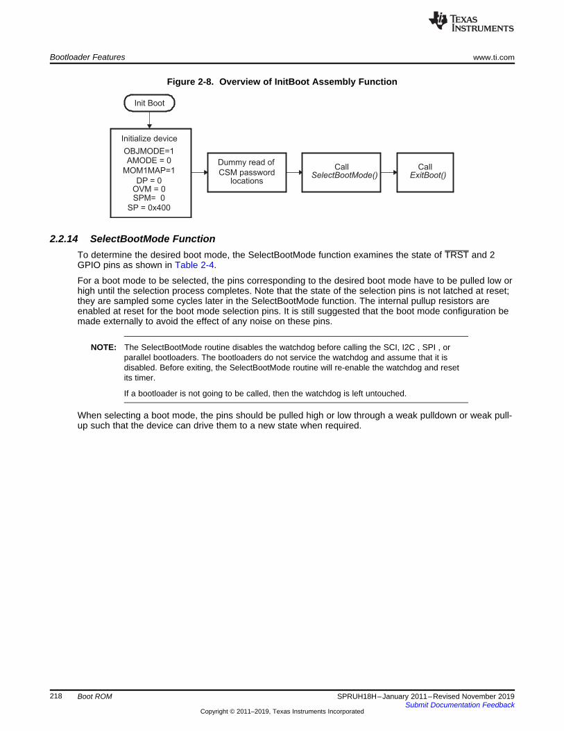
Init Boot
Initialize device
OBJMODE=1AMODE = 0
MOM1MAP=1
DP = 0OVM = 0SPM= 0
SP = 0x400
Dummy read of
CSM passwordlocations
CallSelectBootMode()
CallExitBoot()
Bootloader Features www.ti.com
218 SPRUH18H–January 2011–Revised November 2019Submit Documentation Feedback
Copyright © 2011–2019, Texas Instruments Incorporated
Boot ROM
Figure 2-8. Overview of InitBoot Assembly Function
2.2.14 SelectBootMode FunctionTo determine the desired boot mode, the SelectBootMode function examines the state of TRST and 2GPIO pins as shown in Table 2-4.
For a boot mode to be selected, the pins corresponding to the desired boot mode have to be pulled low orhigh until the selection process completes. Note that the state of the selection pins is not latched at reset;they are sampled some cycles later in the SelectBootMode function. The internal pullup resistors areenabled at reset for the boot mode selection pins. It is still suggested that the boot mode configuration bemade externally to avoid the effect of any noise on these pins.
NOTE: The SelectBootMode routine disables the watchdog before calling the SCI, I2C , SPI , orparallel bootloaders. The bootloaders do not service the watchdog and assume that it isdisabled. Before exiting, the SelectBootMode routine will re-enable the watchdog and resetits timer.
If a bootloader is not going to be called, then the watchdog is left untouched.
When selecting a boot mode, the pins should be pulled high or low through a weak pulldown or weak pull-up such that the device can drive them to a new state when required.

SelectBootMode
DIVSEL=/1ADCENCLK=1
Call DEVICE_CAL()ADCENCLK=0
Read CSM Password
TRST==0?Yes
No
EMU_KEY=0x55AA
?
No
TDO is a GPIOBoot Mode=
GPIO37:GPIO34*EMU_KEY=0x55AA
*EMU_MODE=Boot Mode
Invalid EMU_KEYBoot Mode=WAIT
Yes
Boot Mode=*EMU_MODE
BootMode=WAIT
?
Yes
No
WaitBoot()
Disable Watchdog
BootMode=
GET MODE?
Yes
No
Boot Mode=Get_Mode()Returns FLASH if Either
the OTP_KEY orOTP_MODE is Invalid
BootMode=FLASH
?
Yes
NoA
EntryAddr=Flash EntryPoint 0x3F 7FF6
Enable WatchdogReturn EntryAddr
ABoot
Mode=OTP?
Yes
No
EntryAddr=OTP EntryPoint 0x3D 7800
BootMode=RAM?
Yes
No
EntryAddr=SARAMEntry Point 0x00 0000
BootMode=SCI?
Yes
No
EntryAddr=SCI_Boot()
BootMode=SPI?
Yes
No
EntryAddr=SPI_Boot()
BootMode=I2C?
Yes
No
EntryAddr=I2C_Boot()
BootMode=
PARALLEL?
Yes
No
EntryAddr=Parallel_IO_Boot()
Invalid EMU_MODEWaitBoot()
This Point is Reached if=1,
*EMU_KEY is Valid and*EMU_MODE is Valid.
TRST
BootMode=CAN?
EntryAddr=CAN_Boot()
Yes
No
www.ti.com Bootloader Features
219SPRUH18H–January 2011–Revised November 2019Submit Documentation Feedback
Copyright © 2011–2019, Texas Instruments Incorporated
Boot ROM
Figure 2-9. Overview of the SelectBootMode Function

Get_mode()Function
OTP_KEY=0x005A
?
No
Yes
Mode=SCI_BOOT
A
OTP_BMODE=SCI_BOOT
?
Yes
No
Mode=SPI_BOOT
OTP_BMODE=SPI_BOOT
?
Yes
No
B
Return Mode
B
Mode=I2C_BOOT
OTP_BMODE=I2C_BOOT
?
Yes
No
Mode=OTP_BOOT
OTP_BMODE=OTP_BOOT
?
Yes
No
Mode=FLASH_BOOT A
OTP_BMODE=CAN?
No
Mode=CAN_BOOT
Yes
Bootloader Features www.ti.com
220 SPRUH18H–January 2011–Revised November 2019Submit Documentation Feedback
Copyright © 2011–2019, Texas Instruments Incorporated
Boot ROM
Figure 2-10. Overview of Get_mode() Function
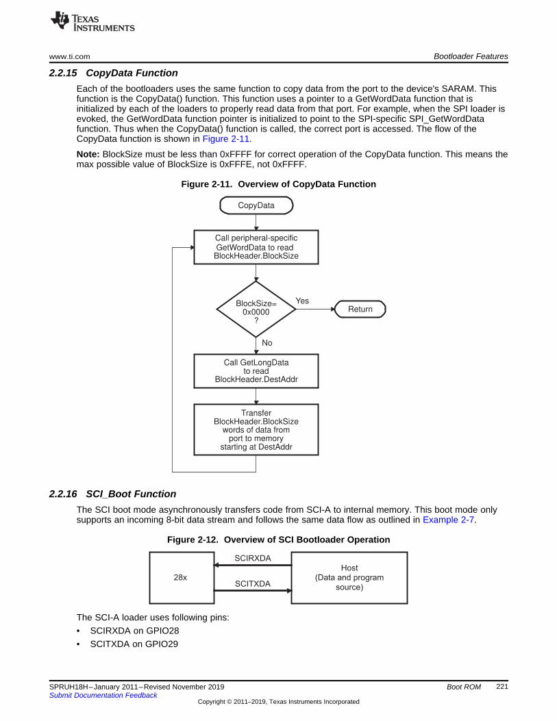
28x
SCIRXDA
SCITXDA
Host(Data and program
source)
CopyData
Call peripheral-specific GetWordData to read
Yes
No
Return
BlockHeader.BlockSize
BlockSize=0x0000
?
Call GetLongDatato read
BlockHeader.DestAddr
TransferBlockHeader.BlockSize
words of data fromport to memory
starting at DestAddr
www.ti.com Bootloader Features
221SPRUH18H–January 2011–Revised November 2019Submit Documentation Feedback
Copyright © 2011–2019, Texas Instruments Incorporated
Boot ROM
2.2.15 CopyData FunctionEach of the bootloaders uses the same function to copy data from the port to the device's SARAM. Thisfunction is the CopyData() function. This function uses a pointer to a GetWordData function that isinitialized by each of the loaders to properly read data from that port. For example, when the SPI loader isevoked, the GetWordData function pointer is initialized to point to the SPI-specific SPI_GetWordDatafunction. Thus when the CopyData() function is called, the correct port is accessed. The flow of theCopyData function is shown in Figure 2-11.
Note: BlockSize must be less than 0xFFFF for correct operation of the CopyData function. This means themax possible value of BlockSize is 0xFFFE, not 0xFFFF.
Figure 2-11. Overview of CopyData Function
2.2.16 SCI_Boot FunctionThe SCI boot mode asynchronously transfers code from SCI-A to internal memory. This boot mode onlysupports an incoming 8-bit data stream and follows the same data flow as outlined in Example 2-7.
Figure 2-12. Overview of SCI Bootloader Operation
The SCI-A loader uses following pins:• SCIRXDA on GPIO28• SCITXDA on GPIO29

SCI_Boot
Enable the SCI-A clockset the LSPCLK to /4
functionality and pullups onEnable the SCIA TX and RX pin
Setup SCI-A for1 stop, 8-bit character,no parity, use internal
SC clock, no loopback,disable Rx/Tx interrupts
Disable SCI FIFOs
Prime SCI-A baud register
Enable autobaud detection
Autobaudlock
?
No
Yes
Echo autobaud character
Read KeyValue
Yes
NoValidKeyValue(0x08AA)
?
Jump to Flash
Read and discard 8reserved words
Read EntryPoint address
Call CopyData
EntryPointReturn
Set GetWord function pointerto SCIA_GetWordData
TX and RX
Bootloader Features www.ti.com
222 SPRUH18H–January 2011–Revised November 2019Submit Documentation Feedback
Copyright © 2011–2019, Texas Instruments Incorporated
Boot ROM
The 28x device communicates with the external host device by communication through the SCI-Aperipheral. The autobaud feature of the SCI port is used to lock baud rates with the host. For this reasonthe SCI loader is very flexible and you can use a number of different baud rates to communicate with thedevice.
After each data transfer, the 28x will echo back the 8-bit character received to the host. In this manner, thehost can perform checks that each character was received by the 28x.
At higher baud rates, the slew rate of the incoming data bits can be effected by transceiver and connectorperformance. While normal serial communications may work well, this slew rate may limit reliable auto-baud detection at higher baud rates (typically beyond 100kbaud) and cause the auto-baud lock feature tofail. To avoid this, the following is recommended:1. Achieve a baud-lock between the host and 28x SCI bootloader using a lower baud rate.2. Load the incoming 28x application or custom loader at this lower baud rate.3. The host may then handshake with the loaded 28x application to set the SCI baud rate register to the
desired high baud rate.
Figure 2-13. Overview of SCI_Boot Function

28x
28x control − AIO6
Host control − AIO12 Host(Data and program
source)
Data GP I/O port GPIO[31,30,5:0]
8
SCIA_GetWordData
Yes
NoDataReceived
?
Echoback LSBto host
Read LSB
DataReceived
?
No
Yes
Read MSB
Echoback MSBto host
Return MSB:LSB
www.ti.com Bootloader Features
223SPRUH18H–January 2011–Revised November 2019Submit Documentation Feedback
Copyright © 2011–2019, Texas Instruments Incorporated
Boot ROM
Figure 2-14. Overview of SCI_GetWordData Function
2.2.17 Parallel_Boot Function (GPIO)The parallel general purpose I/O (GPIO) boot mode asynchronously transfers code from GPIO0 -GPIO5,GPIO30-GPIO31 to internal memory. Each value is 8 bits long and follows the same data flow as outlinedin Section 2.2.11.
Figure 2-15. Overview of Parallel GPIO bootloader Operation
The parallel GPIO loader uses following pins:• Data on GPIO[31,30,5:0]• 28x Control on AIO6 (external pull-up resistor may be required)• Host Control on AIO12 (external pull-up resistor required)
The 28x communicates with the external host device by polling/driving the AIO12 and AIO6 lines. Anexternal pull-up resistor is required for AIO12 because AIO pins lack internal pull-up circuitry required toprevent the 28x from reading data prematurely. Depending on your system an external pull-up may alsobe required on AIO6. The handshake protocol shown in Figure 2-16 must be used to successfully transfereach word via . This protocol is very robust and allows for a slower or faster host to communicate with the28x.
Two consecutive 8-bit words are read to form a single 16-bit word. The most significant byte (MSB) is readfirst followed by the least significant byte (LSB). In this case, data is read from GPIO[31,30,5:0].
The 8-bit data stream is shown in Table 2-11.

Host control
AIO12
28x control
AIO6
1 2 3 4 65
Bootloader Features www.ti.com
224 SPRUH18H–January 2011–Revised November 2019Submit Documentation Feedback
Copyright © 2011–2019, Texas Instruments Incorporated
Boot ROM
Table 2-11. Parallel GPIO Boot 8-Bit Data Stream
Bytes GPIO[ 31,30,5:0](Byte 1 of 2)
GPIO[ 31,30,5:0](Byte 2 of 2)
Description
1 2 AA 08 0x08AA (KeyValue for memory width = 16bits)3 4 00 00 8 reserved words (words 2 - 9)... ... ... ... ...17 18 00 00 Last reserved word19 20 BB 00 Entry point PC[22:16]21 22 DD CC Entry point PC[15:0] (PC = 0x00BBCCDD)23 24 NN MM Block size of the first block of data to load = 0xMMNN words25 26 BB AA Destination address of first block Addr[31:16]27 28 DD CC Destination address of first block Addr[15:0] (Addr = 0xAABBCCDD)29 30 BB AA First word of the first block in the source being loaded = 0xAABB......
...Data for this section....
. BB AA Last word of the first block of the source being loaded = 0xAABB
. NN MM Block size of the 2nd block to load = 0xMMNN words
. BB AA Destination address of second block Addr[31:16]
. DD CC Destination address of second block Addr[15:0]
. BB AA First word of the second block in the source being loaded
. …n n+1 BB AA Last word of the last block of the source being loaded
(More sections if required)n+2 n+3 00 00 Block size of 0000h - indicates end of the source program
The 28x device first signals the host that it is ready to begin data transfer by pulling the AIO6 pin low. Thehost load then initiates the data transfer by pulling the AIO12 pin low. The complete protocol is shown inthe diagram below:
Figure 2-16. Parallel GPIO Boot Loader Handshake Protocol
1. The 28x device indicates it is ready to start receiving data by pulling the AIO6pin low.2. The bootloader waits until the host puts data on GPIO [31,30,5:0].The host signals to the 28x device
that data is ready by pulling the AIO12 pin low.3. The 28x device reads the data and signals the host that the read is complete by pulling AIO6 high.4. The bootloader waits until the host acknowledges the 28x by pulling AIO12 high.5. The 28x device again indicates it is ready for more data by pulling the AIO6 pin low.
This process is repeated for each data value to be sent.
Figure 2-17 shows an overview of the Parallel GPIO bootloader flow.

Parallel_Boot
No
Yes
Initialize GP I/O MUXand Dir registers
AIO[31,30,5:0] = inputAIO12 = inputAIO6 = output
ValidKeyValue
(0x08AA)?
reserved wordsRead and discard 8
Read EntryPointaddress
CopyDataCall
ReturnEntryPoint
Enable pullups onGPIO[31,30,5:0]
Jump to Flash
www.ti.com Bootloader Features
225SPRUH18H–January 2011–Revised November 2019Submit Documentation Feedback
Copyright © 2011–2019, Texas Instruments Incorporated
Boot ROM
Figure 2-17. Parallel GPIO Mode Overview
Figure 2-18 shows the transfer flow from the host side. The operating speed of the CPU and host are notcritical in this mode as the host will wait for the 28x and the 28x will in turn wait for the host. In this mannerthe protocol will work with both a host running faster and a host running slower than the 28x.
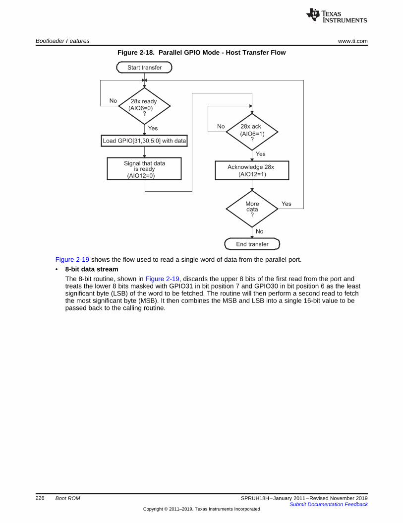
Start transfer
No
Moredata
?
28x ready(AIO6=0)
?
Yes
Load GPIO[31,30,5:0] with data
Signal that datais ready
(AIO12=0)
28x ack
(AIO6=1)?
No
Yes
Acknowledge 28x
(AIO12=1)
Yes
No
End transfer
Bootloader Features www.ti.com
226 SPRUH18H–January 2011–Revised November 2019Submit Documentation Feedback
Copyright © 2011–2019, Texas Instruments Incorporated
Boot ROM
Figure 2-18. Parallel GPIO Mode - Host Transfer Flow
Figure 2-19 shows the flow used to read a single word of data from the parallel port.• 8-bit data stream
The 8-bit routine, shown in Figure 2-19, discards the upper 8 bits of the first read from the port andtreats the lower 8 bits masked with GPIO31 in bit position 7 and GPIO30 in bit position 6 as the leastsignificant byte (LSB) of the word to be fetched. The routine will then perform a second read to fetchthe most significant byte (MSB). It then combines the MSB and LSB into a single 16-bit value to bepassed back to the calling routine.

(AIO6 = 0)
Signal host that 28x is ready
Parallel_GetWordData8 bit
(AIO12 = 0)?
Dataready
Yes
from GPIO[31,30,5:0]Read word of data
(AIO6 = 1)
28x ack read complete
(AIO12 = 1)
ackHost
No
?
A
ackHost
(AIO12 = 1)
28x ack read complete
(AIO6 = 1)
?
readyData
(AIO12 = 0)
Signal host that 28x
(AIO6 = 0)is ready to read MSB
?
A
Read GPIO[15:0]with GPIO[31:30] masked
into GPIO[7:6] for LSB of data,Discard GPIO[15:8],
repeat for MSB of data.
Return WordData
WordData = MSB:LSB
No No
No
Yes
Yes
Yes
www.ti.com Bootloader Features
227SPRUH18H–January 2011–Revised November 2019Submit Documentation Feedback
Copyright © 2011–2019, Texas Instruments Incorporated
Boot ROM
Figure 2-19. 8-Bit Parallel GetWord Function

SPISIMOA
SPISOMIA
SPICLKA
SPIESTEA
DIN
DOUT
CLK
CS
28x
Serial SPI
EEPROM
Bootloader Features www.ti.com
228 SPRUH18H–January 2011–Revised November 2019Submit Documentation Feedback
Copyright © 2011–2019, Texas Instruments Incorporated
Boot ROM
2.2.18 SPI_Boot FunctionThe SPI boot ROM loader initializes the SPI module to interface to a SPI-compatible, 16-bit or 24-bitaddressable serial EEPROM or flash device. It expects such a device to be present on the SPI-A pins asindicated in Figure 2-20. The SPI bootloader supports an 8-bit data stream. It does not support a 16-bitdata stream.
Figure 2-20. SPI Loader
The SPI-A loader uses following pins:• SPISIMOA on GPIO16• SPISOMIA on GPIO17• SPICLKA on GPIO18• SPISTEA on GPIO19
The SPI boot ROM loader initializes the SPI with the following settings: FIFO enabled, 8-bit character,internal SPICLK master mode and talk mode, clock phase = 1, polarity = 0, using the slowest baud rate.
If the download is to be performed from an SPI port on another device, then that device must be setup tooperate in the slave mode and mimic a serial SPI EEPROM. Immediately after entering the SPI_Bootfunction, the pin functions for the SPI pins are set to primary and the SPI is initialized. The initialization isdone at the slowest speed possible. Once the SPI is initialized and the key value read, you could specify achange in baud rate or low speed peripheral clock.
Table 2-12. SPI 8-Bit Data Stream
Byte Contents1 LSB: AA (KeyValue for memory width = 8-bits)2 MSB: 08h (KeyValue for memory width = 8-bits)3 LSB: LOSPCP4 MSB: SPIBRR5 LSB: reserved for future use6 MSB: reserved for future use......
...Data for this section....
17 LSB: reserved for future use18 MSB: reserved for future use19 LSB: Upper half (MSW) of Entry point PC[23:16]20 MSB: Upper half (MSW) of Entry point PC[31:24] (Note: Always 0x00)21 LSB: Lower half (LSW) of Entry point PC[7:0]22 MSB: Lower half (LSW) of Entry point PC[15:8]......
....Data for this section....
... Blocks of data in the format size/destination address/data as shown in the genericdata stream description
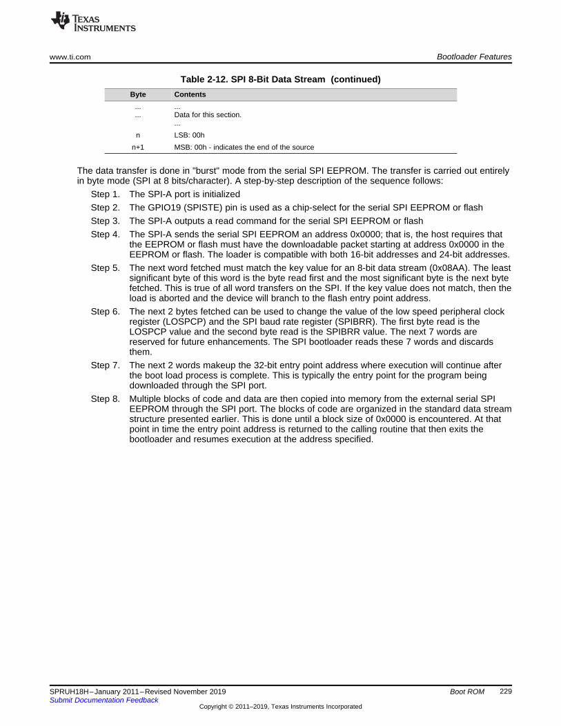
www.ti.com Bootloader Features
229SPRUH18H–January 2011–Revised November 2019Submit Documentation Feedback
Copyright © 2011–2019, Texas Instruments Incorporated
Boot ROM
Table 2-12. SPI 8-Bit Data Stream (continued)Byte Contents
...
......Data for this section....
n LSB: 00hn+1 MSB: 00h - indicates the end of the source
The data transfer is done in "burst" mode from the serial SPI EEPROM. The transfer is carried out entirelyin byte mode (SPI at 8 bits/character). A step-by-step description of the sequence follows:
Step 1. The SPI-A port is initializedStep 2. The GPIO19 (SPISTE) pin is used as a chip-select for the serial SPI EEPROM or flashStep 3. The SPI-A outputs a read command for the serial SPI EEPROM or flashStep 4. The SPI-A sends the serial SPI EEPROM an address 0x0000; that is, the host requires that
the EEPROM or flash must have the downloadable packet starting at address 0x0000 in theEEPROM or flash. The loader is compatible with both 16-bit addresses and 24-bit addresses.
Step 5. The next word fetched must match the key value for an 8-bit data stream (0x08AA). The leastsignificant byte of this word is the byte read first and the most significant byte is the next bytefetched. This is true of all word transfers on the SPI. If the key value does not match, then theload is aborted and the device will branch to the flash entry point address.
Step 6. The next 2 bytes fetched can be used to change the value of the low speed peripheral clockregister (LOSPCP) and the SPI baud rate register (SPIBRR). The first byte read is theLOSPCP value and the second byte read is the SPIBRR value. The next 7 words arereserved for future enhancements. The SPI bootloader reads these 7 words and discardsthem.
Step 7. The next 2 words makeup the 32-bit entry point address where execution will continue afterthe boot load process is complete. This is typically the entry point for the program beingdownloaded through the SPI port.
Step 8. Multiple blocks of code and data are then copied into memory from the external serial SPIEEPROM through the SPI port. The blocks of code are organized in the standard data streamstructure presented earlier. This is done until a block size of 0x0000 is encountered. At thatpoint in time the entry point address is returned to the calling routine that then exits thebootloader and resumes execution at the address specified.

SPIA_GetWordData
Yes
NoDataReceived
?
Send dummycharacter
Read LSB
DataReceived
?
No
Yes
Read MSB
Return MSB:LSB
Send dummycharacter
SPI_Boot
Yes
No
(0x08AA)?
ValidKeyValue
Enable the SPI-A clock
Set the LSPCLK to 4
Enable SPISIMOA,SPISOMI and SPICLKA
pin functionality and enable
Set up SPI-A for8-bit character,
Use internal SPI clock,master mode
Use slowest baud rate (0x7F)Relinquish SPI-A from reset
(GPIO19)Set chip enable high
Enable EEPROMSend read command and
start at EEPROM address0x0000
Read KeyValue
Jump to Flash
Read LOSPCP value Change LOSPCP
Change SPIBRRRead SPIBRR value
Read and discard 7reserved words
addressRead EntryPoint
Call CopyData EntryPointReturn
pullups on those pins
Bootloader Features www.ti.com
230 SPRUH18H–January 2011–Revised November 2019Submit Documentation Feedback
Copyright © 2011–2019, Texas Instruments Incorporated
Boot ROM
Figure 2-21. Data Transfer From EEPROM Flow
Figure 2-22. Overview of SPIA_GetWordData Function
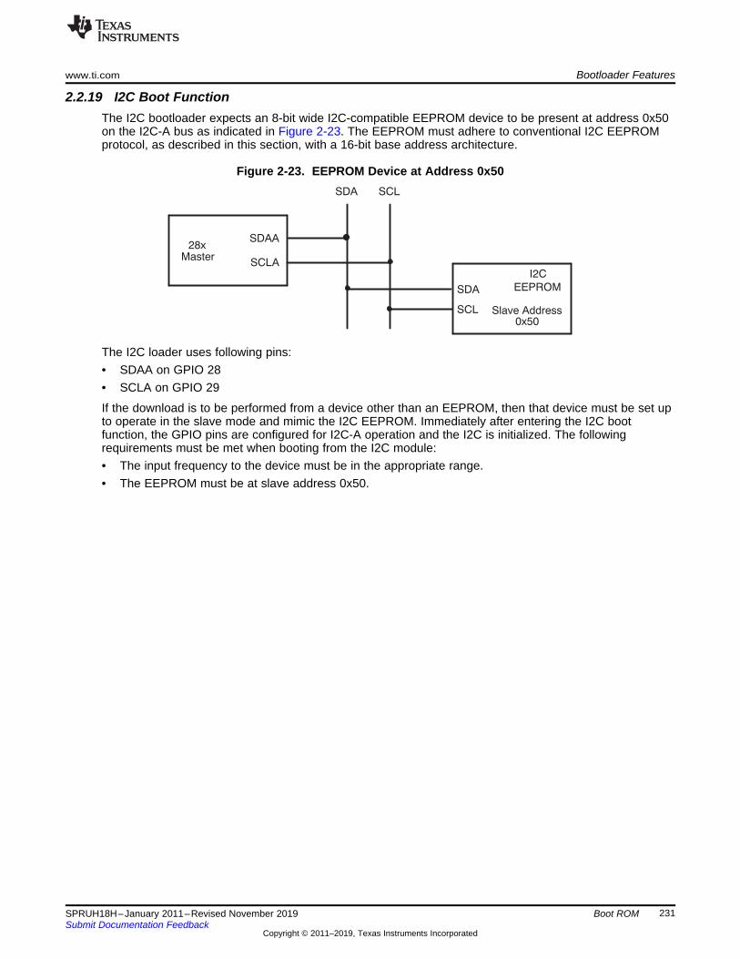
28x
Master
SDAA
SCLA
SDA SCL
SDA
SCL
I2C
EEPROM
Slave Address
0x50
www.ti.com Bootloader Features
231SPRUH18H–January 2011–Revised November 2019Submit Documentation Feedback
Copyright © 2011–2019, Texas Instruments Incorporated
Boot ROM
2.2.19 I2C Boot FunctionThe I2C bootloader expects an 8-bit wide I2C-compatible EEPROM device to be present at address 0x50on the I2C-A bus as indicated in Figure 2-23. The EEPROM must adhere to conventional I2C EEPROMprotocol, as described in this section, with a 16-bit base address architecture.
Figure 2-23. EEPROM Device at Address 0x50
The I2C loader uses following pins:• SDAA on GPIO 28• SCLA on GPIO 29
If the download is to be performed from a device other than an EEPROM, then that device must be set upto operate in the slave mode and mimic the I2C EEPROM. Immediately after entering the I2C bootfunction, the GPIO pins are configured for I2C-A operation and the I2C is initialized. The followingrequirements must be met when booting from the I2C module:• The input frequency to the device must be in the appropriate range.• The EEPROM must be at slave address 0x50.

I2C_Boot
Set CopyWord functionpointer to
I2C_CopyWord
Enable SDAA andSCLA pins
Enable pullups onSDAA and SCLA
Enable I2C-A clock
Set slave address 0x50I2C prescaler I2CPSC = or 0
100-kHz bit rate
Enable TX/RX FIFOs to
receive 2 bytes.
Place I2C in master
transmitter mode
Set EEPROM address
pointer to 0x0000
NACK
received
?
Yes
Read KeyValue
No
ValidKeyValue
(0x08AA)?
Jump to Flash
No
Read I2CPSC value
Read I2CCLKH value
Read 12CCLKL value
Put 12c-A in Reset
Set I2CPSC value
Set I2CCLKH value
Set I2CCLKL value
Bring I2C-A out of Reset
Read and discard 5reserved words
Yes
Read EntryPointaddress
Call CopyData
ReturnEntryPoint
Jump to Flash
Bootloader Features www.ti.com
232 SPRUH18H–January 2011–Revised November 2019Submit Documentation Feedback
Copyright © 2011–2019, Texas Instruments Incorporated
Boot ROM
Figure 2-24. Overview of I2C_Boot Function
The bit-period prescalers (I2CCLKH and I2CCLKL) are configured by the bootloader to run the I2C at a 50percent duty cycle at 100-kHz bit rate (standard I2C mode) when the system clock is 10 MHz. Theseregisters can be modified after receiving the first few bytes from the EEPROM. This allows thecommunication to be increased up to a 400-kHz bit rate (fast I2C mode) during the remaining data reads.
Arbitration, bus busy, and slave signals are not checked. Therefore, no other master is allowed to controlthe bus during this initialization phase. If the application requires another master during I2C boot mode,that master must be configured to hold off sending any I2C messages until the application softwaresignals that it is past the bootloader portion of initialization.
The non-acknowledgment bit is checked only during the first message sent to initialize the EEPROM baseaddress. This is to make sure that an EEPROM is present at address 0x50 before continuing. If anEEPROM is not present, code will The non-acknowledgment bit is not checked during the address phaseof the data read messages (I2C_Get Word). If a non acknowledgment is received during the data readmessages, the I2C bus will hang. Table 3-2 shows the 8-bit data stream used by the I2C.

�SDA LINE
���
STA
RT
� � � � �
RE
AD
AC
K
AC
K
NO
AC
K
ST
OP
Device
Address
DATA BYTE n DATA BYTE n+1
�SDA LINE
STA
RT
MS
B
LS
B
� � �� � ��� � � � � � � � �
WR
ITE
AC
K
� � � � � � � �� ��� � �
AC
K
�
RE
STA
RT
MS
B
� � �
LS
B
� �
RE
AD
AC
K
AC
K
NO
AC
K
ST
OP
Device
Address
Address
Pointer, MSB
Address
Pointer, LSB
AC
K
Device
Address
DATA BYTE 1 DATA BYTE 2
www.ti.com Bootloader Features
233SPRUH18H–January 2011–Revised November 2019Submit Documentation Feedback
Copyright © 2011–2019, Texas Instruments Incorporated
Boot ROM
Table 2-13. I2C 8-Bit Data Stream
Byte Contents1 LSB: AA (KeyValue for memory width = 8 bits)2 MSB: 08h (KeyValue for memory width = 8 bits)3 LSB: I2CPSC[7:0]4 reserved5 LSB: I2CCLKH[7:0]6 MSB: I2CCLKH[15:8]7 LSB: I2CCLKL[7:0]8 MSB: I2CCLKL[15:8]......
...Data for this section....
17 LSB: Reserved for future use18 MSB: Reserved for future use19 LSB: Upper half of entry point PC20 MSB: Upper half of entry point PC[22:16] (Note: Always 0x00)21 LSB: Lower half of entry point PC[15:8]22 MSB: Lower half of entry point PC[7:0]......
...Data for this section....Blocks of data in the format size/destination address/data as shown in the generic data streamdescription.
...
......Data for this section....
LSB: 00hn+1 MSB: 00h - indicates the end of the source
The I2C EEPROM protocol required by the I2C bootloader is shown in Figure 2-25 and Figure 2-26. Thefirst communication, which sets the EEPROM address pointer to 0x0000 and reads the KeyValue(0x08AA) from it, is shown in Figure 2-25. All subsequent reads are shown in Figure 2-26 and are readtwo bytes at a time.
Figure 2-25. Random Read
Figure 2-26. Sequential Read

28x
28x
CAN
hostC
AN
bus
Bootloader Features www.ti.com
234 SPRUH18H–January 2011–Revised November 2019Submit Documentation Feedback
Copyright © 2011–2019, Texas Instruments Incorporated
Boot ROM
2.2.20 eCAN Boot FunctionThe eCAN bootloader asynchronously transfers code from eCAN-A to internal memory. The host can beany CAN node. The communication is first done with 11-bit standard identifiers (with a MSGID of 0x1)using two bytes per data frame. The host can download a kernel to reconfigure the eCAN if higher datathroughput is desired.
The eCAN-A loader uses following pins:• CANRXA on GPIO30• CANTXA on GPIO31
Figure 2-27. Overview of eCAN-A bootloader Operation
The bit-timing registers are programmed in such a way that a valid bit-rate is achieved for a 10 MHzinternal oscillator frequency as shown in Table 2-14.
Table 2-14. Bit-Rate Value for Internal Oscillators
OSCCLK SYSCLKOUT Bit Rate10 MHz 10 MHz 100 kbps
The SYSCLKOUT values shown are the reset values with the default PLL setting. The BRPreg and bit-timevalues are hard-coded to 1 and 25, respectively.
Mailbox 1 is programmed with a standard MSGID of 0x1 for boot-loader communication. The CAN hostshould transmit only 2 bytes at a time, LSB first and MSB next. For example, to transmit the word 0x08AAto the device, transmit AA first, followed by 08. The program flow of the CAN bootloader is identical to theSCI bootloader. The data sequence for the CAN bootloader is shown in Table 2-15:

www.ti.com Bootloader Features
235SPRUH18H–January 2011–Revised November 2019Submit Documentation Feedback
Copyright © 2011–2019, Texas Instruments Incorporated
Boot ROM
Table 2-15. eCAN 8-Bit Data Stream
Bytes Byte 1 of 2 Byte 2 of 2 Description1 2 AA 08 0x08AA (KeyValue for memory width = 16bits)3 4 00 00 reserved5 6 00 00 reserved7 8 00 00 reserved9 10 00 00 reserved11 12 00 00 reserved13 14 00 00 reserved15 16 00 00 reserved17 18 00 00 reserved19 20 BB 00 Entry point PC[22:16]21 22 DD CC Entry point PC[15:0] (PC = 0xAABBCCDD)23 24 NN MM Block size of the first block of data to load = 0xMMNN words25 26 BB AA Destination address of first block Addr[31:16]27 28 DD CC Destination address of first block Addr[15:0] (Addr = 0xAABBCCDD)29 30 BB AA First word of the first block in the source being loaded = 0xAABB......
....Data for this section....
. BB AA Last word of the first block of the source being loaded = 0xAABB
. NN MM Block size of the 2nd block to load = 0xMMNN words
. BB AA Destination address of second block Addr[31:16]
. DD CC Destination address of second block Addr[15:0]
. BB AA First word of the second block in the source being loaded
. …n n+1 BB AA Last word of the last block of the source being loaded
(More sections if required)n+2 n+3 00 00 Block size of 0000h - indicates end of the source program

Reset
InitBoot
Yes
No
CallBootLoader
?
Call ExitBoot
Cleanup CPUregisters to defaultvalue after reset*
CallSelectBootMode
Call Boot Loader
Deallocate stack(SP=0x400)
Branch to EntryPoint
Begin executionat EntryPoint
Bootloader Features www.ti.com
236 SPRUH18H–January 2011–Revised November 2019Submit Documentation Feedback
Copyright © 2011–2019, Texas Instruments Incorporated
Boot ROM
2.2.21 ExitBoot Assembly RoutineThe Boot ROM includes an ExitBoot routine that restores the CPU registers to their default state at reset.This is performed on all registers with one exception. The OBJMODE bit in ST1 is left set so that thedevice remains configured for C28x operation. This flow is detailed in the following diagram:
Figure 2-28. ExitBoot Procedure Flow
The following CPU registers are restored to their default values:• ACC = 0x0000 0000• RPC = 0x0000 0000• P = 0x0000 0000• XT = 0x0000 0000• ST0 = 0x0000• ST1 = 0x0A0B• XAR0 = XAR7 = 0x0000 0000
After the ExitBoot routine completes and the program flow is redirected to the entry point address, theCPU registers will have the following values:

www.ti.com Building the Boot Table
237SPRUH18H–January 2011–Revised November 2019Submit Documentation Feedback
Copyright © 2011–2019, Texas Instruments Incorporated
Boot ROM
Table 2-16. CPU Register Restored Values
Register Value Register ValueACC 0x0000 0000 P 0x0000 0000XT 0x0000 0000 RPC 0x00 0000XAR0-XAR7 0x0000 0000 DP 0x0000ST0 0x0000 15:10 OVC = 0 ST1 0x0A0B 15:13 ARP = 0
9:7 PM = 0 12 XF = 06 V = 0 11 M0M1MAP = 15 N = 0 10 reserved4 Z = 0 9 OBJMODE = 13 C = 0 8 AMODE = 02 TC = 0 7 IDLESTAT = 01 OVM = 0 6 EALLOW = 00 SXM = 0 5 LOOP = 0
4 SPA = 03 VMAP = 12 PAGE0 = 01 DBGM = 10 INTM = 1
2.3 Building the Boot TableThis chapter explains how to generate the data stream and boot table required for the bootloader.
2.3.1 The C2000 Hex UtilityTo use the features of the bootloader, you must generate a data stream and boot table as described inSection 2.2.11. The hex conversion utility tool, included with the 28x code generation tools, can generatethe required data stream including the required boot table. This section describes the hex2000 utility. Anexample of a file conversion performed by hex2000 is described in Section 2.3.2.
The hex utility supports creation of the boot table required for the SCI, SPI, I2C, eCAN, and parallel I/Oloaders. That is, the hex utility adds the required information to the file such as the key value, reservedbits, entry point, address, block start address, block length and terminating value. The contents of the boottable vary slightly depending on the boot mode and the options selected when running the hex conversionutility. The actual file format required by the host (ASCII, binary, hex, etc.) will differ from one specificapplication to another and some additional conversion may be required.
To build the boot table, follow these steps:1. Assemble or compile the code.
This creates the object files that will then be used by the linker to create a single output file.2. Link the file.
The linker combines all of the object files into a single output file in common object file format (COFF).The specified linker command file is used by the linker to allocate the code sections to differentmemory blocks. Each block of the boot table data corresponds to an initialized section in the COFF file.Uninitialized sections are not converted by the hex conversion utility. The following options may beuseful:The linker -m option can be used to generate a map file. This map file will show all of the sections thatwere created, their location in memory and their length. It can be useful to check this file to make surethat the initialized sections are where you expect them to be.The linker -w option is also very useful. This option indicates if the linker has assigned a section to amemory region on its own. For example, if you have a section in your code called ramfuncs.
3. Run the hex conversion utility.Choose the appropriate options for the desired boot mode and run the hex conversion utility to convert

Building the Boot Table www.ti.com
238 SPRUH18H–January 2011–Revised November 2019Submit Documentation Feedback
Copyright © 2011–2019, Texas Instruments Incorporated
Boot ROM
the COFF file produced by the linker to a boot table.
See the TMS320C28x Assembly Language Tools User's Guide (SPRU513) and the TMS320C28xOptimizing C/C++ Compiler User's Guide (SPRU514) for more information on the compiling and linkingprocess.
Table 2-17 summarizes the hex conversion utility options available for the bootloader. See theTMS320C28x Assembly Language Tools User's Guide (SPRU513) for a detailed description of thehex2000 operations used to generate a boot table. Updates will be made to support the I2C boot. See theCodegen release notes for the latest information.
Table 2-17. Boot Loader Options
Option Description-boot Convert all sections into bootable form (use instead of a SECTIONS directive)-sci8 Specify the source of the bootloader table as the SCI-A port, 8-bit mode-spi8 Specify the source of the bootloader table as the SPI-A port, 8-bit mode-gpio8 Specify the source of the bootloader table as the GPIO port, 8-bit mode-gpio16 Specify the source of the bootloader table as the GPIO port, 16-bit mode-bootorg value Specify the source address of the bootloader table-lospcp value Specify the initial value for the LOSPCP register. This value is used only for the spi8 boot table format
and ignored for all other formats. If the value is greater than 0x7F, the value is truncated to 0x7F.-spibrr value Specify the initial value for the SPIBRR register. This value is used only for the spi8 boot table format and
ignored for all other formats. If the value is greater than 0x7F, the value is truncated to 0x7F.-e value Specify the entry point at which to begin execution after boot loading. The value can be an address or a
global symbol. This value is optional. The entry point can be defined at compile time using the linker -eoption to assign the entry point to a global symbol. The entry point for a C program is normally _c_int00unless defined otherwise by the -e linker option.
-i2c8 Specify the source of the bootloader table as the I2C-A port, 8-bit-i2cpsc value Specify the value for the I2CPSC register. This value will be loaded and take effect after all I2C options
are loaded, prior to reading data from the EEPROM. This value will be truncated to the least significanteight bits and should be set to maintain an I2C module clock of 7-12 MHz.
-i2cclkh value Specify the value for the I2CCLKH register. This value will be loaded and take effect after all I2C optionsare loaded, prior to reading data from the EEPROM.
-i2cclkl value Specify the value for the I2CCLKL register. This value will be loaded and take effect after all I2C optionsare loaded, prior to reading data from the EEPROM.
2.3.2 Example: Preparing a COFF File For eCAN BootloadingThis section shows how to convert a COFF file into a format suitable for CAN based bootloading. Thisexample assumes that the host sending the data stream is capable of reading an ASCII hex format file. Anexample COFF file named GPIO34TOG.out has been used for the conversion.
Build the project and link using the -m linker option to generate a map file. Examine the .map file producedby the linker. The information shown in Example 2-8 has been copied from the example map file(GPIO34TOG.map). This shows the section allocation map for the code. The map file includes thefollowing information:
• Output SectionThis is the name of the output section specified with the SECTIONS directive in the linker commandfile.
• OriginThe first origin listed for each output section is the starting address of that entire output section. Thefollowing origin values are the starting address of that portion of the output section.
• LengthThe first length listed for each output section is the length for that entire output section. The followinglength values are the lengths associated with that portion of the output section.
• Attributes/input sections

www.ti.com Building the Boot Table
239SPRUH18H–January 2011–Revised November 2019Submit Documentation Feedback
Copyright © 2011–2019, Texas Instruments Incorporated
Boot ROM
This lists the input files that are part of the section or any value associated with an output section.
See the TMS320C28x Assembly Language Tools User's Guide (SPRU513) for detailed information ongenerating a linker command file and a memory map.
All sections shown in Example 2-8 that are initialized need to be loaded into the DSP in order for the codeto execute properly. In this case, the codestart, ramfuncs, .cinit, myreset and .text sections need to beloaded. The other sections are uninitialized and will not be included in the loading process. The map filealso indicates the size of each section and the starting address. For example, the .text section has 0x155words and starts at 0x3FA000.
Example 2-8. GPIO34TOG Map File
output attributes/section page origin length input sections-------- ---- ---------- ---------- ----------------codestart
0 00000000 0000000200000000 00000002 DSP280x_CodeStartBranch.obj (codestart)
.pinit 0 00000002 00000000
.switch 0 00000002 00000000 UNINITIALIZED
ramfuncs 0 00000002 0000001600000002 00000016 DSP280x_SysCtrl.obj (ramfuncs)
.cinit 0 00000018 0000001900000018 0000000e rts2800_ml.lib : exit.obj (.cinit)00000026 0000000a : _lock.obj (.cinit)00000030 00000001 --HOLE-- [fill = 0]
myreset 0 00000032 0000000200000032 00000002 DSP280x_CodeStartBranch.obj (myreset)
IQmath 0 003fa000 00000000 UNINITIALIZED
.text 0 003fa000 00000155003fa000 00000046 rts2800_ml.lib : boot.obj (.text)
To load the code using the CAN bootloader, the host must send the data in the format that the bootloaderunderstands. That is, the data must be sent as blocks of data with a size, starting address followed by thedata. A block size of 0 indicates the end of the data. The HEX2000.exe utility can be used to convert theCOFF file into a format that includes this boot information. The following command syntax has been usedto convert the application into an ASCII hex format file that includes all of the required information for thebootloader:
Example 2-9. HEX2000.exe Command Syntax
C: HEX2000 GPIO34TOG.OUT -boot -gpio8 -a
Where:- boot Convert all sections into bootable form.- gpio8 Use the GPIO in 8-bit mode data format. The eCAN
uses the same data format as the GPIO in 8-bit mode.- a Select ASCII-Hex as the output format.

Building the Boot Table www.ti.com
240 SPRUH18H–January 2011–Revised November 2019Submit Documentation Feedback
Copyright © 2011–2019, Texas Instruments Incorporated
Boot ROM
The command line shown in Example 2-9 will generate an ASCII-Hex output file called GPIO34TOG.a00,whose contents are explained in Example 2-10. This example assumes that the host will be able to readan ASCII hex format file. The format may differ for your application. . Each section of data loaded can betied back to the map file described in Example 2-8. After the data stream is loaded, the boot ROM willjump to the Entrypoint address that was read as part of the data stream. In this case, execution will beginat 0x3FA0000.

www.ti.com Building the Boot Table
241SPRUH18H–January 2011–Revised November 2019Submit Documentation Feedback
Copyright © 2011–2019, Texas Instruments Incorporated
Boot ROM
Example 2-10. GPIO34TOG Data Stream
AA 08 ;Keyvalue00 00 00 00 00 00 00 00 ;8 reserved words00 00 00 00 00 00 00 003F 00 00 A0 ;Entrypoint 0x003FA00002 00 ;Load 2 words - codestart section00 00 00 00 ;Load block starting at 0x0000007F 00 9A A0 ;Data block 0x007F, 0xA09A16 00 ;Load 0x0016 words - ramfuncs section00 00 02 00 ;Load block starting at 0x00000222 76 1F 76 2A 00 00 1A 01 00 06 CC F0 ;Data = 0x7522, 0x761F etc...FF 05 50 06 96 06 CC FF F0 A9 1A 00 0506 96 04 1A FF 00 05 1A FF 00 1A 76 07F6 00 77 06 0055 01 ;Load 0x0155 words - .text section3F 00 00 A0 ;Load block starting at 0x003FA000AD 28 00 04 69 FF 1F 56 16 56 1A 56 40 ;Data = 0x28AD, 0x4000 etc...29 1F 76 00 00 02 29 1B 76 22 76 A9 2818 00 A8 28 00 00 01 09 1D 61 C0 76 1800 04 29 0F 6F 00 9B A9 24 01 DF 04 6C04 29 A8 24 01 DF A6 1E A1 F7 86 24 A706 .. .... .. .... .. ..FC 63 E6 6F19 00 ;Load 0x0019 words - .cinit section00 00 18 00 ;Load block starting at 0x000018FF FF 00 B0 3F 00 00 00 FE FF 02 B0 3F ;Data = 0xFFFF, 0xB000 etc...00 00 00 00 00 FE FF 04 B0 3F 00 00 0000 00 FE FF .. .. .... .. ..3F 00 00 0002 00 ;Load 0x0002 words - myreset section00 00 32 00 ;Load block starting at 0x00003200 00 00 00 ;Data = 0x0000, 0x000000 00 ;Block size of 0 - end of data

Bootloader Code Overview www.ti.com
242 SPRUH18H–January 2011–Revised November 2019Submit Documentation Feedback
Copyright © 2011–2019, Texas Instruments Incorporated
Boot ROM
2.4 Bootloader Code OverviewThis chapter contains information on the Boot ROM version, checksum, and code.
2.4.1 Boot ROM Version and Checksum InformationThe boot ROM contains its own version number located at address 0x3F FFBA. This version numberstarts at 1 and will be incremented any time the boot ROM code is modified. The next address, 0x3FFFBB contains the month and year (MM/YY in decimal) that the boot code was released. The next fourmemory locations contain a checksum value for the boot ROM. Taking a 64-bit summation of alladdresses within the ROM, except for the checksum locations, generates this checksum.
Table 2-18. Bootloader Revision and Checksum Information
Address Contents0x3F FFB90x3F FFBA Boot ROM Version Number0x3F FFBB MM/YY of release (in decimal)0x3F FFBC Least significant word of checksum0x3F FFBD . . .0x3F FFBE . . .0x3F FFBF Most significant word of checksum

243SPRUH18H–January 2011–Revised November 2019Submit Documentation Feedback
Copyright © 2011–2019, Texas Instruments Incorporated
Enhanced Pulse Width Modulator (ePWM) Module
Chapter 3SPRUH18H–January 2011–Revised November 2019
Enhanced Pulse Width Modulator (ePWM) Module
The enhanced pulse width modulator (ePWM) peripheral is a key element in controlling many of the powerelectronic systems found in both commercial and industrial equipments. These systems include digitalmotor control, switch mode power supply control, uninterruptible power supplies (UPS), and other forms ofpower conversion. The ePWM peripheral performs a digital to analog (DAC) function, where the duty cycleis equivalent to a DAC analog value; it is sometimes referred to as a Power DAC.
This chapter guide is applicable for ePWM type 1. See the TMS320x28xx, 28xxx DSP PeripheralReference Guide (SPRU566) for a list of all devices with an ePWM module of the same type, to determinethe differences between the types, and for a list of device-specific differences within a type.
This chapter includes an overview of the module and information about each of its sub-modules:• Time-Base Module• Counter Compare Module• Action Qualifier Module• Dead-Band Generator Module• PWM Chopper (PC) Module• Trip Zone Module• Event Trigger Module
ePWM Type 1 is fully compatible to the Type 0 module. Type 1 has the following enhancements inaddition to the Type 0 features:• Increased Dead-Band Resolution
The dead-band clocking has been enhanced to allow half-cycle clocking to double resolution.• Enhanced interrupt and SOC generation
Interrupts and ADC start-of-conversion can now be generated on both the TBCTR == zero and TBCTR== period events. This feature enables dual edge PWM control. Additionally, the ADC start-of-conversion can be generated from an event defined in the digital compare sub-module.
• High Resolution Period CapabilityProvides the ability to enable high-resolution period. This is discussed in more detail in the device-specific HRPWM Reference Guide.
• Digital Compare Sub-moduleThe digital compare sub-module enhances the event triggering and trip zone sub-modules by providingfiltering, blanking and improved trip functionality to digital compare signals. Such features are essentialfor peak current mode control and for support of analog comparators.
Topic ........................................................................................................................... Page
3.1 Introduction ..................................................................................................... 2443.2 ePWM Submodules........................................................................................... 2503.3 Applications to Power Topologies ...................................................................... 3073.4 Registers ......................................................................................................... 334

Introduction www.ti.com
244 SPRUH18H–January 2011–Revised November 2019Submit Documentation Feedback
Copyright © 2011–2019, Texas Instruments Incorporated
Enhanced Pulse Width Modulator (ePWM) Module
3.1 IntroductionAn effective PWM peripheral must be able to generate complex pulse width waveforms with minimal CPUoverhead or intervention. It needs to be highly programmable and very flexible while being easy tounderstand and use. The ePWM unit described here addresses these requirements by allocating allneeded timing and control resources on a per PWM channel basis. Cross coupling or sharing of resourceshas been avoided; instead, the ePWM is built up from smaller single channel modules with separateresources that can operate together as required to form a system. This modular approach results in anorthogonal architecture and provides a more transparent view of the peripheral structure, helping users tounderstand its operation quickly.
In this document the letter x within a signal or module name is used to indicate a generic ePWM instanceon a device. For example output signals EPWMxA and EPWMxB refer to the output signals from theePWMx instance. Thus, EPWM1A and EPWM1B belong to ePWM1 and likewise EPWM4A and EPWM4Bbelong to ePWM4.
3.1.1 Submodule OverviewThe ePWM module represents one complete PWM channel composed of two PWM outputs: EPWMxAand EPWMxB. Multiple ePWM modules are instanced within a device as shown in Figure 3-1. EachePWM instance is identical with one exception. Some instances include a hardware extension that allowsmore precise control of the PWM outputs. This extension is the high-resolution pulse width modulator(HRPWM) and is described in the device-specific High-Resolution Pulse Width Modulator (HRPWM)section. See the device-specific data manual to determine which ePWM instances include this feature.Each ePWM module is indicated by a numerical value starting with 1. For example ePWM1 is the firstinstance and ePWM3 is the third instance in the system and ePWMx indicates any instance.
The ePWM modules are chained together via a clock synchronization scheme that allows them to operateas a single system when required. Additionally, this synchronization scheme can be extended to thecapture peripheral modules (eCAP). The number of modules is device-dependent and based on targetapplication needs. Modules can also operate stand-alone.
Each ePWM module supports the following features:• Dedicated 16-bit time-base counter with period and frequency control• Two PWM outputs (EPWMxA and EPWMxB) that can be used in the following configurations:
– Two independent PWM outputs with single-edge operation– Two independent PWM outputs with dual-edge symmetric operation– One independent PWM output with dual-edge asymmetric operation
• Asynchronous override control of PWM signals through software.• Programmable phase-control support for lag or lead operation relative to other ePWM modules.• Hardware-locked (synchronized) phase relationship on a cycle-by-cycle basis.• Dead-band generation with independent rising and falling edge delay control.• Programmable trip zone allocation of both cycle-by-cycle trip and one-shot trip on fault conditions.• A trip condition can force either high, low, or high-impedance state logic levels at PWM outputs.• Comparator module outputs and trip zone inputs can generate events, filtered events, or trip
conditions.• All events can trigger both CPU interrupts and ADC start of conversion (SOC)• Programmable event prescaling minimizes CPU overhead on interrupts.• PWM chopping by high-frequency carrier signal, useful for pulse transformer gate drives.
Each ePWM module is connected to the input/output signals shown in Figure 3-1. The signals aredescribed in detail in subsequent sections.

EPWM1TZINT
PIE
EPWM1INT
EPWM2TZINT
EPWM2INT
EPWMxTZINT
EPWMxINT
COMPOUT1COMPOUT2
COMP
SOCA1ADC
SOCB1
SOCA2
SOCB2
SOCAx
SOCBx
EPWM1SYNCI
EPWM2SYNCI
EPWM1SYNCO
EPWM2SYNCO
EPWM1Module
EPWM2Module
EPWMxSYNCI
EPWMxModule
TZ6
TZ6
TZ1 TZ3to
TZ5CLOCKFAIL
TZ4EQEP1ERR
(A)
EMUSTOP
TZ5CLOCKFAIL
TZ4EQEP1ERR
(A)
EMUSTOP
EPWM1ENCLK
TBCLKSYNC
EPWM2ENCLK
TBCLKSYNC
TZ5
TZ6EPWMxENCLK
TBCLKSYNC
CLOCKFAILTZ4
EQEP1ERR(A)
EMUSTOP
EPWM1B
C28x CPU
System Control
eQEP1
TZ1 TZ3to
TZ1 TZ3to
EPWM1SYNCO
EPWM2B
eCAPI
EPWMxB
EQEP1ERR
HRPWM
EPWMxA
EPWM2A
EPWM1A
GPIO
MUX
ADCSOCBO
ADCSOCAO
Peri
ph
era
l B
us
Pulse Stretch(32 SYSCLKOUT Cycles, Active-Low Output)
SOCA1SOCA2SPCAx
Pulse Stretch(32 SYSCLKOUT Cycles, Active-Low Output)
SOCB1SOCB2SPCBx
EPWMSYNCI
www.ti.com Introduction
245SPRUH18H–January 2011–Revised November 2019Submit Documentation Feedback
Copyright © 2011–2019, Texas Instruments Incorporated
Enhanced Pulse Width Modulator (ePWM) Module
Figure 3-1. Multiple ePWM Modules
A This signal exists only on devices with an eQEP1 module.
The order in which the ePWM modules are connected may differ from what is shown in Figure 3-1. SeeSection 3.2.2.3.3 for the synchronization scheme for a particular device. Each ePWM module consists ofeight submodules and is connected within a system via the signals shown in Figure 3-2.

EPWMxINT
EPWMxTZINT
EPWMxSOCA
EPWMxSOCB
EPWMxSYNCI
EPWMxSYNCOTime-base (TB) module
Counter-compare (CC) module
Action-qualifier (AQ) module
Dead-band (DB) module
PWM-chopper (PC) module
Event-trigger (ET) module
Trip-zone (TZ) modulePeripheral bus
ePWM module
TZ1 TZ3to
EPWMxA
EPWMxB
PIE
ADC
GPIOMUX
COMPxOUTCOMP
Digital Compare (DC) module
EQEP1ERR
CLOCKFAIL
EMUSTOP
Introduction www.ti.com
246 SPRUH18H–January 2011–Revised November 2019Submit Documentation Feedback
Copyright © 2011–2019, Texas Instruments Incorporated
Enhanced Pulse Width Modulator (ePWM) Module
Figure 3-2. Submodules and Signal Connections for an ePWM Module
Figure 3-3 shows more internal details of a single ePWM module. The main signals used by the ePWMmodule are:• PWM output signals (EPWMxA and EPWMxB).
The PWM output signals are made available external to the device through the GPIO peripheraldescribed in the system control and interrupts guide for your device.
• Trip-zone signals (TZ1 to TZ6).These input signals alert the ePWM module of fault conditions external to the ePWM module. Eachmodule on a device can be configured to either use or ignore any of the trip-zone signals. The TZ1 toTZ3 trip-zone signals can be configured as asynchronous inputs through the GPIO peripheral. TZ4 isconnected to an inverted EQEP1 error signal (EQEP1ERR) from the EQEP1 module (for those deviceswith an EQEP1 module). TZ5 is connected to the system clock fail logic, and TZ6 is connected to theEMUSTOP output from the CPU. This allows you to configure a trip action when the clock fails or theCPU halts.
• Time-base synchronization input (EPWMxSYNCI) and output (EPWMxSYNCO) signals.The synchronization signals daisy chain the ePWM modules together. Each module can be configuredto either use or ignore its synchronization input. The clock synchronization input and output signal arebrought out to pins only for ePWM1 (ePWM module #1). The synchronization output for ePWM1(EPWM1SYNCO) is also connected to the SYNCI of the first enhanced capture module (eCAP1).
• ADC start-of-conversion signals (EPWMxSOCA and EPWMxSOCB).Each ePWM module has two ADC start of conversion signals . Any ePWM module can trigger a startof conversion. Whichever event triggers the start of conversion is configured in the Event-Triggersubmodule of the ePWM.
• Comparator output signals (COMPxOUT).Output signals from the comparator module in conjunction with the trip zone signals can generatedigital compare events.
• Peripheral BusThe peripheral bus is 32-bits wide and allows both 16-bit and 32-bit writes to the ePWM register file.
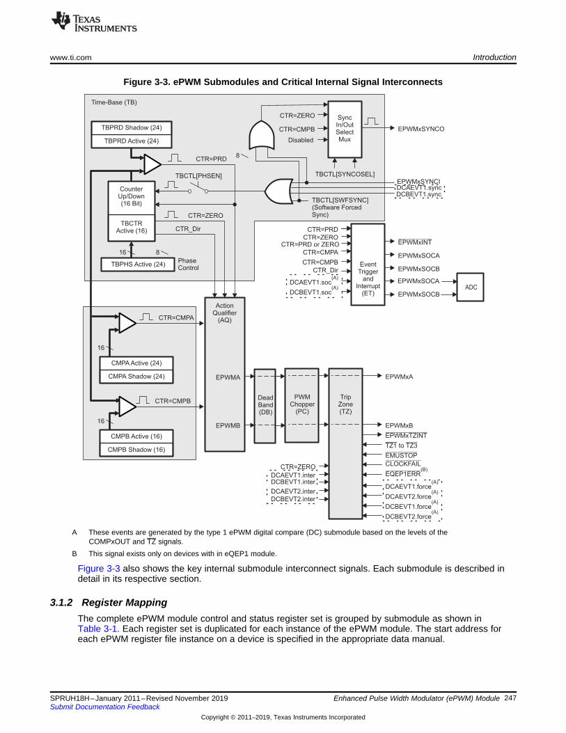
TBPRD Shadow (24)
TBPRD Active (24)
CounterUp/Down(16 Bit)
TBCTRActive (16)
TBCTL[PHSEN]
CTR=PRD
16
PhaseControl
8
CTR=ZERO
CTR_Dir
8
CTR=ZERO
CTR=CMPB
Disabled
TBCTL[SYNCOSEL]
EPWMxSYNCO
Time-Base (TB)
TBPHS Active (24)
SyncIn/OutSelectMux
CTR=PRD
CTR=ZERO
CTR=CMPA
CTR=CMPB
CTR_Dir
DCAEVT1.soc(A)
DCBEVT1.soc(A)
EventTrigger
andInterrupt
(ET)
EPWMxINT
EPWMxSOCA
EPWMxSOCB
EPWMxSOCA
EPWMxSOCBADC
ActionQualifier
(AQ)
EPWMA
DeadBand(DB)
EPWMB
PWMChopper
(PC)
TripZone(TZ)
EPWMxA
EPWMxB
CTR=ZERO
EPWMxTZINT
TZ1 TZ3to
EMUSTOP
CLOCKFAIL
EQEP1ERR(B)
DCAEVT1.force(A)
DCAEVT2.force(A)
DCBEVT1.force(A)
DCBEVT2.force(A)
CTR=CMPA
16
CTR=CMPB
16
CMPB Active (16)
CMPB Shadow (16)
CTR=PRD or ZERO
DCAEVT1.interDCBEVT1.inter
DCAEVT2.inter
DCBEVT2.inter
EPWMxSYNCI
TBCTL[SWFSYNC](Software ForcedSync)
DCAEVT1.syncDCBEVT1.sync
CMPA Active (24)
CMPA Shadow (24)
www.ti.com Introduction
247SPRUH18H–January 2011–Revised November 2019Submit Documentation Feedback
Copyright © 2011–2019, Texas Instruments Incorporated
Enhanced Pulse Width Modulator (ePWM) Module
Figure 3-3. ePWM Submodules and Critical Internal Signal Interconnects
A These events are generated by the type 1 ePWM digital compare (DC) submodule based on the levels of theCOMPxOUT and TZ signals.
B This signal exists only on devices with in eQEP1 module.
Figure 3-3 also shows the key internal submodule interconnect signals. Each submodule is described indetail in its respective section.
3.1.2 Register MappingThe complete ePWM module control and status register set is grouped by submodule as shown inTable 3-1. Each register set is duplicated for each instance of the ePWM module. The start address foreach ePWM register file instance on a device is specified in the appropriate data manual.

Introduction www.ti.com
248 SPRUH18H–January 2011–Revised November 2019Submit Documentation Feedback
Copyright © 2011–2019, Texas Instruments Incorporated
Enhanced Pulse Width Modulator (ePWM) Module
(1) Locations not shown are reserved.(2) These registers are only available on ePWM instances that include the high-resolution PWM extension. Otherwise these locations are
reserved. These registers are described in the High-Resolution Pulse Width Modulator (HRPWM) section of this manual. See the devicespecific data manual to determine which instances include the HRPWM.
(3) EALLOW protected registers as described in the specific device version of the System Control and Interrupts section.(4) These registers only exist in the ePWM1 register space. They cannot be accessed from any other ePWM module's register space.
Table 3-1. ePWM Module Control and Status Register Set Grouped by Submodule
Name Offset (1)Size(x16) Shadow EALLOW Description
Time-Base Submodule RegistersTBCTL 0x0000 1 Time-Base Control RegisterTBSTS 0x0001 1 Time-Base Status RegisterTBPHSHR 0x0002 1 Extension for HRPWM Phase Register (2)
TBPHS 0x0003 1 Time-Base Phase RegisterTBCTR 0x0004 1 Time-Base Counter RegisterTBPRD 0x0005 1 Yes Time-Base Period RegisterTBPRDHR 0x0006 1 Yes Time Base Period High Resolution Register (3)
Counter-Compare Submodule RegistersCMPCTL 0x0007 1 Counter-Compare Control RegisterCMPAHR 0x0008 1 Yes Extension for HRPWM Counter-Compare A Register (2)
CMPA 0x0009 1 Yes Counter-Compare A RegisterCMPB 0x000A 1 Yes Counter-Compare B Register
Action-Qualifier Submodule RegistersAQCTLA 0x000B 1 Action-Qualifier Control Register for Output A (EPWMxA)AQCTLB 0x000C 1 Action-Qualifier Control Register for Output B (EPWMxB)AQSFRC 0x000D 1 Action-Qualifier Software Force RegisterAQCSFRC 0x000E 1 Yes Action-Qualifier Continuous S/W Force Register Set
Dead-Band Generator Submodule RegistersDBCTL 0x000F 1 Dead-Band Generator Control RegisterDBRED 0x0010 1 Dead-Band Generator Rising Edge Delay Count RegisterDBFED 0x0011 1 Dead-Band Generator Falling Edge Delay Count Register
Trip-Zone Submodule RegistersTZSEL 0x0012 1 Yes Trip-Zone Select RegisterTZDCSEL 0x0013 1 Yes Trip Zone Digital Compare Select RegisterTZCTL 0x0014 1 Yes Trip-Zone Control Register (3)
TZEINT 0x0015 1 Yes Trip-Zone Enable Interrupt Register (3)
TZFLG 0x0016 1 Trip-Zone Flag Register (3)
TZCLR 0x0017 1 Yes Trip-Zone Clear Register (3)
TZFRC 0x0018 1 Yes Trip-Zone Force Register (3)
Event-Trigger Submodule RegistersETSEL 0x0019 1 Event-Trigger Selection RegisterETPS 0x001A 1 Event-Trigger Pre-Scale RegisterETFLG 0x001B 1 Event-Trigger Flag RegisterETCLR 0x001C 1 Event-Trigger Clear RegisterETFRC 0x001D 1 Event-Trigger Force Register
PWM-Chopper Submodule RegistersPCCTL 0x001E 1 PWM-Chopper Control Register
High-Resolution Pulse Width Modulator (HRPWM) ExtensionRegisters
HRCNFG 0x0020 1 Yes HRPWM Configuration Register (2) (3)
HRPWR 0x0021 1 Yes HRPWM Power Register (3) (4)
HRMSTEP 0x0026 1 Yes HRPWM MEP Step Register (3) (4)

www.ti.com Introduction
249SPRUH18H–January 2011–Revised November 2019Submit Documentation Feedback
Copyright © 2011–2019, Texas Instruments Incorporated
Enhanced Pulse Width Modulator (ePWM) Module
Table 3-1. ePWM Module Control and Status Register Set Grouped by Submodule (continued)
Name Offset (1)Size(x16) Shadow EALLOW Description
HRPCTL 0x0028 1 Yes High Resolution Period Control Register (3)
TBPRDHRM 0x002A 1 Writes Time Base Period High Resolution Register Mirror (3)
TBPRDM 0x002B 1 Writes Time Base Period Register MirrorCMPAHRM 0x002C 1 Writes Compare A High Resolution Register Mirror (3)
CMPAM 0x002D 1 Writes Compare A Register MirrorDigital Compare Event Registers
DCTRIPSEL 0x0030 1 Yes Digital Compare Trip Select RegisterDCACTL 0x0031 1 Yes Digital Compare A Control RegisterDCBCTL 0x0032 1 Yes Digital Compare B Control RegisterDCFCTL 0x0033 1 Yes Digital Compare Filter Control RegisterDCCAPCTL 0x0034 1 Yes Digital Compare Capture Control RegisterDCFOFFSET 0x0035 1 Writes Digital Compare Filter Offset RegisterDCFOFFSETCNT 0x0036 1 Digital Compare Filter Offset Counter RegisterDCFWINDOW 0x0037 1 Digital Compare Filter Window RegisterDCFWINDOWCNT 0x0038 1 Digital Compare Filter Window Counter RegisterDCCAP 0x0039 1 Yes Digital Compare Counter Capture Register
The CMPA, CMPAHR, TBPRD, and TBPRDHR registers are mirrored in the register map (Mirror registersinclude an "-M" suffix - CMPAM, CMPAHRM, TBPRDM, and TBPRDHRM). Note in the tables below, thatin both Immediate mode and Shadow mode, reads from these mirror registers result in the active value ofthe register or a TI internal test value.
In Immediate Mode:
Register Offset Write Read Register Offset Write ReadTBPRDHR 0x06 Active Active TBPRDHRM 0x2A Active TI_Internal
TBPRD 0x05 Active Active TBPRDM 0x2B Active ActiveCMPAHR 0x08 Active Active CMPAHRM 0x2C Active TI_Internal
CMPA 0x09 Active Active CMPAM 0x2D Active Active
In Shadow Mode:
Register Offset Write Read Register Offset Write ReadTBPRDHR 0x06 Sahdow Sahdow TBPRDHRM 0x2A Sahdow TI_Internal
TBPRD 0x05 Shadow Shadow TBPRDM 0x2B Shadow ActiveCMPAHR 0x08 Sahdow Sahdow CMPAHRM 0x2C Sahdow TI_Internal
CMPA 0x09 Shadow Shadow CMPAM 0x2D Shadow Active

ePWM Submodules www.ti.com
250 SPRUH18H–January 2011–Revised November 2019Submit Documentation Feedback
Copyright © 2011–2019, Texas Instruments Incorporated
Enhanced Pulse Width Modulator (ePWM) Module
3.2 ePWM SubmodulesEight submodules are included in every ePWM peripheral. Each of these submodules performs specifictasks that can be configured by software.
3.2.1 OverviewTable 3-2 lists the eight key submodules together with a list of their main configuration parameters. Forexample, if you need to adjust or control the duty cycle of a PWM waveform, then you should see thecounter-compare submodule in Section 3.2.3 for relevant details.
Table 3-2. Submodule Configuration Parameters
Submodule Configuration Parameter or OptionTime-base (TB) • Scale the time-base clock (TBCLK) relative to the system clock (SYSCLKOUT).
• Configure the PWM time-base counter (TBCTR) frequency or period.• Set the mode for the time-base counter:
– count-up mode: used for asymmetric PWM– count-down mode: used for asymmetric PWM– count-up-and-down mode: used for symmetric PWM
• Configure the time-base phase relative to another ePWM module.• Synchronize the time-base counter between modules through hardware or software.• Configure the direction (up or down) of the time-base counter after a synchronization event.• Configure how the time-base counter will behave when the device is halted by an emulator.• Specify the source for the synchronization output of the ePWM module:
– Synchronization input signal– Time-base counter equal to zero– Time-base counter equal to counter-compare B (CMPB)– No output synchronization signal generated.
Counter-compare (CC) • Specify the PWM duty cycle for output EPWMxA and/or output EPWMxB• Specify the time at which switching events occur on the EPWMxA or EPWMxB output
Action-qualifier (AQ) • Specify the type of action taken when a time-base or counter-compare submodule event occurs:– No action taken– Output EPWMxA and/or EPWMxB switched high– Output EPWMxA and/or EPWMxB switched low– Output EPWMxA and/or EPWMxB toggled
• Force the PWM output state through software control• Configure and control the PWM dead-band through software
Dead-band (DB) • Control of traditional complementary dead-band relationship between upper and lower switches• Specify the output rising-edge-delay value• Specify the output falling-edge delay value• Bypass the dead-band module entirely. In this case the PWM waveform is passed through
without modification.• Option to enable half-cycle clocking for double resolution.
PWM-chopper (PC) • Create a chopping (carrier) frequency.• Pulse width of the first pulse in the chopped pulse train.• Duty cycle of the second and subsequent pulses.• Bypass the PWM-chopper module entirely. In this case the PWM waveform is passed through
without modification.

www.ti.com ePWM Submodules
251SPRUH18H–January 2011–Revised November 2019Submit Documentation Feedback
Copyright © 2011–2019, Texas Instruments Incorporated
Enhanced Pulse Width Modulator (ePWM) Module
Table 3-2. Submodule Configuration Parameters (continued)Submodule Configuration Parameter or OptionTrip-zone (TZ) • Configure the ePWM module to react to one, all, or none of the trip-zone signals or digital
compare events.• Specify the tripping action taken when a fault occurs:
– Force EPWMxA and/or EPWMxB high– Force EPWMxA and/or EPWMxB low– Force EPWMxA and/or EPWMxB to a high-impedance state– Configure EPWMxA and/or EPWMxB to ignore any trip condition.
• Configure how often the ePWM will react to each trip-zone signal:– One-shot– Cycle-by-cycle
• Enable the trip-zone to initiate an interrupt.• Bypass the trip-zone module entirely.
Event-trigger (ET) • Enable the ePWM events that will trigger an interrupt.• Enable ePWM events that will trigger an ADC start-of-conversion event.• Specify the rate at which events cause triggers (every occurrence or every second or third
occurrence)• Poll, set, or clear event flags
Digital-compare (DC) • Enables comparator (COMP) module outputs and trip zone signals to create events and filteredevents
• Specify event-filtering options to capture TBCTR counter or generate blanking window
Code examples are provided in the remainder of this document that show how to implement variousePWM module configurations. These examples use the constant definitions in the device EPwm_defines.hfile in the device-specific header file and peripheral examples software package.

Digital CompareSignals
Counter CompareSignals
Time BaseSignals
DeadBand(DB)
CounterCompare
(CC)
ActionQualifier
(AQ)
EPWMxA
EPWMxB
CTR = CMPBCTR = 0
EPWMxINT
EPWMxSOCA
EPWMxSOCB
EPWMxA
EPWMxB
TZ1 TZ3to
CTR = CMPA
Time-Base(TB)
CTR = PRD
CTR = 0
CTR_Dir
EPWMxSYNCI
EPWMxSYNCO
EPWMxTZINT
PWM-chopper
(PC)
EventTrigger
and
Interrupt
(ET)
TripZone(TZ)
GPIOMUX
ADC
PIE
PIE
DigitalCompare
(DC)
EMUSTOP
CLOCKFAIL
EQEP1ERR
Digital CompareSignals
COMPCOMPxOUT
CPU
SYSCTRL
EQEP1
Digital CompareSignals
ePWM Submodules www.ti.com
252 SPRUH18H–January 2011–Revised November 2019Submit Documentation Feedback
Copyright © 2011–2019, Texas Instruments Incorporated
Enhanced Pulse Width Modulator (ePWM) Module
3.2.2 Time-Base (TB) SubmoduleEach ePWM module has its own time-base submodule that determines all of the event timing for theePWM module. Built-in synchronization logic allows the time-base of multiple ePWM modules to worktogether as a single system. Figure 3-4 illustrates the time-base module's place within the ePWM.
Figure 3-4. Time-Base Submodule Block Diagram
3.2.2.1 Purpose of the Time-Base SubmoduleYou can configure the time-base submodule for the following:• Specify the ePWM time-base counter (TBCTR) frequency or period to control how often events occur.• Manage time-base synchronization with other ePWM modules.• Maintain a phase relationship with other ePWM modules.• Set the time-base counter to count-up, count-down, or count-up-and-down mode.• Generate the following events:
– CTR = PRD: Time-base counter equal to the specified period (TBCTR = TBPRD) .– CTR = Zero: Time-base counter equal to zero (TBCTR = 0x0000).
• Configure the rate of the time-base clock; a prescaled version of the CPU system clock(SYSCLKOUT). This allows the time-base counter to increment/decrement at a slower rate.

TBCTL[SYNCOSEL]
TBPRDPeriod Active
TBPRDPeriod Shadow
16
DCAEVT1.sync(A)
CTR = PRD
TBPHSPhase Active Reg
CounterUP/DOWN
16
SyncOut
Select
EPWMxSYNCO
Reset
Load
16
TBCTL[PHSEN]
CTR = Zero
CTR = CMPB
DisableX
EPWMxSYNCI
TBCTL[PRDLD]
TBCTR[15:0]
Mode TBCTL[CTRMODE]
CTR = Zero
CTR_max
TBCLK
ClockPrescale
SYSCLKOUT TBCLK
TBCTL[HSPCLKDIV]
TBCTL[CLKDIV]
CTR_dir
TBCTRCounter Active Reg
clk
Max
Dir
Zero
TBCTL[SWFSYNC]
DCBEVT1.sync(A)
A. These signals are generated by the digital compare (DC) submodule.
www.ti.com ePWM Submodules
253SPRUH18H–January 2011–Revised November 2019Submit Documentation Feedback
Copyright © 2011–2019, Texas Instruments Incorporated
Enhanced Pulse Width Modulator (ePWM) Module
3.2.2.2 Controlling and Monitoring the Time-base SubmoduleTable 3-3 shows the registers used to control and monitor the time-base submodule.
(1) This register is available only on ePWM instances that include the high-resolution extension (HRPWM). On ePWM modules thatdo not include the HRPWM, this location is reserved. This register is described in the device-specific High-Resolution PulseWidth Modulator (HRPWM) Reference Guide. See the device specific data manual to determine which ePWM instances includethis feature.
Table 3-3. Time-Base Submodule Registers
Register Address offset Shadowed DescriptionTBCTL 0x0000 No Time-Base Control RegisterTBSTS 0x0001 No Time-Base Status RegisterTBPHSHR 0x0002 No HRPWM Extension Phase Register (1)
TBPHS 0x0003 No Time-Base Phase RegisterTBCTR 0x0004 No Time-Base Counter RegisterTBPRD 0x0005 Yes Time-Base Period RegisterTBPRDHR 0x0006 Yes HRPWM Extension Period Register (1)
TBPRDHRM 0x002A Yes HRPWM Time-Base Period Extension Mirror Register (1)
TBPRDM 0x002B Yes HRPWM Extension Period Mirror Register (1)
The block diagram in Figure 3-5 shows the critical signals and registers of the time-base submodule.Table 3-4 provides descriptions of the key signals associated with the time-base submodule.
Figure 3-5. Time-Base Submodule Signals and Registers

ePWM Submodules www.ti.com
254 SPRUH18H–January 2011–Revised November 2019Submit Documentation Feedback
Copyright © 2011–2019, Texas Instruments Incorporated
Enhanced Pulse Width Modulator (ePWM) Module
Table 3-4. Key Time-Base Signals
Signal DescriptionEPWMxSYNCI Time-base synchronization input.
Input pulse used to synchronize the time-base counter with the counter of ePWM module earlier in thesynchronization chain. An ePWM peripheral can be configured to use or ignore this signal. For the first ePWMmodule (EPWM1) this signal comes from a device pin. For subsequent ePWM modules this signal is passedfrom another ePWM peripheral. For example, EPWM2SYNCI is generated by the ePWM1 peripheral,EPWM3SYNCI is generated by ePWM2 and so forth. See Section 3.2.2.3.3 for information on thesynchronization order of a particular device.
EPWMxSYNCO Time-base synchronization output.This output pulse is used to synchronize the counter of an ePWM module later in the synchronization chain.The ePWM module generates this signal from one of three event sources:1. EPWMxSYNCI (Synchronization input pulse)2. CTR = Zero: The time-base counter equal to zero (TBCTR = 0x0000).3. CTR = CMPB: The time-base counter equal to the counter-compare B (TBCTR = CMPB) register.
CTR = PRD Time-base counter equal to the specified period.This signal is generated whenever the counter value is equal to the active period register value. That is whenTBCTR = TBPRD.
CTR = Zero Time-base counter equal to zeroThis signal is generated whenever the counter value is zero. That is when TBCTR equals 0x0000.
CTR = CMPB Time-base counter equal to active counter-compare B register (TBCTR = CMPB).This event is generated by the counter-compare submodule and used by the synchronization out logic
CTR_dir Time-base counter direction.Indicates the current direction of the ePWM's time-base counter. This signal is high when the counter isincreasing and low when it is decreasing.
CTR_max Time-base counter equal max value. (TBCTR = 0xFFFF)Generated event when the TBCTR value reaches its maximum value. This signal is only used only as a statusbit
TBCLK Time-base clock.This is a prescaled version of the system clock (SYSCLKOUT) and is used by all submodules within theePWM. This clock determines the rate at which time-base counter increments or decrements.
3.2.2.3 Calculating PWM Period and FrequencyThe frequency of PWM events is controlled by the time-base period (TBPRD) register and the mode of thetime-base counter. Figure 3-6 shows the period (Tpwm) and frequency (Fpwm) relationships for the up-count,down-count, and up-down-count time-base counter modes when when the period is set to 4 (TBPRD = 4).The time increment for each step is defined by the time-base clock (TBCLK) which is a prescaled versionof the system clock (SYSCLKOUT).
The time-base counter has three modes of operation selected by the time-base control register (TBCTL):• Up-Down-Count Mode:
In up-down-count mode, the time-base counter starts from zero and increments until the period(TBPRD) value is reached. When the period value is reached, the time-base counter then decrementsuntil it reaches zero. At this point the counter repeats the pattern and begins to increment.
• Up-Count Mode:In this mode, the time-base counter starts from zero and increments until it reaches the value in theperiod register (TBPRD). When the period value is reached, the time-base counter resets to zero andbegins to increment once again.
• Down-Count Mode:In down-count mode, the time-base counter starts from the period (TBPRD) value and decrements untilit reaches zero. When it reaches zero, the time-base counter is reset to the period value and it beginsto decrement once again.

PRD
4
4 4
PRD
4
1
2
3
0
1
2
3
0
1
2
3
0Z
1
2
3
4
0
1
2
3
CTR_dir
1
2
3
4
0
1
2
3
0
Up Down DownUp
TPWM = (TBPRD + 1) x TTBCLK
For Up Count and Down Count
For Up and Down Count
FPWM = 1/ (TPWM)
TPWM = 2 x TBPRD x TTBCLK
FPWM = 1 / (TPWM)
1
2
3
4
0
1
2
3
4
0
1
2
3
0
TPWM
Z
TPWM
TPWM TPWM
www.ti.com ePWM Submodules
255SPRUH18H–January 2011–Revised November 2019Submit Documentation Feedback
Copyright © 2011–2019, Texas Instruments Incorporated
Enhanced Pulse Width Modulator (ePWM) Module
Figure 3-6. Time-Base Frequency and Period
3.2.2.3.1 Time-Base Period Shadow RegisterThe time-base period register (TBPRD) has a shadow register. Shadowing allows the register update tobe synchronized with the hardware. The following definitions are used to describe all shadow registers inthe ePWM module:• Active Register
The active register controls the hardware and is responsible for actions that the hardware causes orinvokes.
• Shadow RegisterThe shadow register buffers or provides a temporary holding location for the active register. It has nodirect effect on any control hardware. At a strategic point in time the shadow register's content istransferred to the active register. This prevents corruption or spurious operation due to the registerbeing asynchronously modified by software.
The memory address of the shadow period register is the same as the active register. Which register iswritten to or read from is determined by the TBCTL[PRDLD] bit. This bit enables and disables the TBPRDshadow register as follows:
• Time-Base Period Shadow Mode:The TBPRD shadow register is enabled when TBCTL[PRDLD] = 0. Reads from and writes to theTBPRD memory address go to the shadow register. The shadow register contents are transferred tothe active register (TBPRD (Active) ← TBPRD (shadow)) when the time-base counter equals zero(TBCTR = 0x0000). By default the TBPRD shadow register is enabled.
• Time-Base Period Immediate Load Mode:

ePWM Submodules www.ti.com
256 SPRUH18H–January 2011–Revised November 2019Submit Documentation Feedback
Copyright © 2011–2019, Texas Instruments Incorporated
Enhanced Pulse Width Modulator (ePWM) Module
If immediate load mode is selected (TBCTL[PRDLD] = 1), then a read from or a write to the TBPRDmemory address goes directly to the active register.
3.2.2.3.2 Time-Base Clock SynchronizationThe TBCLKSYNC bit in the peripheral clock enable registers allows all users to globally synchronize allenabled ePWM modules to the time-base clock (TBCLK). When set, all enabled ePWM module clocks arestarted with the first rising edge of TBCLK aligned. For perfectly synchronized TBCLKs, the prescalers foreach ePWM module must be set identically.
The proper procedure for enabling ePWM clocks is as follows:1. Enable ePWM module clocks in the PCLKCRx register2. Set TBCLKSYNC= 03. Configure ePWM modules4. Set TBCLKSYNC=1
3.2.2.3.3 Time-Base Counter SynchronizationA time-base synchronization scheme connects all of the ePWM modules on a device. Each ePWMmodule has a synchronization input (EPWMxSYNCI) and a synchronization output (EPWMxSYNCO). Theinput synchronization for the first instance (ePWM1) comes from an external pin. The possiblesynchronization connections for the remaining ePWM modules are shown in Figure 3-7.
Scheme 1 shown in Figure 3-7 applies to the 280x, 2801x, 2802x, 2803x, 2805x and 2806x devices.

EPWM2SYNCI
ePWM2
EPWM2SYNCO
EPWM1SYNCO
ePWM1
EPWM1SYNCI
GPIO
MUX
EPWM3SYNCO
ePWM3
EPWM3SYNCI
ePWMx
EPWMxSYNCI
SYNCI
eCAP1
EPWMxSYNCO
www.ti.com ePWM Submodules
257SPRUH18H–January 2011–Revised November 2019Submit Documentation Feedback
Copyright © 2011–2019, Texas Instruments Incorporated
Enhanced Pulse Width Modulator (ePWM) Module
Figure 3-7. Time-Base Counter Synchronization Scheme 1
Each ePWM module can be configured to use or ignore the synchronization input. If the TBCTL[PHSEN]bit is set, then the time-base counter (TBCTR) of the ePWM module will be automatically loaded with thephase register (TBPHS) contents when one of the following conditions occur:• EPWMxSYNCI: Synchronization Input Pulse:
The value of the phase register is loaded into the counter register when an input synchronization pulseis detected (TBPHS → TBCTR). This operation occurs on the next valid time-base clock (TBCLK)edge.The delay from internal master module to slave modules is given by:– if ( TBCLK = SYSCLKOUT): 2 x SYSCLKOUT– if ( TBCLK != SYSCLKOUT):1 TBCLK
• Software Forced Synchronization Pulse:Writing a 1 to the TBCTL[SWFSYNC] control bit invokes a software forced synchronization. This pulseis ORed with the synchronization input signal, and therefore has the same effect as a pulse onEPWMxSYNCI.
• Digital Compare Event Synchronization Pulse:DCAEVT1 and DCBEVT1 digital compare events can be configured to generate synchronizationpulses which have the same affect as EPWMxSYNCI.

ePWM Submodules www.ti.com
258 SPRUH18H–January 2011–Revised November 2019Submit Documentation Feedback
Copyright © 2011–2019, Texas Instruments Incorporated
Enhanced Pulse Width Modulator (ePWM) Module
This feature enables the ePWM module to be automatically synchronized to the time base of anotherePWM module. Lead or lag phase control can be added to the waveforms generated by different ePWMmodules to synchronize them. In up-down-count mode, the TBCTL[PSHDIR] bit configures the direction ofthe time-base counter immediately after a synchronization event. The new direction is independent of thedirection prior to the synchronization event. The PHSDIR bit is ignored in count-up or count-down modes.See Figure 3-8 through Figure 3-11 for examples.
Clearing the TBCTL[PHSEN] bit configures the ePWM to ignore the synchronization input pulse. Thesynchronization pulse can still be allowed to flow-through to the EPWMxSYNCO and be used tosynchronize other ePWM modules. In this way, you can set up a master time-base (for example, ePWM1)and downstream modules (ePWM2 - ePWMx) may elect to run in synchronization with the master. Seethe Application to Power Topologies Section 3.3 for more details on synchronization strategies.
3.2.2.4 Phase Locking the Time-Base Clocks of Multiple ePWM ModulesThe TBCLKSYNC bit can be used to globally synchronize the time-base clocks of all enabled ePWMmodules on a device. This bit is part of the device's clock enable registers and is described in the SystemControl and Interrupts section of this manual. When TBCLKSYNC = 0, the time-base clock of all ePWMmodules is stopped (default). When TBCLKSYNC = 1, all ePWM time-base clocks are started with therising edge of TBCLK aligned. For perfectly synchronized TBCLKs, the prescaler bits in the TBCTLregister of each ePWM module must be set identically. The proper procedure for enabling the ePWMclocks is as follows:1. Enable the individual ePWM module clocks. This is described in the device-specific version of the
System Control and Interrupts section.2. Set TBCLKSYNC = 0. This will stop the time-base clock within any enabled ePWM module.3. Configure the prescaler values and desired ePWM modes.4. Set TBCLKSYNC = 1.
3.2.2.5 Time-base Counter Modes and Timing WaveformsThe time-base counter operates in one of four modes:• Up-count mode which is asymmetrical• Down-count mode which is asymmetrical• Up-down-count which is symmetrical• Frozen where the time-base counter is held constant at the current value
To illustrate the operation of the first three modes, the following timing diagrams show when events aregenerated and how the time-base responds to an EPWMxSYNCI signal.

0000
EPWMxSYNCI
TBCTR[15:0]
CTR_dir
CTR = zero
CNT_max
CTR = PRD
0xFFFF
TBPHS(value)
TBPRD(value)
www.ti.com ePWM Submodules
259SPRUH18H–January 2011–Revised November 2019Submit Documentation Feedback
Copyright © 2011–2019, Texas Instruments Incorporated
Enhanced Pulse Width Modulator (ePWM) Module
Figure 3-8. Time-Base Up-Count Mode Waveforms

0x0000
0xFFFF
TBCTR[15:0]
UP
DOWN
UP
DOWN
UP
DOWN
UP
TBPHS(value)
TBPRD(value)
EPWMxSYNCI
CTR_dir
CTR = zero
CNT_max
CTR = PRD
0x000
0xFFFF
TBCTR[15:0]
TBPHS(value)
TBPRD(value)
EPWMxSYNCI
CTR_dir
CTR = zero
CNT_max
CTR = PRD
ePWM Submodules www.ti.com
260 SPRUH18H–January 2011–Revised November 2019Submit Documentation Feedback
Copyright © 2011–2019, Texas Instruments Incorporated
Enhanced Pulse Width Modulator (ePWM) Module
Figure 3-9. Time-Base Down-Count Mode Waveforms
Figure 3-10. Time-Base Up-Down-Count Waveforms, TBCTL[PHSDIR = 0] Count Down OnSynchronization Event

Digital CompareSignals
Counter CompareSignals
Time BaseSignals
DeadBand(DB)
CounterCompare
(CC)
ActionQualifier
(AQ)
EPWMxA
EPWMxB
CTR = CMPBCTR = 0
EPWMxINT
EPWMxSOCA
EPWMxSOCB
EPWMxA
EPWMxB
TZ1 TZ3to
CTR = CMPA
Time-Base(TB)
CTR = PRD
CTR = 0
CTR_Dir
EPWMxSYNCI
EPWMxSYNCO
EPWMxTZINT
PWM-chopper
(PC)
EventTrigger
and
Interrupt
(ET)
TripZone(TZ)
GPIOMUX
ADC
PIE
PIE
DigitalCompare
(DC)
EMUSTOP
CLOCKFAIL
EQEP1ERR
Digital CompareSignals
COMPCOMPxOUT
CPU
SYSCTRL
EQEP1
Digital CompareSignals
0x0000
0xFFFF
TBCTR[15:0]
UP
DOWN
UP
DOWN
UP
DOWN
TBPHS (value)
TBPRD (value)
EPWMxSYNCI
CTR_dir
CTR = zero
CNT_max
CTR = PRD
www.ti.com ePWM Submodules
261SPRUH18H–January 2011–Revised November 2019Submit Documentation Feedback
Copyright © 2011–2019, Texas Instruments Incorporated
Enhanced Pulse Width Modulator (ePWM) Module
Figure 3-11. Time-Base Up-Down Count Waveforms, TBCTL[PHSDIR = 1] Count Up On SynchronizationEvent
3.2.3 Counter-Compare (CC) SubmoduleFigure 3-12 illustrates the counter-compare submodule within the ePWM.
Figure 3-12. Counter-Compare Submodule
Figure 3-13 shows the basic structure of the counter-compare submodule.

ePWM Submodules www.ti.com
262 SPRUH18H–January 2011–Revised November 2019Submit Documentation Feedback
Copyright © 2011–2019, Texas Instruments Incorporated
Enhanced Pulse Width Modulator (ePWM) Module
3.2.3.1 Purpose of the Counter-Compare SubmoduleThe counter-compare submodule takes as input the time-base counter value. This value is continuouslycompared to the counter-compare A (CMPA) and counter-compare B (CMPB) registers. When the time-base counter is equal to one of the compare registers, the counter-compare unit generates an appropriateevent.
The counter-compare:• Generates events based on programmable time stamps using the CMPA and CMPB registers
– CTR = CMPA: Time-base counter equals counter-compare A register (TBCTR = CMPA)– CTR = CMPB: Time-base counter equals counter-compare B register (TBCTR = CMPB)
• Controls the PWM duty cycle if the action-qualifier submodule is configured appropriately• Shadows new compare values to prevent corruption or glitches during the active PWM cycle
3.2.3.2 Controlling and Monitoring the Counter-Compare SubmoduleThe counter-compare submodule operation is controlled and monitored by the registers shown in Table 3-5:
(1) This register is available only on ePWM modules with the high-resolution extension (HRPWM). On ePWM modules that do notinclude the HRPWM this location is reserved. This register is described in the device-specific High-Resolution Pulse WidthModulator (HRPWM) section of this manual. Refer to the device specific data manual to determine which ePWM instancesinclude this feature.
Table 3-5. Counter-Compare Submodule Registers
Register Name Address Offset Shadowed DescriptionCMPCTL 0x0007 No Counter-Compare Control Register.CMPAHR 0x0008 Yes HRPWM Counter-Compare A Extension Register (1)
CMPA 0x0009 Yes Counter-Compare A RegisterCMPB 0x000A Yes Counter-Compare B RegisterCMPAHRM 0x002C Writes HRPWM counter-compare A Extension Mirror Register (1)
CMPAM 0x002D Writes Counter-compare A mirror Register

TBCTR[15:0]TimeBase(TB)
Module16CMPA[15:0]
16
16
16
CMPACompare A Active Reg.
CTR = CMPA
CTR = CMPB
ActionQualifier
Module
Digital
comparator B
CMPB[15:0]
TBCTR[15:0]
CTR = PRD
CTR =0
CMPCTL[LOADAMODE]
Shadow
loadCTR = PRD
CTR = 0
CMPCTL[LOADBMODE]
CMPCTL[SHDWBFULL]
CMPCTL[SHDWBMODE]
CMPCTL
[SHDWAFULL]
CMPCTL
[SHDWAMODE]CMPACompare A Shadow Reg.
Digital
comparator A
CMPBCompare B Active Reg.
CMPBCompare B Shadow Reg.
Shadow
load(AQ)
www.ti.com ePWM Submodules
263SPRUH18H–January 2011–Revised November 2019Submit Documentation Feedback
Copyright © 2011–2019, Texas Instruments Incorporated
Enhanced Pulse Width Modulator (ePWM) Module
Figure 3-13. Detailed View of the Counter-Compare Submodule
The key signals associated with the counter-compare submodule are described in Table 3-6.
Table 3-6. Counter-Compare Submodule Key Signals
Signal Description of Event Registers ComparedCTR = CMPA Time-base counter equal to the active counter-compare A value TBCTR = CMPACTR = CMPB Time-base counter equal to the active counter-compare B value TBCTR = CMPBCTR = PRD Time-base counter equal to the active period.
Used to load active counter-compare A and B registers from theshadow register
TBCTR = TBPRD
CTR = ZERO Time-base counter equal to zero.Used to load active counter-compare A and B registers from theshadow register
TBCTR = 0x0000
3.2.3.3 Operational Highlights for the Counter-Compare SubmoduleThe counter-compare submodule is responsible for generating two independent compare events based ontwo compare registers:1. CTR = CMPA: Time-base counter equal to counter-compare A register (TBCTR = CMPA)2. CTR = CMPB: Time-base counter equal to counter-compare B register (TBCTR = CMPB)
For up-count or down-count mode, each event occurs only once per cycle. For up-down-count mode eachevent occurs twice per cycle if the compare value is between 0x0000-TBPRD and once per cycle if thecompare value is equal to 0x0000 or equal to TBPRD. These events are fed into the action-qualifiersubmodule where they are qualified by the counter direction and converted into actions if enabled. Referto Section 3.2.4.1 for more details.

ePWM Submodules www.ti.com
264 SPRUH18H–January 2011–Revised November 2019Submit Documentation Feedback
Copyright © 2011–2019, Texas Instruments Incorporated
Enhanced Pulse Width Modulator (ePWM) Module
The counter-compare registers CMPA and CMPB each have an associated shadow register. Shadowingprovides a way to keep updates to the registers synchronized with the hardware. When shadowing isused, updates to the active registers only occur at strategic points. This prevents corruption or spuriousoperation due to the register being asynchronously modified by software. The memory address of theactive register and the shadow register is identical. Which register is written to or read from is determinedby the CMPCTL[SHDWAMODE] and CMPCTL[SHDWBMODE] bits. These bits enable and disable theCMPA shadow register and CMPB shadow register respectively. The behavior of the two load modes isdescribed below:
Shadow Mode:The shadow mode for the CMPA is enabled by clearing the CMPCTL[SHDWAMODE] bit and the shadowregister for CMPB is enabled by clearing the CMPCTL[SHDWBMODE] bit. Shadow mode is enabled bydefault for both CMPA and CMPB.
If the shadow register is enabled then the content of the shadow register is transferred to the activeregister on one of the following events as specified by the CMPCTL[LOADAMODE] andCMPCTL[LOADBMODE] register bits:• CTR = PRD: Time-base counter equal to the period (TBCTR = TBPRD)• CTR = Zero: Time-base counter equal to zero (TBCTR = 0x0000)• Both CTR = PRD and CTR = Zero
Only the active register contents are used by the counter-compare submodule to generate events to besent to the action-qualifier.
Immediate Load Mode:If immediate load mode is selected (TBCTL[SHADWAMODE] = 1 or TBCTL[SHADWBMODE] = 1), then aread from or a write to the register will go directly to the active register.
3.2.3.4 Count Mode Timing WaveformsThe counter-compare module can generate compare events in all three count modes:• Up-count mode: used to generate an asymmetrical PWM waveform• Down-count mode: used to generate an asymmetrical PWM waveform• Up-down-count mode: used to generate a symmetrical PWM waveform
To best illustrate the operation of the first three modes, the timing diagrams in Figure 3-14 throughFigure 3-17 show when events are generated and how the EPWMxSYNCI signal interacts.

0x0000
0xFFFF
CTR = CMPA
TBCTR[15:0]
CMPA(value)
CMPB(value)
TBPHS(value)
TBPRD(value)
CTR = CMPB
EPWMxSYNCI
www.ti.com ePWM Submodules
265SPRUH18H–January 2011–Revised November 2019Submit Documentation Feedback
Copyright © 2011–2019, Texas Instruments Incorporated
Enhanced Pulse Width Modulator (ePWM) Module
Figure 3-14. Counter-Compare Event Waveforms in Up-Count Mode
NOTE: An EPWMxSYNCI external synchronization event can cause a discontinuity in the TBCTR countsequence. This can lead to a compare event being skipped. This skipping is considered normal operation andmust be taken into account.

TBCTR[15:0]
0x0000
0xFFFF
CTR = CMPA
CMPA(value)
CMPB(value)
TBPHS(value)
TBPRD(value)
CTR = CMPB
EPWMxSYNCI
ePWM Submodules www.ti.com
266 SPRUH18H–January 2011–Revised November 2019Submit Documentation Feedback
Copyright © 2011–2019, Texas Instruments Incorporated
Enhanced Pulse Width Modulator (ePWM) Module
Figure 3-15. Counter-Compare Events in Down-Count Mode

0x0000
0xFFFF
TBCTR[15:0]
CMPA
(value)
CMPB
(value)
TBPHS
(value)
TBPRD
(value)
CTR = CMPA
CTR = CMPB
EPWMxSYNCI
0x0000
0xFFFF
TBCTR[15:0]
CTR = CMPA
CMPA (value)
CMPB (value)
TBPHS (value)
TBPRD (value)
CTR = CMPB
EPWMxSYNCI
www.ti.com ePWM Submodules
267SPRUH18H–January 2011–Revised November 2019Submit Documentation Feedback
Copyright © 2011–2019, Texas Instruments Incorporated
Enhanced Pulse Width Modulator (ePWM) Module
Figure 3-16. Counter-Compare Events In Up-Down-Count Mode, TBCTL[PHSDIR = 0] Count Down OnSynchronization Event
Figure 3-17. Counter-Compare Events In Up-Down-Count Mode, TBCTL[PHSDIR = 1] Count Up OnSynchronization Event
3.2.4 Action-Qualifier (AQ) SubmoduleFigure 3-18 shows the action-qualifier (AQ) submodule (see shaded block) in the ePWM system.

Digital CompareSignals
Counter CompareSignals
Time BaseSignals
DeadBand(DB)
CounterCompare
(CC)
ActionQualifier
(AQ)
EPWMxA
EPWMxB
CTR = CMPBCTR = 0
EPWMxINT
EPWMxSOCA
EPWMxSOCB
EPWMxA
EPWMxB
TZ1 TZ3to
CTR = CMPA
Time-Base(TB)
CTR = PRD
CTR = 0
CTR_Dir
EPWMxSYNCI
EPWMxSYNCO
EPWMxTZINT
PWM-chopper
(PC)
EventTrigger
and
Interrupt
(ET)
TripZone(TZ)
GPIOMUX
ADC
PIE
PIE
DigitalCompare
(DC)
EMUSTOP
CLOCKFAIL
EQEP1ERR
Digital CompareSignals
COMPCOMPxOUT
CPU
SYSCTRL
EQEP1
Digital CompareSignals
ePWM Submodules www.ti.com
268 SPRUH18H–January 2011–Revised November 2019Submit Documentation Feedback
Copyright © 2011–2019, Texas Instruments Incorporated
Enhanced Pulse Width Modulator (ePWM) Module
Figure 3-18. Action-Qualifier Submodule
The action-qualifier submodule has the most important role in waveform construction and PWMgeneration. It decides which events are converted into various action types, thereby producing therequired switched waveforms at the EPWMxA and EPWMxB outputs.
3.2.4.1 Purpose of the Action-Qualifier SubmoduleThe action-qualifier submodule is responsible for the following:• Qualifying and generating actions (set, clear, toggle) based on the following events:
– CTR = PRD: Time-base counter equal to the period (TBCTR = TBPRD).– CTR = Zero: Time-base counter equal to zero (TBCTR = 0x0000)– CTR = CMPA: Time-base counter equal to the counter-compare A register (TBCTR = CMPA)– CTR = CMPB: Time-base counter equal to the counter-compare B register (TBCTR = CMPB)
• Managing priority when these events occur concurrently• Providing independent control of events when the time-base counter is increasing and when it is
decreasing
3.2.4.2 Action-Qualifier Submodule Control and Status Register DefinitionsThe action-qualifier submodule operation is controlled and monitored via the registers in Table 3-7.
Table 3-7. Action-Qualifier Submodule Registers
RegisterName
Address offset Shadowed Description
AQCTLA 0x000B No Action-Qualifier Control Register For Output A (EPWMxA)AQCTLB 0x000C No Action-Qualifier Control Register For Output B (EPWMxB)AQSFRC 0x000D No Action-Qualifier Software Force RegisterAQCSFRC 0x000E Yes Action-Qualifier Continuous Software Force

Action-qualifier (AQ) Module
AQCTLA[15:0]Action-qualifier control A
EPWMA
EPWMB
TBCLK
CTR = PRD
CTR = Zero
CTR = CMPA
CTR = CMPB
CTR_dir
AQCTLB[15:0]Action-qualifier control B
AQSFRC[15:0]Action-qualifier S/W force
AQCSFRC[3:0] (shadow)continuous S/W force
AQCSFRC[3:0] (active)continuous S/W force
www.ti.com ePWM Submodules
269SPRUH18H–January 2011–Revised November 2019Submit Documentation Feedback
Copyright © 2011–2019, Texas Instruments Incorporated
Enhanced Pulse Width Modulator (ePWM) Module
The action-qualifier submodule is based on event-driven logic. It can be thought of as a programmablecross switch with events at the input and actions at the output, all of which are software controlled via theset of registers shown in Table 3-7.
Figure 3-19. Action-Qualifier Submodule Inputs and Outputs
For convenience, the possible input events are summarized again in Table 3-8.
Table 3-8. Action-Qualifier Submodule Possible Input Events
Signal Description Registers ComparedCTR = PRD Time-base counter equal to the period value TBCTR = TBPRDCTR = Zero Time-base counter equal to zero TBCTR = 0x0000CTR = CMPA Time-base counter equal to the counter-compare A TBCTR = CMPACTR = CMPB Time-base counter equal to the counter-compare B TBCTR = CMPBSoftware forced event Asynchronous event initiated by software
The software forced action is a useful asynchronous event. This control is handled by registers AQSFRCand AQCSFRC.
The action-qualifier submodule controls how the two outputs EPWMxA and EPWMxB behave when aparticular event occurs. The event inputs to the action-qualifier submodule are further qualified by thecounter direction (up or down). This allows for independent action on outputs on both the count-up andcount-down phases.
The possible actions imposed on outputs EPWMxA and EPWMxB are:• Set High:
Set output EPWMxA or EPWMxB to a high level.• Clear Low:
Set output EPWMxA or EPWMxB to a low level.• Toggle:
If EPWMxA or EPWMxB is currently pulled high, then pull the output low. If EPWMxA or EPWMxB iscurrently pulled low, then pull the output high.
• Do Nothing:Keep outputs EPWMxA and EPWMxB at same level as currently set. Although the "Do Nothing" optionprevents an event from causing an action on the EPWMxA and EPWMxB outputs, this event can stilltrigger interrupts and ADC start of conversion. See the Event-trigger Submodule description inSection 3.2.8 for details.
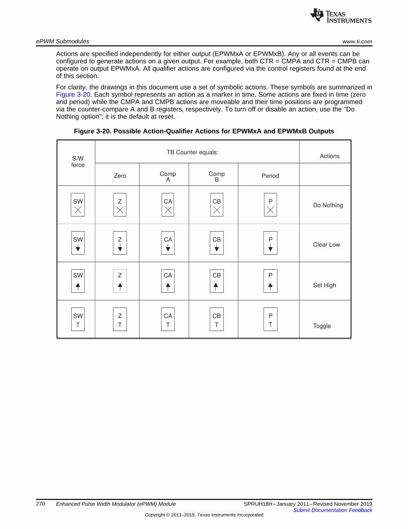
Z
Z
Z
CA
CA
CA
Z
T
CB
T
P
T
CA
T
CB P
CB
CB PDo Nothing
Clear Low
Set High
Toggle
P
Zero CompA
CompB
Period
TB Counter equals:ActionsS/W
force
SW
SW
SW
SW
T
ePWM Submodules www.ti.com
270 SPRUH18H–January 2011–Revised November 2019Submit Documentation Feedback
Copyright © 2011–2019, Texas Instruments Incorporated
Enhanced Pulse Width Modulator (ePWM) Module
Actions are specified independently for either output (EPWMxA or EPWMxB). Any or all events can beconfigured to generate actions on a given output. For example, both CTR = CMPA and CTR = CMPB canoperate on output EPWMxA. All qualifier actions are configured via the control registers found at the endof this section.
For clarity, the drawings in this document use a set of symbolic actions. These symbols are summarized inFigure 3-20. Each symbol represents an action as a marker in time. Some actions are fixed in time (zeroand period) while the CMPA and CMPB actions are moveable and their time positions are programmedvia the counter-compare A and B registers, respectively. To turn off or disable an action, use the "DoNothing option"; it is the default at reset.
Figure 3-20. Possible Action-Qualifier Actions for EPWMxA and EPWMxB Outputs

www.ti.com ePWM Submodules
271SPRUH18H–January 2011–Revised November 2019Submit Documentation Feedback
Copyright © 2011–2019, Texas Instruments Incorporated
Enhanced Pulse Width Modulator (ePWM) Module
3.2.4.3 Action-Qualifier Event PriorityIt is possible for the ePWM action qualifier to receive more than one event at the same time. In this caseevents are assigned a priority by the hardware. The general rule is events occurring later in time have ahigher priority and software forced events always have the highest priority. The event priority levels for up-down-count mode are shown in Table 3-9. A priority level of 1 is the highest priority and level 7 is thelowest. The priority changes slightly depending on the direction of TBCTR.
Table 3-9. Action-Qualifier Event Priority for Up-Down-Count Mode
Priority Level Event If TBCTR is IncrementingTBCTR = Zero up to TBCTR = TBPRD
Event If TBCTR is DecrementingTBCTR = TBPRD down to TBCTR = 1
1 (Highest) Software forced event Software forced event2 Counter equals CMPB on up-count (CBU) Counter equals CMPB on down-count (CBD)3 Counter equals CMPA on up-count (CAU) Counter equals CMPA on down-count (CAD)4 Counter equals zero Counter equals period (TBPRD)5 Counter equals CMPB on down-count (CBD) Counter equals CMPB on up-count (CBU)
6 (Lowest) Counter equals CMPA on down-count (CAD) Counter equals CMPA on up-count (CBU)
Table 3-10 shows the action-qualifier priority for up-count mode. In this case, the counter direction isalways defined as up and thus down-count events will never be taken.
Table 3-10. Action-Qualifier Event Priority for Up-Count Mode
Priority Level Event1 (Highest) Software forced event
2 Counter equal to period (TBPRD)3 Counter equal to CMPB on up-count (CBU)4 Counter equal to CMPA on up-count (CAU)
5 (Lowest) Counter equal to Zero
Table 3-11 shows the action-qualifier priority for down-count mode. In this case, the counter direction isalways defined as down and thus up-count events will never be taken.
Table 3-11. Action-Qualifier Event Priority for Down-Count Mode
Priority Level Event1 (Highest) Software forced event
2 Counter equal to Zero3 Counter equal to CMPB on down-count (CBD)4 Counter equal to CMPA on down-count (CAD)
5 (Lowest) Counter equal to period (TBPRD)
It is possible to set the compare value greater than the period. In this case the action will take place asshown in Table 3-12.
Table 3-12. Behavior if CMPA/CMPB is Greater than the Period
Counter Mode Compare on Up-Count EventCAU/CBU
Compare on Down-Count EventCAD/CBD
Up-Count Mode If CMPA/CMPB ≤ TBPRD period, then the eventoccurs on a compare match (TBCTR=CMPA orCMPB).
Never occurs.
If CMPA/CMPB > TBPRD, then the event will notoccur.

ePWM Submodules www.ti.com
272 SPRUH18H–January 2011–Revised November 2019Submit Documentation Feedback
Copyright © 2011–2019, Texas Instruments Incorporated
Enhanced Pulse Width Modulator (ePWM) Module
Table 3-12. Behavior if CMPA/CMPB is Greater than the Period (continued)Counter Mode Compare on Up-Count Event
CAU/CBUCompare on Down-Count EventCAD/CBD
Down-Count Mode Never occurs. If CMPA/CMPB < TBPRD, the event will occur on acompare match (TBCTR=CMPA or CMPB).If CMPA/CMPB ≥ TBPRD, the event will occur on aperiod match (TBCTR=TBPRD).
Up-Down-CountMode
If CMPA/CMPB < TBPRD and the counter isincrementing, the event occurs on a compare match(TBCTR=CMPA or CMPB).
If CMPA/CMPB < TBPRD and the counter isdecrementing, the event occurs on a compare match(TBCTR=CMPA or CMPB).
If CMPA/CMPB is ≥ TBPRD, the event will occur on aperiod match (TBCTR = TBPRD).
If CMPA/CMPB ≥ TBPRD, the event occurs on aperiod match (TBCTR=TBPRD).
3.2.4.4 Waveforms for Common Configurations
NOTE: The waveforms in this document show the ePWMs behavior for a static compare registervalue. In a running system, the active compare registers (CMPA and CMPB) are typicallyupdated from their respective shadow registers once every period. The user specifies whenthe update will take place; either when the time-base counter reaches zero or when the time-base counter reaches period. There are some cases when the action based on the newvalue can be delayed by one period or the action based on the old value can take effect foran extra period. Some PWM configurations avoid this situation. These include, but are notlimited to, the following:
Use up-down-count mode to generate a symmetric PWM:• If you load CMPA/CMPB on zero, then use CMPA/CMPB values greater
than or equal to 1.• If you load CMPA/CMPB on period, then use CMPA/CMPB values less than
or equal to TBPRD-1.This means there will always be a pulse of at least one TBCLK cycle in aPWM period which, when very short, tend to be ignored by the system.
Use up-down-count mode to generate an asymmetric PWM:• To achieve 50%-0% asymmetric PWM use the following configuration: Load
CMPA/CMPB on period and use the period action to clear the PWM and acompare-up action to set the PWM. Modulate the compare value from 0 toTBPRD to achieve 50%-0% PWM duty.
When using up-count mode to generate an asymmetric PWM:• To achieve 0-100% asymmetric PWM use the following configuration: Load
CMPA/CMPB on TBPRD. Use the Zero action to set the PWM and acompare-up action to clear the PWM. Modulate the compare value from 0 toTBPRD+1 to achieve 0-100% PWM duty.
See the Using Enhanced Pulse Width Modulator (ePWM) Module for 0-100%Duty Cycle Control Application Report (literature number SPRAAI1). Thesoftware configurations described in this application report are not applicablewhen changing compare registers from a non-zero value to zero. However, theystill apply when changing from a compare value of 0 to a non-zero value.
Figure 3-21 shows how a symmetric PWM waveform can be generated using the up-down-count mode ofthe TBCTR. In this mode 0%-100% DC modulation is achieved by using equal compare matches on theup count and down count portions of the waveform. In the example shown, CMPA is used to make thecomparison. When the counter is incrementing the CMPA match will pull the PWM output high. Likewise,when the counter is decrementing the compare match will pull the PWM signal low. When CMPA = 0, thePWM signal is low for the entire period giving the 0% duty waveform. When CMPA = TBPRD, the PWMsignal is high achieving 100% duty.

UP DOWNUP DOWN
2
0
3
4
1
2
3
1
2
0
3
4
1
2
0
3
1
TBCTR
TBCTR Direction
EPWMxA/EPWMxB
Case 2:CMPA = 3, 25% Duty
Case 3:CMPA = 2, 50% Duty
Case 3:CMPA = 1, 75% Duty
Case 4:CMPA = 0, 100% Duty
Case 1:CMPA = 4, 0% Duty
EPWMxA/EPWMxB
EPWMxA/EPWMxB
EPWMxA/EPWMxB
EPWMxA/EPWMxB
Mode: Up-Down CountTBPRD = 4CAU = SET, CAD = CLEAR0% - 100% Duty
www.ti.com ePWM Submodules
273SPRUH18H–January 2011–Revised November 2019Submit Documentation Feedback
Copyright © 2011–2019, Texas Instruments Incorporated
Enhanced Pulse Width Modulator (ePWM) Module
When using this configuration in practice, if you load CMPA/CMPB on zero, then use CMPA/CMPB valuesgreater than or equal to 1. If you load CMPA/CMPB on period, then use CMPA/CMPB values less than orequal to TBPRD-1. This means there will always be a pulse of at least one TBCLK cycle in a PWM periodwhich, when very short, tend to be ignored by the system.
Figure 3-21. Up-Down-Count Mode Symmetrical Waveform
The PWM waveforms in Figure 3-22 through Figure 3-27 show some common action-qualifierconfigurations. The C-code samples in Example 3-1 through Example 3-6 shows how to configure anePWM module for each case. Some conventions used in the figures and examples are as follows:• TBPRD, CMPA, and CMPB refer to the value written in their respective registers. The active register,
not the shadow register, is used by the hardware.• CMPx, refers to either CMPA or CMPB.• EPWMxA and EPWMxB refer to the output signals from ePWMx• Up-Down means Count-up-and-down mode, Up means up-count mode and Dwn means down-count
mode• Sym = Symmetric, Asym = Asymmetric

TBCTR
EPWMxA
EPWMxB
TBPRDvalue
CAZ P CB Z P CB CA Z P
Z P CA Z P CA Z PCBCB
ePWM Submodules www.ti.com
274 SPRUH18H–January 2011–Revised November 2019Submit Documentation Feedback
Copyright © 2011–2019, Texas Instruments Incorporated
Enhanced Pulse Width Modulator (ePWM) Module
Figure 3-22. Up, Single Edge Asymmetric Waveform, With Independent Modulation on EPWMxA andEPWMxB—Active High
A PWM period = (TBPRD + 1 ) × TTBCLK
B Duty modulation for EPWMxA is set by CMPA, and is active high (that is, high time duty proportional to CMPA).C Duty modulation for EPWMxB is set by CMPB and is active high (that is, high time duty proportional to CMPB).D The "Do Nothing" actions ( X ) are shown for completeness, but will not be shown on subsequent diagrams.E Actions at zero and period, although appearing to occur concurrently, are actually separated by one TBCLK period.
TBCTR wraps from period to 0000.
Example 3-1 contains a code sample showing initialization and run time for the waveforms in Figure 3-22.
Example 3-1. Code Sample for Figure 3-22
// Initialization Time// = = = = = = = = = = = = = = = = = = = = = = = =EPwm1Regs.TBPRD = 600; // Period = 601 TBCLK countsEPwm1Regs.CMPA.half.CMPA = 350; // Compare A = 350 TBCLK countsEPwm1Regs.CMPB = 200; // Compare B = 200 TBCLK countsEPwm1Regs.TBPHS = 0; // Set Phase register to zeroEPwm1Regs.TBCTR = 0; // clear TB counterEPwm1Regs.TBCTL.bit.CTRMODE = TB_COUNT_UP;EPwm1Regs.TBCTL.bit.PHSEN = TB_DISABLE; // Phase loading disabledEPwm1Regs.TBCTL.bit.PRDLD = TB_SHADOW;EPwm1Regs.TBCTL.bit.SYNCOSEL = TB_SYNC_DISABLE;EPwm1Regs.TBCTL.bit.HSPCLKDIV = TB_DIV1; // TBCLK = SYSCLKEPwm1Regs.TBCTL.bit.CLKDIV = TB_DIV1;EPwm1Regs.CMPCTL.bit.SHDWAMODE = CC_SHADOW;EPwm1Regs.CMPCTL.bit.SHDWBMODE = CC_SHADOW;EPwm1Regs.CMPCTL.bit.LOADAMODE = CC_CTR_ZERO; // load on CTR = ZeroEPwm1Regs.CMPCTL.bit.LOADBMODE = CC_CTR_ZERO; // load on CTR = ZeroEPwm1Regs.AQCTLA.bit.ZRO = AQ_SET;EPwm1Regs.AQCTLA.bit.CAU = AQ_CLEAR;EPwm1Regs.AQCTLB.bit.ZRO = AQ_SET;EPwm1Regs.AQCTLB.bit.CBU = AQ_CLEAR;//// Run Time// = = = = = = = = = = = = = = = = = = = = = = = =EPwm1Regs.CMPA.half.CMPA = Duty1A; // adjust duty for output EPWM1A

www.ti.com ePWM Submodules
275SPRUH18H–January 2011–Revised November 2019Submit Documentation Feedback
Copyright © 2011–2019, Texas Instruments Incorporated
Enhanced Pulse Width Modulator (ePWM) Module
Example 3-1. Code Sample for Figure 3-22 (continued)EPwm1Regs.CMPB = Duty1B; // adjust duty for output EPWM1B

TBCTR
EPWMxA
EPWMxB
TBPRDvalue
CB
CAP
P P
P
CB
CA
P
P
ePWM Submodules www.ti.com
276 SPRUH18H–January 2011–Revised November 2019Submit Documentation Feedback
Copyright © 2011–2019, Texas Instruments Incorporated
Enhanced Pulse Width Modulator (ePWM) Module
Figure 3-23. Up, Single Edge Asymmetric Waveform With Independent Modulation on EPWMxA andEPWMxB—Active Low
A PWM period = (TBPRD + 1 ) × TTBCLK
B Duty modulation for EPWMxA is set by CMPA, and is active low (that is, the low time duty is proportional to CMPA).C Duty modulation for EPWMxB is set by CMPB and is active low (that is, the low time duty is proportional to CMPB).D Actions at zero and period, although appearing to occur concurrently, are actually separated by one TBCLK period.
TBCTR wraps from period to 0000.
Example 3-2 contains a code sample showing initialization and run time for the waveforms in Figure 3-23.

TBCTR
EPWMxA
EPWMxB
TBPRDvalue
CA
T
Z
T
Z
T
Z
CA CB CB
www.ti.com ePWM Submodules
277SPRUH18H–January 2011–Revised November 2019Submit Documentation Feedback
Copyright © 2011–2019, Texas Instruments Incorporated
Enhanced Pulse Width Modulator (ePWM) Module
Example 3-2. Code Sample for Figure 3-23
// Initialization Time// = = = = = = = = = = = = = = = = = = = = = = = =EPwm1Regs.TBPRD = 600; // Period = 601 TBCLK countsEPwm1Regs.CMPA.half.CMPA = 350; // Compare A = 350 TBCLK countsEPwm1Regs.CMPB = 200; // Compare B = 200 TBCLK countsEPwm1Regs.TBPHS = 0; // Set Phase register to zeroEPwm1Regs.TBCTR = 0; // clear TB counterEPwm1Regs.TBCTL.bit.CTRMODE = TB_COUNT_UP;EPwm1Regs.TBCTL.bit.PHSEN = TB_DISABLE; // Phase loading disabledEPwm1Regs.TBCTL.bit.PRDLD = TB_SHADOW;EPwm1Regs.TBCTL.bit.SYNCOSEL = TB_SYNC_DISABLE;EPwm1Regs.TBCTL.bit.HSPCLKDIV = TB_DIV1; // TBCLK = SYSCLKOUTEPwm1Regs.TBCTL.bit.CLKDIV = TB_DIV1;EPwm1Regs.CMPCTL.bit.SHDWAMODE = CC_SHADOW;EPwm1Regs.CMPCTL.bit.SHDWBMODE = CC_SHADOW;EPwm1Regs.CMPCTL.bit.LOADAMODE = CC_CTR_ZERO; // load on TBCTR = ZeroEPwm1Regs.CMPCTL.bit.LOADBMODE = CC_CTR_ZERO; // load on TBCTR = ZeroEPwm1Regs.AQCTLA.bit.PRD = AQ_CLEAR;EPwm1Regs.AQCTLA.bit.CAU = AQ_SET;EPwm1Regs.AQCTLB.bit.PRD = AQ_CLEAR;EPwm1Regs.AQCTLB.bit.CBU = AQ_SET;//// Run Time// = = = = = = = = = = = = = = = = = = = = = = = =EPwm1Regs.CMPA.half.CMPA = Duty1A; // adjust duty for output EPWM1AEPwm1Regs.CMPB = Duty1B; // adjust duty for output EPWM1B
Figure 3-24. Up-Count, Pulse Placement Asymmetric Waveform With Independent Modulation onEPWMxA
A PWM frequency = 1/( (TBPRD + 1 ) × TTBCLK )B Pulse can be placed anywhere within the PWM cycle (0000 - TBPRD)C High time duty proportional to (CMPB - CMPA)D EPWMxB can be used to generate a 50% duty square wave with frequency = � × ( (TBPRD + 1 ) × TBCLK )
Example 3-3 contains a code sample showing initialization and run time for the waveforms Figure 3-24.Use the constant definitions in the device-specific header file.

ePWM Submodules www.ti.com
278 SPRUH18H–January 2011–Revised November 2019Submit Documentation Feedback
Copyright © 2011–2019, Texas Instruments Incorporated
Enhanced Pulse Width Modulator (ePWM) Module
Example 3-3. Use the code in Code Sample for Figure 3-24
// Initialization Time// = = = = = = = = = = = = = = = = = = = = = = = =EPwm1Regs.TBPRD = 600; // Period = 601 TBCLK countsEPwm1Regs.CMPA.half.CMPA = 200; // Compare A = 200 TBCLK countsEPwm1Regs.CMPB = 400; // Compare B = 400 TBCLK countsEPwm1Regs.TBPHS = 0; // Set Phase register to zeroEPwm1Regs.TBCTR = 0; // clear TB counterEPwm1Regs.TBCTL.bit.CTRMODE = TB_COUNT_UP;EPwm1Regs.TBCTL.bit.PHSEN = TB_DISABLE; // Phase loading disabledEPwm1Regs.TBCTL.bit.PRDLD = TB_SHADOW;EPwm1Regs.TBCTL.bit.SYNCOSEL = TB_SYNC_DISABLE;EPwm1Regs.TBCTL.bit.HSPCLKDIV = TB_DIV1; // TBCLK = SYSCLKOUTEPwm1Regs.TBCTL.bit.CLKDIV = TB_DIV1;EPwm1Regs.CMPCTL.bit.SHDWAMODE = CC_SHADOW;EPwm1Regs.CMPCTL.bit.SHDWBMODE = CC_SHADOW;EPwm1Regs.CMPCTL.bit.LOADAMODE = CC_CTR_ZERO; // load on TBCTR = ZeroEPwm1Regs.CMPCTL.bit.LOADBMODE = CC_CTR_ZERO; // load on TBCTR = ZeroEPwm1Regs.AQCTLA.bit.CAU = AQ_SET;EPwm1Regs.AQCTLA.bit.CBU = AQ_CLEAR;EPwm1Regs.AQCTLB.bit.ZRO = AQ_TOGGLE;//// Run Time// = = = = = = = = = = = = = = = = = = = = = = = =EPwm1Regs.CMPA.half.CMPA = EdgePosA; // adjust duty for output EPWM1A onlyEPwm1Regs.CMPB = EdgePosB;

TBCTR
EPWMxA
EPWMxB
TBPRDvalue
CACA CACA
CBCB CB CB CB
www.ti.com ePWM Submodules
279SPRUH18H–January 2011–Revised November 2019Submit Documentation Feedback
Copyright © 2011–2019, Texas Instruments Incorporated
Enhanced Pulse Width Modulator (ePWM) Module
Figure 3-25. Up-Down-Count, Dual Edge Symmetric Waveform, With Independent Modulation onEPWMxA and EPWMxB — Active Low
A PWM period = 2 x TBPRD × TTBCLK
B Duty modulation for EPWMxA is set by CMPA, and is active low (that is, the low time duty is proportional to CMPA).C Duty modulation for EPWMxB is set by CMPB and is active low (that is, the low time duty is proportional to CMPB).D Outputs EPWMxA and EPWMxB can drive independent power switches
Example 3-4 contains a code sample showing initialization and run time for the waveforms in Figure 3-25.Use the constant definitions in the device-specific header file.
Example 3-4. Code Sample for Figure 3-25
// Initialization Time// = = = = = = = = = = = = = = = = = = = = = = = =EPwm1Regs.TBPRD = 600; // Period = 2´600 TBCLK countsEPwm1Regs.CMPA.half.CMPA = 400; // Compare A = 400 TBCLK countsEPwm1Regs.CMPB = 500; // Compare B = 500 TBCLK countsEPwm1Regs.TBPHS = 0; // Set Phase register to zeroEPwm1Regs.TBCTR = 0; // clear TB counterEPwm1Regs.TBCTL.bit.CTRMODE = TB_COUNT_UPDOWN; // SymmetricxEPwm1Regs.TBCTL.bit.PHSEN = TB_DISABLE; // Phase loading disabledxEPwm1Regs.TBCTL.bit.PRDLD = TB_SHADOW;EPwm1Regs.TBCTL.bit.SYNCOSEL = TB_SYNC_DISABLE;EPwm1Regs.TBCTL.bit.HSPCLKDIV = TB_DIV1; // TBCLK = SYSCLKOUTEPwm1Regs.TBCTL.bit.CLKDIV = TB_DIV1;EPwm1Regs.CMPCTL.bit.SHDWAMODE = CC_SHADOW;EPwm1Regs.CMPCTL.bit.SHDWBMODE = CC_SHADOW;EPwm1Regs.CMPCTL.bit.LOADAMODE = CC_CTR_ZERO; // load on CTR = ZeroEPwm1Regs.CMPCTL.bit.LOADBMODE = CC_CTR_ZERO; // load on CTR = ZeroEPwm1Regs.AQCTLA.bit.CAU = AQ_SET;EPwm1Regs.AQCTLA.bit.CAD = AQ_CLEAR;EPwm1Regs.AQCTLB.bit.CBU = AQ_SET;EPwm1Regs.AQCTLB.bit.CBD = AQ_CLEAR;//// Run Time// = = = = = = = = = = = = = = = = = = = = = = = =EPwm1Regs.CMPA.half.CMPA = Duty1A; // adjust duty for output EPWM1AEPwm1Regs.CMPB = Duty1B; // adjust duty for output EPWM1B

CA CA CA CA
CB CB CB CB
TBCTR
EPWMxA
EPWMxB
TBPRDvalue
ePWM Submodules www.ti.com
280 SPRUH18H–January 2011–Revised November 2019Submit Documentation Feedback
Copyright © 2011–2019, Texas Instruments Incorporated
Enhanced Pulse Width Modulator (ePWM) Module
Figure 3-26. Up-Down-Count, Dual Edge Symmetric Waveform, With Independent Modulation onEPWMxA and EPWMxB — Complementary
A PWM period = 2 × TBPRD × TTBCLK
B Duty modulation for EPWMxA is set by CMPA, and is active low, that is, low time duty proportional to CMPAC Duty modulation for EPWMxB is set by CMPB and is active high, that is, high time duty proportional to CMPBD Outputs EPWMx can drive upper/lower (complementary) power switchesE Dead-band = CMPB - CMPA (fully programmable edge placement by software). Note the dead-band module is also
available if the more classical edge delay method is required.
Example 3-5 contains a code sample showing initialization and run time for the waveforms in Figure 3-26.Use the constant definitions in the device-specific header file.
Example 3-5. Code Sample for Figure 3-26
// Initialization Time// = = = = = = = = = = = = = = = = = = = = = = = =EPwm1Regs.TBPRD = 600; // Period = 2´600 TBCLK countsEPwm1Regs.CMPA.half.CMPA = 350; // Compare A = 350 TBCLK countsEPwm1Regs.CMPB = 400; // Compare B = 400 TBCLK countsEPwm1Regs.TBPHS = 0; // Set Phase register to zeroEPwm1Regs.TBCTR = 0; // clear TB counterEPwm1Regs.TBCTL.bit.CTRMODE = TB_COUNT_UPDOWN; // SymmetricEPwm1Regs.TBCTL.bit.PHSEN = TB_DISABLE; // Phase loading disabledEPwm1Regs.TBCTL.bit.PRDLD = TB_SHADOW;EPwm1Regs.TBCTL.bit.SYNCOSEL = TB_SYNC_DISABLE;EPwm1Regs.TBCTL.bit.HSPCLKDIV = TB_DIV1; // TBCLK = SYSCLKOUTEPwm1Regs.TBCTL.bit.CLKDIV = TB_DIV1;EPwm1Regs.CMPCTL.bit.SHDWAMODE = CC_SHADOW;EPwm1Regs.CMPCTL.bit.SHDWBMODE = CC_SHADOW;EPwm1Regs.CMPCTL.bit.LOADAMODE = CC_CTR_ZERO; // load on CTR = ZeroEPwm1Regs.CMPCTL.bit.LOADBMODE = CC_CTR_ZERO; // load on CTR = ZeroEPwm1Regs.AQCTLA.bit.CAU = AQ_SET;EPwm1Regs.AQCTLA.bit.CAD = AQ_CLEAR;EPwm1Regs.AQCTLB.bit.CBU = AQ_CLEAR;EPwm1Regs.AQCTLB.bit.CBD = AQ_SET;// Run Time// = = = = = = = = = = = = = = = = = = = = = = = =EPwm1Regs.CMPA.half.CMPA = Duty1A; // adjust duty for output EPWM1AEPwm1Regs.CMPB = Duty1B; // adjust duty for output EPWM1B

Z P Z P
TBCTR
EPWMxA
EPWMxB
CA CACB CB
www.ti.com ePWM Submodules
281SPRUH18H–January 2011–Revised November 2019Submit Documentation Feedback
Copyright © 2011–2019, Texas Instruments Incorporated
Enhanced Pulse Width Modulator (ePWM) Module
Figure 3-27. Up-Down-Count, Dual Edge Asymmetric Waveform, With Independent Modulation onEPWMxA—Active Low
A PWM period = 2 × TBPRD × TBCLKB Rising edge and falling edge can be asymmetrically positioned within a PWM cycle. This allows for pulse placement
techniques.C Duty modulation for EPWMxA is set by CMPA and CMPB.D Low time duty for EPWMxA is proportional to (CMPA + CMPB).E To change this example to active high, CMPA and CMPB actions need to be inverted (i.e., Set ! Clear and Clear Set).F Duty modulation for EPWMxB is fixed at 50% (utilizes spare action resources for EPWMxB)
Example 3-6 contains a code sample showing initialization and run time for the waveforms in Figure 3-27.Use the constant definitions in the device-specific header file.
Example 3-6. Code Sample for Figure 3-27
// Initialization Time// = = = = = = = = = = = = = = = = = = = = = = = =EPwm1Regs.TBPRD = 600; // Period = 2 ´ 600 TBCLK countsEPwm1Regs.CMPA.half.CMPA = 250; // Compare A = 250 TBCLK countsEPwm1Regs.CMPB = 450; // Compare B = 450 TBCLK countsEPwm1Regs.TBPHS = 0; // Set Phase register to zeroEPwm1Regs.TBCTR = 0; // clear TB counterEPwm1Regs.TBCTL.bit.CTRMODE = TB_COUNT_UPDOWN; // SymmetricEPwm1Regs.TBCTL.bit.PHSEN = TB_DISABLE; // Phase loading disabledEPwm1Regs.TBCTL.bit.PRDLD = TB_SHADOW;EPwm1Regs.TBCTL.bit.SYNCOSEL = TB_SYNC_DISABLE;EPwm1Regs.TBCTL.bit.HSPCLKDIV = TB_DIV1; // TBCLK = SYSCLKOUTEPwm1Regs.TBCTL.bit.CLKDIV = TB_DIV1;EPwm1Regs.CMPCTL.bit.SHDWAMODE = CC_SHADOW;EPwm1Regs.CMPCTL.bit.SHDWBMODE = CC_SHADOW;EPwm1Regs.CMPCTL.bit.LOADAMODE = CC_CTR_ZERO; // load on CTR = ZeroEPwm1Regs.CMPCTL.bit.LOADBMODE = CC_CTR_ZERO; // load on CTR = ZeroEPwm1Regs.AQCTLA.bit.CAU = AQ_SET;EPwm1Regs.AQCTLA.bit.CBD = AQ_CLEAR;EPwm1Regs.AQCTLB.bit.ZRO = AQ_CLEAR;EPwm1Regs.AQCTLB.bit.PRD = AQ_SET;// Run Time// = = = = = = = = = = = = = = = = = = = = = = = =EPwm1Regs.CMPA.half.CMPA = EdgePosA; // adjust duty for output EPWM1A onlyEPwm1Regs.CMPB = EdgePosB;

Digital CompareSignals
Counter CompareSignals
Time BaseSignals
DeadBand(DB)
CounterCompare
(CC)
ActionQualifier
(AQ)
EPWMxA
EPWMxB
CTR = CMPBCTR = 0
EPWMxINT
EPWMxSOCA
EPWMxSOCB
EPWMxA
EPWMxB
TZ1 TZ3to
CTR = CMPA
Time-Base(TB)
CTR = PRD
CTR = 0
CTR_Dir
EPWMxSYNCI
EPWMxSYNCO
EPWMxTZINT
PWM-chopper
(PC)
EventTrigger
and
Interrupt
(ET)
TripZone(TZ)
GPIOMUX
ADC
PIE
PIE
DigitalCompare
(DC)
EMUSTOP
CLOCKFAIL
EQEP1ERR
Digital CompareSignals
COMPCOMPxOUT
CPU
SYSCTRL
EQEP1
Digital CompareSignals
ePWM Submodules www.ti.com
282 SPRUH18H–January 2011–Revised November 2019Submit Documentation Feedback
Copyright © 2011–2019, Texas Instruments Incorporated
Enhanced Pulse Width Modulator (ePWM) Module
3.2.5 Dead-Band Generator (DB) SubmoduleFigure 3-28 illustrates the dead-band submodule within the ePWM module.
Figure 3-28. Dead-Band Submodule
3.2.5.1 Purpose of the Dead-Band SubmoduleThe "Action-qualifier (AQ) Module" section discussed how it is possible to generate the required dead-band by having full control over edge placement using both the CMPA and CMPB resources of the ePWMmodule. However, if the more classical edge delay-based dead-band with polarity control is required, thenthe dead-band submodule described here should be used.
The key functions of the dead-band module are:• Generating appropriate signal pairs (EPWMxA and EPWMxB) with dead-band relationship from a
single EPWMxA input• Programming signal pairs for:
– Active high (AH)– Active low (AL)– Active high complementary (AHC)– Active low complementary (ALC)
• Adding programmable delay to rising edges (RED)• Adding programmable delay to falling edges (FED)• Can be totally bypassed from the signal path (note dotted lines in diagram)
3.2.5.2 Controlling and Monitoring the Dead-Band SubmoduleThe dead-band submodule operation is controlled and monitored via the following registers:
Table 3-13. Dead-Band Generator Submodule Registers
Register Name Address offset Shadowed DescriptionDBCTL 0x000F No Dead-Band Control RegisterDBRED 0x0010 No Dead-Band Rising Edge Delay Count RegisterDBFED 0x0011 No Dead-Band Falling Edge Delay Count Register

0
1
S2
1
0 S1
RED
OutIn
Rising edgedelay
(10-bitcounter)
(10-bitcounter)
delayFalling edge
In Out
FED
1
0 S3
0
S01
EPWMxA
EPWMxB
DBCTL[POLSEL] DBCTL[OUT_MODE]
S5
DBCTL[IN_MODE]
1
0
S40
1
EPWMxA in
EPWMxB in
DBCTL[HALFCYCLE]
www.ti.com ePWM Submodules
283SPRUH18H–January 2011–Revised November 2019Submit Documentation Feedback
Copyright © 2011–2019, Texas Instruments Incorporated
Enhanced Pulse Width Modulator (ePWM) Module
3.2.5.3 Operational Highlights for the Dead-Band SubmoduleThe following sections provide the operational highlights.
The dead-band submodule has two groups of independent selection options as shown in Figure 3-29.• Input Source Selection:
The input signals to the dead-band module are the EPWMxA and EPWMxB output signals from theaction-qualifier. In this section they will be referred to as EPWMxA In and EPWMxB In. Using theDBCTL[IN_MODE) control bits, the signal source for each delay, falling-edge or rising-edge, can beselected:– EPWMxA In is the source for both falling-edge and rising-edge delay. This is the default mode.– EPWMxA In is the source for falling-edge delay, EPWMxB In is the source for rising-edge delay.– EPWMxA In is the source for rising edge delay, EPWMxB In is the source for falling-edge delay.– EPWMxB In is the source for both falling-edge and rising-edge delay.
• Half Cycle Clocking:The dead-band submodule can be clocked using half cycle clocking to double the resolution (that is,counter clocked at 2× TBCLK).
• Output Mode Control:The output mode is configured by way of the DBCTL[OUT_MODE] bits. These bits determine if thefalling-edge delay, rising-edge delay, neither, or both are applied to the input signals.
• Polarity Control:The polarity control (DBCTL[POLSEL]) allows you to specify whether the rising-edge delayed signaland/or the falling-edge delayed signal is to be inverted before being sent out of the dead-bandsubmodule.
Figure 3-29. Configuration Options for the Dead-Band Submodule
Although all combinations are supported, not all are typical usage modes. Table 3-14 documents someclassical dead-band configurations. These modes assume that the DBCTL[IN_MODE] is configured suchthat EPWMxA In is the source for both falling-edge and rising-edge delay. Enhanced, or non-traditionalmodes can be achieved by changing the input signal source. The modes shown in Table 3-14 fall into thefollowing categories:• Mode 1: Bypass both falling-edge delay (FED) and rising-edge delay (RED)
Allows you to fully disable the dead-band submodule from the PWM signal path.• Mode 2-5: Classical Dead-Band Polarity Settings:

ePWM Submodules www.ti.com
284 SPRUH18H–January 2011–Revised November 2019Submit Documentation Feedback
Copyright © 2011–2019, Texas Instruments Incorporated
Enhanced Pulse Width Modulator (ePWM) Module
These represent typical polarity configurations that should address all the active high/low modesrequired by available industry power switch gate drivers. The waveforms for these typical cases areshown in Figure 3-30. Note that to generate equivalent waveforms to Figure 3-30, configure the action-qualifier submodule to generate the signal as shown for EPWMxA.
• Mode 6: Bypass rising-edge-delay and Mode 7: Bypass falling-edge-delayFinally the last two entries in Table 3-14 show combinations where either the falling-edge-delay (FED)or rising-edge-delay (RED) blocks are bypassed.
Table 3-14. Classical Dead-Band Operating Modes
Mode Mode DescriptionDBCTL[POLSEL] DBCTL[OUT_MODE]
S3 S2 S1 S01 EPWMxA and EPWMxB Passed Through (No Delay) X X 0 02 Active High Complementary (AHC) 1 0 1 13 Active Low Complementary (ALC) 0 1 1 14 Active High (AH) 0 0 1 15 Active Low (AL) 1 1 1 1
6EPWMxA Out = EPWMxA In (No Delay)
0 or 1 0 or 1 0 1EPWMxB Out = EPWMxA In with Falling Edge Delay
7EPWMxA Out = EPWMxA In with Rising Edge Delay
0 or 1 0 or 1 1 0EPWMxB Out = EPWMxB In with No Delay

Original
(outA)
Rising Edge
Delayed (RED)
Falling Edge
Delayed (FED)
Active HighComplementary
(AHC)
Active LowComplementary
(ALC)
Active High
(AH)
Active Low
(AL)
RED
FED
Period
www.ti.com ePWM Submodules
285SPRUH18H–January 2011–Revised November 2019Submit Documentation Feedback
Copyright © 2011–2019, Texas Instruments Incorporated
Enhanced Pulse Width Modulator (ePWM) Module
Figure 3-30 shows waveforms for typical cases where 0% < duty < 100%.
Figure 3-30. Dead-Band Waveforms for Typical Cases (0% < Duty < 100%)

ePWM Submodules www.ti.com
286 SPRUH18H–January 2011–Revised November 2019Submit Documentation Feedback
Copyright © 2011–2019, Texas Instruments Incorporated
Enhanced Pulse Width Modulator (ePWM) Module
The dead-band submodule supports independent values for rising-edge (RED) and falling-edge (FED)delays. The amount of delay is programmed using the DBRED and DBFED registers. These are 10-bitregisters and their value represents the number of time-base clock, TBCLK, periods a signal edge isdelayed by. For example, the formula to calculate falling-edge-delay and rising-edge-delay are:
FED = DBFED × TTBCLK
RED = DBRED × TTBCLK
Where TTBCLK is the period of TBCLK, the prescaled version of SYSCLKOUT.
When half-cycle clocking is enabled, the formula to calculate the falling-edge-delay and rising-edge-delaybecomes:
FED = DBFED × TTBCLK/2RED = DBRED × TTBCLK/2
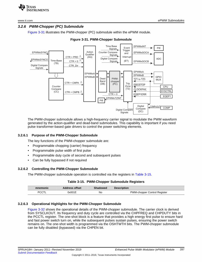
Digital CompareSignals
Counter CompareSignals
Time BaseSignals
DeadBand(DB)
CounterCompare
(CC)
ActionQualifier
(AQ)
EPWMxA
EPWMxB
CTR = CMPBCTR = 0
EPWMxINT
EPWMxSOCA
EPWMxSOCB
EPWMxA
EPWMxB
TZ1 TZ3to
CTR = CMPA
Time-Base(TB)
CTR = PRD
CTR = 0
CTR_Dir
EPWMxSYNCI
EPWMxSYNCO
EPWMxTZINT
PWM-chopper
(PC)
EventTrigger
and
Interrupt
(ET)
TripZone(TZ)
GPIOMUX
ADC
PIE
PIE
DigitalCompare
(DC)
EMUSTOP
CLOCKFAIL
EQEP1ERR
Digital CompareSignals
COMPCOMPxOUT
CPU
SYSCTRL
EQEP1
Digital CompareSignals
www.ti.com ePWM Submodules
287SPRUH18H–January 2011–Revised November 2019Submit Documentation Feedback
Copyright © 2011–2019, Texas Instruments Incorporated
Enhanced Pulse Width Modulator (ePWM) Module
3.2.6 PWM-Chopper (PC) SubmoduleFigure 3-31 illustrates the PWM-chopper (PC) submodule within the ePWM module.
Figure 3-31. PWM-Chopper Submodule
The PWM-chopper submodule allows a high-frequency carrier signal to modulate the PWM waveformgenerated by the action-qualifier and dead-band submodules. This capability is important if you needpulse transformer-based gate drivers to control the power switching elements.
3.2.6.1 Purpose of the PWM-Chopper SubmoduleThe key functions of the PWM-chopper submodule are:• Programmable chopping (carrier) frequency• Programmable pulse width of first pulse• Programmable duty cycle of second and subsequent pulses• Can be fully bypassed if not required
3.2.6.2 Controlling the PWM-Chopper SubmoduleThe PWM-chopper submodule operation is controlled via the registers in Table 3-15.
Table 3-15. PWM-Chopper Submodule Registers
mnemonic Address offset Shadowed DescriptionPCCTL 0x001E No PWM-chopper Control Register
3.2.6.3 Operational Highlights for the PWM-Chopper SubmoduleFigure 3-32 shows the operational details of the PWM-chopper submodule. The carrier clock is derivedfrom SYSCLKOUT. Its frequency and duty cycle are controlled via the CHPFREQ and CHPDUTY bits inthe PCCTL register. The one-shot block is a feature that provides a high energy first pulse to ensure hardand fast power switch turn on, while the subsequent pulses sustain pulses, ensuring the power switchremains on. The one-shot width is programmed via the OSHTWTH bits. The PWM-chopper submodulecan be fully disabled (bypassed) via the CHPEN bit.

PSCLK
EPWMxA
EPWMxB
EPWMxA
EPWMxB
Start
Clk
Oneshot
Pulse-width
PCCTL[OSHTWTH]
PWMA_ch
Bypass
Divider andduty control
PSCLK
OSHT
EPWMxA
PCCTL[CHPEN]
EPWMxA
/8SYSCLKOUT
Pulse-width
Start
shot
Clk
One
PCCTL[OSHTWTH]
1OSHT
PCCTL[CHPFREQ]PCCTL[CHPDUTY]
PWMB_ch
Bypass
EPWMxBEPWMxB
1
0
0
ePWM Submodules www.ti.com
288 SPRUH18H–January 2011–Revised November 2019Submit Documentation Feedback
Copyright © 2011–2019, Texas Instruments Incorporated
Enhanced Pulse Width Modulator (ePWM) Module
Figure 3-32. PWM-Chopper Submodule Operational Details
3.2.6.4 WaveformsFigure 3-33 shows simplified waveforms of the chopping action only; one-shot and duty-cycle control arenot shown. Details of the one-shot and duty-cycle control are discussed in the following sections.
Figure 3-33. Simple PWM-Chopper Submodule Waveforms Showing Chopping Action Only

PSCLK
OSHT
EPWMxA in
EPWMxA out
Prog. pulse width
(OSHTWTH)
Start OSHT pulse
Sustaining pulses
www.ti.com ePWM Submodules
289SPRUH18H–January 2011–Revised November 2019Submit Documentation Feedback
Copyright © 2011–2019, Texas Instruments Incorporated
Enhanced Pulse Width Modulator (ePWM) Module
3.2.6.4.1 One-Shot PulseThe width of the first pulse can be programmed to any of 16 possible pulse width values. The width orperiod of the first pulse is given by:
T1stpulse = TSYSCLKOUT × 8 × OSHTWTH
Where TSYSCLKOUT is the period of the system clock (SYSCLKOUT) and OSHTWTH is the four control bits(value from 1 to 16)
Figure 3-34 shows the first and subsequent sustaining pulses and Table 3-16 gives the possible pulsewidth values for a SYSCLKOUT = 80 MHz.
Figure 3-34. PWM-Chopper Submodule Waveforms Showing the First Pulse and Subsequent SustainingPulses
Table 3-16. Possible Pulse Width Values forSYSCLKOUT = 90 MHz
OSHTWTHz(hex)
Pulse Width(nS)
0 891 1782 2673 3564 4455 5336 6227 7118 8009 889A 978B 1067C 1156D 1245E 1334F 1422

Duty
1/8
Duty
2/8
Duty
3/8
Duty
4/8
Duty
5/8
Duty
6/8
Duty
7/8
PSCLK
12.5%25%
37.5%50%
62.5%75%
87.5%
PSCLK Period
PSCLK
period
ePWM Submodules www.ti.com
290 SPRUH18H–January 2011–Revised November 2019Submit Documentation Feedback
Copyright © 2011–2019, Texas Instruments Incorporated
Enhanced Pulse Width Modulator (ePWM) Module
3.2.6.4.2 Duty Cycle ControlPulse transformer-based gate drive designs need to comprehend the magnetic properties orcharacteristics of the transformer and associated circuitry. Saturation is one such consideration. To assistthe gate drive designer, the duty cycles of the second and subsequent pulses have been madeprogrammable. These sustaining pulses ensure the correct drive strength and polarity is maintained on thepower switch gate during the on period, and hence a programmable duty cycle allows a design to betuned or optimized via software control.
Figure 3-35 shows the duty cycle control that is possible by programming the CHPDUTY bits. One ofseven possible duty ratios can be selected ranging from 12.5% to 87.5%.
Figure 3-35. PWM-Chopper Submodule Waveforms Showing the Pulse Width (Duty Cycle) Control ofSustaining Pulses

Digital CompareSignals
Counter CompareSignals
Time BaseSignals
DeadBand(DB)
CounterCompare
(CC)
ActionQualifier
(AQ)
EPWMxA
EPWMxB
CTR = CMPBCTR = 0
EPWMxINT
EPWMxSOCA
EPWMxSOCB
EPWMxA
EPWMxB
TZ1 TZ3to
CTR = CMPA
Time-Base(TB)
CTR = PRD
CTR = 0
CTR_Dir
EPWMxSYNCI
EPWMxSYNCO
EPWMxTZINT
PWM-chopper
(PC)
EventTrigger
and
Interrupt
(ET)
TripZone(TZ)
GPIOMUX
ADC
PIE
PIE
DigitalCompare
(DC)
EMUSTOP
CLOCKFAIL
EQEP1ERR
Digital CompareSignals
COMPCOMPxOUT
CPU
SYSCTRL
EQEP1
Digital CompareSignals
www.ti.com ePWM Submodules
291SPRUH18H–January 2011–Revised November 2019Submit Documentation Feedback
Copyright © 2011–2019, Texas Instruments Incorporated
Enhanced Pulse Width Modulator (ePWM) Module
3.2.7 Trip-Zone (TZ) SubmoduleFigure 3-36 shows how the trip-zone (TZ) submodule fits within the ePWM module.
Figure 3-36. Trip-Zone Submodule
Each ePWM module is connected to six TZn signals (TZ1 to TZ6). TZ1 to TZ3 are sourced from the GPIOmux. TZ4 is sourced from an inverted EQEP1ERR signal on those devices with an EQEP1 module. TZ5 isconnected to the system clock fail logic, and TZ6 is sourced from the EMUSTOP output from the CPU.These signals indicate external fault or trip conditions, and the ePWM outputs can be programmed torespond accordingly when faults occur.
3.2.7.1 Purpose of the Trip-Zone SubmoduleThe key functions of the Trip-Zone submodule are:• Trip inputs TZ1 to TZ6 can be flexibly mapped to any ePWM module.• Upon a fault condition, outputs EPWMxA and EPWMxB can be forced to one of the following:
– High– Low– High-impedance– No action taken
• Support for one-shot trip (OSHT) for major short circuits or over-current conditions.• Support for cycle-by-cycle tripping (CBC) for current limiting operation.• Support for digital compare tripping (DC) based on state of on-chip analog comparator module outputs
and/or TZ1 to TZ3 signals.• Each trip-zone input and digital compare (DC) submodule DCAEVT1/2 or DCBEVT1/2 force event can
be allocated to either one-shot or cycle-by-cycle operation.• Interrupt generation is possible on any trip-zone input.• Software-forced tripping is also supported.• The trip-zone submodule can be fully bypassed if it is not required.

ePWM Submodules www.ti.com
292 SPRUH18H–January 2011–Revised November 2019Submit Documentation Feedback
Copyright © 2011–2019, Texas Instruments Incorporated
Enhanced Pulse Width Modulator (ePWM) Module
3.2.7.2 Controlling and Monitoring the Trip-Zone SubmoduleThe trip-zone submodule operation is controlled and monitored through the following registers:
(1) All trip-zone registers are EALLOW protected and can be modified only after executing the EALLOW instruction. For moreinformation, see the device-specific version of the System Control and Interrupts Reference Guide listed in Section 1.
(2) This register is discussed in more detail in Section 3.2.9 Digital Compare submodule.
Table 3-17. Trip-Zone Submodule Registers
Register Name Address offset Shadowed Description (1)
TZSEL 0x0012 No Trip-Zone Select RegisterTZDCSEL 0x0013 No Trip-zone Digital Compare Select Register (2)
TZCTL 0x0014 No Trip-Zone Control RegisterTZEINT 0x0015 No Trip-Zone Enable Interrupt RegisterTZFLG 0x0016 No Trip-Zone Flag RegisterTZCLR 0x0017 No Trip-Zone Clear RegisterTZFRC 0x0018 No Trip-Zone Force Register
3.2.7.3 Operational Highlights for the Trip-Zone SubmoduleThe following sections describe the operational highlights and configuration options for the trip-zonesubmodule.
The trip-zone signals TZ1 to TZ6 (also collectively referred to as TZn) are active low input signals. Whenone of these signals goes low, or when a DCAEVT1/2 or DCBEVT1/2 force happens based on theTZDCSEL register event selection, it indicates that a trip event has occurred. Each ePWM module can beindividually configured to ignore or use each of the trip-zone signals or DC events. Which trip-zone signalsor DC events are used by a particular ePWM module is determined by the TZSEL register for that specificePWM module. The trip-zone signals may or may not be synchronized to the system clock (SYSCLKOUT)and digitally filtered within the GPIO MUX block. A minimum of 3*TBCLK low pulse width on TZn inputs issufficient to trigger a fault condition on the ePWM module. If the pulse width is less than this, the tripcondition may not be latched by CBC or OST latches. The asynchronous trip makes sure that if clocks aremissing for any reason, the outputs can still be tripped by a valid event present on TZn inputs . TheGPIOs or peripherals must be appropriately configured. For more information, see the System Control andInterrupts chapter.
Each TZn input can be individually configured to provide either a cycle-by-cycle or one-shot trip event foran ePWM module. DCAEVT1 and DCBEVT1 events can be configured to directly trip an ePWM module orprovide a one-shot trip event to the module. Likewise, DCAVET2 and DCBEVT2 events can also beconfigured to directly trip an ePWM module or provide a cycle-by-cycle trip event to the module. Thisconfiguration is determined by the TZSEL[DCAEVT1/2], TZSEL[DCBEVT1/2], TZSEL[CBCn], andTZSEL[OSHTn] control bits (where n corresponds to the trip input) respectively.• Cycle-by-Cycle (CBC):
When a cycle-by-cycle trip event occurs, the action specified in the TZCTL[TZA] and TZCTL[TZB] bitsis carried out immediately on the EPWMxA and/or EPWMxB output. Table 3-18 lists the possibleactions. In addition, the cycle-by-cycle trip event flag (TZFLG[CBC]) is set and a EPWMx_TZINTinterrupt is generated if it is enabled in the TZEINT register and PIE peripheral.If the CBC interrupt is enabled via the TZEINT register, and DCAEVT2 or DCBEVT2 are selected asCBC trip sources via the TZSEL register, it is not necessary to also enable the DCAEVT2 or DCBEVT2interrupts in the TZEINT register, as the DC events trigger interrupts through the CBC mechanism.The specified condition on the inputs is automatically cleared when the ePWM time-base counterreaches zero (TBCTR = 0x0000) if the trip event is no longer present. Therefore, in this mode, the tripevent is cleared or reset every PWM cycle. The TZFLG[CBC] flag bit will remain set until it is manuallycleared by writing to the TZCLR[CBC] bit. If the cycle-by-cycle trip event is still present when theTZFLG[CBC] bit is cleared, then it will again be immediately set.
• One-Shot (OSHT):When a one-shot trip event occurs, the action specified in the TZCTL[TZA] and TZCTL[TZB] bits iscarried out immediately on the EPWMxA and/or EPWMxB output. Table 3-18 lists the possible actions.

www.ti.com ePWM Submodules
293SPRUH18H–January 2011–Revised November 2019Submit Documentation Feedback
Copyright © 2011–2019, Texas Instruments Incorporated
Enhanced Pulse Width Modulator (ePWM) Module
In addition, the one-shot trip event flag (TZFLG[OST]) is set and a EPWMx_TZINT interrupt isgenerated if it is enabled in the TZEINT register and PIE peripheral. The one-shot trip condition mustbe cleared manually by writing to the TZCLR[OST] bit.If the one-shot interrupt is enabled via the TZEINT register, and DCAEVT1 or DCBEVT1 are selectedas OSHT trip sources via the TZSEL register, it is not necessary to also enable the DCAEVT1 orDCBEVT1 interrupts in the TZEINT register, as the DC events trigger interrupts through the OSHTmechanism.
• Digital Compare Events (DCAEVT1/2 and DCBEVT1/2):A digital compare DCAEVT1/2 or DCBEVT1/2 event is generated based on a combination of theDCAH/DCAL and DCBH/DCBL signals as selected by the TZDCSEL register. The signals whichsource the DCAH/DCAL and DCBH/DCBL signals are selected via the DCTRIPSEL register and canbe either trip zone input pins or analog comparator COMPxOUT signals. For more information on thedigital compare submodule signals, see Section 3.2.9.When a digital compare event occurs, the action specified in the TZCTL[DCAEVT1/2] andTZCTL[DCBEVT1/2] bits is carried out immediately on the EPWMxA and/or EPWMxB output. Table 3-18 lists the possible actions. In addition, the relevant DC trip event flag (TZFLG[DCAEVT1/2] /TZFLG[DCBEVT1/2]) is set and a EPWMx_TZINT interrupt is generated if it is enabled in the TZEINTregister and PIE peripheral.The specified condition on the pins is automatically cleared when the DC trip event is no longerpresent. The TZFLG[DCAEVT1/2] or TZFLG[DCBEVT1/2] flag bit will remain set until it is manuallycleared by writing to the TZCLR[DCAEVT1/2] or TZCLR[DCBEVT1/2] bit. If the DC trip event is stillpresent when the TZFLG[DCAEVT1/2] or TZFLG[DCBEVT1/2] flag is cleared, then it will again beimmediately set.
The action taken when a trip event occurs can be configured individually for each of the ePWM outputpins by way of the TZCTL register bit fields. One of four possible actions, shown in Table 3-18, can betaken on a trip event.

ePWM Submodules www.ti.com
294 SPRUH18H–January 2011–Revised November 2019Submit Documentation Feedback
Copyright © 2011–2019, Texas Instruments Incorporated
Enhanced Pulse Width Modulator (ePWM) Module
Table 3-18. Possible Actions On a Trip Event
TZCTL Register bit-fieldSettings
EPWMxAand/or
EPWMxB
Comment
0,0 High-Impedance Tripped0,1 Force to High State Tripped1,0 Force to Low State Tripped1,1 No Change Do Nothing.
No change is made to the output.
Example 3-7. Trip-Zone Configurations
Scenario A:A one-shot trip event on TZ1 pulls both EPWM1A, EPWM1B low and also forces EPWM2A and EPWM2Bhigh.• Configure the ePWM1 registers as follows:
– TZSEL[OSHT1] = 1: enables TZ1 as a one-shot event source for ePWM1– TZCTL[TZA] = 2: EPWM1A will be forced low on a trip event.– TZCTL[TZB] = 2: EPWM1B will be forced low on a trip event.
• Configure the ePWM2 registers as follows:– TZSEL[OSHT1] = 1: enables TZ1 as a one-shot event source for ePWM2– TZCTL[TZA] = 1: EPWM2A will be forced high on a trip event.– TZCTL[TZB] = 1: EPWM2B will be forced high on a trip event.
Scenario B:A cycle-by-cycle event on TZ5 pulls both EPWM1A, EPWM1B low.A one-shot event on TZ1 or TZ6 puts EPWM2A into a high impedance state.• Configure the ePWM1 registers as follows:
– TZSEL[CBC5] = 1: enables TZ5 as a one-shot event source for ePWM1– TZCTL[TZA] = 2: EPWM1A will be forced low on a trip event.– TZCTL[TZB] = 2: EPWM1B will be forced low on a trip event.
• Configure the ePWM2 registers as follows:– TZSEL[OSHT1] = 1: enables TZ1 as a one-shot event source for ePWM2– TZSEL[OSHT6] = 1: enables TZ6 as a one-shot event source for ePWM2– TZCTL[TZA] = 0: EPWM2A will be put into a high-impedance state on a trip event.– TZCTL[TZB] = 3: EPWM2B will ignore the trip event.
3.2.7.4 Generating Trip Event InterruptsFigure 3-37 and Figure 3-38 illustrate the trip-zone submodule control and interrupt logic, respectively.DCAEVT1/2 and DCBEVT1/2 signals are described in further detail in Section 3.2.9.

CTR=zero
TZFRC[CBC]
TZ1
TZ2
TZ3
TZ4
TZ5
TZ6
Clear
TZSEL[CBC1 to CBC6, DCAEVT2, DCBEVT2]
TZCLR[OST]
TZSEL[OSHT1 to OSHT6, DCAEVT1, DCBEVT1]
TZFRC[OSHT]
Trip
Cycle-by-Cycle (CBC)Trip Events
One-Shot (OSHT)Trip Events
DigitalCompare
Submodule
DCAEVT1.force
DCAEVT2.force
DCBEVT1.force
DCBEVT2.force
COMPxOUT
TZ1
TZ2
TZ3
DCAEVT2.force
DCBEVT2.force
TZ1
TZ2
TZ3
TZ4
TZ5
TZ6
DCAEVT1.force
DCBEVT1.force
AsyncTripSet
ClearTZCLR[CBC]
TZFLG[CBC]
Sync
CBC Latch
Set
Clear
Trip
AsyncTripSetClear
TZFLG[OST]
Sync
OSHT Latch
Set
EPWMxA (from PC submodule)
EPWMxA
TZCTL[TZA, DCAEVT1, DCAEVT2]
EPWMATrip
Logic
DCAEVT1.forceDCAEVT2.force
EPWMxB (from PC submodule)
EPWMxB
TZCTL[TZB, DCBEVT1, DCBEVT2]
EPWMBTrip
Logic
DCBEVT1.forceDCBEVT2.force
www.ti.com ePWM Submodules
295SPRUH18H–January 2011–Revised November 2019Submit Documentation Feedback
Copyright © 2011–2019, Texas Instruments Incorporated
Enhanced Pulse Width Modulator (ePWM) Module
Figure 3-37. Trip-Zone Submodule Mode Control Logic

Clear
Latch
Set
TZCLR[CBC]
CBC ForceOutput Event
TZEINT[CBC]
TZFLG[CBC]
Clear
Latch
Set
TZCLR[OST]
OST ForceOutput Event
TZEINT[OST]
TZFLG[OST]
Clear
Latch
Set
TZCLR[DCAEVT1]
DCAEVT1.interTZEINT[DCAEVT1]
TZFLG[DCAEVT1]
Clear
Latch
Set
TZCLR[DCAEVT2]
DCAEVT2.interTZEINT[DCAEVT2]
TZFLG[DCAEVT2]
Clear
Latch
Set
TZCLR[DCBEVT1]
DCBEVT1.interTZEINT[DCBEVT1]
TZFLG[DCBEVT1]
Clear
Latch
Set
TZCLR[DCBEVT2]
DCBEVT2.interTZEINT[DCBEVT2]
TZFLG[DCBEVT2]
GenerateInterrupt
PulseWhen
Input = 1
Clear
Latch
Set
TZFLG[INT]
TZCLR[INT]
EPWMxTZINT (PIE)
ePWM Submodules www.ti.com
296 SPRUH18H–January 2011–Revised November 2019Submit Documentation Feedback
Copyright © 2011–2019, Texas Instruments Incorporated
Enhanced Pulse Width Modulator (ePWM) Module
Figure 3-38. Trip-Zone Submodule Interrupt Logic
3.2.8 Event-Trigger (ET) SubmoduleThe key functions of the event-trigger submodule are:• Receives event inputs generated by the time-base, counter-compare, and digital-compare submodules• Uses the time-base direction information for up/down event qualification• Uses prescaling logic to issue interrupt requests and ADC start of conversion at:
– Every event– Every second event– Every third event
• Provides full visibility of event generation via event counters and flags• Allows software forcing of Interrupts and ADC start of conversion
The event-trigger submodule manages the events generated by the time-base submodule, the counter-compare submodule, and the digital-compare submodule to generate an interrupt to the CPU and/or astart of conversion pulse to the ADC when a selected event occurs. Figure 3-39 illustrates where theevent-trigger submodule fits within the ePWM system.

EPWM1
module
EPWM2
module
EPWMx
module
PIE
ADCTRIG5
ADCTRIG6
ADCTRIG7
ADCTRIG8
ADCTRIG(2x+3)
ADCTRIG(2x+4)
EPWM1SOCA
EPWM1SOCB
EPWM2SOCA
EPWM2SOCB
EPWMxSOCB
EPWM1INT
EPWM2INT
EPWMxINT
EPWMxSOCA
ADC
Digital CompareSignals
Counter CompareSignals
Time BaseSignals
DeadBand(DB)
CounterCompare
(CC)
ActionQualifier
(AQ)
EPWMxA
EPWMxB
CTR = CMPBCTR = 0
EPWMxINT
EPWMxSOCA
EPWMxSOCB
EPWMxA
EPWMxB
TZ1 TZ3to
CTR = CMPA
Time-Base(TB)
CTR = PRD
CTR = 0
CTR_Dir
EPWMxSYNCI
EPWMxSYNCO
EPWMxTZINT
PWM-chopper
(PC)
EventTrigger
and
Interrupt
(ET)
TripZone(TZ)
GPIOMUX
ADC
PIE
PIE
DigitalCompare
(DC)
EMUSTOP
CLOCKFAIL
EQEP1ERR
Digital CompareSignals
COMPCOMPxOUT
CPU
SYSCTRL
EQEP1
Digital CompareSignals
www.ti.com ePWM Submodules
297SPRUH18H–January 2011–Revised November 2019Submit Documentation Feedback
Copyright © 2011–2019, Texas Instruments Incorporated
Enhanced Pulse Width Modulator (ePWM) Module
Figure 3-39. Event-Trigger Submodule
3.2.8.1 Operational Overview of the Event-Trigger SubmoduleThe following sections describe the event-trigger submodule's operational highlights.
Each ePWM module has one interrupt request line connected to the PIE and two start of conversionsignals connected to the ADC module. As shown in Figure 3-40, ADC start of conversion for all ePWMmodules are connected to individual ADC trigger inputs to the ADC, and hence multiple modules caninitiate an ADC start of conversion via the ADC trigger inputs.
Figure 3-40. Event-Trigger Submodule Inter-Connectivity of ADC Start of Conversion
The event-trigger submodule monitors various event conditions (the left side inputs to event-triggersubmodule shown in Figure 3-41) and can be configured to prescale these events before issuing anInterrupt request or an ADC start of conversion. The event-trigger prescaling logic can issue Interruptrequests and ADC start of conversion at:• Every event• Every second event

PIEEvent Trigger
Module Logic
CTR=Zero
CTR=PRD
CTR=CMPA
EPWMxINTn
CTR=CMPB
CTR_dir
Direction
qualifier
CTRU=CMPAETSEL reg
EPWMxSOCA
/n
/n
/n
EPWMxSOCB
ADC
clear
count
count
clear
count
clear
CTRD=CMPA
CTRU=CMPB
CTRD=CMPB
ETPS reg
ETFLG reg
ETCLR reg
ETFRC reg
CTR=Zero or PRD
DCAEVT1.soc
DCBEVT1.socFrom Digital Compare
(DC) Submodule
ePWM Submodules www.ti.com
298 SPRUH18H–January 2011–Revised November 2019Submit Documentation Feedback
Copyright © 2011–2019, Texas Instruments Incorporated
Enhanced Pulse Width Modulator (ePWM) Module
• Every third event
Figure 3-41. Event-Trigger Submodule Showing Event Inputs and Prescaled Outputs
The key registers used to configure the event-trigger submodule are shown in Table 3-19:
Table 3-19. Event-Trigger Submodule Registers
Register Name Address offset Shadowed DescriptionETSEL 0x0019 No Event-trigger Selection RegisterETPS 0x001A No Event-trigger Prescale Register
ETFLG 0x001B No Event-trigger Flag RegisterETCLR 0x001C No Event-trigger Clear RegisterETFRC 0x001D No Event-trigger Force Register
• ETSEL—This selects which of the possible events will trigger an interrupt or start an ADC conversion• ETPS—This programs the event prescaling options mentioned above.• ETFLG—These are flag bits indicating status of the selected and prescaled events.• ETCLR—These bits allow you to clear the flag bits in the ETFLG register via software.• ETFRC—These bits allow software forcing of an event. Useful for debugging or s/w intervention.
A more detailed look at how the various register bits interact with the Interrupt and ADC start ofconversion logic are shown in Figure 3-42, Figure 3-43, and Figure 3-44.
Figure 3-42 shows the event-trigger's interrupt generation logic. The interrupt-period (ETPS[INTPRD]) bitsspecify the number of events required to cause an interrupt pulse to be generated. The choices availableare:• Do not generate an interrupt.• Generate an interrupt on every event• Generate an interrupt on every second event• Generate an interrupt on every third event
Which event can cause an interrupt is configured by the interrupt selection (ETSEL[INTSEL]) bits. Theevent can be one of the following:• Time-base counter equal to zero (TBCTR = 0x0000).• Time-base counter equal to period (TBCTR = TBPRD).• Time-base counter equal to zero or period (TBCTR = 0x0000 || TBCTR = TBPRD)

Latch
Generate
Interrupt
Pulse
When
Input = 12-bit
Counter
Set
Clear
1
0
0Clear CNT
Inc CNT
ETPS[INTCNT]
ETPS[INTPRD]
ETCLR[INT]
EPWMxINT
ETFRC[INT]
ETSEL[INT]
000001010011100101
111110
0
ETFLG[INT]
CTR=ZeroCTR=PRD
CTRU=CMPACTRD=CMPACTRU=CMPBCTRD=CMPB
ETSEL[INTSEL]
www.ti.com ePWM Submodules
299SPRUH18H–January 2011–Revised November 2019Submit Documentation Feedback
Copyright © 2011–2019, Texas Instruments Incorporated
Enhanced Pulse Width Modulator (ePWM) Module
• Time-base counter equal to the compare A register (CMPA) when the timer is incrementing.• Time-base counter equal to the compare A register (CMPA) when the timer is decrementing.• Time-base counter equal to the compare B register (CMPB) when the timer is incrementing.• Time-base counter equal to the compare B register (CMPB) when the timer is decrementing.
The number of events that have occurred can be read from the interrupt event counter (ETPS[INTCNT])register bits. That is, when the specified event occurs the ETPS[INTCNT] bits are incremented until theyreach the value specified by ETPS[INTPRD]. When ETPS[INTCNT] = ETPS[INTPRD] the counter stopscounting and its output is set. The counter is only cleared when an interrupt is sent to the PIE.
When ETPS[INTCNT] reaches ETPS[INTPRD] the following behaviors will occur:• If interrupts are enabled, ETSEL[INTEN] = 1 and the interrupt flag is clear, ETFLG[INT] = 0, then an
interrupt pulse is generated and the interrupt flag is set, ETFLG[INT] = 1, and the event counter iscleared ETPS[INTCNT] = 0. The counter will begin counting events again.
• If interrupts are disabled, ETSEL[INTEN] = 0, or the interrupt flag is set, ETFLG[INT] = 1, the counterstops counting events when it reaches the period value ETPS[INTCNT] = ETPS[INTPRD].
• If interrupts are enabled, but the interrupt flag is already set, then the counter will hold its output highuntil the ETFLG[INT] flag is cleared. This allows for one interrupt to be pending while one is serviced.
When writing INTPRD values the following occur:• Writing to the INTPRD bits will automatically clear the counter INTCNT = 0 and the counter output will
be reset (so no interrupts are generated).• Writing an INTPRD value that is GREATER or equal to the current counter value will reset the INTCNT
= 0.• Writing an INTPRD value that is equal to the current counter value will trigger an interrupt if it is
enabled and the status flag is cleared (and INTCNT will also be cleared to 0)• Writing an INTPRD value that is LESS than the current counter value will result in undefined behavior
(that is, INTCNT stops counting because INTPRD is below INTCNT, and interrupt will never fire).• Writing a 1 to the ETFRC[INT] bit will increment the event counter INTCNT. The counter will behave as
described above when INTCNT = INTPRD.• When INTPRD = 0, the counter is disabled and hence no events will be detected and the ETFRC[INT]
bit is also ignored.
The above definition means that you can generate an interrupt on every event, on every second event, oron every third event. An interrupt cannot be generated on every fourth or more events.
Figure 3-42. Event-Trigger Interrupt Generator

Latch
Generate
SOC
Pulse
When
Input = 1
2-bit
Counter
Set
Clear
Clear CNT
Inc CNT
ETPS[SOCBCNT]
ETPS[SOCBPRD]
ETCLR[SOCB]
SOCBETFRC[SOCB]
ETSEL[SOCB]
000001010011100101
111110
DCBEVT1.soc[A]
ETFLG[SOCB]
CTR=ZeroCTR=PRD
CTRU=CMPACTRD=CMPACTRU=CMPBCTRD=CMPB
ETSEL[SOCBSEL]
Latch
Generate
SOC
Pulse
When
Input = 1
2-bit
Counter
Set
Clear
Clear CNT
Inc CNT
ETPS[SOCACNT]
ETPS[SOCAPRD]
ETCLR[SOCA]
SOCAETFRC[SOCA]
ETSEL[SOCA]
000001010011100101
111110
DCAEVT1.soc [A]
ETFLG[SOCA]
CTRU=CMPACTRD=CMPACTRU=CMPBCTRD=CMPB
ETSEL[SOCASEL]
CTR=ZeroCTR=PRD
ePWM Submodules www.ti.com
300 SPRUH18H–January 2011–Revised November 2019Submit Documentation Feedback
Copyright © 2011–2019, Texas Instruments Incorporated
Enhanced Pulse Width Modulator (ePWM) Module
Figure 3-43 shows the operation of the event-trigger's start-of-conversion-A (SOCA) pulse generator. TheETPS[SOCACNT] counter and ETPS[SOCAPRD] period values behave similarly to the interrupt generatorexcept that the pulses are continuously generated. That is, the pulse flag ETFLG[SOCA] is latched when apulse is generated, but it does not stop further pulse generation. The enable/disable bit ETSEL[SOCAEN]stops pulse generation, but input events can still be counted until the period value is reached as with theinterrupt generation logic. The event that will trigger an SOCA and SOCB pulse can be configuredseparately in the ETSEL[SOCASEL] and ETSEL[SOCBSEL] bits. The possible events are the sameevents that can be specified for the interrupt generation logic with the addition of the DCAEVT1.soc andDCBEVT1.soc event signals from the digital compare (DC) submodule.
Figure 3-43. Event-Trigger SOCA Pulse Generator
A The DCAEVT1.soc signals are signals generated by the Digital compare (DC) submodule described later inSection 3.2.9
Figure 3-44 shows the operation of the event-trigger's start-of-conversion-B (SOCB) pulse generator. Theevent-trigger's SOCB pulse generator operates the same way as the SOCA.
Figure 3-44. Event-Trigger SOCB Pulse Generator
A The DCBEVT1.soc signals are signals generated by the Digital compare (DC) submodule described later inSection 3.2.9

Event A
QualDCAL
DCAEVT1
DCAEVT2
Event
Triggering DCAEVT1.inter
DCAEVT2.inter
DCBEVT1.soc
DCBEVT1.interDCBEVT2.inter
DCAEVT1.sync
DCAEVT1.soc
DCBEVT1.sync
DCBH Event B
QualDCBL
DCBEVT1DCBEVT2
Event
Filtering
Blanking
Window
Counter
Capture
DCEVTFILT
D
C
T
RI
P
S
E
L
TZ1TZ2TZ3
COMPxOUTCOMP
DCAH
Digital Compare Submodule
Time-Base
submodule
Trip-Zone
submodule
Event-Trigger
submodule
DCAEVT1.force
DCAEVT2.force
DCBEVT1.force
DCBEVT2.forceCOMP
COMPGPIOMUX
www.ti.com ePWM Submodules
301SPRUH18H–January 2011–Revised November 2019Submit Documentation Feedback
Copyright © 2011–2019, Texas Instruments Incorporated
Enhanced Pulse Width Modulator (ePWM) Module
3.2.9 Digital Compare (DC) SubmoduleFigure 3-45 illustrates where the digital compare (DC) submodule signals interface to other submodules inthe ePWM system.
Figure 3-45. Digital-Compare Submodule High-Level Block Diagram
The digital compare (DC) submodule compares signals external to the ePWM module (for instance,COMPxOUT signals from the analog comparators) to directly generate PWM events/actions which thenfeed to the event-trigger, trip-zone, and time-base submodules. Additionally, blanking window functionalityis supported to filter noise or unwanted pulses from the DC event signals.
3.2.9.1 Purpose of the Digital Compare SubmoduleThe key functions of the digital compare submodule are:• Analog Comparator (COMP) module outputs and TZ1, TZ2, and TZ3 inputs generate Digital Compare
A High/Low (DCAH, DCAL) and Digital Compare B High/Low (DCBH, DCBL) signals.• DCAH/L and DCBH/L signals trigger events which can then either be filtered or fed directly to the trip-
zone, event-trigger, and time-base submodules to:– generate a trip zone interrupt– generate an ADC start of conversion– force an event– generate a synchronization event for synchronizing the ePWM module TBCTR.
• Event filtering (blanking window logic) can optionally blank the input signal to remove noise.
3.2.9.2 Controlling and Monitoring the Digital Compare SubmoduleThe digital compare submodule operation is controlled and monitored through the following registers:
(1) These registers are EALLOW protected and can be modified only after executing the EALLOW instruction. For more information,see the System Control and Interrupts chapter.
(2) The TZDCSEL register is part of the trip-zone submodule but is mentioned again here because of its functional significance tothe digital compare submodule.
Table 3-20. Digital Compare Submodule Registers
Register Name Address offset Shadowed DescriptionTZDCSEL (1) (2) 0x13 No Trip Zone Digital Compare Select RegisterDCTRIPSEL (1) 0x30 No Digital Compare Trip Select RegisterDCACTL (1) 0x31 No Digital Compare A Control RegisterDCBCTL (1) 0x32 No Digital Compare B Control RegisterDCFCTL (1) 0x33 No Digital Compare Filter Control RegisterDCCAPCTL (1) 0x34 No Digital Compare Capture Control Register

ePWM Submodules www.ti.com
302 SPRUH18H–January 2011–Revised November 2019Submit Documentation Feedback
Copyright © 2011–2019, Texas Instruments Incorporated
Enhanced Pulse Width Modulator (ePWM) Module
Table 3-20. Digital Compare Submodule Registers (continued)Register Name Address offset Shadowed DescriptionDCFOFFSET 0x35 Writes Digital Compare Filter Offset RegisterDCFOFFSETCNT 0x36 No Digital Compare Filter Offset Counter RegisterDCFWINDOW 0x37 No Digital Compare Filter Window RegisterDCFWINDOWCNT 0x38 No Digital Compare Filter Window Counter RegisterDCCAP 0x39 Yes Digital Compare Counter Capture Register
3.2.9.3 Operation Highlights of the Digital Compare SubmoduleThe following sections describe the operational highlights and configuration options for the digital comparesubmodule.
3.2.9.3.1 Digital Compare EventsAs illustrated in Figure 3-45 earlier in this section, trip zone inputs (TZ1, TZ2, and TZ3) and COMPxOUTsignals from the analog comparator (COMP) module can be selected via the DCTRIPSEL bits to generatethe Digital Compare A High and Low (DCAH/L) and Digital Compare B High and Low (DCBH/L) signals.Then, the configuration of the TZDCSEL register qualifies the actions on the selected DCAH/L andDCBH/L signals, which generate the DCAEVT1/2 and DCBEVT1/2 events (Event Qualification A and B).
NOTE: The TZn signals, when used as a DCEVT tripping functions, are treated as a normal inputsignal and can be defined to be active high or active low inputs. EPWM outputs areasynchronously tripped when either the TZn, DCAEVTx.force, or DCBEVTx.force signals areactive. For the condition to remain latched, a minimum of 3*TBCLK sync pulse width isrequired. If pulse width is < 3*TBCLK sync pulse width, the trip condition may or may not getlatched by CBC or OST latches.
The DCAEVT1/2 and DCBEVT1/2 events can then be filtered to provide a filtered version of the eventsignals (DCEVTFILT) or the filtering can be bypassed. Filtering is discussed further in Section 3.2.9.3.2.Either the DCAEVT1/2 and DCBEVT1/2 event signals or the filtered DCEVTFILT event signals cangenerate a force to the trip zone module, a TZ interrupt, an ADC SOC, or a PWM sync signal.• force signal:
DCAEVT1/2.force signals force trip zone conditions which either directly influence the output on theEPWMxA pin (via TZCTL[DCAEVT1 or DCAEVT2] configurations) or, if the DCAEVT1/2 signals areselected as one-shot or cycle-by-cycle trip sources (via the TZSEL register), the DCAEVT1/2.forcesignals can effect the trip action via the TZCTL[TZA] configuration. The DCBEVT1/2.force signalsbehaves similarly, but affect the EPWMxB output pin instead of the EPWMxA output pin.The priority of conflicting actions on the TZCTL register is as follows (highest priority overrides lowerpriority):
Output EPWMxA: TZA (highest) -> DCAEVT1 -> DCAEVT2 (lowest)Output EPWMxB: TZB (highest) -> DCBEVT1 -> DCBEVT2 (lowest)
• interrupt signal:DCAEVT1/2.interrupt signals generate trip zone interrupts to the PIE. To enable the interrupt, the usermust set the DCAEVT1, DCAEVT2, DCBEVT1, or DCBEVT2 bits in the TZEINT register. Once one ofthese events occurs, an EPWMxTZINT interrupt is triggered, and the corresponding bit in the TZCLRregister must be set in order to clear the interrupt.
• soc signal:The DCAEVT1.soc signal interfaces with the event-trigger submodule and can be selected as an eventwhich generates an ADC start-of-conversion-A (SOCA) pulse via the ETSEL[SOCASEL] bit. Likewise,the DCBEVT1.soc signal can be selected as an event which generates an ADC start-of-conversion-B(SOCB) pulse via the ETSEL[SOCBSEL] bit.
• sync signal:

Set
Latch
Clear
TZCLR[DCAEVT2]
DCAEVT2.inter
TZEINT[DCAEVT2]
TZFLG[DCAEVT2]
DCAEVT2.force
1
0Sync
TBCLK
Async1
0
DCACTL[EVT2SRCSEL]
DCEVTFILT
DCAEVT2
DCACTL[EVT2FRCSYNCSEL]
TZFRC[DCAEVT2]
DCACTL[EVT1SYNCE]
DCAEVT1.sync
DCACTL[EVT1SOCE]
DCAEVT1.soc
Set
Latch
Clear
TZCLR[DCAEVT1]
DCAEVT1.inter
TZEINT[DCAEVT1]
TZFLG[DCAEVT1]
DCAEVT1.force
1
0Sync
TBCLK
Async1
0
DCACTL[EVT1SRCSEL]
DCEVTFILT
DCAEVT1
DCACTL[EVT1FRCSYNCSEL]
TZFRC[DCAEVT1]
www.ti.com ePWM Submodules
303SPRUH18H–January 2011–Revised November 2019Submit Documentation Feedback
Copyright © 2011–2019, Texas Instruments Incorporated
Enhanced Pulse Width Modulator (ePWM) Module
The DCAEVT1.sync and DCBEVT1.sync events are ORed with the EPWMxSYNCI input signal and theTBCTL[SWFSYNC] signal to generate a synchronization pulse to the time-base counter.
The diagrams below show how the DCAEVT1, DCAEVT2 or DCEVTFLT signals are processed togenerate the digital compare A event force, interrupt, soc and sync signals.
Figure 3-46. DCAEVT1 Event Triggering
Figure 3-47. DCAEVT2 Event Triggering

Sync DCBEVT2.force
1
0
TBCLK
DCBEVT2
1
0
TZFRC[DCBEVT2]
Latchset
clear
TZCLR[DCBEVT2] TZFLG[DCBEVT2]
TZEINT[DCBEVT2]
DCBEVT2.inter
asyncDCEVTFILT
DCBCTL[EVT2FRCSYNCSEL]DCBCTL[EVT2SRCSEL]
Sync DCBEVT1.force
1
0
TBCLK
DCBEVT1
1
0
TZFRC[DCBEVT1]
DCBEVT1.soc
DCBCTL[EVT1SOCE]
Latchset
clear
TZCLR[DCBEVT1] TZFLG[DCBEVT1]
TZEINT[DCBEVT1]
DCBEVT1.inter
DCBEVT1.sync
DCBCTL[EVT1SYNCE]
asyncDCEVTFILT
DCBCTL[EVT1FRCSYNCSEL]DCBCTL[EVT1SRCSEL]
ePWM Submodules www.ti.com
304 SPRUH18H–January 2011–Revised November 2019Submit Documentation Feedback
Copyright © 2011–2019, Texas Instruments Incorporated
Enhanced Pulse Width Modulator (ePWM) Module
The diagrams below show how the DCBEVT1, DCBEVT2 or DCEVTFLT signals are processed togenerate the digital compare B event force, interrupt, soc and sync signals.
Figure 3-48. DCBEVT1 Event Triggering
Figure 3-49. DCBEVT2 Event Triggering
3.2.9.3.2 Event FilteringThe DCAEVT1/2 and DCBEVT1/2 events can be filtered via event filtering logic to remove noise byoptionally blanking events for a certain period of time. This is useful for cases where the analogcomparator outputs may be selected to trigger DCAEVT1/2 and DCBEVT1/2 events, and the blankinglogic is used to filter out potential noise on the signal prior to tripping the PWM outputs or generating aninterrupt or ADC start-of-conversion. The event filtering can also capture the TBCTR value of the tripevent. The diagram below shows the details of the event filtering logic.

DCAEVT1
DCFOFFSET[OFFSET]
Sync
Blank
Control
LogicDCFWINDOW[WINDOW]
DCFCTL[BLANKE, PULSESEL]
DCCAP[15:0] Reg
DCAEVT2
DCBEVT1
DCBEVT2
00
01
10
11
DCFCTL[PULSESEL]
TBCTR(16)
Capture
Control
Logic
CTR = PRDCTR = 0TBCLK
CTR=PRD
CTR=ZeroTBCLK
TBCLK
DCEVTFILTasync
DCFCTL[SRCSEL]
1 0
BLANKWDW
DCFCTL[INVERT]DCCAPCTL[CAPE, SHDWMODE]
www.ti.com ePWM Submodules
305SPRUH18H–January 2011–Revised November 2019Submit Documentation Feedback
Copyright © 2011–2019, Texas Instruments Incorporated
Enhanced Pulse Width Modulator (ePWM) Module
Figure 3-50. Event Filtering
If the blanking logic is enabled, one of the digital compare events – DCAEVT1, DCAEVT2, DCBEVT1,DCBEVT2 – is selected for filtering. The blanking window, which filters out all event occurrences on thesignal while it is active, will be aligned to either a CTR = PRD pulse or a CTR = 0 pulse (configured by theDCFCTL[PULSESEL] bits). An offset value in TBCLK counts is programmed into the DCFOFFSETregister, which determines at what point after the CTR = PRD or CTR = 0 pulse the blanking windowstarts. The duration of the blanking window, in number of TBCLK counts after the offset counter expires, iswritten to the DCFWINDOW register by the application. During the blanking window, all events areignored. Before and after the blanking window ends, events can generate soc, sync, interrupt, and forcesignals as before.
Figure 3-51 illustrates several timing conditions for the offset and blanking window within an ePWMperiod. Notice that if the blanking window crosses the CTR = 0 or CTR = PRD boundary, the next windowstill starts at the same offset value after the CTR = 0 or CTR = PRD pulse.

Offset(n)
Window(n)
Offset(n+1)
Window(n+1)
Period
Offset(n)
Window(n)
Offset(n+1)
Window(n+1)
Offset(n)
Window(n)
Offset(n+1)
Window(n+1)
TBCLK
CTR = PRD
or CTR = 0
BLANKWDW
BLANKWDW
BLANKWDW
ePWM Submodules www.ti.com
306 SPRUH18H–January 2011–Revised November 2019Submit Documentation Feedback
Copyright © 2011–2019, Texas Instruments Incorporated
Enhanced Pulse Width Modulator (ePWM) Module
Figure 3-51. Blanking Window Timing Diagram

CTR = 0
CTR=CMPBX
EN
SyncOut
Phase reg
EPWMxA
EPWMxB
SyncIn
Φ=0°
www.ti.com Applications to Power Topologies
307SPRUH18H–January 2011–Revised November 2019Submit Documentation Feedback
Copyright © 2011–2019, Texas Instruments Incorporated
Enhanced Pulse Width Modulator (ePWM) Module
3.3 Applications to Power TopologiesAn ePWM module has all the local resources necessary to operate completely as a standalone module orto operate in synchronization with other identical ePWM modules.
3.3.1 Overview of Multiple ModulesPreviously in this user's guide, all discussions have described the operation of a single module. Tofacilitate the understanding of multiple modules working together in a system, the ePWM moduledescribed in reference is represented by the more simplified block diagram shown in Figure 3-52. Thissimplified ePWM block shows only the key resources needed to explain how a multiswitch power topologyis controlled with multiple ePWM modules working together.
Figure 3-52. Simplified ePWM Module
3.3.2 Key Configuration CapabilitiesThe key configuration choices available to each module are as follows:• Options for SyncIn• Load own counter with phase register on an incoming sync strobe—enable (EN) switch closed• Do nothing or ignore incoming sync strobe—enable switch open• Sync flow-through - SyncOut connected to SyncIn• Master mode, provides a sync at PWM boundaries—SyncOut connected to CTR = PRD• Master mode, provides a sync at any programmable point in time—SyncOut connected to CTR =
CMPB• Module is in standalone mode and provides No sync to other modules—SyncOut connected to X
(disabled)• Options for SyncOut
– Sync flow-through - SyncOut connected to SyncIn– Master mode, provides a sync at PWM boundaries—SyncOut connected to CTR = PRD– Master mode, provides a sync at any programmable point in time—SyncOut connected to CTR =
CMPB– Module is in standalone mode and provides No sync to other modules—SyncOut connected to X
(disabled)
For each choice of SyncOut, a module may also choose to load its own counter with a new phase valueon a SyncIn strobe input or choose to ignore it, i.e., via the enable switch. Although various combinationsare possible, the two most common—master module and slave module modes—are shown in Figure 3-53.

CTR=0
CTR=CMPBX
EN
SyncOut
Phase reg
Ext SyncIn(optional)
EPWM1A
EPWM1B
SyncOut
Phase reg
CTR=CMPB
CTR=0
X
EN
EPWM2B
EPWM2A
SlaveMaster
SyncIn SyncIn
1 2
Φ=0° Φ=0°
Applications to Power Topologies www.ti.com
308 SPRUH18H–January 2011–Revised November 2019Submit Documentation Feedback
Copyright © 2011–2019, Texas Instruments Incorporated
Enhanced Pulse Width Modulator (ePWM) Module
Figure 3-53. EPWM1 Configured as a Typical Master, EPWM2 Configured as a Slave
3.3.3 Controlling Multiple Buck Converters With Independent FrequenciesOne of the simplest power converter topologies is the buck. A single ePWM module configured as amaster can control two buck stages with the same PWM frequency. If independent frequency control isrequired for each buck converter, then one ePWM module must be allocated for each converter stage.Figure 3-54 shows four buck stages, each running at independent frequencies. In this case, all four ePWMmodules are configured as masters and no synchronization is used. Figure 3-55 shows the waveformsgenerated by the setup shown in Figure 3-54; note that only three waveforms are shown, although thereare four stages.

CTR=zero
CTR=CMPBX
En
SyncOut
Phase reg
Ext SyncIn(optional)
EPWM1A
EPWM1B
SyncOut
Phase reg
CTR=CMPB
CTR=zero
X
En
EPWM2B
EPWM2A
Master2
Master1
SyncIn
CTR=zero
CTR=CMPB
SyncOutX
EPWM3B
Phase reg
Master3
EnEPWM3A
1
2
3
Φ=X
Φ=X
Φ=X
CTR=zero
CTR=CMPB
SyncOutX
EPWM4B
Phase reg
Master4
EnEPWM4A
3
Φ=X
Buck #1
Vout1Vin1
EPWM1A
Buck #2
Vin2
EPWM2A
Vout2
Buck #4
Buck #3
Vin3
EPWM4A
Vin4
EPWM3A
Vout3
Vout4
SyncIn
SyncIn
SyncIn
www.ti.com Applications to Power Topologies
309SPRUH18H–January 2011–Revised November 2019Submit Documentation Feedback
Copyright © 2011–2019, Texas Instruments Incorporated
Enhanced Pulse Width Modulator (ePWM) Module
Figure 3-54. Control of Four Buck Stages. Here FPWM1≠ FPWM2≠ FPWM3≠ FPWM4
NOTE: Θ = X indicates value in phase register is a "don't care"

P CA CBA
P CA P
Pulse center
EPWM1A
700 9501200
P CA CBA
P CA
700 11501400
EPWM2A
CA P CA
CB
A
P CA P
500
650
800
EPWM3A
P Indicates this event triggers an interrupt CBAI
PI
PI
PI
Indicates this event triggers an ADC start
of conversion
Applications to Power Topologies www.ti.com
310 SPRUH18H–January 2011–Revised November 2019Submit Documentation Feedback
Copyright © 2011–2019, Texas Instruments Incorporated
Enhanced Pulse Width Modulator (ePWM) Module
Figure 3-55. Buck Waveforms for Figure 3-54 (Note: Only three bucks shown here)

www.ti.com Applications to Power Topologies
311SPRUH18H–January 2011–Revised November 2019Submit Documentation Feedback
Copyright © 2011–2019, Texas Instruments Incorporated
Enhanced Pulse Width Modulator (ePWM) Module
Example 3-8. Configuration for Example in Figure 3-55
//=====================================================================// (Note: code for only 3 modules shown)// Initialization Time//========================// EPWM Module 1 config
EPwm1Regs.TBPRD = 1200; // Period = 1201 TBCLK countsEPwm1Regs.TBPHS.half.TBPHS = 0; // Set Phase register to zeroEPwm1Regs.TBCTL.bit.CTRMODE = TB_COUNT_UP; // Asymmetrical modeEPwm1Regs.TBCTL.bit.PHSEN = TB_DISABLE; // Phase loading disabledEPwm1Regs.TBCTL.bit.PRDLD = TB_SHADOW;EPwm1Regs.TBCTL.bit.SYNCOSEL = TB_SYNC_DISABLE;EPwm1Regs.CMPCTL.bit.SHDWAMODE = CC_SHADOW;EPwm1Regs.CMPCTL.bit.SHDWBMODE = CC_SHADOW;EPwm1Regs.CMPCTL.bit.LOADAMODE = CC_CTR_ZERO; // load on CTR=ZeroEPwm1Regs.CMPCTL.bit.LOADBMODE = CC_CTR_ZERO; // load on CTR=ZeroEPwm1Regs.AQCTLA.bit.PRD = AQ_CLEAR;EPwm1Regs.AQCTLA.bit.CAU = AQ_SET;
// EPWM Module 2 configEPwm2Regs.TBPRD = 1400; // Period = 1401 TBCLK countsEPwm2Regs.TBPHS.half.TBPHS = 0; // Set Phase register to zeroEPwm2Regs.TBCTL.bit.CTRMODE = TB_COUNT_UP; // Asymmetrical modeEPwm2Regs.TBCTL.bit.PHSEN = TB_DISABLE; // Phase loading disabledEPwm2Regs.TBCTL.bit.PRDLD = TB_SHADOW;EPwm2Regs.TBCTL.bit.SYNCOSEL = TB_SYNC_DISABLE;EPwm2Regs.CMPCTL.bit.SHDWAMODE = CC_SHADOW;EPwm2Regs.CMPCTL.bit.SHDWBMODE = CC_SHADOW;EPwm2Regs.CMPCTL.bit.LOADAMODE = CC_CTR_ZERO; // load on CTR=ZeroEPwm2Regs.CMPCTL.bit.LOADBMODE = CC_CTR_ZERO; // load on CTR=ZeroEPwm2Regs.AQCTLA.bit.PRD = AQ_CLEAR;EPwm2Regs.AQCTLA.bit.CAU = AQ_SET;
// EPWM Module 3 configEPwm3Regs.TBPRD = 800; // Period = 801 TBCLK countsEPwm3Regs.TBPHS.half.TBPHS = 0; // Set Phase register to zeroEPwm3Regs.TBCTL.bit.CTRMODE = TB_COUNT_UP;EPwm3Regs.TBCTL.bit.PHSEN = TB_DISABLE; // Phase loading disabledEPwm3Regs.TBCTL.bit.PRDLD = TB_SHADOW;EPwm3Regs.TBCTL.bit.SYNCOSEL = TB_SYNC_DISABLE;EPwm3Regs.CMPCTL.bit.SHDWAMODE = CC_SHADOW;EPwm3Regs.CMPCTL.bit.SHDWBMODE = CC_SHADOW;EPwm3Regs.CMPCTL.bit.LOADAMODE = CC_CTR_ZERO; // load on CTR=ZeroEPwm3Regs.CMPCTL.bit.LOADBMODE = CC_CTR_ZERO; // load on CTR=ZeroEPwm3Regs.AQCTLA.bit.PRD = AQ_CLEAR;EPwm3Regs.AQCTLA.bit.CAU = AQ_SET;
//// Run Time (Note: Example execution of one run-time instant)//=========================================================
EPwm1Regs.CMPA.half.CMPA = 700; // adjust duty for output EPWM1AEPwm2Regs.CMPA.half.CMPA = 700; // adjust duty for output EPWM2AEPwm3Regs.CMPA.half.CMPA = 500; // adjust duty for output EPWM3A

CTR=zero
CTR=CMPBX
EnΦ=0°
SyncOut
Phase reg
Ext SyncIn(optional)
EPWM1A
EPWM1B
SyncOut
Phase reg
CTR=CMPB
CTR=zero
X
Φ=XEn
EPWM2B
EPWM2A
Slave
Master
Buck #1
Vout1Vin1
EPWM1A
Buck #2
Vin2
EPWM1B
Vout2
Buck #4
Buck #3
Vin3
EPWM2B
Vin4
EPWM2A
Vout3
Vout4
SyncIn
SyncIn
Applications to Power Topologies www.ti.com
312 SPRUH18H–January 2011–Revised November 2019Submit Documentation Feedback
Copyright © 2011–2019, Texas Instruments Incorporated
Enhanced Pulse Width Modulator (ePWM) Module
3.3.4 Controlling Multiple Buck Converters With Same FrequenciesIf synchronization is a requirement, ePWM module 2 can be configured as a slave and can operate atinteger multiple (N) frequencies of module 1. The sync signal from master to slave ensures these modulesremain locked. Figure 3-56 shows such a configuration; Figure 3-57 shows the waveforms generated bythe configuration.
Figure 3-56. Control of Four Buck Stages. (Note: FPWM2 = N x FPWM1)

200
400
600
400
200
300
500
300
500
EPWM1A
EPWM1B
EPWM2B
EPWM2A
Z
I
A
P CACA
Z
I
Z
I
A
P CACA
CBCBCBCB
CA CACA CA
CBCBCBCB
www.ti.com Applications to Power Topologies
313SPRUH18H–January 2011–Revised November 2019Submit Documentation Feedback
Copyright © 2011–2019, Texas Instruments Incorporated
Enhanced Pulse Width Modulator (ePWM) Module
Figure 3-57. Buck Waveforms for Figure 3-56 (Note: FPWM2 = FPWM1))

Applications to Power Topologies www.ti.com
314 SPRUH18H–January 2011–Revised November 2019Submit Documentation Feedback
Copyright © 2011–2019, Texas Instruments Incorporated
Enhanced Pulse Width Modulator (ePWM) Module
Example 3-9. Code Snippet for Configuration in Figure 3-56
//========================// EPWM Module 1 config
EPwm1Regs.TBPRD = 600; // Period = 1200 TBCLK countsEPwm1Regs.TBPHS.half.TBPHS = 0; // Set Phase register to zeroEPwm1Regs.TBCTL.bit.CTRMODE = TB_COUNT_UPDOWN; // Symmetrical modeEPwm1Regs.TBCTL.bit.PHSEN = TB_DISABLE; // Master moduleEPwm1Regs.TBCTL.bit.PRDLD = TB_SHADOW;EPwm1Regs.TBCTL.bit.SYNCOSEL = TB_CTR_ZERO; // Sync down-stream moduleEPwm1Regs.CMPCTL.bit.SHDWAMODE = CC_SHADOW;EPwm1Regs.CMPCTL.bit.SHDWBMODE = CC_SHADOW;EPwm1Regs.CMPCTL.bit.LOADAMODE = CC_CTR_ZERO; // load on CTR=ZeroEPwm1Regs.CMPCTL.bit.LOADBMODE = CC_CTR_ZERO; // load on CTR=ZeroEPwm1Regs.AQCTLA.bit.CAU = AQ_SET; // set actions for EPWM1AEPwm1Regs.AQCTLA.bit.CAD = AQ_CLEAR;EPwm1Regs.AQCTLB.bit.CBU = AQ_SET; // set actions for EPWM1BEPwm1Regs.AQCTLB.bit.CBD = AQ_CLEAR;
// EPWM Module 2 configEPwm2Regs.TBPRD = 600; // Period = 1200 TBCLK countsEPwm2Regs.TBPHS.half.TBPHS = 0; // Set Phase register to zeroEPwm2Regs.TBCTL.bit.CTRMODE = TB_COUNT_UPDOWN; // Symmetrical modeEPwm2Regs.TBCTL.bit.PHSEN = TB_ENABLE; // Slave moduleEPwm2Regs.TBCTL.bit.PRDLD = TB_SHADOW;EPwm2Regs.TBCTL.bit.SYNCOSEL = TB_SYNC_IN; // sync flow-throughEPwm2Regs.CMPCTL.bit.SHDWAMODE = CC_SHADOW;EPwm2Regs.CMPCTL.bit.SHDWBMODE = CC_SHADOW;EPwm2Regs.CMPCTL.bit.LOADAMODE = CC_CTR_ZERO; // load on CTR=ZeroEPwm2Regs.CMPCTL.bit.LOADBMODE = CC_CTR_ZERO; // load on CTR=ZeroEPwm2Regs.AQCTLA.bit.CAU = AQ_SET; // set actions for EPWM2AEPwm2Regs.AQCTLA.bit.CAD = AQ_CLEAR;EPwm2Regs.AQCTLB.bit.CBU = AQ_SET; // set actions for EPWM2BEPwm2Regs.AQCTLB.bit.CBD = AQ_CLEAR;
//// Run Time (Note: Example execution of one run-time instance)//===========================================================
EPwm1Regs.CMPA.half.CMPA = 400; // adjust duty for output EPWM1AEPwm1Regs.CMPB = 200; // adjust duty for output EPWM1BEPwm2Regs.CMPA.half.CMPA = 500; // adjust duty for output EPWM2AEPwm2Regs.CMPB = 300; // adjust duty for output EPWM2B

CTR=zero
CTR=CMPBX
En
SyncOut
Phase reg
Ext SyncIn(optional)
EPWM1A
EPWM1B
SyncOut
Phase reg
CTR=CMPB
CTR=zero
X
En
EPWM2B
EPWM2A
Slave
Master
Vout1
EPWM1ASyncIn
SyncIn
VDC_bus
EPWM1B
EPWM2B
EPWM2A
VDC_busVout2
Φ=0°
Φ=0°
www.ti.com Applications to Power Topologies
315SPRUH18H–January 2011–Revised November 2019Submit Documentation Feedback
Copyright © 2011–2019, Texas Instruments Incorporated
Enhanced Pulse Width Modulator (ePWM) Module
3.3.5 Controlling Multiple Half H-Bridge (HHB) ConvertersTopologies that require control of multiple switching elements can also be addressed with these sameePWM modules. It is possible to control a Half-H bridge stage with a single ePWM module. This controlcan be extended to multiple stages. Figure 3-58 shows control of two synchronized Half-H bridge stageswhere stage 2 can operate at integer multiple (N) frequencies of stage 1. Figure 3-59 shows thewaveforms generated by the configuration shown in Figure 3-58.
Module 2 (slave) is configured for Sync flow-through; if required, this configuration allows for a third Half-Hbridge to be controlled by PWM module 3 and also, most importantly, to remain in synchronization withmaster module 1.
Figure 3-58. Control of Two Half-H Bridge Stages (FPWM2 = N x FPWM1)

EPWM1A
EPWM1B
EPWM2A
EPWM2B
600
200
400 400
200
250
500500
250
Pulse Center
A
CB CAZ
Z
I
Z
I
Z
I
Z
I
A
CB CAZ
Z
A
CBCA
Pulse Center
Z
A
CBCA
A
CB CAZ
A
CB CAZ
A
CB ZCA
A
CB ZCA
Applications to Power Topologies www.ti.com
316 SPRUH18H–January 2011–Revised November 2019Submit Documentation Feedback
Copyright © 2011–2019, Texas Instruments Incorporated
Enhanced Pulse Width Modulator (ePWM) Module
Figure 3-59. Half-H Bridge Waveforms for Figure 3-58 (Note: Here FPWM2 = FPWM1 )

www.ti.com Applications to Power Topologies
317SPRUH18H–January 2011–Revised November 2019Submit Documentation Feedback
Copyright © 2011–2019, Texas Instruments Incorporated
Enhanced Pulse Width Modulator (ePWM) Module
Example 3-10. Code Snippet for Configuration in Figure 3-58
//=====================================================================// Config//=====================================================================// Initialization Time//========================// EPWM Module 1 config
EPwm1Regs.TBPRD = 600; // Period = 1200 TBCLK countsEPwm1Regs.TBPHS.half.TBPHS = 0; // Set Phase register to zeroEPwm1Regs.TBCTL.bit.CTRMODE = TB_COUNT_UPDOWN; // Symmetrical modeEPwm1Regs.TBCTL.bit.PHSEN = TB_DISABLE; // Master moduleEPwm1Regs.TBCTL.bit.PRDLD = TB_SHADOW;EPwm1Regs.TBCTL.bit.SYNCOSEL = TB_CTR_ZERO; // Sync down-stream moduleEPwm1Regs.CMPCTL.bit.SHDWAMODE = CC_SHADOW;EPwm1Regs.CMPCTL.bit.SHDWBMODE = CC_SHADOW;EPwm1Regs.CMPCTL.bit.LOADAMODE = CC_CTR_ZERO; // load on CTR=ZeroEPwm1Regs.CMPCTL.bit.LOADBMODE = CC_CTR_ZERO; // load on CTR=ZeroEPwm1Regs.AQCTLA.bit.ZRO = AQ_SET; // set actions for EPWM1AEPwm1Regs.AQCTLA.bit.CAU = AQ_CLEAR;EPwm1Regs.AQCTLB.bit.ZRO = AQ_CLEAR; // set actions for EPWM1BEPwm1Regs.AQCTLB.bit.CAD = AQ_SET;
// EPWM Module 2 configEPwm2Regs.TBPRD = 600; // Period = 1200 TBCLK countsEPwm2Regs.TBPHS.half.TBPHS = 0; // Set Phase register to zeroEPwm2Regs.TBCTL.bit.CTRMODE = TB_COUNT_UPDOWN; // Symmetrical modeEPwm2Regs.TBCTL.bit.PHSEN = TB_ENABLE; // Slave moduleEPwm2Regs.TBCTL.bit.PRDLD = TB_SHADOW;EPwm2Regs.TBCTL.bit.SYNCOSEL = TB_SYNC_IN; // sync flow-throughEPwm2Regs.CMPCTL.bit.SHDWAMODE = CC_SHADOW;EPwm2Regs.CMPCTL.bit.SHDWBMODE = CC_SHADOW;EPwm2Regs.CMPCTL.bit.LOADAMODE = CC_CTR_ZERO; // load on CTR=ZeroEPwm2Regs.CMPCTL.bit.LOADBMODE = CC_CTR_ZERO; // load on CTR=ZeroEPwm2Regs.AQCTLA.bit.ZRO = AQ_SET; // set actions for EPWM1AEPwm2Regs.AQCTLA.bit.CAU = AQ_CLEAR;EPwm2Regs.AQCTLB.bit.ZRO = AQ_CLEAR; // set actions for EPWM1BEPwm2Regs.AQCTLB.bit.CAD = AQ_SET;
//============================================================EPwm1Regs.CMPA.half.CMPA = 400; // adjust duty for output EPWM1A & EPWM1BEPwm1Regs.CMPB = 200; // adjust point-in-time for ADCSOC triggerEPwm2Regs.CMPA.half.CMPA = 500; // adjust duty for output EPWM2A & EPWM2BEPwm2Regs.CMPB = 250; // adjust point-in-time for ADCSOC trigger
3.3.6 Controlling Dual 3-Phase Inverters for Motors (ACI and PMSM)The idea of multiple modules controlling a single power stage can be extended to the 3-phase Invertercase. In such a case, six switching elements can be controlled using three PWM modules, one for eachleg of the inverter. Each leg must switch at the same frequency and all legs must be synchronized. Amaster + two slaves configuration can easily address this requirement. Figure 3-60 shows how six PWMmodules can control two independent 3-phase Inverters; each running a motor.
As in the cases shown in the previous sections, we have a choice of running each inverter at a differentfrequency (module 1 and module 4 are masters as in Figure 3-60), or both inverters can be synchronizedby using one master (module 1) and five slaves. In this case, the frequency of modules 4, 5, and 6 (allequal) can be integer multiples of the frequency for modules 1, 2, 3 (also all equal).

Φ=0°
CTR=zeroCTR=CMPB
X
En
SyncOut
Phase reg
Ext SyncIn(optional)
EPWM1A
EPWM1B
SyncOut
Phase reg
CTR=CMPBCTR=zero
X
En
EPWM2B
EPWM2A
Slave
Master
EPWM1A
EPWM1B
EPWM2A
EPWM2B EPWM3B
EPWM3A
VAB
VCD
VEF
3 phase motor
EPWM4B EPWM5B
VAB
EPWM4A
VCD
EPWM5A
EPWM6B3 phase motor
VEF
EPWM6A
3 phase inverter #1
3 phase inverter #2
1
2
CTR=zeroCTR=CMPB
Phase reg
3
Slave
SyncOutX
En
EPWM3B
EPWM3A
Phase reg
CTR=CMPBCTR=zero
4
Slave
SyncOutX
EPWM4A
EPWM4B
En
SyncOut
CTR=zeroCTR=CMPB
Phase reg
Phase reg
CTR=CMPBCTR=zero
Slave
6
5
Slave
X
EnSyncIn
EPWM6B
EPWM6A
SyncOutX
EPWM5A
EPWM5B
En
Φ=0°
Φ=0°
Φ=0°
Φ=0°
Φ=0°
SyncIn
SyncIn
SyncIn
SyncIn
SyncIn
Applications to Power Topologies www.ti.com
318 SPRUH18H–January 2011–Revised November 2019Submit Documentation Feedback
Copyright © 2011–2019, Texas Instruments Incorporated
Enhanced Pulse Width Modulator (ePWM) Module
Figure 3-60. Control of Dual 3-Phase Inverter Stages as Is Commonly Used in Motor Control

RED
FED
FED
FED
RED
RED
RED
FED
EPWM1A
EPWM1B
EPWM2A
EPWM2B
EPWM3A
EPWM3B
Φ2=0
Φ3=0
800
500 500
600 600
700 700
Z
I
A
P CACA
Z
I
A
P CACA
CA CA CA CA
CA CA CA CA
www.ti.com Applications to Power Topologies
319SPRUH18H–January 2011–Revised November 2019Submit Documentation Feedback
Copyright © 2011–2019, Texas Instruments Incorporated
Enhanced Pulse Width Modulator (ePWM) Module
Figure 3-61. 3-Phase Inverter Waveforms for Figure 3-60 (Only One Inverter Shown)

Applications to Power Topologies www.ti.com
320 SPRUH18H–January 2011–Revised November 2019Submit Documentation Feedback
Copyright © 2011–2019, Texas Instruments Incorporated
Enhanced Pulse Width Modulator (ePWM) Module
Example 3-11. Code Snippet for Configuration in Figure 3-60
//=====================================================================// Configuration//=====================================================================// Initialization Time//========================// EPWM Module 1 config
EPwm1Regs.TBPRD = 800; // Period = 1600 TBCLK countsEPwm1Regs.TBPHS.half.TBPHS = 0; // Set Phase register to zeroEPwm1Regs.TBCTL.bit.CTRMODE = TB_COUNT_UPDOWN; // Symmetrical modeEPwm1Regs.TBCTL.bit.PHSEN = TB_DISABLE; // Master moduleEPwm1Regs.TBCTL.bit.PRDLD = TB_SHADOW;EPwm1Regs.TBCTL.bit.SYNCOSEL = TB_CTR_ZERO; // Sync down-stream moduleEPwm1Regs.CMPCTL.bit.SHDWAMODE = CC_SHADOW;EPwm1Regs.CMPCTL.bit.SHDWBMODE = CC_SHADOW;EPwm1Regs.CMPCTL.bit.LOADAMODE = CC_CTR_ZERO; // load on CTR=ZeroEPwm1Regs.CMPCTL.bit.LOADBMODE = CC_CTR_ZERO; // load on CTR=ZeroEPwm1Regs.AQCTLA.bit.CAU = AQ_SET; // set actions for EPWM1AEPwm1Regs.AQCTLA.bit.CAD = AQ_CLEAR;EPwm1Regs.DBCTL.bit.OUT_MODE = DB_FULL_ENABLE; // enable Dead-band moduleEPwm1Regs.DBCTL.bit.POLSEL = DB_ACTV_HIC; // Active Hi complementaryEPwm1Regs.DBFED = 50; // FED = 50 TBCLKsEPwm1Regs.DBRED = 50; // RED = 50 TBCLKs
// EPWM Module 2 configEPwm2Regs.TBPRD = 800; // Period = 1600 TBCLK countsEPwm2Regs.TBPHS.half.TBPHS = 0; // Set Phase register to zeroEPwm2Regs.TBCTL.bit.CTRMODE = TB_COUNT_UPDOWN; // Symmetrical modeEPwm2Regs.TBCTL.bit.PHSEN = TB_ENABLE; // Slave moduleEPwm2Regs.TBCTL.bit.PRDLD = TB_SHADOW;EPwm2Regs.TBCTL.bit.SYNCOSEL = TB_SYNC_IN; // sync flow-throughEPwm2Regs.CMPCTL.bit.SHDWAMODE = CC_SHADOW;EPwm2Regs.CMPCTL.bit.SHDWBMODE = CC_SHADOW;EPwm2Regs.CMPCTL.bit.LOADAMODE = CC_CTR_ZERO; // load on CTR=ZeroEPwm2Regs.CMPCTL.bit.LOADBMODE = CC_CTR_ZERO; // load on CTR=ZeroEPwm2Regs.AQCTLA.bit.CAU = AQ_SET; // set actions for EPWM2AEPwm2Regs.AQCTLA.bit.CAD = AQ_CLEAR;EPwm2Regs.DBCTL.bit.OUT_MODE = DB_FULL_ENABLE; // enable Dead-band moduleEPwm2Regs.DBCTL.bit.POLSEL = DB_ACTV_HIC; // Active Hi complementaryEPwm2Regs.DBFED = 50; // FED = 50 TBCLKsEPwm2Regs.DBRED = 50; // RED = 50 TBCLKs
// EPWM Module 3 configEPwm3Regs.TBPRD = 800; // Period = 1600 TBCLK countsEPwm3Regs.TBPHS.half.TBPHS = 0; // Set Phase register to zeroEPwm3Regs.TBCTL.bit.CTRMODE = TB_COUNT_UPDOWN; // Symmetrical modeEPwm3Regs.TBCTL.bit.PHSEN = TB_ENABLE; // Slave moduleEPwm3Regs.TBCTL.bit.PRDLD = TB_SHADOW;EPwm3Regs.TBCTL.bit.SYNCOSEL = TB_SYNC_IN; // sync flow-throughEPwm3Regs.CMPCTL.bit.SHDWAMODE = CC_SHADOW;EPwm3Regs.CMPCTL.bit.SHDWBMODE = CC_SHADOW;EPwm3Regs.CMPCTL.bit.LOADAMODE = CC_CTR_ZERO; // load on CTR=ZeroEPwm3Regs.CMPCTL.bit.LOADBMODE = CC_CTR_ZERO; // load on CTR=ZeroEPwm3Regs.AQCTLA.bit.CAU = AQ_SET; // set actions for EPWM3AEPwm3Regs.AQCTLA.bit.CAD = AQ_CLEAR;EPwm3Regs.DBCTL.bit.OUT_MODE = DB_FULL_ENABLE; // enable Dead-band moduleEPwm3Regs.DBCTL.bit.POLSEL = DB_ACTV_HIC; // Active Hi complementaryEPwm3Regs.DBFED = 50; // FED = 50 TBCLKsEPwm3Regs.DBRED = 50; // RED = 50 TBCLKs
// Run Time (Note: Example execution of one run-time instant)//=========================================================
EPwm1Regs.CMPA.half.CMPA = 500; // adjust duty for output EPWM1AEPwm2Regs.CMPA.half.CMPA = 600; // adjust duty for output EPWM2AEPwm3Regs.CMPA.half.CMPA = 700; // adjust duty for output EPWM3A

CTR=zero
CTR=CMPBX
En
SyncOut
Phase reg
Ext SyncIn(optional)
EPWM1A
EPWM1B
SyncOut
Phase reg
CTR=CMPB
CTR=zero
X
En
EPWM2B
EPWM2A
Slave
Master
SyncIn
SyncIn
1
2
Φ=0°
Φ=120°
www.ti.com Applications to Power Topologies
321SPRUH18H–January 2011–Revised November 2019Submit Documentation Feedback
Copyright © 2011–2019, Texas Instruments Incorporated
Enhanced Pulse Width Modulator (ePWM) Module
3.3.7 Practical Applications Using Phase Control Between PWM ModulesSo far, none of the examples have made use of the phase register (TBPHS). It has either been set to zeroor its value has been a don't care. However, by programming appropriate values into TBPHS, multiplePWM modules can address another class of power topologies that rely on phase relationship betweenlegs (or stages) for correct operation. As described in the TB module section, a PWM module can beconfigured to allow a SyncIn pulse to cause the TBPHS register to be loaded into the TBCTR register. Toillustrate this concept, Figure 3-62 shows a master and slave module with a phase relationship of 120°,i.e., the slave leads the master.
Figure 3-62. Configuring Two PWM Modules for Phase Control
Figure 3-63 shows the associated timing waveforms for this configuration. Here, TBPRD = 600 for bothmaster and slave. For the slave, TBPHS = 200 (200/600 X 360° = 120°). Whenever the master generatesa SyncIn pulse (CTR = PRD), the value of TBPHS = 200 is loaded into the slave TBCTR register so theslave time-base is always leading the master's time-base by 120°.

0000
FFFFh
TBPRD
TBCTR[0-15]
timeCTR = PRD
(SycnOut)
Master Module
Φ2 Phase = 120°
0000
FFFFh
TBPRD
TBCTR[0-15]
timeSyncIn
Slave Module
TBPHS
600 600
600 600
200 200
Applications to Power Topologies www.ti.com
322 SPRUH18H–January 2011–Revised November 2019Submit Documentation Feedback
Copyright © 2011–2019, Texas Instruments Incorporated
Enhanced Pulse Width Modulator (ePWM) Module
Figure 3-63. Timing Waveforms Associated With Phase Control Between 2 Modules
3.3.8 Controlling a 3-Phase Interleaved DC/DC ConverterA popular power topology that makes use of phase-offset between modules is shown in Figure 3-64. Thissystem uses three PWM modules, with module 1 configured as the master. To work, the phaserelationship between adjacent modules must be F = 120°. This is achieved by setting the slave TBPHSregisters 2 and 3 with values of 1/3 and 2/3 of the period value, respectively. For example, if the periodregister is loaded with a value of 600 counts, then TBPHS (slave 2) = 200 and TBPHS (slave 3) = 400.Both slave modules are synchronized to the master 1 module.
This concept can be extended to four or more phases, by setting the TBPHS values appropriately. Thefollowing formula gives the TBPHS values for N phases:
TBPHS(N,M) = (TBPRD/N) x (—1)Where:
N = number of phasesM = PWM module number
For example, for the 3-phase case (N=3), TBPRD = 600,TBPHS(3,2) = (600/3) x (2-1) = 200 (that is, Phase value for Slave module 2)TBPHS(3,3) = 400 (Phase value for Slave module 3)

CTR=zero
CTR=CMPBX
En
SyncOut
Phase reg
Ext SyncIn(optional)
EPWM1A
EPWM1B
SyncOut
Phase reg
CTR=CMPB
CTR=zero
X
En
EPWM2B
EPWM2A
Slave
Master
EPWM1A
SyncIn
SyncInEPWM1B
CTR=zero
CTR=CMPB
SyncOut
X
EPWM3B
Phase reg
Slave
En
SyncIn
EPWM3A
1
2
3
VIN
EPWM2B
EPWM2A EPWM3A
EPWM3B VOUT
Φ=0°
Φ=120°Φ=120°
Φ=240°
www.ti.com Applications to Power Topologies
323SPRUH18H–January 2011–Revised November 2019Submit Documentation Feedback
Copyright © 2011–2019, Texas Instruments Incorporated
Enhanced Pulse Width Modulator (ePWM) Module
Figure 3-65 shows the waveforms for the configuration in Figure 3-64.
Figure 3-64. Control of a 3-Phase Interleaved DC/DC Converter

285
450
285
EPWM1A
EPWM1B
RED RED RED
FED FED FED
300
TBPHS(=300)
300
EPWM2A
EPWM2B
TBPHS(=300)
EPWM3A
EPWM3B
Φ2=120°
Φ2=120°
Z
I
Z
I
Z
I
Z
I
Z
I
A
P CACA
A
P CACA
A
P CACA
Applications to Power Topologies www.ti.com
324 SPRUH18H–January 2011–Revised November 2019Submit Documentation Feedback
Copyright © 2011–2019, Texas Instruments Incorporated
Enhanced Pulse Width Modulator (ePWM) Module
Figure 3-65. 3-Phase Interleaved DC/DC Converter Waveforms for Figure 3-64

www.ti.com Applications to Power Topologies
325SPRUH18H–January 2011–Revised November 2019Submit Documentation Feedback
Copyright © 2011–2019, Texas Instruments Incorporated
Enhanced Pulse Width Modulator (ePWM) Module
Example 3-12. Code Snippet for Configuration in Figure 3-64
//=====================================================================// Config// Initialization Time//===========================================================================
// EPWM Module 1 configEPwm1Regs.TBPRD = 450; // Period = 900 TBCLK countsEPwm1Regs.TBPHS.half.TBPHS = 0; // Set Phase register to zeroEPwm1Regs.TBCTL.bit.CTRMODE = TB_COUNT_UPDOWN; // Symmetrical modeEPwm1Regs.TBCTL.bit.PHSEN = TB_DISABLE; // Master moduleEPwm1Regs.TBCTL.bit.PRDLD = TB_SHADOW;EPwm1Regs.TBCTL.bit.SYNCOSEL = TB_CTR_ZERO; // Sync down-stream moduleEPwm1Regs.CMPCTL.bit.SHDWAMODE = CC_SHADOW;EPwm1Regs.CMPCTL.bit.SHDWBMODE = CC_SHADOW;EPwm1Regs.CMPCTL.bit.LOADAMODE = CC_CTR_ZERO; // load on CTR=ZeroEPwm1Regs.CMPCTL.bit.LOADBMODE = CC_CTR_ZERO; // load on CTR=ZeroEPwm1Regs.AQCTLA.bit.CAU = AQ_SET; // set actions for EPWM1AEPwm1Regs.AQCTLA.bit.CAD = AQ_CLEAR;EPwm1Regs.DBCTL.bit.OUT_MODE = DB_FULL_ENABLE; // enable Dead-band moduleEPwm1Regs.DBCTL.bit.POLSEL = DB_ACTV_HIC; // Active Hi complementaryEPwm1Regs.DBFED = 20; // FED = 20 TBCLKsEPwm1Regs.DBRED = 20; // RED = 20 TBCLKs
// EPWM Module 2 configEPwm2Regs.TBPRD = 450; // Period = 900 TBCLK countsEPwm2Regs.TBPHS.half.TBPHS = 300; // Phase = 300/900 * 360 = 120 degEPwm2Regs.TBCTL.bit.CTRMODE = TB_COUNT_UPDOWN; // Symmetrical modeEPwm2Regs.TBCTL.bit.PHSEN = TB_ENABLE; // Slave moduleEPwm2Regs.TBCTL.bit.PHSDIR = TB_DOWN; // Count DOWN on sync (=120 deg)EPwm2Regs.TBCTL.bit.PRDLD = TB_SHADOW;EPwm2Regs.TBCTL.bit.SYNCOSEL = TB_SYNC_IN; // sync flow-throughEPwm2Regs.CMPCTL.bit.SHDWAMODE = CC_SHADOW;EPwm2Regs.CMPCTL.bit.SHDWBMODE = CC_SHADOW;EPwm2Regs.CMPCTL.bit.LOADAMODE = CC_CTR_ZERO; // load on CTR=ZeroEPwm2Regs.CMPCTL.bit.LOADBMODE = CC_CTR_ZERO; // load on CTR=ZeroEPwm2Regs.AQCTLA.bit.CAU = AQ_SET; // set actions for EPWM2AEPwm2Regs.AQCTLA.bit.CAD = AQ_CLEAR;EPwm2Regs.DBCTL.bit.OUT_MODE = DB_FULL_ENABLE; // enable dead-band moduleEPwm2Regs.DBCTL.bit.POLSEL = DB_ACTV_HIC; // Active Hi ComplementaryEPwm2Regs.DBFED = 20; // FED = 20 TBCLKsEPwm2Regs.DBRED = 20; // RED = 20 TBCLKs
// EPWM Module 3 configEPwm3Regs.TBPRD = 450; // Period = 900 TBCLK countsEPwm3Regs.TBPHS.half.TBPHS = 300; // Phase = 300/900 * 360 = 120 degEPwm3Regs.TBCTL.bit.CTRMODE = TB_COUNT_UPDOWN; // Symmetrical modeEPwm3Regs.TBCTL.bit.PHSEN = TB_ENABLE; // Slave moduleEPwm2Regs.TBCTL.bit.PHSDIR = TB_UP; // Count UP on sync (=240 deg)EPwm3Regs.TBCTL.bit.PRDLD = TB_SHADOW;EPwm3Regs.TBCTL.bit.SYNCOSEL = TB_SYNC_IN; // sync flow-throughEPwm3Regs.CMPCTL.bit.SHDWAMODE = CC_SHADOW;EPwm3Regs.CMPCTL.bit.SHDWBMODE = CC_SHADOW;EPwm3Regs.CMPCTL.bit.LOADAMODE = CC_CTR_ZERO; // load on CTR=ZeroEPwm3Regs.CMPCTL.bit.LOADBMODE = CC_CTR_ZERO; // load on CTR=ZeroEPwm3Regs.AQCTLA.bit.CAU = AQ_SET; // set actions for EPWM3AiEPwm3Regs.AQCTLA.bit.CAD = AQ_CLEAR;EPwm3Regs.DBCTL.bit.OUT_MODE = DB_FULL_ENABLE; // enable Dead-band moduleEPwm3Regs.DBCTL.bit.POLSEL = DB_ACTV_HIC; // Active Hi complementaryEPwm3Regs.DBFED = 20; // FED = 20 TBCLKsEPwm3Regs.DBRED = 20; // RED = 20 TBCLKs// Run Time (Note: Example execution of one run-time instant)//===========================================================EPwm1Regs.CMPA.half.CMPA = 285; // adjust duty for output EPWM1AEPwm2Regs.CMPA.half.CMPA = 285; // adjust duty for output EPWM2A

Applications to Power Topologies www.ti.com
326 SPRUH18H–January 2011–Revised November 2019Submit Documentation Feedback
Copyright © 2011–2019, Texas Instruments Incorporated
Enhanced Pulse Width Modulator (ePWM) Module
Example 3-12. Code Snippet for Configuration in Figure 3-64 (continued)EPwm3Regs.CMPA.half.CMPA = 285; // adjust duty for output EPWM3A

CTR=zero
CTR=CMPBX
En
SyncOut
Phase reg
Ext SyncIn(optional)
EPWM1A
EPWM1B
SyncOut
Phase reg
CTR=CMPB
CTR=zero
X
En
EPWM2B
EPWM2A
Slave
Master
Vout
EPWM1A
SyncIn
SyncIn
VDC_bus
EPWM1B
EPWM2A
EPWM2B
Φ=0°
Φ=Var°
Var = Variable
www.ti.com Applications to Power Topologies
327SPRUH18H–January 2011–Revised November 2019Submit Documentation Feedback
Copyright © 2011–2019, Texas Instruments Incorporated
Enhanced Pulse Width Modulator (ePWM) Module
3.3.9 Controlling Zero Voltage Switched Full Bridge (ZVSFB) ConverterThe example given in Figure 3-66 assumes a static or constant phase relationship between legs(modules). In such a case, control is achieved by modulating the duty cycle. It is also possible todynamically change the phase value on a cycle-by-cycle basis. This feature lends itself to controlling aclass of power topologies known as phase-shifted full bridge, or zero voltage switched full bridge. Here thecontrolled parameter is not duty cycle (this is kept constant at approximately 50 percent); instead it is thephase relationship between legs. Such a system can be implemented by allocating the resources of twoPWM modules to control a single power stage, which in turn requires control of four switching elements.Figure 3-67 shows a master/slave module combination synchronized together to control a full H-bridge. Inthis case, both master and slave modules are required to switch at the same PWM frequency. The phaseis controlled by using the slave's phase register (TBPHS). The master's phase register is not used andtherefore can be initialized to zero.
Figure 3-66. Controlling a Full-H Bridge Stage (FPWM2 = FPWM1)

Power phase
EPWM1A
EPWM1B
RED
300 Φ2=variable
TBPHS
=(1200−Φ2)
REDEPWM2A
EPWM2B
Power phase
FED
200
6001200
FEDZVS transition
ZVS transition
ZCA
Z
I
Z
I
Z
I
Z CB
ACACB
AZ
Z
CB
A
CAZ Z
CB
A
CA
Applications to Power Topologies www.ti.com
328 SPRUH18H–January 2011–Revised November 2019Submit Documentation Feedback
Copyright © 2011–2019, Texas Instruments Incorporated
Enhanced Pulse Width Modulator (ePWM) Module
Figure 3-67. ZVS Full-H Bridge Waveforms

www.ti.com Applications to Power Topologies
329SPRUH18H–January 2011–Revised November 2019Submit Documentation Feedback
Copyright © 2011–2019, Texas Instruments Incorporated
Enhanced Pulse Width Modulator (ePWM) Module
Example 3-13. Code Snippet for Configuration in Figure 3-66
//=====================================================================// Config//=====================================================================// Initialization Time//========================// EPWM Module 1 configEPwm1Regs.TBPRD = 1200; // Period = 1201 TBCLK countsEPwm1Regs.CMPA.half.CMPA = 600; // Set 50% fixed duty for EPWM1AEPwm1Regs.TBPHS.half.TBPHS = 0; // Set Phase register to zeroEPwm1Regs.TBCTL.bit.CTRMODE = TB_COUNT_UP; // Asymmetrical modeEPwm1Regs.TBCTL.bit.PHSEN = TB_DISABLE; // Master moduleEPwm1Regs.TBCTL.bit.PRDLD = TB_SHADOW;EPwm1Regs.TBCTL.bit.SYNCOSEL = TB_CTR_ZERO; // Sync down-stream moduleEPwm1Regs.CMPCTL.bit.SHDWAMODE = CC_SHADOW;EPwm1Regs.CMPCTL.bit.SHDWBMODE = CC_SHADOW;EPwm1Regs.CMPCTL.bit.LOADAMODE = CC_CTR_ZERO; // load on CTR=ZeroEPwm1Regs.CMPCTL.bit.LOADBMODE = CC_CTR_ZERO; // load on CTR=ZeroEPwm1Regs.AQCTLA.bit.ZRO = AQ_SET; // set actions for EPWM1AEPwm1Regs.AQCTLA.bit.CAU = AQ_CLEAR;EPwm1Regs.DBCTL.bit.OUT_MODE = DB_FULL_ENABLE; // enable Dead-band moduleEPwm1Regs.DBCTL.bit.POLSEL = DB_ACTV_HIC; // Active Hi complementaryEPwm1Regs.DBFED = 50; // FED = 50 TBCLKs initiallyEPwm1Regs.DBRED = 70; // RED = 70 TBCLKs initially
// EPWM Module 2 configEPwm2Regs.TBPRD = 1200; // Period = 1201 TBCLK countsEPwm2Regs.CMPA.half.CMPA = 600; // Set 50% fixed duty EPWM2AEPwm2Regs.TBPHS.half.TBPHS = 0; // Set Phase register to zero initiallyEPwm2Regs.TBCTL.bit.CTRMODE = TB_COUNT_UP; // Asymmetrical modeEPwm2Regs.TBCTL.bit.PHSEN = TB_ENABLE; // Slave moduleEPwm2Regs.TBCTL.bit.PRDLD = TB_SHADOW;EPwm2Regs.TBCTL.bit.SYNCOSEL = TB_SYNC_IN; // sync flow-throughEPwm2Regs.CMPCTL.bit.SHDWAMODE = CC_SHADOW;EPwm2Regs.CMPCTL.bit.SHDWBMODE = CC_SHADOW;EPwm2Regs.CMPCTL.bit.LOADAMODE = CC_CTR_ZERO; // load on CTR=ZeroEPwm2Regs.CMPCTL.bit.LOADBMODE = CC_CTR_ZERO; // load on CTR=ZeroEPwm2Regs.AQCTLA.bit.ZRO = AQ_SET; // set actions for EPWM2AEPwm2Regs.AQCTLA.bit.CAU = AQ_CLEAR;EPwm2Regs.DBCTL.bit.OUT_MODE = DB_FULL_ENABLE; // enable Dead-band moduleEPwm2Regs.DBCTL.bit.POLSEL = DB_ACTV_HIC; // Active Hi complementaryEPwm2Regs.DBFED = 30; // FED = 30 TBCLKs initiallyEPwm2Regs.DBRED = 40; // RED = 40 TBCLKs initially// Run Time (Note: Example execution of one run-time instant)//============================================================EPwm2Regs.TBPHS = 1200-300; // Set Phase reg to
// 300/1200 * 360 = 90 degEPwm1Regs.DBFED = FED1_NewValue; // Update ZVS transition intervalEPwm1Regs.DBRED = RED1_NewValue; // Update ZVS transition intervalEPwm2Regs.DBFED = FED2_NewValue; // Update ZVS transition intervalEPwm2Regs.DBRED = RED2_NewValue; // Update ZVS transition intervalEPwm1Regs.CMPB = 200; // Adjust point-in-time for ADCSOC trigger
3.3.10 Controlling a Peak Current Mode Controlled Buck ModulePeak current control techniques offer a number of benefits like automatic over current limiting, fastcorrection for input voltage variations, and reducing magnetic saturation. Figure 3-68 shows the use ofePWM1A along with the on-chip analog comparator for buck converter topology. The output current issensed through a current sense resistor and fed to the positive terminal of the on-chip comparator. Theinternal programmable 10-bit DAC can be used to provide a reference peak current at the negative
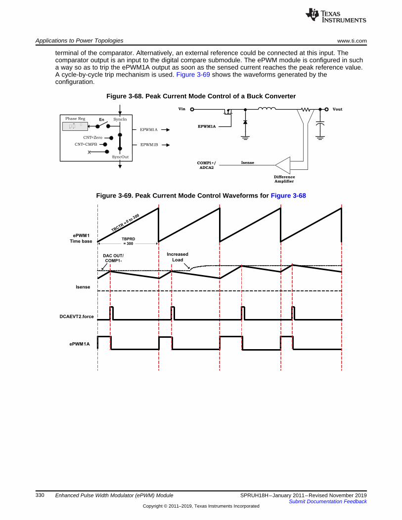
ePWM1A
ePWM1
Time baseTBPRD
= 300
TBCTR =0 to
300
Increased
Load
Isense
DAC OUT/
COMP1-
DCAEVT2.force
Applications to Power Topologies www.ti.com
330 SPRUH18H–January 2011–Revised November 2019Submit Documentation Feedback
Copyright © 2011–2019, Texas Instruments Incorporated
Enhanced Pulse Width Modulator (ePWM) Module
terminal of the comparator. Alternatively, an external reference could be connected at this input. Thecomparator output is an input to the digital compare submodule. The ePWM module is configured in sucha way so as to trip the ePWM1A output as soon as the sensed current reaches the peak reference value.A cycle-by-cycle trip mechanism is used. Figure 3-69 shows the waveforms generated by theconfiguration.
Figure 3-68. Peak Current Mode Control of a Buck Converter
Figure 3-69. Peak Current Mode Control Waveforms for Figure 3-68
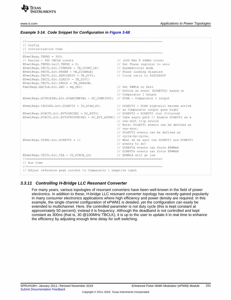
www.ti.com Applications to Power Topologies
331SPRUH18H–January 2011–Revised November 2019Submit Documentation Feedback
Copyright © 2011–2019, Texas Instruments Incorporated
Enhanced Pulse Width Modulator (ePWM) Module
Example 3-14. Code Snippet for Configuration in Figure 3-68
//===========================================================================// Config// Initialization Time//===========================================================================EPwm1Regs.TBPRD = 300;// Period = 300 TBCLK counts // (200 KHz @ 60MHz clock)EPwm1Regs.TBPHS.half.TBPHS = 0; // Set Phase register to zeroEPwm1Regs.TBCTL.bit.CTRMODE = TB_COUNT_UP; // Asymmetrical modeEPwm1Regs.TBCTL.bit.PHSEN = TB_DISABLE; // Phase loading disabledEPwm1Regs.TBCTL.bit.HSPCLKDIV = TB_DIV1; // Clock ratio to SYSCLKOUTEPwm1Regs.TBCTL.bit.CLKDIV = TB_DIV1;EPwm1Regs.TBCTL.bit.PRDLD = TB_SHADOW;Pwm1Regs.AQCTLA.bit.ZRO = AQ_SET; // Set PWM1A on Zero
// Define an event (DCAEVT2) based on// Comparator 1 Output
EPwm1Regs.DCTRIPSEL.bit.DCAHCOMPSEL = DC_COMP1OUT; // DCAH = Comparator 1 output
EPwm1Regs.TZDCSEL.bit.DCAEVT2 = TZ_DCAH_HI; // DCAEVT2 = DCAH high(will become active// as Comparator output goes high)
EPwm1Regs.DCACTL.bit.EVT2SRCSEL = DC_EVT2; // DCAEVT2 = DCAEVT2 (not filtered)EPwm1Regs.DCACTL.bit.EVT2FRCSYNCSEL = DC_EVT_ASYNC; // Take async path // Enable DCAEVT2 as a
// one-shot trip source// Note: DCxEVT1 events can be defined as// one-shot.// DCxEVT2 events can be defined as// cycle-by-cycle.
EPwm1Regs.TZSEL.bit.DCAEVT2 = 1; // What do we want the DCAEVT1 and DCBEVT1// events to do?// DCAEVTx events can force EPWMxA// DCBEVTx events can force EPWMxB
EPwm1Regs.TZCTL.bit.TZA = TZ_FORCE_LO; // EPWM1A will go low//===========================================================================// Run Time//===========================================================================// Adjust reference peak current to Comparator 1 negative input
3.3.11 Controlling H-Bridge LLC Resonant ConverterFor many years, various topologies of resonant converters have been well-known in the field of powerelectronics. In addition to these, H-bridge LLC resonant converter topology has recently gained popularityin many consumer electronics applications where high efficiency and power density are required. In thisexample, the single channel configuration of ePWM1 is detailed, yet the configuration can easily beextended to multichannel. Here, the controlled parameter is not duty cycle (this is kept constant atapproximately 50 percent); instead it is frequency. Although the deadband is not controlled and keptconstant as 300ns (that is, 30 @100MHz TBCLK), it is up to the user to update it in real time to enhancethe efficiency by adjusting enough time delay for soft switching.

CACB
A
P P CACB
A
P
RED
FED
EPWMxA
EPWMxB
P
I
P
I
P
I
ZVS
transition
ZVS
transition
period/2
period
period/4
P
IIndicates this event triggers an interrupt
CB
A
Indicates this event triggers an ADC
start of conversion
VDC_busVOUT
EPWM1A
EPWM1B Cr
Integrated
Magnetcis
LLC Resonant
TransformerEn SyncIn
SyncOut
CNT=Zero
CNT=CMPB
X
!"#" X
Phase Reg
Master
1
Ext Sync In
(optional)
EPWM1A
EPWM1B
NOTE: Θ = X indicates value in phase register is a"don't care"
Applications to Power Topologies www.ti.com
332 SPRUH18H–January 2011–Revised November 2019Submit Documentation Feedback
Copyright © 2011–2019, Texas Instruments Incorporated
Enhanced Pulse Width Modulator (ePWM) Module
Figure 3-70. Control of Two Resonant Converter Stages
Figure 3-71. H-Bridge LLC Resonant Converter PWM Waveforms

www.ti.com Applications to Power Topologies
333SPRUH18H–January 2011–Revised November 2019Submit Documentation Feedback
Copyright © 2011–2019, Texas Instruments Incorporated
Enhanced Pulse Width Modulator (ePWM) Module
Example 3-15. Code Snippet for Configuration in Figure 3-70
//=====================================================================// Config//===================================================================== //Initialization Time//======================== //EPWMxA & EPWMxB configEPwm1Regs.TBCTL.bit.PRDLD = TB_IMMEDIATE; // Set immediate loadEPwm1Regs.TBPRD = period; // PWM frequency = 1 / periodEPwm1Regs.CMPA.half.CMPA = period/2; // Set duty as 50%EPwm1Regs.CMPB = period/4; // Set duty as 25%EPwm1Regs.TBPHS.half.TBPHS = 0; // Set as master, phase =0EPwm1Regs.TBCTR = 0; // Time base counter =0EPwm1Regs.TBCTL.bit.CTRMODE = TB_COUNT_UP; // Count-up mode: used for asymmetric PWMEPwm1Regs.TBCTL.bit.PHSEN = TB_DISABLE; // Disable phase loadingEPwm1Regs.TBCTL.bit.SYNCOSEL = TB_CTR_ZERO; // Used to sync EPWM(n+1)"down-stream"EPwm1Regs.TBCTL.bit.HSPCLKDIV = TB_DIV1; // Set the clock rateEPwm1Regs.TBCTL.bit.CLKDIV = TB_DIV1; // Set the clock rateEPwm1Regs.CMPCTL.bit.LOADAMODE = CC_CTR_PRD; // Load on CTR=PRDEPwm1Regs.CMPCTL.bit.LOADBMODE = CC_CTR_PRD; // Load on CTR=PRDEPwm1Regs.CMPCTL.bit.SHDWAMODE = CC_SHADOW; // Shadow mode. Operates as a double buffer.EPwm1Regs.CMPCTL.bit.SHDWBMODE = CC_SHADOW; // Shadow mode. Operates as a double buffer.EPwm1Regs.AQCTLA.bit.ZRO = AQ_SET; // Set PWM1A on ZeroEPwm1Regs.AQCTLA.bit.CAU = AQ_CLEAR; // Clear PWM1A on event A, up countEPwm1Regs.AQCTLB.bit.CAU = AQ_SET; // Set PWM1B on event A, up countEPwm1Regs.AQCTLB.bit.PRD = AQ_CLEAR; // Clear PWM1B on PRDEPwm1Regs.DBCTL.bit.IN_MODE = DBA_ALL; // EPWMxA is the source for both delaysEPwm1Regs.DBCTL.bit.OUT_MODE = DB_FULL_ENABLE; // Enable Dead-band moduleEPwm1Regs.DBCTL.bit.POLSEL = DB_ACTV_HIC; // Active High Complementary (AHC)EPwm1Regs.DBRED = 30; // RED = 30 TBCLKs initiallyEPwm1Regs.DBFED = 30; // FED = 30 TBCLKs initially
// Configure TZ1 for short cct// protection EALLOW;
EPwm1Regs.TZSEL.bit.OSHT1 = 1; // one-shot source EPwm1Regs.TZCTL.bit.TZA = TZ_FORCE_LO;
// set EPWM1A to low at faultEPwm1Regs.TZCTL.bit.TZB = TZ_FORCE_LO; // set EPWM1B to low at fault instantEPwm1Regs.TZEINT.bit.OST = 1; // Enable TZ interrupt EDIS;
// Enable HiRes option EALLOW;EPwm1Regs.HRCNFG.all = 0x0;EPwm1Regs.HRCNFG.bit.EDGMODE = HR_FEP;EPwm1Regs.HRCNFG.bit.CTLMODE = HR_CMP;EPwm1Regs.HRCNFG.bit.HRLOAD = HR_CTR_PRD;EDIS; // Run Time (Note: Example execution of
// one run-time instant)//============================================================EPwm1Regs.TBPRD = period_new value; // Update new period
// EPwm1Regs.CMPA.half.CMPA= period_new// value/2;// Update new CMPA EPwm1Regs.CMPB= period_new// value/4;// Update new CMPB// Update new CMPB// Update new CMPB

Registers www.ti.com
334 SPRUH18H–January 2011–Revised November 2019Submit Documentation Feedback
Copyright © 2011–2019, Texas Instruments Incorporated
Enhanced Pulse Width Modulator (ePWM) Module
3.4 RegistersThis chapter includes the register layouts and bit description for the submodules.
3.4.1 Time-Base Submodule RegistersFigure 3-72 through Figure 3-80 and Table 3-21 through Table 3-29 provide the time-base registerdefinitions.
Figure 3-72. Time-Base Period Register (TBPRD)15 0
TBPRDR/W-0
LEGEND: R/W = Read/Write; R = Read only; -n = value after reset
Table 3-21. Time-Base Period Register (TBPRD) Field Descriptions
Bit Field Value Description15-0 TBPRD 0000-
FFFFhThese bits determine the period of the time-base counter. This sets the PWM frequency.Shadowing of this register is enabled and disabled by the TBCTL[PRDLD] bit. By default thisregister is shadowed.• If TBCTL[PRDLD] = 0, then the shadow is enabled and any write or read will automatically go to
the shadow register. In this case, the active register will be loaded from the shadow registerwhen the time-base counter equals zero.
• If TBCTL[PRDLD] = 1, then the shadow is disabled and any write or read will go directly to theactive register, that is the register actively controlling the hardware.
• The active and shadow registers share the same memory map address.
Figure 3-73. Time Base Period High Resolution Register (TBPRDHR)15 8
TBPRDHRR/W-0
7 0Reserved
R-0LEGEND: R/W = Read/Write; R = Read only; -n = value after reset
Table 3-22. Time Base Period High Resolution Register (TBPRDHR) Field Descriptions
Bit Field Value Description15-8 TBPRDHR 00-FFh Period High Resolution Bits
These 8-bits contain the high-resolution portion of the period value.The TBPRDHR register is not affected by the TBCTL[PRDLD] bit. Reads from this register alwaysreflect the shadow register. Likewise writes are also to the shadow register. The TBPRDHR registeris only used when the high resolution period feature is enabled.This register is only available with ePWM modules which support high-resolution period control.
7-0 Reserved 0 Reserved
Figure 3-74. Time Base Period Mirror Register (TBPRDM)15 0
TBPRDR/W-0
LEGEND: R/W = Read/Write; R = Read only; -n = value after reset

www.ti.com Registers
335SPRUH18H–January 2011–Revised November 2019Submit Documentation Feedback
Copyright © 2011–2019, Texas Instruments Incorporated
Enhanced Pulse Width Modulator (ePWM) Module
Table 3-23. Time Base Period Mirror Register (TBPRDM) Field Descriptions
Bit Field Value Description15-0 TBPRD 0000-FFFFh TBPRDM and TBPRD can both be used to access the time-base period.
TBPRD provides backwards compatibility with earlier ePWM modules. The mirror registers(TBPRDM and TBPRDHRM) allow for 32-bit writes to TBPRDHR in one access. Due to the oddaddress memory location of the TBPRD legacy register, a 32-bit write is not possible.By default writes to this register are shadowed. Unlike the TBPRD register, reads of TBPRDMalways return the active register value. Shadowing is enabled and disabled by theTBCTL[PRDLD] bit.
• If TBCTL[PRDLD] = 0, then the shadow is enabled and any write will automatically go to theshadow register. In this case the active register will be loaded from the shadow register whenthe time-base counter equals zero. Reads return the active value.
• If TBCTL[PRDLD] = 1, then the shadow is disabled and any write to this register will godirectly to the active register controlling the hardware. Likewise reads return the active value.
Figure 3-75. Time-Base Period High Resolution Mirror Register (TBPRDHRM)15 8
TBPRDHRR/W-0
7 0Reserved
R-0LEGEND: R/W = Read/Write; R = Read only; -n = value after reset
Table 3-24. Time-Base Period High Resolution Mirror Register (TBPRDHRM) Field Descriptions
Bit Field Value Description15-8 TBPRDHR 00-FFh Period High Resolution Bits
These 8-bits contain the high-resolution portion of the period valueTBPRD provides backwards compatibility with earlier ePWM modules. The mirror registers(TBPRDM and TBPRDHRM) allow for 32-bit writes to TBPRDHR in one access. Due to the odd-numbered memory address location of the TBPRD legacy register, a 32-bit write is not possiblewith TBPRD and TBPRDHR.The TBPRDHRM register is not affected by the TBCTL[PRDLD] bitWrites to both the TBPRDHR and TBPRDM locations access the high-resolution (least significant 8-bit) portion of the Time Base Period value. The only difference is that unlike TBPRDHR, reads fromthe mirror register TBPRDHRM, are indeterminate (reserved for TI Test).The TBPRDHRM register is available with ePWM modules which support high-resolution periodcontrol and is used only when the high resolution period feature is enabled.
7-0 Reserved 00-FFh Reserved for TI Test
Figure 3-76. Time-Base Phase Register (TBPHS)15 0
TBPHSR/W-0
LEGEND: R/W = Read/Write; R = Read only; -n = value after reset
Table 3-25. Time-Base Phase Register (TBPHS) Field Descriptions
Bits Name Value Description15-0 TBPHS 0000-FFFF These bits set time-base counter phase of the selected ePWM relative to the time-base that is
supplying the synchronization input signal.• If TBCTL[PHSEN] = 0, then the synchronization event is ignored and the time-base counter is
not loaded with the phase.• If TBCTL[PHSEN] = 1, then the time-base counter (TBCTR) will be loaded with the phase
(TBPHS) when a synchronization event occurs. The synchronization event can be initiated bythe input synchronization signal (EPWMxSYNCI) or by a software forced synchronization.

Registers www.ti.com
336 SPRUH18H–January 2011–Revised November 2019Submit Documentation Feedback
Copyright © 2011–2019, Texas Instruments Incorporated
Enhanced Pulse Width Modulator (ePWM) Module
Figure 3-77. Time-Base Phase High Resolution Register (TBPHSHR)15 8
TBPHSHRR/W-0
7 0Reserved
R-0LEGEND: R/W = Read/Write; R = Read only; -n = value after reset
Table 3-26. Time-Base Phase High Resolution Register (TBPHSHR) Field Descriptions
Bit Field Value Description15-8 TBPHSHR 00-FFh Time base phase high-resolution bits7-0 Reserved Reserved
Figure 3-78. Time-Base Counter Register (TBCTR)15 0
TBCTRR/W-0
LEGEND: R/W = Read/Write; R = Read only; -n = value after reset
Table 3-27. Time-Base Counter Register (TBCTR) Field Descriptions
Bits Name Value Description15-0 TBCTR 0000-
FFFFReading these bits gives the current time-base counter value.
Writing to these bits sets the current time-base counter value. The update happens as soon as thewrite occurs; the write is NOT synchronized to the time-base clock (TBCLK) and the register is notshadowed.
Figure 3-79. Time-Base Control Register (TBCTL)15 14 13 12 10 9 8
FREE, SOFT PHSDIR CLKDIV HSPCLKDIVR/W-0 R/W-0 R/W-0 R/W-0,0,1
7 6 5 4 3 2 1 0HSPCLKDIV SWFSYNC SYNCOSEL PRDLD PHSEN CTRMODE
R/W-0,0,1 R/W-0 R/W-0 R/W-0 R/W-0 R/W-11LEGEND: R/W = Read/Write; R = Read only; -n = value after reset
Table 3-28. Time-Base Control Register (TBCTL) Field Descriptions
Bit Field Value Description15:14 FREE, SOFT Emulation Mode Bits. These bits select the behavior of the ePWM time-base counter during
emulation events:00 Stop after the next time-base counter increment or decrement01 Stop when counter completes a whole cycle:
• Up-count mode: stop when the time-base counter = period (TBCTR = TBPRD)• Down-count mode: stop when the time-base counter = 0x0000 (TBCTR = 0x0000)• Up-down-count mode: stop when the time-base counter = 0x0000 (TBCTR = 0x0000)
1X Free run

www.ti.com Registers
337SPRUH18H–January 2011–Revised November 2019Submit Documentation Feedback
Copyright © 2011–2019, Texas Instruments Incorporated
Enhanced Pulse Width Modulator (ePWM) Module
Table 3-28. Time-Base Control Register (TBCTL) Field Descriptions (continued)Bit Field Value Description13 PHSDIR Phase Direction Bit.
This bit is only used when the time-base counter is configured in the up-down-count mode. ThePHSDIR bit indicates the direction the time-base counter (TBCTR) will count after a synchronizationevent occurs and a new phase value is loaded from the phase (TBPHS) register. This isirrespective of the direction of the counter before the synchronization event..In the up-count and down-count modes this bit is ignored.
0 Count down after the synchronization event.1 Count up after the synchronization event.
12:10 CLKDIV Time-base Clock Prescale BitsThese bits determine part of the time-base clock prescale value.TBCLK = SYSCLKOUT / (HSPCLKDIV × CLKDIV)
000 /1 (default on reset)001 /2010 /4011 /8100 /16101 /32110 /64111 /128
9:7 HSPCLKDIV High Speed Time-base Clock Prescale BitsThese bits determine part of the time-base clock prescale value.TBCLK = SYSCLKOUT / (HSPCLKDIV × CLKDIV)This divisor emulates the HSPCLK in the TMS320x281x system as used on the Event Manager(EV) peripheral.
000 /1001 /2 (default on reset)010 /4011 /6100 /8101 /10110 /12111 /14
6 SWFSYNC Software Forced Synchronization Pulse0 Writing a 0 has no effect and reads always return a 0.1 Writing a 1 forces a one-time synchronization pulse to be generated.
This event is ORed with the EPWMxSYNCI input of the ePWM module.SWFSYNC is valid (operates) only when EPWMxSYNCI is selected by SYNCOSEL = 00.
5:4 SYNCOSEL Synchronization Output Select. These bits select the source of the EPWMxSYNCO signal.00 EPWMxSYNC:01 CTR = zero: Time-base counter equal to zero (TBCTR = 0x0000)10 CTR = CMPB : Time-base counter equal to counter-compare B (TBCTR = CMPB)11 Disable EPWMxSYNCO signal
3 PRDLD Active Period Register Load From Shadow Register Select0 The period register (TBPRD) is loaded from its shadow register when the time-base counter,
TBCTR, is equal to zero.A write or read to the TBPRD register accesses the shadow register.
1 Load the TBPRD register immediately without using a shadow register.A write or read to the TBPRD register directly accesses the active register.

Registers www.ti.com
338 SPRUH18H–January 2011–Revised November 2019Submit Documentation Feedback
Copyright © 2011–2019, Texas Instruments Incorporated
Enhanced Pulse Width Modulator (ePWM) Module
Table 3-28. Time-Base Control Register (TBCTL) Field Descriptions (continued)Bit Field Value Description2 PHSEN Counter Register Load From Phase Register Enable
0 Do not load the time-base counter (TBCTR) from the time-base phase register (TBPHS)1 Load the time-base counter with the phase register when an EPWMxSYNCI input signal occurs or
when a software synchronization is forced by the SWFSYNC bit, or when a digital compare syncevent occurs.
1:0 CTRMODE Counter ModeThe time-base counter mode is normally configured once and not changed during normal operation.If you change the mode of the counter, the change will take effect at the next TBCLK edge and thecurrent counter value shall increment or decrement from the value before the mode change.These bits set the time-base counter mode of operation as follows:
00 Up-count mode01 Down-count mode10 Up-down-count mode11 Stop-freeze counter operation (default on reset)

www.ti.com Registers
339SPRUH18H–January 2011–Revised November 2019Submit Documentation Feedback
Copyright © 2011–2019, Texas Instruments Incorporated
Enhanced Pulse Width Modulator (ePWM) Module
Figure 3-80. Time-Base Status Register (TBSTS)15 8
ReservedR-0
7 3 2 1 0Reserved CTRMAX SYNCI CTRDIR
R-0 R/W1C-0 R/W1C-0 R-1LEGEND: R/W = Read/Write; R = Read only; R/W1C = Read/Write 1 to clear; -n = value after reset
Table 3-29. Time-Base Status Register (TBSTS) Field Descriptions
Bit Field Value Description15:3 Reserved Reserved
2 CTRMAX Time-Base Counter Max Latched Status Bit0 Reading a 0 indicates the time-base counter never reached its maximum value. Writing a 0 will
have no effect.1 Reading a 1 on this bit indicates that the time-base counter reached the max value 0xFFFF. Writing
a 1 to this bit will clear the latched event.1 SYNCI Input Synchronization Latched Status Bit
0 Writing a 0 will have no effect. Reading a 0 indicates no external synchronization event hasoccurred.
1 Reading a 1 on this bit indicates that an external synchronization event has occurred(EPWMxSYNCI). Writing a 1 to this bit will clear the latched event.
0 CTRDIR Time-Base Counter Direction Status Bit. At reset, the counter is frozen; therefore, this bit has nomeaning. To make this bit meaningful, you must first set the appropriate mode viaTBCTL[CTRMODE].
0 Time-Base Counter is currently counting down.1 Time-Base Counter is currently counting up.
Figure 3-81. EPWM DMA/CLA Configuration (EPWMCFG) Register15 14 13 12 11 10 9 8 7 6 5 4 3 2 1 0
Reserved CONFIG
R-0 R/W-0LEGEND: R/W = Read/Write; R = Read only; -n = value after reset
Table 3-30. EPWM DMA/CLA Configuration (EPWMCFG) Register Field Descriptions
Bit Field Value Description15-1 Reserved Any writes to these bits must always have a value of 0.
0 CONFIG EPWM DMA Enable Bit:0 The EPWM blocks are connected to the CLA bus and are inaccessible to the DMA bus1 The EPWM blocks are connected to the DMA bus and are inaccessible to the CLA bus
Figure 3-82. High Resolution Period Control Register (HRPCTL)15 8
ReservedR-0
7 3 2 1 0Reserved TBPHSHR
LOADEReserved HRPE
R-0 R/W-0 R-0 R/W-0LEGEND: R/W = Read/Write; R = Read only; -n = value after reset
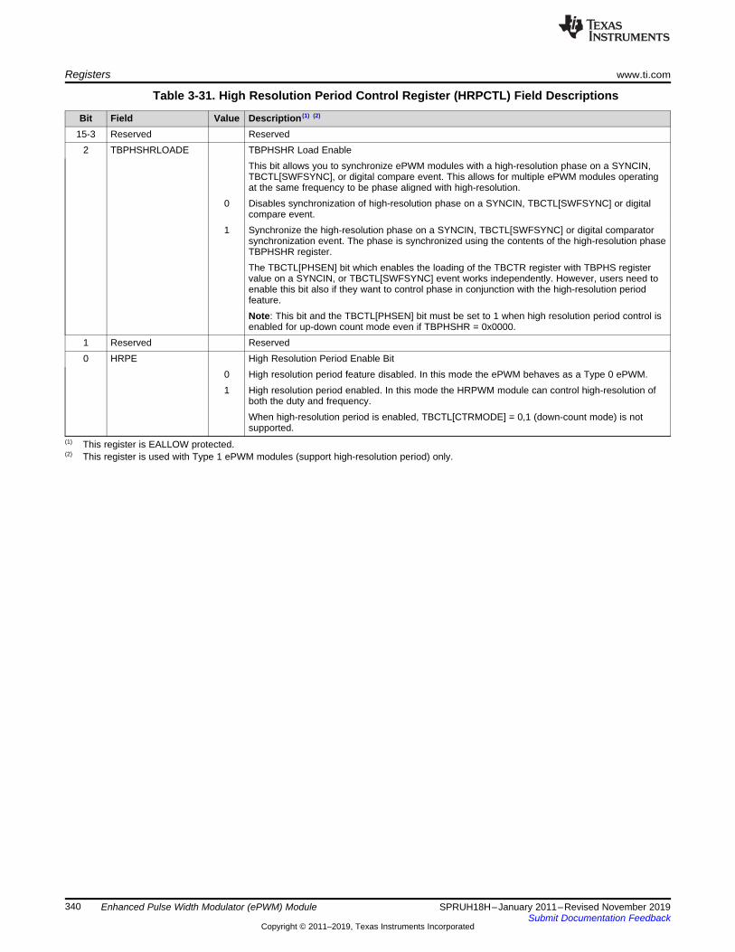
Registers www.ti.com
340 SPRUH18H–January 2011–Revised November 2019Submit Documentation Feedback
Copyright © 2011–2019, Texas Instruments Incorporated
Enhanced Pulse Width Modulator (ePWM) Module
(1) This register is EALLOW protected.(2) This register is used with Type 1 ePWM modules (support high-resolution period) only.
Table 3-31. High Resolution Period Control Register (HRPCTL) Field Descriptions
Bit Field Value Description (1) (2)
15-3 Reserved Reserved2 TBPHSHRLOADE TBPHSHR Load Enable
This bit allows you to synchronize ePWM modules with a high-resolution phase on a SYNCIN,TBCTL[SWFSYNC], or digital compare event. This allows for multiple ePWM modules operatingat the same frequency to be phase aligned with high-resolution.
0 Disables synchronization of high-resolution phase on a SYNCIN, TBCTL[SWFSYNC] or digitalcompare event.
1 Synchronize the high-resolution phase on a SYNCIN, TBCTL[SWFSYNC] or digital comparatorsynchronization event. The phase is synchronized using the contents of the high-resolution phaseTBPHSHR register.The TBCTL[PHSEN] bit which enables the loading of the TBCTR register with TBPHS registervalue on a SYNCIN, or TBCTL[SWFSYNC] event works independently. However, users need toenable this bit also if they want to control phase in conjunction with the high-resolution periodfeature.Note: This bit and the TBCTL[PHSEN] bit must be set to 1 when high resolution period control isenabled for up-down count mode even if TBPHSHR = 0x0000.
1 Reserved Reserved0 HRPE High Resolution Period Enable Bit
0 High resolution period feature disabled. In this mode the ePWM behaves as a Type 0 ePWM.1 High resolution period enabled. In this mode the HRPWM module can control high-resolution of
both the duty and frequency.When high-resolution period is enabled, TBCTL[CTRMODE] = 0,1 (down-count mode) is notsupported.

www.ti.com Registers
341SPRUH18H–January 2011–Revised November 2019Submit Documentation Feedback
Copyright © 2011–2019, Texas Instruments Incorporated
Enhanced Pulse Width Modulator (ePWM) Module
3.4.2 Counter-Compare Submodule RegistersFigure 3-83 through Figure 3-85 and Table 3-32 through Table 3-34 illustrate the counter-comparesubmodule control and status registers.
Figure 3-83. Counter-Compare A Register (CMPA)15 0
CMPAR/W-0
LEGEND: R/W = Read/Write; R = Read only; -n = value after reset
Table 3-32. Counter-Compare A Register (CMPA) Field Descriptions
Bits Name Description15-0 CMPA The value in the active CMPA register is continuously compared to the time-base counter (TBCTR). When
the values are equal, the counter-compare module generates a "time-base counter equal to countercompare A" event. This event is sent to the action-qualifier where it is qualified and converted it into oneor more actions. These actions can be applied to either the EPWMxA or the EPWMxB output dependingon the configuration of the AQCTLA and AQCTLB registers. The actions that can be defined in theAQCTLA and AQCTLB registers include:
• Do nothing; the event is ignored.• Clear: Pull the EPWMxA and/or EPWMxB signal low• Set: Pull the EPWMxA and/or EPWMxB signal high• Toggle the EPWMxA and/or EPWMxB signal
Shadowing of this register is enabled and disabled by the CMPCTL[SHDWAMODE] bit. By default thisregister is shadowed.
• If CMPCTL[SHDWAMODE] = 0, then the shadow is enabled and any write or read will automaticallygo to the shadow register. In this case, the CMPCTL[LOADAMODE] bit field determines which eventwill load the active register from the shadow register.
• Before a write, the CMPCTL[SHDWAFULL] bit can be read to determine if the shadow register iscurrently full.
• If CMPCTL[SHDWAMODE] = 1, then the shadow register is disabled and any write or read will godirectly to the active register, that is the register actively controlling the hardware.
• In either mode, the active and shadow registers share the same memory map address.
Figure 3-84. Counter-Compare B Register (CMPB)15 0
CMPBR/W-0
LEGEND: R/W = Read/Write; R = Read only; -n = value after reset

Registers www.ti.com
342 SPRUH18H–January 2011–Revised November 2019Submit Documentation Feedback
Copyright © 2011–2019, Texas Instruments Incorporated
Enhanced Pulse Width Modulator (ePWM) Module
Table 3-33. Counter-Compare B Register (CMPB) Field Descriptions
Bits Name Description15-0 CMPB The value in the active CMPB register is continuously compared to the time-base counter (TBCTR). When
the values are equal, the counter-compare module generates a "time-base counter equal to countercompare B" event. This event is sent to the action-qualifier where it is qualified and converted it into oneor more actions. These actions can be applied to either the EPWMxA or the EPWMxB output dependingon the configuration of the AQCTLA and AQCTLB registers. The actions that can be defined in theAQCTLA and AQCTLB registers include:
• Do nothing. event is ignored.• Clear: Pull the EPWMxA and/or EPWMxB signal low• Set: Pull the EPWMxA and/or EPWMxB signal high• Toggle the EPWMxA and/or EPWMxB signal
Shadowing of this register is enabled and disabled by the CMPCTL[SHDWBMODE] bit. By default thisregister is shadowed.
• If CMPCTL[SHDWBMODE] = 0, then the shadow is enabled and any write or read will automaticallygo to the shadow register. In this case, the CMPCTL[LOADBMODE] bit field determines which eventwill load the active register from the shadow register:
• Before a write, the CMPCTL[SHDWBFULL] bit can be read to determine if the shadow register iscurrently full.
• If CMPCTL[SHDWBMODE] = 1, then the shadow register is disabled and any write or read will godirectly to the active register, that is the register actively controlling the hardware.
• In either mode, the active and shadow registers share the same memory map address.

www.ti.com Registers
343SPRUH18H–January 2011–Revised November 2019Submit Documentation Feedback
Copyright © 2011–2019, Texas Instruments Incorporated
Enhanced Pulse Width Modulator (ePWM) Module
Figure 3-85. Counter-Compare Control Register (CMPCTL)15 10 9 8
Reserved SHDWBFULL SHDWAFULLR-0 R-0 R-0
7 6 5 4 3 2 1 0Reserved SHDWBMODE Reserved SHDWAMODE LOADBMODE LOADAMODE
R-0 R/W-0 R-0 R/W-0 R/W-0 R/W-0LEGEND: R/W = Read/Write; R = Read only; -n = value after reset
Table 3-34. Counter-Compare Control Register (CMPCTL) Field Descriptions
Bits Name Value Description15-10 Reserved Reserved
9 SHDWBFULL Counter-compare B (CMPB) Shadow Register Full Status FlagThis bit self clears once a load-strobe occurs.
0 CMPB shadow FIFO not full yet1 Indicates the CMPB shadow FIFO is full; a CPU write will overwrite current shadow value.
8 SHDWAFULL Counter-compare A (CMPA) Shadow Register Full Status FlagThe flag bit is set when a 32-bit write to CMPA:CMPAHR register or a 16-bit write to CMPAregister is made. A 16-bit write to CMPAHR register will not affect the flag.This bit self clears once a load-strobe occurs.
0 CMPA shadow FIFO not full yet1 Indicates the CMPA shadow FIFO is full, a CPU write will overwrite the current shadow
value.7 Reserved Reserved6 SHDWBMODE Counter-compare B (CMPB) Register Operating Mode
0 Shadow mode. Operates as a double buffer. All writes via the CPU access the shadowregister.
1 Immediate mode. Only the active compare B register is used. All writes and reads directlyaccess the active register for immediate compare action.
5 Reserved Reserved4 SHDWAMODE Counter-compare A (CMPA) Register Operating Mode
0 Shadow mode. Operates as a double buffer. All writes via the CPU access the shadowregister.
1 Immediate mode. Only the active compare register is used. All writes and reads directlyaccess the active register for immediate compare action
3-2 LOADBMODE Active Counter-Compare B (CMPB) Load From Shadow Select ModeThis bit has no effect in immediate mode (CMPCTL[SHDWBMODE] = 1).
00 Load on CTR = Zero: Time-base counter equal to zero (TBCTR = 0x0000)01 Load on CTR = PRD: Time-base counter equal to period (TBCTR = TBPRD)10 Load on either CTR = Zero or CTR = PRD11 Freeze (no loads possible)
1-0 LOADAMODE Active Counter-Compare A (CMPA) Load From Shadow Select Mode.This bit has no effect in immediate mode (CMPCTL[SHDWAMODE] = 1).
00 Load on CTR = Zero: Time-base counter equal to zero (TBCTR = 0x0000)01 Load on CTR = PRD: Time-base counter equal to period (TBCTR = TBPRD)10 Load on either CTR = Zero or CTR = PRD11 Freeze (no loads possible)

Registers www.ti.com
344 SPRUH18H–January 2011–Revised November 2019Submit Documentation Feedback
Copyright © 2011–2019, Texas Instruments Incorporated
Enhanced Pulse Width Modulator (ePWM) Module
Figure 3-86. Compare A High Resolution Register (CMPAHR)15 8
CMPAHRR/W-0
7 0Reserved
R-0LEGEND: R/W = Read/Write; R = Read only; -n = value after reset
Table 3-35. Compare A High Resolution Register (CMPAHR) Field Descriptions
Bit Field Value Description15-8 CMPAHR 00-FFh These 8-bits contain the high-resolution portion (least significant 8-bits) of the counter-compare A
value. CMPA:CMPAHR can be accessed in a single 32-bit read/write.Shadowing is enabled and disabled by the CMPCTL[SHDWAMODE] bit as described for the CMPAregister.
7-0 Reserved Reserved for TI Test
Figure 3-87. Counter-Compare A Mirror Register (CMPAM)15 0
CMPAR/W-0
LEGEND: R/W = Read/Write; R = Read only; -n = value after reset
Table 3-36. Counter-Compare A Mirror Register (CMPAM) Field Descriptions
Bit Field Value Description15-0 CMPA 0000-FFFFh CMPA and CMPAM can both be used to access the counter-compare A value. The only difference
is that the mirror register always reads back the active value.By default writes to this register are shadowed. Unlike the CMPA register, reads of CMPAM alwaysreturn the active register value. Shadowing is enabled and disabled by theCMPCTL[SHDWAMODE] bit.
• If CMPCTL[SHDWAMODE] = 0, then the shadow is enabled and any write will automatically goto the shadow register. All reads will reflect the active register value. In this case, theCMPCTL[LOADAMODE] bit field determines which event will load the active register from theshadow register.
• Before a write, the CMPCTL[SHDWAFULL] bit can be read to determine if the shadow registeris currently full.
• If CMPCTL[SHDWAMODE] = 1, then the shadow register is disabled and any write will godirectly to the active register, that is the register actively controlling the hardware.
Figure 3-88. Compare A High Resolution Mirror Register15 8
CMPAHRR/W-0
7 0Reserved
R-0LEGEND: R/W = Read/Write; R = Read only; -n = value after reset

www.ti.com Registers
345SPRUH18H–January 2011–Revised November 2019Submit Documentation Feedback
Copyright © 2011–2019, Texas Instruments Incorporated
Enhanced Pulse Width Modulator (ePWM) Module
Table 3-37. Compare A High-Resolution Mirror Register (CMPAHRM) Field Descriptions
Bit Field Value Description15-8 CMPAHR 00-FFh Compare A High Resolution Bits
Writes to both the CMPAHR and CMPAHRM locations access the high-resolution (least significant8-bit) portion of the Counter Compare A value. The only difference is that unlike CMPAHR, readsfrom the mirror register, CMPAHRM, are indeterminate (reserved for TI Test).By default writes to this register are shadowed. Shadowing is enabled and disabled by theCMPCTL[SHDWAMODE] bit as described for the CMPAM register.
7-0 Reserved Reserved for TI Test
3.4.3 Action-Qualifier Submodule RegistersFigure 3-89 through Figure 3-92 and Table 3-38 through Table 3-41 provide the action-qualifier submoduleregister definitions.
Figure 3-89. Action-Qualifier Output A Control Register (AQCTLA)15 12 11 10 9 8
Reserved CBD CBUR-0 R/W-0 R/W-0
7 6 5 4 3 2 1 0CAD CAU PRD ZRO
R/W-0 R/W-0 R/W-0 R/W-0LEGEND: R/W = Read/Write; R = Read only; -n = value after reset
Table 3-38. Action-Qualifier Output A Control Register (AQCTLA) Field Descriptions
Bits Name Value Description15-12 Reserved Reserved11-10 CBD Action when the time-base counter equals the active CMPB register and the counter is
decrementing.00 Do nothing (action disabled)01 Clear: force EPWMxA output low.10 Set: force EPWMxA output high.11 Toggle EPWMxA output: low output signal will be forced high, and a high signal will be forced low.
9-8 CBU Action when the counter equals the active CMPB register and the counter is incrementing.00 Do nothing (action disabled)01 Clear: force EPWMxA output low.10 Set: force EPWMxA output high.11 Toggle EPWMxA output: low output signal will be forced high, and a high signal will be forced low.
7-6 CAD Action when the counter equals the active CMPA register and the counter is decrementing.00 Do nothing (action disabled)01 Clear: force EPWMxA output low.10 Set: force EPWMxA output high.11 Toggle EPWMxA output: low output signal will be forced high, and a high signal will be forced low.
5-4 CAU Action when the counter equals the active CMPA register and the counter is incrementing.00 Do nothing (action disabled)01 Clear: force EPWMxA output low.10 Set: force EPWMxA output high.11 Toggle EPWMxA output: low output signal will be forced high, and a high signal will be forced low.

Registers www.ti.com
346 SPRUH18H–January 2011–Revised November 2019Submit Documentation Feedback
Copyright © 2011–2019, Texas Instruments Incorporated
Enhanced Pulse Width Modulator (ePWM) Module
Table 3-38. Action-Qualifier Output A Control Register (AQCTLA) Field Descriptions (continued)Bits Name Value Description3-2 PRD Action when the counter equals the period.
Note: By definition, in count up-down mode when the counter equals period the direction is definedas 0 or counting down.
00 Do nothing (action disabled)01 Clear: force EPWMxA output low.10 Set: force EPWMxA output high.11 Toggle EPWMxA output: low output signal will be forced high, and a high signal will be forced low.
1-0 ZRO Action when counter equals zero.Note: By definition, in count up-down mode when the counter equals 0 the direction is defined as 1or counting up.
00 Do nothing (action disabled)01 Clear: force EPWMxA output low.10 Set: force EPWMxA output high.11 Toggle EPWMxA output: low output signal will be forced high, and a high signal will be forced low.
Figure 3-90. Action-Qualifier Output B Control Register (AQCTLB)15 12 11 10 9 8
Reserved CBD CBUR-0 R/W-0 R/W-0
7 6 5 4 3 2 1 0CAD CAU PRD ZRO
R/W-0 R/W-0 R/W-0 R/W-0LEGEND: R/W = Read/Write; R = Read only; -n = value after reset
Table 3-39. Action-Qualifier Output B Control Register (AQCTLB) Field Descriptions
Bits Name Value Description15-12 Reserved11-10 CBD Action when the counter equals the active CMPB register and the counter is decrementing.
00 Do nothing (action disabled)01 Clear: force EPWMxB output low.10 Set: force EPWMxB output high.11 Toggle EPWMxB output: low output signal will be forced high, and a high signal will be forced low.
9-8 CBU Action when the counter equals the active CMPB register and the counter is incrementing.00 Do nothing (action disabled)01 Clear: force EPWMxB output low.10 Set: force EPWMxB output high.11 Toggle EPWMxB output: low output signal will be forced high, and a high signal will be forced low.
7-6 CAD Action when the counter equals the active CMPA register and the counter is decrementing.00 Do nothing (action disabled)01 Clear: force EPWMxB output low.10 Set: force EPWMxB output high.11 Toggle EPWMxB output: low output signal will be forced high, and a high signal will be forced low.
5-4 CAU Action when the counter equals the active CMPA register and the counter is incrementing.00 Do nothing (action disabled)01 Clear: force EPWMxB output low.10 Set: force EPWMxB output high.11 Toggle EPWMxB output: low output signal will be forced high, and a high signal will be forced low.

www.ti.com Registers
347SPRUH18H–January 2011–Revised November 2019Submit Documentation Feedback
Copyright © 2011–2019, Texas Instruments Incorporated
Enhanced Pulse Width Modulator (ePWM) Module
Table 3-39. Action-Qualifier Output B Control Register (AQCTLB) Field Descriptions (continued)Bits Name Value Description3-2 PRD Action when the counter equals the period.
Note: By definition, in count up-down mode when the counter equals period the direction is definedas 0 or counting down.
00 Do nothing (action disabled)01 Clear: force EPWMxB output low.10 Set: force EPWMxB output high.11 Toggle EPWMxB output: low output signal will be forced high, and a high signal will be forced low.
1-0 ZRO Action when counter equals zero.Note: By definition, in count up-down mode when the counter equals 0 the direction is defined as 1or counting up.
00 Do nothing (action disabled)01 Clear: force EPWMxB output low.10 Set: force EPWMxB output high.11 Toggle EPWMxB output: low output signal will be forced high, and a high signal will be forced low.
Figure 3-91. Action-Qualifier Software Force Register (AQSFRC)15 8
ReservedR-0
7 6 5 4 3 2 1 0RLDCSF OTSFB ACTSFB OTSFA ACTSFA
R/W-0 R/W-0 R/W-0 R/W-0 R/W-0LEGEND: R/W = Read/Write; R = Read only; -n = value after reset
Table 3-40. Action-Qualifier Software Force Register (AQSFRC) Field Descriptions
Bit Field Value Description15:8 Reserved7:6 RLDCSF AQCSFRC Active Register Reload From Shadow Options
00 Load on event counter equals zero01 Load on event counter equals period10 Load on event counter equals zero or counter equals period11 Load immediately (the active register is directly accessed by the CPU and is not loaded from the
shadow register).5 OTSFB One-Time Software Forced Event on Output B
0 Writing a 0 (zero) has no effect. Always reads back a 0This bit is auto cleared once a write to this register is complete, i.e., a forced event is initiated.)This is a one-shot forced event. It can be overridden by another subsequent event on output B.
1 Initiates a single s/w forced event4:3 ACTSFB Action when One-Time Software Force B Is invoked
00 Does nothing (action disabled)01 Clear (low)10 Set (high)11 Toggle (Low -> High, High -> Low)
Note: This action is not qualified by counter direction (CNT_dir)

Registers www.ti.com
348 SPRUH18H–January 2011–Revised November 2019Submit Documentation Feedback
Copyright © 2011–2019, Texas Instruments Incorporated
Enhanced Pulse Width Modulator (ePWM) Module
Table 3-40. Action-Qualifier Software Force Register (AQSFRC) Field Descriptions (continued)Bit Field Value Description2 OTSFA One-Time Software Forced Event on Output A
0 Writing a 0 (zero) has no effect. Always reads back a 0.This bit is auto cleared once a write to this register is complete ( i.e., a forced event is initiated).
1 Initiates a single software forced event1:0 ACTSFA Action When One-Time Software Force A Is Invoked
00 Does nothing (action disabled)01 Clear (low)10 Set (high)11 Toggle (Low → High, High → Low)
Note: This action is not qualified by counter direction (CNT_dir)
Figure 3-92. Action-Qualifier Continuous Software Force Register (AQCSFRC)15 8
ReservedR-0
7 4 3 2 1 0Reserved CSFB CSFA
R-0 R/W-0 R/W-0LEGEND: R/W = Read/Write; R = Read only; -n = value after reset
Table 3-41. Action-qualifier Continuous Software Force Register (AQCSFRC) Field Descriptions
Bits Name Value Description15-4 Reserved Reserved3-2 CSFB Continuous Software Force on Output B
In immediate mode, a continuous force takes effect on the next TBCLK edge.In shadow mode, a continuous force takes effect on the next TBCLK edge after a shadow load intothe active register. To configure shadow mode, use AQSFRC[RLDCSF].
00 Software forcing is disabled and has no effect01 Forces a continuous low on output B10 Forces a continuous high on output B11 Software forcing is disabled and has no effect
1-0 CSFA Continuous Software Force on Output AIn immediate mode, a continuous force takes effect on the next TBCLK edge.In shadow mode, a continuous force takes effect on the next TBCLK edge after a shadow load intothe active register.
00 Software forcing is disabled and has no effect01 Forces a continuous low on output A10 Forces a continuous high on output A11 Software forcing is disabled and has no effect
3.4.4 Dead-Band Submodule RegistersFigure 3-93 through Table 3-44 provide the register definitions.

www.ti.com Registers
349SPRUH18H–January 2011–Revised November 2019Submit Documentation Feedback
Copyright © 2011–2019, Texas Instruments Incorporated
Enhanced Pulse Width Modulator (ePWM) Module
Figure 3-93. Dead-Band Generator Control Register (DBCTL)15 14 8
HALFCYCLE ReservedR/W-0 R-0
7 6 5 4 3 2 1 0Reserved IN_MODE POLSEL OUT_MODE
R-0 R/W-0 R/W-0 R/W-0LEGEND: R/W = Read/Write; R = Read only; -n = value after reset
Table 3-42. Dead-Band Generator Control Register (DBCTL) Field Descriptions
Bits Name Value Description15 HALFCYCLE Half Cycle Clocking Enable Bit:
0 Full cycle clocking enabled. The dead-band counters are clocked at the TBCLK rate.1 Half cycle clocking enabled. The dead-band counters are clocked at TBCLK*2.
14-6 Reserved Reserved5-4 IN_MODE Dead Band Input Mode Control
Bit 5 controls the S5 switch and bit 4 controls the S4 switch shown in Figure 3-29.This allows you to select the input source to the falling-edge and rising-edge delay.To produce classical dead-band waveforms the default is EPWMxA In is the source for bothfalling and rising-edge delays.
00 EPWMxA In (from the action-qualifier) is the source for both falling-edge and rising-edgedelay.
01 EPWMxB In (from the action-qualifier) is the source for rising-edge delayed signal.EPWMxA In (from the action-qualifier) is the source for falling-edge delayed signal.
10 EPWMxA In (from the action-qualifier) is the source for rising-edge delayed signal.EPWMxB In (from the action-qualifier) is the source for falling-edge delayed signal.
11 EPWMxB In (from the action-qualifier) is the source for both rising-edge delay and falling-edge delayed signal.
3-2 POLSEL Polarity Select ControlBit 3 controls the S3 switch and bit 2 controls the S2 switch shown in Figure 3-29.This allows you to selectively invert one of the delayed signals before it is sent out of thedead-band submodule.The following descriptions correspond to classical upper/lower switch control as found in oneleg of a digital motor control inverter.These assume that DBCTL[OUT_MODE] = 1,1 and DBCTL[IN_MODE] = 0,0. Otherenhanced modes are also possible, but not regarded as typical usage modes.
00 Active high (AH) mode. Neither EPWMxA nor EPWMxB is inverted (default).01 Active low complementary (ALC) mode. EPWMxA is inverted.10 Active high complementary (AHC). EPWMxB is inverted.11 Active low (AL) mode. Both EPWMxA and EPWMxB are inverted.

Registers www.ti.com
350 SPRUH18H–January 2011–Revised November 2019Submit Documentation Feedback
Copyright © 2011–2019, Texas Instruments Incorporated
Enhanced Pulse Width Modulator (ePWM) Module
Table 3-42. Dead-Band Generator Control Register (DBCTL) Field Descriptions (continued)Bits Name Value Description1-0 OUT_MODE Dead-band Output Mode Control
Bit 1 controls the S1 switch and bit 0 controls the S0 switch shown in Figure 3-29.This allows you to selectively enable or bypass the dead-band generation for the falling-edgeand rising-edge delay.
00 Dead-band generation is bypassed for both output signals. In this mode, both the EPWMxAand EPWMxB output signals from the action-qualifier are passed directly to the PWM-choppersubmodule.In this mode, the POLSEL and IN_MODE bits have no effect.
01 Disable rising-edge delay. The EPWMxA signal from the action-qualifier is passed straightthrough to the EPWMxA input of the PWM-chopper submodule.The falling-edge delayed signal is seen on output EPWMxB. The input signal for the delay isdetermined by DBCTL[IN_MODE].
10 The rising-edge delayed signal is seen on output EPWMxA. The input signal for the delay isdetermined by DBCTL[IN_MODE].Disable falling-edge delay. The EPWMxB signal from the action-qualifier is passed straightthrough to the EPWMxB input of the PWM-chopper submodule.
11 Dead-band is fully enabled for both rising-edge delay on output EPWMxA and falling-edgedelay on output EPWMxB. The input signal for the delay is determined by DBCTL[IN_MODE].
Figure 3-94. Dead-Band Generator Rising Edge Delay Register (DBRED)15 10 9 8
Reserved DELR-0 R/W-0
7 0DEL
R/W-0LEGEND: R/W = Read/Write; R = Read only; -n = value after reset
Table 3-43. Dead-Band Generator Rising Edge Delay Register (DBRED) Field Descriptions
Bits Name Value Description15-10 Reserved Reserved9-0 DEL Rising Edge Delay Count. 10-bit counter.
Figure 3-95. Dead-Band Generator Falling Edge Delay Register (DBFED)15 10 9 8
Reserved DELR-0 R/W-0
7 0DEL
R/W-0LEGEND: R/W = Read/Write; R = Read only; -n = value after reset
Table 3-44. Dead-Band Generator Falling Edge Delay Register (DBFED) Field Descriptions
Bits Name Description15-10 Reserved Reserved9-0 DEL Falling Edge Delay Count. 10-bit counter

www.ti.com Registers
351SPRUH18H–January 2011–Revised November 2019Submit Documentation Feedback
Copyright © 2011–2019, Texas Instruments Incorporated
Enhanced Pulse Width Modulator (ePWM) Module
3.4.5 PWM-Chopper Submodule Control RegisterFigure 3-96 and Table 3-45 provide the definitions for the PWM-chopper submodule control register.
Figure 3-96. PWM-Chopper Control Register (PCCTL)15 11 10 8
Reserved CHPDUTYR-0 R/W-0
7 5 4 1 0CHPFREQ OSHTWTH CHPEN
R/W-0 R/W-0 R/W-0LEGEND: R/W = Read/Write; R = Read only; -n = value after reset
Table 3-45. PWM-Chopper Control Register (PCCTL) Bit Descriptions
Bits Name Value Description15-11 Reserved Reserved10-8 CHPDUTY Chopping Clock Duty Cycle
000 Duty = 1/8 (12.5%)001 Duty = 2/8 (25.0%)010 Duty = 3/8 (37.5%)011 Duty = 4/8 (50.0%)100 Duty = 5/8 (62.5%)101 Duty = 6/8 (75.0%)110 Duty = 7/8 (87.5%)111 Reserved
7:5 CHPFREQ Chopping Clock Frequency000 Divide by 1 (no prescale, = 11.25 MHz at 90 MHz SYSCLKOUT)001 Divide by 2 (5.63 MHz at 90 MHz SYSCLKOUT)010 Divide by 3 (3.75 MHz at 90 MHz SYSCLKOUT)011 Divide by 4 (2.81 MHz at 90 MHz SYSCLKOUT)100 Divide by 5 (2.25 MHz at 90 MHz SYSCLKOUT)101 Divide by 6 (1.88 MHz at 90 MHz SYSCLKOUT)110 Divide by 7 (1.61 MHz at 90 MHz SYSCLKOUT)111 Divide by 8 (1.41 MHz at 90 MHz SYSCLKOUT)
4:1 OSHTWTH One-Shot Pulse Width0000 1 x SYSCLKOUT / 8 wide ( = 80 nS at 100 MHz SYSCLKOUT)0001 2 x SYSCLKOUT / 8 wide ( = 160 nS at 100 MHz SYSCLKOUT)0010 3 x SYSCLKOUT / 8 wide ( = 240 nS at 100 MHz SYSCLKOUT)0011 4 x SYSCLKOUT / 8 wide ( = 320 nS at 100 MHz SYSCLKOUT)0100 5 x SYSCLKOUT / 8 wide ( = 400 nS at 100 MHz SYSCLKOUT)0101 6 x SYSCLKOUT / 8 wide ( = 480 nS at 100 MHz SYSCLKOUT)0110 7 x SYSCLKOUT / 8 wide ( = 560 nS at 100 MHz SYSCLKOUT)0111 8 x SYSCLKOUT / 8 wide ( = 640 nS at 100 MHz SYSCLKOUT)1000 9 x SYSCLKOUT / 8 wide ( = 720 nS at 100 MHz SYSCLKOUT)1001 10 x SYSCLKOUT / 8 wide ( = 800 nS at 100 MHz SYSCLKOUT)1010 11 x SYSCLKOUT / 8 wide ( = 880 nS at 100 MHz SYSCLKOUT)1011 12 x SYSCLKOUT / 8 wide ( = 960 nS at 100 MHz SYSCLKOUT)1100 13 x SYSCLKOUT / 8 wide ( = 1040 nS at 100 MHz SYSCLKOUT)1101 14 x SYSCLKOUT / 8 wide ( = 1120 nS at 100 MHz SYSCLKOUT)1110 15 x SYSCLKOUT / 8 wide ( = 1200 nS at 100 MHz SYSCLKOUT)1111 16 x SYSCLKOUT / 8 wide ( = 1280 nS at 100 MHz SYSCLKOUT)

Registers www.ti.com
352 SPRUH18H–January 2011–Revised November 2019Submit Documentation Feedback
Copyright © 2011–2019, Texas Instruments Incorporated
Enhanced Pulse Width Modulator (ePWM) Module
Table 3-45. PWM-Chopper Control Register (PCCTL) Bit Descriptions (continued)Bits Name Value Description
0 CHPEN PWM-chopping Enable0 Disable (bypass) PWM chopping function1 Enable chopping function

www.ti.com Registers
353SPRUH18H–January 2011–Revised November 2019Submit Documentation Feedback
Copyright © 2011–2019, Texas Instruments Incorporated
Enhanced Pulse Width Modulator (ePWM) Module
3.4.6 Trip-Zone Submodule Control and Status Registers
Figure 3-97. Trip-Zone Select Register (TZSEL)15 14 13 12 11 10 9 8
DCBEVT1 DCAEVT1 OSHT6 OSHT5 OSHT4 OSHT3 OSHT2 OSHT1R-0 R-0 R/W-0 R/W-0 R/W-0 R/W-0 R/W-0 R/W-0
7 6 5 4 3 2 1 0DCBEVT2 DCAEVT2 CBC6 CBC5 CBC4 CBC3 CBC2 CBC1
R-0 R/W-0 R/W-0 R/W-0 R/W-0 R/W-0 R/W-0LEGEND: R/W = Read/Write; R = Read only; -n = value after reset
Table 3-46. Trip-Zone Submodule Select Register (TZSEL) Field Descriptions
Bits Name Value DescriptionOne-Shot (OSHT) Trip-zone enable/disable. When any of the enabled pins go low, a one-shot trip event occurs for thisePWM module. When the event occurs, the action defined in the TZCTL register (Figure 3-98) is taken on the EPWMxAand EPWMxB outputs. The one-shot trip condition remains latched until the user clears the condition via the TZCLRregister (Figure 3-101).
15 DCBEVT1 Digital Compare Output B Event 1 Select0 Disable DCBEVT1 as one-shot-trip source for this ePWM module.1 Enable DCBEVT1 as one-shot-trip source for this ePWM module.
14 DCAEVT1 Digital Compare Output A Event 1 Select0 Disable DCAEVT1 as one-shot-trip source for this ePWM module.1 Enable DCAEVT1 as one-shot-trip source for this ePWM module.
13 OSHT6 Trip-zone 6 (TZ6) Select0 Disable TZ6 as a one-shot trip source for this ePWM module.1 Enable TZ6 as a one-shot trip source for this ePWM module.
12 OSHT5 Trip-zone 5 (TZ5) Select0 Disable TZ5 as a one-shot trip source for this ePWM module1 Enable TZ5 as a one-shot trip source for this ePWM module
11 OSHT4 Trip-zone 4 (TZ4) Select0 Disable TZ4 as a one-shot trip source for this ePWM module1 Enable TZ4 as a one-shot trip source for this ePWM module
10 OSHT3 Trip-zone 3 (TZ3) Select0 Disable TZ3 as a one-shot trip source for this ePWM module1 Enable TZ3 as a one-shot trip source for this ePWM module
9 OSHT2 Trip-zone 2 (TZ2) Select0 Disable TZ2 as a one-shot trip source for this ePWM module1 Enable TZ2 as a one-shot trip source for this ePWM module
8 OSHT1 Trip-zone 1 (TZ1) Select0 Disable TZ1 as a one-shot trip source for this ePWM module1 Enable TZ1 as a one-shot trip source for this ePWM module
Cycle-by-Cycle (CBC) Trip-zone enable/disable. When any of the enabled pins go low, a cycle-by-cycle trip event occursfor this ePWM module. When the event occurs, the action defined in the TZCTL register (Figure 3-98) is taken on theEPWMxA and EPWMxB outputs. A cycle-by-cycle trip condition is automatically cleared when the time-base counterreaches zero.
7 DCBEVT2 Digital Compare Output B Event 2 Select0 Disable DCBEVT2 as a CBC trip source for this ePWM module1 Enable DCBEVT2 as a CBC trip source for this ePWM module
6 DCAEVT2 Digital Compare Output A Event 2 Select0 Disable DCAEVT2 as a CBC trip source for this ePWM module1 Enable DCAEVT2 as a CBC trip source for this ePWM module

Registers www.ti.com
354 SPRUH18H–January 2011–Revised November 2019Submit Documentation Feedback
Copyright © 2011–2019, Texas Instruments Incorporated
Enhanced Pulse Width Modulator (ePWM) Module
Table 3-46. Trip-Zone Submodule Select Register (TZSEL) Field Descriptions (continued)Bits Name Value Description
5 CBC6 Trip-zone 6 (TZ6) Select0 Disable TZ6 as a CBC trip source for this ePWM module1 Enable TZ6 as a CBC trip source for this ePWM module
4 CBC5 Trip-zone 5 (TZ5) Select0 Disable TZ5 as a CBC trip source for this ePWM module1 Enable TZ5 as a CBC trip source for this ePWM module
3 CBC4 Trip-zone 4 (TZ4) Select0 Disable TZ4 as a CBC trip source for this ePWM module1 Enable TZ4 as a CBC trip source for this ePWM module
2 CBC3 Trip-zone 3 (TZ3) Select0 Disable TZ3 as a CBC trip source for this ePWM module1 Enable TZ3 as a CBC trip source for this ePWM module
1 CBC2 Trip-zone 2 (TZ2) Select0 Disable TZ2 as a CBC trip source for this ePWM module1 Enable TZ2 as a CBC trip source for this ePWM module
0 CBC1 Trip-zone 1 (TZ1) Select0 Disable TZ1 as a CBC trip source for this ePWM module1 Enable TZ1 as a CBC trip source for this ePWM module
Figure 3-98. Trip-Zone Control Register (TZCTL)15 12 11 10 9 8
Reserved DCBEVT2 DCBEVT1R-0 R/W-0 R/W-0
7 6 5 4 3 2 1 0DCAEVT2 DCAEVT1 TZB TZA
R/W-0 R/W-0 R/W-0 R/W-0LEGEND: R/W = Read/Write; R = Read only; -n = value after reset
Table 3-47. Trip-Zone Control Register Field Descriptions
Bit Field Value Description15-12 Reserved Reserved11-10 DCBEVT2 Digital Compare Output B Event 2 Action On EPWMxB:
00 High-impedance (EPWMxB = High-impedance state)01 Force EPWMxB to a high state.10 Force EPWMxB to a low state.11 Do Nothing, trip action is disabled
9-8 DCBEVT1 Digital Compare Output B Event 1 Action On EPWMxB:00 High-impedance (EPWMxB = High-impedance state)01 Force EPWMxB to a high state.10 Force EPWMxB to a low state.11 Do Nothing, trip action is disabled
7-6 DCAEVT2 Digital Compare Output A Event 2 Action On EPWMxA:00 High-impedance (EPWMxA = High-impedance state)01 Force EPWMxA to a high state.10 Force EPWMxA to a low state.11 Do Nothing, trip action is disabled

www.ti.com Registers
355SPRUH18H–January 2011–Revised November 2019Submit Documentation Feedback
Copyright © 2011–2019, Texas Instruments Incorporated
Enhanced Pulse Width Modulator (ePWM) Module
Table 3-47. Trip-Zone Control Register Field Descriptions (continued)Bit Field Value Description5-4 DCAEVT1 Digital Compare Output A Event 1 Action On EPWMxA:
00 High-impedance (EPWMxA = High-impedance state)01 Force EPWMxA to a high state.10 Force EPWMxA to a low state.11 Do Nothing, trip action is disabled
3-2 TZB When a trip event occurs the following action is taken on output EPWMxB. Which trip-zone pins cancause an event is defined in the TZSEL register.
00 High-impedance (EPWMxB = High-impedance state)01 Force EPWMxB to a high state10 Force EPWMxB to a low state11 Do nothing, no action is taken on EPWMxB.
1-0 TZA When a trip event occurs the following action is taken on output EPWMxA. Which trip-zone pins cancause an event is defined in the TZSEL register.
00 High-impedance (EPWMxA = High-impedance state)01 Force EPWMxA to a high state10 Force EPWMxA to a low state11 Do nothing, no action is taken on EPWMxA.
Figure 3-99. Trip-Zone Enable Interrupt Register (TZEINT)15 8
ReservedR -0
7 6 5 4 3 2 1 0Reserved DCBEVT2 DCBEVT1 DCAEVT2 DCAEVT1 OST CBC Reserved
R-0 R/W-0 R/W-0 R/W-0 R/W-0 R/W-0 R/W-0 R-0LEGEND: R/W = Read/Write; R = Read only; -n = value after reset
Table 3-48. Trip-Zone Enable Interrupt Register (TZEINT) Field Descriptions
Bits Name Value Description15-3 Reserved Reserved
6 DCBEVT2 Digital Comparator Output B Event 2 Interrupt Enable0 Disabled1 Enabled
5 DCBEVT1 Digital Comparator Output B Event 1 Interrupt Enable0 Disabled1 Enabled
4 DCAEVT2 Digital Comparator Output A Event 2 Interrupt Enable0 Disabled1 Enabled
3 DCAEVT1 Digital Comparator Output A Event 1 Interrupt Enable0 Disabled1 Enabled
2 OST Trip-zone One-Shot Interrupt Enable0 Disable one-shot interrupt generation1 Enable Interrupt generation; a one-shot trip event will cause a EPWMx_TZINT PIE interrupt.
1 CBC Trip-zone Cycle-by-Cycle Interrupt Enable0 Disable cycle-by-cycle interrupt generation.

Registers www.ti.com
356 SPRUH18H–January 2011–Revised November 2019Submit Documentation Feedback
Copyright © 2011–2019, Texas Instruments Incorporated
Enhanced Pulse Width Modulator (ePWM) Module
Table 3-48. Trip-Zone Enable Interrupt Register (TZEINT) Field Descriptions (continued)Bits Name Value Description
1 Enable interrupt generation; a cycle-by-cycle trip event will cause an EPWMx_TZINT PIEinterrupt.
0 Reserved Reserved
Figure 3-100. Trip-Zone Flag Register (TZFLG)15 8
ReservedR-0
7 6 5 4 3 2 1 0Reserved DCBEVT2 DCBEVT1 DCAEVT2 DCAEVT1 OST CBC INT
R-0 R-0 R-0 R-0 R-0 R-0 R-0 R-0LEGEND: R/W = Read/Write; R = Read only; -n = value after reset
Table 3-49. Trip-Zone Flag Register Field Descriptions
Bit Field Value Description15:7 Reserved Reserved
6 DCBEVT2 Latched Status Flag for Digital Compare Output B Event 20 Indicates no trip event has occurred on DCBEVT21 Indicates a trip event has occurred for the event defined for DCBEVT2
5 DCBEVT1 Latched Status Flag for Digital Compare Output B Event 10 Indicates no trip event has occurred on DCBEVT11 Indicates a trip event has occurred for the event defined for DCBEVT1
4 DCAEVT2 Latched Status Flag for Digital Compare Output A Event 20 Indicates no trip event has occurred on DCAEVT21 Indicates a trip event has occurred for the event defined for DCAEVT2
3 DCAEVT1 Latched Status Flag for Digital Compare Output A Event 10 Indicates no trip event has occurred on DCAEVT11 Indicates a trip event has occurred for the event defined for DCAEVT1
2 OST Latched Status Flag for A One-Shot Trip Event0 No one-shot trip event has occurred.1 Indicates a trip event has occurred on a pin selected as a one-shot trip source.
This bit is cleared by writing the appropriate value to the TZCLR register .1 CBC Latched Status Flag for Cycle-By-Cycle Trip Event
0 No cycle-by-cycle trip event has occurred.1 Indicates a trip event has occurred on a signal selected as a cycle-by-cycle trip source. The
TZFLG[CBC] bit will remain set until it is manually cleared by the user. If the cycle-by-cycle tripevent is still present when the CBC bit is cleared, then CBC will be immediately set again. Thespecified condition on the signal is automatically cleared when the ePWM time-base counterreaches zero (TBCTR = 0x0000) if the trip condition is no longer present. The condition on thesignal is only cleared when the TBCTR = 0x0000 no matter where in the cycle the CBC flag iscleared.This bit is cleared by writing the appropriate value to the TZCLR register .
0 INT Latched Trip Interrupt Status Flag0 Indicates no interrupt has been generated.1 Indicates an EPWMx_TZINT PIE interrupt was generated because of a trip condition.
No further EPWMx_TZINT PIE interrupts will be generated until this flag is cleared. If the interruptflag is cleared when either CBC or OST is set, then another interrupt pulse will be generated.Clearing all flag bits will prevent further interrupts.This bit is cleared by writing the appropriate value to the TZCLR register .

www.ti.com Registers
357SPRUH18H–January 2011–Revised November 2019Submit Documentation Feedback
Copyright © 2011–2019, Texas Instruments Incorporated
Enhanced Pulse Width Modulator (ePWM) Module
Figure 3-101. Trip-Zone Clear Register (TZCLR)15 8
ReservedR-0
7 6 5 4 3 2 1 0Reserved DCBEVT2 DCBEVT1 DCAEVT2 DCAEVT1 OST CBC INT
R-0 R/W1C-0 R/W1C-0 R/W1C-0 R/W1C-0 R/W-0 R/W-0 R/W-0LEGEND: R/W = Read/Write; nC - write n to clear; R = Read only; -n = value after reset
Table 3-50. Trip-Zone Clear Register (TZCLR) Field Descriptions
Bit Field Value Description15-7 Reserved Reserved
6 DCBEVT2 Clear Flag for Digital Compare Output B Event 20 Writing 0 has no effect. This bit always reads back 0.1 Writing 1 clears the DCBEVT2 event trip condition.
5 DCBEVT1 Clear Flag for Digital Compare Output B Event 10 Writing 0 has no effect. This bit always reads back 0.1 Writing 1 clears the DCBEVT1 event trip condition.
4 DCAEVT2 Clear Flag for Digital Compare Output A Event 20 Writing 0 has no effect. This bit always reads back 0.1 Writing 1 clears the DCAEVT2 event trip condition.
3 DCAEVT1 Clear Flag for Digital Compare Output A Event 10 Writing 0 has no effect. This bit always reads back 0.1 Writing 1 clears the DCAEVT1 event trip condition.
2 OST Clear Flag for One-Shot Trip (OST) Latch0 Has no effect. Always reads back a 0.1 Clears this Trip (set) condition.
1 CBC Clear Flag for Cycle-By-Cycle (CBC) Trip Latch0 Has no effect. Always reads back a 0.1 Clears this Trip (set) condition.
0 INT Global Interrupt Clear Flag0 Has no effect. Always reads back a 0.1 Clears the trip-interrupt flag for this ePWM module (TZFLG[INT]).
NOTE: No further EPWMx_TZINT PIE interrupts will be generated until the flag is cleared. If theTZFLG[INT] bit is cleared and any of the other flag bits are set, then another interrupt pulse will begenerated. Clearing all flag bits will prevent further interrupts.
Figure 3-102. Trip-Zone Force Register (TZFRC)15 8
ReservedR-0
7 6 5 4 3 2 1 0Reserved DCBEVT2 DCBEVT1 DCAEVT2 DCAEVT1 OST CBC Reserved
R-0 R/W-0 R/W-0 R/W-0 R/W-0 R/W-0 R/W-0 R- 0LEGEND: R/W = Read/Write; R = Read only; -n = value after reset
Table 3-51. Trip-Zone Force Register (TZFRC) Field Descriptions
Bits Name Value Description15- 7 Reserved Reserved
6 DCBEVT2 Force Flag for Digital Compare Output B Event 2

Registers www.ti.com
358 SPRUH18H–January 2011–Revised November 2019Submit Documentation Feedback
Copyright © 2011–2019, Texas Instruments Incorporated
Enhanced Pulse Width Modulator (ePWM) Module
Table 3-51. Trip-Zone Force Register (TZFRC) Field Descriptions (continued)Bits Name Value Description
0 Writing 0 has no effect. This bit always reads back 0.1 Writing 1 forces the DCBEVT2 event trip condition and sets the TZFLG[DCBEVT2] bit.
5 DCBEVT1 Force Flag for Digital Compare Output B Event 10 Writing 0 has no effect. This bit always reads back 0.1 Writing 1 forces the DCBEVT1 event trip condition and sets the TZFLG[DCBEVT1] bit.
4 DCAEVT2 Force Flag for Digital Compare Output A Event 20 Writing 0 has no effect. This bit always reads back 0.1 Writing 1 forces the DCAEVT2 event trip condition and sets the TZFLG[DCAEVT2] bit.
3 DCAEVT1 Force Flag for Digital Compare Output A Event 10 Writing 0 has no effect. This bit always reads back 01 Writing 1 forces the DCAEVT1 event trip condition and sets the TZFLG[DCAEVT1] bit.
2 OST Force a One-Shot Trip Event via Software0 Writing of 0 is ignored. Always reads back a 0.1 Forces a one-shot trip event and sets the TZFLG[OST] bit.
1 CBC Force a Cycle-by-Cycle Trip Event via Software0 Writing of 0 is ignored. Always reads back a 0.1 Forces a cycle-by-cycle trip event and sets the TZFLG[CBC] bit.
0 Reserved Reserved
Figure 3-103. Trip Zone Digital Compare Event Select Register (TZDCSEL)15 12 11 9 8 6 5 3 2 0
Reserved DCBEVT2 DCBEVT1 DCAEVT2 DCAEVT1R-0 R/W-0 R/W-0 R/W-0 R/W-0
LEGEND: R/W = Read/Write; R = Read only; -n = value after reset
Table 3-52. Trip Zone Digital Compare Event Select Register (TZDCSEL) Field Descriptions
Bit Field Value Description15-12 Reserved Reserved11-9 DCBEVT2 Digital Compare Output B Event 2 Selection
000 Event disabled001 DCBH = low, DCBL = don't care010 DCBH = high, DCBL = don't care011 DCBL = low, DCBH = don't care100 DCBL = high, DCBH = don't care101 DCBL = high, DCBH = low110 reserved111 reserved
8-6 DCBEVT1 Digital Compare Output B Event 1 Selection000 Event disabled001 DCBH = low, DCBL = don't care010 DCBH = high, DCBL = don't care011 DCBL = low, DCBH = don't care100 DCBL = high, DCBH = don't care101 DCBL = high, DCBH = low110 reserved111 reserved

www.ti.com Registers
359SPRUH18H–January 2011–Revised November 2019Submit Documentation Feedback
Copyright © 2011–2019, Texas Instruments Incorporated
Enhanced Pulse Width Modulator (ePWM) Module
Table 3-52. Trip Zone Digital Compare Event Select Register (TZDCSEL) Field Descriptions (continued)Bit Field Value Description5-3 DCAEVT2 Digital Compare Output A Event 2 Selection
000 Event disabled001 DCAH = low, DCAL = don't care010 DCAH = high, DCAL = don't care011 DCAL = low, DCAH = don't care100 DCAL = high, DCAH = don't care101 DCAL = high, DCAH = low110 reserved111 reserved
2-0 DCAEVT1 Digital Compare Output A Event 1 Selection000 Event disabled001 DCAH = low, DCAL = don't care010 DCAH = high, DCAL = don't care011 DCAL = low, DCAH = don't care100 DCAL = high, DCAH = don't care101 DCAL = high, DCAH = low110 reserved111 reserved

Registers www.ti.com
360 SPRUH18H–January 2011–Revised November 2019Submit Documentation Feedback
Copyright © 2011–2019, Texas Instruments Incorporated
Enhanced Pulse Width Modulator (ePWM) Module
3.4.7 Digital Compare Submodule Registers
Figure 3-104. Digital Compare Trip Select (DCTRIPSEL)15 12 11 8
DCBLCOMPSEL DCBHCOMPSELR/W-0 R/W-0
7 4 3 0DCALCOMPSEL DCAHCOMPSEL
R/W-0 R/W-0LEGEND: R/W = Read/Write; R = Read only; -n = value after reset
Table 3-53. Digital Compare Trip Select (DCTRIPSEL) Field Descriptions
Bit Field Value Description15-12 DCBLCOMPSEL Digital Compare B Low Input Select
Defines the source for the DCBL input. The TZ signals, when used as trip signals, are treated asnormal inputs and can be defined as active high or active low.
0000 TZ1 input0001 TZ2 input0010 TZ3 input1000 COMP1OUT input1001 COMP2OUT input1010 COMP3OUT input
Values not shown are reserved. If a device does not have a particular comparator, then that optionis reserved.
11-8 DCBHCOMPSEL Digital Compare B High Input SelectDefines the source for the DCBH input. The TZ signals, when used as trip signals, are treated asnormal inputs and can be defined as active high or active low.
0000 TZ1 input0001 TZ2 input0010 TZ3 input1000 COMP1OUT input1001 COMP2OUT input1010 COMP3OUT input
Values not shown are reserved. If a device does not have a particular comparator, then that optionis reserved.
7-4 DCALCOMPSEL Digital Compare A Low Input SelectDefines the source for the DCAL input. The TZ signals, when used as trip signals, are treated asnormal inputs and can be defined as active high or active low.
0000 TZ1 input0001 TZ2 input0010 TZ3 input1000 COMP1OUT input1001 COMP2OUT input1010 COMP3OUT input
Values not shown are reserved. If a device does not have a particular comparator, then that optionis reserved.

www.ti.com Registers
361SPRUH18H–January 2011–Revised November 2019Submit Documentation Feedback
Copyright © 2011–2019, Texas Instruments Incorporated
Enhanced Pulse Width Modulator (ePWM) Module
Table 3-53. Digital Compare Trip Select (DCTRIPSEL) Field Descriptions (continued)Bit Field Value Description3-0 DCAHCOMPSEL Digital Compare A High Input Select
Defines the source for the DCAH input. The TZ signals, when used as trip signals, are treated asnormal inputs and can be defined as active high or active low.
0000 TZ1 input0001 TZ2 input0010 TZ3 input1000 COMP1OUT input1001 COMP2OUT input1010 COMP3OUT input
Values not shown are reserved. If a device does not have a particular comparator, then that optionis reserved.
Figure 3-105. Digital Compare A Control Register (DCACTL)15 10 9 8
Reserved EVT2FRCSYNCSEL
EVT2SRCSEL
R-0 R/W-0 R/W-0
7 4 3 2 1 0Reserved EVT1SYNCE EVT1SOCE EVT1FRC
SYNCSELEVT1SRCSEL
R-0 R/W-0 R/W-0 R/W-0 R/W-0LEGEND: R/W = Read/Write; R = Read only; -n = value after reset
Table 3-54. Digital Compare A Control Register (DCACTL) Field Descriptions
Bit Field Value Description15-10 Reserved Reserved
9 EVT2FRCSYNCSEL
DCAEVT2 Force Synchronization Signal Select0 Source Is Synchronous Signal1 Source Is Asynchronous Signal
8 EVT2SRCSEL DCAEVT2 Source Signal Select0 Source Is DCAEVT2 Signal1 Source Is DCEVTFILT Signal
7-4 Reserved Reserved3 EVT1SYNCE DCAEVT1 SYNC, Enable/Disable
0 SYNC Generation Disabled1 SYNC Generation Enabled
2 EVT1SOCE DCAEVT1 SOC, Enable/Disable0 SOC Generation Disabled1 SOC Generation Enabled
1 EVT1FRCSYNCSEL
DCAEVT1 Force Synchronization Signal Select0 Source Is Synchronous Signal1 Source Is Asynchronous Signal
0 EVT1SRCSEL DCAEVT1 Source Signal Select0 Source Is DCAEVT1 Signal1 Source Is DCEVTFILT Signal

Registers www.ti.com
362 SPRUH18H–January 2011–Revised November 2019Submit Documentation Feedback
Copyright © 2011–2019, Texas Instruments Incorporated
Enhanced Pulse Width Modulator (ePWM) Module
Figure 3-106. Digital Compare B Control Register (DCBCTL)15 10 9 8
Reserved EVT2FRCSYNCSEL
EVT2SRCSEL
R-0 R/W-0 R/W-0
7 4 3 2 1 0Reserved EVT1SYNCE EVT1SOCE EVT1FRC
SYNCSELEVT1SRCSEL
R-0 R/W-0 R/W-0 R/W-0 R/W-0LEGEND: R/W = Read/Write; R = Read only; -n = value after reset
Table 3-55. Digital Compare B Control Register (DCBCTL) Field Descriptions
Bit Field Value Description15-10 Reserved Reserved
9 EVT2FRCSYNCSEL
DCBEVT2 Force Synchronization Signal Select0 Source Is Synchronous Signal1 Source Is Asynchronous Signal
8 EVT2SRCSEL DCBEVT2 Source Signal Select0 Source Is DCBEVT2 Signal1 Source Is DCEVTFILT Signal
7-4 Reserved Reserved3 EVT1SYNCE DCBEVT1 SYNC, Enable/Disable
0 SYNC Generation Disabled1 SYNC Generation Enabled
2 EVT1SOCE DCBEVT1 SOC, Enable/Disable0 SOC Generation Disabled1 SOC Generation Enabled
1 EVT1FRCSYNCSEL
DCBEVT1 Force Synchronization Signal Select0 Source Is Synchronous Signal1 Source Is Asynchronous Signal
0 EVT1SRCSEL DCBEVT1 Source Signal Select0 Source Is DCBEVT1 Signal1 Source Is DCEVTFILT Signal
Figure 3-107. Digital Compare Filter Control Register (DCFCTL)15 13 12 8
Reserved ReservedR-0 R-0
7 6 5 4 3 2 1 0Reserved Reserved PULSESEL BLANKINV BLANKE SRCSEL
R-0 R-0 R/W-0 R/W-0 R/W-0 R/W-0LEGEND: R/W = Read/Write; R = Read only; -n = value after reset
Table 3-56. Digital Compare Filter Control Register (DCFCTL) Field Descriptions
Bit Field Value Description15-13 Reserved Reserved12-8 Reserved Reserved for TI Test
7 Reserved Reserved6 Reserved Reserved for TI Test

www.ti.com Registers
363SPRUH18H–January 2011–Revised November 2019Submit Documentation Feedback
Copyright © 2011–2019, Texas Instruments Incorporated
Enhanced Pulse Width Modulator (ePWM) Module
Table 3-56. Digital Compare Filter Control Register (DCFCTL) Field Descriptions (continued)Bit Field Value Description5-4 PULSESEL Pulse Select For Blanking & Capture Alignment
00 Time-base counter equal to period (TBCTR = TBPRD)01 Time-base counter equal to zero (TBCTR = 0x0000)10 Reserved11 Reserved
3 BLANKINV Blanking Window Inversion0 Blanking window not inverted1 Blanking window inverted
2 BLANKE Blanking Window Enable/Disable0 Blanking window is disabled1 Blanking window is enabled
1-0 SRCSEL Filter Block Signal Source Select00 Source Is DCAEVT1 Signal01 Source Is DCAEVT2 Signal10 Source Is DCBEVT1 Signal11 Source Is DCBEVT2 Signal
Figure 3-108. Digital Compare Capture Control Register (DCCAPCTL)15 8
ReservedR-0
7 2 1 0Reserved SHDWMODE CAPE
R-0 R/W-0 R/W-0LEGEND: R/W = Read/Write; R = Read only; -n = value after reset
Table 3-57. Digital Compare Capture Control Register (DCCAPCTL) Field Descriptions
Bit Field Value Description15-2 Reserved Reserved
1 SHDWMODE TBCTR Counter Capture Shadow Select Mode0 Enable shadow mode. The DCCAP active register is copied to shadow register on a TBCTR =
TBPRD or TBCTR = zero event as defined by the DCFCTL[PULSESEL] bit. CPU reads of theDCCAP register will return the shadow register contents.
1 Active Mode. In this mode the shadow register is disabled. CPU reads from the DCCAP register willalways return the active register contents.
0 CAPE TBCTR Counter Capture Enable/Disable0 Disable the time-base counter capture.1 Enable the time-base counter capture.
Figure 3-109. Digital Compare Counter Capture Register (DCCAP)15 0
DCCAPR-0
LEGEND: R/W = Read/Write; R = Read only; -n = value after reset

Registers www.ti.com
364 SPRUH18H–January 2011–Revised November 2019Submit Documentation Feedback
Copyright © 2011–2019, Texas Instruments Incorporated
Enhanced Pulse Width Modulator (ePWM) Module
Table 3-58. Digital Compare Counter Capture Register (DCCAP) Field Descriptions
Bit Field Value Description15-0 DCCAP 0000-FFFFh Digital Compare Time-Base Counter Capture
To enable time-base counter capture, set the DCCAPCLT[CAPE] bit to 1.If enabled, reflects the value of the time-base counter (TBCTR) on the low to high edge transitionof a filtered (DCEVTFLT) event. Further capture events are ignored until the next period or zeroas selected by the DCFCTL[PULSESEL] bit.Shadowing of DCCAP is enabled and disabled by the DCCAPCTL[SHDWMODE] bit. By defaultthis register is shadowed.• If DCCAPCTL[SHDWMODE] = 0, then the shadow is enabled. In this mode, the active register
is copied to the shadow register on the TBCTR = TBPRD or TBCTR = zero as defined by theDCFCTL[PULSESEL] bit. CPU reads of this register will return the shadow register value.
• If DCCAPCTL[SHDWMODE] = 1, then the shadow register is disabled. In this mode, CPUreads will return the active register value.
The active and shadow registers share the same memory map address.
Figure 3-110. Digital Compare Filter Offset Register (DCFOFFSET)15 0
DCOFFSETR-0
LEGEND: R/W = Read/Write; R = Read only; -n = value after reset
Table 3-59. Digital Compare Filter Offset Register (DCFOFFSET) Field Descriptions
Bit Field Value Description15-0 OFFSET 0000- FFFFh Blanking Window Offset
These 16-bits specify the number of TBCLK cycles from the blanking window reference to thepoint when the blanking window is applied. The blanking window reference is either period orzero as defined by the DCFCTL[PULSESEL] bit.This offset register is shadowed and the active register is loaded at the reference point definedby DCFCTL[PULSESEL]. The offset counter is also initialized and begins to count down whenthe active register is loaded. When the counter expires, the blanking window is applied. If theblanking window is currently active, then the blanking window counter is restarted.
Figure 3-111. Digital Compare Filter Offset Counter Register (DCFOFFSETCNT)15 0
OFFSETCNTR-0
LEGEND: R/W = Read/Write; R = Read only; -n = value after reset
Table 3-60. Digital Compare Filter Offset Counter Register (DCFOFFSETCNT) Field Descriptions
Bit Field Value Description15-0 OFFSETCNT 0000- FFFFh Blanking Offset Counter
These 16-bits are read only and indicate the current value of the offset counter. The countercounts down to zero and then stops until it is re-loaded on the next period or zero event asdefined by the DCFCTL[PULSESEL] bit.The offset counter is not affected by the free/soft emulation bits. That is, it will alwayscontinue to count down if the device is halted by a emulation stop.

www.ti.com Registers
365SPRUH18H–January 2011–Revised November 2019Submit Documentation Feedback
Copyright © 2011–2019, Texas Instruments Incorporated
Enhanced Pulse Width Modulator (ePWM) Module
Figure 3-112. Digital Compare Filter Window Register (DCFWINDOW)15 8
ReservedR-0
7 0WINDOW
R/W-0LEGEND: R/W = Read/Write; R = Read only; -n = value after reset
Table 3-61. Digital Compare Filter Window Register (DCFWINDOW) Field Descriptions
Bit Field Value Description15-8 Reserved Reserved7-0 WINDOW Blanking Window Width
00h No blanking window is generated.01-FFh Specifies the width of the blanking window in TBCLK cycles. The blanking window begins
when the offset counter expires. When this occurs, the window counter is loaded and beginsto count down. If the blanking window is currently active and the offset counter expires, theblanking window counter is restarted.The blanking window can cross a PWM period boundary.
Figure 3-113. Digital Compare Filter Window Counter Register (DCFWINDOWCNT)15 8
ReservedR-0
7 0WINDOWCNT
R-0LEGEND: R/W = Read/Write; R = Read only; -n = value after reset
Table 3-62. Digital Compare Filter Window Counter Register (DCFWINDOWCNT) Field Descriptions
Bit Field Value Description15-8 Reserved Any writes to these bit(s) must always have a value of 0.7-0 WINDOWCNT 00-FF Blanking Window Counter
These 8 bits are read only and indicate the current value of the window counter. The countercounts down to zero and then stops until it is re-loaded when the offset counter reaches zeroagain.
3.4.8 Event-Trigger Submodule RegistersFigure 3-114 through Figure 3-118 and Table 3-63 through Table 3-67 describe the registers for the event-trigger submodule.
Figure 3-114. Event-Trigger Selection Register (ETSEL)15 14 12 11 10 8
SOCBEN SOCBSEL SOCAEN SOCASELR/W-0 R/W-0 R/W-0 R/W-0
7 4 3 2 0Reserved INTEN INTSEL
R-0 R/W-0 R/W-0LEGEND: R/W = Read/Write; R = Read only; -n = value after reset

Registers www.ti.com
366 SPRUH18H–January 2011–Revised November 2019Submit Documentation Feedback
Copyright © 2011–2019, Texas Instruments Incorporated
Enhanced Pulse Width Modulator (ePWM) Module
Table 3-63. Event-Trigger Selection Register (ETSEL) Field Descriptions
Bits Name Value Description15 SOCBEN Enable the ADC Start of Conversion B (EPWMxSOCB) Pulse
0 Disable EPWMxSOCB.1 Enable EPWMxSOCB pulse.
14-12 SOCBSEL EPWMxSOCB Selection OptionsThese bits determine when a EPWMxSOCB pulse will be generated.
000 Enable DCBEVT1.soc event001 Enable event time-base counter equal to zero. (TBCTR = 0x0000)010 Enable event time-base counter equal to period (TBCTR = TBPRD)011 Enable event time-base counter equal to zero or period (TBCTR = 0x0000 or TBCTR =
TBPRD). This mode is useful in up-down count mode.100 Enable event time-base counter equal to CMPA when the timer is incrementing.101 Enable event time-base counter equal to CMPA when the timer is decrementing.110 Enable event: time-base counter equal to CMPB when the timer is incrementing.111 Enable event: time-base counter equal to CMPB when the timer is decrementing.
11 SOCAEN Enable the ADC Start of Conversion A (EPWMxSOCA) Pulse0 Disable EPWMxSOCA.1 Enable EPWMxSOCA pulse.
10-8 SOCASEL EPWMxSOCA Selection OptionsThese bits determine when a EPWMxSOCA pulse will be generated.
000 Enable DCAEVT1.soc event001 Enable event time-base counter equal to zero. (TBCTR = 0x0000)010 Enable event time-base counter equal to period (TBCTR = TBPRD)011 Enable event time-base counter equal to zero or period (TBCTR = 0x0000 or TBCTR =
TBPRD). This mode is useful in up-down count mode.100 Enable event time-base counter equal to CMPA when the timer is incrementing.101 Enable event time-base counter equal to CMPA when the timer is decrementing.110 Enable event: time-base counter equal to CMPB when the timer is incrementing.111 Enable event: time-base counter equal to CMPB when the timer is decrementing.
7-4 Reserved Reserved3 INTEN Enable ePWM Interrupt (EPWMx_INT) Generation
0 Disable EPWMx_INT generation1 Enable EPWMx_INT generation
2-0 INTSEL ePWM Interrupt (EPWMx_INT) Selection Options000 Reserved001 Enable event time-base counter equal to zero. (TBCTR = 0x0000)010 Enable event time-base counter equal to period (TBCTR = TBPRD)011 Enable event time-base counter equal to zero or period (TBCTR = 0x0000 or TBCTR =
TBPRD). This mode is useful in up-down count mode.100 Enable event time-base counter equal to CMPA when the timer is incrementing.101 Enable event time-base counter equal to CMPA when the timer is decrementing.110 Enable event: time-base counter equal to CMPB when the timer is incrementing.111 Enable event: time-base counter equal to CMPB when the timer is decrementing.

www.ti.com Registers
367SPRUH18H–January 2011–Revised November 2019Submit Documentation Feedback
Copyright © 2011–2019, Texas Instruments Incorporated
Enhanced Pulse Width Modulator (ePWM) Module
Figure 3-115. Event-Trigger Prescale Register (ETPS)15 14 13 12 11 10 9 8
SOCBCNT SOCBPRD SOCACNT SOCAPRDR-0 R/W-0 R-0 R/W-0
7 4 3 2 1 0Reserved INTCNT INTPRD
R-0 R-0 R/W-0LEGEND: R/W = Read/Write; R = Read only; -n = value after reset
Table 3-64. Event-Trigger Prescale Register (ETPS) Field Descriptions
Bits Name Description15-14 SOCBCNT ePWM ADC Start-of-Conversion B Event (EPWMxSOCB) Counter Register
These bits indicate how many selected ETSEL[SOCBSEL] events have occurred:00 No events have occurred.01 1 event has occurred.10 2 events have occurred.11 3 events have occurred.
13-12 SOCBPRD ePWM ADC Start-of-Conversion B Event (EPWMxSOCB) Period SelectThese bits determine how many selected ETSEL[SOCBSEL] events need to occur before anEPWMxSOCB pulse is generated. To be generated, the pulse must be enabled(ETSEL[SOCBEN] = 1). The SOCB pulse will be generated even if the status flag is set froma previous start of conversion (ETFLG[SOCB] = 1). Once the SOCB pulse is generated, theETPS[SOCBCNT] bits will automatically be cleared.
00 Disable the SOCB event counter. No EPWMxSOCB pulse will be generated01 Generate the EPWMxSOCB pulse on the first event: ETPS[SOCBCNT] = 0,110 Generate the EPWMxSOCB pulse on the second event: ETPS[SOCBCNT] = 1,011 Generate the EPWMxSOCB pulse on the third event: ETPS[SOCBCNT] = 1,1
11-10 SOCACNT ePWM ADC Start-of-Conversion A Event (EPWMxSOCA) Counter RegisterThese bits indicate how many selected ETSEL[SOCASEL] events have occurred:
00 No events have occurred.01 1 event has occurred.10 2 events have occurred.11 3 events have occurred.
9-8 SOCAPRD ePWM ADC Start-of-Conversion A Event (EPWMxSOCA) Period SelectThese bits determine how many selected ETSEL[SOCASEL] events need to occur before anEPWMxSOCA pulse is generated. To be generated, the pulse must be enabled(ETSEL[SOCAEN] = 1). The SOCA pulse will be generated even if the status flag is set froma previous start of conversion (ETFLG[SOCA] = 1). Once the SOCA pulse is generated, theETPS[SOCACNT] bits will automatically be cleared.
00 Disable the SOCA event counter. No EPWMxSOCA pulse will be generated01 Generate the EPWMxSOCA pulse on the first event: ETPS[SOCACNT] = 0,110 Generate the EPWMxSOCA pulse on the second event: ETPS[SOCACNT] = 1,011 Generate the EPWMxSOCA pulse on the third event: ETPS[SOCACNT] = 1,1
7-4 Reserved Reserved3-2 INTCNT ePWM Interrupt Event (EPWMx_INT) Counter Register
These bits indicate how many selected ETSEL[INTSEL] events have occurred. These bits areautomatically cleared when an interrupt pulse is generated. If interrupts are disabled,ETSEL[INT] = 0 or the interrupt flag is set, ETFLG[INT] = 1, the counter will stop countingevents when it reaches the period value ETPS[INTCNT] = ETPS[INTPRD].
00 No events have occurred.01 1 event has occurred.10 2 events have occurred.11 3 events have occurred.

Registers www.ti.com
368 SPRUH18H–January 2011–Revised November 2019Submit Documentation Feedback
Copyright © 2011–2019, Texas Instruments Incorporated
Enhanced Pulse Width Modulator (ePWM) Module
Table 3-64. Event-Trigger Prescale Register (ETPS) Field Descriptions (continued)Bits Name Description1-0 INTPRD ePWM Interrupt (EPWMx_INT) Period Select
These bits determine how many selected ETSEL[INTSEL] events need to occur before aninterrupt is generated. To be generated, the interrupt must be enabled (ETSEL[INT] = 1). Ifthe interrupt status flag is set from a previous interrupt (ETFLG[INT] = 1) then no interrupt willbe generated until the flag is cleared via the ETCLR[INT] bit. This allows for one interrupt tobe pending while another is still being serviced. Once the interrupt is generated, theETPS[INTCNT] bits will automatically be cleared.Writing a INTPRD value that is the same as the current counter value will trigger an interruptif it is enabled and the status flag is clear.Writing a INTPRD value that is less than the current counter value will result in an undefinedstate.If a counter event occurs at the same instant as a new zero or non-zero INTPRD value iswritten, the counter is incremented.
00 Disable the interrupt event counter. No interrupt will be generated and ETFRC[INT] isignored.
01 Generate an interrupt on the first event INTCNT = 01 (first event)10 Generate interrupt on ETPS[INTCNT] = 1,0 (second event)11 Generate interrupt on ETPS[INTCNT] = 1,1 (third event)
Figure 3-116. Event-Trigger Flag Register (ETFLG)15 8
ReservedR-0
7 4 3 2 1 0Reserved SOCB SOCA Reserved INT
R-0 R-0 R-0 R-0 R-0LEGEND: R/W = Read/Write; R = Read only; -n = value after reset
Table 3-65. Event-Trigger Flag Register (ETFLG) Field Descriptions
Bits Name Value Description15-4 Reserved Reserved
3 SOCB Latched ePWM ADC Start-of-Conversion B (EPWMxSOCB) Status Flag0 Indicates no EPWMxSOCB event occurred1 Indicates that a start of conversion pulse was generated on EPWMxSOCB. The
EPWMxSOCB output will continue to be generated even if the flag bit is set.2 SOCA Latched ePWM ADC Start-of-Conversion A (EPWMxSOCA) Status Flag
Unlike the ETFLG[INT] flag, the EPWMxSOCA output will continue to pulse even if the flag bitis set.
0 Indicates no event occurred1 Indicates that a start of conversion pulse was generated on EPWMxSOCA. The
EPWMxSOCA output will continue to be generated even if the flag bit is set.1 Reserved Reserved0 INT Latched ePWM Interrupt (EPWMx_INT) Status Flag
0 Indicates no event occurred1 Indicates that an ePWMx interrupt (EWPMx_INT) was generated. No further interrupts will be
generated until the flag bit is cleared. Up to one interrupt can be pending while theETFLG[INT] bit is still set. If an interrupt is pending, it will not be generated until after theETFLG[INT] bit is cleared. Refer to Figure 3-42.

www.ti.com Registers
369SPRUH18H–January 2011–Revised November 2019Submit Documentation Feedback
Copyright © 2011–2019, Texas Instruments Incorporated
Enhanced Pulse Width Modulator (ePWM) Module
Figure 3-117. Event-Trigger Clear Register (ETCLR)15 8
ReservedR-0
7 4 3 2 1 0Reserved SOCB SOCA Reserved INT
R-0 R/W-0 R/W-0 R-0 R/W-0LEGEND: R/W = Read/Write; R = Read only; -n = value after reset
Table 3-66. Event-Trigger Clear Register (ETCLR) Field Descriptions
Bits Name Value Description15-4 Reserved Reserved
3 SOCB ePWM ADC Start-of-Conversion B (EPWMxSOCB) Flag Clear Bit0 Writing a 0 has no effect. Always reads back a 01 Clears the ETFLG[SOCB] flag bit
2 SOCA ePWM ADC Start-of-Conversion A (EPWMxSOCA) Flag Clear Bit0 Writing a 0 has no effect. Always reads back a 01 Clears the ETFLG[SOCA] flag bit
1 Reserved Reserved0 INT ePWM Interrupt (EPWMx_INT) Flag Clear Bit
0 Writing a 0 has no effect. Always reads back a 01 Clears the ETFLG[INT] flag bit and enable further interrupts pulses to be generated
Figure 3-118. Event-Trigger Force Register (ETFRC)15 8
ReservedR-0
7 4 3 2 1 0Reserved SOCB SOCA Reserved INT
R-0 R/W-0 R/W-0 R-0 R/W-0LEGEND: R/W = Read/Write; R = Read only; -n = value after reset
Table 3-67. Event-Trigger Force Register (ETFRC) Field Descriptions
Bits Name Value Description15-4 Reserved Reserved
3 SOCB SOCB Force Bit. The SOCB pulse will only be generated if the event is enabled in theETSEL register. The ETFLG[SOCB] flag bit will be set regardless.
0 Has no effect. Always reads back a 0.1 Generates a pulse on EPWMxSOCB and sets the SOCBFLG bit. This bit is used for test
purposes.2 SOCA SOCA Force Bit. The SOCA pulse will only be generated if the event is enabled in the
ETSEL register. The ETFLG[SOCA] flag bit will be set regardless.0 Writing 0 to this bit will be ignored. Always reads back a 0.1 Generates a pulse on EPWMxSOCA and set the SOCAFLG bit. This bit is used for test
purposes.1 Reserved 0 Reserved0 INT INT Force Bit. The interrupt will only be generated if the event is enabled in the ETSEL
register. The INT flag bit will be set regardless.0 Writing 0 to this bit will be ignored. Always reads back a 0.1 Generates an interrupt on EPWMxINT and set the INT flag bit. This bit is used for test
purposes.

Registers www.ti.com
370 SPRUH18H–January 2011–Revised November 2019Submit Documentation Feedback
Copyright © 2011–2019, Texas Instruments Incorporated
Enhanced Pulse Width Modulator (ePWM) Module

www.ti.com Registers
371SPRUH18H–January 2011–Revised November 2019Submit Documentation Feedback
Copyright © 2011–2019, Texas Instruments Incorporated
Enhanced Pulse Width Modulator (ePWM) Module
3.4.9 Proper Interrupt Initialization ProcedureWhen the ePWM peripheral clock is enabled it may be possible that interrupt flags may be set due tospurious events due to the ePWM registers not being properly initialized. The proper procedure forinitializing the ePWM peripheral is as follows:1. Disable global interrupts (CPU INTM flag)2. Disable ePWM interrupts3. Set TBCLKSYNC=04. Initialize peripheral registers5. Set TBCLKSYNC=16. Clear any spurious ePWM flags (including PIEIFR)7. Enable ePWM interrupts8. Enable global interrupts
372 SPRUH18H–January 2011–Revised November 2019Submit Documentation Feedback
Copyright © 2011–2019, Texas Instruments Incorporated
High-Resolution Pulse Width Modulator (HRPWM)
Chapter 4SPRUH18H–January 2011–Revised November 2019
High-Resolution Pulse Width Modulator (HRPWM)
This document is used in conjunction with the device-specific Enhanced Pulse Width Modulator (ePWM)Module Reference Guide. The HRPWM module described in this reference guide is a Type 1 HRPWM.See the TMS320x28xx, 28xxx DSP Peripheral Reference Guide (SPRU566) for a list of all devices with anHRPWM module of the same type, to determine the differences between types, and for a list of device-specific differences within a type.
The HRPWM module extends the time resolution capabilities of the conventionally derived digital pulsewidth modulator (PWM). HRPWM is typically used when PWM resolution falls below ~ 9-10 bits. The keyfeatures of HRPWM are:• Extended time resolution capability• Used in both duty cycle and phase-shift control methods• Finer time granularity control or edge positioning using extensions to the Compare A and Phase
registers• Implemented using the A signal path of PWM, that is, on the EPWMxA output.• Self-check diagnostics software mode to check if the micro edge positioner (MEP) logic is running
optimally• Enables high-resolution output on B signal path of PWM via PWM A and B channel path swapping• Enables high-resolution output on B signal output via inversion of A signal output• Enables high-resolution period control on the ePWMxA output on devices with a type 1 ePWM module.
See the device-specific data manual to determine if your device has a type 1 ePWM module for high-resolution period support. The ePWMxB output will have +/- 1-2 cycle jitter in this mode.
Topic ........................................................................................................................... Page
4.1 Introduction ..................................................................................................... 3734.2 Operational Description of HRPWM .................................................................... 3754.3 HRPWM Register Descriptions ........................................................................... 3954.4 Appendix A: SFO Library Software - SFO_TI_Build_V6.lib ..................................... 4004.5 Scale Factor Optimizer Function - int SFO() ......................................................... 4004.6 Software Usage ................................................................................................ 4014.7 SFO Library Version Software Differences........................................................... 402
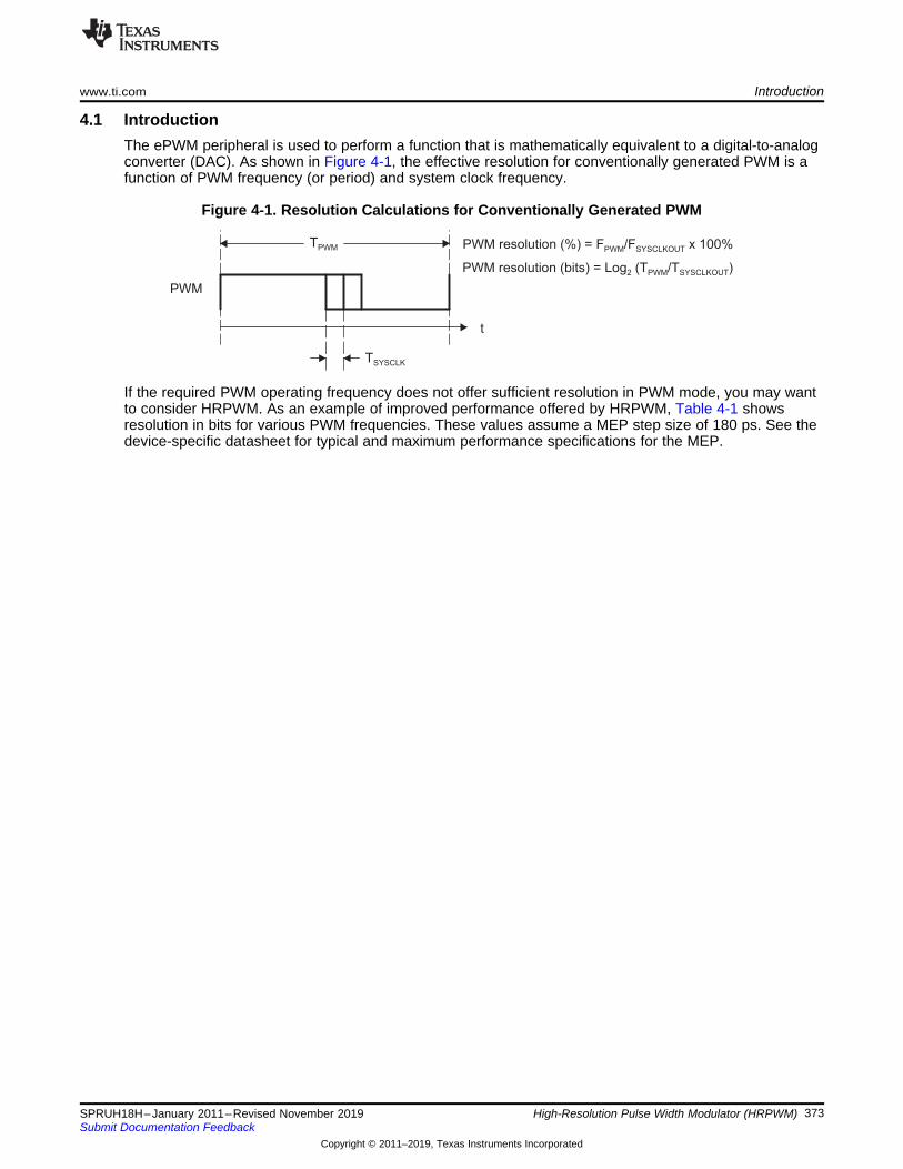
PWM
t
TPWM
TSYSCLK
PWM resolution (%) = F /F x 100%PWM SYSCLKOUT
PWM resolution (bits) = Log (T /T )2 PWM SYSCLKOUT
www.ti.com Introduction
373SPRUH18H–January 2011–Revised November 2019Submit Documentation Feedback
Copyright © 2011–2019, Texas Instruments Incorporated
High-Resolution Pulse Width Modulator (HRPWM)
4.1 IntroductionThe ePWM peripheral is used to perform a function that is mathematically equivalent to a digital-to-analogconverter (DAC). As shown in Figure 4-1, the effective resolution for conventionally generated PWM is afunction of PWM frequency (or period) and system clock frequency.
Figure 4-1. Resolution Calculations for Conventionally Generated PWM
If the required PWM operating frequency does not offer sufficient resolution in PWM mode, you may wantto consider HRPWM. As an example of improved performance offered by HRPWM, Table 4-1 showsresolution in bits for various PWM frequencies. These values assume a MEP step size of 180 ps. See thedevice-specific datasheet for typical and maximum performance specifications for the MEP.

Introduction www.ti.com
374 SPRUH18H–January 2011–Revised November 2019Submit Documentation Feedback
Copyright © 2011–2019, Texas Instruments Incorporated
High-Resolution Pulse Width Modulator (HRPWM)
Table 4-1. Resolution for PWM and HRPWM
PWM Freq Regular Resolution (PWM) High Resolution (HRPWM)90 MHz SYSCLKOUT
(kHz) Bits % Bits %20 12.1 0.0 18.1 0.00050 10.8 0.1 16.8 0.001100 9.8 0.1 15.8 0.002150 9.2 0.2 15.2 0.003200 8.8 0.2 14.8 0.004250 8.5 0.3 14.4 0.005500 7.5 0.6 13.4 0.0091000 6.5 1.1 12.4 0.0181500 5.9 1.7 11.9 0.0272000 5.5 2.2 11.4 0.036
Although each application may differ, typical low frequency PWM operation (below 250 kHz) may notrequire HRPWM. HRPWM capability is most useful for high frequency PWM requirements of powerconversion topologies such as:• Single-phase buck, boost, and flyback• Multi-phase buck, boost, and flyback• Phase-shifted full bridge• Direct modulation of D-Class power amplifiers

(1 SYSCLK cycle)
+ 0.5 (rounding)
(0x0080 in Q8 format)
(upper 8 bits)
www.ti.com Operational Description of HRPWM
375SPRUH18H–January 2011–Revised November 2019Submit Documentation Feedback
Copyright © 2011–2019, Texas Instruments Incorporated
High-Resolution Pulse Width Modulator (HRPWM)
4.2 Operational Description of HRPWMThe HRPWM is based on micro edge positioner (MEP) technology. MEP logic is capable of positioning anedge very finely by sub-dividing one coarse system clock of a conventional PWM generator. The time stepaccuracy is on the order of 150 ps. See the device-specific data sheet for the typical MEP step size on aparticular device. The HRPWM also has a self-check software diagnostics mode to check if the MEP logicis running optimally, under all operating conditions. Details on software diagnostics and functions are inSection 4.2.4.
Figure 4-2 shows the relationship between one coarse system clock and edge position in terms of MEPsteps, which are controlled via an 8-bit field in the Compare A extension register (CMPAHR).
Figure 4-2. Operating Logic Using MEP
To generate an HRPWM waveform, configure the TBM, CCM, and AQM registers as you would togenerate a conventional PWM of a given frequency and polarity. The HRPWM works together with theTBM, CCM, and AQM registers to extend edge resolution, and should be configured accordingly. Althoughmany programming combinations are possible, only a few are needed and practical. These methods aredescribed in Section 4.2.5.
Registers discussed but not found in this document can be seen in the device-specific Enhanced PulseWidth Modulator (ePWM) Module Reference Guide.
The HRPWM operation is controlled and monitored using the following registers:
Table 4-2. HRPWM Registers
mnemonic Address Offset Shadowed DescriptionTBPHSHR 0x0002 No Extension Register for HRPWM Phase (8 bits)TBPRDHR 0x0006 Yes Extension Register for HRPWM Period (8 bits)CMPAHR 0x0008 Yes Extension Register for HRPWM Duty (8 bits)HRCNFG 0x0020 No HRPWM Configuration RegisterHRMSTEP 0x0026 No HRPWM MEP Step RegisterTBPRDHRM 0x002A Yes Extension Mirror Register for HRPWM Period (8 bits)CMPAHRM 0x002C Yes Extension Mirror Register for HRPWM Duty (8 bits)

TBPHSHR (8) Reserved (8)
TBPHS (16)
Reserved (8)TBPHSHR (8)TBPHS (16)
31 16 15 8 7 0
Single 32 bit write
Reserved (8)
CMPAA(16)
CMPAHR (8)A
Single 32 bit write
CMPAA(16)
31
CMPAHR (8)A
Reserved (8)
16 15 8 7 0
Reserved (8)
TBPRDA(16)
TBPRDHR (8)A
Single 32 bit writeB
TBPRDMA(16)
31
TBPRDHRM (8)A
Reserved (8)
16 15 8 7 0
Operational Description of HRPWM www.ti.com
376 SPRUH18H–January 2011–Revised November 2019Submit Documentation Feedback
Copyright © 2011–2019, Texas Instruments Incorporated
High-Resolution Pulse Width Modulator (HRPWM)
4.2.1 Controlling the HRPWM CapabilitiesThe MEP of the HRPWM is controlled by three extension registers, each 8-bits wide. These HRPWMregisters are concatenated with the 16-bit TBPHS, TBPRD, and CMPA registers used to control PWMoperation.• TBPHSHR - Time Base Phase High Resolution Register• CMPAHR - Counter Compare A High Resolution Register• TBPRDHR - Time Base Period High Resolution Register. (available on some devices)
Figure 4-3. HRPWM Extension Registers and Memory Configuration
A These registers are mirrored and can be written to at two different memory locations (mirrored registers have an "M"suffix ( i.e. CMPA mirror = CMPAM). Reads of the high-resolution mirror registers will result in indeterminate values.
B TBPRDHR and TBPRD may be written to as a 32-bit value only at the mirrored addressNot all devices may have TBPRD and TBPRDHR registers. See device-specific data sheet for more information
HRPWM capabilities are controlled using the Channel A PWM signal path. HRPWM support on thechannel B signal path is available by properly configuring the HRCNFG register. Figure 4-4 shows how theHRPWM interfaces with the 8-bit extension registers.

TBPRD Shadow (24)
TBPRD Active (24)
CounterUp/Down(16 Bit)
TCBNTActive (16)
TBCTL[CNTLDE]
CTR=PRD
16
PhaseControl
8
CTR=ZERO
CTR_Dir
TBPHSHR (8)
TBPRDHR (8)
8
CTR=ZERO
CTR=CMPB
Disabled
TBCTL[SYNCOSEL]
EPWMxSYNCO
EPWMxSYNCI
TBCTL[SWFSYNC](Software ForcedSync)
Time-Base (TB)
TBPHS Active (24)
SyncIn/OutSelectMux
CTR=PRD
CTR=ZERO
CTR=CMPA
CTR=CMPB
CTR_Dir
DCAEVT1.soc(A)
DCBEVT1.soc(A)
EventTrigger
andInterrupt
(ET)
EPWMxINT
EPWMxSOCA
EPWMxSOCB
EPWMxSOCA
EPWMxSOCBADC
CMPA Active (24)
ActionQualifier
(AQ)
EPWMA
DeadBand(DB)
EPWMB
PWMChopper
(PC)
TripZone(TZ)
EPWMxA
EPWMxB
CTR=ZERO
EPWMxTZINT
TZ1 TZ3to
EMUSTOP
CLOCKFAIL
DCAEVT1.force(A)
DCAEVT2.force(A)
DCBEVT1.force(A)
DCBEVT2.force(A)
CTR=CMPA
16
CMPAHR (8)
CTR=CMPB
16
CMPB Active (16)
CMPB Shadow (16)
HiRes PWM (HRPWM)
CTR=PRD or ZERO
DCAEVT1.syncDCBEVT1.sync
DCAEVT1.interDCBEVT1.inter
DCAEVT2.inter
DCBEVT2.inter
CMPA Shadow (24)
www.ti.com Operational Description of HRPWM
377SPRUH18H–January 2011–Revised November 2019Submit Documentation Feedback
Copyright © 2011–2019, Texas Instruments Incorporated
High-Resolution Pulse Width Modulator (HRPWM)
Figure 4-4. HRPWM System Interface
A These events are generated by the type 1 ePWM digital compare (DC) submodule based on the levels of theCOMPxOUT and TZ signals.

Action
Qualifier
(AQ)
PWM
chopper
(PC)
EPWMA
EPWMB
Dead
band
(DB)
Trip
zone
(TZ)
TBPHSHR(8)1
CMPAHR(8)2
TBPRDHR(8)1
High-Resolution PWM (HRPWM)
HRPWM
Micro-edge Positioner
(MEP) Calibration Module
HRMSTEP
HRCNFG
EPWMxAO
EPWMxBO
Operational Description of HRPWM www.ti.com
378 SPRUH18H–January 2011–Revised November 2019Submit Documentation Feedback
Copyright © 2011–2019, Texas Instruments Incorporated
High-Resolution Pulse Width Modulator (HRPWM)
Figure 4-5. HRPWM Block Diagram
(1) From ePWM Time-base (TB) submodule(2) From ePWM counter-compare (CC) submodule
4.2.2 Configuring the HRPWMOnce the ePWM has been configured to provide conventional PWM of a given frequency and polarity, theHRPWM is configured by programming the HRCNFG register located at offset address 20h. This registerprovides the following configuration options:
Edge Mode — The MEP can be programmed to provide precise position control on the rising edge (RE),falling edge (FE) or both edges (BE) at the same time. FE and RE are used for power topologiesrequiring duty cycle control(CMPA high-resolution control), while BE is used for topologies requiringphase shifting, e.g., phase shifted full bridge (TBPHS or TBPRD high-resolution control).
Control Mode — The MEP is programmed to be controlled either from the CMPAHR register (duty cyclecontrol) or the TBPHSHR register (phase control). RE or FE control mode should be used withCMPAHR register. BE control mode should be used with TBPHSHR register. When the MEP iscontrolled from the TBPRDHR register (period control) the duty cycle and phase can also becontrolled via their respective high-resolution registers.
Shadow Mode — This mode provides the same shadowing (double buffering) option as in regular PWMmode. This option is valid only when operating from the CMPAHR and TBPRDHR registers andshould be chosen to be the same as the regular load option for the CMPA register. If TBPHSHR isused, then this option has no effect.
High-Resolution B Signal Control — The B signal path of an ePWM channel can generate a high-resolution output by either swapping the A and B outputs (the high- resolution signal will appear onePWMxB instead of ePWMxA) or by outputting an inverted version of the high-resolution ePWMxAsignal on the ePWMxB pin.
Auto-conversion Mode — This mode is used in conjunction with the scale factor optimization softwareonly. For a type 1 HRPWM module, if auto-conversion is enabled, CMPAHR =fraction(PWMduty*PWMperiod)<<8. The scale factor optimization software will calculate the MEPscale factor in background code and automatically update the HRMSTEP register with thecalculated number of MEP steps per coarse step. The MEP Calibration Module will then use thevalues in the HRMSTEP and CMPAHR register to automatically calculate the appropriate numberof MEP steps represented by the fractional duty cycle and move the high-resolution ePWM signaledge accordingly. If auto-conversion is disabled, the CMPAHR register behaves like a type 0

www.ti.com Operational Description of HRPWM
379SPRUH18H–January 2011–Revised November 2019Submit Documentation Feedback
Copyright © 2011–2019, Texas Instruments Incorporated
High-Resolution Pulse Width Modulator (HRPWM)
HRPWM module and CMPAHR = (fraction(PWMduty * PWMperiod) * MEP Scale Factor +0.5)<<8). All of these calculations will need to be performed by user code in this mode, and theHRMSTEP register is ignored. Auto-conversion for high-resolution period has the same behavior asauto-conversion for high-resolution duty cycle. Auto-conversion must always be enabled for high-resolution period mode.
4.2.3 Principle of OperationThe MEP logic is capable of placing an edge in one of 255 (8 bits) discrete time steps (see device-specificdata sheet for typical MEP step size). The MEP works with the TBM and CCM registers to be certain thattime steps are optimally applied and that edge placement accuracy is maintained over a wide range ofPWM frequencies, system clock frequencies and other operating conditions. Table 4-3 shows the typicalrange of operating frequencies supported by the HRPWM.
(1) System frequency = SYSCLKOUT, i.e., CPU clock. TBCLK = SYSCLKOUT.(2) Table data based on a MEP time resolution of 180 ps (this is an example value. See the device-specific data sheet for MEP
limits)(3) MEP steps applied = TSYSCLKOUT/180 ps in this example.(4) PWM minimum frequency is based on a maximum period value, i.e., TBPRD = 65535. PWM mode is asymmetrical up-count.(5) Resolution in bits is given for the maximum PWM frequency stated.
Table 4-3. Relationship Between MEP Steps, PWM Frequency and Resolution
System(MHz)
MEP Steps PerSYSCLKOUT (1) (2) (3)
PWM MIN(Hz) (4)
PWM MAX(MHz)
Res. @ MAX(Bits) (5)
60.0 93 916 3.00 10.970.0 79 1068 3.50 10.680.0 69 1221 4.00 10.490.0 62 1373 4.50 10.3100.0 56 1526 5.00 10.1

Tpwm = 800 ns
240 ns
19 20 21 22 23
13.8 ns steps
26.3%
27.8%
29.2%
30.6%
31.9%
Demanded
duty (30.0%)
EPWM1A
0 72
Operational Description of HRPWM www.ti.com
380 SPRUH18H–January 2011–Revised November 2019Submit Documentation Feedback
Copyright © 2011–2019, Texas Instruments Incorporated
High-Resolution Pulse Width Modulator (HRPWM)
4.2.3.1 Edge PositioningIn a typical power control loop (for example, switch modes, digital motor control [DMC], uninterruptiblepower supply [UPS]), a digital controller (PID, 2pole/2zero, lag/lead, and so on) issues a duty command,usually expressed in a per unit or percentage terms. Assume that for a particular operating point, thedemanded duty cycle is 0.300 or 30.0% on time and the required converter PWM frequency is 1.25 MHz.In conventional PWM generation with a system clock of 90 MHz, the duty cycle choices are in the vicinityof 30.0%. In Figure 4-6, a compare value of 22 counts (that is, duty = 30.6%) is the closest to 30.0% thatyou can attain. This is equivalent to an edge position of 244.4 ns instead of the desired 240.0 ns. Thisdata is shown in Table 4-4.
By utilizing the MEP, you can achieve an edge position much closer to the desired point of 240 ns.Table 4-4 shows that in addition to the CMPA value of 21 (that is, duty = 29.2% and edge positioning at233.3 ns), 37 steps of the MEP (CMPAHR register) will position the edge at 239.96 ns, resulting in almostzero error. In this example, it is assumed that the MEP has a step resolution of 180 ps.
Figure 4-6. Required PWM Waveform for a Requested Duty = 30.0%

www.ti.com Operational Description of HRPWM
381SPRUH18H–January 2011–Revised November 2019Submit Documentation Feedback
Copyright © 2011–2019, Texas Instruments Incorporated
High-Resolution Pulse Width Modulator (HRPWM)
(1) System clock, SYSCLKOUT and TBCLK = 90 MHz, 11.1 ns(2) For a PWM Period register value of 72 counts, PWM Period = 72 x 11.1 ns = 800 ns, PWM frequency = 1/800 ns = 1.25 MHz(3) Assumed MEP step size for the above example = 180 ps
See the device-specific data manual for typical and maximum MEP values.
Table 4-4. CMPA vs Duty (left), and [CMPA:CMPAHR] vs Duty (right)
CMPA (count) (1)
(2) (3)Duty % High Time (ns) CMPA (count) CMPAHR (count) Duty (%) High Time (ns)
17 23.61% 188.9 21 31 29.86% 238.8818 25.0% 200.0 21 32 29.88% 239.0619 26.39% 211.1 21 33 29.91% 239.2420 27.78% 222.2 21 34 29.93% 239.4221 29.17% 233.4 21 35 29.95% 239.6022 30.56% 244.5 21 36 29.97% 239.7823 31.94% 255.5 21 37 30.00% 239.9624 33.33% 266.6 21 38 30.02% 240.1425 34.72% 277.8 21 39 30.04% 240.32
Required 21 40 30.06% 240.5021.6 30.0% 240.0 21 41 30.09% 240.68
4.2.3.2 Scaling ConsiderationsThe mechanics of how to position an edge precisely in time has been demonstrated using the resourcesof the standard CMPA and MEP (CMPAHR) registers. In a practical application, however, it is necessaryto seamlessly provide the CPU a mapping function from a per-unit (fractional) duty cycle to a final integer(non-fractional) representation that is written to the [CMPA:CMPAHR] register combination. This sectiondescribes the mapping from a per-unit duty cycle only. The method for mapping from a per-unit period isdescribed in Section 4.2.3.4.
To do this, first examine the scaling or mapping steps involved. It is common in control software toexpress duty cycle in a per-unit or percentage basis. This has the advantage of performing all neededmath calculations without concern for the final absolute duty cycle, expressed in clock counts or high timein ns. Furthermore, it makes the code more transportable across multiple converter types running differentPWM frequencies.
To implement the mapping scheme, a two-step scaling procedure is required.

Operational Description of HRPWM www.ti.com
382 SPRUH18H–January 2011–Revised November 2019Submit Documentation Feedback
Copyright © 2011–2019, Texas Instruments Incorporated
High-Resolution Pulse Width Modulator (HRPWM)
Assumptions for this example:
System clock , SYSCLKOUT = 11.1 ns (90 MHz)PWM frequency = 1.25 MHz (1/800 ns)Required PWM duty cycle, PWMDuty = 0.300 (30.0%)PWM period in terms of coarse steps,PWMperiod (800 ns/ 11.1 ns)
= 72
Number of MEP steps per coarse step at180 ps ( 11.1 ns/ 180 ps), MEP_ScaleFactor
= 61
Value to keep CMPAHR within the range of1-255 and fractional rounding constant(default value). In the event thatfrac(PWMDuty * PWMperiod) *MEP_ScaleFactor results in a value with adecimal portion ≥ 0.5, this rounding constantwill round the CMPAHR value up 1 MEPstep. = 0.5 (0 080h in Q8 format)
Step 1: Percentage Integer Duty value conversion for CMPA register
CMPA register value = int(PWMDuty*PWMperiod); int means integer part= int(0.300* 72)
CMPA register value = 21 (15h)
Step 2: Fractional value conversion for CMPAHR register
CMPAHR register value = (frac(PWMDuty*PWMperiod)*MEP_ScaleFactor+0.5) << 8; frac means fractional part
= (frac( 21.6)* 72+ 0.5) <<8; Shift is to move the valueas CMPAHR high byte
= ((0.6 * 61 + 0.5) << 8)= (( 37.1 + 0.5) <<8)= 37.6 * 256 ; Shifting left by 8 is the same as
multiplying by 256.= 9,625
CMPAHR value = 2559h; lower 8 bits will be ignored by hardware.
NOTE: If the AUTOCONV bit (HRCNFG.6) is set and the MEP_ScaleFactor is in the HRMSTEPregister, then CMPAHR register value = frac (PWMDuty*PWMperiod<<8). The rest of theconversion calculations are performed automatically in hardware, and the correct MEP-scaled signal edge appears on the ePWM channel output. If AUTOCONV is not set, theabove calculations must be performed by software.
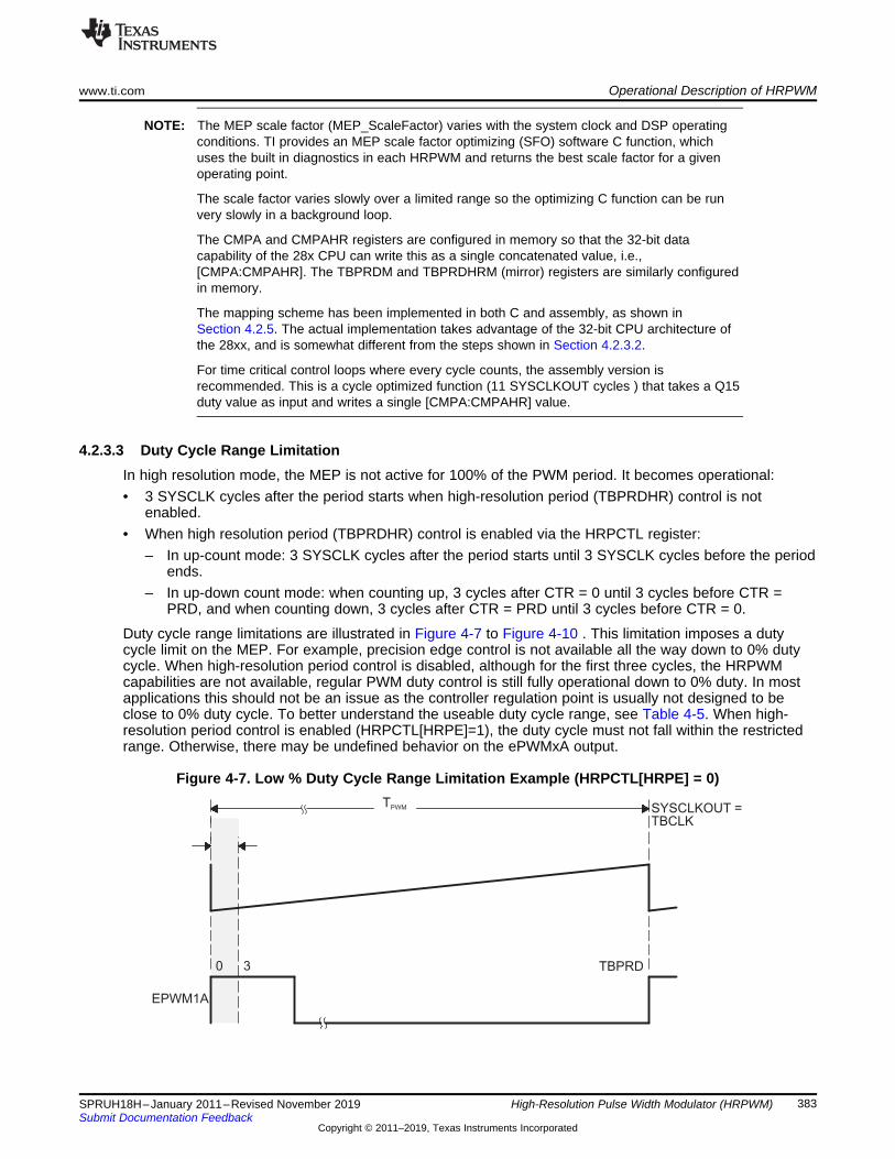
TPWM
EPWM1A
0 TBPRD3
SYSCLKOUT =
TBCLK
www.ti.com Operational Description of HRPWM
383SPRUH18H–January 2011–Revised November 2019Submit Documentation Feedback
Copyright © 2011–2019, Texas Instruments Incorporated
High-Resolution Pulse Width Modulator (HRPWM)
NOTE: The MEP scale factor (MEP_ScaleFactor) varies with the system clock and DSP operatingconditions. TI provides an MEP scale factor optimizing (SFO) software C function, whichuses the built in diagnostics in each HRPWM and returns the best scale factor for a givenoperating point.
The scale factor varies slowly over a limited range so the optimizing C function can be runvery slowly in a background loop.
The CMPA and CMPAHR registers are configured in memory so that the 32-bit datacapability of the 28x CPU can write this as a single concatenated value, i.e.,[CMPA:CMPAHR]. The TBPRDM and TBPRDHRM (mirror) registers are similarly configuredin memory.
The mapping scheme has been implemented in both C and assembly, as shown inSection 4.2.5. The actual implementation takes advantage of the 32-bit CPU architecture ofthe 28xx, and is somewhat different from the steps shown in Section 4.2.3.2.
For time critical control loops where every cycle counts, the assembly version isrecommended. This is a cycle optimized function (11 SYSCLKOUT cycles ) that takes a Q15duty value as input and writes a single [CMPA:CMPAHR] value.
4.2.3.3 Duty Cycle Range LimitationIn high resolution mode, the MEP is not active for 100% of the PWM period. It becomes operational:• 3 SYSCLK cycles after the period starts when high-resolution period (TBPRDHR) control is not
enabled.• When high resolution period (TBPRDHR) control is enabled via the HRPCTL register:
– In up-count mode: 3 SYSCLK cycles after the period starts until 3 SYSCLK cycles before the periodends.
– In up-down count mode: when counting up, 3 cycles after CTR = 0 until 3 cycles before CTR =PRD, and when counting down, 3 cycles after CTR = PRD until 3 cycles before CTR = 0.
Duty cycle range limitations are illustrated in Figure 4-7 to Figure 4-10 . This limitation imposes a dutycycle limit on the MEP. For example, precision edge control is not available all the way down to 0% dutycycle. When high-resolution period control is disabled, although for the first three cycles, the HRPWMcapabilities are not available, regular PWM duty control is still fully operational down to 0% duty. In mostapplications this should not be an issue as the controller regulation point is usually not designed to beclose to 0% duty cycle. To better understand the useable duty cycle range, see Table 4-5. When high-resolution period control is enabled (HRPCTL[HRPE]=1), the duty cycle must not fall within the restrictedrange. Otherwise, there may be undefined behavior on the ePWMxA output.
Figure 4-7. Low % Duty Cycle Range Limitation Example (HRPCTL[HRPE] = 0)

Operational Description of HRPWM www.ti.com
384 SPRUH18H–January 2011–Revised November 2019Submit Documentation Feedback
Copyright © 2011–2019, Texas Instruments Incorporated
High-Resolution Pulse Width Modulator (HRPWM)
(1) System clock - TSYSCLKOUT = 11.1 ns System clock = TBCLK = 90 MHz(2) This limitation applies only if high-resolution period (TBPRDHR) control is enabled.
Table 4-5. Duty Cycle Range Limitation for 3 SYSCLK/TBCLK Cycles
PWM Frequency (1)
(kHz)3 Cycles
Minimum Duty3 Cycles
Maximum Duty (2)
200 0.67% 99.33%99.00%400 1.33% 98.67%600 2.00% 98.00%800 2.67% 97.33%1000 3.33% 97.67%1200 4.00% 96.00%1400 4.67% 95.33%1600 5.33% 95.67%1800 6.00% 94.00%2000 6.67% 93.33%
If the application demands HRPWM operation in the low percent duty cycle region, then the HRPWM canbe configured to operate in count-down mode with the rising edge position (REP) controlled by the MEPwhen high-resolution period is disabled (HRPCTL[HRPE] = 0). This is illustrated in Figure 4-8. In this case,low percent duty limitation is no longer an issue. However, there will be a maximum duty limitation withsame percent numbers as given in Table 4-5.

Tpwm
EPWM1A
0TBPRD
3
SYSCLKOUT=
TBCLK
TBPRD - 3
Tpwm
EPWM1A
0TBPRD
3
SYSCLKOUT
www.ti.com Operational Description of HRPWM
385SPRUH18H–January 2011–Revised November 2019Submit Documentation Feedback
Copyright © 2011–2019, Texas Instruments Incorporated
High-Resolution Pulse Width Modulator (HRPWM)
Figure 4-8. High % Duty Cycle Range Limitation Example (HRPCTL[HRPE] = 0)
Figure 4-9. Up-Count Duty Cycle Range Limitation Example (HRPCTL[HRPE]=1)
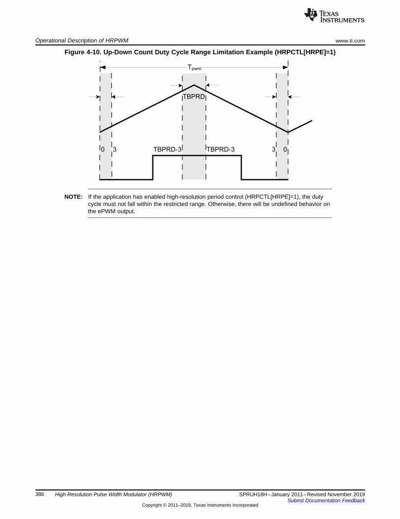
0 3 3 0TBPRD-3 TBPRD-3
TBPRD
Tpwm
Operational Description of HRPWM www.ti.com
386 SPRUH18H–January 2011–Revised November 2019Submit Documentation Feedback
Copyright © 2011–2019, Texas Instruments Incorporated
High-Resolution Pulse Width Modulator (HRPWM)
Figure 4-10. Up-Down Count Duty Cycle Range Limitation Example (HRPCTL[HRPE]=1)
NOTE: If the application has enabled high-resolution period control (HRPCTL[HRPE]=1), the dutycycle must not fall within the restricted range. Otherwise, there will be undefined behavior onthe ePWM output.

www.ti.com Operational Description of HRPWM
387SPRUH18H–January 2011–Revised November 2019Submit Documentation Feedback
Copyright © 2011–2019, Texas Instruments Incorporated
High-Resolution Pulse Width Modulator (HRPWM)
4.2.3.4 High Resolution PeriodHigh resolution period control using the MEP logic is supported on devices with a Type 1 ePWM modulevia the TBPRDHR(M) register.
NOTE: When high-resolution period control is enabled, the ePWMxB output will have +/- 1 TBCLKcycle jitter in up-count mode and +/- 2 TBCLK cycle jitter in up-down count mode.
The scaling procedure described for duty cycle in Section 4.2.3.2 applies for high-resolution period aswell:
Assumptions for this example:
System clock , SYSCLKOUT = 11.1 ns (90 MHz)Required PWM frequency = 175 kHz (TBPRD value of 514.286)Number of MEP steps per coarse step at 180 ps(MEP_ScaleFactor)
= 61 (11.1 ns/180 ps)
Value to keep TBPRDHR within range of 1-255 andfractional rounding constant (default value)
= 0.5 (0080h in Q8 format)
Problem:In up-count mode:
If TBPRD = 514, then PWM frequency = 174.75 kHz (period = (514+1)* TTBCLK).
TBPRD = 513, then PWM frequency = 175.10 kHz (period = (513+1)* TTBCLK).
In up-down count mode:
If TBPRD = 258, then PWM frequency = 174.42 kHz (period = (258*2)* TTBCLK).
If TBPRD = 257, then PWM frequency = 175.10 kHz (period = (257*2)* TTBCLK).
Solution:With 61 MEP steps per coarse step at 180 ps each:
Step 1: Percentage Integer Period value conversion for TBPRD register
Integer period value = 514 * TTBCLK
= int (514.286) * TTBCLK
= int (PWMperiod) * TTBCLK
In up-count mode:TBPRD register value = 513 (TBPRD = period value - 1)
= 0201hIn up-down count mode: = 257 (TBPRD = period value / 2)
TBPRD register value = 0101h
Step 2: Fractional value conversion for TBPRDHR register
TBPRDHR register value = (frac(PWMperiod) * MEP_ScaleFactor + 0.5)(shift is to move the value as TBPRDHR high byte)
If auto-conversion enabled and HRMSTEP =MEP_ScaleFactor value (61): =frac (PWMperiod)<<8TBPRDHR register value =frac (514.286)<<8
=0.286 × 256=0049h
Operational Description of HRPWM www.ti.com
388 SPRUH18H–January 2011–Revised November 2019Submit Documentation Feedback
Copyright © 2011–2019, Texas Instruments Incorporated
High-Resolution Pulse Width Modulator (HRPWM)
The autoconversion will then automatically performthe calculation such that TBPRDHR MEP delay isscaled by hardware to:
=((TBPRDHR(15:0) >> 8) × HRMSTEP + 80h) >> 8
= (0049h × 61 + 80h) >> 8=(11E5h) >> 8
Period MEP delay =0011h MEP Steps
4.2.3.4.1 High-Resolution Period ConfigurationTo use High Resolution Period, the ePWMx module must be initialized, following the steps in this exactorder:1. Enable ePWMx clock2. Disable TBCLKSYNC3. Configure ePWMx registers - AQ, TBPRD, CC, etc.
• ePWMx may only be configured for up-count or up-down count modes. High-resolution period isnot compatible with down-count mode.
• TBCLK must equal SYSCLKOUT• TBPRD and CC registers must be configured for shadow loads.• CMPCTL[LOADAMODE]
– In up-count mode:CMPCTL[LOADAMODE] = 1 (load on CTR = PRD)– In up-down count mode: CMPCTL[LOADAMODE] = 2 (load on CTR=0 or CTR=PRD)
4. Configure HRPWM register such that:• HRCNFG[HRLOAD] = 2 (load on either CTR = 0 or CTR = PRD)• HRCNFG[AUTOCONV] = 1 (Enable auto-conversion)• HRCNFG[EDGMODE] = 3 (MEP control on both edges)
5. For TBPHS: TBPHSHR synchronization with high-resolution period, set bothHRPCTL[TBPSHRLOADE] = 1 and TBCTL[PHSEN] = 1. In up-down count mode these bits must beset to 1 regardless of the contents of TBPHSHR.
6. Enable high-resolution period control (HRPCTL[HRPE] = 1)7. Enable TBCLKSYNC8. TBCTL[SWFSYNC] = 19. HRMSTEP must contain an accurate MEP scale factor (# of MEP steps per SYSCLKOUT coarse step)
because auto-conversion is enabled. The MEP scale factor can be acquired via the SFO() functiondescribed in Section 4.4.
10. To control high-resolution period, write to the TBPRDHR(M) registers.
NOTE: When high-resolution period mode is enabled, an EPWMxSYNC pulse will introduce +/- 1 - 2cycle jitter to the PWM (+/- 1 cycle in up-count mode and +/- 2 cycle in up-down countmode). For this reason, TBCTL[SYNCOSEL] should not be set to 1 (CTR = 0 isEPWMxSYNCO source) or 2 (CTR = CMPB is EPWMxSYNCO source). Otherwise, the jitterwill occur on every PWM cycle with the synchronization pulse.
When TBCTL[SYNCOSEL] = 0 (EPWMxSYNCI is EPWMxSYNCO source), a softwaresynchronization pulse should be issued only once during high-resolution period initialization.If a software sync pulse is applied while the PWM is running, the jitter will appear on thePWM output at the time of the sync pulse.

www.ti.com Operational Description of HRPWM
389SPRUH18H–January 2011–Revised November 2019Submit Documentation Feedback
Copyright © 2011–2019, Texas Instruments Incorporated
High-Resolution Pulse Width Modulator (HRPWM)
4.2.4 Scale Factor Optimizing Software (SFO)The micro edge positioner (MEP) logic is capable of placing an edge in one of 255 discrete time steps. Aspreviously mentioned, the size of these steps is on the order of 150 ps (see device-specific data sheet fortypical MEP step size on your device). The MEP step size varies based on worst-case processparameters, operating temperature, and voltage. MEP step size increases with decreasing voltage andincreasing temperature and decreases with increasing voltage and decreasing temperature. Applicationsthat use the HRPWM feature should use the TI-supplied MEP scale factor optimizer (SFO) softwarefunction. The SFO function helps to dynamically determine the number of MEP steps per SYSCLKOUTperiod while the HRPWM is in operation.
To utilize the MEP capabilities effectively during the Q15 duty (or period) to [CMPA:CMPAHR] or[TBPRD(M):TBPRDHR(M)] mapping function (see Section 4.2.3.2), the correct value for the MEP scalingfactor (MEP_ScaleFactor) needs to be known by the software. To accomplish this, the HRPWM modulehas built in self-check and diagnostics capabilities that can be used to determine the optimumMEP_ScaleFactor value for any operating condition. TI provides a C-callable library containing one SFOfunction that utilizes this hardware and determines the optimum MEP_ScaleFactor. As such, MEP Controland Diagnostics registers are reserved for TI use.
A detailed description of the SFO library - SFO_TI_Build_V6.lib software can be found in Section 4.4.
4.2.5 HRPWM Examples Using Optimized Assembly Code.The best way to understand how to use the HRPWM capabilities is through two real examples:1. Simple buck converter using asymmetrical PWM (i.e. count-up) with active high polarity.2. DAC function using simple R+C reconstruction filter.
The following examples all have Initialization/configuration code written in C. To make these easier tounderstand, the #defines shown below are used. Note, #defines introduced in the device-specific PulseWidth Modulator (ePWM) Module Reference Guide are also used.
Example 4-1 This example assumes MEP step size of 150 ps and does not use the SFO library.
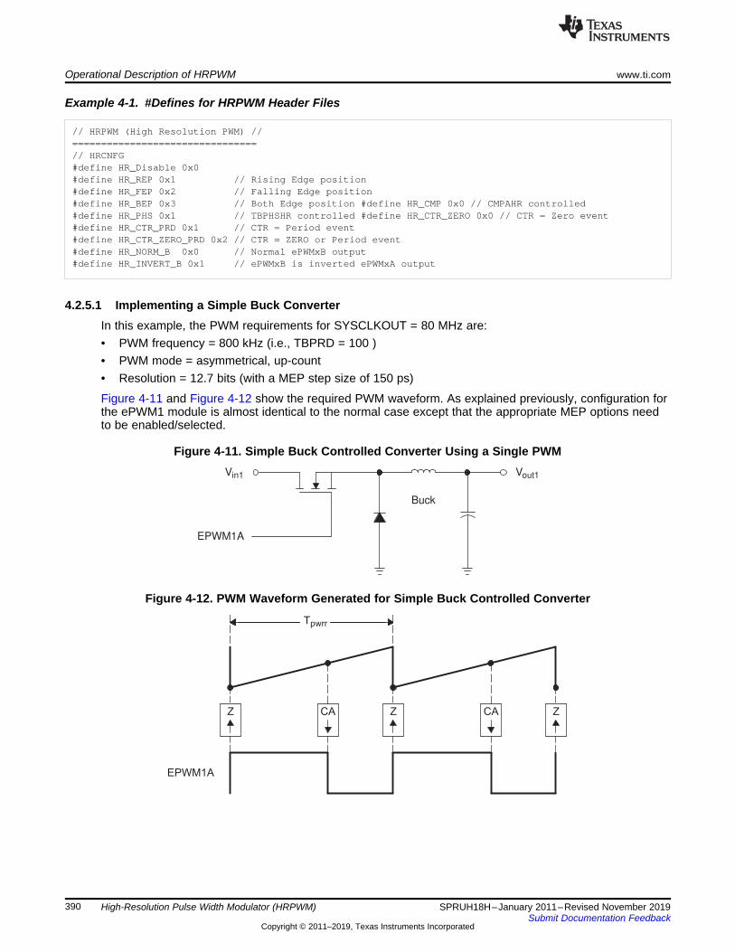
Z CA Z CA Z
Tpwrr
EPWM1A
EPWM1A
Vin1 Vout1
Buck
Operational Description of HRPWM www.ti.com
390 SPRUH18H–January 2011–Revised November 2019Submit Documentation Feedback
Copyright © 2011–2019, Texas Instruments Incorporated
High-Resolution Pulse Width Modulator (HRPWM)
Example 4-1. #Defines for HRPWM Header Files
// HRPWM (High Resolution PWM) //================================// HRCNFG#define HR_Disable 0x0#define HR_REP 0x1 // Rising Edge position#define HR_FEP 0x2 // Falling Edge position#define HR_BEP 0x3 // Both Edge position #define HR_CMP 0x0 // CMPAHR controlled#define HR_PHS 0x1 // TBPHSHR controlled #define HR_CTR_ZERO 0x0 // CTR = Zero event#define HR_CTR_PRD 0x1 // CTR = Period event#define HR_CTR_ZERO_PRD 0x2 // CTR = ZERO or Period event#define HR_NORM_B 0x0 // Normal ePWMxB output#define HR_INVERT_B 0x1 // ePWMxB is inverted ePWMxA output
4.2.5.1 Implementing a Simple Buck ConverterIn this example, the PWM requirements for SYSCLKOUT = 80 MHz are:• PWM frequency = 800 kHz (i.e., TBPRD = 100 )• PWM mode = asymmetrical, up-count• Resolution = 12.7 bits (with a MEP step size of 150 ps)
Figure 4-11 and Figure 4-12 show the required PWM waveform. As explained previously, configuration forthe ePWM1 module is almost identical to the normal case except that the appropriate MEP options needto be enabled/selected.
Figure 4-11. Simple Buck Controlled Converter Using a Single PWM
Figure 4-12. PWM Waveform Generated for Simple Buck Controlled Converter

www.ti.com Operational Description of HRPWM
391SPRUH18H–January 2011–Revised November 2019Submit Documentation Feedback
Copyright © 2011–2019, Texas Instruments Incorporated
High-Resolution Pulse Width Modulator (HRPWM)
The example code shown consists of two main parts:• Initialization code (executed once)• Run time code (typically executed within an ISR)
Example 4-2 shows the Initialization code. The first part is configured for conventional PWM. The secondpart sets up the HRPWM resources.
This example assumes MEP step size of 150 ps and does not use the SFO library.
Example 4-2. HRPWM Buck Converter Initialization Code
void HrBuckDrvCnf(void){
// Config for conventional PWM firstEPwm1Regs.TBCTL.bit.PRDLD = TB_IMMEDIATE; // set Immediate loadEPwm1Regs.TBPRD = 100; // Period set for 800 kHz PWMhrbuck_period = 200; // Used for Q15 to Q0 scalingEPwm1Regs.TBCTL.bit.CTRMODE = TB_COUNT_UP;EPwm1Regs.TBCTL.bit.PHSEN = TB_DISABLE; // EPWM1 is the MasterEPwm1Regs.TBCTL.bit.SYNCOSEL = TB_SYNC_DISABLE;EPwm1Regs.TBCTL.bit.HSPCLKDIV = TB_DIV1;EPwm1Regs.TBCTL.bit.CLKDIV = TB_DIV1;// Note: ChB is initialized here only for comparison purposes, it is not required
EPwm1Regs.CMPCTL.bit.LOADAMODE = CC_CTR_ZERO;EPwm1Regs.CMPCTL.bit.SHDWAMODE = CC_SHADOW;EPwm1Regs.CMPCTL.bit.LOADBMODE = CC_CTR_ZERO; // optionalEPwm1Regs.CMPCTL.bit.SHDWBMODE = CC_SHADOW; // optional
EPwm1Regs.AQCTLA.bit.ZRO = AQ_SET;EPwm1Regs.AQCTLA.bit.CAU = AQ_CLEAR;EPwm1Regs.AQCTLB.bit.ZRO = AQ_SET; // optionalEPwm1Regs.AQCTLB.bit.CBU = AQ_CLEAR; // optional// Now configure the HRPWM resourcesEALLOW; // Note these registers are protected
// and act only on ChAEPwm1Regs.HRCNFG.all = 0x0; // clear all bits firstEPwm1Regs.HRCNFG.bit.EDGMODE = HR_FEP; // Control Falling Edge PositionEPwm1Regs.HRCNFG.bit.CTLMODE = HR_CMP; // CMPAHR controls the MEPEPwm1Regs.HRCNFG.bit.HRLOAD = HR_CTR_ZERO; // Shadow load on CTR=ZeroEDIS;MEP_ScaleFactor = 83*256; // Start with typical Scale Factor
// value for 80 MHz// Note: Use SFO functions to update
MEP_ScaleFactor dynamically}
Example 4-3 shows an assembly example of run-time code for the HRPWM buck converter.

EPWM1A
CA
TPWM = 2.5 µs
Z CA ZZ
EPWM1A VOUT1
LPF
Operational Description of HRPWM www.ti.com
392 SPRUH18H–January 2011–Revised November 2019Submit Documentation Feedback
Copyright © 2011–2019, Texas Instruments Incorporated
High-Resolution Pulse Width Modulator (HRPWM)
Example 4-3. HRPWM Buck Converter Run-Time Code
EPWM1_BASE .set 0x6800CMPAHR1 .set EPWM1_BASE+0x8;===============================================HRBUCK_DRV; (can execute within an ISR or loop);===============================================
MOVW DP, #_HRBUCK_InMOVL XAR2,@_HRBUCK_In ; Pointer to Input Q15 Duty (XAR2)MOVL XAR3,#CMPAHR1 ; Pointer to HRPWM CMPA reg (XAR3)
; Output for EPWM1A (HRPWM)MOV T,*XAR2 ; T <= DutyMPYU ACC,T,@_hrbuck_period ; Q15 to Q0 scaling based on PeriodMOV T,@_MEP_ScaleFactor ; MEP scale factor (from optimizer s/w)MPYU P,T,@AL ; P <= T * AL, Optimizer scalingMOVH @AL,P ; AL <= P, move result back to ACCADD ACC, #0x080 ; MEP range and rounding adjustmentMOVL *XAR3,ACC ; CMPA:CMPAHR(31:8) <= ACC
; Output for EPWM1B (Regular Res) Optional - for comparison purpose onlyMOV *+XAR3[2],AH ; Store ACCH to regular CMPB
4.2.5.2 Implementing a DAC function Using an R+C Reconstruction FilterIn this example, the PWM requirements are:• PWM frequency = 533 kHz (i.e. TBPRD = 150)• PWM mode = Asymmetrical, Up-count• Resolution = 14 bits ( MEP step size = 150 ps)
Figure 4-13 and Figure 4-14 show the DAC function and the required PWM waveform. As explainedpreviously, configuration for the ePWM1 module is almost identical to the normal case except that theappropriate MEP options need to be enabled/selected.
Figure 4-13. Simple Reconstruction Filter for a PWM Based DAC
Figure 4-14. PWM Waveform Generated for the PWM DAC Function
The example code shown consists of two main parts:• Initialization code (executed once)• Run time code (typically executed within an ISR)

www.ti.com Operational Description of HRPWM
393SPRUH18H–January 2011–Revised November 2019Submit Documentation Feedback
Copyright © 2011–2019, Texas Instruments Incorporated
High-Resolution Pulse Width Modulator (HRPWM)
This example assumes a typical MEP_SP and does not use the SFO library.
Example 4-4 shows the Initialization code. The first part is configured for conventional PWM. The secondpart sets up the HRPWM resources.
Example 4-4. PWM DAC Function Initialization Code
void HrPwmDacDrvCnf(void){// Config for conventional PWM firstEPwm1Regs.TBCTL.bit.PRDLD = TB_IMMEDIATE; // Set Immediate loadEPwm1Regs.TBPRD = 150; // Period set for 533 kHz PWMhrDAC_period = 150; // Used for Q15 to Q0 scalingEPwm1Regs.TBCTL.bit.CTRMODE = TB_COUNT_UP;EPwm1Regs.TBCTL.bit.PHSEN = TB_DISABLE; // EPWM1 is the MasterEPwm1Regs.TBCTL.bit.SYNCOSEL = TB_SYNC_DISABLE;EPwm1Regs.TBCTL.bit.HSPCLKDIV = TB_DIV1;EPwm1Regs.TBCTL.bit.CLKDIV = TB_DIV1;// Note: ChB is initialized here only for comparison purposes, it is not required
EPwm1Regs.CMPCTL.bit.LOADAMODE = CC_CTR_ZERO;EPwm1Regs.CMPCTL.bit.SHDWAMODE = CC_SHADOW;EPwm1Regs.CMPCTL.bit.LOADBMODE = CC_CTR_ZERO; // optionalEPwm1Regs.CMPCTL.bit.SHDWBMODE = CC_SHADOW; // optional
EPwm1Regs.AQCTLA.bit.ZRO = AQ_SET;EPwm1Regs.AQCTLA.bit.CAU = AQ_CLEAR;EPwm1Regs.AQCTLB.bit.ZRO = AQ_SET; // optionalEPwm1Regs.AQCTLB.bit.CBU = AQ_CLEAR; // optional// Now configure the HRPWM resourcesEALLOW; // Note these registers are protected
// and act only on ChA.EPwm1Regs.HRCNFG.all = 0x0; // Clear all bits firstEPwm1Regs.HRCNFG.bit.EDGMODE = HR_FEP; // Control falling edge positionEPwm1Regs.HRCNFG.bit.CTLMODE = HR_CMP; // CMPAHR controls the MEP.EPwm1Regs.HRCNFG.bit.HRLOAD = HR_CTR_ZERO; // Shadow load on CTR=Zero.EDIS;MEP_ScaleFactor = 83*256; // Start with typical Scale Factor
// value for 80 MHz.// Use SFO functions to update MEP_ScaleFactor// dynamically.
}
Example 4-5 shows an assembly example of run-time code that can execute in a high-speed ISR loop.

Operational Description of HRPWM www.ti.com
394 SPRUH18H–January 2011–Revised November 2019Submit Documentation Feedback
Copyright © 2011–2019, Texas Instruments Incorporated
High-Resolution Pulse Width Modulator (HRPWM)
Example 4-5. PWM DAC Function Run-Time Code
EPWM1_BASE .set 0x6800CMPAHR1 .set EPWM1_BASE+0x8;=================================================HRPWM_DAC_DRV; (can execute within an ISR or loop);=================================================
MOVW DP, #_HRDAC_InMOVL XAR2,@_HRDAC_In ; Pointer to input Q15 duty (XAR2)MOVL XAR3,#CMPAHR1 ; Pointer to HRPWM CMPA reg (XAR3)
; Output for EPWM1A (HRPWMMOV T,*XAR2 ; T <= dutyMPY ACC,T,@_hrDAC_period ; Q15 to Q0 scaling based on periodADD ACC,@_HrDAC_period<<15 ; Offset for bipolar operationMOV T,@_MEP_ScaleFactor ; MEP scale factor (from optimizer s/w)MPYU P,T,@AL ; P <= T * AL, optimizer scalingMOVH @AL,P ; AL <= P, move result back to ACCADD ACC, #0x080 ; MEP range and rounding adjustmentMOVL *XAR3,ACC ; CMPA:CMPAHR(31:8) <= ACC
; Output for EPWM1B (Regular Res) Optional - for comparison purpose onlyMOV *+XAR3[2],AH ; Store ACCH to regular CMPB

www.ti.com HRPWM Register Descriptions
395SPRUH18H–January 2011–Revised November 2019Submit Documentation Feedback
Copyright © 2011–2019, Texas Instruments Incorporated
High-Resolution Pulse Width Modulator (HRPWM)
4.3 HRPWM Register DescriptionsThis section describes the applicable HRPWM registers.
4.3.1 Register SummaryA summary of the registers required for the HRPWM is shown in the table below.
Table 4-6. Register Descriptions
Name Offset Size(x16)/Shadow DescriptionTime Base RegistersTBCTL 0x0000 1/0 Time Base Control RegisterTBSTS 0x0001 1/0 Time Base Status RegisterTBPHSHR 0x0002 1/0 Time Base Phase High
Resolution RegisterTBPHS 0x0003 1/0 Time Base Phase RegisterTBCNT 0x0004 1/0 Time Base Counter RegisterTBPRD 0x0005 1/1 Time Base Period Register SetTBPRDHR 0x0006 1/1 Time Base Period High
Resolution Register SetCompare RegistersCMPCTL 0x0007 1/0 Counter Compare Control
RegisterCMPAHR 0x0008 1/1 Counter Compare A High
Resolution Register SetCMPA 0x0009 1/1 Counter Compare A Register
SetCMPB 0x000A 1/1 Counter Compare B Register
SetHRPWM RegistersHRCNFG 0x0020 1/0 HRPWM Configuration
RegisterHRMSTEP 0x0026 1/0 HRPWM MEP Step RegisterHigh Resolution Period &Mirror RegistersHRPCTL 0x0028 1/0 High Resolution Period Control
RegisterTBPRDHRM 0x002A 1/1 Time Base Period High
Resolution Mirror Register SetTBPRDM 0x002B 1/1 Time Base Period Mirror
Register SetCMPAHRM 0x002C 1/1 Counter Compare A High
Resolution Mirror Register SetCMPAM 0x002D 1/1 Counter Compare A Mirror
Register Set

HRPWM Register Descriptions www.ti.com
396 SPRUH18H–January 2011–Revised November 2019Submit Documentation Feedback
Copyright © 2011–2019, Texas Instruments Incorporated
High-Resolution Pulse Width Modulator (HRPWM)
4.3.2 Registers and Field Descriptions
Figure 4-15. HRPWM Configuration Register (HRCNFG)15 8
ReservedR-0
7 6 5 4 3 2 1 0SWAPAB AUTOCONV SELOUTB HRLOAD CTLMODE EDGMODE
R/W-0 R/W-0 R/W-0 R/W-0 R/W-0 R/W-0LEGEND: R/W = Read/Write; R = Read only; -n = value after reset
(1) This register is EALLOW protected.
Table 4-7. HRPWM Configuration Register (HRCNFG) Field Descriptions
Bit Field Value Description (1)
15-8 Reserved Reserved7 SWAPAB Swap ePWM A & B Output Signals
This bit enables the swapping of the A & B signal outputs. The selection is as follows:0 ePWMxA and ePWMxB outputs are unchanged.1 ePWMxA signal appears on ePWMxB output and ePWMxB signal appears on ePWMxA output.
6 AUTOCONV Auto Convert Delay Line ValueSelects whether the fractional duty cycle/period/phase in the CMPAHR/TBPRDHR/TBPHSHR register isautomatically scaled by the MEP scale factor in the HRMSTEP register or manually scaled bycalculations in application software. The SFO library function automatically updates the HRMSTEPregister with the appropriate MEP scale factor.
0 Automatic HRMSTEP scaling is disabled.1 Automatic HRMSTEP scaling is enabled.
If application software is manually scaling the fractional duty cycle, or phase (i.e. software setsCMPAHR = (fraction(PWMduty * PWMperiod) * MEP Scale Factor)<<8 + 0x080 for duty cycle), then thismode must be disabled.
5 SELOUTB EPWMxB Output Select BitThis bit selects which signal is output on the ePWMxB channel output.
0 ePWMxB output is normal.1 ePWMxB output is inverted version of ePWMxA signal.
4-3 HRLOAD Shadow Mode BitSelects the time event that loads the CMPAHR shadow value into the active register.
00 Load on CTR = Zero: Time-base counter equal to zero (TBCTR = 0x0000)01 Load on CTR = PRD: Time-base counter equal to period (TBCTR = TBPRD)10 Load on either CTR = Zero or CTR = PRD11 Reserved
2 CTLMODE Control Mode BitsSelects the register (CMP/TBPRD or TBPHS) that controls the MEP:
0 CMPAHR(8) or TBPRDHR(8) Register controls the edge position (i.e., this is duty or period controlmode). (Default on Reset)
1 TBPHSHR(8) Register controls the edge position (i.e., this is phase control mode).1-0 EDGMODE Edge Mode Bits
Selects the edge of the PWM that is controlled by the micro-edge position (MEP) logic:00 HRPWM capability is disabled (default on reset)01 MEP control of rising edge (CMPAHR)10 MEP control of falling edge (CMPAHR)11 MEP control of both edges (TBPHSHR or TBPRDHR)

www.ti.com HRPWM Register Descriptions
397SPRUH18H–January 2011–Revised November 2019Submit Documentation Feedback
Copyright © 2011–2019, Texas Instruments Incorporated
High-Resolution Pulse Width Modulator (HRPWM)
Figure 4-16. Counter Compare A High Resolution Register (CMPAHR)15 8 7 0
CMPAHR ReservedR/W-0 R-0
LEGEND: R/W = Read/Write; R = Read only; -n = value after reset
Table 4-8. Counter Compare A High Resolution Register (CMPAHR) Field Descriptions
Bit Field Value Description15-8 CMPAHR 00-
FEhCompare A High Resolution register bits for MEP step control. These 8-bits contain the high-resolutionportion (least significant 8-bits) of the counter-compare A value. CMPA:CMPAHR can be accessed in asingle 32-bit read/write. Shadowing is enabled and disabled by the CMPCTL[SHDWAMODE] bit.
7-0 Reserved 00-FFh
Any writes to these bit(s) must always have a value of 0.
Figure 4-17. TB Phase High Resolution Register (TBPHSHR)15 8 7 0
TBPHSH ReservedR/W-0 R-0
LEGEND: R/W = Read/Write; R = Read only; -n = value after reset
Table 4-9. TB Phase High Resolution Register (TBPHSHR) Field Descriptions
Bit Field Value Description15-8 TBPHSH 00-FEh Time base phase high resolution bits7-0 Reserved 00-FFh Any writes to these bit(s) must always have a value of 0.
Figure 4-18. Time Base Period High Resolution Register15 8
TBPRDHRR/W-0
7 0Reserved
R-0LEGEND: R/W = Read/Write; R = Read only; -n = value after reset
Table 4-10. Time Base Period High-Resolution Register (TBPRDHR) Field Descriptions
Bit Field Value Description15-8 PRDHR 00-FFh Period High Resolution Bits
These 8-bits contain the high-resolution portion of the period value.The TBPRDHR register is not affected by the TBCTL[PRDLD] bit. Reads from this register alwaysreflect the shadow register. Likewise writes are also to the shadow register. The TBPRDHR registeris only used when the high resolution period feature is enabled.This register is only available with ePWM modules which support high-resolution period control.
7-0 Reserved Reserved for TI Test

HRPWM Register Descriptions www.ti.com
398 SPRUH18H–January 2011–Revised November 2019Submit Documentation Feedback
Copyright © 2011–2019, Texas Instruments Incorporated
High-Resolution Pulse Width Modulator (HRPWM)
Figure 4-19. Compare A High Resolution Mirror Register15 8
CMPAHRR/W-0
7 0Reserved
R-0LEGEND: R/W = Read/Write; R = Read only; -n = value after reset
Table 4-11. Compare A High-Resolution Mirror Register (CMPAHRM) Field Descriptions
Bit Field Value Description15-8 CMPAHR 00-FFh Compare A High Resolution Bits
Writes to both the CMPAHR and CMPAHRM locations access the high-resolution (leastsignificant 8-bit) portion of the Counter Compare A value. The only difference is that unlikeCMPAHR, reads from the mirror register, CMPAHRM, are indeterminate (reserved for TI Test).By default writes to this register are shadowed. Shadowing is enabled and disabled by theCMPCTL[SHDWAMODE] bit as described for the CMPAM register.
7-0 Reserved 00-FFh Reserved for TI Test
Figure 4-20. Time-Base Period High Resolution Mirror Register15 8
TBPRDHRR/W-0
7 0Reserved
R-0LEGEND: R/W = Read/Write; R = Read only; -n = value after reset
Table 4-12. Time-Base Period High-Resolution Mirror Register (TBPRDHRM) Field Descriptions
Bit Field Value Description15-8 TBPRDHR 00-FFh Period High Resolution Bits
These 8-bits contain the high-resolution portion of the period value.TBPRD provides backwards compatibility with earlier ePWM modules. The mirror registers(TBPRDM and TBPRDHRM) allow for 32-bit writes to TBPRDHR in one access. Due to the odd-numbered memory address location of the TBPRD legacy register, a 32-bit write is not possiblewith TBPRD and TBPRDHR.The TBPRDHRM register is not affected by the TBCTL[PRDLD] bitWrites to both the TBPRDHR and TBPRDM locations access the high-resolution (least significant 8-bit) portion of the Time Base Period value. The only difference is that unlike TBPRDHR, reads fromthe mirror registerTBPRDHRM, are indeterminate (reserved for TI Test).The TBPRDHRM register is available with ePWM modules which support high-respolution periodcontrol and is used only when the high resolution period feature is enabled.
7-0 Reserved Reserved
Figure 4-21. High Resolution Period Control Register (HRPCTL)15 8
ReservedR-0
7 3 2 1 0Reserved TBPHSHR
LOADEPWMSYNCSEL HRPE
R-0 R/W-0 R/W-0 R/W-0LEGEND: R/W = Read/Write; R = Read only; -n = value after reset

www.ti.com HRPWM Register Descriptions
399SPRUH18H–January 2011–Revised November 2019Submit Documentation Feedback
Copyright © 2011–2019, Texas Instruments Incorporated
High-Resolution Pulse Width Modulator (HRPWM)
(1) This register is EALLOW protected.(2) This register is used with Type 1 ePWM modules (support high-resolution period) only.
Table 4-13. High Resolution Period Control Register (HRPCTL) Field Descriptions
Bit Field Value Description (1) (2)
15-3 Reserved Reserved2 TBPHSHRLOADE TBPHSHR Load Enable
This bit allows you to synchronize ePWM modules with a high-resolution phase on a SYNCIN,TBCTL[SWFSYNC] or digital compare event. This allows for multiple ePWM modules operating atthe same frequency to be phase aligned with high-resolution.
0 Disables synchronization of high-resolution phase on a SYNCIN, TBCTL[SWFSYNC] or digitalcompare event:
1 Synchronize the high-resolution phase on a SYNCIN, TBCTL[SWFSYNC] or digital comparatorsynchronization event. The phase is synchronized using the contents of the high-resolution phaseTBPHSHR register.The TBCTL[PHSEN] bit which enables the loading of the TBCTR register with TBPHS registervalue on a SYNCIN or TBCTL[SWFSYNC] event works independently. However, users need toenable this bit also if they want to control phase in conjunction with the high-resolution periodfeature.This bit and the TBCTL[PHSEN] bit must be set to 1 when high-resolution period is enabled forup-down count mode even if TBPHSHR = 0x0000. This bit does not need to be set when onlyhigh-resolution duty is enabled.
1 PWMSYNCSEL PWMSYNC Source Select BitThis bit selects the source for the PWMSYNC signal.The PWMSYNC signal is used by external modules (such as COMP+DAC) for synchronizingtiming to the selected ePWM module.Note: This bit is not used for high-resolution period control.
0 PWMSYNC is generated by TBCTR = PRD pulse.1 PWMSYNC is generated by TBCTR = 0 pulse.
0 HRPE High Resolution Period Enable Bit0 High resolution period feature disabled. In this mode the ePWM behaves as a Type 0 ePWM.1 High resolution period enabled. In this mode the HRPWM module can control high-resolution of
both the duty and frequency.When high-resolution period is enabled, TBCTL[CTRMODE] = 0,1 (down-count mode) is notsupported.
Figure 4-22. High Resolution Micro Step Register (HRMSTEP) (EALLOW protected):15 8 7 0
Reserved HRMSTEPR-0 R/W-0
LEGEND: R/W = Read/Write; R = Read only; -n = value after reset
Table 4-14. High Resolution Micro Step Register (HRMSTEP) Field Descriptions
Bit Field Value Description15:8 Reserved Reserved7:0 HRMSTEP 00-FFh High Resolution MEP Step
When auto-conversion is enabled (HRCNFG[AUTOCONV] = 1), This 8-bit field contains theMEP_ScaleFactor (number of MEP steps per coarse steps) used by the hardware toautomatically convert the value in the CMPAHR, TBPHSHR, or TBPRDHR register to a scaledmicro-edge delay on the high-resolution ePWM output.The value in this register is written by the SFO calibration software at the end of each calibrationrun.

Appendix A: SFO Library Software - SFO_TI_Build_V6.lib www.ti.com
400 SPRUH18H–January 2011–Revised November 2019Submit Documentation Feedback
Copyright © 2011–2019, Texas Instruments Incorporated
High-Resolution Pulse Width Modulator (HRPWM)
4.4 Appendix A: SFO Library Software - SFO_TI_Build_V6.libThe following table lists several features of the SFO_TI_Build_V6.lib library.
Table 4-15. SFO Library Features
SYSCLK Freq SFO_TI_Build_V6.lib UnitMax. HRPWM channels supported - 8 channelsTotal static variable memory size - 11 wordsCompletion-checking? - Yes -Typical time required for SFO() to updateMEP_ScaleFactor if called repetitivelywithout interrupts
80 MHz 1.3 milliseconds
60 MHz 2.23 milliseconds
A functional description of the SFO library routine, SFO(), is found below.
4.5 Scale Factor Optimizer Function - int SFO()This routine drives the micro-edge positioner (MEP) calibration module to run SFO diagnostics anddetermine the appropriate MEP scale factor (number of MEP steps per coarse SYSCLKOUT step) for adevice at any given time.
If SYSCLKOUT = TBCLK = 80 MHz and assuming the MEP step size is 150 ps, the typical scale factorvalue at 80 MHz = 83 MEP steps per TBCLK unit (12.5 ns)
The function returns a MEP scale factor value:
MEP_ScaleFactor = Number of MEP steps/SYSCLKOUT.
Constraints when using this function:• SFO() can be used with a minimum SYSCLKOUT = TBCLK = 50 MHz. MEP diagnostics logic uses
SYSCLKOUT and not TBCLK, so the SYSCLKOUT restriction is an important constraint. Below 50MHz, with device process variation, the MEP step size may decrease under cold temperature and highcore voltage conditions to such a point, that 255 MEP steps will not span an entire SYSCLKOUT cycle.
• At any time, SFO() can be called to run SFO diagnostics on the MEP calibration module
Usage:• SFO() can be called at any time in the background while the ePWM channels are running in HRPWM
mode. The scale factor result obtained in MEP_ScaleFactor can be applied to all ePWM channelsrunning in HRPWM mode because the function makes use of the diagnostics logic in the MEPcalibration module (which runs independently of ePWM channels).
• This routine returns a 1 when calibration is finished, and a new scale factor has been calculated or a 0if calibration is still running. The routine returns a 2 if there is an error, and the MEP_ScaleFactor isgreater than the maximum 255 fine steps per coarse SYSCLKOUT cycle. In this case, the HRMSTEPregister will maintain the last MEP scale factor value less than 256 for auto conversion.
• All ePWM modules operating in HRPWM incur only a 3-SYSCLKOUT cycle minimum duty cyclelimitation when high-resolution period control is not used. If high-resolution period control is enabled,there is an additional duty cycle limitation 3-SYSCLKOUT cycles before the end of the PWM period(see Section 4.2.3.3).
• In SFO_TI_Build_V6b.lib, the SFO() function also updates the HRMSTEP register with the scale factorresult. If the HRCNFG[AUTOCONV] bit is set, the application software is responsible only for settingCMPAHR = fraction(PWMduty*PWMperiod)<<8 or TBPRDHR = fraction (PWMperiod) while runningSFO() in the background. The MEP Calibration Module will then use the values in the HRMSTEP andCMPAHR/TBPRDHR register to automatically calculate the appropriate number of MEP stepsrepresented by the fractional duty cycle or period and move the high-resolution ePWM signal edgeaccordingly. In SFO_TI_Build_V6.lib, the SFO() function does not automatically update the HRMSTEPregister. Therefore, after the SFO function completes, the application software must writeMEP_ScaleFactor to the HRMSTEP register (EALLOW-protected).
• If the HRCNFG[AUTOCONV] bit is clear, the HRMSTEP register is ignored. The application software
www.ti.com Software Usage
401SPRUH18H–January 2011–Revised November 2019Submit Documentation Feedback
Copyright © 2011–2019, Texas Instruments Incorporated
High-Resolution Pulse Width Modulator (HRPWM)
will need to perform the necessary calculations manually so that:– CMPAHR = (fraction(PWMduty * PWMperiod) * MEP Scale Factor)<<8 + 0x080.– Similar behavior applies for TBPHSHR. Auto-conversion must be enabled when using TBPRDHR.
The routine can be run as a background tasks in a slow loop requiring negligible CPU cycles. Therepetition rate at which an SFO function needs to be executed depends on the application's operatingenvironment. As with all digital CMOS devices temperature and supply voltage variations have an effecton MEP operation. However, in most applications these parameters vary slowly and therefore it is oftensufficient to execute the SFO function once every 5 to 10 seconds or so. If more rapid variations areexpected, then execution may have to be performed more frequently to match the application. Note, thereis no high limit restriction on the SFO function repetition rate, hence it can execute as quickly as thebackground loop is capable.
While using the HRPWM feature, HRPWM logic will not be active for the first 3 SYSCLKOUT cycles of thePWM period (and the last 3 SYSCLKOUT cycles of the PWM period if TBPRDHR is used). While runningthe application in this configuration, if high-resolution period control is disabled (HRPCTL[HRPE=0]) andthe CMPA register value is less than 3 cycles, then its CMPAHR register must be cleared to zero. If high-resolution period control is enabled (HRPCTL[HRPE=1]), the CMPA register value must not fall below 3 orabove TBPRD-3.This would avoid any unexpected transitions on the PWM signal.
4.6 Software UsageThe software library function SFO(), calculates the MEP scale factor for the HRPWM-supported ePWMmodules. The scale factor is an integer value in the range 1-255, and represents the number of micro stepedge positions available for a system clock period. The scale factor value is returned in an integer variablecalled MEP_ScaleFactor. For example, see Table 4-16.
Table 4-16. Factor Values
Software Function call Functional Description Updated VariablesSFO() Returns MEP scale factor in MEP_ScaleFactor MEP_ScaleFactor & HRMSTEP register.
Returns MEP scale factor in the HRMSTEP registerin SFO_TI_Build_V6b.lib
To use the HRPWM feature of the ePWMs it is recommended that the SFO function be used as describedhere.
Step 1. Add "Include" FilesThe SFO_V6.h file needs to be included as follows. This include file is mandatory while using the SFOlibrary function. For the TMS320F2806x devices, the F2806x C/C++ Header Files and PeripheralExamples in controlSUITE F2806x_Device.h and F2806x_Epwm_defines.h are necessary. For otherdevice families, the device-specific equivalent files in the header files and peripheral examples softwarepackages for those devices should be used. These include files are optional if customized header files areused in the end applications.
Example 4‑‑6. A Sample of How to Add "Include" Files
#include "F2806x_Device.h" // F2806x Headerfile#include "F2806x_EPwm_defines.h" // init defines#include "SFO_V6.h" // SFO lib functions (needed for HRPWM)
Step 2. Element DeclarationDeclare an integer variable for the scale factor value as shown below.
Example 4‑‑7. Declaring an Element
int MEP_ScaleFactor = 0; //scale factor valuevolatile struct EPWM_REGS *ePWM[] = {0, &EPwm1Regs, &EPwm2Regs, &EPwm3Regs,

Software Usage www.ti.com
402 SPRUH18H–January 2011–Revised November 2019Submit Documentation Feedback
Copyright © 2011–2019, Texas Instruments Incorporated
High-Resolution Pulse Width Modulator (HRPWM)
Example 4‑‑7. Declaring an Element (continued)&EPwm4Regs};
Step 3. MEP_ScaleFactor InitializationThe SFO() function does not require a starting scale factor value in MEP_ScaleFactor. Prior to using theMEP_ScaleFactor variable in application code, SFO() should be called to drive the MEP calibrationmodule to calculate an MEP_ScaleFactor value.
As part of the one-time initialization code prior to using MEP_ScaleFactor, include the following:
Example 4‑‑8. Initializing With a Scale Factor Value
MEP_ScaleFactor initialized using function SFO ()while (SFO() == 0) {} // MEP_ScaleFactor calculated by MEP Cal Module
Step 4. Application CodeWhile the application is running, fluctuations in both device temperature and supply voltage may beexpected. To be sure that optimal Scale Factors are used for each ePWM module, the SFO functionshould be re-run periodically as part of a slower back-ground loop. Some examples of this are shownhere.
NOTE: See the HRPWM_SFO example in the device-specific C/C++ header files and peripheralexamples available from the TI website.
Example 4‑‑9. SFO Function Calls
main (){int status;
// User code// ePWM1, 2, 3, 4 are running in HRPWM mode// The status variable returns 1 once a new MEP_ScaleFactor has been// calculated by the MEP Calibration Module running SFO// diagnostics.
status = SFO();if(status==2) {ESTOP0;} // The function returns a 2 if MEP_ScaleFactor is greater
// than the maximum 255 allowed (error condition)}
4.7 SFO Library Version Software DifferencesThere are two different versions of the SFO library - SFO_TI_Build_V6.lib, and SFO_TI_Build_V6b.lib.SFO_TI_Build_V6.lib does not update the HRMSTEP register with the value in MEP_ScaleFactor, whileSFO_TI_Build_V6b.lib updates the register. Therefore, if using SFO_TI_Build_V6.lib and auto-conversionis enabled, the application should write MEP_Scalefactor in the HRMSTEP register as shown below.

www.ti.com SFO Library Version Software Differences
403SPRUH18H–January 2011–Revised November 2019Submit Documentation Feedback
Copyright © 2011–2019, Texas Instruments Incorporated
High-Resolution Pulse Width Modulator (HRPWM)
Example 4‑‑10. Manually Updating the HRMSTEP Register if using SFO_TI_Build_V6b.lib
main (){
int status;
status = SFO_INCOMPLETE;
while (status==SFO_INCOMPLETE) {status = SFO();
}
if(status!=SFO_ERROR) { // IF SFO() is complete with no errorsEALLOW;EPwm1Regs.HRMSTEP=MEP_ScaleFactor;EDIS;
}

404 SPRUH18H–January 2011–Revised November 2019Submit Documentation Feedback
Copyright © 2011–2019, Texas Instruments Incorporated
High Resolution Capture (HRCAP)
Chapter 5SPRUH18H–January 2011–Revised November 2019
High Resolution Capture (HRCAP)
This chapter describes the operation of the high-resolution capture (HRCAP) module. The HRCAP moduledescribed here is a Type 0 HRCAP. HRCAP measures the width of external pulses with a typicalresolution within hundreds of picoseconds. See the TMS320x28xx, 28xxx DSP Peripheral ReferenceGuide (SPRU566) for a list of all devices with an HRCAP module of the same type, to determine thedifferences between types, and for a list of device-specific differences within a type.
Topic ........................................................................................................................... Page
5.1 Introduction ..................................................................................................... 4055.2 Description ...................................................................................................... 4055.3 Operational Details ........................................................................................... 4065.4 Register Descriptions........................................................................................ 4115.5 HRCAP Calibration Library ............................................................................... 417

HRCAP Calibration Logic
HRCAPxENCLK
SYSCLKOUT
PLL2CKHRCAPx
Module
HRCAPxINTnPIE
EPWMx
HRCAP Calibration Signal (internal)
EPWMxA(A) HRPWM
GPIO
Mux
HRCAPx
www.ti.com Introduction
405SPRUH18H–January 2011–Revised November 2019Submit Documentation Feedback
Copyright © 2011–2019, Texas Instruments Incorporated
High Resolution Capture (HRCAP)
5.1 IntroductionUses for the HRCAP include:• Capactive touch applications• High-resolution period and duty cycle measurements of pulse-train cycles• Instantaneous speed measurements• Instantaneous frequency measurements• Voltage measurements across an isolation boundary• Distance/sonar measurement and scanning
The HRCAP module includes the following features:• Pulse-width capture in either non-high-resolution or high-resolution modes• Difference (Delta) mode pulse-width capture• Typical high-resolution capture on the order of 300 ps resolution on each edge• Interrupt on either falling or rising edge• Continuous mode capture of pulse widths in 2-deep buffer• Calibration logic for precision high-resolution capture• All of the above resources are dedicated to a single input pin.
5.2 DescriptionThe HRCAP module includes one capture channel in addition to a high-resolution calibration block, whichconnects internally to an HRPWM channel during calibration. See the device-specific data manual todetermine which HRPWM channel output the HRCAP module is internally tied to during calibration.
Each HRCAP channel has the following independent key resources:• Dedicated input capture pin• 16-bit HRCAP clock (HCCAPCLK) which is either equal to the PLL2 output frequency (asynchronous
to SYSCLK2) or equal to the SYSCLKOUT frequency.• High-resolution pulse width capture in a two-deep buffer• High-resolution calibration logic utilizing an internal connection to an HRPWM output
Figure 5-1. HRCAP Module System Block Diagram
A In general, the largest numerical instance of an HRPWM module channel A output is the internal HRCAP calibrationsignal input. For instance, on devices where there are eight HRPWM instances, ePWM8A HRPWM output is theinternal HRCAP calibration signal input.
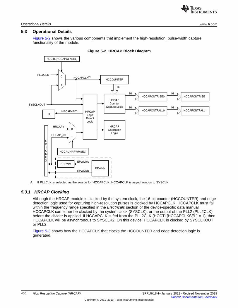
HCCAPCNTRISE0
HCCAPCNTFALL0
HCCAPCNTRISE1
HCCAPCNTFALL1
16
16
16
16
HRCAP
Counter
Capture Logic
HRCAP
Calibration
Logic
HRCAP
Edge
Detect
Logic
HCCOUNTER
0
1
0
1
PIE
SYSCLKOUT
PLL2CLK
HCCAL[HRPWMSEL]
HRPWM
G
P
I
O
M
U
X EPWMxA
EPWMxEPWMxB
HCCAPCLK(A)
HCCTL[HCCAPCLKSEL]
16
HRCAPx
HRCAP_cal
HRCAPxINTn
Operational Details www.ti.com
406 SPRUH18H–January 2011–Revised November 2019Submit Documentation Feedback
Copyright © 2011–2019, Texas Instruments Incorporated
High Resolution Capture (HRCAP)
5.3 Operational DetailsFigure 5-2 shows the various components that implement the high-resolution, pulse-width capturefunctionality of the module.
Figure 5-2. HRCAP Block Diagram
A If PLLCLK is selected as the source for HCCAPCLK, HCCAPCLK is asynchronous to SYSCLK.
5.3.1 HRCAP ClockingAlthough the HRCAP module is clocked by the system clock, the 16-bit counter (HCCOUNTER) and edgedetection logic used for capturing high-resolution pulses is clocked by HCCAPCLK. HCCAPCLK must fallwithin the frequency range specified in the Electricals section of the device-specific data manual.HCCAPCLK can either be clocked by the system clock (SYSCLK), or the output of the PLL2 (PLL2CLK)before the divider is applied. If HCCAPCLK is fed from the PLL2CLK (HCCTL[HCCAPCLKSEL] = 1), thenHCCAPCLK will be asynchronous to SYSCLK2. On this device, HCCAPCLK is clocked by SYSCLKOUTor PLL2.
Figure 5-3 shows how the HCCAPCLK that clocks the HCCOUNTER and edge detection logic isgenerated.

HCCAPCLK
HRCAPx
HCCOUNTER m-1 m 0x0000 0x0001 0x0002 0x0003 0x0004 ... n-2 n-1 n 0x0000
HCCAPCNTFALL0 + 1
PLL2SYSCLK2
Divider(A)
1
0
HCCTL[HCCAPCLKSEL]
PLL2CLK
SYSCLKOUTHCCAPCLK
(A)
www.ti.com Operational Details
407SPRUH18H–January 2011–Revised November 2019Submit Documentation Feedback
Copyright © 2011–2019, Texas Instruments Incorporated
High Resolution Capture (HRCAP)
Figure 5-3. HCCAPCLK Generation
A On this device, the clock divider is a default value of of /2 when DEVICECNF[SYSCLK2DIV2DIS] =0.
5.3.2 HRCAP Modes of OperationThe HRCAP module has two modes of operation:• Normal capture mode: The HRCAP module captures pulse widths in normal resolution within +/- 1
SYSCLK (where SYSCLK is sourced from the same PLL output clock that sources HCCAPCLK — onthis device, this is SYSCLK2). This mode requires less software overhead than high-resolution capturemode.
• High-resolution capture mode: The HRCAP module captures pulse widths with the resolution ofeach edge captured within +/- 300 ps typical and requires the usage of the HCCal calibration libraryprovided by Texas Instruments. In this mode, one HRCAP channel and the ePWM module connectedto the HRCAP calibration input must be dedicated to HRCAP calibration and are not functionallyavailable to the application during calibration.
5.3.2.1 HRCAP CounterBoth modes of operation utilize HCCOUNTER, which resets to 0 and starts counting HCCAPCLK cyclesagain under the following conditions:• SOFTRESET• Detection of rising edge• Detection of falling edge• Device reset and reenable of HRCAP clock
When a rising edge is detected, the value in HCCOUNTER is captured into the 16-bit HCCAPCNTRISE0register before the counter resets to 0. When a falling edge is detected, the value in HCCOUNTER iscaptured into the 16-bit HCCAPCNTFALL0 register before the counter resets to 0. Because theHCCOUNTER starts counting at 0 after an edge is detected, the actual low and high pulse widths (non-high-resolution) are HCCAPCNTFALL0 + 1 and HCCAPCNTRISE0 + 1, respectively, where the “+1” isadded to account for the “0” HCCAPCLK cycle. This behavior is illustrated for high pulse width capture inFigure 5-4.
Figure 5-4. HCCOUNTER Behavior During High Pulse Width Capture

Previous RISE interrupt
HCCAPCNTFALL1
Service RISE interrupt
Previous FALL interrupt Service FALL interrupt
HCCAPCNTRISE1 HCCAPCNTRISE0
HCCAPCNTRISE1 HCCAPCNTRISE0
HCCAPCNTFALL1 HCCAPCNTFALL0
Operational Details www.ti.com
408 SPRUH18H–January 2011–Revised November 2019Submit Documentation Feedback
Copyright © 2011–2019, Texas Instruments Incorporated
High Resolution Capture (HRCAP)
Because the HCCOUNTER starts counting immediately after SOFTRESET, the first capture result into thecapture “0” registers should be discarded. The value captured will be the number of HCCAPCLK cyclessince the last SOFTRESET or the HRCAPCLKEN bit was set rather than an actual pulse widthmeasurement.
5.3.2.2 HCCAP0 - HCCAP1 RegistersThe HRCAP capture registers include a 2-deep FIFO buffer to store two pulse widths’ worth of data.
When a rising edge event occurs, HCCAPCNTRISE0 is loaded with the pulse width data from the lastfalling edge to the current rising edge (low pulse width). At the next rising edge event, the value in theHCCAPCNTRISE0 register is loaded into HCCAPCNTRISE1.
When a falling edge event occurs, HCCAPCNTFALL0 is loaded with the pulse width data from the lastrising edge to the current falling edge (high pulse width). For falling edge events, the HRCAP logicoperates such that the HCCAPCNTFALL0 register value is then loaded into the HCCAPCNTFALL1register at the next rising edge event rather than waiting until the next falling edge event.
5.3.2.3 RISE vs FALL Capture EventsHRCAP capture registers can be read either during rising edge capture events or during falling edgecapture events. They should not be read during both events.
There are a number of differences with regard to using RISE events to read captured registers vs. usingFALL events to read captured registers as shown below in Figure 5-5.
Figure 5-5. Rise vs. Fall Capture Events
5.3.2.3.1 RISE Capture EventsWhen a RISE event occurs, the application code has access to full valid capture data for two pulse widths(1 period) in high-resolution capture mode and three pulse widths (1.5 periods) in normal capture mode.HCCAPCNTFALL0 does not have valid data available on RISE events, as this values are not captureduntil the falling edge event after the current rising edge event (event has not yet occurred).
The application code has until the next RISE event to read all relevant capture data and clear the RISEevent. Otherwise, the data will be overwritten and invalid. Therefore RISE events are generally used tocapture data for period signals where duty cycle may vary significantly.
NOTE: Because HCCOUNTER starts counting immediately after SOFTRESET, the first RISEcapture result into HCCAPCNTRISE0 does not include valid pulse width data and should bediscarded. When the second RISE capture event occurs, this invalid data is transferred toHCCAPCNTRISE1, and therefore the data in this register should also be discarded. After thesecond rise interrupt, all capture data is valid and can be used normally.
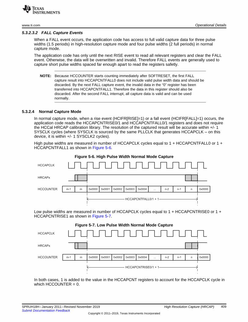
HCCAPCLK
HRCAPx
HCCOUNTER m-1 m 0x0000 0x0001 0x0002 0x0003 0x0004 ... n-2 n-1 n 0x0000
HCCAPCNTRISE0/1 + 1
HCCAPCLK
HRCAPx
HCCOUNTER m-1 m 0x0000 0x0001 0x0002 0x0003 0x0004 ... n-2 n-1 n 0x0000
HCCAPCNTFALL0/1 + 1
www.ti.com Operational Details
409SPRUH18H–January 2011–Revised November 2019Submit Documentation Feedback
Copyright © 2011–2019, Texas Instruments Incorporated
High Resolution Capture (HRCAP)
5.3.2.3.2 FALL Capture EventsWhen a FALL event occurs, the application code has access to full valid capture data for three pulsewidths (1.5 periods) in high-resolution capture mode and four pulse widths (2 full periods) in normalcapture mode.
The application code has only until the next RISE event to read all relevant registers and clear the FALLevent. Otherwise, the data will be overwritten and invalid. Therefore FALL events are generally used tocapture short pulse widths spaced far enough apart to read the registers safetly.
NOTE: Because HCCOUNTER starts counting immediately after SOFTRESET, the first FALLcapture result into HCCAPCNTFALL0 does not include valid pulse width data and should bediscarded. By the next FALL capture event, the invalid data in the “0” register has beentransferred into HCCAPCNTFALL1. Therefore the data in this register should also bediscarded. After the second FALL interrupt, all capture data is valid and can be usednormally.
5.3.2.4 Normal Capture ModeIn normal capture mode, when a rise event (HCIFR[RISE]=1) or a fall event (HCIFR[FALL]=1) occurs, theapplication code reads the HCCAPCNTRISE0/1 and HCCAPCNTFALL0/1 registers and does not requirethe HCCal HRCAP calibration library. The resolution of the captured result will be accurate within +/- 1SYSCLK cycles (where SYSCLK is sourced by the same PLLCLK that generates HCCAPCLK – on thisdevice, it is within +/- 1 SYSCLK2 cycles).
High pulse widths are measured in number of HCCAPCLK cycles equal to 1 + HCCAPCNTFALL0 or 1 +HCCAPCNTFALL1 as shown in Figure 5-6.
Figure 5-6. High Pulse Width Normal Mode Capture
Low pulse widths are measured in number of HCCAPCLK cycles equal to 1 + HCCAPCNTRISE0 or 1 +HCCAPCNTRISE1 as shown in Figure 5-7.
Figure 5-7. Low Pulse Width Normal Mode Capture
In both cases, 1 is added to the value in the HCCAPCNT registers to account for the HCCAPCLK cycle inwhich HCCOUNTER = 0.

HRCAPx
HRCAP step~ 300 ps
HCCAPCLK cycle8.33 ns at 120 MHz
Fn(HCCAPCNT registers, HCCal calibration)
0.0 – 0. in Q16 format9 0.0 – 0. in Q16 format9
Operational Details www.ti.com
410 SPRUH18H–January 2011–Revised November 2019Submit Documentation Feedback
Copyright © 2011–2019, Texas Instruments Incorporated
High Resolution Capture (HRCAP)
5.3.2.5 High Resolution Capture ModeIn high-resolution capture mode, the application code utilizes the HCCal HRCAP calibration libraryfunctions to capture the high-resolution pulse width with each edge captured at a typical resolution of +/-300 ps (with two edges, the resolution of the measured pulse width could vary by +/- 600 ps). Note thatalthough the HRCAP logic itself can be calibrated to capture high-resolution pulse widths, if the jitter onthe input signal is greater than +/- 300 ps, the captured value will also vary according to the jitter on theinput signal.
In order to use high-resolution capture mode, the high-resolution capture logic must be calibrated to scalethe HRCAP step size to a Q16 fraction of the HCCAPCLK. One HRCAP module and the ePWM moduleinternally connected to the HRCAP calibration input must be dedicated only to calibration and cannot beused functionally in the application during calibration.
Texas Instruments provides a calibration function in the HCCal HRCAP calibration library to perform thiscalibration once prior to using the HRCAP in high-resolution capture mode and periodically in a slow loopto account for changes in the HRCAP step size due to voltage and temperature changes while theapplication is running.
The library also provides functions to measure the high resolution high pulse width, low pulse width, andperiod. The pulse and period width measurement results are returned in Q16 fixed-point format with thefractional portion of the result representing a fraction of an HCCAPCLK cycle. (For instance a pulse widthmay appear in the form of 500.25 HCCAPCLK cycles). Figure 5-8 shows how the high-resolution pulsewidth is a function of the calibration of the HRCAP step size and the values in the HCCAPCNT registers.
Figure 5-8. HRCAP High-Resolution Mode Operating Logic
For details on using the HCCal HRCAP calibration library in high-resolution capture mode, seeSection 5.5.
5.3.3 HRCAP InterruptsRising edge capture (RISE), falling edge capture (FALL), and HCCOUNTER overflow (OVF) events cangenerate interrupts to the PIE from the HRCAP module. Additionally, if the rising edge capture flag is set(HCIFR[RISE]) when another rising edge capture event occurs, a rising edge overflow (RISEOVF)interrupt can also generate an interrupt to the PIE. The HRCAP interrupt logic is shown below in Figure 5-9.

Latchset
clear
Generate
Interrupt
Pulse
When
Input = 1
0
0
1HRCAPxINTn
HCICLR[INT]
HCIFR[INT]
RISE Capture
Interrupt Event
Latchset
clear HCICLR[RISE]
HCIFR[RISE]
Latchset
clear HCICLR[FALL]
HCIFR[FALL]
HCCTL[FALLINTE]
HCCTL[RISEINTE]
Counter Overflow
Event
Latchset
clear HCICLR[OVF]
HCIFR[OVF]
HCCTL[OVFINTE]
HCIFRC[RISE]
FALL Capture
Interrupt Event
HCIFRC[FALL]
HCIFRC[OVF]
Set RISOVF Flag To "1"
If RISE Flag Is "1" On
A New RISE Event
HCIFR[RISEOVF]
HCICLR[RISEOVF]
www.ti.com Register Descriptions
411SPRUH18H–January 2011–Revised November 2019Submit Documentation Feedback
Copyright © 2011–2019, Texas Instruments Incorporated
High Resolution Capture (HRCAP)
Figure 5-9. Interrupts in HRCAP Module
RISE/RISEOVF, FALL, and OVF events will only generate an interrupt if the corresponding interruptenable bits in the HCCTL register are set to 1. Interrupt events can be cleared by writing a 1 to thecorresponding bits in the HCICLR register. For testing purposes, interrupt events can be forced by writinga 1 to the corresponding bits in the HCIFRC register.
For proper operation, RISE and FALL interrupts should not be enabled at the same time. Captureregisters should be read during rising edge interrupt events only, or during falling edge interrupt eventsonly, and not during both interrupt events simultaneously. If RISEOVF interrupts are enabled, the RISEflag must always be acknowledged after a RISE event, otherwise a rise overflow condition will occur.
5.4 Register DescriptionsThe complete HRCAP register set is shown in Table 5-1.
Table 5-1. HRCAP Register Summary
Name Address DescriptionOffset
HCCTL 0x00 HRCAP Control RegisterHCIFR 0x01 HRCAP Interrupt Flag RegisterHCICLR 0x02 HRCAP Interrupt Clear RegisterHCIFRC 0x03 HRCAP Interrupt Force RegisterHCCOUNTER 0x04 HRCAP 16-bit Counter RegisterHCCAPCNTRISE0 0x10 HRCAP Capture Counter On Rising Edge 0 RegisterHCCAPCNTFALL0 0x12 HRCAP Capture Counter On Falling Edge 0 RegisterHCCAPCNTRISE1 0x18 HRCAP Capture Counter On Rising Edge 1 RegisterHCCAPCNTFALL1 0x1A HRCAP Capture Counter On Falling Edge 1 Register
5.4.1 HRCAP Control Register (HCCTL) – EALLOW protectedThe HRCAP control register (HCCTL) is shown and described in the figure and table below.

Register Descriptions www.ti.com
412 SPRUH18H–January 2011–Revised November 2019Submit Documentation Feedback
Copyright © 2011–2019, Texas Instruments Incorporated
High Resolution Capture (HRCAP)
Figure 5-10. HRCAP Control Register (HCCTL)15 9 8
Reserved HCCAPCLKSELR-0 R/W-0
7 4 3 2 1 0Reserved OVFINTE FALLINTE RISEINTE SOFTRESET
R-0 R/W-0 R/W-0 R/W-0 R/W-0LEGEND: R/W = Read/Write; R = Read only; -n = value after reset
Table 5-2. HRCAP Control Register (HCCTL) Field Descriptions
Bit Field Value Description15-9 Reserved Reserved
8 HCCAPCLKSEL Capture clock select bit. This bit is used to select the clock source for HCCAPCLK. This bit shouldbe set such that HCCAPCLK falls between the frequency range limits specified in the HRCAPElectricals section of the device-specific data manual.
0 HCCAPCLK = SYSCLKOUT1 HCCAPCLK = PLL2CLK
7-4 Reserved Reserved3 OVFINTE Counter overflow interrupt enable bit
0 Disable counter overflow interrupt1 Enable counter overflow interrupt
2 FALLINTE Falling edge capture interrupt enable bit0 Disable falling edge capture interrupt1 Enable rising edge capture interrupt
1 RISEINTE Rising edge capture interrupt enable bit0 Disable rising edge capture interrupt1 Enable rising edge capture interrupt
0 SOFTRESET Soft reset0 Writes of "0" are ignored. This bit always reads "0".1 Writes of "1" to this bit will clear HCCOUNTER, all capture registers, and the IFR register bits.
5.4.2 HRCAP Interrupt Flag Register (HCIFR) – EALLOW protectedThe HRCAP interrupt flag register (HCIFR) is shown and described in the figure and table below.
Figure 5-11. HRCAP Interrupt Flag Register (HCIFR)15 8
ReservedR-0
7 5 4 3 2 1 0Reserved RISEOVF COUNTEROVF FALL RISE INT
R-0 R-0 R-0 R-0 R-0 R-0LEGEND: R/W = Read/Write; R = Read only; -n = value after reset
Table 5-3. HRCAP Interrupt Flag Register (HCIFR) Field Descriptions
Bit Field Value Description15-5 Reserved Reserved
4 RISEOVF Rising edge interrupt overflow event flag0 No rising edge interrupt overflow event has occurred. This bit is cleared to 0 by writing to the
corresponding bit in the HCICLR register. This bit is also cleared by HCCTL[SOFTRESET].1 This bit is set to "1" if the RISE flag is "1" when a new RISE event occurs.

www.ti.com Register Descriptions
413SPRUH18H–January 2011–Revised November 2019Submit Documentation Feedback
Copyright © 2011–2019, Texas Instruments Incorporated
High Resolution Capture (HRCAP)
Table 5-3. HRCAP Interrupt Flag Register (HCIFR) Field Descriptions (continued)Bit Field Value Description3 COUNTEROVF Counter overflow interrupt flag
0 The HCCOUNTER has not overflowed. This bit is cleared to 0 by writing to the corresponding bit inthe HCICLR register. This bit is also cleared by HCCTL[SOFTRESET].
1 This bit is set to 1 when the 16-bit HCCOUNTER overflows (from 0xFFFF to 0x0000). This bit canalso be set to 1 by writing to the corresponding bit in the HCIFRC register.
2 FALL Falling edge capture interrupt flag:0 No falling edge interrupt has occurred. This bit is cleared to 0 by writing to the corresponding bit in
the HCICLR register. This bit is also cleared by HCCTL[SOFTRESET].1 A falling edge input capture event has occurred. This bit can also be set to 1 by writing to the
corresponding bit in the HCIFRC register.1 RISE Rising edge capture interrupt flag
0 No rising edge interrupt has occurred. This bit is cleared to 0 by writing to the corresponding bit inthe HCICLR register. This bit is also cleared by HCCTL[SOFTRESET].
1 A rising edge input capture event has occurred. This bit can also be set to 1 by writing to thecorresponding bit in the HCIFRC register.
0 INT Global interrupt flag0 No HRCAP interrupt has occurred. This bit is cleared to 0 by writing to the corresponding bit in the
HCICLR register. This bit is also cleared by HCCTL[SOFTRESET].1 An enabled RISE, FALL or COUNTEROVF interrupt has been generated. No further interrupts are
generated until this bit is cleared.

Register Descriptions www.ti.com
414 SPRUH18H–January 2011–Revised November 2019Submit Documentation Feedback
Copyright © 2011–2019, Texas Instruments Incorporated
High Resolution Capture (HRCAP)
5.4.3 HRCAP Interrupt Clear Register (HCICLR) – EALLOW protectedThe HRCAP interrupt clear register (HCICLR) is shown and described in the figure and table below.
Figure 5-12. HRCAP Interrupt Clear Register (HCICLR)15 8
ReservedR-0
7 5 4 3 2 1 0Reserved RISEOVF COUNTEROVF FALL RISE INT
R-0 R/W-0 R/W-0 R/W-0 R/W-0 R/W-0LEGEND: R/W = Read/Write; R = Read only; -n = value after reset
Table 5-4. HRCAP Interrupt Clear Register (HCICLR) Field Descriptions
Bit Field Value Description15-5 Reserved Reserved
4 RISEOVF Rising edge interrupt overflow clear bit0 Writes of "0" are ignored. This bit always reads "0".1 Writes of "1" to this bit will clear the corresponding RISEOVF flag bit in the HCIFR register to "0".
The hardware setting of HCIFR[RISEOVF] flag bit has priority over the software clear if bothhappen on the same cycle.
3 COUNTEROVF Counter overflow interrupt clear bit0 Writes of "0" are ignored. This bit always reads "0".1 Writes of "1" to this bit will clear the corresponding COUNTEROVF flag bit in the HCIFR register to
"0". The hardware setting of HCIFR[COUNTEROVF] flag bit has priority over the software clear ifboth happen on the same cycle.
2 FALL Falling edge capture interrupt clear bit:0 Writes of "0" are ignored. This bit always reads "0".1 Writes of "1" to this bit will clear the corresponding FALL flag bit in the HCIFR register to "0". The
hardware setting of HCIFR[FALL] flag bit has priority over the software clear if both happen on thesame cycle.
1 RISE Rising edge capture interrupt clear bit0 Writes of "0" are ignored. This bit always reads "0".1 Writes of "1" to this bit will clear the corresponding RISE flag bit in the HCIFR register to "0". The
hardware setting of HCIFR[RISE] flag bit has priority over the software clear if both happen on thesame cycle.
0 INT Global interrupt clear bit0 Writes of "0" are ignored. This bit always reads "0".1 Writes of "1" to this bit will clear the corresponding INT flag bit in the HCIFR register to "0". The
hardware setting of HCIFR[INT] flag bit has priority over the software clear if both happen on thesame cycle.

www.ti.com Register Descriptions
415SPRUH18H–January 2011–Revised November 2019Submit Documentation Feedback
Copyright © 2011–2019, Texas Instruments Incorporated
High Resolution Capture (HRCAP)
5.4.4 HRCAP Interrupt Force Register (HCIFRC)– EALLOW protectedThe HRCAP interrupt force register (HCIFRC) is shown and described in the figure and table below.
Figure 5-13. HRCAP Interrupt Force Register (HCIFRC)15 8
ReservedR-0
7 4 3 2 1 0Reserved COUNTEROVF FALL RISE Reserved
R-0 R/W-0 R/W-0 R/W-0 R-0LEGEND: R/W = Read/Write; R = Read only; -n = value after reset
Table 5-5. HRCAP Interrupt Force Register (HCIFRC) Field Descriptions
Bit Field Value Description15-4 Reserved Reserved
3 COUNTEROVF Counter overflow interrupt force bits0 Writes of "0" are ignored. This bit always reads "0".1 Writes of "1" to this bit will force the corresponding COUNTEROVF flag bit in HCIFR register to "1".
The software HCCTL[SOFTRESET] clearing of the HCIFR[COUNTEROVF] bit has priority over thehardware trying to set the bit in the same cycle.
2 FALL Falling edge interrupt force bits0 Writes of "0" are ignored. This bit always reads "0".1 Writes of "1" to this bit will force the corresponding FALL flag bit in HCIFR register to "1". The
software HCCTL[SOFTRESET] clearing of the HCIFR[FALL] bit has priority over the hardwaretrying to set the bit in the same cycle.
1 RISE Rising edge interrupt force bits0 Writes of "0" are ignored. This bit always reads "0".1 Writes of "1" to this bit will force the corresponding RISE flag bit in HCIFR register to "1". The
software HCCTL[SOFTRESET] clearing of the HCIFR[RISE] bit has priority over the hardwaretrying to set the bit in the same cycle.
0 Reserved Reserved
5.4.5 HRCAP Counter Register (HCCOUNTER)The HRCAP counter register (HCCOUNTER) is shown and described in the figure and table below.
Figure 5-14. HRCAP Counter Register (HCCOUNTER)15 0
COUNTERR-0
LEGEND: R/W = Read/Write; R = Read only; -n = value after reset
Table 5-6. HRCAP Counter Register (HCCOUNTER) Field Descriptions
Bit Field Value Description15-0 COUNTER 0 16-bit capture counter
This free running counter is used to capture rising and falling edge events. The HCCOUNTER isincremented on every HCCAPCLK cycle. When the counter reaches 0xFFFF, it will overflow to0x0000 on the next cycle and generate a COUNTEROVF interrupt event.The counter is reset to 0x0000 on every rising and falling edge event.The counter can also be reset to 0x0000 by a system reset or by setting the HCCTL[SOFTRESET]bit.NOTE: Because the counter is clocked from HCCAPCLK, which can be asynchronous to SYSCLK,CPU reads to this register should not be performed unless the clocks to the HRCAP module aredisabled (HRCAPxENCLK = 0).
Register Descriptions www.ti.com
416 SPRUH18H–January 2011–Revised November 2019Submit Documentation Feedback
Copyright © 2011–2019, Texas Instruments Incorporated
High Resolution Capture (HRCAP)
5.4.6 HRCAP Capture Counter On Rising Edge 0 Register (HCCAPCNTRISE0)The HRCAP capture counter on rising edge 0 register (HCCAPCNTRISE0) is shown and described in thefigure and table below.
Figure 5-15. HRCAP Capture Counter On Rising Edge 0 Register (HCCAPCNTRISE0)15 0
HCCAPCNTRISE0R-0
LEGEND: R/W = Read/Write; R = Read only; -n = value after reset
Table 5-7. HRCAP Capture Counter On Rising Edge 0 Register (HCCAPCNTRISE0) FieldDescriptions
Bit Field Value Description15-0 HCCAPCNTRISE0 0 HRCAP capture counter on rising edge 0 register
This register captures the16-bit HCCOUNTER value when a rising edge event is detected.
5.4.7 HRCAP Capture Counter On Rising Edge 1 Register (HCCAPCNTRISE1)The HRCAP capture counter on rising edge 1 register (HCCAPCNTRISE1) is shown and described in thefigure and table below.
Figure 5-16. HRCAP Capture Counter On Rising Edge 1 Register (HCCAPCNTRISE1)15 0
HCCAPCNTRISE1R-0
LEGEND: R/W = Read/Write; R = Read only; -n = value after reset
Table 5-8. HRCAP Capture Counter On Rising Edge 1 Register (HCCAPCNTRISE1) FieldDescriptions
Bit Field Value Description15-0 HCCAPCNTRISE1 0 HRCAP capture counter on rising edge 1 register
On an input rising edge event, the value in the HCCAPCNTRISE0 register is copied into theHCCAPCNTRISE1 register before the HCCOUNTER value is captured into theHCCAPCNTRISE0 register.
5.4.8 HRCAP Capture Counter On Falling Edge 0 Register (HCCAPCNTFALL0)The HRCAP capture counter on falling edge 0 register (HCCAPCNTFALL0) is shown and described in thefigure and table below.
Figure 5-17. HRCAP Capture Counter On Falling Edge 0 Register (HCCAPCNTFALL0)15 0
HCCAPCNTFALL0R-0
LEGEND: R/W = Read/Write; R = Read only; -n = value after reset
Table 5-9. HRCAP Capture Counter On Falling Edge 0 Register (HCCAPCNTFALL0) FieldDescriptions
Bit Field Value Description15-0 HCCAPCNTFALL0 0 HRCAP capture counter on falling edge 0 register
This register captures the16-bit HCCOUNTER value when a Falling edge event is detected.

www.ti.com Register Descriptions
417SPRUH18H–January 2011–Revised November 2019Submit Documentation Feedback
Copyright © 2011–2019, Texas Instruments Incorporated
High Resolution Capture (HRCAP)
5.4.9 HRCAP Capture Counter On Falling Edge 1 Register (HCCAPCNTFALL1)The HRCAP capture counter on falling edge 1 register (HCCAPCNTFALL1) is shown and described in thefigure and table below.
Figure 5-18. HRCAP Capture Counter On Falling Edge 1 Register (HCCAPCNTFALL1)15 0
HCCAPCNTFALL1R-0
LEGEND: R/W = Read/Write; R = Read only; -n = value after reset
Table 5-10. HRCAP Capture Counter On Falling Edge 1 Register (HCCAPCNTFALL1) FieldDescriptions
Bit Field Value Description15-0 HCCAPCNTFALL1 0 HRCAP capture counter on falling edge 1 register
On an input falling edge event, the value in the HCCAPCNTFALL0 register is copied into theHCCAPCNTFALL1 register before the HCCOUNTER value is captured into theHCCAPCNTFALL0 register.
5.5 HRCAP Calibration LibraryThe HRCAP calibration (HCCal) logic is capable of capturing an edge in discrete time steps whichsubdivide an HCCAPCLK cycle. As previously mentioned, the size of each step is on the order of 300 ps(see device-specific data sheet for typical HRCAP step size on your device). The HRCAP_Cal() function inthe HRCAP calibration library must be run periodically to be certain that time steps are optimally appliedand that the edge capture accuracy is maintained over a wide range of PWM frequencies, system clockfrequencies, voltages, and temperatures. The HRCAP step size varies based on worst-case processparameters, operating temperature, and voltage. HRCAP step size increases with decreasing voltage andincreasing temperature and decreases with increasing voltage and decreasing temperature.
Applications that use the HRCAP in high-resolution capture mode should use the TI-supplied HRCAPcalibration (HCCal) software HRCAP_Cal() function. The HRCAP_Cal function helps to dynamically scalethe HRCAP step size to a fraction of the HCCAPCLK cycle while the HRCAP is in high-resolution mode.To utilize the HCCal capabilities effectively during HRCAP operation, the HRCAP calibration logic usesbuilt-in self-check and diagnostics capabilities to scale the HRCAP step size appropriately for anyoperating condition.
TI provides a C-callable library containing one HRCAP calibration function that utilizes this hardware andproperly calibrates the internal HRCAP step logic as a fraction of a HCCAPCLK cycle. The library suppliesadditional high-resolution capture functions to calculate pulse widths captured in Q16 integer + fractionalHCCAPCLK cycles based on the values in the HCCAPCNT registers and the calibration results.
The contents of these functions are proprietary to Texas Instruments and will not be published.
Currently, there is 1 released version of the HCCal Type 0 library, HCCal_Type0_V1.lib, which is locatedin the C2000ware software package under the \libraries\calibration\hrcap\ directory.

HRCAP Calibration Library www.ti.com
418 SPRUH18H–January 2011–Revised November 2019Submit Documentation Feedback
Copyright © 2011–2019, Texas Instruments Incorporated
High Resolution Capture (HRCAP)
5.5.1 HRCAP Calibration Library Functions
5.5.1.1 HRCAP_CalThe HRCAP_Cal() function runs calibration and self-check diagnostics logic on a given HRCAP module tointernally scale the HCCal step logic as a fraction of a HCCAPCLK cycle.
Prototype:Uint16 HRCAP_Cal(Uint16 HRCAPModule, Uint16 PLLClk, volatile struct EPWM_REGS *ePWMModule);
Parameters:
HRCAPModule The HRCAP module number as an integer value (i.e., “1” forHRCAP1, and “2” for HRCAP2). This HRCAP module will bededicated to calibration only and cannot be used functionally tocapture pulse widths.
PLLClk If 0, then HCCAPCLK is clocked by SYSCLK, where SYSCLK is thesystem clock that clocks the HRCAP module. If 1, then HCCAPCLK isclocked by PLLCLK, where the PLLCLK frequency is a multiple of thesystem clock that clocks the HRCAP module.
ePWMModule A pointer to the address of the EPWM_REGS structure for theHRPWM module used to calibrate the HRCAP (i.e., if HRPWM7Aoutput is connected to the HRCAP’s internal calibration logic, then&EPwm7Regs is passed into this parameter, and if HRPWM8A outputis connected to the HRCAP’s internal calibration logic, then&EPwm8Regs is passed into this parameter). The single ePWMmodule used for HRCAP calibration is device-dependent.
Returns:
0 If HCCal calibration is in progress without encountering errors.
1 If HCCal has exited with errors. User should check that PLL isconfigured such that the HCCAPCLK frequency falls within thefrequency limits designated by the HRCAP Electricals section of thedata manual.
2 If HCCal calibration has completed without errors.
Description:This function drives the HRCAP calibration module logic to subdivide an HCCAPCLK cycle into HRCAPtime steps equivalent to a fraction of an HCCAPCLK cycle at any given time.
HRCAP_Cal() can only be used with HCCAPCLK between 98 Mhz and 120 MHz (See your device-specific data manual’s HRCAP Electricals section for the device-specific HCCAPCLK frequency limits).
The function can be called at any time on a single HRCAP module which is dedicated to calibration only.
The calibration HRCAP module cannot be used functionally to capture pulse widths. The calibration logicdriven by this function uses a single ePWMxA HRPWM channel output connected internally to the HRCAPinput to run diagnostics. During calibration, that ePWM module cannot be used for normal ePWMfunctions in the application. For instance, on this device, while the HRCAP is in use in high-resolutioncapture mode, ePWM8 cannot be used functionally by the application during calibration.

Service FALL interrupt
Service RISE interrupt
HCCAPCNTFALL0HCCAPCNTRISE0HCCAPCNTFALL1
HCCAPCNTRISE0HCCAPCNTFALL1HCCAPCNTRISE1
LowPulseWidth0
LowPulseWidth0
www.ti.com HRCAP Calibration Library
419SPRUH18H–January 2011–Revised November 2019Submit Documentation Feedback
Copyright © 2011–2019, Texas Instruments Incorporated
High Resolution Capture (HRCAP)
5.5.1.2 LowPulseWidth0The LowPulseWidth0() function captures the high-resolution low pulse width around HCCAPCNTRISE0 inHCCAPCLK cycles.
Prototype:Uint32 LowPulseWidth0 (Uint16 * ptrHRCAPmodule);
Parameters:
ptrHRCAPmodule A 16-bit pointer to the first address of the HRCAP register block of theHRCAP module used to capture pulses.
Returns:32-bit high-resolution low pulse width around HCCAPCNTRISE0 as Q16 fixed-point value in number ofHCCAPCLK cycles.
Description:This function can be called for any of the HRCAP modules not used for calibration to convert theHCCAPCNTRISE0 and HRCAP calibration results into a fixed-point Q16 integer + fractional high-resolution low-pulse width in HCCAPCLK cycles. Figure 5-19 shows which low pulse widths can becaptured on a RISE and FALL event.
Figure 5-19. LowPulseWidth0 Capture on RISE and FALL Events

Service RISE interrupt
HCCAPCNTFALL0HCCAPCNTFALL1
HCCAPCNTFALL1
HighPulseWidth0HighPulseWidth1
HighPulseWidth1
HCCAPCNTRISE0HCCAPCNTRISE1
HCCAPCNTRISE0
HRCAP Calibration Library www.ti.com
420 SPRUH18H–January 2011–Revised November 2019Submit Documentation Feedback
Copyright © 2011–2019, Texas Instruments Incorporated
High Resolution Capture (HRCAP)
5.5.1.3 HighPulseWidth0 and HighPulseWidth1The HighPulseWidth0()function captures the high-resolution high pulse width around HCCAPCNTFALL0 inHCCAPCLK cycles. The HighPulseWidth1()function captures the high-resolution high pulse width aroundHCCAPCNTFALL1 in HCCAPCLK cycles.
Prototypes:Uint32 HighPulseWidth0 (Uint16 * ptrHRCAPmodule);Uint32 HighPulseWidth1 (Uint16 * ptrHRCAPmodule);
Parameters:
ptrHRCAPmodule A 16-bit pointer to the first address of the HRCAP register block of theHRCAP module used to capture pulses.
Returns:32-bit high-resolution high pulse width around HCCAPCNTFALL0/1 as Q16 fixed-point value in number ofHCCAPCLK cycles.
Description:These functions can be called for any of the HRCAP modules not used for calibration. They use thecalibration logic to convert the HCCAPCNTFALL0/1 register value and HCCal calibration results into afixed-point Q16 integer + fractional high-resolution high-pulse width in HCCAPCLK cycles. Figure 5-20shows which high pulse widths can be captured on a RISE and FALL event.
Figure 5-20. HighPulseWidth0/1 Capture on RISE and FALL Events
5.5.1.4 PeriodWidthRise0The PeriodWidthRise0() function captures the rising edge to rising edge high-resolution period widtharound HCCAPCNTRISE0 and HCCAPCNTFALL1 in HCCAPCLK cycles.
Prototype:Uint32 PeriodWidthRise0 (Uint16 * ptrHRCAPmodule)
Parameters:
ptrHRCAPmodule A 16-bit pointer to the first address of the HRCAP register block of theHRCAP module used to capture pulses.
Returns:32-bit high-resolution rising edge to rising edge period width aroundHCCAPCNTRISE0+HCCAPCNTFALL1 as Q16 fixed-point value in number of HCCAPCLK cycles.

Service FALL interrupt
Service RISE interrupt
HCCAPCNTRISE0HCCAPCNTRISE1
HCCAPCNTFALL0HCCAPCNTRISE0HCCAPCNTFALL1
HCCAPCNTFALL1
HCCAPCNTRISE1
PeriodWidthRise0 PeriodWidthFall0
PeriodWidthRise0
www.ti.com HRCAP Calibration Library
421SPRUH18H–January 2011–Revised November 2019Submit Documentation Feedback
Copyright © 2011–2019, Texas Instruments Incorporated
High Resolution Capture (HRCAP)
Description:This function can be called for any of the HRCAP modules not used for calibration. It uses the calibrationlogic to convert the HCCAPCNTRISE0 and HCCAPCNTFALL1 register values and HCCal calibrationresults into the function into a fixed-point Q16 integer + fractional high-resolution period width inHCCAPCLK cycles. Figure 5-21 shows which period widths can be captured on a RISE and FALL event.
5.5.1.5 PeriodWidthFall0The PeriodWidthFall0()function captures the falling edge to falling edge high-resolution period widtharound HCCAPCNTFALL0 and HCCAPCNTRISE0 in HCCAPCLK cycles.
Prototype:
Uint32 PeriodWidthFall0 (Uint16 * ptrHRCAPmodule);
Parameters:
ptrHRCAPmodule A 16-bit pointer to the first address of the HRCAP register block of theHRCAP module used to capture pulses.
Returns:32-bit high-resolution falling edge to falling edge period width aroundHCCAPCNTFALL0+HCCAPCNTRISE0 as Q16 fixed-point value in number of HCCAPCLK cycles.
Description:
This function can be called for any of the HRCAP modules not used for calibration. It uses the calibrationlogic to convert the HCCAPCNTFALL0 and HCCAPCNTRISE0 register values and HCCal calibrationresults into a fixed-point Q16 integer + fractional high-resolution period width in HCCAPCLK cycles.Figure 5-21 shows which period widths can be captured on a RISE and FALL event.
Figure 5-21. PeriodWidthRise0 and PeriodWidthFall0 Capture on RISE and FALL Events

HRCAP Calibration Library www.ti.com
422 SPRUH18H–January 2011–Revised November 2019Submit Documentation Feedback
Copyright © 2011–2019, Texas Instruments Incorporated
High Resolution Capture (HRCAP)
5.5.2 HRCAP Calibration Library Software UsageTo use the HRCAP in high-resolution mode, it is recommended that the HRCAP calibration functions beused as described here.
Step 1: Add "Include" FilesThe HCCal_Type0_V1.h file needs to be included as follows. This include file is mandatory while using theHRCAP calibration library functions. For these devices, the F2806x_Device.h and F2806x_Examples.hfiles in the F2806x C/C++ Header Files and Peripheral Examples package in C2000ware are necessary.For other device families, the device-specific equivalent files in the header files and peripheral examplessoftware packages for those devices should be used. These include files are optional if customizedheader files are used in the end applications.
Example 1: A Sample of How to Add "Include" Files#include "F2806x_Device.h" // F2806x Headerfile#include "F2806x_Examples.h" // F2806x Examples Headerfile#include "HCCal_Type0_V1.h"
Step 2: HRCAP Register Array DeclarationDeclare an array of pointers to HRCAP_REGS structures which includes all available HRCAP modules onthe device. Position 0 includes a 0 value which is not used by the HRCAP_Cal function.
Example 2: A Sample of How to Declare an HRCAP Register Array#define NUM_HRCAP 5 // # of HRCAP modules on 2806x + 1
volatile struct HRCAP_REGS *HRCAP[NUM_HRCAP] = {0, &HRCap1Regs,&HRCap2Regs, &HRCap3Regs, &HRCap4Regs};
Step 3: HRCAP Pre-CalibrationPrior to using the HRCAP in high-resolution mode in application code, HRCAP_Cal() should be called tocalibrate the HRCAP step size subdivision into HCCAPCLK.
As part of the one-time pre-calibration prior to using the HRCAP in high-resolution mode, include thefollowing:
Example 3: A Sample of HRCAP Pre-Calibrationwhile (status!= HCCAL_COMPLETE) // While calibration is incomplete
{// Use HRCAP2 to calibrate with:// HCCAPCLK = PLL2CLK// ePWM8A = HRCAP calibration input
status = HRCAP_Cal(2,HCCAPCLK_PLLCLK, &EPwm8Regs);
if (status == HCCAL_ERROR){
ESTOP0; // Error, stop and check HCCAPCLK frequency}
}

www.ti.com HRCAP Calibration Library
423SPRUH18H–January 2011–Revised November 2019Submit Documentation Feedback
Copyright © 2011–2019, Texas Instruments Incorporated
High Resolution Capture (HRCAP)
Step 4: Application Code CalibrationWhile the application is running, fluctuations in both device temperature and supply voltage may beexpected. To be sure that optimal HRCAP step size is used for each HRCAP module, the HRCAP_Calfunction should be re-run periodically as part of a slower back-ground loop. Some examples of this areshown here.
NOTE: See the hrcap_capture_hrpwm example in the device-specific C/C++ header files and peripheralexamples available in C2000ware from the TI website
Example 4: HRCAP_Cal Function Callsmain (){
int status;
// User code// HRCAP 1, 3, and 4 are running in high-resolution mode// The status variable returns 2 once calibration has been// completed by the HCCal Calibration Module running// diagnostics.
status = HRCAP_Cal(2,HCCAPCLK_PLLCLK, &EPwm8Regs);
// The function returns a 2 if HCCAPCLK is not within the// appropriate frequency range.
if(status==HCCAL_ERROR) {ESTOP0;}}

HRCAP Calibration Library www.ti.com
424 SPRUH18H–January 2011–Revised November 2019Submit Documentation Feedback
Copyright © 2011–2019, Texas Instruments Incorporated
High Resolution Capture (HRCAP)
Step 5: Application Code Pulse Width MeasurementWhile the application is running, when a RISE or FALL event occurs, pulse and period widths can bemeasured using the high resolution pulse width functions as shown below.
Example 5: LowPulseWidth, HighPulseWidth, and PeriodWidth Function Calls
interrupt void HRCAP1_Isr (void){
EALLOW;if (HRCap1Regs.HCIFR.bit.RISEOVF == 1) {
ESTOP0; // Another rising edge detected}
if (first < 1) {first++; // Discard first data (because first interrupt
// after reset/clk enable measures time from// clock start to edge - invalid pulse width)
} else {
periodwidth = PeriodWidthRise0((Uint16 *)&HRCap1Regs);pulsewidthlow = LowPulseWidth0((Uint16 *)&HRCap1Regs);pulsewidthhigh = HighPulseWidth0((Uint16 *)&HRCap1Regs);
}
HRCap1Regs.HCICLR.bit.RISE=1;HRCap1Regs.HCICLR.bit.INT=1;PieCtrlRegs.PIEACK.bit.ACK4=1;EDIS;
}

425SPRUH18H–January 2011–Revised November 2019Submit Documentation Feedback
Copyright © 2011–2019, Texas Instruments Incorporated
Enhanced Capture (eCAP)
Chapter 6SPRUH18H–January 2011–Revised November 2019
Enhanced Capture (eCAP)
This chapter describes the enhanced capture (eCAP) module, which is used in systems where accuratetiming of external events is important.
Topic ........................................................................................................................... Page
6.1 Introduction ..................................................................................................... 4266.2 Features .......................................................................................................... 4266.3 Description ...................................................................................................... 4266.4 Capture and APWM Operating Mode ................................................................... 4286.5 Capture Mode Description ................................................................................. 4296.6 Application of the eCAP Module ........................................................................ 4376.7 Application of the APWM Mode .......................................................................... 4416.8 eCAP Registers ................................................................................................ 442

Introduction www.ti.com
426 SPRUH18H–January 2011–Revised November 2019Submit Documentation Feedback
Copyright © 2011–2019, Texas Instruments Incorporated
Enhanced Capture (eCAP)
6.1 IntroductionThis eCAP module is a Type-0 eCAP. See the TMS320C28xx, 28xxx DSP Peripheral Reference Guide fora list of all devices with an eCAP module of the same type, to determine the differences between thetypes, and for a list of device-specific differences within a type.
6.2 FeaturesFeatures for eCAP include:• Speed measurements of rotating machinery (for example, toothed sprockets sensed via Hall sensors)• Elapsed time measurements between position sensor pulses• Period and duty cycle measurements of pulse train signals• Decoding current or voltage amplitude derived from duty cycle encoded current/voltage sensors
The eCAP module described in this guide includes the following features:• 4-event time-stamp registers (each 32 bits)• Edge polarity selection for up to four sequenced time-stamp capture events• Interrupt on either of the four events• Single-shot capture of up to four event time-stamps• Continuous mode capture of time stamps in a four-deep circular buffer• Absolute time-stamp capture• Difference (Delta) mode time-stamp capture• All above resources are dedicated to a single input pin• When not used in capture mode, the eCAP module can be configured as a single-channel PWM output
6.3 DescriptionThe eCAP module represents one complete capture channel that can be instantiated multiple times,depending on the target device. In the context of this guide, one eCAP channel has the followingindependent key resources:• Dedicated input capture pin• 32-bit time base (counter)• 4 x 32-bit time-stamp capture registers (CAP1-CAP4)• Four-stage sequencer (modulo4 counter) that is synchronized to external events, eCAP pin
rising/falling edges.• Independent edge polarity (rising/falling edge) selection for all four events• Input capture signal prescaling (from 2-62 or bypass)• One-shot compare register (two bits) to freeze captures after 1-4 time-stamp events• Control for continuous time-stamp captures using a four-deep circular buffer (CAP1-CAP4) scheme• Interrupt capabilities on any of the four capture events
Multiple identical eCAP modules can be contained in a system as shown in Figure 6-1. The number ofmodules is device-dependent and is based on target application needs.

ECAP1module
PIE
From EPWM
ECAP1INT
SyncIn
VBus32
SyncOut
ECAP2/
SyncOut
APWM2module
SyncIn
ECAP2INT
SyncOut
SyncIn
moduleAPWMxECAPx/
ECAPxINT
ECAP1
GPIOMUX
ECAP2
ECAPx
www.ti.com Description
427SPRUH18H–January 2011–Revised November 2019Submit Documentation Feedback
Copyright © 2011–2019, Texas Instruments Incorporated
Enhanced Capture (eCAP)
Figure 6-1. Multiple eCAP Modules In A C28x System

Counter (”timer”)SyncIn
32
CAP1 reg
CAP2 reg
CAP4 reg
CAP3 reg
Interrupt I/FECAPxINT
SequencingEdge detectionEdge polarity
Prescale
ECAPxpin
Note:Same pin
depends onoperating
mode
Counter (”timer”)SyncIn
32
Capturemode
APWMmode
Period reg(active) (”CAP1”)
Compare reg(active) (”CAP2”)
Period reg(shadow) (”CAP3”)
(shadow) (”CAP4”)Compare reg
Interrupt I/FECAPxINT
PWMCompare logic
APWMxpin
Or
Syncout
Capture and APWM Operating Mode www.ti.com
428 SPRUH18H–January 2011–Revised November 2019Submit Documentation Feedback
Copyright © 2011–2019, Texas Instruments Incorporated
Enhanced Capture (eCAP)
6.4 Capture and APWM Operating ModeYou can use the eCAP module resources to implement a single-channel PWM generator (with 32-bitcapabilities) when it is not being used for input captures. The counter operates in count-up mode,providing a time-base for asymmetrical pulse width modulation (PWM) waveforms. The CAP1 and CAP2registers become the active period and compare registers, respectively, while CAP3 and CAP4 registersbecome the period and capture shadow registers, respectively. Figure 6-2 is a high-level view of both thecapture and auxiliary pulse-width modulator (APWM) modes of operation.
Figure 6-2. Capture and APWM Modes of Operation
A A single pin is shared between CAP and APWM functions. In capture mode, it is an input; in APWM mode, it is anoutput.
B In APWM mode, writing any value to CAP1/CAP2 active registers also writes the same value to the correspondingshadow registers CAP3/CAP4. This emulates immediate mode. Writing to the shadow registers CAP3/CAP4 invokesthe shadow mode.
Figure 6-3 further descries the output of the eCAP in APWM mode based on the CMP and PRD values.

FFFFFFFF
0000000C
On
time
Off−timePeriod
ECAPxOUT
QCTR = CMP
DigitalComparator
CTR = PRD
DigitalComparator
32
32
32
PRD [0-31]
CTR [0-31]
CMP [0-31]
ECAPOUT
POLSEL
set
clear
PeriodRegisterPRD [0-31]
CompareRegisterCMP [0-31]
clear clear
CTR [0-31]
set set
www.ti.com Capture Mode Description
429SPRUH18H–January 2011–Revised November 2019Submit Documentation Feedback
Copyright © 2011–2019, Texas Instruments Incorporated
Enhanced Capture (eCAP)
Figure 6-3. Counter Compare and PRD Effects on the eCAP Output in APWM Mode
6.5 Capture Mode DescriptionFigure 6-4 shows the various components that implement the capture function.

TSCTR
(counter−32 bit)
RST
CAP1
(APRD active)LD
CAP2
(ACMP active)LD
CAP3
(APRD shadow)LD
CAP4
(ACMP shadow)LD
Continuous /
Oneshot
Capture Control
LD1
LD2
LD3
LD4
32
32
PRD [0−31]
CMP [0−31]
CTR [0−31]
ECAPx
Interrupt
Trigger
and
Flag
control
to PIE
CTR=CMP
32
32
32
32
32
ACMP
shadow
Event
Prescale
CTRPHS
(phase register−32 bit)
SYNCOut
SYNCIn
Event
qualifier
Polarity
select
Polarity
select
Polarity
select
Polarity
select
CTR=PRD
CTR_OVF
4
PWM
compare
logic
CTR [0−31]
PRD [0−31]
CMP [0−31]
CTR=CMP
CTR=PRD
CTR_OVFOVF
APWM mode
Delta−mode
SY
NC
4Capture events
CEVT[1:4]
APRD
shadow
32
32
MO
DE
SE
LE
CT
ECCTL2 [ SYNCI_EN, SYNCOSEL, SWSYNC]
ECCTL2[CAP/APWM]
Edge Polarity Select
ECCTL1[CAPxPOL]
ECCTL1[EVTPS]
ECCTL1 [ CAPLDEN, CTRRSTx]
ECCTL2 [ RE−ARM, CONT/ONESHT, STOP_WRAP]
Registers: ECEINT, ECFLG, ECCLR, ECFRC
Capture Mode Description www.ti.com
430 SPRUH18H–January 2011–Revised November 2019Submit Documentation Feedback
Copyright © 2011–2019, Texas Instruments Incorporated
Enhanced Capture (eCAP)
Figure 6-4. eCAP Block Diagram
6.5.1 Event Prescaler• An input capture signal (pulse train) can be prescaled by N = 2-62 (in multiples of 2) or can bypass the
prescaler.This is useful when very high frequency signals are used as inputs. Figure 6-5 shows a functionaldiagram and Figure 6-6 shows the operation of the prescale function.

ECAPx
PSout
div 2
PSout
div 4
PSout
div 6
PSout
div 8
PSout
div 10
0
1 /n
5
ECCTL1[EVTPS]prescaler [5 bits]
(counter)
By−pass
Event prescaler
ECAPx pin
(from GPIO)
PSout
www.ti.com Capture Mode Description
431SPRUH18H–January 2011–Revised November 2019Submit Documentation Feedback
Copyright © 2011–2019, Texas Instruments Incorporated
Enhanced Capture (eCAP)
Figure 6-5. Event Prescale Control
A When a prescale value of 1 is chosen ( ECCTL1[13:9] = 0,0,0,0,0 ), the input capture signal bypasses the prescalelogic completely.
Figure 6-6. Prescale Function Waveforms
6.5.2 Edge Polarity Select and QualifierFunctionality and features include:• Four independent edge polarity (rising edge/falling edge) selection muxes are used, one for each
capture event.• Each edge (up to 4) is event qualified by the Modulo4 sequencer.• The edge event is gated to its respective CAPx register by the Mod4 counter. The CAPx register is
loaded on the falling edge.
6.5.3 Continuous/One-Shot ControlOperation of eCAP in Continuous/One-Shot mode:• The Mod4 (2-bit) counter is incremented via edge qualified events (CEVT1-CEVT4).• The Mod4 counter continues counting (0->1->2->3->0) and wraps around unless stopped.• A 2-bit stop register is used to compare the Mod4 counter output, and when equal, stops the Mod4

CEVT1
CEVT2
CEVT3
CEVT4
One−shotcontrol logic
Stop
CLK
RST
Modulo 4counter
2
Mod_eq
Stop value (2b)
ECCTL2[STOP_WRAP] ECCTL2[RE−ARM]ECCTL2[CONT/ONESHT]
0 1 32
2:4 MUX
Capture Mode Description www.ti.com
432 SPRUH18H–January 2011–Revised November 2019Submit Documentation Feedback
Copyright © 2011–2019, Texas Instruments Incorporated
Enhanced Capture (eCAP)
counter and inhibits further loads of the CAP1-CAP4 registers. This occurs during one-shot operation.
The continuous/one-shot block controls the start, stop and reset (zero) functions of the Mod4 counter, viaa mono-shot type of action that can be triggered by the stop-value comparator and re-armed via softwarecontrol.
Once armed, the eCAP module waits for 1-4 (defined by stop-value) capture events before freezing boththe Mod4 counter and contents of CAP1-4 registers (time stamps).
Re-arming prepares the eCAP module for another capture sequence. Also, re-arming clears (to zero) theMod4 counter and permits loading of CAP1-4 registers again, providing the CAPLDEN bit is set.
In continuous mode, the Mod4 counter continues to run (0->1->2->3->0, the one-shot action is ignored,and capture values continue to be written to CAP1-4 in a circular buffer sequence.
Figure 6-7. Details of the Continuous/One-shot Block
6.5.4 32-Bit Counter and Phase ControlThis counter provides the time-base for event captures, and is clocked via the system clock.
A phase register is provided to achieve synchronization with other counters, via a hardware and softwareforced sync. This is useful in APWM mode when a phase offset between modules is needed.
On any of the four event loads, an option to reset the 32-bit counter is given. This is useful for timedifference capture. The 32-bit counter value is captured first, then it is reset to 0 by any of the LD1-LD4signals.

SYNCI
CTR=PRD
Disable
Disable
Sync outselect
ECCTL2[SYNCOSEL]
SYNCO
ECCTL2[SWSYNC]
SYNC
ECCTL2[SYNCI_EN]
CTRPHS
LD_CTRPHS
CLK
TSCTR(counter 32b)
RST
OVFSYSCLK
Delta−mode
CTR−OVF
CTR[31−0]
www.ti.com Capture Mode Description
433SPRUH18H–January 2011–Revised November 2019Submit Documentation Feedback
Copyright © 2011–2019, Texas Instruments Incorporated
Enhanced Capture (eCAP)
Figure 6-8. Details of the Counter and Synchronization Block
6.5.5 CAP1-CAP4 RegistersThese 32-bit registers are fed by the 32-bit counter timer bus, CTR[0-31] and are loaded (capture a time-stamp) when their respective LD inputs are strobed.
Control bit CAPLDEN can inhibit loading of the capture registers. During one-shot operation, this bit iscleared (loading is inhibited) automatically when a stop condition occurs, StopValue = Mod4.
CAP1 and CAP2 registers become the active period and compare registers, respectively, in APWM mode.
CAP3 and CAP4 registers become the respective shadow registers (APRD and ACMP) for CAP1 andCAP2 during APWM operation.
6.5.6 eCAP Synchronization
6.5.6.1 Example 1 - Using SWSYNC with ECAP ModuleImplement the following steps to use SWSYNC with ECAP1 and ECAP3.
To use SWSYNC with other eCAP modules, ensure that the previous eCAP chain is not generating aSYNCOUT signal which will interfere with the software synchronization.
6.5.7 Interrupt ControlOperation and features of eCAP Interrupt Control include:
• An Interrupt can be generated on capture events (CEVT1-CEVT4, CTROVF) or APWM events (CTR =PRD, CTR = CMP).
• A counter overflow event (FFFFFFFF->00000000) is also provided as an interrupt source (CTROVF).• The capture events are edge and sequencer-qualified (ordered in time) by the polarity select and Mod4
gating, respectively.

Capture Mode Description www.ti.com
434 SPRUH18H–January 2011–Revised November 2019Submit Documentation Feedback
Copyright © 2011–2019, Texas Instruments Incorporated
Enhanced Capture (eCAP)
• One of these events can be selected as the interrupt source (from the eCAPx module) going to thePIE.
• Seven interrupt events (CEVT1, CEVT2, CEVT3, CEVT4, CNTOVF, CTR=PRD, CTR=CMP) can begenerated. The interrupt enable register (ECEINT) is used to enable/disable individual interrupt eventsources. The interrupt flag register (ECFLG) indicates if any interrupt event has been latched andcontains the global interrupt flag bit (INT). An interrupt pulse is generated to the PIE only if any of theinterrupt events are enabled, the flag bit is 1, and the INT flag bit is 0. The interrupt service routinemust clear the global interrupt flag bit and the serviced event via the interrupt clear register (ECCLR)before any other interrupt pulses are generated. You can force an interrupt event via the interrupt forceregister (ECFRC). This is useful for test purposes.
Note: The CEVT1, CEVT2, CEVT3, CEVT4 flags are only active in capture mode (ECCTL2[CAP/APWM== 0]). The CTR=PRD, CTR=CMP flags are only valid in APWM mode (ECCTL2[CAP/APWM == 1]).CNTOVF flag is valid in both modes.
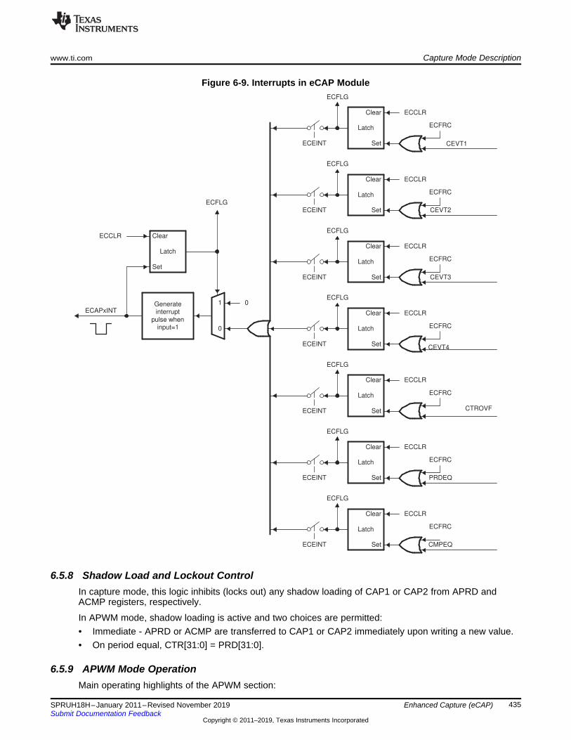
PRDEQ
Clear
Set
Latch
CEVT1
ECFRC
ECCLR
ECFLG
ECEINT
ECCLR
ECEINT Set
Clear
Latch
CEVT2
ECFRC
ECFLG
ECCLR
ECCLR
Clear
ECEINT
Latch
Set
ECFLG
ECEINT Set
Clear
Latch
ECFRC
CEVT4
CEVT3
ECFRC
ECFLG
ECFRC
ECCLR
ECEINT Set
ECEINT
ECFLG
Latch
Clear
Latch
Set
CMPEQ
ECFRC
ECCLR
ECCLRClear
ECFLG
ECEINT
Clear
Latch
Set
ECFRC
CTROVF
ECFLG
01
0
Generateinterrupt
pulse wheninput=1
Latch
Clear
Set
ECCLR
ECAPxINT
ECFLG
www.ti.com Capture Mode Description
435SPRUH18H–January 2011–Revised November 2019Submit Documentation Feedback
Copyright © 2011–2019, Texas Instruments Incorporated
Enhanced Capture (eCAP)
Figure 6-9. Interrupts in eCAP Module
6.5.8 Shadow Load and Lockout ControlIn capture mode, this logic inhibits (locks out) any shadow loading of CAP1 or CAP2 from APRD andACMP registers, respectively.
In APWM mode, shadow loading is active and two choices are permitted:• Immediate - APRD or ACMP are transferred to CAP1 or CAP2 immediately upon writing a new value.• On period equal, CTR[31:0] = PRD[31:0].
6.5.9 APWM Mode OperationMain operating highlights of the APWM section:

APRD
TSCTR
FFFFFFFF
ACMP
0000000C
APWMx
(o/p pin)
On
time
Off−timePeriod
1000h
500h
300h
Capture Mode Description www.ti.com
436 SPRUH18H–January 2011–Revised November 2019Submit Documentation Feedback
Copyright © 2011–2019, Texas Instruments Incorporated
Enhanced Capture (eCAP)
• The time-stamp counter bus is made available for comparison via 2 digital (32-bit) comparators.• When CAP1/2 registers are not used in capture mode, their contents can be used as Period and
Compare values in APWM mode.• Double buffering is achieved via shadow registers APRD and ACMP (CAP3/4). The shadow register
contents are transferred over to CAP1/2 registers, either immediately upon a write, or on a CTR = PRDtrigger.
• In APWM mode, writing to CAP1/CAP2 active registers will also write the same value to thecorresponding shadow registers CAP3/CAP4. This emulates immediate mode. Writing to the shadowregisters CAP3/CAP4 will invoke the shadow mode.
• During initialization, you must write to the active registers for both period and compare. Thisautomatically copies the initial values into the shadow values. For subsequent compare updates,during run-time, you only need to use the shadow registers.
Figure 6-10. PWM Waveform Details Of APWM Mode Operation
The behavior of APWM active high mode (APWMPOL == 0) is as follows:CMP = 0x00000000, output low for duration of period (0% duty)
CMP = 0x00000001, output high 1 cycle
CMP = 0x00000002, output high 2 cycles
CMP = PERIOD, output high except for 1 cycle (<100% duty)
CMP = PERIOD+1, output high for complete period (100% duty)
CMP > PERIOD+1, output high for complete period
The behavior of APWM active low mode (APWMPOL == 1) is as follows:CMP = 0x00000000, output high for duration of period (0% duty)
CMP = 0x00000001, output low 1 cycle
CMP = 0x00000002, output low 2 cycles
CMP = PERIOD, output low except for 1 cycle (<100% duty)
CMP = PERIOD+1, output low for complete period (100% duty)
CMP > PERIOD+1, output low for complete period

CEVT1 CEVT2 CEVT3 CEVT4 CEVT1
CAPx pin
0 1 2 3 0 1
XX t5
XX t2
XX t3
XX t4
t1
Capture registers [1−4]
All capture values valid(can be read) at this time
00000000
FFFFFFFF
CTR[0−31] t1
t2
t3
t4t5
MOD4CTR
CAP1
CAP2
CAP3
CAP4
t
Polarity selection
0
1
2
3
4
TPWM
0
1
2
3
4
0
1
2
3
4
� � � u
PWM TSCTR
PWM
PWM
T CAP1 1 T
1F
T
www.ti.com Application of the eCAP Module
437SPRUH18H–January 2011–Revised November 2019Submit Documentation Feedback
Copyright © 2011–2019, Texas Instruments Incorporated
Enhanced Capture (eCAP)
Figure 6-11. Time-Base Frequency and Period Calculation
6.6 Application of the eCAP ModuleThe following sections will provide applications examples to show how to operate the eCAP module.
6.6.1 Example 1 - Absolute Time-Stamp Operation Rising Edge TriggerFigure 6-12 shows an example of continuous capture operation (Mod4 counter wraps around). In thisfigure, TSCTR counts-up without resetting and capture events are qualified on the rising edge only, thisgives period (and frequency) information.
On an event, the TSCTR contents (time-stamp) is first captured, then Mod4 counter is incremented to thenext state. When the TSCTR reaches FFFFFFFF (maximum value), it wraps around to 00000000 (notshown in Figure 6-12), if this occurs, the CTROVF (counter overflow) flag is set, and an interrupt (ifenabled) occurs, CTROVF (counter overflow) Flag is set, and an Interrupt (if enabled) occurs. CapturedTime-stamps are valid at the point indicated by the diagram (after the 4th event), hence event CEVT4 canconveniently be used to trigger an interrupt and the CPU can read data from the CAPx registers.
Figure 6-12. Capture Sequence for Absolute Time-stamp and Rising Edge Detect

CEVT1CEVT2
CEVT3CEVT4
CEVT1
FFFFFFFF
CTR[0−31]
00000000
CAPx pin
t
MOD4CTR
CAP1
CAP2
CAP3
CAP4
Capture registers [1−4]
CEVT2CEVT1 CEVT3
CEVT4
t1
t2
t3t4
t5t6
t7t8
t9
0 1 2 3 0 1 2 3 0
XX t1 t5
XX t2 t6
XX t3 t7
XX t4 t8
Polarity selection
t
Application of the eCAP Module www.ti.com
438 SPRUH18H–January 2011–Revised November 2019Submit Documentation Feedback
Copyright © 2011–2019, Texas Instruments Incorporated
Enhanced Capture (eCAP)
6.6.2 Example 2 - Absolute Time-Stamp Operation Rising and Falling Edge TriggerIn Figure 6-13 the eCAP operating mode is almost the same as in the previous section except captureevents are qualified as either rising or falling edge, this now gives both period and duty cycle information,that is: Period1 = t3 – t1, Period2 = t5 – t3, …and so on. Duty Cycle1 (on-time %) = (t2 – t1) / Period1 x100%, etc. Duty Cycle1 (off-time %) = (t3 – t2) / Period1 x 100%, and so on.
Figure 6-13. Capture Sequence for Absolute Time-stamp With Rising and Falling Edge Detect

CEVT1 CEVT2 CEVT1
FFFFFFFF
CTR[0−31]
00000000
CAPx pin
t
MOD4CTR
CAP1
CAP2
CAP3
CAP4
Capture registers [1−4]
CEVT3 CEVT4
0 1 2 3 0 1
XX
XX
t2XX
t3XX
t4
T1 T2T3 T4
CTR value at CEVT1
t1
All capture values valid(can be read) at this time
Polarity selection
www.ti.com Application of the eCAP Module
439SPRUH18H–January 2011–Revised November 2019Submit Documentation Feedback
Copyright © 2011–2019, Texas Instruments Incorporated
Enhanced Capture (eCAP)
6.6.3 Example 3 - Time Difference (Delta) Operation Rising Edge TriggerThis example Figure 6-14 shows how the eCAP module can be used to collect Delta timing data frompulse train waveforms. Here Continuous Capture mode (TSCTR counts-up without resetting, and Mod4counter wraps around) is used. In Delta-time mode, TSCTR is Reset back to Zero on every valid event.Here Capture events are qualified as Rising edge only. On an event, TSCTR contents (Time-Stamp) iscaptured first, and then TSCTR is reset to Zero. The Mod4 counter then increments to the next state. IfTSCTR reaches FFFFFFFF (Max value), before the next event, it wraps around to 00000000 andcontinues, a CNTOVF (counter overflow) Flag is set, and an Interrupt (if enabled) occurs. The advantageof Delta-time Mode is that the CAPx contents directly give timing data without the need for CPUcalculations, that is, Period1 = T1, Period2 = T2,…etc. As shown in the diagram, the CEVT1 event is agood trigger point to read the timing data, T1, T2, T3, T4 are all valid here.
Figure 6-14. Capture Sequence for Delta Mode Time-stamp and Rising Edge Detect

CEVT1
CEVT2
CEVT5
FFFFFFFF
CTR[0−31]
00000000
CAPx pin
t
MOD4CTR
CAP1
CAP2
CAP3
CAP4
Capture registers [1−4]
CEVT3
CEVT4
0 1 2 3 0 1
XX
XX
t2XX
t3XX
t4CTR value at CEVT1
t1
T1
T2
2 3 0
t5
t6
t7
T3
T4
T5
T6
T7
T8
CEVT1
CEVT2
CEVT3
CEVT4
Polarity selection
Application of the eCAP Module www.ti.com
440 SPRUH18H–January 2011–Revised November 2019Submit Documentation Feedback
Copyright © 2011–2019, Texas Instruments Incorporated
Enhanced Capture (eCAP)
6.6.4 Example 4 - Time Difference (Delta) Operation Rising and Falling Edge TriggerIn Figure 6-15 the eCAP operating mode is almost the same as in previous section except Capture eventsare qualified as either Rising or Falling edge, this now gives both Period and Duty cycle information, thatis: Period1 = T1+T2, Period2 = T3+T4, …and so on, Duty Cycle1 (on-time %) = T1 / Period1 x 100%, DutyCycle1 (off-time %) = T2 / Period1 x 100%, and so on.
Figure 6-15. Capture Sequence for Delta Mode Time-stamp With Rising and Falling Edge Detect
During initialization, you must write to the active registers for both period and compare. This action willautomatically copy the init values into the shadow values. For subsequent compare updates during run-time, the shadow registers must be used.
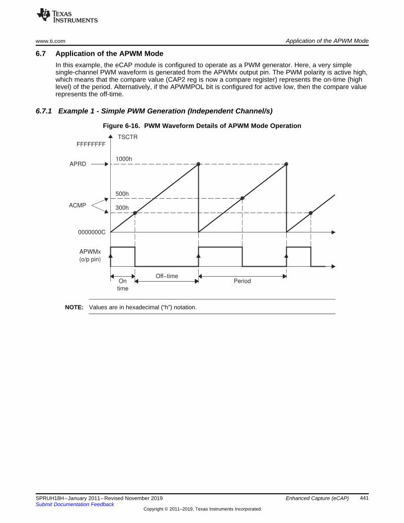
APRD
TSCTR
FFFFFFFF
ACMP
0000000C
APWMx
(o/p pin)
On
time
Off−timePeriod
1000h
500h
300h
www.ti.com Application of the APWM Mode
441SPRUH18H–January 2011–Revised November 2019Submit Documentation Feedback
Copyright © 2011–2019, Texas Instruments Incorporated
Enhanced Capture (eCAP)
6.7 Application of the APWM ModeIn this example, the eCAP module is configured to operate as a PWM generator. Here, a very simplesingle-channel PWM waveform is generated from the APWMx output pin. The PWM polarity is active high,which means that the compare value (CAP2 reg is now a compare register) represents the on-time (highlevel) of the period. Alternatively, if the APWMPOL bit is configured for active low, then the compare valuerepresents the off-time.
6.7.1 Example 1 - Simple PWM Generation (Independent Channel/s)
Figure 6-16. PWM Waveform Details of APWM Mode Operation
NOTE: Values are in hexadecimal (“h”) notation.

eCAP Registers www.ti.com
442 SPRUH18H–January 2011–Revised November 2019Submit Documentation Feedback
Copyright © 2011–2019, Texas Instruments Incorporated
Enhanced Capture (eCAP)
6.8 eCAP RegistersThis section describes the Enhanced Capture Registers.
6.8.1 eCAP Base Addresses
Table 6-1. ECAP Base Address TableBit Field Name
Base AddressInstance Structure
ECap1Regs ECAP_REGS 0x0000_6A00
ECap2Regs ECAP_REGS 0x0000_6A20
ECap3Regs ECAP_REGS 0x0000_6A40

www.ti.com eCAP Registers
443SPRUH18H–January 2011–Revised November 2019Submit Documentation Feedback
Copyright © 2011–2019, Texas Instruments Incorporated
Enhanced Capture (eCAP)
6.8.2 ECAP_REGS RegistersTable 6-2 lists the ECAP_REGS registers. All register offset addresses not listed in Table 6-2 should beconsidered as reserved locations and the register contents should not be modified.
Table 6-2. ECAP_REGS Registers
Offset Acronym Register Name Write Protection Section0h TSCTR Time-Stamp Counter Go2h CTRPHS Counter Phase Offset Value Register Go4h CAP1 Capture 1 Register Go6h CAP2 Capture 2 Register Go8h CAP3 Capture 3 Register GoAh CAP4 Capture 4 Register Go14h ECCTL1 Capture Control Register 1 Go15h ECCTL2 Capture Control Register 2 Go16h ECEINT Capture Interrupt Enable Register Go17h ECFLG Capture Interrupt Flag Register Go18h ECCLR Capture Interrupt Clear Register Go19h ECFRC Capture Interrupt Force Register Go
Complex bit access types are encoded to fit into small table cells. Table 6-3 shows the codes that areused for access types in this section.
Table 6-3. ECAP_REGS Access Type Codes
Access Type Code DescriptionRead TypeR R ReadR-0 R
-0ReadReturns 0s
Write TypeW W WriteW1C W
1CWrite1 to clear
W1S W1S
Write1 to set
Reset or Default Value-n Value after reset or the default
valueRegister Array Variablesi,j,k,l,m,n When these variables are used in
a register name, an offset, or anaddress, they refer to the value ofa register array where the registeris part of a group of repeatingregisters. The register groups forma hierarchical structure and thearray is represented with aformula.
y When this variable is used in aregister name, an offset, or anaddress it refers to the value of aregister array.

eCAP Registers www.ti.com
444 SPRUH18H–January 2011–Revised November 2019Submit Documentation Feedback
Copyright © 2011–2019, Texas Instruments Incorporated
Enhanced Capture (eCAP)
6.8.2.1 TSCTR Register (Offset = 0h) [reset = 0h]TSCTR is shown in Figure 6-17 and described in Table 6-4.
Return to the Summary Table.
Time-Stamp Counter
Figure 6-17. TSCTR Register31 30 29 28 27 26 25 24 23 22 21 20 19 18 17 16 15 14 13 12 11 10 9 8 7 6 5 4 3 2 1 0
TSCTRR/W-0h
Table 6-4. TSCTR Register Field Descriptions
Bit Field Type Reset Description31-0 TSCTR R/W 0h Active 32-bit counter register that is used as the capture time-base
Reset type: SYSRSn

www.ti.com eCAP Registers
445SPRUH18H–January 2011–Revised November 2019Submit Documentation Feedback
Copyright © 2011–2019, Texas Instruments Incorporated
Enhanced Capture (eCAP)
6.8.2.2 CTRPHS Register (Offset = 2h) [reset = 0h]CTRPHS is shown in Figure 6-18 and described in Table 6-5.
Return to the Summary Table.
Counter Phase Offset Value Register
Figure 6-18. CTRPHS Register31 30 29 28 27 26 25 24 23 22 21 20 19 18 17 16 15 14 13 12 11 10 9 8 7 6 5 4 3 2 1 0
CTRPHSR/W-0h
Table 6-5. CTRPHS Register Field Descriptions
Bit Field Type Reset Description31-0 CTRPHS R/W 0h Counter phase value register that can be programmed for phase
lag/lead. This register CTRPHS is loaded into TSCTR upon either aSYNCI event or S/W force via a control bit. Used to achieve phasecontrol synchronization with respect to other eCAP and EPWMtimebases.
Reset type: SYSRSn

eCAP Registers www.ti.com
446 SPRUH18H–January 2011–Revised November 2019Submit Documentation Feedback
Copyright © 2011–2019, Texas Instruments Incorporated
Enhanced Capture (eCAP)
6.8.2.3 CAP1 Register (Offset = 4h) [reset = 0h]CAP1 is shown in Figure 6-19 and described in Table 6-6.
Return to the Summary Table.
Capture 1 Register
Figure 6-19. CAP1 Register31 30 29 28 27 26 25 24 23 22 21 20 19 18 17 16 15 14 13 12 11 10 9 8 7 6 5 4 3 2 1 0
CAP1R/W-0h
Table 6-6. CAP1 Register Field Descriptions
Bit Field Type Reset Description31-0 CAP1 R/W 0h This register can be loaded (written) by:
- Time-Stamp counter value (TSCTR) during a capture event- Software - may be useful for test purposes or initialization- ARPD shadow register (CAP3) when used in APWM mode
Reset type: SYSRSn

www.ti.com eCAP Registers
447SPRUH18H–January 2011–Revised November 2019Submit Documentation Feedback
Copyright © 2011–2019, Texas Instruments Incorporated
Enhanced Capture (eCAP)
6.8.2.4 CAP2 Register (Offset = 6h) [reset = 0h]CAP2 is shown in Figure 6-20 and described in Table 6-7.
Return to the Summary Table.
Capture 2 Register
Figure 6-20. CAP2 Register31 30 29 28 27 26 25 24 23 22 21 20 19 18 17 16 15 14 13 12 11 10 9 8 7 6 5 4 3 2 1 0
CAP2R/W-0h
Table 6-7. CAP2 Register Field Descriptions
Bit Field Type Reset Description31-0 CAP2 R/W 0h This register can be loaded (written) by:
- Time-Stamp ( counter value) during a capture event- Software - may be useful for test purposes- ACMP shadow register (CAP4) when used in APWM mode
Reset type: SYSRSn

eCAP Registers www.ti.com
448 SPRUH18H–January 2011–Revised November 2019Submit Documentation Feedback
Copyright © 2011–2019, Texas Instruments Incorporated
Enhanced Capture (eCAP)
6.8.2.5 CAP3 Register (Offset = 8h) [reset = 0h]CAP3 is shown in Figure 6-21 and described in Table 6-8.
Return to the Summary Table.
Capture 3 Register
Figure 6-21. CAP3 Register31 30 29 28 27 26 25 24 23 22 21 20 19 18 17 16 15 14 13 12 11 10 9 8 7 6 5 4 3 2 1 0
CAP3R/W-0h
Table 6-8. CAP3 Register Field Descriptions
Bit Field Type Reset Description31-0 CAP3 R/W 0h In CMP mode, this is a time-stamp capture register.
In APWM mode, this is the period shadow (APRD) register. You canupdate the PWM period value through this register. CAP3 (APRD)shadows CAP1 in this mode.
Reset type: SYSRSn

www.ti.com eCAP Registers
449SPRUH18H–January 2011–Revised November 2019Submit Documentation Feedback
Copyright © 2011–2019, Texas Instruments Incorporated
Enhanced Capture (eCAP)
6.8.2.6 CAP4 Register (Offset = Ah) [reset = 0h]CAP4 is shown in Figure 6-22 and described in Table 6-9.
Return to the Summary Table.
Capture 4 Register
Figure 6-22. CAP4 Register31 30 29 28 27 26 25 24 23 22 21 20 19 18 17 16 15 14 13 12 11 10 9 8 7 6 5 4 3 2 1 0
CAP4R/W-0h
Table 6-9. CAP4 Register Field Descriptions
Bit Field Type Reset Description31-0 CAP4 R/W 0h In CMP mode, this is a time-stamp capture register.
In APWM mode, this is the compare shadow (ACMP) register. Youcan update the PWM compare value via this register. CAP4 (ACMP)shadows CAP2 in this mode.
Reset type: SYSRSn

eCAP Registers www.ti.com
450 SPRUH18H–January 2011–Revised November 2019Submit Documentation Feedback
Copyright © 2011–2019, Texas Instruments Incorporated
Enhanced Capture (eCAP)
6.8.2.7 ECCTL1 Register (Offset = 14h) [reset = 0h]ECCTL1 is shown in Figure 6-23 and described in Table 6-10.
Return to the Summary Table.
Capture Control Register 1
Figure 6-23. ECCTL1 Register15 14 13 12 11 10 9 8
FREE_SOFT PRESCALE CAPLDENR/W-0h R/W-0h R/W-0h
7 6 5 4 3 2 1 0CTRRST4 CAP4POL CTRRST3 CAP3POL CTRRST2 CAP2POL CTRRST1 CAP1POL
R/W-0h R/W-0h R/W-0h R/W-0h R/W-0h R/W-0h R/W-0h R/W-0h
Table 6-10. ECCTL1 Register Field Descriptions
Bit Field Type Reset Description15-14 FREE_SOFT R/W 0h Emulation Control
Reset type: SYSRSn0h (R/W) = TSCTR counter stops immediately on emulationsuspend1h (R/W) = TSCTR counter runs until = 02h (R/W) = TSCTR counter is unaffected by emulation suspend(Run Free)3h (R/W) = TSCTR counter is unaffected by emulation suspend(Run Free)
13-9 PRESCALE R/W 0h Event Filter prescale selectReset type: SYSRSn0h (R/W) = Divide by 1 (i.e,. no prescale, by-pass the prescaler)1h (R/W) = Divide by 22h (R/W) = Divide by 43h (R/W) = Divide by 64h (R/W) = Divide by 85h (R/W) = Divide by 101Eh (R/W) = Divide by 601Fh (R/W) = Divide by 62
8 CAPLDEN R/W 0h Enable Loading of CAP1-4 registers on a capture event. Note thatthis bit does not disable CEVTn events from being generated.
Reset type: SYSRSn0h (R/W) = Disable CAP1-4 register loads at capture event time.1h (R/W) = Enable CAP1-4 register loads at capture event time.
7 CTRRST4 R/W 0h Counter Reset on Capture Event 4Reset type: SYSRSn0h (R/W) = Do not reset counter on Capture Event 4 (absolute timestamp operation)1h (R/W) = Reset counter after Capture Event 4 time-stamp hasbeen captured (used in difference mode operation)
6 CAP4POL R/W 0h Capture Event 4 Polarity selectReset type: SYSRSn0h (R/W) = Capture Event 4 triggered on a rising edge (RE)1h (R/W) = Capture Event 4 triggered on a falling edge (FE)

www.ti.com eCAP Registers
451SPRUH18H–January 2011–Revised November 2019Submit Documentation Feedback
Copyright © 2011–2019, Texas Instruments Incorporated
Enhanced Capture (eCAP)
Table 6-10. ECCTL1 Register Field Descriptions (continued)Bit Field Type Reset Description5 CTRRST3 R/W 0h Counter Reset on Capture Event 3
Reset type: SYSRSn0h (R/W) = Do not reset counter on Capture Event 3 (absolute timestamp)1h (R/W) = Reset counter after Event 3 time-stamp has beencaptured (used in difference mode operation)
4 CAP3POL R/W 0h Capture Event 3 Polarity selectReset type: SYSRSn0h (R/W) = Capture Event 3 triggered on a rising edge (RE)1h (R/W) = Capture Event 3 triggered on a falling edge (FE)
3 CTRRST2 R/W 0h Counter Reset on Capture Event 2Reset type: SYSRSn0h (R/W) = Do not reset counter on Capture Event 2 (absolute timestamp)1h (R/W) = Reset counter after Event 2 time-stamp has beencaptured (used in difference mode operation)
2 CAP2POL R/W 0h Capture Event 2 Polarity selectReset type: SYSRSn0h (R/W) = Capture Event 2 triggered on a rising edge (RE)1h (R/W) = Capture Event 2 triggered on a falling edge (FE)
1 CTRRST1 R/W 0h Counter Reset on Capture Event 1Reset type: SYSRSn0h (R/W) = Do not reset counter on Capture Event 1 (absolute timestamp)1h (R/W) = Reset counter after Event 1 time-stamp has beencaptured (used in difference mode operation)
0 CAP1POL R/W 0h Capture Event 1 Polarity selectReset type: SYSRSn0h (R/W) = Capture Event 1 triggered on a rising edge (RE)1h (R/W) = Capture Event 1 triggered on a falling edge (FE)

eCAP Registers www.ti.com
452 SPRUH18H–January 2011–Revised November 2019Submit Documentation Feedback
Copyright © 2011–2019, Texas Instruments Incorporated
Enhanced Capture (eCAP)
6.8.2.8 ECCTL2 Register (Offset = 15h) [reset = 6h]ECCTL2 is shown in Figure 6-24 and described in Table 6-11.
Return to the Summary Table.
Capture Control Register 2
Figure 6-24. ECCTL2 Register15 14 13 12 11 10 9 8
RESERVED APWMPOL CAP_APWM SWSYNCR-0h R/W-0h R/W-0h R-0/W1S-0h
7 6 5 4 3 2 1 0SYNCO_SEL SYNCI_EN TSCTRSTOP REARM STOP_WRAP CONT_ONESH
TR/W-0h R/W-0h R/W-0h R-0/W1S-0h R/W-3h R/W-0h
Table 6-11. ECCTL2 Register Field Descriptions
Bit Field Type Reset Description15-11 RESERVED R 0h Reserved
10 APWMPOL R/W 0h APWM output polarity select. This is applicable only in APWMoperating mode.
Reset type: SYSRSn0h (R/W) = Output is active high (Compare value defines high time)1h (R/W) = Output is active low (Compare value defines low time)
9 CAP_APWM R/W 0h CAP/APWM operating mode selectReset type: SYSRSn0h (R/W) = ECAP module operates in capture mode. This modeforces the following configuration:- Inhibits TSCTR resets via CTR = PRD event- Inhibits shadow loads on CAP1 and 2 registers- Permits user to enable CAP1-4 register load- CAPx/APWMx pin operates as a capture input1h (R/W) = ECAP module operates in APWM mode. This modeforces the following configuration:- Resets TSCTR on CTR = PRD event (period boundary- Permits shadow loading on CAP1 and 2 registers- Disables loading of time-stamps into CAP1-4 registers- CAPx/APWMx pin operates as a APWM output
8 SWSYNC R-0/W1S 0h Software-forced Counter (TSCTR) Synchronizer. This provides theuser a method to generate a synchronization pulse through software.In APWM mode, the synchronization pulse can also be sourced fromthe CTR = PRD event.
Reset type: SYSRSn0h (R/W) = Writing a zero has no effect. Reading always returns azero1h (R/W) = Writing a one forces a TSCTR shadow load of currentECAP module and any ECAP modules down-stream providing theSYNCO_SEL bits are 0,0. After writing a 1, this bit returns to azero.Note: Selection CTR = PRD is meaningful only in APWM modehowever, you can choose it in CAP mode if you find doing souseful.
7-6 SYNCO_SEL R/W 0h Sync-Out SelectReset type: SYSRSn0h (R/W) = Select sync-in event to be the sync-out signal (passthrough)1h (R/W) = Select CTR = PRD event to be the sync-out signal2h (R/W) = Disable sync out signal3h (R/W) = Disable sync out signal

www.ti.com eCAP Registers
453SPRUH18H–January 2011–Revised November 2019Submit Documentation Feedback
Copyright © 2011–2019, Texas Instruments Incorporated
Enhanced Capture (eCAP)
Table 6-11. ECCTL2 Register Field Descriptions (continued)Bit Field Type Reset Description5 SYNCI_EN R/W 0h Counter (TSCTR) Sync-In select mode
Reset type: SYSRSn0h (R/W) = Disable sync-in option1h (R/W) = Enable counter (TSCTR) to be loaded from CTRPHSregister upon either a SYNCI signal or a S/W force event.
4 TSCTRSTOP R/W 0h Time Stamp (TSCTR) Counter Stop (freeze) ControlReset type: SYSRSn0h (R/W) = TSCTR stopped1h (R/W) = TSCTR free-running
3 REARM R-0/W1S 0h Re-Arming Control. Note: The re-arm function is valid in one shot orcontinuous mode.
Reset type: SYSRSn0h (R/W) = Has no effect (reading always returns a 0)1h (R/W) = Arms the one-shot sequence as follows:1) Resets the Mod4 counter to zero2) Unfreezes the Mod4 counter3) Enables capture register loads
2-1 STOP_WRAP R/W 3h Stop value for one-shot mode. This is the number (between 1-4) ofcaptures allowed to occur before the CAP(1-4) registers are frozen,that is, capture sequence is stopped.Wrap value for continuous mode. This is the number (between 1-4)of the capture register in which the circular buffer wraps around andstarts again.
Notes: STOP_WRAP is compared to Mod4 counter and, whenequal, 2 actions occur:- Mod4 counter is stopped (frozen)- Capture register loads are inhibitedIn one-shot mode, further interrupt events are blocked until re-armed.
Reset type: SYSRSn0h (R/W) = Stop after Capture Event 1 in one-shot modeWrap after Capture Event 1 in continuous mode.1h (R/W) = Stop after Capture Event 2 in one-shot modeWrap after Capture Event 2 in continuous mode.2h (R/W) = Stop after Capture Event 3 in one-shot modeWrap after Capture Event 3 in continuous mode.3h (R/W) = Stop after Capture Event 4 in one-shot modeWrap after Capture Event 4 in continuous mode.
0 CONT_ONESHT R/W 0h Continuous or one-shot mode control (applicable only in capturemode)
Reset type: SYSRSn0h (R/W) = Operate in continuous mode1h (R/W) = Operate in one-Shot mode

eCAP Registers www.ti.com
454 SPRUH18H–January 2011–Revised November 2019Submit Documentation Feedback
Copyright © 2011–2019, Texas Instruments Incorporated
Enhanced Capture (eCAP)
6.8.2.9 ECEINT Register (Offset = 16h) [reset = 0h]ECEINT is shown in Figure 6-25 and described in Table 6-12.
Return to the Summary Table.
The interrupt enable bits (CEVT1, ...) block any of the selected events from generating an interrupt.Events will still be latched into the flag bit (ECFLG register) and can be forced/cleared via theECFRC/ECCLR registers.The proper procedure for configuring peripheral modes and interrupts is as follows:- Disable global interrupts- Stop eCAP counter- Disable eCAP interrupts- Configure peripheral registers- Clear spurious eCAP interrupt flags- Enable eCAP interrupts- Start eCAP counter- Enable global interrupts
Figure 6-25. ECEINT Register15 14 13 12 11 10 9 8
RESERVEDR-0h
7 6 5 4 3 2 1 0CTR_EQ_CMP CTR_EQ_PRD CTROVF CEVT4 CEVT3 CEVT2 CEVT1 RESERVED
R/W-0h R/W-0h R/W-0h R/W-0h R/W-0h R/W-0h R/W-0h R-0h
Table 6-12. ECEINT Register Field Descriptions
Bit Field Type Reset Description15-8 RESERVED R 0h Reserved
7 CTR_EQ_CMP R/W 0h Counter Equal Compare Interrupt EnableReset type: SYSRSn0h (R/W) = Disable Compare Equal as an Interrupt source1h (R/W) = Enable Compare Equal as an Interrupt source
6 CTR_EQ_PRD R/W 0h Counter Equal Period Interrupt EnableReset type: SYSRSn0h (R/W) = Disable Period Equal as an Interrupt source1h (R/W) = Enable Period Equal as an Interrupt source
5 CTROVF R/W 0h Counter Overflow Interrupt EnableReset type: SYSRSn0h (R/W) = Disabled counter Overflow as an Interrupt source1h (R/W) = Enable counter Overflow as an Interrupt source
4 CEVT4 R/W 0h Capture Event 4 Interrupt EnableReset type: SYSRSn0h (R/W) = Disable Capture Event 4 as an Interrupt source1h (R/W) = Capture Event 4 Interrupt Enable
3 CEVT3 R/W 0h Capture Event 3 Interrupt EnableReset type: SYSRSn0h (R/W) = Disable Capture Event 3 as an Interrupt source1h (R/W) = Enable Capture Event 3 as an Interrupt source
2 CEVT2 R/W 0h Capture Event 2 Interrupt EnableReset type: SYSRSn0h (R/W) = Disable Capture Event 2 as an Interrupt source1h (R/W) = Enable Capture Event 2 as an Interrupt source

www.ti.com eCAP Registers
455SPRUH18H–January 2011–Revised November 2019Submit Documentation Feedback
Copyright © 2011–2019, Texas Instruments Incorporated
Enhanced Capture (eCAP)
Table 6-12. ECEINT Register Field Descriptions (continued)Bit Field Type Reset Description1 CEVT1 R/W 0h Capture Event 1 Interrupt Enable
Reset type: SYSRSn0h (R/W) = Disable Capture Event 1 as an Interrupt source1h (R/W) = Enable Capture Event 1 as an Interrupt source
0 RESERVED R 0h Reserved

eCAP Registers www.ti.com
456 SPRUH18H–January 2011–Revised November 2019Submit Documentation Feedback
Copyright © 2011–2019, Texas Instruments Incorporated
Enhanced Capture (eCAP)
6.8.2.10 ECFLG Register (Offset = 17h) [reset = 0h]ECFLG is shown in Figure 6-26 and described in Table 6-13.
Return to the Summary Table.
Capture Interrupt Flag Register
Figure 6-26. ECFLG Register15 14 13 12 11 10 9 8
RESERVEDR-0h
7 6 5 4 3 2 1 0CTR_CMP CTR_PRD CTROVF CEVT4 CEVT3 CEVT2 CEVT1 INT
R-0h R-0h R-0h R-0h R-0h R-0h R-0h R-0h
Table 6-13. ECFLG Register Field Descriptions
Bit Field Type Reset Description15-8 RESERVED R 0h Reserved
7 CTR_CMP R 0h Compare Equal Compare Status Flag. This flag is active only inAPWM mode.
Reset type: SYSRSn0h (R/W) = Indicates no event occurred1h (R/W) = Indicates the counter (TSCTR) reached the compareregister value (ACMP)
6 CTR_PRD R 0h Counter Equal Period Status Flag. This flag is only active in APWMmode.
Reset type: SYSRSn0h (R/W) = Indicates no event occurred1h (R/W) = Indicates the counter (TSCTR) reached the periodregister value (APRD) and was reset.
5 CTROVF R 0h Counter Overflow Status Flag. This flag is active in CAP and APWMmode.
Reset type: SYSRSn0h (R/W) = Indicates no event occurred1h (R/W) = Indicates the counter (TSCTR) has made the transitionfrom FFFFFFFF " 00000000
4 CEVT4 R 0h Capture Event 4 Status Flag This flag is only active in CAP mode.Reset type: SYSRSn0h (R/W) = Indicates no event occurred1h (R/W) = Indicates the fourth event occurred at ECAPx pin
3 CEVT3 R 0h Capture Event 3 Status Flag. This flag is active only in CAP mode.Reset type: SYSRSn0h (R/W) = Indicates no event occurred1h (R/W) = Indicates the third event occurred at ECAPx pin.
2 CEVT2 R 0h Capture Event 2 Status Flag. This flag is only active in CAP mode.Reset type: SYSRSn0h (R/W) = Indicates no event occurred1h (R/W) = Indicates the second event occurred at ECAPx pin.
1 CEVT1 R 0h Capture Event 1 Status Flag. This flag is only active in CAP mode.Reset type: SYSRSn0h (R/W) = Indicates no event occurred1h (R/W) = Indicates the first event occurred at ECAPx pin.

www.ti.com eCAP Registers
457SPRUH18H–January 2011–Revised November 2019Submit Documentation Feedback
Copyright © 2011–2019, Texas Instruments Incorporated
Enhanced Capture (eCAP)
Table 6-13. ECFLG Register Field Descriptions (continued)Bit Field Type Reset Description0 INT R 0h Global Interrupt Status Flag
Reset type: SYSRSn0h (R/W) = Indicates no event occurred1h (R/W) = Indicates that an interrupt was generated.
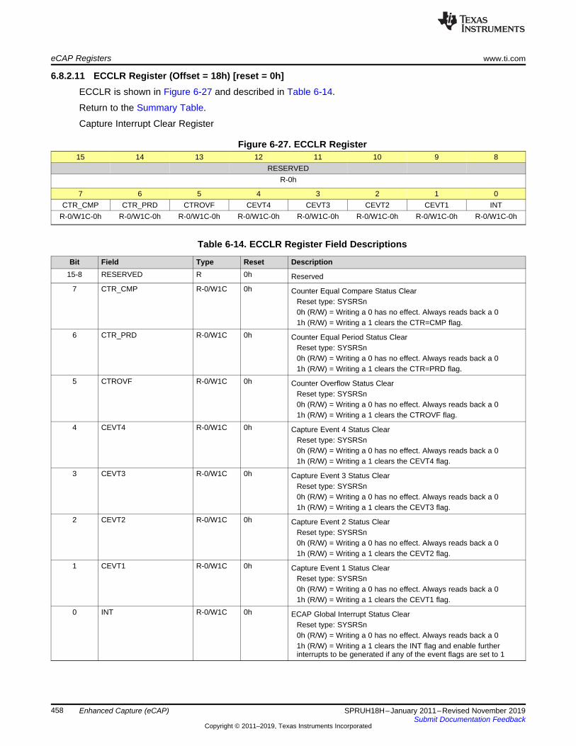
eCAP Registers www.ti.com
458 SPRUH18H–January 2011–Revised November 2019Submit Documentation Feedback
Copyright © 2011–2019, Texas Instruments Incorporated
Enhanced Capture (eCAP)
6.8.2.11 ECCLR Register (Offset = 18h) [reset = 0h]ECCLR is shown in Figure 6-27 and described in Table 6-14.
Return to the Summary Table.
Capture Interrupt Clear Register
Figure 6-27. ECCLR Register15 14 13 12 11 10 9 8
RESERVEDR-0h
7 6 5 4 3 2 1 0CTR_CMP CTR_PRD CTROVF CEVT4 CEVT3 CEVT2 CEVT1 INT
R-0/W1C-0h R-0/W1C-0h R-0/W1C-0h R-0/W1C-0h R-0/W1C-0h R-0/W1C-0h R-0/W1C-0h R-0/W1C-0h
Table 6-14. ECCLR Register Field Descriptions
Bit Field Type Reset Description15-8 RESERVED R 0h Reserved
7 CTR_CMP R-0/W1C 0h Counter Equal Compare Status ClearReset type: SYSRSn0h (R/W) = Writing a 0 has no effect. Always reads back a 01h (R/W) = Writing a 1 clears the CTR=CMP flag.
6 CTR_PRD R-0/W1C 0h Counter Equal Period Status ClearReset type: SYSRSn0h (R/W) = Writing a 0 has no effect. Always reads back a 01h (R/W) = Writing a 1 clears the CTR=PRD flag.
5 CTROVF R-0/W1C 0h Counter Overflow Status ClearReset type: SYSRSn0h (R/W) = Writing a 0 has no effect. Always reads back a 01h (R/W) = Writing a 1 clears the CTROVF flag.
4 CEVT4 R-0/W1C 0h Capture Event 4 Status ClearReset type: SYSRSn0h (R/W) = Writing a 0 has no effect. Always reads back a 01h (R/W) = Writing a 1 clears the CEVT4 flag.
3 CEVT3 R-0/W1C 0h Capture Event 3 Status ClearReset type: SYSRSn0h (R/W) = Writing a 0 has no effect. Always reads back a 01h (R/W) = Writing a 1 clears the CEVT3 flag.
2 CEVT2 R-0/W1C 0h Capture Event 2 Status ClearReset type: SYSRSn0h (R/W) = Writing a 0 has no effect. Always reads back a 01h (R/W) = Writing a 1 clears the CEVT2 flag.
1 CEVT1 R-0/W1C 0h Capture Event 1 Status ClearReset type: SYSRSn0h (R/W) = Writing a 0 has no effect. Always reads back a 01h (R/W) = Writing a 1 clears the CEVT1 flag.
0 INT R-0/W1C 0h ECAP Global Interrupt Status ClearReset type: SYSRSn0h (R/W) = Writing a 0 has no effect. Always reads back a 01h (R/W) = Writing a 1 clears the INT flag and enable furtherinterrupts to be generated if any of the event flags are set to 1

www.ti.com eCAP Registers
459SPRUH18H–January 2011–Revised November 2019Submit Documentation Feedback
Copyright © 2011–2019, Texas Instruments Incorporated
Enhanced Capture (eCAP)
6.8.2.12 ECFRC Register (Offset = 19h) [reset = 0h]ECFRC is shown in Figure 6-28 and described in Table 6-15.
Return to the Summary Table.
Capture Interrupt Force Register
Figure 6-28. ECFRC Register15 14 13 12 11 10 9 8
RESERVEDR-0h
7 6 5 4 3 2 1 0CTR_CMP CTR_PRD CTROVF CEVT4 CEVT3 CEVT2 CEVT1 RESERVED
R-0/W1S-0h R-0/W1S-0h R-0/W1S-0h R-0/W1S-0h R-0/W1S-0h R-0/W1S-0h R-0/W1S-0h R-0h
Table 6-15. ECFRC Register Field Descriptions
Bit Field Type Reset Description15-8 RESERVED R 0h Reserved
7 CTR_CMP R-0/W1S 0h Force Counter Equal Compare Interrupt. This event is only active inAPWM mode.
Reset type: SYSRSn0h (R/W) = No effect. Always reads back a 0.1h (R/W) = Writing a 1 sets the CTR=CMP flag.
6 CTR_PRD R-0/W1S 0h Force Counter Equal Period Interrupt. This event is only active inAPWM mode.
Reset type: SYSRSn0h (R/W) = No effect. Always reads back a 0.1h (R/W) = Writing a 1 sets the CTR=PRD flag.
5 CTROVF R-0/W1S 0h Force Counter Overflow.Reset type: SYSRSn0h (R/W) = No effect. Always reads back a 0.1h (R/W) = Writing a 1 to this bit sets the CTROVF flag.
4 CEVT4 R-0/W1S 0h Force Capture Event 4. This event is only active in CAP mode.Reset type: SYSRSn0h (R/W) = No effect. Always reads back a 0.1h (R/W) = Writing a 1 sets the CEVT4 flag.
3 CEVT3 R-0/W1S 0h Force Capture Event 3. This event is only active in CAP mode.Reset type: SYSRSn0h (R/W) = No effect. Always reads back a 0.1h (R/W) = Writing a 1 sets the CEVT3 flag.
2 CEVT2 R-0/W1S 0h Force Capture Event 2. This event is only active in CAP mode.Reset type: SYSRSn0h (R/W) = No effect. Always reads back a 0.1h (R/W) = Writing a 1 sets the CEVT2 flag.
1 CEVT1 R-0/W1S 0h Force Capture Event 1. This event is only active in CAP mode.Reset type: SYSRSn0h (R/W) = No effect. Always reads back a 0.1h (R/W) = Sets the CEVT1 flag.
0 RESERVED R 0h Reserved

460 SPRUH18H–January 2011–Revised November 2019Submit Documentation Feedback
Copyright © 2011–2019, Texas Instruments Incorporated
Enhanced Quadrature Encoder Pulse (eQEP)
Chapter 7SPRUH18H–January 2011–Revised November 2019
Enhanced Quadrature Encoder Pulse (eQEP)
The enhanced Quadrature Encoder Pulse (eQEP) module described here is a Type-0 eQEP. See theTMS320x28xx, 28xxx DSP Peripheral Reference Guide (SPRU566) for a list of all devices with a moduleof the same type to determine the differences between types and for a list of device-specific differenceswithin a type.
The enhanced quadrature encoder pulse (eQEP) module is used for direct interface with a linear or rotaryincremental encoder to get position, direction, and speed information from a rotating machine for use in ahigh-performance motion and position-control system.
Topic ........................................................................................................................... Page
7.1 Introduction ..................................................................................................... 4617.2 Configuring Device Pins.................................................................................... 4637.3 Description ...................................................................................................... 4637.4 Quadrature Decoder Unit (QDU) ......................................................................... 4667.5 Position Counter and Control Unit (PCCU) .......................................................... 4697.6 eQEP Edge Capture Unit ................................................................................... 4757.7 eQEP Watchdog ............................................................................................... 4797.8 Unit Timer Base................................................................................................ 4797.9 eQEP Interrupt Structure ................................................................................... 4807.10 eQEP Registers ................................................................................................ 481

T0
0 1 2 3 4 5 6 7 N−6 N−5 N−4 N−3 N−2 N−1 0
QEPA
QEPB
QEPI
Clockwise shaft rotation/forward movement
Anti-clockwise shaft rotation/reverse movement
0 N−1 N−2 N−3 N−4 N−5 N−6 N−7 6 5 4 3 2 1 0 N−1 N−2
QEPA
QEPB
QEPI
T0
Legend: N = lines per revolution
QEPA
QEPB
QEPI
www.ti.com Introduction
461SPRUH18H–January 2011–Revised November 2019Submit Documentation Feedback
Copyright © 2011–2019, Texas Instruments Incorporated
Enhanced Quadrature Encoder Pulse (eQEP)
7.1 IntroductionAn incremental encoder disk is patterned with a track of slots along its periphery, as shown in Figure 7-1.These slots create an alternating pattern of dark and light lines. The disk count is defined as the numberof dark and light line pairs that occur per revolution (lines per revolution). As a rule, a second track isadded to generate a signal that occurs once per revolution (index signal: QEPI), which can be used toindicate an absolute position. Encoder manufacturers identify the index pulse using different terms such asindex, marker, home position, and zero reference
Figure 7-1. Optical Encoder Disk
To derive direction information, the lines on the disk are read out by two different photo-elements that"look" at the disk pattern with a mechanical shift of 1/4 the pitch of a line pair between them. This shift isdetected with a reticle or mask that restricts the view of the photo-element to the desired part of the disklines. As the disk rotates, the two photo-elements generate signals that are shifted 90° out of phase fromeach other. These are commonly called the quadrature QEPA and QEPB signals. The clockwise directionfor most encoders is defined as the QEPA channel going positive before the QEPB channel and viseversa as shown in Figure 7-2.
Figure 7-2. QEP Encoder Output Signal for Forward/Reverse Movement
The encoder wheel typically makes one revolution for every revolution of the motor, or the wheel may beat a geared rotation ratio with respect to the motor. Therefore, the frequency of the digital signal comingfrom the QEPA and QEPB outputs varies proportionally with the velocity of the motor. For example, a2000-line encoder directly coupled to a motor running at 5000 revolutions per minute (rpm) results in afrequency of 166.6 KHz, so by measuring the frequency of either the QEPA or QEPB output, theprocessor can determine the velocity of the motor.

v(k) � Xt(k)� t(k� 1)
�X�T
v(k) �x(k)� x(k� 1)
T�
�XT
T0
0.25T0 ±0.1T0
0.5T0 ±0.1T0
T0 ±0.5T0
QEPA
QEPB
QEPI(gated to
A and B)
QEPI(gated to A)
QEPI(ungated)
Introduction www.ti.com
462 SPRUH18H–January 2011–Revised November 2019Submit Documentation Feedback
Copyright © 2011–2019, Texas Instruments Incorporated
Enhanced Quadrature Encoder Pulse (eQEP)
Quadrature encoders from different manufacturers come with two forms of index pulse (gated index pulseor ungated index pulse) as shown in Figure 7-3. A nonstandard form of index pulse is ungated. In theungated configuration, the index edges are not necessarily coincident with A and B signals. The gatedindex pulse is aligned to any of the four quadrature edges and width of the index pulse and can be equalto a quarter, half, or full period of the quadrature signal.
Figure 7-3. Index Pulse Example
Some typical applications of shaft encoders include robotics and computer input in the form of a mouse.Inside your mouse you can see where the mouse ball spins a pair of axles (a left/right, and an up/downaxle). These axles are connected to optical shaft encoders that effectively tell the computer how fast andin what direction the mouse is moving.
General Issues: Estimating velocity from a digital position sensor is a cost-effective strategy in motorcontrol. Two different first order approximations for velocity may be written as:
(1)
(2)
where
v(k): Velocity at time instant k
x(k): Position at time instant k
x(k-1): Position at time instant k-1
T: Fixed unit time or inverse of velocity calculation rate
ΔX: Incremental position movement in unit time
t(k): Time instant "k"
t(k-1): Time instant "k-1"
X: Fixed unit position
ΔT: Incremental time elapsed for unit position movement.
Equation 1 is the conventional approach to velocity estimation and it requires a time base to provide a unittime event for velocity calculation. Unit time is basically the inverse of the velocity calculation rate.

www.ti.com Configuring Device Pins
463SPRUH18H–January 2011–Revised November 2019Submit Documentation Feedback
Copyright © 2011–2019, Texas Instruments Incorporated
Enhanced Quadrature Encoder Pulse (eQEP)
The encoder count (position) is read once during each unit time event. The quantity [x(k) - x(k-1)] isformed by subtracting the previous reading from the current reading. Then the velocity estimate iscomputed by multiplying by the known constant 1/T (where T is the constant time between unit timeevents and is known in advance).
Estimation based on Equation 1 has an inherent accuracy limit directly related to the resolution of theposition sensor and the unit time period T. For example, consider a 500-line per revolution quadratureencoder with a velocity calculation rate of 400 Hz. When used for position, the quadrature encoder gives afour-fold increase in resolution; in this case, 2000 counts per revolution. The minimum rotation that can bedetected is therefore 0.0005 revolutions, which gives a velocity resolution of 12 rpm when sampled at 400Hz. While this resolution may be satisfactory at moderate or high speeds, for example 1% error at 1200rpm, it would clearly prove inadequate at low speeds. In fact, at speeds below 12 rpm, the speed estimatewould erroneously be zero much of the time.
At low speed, Equation 2 provides a more accurate approach. It requires a position sensor that outputs afixed interval pulse train, such as the aforementioned quadrature encoder. The width of each pulse isdefined by motor speed for a given sensor resolution. Equation 2 can be used to calculate motor speed bymeasuring the elapsed time between successive quadrature pulse edges. However, this method suffersfrom the opposite limitation, as does Equation 1. A combination of relatively large motor speeds and highsensor resolution makes the time interval ΔT small, and thus more greatly influenced by the timerresolution. This can introduce considerable error into high-speed estimates.
For systems with a large speed range (that is, speed estimation is needed at both low and high speeds),one approach is to use Equation 2 at low speed and have the DSP software switch over to Equation 1when the motor speed rises above some specified threshold.
7.2 Configuring Device PinsThe GPIO mux registers must be configured to connect this peripheral to the device pins.
For proper operation of the eQEP module, input GPIO pins must be configured via the GPxQSELnregisters for synchronous input mode (with or without qualification). The asynchronous mode should notbe used for eQEP input pins. The internal pullups can be configured in the GPyPUD register.
See the GPIO chapter for more details on GPIO mux and settings.
7.3 DescriptionThis section provides the eQEP inputs, memory map, and functional description.
7.3.1 EQEP InputsThe eQEP inputs include two pins for quadrature-clock mode or direction-count mode, an index (or 0marker), and a strobe input. The eQEP module requires that the QEPA, QEPB, and QEPI inputs aresynchronized to SYSCLK prior to entering the module. The application code should enable thesynchronous GPIO input feature on any eQEP-enabled GPIO pins (see the System Control and Interruptschapter for more details).• QEPA/XCLK and QEPB/XDIR
These two pins can be used in quadrature-clock mode or direction-count mode.– Quadrature-clock Mode
The eQEP encoders provide two square wave signals (A and B) 90 electrical degrees out of phase.This phase relationship is used to determine the direction of rotation of the input shaft and numberof eQEP pulses from the index position to derive the relative position information. For forward orclockwise rotation, QEPA signal leads QEPB signal and vice versa. The quadrature decoder usesthese two inputs to generate quadrature-clock and direction signals.
– Direction-count ModeIn direction-count mode, direction and clock signals are provided directly from the external source.Some position encoders have this type of output instead of quadrature output. The QEPA pinprovides the clock input and the QEPB pin provides the direction input.
• QEPI: Index or Zero Marker

QWDTMR
QWDPRD
16
QWDOGUTIME
QUPRD
QUTMR
32
UTOUT
WDTOUT
Quadraturecapture unit
(QCAP)QCPRDLAT
QCTMRLAT
16
QFLG
QEPSTS
QEPCTL
Registersused by
multiple units
QCLK
QDIR
QI
QS
PHE
PCSOUT
Quadraturedecoder(QDU)
QDECCTL
16
Position counter/control unit
(PCCU)QPOSLAT
QPOSSLAT
32
QPOSILAT
EQEPxAIN
EQEPxBIN
EQEPxIIN
EQEPxIOUT
EQEPxIOE
EQEPxSIN
EQEPxSOUT
EQEPxSOE
GPIOMUX
EQEPxA/XCLK
EQEPxB/XDIR
EQEPxS
EQEPxI
QPOSCMP QEINT
QFRC
32
QCLR
QPOSCTL
1632
QPOSCNT
QPOSMAX
QPOSINIT
PIEEQEPxINT
Enhanced QEP (eQEP) peripheral
Systemcontrol registers
QCTMR
QCPRD
1616
QCAPCTL
EQEPxENCLK
SYSCLKOUT
Data
bus
To CPU
Description www.ti.com
464 SPRUH18H–January 2011–Revised November 2019Submit Documentation Feedback
Copyright © 2011–2019, Texas Instruments Incorporated
Enhanced Quadrature Encoder Pulse (eQEP)
The eQEP encoder uses an index signal to assign an absolute start position from which positioninformation is incrementally encoded using quadrature pulses. This pin is connected to the indexoutput of the eQEP encoder to optionally reset the position counter for each revolution. This signal canbe used to initialize or latch the position counter on the occurrence of a desired event on the index pin.
• QEPS: Strobe InputThis general-purpose strobe signal can initialize or latch the position counter on the occurrence of adesired event on the strobe pin. This signal is typically connected to a sensor or limit switch to notifythat the motor has reached a defined position.
7.3.2 Functional DescriptionThe eQEP peripheral contains the following major functional units (as shown in Figure 7-4):• Programmable input qualification for each pin (part of the GPIO MUX)• Quadrature decoder unit (QDU)• Position counter and control unit for position measurement (PCCU)• Quadrature edge-capture unit for low-speed measurement (QCAP)• Unit time base for speed/frequency measurement (UTIME)• Watchdog timer for detecting stalls (QWDOG)
Figure 7-4. Functional Block Diagram of the eQEP Peripheral

www.ti.com Description
465SPRUH18H–January 2011–Revised November 2019Submit Documentation Feedback
Copyright © 2011–2019, Texas Instruments Incorporated
Enhanced Quadrature Encoder Pulse (eQEP)
7.3.3 eQEP Memory MapTable 7-1 lists the registers with their memory locations, sizes, and reset values.
Table 7-1. EQEP Memory Map
Name OffsetSize(x16)/#shadow Reset Register Description
QPOSCNT 0x00 2/0 0x00000000 eQEP Position CounterQPOSINIT 0x02 2/0 0x00000000 eQEP Initialization Position CountQPOSMAX 0x04 2/0 0x00000000 eQEP Maximum Position CountQPOSCMP 0x06 2/1 0x00000000 eQEP Position-compareQPOSILAT 0x08 2/0 0x00000000 eQEP Index Position LatchQPOSSLAT 0x0A 2/0 0x00000000 eQEP Strobe Position LatchQPOSLAT 0x0C 2/0 0x00000000 eQEP Position LatchQUTMR 0x0E 2/0 0x00000000 QEP Unit TimerQUPRD 0x10 2/0 0x00000000 eQEP Unit Period RegisterQWDTMR 0x12 1/0 0x0000 eQEP Watchdog TimerQWDPRD 0x13 1/0 0x0000 eQEP Watchdog Period RegisterQDECCTL 0x14 1/0 0x0000 eQEP Decoder Control RegisterQEPCTL 0x15 1/0 0x0000 eQEP Control RegisterQCAPCTL 0x16 1/0 0x0000 eQEP Capture Control RegisterQPOSCTL 0x17 1/0 0x00000 eQEP Position-compare Control RegisterQEINT 0x18 1/0 0x0000 eQEP Interrupt Enable RegisterQFLG 0x19 1/0 0x0000 eQEP Interrupt Flag RegisterQCLR 0x1A 1/0 0x0000 eQEP Interrupt Clear RegisterQFRC 0x1B 1/0 0x0000 eQEP Interrupt Force RegisterQEPSTS 0x1C 1/0 0x0000 eQEP Status RegisterQCTMR 0x1D 1/0 0x0000 eQEP Capture TimerQCPRD 0x1E 1/0 0x0000 eQEP Capture Period RegisterQCTMRLAT 0x1F 1/0 0x0000 eQEP Capture Timer LatchQCPRDLAT 0x20 1/0 0x0000 eQEP Capture Period Latchreserved 0x21
to0x3F
31/0

0
1
1
0
QA
QB
1
1
0
0
����������
Quadraturedecoder
00
01
10
11
iCLK
xCLK
xCLK
xCLK
01
11
10
00iDIR
xDIR
1
0
������������
2
����� �
PHE
����������
x1x2
x1, x2
�����������
0
1
1
0
���������
QDECCTL:IGATE
QCLK
QDIR
QI
1
0
����������
0
1
QDECCTL:SPSEL
QDECCTL:SPSEL
1
0QDECCTL:SOEN
QS
�����
EQEPxIOE
EQEPxSOE
��� ����
��� �����
EQEPxSIN
EQEPxIIN
EQEPxBIN
EQEPxAIN
����������� �� �������
EQEPA
EQEPB
Quadrature Decoder Unit (QDU) www.ti.com
466 SPRUH18H–January 2011–Revised November 2019Submit Documentation Feedback
Copyright © 2011–2019, Texas Instruments Incorporated
Enhanced Quadrature Encoder Pulse (eQEP)
7.4 Quadrature Decoder Unit (QDU)Figure 7-5 shows a functional block diagram of the QDU.
Figure 7-5. Functional Block Diagram of Decoder Unit
7.4.1 Position Counter Input ModesClock and direction input to the position counter is selected using QDECCTL[QSRC] bits, based oninterface input requirement as follows:• Quadrature-count mode• Direction-count mode• UP-count mode• DOWN-count mode

(00)
(10)
(11)
(01)(A,B)=
QEPA
QEPB
eQEP signals
10
01
00 11
Incrementcounter
Decrementcounter
Decrementcounter
Incrementcounter
Decrementcounter
Decrementcounter
Incrementcounter
Incrementcounter
www.ti.com Quadrature Decoder Unit (QDU)
467SPRUH18H–January 2011–Revised November 2019Submit Documentation Feedback
Copyright © 2011–2019, Texas Instruments Incorporated
Enhanced Quadrature Encoder Pulse (eQEP)
7.4.1.1 Quadrature Count ModeThe quadrature decoder generates the direction and clock to the position counter in quadrature countmode.
Direction Decoding— The direction decoding logic of the eQEP circuit determines which one of thesequences (QEPA, QEPB) is the leading sequence and accordingly updates the directioninformation in the QEPSTS[QDF] bit. Table 7-2 and Figure 7-6 show the direction decoding logic intruth table and state machine form. Both edges of the QEPA and QEPB signals are sensed togenerate count pulses for the position counter. Therefore, the frequency of the clock generated bythe eQEP logic is four times that of each input sequence. Figure 7-7 shows the direction decodingand clock generation from the eQEP input signals.
Table 7-2. Quadrature Decoder Truth Table
.Previous Edge Present Edge QDIR QPOSCNT
QA↑ QB↑ UP IncrementQB↓ DOWN DecrementQA↓ TOGGLE Increment or Decrement
QA↓ QB↓ UP IncrementQB↑ DOWN DecrementQA↑ TOGGLE Increment or Decrement
QB↑ QA↑ DOWN IncrementQA↓ UP DecrementQB↓ TOGGLE Increment or Decrement
QB↓ QA↓ DOWN IncrementQA↑ UP DecrementQB↑ TOGGLE Increment or Decrement
Figure 7-6. Quadrature Decoder State Machine

+1 +1 +1+1 +1+1+1 −1 −1 −1−1 −1−1−1−1 −1−1 −1 +1+1+1
−1 −1 −1 −1 −1 −1 −1 +1 +1 +1 +1 +1 +1 +1+1+1+1 +1 −1−1−1
QA
QB
QCLK
QDIR
QPOSCNT
QA
QB
QCLK
QDIR
QPOSCNT
Quadrature Decoder Unit (QDU) www.ti.com
468 SPRUH18H–January 2011–Revised November 2019Submit Documentation Feedback
Copyright © 2011–2019, Texas Instruments Incorporated
Enhanced Quadrature Encoder Pulse (eQEP)
Figure 7-7. Quadrature-clock and Direction Decoding
Phase Error Flag— In normal operating conditions, quadrature inputs QEPA and QEPB will be 90degrees out of phase. The phase error flag (PHE) is set in the QFLG register and the QPOSCNTvalue can be incorrect and offset by multiples of 1 or 3. That is, when edge transition is detectedsimultaneously on the QEPA and QEPB signals to optionally generate interrupts. State transitionsmarked by dashed lines in Figure 7-6 are invalid transitions that generate a phase error.
Count Multiplication— The eQEP position counter provides 4x times the resolution of an input clock bygenerating a quadrature-clock (QCLK) on the rising/falling edges of both eQEP input clocks (QEPAand QEPB) as shown in Figure 7-7 .
Reverse Count— In normal quadrature count operation, QEPA input is fed to the QA input of thequadrature decoder and the QEPB input is fed to the QB input of the quadrature decoder. Reversecounting is enabled by setting the SWAP bit in the QDECCTL register. This will swap the input tothe quadrature decoder, thereby reversing the counting direction.
7.4.1.2 Direction-Count ModeSome position encoders provide direction and clock outputs, instead of quadrature outputs. In such cases,direction-count mode can be used. QEPA input will provide the clock for the position counter and theQEPB input will have the direction information. The position counter is incremented on every rising edgeof a QEPA input when the direction input is high, and decremented when the direction input is low.
www.ti.com Quadrature Decoder Unit (QDU)
469SPRUH18H–January 2011–Revised November 2019Submit Documentation Feedback
Copyright © 2011–2019, Texas Instruments Incorporated
Enhanced Quadrature Encoder Pulse (eQEP)
7.4.1.3 Up-Count ModeThe counter direction signal is hard-wired for up-count and the position counter is used to measure thefrequency of the QEPA input. Clearing the QDECCTL[XCR] bit enables clock generation to the positioncounter on both edges of the QEPA input, thereby increasing the measurement resolution by a factor of2x. In up-count mode, it is recommended that the application not configure QEPB as a GPIO mux option,or ensure that a signal edge is not generated on the QEPB input.
7.4.1.4 Down-Count ModeThe counter direction signal is hardwired for a down-count and the position counter is used to measure thefrequency of the QEPA input. Setting the QDECCTL[XCR] bit enables clock generation to the positioncounter on both edges of a QEPA input, thereby increasing the measurement resolution by a factor of 2x.In down-count mode, it is recommended that the application not configure QEPB as a GPIO mux option,or ensure that a signal edge is not generated on the QEPB input.
7.4.2 eQEP Input Polarity SelectionEach eQEP input can be inverted using QDECCTL[8:5] control bits. As an example, setting theQDECCTL[QIP] bit will invert the index input.
7.4.3 Position-Compare Sync OutputThe enhanced eQEP peripheral includes a position-compare unit that is used to generate the position-compare sync signal on compare match between the position-counter register (QPOSCNT) and theposition- compare register (QPOSCMP). This sync signal can be output using an index pin or strobe pin ofthe EQEP peripheral.
Setting the QDECCTL[SOEN] bit enables the position-compare sync output and the QDECCTL[SPSEL] bitselects either an eQEP index pin or an eQEP strobe pin.
7.5 Position Counter and Control Unit (PCCU)The position-counter and control unit provides two configuration registers (QEPCTL and QPOSCTL) forsetting up position-counter operational modes, position-counter initialization/latch modes and position-compare logic for sync signal generation.
7.5.1 Position Counter Operating ModesPosition-counter data may be captured in different manners. In some systems, the position counter isaccumulated continuously for multiple revolutions and the position-counter value provides the positioninformation with respect to the known reference. An example of this is the quadrature encoder mounted onthe motor controlling the print head in the printer. Here the position counter is reset by moving the printhead to the home position and then the position counter provides absolute position information withrespect to home position.
In other systems, the position counter is reset on every revolution using index pulse, and the positioncounter provides a rotor angle with respect to the index pulse position.
The position counter can be configured to operate in following four modes• Position-Counter Reset on Index Event• Position-Counter Reset on Maximum Position• Position-Counter Reset on the first Index Event• Position-Counter Reset on Unit Time Out Event (Frequency Measurement)
In all the above operating modes, the position counter is reset to 0 on overflow and to the QPOSMAXregister value on underflow. Overflow occurs when the position counter counts up after the QPOSMAXvalue. Underflow occurs when the position counter counts down after "0". The Interrupt flag is set toindicate overflow/underflow in QFLG register.

Position Counter and Control Unit (PCCU) www.ti.com
470 SPRUH18H–January 2011–Revised November 2019Submit Documentation Feedback
Copyright © 2011–2019, Texas Instruments Incorporated
Enhanced Quadrature Encoder Pulse (eQEP)
7.5.1.1 Position Counter Reset on Index Event (QEPCTL[PCRM]=00)If the index event occurs during the forward movement, then the position counter is reset to 0 on the nexteQEP clock. If the index event occurs during the reverse movement, then the position counter is reset tothe value in the QPOSMAX register on the next eQEP clock.
First index marker is defined as the quadrature edge following the first index edge. The eQEP peripheralrecords the occurrence of the first index marker (QEPSTS[FIMF]) and direction on the first index eventmarker (QEPSTS[FIDF]) in QEPSTS registers, it also remembers the quadrature edge on the first indexmarker so that same relative quadrature transition is used for index event reset operation.
For example, if the first reset operation occurs on the falling edge of QEPB during the forward direction,then all the subsequent reset must be aligned with the falling edge of QEPB for the forward rotation andon the rising edge of QEPB for the reverse rotation as shown in Figure 7-8.
The position-counter value is latched to the QPOSILAT register and direction information is recorded inthe QEPSTS[QDLF] bit on every index event marker. The position-counter error flag (QEPSTS[PCEF])and error interrupt flag (QFLG[PCE]) are set if the latched value is not equal to 0 or QPOSMAX. Theposition-counter error flag (QEPSTS[PCEF]) is updated on every index event marker and an interrupt flag(QFLG[PCE]) will be set on error that can be cleared only through software.
The index event latch configuration QEPCTL[IEL] must be configured to '00' or '11' when pcrm=0 and theposition counter error flag/interrupt flag are generated only in index event reset mode. The positioncounter value is latched into the IPOSLAT register on every index marker.
Figure 7-8. Position Counter Reset by Index Pulse for 1000 Line Encoder (QPOSMAX = 3999 or 0xF9F)
NOTE: In case of boundary condition where time period between Index Event and previous QCLKedge is less than SYSCLK period, then QPOSCNT gets reset to zero or QPOSMAX in thesame SYSCLK cycle and does not wait for next QCLK edge to occur.
7.5.1.2 Position Counter Reset on Maximum Position (QEPCTL[PCRM]=01)If the position counter is equal to QPOSMAX, then the position counter is reset to 0 on the next eQEPclock for forward movement and position counter overflow flag is set. If the position counter is equal toZERO, then the position counter is reset to QPOSMAX on the next QEP clock for reverse movement andposition-counter underflow flag is set. Figure 7-9 shows the position-counter reset operation in this mode.

QA
QB
QCLK
QDIR
QPOSCNT
OV/UF
QA
QB
QCLK
QDIR
QPOSCNT
OV/UF
1 2 3 4 0 1 2 1 0 4 3 2 1 0 4 3 2 1 2 3 4 0
1 0 4 3 2 1 0 1 2 3 4 0 1 2 3 4 0 1 0 4 3
www.ti.com Position Counter and Control Unit (PCCU)
471SPRUH18H–January 2011–Revised November 2019Submit Documentation Feedback
Copyright © 2011–2019, Texas Instruments Incorporated
Enhanced Quadrature Encoder Pulse (eQEP)
The first index marker fields (QEPSTS[FIDF] and QEPSTS[FIMF]) are not applicable in this mode.
Figure 7-9. Position Counter Underflow/Overflow (QPOSMAX = 4)
7.5.1.3 Position Counter Reset on the First Index Event (QEPCTL[PCRM] = 10)If the index event occurs during forward movement, then the position counter is reset to 0 on the nexteQEP clock. If the index event occurs during the reverse movement, then the position counter is reset tothe value in the QPOSMAX register on the next eQEP clock. Note that this is done only on the firstoccurrence and subsequently the position-counter value is not reset on an index event; rather, it is resetbased on maximum position as described in Section 7.5.1.2.
The first index marker fields (QEPSTS[FIDF] and QEPSTS[FIMF]) are not applicable in this mode.
7.5.1.4 Position Counter Reset on Unit Time out Event (QEPCTL[PCRM] = 11)In this mode, QPOSCNT is set to 0 or QPOMAX, depending on the direction mode selected byQDECCTL[QSRC] bits on a unit time event. This is useful for frequency measurement.
7.5.2 Position Counter LatchThe eQEP index and strobe input can be configured to latch the position counter (QPOSCNT) intoQPOSILAT and QPOSSLAT, respectively, on occurrence of a definite event on these pins.

Position Counter and Control Unit (PCCU) www.ti.com
472 SPRUH18H–January 2011–Revised November 2019Submit Documentation Feedback
Copyright © 2011–2019, Texas Instruments Incorporated
Enhanced Quadrature Encoder Pulse (eQEP)
7.5.2.1 Index Event LatchIn some applications, it may not be desirable to reset the position counter on every index event andinstead it may be required to operate the position counter in full 32-bit mode (QEPCTL[PCRM] = 01 andQEPCTL[PCRM] = 10 modes).
In such cases, the eQEP position counter can be configured to latch on the following events and directioninformation is recorded in the QEPSTS[QDLF] bit on every index event marker.• Latch on Rising edge (QEPCTL[IEL]=01)• Latch on Falling edge (QEPCTL[IEL]=10)• Latch on Index Event Marker (QEPCTL[IEL]=11)
This is particularly useful as an error checking mechanism to check if the position counter accumulatedthe correct number of counts between index events. As an example, the 1000-line encoder must count4000 times when moving in the same direction between the index events.
The index event latch interrupt flag (QFLG[IEL]) is set when the position counter is latched to theQPOSILAT register. The index event latch configuration bits (QEPCTZ[IEL]) are ignored whenQEPCTL[PCRM] = 00.
Latch on Rising Edge (QEPCTL[IEL]=01)— The position-counter value (QPOSCNT) is latched to theQPOSILAT register on every rising edge of an index input.
Latch on Falling Edge (QEPCTL[IEL] = 10)— The position-counter value (QPOSCNT) is latched to theQPOSILAT register on every falling edge of index input.
Latch on Index Event Marker/Software Index Marker (QEPCTL[IEL] = 11— The first index marker isdefined as the quadrature edge following the first index edge. The eQEP peripheral records theoccurrence of the first index marker (QEPSTS[FIMF]) and direction on the first index event marker(QEPSTS[FIDF]) in the QEPSTS registers. It also remembers the quadrature edge on the firstindex marker so that same relative quadrature transition is used for latching the position counter(QEPCTL[IEL]=11).
Figure 7-10 shows the position counter latch using an index event marker.
Figure 7-10. Software Index Marker for 1000-line Encoder (QEPCTL[IEL] = 1)
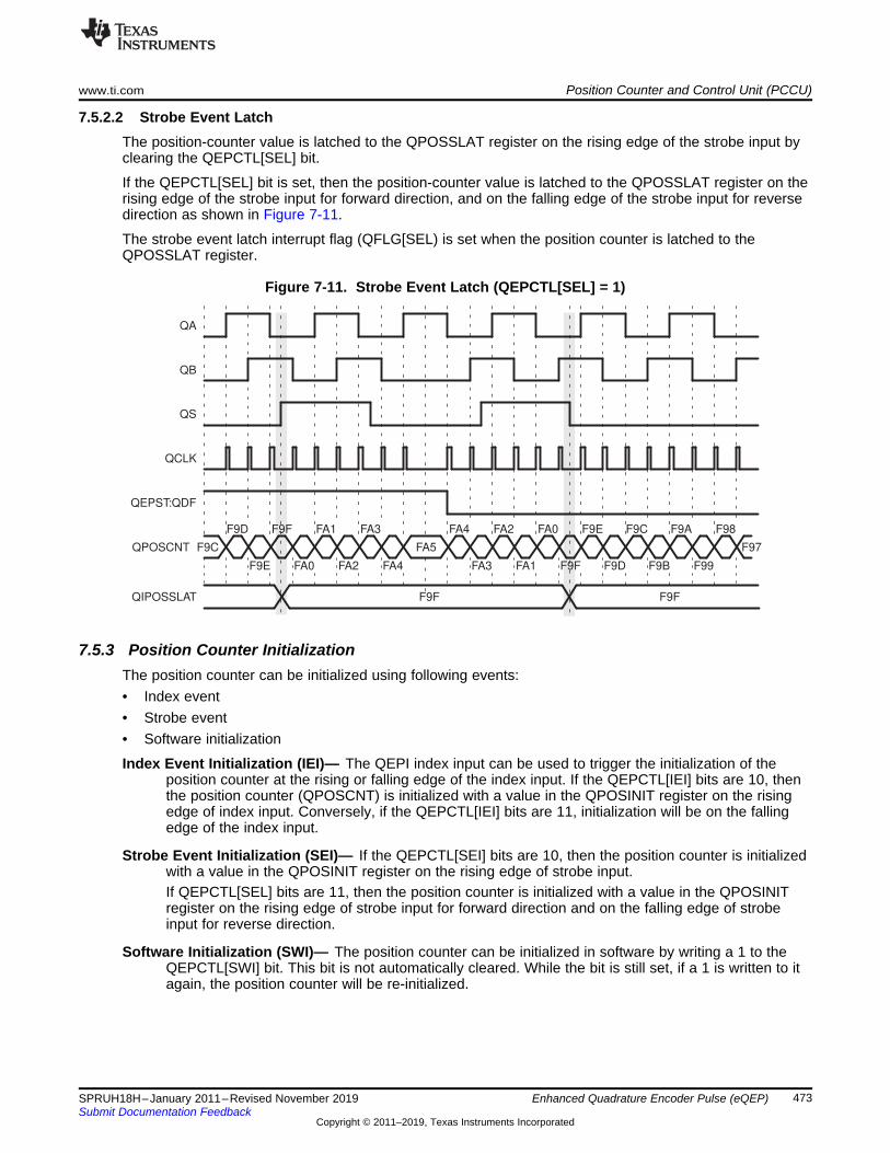
F9C
F9D
F9E
F9F
FA0
FA1
FA2
FA3
FA4
FA5
FA4
FA3
FA2
FA1
FA0
F9F
F9E
F9D
F9C
F9B
F9A
F99
F98
F97
F9F F9F
QA
QB
QS
QCLK
QEPST:QDF
QPOSCNT
QIPOSSLAT
www.ti.com Position Counter and Control Unit (PCCU)
473SPRUH18H–January 2011–Revised November 2019Submit Documentation Feedback
Copyright © 2011–2019, Texas Instruments Incorporated
Enhanced Quadrature Encoder Pulse (eQEP)
7.5.2.2 Strobe Event LatchThe position-counter value is latched to the QPOSSLAT register on the rising edge of the strobe input byclearing the QEPCTL[SEL] bit.
If the QEPCTL[SEL] bit is set, then the position-counter value is latched to the QPOSSLAT register on therising edge of the strobe input for forward direction, and on the falling edge of the strobe input for reversedirection as shown in Figure 7-11.
The strobe event latch interrupt flag (QFLG[SEL) is set when the position counter is latched to theQPOSSLAT register.
Figure 7-11. Strobe Event Latch (QEPCTL[SEL] = 1)
7.5.3 Position Counter InitializationThe position counter can be initialized using following events:• Index event• Strobe event• Software initialization
Index Event Initialization (IEI)— The QEPI index input can be used to trigger the initialization of theposition counter at the rising or falling edge of the index input. If the QEPCTL[IEI] bits are 10, thenthe position counter (QPOSCNT) is initialized with a value in the QPOSINIT register on the risingedge of index input. Conversely, if the QEPCTL[IEI] bits are 11, initialization will be on the fallingedge of the index input.
Strobe Event Initialization (SEI)— If the QEPCTL[SEI] bits are 10, then the position counter is initializedwith a value in the QPOSINIT register on the rising edge of strobe input.If QEPCTL[SEL] bits are 11, then the position counter is initialized with a value in the QPOSINITregister on the rising edge of strobe input for forward direction and on the falling edge of strobeinput for reverse direction.
Software Initialization (SWI)— The position counter can be initialized in software by writing a 1 to theQEPCTL[SWI] bit. This bit is not automatically cleared. While the bit is still set, if a 1 is written to itagain, the position counter will be re-initialized.

QPOSCTL:PCSPW
12
Pulse
stretcher
QFLG:PCM
QPOSCNT
32
QPOSCMP QFLG:PCR
32
QPOSCTL:PCSHDW
QPOSCTL:PCLOAD
0
1
QPOSCTL:PCPOL
PCSOUT
PCEVENT
Position Counter and Control Unit (PCCU) www.ti.com
474 SPRUH18H–January 2011–Revised November 2019Submit Documentation Feedback
Copyright © 2011–2019, Texas Instruments Incorporated
Enhanced Quadrature Encoder Pulse (eQEP)
7.5.4 eQEP Position-compare UnitThe eQEP peripheral includes a position-compare unit that is used to generate a sync output and/orinterrupt on a position-compare match. Figure 7-12 shows a diagram. The position-compare (QPOSCMP)register is shadowed and shadow mode can be enabled or disabled using the QPOSCTL[PSSHDW] bit. Ifthe shadow mode is not enabled, the CPU writes directly to the active position compare register.
Figure 7-12. eQEP Position-compare Unit
In shadow mode, you can configure the position-compare unit (QPOSCTL[PCLOAD]) to load the shadowregister value into the active register on the following events, and to generate the position-compare ready(QFLG[PCR]) interrupt after loading.• Load on compare match• Load on position-counter zero event
The position-compare match (QFLG[PCM]) is set when the position-counter value (QPOSCNT) matcheswith the active position-compare register (QPOSCMP) and the position-compare sync output of theprogrammable pulse width is generated on compare-match to trigger an external device.
For example, if QPOSCMP = 2, the position-compare unit generates a position-compare event on 1 to 2transitions of the eQEP position counter for forward counting direction and on 3 to 2 transitions of theeQEP position counter for reverse counting direction (see Figure 7-13).
See the register section for the layout of the eQEP Position-Compare Control Register (QPOSCTL) anddescription of the QPOSCTL bit fields.

v(k) � Xt(k)� t(k� 1)
�X�T
DIR
QPOSCMP
QPOSCNT
PCSOUT (active HIGH)
PCSPWPCSPW
PCSPW
PCEVNT
POSCMP=2
0
1
2
3
4
3
2
1
0
1
2
3
4
3
2
1
0
eQEP counter
PCEVNT
PCSOUT (active HIGH)
PCSOUT (active LOW)
PCSPW
www.ti.com eQEP Edge Capture Unit
475SPRUH18H–January 2011–Revised November 2019Submit Documentation Feedback
Copyright © 2011–2019, Texas Instruments Incorporated
Enhanced Quadrature Encoder Pulse (eQEP)
Figure 7-13. eQEP Position-compare Event Generation Points
The pulse stretcher logic in the position-compare unit generates a programmable position-compare syncpulse output on the position-compare match. In the event of a new position-compare match while aprevious position-compare pulse is still active, then the pulse stretcher generates a pulse of specifiedduration from the new position-compare event as shown in Figure 7-14.
Figure 7-14. eQEP Position-compare Sync Output Pulse Stretcher
7.6 eQEP Edge Capture UnitThe eQEP peripheral includes an integrated edge capture unit to measure the elapsed time between theunit position events as shown in Figure 7-15. This feature is typically used for low speed measurementusing the following equation:
(3)
where,

eQEP Edge Capture Unit www.ti.com
476 SPRUH18H–January 2011–Revised November 2019Submit Documentation Feedback
Copyright © 2011–2019, Texas Instruments Incorporated
Enhanced Quadrature Encoder Pulse (eQEP)
• X - Unit position is defined by integer multiple of quadrature edges (see Figure 7-16)• ΔT - Elapsed time between unit position events• v(k) - Velocity at time instant "k"
The eQEP capture timer (QCTMR) runs from prescaled SYSCLKOUT and the prescaler is programmedby the QCAPCTL[CCPS] bits. The capture timer (QCTMR) value is latched into the capture period register(QCPRD) on every unit position event and then the capture timer is reset, a flag is set inQEPSTS:UPEVNT to indicate that new value is latched into the QCPRD register. Software can check thisstatus flag before reading the period register for low speed measurement, and clear the flag by writing 1.
Time measurement (ΔT) between unit position events will be correct if the following conditions are met:• No more than 65,535 counts have occurred between unit position events.• No direction change between unit position events.
The capture unit sets the eQEP overflow error flag (QEPSTS[COEF]) in the event of capture timeroverflow between unit position events. If a direction change occurs between the unit position events, thenan error flag is set in the status register (QEPSTS[CDEF]).
The Capture Timer (QCTMR) and Capture Period register (QCPRD) can be configured to latch onfollowing events.• CPU read of QPOSCNT register• Unit time-out event
If the QEPCTL[QCLM] bit is cleared, then the capture timer and capture period values are latched into theQCTMRLAT and QCPRDLAT registers, respectively, when the CPU reads the position counter(QPOSCNT).
If the QEPCTL[QCLM] bit is set, then the position counter, capture timer, and capture period values arelatched into the QPOSLAT, QCTMRLAT and QCPRDLAT registers, respectively, on unit time out.
Figure 7-17 shows the capture unit operation along with the position counter.

X=N x P
P
QA
QB
QCLK
UPEVNT
QCAPCTL:CEN
Capture timercontrol unit
(CTCU)
QCPRD
QCTMR QCTMRLAT
QCPRDLAT
16 16
3-bit binarydivider
x1, 1/2, 1/4...,1/128
CAPCLK
QCAPCTL:CCPS
3
SYSCLKOUT
16
0xFFFF16
QEPSTS:COEF
x1, 1/2, 1/4...,1/2048
4-bit binarydivider QCLK
Rising/fallingedge detect
QDIRQEPSTS:CDEF
QEPCTL:UTE
QUTMR
QUPRD
SYSCLKOUT
QFLG:UTO
UTIME
4
QCAPCTL:UPPS
UTOUT
QEPSTS:UPEVNT
UPEVNT
www.ti.com eQEP Edge Capture Unit
477SPRUH18H–January 2011–Revised November 2019Submit Documentation Feedback
Copyright © 2011–2019, Texas Instruments Incorporated
Enhanced Quadrature Encoder Pulse (eQEP)
Figure 7-15. eQEP Edge Capture Unit
NOTE: The QCAPCTL[UPPS] prescaler should not be modified dynamically (such as switching theunit event prescaler from QCLK/4 to QCLK/8). Doing so may result in undefined behavior.The QCAPCTL[CPPS] prescaler can be modified dynamically (such as switching CAPCLKprescaling mode from SYSCLK/4 to SYSCLK/8) only after the capture unit is disabled.
Figure 7-16. Unit Position Event for Low Speed Measurement (QCAPCTL[UPPS] = 0010)
A N - Number of quadrature periods selected using QCAPCTL[UPPS] bits

v(k) �x(k)� x(k� 1)
T�
�XT
o
∆X
x(k−1)
∆T
t(k)
t(k−1)
T
QEPA
QEPB
QCLK
QPOSCNT
UPEVNT
QCTMR
UTOUT
x(k)
eQEP Edge Capture Unit www.ti.com
478 SPRUH18H–January 2011–Revised November 2019Submit Documentation Feedback
Copyright © 2011–2019, Texas Instruments Incorporated
Enhanced Quadrature Encoder Pulse (eQEP)
Figure 7-17. eQEP Edge Capture Unit - Timing Details
Velocity calculation equations:
(4)
where
v(k): Velocity at time instant k
x(k): Position at time instant k
x(k-1): Position at time instant k-1
T: Fixed unit time or inverse of velocity calculation rate
ΔX: Incremental position movement in unit time
X: Fixed unit position
ΔT: Incremental time elapsed for unit position movement
t(k): Time instant "k"
t(k-1): Time instant "k-1"
Unit time (T) and unit period(X) are configured using the QUPRD and QCAPCTL[UPPS] registers.Incremental position output and incremental time output is available in the QPOSLAT and QCPRDLATregisters.

QFLG:WTOQWDPRD
16
QWDTMR
16
QEPCTL:WDE
QWDOG
RESET
SYSCLKOUT/64
SYSCLKOUT
QCLK WDTOUT
www.ti.com eQEP Watchdog
479SPRUH18H–January 2011–Revised November 2019Submit Documentation Feedback
Copyright © 2011–2019, Texas Instruments Incorporated
Enhanced Quadrature Encoder Pulse (eQEP)
Parameter Relevant Register to Configure or Read the InformationT Unit Period Register (QUPRD)ΔX Incremental Position = QPOSLAT(k) - QPOSLAT(K-1)X Fixed unit position defined by sensor resolution and ZCAPCTL[UPPS] bitsΔT Capture Period Latch (QCPRDLAT)
7.7 eQEP WatchdogThe eQEP peripheral contains a 16-bit watchdog timer that monitors the quadrature-clock to indicateproper operation of the motion-control system. The eQEP watchdog timer is clocked fromSYSCLKOUT/64 and the quadrate clock event (pulse) resets the watchdog timer. If no quadrature-clockevent is detected until a period match (QWDPRD = QWDTMR), then the watchdog timer will time out andthe watchdog interrupt flag will be set (QFLG[WTO]). The time-out value is programmable through thewatchdog period register (QWDPRD).
Figure 7-18. eQEP Watchdog Timer
7.8 Unit Timer BaseThe eQEP peripheral includes a 32-bit timer (QUTMR) that is clocked by SYSCLKOUT to generateperiodic interrupts for velocity calculations. Whenever the unit timer (QUTMR) matches the unit periodregister (QUPRD), it resets the unit timer (QUPRD) it resets the unit timer (QUTMR) and also generatesthe unit time out interrupt flag (QFLG[UTO]). The unit timer gets reset whenever timer value equals toconfigured period value.
The eQEP peripheral can be configured to latch the position counter, capture timer, and capture periodvalues on a unit time out event so that latched values are used for velocity calculation as described inSection 7.6.

Clr
Set
Latch
QFRC:PCE
PCE
QCLR:PCE
QFLG:PCE
QEINT:PCE
QCLR:UTO
QFRC:UTO
QEINT:UTO
set
Latch
clr
UTOQFLG:UTO
0
1
0Pulsegenerator
wheninput=1
QFLG:INTLatch
Set Clr QCLR:INT
EQEPxINT
QFLG:UTOQUPRD
32
QUTMR
32
QEPCTL:UTE
UTIME
SYSCLKOUT
UTOUT
eQEP Interrupt Structure www.ti.com
480 SPRUH18H–January 2011–Revised November 2019Submit Documentation Feedback
Copyright © 2011–2019, Texas Instruments Incorporated
Enhanced Quadrature Encoder Pulse (eQEP)
Figure 7-19. eQEP Unit Time Base
7.9 eQEP Interrupt StructureFigure 7-20 shows how the interrupt mechanism works in the EQEP module.
Figure 7-20. EQEP Interrupt Generation
Eleven interrupt events (PCE, PHE, QDC, WTO, PCU, PCO, PCR, PCM, SEL, IEL and UTO) can begenerated. The interrupt control register (QEINT) is used to enable/disable individual interrupt eventsources. The interrupt flag register (QFLG) indicates if any interrupt event has been latched and containsthe global interrupt flag bit (INT).
An Interrupt pulse is generated to PIE when:a. Interrupt is enabled for eQEP event inside QEINT registerb. Interrupt flag for eQEP event inside QFLG register is set, andc. Global interrupt status flag bit QFLG[INT] had been cleared for previously generated interrupt event.
The interrupt service routine will need to clear the global interrupt flag bit and the serviced event, viathe interrupt clear register (QCLR), before any other interrupt pulses are generated.If either flags insidethe QFLG register are not cleared, further interrupt event will not generate interrupt to PIE. You canforce an interrupt event by way of the interrupt force register (QFRC), which is useful for test purposes.

www.ti.com eQEP Registers
481SPRUH18H–January 2011–Revised November 2019Submit Documentation Feedback
Copyright © 2011–2019, Texas Instruments Incorporated
Enhanced Quadrature Encoder Pulse (eQEP)
7.10 eQEP RegistersThis section describes the Enhanced Quadrature Encoder Pulse Registers.
7.10.1 eQEP Base Addresses
Table 7-3. EQEP Base Address TableBit Field Name
Base AddressInstance Structure
EQep1Regs EQEP_REGS 0x0000_6B00
EQep2Regs EQEP_REGS 0x0000_6B40

eQEP Registers www.ti.com
482 SPRUH18H–January 2011–Revised November 2019Submit Documentation Feedback
Copyright © 2011–2019, Texas Instruments Incorporated
Enhanced Quadrature Encoder Pulse (eQEP)
7.10.2 EQEP_REGS RegistersTable 7-4 lists the EQEP_REGS registers. All register offset addresses not listed in Table 7-4 should beconsidered as reserved locations and the register contents should not be modified.
Table 7-4. EQEP_REGS Registers
Offset Acronym Register Name Write Protection Section0h QPOSCNT Position Counter Go2h QPOSINIT Position Counter Init Go4h QPOSMAX Maximum Position Count Go6h QPOSCMP Position Compare Go8h QPOSILAT Index Position Latch GoAh QPOSSLAT Strobe Position Latch GoCh QPOSLAT Position Latch GoEh QUTMR QEP Unit Timer Go10h QUPRD QEP Unit Period Go12h QWDTMR QEP Watchdog Timer Go13h QWDPRD QEP Watchdog Period Go14h QDECCTL Quadrature Decoder Control Go15h QEPCTL QEP Control Go16h QCAPCTL Qaudrature Capture Control Go17h QPOSCTL Position Compare Control Go18h QEINT QEP Interrupt Control Go19h QFLG QEP Interrupt Flag Go1Ah QCLR QEP Interrupt Clear Go1Bh QFRC QEP Interrupt Force Go1Ch QEPSTS QEP Status Go1Dh QCTMR QEP Capture Timer Go1Eh QCPRD QEP Capture Period Go1Fh QCTMRLAT QEP Capture Latch Go20h QCPRDLAT QEP Capture Period Latch Go
Complex bit access types are encoded to fit into small table cells. Table 7-5 shows the codes that areused for access types in this section.
Table 7-5. EQEP_REGS Access Type Codes
Access Type Code DescriptionRead TypeR R ReadR-0 R
-0ReadReturns 0s
Write TypeW W WriteW1S W
1SWrite1 to set
Reset or Default Value-n Value after reset or the default
valueRegister Array Variables

www.ti.com eQEP Registers
483SPRUH18H–January 2011–Revised November 2019Submit Documentation Feedback
Copyright © 2011–2019, Texas Instruments Incorporated
Enhanced Quadrature Encoder Pulse (eQEP)
Table 7-5. EQEP_REGS Access TypeCodes (continued)
Access Type Code Descriptioni,j,k,l,m,n When these variables are used in
a register name, an offset, or anaddress, they refer to the value ofa register array where the registeris part of a group of repeatingregisters. The register groups forma hierarchical structure and thearray is represented with aformula.
y When this variable is used in aregister name, an offset, or anaddress it refers to the value of aregister array.
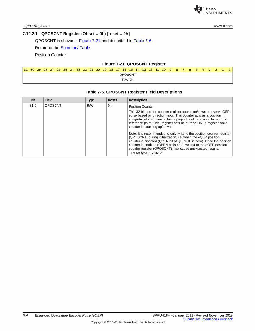
eQEP Registers www.ti.com
484 SPRUH18H–January 2011–Revised November 2019Submit Documentation Feedback
Copyright © 2011–2019, Texas Instruments Incorporated
Enhanced Quadrature Encoder Pulse (eQEP)
7.10.2.1 QPOSCNT Register (Offset = 0h) [reset = 0h]QPOSCNT is shown in Figure 7-21 and described in Table 7-6.
Return to the Summary Table.
Position Counter
Figure 7-21. QPOSCNT Register31 30 29 28 27 26 25 24 23 22 21 20 19 18 17 16 15 14 13 12 11 10 9 8 7 6 5 4 3 2 1 0
QPOSCNTR/W-0h
Table 7-6. QPOSCNT Register Field Descriptions
Bit Field Type Reset Description31-0 QPOSCNT R/W 0h Position Counter
This 32-bit position counter register counts up/down on every eQEPpulse based on direction input. This counter acts as a positionintegrator whose count value is proportional to position from a givereference point. This Register acts as a Read ONLY register whilecounter is counting up/down.
Note: It is recommended to only write to the position counter register(QPOSCNT) during initialization, i.e. when the eQEP positioncounter is disabled (QPEN bit of QEPCTL is zero). Once the positioncounter is enabled (QPEN bit is one), writing to the eQEP positioncounter register (QPOSCNT) may cause unexpected results.
Reset type: SYSRSn

www.ti.com eQEP Registers
485SPRUH18H–January 2011–Revised November 2019Submit Documentation Feedback
Copyright © 2011–2019, Texas Instruments Incorporated
Enhanced Quadrature Encoder Pulse (eQEP)
7.10.2.2 QPOSINIT Register (Offset = 2h) [reset = 0h]QPOSINIT is shown in Figure 7-22 and described in Table 7-7.
Return to the Summary Table.
Position Counter Init
Figure 7-22. QPOSINIT Register31 30 29 28 27 26 25 24 23 22 21 20 19 18 17 16 15 14 13 12 11 10 9 8 7 6 5 4 3 2 1 0
QPOSINITR/W-0h
Table 7-7. QPOSINIT Register Field Descriptions
Bit Field Type Reset Description31-0 QPOSINIT R/W 0h Position Counter Init
This register contains the position value that is used to initialize theposition counter based on external strobe or index event. Theposition counter can be initialized through software. Writes to thisregister should always be full 32-bit writes.
Reset type: SYSRSn

eQEP Registers www.ti.com
486 SPRUH18H–January 2011–Revised November 2019Submit Documentation Feedback
Copyright © 2011–2019, Texas Instruments Incorporated
Enhanced Quadrature Encoder Pulse (eQEP)
7.10.2.3 QPOSMAX Register (Offset = 4h) [reset = 0h]QPOSMAX is shown in Figure 7-23 and described in Table 7-8.
Return to the Summary Table.
Maximum Position Count
Figure 7-23. QPOSMAX Register31 30 29 28 27 26 25 24 23 22 21 20 19 18 17 16 15 14 13 12 11 10 9 8 7 6 5 4 3 2 1 0
QPOSMAXR/W-0h
Table 7-8. QPOSMAX Register Field Descriptions
Bit Field Type Reset Description31-0 QPOSMAX R/W 0h Maximum Position Count
This register contains the maximum position counter value. Writes tothis register should always be full 32-bit writes.
Reset type: SYSRSn

www.ti.com eQEP Registers
487SPRUH18H–January 2011–Revised November 2019Submit Documentation Feedback
Copyright © 2011–2019, Texas Instruments Incorporated
Enhanced Quadrature Encoder Pulse (eQEP)
7.10.2.4 QPOSCMP Register (Offset = 6h) [reset = 0h]QPOSCMP is shown in Figure 7-24 and described in Table 7-9.
Return to the Summary Table.
Position Compare
Figure 7-24. QPOSCMP Register31 30 29 28 27 26 25 24 23 22 21 20 19 18 17 16 15 14 13 12 11 10 9 8 7 6 5 4 3 2 1 0
QPOSCMPR/W-0h
Table 7-9. QPOSCMP Register Field Descriptions
Bit Field Type Reset Description31-0 QPOSCMP R/W 0h Position Compare
The position-compare value in this register is compared with theposition counter (QPOSCNT) to generate sync output and/orinterrupt on compare match.
Reset type: SYSRSn

eQEP Registers www.ti.com
488 SPRUH18H–January 2011–Revised November 2019Submit Documentation Feedback
Copyright © 2011–2019, Texas Instruments Incorporated
Enhanced Quadrature Encoder Pulse (eQEP)
7.10.2.5 QPOSILAT Register (Offset = 8h) [reset = 0h]QPOSILAT is shown in Figure 7-25 and described in Table 7-10.
Return to the Summary Table.
Index Position Latch
Figure 7-25. QPOSILAT Register31 30 29 28 27 26 25 24 23 22 21 20 19 18 17 16 15 14 13 12 11 10 9 8 7 6 5 4 3 2 1 0
QPOSILATR-0h
Table 7-10. QPOSILAT Register Field Descriptions
Bit Field Type Reset Description31-0 QPOSILAT R 0h Index Position Latch
The position-counter value is latched into this register on an indexevent as defined by the QEPCTL[IEL] bits.
Reset type: SYSRSn
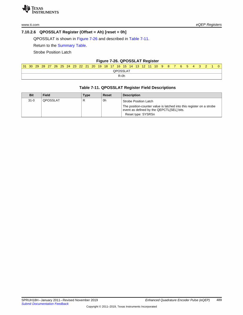
www.ti.com eQEP Registers
489SPRUH18H–January 2011–Revised November 2019Submit Documentation Feedback
Copyright © 2011–2019, Texas Instruments Incorporated
Enhanced Quadrature Encoder Pulse (eQEP)
7.10.2.6 QPOSSLAT Register (Offset = Ah) [reset = 0h]QPOSSLAT is shown in Figure 7-26 and described in Table 7-11.
Return to the Summary Table.
Strobe Position Latch
Figure 7-26. QPOSSLAT Register31 30 29 28 27 26 25 24 23 22 21 20 19 18 17 16 15 14 13 12 11 10 9 8 7 6 5 4 3 2 1 0
QPOSSLATR-0h
Table 7-11. QPOSSLAT Register Field Descriptions
Bit Field Type Reset Description31-0 QPOSSLAT R 0h Strobe Position Latch
The position-counter value is latched into this register on a strobeevent as defined by the QEPCTL[SEL] bits.
Reset type: SYSRSn

eQEP Registers www.ti.com
490 SPRUH18H–January 2011–Revised November 2019Submit Documentation Feedback
Copyright © 2011–2019, Texas Instruments Incorporated
Enhanced Quadrature Encoder Pulse (eQEP)
7.10.2.7 QPOSLAT Register (Offset = Ch) [reset = 0h]QPOSLAT is shown in Figure 7-27 and described in Table 7-12.
Return to the Summary Table.
Position Latch
Figure 7-27. QPOSLAT Register31 30 29 28 27 26 25 24 23 22 21 20 19 18 17 16 15 14 13 12 11 10 9 8 7 6 5 4 3 2 1 0
QPOSLATR-0h
Table 7-12. QPOSLAT Register Field Descriptions
Bit Field Type Reset Description31-0 QPOSLAT R 0h Position Latch
The position-counter value is latched into this register on a unit timeout event.
Reset type: SYSRSn

www.ti.com eQEP Registers
491SPRUH18H–January 2011–Revised November 2019Submit Documentation Feedback
Copyright © 2011–2019, Texas Instruments Incorporated
Enhanced Quadrature Encoder Pulse (eQEP)
7.10.2.8 QUTMR Register (Offset = Eh) [reset = 0h]QUTMR is shown in Figure 7-28 and described in Table 7-13.
Return to the Summary Table.
QEP Unit Timer
Figure 7-28. QUTMR Register31 30 29 28 27 26 25 24 23 22 21 20 19 18 17 16 15 14 13 12 11 10 9 8 7 6 5 4 3 2 1 0
QUTMRR/W-0h
Table 7-13. QUTMR Register Field Descriptions
Bit Field Type Reset Description31-0 QUTMR R/W 0h QEP Unit Timer
This register acts as time base for unit time event generation. Whenthis timer value matches the unit time period value a unit time eventis generated.
Reset type: SYSRSn

eQEP Registers www.ti.com
492 SPRUH18H–January 2011–Revised November 2019Submit Documentation Feedback
Copyright © 2011–2019, Texas Instruments Incorporated
Enhanced Quadrature Encoder Pulse (eQEP)
7.10.2.9 QUPRD Register (Offset = 10h) [reset = 0h]QUPRD is shown in Figure 7-29 and described in Table 7-14.
Return to the Summary Table.
QEP Unit Period
Figure 7-29. QUPRD Register31 30 29 28 27 26 25 24 23 22 21 20 19 18 17 16 15 14 13 12 11 10 9 8 7 6 5 4 3 2 1 0
QUPRDR/W-0h
Table 7-14. QUPRD Register Field Descriptions
Bit Field Type Reset Description31-0 QUPRD R/W 0h QEP Unit Period
This register contains the period count for the unit timer to generateperiodic unit time events. These events latch the eQEP positioninformation at periodic intervals and optionally generate an interrupt.Writes to this register should always be full 32-bit writes.
Reset type: SYSRSn

www.ti.com eQEP Registers
493SPRUH18H–January 2011–Revised November 2019Submit Documentation Feedback
Copyright © 2011–2019, Texas Instruments Incorporated
Enhanced Quadrature Encoder Pulse (eQEP)
7.10.2.10 QWDTMR Register (Offset = 12h) [reset = 0h]QWDTMR is shown in Figure 7-30 and described in Table 7-15.
Return to the Summary Table.
QEP Watchdog Timer
Figure 7-30. QWDTMR Register15 14 13 12 11 10 9 8
QWDTMRR/W-0h
7 6 5 4 3 2 1 0QWDTMR
R/W-0h
Table 7-15. QWDTMR Register Field Descriptions
Bit Field Type Reset Description15-0 QWDTMR R/W 0h QEP Watchdog Timer
This register acts as time base for the watchdog to detect motorstalls. When this timer value matches with the watchdog's periodvalue a watchdog timeout interrupt is generated. This register isreset upon edge transition in quadrature-clock indicating the motion.
Reset type: SYSRSn

eQEP Registers www.ti.com
494 SPRUH18H–January 2011–Revised November 2019Submit Documentation Feedback
Copyright © 2011–2019, Texas Instruments Incorporated
Enhanced Quadrature Encoder Pulse (eQEP)
7.10.2.11 QWDPRD Register (Offset = 13h) [reset = 0h]QWDPRD is shown in Figure 7-31 and described in Table 7-16.
Return to the Summary Table.
QEP Watchdog Period
Figure 7-31. QWDPRD Register15 14 13 12 11 10 9 8
QWDPRDR/W-0h
7 6 5 4 3 2 1 0QWDPRD
R/W-0h
Table 7-16. QWDPRD Register Field Descriptions
Bit Field Type Reset Description15-0 QWDPRD R/W 0h QEP Watchdog Period
This register contains the time-out count for the eQEP peripheralwatch dog timer.When the watchdog timer value matches the watchdog period value,a watchdog timeout interrupt is generated.
Reset type: SYSRSn

www.ti.com eQEP Registers
495SPRUH18H–January 2011–Revised November 2019Submit Documentation Feedback
Copyright © 2011–2019, Texas Instruments Incorporated
Enhanced Quadrature Encoder Pulse (eQEP)
7.10.2.12 QDECCTL Register (Offset = 14h) [reset = 0h]QDECCTL is shown in Figure 7-32 and described in Table 7-17.
Return to the Summary Table.
Quadrature Decoder Control
Figure 7-32. QDECCTL Register15 14 13 12 11 10 9 8
QSRC SOEN SPSEL XCR SWAP IGATE QAPR/W-0h R/W-0h R/W-0h R/W-0h R/W-0h R/W-0h R/W-0h
7 6 5 4 3 2 1 0QBP QIP QSP RESERVED
R/W-0h R/W-0h R/W-0h R-0h
Table 7-17. QDECCTL Register Field Descriptions
Bit Field Type Reset Description15-14 QSRC R/W 0h Position-counter source selection
Reset type: SYSRSn0h (R/W) = Quadrature count mode (QCLK = iCLK, QDIR = iDIR)1h (R/W) = Direction-count mode (QCLK = xCLK, QDIR = xDIR)2h (R/W) = UP count mode for frequency measurement (QCLK =xCLK, QDIR = 1)3h (R/W) = DOWN count mode for frequency measurement (QCLK= xCLK, QDIR = 0)
13 SOEN R/W 0h Sync output-enableReset type: SYSRSn0h (R/W) = Disable position-compare sync output1h (R/W) = Enable position-compare sync output
12 SPSEL R/W 0h Sync output pin selectionReset type: SYSRSn0h (R/W) = Index pin is used for sync output1h (R/W) = Strobe pin is used for sync output
11 XCR R/W 0h External Clock RateReset type: SYSRSn0h (R/W) = 2x resolution: Count the rising/falling edge1h (R/W) = 1x resolution: Count the rising edge only
10 SWAP R/W 0h CLK/DIR Signal Source for Position CounterReset type: SYSRSn0h (R/W) = Quadrature-clock inputs are not swapped1h (R/W) = Quadrature-clock inputs are swapped
9 IGATE R/W 0h Index pulse gating optionReset type: SYSRSn0h (R/W) = Disable gating of Index pulse1h (R/W) = Gate the index pin with strobe
8 QAP R/W 0h QEPA input polarityReset type: SYSRSn0h (R/W) = No effect1h (R/W) = Negates QEPA input
7 QBP R/W 0h QEPB input polarityReset type: SYSRSn0h (R/W) = No effect1h (R/W) = Negates QEPB input

eQEP Registers www.ti.com
496 SPRUH18H–January 2011–Revised November 2019Submit Documentation Feedback
Copyright © 2011–2019, Texas Instruments Incorporated
Enhanced Quadrature Encoder Pulse (eQEP)
Table 7-17. QDECCTL Register Field Descriptions (continued)Bit Field Type Reset Description6 QIP R/W 0h QEPI input polarity
Reset type: SYSRSn0h (R/W) = No effect1h (R/W) = Negates QEPI input
5 QSP R/W 0h QEPS input polarityReset type: SYSRSn0h (R/W) = No effect1h (R/W) = Negates QEPS input
4-0 RESERVED R 0h Reserved

www.ti.com eQEP Registers
497SPRUH18H–January 2011–Revised November 2019Submit Documentation Feedback
Copyright © 2011–2019, Texas Instruments Incorporated
Enhanced Quadrature Encoder Pulse (eQEP)
7.10.2.13 QEPCTL Register (Offset = 15h) [reset = 0h]QEPCTL is shown in Figure 7-33 and described in Table 7-18.
Return to the Summary Table.
QEP Control
Figure 7-33. QEPCTL Register15 14 13 12 11 10 9 8
FREE_SOFT PCRM SEI IEIR/W-0h R/W-0h R/W-0h R/W-0h
7 6 5 4 3 2 1 0SWI SEL IEL QPEN QCLM UTE WDE
R/W-0h R/W-0h R/W-0h R/W-0h R/W-0h R/W-0h R/W-0h
Table 7-18. QEPCTL Register Field Descriptions
Bit Field Type Reset Description15-14 FREE_SOFT R/W 0h Emulation mode
Reset type: SYSRSn0h (R/W) = QPOSCNT behaviorPosition counter stops immediately on emulation suspend0h (R/W) = QWDTMR behaviorWatchdog counter stops immediately0h (R/W) = QUTMR behaviorUnit timer stops immediately0h (R/W) = QCTMR behaviorCapture Timer stops immediately1h (R/W) = QPOSCNT behaviorPosition counter continues to count until the rollover1h (R/W) = QWDTMR behaviorWatchdog counter counts until WD period match roll over1h (R/W) = QUTMR behaviorUnit timer counts until period rollover1h (R/W) = QCTMR behaviorCapture Timer counts until next unit period event2h (R/W) = QPOSCNT behaviorPosition counter is unaffected by emulation suspend2h (R/W) = QWDTMR behaviorWatchdog counter is unaffected by emulation suspend2h (R/W) = QUTMR behaviorUnit timer is unaffected by emulation suspend2h (R/W) = QCTMR behaviorCapture Timer is unaffected by emulation suspend3h (R/W) = Same as FREE_SOFT_2
13-12 PCRM R/W 0h Postion counter resetReset type: SYSRSn0h (R/W) = Position counter reset on an index event1h (R/W) = Position counter reset on the maximum position2h (R/W) = Position counter reset on the first index event3h (R/W) = Position counter reset on a unit time event
11-10 SEI R/W 0h Strobe event initialization of position counterReset type: SYSRSn0h (R/W) = Does nothing (action disabled)1h (R/W) = Does nothing (action disabled)2h (R/W) = Initializes the position counter on rising edge of theQEPS signal3h (R/W) = Clockwise Direction:Initializes the position counter on the rising edge of QEPS strobeCounter Clockwise Direction:Initializes the position counter on the falling edge of QEPS strobe

eQEP Registers www.ti.com
498 SPRUH18H–January 2011–Revised November 2019Submit Documentation Feedback
Copyright © 2011–2019, Texas Instruments Incorporated
Enhanced Quadrature Encoder Pulse (eQEP)
Table 7-18. QEPCTL Register Field Descriptions (continued)Bit Field Type Reset Description9-8 IEI R/W 0h Index event init of position count
Reset type: SYSRSn0h (R/W) = Do nothing (action disabled)1h (R/W) = Do nothing (action disabled)2h (R/W) = Initializes the position counter on the rising edge of theQEPI signal (QPOSCNT = QPOSINIT)3h (R/W) = Initializes the position counter on the falling edge ofQEPI signal (QPOSCNT = QPOSINIT)
7 SWI R/W 0h Software init position counterReset type: SYSRSn0h (R/W) = Do nothing (action disabled)1h (R/W) = Initialize position counter (QPOSCNT=QPOSINIT). Thisbit is not cleared automatically
6 SEL R/W 0h Strobe event latch of position counterReset type: SYSRSn0h (R/W) = The position counter is latched on the rising edge ofQEPS strobe (QPOSSLAT = POSCCNT). Latching on the fallingedge can be done by inverting the strobe input using the QSP bit inthe QDECCTL register1h (R/W) = Clockwise Direction:Position counter is latched on rising edge of QEPS strobeCounter Clockwise Direction:Position counter is latched on falling edge of QEPS strobe
5-4 IEL R/W 0h Index event latch of position counter (software index marker)Reset type: SYSRSn0h (R/W) = Reserved1h (R/W) = Latches position counter on rising edge of the indexsignal2h (R/W) = Latches position counter on falling edge of the indexsignal3h (R/W) = Software index marker. Latches the position counterand quadrature direction flag on index event marker. The positioncounter is latched to the QPOSILAT register and the direction flagis latched in the QEPSTS[QDLF] bit. This mode is useful forsoftware index marking.
3 QPEN R/W 0h Quadrature position counter enable/software resetReset type: SYSRSn0h (R/W) = Reset the eQEP peripheral internal operatingflags/read-only registers. Control/configuration registers are notdisturbed by a software reset.When QPEN is disabled, some flags in the QFLG register do notget reset or cleared and show the actual state of that flag.1h (R/W) = eQEP position counter is enabled
2 QCLM R/W 0h QEP capture latch modeReset type: SYSRSn0h (R/W) = Latch on position counter read by CPU. Capture timerand capture period values are latched into QCTMRLAT andQCPRDLAT registers when CPU reads the QPOSCNT register.1h (R/W) = Latch on unit time out. Position counter, capture timerand capture period values are latched into QPOSLAT, QCTMRLATand QCPRDLAT registers on unit time out.
1 UTE R/W 0h QEP unit timer enableReset type: SYSRSn0h (R/W) = Disable eQEP unit timer1h (R/W) = Enable unit timer

www.ti.com eQEP Registers
499SPRUH18H–January 2011–Revised November 2019Submit Documentation Feedback
Copyright © 2011–2019, Texas Instruments Incorporated
Enhanced Quadrature Encoder Pulse (eQEP)
Table 7-18. QEPCTL Register Field Descriptions (continued)Bit Field Type Reset Description0 WDE R/W 0h QEP watchdog enable
Reset type: SYSRSn0h (R/W) = Disable the eQEP watchdog timer1h (R/W) = Enable the eQEP watchdog timer

eQEP Registers www.ti.com
500 SPRUH18H–January 2011–Revised November 2019Submit Documentation Feedback
Copyright © 2011–2019, Texas Instruments Incorporated
Enhanced Quadrature Encoder Pulse (eQEP)
7.10.2.14 QCAPCTL Register (Offset = 16h) [reset = 0h]QCAPCTL is shown in Figure 7-34 and described in Table 7-19.
Return to the Summary Table.
Qaudrature Capture Control
Figure 7-34. QCAPCTL Register15 14 13 12 11 10 9 8
CEN RESERVEDR/W-0h R-0h
7 6 5 4 3 2 1 0RESERVED CCPS UPPS
R-0h R/W-0h R/W-0h
Table 7-19. QCAPCTL Register Field Descriptions
Bit Field Type Reset Description15 CEN R/W 0h Enable eQEP capture
Reset type: SYSRSn0h (R/W) = eQEP capture unit is disabled1h (R/W) = eQEP capture unit is enabled
14-7 RESERVED R 0h Reserved6-4 CCPS R/W 0h eQEP capture timer clock prescaler
Reset type: SYSRSn0h (R/W) = CAPCLK = SYSCLKOUT/11h (R/W) = CAPCLK = SYSCLKOUT/22h (R/W) = CAPCLK = SYSCLKOUT/43h (R/W) = CAPCLK = SYSCLKOUT/84h (R/W) = CAPCLK = SYSCLKOUT/165h (R/W) = CAPCLK = SYSCLKOUT/326h (R/W) = CAPCLK = SYSCLKOUT/647h (R/W) = CAPCLK = SYSCLKOUT/128
3-0 UPPS R/W 0h Unit position event prescalerReset type: SYSRSn0h (R/W) = UPEVNT = QCLK/11h (R/W) = UPEVNT = QCLK/22h (R/W) = UPEVNT = QCLK/43h (R/W) = UPEVNT = QCLK/84h (R/W) = UPEVNT = QCLK/165h (R/W) = UPEVNT = QCLK/326h (R/W) = UPEVNT = QCLK/647h (R/W) = UPEVNT = QCLK/1288h (R/W) = UPEVNT = QCLK/2569h (R/W) = UPEVNT = QCLK/512Ah (R/W) = UPEVNT = QCLK/1024Bh (R/W) = UPEVNT = QCLK/2048Ch (R/W) = ReservedDh (R/W) = ReservedEh (R/W) = ReservedFh (R/W) = Reserved

www.ti.com eQEP Registers
501SPRUH18H–January 2011–Revised November 2019Submit Documentation Feedback
Copyright © 2011–2019, Texas Instruments Incorporated
Enhanced Quadrature Encoder Pulse (eQEP)
7.10.2.15 QPOSCTL Register (Offset = 17h) [reset = 0h]QPOSCTL is shown in Figure 7-35 and described in Table 7-20.
Return to the Summary Table.
Position Compare Control
Figure 7-35. QPOSCTL Register15 14 13 12 11 10 9 8
PCSHDW PCLOAD PCPOL PCE PCSPWR/W-0h R/W-0h R/W-0h R/W-0h R/W-0h
7 6 5 4 3 2 1 0PCSPWR/W-0h
Table 7-20. QPOSCTL Register Field Descriptions
Bit Field Type Reset Description15 PCSHDW R/W 0h Position compare of shadow enable
Reset type: SYSRSn0h (R/W) = Shadow disabled, load Immediate1h (R/W) = Shadow enabled
14 PCLOAD R/W 0h Position compare of shadow loadReset type: SYSRSn0h (R/W) = Load on QPOSCNT = 01h (R/W) = Load when QPOSCNT = QPOSCMP
13 PCPOL R/W 0h Polarity of sync outputReset type: SYSRSn0h (R/W) = Active HIGH pulse output1h (R/W) = Active LOW pulse output
12 PCE R/W 0h Position compare enable/disableReset type: SYSRSn0h (R/W) = Disable position compare unit1h (R/W) = Enable position compare unit
11-0 PCSPW R/W 0h Select-position-compare sync output pulse widthReset type: SYSRSn0h (R/W) = 1 * 4 * SYSCLKOUT cycles1h (R/W) = 2 * 4 * SYSCLKOUT cyclesFFFh (R/W) = 4096 * 4 * SYSCLKOUT cycles

eQEP Registers www.ti.com
502 SPRUH18H–January 2011–Revised November 2019Submit Documentation Feedback
Copyright © 2011–2019, Texas Instruments Incorporated
Enhanced Quadrature Encoder Pulse (eQEP)
7.10.2.16 QEINT Register (Offset = 18h) [reset = 0h]QEINT is shown in Figure 7-36 and described in Table 7-21.
Return to the Summary Table.
QEP Interrupt Control
Figure 7-36. QEINT Register15 14 13 12 11 10 9 8
RESERVED UTO IEL SEL PCMR-0h R/W-0h R/W-0h R/W-0h R/W-0h
7 6 5 4 3 2 1 0PCR PCO PCU WTO QDC QPE PCE RESERVED
R/W-0h R/W-0h R/W-0h R/W-0h R/W-0h R/W-0h R/W-0h R-0h
Table 7-21. QEINT Register Field Descriptions
Bit Field Type Reset Description15-12 RESERVED R 0h Reserved
11 UTO R/W 0h Unit time out interrupt enableReset type: SYSRSn0h (R/W) = Interrupt is disabled1h (R/W) = Interrupt is enabled
10 IEL R/W 0h Index event latch interrupt enableReset type: SYSRSn0h (R/W) = Interrupt is disabled1h (R/W) = Interrupt is enabled
9 SEL R/W 0h Strobe event latch interrupt enableReset type: SYSRSn0h (R/W) = Interrupt is disabled1h (R/W) = Interrupt is enabled
8 PCM R/W 0h Position-compare match interrupt enableReset type: SYSRSn0h (R/W) = Interrupt is disabled1h (R/W) = Interrupt is enabled
7 PCR R/W 0h Position-compare ready interrupt enableReset type: SYSRSn0h (R/W) = Interrupt is disabled1h (R/W) = Interrupt is enabled
6 PCO R/W 0h Position counter overflow interrupt enableReset type: SYSRSn0h (R/W) = Interrupt is disabled1h (R/W) = Interrupt is enabled
5 PCU R/W 0h Position counter underflow interrupt enableReset type: SYSRSn0h (R/W) = Interrupt is disabled1h (R/W) = Interrupt is enabled
4 WTO R/W 0h Watchdog time out interrupt enableReset type: SYSRSn0h (R/W) = Interrupt is disabled1h (R/W) = Interrupt is enabled

www.ti.com eQEP Registers
503SPRUH18H–January 2011–Revised November 2019Submit Documentation Feedback
Copyright © 2011–2019, Texas Instruments Incorporated
Enhanced Quadrature Encoder Pulse (eQEP)
Table 7-21. QEINT Register Field Descriptions (continued)Bit Field Type Reset Description3 QDC R/W 0h Quadrature direction change interrupt enable
Reset type: SYSRSn0h (R/W) = Interrupt is disabled1h (R/W) = Interrupt is enabled
2 QPE R/W 0h Quadrature phase error interrupt enableReset type: SYSRSn0h (R/W) = Interrupt is disabled1h (R/W) = Interrupt is enabled
1 PCE R/W 0h Position counter error interrupt enableReset type: SYSRSn0h (R/W) = Interrupt is disabled1h (R/W) = Interrupt is enabled
0 RESERVED R 0h Reserved

eQEP Registers www.ti.com
504 SPRUH18H–January 2011–Revised November 2019Submit Documentation Feedback
Copyright © 2011–2019, Texas Instruments Incorporated
Enhanced Quadrature Encoder Pulse (eQEP)
7.10.2.17 QFLG Register (Offset = 19h) [reset = 0h]QFLG is shown in Figure 7-37 and described in Table 7-22.
Return to the Summary Table.
QEP Interrupt Flag
Figure 7-37. QFLG Register15 14 13 12 11 10 9 8
RESERVED UTO IEL SEL PCMR-0h R-0h R-0h R-0h R-0h
7 6 5 4 3 2 1 0PCR PCO PCU WTO QDC PHE PCE INTR-0h R-0h R-0h R-0h R-0h R-0h R-0h R-0h
Table 7-22. QFLG Register Field Descriptions
Bit Field Type Reset Description15-12 RESERVED R 0h Reserved
11 UTO R 0h Unit time out interrupt flagReset type: SYSRSn0h (R/W) = No interrupt generated1h (R/W) = Interrupt was generated
10 IEL R 0h Index event latch interrupt flagReset type: SYSRSn0h (R/W) = No interrupt generated1h (R/W) = Interrupt was generated
9 SEL R 0h Strobe event latch interrupt flagReset type: SYSRSn0h (R/W) = No interrupt generated1h (R/W) = Interrupt was generated
8 PCM R 0h eQEP compare match event interrupt flagReset type: SYSRSn0h (R/W) = No interrupt generated1h (R/W) = Interrupt was generated
7 PCR R 0h Position-compare ready interrupt flagReset type: SYSRSn0h (R/W) = No interrupt generated1h (R/W) = Interrupt was generated
6 PCO R 0h Position counter overflow interrupt flagReset type: SYSRSn0h (R/W) = No interrupt generated1h (R/W) = Interrupt was generated
5 PCU R 0h Position counter underflow interrupt flagReset type: SYSRSn0h (R/W) = No interrupt generated1h (R/W) = Interrupt was generated
4 WTO R 0h Watchdog timeout interrupt flagReset type: SYSRSn0h (R/W) = No interrupt generated1h (R/W) = Interrupt was generated

www.ti.com eQEP Registers
505SPRUH18H–January 2011–Revised November 2019Submit Documentation Feedback
Copyright © 2011–2019, Texas Instruments Incorporated
Enhanced Quadrature Encoder Pulse (eQEP)
Table 7-22. QFLG Register Field Descriptions (continued)Bit Field Type Reset Description3 QDC R 0h Quadrature direction change interrupt flag
Reset type: SYSRSn0h (R/W) = No interrupt generated1h (R/W) = Interrupt was generated
2 PHE R 0h Quadrature phase error interrupt flagReset type: SYSRSn0h (R/W) = No interrupt generated1h (R/W) = Interrupt was generated
1 PCE R 0h Position counter error interrupt flagReset type: SYSRSn0h (R/W) = No interrupt generated1h (R/W) = Interrupt was generated
0 INT R 0h Global interrupt status flagReset type: SYSRSn0h (R/W) = No interrupt generated1h (R/W) = Interrupt was generated

eQEP Registers www.ti.com
506 SPRUH18H–January 2011–Revised November 2019Submit Documentation Feedback
Copyright © 2011–2019, Texas Instruments Incorporated
Enhanced Quadrature Encoder Pulse (eQEP)
7.10.2.18 QCLR Register (Offset = 1Ah) [reset = 0h]QCLR is shown in Figure 7-38 and described in Table 7-23.
Return to the Summary Table.
QEP Interrupt Clear
Figure 7-38. QCLR Register15 14 13 12 11 10 9 8
RESERVED UTO IEL SEL PCMR-0h R-0/W1S-0h R-0/W1S-0h R-0/W1S-0h R-0/W1S-0h
7 6 5 4 3 2 1 0PCR PCO PCU WTO QDC PHE PCE INT
R-0/W1S-0h R-0/W1S-0h R-0/W1S-0h R-0/W1S-0h R-0/W1S-0h R-0/W1S-0h R-0/W1S-0h R-0/W1S-0h
Table 7-23. QCLR Register Field Descriptions
Bit Field Type Reset Description15-12 RESERVED R 0h Reserved
11 UTO R-0/W1S 0h Clear unit time out interrupt flagReset type: SYSRSn0h (R/W) = No effect1h (R/W) = Clears the interrupt flag
10 IEL R-0/W1S 0h Clear index event latch interrupt flagReset type: SYSRSn0h (R/W) = No effect1h (R/W) = Clears the interrupt flag
9 SEL R-0/W1S 0h Clear strobe event latch interrupt flagReset type: SYSRSn0h (R/W) = No effect1h (R/W) = Clears the interrupt flag
8 PCM R-0/W1S 0h Clear eQEP compare match event interrupt flagReset type: SYSRSn0h (R/W) = No effect1h (R/W) = Clears the interrupt flag
7 PCR R-0/W1S 0h Clear position-compare ready interrupt flagReset type: SYSRSn0h (R/W) = No effect1h (R/W) = Clears the interrupt flag
6 PCO R-0/W1S 0h Clear position counter overflow interrupt flagReset type: SYSRSn0h (R/W) = No effect1h (R/W) = Clears the interrupt flag
5 PCU R-0/W1S 0h Clear position counter underflow interrupt flagReset type: SYSRSn0h (R/W) = No effect1h (R/W) = Clears the interrupt flag
4 WTO R-0/W1S 0h Clear watchdog timeout interrupt flagReset type: SYSRSn0h (R/W) = No effect1h (R/W) = Clears the interrupt flag

www.ti.com eQEP Registers
507SPRUH18H–January 2011–Revised November 2019Submit Documentation Feedback
Copyright © 2011–2019, Texas Instruments Incorporated
Enhanced Quadrature Encoder Pulse (eQEP)
Table 7-23. QCLR Register Field Descriptions (continued)Bit Field Type Reset Description3 QDC R-0/W1S 0h Clear quadrature direction change interrupt flag
Reset type: SYSRSn0h (R/W) = No effect1h (R/W) = Clears the interrupt flag
2 PHE R-0/W1S 0h Clear quadrature phase error interrupt flagReset type: SYSRSn0h (R/W) = No effect1h (R/W) = Clears the interrupt flag
1 PCE R-0/W1S 0h Clear position counter error interrupt flagReset type: SYSRSn0h (R/W) = No effect1h (R/W) = Clears the interrupt flag
0 INT R-0/W1S 0h Global interrupt clear flagReset type: SYSRSn0h (R/W) = No effect1h (R/W) = Clears the interrupt flag

eQEP Registers www.ti.com
508 SPRUH18H–January 2011–Revised November 2019Submit Documentation Feedback
Copyright © 2011–2019, Texas Instruments Incorporated
Enhanced Quadrature Encoder Pulse (eQEP)
7.10.2.19 QFRC Register (Offset = 1Bh) [reset = 0h]QFRC is shown in Figure 7-39 and described in Table 7-24.
Return to the Summary Table.
QEP Interrupt Force
Figure 7-39. QFRC Register15 14 13 12 11 10 9 8
RESERVED UTO IEL SEL PCMR-0h R/W-0h R/W-0h R/W-0h R/W-0h
7 6 5 4 3 2 1 0PCR PCO PCU WTO QDC PHE PCE RESERVED
R/W-0h R/W-0h R/W-0h R/W-0h R/W-0h R/W-0h R/W-0h R-0h
Table 7-24. QFRC Register Field Descriptions
Bit Field Type Reset Description15-12 RESERVED R 0h Reserved
11 UTO R/W 0h Force unit time out interruptReset type: SYSRSn0h (R/W) = No effect1h (R/W) = Force the interrupt
10 IEL R/W 0h Force index event latch interruptReset type: SYSRSn0h (R/W) = No effect1h (R/W) = Force the interrupt
9 SEL R/W 0h Force strobe event latch interruptReset type: SYSRSn0h (R/W) = No effect1h (R/W) = Force the interrupt
8 PCM R/W 0h Force position-compare match interruptReset type: SYSRSn0h (R/W) = No effect1h (R/W) = Force the interrupt
7 PCR R/W 0h Force position-compare ready interruptReset type: SYSRSn0h (R/W) = No effect1h (R/W) = Force the interrupt
6 PCO R/W 0h Force position counter overflow interruptReset type: SYSRSn0h (R/W) = No effect1h (R/W) = Force the interrupt
5 PCU R/W 0h Force position counter underflow interruptReset type: SYSRSn0h (R/W) = No effect1h (R/W) = Force the interrupt
4 WTO R/W 0h Force watchdog time out interruptReset type: SYSRSn0h (R/W) = No effect1h (R/W) = Force the interrupt

www.ti.com eQEP Registers
509SPRUH18H–January 2011–Revised November 2019Submit Documentation Feedback
Copyright © 2011–2019, Texas Instruments Incorporated
Enhanced Quadrature Encoder Pulse (eQEP)
Table 7-24. QFRC Register Field Descriptions (continued)Bit Field Type Reset Description3 QDC R/W 0h Force quadrature direction change interrupt
Reset type: SYSRSn0h (R/W) = No effect1h (R/W) = Force the interrupt
2 PHE R/W 0h Force quadrature phase error interruptReset type: SYSRSn0h (R/W) = No effect1h (R/W) = Force the interrupt
1 PCE R/W 0h Force position counter error interruptReset type: SYSRSn0h (R/W) = No effect1h (R/W) = Force the interrupt
0 RESERVED R 0h Reserved

eQEP Registers www.ti.com
510 SPRUH18H–January 2011–Revised November 2019Submit Documentation Feedback
Copyright © 2011–2019, Texas Instruments Incorporated
Enhanced Quadrature Encoder Pulse (eQEP)
7.10.2.20 QEPSTS Register (Offset = 1Ch) [reset = 0h]QEPSTS is shown in Figure 7-40 and described in Table 7-25.
Return to the Summary Table.
QEP Status
Figure 7-40. QEPSTS Register15 14 13 12 11 10 9 8
RESERVEDR-0h
7 6 5 4 3 2 1 0UPEVNT FIDF QDF QDLF COEF CDEF FIMF PCEFR/W-0h R-0h R-0h R-0h R/W-0h R/W-0h R/W-0h R-0h
Table 7-25. QEPSTS Register Field Descriptions
Bit Field Type Reset Description15-8 RESERVED R 0h Reserved
7 UPEVNT R/W 0h Unit position event flagReset type: SYSRSn0h (R/W) = No unit position event detected1h (R/W) = Unit position event detected. Write 1 to clear
6 FIDF R 0h Direction on the first index markerStatus of the direction is latched on the first index event marker.
Reset type: SYSRSn0h (R/W) = Counter-clockwise rotation (or reverse movement) onthe first index event1h (R/W) = Clockwise rotation (or forward movement) on the firstindex event
5 QDF R 0h Quadrature direction flagReset type: SYSRSn0h (R/W) = Counter-clockwise rotation (or reverse movement)1h (R/W) = Clockwise rotation (or forward movement)
4 QDLF R 0h eQEP direction latch flagReset type: SYSRSn0h (R/W) = Counter-clockwise rotation (or reverse movement) onindex event marker1h (R/W) = Clockwise rotation (or forward movement) on indexevent marker
3 COEF R/W 0h Capture overflow error flagReset type: SYSRSn0h (R/W) = Overflow has not occurred.1h (R/W) = Overflow occurred in eQEP Capture timer (QEPCTMR).
2 CDEF R/W 0h Capture direction error flagReset type: SYSRSn0h (R/W) = Capture direction error has not occurred.1h (R/W) = Direction change occurred between the captureposition event.
1 FIMF R/W 0h First index marker flag
Note: Once this flag has been set, if the flag is cleared the flag willnot be set again until the module is reset by a peripheral or systemreset.
Reset type: SYSRSn0h (R/W) = First index pulse has not occurred.1h (R/W) = Set by first occurrence of index pulse.

www.ti.com eQEP Registers
511SPRUH18H–January 2011–Revised November 2019Submit Documentation Feedback
Copyright © 2011–2019, Texas Instruments Incorporated
Enhanced Quadrature Encoder Pulse (eQEP)
Table 7-25. QEPSTS Register Field Descriptions (continued)Bit Field Type Reset Description0 PCEF R 0h Position counter error flag.
This bit is not sticky and it is updated for every index event.Reset type: SYSRSn0h (R/W) = No error occurred during the last index transition1h (R/W) = Position counter error

eQEP Registers www.ti.com
512 SPRUH18H–January 2011–Revised November 2019Submit Documentation Feedback
Copyright © 2011–2019, Texas Instruments Incorporated
Enhanced Quadrature Encoder Pulse (eQEP)
7.10.2.21 QCTMR Register (Offset = 1Dh) [reset = 0h]QCTMR is shown in Figure 7-41 and described in Table 7-26.
Return to the Summary Table.
QEP Capture Timer
Figure 7-41. QCTMR Register15 14 13 12 11 10 9 8
QCTMRR/W-0h
7 6 5 4 3 2 1 0QCTMRR/W-0h
Table 7-26. QCTMR Register Field Descriptions
Bit Field Type Reset Description15-0 QCTMR R/W 0h This register provides time base for edge capture unit.
Reset type: SYSRSn

www.ti.com eQEP Registers
513SPRUH18H–January 2011–Revised November 2019Submit Documentation Feedback
Copyright © 2011–2019, Texas Instruments Incorporated
Enhanced Quadrature Encoder Pulse (eQEP)
7.10.2.22 QCPRD Register (Offset = 1Eh) [reset = 0h]QCPRD is shown in Figure 7-42 and described in Table 7-27.
Return to the Summary Table.
QEP Capture Period
Figure 7-42. QCPRD Register15 14 13 12 11 10 9 8
QCPRDR/W-0h
7 6 5 4 3 2 1 0QCPRDR/W-0h
Table 7-27. QCPRD Register Field Descriptions
Bit Field Type Reset Description15-0 QCPRD R/W 0h This register holds the period count value between the last
successive eQEP position eventsReset type: SYSRSn

eQEP Registers www.ti.com
514 SPRUH18H–January 2011–Revised November 2019Submit Documentation Feedback
Copyright © 2011–2019, Texas Instruments Incorporated
Enhanced Quadrature Encoder Pulse (eQEP)
7.10.2.23 QCTMRLAT Register (Offset = 1Fh) [reset = 0h]QCTMRLAT is shown in Figure 7-43 and described in Table 7-28.
Return to the Summary Table.
QEP Capture Latch
Figure 7-43. QCTMRLAT Register15 14 13 12 11 10 9 8
QCTMRLATR-0h
7 6 5 4 3 2 1 0QCTMRLAT
R-0h
Table 7-28. QCTMRLAT Register Field Descriptions
Bit Field Type Reset Description15-0 QCTMRLAT R 0h The eQEP capture timer value can be latched into this register on
two events viz., unit timeout event, reading the eQEP positioncounter.
Reset type: SYSRSn

www.ti.com eQEP Registers
515SPRUH18H–January 2011–Revised November 2019Submit Documentation Feedback
Copyright © 2011–2019, Texas Instruments Incorporated
Enhanced Quadrature Encoder Pulse (eQEP)
7.10.2.24 QCPRDLAT Register (Offset = 20h) [reset = 0h]QCPRDLAT is shown in Figure 7-44 and described in Table 7-29.
Return to the Summary Table.
QEP Capture Period Latch
Figure 7-44. QCPRDLAT Register15 14 13 12 11 10 9 8
QCPRDLATR-0h
7 6 5 4 3 2 1 0QCPRDLAT
R-0h
Table 7-29. QCPRDLAT Register Field Descriptions
Bit Field Type Reset Description15-0 QCPRDLAT R 0h eQEP capture period value can be latched into this register on two
events viz., unit timeout event, reading the eQEP position counter.Reset type: SYSRSn

516 SPRUH18H–January 2011–Revised November 2019Submit Documentation Feedback
Copyright © 2011–2019, Texas Instruments Incorporated
Analog-to-Digital Converter (ADC)
Chapter 8SPRUH18H–January 2011–Revised November 2019
Analog-to-Digital Converter (ADC)
The ADC module described in this reference guide is a Type 3 ADC and exists on the Piccolo™ family ofdevices. See the C2000 Real-Time Control Peripherals Reference Guide (SPRU566) for a list of alldevices with modules of the same type, to determine the differences between the types, and for a list ofdevice-specific differences within a type.
Topic ........................................................................................................................... Page
8.1 ADC Overview .................................................................................................. 5178.2 Features .......................................................................................................... 5178.3 Block Diagram.................................................................................................. 5178.4 SOC Principle of Operation................................................................................ 5188.5 ONESHOT Single Conversion Support ................................................................ 5258.6 ADC Conversion Priority ................................................................................... 5268.7 Sequential Sampling Mode ................................................................................ 5298.8 Simultaneous Sampling Mode............................................................................ 5298.9 EOC and Interrupt Operation.............................................................................. 5308.10 Power-Up Sequence.......................................................................................... 5308.11 ADC Calibration................................................................................................ 5318.12 Internal/External Reference Voltage Selection...................................................... 5328.13 ADC Registers.................................................................................................. 5348.14 ADC Timings.................................................................................................... 5518.15 Internal Temperature Sensor.............................................................................. 555
www.ti.com ADC Overview
517SPRUH18H–January 2011–Revised November 2019Submit Documentation Feedback
Copyright © 2011–2019, Texas Instruments Incorporated
Analog-to-Digital Converter (ADC)
8.1 ADC OverviewThe ADC module described in this reference guide is a 12-bit recyclic ADC; part SAR, part pipelined. Theanalog circuits of this converter, referred to as the "core" in this document, include the front-end analogmultiplexers (MUXs), sample-and-hold (S+H) circuits, the conversion core, voltage regulators, and otheranalog supporting circuits. Digital circuits, referred to as the "wrapper" in this document, includeprogrammable conversions, result registers, interface to analog circuits, interface to device peripheral bus,and interface to other on-chip modules.
8.2 FeaturesThe core of the ADC contains a single 12-bit converter fed by two sample and hold circuits. The sampleand hold circuits can be sampled simultaneously or sequentially. These, in turn, are fed by a total of up to16 analog input channels. See the device datasheet for the specific number of channels available. Theconverter can be configured to run with an internal bandgap reference to create true-voltage basedconversions or with a pair of external voltage references (VREFHI/LO) to create ratiometric basedconversions.
Contrary to previous ADC types, this ADC is not sequencer based. It is easy for the user to create aseries of conversions from a single trigger. However, the basic principle of operation is centered aroundthe configurations of individual conversions, called SOC’s, or Start-Of-Conversions.
Functions of the ADC module include:• 12-bit ADC core with built-in dual sample-and-hold (S+H)• Simultaneous sampling or sequential sampling modes• Full range analog input: 0 V to 3.3 V fixed, or VREFHI/VREFLO ratiometric• Up to 16-channel, multiplexed inputs• 16 SOC’s, configurable for trigger, sample window, and channel• 16 result registers (individually addressable) to store conversion values• Multiple trigger sources
– S/W - software immediate start– ePWM 1-8– GPIO XINT2– CPU Timers 0/1/2– ADCINT1/2
• 9 flexible PIE interrupts, can configure interrupt request after any conversion
8.3 Block DiagramFigure 8-1 shows the block diagram of the ADC module.

Input Circuit
Reference Voltage Generator
ADC Sample
Generation
Logic
SOC0 – SOC15
Configurations
0
1
2
ADCINA0
ADCCTL1.VREFLOCONV
Converter
S/H-A
ADCINA1ADCINA2ADCINA3ADCINA4ADCINA5
ADCINA6ADCINA7
3
4
5
6
7
0
1
2
ADCINB0
S/H-B
ADCINB1ADCINB2ADCINB3ADCINB4ADCINB5
ADCINB6ADCINB7
3
4
5
6
7
RESULT
Registers
VREFLO0
1
VREFLO
VREFHI
Int Gain
Trim
Bandgap
Reference
Circuit
Ext Gain
Trim
ADCCTL1.ADCREFSEL01
SO
Cx
Sig
nals
SOC
ADC
Interrupt
Logic
EOCx
CHSELCHSEL[2:0]
ACQPS
CH
SE
L[3
]
ADCINT1-9
SOC
Result
ADCINT1ADCINT2
SO
Cx
Tri
ggers
SW, ePWM,
Timer, GPIOADCCTL1.TEMPCONV
0
1TEMP SENSOR
SOC Principle of Operation www.ti.com
518 SPRUH18H–January 2011–Revised November 2019Submit Documentation Feedback
Copyright © 2011–2019, Texas Instruments Incorporated
Analog-to-Digital Converter (ADC)
Figure 8-1. ADC Block Diagram
8.4 SOC Principle of OperationContrary to previous ADC types, this ADC is not sequencer based. Instead, it is SOC based. The termSOC is configuration set defining the single conversion of a single channel. In that set there are threeconfigurations: the trigger source that starts the conversion, the channel to convert, and the acquisition(sample) window size. Each SOC is independently configured and can have any combination of thetrigger, channel, and sample window size available. Multiple SOCs can be configured for the same trigger,channel, and/or acquisition window as desired. This provides a very flexible means of configuringconversions ranging from individual samples of different channels with different triggers, to oversamplingthe same channel using a single trigger, to creating your own series of conversions of different channelsall from a single trigger.
The trigger source for SOCx is configured by a combination of the TRIGSEL field in the ADCSOCxCTLregister and the appropriate bits in the ADCINTSOCSEL1 or ADCINTSOCSEL2 register. Software canalso force an SOC event with the ADCSOCFRC1 register. The channel and sample window size for SOCxare configured with the CHSEL and ACQPS fields of the ADCSOCxCTL register.

SOC15
SOC2SOC1
ADC Sample
Generation
Logic
ADCSOC2CTL.ACQPS
AC
QP
SC
HS
EL
SO
C
SOC0
ADCSOCFRC1.SOC0
0
1
12
2
ADCTRIG1
ADCTRIG2
ADCTRIG12
0
1
2
3
ADCINT1
ADCINT2
undefined
ADCSOC2CTL.CHSEL
ADCSOC0CTL.CHSEL
Latch
Set
Clear
SOCOVF
ADCSOCFLG1.SOC0
ADCSOC15CTL.ACQPS
ADCSOC0CTL.ACQPS
ADCSOC0CTL.CHSEL
ADCSOCFLG1.SOC2
ADCSOCFLG1.SOC15
ADCSOC15CTL.CHSEL
Start of SOC0
ADCSOC0CTL.TRIGSEL
ADCINTSOCSEL1.SOC0
ADCSOC1CTL.ACQPS
ADCSOC0CTL.ACQPS
ADCSOC1CTL.CHSEL
ADCSOCFLG1.SOC1
www.ti.com SOC Principle of Operation
519SPRUH18H–January 2011–Revised November 2019Submit Documentation Feedback
Copyright © 2011–2019, Texas Instruments Incorporated
Analog-to-Digital Converter (ADC)
Figure 8-2. SOC Block Diagram
For example, to configure a single conversion on channel ADCINA1 to occur when the ePWM3 timerreaches its period match you must first setup ePWM3 to output an SOCA or SOCB signal on a periodmatch. See the Enhanced Pulse Width Modulator Module (ePWM) on how to do this. In this case, we willuse SOCA. Then, set up one of the SOCs using its ADCSOCxCTL register. It makes no difference whichSOC we choose, so we will use SOC0. The fastest allowable sample window for the ADC is 7 cycles.Choosing the fastest time for the sample window, channel ADCINA1 for the channel to convert, andePWM3 for the SOC0 trigger, we’ll set the ACQPS field to 6, the CHSEL field to 1, and the TRIGSEL fieldto 9, respectively. The resulting value written into the register will be:
ADCSOC0CTL = 4846h; // (ACQPS=6, CHSEL=1, TRIGSEL=9)
When configured as such, a single conversion of ADCINA1 will be started on an ePWM3 SOCA event withthe resulting value stored in the ADCRESULT0 register.
If instead ADCINA1 needed to be oversampled by 3X, then SOC1, SOC2, and SOC3 could all be giventhe same configuration as SOC0.
ADCSOC1CTL = 4846h; // (ACQPS=6, CHSEL=1, TRIGSEL=9)ADCSOC2CTL = 4846h; // (ACQPS=6, CHSEL=1, TRIGSEL=9)ADCSOC3CTL = 4846h; // (ACQPS=6, CHSEL=1, TRIGSEL=9)
When configured as such, four conversions of ADCINA1 will be started in series on an ePWM3 SOCAevent with the resulting values stored in the ADCRESULT0 – ADCRESULT3 registers.
Another application may require 3 different signals to be sampled from the same trigger. This can be doneby simply changing the CHSEL field for SOC0-SOC2 while leaving the TRIGSEL field unchanged.

Internal to device
To ADCADCINxRs
Source
SignalCs Cp
5pF
S+H
Switch
Ch
1.6pF
Ron
3.4k
SOC Principle of Operation www.ti.com
520 SPRUH18H–January 2011–Revised November 2019Submit Documentation Feedback
Copyright © 2011–2019, Texas Instruments Incorporated
Analog-to-Digital Converter (ADC)
ADCSOC0CTL = 4846h; // (ACQPS=6, CHSEL=1, TRIGSEL=9)ADCSOC1CTL = 4886h; // (ACQPS=6, CHSEL=2, TRIGSEL=9)ADCSOC2CTL = 48C6h; // (ACQPS=6, CHSEL=3, TRIGSEL=9)
When configured this way, three conversions will be started in series on an ePWM3 SOCA event. Theresult of the conversion on channel ADCINA1 will show up in ADCRESULT0. The result of the conversionon channel ADCINA2 will show up in ADCRESULT1. The result of the conversion on channel ADCINA3will show up in ADCRESULT2. The channel converted and the trigger have no bearing on where the resultof the conversion shows up. The RESULT register is associated with the SOC.
NOTE: These examples are incomplete. Clocks must be enabled via the PCLKCR0 register and theADC must be powered to work correctly. For a description of the PCLKCR0 register see theSystem Control and Interrupts section in this manual. For the power-up sequence of theADC, see Section 8.10. The CLKDIV2EN bit in the ADCCTL2 register must also be set to aproper value to obtain correct frequency of operation. For more information on the ADCCTL2register please refer to Section 8.13
8.4.1 ADC Acquisition (Sample and Hold) WindowExternal drivers vary in their ability to drive an analog signal quickly and effectively. Some circuits requirelonger times to properly transfer the charge into the sampling capacitor of an ADC. To address this, theADC supports control over the sample window length for each individual SOC configuration. EachADCSOCxCTL register has a 6-bit field, ACQPS, that determines the sample and hold (S+H) window size.The value written to this field is one less than the number of cycles desired for the sampling window forthat SOC. Thus, a value of 15 in this field will give 16 clock cycles of sample time. The minimum numberof sample cycles allowed is 7 (ACQPS=6). The total sampling time is found by adding the sample windowsize to the conversion time of the ADC, 13 ADC clocks. Examples of various sample times are shownbelow in Table 8-1.
(1) The total times are for a single conversion and do not include pipelining effects that increase the average speed over time.
Table 8-1. Sample Timings with Different Values of ACQPS
SYSCLKOUT ADC Clock ACQPS Sample Window Conversion Time(13 cycles)
Total Time to ProcessAnalog Voltage (1)
90Mhz 45MHz 6 155.56ns 288.89ns 444.44ns90Mhz 45MHz 25 577.78ns 288.89ns 866.67ns
As shown in Figure 8-3 , the ADCIN pins can be modeled as an RC circuit. With VREFLO connected toground, a voltage swing from 0 to 3.3v on ADCIN yields a typical RC time constant of 2ns.
Figure 8-3. ADCINx Input Model

#%325 = :PO+D ® B#&%%.-;F 1
PO+D = G ® ì
G = ln l 2J
OAPPHEJC ANNKNp F ln l%O + %L
%Dp
ì = :4O + 4KJ;:%D;+ :4O;k%O + %Lo
www.ti.com SOC Principle of Operation
521SPRUH18H–January 2011–Revised November 2019Submit Documentation Feedback
Copyright © 2011–2019, Texas Instruments Incorporated
Analog-to-Digital Converter (ADC)
NOTE: The ADC does not precondition the Ch capacitor voltage before conversions, therefore thefollowing behaviors apply:1. There is no predetermined ADC conversion value when the ADCIN pin is not
connected to a Source Signal2. Residual charge will remain on Ch between ADC conversions3. Sequential conversions may suffer from cross-talk if the ACQPS window is too
short for Ch to settle
For correct operation, the input signal to the ADC must be allowed adequate time to charge the sampleand hold capacitor, Ch. Typically, the S+H duration is chosen such that Ch will be charged to within ½ LSBor ¼ LSB of the final value, depending on the tolerable settling error.
The S+H time required to satisfy the settling error is largely influenced by the bandwidth of the sourcesignal. Therefore, the following recommendations for approximating the S+H duration will be simplified intotwo practical scenarios of either high bandwidth or low bandwidth signals. A high bandwidth source signalwill be characterized as being able to meet the settling error and real-time requirements of the systemusing a supported ACQPS setting. A low bandwidth source signal is one that requires a longer S+Hduration than is acceptable.
8.4.1.1 ACQPS Approximation for High Bandwidth SignalsSignals that must be sampled frequently with minimal phase delay (such as feedback sensors used incontrol-loop calculations) are high bandwidth signals. These signal paths require a small RsCs timeconstant as seen by the ADCINx pin. An external signal buffer (such as an op-amp) may be used to boostthe sampling bandwidth; such buffers should ideally have a bandwidth that is high enough to fully chargeCh within the selected ACPQS S+H window.
8.4.1.1.1 ACQPS Approximation Equations for High Bandwidth SignalsAn approximation of the required settling time can be determined using an RC settling model. The timeconstant (τ) for the model is given by the equation:
And the number of time constants needed is given by the equation:
So the total S+H time (tS+H)should be set to at least:
Finally, tS+H is used to determine the minimum value to program into the ACQPS field of theADCSOCxCTL registers:
Where the following parameters are provided by the ADC input model:• n = ADC resolution (in bits)• Ron = ADC sampling switch resistance• Ch = ADC sampling capacitor• Cp = ADC parasitic pin capacitance for the channel
And the following parameters are dependent on the application design:• settling error = tolerable settling error (in LSBs)

%O = %D l 2J
OAPPHEJC ANNKNp
#%325 = :322.5JO ® 30/*V;F 1 = 8.7\ 9
PO+D = 2.5 ® 129JO = 322.5JO
G = lnF 212
.5$
0.25 .5$GF ln l2200L( + 5L(
1.6L(p = 9.7F 7.2 = 2.5
ì = :563+ 34003;:1.6L(;+ :563;:2200L( + 5L(; = 5.5JO + 123.5JO = 129JO
SOC Principle of Operation www.ti.com
522 SPRUH18H–January 2011–Revised November 2019Submit Documentation Feedback
Copyright © 2011–2019, Texas Instruments Incorporated
Analog-to-Digital Converter (ADC)
• Rs = ADC driving circuit source impedance• Cs = ADC driving circuit source capacitance on ADC input pin• fADCCLK = ADC clock frequency
8.4.1.1.2 ACQPS Approximation Example for High Bandwidth SignalsFor example, assuming the following parameters:• n = 12-bits• settling error =¼ LSB• Ron = 3400Ω• Ch = 1.6pF• Cp = 5pF• Rs = 56Ω• Cs = 2.2nF• fADCCLK = 30MHz
The time constant would be calculated as:
And the number of required time constants would be:
So the S+H time should be set to at least:
Finally, the minimum ACQPS value is calculated and rounded up to the nearest supported value:
While this gives a rough estimate of the required acquisition window, a better method would be to setup acircuit with the ADC input model, a model of the source impedance/capacitance, and any board parasiticsin SPICE (or similar software) and simulate to verify that the sampling capacitor settles to the desiredaccuracy.
8.4.1.2 ACQPS Approximation for Low Bandwidth SignalsSignals that are sampled infrequently and are tolerant of low-pass filtering (such as ambient temperaturesensors) can be treated as low bandwidth signals. A large Cs that is sized to be much larger than Ch willallow the ADC to sample the RsCs filtered signal quickly at the expense of increased phase delay. Ch willreceive the bulk of its charge from Cs during the S+H window, and Cs will recover its charge through Rsbetween ADC samples.
8.4.1.2.1 ACQPS Approximation Equations for Low Bandwidth SignalsThe desired settling accuracy will determine the value of Cs:
The desired recovery time and acceptable charge error will determine the value of Rs:

#%325 = :PO+D ® B#&%%.-;F 1
PO+D = G ® ì
G = ln l 2J
OAPPHEJC ANNKNp
ì = 4KJ ® %D
4O =PNA?KRANU
Jì ® %O
www.ti.com SOC Principle of Operation
523SPRUH18H–January 2011–Revised November 2019Submit Documentation Feedback
Copyright © 2011–2019, Texas Instruments Incorporated
Analog-to-Digital Converter (ADC)
With this configuration, Cs acts as the effective source signal, which simplifies the equations for calculating(k) and (τ) as follows:
So the total S+H time (tS+H)should be set to at least:
(5)
Finally, tS+H is used to determine the minimum value to program into the ACQPS field of theADCSOCxCTL registers:
(6)
Where the following parameters are provided by the ADC input model:• n = ADC resolution (in bits)• Ron = ADC sampling switch resistance• Ch = ADC sampling capacitor• Cp = ADC parasitic pin capacitance for the channel
And the following parameters are dependent on the application design:• settling error = tolerable settling error (in LSBs)• trecovery = amount of time between ADC samples• nτ = number of RC time constants that comprise trecovery
• Rs = ADC driving circuit source impedance• Cs = ADC driving circuit source capacitance on ADC input pin• fADCCLK = ADC clock frequency
The selection of nτ will determine how much the voltage on Cs is able to recover between samples. Aninsufficient amount of recovery time will introduce a droop error by way of an undercharged Cs. Table 8-2shows the relationship between nτ and the estimated droop error.
Table 8-2. Estimated Droop Error from nτ Value
nτDroop Error
(% of Settling Error)Droop Error for Cs sized to¼ LSB Settling Error (LSB)
Total Error (Droop Error +¼ LSB Settling Error)
0.25 352% 0.88 LSB 1.13 LSB0.50 154% 0.39 LSB 0.64 LSB0.75 90% 0.23 LSB 0.48 LSB1.00 58% 0.15 LSB 0.40 LSB2.00 16% 0.04 LSB 0.29 LSB3.00 5% 0.01 LSB 0.26 LSB4.00 2% 0.01 LSB 0.26 LSB5.00 1% 0.00 LSB 0.25 LSB

#%325 = :52.4JO ® 30/*V;F 1 = 0.6\ 6
PO+D = 9.7 ® 5.4JO = 52.4JO
G = lnF 212
.5$
0.25 .5$G = 9.7
ì = 34003 ® 1.6L( = 5.4JO
4O =1IO
2 ® 33J(= 15.2G3 \ 12k3
%O = 1.6L( F 212
.5$
0.25 .5$G = 26.2J( \ 33J(
SOC Principle of Operation www.ti.com
524 SPRUH18H–January 2011–Revised November 2019Submit Documentation Feedback
Copyright © 2011–2019, Texas Instruments Incorporated
Analog-to-Digital Converter (ADC)
8.4.1.2.2 ACQPS Approximation Example for Low Bandwidth SignalsFor example, assuming the following parameters:• n = 12-bits• settling error =¼ LSB• trecovery = 1ms• nτ = 2• Ron = 3400Ω• Ch = 1.6pF• Cp = 5pF• fADCCLK = 30MHz
The minimum source capacitance would be calculated and rounded up to a common value:
Then the maximum source resistance would be calculated and rounded down to a common value:
Now the time constant (τ) and multiple (k) can be calculated as:
So the S+H time should be set to at least:
Finally, the minimum ACQPS value is calculated and rounded up to the nearest supported value:
While this gives a rough estimate of the required acquisition window, a better method would be to setup acircuit with the ADC input model, a model of the source impedance/capacitance, and any board parasiticsin SPICE (or similar software) and simulate to verify that the sampling capacitor settles to the desiredaccuracy.
8.4.2 Trigger OperationEach SOC can be configured to start on one of many input triggers. Multiple SOCs can be configured forthe same channel if desired. Following is a list of the available input triggers:• Software• CPU Timers 0/1/2 interrupts• XINT2 SOC• ePWM1-8 SOCA and SOCB
See the ADCSOCxCTL register bit definitions for the configuration details of these triggers.
Additionally ADCINT1 and ADCINT2 can be fed back to trigger another conversion. This configuration iscontrolled in the ADCINTSOCSEL1/2 registers. This mode is useful if a continuous stream of conversionsis desired. See Section 8.9 for information on the ADC interrupt signals.

Incoming ADC Trigger
ONESHOT ! = 0
Process samplingwith current ADC
state machine
Beginning with current Round RobinPointer, only set the SOCFLGbit for next triggered sequence
No
Yes
www.ti.com SOC Principle of Operation
525SPRUH18H–January 2011–Revised November 2019Submit Documentation Feedback
Copyright © 2011–2019, Texas Instruments Incorporated
Analog-to-Digital Converter (ADC)
8.4.3 Channel SelectionEach SOC can be configured to convert any of the available ADCIN input channels. When an SOC isconfigured for sequential sampling mode, the four bit CHSEL field of the ADCSOCxCTL register defineswhich channel to convert. When an SOC is configured for simultaneous sampling mode, the mostsignificant bit of the CHSEL field is dropped and the lower three bits determine which pair of channels areconverted.
ADCINA0 is shared with VREFHI, and therefore cannot be used as a variable input source when usingexternal reference voltage mode. See Section 8.12 for details on this mode.
8.5 ONESHOT Single Conversion SupportThis mode will allow you to perform a single conversion on the next triggered SOC in the round robinscheme. The ONESHOT mode is only valid for channels present in the round robin wheel. Channelswhich are not configured for triggered SOC in the round robin scheme will get priority based on contentsof the SOCPRIORITY field in the ADCSOCPRIORITYCTL register.
Figure 8-4. ONESHOT Single Conversion
The effect of ONESHOT mode on Sequential Mode and Simultaneous Mode is explained below.
Sequential mode: Only the next active SOC in RR mode (one up from current RR pointer) will be allowedto generate SOC; all other triggers for other SOC slots will be ignored.
Simultaneous mode: If current RR pointer has SOC with simultaneous enabled; active SOC will beincremented by 2 from the current RR pointer. This is because simultaneous mode will create result forSOCx and SOCx+1, and SOCx+1 will never be triggered by the user.
NOTE: ONESHOT = 1 and SOCPRIORITY = 10h is not a valid combination for aboveimplementation reasons. This should not be a desired mode of operation by the user in anycase. The limitation of the above is that the next SOCs must eventually be triggered, or elsethe ADC will not generate new SOCs for other out-of-order triggers. Any non-orthogonalchannels should be placed in the priority mode which is unaffected by ONESHOT mode

ADC Conversion Priority www.ti.com
526 SPRUH18H–January 2011–Revised November 2019Submit Documentation Feedback
Copyright © 2011–2019, Texas Instruments Incorporated
Analog-to-Digital Converter (ADC)
8.6 ADC Conversion PriorityWhen multiple SOC flags are set at the same time, one of two forms of priority determines the order inwhich they are converted. The default priority method is round robin. In this scheme, no SOC has aninherent higher priority than another. Priority depends on the round robin pointer (RRPOINTER). TheRRPOINTER reflected in the ADCSOCPRIORITYCTL register points to the last SOC converted. Thehighest priority SOC is given to the next value greater than the RRPOINTER value, wrapping around backto SOC0 after SOC15. At reset the value is 16 since 0 indicates a conversion has already occurred. WhenRRPOINTER equals 16, the highest priority is given to SOC0. The RRPOINTER is reset by a devicereset, when the ADCCTL1.RESET bit is set, or when the SOCPRICTL register is written.
An example of the round robin priority method is given in Figure 8-5 .

SOC
12
SOC
0
SOC
4
SOC
8
SOC
2
SOC
14
SOC
6
SOC
10
SOC
15
SOC
1
SOC
3
SOC
5
SOC
7
SOC
9
SOC
11
SOC
13
RRPOINTER
(value = 7)
C
SOC
12
SOC
0
SOC
4
SOC
8
SOC
2
SOC
14
SOC
6
SOC
10
SOC
15
SOC
1
SOC
3
SOC
5
SOC
7
SOC
9
SOC
11
SOC
13
RRPOINTER
(default = 16)
A
SOC
12
SOC
0
SOC
4
SOC
8
SOC
2
SOC
14
SOC
6
SOC
10
SOC
15
SOC
1
SOC
3
SOC
5
SOC
7
SOC
9
SOC
11
SOC
13
RRPOINTER
(value = 7)
B
SOC
12
SOC
0
SOC
4
SOC
8
SOC
2
SOC
14
SOC
6
SOC
10
SOC
15
SOC
1
SOC
3
SOC
5
SOC
7
SOC
9
SOC
11
SOC
13
RRPOINTER
(value = 12)
D
SOC
12
SOC
0
SOC
4
SOC
8
SOC
2
SOC
14
SOC
6
SOC
10
SOC
15
SOC
1
SOC
3
SOC
5
SOC
7
SOC
9
SOC
11
SOC
13
RRPOINTER
(value = 2)
E
A
B
C
D
E
After reset, SOC0 is highest priority SOC ;
SOC7 receives trigger ;
SOC7 configured channel is converted
immediately .
RRPOINTER changes to point to SOC 7;
SOC8 is now highest priority SOC .
SOC2 & SOC12 triggers rcvd. simultaneously ;
SOC12 is first on round robin wheel ;
SOC12 configured channel is converted while
SOC2 stays pending .
RRPOINTER changes to point to SOC 12;
SOC2 configured channel is now converted .
RRPOINTER changes to point to SOC 2;
SOC3 is now highest priority SOC .
www.ti.com ADC Conversion Priority
527SPRUH18H–January 2011–Revised November 2019Submit Documentation Feedback
Copyright © 2011–2019, Texas Instruments Incorporated
Analog-to-Digital Converter (ADC)
Figure 8-5. Round Robin Priority Example
The SOCPRIORITY field in the ADCSOCPRIORITYCTL register can be used to assign high priority froma single to all of the SOC’s. When configured as high priority, an SOC will interrupt the round robin wheelafter any current conversion completes and insert itself in as the next conversion. After its conversioncompletes, the round robin wheel will continue where it was interrupted. If two high priority SOC’s aretriggered at the same time, the SOC with the lower number will take precedence.
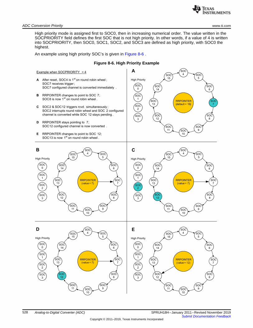
SOC
12
SOC
0
SOC
4
SOC
8
SOC
2
SOC
14
SOC
6
SOC
10
SOC
15
SOC
1
SOC
3
SOC
5
SOC7
SOC
9
SOC
11
SOC13
RRPOINTER
(value = 7)
B
Example when SOCPRIORITY = 4
A
B
C
D
E
After reset, SOC4 is 1st on round robin wheel ;
SOC7 receives trigger ;
SOC7 configured channel is converted immediately .
RRPOINTER changes to point to SOC 7;
SOC8 is now 1st on round robin wheel .
SOC2 & SOC12 triggers rcvd. simultaneously ;
SOC2 interrupts round robin wheel and SOC 2 configured
channel is converted while SOC 12 stays pending .
RRPOINTER stays pointing to 7;
SOC12 configured channel is now converted .
RRPOINTER changes to point to SOC 12;
SOC13 is now 1st on round robin wheel .
High Priority
SOC
12
SOC0
SOC
4
SOC
8
SOC2
SOC
14
SOC
6
SOC
10
SOC
15
SOC1
SOC3
SOC
5
SOC
7
SOC
9
SOC
11
SOC
13
RRPOINTER
(value = 7)
C
High Priority
SOC
12
SOC
0
SOC
4
SOC
8
SOC
2
SOC
14
SOC
6
SOC
10
SOC
15
SOC
1
SOC
3
SOC
5
SOC
7
SOC
9
SOC
11
SOC
13
RRPOINTER
(default = 16)
A
High Priority
SOC
12
SOC
0
SOC
4
SOC
8
SOC
2
SOC
14
SOC
6
SOC
10
SOC
15
SOC
1
SOC
3
SOC
5
SOC
7
SOC
9
SOC
11
SOC
13
RRPOINTER
(value = 12)
E
High Priority
SOC
12
SOC
0
SOC
4
SOC
8
SOC
2
SOC
14
SOC
6
SOC
10
SOC15
SOC
1
SOC
3
SOC
5
SOC
7
SOC
9
SOC
11
SOC
13RRPOINTER(value = 7)
D
High Priority
ADC Conversion Priority www.ti.com
528 SPRUH18H–January 2011–Revised November 2019Submit Documentation Feedback
Copyright © 2011–2019, Texas Instruments Incorporated
Analog-to-Digital Converter (ADC)
High priority mode is assigned first to SOC0, then in increasing numerical order. The value written in theSOCPRIORITY field defines the first SOC that is not high priority. In other words, if a value of 4 is writteninto SOCPRIORITY, then SOC0, SOC1, SOC2, and SOC3 are defined as high priority, with SOC0 thehighest.
An example using high priority SOC’s is given in Figure 8-6 .
Figure 8-6. High Priority Example

www.ti.com Sequential Sampling Mode
529SPRUH18H–January 2011–Revised November 2019Submit Documentation Feedback
Copyright © 2011–2019, Texas Instruments Incorporated
Analog-to-Digital Converter (ADC)
8.7 Sequential Sampling ModeThe default behavior of the ADC is to treat triggered SOCs as single conversions to be processedsequentially. Sequential sampling can convert both A-channels and B-channels without restriction onordering.
However, a by-product of supporting the Simultaneous Sampling Mode is that the sampling capacitor fromthe paired simultaneous channel will also be connected to its respective input at the same time as thedesired sequential sampling ACQPS window; the ADC will not convert the sample from the pairedchannel. (The Simultaneous Sampling Mode is described in Section 8.8, and the sampling capacitor isdenoted as Ch in Figure 8-3.)
For example, assume that SOC0 is configured to convert ADCINB3, and SOC1 is configured to convertADCINA5. If SOC0 and SOC1 are triggered together, the following sequence of simplified events wouldtake place:
1. SOC0 Sample: A-channel and B-channel sampling capacitors are connected to ADCINA3 andADCINB3 for SOC0 ACQPS window
2. SOC0 Convert: ADC converts B-channel sampling capacitor and stores result to ADCRESULT03. SOC1 Sample: A-channel and B-channel sampling capacitors are connected to ADCINA5 and
ADCINB5 for SOC1 ACQPS window4. SOC1 Convert: ADC converts A-channel sampling capacitor and stores result to ADCRESULT1
The extraneous sampling capacitor exposure should be taken into consideration for input signals that havea slow recovery or settling time. Typical examples of slow inputs are sensors with high impedance outputsand signals that are conditioned with low-pass filters.
8.8 Simultaneous Sampling ModeIn some applications it is important to keep the delay between the sampling of two signals minimal. TheADC contains dual sample and hold circuits to allow two different channels to be sampled simultaneously.Simultaneous sampling mode is configured for a pair of SOCx's with the ADCSAMPLEMODE register.The even-numbered SOCx and the following odd-numbered SOCx (SOC0 and SOC1) are coupledtogether with one enable bit (SIMULEN0, in this case). The coupling behavior is as follows:• Either SOCx’s trigger will start a pair of conversions.• The pair of channels converted will consist of the A-channel and the B-channel corresponding to the
value of the CHSEL field of the triggered SOCx. The valid values in this mode are 0-7.• Both channels will be sampled simultaneously.• The A channel will always convert first.• The even EOCx pulse will be generated based off of the A-channel conversion, the odd EOCx pulse
will be generated off of the B-channel conversion. See Section 1.6 for an explanation of the EOCxsignals.
• The result of the A-channel conversion is placed in the even ADCRESULTx register and the result ofthe B-channel conversion is written to the odd ADCRESULTx register.
For example, if the ADCSAMPLEMODE.SIMULEN0 bit is set, and SOC0 is configured as follows:
CHSEL = 2 (ADCINA2/ADCINB2 pair)
TRIGSEL = 5 (ADCTRIG5 = ePWM1.ADCSOCA)
When the ePWM1 sends out an ADCSOCA trigger, both ADCINA2 and ADCINB2 will be sampledsimultaneously (assuming priority). Immediately after, the ADCINA2 channel will be converted and itsvalue will be stored in the ADCRESULT0 register. Depending on the ADCCTL1.INTPULSEPOS setting,the EOC0 pulse will either occur when the conversion of ADCINA2 begins or completes. Then theADCINB2 channel will be converted and its value will be stored in the ADCRESULT1 register. Dependingon the ADCCTL1.INTPULSEPOS setting, the EOC1 pulse will either occur when the conversion ofADCINB2 begins or completes.

INT9
INT3INT2
ADC Sample
Generation
Logic
EO
C
INT1
0
1
15
2
ADCINT1 to PIE
Latch
Set
Clear
INTSEL1N2.INT1SEL
EOC15:EOC0
INTSEL1N2.INT1E
1
0
1
0
INTSEL1N2.INT1CONT
ADCINTFLGCLR.ADCINT1
ADCINTFLG.ADCINT1
INTOVF
EOC and Interrupt Operation www.ti.com
530 SPRUH18H–January 2011–Revised November 2019Submit Documentation Feedback
Copyright © 2011–2019, Texas Instruments Incorporated
Analog-to-Digital Converter (ADC)
Typically in an application it is expected that only the even SOCx of the pair will be used. However, it ispossible to use the odd SOCx instead, or even both. In the latter case, both SOCx triggers will start aconversion. Therefore, caution is urged as both SOCx's will store their results to the same ADCRESULTxregisters, possibly overwriting each other.
The rules of priority for the SOCx’s remain the same as in sequential sampling mode.
Section 8.14 shows the timing of simultaneous sampling mode.
8.9 EOC and Interrupt OperationJust as there are 16 independent SOCx configuration sets, there are 16 EOCx pulses. In sequentialsampling mode, the EOCx is associated directly with the SOCx. In simultaneous sampling mode, the evenand the following odd EOCx pair are associated with the even and the following odd SOCx pair, asdescribed in Section 8.8. Depending on the ADCCTL1.INTPULSEPOS setting, the EOCx pulse will occureither at the beginning of a conversion or the end. See section 1.11 for exact timings on the EOCx pulses.
The ADC contains 9 interrupts that can be flagged and/or passed on to the PIE. Each of these interruptscan be configured to accept any of the available EOCx signals as its source. The configuration of whichEOCx is the source is done in the INTSELxNy registers. Additionally, the ADCINT1 and ADCINT2 signalscan be configured to generate an SOCx trigger. This is beneficial to creating a continuous stream ofconversions.
Figure 8-7 shows a block diagram of the interrupt structure of the ADC.
Figure 8-7. Interrupt Structure
NOTE: Interrupt generation may be disrupted in non-continuous conversion mode when the interruptoverflow bit in ADCINTOVF is set.
8.10 Power-Up SequenceThe ADC resets to the ADC off state. Before writing to any of the ADC registers the ADCENCLK bit in thePCLKCR0 register must be set. For a description of the PCLKCR0 register, see the System Control andInterrupts section in this manual. When powering up the ADC, use the following sequence:1. If an external reference is desired, enable this mode using bit 3 (ADCREFSEL) in the ADCCTL1
register.2. Power up the reference, bandgap, and analog circuits together by setting bits 7-5 (ADCPWDN,

www.ti.com ADC Calibration
531SPRUH18H–January 2011–Revised November 2019Submit Documentation Feedback
Copyright © 2011–2019, Texas Instruments Incorporated
Analog-to-Digital Converter (ADC)
ADCBGPWD, ADCREFPWD) in the ADCCTL1 register.3. Enable the ADC by setting bit 14 (ADCENABLE) of the ADCCTL1 register.4. Before performing the first conversion, a delay of 1 millisecond after step 2 is required.
Alternatively, steps 1 through 3 can be performed simultaneously.
When powering down the ADC, all three bits in step 2 can be cleared simultaneously. The ADC powerlevels must be controlled via software and they are independent of the state of the device power modes.
NOTE: This type ADC requires a 1ms delay after all of the circuits are powered up. This differs fromthe previous type ADC's.
8.11 ADC CalibrationInherent in any converter is a zero offset error and a full scale gain error. The ADC is factory calibrated at30-degrees Celsius to correct both of these while allowing the user to modify the offset correction for anyapplication environmental effects, such as the ambient temperature. Except under certain emulationconditions, or unless a modification from the factory settings is desired, the user is not required to performany specific action. The ADC will be properly calibrated during the device boot process.
NOTE: If the system is reset or the ADC module is reset using Bit 15 (RESET) from the ADCControl Register 1, the Device_cal() routine must be repeated.
8.11.1 Factory Settings and Calibration FunctionDuring the fabrication and test process Texas Instruments calibrates several ADC settings along with acouple of internal oscillator settings. These settings are embedded into the TI reserved OTP memory aspart of a C-callable function named Device_cal(). Called during the startup boot procedure in the BootROM this function writes the factory settings into their respective active registers. Until this occurs, theADC and the internal oscillators will not adhere to their specified parameters. If the boot process isskipped during emulation, the user must ensure the trim settings are written to their respective registers toensure the ADC and the internal oscillators meet the specifications in the datasheet. This can be doneeither by calling this function manually or in the application itself, or by a direct write via CCS. A gelfunction for device calibration is included in CCS when the appropriate .ccxml file is created for the targetMCU.
For more information on the Device_cal() function refer to the Boot ROM section in this manual.
Texas Instruments cannot guarantee the parameters specified in the datasheet if a value other than thefactory settings contained in the TI reserved OTP memory is written into the ADC trim registers.
8.11.2 ADC Zero Offset CalibrationZero offset error is defined as the resultant digital value that occurs when converting a voltage atVREFLO. This base error affects all conversions of the ADC and together with the full scale gain andlinearity specifications, determine the DC accuracy of a converter. The zero offset error can be positive,meaning that a positive digital value is output when VREFLO is presented, or negative, meaning that avoltage higher than a one step above VREFLO still reads as a digital zero value. To correct this error, thetwo's complement of the error is written into the ADCOFFTRIM register. The value contained in thisregister will be applied before the results are available in the ADC result registers. This operation is fullycontained within the ADC core, so the timing for the results will not be affected and the full dynamic rangeof the ADC will be maintained for any trim value. Calling the Device_cal() function writes theADCOFFTRIM register with the factory calibrated offset error correction, but the user can modify theADCOFFTRIM register to compensate for additional offset error induced by the application environment.This can be done without sacrificing an ADC channel by using the VREFLOCONV bit in the ADCCTRL1register.
Use the following procedure to re-calibrate the ADC offset:1. Set ADCOFFTRIM to 80 (50h). This adds an artificial offset to account for negative offset that may

ADC Calibration www.ti.com
532 SPRUH18H–January 2011–Revised November 2019Submit Documentation Feedback
Copyright © 2011–2019, Texas Instruments Incorporated
Analog-to-Digital Converter (ADC)
reside in the ADC core.2. Set ADCCTL1.VREFLOCONV to 1. This internally connects VREFLO to input channel B5. See the
ADCCTL1 register description for more details.3. Perform multiple conversions on B5 (sample VREFLO) and take an average to account for
board noise. See Section 8.4 on how to setup and initiate the ADC to sample B5.4. Set ADCOFFTRIM to 80 (50h) minus the average obtained in step 3. This removes the artificial
offset from step 1 and creates a two's compliment of the offset error.5. Set ADCCTL1.VREFLOCONV to 0. This connects B5 back to the external ADCINB5 input pin.
NOTE: The AdcOffsetSelfCal() function located in F2806x_Adc.c in the common header filesperforms these steps.
8.11.3 ADC Full Scale Gain CalibrationGain error occurs as an incremental error as the voltage input is increased. Full scale gain error occurs atthe maximum input voltage. As in offset error, gain error can be positive or negative. A positive full scalegain error means that the full scale digital result is reached before the maximum voltage is input. Anegative full scale error implies that the full digital result will never be achieved. The calibration functionDevice_cal() writes a factory trim value to correct the ADC full scale gain error into the ADCREFTRIMregister. This register should not be modified after the Device_cal() function is called.
8.11.4 ADC Bias Current CalibrationTo further increase the accuracy of the ADC, the calibration function Device_cal() also writes a factory trimvalue to an ADC register for the ADC bias currents. This register should not be modified after theDevice_cal() function is called.
8.12 Internal/External Reference Voltage Selection
8.12.1 Internal Reference VoltageThe ADC can operate in two different reference modes, selected by the ADCCTL1.ADCREFSEL bit. Bydefault the internal bandgap is chosen to generate the reference voltage for the ADC. This will convert thevoltage presented according to a fixed scale 0 to 3.3v range. The equation governing conversions in thismode is:
Digital Value = 0 when Input ≤ 0vDigital Value = 4096 [(Input – VREFLO)/3.3v] when 0v < Input < 3.3vDigital Value = 4095, when Input ≥ 3.3v*All fractional values are truncated**VREFLO must be tied to ground in this mode. This is done internally on some devices.
8.12.2 External Reference VoltageTo convert the voltage presented as a ratiometric signal, the external VREFHI/VREFLO pins should bechosen to generate the reference voltage. In contrast with the fixed 0 to 3.3v input range of the internalbandgap mode, the ratiometric mode has an input range from VREFLO to VREFHI. Converted values willscale to this range. For instance, if VREFLO is set to 0.5v and VREFHI is 3.0v, a voltage of 1.75v will beconverted to the digital result of 2048. See the device datasheet for the allowable ranges of VREFLO andVREFHI. On some devices VREFLO is tied to ground internally, and hence limited to 0v. The equationgoverning the conversions in this mode is:

www.ti.com Internal/External Reference Voltage Selection
533SPRUH18H–January 2011–Revised November 2019Submit Documentation Feedback
Copyright © 2011–2019, Texas Instruments Incorporated
Analog-to-Digital Converter (ADC)
Digital Value = 0 when Input ≤ VREFLODigital Value = 4096 [(Input – VREFLO)/(VREFHI – VREFLO)] when VREFLO < Input < VREFHIDigital Value = 4095, when Input ≥ VREFHI*All fractional values are truncated

ADC Registers www.ti.com
534 SPRUH18H–January 2011–Revised November 2019Submit Documentation Feedback
Copyright © 2011–2019, Texas Instruments Incorporated
Analog-to-Digital Converter (ADC)
8.13 ADC RegistersThis section contains the ADC registers and bit definitions with the registers grouped by function. All of theADC registers are located in Peripheral Frame 2 except the ADCRESULTx registers, which are found inPeripheral Frame 0. See the device datasheet for specific addresses.
(1) This register is EALLOW protected.(2) The base address of the ADCRESULT registers differs from the base address of the other ADC registers. In the header files, the
ADCRESULT registers are found in the AdcResult register file, not AdcRegs.
Table 8-3. ADC Configuration and Control Registers (AdcRegs and AdcResult):
Register Name Address Offset Size(x16)
Description
ADCCTL1 0x00 1 Control 1 Register (1)
ADCCTL2 0x01 1 Control 2 Register (1)
ADCINTFLG 0x04 1 Interrupt Flag RegisterADCINTFLGCLR 0x05 1 Interrupt Flag Clear RegisterADCINTOVF 0x06 1 Interrupt Overflow RegisterADCINTOVFCLR 0x07 1 Interrupt Overflow Clear RegisterINTSEL1N2 0x08 1 Interrupt 1 and 2 Selection Register (1)
INTSEL3N4 0x09 1 Interrupt 3 and 4 Selection Register (1)
INTSEL5N6 0x0A 1 Interrupt 5 and 6 Selection Register (1)
INTSEL7N8 0x0B 1 Interrupt 7 and 8 Selection Register (1)
INTSEL9N10 0x0C 1 Interrupt 9 Selection Register (reserved Interrupt 10 Selection) (1)
SOCPRICTL 0x10 1 SOC Priority Control Register (1)
ADCSAMPLEMODE 0x12 1 Sampling Mode Register (1)
ADCINTSOCSEL1 0x14 1 Interrupt SOC Selection 1 Register (for 8 channels) (1)
ADCINTSOCSEL2 0x15 1 Interrupt SOC Selection 2 Register (for 8 channels) (1)
ADCSOCFLG1 0x18 1 SOC Flag 1 Register (for 16 channels)ADCSOCFRC1 0x1A 1 SOC Force 1 Register (for 16 channels)ADCSOCOVF1 0x1C 1 SOC Overflow 1 Register (for 16 channels)ADCSOCOVFCLR1 0x1E 1 SOC Overflow Clear 1 Register (for 16 channels)ADCSOC0CTL - ADCSOC15CTL 0x20 - 0x2F 1 SOC0 Control Register to SOC15 Control Register (1)
ADCREFTRIM 0x40 1 Reference Trim Register (1)
ADCOFFTRIM 0x41 1 Offset Trim Register (1)
COMPHYSTCTL 0x4C 1 Comp Hysteresis Control Register (1)
ADCREV – reserved 0x4F 1 Revision RegisterADCRESULT0 - ADCRESULT15 0x00 - 0x0F (2) 1 ADC Result 0 Register to ADC Result 15 Register
8.13.1 ADC Control Register 1 (ADCCTL1)
NOTE: The following ADC Control Register is EALLOW protected.
Figure 8-8. ADC Control Register 1 (ADCCTL1) (Address Offset 00h)15 14 13 12 8
RESET ADCENABLE ADCBSY ADCBSYCHNR-0/W-1 R-1 R-0 R-0
7 6 5 4 3 2 1 0ADCPWN ADCBGPWD ADCREFPWD Reserved ADCREFSEL INTPULSEPOS VREFLO
CONVTEMPCONV
R/W-0 R/W-0 R/W-0 R-0 R/W-0 R/W-0 R/W-0 R/W-0LEGEND: R/W = Read/Write; R = Read only; R-0/W-1 = always read as 0, write 1 to set; -n = value after reset

www.ti.com ADC Registers
535SPRUH18H–January 2011–Revised November 2019Submit Documentation Feedback
Copyright © 2011–2019, Texas Instruments Incorporated
Analog-to-Digital Converter (ADC)
Table 8-4. ADC Control Register 1 (ADCCTL1) Field Descriptions
Bit Field Value Description15 RESET ADC module software reset. This bit causes a master reset on the entire ADC module. All register bits
and state machines are reset to the initial state as occurs when the device reset pin is pulled low (orafter a power-on reset). This is a one-time-effect bit, meaning this bit is self-cleared immediately after itis set to 1. Read of this bit always returns a 0. Also, the reset of ADC has a latency of two clock cycles(that is, other ADC control register bits should not be modified until two clock cycles after the instructionthat resets the ADC.
0 no effect1 Resets entire ADC module (bit is then set back to 0 by ADC logic)
Note: The ADC module is reset during a system reset. If an ADC module reset is desired at any othertime, you can do so by writing a 1 to this bit. After two clock cycles, you can then write the appropriatevalues to the ADCCTL1 register bits. Assembly code:MOV ADCCTL1, #1xxxxxxxxxxxxxxxb ; Resets the ADC (RESET = 1)NOP ; Delay two cyclesNOPMOV ADCCTL1, #0xxxxxxxxxxxxxxxb ; Set to user-desired valueNote: The second MOV is not required if the default configuration is sufficient.Note: If the system is reset or the ADC module is reset using Bit 15 (RESET) from the ADC ControlRegister 1, the Device_cal() routine must be repeated .
14 ADCENABLE ADC Enable0 ADC disabled (does not power down ADC)1 ADC Enabled. Must set before an ADC conversion (recommend that it be set directly after setting ADC
power-up bits13 ADCBSY ADC Busy
Set when ADC SOC is generated, cleared per below. Used by the ADC state machine to determine ifADC is available to sample.Sequential Mode: Cleared 4 ADC clocks after negative edge of S+H pulseSimultaneous Mode: Cleared 14 ADC clocks after negative edge of S+H pulse
0 ADC is available to sample next channel1 ADC is busy and cannot sample another channel
12-8 ADCBSYCHN Set when ADC SOC for current SOC is generatedWhen ADCBSY = 0: holds the value of the last converted SOCWhen ADCBSY = 1: reflects SOC currently being processed
00h SOC0 is currently processing or was last SOC converted01h SOC1 is currently processing or was last SOC converted02h SOC2 is currently processing or was last SOC converted03h SOC3 is currently processing or was last SOC converted04h SOC4 is currently processing or was last SOC converted05h SOC5 is currently processing or was last SOC converted06h SOC6 is currently processing or was last SOC converted07h SOC7 is currently processing or was last SOC converted08h SOC8 is currently processing or was last SOC converted09h SOC9 is currently processing or was last SOC converted0Ah SOC10 is currently processing or was last SOC converted0Bh SOC11 is currently processing or was last SOC converted0Ch SOC12 is currently processing or was last SOC converted0Dh SOC13 is currently processing or was last SOC converted0Eh SOC14 is currently processing or was last SOC converted0Fh ADCINB15 is currently processing or was last SOC converted1xh Invalid value

ADC Registers www.ti.com
536 SPRUH18H–January 2011–Revised November 2019Submit Documentation Feedback
Copyright © 2011–2019, Texas Instruments Incorporated
Analog-to-Digital Converter (ADC)
Table 8-4. ADC Control Register 1 (ADCCTL1) Field Descriptions (continued)Bit Field Value Description7 ADCPWDN ADC power down (active low).
This bit controls the power up and power down of all the analog circuitry inside the analog core exceptthe bandgap and reference circuitry
0 All analog circuitry inside the core except the bandgap and reference circuitry is powered down1 The analog circuitry inside the core is powered up
6 ADCBGPWD Bandgap circuit power down (active low)0 Bandgap circuitry is powered down1 Bandgap buffer's circuitry inside core is powered up
5 ADCREFPWD Reference buffers circuit power down (active low)0 Reference buffers circuitry is powered down1 Reference buffers circuitry inside the core is powered up
4 Reserved 0 Reads return a zero; Writes have no effect.3 ADCREFSEL Internal or external reference select
0 Internal Bandgap used for reference generation1 External VREFHI or VREFLO pins used for reference generation. On some devices the VREFHI pin is
shared with ADCINA0. In this case ADCINA0 will not be available for conversions in this mode. Onsome devices the VREFLO pin is shared with VSSA. In this case the VREFLO voltage cannot be varied.
2 INTPULSEPOS INT Pulse Generation control0 INT pulse generation occurs when ADC begins conversion (neg edge of sample pulse od the sampled
signal)1 INT pulse generation occurs 1 cycle prior to ADC result latching into its result register
1 VREFLOCONV VREFLO Convert.When enabled, internally connects VREFLO to the ADC channel B5 and disconnects the ADCINB5 pinfrom the ADC. Whether the pin ADCINB5 exists on the device does not affect this function. Any externalcircuitry on the ADCINB5 pin is unaffected by this mode.
0 ADCINB5 is passed to the ADC module as normal, VREFLO connection to ADCINB5 is disabled1 VREFLO internally connected to the ADC for sampling
0 TEMPCONV Temperature sensor convert. When enabled internally connects the internal temperature sensor to ADCchannel A5 and disconnects the ADCINA5 pin from the ADC. Whether the pin ADCINA5 exists on thedevice does not affect this function. Any external circuitry on the ADCINA5 pin is unaffected by thismode
0 ADCINA5 is passed to the ADC module as normal, internal temperature sensor connection to ADCINA5is disabled.
1 Temperature sensor is internally connected to the ADC for sampling
8.13.2 ADC Control Register 2 (ADCCTL2)
NOTE: The following ADC Control Register is EALLOW protected.
Figure 8-9. ADC Control Register 2 (ADCCTL2) (Address Offset 01h)15 3 2 1 0
Reserved CLKDIV4EN ADCNONOVERLAP CLKDIV2ENR-0 R/W-0 R/W-0 R/W-0
LEGEND: R/W = Read/Write; R = Read only; -n = value after reset

www.ti.com ADC Registers
537SPRUH18H–January 2011–Revised November 2019Submit Documentation Feedback
Copyright © 2011–2019, Texas Instruments Incorporated
Analog-to-Digital Converter (ADC)
Table 8-5. ADC Control Register 2 (ADCCTL2) Field Descriptions
Bit Field Value Description15-3 Reserved 0 Reads return a zero; writes have no effect.
2 CLKDIV4EN ADC Clock Prescaler. Used in conjunction with CLKDIV2EN to divide ADCCLKfrom SYSCLK. See usage note below for details.
0 ADCCLK = SYSCLK or SYSCLK / 21 ADCCLK = SYSCLK or SYSCLK / 4
1 ADCNONOVERLAP ADCNONOVERLAP control bit0 Overlap of sample and conversion is allowed1 Overlap of sample is not allowed
0 CLKDIV2EN ADC Clock Prescaler. Used in conjunction with CLKDIV4EN to divide ADCCLKfrom SYSCLK. See usage note below for details.
0 ADCCLK = SYSCLK1 ADCCLK = SYSCLK / 2 or SYSCLK / 4
CLKDIV2EN and CLKDIV4EN usage note:
CLKDIV2EN CLKDIV4EN ADCCLK0 0 SYSCLK0 1 SYSCLK1 0 SYSCLK / 21 1 SYSCLK / 4
8.13.3 ADC Interrupt Registers
Figure 8-10. ADC Interrupt Flag Register (ADCINTFLG) (Address Offset 04h)15 9 8
Reserved ADCINT9R-0 R-0
7 6 5 4 3 2 1 0ADCINT8 ADCINT7 ADCINT6 ADCINT5 ADCINT4 ADCINT3 ADCINT2 ADCINT1
R-0 R-0 R-0 R-0 R-0 R-0 R-0 R-0LEGEND: R/W = Read/Write; R = Read only; -n = value after reset
Table 8-6. ADC Interrupt Flag Register (ADCINTFLG) Field Descriptions
Bit Field Value Description15-9 Reserved 0 Reads return a zero; Writes have no effect.8-0 ADCINTx
(x = 9 to 1)ADC Interrupt Flag Bits: Reading this bit indicates if an ADCINT pulse was generated
0 No ADC interrupt pulse generated1 ADC Interrupt pulse generated
If the ADC interrupt is placed in continuous mode (INTSELxNy register) then further interrupt pulsesare generated whenever a selected EOC event occurs even if the flag bit is set.If the continuous mode is not enabled, then no further interrupt pulses are generated until the userclears this flag bit using the ADCINTFLGCLR register. The ADCINTOVF flag will be set if EOCevents are generated while the ADCINTFLG flag is set. Both ADCINTFLG and ADCINTOVF flagsmust be cleared before normal interrupt operation can resume in non-continuous mode.

ADC Registers www.ti.com
538 SPRUH18H–January 2011–Revised November 2019Submit Documentation Feedback
Copyright © 2011–2019, Texas Instruments Incorporated
Analog-to-Digital Converter (ADC)
Figure 8-11. ADC Interrupt Flag Clear Register (ADCINTFLGCLR) (Address Offset 05h)15 9 8
Reserved ADCINT9R-0 R/W-0
7 6 5 4 3 2 1 0ADCINT8 ADCINT7 ADCINT6 ADCINT5 ADCINT4 ADCINT3 ADCINT2 ADCINT1
R/W-0 R/W-0 R/W-0 R/W-0 R/W-0 R/W-0 R/W-0 R/W-0LEGEND: R/W = Read/Write; R = Read only; -n = value after reset
Table 8-7. ADC Interrupt Flag Clear Register (ADCINTFLGCLR) Field Descriptions
Bit Field Value Description15-9 Reserved 0 Reads return a zero; Writes have no effect.8-0 ADCINTx
(x = 9 to 1)ADC interrupt Flag Clear Bit
0 No action.1 Clears respective flag bit in the ADCINTFLG register.
Boundary condition for clearing or setting flag bits: If hardware tries to set a flag bit whilesoftware tries to clear the flag bit in the same cycle, the following will take place:1. SW has priority, and will clear the flag2. HW set will be discarded, no signal will propagate to the PIE form the latch3. Overflow flag or condition will be generated
Figure 8-12. ADC Interrupt Overflow Register (ADCINTOVF) (Address Offset 06h)15 9 8
Reserved ADCINT9R-0 R-0
7 6 5 4 3 2 1 0ADCINT8 ADCINT7 ADCINT6 ADCINT5 ADCINT4 ADCINT3 ADCINT2 ADCINT1
R-0 R-0 R-0 R-0 R-0 R-0 R-0 R-0LEGEND: R/W = Read/Write; R = Read only; -n = value after reset
Table 8-8. ADC Interrupt Overflow Register (ADCINTOVF) Field Descriptions
Bit Field Value Description15-9 Reserved 0 Reserved8-0 ADCINTx
(x = 9 to 1)ADC Interrupt Overflow Bits.Indicates if an overflow occurred when generating ADCINT pulses. If the respective ADCINTFLG bitis set and a selected additional EOC trigger is generated, then an overflow condition occurs.
0 No ADC interrupt overflow event detected.1 ADC Interrupt overflow event detected.
The overflow bit does not care about the continuous mode bit state. An overflow condition isgenerated irrespective of this mode selection. Both ADCINTFLG and ADCINTOVF flags must becleared before normal interrupt operation can resume in non-continuous mode.
Figure 8-13. ADC Interrupt Overflow Clear Register (ADCINTOVFCLR) (Address Offset 07h)15 9 8
Reserved ADCINT9R-0 R-0/W-1
7 6 5 4 3 2 1 0ADCINT8 ADCINT7 ADCINT6 ADCINT5 ADCINT4 ADCINT3 ADCINT2 ADCINT1R-0/W-1 R-0/W-1 R-0/W-1 R-0/W-1 R-0/W-1 R-0/W-1 R-0/W-1 R-0/W-1
LEGEND: R/W = Read/Write; R = Read only; R-0/W-1 =always read 0, write 1 to set; -n = value after reset

www.ti.com ADC Registers
539SPRUH18H–January 2011–Revised November 2019Submit Documentation Feedback
Copyright © 2011–2019, Texas Instruments Incorporated
Analog-to-Digital Converter (ADC)
Table 8-9. ADC Interrupt Overflow Clear Register (ADCINTOVFCLR) Field Descriptions
Bit Field Value Description15-9 Reserved 0 Reads return a zero; Writes have no effect.8-0 ADCINTx
(x = 9 to 1)ADC Interrupt Overflow Clear Bits.
0 No action.1 Clears the respective overflow bit in the ADCINTOVF register. If software tries to set this bit on the
same clock cycle that hardware tries to set the overflow bit in the ADCINTOVF register, thenhardware has priority and the ADCINTOVF bit will be set.
NOTE: The following Interrupt Select Registers are EALLOW protected.
Figure 8-14. Interrupt Select 1 And 2 Register (INTSEL1N2) (Address Offset 08h)15 14 13 12 8
Reserved INT2CONT INT2E INT2SELR-0 R/W-0 R/W-0 R/W-0
7 6 5 4 0Reserved INT1CONT INT1E INT1SEL
R-0 R/W-0 R/W-0 R/W-0LEGEND: R/W = Read/Write; R = Read only; -n = value after reset
Figure 8-15. Interrupt Select 3 And 4 Register (INTSEL3N4) (Address Offset 09h)15 14 13 12 8
Reserved INT4CONT INT4E INT4SELR-0 R/W-0 R/W-0 R/W-0
7 6 5 4 0Reserved INT3CONT INT3E INT3SEL
R-0 R/W-0 R/W-0 R/W-0LEGEND: R/W = Read/Write; R = Read only; -n = value after reset
Figure 8-16. Interrupt Select 5 And 6 Register (INTSEL5N6) (Address Offset 0Ah)15 14 13 12 8
Reserved INT6CONT INT6E INT6SELR-0 R/W-0 R/W-0 R/W-0
7 6 5 4 0Reserved INT5CONT INT5E INT5SEL
R-0 R/W-0 R/W-0 R/W-0LEGEND: R/W = Read/Write; R = Read only; -n = value after reset
Figure 8-17. Interrupt Select 7 And 8 Register (INTSEL7N8) (Address Offset 0Bh)15 14 13 12 8
Reserved INT8CONT INT8E INT8SELR-0 R/W-0 R/W-0 R/W-0
7 6 5 4 0Reserved INT7CONT INT7E INT7SEL
R-0 R/W-0 R/W-0 R/W-0LEGEND: R/W = Read/Write; R = Read only; -n = value after reset

ADC Registers www.ti.com
540 SPRUH18H–January 2011–Revised November 2019Submit Documentation Feedback
Copyright © 2011–2019, Texas Instruments Incorporated
Analog-to-Digital Converter (ADC)
Figure 8-18. Interrupt Select 9 And 10 Register (INTSEL9N10) (Address Offset 0Ch)15 8
ReservedR-0
7 6 5 4 0Reserved INT9CONT INT9E INT9SEL
R-0 R/W-0 R/W-0 R/W-0LEGEND: R/W = Read/Write; R = Read only; -n = value after reset
Table 8-10. INTSELxNy Register Field Descriptions
Bit Field Value Description15 Reserved 0 Reserved14 INTyCONT ADCINTy Continuous Mode Enable
0 No further ADCINTy pulses are generated until ADCINTy flag (in ADCINTFLG register)is cleared by user.
1 ADCINTy pulses are generated whenever an EOC pulse is generated irrespective if theflag bit is cleared or not.
13 INTyE ADCINTy Interrupt Enable0 ADCINTy is disabled.1 ADCINTy is enabled.
12-8 INTySEL ADCINTy EOC Source Select00h EOC0 is trigger for ADCINTy01h EOC1 is trigger for ADCINTy02h EOC2 is trigger for ADCINTy03h EOC3 is trigger for ADCINTy04h EOC4 is trigger for ADCINTy05h EOC5 is trigger for ADCINTy06h EOC6 is trigger for ADCINTy07h EOC7 is trigger for ADCINTy08h EOC8 is trigger for ADCINTy09h EOC9 is trigger for ADCINTy0Ah EOC10 is trigger for ADCINTy0Bh EOC11 is trigger for ADCINTy0Ch EOC12 is trigger for ADCINTy0Dh EOC13 is trigger for ADCINTy0Eh EOC14 is trigger for ADCINTy0Fh EOC15 is trigger for ADCINTy1xh Invalid value.
7 Reserved 0 Reads return a zero; Writes have no effect.6 INTxCONT ADCINTx Continuous Mode Enable.
0 No further ADCINTx pulses are generated until ADCINTx flag (in ADCINTFLG register)is cleared by user.
1 ADCINTx pulses are generated whenever an EOC pulse is generated irrespective if theflag bit is cleared or not.
5 INTxE ADCINTx Interrupt Enable0 ADCINTx is disabled.1 ADCINTx is enabled .

www.ti.com ADC Registers
541SPRUH18H–January 2011–Revised November 2019Submit Documentation Feedback
Copyright © 2011–2019, Texas Instruments Incorporated
Analog-to-Digital Converter (ADC)
Table 8-10. INTSELxNy Register Field Descriptions (continued)Bit Field Value Description4-0 INTxSEL ADCINTx EOC Source Select
00h EOC0 is trigger for ADCINTx01h EOC1 is trigger for ADCINTx02h EOC2 is trigger for IADCNTx03h EOC3 is trigger for ADCINTx04h EOC4 is trigger for ADCINTx05h EOC5 is trigger for ADCINTx06h EOC6 is trigger for ADCINTx07h EOC7 is trigger for ADCINTx08h EOC8 is trigger for ADCINTx09h EOC9 is trigger for ADCINTx0Ah EOC10 is trigger for ADCINTx0Bh EOC11 is trigger for ADCINTx0Ch EOC12 is trigger for ADCINTx.0Dh EOC13 is trigger for ADCINTx0Eh EOC14 is trigger for ADCINTx0Fh EOC15 is trigger for ADCINTx1xh Invalid value.
8.13.4 ADC Priority Register
NOTE: The following SOC Priority Control Register is EALLOW protected.
Figure 8-19. ADC Start of Conversion Priority Control Register (SOCPRICTL)15 14 11 10 5 4 0
ONESHOT Reserved RRPOINTER SOCPRIORITYR/W-0 R-0 R-20h R/W-0
LEGEND: R/W = Read/Write; R = Read only; -n = value after reset
Table 8-11. SOCPRICTL Register Field Descriptions
Bit Field Value Description15 ONESHOT 0 One shot mode disabled
1 One shot mode enabled14-11 Reserved Reads return a zero; Writes have no effect.

ADC Registers www.ti.com
542 SPRUH18H–January 2011–Revised November 2019Submit Documentation Feedback
Copyright © 2011–2019, Texas Instruments Incorporated
Analog-to-Digital Converter (ADC)
Table 8-11. SOCPRICTL Register Field Descriptions (continued)Bit Field Value Description
10-5 RRPOINTER Round Robin Pointer. Holds the value of the last converted round robin SOCx to be used by theround robin scheme to determine order of conversions.
00h SOC0 was last round robin SOC to convert. SOC1 is highest round robin priority.01h SOC1 was last round robin SOC to convert. SOC2 is highest round robin priority.02h SOC2 was last round robin SOC to convert. SOC3 is highest round robin priority.03h SOC3 was last round robin SOC to convert. SOC4 is highest round robin priority.04h SOC4 was last round robin SOC to convert. SOC5 is highest round robin priority.05h SOC5 was last round robin SOC to convert. SOC6 is highest round robin priority.06h SOC6 was last round robin SOC to convert. SOC7 is highest round robin priority.07h SOC7 was last round robin SOC to convert. SOC8 is highest round robin priority.08h SOC8 was last round robin SOC to convert. SOC9 is highest round robin priority.09h SOC9 was last round robin SOC to convert. SOC10 is highest round robin priority.0Ah SOC10 was last round robin SOC to convert. SOC11 is highest round robin priority.0Bh SOC11 was last round robin SOC to convert. SOC12 is highest round robin priority.0Ch SOC12 was last round robin SOC to convert. SOC13 is highest round robin priority.0Dh SOC13 was last round robin SOC to convert. SOC14 is highest round robin priority.0Eh SOC14 was last round robin SOC to convert. SOC15 is highest round robin priority.0Fh SOC15 was last round robin SOC to convert. SOC0 is highest round robin priority.1xh Invalid value20h Reset value to indicate no SOC has been converted. SOC0 is highest round robin priority. Set to
this value when the device is reset, when the ADCCTL1.RESET bit is set, or when the SOCPRICTLregister is written. In the latter case, if a conversion is currently in progress, it will complete andthen the new priority will take effect.
Others Invalid selection.4-0 SOCPRIORITY SOC Priority.
Determines the cutoff point for priority mode and round robin arbitration for SOCx00h SOC priority is handled in round robin mode for all channels.01h SOC0 is high priority, rest of channels are in round robin mode.02h SOC0-SOC1 are high priority, SOC2-SOC15 are in round robin mode.03h SOC0-SOC2 are high priority, SOC3-SOC15 are in round robin mode.04h SOC0-SOC3 are high priority, SOC4-SOC15 are in round robin mode.05h SOC0-SOC4 are high priority, SOC5-SOC15 are in round robin mode.06h SOC0-SOC5 are high priority, SOC6-SOC15 are in round robin mode.07h SOC0-SOC6 are high priority, SOC7-SOC15 are in round robin mode.08h SOC0-SOC7 are high priority, SOC8-SOC15 are in round robin mode.09h SOC0-SOC8 are high priority, SOC9-SOC15 are in round robin mode.0Ah SOC0-SOC9 are high priority, SOC10-SOC15 are in round robin mode.0Bh SOC0-SOC10 are high priority, SOC11-SOC15 are in round robin mode.0Ch SOC0-SOC11 are high priority, SOC12-SOC15 are in round robin mode.0Dh SOC0-SOC12 are high priority, SOC13-SOC15 are in round robin mode.0Eh SOC0-SOC13 are high priority, SOC14-SOC15 are in round robin mode.0Fh SOC0-SOC14 are high priority, SOC15 is in round robin mode.10h All SOCs are in high priority mode, arbitrated by SOC number
Others Invalid selection.

www.ti.com ADC Registers
543SPRUH18H–January 2011–Revised November 2019Submit Documentation Feedback
Copyright © 2011–2019, Texas Instruments Incorporated
Analog-to-Digital Converter (ADC)
8.13.5 ADC SOC Registers
NOTE: The following ADC Sample Mode Register is EALLOW protected.
Figure 8-20. ADC Sample Mode Register (ADCSAMPLEMODE) (Address Offset 12h)15 8
ReservedR-0
7 6 5 4 3 2 1 0SIMULEN14 SIMULEN12 SIMULEN10 SIMULEN8 SIMULEN6 SIMULEN4 SIMULEN2 SIMULEN0
R/W-0 R/W-0 R/W-0 R/W-0 R/W-0 R/W-0 R/W-0 R/W-0LEGEND: R/W = Read/Write; R = Read only; -n = value after reset
Table 8-12. ADC Sample Mode Register (ADCSAMPLEMODE) Field Descriptions
Bit Field Value Description15:8 Reserved 0 Reserved
7 SIMULEN14 Simultaneous sampling enable for SOC14/SOC15. Couples SOC14 and SOC15 in simultaneoussampling mode. See section 1.5 for details. This bit should not be set when the ADC is activelyconverting SOC14 or SOC15.
0 Single sample mode set for SOC14 and SOC15. All bits of CHSEL field define channel to beconverted. EOC14 associated with SOC14. EOC15 associated with SOC15. SOC14’s result placedin ADCRESULT14 register. SOC15’s result placed in ADCRESULT15.
1 Simultaneous sample for SOC14 and SOC15. Lowest three bits of CHSEL field define the pair ofchannels to be converted. EOC14 and EOC15 associated with SOC14 and SOC15 pair. SOC14’sand SOC15’s results will be placed in ADCRESULT14 and ADCRESULT15 registers, respectively.
6 SIMULEN12 Simultaneous sampling enable for SOC12/SOC13. Couples SOC12 and SOC13 in simultaneoussampling mode. See section 1.5 for details. This bit should not be set when the ADC is activelyconverting SOC12 or SOC13.
0 Single sample mode set for SOC12 and SOC13. All bits of CHSEL field define channel to beconverted. EOC12 associated with SOC12. EOC13 associated with SOC13. SOC12’s result placedin ADCRESULT12 register. SOC13’s result placed in ADCRESULT13.
1 Simultaneous sample for SOC12 and SOC13. Lowest three bits of CHSEL field define the pair ofchannels to be converted. EOC12 and EOC13 associated with SOC12 and SOC13 pair. SOC12’sand SOC13’s results will be placed in ADCRESULT12 and ADCRESULT13 registers, respectively.
5 SIMULEN10 Simultaneous sampling enable for SOC10/SOC11. Couples SOC10 and SOC11 in simultaneoussampling mode. See section 1.5 for details. This bit should not be set when the ADC is activelyconverting SOC10 or SOC11.
0 Single sample mode set for SOC10 and SOC11. All bits of CHSEL field define channel to beconverted. EOC10 associated with SOC10. EOC11 associated with SOC11. SOC10’s result placedin ADCRESULT10 register. SOC11’s result placed in ADCRESULT11.
1 Simultaneous sample for SOC10 and SOC11. Lowest three bits of CHSEL field define the pair ofchannels to be converted. EOC10 and EOC11 associated with SOC10 and SOC11 pair. SOC10’sand SOC11’s results will be placed in ADCRESULT10 and ADCRESULT11 registers, respectively.
4 SIMULEN8 Simultaneous sampling enable for SOC8/SOC9. Couples SOC8 and SOC9 in simultaneoussampling mode. See section 1.5 for details. This bit should not be set when the ADC is activelyconverting SOC8 or SOC9.
0 Single sample mode set for SOC8 and SOC9. All bits of CHSEL field define channel to beconverted. EOC8 associated with SOC8. EOC9 associated with SOC9. SOC8’s result placed inADCRESULT8 register. SOC9’s result placed in ADCRESULT9.
1 Simultaneous sample for SOC8 and SOC9. Lowest three bits of CHSEL field define the pair ofchannels to be converted. EOC8 and EOC9 associated with SOC8 and SOC9 pair. SOC8’s andSOC9’s results will be placed in ADCRESULT8 and ADCRESULT9 registers, respectively.

ADC Registers www.ti.com
544 SPRUH18H–January 2011–Revised November 2019Submit Documentation Feedback
Copyright © 2011–2019, Texas Instruments Incorporated
Analog-to-Digital Converter (ADC)
Table 8-12. ADC Sample Mode Register (ADCSAMPLEMODE) Field Descriptions (continued)Bit Field Value Description3 SIMULEN6 Simultaneous sampling enable for SOC6/SOC7. Couples SOC6 and SOC7 in simultaneous
sampling mode. See section 1.5 for details. This bit should not be set when the ADC is activelyconverting SOC6 or SOC7.
0 Single sample mode set for SOC6 and SOC7. All bits of CHSEL field define channel to beconverted. EOC6 associated with SOC6. EOC7 associated with SOC7. SOC6’s result placed inADCRESULT6 register. SOC7’s result placed in ADCRESULT7.
1 Simultaneous sample for SOC6 and SOC7. Lowest three bits of CHSEL field define the pair ofchannels to be converted. EOC6 and EOC7 associated with SOC6 and SOC7 pair. SOC6’s andSOC7’s results will be placed in ADCRESULT6 and ADCRESULT7 registers, respectively.
2 SIMULEN4 Simultaneous sampling enable for SOC4/SOC5. Couples SOC4 and SOC5 in simultaneoussampling mode. See section 1.5 for details. This bit should not be set when the ADC is activelyconverting SOC4 or SOC5.
0 Single sample mode set for SOC4 and SOC5. All bits of CHSEL field define channel to beconverted. EOC4 associated with SOC4. EOC5 associated with SOC5. SOC4’s result placed inADCRESULT4 register. SOC5’s result placed in ADCRESULT5.
1 Simultaneous sample for SOC4 and SOC5. Lowest three bits of CHSEL field define the pair ofchannels to be converted. EOC4 and EOC5 associated with SOC4 and SOC5 pair. SOC4’s andSOC5’s results will be placed in ADCRESULT4 and ADCRESULT5 registers, respectively.
1 SIMULEN2 Simultaneous sampling enable for SOC2/SOC3. Couples SOC2 and SOC3 in simultaneoussampling mode. See section 1.5 for details. This bit should not be set when the ADC is activelyconverting SOC2 or SOC3.
0 Single sample mode set for SOC2 and SOC3. All bits of CHSEL field define channel to beconverted. EOC2 associated with SOC2. EOC3 associated with SOC3. SOC2’s result placed inADCRESULT2 register. SOC3’s result placed in ADCRESULT3.
1 Simultaneous sample for SOC2 and SOC3. Lowest three bits of CHSEL field define the pair ofchannels to be converted. EOC2 and EOC3 associated with SOC2 and SOC3 pair. SOC2’s andSOC3’s results will be placed in ADCRESULT2 and ADCRESULT3 registers, respectively.
0 SIMULEN0 Simultaneous sampling enable for SOC0/SOC1. Couples SOC0 and SOC1 in simultaneoussampling mode. See section 1.5 for details. This bit should not be set when the ADC is activelyconverting SOC0 or SOC1.
0 Single sample mode set for SOC0 and SOC1. All bits of CHSEL field define channel to beconverted. EOC0 associated with SOC0. EOC1 associated with SOC1. SOC0’s result placed inADCRESULT0 register. SOC1’s result placed in ADCRESULT1.
1 Simultaneous sample for SOC0 and SOC1. Lowest three bits of CHSEL field define the pair ofchannels to be converted. EOC0 and EOC1 associated with SOC0 and SOC1 pair. SOC0’s andSOC1’s results will be placed in ADCRESULT0 and ADCRESULT1 registers, respectively.
NOTE: The following ADC Interrupt SOC Select Registers are EALLOW protected.
Figure 8-21. ADC Interrupt Trigger SOC Select 1 Register (ADCINTSOCSEL1) (Address Offset 14h)15 14 13 12 11 10 9 8 7 6 5 4 3 2 1 0
SOC7 SOC6 SOC5 SOC4 SOC3 SOC2 SOC1 SOC0R/W-0 R/W-0 R/W-0 R/W-0 R/W-0 R/W-0 R/W-0 R/W-0
LEGEND: R/W = Read/Write; R = Read only; -n = value after reset
Table 8-13. ADC Interrupt Trigger SOC Select 1 Register (ADCINTSOCSEL1) Register FieldDescriptions
Bit Field Value Description15--0 SOCx
(x = 7 to 0)SOCx ADC Interrupt Trigger Select. Select ADCINT to trigger SOCx. The ADCINT trigger is OR'edwith the trigger selected by the TRIGSEL field in the ADCSOCxCTL register, as well as thesoftware force trigger signal from the ADCSOCFRC1 register.
00 No ADCINT will trigger SOCx.01 ADCINT1 will trigger SOCx.10 ADCINT2 will trigger SOCx.11 Invalid selection.

www.ti.com ADC Registers
545SPRUH18H–January 2011–Revised November 2019Submit Documentation Feedback
Copyright © 2011–2019, Texas Instruments Incorporated
Analog-to-Digital Converter (ADC)
Figure 8-22. ADC Interrupt Trigger SOC Select 2 Register (ADCINTSOCSEL2) (Address Offset 15h)15 14 13 12 11 10 9 8 7 6 5 4 3 2 1 0
SOC15 SOC14 SOC13 SOC12 SOC11 SOC10 SOC9 SOC8R/W-0 R/W-0 R/W-0 R/W-0 R/W-0 R/W-0 R/W-0 R/W-0
LEGEND: R/W = Read/Write; R = Read only; -n = value after reset
Table 8-14. ADC Interrupt Trigger SOC Select 2 Register (ADCINTSOCSEL2) Field Descriptions
Bit Field Value Description15-0 SOCx
(x = 15 to 8)SOCx ADC Interrupt Trigger Select. Select ADCINT to trigger SOCx. The ADCINT trigger is OR'edwith the trigger selected by the TRIGSEL field in the ADCSOCxCTL register, as well as thesoftware force trigger signal from the ADCSOCFRC1 register.
00 No ADCINT will trigger SOCx.01 ADCINT1 will trigger SOCx.10 ADCINT2 will trigger SOCx.11 Invalid selection.
Figure 8-23. ADC SOC Flag 1 Register (ADCSOCFLG1) (Address Offset 18h)15 14 13 12 11 10 9 8
SOC15 SOC14 SOC13 SOC12 SOC11 SOC10 SOC9 SOC8R-0 R-0 R-0 R-0 R-0 R-0 R-0 R-0
7 6 5 4 3 2 1 0SOC7 SOC6 SOC5 SOC4 SOC3 SOC2 SOC1 SOC0R-0 R-0 R-0 R-0 R-0 R-0 R-0 R-0
LEGEND: R/W = Read/Write; R = Read only; -n = value after reset
Table 8-15. ADC SOC Flag 1 Register (ADCSOCFLG1) Field Descriptions
Bit Field Value Description15-0 SOCx
(x = 15 to 0)SOCx Start of Conversion Flag. Indicates the state of individual SOC conversions.
0 No sample pending for SOCx.1 Trigger has been received and sample is pending for SOCx.
The bit will be automatically cleared when the respective SOCx conversion is started. If contentionexists where this bit receives both a request to set and a request to clear on the same cycle,regardless of the source of either, this bit will be set and the request to clear will be ignored. In thiscase the overflow bit in the ADCSOCOVF1 register will not be affected regardless of whether thisbit was previously set or not.
Figure 8-24. ADC SOC Force 1 Register (ADCSOCFRC1) (Address Offset 1Ah)15 14 13 12 11 10 9 8
SOC15 SOC14 SOC13 SOC12 SOC11 SOC10 SOC9 SOC8R/W-0 R/W-0 R/W-0 R/W-0 R/W-0 R/W-0 R/W-0 R/W-0
7 6 5 4 3 2 1 0SOC7 SOC6 SOC5 SOC4 SOC3 SOC2 SOC1 SOC0R/W-0 R/W-0 R/W-0 R/W-0 R/W-0 R/W-0 R/W-0 R/W-0
LEGEND: R/W = Read/Write; R = Read only; -n = value after reset

ADC Registers www.ti.com
546 SPRUH18H–January 2011–Revised November 2019Submit Documentation Feedback
Copyright © 2011–2019, Texas Instruments Incorporated
Analog-to-Digital Converter (ADC)
Table 8-16. ADC SOC Force 1 Register (ADCSOCFRC1) Field Descriptions
Bit Field Value Description15-0 SOCx
(x = 15 to 0)SOCx Force Start of Conversion Flag. Writing a 1 will force to 1 the respective SOCx flag bit in theADCSOCFLG1 register. This can be used to initiate a software initiated conversion. Writes of 0 areignored.
0 No action.1 Force SOCx flag bit to 1. This will cause a conversion to start once priority is given to SOCx.
If software tries to set this bit on the same clock cycle that hardware tries to clear the SOCx bit inthe ADCSOCFLG1 register, then software has priority and the ADCSOCFLG1 bit will be set. In thiscase the overflow bit in the ADCSOCOVF1 register will not be affected regardless of whether theADCSOCFLG1 bit was previously set or not.
Figure 8-25. ADC SOC Overflow 1 Register (ADCSOCOVF1) (Address Offset 1Ch)15 14 13 12 11 10 9 8
SOC15 SOC14 SOC13 SOC12 SOC11 SOC10 SOC9 SOC8R-0 R-0 R-0 R-0 R-0 R-0 R-0 R-0
7 6 5 4 3 2 1 0SOC7 SOC6 SOC5 SOC4 SOC3 SOC2 SOC1 SOC0R-0 R-0 R-0 R-0 R-0 R-0 R-0 R-0
LEGEND: R/W = Read/Write; R = Read only; -n = value after reset
Table 8-17. ADC SOC Overflow 1 Register (ADCSOCOVF1) Field Descriptions
Bit Field Value Description15-0 SOCx
(x = 15 to 0)SOCx Start of Conversion Overflow Flag. Indicates an SOCx event was generated while an existingSOCx event was already pending.
0 No SOCx event overflow1 SOCx event overflow
An overflow condition does not stop SOCx events from being processed. It simply is an indicationthat a trigger was missed.
Figure 8-26. ADC SOC Overflow Clear 1 Register (ADCSOCOVFCLR1) (Address Offset 1Eh)15 14 13 12 11 10 9 8
SOC15 SOC14 SOC13 SOC12 SOC11 SOC10 SOC9 SOC8R/W-0 R/W-0 R/W-0 R/W-0 R/W-0 R/W-0 R/W-0 R/W-0
7 6 5 4 3 2 1 0SOC7 SOC6 SOC5 SOC4 SOC3 SOC2 SOC1 SOC0R/W-0 R/W-0 R/W-0 R/W-0 R/W-0 R/W-0 R/W-0 R/W-0
LEGEND: R/W = Read/Write; R = Read only; -n = value after reset
Table 8-18. ADC SOC Overflow Clear 1 Register (ADCSOCOVFCLR1) Field Descriptions
Bit Field Value Description15-0 SOCx
(x = 15 to 0)SOCx Clear Start of Conversion Overflow Flag. Writing a 1 will clear the respective SOCx overflowflag in the ADCSOCOVF1 register. Writes of 0 are ignored.
0 No action.1 Clear SOCx overflow flag.
If software tries to set this bit on the same clock cycle that hardware tries to set the overflow bit inthe ADCSOCOVF1 register, then hardware has priority and the ADCSOCOVF1 bit will be set.
NOTE: The following ADC SOC0 - SOC15 Control Registers are EALLOW protected.
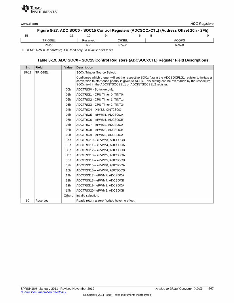
www.ti.com ADC Registers
547SPRUH18H–January 2011–Revised November 2019Submit Documentation Feedback
Copyright © 2011–2019, Texas Instruments Incorporated
Analog-to-Digital Converter (ADC)
Figure 8-27. ADC SOC0 - SOC15 Control Registers (ADCSOCxCTL) (Address Offset 20h - 2Fh)15 11 10 9 6 5 0
TRIGSEL Reserved CHSEL ACQPSR/W-0 R-0 R/W-0 R/W-0
LEGEND: R/W = Read/Write; R = Read only; -n = value after reset
Table 8-19. ADC SOC0 - SOC15 Control Registers (ADCSOCxCTL) Register Field Descriptions
Bit Field Value Description15-11 TRIGSEL SOCx Trigger Source Select.
Configures which trigger will set the respective SOCx flag in the ADCSOCFLG1 register to initiate aconversion to start once priority is given to SOCx. This setting can be overridden by the respectiveSOCx field in the ADCINTSOCSEL1 or ADCINTSOCSEL2 register.
00h ADCTRIG0 - Software only.01h ADCTRIG1 - CPU Timer 0, TINT0n02h ADCTRIG2 - CPU Timer 1, TINT1n03h ADCTRIG3 - CPU Timer 2, TINT2n04h ADCTRIG4 – XINT2, XINT2SOC05h ADCTRIG5 – ePWM1, ADCSOCA06h ADCTRIG6 – ePWM1, ADCSOCB07h ADCTRIG7 – ePWM2, ADCSOCA08h ADCTRIG8 – ePWM2, ADCSOCB09h ADCTRIG9 – ePWM3, ADCSOCA0Ah ADCTRIG10 – ePWM3, ADCSOCB0Bh ADCTRIG11 – ePWM4, ADCSOCA0Ch ADCTRIG12 – ePWM4, ADCSOCB0Dh ADCTRIG13 – ePWM5, ADCSOCA0Eh ADCTRIG14 – ePWM5, ADCSOCB0Fh ADCTRIG15 – ePWM6, ADCSOCA10h ADCTRIG16 – ePWM6, ADCSOCB11h ADCTRIG17 - ePWM7, ADCSOCA12h ADCTRIG18 - ePWM7, ADCSOCB13h ADCTRIG19 - ePWM8, ADCSOCA14h ADCTRIG20 - ePWM8, ADCSOCB
Others Invalid selection.10 Reserved Reads return a zero; Writes have no effect.

ADC Registers www.ti.com
548 SPRUH18H–January 2011–Revised November 2019Submit Documentation Feedback
Copyright © 2011–2019, Texas Instruments Incorporated
Analog-to-Digital Converter (ADC)
Table 8-19. ADC SOC0 - SOC15 Control Registers (ADCSOCxCTL) Register FieldDescriptions (continued)
Bit Field Value Description9-6 CHSEL SOCx Channel Select. Selects the channel to be converted when SOCx is received by the ADC.
Sequential Sampling Mode (SIMULENx = 0):0h ADCINA01h ADCINA12h ADCINA23h ADCINA34h ADCINA45h ADCINA56h ADCINA67h ADCINA78h ADCINB09h ADCINB1Ah ADCINB2Bh ADCINB3Ch ADCINB4Dh ADCINB5Eh ADCINB6Fh ADCINB7
Simultaneous Sampling Mode (SIMULENx = 1):0h ADCINA0/ADCINB0 pair1h ADCINA1/ADCINB1 pair2h ADCINA2/ADCINB2 pair3h ADCINA3/ADCINB3 pair4h ADCINA4/ADCINB4 pair5h ADCINA5/ADCINB5 pair6h ADCINA6/ADCINB6 pair7h ADCINA7/ADCINB7 pair8h Invalid selection.9h Invalid selection.Ah Invalid selection.Bh Invalid selection.Ch Invalid selection.Dh Invalid selection.Eh Invalid selection.Fh Invalid selection.
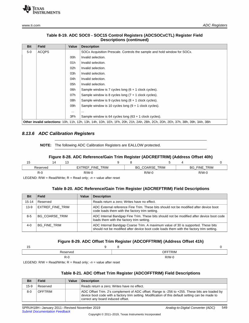
www.ti.com ADC Registers
549SPRUH18H–January 2011–Revised November 2019Submit Documentation Feedback
Copyright © 2011–2019, Texas Instruments Incorporated
Analog-to-Digital Converter (ADC)
Table 8-19. ADC SOC0 - SOC15 Control Registers (ADCSOCxCTL) Register FieldDescriptions (continued)
Bit Field Value Description5-0 ACQPS SOCx Acquisition Prescale. Controls the sample and hold window for SOCx.
00h Invalid selection.01h Invalid selection.02h Invalid selection.03h Invalid selection.04h Invalid selection.05h Invalid selection.06h Sample window is 7 cycles long (6 + 1 clock cycles).07h Sample window is 8 cycles long (7 + 1 clock cycles).08h Sample window is 9 cycles long (8 + 1 clock cycles).09h Sample window is 10 cycles long (9 + 1 clock cycles).... ...
3Fh Sample window is 64 cycles long (63 + 1 clock cycles).Other invalid selections: 10h, 11h, 12h, 13h, 14h, 1Dh, 1Eh, 1Fh, 20h, 21h, 2Ah, 2Bh, 2Ch, 2Dh, 2Eh, 37h, 38h, 39h, 3Ah, 3Bh
8.13.6 ADC Calibration Registers
NOTE: The following ADC Calibration Registers are EALLOW protected.
Figure 8-28. ADC Reference/Gain Trim Register (ADCREFTRIM) (Address Offset 40h)15 14 13 9 8 5 4 0
Reserved EXTREF_FINE_TRIM BG_COARSE_TRIM BG_FINE_TRIMR-0 R/W-0 R/W-0 R/W-0
LEGEND: R/W = Read/Write; R = Read only; -n = value after reset
Table 8-20. ADC Reference/Gain Trim Register (ADCREFTRIM) Field Descriptions
Bit Field Value Description15-14 Reserved Reads return a zero; Writes have no effect.13-9 EXTREF_FINE_TRIM ADC External reference Fine Trim. These bits should not be modified after device boot
code loads them with the factory trim setting.8-5 BG_COARSE_TRIM ADC Internal Bandgap Fine Trim. These bits should not be modified after device boot code
loads them with the factory trim setting.4-0 BG_FINE_TRIM ADC Internal Bandgap Coarse Trim. A maximum value of 30 is supported. These bits
should not be modified after device boot code loads them with the factory trim setting.
Figure 8-29. ADC Offset Trim Register (ADCOFFTRIM) (Address Offset 41h)15 9 8 0
Reserved OFFTRIMR-0 R/W-0
LEGEND: R/W = Read/Write; R = Read only; -n = value after reset
Table 8-21. ADC Offset Trim Register (ADCOFFTRIM) Field Descriptions
Bit Field Value Description15-9 Reserved Reads return a zero; Writes have no effect.8-0 OFFTRIM ADC Offset Trim. 2's complement of ADC offset. Range is -256 to +255. These bits are loaded by
device boot code with a factory trim setting. Modification of this default setting can be made tocorrect any board induced offset.

ADC Registers www.ti.com
550 SPRUH18H–January 2011–Revised November 2019Submit Documentation Feedback
Copyright © 2011–2019, Texas Instruments Incorporated
Analog-to-Digital Converter (ADC)
8.13.7 Comparator Hysteresis Control Register
NOTE: The following Comparator Hysteresis Control register is EALLOW protected.
Figure 8-30. Comparator Hysteresis Control Register (COMPHYSTCTL) (Address Offset 4Ch)15 12 11 10 7 6 5 2 1 0
Reserved COMP3_HYST_DISABLE
Reserved COMP2_HYST_DISABLE
Reserved COMP1_HYST_DISABLE
Reserved
R-0 R/W--0 R-0 R/W--0 R-0 R/W--0 R-0LEGEND: R/W = Read/Write; R = Read only; -n = value after reset
Table 8-22. Comparator Hysteresis Control Register (COMPHYSTCTL) Field Descriptions
Bit Field Value Description15-12 Reserved Reads return a zero; Writes have no effect.
11 COMP3_HYST_DISABLE
.0 Hysteresis enabled1 Hysteresis disabled
10-7 Reserved Reserved6 COMP2_HYST_D
ISABLE 0 Hysteresis enabled1 Hysteresis disabled
5-21 COMP1_HYST_D
ISABLE 0 Hysteresis enabled1 Hysteresis disabled
0 Reserved Reserved
8.13.8 ADC Revision Register
Figure 8-31. ADC Revision Register (ADCREV) (Address Offset 4Fh)15 8
REVR-x
7 0TYPER-3h
LEGEND: R/W = Read/Write; R = Read only; -n = value after reset
Table 8-23. ADC Revision Register (ADCREV) Field Descriptions
Bit Field Value Description15-8 REV ADC Revision. To allow documentation of differences between revisions. First version is labeled as
00h.7-0 TYPE 3 ADC Type. Always set to 3 for this type ADC
8.13.9 ADC Result RegistersThe ADC Result Registers are found in Peripheral Frame 0 (PF0). In the header files, the ADCRESULTxregisters are located in the AdcResult register file, not AdcRegs.

SOC0
ADCCLK
ADCRESULT 0
S/H Window Pulse to Core
ADCCTL 1.INTPULSEPOS
ADCSOCFLG 1.SOC0
ADCINTFLG.ADCINTx
SOC1 SOC2
9 15 22 24 3720
Result 0 Latched
ADCSOCFLG 1.SOC1
ADCSOCFLG 1.SOC2
ADCRESULT 1
EOC0 Pulse
EOC1 Pulse
Conversion 0
13 ADC Clocks
Minimum
7 ADCCLKs
6
ADCCLKs
Conversion 1
13 ADC Clocks
Minimum
7 ADCCLKs
2 ADCCLKs
1 ADCCLK
Analog Input
SOC1 SampleWindow
SOC0 SampleWindow
SOC2 SampleWindow
www.ti.com ADC Timings
551SPRUH18H–January 2011–Revised November 2019Submit Documentation Feedback
Copyright © 2011–2019, Texas Instruments Incorporated
Analog-to-Digital Converter (ADC)
Figure 8-32. ADC RESULT0 - RESULT15 Registers (ADCRESULTx) (PF1 Block Address Offset 00h -0Fh)
15 12 11 0Reserved RESULT
R-0 R-0LEGEND: R/W = Read/Write; R = Read only; -n = value after reset
Table 8-24. ADC RESULT0 - ADCRESULT15 Registers (ADCRESULTx) Field Descriptions
Bit Field Value Description15-12 Reserved Reads return a zero; Writes have no effect.11-0 RESULT 12-bit right-justified ADC result
Sequential Sampling Mode (SIMULENx = 0):After the ADC completes a conversion of an SOCx, the digital result is placed in the correspondingADCRESULTx register. For example, if SOC4 is configured to sample ADCINA1, the completedresult of that conversion will be placed in ADCRESULT4.Simultaneous Sampling Mode (SIMULENx = 1):After the ADC completes a conversion of a channel pair, the digital results are found in thecorresponding ADCRESULTx and ADCRESULTx+1 registers (assuming x is even). For example,for SOC4, the completed results of those conversions will be placed in ADCRESULT4 andADCRESULT5. See 1.11 for timings of when this register is written.
8.14 ADC Timings
Figure 8-33. Timing Example For Sequential Mode / Late Interrupt Pulse

Conversion 0
13 ADC Clocks
Minimum
7 ADCCLKs
SOC0
ADCCLK
ADCRESULT 0
S/H Window Pulse to Core
ADCCTL1.INTPULSEPOS
ADCSOCFLG 1.SOC0
ADCINTFLG.ADCINTx
SOC1 SOC2
9 15 22 24 37
6
ADCCLKs
20
Result 0 Latched
Conversion 1
13 ADC Clocks
Minimum
7 ADCCLKs
ADCSOCFLG 1.SOC1
ADCSOCFLG 1.SOC2
ADCRESULT 1
EOC0 Pulse
EOC1 Pulse
EOC2 Pulse
2 ADCCLKs
Analog Input
SOC1 SampleWindow
SOC0 SampleWindow
SOC2 SampleWindow
ADC Timings www.ti.com
552 SPRUH18H–January 2011–Revised November 2019Submit Documentation Feedback
Copyright © 2011–2019, Texas Instruments Incorporated
Analog-to-Digital Converter (ADC)
Figure 8-34. Timing Example For Sequential Mode / Early Interrupt Pulse

Conversion 0 (A)
13 ADC Clocks
Minimum
7 ADCCLKs
SOC0 (A/B)
ADCCLK
ADCRESULT 0
S/H Window Pulse to Core
ADCCTL1.INTPULSEPOS
ADCSOCFLG 1.SOC0
ADCINTFLG .ADCINTx
SOC2 (A/B)
9 22 24 37
19
ADCCLKs
20
Result 0 (A) Latched
Conversion 0 (B)
13 ADC Clocks
Minimum
7 ADCCLKs
ADCSOCFLG 1.SOC1
ADCSOCFLG 1.SOC2
ADCRESULT 1 Result 0 (B) Latched
Conversion 1 (A)
13 ADC Clocks
ADCRESULT 2
50
EOC0 Pulse
EOC1 Pulse
EOC2 Pulse
1 ADCCLK
2 ADCCLKs
2 ADCCLKs
Analog Input B
SOC0 SampleB Window
SOC2 SampleB Window
Analog Input A
SOC0 SampleA Window
SOC2 SampleA Window
www.ti.com ADC Timings
553SPRUH18H–January 2011–Revised November 2019Submit Documentation Feedback
Copyright © 2011–2019, Texas Instruments Incorporated
Analog-to-Digital Converter (ADC)
Figure 8-35. Timing Example For Simultaneous Mode / Late Interrupt Pulse

Sequential Sampling
Sample 1 Sample 2
156ns minX ADC Clocks
Conversion 113 ADC Clocks
Wrapper responsible forholding off new SOCs tillConversion is complete
Conversion 1 read byCPU from ADC on
15th cycle post sample
156ns minX ADC Clocks Conversion 2
13 ADC Clocks
Conversion 0 (A)
13 ADC Clocks
Minimum
7 ADCCLKs
SOC0 (A/B)
ADCCLK
ADCRESULT 0
S/H Window Pulse to Core
ADCCTL1.INTPULSEPOS
ADCSOCFLG 1.SOC0
ADCINTFLG .ADCINTx
SOC2 (A/B)
9 22 24 37
19
ADCCLKs
20
Result 0 (A) Latched
Conversion 0 (B)
13 ADC Clocks
Minimum
7 ADCCLKs
ADCSOCFLG 1.SOC1
ADCSOCFLG 1.SOC2
ADCRESULT 1 Result 0 (B) Latched
Conversion 1 (A)
13 ADC Clocks
ADCRESULT 2
50
EOC0 Pulse
EOC1 Pulse
EOC2 Pulse
2 ADCCLKs
2 ADCCLKs
Analog Input B
SOC0 SampleB Window
SOC2 SampleB Window
Analog Input A
SOC0 SampleA Window
SOC2 SampleA Window
ADC Timings www.ti.com
554 SPRUH18H–January 2011–Revised November 2019Submit Documentation Feedback
Copyright © 2011–2019, Texas Instruments Incorporated
Analog-to-Digital Converter (ADC)
Figure 8-36. Timing Example For Simultaneous Mode / Early Interrupt Pulse
Figure 8-37. Timing Example for NONOVERLAP Mode
NOTE: The NONOVERLAP bit in the ADCCTL2 register, when enabled, removes the overlap ofsampling and conversion stages.

Slope (°C/LSB)
LSB
Offset (0°C LSB value)
Tem
pera
ture
www.ti.com Internal Temperature Sensor
555SPRUH18H–January 2011–Revised November 2019Submit Documentation Feedback
Copyright © 2011–2019, Texas Instruments Incorporated
Analog-to-Digital Converter (ADC)
8.15 Internal Temperature SensorThe internal temperature sensor measures the junction temperature of the device. The sensor output canbe sampled with the ADC on channel A5 using a switch controlled by the ADCCTL1.TEMPCONV bit. Theswitch allows A5 to be used both as an external ADC input pin and the temperature sensor access point.When sampling the temperature sensor, the external circuitry on ADCINA5 has no affect on the sample.Refer to Section 8.13.1 for information about switching between the external ADCINA5 input pin and theinternal temperature sensor.
8.15.1 Transfer FunctionThe temperature sensor output and the resulting ADC values increase with increasing junctiontemperature. The offset is defined as the 0 ºC LSB crossing as illustrated in Figure 8-38. This informationcan be used to convert the ADC sensor sample into a temperature unit.
The transfer function to determine a temperature is defined as:
Temperature = (sensor - Offset) * Slope
Figure 8-38. Temperature Sensor Transfer Function
Refer to the electrical characteristics section in TMS320F28069, TMS320F28068, TMS320F28067,TMS320F28066, TMS320F28065, TMS320F28064, TMS320F28063, TMS320F28062 PiccoloMicrocontrollers Data Manual (SPRS698) for the slope and offset, or use the stored slope and offsetcalibrated per device in the factory which can be extract by a function at the following locations.
For F2806x:• 0x3D7E82 - Slope (ºC / LSB, fixed-point Q15 format)• 0x3D7E85 - Offset (0 ºC LSB value)
The values listed are assuming a 3.3v full scale range. Using the internal reference mode automaticallyachieves this fixed range, but if using the external mode, the temperature sensor values must be adjustedaccordingly to the external reference voltages.
ExampleThe header files include an example project to easily sample the temperature sensor and convert theresult into two different temperature units. There are threee steps to using the temperature sensor:1. Configure the ADC to sample the temperature sensor2. Sample the temperature sensor

Internal Temperature Sensor www.ti.com
556 SPRUH18H–January 2011–Revised November 2019Submit Documentation Feedback
Copyright © 2011–2019, Texas Instruments Incorporated
Analog-to-Digital Converter (ADC)
3. Convert the result into a temperature unit, such as ºC.
Here is an example of these steps:// Configure the ADC to sample the temperature sensor
EALLOW;
AdcRegs.ADCCTL1.bit.TEMPCONV = 1; //Connect A5 - temp sensor
AdcRegs.ADCSOC0CTL.bit.CHSEL = 5; //Set SOC0 to sample A5
AdcRegs.ADCSOC1CTL.bit.CHSEL = 5; //Set SOC1 to sample A5
AdcRegs.ADCSOC0CTL.bit.ACQPS = 6; //Set SOC0 ACQPS to 7 ADCCLK
AdcRegs.ADCSOC1CTL.bit.ACQPS = 6; //Set SOC1 ACQPS to 7 ADCCLK
AdcRegs.INTSEL1N2.bit.INT1SEL = 1; //Connect ADCINT1 to EOC1
AdcRegs.INTSEL1N2.bit.INT1E = 1; //Enable ADCINT1
EDIS;
// Sample the temperature sensor
AdcRegs.ADCSOCFRC1.all = 0x03; //Sample temp sensor
while(AdcRegs.ADCINTFLG.bit.ADCINT1 == 0){} //Wait for ADCINT1
AdcRegs.ADCINTFLGCLR.bit.ADCINT1 = 1; //Clear ADCINT1
sensorSample = AdcResult.ADCRESULT1; //Get temp sensor sample result
//Convert raw temperature sensor output to a temperature (degC)
DegreesC = (sensorSample - TempSensorOffset) * TempSensorSlope;
For the F2806x, call the below factory stored slope and offset get functions:
//Slope of temperature sensor (deg. C / ADC code, fixed pt Q15 format)
#define getTempSlope() (*(int (*)(void))0x3D7E82)()
//ADC code corresponding to temperature sensor output at 0-degreesC
#define getTempOffset() (*(int (*)(void))0x3D7E85)()

557SPRUH18H–January 2011–Revised November 2019Submit Documentation Feedback
Copyright © 2011–2019, Texas Instruments Incorporated
Comparator
Chapter 9SPRUH18H–January 2011–Revised November 2019
Comparator
The Comparator module described in this chapter is a Type 0 Comparator. See the C2000 Real-TimeControl Peripherals Reference Guide (SPRU566) for a list of all devices with modules of the same type, todetermine the differences between the types, and for a list of device-specific differences within a type.
Topic ........................................................................................................................... Page
9.1 Introduction ..................................................................................................... 5589.2 Features .......................................................................................................... 5589.3 Block Diagram.................................................................................................. 5589.4 Comparator Function ........................................................................................ 5589.5 DAC Reference................................................................................................. 5599.6 Ramp Generator Input....................................................................................... 5599.7 Initialization ..................................................................................................... 5619.8 Digital Domain Manipulation .............................................................................. 5619.9 Comparator Registers ....................................................................................... 562

COMPx
+
±
Qualification
~100 k
VDDA
10-bit
DAC
VDDAEPWM GPIO Mux
1
0 0
1
SYSCLK
0
1
0
1
COMPxA Pin
COMPxB Pin
COMPCTL[COMPSOURCE]
High-Z
COMPHYSTCTL[COMPx_HYST_DISABLE]
COMPCTL[CMPINV]
Ramp
Generator
DACVAL[9:0]
RAMPSTS[15:6]
COMPCTL[SYNCSEL]
COMPCTL[QUALSEL]
COMPSTS
DACCTL[DACSOURCE]
0
1
0
n-1
1......
PWMSYNC1
PWMSYNC2
PWMSYNCn
DACCTL[RAMPSOURCE]
VSSA
VSSA
Introduction www.ti.com
558 SPRUH18H–January 2011–Revised November 2019Submit Documentation Feedback
Copyright © 2011–2019, Texas Instruments Incorporated
Comparator
9.1 IntroductionThe comparator module is a true analog voltage comparator in the VDDA domain. The core analogcircuits include the comparator, its inputs and outputs, and the internal DAC reference. The supportingdigital circuits include the DAC controls, interface to other on-chip logic, output qualification block, and theprogrammable control signals.
9.2 FeaturesThe comparator block can monitor two external analog inputs, or monitor one external analog input usingthe internal DAC reference for the other input. The output of the comparator can be passedasynchronously, or be qualified and synchronized to the system clock period. The comparator output isrouted to both the ePWM Trip Zone modules, as well as the GPIO output multiplexer.
9.3 Block Diagram
Figure 9-1. Comparator Block Diagram
NOTE: Comparator hysteresis feedback is enabled by default and may interfere with highimpedance input signals. Use the COMPHYSTCTL register from the ADC module toconfigure the comparator hysteresis.
9.4 Comparator FunctionThe comparator is an analog comparator module, and as such its output is asynchronous to the systemclock. The truth table for the comparator is shown in Table 9-1.

DACVAL * (VDDA-VSSA)
1023V =
Comparator
A
B
Output
www.ti.com DAC Reference
559SPRUH18H–January 2011–Revised November 2019Submit Documentation Feedback
Copyright © 2011–2019, Texas Instruments Incorporated
Comparator
Figure 9-2. Comparator
Table 9-1. Comparator Truth Table
Voltages OutputVoltage A > Voltage B 1Voltage B > Voltage A 0
There is no definition for the condition Voltage A = Voltage B since there is hysteresis in the response ofthe comparator output. Refer to the device datasheet for the value of this hysteresis. This also limits thesensitivity of the comparator output to noise on the input voltages.
The output state of the comparator, after qualification, is reflected by the COMPSTS bit in the COMPSTSregister. The COMPSTS register will not update if the module clock is not enabled.
9.5 DAC ReferenceEach comparator block contains an internal 10-bit voltage DAC reference that can used to supply theinverting input (B side input) of the comparator. The voltage output of the DAC is controlled by theDACVAL bit field in the DACVAL register. The output of the DAC is given by the equation:
Since the DAC is also in the analog domain it does not require a clock to maintain its voltage output. Aclock is required, however, to modify the digital inputs that control the DAC.
9.6 Ramp Generator InputWhen selected, the ramp generator (see Figure 9-3) can produce a falling-ramp DAC output signal. In thismode, the DAC uses the most significant 10-bits of the 16-bit RAMPSTS countdown register as its input.

RAMPDECVALS RAMPDECVALA
RAMPMAXREFS RAMPMAXREFA
D Q
D QRAMPSTS (16b)
15 14 13 12 11 10 9 8 7 6 5 4 3 2 1 0 STOP
START
To DAC
0
1
PWMSYNC
PWMSYNC
SYSCLK
PWMSYNC
COMP_RESETOR
DACCTL[DACSOURCE]
AND COMP_RESETCOMPSTS
COMPCTL[CMPINV]
SYNC_RESETORPWMSYNC
DACCTL[DACSOURCE]
Read Only
Read Only
Read Only
2
1: COMP_RESET
2: SYNC_RESET
0: No Reset
Ramp Generator Input www.ti.com
560 SPRUH18H–January 2011–Revised November 2019Submit Documentation Feedback
Copyright © 2011–2019, Texas Instruments Incorporated
Comparator
Figure 9-3. Ramp Generator Block Diagram
NOTE: The PWMSYNC signal for the Ramp Generator is derived from the HRPWM register fieldHRPCTL[PWMSYNCSEL]. The PWMSYNC signal is not the same as the EPWMSYNCI andEPWMSYNCO signals.
The RAMPSTS register is set to the value of RAMPMAXREF_SHDW when a selected PWMSYNC signalis received, and the value of RAMPDECVAL_ACTIVE is subtracted from RAMPSTS on every SYSCLKcycle thereafter. When the ramp generator is first enabled by setting DACSOURCE = 1, the value ofRAMPSTS is loaded from RAMPMAXREF_SHDW, and the register remains static until the firstPWMSYNC signal is received.
If the COMPSTS bit is set by the comparator while the ramp generator is active, the RAMPSTS registerwill reset to the value of RAMPMAXREF_ACTIVE and remain static until the next PWMSYNC signal isreceived. If the value of RAMPSTS reaches zero, the RAMPSTS register will remain static at zero until thenext PWMSYNC signal is received.
To reduce the likelihood of race conditions when updating the ramp generator RAMPMAXREFA andRAMPDECVALA values, only the shadow registers RAMPMAXREF_SHDW and RAMPDECVAL_SHDWhave write permissions. The values of the shadow registers are copied to the active registers on the nextPWMSYNC signal. User software should take further steps to avoid writing to the shadow registers in thesame cycle as a PWMSYNC signal or else the previous shadow register value may be lost.
The PWMSYNC signal width must be greater than SYSCLK to ensure that the ramp generator is able todetect the PWMSYNC signal.
The ramp generator behavior is further illustrated in Figure 9-4

PWMSYNC
RAMPSTS
COMPSTS
0x0000
0xFFFF
RAMPMAXREF
RAMPMAXREF
RAMPMAXREF
RAMPMAXREF
www.ti.com Initialization
561SPRUH18H–January 2011–Revised November 2019Submit Documentation Feedback
Copyright © 2011–2019, Texas Instruments Incorporated
Comparator
Figure 9-4. Ramp Generator Behavior
9.7 InitializationThere are 2 steps that must be performed prior to using the comparator block:1. Enable the Band Gap inside the ADC by writing a 1 to the ADCBGPWD bit inside ADCCTL1.2. Enable the comparator block by writing a 1 to the COMPDACEN bit in the COMPCTL register.
9.8 Digital Domain ManipulationAt the output of the comparator there are two more functional blocks that can be used to influence thebehavior of the comparator output. They are:1. Inverter circuit: Controlled by the CMPINV bit in the COMPCTL register; will apply a logical NOT to the
output of the comparator. This function is asynchronous, while its control requires a clock present inorder to change its value.
2. Qualification block: Controlled by the QUALSEL bit field in the COMPCTL register, and gated by theSYNCSEL bit in the COMPCTL register. This block can be used as a simple filter to only pass theoutput of the comparator once it is synchronized to the system clock. and qualified by the number ofsystem clocks defined in QUALSEL bit field.

Comparator Registers www.ti.com
562 SPRUH18H–January 2011–Revised November 2019Submit Documentation Feedback
Copyright © 2011–2019, Texas Instruments Incorporated
Comparator
9.9 Comparator RegistersThese devices have three comparators as shown ibelow and described in Table 9-2.
Name Address Range Size(x16) DescriptionCOMP1 6400h – 641Fh 1 ComparatorCOMP2 6420h – 643Fh 1 ComparatorCOMP3 6440h – 645Fh 1 Comparator
(1) This register is EALLOW protected.
Table 9-2. Comparator Module Registers
Name Address Range(base) Size(x16) DescriptionCOMPCTL 0x00 1 Comparator Control (1)
Reserved 0x01 1 ReservedCOMPSTS 0x02 1 Compare Output StatusReserved 0x03 1 ReservedDACCTL 0x04 1 DAC Control (1)
Reserved 0x05 1 ReservedDACVAL 0x06 1 10-bit DAC ValueReserved 0x07 1 ReservedRAMPMAXREF_ACTIVE 0x08 1 Ramp Generator Maximum
Reference (Active)Reserved 0x09 1 ReservedRAMPMAXREF_SHDW 0x0A 1 Ramp Generator Maximum
Reference (Shadow)Reserved 0x0B 1 ReservedRAMPDECVAL_ACTIVE 0x0C 1 Ramp Generator Decrement
Value (Active)Reserved 0x0D 1 ReservedRAMPDECVAL_SHDW 0x0E 1 Ramp Generator Decrement
Value (Shadow)Reserved 0x0F 1 ReservedRAMPSTS 0x10 1 Ramp Generator StatusReserved 0x11
0x1F15 Reserved
9.9.1 Comparator Control (COMPCTL) Register
Figure 9-5. Comparator Control (COMPCTL) Register15 9 8
Reserved SYNCSELR-0 R/W-0
7 3 2 1 0QUALSEL CMPINV COMPSOURCE COMPDACEN
R/W-0 R/W-0 R/W-0 R/W-0LEGEND: R/W = Read/Write; R = Read only; -n = value after reset
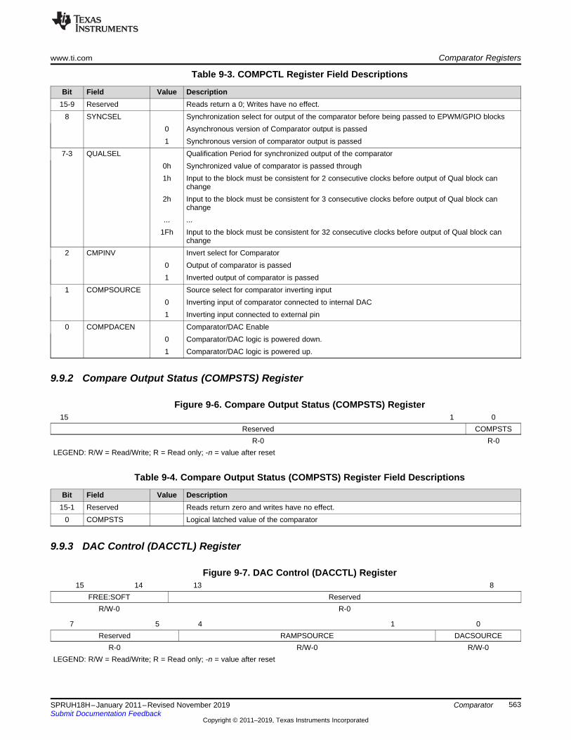
www.ti.com Comparator Registers
563SPRUH18H–January 2011–Revised November 2019Submit Documentation Feedback
Copyright © 2011–2019, Texas Instruments Incorporated
Comparator
Table 9-3. COMPCTL Register Field Descriptions
Bit Field Value Description15-9 Reserved Reads return a 0; Writes have no effect.
8 SYNCSEL Synchronization select for output of the comparator before being passed to EPWM/GPIO blocks0 Asynchronous version of Comparator output is passed1 Synchronous version of comparator output is passed
7-3 QUALSEL Qualification Period for synchronized output of the comparator0h Synchronized value of comparator is passed through1h Input to the block must be consistent for 2 consecutive clocks before output of Qual block can
change2h Input to the block must be consistent for 3 consecutive clocks before output of Qual block can
change... ...
1Fh Input to the block must be consistent for 32 consecutive clocks before output of Qual block canchange
2 CMPINV Invert select for Comparator0 Output of comparator is passed1 Inverted output of comparator is passed
1 COMPSOURCE Source select for comparator inverting input0 Inverting input of comparator connected to internal DAC1 Inverting input connected to external pin
0 COMPDACEN Comparator/DAC Enable0 Comparator/DAC logic is powered down.1 Comparator/DAC logic is powered up.
9.9.2 Compare Output Status (COMPSTS) Register
Figure 9-6. Compare Output Status (COMPSTS) Register15 1 0
Reserved COMPSTSR-0 R-0
LEGEND: R/W = Read/Write; R = Read only; -n = value after reset
Table 9-4. Compare Output Status (COMPSTS) Register Field Descriptions
Bit Field Value Description15-1 Reserved Reads return zero and writes have no effect.
0 COMPSTS Logical latched value of the comparator
9.9.3 DAC Control (DACCTL) Register
Figure 9-7. DAC Control (DACCTL) Register15 14 13 8
FREE:SOFT ReservedR/W-0 R-0
7 5 4 1 0Reserved RAMPSOURCE DACSOURCE
R-0 R/W-0 R/W-0LEGEND: R/W = Read/Write; R = Read only; -n = value after reset

Comparator Registers www.ti.com
564 SPRUH18H–January 2011–Revised November 2019Submit Documentation Feedback
Copyright © 2011–2019, Texas Instruments Incorporated
Comparator
Table 9-5. DACCTL Register Field Descriptions
Bit Field Value Description15-14 FREE:SOFT Emulation mode behavior. Selects ramp generator behavior during emulation suspend.
0h Stop immediately1h Complete current ramp, and stop on the next PWMSYNC signal
2h-3h Run free13-5 Reserved Reads return a 0; Writes have no effect.4-1 RAMPSOURCE Ramp generator source sync select. PWMSYNC is derived from the HRPWM register field
HRPCTL[PWMSYNCSEL].0h PWMSYNC1 is the source sync1h PWMSYNC2 is the source sync2h PWMSYNC3 is the source sync... ...
n-1 PWMSYNCn is the source sync0 DACSOURCE DAC source control. Select DACVAL or ramp generator to control the DAC.
0 DAC controlled by DACVAL1 DAC controlled by ramp generator
9.9.4 DAC Value (DACVAL) Register
Figure 9-8. DAC Value (DACVAL) Register15 10 9 0
Reserved DACVALR-0 R/W-0
LEGEND: R/W = Read/Write; R = Read only; -n = value after reset
Table 9-6. DAC Value (DACVAL) Register Field Descriptions
Bit Field Value Description15-10 Reserved Reads return zero and writes have no effect.
9-0 DACVAL 0-3FFh DAC Value bits, scales the output of the DAC from 0 – 1023.
9.9.5 Ramp Generator Maximum Reference Active (RAMPMAXREF_ACTIVE) Register
Figure 9-9. Ramp Generator Maximum Reference Active (RAMPMAXREF_ACTIVE) Register15 0
RAMPMAXREFAR-0
LEGEND: R = Read only; -n = value after reset
Table 9-7. Ramp Generator Maximum Reference Active (RAMPMAXREF_ACTIVE) Register FieldDescriptions
Bit Field Value Description15-0 RAMPMAXREFA 0-FFFFh 16-bit maximum reference active value for down ramp generator.
This value is loaded from RAMPMAXREF_SHDW when the PWMSYNC signal is received.

www.ti.com Comparator Registers
565SPRUH18H–January 2011–Revised November 2019Submit Documentation Feedback
Copyright © 2011–2019, Texas Instruments Incorporated
Comparator
9.9.6 Ramp Generator Maximum Reference Shadow (RAMPMAXREF_SHDW) Register
Figure 9-10. Ramp Generator Maximum Reference Shadow (RAMPMAXREF_SHDW) Register15 0
RAMPMAXREFSR/W-0
LEGEND: R/W = Read/Write; -n = value after reset
Table 9-8. Ramp Generator Maximum Reference Shadow (RAMPMAXREF_SHDW) Register FieldDescriptions
Bit Field Value Description15-0 RAMPMAXREFS 0-FFFFh 16-bit maximum reference shadow value for down ramp generator
9.9.7 Ramp Generator Decrement Value Active (RAMPDECVAL_ACTIVE) Register
Figure 9-11. Ramp Generator Decrement Value Active (RAMPDECVAL_ACTIVE) Register15 0
RAMPDECVALAR-0
LEGEND: R = Read only; -n = value after reset
Table 9-9. Ramp Generator Decrement Value Active (RAMPDECVAL_ACTIVE) Register FieldDescriptions
Bit Field Value Description15-0 RAMPDECVALA 0-FFFFh 16-bit decrement active value for down ramp generator.
This value is loaded from RAMPDECVAL_SHDW when the PWMSYNC signal is received.
9.9.8 Ramp Generator Decrement Value Shadow (RAMPDECVAL_SHDW) Register
Figure 9-12. Ramp Generator Decrement Value Shadow (RAMPDECVAL_SHDW) Register15 0
RAMPDECVALSR/W-0
LEGEND: R/W = Read/Write; -n = value after reset
Table 9-10. Ramp Generator Decrement Value Shadow (RAMPDECVAL_SHDW) Register FieldDescriptions
Bit Field Value Description15-0 RAMPDECVALS 0-FFFFh 16-bit decrement shadow value for down ramp generator
9.9.9 Ramp Generator Status (RAMPSTS) Register
Figure 9-13. Ramp Generator Status (RAMPSTS) Register15 0
RAMPVALUER-0
LEGEND: R = Read only; -n = value after reset

Comparator Registers www.ti.com
566 SPRUH18H–January 2011–Revised November 2019Submit Documentation Feedback
Copyright © 2011–2019, Texas Instruments Incorporated
Comparator
Table 9-11. Ramp Generator Status (RAMPSTS) Register Field Descriptions
Bit Field Value Description15-0 RAMPVALUE 0-FFFFh 16-bit value of down ramp generator

567SPRUH18H–January 2011–Revised November 2019Submit Documentation Feedback
Copyright © 2011–2019, Texas Instruments Incorporated
Control Law Accelerator (CLA)
Chapter 10SPRUH18H–January 2011–Revised November 2019
Control Law Accelerator (CLA)
The Control Law Accelerator (CLA) Type-0 is an independent, fully-programmable, 32-bit floating-pointmath processor that brings concurrent control-loop execution to the C28x family. The low interrupt latencyof the CLA allows it to read ADC samples "just-in-time." This significantly reduces the ADC sample tooutput delay to enable faster system response and higher MHz control loops. By using the CLA to servicetime-critical control loops, the main CPU is free to perform other system tasks such as communicationsand diagnostics. This chapter provides an overview of the architectural structure and components of thecontrol law accelerator.
Topic ........................................................................................................................... Page
10.1 Introduction ..................................................................................................... 56810.2 Features .......................................................................................................... 56810.3 CLA Interface ................................................................................................... 57010.4 CLA and CPU Arbitration................................................................................... 57310.5 CLA Configuration and Debug ........................................................................... 57810.6 Pipeline ........................................................................................................... 58210.7 Instruction Set.................................................................................................. 58710.8 Register Set ..................................................................................................... 702

Introduction www.ti.com
568 SPRUH18H–January 2011–Revised November 2019Submit Documentation Feedback
Copyright © 2011–2019, Texas Instruments Incorporated
Control Law Accelerator (CLA)
10.1 IntroductionThe Control Law Accelerator extends the capabilities of the C28x CPU by adding parallel processing.Time-critical control loops serviced by the CLA can achieve low ADC sample to output delay. Thus, theCLA enables faster system response and higher frequency control loops. Utilizing the CLA for time-criticaltasks frees up the main CPU to perform other system and communication functions concurrently.
10.2 FeaturesThe following is a list of major features of the CLA:• C compilers are available for CLA software development.• Clocked at the same rate as the main CPU (SYSCLKOUT).• An independent architecture allowing CLA algorithm execution independent of the main C28x CPU.
– Complete bus architecture:• Program Address Bus (PAB) and Program Data Bus (PDB)• Data Read Address Bus (DRAB), Data Read Data Bus (DRDB), Data Write Address Bus
(DWAB), and Data Write Data Bus (DWDB)– Independent eight stage pipeline.– 12-bit program counter (MPC)– Four 32-bit result registers (MR0-MR3)– Two 16-bit auxiliary registers (MAR0, MAR1)– Status register (MSTF)
• Instruction set includes:– IEEE single-precision (32-bit) floating point math operations– Floating-point math with parallel load or store– Floating-point multiply with parallel add or subtract– 1/X and 1/sqrt(X) estimations– Data type conversions.– Conditional branch and call– Data load/store operations
• The CLA program code can consist of up to eight tasks or interrupt service routines– The start address of each task is specified by the MVECT registers.– No limit on task size as long as the tasks fit within the configurable CLA program memory space.– One task is serviced at a time until its completion. There is no nesting of tasks.– Upon task completion a task-specific interrupt is flagged within the PIE.– When a task finishes the next highest-priority pending task is automatically started.
• Task trigger mechanisms:– C28x CPU via the IACK instruction– Task1 to Task8: trigger sources from peripherals connected to the shared bus on which the CLA
assumes secondary ownership.• Memory and Shared Peripherals:
– Two dedicated message RAMs for communication between the CLA and the main CPU.– The C28x CPU can map CLA program and data memory to the main CPU space or CLA space.

CLA Program Bus
MR0 (32)
MVECT1 (16)
MIFR (16)
MPC (12)
MIER (16)
MIFRC (16)
MIRUN (16)
MR1 (32)
MR3 (32)MAR0 (16)
CPU Read/Write Data Bus
CLA Execution
Register Set
CLA Control
Register Set
MSTF (32)
PIE
From Shared
Peripherals
CLA Program
Memory
MR2 (32)
MAR1 (16)
MIOVF (16)
MICLR (16)
MCTL (16)
MICLROVF (16)
MEALLOW
CL
A D
ata
Bu
s
C28x
CPU
MVECT2 (16)
MVECT3 (16)
MVECT4 (16)
MVECT5 (16)MVECT6 (16)
MVECT7 (16)
MVECT8 (16)
CP
U D
ata
Bu
s
MMEMCFG (16)
MPISRCSEL1 (32)
CLA Data
Memory
CLA Message
RAM
Shared
Peripherals
CPU Read Data Bus
MPERINT1
to
MPERINT8
CLA_INT1
to
CLA_INT8
LUF
LVF
INT11
INT12
SYSCLK
CLA Clock Enable
SYSRS
www.ti.com Features
569SPRUH18H–January 2011–Revised November 2019Submit Documentation Feedback
Copyright © 2011–2019, Texas Instruments Incorporated
Control Law Accelerator (CLA)
Figure 10-1. CLA (Type 0) Block Diagram

CLA Interface www.ti.com
570 SPRUH18H–January 2011–Revised November 2019Submit Documentation Feedback
Copyright © 2011–2019, Texas Instruments Incorporated
Control Law Accelerator (CLA)
10.3 CLA InterfaceThis chapter describes how the C28x main CPU can interface to the CLA and vice versa.
10.3.1 CLA MemoryThe CLA can access three types of memory: program, data and message RAMs. The behavior andarbitration for each type of memory is described in detail below. The CLA RAMs are protected by the CSMmodule. Refer to Section 1.3 for more details on the security scheme.• CLA Program Memory
The CLA program can be loaded to a designated memory block. At reset, all memory blocks aremapped to the CPU. While mapped to the CPU space, the CPU can copy the CLA program code intothe memory. During debug, the memory can also be loaded directly by Code Composer Studio™.Once the memory is initialized with CLA code, the CPU maps it to the CLA program space by settingthe MMEMCFG[PROGE] bit.When a memory block is configured as CLA program memory, debug accesses are allowed only oncycles where the CLA is not fetching a new instruction. A detailed explanation of the memoryconfigurations and access arbitration (CPU, CLA, and DEBUG) process can be found in Section 10.4.All CLA program fetches are performed as 32-bit read operations and all opcodes must be aligned toan even address. Since all CLA opcodes are 32-bits, this alignment occurs naturally.
• CLA Data MemoryDesignated memory locations can serve as data memory blocks to the CLA. At reset, all blocks aremapped to the CPU memory space, whereby the CPU can initialize the memory with data tables,coefficients, and so on, for the CLA to use.Once the memory is initialized with CLA data, the CPU maps it to the CLA data space by setting therespective MMEMCFG[RAMxE] bit.When a memory block is configured as CLA data memory, CLA read and write accesses are arbitratedalong with CPU accesses. The user has the option of turning on CPU fetch or write protection to thememory by writing to the appropriate MMEMCFG[RAMnCPUE] bits. A detailed explanation of thememory configurations and access arbitration (CPU, CLA, and DEBUG) process can be found inSection 10.4.
• CLA Shared Message RAMsThere are two memory blocks for data sharing and communication between the CLA and the CPU.The message RAMs are always mapped to both CPU and CLA memory spaces, and only data accessis allowed; no program fetches can be performed.– CLA to CPU Message RAM
The CLA can use this block to pass data to the CPU. This block is both readable and writable bythe CLA. This block is also readable by the CPU but writes by the CPU are ignored.
– CPU to CLA Message RAMThe CPU can use this block to pass data and messages to the CLA. This message RAM is bothreadable and writable by the CPU. The CLA can perform reads but writes by the CLA are ignored.
10.3.2 CLA Memory BusThe CLA has dedicated bus architecture similar to that of the C28x CPU where there are separateprogram read, data read, and data write buses. Thus, there can be simultaneous instruction fetch, dataread, and data write in a single cycle. Like the C28x CPU, the CLA expects memory logic to align any 32-bit read or write to an even address. If the address-generation logic generates an odd address, the CLAwill begin reading or writing at the previous even address. This alignment does not affect the addressvalues generated by the address-generation logic.• CLA Program Bus
The CLA program bus has an access range of 2048 32-bit instructions. Since all CLA instructions are32 bits, this bus always fetches 32 bits at a time and the opcodes must be even-word aligned. Theamount of program space available for the CLA is limited to the number of allocated memory blocks.This number is device-dependent and will be described in the device-specific data manual.

www.ti.com CLA Interface
571SPRUH18H–January 2011–Revised November 2019Submit Documentation Feedback
Copyright © 2011–2019, Texas Instruments Incorporated
Control Law Accelerator (CLA)
• CLA Data Read BusThe CLA data read bus has a 64K x 16 address range. The bus can perform 16 or 32-bit reads andwill automatically stall if there are memory access conflicts. The data read bus has access to both themessage RAMs, CLA data memory, and the shared peripherals.
• CLA Data Write BusThe CLA data write bus has a 64K x 16 address range. This bus can perform 16 or 32-bit writes. Thebus will automatically stall if there are memory access conflicts. The data write bus has access to theCLA to CPU message RAM, CLA data memory, and the shared peripherals.
10.3.3 Shared Peripherals and EALLOW ProtectionThe CPU and CLA share access to some peripherals. Section 10.4 describes the arbitration between theCPU and CLA.
Refer to the device data manual for the list of peripherals connected to the bus.
Several peripheral control registers are protected from spurious 28x CPU writes by the EALLOWprotection mechanism. These same registers are also protected from spurious CLA writes. The EALLOWbit in the CPU status register 1 (ST1) indicates the state of protection for the CPU. Likewise theMEALLOW bit in the CLA status register (MSTF) indicates the state of write protection for the CLA. TheMEALLOW CLA instruction enables write access by the CLA to EALLOW protected registers. Likewise theMEDIS CLA instruction will disable write access. This way the CLA can enable/disable write accessindependent of the CPU.
The ADC offers the option to generate an early interrupt pulse at the start of a sample conversion. If thisoption is used to start an ADC-triggered CLA task, the user may use the intervening cycles, until thecompletion of the conversion, to perform preliminary calculations or loads and stores before finally readingthe ADC value. The CLA pipeline activity for this scenario is shown in Section 10.6.

CLA Interface www.ti.com
572 SPRUH18H–January 2011–Revised November 2019Submit Documentation Feedback
Copyright © 2011–2019, Texas Instruments Incorporated
Control Law Accelerator (CLA)
10.3.4 CLA Tasks and Interrupt VectorsThe CLA program code is divided up into tasks or interrupt service routines. Tasks do not have a fixedstarting location or length. The CLA program memory can be divided up as desired. The CLA uses thecontents of the interrupt vectors (MVECT1 to MVECT8) to determine where a task begins; tasks areterminated by the MSTOP instruction.
The CLA supports eight tasks. Task 1 has the highest priority and task 8 has the lowest priority.
A task can be requested by a peripheral interrupt or by software:• Peripheral interrupt trigger
Each task can be triggered by software-selectable interrupt sources. The trigger for each task isdefined by writing an appropriate value to the MPISRCSEL1[PERINTnSEL] bit field. Each optionspecifies an interrupt source from a specific peripheral on the shared bus. The peripheral interrupttriggers are listed in Section 10.8.3.3.For example, Task 1 (MVECT1) can be set to trigger on EPWM1_INT by writing 2 toMPISRCSEL1[PERINT1SEL]. To disable the triggering of a task by a peripheral, the user mustconfigure the MPISRCSEL1[PERINTxSEL] bit field to a "No interrupt source" selection.
• Software TriggerCPU software can trigger tasks by writing to the MIFRC register or by the IACK instruction. Using theIACK instruction is more efficient because it does not require you to issue an EALLOW to set MIFRbits. Set the MCTL[IACKE] bit to enable the IACK feature. Each bit in the operand of the IACKinstruction corresponds to a task. For example IACK #0x0001 will set bit 0 in the MIFR register to starttask 1. Likewise IACK #0x0003 will set bits 0 and 1 in the MIFR register to start task 1 and task 2.
The CLA has its own fetch mechanism and can run and execute a task independent of the CPU. Only onetask is serviced at a time; there is no nesting of tasks. The task currently running is indicated in theMIRUN register. Interrupts that have been received but not yet serviced are indicated in the flag register(MIFR). If an interrupt request from a peripheral is received and that same task is already flagged, thenthe overflow flag bit is set. Overflow flags will remain set until they are cleared by the CPU.
If the CLA is idle (no task is currently running) then the highest priority interrupt request that is bothflagged (MIFR) and enabled (MIER) will start. The flow is as follows:1. The associated RUN register bit is set (MIRUN) and the flag bit (MIFR) is cleared.2. The CLA begins execution at the location indicated by the associated interrupt vector (MVECTx).
MVECT contains the absolute 16-bit address of the task in the lower 64K memory space.3. The CLA executes instructions until the MSTOP instruction is found. This indicates the end of the task.4. The MIRUN bit is cleared.5. The task-specific interrupt to the PIE is issued. This informs the main CPU that the task has
completed.6. The CLA returns to idle.
Once a task completes the next highest-priority pending task is automatically serviced and this sequencerepeats.

www.ti.com CLA and CPU Arbitration
573SPRUH18H–January 2011–Revised November 2019Submit Documentation Feedback
Copyright © 2011–2019, Texas Instruments Incorporated
Control Law Accelerator (CLA)
10.4 CLA and CPU ArbitrationThis section describes the arbitration between CLA and CPU accesses to shared resources.
10.4.1 CLA and CPU ArbitrationThe CLA typically operates independently of the CPU. Under circumstance where both the CLA and theCPU are attempting to currently access memory or a peripheral register, an arbitration procedure willoccur. The one exception is the ADC result registers which do not create a conflict when read by both theCPU and the CLA simultaneously.
The interfaces that can experience access conflicts are:• CLA Message RAMs• CLA Program Memory• CLA Data RAMs
10.4.1.1 CLA Message RAMsMessage RAMs consist of two blocks. These blocks are useful for passing data between the CPU andCLA. No opcode fetches are allowed from the message RAMs. The message RAMs have the followingcharacteristics:• CLA to CPU Message RAM:
The following accesses are allowed:– CPU reads– CLA reads and writes– CPU debug reads and writes
The following accesses are ignored– CPU writes
Priority of accesses are (highest priority first):1. CLA write2. CPU debug write3. CPU data read, program read, CPU debug read4. CLA data read

CLA and CPU Arbitration www.ti.com
574 SPRUH18H–January 2011–Revised November 2019Submit Documentation Feedback
Copyright © 2011–2019, Texas Instruments Incorporated
Control Law Accelerator (CLA)
• CPU to CLA Message RAM:The following accesses are allowed:– CPU reads and writes– CLA reads– CPU debug reads and writes
The following accesses are ignored– CLA writes
Priority of accesses are (highest priority first):1. CLA read2. CPU data write, program write, CPU debug write3. CPU data read, CPU debug read4. CPU program read
10.4.1.2 CLA Program MemoryThe behavior of the program memory depends on the state of the MMEMCFG[PROGE] bit. This bitcontrols whether the memory is mapped to CLA space or CPU space.• MMEMCFG[PROGE] == 0
In this case the memory is mapped to the CPU. The CLA will be halted and no tasks shoud beincoming.– Any CLA fetch will be treated as an illegal opcode condition as described in Section 10.5.4. This
condition will not occur if the proper procedure is followed to map the program memory.– CLA reads and writes cannot occur– The memory block behaves as any normal RAM block mapped to CPU memory space.
Priority of accesses are (highest priority first):1. CPU data write, program write, debug write2. CPU data read, program read, debug read3. CPU fetch, program read
• MMEMCFG[PROGE] == 1In this case the memory block is mapped to CLA space. The CPU can only make debug accesses.– CLA reads and writes cannot occur– CLA fetches are allowed– CPU fetches return 0 which is an illegal opcode and will cause an ITRAP interrupt.– CPU data reads and program reads return 0– CPU data writes and program writes are ignored
Priroty of accesses are (highest priority first):1. CLA fetch2. CPU debug write3. CPU debug read

www.ti.com CLA and CPU Arbitration
575SPRUH18H–January 2011–Revised November 2019Submit Documentation Feedback
Copyright © 2011–2019, Texas Instruments Incorporated
Control Law Accelerator (CLA)
NOTE: Because the CLA fetch has higher priority than CPU debug reads, it is possible for the CLAto permanently block debug accesses if the CLA is executing in a loop. This might occurwhen initially developing CLA code due to a bug. To avoid this issue, the program memorywill return all 0x0000 for CPU debug reads (ignore writes) when the CLA is running. Whenthe CLA is halted or idle then normal CPU debug read and write access can be performed.

CLA and CPU Arbitration www.ti.com
576 SPRUH18H–January 2011–Revised November 2019Submit Documentation Feedback
Copyright © 2011–2019, Texas Instruments Incorporated
Control Law Accelerator (CLA)
10.4.1.3 CLA Data MemoryThere are three independent data memory blocks. The behavior of the data memory depends on thestate of the MMEMCFG[RAM0E], MMEMCFG[RAM1E] and MMEMCFG[RAM2E] bits. These bitsdetermine whether the memory blocks are mapped to CLA space or CPU space.
• MMEMCFG[RAMxE] == 0, MMEMCFG[RAMxCPUE] = 0/1In this case the memory block is mapped to the CPU.– CLA fetches cannot occur to this block.– CLA reads return 0.– CLA writes are ignored.– The memory block behaves as any normal RAM block mapped to the CPU memory space.
Priroty of accesses are (highest priority first):1. CPU data write/program write/debug access write2. CPU data read/debug access read3. CPU fetch/program read
• MMEMCFG[RAMxE] == 1, MMEMCFG[RAMxCPUE] = 0In this case the memory block is mapped to CLA space. The CPU can make only debug accesses.– CLA fetches cannot occur to this block.– CLA read and CLA writes are allowed.– CPU fetches return 0– CPU data reads and program reads return 0.– CPU data writes and program writes are ignored.
Priority of accesses are (highest priority first):1. CLA data write2. CPU debug write3. CPU debug read4. CLA read
• MMEMCFG[RAMxE] == 1, MMEMCFG[RAMxCPUE] = 1In this case the memory block is mapped to CLA space. The CPU has read and write access to thememory in addition to debug accesses.– CLA fetches cannot occur to this block.– CLA read and CLA writes are allowed.– CPU fetches return 0– CPU data reads and writes are allowed.– CPU program reads return 0 while program writes are ignored.
Priority of accesses are (highest priority first):1. CLA data write2. CPU debug access write/CPU data write3. CPU debug access read/ CPU data read4. CLA read

www.ti.com CLA and CPU Arbitration
577SPRUH18H–January 2011–Revised November 2019Submit Documentation Feedback
Copyright © 2011–2019, Texas Instruments Incorporated
Control Law Accelerator (CLA)
10.4.1.4 Peripheral Registers (ePWM, HRPWM, Comparator, eCAP, eQEP)Accesses to the registers follow these rules:• If both the CPU and CLA request access at the same time, then the CLA will have priority and the
main CPU is stalled.• If a CPU access is in progress and another CPU access is pending, then the CLA will have priority
over the pending CPU access. In this case the CLA access will begin when the current CPU accesscompletes.
• While a CPU access is in progress any incoming CLA access will be stalled.• While a CLA access is in progress any incoming CPU access will be stalled.• A CPU write operation has priority over a CPU read operation.• A CLA write operation has priority over a CLA read operation.• If the CPU is performing a read-modify-write operation and the CLA performs a write to the same
location, the CLA write may be lost if the operation occurs in-between the CPU read and write. For thisreason, you should not mix CPU and CLA accesses to same location.

CLA Configuration and Debug www.ti.com
578 SPRUH18H–January 2011–Revised November 2019Submit Documentation Feedback
Copyright © 2011–2019, Texas Instruments Incorporated
Control Law Accelerator (CLA)
10.5 CLA Configuration and DebugThis section discusses the steps necessary to configure and debug the CLA.
10.5.1 Building a CLA ApplicationThe control law accelerator can be programmed in either CLA assembly code, using the instructionsdescribed in Section 10.7, or a reduced subset of the C language. CLA assembly code resides in thesame project with C28x code. The only restriction is the CLA code must be in its own assembly section.This can be easily done using the .sect assembly directive. This does not prevent CLA and C28x codefrom being linked into the same memory region in the linker command file.
System and CLA initialization are performed by the main CPU. This would typically be done in C or C++but can also include C28x assembly code. The main CPU will also copy the CLA code to the programmemory and, if needed, initialize the CLA data RAM(s). Once system initialization is complete and theapplication begins, the CLA will service its interrupts using the CLA assembly code (or tasks). The mainCPU can perform other tasks concurrently with CLA program execution.
The CLA Type 0 requires Codegen V5.2.0 or later with the compiler switch: --cla_support=cla0.
10.5.2 Typical CLA Initialization SequenceA typical CLA initialization sequence is performed by the main CPU as described in this section.1. Copy CLA code into the CLA program RAM
The source for the CLA code can initially reside in the flash or a data stream from a communicationsperipheral or anywhere the main CPU can access it. The debugger can also be used to load codedirectly to the CLA program RAM during development.
2. Initialize CLA data RAM, if necessaryPopulate the CLA data RAM with any required data coefficients or constants.
3. Configure the CLA registersConfigure the CLA registers, but keep interrupts disabled until later (leave MIER = 0):• Enable the CLA peripheral clock using the assigned PCLKCRn register
The peripheral clock control (PCLKCRn) registers are defined in Section 1.4.1.1.• Populate the CLA task interrupt vectors
– MVECT1 to MVECT8Each vector needs to be initialized with the start address of the task to be executed when theCLA receives the associated interrupt. The address is an offset from the base address of theassigned CLA Program memory block.
• Select the task interrupt sourcesFor each task select the interrupt source in the CLA1TASKSRCSELx register. If a task is softwaretriggered, select no interrupt.
• Enable IACK to start a task from software, if desiredTo enable the IACK instruction to start a task set the MCTL[IACKE] bit. Using the IACK instructionavoids having to set and clear the EALLOW bit.
• Map CLA data RAM to CLA space, if necessaryMap the data RAM to the CLA space by writing a 1 to the MMEMCFG[RAMxE] bit. The CPU willhave restricted access to the memory block once the MMEMCFG[RAMxE] bit is set. CPU access toCLA data RAM can be granted through the MMEMCFG[RAMxCPUE] bit. Allow two SYSCLK cyclesfor MMEMCFG updates to take effect.
• Map CLA program RAM to CLA spaceMap the CLA program RAM to CLA space by setting the MMEMCFG[PROGE] bit. The CPU willonly have debug access to program RAM once the MMEMCFG[PROGE] bit is set. Allow twoSYSCLK cycles for MMEMCFG updates to take effect.
4. Initialize the PIE vector table and registersWhen a CLA task completes, the associated interrupt in the PIE will be flagged. The CLA overflow and

www.ti.com CLA Configuration and Debug
579SPRUH18H–January 2011–Revised November 2019Submit Documentation Feedback
Copyright © 2011–2019, Texas Instruments Incorporated
Control Law Accelerator (CLA)
underflow flags also have associated interrupts within the PIE.5. Enable CLA tasks/interrupts
Set appropriate bits in the interrupt enable register (MIER) to allow the CLA to service interrupts.6. Initialize other peripherals
Initialize any peripherals (such as ePWM, ADC, and others) that will generate interrupt triggers forenabled CLA tasks.The CLA is now ready to service interrupts and the message RAMs can be used to pass data betweenthe CPU and the CLA. Mapping of the CLA program and data RAMs typically occurs only during theinitialization process. If the RAM mapping needs to be changed after initialization, the CLA interruptsmust be disabled and all tasks must be completed (by checking the MIRUN register) prior to modifyingthe RAM ownership.
10.5.3 Debugging CLA CodeDebugging the CLA code is a simple process that occurs independently of the main CPU. .
10.5.3.1 Breakpoint Support (MDEBUGSTOP)1. Insert a breakpoint in CLA code
Insert a CLA breakpoint (MDEBUGSTOP instruction) into the code where you want the CLA to halt,then rebuild and reload the code. Because the CLA does not flush its pipeline when you single-step,the MDEBUGSTOP instruction must be inserted as part of the code. The debugger cannot insert it asneeded.If CLA breakpoints are not enabled, then the MDEBUGSTOP will be ignored and is treated as aMNOP. The MDEBUGSTOP instruction can be placed anywhere in the CLA code as long as it is notwithin three instructions of a MBCNDD, MCCNDD, or MRCNDD instruction. When programming in C,the user can use the __mdebugstop() intrinsic instead; the compiler will ensure that the placement ofthe MDEBUSTOP instruction in the generated assembly does not violate any of the pipelinerestrictions.
2. Enable CLA breakpointsEnable the CLA breakpoints in the debugger. In Code Composer Studio, this is done by connecting tothe CLA core (or tap) from the debug perspective. Breakpoints are disabled when the core isdisconnected.
3. Start the taskThere are three ways to start the task:1. The peripheral can assert an interrupt,2. The main CPU can execute an IACK instruction, or3. The user can manually write to the MIFRC register in the debugger window
When the task starts, the CLA will execute instructions until the MDEBUGSTOP is in the D2 phase ofthe pipeline. At this point, the CLA will halt and the pipeline will be frozen. The MPC register will reflectthe address of the MDEBUGSTOP instruction.
4. Single-step the CLA codeOnce halted, the user can single-step the CLA code. The behavior of a CLA single-step is differentthan the main C28x. When issuing a CLA single-step, the pipeline is clocked only one cycle and thenagain frozen. On the 28x CPU, the pipeline is flushed for each single-step.You can also run to the next MDEBUGSTOP or to the end of the task. If another task is pending, it willautomatically start when you run to the end of the task.

CLA Configuration and Debug www.ti.com
580 SPRUH18H–January 2011–Revised November 2019Submit Documentation Feedback
Copyright © 2011–2019, Texas Instruments Incorporated
Control Law Accelerator (CLA)
NOTE: A CLA fetch has higher priority than CPU debug reads. For this reason, it is possible for theCLA to permanently block CPU debug accesses if the CLA is executing in a loop. This mightoccur when initially developing CLA code due to a bug that causes an infinite loop. To avoidlocking up the main CPU, the program memory will return all 0x0000 for CPU debug readswhen the CLA is running. When the CLA is halted or idle then normal CPU debug read andwrite access to CLA program memory can be performed.
If the CLA gets caught in an infinite loop, you can use a soft or hard reset to exit thecondition. A debugger reset will also exit the condition.
There are special cases that can occur when single-stepping a task such that the program counter,MPC, reaches the MSTOP instruction at the end of the task.• MPC halts at or after the MSTOP with a task already pending
If you are single-stepping or halted in "task A" and "task B" comes in before the MPC reaches theMSTOP, then "task B" will start if you continue to step through the MSTOP instruction. Basically if"task B" is pending before the MPC reaches MSTOP in "task A" then there is no issue in "task B"starting and no special action is required.
• MPC halts at or after the MSTOP with no task pendingIn this case you have single-stepped or halted in "task A" and the MPC has reached the MSTOPwith no tasks pending. If "task B" comes in at this point, it will be flagged in the MIFR register but itmay or may not start if you continue to single-step through the MSTOP instruction of "task A."It depends on exactly when the new task comes in. To reliably start "task B" perform a soft resetand reconfigure the MIER bits. Once this is done, you can start single-stepping "task B."This case can be handled slightly differently if there is control over when "task B" comes in (forexample using the IACK instruction to start the task). In this case you have single-stepped or haltedin "task A" and the MPC has reached the MSTOP with no tasks pending. Before forcing "task B,"run free to force the CLA out of the debug state. Once this is done you can force "task B" andcontinue debugging.
5. Disable CLA breakpoints, if desiredIn Code Composer Studio you can disable the CLA breakpoints by disconnecting the CLA core in thedebug perspective. Make sure to first issue a run or reset; otherwise, the CLA will be halted and noother tasks will start.
10.5.4 CLA Illegal Opcode BehaviorIf the CLA fetches an opcode that does not correspond to a legal instruction, it will behave as follows:• The CLA will halt with the illegal opcode in the D2 phase of the pipeline as if it were a breakpoint. This
will occur whether CLA breakpoints are enabled or not.• The CLA will issue the task-specific interrupt to the PIE.• The MIRUN bit for the task will remain set.
Further single-stepping is ignored once execution halts due to an illegal op-code. To exit this situation,issue either a soft or hard reset of the CLA as described in Section 10.5.5.
10.5.5 Resetting the CLAThere may be times when you need to reset the CLA. For example, during code debug the CLA may enteran infinite loop due to a code bug. The CLA has two types of resets: hard and soft. Both of these resetscan be performed by the debugger or by the main CPU.• Hard Reset
Writing a 1 to the MCTL[HARDRESET] bit will perform a hard reset of the CLA. The behavior of a hardreset is the same as a system reset (via XRS or the debugger). In this case all CLA configuration andexecution registers will be set to their default state and CLA execution will halt.
• Soft ResetWriting a 1 to the MCTL[SOFTRESET] bit performs a soft reset of the CLA. If a task is executing it willhalt and the associated MIRUN bit will be cleared. All bits within the interrupt enable (MIER) register

www.ti.com CLA Configuration and Debug
581SPRUH18H–January 2011–Revised November 2019Submit Documentation Feedback
Copyright © 2011–2019, Texas Instruments Incorporated
Control Law Accelerator (CLA)
will also be cleared so that no new tasks start.

Pipeline www.ti.com
582 SPRUH18H–January 2011–Revised November 2019Submit Documentation Feedback
Copyright © 2011–2019, Texas Instruments Incorporated
Control Law Accelerator (CLA)
10.6 PipelineThis section describes the CLA pipeline stages and presents cases where pipeline alignment must beconsidered.
10.6.1 Pipeline OverviewThe CLA pipeline is very similar to the C28x pipeline with eight stages:1. Fetch 1 (F1)
During the F1 stage the program read address is placed on the CLA program address bus.2. Fetch 2 (F2)
During the F2 stage the instruction is read using the CLA program data bus.3. Decode 1 (D1)
During D1 the instruction is decoded.4. Decode 2 (D2)
Generate the data read address. Changes to MAR0 and MAR1 due to post-increment using indirectaddressing takes place in the D2 phase. Conditional branch decisions are also made at this stagebased on the MSTF register flags.
5. Read 1 (R1)Place the data read address on the CLA data-read address bus. If a memory conflict exists, the R1stage will be stalled.
6. Read 2 (R2)Read the data value using the CLA data read data bus.
7. Execute (EXE)Execute the operation. Changes to MAR0 and MAR1 due to loading an immediate value or value frommemory take place in this stage.
8. Write (W)Place the write address and write data on the CLA write data bus. If a memory conflict exists, the Wstage will be stalled.
10.6.2 CLA Pipeline AlignmentThe majority of the CLA instructions do not require any special pipeline considerations. This section liststhe few operations that do require special consideration.• Write Followed by Read
In both the C28x and the CLA pipeline the read operation occurs before the write. This means that if aread operation immediately follows a write, then the read will complete first as shown in Table 10-1. Inmost cases this does not cause a problem since the contents of one memory location does not dependon the state of another. For accesses to peripherals where a write to one location can affect the valuein another location the code must wait for the write to complete before issuing the read as shown inTable 10-2.This behavior is different for the 28x CPU. For the 28x CPU any write followed by read to the samelocation is protected by what is called write-followed-by-read protection. This protection automaticallystalls the pipeline so that the write will complete before the read. In addition some peripheral framesare protected such that a 28x CPU write to one location within the frame will always complete before aread to the frame. The CLA does not have this protection mechanism. Instead the code must wait toperform the read.

www.ti.com Pipeline
583SPRUH18H–January 2011–Revised November 2019Submit Documentation Feedback
Copyright © 2011–2019, Texas Instruments Incorporated
Control Law Accelerator (CLA)
Table 10-1. Write Followed by Read - Read Occurs FirstInstruction F1 F2 D1 D2 R1 R2 E W
I1 MMOV16 @Reg1, MR3 I1
I2 MMOV16 MR2, @Reg2 I2 I1
I2 I1
I2 I1
I2 I1
I2 I1
I2 I1
I2 I1
Table 10-2. Write Followed by Read - Write Occurs FirstInstruction F1 F2 D1 D2 R1 R2 E W
I1 MMOV16 @Reg1, MR3 I1
I2 I2 I1
I3 I3 I2 I1
I4 I4 I3 I2 I1
I5 MMOV16 MR2, @Reg2 I5 I4 I3 I2 I1
I5 I4 I3 I2 I1
I5 I4 I3 I2 I1
I5 I4 I3 I2 I1
I5 I4 I3
I5 I4
I5
• Delayed Conditional instructions: MBCNDD, MCCNDD and MRCNDDReferring to Example 10-1, the following applies to delayed conditional instructions:– I1
I1 is the last instruction that can effect the CNDF flags for the branch, call or return instruction. TheCNDF flags are tested in the D2 phase of the pipeline. That is, a decision is made whether tobranch or not when MBCNDD, MCCNDD or MRCNDD is in the D2 phase.
– I2, I3 and I4The three instructions preceding MBCNDD can change MSTF flags but will have no effect onwhether the MBCNDD instruction branches or not. This is because the flag modification will occurafter the D2 phase of the branch, call or return instruction. These three instructions must not be aMSTOP, MDEBUGSTOP, MBCNDD, MCCNDD or MRCNDD.
– I5, I6 and I7The three instructions following a branch, call or return are always executed irrespective of whetherthe condition is true or not. These instructions must not be MSTOP, MDEBUGSTOP, MBCNDD,MCCNDD or MRCNDD.
For a more detailed description refer to the functional description for MBCNDD, MCCNDD andMRCNDD.

Pipeline www.ti.com
584 SPRUH18H–January 2011–Revised November 2019Submit Documentation Feedback
Copyright © 2011–2019, Texas Instruments Incorporated
Control Law Accelerator (CLA)
Example 10-1. Code Fragment For MBCNDD, MCCNDD or MRCNDD
<Instruction 1> ; I1 Last instruction that can affect flags for; the branch, call or return operation
<Instruction 2> ; I2 Cannot be stop, branch, call or return<Instruction 3> ; I3 Cannot be stop, branch, call or return<Instruction 4> ; I4 Cannot be stop, branch, call or return
<branch/call/ret> ; MBCNDD, MCCNDD or MRCNDD
; I5-I7: Three instructions after are always; executed whether the branch/call or return is; taken or not
<Instruction 5> ; I5 Cannot be stop, branch, call or return<Instruction 6> ; I6 Cannot be stop, branch, call or return<Instruction 7> ; I7 Cannot be stop, branch, call or return
<Instruction 8> ; I8<Instruction 9> ; I9....
• Stop or Halting a Task: MSTOP and MDEBUGSTOPThe MSTOP and MDEBUGSTOP instructions cannot be placed three instructions before or after aconditional branch, call or return instruction (MBCNDD, MCCNDD or MRCNDD). Refer to Example 10-1. To single-step through a branch/call or return, insert the MDEBUGSTOP at least four instructionsback and step from there.
• Loading MAR0 or MAR1A load of auxiliary register MAR0 or MAR1 will occur in the EXE phase of the pipeline. Any postincrement of MAR0 or MAR1 using indirect addressing will occur in the D2 phase of the pipeline.Referring to Example 10-2, the following applies when loading the auxiliary registers:– I1 and I2
The two instructions following the load instruction will use the value in MAR0 or MAR1 before theupdate occurs.
– I3Loading of an auxiliary register occurs in the EXE phase while updates due to post-incrementaddressing occur in the D2 phase. Thus I3 cannot use the auxiliary register or there will be aconflict. In the case of a conflict, the update due to address-mode post increment will win and theauxiliary register will not be updated with #_X.
– I4Starting with the 4th instruction MAR0 or MAR1 will have the new value.
Example 10-2. Code Fragment for Loading MAR0 or MAR1
; Assume MAR0 is 50 and #_X is 20
MMOVI16 MAR0, #_X ; Load MAR0 with address of X (20)<Instruction 1> ; I1 Will use the old value of MAR0 (50)<Instruction 2> ; I2 Will use the old value of MAR0 (50)<Instruction 3> ; I3 Cannot use MAR0<Instruction 4> ; I4 Will use the new value of MAR0 (20)<Instruction 5> ; I5 Will use the new value of MAR0 (20....

www.ti.com Pipeline
585SPRUH18H–January 2011–Revised November 2019Submit Documentation Feedback
Copyright © 2011–2019, Texas Instruments Incorporated
Control Law Accelerator (CLA)
10.6.2.1 ADC Early Interrupt to CLA ResponseThe ADC can be configured to generate an early interrupt pulse before the ADC conversion completes. Ifthis option is used to start a CLA task, the CLA will be able to read the result as soon as the conversionresult is available in the ADC result register. This combination of just-in-time sampling along with the lowinterrupt response of the CLA enable faster system response and higher frequency control loops.
Timings for ADC conversions are shown in the timing diagrams of the ADC chapter. If the ADCCLK is adivided down version of the SYSCLK, the user will have to account for the conversion time in SYSCLKcycles.
For example, if using the ADC with ADCCLK at SYSCLK / 2, it would take 13 ADCCLK x 2 SYSCLK = 26SYSCLK cycles to complete a conversion.
From a CLA perspective, the pipeline activity is shown in Table 10-3 for an N-cycle (SYSCLK) ADCconversion. The N-2 instruction will arrive in the R2 phase just in time to read the result register. While theprior instructions will enter the R2 phase of the pipeline too soon to read the conversion, they can beefficiently used for pre-processing calculations needed by the task.
Table 10-3. ADC to CLA Early Interrupt ResponseADC Activity CLA Activity F1 F2 D1 D2 R1 R2 E W
Sample
Sample
...
Sample
Conversion(Cycle 1) Interrupt Received
Conversion(Cycle 2) Task Startup
Conversion(Cycle 3) Task Startup
Conversion(Cycle 4) I(Cycle 4) I(Cycle 4)
Conversion(Cycle 5) I(Cycle 5) I(Cycle 5) I(Cycle 4)
Conversion(...) ... ... ... ... ... ... ...
Conversion(Cycle N-6) I(Cycle N-6) I(Cycle N-6) I(Cycle N-7) I(Cycle N-8) I(Cycle N-9) I(Cycle N-10) I(Cycle N-11)
Conversion(Cycle N-5) I(Cycle N-5) I(Cycle N-5) I(Cycle N-6) I(Cycle N-7) I(Cycle N-8) I(Cycle N-9) I(Cycle N-10)
Conversion(Cycle N-4) I(Cycle N-4) I(Cycle N-4) I(Cycle N-5) I(Cycle N-6) I(Cycle N-7) I(Cycle N-8) I(Cycle N-9)
Conversion(Cycle N-3) I(Cycle N-3) I(Cycle N-3) I(Cycle N-4) I(Cycle N-5) I(Cycle N-6) I(Cycle N-7) I(Cycle N-8)
Conversion(Cycle N-2) Read RESULT ReadRESULT I(Cycle N-3) I(Cycle N-4) I(Cycle N-5) I(Cycle N-6) I(Cycle N-7)
Conversion(Cycle N-1)ReadRESULT I(Cycle N-3) I(Cycle N-4) I(Cycle N-5) I(Cycle N-6)
Conversion(Cycle N-0)ReadRESULT I(Cycle N-3) I(Cycle N-4) I(Cycle N-5)
Conversion Complete ReadRESULT I(Cycle N-3) I(Cycle N-4)
RESULT Latched ReadRESULT I(Cycle N-3)
RESULT Available ReadRESULT

Pipeline www.ti.com
586 SPRUH18H–January 2011–Revised November 2019Submit Documentation Feedback
Copyright © 2011–2019, Texas Instruments Incorporated
Control Law Accelerator (CLA)
10.6.3 Parallel InstructionsParallel instructions are single opcodes that perform two operations in parallel. The following types ofparallel instructions are available: math operation in parallel with a move operation, or two mathoperations in parallel. Both operations complete in a single cycle and there are no special pipelinealignment requirements.
Example 10-3. Math Operation with Parallel Load
; MADDF32 || MMOV32 instruction: 32-bit floating-point add with parallel move; MADDF32 is a 1 cycle operation; MMOV32 is a 1 cycle operation
MADDF32 MR0, MR1, #2 ; MR0 = MR1 + 2,|| MMOV32 MR1, @Val ; MR1 gets the contents of Val
; <-- MMOV32 completes here (MR1 is valid); <-- DDF32 completes here (MR0 is valid)
MMPYF32 MR0, MR0, MR1 ; Any instruction, can use MR1 and/or MR0
Example 10-4. Multiply with Parallel Add
; MMPYF32 || MADDF32 instruction: 32-bit floating-point multiply with parallel add; MMPYF32 is a 1 cycle operation; MADDF32 is a 1 cycle operation
MMPYF32 MR0, MR1, MR3 ; MR0 = MR1 * MR3|| MADDF32 MR1, MR2, MR0 ; MR1 = MR2 + MR0 (Uses value of MR0 before MMPYF32)
; <-- MMPYF32 and MADDF32 complete here (MR0 and MR1 are valid)MMPYF32 MR1, MR1, MR0 ; Any instruction, can use MR1 and/or MR0

www.ti.com Instruction Set
587SPRUH18H–January 2011–Revised November 2019Submit Documentation Feedback
Copyright © 2011–2019, Texas Instruments Incorporated
Control Law Accelerator (CLA)
10.7 Instruction SetThis section describes the assembly language instructions of the control law accelerator. Also describedare parallel operations, conditional operations, resource constraints, and addressing modes. Theinstructions listed here are independent from C28x and C28x+FPU instruction sets.
10.7.1 Instruction DescriptionsThis section gives detailed information on the instruction set. Each instruction may present the followinginformation:• Operands• Opcode• Description• Exceptions• Pipeline• Examples• See also
The example INSTRUCTION is shown to familiarize you with the way each instruction is described. Theexample describes the kind of information you will find in each part of the individual instruction descriptionand where to obtain more information. CLA instructions follow the same format as the C28x; the sourceoperand(s) are always on the right and the destination operand(s) are on the left.
The explanations for the syntax of the operands used in the instruction descriptions for the C28x CLA aregiven in Table 10-4.
Table 10-4. Operand Nomenclature
Symbol Description#16FHi 16-bit immediate (hex or float) value that represents the upper 16-bits of an IEEE 32-bit floating-point value.
Lower 16-bits of the mantissa are assumed to be zero.#16FHiHex 16-bit immediate hex value that represents the upper 16-bits of an IEEE 32-bit floating-point value.
Lower 16-bits of the mantissa are assumed to be zero.#16FLoHex A 16-bit immediate hex value that represents the lower 16-bits of an IEEE 32-bit floating-point value#32Fhex 32-bit immediate value that represents an IEEE 32-bit floating-point value#32F Immediate float value represented in floating-point representation#0.0 Immediate zero#SHIFT Immediate value of 1 to 32 used for arithmetic and logical shifts.addr Opcode field indicating the addressing modeCNDF Condition to test the flags in the MSTF registerFLAG Selected flags from MSTF register (OR) 8 bit mask indicating which floating-point status flags to changeMAR0 auxiliary register 0MAR1 auxiliary register 1MARx Either MAR0 or MAR1mem16 16-bit memory location accessed using direct, indirect, or offset addressing modesmem32 32-bit memory location accessed using direct, indirect, or offset addressing modesMRa MR0 to MR3 registersMRb MR0 to MR3 registersMRc MR0 to MR3 registersMRd MR0 to MR3 registersMRe MR0 to MR3 registersMRf MR0 to MR3 registersMSTF CLA Floating-point Status Registershift Opcode field indicating the number of bits to shift.VALUE Flag value of 0 or 1 for selected flag (OR) 8 bit mask indicating the flag value; 0 or 1

Instruction Set www.ti.com
588 SPRUH18H–January 2011–Revised November 2019Submit Documentation Feedback
Copyright © 2011–2019, Texas Instruments Incorporated
Control Law Accelerator (CLA)
Each instruction has a table that gives a list of the operands and a short description. Instructions alwayshave their destination operand(s) first followed by the source operand(s).
Table 10-5. INSTRUCTION dest, source1, source2 Short Description
Descriptiondest1 Description for the 1st operand for the instructionsource1 Description for the 2nd operand for the instructionsource2 Description for the 3rd operand for the instructionOpcode This section shows the opcode for the instructionDescription Detailed description of the instruction execution is described. Any constraints on the operands imposed by
the processor or the assembler are discussed.Restrictions Any constraints on the operands or use of the instruction imposed by the processor are discussed.Pipeline This section describes the instruction in terms of pipeline cycles as described in Section 10.6Example Examples of instruction execution. If applicable, register and memory values are given before and after
instruction execution. Some examples are code fragments while other examples are full tasks that assumethe CLA is correctly configured and the main CPU has passed it data.
Operands Each instruction has a table that gives a list of the operands and a short description. Instructions alwayshave their destination operand(s) first followed by the source operand(s).

www.ti.com Instruction Set
589SPRUH18H–January 2011–Revised November 2019Submit Documentation Feedback
Copyright © 2011–2019, Texas Instruments Incorporated
Control Law Accelerator (CLA)
10.7.2 Addressing Modes and EncodingThe CLA uses the same address to access data and registers as the main CPU. For example if the mainCPU accesses an ePWM register at address 0x00 6800, then the CLA will access it using address0x6800. Since all CLA accessible memory and registers are within the low 64k x 16 of memory, only thelow 16-bits of the address are used by the CLA.
To address the CLA data memory, message RAMs and shared peripherals, the CLA supports twoaddressing modes:• Direct addressing mode: Uses the address of the variable or register directly.• Indirect addressing with 16-bit post increment. This mode uses either XAR0 or XAR1.
The CLA does not use a data page pointer or a stack pointer. The two addressing modes are encoded asshown Table 10-6.
(1) Values not shown are reserved.
Table 10-6. Addressing Modes
Addressing Mode 'addr' OpcodeFieldEncode (1)
Description
@dir 0000 Direct Addressing ModeExample 1: MMOV32 MR1, @_VarAExample 2: MMOV32 MR1, @_EPwm1Regs.CMPA.allIn this case the 'mmmm mmmm mmmm mmmm' opcode field will be populated with the16-bit address of the variable. This is the low 16-bits of the address that you would use toaccess the variable using the main CPU.For example @_VarA will populate the address of the variable VarA. and@_EPwm1Regs.CMPA.all will populate the address of the CMPA register.
*MAR0[#imm16]++ 0001 MAR0 Indirect Addressing with 16-bit Immediate Post Increment*MAR1[#imm16]++ 0010 MAR1 Indirect Addressing with 16-bit Immediate Post Increment
addr = MAR0 (or MAR1)MAR0 (or MAR1) +=#imm16
Access memory using the address stored in MAR0 (or MAR1).Then post increment MAR0 (or MAR1) by #imm16.
Example 1: MMOV32 MR0, *MAR0[2]++Example 2: MMOV32 MR1, *MAR1[-2]++For a post increment of 0 the assembler will accept both *MAR0 and *MAR0[0]++.The 'mmmm mmmm mmmm mmmm' opcode field will be populated with the signed 16-bitpointer offset. For example if #imm16 is 2, then the opcode field will be 0x0002. Likewise if#imm16 is -2, then the opcode field will be 0xFFFE.If addition of the 16-bit immediate causes overflow, then the value will wrap around on a16-bit boundary.
Encoding for the shift fields in the MASR32, MLSR32 and MLSL32 instructions is shown in Table 10-7.
Table 10-7. Shift Field Encoding
Shift Value 'shift' OpcodeField Encode
1 00002 00013 0010.... ....32 1111

Instruction Set www.ti.com
590 SPRUH18H–January 2011–Revised November 2019Submit Documentation Feedback
Copyright © 2011–2019, Texas Instruments Incorporated
Control Law Accelerator (CLA)
Table 10-9 shows the condition field encoding for conditional instructions such as MNEGF, MSWAPF,MBCNDD, MCCNDD, and MRCNDD.
For instructions that use MRx (where x could be 'a' through 'f') as operands, the trailing alphabet appearsin the opcode as a two-bit field. For example,MMPYF32 MRa, MRb, MRc ||MADDF32 MRd, MRe, MRf
whose opcode is,LSW: 0000 ffee ddcc bbaaMSW: 0111 1010 0000 0000
The two-bit field specifies one of four working registers according to Table 10-8.
Table 10-8. Operand Encoding
Two-Bit Field Working Registerb’00 MR0b’01 MR1b’10 MR2b’11 MR3
(1) Values not shown are reserved.(2) This is the default operation if no CNDF field is specified. This condition will allow the ZF and NF flags to be modified when a
conditional operation is executed. All other conditions will not modify these flags.
Table 10-9. Condition Field Encoding
Encode (1) CNDF Description MSTF Flags Tested0000 NEQ Not equal to zero ZF == 00001 EQ Equal to zero ZF == 10010 GT Greater than zero ZF == 0 AND NF == 00011 GEQ Greater than or equal to zero NF == 00100 LT Less than zero NF == 10101 LEQ Less than or equal to zero ZF == 1 OR NF == 11010 TF Test flag set TF == 11011 NTF Test flag not set TF == 01100 LU Latched underflow LUF == 11101 LV Latched overflow LVF == 11110 UNC Unconditional None1111 UNCF (2) Unconditional with flag modification None

www.ti.com Instruction Set
591SPRUH18H–January 2011–Revised November 2019Submit Documentation Feedback
Copyright © 2011–2019, Texas Instruments Incorporated
Control Law Accelerator (CLA)
10.7.3 InstructionsThe instructions are listed alphabetically, preceded by a summary.
Table 10-10. General InstructionsTitle ...................................................................................................................................... Page
MMABSF32 MRa, MRb —32-Bit Floating-Point Absolute Value................................................................. 593MADD32 MRa, MRb, MRc —32-Bit Integer Add................................................................................... 594MADDF32 MRa, #16FHi, MRb —32-Bit Floating-Point Addition ................................................................ 595MADDF32 MRa, MRb, #16FHi —32-Bit Floating-Point Addition................................................................. 596MADDF32 MRa, MRb, MRc —32-Bit Floating-Point Addition .................................................................... 598MADDF32 MRd, MRe, MRf||MMOV32 mem32, MRa —32-Bit Floating-Point Addition with Parallel Move............... 599MADDF32 MRd, MRe, MRf ||MMOV32 MRa, mem32 —32-Bit Floating-Point Addition with Parallel Move............... 600MAND32 MRa, MRb, MRc —Bitwise AND.......................................................................................... 602MASR32 MRa, #SHIFT —Arithmetic Shift Right ................................................................................... 603MBCNDD 16BitDest {, CNDF} —Branch Conditional Delayed .................................................................. 604MCCNDD 16BitDest {, CNDF} —Call Conditional Delayed ...................................................................... 609MCMP32 MRa, MRb —32-Bit Integer Compare for Equal, Less Than or Greater Than...................................... 613MCMPF32 MRa, MRb —32-Bit Floating-Point Compare for Equal, Less Than or Greater Than............................ 614MCMPF32 MRa, #16FHi —32-Bit Floating-Point Compare for Equal, Less Than or Greater Than......................... 615MDEBUGSTOP —Debug Stop Task................................................................................................ 617MEALLOW —Enable CLA Write Access to EALLOW Protected Registers ................................................... 618MEDIS —Disable CLA Write Access to EALLOW Protected Registers ....................................................... 619MEINVF32 MRa, MRb —32-Bit Floating-Point Reciprocal Approximation...................................................... 620MEISQRTF32 MRa, MRb —32-Bit Floating-Point Square-Root Reciprocal Approximation .................................. 621MF32TOI16 MRa, MRb —Convert 32-Bit Floating-Point Value to 16-Bit Integer .............................................. 622MF32TOI16R MRa, MRb —Convert 32-Bit Floating-Point Value to 16-Bit Integer and Round .............................. 623MF32TOI32 MRa, MRb —Convert 32-Bit Floating-Point Value to 32-Bit Integer .............................................. 624MF32TOUI16 MRa, MRb —Convert 32-Bit Floating-Point Value to 16-bit Unsigned Integer ............................... 625MF32TOUI16R MRa, MRb —Convert 32-Bit Floating-Point Value to 16-bit Unsigned Integer and Round ................ 626MF32TOUI32 MRa, MRb —Convert 32-Bit Floating-Point Value to 32-Bit Unsigned Integer ............................... 627MFRACF32 MRa, MRb —Fractional Portion of a 32-Bit Floating-Point Value ................................................. 628MI16TOF32 MRa, MRb —Convert 16-Bit Integer to 32-Bit Floating-Point Value ............................................. 629MI16TOF32 MRa, mem16 —Convert 16-Bit Integer to 32-Bit Floating-Point Value .......................................... 630MI32TOF32 MRa, mem32 —Convert 32-Bit Integer to 32-Bit Floating-Point Value .......................................... 631MI32TOF32 MRa, MRb —Convert 32-Bit Integer to 32-Bit Floating-Point Value ............................................. 632MLSL32 MRa, #SHIFT —Logical Shift Left ......................................................................................... 633MLSR32 MRa, #SHIFT —Logical Shift Right ....................................................................................... 634MMACF32 MR3, MR2, MRd, MRe, MRf ||MMOV32 MRa, mem32 —32-Bit Floating-Point Multiply and Accumulate
with Parallel Move ............................................................................................................ 635MMAXF32 MRa, MRb —32-Bit Floating-Point Maximum ......................................................................... 638MMAXF32 MRa, #16FHi —32-Bit Floating-Point Maximum ...................................................................... 640MMINF32 MRa, MRb —32-Bit Floating-Point Minimum ........................................................................... 641MMINF32 MRa, #16FHi —32-Bit Floating-Point Minimum ........................................................................ 643MMOV16 MARx, MRa, #16I —Load the Auxiliary Register with MRa + 16-bit Immediate Value ........................... 644MMOV16 MARx, mem16 —Load MAR1 with 16-bit Value ....................................................................... 647MMOV16 mem16, MARx —Move 16-Bit Auxiliary Register Contents to Memory............................................. 649MMOV16 mem16, MRa —Move 16-Bit Floating-Point Register Contents to Memory ........................................ 650MMOV32 mem32, MRa —Move 32-Bit Floating-Point Register Contents to Memory ....................................... 652MMOV32 mem32, MSTF —Move 32-Bit MSTF Register to Memory ........................................................... 653MMOV32 MRa, mem32 {, CNDF} —Conditional 32-Bit Move ................................................................... 654MMOV32 MRa, MRb {, CNDF} —Conditional 32-Bit Move ....................................................................... 656

Instruction Set www.ti.com
592 SPRUH18H–January 2011–Revised November 2019Submit Documentation Feedback
Copyright © 2011–2019, Texas Instruments Incorporated
Control Law Accelerator (CLA)
Table 10-10. General Instructions (continued)MMOV32 MSTF, mem32 —Move 32-Bit Value from Memory to the MSTF Register ......................................... 658MMOVD32 MRa, mem32 —Move 32-Bit Value from Memory with Data Copy ................................................ 659MMOVF32 MRa, #32F —Load the 32-Bits of a 32-Bit Floating-Point Register ................................................ 660MMOVI16 MARx, #16I —Load the Auxiliary Register with the 16-Bit Immediate Value ...................................... 661MMOVI32 MRa, #32FHex —Load the 32-Bits of a 32-Bit Floating-Point Register with the Immediate..................... 662MMOVIZ MRa, #16FHi —Load the Upper 16-Bits of a 32-Bit Floating-Point Register ....................................... 663MMOVZ16 MRa, mem16 —Load MRx With 16-bit Value......................................................................... 664MMOVXI MRa, #16FLoHex —Move Immediate to the Low 16-Bits of a Floating-Point Register ........................... 665MMPYF32 MRa, MRb, MRc —32-Bit Floating-Point Multiply..................................................................... 666MMPYF32 MRa, #16FHi, MRb —32-Bit Floating-Point Multiply ................................................................. 667MMPYF32 MRa, MRb, #16FHi —32-Bit Floating-Point Multiply ................................................................. 669MMPYF32 MRa, MRb, MRc||MADDF32 MRd, MRe, MRf —32-Bit Floating-Point Multiply with Parallel Add............. 671MMPYF32 MRd, MRe, MRf ||MMOV32 MRa, mem32 —32-Bit Floating-Point Multiply with Parallel Move ............... 673MMPYF32 MRd, MRe, MRf ||MMOV32 mem32, MRa —32-Bit Floating-Point Multiply with Parallel Move ............... 675MMPYF32 MRa, MRb, MRc ||MSUBF32 MRd, MRe, MRf —32-Bit Floating-Point Multiply with Parallel Subtract ....... 676MNEGF32 MRa, MRb{, CNDF} —Conditional Negation .......................................................................... 677MNOP —No Operation .............................................................................................................. 679MOR32 MRa, MRb, MRc —Bitwise OR ............................................................................................. 680MRCNDD {CNDF} —Return Conditional Delayed ................................................................................. 681MSETFLG FLAG, VALUE —Set or Clear Selected Floating-Point Status Flags ............................................. 685MSTOP —Stop Task .................................................................................................................. 686MSUB32 MRa, MRb, MRc —32-Bit Integer Subtraction .......................................................................... 688MSUBF32 MRa, MRb, MRc —32-Bit Floating-Point Subtraction ............................................................... 689MSUBF32 MRa, #16FHi, MRb —32-Bit Floating-Point Subtraction ............................................................. 690MSUBF32 MRd, MRe, MRf ||MMOV32 MRa, mem32 —32-Bit Floating-Point Subtraction with Parallel Move .......... 691MSUBF32 MRd, MRe, MRf ||MMOV32 mem32, MRa —32-Bit Floating-Point Subtraction with Parallel Move .......... 692MSWAPF MRa, MRb {, CNDF} —Conditional Swap ............................................................................. 693MTESTTF CNDF —Test MSTF Register Flag Condition.......................................................................... 695MUI16TOF32 MRa, mem16 —Convert Unsigned 16-Bit Integer to 32-Bit Floating-Point Value ............................ 697MUI16TOF32 MRa, MRb —Convert Unsigned 16-Bit Integer to 32-Bit Floating-Point Value ................................ 698MUI32TOF32 MRa, mem32 —Convert Unsigned 32-Bit Integer to 32-Bit Floating-Point Value ............................ 699MUI32TOF32 MRa, MRb —Convert Unsigned 32-Bit Integer to 32-Bit Floating-Point Value ................................ 700MXOR32 MRa, MRb, MRc —Bitwise Exclusive Or ................................................................................ 701

www.ti.com Instruction Set
593SPRUH18H–January 2011–Revised November 2019Submit Documentation Feedback
Copyright © 2011–2019, Texas Instruments Incorporated
Control Law Accelerator (CLA)
MMABSF32 MRa, MRb 32-Bit Floating-Point Absolute Value
OperandsMRa CLA floating-point destination register (MR0 to MR3)MRb CLA floating-point source register (MR0 to MR3)
Opcode LSW: 0000 0000 0000 bbaaMSW: 0111 1110 0010 0000
Description The absolute value of MRb is loaded into MRa. Only the sign bit of the operand ismodified by the MMABSF32 instruction.if (MRb < 0) {MRa = -MRb};
else {MRa = MRb};
Flags This instruction modifies the following flags in the MSTF register:Flag TF ZF NF LUF LVFModified No Yes Yes No No
The MSTF register flags are modified as follows:NF = 0;ZF = 0;if ( MRa(30:23) == 0) ZF = 1;
Pipeline This is a single-cycle instruction.
Example MMOVIZ MR0, #-2.0 ; MR0 = -2.0 (0xC0000000)MMABSF32 MR0, MR0 ; MR0 = 2.0 (0x40000000), ZF = NF = 0
MMOVIZ MR0, #5.0 ; MR0 = 5.0 (0x40A00000)MMABSF32 MR0, MR0 ; MR0 = 5.0 (0x40A00000), ZF = NF = 0
MMOVIZ MR0, #0.0 ; MR0 = 0.0MMABSF32 MR0, MR0 ; MR0 = 0.0 ZF = 1, NF = 0
See also MNEGF32 MRa, MRb {, CNDF}

Instruction Set www.ti.com
594 SPRUH18H–January 2011–Revised November 2019Submit Documentation Feedback
Copyright © 2011–2019, Texas Instruments Incorporated
Control Law Accelerator (CLA)
MADD32 MRa, MRb, MRc 32-Bit Integer Add
OperandsMRa CLA floating-point destination register (MR0 to MR3)MRb CLA floating-point destination register (MR0 to MR3)MRc CLA floating-point destination register (MR0 to MR3)
Opcode LSW: 0000 0000 000cc bbaaMSW: 0111 1110 1100 0000
Description 32-bit integer addition of MRb and MRc.MRa(31:0) = MRb(31:0) + MRc(31:0);
Flags This instruction modifies the following flags in the MSTF register:Flag TF ZF NF LUF LVFModified No Yes Yes No No
The MSTF register flags are modified based on the integer results of the operation.NF = MRa(31);ZF = 0;if(MRa(31:0) == 0) { ZF = 1; };
Pipeline This is a single-cycle instruction.
Example ; Given A = (int32)1; B = (int32)2; C = (int32)-7;; Calculate Y2 = A + B + C;_Cla1Task1:
MMOV32 MR0, @_A ; MR0 = 1 (0x00000001)MMOV32 MR1, @_B ; MR1 = 2 (0x00000002)MMOV32 MR2, @_C ; MR2 = -7 (0xFFFFFFF9)MADD32 MR3, MR0, MR1 ; A + BMADD32 MR3, MR2, MR3 ; A + B + C = -4 (0xFFFFFFFC)MMOV32 @_y2, MR3 ; Store y2MSTOP ; end of task
See also MAND32 MRa, MRb, MRcMASR32 MRa, #SHIFTMLSL32 MRa, #SHIFTMLSR32 MRa, #SHIFTMOR32 MRa, MRb, MRcMXOR32 MRa, MRb, MRcMSUB32 MRa, MRb, MRc

www.ti.com Instruction Set
595SPRUH18H–January 2011–Revised November 2019Submit Documentation Feedback
Copyright © 2011–2019, Texas Instruments Incorporated
Control Law Accelerator (CLA)
MADDF32 MRa, #16FHi, MRb 32-Bit Floating-Point Addition
OperandsMRa CLA floating-point destination register (MR0 to MR3)#16FHi A 16-bit immediate value that represents the upper 16-bits of an IEEE 32-bit floating-
point value. The low 16-bits of the mantissa are assumed to be all 0.MRb CLA floating-point source register (MR0 to MR3)
Opcode LSW: IIII IIII IIII IIIIMSW: 0111 0111 1100 bbaa
Description Add MRb to the floating-point value represented by the immediate operand. Store theresult of the addition in MRa.
#16FHi is a 16-bit immediate value that represents the upper 16-bits of an IEEE 32-bitfloating-point value. The low 16-bits of the mantissa are assumed to be all 0. #16FHi ismost useful for representing constants where the lowest 16-bits of the mantissa are 0.Some examples are 2.0 (0x40000000), 4.0 (0x40800000), 0.5 (0x3F000000), and -1.5(0xBFC00000). The assembler will accept either a hex or float as the immediate value.That is, the value -1.5 can be represented as #-1.5 or #0xBFC0.MRa = MRb + #16FHi:0;
This instruction can also be written as MADDF32 MRa, MRb, #16FHi.
Flags This instruction modifies the following flags in the MSTF register:Flag TF ZF NF LUF LVFModified No No No Yes Yes
The MSTF register flags are modified as follows:• LUF = 1 if MADDF32 generates an underflow condition.• LVF = 1 if MADDF32 generates an overflow condition.
Pipeline This is a single-cycle instruction.
Example ; Add to MR1 the value 2.0 in 32-bit floating-point format; Store the result in MR0
MADDF32 MR0, #2.0, MR1 ; MR0 = 2.0 + MR1
; Add to MR3 the value -2.5 in 32-bit floating-point format; Store the result in MR2
MADDF32 MR2, #-2.5, MR3 ; MR2 = -2.5 + MR3
; Add to MR3 the value 0x3FC00000 (1.5); Store the result in MR3
MADDF32 MR3, #0x3FC0, MR3 ; MR3 = 1.5 + MR3
See also MADDF32 MRa, MRb, #16FHiMADDF32 MRa, MRb, MRcMADDF32 MRd, MRe, MRf || MMOV32 MRa, mem32MADDF32 MRd, MRe, MRf || MMOV32 mem32, MRaMMPYF32 MRa, MRb, MRc || MADDF32 MRd, MRe, MRf

Instruction Set www.ti.com
596 SPRUH18H–January 2011–Revised November 2019Submit Documentation Feedback
Copyright © 2011–2019, Texas Instruments Incorporated
Control Law Accelerator (CLA)
MADDF32 MRa, MRb, #16FHi 32-Bit Floating-Point Addition
OperandsMRa CLA floating-point destination register (MR0 to MR3)MRb CLA floating-point source register (MR0 to MR3)#16FHi A 16-bit immediate value that represents the upper 16-bits of an IEEE 32-bit floating-
point value. The low 16-bits of the mantissa are assumed to be all 0.
Opcode LSW: IIII IIII IIII IIIIMSW: 0111 0111 1100 bbaa
Description Add MRb to the floating-point value represented by the immediate operand. Store theresult of the addition in MRa.
#16FHi is a 16-bit immediate value that represents the upper 16-bits of an IEEE 32-bitfloating-point value. The low 16-bits of the mantissa are assumed to be all 0. #16FHi ismost useful for representing constants where the lowest 16-bits of the mantissa are 0.Some examples are 2.0 (0x40000000), 4.0 (0x40800000), 0.5 (0x3F000000), and -1.5(0xBFC00000). The assembler will accept either a hex or float as the immediate value.That is, the value -1.5 can be represented as #-1.5 or #0xBFC0.MRa = MRb + #16FHi:0;
This instruction can also be written as MADDF32 MRa, #16FHi, MRb.
Flags This instruction modifies the following flags in the MSTF register:Flag TF ZF NF LUF LVFModified No No No Yes Yes
The MSTF register flags are modified as follows:• LUF = 1 if MADDF32 generates an underflow condition.• LVF = 1 if MADDF32 generates an overflow condition.
Pipeline This is a single-cycle instruction.
Example 1 ; X is an array of 32-bit floating-point values; Find the maximum value in an array X; and store it in Result;_Cla1Task1:
MMOVI16 MAR1,#_X ; Start addressMUI16TOF32 MR0, @_len ; Length of the arrayMNOP ; delay for MAR1 loadMNOP ; delay for MAR1 loadMMOV32 MR1, *MAR1[2]++ ; MR1 = X0
LOOPMMOV32 MR2, *MAR1[2]++ ; MR2 = next elementMMAXF32 MR1, MR2 ; MR1 = MAX(MR1, MR2)MADDF32 MR0, MR0, #-1.0 ; Decrement the counterMCMPF32 MR0 #0.0 ; Set/clear flags for MBCNDDMNOPMNOPMNOPMBCNDD LOOP, NEQ ; Branch if not equal to zeroMMOV32 @_Result, MR1 ; Always executedMNOP ; Always executedMNOP ; Always executedMSTOP ; End of task

www.ti.com Instruction Set
597SPRUH18H–January 2011–Revised November 2019Submit Documentation Feedback
Copyright © 2011–2019, Texas Instruments Incorporated
Control Law Accelerator (CLA)
Example 2 ; Show the basic operation of MADDF32;; Add to MR1 the value 2.0 in 32-bit floating-point format; Store the result in MR0
MADDF32 MR0, MR1, #2.0 ; MR0 = MR1 + 2.0
; Add to MR3 the value -2.5 in 32-bit floating-point format; Store the result in MR2
MADDF32 MR2, MR3, #-2.5 ; MR2 = MR3 + (-2.5)
; Add to MR0 the value 0x3FC00000 (1.5); Store the result in MR0
MADDF32 MR0, MR0, #0x3FC0 ; MR0 = MR0 + 1.5
See also MADDF32 MRa, #16FHi, MRbMADDF32 MRa, MRb, MRcMADDF32 MRd, MRe, MRf || MMOV32 MRa, mem32MADDF32 MRd, MRe, MRf || MMOV32 mem32, MRaMMPYF32 MRa, MRb, MRc || MADDF32 MRd, MRe, MRf

Instruction Set www.ti.com
598 SPRUH18H–January 2011–Revised November 2019Submit Documentation Feedback
Copyright © 2011–2019, Texas Instruments Incorporated
Control Law Accelerator (CLA)
MADDF32 MRa, MRb, MRc 32-Bit Floating-Point Addition
OperandsMRa CLA floating-point destination register (MR0 to MR3)MRb CLA floating-point source register (MR0 to MR3)MRc CLA floating-point source register (MR0 to MR3)
Opcode LSW: 000 0000 00cc bbaaMSW: 0111 1100 0010 0000
Description Add the contents of MRc to the contents of MRb and load the result into MRa.MRa = MRb + MRc;
Flags This instruction modifies the following flags in the MSTF register:Flag TF ZF NF LUF LVFModified No No No Yes Yes
The MSTF register flags are modified as follows:• LUF = 1 if MADDF32 generates an underflow condition.• LVF = 1 if MADDF32 generates an overflow condition.
Pipeline This is a single-cycle instruction.
Example ; Given M1, X1 and B1 are 32-bit floating point numbers; Calculate Y1 = M1*X1+B1;_Cla1Task1:
MMOV32 MR0,@M1 ; Load MR0 with M1MMOV32 MR1,@X1 ; Load MR1 with X1MMPYF32 MR1,MR1,MR0 ; Multiply M1*X1
|| MMOV32 MR0,@B1 ; and in parallel load MR0 with B1MADDF32 MR1,MR1,MR0 ; Add M*X1 to B1 and store in MR1MMOV32 @Y1,MR1 ; Store the resultMSTOP ; end of task
See also MADDF32 MRa, #16FHi, MRbMADDF32 MRa, MRb, #16FHiMADDF32 MRd, MRe, MRf || MMOV32 MRa, mem32MADDF32 MRd, MRe, MRf || MMOV32 mem32, MRaMMPYF32 MRa, MRb, MRc || MADDF32 MRd, MRe, MRf

www.ti.com Instruction Set
599SPRUH18H–January 2011–Revised November 2019Submit Documentation Feedback
Copyright © 2011–2019, Texas Instruments Incorporated
Control Law Accelerator (CLA)
MADDF32 MRd, MRe, MRf||MMOV32 mem32, MRa 32-Bit Floating-Point Addition with Parallel Move
OperandsMRd CLA floating-point destination register for the MADDF32 (MR0 to MR3)MRe CLA floating-point source register for the MADDF32 (MR0 to MR3)MRf CLA floating-point source register for the MADDF32 (MR0 to MR3)mem32 32-bit memory location accessed using one of the available addressing modes. This
will be the destination of the MMOV32.MRa CLA floating-point source register for the MMOV32 (MR0 to MR3)
Opcode LSW: mmmm mmmm mmmm mmmmMSW: 0101 ffee ddaa addr
Description Perform an MADDF32 and a MMOV32 in parallel. Add MRf to the contents of MRe andstore the result in MRd. In parallel move the contents of MRa to the 32-bit locationmem32.MRd = MRe + MRf;[mem32] = MRa;
Flags This instruction modifies the following flags in the MSTF register:Flag TF ZF NF LUF LVFModified No No No Yes Yes
The MSTF register flags are modified as follows:• LUF = 1 if MADDF32 generates an underflow condition.• LVF = 1 if MADDF32 generates an overflow condition.
Pipeline Both MADDF32 and MMOV32 complete in a single cycle.
Example ; Given A, B and C are 32-bit floating-point numbers; Calculate Y2 = (A * B); Y3 = (A * B) + C;_Cla1Task2:
MMOV32 MR0, @_A ; Load MR0 with AMMOV32 MR1, @_B ; Load MR1 with BMMPYF32 MR1, MR1, MR0 ; Multiply A*B
|| MMOV32 MR0, @_C ; and in parallel load MR0 with CMADDF32 MR1, MR1, MR0 ; Add (A*B) to C
|| MMOV32 @_Y2, MR1 ; and in parallel store A*BMMOV32 @_Y3, MR1 ; Store the A*B + CMSTOP ; end of task
See also MADDF32 MRa, #16FHi, MRbMADDF32 MRa, MRb, #16FHiMADDF32 MRa, MRb, MRcMMPYF32 MRa, MRb, MRc || MADDF32 MRd, MRe, MRfMADDF32 MRd, MRe, MRf || MMOV32 MRa, mem32

Instruction Set www.ti.com
600 SPRUH18H–January 2011–Revised November 2019Submit Documentation Feedback
Copyright © 2011–2019, Texas Instruments Incorporated
Control Law Accelerator (CLA)
MADDF32 MRd, MRe, MRf ||MMOV32 MRa, mem32 32-Bit Floating-Point Addition with Parallel Move
OperandsMRd CLA floating-point destination register for the MADDF32 (MR0 to MR3).
MRd cannot be the same register as MRa.MRe CLA floating-point source register for the MADDF32 (MR0 to MR3)MRf CLA floating-point source register for the MADDF32 (MR0 to MR3)MRa CLA floating-point destination register for the MMOV32 (MR0 to MR3).
MRa cannot be the same register as MRd.mem32 32-bit memory location accessed using one of the available addressing modes. This is
the source for the MMOV32.
Opcode LSW: mmmm mmmm mmmm mmmmMSW: 0001 ffee ddaa addr
Description Perform an MADDF32 and a MMOV32 operation in parallel. Add MRf to the contents ofMRe and store the result in MRd. In parallel move the contents of the 32-bit locationmem32 to MRa.MRd = MRe + MRf;MRa = [mem32];
Restrictions The destination register for the MADDF32 and the MMOV32 must be unique. That is,MRa and MRd cannot be the same register.
Flags This instruction modifies the following flags in the MSTF register:Flag TF ZF NF LUF LVFModified No Yes Yes Yes Yes
The MSTF register flags are modified as follows:• LUF = 1 if MADDF32 generates an underflow condition.• LVF = 1 if MADDF32 generates an overflow condition.
The MMOV32 Instruction will set the NF and ZF flags as follows:NF = MRa(31);ZF = 0;if(MRa(30:23) == 0) { ZF = 1; NF = 0; };
Pipeline The MADDF32 and the MMOV32 both complete in a single cycle.
Example 1 ; Given A, B and C are 32-bit floating-point numbers; Calculate Y1 = A + 4B; Y2 = A + C;_Cla1Task1:
MMOV32 MR0, @A ; Load MR0 with AMMOV32 MR1, @B ; Load MR1 with BMMPYF32 MR1, MR1, #4.0 ; Multiply 4 * B
|| MMOV32 MR2, @C and in parallel load CMADDF32 MR3, MR0, MR1 ; Add A + 4BMADDF32 MR3, MR0, MR2 ; Add A + C
|| MMOV32 @Y1, MR3 ; and in parallel store A+4BMMOV32 @Y2, MR3 ; store A + C MSTOP
; end of task

www.ti.com Instruction Set
601SPRUH18H–January 2011–Revised November 2019Submit Documentation Feedback
Copyright © 2011–2019, Texas Instruments Incorporated
Control Law Accelerator (CLA)
Example 2 ; Given A, B and C are 32-bit floating-point numbers; Calculate Y3 = (A + B); Y4 = (A + B) * C;_Cla1Task2:
MMOV32 MR0, @A ; Load MR0 with AMMOV32 MR1, @B ; Load MR1 with BMADDF32 MR1, MR1, MR0 ; Add A+B
|| MMOV32 MR0, @C ; and in parallel load MR0 with CMMPYF32 MR1, MR1, MR0 ; Multiply (A+B) by C
|| MMOV32 @Y3, MR1 ; and in parallel store A+BMMOV32 @Y4, MR1 ; Store the (A+B) * CMSTOP ; end of task
See also MADDF32 MRa, #16FHi, MRbMADDF32 MRa, MRb, #16FHiMADDF32 MRa, MRb, MRcMADDF32 MRd, MRe, MRf || MMOV32 mem32, MRaMMPYF32 MRa, MRb, MRc || MADDF32 MRd, MRe, MRf

Instruction Set www.ti.com
602 SPRUH18H–January 2011–Revised November 2019Submit Documentation Feedback
Copyright © 2011–2019, Texas Instruments Incorporated
Control Law Accelerator (CLA)
MAND32 MRa, MRb, MRc Bitwise AND
OperandsMRa CLA floating-point destination register (MR0 to MR3)MRb CLA floating-point source register (MR0 to MR3)MRc CLA floating-point source register (MR0 to MR3)
Opcode LSW: 0000 0000 00cc bbaaMSW: 0111 1100 0110 0000
Description Bitwise AND of MRb with MRc.MRa(31:0) = MRb(31:0) AND MRc(31:0);
Flags This instruction modifies the following flags in the MSTF register:Flag TF ZF NF LUF LVFModified No Yes Yes No No
The MSTF register flags are modified based on the integer results of the operation.NF = MRa(31);ZF = 0;if(MRa(31:0) == 0) { ZF = 1; }
Pipeline This is a single-cycle instruction.
Example MMOVIZ MR0, #0x5555 ; MR0 = 0x5555AAAAMMOVXI MR0, #0xAAAA
MMOVIZ MR1, #0x5432 ; MR1 = 0x5432FEDCMMOVXI MR1, #0xFEDC
; 0101 AND 0101 = 0101 (5); 0101 AND 0100 = 0100 (4); 0101 AND 0011 = 0001 (1); 0101 AND 0010 = 0000 (0); 1010 AND 1111 = 1010 (A); 1010 AND 1110 = 1010 (A); 1010 AND 1101 = 1000 (8); 1010 AND 1100 = 1000 (8)
MAND32 MR2, MR1, MR0 ; MR3 = 0x5410AA88
See also MADD32 MRa, MRb, MRcMASR32 MRa, #SHIFTMLSL32 MRa, #SHIFTMLSR32 MRa, #SHIFTMOR32 MRa, MRb, MRcMXOR32 MRa, MRb, MRcMSUB32 MRa, MRb, MRc

www.ti.com Instruction Set
603SPRUH18H–January 2011–Revised November 2019Submit Documentation Feedback
Copyright © 2011–2019, Texas Instruments Incorporated
Control Law Accelerator (CLA)
MASR32 MRa, #SHIFT Arithmetic Shift Right
OperandsMRa CLA floating-point source/destination register (MR0 to MR3)#SHIFT Number of bits to shift (1 to 32)
Opcode LSW: 0000 0000 0shi ftaaMSW: 0111 1011 0100 0000
Description Arithmetic shift right of MRa by the number of bits indicated. The number of bits can be 1to 32.MARa(31:0) = Arithmetic Shift(MARa(31:0) by #SHIFT bits);
Flags This instruction modifies the following flags in the MSTF register:Flag TF ZF NF LUF LVFModified No Yes Yes No No
The MSTF register flags are modified based on the integer results of the operation.NF = MRa(31);ZF = 0;if(MRa(31:0) == 0) { ZF = 1; }
Pipeline This is a single-cycle instruction.
Example ; Given m2 = (int32)32; x2 = (int32)64; b2 = (int32)-128;; Calculate; m2 = m2/2; x2 = x2/4; b2 = b2/8;_Cla1Task2:
MMOV32 MR0, @_m2 ; MR0 = 32 (0x00000020)MMOV32 MR1, @_x2 ; MR1 = 64 (0x00000040)MMOV32 MR2, @_b2 ; MR2 = -128 (0xFFFFFF80)MASR32 MR0, #1 ; MR0 = 16 (0x00000010)MASR32 MR1, #2 ; MR1 = 16 (0x00000010)MASR32 MR2, #3 ; MR2 = -16 (0xFFFFFFF0)MMOV32 @_m2, MR0 ; store resultsMMOV32 @_x2, MR1MMOV32 @_b2, MR2MSTOP ; end of task
See also MADD32 MRa, MRb, MRcMAND32 MRa, MRb, MRcMLSL32 MRa, #SHIFTMLSR32 MRa, #SHIFTMOR32 MRa, MRb, MRcMXOR32 MRa, MRb, MRcMSUB32 MRa, MRb, MRc

Instruction Set www.ti.com
604 SPRUH18H–January 2011–Revised November 2019Submit Documentation Feedback
Copyright © 2011–2019, Texas Instruments Incorporated
Control Law Accelerator (CLA)
MBCNDD 16BitDest {, CNDF} Branch Conditional Delayed
Operands16BitDest 16-bit destination if condition is trueCNDF Optional condition tested
Opcode LSW: dest dest dest destMSW: 0111 1001 1000 cndf
Description If the specified condition is true, then branch by adding the signed 16BitDest value to theMPC value. Otherwise, continue without branching. If the address overflows, it wrapsaround. Therefore a value of "0xFFFE" will put the MPC back to the MBCNDDinstruction.
Please refer to the pipeline section for important information regarding this instruction.if (CNDF == TRUE) MPC += 16BitDest;
CNDF is one of the following conditions:
(1) Values not shown are reserved.(2) This is the default operation if no CNDF field is specified. This condition will allow the ZF and NF flags to
be modified when a conditional operation is executed. All other conditions will not modify these flags.
Encode (1) CNDF Description MSTF Flags Tested0000 NEQ Not equal to zero ZF == 00001 EQ Equal to zero ZF == 10010 GT Greater than zero ZF == 0 AND NF == 00011 GEQ Greater than or equal to zero NF == 00100 LT Less than zero NF == 10101 LEQ Less than or equal to zero ZF == 1 OR NF == 11010 TF Test flag set TF == 11011 NTF Test flag not set TF == 01100 LU Latched underflow LUF == 11101 LV Latched overflow LVF == 11110 UNC Unconditional None1111 UNCF (2) Unconditional with flag
modificationNone
Restrictions The MBCNDD instruction is not allowed three instructions before or after a MBCNDD,MCCNDD or MRCNDD instruction. Refer to the pipeline section for more information.
Flags This instruction does not modify flags in the MSTF register.Flag TF ZF NF LUF LVFModified No No No No No
Pipeline The MBCNDD instruction by itself is a single-cycle instruction. As shown in Table 10-11for each branch 6 instruction slots are executed; three before the branch instruction (I2-I4) and three after the branch instruction (I5-I7). The total number of cycles for a branchtaken or not taken depends on the usage of these slots. That is, the number of cyclesdepends on how many slots are filled with a MNOP as well as which slots are filled. Theeffective number of cycles for a branch can, therefore, range from 1 to 7 cycles. Thenumber of cycles for a branch taken may not be the same as for a branch not taken.

www.ti.com Instruction Set
605SPRUH18H–January 2011–Revised November 2019Submit Documentation Feedback
Copyright © 2011–2019, Texas Instruments Incorporated
Control Law Accelerator (CLA)
Referring to Table 10-11 and Table 10-12, the instructions before and after MBCNDDhave the following properties:• I1
– I1 is the last instruction that can effect the CNDF flags for the MBCNDDinstruction. The CNDF flags are tested in the D2 phase of the pipeline. That is, adecision is made whether to branch or not when MBCNDD is in the D2 phase.
– There are no restrictions on the type of instruction for I1.• I2, I3 and I4
– The three instructions proceeding MBCNDD can change MSTF flags but will haveno effect on whether the MBCNDD instruction branches or not. This is becausethe flag modification will occur after the D2 phase of the MBCNDD instruction.
– These instructions must not be the following: MSTOP, MDEBUGSTOP,MBCNDD, MCCNDD or MRCNDD.
• I5, I6 and I7– The three instructions following MBCNDD are always executed irrespective of
whether the branch is taken or not.– These instructions must not be the following: MSTOP, MDEBUGSTOP,
MBCNDD, MCCNDD or MRCNDD.<Instruction 1> ; I1 Last instruction that can affect flags for
; the MBCNDD operation<Instruction 2> ; I2 Cannot be stop, branch, call or return<Instruction 3> ; I3 Cannot be stop, branch, call or return<Instruction 4> ; I4 Cannot be stop, branch, call or returnMBCNDD _Skip, NEQ ; Branch to Skip if not eqal to zero
; Three instructions after MBCNDD are always; executed whether the branch is taken or not
<Instruction 5> ; I5 Cannot be stop, branch, call or return<Instruction 6> ; I6 Cannot be stop, branch, call or return<Instruction 7> ; I7 Cannot be stop, branch, call or return<Instruction 8> ; I8<Instruction 9> ; I9...._Skip:
<Destination 1> ; d1 Can be any instruction<Destination 2> ; d2<Destination 3> ; d3
....
....MSTOP....

Instruction Set www.ti.com
606 SPRUH18H–January 2011–Revised November 2019Submit Documentation Feedback
Copyright © 2011–2019, Texas Instruments Incorporated
Control Law Accelerator (CLA)
Table 10-11. Pipeline Activity For MBCNDD, Branch Not Taken
Instruction F1 F2 D1 D2 R1 R2 E W
I1 I1
I2 I2 I1
I3 I3 I2 I1
I4 I4 I3 I2 I1
MBCNDD MBCNDD I4 I3 I2 I1
I5 I5 MBCNDD I4 I3 I2 I1
I6 I6 I5 MBCNDD I4 I3 I2 I1
I7 I7 I6 I5 MBCNDD I4 I3 I2
I8 I8 I7 I6 I5 - I4 I3
I9 I9 I8 I7 I6 I5 - I4
I10 I10 I9 I8 I7 I6 I5 -
I10 I9 I8 I7 I6 I5
I10 I9 I8 I7 I6
I10 I9 I8 I7
I10 I9 I8
I10 I9
I10
Table 10-12. Pipeline Activity For MBCNDD, Branch Taken
Instruction F1 F2 D1 D2 R1 R2 E W
I1 I1
I2 I2 I1
I3 I3 I2 I1
I4 I4 I3 I2 I1
MBCNDD MBCNDD I4 I3 I2 I1
I5 I5 MBCNDD I4 I3 I2 I1
I6 I6 I5 MBCNDD I4 I3 I2 I1
I7 I7 I6 I5 MBCNDD I4 I3 I2
d1 d1 I7 I6 I5 - I4 I3
d2 d2 d1 I7 I6 I5 - I4
d3 d3 d2 d1 I7 I6 I5 -
d3 d2 d1 I7 I6 I5
d3 d2 d1 I7 I6
d3 d2 d1 I7
d3 d2 d1
d3 d2
d3
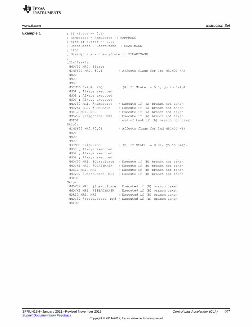
www.ti.com Instruction Set
607SPRUH18H–January 2011–Revised November 2019Submit Documentation Feedback
Copyright © 2011–2019, Texas Instruments Incorporated
Control Law Accelerator (CLA)
Example 1 ; if (State == 0.1); RampState = RampState || RAMPMASK; else if (State == 0.01); CoastState = CoastState || COASTMASK; else; SteadyState = SteadyState || STEADYMASK;_Cla1Task1:
MMOV32 MR0, @StateMCMPF32 MR0, #0.1 ; Affects flags for 1st MBCNDD (A)MNOPMNOPMNOPMBCNDD Skip1, NEQ ; (A) If State != 0.1, go to Skip1MNOP ; Always executedMNOP ; Always executedMNOP ; Always executedMMOV32 MR1, @RampState ; Execute if (A) branch not takenMMOVXI MR2, #RAMPMASK ; Execute if (A) branch not takenMOR32 MR1, MR2 ; Execute if (A) branch not takenMMOV32 @RampState, MR1 ; Execute if (A) branch not takenMSTOP ; end of task if (A) branch not taken
Skip1:MCMPF32 MR0,#0.01 ; Affects flags for 2nd MBCNDD (B)MNOPMNOPMNOPMBCNDD Skip2,NEQ ; (B) If State != 0.01, go to Skip2MNOP ; Always executedMNOP ; Always executedMNOP ; Always executedMMOV32 MR1, @CoastState ; Execute if (B) branch not takenMMOVXI MR2, #COASTMASK ; Execute if (B) branch not takenMOR32 MR1, MR2 ; Execute if (B) branch not takenMMOV32 @CoastState, MR1 ; Execute if (B) branch not takenMSTOP
Skip2:MMOV32 MR3, @SteadyState ; Executed if (B) branch takenMMOVXI MR2, #STEADYMASK ; Executed if (B) branch takenMOR32 MR3, MR2 ; Executed if (B) branch takenMMOV32 @SteadyState, MR3 ; Executed if (B) branch takenMSTOP

Instruction Set www.ti.com
608 SPRUH18H–January 2011–Revised November 2019Submit Documentation Feedback
Copyright © 2011–2019, Texas Instruments Incorporated
Control Law Accelerator (CLA)
Example 2 ; This example is the same as Example 1, except; the code is optimized to take advantage of delay slots;; if (State == 0.1); RampState = RampState || RAMPMASK; else if (State == 0.01); CoastState = CoastState || COASTMASK; else; SteadyState = SteadyState || STEADYMASK;_Cla1Task2:
MMOV32 MR0, @StateMCMPF32 MR0, #0.1 ; Affects flags for 1st MBCNDD (A)MCMPF32 MR0, #0.01 ; Check used by 2nd MBCNDD (B)MTESTTF EQ ; Store EQ flag in TF for 2nd MBCNDD (B)MNOPMBCNDD Skip1, NEQ ; (A) If State != 0.1, go to Skip1MMOV32 MR1, @RampState ; Always executedMMOVXI MR2, #RAMPMASK ; Always executedMOR32 MR1, MR2 ; Always executedMMOV32 @RampState, MR1 ; Execute if (A) branch not takenMSTOP ; end of task if (A) branch not taken
Skip1:MMOV32 MR3, @SteadyStateMMOVXI MR2, #STEADYMASKMOR32 MR3, MR2MBCNDD Skip2, NTF ; (B) if State != .01, go to Skip2MMOV32 MR1, @CoastState ; Always executedMMOVXI MR2, #COASTMASK ; Always executedMOR32 MR1, MR2 ; Always executedMMOV32 @CoastState, MR1 ; Execute if (B) branch not takenMSTOP ; end of task if (B) branch not taken
Skip2:MMOV32 @SteadyState, MR3 ; Executed if (B) branch takenMSTOP
See also MCCNDD 16BitDest, CNDFMRCNDD CNDF

www.ti.com Instruction Set
609SPRUH18H–January 2011–Revised November 2019Submit Documentation Feedback
Copyright © 2011–2019, Texas Instruments Incorporated
Control Law Accelerator (CLA)
MCCNDD 16BitDest {, CNDF} Call Conditional Delayed
Operands16BitDest 16-bit destination if condition is trueCNDF Optional condition to be tested
Opcode LSW: dest dest dest destMSW: 0111 1001 1001 cndf
Description If the specified condition is true, then store the return address in the RPC field of MSTFand make the call by adding the signed 16BitDest value to the MPC value. Otherwise,continue code execution without making the call. If the address overflows, it wrapsaround. Therefore a value of "0xFFFE" will put the MPC back to the MCCNDDinstruction.
Please refer to the pipeline section for important information regarding this instruction.if (CNDF == TRUE){
RPC = return address;MPC += 16BitDest;
};
CNDF is one of the following conditions:
(3) Values not shown are reserved.(4) This is the default operation if no CNDF field is specified. This condition will allow the ZF and NF flags to
be modified when a conditional operation is executed. All other conditions will not modify these flags.
Encode (3) CNDF Description MSTF Flags Tested0000 NEQ Not equal to zero ZF == 00001 EQ Equal to zero ZF == 10010 GT Greater than zero ZF == 0 AND NF == 00011 GEQ Greater than or equal to zero NF == 00100 LT Less than zero NF == 10101 LEQ Less than or equal to zero ZF == 1 OR NF == 11010 TF Test flag set TF == 11011 NTF Test flag not set TF == 01100 LU Latched underflow LUF == 11101 LV Latched overflow LVF == 11110 UNC Unconditional None1111 UNCF (4) Unconditional with flag
modificationNone
Restrictions The MCCNDD instruction is not allowed three instructions before or after a MBCNDD,MCCNDD, or MRCNDD instruction. Refer to the Pipeline section for more details.
Flags This instruction does not modify flags in the MSTF register.Flag TF ZF NF LUF LVFModified No No No No No

Instruction Set www.ti.com
610 SPRUH18H–January 2011–Revised November 2019Submit Documentation Feedback
Copyright © 2011–2019, Texas Instruments Incorporated
Control Law Accelerator (CLA)
Pipeline The MCCNDD instruction by itself is a single-cycle instruction. As shown in Table 10-13,for each call 6 instruction slots are executed; three before the call instruction (I2-I4) andthree after the call instruction (I5-I7). The total number of cycles for a call taken or nottaken depends on the usage of these slots. That is, the number of cycles depends onhow many slots are filled with a MNOP as well as which slots are filled. The effectivenumber of cycles for a call can, therefore, range from 1 to 7 cycles. The number ofcycles for a call taken may not be the same as for a call not taken.
Referring to the following code fragment and the pipeline diagrams in Table 10-13 andTable 10-14, the instructions before and after MCCNDD have the following properties:• I1
– I1 is the last instruction that can effect the CNDF flags for the MCCNDDinstruction. The CNDF flags are tested in the D2 phase of the pipeline. That is, adecision is made whether to branch or not when MCCNDD is in the D2 phase.
– There are no restrictions on the type of instruction for I1.• I2, I3 and I4
– The three instructions proceeding MCCNDD can change MSTF flags but will haveno effect on whether the MCCNDD instruction makes the call or not. This isbecause the flag modification will occur after the D2 phase of the MCCNDDinstruction.
– These instructions must not be the following: MSTOP, MDEBUGSTOP,MBCNDD, MCCNDD or MRCNDD.
• I5, I6 and I7– The three instructions following MBCNDD are always executed irrespective of
whether the branch is taken or not.– These instructions must not be the following: MSTOP, MDEBUGSTOP,
MBCNDD, MCCNDD or MRCNDD.

www.ti.com Instruction Set
611SPRUH18H–January 2011–Revised November 2019Submit Documentation Feedback
Copyright © 2011–2019, Texas Instruments Incorporated
Control Law Accelerator (CLA)
<Instruction 1> ; I1 Last instruction that can affect flags for; the MCCNDD operation
<Instruction 2> ; I2 Cannot be stop, branch, call or return<Instruction 3> ; I3 Cannot be stop, branch, call or return<Instruction 4> ; I4 Cannot be stop, branch, call or return
MCCNDD _func, NEQ ; Call to func if not eqal to zero
; Three instructions after MCCNDD are always; executed whether the call is taken or not
<Instruction 5> ; I5 Cannot be stop, branch, call or return<Instruction 6> ; I6 Cannot be stop, branch, call or return<Instruction 7> ; I7 Cannot be stop, branch, call or return<Instruction 8> ; I8 The address of this instruction is saved
; in the RPC field of the MSTF register.; Upon return this value is loaded into MPC; and fetching continues from this point.
<Instruction 9> ; I9...._func:<Destination 1> ; d1 Can be any instruction<Destination 2> ; d2<Destination 3> ; d3<Destination 4> ; d4 Last instruction that can affect flags for
; the MRCNDD operation
<Destination 5> ; d5 Cannot be stop, branch, call or return<Destination 6> ; d6 Cannot be stop, branch, call or return<Destination 7> ; d7 Cannot be stop, branch, call or return
MRCNDD UNC ; Return to <Instruction 8>, unconditional
; Three instructions after MRCNDD are always; executed whether the return is taken or not
<Destination 8> ; d8 Cannot be stop, branch, call or return<Destination 9> ; d9 Cannot be stop, branch, call or return<Destination 10> ; d10 Cannot be stop, branch, call or return<Destination 11> ; d11....MSTOP

Instruction Set www.ti.com
612 SPRUH18H–January 2011–Revised November 2019Submit Documentation Feedback
Copyright © 2011–2019, Texas Instruments Incorporated
Control Law Accelerator (CLA)
Table 10-13. Pipeline Activity For MCCNDD, Call Not TakenInstruction F1 F2 D1 D2 R1 R2 E W
I1 I1
I2 I2 I1
I3 I3 I2 I1
I4 I4 I3 I2 I1
MCCNDD MCCNDD I4 I3 I2 I1
I5 I5 MCCNDD I4 I3 I2 I1
I6 I6 I5 MCCNDD I4 I3 I2 I1
I7 I7 I6 I5 MCCNDD I4 I3 I2
I8 I8 I7 I6 I5 - I4 I3
I9 I9 I8 I7 I6 I5 - I4
I10 I10 I9 I8 I7 I6 I5 -
etc .... I10 I9 I8 I7 I6 I5
.... I10 I9 I8 I7 I6
.... I10 I9 I8 I7
.... I10 I9 I8
I10 I9
I10
(1) The RPC value in the MSTF register will point to the instruction following I7 (instruction I8).
Table 10-14. Pipeline Activity For MCCNDD, Call TakenInstruction F1 F2 D1 D2 R1 R2 E W
I1 I1
I2 I2 I1
I3 I3 I2 I1
I4 I4 I3 I2 I1
MCCNDD MCCNDD I4 I3 I2 I1
I5 I5 MCCNDD I4 I3 I2 I1
I6 I6 I5 MCCNDD I4 I3 I2 I1
I7 (1) I7 I6 I5 MCCNDD I4 I3 I2
d1 d1 I7 I6 I5 - I4 I3
d2 d2 d1 I7 I6 I5 - I4
d3 d3 d2 d1 I7 I6 I5 -
etc .... d3 d2 d1 I7 I6 I5
.... d3 d2 d1 I7 I6
.... d3 d2 d1 I7
.... d3 d2 d1
d3 d2
d3
Example ;
See also MBCNDD #16BitDest, CNDFMMOV32 mem32, MSTFMMOV32 MSTF, mem32MRCNDD CNDF

www.ti.com Instruction Set
613SPRUH18H–January 2011–Revised November 2019Submit Documentation Feedback
Copyright © 2011–2019, Texas Instruments Incorporated
Control Law Accelerator (CLA)
MCMP32 MRa, MRb 32-Bit Integer Compare for Equal, Less Than or Greater Than
OperandsMRa CLA floating-point source register (MR0 to MR3)MRb CLA floating-point source register (MR0 to MR3)
Opcode LSW: 0000 0000 0000 bbaaMSW: 0111 1111 0010 0000
Description Set ZF and NF flags on the result of MRa - MRb where MRa and MRb are 32-bitintegers. For a floating point compare refer to MCMPF32.
NOTE: A known hardware issue exists in the MCMP32 instruction. Signedinteger comparisons using MCMP32 by itself will set the status bits in away that is not useful for comparison when the difference between thetwo operands is too large, such as when the inputs have opposite signand are near the extreme 32-bit signed values. This affects both signedand unsigned integer comparisons.
The compiler (version 18.1.5.LTS or higher) has implemented aworkaround for this issue. The compiler can check the upper bits of theoperands by performing a floating point comparison before proceeding todo the integer comparison or subtraction.
Flags This instruction modifies the following flags in the MSTF register:Flag TF ZF NF LUF LVFModified No Yes Yes No No
The MSTF register flags are modified based on the integer results of the operation.
If(MRa == MRb) {ZF=1; NF=0;}If(MRa > MRb) {ZF=0; NF=0;}If(MRa < MRb) {ZF=0; NF=1;}
Pipeline This is a single-cycle instruction.
Example ; Behavior of ZF and NF flags for different comparisons;; Given A = (int32)1; B = (int32)2; C = (int32)-7;
MMOV32 MR0, @_A ; MR0 = 1 (0x00000001)MMOV32 MR1, @_B ; MR1 = 2 (0x00000002)MMOV32 MR2, @_C ; MR2 = -7 (0xFFFFFFF9)MCMP32 MR2, MR2 ; NF = 0, ZF = 1MCMP32 MR0, MR1 ; NF = 1, ZF = 0MCMP32 MR1, MR0 ; NF = 0, ZF = 0
See also MADD32 MRa, MRb, MRcMSUB32 MRa, MRb, MRc

Instruction Set www.ti.com
614 SPRUH18H–January 2011–Revised November 2019Submit Documentation Feedback
Copyright © 2011–2019, Texas Instruments Incorporated
Control Law Accelerator (CLA)
MCMPF32 MRa, MRb 32-Bit Floating-Point Compare for Equal, Less Than or Greater Than
OperandsMRa CLA floating-point source register (MR0 to MR3)MRb CLA floating-point source register (MR0 to MR3)
Opcode LSW: 0000 0000 0000 bbaaMSW: 0111 1101 0000 0000
Description Set ZF and NF flags on the result of MRa - MRb. The MCMPF32 instruction is performedas a logical compare operation. This is possible because of the IEEE format offsettingthe exponent. Basically the bigger the binary number, the bigger the floating-point value.
Special cases for inputs:• Negative zero will be treated as positive zero.• A denormalized value will be treated as positive zero.• Not-a-Number (NaN) will be treated as infinity.
Flags This instruction modifies the following flags in the MSTF register:Flag TF ZF NF LUF LVFModified No Yes Yes No No
The MSTF register flags are modified as follows:
If(MRa == MRb) {ZF=1; NF=0;}If(MRa > MRb) {ZF=0; NF=0;}If(MRa < MRb) {ZF=0; NF=1;}
Pipeline This is a single-cycle instruction.
Example ; Behavior of ZF and NF flags for different comparisons
MMOVIZ MR1, #-2.0 ; MR1 = -2.0 (0xC0000000)MMOVIZ MR0, #5.0 ; MR0 = 5.0 (0x40A00000)MCMPF32 MR1, MR0 ; ZF = 0, NF = 1MCMPF32 MR0, MR1 ; ZF = 0, NF = 0MCMPF32 MR0, MR0 ; ZF = 1, NF = 0
See also MCMPF32 MRa, #16FHiMMAXF32 MRa, #16FHiMMAXF32 MRa, MRbMMINF32 MRa, #16FHiMMINF32 MRa, MRb

www.ti.com Instruction Set
615SPRUH18H–January 2011–Revised November 2019Submit Documentation Feedback
Copyright © 2011–2019, Texas Instruments Incorporated
Control Law Accelerator (CLA)
MCMPF32 MRa, #16FHi 32-Bit Floating-Point Compare for Equal, Less Than or Greater Than
OperandsMRa CLA floating-point source register (MR0 to MR3)#16FHi A 16-bit immediate value that represents the upper 16-bits of an IEEE 32-bit floating-
point value. The low 16-bits of the mantissa are assumed to be all 0.
Opcode LSW: IIII IIII IIII IIIIMSW: 0111 1000 1100 00aa
Description Compare the value in MRa with the floating-point value represented by the immediateoperand. Set the ZF and NF flags on (MRa - #16FHi:0).
#16FHi is a 16-bit immediate value that represents the upper 16-bits of an IEEE 32-bitfloating-point value. The low 16-bits of the mantissa are assumed to be all 0. Thisaddressing mode is most useful for constants where the lowest 16-bits of the mantissaare 0. Some examples are 2.0 (0x40000000), 4.0 (0x40800000), 0.5 (0x3F000000), and-1.5 (0xBFC00000). The assembler will accept either a hex or float as the immediatevalue. That is, -1.5 can be represented as #-1.5 or #0xBFC0.
The MCMPF32 instruction is performed as a logical compare operation. This is possiblebecause of the IEEE floating-point format offsets the exponent. Basically the bigger thebinary number, the bigger the floating-point value.
Special cases for inputs:• Negative zero will be treated as positive zero.• Denormalized value will be treated as positive zero.• Not-a-Number (NaN) will be treated as infinity.
Flags This instruction modifies the following flags in the MSTF register:Flag TF ZF NF LUF LVFModified No Yes Yes No No
The MSTF register flags are modified as follows:
If(MRa == #16FHi:0) {ZF=1, NF=0;}If(MRa > #16FHi:0) {ZF=0, NF=0;}If(MRa < #16FHi:0) {ZF=0, NF=1;}
Pipeline This is a single-cycle instruction
Example 1 ; Behavior of ZF and NF flags for different comparisons
MMOVIZ MR1, #-2.0 ; MR1 = -2.0 (0xC0000000)MMOVIZ MR0, #5.0 ; MR0 = 5.0 (0x40A00000)MCMPF32 MR1, #-2.2 ; ZF = 0, NF = 0MCMPF32 MR0, #6.5 ; ZF = 0, NF = 1MCMPF32 MR0, #5.0 ; ZF = 1, NF = 0

Instruction Set www.ti.com
616 SPRUH18H–January 2011–Revised November 2019Submit Documentation Feedback
Copyright © 2011–2019, Texas Instruments Incorporated
Control Law Accelerator (CLA)
Example 2 ; X is an array of 32-bit floating-point values; and has len elements. Find the maximum value in; the array and store it in Result;; Note: MCMPF32 and MSWAPF can be replaced with MMAXF32;_Cla1Task1:
MMOVI16 MAR1,#_X ; Start addressMUI16TOF32 MR0, @_len ; Length of the arrayMNOP ; delay for MAR1 loadMNOP ; delay for MAR1 loadMMOV32 MR1, *MAR1[2]++ ; MR1 = X0
LOOPMMOV32 MR2, *MAR1[2]++ ; MR2 = next elementMCMPF32 MR2, MR1 ; Compare MR2 with MR1MSWAPF MR1, MR2, GT ; MR1 = MAX(MR1, MR2)MADDF32 MR0, MR0, #-1.0 ; Decrememt the counterMCMPF32 MR0 #0.0 ; Set/clear flags for MBCNDDMNOPMNOPMNOPMBCNDD LOOP, NEQ ; Branch if not equal to zeroMMOV32 @_Result, MR1 ; Always executedMNOP ; Always executedMNOP ; Always executedMSTOP ; End of task
See also MCMPF32 MRa, MRbMMAXF32 MRa, #16FHiMMAXF32 MRa, MRbMMINF32 MRa, #16FHiMMINF32 MRa, MRb

www.ti.com Instruction Set
617SPRUH18H–January 2011–Revised November 2019Submit Documentation Feedback
Copyright © 2011–2019, Texas Instruments Incorporated
Control Law Accelerator (CLA)
MDEBUGSTOP Debug Stop Task
Operandsnone This instruction does not have any operands
Opcode LSW: 0000 0000 0000 0000MSW: 0111 1111 0110 0000
Description When CLA breakpoints are enabled, the MDEBUGSTOP instruction is used to halt atask so that it can be debugged. That is, MDEBUGSTOP is the CLA breakpoint. If CLAbreakpoints are not enabled, the MDEBUGSTOP instruction behaves like a MNOP.Unlike the MSTOP, the MIRUN flag is not cleared and an interrupt is not issued. Asingle-step or run operation will continue execution of the task.
Restrictions The MDEBUGSTOP instruction cannot be placed 3 instructions before or after aMBCNDD, MCCNDD or MRCNDD instruction.
Flags This instruction does not modify flags in the MSTF register.Flag TF ZF NF LUF LVFModified No No No No No
Pipeline This is a single-cycle instruction.
Example ;
See also MSTOP,

Instruction Set www.ti.com
618 SPRUH18H–January 2011–Revised November 2019Submit Documentation Feedback
Copyright © 2011–2019, Texas Instruments Incorporated
Control Law Accelerator (CLA)
MEALLOW Enable CLA Write Access to EALLOW Protected Registers
Operandsnone This instruction does not have any operands
Opcode LSW: 0000 0000 0000 0000MSW: 0111 1111 1001 0000
Description This instruction sets the MEALLOW bit in the CLA status register MSTF. When this bit isset, the CLA is allowed write access to EALLOW protected registers. To again protectagainst CLA writes to protected registers, use the MEDIS instruction.
MEALLOW and MEDIS only control CLA write access; reads are allowed even ifMEALLOW has not been executed. MEALLOW and MEDIS are also independent fromthe main CPU's EALLOW/EDIS. This instruction does not modify the EALLOW bit in themain CPU's status register. The MEALLOW bit in MSTF only controls access for theCLA while the EALLOW bit in the ST1 register only controls access for the main CPU.
As with EALLOW, the MEALLOW bit is overridden via the JTAG port, allowing full controlof register accesses during debug from Code Composer Studio.
Flags This instruction does not modify flags in the MSTF register.Flag TF ZF NF LUF LVFModified No No No No No
Pipeline This is a single-cycle instruction.
Example ; C header file including definition of; the EPwm1Regs structure;; The ePWM TZSEL register is EALLOW protected;
.cdecls C,LIST,"CLAShared.h"
..._Cla1Task1:
...MEALLOW ; Allow CLA write accessMMOV16 @_EPwm1Regs.TZSEL.all, MR3 ; Write to TZSELMEDIS ; Disallow CLA write access......MSTOP
See also MEDIS

www.ti.com Instruction Set
619SPRUH18H–January 2011–Revised November 2019Submit Documentation Feedback
Copyright © 2011–2019, Texas Instruments Incorporated
Control Law Accelerator (CLA)
MEDIS Disable CLA Write Access to EALLOW Protected Registers
Operandsnone This instruction does not have any operands
Opcode LSW: 0000 0000 0000 0000MSW: 0111 1111 1011 0000
Description This instruction clears the MEALLOW bit in the CLA status register MSTF. When this bitis clear, the CLA is not allowed write access to EALLOW-protected registers. To enableCLA writes to protected registers, use the MEALLOW instruction.
MEALLOW and MEDIS only control CLA write access; reads are allowed even ifMEALLOW has not been executed. MEALLOW and MEDIS are also independent fromthe main CPU's EALLOW/EDIS. This instruction does not modify the EALLOW bit in themain CPU's status register. The MEALLOW bit in MSTF only controls access for theCLA while the EALLOW bit in the ST1 register only controls access for the main CPU.
As with EALLOW, the MEALLOW bit is overridden via the JTAG port, allowing full controlof register accesses during debug from Code Composer Studio.
Flags This instruction does not modify flags in the MSTF register.Flag TF ZF NF LUF LVFModified No No No No No
Pipeline This is a single-cycle instruction.
Example ; C header file including definition of; the EPwm1Regs structure;; The ePWM TZSEL register is EALLOW protected;
.cdecls C,LIST,"CLAShared.h"
..._Cla1Task1:
...MEALLOW ; Allow CLA write accessMMOV16 @_EPwm1Regs.TZSEL.all, MR3 ; Write to TZSELMEDIS ; Disallow CLA write access......MSTOP
See also MEALLOW

Instruction Set www.ti.com
620 SPRUH18H–January 2011–Revised November 2019Submit Documentation Feedback
Copyright © 2011–2019, Texas Instruments Incorporated
Control Law Accelerator (CLA)
MEINVF32 MRa, MRb 32-Bit Floating-Point Reciprocal Approximation
OperandsMRa CLA floating-point destination register (MR0 to MR3)MRb CLA floating-point source register (MR0 to MR3)
Opcode LSW: 0000 0000 0000 bbaaMSW: 0111 1111 0000 0000
Description This operation generates an estimate of 1/X in 32-bit floating-point format accurate toapproximately 8 bits. This value can be used in a Newton-Raphson algorithm to get amore accurate answer. That is:Ye = Estimate(1/X);Ye = Ye*(2.0 - Ye*X);Ye = Ye*(2.0 - Ye*X);
After two iterations of the Newton-Raphson algorithm, you will get an exact answeraccurate to the 32-bit floating-point format. On each iteration the mantissa bit accuracyapproximately doubles. The MEINVF32 operation will not generate a negative zero,DeNorm or NaN value.MRa = Estimate of 1/MRb;
Flags This instruction modifies the following flags in the MSTF register:Flag TF ZF NF LUF LVFModified No No No Yes Yes
The MSTF register flags are modified as follows:• LUF = 1 if MEINVF32 generates an underflow condition.• LVF = 1 if MEINVF32 generates an overflow condition.
Pipeline This is a single-cycle instruction.
Example ; Calculate Num/Den using a Newton-Raphson algorithum for 1/Den; Ye = Estimate(1/X); Ye = Ye*(2.0 - Ye*X); Ye = Ye*(2.0 - Ye*X);_Cla1Task1:
MMOV32 MR1, @_Den ; MR1 = DenMEINVF32 MR2, MR1 ; MR2 = Ye = Estimate(1/Den)MMPYF32 MR3, MR2, MR1 ; MR3 = Ye*DenMSUBF32 MR3, #2.0, MR3 ; MR3 = 2.0 - Ye*DenMMPYF32 MR2, MR2, MR3 ; MR2 = Ye = Ye*(2.0 - Ye*Den)MMPYF32 MR3, MR2, MR1 ; MR3 = Ye*Den
|| MMOV32 MR0, @_Num ; MR0 = NumMSUBF32 MR3, #2.0, MR3 ; MR3 = 2.0 - Ye*DenMMPYF32 MR2, MR2, MR3 ; MR2 = Ye = Ye*(2.0 - Ye*Den)
|| MMOV32 MR1, @_Den ; Reload Den To Set SignMNEGF32 MR0, MR0, EQ ; if(Den == 0.0) Change Sign Of NumMMPYF32 MR0, MR2, MR0 ; MR0 = Y = Ye*NumMMOV32 @_Dest, MR0 ; Store resultMSTOP ; end of task
See also MEISQRTF32 MRa, MRb

www.ti.com Instruction Set
621SPRUH18H–January 2011–Revised November 2019Submit Documentation Feedback
Copyright © 2011–2019, Texas Instruments Incorporated
Control Law Accelerator (CLA)
MEISQRTF32 MRa, MRb 32-Bit Floating-Point Square-Root Reciprocal Approximation
OperandsMRa CLA floating-point destination register (MR0 to MR3)MRb CLA floating-point source register (MR0 to MR3)
Opcode LSW: 0000 0000 0000 bbaaMSW: 0111 1110 0100 0000
Description This operation generates an estimate of 1/sqrt(X) in 32-bit floating-point format accurateto approximately 8 bits. This value can be used in a Newton-Raphson algorithm to get amore accurate answer. That is:Ye = Estimate(1/sqrt(X));Ye = Ye*(1.5 - Ye*Ye*X/2.0);Ye = Ye*(1.5 - Ye*Ye*X/2.0);
After 2 iterations of the Newton-Raphson algorithm, you will get an exact answeraccurate to the 32-bit floating-point format. On each iteration the mantissa bit accuracyapproximately doubles. The MEISQRTF32 operation will not generate a negative zero,DeNorm or NaN value.MRa = Estimate of 1/sqrt (MRb);
Flags This instruction modifies the following flags in the MSTF register:Flag TF ZF NF LUF LVFModified No No No Yes Yes
The MSTF register flags are modified as follows:• LUF = 1 if MEISQRTF32 generates an underflow condition.• LVF = 1 if MEISQRTF32 generates an overflow condition.
Pipeline This is a single-cycle instruction.
Example ; Y = sqrt(X); Ye = Estimate(1/sqrt(X));; Ye = Ye*(1.5 - Ye*Ye*X*0.5); Ye = Ye*(1.5 - Ye*Ye*X*0.5); Y = X*Ye;_Cla1Task3:
MMOV32 MR0, @_x ; MR0 = XMEISQRTF32 MR1, MR0 ; MR1 = Ye = Estimate(1/sqrt(X))MMOV32 MR1, @_x, EQ ; if(X == 0.0) Ye = 0.0MMPYF32 MR3, MR0, #0.5 ; MR3 = X*0.5MMPYF32 MR2, MR1, MR3 ; MR2 = Ye*X*0.5MMPYF32 MR2, MR1, MR2 ; MR2 = Ye*Ye*X*0.5MSUBF32 MR2, #1.5, MR2 ; MR2 = 1.5 - Ye*Ye*X*0.5MMPYF32 MR1, MR1, MR2 ; MR1 = Ye = Ye*(1.5 - Ye*Ye*X*0.5)MMPYF32 MR2, MR1, MR3 ; MR2 = Ye*X*0.5MMPYF32 MR2, MR1, MR2 ; MR2 = Ye*Ye*X*0.5MSUBF32 MR2, #1.5, MR2 ; MR2 = 1.5 - Ye*Ye*X*0.5MMPYF32 MR1, MR1, MR2 ; MR1 = Ye = Ye*(1.5 - Ye*Ye*X*0.5)MMPYF32 MR0, MR1, MR0 ; MR0 = Y = Ye*XMMOV32 @_y, MR0 ; Store Y = sqrt(X)MSTOP ; end of task
See also MEINVF32 MRa, MRb

Instruction Set www.ti.com
622 SPRUH18H–January 2011–Revised November 2019Submit Documentation Feedback
Copyright © 2011–2019, Texas Instruments Incorporated
Control Law Accelerator (CLA)
MF32TOI16 MRa, MRb Convert 32-Bit Floating-Point Value to 16-Bit Integer
OperandsMRa CLA floating-point destination register (MR0 to MR3)MRb CLA floating-point source register (MR0 to MR3)
Opcode LSW: 0000 0000 0000 bbaaMSW: 0111 1101 1110 0000
Description Convert a 32-bit floating point value in MRb to a 16-bit integer and truncate. The resultwill be stored in MRa.MRa(15:0) = F32TOI16(MRb);MRa(31:16) = sign extension of MRa(15);
Flags This instruction does not affect any flags:Flag TF ZF NF LUF LVFModified No No No No No
Pipeline This is a single-cycle instruction.
Example MMOVIZ MR0, #5.0 ; MR0 = 5.0 (0x40A00000)MF32TOI16 MR1, MR0 ; MR1(15:0) = MF32TOI16(MR0) = 0x0005
; MR1(31:16) = Sign extension of MR1(15) = 0x0000MMOVIZ MR2, #-5.0 ; MR2 = -5.0 (0xC0A00000)MF32TOI16 MR3, MR2 ; MR3(15:0) = MF32TOI16(MR2) = -5 (0xFFFB)
; MR3(31:16) = Sign extension of MR3(15) = 0xFFFF
See also MF32TOI16R MRa, MRbMF32TOUI16 MRa, MRbMF32TOUI16R MRa, MRbMI16TOF32 MRa, MRbMI16TOF32 MRa, mem16MUI16TOF32 MRa, mem16MUI16TOF32 MRa, MRb

www.ti.com Instruction Set
623SPRUH18H–January 2011–Revised November 2019Submit Documentation Feedback
Copyright © 2011–2019, Texas Instruments Incorporated
Control Law Accelerator (CLA)
MF32TOI16R MRa, MRb Convert 32-Bit Floating-Point Value to 16-Bit Integer and Round
OperandsMRa CLA floating-point destination register (MR0 to MR3)MRb CLA floating-point source register (MR0 to MR3)
Opcode LSW: 0000 0000 0000 bbaaMSW: 0111 1110 0110 0000
Description Convert the 32-bit floating point value in MRb to a 16-bit integer and round to the nearesteven value. The result is stored in MRa.MRa(15:0) = F32TOI16round(MRb);MRa(31:16) = sign extension of MRa(15);
Flags This instruction does not affect any flags:Flag TF ZF NF LUF LVFModified No No No No No
Pipeline This is a single-cycle instruction.
Example MMOVIZ MR0, #0x3FD9 ; MR0(31:16) = 0x3FD9MMOVXI MR0, #0x999A ; MR0(15:0) = 0x999A
; MR0 = 1.7 (0x3FD9999A)MF32TOI16R MR1, MR0 ; MR1(15:0) = MF32TOI16round (MR0) = 2 (0x0002)
; MR1(31:16) = Sign extension of MR1(15) = 0x0000MMOVF32 MR2, #-1.7 ; MR2 = -1.7 (0xBFD9999A)MF32TOI16R MR3, MR2 ; MR3(15:0) = MF32TOI16round (MR2) = -2 (0xFFFE)
; MR3(31:16) = Sign extension of MR2(15) = 0xFFFF
See also MF32TOI16 MRa, MRbMF32TOUI16 MRa, MRbMF32TOUI16R MRa, MRbMI16TOF32 MRa, MRbMI16TOF32 MRa, mem16MUI16TOF32 MRa, mem16MUI16TOF32 MRa, MRb

Instruction Set www.ti.com
624 SPRUH18H–January 2011–Revised November 2019Submit Documentation Feedback
Copyright © 2011–2019, Texas Instruments Incorporated
Control Law Accelerator (CLA)
MF32TOI32 MRa, MRb Convert 32-Bit Floating-Point Value to 32-Bit Integer
OperandsMRa CLA floating-point destination register (MR0 to MR3)MRb CLA floating-point source register (MR0 to MR3)
Opcode LSW: 0000 0000 0000 bbaaMSW: 0111 1101 0110 0000
Description Convert the 32-bit floating-point value in MRb to a 32-bit integer value and truncate.Store the result in MRa.MRa = F32TOI32(MRb);
Flags This instruction does not affect any flags:Flag TF ZF NF LUF LVFModified No No No No No
Pipeline This is a single-cycle instruction.
Example 1 MMOVF32 MR2, #11204005.0 ; MR2 = 11204005.0 (0x4B2AF5A5)MF32TOI32 MR3, MR2 ; MR3 = MF32TOI32(MR2) = 11204005 (0x00AAF5A5)MMOVF32 MR0, #-11204005.0 ; MR0 = -11204005.0 (0xCB2AF5A5)MF32TOI32 MR1, MR0 ; MR1 = MF32TOI32(MR0) = -11204005 (0xFF550A5B)
Example 2 ; Given X, M and B are IQ24 numbers:; X = IQ24(+2.5) = 0x02800000; M = IQ24(+1.5) = 0x01800000; B = IQ24(-0.5) = 0xFF800000;; Calculate Y = X * M + B;; Convert M, X and B from IQ24 to float;_Cla1Task2:
MI32TOF32 MR0, @_M ; MR0 = 0x4BC00000MI32TOF32 MR1, @_X ; MR1 = 0x4C200000MI32TOF32 MR2, @_B ; MR2 = 0xCB000000MMPYF32 MR0, MR0, #0x3380 ; M = 1/(1*2^24) * iqm = 1.5 (0x3FC00000)MMPYF32 MR1, MR1, #0x3380 ; X = 1/(1*2^24) * iqx = 2.5 (0x40200000)MMPYF32 MR2, MR2, #0x3380 ; B = 1/(1*2^24) * iqb = -.5 (0xBF000000)MMPYF32 MR3, MR0, MR1 ; M*XMADDF32 MR2, MR2, MR3 ; Y=MX+B = 3.25 (0x40500000)
; Convert Y from float32 to IQ24MMPYF32 MR2, MR2, #0x4B80 ; Y * 1*2^24MF32TOI32 MR2, MR2 ; IQ24(Y) = 0x03400000MMOV32 @_Y, MR2 ; store resultMSTOP ; end of task
See also MF32TOUI32 MRa, MRbMI32TOF32 MRa, MRbMI32TOF32 MRa, mem32MUI32TOF32 MRa, MRbMUI32TOF32 MRa, mem32
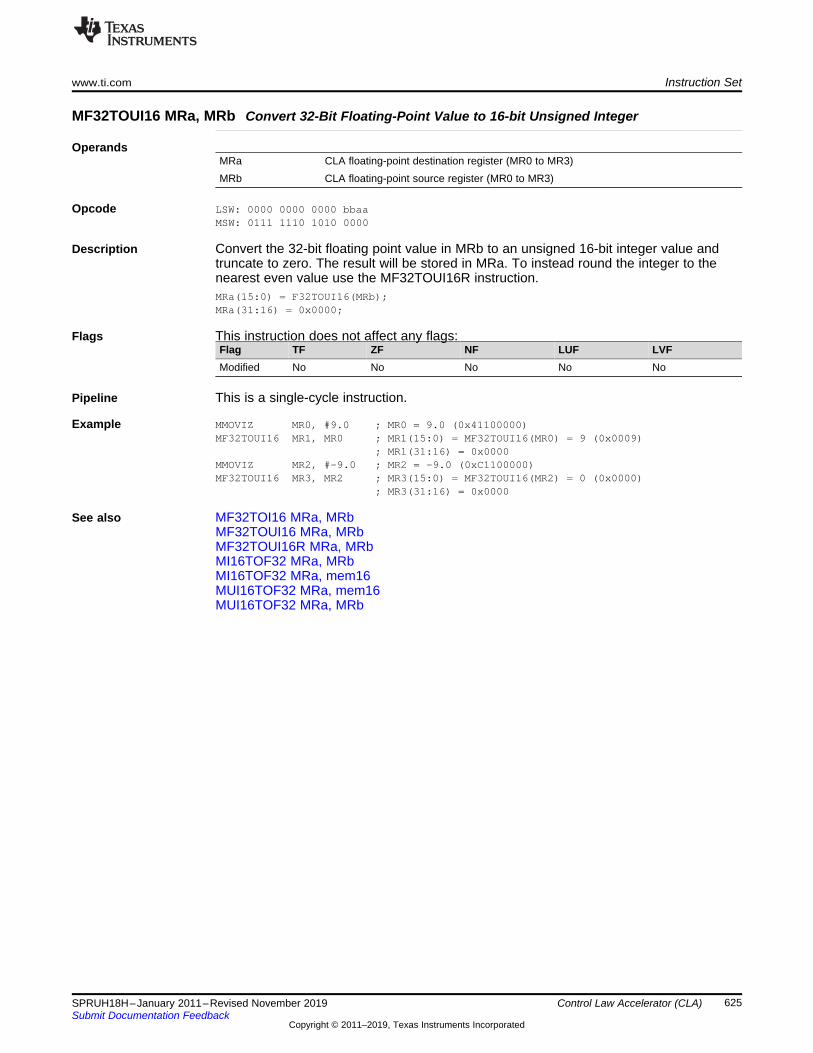
www.ti.com Instruction Set
625SPRUH18H–January 2011–Revised November 2019Submit Documentation Feedback
Copyright © 2011–2019, Texas Instruments Incorporated
Control Law Accelerator (CLA)
MF32TOUI16 MRa, MRb Convert 32-Bit Floating-Point Value to 16-bit Unsigned Integer
OperandsMRa CLA floating-point destination register (MR0 to MR3)MRb CLA floating-point source register (MR0 to MR3)
Opcode LSW: 0000 0000 0000 bbaaMSW: 0111 1110 1010 0000
Description Convert the 32-bit floating point value in MRb to an unsigned 16-bit integer value andtruncate to zero. The result will be stored in MRa. To instead round the integer to thenearest even value use the MF32TOUI16R instruction.MRa(15:0) = F32TOUI16(MRb);MRa(31:16) = 0x0000;
Flags This instruction does not affect any flags:Flag TF ZF NF LUF LVFModified No No No No No
Pipeline This is a single-cycle instruction.
Example MMOVIZ MR0, #9.0 ; MR0 = 9.0 (0x41100000)MF32TOUI16 MR1, MR0 ; MR1(15:0) = MF32TOUI16(MR0) = 9 (0x0009)
; MR1(31:16) = 0x0000MMOVIZ MR2, #-9.0 ; MR2 = -9.0 (0xC1100000)MF32TOUI16 MR3, MR2 ; MR3(15:0) = MF32TOUI16(MR2) = 0 (0x0000)
; MR3(31:16) = 0x0000
See also MF32TOI16 MRa, MRbMF32TOUI16 MRa, MRbMF32TOUI16R MRa, MRbMI16TOF32 MRa, MRbMI16TOF32 MRa, mem16MUI16TOF32 MRa, mem16MUI16TOF32 MRa, MRb

Instruction Set www.ti.com
626 SPRUH18H–January 2011–Revised November 2019Submit Documentation Feedback
Copyright © 2011–2019, Texas Instruments Incorporated
Control Law Accelerator (CLA)
MF32TOUI16R MRa, MRb Convert 32-Bit Floating-Point Value to 16-bit Unsigned Integer and Round
OperandsMRa CLA floating-point destination register (MR0 to MR3)MRb CLA floating-point source register (MR0 to MR3)
Opcode LSW: 0000 0000 0000 bbaaMSW: 0111 1110 1100 0000
Description Convert the 32-bit floating-point value in MRb to an unsigned 16-bit integer and round tothe closest even value. The result will be stored in MRa. To instead truncate theconverted value, use the MF32TOUI16 instruction.MRa(15:0) = MF32TOUI16round(MRb);MRa(31:16) = 0x0000;
Flags This instruction does not affect any flags:Flag TF ZF NF LUF LVFModified No No No No No
Pipeline This is a single-cycle instruction.
Example MMOVIZ MR0, #0x412C ; MR0 = 0x412CMMOVXI MR0, #0xCCCD ; MR0 = 0xCCCD ; MR0 = 10.8 (0x412CCCCD)MF32TOUI16R MR1, MR0 ; MR1(15:0) = MF32TOUI16round(MR0) = 11 (0x000B)
; MR1(31:16) = 0x0000MMOVF32 MR2, #-10.8 ; MR2 = -10.8 (0x0xC12CCCCD)MF32TOUI16R MR3, MR2 ; MR3(15:0) = MF32TOUI16round(MR2) = 0 (0x0000)
; MR3(31:16) = 0x0000
See also MF32TOI16 MRa, MRbMF32TOI16R MRa, MRbMF32TOUI16 MRa, MRbMI16TOF32 MRa, MRbMI16TOF32 MRa, mem16MUI16TOF32 MRa, mem16MUI16TOF32 MRa, MRb

www.ti.com Instruction Set
627SPRUH18H–January 2011–Revised November 2019Submit Documentation Feedback
Copyright © 2011–2019, Texas Instruments Incorporated
Control Law Accelerator (CLA)
MF32TOUI32 MRa, MRb Convert 32-Bit Floating-Point Value to 32-Bit Unsigned Integer
OperandsMRa CLA floating-point destination register (MR0 to MR3)MRb CLA floating-point source register (MR0 to MR3)
Opcode LSW: 0000 0000 0000 bbaaMSW: 0111 1101 1010 0000
Description Convert the 32-bit floating-point value in MRb to an unsigned 32-bit integer and store theresult in MRa.MRa = F32TOUI32(MRb);
Flags This instruction does not affect any flags:Flag TF ZF NF LUF LVFModified No No No No No
Pipeline This is a single-cycle instruction.
Example MMOVIZ MR0, #12.5 ; MR0 = 12.5 (0x41480000)MF32TOUI32 MR0, MR0 ; MR0 = MF32TOUI32 (MR0) = 12 (0x0000000C)MMOVIZ MR1, #-6.5 ; MR1 = -6.5 (0xC0D00000)MF32TOUI32 MR2, MR1 ; MR2 = MF32TOUI32 (MR1) = 0.0 (0x00000000)
See also MF32TOI32 MRa, MRbMI32TOF32 MRa, MRbMI32TOF32 MRa, mem32MUI32TOF32 MRa, MRbMUI32TOF32 MRa, mem32

Instruction Set www.ti.com
628 SPRUH18H–January 2011–Revised November 2019Submit Documentation Feedback
Copyright © 2011–2019, Texas Instruments Incorporated
Control Law Accelerator (CLA)
MFRACF32 MRa, MRb Fractional Portion of a 32-Bit Floating-Point Value
OperandsMRa CLA floating-point destination register (MR0 to MR3)MRb CLA floating-point source register (MR0 to MR3)
Opcode LSW: 0000 0000 0000 bbaaMSW: 0111 1110 0000 0000
Description Returns in MRa the fractional portion of the 32-bit floating-point value in MRb
Flags This instruction does not affect any flags:Flag TF ZF NF LUF LVFModified No No No No No
Pipeline This is a single-cycle instruction.
Example MMOVIZ MR2, #19.625 ; MR2 = 19.625 (0x419D0000)MFRACF32 MR3, MR2 ; MR3 = MFRACF32(MR2) = 0.625 (0x3F200000)0)
See also

www.ti.com Instruction Set
629SPRUH18H–January 2011–Revised November 2019Submit Documentation Feedback
Copyright © 2011–2019, Texas Instruments Incorporated
Control Law Accelerator (CLA)
MI16TOF32 MRa, MRb Convert 16-Bit Integer to 32-Bit Floating-Point Value
OperandsMRa CLA floating-point destination register (MR0 to MR3)MRb CLA floating-point source register (MR0 to MR3)
Opcode LSW: 0000 0000 0000 bbaaMSW: 0111 1110 1000 0000
Description Convert the 16-bit signed integer in MRb to a 32-bit floating point value and store theresult in MRa.MRa = MI16TOF32(MRb);
Flags This instruction does not affect any flags:Flag TF ZF NF LUF LVFModified No No No No No
Pipeline This is a single-cycle instruction.
Example MMOVIZ MR0, #0x0000 ; MR0(31:16) = 0.0 (0x0000)MMOVXI MR0, #0x0004 ; MR0(15:0) = 4.0 (0x0004)MI16TOF32 MR1, MR0 ; MR1 = MI16TOF32 (MR0) = 4.0 (0x40800000)
MMOVIZ MR2, #0x0000 ; MR2(31:16) = 0.0 (0x0000)MMOVXI MR2, #0xFFFC ; MR2(15:0) = -4.0 (0xFFFC)MI16TOF32 MR3, MR2 ; MR3 = MI16TOF32 (MR2) = -4.0 (0xC0800000)MSTOP
See also MF32TOI16 MRa, MRbMF32TOI16R MRa, MRbMF32TOUI16 MRa, MRbMF32TOUI16R MRa, MRbMI16TOF32 MRa, mem16MUI16TOF32 MRa, mem16MUI16TOF32 MRa, MRb

Instruction Set www.ti.com
630 SPRUH18H–January 2011–Revised November 2019Submit Documentation Feedback
Copyright © 2011–2019, Texas Instruments Incorporated
Control Law Accelerator (CLA)
MI16TOF32 MRa, mem16 Convert 16-Bit Integer to 32-Bit Floating-Point Value
OperandsMRa CLA floating-point destination register (MR0 to MR3)mem16 16-bit source memory location to be converted
Opcode LSW: mmmm mmmm mmmm mmmmMSW: 0111 0101 00aa addr
Description Convert the 16-bit signed integer indicated by the mem16 pointer to a 32-bit floating-point value and store the result in MRa.MRa = MI16TOF32[mem16];
Flags This instruction does not affect any flags:Flag TF ZF NF LUF LVFModified No No No No No
Pipeline This is a single-cycle instruction:
Example ; Assume A = 4 (0x0004); B = -4 (0xFFFC)
MI16TOF32 MR0, @_A ; MR0 = MI16TOF32(A) = 4.0 (0x40800000)MI16TOF32 MR1, @_B ; MR1 = MI16TOF32(B) = -4.0 (0xC0800000
See also MF32TOI16 MRa, MRbMF32TOI16R MRa, MRbMF32TOUI16 MRa, MRbMF32TOUI16R MRa, MRbMI16TOF32 MRa, MRbMUI16TOF32 MRa, mem16MUI16TOF32 MRa, MRb

www.ti.com Instruction Set
631SPRUH18H–January 2011–Revised November 2019Submit Documentation Feedback
Copyright © 2011–2019, Texas Instruments Incorporated
Control Law Accelerator (CLA)
MI32TOF32 MRa, mem32 Convert 32-Bit Integer to 32-Bit Floating-Point Value
OperandsMRa CLA floating-point destination register (MR0 to MR3)mem32 32-bit memory source for the MMOV32 operation.
Opcode LSW: mmmm mmmm mmmm mmmmMSW: 0111 0100 01aa addr
Description Convert the 32-bit signed integer indicated by mem32 to a 32-bit floating point value andstore the result in MRa.MRa = MI32TOF32[mem32];
Flags This instruction does not affect any flags:Flag TF ZF NF LUF LVFModified No No No No No
Pipeline This is a single-cycle instruction.
Example ; Given X, M and B are IQ24 numbers:; X = IQ24(+2.5) = 0x02800000; M = IQ24(+1.5) = 0x01800000; B = IQ24(-0.5) = 0xFF800000;; Calculate Y = X * M + B;; Convert M, X and B from IQ24 to float;
_Cla1Task3:MI32TOF32 MR0, @_M ; MR0 = 0x4BC00000MI32TOF32 MR1, @_X ; MR1 = 0x4C200000MI32TOF32 MR2, @_B ; MR2 = 0xCB000000MMPYF32 MR0, MR0, #0x3380 ; M = 1/(1*2^24) * iqm = 1.5 (0x3FC00000)MMPYF32 MR1, MR1, #0x3380 ; X = 1/(1*2^24) * iqx = 2.5 (0x40200000)MMPYF32 MR2, MR2, #0x3380 ; B = 1/(1*2^24) * iqb = -.5 (0xBF000000)MMPYF32 MR3, MR0, MR1 ; M*XMADDF32 MR2, MR2, MR3 ; Y=MX+B = 3.25 (0x40500000)
; Convert Y from float32 to IQ24MMPYF32 MR2, MR2, #0x4B80 ; Y * 1*2^24MF32TOI32 MR2, MR2 ; IQ24(Y) = 0x03400000MMOV32 @_Y, MR2 ; store resultMSTOP ; end of task
See also MF32TOI32 MRa, MRbMF32TOUI32 MRa, MRbMI32TOF32 MRa, MRbMUI32TOF32 MRa, MRbMUI32TOF32 MRa, mem32

Instruction Set www.ti.com
632 SPRUH18H–January 2011–Revised November 2019Submit Documentation Feedback
Copyright © 2011–2019, Texas Instruments Incorporated
Control Law Accelerator (CLA)
MI32TOF32 MRa, MRb Convert 32-Bit Integer to 32-Bit Floating-Point Value
OperandsMRa CLA floating-point destination register (MR0 to MR3)MRb CLA floating-point source register (MR0 to MR3)
Opcode LSW: 0000 0000 0000 bbaaMSW: 0111 1101 1000 0000
Description Convert the signed 32-bit integer in MRb to a 32-bit floating-point value and store theresult in MRa.MRa = MI32TOF32(MRb);
Flags This instruction does not affect any flags:Flag TF ZF NF LUF LVFModified No No No No No
Pipeline This is a single-cycle instruction.
Example ; Example1:;
MMOVIZ MR2, #0x1111 ; MR2(31:16) = 4369 (0x1111)MMOVXI MR2, #0x1111 ; MR2(15:0) = 4369 (0x1111)
; MR2 = +286331153 (0x11111111)MI32TOF32 MR3, MR2 ; MR3 = MI32TOF32 (MR2) = 286331153.0 (0x4D888888)
See also MF32TOI32 MRa, MRbMF32TOUI32 MRa, MRbMI32TOF32 MRa, mem32MUI32TOF32 MRa, MRbMUI32TOF32 MRa, mem32

www.ti.com Instruction Set
633SPRUH18H–January 2011–Revised November 2019Submit Documentation Feedback
Copyright © 2011–2019, Texas Instruments Incorporated
Control Law Accelerator (CLA)
MLSL32 MRa, #SHIFT Logical Shift Left
OperandsMRa CLA floating-point source/destination register (MR0 to MR3)#SHIFT Number of bits to shift (1 to 32)
Opcode LSW: 0000 0000 0shi ftaaMSW: 0111 1011 1100 0000
Description Logical shift left of MRa by the number of bits indicated. The number of bits can be 1 to32.MARa(31:0) = Logical Shift Left(MARa(31:0) by #SHIFT bits);
Flags This instruction modifies the following flags in the MSTF register:Flag TF ZF NF LUF LVFModified No Yes Yes No No
The MSTF register flags are modified based on the integer results of the operation.NF = MRa(31);ZF = 0;if(MRa(31:0) == 0) { ZF = 1; }
Pipeline This is a single-cycle instruction.
Example ; Given m2 = (int32)32; x2 = (int32)64; b2 = (int32)-128;; Calculate:; m2 = m2*2; x2 = x2*4; b2 = b2*8;_Cla1Task3:
MMOV32 MR0, @_m2 ; MR0 = 32 (0x00000020)MMOV32 MR1, @_x2 ; MR1 = 64 (0x00000040)MMOV32 MR2, @_b2 ; MR2 = -128 (0xFFFFFF80)MLSL32 MR0, #1 ; MR0 = 64 (0x00000040)MLSL32 MR1, #2 ; MR1 = 256 (0x00000100)MLSL32 MR2, #3 ; MR2 = -1024 (0xFFFFFC00)MMOV32 @_m2, MR0 ; Store resultsMMOV32 @_x2, MR1MMOV32 @_b2, MR2MSTOP ; end of task
See also MADD32 MRa, MRb, MRcMASR32 MRa, #SHIFTMAND32 MRa, MRb, MRcMLSR32 MRa, #SHIFTMOR32 MRa, MRb, MRcMXOR32 MRa, MRb, MRcMSUB32 MRa, MRb, MRc

Instruction Set www.ti.com
634 SPRUH18H–January 2011–Revised November 2019Submit Documentation Feedback
Copyright © 2011–2019, Texas Instruments Incorporated
Control Law Accelerator (CLA)
MLSR32 MRa, #SHIFT Logical Shift Right
OperandsMRa CLA floating-point source/destination register (MR0 to MR3)#SHIFT Number of bits to shift (1 to 32)
Opcode LSW: 0000 0000 0shi ftaaMSW: 0111 1011 1000 0000
Description Logical shift right of MRa by the number of bits indicated. The number of bits can be 1 to32. Unlike the arithmetic shift (MASR32), the logical shift does not preserve the number'ssign bit. Every bit in the operand is moved the specified number of bit positions, and thevacant bit-positions are filled in with zerosMARa(31:0) = Logical Shift Right(MARa(31:0) by #SHIFT bits);
Flags This instruction modifies the following flags in the MSTF register:Flag TF ZF NF LUF LVFModified No Yes Yes No No
The MSTF register flags are modified based on the integer results of the operation.NF = MRa(31);ZF = 0;if(MRa(31:0) == 0) { ZF = 1;}
Pipeline This is a single-cycle instruction.
Example ; Illustrate the difference between MASR32 and MLSR32
MMOVIZ MR0, #0xAAAA ; MR0 = 0xAAAA5555MMOVXI MR0, #0x5555
MMOV32 MR1, MR0 ; MR1 = 0xAAAA5555MMOV32 MR2, MR0 ; MR2 = 0xAAAA5555
MASR32 MR1, #1 ; MR1 = 0xD5552AAAMLSR32 MR2, #1 ; MR2 = 0x55552AAA
MASR32 MR1, #1 ; MR1 = 0xEAAA9555MLSR32 MR2, #1 ; MR2 = 0x2AAA9555
MASR32 MR1, #6 ; MR1 = 0xFFAAAA55MLSR32 MR2, #6 ; MR2 = 0x00AAAA55
See also MADD32 MRa, MRb, MRcMASR32 MRa, #SHIFTMAND32 MRa, MRb, MRcMLSL32 MRa, #SHIFTMOR32 MRa, MRb, MRcMXOR32 MRa, MRb, MRcMSUB32 MRa, MRb, MRc

www.ti.com Instruction Set
635SPRUH18H–January 2011–Revised November 2019Submit Documentation Feedback
Copyright © 2011–2019, Texas Instruments Incorporated
Control Law Accelerator (CLA)
MMACF32 MR3, MR2, MRd, MRe, MRf ||MMOV32 MRa, mem32 32-Bit Floating-Point Multiply andAccumulate with Parallel Move
OperandsMR3 floating-point destination/source register MR3 for the add operationMR2 CLA floating-point source register MR2 for the add operationMRd CLA floating-point destination register (MR0 to MR3) for the multiply operation
MRd cannot be the same register as MRaMRe CLA floating-point source register (MR0 to MR3) for the multiply operationMRf CLA floating-point source register (MR0 to MR3) for the multiply operationMRa CLA floating-point destination register for the MMOV32 operation (MR0 to MR3).
MRa cannot be MR3 or the same register as MRd.mem32 32-bit source for the MMOV32 operation
Opcode LSW: mmmm mmmm mmmm mmmmMSW: 0011 ffee ddaa addr
Description Multiply and accumulate the contents of floating-point registers and move from registerto memory. The destination register for the MMOV32 cannot be the same as thedestination registers for the MMACF32.MR3 = MR3 + MR2;MRd = MRe * MRf;MRa = [mem32];
Restrictions The destination registers for the MMACF32 and the MMOV32 must be unique. That is,MRa cannot be MR3 and MRa cannot be the same register as MRd.
Flags This instruction modifies the following flags in the MSTF register:Flag TF ZF NF LUF LVFModified No Yes Yes Yes Yes
The MSTF register flags are modified as follows:• LUF = 1 if MMACF32 (add or multiply) generates an underflow condition.• LVF = 1 if MMACF32 (add or multiply) generates an overflow condition.
MMOV32 sets the NF and ZF flags as follows:NF = MRa(31);ZF = 0;if(MRa(30:23) == 0) { ZF = 1; NF = 0; }
Pipeline MMACF32 and MMOV32 complete in a single cycle.

Instruction Set www.ti.com
636 SPRUH18H–January 2011–Revised November 2019Submit Documentation Feedback
Copyright © 2011–2019, Texas Instruments Incorporated
Control Law Accelerator (CLA)
Example 1 ; Perform 5 multiply and accumulate operations:;; X and Y are 32-bit floating point arrays;; 1st multiply: A = X0 * Y0; 2nd multiply: B = X1 * Y1; 3rd multiply: C = X2 * Y2; 4th multiply: D = X3 * Y3; 5th multiply: E = X3 * Y3;; Result = A + B + C + D + E;_Cla1Task1:
MMOVI16 MAR0, #_X ; MAR0 points to X arrayMMOVI16 MAR1, #_Y ; MAR1 points to Y arrayMNOP ; Delay for MAR0, MAR1 loadMNOP ; Delay for MAR0, MAR1 load
; <-- MAR0 validMMOV32 MR0, *MAR0[2]++ ; MR0 = X0, MAR0 += 2
; <-- MAR1 validMMOV32 MR1, *MAR1[2]++ ; MR1 = Y0, MAR1 += 2
MMPYF32 MR2, MR0, MR1 ; MR2 = A = X0 * Y0|| MMOV32 MR0, *MAR0[2]++ ; In parallel MR0 = X1, MAR0 += 2
MMOV32 MR1, *MAR1[2]++ ; MR1 = Y1, MAR1 += 2
MMPYF32 MR3, MR0, MR1 ; MR3 = B = X1 * Y1|| MMOV32 MR0, *MAR0[2]++ ; In parallel MR0 = X2, MAR0 += 2
MMOV32 MR1, *MAR1[2]++ ; MR1 = Y2, MAR2 += 2
MMACF32 MR3, MR2, MR2, MR0, MR1 ; MR3 = A + B, MR2 = C = X2 * Y2|| MMOV32 MR0, *MAR0[2]++ ; In parallel MR0 = X3
MMOV32 MR1, *MAR1[2]++ ; MR1 = Y3 M
MACF32 MR3, MR2, MR2, MR0, MR1 ; MR3 = (A + B) + C, MR2 = D = X3 * Y3|| MMOV32 MR0, *MAR0 ; In parallel MR0 = X4
MMOV32 MR1, *MAR1 ; MR1 = Y4
MMPYF32 MR2, MR0, MR1 ; MR2 = E = X4 * Y4|| MADDF32 MR3, MR3, MR2 ; in parallel MR3 = (A + B + C) + D
MADDF32 MR3, MR3, MR2 ; MR3 = (A + B + C + D) + EMMOV32 @_Result, MR3 ; Store the resultMSTOP ; end of task

www.ti.com Instruction Set
637SPRUH18H–January 2011–Revised November 2019Submit Documentation Feedback
Copyright © 2011–2019, Texas Instruments Incorporated
Control Law Accelerator (CLA)
Example 2 ; sum = X0*B0 + X1*B1 + X2*B2 + Y1*A1 + Y2*B2;; X2 = X1; X1 = X0; Y2 = Y1 ; Y1 = sum;_ClaTask2:
MMOV32 MR0, @_B2 ; MR0 = B2MMOV32 MR1, @_X2 ; MR1 = X2MMPYF32 MR2, MR1, MR0 ; MR2 = X2*B2
|| MMOV32 MR0, @_B1 ; MR0 = B1MMOVD32 MR1, @_X1 ; MR1 = X1, X2 = X1MMPYF32 MR3, MR1, MR0 ; MR3 = X1*B1
|| MMOV32 MR0, @_B0 ; MR0 = B0MMOVD32 MR1, @_X0 ; MR1 = X0, X1 = X0
; MR3 = X1*B1 + X2*B2, MR2 = X0*B0; MR0 = A2
MMACF32 MR3, MR2, MR2, MR1, MR0|| MMOV32 MR0, @_A2 M
MOV32 MR1, @_Y2 ; MR1 = Y2
; MR3 = X0*B0 + X1*B1 + X2*B2, MR2 = Y2*A2; MR0 = A1
MMACF32 MR3, MR2, MR2, MR1, MR0|| MMOV32 MR0, @_A1
MMOVD32 MR1,@_Y1 ; MR1 = Y1, Y2 = Y1MADDF32 MR3, MR3, MR2 ; MR3 = Y2*A2 + X0*B0 + X1*B1 + X2*B2
|| MMPYF32 MR2, MR1, MR0 ; MR2 = Y1*A1MADDF32 MR3, MR3, MR2 ; MR3 = Y1*A1 + Y2*A2 + X0*B0 + X1*B1 + X2*B2MMOV32 @_Y1, MR3 ; Y1 = MR3MSTOP ; end of task
See also MMPYF32 MRa, MRb, MRc || MADDF32 MRd, MRe, MRf

Instruction Set www.ti.com
638 SPRUH18H–January 2011–Revised November 2019Submit Documentation Feedback
Copyright © 2011–2019, Texas Instruments Incorporated
Control Law Accelerator (CLA)
MMAXF32 MRa, MRb 32-Bit Floating-Point Maximum
OperandsMRa CLA floating-point source/destination register (MR0 to MR3)MRb CLA floating-point source register (MR0 to MR3)
Opcode LSW: 0000 0000 0000 bbaaMSW: 0111 1101 0010 0000
Description if(MRa < MRb) MRa = MRb;
Special cases for the output from the MMAXF32 operation:• NaN output will be converted to infinity• A denormalized output will be converted to positive zero.
Flags This instruction modifies the following flags in the MSTF register:Flag TF ZF NF LUF LVFModified No Yes Yes No No
The ZF and NF flags are configured on the result of the operation, not the result storedin the destination register.if(MRa == MRb) {ZF=1; NF=0;}if(MRa > MRb) {ZF=0; NF=0;}if(MRa < MRb) {ZF=0; NF=1;}
Pipeline This is a single-cycle instruction.
Example 1 MMOVIZ MR0, #5.0 ; MR0 = 5.0 (0x40A00000)MMOVIZ MR1, #-2.0 ; MR1 = -2.0 (0xC0000000)MMOVIZ MR2, #-1.5 ; MR2 = -1.5 (0xBFC00000)MMAXF32 MR2, MR1 ; MR2 = -1.5, ZF = NF = 0MMAXF32 MR1, MR2 ; MR1 = -1.5, ZF = 0, NF = 1MMAXF32 MR2, MR0 ; MR2 = 5.0, ZF = 0, NF = 1MAXF32 MR0, MR2 ; MR2 = 5.0, ZF = 1, NF = 0
Example 2 ; X is an array of 32-bit floating-point values; Find the maximum value in an array X; and store it in Result;_Cla1Task1:
MMOVI16 MAR1,#_X ; Start addressMUI16TOF32 MR0, @_len ; Length of the arrayMNOP ; delay for MAR1 loadMNOP ; delay for MAR1 loadMMOV32 MR1, *MAR1[2]++ ; MR1 = X0
LOOPMMOV32 MR2, *MAR1[2]++ ; MR2 = next elementMMAXF32 MR1, MR2 ; MR1 = MAX(MR1, MR2)MADDF32 MR0, MR0, #-1.0 ; Decrememt the counterMCMPF32 MR0 #0.0 ; Set/clear flags for MBCNDDMNOPMNOPMNOPMBCNDD LOOP, NEQ ; Branch if not equal to zeroMMOV32 @_Result, MR1 ; Always executedMNOP ; Always executedMNOP ; Always executedMSTOP ; End of task

www.ti.com Instruction Set
639SPRUH18H–January 2011–Revised November 2019Submit Documentation Feedback
Copyright © 2011–2019, Texas Instruments Incorporated
Control Law Accelerator (CLA)
See also MCMPF32 MRa, MRbMCMPF32 MRa, #16FHiMMAXF32 MRa, #16FHiMMINF32 MRa, MRbMMINF32 MRa, #16FHi

Instruction Set www.ti.com
640 SPRUH18H–January 2011–Revised November 2019Submit Documentation Feedback
Copyright © 2011–2019, Texas Instruments Incorporated
Control Law Accelerator (CLA)
MMAXF32 MRa, #16FHi 32-Bit Floating-Point Maximum
OperandsMRa CLA floating-point source/destination register (MR0 to MR3)#16FHi A 16-bit immediate value that represents the upper 16-bits of an IEEE 32-bit floating-
point value. The low 16-bits of the mantissa are assumed to be all 0.
Opcode LSW: IIII IIII IIII IIIIMSW: 0111 1001 0000 00aa
Description Compare MRa with the floating-point value represented by the immediate operand. If theimmediate value is larger, then load it into MRa.if(MRa < #16FHi:0) MRa = #16FHi:0;
#16FHi is a 16-bit immediate value that represents the upper 16-bits of an IEEE 32-bitfloating-point value. The low 16-bits of the mantissa are assumed to be all 0. Thisaddressing mode is most useful for constants where the lowest 16-bits of the mantissaare 0. Some examples are 2.0 (0x40000000), 4.0 (0x40800000), 0.5 (0x3F000000), and-1.5 (0xBFC00000). The assembler will accept either a hex or float as the immediatevalue. That is, -1.5 can be represented as #-1.5 or #0xBFC0.
Special cases for the output from the MMAXF32 operation:• NaN output will be converted to infinity• A denormalized output will be converted to positive zero.
Flags This instruction modifies the following flags in the MSTF register:Flag TF ZF NF LUF LVFModified No Yes Yes No No
The ZF and NF flags are configured on the result of the operation, not the result storedin the destination register.if(MRa == #16FHi:0) {ZF=1; NF=0;}if(MRa > #16FHi:0) {ZF=0; NF=0;}if(MRa < #16FHi:0) {ZF=0; NF=1;}
Pipeline This is a single-cycle instruction.
Example MMOVIZ MR0, #5.0 ; MR0 = 5.0 (0x40A00000)MMOVIZ MR1, #4.0 ; MR1 = 4.0 (0x40800000)MMOVIZ MR2, #-1.5 ; MR2 = -1.5 (0xBFC00000)MMAXF32 MR0, #5.5 ; MR0 = 5.5, ZF = 0, NF = 1MMAXF32 MR1, #2.5 ; MR1 = 4.0, ZF = 0, NF = 0MMAXF32 MR2, #-1.0 ; MR2 = -1.0, ZF = 0, NF = 1MMAXF32 MR2, #-1.0 ; MR2 = -1.5, ZF = 1, NF = 0
See also MMAXF32 MRa, MRbMMINF32 MRa, MRbMMINF32 MRa, #16FHi

www.ti.com Instruction Set
641SPRUH18H–January 2011–Revised November 2019Submit Documentation Feedback
Copyright © 2011–2019, Texas Instruments Incorporated
Control Law Accelerator (CLA)
MMINF32 MRa, MRb 32-Bit Floating-Point Minimum
OperandsMRa CLA floating-point source/destination register (MR0 to MR3)MRb CLA floating-point source register (MR0 to MR3)
Opcode LSW: 0000 0000 0000 bbaaMSW: 0111 1101 0100 0000
Description if(MRa > MRb) MRa = MRb;
Special cases for the output from the MMINF32 operation:• NaN output will be converted to infinity• A denormalized output will be converted to positive zero.
Flags This instruction modifies the following flags in the MSTF register:Flag TF ZF NF LUF LVFModified No Yes Yes No No
The ZF and NF flags are configured on the result of the operation, not the result storedin the destination register.if(MRa == MRb) {ZF=1; NF=0;}if(MRa > MRb) {ZF=0; NF=0;}if(MRa < MRb) {ZF=0; NF=1;}
Pipeline This is a single-cycle instruction.
Example 1 MMOVIZ MR0, #5.0 ; MR0 = 5.0 (0x40A00000)MMOVIZ MR1, #4.0 ; MR1 = 4.0 (0x40800000)MMOVIZ MR2, #-1.5 ; MR2 = -1.5 (0xBFC00000)MMINF32 MR0, MR1 ; MR0 = 4.0, ZF = 0, NF = 0MMINF32 MR1, MR2 ; MR1 = -1.5, ZF = 0, NF = 0MMINF32 MR2, MR1 ; MR2 = -1.5, ZF = 1, NF = 0MMINF32 MR1, MR0 ; MR2 = -1.5, ZF = 0, NF = 1
Example 2 ;; X is an array of 32-bit floating-point values; Find the minimum value in an array X; and store it in Result;
_Cla1Task1:MMOVI16 MAR1,#_X ; Start addressMUI16TOF32 MR0, @_len ; Length of the arrayMNOP ; delay for MAR1 loadMNOP ; delay for MAR1 loadMMOV32 MR1, *MAR1[2]++ ; MR1 = X0LOOPMMOV32 MR2, *MAR1[2]++ ; MR2 = next elementMMINF32 MR1, MR2 ; MR1 = MAX(MR1, MR2)MADDF32 MR0, MR0, #-1.0 ; Decrememt the counterMCMPF32 MR0 #0.0 ; Set/clear flags for MBCNDDMNOPMNOPMNOPMBCNDD LOOP, NEQ ; Branch if not equal to zeroMMOV32 @_Result, MR1 ; Always executedMNOP ; Always executedMNOP ; Always executedMSTOP ; End of task

Instruction Set www.ti.com
642 SPRUH18H–January 2011–Revised November 2019Submit Documentation Feedback
Copyright © 2011–2019, Texas Instruments Incorporated
Control Law Accelerator (CLA)
See also MMAXF32 MRa, MRbMMAXF32 MRa, #16FHiMMINF32 MRa, #16FHi

www.ti.com Instruction Set
643SPRUH18H–January 2011–Revised November 2019Submit Documentation Feedback
Copyright © 2011–2019, Texas Instruments Incorporated
Control Law Accelerator (CLA)
MMINF32 MRa, #16FHi 32-Bit Floating-Point Minimum
OperandsMRa floating-point source/destination register (MR0 to MR3)#16FHi A 16-bit immediate value that represents the upper 16-bits of an IEEE 32-bit floating-
point value. The low 16-bits of the mantissa are assumed to be all 0.
Opcode LSW: IIII IIII IIII IIIIMSW: 0111 1001 0100 00aa
Description Compare MRa with the floating-point value represented by the immediate operand. If theimmediate value is smaller, then load it into MRa.if(MRa > #16FHi:0) MRa = #16FHi:0;
#16FHi is a 16-bit immediate value that represents the upper 16-bits of an IEEE 32-bitfloating-point value. The low 16-bits of the mantissa are assumed to be all 0. Thisaddressing mode is most useful for constants where the lowest 16-bits of the mantissaare 0. Some examples are 2.0 (0x40000000), 4.0 (0x40800000), 0.5 (0x3F000000), and-1.5 (0xBFC00000). The assembler will accept either a hex or float as the immediatevalue. That is, -1.5 can be represented as #-1.5 or #0xBFC0.
Special cases for the output from the MMINF32 operation:• NaN output will be converted to infinity• A denormalized output will be converted to positive zero.
Flags This instruction modifies the following flags in the MSTF register:Flag TF ZF NF LUF LVFModified No Yes Yes No No
The ZF and NF flags are configured on the result of the operation, not the result storedin the destination register.if(MRa == #16FHi:0) {ZF=1; NF=0;}if(MRa > #16FHi:0) {ZF=0; NF=0;}if(MRa < #16FHi:0) {ZF=0; NF=1;}
Pipeline This is a single-cycle instruction.
Example MMOVIZ MR0, #5.0 ; MR0 = 5.0 (0x40A00000)MMOVIZ MR1, #4.0 ; MR1 = 4.0 (0x40800000)MMOVIZ MR2, #-1.5 ; MR2 = -1.5 (0xBFC00000)MMINF32 MR0, #5.5 ; MR0 = 5.0, ZF = 0, NF = 1MMINF32 MR1, #2.5 ; MR1 = 2.5, ZF = 0, NF = 0MMINF32 MR2, #-1.0 ; MR2 = -1.5, ZF = 0, NF = 1MMINF32 MR2, #-1.5 ; MR2 = -1.5, ZF = 1, NF = 0
See also MMAXF32 MRa, #16FHiMMAXF32 MRa, MRbMMINF32 MRa, MRb

Instruction Set www.ti.com
644 SPRUH18H–January 2011–Revised November 2019Submit Documentation Feedback
Copyright © 2011–2019, Texas Instruments Incorporated
Control Law Accelerator (CLA)
MMOV16 MARx, MRa, #16I Load the Auxiliary Register with MRa + 16-bit Immediate Value
OperandsMARx Auxiliary register MAR0 or MAR1MRa CLA Floating-point register (MR0 to MR3)#16I 16-bit immediate value
Opcode LSW: IIII IIII IIII IIII (opcode of MMOV16 MAR0, MRa, #16I)MSW: 0111 1111 1101 00AA
LSW: IIII IIII IIII IIII (opcode of MMOV16 MAR1, MRa, #16I)MSW: 0111 1111 1111 00AA
Description Load the auxiliary register, MAR0 or MAR1, with MRa(15:0) + 16-bit immediate value.Refer to the pipeline section for important information regarding this instruction.MARx = MRa(15:0) + #16I;
Flags This instruction does not modify flags in the MSTF register:Flag TF ZF NF LUF LVFModified No No No No No
Pipeline This is a single-cycle instruction. The load of MAR0 or MAR1 will occur in the EXEphase of the pipeline. Any post increment of MAR0 or MAR1 using indirect addressingwill occur in the D2 phase of the pipeline. Therefore the following applies when loadingthe auxiliary registers:• I1 and I2
The two instructions following MMOV16 will use MAR0/MAR1 before the updateoccurs. Thus these two instructions will use the old value of MAR0 or MAR1.
• I3Loading of an auxiliary register occurs in the EXE phase while updates due to post-increment addressing occur in the D2 phase. Thus I3 cannot use the auxiliaryregister or there will be a conflict. In the case of a conflict, the update due to address-mode post increment will win and the auxiliary register will not be updated with #_X.
• I4Starting with the 4th instruction MAR0 or MAR1 will be the new value loaded withMMOVI16.
; Assume MAR0 is 50, MR0 is 10, and #_X is 20
MMOV16 MAR0, MR0, #_X ; Load MAR0 with address of X (20) + MR0 (10)<Instruction 1> ; I1 Will use the old value of MAR0 (50)<Instruction 2> ; I2 Will use the old value of MAR0 (50)<Instruction 3> ; I3 Cannot use MAR0<Instruction 4> ; I4 Will use the new value of MAR0 (30)<Instruction 5> ; I5
Table 10-15. Pipeline Activity For MMOV16 MARx, MRa , #16I
Instruction F1 F2 D1 D2 R1 R2 E W
MMOV16 MAR0, MR0, #_X MMOV16
I1 I1 MMOV16
I2 I2 I1 MMOV16
I3 I3 I2 I1 MMOV16
I4 I4 I3 I2 I1 MMOV16
I5 I5 I4 I3 I2 I1 MMOV16
I6 I6 I5 I4 I3 I2 I1 MMOV16

www.ti.com Instruction Set
645SPRUH18H–January 2011–Revised November 2019Submit Documentation Feedback
Copyright © 2011–2019, Texas Instruments Incorporated
Control Law Accelerator (CLA)
Example 1 ; Calculate an offset into a sin/cos table;_Cla1Task1:
MMOV32 MR0,@_rad ; MR0 = radMMOV32 MR1,@_TABLE_SIZEDivTwoPi ; MR1 = TABLE_SIZE/(2*Pi)MMPYF32 MR1,MR0,MR1 ; MR1 = rad* TABLE_SIZE/(2*Pi)
|| MMOV32 MR2,@_TABLE_MASK ; MR2 = TABLE_MASKMF32TOI32 MR3,MR1 ; MR3 = K=int(rad*TABLE_SIZE/(2*Pi))MAND32 MR3,MR3,MR2 ; MR3 = K & TABLE_MASKMLSL32 MR3,#1 ; MR3 = K * 2
MMOV16 MAR0,MR3,#_Cos0 ; MAR0 K*2+addr of table.Cos0MFRACF32 MR1,MR1 ; I1MMOV32 MR0,@_TwoPiDivTABLE_SIZE ; I2MMPYF32 MR1,MR1,MR0 ; I3
|| MMOV32 MR0,@_Coef3
MMOV32 MR2,*MAR0[#-64]++ ; MR2 = *MAR0, MAR0 += (-64)......MSTOP ; end of task
Example 2 ; This task logs the last NUM_DATA_POINTS; ADCRESULT1 values in the array VoltageCLA;; When the last element in the array has been; filled, the task will go back to the; the first element.;; Before starting the ADC conversions, force; Task 8 to initialize the ConversionCount to zero;; The ADC is set to sample (acquire) for 15 SYSCLK cycles; or 75ns. After the capacitor has captured the analog; value, the ADC will trigger this task early.; It takes 10.5 ADCCLKs to complete a conversion,; the ADCCLK being SYSCLK/4; T_sys = 1/200MHz = 5ns; T_adc = 4*T_sys = 20ns; The ADC will take 10.5 * 4 or 42 SYSCLK cycles to complete; a conversion. The ADC result register may be read on the; 36th instruction after the task begins.;_Cla1Task2:
.asg 0, N
.loopMNOP ;I1 - I28 Wait till I36 to read result.eval N + 1, N.break N = 28.endloopMMOVZ16 MR0, @_ConversionCount ;I29 Current ConversionMMOV16 MAR1, MR0, #_VoltageCLA ;I30 Next array locationMUI16TOF32 MR0, MR0 ;I31 Convert count to float32MADDF32 MR0, MR0, #1.0 ;I32 Add 1 to conversion countMCMPF32 MR0, #NUM_DATA_POINTS.0 ;I33 Compare count to maxMF32TOUI16 MR0, MR0 ;I34 Convert count to Uint16MNOP ;I35 Wait till I36 to read resultMMOVZ16 MR2, @_AdcaResultRegs.ADCRESULT1 ;I36 Read ADCRESULT1MMOV16 *MAR1, MR2 ; Store ADCRESULT1MBCNDD _RestartCount, GEQ ; If count >= NUM_DATA_POINTSMMOVIZ MR1, #0.0 ; Always executed: MR1=0MNOPMNOPMMOV16 @_ConversionCount, MR0 ; If branch not takenMSTOP ; store current count

Instruction Set www.ti.com
646 SPRUH18H–January 2011–Revised November 2019Submit Documentation Feedback
Copyright © 2011–2019, Texas Instruments Incorporated
Control Law Accelerator (CLA)
_RestartCountMMOV16 @_ConversionCount, MR1 ; If branch taken, restart countMSTOP ; end of task
; This task initializes the ConversionCount; to zero;_Cla1Task8:
MMOVIZ MR0, #0.0MMOV16 @_ConversionCount, MR0MSTOP
_ClaT8End:
See also

www.ti.com Instruction Set
647SPRUH18H–January 2011–Revised November 2019Submit Documentation Feedback
Copyright © 2011–2019, Texas Instruments Incorporated
Control Law Accelerator (CLA)
MMOV16 MARx, mem16 Load MAR1 with 16-bit Value
OperandsMARx CLA auxiliary register MAR0 or MAR1mem16 16-bit destination memory accessed using one of the available addressing modes
Opcode LSW: mmmm mmmm mmmm mmmm (Opcode for MMOV16 MAR0, mem16)MSW: 0111 0110 0000 addr
LSW: mmmm mmmm mmmm mmmm (Opcode for MMOV16 MAR1, mem16)MSW: 0111 0110 0100 addr
Description Load MAR0 or MAR1 with the 16-bit value pointed to by mem16. Refer to the pipelinesection for important information regarding this instruction.MAR1 = [mem16];
Flags No flags MSTF flags are affected.Flag TF ZF NF LUF LVFModified No No No No No
Pipeline This is a single-cycle instruction. The load of MAR0 or MAR1 will occur in the EXEphase of the pipeline. Any post increment of MAR0 or MAR1 using indirect addressingwill occur in the D2 phase of the pipeline. Therefore the following applies when loadingthe auxiliary registers:• I1 and I2
The two instructions following MMOV16 will use MAR0/MAR1 before the updateoccurs. Thus these two instructions will use the old value of MAR0 or MAR1.
• I3Loading of an auxiliary register occurs in the EXE phase while updates due to post-increment addressing occur in the D2 phase. Thus I3 cannot use the auxiliaryregister or there will be a conflict. In the case of a conflict, the update due to address-mode post increment will win send the auxiliary register will not be updated with #_X.
• I4Starting with the 4th instruction MAR0 or MAR1 will be the new value loaded withMMOV16.
; Assume MAR0 is 50 and @_X is 20
MMOV16 MAR0, @_X ; Load MAR0 with the contents of X (20)<Instruction 1> ; I1 Will use the old value of MAR0 (50)<Instruction 2> ; I2 Will use the old value of MAR0 (50)<Instruction 3> ; I3 Cannot use MAR0<Instruction 4> ; I4 Will use the new value of MAR0 (20)<Instruction 5> ; I5....
Table 10-16. Pipeline Activity For MMOV16 MAR0/MAR1, mem16
Instruction F1 F2 D1 D2 R1 R2 E W
MMOV16 MAR0, @_X MMOV16
I1 I1 MMOV16
I2 I2 I1 MMOV16
I3 I3 I2 I1 MMOV16
I4 I4 I3 I2 I1 MMOV16
I5 I5 I4 I3 I2 I1 MMOV16
I6 I6 I5 I4 I3 I2 I1 MMOV16

Instruction Set www.ti.com
648 SPRUH18H–January 2011–Revised November 2019Submit Documentation Feedback
Copyright © 2011–2019, Texas Instruments Incorporated
Control Law Accelerator (CLA)
Example ; This task logs the last NUM_DATA_POINTS; ADCRESULT1 values in the array VoltageCLA;; When the last element in the array has been; filled, the task will go back to the; the first element.;; Before starting the ADC conversions, force; Task 8 to initialize the ConversionCount to zero;; The ADC is set to sample (acquire) for 15 SYSCLK cycles; or 75ns. After the capacitor has captured the analog; value, the ADC will trigger this task early.; It takes 10.5 ADCCLKs to complete a conversion,; the ADCCLK being SYSCLK/4; T_sys = 1/200MHz = 5ns; T_adc = 4*T_sys = 20ns; The ADC will take 10.5 * 4 or 42 SYSCLK cycles to complete; a conversion. The ADC result register may be read on the; 36th instruction after the task begins.;_Cla1Task2:
.asg 0, N
.loopMNOP
;I1 - I28 Wait till I36 to read result.eval N + 1, N.break N = 28.endloopMMOVZ16 MR0, @_ConversionCount ;I29 Current ConversionMMOV16 MAR1, MR0, #_VoltageCLA ;I30 Next array locationMUI16TOF32 MR0, MR0 ;I31 Convert count to float32MADDF32 MR0, MR0, #1.0 ;I32 Add 1 to conversion countMCMPF32 MR0, #NUM_DATA_POINTS.0 ;I33 Compare count to maxMF32TOUI16 MR0, MR0 ;I34 Convert count to Uint16MNOP ;I35 Wait till I36 to read resultMMOVZ16 MR2, @_AdcaResultRegs.ADCRESULT1 ;I36 Read ADCRESULT1MMOV16 *MAR1, MR2 ; Store ADCRESULT1MBCNDD _RestartCount, GEQ ; If count >= NUM_DATA_POINTSMMOVIZ MR1, #0.0 ; Always executed: MR1=0MNOPMNOPMMOV16 @_ConversionCount, MR0 ; If branch not takenMSTOP ; store current count
_RestartCountMMOV16 @_ConversionCount, MR1 ; If branch taken, restart countMSTOP ; end of task
; This task initializes the ConversionCount; to zero;_Cla1Task8:
MMOVIZ MR0, #0.0MMOV16 @_ConversionCount, MR0MSTOP
_ClaT8End:
See also
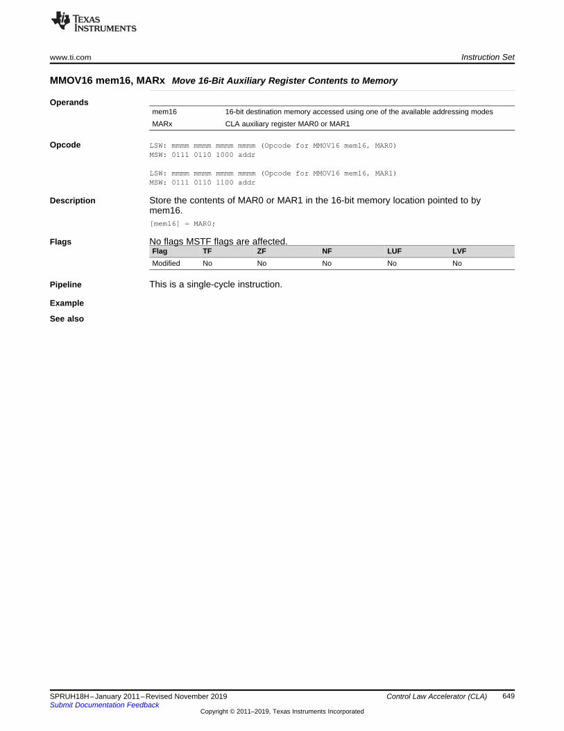
www.ti.com Instruction Set
649SPRUH18H–January 2011–Revised November 2019Submit Documentation Feedback
Copyright © 2011–2019, Texas Instruments Incorporated
Control Law Accelerator (CLA)
MMOV16 mem16, MARx Move 16-Bit Auxiliary Register Contents to Memory
Operandsmem16 16-bit destination memory accessed using one of the available addressing modesMARx CLA auxiliary register MAR0 or MAR1
Opcode LSW: mmmm mmmm mmmm mmmm (Opcode for MMOV16 mem16, MAR0)MSW: 0111 0110 1000 addr
LSW: mmmm mmmm mmmm mmmm (Opcode for MMOV16 mem16, MAR1)MSW: 0111 0110 1100 addr
Description Store the contents of MAR0 or MAR1 in the 16-bit memory location pointed to bymem16.[mem16] = MAR0;
Flags No flags MSTF flags are affected.Flag TF ZF NF LUF LVFModified No No No No No
Pipeline This is a single-cycle instruction.
Example
See also

Instruction Set www.ti.com
650 SPRUH18H–January 2011–Revised November 2019Submit Documentation Feedback
Copyright © 2011–2019, Texas Instruments Incorporated
Control Law Accelerator (CLA)
MMOV16 mem16, MRa Move 16-Bit Floating-Point Register Contents to Memory
Operandsmem16 16-bit destination memory accessed using one of the available addressing modesMRa CLA floating-point source register (MR0 to MR3)
Opcode LSW: mmmm mmmm mmmm mmmmMSW: 0111 0101 11aa addr
Description Move 16-bit value from the lower 16-bits of the floating-point register (MRa(15:0)) to thelocation pointed to by mem16.[mem16] = MRa(15:0);
Flags No flags MSTF flags are affected.Flag TF ZF NF LUF LVFModified No No No No No
Pipeline This is a single-cycle instruction.
Example ; This task logs the last NUM_DATA_POINTS; ADCRESULT1 values in the array VoltageCLA;; When the last element in the array has been; filled, the task will go back to the; the first element.;; Before starting the ADC conversions, force; Task 8 to initialize the ConversionCount to zero;; The ADC is set to sample (acquire) for 15 SYSCLK cycles; or 75ns. After the capacitor has captured the analog; value, the ADC will trigger this task early.; It takes 10.5 ADCCLKs to complete a conversion,; the ADCCLK being SYSCLK/4; T_sys = 1/200MHz = 5ns; T_adc = 4*T_sys = 20ns; The ADC will take 10.5 * 4 or 42 SYSCLK cycles to complete; a conversion. The ADC result register may be read on the; 36th instruction after the task begins.;_Cla1Task2:
.asg 0, N
.loopMNOP
;I1 - I28 Wait till I36 to read result.eval N + 1, N.break N = 28.endloopMMOVZ16 MR0, @_ConversionCount ;I29 Current ConversionMMOV16 MAR1, MR0, #_VoltageCLA ;I30 Next array locationMUI16TOF32 MR0, MR0 ;I31 Convert count to float32MADDF32 MR0, MR0, #1.0 ;I32 Add 1 to conversion countMCMPF32 MR0, #NUM_DATA_POINTS.0 ;I33 Compare count to maxMF32TOUI16 MR0, MR0 ;I34 Convert count to Uint16MNOP ;I35 Wait till I36 to read resultMMOVZ16 MR2, @_AdcaResultRegs.ADCRESULT1 ;I36 Read ADCRESULT1MMOV16 *MAR1, MR2 ; Store ADCRESULT1MBCNDD _RestartCount, GEQ ; If count >= NUM_DATA_POINTSMMOVIZ MR1, #0.0 ; Always executed: MR1=0MNOPMNOPMMOV16 @_ConversionCount, MR0 ; If branch not takenMSTOP ; store current count

www.ti.com Instruction Set
651SPRUH18H–January 2011–Revised November 2019Submit Documentation Feedback
Copyright © 2011–2019, Texas Instruments Incorporated
Control Law Accelerator (CLA)
_RestartCountMMOV16 @_ConversionCount, MR1 ; If branch taken, restart countMSTOP ; end of task
; This task initializes the ConversionCount; to zero;_Cla1Task8:
MMOVIZ MR0, #0.0MMOV16 @_ConversionCount, MR0MSTOP
_ClaT8End:
See also MMOVIZ MRa, #16FHiMMOVXI MRa, #16FLoHex

Instruction Set www.ti.com
652 SPRUH18H–January 2011–Revised November 2019Submit Documentation Feedback
Copyright © 2011–2019, Texas Instruments Incorporated
Control Law Accelerator (CLA)
MMOV32 mem32, MRa Move 32-Bit Floating-Point Register Contents to Memory
OperandsMRa floating-point register (MR0 to MR3)mem32 32-bit destination memory accessed using one of the available addressing modes
Opcode LSW: mmmm mmmm mmmm mmmmMSW: 0111 0100 11aa addr
Description Move from MRa to 32-bit memory location indicated by mem32.[mem32] = MRa;
Flags This instruction modifies the following flags in the MSTF register:Flag TF ZF NF LUF LVFModified No No No No No
No flags affected.
Pipeline This is a single-cycle instruction.
Example ; Perform 5 multiply and accumulate operations:;; X and Y are 32-bit floating point arrays;; 1st multiply: A = X0 * Y0; 2nd multiply: B = X1 * Y1; 3rd multiply: C = X2 * Y2; 4th multiply: D = X3 * Y3; 5th multiply: E = X3 * Y3;; Result = A + B + C + D + E;_Cla1Task1:
MMOVI16 MAR0, #_X ; MAR0 points to X arrayMMOVI16 MAR1, #_Y ; MAR1 points to Y arrayMNOP ; Delay for MAR0, MAR1 loadMNOP ; Delay for MAR0, MAR1 load
; <-- MAR0 validMMOV32 MR0, *MAR0[2]++ ; MR0 = X0, MAR0 += 2
; <-- MAR1 validMMOV32 MR1, *MAR1[2]++ ; MR1 = Y0, MAR1 += 2MMPYF32 MR2, MR0, MR1 ; MR2 = A = X0 * Y0
|| MMOV32 MR0, *MAR0[2]++ ; In parallel MR0 = X1, MAR0 += 2MMOV32 MR1, *MAR1[2]++ ; MR1 = Y1, MAR1 += 2MMPYF32 MR3, MR0, MR1 ; MR3 = B = X1 * Y1
|| MMOV32 MR0, *MAR0[2]++ ; In parallel MR0 = X2, MAR0 += 2MMOV32 MR1, *MAR1[2]++ ; MR1 = Y2, MAR2 += 2
MMACF32 MR3, MR2, MR2, MR0, MR1 ; MR3 = A + B, MR2 = C = X2 * Y2|| MMOV32 MR0, *MAR0[2]++ ; In parallel MR0 = X3
MMOV32 MR1, *MAR1[2]++ ; MR1 = Y3
MMACF32 MR3, MR2, MR2, MR0, MR1 ; MR3 = (A + B) + C, MR2 = D = X3 * Y3|| MMOV32 MR0, *MAR0 ; In parallel MR0 = X4
MMOV32 MR1, *MAR1 ; MR1 = Y4MMPYF32 MR2, MR0, MR1 ; MR2 = E = X4 * Y4
|| MADDF32 MR3, MR3, MR2 ; in parallel MR3 = (A + B + C) + DMADDF32 MR3, MR3, MR2 ; MR3 = (A + B + C + D) + EMMOV32 @_Result, MR3 ; Store the result MSTOP ; end of task
See also MMOV32 mem32, MSTF

www.ti.com Instruction Set
653SPRUH18H–January 2011–Revised November 2019Submit Documentation Feedback
Copyright © 2011–2019, Texas Instruments Incorporated
Control Law Accelerator (CLA)
MMOV32 mem32, MSTF Move 32-Bit MSTF Register to Memory
OperandsMSTF floating-point status registermem32 32-bit destination memory
Opcode LSW: mmmm mmmm mmmm mmmmMSW: 0111 0111 0100 addr
Description Copy the CLA's floating-point status register, MSTF, to memory.[mem32] = MSTF;
Flags This instruction does not modify flags in the MSTF register:Flag TF ZF NF LUF LVFModified No No No No No
Pipeline This is a single-cycle instruction.
One of the uses of this instruction is to save off the return PC (RPC) prior to calling afunction. The decision to jump to a function is made when the MCCNDD is in thedecode2 (D2) phase of the pipeline; the RPC is also updated in this phase. The actualjump occurs three cycles later when MCCNDD enters its execution (E) phase. The usermust, therefore, save the old RPC before MCCNDD updates it in the D2 phase, that is, itmust save MSTF three instructions prior to the function call.
Example The following example illustrates the pipeline flow for the context save (of the flags andRPC) prior to a function call. The first column in the comments shows the pipeline stagesfor the MMOV32 instruction while the second column pertains to the MCCNDDinstruction.
MMOV32 @_temp, MSTF ; D2| |MNOP ; R1|F1| MCCNDD is fetchedMNOP ; R2|F2|MNOP ; E |D1|MCCNDD _bar, UNC ; W |D2| old RPC written to memory,
; | | RPC updated with MPC+1MNOP ; |R1|MNOP ; |R2|MNOP ; |E | execution branches to _bar
See also MMOV32 mem32, MRa

Instruction Set www.ti.com
654 SPRUH18H–January 2011–Revised November 2019Submit Documentation Feedback
Copyright © 2011–2019, Texas Instruments Incorporated
Control Law Accelerator (CLA)
MMOV32 MRa, mem32 {, CNDF} Conditional 32-Bit Move
OperandsMRa CLA floating-point destination register (MR0 to MR3)mem32 32-bit memory location accessed using one of the available addressing modesCNDF optional condition.
Opcode LSW: mmmm mmmm mmmm mmmmMSW: 0111 00cn dfaa addr
Description If the condition is true, then move the 32-bit value referenced by mem32 to the floating-point register indicated by MRa.if (CNDF == TRUE) MRa = [mem32];
CNDF is one of the following conditions:
(1) Values not shown are reserved.(2) This is the default operation if no CNDF field is specified. This condition will allow the ZF and NF flags to
be modified when a conditional operation is executed. All other conditions will not modify these flags.
Encode (1) CNDF Description MSTF Flags Tested0000 NEQ Not equal to zero ZF == 00001 EQ Equal to zero ZF == 10010 GT Greater than zero ZF == 0 AND NF == 00011 GEQ Greater than or equal to zero NF == 00100 LT Less than zero NF == 10101 LEQ Less than or equal to zero ZF == 1 OR NF == 11010 TF Test flag set TF == 11011 NTF Test flag not set TF == 01100 LU Latched underflow LUF == 11101 LV Latched overflow LVF == 11110 UNC Unconditional None1111 UNCF (2) Unconditional with flag
modificationNone
Flags This instruction modifies the following flags in the MSTF register:Flag TF ZF NF LUF LVFModified No Yes Yes No No
if(CNDF == UNCF){
NF = MRa(31);ZF = 0;if(MRa(30:23) == 0) { ZF = 1; NF = 0; }
}else No flags modified;
Pipeline This is a single-cycle instruction.

www.ti.com Instruction Set
655SPRUH18H–January 2011–Revised November 2019Submit Documentation Feedback
Copyright © 2011–2019, Texas Instruments Incorporated
Control Law Accelerator (CLA)
Example ; Given A, B, X, M1 and M2 are 32-bit floating-point; numbers;; if(A == B) calculate Y = X*M1; if(A! = B) calculate Y = X*M2;_Cla1Task5:
MMOV32 MR0, @_AMMOV32 MR1, @_BMCMPF32 MR0, MR1MMOV32 MR2, @_M1, EQ ; if A == B, MR2 = M1
; Y = M1*XMMOV32 MR2, @_M2, NEQ ; if A! = B, MR2 = M2
; Y = M2*XMMOV32 MR3, @_XMMPYF32 MR3, MR2, MR3 ; Calculate YMMOV32 @_Y, MR3 ; Store YMSTOP ; end of task
See also MMOV32 MRa, MRb {, CNDF}MMOVD32 MRa, mem32

Instruction Set www.ti.com
656 SPRUH18H–January 2011–Revised November 2019Submit Documentation Feedback
Copyright © 2011–2019, Texas Instruments Incorporated
Control Law Accelerator (CLA)
MMOV32 MRa, MRb {, CNDF} Conditional 32-Bit Move
OperandsMRa CLA floating-point destination register (MR0 to MR3)MRb CLA floating-point source register (MR0 to MR3)CNDF optional condition.
Opcode LSW: 0000 0000 cndf bbaaMSW: 0111 1010 1100 0000
Description If the condition is true, then move the 32-bit value in MRb to the floating-point registerindicated by MRa.if (CNDF == TRUE) MRa = MRb;
CNDF is one of the following conditions:
(3) Values not shown are reserved.(4) This is the default operation if no CNDF field is specified. This condition will allow the ZF, and NF flags to
be modified when a conditional operation is executed. All other conditions will not modify these flags.
Encode (3) CNDF Description MSTF Flags Tested0000 NEQ Not equal to zero ZF == 00001 EQ Equal to zero ZF == 10010 GT Greater than zero ZF == 0 AND NF == 00011 GEQ Greater than or equal to zero NF == 00100 LT Less than zero NF == 10101 LEQ Less than or equal to zero ZF == 1 OR NF == 11010 TF Test flag set TF == 11011 NTF Test flag not set TF == 01100 LU Latched underflow LUF == 11101 LV Latched overflow LVF == 11110 UNC Unconditional None1111 UNCF (4) Unconditional with flag
modificationNone
Flags This instruction modifies the following flags in the MSTF register:Flag TF ZF NF LUF LVFModified No Yes Yes No No
if(CNDF == UNCF){
NF = MRa(31); ZF = 0;if(MRa(30:23) == 0) {ZF = 1; NF = 0;}
}else No flags modified;
Pipeline This is a single-cycle instruction.

www.ti.com Instruction Set
657SPRUH18H–January 2011–Revised November 2019Submit Documentation Feedback
Copyright © 2011–2019, Texas Instruments Incorporated
Control Law Accelerator (CLA)
Example ; Given: X = 8.0; Y = 7.0; A = 2.0; B = 5.0; _ClaTask1
MMOV32 MR3, @_X ; MR3 = X = 8.0MMOV32 MR0, @_Y ; MR0 = Y = 7.0MMAXF32 MR3, MR0 ; ZF = 0, NF = 0, MR3 = 8.0MMOV32 MR1, @_A, GT ; true, MR1 = A = 2.0MMOV32 MR1, @_B, LT ; false, does not load MR1MMOV32 MR2, MR1, GT ; true, MR2 = MR1 = 2.0MMOV32 MR2, MR0, LT ; false, does not load MR2MSTOP
See also MMOV32 MRa, mem32 {,CNDF}

Instruction Set www.ti.com
658 SPRUH18H–January 2011–Revised November 2019Submit Documentation Feedback
Copyright © 2011–2019, Texas Instruments Incorporated
Control Law Accelerator (CLA)
MMOV32 MSTF, mem32 Move 32-Bit Value from Memory to the MSTF Register
OperandsMSTF CLA status registermem32 32-bit source memory location
Opcode LSW: mmmm mmmm mmmm mmmmMSW: 0111 0111 0000 addr
Description Move from memory to the CLA's status register MSTF. This instruction is most usefulwhen nesting function calls (via MCCNDD).MSTF = [mem32];
Flags This instruction modifies the following flags in the MSTF register:Flag TF ZF NF LUF LVFModified Yes Yes Yes Yes Yes
Loading the status register will overwrite all flags and the RPC field. The MEALLOW fieldis not affected.
Pipeline This is a single-cycle instruction.
Example
See also MMOV32 mem32, MSTF

www.ti.com Instruction Set
659SPRUH18H–January 2011–Revised November 2019Submit Documentation Feedback
Copyright © 2011–2019, Texas Instruments Incorporated
Control Law Accelerator (CLA)
MMOVD32 MRa, mem32 Move 32-Bit Value from Memory with Data Copy
OperandsMRa CLA floating-point register (MR0 to MR3)mem32 32-bit memory location accessed using one of the available addressing modes
Opcode LSW: mmmm mmmm mmmm mmmmMSW: 0111 0100 00aa addr
Description Move the 32-bit value referenced by mem32 to the floating-point register indicated byMRa.MRa = [mem32];[mem32+2] = [mem32];
Flags This instruction modifies the following flags in the MSTF register:Flag TF ZF NF LUF LVFModified No Yes Yes No No
NF = MRa(31);ZF = 0;if(MRa(30:23) == 0){ ZF = 1; NF = 0; }
Pipeline This is a single-cycle instruction.
Example ; sum = X0*B0 + X1*B1 + X2*B2 + Y1*A1 + Y2*B2;; X2 = X1; X1 = X0; Y2 = Y1; Y1 = sum;_Cla1Task2:
MMOV32 MR0, @_B2 ; MR0 = B2MMOV32 MR1, @_X2 ; MR1 = X2MMPYF32 MR2, MR1, MR0 ; MR2 = X2*B2
|| MMOV32 MR0, @_B1 ; MR0 = B1MMOVD32 MR1, @_X1 ; MR1 = X1, X2 = X1MMPYF32 MR3, MR1, MR0 ; MR3 = X1*B1
|| MMOV32 MR0, @_B0 ; MR0 = B0MMOVD32 MR1, @_X0 ; MR1 = X0, X1 = X0
; MR3 = X1*B1 + X2*B2, MR2 = X0*B0; MR0 = A2
MMACF32 MR3, MR2, MR2, MR1, MR0|| MMOV32 MR0, @_A2
MMOV32 MR1, @_Y2 ; MR1 = Y2
; MR3 = X0*B0 + X1*B1 + X2*B2, MR2 = Y2*A2; MR0 = A1
MMACF32 MR3, MR2, MR2, MR1, MR0|| MMOV32 MR0, @_A1
MMOVD32 MR1,@_Y1 ; MR1 = Y1, Y2 = Y1MADDF32 MR3, MR3, MR2 ; MR3 = Y2*A2 + X0*B0 + X1*B1 + X2*B2
|| MMPYF32 MR2, MR1, MR0 ; MR2 = Y1*A1MADDF32 MR3, MR3, MR2 ; MR3 = Y1*A1 + Y2*A2 + X0*B0 + X1*B1 + X2*B2MMOV32 @_Y1, MR3 ; Y1 = MR3MSTOP ; end of task
See also MMOV32 MRa, mem32 {,CNDF}

Instruction Set www.ti.com
660 SPRUH18H–January 2011–Revised November 2019Submit Documentation Feedback
Copyright © 2011–2019, Texas Instruments Incorporated
Control Law Accelerator (CLA)
MMOVF32 MRa, #32F Load the 32-Bits of a 32-Bit Floating-Point Register
Operands This instruction is an alias for MMOVIZ and MMOVXI instructions. The second operandis translated by the assembler such that the instruction becomes:
MMOVIZ MRa, #16FHiHex MMOVXI MRa, #16FLoHexMRa CLA floating-point destination register (MR0 to MR3)#32F immediate float value represented in floating-point representation
Opcode LSW: IIII IIII IIII IIII (opcode of MMOVIZ MRa, #16FHiHex)MSW: 0111 1000 0100 00aaLSW: IIII IIII IIII IIII (opcode of MMOVXI MRa, #16FLoHex)MSW: 0111 1000 1000 00aa
Description Note: This instruction accepts the immediate operand only in floating-pointrepresentation. To specify the immediate value as a hex value (IEEE 32-bit floating-point format) use the MOVI32 MRa, #32FHex instruction.
Load the 32-bits of MRa with the immediate float value represented by #32F.
#32F is a float value represented in floating-point representation. The assembler will onlyaccept a float value represented in floating-point representation. That is, 3.0 can only berepresented as #3.0. #0x40400000 will result in an error.MRa = #32F;
Flags This instruction modifies the following flags in the MSTF register:Flag TF ZF NF LUF LVFModified No No No No No
Pipeline Depending on #32FH, this instruction takes one or two cycles. If all of the lower 16-bitsof the IEEE 32-bit floating-point format of #32F are zeros, then the assembler willconvert MMOVF32 into only MMOVIZ instruction. If the lower 16-bits of the IEEE 32-bitfloating-point format of #32F are not zeros, then the assembler will convert MMOVF32into MMOVIZ and MMOVXI instructions.
Example MMOVF32 MR1, #3.0 ; MR1 = 3.0 (0x40400000); Assembler converts this instruction as; MMOVIZ MR1, #0x4040
MMOVF32 MR2, #0.0 ; MR2 = 0.0 (0x00000000); Assembler converts this instruction as; MMOVIZ MR2, #0x0
MMOVF32 MR3, #12.265 ; MR3 = 12.625 (0x41443D71); Assembler converts this instruction as; MMOVIZ MR3, #0x4144; MMOVXI MR3, #0x3D71
See also MMOVIZ MRa, #16FHiMMOVXI MRa, #16FLoHexMMOVI32 MRa, #32FHex

www.ti.com Instruction Set
661SPRUH18H–January 2011–Revised November 2019Submit Documentation Feedback
Copyright © 2011–2019, Texas Instruments Incorporated
Control Law Accelerator (CLA)
MMOVI16 MARx, #16I Load the Auxiliary Register with the 16-Bit Immediate Value
OperandsMARx Auxiliary register MAR0 or MAR1#16I 16-bit immediate value
Opcode LSW: IIII IIII IIII IIII (opcode of MMOVI16 MAR0, #16I)MSW: 0111 1111 1100 0000
LSW: IIII IIII IIII IIII (opcode of MMOVI16 MAR1, #16I)MSW: 0111 1111 1110 0000
Description Load the auxiliary register, MAR0 or MAR1, with a 16-bit immediate value. Refer to thepipeline section for important information regarding this instruction.MARx = #16I;
Flags This instruction does not modify flags in the MSTF register:Flag TF ZF NF LUF LVFModified No No No No No
Pipeline This is a single-cycle instruction. The immediate load of MAR0 or MAR1 will occur in theEXE phase of the pipeline. Any post increment of MAR0 or MAR1 using indirectaddressing will occur in the D2 phase of the pipeline. Therefore the following applieswhen loading the auxiliary registers:• I1 and I2
The two instructions following MMOVI16 will use MAR0/MAR1 before the updateoccurs. Thus these two instructions will use the old value of MAR0 or MAR1.
• I3Loading of an auxiliary register occurs in the EXE phase while updates due to post-increment addressing occur in the D2 phase. Thus I3 cannot use the auxiliaryregister or there will be a conflict. In the case of a conflict, the update due to address-mode post increment will win snd the auxiliary register will not be updated with #_X.
• I4Starting with the 4th instruction MAR0 or MAR1 will be the new value loaded withMMOVI16.
; Assume MAR0 is 50 and #_X is 20
MMOVI16 MAR0, #_X ; Load MAR0 with address of X (20)<Instruction 1> ; I1 Will use the old value of MAR0 (50)<Instruction 2> ; I2 Will use the old value of MAR0 (50)<Instruction 3> ; I3 Cannot use MAR0<Instruction 4> ; I4 Will use the new value of MAR0 (20)<Instruction 5> ; I5....
Table 10-17. Pipeline Activity For MMOVI16 MAR0/MAR1, #16I
Instruction F1 F2 D1 D2 R1 R2 E W
MMOVI16 MAR0, #_X MMOVI16
I1 I1 MMOVI16
I2 I2 I1 MMOVI16
I3 I3 I2 I1 MMOVI16
I4 I4 I3 I2 I1 MMOVI16
I5 I5 I4 I3 I2 I1 MMOVI16
I6 I6 I5 I4 I3 I2 I1 MMOVI16

Instruction Set www.ti.com
662 SPRUH18H–January 2011–Revised November 2019Submit Documentation Feedback
Copyright © 2011–2019, Texas Instruments Incorporated
Control Law Accelerator (CLA)
MMOVI32 MRa, #32FHex Load the 32-Bits of a 32-Bit Floating-Point Register with the Immediate
OperandsMRa floating-point register (MR0 to MR3)#32FHex A 32-bit immediate value that represents an IEEE 32-bit floating-point value.
This instruction is an alias for MMOVIZ and MMOVXI instructions. The second operandis translated by the assembler such that the instruction becomes:MMOVIZ MRa, #16FHiHexMMOVXI MRa, #16FLoHex
Opcode LSW: IIII IIII IIII IIII (opcode of MMOVIZ MRa, #16FHiHex)MSW: 0111 1000 0100 00aa
LSW: IIII IIII IIII IIII (opcode of MMOVXI MRa, #16FLoHex)MSW: 0111 1000 1000 00aa
Description Note: This instruction only accepts a hex value as the immediate operand. To specify theimmediate value with a floating-point representation use the MMOVF32 MRa, #32Finstruction.
Load the 32-bits of MRa with the immediate 32-bit hex value represented by #32Fhex.
#32Fhex is a 32-bit immediate hex value that represents the IEEE 32-bit floating-pointvalue of a floating-point number. The assembler will only accept a hex immediate value.That is, 3.0 can only be represented as #0x40400000. #3.0 will result in an error.MRa = #32FHex;
Flags This instruction modifies the following flags in the MSTF register:Flag TF ZF NF LUF LVFModified No No No No No
Pipeline Depending on #32FHex, this instruction takes one or two cycles. If all of the lower 16-bits of #32FHex are zeros, then assembler will convert MOVI32 to the MMOVIZinstruction. If the lower 16-bits of #32FHex are not zeros, then assembler will convertMOVI32 to a MMOVIZ and a MMOVXI instruction.
Example MOVI32 MR1, #0x40400000 ; MR1 = 0x40400000; Assembler converts this instruction as; MMOVIZ MR1, #0x4040
MOVI32 MR2, #0x00000000 ; MR2 = 0x00000000; Assembler converts this instruction as; MMOVIZ MR2, #0x0
MOVI32 MR3, #0x40004001 ; MR3 = 0x40004001; Assembler converts this instruction as; MMOVIZ MR3, #0x4000; MMOVXI MR3, #0x4001
MOVI32 MR0, #0x00004040 ; MR0 = 0x00004040; Assembler converts this instruction as; MMOVIZ MR0, #0x0000; MMOVXI MR0, #0x4040
See also MMOVIZ MRa, #16FHiMMOVXI MRa, #16FLoHexMMOVF32 MRa, #32F

www.ti.com Instruction Set
663SPRUH18H–January 2011–Revised November 2019Submit Documentation Feedback
Copyright © 2011–2019, Texas Instruments Incorporated
Control Law Accelerator (CLA)
MMOVIZ MRa, #16FHi Load the Upper 16-Bits of a 32-Bit Floating-Point Register
OperandsMRa floating-point register (MR0 to MR3)#16FHi A 16-bit immediate value that represents the upper 16-bits of an IEEE 32-bit floating-
point value. The low 16-bits of the mantissa are assumed to be all 0.
Opcode LSW: IIII IIII IIII IIIIMSW: 0111 1000 0100 00aa
Description Load the upper 16-bits of MRa with the immediate value #16FHi and clear the low 16-bits of MRa.
#16FHiHex is a 16-bit immediate value that represents the upper 16-bits of an IEEE 32-bit floating-point value. The low 16-bits of the mantissa are assumed to be all 0. Theassembler will only accept a decimal or hex immediate value. That is, -1.5 can berepresented as #-1.5 or #0xBFC0.
By itself, MMOVIZ is useful for loading a floating-point register with a constant in whichthe lowest 16-bits of the mantissa are 0. Some examples are 2.0 (0x40000000), 4.0(0x40800000), 0.5 (0x3F000000), and -1.5 (0xBFC00000). If a constant requires all 32-bits of a floating-point register to be iniitalized, then use MMOVIZ along with theMMOVXI instruction.MRa(31:16) = #16FHi;MRa(15:0) = 0;
Flags This instruction modifies the following flags in the MSTF register:Flag TF ZF NF LUF LVFModified No No No No No
Pipeline This is a single-cycle instruction.
Example ; Load MR0 and MR1 with -1.5 (0xBFC00000)MMOVIZ MR0, #0xBFC0 ; MR0 = 0xBFC00000 (1.5)MMOVIZ MR1, #-1.5 ; MR1 = -1.5 (0xBFC00000)
; Load MR2 with pi = 3.141593 (0x40490FDB)MMOVIZ MR2, #0x4049 ; MR2 = 0x40490000MMOVXI MR2, #0x0FDB ; MR2 = 0x40490FDB
See also MMOVF32 MRa, #32FMMOVI32 MRa, #32FHexMMOVXI MRa, #16FLoHex

Instruction Set www.ti.com
664 SPRUH18H–January 2011–Revised November 2019Submit Documentation Feedback
Copyright © 2011–2019, Texas Instruments Incorporated
Control Law Accelerator (CLA)
MMOVZ16 MRa, mem16 Load MRx With 16-bit Value
OperandsMRa CLA floating-point destination register (MR0 to MR3)mem16 16-bit source memory location
Opcode LSW: mmmm mmmm mmmm mmmmMSW: 0111 0101 10aa addr
Description Move the 16-bit value referenced by mem16 to the floating-point register indicated byMRa.MRa(31:16) = 0;MRa(15:0) = [mem16];
Flags This instruction modifies the following flags in the MSTF register:Flag TF ZF NF LUF LVFModified No Yes Yes No No
The MSTF register flags are modified based on the integer results of the operation.NF = 0;if (MRa(31:0)== 0) { ZF = 1; }
Pipeline This is a single-cycle instruction.

www.ti.com Instruction Set
665SPRUH18H–January 2011–Revised November 2019Submit Documentation Feedback
Copyright © 2011–2019, Texas Instruments Incorporated
Control Law Accelerator (CLA)
MMOVXI MRa, #16FLoHex Move Immediate to the Low 16-Bits of a Floating-Point Register
OperandsMRa CLA floating-point register (MR0 to MR3)#16FLoHex A 16-bit immediate hex value that represents the lower 16-bits of an IEEE 32-bit
floating-point value. The upper 16-bits will not be modified.
Opcode LSW: IIII IIII IIII IIIIMSW: 0111 1000 1000 00aa
Description Load the low 16-bits of MRa with the immediate value #16FLoHex. #16FLoHexrepresents the lower 16-bits of an IEEE 32-bit floating-point value. The upper 16-bits ofMRa will not be modified. MMOVXI can be combined with the MMOVIZ instruction toinitialize all 32-bits of a MRa register.MRa(15:0) = #16FLoHex;MRa(31:16) = Unchanged;
FlagsFlag TF ZF NF LUF LVFModified No No No No No
Pipeline This is a single-cycle instruction.
Example ; Load MR0 with pi = 3.141593 (0x40490FDB)MMOVIZ MR0,#0x4049 ; MR0 = 0x40490000MMOVXI MR0,#0x0FDB ; MR0 = 0x40490FDB
See also MMOVIZ MRa, #16FHi

Instruction Set www.ti.com
666 SPRUH18H–January 2011–Revised November 2019Submit Documentation Feedback
Copyright © 2011–2019, Texas Instruments Incorporated
Control Law Accelerator (CLA)
MMPYF32 MRa, MRb, MRc 32-Bit Floating-Point Multiply
OperandsMRa CLA floating-point destination register (MR0 to MR3)MRb CLA floating-point source register (MR0 to MR3)MRc CLA floating-point source register (MR0 to MR3)
Opcode LSW: 0000 0000 00cc bbaaMSW: 0111 1100 0000 0000
Description Multiply the contents of two floating-point registers.MRa = MRb * MRc;
Flags This instruction modifies the following flags in the MSTF register:Flag TF ZF NF LUF LVFModified No No No Yes Yes
The MSTF register flags are modified as follows:• LUF = 1 if MMPYF32 generates an underflow condition.• LVF = 1 if MMPYF32 generates an overflow condition.
Pipeline This is a single-cycle instruction.
Example ; Calculate Num/Den using a Newton-Raphson algorithum for 1/Den; Ye = Estimate(1/X); Ye = Ye*(2.0 - Ye*X); Ye = Ye*(2.0 - Ye*X);_Cla1Task1:
MMOV32 MR1, @_Den ; MR1 = DenMEINVF32 MR2, MR1 ; MR2 = Ye = Estimate(1/Den)MMPYF32 MR3, MR2, MR1 ; MR3 = Ye*DenMSUBF32 MR3, #2.0, MR3 ; MR3 = 2.0 - Ye*DenMMPYF32 MR2, MR2, MR3 ; MR2 = Ye = Ye*(2.0 - Ye*Den)MMPYF32 MR3, MR2, MR1 ; MR3 = Ye*Den
|| MMOV32 MR0, @_Num ; MR0 = NumMSUBF32 MR3, #2.0, MR3 ; MR3 = 2.0 - Ye*DenMMPYF32 MR2, MR2, MR3 ; MR2 = Ye = Ye*(2.0 - Ye*Den)
|| MMOV32 MR1, @_Den ; Reload Den To Set SignMNEGF32 MR0, MR0, EQ ; if(Den == 0.0) Change Sign Of NumMMPYF32 MR0, MR2, MR0 ; MR0 = Y = Ye*NumMMOV32 @_Dest, MR0 ; Store resultMSTOP ; end of task
See also MMPYF32 MRa, #16FHi, MRbMMPYF32 MRa, MRb, MRc || MADDF32 MRd, MRe, MRfMMPYF32 MRd, MRe, MRf || MMOV32 MRa, mem32MMPYF32 MRd, MRe, MRf || MMOV32 mem32, MRaMMPYF32 MRa, MRb, MRc || MSUBF32 MRd, MRe, MRfMMACF32 MR3, MR2, MRd, MRe, MRf || MMOV32 MRa, mem32

www.ti.com Instruction Set
667SPRUH18H–January 2011–Revised November 2019Submit Documentation Feedback
Copyright © 2011–2019, Texas Instruments Incorporated
Control Law Accelerator (CLA)
MMPYF32 MRa, #16FHi, MRb 32-Bit Floating-Point Multiply
OperandsMRa CLA floating-point destination register (MR0 to MR3)#16FHi A 16-bit immediate value that represents the upper 16-bits of an IEEE 32-bit floating-
point value. The low 16-bits of the mantissa are assumed to be all 0.MRb CLA floating-point source register (MR0 to MR3)
Opcode LSW: IIII IIII IIII IIIIMSW: 0111 0111 1000 bbaa
Description Multiply MRb with the floating-point value represented by the immediate operand. Storethe result of the addition in MRa.
#16FHi is a 16-bit immediate value that represents the upper 16-bits of an IEEE 32-bitfloating-point value. The low 16-bits of the mantissa are assumed to be all 0. #16FHi ismost useful for representing constants where the lowest 16-bits of the mantissa are 0.Some examples are 2.0 (0x40000000), 4.0 (0x40800000), 0.5 (0x3F000000), and -1.5(0xBFC00000). The assembler will accept either a hex or float as the immediate value.That is, the value -1.5 can be represented as #-1.5 or #0xBFC0.MRa = MRb * #16FHi:0;
This instruction can also be written as MMPYF32 MRa, MRb, #16FHi.
Flags This instruction modifies the following flags in the MSTF register:.Flag TF ZF NF LUF LVFModified No No No Yes Yes
The MSTF register flags are modified as follows:• LUF = 1 if MMPYF32 generates an underflow condition.• LVF = 1 if MMPYF32 generates an overflow condition.
Pipeline This is a single-cycle instruction.
Example 1 ; Same as example 2 but #16FHi is represented in floatMMOVIZ MR3, #2.0 ; MR3 = 2.0 (0x40000000)MMPYF32 MR0, #3.0, MR3 ; MR0 = 3.0 * MR3 = 6.0 (0x40C00000)MMOV32 @_X, MR0 ; Save the result in variable X
Example 2 ; Same as example 1 but #16FHi is represented in HexMMOVIZ MR3, #2.0 ; MR3 = 2.0 (0x40000000)MMPYF32 MR0, #0x4040, MR3 ; MR0 = 0x4040 * MR3 = 6.0 (0x40C00000)MMOV32 @_X, MR0 ; Save the result in variable X

Instruction Set www.ti.com
668 SPRUH18H–January 2011–Revised November 2019Submit Documentation Feedback
Copyright © 2011–2019, Texas Instruments Incorporated
Control Law Accelerator (CLA)
Example 3 ; Given X, M and B are IQ24 numbers:; X = IQ24(+2.5) = 0x02800000; M = IQ24(+1.5) = 0x01800000; B = IQ24(-0.5) = 0xFF800000;; Calculate Y = X * M + B;;_Cla1Task2:;; Convert M, X and B from IQ24 to float
MI32TOF32 MR0, @_M ; MR0 = 0x4BC00000MI32TOF32 MR1, @_X ; MR1 = 0x4C200000MI32TOF32 MR2, @_B ; MR2 = 0xCB000000MMPYF32 MR0, MR0, #0x3380 ; M = 1/(1*2^24) * iqm = 1.5 (0x3FC00000)MMPYF32 MR1, MR1, #0x3380 ; X = 1/(1*2^24) * iqx = 2.5 (0x40200000)MMPYF32 MR2, MR2, #0x3380 ; B = 1/(1*2^24) * iqb = -.5 (0xBF000000)MMPYF32 MR3, MR0, MR1 ; M*XMADDF32 MR2, MR2, MR3 ; Y=MX+B = 3.25 (0x40500000)
; Convert Y from float32 to IQ24MMPYF32 MR2, MR2, #0x4B80 ; Y * 1*2^24MF32TOI32 MR2, MR2 ; IQ24(Y) = 0x03400000MMOV32 @_Y, MR2 ; store resultMSTOP ; end of task
See also MMPYF32 MRa, MRb, #16FHiMMPYF32 MRa, MRb, MRcMMPYF32 MRa, MRb, MRc || MADDF32 MRd, MRe, MRf

www.ti.com Instruction Set
669SPRUH18H–January 2011–Revised November 2019Submit Documentation Feedback
Copyright © 2011–2019, Texas Instruments Incorporated
Control Law Accelerator (CLA)
MMPYF32 MRa, MRb, #16FHi 32-Bit Floating-Point Multiply
OperandsMRa CLA floating-point destination register (MR0 to MR3)MRb CLA floating-point source register (MR0 to MR3)#16FHi A 16-bit immediate value that represents the upper 16-bits of an IEEE 32-bit floating-
point value. The low 16-bits of the mantissa are assumed to be all 0.
Opcode LSW: IIII IIII IIII IIIIMSW: 0111 0111 1000 bbaa
Description Multiply MRb with the floating-point value represented by the immediate operand. Storethe result of the addition in MRa.
#16FHi is a 16-bit immediate value that represents the upper 16-bits of an IEEE 32-bitfloating-point value. The low 16-bits of the mantissa are assumed to be all 0. #16FHi ismost useful for representing constants where the lowest 16-bits of the mantissa are 0.Some examples are 2.0 (0x40000000), 4.0 (0x40800000), 0.5 (0x3F000000), and -1.5(0xBFC00000). The assembler will accept either a hex or float as the immediate value.That is, the value -1.5 can be represented as #-1.5 or #0xBFC0.MRa = MRb * #16FHi:0;
This instruction can also be writen as MMPYF32 MRa, #16FHi, MRb.
Flags This instruction modifies the following flags in the MSTF register:.Flag TF ZF NF LUF LVFModified No No No Yes Yes
The MSTF register flags are modified as follows:• LUF = 1 if MMPYF32 generates an underflow condition.• LVF = 1 if MMPYF32 generates an overflow condition.
Pipeline This is a single-cycle instruction.
Example 1 ;Same as example 2 but #16FHi is represented in floatMMOVIZ MR3, #2.0 ; MR3 = 2.0 (0x40000000)MMPYF32 MR0, MR3, #3.0 ; MR0 = MR3 * 3.0 = 6.0 (0x40C00000)MMOV32 @_X, MR0 ; Save the result in variable X
Example 2 ;Same as above example but #16FHi is represented in HexMMOVIZ MR3, #2.0 ; MR3 = 2.0 (0x40000000)MMPYF32 MR0, MR3, #0x4040 ; MR0 = MR3 * 0x4040 = 6.0 (0x40C00000)MMOV32 @_X, MR0 ; Save the result in variable X

Instruction Set www.ti.com
670 SPRUH18H–January 2011–Revised November 2019Submit Documentation Feedback
Copyright © 2011–2019, Texas Instruments Incorporated
Control Law Accelerator (CLA)
Example 3 ; Given X, M and B are IQ24 numbers:; X = IQ24(+2.5) = 0x02800000; M = IQ24(+1.5) = 0x01800000; B = IQ24(-0.5) = 0xFF800000;; Calculate Y = X * M + B;_Cla1Task2:;; Convert M, X and B from IQ24 to float
MI32TOF32 MR0, @_M ; MR0 = 0x4BC00000MI32TOF32 MR1, @_X ; MR1 = 0x4C200000MI32TOF32 MR2, @_B ; MR2 = 0xCB000000MMPYF32 MR0, #0x3380, MR0 ; M = 1/(1*2^24) * iqm = 1.5 (0x3FC00000)MMPYF32 MR1, #0x3380, MR1 ; X = 1/(1*2^24) * iqx = 2.5 (0x40200000)MMPYF32 MR2, #0x3380, MR2 ; B = 1/(1*2^24) * iqb = -.5 (0xBF000000)MMPYF32 MR3, MR0, MR1 ; M*XMADDF32 MR2, MR2, MR3 ; Y=MX+B = 3.25 (0x40500000)
; Convert Y from float32 to IQ24MMPYF32 MR2, #0x4B80, MR2 ; Y * 1*2^24MF32TOI32 MR2, MR2 ; IQ24(Y) = 0x03400000MMOV32 @_Y, MR2 ; store resultMSTOP ; end of task
See also MMPYF32 MRa, #16FHi, MRbMMPYF32 MRa, MRb, MRc

www.ti.com Instruction Set
671SPRUH18H–January 2011–Revised November 2019Submit Documentation Feedback
Copyright © 2011–2019, Texas Instruments Incorporated
Control Law Accelerator (CLA)
MMPYF32 MRa, MRb, MRc||MADDF32 MRd, MRe, MRf 32-Bit Floating-Point Multiply with ParallelAdd
OperandsMRa CLA floating-point destination register for MMPYF32 (MR0 to MR3)
MRa cannot be the same register as MRdMRb CLA floating-point source register for MMPYF32 (MR0 to MR3)MRc CLA floating-point source register for MMPYF32 (MR0 to MR3)MRd CLA floating-point destination register for MADDF32 (MR0 to MR3)
MRd cannot be the same register as MRaMRe CLA floating-point source register for MADDF32 (MR0 to MR3)MRf CLA floating-point source register for MADDF32 (MR0 to MR3)
Opcode LSW: 0000 ffee ddcc bbaaMSW: 0111 1010 0000 0000
Description Multiply the contents of two floating-point registers with parallel addition of two registers.MRa = MRb * MRc;MRd = MRe + MRf;
Restrictions The destination register for the MMPYF32 and the MADDF32 must be unique. That is,MRa cannot be the same register as MRd.
Flags This instruction modifies the following flags in the MSTF register:Flag TF ZF NF LUF LVFModified No No No Yes Yes
The MSTF register flags are modified as follows:• LUF = 1 if MMPYF32 or MADDF32 generates an underflow condition.• LVF = 1 if MMPYF32 or MADDF32 generates an overflow condition.
Pipeline Both MMPYF32 and MADDF32 complete in a single cycle.

Instruction Set www.ti.com
672 SPRUH18H–January 2011–Revised November 2019Submit Documentation Feedback
Copyright © 2011–2019, Texas Instruments Incorporated
Control Law Accelerator (CLA)
Example ; Perform 5 multiply and accumulate operations:;; X and Y are 32-bit floating point arrays;; 1st multiply: A = X0 * Y0; 2nd multiply: B = X1 * Y1; 3rd multiply: C = X2 * Y2; 4th multiply: D = X3 * Y3; 5th multiply: E = X3 * Y3;; Result = A + B + C + D + E;_Cla1Task1:
MMOVI16 MAR0, #_X ; MAR0 points to X arrayMMOVI16 MAR1, #_Y ; MAR1 points to Y arrayMNOP ; Delay for MAR0, MAR1 loadMNOP ; Delay for MAR0, MAR1 load
; <-- MAR0 validMMOV32 MR0, *MAR0[2]++ ; MR0 = X0, MAR0 += 2
; <-- MAR1 validMMOV32 MR1, *MAR1[2]++ ; MR1 = Y0, MAR1 += 2
MMPYF32 MR2, MR0, MR1 ; MR2 = A = X0 * Y0|| MMOV32 MR0, *MAR0[2]++ ; In parallel MR0 = X1, MAR0 += 2
MMOV32 MR1, *MAR1[2]++ ; MR1 = Y1, MAR1 += 2
MMPYF32 MR3, MR0, MR1 ; MR3 = B = X1 * Y1|| MMOV32 MR0, *MAR0[2]++ ; In parallel MR0 = X2, MAR0 += 2
MMOV32 MR1, *MAR1[2]++ ; MR1 = Y2, MAR2 += 2
MMACF32 MR3, MR2, MR2, MR0, MR1 ; MR3 = A + B, MR2 = C = X2 * Y2|| MMOV32 MR0, *MAR0[2]++ ; In parallel MR0 = X3
MMOV32 MR1, *MAR1[2]++ ; MR1 = Y3
MMACF32 MR3, MR2, MR2, MR0, MR1 ; MR3 = (A + B) + C, MR2 = D = X3 * Y3|| MMOV32 MR0, *MAR0 ; In parallel MR0 = X4
MMOV32 MR1, *MAR1 ; MR1 = Y4
MMPYF32 MR2, MR0, MR1 ; MR2 = E = X4 * Y4|| MADDF32 MR3, MR3, MR2 ; in parallel MR3 = (A + B + C) + D
MADDF32 MR3, MR3, MR2 ; MR3 = (A + B + C + D) + EMMOV32 @_Result, MR3 ; Store the resultMSTOP ; end of task
See also MMACF32 MR3, MR2, MRd, MRe, MRf || MMOV32 MRa, mem32

www.ti.com Instruction Set
673SPRUH18H–January 2011–Revised November 2019Submit Documentation Feedback
Copyright © 2011–2019, Texas Instruments Incorporated
Control Law Accelerator (CLA)
MMPYF32 MRd, MRe, MRf ||MMOV32 MRa, mem32 32-Bit Floating-Point Multiply with Parallel Move
OperandsMRd CLA floating-point destination register for the MMPYF32 (MR0 to MR3)
MRd cannot be the same register as MRaMRe CLA floating-point source register for the MMPYF32 (MR0 to MR3)MRf CLA floating-point source register for the MMPYF32 (MR0 to MR3)MRa CLA floating-point destination register for the MMOV32 (MR0 to MR3)
MRa cannot be the same register as MRdmem32 32-bit memory location accessed using one of the available addressing modes. This
will be the source of the MMOV32.
Opcode LSW: mmmm mmmm mmmm mmmmMSW: 0000 ffee ddaa addr
Description Multiply the contents of two floating-point registers and load another.MRd = MRe * MRf;MRa = [mem32];
Restrictions The destination register for the MMPYF32 and the MMOV32 must be unique. That is,MRa cannot be the same register as MRd.
Flags This instruction modifies the following flags in the MSTF register:.Flag TF ZF NF LUF LVFModified No Yes Yes Yes Yes
The MSTF register flags are modified as follows:• LUF = 1 if MMPYF32 generates an underflow condition.• LVF = 1 if MMPYF32 generates an overflow condition.
The MMOV32 Instruction will set the NF and ZF flags as follows:NF = MRa(31);ZF = 0;if(MRa(30:23) == 0) { ZF = 1; NF = 0; }
Pipeline Both MMPYF32 and MMOV32 complete in a single cycle.
Example 1 ; Given M1, X1 and B1 are 32-bit floating point; Calculate Y1 = M1*X1+B1;_Cla1Task1:
MMOV32 MR0, @M1 ; Load MR0 with M1MMOV32 MR1, @X1 ; Load MR1 with X1MMPYF32 MR1, MR1, MR0 ; Multiply M1*X1
|| MMOV32 MR0, @B1 ; and in parallel load MR0 with B1MADDF32 MR1, MR1, MR0 ; Add M*X1 to B1 and store in MR1MMOV32 @Y1, MR1 ; Store the resultMSTOP ; end of task

Instruction Set www.ti.com
674 SPRUH18H–January 2011–Revised November 2019Submit Documentation Feedback
Copyright © 2011–2019, Texas Instruments Incorporated
Control Law Accelerator (CLA)
Example 2 ; Given A, B and C are 32-bit floating-point numbers; Calculate Y2 = (A * B); Y3 = (A * B) * C;_Cla1Task2:
MMOV32 MR0, @A ; Load MR0 with AMMOV32 MR1, @B ; Load MR1 with BMMPYF32 MR1, MR1, MR0 ; Multiply A*B
|| MMOV32 MR0, @C ; and in parallel load MR0 with CMMPYF32 MR1, MR1, MR0 ; Multiply (A*B) by C
|| MMOV32 @Y2, MR1 ; and in parallel store A*BMMOV32 @Y3, MR1 ; Store the resultMSTOP ; end of task
See also MMPYF32 MRd, MRe, MRf || MMOV32 mem32, MRaMMACF32 MR3, MR2, MRd, MRe, MRf || MMOV32 MRa, mem32

www.ti.com Instruction Set
675SPRUH18H–January 2011–Revised November 2019Submit Documentation Feedback
Copyright © 2011–2019, Texas Instruments Incorporated
Control Law Accelerator (CLA)
MMPYF32 MRd, MRe, MRf ||MMOV32 mem32, MRa 32-Bit Floating-Point Multiply with Parallel Move
OperandsMRd CLA floating-point destination register for the MMPYF32 (MR0 to MR3)MRe CLA floating-point source register for the MMPYF32 (MR0 to MR3)MRf CLA floating-point source register for the MMPYF32 (MR0 to MR3)mem32 32-bit memory location accessed using one of the available addressing modes. This
will be the destination of the MMOV32.MRa CLA floating-point source register for the MMOV32 (MR0 to MR3)
Opcode LSW: mmmm mmmm mmmm mmmmMSW: 0100 ffee ddaa addr
Description Multiply the contents of two floating-point registers and move from memory to register.MRd = MRe * MRf;[mem32] = MRa;
Flags This instruction modifies the following flags in the MSTF register:Flag TF ZF NF LUF LVFModified No No No Yes Yes
The MSTF register flags are modified as follows:• LUF = 1 if MMPYF32 generates an underflow condition.• LVF = 1 if MMPYF32 generates an overflow condition.
Pipeline MMPYF32 and MMOV32 both complete in a single cycle.
Example ; Given A, B and C are 32-bit floating-point numbers; Calculate Y2 = (A * B); Y3 = (A * B) * C;_Cla1Task2:
MMOV32 MR0, @A ; Load MR0 with AMMOV32 MR1, @B ; Load MR1 with BMMPYF32 MR1, MR1, MR0 ; Multiply A*B
|| MMOV32 MR0, @C ; and in parallel load MR0 with CMMPYF32 MR1, MR1, MR0 ; Multiply (A*B) by C
|| MMOV32 @Y2, MR1 ; and in parallel store A*BMMOV32 @Y3, MR1 ; Store the resultMSTOP ; end of task
See also MMPYF32 MRd, MRe, MRf || MMOV32 MRa, mem32MMACF32 MR3, MR2, MRd, MRe, MRf || MMOV32 MRa, mem32

Instruction Set www.ti.com
676 SPRUH18H–January 2011–Revised November 2019Submit Documentation Feedback
Copyright © 2011–2019, Texas Instruments Incorporated
Control Law Accelerator (CLA)
MMPYF32 MRa, MRb, MRc ||MSUBF32 MRd, MRe, MRf 32-Bit Floating-Point Multiply with ParallelSubtract
OperandsMRa CLA floating-point destination register for MMPYF32 (MR0 to MR3)
MRa cannot be the same register as MRdMRb CLA floating-point source register for MMPYF32 (MR0 to MR3)MRc CLA floating-point source register for MMPYF32 (MR0 to MR3)MRd CLA floating-point destination register for MSUBF32 (MR0 to MR3)
MRd cannot be the same register as MRaMRe CLA floating-point source register for MSUBF32 (MR0 to MR3)MRf CLA floating-point source register for MSUBF32 (MR0 to MR3)
Opcode LSW: 0000 ffee ddcc bbaaMSW: 0111 1010 0100 0000
Description Multiply the contents of two floating-point registers with parallel subtraction of tworegisters.MRa = MRb * MRc;MRd = MRe - MRf;
Restrictions The destination register for the MMPYF32 and the MSUBF32 must be unique. That is,MRa cannot be the same register as MRd.
Flags This instruction modifies the following flags in the MSTF register:.Flag TF ZF NF LUF LVFModified No No No Yes Yes
The MSTF register flags are modified as follows:• LUF = 1 if MMPYF32 or MSUBF32 generates an underflow condition.• LVF = 1 if MMPYF32 or MSUBF32 generates an overflow condition.
Pipeline MMPYF32 and MSUBF32 both complete in a single cycle.
Example ; Given A, B and C are 32-bit floating-point numbers; Calculate Y2 = (A * B); Y3 = (A - B);_Cla1Task2:
MMOV32 MR0, @A ; Load MR0 with AMMOV32 MR1, @B ; Load MR1 with BMMPYF32 MR2, MR0, MR1 ; Multiply (A*B)
|| MSUBF32 MR3, MR0, MR1 ; and in parallel Sub (A-B)MMOV32 @Y2, MR2 ; Store A*BMMOV32 @Y3, MR3 ; Store A-BMSTOP ; end of task
See also MSUBF32 MRa, MRb, MRcMSUBF32 MRd, MRe, MRf || MMOV32 MRa, mem32MSUBF32 MRd, MRe, MRf || MMOV32 mem32, MRa
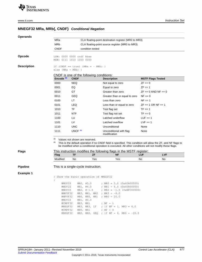
www.ti.com Instruction Set
677SPRUH18H–January 2011–Revised November 2019Submit Documentation Feedback
Copyright © 2011–2019, Texas Instruments Incorporated
Control Law Accelerator (CLA)
MNEGF32 MRa, MRb{, CNDF} Conditional Negation
OperandsMRa CLA floating-point destination register (MR0 to MR3)MRb CLA floating-point source register (MR0 to MR3)CNDF condition tested
Opcode LSW: 0000 0000 cndf bbaaMSW: 0111 1010 1000 0000
Description if (CNDF == true) {MRa = - MRb; }else {MRa = MRb; }
CNDF is one of the following conditions:
(5) Values not shown are reserved.(6) This is the default operation if no CNDF field is specified. This condition will allow the ZF, and NF flags to
be modified when a conditional operation is executed. All other conditions will not modify these flags.
Encode (5) CNDF Description MSTF Flags Tested0000 NEQ Not equal to zero ZF == 00001 EQ Equal to zero ZF == 10010 GT Greater than zero ZF == 0 AND NF == 00011 GEQ Greater than or equal to zero NF == 00100 LT Less than zero NF == 10101 LEQ Less than or equal to zero ZF == 1 OR NF == 11010 TF Test flag set TF == 11011 NTF Test flag not set TF == 01100 LU Latched underflow LUF == 11101 LV Latched overflow LVF == 11110 UNC Unconditional None1111 UNCF (6) Unconditional with flag
modificationNone
Flags This instruction modifies the following flags in the MSTF register:Flag TF ZF NF LUF LVFModified No Yes Yes No No
Pipeline This is a single-cycle instruction.
Example 1; Show the basic operation of MNEGF32;
MMOVIZ MR0, #5.0 ; MR0 = 5.0 (0x40A00000)MMOVIZ MR1, #4.0 ; MR1 = 4.0 (0x40800000)MMOVIZ MR2, #-1.5 ; MR2 = -1.5 (0xBFC00000)MMPYF32 MR3, MR1, MR2 ; MR3 = -6.0MMPYF32 MR0, MR0, MR1 ; MR0 = 20.0MMOVIZ MR1, #0.0MCMPF32 MR3, MR1 ; NF = 1MNEGF32 MR3, MR3, LT ; if NF = 1, MR3 = 6.0MCMPF32 MR0, MR1 ; NF = 0MNEGF32 MR0, MR0, GEQ ; if NF = 0, MR0 = -20.0
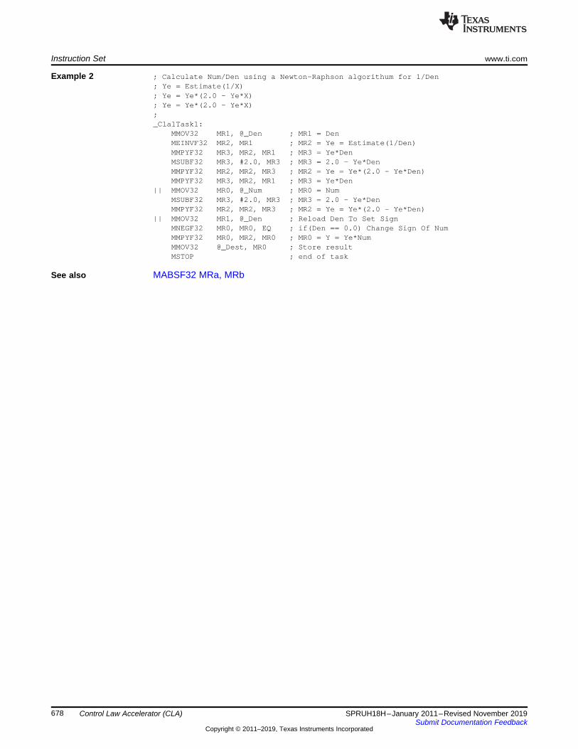
Instruction Set www.ti.com
678 SPRUH18H–January 2011–Revised November 2019Submit Documentation Feedback
Copyright © 2011–2019, Texas Instruments Incorporated
Control Law Accelerator (CLA)
Example 2 ; Calculate Num/Den using a Newton-Raphson algorithum for 1/Den; Ye = Estimate(1/X); Ye = Ye*(2.0 - Ye*X); Ye = Ye*(2.0 - Ye*X);_Cla1Task1:
MMOV32 MR1, @_Den ; MR1 = DenMEINVF32 MR2, MR1 ; MR2 = Ye = Estimate(1/Den)MMPYF32 MR3, MR2, MR1 ; MR3 = Ye*DenMSUBF32 MR3, #2.0, MR3 ; MR3 = 2.0 - Ye*DenMMPYF32 MR2, MR2, MR3 ; MR2 = Ye = Ye*(2.0 - Ye*Den)MMPYF32 MR3, MR2, MR1 ; MR3 = Ye*Den
|| MMOV32 MR0, @_Num ; MR0 = NumMSUBF32 MR3, #2.0, MR3 ; MR3 = 2.0 - Ye*DenMMPYF32 MR2, MR2, MR3 ; MR2 = Ye = Ye*(2.0 - Ye*Den)
|| MMOV32 MR1, @_Den ; Reload Den To Set SignMNEGF32 MR0, MR0, EQ ; if(Den == 0.0) Change Sign Of NumMMPYF32 MR0, MR2, MR0 ; MR0 = Y = Ye*NumMMOV32 @_Dest, MR0 ; Store resultMSTOP ; end of task
See also MABSF32 MRa, MRb
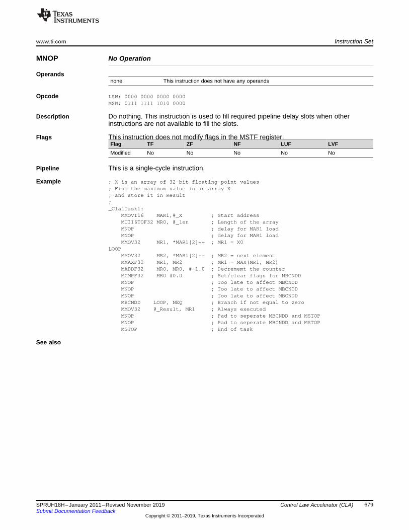
www.ti.com Instruction Set
679SPRUH18H–January 2011–Revised November 2019Submit Documentation Feedback
Copyright © 2011–2019, Texas Instruments Incorporated
Control Law Accelerator (CLA)
MNOP No Operation
Operandsnone This instruction does not have any operands
Opcode LSW: 0000 0000 0000 0000MSW: 0111 1111 1010 0000
Description Do nothing. This instruction is used to fill required pipeline delay slots when otherinstructions are not available to fill the slots.
Flags This instruction does not modify flags in the MSTF register.Flag TF ZF NF LUF LVFModified No No No No No
Pipeline This is a single-cycle instruction.
Example ; X is an array of 32-bit floating-point values; Find the maximum value in an array X; and store it in Result;_Cla1Task1:
MMOVI16 MAR1,#_X ; Start addressMUI16TOF32 MR0, @_len ; Length of the arrayMNOP ; delay for MAR1 loadMNOP ; delay for MAR1 loadMMOV32 MR1, *MAR1[2]++ ; MR1 = X0
LOOPMMOV32 MR2, *MAR1[2]++ ; MR2 = next elementMMAXF32 MR1, MR2 ; MR1 = MAX(MR1, MR2)MADDF32 MR0, MR0, #-1.0 ; Decrememt the counterMCMPF32 MR0 #0.0 ; Set/clear flags for MBCNDDMNOP ; Too late to affect MBCNDDMNOP ; Too late to affect MBCNDDMNOP ; Too late to affect MBCNDDMBCNDD LOOP, NEQ ; Branch if not equal to zeroMMOV32 @_Result, MR1 ; Always executedMNOP ; Pad to seperate MBCNDD and MSTOPMNOP ; Pad to seperate MBCNDD and MSTOPMSTOP ; End of task
See also
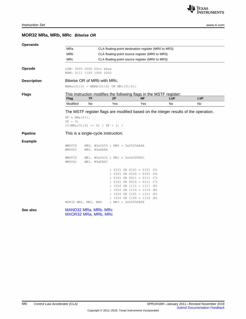
Instruction Set www.ti.com
680 SPRUH18H–January 2011–Revised November 2019Submit Documentation Feedback
Copyright © 2011–2019, Texas Instruments Incorporated
Control Law Accelerator (CLA)
MOR32 MRa, MRb, MRc Bitwise OR
OperandsMRa CLA floating-point destination register (MR0 to MR3)MRb CLA floating-point source register (MR0 to MR3)MRc CLA floating-point source register (MR0 to MR3)
Opcode LSW: 0000 0000 00cc bbaaMSW: 0111 1100 1000 0000
Description Bitwise OR of MRb with MRc.MARa(31:0) = MARb(31:0) OR MRc(31:0);
Flags This instruction modifies the following flags in the MSTF register:Flag TF ZF NF LUF LVFModified No Yes Yes No No
The MSTF register flags are modified based on the integer results of the operation.NF = MRa(31);ZF = 0;if(MRa(31:0) == 0) { ZF = 1; }
Pipeline This is a single-cycle instruction.
ExampleMMOVIZ MR0, #0x5555 ; MR0 = 0x5555AAAAMMOVXI MR0, #0xAAAA
MMOVIZ MR1, #0x5432 ; MR1 = 0x5432FEDCMMOVXI MR1, #0xFEDC
; 0101 OR 0101 = 0101 (5); 0101 OR 0100 = 0101 (5); 0101 OR 0011 = 0111 (7); 0101 OR 0010 = 0111 (7); 1010 OR 1111 = 1111 (F); 1010 OR 1110 = 1110 (E); 1010 OR 1101 = 1111 (F); 1010 OR 1100 = 1110 (E)
MOR32 MR2, MR1, MR0 ; MR3 = 0x5555FEFE
See also MAND32 MRa, MRb, MRcMXOR32 MRa, MRb, MRc

www.ti.com Instruction Set
681SPRUH18H–January 2011–Revised November 2019Submit Documentation Feedback
Copyright © 2011–2019, Texas Instruments Incorporated
Control Law Accelerator (CLA)
MRCNDD {CNDF} Return Conditional Delayed
OperandsCNDF optional condition.
Opcode LSW: 0000 0000 0000 0000MSW: 0111 1001 1010 cndf
Description If the specified condition is true, then the RPC field of MSTF is loaded into MPC andfetching continues from that location. Otherwise program fetches will continue withoutthe return.
Please refer to the pipeline section for important information regarding this instruction.if (CNDF == TRUE) MPC = RPC;
CNDF is one of the following conditions:
(7) Values not shown are reserved.(8) This is the default operation if no CNDF field is specified. This condition will allow the ZF and NF flags to
be modified when a conditional operation is executed. All other conditions will not modify these flags.
Encode (7) CNDF Description MSTF Flags Tested0000 NEQ Not equal to zero ZF == 00001 EQ Equal to zero ZF == 10010 GT Greater than zero ZF == 0 AND NF == 00011 GEQ Greater than or equal to zero NF == 00100 LT Less than zero NF == 10101 LEQ Less than or equal to zero ZF == 1 OR NF == 11010 TF Test flag set TF == 11011 NTF Test flag not set TF == 01100 LU Latched underflow LUF == 11101 LV Latched overflow LVF == 11110 UNC Unconditional None1111 UNCF (8) Unconditional with flag
modificationNone
Flags This instruction does not modify flags in the MSTF register.Flag TF ZF NF LUF LVFModified No No No No No

Instruction Set www.ti.com
682 SPRUH18H–January 2011–Revised November 2019Submit Documentation Feedback
Copyright © 2011–2019, Texas Instruments Incorporated
Control Law Accelerator (CLA)
Pipeline The MRCNDD instruction by itself is a single-cycle instruction. As shown in Table 10-18,for each return 6 instruction slots are executed; three before the return instruction (d5-d7) and three after the return instruction (d8-d10). The total number of cycles for a returntaken or not taken depends on the usage of these slots. That is, the number of cyclesdepends on how many slots are filled with a MNOP as well as which slots are filled. Theeffective number of cycles for a return can, therefore, range from 1 to 7 cycles. Thenumber of cycles for a return taken may not be the same as for a return not taken.
Referring to the following code fragment and the pipeline diagrams in Table 10-18 andTable 10-19, the instructions before and after MRCNDD have the following properties:
;;<Instruction 1> ; I1 Last instruction that can affect flags for
; the MCCNDD operation<Instruction 2> ; I2 Cannot be stop, branch, call or return<Instruction 3> ; I3 Cannot be stop, branch, call or return<Instruction 4> ; I4 Cannot be stop, branch, call or return
MCCNDD _func, NEQ ; Call to func if not eqal to zero; Three instructions after MCCNDD are always; executed whether the call is taken or not
<Instruction 5> ; I5 Cannot be stop, branch, call or return<Instruction 6> ; I6 Cannot be stop, branch, call or return<Instruction 7> ; I7 Cannot be stop, branch, call or return<Instruction 8> ; I8 The address of this instruction is saved
; in the RPC field of the MSTF register.; Upon return this value is loaded into MPC; and fetching continues from this point.
<Instruction 9> ; I9<Instruction 10> ; I10........_func:<Destination 1> ; d1 Can be any instruction<Destination 2> ; d2<Destination 3> ; d3<Destination 4> ; d4 Last instruction that can affect flags for
; the MRCNDD operation<Destination 5> ; d5 Cannot be stop, branch, call or return<Destination 6> ; d6 Cannot be stop, branch, call or return<Destination 7> ; d7 Cannot be stop, branch, call or return
MRCNDD NEQ ; Return to <Instruction 8> if not equal to zero; Three instructions after MRCNDD are always; executed whether the return is taken or not
<Destination 8> ; d8 Cannot be stop, branch, call or return<Destination 9> ; d9 Cannot be stop, branch, call or return<Destination 10> ; d10 Cannot be stop, branch, call or return<Destination 11> ; d11<Destination 12> ; d12........MSTOP....
• d4– d4 is the last instruction that can effect the CNDF flags for the MRCNDD
instruction. The CNDF flags are tested in the D2 phase of the pipeline. That is, adecision is made whether to return or not when MRCNDD is in the D2 phase.
– There are no restrictions on the type of instruction for d4.• d5, d6 and d7
– The three instructions proceeding MRCNDD can change MSTF flags but will haveno effect on whether the MRCNDD instruction makes the return or not. This is

www.ti.com Instruction Set
683SPRUH18H–January 2011–Revised November 2019Submit Documentation Feedback
Copyright © 2011–2019, Texas Instruments Incorporated
Control Law Accelerator (CLA)
because the flag modification will occur after the D2 phase of the MRCNDDinstruction.
– These instructions must not be the following: MSTOP, MDEBUGSTOP,MBCNDD, MCCNDD or MRCNDD.
• d8, d9 and d10– The three instructions following MRCNDD are always executed irrespective of
whether the return is taken or not.– These instructions must not be the following: MSTOP, MDEBUGSTOP,
MBCNDD, MCCNDD or MRCNDD.
Table 10-18. Pipeline Activity For MRCNDD, Return Not TakenInstruction F1 F2 D1 D2 R1 R2 E W
d4 d4 d3 d2 d1 I7 I6 I5
d5 d5 d4 d3 d2 d1 I7 I6
d6 d6 d5 d4 d3 d2 d1 i7
d7 d7 d6 d5 d4 d3 d2 d1
MRCNDD MRCNDD d7 d6 d5 d4 d3 d2
d8 d8 MRCNDD d7 d6 d5 d4 d3
d9 d9 d8 MRCNDD d7 d6 d5 d4
d10 d10 d9 d8 MRCNDD d7 d6 d5
d11 d11 d10 d9 d8 - d7 d6
d12 d12 d11 d10 d9 d8 - d7
etc.... .... d12 d11 d10 d9 d8 -
.... .... .... d12 d11 d10 d9 d8
.... .... .... .... d12 d11 d10 d9
d12 d11 d10
d12 d11
d12
Table 10-19. Pipeline Activity For MRCNDD, Return TakenInstruction F1 F2 D1 D2 R1 R2 E W
d4 d4 d3 d2 d1 I7 I6 I5
d5 d5 d4 d3 d2 d1 I7 I6
d6 d6 d5 d4 d3 d2 d1 i7
d7 d7 d6 d5 d4 d3 d2 d1
MRCNDD MRCNDD d7 d6 d5 d4 d3 d2
d8 d8 MRCNDD d7 d6 d5 d4 d3
d9 d9 d8 MRCNDD d7 d6 d5 d4
d10 d10 d9 d8 MRCNDD d7 d6 d5
I8 I8 d10 d9 d8 - d7 d6
I9 I9 I8 d10 d9 d8 - d7
I10 I10 I9 I8 d10 d9 d8 -
etc.... .... I10 I9 I8 d10 d9 d8
.... .... I10 I9 I8 d10 d9
.... .... I10 I9 I8 d10
I10 I9 I8
I10 I9
I10

Instruction Set www.ti.com
684 SPRUH18H–January 2011–Revised November 2019Submit Documentation Feedback
Copyright © 2011–2019, Texas Instruments Incorporated
Control Law Accelerator (CLA)
Example ;
See also MBCNDD #16BitDest, CNDFMCCNDD 16BitDest, CNDFMMOV32 mem32, MSTFMMOV32 MSTF, mem32

www.ti.com Instruction Set
685SPRUH18H–January 2011–Revised November 2019Submit Documentation Feedback
Copyright © 2011–2019, Texas Instruments Incorporated
Control Law Accelerator (CLA)
MSETFLG FLAG, VALUE Set or Clear Selected Floating-Point Status Flags
OperandsFLAG 8 bit mask indicating which floating-point status flags to change.VALUE 8 bit mask indicating the flag value; 0 or 1.
Opcode LSW: FFFF FFFF VVVV VVVVMSW: 0111 1001 1100 0000
Description The MSETFLG instruction is used to set or clear selected floating-point status flags inthe MSTF register. The FLAG field is an 11-bit value that indicates which flags will bechanged. That is, if a FLAG bit is set to 1 it indicates that flag will be changed; all otherflags will not be modified. The bit mapping of the FLAG field is shown below:
RNDF32
reserved
reserved
TF reserved
reserved ZF NF LUF LVF
9 8 7 6 5 4 3 2 1 0
The VALUE field indicates the value the flag should be set to; 0 or 1.
Flags This instruction modifies the following flags in the MSTF register:Flag TF ZF NF LUF LVFModified Yes Yes Yes Yes Yes
Any flag can be modified by this instruction. The MEALLOW and RPC fields cannot bemodified with this instruction.
Pipeline This is a single-cycle instruction.
Example To make it easier and legible, the assembler accepts a FLAG=VALUE syntax for theMSTFLG operation as shown below:
MSETFLG RNDF32=0, TF=0, NF=1; FLAG = 11000100; VALUE = 00XXX1XX;
See also MMOV32 mem32, MSTFMMOV32 MSTF, mem32
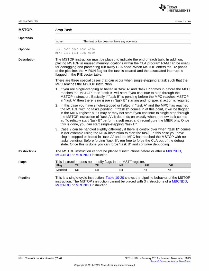
Instruction Set www.ti.com
686 SPRUH18H–January 2011–Revised November 2019Submit Documentation Feedback
Copyright © 2011–2019, Texas Instruments Incorporated
Control Law Accelerator (CLA)
MSTOP Stop Task
Operandsnone This instruction does not have any operands
Opcode LSW: 0000 0000 0000 0000MSW: 0111 1111 1000 0000
Description The MSTOP instruction must be placed to indicate the end of each task. In addition,placing MSTOP in unused memory locations within the CLA program RAM can be usefulfor debugging and preventing run away CLA code. When MSTOP enters the D2 phaseof the pipeline, the MIRUN flag for the task is cleared and the associated interrupt isflagged in the PIE vector table.
There are three special cases that can occur when single-stepping a task such that theMPC reaches the MSTOP instruction.1. If you are single-stepping or halted in "task A" and "task B" comes in before the MPC
reaches the MSTOP, then "task B" will start if you continue to step through theMSTOP instruction. Basically if "task B" is pending before the MPC reaches MSTOPin "task A" then there is no issue in "task B" starting and no special action is required.
2. In this case you have single-stepped or halted in "task A" and the MPC has reachedthe MSTOP with no tasks pending. If "task B" comes in at this point, it will be flaggedin the MIFR register but it may or may not start if you continue to single-step throughthe MSTOP instruction of "task A". It depends on exactly when the new task comesin. To reliably start "task B" perform a soft reset and reconfigure the MIER bits. Oncethis is done, you can start single-stepping "task B".
3. Case 2 can be handled slightly differently if there is control over when "task B" comesin (for example using the IACK instruction to start the task). In this case you havesingle-stepped or halted in "task A" and the MPC has reached the MSTOP with notasks pending. Before forcing "task B", run free to force the CLA out of the debugstate. Once this is done you can force "task B" and continue debugging.
Restrictions The MSTOP instruction cannot be placed 3 instructions before or after a MBCNDD,MCCNDD or MRCNDD instruction.
Flags This instruction does not modify flags in the MSTF register.Flag TF ZF NF LUF LVFModified No No No No No
Pipeline This is a single-cycle instruction. Table 10-20 shows the pipeline behavior of the MSTOPinstruction. The MSTOP instruction cannot be placed with 3 instructions of a MBCNDD,MCCNDD or MRCNDD instruction.
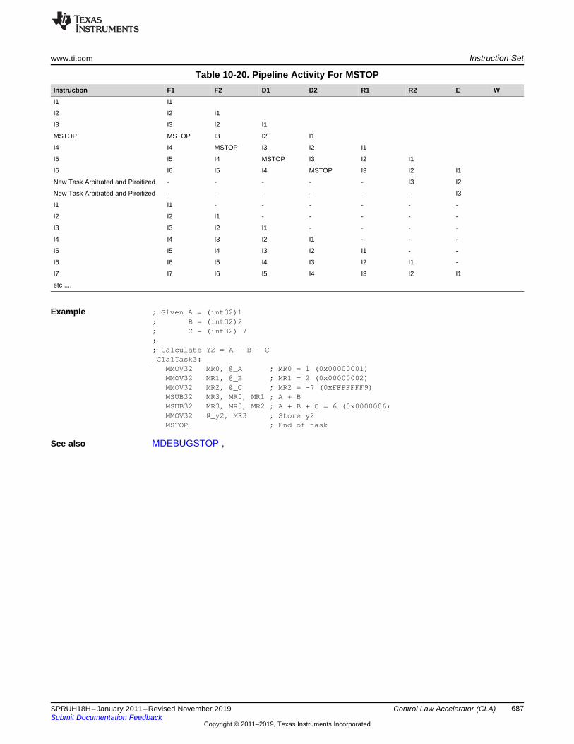
www.ti.com Instruction Set
687SPRUH18H–January 2011–Revised November 2019Submit Documentation Feedback
Copyright © 2011–2019, Texas Instruments Incorporated
Control Law Accelerator (CLA)
Table 10-20. Pipeline Activity For MSTOPInstruction F1 F2 D1 D2 R1 R2 E W
I1 I1
I2 I2 I1
I3 I3 I2 I1
MSTOP MSTOP I3 I2 I1
I4 I4 MSTOP I3 I2 I1
I5 I5 I4 MSTOP I3 I2 I1
I6 I6 I5 I4 MSTOP I3 I2 I1
New Task Arbitrated and Piroitized - - - - - I3 I2
New Task Arbitrated and Piroitized - - - - - - I3
I1 I1 - - - - - -
I2 I2 I1 - - - - -
I3 I3 I2 I1 - - - -
I4 I4 I3 I2 I1 - - -
I5 I5 I4 I3 I2 I1 - -
I6 I6 I5 I4 I3 I2 I1 -
I7 I7 I6 I5 I4 I3 I2 I1
etc ....
Example ; Given A = (int32)1; B = (int32)2; C = (int32)-7;; Calculate Y2 = A - B - C_Cla1Task3:
MMOV32 MR0, @_A ; MR0 = 1 (0x00000001)MMOV32 MR1, @_B ; MR1 = 2 (0x00000002)MMOV32 MR2, @_C ; MR2 = -7 (0xFFFFFFF9)MSUB32 MR3, MR0, MR1 ; A + BMSUB32 MR3, MR3, MR2 ; A + B + C = 6 (0x0000006)MMOV32 @_y2, MR3 ; Store y2MSTOP ; End of task
See also MDEBUGSTOP ,

Instruction Set www.ti.com
688 SPRUH18H–January 2011–Revised November 2019Submit Documentation Feedback
Copyright © 2011–2019, Texas Instruments Incorporated
Control Law Accelerator (CLA)
MSUB32 MRa, MRb, MRc 32-Bit Integer Subtraction
OperandsMRa CLA floating-point destination register (MR0 to MR3)MRb CLA floating-point destination register (MR0 to MR3)MRc CLA floating-point destination register (MR0 to MR3)
Opcode LSW: 0000 0000 00cc bbaaMSW: 0111 1100 1110 0000
Description 32-bit integer addition of MRb and MRc.MARa(31:0) = MARb(31:0) - MRc(31:0);
Flags This instruction modifies the following flags in the MSTF register:Flag TF ZF NF LUF LVFModified No Yes Yes No No
The MSTF register flags are modified as follows:NF = MRa(31);ZF = 0;if(MRa(31:0) == 0) { ZF = 1; }
Pipeline This is a single-cycle instruction.
Example ; Given A = (int32)1; B = (int32)2; C = (int32)-7;;Calculate Y2 = A - B - C;_Cla1Task3:
MMOV32 MR0, @_A ; MR0 = 1 (0x00000001)MMOV32 MR1, @_B ; MR1 = 2 (0x00000002)MMOV32 MR2, @_C ; MR2 = -7 (0xFFFFFFF9)MSUB32 MR3, MR0, MR1 ; A + BMSUB32 MR3, MR3, MR2 ; A + B + C = 6 (0x0000006)MMOV32 @_y2, MR3 ; Store y2MSTOP ; End of task
See also MADD32 MRa, MRb, MRcMAND32 MRa, MRb, MRcMASR32 MRa, #SHIFTMLSL32 MRa, #SHIFTMLSR32 MRa, #SHIFTMOR32 MRa, MRb, MRcMXOR32 MRa, MRb, MRc

www.ti.com Instruction Set
689SPRUH18H–January 2011–Revised November 2019Submit Documentation Feedback
Copyright © 2011–2019, Texas Instruments Incorporated
Control Law Accelerator (CLA)
MSUBF32 MRa, MRb, MRc 32-Bit Floating-Point Subtraction
OperandsMRa CLA floating-point destination register (MR0 to R1)MRb CLA floating-point source register (MR0 to R1)MRc CLA floating-point source register (MR0 to R1)
Opcode LSW: 0000 0000 00cc bbaaMSW: 0111 1100 0100 0000
Description Subtract the contents of two floating-point registersMRa = MRb - MRc;
Flags This instruction modifies the following flags in the MSTF register:Flag TF ZF NF LUF LVFModified No No No Yes Yes
The MSTF register flags are modified as follows:• LUF = 1 if MSUBF32 generates an underflow condition.• LVF = 1 if MSUBF32 generates an overflow condition.
Pipeline This is a single-cycle instruction.
Example; Given A, B and C are 32-bit floating-point numbers; Calculate Y2 = A + B - C;_Cla1Task5:
MMOV32 MR0, @_A ; Load MR0 with AMMOV32 MR1, @_B ; Load MR1 with BMADDF32 MR0, MR1, MR0 ; Add A + B
|| MMOV32 MR1, @_C ; and in parallel load CMSUBF32 MR0, MR0, MR1 ; Subtract C from (A + B)MMOV32 @Y, MR0 ; (A+B) - CMSTOP ; end of task
See also MSUBF32 MRa, #16FHi, MRbMSUBF32 MRd, MRe, MRf || MMOV32 MRa, mem32MSUBF32 MRd, MRe, MRf || MMOV32 mem32, MRaMMPYF32 MRa, MRb, MRc || MSUBF32 MRd, MRe, MRf

Instruction Set www.ti.com
690 SPRUH18H–January 2011–Revised November 2019Submit Documentation Feedback
Copyright © 2011–2019, Texas Instruments Incorporated
Control Law Accelerator (CLA)
MSUBF32 MRa, #16FHi, MRb 32-Bit Floating-Point Subtraction
OperandsMRa CLA floating-point destination register (MR0 to R1)#16FHi A 16-bit immediate value that represents the upper 16-bits of an IEEE 32-bit floating-
point value. The low 16-bits of the mantissa are assumed to be all 0.MRb CLA floating-point source register (MR0 to R1)
Opcode LSW: IIII IIII IIII IIIIMSW: 0111 1000 0000 baaa
Description Subtract MRb from the floating-point value represented by the immediate operand. Storethe result of the addition in MRa.
#16FHi is a 16-bit immediate value that represents the upper 16-bits of an IEEE 32-bitfloating-point value. The low 16-bits of the mantissa are assumed to be all 0. #16FHi ismost useful for representing constants where the lowest 16-bits of the mantissa are 0.Some examples are 2.0 (0x40000000), 4.0 (0x40800000), 0.5 (0x3F000000), and -1.5(0xBFC00000). The assembler will accept either a hex or float as the immediate value.That is, the value -1.5 can be represented as #-1.5 or #0xBFC0.MRa = #16FHi:0 - MRb;
Flags This instruction modifies the following flags in the MSTF register:Flag TF ZF NF LUF LVFModified No No No Yes Yes
The MSTF register flags are modified as follows:• LUF = 1 if MSUBF32 generates an underflow condition.• LVF = 1 if MSUBF32 generates an overflow condition.
Pipeline This is a single-cycle instruction.
Example ; Y = sqrt(X); Ye = Estimate(1/sqrt(X));; Ye = Ye*(1.5 - Ye*Ye*X*0.5); Ye = Ye*(1.5 - Ye*Ye*X*0.5); Y = X*Ye;_Cla1Task3:
MMOV32 MR0, @_x ; MR0 = XMEISQRTF32 MR1, MR0 ; MR1 = Ye = Estimate(1/sqrt(X))MMOV32 MR1, @_x, EQ ; if(X == 0.0) Ye = 0.0MMPYF32 MR3, MR0, #0.5 ; MR3 = X*0.5MMPYF32 MR2, MR1, MR3 ; MR2 = Ye*X*0.5MMPYF32 MR2, MR1, MR2 ; MR2 = Ye*Ye*X*0.5MSUBF32 MR2, #1.5, MR2 ; MR2 = 1.5 - Ye*Ye*X*0.5MMPYF32 MR1, MR1, MR2 ; MR1 = Ye = Ye*(1.5 - Ye*Ye*X*0.5)MMPYF32 MR2, MR1, MR3 ; MR2 = Ye*X*0.5MMPYF32 MR2, MR1, MR2 ; MR2 = Ye*Ye*X*0.5MSUBF32 MR2, #1.5, MR2 ; MR2 = 1.5 - Ye*Ye*X*0.5MMPYF32 MR1, MR1, MR2 ; MR1 = Ye = Ye*(1.5 - Ye*Ye*X*0.5)MMPYF32 MR0, MR1, MR0 ; MR0 = Y = Ye*XMMOV32 @_y, MR0 ; Store Y = sqrt(X)MSTOP ; end of task
See also MSUBF32 MRa, MRb, MRcMSUBF32 MRd, MRe, MRf || MMOV32 MRa, mem32MSUBF32 MRd, MRe, MRf || MMOV32 mem32, MRaMMPYF32 MRa, MRb, MRc || MSUBF32 MRd, MRe, MRf

www.ti.com Instruction Set
691SPRUH18H–January 2011–Revised November 2019Submit Documentation Feedback
Copyright © 2011–2019, Texas Instruments Incorporated
Control Law Accelerator (CLA)
MSUBF32 MRd, MRe, MRf ||MMOV32 MRa, mem32 32-Bit Floating-Point Subtraction with ParallelMove
OperandsMRd CLA floating-point destination register (MR0 to MR3) for the MSUBF32 operation
MRd cannot be the same register as MRaMRe CLA floating-point source register (MR0 to MR3) for the MSUBF32 operationMRf CLA floating-point source register (MR0 to MR3) for the MSUBF32 operationMRa CLA floating-point destination register (MR0 to MR3) for the MMOV32 operation
MRa cannot be the same register as MRdmem32 32-bit memory location accessed using one of the available addressing modes. Source
for the MMOV32 operation.
Opcode LSW: mmmm mmmm mmmm mmmmMSW: 0010 ffee ddaa addr
Description Subtract the contents of two floating-point registers and move from memory to a floating-point register.MRd = MRe - MRf;MRa = [mem32];
Restrictions The destination register for the MSUBF32 and the MMOV32 must be unique. That is,MRa cannot be the same register as MRd.
Flags This instruction modifies the following flags in the MSTF register:Flag TF ZF NF LUF LVFModified No Yes Yes Yes Yes
The MSTF register flags are modified as follows:• LUF = 1 if MSUBF32 generates an underflow condition.• LVF = 1 if MSUBF32 generates an overflow condition.
The MMOV32 Instruction will set the NF and ZF flags as follows:
Pipeline Both MSUBF32 and MMOV32 complete in a single cycle.
Example NF = MRa(31);ZF = 0;if(MRa(30:23) == 0) { ZF = 1; NF = 0; }
See also MSUBF32 MRa, MRb, MRcMSUBF32 MRa, #16FHi, MRbMMPYF32 MRa, MRb, MRc || MSUBF32 MRd, MRe, MRf

Instruction Set www.ti.com
692 SPRUH18H–January 2011–Revised November 2019Submit Documentation Feedback
Copyright © 2011–2019, Texas Instruments Incorporated
Control Law Accelerator (CLA)
MSUBF32 MRd, MRe, MRf ||MMOV32 mem32, MRa 32-Bit Floating-Point Subtraction with ParallelMove
OperandsMRd CLA floating-point destination register (MR0 to MR3) for the MSUBF32 operationMRe CLA floating-point source register (MR0 to MR3) for the MSUBF32 operationMRf CLA floating-point source register (MR0 to MR3) for the MSUBF32 operationmem32 32-bit destination memory location for the MMOV32 operationMRa CLA floating-point source register (MR0 to MR3) for the MMOV32 operation
Opcode LSW: mmmm mmmm mmmm mmmmMSW: 0110 ffee ddaa addr
Description Subtract the contents of two floating-point registers and move from a floating-pointregister to memory.MRd = MRe - MRf;[mem32] = MRa;
Flags This instruction modifies the following flags in the MSTF register:Flag TF ZF NF LUF LVFModified No No No Yes Yes
The MSTF register flags are modified as follows:• LUF = 1 if MSUBF32 generates an underflow condition.• LVF = 1 if MSUBF32 generates an overflow condition.
Pipeline Both MSUBF32 and MMOV32 complete in a single cycle.
Example
See also MSUBF32 MRa, MRb, MRcMSUBF32 MRa, #16FHi, MRbMSUBF32 MRd, MRe, MRf || MMOV32 MRa, mem32MMPYF32 MRa, MRb, MRc || MSUBF32 MRd, MRe, MRf

www.ti.com Instruction Set
693SPRUH18H–January 2011–Revised November 2019Submit Documentation Feedback
Copyright © 2011–2019, Texas Instruments Incorporated
Control Law Accelerator (CLA)
MSWAPF MRa, MRb {, CNDF} Conditional Swap
OperandsMRa CLA floating-point register (MR0 to MR3)MRb CLA floating-point register (MR0 to MR3)CNDF Optional condition tested based on the MSTF flags
Opcode LSW: 0000 0000 CNDF bbaaMSW: 0111 1011 0000 0000
Description Conditional swap of MRa and MRb.if (CNDF == true) swap MRa and MRb;
CNDF is one of the following conditions:
(1) Values not shown are reserved.(2) This is the default operation if no CNDF field is specified. This condition will allow the ZF and NF flags to
be modified when a conditional operation is executed. All other conditions will not modify these flags.
Encode (1) CNDF Description MSTF Flags Tested0000 NEQ Not equal to zero ZF == 00001 EQ Equal to zero ZF == 10010 GT Greater than zero ZF == 0 AND NF == 00011 GEQ Greater than or equal to zero NF == 00100 LT Less than zero NF == 10101 LEQ Less than or equal to zero ZF == 1 OR NF == 11010 TF Test flag set TF == 11011 NTF Test flag not set TF == 01100 LU Latched underflow LUF == 11101 LV Latched overflow LVF == 11110 UNC Unconditional None1111 UNCF (2) Unconditional with flag
modificationNone
Flags This instruction modifies the following flags in the MSTF register:Flag TF ZF NF LUF LVFModified No No No No No
No flags affected
Pipeline This is a single-cycle instruction.

Instruction Set www.ti.com
694 SPRUH18H–January 2011–Revised November 2019Submit Documentation Feedback
Copyright © 2011–2019, Texas Instruments Incorporated
Control Law Accelerator (CLA)
Example ; X is an array of 32-bit floating-point values; and has len elements. Find the maximum value in; the array and store it in Result;; Note: MCMPF32 and MSWAPF can be replaced by MMAXF32;_Cla1Task1:
MMOVI16 MAR1,#_X ; Start addressMUI16TOF32 MR0, @_len ; Length of the arrayMNOP ; delay for MAR1 loadMNOP ; delay for MAR1 loadMMOV32 MR1, *MAR1[2]++ ; MR1 = X0
LOOPMMOV32 MR2, *MAR1[2]++ ; MR2 = next elementMCMPF32 MR2, MR1 ; Compare MR2 with MR1MSWAPF MR1, MR2, GT ; MR1 = MAX(MR1, MR2)MADDF32 MR0, MR0, #-1.0 ; Decrememt the counterMCMPF32 MR0 #0.0 ; Set/clear flags for MBCNDDMNOPMNOPMNOPMBCNDD LOOP, NEQ ; Branch if not equal to zeroMMOV32 @_Result, MR1 ; Always executedMNOP ; Always executedMNOP ; Always executedMSTOP ; End of task
See also

www.ti.com Instruction Set
695SPRUH18H–January 2011–Revised November 2019Submit Documentation Feedback
Copyright © 2011–2019, Texas Instruments Incorporated
Control Law Accelerator (CLA)
MTESTTF CNDF Test MSTF Register Flag Condition
OperandsCNDF condition to test based on MSTF flags
Opcode LSW: 0000 0000 0000 cndfMSW: 0111 1111 0100 0000
Description Test the CLA floating-point condition and if true, set the MSTF[TF] flag. If the condition isfalse, clear the MSTF[TF] flag. This is useful for temporarily storing a condition for lateruse.if (CNDF == true) TF = 1;else TF = 0;
CNDF is one of the following conditions:
(3) Values not shown are reserved.(4) This is the default operation if no CNDF field is specified. This condition will allow the ZF and NF flags to
be modified when a conditional operation is executed. All other conditions will not modify these flags.
Encode (3) CNDF Description MSTF Flags Tested0000 NEQ Not equal to zero ZF == 00001 EQ Equal to zero ZF == 10010 GT Greater than zero ZF == 0 AND NF == 00011 GEQ Greater than or equal to zero NF == 00100 LT Less than zero NF == 10101 LEQ Less than or equal to zero ZF == 1 OR NF == 11010 TF Test flag set TF == 11011 NTF Test flag not set TF == 01100 LU Latched underflow LUF == 11101 LV Latched overflow LVF == 11110 UNC Unconditional None1111 UNCF (4) Unconditional with flag
modificationNone
Flags This instruction modifies the following flags in the MSTF register:Flag TF ZF NF LUF LVFModified Yes No No No No
TF = 0;if (CNDF == true) TF = 1;
Note: If (CNDF == UNC or UNCF), the TF flag will be set to 1.
Pipeline This is a single-cycle instruction.

Instruction Set www.ti.com
696 SPRUH18H–January 2011–Revised November 2019Submit Documentation Feedback
Copyright © 2011–2019, Texas Instruments Incorporated
Control Law Accelerator (CLA)
Example ; if (State == 0.1); RampState = RampState || RAMPMASK; else if (State == 0.01); CoastState = CoastState || COASTMASK; else; SteadyState = SteadyState || STEADYMASK;_Cla1Task2:
MMOV32 MR0, @_StateMCMPF32 MR0, #0.1 ; Affects flags for 1st MBCNDD (A)MCMPF32 MR0, #0.01 ; Check used by 2nd MBCNDD (B)MTESTTF EQ ; Store EQ flag in TF for 2nd MBCNDD (B)MNOPMBCNDD _Skip1, NEQ ; (A) If State != 0.1, go to Skip1MMOV32 MR1, @_RampState ; Always executedMMOVXI MR2, #RAMPMASK ; Always executedMOR32 MR1, MR2 ; Always executedMMOV32 @_RampState, MR1 ; Execute if (A) branch not takenMSTOP ; end of task if (A) branch not taken
_Skip1:MMOV32 MR3, @_SteadyStateMMOVXI MR2, #STEADYMASKMOR32 MR3, MR2MBCNDD _Skip2, NTF ; (B) if State != .01, go to Skip2MMOV32 MR1, @_CoastState ; Always executedMMOVXI MR2, #COASTMASK ; Always executedMOR32 MR1, MR2 ; Always executedMMOV32 @_CoastState, MR1 ; Execute if (B) branch not takenMSTOP ; end of task if (B) branch not taken
_Skip2:MMOV32 @_SteadyState, MR3 ; Executed if (B) branch takenMSTOP
See also

www.ti.com Instruction Set
697SPRUH18H–January 2011–Revised November 2019Submit Documentation Feedback
Copyright © 2011–2019, Texas Instruments Incorporated
Control Law Accelerator (CLA)
MUI16TOF32 MRa, mem16 Convert Unsigned 16-Bit Integer to 32-Bit Floating-Point Value
OperandsMRa CLA floating-point destination register (MR0 to MR3)mem16 16-bit source memory location
Opcode LSW: mmmm mmmm mmmm mmmm
MSW: 0111 0101 01aa addr
Description When converting F32 to I16/UI16 data format, the MF32TOI16/UI16 operation truncatesto zero while the MF32TOI16R/UI16R operation will round to nearest (even) value.MRa = UI16TOF32[mem16];
Flags This instruction does not affect any flags:Flag TF ZF NF LUF LVFModified No No No No No
Pipeline This is a single-cycle instruction.
Example
See also MF32TOI16 MRa, MRbMF32TOI16R MRa, MRbMF32TOUI16 MRa, MRbMF32TOUI16R MRa, MRbMI16TOF32 MRa, MRbMI16TOF32 MRa, mem16MUI16TOF32 MRa, MRb

Instruction Set www.ti.com
698 SPRUH18H–January 2011–Revised November 2019Submit Documentation Feedback
Copyright © 2011–2019, Texas Instruments Incorporated
Control Law Accelerator (CLA)
MUI16TOF32 MRa, MRb Convert Unsigned 16-Bit Integer to 32-Bit Floating-Point Value
OperandsMRa CLA floating-point destination register (MR0 to MR3)MRb CLA floating-point source register (MR0 to MR3)
Opcode LSW: 0000 0000 0000 bbaa
MSW: 0111 1110 1110 0000
Description Convert an unsigned 16-bit integer to a 32-bit floating-point value. When convertingfloat32 to I16/UI16 data format, the MF32TOI16/UI16 operation truncates to zero whilethe MF32TOI16R/UI16R operation will round to nearest (even) value.MRa = UI16TOF32[MRb];
Flags This instruction does not affect any flags:Flag TF ZF NF LUF LVFModified No No No No No
Pipeline This is a single-cycle instruction.
Example MMOVXI MR1, #0x800F ; MR1(15:0) = 32783 (0x800F)MUI16TOF32 MR0, MR1 ; MR0 = UI16TOF32 (MR1(15:0))
; = 32783.0 (0x47000F00)
See also MF32TOI16 MRa, MRbMF32TOI16R MRa, MRbMF32TOUI16 MRa, MRbMF32TOUI16R MRa, MRbMI16TOF32 MRa, MRbMI16TOF32 MRa, mem16MUI16TOF32 MRa, mem16

www.ti.com Instruction Set
699SPRUH18H–January 2011–Revised November 2019Submit Documentation Feedback
Copyright © 2011–2019, Texas Instruments Incorporated
Control Law Accelerator (CLA)
MUI32TOF32 MRa, mem32 Convert Unsigned 32-Bit Integer to 32-Bit Floating-Point Value
OperandsMRa CLA floating-point destination register (MR0 to MR3)mem32 32-bit memory location accessed using one of the available addressing modes
Opcode LSW: mmmm mmmm mmmm mmmm
MSW: 0111 0100 10aa addr
Description MRa = UI32TOF32[mem32];
Flags This instruction does not affect any flags:Flag TF ZF NF LUF LVFModified No No No No No
Pipeline This is a single-cycle instruction.
Example ; Given x2, m2 and b2 are Uint32 numbers:;; x2 = Uint32(2) = 0x00000002; m2 = Uint32(1) = 0x00000001; b2 = Uint32(3) = 0x00000003;; Calculate y2 = x2 * m2 + b2;_Cla1Task1:
MUI32TOF32 MR0, @_m2 ; MR0 = 1.0 (0x3F800000)MUI32TOF32 MR1, @_x2 ; MR1 = 2.0 (0x40000000)MUI32TOF32 MR2, @_b2 ; MR2 = 3.0 (0x40400000)MMPYF32 MR3, MR0, MR1 ; M*XMADDF32 MR3, MR2, MR3 ; Y=MX+B = 5.0 (0x40A00000)MF32TOUI32 MR3, MR3 ; Y = Uint32(5.0) = 0x00000005MMOV32 @_y2, MR3 ; store resultMSTOP ; end of task
See also MF32TOI32 MRa, MRbMF32TOUI32 MRa, MRbMI32TOF32 MRa, mem32MI32TOF32 MRa, MRbMUI32TOF32 MRa, MRb
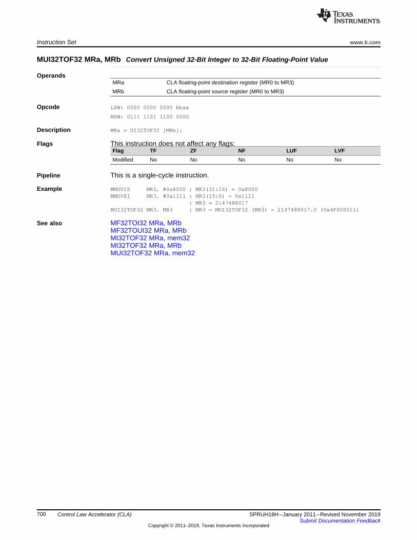
Instruction Set www.ti.com
700 SPRUH18H–January 2011–Revised November 2019Submit Documentation Feedback
Copyright © 2011–2019, Texas Instruments Incorporated
Control Law Accelerator (CLA)
MUI32TOF32 MRa, MRb Convert Unsigned 32-Bit Integer to 32-Bit Floating-Point Value
OperandsMRa CLA floating-point destination register (MR0 to MR3)MRb CLA floating-point source register (MR0 to MR3)
Opcode LSW: 0000 0000 0000 bbaa
MSW: 0111 1101 1100 0000
Description MRa = UI32TOF32 [MRb];
Flags This instruction does not affect any flags:Flag TF ZF NF LUF LVFModified No No No No No
Pipeline This is a single-cycle instruction.
Example MMOVIZ MR3, #0x8000 ; MR3(31:16) = 0x8000MMOVXI MR3, #0x1111 ; MR3(15:0) = 0x1111
; MR3 = 2147488017MUI32TOF32 MR3, MR3 ; MR3 = MUI32TOF32 (MR3) = 2147488017.0 (0x4F000011)
See also MF32TOI32 MRa, MRbMF32TOUI32 MRa, MRbMI32TOF32 MRa, mem32MI32TOF32 MRa, MRbMUI32TOF32 MRa, mem32

www.ti.com Instruction Set
701SPRUH18H–January 2011–Revised November 2019Submit Documentation Feedback
Copyright © 2011–2019, Texas Instruments Incorporated
Control Law Accelerator (CLA)
MXOR32 MRa, MRb, MRc Bitwise Exclusive Or
OperandsMRa CLA floating-point destination register (MR0 to MR3)MRb CLA floating-point source register (MR0 to MR3)MRc CLA floating-point source register (MR0 to MR3)
Opcode LSW: 0000 0000 00cc bbaaMSW: 0111 1100 1010 0000
Description Bitwise XOR of MRb with MRc.MARa(31:0) = MARb(31:0) XOR MRc(31:0);
Flags This instruction modifies the following flags in the MSTF register:Flag TF ZF NF LUF LVFModified No Yes Yes No No
The MSTF register flags are modified based on the integer results of the operation.NF = MRa(31);ZF = 0;if(MRa(31:0) == 0) { ZF = 1; }
Pipeline This is a single-cycle instruction.
Example MMOVIZ MR0, #0x5555 ; MR0 = 0x5555AAAAMMOVXI MR0, #0xAAAA
MMOVIZ MR1, #0x5432 ; MR1 = 0x5432FEDCMMOVXI MR1, #0xFEDC
; 0101 XOR 0101 = 0000 (0); 0101 XOR 0100 = 0001 (1); 0101 XOR 0011 = 0110 (6); 0101 XOR 0010 = 0111 (7); 1010 XOR 1111 = 0101 (5); 1010 XOR 1110 = 0100 (4); 1010 XOR 1101 = 0111 (7); 1010 XOR 1100 = 0110 (6)
MXOR32 MR2, MR1, MR0 ; MR3 = 0x01675476
See also MAND32 MRa, MRb, MRcMOR32 MRa, MRb, MRc

Register Set www.ti.com
702 SPRUH18H–January 2011–Revised November 2019Submit Documentation Feedback
Copyright © 2011–2019, Texas Instruments Incorporated
Control Law Accelerator (CLA)
10.8 Register SetThe CLA register set is independent from that of the main CPU. This chapter describes the CLA registerset.
10.8.1 Register Memory MappingThe table below describes the CLA module control and status register set.
(1) The main C28x CPU only has read access to the CLA execution registers for debug purposes. The main CPU cannot performCPU or debugger writes to these registers.
Table 10-21. CLA Module Control and Status Register Set
Name OffsetSize(x16) EALLOW
CSMProtected Description
Task Interrupt VectorsMVECT1 0x0000 1 Yes Yes Task 1 Interrupt VectorMVECT2 0x0001 1 Yes Yes Task 2 Interrupt VectorMVECT3 0x0002 1 Yes Yes Task 3 Interrupt VectorMVECT4 0x0003 1 Yes Yes Task 4 Interrupt VectorMVECT5 0x0004 1 Yes Yes Task 5 Interrupt VectorMVECT6 0x0005 1 Yes Yes Task 6 Interrupt VectorMVECT7 0x0006 1 Yes Yes Task 7 Interrupt VectorMVECT8 0x0007 1 Yes Yes Task 8 Interrupt Vector
Configuration RegistersMCTL 0x0010 1 Yes Yes Control RegisterMMEMCFG 0x0011 1 Yes Yes Memory Configuration RegisterMPISRCSEL1 0x0014 2 Yes Yes Peripheral Interrupt Source Select 1 RegisterMIFR 0x0020 1 Yes Yes Interrupt Flag RegisterMIOVF 0x0021 1 Yes Yes Interrupt Overflow Flag RegisterMIFRC 0x0022 1 Yes Yes Interrupt Force RegisterMICLR 0x0023 1 Yes Yes Interrupt Flag Clear RegisterMICLROVF 0x0024 1 Yes Yes Interrupt Overflow Flag Clear RegisterMIER 0x0025 1 Yes Yes Interrupt Enable RegisterMIRUN 0x0026 1 Yes Yes Interrupt Run Status Register
Execution Registers (1)
MPC 0x0028 1 - Yes CLA Program CounterMAR0 0x002A 1 - Yes CLA Auxiliary Register 0MAR1 0x002B 1 - Yes CLA Auxiliary Register 1MSTF 0x002E 2 - Yes CLA Floating-Point Status RegisterMR0 0x0030 2 - Yes CLA Floating-Point Result Register 0MR1 0x0034 2 - Yes CLA Floating-Point Result Register 1MR2 0x0038 2 - Yes CLA Floating-Point Result Register 2MR3 0x003C 2 - Yes CLA Floating-Point Result Register 3

www.ti.com Register Set
703SPRUH18H–January 2011–Revised November 2019Submit Documentation Feedback
Copyright © 2011–2019, Texas Instruments Incorporated
Control Law Accelerator (CLA)
10.8.2 Task Interrupt Vector RegistersEach CLA interrupt has its own interrupt vector (MVECT1 to MVECT8). This interrupt vector points to thefirst instruction of the associated task. When a task begins, the CLA will start fetching instructions at thelocation indicated by the appropriate MVECT register .
10.8.2.1 Task Interrupt Vector (MVECT1/2/3/4/5/6/7/8) RegisterThe task interrupt vector registers (MVECT1/2/3/4/5/6/7/8) are is shown in Section 10.8.2.1 and describedin Figure 10-2.
Figure 10-2. Task Interrupt Vector (MVECT1/2/3/4/5/6/7/8) Register15 12 11 0
Reserved MVECT
R-0 R-0LEGEND: R/W = Read/Write; R = Read only; -n = value after reset
(1) These registers are protected by EALLOW and the code security module.
Table 10-22. Task Interrupt Vector (MVECT1/2/3/4/5/6/7/8) Field Descriptions
Bits Name Value Description (1)
15-12 Reserved Any writes to these bit(s) must always have a value of 0.11-0 MVECT 0000 -
0FFFOffset of the first instruction in the associated task from the start of CLA program space. The CLAwill begin instruction fetches from this location when the specific task begins.For example: If CLA program memory begins at CPU address 0x009000 and the code for task 5
begins at CPU address 0x009120, then MVECT5 should be initialized with0x0120.
There is one MVECT register per task. Interrupt 1 uses MVECT1, interrupt 2 uses MVECT2 andso forth.

Register Set www.ti.com
704 SPRUH18H–January 2011–Revised November 2019Submit Documentation Feedback
Copyright © 2011–2019, Texas Instruments Incorporated
Control Law Accelerator (CLA)
10.8.3 Configuration RegistersThe configuration registers are described here.
10.8.3.1 Control Register (MCTL)The configuration control register (MCTL) is shown in Figure 10-3 and described in Table 10-23.
Figure 10-3. Control Register (MCTL)15 8
ReservedR -0
7 3 2 1 0Reserved IACKE SOFTRESET HARDRESET
R/W-0 R/W-0 R/W-0 R/W-0LEGEND: R/W = Read/Write; R = Read only; -n = value after reset
(1) This register is protected by EALLOW and the code security module.
Table 10-23. Control Register (MCTL) Field Descriptions
Bits Name Value Description (1)
15-3 Reserved Any writes to these bit(s) must always have a value of 0.2 IACKE IACK enable
0 The CLA ignores the IACK instruction. (default)1 Enable the main CPU to use the IACK #16bit instruction to set MIFR bits in the same manner as
writing to the MIFRC register. Each bit in the operand, #16bit, corresponds to a bit in the MIFRCregister. Using IACK has the advantage of not having to first set the EALLOW bit. This allows themain CPU to efficiently trigger a CLA task through software.Examples IACK #0x0001 Write a 1 to MIFRC bit 0 to force task 1
IACK #0x0003 Write a 1 to MIFRC bit 0 and 1 to force task 1 and task 2
1 SOFTRESET Soft Reset0 This bit always reads back 0 and writes of 0 are ignored.1 Writing a 1 will cause a soft reset of the CLA. This will stop the current task, clear the MIRUN flag
and clear all bits in the MIER register. After a soft reset you must wait at least 1 SYSCLKOUT cyclebefore reconfiguring the MIER bits. If these two operations are done back-to-back then the MIERbits will not get set.
0 HARDRESET Hard Reset0 This bit always reads back 0 and writes of 0 are ignored.1 Writing a 1 will cause a hard reset of the CLA. This will set all CLA registers to their default state.

www.ti.com Register Set
705SPRUH18H–January 2011–Revised November 2019Submit Documentation Feedback
Copyright © 2011–2019, Texas Instruments Incorporated
Control Law Accelerator (CLA)
10.8.3.2 Memory Configuration Register (MMEMCFG)The MMEMCFG register is used to map the CLA program and data RAMs to either the CPU or the CLAmemory space.
NOTE: CPU reads of bits 8, 9, and 10 of the MMEMCFG register will always return a zero whereaswrites to these bits work as expected. This is a silicon bug in revisions 0, A and B.
To modify the bits of this register, a single write to the entire register with the complete configurationshould be performed. Read-Modify-Write should not be used, as any Read-Modify-Write operation to theregister will read a zero for bits 8, 9, and 10 and can write back a zero to those bits, and thus modify thesebits unintentionally. An example is shown below:#define CLA_PROG_ENABLE 0x0001#define CLARAM0_ENABLE 0x0010#define CLARAM1_ENABLE 0x0020#define CLARAM2_ENABLE 0x0040#define CLA_RAM0CPUE 0x0100#define CLA_RAM1CPUE 0x0200#define CLA_RAM1CPUE 0x0400
Cla1Regs.MMEMCFG.all = CLA_PROG_ENABLE1|CLARAM0_ENABLE|CLARAM1_ENABLE|CLARAM2_ENABLE|CLA_RAM1CPUE
Figure 10-4. Memory Configuration Register (MMEMCFG)15 11 10 9 8
Reserved RAM2CPUE RAM1CPUE RAM0CPUER-0 R/W-0 R/W-0 R/W-0
7 6 5 4 3 1 0Reserved RAM2E RAM1E RAM0E Reserved PROGE
R-0 R/W-0 R/W-0 R/W-0 R-0 R/W-0LEGEND: R/W = Read/Write; R = Read only; -n = value after reset
Table 10-24. Memory Configuration Register (MMEMCFG) Field Descriptions
Bits Field Value Description15-11 Reserved Any writes to these bit(s) must always have a value of 0
10 RAM2CPUE CLA Data RAM2 CPU Access EnableEnables CPU data access to CLA Data RAM2 when RAM2E=1. The CPU always hasaccess when RAM2E=0Allow two SYSCLKOUT cycles between changing this bit and accessing the memory0CPU access is not allowed
1 CPU access is allowed9 RAM1CPUE CLA Data RAM1 CPU Access Enable
Enables CPU data access to CLA Data RAM1 when RAM1E=1. The CPU always hasaccess when RAM1E=0Allow two SYSCLKOUT cycles between changing this bit and accessing the memory0CPU access is not allowed
1 CPU access is allowed8 RAM0CPUE CLA Data RAM0 CPU Access Enable
Enables CPU data access to CLA Data RAM0 when RAM0E=1. The CPU always hasaccess when RAM0E=0Allow two SYSCLKOUT cycles between changing this bit and accessing the memory0CPU access is not allowed
1 CPU access is allowed7 Reserved Any writes to this bit must always have a value of 0

Register Set www.ti.com
706 SPRUH18H–January 2011–Revised November 2019Submit Documentation Feedback
Copyright © 2011–2019, Texas Instruments Incorporated
Control Law Accelerator (CLA)
Table 10-24. Memory Configuration Register (MMEMCFG) Field Descriptions (continued)Bits Field Value Description
6 RAM2E CLA Data RAM 2 EnableAllow two SYSCLKOUT cycles between changing this bit and accessing the memory
0 CLA data RAM block 2 is mapped to the main CPU program and data space. CLA readswill return zero. (default)
1 CLA data RAM block 2 is mapped to the CLA space. The RAM2CPUE bit determines theCPU access to this memory
5 RAM1E CLA Data RAM 1 EnableAllow two SYSCLKOUT cycles between changing this bit and accessing the memory
0 CLA data RAM block 1 is mapped to the main CPU program and data space. CLA readswill return zero. (default)
1 CLA data RAM block 1 is mapped to the CLA space. The RAM1CPUE bit determines theCPU access to this memory
4 RAM0E CLA Data RAM 0 EnableAllow two SYSCLKOUT cycles between changing this bit and accessing the memory
0 CLA data RAM block 0 is mapped to the main CPU program and data space. CLA readswill return zero. (default)
1 CLA data RAM block 0 is mapped to the CLA space. The RAM0CPUE bit determines theCPU access to this memory
3 - 1 Reserved Any writes to these bit(s) must always have a value of 00 PROGE CLA Program Space Enable
Allow two SYSCLKOUT cycles between changing this bit and accessing the memory0 CLA program RAM is mapped to the main CPU program and data space. If the CLA
attempts a program fetch the result will be the same as an illegal opcode fetch asdescribed in Section 3.4.(default)
1 CLA program RAM is mapped to the CLA program space. The main SPU can only makedebug accesses to this blockIn this state the CLA has higher priority than CPU debug reads. It is, therefore, possiblefor the CLA to permanently block debug accesses if the CLA is executing in a loop. Thismight occur when if the CLA code has a bug. To avoid this issue, the program memorywill reutrn 0x0000 for CPU debug reads (ignore writes) when the CLA is running. Whenthe CLA is halted or idle then normal CPU debug read and write access can beperformed
10.8.3.3 CLA Peripheral Interrupt Source Select 1 Register (MPISRCSEL1)Each task has specific peripherals that can start it. For example, Task2 can be started by ADCINT2 orEPWM2_INT. To configure which of the possible peripherals will start a task configure the MPISRCSEL1register shown in Figure 10-5. Choosing the option "no interrupt source" means that only the main CPUsoftware will be able to start the given task.
Figure 10-5. CLA Peripheral Interrupt Source Select 1 Register (MPISRCSEL1)31 28 27 24 23 20 19 16
PERINT8SEL PERINT7SEL PERINT6SEL PERINT5SEL
R/W-0 R/W-0 R/W-0 R/W-0
15 12 11 8 7 4 3 0PERINT4SEL PERINT3SEL PERINT2SEL PERINT1SEL
R/W-0 R/W-0 R/W-0 R/W-0LEGEND: R/W = Read/Write; R = Read only; -n = value after reset

www.ti.com Register Set
707SPRUH18H–January 2011–Revised November 2019Submit Documentation Feedback
Copyright © 2011–2019, Texas Instruments Incorporated
Control Law Accelerator (CLA)
(1) All values not shown are reserved.(2) This register is protected by EALLOW and the code security module.
Table 10-25. Peripheral Interrupt Source Select 1 (MPISRCSEL1) Register Field Descriptions
Bits Field Value (1) Description (2)
31 - 28 PERINT8SEL Task 8 Peripheral Interrupt Input Select0000 ADCINT8 is the input for interrupt task 8. (default)0010 CPU Timer 0 is the input for interrupt task 8. (TINT0)0100 eQEP1 is the input for interrupt task 8. (EQEP1_INT)0101 eQEP2 is the input for interrupt task 8. (EQEP2_INT)1000 eCAP1 is the input for interrupt task 8. (ECAP1_INT)1001 eCAP2 is the input for interrupt task 8. (ECAP2_INT)1010 eCAP3 is the input for interrupt task 8. (ECAP3_INT)Other No interrupt source for task 8.
27 - 24 PERINT7SEL Task 7 Peripheral Interrupt Input Select0000 ADCINT7 is the input for interrupt task 7. (default)0010 ePWM7 is the input for interrupt task 7. (EPWM7_INT)0100 eQEP1 is the input for interrupt task 7. (EQEP1_INT)0101 eQEP2 is the input for interrupt task 7. (EQEP2_INT)1000 eCAP1 is the input for interrupt task 7. (ECAP1_INT)1001 eCAP2 is the input for interrupt task 7. (ECAP2_INT)1010 eCAP3 is the input for interrupt task 7. (ECAP3_INT)Other No interrupt source for task 7.
23 - 20 PERINT6SEL Task 6 Peripheral Interrupt Input Select0000 ADCINT6 is the input for interrupt task 6. (default)0010 ePWM6 is the input for interrupt task 6. (EPWM6_INT)0100 eQEP1 is the input for interrupt task 6. (EQEP1_INT)0101 eQEP2 is the input for interrupt task 6. (EQEP2_INT)1000 eCAP1 is the input for interrupt task 6. (ECAP1_INT)1001 eCAP2 is the input for interrupt task 6. (ECAP2_INT)1010 eCAP3 is the input for interrupt task 6. (ECAP3_INT)Other No interrupt source for task 6.
19 - 16 PERINT5SEL Task 5 Peripheral Interrupt Input Select0000 ADCINT5 is the input for interrupt task 5. (default)0010 ePWM5 is the input for interrupt task 5. (EPWM5_INT)0100 eQEP1 is the input for interrupt task 5. (EQEP1_INT)0101 eQEP2 is the input for interrupt task 5. (EQEP2_INT)1000 eCAP1 is the input for interrupt task 5. (ECAP1_INT)1001 eCAP2 is the input for interrupt task 5. (ECAP2_INT)1010 eCAP3 is the input for interrupt task 5. (ECAP3_INT)Other No interrupt source for task 5.
15 - 12 PERINT4SEL Task 4 Peripheral Interrupt Input Select0000 ADCINT4 is the input for interrupt task 4. (default)0010 ePWM4 is the input for interrupt task 4. (EPWM4_INT)0100 eQEP1 is the input for interrupt task 4. (EQEP1_INT)0101 eQEP2 is the input for interrupt task 4. (EQEP2_INT)1000 eCAP1 is the input for interrupt task 4. (ECAP1_INT)1001 eCAP2 is the input for interrupt task 4. (ECAP2_INT)1010 eCAP3 is the input for interrupt task 4. (ECAP3_INT)Other No interrupt source for task 4.
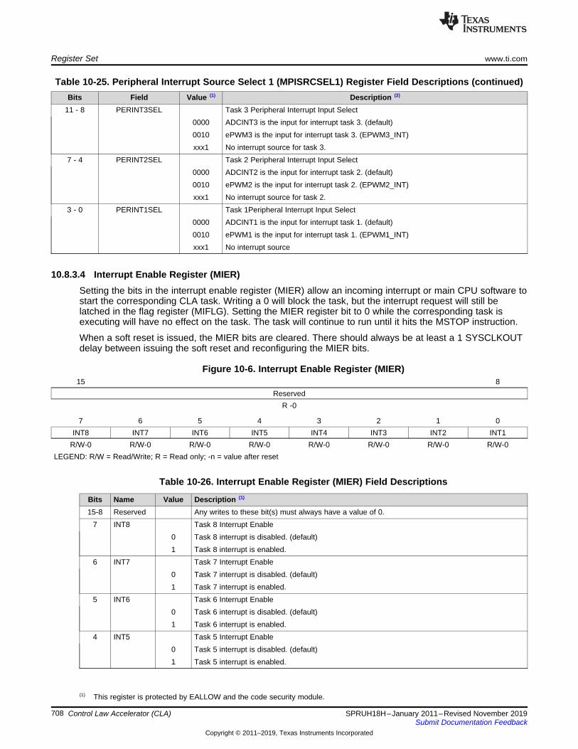
Register Set www.ti.com
708 SPRUH18H–January 2011–Revised November 2019Submit Documentation Feedback
Copyright © 2011–2019, Texas Instruments Incorporated
Control Law Accelerator (CLA)
Table 10-25. Peripheral Interrupt Source Select 1 (MPISRCSEL1) Register Field Descriptions (continued)Bits Field Value (1) Description (2)
11 - 8 PERINT3SEL Task 3 Peripheral Interrupt Input Select0000 ADCINT3 is the input for interrupt task 3. (default)0010 ePWM3 is the input for interrupt task 3. (EPWM3_INT)xxx1 No interrupt source for task 3.
7 - 4 PERINT2SEL Task 2 Peripheral Interrupt Input Select0000 ADCINT2 is the input for interrupt task 2. (default)0010 ePWM2 is the input for interrupt task 2. (EPWM2_INT)xxx1 No interrupt source for task 2.
3 - 0 PERINT1SEL Task 1Peripheral Interrupt Input Select0000 ADCINT1 is the input for interrupt task 1. (default)0010 ePWM1 is the input for interrupt task 1. (EPWM1_INT)xxx1 No interrupt source
10.8.3.4 Interrupt Enable Register (MIER)Setting the bits in the interrupt enable register (MIER) allow an incoming interrupt or main CPU software tostart the corresponding CLA task. Writing a 0 will block the task, but the interrupt request will still belatched in the flag register (MIFLG). Setting the MIER register bit to 0 while the corresponding task isexecuting will have no effect on the task. The task will continue to run until it hits the MSTOP instruction.
When a soft reset is issued, the MIER bits are cleared. There should always be at least a 1 SYSCLKOUTdelay between issuing the soft reset and reconfiguring the MIER bits.
Figure 10-6. Interrupt Enable Register (MIER)15 8
ReservedR -0
7 6 5 4 3 2 1 0INT8 INT7 INT6 INT5 INT4 INT3 INT2 INT1
R/W-0 R/W-0 R/W-0 R/W-0 R/W-0 R/W-0 R/W-0 R/W-0LEGEND: R/W = Read/Write; R = Read only; -n = value after reset
(1) This register is protected by EALLOW and the code security module.
Table 10-26. Interrupt Enable Register (MIER) Field Descriptions
Bits Name Value Description (1)
15-8 Reserved Any writes to these bit(s) must always have a value of 0.7 INT8 Task 8 Interrupt Enable
0 Task 8 interrupt is disabled. (default)1 Task 8 interrupt is enabled.
6 INT7 Task 7 Interrupt Enable0 Task 7 interrupt is disabled. (default)1 Task 7 interrupt is enabled.
5 INT6 Task 6 Interrupt Enable0 Task 6 interrupt is disabled. (default)1 Task 6 interrupt is enabled.
4 INT5 Task 5 Interrupt Enable0 Task 5 interrupt is disabled. (default)1 Task 5 interrupt is enabled.

www.ti.com Register Set
709SPRUH18H–January 2011–Revised November 2019Submit Documentation Feedback
Copyright © 2011–2019, Texas Instruments Incorporated
Control Law Accelerator (CLA)
Table 10-26. Interrupt Enable Register (MIER) Field Descriptions (continued)Bits Name Value Description (1)
3 INT4 Task 4 Interrupt Enable0 Task 4 interrupt is disabled. (default)1 Task 4 interrupt is enabled.
2 INT3 Task 3 Interrupt Enable0 Task 3 interrupt is disabled. (default)1 Task 3 interrupt is enabled.
1 INT2 Task 2 Interrupt Enable0 Task 2 interrupt is disabled. (default)1 Task 2 interrupt is enabled.
0 INT1 Task 1 Interrupt Enable0 Task 1 interrupt is disabled. (default)1 Task 1 interrupt is enabled.
10.8.3.5 Interrupt Flag Register (MIFR)Each bit in the interrupt flag register corresponds to a CLA task. The corresponding bit is automatically setwhen the task request is received from the peripheral interrupt. The bit can also be set by the main CPUwriting to the MIFRC register or using the IACK instruction to start the task. To use the IACK instruction tobegin a task first enable this feature in the MCTL register. If the bit is already set when a new peripheralinterrupt is received, then the corresponding overflow bit will be set in the MIOVF register.
The corresponding MIFR bit is automatically cleared when the task begins execution. This will occur if theinterrupt is enabled in the MIER register and no other higher priority task is pending. The bits can also becleared manually by writing to the MICLR register. Writes to the MIFR register are ignored.
Figure 10-7. Interrupt Flag Register (MIFR)15 8
ReservedR -0
7 6 5 4 3 2 1 0INT8 INT7 INT6 INT5 INT4 INT3 INT2 INT1R-0 R-0 R-0 R-0 R-0 R-0 R-0 R-0
LEGEND: R/W = Read/Write; R = Read only; -n = value after reset
(1) This register is protected by the code security module.
Table 10-27. Interrupt Flag Register (MIFR) Field Descriptions
Bits Name Value Description (1)
15-8 Reserved Any writes to these bit(s) must always have a value of 0.7 INT8 Task 8 Interrupt Flag
0 A task 8 interrupt is currently not flagged. (default)1 A task 8 interrupt has been received and is pending execution.
6 INT7 Task 7 Interrupt Flag0 A task 7 interrupt is currently not flagged. (default)1 A task 7 interrupt has been received and is pending execution.
5 INT6 Task 6 Interrupt Flag0 A task 6 interrupt is currently not flagged. (default)1 A task 6 interrupt has been received and is pending execution.

Register Set www.ti.com
710 SPRUH18H–January 2011–Revised November 2019Submit Documentation Feedback
Copyright © 2011–2019, Texas Instruments Incorporated
Control Law Accelerator (CLA)
Table 10-27. Interrupt Flag Register (MIFR) Field Descriptions (continued)Bits Name Value Description (1)
4 INT5 Task 5 Interrupt Flag0 A task 5 interrupt is currently not flagged. (default)1 A task 5 interrupt has been received and is pending execution.
3 INT4 Task 4 Interrupt Flag0 A task 4 interrupt is currently not flagged. (default)1 A task 4 interrupt has been received and is pending execution.
2 INT3 Task 3 Interrupt Flag0 A task 3 interrupt is currently not flagged. (default)1 A task 3 interrupt has been received and is pending execution.
1 INT2 Task 2 Interrupt Flag0 A task 2 interrupt is currently not flagged. (default)1 A task 2 interrupt has been received and is pending execution.
0 INT1 Task 1 Interrupt Flag0 A task 1 interrupt is currently not flagged. (default)1 A task 1 interrupt has been received and is pending execution.
10.8.3.6 Interrupt Overflow Flag Register (MIOVF)Each bit in the overflow flag register corresponds to a CLA task. The bit is set when an interrupt overflowevent has occurred for the specific task. An overflow event occurs when the MIFR register bit is alreadyset when a new interrupt is received from a peripheral source. The MIOVF bits are only affected byperipheral interrupt events. They do not respond to a task request by the main CPU IACK instruction or bydirectly setting MIFR bits. The overflow flag will remain latched and can only be cleared by writing to theoverflow flag clear (MICLROVF) register. Writes to the MIOVF register are ignored.
Figure 10-8. Interrupt Overflow Flag Register (MIOVF)15 8
ReservedR -0
7 6 5 4 3 2 1 0INT8 INT7 INT6 INT5 INT4 INT3 INT2 INT1R-0 R-0 R-0 R-0 R-0 R-0 R-0 R-0
LEGEND: R/W = Read/Write; R = Read only; -n = value after reset
(1) This register is protected by the code security module.
Table 10-28. Interrupt Overflow Flag Register (MIOVF) Field Descriptions
Bits Name Value Description (1)
15-8 Reserved Any writes to these bit(s) must always have a value of 0.7 INT8 Task 8 Interrupt Overflow Flag
0 A task 8 interrupt overflow has not occurred. (default)1 A task 8 interrupt overflow has occurred.
6 INT7 Task 7 Interrupt Overflow Flag0 A task 7 interrupt overflow has not occurred. (default)1 A task 7 interrupt overflow has occurred.
5 INT6 Task 6 Interrupt Overflow Flag0 A task 6 interrupt overflow has not occurred. (default)1 A task 6 interrupt overflow has occurred.

www.ti.com Register Set
711SPRUH18H–January 2011–Revised November 2019Submit Documentation Feedback
Copyright © 2011–2019, Texas Instruments Incorporated
Control Law Accelerator (CLA)
Table 10-28. Interrupt Overflow Flag Register (MIOVF) Field Descriptions (continued)Bits Name Value Description (1)
4 INT5 Task 5 Interrupt Overflow Flag0 A task 5 interrupt overflow has not occurred. (default)1 A task 5 interrupt overflow has occurred.
3 INT4 Task 4 Interrupt Overflow Flag0 A task 4 interrupt overflow has not occurred. (default)1 A task 4 interrupt overflow has occurred.
2 INT3 Task 3 Interrupt Overflow Flag0 A task 3 interrupt overflow has not occurred. (default)1 A task 3 interrupt overflow has occurred.
1 INT2 Task 2 Interrupt Overflow Flag0 A task 2 interrupt overflow has not occurred. (default)1 A task 2 interrupt overflow has occurred.
0 INT1 Task 1 Interrupt Overflow Flag0 A task 1 interrupt overflow has not occurred. (default)1 A task 1 interrupt overflow has occurred.
10.8.3.7 Interrupt Run Status Register (MIRUN)The interrupt run status register (MIRUN) indicates which task is currently executing. Only one MIRUN bitwill ever be set to a 1 at any given time. The bit is automatically cleared when the task competes and therespective interrupt is fed to the peripheral interrupt expansion (PIE) block of the device. This lets the mainCPU know when a task has completed. The main CPU can stop a currently running task by writing to theMCTL[SOFTRESET] bit. This will clear the MIRUN flag and stop the task. In this case no interrupt will begenerated to the PIE.
Figure 10-9. Interrupt Run Status Register (MIRUN)15 8
ReservedR -0
7 6 5 4 3 2 1 0INT8 INT7 INT6 INT5 INT4 INT3 INT2 INT1R-0 R-0 R-0 R-0 R-0 R-0 R-0 R-0
LEGEND: R/W = Read/Write; R = Read only; -n = value after reset
(1) This register is protected by the code security module.
Table 10-29. Interrupt Run Status Register (MIRUN) Field Descriptions
Bits Name Value Description (1)
15-8 Reserved Any writes to these bit(s) must always have a value of 0.7 INT8 Task 8 Run Status
0 Task 8 is not executing. (default)1 Task 8 is executing.
6 INT7 Task 7 Run Status0 Task 7 is not executing. (default)1 Task 7 is executing.
5 INT6 Task 6 Run Status0 Task 6 is not executing. (default)1 Task 6 is executing.

Register Set www.ti.com
712 SPRUH18H–January 2011–Revised November 2019Submit Documentation Feedback
Copyright © 2011–2019, Texas Instruments Incorporated
Control Law Accelerator (CLA)
Table 10-29. Interrupt Run Status Register (MIRUN) Field Descriptions (continued)Bits Name Value Description (1)
4 INT5 Task 5 Run Status0 Task 5 is not executing. (default)1 Task 5 is executing.
3 INT4 Task 4 Run Status0 Task 4 is not executing. (default)1 Task 4 is executing.
2 INT3 Task 3 Run Status0 Task 3 is not executing. (default)1 Task 3 is executing.
1 INT2 Task 2 Run Status0 Task 2 is not executing. (default)1 Task 2 is executing.
0 INT1 Task 1 Run Status0 Task 1 is not executing. (default)1 Task 1 is executing.

www.ti.com Register Set
713SPRUH18H–January 2011–Revised November 2019Submit Documentation Feedback
Copyright © 2011–2019, Texas Instruments Incorporated
Control Law Accelerator (CLA)
10.8.3.8 Interrupt Force Register (MIFRC)The interrupt force register can be used by the main CPU to start tasks through software. Writing a 1 to aMIFRC bit will set the corresponding bit in the MIFR register. Writes of 0 are ignored and reads alwaysreturn 0. The IACK #16bit operation can also be used to start tasks and has the same effect as theMIFRC register. To enable IACK to set MIFR bits you must first set the MCTL[IACKE] bit. Using IACK hasthe advantage of not having to first set the EALLOW bit. This allows the main CPU to efficiently triggerCLA tasks through software.
Figure 10-10. Interrupt Force Register (MIFRC)15 8
ReservedR -0
7 6 5 4 3 2 1 0INT8 INT7 INT6 INT5 INT4 INT3 INT2 INT1
R/W-0 R/W-0 R/W-0 R/W-0 R/W-0 R/W-0 R/W-0 R/W-0LEGEND: R/W = Read/Write; R = Read only; -n = value after reset
(1) This register is protected by EALLOW and the code security module.
Table 10-30. Interrupt Force Register (MIFRC) Field Descriptions
Bits Name Value Description (1)
15-8 Reserved Any writes to these bit(s) must always have a value of 0.7 INT8 Task 8 Interrupt Force
0 This bit always reads back 0 and writes of 0 have no effect.1 Write a 1 to force the task 8 interrupt.
6 INT7 Task 7 Interrupt Force0 This bit always reads back 0 and writes of 0 have no effect.1 Write a 1 to force the task 7 interrupt.
5 INT6 Task 6 Interrupt Force0 This bit always reads back 0 and writes of 0 have no effect.1 Write a 1 to force the task 6 interrupt.
4 INT5 Task 5 Interrupt Force0 This bit always reads back 0 and writes of 0 have no effect.1 Write a 1 to force the task 5 interrupt.
3 INT4 Task 4 Interrupt Force0 This bit always reads back 0 and writes of 0 have no effect.1 Write a 1 to force the task 4 interrupt.
2 INT3 Task 3 Interrupt Force0 This bit always reads back 0 and writes of 0 have no effect.1 Write a 1 to force the task 3 interrupt.
1 INT2 Task 2 Interrupt Force0 This bit always reads back 0 and writes of 0 have no effect.1 Write a 1 to force the task 2 interrupt.
0 INT1 Task 1 Interrupt Force0 This bit always reads back 0 and writes of 0 have no effect.1 Write a 1 to force the task 1 interrupt.

Register Set www.ti.com
714 SPRUH18H–January 2011–Revised November 2019Submit Documentation Feedback
Copyright © 2011–2019, Texas Instruments Incorporated
Control Law Accelerator (CLA)
10.8.3.9 Interrupt Flag Clear Register (MICLR)Normally bits in the MIFR register are automatically cleared when a task begins. The interrupt flag clearregister can be used to instead manually clear bits in the interrupt flag (MIFR) register. Writing a 1 to aMICLR bit will clear the corresponding bit in the MIFR register. Writes of 0 are ignored and reads alwaysreturn 0.
Figure 10-11. Interrupt Flag Clear Register (MICLR)15 8
ReservedR -0
7 6 5 4 3 2 1 0INT8 INT7 INT6 INT5 INT4 INT3 INT2 INT1
R/W-0 R/W-0 R/W-0 R/W-0 R/W-0 R/W-0 R/W-0 R/W-0LEGEND: R/W = Read/Write; R = Read only; -n = value after reset
(1) This register is protected by EALLOW and the code security module.
Table 10-31. Interrupt Flag Clear Register (MICLR) Field Descriptions
Bits Name Value Description (1)
15-8 Reserved Any writes to these bit(s) must always have a value of 0.7 INT8 Task 8 Interrupt Flag Clear
0 This bit always reads back 0 and writes of 0 have no effect.1 Write a 1 to clear the task 8 interrupt flag.
6 INT7 Task 7 Interrupt Flag Clear0 This bit always reads back 0 and writes of 0 have no effect.1 Write a 1 to clear the task 7 interrupt flag.
5 INT6 Task 6 Interrupt Flag Clear0 This bit always reads back 0 and writes of 0 have no effect.1 Write a 1 to clear the task 6 interrupt flag.
4 INT5 Task 5 Interrupt Flag Clear0 This bit always reads back 0 and writes of 0 have no effect.1 Write a 1 to clear the task 5 interrupt flag.
3 INT4 Task 4 Interrupt Flag Clear0 This bit always reads back 0 and writes of 0 have no effect.1 Write a 1 to clear the task 4 interrupt flag.
2 INT3 Task 3 Interrupt Flag Clear0 This bit always reads back 0 and writes of 0 have no effect.1 Write a 1 to clear the task 3 interrupt flag.
1 INT2 Task 2 Interrupt Flag Clear0 This bit always reads back 0 and writes of 0 have no effect.1 Write a 1 to clear the task 2 interrupt flag.
0 INT1 Task 1 Interrupt Flag Clear0 This bit always reads back 0 and writes of 0 have no effect.1 Write a 1 to clear the task 1 interrupt flag.

www.ti.com Register Set
715SPRUH18H–January 2011–Revised November 2019Submit Documentation Feedback
Copyright © 2011–2019, Texas Instruments Incorporated
Control Law Accelerator (CLA)
10.8.3.10 Interrupt Overflow Flag Clear Register (MICLROVF)Overflow flag bits in the MIOVF register are latched until manually cleared using the MICLROVF register.Writing a 1 to a MICLROVF bit will clear the corresponding bit in the MIOVF register. Writes of 0 areignored and reads always return 0.
Figure 10-12. Interrupt Overflow Flag Clear Register (MICLROVF)15 8
ReservedR -0
7 6 5 4 3 2 1 0INT8 INT7 INT6 INT5 INT4 INT3 INT2 INT1
R/W-0 R/W-0 R/W-0 R/W-0 R/W-0 R/W-0 R/W-0 R/W-0LEGEND: R/W = Read/Write; R = Read only; -n = value after reset
(1) This register is protected by EALLOW and the code security module.
Table 10-32. Interrupt Overflow Flag Clear Register (MICLROVF) Field Descriptions
Bits Name Value Description (1)
15-8 Reserved Any writes to these bit(s) must always have a value of 0.7 INT8 Task 8 Interrupt Overflow Flag Clear
0 This bit always reads back 0 and writes of 0 have no effect.1 Write a 1 to clear the task 8 interrupt overflow flag.
6 INT7 Task 7 Interrupt Overflow Flag Clear0 This bit always reads back 0 and writes of 0 have no effect.1 Write a 1 to clear the task 7 interrupt overflow flag.
5 INT6 Task 6 Interrupt Overflow Flag Clear0 This bit always reads back 0 and writes of 0 have no effect.1 Write a 1 to clear the task 6 interrupt overflow flag.
4 INT5 Task 5 Interrupt Overflow Flag Clear0 This bit always reads back 0 and writes of 0 have no effect.1 Write a 1 to clear the task 5 interrupt overflow flag.
3 INT4 Task 4 Interrupt Overflow Flag Clear0 This bit always reads back 0 and writes of 0 have no effect.1 Write a 1 to clear the task 4 interrupt overflow flag.
2 INT3 Task 3 Interrupt Overflow Flag Clear0 This bit always reads back 0 and writes of 0 have no effect.1 Write a 1 to clear the task 3 interrupt overflow flag.
1 INT2 Task 2 Interrupt Overflow Flag Clear0 This bit always reads back 0 and writes of 0 have no effect.1 Write a 1 to clear the task 2 interrupt overflow flag.
0 INT1 Task 1 Interrupt Overflow Flag Clear0 This bit always reads back 0 and writes of 0 have no effect.1 Write a 1 to clear the task 1 interrupt overflow flag.

Register Set www.ti.com
716 SPRUH18H–January 2011–Revised November 2019Submit Documentation Feedback
Copyright © 2011–2019, Texas Instruments Incorporated
Control Law Accelerator (CLA)
10.8.4 Execution RegistersThe CLA program counter is initialized by the appropriate MVECTx register when an interrupt is receivedand a task begins execution. The MPC points to the instruction in the decode 2 (D2) stage of the CLApipeline. After a MSTOP operation, if no other tasks are pending, the MPC will remain pointing to theMSTOP instruction. The MPC register can be read by the main C28x CPU for debug purposes. The mainCPU cannot write to MPC.
10.8.4.1 MPC RegisterThe MPC register is described in Figure 10-13 and described in Table 10-33.
Figure 10-13. Program Counter (MPC)15 12 11 0
Reserved MPC
R-0 R-0LEGEND: R/W = Read/Write; R = Read only; -n = value after reset
(1) This register is protected by the code security module. The main CPU can read this register for debug purposes but it can notwrite to it.
Table 10-33. Program Counter (MPC) Field Descriptions
Bits Name Value Description (1)
15-12 Reserved Any writes to these bit(s) must always have a value of 0.11-0 MPC 0000 -
0FFFPoints to the instruction currently in the decode 2 phase of the CLA pipeline. The value is theoffset from the first address in the CLA program space.
10.8.4.2 MSTF RegisterThe CLA status register (MSTF) reflects the results of different operations. These are the basic rules forthe flags:• Zero and negative flags are cleared or set based on:
– floating-point moves to registers– the result of compare, minimum, maximum, negative and absolute value operations– the integer result of operations such as MMOV16, MAND32, MOR32, MXOR32, MCMP32,
MASR32, MLSR32• Overflow and underflow flags are set by floating-point math instructions such as multiply, add, subtract
and 1/x. These flags may also be connected to the peripheral interrupt expansion (PIE) block on yourdevice. This can be useful for debugging underflow and overflow conditions within an application.
The MSTF register is shown in Figure 10-14 and described in Table 10-34.
Figure 10-14. CLA Status Register (MSTF)31 24 23 16
Reserved RPC
R/W-0 R/W-0
15 12 11 10 9 8 7 6 5 4 3 2 1 0RPC MEALLOW Reserved RND32 Reserved TF Reserved ZF NF LUF LVF
R/W-0 R/W-0 R-0 R/W-0 R-0 R/W-0 R-0 R/W-0 R/W-0 R/W-0 R/W-0LEGEND: R/W = Read/Write; R = Read only; -n = value after reset

www.ti.com Register Set
717SPRUH18H–January 2011–Revised November 2019Submit Documentation Feedback
Copyright © 2011–2019, Texas Instruments Incorporated
Control Law Accelerator (CLA)
(1) This register is protected by the code security module. The main CPU can read this register for debug purposes but it can not write to it.(2) A negative zero floating-point value is treated as a positive zero value when configuring the ZF and NF flags.(3) A DeNorm floating-point value is treated as a positive zero value when configuring the ZF and NF flags.
Table 10-34. CLA Status (MSTF) Register Field Descriptions
Bits Field Value Description (1)
31 - 24 Reserved 0 Reserved for future use23 - 12 RPC Return program counter.
The RPC is used to save and restore the MPC address by the MCCNDD and MRCNDD operations.11 MEALLOW This bit enables and disables CLA write access to EALLOW protected registers. This is independent of
the state of the EALLOW bit in the main CPU status register. This status bit can be saved and restoredby the MMOV32 STF, mem32 instruction.
0 The CLA cannot write to EALLOW protected registers. This bit is cleared by the CLA instruction,MEDIS.
1 The CLA is allowed to write to EALLOW protected registers. This bit is set by the CLA instruction,MEALLOW.
10 Reserved 0 Any writes to these bit(s) must always have a value of 0.9 RND32 Round 32-bit Floating-Point Mode
Use the MSETFLG and MMOV32 MSTF, mem32 instructions to change the rounding mode.0 If this bit is zero, the MMPYF32, MADDF32 and MSUBF32 instructions will round to zero (truncate).1 If this bit is one, the MMPYF32, MADDF32 and MSUBF32 instructions will round to the nearest even
value.8 - 7 Reserved 0 Reserved for future use
6 TF Test FlagThe MTESTTF instruction can modify this flag based on the condition tested. The MSETFLG andMMOV32 MSTF, mem32 instructions can also be used to modify this flag.
0 The condition tested with the MTESTTF instruction is false.1 The condition tested with the MTESTTF instruction is true.
5 - 4 Reserved These two bits may change based on integer results. These flags are not, however, used by the CLAand therefore marked as reserved.
3 ZF Zero Flag (2) (3)
• Instructions that modify this flag based on the floating-point value stored in the destination register:
MMOV32, MMOVD32, MABSF32, MNEGF32• Instructions that modify this flag based on the floating-point result of the operation:
MCMPF32, MMAXF32, and MMINF32• Instructions that modify this flag based on the integer result of the operation:
MMOV16, MAND32, MOR32, MXOR32, MCMP32, MASR32, MLSR32 andMLSL32
The MSETFLG and MMOV32 MSTF, mem32 instructions can also be used to modify this flag0 The value is not zero.1 The value is zero.
2 NF Negative Flag (2) (3)
• Instructions that modify this flag based on the floating-point value stored in the destination register:
MMOV32, MMOVD32, MABSF32, MNEGF32• Instructions that modify this flag based on the floating-point result of the operation:
MCMPF32, MMAXF32, and MMINF32• Instructions that modify this flag based on the integer result of the operation:
MMOV16, MAND32, MOR32, MXOR32, MCMP32, MASR32, MLSR32 andMLSL32
The MSETFLG and MMOV32 MSTF, mem32 instructions can also be used to modify this flag.0 The value is not negative.1 The value is negative.
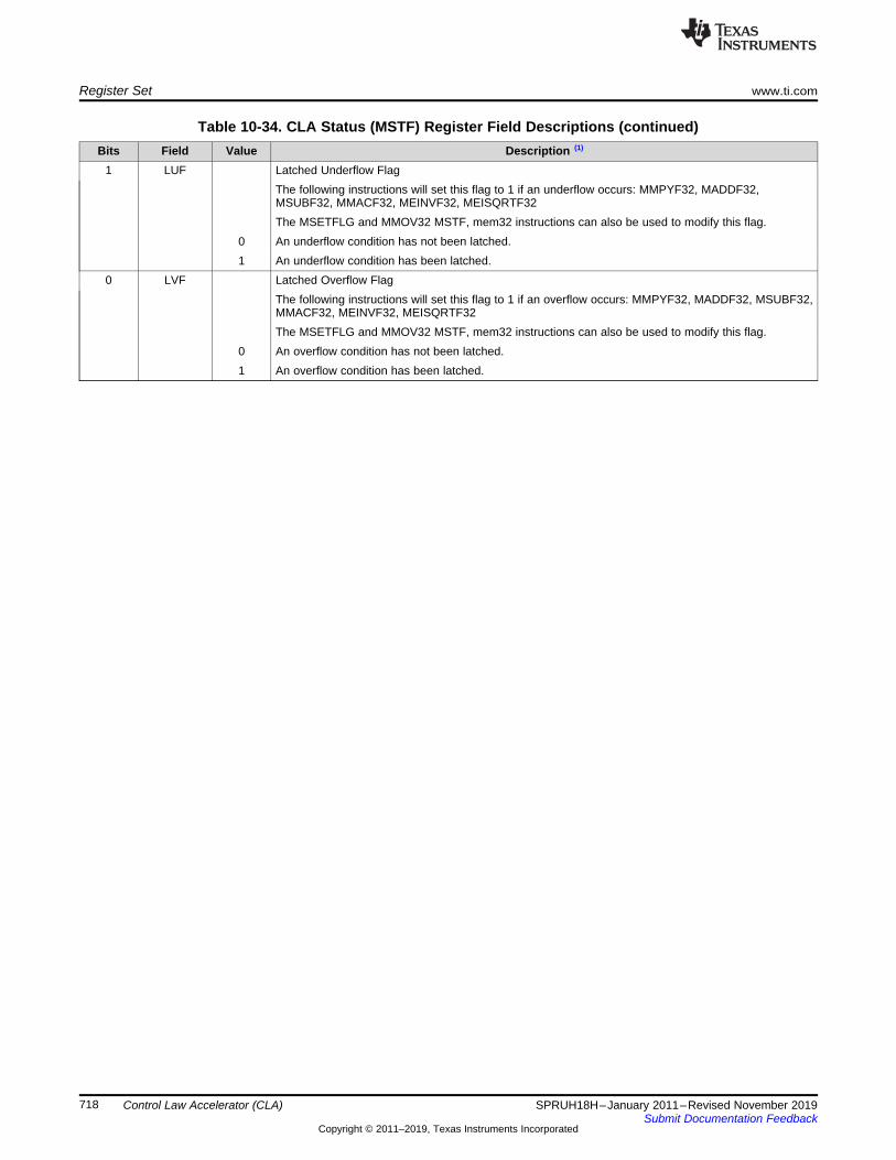
Register Set www.ti.com
718 SPRUH18H–January 2011–Revised November 2019Submit Documentation Feedback
Copyright © 2011–2019, Texas Instruments Incorporated
Control Law Accelerator (CLA)
Table 10-34. CLA Status (MSTF) Register Field Descriptions (continued)Bits Field Value Description (1)
1 LUF Latched Underflow FlagThe following instructions will set this flag to 1 if an underflow occurs: MMPYF32, MADDF32,MSUBF32, MMACF32, MEINVF32, MEISQRTF32The MSETFLG and MMOV32 MSTF, mem32 instructions can also be used to modify this flag.
0 An underflow condition has not been latched.1 An underflow condition has been latched.
0 LVF Latched Overflow FlagThe following instructions will set this flag to 1 if an overflow occurs: MMPYF32, MADDF32, MSUBF32,MMACF32, MEINVF32, MEISQRTF32The MSETFLG and MMOV32 MSTF, mem32 instructions can also be used to modify this flag.
0 An overflow condition has not been latched.1 An overflow condition has been latched.

719SPRUH18H–January 2011–Revised November 2019Submit Documentation Feedback
Copyright © 2011–2019, Texas Instruments Incorporated
Direct Memory Access (DMA) Module
Chapter 11SPRUH18H–January 2011–Revised November 2019
Direct Memory Access (DMA) Module
The direct memory access (DMA) module provides a hardware method of transferring data betweenperipherals and/or memory without intervention from the CPU, thereby freeing up bandwidth for othersystem functions. Additionally, the DMA has the capability to orthogonally rearrange the data as it istransferred as well as “ping-pong” data between buffers. These features are useful for structuring data intoblocks for optimal CPU processing.
Topic ........................................................................................................................... Page
11.1 Introduction .................................................................................................... 72011.2 DMA Overview.................................................................................................. 72011.3 Architecture ..................................................................................................... 72011.4 Pipeline Timing and Throughput ........................................................................ 72411.5 CPU Arbitration ................................................................................................ 72511.6 Channel Priority ............................................................................................... 72511.7 Address Pointer and Transfer Control................................................................. 72611.8 Overrun Detection Feature................................................................................. 73111.9 Register Descriptions........................................................................................ 733

Introduction www.ti.com
720 SPRUH18H–January 2011–Revised November 2019Submit Documentation Feedback
Copyright © 2011–2019, Texas Instruments Incorporated
Direct Memory Access (DMA) Module
11.1 IntroductionThe strength of a controller is not measured purely in processor speed, but in total system capabilities. Asa part of the equation, any time the CPU bandwidth for a given function can be reduced, the greater thesystem capabilities. Many times applications spend a significant amount of their bandwidth moving data,whether it is from off-chip memory to on-chip memory, or from a peripheral such as an analog-to-digitalconverter (ADC) to RAM, or even from one peripheral to another. Furthermore, many times this datacomes in a format that is not conducive to the optimum processing powers of the CPU. The DMA moduledescribed in this reference guide has the ability to free up CPU bandwidth and rearrange the data into apattern for more streamlined processing.
11.2 DMA OverviewThe DMA module is an event-based machine, meaning it requires a peripheral interrupt trigger to start aDMA transfer. Although it can be made into a periodic time-driven machine by configuring a timer as theinterrupt trigger source, there is no mechanism within the module itself to start memory transfersperiodically. The interrupt trigger source for each of the six DMA channels can be configured separatelyand each channel contains its own independent PIE interrupt to let the CPU know when a DMA transfershas either started or completed. Five of the six channels are exactly the same, while Channel 1 has oneadditional feature: the ability to be configured at a higher priority than the others. At the heart of the DMAis a state machine and tightly coupled address control logic. It is this address control logic that allows forrearrangement of the block of data during the transfer as well as the process of ping-ponging databetween buffers. Each of these features, along with others will be discussed in detail in this document.• Six channels with independent PIE interrupts• Peripheral interrupt trigger sources
– ADC interrupts 1 and 2– Multichannel buffered serial port transmit and receive– XINT1-3– CPU Timers– ePWM2-7 ADCSOCA and ADSOCB signals– USB endpoints 1-3 transmit and receive– Software
• Data sources/destinations:– L5-L8 32K x 16 SARAM– ADC memory bus mapped result registers– McBSP transmit and receive buffers– ePWM1-8 / HRPWM1-8The DMA module can access all the PWM modules as shown in Figure 11-1 . However, only 6 out of 8PWM modules (ePWM2-ePWM7) can trigger DMA using PERINTSEL.
• Word Size: 16-bit or 32-bit (McBSP limited to 16-bit)• Throughput: 4 cycles/word (5 cycles/word for McBSP reads)
11.3 Architecture
11.3.1 Block DiagramFigure 11-1 shows a device level block diagram of the DMA.

ADCRESULTregisters
ADCCPUPF0I/F
ADCDMAPF0I/F
ADCcontrol
andRESULTregisters
ADCPF2I/F
L5I/F
L5SARAM(8Kx16)
L6I/F
L6SARAM(8Kx16)
L7I/F
L7SARAM(8Kx16)
L8I/F
L8SARAM(8Kx16)
PF3 I/F McBSPEvent
triggersDMA6-ch
Externalinterrupts
CPUtimers
CPU bus
DMA bus
PIE
INT7
DIN
T[C
H1:C
H6]
CPU
ePWM/HRPWMregisters
PF3 I/F
PF3 I/F USB
CLAbus
www.ti.com Architecture
721SPRUH18H–January 2011–Revised November 2019Submit Documentation Feedback
Copyright © 2011–2019, Texas Instruments Incorporated
Direct Memory Access (DMA) Module
Figure 11-1. DMA Block Diagram
11.3.2 Peripheral Interrupt Event Trigger SourcesThe peripheral interrupt event trigger can be independently configured as one twenty-nine differentsources for each of the six DMA channels. Included in these sources are three external interrupt signalswhich can be connected to most of the general-purpose input/output (GPIO) pins on the device. This addssignificant flexibility to the event trigger capabilities. A bit field called PERINTSEL in the MODE register ofeach channel is used to select that channels interrupt trigger source. An active peripheral interrupt triggerwill be latched into the PERINTFLG bit of the CONTROL register, and if the respective interrupt and DMAchannel is enabled (see the MODE.CHx[PERINTE] and CONTROL.CHx[RUNSTS] bits), it will be servicedby the DMA channel. Upon receipt of a peripheral interrupt event signal, the DMA will automatically send aclear signal to the interrupt source so that subsequent interrupt events will occur.
Regardless of the value of the MODE.CHx[PERINTSEL] bit field, software can always force a trigger byusing the CONTROL.CHx[PERINTFRC] bit. Likewise, software can always clear a pending DMA triggerusing the CONTROL.CHx[PERINTCLR] bit.
Once a particular interrupt trigger sets a channel’s PERINTFLG bit, the bit stays pending until the prioritylogic of the state machine starts the burst transfer for that channel. Once the burst transfer starts, the flagis cleared. If a new interrupt trigger is generated while a burst is in progress, the burst will complete beforeresponding to the new interrupt trigger (after proper prioritization). If a third interrupt trigger occurs beforethe pending interrupt is serviced, an error flag is set in the CONTROL.CHx[OVRFLG] bit. If a peripheralinterrupt trigger occurs at the same time as the latched flag is being cleared, the peripheral interrupttrigger has priority and the PERINTFLG will remain set.
Figure 11-2 shows a diagram of the trigger select circuit. See the MODE.CHx[PERINTSEL] bit fielddescription for the complete list of peripheral interrupt trigger sources.

None
ADCINT1
ADCINT2
EPWM7SOCB
USB0EP3RX
USB0EP3TX
.
.
.
MODE.CHx[PERINTSEL]
CONTROL.CHx[PERINTFRC]
CONTROL.CHx[PERINTCLR]
Clear
Set
Latch
Clear peripheral interrupttrigger flag if appropriate
CONTROL.CHx[PERINTFLG]
PeripheralInt
MODE.CHx[PERINTE]
Clear interrupt
DMAchannel xprocessing
logic
Architecture www.ti.com
722 SPRUH18H–January 2011–Revised November 2019Submit Documentation Feedback
Copyright © 2011–2019, Texas Instruments Incorporated
Direct Memory Access (DMA) Module
Figure 11-2. Peripheral Interrupt Trigger Input Diagram
Table 11-1 shows the interrupt trigger source options that are available for each channel.

www.ti.com Architecture
723SPRUH18H–January 2011–Revised November 2019Submit Documentation Feedback
Copyright © 2011–2019, Texas Instruments Incorporated
Direct Memory Access (DMA) Module
Table 11-1. Peripheral Interrupt Trigger Source Options
Peripheral Interrupt Trigger SourceCPU DMA Software bit (CHx.CONTROL.PERINTFRC) onlyADC ADCINT 1
ADCINT 2External Interrupts External Interrupt 1
External Interrupt 2External Interrupt 3
CPU Timers Timer 0 OverflowTimer 1 OverflowTimer 2 Overflow
McBSP McBSP Transmit Buffer EmptyMcBSP Receive Buffer Full
ePWM2 ADC Start of Conversion AADC Start of Conversion B
ePWM3 ADC Start of Conversion AADC Start of Conversion B
ePWM4 ADC Start of Conversion AADC Start of Conversion B
ePWM5 ADC Start of Conversion AADC Start of Conversion B
ePWM6 ADC Start of Conversion AADC Start of Conversion B
ePWM7 ADC Start of Conversion AADC Start of Conversion B
USB USB Endpoint 1 Receive FullUSB USB Endpoint 1 Transmit EmptyUSB USB Endpoint 2 Receive FullUSB USB Endpoint 2 Transmit EmptyUSB USB Endpoint 3 Receive FullUSB USB Endpoint 3 Transmit Empty
11.3.3 DMA BusThe DMA bus architecture consists of a 22-bit address bus, a 32-bit data read bus, and a 32-bit data writebus. Memories and register locations connected to the DMA bus are via interfaces that sometimes shareresources with the CPU memory or peripheral bus. Arbitration rules are defined in Section 11.5. Thefollowing resources are connected to the DMA bus:• L5 SARAM• L6 SARAM• L7 SARAM• L8 SARAM• ADC Memory Mapped Result Registers• McBSP Data Receive Registers (DRR2/DRR1) and Data Transmit Registers (DXR2/DXR1)• ePWM1-8/HRPWM1-8 Registers• USB Transmit and Receive Endpoints 1-3

OutSRCaddr(N)
ReadSRCdata(N)
OutDSTaddr(N)
WriteDSTdata(N)
GenSRCaddr(N+1)
GenDSTaddr(N+1)
GenSRCaddr(N+2)
OutDSTaddr(N+1)
WriteDSTdata
(N+1)
GenDSTaddr(N+2)
SYSCLK
Addr bus
Data bus
Generateaddress
OutSRCaddr(N+1)
ReadSRCdata
(N+1)
OutSRCaddr(N)
ReadSRCdata(N)
OutDSTaddr(N)
OutSRCaddr(N+1)
WriteDSTdata(N)
GenSRCaddr(N+1)
GenDSTaddr(N+1)
GenSRCaddr(N+2)
ReadSRCdata
(N+1)
OutDSTaddr(N+1)
OutSRCaddr(N+2)
WriteDSTdata
(N+1)
GenDSTaddr(N+2)
GenSRCaddr(N+3)
ReadSRCdata
(N+2)
SYSCLK
Addr bus
Data bus
Generateaddress
Pipeline Timing and Throughput www.ti.com
724 SPRUH18H–January 2011–Revised November 2019Submit Documentation Feedback
Copyright © 2011–2019, Texas Instruments Incorporated
Direct Memory Access (DMA) Module
11.4 Pipeline Timing and ThroughputThe DMA consists of a 4-stage pipeline as shown in Figure 11-3. The one exception to this is when aDMA channel is configured to have the McBSP as its data source. A read of a McBSP DRR register stallsthe DMA bus for one cycle during the read portion of the transfer, as shown in Figure 11-4.
Figure 11-3. 4-Stage Pipeline DMA Transfer
Figure 11-4. 4-Stage Pipeline With One Read Stall (McBSP as source)
In addition to the pipeline there are a few other behaviors of the DMA that affect it’s total throughput• A 1-cycle delay is added at the beginning of each burst• A 1-cycle delay is added when returning from a CH1 high priority interrupt• 32-bit transfers run at double the speed of a 16-bit transfer (i.e., it takes the same amount of time to
transfer a 32-bit word as it does a 16-bit word)• Collisions with the CPU may add delay slots (see Section 11.5)
For example, to transfer 128 16-bit words from ADC to RAM a channel can be configured to transfer 8bursts of 16 words/burst. This will give:
8 bursts * [(4 cycles/word * 16 words/burst) + 1] = 520 cycles
If instead the channel were configured to transfer the same amount of data 32 bits at a time (the word sizeis configured to 32 bits) the transfer would take:
8 bursts * [(4 cycles/word * 8 words/burst) + 1] = 264 cycles

www.ti.com CPU Arbitration
725SPRUH18H–January 2011–Revised November 2019Submit Documentation Feedback
Copyright © 2011–2019, Texas Instruments Incorporated
Direct Memory Access (DMA) Module
11.5 CPU ArbitrationTypically, DMA activity is independent of the CPU activity. Under the circumstance where both the DMAand the CPU are attempting to access memory or a peripheral register within the same interfaceconcurrently, an arbitration procedure will occur. The one exception is with the memory mapped (PF0)ADC registers, which do not create a conflict when read by both the CPU and the DMA simultaneously,even if different addresses are accessed. Any combined accesses between the different interfaces, orwhere the CPU access is outside of the interface that the DMA is accessing do not create a conflict.
The interfaces which internally contain conflicts are:• L5 RAM• L6 RAM• L7 RAM• L8 RAM• McBSP Peripheral Frame 3• ePWM/HRPWM Peripheral Frame 3• USB Peripheral Frame 3
If the CPU and the DMA make an access to the same interface in the same cycle, the DMA has priorityand the CPU is stalled.
If a CPU access to an interface is in progress and another CPU access to the same interface is pending,for example, the CPU is performing a write operation and a read operation from the CPU is pending, thena DMA access to that same interface has priority over the pending CPU access when the current CPUaccess completes.
NOTE: If the CPU is performing a read-modify-write operation and the DMA performs a write to thesame location, the DMA write may be lost if the operation occurs in between the CPU readand the CPU write. For this reason, it is advised not to mix such CPU accesses with DMAaccesses to the same locations.
In the case of RAM, a ping-pong scheme can be implemented to avoid the CPU and the DMA accessingthe same RAM block concurrently, thus avoiding any stalls or corruption issues.
11.6 Channel PriorityTwo priority schemes exist when determining channel priority: Round-robin mode and Channel 1 high-priority mode.
11.6.1 Round-Robin ModeIn this mode, all channels have equal priority and each enabled channel is serviced in round-robin fashionas follows:
CH1 → CH2 → CH3 → CH4 → CH5 → CH6 → CH1 → CH2 → …
In the case above, after each channel has transferred a burst of words, the next channel is serviced. Youcan specify the size of the burst for each channel. Once CH6 (or the last enabled channel) has beenserviced, and no other channels are pending, the round-robin state machine enters an idle state.
From the idle state, channel 1 (if enabled) is always serviced first. However, if the DMA is currentlyprocessing another channel x, all other pending channels between x and the end of the round are servicedbefore CH1. It is in this sense that all the channels are of equal priority. For instance, take an examplewhere CH1, CH4, and CH5 are enabled in round-robin mode and CH4 is currently being processed. ThenCH1 and CH5 both receive an interrupt trigger from their respective peripherals before CH4 completes.CH1 and CH5 are now both pending. When CH4 completes its burst, CH5 will be serviced next. Only afterCH5 completes will CH1 be serviced. Upon completion of CH1, if there are no more channels pending, theround-robin state machine will enter an idle state.

Channel Priority www.ti.com
726 SPRUH18H–January 2011–Revised November 2019Submit Documentation Feedback
Copyright © 2011–2019, Texas Instruments Incorporated
Direct Memory Access (DMA) Module
A more complicated example is shown below:• Assume all channels are enabled, and the DMA is in an idle state,• Initially a trigger occurs on CH1, CH3, and CH5 on the same cycle,• When the CH1 burst transfer starts, requests from CH3 and CH5 are pending,• Before completion of the CH1 burst, the DMA receives a request from CH2. Now the pending requests
are from CH2, CH3, and CH5,• After completing the CH1 burst, CH2 will be serviced since it is next in the round-robin scheme after
CH1.• After the burst from CH2 is finished, the CH3 burst will be serviced, followed by CH5 burst.• Now while the CH5 burst is being serviced, the DMA receives a request from CH1, CH3, and CH6.• The burst from CH6 will start after the completion of the CH5 burst since it is the next channel after
CH5 in the round-robin scheme.• This will be followed by the CH1 burst and then the CH3 burst• After the CH3 burst finishes, assuming no more triggers have occurred, the round-robin state machine
will enter an idle state.
The round-robin state machine may be reset to the idle state via the DMACTRL[PRIORITYRESET] bit.
11.6.2 Channel 1 High Priority ModeIn this mode, if a CH1 trigger occurs, the current word transfer or the current + 1 word transfer (dependson which phase of the current DMA transfer the new CH1 trigger occurred)on any other channel iscompleted (not the complete burst), execution is halted, and CH1 is serviced for the complete burst count.When the CH1 burst is complete, execution returns to the channel that was active when the CH1 triggeroccurred. All other channels have equal priority and each enabled channel is serviced in round-robinfashion as follows:
Higher Priority: CH1Lower priority: CH2 → CH3 → CH4 → CH5 → CH6 → CH2 → …
Given an example where CH1, CH4 and CH5 are enabled in Channel 1 High Priority Mode and CH4 iscurrently being processed. Then CH1 and CH5 both receive an interrupt trigger from their respectiveperipherals before CH4 completes. CH1 and CH5 are now both pending. When the current CH4 wordtransfer is completed, regardless of whether the DMA has completed the entire CH4 burst, CH4 executionwill be suspended and CH1 will be serviced. After the CH1 burst completes, CH4 will resume execution.
Upon completion of CH4, CH5 will be serviced. After CH5 completes, if there are no more channelspending, the round-robin state machine will enter an idle state.
Typically Channel 1 would be used in this mode for the ADC, since its data rate is so high. However,Channel 1 High Priority Mode may be used in conjunction with any peripheral.
NOTE: High-priority mode and ONESHOT mode may not be used at the same time on channel 1.Other channels may use ONESHOT mode when channel 1 is in high-priority mode.
11.7 Address Pointer and Transfer ControlThe DMA state machine is, at its most basic level, two nested loops. The inner loop transfers a burst ofdata when a peripheral interrupt trigger is received. A burst is the smallest amount of data that can betransferred at one time and its size is defined by the BURST_SIZE register for each channel. TheBURST_SIZE register allows a maximum of 32 sixteen-bit words to be transferred in one burst. The outerloop, whose size is set by the TRANSFER_SIZE register for each channel, defines how many bursts areperformed in the entire transfer. Since TRANSFER_SIZE is a 16-bit register, the total size of a transferallowed is well beyond any practical requirement. One CPU interrupt is generated, if enabled, for eachtransfer. This interrupt can be configured to occur at the beginning or the end of the transfer via theMODE.CHx[CHINTMODE] bit.

www.ti.com Address Pointer and Transfer Control
727SPRUH18H–January 2011–Revised November 2019Submit Documentation Feedback
Copyright © 2011–2019, Texas Instruments Incorporated
Direct Memory Access (DMA) Module
In the default setting of the MODE.CHx[ONESHOT] bit, the DMA transfers one burst of data each time aperipheral interrupt trigger is received. After the burst is completed, the state machine moves on to thenext pending channel in the priority scheme, even if another trigger for the channel just completed ispending. This feature keeps any single channel from monopolizing the DMA bus. If a transfer of more thanthe maximum number of words per burst is desired for a single trigger, the MODE.CHx[ONESHOT] bit canbe set to complete the entire transfer when triggered. Care is advised when using this mode, since thiscan create a condition where one trigger uses up the majority of the DMA bandwidth.
Each DMA channel contains a shadowed address pointer for the source and the destination address.These pointers, SRC_ADDR and DST_ADDR, can be independently controlled during the state machineoperation. At the beginning of each transfer, the shadowed version of each pointer is copied into itsrespective active register. During the burst loop, after each word is transferred, the signed value containedin the appropriate source or destination BURST_STEP register is added to the active SRC/DST_ADDRregister. During the transfer loop, after each burst is complete, there are two methods that can be used tomodify the active address pointer. The first, and default, method is by adding the signed value containedin the SRC/DST_TRANSFER_STEP register to the appropriate pointer. The second is via a processcalled wrapping, where a wrap address is loaded into the active address pointer. When a wrap procedureoccurs, the associated SRC/DST_TRANSFER_STEP register has no effect.
Address wrapping occurs when a number of bursts specified by the appropriate SRC/DST_WRAP_SIZEregister completes. Each DMA channel contains two shadowed wrap address pointers, SRC_BEG_ADDRand DST_BEG_ADDR, allowing the source and destination wrapping to be independent of each other.Like the SRC_ADDR and DST_ADDR registers, the active SRC/DST_BEG_ADDR registers are loadedfrom their shadow counterpart at the beginning of a transfer. When the specified number of bursts hasoccurred, a two part wrap procedure takes place:• The appropriate active SRC/DST_BEG_ADDR register is incremented by the signed value contained in
the SRC/DST_WRAP_STEP register, then• The new active SRC/DST_BEG_ADDR register is loaded into the active SRC/DST_ADDR register.
Additionally the wrap counter (SRC/DST_WRAP_COUNT) register is reloaded with theSRC/DST_WRAP_SIZE value to setup the next wrap period. This allows the channel to wrap multipletimes within a single transfer. Combined with the first bullet above, this allows the channel to addressmultiple buffers within a single transfer.
The DMA contains both an active and shadow set of the following address pointers. When a DMA transferbegins, the shadow register set is copied to the active working set of registers. This allows you to programthe values of the shadow registers for the next transfer while the DMA works with the active set. It alsoallows you to implement Ping-Pong buffer schemes without disrupting the DMA channel execution.
Source/Destination Address Pointers (SRC/DST_ADDR)— The value written into the shadow registeris the start address of the first location where data is read or written to.At the beginning of a transfer the shadow register is copied into the active register. The activeregister performs as the current address pointer.
Source/Destination Begin Address Pointers (SRC/DST_BEG_ADDR)— This is the wrap pointer.The value written into the shadow register will be loaded into the active register at the start of atransfer. On a wrap condition, the active register will be incremented by the signed value in theappropriate SRC/DST_WRAP_STEP register prior to being loaded into the active SRC/DST_ADDRregister.
For each channel, the transfer process can be controlled with the following size values:
Source and Destination Burst Size (BURST_SIZE): — This specifies the number of words to betransferred in a burst.This value is loaded into the BURST_COUNT register at the beginning of each burst. TheBURST_COUNT decrements each word that is transferred and when it reaches a zero value, theburst is complete, indicating that the next channel can be serviced. The behavior of the currentchannel is defined by the ONE_SHOT bit in the MODE register. The maximum size of the burst isdictated by the type of peripheral. For the ADC, the burst size could be all 16 registers (if all 16registers are used). For a McBSP peripheral, the burst size is limited to 1 since there is no FIFOand the receive or transmit data register must be loaded or copied every word transferred. For RAMthe burst size can be up to the maximum allowed by the BURST_SIZE register, which is 32.

Address Pointer and Transfer Control www.ti.com
728 SPRUH18H–January 2011–Revised November 2019Submit Documentation Feedback
Copyright © 2011–2019, Texas Instruments Incorporated
Direct Memory Access (DMA) Module
Source and Destination Transfer Size (TRANSFER_SIZE): — This specifies the number of bursts to betransferred before per CPU interrupt (if enabled).Whether this interrupt is generated at the beginning or the end of the transfer is defined in theCHINTMODE bit in the MODE register. Whether the channel remains enabled or not after thetransfer is completed is defined by the CONTINUOUS bit in the MODE register. TheTRANSFER_SIZE register is loaded into the TRANSFER_COUNT register at the beginning of eachtransfer. The TRANSFER_COUNT register keeps track of how many bursts of data the channel hastransferred and when it reaches zero, the DMA transfer is complete.
Source/Destination Wrap Size (SRC/DST_WRAP_SIZE)— This specifies the number of bursts to betransferred before the current address pointer wraps around to the beginning.This feature is used to implement a circular addressing type function. This value is loaded into theappropriate SRC/DST_WRAP_COUNT register at the beginning of each transfer. TheSRC/DST_WRAP_COUNT registers keep track of how many bursts of data the channel hastransferred and when they reaches zero, the wrap procedure is performed on the appropriatesource or destination address pointer. A separate size and count register is allocated for sourceand destination pointers. To disable the wrap function, assign the value of these registers to belarger than the TRANSFER_SIZE.
NOTE: The value written to the SIZE registers is one less than the intended size. So, to transferthree 16-bit words, the value 2 should be placed in the SIZE register.
Regardless of the state of the DATASIZE bit, the value specified in the SIZE registers are for16-bit addresses. So, to transfer three 32-bit words, the value 5 should be placed in the SIZEregister.
For each source/destination pointer, the address changes can be controlled with the following step values:
Source/Destination Burst Step (SRC/DST_BURST_STEP)— Within each burst transfer, the addresssource and destination step sizes are specified by these registers.This value is a signed 2's compliment number so that the address pointer can be incremented ordecremented as required. If no increment is desired, such as when accessing the McBSP datareceive or transmit registers, the value of these registers should be set to zero.
Source/Destination Transfer Step (SRC/DST_TRANSFER_STEP)— This specifies the address offset tostart the next burst transfer after completing the current burst transfer.This is used in cases where registers or data memory locations are spaced at constant intervals.This value is a signed 2's compliment number so that the address pointer can be incremented ordecremented as required.
Source/Destination Wrap Step (SRC/DST_WRAP_STEP): — When the wrap counter reaches zero, thisvalue specifies the number of words to add/subtract from the BEG_ADDR pointer and hence setsthe new start address.This implements a circular type of addressing mode, useful in many applications. This value is asigned 2's compliment number so that the address pointer can be incremented or decremented asrequired.
NOTE: Regardless of the state of the DATASIZE bit, the value specified in the STEP registers arefor 16-bit addresses. So, to increment one 32-bit address, a value of 2 should be placed inthese registers.
Three modes are provided to control the way the state machine behaves during the burst loop and thetransfer loop:
One Shot Mode (ONESHOT)— If one shot mode is enabled when an interrupt event trigger occurs, theDMA will continue transferring data in bursts until TRANSFER_COUNT is zero. If one shot mode isdisabled, then an interrupt event trigger is required for each burst transfer and this will continue untilTRANSFER_COUNT is zero.

www.ti.com Address Pointer and Transfer Control
729SPRUH18H–January 2011–Revised November 2019Submit Documentation Feedback
Copyright © 2011–2019, Texas Instruments Incorporated
Direct Memory Access (DMA) Module
NOTE: When ONESHOT mode is enabled, the DMA will continuously transfer bursts of data on thegiven channel until the TRANSFER_COUNT value is zero. This could potentially hog thebandwidth of a peripheral and cause long CPU stalls to occur. To avoid this, you couldconfigure a CPU timer (or similar) and disable ONESHOT so as to avoid this situation.
High-priority mode and ONESHOT mode may not be used at the same time on channel 1.Other channels may use ONESHOT mode when channel 1 is in high-priority mode.
Continuous Mode (CONTINUOUS)— If continuous mode is disabled the RUNSTS bit in the CONTROLregister is cleared at the end of the transfer, disabling the DMA channel.The channel must be re-enabled by setting the RUN bit in the CONTROL register before anothertransfer can be started on that channel. If the continuous mode is enabled the RUNSTS bit is notcleared at the end of the transfer.
Channel Interrupt Mode (CHINTMODE)— This mode bit selects whether the DMA interrupt from therespective channel is generated at the beginning of a new transfer or at the end of the transfer.If implementing a ping-pong buffer scheme with continuous mode of operation, then the interruptwould be generated at the beginning, just after the working registers are copied to the shadow set.If the DMA does not operate in continuous mode, then the interrupt is typically generated at the endwhen the transfer is complete.
All of the above features and modes are shown in Figure 11-5.

Copy all addr shadow registersto Active Set
TRANSFER_COUNT = TRANSFER_SIZEWRAP_COUNT = WRAP_SIZE
TRANSFERSTS = 1
CHINTMODE== 0
?
Yes
No
Generate DMACHxinterrupt to CPUat beginning of
transfer (if enabled)
Peripheralint?
NoYes
HALThere
SYNCE == 1 &SYNCFLG == 1 &WRAP_COUNT !=
WRAP_SIZE?
Yes
No
WRAP_COUNT = WRAP_SIZEADDR = BEG_ADDR
SYNCERR = 1
BURST_COUNT = BURST_SIZEBURSTSTS = 1
Clear PERINTFLG bitClear SYNCFLG bit
Peripheralint?
NoYes
HALThere
Out active SRC_ADDR
Read data
Write dataOut active DST_ADDR
BURST_COUNT--ADDR += BURST_STEP
BURST_COUNT
== 0?
No
BURSTSTS = 0
TRANSFER_COUNT == 0
?
Yes
No
WRAP_COUNT == 0
?
Yes
No
BEG_ADDR += WRAP_STEPADDR = BEG_ADDR
WRAP_COUNT = WRAP_SIZE
WRAP_COUNT--
TRANSFER_COUNT--
ONESHOT== 1
?
Yes
No
NoCHINTMODE== 1
?
Yes
TRANSFERSTS = 0
Generate DMACHx interruptto CPU at end of
transfer (if enabled)
CONTINUOUS== 1
?
RUNSTS = 0
Yes
No
Points where statemachine branches
to next channel
HALThere
RUNSTS = 1
Yes
ADDR += TRANSFER STEP
Address Pointer and Transfer Control www.ti.com
730 SPRUH18H–January 2011–Revised November 2019Submit Documentation Feedback
Copyright © 2011–2019, Texas Instruments Incorporated
Direct Memory Access (DMA) Module
Figure 11-5. DMA State Diagram

www.ti.com Overrun Detection Feature
731SPRUH18H–January 2011–Revised November 2019Submit Documentation Feedback
Copyright © 2011–2019, Texas Instruments Incorporated
Direct Memory Access (DMA) Module
The following items are in reference to Figure 11-5.• The HALT points represent where the channel halts operation when interrupted by a high priority
channel 1 trigger, or when the HALT command is set, or when an emulation halt is issued and theFREE bit is cleared to 0.
• The ADDR registers are not affected by BEG_ADDR at the start of a transfer. BEG_ADDR only affectsthe ADDR registers on a wrap or sync error. Following is what happens to each of the ADDR registerswhen a transfer first starts:– BEG_ADDR_SHADOW remains unchanged.– ADDR_SHADOW remains unchanged.– BEG_ADDR = BEG_ADDR_SHADOW– ADDR = ADDR_SHADOW
• The active registers get updated when a wrap occurs. The shadow registers remain unchanged.Specifically:– BEG_ADDR_SHADOW remains unchanged.– ADDR_SHADOW remains unchanged.– BEG_ADDR += WRAP_STEP– ADDR = BEG_ADDR
• The active registers get updated when a sync error occurs. The shadow registers remain unchanged.Specifically:– BEG_ADDR_SHADOW remains unchanged.– ADDR_SHADOW remains unchanged.– BEG_ADDR remains unchanged.– ADDR = BEG_ADDR
Probably the easiest way to remember all this is that:• The shadow registers never change except by software.• The active registers never change except by hardware, and a shadow register is only copied into its
own active register, never an active register by another name.
11.8 Overrun Detection FeatureThe DMA contains overrun detection logic. When a peripheral event trigger is received by the DMA, thePERINTFLG bit in the CONTROL register is set, pending the channel to the DMA state machine. Whenthe burst for that channel is started, the PERINTFLG is cleared. If however, between the time that thePERINTFLG bit is set by an event trigger and cleared by the start of the burst, an additional event triggerarrives, the second trigger will be lost. This condition will set the OVRFLG bit in the CONTROL register asin Figure 11-6. If the overrun interrupt is enabled then the channel interrupt will be generated to the PIEmodule.
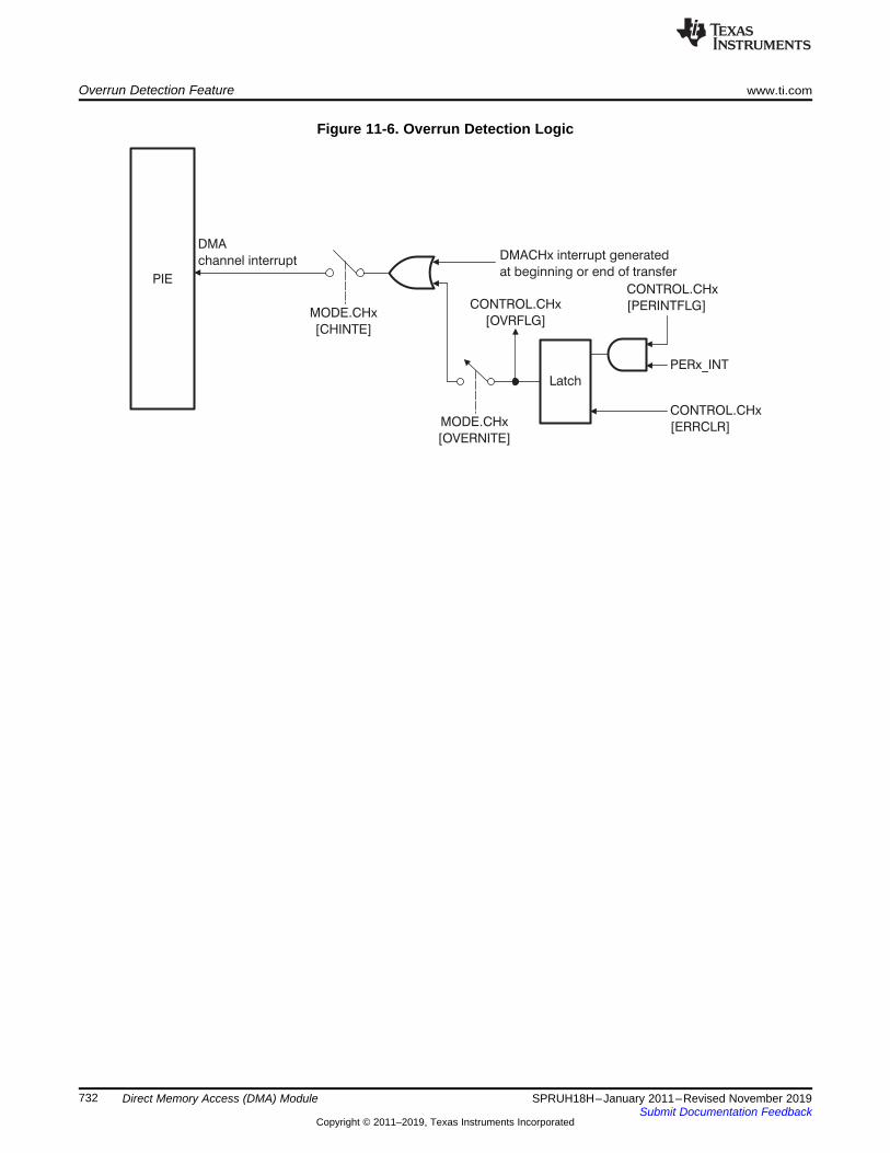
PIECONTROL.CHx
[PERINTFLG]
Latch
DMA
channel interrupt
CONTROL.CHx
[OVRFLG]
DMACHx interrupt generated
at beginning or end of transfer
MODE.CHx
[CHINTE]
PERx_INT
CONTROL.CHx
[ERRCLR]MODE.CHx
[OVERNITE]
Overrun Detection Feature www.ti.com
732 SPRUH18H–January 2011–Revised November 2019Submit Documentation Feedback
Copyright © 2011–2019, Texas Instruments Incorporated
Direct Memory Access (DMA) Module
Figure 11-6. Overrun Detection Logic

www.ti.com Register Descriptions
733SPRUH18H–January 2011–Revised November 2019Submit Documentation Feedback
Copyright © 2011–2019, Texas Instruments Incorporated
Direct Memory Access (DMA) Module
11.9 Register DescriptionsThe complete DMA register set is shown in Table 11-2.
(1) All DMA register writes are EALLOW protected.
Table 11-2. DMA Register Summary (1)
Address Acronym Description SectionDMA Control, Mode and Status Registers
0x1000 DMACTRL DMA Control Register Section 11.9.10x1001 DEBUGCTRL Debug Control Register Section 11.9.20x1002 REVISION Peripheral Revision Register Section 11.9.30x1003 Reserved Reserved0x1004 PRIORITYCTRL1 Priority Control Register 1 Section 11.9.40x1005 Reserved Reserved0x1006 PRIORITYSTAT Priority Status Register Table 11-70x10070x101F
Reserved Reserved
DMA Channel 1 Registers0x1020 MODE Mode Register Section 11.9.60x1021 CONTROL Control Register Section 11.9.70x1022 BURST_SIZE Burst Size Register Section 11.9.80x1023 BURST_COUNT Burst Count Register Section 11.9.90x1024 SRC_BURST_STEP Source Burst Step Size Register Section
11.9.100x1025 DST_BURST_STEP Destination Burst Step Size Register Section
11.9.110x1026 TRANSFER_SIZE Transfer Size Register Table 11-130x1027 TRANSFER_COUNT Transfer Count Register Section
11.9.130x1028 SRC_TRANSFER_STEP Source Transfer Step Size Register Section
11.9.140x1029 DST_TRANSFER_STEP Destination Transfer Step Size Register Section
11.9.150x102A SRC_WRAP_SIZE Source Wrap Size Register Section
11.9.160x102B SRC_WRAP_COUNT Source Wrap Count Register Section
11.9.170x102C SRC_WRAP_STEP Source Wrap Step Size Register Section
11.9.180x102D DST_WRAP_SIZE Destination Wrap Size Register Section
11.9.160x102E DST_WRAP_COUNT Destination Wrap Count Register Section
11.9.170x102F DST_WRAP_STEP Destination Wrap Step Size Register Section
11.9.180x1030 SRC_BEG_ADDR_SHADOW Shadow Source Begin and Current Address Pointer Registers Section
11.9.190x1032 SRC_ADDR_SHADOW Section
11.9.190x1034 SRC_BEG_ADDR Active Source Begin and Current Address Pointer Registers Section
11.9.200x1036 SRC_ADDR Section
11.9.200x1038 DST_BEG_ADDR_SHADOW Shadow Destination Begin and Current Address Pointer
RegistersSection11.9.21

Register Descriptions www.ti.com
734 SPRUH18H–January 2011–Revised November 2019Submit Documentation Feedback
Copyright © 2011–2019, Texas Instruments Incorporated
Direct Memory Access (DMA) Module
Table 11-2. DMA Register Summary (1) (continued)Address Acronym Description Section0x103A DST_ADDR_SHADOW Section
11.9.210x103C DST_BEG_ADDR Active Destination Begin and Current Address Pointer Registers Section
11.9.220x103E DST_ADDR Section
11.9.220x103F Reserved Reserved
DMA Channel 2 Registers0x10400x105F
Same as above
DMA Channel 3 Registers0x10600x107F
Same as above
DMA Channel 4 Registers0x10800x109F
Same as above
DMA Channel 5 Registers0x10A00x10BF
Same as above
DMA Channel 6 Registers0x10C00x10DF
Same as above
11.9.1 DMA Control Register (DMACTRL) — EALLOW ProtectedThe DMA control register (DMACTRL) is shown in Figure 11-7 and described in Table 11-3.
Figure 11-7. DMA Control Register (DMACTRL)15 8
ReservedR-0
7 2 1 0Reserved PRIORITY
RESETHARDRESET
R-0 R0/S-0 R0/S-0LEGEND: R0/S = Read 0/Set; R = Read only; -n = value after reset
Table 11-3. DMA Control Register (DMACTRL) Field Descriptions
Bit Field Value Description15-2 Reserved Reserved
1 PRIORITYRESET 0 The priority reset bit resets the round-robin state machine when a 1 is written. Service startsfrom the first enabled channel. Writes of 0 are ignored and this bit always reads back a 0.When a 1 is written to this bit, any pending burst transfer completes before resetting thechannel priority machine. If CH1 is configured as a high priority channel, and this bit iswritten to while CH1 is servicing a burst, the CH1 burst is completed and then any lowerpriority channel burst is also completed (if CH1 interrupted in the middle of a burst), beforethe state machine is reset.In case CH1 is high priority, the state machine restarts from CH2 (or the next highestenabled channel).

www.ti.com Register Descriptions
735SPRUH18H–January 2011–Revised November 2019Submit Documentation Feedback
Copyright © 2011–2019, Texas Instruments Incorporated
Direct Memory Access (DMA) Module
Table 11-3. DMA Control Register (DMACTRL) Field Descriptions (continued)Bit Field Value Description0 HARDRESET 0 Writing a 1 to the hard reset bit resets the whole DMA and aborts any current access
(similar to applying a device reset). Writes of 0 are ignored and this bit always reads back a0.For a soft reset, a bit is provided for each channel to perform a gentler reset. Refer to thechannel control registers.If the DMA was performing an access to the XINTF and the DMA access was stalled(XREADY not responding), then a HARDRESET would abort the access. The XINTFaccess would only complete if XREADY is released.When writing to this bit, there is a one cycle delay before it takes effect. Hence at least aone cycle delay (i.e., a NOP instruction) after writing to this bit should be introduced beforeattempting an access to any other DMA register.

Register Descriptions www.ti.com
736 SPRUH18H–January 2011–Revised November 2019Submit Documentation Feedback
Copyright © 2011–2019, Texas Instruments Incorporated
Direct Memory Access (DMA) Module
11.9.2 Debug Control Register (DEBUGCTRL) — EALLOW ProtectedThe debug control register (DEBUGCTRL) is shown in Figure 11-8 and described in Table 11-4.
Figure 11-8. Debug Control Register (DEBUGCTRL)15 14 0
FREE ReservedR/W-0 R-0LEGEND: R/W = Read/Write; R = Read only; -n = value after reset
Table 11-4. Debug Control Register (DEBUGCTRL) Field Descriptions
Bit Field Value Description15 FREE Emulation Control Bit: This bit specifies the action when an emulation halt event occurs.
0 DMA runs until the current DMA read-write access is completed and the current status of a DMA isfrozen. See the HALT points in Figure 11-5 for possible halt states.
1 DMA is unaffected by emulation suspend (run free)14-0 Reserved Reserved
11.9.3 Revision Register (REVISION)The revision register (REVISION) is shown in Figure 11-9 and described in Table 11-5.
Figure 11-9. Revision Register (REVISION)15 8 7 0
TYPE REVR R
LEGEND: R/W = Read/Write; R = Read only; -n = value after reset
Table 11-5. Revision Register (REVISION) Field Descriptions
Bit Field Value Description15-8 TYPE DMA Type Bits. A type change represents a major functional feature difference in a peripheral
module. Within a peripheral type, there may be minor differences between devices which do notaffect the basic functionality of the module. These device-specific differences are listed in theTMS320x28xx, 28xxx DSP Peripheral Reference Guide (SPRU566).
0x0000 This document describes a Type0 DMA.7-0 REV DMA Silicon Revision Bits: These bits specify the DMA revision and are changed if any bug
fixes are performed.0x0000 First release

www.ti.com Register Descriptions
737SPRUH18H–January 2011–Revised November 2019Submit Documentation Feedback
Copyright © 2011–2019, Texas Instruments Incorporated
Direct Memory Access (DMA) Module
11.9.4 Priority Control Register 1 (PRIORITYCTRL1) — EALLOW ProtectedThe priority control register 1 (PRIORITYCTRL1) is shown in Figure 11-10 and described in Table 11-6.
Figure 11-10. Priority Control Register 1 (PRIORITYCTRL1)15 1 0
Reserved CH1PRIORITY
R-0 R/W-0LEGEND: R/W = Read/Write; R = Read only; -n = value after reset
Table 11-6. Priority Control Register 1 (PRIORITYCTRL1) Field Descriptions
Bit Field Value Description15-1 Reserved Reserved
0 CH1PRIORITY DMA Ch1 Priority: This bit selects whether channel 1 has higher priority or not:0 Same priority as all other channels1 Highest priority channel
Channel priority can only be changed when all channels are disabled. A priority reset shouldbe performed before restarting channels after changing priority.

Register Descriptions www.ti.com
738 SPRUH18H–January 2011–Revised November 2019Submit Documentation Feedback
Copyright © 2011–2019, Texas Instruments Incorporated
Direct Memory Access (DMA) Module
11.9.5 Priority Status Register (PRIORITYSTAT)The priority status register (PRIORITYSTAT) is shown in Figure 11-11 and described in Table 11-7.
Figure 11-11. Priority Status Register (PRIORITYSTAT)15 8
ReservedR-0
7 6 4 3 2 0Reserved ACTIVESTS_SHADOW Reserved ACTIVESTS
R-0 R-0 R-0 R-0LEGEND: R/W = Read/Write; R = Read only; -n = value after reset
Table 11-7. Priority Status Register (PRIORITYSTAT) Field Descriptions
Bit Field Value Description15-7 Reserved Reserved6-4 ACTIVESTS_SH
ADOWActive Channel Status Shadow Bits: These bits are only useful when CH1 is enabled as a higherpriority channel. When CH1 is serviced, the ACTIVESTS bits are copied to the shadow bits andindicate which channel was interrupted by CH1. When CH1 service is completed, the shadow bitsare copied back to the ACTIVESTS bits. If this bit field is zero or the same as the ACTIVESTS bitfield, then no channel is pending due to a CH1 interrupt. When CH1 is not a higher priority channel,these bits should be ignored:
0,0,0 No channel pending0,0,1 CH 10,1,0 CH 20,1,1 CH 31,0,0 CH 41,0,1 CH 51,1,0 CH 6
3 Reserved Reserved2-0 ACTIVESTS Active Channel Status Bits: These bits indicate which channel is currently active or performing a
transfer:0,0,0 no channel active0,0,1 CH 10,1,0 CH 20,1,1 CH 31,0,0 CH 41,0,1 CH 51,1,0 CH 6

www.ti.com Register Descriptions
739SPRUH18H–January 2011–Revised November 2019Submit Documentation Feedback
Copyright © 2011–2019, Texas Instruments Incorporated
Direct Memory Access (DMA) Module
11.9.6 Mode Register (MODE) — EALLOW ProtectedThe mode register (MODE) is shown in Figure 11-12 and described in Table 11-8.
Figure 11-12. Mode Register (MODE)15 14 13 12 11 10 9 8
CHINTE DATASIZE Reserved CONTINUOUS ONESHOT CHINTMODE PERINTER/W-0 R/W-0 R/W-0 R/W-0 R/W-0 R/W-0 R/W-0
7 6 5 4 0OVRINTE Reserved PERINTSEL
R/W-0 R-0 R/W-0LEGEND: R/W = Read/Write; R = Read only; -n = value after reset
Table 11-8. Mode Register (MODE) Field Descriptions
Bit Field Value Description15 CHINTE Channel Interrupt Enable Bit: This bit enables/disables the respective DMA channel interrupt
to the CPU (via the PIE).0 Interrupt disabled1 Interrupt enabled
14 DATASIZE Data Size Mode Bit: This bit selects if the DMA channel transfers 16-bits or 32-bits of data at atime.
0 16-bit data transfer size1 32-bit data transfer size
NOTE: Regardless of the value of this bit all of the registers in theDMA refer to 16-bit words. The only effect this bit causesis whether the databus width is 16 or 32 bits.
It is up to you to configure the pointer step increment andsize to accommodate 32-bit data transfers. See sectionSection 11.7 for details.
13-12 Reserved Reserved11 CONTINUOUS Continuous Mode Bit: If this bit is set to 1, then DMA re-initializes when TRANSFER_COUNT
is zero and waits for the next interrupt event trigger. If this bit is 0, then the DMA stops andclears the RUNSTS bit to 0.
10 ONESHOT One Shot Mode Bit: If this bit is set to 1, then subsequent burst transfers occur withoutadditional event triggers after the first event trigger. If this bit is 0 then only one burst transferis performed per event trigger.Note: High-priority mode and One-shot mode may not be used at the same time on CH1.
9 CHINTMODE Channel Interrupt Generation Mode Bit: This bit specifies when the respective DMA channelinterrupt should be generated to the CPU (via the PIE).
0 Generate interrupt at beginning of new transfer1 Generate interrupt at end of transfer.
8 PERINTE Peripheral Interrupt Trigger Enable Bit: This bit enables/disables the selected peripheralinterrupt trigger to the DMA.
0 Interrupt trigger disabled. Neither the selected peripheral nor software can start a DMA burst.1 Interrupt trigger enabled.
7 OVRINTE Overflow Interrupt Enable: This bit when set to 1 enables the DMA to generate an interruptwhen an overflow event is detected.
0 Overflow interrupt disabled1 Overflow interrupt enabled
An overflow interrupt is generated when the PERINTFLG is set and another interrupt eventoccurs. The PERINTFLG being set indicates a previous peripheral event is latched and hasnot been serviced by the DMA.
6-5 Reserved Reserved

Register Descriptions www.ti.com
740 SPRUH18H–January 2011–Revised November 2019Submit Documentation Feedback
Copyright © 2011–2019, Texas Instruments Incorporated
Direct Memory Access (DMA) Module
Table 11-8. Mode Register (MODE) Field Descriptions (continued)Bit Field Value Description4-0 PERINTSEL Peripheral Interrupt Source Select Bits: These bits select which interrupt triggers a DMA burst
for the given channel. Only one interrupt source can be selected. A DMA burst can also beforced via the PERINTFRC bit.
Value Interrupt Sync Peripheral0 None None No peripheral connection1 ADCINT1 None ADC2 ADCINT2 None3 XINT1 None External Interrupts4 XINT2 None5 XINT3 None6 Reserved None No peripheral connection7 USB0EP1RX None USB-08 USB0EP1TX None9 USB0EP2RX None10 USB0EP2TX None11 TINT0 None CPU Timers12 TINT1 None13 TINT2 None14 MXEVTA None McBSP-A15 MREVTA None16 Reserved None No peripheral conneciton17 Reserved None18 ePWM2SOCA None ePWM219 ePWM2SOCB None20 ePWM3SOCA None ePWM321 ePWM3SOCB None22 ePWM4SOCA None ePWM423 ePWM4SOCB None24 ePWM5SOCA None ePWM525 ePWM5SOCB None26 ePWM6SOCA None ePWM627 ePWM6SOCB None28 ePWM7SOCA None ePWM729 ePWM7 SOCB None30 USB0EP3RX None USB-031 USB0EP3TX None

www.ti.com Register Descriptions
741SPRUH18H–January 2011–Revised November 2019Submit Documentation Feedback
Copyright © 2011–2019, Texas Instruments Incorporated
Direct Memory Access (DMA) Module
11.9.7 Control Register (CONTROL) — EALLOW ProtectedThe control register (CONTROL) is shown in Figure 11-13 and described in Table 11-9.
Figure 11-13. Control Register (CONTROL)15 14 13 12 11 10 9 8
Reserved OVRFLG RUNSTS BURSTSTS TRANSFERSTS Reserved PERINTFLGR-0 R-0 R-0 R-0 R-0 R-0 R-0
7 6 5 4 3 2 1 0ERRCLR Reserved PERINTCLR PERINTFRC SOFTRESET HALT RUNR0/S-0 R-0 R0/S-0 R0/S-0 R0/S-0 R0/S-0 R0/S-0
LEGEND: R0/S = Read 0/Set; R = Read only; -n = value after reset
Table 11-9. Control Register (CONTROL) Field Descriptions
Bit Field Value Description15 Reserved Reserved14 OVRFLG Overflow Flag Bit: This bit indicates if a peripheral interrupt event trigger is received from the
selected peripheral and the PERINTFLG is already set.0 No overflow event1 Overflow event
The ERRCLR bit can be used to clear the state of this bit to 0. The OVRFLG bit is not affectedby the PERINTFRC event.
13 RUNSTS Run Status Bit: This bit is set to 1 when the RUN bit is written to with a 1. This indicates the DMAchannel is now ready to process peripheral interrupt event triggers. This bit is cleared to 0 whenTRANSFER_COUNT reaches zero and CONTINUOUS mode bit is set to 0. This bit is alsocleared to 0 when either the HARDRESET bit, the SOFTRESET bit, or the HALT bit is activated.
0 Chanel is disabled.1 Channel is enabled.
12 BURSTSTS Burst Status Bit: This bit is set to 1 when a DMA burst transfer begins and the BURST_COUNTis initialized with the BURST_SIZE. This bit is cleared to zero when BURST_COUNT reacheszero. This bit is also cleared to 0 when either the HARDRESET or the SOFTRESET bit isactivated.
0 No burst activity1 The DMA is currently servicing or suspending a burst transfer from this channel.
11 TRANSFERSTS Transfer Status Bit: This bit is set to 1 when a DMA transfer begins and the address registers arecopied to the shadow set and the TRANSFER_COUNT is initialized with the TRANSFER_SIZE.This bit is cleared to zero when TRANSFER_COUNT reaches zero. This bit is also cleared to 0when either the HARDRESET or the SOFTRESET bit is activated.
0 No transfer activity1 The channel is currently in the middle of a transfer regardless of whether a burst of data is
actively being transferred or not.10-9 Reserved Reserved
8 PERINTFLG Peripheral Interrupt Trigger Flag Bit: This bit indicates if a peripheral interrupt event trigger hasoccurred. This flag is automatically cleared when the first burst transfer begins.
0 No interrupt event trigger1 Interrupt event trigger
The PERINTFRC bit can be used to set the state of this bit to 1 and force a software DMA event.The PERINTCLR bit can be used to clear the state of this bit to 0.
7 ERRCLR 0 Error Clear Bit: Writing a 1 to this bit will clear any latched sync error event and clear theSYNCERR bit. This bit will also clear the OVRFLG bit. This bit would normally be used wheninitializing the DMA for the first time or if an overflow condition is detected. If an ADCSYNC errorevent or overflow event occurs at the same time as writing to this bit, the ADC or overrun haspriority and the SYNCERR or OVRFLG bit is set.
6-5 Reserved Reserved

Register Descriptions www.ti.com
742 SPRUH18H–January 2011–Revised November 2019Submit Documentation Feedback
Copyright © 2011–2019, Texas Instruments Incorporated
Direct Memory Access (DMA) Module
Table 11-9. Control Register (CONTROL) Field Descriptions (continued)Bit Field Value Description4 PERINTCLR 0 Peripheral Interrupt Clear Bit: Writing a 1 to this bit clears any latched peripheral interrupt event
and clears the PERINTFLG bit. This bit would normally be used when initializing the DMA for thefirst time. If a peripheral event occurs at the same time as writing to this bit, the peripheral haspriority and the PERINTFLG bit is set.
3 PERINTFRC 0 Peripheral Interrupt Force Bit: Writing a 1 to this bit latches a peripheral interrupt event triggerand sets the PERINTFLG bit. If the PERINTE bit is set, this bit can be used like a software forcefor a DMA burst transfer.
2 SOFTRESET 0 Channel Soft Reset Bit: Writing a 1 to this bit completes current read-write access and places thechannel into a default state as follows:RUNSTS = 0TRANSFERSTS = 0BURSTSTS = 0BURST_COUNT = 0TRANSFER_COUNT = 0SRC_WRAP_COUNT = 0DST_WRAP_COUNT = 0This is a soft reset that basically allows the DMA to complete the current read-write access andthen places the DMA channel into the default reset state.
1 HALT 0 Channel Halt Bit: Writing a 1 to this bit halts the DMA at the current state and any current read-write access is completed. See Figure 11-5 for the various positions the state machine can be atwhen HALTED. The RUNSTS bit is set to 0. To take the device out of HALT, the RUN bit needsto be activated.
0 RUN 0 Channel Run Bit: Writing a 1 to this bit starts the DMA channel. The RUNSTS bit is set to 1. Thisbit is also used to take the device out of HALT.The RUN bit is typically used to start the DMA running after you have configured the DMA. It willthen wait for the first interrupt event (PERINTFLG == 1) to start operation. The RUN bit can alsobe used to take the DMA channel out of a HALT condition See Figure 11-5 for the variouspositions the state machine can be at when HALTED.

www.ti.com Register Descriptions
743SPRUH18H–January 2011–Revised November 2019Submit Documentation Feedback
Copyright © 2011–2019, Texas Instruments Incorporated
Direct Memory Access (DMA) Module
11.9.8 Burst Size Register (BURST_SIZE) — EALLOW ProtectedThe burst size register (BURST_SIZE) is shown in Figure 11-14 and described in Table 11-10.
Figure 11-14. Burst Size Register (BURST_SIZE)15 5 4 0
Reserved BURSTSIZER-0 R/W-0
LEGEND: R/W = Read/Write; R = Read only; -n = value after reset
Table 11-10. Burst Size Register (BURST_SIZE) Field Descriptions
Bit Field Value Description15-5 Reserved Reserved4-0 BURSTSIZE These bits specify the burst transfer size:
0 Transfer 1 word in a burst1 Transfer 2 words in a burst... ...31 Transfer 32 words in a burst
11.9.9 BURST_COUNT RegisterThe burst count register (BURST_COUNT) is shown in Figure 11-15 and described in Table 11-11.
Figure 11-15. Burst Count Register (BURST_COUNT)15 5 4 0
Reserved BURSTCOUNTR-0 R/W-0
LEGEND: R/W = Read/Write; R = Read only; -n = value after reset
Table 11-11. Burst Count Register (BURST_COUNT) Field Descriptions
Bit Field Value Description15-5 Reserved Reserved4-0 BURSTCOUNT These bits indicate the current burst counter value:
0 0 word left in a burst1 1 word left in a burst2 2 words left in a burst... ...31 31 words left in a burst
The above values represent the state of the counter at the HALT conditions.

Register Descriptions www.ti.com
744 SPRUH18H–January 2011–Revised November 2019Submit Documentation Feedback
Copyright © 2011–2019, Texas Instruments Incorporated
Direct Memory Access (DMA) Module
11.9.10 Source Burst Step Register Size (SRC_BURST_STEP) — EALLOW ProtectedThe source burst step size register (SRC_BURST_STEP) is shown in Figure 11-16 and described inTable 11-12.
Figure 11-16. Source Burst Step Size Register (SRC_BURST_STEP)15 0
SRCBURSTSTEPR/W-0
LEGEND: R/W = Read/Write; R = Read only; -n = value after reset
Table 11-12. Source Burst Step Size Register (SRC_BURST_STEP) Field Descriptions
Bit Field Value Description15-0 SRCBURSTSTEP These bits specify the source address post-increment/decrement step size while
processing a burst of data:0x0FFF Add 4095 to address
... ...0x0002 Add 2 to address0x0001 Add 1 to address0x0000 No address change0xFFFF Sub 1 from address0xFFFE Sub 2 from address
... ...0xF000 Sub 4096 from address
Only values from -4096 to 4095 are valid.

www.ti.com Register Descriptions
745SPRUH18H–January 2011–Revised November 2019Submit Documentation Feedback
Copyright © 2011–2019, Texas Instruments Incorporated
Direct Memory Access (DMA) Module
11.9.11 Destination Burst Step Register Size (DST_BURST_STEP) — EALLOW ProtectedThe destination burst step register size (DST_BURST_STEP) is shown in Figure 11-17 and described inTable 11-13.
Figure 11-17. Destination Burst Step Register Size (DST_BURST_STEP)15 0
DSTBURSTSTEPR/W-0
LEGEND: R/W = Read/Write; R = Read only; -n = value after reset
Table 11-13. Destination Burst Step Register Size (DST_BURST_STEP) Field Descriptions
Bit Field Value Description15-0 DSTBURSTSTEP These bits specify the destination address post-increment/decrement step size while
processing a burst of data:0x0FFF Add 4095 to address
... ...0x0002 Add 2 to address0x0001 Add 1 to address0x0000 No address change0xFFFF Sub 1 from address0xFFFE Sub 2 from address
... ...0xF000 Sub 4096 from address
Only values from -4096 to 4095 are valid.
11.9.12 Transfer Size Register (TRANSFER_SIZE) — EALLOW ProtectedThe transfer size register (TRANSFER_SIZE) is shown in Figure 11-18 and described in Table 11-14.
Figure 11-18. Transfer Size Register (TRANSFER_SIZE)15 0
TRANSFERSIZER/W-0
LEGEND: R/W = Read/Write; R = Read only; -n = value after reset
Table 11-14. Transfer Size Register (TRANSFER_SIZE) Field Descriptions
Bit Field Value Description15-0 TRANSFERSIZE These bits specify the number of bursts to transfer:
0x0000 Transfer 1 burst0x0001 Transfer 2 bursts0x0002 Transfer 3 bursts
... ...0xFFFF Transfer 65536 bursts

Register Descriptions www.ti.com
746 SPRUH18H–January 2011–Revised November 2019Submit Documentation Feedback
Copyright © 2011–2019, Texas Instruments Incorporated
Direct Memory Access (DMA) Module
11.9.13 Transfer Count Register (TRANSFER_COUNT)The transfer count register (TRANSFER_COUNT) is shown in Figure 11-19 and described in Table 11-15.
Figure 11-19. Transfer Count Register (TRANSFER_COUNT)15 0
TRANSFERCOUNTR/W-0
LEGEND: R/W = Read/Write; R = Read only; -n = value after reset
Table 11-15. Transfer Count Register (TRANSFER_COUNT) Field Descriptions
Bit Field Value Description15-0 TRANSFERCOUNT These bits specify the current transfer counter value:
0x0000 0 bursts left to transfer0x0001 1 burst left to transfer0x0002 2 bursts left to transfer
... ...0xFFFF 65535 bursts left to transfer
The above values represent the state of the counter at the HALT conditions.
11.9.14 Source Transfer Step Size Register (SRC_TRANSFER_STEP) — EALLOW ProtectedThe source transfer step size register (SRC_TRANSFER_STEP) is shown in Figure 11-20 and describedin Table 11-16.
Figure 11-20. Source Transfer Step Size Register (SRC_TRANSFER_STEP)15 0
SRCTRANSFERSTEPR/W-0
LEGEND: R/W = Read/Write; R = Read only; -n = value after reset
Table 11-16. Source Transfer Step Size Register (SRC_TRANSFER_STEP) Field Descriptions
Bit Field Value Description15-0 SRCTRANSFERSTEP These bits specify the source address pointer post-increment/decrement step
size after processing a burst of data:0x0FFF Add 4095 to address
... ...0x0002 Add 2 to address0x0001 Add 1 to address0x0000 No address change0xFFFF Sub 1 from address0xFFFE Sub 2 from address
... ...0xF000 Sub 4096 from address
Only values from -4096 to 4095 are valid.

www.ti.com Register Descriptions
747SPRUH18H–January 2011–Revised November 2019Submit Documentation Feedback
Copyright © 2011–2019, Texas Instruments Incorporated
Direct Memory Access (DMA) Module
11.9.15 Destination Transfer Step Size Register (DST_TRANSFER_STEP) — EALLOWProtectedThe destination transfer step size register (DST_TRANSFER_STEP) is shown in Figure 11-21 anddescribed in Table 11-17.
Figure 11-21. Destination Transfer Step Size Register (DST_TRANSFER_STEP)15 0
DSTTRANSFERSTEPR/W-0
LEGEND: R/W = Read/Write; R = Read only; -n = value after reset
Table 11-17. Destination Transfer Step Size Register (DST_TRANSFER_STEP) Field Descriptions
Bit Field Value Description15-0 DSTTRANSFERSTEP These bits specify the destination address pointer post-increment/decrement
step size after processing a burst of data:0x0FFF Add 4095 to address
... ...0x0002 Add 2 to address0x0001 Add 1 to address0x0000 No address change0xFFFF Sub 1 from address0xFFFE Sub 2 from address
... ...0xF000 Sub 4096 from address
Only values from -4096 to 4095 are valid.
11.9.16 Source/Destination Wrap Size Register (SRC/DST_WRAP_SIZE) — EALLOW protected)The source/destination wrap size register is shown in Figure 11-22 and described in Table 11-18.
Figure 11-22. Source/Destination Wrap Size Register (SRC/DST_WRAP_SIZE)15 0
WRAPSIZER/W-0
LEGEND: R/W = Read/Write; R = Read only; -n = value after reset
Table 11-18. Source/Destination Wrap Size Register (SRC/DST_WRAP_SIZE) Field Descriptions
Bit Field Value Description15-0 WRAPSIZE These bits specify the number of bursts to transfer before wrapping back to
begin address pointer:0x0000 Wrap after 1 burst0x0001 Wrap after 2 bursts0x0002 Wrap after 3 bursts
... ...0xFFFF Wrap after 65536 bursts
To disable the wrap function, set the WRAPSIZE bit field to a number larger thanthe TRANSFERSIZE bit field.

Register Descriptions www.ti.com
748 SPRUH18H–January 2011–Revised November 2019Submit Documentation Feedback
Copyright © 2011–2019, Texas Instruments Incorporated
Direct Memory Access (DMA) Module
11.9.17 Source/Destination Wrap Count Register (SCR/DST_WRAP_COUNT)The source/destination wrap count register (SCR/DST_WRAP_COUNT) is shown in Figure 11-23 anddescribed in Table 11-19.
Figure 11-23. Source/Destination Wrap Count Register (SCR/DST_WRAP_COUNT)15 0
WRAPCOUNTR/W-0
LEGEND: R/W = Read/Write; R = Read only; -n = value after reset
Table 11-19. Source/Destination Wrap Count Register (SCR/DST_WRAP_COUNT) FieldDescriptions
Bit Field Value Description15-0 WRAPCOUNT These bits indicate the current wrap counter value:
0x0000 Wrap complete0x0001 1 burst left0x0002 2 burst left
... ...0xFFFF 65535 burst left
The above values represent the state of the counter at the HALT conditions.
11.9.18 Source/Destination Wrap Step Size Registers (SRC/DST_WRAP_STEP) —EALLOW ProtectedThe source/destination wrap step size register (SRC/DST_WRAP_STEP) are shown in Figure 11-24 anddescribed in Table 11-20.
Figure 11-24. Source/Destination Wrap Step Size Registers (SRC/DST_WRAP_STEP)15 0
WRAPSTEPR/W-0
LEGEND: R/W = Read/Write; R = Read only; -n = value after reset
Table 11-20. Source/Destination Wrap Step Size Registers (SRC/DST_WRAP_STEP) FieldDescriptions
Bit Field Value Description15-0 WRAPSTEP These bits specify the source begin address pointer post-increment/decrement
step size after wrap counter expires:0x0FFF Add 4095 to address
... ...0x0002 Add 2 to address0x0001 Add 1 to address0x0000 No address change0xFFFF Sub 1 from address0xFFFE Sub 2 from address
... ...0xF000 Sub 4096 from address
Only values from -4096 to 4095 are valid.

www.ti.com Register Descriptions
749SPRUH18H–January 2011–Revised November 2019Submit Documentation Feedback
Copyright © 2011–2019, Texas Instruments Incorporated
Direct Memory Access (DMA) Module
11.9.19 Shadow Source Begin and Current Address Pointer Registers(SRC_BEG_ADDR_SHADOW/DST_BEG_ADDR_SHADOW) — All EALLOW ProtectedThe shadow source begin and current address pointer registers(SRC_BEG_ADDR_SHADOW/DST_BEG_ADDR_SHADOW) are shown in Figure 11-25 and described inTable 11-21.
Figure 11-25. Shadow Source Begin and Current Address Pointer Registers(SRC_BEG_ADDR_SHADOW/DST_BEG_ADDR_SHADOW)
31 22 21 0Reserved BEGADDR
R-0 R/W-0LEGEND: R/W = Read/Write; R = Read only; -n = value after reset
Table 11-21. Shadow Source Begin and Current Address Pointer Registers(SRC_BEG_ADDR_SHADOW/DST_BEG_ADDR_SHADOW) Field Descriptions
Bit Field Value Description31-22 Reserved Reserved21-0 BEGADDR 22-bit address value
11.9.20 Active Source Begin and Current Address Pointer Registers(SRC_BEG_ADDR/DST_BEG_ADDR)The active source begin and current address pointer registers (SRC_BEG_ADDR/DST_BEG_ADDR) areshown in Table 11-22 and described in Table 11-22.
Figure 11-26. Active Source Begin and Current Address Pointer Registers(SRC_BEG_ADDR/DST_BEG_ADDR)
31 22 21 0Reserved BEGADDR
R-0 R-0LEGEND: R/W = Read/Write; R = Read only; -n = value after reset
Table 11-22. Active Source Begin and Current Address Pointer Registers(SRC_BEG_ADDR/DST_BEG_ADDR) Field Descriptions
Bit Field Value Description31-22 Reserved Reserved21-0 BEGADDR 22-bit address value

Register Descriptions www.ti.com
750 SPRUH18H–January 2011–Revised November 2019Submit Documentation Feedback
Copyright © 2011–2019, Texas Instruments Incorporated
Direct Memory Access (DMA) Module
11.9.21 Shadow Destination Begin and Current Address Pointer Registers(SRC_ADDR_SHADOW/DST_ADDR_SHADOW) — All EALLOW ProtectedThe shadow destination begin and current address pointer registers(SRC_ADDR_SHADOW/DST_ADDR_SHADOW) are shown in Figure 11-27 and described in Table 11-23.
Figure 11-27. Shadow Destination Begin and Current Address Pointer Registers(SRC_ADDR_SHADOW/DST_ADDR_SHADOW)
31 22 21 0Reserved ADDR
R-0 R/W-0LEGEND: R/W = Read/Write; R = Read only; -n = value after reset
Table 11-23. Shadow Destination Begin and Current Address Pointer Registers(SRC_ADDR_SHADOW/DST_ADDR_SHADOW) Field Descriptions
Bit Field Value Description31-22 Reserved Reserved21-0 ADDR 22-bit address value
11.9.22 Active Destination Begin and Current Address Pointer Registers(SRC_ADDR/DST_ADDR)The active destination begin and current address pointer registers (SRC_ADDR/DST_ADDR) are shown inFigure 11-28 and described in Table 11-24.
Figure 11-28. Active Destination Begin and Current Address Pointer Registers(SRC_ADDR/DST_ADDR)
31 22 21 0Reserved ADDR
R-0 R-0LEGEND: R/W = Read/Write; R = Read only; -n = value after reset
Table 11-24. Active Destination Begin and Current Address Pointer Registers(SRC_ADDR/DST_ADDR) Field Descriptions
Bit Field Value Description31-22 Reserved Reserved21-0 ADDR 22-bit address value

751SPRUH18H–January 2011–Revised November 2019Submit Documentation Feedback
Copyright © 2011–2019, Texas Instruments Incorporated
Serial Peripheral Interface (SPI)
Chapter 12SPRUH18H–January 2011–Revised November 2019
Serial Peripheral Interface (SPI)
This chapter describes the serial peripheral interface (SPI) which is a high-speed synchronous serial inputand output (I/O) port that allows a serial bit stream of programmed length (one to 16 bits) to be shifted intoand out of the device at a programmed bit-transfer rate. The SPI is normally used for communicationsbetween the MCU controller and external peripherals or another controller. Typical applications includeexternal I/O or peripheral expansion via devices such as shift registers, display drivers, and analog-to-digital converters (ADCs). Multi-device communications are supported by the master or slave operation ofthe SPI. The port supports a 4-level, receive and transmit FIFO for reducing CPU servicing overhead.
Topic ........................................................................................................................... Page
12.1 Introduction ..................................................................................................... 75212.2 System-Level Integration ................................................................................... 75312.3 SPI Operation................................................................................................... 75612.4 Programming Procedure ................................................................................... 76412.5 SPI Registers ................................................................................................... 769

Introduction www.ti.com
752 SPRUH18H–January 2011–Revised November 2019Submit Documentation Feedback
Copyright © 2011–2019, Texas Instruments Incorporated
Serial Peripheral Interface (SPI)
12.1 Introduction
12.1.1 FeaturesThe SPI module features include:• SPISOMI: SPI slave-output/master-input pin• SPISIMO: SPI slave-input/master-output pin• SPISTE: SPI slave transmit-enable pin• SPICLK: SPI serial-clock pin
NOTE: All four pins can be used as GPIO if the SPI module is not used.
• Two operational modes: Master and Slave• Baud rate: 125 different programmable rates. The maximum baud rate that can be employed is limited
by the maximum speed of the I/O buffers used on the SPI pins. See the device-specific data manualfor more details.
• Data word length: one to sixteen data bits• Four clocking schemes (controlled by clock polarity and clock phase bits) include:
– Falling edge without phase delay: SPICLK active-high. SPI transmits data on the falling edge of theSPICLK signal and receives data on the rising edge of the SPICLK signal.
– Falling edge with phase delay: SPICLK active-high. SPI transmits data one half-cycle ahead of thefalling edge of the SPICLK signal and receives data on the falling edge of the SPICLK signal.
– Rising edge without phase delay: SPICLK inactive-low. SPI transmits data on the rising edge of theSPICLK signal and receives data on the falling edge of the SPICLK signal.
– Rising edge with phase delay: SPICLK inactive-low. SPI transmits data one half-cycle ahead of therising edge of the SPICLK signal and receives data on the rising edge of the SPICLK signal.
• Simultaneous receive and transmit operation (transmit function can be disabled in software)• Transmitter and receiver operations are accomplished through either interrupt- driven or polled
algorithm• 4-level transmit/receive FIFO• Delayed transmit control• 3-wire SPI mode• SPISTE inversion for digital audio interface receive mode on devices with two SPI modules
12.1.2 Block DiagramFigure 12-1 shows the SPI CPU interfaces.

CPU
SYSCLKOUTLow speedprescaler
Systemcontrolblock
PIEblock
SPIINT/RXINT
TXINTR
eg
iste
rsSPI
SPIAENCLK LSPCLK
SPISOMI
GPIO
MUX
SPISIMO
SPICLK
SPISTE Periphera
l B
us
SYSRS
www.ti.com System-Level Integration
753SPRUH18H–January 2011–Revised November 2019Submit Documentation Feedback
Copyright © 2011–2019, Texas Instruments Incorporated
Serial Peripheral Interface (SPI)
Figure 12-1. SPI CPU Interface
12.2 System-Level IntegrationThis section describes the various functionality that is applicable to the device integration. These featuresrequire configuration of other modules in the device that are not within the scope of this chapter.
12.2.1 SPI Module SignalsTable 12-1 classifies and provides a summary of the SPI module signals.
Table 12-1. SPI Module Signal Summary
Signal Name DescriptionExternal SignalsSPICLK SPI clockSPISIMO SPI slave in, master outSPISOMI SPI slave out, master inSPISTE SPI slave transmit enableControlSPI Clock Rate LSPCLKInterrupt SignalsSPIINT/SPIRXINT Transmit interrupt/ Receive Interrupt in non FIFO mode (referred to as SPIINT)
Receive interrupt in FIFO modeSPITXINT Transmit interrupt in FIFO mode
Special ConsiderationsThe SPISTE signal provides the ability to gate any spurious clock and data pulses when the SPI is inslave mode. An active SPISTE will not allow the slave to receive data. This prevents the SPI slave fromlosing synchronization with the master. It is this reason that TI does not recommend that the SPISTEalways be tied to the active state.

System-Level Integration www.ti.com
754 SPRUH18H–January 2011–Revised November 2019Submit Documentation Feedback
Copyright © 2011–2019, Texas Instruments Incorporated
Serial Peripheral Interface (SPI)
If the SPI slave does ever lose synchronization with the master, toggling SPISWRESET will reset internalbit counter as well as the various status flags in the module. By resetting the bit counter, the SPI willinterpret the next clock transition as the first bit of a new transmission. The register bit fields which arereset by SPISWRESET can be found in Section 12.5
Configuring a GPIO to emulate SPISTEIn many systems, a SPI master may be connected to multiple SPI slaves using multiple instances ofSPISTE. Though this SPI module does not natively support multiple SPISTE signals, it is possible toemulate this behavior in software using GPIOs. In this configuration, the SPI must be configured as themaster. Rather than using the GPIO Mux to select SPISTE, the application would configure pins to beGPIO outputs, one GPIO per SPI slave. Before transmitting any data, the application would drive thedesired GPIO to the active state. Immediately after the transmission has been completed, the GPIO chipselect would be driven to the inactive state. This process can be repeated for many slaves which sharethe SPICLK, SPISIMO, and SPISOMI lines.
12.2.2 Configuring Device PinsThe GPIO mux registers must be configured to connect this peripheral to the device pins.
Some IO functionality is defined by GPIO register settings independent of this peripheral. For inputsignals, the GPIO input qualification should be set to asynchronous mode by setting the appropriateGPxQSELn register bits to 11b. The internal pullups can be configured in the GPyPUD register.
See the GPIO chapter for more details on GPIO mux and settings.
12.2.3 SPI InterruptsThis section includes information on the available interrupts present in the SPI module.
The SPI module contains two interrupt lines: SPIINT/SPIRXINT and SPITXINT. When the SPI is operatingin non-FIFO mode, all available interrupts are routed together to generate the single SPIINT interrupt.When FIFO mode is used, both SPIRXINT and SPITXINT can be generated.
SPIINT/SPIRXINTWhen the SPI is operating in non-FIFO mode, the interrupt generated is called SPIINT. If FIFOenhancements are enabled, the interrupt is called SPIRXINT. These interrupts share the same interruptvector in the Peripheral Interrupt Expansion (PIE) block.
In non-FIFO mode, two conditions can trigger an interrupt: a transmission is complete (INT_FLAG), orthere is overrun in the receiver (OVERRUN_FLAG). Both of these conditions share the same interruptvector: SPIINT.
The transmission complete flag (INT_FLAG) indicates that the SPI has completed sending or receiving thelast bit and is ready to be serviced. At the same time this bit is set, the received character is placed in thereceiver buffer (SPIRXBUF). The INT_FLAG will generate an interrupt on the SPIINT vector if theSPIINTENA bit is set.
The receiver overrun flag (OVERRUN_FLAG) indicates that a transmit or receive operation has completedbefore the previous character has been read from the buffer. The OVERRUN_FLAG will generate aninterrupt on the SPIINT vector if the OVERRUNINTENA bit is set and OVERRUN_FLAG was previouslycleared.
In FIFO mode, the SPI can interrupt the CPU upon a match condition between the current receive FIFOstatus (RXFFST) and the receive FIFO interrupt level (RXFFIL). If RXFFST is greater than or equal toRXFFIL, the receive FIFO interrupt flag (RXFFINT) will be set. SPIRXINT will be triggered in the PIE blockif RXFFINT is set and the receive FIFO interrupt is enabled (RXFFIENA = 1).
SPITXINTThe SPITXINT interrupt is not available when the SPI is operating in non-FIFO mode.

www.ti.com System-Level Integration
755SPRUH18H–January 2011–Revised November 2019Submit Documentation Feedback
Copyright © 2011–2019, Texas Instruments Incorporated
Serial Peripheral Interface (SPI)
In FIFO mode, the SPITXINT behavior is similar to the SPIRXINT. SPITXINT is generated upon a matchcondition between the current transmit FIFO status (TXFFST) and the transmit FIFO interrupt level(TXFFIL). If TXFFST is less than or equal to TXFFIL, the transmit FIFO interrupt flag (TXFFINT) will beset. SPITXINT will be triggered in the PIE block if TXFFINT is set and the transmit FIFO interrupt isenabled in the SPI module (TXFFIENA = 1).
Figure 12-2 and Table 12-2 show how these control bits influence the SPI interrupt generation.
Figure 12-2. SPI Interrupt Flags and Enable Logic Generation

SPI master (master/slave = 1) SPI slave (master/slave = 0)
SPIRXBUF.15−0
Serial input bufferSPIRXBUF
Shift register(SPIDAT)
SPITXBUF.15−0
Serial transmit bufferSPITXBUF
Processor 1
SPIDAT.15−0
SPICLK
SPISOMI
SPISTE
SPISIMO
SPICLK
SPISOMI
SPISTE
SPISIMO
Slave in/
master out
SPI
strobe
Slave out/
master in
Serial
clock
SPIRXBUF.15−0
Serial input bufferSPIRXBUF
Shift register(SPIDAT)
SPITXBUF.15−0
Serial transmit bufferSPITXBUF
SPIDAT.15−0
Processor 2
LSBMSB LSBMSB
SPI Operation www.ti.com
756 SPRUH18H–January 2011–Revised November 2019Submit Documentation Feedback
Copyright © 2011–2019, Texas Instruments Incorporated
Serial Peripheral Interface (SPI)
(1) In non-FIFO mode, SPIRXINT is the same name as the SPIINT interrupt in 28x devices.
Table 12-2. SPI Interrupt Flag Modes
FIFO Options SPI interruptSource Interrupt Flags Interrupt Enables FIFO Enable
(SPIFFENA) Interrupt (1)Line
SPI without FIFOReceive overrun RXOVRN OVRNINTENA 0 SPIRXINT
Data receive SPIINT SPIINTENA 0 SPIRXINTTransmit empty SPIINT SPIINTENA 0 SPIRXINT
SPI FIFO modeFIFO receive RXFFIL RXFFIENA 1 SPIRXINT
Transmit empty TXFFIL TXFFIENA 1 SPITXINT
12.3 SPI OperationThis section describes the various modes of operation of the SPI. Included are explanations of theoperational modes, interrupts, data format, clock sources, and initialization. Typical timing diagrams fordata transfers are given.
12.3.1 Introduction to OperationFigure 12-3 shows typical connections of the SPI for communications between two controllers: a masterand a slave.
The master transfers data by sending the SPICLK signal. For both the slave and the master, data isshifted out of the shift registers on one edge of the SPICLK and latched into the shift register on theopposite SPICLK clock edge. If the CLK_PHASE bit is high, data is transmitted and received a half-cyclebefore the SPICLK transition. As a result, both controllers send and receive data simultaneously. Theapplication software determines whether the data is meaningful or dummy data. There are three possiblemethods for data transmission:• Master sends data; slave sends dummy data.• Master sends data; slave sends data.• Master sends dummy data; slave sends data.
The master can initiate data transfer at any time because it controls the SPICLK signal. The software,however, determines how the master detects when the slave is ready to broadcast data.
Figure 12-3. SPI Master/Slave Connection
The SPI can operate in master or slave mode. The MASTER_SLAVE bit selects the operating mode andthe source of the SPICLK signal.
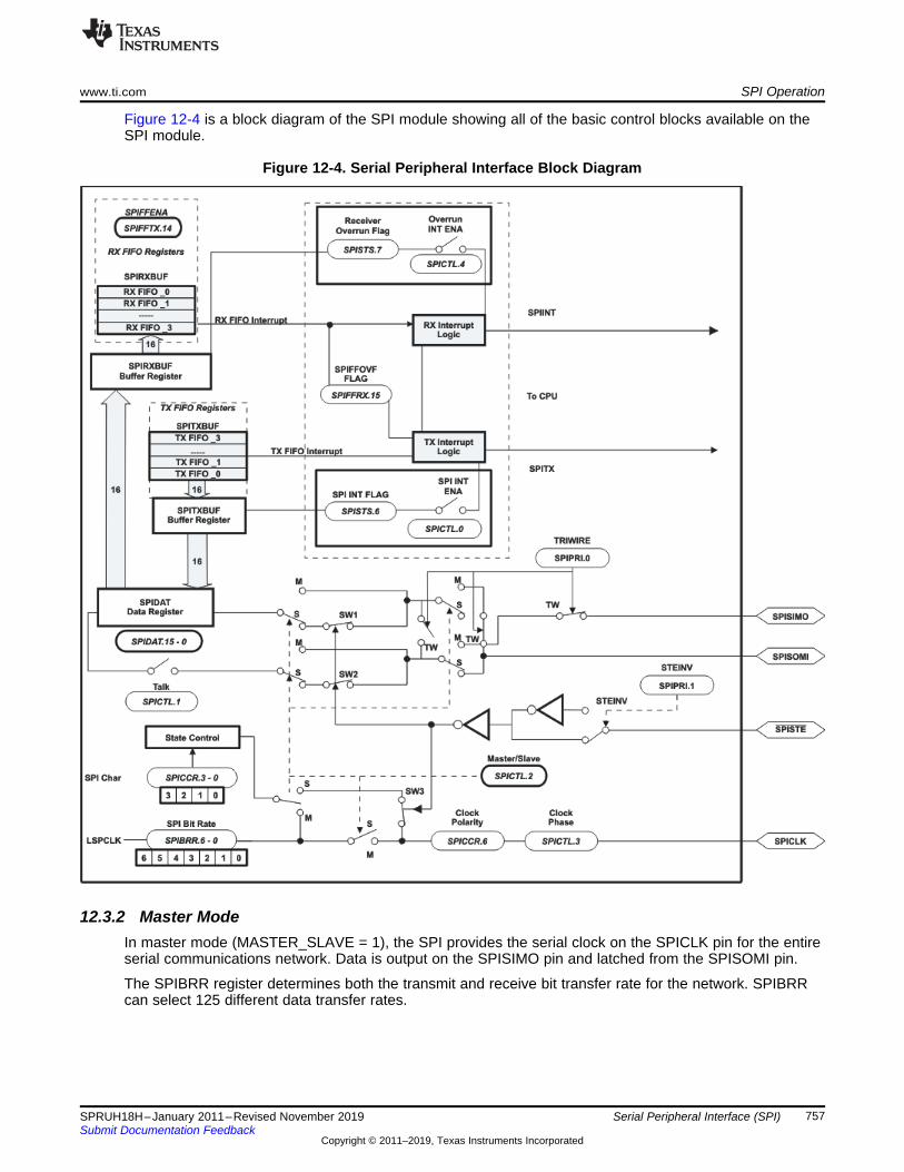
www.ti.com SPI Operation
757SPRUH18H–January 2011–Revised November 2019Submit Documentation Feedback
Copyright © 2011–2019, Texas Instruments Incorporated
Serial Peripheral Interface (SPI)
Figure 12-4 is a block diagram of the SPI module showing all of the basic control blocks available on theSPI module.
Figure 12-4. Serial Peripheral Interface Block Diagram
12.3.2 Master ModeIn master mode (MASTER_SLAVE = 1), the SPI provides the serial clock on the SPICLK pin for the entireserial communications network. Data is output on the SPISIMO pin and latched from the SPISOMI pin.
The SPIBRR register determines both the transmit and receive bit transfer rate for the network. SPIBRRcan select 125 different data transfer rates.
SPI Operation www.ti.com
758 SPRUH18H–January 2011–Revised November 2019Submit Documentation Feedback
Copyright © 2011–2019, Texas Instruments Incorporated
Serial Peripheral Interface (SPI)
Data written to SPIDAT or SPITXBUF initiates data transmission on the SPISIMO pin, MSB (mostsignificant bit) first. Simultaneously, received data is shifted through the SPISOMI pin into the LSB (leastsignificant bit) of SPIDAT. When the selected number of bits has been transmitted, the received data istransferred to the SPIRXBUF (buffered receiver) for the CPU to read. Data is stored right-justified inSPIRXBUF.
When the specified number of data bits has been shifted through SPIDAT, the following events occur:• SPIDAT contents are transferred to SPIRXBUF.• INT_FLAG bit is set to 1.• If there is valid data in the transmit buffer SPITXBUF, as indicated by the Transmit Buffer Full Flag
(BUFFULL_FLAG), this data is transferred to SPIDAT and is transmitted; otherwise, SPICLK stopsafter all bits have been shifted out of SPIDAT.
• If the SPIINTENA bit is set to 1, an interrupt is asserted.
In a typical application, the SPISTE pin serves as a chip-enable pin for a slave SPI device. This pin isdriven low by the master before transmitting data to the slave and is taken high after the transmission iscomplete.
12.3.3 Slave ModeIn slave mode (MASTER_SLAVE = 0), data shifts out on the SPISOMI pin and in on the SPISIMO pin.The SPICLK pin is used as the input for the serial shift clock, which is supplied from the external networkmaster. The transfer rate is defined by this clock. The SPICLK input frequency should be no greater thanthe LSPCLK frequency divided by 4.
Data written to SPIDAT or SPITXBUF is transmitted to the network when appropriate edges of theSPICLK signal are received from the network master. Data written to the SPITXBUF register will betransferred to the SPIDAT register when all bits of the character to be transmitted have been shifted out ofSPIDAT. If no character is currently being transmitted when SPITXBUF is written to, the data will betransferred immediately to SPIDAT. To receive data, the SPI waits for the network master to send theSPICLK signal and then shifts the data on the SPISIMO pin into SPIDAT. If data is to be transmitted bythe slave simultaneously, and SPITXBUF has not been previously loaded, the data must be written toSPITXBUF or SPIDAT before the beginning of the SPICLK signal.
When the TALK bit is cleared, data transmission is disabled, and the output line (SPISOMI) is put into thehigh-impedance state. If this occurs while a transmission is active, the current character is completelytransmitted even though SPISOMI is forced into the high-impedance state. This ensures that the SPI isstill able to receive incoming data correctly. This TALK bit allows many slave devices to be tied togetheron the network, but only one slave at a time is allowed to drive the SPISOMI line.
The SPISTE pin operates as the slave-select pin. An active-low signal on the SPISTE pin allows the slaveSPI to transfer data to the serial data line; an inactive- high signal causes the slave SPI serial shift registerto stop and its serial output pin to be put into the high-impedance state. This allows many slave devices tobe tied together on the network, although only one slave device is selected at a time.
12.3.4 Data FormatThe four-bit SPICHAR register field specifies the number of bits in the data character (1 to 16). Thisinformation directs the state control logic to count the number of bits received or transmitted to determinewhen a complete character has been processed.
The following statements apply to characters with fewer than 16 bits:• Data must be left-justified when written to SPIDAT and SPITXBUF.• Data read back from SPIRXBUF is right-justified.• SPIRXBUF contains the most recently received character, right-justified, plus any bits that remain from
previous transmission(s) that have been shifted to the left (shown in Example 12-1).
Example 12-1. Transmission of Bit From SPIRXBUF
Conditions:

SPI Baud RateLSPCLK
4=
SPI Baud RateLSPCLK
(SPIBRR 1)=
+
www.ti.com SPI Operation
759SPRUH18H–January 2011–Revised November 2019Submit Documentation Feedback
Copyright © 2011–2019, Texas Instruments Incorporated
Serial Peripheral Interface (SPI)
Example 12-1. Transmission of Bit From SPIRXBUF (continued)1. Transmission character length = 1 bit (specified in bits SPICHAR)2. The current value of SPIDAT = 737Bh
(1) x = 1 if SPISOMI data is high; x = 0 if SPISOMI data is low; master mode is assumed.
SPIDAT (before transmission)0 1 1 1 0 0 1 1 0 1 1 1 1 0 1 1
SPIDAT (after transmission)(TXed) 0 ← 1 1 1 0 0 1 1 0 1 1 1 1 0 1 1 x (1) ← (RXed)
SPIRXBUF (after transmission)1 1 1 0 0 1 1 0 1 1 1 1 0 1 1 x (1)
12.3.5 Baud Rate SelectionThe SPI module supports 125 different baud rates and four different clock schemes. Depending onwhether the SPI clock is in slave or master mode, the SPICLK pin can receive an external SPI clock signalor provide the SPI clock signal, respectively.• In the slave mode, the SPI clock is received on the SPICLK pin from the external source, and can be
no greater than the LSPCLK frequency divided by 4.• In the master mode, the SPI clock is generated by the SPI and is output on the SPICLK pin, and can
be no greater than the LSPCLK frequency divided by 4.
NOTE: The baud rate should be configured to not exceed the maximum rated GPIO togglefrequency. Refer to the device Data Manual for the maximum GPIO toggle frequency
Example 12-2 shows how to determine the SPI baud rates.
Example 12-2. Baud Rate Determination
For SPIBRR = 3 to 127:
(7)
For SPIBRR = 0, 1, or 2:
(8)
where:
LSPCLK = Low-speed peripheral clock frequency of the device
SPIBRR = Contents of the SPIBRR in the master SPI device
To determine what value to load into SPIBRR, you must know the device system clock (LSPCLK) frequency(which is device-specific) and the baud rate at which you will be operating.
The following example shows how to calculate the baud rate of the SPI module.
Example 12-3. Baud Rate Calculation
(9)

SPICLK cycle
number1 2 3 4 5 6 7 8
SPICLK
(Falling edge
without delay)
SPICLK
(Falling edge
with delay)
SPISIMO/
SPISOMI
SPISTE
MSB LSB
Note: Previous data bit
(Into slave)
Receive latch
points
SPICLK
(Rising edge
without delay)
SPICLK
(Rising edge
with delay)
See note
SPI Operation www.ti.com
760 SPRUH18H–January 2011–Revised November 2019Submit Documentation Feedback
Copyright © 2011–2019, Texas Instruments Incorporated
Serial Peripheral Interface (SPI)
12.3.6 SPI Clocking SchemesThe clock polarity select bit (CLKPOLARITY) and the clock phase select bit (CLK_PHASE) control fourdifferent clocking schemes on the SPICLK pin. CLKPOLARITY selects the active edge, either rising orfalling, of the clock. CLK_PHASE selects a half-cycle delay of the clock. The four different clockingschemes are as follows:• Falling Edge Without Delay. The SPI transmits data on the falling edge of the SPICLK and receives
data on the rising edge of the SPICLK.• Falling Edge With Delay. The SPI transmits data one half-cycle ahead of the falling edge of the
SPICLK signal and receives data on the falling edge of the SPICLK signal.• Rising Edge Without Delay. The SPI transmits data on the rising edge of the SPICLK signal and
receives data on the falling edge of the SPICLK signal.• Rising Edge With Delay. The SPI transmits data one half-cycle ahead of the rising edge of the SPICLK
signal and receives data on the rising edge of the SPICLK signal.
The selection procedure for the SPI clocking scheme is shown in Table 12-3. Examples of these fourclocking schemes relative to transmitted and received data are shown in Figure 12-5.
(1) The description of CLK_PHASE and CLKPOLARITY differs between manufacturers. For proper operation, select the desiredwaveform to determine the clock phase and clock polarity settings.
Table 12-3. SPI Clocking Scheme Selection Guide
SPICLK Scheme CLKPOLARITY CLK_PHASE (1)
Rising edge without delay 0 0Rising edge with delay 0 1
Falling edge without delay 1 0Falling edge with delay 1 1
Figure 12-5. SPICLK Signal Options

LSPCLK
SPICLK
2 cycles 3 cycles 2 cycles
www.ti.com SPI Operation
761SPRUH18H–January 2011–Revised November 2019Submit Documentation Feedback
Copyright © 2011–2019, Texas Instruments Incorporated
Serial Peripheral Interface (SPI)
SPICLK symmetry is retained only when the result of (SPIBRR+1) is an even value. When (SPIBRR + 1)is an odd value and SPIBRR is greater than 3, SPICLK becomes asymmetrical. The low pulse of SPICLKis one LSPCLK cycle longer than the high pulse when CLKPOLARITY bit is clear (0). WhenCLKPOLARITY bit is set to 1, the high pulse of the SPICLK is one LSPCLK cycle longer than the lowpulse, as shown in Figure 12-6.
Figure 12-6. SPI: SPICLK-LSPCLK Characteristic When (BRR + 1) is Odd, BRR > 3, and CLKPOLARITY =1
12.3.7 SPI FIFO DescriptionThe following steps explain the FIFO features and help with programming the SPI FIFOs:1. Reset. At reset the SPI powers up in standard SPI mode and the FIFO function is disabled. The FIFO
registers SPIFFTX, SPIFFRX and SPIFFCT remain inactive.2. Standard SPI. The standard 28x SPI mode will work with SPIINT/SPIRXINT as the interrupt source.3. Mode change. FIFO mode is enabled by setting the SPIFFENA bit to 1 in the SPIFFTX register.
SPIRST can reset the FIFO mode at any stage of its operation.4. Active registers. All the SPI registers and SPI FIFO registers SPIFFTX, SPIFFRX, and SPIFFCT will
be active.5. Interrupts. FIFO mode has two interrupts one for the transmit FIFO, SPITXINT and one for the receive
FIFO, SPIRXINT. SPIRXINT is the common interrupt for SPI FIFO receive, receive error and receiveFIFO overflow conditions. The single SPIINT for both transmit and receive sections of the standard SPIwill be disabled and this interrupt will service as SPI receive FIFO interrupt. For more information, referto Section 12.2.3
6. Buffers. Transmit and receive buffers are each supplemented with a 4 word FIFO. The one-wordtransmit buffer (SPITXBUF) of the standard SPI functions as a transition buffer between the transmitFIFO and shift register. The one-word transmit buffer will be loaded from transmit FIFO only after thelast bit of the shift register is shifted out.
7. Delayed transfer. The rate at which transmit words in the FIFO are transferred to transmit shiftregister is programmable. The SPIFFCT register bits (7−0) FFTXDLY7−FFTXDLY0 define the delaybetween the word transfer. The delay is defined in number SPI serial clock cycles. The 8-bit registercould define a minimum delay of 0 SPICLK cycles and a maximum of 255 SPICLK cycles. With zerodelay, the SPI module can transmit data in continuous mode with the FIFO words shifting out back toback. With the 255 clock delay, the SPI module can transmit data in a maximum delayed mode withthe FIFO words shifting out with a delay of 255 SPICLK cycles between each words. Theprogrammable delay facilitates glueless interface to various slow SPI peripherals, such as EEPROMs,ADC, DAC, and so on.
8. FIFO status bits. Both transmit and receive FIFOs have status bits TXFFST or RXFFST that definethe number of words available in the FIFOs at any time. The transmit FIFO reset bit (TXFIFO) andreceive reset bit (RXFIFO) will reset the FIFO pointers to zero when these bits are set to 1. The FIFOswill resume operation from start once these bits are cleared to zero.
9. Programmable interrupt levels. Both transmit and receive FIFOs can generate CPU interrupts. Thetransmit interrupt (SPITXINT) is generated whenever the transmit FIFO status bits (TXFFST) match(less than or equal to) the interrupt trigger level bits (TXFFIL). The receive interrupt (SPIRXINT) isgenerated whenever the receive FIFO status bits (RXFFST) match (greater than or equal to) theinterrupt trigger level RXFFIL. This provides a programmable interrupt trigger for transmit and receivesections of the SPI. The default value for these trigger level bits will be 0x11111 for receive FIFO and0x00000 for transmit FIFO, respectively.

SPIDAT
Data RX
Data TX
SPI Module GPIO MUX
Talk
SPICTL.1
Free pin
SPIMOMIx
SPI Operation www.ti.com
762 SPRUH18H–January 2011–Revised November 2019Submit Documentation Feedback
Copyright © 2011–2019, Texas Instruments Incorporated
Serial Peripheral Interface (SPI)
12.3.8 SPI 3-Wire Mode DescriptionSPI 3-wire mode allows for SPI communication over three pins instead of the normal four pins.
In master mode, if the TRIWIRE bit is set, enabling 3-wire SPI mode, SPISIMOx becomes the bi-directional SPIMOMIx (SPI master out, master in) pin, and SPISOMIx is no longer used by the SPI. Inslave mode, if the TRIWIRE bit is set, SPISOMIx becomes the bi-directional SPISISOx (SPI slave in, slaveout) pin, and SPISIMOx is no longer used by the SPI.
Table 12-4 indicates the pin function differences between 3-wire and 4-wire SPI mode for a master andslave SPI.
Table 12-4. 4-wire vs. 3-wire SPI Pin Functions
4-wire SPI 3-wire SPI (Master) 3-wire SPI(Slave)SPICLKx SPICLKx SPICLKxSPISTEx SPISTEx SPISTExSPISIMOx SPIMOMIx FreeSPISOMIx Free SPISISOx
Because in 3-wire mode, the receive and transmit paths within the SPI are connected, any datatransmitted by the SPI module is also received by itself. The application software must take care toperform a dummy read to clear the SPI data register of the additional received data.
The TALK bit plays an important role in 3-wire SPI mode. The bit must be set to transmit data and clearedprior to reading data. In master mode, in order to initiate a read, the application software must writedummy data to the SPI data register (SPIDAT or SPIRXBUF) while the TALK bit is cleared (no data istransmitted out the SPIMOMI pin) before reading from the data register.
Figure 12-7 and Figure 12-8 illustrate 3-wire master and slave mode.
Figure 12-7. SPI 3-wire Master Mode

SPIDAT
Data RX
Data TX
SPI Module GPIO MUX
Talk
SPICTL.1
Free pin
SPISISOx
www.ti.com SPI Operation
763SPRUH18H–January 2011–Revised November 2019Submit Documentation Feedback
Copyright © 2011–2019, Texas Instruments Incorporated
Serial Peripheral Interface (SPI)
Figure 12-8. SPI 3-wire Slave Mode
Table 12-5 indicates how data is received or transmitted in the various SPI modes while the TALK bit isset or cleared.
Table 12-5. 3-Wire SPI Pin Configuration
Pin Mode SPIPRI[TRIWIRE] SPICTL[TALK] SPISIMO SPISOMIMaster Mode
4-wire 0 X TX RX3-pin mode 1 0 RX Disconnect from SPI
1 TX/RXSlave Mode
4-wire 0 X RX TX3-pin mode 1 0 Disconnect from SPI RX
1 TX/RX

Programming Procedure www.ti.com
764 SPRUH18H–January 2011–Revised November 2019Submit Documentation Feedback
Copyright © 2011–2019, Texas Instruments Incorporated
Serial Peripheral Interface (SPI)
12.4 Programming ProcedureThis section describes the procedure for configuring the SPI for the various modes of operation.
12.4.1 Initialization Upon ResetA system reset forces the SPI peripheral into the following default configuration:• Unit is configured as a slave module (MASTER_SLAVE = 0)• Transmit capability is disabled (TALK = 0)• Data is latched at the input on the falling edge of the SPICLK signal• Character length is assumed to be one bit• SPI interrupts are disabled• Data in SPIDAT is reset to 0000h
12.4.2 Configuring the SPIThis section describes the procedure in which to configure the SPI module for operation. To preventunwanted and unforeseen events from occurring during or as a result of initialization changes, clear theSPISWRESET bit before making initialization changes, and then set this bit after initialization is complete.While the SPI is held in reset (SPISWRESET = 0), configuration may be changed in any order. Thefollowing list shows the SPI configuration procedure in a logical order. However, the SPI registers can bewritten with single 16-bit writes, so the order is not required with the exception of SPISWRESET.
To change the SPI configuration:Step 1. Clear the SPI Software Reset bit (SPISWRESET) to 0 to force the SPI to the reset state.Step 2. Configure the SPI as desired:
• Select either master or slave mode (MASTER_SLAVE).• Choose SPICLK polarity and phase (CLKPOLARITY and CLK_PHASE).• Set the desired baud rate (SPIBRR).• Set the SPI character length (SPICHAR).• Clear the SPI Flags (OVERRUN_FLAG, INT_FLAG).• Enable SPISTE inversion (STEINV) if needed.• Enable 3-wire mode (TRIWIRE) if needed.• If using FIFO enhancements:
– Enable the FIFO enhancements (SPIFFENA).– Clear the FIFO Flags (TXFFINTCLR, RXFFOVFCLR, and RXFFINTCLR).– Release transmit and receive FIFO resets (TXFIFO and RXFIFORESET).– Release SPI FIFO channels from reset (SPIRST).
Step 3. If interrupts are used:• In non-FIFO mode, enable the receiver overrun and/or SPI interrupts (OVERRUNINTENA
and SPIINTENA).• In FIFO mode, set the transmit and receive interrupt levels (TXFFIL and RXFFIL) then
enable the interrupts (TXFFIENA and RXFFIENA).Step 4. Set SPISWRESET to 1 to release the SPI from the reset state.
NOTE: Do not change the SPI configuration when communication is in progress.
12.4.3 Data Transfer ExampleThe timing diagram shown in Figure 12-9 illustrates an SPI data transfer between two devices using acharacter length of five bits with the SPICLK being symmetrical.

www.ti.com Programming Procedure
765SPRUH18H–January 2011–Revised November 2019Submit Documentation Feedback
Copyright © 2011–2019, Texas Instruments Incorporated
Serial Peripheral Interface (SPI)
The timing diagram with SPICLK asymmetrical (Figure 12-6) shares similar characterizations withFigure 12-9 except that the data transfer is one LSPCLK cycle longer per bit during the low pulse(CLKPOLARITY = 0) or during the high pulse (CLKPOLARITY = 1) of the SPICLK.
Figure 12-9 is applicable for 8-bit SPI only and is not for C28x devices that are capable of working with16-bit data. The figure is shown for illustrative purposes only.

A C D E F G H I J
7 6 5 4 3 7 6 345
7 6 5 4 3 7 6 345
Master SPI
Int flag
Slave SPI
Int flag
SPISOMI
from slave
CLOCK POLARITY = 0
CLOCK PHASE = 0
CLOCK POLARITY = 1
CLOCK PHASE = 0
SPISIMO
from master
CLOCK POLARITY = 1
CLOCK PHASE = 1
CLOCK POLARITY = 0
CLOCK PHASE = 1
B
SPISTE
K
SPICLK signal options:
Programming Procedure www.ti.com
766 SPRUH18H–January 2011–Revised November 2019Submit Documentation Feedback
Copyright © 2011–2019, Texas Instruments Incorporated
Serial Peripheral Interface (SPI)
Figure 12-9. Five Bits per Character
A Slave writes 0D0h to SPIDAT and waits for the master to shift out the data.B Master sets the slave SPISTE signal low (active).C Master writes 058h to SPIDAT, which starts the transmission procedure.D First byte is finished and sets the interrupt flags.E Slave reads 0Bh from its SPIRXBUF (right-justified).F Slave writes 04Ch to SPIDAT and waits for the master to shift out the data.G Master writes 06Ch to SPIDAT, which starts the transmission procedure.H Master reads 01Ah from the SPIRXBUF (right−justified).I Second byte is finished and sets the interrupt flags.J Master reads 89h and the slave reads 8Dh from their respective SPIRXBUF. After the user’s software masks off the
unused bits, the master receives 09h and the slave receives 0Dh.K Master clears the slave SPISTE signal high (inactive).
12.4.4 SPI 3-Wire Mode Code ExamplesIn addition to the normal SPI initialization, to configure the SPI module for 3-wire mode, the TRIWIRE bit(SPIPRI.0) must be set to 1. After initialization, there are several considerations to take into account whentransmitting and receiving data in 3-wire master and slave mode. The following examples demonstratethese considerations.
In 3-wire master mode, SPICLKx, SPISTEx, and SPISIMOx pins must be configured as SPI pins(SPISOMIx pin can be configured as non-SPI pin). When the master transmits, it receives the data ittransmits (because SPISIMOx and SPISOMIx are connected internally in 3-wire mode). Therefore, thejunk data received must be cleared from the receive buffer every time data is transmitted.
Example 12-4. 3-Wire Master Mode Transmit
Uint16 data;Uint16 dummy;
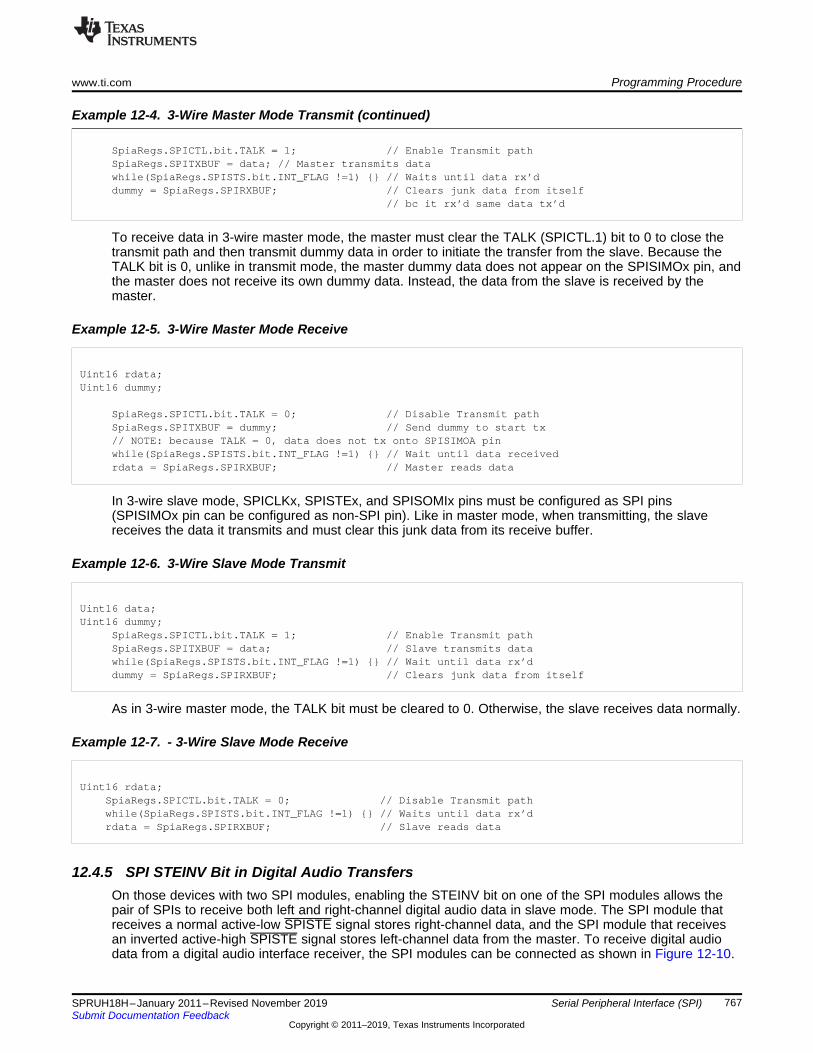
www.ti.com Programming Procedure
767SPRUH18H–January 2011–Revised November 2019Submit Documentation Feedback
Copyright © 2011–2019, Texas Instruments Incorporated
Serial Peripheral Interface (SPI)
Example 12-4. 3-Wire Master Mode Transmit (continued)
SpiaRegs.SPICTL.bit.TALK = 1; // Enable Transmit pathSpiaRegs.SPITXBUF = data; // Master transmits datawhile(SpiaRegs.SPISTS.bit.INT_FLAG !=1) {} // Waits until data rx’ddummy = SpiaRegs.SPIRXBUF; // Clears junk data from itself
// bc it rx’d same data tx’d
To receive data in 3-wire master mode, the master must clear the TALK (SPICTL.1) bit to 0 to close thetransmit path and then transmit dummy data in order to initiate the transfer from the slave. Because theTALK bit is 0, unlike in transmit mode, the master dummy data does not appear on the SPISIMOx pin, andthe master does not receive its own dummy data. Instead, the data from the slave is received by themaster.
Example 12-5. 3-Wire Master Mode Receive
Uint16 rdata;Uint16 dummy;
SpiaRegs.SPICTL.bit.TALK = 0; // Disable Transmit pathSpiaRegs.SPITXBUF = dummy; // Send dummy to start tx// NOTE: because TALK = 0, data does not tx onto SPISIMOA pinwhile(SpiaRegs.SPISTS.bit.INT_FLAG !=1) {} // Wait until data receivedrdata = SpiaRegs.SPIRXBUF; // Master reads data
In 3-wire slave mode, SPICLKx, SPISTEx, and SPISOMIx pins must be configured as SPI pins(SPISIMOx pin can be configured as non-SPI pin). Like in master mode, when transmitting, the slavereceives the data it transmits and must clear this junk data from its receive buffer.
Example 12-6. 3-Wire Slave Mode Transmit
Uint16 data;Uint16 dummy;
SpiaRegs.SPICTL.bit.TALK = 1; // Enable Transmit pathSpiaRegs.SPITXBUF = data; // Slave transmits datawhile(SpiaRegs.SPISTS.bit.INT_FLAG !=1) {} // Wait until data rx’ddummy = SpiaRegs.SPIRXBUF; // Clears junk data from itself
As in 3-wire master mode, the TALK bit must be cleared to 0. Otherwise, the slave receives data normally.
Example 12-7. - 3-Wire Slave Mode Receive
Uint16 rdata;SpiaRegs.SPICTL.bit.TALK = 0; // Disable Transmit pathwhile(SpiaRegs.SPISTS.bit.INT_FLAG !=1) {} // Waits until data rx’drdata = SpiaRegs.SPIRXBUF; // Slave reads data
12.4.5 SPI STEINV Bit in Digital Audio TransfersOn those devices with two SPI modules, enabling the STEINV bit on one of the SPI modules allows thepair of SPIs to receive both left and right-channel digital audio data in slave mode. The SPI module thatreceives a normal active-low SPISTE signal stores right-channel data, and the SPI module that receivesan inverted active-high SPISTE signal stores left-channel data from the master. To receive digital audiodata from a digital audio interface receiver, the SPI modules can be connected as shown in Figure 12-10.

L/R CLK
AUDIO BIT CLK
DATA OUT 0 n n-1 2 1 0 n n-1 2 01
1/fs
L-channel R-channel
SPI-B Receive ( invert)SPIx_STE SPI-A Receive (normal )SPIx_STE
SPIx_STE
SPIx_CLK
SPIx_SIMO
SPIB_STE
SPIB_SOMI
SPIB_SIMO
SPIB_CLK
SPI-BSPI-A
SPIA_CLK
SPIA_SIMO
SPIA_SOMI
SPIA_STE
AU
DIO
BIT
CLK
L/R
CLK
DA
TA
OU
T
DIGITALAUDIO
RECEiVER
Programming Procedure www.ti.com
768 SPRUH18H–January 2011–Revised November 2019Submit Documentation Feedback
Copyright © 2011–2019, Texas Instruments Incorporated
Serial Peripheral Interface (SPI)
NOTE: This configuration is only applicable to slave mode (MASTER_SLAVE = 0). When the SPI isconfigured as master (MASTER_SLAVE = 1), the STEINV bit will have no effect on theSPISTE pin.
Figure 12-10. SPI Digital Audio Receiver Configuration Using Two SPIs
Standard C28x SPI timing requirements limit the number of digital audio interface formats supported usingthe 2-SPI configuration with the STEINV bit. See your device-specific data sheet electrical specificationsfor SPI timing requirements. With the SPI clock phase configured such that the CLKPOLARITY bit is 0 andthe CLK_PHASE bit is 1 (data latched on rising edge of clock), standard right-justified digital audiointerface data format is supported as shown in Figure 12-11.
Figure 12-11. Standard Right-Justified Digital Audio Data Format

www.ti.com SPI Registers
769SPRUH18H–January 2011–Revised November 2019Submit Documentation Feedback
Copyright © 2011–2019, Texas Instruments Incorporated
Serial Peripheral Interface (SPI)
12.5 SPI RegistersThis section describes the Serial Peripheral Interface registers. It is important to note that the SPI registersonly allow 16-bit accesses.
12.5.1 SPI Base Addresses
Table 12-6. SPI Base Address TableBit Field Name
Base AddressInstance Structure
SpiaRegs SPI_REGS 0x0000_7040
SpibRegs SPI_REGS 0x0000_7740

SPI Registers www.ti.com
770 SPRUH18H–January 2011–Revised November 2019Submit Documentation Feedback
Copyright © 2011–2019, Texas Instruments Incorporated
Serial Peripheral Interface (SPI)
12.5.2 SPI_REGS RegistersTable 12-7 lists the SPI_REGS registers. All register offset addresses not listed in Table 12-7 should beconsidered as reserved locations and the register contents should not be modified.
Table 12-7. SPI_REGS Registers
Offset Acronym Register Name Write Protection Section0h SPICCR SPI Configuration Control Register Go1h SPICTL SPI Operation Control Register Go2h SPISTS SPI Status Register Go4h SPIBRR SPI Baud Rate Register Go6h SPIRXEMU SPI Emulation Buffer Register Go7h SPIRXBUF SPI Serial Input Buffer Register Go8h SPITXBUF SPI Serial Output Buffer Register Go9h SPIDAT SPI Serial Data Register GoAh SPIFFTX SPI FIFO Transmit Register GoBh SPIFFRX SPI FIFO Receive Register GoCh SPIFFCT SPI FIFO Control Register GoFh SPIPRI SPI Priority Control Register Go
Complex bit access types are encoded to fit into small table cells. Table 12-8 shows the codes that areused for access types in this section.
Table 12-8. SPI_REGS Access Type Codes
Access Type Code DescriptionRead TypeR R ReadRC R
CReadto Clear
Write TypeW W WriteW1C W
1CWrite1 to clear
Reset or Default Value-n Value after reset or the default
valueRegister Array Variablesi,j,k,l,m,n When these variables are used in
a register name, an offset, or anaddress, they refer to the value ofa register array where the registeris part of a group of repeatingregisters. The register groups forma hierarchical structure and thearray is represented with aformula.
y When this variable is used in aregister name, an offset, or anaddress it refers to the value of aregister array.

www.ti.com SPI Registers
771SPRUH18H–January 2011–Revised November 2019Submit Documentation Feedback
Copyright © 2011–2019, Texas Instruments Incorporated
Serial Peripheral Interface (SPI)
12.5.2.1 SPICCR Register (Offset = 0h) [reset = 0h]SPICCR is shown in Figure 12-12 and described in Table 12-9.
Return to the Summary Table.
SPICCR controls the setup of the SPI for operation.
Figure 12-12. SPICCR Register15 14 13 12 11 10 9 8
RESERVEDR-0h
7 6 5 4 3 2 1 0SPISWRESET CLKPOLARITY RESERVED SPILBK SPICHAR
R/W-0h R/W-0h R-0h R/W-0h R/W-0h
Table 12-9. SPICCR Register Field Descriptions
Bit Field Type Reset Description15-8 RESERVED R 0h Reserved
7 SPISWRESET R/W 0h SPI Software ResetWhen changing configuration, you should clear this bit before thechanges and set this bit before resuming operation.
Reset type: SYSRSn0h (R/W) = Initializes the SPI operating flags to the reset condition.Specifically, the RECEIVER OVERRUN Flag bit (SPISTS.7), theSPI INT FLAG bit (SPISTS.6), and the TXBUF FULL Flag bit(SPISTS.5) are cleared. SPISTE will become inactive. SPICLK willbe immediately driven to 0 regardless of the clock polarity. The SPIconfiguration remains unchanged.1h (R/W) = SPI is ready to transmit or receive the next character.When the SPI SW RESET bit is a 0, a character written to thetransmitter will not be shifted out when this bit is set. A newcharacter must be written to the serial data register. SPICLK will bereturned to its inactive state one SPICLK cycle after this bit is set.
6 CLKPOLARITY R/W 0h Shift Clock PolarityThis bit controls the polarity of the SPICLK signal. CLOCKPOLARITY and POLARITY CLOCK PHASE (SPICTL.3) control fourclocking schemes on the SPICLK pin.
Reset type: SYSRSn0h (R/W) = Data is output on rising edge and input on falling edge.When no SPI data is sent, SPICLK is at low level. The data inputand output edges depend on the value of the CLOCK PHASE bit(SPICTL.3) as follows:- CLOCK PHASE = 0: Data is output on the rising edge of theSPICLK signal. Input data is latched on the falling edge of theSPICLK signal.- CLOCK PHASE = 1: Data is output one half-cycle before the firstrising edge of the SPICLK signal and on subsequent falling edgesof the SPICLK signal. Input data is latched on the rising edge ofthe SPICLK signal.1h (R/W) = Data is output on falling edge and input on rising edge.When no SPI data is sent, SPICLK is at high level. The data inputand output edges depend on the value of the CLOCK PHASE bit(SPICTL.3) as follows:- CLOCK PHASE = 0: Data is output on the falling edge of theSPICLK signal. Input data is latched on the rising edge of theSPICLK signal.- CLOCK PHASE = 1: Data is output one half-cycle before the firstfalling edge of the SPICLK signal and on subsequent rising edgesof the SPICLK signal. Input data is latched on the falling edge ofthe SPICLK signal.
5 RESERVED R 0h Reserved

SPI Registers www.ti.com
772 SPRUH18H–January 2011–Revised November 2019Submit Documentation Feedback
Copyright © 2011–2019, Texas Instruments Incorporated
Serial Peripheral Interface (SPI)
Table 12-9. SPICCR Register Field Descriptions (continued)Bit Field Type Reset Description4 SPILBK R/W 0h SPI Loopback Mode Select
Loopback mode allows module validation during device testing. Thismode is valid only in master mode of the SPI.
Reset type: SYSRSn0h (R/W) = SPI loopback mode disabled. This is the default valueafter reset.1h (R/W) = SPI loopback mode enabled, SIMO/SOMI lines areconnected internally. Used for module self-tests.
3-0 SPICHAR R/W 0h Character Length Control BitsThese four bits determine the number of bits to be shifted in or SPICHAR0 out as a single character during one shift sequence.
SPICHAR = Word length - 1Reset type: SYSRSn0h (R/W) = 1-bit word1h (R/W) = 2-bit word2h (R/W) = 3-bit word3h (R/W) = 4-bit word4h (R/W) = 5-bit word5h (R/W) = 6-bit word6h (R/W) = 7-bit word7h (R/W) = 8-bit word8h (R/W) = 9-bit word9h (R/W) = 10-bit wordAh (R/W) = 11-bit wordBh (R/W) = 12-bit wordCh (R/W) = 13-bit wordDh (R/W) = 14-bit wordEh (R/W) = 15-bit wordFh (R/W) = 16-bit word

www.ti.com SPI Registers
773SPRUH18H–January 2011–Revised November 2019Submit Documentation Feedback
Copyright © 2011–2019, Texas Instruments Incorporated
Serial Peripheral Interface (SPI)
12.5.2.2 SPICTL Register (Offset = 1h) [reset = 0h]SPICTL is shown in Figure 12-13 and described in Table 12-10.
Return to the Summary Table.
SPICTL controls data transmission, the SPI's ability to generate interrupts, the SPICLK phase, and theoperational mode (slave or master).
Figure 12-13. SPICTL Register15 14 13 12 11 10 9 8
RESERVEDR-0h
7 6 5 4 3 2 1 0RESERVED OVERRUNINT
ENACLK_PHASE MASTER_SLA
VETALK SPIINTENA
R-0h R/W-0h R/W-0h R/W-0h R/W-0h R/W-0h
Table 12-10. SPICTL Register Field Descriptions
Bit Field Type Reset Description15-5 RESERVED R 0h Reserved
4 OVERRUNINTENA R/W 0h Overrun Interrupt EnableOverrun Interrupt Enable. Setting this bit causes an interrupt to begenerated when the RECEIVER OVERRUN Flag bit (SPISTS.7) isset by hardware. Interrupts generated by the RECEIVER OVERRUNFlag bit and the SPI INT FLAG bit (SPISTS.6) share the sameinterrupt vector.
Reset type: SYSRSn0h (R/W) = Disable RECEIVER OVERRUN interrupts.1h (R/W) = Enable RECEIVER_OVERRUN interrupts.
3 CLK_PHASE R/W 0h SPI Clock Phase SelectThis bit controls the phase of the SPICLK signal. CLOCK PHASEand CLOCK POLARITY (SPICCR.6) make four different clockingschemes possible (see clocking figures in SPI chapter). Whenoperating with CLOCK PHASE high, the SPI (master or slave)makes the first bit of data available after SPIDAT is written andbefore the first edge of the SPICLK signal, regardless of which SPImode is being used.
Reset type: SYSRSn0h (R/W) = Normal SPI clocking scheme, depending on theCLOCK POLARITY bit (SPICCR.6).1h (R/W) = SPICLK signal delayed by one half-cycle. Polaritydetermined by the CLOCK POLARITY bit.
2 MASTER_SLAVE R/W 0h SPI Network Mode ControlThis bit determines whether the SPI is a network master or slave.SLAVE During reset initialization, the SPI is automatically configuredas a network slave.
Reset type: SYSRSn0h (R/W) = SPI is configured as a slave.1h (R/W) = SPI is configured as a master.

SPI Registers www.ti.com
774 SPRUH18H–January 2011–Revised November 2019Submit Documentation Feedback
Copyright © 2011–2019, Texas Instruments Incorporated
Serial Peripheral Interface (SPI)
Table 12-10. SPICTL Register Field Descriptions (continued)Bit Field Type Reset Description1 TALK R/W 0h Transmit Enable
The TALK bit can disable data transmission (master or slave) byplacing the serial data output in the high-impedance state. If this bitis disabled during a transmission, the transmit shift registercontinues to operate until the previous character is shifted out. Whenthe TALK bit is disabled, the SPI is still able to receive charactersand update the status flags. TALK is cleared (disabled) by a systemreset.
Reset type: SYSRSn0h (R/W) = Disables transmission:- Slave mode operation: If not previously configured as a general-purpose I/O pin, the SPISOMI pin will be put in the high-impedancestate.- Master mode operation: If not previously configured as a general-purpose I/O pin, the SPISIMO pin will be put in the high-impedancestate.1h (R/W) = Enables transmission For the 4-pin option, ensure toenable the receiver's SPISTEn input pin.
0 SPIINTENA R/W 0h SPI Interrupt EnableThis bit controls the SPI's ability to generate a transmit/receiveinterrupt. The SPI INT FLAG bit (SPISTS.6) is unaffected by this bit.
Reset type: SYSRSn0h (R/W) = Disables the interrupt.1h (R/W) = Enables the interrupt.

www.ti.com SPI Registers
775SPRUH18H–January 2011–Revised November 2019Submit Documentation Feedback
Copyright © 2011–2019, Texas Instruments Incorporated
Serial Peripheral Interface (SPI)
12.5.2.3 SPISTS Register (Offset = 2h) [reset = 0h]SPISTS is shown in Figure 12-14 and described in Table 12-11.
Return to the Summary Table.
SPISTS contrains interrupt and status bits.
Figure 12-14. SPISTS Register15 14 13 12 11 10 9 8
RESERVEDR-0h
7 6 5 4 3 2 1 0OVERRUN_FL
AGINT_FLAG BUFFULL_FLA
GRESERVED
W1C-0h RC-0h R-0h R-0h
Table 12-11. SPISTS Register Field Descriptions
Bit Field Type Reset Description15-8 RESERVED R 0h Reserved
7 OVERRUN_FLAG W1C 0h SPI Receiver Overrun FlagThis bit is a read/clear-only flag. The SPI hardware sets this bit whena receive or transmit operation completes before the previouscharacter has been read from the buffer. The bit is cleared in one ofthree ways:- Writing a 1 to this bit- Writing a 0 to SPI SW RESET (SPICCR.7)- Resetting the systemIf the OVERRUN INT ENA bit (SPICTL.4) is set, the SPI requestsonly one interrupt upon the first occurrence of setting the RECEIVEROVERRUN Flag bit. Subsequent overruns will not request additionalinterrupts if this flag bit is already set. This means that in order toallow new overrun interrupt requests the user must clear this flag bitby writing a 1 to SPISTS.7 each time an overrun condition occurs. Inother words, if the RECEIVER OVERRUN Flag bit is left set (notcleared) by the interrupt service routine, another overrun interruptwill not be immediately re-entered when the interrupt service routineis exited.
Reset type: SYSRSn0h (R/W) = A receive overrun condition has not occurred.1h (R/W) = The last received character has been overwritten andtherefore lost (when the SPIRXBUF was overwritten by the SPImodule before the previous character was read by the userapplication).Writing a '1' will clear this bit. The RECEIVER OVERRUN Flag bitshould be cleared during the interrupt service routine because theRECEIVER OVERRUN Flag bit and SPI INT FLAG bit (SPISTS.6)share the same interrupt vector. This will alleviate any possibledoubt as to the source of the interrupt when the next byte isreceived.

SPI Registers www.ti.com
776 SPRUH18H–January 2011–Revised November 2019Submit Documentation Feedback
Copyright © 2011–2019, Texas Instruments Incorporated
Serial Peripheral Interface (SPI)
Table 12-11. SPISTS Register Field Descriptions (continued)Bit Field Type Reset Description6 INT_FLAG RC 0h SPI Interrupt Flag
SPI INT FLAG is a read-only flag. Hardware sets this bit to indicatethat the SPI has completed sending or receiving the last bit and isready to be serviced. This flag causes an interrupt to be requested ifthe SPI INT ENA bit (SPICTL.0) is set. The received character isplaced in the receiver buffer at the same time this bit is set. This bitis cleared in one of three ways:- Reading SPIRXBUF- Writing a 0 to SPI SW RESET (SPICCR.7)- Resetting the system
Note: This bit should not be used if FIFO mode is enabled. Theinternal process of copying the received word from SPIRXBUF to theReceive FIFO will clear this bit. Use the FIFO status, or FIFOinterrupt bits for similar functionality.
Reset type: SYSRSn0h (R/W) = No full words have been received or transmitted.1h (R/W) = Indicates that the SPI has completed sending orreceiving the last bit and is ready to be serviced.
5 BUFFULL_FLAG R 0h SPI Transmit Buffer Full FlagThis read-only bit gets set to 1 when a character is written to the SPITransmit buffer SPITXBUF. It is cleared when the character isautomatically loaded into SPIDAT when the shifting out of a previouscharacter is complete.
Reset type: SYSRSn0h (R/W) = Transmit buffer is not full.1h (R/W) = Transmit buffer is full.
4-0 RESERVED R 0h Reserved

www.ti.com SPI Registers
777SPRUH18H–January 2011–Revised November 2019Submit Documentation Feedback
Copyright © 2011–2019, Texas Instruments Incorporated
Serial Peripheral Interface (SPI)
12.5.2.4 SPIBRR Register (Offset = 4h) [reset = 0h]SPIBRR is shown in Figure 12-15 and described in Table 12-12.
Return to the Summary Table.
SPIBRR contains the bits used for baud-rate selection.
Figure 12-15. SPIBRR Register15 14 13 12 11 10 9 8
RESERVEDR-0h
7 6 5 4 3 2 1 0RESERVED SPI_BIT_RATE
R-0h R/W-0h
Table 12-12. SPIBRR Register Field Descriptions
Bit Field Type Reset Description15-7 RESERVED R 0h Reserved6-0 SPI_BIT_RATE R/W 0h SPI Baud Rate Control
These bits determine the bit transfer rate if the SPI is the networkSPI BIT RATE 0 master. There are 125 data-transfer rates (each afunction of the CPU clock, LSPCLK) that can be selected. One databit is shifted per SPICLK cycle. (SPICLK is the baud rate clockoutput on the SPICLK pin.)
If the SPI is a network slave, the module receives a clock on theSPICLK pin from the network master. Therefore, these bits have noeffect on the SPICLK signal. The frequency of the input clock fromthe master should not exceed the slave SPI's LSPCLK signal dividedby 4.
In master mode, the SPI clock is generated by the SPI and is outputon the SPICLK pin. The SPI baud rates are determined by thefollowing formula:For SPIBRR = 3 to 127: SPI Baud Rate = LSPCLK / (SPIBRR + 1)For SPIBRR = 0, 1, or 2: SPI Baud Rate = LSPCLK / 4
Reset type: SYSRSn3h (R/W) = SPI Baud Rate = LSPCLK/44h (R/W) = SPI Baud Rate = LSPCLK/57Eh (R/W) = SPI Baud Rate = LSPCLK/1277Fh (R/W) = SPI Baud Rate = LSPCLK/128

SPI Registers www.ti.com
778 SPRUH18H–January 2011–Revised November 2019Submit Documentation Feedback
Copyright © 2011–2019, Texas Instruments Incorporated
Serial Peripheral Interface (SPI)
12.5.2.5 SPIRXEMU Register (Offset = 6h) [reset = 0h]SPIRXEMU is shown in Figure 12-16 and described in Table 12-13.
Return to the Summary Table.
SPIRXEMU contains the received data. Reading SPIRXEMU does not clear the SPI INT FLAG bit ofSPISTS. This is not a real register but a dummy address from which the contents of SPIRXBUF can beread by the emulator without clearing the SPI INT FLAG.
Figure 12-16. SPIRXEMU Register15 14 13 12 11 10 9 8
ERXBnR-0h
7 6 5 4 3 2 1 0ERXBn
R-0h
Table 12-13. SPIRXEMU Register Field Descriptions
Bit Field Type Reset Description15-0 ERXBn R 0h Emulation Buffer Received Data
SPIRXEMU functions almost identically to SPIRXBUF, except thatreading SPIRXEMU does not clear the SPI INT FLAG bit(SPISTS.6). Once the SPIDAT has received the complete character,the character is transferred to SPIRXEMU and SPIRXBUF, where itcan be read. At the same time, SPI INT FLAG is set.
This mirror register was created to support emulation. ReadingSPIRXBUF clears the SPI INT FLAG bit (SPISTS.6). In the normaloperation of the emulator, the control registers are read tocontinually update the contents of these registers on the displayscreen. SPIRXEMU was created so that the emulator can read thisregister and properly update the contents on the display screen.Reading SPIRXEMU does not clear the SPI INT FLAG bit, butreading SPIRXBUF clears this flag. In other words, SPIRXEMUenables the emulator to emulate the true operation of the SPI moreaccurately.
It is recommended that you view SPIRXEMU in the normal emulatorrun mode.
Reset type: SYSRSn

www.ti.com SPI Registers
779SPRUH18H–January 2011–Revised November 2019Submit Documentation Feedback
Copyright © 2011–2019, Texas Instruments Incorporated
Serial Peripheral Interface (SPI)
12.5.2.6 SPIRXBUF Register (Offset = 7h) [reset = 0h]SPIRXBUF is shown in Figure 12-17 and described in Table 12-14.
Return to the Summary Table.
SPIRXBUF contains the received data. Reading SPIRXBUF clears the SPI INT FLAG bit in SPISTS. IfFIFO mode is enabled, reading this register will also decrement the RXFFST counter in SPIFFRX.
Figure 12-17. SPIRXBUF Register15 14 13 12 11 10 9 8
RXBnR-0h
7 6 5 4 3 2 1 0RXBnR-0h
Table 12-14. SPIRXBUF Register Field Descriptions
Bit Field Type Reset Description15-0 RXBn R 0h Received Data
Once SPIDAT has received the complete character, the character istransferred to SPIRXBUF, where it can be read. At the same time,the SPI INT FLAG bit (SPISTS.6) is set. Since data is shifted into theSPI's most significant bit first, it is stored right-justified in thisregister.
Reset type: SYSRSn

SPI Registers www.ti.com
780 SPRUH18H–January 2011–Revised November 2019Submit Documentation Feedback
Copyright © 2011–2019, Texas Instruments Incorporated
Serial Peripheral Interface (SPI)
12.5.2.7 SPITXBUF Register (Offset = 8h) [reset = 0h]SPITXBUF is shown in Figure 12-18 and described in Table 12-15.
Return to the Summary Table.
SPITXBUF stores the next character to be tranmitted. Writing to this register sets the TX BUF FULL Flagbit in SPISTS. When the transmission of the current character is complete, the contents of this register areautomatically loaded in SPIDAT and the TX BUF FULL Flag is cleared. If no tranmission is currentlyactive, data written to this register falls through into the SPIDAT register and the TX BUF FULL Flag is notset.In master mode, if no tranmission is currently active, writing to this register initiates a transmission in thesame manner that writing to SPIDAT does.
Figure 12-18. SPITXBUF Register15 14 13 12 11 10 9 8
TXBnR/W-0h
7 6 5 4 3 2 1 0TXBn
R/W-0h
Table 12-15. SPITXBUF Register Field Descriptions
Bit Field Type Reset Description15-0 TXBn R/W 0h Transmit Data Buffer
This is where the next character to be transmitted is stored. Whenthe transmission of the current character has completed, if the TXBUF FULL Flag bit is set, the contents of this register isautomatically transferred to SPIDAT, and the TX BUF FULL Flag iscleared. Writes to SPITXBUF must be left-justified.
Reset type: SYSRSn

www.ti.com SPI Registers
781SPRUH18H–January 2011–Revised November 2019Submit Documentation Feedback
Copyright © 2011–2019, Texas Instruments Incorporated
Serial Peripheral Interface (SPI)
12.5.2.8 SPIDAT Register (Offset = 9h) [reset = 0h]SPIDAT is shown in Figure 12-19 and described in Table 12-16.
Return to the Summary Table.
SPIDAT is the transmit and receive shift register. Data written to SPIDAT is shifted out (MSB) onsubsequent SPICLK cycles. For every bit (MSB) shifted out of the SPI, a bit is shifted into the LSB end ofthe shift register.
Figure 12-19. SPIDAT Register15 14 13 12 11 10 9 8
SDATnR/W-0h
7 6 5 4 3 2 1 0SDATnR/W-0h
Table 12-16. SPIDAT Register Field Descriptions
Bit Field Type Reset Description15-0 SDATn R/W 0h Serial Data Shift Register
- It provides data to be output on the serial output pin if the TALK bit(SPICTL.1) is set.- When the SPI is operating as a master, a data transfer is initiated.When initiating a transfer, check the CLOCK POLARITY bit(SPICCR.6) described in Section 10.2.1.1 and the CLOCK PHASEbit (SPICTL.3) described in Section 10.2.1.2, for the requirements.
In master mode, writing dummy data to SPIDAT initiates a receiversequence. Since the data is not hardware-justified for charactersshorter than sixteen bits, transmit data must be written in left-justifiedform, and received data read in right-justified form.
Reset type: SYSRSn

SPI Registers www.ti.com
782 SPRUH18H–January 2011–Revised November 2019Submit Documentation Feedback
Copyright © 2011–2019, Texas Instruments Incorporated
Serial Peripheral Interface (SPI)
12.5.2.9 SPIFFTX Register (Offset = Ah) [reset = A000h]SPIFFTX is shown in Figure 12-20 and described in Table 12-17.
Return to the Summary Table.
SPIFFTX contains both control and status bits related to the output FIFO buffer. This includes FIFO resetcontrol, FIFO interrupt level control, FIFO level status, as well as FIFO interrupt enable and clear bits.
Figure 12-20. SPIFFTX Register15 14 13 12 11 10 9 8
SPIRST SPIFFENA TXFIFO TXFFSTR/W-1h R/W-0h R/W-1h R-0h
7 6 5 4 3 2 1 0TXFFINT TXFFINTCLR TXFFIENA TXFFIL
R-0h W-0h R/W-0h R/W-0h
Table 12-17. SPIFFTX Register Field Descriptions
Bit Field Type Reset Description15 SPIRST R/W 1h SPI Reset
Reset type: SYSRSn0h (R/W) = Write 0 to reset the SPI transmit and receive channels.The SPI FIFO register configuration bits will be left as is.1h (R/W) = SPI FIFO can resume transmit or receive. No effect tothe SPI registers bits.
14 SPIFFENA R/W 0h SPI FIFO Enhancements EnableReset type: SYSRSn0h (R/W) = SPI FIFO enhancements are disabled.1h (R/W) = SPI FIFO enhancements are enabled.
13 TXFIFO R/W 1h TX FIFO ResetReset type: SYSRSn0h (R/W) = Write 0 to reset the FIFO pointer to zero, and hold inreset.1h (R/W) = Release transmit FIFO from reset.
12-8 TXFFST R 0h Transmit FIFO StatusReset type: SYSRSn0h (R/W) = Transmit FIFO is empty.1h (R/W) = Transmit FIFO has 1 word.2h (R/W) = Transmit FIFO has 2 words.3h (R/W) = Transmit FIFO has 3 words.4h (R/W) = Transmit FIFO has 4 words, which is the maximum.1Fh (R/W) = Reserved.
7 TXFFINT R 0h TX FIFO Interrupt FlagReset type: SYSRSn0h (R/W) = TXFIFO interrupt has not occurred, This is a read-onlybit.1h (R/W) = TXFIFO interrupt has occurred, This is a read-only bit.
6 TXFFINTCLR W 0h TXFIFO Interrupt ClearReset type: SYSRSn0h (R/W) = Write 0 has no effect on TXFIFINT flag bit, Bit readsback a zero.1h (R/W) = Write 1 to clear SPIFFTX[TXFFINT] flag.

www.ti.com SPI Registers
783SPRUH18H–January 2011–Revised November 2019Submit Documentation Feedback
Copyright © 2011–2019, Texas Instruments Incorporated
Serial Peripheral Interface (SPI)
Table 12-17. SPIFFTX Register Field Descriptions (continued)Bit Field Type Reset Description5 TXFFIENA R/W 0h TX FIFO Interrupt Enable
Reset type: SYSRSn0h (R/W) = TX FIFO interrupt based on TXFFIL match (less than orequal to) will be disabled.1h (R/W) = TX FIFO interrupt based on TXFFIL match (less than orequal to) will be enabled.
4-0 TXFFIL R/W 0h Transmit FIFO Interrupt Level BitsTransmit FIFO will generate interrupt when the FIFO status bits(TXFFST4-0) and FIFO level bits (TXFFIL4-0 ) match (less than orequal to).
Reset type: SYSRSn0h (R/W) = A TX FIFO interrupt request is generated when thereare no words remaining in the TX buffer.1h (R/W) = A TX FIFO interrupt request is generated when there is1 word or no words remaining in the TX buffer.2h (R/W) = A TX FIFO interrupt request is generated when there is2 words or fewer remaining in the TX buffer.3h (R/W) = A TX FIFO interrupt request is generated when thereare 3 words or fewer remaining in the TX buffer.4h (R/W) = A TX FIFO interrupt request is generated when thereare 4 words or fewer remaining in the TX buffer.1Fh (R/W) = Reserved.

SPI Registers www.ti.com
784 SPRUH18H–January 2011–Revised November 2019Submit Documentation Feedback
Copyright © 2011–2019, Texas Instruments Incorporated
Serial Peripheral Interface (SPI)
12.5.2.10 SPIFFRX Register (Offset = Bh) [reset = 201Fh]SPIFFRX is shown in Figure 12-21 and described in Table 12-18.
Return to the Summary Table.
SPIFFRX contains both control and status bits related to the input FIFO buffer. This includes FIFO resetcontrol, FIFO interrupt level control, FIFO level status, as well as FIFO interrupt enable and clear bits.
Figure 12-21. SPIFFRX Register15 14 13 12 11 10 9 8
RXFFOVF RXFFOVFCLR RXFIFORESET RXFFSTR-0h W-0h R/W-1h R-0h
7 6 5 4 3 2 1 0RXFFINT RXFFINTCLR RXFFIENA RXFFIL
R-0h W-0h R/W-0h R/W-1Fh
Table 12-18. SPIFFRX Register Field Descriptions
Bit Field Type Reset Description15 RXFFOVF R 0h Receive FIFO Overflow Flag
Reset type: SYSRSn0h (R/W) = Receive FIFO has not overflowed. This is a read-onlybit.1h (R/W) = Receive FIFO has overflowed, read-only bit. More than4 words have been received in to the FIFO, and the first receivedword is lost.
14 RXFFOVFCLR W 0h Receive FIFO Overflow ClearReset type: SYSRSn0h (R/W) = Write 0 does not affect RXFFOVF flag bit, Bit readsback a zero.1h (R/W) = Write 1 to clear SPIFFRX[RXFFOVF].
13 RXFIFORESET R/W 1h Receive FIFO ResetReset type: SYSRSn0h (R/W) = Write 0 to reset the FIFO pointer to zero, and hold inreset.1h (R/W) = Re-enable receive FIFO operation.
12-8 RXFFST R 0h Receive FIFO StatusReset type: SYSRSn0h (R/W) = Receive FIFO is empty.1h (R/W) = Receive FIFO has 1 word.2h (R/W) = Receive FIFO has 2 words.3h (R/W) = Receive FIFO has 3 words.4h (R/W) = Receive FIFO has 4 words, which is the maximum.1Fh (R/W) = Reserved.
7 RXFFINT R 0h Receive FIFO Interrupt FlagReset type: SYSRSn0h (R/W) = RXFIFO interrupt has not occurred. This is a read-onlybit.1h (R/W) = RXFIFO interrupt has occurred. This is a read-only bit.
6 RXFFINTCLR W 0h Receive FIFO Interrupt ClearReset type: SYSRSn0h (R/W) = Write 0 has no effect on RXFIFINT flag bit, Bit readsback a zero.1h (R/W) = Write 1 to clear SPIFFRX[RXFFINT] flag

www.ti.com SPI Registers
785SPRUH18H–January 2011–Revised November 2019Submit Documentation Feedback
Copyright © 2011–2019, Texas Instruments Incorporated
Serial Peripheral Interface (SPI)
Table 12-18. SPIFFRX Register Field Descriptions (continued)Bit Field Type Reset Description5 RXFFIENA R/W 0h RX FIFO Interrupt Enable
Reset type: SYSRSn0h (R/W) = RX FIFO interrupt based on RXFFIL match (greaterthan or equal to) will be disabled.1h (R/W) = RX FIFO interrupt based on RXFFIL match (greaterthan or equal to) will be enabled.
4-0 RXFFIL R/W 1Fh Receive FIFO Interrupt Level BitsReceive FIFO generates an interrupt when the FIFO status bits(RXFFST4-0) are greater than or equal to the FIFO level bits(RXFFIL4-0). The default value of these bits after reset is 11111.This avoids frequent interrupts after reset, as the receive FIFO willbe empty most of the time.
Reset type: SYSRSn0h (R/W) = A RX FIFO interrupt request is generated when there is0 or more words in the RX buffer.1h (R/W) = A RX FIFO interrupt request is generated when thereare 1 or more words in the RX buffer.2h (R/W) = A RX FIFO interrupt request is generated when thereare 2 or more words in the RX buffer.3h (R/W) = A RX FIFO interrupt request is generated when thereare 3 or more words in the RX buffer.4h (R/W) = A RX FIFO interrupt request is generated when thereare 4 words in the RX buffer.1Fh (R/W) = Reserved.

SPI Registers www.ti.com
786 SPRUH18H–January 2011–Revised November 2019Submit Documentation Feedback
Copyright © 2011–2019, Texas Instruments Incorporated
Serial Peripheral Interface (SPI)
12.5.2.11 SPIFFCT Register (Offset = Ch) [reset = 0h]SPIFFCT is shown in Figure 12-22 and described in Table 12-19.
Return to the Summary Table.
SPIFFCT controls the FIFO transmit delay bits.
Figure 12-22. SPIFFCT Register15 14 13 12 11 10 9 8
RESERVEDR-0h
7 6 5 4 3 2 1 0TXDLYR/W-0h
Table 12-19. SPIFFCT Register Field Descriptions
Bit Field Type Reset Description15-8 RESERVED R 0h Reserved7-0 TXDLY R/W 0h FIFO Transmit Delay Bits
These bits define the delay between every transfer from FIFOtransmit buffer to transmit shift register. The delay is defined innumber SPI serial clock cycles. The 8-bit register could define aminimum delay of 0 serial clock cycles and a maximum of 255 serialclock cycles. In FIFO mode, the buffer (TXBUF) between the shiftregister and the FIFO should be filled only after the shift register hascompleted shifting of the last bit. This is required to pass on thedelay between transfers to the data stream. In the FIFO modeTXBUF should not be treated as one additional level of buffer.
Reset type: SYSRSn0h (R/W) = The next word in the TX FIFO buffer is transferred toSPITXBUF immediately upon completion of transmission of theprevious word.1h (R/W) = The next word in the TX FIFO buffer is transferred toSPITXBUF1 serial clock cycle after completion of transmission ofthe previous word.2h (R/W) = The next word in the TX FIFO buffer is transferred toSPITXBUF 2 serial clock cycles after completion of transmission ofthe previous word.FFh (R/W) = The next word in the TX FIFO buffer is transferred toSPITXBUF 255 serial clock cycles after completion of transmissionof the previous word.
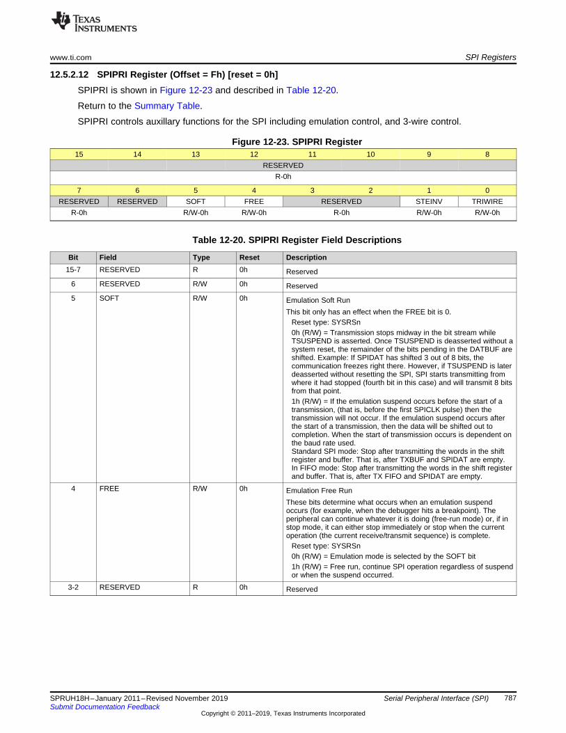
www.ti.com SPI Registers
787SPRUH18H–January 2011–Revised November 2019Submit Documentation Feedback
Copyright © 2011–2019, Texas Instruments Incorporated
Serial Peripheral Interface (SPI)
12.5.2.12 SPIPRI Register (Offset = Fh) [reset = 0h]SPIPRI is shown in Figure 12-23 and described in Table 12-20.
Return to the Summary Table.
SPIPRI controls auxillary functions for the SPI including emulation control, and 3-wire control.
Figure 12-23. SPIPRI Register15 14 13 12 11 10 9 8
RESERVEDR-0h
7 6 5 4 3 2 1 0RESERVED RESERVED SOFT FREE RESERVED STEINV TRIWIRE
R-0h R/W-0h R/W-0h R-0h R/W-0h R/W-0h
Table 12-20. SPIPRI Register Field Descriptions
Bit Field Type Reset Description15-7 RESERVED R 0h Reserved
6 RESERVED R/W 0h Reserved5 SOFT R/W 0h Emulation Soft Run
This bit only has an effect when the FREE bit is 0.Reset type: SYSRSn0h (R/W) = Transmission stops midway in the bit stream whileTSUSPEND is asserted. Once TSUSPEND is deasserted without asystem reset, the remainder of the bits pending in the DATBUF areshifted. Example: If SPIDAT has shifted 3 out of 8 bits, thecommunication freezes right there. However, if TSUSPEND is laterdeasserted without resetting the SPI, SPI starts transmitting fromwhere it had stopped (fourth bit in this case) and will transmit 8 bitsfrom that point.1h (R/W) = If the emulation suspend occurs before the start of atransmission, (that is, before the first SPICLK pulse) then thetransmission will not occur. If the emulation suspend occurs afterthe start of a transmission, then the data will be shifted out tocompletion. When the start of transmission occurs is dependent onthe baud rate used.Standard SPI mode: Stop after transmitting the words in the shiftregister and buffer. That is, after TXBUF and SPIDAT are empty.In FIFO mode: Stop after transmitting the words in the shift registerand buffer. That is, after TX FIFO and SPIDAT are empty.
4 FREE R/W 0h Emulation Free RunThese bits determine what occurs when an emulation suspendoccurs (for example, when the debugger hits a breakpoint). Theperipheral can continue whatever it is doing (free-run mode) or, if instop mode, it can either stop immediately or stop when the currentoperation (the current receive/transmit sequence) is complete.
Reset type: SYSRSn0h (R/W) = Emulation mode is selected by the SOFT bit1h (R/W) = Free run, continue SPI operation regardless of suspendor when the suspend occurred.
3-2 RESERVED R 0h Reserved

SPI Registers www.ti.com
788 SPRUH18H–January 2011–Revised November 2019Submit Documentation Feedback
Copyright © 2011–2019, Texas Instruments Incorporated
Serial Peripheral Interface (SPI)
Table 12-20. SPIPRI Register Field Descriptions (continued)Bit Field Type Reset Description1 STEINV R/W 0h SPISTEn Inversion Bit
On devices with 2 SPI modules, inverting the SPISTE signal on oneof the modules allows the device to receive left and right- channeldigital audio data.
This bit is only applicable to slave mode. Writing to this bit whileconfigured as master (MASTER_SLAVE = 1) has no effect
Reset type: SYSRSn0h (R/W) = SPISTEn is active low (normal)1h (R/W) = SPISTE is active high (inverted)
0 TRIWIRE R/W 0h SPI 3-wire Mode EnableReset type: SYSRSn0h (R/W) = Normal 4-wire SPI mode.1h (R/W) = 3-wire SPI mode enabled. The unused pin becomes aGPIO pin. In master mode, the SPISIMO pin becomes theSPIMOMI (master receive and transmit) pin and SPISOMI is freefor non-SPI use. In slave mode, the SPISOMI pin becomes theSPISISO (slave receive and transmit) pin and SPISIMO is free fornon-SPI use.

789SPRUH18H–January 2011–Revised November 2019Submit Documentation Feedback
Copyright © 2011–2019, Texas Instruments Incorporated
Serial Communications Interface (SCI)
Chapter 13SPRUH18H–January 2011–Revised November 2019
Serial Communications Interface (SCI)
This chapter describes the features and operation of the serial communication interface (SCI) module. SCIis a two−wire asynchronous serial port, commonly known as a UART. The SCI modules support digitalcommunications between the CPU and other asynchronous peripherals that use the standard non-return-to-zero (NRZ) format. The SCI receiver and transmitter each have a 4-level deep FIFO for reducingservicing overhead, and each has its own separate enable and interrupt bits. Both can be operatedindependently for half-duplex communication, or simultaneously for full-duplex communication.
To specify data integrity, the SCI checks received data for break detection, parity, overrun, and framingerrors. The bit rate is programmable to different speeds through a 16-bit baud-select register.
Topic ........................................................................................................................... Page
13.1 Introduction ..................................................................................................... 79013.2 Architecture ..................................................................................................... 79213.3 SCI Module Signal Summary.............................................................................. 79213.4 Configuring Device Pins.................................................................................... 79213.5 Multiprocessor and Asynchronous Communication Modes ................................... 79213.6 SCI Programmable Data Format ......................................................................... 79313.7 SCI Multiprocessor Communication.................................................................... 79313.8 Idle-Line Multiprocessor Mode ........................................................................... 79413.9 Address-Bit Multiprocessor Mode ...................................................................... 79613.10 SCI Communication Format.............................................................................. 79713.11 SCI Port Interrupts........................................................................................... 79913.12 SCI Baud Rate Calculations.............................................................................. 80013.13 SCI Enhanced Features.................................................................................... 80013.14 SCI Registers.................................................................................................. 803

SCITXD
SCIRXDSCI
Low Speed
Prescaler
PIE
LSPCLK SYSCLK
SYSRS
RXINT
TXINT
Pe
rip
he
ral
Bu
s
CPU
PCLKCR7
GPIO
MUX
Bit
Clock
Introduction www.ti.com
790 SPRUH18H–January 2011–Revised November 2019Submit Documentation Feedback
Copyright © 2011–2019, Texas Instruments Incorporated
Serial Communications Interface (SCI)
13.1 IntroductionThe SCI interfaces are shown in Figure 13-1.
Figure 13-1. SCI CPU Interface
Features of the SCI module include:• Two external pins:
– SCITXD: SCI transmit-output pin– SCIRXD: SCI receive-input pin
Both pins can be used as GPIO if not used for SCI.• Baud rate programmable to 64K different rates• Data-word format
– One start bit– Data-word length programmable from one to eight bits– Optional even/odd/no parity bit– One or two stop bits– An extra bit to distinguish addresses from data (address bit mode only)
• Four error-detection flags: parity, overrun, framing, and break detection• Two wake-up multiprocessor modes: idle-line and address bit• Half- or full-duplex operation• Double-buffered receive and transmit functions• Transmitter and receiver operations can be accomplished through interrupt-driven or polled algorithms
with status flags.• Separate enable bits for transmitter and receiver interrupts (except BRKDT)• NRZ (non-return-to-zero) format

TX FIFO _0
LSPCLK
WUT
Frame Format and Mode
Even/Odd EnableParity
SCI RX Interrupt select logic
BRKDT
RXRDY
SCIRXST.6
SCICTL1.3
8SCICTL2.1
RX/BK INT ENA
SCIRXD
SCIRXST.1
TXENA
SCI TX Interrupt select logic
TX EMPTY
TXRDY
SCICTL2.0
TX INT ENA
SCITXD
RXENA
SCIRXD
RXWAKE
SCICTL1.6
RX ERR INT ENA
TXWAKE
SCITXD
SCICCR.6 SCICCR.5
SCITXBUF.7-0
SCIHBAUD. 15 - 8
Baud RateMSbyteRegister
SCILBAUD. 7 - 0
Transmitter-DataBuffer Register
8 SCICTL2.6
SCICTL2.7
Baud RateLSbyte
Register
RXSHFRegister
TXSHFRegister
SCIRXST.5
1 TX FIFO _1
-----TX FIFO _3
8
TX FIFO registers
TX FIFO
TX Interrupt
Logic
TXINT
SCIFFTX.14
RX FIFO _0
SCIRXBUF.7-0
Receive Data
Buffer register
SCIRXBUF.7-0
-----RX FIFO_2
RX FIFO _3
8
RX FIFO registers
SCICTL1.0
RX Interrupt
Logic
RXINT
RX FIFO
SCIFFRX.15
RXFFOVF
RX Error
SCIRXST.7
PEFE OERX Error
SCIRXST.4 - 2
To CPU
To CPU
AutoBaud Detect logic
SCICTL1.1
SCIFFENA
Interrupts
Interrupts
www.ti.com Introduction
791SPRUH18H–January 2011–Revised November 2019Submit Documentation Feedback
Copyright © 2011–2019, Texas Instruments Incorporated
Serial Communications Interface (SCI)
Enhanced features include:• Auto-baud-detect hardware logic• 4-level transmit/receive FIFO
Figure 13-2 shows the SCI module block diagram. The SCI port operation is configured and controlled bythe registers listed in Section 13.14 of this chapter.
Figure 13-2. Serial Communications Interface (SCI) Module Block Diagram
Architecture www.ti.com
792 SPRUH18H–January 2011–Revised November 2019Submit Documentation Feedback
Copyright © 2011–2019, Texas Instruments Incorporated
Serial Communications Interface (SCI)
13.2 ArchitectureThe major elements used in full-duplex operation are shown in Figure 13-2 and include:• A transmitter (TX) and its major registers (upper half of Figure 13-2)
– SCITXBUF — transmitter data buffer register. Contains data (loaded by the CPU) to be transmitted– TXSHF register — transmitter shift register. Accepts data from register SCITXBUF and shifts data
onto the SCITXD pin, one bit at a time• A receiver (RX) and its major registers (lower half of Figure 13-2)
– RXSHF register — receiver shift register. Shifts data in from SCIRXD pin, one bit at a time– SCIRXBUF — receiver data buffer register. Contains data to be read by the CPU. Data from a
remote processor is loaded into register RXSHF and then into registers SCIRXBUF andSCIRXEMU
• A programmable baud generator• Control and status registers
The SCI receiver and transmitter can operate either independently or simultaneously.
13.3 SCI Module Signal SummaryA summarized description of each SCI signal name is shown in Table 13-1.
Table 13-1. SCI Module Signal Summary
Signal Name DescriptionExternal signals
SCIRXD SCI Asynchronous Serial Port receive dataSCITXD SCI Asynchronous Serial Port transmit data
ControlBaud clock LSPCLK Prescaled clock
Interrupt signalsTXINT Transmit interruptRXINT Receive Interrupt
13.4 Configuring Device PinsThe GPIO mux registers must be configured to connect this peripheral to the device pins. To avoidglitches on the pins, the GPyGMUX bits must be configured first (while keeping the correspondingGPyMUX bits at the default of zero), followed by writing the GPyMUX register to the desired value.
Some IO functionality is defined by GPIO register settings independent of this peripheral. For inputsignals, the GPIO input qualification should be set to asynchronous mode by setting the appropriateGPxQSELn register bits to 11b. The internal pullups can be configured in the GPyPUD register.
See the GPIO chapter for more details on GPIO mux and settings.
13.5 Multiprocessor and Asynchronous Communication ModesThe SCI has two multiprocessor protocols, the idle-line multiprocessor mode (see Section 13.8) and theaddress-bit multiprocessor mode (see Section 13.9). These protocols allow efficient data transfer betweenmultiple processors.
The SCI offers the universal asynchronous receiver/transmitter (UART) communications mode forinterfacing with many popular peripherals. The asynchronous mode (see Section 13.10) requires two linesto interface with many standard devices such as terminals and printers that use RS-232-C formats. Datatransmission characteristics include:• One start bit• One to eight data bits

Start LSB 2 3 Parity Stop4 5 6 7 MSB
Start LSB 2 3 Addr/data
Parity4 5 6 7 MSB Stop
Idle-line mode(Normal nonmultiprocessor communications)
Address-bit mode
Address bit
www.ti.com SCI Programmable Data Format
793SPRUH18H–January 2011–Revised November 2019Submit Documentation Feedback
Copyright © 2011–2019, Texas Instruments Incorporated
Serial Communications Interface (SCI)
• An even/odd parity bit or no parity bit• One or two stop bits
13.6 SCI Programmable Data FormatSCI data, both receive and transmit, is in NRZ (non-return-to-zero) format. The NRZ data format, shown inFigure 13-3, consists of:• One start bit• One to eight data bits• An even/odd parity bit (optional)• One or two stop bits• An extra bit to distinguish addresses from data (address-bit mode only)
The basic unit of data is called a character and is one to eight bits in length. Each character of data isformatted with a start bit, one or two stop bits, and optional parity and address bits. A character of datawith its formatting information is called a frame and is shown in Figure 13-3.
Figure 13-3. Typical SCI Data Frame Formats
To program the data format, use the SCICCR register. The bits used to program the data format areshown in Table 13-2.
Table 13-2. Programming the Data Format Using SCICCR
Bit(s) Bit Name Designation Functions2-0 SCI CHAR2-0 SCICCR.2:0 Select the character (data) length (one to eight bits).5 PARITY SCICCR.5 Enables the parity function if set to 1, or disables the parity function
ENABLE if cleared to 0.6 EVEN/ODD SCICCR.6 If parity is enabled, selects odd parity if cleared to 0 or even parity if
PARITY set to 1.7 STOP BITS SCICCR.7 Determines the number of stop bits transmitted—one stop bit if cleared to 0 or two
stop bits if set to 1.
13.7 SCI Multiprocessor CommunicationThe multiprocessor communication format allows one processor to efficiently send blocks of data to otherprocessors on the same serial link. On one serial line, there should be only one transfer at a time. In otherwords, there can be only one talker on a serial line at a time.
Address ByteThe first byte of a block of information that the talker sends contains an address byte that is read by alllisteners. Only listeners with the correct address can be interrupted by the data bytes that follow theaddress byte. The listeners with an incorrect address remain uninterrupted until the next address byte.

SCI Multiprocessor Communication www.ti.com
794 SPRUH18H–January 2011–Revised November 2019Submit Documentation Feedback
Copyright © 2011–2019, Texas Instruments Incorporated
Serial Communications Interface (SCI)
Sleep BitAll processors on the serial link set the SCI SLEEP bit (bit 2 of SCICTL1) to 1 so that they are interruptedonly when the address byte is detected. When a processor reads a block address that corresponds to theCPU device address as set by your application software, your program must clear the SLEEP bit to enablethe SCI to generate an interrupt on receipt of each data byte.
Although the receiver still operates when the SLEEP bit is 1, it does not set RXRDY, RXINT, or any of thereceiver error status bits to 1 unless the address byte is detected and the address bit in the receivedframe is a 1 (applicable to address-bit mode). The SCI does not alter the SLEEP bit; your software mustalter the SLEEP bit.
13.7.1 Recognizing the Address ByteA processor recognizes an address byte differently, depending on the multiprocessor mode used. Forexample:• The idle-line mode (Section 13.8) leaves a quiet space before the address byte. This mode does not
have an extra address/data bit and is more efficient than the address-bit mode for handling blocks thatcontain more than ten bytes of data. The idle-line mode should be used for typical non-multiprocessorSCI communication.
• The address-bit mode (Section 13.9) adds an extra bit (that is, an address bit) into every byte todistinguish addresses from data. This mode is more efficient in handling many small blocks of databecause, unlike the idle mode, it does not have to wait between blocks of data. However, at a hightransmit speed, the program is not fast enough to avoid a 10-bit idle in the transmission stream.
13.7.2 Controlling the SCI TX and RX FeaturesThe multiprocessor mode is software selectable via the ADDR/IDLE MODE bit (SCICCR, bit 3). Bothmodes use the TXWAKE flag bit (SCICTL1, bit 3), RXWAKE flag bit (SCIRXST, bit1), and the SLEEP flagbit (SCICTL1, bit 2) to control the SCI transmitter and receiver features of these modes.
13.7.3 Receipt SequenceIn both multiprocessor modes, the receive sequence is as follows:1. At the receipt of an address block, the SCI port wakes up and requests an interrupt (bit number 1
RX/BK INT ENA-of SCICTL2 must be enabled to request an interrupt). It reads the first frame of theblock, which contains the destination address.
2. A software routine is entered through the interrupt and checks the incoming address. This addressbyte is checked against its device address byte stored in memory.
3. If the check shows that the block is addressed to the device CPU, the CPU clears the SLEEP bit andreads the rest of the block. If not, the software routine exits with the SLEEP bit still set, and does notreceive interrupts until the next block start.
13.8 Idle-Line Multiprocessor ModeIn the idle-line multiprocessor protocol (ADDR/IDLE MODE bit=0), blocks are separated by having alonger idle time between the blocks than between frames in the blocks. An idle time of ten or more high-level bits after a frame indicates the start of a new block. The time of a single bit is calculated directly fromthe baud value (bits per second). The idle-line multiprocessor communication format is shown inFigure 13-4 (ADDR/IDLE MODE bit is bit 3 of SCICCR).

Address Data Last Data
First frame within block
Is address; it follows idle
period of 10 bits or more
Frame within
block
Idle period
less than 10
bits
Idle period
of 10 bits
or more
ÇÇÇ
ÇÇÇ
ÇÇÇ
ÇÇÇ
ÇÇÇ
ÇÇÇ
ÇÇÇ
ÇÇÇ
ÇÇÇ
ÇÇÇ
ÇÇÇ
ÇÇÇ
ÇÇ
ÇÇ
ÇÇ
ÇÇ
ÇÇ
ÇÇ
ÇÇ
ÇÇ
ÇÇ
ÇÇ
ÇÇ
ÇÇ
ÇÇ
ÇÇ
ÇÇ
ÇÇ
ÇÇ
ÇÇ
ÇÇ
ÇÇ
ÇÇ
ÇÇ
ÇÇ
ÇÇ
Several blocks of frames
Data format
(Pins SCIRXD, SCITXD)
Data format expanded
Idle periods of 10 bits or more
separate the blocks
Sta
rt
Sta
rt
Sta
rt
One block of frames
www.ti.com Idle-Line Multiprocessor Mode
795SPRUH18H–January 2011–Revised November 2019Submit Documentation Feedback
Copyright © 2011–2019, Texas Instruments Incorporated
Serial Communications Interface (SCI)
Figure 13-4. Idle-Line Multiprocessor Communication Format
13.8.1 Idle-Line Mode StepsThe steps followed by the idle-line mode:
Step 1. SCI wakes up after receipt of the block-start signal.Step 2. The processor recognizes the next SCI interrupt.Step 3. The interrupt service routine compares the received address (sent by a remote transmitter) to
its own.Step 4. If the CPU is being addressed, the service routine clears the SLEEP bit and receives the rest
of the data block.Step 5. If the CPU is not being addressed, the SLEEP bit remains set. This lets the CPU continue to
execute its main program without being interrupted by the SCI port until the next detection ofa block start.

TXWAKE
WUT
Transmit buffer (SCITXBUF)
TXSHF
1 8
Idle-Line Multiprocessor Mode www.ti.com
796 SPRUH18H–January 2011–Revised November 2019Submit Documentation Feedback
Copyright © 2011–2019, Texas Instruments Incorporated
Serial Communications Interface (SCI)
13.8.2 Block Start SignalThere are two ways to send a block-start signal:1. Method 1: Deliberately leave an idle time of ten bits or more by delaying the time between the
transmission of the last frame of data in the previous block and the transmission of the address frameof the new block.
2. Method 2: The SCI port first sets the TXWAKE bit (SCICTL1, bit 3) to 1 before writing to theSCITXBUF register. This sends an idle time of exactly 11 bits. In this method, the serialcommunications line is not idle any longer than necessary. (A don't care byte has to be written toSCITXBUF after setting TXWAKE, and before sending the address, so as to transmit the idle time.)
13.8.3 Wake-UP Temporary (WUT) FlagAssociated with the TXWAKE bit is the wake-up temporary (WUT) flag. WUT is an internal flag, double-buffered with TXWAKE. When TXSHF is loaded from SCITXBUF, WUT is loaded from TXWAKE, and theTXWAKE bit is cleared to 0. This arrangement is shown in Figure 13-5.
Figure 13-5. Double-Buffered WUT and TXSHF
13.8.3.1 Sending a Block Start SignalTo send out a block-start signal of exactly one frame time during a sequence of block transmissions:1. Write a 1 to the TXWAKE bit.2. Write a data word (content not important: a don’t care) to the SCITXBUF register (transmit data buffer)
to send a block-start signal. (The first data word written is suppressed while the block-start signal issent out and ignored after that.) When the TXSHF (transmit shift register) is free again, SCITXBUFcontents are shifted to TXSHF, the TXWAKE value is shifted to WUT, and then TXWAKE is cleared.Because TXWAKE was set to a 1, the start, data, and parity bits are replaced by an idle period of 11bits transmitted following the last stop bit of the previous frame.
3. Write a new address value to SCITXBUFA don’t-care data word must first be written to register SCITXBUF so that the TXWAKE bit value canbe shifted to WUT. After the don’t-care data word is shifted to the TXSHF register, the SCITXBUF (andTXWAKE if necessary) can be written to again because TXSHF and WUT are both double-buffered.
13.8.4 Receiver OperationThe receiver operates regardless of the SLEEP bit. However, the receiver neither sets RXRDY nor theerror status bits, nor does it request a receive interrupt until an address frame is detected.
13.9 Address-Bit Multiprocessor ModeIn the address-bit protocol (ADDR/IDLE MODE bit=1), frames have an extra bit called an address bit thatimmediately follows the last data bit. The address bit is set to 1 in the first frame of the block and to 0 in allother frames. The idle period timing is irrelevant (see Figure 13-6).
13.9.1 Sending an AddressThe TXWAKE bit value is placed in the address bit. During transmission, when the SCITXBUF registerand TXWAKE are loaded into the TXSHF register and WUT respectively, TXWAKE is reset to 0 and WUTbecomes the value of the address bit of the current frame. Thus, to send an address:1. Set the TXWAKE bit to 1 and write the appropriate address value to the SCITXBUF register.

MSB Parity
01Addr Data Addr
ÉÉ
ÉÉ
ÉÉ
ÉÉ
ÉÉ
ÉÉ
ÉÉ
ÉÉ
Data format
(Pins SCIRXD, SCITXD)
Data format expanded
First frame within
block is address
(Address bit is 1)
1
ÉÉ
ÉÉ
ÉÉ
ÉÉ
ÉÉÉ
ÉÉÉ
ÉÉÉ
ÉÉÉ
ÉÉÉ
ÉÉÉ
ÉÉÉ
ÉÉÉ
ÉÉ
ÉÉ
ÉÉ
ÉÉ
ÉÉÉ
ÉÉÉ
ÉÉÉ
ÉÉÉ
ÉÉÉ
ÉÉÉ
ÉÉÉ
ÉÉÉ
Idle time is of
no significance
Next frame is address
for next block
(Address bit is 1)
Start LSB Stop
Address-bit mode frame example
Address bit
Frame within block
(Address bit is 0)
1
Sta
rt
Sta
rt
Sta
rt
One block
Idle periods of no significance
Blocks of frames
www.ti.com SCI Communication Format
797SPRUH18H–January 2011–Revised November 2019Submit Documentation Feedback
Copyright © 2011–2019, Texas Instruments Incorporated
Serial Communications Interface (SCI)
When this address value is transferred to the TXSHF register and shifted out, its address bit is sent asa 1. This flags the other processors on the serial link to read the address.
2. Write to SCITXBUF and TXWAKE after TXSHF and WUT are loaded. (Can be written to immediatelysince both TXSHF and WUT are both double-buffered.
3. Leave the TXWAKE bit set to 0 to transmit non-address frames in the block.
NOTE: As a general rule, the address-bit format is typically used for data frames of 11 bytes or less.This format adds one bit value (1 for an address frame, 0 for a data frame) to all data bytestransmitted. The idle-line format is typically used for data frames of 12 bytes or more.
Figure 13-6. Address-Bit Multiprocessor Communication Format
13.10 SCI Communication FormatThe SCI asynchronous communication format uses either single line (one way) or two line (two way)communications. In this mode, the frame consists of a start bit, one to eight data bits, an optionaleven/odd parity bit, and one or two stop bits (shown in Figure 13-7). There are eight SCICLK periods perdata bit.
The receiver begins operation on receipt of a valid start bit. A valid start bit is identified by fourconsecutive internal SCICLK periods of zero bits as shown in Figure 13-7. If any bit is not zero, then theprocessor starts over and begins looking for another start bit.
For the bits following the start bit, the processor determines the bit value by making three samples in themiddle of the bits. These samples occur on the fourth, fifth, and sixth SCICLK periods, and bit-valuedetermination is on a majority (two out of three) basis. Figure 13-7 illustrates the asynchronouscommunication format for this with a start bit showing where a majority vote is taken.
Since the receiver synchronizes itself to frames, the external transmitting and receiving devices do nothave to use a synchronized serial clock. The clock can be generated locally.

RXENA
RXRDY
1 6
3 452
0 1 2 3 4 5 0 1 2Start Stop StartAd PaSCIRXD pin
Frame
Majority
vote
Start bit LSB of data
SCICLK
(internal)
SCIRXD
1 2 3 4 5 6 7 8 1 2 3 4 5 6 7 8 1
8 SCICLK periods per data bit 8 SCICLK periods per data bit
SCI Communication Format www.ti.com
798 SPRUH18H–January 2011–Revised November 2019Submit Documentation Feedback
Copyright © 2011–2019, Texas Instruments Incorporated
Serial Communications Interface (SCI)
Figure 13-7. SCI Asynchronous Communications Format
13.10.1 Receiver Signals in Communication ModesFigure 13-8 illustrates an example of receiver signal timing that assumes the following conditions:• Address-bit wake-up mode (address bit does not appear in idle-line mode)• Six bits per character
Figure 13-8. SCI RX Signals in Communication Modes
(1) Data arrives on the SCIRXD pin, start bit detected.(2) Bit RXENA is brought low to disable the receiver. Data continues to be assembled in RXSHF but is not
transferred to the receiver buffer register.
Notes:1. Flag bit RXENA (SCICTL1, bit 0) goes high to enable the receiver.2. Data arrives on the SCIRXD pin, start bit detected.3. Data is shifted from RXSHF to the receiver buffer register (SCIRXBUF); an interrupt is requested. Flag
bit RXRDY (SCIRXST, bit 6) goes high to signal that a new character has been received.4. The program reads SCIRXBUF; flag RXRDY is automatically cleared.5. The next byte of data arrives on the SCIRXD pin; the start bit is detected, then cleared.6. Bit RXENA is brought low to disable the receiver. Data continues to be assembled in RXSHF but is not
transferred to the receiver buffer register.
13.10.2 Transmitter Signals in Communication ModesFigure 13-9 illustrates an example of transmitter signal timing that assumes the following conditions:• Address-bit wake-up mode (address bit does not appear in idle-line mode)• Three bits per character

Ad
TXENA
SCITXD pin
1 6
3 4
5
2
0 1 2 0 1 2
TXRDY
TX EMPTY
7
Start Start StopStopAd PaPa
First Character Second Character
Frame Frame
www.ti.com SCI Port Interrupts
799SPRUH18H–January 2011–Revised November 2019Submit Documentation Feedback
Copyright © 2011–2019, Texas Instruments Incorporated
Serial Communications Interface (SCI)
Figure 13-9. SCI TX Signals in Communications Mode
Notes:1. Bit TXENA (SCICTL1, bit 1) goes high, enabling the transmitter to send data.2. SCITXBUF is written to; thus, (1) the transmitter is no longer empty, and (2) TXRDY goes low.3. The SCI transfers data to the shift register (TXSHF). The transmitter is ready for a second character
(TXRDY goes high), and it requests an interrupt (to enable an interrupt, bit TX INT ENA — SCICTL2,bit 0 — must be set).
4. The program writes a second character to SCITXBUF after TXRDY goes high (item 3). (TXRDY goeslow again after the second character is written to SCITXBUF.)
5. Transmission of the first character is complete. Transfer of the second character to shift registerTXSHF begins.
6. Bit TXENA goes low to disable the transmitter; the SCI finishes transmitting the current character.7. Transmission of the second character is complete; transmitter is empty and ready for new character.
13.11 SCI Port InterruptsThe SCI receiver and transmitter can be interrupt controlled. The SCICTL2 register has one flag bit(TXRDY) that indicates active interrupt conditions, and the SCIRXST register has two interrupt flag bits(RXRDY and BRKDT), plus the RX ERROR interrupt flag which is a logical OR of the FE, OE, BRKDT,and PE conditions. The transmitter and receiver have separate interrupt-enable bits. When not enabled,the interrupts are not asserted; however, the condition flags remain active, reflecting transmission andreceipt status.
The SCI has independent peripheral interrupt vectors for the receiver and transmitter. Peripheral interruptrequests can be either high priority or low priority. This is indicated by the priority bits which are outputfrom the peripheral to the PIE controller. When both RX and TX interrupt requests are made at the samepriority level, the receiver always has higher priority than the transmitter, reducing the possibility ofreceiver overrun.
The operation of peripheral interrupts is described in the peripheral interrupt expansion controller sectionof the External Peripheral Interface (ePIE) chapter.• If the RX/BK INT ENA bit (SCICTL2, bit 1) is set, the receiver peripheral interrupt request is asserted
when one of the following events occurs:– The SCI receives a complete frame and transfers the data in the RXSHF register to the SCIRXBUF
register. This action sets the RXRDY flag (SCIRXST, bit 6) and initiates an interrupt.– A break detect condition occurs (the SCIRXD is low for ten bit periods following a missing stop bit).
This action sets the BRKDT flag bit (SCIRXST, bit 5) and initiates an interrupt.• If the TX INT ENA bit (SCICTL2.0) is set, the transmitter peripheral interrupt request is asserted
whenever the data in the SCITXBUF register is transferred to the TXSHF register, indicating that theCPU can write to SCITXBUF; this action sets the TXRDY flag bit (SCICTL2, bit 7) and initiates aninterrupt.

SCI Baud Rate Calculations www.ti.com
800 SPRUH18H–January 2011–Revised November 2019Submit Documentation Feedback
Copyright © 2011–2019, Texas Instruments Incorporated
Serial Communications Interface (SCI)
NOTE: Interrupt generation due to the RXRDY and BRKDT bits is controlled by the RX/BK INT ENAbit (SCICTL2, bit 1). Interrupt generation due to the RX ERROR bit is controlled by the RXERR INT ENA bit (SCICTL1, bit 6).
13.12 SCI Baud Rate CalculationsThe internally generated serial clock is determined by the low-speed peripheral clock LSPCLK) and thebaud-select registers. The SCI uses the 16-bit value of the baud-select registers to select one of the 64Kdifferent serial clock rates possible for a given LSPCLK.
See the bit descriptions in the baud-select registers, for the formula to use when calculating the SCIasynchronous baud. Table 13-3 shows the baud-select values for common SCI bit rates.
Table 13-3. Asynchronous Baud Register Values for Common SCI Bit Rates
LSPCLK Clock Frequency, 100 MHzIdeal Baud BRR Actual Baud % Error
2400 5207 (1457h) 2400 04800 2603 (A2Bh) 4800 09600 1301 (515h) 9601 0.0119200 650 (28Ah) 19201 0.0138400 324 (144h) 38462 0.16
LSPCLK/16 is the maximum baud rate. For example, if LSPCLK is 100MHz, then the maximum baud rateis 6.25Mbps.
13.13 SCI Enhanced FeaturesThe 28x SCI features autobaud detection and transmit/receive FIFO. The following section explains theFIFO operation.
13.13.1 SCI FIFO DescriptionThe following steps explain the FIFO features and help with programming the SCI with FIFOs.1. Reset. At reset the SCI powers up in standard SCI mode and the FIFO function is disabled. The FIFO
registers SCIFFTX, SCIFFRX, and SCIFFCT remain inactive.2. Standard SCI. The standard SCI modes will work normally with TXINT/RXINT interrupts as the
interrupt source for the module.3. FIFO enable. FIFO mode is enabled by setting the SCIFFEN bit in the SCIFFTX register. SCIRST can
reset the FIFO mode at any stage of its operation.4. Active registers. All the SCI registers and SCI FIFO registers (SCIFFTX, SCIFFRX, and SCIFFCT) are
active.5. Interrupts. FIFO mode has two interrupts; one for transmit FIFO, TXINT and one for receive FIFO,
RXINT. RXINT is the common interrupt for SCI FIFO receive, receive error, and receive FIFO overflowconditions. The TXINT of the standard SCI will be disabled and this interrupt will service as SCItransmit FIFO interrupt.
6. Buffers. Transmit and receive buffers are supplemented with two 16-level FIFOs. The transmit FIFOregisters are 8 bits wide and receive FIFO registers are 10 bits wide. The one-word transmit buffer ofthe standard SCI functions as a transition buffer between the transmit FIFO and shift register. The one-word transmit buffer is loaded from the transmit FIFO only after the last bit of the shift register is shiftedout. With the FIFO enabled, TXSHF is directly loaded after an optional delay value (SCIFFCT), TXBUFis not used. When FIFO mode is enabled for SCI, characters written to SCITXBUF are queued in toSCI-TXFIFO and the characters received in SCI-RXFIFO can be read using SCIRXBUF.
7. Delayed transfer. The rate at which words in the FIFO are transferred to the transmit shift register isprogrammable. The SCIFFCT register bits (7−0) FFTXDLY7−FFTXDLY0 define the delay between theword transfer. The delay is defined in the number SCI baud clock cycles. The 8 bit register can define

RX FIFO 15
RX FIFO 0
RX BUF
RXSHF
TX FIFO 15
TX FIFO 0
TX
RX
16x8 bit FIFO
RXFFOVF flag
RXFFIL
RXERR flag
RXRDY/BRKDT
TXFFIL
1
0
RXINT
RXFFIENA
RXERRINTENA
RX/BKINTENA
TXFFIENA
TX BUF
TXSHF
SCIFFENA
TXRDY flag
TXINTENASCIFFENA0
1
TXINT
Auto-bauddetect logic
ABD bit
CDC bit
www.ti.com SCI Enhanced Features
801SPRUH18H–January 2011–Revised November 2019Submit Documentation Feedback
Copyright © 2011–2019, Texas Instruments Incorporated
Serial Communications Interface (SCI)
a minimum delay of 0 baud clock cycles and a maximum of 256-baud clock cycles. With zero delay,the SCI module can transmit data in continuous mode with the FIFO words shifting out back to back.With the 256 clock delay the SCI module can transmit data in a maximum delayed mode with the FIFOwords shifting out with a delay of 256 baud clocks between each words. The programmable delayfacilitates communication with slow SCI/UARTs with little CPU intervention.
8. FIFO status bits. Both the transmit and receive FIFOs have status bits TXFFST or RXFFST (bits 12−8)that define the number of words available in the FIFOs at any time. The transmit FIFO reset bitTXFIFO and receive reset bit RXFIFO reset the FIFO pointers to zero when these bits are cleared to 0.The FIFOs resumes operation from start once these bits are set to one.
9. Programmable interrupt levels. Both transmit and receive FIFO can generate CPU interrupts. Theinterrupt trigger is generated whenever the transmit FIFO status bits TXFFST (bits 12−8) match (lessthan or equal to) the interrupt trigger level bits TXFFIL (bits 4−0 ). This provides a programmableinterrupt trigger for transmit and receive sections of the SCI. Default value for these trigger level bitswill be 0x11111 for receive FIFO and 0x00000 for transmit FIFO, respectively.
Figure 13-10 and Table 13-4 explain the operation/configuration of SCI interrupts in nonFIFO/FFO mode.
Figure 13-10. SCI FIFO Interrupt Flags and Enable Logic
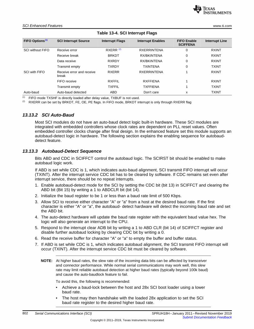
SCI Enhanced Features www.ti.com
802 SPRUH18H–January 2011–Revised November 2019Submit Documentation Feedback
Copyright © 2011–2019, Texas Instruments Incorporated
Serial Communications Interface (SCI)
(1) FIFO mode TXSHF is directly loaded after delay value, TXBUF is not used.(2) RXERR can be set by BRKDT, FE, OE, PE flags. In FIFO mode, BRKDT interrupt is only through RXERR flag
Table 13-4. SCI Interrupt Flags
FIFO Options (1) SCI Interrupt Source Interrupt Flags Interrupt Enables FIFO EnableSCIFFENA
Interrupt Line
SCI without FIFO Receive error RXERR (2) RXERRINTENA 0 RXINTReceive break BRKDT RX/BKINTENA 0 RXINTData receive RXRDY RX/BKINTENA 0 RXINTTransmit empty TXRDY TXINTENA 0 TXINT
SCI with FIFO Receive error and receivebreak
RXERR RXERRINTENA 1 RXINT
FIFO receive RXFFIL RXFFIENA 1 RXINTTransmit empty TXFFIL TXFFIENA 1 TXINT
Auto-baud Auto-baud detected ABD Don’t care x TXINT
13.13.2 SCI Auto-BaudMost SCI modules do not have an auto-baud detect logic built-in hardware. These SCI modules areintegrated with embedded controllers whose clock rates are dependent on PLL reset values. Oftenembedded controller clocks change after final design. In the enhanced feature set this module supports anautobaud-detect logic in hardware. The following section explains the enabling sequence for autobaud-detect feature.
13.13.3 Autobaud-Detect SequenceBits ABD and CDC in SCIFFCT control the autobaud logic. The SCIRST bit should be enabled to makeautobaud logic work.
If ABD is set while CDC is 1, which indicates auto-baud alignment, SCI transmit FIFO interrupt will occur(TXINT). After the interrupt service CDC bit has to be cleared by software. If CDC remains set even afterinterrupt service, there should be no repeat interrupts.1. Enable autobaud-detect mode for the SCI by setting the CDC bit (bit 13) in SCIFFCT and clearing the
ABD bit (Bit 15) by writing a 1 to ABDCLR bit (bit 14).2. Initialize the baud register to be 1 or less than a baud rate limit of 500 Kbps.3. Allow SCI to receive either character "A" or "a" from a host at the desired baud rate. If the first
character is either "A" or "a", the autobaud- detect hardware will detect the incoming baud rate and setthe ABD bit.
4. The auto-detect hardware will update the baud rate register with the equivalent baud value hex. Thelogic will also generate an interrupt to the CPU.
5. Respond to the interrupt clear ADB bit by writing a 1 to ABD CLR (bit 14) of SCIFFCT register anddisable further autobaud locking by clearing CDC bit by writing a 0.
6. Read the receive buffer for character "A" or "a" to empty the buffer and buffer status.7. If ABD is set while CDC is 1, which indicates autobaud alignment, the SCI transmit FIFO interrupt will
occur (TXINT). After the interrupt service CDC bit must be cleared by software.
NOTE: At higher baud rates, the slew rate of the incoming data bits can be affected by transceiverand connector performance. While normal serial communications may work well, this slewrate may limit reliable autobaud detection at higher baud rates (typically beyond 100k baud)and cause the auto-baudlock feature to fail.
To avoid this, the following is recommended:• Achieve a baud-lock between the host and 28x SCI boot loader using a lower
baud rate.• The host may then handshake with the loaded 28x application to set the SCI
baud rate register to the desired higher baud rate.

www.ti.com SCI Registers
803SPRUH18H–January 2011–Revised November 2019Submit Documentation Feedback
Copyright © 2011–2019, Texas Instruments Incorporated
Serial Communications Interface (SCI)
13.14 SCI RegistersThe section describes the Serial Communication Interface module Registers.
13.14.1 SCI Base Addresses
Table 13-5. SCI Base Address TableBit Field Name
Base AddressInstance Structure
SciaRegs SCI_REGS 0x0000_7050
ScibRegs SCI_REGS 0x0000_7750

SCI Registers www.ti.com
804 SPRUH18H–January 2011–Revised November 2019Submit Documentation Feedback
Copyright © 2011–2019, Texas Instruments Incorporated
Serial Communications Interface (SCI)
13.14.2 SCI_REGS RegistersTable 13-6 lists the SCI_REGS registers. All register offset addresses not listed in Table 13-6 should beconsidered as reserved locations and the register contents should not be modified.
Table 13-6. SCI_REGS Registers
Offset Acronym Register Name Write Protection Section0h SCICCR Communications control register Go1h SCICTL1 Control register 1 Go2h SCIHBAUD Baud rate (high) register Go3h SCILBAUD Baud rate (low) register Go4h SCICTL2 Control register 2 Go5h SCIRXST Receive status register Go6h SCIRXEMU Receive emulation buffer register Go7h SCIRXBUF Receive data buffer Go9h SCITXBUF Transmit data buffer GoAh SCIFFTX FIFO transmit register GoBh SCIFFRX FIFO receive register GoCh SCIFFCT FIFO control register GoFh SCIPRI SCI priority control Go
Complex bit access types are encoded to fit into small table cells. Table 13-7 shows the codes that areused for access types in this section.
Table 13-7. SCI_REGS Access Type Codes
Access Type Code DescriptionRead TypeR R ReadR-0 R
-0ReadReturns 0s
Write TypeW W WriteW1S W
1SWrite1 to set
Reset or Default Value-n Value after reset or the default
valueRegister Array Variablesi,j,k,l,m,n When these variables are used in
a register name, an offset, or anaddress, they refer to the value ofa register array where the registeris part of a group of repeatingregisters. The register groups forma hierarchical structure and thearray is represented with aformula.
y When this variable is used in aregister name, an offset, or anaddress it refers to the value of aregister array.

www.ti.com SCI Registers
805SPRUH18H–January 2011–Revised November 2019Submit Documentation Feedback
Copyright © 2011–2019, Texas Instruments Incorporated
Serial Communications Interface (SCI)
13.14.2.1 SCICCR Register (Offset = 0h) [reset = 0h]SCICCR is shown in Figure 13-11 and described in Table 13-8.
Return to the Summary Table.
SCICCR defines the character format, protocol, and communications mode used by the SCI.
Figure 13-11. SCICCR Register15 14 13 12 11 10 9 8
RESERVEDR-0h
7 6 5 4 3 2 1 0STOPBITS PARITY PARITYENA LOOPBKENA ADDRIDLE_M
ODESCICHAR
R/W-0h R/W-0h R/W-0h R/W-0h R/W-0h R/W-0h
Table 13-8. SCICCR Register Field Descriptions
Bit Field Type Reset Description15-8 RESERVED R 0h Reserved
7 STOPBITS R/W 0h SCI number of stop bits.This bit specifies the number of stop bits transmitted. The receiverchecks for only one stop bit.
Reset type: SYSRSn0h (R/W) = One stop bit1h (R/W) = Two stop bits
6 PARITY R/W 0h SCI parity odd/even selection.If the PARITY ENABLE bit (SCICCR, bit 5) is set, PARITY (bit 6)designates odd or even parity (odd or even number of bits with thevalue of 1 in both transmitted and received characters).
Reset type: SYSRSn0h (R/W) = Odd parity1h (R/W) = Even parity
5 PARITYENA R/W 0h SCI parity enable.This bit enables or disables the parity function. If the SCI is in theaddressbit multiprocessor mode (set using bit 3 of this register), theaddress bit is included in the parity calculation (if parity is enabled).For characters of less than eight bits, the remaining unused bitsshould be masked out of the parity calculation.
Reset type: SYSRSn0h (R/W) = Parity disabledno parity bit is generated during transmission or is expected duringreception1h (R/W) = Parity is enabled
4 LOOPBKENA R/W 0h Loop Back test mode enable.This bit enables the Loop Back test mode where the Tx pin isinternally connected to the Rx pin.
Reset type: SYSRSn0h (R/W) = Loop Back test mode disabled1h (R/W) = Loop Back test mode enabled

SCI Registers www.ti.com
806 SPRUH18H–January 2011–Revised November 2019Submit Documentation Feedback
Copyright © 2011–2019, Texas Instruments Incorporated
Serial Communications Interface (SCI)
Table 13-8. SCICCR Register Field Descriptions (continued)Bit Field Type Reset Description3 ADDRIDLE_MODE R/W 0h SCI multiprocessor mode control bit.
This bit selects one of the multiprocessor protocols.Multiprocessorcommunication is different from the other communication modesbecause it uses SLEEP and TXWAKE functions (bits SCICTL1, bit 2and SCICTL1, bit 3, respectively). The idle-line mode is usually usedfor normal communications because the address-bit modeadds an extra bit to the frame. The idle-line mode does not add thisextra bit and is compatible with RS-232 type communications.
Reset type: SYSRSn0h (R/W) = Idle-line mode protocol selected1h (R/W) = Address-bit mode protocol selected
2-0 SCICHAR R/W 0h Character-length control bits 2-0.
These bits select the SCI character length from one to eight bits.Characters of less than eight bits are right-justified in SCIRXBUFand SCIRXEMU and are padded with leading zeros in SCIRXBUF.SCITXBUF doesn't need to be padded with leading zeros.
Reset type: SYSRSn0h (R/W) = SCICHAR_LENGTH_11h (R/W) = SCICHAR_LENGTH_22h (R/W) = SCICHAR_LENGTH_33h (R/W) = SCICHAR_LENGTH_44h (R/W) = SCICHAR_LENGTH_55h (R/W) = SCICHAR_LENGTH_66h (R/W) = SCICHAR_LENGTH_77h (R/W) = SCICHAR_LENGTH_8

www.ti.com SCI Registers
807SPRUH18H–January 2011–Revised November 2019Submit Documentation Feedback
Copyright © 2011–2019, Texas Instruments Incorporated
Serial Communications Interface (SCI)
13.14.2.2 SCICTL1 Register (Offset = 1h) [reset = 0h]SCICTL1 is shown in Figure 13-12 and described in Table 13-9.
Return to the Summary Table.
SCICTL1 controls the receiver/transmitter enable, TXWAKE and SLEEP functions, and the SCI softwarereset.
Figure 13-12. SCICTL1 Register15 14 13 12 11 10 9 8
RESERVEDR-0h
7 6 5 4 3 2 1 0RESERVED RXERRINTEN
ASWRESET RESERVED TXWAKE SLEEP TXENA RXENA
R-0h R/W-0h R/W-0h R-0h R/W-0h R/W-0h R/W-0h R/W-0h
Table 13-9. SCICTL1 Register Field Descriptions
Bit Field Type Reset Description15-7 RESERVED R 0h Reserved
6 RXERRINTENA R/W 0h SCI receive error interrupt enable.Setting this bit enables an interrupt if the RX ERROR bit (SCIRXST,bit 7) becomes set because of errors occurring.
Reset type: SYSRSn0h (R/W) = Receive error interrupt disabled1h (R/W) = Receive error interrupt enabled
5 SWRESET R/W 0h SCI software reset (active low).Writing a 0 to this bit initializes the SCI state machines and operatingflags (registers SCICTL2 and SCIRXST) to the reset condition. TheSW RESET bit does not affect any of the configuration bits.All affected logic is held in the specified reset state until a 1 is writtento SW RESET (the bit values following a reset are shown beneatheach register diagram in this section). Thus, after a system reset, re-enable the SCI by writing a 1 to this bit. Clear this bit after a receiverbreak detect (BRKDT flag, bit SCIRXST, bit 5).
SW RESET affects the operating flags of the SCI, but it neitheraffects the configuration bits nor restores the reset values. Once SWRESET is asserted, the flags are frozen until the bit is deasserted.The affected flags are as follows:
Value After SW SCI Flag Register BitRESET1 TXRDY SCICTL2, bit 71 TX EMPTY SCICTL2, bit 60 RXWAKE SCIRXST, bit 10 PE SCIRXST, bit 20 OE SCIRXST, bit 30 FE SCIRXST, bit 40 BRKDT SCIRXST, bit 50 RXRDY SCIRXST, bit 60 RX ERROR SCIRXST, bit 7
Reset type: SYSRSn0h (R/W) = Writing a 0 to this bit initializes the SCI state machinesand operating flags (registers SCICTL2 and SCIRXST) to the resetcondition.1h (R/W) = After a system reset, re-enable the SCI by writing a 1to this bit.

SCI Registers www.ti.com
808 SPRUH18H–January 2011–Revised November 2019Submit Documentation Feedback
Copyright © 2011–2019, Texas Instruments Incorporated
Serial Communications Interface (SCI)
Table 13-9. SCICTL1 Register Field Descriptions (continued)Bit Field Type Reset Description4 RESERVED R 0h Reserved3 TXWAKE R/W 0h SCI transmitter wake-up method select.
The TXWAKE bit controls selection of the data-transmit feature,depending on which transmit mode (idle-line or address-bit) isspecified at the ADDR/IDLE MODE bit (SCICCR, bit 3)
Reset type: SYSRSn0h (R/W) = Transmit feature is not selected. In idle-line mode: writea 1 to TXWAKE, then write data to register SCITXBUF to generatean idle period of 11 data bits In address-bit mode: write a 1 toTXWAKE, then write data to SCITXBUF to set the address bit forthat frame to 11h (R/W) = Transmit feature selected is dependent on the mode,idle-line or address-bit: TXWAKE is not cleared by the SW RESETbit (SCICTL1, bit 5)it is cleared by a system reset or the transfer of TXWAKE to theWUT flag.
2 SLEEP R/W 0h SCI sleep.The TXWAKE bit controls selection of the data-transmit feature,depending on which transmit mode (idle-line or address-bit) isspecified at the ADDR/IDLE MODE bit (SCICCR, bit 3). In amultiprocessor configuration, this bit controls the receiver sleepfunction. Clearing this bit brings the SCI out of the sleep mode.
The receiver still operates when the SLEEP bit is sethowever, operation does not update the receiver buffer ready bit(SCIRXST, bit 6, RXRDY) or the error status bits (SCIRXST, bit 5-2:BRKDT, FE, OE, and PE) unless the address byte is detected.SLEEP is not cleared when the address byte is detected.
Reset type: SYSRSn0h (R/W) = Sleep mode disabled1h (R/W) = Sleep mode enabled
1 TXENA R/W 0h SCI transmitter enable.Data is transmitted through the SCITXD pin only when TXENA isset. If reset, transmission is halted but only after all data previouslywritten to SCITXBUF has been sent. Data written into SCITXBUFwhen TXENA is disabled will not be transmitted even if the TXENA isenabled later.
Reset type: SYSRSn0h (R/W) = Transmitter disabled1h (R/W) = Transmitter enabled
0 RXENA R/W 0h SCI receiver enable.Data is received on the SCIRXD pin and is sent to the receiver shiftregister and then the receiver buffers. This bit enables or disablesthe receiver (transfer to the buffers).Clearing RXENA stops received characters from being transferred tothe two receiver buffers and also stops the generation of receiverinterrupts. However, the receiver shift register can continue toassemble characters. Thus, if RXENA is set during the reception of acharacter, the complete character will be transferred into the receiverbuffer registers, SCIRXEMU and SCIRXBUF.
Reset type: SYSRSn0h (R/W) = Prevent received characters from transfer into theSCIRXEMU and SCIRXBUF receiver buffers1h (R/W) = Send received characters to SCIRXEMU andSCIRXBUF

www.ti.com SCI Registers
809SPRUH18H–January 2011–Revised November 2019Submit Documentation Feedback
Copyright © 2011–2019, Texas Instruments Incorporated
Serial Communications Interface (SCI)
13.14.2.3 SCIHBAUD Register (Offset = 2h) [reset = 0h]SCIHBAUD is shown in Figure 13-13 and described in Table 13-10.
Return to the Summary Table.
The values in SCIHBAUD and SCILBAUD specify the baud rate for the SCI.
Figure 13-13. SCIHBAUD Register15 14 13 12 11 10 9 8
RESERVEDR-0h
7 6 5 4 3 2 1 0BAUD
R/W-0h
Table 13-10. SCIHBAUD Register Field Descriptions
Bit Field Type Reset Description15-8 RESERVED R 0h Reserved7-0 BAUD R/W 0h SCI 16-bit baud selection Registers SCIHBAUD (MSbyte).
The internally-generated serial clock is determined by the low speedperipheral clock (LSPCLK) signal and the two baud-select registers.The SCI uses the 16-bit value of these registers to select one of 64Kserial clock rates for the communication modes.
BRR = (SCIHBAUD << 8) + (SCILBAUD)
The SCI baud rate is calculated using the following equation:
SCI Asynchronous Baud = LSPCLK / ((BRR + 1) *8)
Alternatively,
BRR = LSPCLK / (SCI Asynchronous Baud * 8) - 1
Note that the above formulas are applicable only when 0 < BRR <65536. If BRR = 0, then
SCI Asynchronous Baud = LSPCLK / 16
Where: BRR = the 16-bit value (in decimal) in the baud-selectregisters
Reset type: SYSRSn
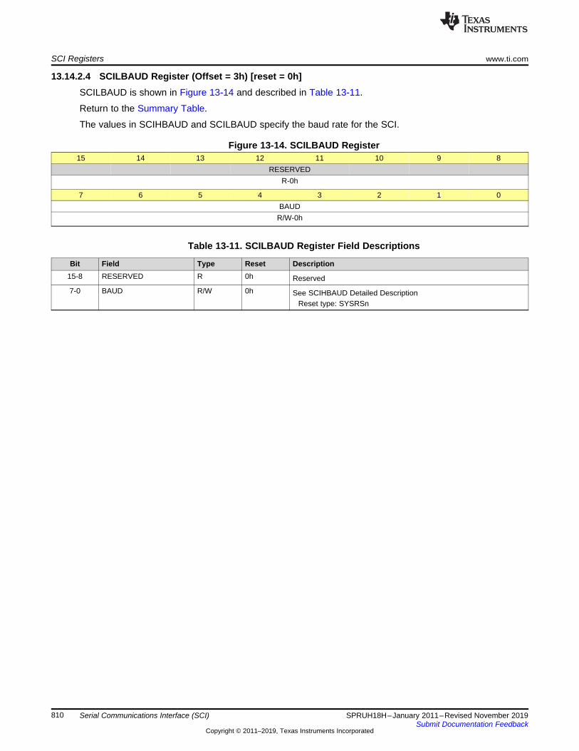
SCI Registers www.ti.com
810 SPRUH18H–January 2011–Revised November 2019Submit Documentation Feedback
Copyright © 2011–2019, Texas Instruments Incorporated
Serial Communications Interface (SCI)
13.14.2.4 SCILBAUD Register (Offset = 3h) [reset = 0h]SCILBAUD is shown in Figure 13-14 and described in Table 13-11.
Return to the Summary Table.
The values in SCIHBAUD and SCILBAUD specify the baud rate for the SCI.
Figure 13-14. SCILBAUD Register15 14 13 12 11 10 9 8
RESERVEDR-0h
7 6 5 4 3 2 1 0BAUD
R/W-0h
Table 13-11. SCILBAUD Register Field Descriptions
Bit Field Type Reset Description15-8 RESERVED R 0h Reserved7-0 BAUD R/W 0h See SCIHBAUD Detailed Description
Reset type: SYSRSn

www.ti.com SCI Registers
811SPRUH18H–January 2011–Revised November 2019Submit Documentation Feedback
Copyright © 2011–2019, Texas Instruments Incorporated
Serial Communications Interface (SCI)
13.14.2.5 SCICTL2 Register (Offset = 4h) [reset = C0h]SCICTL2 is shown in Figure 13-15 and described in Table 13-12.
Return to the Summary Table.
SCICTL2 enables the receive-ready, break-detect, and transmit-ready interrupts as well as transmitter-ready and -empty flags.
Figure 13-15. SCICTL2 Register15 14 13 12 11 10 9 8
RESERVEDR-0h
7 6 5 4 3 2 1 0TXRDY TXEMPTY RESERVED RXBKINTENA TXINTENA
R-1h R-1h R-0h R/W-0h R/W-0h
Table 13-12. SCICTL2 Register Field Descriptions
Bit Field Type Reset Description15-8 RESERVED R 0h Reserved
7 TXRDY R 1h Transmitter buffer register ready flag.When set, this bit indicates that the transmit data buffer register,SCITXBUF, is ready to receive another character. Writing data to theSCITXBUF automatically clears this bit. When set, this flag asserts atransmitter interrupt request if the interrupt-enable bit, TX INT ENA(SCICTL2.0), is also set. TXRDY is set to 1 by enabling the SWRESET bit (SCICTL1.5) or by a system reset.
Reset type: SYSRSn0h (R/W) = SCITXBUF is full1h (R/W) = SCITXBUF is ready to receive the next character
6 TXEMPTY R 1h Transmitter empty flag.This flag's value indicates the contents of the transmitter's bufferregister (SCITXBUF) and shift register (TXSHF). An active SWRESET (SCICTL1.5), or a system reset, sets this bit. This bit doesnot cause an interrupt request.
Reset type: SYSRSn0h (R/W) = Transmitter buffer or shift register or both are loadedwith data1h (R/W) = Transmitter buffer and shift registers are both empty
5-2 RESERVED R 0h Reserved1 RXBKINTENA R/W 0h Receiver-buffer/break interrupt enable.
This bit controls the interrupt request caused by either the RXRDYflag or the BRKDT flag (bits SCIRXST.6 and .5) being set. However,RX/BK INT ENA does not prevent the setting of these flags.
Reset type: SYSRSn0h (R/W) = Disable RXRDY/BRKDT interrupt1h (R/W) = Enable RXRDY/BRKDT interrupt

SCI Registers www.ti.com
812 SPRUH18H–January 2011–Revised November 2019Submit Documentation Feedback
Copyright © 2011–2019, Texas Instruments Incorporated
Serial Communications Interface (SCI)
Table 13-12. SCICTL2 Register Field Descriptions (continued)Bit Field Type Reset Description0 TXINTENA R/W 0h SCITXBUF-register interrupt enable.
This bit controls the interrupt request caused by the setting ofTXRDY flag bit (SCICTL2.7). However, it does not prevent theTXRDY flag from being set (which indicates SCITXBUF is ready toreceive another character).
0 Disable TXRDY interrupt1 Enable TXRDY interrupt.
In non-FIFO mode, a dummy (or a valid) data has to be written toSCITXBUF for the first transmit interrupt to occur. This is the casewhen you enable the transmit interrupt for the first time and alsowhen you re-enable (disable and then enable) the transmit interrupt.If TXINTENA is enabled after writing the data to SCITXBUF, it willnot generate an interrupt.
Reset type: SYSRSn0h (R/W) = Disable TXRDY interrupt1h (R/W) = Enable TXRDY interrupt

www.ti.com SCI Registers
813SPRUH18H–January 2011–Revised November 2019Submit Documentation Feedback
Copyright © 2011–2019, Texas Instruments Incorporated
Serial Communications Interface (SCI)
13.14.2.6 SCIRXST Register (Offset = 5h) [reset = 0h]SCIRXST is shown in Figure 13-16 and described in Table 13-13.
Return to the Summary Table.
SCIRXST contains seven bits that are receiver status flags (two of which can generate interrupt requests).Each time a complete character is transferred to the receiver buffers (SCIRXEMU and SCIRXBUF), thestatus flags are updated.
Figure 13-16. SCIRXST Register15 14 13 12 11 10 9 8
RESERVEDR-0h
7 6 5 4 3 2 1 0RXERROR RXRDY BRKDT FE OE PE RXWAKE RESERVED
R-0h R-0h R-0h R-0h R-0h R-0h R-0h R-0h
Table 13-13. SCIRXST Register Field Descriptions
Bit Field Type Reset Description15-8 RESERVED R 0h Reserved
7 RXERROR R 0h SCI receiver error flag.The RX ERROR flag indicates that one of the error flags in thereceiver status register is set. RX ERROR is a logical OR of thebreak detect, framing error, overrun, and parity error enable flags(bits 5-2: BRKDT, FE, OE, and PE).A 1 on this bit will cause an interrupt if the RX ERR INT ENA bit(SCICTL1.6) is set. This bit can be used for fast error-conditionchecking during the interrupt service routine. This error flag cannotbe cleared directlyit is cleared by an active SW RESET or by a system reset.
Reset type: SYSRSn0h (R/W) = No error flags set1h (R/W) = Error flag(s) set
6 RXRDY R 0h SCI receiver-ready flag.When a new character is ready to be read from the SCIRXBUFregister, the receiver sets this bit, and a receiver interrupt isgenerated if the RX/BK INT ENA bit (SCICTL2.1) is a 1. RXRDY iscleared by a reading of the SCIRXBUF register, by an active SWRESET, or by a system reset.
Reset type: SYSRSn0h (R/W) = No new character in SCIRXBUF1h (R/W) = Character ready to be read from SCIRXBUF
5 BRKDT R 0h SCI break-detect flag.The SCI sets this bit when a break condition occurs. A breakconditionoccurs when the SCI receiver data line (SCIRXD) remainscontinuously low for at least ten bits,beginning after a missing first stop bit. The occurrence of a breakcauses a receiver interrupt to be generated if the RX/BK INT ENA bitis a 1, but it does not cause the receiver buffer to be loaded. ABRKDT interrupt can occur even if the receiver SLEEP bit is set to 1.BRKDT is cleared by an active SW RESET or by a system reset. Itis not cleared by receipt of a character after the break is detected. Inorder to receive more characters, the SCI must be reset by togglingthe SW RESET bit or by a system reset.
Reset type: SYSRSn0h (R/W) = No break condition1h (R/W) = Break condition occurred

SCI Registers www.ti.com
814 SPRUH18H–January 2011–Revised November 2019Submit Documentation Feedback
Copyright © 2011–2019, Texas Instruments Incorporated
Serial Communications Interface (SCI)
Table 13-13. SCIRXST Register Field Descriptions (continued)Bit Field Type Reset Description4 FE R 0h SCI framing-error flag.
The SCI sets this bit when an expected stop bit is not found. Onlythe first stop bit is checked. The missing stop bit indicates thatsynchronization with the start bit has been lost and that the characteris incorrectly framed. The FE bit is reset by a clearing of the SWRESET bit or by a system reset.
Reset type: SYSRSn0h (R/W) = No framing error detected1h (R/W) = Framing error detected
3 OE R 0h SCI overrun-error flag.The SCI sets this bit when a character is transferred into registersSCIRXEMU and SCIRXBUF before the previous character is fullyread by the CPU or DMAC. The previous character is overwrittenand lost. The OE flag bit is reset by an active SW RESET or by asystem reset.
Reset type: SYSRSn0h (R/W) = No overrun error detected1h (R/W) = Overrun error detected
2 PE R 0h SCI parity-error flag.This flag bit is set when a character is received with a mismatchbetween the number of 1s and its parity bit. The address bit isincluded in the calculation. If parity generation and detection is notenabled, the PE flag is disabled and read as 0. The PE bit is resetby an active SW RESET or a system reset.
Reset type: SYSRSn0h (R/W) = No parity error or parity is disabled1h (R/W) = Parity error is detected
1 RXWAKE R 0h Receiver wake-up-detect flagReset type: SYSRSn0h (R/W) = No detection of a receiver wake-up condition1h (R/W) = A value of 1 in this bit indicates detection of a receiverwake-up condition. In the address-bit multiprocessor mode(SCICCR.3 = 1), RXWAKE reflects the value of the address bit forthe character contained in SCIRXBUF. In the idle-linemultiprocessor mode, RXWAKE is set if the SCIRXD data line isdetected as idle. RXWAKE is a read-only flag, cleared by one ofthe following:- The transfer of the first byte after the address byte to SCIRXBUF(only in non-FIFO mode)- The reading of SCIRXBUF- An active SW RESET- A system reset
0 RESERVED R 0h Reserved
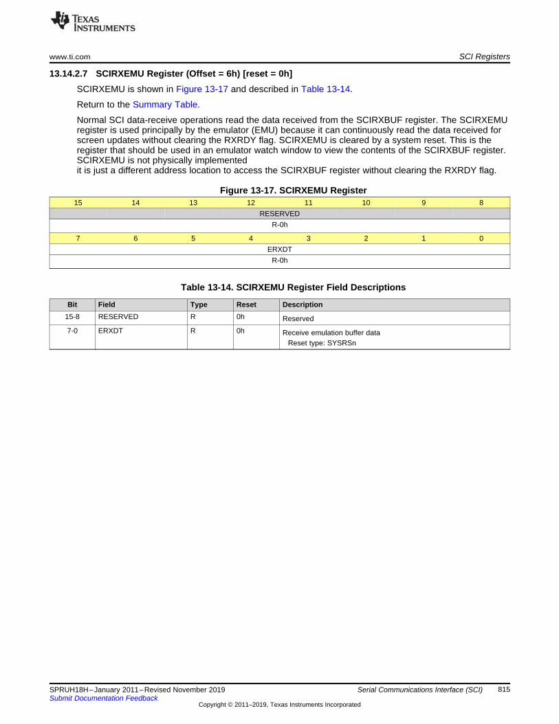
www.ti.com SCI Registers
815SPRUH18H–January 2011–Revised November 2019Submit Documentation Feedback
Copyright © 2011–2019, Texas Instruments Incorporated
Serial Communications Interface (SCI)
13.14.2.7 SCIRXEMU Register (Offset = 6h) [reset = 0h]SCIRXEMU is shown in Figure 13-17 and described in Table 13-14.
Return to the Summary Table.
Normal SCI data-receive operations read the data received from the SCIRXBUF register. The SCIRXEMUregister is used principally by the emulator (EMU) because it can continuously read the data received forscreen updates without clearing the RXRDY flag. SCIRXEMU is cleared by a system reset. This is theregister that should be used in an emulator watch window to view the contents of the SCIRXBUF register.SCIRXEMU is not physically implementedit is just a different address location to access the SCIRXBUF register without clearing the RXRDY flag.
Figure 13-17. SCIRXEMU Register15 14 13 12 11 10 9 8
RESERVEDR-0h
7 6 5 4 3 2 1 0ERXDT
R-0h
Table 13-14. SCIRXEMU Register Field Descriptions
Bit Field Type Reset Description15-8 RESERVED R 0h Reserved7-0 ERXDT R 0h Receive emulation buffer data
Reset type: SYSRSn

SCI Registers www.ti.com
816 SPRUH18H–January 2011–Revised November 2019Submit Documentation Feedback
Copyright © 2011–2019, Texas Instruments Incorporated
Serial Communications Interface (SCI)
13.14.2.8 SCIRXBUF Register (Offset = 7h) [reset = 0h]SCIRXBUF is shown in Figure 13-18 and described in Table 13-15.
Return to the Summary Table.
When the current data received is shifted from RXSHF to the receiver buffer, flag bit RXRDY is set andthe data is ready to be read. If the RXBKINTENA bit (SCICTL2.1) is set, this shift also causes an interrupt.When SCIRXBUF is read, the RXRDY flag is reset. SCIRXBUF is cleared by a system reset.
Figure 13-18. SCIRXBUF Register15 14 13 12 11 10 9 8
SCIFFFE SCIFFPE RESERVEDR-0h R-0h R-0h
7 6 5 4 3 2 1 0SARR-0h
Table 13-15. SCIRXBUF Register Field Descriptions
Bit Field Type Reset Description15 SCIFFFE R 0h SCIFFFE. SCI FIFO Framing error flag bit (applicable only if the
FIFO is enabled)Reset type: SYSRSn0h (R/W) = No frame error occurred while receiving the character,in bits 7-0. This bit is associated with the character on the top ofthe FIFO.1h (R/W) = A frame error occurred while receiving the character inbits 7-0. This bit is associated with the character on the top of theFIFO.
14 SCIFFPE R 0h SCIFFPE. SCI FIFO parity error flag bit (applicable only if the FIFOis enabled)
Reset type: SYSRSn0h (R/W) = No parity error occurred while receiving the character,in bits 7-0. This bit is associated with the character on the top ofthe FIFO.1h (R/W) = A parity error occurred while receiving the character inbits 7-0. This bit is associated with the character on the top of theFIFO.
13-8 RESERVED R 0h Reserved7-0 SAR R 0h Receive Character bits
Reset type: SYSRSn

www.ti.com SCI Registers
817SPRUH18H–January 2011–Revised November 2019Submit Documentation Feedback
Copyright © 2011–2019, Texas Instruments Incorporated
Serial Communications Interface (SCI)
13.14.2.9 SCITXBUF Register (Offset = 9h) [reset = 0h]SCITXBUF is shown in Figure 13-19 and described in Table 13-16.
Return to the Summary Table.
Data bits to be transmitted are written to SCITXBUF. These bits must be rightjustified because theleftmost bits are ignored for characters less than eight bits long. The transfer of data from this register tothe TXSHF transmitter shift register sets the TXRDY flag (SCICTL2.7), indicating that SCITXBUF is readyto receive another set of data. If bit TXINTENA (SCICTL2.0) is set, this data transfer also causes aninterrupt.
Figure 13-19. SCITXBUF Register15 14 13 12 11 10 9 8
RESERVEDR-0h
7 6 5 4 3 2 1 0TXDT
R/W-0h
Table 13-16. SCITXBUF Register Field Descriptions
Bit Field Type Reset Description15-8 RESERVED R 0h Reserved7-0 TXDT R/W 0h Transmit data buffer
Reset type: SYSRSn

SCI Registers www.ti.com
818 SPRUH18H–January 2011–Revised November 2019Submit Documentation Feedback
Copyright © 2011–2019, Texas Instruments Incorporated
Serial Communications Interface (SCI)
13.14.2.10 SCIFFTX Register (Offset = Ah) [reset = A000h]SCIFFTX is shown in Figure 13-20 and described in Table 13-17.
Return to the Summary Table.
SCIFFTX controls the transmit FIFO interrupt, FIFO enhancements, and reset for the SCI transmit andreceive channels.
Figure 13-20. SCIFFTX Register15 14 13 12 11 10 9 8
SCIRST SCIFFENA TXFIFORESET TXFFSTR/W-1h R/W-0h R/W-1h R-0h
7 6 5 4 3 2 1 0TXFFINT TXFFINTCLR TXFFIENA TXFFIL
R-0h R-0/W1S-0h R/W-0h R/W-0h
Table 13-17. SCIFFTX Register Field Descriptions
Bit Field Type Reset Description15 SCIRST R/W 1h SCI Reset
0 Write 0 to reset the SCI transmit and receive channels. SCI FIFOregister configuration bits will be left as is.1 SCI FIFO can resume transmit or receive. SCIRST should be 1even for Autobaud logic to work.
Reset type: SYSRSn14 SCIFFENA R/W 0h SCI FIFO enable
Reset type: SYSRSn0h (R/W) = SCI FIFO enhancements are disabled1h (R/W) = SCI FIFO enhancements are enabled
13 TXFIFORESET R/W 1h Transmit FIFO resetReset type: SYSRSn0h (R/W) = Reset the FIFO pointer to zero and hold in reset1h (R/W) = Re-enable transmit FIFO operation
12-8 TXFFST R 0h FIFO statusReset type: SYSRSn0h (R/W) = Transmit FIFO is empty1h (R/W) = Transmit FIFO has 1 words2h (R/W) = Transmit FIFO has 2 words3h (R/W) = Transmit FIFO has 3 words4h (R/W) = Transmit FIFO has 4 words
7 TXFFINT R 0h Transmit FIFO interruptReset type: SYSRSn0h (R/W) = TXFIFO interrupt has not occurred, read-only bit1h (R/W) = TXFIFO interrupt has occurred, read-only bit
6 TXFFINTCLR R-0/W1S 0h Transmit FIFO clearReset type: SYSRSn0h (R/W) = Write 0 has no effect on TXFIFINT flag bit, Bit readsback a zero1h (R/W) = Write 1 to clear TXFFINT flag in bit 7
5 TXFFIENA R/W 0h Transmit FIFO interrrupt enableReset type: SYSRSn0h (R/W) = TX FIFO interrupt is disabled1h (R/W) = TX FIFO interrupt is enabled. This interrupt is triggeredwhenever the transmit FIFO status (TXFFST) bits match (equal toor less than) the interrupt trigger level bits TXFFIL (bits 4-0).

www.ti.com SCI Registers
819SPRUH18H–January 2011–Revised November 2019Submit Documentation Feedback
Copyright © 2011–2019, Texas Instruments Incorporated
Serial Communications Interface (SCI)
Table 13-17. SCIFFTX Register Field Descriptions (continued)Bit Field Type Reset Description4-0 TXFFIL R/W 0h TXFFIL4-0 Transmit FIFO interrupt level bits.
The transmit FIFO generates an interrupt whenever the FIFO statusbits (TXFFST4-0) are less than or equal to the FIFO level bits(TXFFIL4-0). The maximum value that can be assigned to these bitsto generate an interrupt cannot be more than the depth of the TXFIFO. The default value of these bits after reset is 00000b. Usersshould set TXFFIL to best fit their application needs by weighingbetween the CPU overhead to service the ISR and the best possibleusage of SCI bus bandwidth.
Reset type: SYSRSn
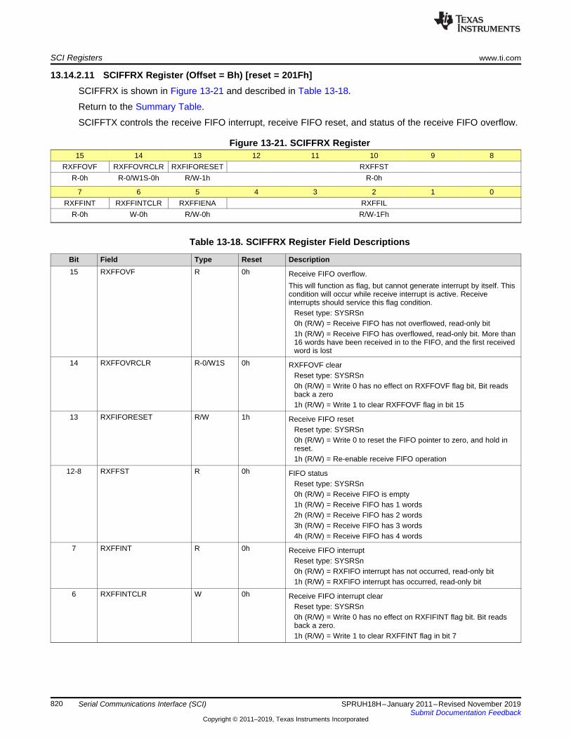
SCI Registers www.ti.com
820 SPRUH18H–January 2011–Revised November 2019Submit Documentation Feedback
Copyright © 2011–2019, Texas Instruments Incorporated
Serial Communications Interface (SCI)
13.14.2.11 SCIFFRX Register (Offset = Bh) [reset = 201Fh]SCIFFRX is shown in Figure 13-21 and described in Table 13-18.
Return to the Summary Table.
SCIFFTX controls the receive FIFO interrupt, receive FIFO reset, and status of the receive FIFO overflow.
Figure 13-21. SCIFFRX Register15 14 13 12 11 10 9 8
RXFFOVF RXFFOVRCLR RXFIFORESET RXFFSTR-0h R-0/W1S-0h R/W-1h R-0h
7 6 5 4 3 2 1 0RXFFINT RXFFINTCLR RXFFIENA RXFFIL
R-0h W-0h R/W-0h R/W-1Fh
Table 13-18. SCIFFRX Register Field Descriptions
Bit Field Type Reset Description15 RXFFOVF R 0h Receive FIFO overflow.
This will function as flag, but cannot generate interrupt by itself. Thiscondition will occur while receive interrupt is active. Receiveinterrupts should service this flag condition.
Reset type: SYSRSn0h (R/W) = Receive FIFO has not overflowed, read-only bit1h (R/W) = Receive FIFO has overflowed, read-only bit. More than16 words have been received in to the FIFO, and the first receivedword is lost
14 RXFFOVRCLR R-0/W1S 0h RXFFOVF clearReset type: SYSRSn0h (R/W) = Write 0 has no effect on RXFFOVF flag bit, Bit readsback a zero1h (R/W) = Write 1 to clear RXFFOVF flag in bit 15
13 RXFIFORESET R/W 1h Receive FIFO resetReset type: SYSRSn0h (R/W) = Write 0 to reset the FIFO pointer to zero, and hold inreset.1h (R/W) = Re-enable receive FIFO operation
12-8 RXFFST R 0h FIFO statusReset type: SYSRSn0h (R/W) = Receive FIFO is empty1h (R/W) = Receive FIFO has 1 words2h (R/W) = Receive FIFO has 2 words3h (R/W) = Receive FIFO has 3 words4h (R/W) = Receive FIFO has 4 words
7 RXFFINT R 0h Receive FIFO interruptReset type: SYSRSn0h (R/W) = RXFIFO interrupt has not occurred, read-only bit1h (R/W) = RXFIFO interrupt has occurred, read-only bit
6 RXFFINTCLR W 0h Receive FIFO interrupt clearReset type: SYSRSn0h (R/W) = Write 0 has no effect on RXFIFINT flag bit. Bit readsback a zero.1h (R/W) = Write 1 to clear RXFFINT flag in bit 7

www.ti.com SCI Registers
821SPRUH18H–January 2011–Revised November 2019Submit Documentation Feedback
Copyright © 2011–2019, Texas Instruments Incorporated
Serial Communications Interface (SCI)
Table 13-18. SCIFFRX Register Field Descriptions (continued)Bit Field Type Reset Description5 RXFFIENA R/W 0h Receive FIFO interrupt enable
Reset type: SYSRSn0h (R/W) = RX FIFO interrupt is disabled1h (R/W) = RX FIFO interrupt is enabled. This interrupt is triggeredwhenever the receive FIFO status (RXFFST) bits match (equal toor greater than) the interrupt trigger level bits RXFFIL (bits 4-0).
4-0 RXFFIL R/W 1Fh Receive FIFO interrupt level bits
The receive FIFO generates an interrupt whenever the FIFO statusbits (RXFFST4-0) are greater than or equal to the FIFO level bits(RXFFIL4-0). The maximum value that can be assigned to these bitsto generate an interrupt cannot be more than the depth of the RXFIFO. The default value of these bits after reset is 11111b. Usersshould set RXFFIL to best fit their application needs by weighingbetween the CPU overhead to service the ISR and the best possibleusage of received SCI data.
Reset type: SYSRSn

SCI Registers www.ti.com
822 SPRUH18H–January 2011–Revised November 2019Submit Documentation Feedback
Copyright © 2011–2019, Texas Instruments Incorporated
Serial Communications Interface (SCI)
13.14.2.12 SCIFFCT Register (Offset = Ch) [reset = 0h]SCIFFCT is shown in Figure 13-22 and described in Table 13-19.
Return to the Summary Table.
SCIFFCT contains the status of auto-baud detect, clears the auto-baud flag, and calibrate for A-detect bit.
Figure 13-22. SCIFFCT Register15 14 13 12 11 10 9 8
ABD ABDCLR CDC RESERVEDR-0h W-0h R/W-0h R-0h
7 6 5 4 3 2 1 0FFTXDLYR/W-0h
Table 13-19. SCIFFCT Register Field Descriptions
Bit Field Type Reset Description15 ABD R 0h Auto-baud detect (ABD) bit
Reset type: SYSRSn0h (R/W) = Auto-baud detection is not complete. "A","a" characterhas not been received successfully.1h (R/W) = Auto-baud hardware has detected "A" or "a" characteron the SCI receive register. Auto-detect iscomplete.
14 ABDCLR W 0h ABD-clear bitReset type: SYSRSn0h (R/W) = Write 0 has no effect on ABD flag bit. Bit reads back azero.1h (R/W) = Write 1 to clear ABD flag in bit 15.
13 CDC R/W 0h CDC calibrate A-detect bitReset type: SYSRSn0h (R/W) = Disables auto-baud alignment1h (R/W) = Enables auto-baud alignment
12-8 RESERVED R 0h Reserved7-0 FFTXDLY R/W 0h FIFO transfer delay. These bits define the delay between every
transfer from FIFO transmit bufferto transmit shift register. The delayis defined in the number of SCI serial baud clock cycles. The 8 bitregister could define a minimum delay of 0 baud clock cycles and amaximum of 256 baud clock cycles
In FIFO mode, the buffer (TXBUF) between the shift register and theFIFO should be filled only after the shift register has completedshifting of the last bit. This is required to pass on the delay betweentransfers to the data stream. In FIFO mode, TXBUF should not betreated as one additional level of buffer. The delayed transmit featurewill help to create an auto-flow scheme without RTS/CTS controls asin standard UARTS.
When SCI is configured for one stop-bit, delay introduced byFFTXDLY between one frame and the next frame is equal to numberof baud clock cycles that FFTXDLY is set to.
When SCI is configured for two stop-bits, delay introduced byFFTXDLY between one frame and the next frame is equal to numberof baud clock cycles that FFTXDLY is set to minus 1.
Reset type: SYSRSn

www.ti.com SCI Registers
823SPRUH18H–January 2011–Revised November 2019Submit Documentation Feedback
Copyright © 2011–2019, Texas Instruments Incorporated
Serial Communications Interface (SCI)
13.14.2.13 SCIPRI Register (Offset = Fh) [reset = 0h]SCIPRI is shown in Figure 13-23 and described in Table 13-20.
Return to the Summary Table.
SCIPRI determines what happens when an emulation suspend event occurs.
Figure 13-23. SCIPRI Register15 14 13 12 11 10 9 8
RESERVEDR-0h
7 6 5 4 3 2 1 0RESERVED FREESOFT RESERVED
R-0h R/W-0h R-0h
Table 13-20. SCIPRI Register Field Descriptions
Bit Field Type Reset Description15-8 RESERVED R 0h Reserved7-5 RESERVED R 0h Reserved4-3 FREESOFT R/W 0h These bits determine what occurs when an emulation suspend event
occurs (for example, when the debugger hits a breakpoint). Theperipheral can continue whatever it is doing (free-run mode), or if instop mode, it can either stop immediately or stop when the currentoperation (the current receive/transmit sequence) is complete.
Reset type: SYSRSn0h (R/W) = Immediate stop on suspend1h (R/W) = Complete current receive/transmit sequence beforestopping2h (R/W) = Free run3h (R/W) = Free run
2-0 RESERVED R 0h Reserved

824 SPRUH18H–January 2011–Revised November 2019Submit Documentation Feedback
Copyright © 2011–2019, Texas Instruments Incorporated
Inter-Integrated Circuit Module (I2C)
Chapter 14SPRUH18H–January 2011–Revised November 2019
Inter-Integrated Circuit Module (I2C)
This chapter describes the features and operation of the inter-integrated circuit (I2C) module. The I2Cmodule provides an interface between one of these devices and devices compliant with the NXPSemiconductors Inter-IC bus (I2C bus) specification version 2.1, and connected by way of an I2C bus.External components attached to this 2-wire serial bus can transmit/receive 1 to 8-bit data to/from thedevice through the I2C module. This guide assumes the reader is familiar with the I2C bus specification.
NOTE: A unit of data transmitted or received by the I2C module can have fewer than 8 bits;however, for convenience, a unit of data is called a data byte throughout this document. Thenumber of bits in a data byte is selectable via the BC bits of the mode register, I2CMDR.
Topic ........................................................................................................................... Page
14.1 Introduction ..................................................................................................... 82514.2 Configuring Device Pins.................................................................................... 82814.3 I2C Module Operational Details .......................................................................... 82914.4 Interrupt Requests Generated by the I2C Module ................................................. 83614.5 Resetting or Disabling the I2C Module ................................................................ 83914.6 I2C Registers ................................................................................................... 840
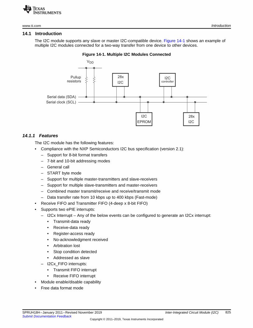
28x
I2C
I2C
EPROM
I2C
I2C
28x
VDD
Pullupresistors
Serial data (SDA)
Serial clock (SCL)
controller
www.ti.com Introduction
825SPRUH18H–January 2011–Revised November 2019Submit Documentation Feedback
Copyright © 2011–2019, Texas Instruments Incorporated
Inter-Integrated Circuit Module (I2C)
14.1 IntroductionThe I2C module supports any slave or master I2C-compatible device. Figure 14-1 shows an example ofmultiple I2C modules connected for a two-way transfer from one device to other devices.
Figure 14-1. Multiple I2C Modules Connected
14.1.1 FeaturesThe I2C module has the following features:• Compliance with the NXP Semiconductors I2C bus specification (version 2.1):
– Support for 8-bit format transfers– 7-bit and 10-bit addressing modes– General call– START byte mode– Support for multiple master-transmitters and slave-receivers– Support for multiple slave-transmitters and master-receivers– Combined master transmit/receive and receive/transmit mode– Data transfer rate from 10 kbps up to 400 kbps (Fast-mode)
• Receive FIFO and Transmitter FIFO (4-deep x 8-bit FIFO)• Supports two ePIE interrupts:
– I2Cx Interrupt – Any of the below events can be configured to generate an I2Cx interrupt:• Transmit-data ready• Receive-data ready• Register-access ready• No-acknowledgment received• Arbitration lost• Stop condition detected• Addressed as slave
– I2Cx_FIFO interrupts:• Transmit FIFO interrupt• Receive FIFO interrupt
• Module enable/disable capability• Free data format mode

Introduction www.ti.com
826 SPRUH18H–January 2011–Revised November 2019Submit Documentation Feedback
Copyright © 2011–2019, Texas Instruments Incorporated
Inter-Integrated Circuit Module (I2C)
14.1.2 Features Not SupportedThe I2C module does not support:• High-speed mode (Hs-mode)• CBUS-compatibility mode
14.1.3 Functional OverviewEach device connected to an I2C bus is recognized by a unique address. Each device can operate aseither a transmitter or a receiver, depending on the function of the device. A device connected to the I2Cbus can also be considered as the master or the slave when performing data transfers. A master device isthe device that initiates a data transfer on the bus and generates the clock signals to permit that transfer.During this transfer, any device addressed by this master is considered a slave. The I2C module supportsthe multi-master mode, in which one or more devices capable of controlling an I2C bus can be connectedto the same I2C bus.
For data communication, the I2C module has a serial data pin (SDA) and a serial clock pin (SCL), asshown in Section 14.6. These two pins carry information between the 28x device and other devicesconnected to the I2C bus. The SDA and SCL pins both are bidirectional. They each must be connected toa positive supply voltage using a pull-up resistor. When the bus is free, both pins are high. The driver ofthese two pins has an open-drain configuration to perform the required wired-AND function.
There are two major transfer techniques: .• Standard Mode: Send exactly n data values, where n is a value you program in an I2C module
register. See Section 14.6 for more information.• Repeat Mode: Keep sending data values until you use software to initiate a STOP condition or a new
START condition. See Registers for RM bit information.
The I2C module consists of the following primary blocks:• A serial interface: one data pin (SDA) and one clock pin (SCL)• Data registers and FIFOs to temporarily hold receive data and transmit data traveling between the
SDA pin and the CPU• Control and status registers• A peripheral bus interface to enable the CPU to access the I2C module registers and FIFOs.• A clock synchronizer to synchronize the I2C input clock (from the device clock generator) and the clock
on the SCL pin, and to synchronize data transfers with masters of different clock speeds• A prescaler to divide down the input clock that is driven to the I2C module• A noise filter on each of the two pins, SDA and SCL• An arbitrator to handle arbitration between the I2C module (when it is a master) and another master• Interrupt generation logic, so that an interrupt can be sent to the CPU• FIFO interrupt generation logic, so that FIFO access can be synchronized to data reception and data
transmission in the I2C module
Figure 14-2 shows the four registers used for transmission and reception in non-FIFO mode. The CPUwrites data for transmission to I2CDXR and reads received data from I2CDRR. When the I2C module isconfigured as a transmitter, data written to I2CDXR is copied to I2CXSR and shifted out on the SDA pinone bit at a time. When the I2C module is configured as a receiver, received data is shifted into I2CRSRand then copied to I2CDRR.

I2CPSC + 1
SYSCLKI2C Module Clock
(ICCL + d) + (ICCH + d)
Master Clock on SCL pin
I2CXSR I2CDXR
I2CRSR I2CDRR
Clocksynchronizer
Prescaler
Noise filters
Arbitrator
I2C INT
Peripheral bus
Interrupt to
CPU/PIE
SDA
SCL
Control/statusregisters CPU
I2C module
TX FIFO
RX FIFO
FIFO Interrupt
to CPU/PIE
www.ti.com Introduction
827SPRUH18H–January 2011–Revised November 2019Submit Documentation Feedback
Copyright © 2011–2019, Texas Instruments Incorporated
Inter-Integrated Circuit Module (I2C)
Figure 14-2. I2C Module Conceptual Block Diagram
14.1.4 Clock GenerationThe I2C module clock determines the frequency at which the I2C module operates. A programmableprescaler in the I2C module divides down the SYSCLK to produce the I2C module clock and this I2Cmodule clock is divided further to produce the I2C master clock on the SCL pin. Figure 14-3 shows theclock generation diagram for I2C module.
Figure 14-3. Clocking Diagram for the I2C Module
To specify the divide-down value, initialize the IPSC field of the prescaler register, I2CPSC. The resultingfrequency is:
NOTE: To meet all of the I2C protocol timing specifications, the I2C module clock must be between7 - 12 MHz.

Master Clock period (Tmst) =I2C Module Clock (Fmod)
[ (ICCH + d) + (ICCL + d) ]
SCL
High-time duration:Tmod × (ICCH + d)
High-time duration:Tmod × (ICCH + d)
Low-time duration:Tmod × (ICCL + d)
Low-time duration:Tmod × (ICCL + d)
Introduction www.ti.com
828 SPRUH18H–January 2011–Revised November 2019Submit Documentation Feedback
Copyright © 2011–2019, Texas Instruments Incorporated
Inter-Integrated Circuit Module (I2C)
The prescaler must be initialized only while the I2C module is in the reset state (IRS = 0 in I2CMDR). Theprescaled frequency takes effect only when IRS is changed to 1. Changing the IPSC value while IRS = 1has no effect.
The master clock appears on the SCL pin when the I2C module is configured to be a master on the I2Cbus. This clock controls the timing of communication between the I2C module and a slave. As shown inFigure 14-3, a second clock divider in the I2C module divides down the module clock to produce themaster clock. The clock divider uses the ICCL value of I2CCLKL to divide down the low portion of themodule clock signal and uses the ICCH value of I2CCLKH to divide down the high portion of the moduleclock signal. See Section 14.1.5 for the master clock frequency equation.
14.1.5 I2C Clock Divider Registers (I2CCLKL and I2CCLKH)As explained in Section 14.1.4, when the I2C module is a master, the I2C module clock is divided downfurther to use as the master clock on the SCL pin. As shown in Figure 14-4, the shape of the master clockdepends on two divide-down values:• ICCL in I2CCLKL. For each master clock cycle, ICCL determines the amount of time the signal is low.• ICCH in I2CCKLH. For each master clock cycle, ICCH determines the amount of time the signal is
high.
Figure 14-4. The Roles of the Clock Divide-Down Values (ICCL and ICCH)
14.1.5.1 Formula for the Master Clock PeriodThe master clock period (Tmst) is a multiple of the period of the I2C Module Clock (Tmod):
where d depends on the divide-down value IPSC, as shown in Table 14-1. IPSC is described in theI2CPSC register.
Table 14-1. Dependency of Delay d on the Divide-DownValue IPSC
IPSC d0 71 6
Greater than 1 5
14.2 Configuring Device PinsThe GPIO mux registers must be configured to connect this peripheral to the device pins.
Some IO functionality is defined by GPIO register settings independent of this peripheral. For inputsignals, the GPIO input qualification should be set to asynchronous mode by setting the appropriateGPxQSELn register bits to 11b. The internal pullups can be configured in the GPyPUD register.
See the GPIO chapter for more details on GPIO mux and settings.

Data linestable data
Change of dataallowed
SDA
SCL
www.ti.com I2C Module Operational Details
829SPRUH18H–January 2011–Revised November 2019Submit Documentation Feedback
Copyright © 2011–2019, Texas Instruments Incorporated
Inter-Integrated Circuit Module (I2C)
14.3 I2C Module Operational DetailsThis section provides an overview of the I2C bus protocol and how it is implemented.
14.3.1 Input and Output Voltage LevelsOne clock pulse is generated by the master device for each data bit transferred. Due to a variety ofdifferent technology devices that can be connected to the I2C bus, the levels of logic 0 (low) and logic 1(high) are not fixed and depend on the associated level of VDD. For details, see the data manual for yourparticular device.
14.3.2 Data ValidityThe data on SDA must be stable during the high period of the clock (see Figure 14-5). The high or lowstate of the data line, SDA, should change only when the clock signal on SCL is low.
Figure 14-5. Bit Transfer on the I2C bus
14.3.3 Operating ModesThe I2C module has four basic operating modes to support data transfers as a master and as a slave.See Table 14-2 for the names and descriptions of the modes.
If the I2C module is a master, it begins as a master-transmitter and typically transmits an address for aparticular slave. When giving data to the slave, the I2C module must remain a master-transmitter. Toreceive data from a slave, the I2C module must be changed to the master-receiver mode.
If the I2C module is a slave, it begins as a slave-receiver and typically sends acknowledgment when itrecognizes its slave address from a master. If the master will be sending data to the I2C module, themodule must remain a slave-receiver. If the master has requested data from the I2C module, the modulemust be changed to the slave-transmitter mode.
Table 14-2. Operating Modes of the I2C Module
Operating Mode DescriptionSlave-receiver modes The I2C module is a slave and receives data from a master.
All slaves begin in this mode. In this mode, serial data bits received on SDA are shifted in withthe clock pulses that are generated by the master. As a slave, the I2C module does notgenerate the clock signal, but it can hold SCL low while the intervention of the device isrequired (RSFULL = 1 in I2CSTR) after a byte has been received. See Section 14.3.7 for moredetails.
Slave-transmitter mode The I2C module is a slave and transmits data to a master.This mode can be entered only from the slave-receiver mode; the I2C module must first receivea command from the master. When you are using any of the 7-bit/10-bit addressing formats,the I2C module enters its slave-transmitter mode if the slave address byte is the same as itsown address (in I2COAR) and the master has transmitted R/W = 1. As a slave-transmitter, theI2C module then shifts the serial data out on SDA with the clock pulses that are generated bythe master. While a slave, the I2C module does not generate the clock signal, but it can holdSCL low while the intervention of the device is required (XSMT = 0 in I2CSTR) after a byte hasbeen transmitted. See Section 14.3.7 for more details.

I2C Module Operational Details www.ti.com
830 SPRUH18H–January 2011–Revised November 2019Submit Documentation Feedback
Copyright © 2011–2019, Texas Instruments Incorporated
Inter-Integrated Circuit Module (I2C)
Table 14-2. Operating Modes of the I2C Module (continued)Operating Mode DescriptionMaster-receiver mode The I2C module is a master and receives data from a slave.
This mode can be entered only from the master-transmitter mode; the I2C module must firsttransmit a command to the slave. When you are using any of the 7-bit/10-bit addressingformats, the I2C module enters its master-receiver mode after transmitting the slave addressbyte and R/W = 1. Serial data bits on SDA are shifted into the I2C module with the clock pulsesgenerated by the I2C module on SCL. The clock pulses are inhibited and SCL is held low whenthe intervention of the device is required (RSFULL = 1 in I2CSTR) after a byte has beenreceived.
Master-transmitter modes The I2C module is a master and transmits control information and data to a slave.All masters begin in this mode. In this mode, data assembled in any of the 7-bit/10-bitaddressing formats is shifted out on SDA. The bit shifting is synchronized with the clock pulsesgenerated by the I2C module on SCL. The clock pulses are inhibited and SCL is held low whenthe intervention of the device is required (XSMT = 0 in I2CSTR) after a byte has beentransmitted.
To summarize, SCL will be held low in the following conditions:• When an overrun condition is detected (RSFULL = 1), in Slave-receiver mode.• When an underflow condition is detected (XSMT = 0), in Slave-transmitter mode.
I2C slave nodes have to accept and provide data when the I2C master node requests it.• To release SCL in slave-receiver mode, read data from I2CDRR.• To release SCL in slave-transmitter mode, write data to I2CDXR.• To force a release without handling the data, reset the module using the I2CMDR.IRS bit.
(1) S = START condition; A = Address; D = Data byte; P = STOP condition;
Table 14-3. Master-Transmitter/Receiver Bus Activity Defined by the RM, STT, and STP Bits ofI2CMDR
RM STT STP Bus Activity (1) Description0 0 0 None No activity0 0 1 P STOP condition0 1 0 S-A-D..(n)..D. START condition, slave address, n data bytes (n = value in
I2CCNT)0 1 1 S-A-D..(n)..D-P START condition, slave address, n data bytes, STOP condition (n =
value in I2CCNT)1 0 0 None No activity1 0 1 P STOP condition1 1 0 S-A-D-D-D. Repeat mode transfer: START condition, slave address, continuous
data transfers until STOP condition or next START condition1 1 1 None Reserved bit combination (No activity)
14.3.4 I2C Module START and STOP ConditionsSTART and STOP conditions can be generated by the I2C module when the module is configured to be amaster on the I2C bus. As shown in Figure 14-6:• The START condition is defined as a high-to-low transition on the SDA line while SCL is high. A
master drives this condition to indicate the start of a data transfer.• The STOP condition is defined as a low-to-high transition on the SDA line while SCL is high. A master
drives this condition to indicate the end of a data transfer.

SDA
SCL
START
condition (S) condition (P)
STOP
www.ti.com I2C Module Operational Details
831SPRUH18H–January 2011–Revised November 2019Submit Documentation Feedback
Copyright © 2011–2019, Texas Instruments Incorporated
Inter-Integrated Circuit Module (I2C)
Figure 14-6. I2C Module START and STOP Conditions
After a START condition and before a subsequent STOP condition, the I2C bus is considered busy, andthe bus busy (BB) bit of I2CSTR is 1. Between a STOP condition and the next START condition, the busis considered free, and BB is 0.
For the I2C module to start a data transfer with a START condition, the master mode bit (MST) and theSTART condition bit (STT) in I2CMDR must both be 1. For the I2C module to end a data transfer with aSTOP condition, the STOP condition bit (STP) must be set to 1. When the BB bit is set to 1 and the STTbit is set to 1, a repeated START condition is generated. For a description of I2CMDR and its bits(including MST, STT, and STP), see Registers Section 14.6.
The I2C peripheral cannot detect a START or STOP condition while it is in reset (IRS = 0). The BB bit willremain in the cleared state (BB = 0) while the I2C peripheral is in reset (IRS = 0). When the I2C peripheralis taken out of reset (IRS set to 1) the BB bit will not correctly reflect the I2C bus status until a START orSTOP condition is detected.
Follow these steps before initiating the first data transfer with I2C:1. After taking the I2C peripheral out of reset by setting the IRS bit to 1, wait a period larger than the total
time taken for the longest data transfer in the application. By waiting for a period of time after I2Ccomes out of reset, users can ensure that at least one START or STOP condition will have occurredon the I2C bus and been captured by the BB bit. After this period, the BB bit will correctly reflect thestate of the I2C bus.
2. Check the BB bit and verify that BB = 0 (bus not busy) before proceeding.3. Begin data transfers.
Not resetting the I2C peripheral in between transfers ensures that the BB bit reflects the actual bus status.If users must reset the I2C peripheral in between transfers, repeat steps 1 through 3 every time the I2Cperipheral is taken out of reset.
14.3.5 Serial Data FormatsFigure 14-7 shows an example of a data transfer on the I2C bus. The I2C module supports 1 to 8-bit datavalues. In Figure 14-7, 8-bit data is transferred. Each bit put on the SDA line equates to 1 pulse on theSCL line, and the values are always transferred with the most significant bit (MSB) first. The number ofdata values that can be transmitted or received is unrestricted. The serial data format used in Figure 14-7is the 7-bit addressing format. The I2C module supports the formats shown in Figure 14-8 throughFigure 14-10 and described in the paragraphs that follow the figures.
NOTE: In Figure 14-7 through Figure 14-10, n = the number of data bits (from 1 to 8) specified bythe bit count (BC) field of I2CMDR.

S
1
1 1 1 1 0 x x
7
x x x x x x x xACK
11 8
ACK
1
Data
n
ACK
1
P
1
x x = 2 MSBs
R/W
8 LSBs of slave address
S
7 bits of slave address
R/W ACK Data ACK Data ACK P
7 n n1 1 1 1 1 1
x x x x x x x
SDA
SCL
MSB
Acknowledgementbit from slave
(No-)Acknowledgementbit from receiver
1 2 7 8 9 1 2 8 9
Slave address ACKSTART
condition (S)STOP
condition (P)R/W ACK Data
I2C Module Operational Details www.ti.com
832 SPRUH18H–January 2011–Revised November 2019Submit Documentation Feedback
Copyright © 2011–2019, Texas Instruments Incorporated
Inter-Integrated Circuit Module (I2C)
Figure 14-7. I2C Module Data Transfer (7-Bit Addressing with 8-bit Data Configuration Shown)
14.3.5.1 7-Bit Addressing FormatThe 7-bit addressing format is the default format after reset. Disabling expanded address (I2CMDR.XA =0) and free data format (I2CMDR.FDF = 0) enables 7-bit addressing format.
In this format (see Figure 14-8), the first byte after a START condition (S) consists of a 7-bit slave addressfollowed by a R/W bit. R/W determines the direction of the data:• R/W = 0: The I2C master writes (transmits) data to the addressed slave. This can be achieved by
setting I2CMDR.TRX = 1 (Transmitter mode)• R/W = 1: The I2C master reads (receives) data from the slave. This can be achieved by setting
I2CMDR.TRX = 0 (Receiver mode)
Figure 14-8. I2C Module 7-Bit Addressing Format (FDF = 0, XA = 0 in I2CMDR)
An extra clock cycle dedicated for acknowledgment (ACK) is inserted after each byte. If the ACK bit isinserted by the slave after the first byte from the master, it is followed by n bits of data from the transmitter(master or slave, depending on the R/W bit). n is a number from 1 to 8 determined by the bit count (BC)field of I2CMDR. After the data bits have been transferred, the receiver inserts an ACK bit.
14.3.5.2 10-Bit Addressing FormatThe 10-bit addressing format can be enabled by setting expanded address (I2CMDR.XA = 1) anddisabling free data format (I2CMDR.FDF = 0).
The 10-bit addressing format (see Figure 14-9) is similar to the 7-bit addressing format, but the mastersends the slave address in two separate byte transfers. The first byte consists of 11110b, the two MSBs ofthe 10-bit slave address, and R/W. The second byte is the remaining 8 bits of the 10-bit slave address.The slave must send acknowledgment after each of the two byte transfers. Once the master has writtenthe second byte to the slave, the master can either write data or use a repeated START condition tochange the data direction. For more details about using 10-bit addressing, see the NXP SemiconductorsI2C bus specification.
Figure 14-9. I2C Module 10-Bit Addressing Format (FDF = 0, XA = 1 in I2CMDR)
14.3.5.3 Free Data FormatThe free data format can be enabled by setting I2CMDR. FDF = 1.

1 7 n 7 n1 1 1 1 1 1 1 1
S Slave address R/W ACK Data ACK S Slave address R/W ACK Data ACK P
1Any
number
1Any number
DataDataS
1
DataACK ACK ACK P
1n n n 111
www.ti.com I2C Module Operational Details
833SPRUH18H–January 2011–Revised November 2019Submit Documentation Feedback
Copyright © 2011–2019, Texas Instruments Incorporated
Inter-Integrated Circuit Module (I2C)
In this format (see Figure 14-10), the first byte after a START condition (S) is a data byte. An ACK bit isinserted after each data byte, which can be from 1 to 8 bits, depending on the BC field of I2CMDR. Noaddress or data-direction bit is sent. Therefore, the transmitter and the receiver must both support the freedata format, and the direction of the data must be constant throughout the transfer.
Figure 14-10. I2C Module Free Data Format (FDF = 1 in I2CMDR)
NOTE: The free data format is not supported in the digital loopback mode (I2CMDR.DLB = 1).
Table 14-4. How the MST and FDF Bits of I2CMDR Affect the Role of the TRX Bit of I2CMDR
MST FDF I2C Module State Function of TRX0 0 In slave mode but not free data
format modeTRX is a don’t care. Depending on the command from the master, the I2Cmodule responds as a receiver or a transmitter.
0 1 In slave mode and free dataformat mode
The free data format mode requires that the I2C module remains thetransmitter or the receiver throughout the transfer. TRX identifies the roleof the I2C module:TRX = 1: The I2C module is a transmitter.TRX = 0: The I2C module is a receiver.
1 0 In master mode but not free dataformat mode
TRX = 1: The I2C module is a transmitter.TRX = 0: The I2C module is a receiver.
1 1 In master mode and free dataformat mode
TRX = 0: The I2C module is a receiver.TRX = 1: The I2C module is a transmitter.
14.3.5.4 Using a Repeated START ConditionI2C master can communicate with multiple slave addresses without having to give up control of the I2Cbus by driving a STOP condition. This can be achieved by driving another START condition at the end ofeach data type. The repeated START condition can be used with the 7-bit addressing, 10-bit addressing,and free data formats. Figure 14-11 shows a repeated START condition in the 7-bit addressing format.
Figure 14-11. Repeated START Condition (in This Case, 7-Bit Addressing Format)
NOTE: In Figure 14-11, n = the number of data bits (from 1 to 8) specified by the bit count (BC) fieldof I2CMDR.
14.3.6 NACK Bit GenerationWhen the I2C module is a receiver (master or slave), it can acknowledge or ignore bits sent by thetransmitter. To ignore any new bits, the I2C module must send a no-acknowledge (NACK) bit during theacknowledge cycle on the bus. Table 14-5 summarizes the various ways you can tell the I2C module tosend a NACK bit.

Waitstate Start HIGH
period
SCL from
device #1
SCL from
device #2
Bus line
SCL
I2C Module Operational Details www.ti.com
834 SPRUH18H–January 2011–Revised November 2019Submit Documentation Feedback
Copyright © 2011–2019, Texas Instruments Incorporated
Inter-Integrated Circuit Module (I2C)
Table 14-5. Ways to Generate a NACK Bit
I2C Module Condition NACK Bit Generation OptionsSlave-receiver modes • Allow an overrun condition (RSFULL = 1 in I2CSTR)
• Reset the module (IRS = 0 in I2CMDR)• Set the NACKMOD bit of I2CMDR before the rising edge of the last data bit you
intend to receiveMaster-receiver mode ANDRepeat mode (RM = 1 in I2CMDR)
• Generate a STOP condition (STP = 1 in I2CMDR)• Reset the module (IRS = 0 in I2CMDR)• Set the NACKMOD bit of I2CMDR before the rising edge of the last data bit you
intend to receiveMaster-receiver mode ANDNonrepeat mode(RM = 0 in I2CMDR)
• If STP = 1 in I2CMDR, allow the internal data counter to count down to 0 and thusforce a STOP condition
• If STP = 0, make STP = 1 to generate a STOP condition• Reset the module (IRS = 0 in I2CMDR). = 1 to generate a STOP condition• Set the NACKMOD bit of I2CMDR before the rising edge of the last data bit you
intend to receive
14.3.7 Clock SynchronizationUnder normal conditions, only one master device generates the clock signal, SCL. During the arbitrationprocedure, however, there are two or more masters and the clock must be synchronized so that the dataoutput can be compared. Figure 14-12 illustrates the clock synchronization. The wired-AND property ofSCL means that a device that first generates a low period on SCL overrules the other devices. At thishigh-to-low transition, the clock generators of the other devices are forced to start their own low period.The SCL is held low by the device with the longest low period. The other devices that finish their lowperiods must wait for SCL to be released, before starting their high periods. A synchronized signal on SCLis obtained, where the slowest device determines the length of the low period and the fastest devicedetermines the length of the high period.
If a device pulls down the clock line for a longer time, the result is that all clock generators must enter thewait state. In this way, a slave slows down a fast master and the slow device creates enough time to storea received byte or to prepare a byte to be transmitted.
Figure 14-12. Synchronization of Two I2C Clock Generators During Arbitration
14.3.8 ArbitrationIf two or more master-transmitters attempt to start a transmission on the same bus at approximately thesame time, an arbitration procedure is invoked. The arbitration procedure uses the data presented on theserial data bus (SDA) by the competing transmitters. Figure 14-13 illustrates the arbitration procedurebetween two devices. The first master-transmitter that releases the SDA line high is overruled by anothermaster-transmitter that drives the SDA low. The arbitration procedure gives priority to the device thattransmits the serial data stream with the lowest binary value. Should two or more devices send identicalfirst bytes, arbitration continues on the subsequent bytes.

1
0 0 01
0 0 0
1 1
111
0
Device #1 loses arbitrationand switches off
Bus line
SCL
Data from
device #1
Data from
device #2
Bus line
SDA
Device #2 drives SDA
www.ti.com I2C Module Operational Details
835SPRUH18H–January 2011–Revised November 2019Submit Documentation Feedback
Copyright © 2011–2019, Texas Instruments Incorporated
Inter-Integrated Circuit Module (I2C)
If the I2C module is the losing master, it switches to the slave-receiver mode, sets the arbitration lost(ARBL) flag, and generates the arbitration-lost interrupt request.
If during a serial transfer the arbitration procedure is still in progress when a repeated START condition ora STOP condition is transmitted to SDA, the master-transmitters involved must send the repeated STARTcondition or the STOP condition at the same position in the format frame. Arbitration is not allowedbetween:• A repeated START condition and a data bit• A STOP condition and a data bit• A repeated START condition and a STOP condition
Figure 14-13. Arbitration Procedure Between Two Master-Transmitters
14.3.9 Digital Loopback ModeThe I2C module support a self-test mode called digital loopback, which is enabled by setting the DLB bit inthe I2CMDR register. In this mode, data transmitted out of the I2CDXR register is received in the I2CDRRregister. The data follows an internal path, and takes n cycles to reach I2CDRR, where:
n = 8 * (SYSCLK) / (I2C module clock (Fmod))
The transmit clock and the receive clock are the same. The address seen on the external SDA pin is theaddress in the I2COAR register. Figure 14-14 shows the signal routing in digital loopback mode.

I2CDRR I2CRSR
0
1
I2CSAR
I2COAR
0
1
I2CDXR
I2CXSR
0
1 0
0
DLB
SCL_IN
SCL_OUT
Address/data
To internal I2C logic
From internal I2C logic
To internal I2C logic
To CPU
From CPU
From CPU
From CPU
SCL
SDA
I2C module
DLB
DLB
Interrupt Requests Generated by the I2C Module www.ti.com
836 SPRUH18H–January 2011–Revised November 2019Submit Documentation Feedback
Copyright © 2011–2019, Texas Instruments Incorporated
Inter-Integrated Circuit Module (I2C)
Figure 14-14. Pin Diagram Showing the Effects of the Digital Loopback Mode (DLB) Bit
NOTE: The free data format (I2CMDR.FDF = 1) is not supported in digital loopback mode.
14.4 Interrupt Requests Generated by the I2C ModuleEach I2C module can generate two CPU interrupts.
1. Basic I2C interrupt: Possible basic I2C interrupt sources which can trigger this interrupt are describedin Section 14.4.1.
2. I2C FIFO interrupt: Possible I2C FIFO interrupt sources which can trigger this interrupt are described inSection 14.4.2
14.4.1 Basic I2C Interrupt RequestsThe I2C module generates the interrupt requests described in Table 14-6. As shown in Figure 14-15, allrequests are multiplexed through an arbiter to a single I2C interrupt request to the CPU. Each interruptrequest has a flag bit in the status register (I2CSTR) and an enable bit in the interrupt enable register(I2CIER). When one of the specified events occurs, its flag bit is set. If the corresponding enable bit is 0,the interrupt request is blocked. If the enable bit is 1, the request is forwarded to the CPU as an I2Cinterrupt.
The I2C interrupt is one of the maskable interrupts of the CPU. As with any maskable interrupt request, ifit is properly enabled in the CPU, the CPU executes the corresponding interrupt service routine(I2CINT1A_ISR). The I2CINT1A_ISR for the I2C interrupt can determine the interrupt source by readingthe interrupt source register, I2CISRC. Then the I2CINT1A_ISR can branch to the appropriate subroutine.
After the CPU reads I2CISRC, the following events occur:1. The flag for the source interrupt is cleared in I2CSTR. Exception: The ARDY, RRDY, and XRDY bits in
I2CSTR are not cleared when I2CISRC is read. To clear one of these bits, write a 1 to it.2. The arbiter determines which of the remaining interrupt requests has the highest priority, writes the
code for that interrupt to I2CISRC, and forwards the interrupt request to the CPU.

www.ti.com Interrupt Requests Generated by the I2C Module
837SPRUH18H–January 2011–Revised November 2019Submit Documentation Feedback
Copyright © 2011–2019, Texas Instruments Incorporated
Inter-Integrated Circuit Module (I2C)
Table 14-6. Descriptions of the Basic I2C Interrupt Requests
I2C Interrupt Request Interrupt SourceXRDYINT Transmit ready condition: The data transmit register (I2CDXR) is ready to accept new data because the
previous data has been copied from I2CDXR to the transmit shift register (I2CXSR).As an alternative to using XRDYINT, the CPU can poll the XRDY bit of the status register, I2CSTR.XRDYINT should not be used when in FIFO mode. Use the FIFO interrupts instead.
RRDYINT Receive ready condition: The data receive register (I2CDRR) is ready to be read because data has beencopied from the receive shift register (I2CRSR) to I2CDRR.As an alternative to using RRDYINT, the CPU can poll the RRDY bit of I2CSTR. RRDYINT should notbe used when in FIFO mode. Use the FIFO interrupts instead.
ARDYINT Register-access ready condition: The I2C module registers are ready to be accessed because thepreviously programmed address, data, and command values have been used.The specific events that generate ARDYINT are the same events that set the ARDY bit of I2CSTR.As an alternative to using ARDYINT, the CPU can poll the ARDY bit.
NACKINT No-acknowledgment condition: The I2C module is configured as a master-transmitter and did notreceived acknowledgment from the slave-receiver.As an alternative to using NACKINT, the CPU can poll the NACK bit of I2CSTR.
ARBLINT Arbitration-lost condition: The I2C module has lost an arbitration contest with another master-transmitter.As an alternative to using ARBLINT, the CPU can poll the ARBL bit of I2CSTR.
SCDINT Stop condition detected: A STOP condition was detected on the I2C bus.As an alternative to using SCDINT, the CPU can poll the SCD bit of the status register, I2CSTR.
AASINT Addressed as slave condition: The I2C has been addressed as a slave device by another master on theI2C bus.As an alternative to using AASINT, the CPU can poll the AAS bit of the status register, I2CSTR.
Figure 14-15. Enable Paths of the I2C Interrupt Requests
The I2C module has a backwards compatibility bit (BC) in the I2CEMDR register. The timing diagram inFigure 14-16 demonstrates the effect the backwards compatibility bit has on I2C module registers andinterrupts when configured as a slave-transmitter.

Empty Data 2 Data 3 Data 4
Empty Data 1 Data 2 Data 3
Empty Data 1 Data 2 Data 3
Empty Data 1 Data 2 Data 3
SSlave
AddressR A Data 1 A Data 2 A Data 2 nA P
SSlave
AddressR A Data 1 A Data 2 A Data 3 nA P
Left in I2CDXR
Interrupt
XRDY
XSMT
I2CDXR
I2CXSR
b) BC = 0
Interrupt
XRDY
XSMT
I2CDXR
I2CXSR
b) BC = 1
Slave-Transmitter
Interrupt Requests Generated by the I2C Module www.ti.com
838 SPRUH18H–January 2011–Revised November 2019Submit Documentation Feedback
Copyright © 2011–2019, Texas Instruments Incorporated
Inter-Integrated Circuit Module (I2C)
Figure 14-16. Backwards Compatibility Mode Bit, Slave Transmitter
14.4.2 I2C FIFO InterruptsIn addition to the seven basic I2C interrupts, the transmit and receive FIFOs each contain the ability togenerate an interrupt (I2CINT2A). The transmit FIFO can be configured to generate an interrupt aftertransmitting a defined number of bytes, up to 4. The receive FIFO can be configured to generate aninterrupt after receiving a defined number of bytes, up to 4. These two interrupt sources are ORedtogether into a single maskable CPU interrupt. Figure 14-17 shows the structure of I2C FIFO interrupt.The interrupt service routine can then read the FIFO interrupt status flags to determine from which sourcethe interrupt came. See the I2C transmit FIFO register (I2CFFTX) and the I2C receive FIFO register(I2CFFRX) descriptions.

www.ti.com Resetting or Disabling the I2C Module
839SPRUH18H–January 2011–Revised November 2019Submit Documentation Feedback
Copyright © 2011–2019, Texas Instruments Incorporated
Inter-Integrated Circuit Module (I2C)
Figure 14-17. I2C FIFO Interrupt
14.5 Resetting or Disabling the I2C ModuleYou can reset or disable the I2C module in two ways:• Write 0 to the I2C reset bit (IRS) in the I2C mode register (I2CMDR). All status bits (in I2CSTR) are
forced to their default values, and the I2C module remains disabled until IRS is changed to 1. The SDAand SCL pins are in the high-impedance state.
• Initiate a device reset by driving the XRS pin low. The entire device is reset and is held in the resetstate until you drive the pin high. When the XRS pin is released, all I2C module registers are reset totheir default values. The IRS bit is forced to 0, which resets the I2C module. The I2C module stays inthe reset state until you write 1 to IRS.
The IRS must be 0 while you configure or reconfigure the I2C module. Forcing IRS to 0 can be used tosave power and to clear error conditions.

I2C Registers www.ti.com
840 SPRUH18H–January 2011–Revised November 2019Submit Documentation Feedback
Copyright © 2011–2019, Texas Instruments Incorporated
Inter-Integrated Circuit Module (I2C)
14.6 I2C RegistersThis section describes the C28x I2C Module Registers.
14.6.1 I2C Base Addresses
Table 14-7. I2C Base Address TableBit Field Name
Base AddressInstance Structure
I2caRegs I2C_REGS 0x0000_7900

www.ti.com I2C Registers
841SPRUH18H–January 2011–Revised November 2019Submit Documentation Feedback
Copyright © 2011–2019, Texas Instruments Incorporated
Inter-Integrated Circuit Module (I2C)
14.6.2 I2C_REGS RegistersTable 14-8 lists the I2C_REGS registers. All register offset addresses not listed in Table 14-8 should beconsidered as reserved locations and the register contents should not be modified.
Table 14-8. I2C_REGS Registers
Offset Acronym Register Name Write Protection Section0h I2COAR I2C Own address Go1h I2CIER I2C Interrupt Enable Go2h I2CSTR I2C Status Go3h I2CCLKL I2C Clock low-time divider Go4h I2CCLKH I2C Clock high-time divider Go5h I2CCNT I2C Data count Go6h I2CDRR I2C Data receive Go7h I2CSAR I2C Slave address Go8h I2CDXR I2C Data Transmit Go9h I2CMDR I2C Mode GoAh I2CISRC I2C Interrupt Source GoBh I2CEMDR I2C Extended Mode GoCh I2CPSC I2C Prescaler Go20h I2CFFTX I2C FIFO Transmit Go21h I2CFFRX I2C FIFO Receive Go
Complex bit access types are encoded to fit into small table cells. Table 14-9 shows the codes that areused for access types in this section.
Table 14-9. I2C_REGS Access Type Codes
Access Type Code DescriptionRead TypeR R ReadR-0 R
-0ReadReturns 0s
Write TypeW W WriteW1C W
1CWrite1 to clear
W1S W1S
Write1 to set
Reset or Default Value-n Value after reset or the default
valueRegister Array Variablesi,j,k,l,m,n When these variables are used in
a register name, an offset, or anaddress, they refer to the value ofa register array where the registeris part of a group of repeatingregisters. The register groups forma hierarchical structure and thearray is represented with aformula.
y When this variable is used in aregister name, an offset, or anaddress it refers to the value of aregister array.

I2C Registers www.ti.com
842 SPRUH18H–January 2011–Revised November 2019Submit Documentation Feedback
Copyright © 2011–2019, Texas Instruments Incorporated
Inter-Integrated Circuit Module (I2C)
14.6.2.1 I2COAR Register (Offset = 0h) [reset = 0h]I2COAR is shown in Figure 14-18 and described in Table 14-10.
Return to the Summary Table.
The I2C own address register (I2COAR) is a 16-bit register. The I2C module uses this register to specifyits own slave address, which distinguishes it from other slaves connected to the I2C-bus. If the 7-bitaddressing mode is selected (XA = 0 in I2CMDR), only bits 6-0 are usedwrite 0s to bits 9-7.
Figure 14-18. I2COAR Register15 14 13 12 11 10 9 8
RESERVED OARR-0h R/W-0h
7 6 5 4 3 2 1 0OAR
R/W-0h
Table 14-10. I2COAR Register Field Descriptions
Bit Field Type Reset Description15-10 RESERVED R 0h Reserved
9-0 OAR R/W 0h In 7-bit addressing mode (XA = 0 in I2CMDR):00h-7Fh Bits 6-0 provide the 7-bit slave address of the I2C module.Write 0s to bits 9-7.
In 10-bit addressing mode (XA = 1 in I2CMDR):000h-3FFh Bits 9-0 provide the 10-bit slave address of the I2Cmodule.
Reset type: SYSRSn

www.ti.com I2C Registers
843SPRUH18H–January 2011–Revised November 2019Submit Documentation Feedback
Copyright © 2011–2019, Texas Instruments Incorporated
Inter-Integrated Circuit Module (I2C)
14.6.2.2 I2CIER Register (Offset = 1h) [reset = 0h]I2CIER is shown in Figure 14-19 and described in Table 14-11.
Return to the Summary Table.
I2CIER is used by the CPU to individually enable or disable I2C interrupt requests.
Figure 14-19. I2CIER Register15 14 13 12 11 10 9 8
RESERVEDR-0h
7 6 5 4 3 2 1 0RESERVED AAS SCD XRDY RRDY ARDY NACK ARBL
R-0h R/W-0h R/W-0h R/W-0h R/W-0h R/W-0h R/W-0h R/W-0h
Table 14-11. I2CIER Register Field Descriptions
Bit Field Type Reset Description15-7 RESERVED R 0h Reserved
6 AAS R/W 0h Addressed as slave interrupt enableReset type: SYSRSn0h (R/W) = Interrupt request disabled1h (R/W) = Interrupt request enabled
5 SCD R/W 0h Stop condition detected interrupt enableReset type: SYSRSn0h (R/W) = Interrupt request disabled1h (R/W) = Interrupt request enabled
4 XRDY R/W 0h Transmit-data-ready interrupt enable bit.This bit should not be set when using FIFO mode.
Reset type: SYSRSn0h (R/W) = Interrupt request disabled1h (R/W) = Interrupt request enabled
3 RRDY R/W 0h Receive-data-ready interrupt enable bit.This bit should not be set when using FIFO mode.
Reset type: SYSRSn0h (R/W) = Interrupt request disabled1h (R/W) = Interrupt request enabled
2 ARDY R/W 0h Register-access-ready interrupt enableReset type: SYSRSn0h (R/W) = Interrupt request disabled1h (R/W) = Interrupt request enabled
1 NACK R/W 0h No-acknowledgment interrupt enableReset type: SYSRSn0h (R/W) = Interrupt request disabled1h (R/W) = Interrupt request enabled
0 ARBL R/W 0h Arbitration-lost interrupt enableReset type: SYSRSn0h (R/W) = Interrupt request disabled1h (R/W) = Interrupt request enabled

I2C Registers www.ti.com
844 SPRUH18H–January 2011–Revised November 2019Submit Documentation Feedback
Copyright © 2011–2019, Texas Instruments Incorporated
Inter-Integrated Circuit Module (I2C)
14.6.2.3 I2CSTR Register (Offset = 2h) [reset = 410h]I2CSTR is shown in Figure 14-20 and described in Table 14-12.
Return to the Summary Table.
The I2C status register (I2CSTR) is a 16-bit register used to determine which interrupt has occurred and toread status information.
Figure 14-20. I2CSTR Register15 14 13 12 11 10 9 8
RESERVED SDIR NACKSNT BB RSFULL XSMT AAS AD0R-0h R/W1C-0h R/W1C-0h R-0h R-0h R-1h R-0h R-0h
7 6 5 4 3 2 1 0RESERVED SCD XRDY RRDY ARDY NACK ARBL
R/W-0h R/W1C-0h R-1h R/W1C-0h R/W1C-0h R/W1C-0h R/W1C-0h
Table 14-12. I2CSTR Register Field Descriptions
Bit Field Type Reset Description15 RESERVED R 0h Reserved14 SDIR R/W1C 0h Slave direction bit
Reset type: SYSRSn0h (R/W) = I2C is not addressed as a slave transmitter. SDIR iscleared by one of the following events:- It is manually cleared. To clear this bit, write a 1 to it.- Digital loopback mode is enabled.- A START or STOP condition occurs on the I2C bus.1h (R/W) = I2C is addressed as a slave transmitter.
13 NACKSNT R/W1C 0h NACK sent bit.This bit is used when the I2C module is in the receiver mode. Oneinstance in which NACKSNT is affected is when the NACK mode isused (see the description for NACKMOD in
Reset type: SYSRSn0h (R/W) = NACK not sent. NACKSNT bit is cleared by any one ofthe following events:- It is manually cleared. To clear this bit, write a 1 to it.- The I2C module is reset (either when 0 is written to the IRS bit ofI2CMDR or when the whole device is reset).1h (R/W) = NACK sent: A no-acknowledge bit was sent during theacknowledge cycle on the I2C-bus.
12 BB R 0h Bus busy bit.BB indicates whether the I2C-bus is busy or is free for another datatransfer. See the paragraph following the table for more information
Reset type: SYSRSn0h (R/W) = Bus free. BB is cleared by any one of the followingevents:- The I2C module receives or transmits a STOP bit (bus free).- The I2C module is reset.1h (R/W) = Bus busy: The I2C module has received or transmitteda START bit on the bus.

www.ti.com I2C Registers
845SPRUH18H–January 2011–Revised November 2019Submit Documentation Feedback
Copyright © 2011–2019, Texas Instruments Incorporated
Inter-Integrated Circuit Module (I2C)
Table 14-12. I2CSTR Register Field Descriptions (continued)Bit Field Type Reset Description11 RSFULL R 0h Receive shift register full bit.
RSFULL indicates an overrun condition during reception. Overrunoccurs when new data is received into the shift register (I2CRSR)and the old data has not been read from the receive register(I2CDRR). As new bits arrive from the SDA pin, they overwrite thebits in I2CRSR. The new data will not be copied to ICDRR until theprevious data is read.
Reset type: SYSRSn0h (R/W) = No overrun detected. RSFULL is cleared by any one ofthe following events:- I2CDRR is read is read by the CPU. Emulator reads of theI2CDRR do not affect this bit.- The I2C module is reset.1h (R/W) = Overrun detected
10 XSMT R 1h Transmit shift register empty bit.XSMT = 0 indicates that the transmitter has experienced underflow.Underflow occurs when the transmit shift register (I2CXSR) is emptybut the data transmit register (I2CDXR) has not been loaded sincethe last I2CDXR-to-I2CXSR transfer. The next I2CDXR-to-I2CXSRtransfer will not occur until new data is in I2CDXR. If new data is nottransferred in time, the previous data may be re-transmitted on theSDA pin.
Reset type: SYSRSn0h (R/W) = Underflow detected (empty)1h (R/W) = No underflow detected (not empty). XSMT is set by oneof the following events:- Data is written to I2CDXR.- The I2C module is reset
9 AAS R 0h Addressed-as-slave bitReset type: SYSRSn0h (R/W) = In the 7-bit addressing mode, the AAS bit is clearedwhen receiving a NACK, a STOP condition, or a repeated STARTcondition. In the 10-bit addressing mode, the AAS bit is clearedwhen receiving a NACK, a STOP condition, or by a slave addressdifferent from the I2C peripheral's own slave address.1h (R/W) = The I2C module has recognized its own slave addressor an address of all zeros (general call).
8 AD0 R 0h Address 0 bitsReset type: SYSRSn0h (R/W) = AD0 has been cleared by a START or STOP condition.1h (R/W) = An address of all zeros (general call) is detected.
7-6 RESERVED R/W 0h Reserved5 SCD R/W1C 0h Stop condition detected bit.
SCD is set when the I2C sends or receives a STOP condition. TheI2C module delays clearing of the I2CMDR[STP] bit until the SCD bitis set.
Reset type: SYSRSn0h (R/W) = STOP condition not detected since SCD was lastcleared. SCD is cleared by any one of the following events:- I2CISRC is read by the CPU when it contains the value 110b(stop condition detected). Emulator reads of the I2CISRC do notaffect this bit.- SCD is manually cleared. To clear this bit, write a 1 to it.- The I2C module is reset.1h (R/W) = A STOP condition has been detected on the I2C bus.

I2C Registers www.ti.com
846 SPRUH18H–January 2011–Revised November 2019Submit Documentation Feedback
Copyright © 2011–2019, Texas Instruments Incorporated
Inter-Integrated Circuit Module (I2C)
Table 14-12. I2CSTR Register Field Descriptions (continued)Bit Field Type Reset Description4 XRDY R 1h Transmit-data-ready interrupt flag bit.
When not in FIFO mode, XRDY indicates that the data transmitregister (I2CDXR) is ready to accept new data because the previousdata has been copied from I2CDXR to the transmit shift register(I2CXSR). The CPU can poll XRDY or use the XRDY interruptrequest When in FIFO mode, use TXFFINT instead.
Reset type: SYSRSn0h (R/W) = I2CDXR not ready. XRDY is cleared when data iswritten to I2CDXR.1h (R/W) = I2CDXR ready: Data has been copied from I2CDXR toI2CXSR.XRDY is also forced to 1 when the I2C module is reset.
3 RRDY R/W1C 0h Receive-data-ready interrupt flag bit.When not in FIFO mode, RRDY indicates that the data receiveregister (I2CDRR) is ready to be read because data has been copiedfrom the receive shift register (I2CRSR) to I2CDRR. The CPU canpoll RRDY or use the RRDY interrupt request When in FIFO mode,use RXFFINT instead.
Reset type: SYSRSn0h (R/W) = I2CDRR not ready. RRDY is cleared by any one of thefollowing events:- I2CDRR is read by the CPU. Emulator reads of the I2CDRR donot affect this bit.- RRDY is manually cleared. To clear this bit, write a 1 to it.- The I2C module is reset.1h (R/W) = I2CDRR ready: Data has been copied from I2CRSR toI2CDRR.
2 ARDY R/W1C 0h Register-access-ready interrupt flag bit (only applicable when the I2Cmodule is in the mastermode).ARDY indicates that the I2C module registers are ready to beaccessed because the previously programmed address, data, andcommand values have been used. The CPU can poll ARDY or usethe ARDY interrupt request.
Reset type: SYSRSn0h (R/W) = The registers are not ready to be accessed. ARDY iscleared by any one of the following events:- The I2C module starts using the current register contents.- ARDY is manually cleared. To clear this bit, write a 1 to it.- The I2C module is reset.1h (R/W) = The registers are ready to be accessed.In the nonrepeat mode (RM = 0 in I2CMDR): If STP = 0 inI2CMDR, the ARDY bit is set when the internal data counter countsdown to 0. If STP = 1, ARDY is not affected (instead, the I2Cmodule generates a STOP condition when the counter reaches 0).In the repeat mode (RM = 1): ARDY is set at the end of each bytetransmitted from I2CDXR.

www.ti.com I2C Registers
847SPRUH18H–January 2011–Revised November 2019Submit Documentation Feedback
Copyright © 2011–2019, Texas Instruments Incorporated
Inter-Integrated Circuit Module (I2C)
Table 14-12. I2CSTR Register Field Descriptions (continued)Bit Field Type Reset Description1 NACK R/W1C 0h No-acknowledgment interrupt flag bit.
NACK applies when the I2C module is a transmitter (master orslave). NACK indicates whether the I2C module has detected anacknowledge bit (ACK) or a noacknowledge bit (NACK) from thereceiver. The CPU can poll NACK or use the NACK interruptrequest.
Reset type: SYSRSn0h (R/W) = ACK received/NACK not received. This bit is cleared byany one of the following events:- An acknowledge bit (ACK) has been sent by the receiver.- NACK is manually cleared. To clear this bit, write a 1 to it.- The CPU reads the interrupt source register (I2CISRC) and theregister contains the code for a NACK interrupt. Emulator reads ofthe I2CISRC do not affect this bit.- The I2C module is reset.1h (R/W) = NACK bit received. The hardware detects that a no-acknowledge (NACK) bit has been received.Note: While the I2C module performs a general call transfer, NACKis 1, even if one or more slaves send acknowledgment.
0 ARBL R/W1C 0h Arbitration-lost interrupt flag bit (only applicable when the I2Cmodule is a master-transmitter).ARBL primarily indicates when the I2C module has lost an arbitrationcontest with another mastertransmitter. The CPU can poll ARBL oruse the ARBL interrupt request.
Reset type: SYSRSn0h (R/W) = Arbitration not lost. AL is cleared by any one of thefollowing events:- AL is manually cleared. To clear this bit, write a 1 to it.- The CPU reads the interrupt source register (I2CISRC) and theregister contains the code for anAL interrupt. Emulator reads of the I2CISRC do not affect this bit.- The I2C module is reset.1h (R/W) = Arbitration lost. AL is set by any one of the followingevents:- The I2C module senses that it has lost an arbitration with two ormore competing transmitters that started a transmission almostsimultaneously.- The I2C module attempts to start a transfer while the BB (busbusy) bit is set to 1.When AL becomes 1, the MST and STP bits of I2CMDR arecleared, and the I2C module becomes a slave-receiver.

I2C Registers www.ti.com
848 SPRUH18H–January 2011–Revised November 2019Submit Documentation Feedback
Copyright © 2011–2019, Texas Instruments Incorporated
Inter-Integrated Circuit Module (I2C)
14.6.2.4 I2CCLKL Register (Offset = 3h) [reset = 0h]I2CCLKL is shown in Figure 14-21 and described in Table 14-13.
Return to the Summary Table.
I2C Clock low-time divider
Figure 14-21. I2CCLKL Register15 14 13 12 11 10 9 8
I2CCLKLR/W-0h
7 6 5 4 3 2 1 0I2CCLKLR/W-0h
Table 14-13. I2CCLKL Register Field Descriptions
Bit Field Type Reset Description15-0 I2CCLKL R/W 0h Clock low-time divide-down value.
To produce the low time duration of the master clock, the period ofthe module clock is multiplied by (ICCL + d). d is an adjustmentfactor based on the prescaler. See the Clock Divider Registerssection of the Introduction for details.
Note: These bits must be set to a non-zero value for proper I2Cclock generation.
Reset type: SYSRSn

www.ti.com I2C Registers
849SPRUH18H–January 2011–Revised November 2019Submit Documentation Feedback
Copyright © 2011–2019, Texas Instruments Incorporated
Inter-Integrated Circuit Module (I2C)
14.6.2.5 I2CCLKH Register (Offset = 4h) [reset = 0h]I2CCLKH is shown in Figure 14-22 and described in Table 14-14.
Return to the Summary Table.
I2C Clock high-time divider
Figure 14-22. I2CCLKH Register15 14 13 12 11 10 9 8
I2CCLKHR/W-0h
7 6 5 4 3 2 1 0I2CCLKHR/W-0h
Table 14-14. I2CCLKH Register Field Descriptions
Bit Field Type Reset Description15-0 I2CCLKH R/W 0h Clock high-time divide-down value.
To produce the high time duration of the master clock, the period ofthe module clock is multiplied by (ICCL + d). d is an adjustmentfactor based on the prescaler. See the Clock Divider Registerssection of the Introduction for details.
Note: These bits must be set to a non-zero value for proper I2Cclock generation.
Reset type: SYSRSn

I2C Registers www.ti.com
850 SPRUH18H–January 2011–Revised November 2019Submit Documentation Feedback
Copyright © 2011–2019, Texas Instruments Incorporated
Inter-Integrated Circuit Module (I2C)
14.6.2.6 I2CCNT Register (Offset = 5h) [reset = 0h]I2CCNT is shown in Figure 14-23 and described in Table 14-15.
Return to the Summary Table.
I2CCNT is a 16-bit register used to indicate how many data bytes to transfer when the I2C module isconfigured as a transmitter, or to receive when configured as a master receiver. In the repeat mode (RM =1), I2CCNT is not used.The value written to I2CCNT is copied to an internal data counter. The internal data counter isdecremented by 1 for each byte transferred (I2CCNT remains unchanged). If a STOP condition isrequested in the master mode (STP = 1 in I2CMDR), the I2C module terminates the transfer with a STOPcondition when the countdown is complete (that is, when the last byte has been transferred).
Figure 14-23. I2CCNT Register15 14 13 12 11 10 9 8
I2CCNTR/W-0h
7 6 5 4 3 2 1 0I2CCNTR/W-0h
Table 14-15. I2CCNT Register Field Descriptions
Bit Field Type Reset Description15-0 I2CCNT R/W 0h Data count value. I2CCNT indicates the number of data bytes to
transfer or receive. The value in I2CCNT is a don't care when theRM bit in I2CMDR is set to 1.The start value loaded to the internal data counter is 65536.The start value loaded to internal data counter is 1-65535.
Reset type: SYSRSn

www.ti.com I2C Registers
851SPRUH18H–January 2011–Revised November 2019Submit Documentation Feedback
Copyright © 2011–2019, Texas Instruments Incorporated
Inter-Integrated Circuit Module (I2C)
14.6.2.7 I2CDRR Register (Offset = 6h) [reset = 0h]I2CDRR is shown in Figure 14-24 and described in Table 14-16.
Return to the Summary Table.
I2CDRR is a 16-bit register used by the CPU to read received data. The I2C module can receive a databyte with 1 to 8 bits. The number of bits is selected with the bit count (BC) bits in I2CMDR. One bit at atime is shifted in from the SDA pin to the receive shift register (I2CRSR). When a complete data byte hasbeen received, the I2C module copies the data byte from I2CRSR to I2CDRR. The CPU cannot accessI2CRSR directly.If a data byte with fewer than 8 bits is in I2CDRR, the data value is right-justified, and the other bits ofI2CDRR(7-0) are undefined. For example, if BC = 011 (3-bit data size), the receive data is in I2CDRR(2-0), and the content of I2CDRR(7-3) is undefined.When in the receive FIFO mode, the I2CDRR register acts as the receive FIFO buffer.
Figure 14-24. I2CDRR Register15 14 13 12 11 10 9 8
RESERVEDR-0h
7 6 5 4 3 2 1 0DATAR-0h
Table 14-16. I2CDRR Register Field Descriptions
Bit Field Type Reset Description15-8 RESERVED R 0h Reserved7-0 DATA R 0h Receive data
Reset type: SYSRSn

I2C Registers www.ti.com
852 SPRUH18H–January 2011–Revised November 2019Submit Documentation Feedback
Copyright © 2011–2019, Texas Instruments Incorporated
Inter-Integrated Circuit Module (I2C)
14.6.2.8 I2CSAR Register (Offset = 7h) [reset = 3FFh]I2CSAR is shown in Figure 14-25 and described in Table 14-17.
Return to the Summary Table.
The I2C slave address register (I2CSAR) is a 16-bit register for storing the next slave address that will betransmitted by the I2C module when it is a master. The SAR field of I2CSAR contains a 7-bit or 10-bitslave address. When the I2C module is not using the free data format (FDF = 0 in I2CMDR), it uses thisaddress to initiate data transfers with a slave, or slaves. When the address is nonzero, the address is for aparticular slave. When the address is 0, the address is a general call to all slaves. If the 7-bit addressingmode is selected (XA = 0 in I2CMDR), only bits 6-0 of I2CSAR are usedwrite 0s to bits 9-7.
Figure 14-25. I2CSAR Register15 14 13 12 11 10 9 8
RESERVED SARR-0h R/W-3FFh
7 6 5 4 3 2 1 0SAR
R/W-3FFh
Table 14-17. I2CSAR Register Field Descriptions
Bit Field Type Reset Description15-10 RESERVED R 0h Reserved
9-0 SAR R/W 3FFh In 7-bit addressing mode (XA = 0 in I2CMDR):00h-7Fh Bits 6-0 provide the 7-bit slave address that the I2C moduletransmits when it is in the master-transmittermode. Write 0s to bits 9-7.
In 10-bit addressing mode (XA = 1 in I2CMDR):000h-3FFh Bits 9-0 provide the 10-bit slave address that the I2Cmodule transmits when it is in the master transmitter mode.
Reset type: SYSRSn

www.ti.com I2C Registers
853SPRUH18H–January 2011–Revised November 2019Submit Documentation Feedback
Copyright © 2011–2019, Texas Instruments Incorporated
Inter-Integrated Circuit Module (I2C)
14.6.2.9 I2CDXR Register (Offset = 8h) [reset = 0h]I2CDXR is shown in Figure 14-26 and described in Table 14-18.
Return to the Summary Table.
The CPU writes transmit data to I2CDXR. This 16-bit register accepts a data byte with 1 to 8 bits. Beforewriting to I2CDXR, specify how many bits are in a data byte by loading the appropriate value into the bitcount (BC) bits of I2CMDR. When writing a data byte with fewer than 8 bits, make sure the value is right-aligned in I2CDXR.After a data byte is written to I2CDXR, the I2C module copies the data byte to the transmit shift register(I2CXSR). The CPU cannot access I2CXSR directly. From I2CXSR, the I2C module shifts the data byteout on the SDA pin, one bit at a time.When in the transmit FIFO mode, the I2CDXR register acts as the transmit FIFO buffer.
Figure 14-26. I2CDXR Register15 14 13 12 11 10 9 8
RESERVEDR-0h
7 6 5 4 3 2 1 0DATA
R/W-0h
Table 14-18. I2CDXR Register Field Descriptions
Bit Field Type Reset Description15-8 RESERVED R 0h Reserved7-0 DATA R/W 0h Transmit data
Reset type: SYSRSn

I2C Registers www.ti.com
854 SPRUH18H–January 2011–Revised November 2019Submit Documentation Feedback
Copyright © 2011–2019, Texas Instruments Incorporated
Inter-Integrated Circuit Module (I2C)
14.6.2.10 I2CMDR Register (Offset = 9h) [reset = 0h]I2CMDR is shown in Figure 14-27 and described in Table 14-19.
Return to the Summary Table.
The I2C mode register (I2CMDR) is a 16-bit register that contains the control bits of the I2C module.
Figure 14-27. I2CMDR Register15 14 13 12 11 10 9 8
NACKMOD FREE STT RESERVED STP MST TRX XAR/W-0h R/W-0h R/W-0h R-0h R/W-0h R/W-0h R/W-0h R/W-0h
7 6 5 4 3 2 1 0RM DLB IRS STB FDF BC
R/W-0h R/W-0h R/W-0h R/W-0h R/W-0h R/W-0h
Table 14-19. I2CMDR Register Field Descriptions
Bit Field Type Reset Description15 NACKMOD R/W 0h NACK mode bit. This bit is only applicable when the I2C module is
acting as a receiver.Reset type: SYSRSn0h (R/W) = In the slave-receiver mode: The I2C module sends anacknowledge (ACK) bit to the transmitter during each acknowledgecycle on the bus. The I2C module only sends a no-acknowledge(NACK) bit if you set the NACKMOD bit.In the master-receiver mode: The I2C module sends an ACK bitduring each acknowledge cycle until the internal data countercounts down to 0. At that point, the I2C module sends a NACK bitto the transmitter. To have a NACK bit sent earlier, you must setthe NACKMOD bit1h (R/W) = In either slave-receiver or master-receiver mode: TheI2C module sends a NACK bit to the transmitter during the nextacknowledge cycle on the bus. Once the NACK bit has been sent,NACKMOD is cleared.Important: To send a NACK bit in the next acknowledge cycle, youmust set NACKMOD before the rising edge of the last data bit.
14 FREE R/W 0h This bit controls the action taken by the I2C module when adebugger breakpoint is encountered.
Reset type: SYSRSn0h (R/W) = When I2C module is master:If SCL is low when the breakpoint occurs, the I2C module stopsimmediately and keeps driving SCL low, whether the I2C module isthe transmitter or the receiver. If SCL is high, the I2C module waitsuntil SCL becomes low and then stops.When I2C module is slave:A breakpoint forces the I2C module to stop when the currenttransmission/reception is complete.1h (R/W) = The I2C module runs freethat is, it continues to operate when a breakpoint occurs.
13 STT R/W 0h START condition bit (only applicable when the I2C module is amaster). The RM, STT, and STP bits determine when the I2Cmodule starts and stops data transmissions (see Table 9-6). Notethat the STT and STP bits can be used to terminate the repeatmode, and that this bit is not writable when IRS = 0.
Reset type: SYSRSn0h (R/W) = In the master mode, STT is automatically cleared afterthe START condition has been generated.1h (R/W) = In the master mode, setting STT to 1 causes the I2Cmodule to generate a START condition on the I2C-bus
12 RESERVED R 0h Reserved
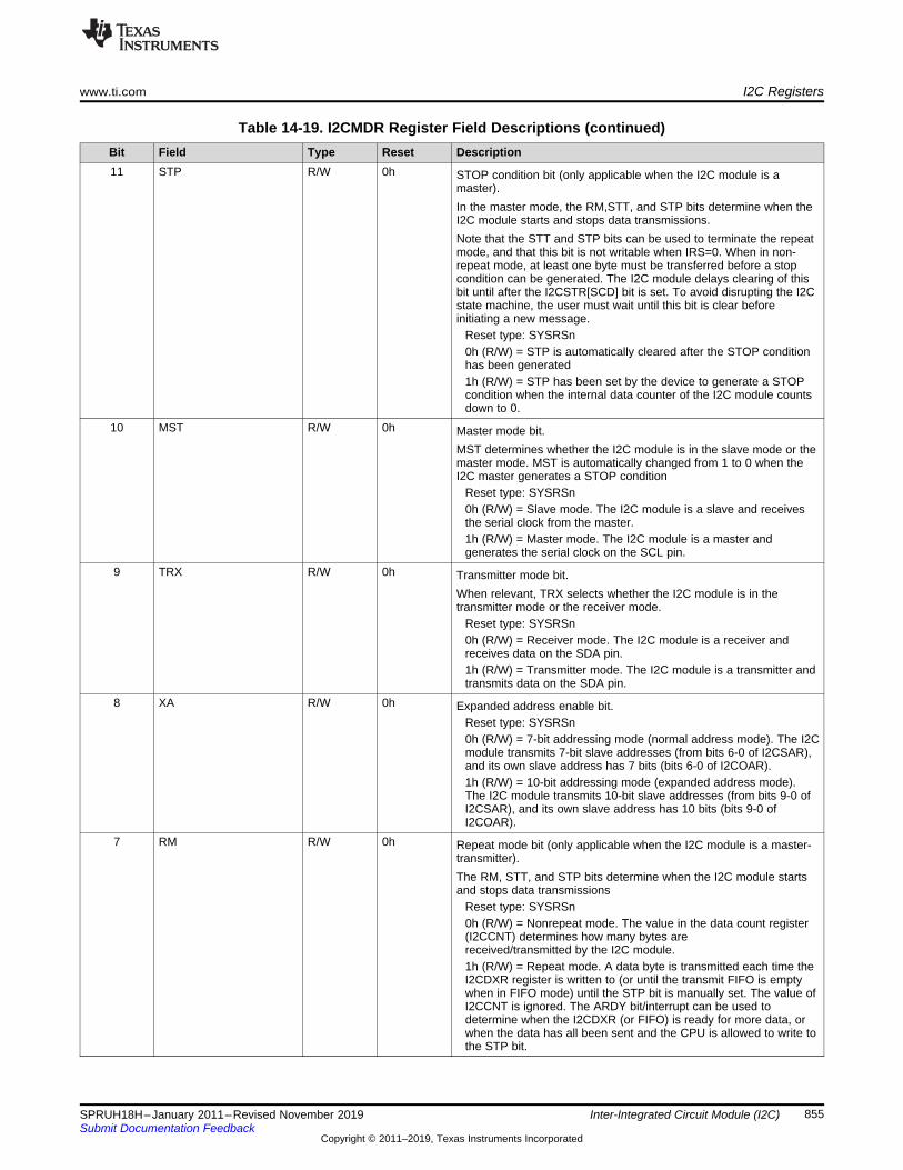
www.ti.com I2C Registers
855SPRUH18H–January 2011–Revised November 2019Submit Documentation Feedback
Copyright © 2011–2019, Texas Instruments Incorporated
Inter-Integrated Circuit Module (I2C)
Table 14-19. I2CMDR Register Field Descriptions (continued)Bit Field Type Reset Description11 STP R/W 0h STOP condition bit (only applicable when the I2C module is a
master).In the master mode, the RM,STT, and STP bits determine when theI2C module starts and stops data transmissions.Note that the STT and STP bits can be used to terminate the repeatmode, and that this bit is not writable when IRS=0. When in non-repeat mode, at least one byte must be transferred before a stopcondition can be generated. The I2C module delays clearing of thisbit until after the I2CSTR[SCD] bit is set. To avoid disrupting the I2Cstate machine, the user must wait until this bit is clear beforeinitiating a new message.
Reset type: SYSRSn0h (R/W) = STP is automatically cleared after the STOP conditionhas been generated1h (R/W) = STP has been set by the device to generate a STOPcondition when the internal data counter of the I2C module countsdown to 0.
10 MST R/W 0h Master mode bit.MST determines whether the I2C module is in the slave mode or themaster mode. MST is automatically changed from 1 to 0 when theI2C master generates a STOP condition
Reset type: SYSRSn0h (R/W) = Slave mode. The I2C module is a slave and receivesthe serial clock from the master.1h (R/W) = Master mode. The I2C module is a master andgenerates the serial clock on the SCL pin.
9 TRX R/W 0h Transmitter mode bit.When relevant, TRX selects whether the I2C module is in thetransmitter mode or the receiver mode.
Reset type: SYSRSn0h (R/W) = Receiver mode. The I2C module is a receiver andreceives data on the SDA pin.1h (R/W) = Transmitter mode. The I2C module is a transmitter andtransmits data on the SDA pin.
8 XA R/W 0h Expanded address enable bit.Reset type: SYSRSn0h (R/W) = 7-bit addressing mode (normal address mode). The I2Cmodule transmits 7-bit slave addresses (from bits 6-0 of I2CSAR),and its own slave address has 7 bits (bits 6-0 of I2COAR).1h (R/W) = 10-bit addressing mode (expanded address mode).The I2C module transmits 10-bit slave addresses (from bits 9-0 ofI2CSAR), and its own slave address has 10 bits (bits 9-0 ofI2COAR).
7 RM R/W 0h Repeat mode bit (only applicable when the I2C module is a master-transmitter).The RM, STT, and STP bits determine when the I2C module startsand stops data transmissions
Reset type: SYSRSn0h (R/W) = Nonrepeat mode. The value in the data count register(I2CCNT) determines how many bytes arereceived/transmitted by the I2C module.1h (R/W) = Repeat mode. A data byte is transmitted each time theI2CDXR register is written to (or until the transmit FIFO is emptywhen in FIFO mode) until the STP bit is manually set. The value ofI2CCNT is ignored. The ARDY bit/interrupt can be used todetermine when the I2CDXR (or FIFO) is ready for more data, orwhen the data has all been sent and the CPU is allowed to write tothe STP bit.

I2C Registers www.ti.com
856 SPRUH18H–January 2011–Revised November 2019Submit Documentation Feedback
Copyright © 2011–2019, Texas Instruments Incorporated
Inter-Integrated Circuit Module (I2C)
Table 14-19. I2CMDR Register Field Descriptions (continued)Bit Field Type Reset Description6 DLB R/W 0h Digital loopback mode bit.
Reset type: SYSRSn0h (R/W) = Digital loopback mode is disabled.1h (R/W) = Digital loopback mode is enabled. For proper operationin this mode, the MST bit must be 1.In the digital loopback mode, data transmitted out of I2CDXR isreceived in I2CDRR after n device cycles by an internal path,where:n = ((I2C input clock frequency/module clock frequency) x 8)The transmit clock is also the receive clock. The addresstransmitted on the SDA pin is the address in I2COAR.Note: The free data format (FDF = 1) is not supported in the digitalloopback mode.
5 IRS R/W 0h I2C module reset bit.Reset type: SYSRSn0h (R/W) = The I2C module is in reset/disabled. When this bit iscleared to 0, all status bits (in I2CSTR) are set to their defaultvalues.1h (R/W) = The I2C module is enabled. This has the effect ofreleasing the I2C bus if the I2C peripheral is holding it.
4 STB R/W 0h START byte mode bit. This bit is only applicable when the I2Cmodule is a master. As described in version 2.1 of the PhilipsSemiconductors I2C-bus specification, the START byte can be usedto help a slave that needs extra time to detect a START condition.When the I2C module is a slave, it ignores a START byte from amaster, regardless of the value of the STB bit.
Reset type: SYSRSn0h (R/W) = The I2C module is not in the START byte mode.1h (R/W) = The I2C module is in the START byte mode. When youset the START condition bit (STT), the I2C module begins thetransfer with more than just a START condition. Specifically, itgenerates:1. A START condition2. A START byte (0000 0001b)3. A dummy acknowledge clock pulse4. A repeated START conditionThen, as normal, the I2C module sends the slave address that is inI2CSAR.
3 FDF R/W 0h Free data format mode bit.Reset type: SYSRSn0h (R/W) = Free data format mode is disabled. Transfers use the7-/10-bit addressing format selected by the XA bit.1h (R/W) = Free data format mode is enabled. Transfers have thefree data (no address) format described in Section 9.2.5.The free data format is not supported in the digital loopback mode(DLB=1).

www.ti.com I2C Registers
857SPRUH18H–January 2011–Revised November 2019Submit Documentation Feedback
Copyright © 2011–2019, Texas Instruments Incorporated
Inter-Integrated Circuit Module (I2C)
Table 14-19. I2CMDR Register Field Descriptions (continued)Bit Field Type Reset Description2-0 BC R/W 0h Bit count bits.
BC defines the number of bits (1 to 8) in the next data byte that is tobe received or transmitted by the I2C module. The number of bitsselected with BC must match the data size of the other device.Notice that when BC = 000b, a data byte has 8 bits. BC does notaffect address bytes, which always have 8 bits.Note: If the bit count is less than 8, receive data is right-justified inI2CDRR(7-0), and the other bits of I2CDRR(7-0) are undefined. Also,transmit data written to I2CDXR must be right-justified
Reset type: SYSRSn0h (R/W) = 8 bits per data byte1h (R/W) = 1 bit per data byte2h (R/W) = 2 bits per data byte3h (R/W) = 3 bits per data byte4h (R/W) = 4 bits per data byte5h (R/W) = 5 bits per data byte6h (R/W) = 6 bits per data byte7h (R/W) = 7 bits per data byte

I2C Registers www.ti.com
858 SPRUH18H–January 2011–Revised November 2019Submit Documentation Feedback
Copyright © 2011–2019, Texas Instruments Incorporated
Inter-Integrated Circuit Module (I2C)
14.6.2.11 I2CISRC Register (Offset = Ah) [reset = 0h]I2CISRC is shown in Figure 14-28 and described in Table 14-20.
Return to the Summary Table.
The I2C interrupt source register (I2CISRC) is a 16-bit register used by the CPU to determine which eventgenerated the I2C interrupt.
Figure 14-28. I2CISRC Register15 14 13 12 11 10 9 8
RESERVED WRITE_ZEROSR-0h R/W-0h
7 6 5 4 3 2 1 0RESERVED INTCODE
R-0h R-0h
Table 14-20. I2CISRC Register Field Descriptions
Bit Field Type Reset Description15-12 RESERVED R 0h Reserved11-8 WRITE_ZEROS R/W 0h TI internal testing bits
These reserved bit locations should always be written as zeros.Reset type: SYSRSn
7-3 RESERVED R 0h Reserved2-0 INTCODE R 0h Interrupt code bits.
The binary code in INTCODE indicates the event that generated anI2C interrupt.
A CPU read will clear this field. If another lower priority interrupt ispending and enabled, the value corresponding to that interrupt willthen be loaded. Otherwise, the value will stay cleared.In the case of an arbitration lost, a no-acknowledgment conditiondetected, or a stop condition detected, a CPU read will also clear theassociated interrupt flag bit in the I2CSTR register.Emulator reads will not affect the state of this field or of the statusbits in the I2CSTR register.
Reset type: SYSRSn0h (R/W) = None1h (R/W) = Arbitration lost2h (R/W) = No-acknowledgment condition detected3h (R/W) = Registers ready to be accessed4h (R/W) = Receive data ready5h (R/W) = Transmit data ready6h (R/W) = Stop condition detected7h (R/W) = Addressed as slave

www.ti.com I2C Registers
859SPRUH18H–January 2011–Revised November 2019Submit Documentation Feedback
Copyright © 2011–2019, Texas Instruments Incorporated
Inter-Integrated Circuit Module (I2C)
14.6.2.12 I2CEMDR Register (Offset = Bh) [reset = 1h]I2CEMDR is shown in Figure 14-29 and described in Table 14-21.
Return to the Summary Table.
I2C Extended Mode
Figure 14-29. I2CEMDR Register15 14 13 12 11 10 9 8
RESERVEDR-0h
7 6 5 4 3 2 1 0RESERVED BC
R-0h R/W-1h
Table 14-21. I2CEMDR Register Field Descriptions
Bit Field Type Reset Description15-1 RESERVED R 0h Reserved
0 BC R/W 1h Backwards compatibility mode.This bit affects the timing of the transmit status bits (XRDY andXSMT) in the I2CSTR register when in slave transmitter mode.Check Backwards Compatibility Mode Bit, Slave Transmitter diagramfor more details.
Reset type: SYSRSn0h (R/W) = See the "Backwards Compatibility Mode Bit, SlaveTransmitter" Figure for details.1h (R/W) = See the "Backwards Compatibility Mode Bit, SlaveTransmitter" Figure for details.

I2C Registers www.ti.com
860 SPRUH18H–January 2011–Revised November 2019Submit Documentation Feedback
Copyright © 2011–2019, Texas Instruments Incorporated
Inter-Integrated Circuit Module (I2C)
14.6.2.13 I2CPSC Register (Offset = Ch) [reset = 0h]I2CPSC is shown in Figure 14-30 and described in Table 14-22.
Return to the Summary Table.
The I2C prescaler register (I2CPSC) is a 16-bit register (see Figure 14-21) used for dividing down the I2Cinput clock to obtain the desired module clock for the operation of the I2C module. See the device-specificdata manual for the supported range of values for the module clock frequency.IPSC must be initialized while the I2C module is in reset (IRS = 0 in I2CMDR). The prescaled frequencytakes effect only when IRS is changed to 1. Changing the IPSC value while IRS = 1 has no effect.
Figure 14-30. I2CPSC Register15 14 13 12 11 10 9 8
RESERVEDR-0h
7 6 5 4 3 2 1 0IPSC
R/W-0h
Table 14-22. I2CPSC Register Field Descriptions
Bit Field Type Reset Description15-8 RESERVED R 0h Reserved7-0 IPSC R/W 0h I2C prescaler divide-down value.
IPSC determines how much the CPU clock is divided to create themodule clock of the I2C module:module clock frequency = I2C input clock frequency/(IPSC + 1)Note: IPSC must be initialized while the I2C module is in reset (IRS= 0 in I2CMDR).
Reset type: SYSRSn

www.ti.com I2C Registers
861SPRUH18H–January 2011–Revised November 2019Submit Documentation Feedback
Copyright © 2011–2019, Texas Instruments Incorporated
Inter-Integrated Circuit Module (I2C)
14.6.2.14 I2CFFTX Register (Offset = 20h) [reset = 0h]I2CFFTX is shown in Figure 14-31 and described in Table 14-23.
Return to the Summary Table.
The I2C transmit FIFO register (I2CFFTX) is a 16-bit register that contains the I2C FIFO mode enable bitas well as the control and status bits for the transmit FIFO mode of operation on the I2C peripheral.
Figure 14-31. I2CFFTX Register15 14 13 12 11 10 9 8
RESERVED I2CFFEN TXFFRST TXFFSTR-0h R/W-0h R/W-0h R-0h
7 6 5 4 3 2 1 0TXFFINT TXFFINTCLR TXFFIENA TXFFIL
R-0h R-0/W1S-0h R/W-0h R/W-0h
Table 14-23. I2CFFTX Register Field Descriptions
Bit Field Type Reset Description15 RESERVED R 0h Reserved14 I2CFFEN R/W 0h I2C FIFO mode enable bit.
This bit must be enabled for either the transmit or the receive FIFOto operate correctly.
Reset type: SYSRSn0h (R/W) = Disable the I2C FIFO mode.1h (R/W) = Enable the I2C FIFO mode.
13 TXFFRST R/W 0h Transmit FIFO ResetReset type: SYSRSn0h (R/W) = Reset the transmit FIFO pointer to 0000 and hold thetransmit FIFO in the reset state.1h (R/W) = Enable the transmit FIFO operation.
12-8 TXFFST R 0h Contains the status of the transmit FIFO:xxxxx Transmit FIFO contains xxxxx bytes.00000 Transmit FIFO is empty.
Note: Since these bits are reset to zero, the transmit FIFO interruptflag will be set when the transmit FIFO operation is enabled and theI2C is taken out of reset. This will generate a transmit FIFO interruptif enabled. To avoid any detrimental effects from this, write a one tothe TXFFINTCLR once the transmit FIFO operation is enabled andthe I2C is taken out of reset.
Reset type: SYSRSn7 TXFFINT R 0h Transmit FIFO interrupt flag.
This bit cleared by a CPU write of a 1 to the TXFFINTCLR bit. If theTXFFIENA bit is set, this bit will generate an interrupt when it is set.
Reset type: SYSRSn0h (R/W) = Transmit FIFO interrupt condition has not occurred.1h (R/W) = Transmit FIFO interrupt condition has occurred.
6 TXFFINTCLR R-0/W1S 0h Transmit FIFO Interrupt Flag ClearReset type: SYSRSn0h (R/W) = Writes of zeros have no effect. Reads return a 0.1h (R/W) = Writing a 1 to this bit clears the TXFFINT flag.
5 TXFFIENA R/W 0h Transmit FIFO Interrupt EnableReset type: SYSRSn0h (R/W) = Disabled. TXFFINT flag does not generate an interruptwhen set.1h (R/W) = Enabled. TXFFINT flag does generate an interruptwhen set.

I2C Registers www.ti.com
862 SPRUH18H–January 2011–Revised November 2019Submit Documentation Feedback
Copyright © 2011–2019, Texas Instruments Incorporated
Inter-Integrated Circuit Module (I2C)
Table 14-23. I2CFFTX Register Field Descriptions (continued)Bit Field Type Reset Description4-0 TXFFIL R/W 0h Transmit FIFO interrupt level.
These bits set the status level that will set the transmit interrupt flag.When the TXFFST4-0 bits reach a value equal to or less than thesebits, the TXFFINT flag will be set. This will generate an interrupt ifthe TXFFIENA bit is set. Because the I2C on this device has a 4-level transmit FIFO, these bits cannot be configured for an interruptof more than 4 FIFO levels.
Reset type: SYSRSn

www.ti.com I2C Registers
863SPRUH18H–January 2011–Revised November 2019Submit Documentation Feedback
Copyright © 2011–2019, Texas Instruments Incorporated
Inter-Integrated Circuit Module (I2C)
14.6.2.15 I2CFFRX Register (Offset = 21h) [reset = 0h]I2CFFRX is shown in Figure 14-32 and described in Table 14-24.
Return to the Summary Table.
The I2C receive FIFO register (I2CFFRX) is a 16-bit register that contains the control and status bits forthe receive FIFO mode of operation on the I2C peripheral.
Figure 14-32. I2CFFRX Register15 14 13 12 11 10 9 8
RESERVED RXFFRST RXFFSTR-0h R/W-0h R-0h
7 6 5 4 3 2 1 0RXFFINT RXFFINTCLR RXFFIENA RXFFIL
R-0h R-0/W1S-0h R/W-0h R/W-0h
Table 14-24. I2CFFRX Register Field Descriptions
Bit Field Type Reset Description15-14 RESERVED R 0h Reserved
13 RXFFRST R/W 0h I2C receive FIFO reset bitReset type: SYSRSn0h (R/W) = Reset the receive FIFO pointer to 0000 and hold thereceive FIFO in the reset state.1h (R/W) = Enable the receive FIFO operation.
12-8 RXFFST R 0h Contains the status of the receive FIFO:
xxxxx Receive FIFO contains xxxxx bytes00000 Receive FIFO is empty.
Reset type: SYSRSn7 RXFFINT R 0h Receive FIFO interrupt flag.
This bit cleared by a CPU write of a 1 to the RXFFINTCLR bit. If theRXFFIENA bit is set, this bit will generate an interrupt when it is set
Reset type: SYSRSn0h (R/W) = Receive FIFO interrupt condition has not occurred.1h (R/W) = Receive FIFO interrupt condition has occurred.
6 RXFFINTCLR R-0/W1S 0h Receive FIFO interrupt flag clear bit.Reset type: SYSRSn0h (R/W) = Writes of zeros have no effect. Reads return a zero.1h (R/W) = Writing a 1 to this bit clears the RXFFINT flag.
5 RXFFIENA R/W 0h Receive FIFO interrupt enable bit.Reset type: SYSRSn0h (R/W) = Disabled. RXFFINT flag does not generate an interruptwhen set.1h (R/W) = Enabled. RXFFINT flag does generate an interruptwhen set.

I2C Registers www.ti.com
864 SPRUH18H–January 2011–Revised November 2019Submit Documentation Feedback
Copyright © 2011–2019, Texas Instruments Incorporated
Inter-Integrated Circuit Module (I2C)
Table 14-24. I2CFFRX Register Field Descriptions (continued)Bit Field Type Reset Description4-0 RXFFIL R/W 0h Receive FIFO interrupt level.
These bits set the status level that will set the receive interrupt flag.When the RXFFST4-0 bits reach a value equal to or greater thanthese bits, the RXFFINT flag is set. This will generate an interrupt ifthe RXFFIENA bit is set.
Note: Since these bits are reset to zero, the receive FIFO interruptflag will be set if the receive FIFO operation is enabled and the I2Cis taken out of reset. This will generate a receive FIFO interrupt ifenabled. To avoid this, modify these bits on the same instruction asor prior to setting the RXFFRST bit. Because the I2C on this devicehas a 4-level receive FIFO, these bits cannot be configured for aninterrupt of more than 4 FIFO levels.
Reset type: SYSRSn

865SPRUH18H–January 2011–Revised November 2019Submit Documentation Feedback
Copyright © 2011–2019, Texas Instruments Incorporated
Multichannel Buffered Serial Port (McBSP)
Chapter 15SPRUH18H–January 2011–Revised November 2019
Multichannel Buffered Serial Port (McBSP)
This chapter describes the multichannel buffered serial port (McBSP). This device provides one high-speed multichannel buffered serial port (McBSP) that allows direct interface to codecs and other devicesin a system.
Topic ........................................................................................................................... Page
15.1 Overview ......................................................................................................... 86615.2 Clocking and Framing Data................................................................................ 87115.3 Frame Phases .................................................................................................. 87315.4 McBSP Sample Rate Generator .......................................................................... 87815.5 McBSP Exception/Error Conditions .................................................................... 88515.6 Multichannel Selection Modes............................................................................ 89315.7 SPI Operation Using the Clock Stop Mode........................................................... 90015.8 Receiver Configuration...................................................................................... 90715.9 Transmitter Configuration.................................................................................. 92615.10 Emulation and Reset Considerations ................................................................. 94315.11 Data Packing Examples.................................................................................... 94515.12 McBSP Registers ............................................................................................ 947

Overview www.ti.com
866 SPRUH18H–January 2011–Revised November 2019Submit Documentation Feedback
Copyright © 2011–2019, Texas Instruments Incorporated
Multichannel Buffered Serial Port (McBSP)
15.1 OverviewThe McBSP consists of a data-flow path and a control path connected to external devices by six pins asshown in Figure 15-1.
Data is communicated to devices interfaced with the McBSP via the data transmit (DX) pin fortransmission and via the data receive (DR) pin for reception. Control information in the form of clockingand frame synchronization is communicated via the following pins: CLKX (transmit clock), CLKR (receiveclock), FSX (transmit frame synchronization), and FSR (receive frame synchronization).
The CPU and the DMA controller communicate with the McBSP through 16-bit-wide registers accessiblevia the internal peripheral bus. The CPU or the DMA controller writes the data to be transmitted to thedata transmit registers (DXR1, DXR2). Data written to the DXRs is shifted out to DX via the transmit shiftregisters (XSR1, XSR2). Similarly, receive data on the DR pin is shifted into the receive shift registers(RSR1, RSR2) and copied into the receive buffer registers (RBR1, RBR2). The contents of the RBRs isthen copied to the DRRs, which can be read by the CPU or the DMA controller. This allows simultaneousmovement of internal and external data communications.
DRR2, RBR2, RSR2, DXR2, and XSR2 are not used (written, read, or shifted) if the serial word length is 8bits, 12 bits, or 16 bits. For larger word lengths, these registers are needed to hold the most significantbits.
The frame and clock loop-back is implemented at chip level to enable CLKX and FSX to drive CLKR andFSR. If the loop-back is enabled, the CLKR and FSR get their signals from the CLKX and FSX pads;instead of the CLKR and FSR pins.
15.1.1 Features of the McBSPThe McBSP features:• Full-duplex communication• Double-buffered transmission and triple-buffered reception, allowing a continuous data stream• Independent clocking and framing for reception and transmission• The capability to send interrupts to the CPU and to send DMA events to the DMA controller• 128 channels for transmission and reception• Multichannel selection modes that enable or disable block transfers in each of the channels• Direct interface to industry-standard codecs, analog interface chips (AICs), and other serially
connected A/D and D/A devices• Support for external generation of clock signals and frame-synchronization signals• A programmable sample rate generator for internal generation and control of clock signals and frame-
synchronization signals• Programmable polarity for frame-synchronization pulses and clock signals• Direct interface to:
– T1/E1 framers– IOM-2 compliant devices– AC97-compliant devices (the necessary multiphase frame capability is provided)– I2S compliant devices– SPI devices
• A wide selection of data sizes: 8, 12, 16, 20, 24, and 32 bits
NOTE: A value of the chosen data size is referred to as a serial word or word throughout theMcBSP documentation. Elsewhere, word is used to describe a 16-bit value.
• μ-law and A-law companding• The option of transmitting/receiving 8-bit data with the LSB first• Status bits for flagging exception/error conditions• ABIS mode is not supported.
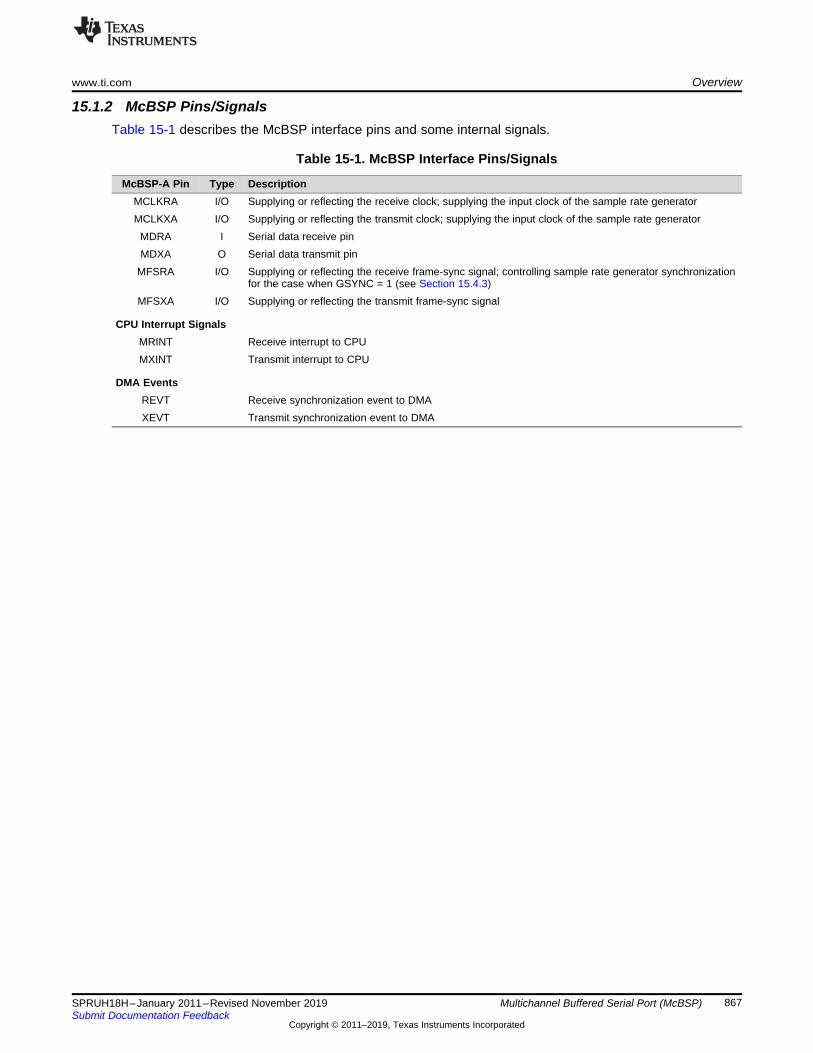
www.ti.com Overview
867SPRUH18H–January 2011–Revised November 2019Submit Documentation Feedback
Copyright © 2011–2019, Texas Instruments Incorporated
Multichannel Buffered Serial Port (McBSP)
15.1.2 McBSP Pins/SignalsTable 15-1 describes the McBSP interface pins and some internal signals.
Table 15-1. McBSP Interface Pins/Signals
McBSP-A Pin Type DescriptionMCLKRA I/O Supplying or reflecting the receive clock; supplying the input clock of the sample rate generatorMCLKXA I/O Supplying or reflecting the transmit clock; supplying the input clock of the sample rate generator
MDRA I Serial data receive pinMDXA O Serial data transmit pin
MFSRA I/O Supplying or reflecting the receive frame-sync signal; controlling sample rate generator synchronizationfor the case when GSYNC = 1 (see Section 15.4.3)
MFSXA I/O Supplying or reflecting the transmit frame-sync signal
CPU Interrupt SignalsMRINT Receive interrupt to CPUMXINT Transmit interrupt to CPU
DMA EventsREVT Receive synchronization event to DMAXEVT Transmit synchronization event to DMA

16
McBSP Receive
Interrupt Select Logic
MDXx
MDRx
Expand Logic
DRR1 Receive Buffer
RXInterrupt
DRR2 Receive Buffer
RBR1 RegisterRBR2 Register
MCLKXx
MFSXx
MCLKRx
MFSRx
16
Compand Logic
DXR2 Transmit Buffer
RSR1
XSR2 XSR1
Peripheral Read Bus
16
1616
1616
RSR2
DXR1 Transmit BufferLSPCLK
MRINT
To CPU
RX Interrupt Logic
McBSP Transmit
Interrupt Select Logic
TXInterruptMXINT
To CPU TX Interrupt Logic
16
16 16
Brid
ge
DMA Bus
Pe
rip
he
ral B
us
Peripheral Write Bus
CPU
CPU
CPU
Overview www.ti.com
868 SPRUH18H–January 2011–Revised November 2019Submit Documentation Feedback
Copyright © 2011–2019, Texas Instruments Incorporated
Multichannel Buffered Serial Port (McBSP)
15.1.2.1 McBSP Generic Block DiagramThe McBSP consists of a data-flow path and a control path connected to external devices by six pins asshown in Figure 15-1. The figure and the text in this section use generic pin names.
Figure 15-1. Conceptual Block Diagram of the McBSP
A Not available in all devices. See the device-specific data sheet
15.1.3 McBSP OperationThis section addresses the following topics:• Data transfer process• Companding (compressing and expanding) data• Clocking and framing data• Frame phases• McBSP reception• McBSP transmission• Interrupts and DMA events generated by McBSPs

ÁÁÁÁ
ÁÁÁÁ
ÁÁÁÁ
ÁÁÁÁ
ÁÁÁÁ
ÁÁÁÁ
ÁÁÁÁ
ÁÁÁÁ
ÁÁÁÁ
ÁÁÁÁ
ÁÁÁÁ
ÁÁÁÁ
DX
DR
Compand
RSR[1,2]
Compress
Expand
XSR[1,2]
ÁÁÁÁ
ÁÁÁÁ
ÁÁÁÁ
ÁÁÁÁ
RBR[1,2] DRR[1,2]ÁÁÁÁ
ÁÁÁÁ
ÁÁÁÁ
ÁÁÁÁ
DXR[1,2]
DRR[1,2]RBR[1,2] To CPU/DMA controller
From CPU/DMA controller
www.ti.com Overview
869SPRUH18H–January 2011–Revised November 2019Submit Documentation Feedback
Copyright © 2011–2019, Texas Instruments Incorporated
Multichannel Buffered Serial Port (McBSP)
15.1.4 Data Transfer Process of McBSP
Figure 15-2 shows a diagram of the McBSP data transfer paths. The McBSP receive operation is triple-buffered, and transmit operation is double-buffered. The use of registers varies, depending on whether thedefined length of each serial word is 16 bits.
Figure 15-2. McBSP Data Transfer Paths
15.1.4.1 Data Transfer Process for Word Length of 8, 12, or 16 BitsIf the word length is 16 bits or smaller, only one 16-bit register is needed at each stage of the data transferpaths. The registers DRR2, RBR2, RSR2, DXR2, and XSR2 are not used (written, read, or shifted).
Receive data arrives on the DR pin and is shifted into receive shift register 1 (RSR1). Once a full word isreceived, the content of RSR1 is copied to receive buffer register 1 (RBR1) if RBR1 is not full withprevious data. RBR1 is then copied to data receive register 1 (DRR1), unless the previous content ofDRR1 has not been read by the CPU or the DMA controller. If the companding feature of the McBSP isimplemented, the required word length is 8 bits and receive data is expanded into the appropriate formatbefore being passed from RBR1 to DRR1. For more details about reception, see Section 15.3.5.
Transmit data is written by the CPU or the DMA controller to data transmit register 1 (DXR1). If there is noprevious data in transmit shift register (XSR1), the value in DXR1 is copied to XSR1; otherwise, DXR1 iscopied to XSR1 when the last bit of the previous data is shifted out on the DX pin. If selected, thecompanding module compresses 16-bit data into the appropriate 8-bit format before passing it to XSR1.After transmit frame synchronization, the transmitter begins shifting bits from XSR1 to the DX pin. Formore details about transmission, see Section 15.3.6.
15.1.4.2 Data Transfer Process for Word Length of 20, 24, or 32 Bits
If the word length is larger than 16 bits, two 16-bit registers are needed at each stage of the data transferpaths. The registers DRR2, RBR2, RSR2, DXR2, and XSR2 are needed to hold the most significant bits.
Receive data arrives on the DR pin and is shifted first into RSR2 and then into RSR1. Once the full wordis received, the contents of RSR2 and RSR1 are copied to RBR2 and RBR1, respectively, if RBR1 is notfull. Then the contents of RBR2 and RBR1 are copied to DRR2 and DRR1, respectively, unless theprevious content of DRR1 has not been read by the CPU or the DMA controller. The CPU or the DMAcontroller must read data from DRR2 first and then from DRR1. When DRR1 is read, the next RBR-to-DRR copy occurs. For more details about reception, see Section 15.3.5.
For transmission, the CPU or the DMA controller must write data to DXR2 first and then to DXR1. Whennew data arrives in DXR1, if there is no previous data in XSR1, the contents of DXR2 and DXR1 arecopied to XSR2 and XSR1, respectively; otherwise, the contents of the DXRs are copied to the XSRswhen the last bit of the previous data is shifted out on the DX pin. After transmit frame synchronization,the transmitter begins shifting bits from the XSRs to the DX pin. For more details about transmission, seeSection 15.3.6.
15.1.5 Companding (Compressing and Expanding) DataCompanding (COMpressing and exPANDing) hardware allows compression and expansion of data ineither μ-law or A-law format. The companding standard employed in the United States and Japan is μ-law.The European companding standard is referred to as A-law. The specifications for μ-law and A-law logPCM are part of the CCITT G.711 recommendation.
A-law and μ-law allow 13 bits and 14 bits of dynamic range, respectively. Any values outside this rangeare set to the most positive or most negative value. Thus, for companding to work best, the datatransferred to and from the McBSP via the CPU or DMA controller must be at least 16 bits wide.

000
2-0
Value
15-3
A-law format in DXR1
µ-law format in DXR1 00Value
1-015-2
From CPU or DMA controllerDXR1
To CPU or DMA controllerDRR1
16
16
DX8
8
XSR1 Compress
ExpandDR RBR1RSR1
Overview www.ti.com
870 SPRUH18H–January 2011–Revised November 2019Submit Documentation Feedback
Copyright © 2011–2019, Texas Instruments Incorporated
Multichannel Buffered Serial Port (McBSP)
The μ-law and A-law formats both encode data into 8-bit code words. Companded data is always 8 bitswide; the appropriate word length bits (RWDLEN1, RWDLEN2, XWDLEN1, XWDLEN2) must therefore beset to 0, indicating an 8-bit wide serial data stream. If companding is enabled and either of the framephases does not have an 8-bit word length, companding continues as if the word length is 8 bits.
Figure 15-3 illustrates the companding processes. When companding is chosen for the transmitter,compression occurs during the process of copying data from DXR1 to XSR1. The transmit data isencoded according to the specified companding law (A-law or μ-law). When companding is chosen for thereceiver, expansion occurs during the process of copying data from RBR1 to DRR1. The receive data isdecoded to twos-complement format.
Figure 15-3. Companding Processes
15.1.5.1 Companding FormatsFor reception, the 8-bit compressed data in RBR1 is expanded to left-justified 16-bit data in DRR1. Thereceive sign-extension and justification mode specified in RJUST is ignored when companding is used.
For transmission using μ-law compression, the 14 data bits must be left-justified in DXR1 and that theremaining two low-order bits are filled with 0s as shown in Figure 15-4.
Figure 15-4. μ-Law Transmit Data Companding Format
For transmission using A-law compression, the 13 data bits must be left-justified in DXR1, with theremaining three low-order bits filled with 0s as shown in Figure 15-5.
Figure 15-5. A-Law Transmit Data Companding Format
15.1.5.2 Capability to Compand Internal DataIf the McBSP is otherwise unused (the serial port transmit and receive sections are reset), thecompanding hardware can compand internal data. This can be used to:• Convert linear to the appropriate μ-law or A-law format• Convert μ-law or A-law to the linear format• Observe the quantization effects in companding by transmitting linear data and compressing and re-
expanding this data. This is useful only if both XCOMPAND and RCOMPAND enable the samecompanding format.
Figure 15-6 shows two methods by which the McBSP can compand internal data. Data paths for thesetwo methods are used to indicate:• When both the transmit and receive sections of the serial port are reset, DRR1 and DXR1 are
connected internally through the companding logic. Values from DXR1 are compressed, as selected byXCOMPAND, and then expanded, as selected by RCOMPAND. RRDY and XRDY bits are not set.However, data is available in DRR1 within four CPU clocks after being written to DXR1.The advantage of this method is its speed. The disadvantage is that there is no synchronizationavailable to the CPU and DMA to control the flow. DRR1 and DXR1 are internally connected if the(X/R)COMPAND bits are set to 10b or 11b (compand using μ-law or A-law).

D(R/X)
FS(R/X)
CLK(R/X)
B0B1B2B3B4B5B6B7A0A1
ÁÁ
ÁÁ
ÁÁ
Á
Á
Á
ÁÁ
ÁÁ
ÁÁ
Internal
Internal
(1)(2) (DLB)
From CPU or DMA controllerDXR1
To CPU or DMA controllerDRR1
DX XSR1 Compress
ExpandDR RBR1RSR1
www.ti.com Clocking and Framing Data
871SPRUH18H–January 2011–Revised November 2019Submit Documentation Feedback
Copyright © 2011–2019, Texas Instruments Incorporated
Multichannel Buffered Serial Port (McBSP)
• The McBSP is enabled in digital loopback mode with companding appropriately enabled byRCOMPAND and XCOMPAND. Receive and transmit interrupts (RINT when RINTM = 0 and XINTwhen XINTM = 0) or synchronization events (REVT and XEVT) allow synchronization of the CPU orDMA to these conversions, respectively. Here, the time for this companding depends on the serial bitrate selected.
Figure 15-6. Two Methods by Which the McBSP Can Compand Internal Data
15.1.5.3 Reversing Bit Order: Option to Transfer LSB FirstGenerally, the McBSP transmits or receives all data with the most significant bit (MSB) first. However,certain 8-bit data protocols (that do not use companded data) require the least significant bit (LSB) to betransferred first. If you set XCOMPAND = 01b in XCR2, the bit ordering of 8-bit words is reversed (LSBfirst) before being sent from the serial port. If you set RCOMPAND = 01b in RCR2, the bit ordering of 8-bitwords is reversed during reception. Similar to companding, this feature is enabled only if the appropriateword length bits are set to 0, indicating that 8-bit words are to be transferred serially. If either phase of theframe does not have an 8-bit word length, the McBSP assumes the word length is eight bits, and LSB-firstordering is done.
15.2 Clocking and Framing DataThis section explains basic concepts and terminology important for understanding how McBSP datatransfers are timed and delimited.
15.2.1 ClockingData is shifted one bit at a time from the DR pin to the RSR(s) or from the XSR(s) to the DX pin. The timefor each bit transfer is controlled by the rising or falling edge of a clock signal.
The receive clock signal (CLKR) controls bit transfers from the DR pin to the RSR(s). The transmit clocksignal (CLKX) controls bit transfers from the XSR(s) to the DX pin. CLKR or CLKX can be derived from apin at the boundary of the McBSP or derived from inside the McBSP. The polarities of CLKR and CLKXare programmable.
In the example in Figure 15-7, the clock signal controls the timing of each bit transfer on the pin.
Figure 15-7. Example - Clock Signal Control of Bit Transfer Timing
NOTE: The McBSP cannot operate at a frequency faster than ½ the LSPCLK frequency. Whendriving CLKX or CLKR at the pin, choose an appropriate input clock frequency. When usingthe internal sample rate generator for CLKX and/or CLKR, choose an appropriate input clockfrequency and divide down value (CLKDV) (i.e., be certain that CLKX or CLKR ≤ LSPCLK/2).
15.2.2 Serial WordsBits traveling between a shift register (RSR or XSR) and a data pin (DR or DX) are transferred in a groupcalled a serial word. You can define how many bits are in a word.

Clocking and Framing Data www.ti.com
872 SPRUH18H–January 2011–Revised November 2019Submit Documentation Feedback
Copyright © 2011–2019, Texas Instruments Incorporated
Multichannel Buffered Serial Port (McBSP)
Bits coming in on the DR pin are held in RSR until RSR holds a full serial word. Only then is the wordpassed to RBR (and ultimately to the DRR).
During transmission, XSR does not accept new data from DXR until a full serial word has been passedfrom XSR to the DX pin.
In the example in Figure 15-7, an 8-bit word size was defined (see bits 7 through 0 of word B beingtransferred).
15.2.3 Frames and Frame SynchronizationOne or more words are transferred in a group called a frame. You can define how many words are in aframe.
All of the words in a frame are sent in a continuous stream. However, there can be pauses between frametransfers. The McBSP uses frame-synchronization signals to determine when each frame isreceived/transmitted. When a pulse occurs on a frame-synchronization signal, the McBSP beginsreceiving/transmitting a frame of data. When the next pulse occurs, the McBSP receives/transmits the nextframe, and so on.
Pulses on the receive frame-synchronization (FSR) signal initiate frame transfers on DR. Pulses on thetransmit frame-sync (FSX) signal initiate frame transfers on DX. FSR or FSX can be derived from a pin atthe boundary of the McBSP or derived from inside the McBSP.
In the example in Figure 15-7, a one-word frame is transferred when a frame-synchronization pulseoccurs.
In McBSP operation, the inactive-to-active transition of the frame-synchronization signal indicates the startof the next frame. For this reason, the frame-synchronization signal may be high for an arbitrary number ofclock cycles. Only after the signal is recognized to have gone inactive, and then active again, does thenext frame synchronization occur.
15.2.4 Generating Transmit and Receive InterruptsThe McBSP can send receive and transmit interrupts to the CPU to indicate specific events in the McBSP.To facilitate detection of frame synchronization, these interrupts can be sent in response to frame-synchronization pulses. Set the appropriate interrupt mode bits to 10b (for reception, RINTM = 10b; fortransmission, XINTM = 10b).
15.2.4.1 Detecting Frame-Synchronization Pulses, Even in Reset StateUnlike other serial port interrupt modes, this mode can operate while the associated portion of the serialport is in reset (such as activating RINT when the receiver is in reset). In this case, FSRM/FSXM andFSRP/FSXP still select the appropriate source and polarity of frame synchronization. Thus, even when theserial port is in the reset state, these signals are synchronized to the CPU clock and then sent to the CPUin the form of RINT and XINT at the point at which they feed the receiver and transmitter of the serial port.Consequently, a new frame-synchronization pulse can be detected, and after this occurs the CPU cantake the serial port out of reset safely.
15.2.5 Ignoring Frame-Synchronization PulsesThe McBSP can be configured to ignore transmit and/or receive frame-synchronization pulses. To havethe receiver or transmitter recognize frame-synchronization pulses, clear the appropriate frame-synchronization ignore bit (RFIG = 0 for the receiver, XFIG = 0 for the transmitter). To have the receiver ortransmitter ignore frame-synchronization pulses until the desired frame length or number of words isreached, set the appropriate frame-synchronization ignore bit (RFIG = 1 for the receiver, XFIG = 1 for thetransmitter). For more details on unexpected frame-synchronization pulses, see one of the followingtopics:• Unexpected Receive Frame-Synchronization Pulse (see Section 15.5.3)• Unexpected Transmit Frame-Synchronization Pulse (see Section 15.5.5)
You can also use the frame-synchronization ignore function for data packing (for more details, seeSection 15.11.2).

D(R/X)
FS(R/X)
CLK(R/X)
C6C7B0B1B2B3B4B5B6B7A0A1A2
Maximum Frame Frequency �Clock Frequency
Number of Bits Per Frame
Frame Frequency �Clock Frequency
Number of Clock Cycles Between Frame- Sync Pulses
www.ti.com Clocking and Framing Data
873SPRUH18H–January 2011–Revised November 2019Submit Documentation Feedback
Copyright © 2011–2019, Texas Instruments Incorporated
Multichannel Buffered Serial Port (McBSP)
15.2.6 Frame FrequencyThe frame frequency is determined by the period between frame-synchronization pulses and is defined asshown by Example 1.
Equation 1: McBSP Frame Frequency
The frame frequency can be increased by decreasing the time between frame-synchronization pulses(limited only by the number of bits per frame). As the frame transmit frequency increases, the inactivityperiod between the data packets for adjacent transfers decreases to zero.
15.2.7 Maximum Frame FrequencyThe minimum number of clock cycles between frame synchronization pulses is equal to the number of bitstransferred per frame. The maximum frame frequency is defined as shown by Example 2.
Equation 2: McBSP Maximum Frame Frequency
Figure 15-8 shows the McBSP operating at maximum packet frequency. At maximum packet frequency,the data bits in consecutive packets are transmitted contiguously with no inactivity between bits.
Figure 15-8. McBSP Operating at Maximum Packet Frequency
If there is a 1-bit data delay as shown in this figure, the frame-synchronization pulse overlaps the last bittransmitted in the previous frame. Effectively, this permits a continuous stream of data, making frame-synchronization pulses redundant. Theoretically, only an initial frame-synchronization pulse is required toinitiate a multipacket transfer.
The McBSP supports operation of the serial port in this fashion by ignoring the successive frame-synchronization pulses. Data is clocked into the receiver or clocked out of the transmitter during everyclock cycle.
NOTE: For XDATDLY = 0 (0-bit data delay), the first bit of data is transmitted asynchronously to theinternal transmit clock signal (CLKX). For more details, see Section 15.9.12, Set theTransmit Data Delay.
15.3 Frame PhasesThe McBSP allows you to configure each frame to contain one or two phases. The number of words andthe number of bits per word can be specified differently for each of the two phases of a frame, allowinggreater flexibility in structuring data transfers. For example, you might define a frame as consisting of onephase containing two words of 16 bits each, followed by a second phase consisting of 10 words of 8 bitseach. This configuration permits you to compose frames for custom applications or, in general, tomaximize the efficiency of data transfers.

D(R/X)
FS(R/X)
CLK(R/X)
Phase 2
Word 3
Phase 2
Word 2
Phase 2
Word 1
ÁÁ
ÁÁ
ÁÁ
ÁÁ
Á
Á
Á
Á
Á
Á
Á
Á
ÁÁ
ÁÁ
ÁÁ
ÁÁ
Á
Á
Á
Á
ÁÁ
ÁÁ
ÁÁ
ÁÁ
Á
Á
Á
Á
ÁÁ
ÁÁ
ÁÁ
ÁÁ
Á
Á
Á
Á
ÁÁ
ÁÁ
ÁÁ
ÁÁ
Á
Á
Á
Á
ÁÁ
ÁÁ
ÁÁ
ÁÁ
ÁÁ
ÁÁ
ÁÁ
ÁÁ
ÁÁ
ÁÁ
ÁÁ
ÁÁ
Á
Á
Á
Á
Á
Á
Á
Á
ÁÁ
ÁÁ
ÁÁ
ÁÁ
ÁÁ
ÁÁ
ÁÁ
ÁÁ
Á
Á
Á
Á
ÁÁ
ÁÁ
ÁÁ
ÁÁ
Á
Á
Á
Á
Á
Á
Á
Á
Á
Á
Á
Á
Á
Á
Á
Á
Á
Á
Á
Á
ÁÁ
ÁÁ
ÁÁ
ÁÁ
Á
Á
Á
Á
ÁÁ
ÁÁ
ÁÁ
ÁÁ
Á
Á
Á
Á
Á
Á
Á
Á
ÁÁ
ÁÁ
ÁÁ
ÁÁ
Á
Á
Á
Á
Á
Á
Á
Á
Á
Á
Á
Á
ÁÁ
ÁÁ
ÁÁ
ÁÁ
ÁÁ
ÁÁ
ÁÁ
ÁÁ
Á
Á
Á
Á
ÁÁ
ÁÁ
ÁÁ
ÁÁ
ÁÁ
ÁÁ
ÁÁ
ÁÁ
ÁÁ
ÁÁ
ÁÁ
ÁÁ
Á
Á
Á
Á
Á
Á
Á
Á
Á
Á
Á
Á
Á
Á
Á
Á
Á
Á
Á
Á
ÁÁ
ÁÁ
ÁÁ
ÁÁ
Á
Á
Á
Á
ÁÁ
ÁÁ
ÁÁ
ÁÁ
Á
Á
Á
Á
ÁÁ
ÁÁ
ÁÁ
ÁÁ
Á
Á
Á
Á
Á
Á
Á
Á
Á
Á
Á
Á
Á
Á
Á
Á
ÁÁ
ÁÁ
ÁÁ
ÁÁ
Phase 1 Word 1Phase 1 Word 2
A1D(R/X)
FS(R/X)
CLK(R/X)
C5C6C7B0B1B2B3B4B5B6B7A0
Á
Á
Á
Á
Á
Á
Á
Á
Á
Á
Á
Á
Á
Á
Á
Á
Frame Phases www.ti.com
874 SPRUH18H–January 2011–Revised November 2019Submit Documentation Feedback
Copyright © 2011–2019, Texas Instruments Incorporated
Multichannel Buffered Serial Port (McBSP)
15.3.1 Number of Phases, Words, and Bits Per FrameTable 15-2 shows which bit-fields in the receive control registers (RCR1 and RCR2) and in the transmitcontrol registers (XCR1 and XCR2) determine the number of phases per frame, the number of words perframe, and number of bits per word for each phase, for the receiver and transmitter. The maximumnumber of words per frame is 128 for a single-phase frame and 256 for a dual-phase frame. The numberof bits per word can be 8, 12, 16, 20, 24, or 32 bits.
Table 15-2. Register Bits That Determine the Number of Phases, Words, and Bits
Operation Number of Phases Words per Frame Set With Bits per Word Set WithReception 1 (RPHASE = 0) RFRLEN1 RWDLEN1Reception 2 (RPHASE = 1) RFRLEN1 and RFRLEN2 RWDLEN1 for phase 1
RWDLEN2 for phase 2Transmission 1 (XPHASE = 0) XFRLEN1 XWDLEN1Transmission 2 (XPHASE = 1) XFRLEN1 and XFRLEN2 XWDLEN1 for phase 1
XWDLEN2 for phase 2
15.3.2 Single-Phase Frame ExampleFigure 15-9 shows an example of a single-phase data frame containing one 8-bit word. Because thetransfer is configured for one data bit delay, the data on the DX and DR pins are available one clock cycleafter FS(R/X) goes active. The figure makes the following assumptions:• (R/X)PHASE = 0: Single-phase frame• (R/X)FRLEN1 = 0b: 1 word per frame• (R/X)WDLEN1 = 000b: 8-bit word length• (R/X)FRLEN2 and (R/X)WDLEN2 are ignored• CLK(X/R)P = 0: Receive data clocked on falling edge; transmit data clocked on rising edge• FS(R/X)P = 0: Active-high frame-synchronization signals• (R/X)DATDLY = 01b: 1-bit data delay
Figure 15-9. Single-Phase Frame for a McBSP Data Transfer
15.3.3 Dual-Phase Frame ExampleFigure 15-10 shows an example of a frame where the first phase consists of two words of 12 bits each,followed by a second phase of three words of 8 bits each. The entire bit stream in the frame is contiguous.There are no gaps either between words or between phases.
Figure 15-10. Dual-Phase Frame for a McBSP Data Transfer
A XRDY gets asserted once per phase. So, if there are 2 phases, XRDY gets asserted twice (once per phase).
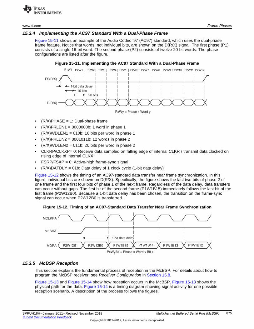
PxWyBz = Phase x Word y Bit z
Á
Á
Á
Á
P2W12B0P2W12B1MDRA P1W1B15 P1W1B12P1W1B13P1W1B14
MFSRA
MCLKRA
1-bit data delay
PxWy = Phase x Word y
D(R/X)
FS(R/X)
P2W12P2W11P2W10P2W9P2W8P2W7P2W6P2W5P2W4P2W3P2W2P2W1P1W1
ÁÁ
ÁÁ
ÁÁ
ÁÁ
20 bits
16 bits
1-bit data delay
www.ti.com Frame Phases
875SPRUH18H–January 2011–Revised November 2019Submit Documentation Feedback
Copyright © 2011–2019, Texas Instruments Incorporated
Multichannel Buffered Serial Port (McBSP)
15.3.4 Implementing the AC97 Standard With a Dual-Phase FrameFigure 15-11 shows an example of the Audio Codec ‘97 (AC97) standard, which uses the dual-phaseframe feature. Notice that words, not individual bits, are shown on the D(R/X) signal. The first phase (P1)consists of a single 16-bit word. The second phase (P2) consists of twelve 20-bit words. The phaseconfigurations are listed after the figure.
Figure 15-11. Implementing the AC97 Standard With a Dual-Phase Frame
• (R/X)PHASE = 1: Dual-phase frame• (R/X)FRLEN1 = 0000000b: 1 word in phase 1• (R/X)WDLEN1 = 010b: 16 bits per word in phase 1• (R/X)FRLEN2 = 0001011b: 12 words in phase 2• (R/X)WDLEN2 = 011b: 20 bits per word in phase 2• CLKRP/CLKXP= 0: Receive data sampled on falling edge of internal CLKR / transmit data clocked on
rising edge of internal CLKX• FSRP/FSXP = 0: Active-high frame-sync signal• (R/X)DATDLY = 01b: Data delay of 1 clock cycle (1-bit data delay)
Figure 15-12 shows the timing of an AC97-standard data transfer near frame synchronization. In thisfigure, individual bits are shown on D(R/X). Specifically, the figure shows the last two bits of phase 2 ofone frame and the first four bits of phase 1 of the next frame. Regardless of the data delay, data transferscan occur without gaps. The first bit of the second frame (P1W1B15) immediately follows the last bit of thefirst frame (P2W12B0). Because a 1-bit data delay has been chosen, the transition on the frame-syncsignal can occur when P2W12B0 is transferred.
Figure 15-12. Timing of an AC97-Standard Data Transfer Near Frame Synchronization
15.3.5 McBSP ReceptionThis section explains the fundamental process of reception in the McBSP. For details about how toprogram the McBSP receiver, see Receiver Configuration in Section 15.8.
Figure 15-13 and Figure 15-14 show how reception occurs in the McBSP. Figure 15-13 shows thephysical path for the data. Figure 15-14 is a timing diagram showing signal activity for one possiblereception scenario. A description of the process follows the figures.

RRDY
DR
FSR
CLKR
Read from DRR1(b)RBR1 to DRR1 copy(B)Read from DRR1(A)RBR1 to DRR1 copy(A)
C5C6C7B0B1B2B3B4B5B6B7A0A1
Á
Á
Á
Á
Á
Á
Á
Á
Á
Á
Á
Á
Á
Á
Á
Á
ÁÁÁÁ
ÁÁÁÁ
ÁÁÁÁ
ÁÁÁ
ÁÁÁ
ÁÁÁ
DR RSR[1,2] Expand
ÁÁÁÁ
ÁÁÁÁ
ÁÁÁÁ
RBR[1,2] DRR[1,2]DRR[1,2]RBR[1,2] To CPU or
DMA controller
justify and bit fillor
Frame Phases www.ti.com
876 SPRUH18H–January 2011–Revised November 2019Submit Documentation Feedback
Copyright © 2011–2019, Texas Instruments Incorporated
Multichannel Buffered Serial Port (McBSP)
Figure 15-13. McBSP Reception Physical Data Path
A RSR[1,2]: Receive shift registers 1 and 2B RBR[1,2]: Receive buffer registers 1 and 2C DRR[1,2]: Data receive registers 1 and 2
Figure 15-14. McBSP Reception Signal Activity
A CLKR: Internal receive clockB FSR: Internal receive frame-synchronization signalC DR: Data on DR pinD RRDY: Status of receiver ready bit (high is 1)
The following process describes how data travels from the DR pin to the CPU or to the DMA controller:1. The McBSP waits for a receive frame-synchronization pulse on internal FSR.2. When the pulse arrives, the McBSP inserts the appropriate data delay that is selected with the
RDATDLY bits of RCR2.In the preceding timing diagram (Figure 15-14), a 1-bit data delay is selected.
3. The McBSP accepts data bits on the DR pin and shifts them into the receive shift register(s).If the word length is 16 bits or smaller, only RSR1 is used. If the word length is larger than 16 bits,RSR2 and RSR1 are used and RSR2 contains the most significant bits. For details on choosing a wordlength, see Section 15.8.8, Set the Receive Word Length(s).
4. When a full word is received, the McBSP copies the contents of the receive shift register(s) to thereceive buffer register(s), provided that RBR1 is not full with previous data.If the word length is 16 bits or smaller, only RBR1 is used. If the word length is larger than 16 bits,RBR2 and RBR1 are used and RBR2 contains the most significant bits.
5. The McBSP copies the contents of the receive buffer register(s) into the data receive register(s),provided that DRR1 is not full with previous data. When DRR1 receives new data, the receiver readybit (RRDY) is set in SPCR1. This indicates that received data is ready to be read by the CPU or theDMA controller.If the word length is 16 bits or smaller, only DRR1 is used. If the word length is larger than 16 bits,DRR2 and DRR1 are used and DRR2 contains the most significant bits.If companding is used during the copy (RCOMPAND = 10b or 11b in RCR2), the 8-bit compresseddata in RBR1 is expanded to a left-justified 16-bit value in DRR1. If companding is disabled, the datacopied from RBR[1,2] to DRR[1,2] is justified and bit filled according to the RJUST bits.
6. The CPU or the DMA controller reads the data from the data receive register(s). When DRR1 is read,RRDY is cleared and the next RBR-to-DRR copy is initiated.
NOTE: If both DRRs are required (word length larger than 16 bits), the CPU or the DMA controllermust read from DRR2 first and then from DRR1. As soon as DRR1 is read, the next RBR-to-DRR copy is initiated. If DRR2 is not read first, the data in DRR2 is lost.
When activity is not properly timed, errors can occur. See the following topics for more details:

Write to DXR1DXR1 to XSR1 copy(C)Write to DXR1(C)DXR1 to XSR1 copy(B)
XRDY
DX
FSX
CLKX
C5C6C7B0B1B2B3B4B5B6B7A0A1
Á
Á
Á
Á
Á
Á
Á
Á
ÁÁ
ÁÁ
ÁÁ
ÁÁ
Á
Á
Á
Á
ÁÁÁÁ
ÁÁÁÁ
ÁÁÁÁ
DX XSR[1,2]
ÁÁÁÁ
ÁÁÁÁ
ÁÁÁÁ
DXR[1,2] From CPU or
DMA controllerCompress
do not modifyor
www.ti.com Frame Phases
877SPRUH18H–January 2011–Revised November 2019Submit Documentation Feedback
Copyright © 2011–2019, Texas Instruments Incorporated
Multichannel Buffered Serial Port (McBSP)
• Overrun in the Receiver (see Section 15.5.2)• Unexpected Receive Frame-Synchronization Pulse (see Section 15.5.3)
15.3.6 McBSP TransmissionThis section explains the fundamental process of transmission in the McBSP. For details about how toprogram the McBSP transmitter, see Section 15.9, Transmitter Configuration.
Figure 15-15 and Figure 15-16 show how transmission occurs in the McBSP. Figure 15-15 shows thephysical path for the data. Figure 15-16 is a timing diagram showing signal activity for one possibletransmission scenario. A description of the process follows the figures.
Figure 15-15. McBSP Transmission Physical Data Path
A XSR[1,2]: Transmit shift registers 1 and 2B DXR[1,2]: Data transmit registers 1 and 2
Figure 15-16. McBSP Transmission Signal Activity
A CLKX: Internal transmit clockB FSX: Internal transmit frame-synchronization signalC DX: Data on DX pinD XRDY: Status of transmitter ready bit (high is 1)
1. The CPU or the DMA controller writes data to the data transmit register(s). When DXR1 is loaded, thetransmitter ready bit (XRDY) is cleared in SPCR2 to indicate that the transmitter is not ready for newdata.If the word length is 16 bits or smaller, only DXR1 is used. If the word length is larger than 16 bits,DXR2 and DXR1 are used and DXR2 contains the most significant bits. For details on choosing a wordlength, see Section 15.9.8, Set the Transmit Word Length(s).
NOTE: If both DXRs are needed (word length larger than 16 bits), the CPU or the DMA controllermust load DXR2 first and then load DXR1. As soon as DXR1 is loaded, the contents of bothDXRs are copied to the transmit shift registers (XSRs), as described in the next step. IfDXR2 is not loaded first, the previous content of DXR2 is passed to the XSR2.
2. When new data arrives in DXR1, the McBSP copies the content of the data transmit register(s) to thetransmit shift register(s). In addition, the transmit ready bit (XRDY) is set. This indicates that thetransmitter is ready to accept new data from the CPU or the DMA controller.If the word length is 16 bits or smaller, only XSR1 is used. If the word length is larger than 16 bits,XSR2 and XSR1 are used and XSR2 contains the most significant bits.If companding is used during the transfer (XCOMPAND = 10b or 11b in XCR2), the McBSPcompresses the 16-bit data in DXR1 to 8-bit data in the μ-law or A-law format in XSR1. If compandingis disabled, the McBSP passes data from the DXR(s) to the XSR(s) without modification.
3. The McBSP waits for a transmit frame-synchronization pulse on internal FSX.4. When the pulse arrives, the McBSP inserts the appropriate data delay that is selected with the
XDATDLY bits of XCR2.

Frame Phases www.ti.com
878 SPRUH18H–January 2011–Revised November 2019Submit Documentation Feedback
Copyright © 2011–2019, Texas Instruments Incorporated
Multichannel Buffered Serial Port (McBSP)
In the preceding timing diagram (Figure 15-16), a 1-bit data delay is selected.5. The McBSP shifts data bits from the transmit shift register(s) to the DX pin.
When activity is not properly timed, errors can occur. See the following topics for more details:• Overwrite in the Transmitter ( Section 15.5.4)• Underflow in the Transmitter (Section 15.5.4.3)• Unexpected Transmit Frame-Synchronization Pulse (Section 15.5.5)
15.3.7 Interrupts and DMA Events Generated by a McBSPThe McBSP sends notification of important events to the CPU and the DMA controller via the internalsignals shown in Table 15-3.
Table 15-3. Interrupts and DMA Events Generated by a McBSP
Internal Signal DescriptionRINT Receive interrupt
The McBSP can send a receive interrupt request to CPU based upon a selected condition in the receiver ofthe McBSP (a condition selected by the RINTM bits of SPCR1).
XINT Transmit interruptThe McBSP can send a transmit interrupt request to CPU based upon a selected condition in the transmitterof the McBSP (a condition selected by the XINTM bits of SPCR2).
REVT Receive synchronization eventAn REVT signal is sent to the DMA when data has been received in the data receive registers (DRRs).
XEVT Transmit synchronization eventAn XEVT signal is sent to the DMA when the data transmit registers (DXRs) are ready to accept the nextserial word for transmission.
15.4 McBSP Sample Rate GeneratorEach McBSP contains a sample rate generator (SRG) that can be programmed to generate an internaldata clock (CLKG) and an internal frame-synchronization signal (FSG). CLKG can be used for bit shiftingon the data receive (DR) pin and/or the data transmit (DX) pin. FSG can be used to initiate frame transferson DR and/or DX. Figure 15-17 is a conceptual block diagram of the sample rate generator.

FSR
GSYNC synchronization
and clock
detection
Frame pulse
SRGR1
[CLKGDV]
CLKSRG
0
1CLKXP
MCLKX pin
CLKRP
MCLKR pin
0
1LSPCLK
SRGR2 [CLKSM]
0
1
PCR
[SCLKSME]
SRGR1
[FWID]
CLKG
FSGpulse
Frame
SRGR2
[FPER]
÷
Reserved
/(CLKGDV + 1)
www.ti.com McBSP Sample Rate Generator
879SPRUH18H–January 2011–Revised November 2019Submit Documentation Feedback
Copyright © 2011–2019, Texas Instruments Incorporated
Multichannel Buffered Serial Port (McBSP)
15.4.1 Block Diagram
Figure 15-17. Conceptual Block Diagram of the Sample Rate Generator
The source clock for the sample rate generator (labeled CLKSRG in the diagram) can be supplied by theLSPCLK, or by an external pin (MCLKX or MCLKR). The source is selected with the SCLKME bit of PCRand the CLKSM bit of SRGR2. If a pin is used, the polarity of the incoming signal can be inverted with theappropriate polarity bit (CLKXP of PCR or CLKRP of PCR).
The sample rate generator has a three-stage clock divider that gives CLKG and FSG programmability.The three stages provide:• Clock divide-down. The source clock is divided according to the CLKGDV bits of SRGR1 to produce
CLKG.• Frame period divide-down. CLKG is divided according to the FPER bits of SRGR2 to control the period
from the start of a frame-pulse to the start of the next pulse.• Frame-synchronization pulse-width countdown. CLKG cycles are counted according to the FWID bits
of SRGR1 to control the width of each frame-synchronization pulse.
NOTE: The McBSP cannot operate at a frequency faster than ½ the source clock frequency.Choose an input clock frequency and a CLKGDV value such that CLKG is less than or equalto ½ the source clock frequency.
In addition to the three-stage clock divider, the sample rate generator has a frame-synchronization pulsedetection and clock synchronization module that allows synchronization of the clock divide down with anincoming frame-synchronization pulse on the FSR pin. This feature is enabled or disabled with theGSYNC bit of SRGR2.
For details on getting the sample rate generator ready for operation, see Section 15.4.4, Reset andInitialization Procedure.

McBSP Sample Rate Generator www.ti.com
880 SPRUH18H–January 2011–Revised November 2019Submit Documentation Feedback
Copyright © 2011–2019, Texas Instruments Incorporated
Multichannel Buffered Serial Port (McBSP)
15.4.1.1 Clock Generation in the Sample Rate GeneratorThe sample rate generator can produce a clock signal (CLKG) for use by the receiver, the transmitter, orboth. Use of the sample rate generator to drive clocking is controlled by the clock mode bits (CLKRM andCLKXM) in the pin control register (PCR). When a clock mode bit is set to 1 (CLKRM = 1 for reception,CLKXM = 1 for transmission), the corresponding data clock (CLKR for reception, CLKX for transmission)is driven by the internal sample rate generator output clock (CLKG).
The effects of CLKRM = 1 and CLKXM = 1 on the McBSP are partially affected by the use of the digitalloopback mode and the clock stop (SPI) mode, respectively, as described in Table 15-4. The digitalloopback mode (described in Section 15.8.4) is selected with the DLB bit of SPCR1. The clock stop mode(described in Section 15.7.2) is selected with the CLKSTP bits of SPCR1.
When using the sample rate generator as a clock source, make sure the sample rate generator is enabled(GRST = 1).
Table 15-4. Effects of DLB and CLKSTP on Clock Modes
Mode Bit Settings EffectCLKRM = 1 DLB = 0
(Digital loopback mode disabled)CLKR is an output pin driven by the sample rate generator output clock(CLKG).
DLB = 1(Digital loopback mode enabled)
CLKR is an output pin driven by internal CLKX. The source for CLKXdepends on the CLKXM bit.
CLKXM = 1 CLKSTP = 00b or 01b(Clock stop (SPI) mode disabled)
CLKX is an output pin driven by the sample rate generator output clock(CLKG).
CLKSTP = 10b or 11b(Clock stop (SPI) mode enabled)
The McBSP is a master in an SPI system. Internal CLKX drives internalCLKR and the shift clocks of any SPI-compliant slave devices in thesystem. CLKX is driven by the internal sample rate generator.
15.4.1.2 Choosing an Input ClockThe sample rate generator must be driven by an input clock signal from one of the three sourcesselectable with the SCLKME bit of PCR and the CLKSM bit of SRGR2 (see Table 15-5). When CLKSM =1, the minimum divide down value in CLKGDV bits is 1. CLKGDV is described in Section 15.4.1.4.
Table 15-5. Choosing an Input Clock for the Sample Rate Generator with theSCLKME and CLKSM Bits
SCLKME CLKSM Input Clock for Sample Rate Generator0 0 Reserved0 1 LSPCLK1 0 Signal on MCLKR pin1 1 Signal on MCLKX pin
15.4.1.3 Choosing a Polarity for the Input ClockAs shown in Figure 15-18, when the input clock is received from a pin, you can choose the polarity of theinput clock. The rising edge of CLKSRG generates CLKG and FSG, but you can determine which edge ofthe input clock causes a rising edge on CLKSRG. The polarity options and their effects are described inTable 15-6.

CLKG frequency�Input clock frequency
(CLKGDV� 1)
CLKSRG
0
1CLKXP
MCLKX pin
CLKRP
MCLKR pin
0
1LSPCLK
CLKSM
0
1
SCLKME
To clock dividers
Reserved
www.ti.com McBSP Sample Rate Generator
881SPRUH18H–January 2011–Revised November 2019Submit Documentation Feedback
Copyright © 2011–2019, Texas Instruments Incorporated
Multichannel Buffered Serial Port (McBSP)
Figure 15-18. Possible Inputs to the Sample Rate Generator and the Polarity Bits
Table 15-6. Polarity Options for the Input to the Sample Rate Generator
Input Clock Polarity Option EffectLSPCLK Always positive polarity Rising edge of CPU clock generates transitions on CLKG and FSG.Signal on MCLKR pin CLKRP = 0 in PCR Falling edge on MCLKR pin generates transitions on CLKG and FSG.
CLKRP = 1 in PCR Rising edge on MCLKR pin generates transitions on CLKG and FSG.Signal on MCLKX pin CLKXP = 0 in PCR Rising edge on MCLKX pin generates transitions on CLKG and FSG.
CLKXP = 1 in PCR Falling edge on MCLKX pin generates transitions on CLKG and FSG.
15.4.1.4 Choosing a Frequency for the Output Clock (CLKG)The input clock (LSPCLK or external clock) can be divided down by a programmable value to drive CLKG.Regardless of the source to the sample rate generator, the rising edge of CLKSRG (see Figure 15-17)generates CLKG and FSG.
The first divider stage of the sample rate generator creates the output clock from the input clock. Thisdivider stage uses a counter that is preloaded with the divide down value in the CLKGDV bits of SRGR1.The output of this stage is the data clock (CLKG). CLKG has the frequency represented by Example 3.
Equation 3: CLKG Frequency
Thus, the input clock frequency is divided by a value between 1 and 256. When CLKGDV is odd or equalto 0, the CLKG duty cycle is 50%. When CLKGDV is an even value, 2p, representing an odd divide down,the high-state duration is p+1 cycles and the low-state duration is p cycles.
15.4.1.5 Keeping CLKG Synchronized to External MCLKRWhen the MCLKR pin is used to drive the sample rate generator (see Section 15.4.1.2), the GSYNC bit inSRGR2 and the FSR pin can be used to configure the timing of the output clock (CLKG) relative to theinput clock. Note that this feature is available only when the MCLKR pin is used to feed the external clock.
GSYNC = 1 ensures that the McBSP and an external device are dividing down the input clock with thesame phase relationship. If GSYNC = 1, an inactive-to-active transition on the FSR pin triggers aresynchronization of CLKG and generation of FSG.
For more details about synchronization, see Section 15.4.3.

McBSP Sample Rate Generator www.ti.com
882 SPRUH18H–January 2011–Revised November 2019Submit Documentation Feedback
Copyright © 2011–2019, Texas Instruments Incorporated
Multichannel Buffered Serial Port (McBSP)
15.4.2 Frame Synchronization Generation in the Sample Rate GeneratorThe sample rate generator can produce a frame-synchronization signal (FSG) for use by the receiver, thetransmitter, or both.
If you want the receiver to use FSG for frame synchronization, make sure FSRM = 1. (When FSRM = 0,receive frame synchronization is supplied via the FSR pin.)
If you want the transmitter to use FSG for frame synchronization, you must set:• FSXM = 1 in PCR: This indicates that transmit frame synchronization is supplied by the McBSP itself
rather than from the FSX pin.• FSGM = 1 in SRGR2: This indicates that when FSXM = 1, transmit frame synchronization is supplied
by the sample rate generator. (When FSGM = 0 and FSXM = 1, the transmitter uses frame-synchronization pulses generated every time data is transferred from DXR[1,2] to XSR[1,2].)
In either case, the sample rate generator must be enabled (GRST = 1) and the frame-synchronizationlogic in the sample rate generator must be enabled (FRST = 0).
15.4.2.1 Choosing the Width of the Frame-Synchronization Pulse on FSGEach pulse on FSG has a programmable width. You program the FWID bits of SRGR1, and the resultingpulse width is (FWID + 1) CLKG cycles, where CLKG is the output clock of the sample rate generator.
15.4.2.2 Controlling the Period Between the Starting Edges of Frame-Synchronization Pulses on FSGYou can control the amount of time from the starting edge of one FSG pulse to the starting edge of thenext FSG pulse. This period is controlled in one of two ways, depending on the configuration of thesample rate generator:• If the sample rate generator is using an external input clock and GSYNC = 1 in SRGR2, FSG pulses in
response to an inactive-to-active transition on the FSR pin. Thus, the frame-synchronization period iscontrolled by an external device.
• Otherwise, you program the FPER bits of SRGR2, and the resulting frame-synchronization period is(FPER + 1) CLKG cycles, where CLKG is the output clock of the sample rate generator.
15.4.2.3 Keeping FSG Synchronized to an External ClockWhen an external signal is selected to drive the sample rate generator (see Section 15.4.1.2 on pageSection 15.4.1.2), the GSYNC bit of SRGR2 and the FSR pin can be used to configure the timing of FSGpulses.
GSYNC = 1 ensures that the McBSP and an external device are dividing down the input clock with thesame phase relationship. If GSYNC = 1, an inactive-to-active transition on the FSR pin triggers aresynchronization of CLKG and generation of FSG.
See Section 15.4.3 for more details about synchronization.
15.4.3 Synchronizing Sample Rate Generator Outputs to an External ClockThe sample rate generator can produce a clock signal (CLKG) and a frame-synchronization signal (FSG)based on an input clock signal that is either the CPU clock signal or a signal at the MCLKR or MCLKX pin.When an external clock is selected to drive the sample rate generator, the GSYNC bit of SRGR2 and theFSR pin can be used to control the timing of CLKG and the pulsing of FSG relative to the chosen inputclock.
Make GSYNC = 1 when you want the McBSP and an external device to divide down the input clock withthe same phase relationship. If GSYNC = 1:• An inactive-to-active transition on the FSR pin triggers a resynchronization of CLKG and a pulsing of
FSG.• CLKG always begins with a high state after synchronization.• FSR is always detected at the same edge of the input clock signal that generates CLKG, no matter
how long the FSR pulse is.

FSG
(Needs resynchronization)CLKG
resynchronize)(No need to
CLKG
(FSRP=1)FSR external
(FSRP=0)FSR external
CLKR
CLKR
www.ti.com McBSP Sample Rate Generator
883SPRUH18H–January 2011–Revised November 2019Submit Documentation Feedback
Copyright © 2011–2019, Texas Instruments Incorporated
Multichannel Buffered Serial Port (McBSP)
• The FPER bits of SRGR2 are ignored because the frame-synchronization period on FSG is determinedby the arrival of the next frame-synchronization pulse on the FSR pin.
If GSYNC = 0, CLKG runs freely and is not resynchronized, and the frame-synchronization period on FSGis determined by FPER.
15.4.3.1 Operating the Transmitter Synchronously with the ReceiverWhen GSYNC = 1, the transmitter can operate synchronously with the receiver, provided that:• FSX is programmed to be driven by FSG (FSGM = 1 in SRGR2 and FSXM = 1 in PCR). If the input
FSR has appropriate timing so that it can be sampled by the falling edge of CLKG, it can be used,instead, by setting FSXM = 0 and connecting FSR to FSX externally.
• The sample rate generator clock drives the transmit and receive clocking (CLKRM = CLKXM = 1 inPCR).
15.4.3.2 Synchronization ExamplesFigure 15-19 and Figure 15-20 show the clock and frame-synchronization operation with various polaritiesof CLKR and FSR. These figures assume FWID = 0 in SRGR1, for an FSG pulse that is one CLKG cyclewide. The FPER bits of SRGR2 are not programmed; the period from the start of a frame-synchronizationpulse to the start of the next pulse is determined by the arrival of the next inactive-to-active transition onthe FSR pin. Each of the figures shows what happens to CLKG when it is initially synchronized andGSYNC = 1, and when it is not initially synchronized and GSYNC = 1. The second figure has a slowerCLKG frequency (it has a larger divide-down value in the CLKGDV bits of SRGR1).
Figure 15-19. CLKG Synchronization and FSG Generation When GSYNC = 1 and CLKGDV = 1

FSG
(Needs resynchronization)CLKG
resynchronize)(No need to
CLKG
(FSRP=1)FSR external
(FSRP=0)FSR external
CLKR
CLKR
McBSP Sample Rate Generator www.ti.com
884 SPRUH18H–January 2011–Revised November 2019Submit Documentation Feedback
Copyright © 2011–2019, Texas Instruments Incorporated
Multichannel Buffered Serial Port (McBSP)
Figure 15-20. CLKG Synchronization and FSG Generation When GSYNC = 1 and CLKGDV = 3
15.4.4 Reset and Initialization Procedure for the Sample Rate GeneratorTo reset and initialize the sample rate generator:
Step 1. Place the McBSP/sample rate generator in reset.During a DSP reset, the sample rate generator, the receiver, and the transmitter reset bits (GRST,RRST, and XRST) are automatically forced to 0. Otherwise, during normal operation, the sample rategenerator can be reset by making GRST = 0 in SPCR2, provided that CLKG and/or FSG is not usedby any portion of the McBSP. Depending on your system you may also want to reset the receiver(RRST = 0 in SPCR1) and reset the transmitter (XRST = 0 in SPCR2).If GRST = 0 due to a device reset, CLKG is driven by the CPU clock divided by 2, and FSG is driveninactive-low. If GRST = 0 due to program code, CLKG and FSG are driven low (inactive).Step 2. Program the registers that affect the sample rate generator.Program the sample rate generator registers (SRGR1 and SRGR2) as required for your application. Ifnecessary, other control registers can be loaded with desired values, provided the respective portion ofthe McBSP (the receiver or transmitter) is in reset.After the sample rate generator registers are programmed, wait 2 CLKSRG cycles. This ensuresproper synchronization internally.Step 3. Enable the sample rate generator (take it out of reset).In SPCR2, make GRST = 1 to enable the sample rate generator.After the sample rate generator is enabled, wait two CLKG cycles for the sample rate generator logic tostabilize.On the next rising edge of CLKSRG, CLKG transitions to 1 and starts clocking with a frequency equalto Example 4.
Table 15-7. Input Clock Selection for Sample Rate Generator
SCLKME CLKSM Input Clock for Sample Rate Generator0 0 Reserved0 1 LSPCLK1 0 Signal on MCLKR pin1 1 Signal on MCLKX pin

CLKG frequency�Input clock frequency
(CLKGDV� 1)
www.ti.com McBSP Exception/Error Conditions
885SPRUH18H–January 2011–Revised November 2019Submit Documentation Feedback
Copyright © 2011–2019, Texas Instruments Incorporated
Multichannel Buffered Serial Port (McBSP)
Step 4. If necessary, enable the receiver and/or the transmitter.If necessary, remove the receiver and/or transmitter from reset by setting RRST and/or XRST = 1.Step 5. If necessary, enable the frame-synchronization logic of the sample rate generator.After the required data acquisition setup is done (DXR[1,2] is loaded with data), set GRST = 1 inSPCR2 if an internally generated frame-synchronization pulse is required. FSG is generated with anactive-high edge after the programmed number of CLKG clocks (FPER + 1) have elapsed.
Equation 4: CLKG Frequency
where the input clock is selected with the SCLKME bit of PCR and the CLKSM bit of SRGR2 in one of theconfigurations shown in Table 15-7.
15.5 McBSP Exception/Error ConditionsThis section describes exception/error conditions and how to handle them.
15.5.1 Types of ErrorsThere are five serial port events that can constitute a system error:• Receiver overrun (RFULL = 1)
This occurs when DRR1 has not been read since the last RBR-to-DRR copy. Consequently, thereceiver does not copy a new word from the RBR(s) to the DRR(s) and the RSR(s) are now full withanother new word shifted in from DR. Therefore, RFULL = 1 indicates an error condition wherein anynew data that can arrive at this time on DR replaces the contents of the RSR(s), and the previous wordis lost. The RSRs continue to be overwritten as long as new data arrives on DR and DRR1 is not read.For more details about overrun in the receiver, see Section 15.5.2.
• Unexpected receive frame-synchronization pulse (RSYNCERR = 1)This occurs during reception when RFIG = 0 and an unexpected frame-synchronization pulse occurs.An unexpected frame-synchronization pulse is one that begins the next frame transfer before all thebits of the current frame have been received. Such a pulse causes data reception to abort and restart.If new data has been copied into the RBR(s) from the RSR(s) since the last RBR-to-DRR copy, thisnew data in the RBR(s) is lost. This is because no RBR-to-DRR copy occurs; the reception has beenrestarted. For more details about receive frame-synchronization errors, see Section 15.5.3.
• Transmitter data overwriteThis occurs when the CPU or DMA controller overwrites data in the DXR(s) before the data is copiedto the XSR(s). The overwritten data never reaches the DX pin. For more details about overwrite in thetransmitter, see Section 15.5.4.
• Transmitter underflow (XEMPTY = 0)If a new frame-synchronization signal arrives before new data is loaded into DXR1, the previous datain the DXR(s) is sent again. This procedure continues for every new frame-synchronization pulse thatarrives until DXR1 is loaded with new data. For more details about underflow in the transmitter, seeSection 15.5.4.3.
• Unexpected transmit frame-synchronization pulse (XSYNCERR = 1)This occurs during transmission when XFIG = 0 and an unexpected frame-synchronization pulseoccurs. An unexpected frame-synchronization pulse is one that begins the next frame transfer beforeall the bits of the current frame have been transferred. Such a pulse causes the current datatransmission to abort and restart. If new data has been written to the DXR(s) since the last DXR-to-XSR copy, the current value in the XSR(s) is lost. For more details about transmit frame-synchronization errors, see Section 15.5.5.
15.5.2 Overrun in the ReceiverRFULL = 1 in SPCR1 indicates that the receiver has experienced overrun and is in an error condition.RFULL is set when all of the following conditions are met:

No RSR1 to RBR1 copy(C)
No read from DRR1(A)No RBR1 to DRR1 copy(B)No read from DRR1(A)
RBR1 to DRR1 copy(A)
D7C0C1C2C3C4C5C6C7B0B1B2B3B4B5B6B7A0A1
RFULL
RRDY
DR
FSR
CLKRÁ
Á
Á
Á
Á
Á
Á
Á
ÁÁ
ÁÁ
ÁÁ
ÁÁ
Á
Á
Á
Á
Á
Á
Á
Á
Á
Á
Á
Á
McBSP Exception/Error Conditions www.ti.com
886 SPRUH18H–January 2011–Revised November 2019Submit Documentation Feedback
Copyright © 2011–2019, Texas Instruments Incorporated
Multichannel Buffered Serial Port (McBSP)
1. DRR1 has not been read since the last RBR-to-DRR copy (RRDY = 1).2. RBR1 is full and an RBR-to-DRR copy has not occurred.3. RSR1 is full and an RSR1-to-RBR copy has not occurred.
As described in the Section 15.3.5, McBSP Reception, data arriving on DR is continuously shifted intoRSR1 (for word length of 16 bits or smaller) or RSR2 and RSR1 (for word length larger than 16 bits).Once a complete word is shifted into the RSR(s), an RSR-to-RBR copy can occur only if the previous datain RBR1 has been copied to DRR1. The RRDY bit is set when new data arrives in DRR1 and is clearedwhen that data is read from DRR1. Until RRDY = 0, the next RBR-to-DRR copy does not take place, andthe data is held in the RSR(s). New data arriving on the DR pin is shifted into RSR(s), and the previouscontent of the RSR(s) is lost.
You can prevent the loss of data if DRR1 is read no later than 2.5 cycles before the end of the third wordis shifted into the RSR1.
NOTE: If both DRRs are needed (word length larger than 16 bits), the CPU or the DMA controllermust read from DRR2 first and then from DRR1. As soon as DRR1 is read, the next RBR-to-DRR copy is initiated. If DRR2 is not read first, the data in DRR2 is lost.
After the receiver starts running from reset, a minimum of three words must be received before RFULL isset. Either of the following events clears the RFULL bit and allows subsequent transfers to be readproperly:• The CPU or DMA controller reads DRR1.• The receiver is reset individually (RRST = 0) or as part of a device reset.
Another frame-synchronization pulse is required to restart the receiver.
15.5.2.1 Example of Overrun ConditionFigure 15-21 shows the receive overrun condition. Because serial word A is not read from DRR1 beforeserial word B arrives in RBR1, B is not transferred to DRR1 yet. Another new word ©) arrives and RSR1 isfull with this data. DRR1 is finally read, but not earlier than 2.5 cycles before the end of word C. Therefore,new data (D) overwrites word C in RSR1. If DRR1 is not read in time, the next word can overwrite D.
Figure 15-21. Overrun in the McBSP Receiver
15.5.2.2 Example of Preventing Overrun ConditionFigure 15-22 shows the case where RFULL is set, but the overrun condition is prevented by a read fromDRR1 at least 2.5 cycles before the next serial word ©) is completely shifted into RSR1. This ensures thatan RBR1-to-DRR1 copy of word B occurs before receiver attempts to transfer word C from RSR1 toRBR1.

Yes
No
Yes
No
running.Receiver continues
ignore frame pulse.With frame ignore,
Case 1:
ÁÁÁÁÁÁÁÁÁÁ
ÁÁÁÁÁÁÁÁÁÁ
ÁÁÁÁÁÁÁÁÁÁ
ÁÁÁÁÁÁÁÁÁÁ
ÁÁÁÁÁÁÁÁÁÁ
ÁÁÁÁÁÁÁÁÁÁ
ÁÁÁÁÁÁÁÁÁÁ
ÁÁÁÁÁÁÁÁÁÁ
Previous word is lost.immediately.
Start next receptionSet RSYNCERR.abort reception.
Without frame ignore,Case 3:
Start receiving data.Normal reception.
Case 2:
ÁÁÁÁÁÁÁÁÁ
ÁÁÁÁÁÁÁÁÁ
ÁÁÁÁÁÁÁÁÁ
ÁÁÁÁÁÁÁÁÁ
ÁÁÁÁÁÁÁÁÁ
pulse occurs.Receive frame-sync
?RFIG=1
ÁÁÁÁÁÁÁ
ÁÁÁÁÁÁÁ
ÁÁÁÁÁÁÁ
ÁÁÁÁÁÁÁ
ÁÁÁÁÁÁÁ
ÁÁÁÁÁÁÁ
ÁÁÁÁÁÁÁ
ÁÁÁÁÁÁÁ
?pulse
frame-syncUnexpected
RBR1 to DRR1(B)
No RBR1 to DRR1 copy(B)No read From DRR1(A)
RBR1 to DRR1 copy(A)
C0C1C2C3C4C5C6C7B0B1B2B3B4B5B6B7A0A1
RFULL
RRDY
DR
FSR
CLKR
Á
Á
Á
Á
Á
Á
Á
Á
Á
Á
Á
Á
Á
Á
Á
Read from DRR1(A)
www.ti.com McBSP Exception/Error Conditions
887SPRUH18H–January 2011–Revised November 2019Submit Documentation Feedback
Copyright © 2011–2019, Texas Instruments Incorporated
Multichannel Buffered Serial Port (McBSP)
Figure 15-22. Overrun Prevented in the McBSP Receiver
15.5.3 Unexpected Receive Frame-Synchronization PulseSection 15.5.3.1 shows how the McBSP responds to any receive frame-synchronization pulses, includingan unexpected pulse. Section 15.5.3.2 and Section 15.5.3.3 show an examples of a frame-synchronizationerror and an example of how to prevent such an error, respectively.
15.5.3.1 Possible Responses to Receive Frame-Synchronization PulsesFigure 15-23 shows the decision tree that the receiver uses to handle all incoming frame-synchronizationpulses. The figure assumes that the receiver has been started (RRST = 1 in SPCR1). Case 3 in the figureis the case in which an error occurs.
Figure 15-23. Possible Responses to Receive Frame-Synchronization Pulses
Any one of three cases can occur:• Case 1: Unexpected internal FSR pulses with RFIG = 1 in RCR2. Receive frame-synchronization
pulses are ignored, and the reception continues.• Case 2: Normal serial port reception. Reception continues normally because the frame-synchronization

Á
Á
Á
Á
ÁÁ
ÁÁ
ÁÁ
ÁÁ
Á
Á
Á
Á
Unexpected frame synchronization
RBR1 to DRR1(B)
C0C1C2C3C4C5C6C7B4B5B6B7A0A1
RSYNCERR
RRDY
DR
FSR
CLKR
Read from DRR1(C)RBR1 to DRR1 copy(C)Read from DRR1(A)RBR1 to DRR1 copy(A)
McBSP Exception/Error Conditions www.ti.com
888 SPRUH18H–January 2011–Revised November 2019Submit Documentation Feedback
Copyright © 2011–2019, Texas Instruments Incorporated
Multichannel Buffered Serial Port (McBSP)
pulse is not unexpected. There are three possible reasons why a receive operation might not be inprogress when the pulse occurs:– The FSR pulse is the first after the receiver is enabled (RRST = 1 in SPCR1).– The FSR pulse is the first after DRR[1,2] is read, clearing a receiver full (RFULL = 1 in SPCR1)
condition.– The serial port is in the interpacket intervals. The programmed data delay for reception
(programmed with the RDATDLY bits in RCR2) may start during these interpacket intervals for thefirst bit of the next word to be received. Thus, at maximum frame frequency, frame synchronizationcan still be received 0 to 2 clock cycles before the first bit of the synchronized frame.
• Case 3: Unexpected receive frame synchronization with RFIG = 0 (frame-synchronization pulses notignored). Unexpected frame-synchronization pulses can originate from an external source or from theinternal sample rate generator.If a frame-synchronization pulse starts the transfer of a new frame before the current frame is fullyreceived, this pulse is treated as an unexpected frame-synchronization pulse, and the receiver sets thereceive frame-synchronization error bit (RSYNCERR) in SPCR1. RSYNCERR can be cleared only by areceiver reset or by a write of 0 to this bit.If you want the McBSP to notify the CPU of receive frame-synchronization errors, you can set a specialreceive interrupt mode with the RINTM bits of SPCR1. When RINTM = 11b, the McBSP sends areceive interrupt (RINT) request to the CPU each time that RSYNCERR is set.
15.5.3.2 Example of Unexpected Receive Frame-Synchronization PulseFigure 15-24 shows an unexpected receive frame-synchronization pulse during normal operation of theserial port, with time intervals between data packets. When the unexpected frame-synchronization pulseoccurs, the RSYNCERR bit is set, the reception of data B is aborted, and the reception of data C begins.In addition, if RINTM = 11b, the McBSP sends a receive interrupt (RINT) request to the CPU.
Figure 15-24. An Unexpected Frame-Synchronization Pulse During a McBSP Reception
15.5.3.3 Preventing Unexpected Receive Frame-Synchronization PulsesEach frame transfer can be delayed by 0, 1, or 2 MCLKR cycles, depending on the value in the RDATDLYbits of RCR2. For each possible data delay, Figure 15-25 shows when a new frame-synchronization pulseon FSR can safely occur relative to the last bit of the current frame.

Write to DXR1(D)
Á
Á
Á
Á
Á
Á
Á
Á
Write to DXR1(E)DXR1 to XSR1 Copy(D)Write to DXR1(C)
D5D6D7B0B1B2B3B4B5B6B7A0A1
XRDY
DX
FSX
CLKX
Á
Á
Á
Á
Á
Á
Á
Á
For 2-bit delay:Next frame-synchronizationpulse here or later is OK.
For 1-bit delay:Next frame-synchronizationpulse here or later is OK.
For 0-bit delay:Next frame-synchronizationpulse here or later is OK.
CLKR/CLKX
FSR/FSX
DR/DX
Last bit ofcurrent frame
Earliest possibletime to begin transferof next frame
www.ti.com McBSP Exception/Error Conditions
889SPRUH18H–January 2011–Revised November 2019Submit Documentation Feedback
Copyright © 2011–2019, Texas Instruments Incorporated
Multichannel Buffered Serial Port (McBSP)
Figure 15-25. Proper Positioning of Frame-Synchronization Pulses
15.5.4 Overwrite in the TransmitterAs described in the section on McBSP transmission (page Section 15.3.6), the transmitter must copy thedata previously written to the DXR(s) by the CPU or DMA controller into the XSR(s) and then shift each bitfrom the XSR(s) to the DX pin. If new data is written to the DXR(s) before the previous data is copied tothe XSR(s), the previous data in the DXR(s) is overwritten and thus lost.
15.5.4.1 Example of Overwrite ConditionFigure 15-26 shows what happens if the data in DXR1 is overwritten before being transmitted. Initially,DXR1 is loaded with data C. A subsequent write to DXR1 overwrites C with D before C is copied to XSR1.Thus, C is never transmitted on DX.
Figure 15-26. Data in the McBSP Transmitter Overwritten and Thus Not Transmitted
15.5.4.2 Preventing OverwritesYou can prevent CPU overwrites by making the CPU:• Poll for XRDY = 1 in SPCR2 before writing to the DXR(s). XRDY is set when data is copied from DXR1
to XSR1 and is cleared when new data is written to DXR1.

XEMPTY_
Á
Á
Á
Á
Á
Á
B5B6B7B0B1B2B3B4B5B6B7A0A1
XRDY
DX
FSX
CLKX
Á
Á
Á
Á
Á
Á
Write to DXR1(C)DXR1 to XSR1 copy(B)
McBSP Exception/Error Conditions www.ti.com
890 SPRUH18H–January 2011–Revised November 2019Submit Documentation Feedback
Copyright © 2011–2019, Texas Instruments Incorporated
Multichannel Buffered Serial Port (McBSP)
• Wait for a transmit interrupt (XINT) before writing to the DXR(s). When XINTM = 00b in SPCR2, thetransmitter sends XINT to the CPU each time XRDY is set.
You can prevent DMA overwrites by synchronizing DMA transfers to the transmit synchronization eventXEVT. The transmitter sends an XEVT signal each time XRDY is set.
15.5.4.3 Underflow in the TransmitterThe McBSP indicates a transmitter empty (or underflow) condition by clearing the XEMPTY bit in SPCR2.Either of the following events activates XEMPTY (XEMPTY = 0):• DXR1 has not been loaded since the last DXR-to-XSR copy, and all bits of the data word in the XSR(s)
have been shifted out on the DX pin.• The transmitter is reset (by forcing XRST = 0 in SPCR2, or by a device reset) and is then restarted.
In the underflow condition, the transmitter continues to transmit the old data that is in the DXR(s) for everynew transmit frame-synchronization signal until a new value is loaded into DXR1 by the CPU or the DMAcontroller.
NOTE: If both DXRs are needed (word length larger than 16 bits), the CPU or the DMA controllermust load DXR2 first and then load DXR1. As soon as DXR1 is loaded, the contents of bothDXRs are copied to the transmit shift registers (XSRs). If DXR2 is not loaded first, theprevious content of DXR2 is passed to the XSR2.
XEMPTY is deactivated (XEMPTY = 1) when a new word in DXR1 is transferred to XSR1. If FSXM = 1 inPCR and FSGM = 0 in SRGR2, the transmitter generates a single internal FSX pulse in response to aDXR-to-XSR copy. Otherwise, the transmitter waits for the next frame-synchronization pulse beforesending out the next frame on DX.
When the transmitter is taken out of reset (XRST = 1), it is in a transmitter ready (XRDY = 1 in SPCR2)and transmitter empty (XEMPTY = 0) state. If DXR1 is loaded by the CPU or the DMA controller beforeinternal FSX goes active high, a valid DXR-to-XSR transfer occurs. This allows for the first word of the firstframe to be valid even before the transmit frame-synchronization pulse is generated or detected.Alternatively, if a transmit frame-synchronization pulse is detected before DXR1 is loaded, zeros areoutput on DX.
15.5.4.3.1 Example of the Underflow ConditionFigure 15-27 shows an underflow condition. After B is transmitted, DXR1 is not reloaded before thesubsequent frame-synchronization pulse. Thus, B is again transmitted on DX.
Figure 15-27. Underflow During McBSP Transmission
15.5.4.3.2 Example of Preventing Underflow ConditionFigure 15-28 shows the case of writing to DXR1 just before an underflow condition would otherwise occur.After B is transmitted, C is written to DXR1 before the next frame-synchronization pulse. As a result, thereis no underflow; B is not transmitted twice.

Yes
No
Yes
No
running.Transmit stays
ignore frame pulse.With frame ignore
Case 1:
transfer.Restart current
Set XSYNCERR.abort transfer.
Without frame ignoreCase 3:
Start new transmit.Normal transmission.
Case 2:
pulse occurs.
Transmit frame-sync
?XFIG=1
?pulse
frame-syncUnexpected
XEMPTY_
Á
Á
Á
Á
Á
Á
C5C6C7B0B1B2B3B4B5B6B7A0A1
XRDY
DX
FSX
CLKX
Á
Á
Á
Á
Á
Á
DXR1 to XSR1 copy(C)Write to DXR1(C)DXR1 to XSR1 copy
www.ti.com McBSP Exception/Error Conditions
891SPRUH18H–January 2011–Revised November 2019Submit Documentation Feedback
Copyright © 2011–2019, Texas Instruments Incorporated
Multichannel Buffered Serial Port (McBSP)
Figure 15-28. Underflow Prevented in the McBSP Transmitter
15.5.5 Unexpected Transmit Frame-Synchronization PulseSection 15.5.5.1 shows how the McBSP responds to any transmit frame-synchronization pulses, includingan unexpected pulse. Section 15.5.5.2 and Section 15.5.5.3 show examples of a frame-synchronizationerror and an example of how to prevent such an error, respectively.
15.5.5.1 Possible Responses to Transmit Frame-Synchronization PulsesFigure 15-29 shows the decision tree that the transmitter uses to handle all incoming frame-synchronization pulses. The figure assumes that the transmitter has been started (XRST = 1 in SPCR2).Case 3 in the figure is the case in which an error occurs.
Figure 15-29. Possible Responses to Transmit Frame-Synchronization Pulses
Any one of three cases can occur:• Case 1: Unexpected internal FSX pulses with XFIG = 1 in XCR2. Transmit frame-synchronization
pulses are ignored, and the transmission continues.• Case 2: Normal serial port transmission. Transmission continues normally because the frame-

Á
Á
Á
B0B1B2B3B4B5B6B7B4B5B6B7A0A1
XSYNCERR
XRDY
DX
FSX
CLKX
Á
Á
Á
Á
Á
Á
Write to DXR1(D)DXR1 to XSR1 (C)Write to DXR1(C)DXR1 to XSR1 copy(B)
Unexpected frame synchronization
McBSP Exception/Error Conditions www.ti.com
892 SPRUH18H–January 2011–Revised November 2019Submit Documentation Feedback
Copyright © 2011–2019, Texas Instruments Incorporated
Multichannel Buffered Serial Port (McBSP)
synchronization pulse is not unexpected. There are two possible reasons why a transmit operationsmight not be in progress when the pulse occurs:This FSX pulse is the first after the transmitter is enabled (XRST = 1).The serial port is in the interpacket intervals. The programmed data delay for transmission(programmed with the XDATDLY bits of XCR2) may start during these interpacket intervals before thefirst bit of the previous word is transmitted. Thus, at maximum packet frequency, frame synchronizationcan still be received 0 to 2 clock cycles before the first bit of the synchronized frame.
• Case 3: Unexpected transmit frame synchronization with XFIG = 0 (frame-synchronization pulses notignored). Unexpected frame-synchronization pulses can originate from an external source or from theinternal sample rate generator.If a frame-synchronization pulse starts the transfer of a new frame before the current frame is fullytransmitted, this pulse is treated as an unexpected frame-synchronization pulse, and the transmittersets the transmit frame-synchronization error bit (XSYNCERR) in SPCR2. XSYNCERR can be clearedonly by a transmitter reset or by a write of 0 to this bit.If you want the McBSP to notify the CPU of frame-synchronization errors, you can set a specialtransmit interrupt mode with the XINTM bits of SPCR2. When XINTM = 11b, the McBSP sends atransmit interrupt (XINT) request to the CPU each time that XSYNCERR is set.
15.5.5.2 Example of Unexpected Transmit Frame-Synchronization PulseFigure 15-30 shows an unexpected transmit frame-synchronization pulse during normal operation of theserial port with intervals between the data packets. When the unexpected frame-synchronization pulseoccurs, the XSYNCERR bit is set and the transmission of data B is restarted because no new data hasbeen passed to XSR1 yet. In addition, if XINTM = 11b, the McBSP sends a transmit interrupt (XINT)request to the CPU.
Figure 15-30. An Unexpected Frame-Synchronization Pulse During a McBSP Transmission
15.5.5.3 Preventing Unexpected Transmit Frame-Synchronization PulsesEach frame transfer can be delayed by 0, 1, or 2 CLKX cycles, depending on the value in the XDATDLYbits of XCR2. For each possible data delay, Figure 15-31 shows when a new frame-synchronization pulseon FSX can safely occur relative to the last bit of the current frame.

For 2-bit delay:Next frame-synchronizationpulse here or later is OK.
For 1-bit delay:Next frame-synchronizationpulse here or later is OK.
For 0-bit delay:Next frame-synchronizationpulse here or later is OK.
CLKR/CLKX
FSR/FSX
DR/DX
Last bit ofcurrent frame
Earliest possibletime to begin transferof next frame
www.ti.com Multichannel Selection Modes
893SPRUH18H–January 2011–Revised November 2019Submit Documentation Feedback
Copyright © 2011–2019, Texas Instruments Incorporated
Multichannel Buffered Serial Port (McBSP)
Figure 15-31. Proper Positioning of Frame-Synchronization Pulses
15.6 Multichannel Selection ModesThis section discusses the multichannel selection modes for the McBSP.
15.6.1 Channels, Blocks, and PartitionsA McBSP channel is a time slot for shifting in/out the bits of one serial word. Each McBSP supports up to128 channels for reception and 128 channels for transmission.
In the receiver and in the transmitter, the 128 available channels are divided into eight blocks that eachcontain 16 contiguous channels (see Table 15-8 through Table 15-10) :• It is possible to have two receive partitions (A & B) and 8 transmit partitions (A – H).• McBSP can transmit/receive on selected channels.• Each channel partition has a dedicated channel-enable register. Each bit controls whether data flow is
allowed or prevented in one of the channels assigned to that partition.• There are three transmit multichannel modes and one receive multichannel mode.
Table 15-8. Block - Channel Assignment
Block Channels0 0 -151 16 - 312 32 - 473 48 - 634 64 - 795 80 - 956 96 - 1117 112 - 127

Multichannel Selection Modes www.ti.com
894 SPRUH18H–January 2011–Revised November 2019Submit Documentation Feedback
Copyright © 2011–2019, Texas Instruments Incorporated
Multichannel Buffered Serial Port (McBSP)
The blocks are assigned to partitions according to the selected partition mode. In the two-partitionmode (described in Section 15.6.4), you assign one even-numbered block (0, 2, 4, or 6) to partition Aand one odd-numbered block (1, 3, 5, or 7) to partition B. In the 8-partition mode (described inSection 15.6.5), blocks 0 through 7 are automatically assigned to partitions, A through H, respectively.
Table 15-9. 2-Partition Mode
Partition BlocksA 0 or 2 or 4 or 6B 1 or 3 or 5 or 7
Table 15-10. 8-Partition mode
Partition Blocks ChannelsA 0 0 -15B 1 16 - 31C 2 32 - 47D 3 48 - 63E 4 64 - 79F 5 80 - 95G 6 96 - 111H 7 112 - 127
The number of partitions for reception and the number of partitions for transmission are independent. Forexample, it is possible to use two receive partitions (A and B) and eight transmit partitions (A-H).
15.6.2 Multichannel SelectionWhen a McBSP uses a time-division multiplexed (TDM) data stream while communicating with otherMcBSPs or serial devices, the McBSP may need to receive and/or transmit on only a few channels. Tosave memory and bus bandwidth, you can use a multichannel selection mode to prevent data flow insome of the channels.
Each channel partition has a dedicated channel enable register. If the appropriate multichannel selectionmode is on, each bit in the register controls whether data flow is allowed or prevented in one of thechannels that is assigned to that partition.
The McBSP has one receive multichannel selection mode (described in Section 15.6.6) and three transmitmultichannel selection modes (described in Section 15.6.7).
15.6.3 Configuring a Frame for Multichannel SelectionBefore you enable a multichannel selection mode, make sure you properly configure the data frame:• Select a single-phase frame (RPHASE/XPHASE = 0). Each frame represents a TDM data stream.• Set a frame length (in RFRLEN1/XFRLEN1) that includes the highest-numbered channel to be used.
For example, if you plan to use channels 0, 15, and 39 for reception, the receive frame length must beat least 40 (RFRLEN1 = 39). If XFRLEN1 = 39 in this case, the receiver creates 40 time slots perframe but only receives data during time slots 0, 15, and 39 of each frame.
15.6.4 Using Two PartitionsFor multichannel selection operation in the receiver and/or the transmitter, you can use two partitions oreight partitions (described in Section 15.6.5). If you choose the 2-partition mode (RMCME = 0 forreception, XMCME = 0 for transmission), McBSP channels are activated using an alternating scheme. Inresponse to a frame-synchronization pulse, the receiver or transmitter begins with the channels in partitionA and then alternates between partitions B and A until the complete frame has been transferred. When thenext frame-synchronization pulse occurs, the next frame is transferred beginning with the channels inpartition A.

0-1516-310-1516-310-1516-310-1516-310-15
Block
Channels
FS(R/X)
ÁÁÁÁÁÁÁÁÁÁÁÁÁÁÁÁÁÁÁÁÁÁÁÁ
ÁÁÁÁÁÁÁÁÁÁÁÁÁÁÁÁÁÁÁÁÁÁÁÁ
ÁÁÁÁÁÁÁÁÁÁÁÁÁÁÁÁÁÁÁÁÁÁÁÁ
ÁÁÁÁÁÁÁÁÁÁÁÁÁÁÁÁÁÁÁÁÁÁÁÁ
ÁÁÁÁÁÁÁÁÁÁÁÁÁÁÁÁÁÁÁÁÁÁÁÁ
0 1 0 1 0 1 0 1 0
Partition A B A B A B A B A
Two-partition mode. Example with fixed block assignments
www.ti.com Multichannel Selection Modes
895SPRUH18H–January 2011–Revised November 2019Submit Documentation Feedback
Copyright © 2011–2019, Texas Instruments Incorporated
Multichannel Buffered Serial Port (McBSP)
15.6.4.1 Assigning Blocks to Partitions A and BFor reception, any two of the eight receive-channel blocks can be assigned to receive partitions A and B,which means up to 32 receive channels can be enabled at any given point in time. Similarly, any two ofthe eight transmit-channel blocks (up 32 enabled transmit channels) can be assigned to transmit partitionsA and B.
For reception:• Assign an even-numbered channel block (0, 2, 4, or 6) to receive partition A by writing to the RPABLK
bits. In the receive multichannel selection mode (described in Section 15.6.6), the channels in thispartition are controlled by receive channel enable register A (RCERA).
• Assign an odd-numbered block (1, 3, 5, or 7) to receive partition B with the RPBBLK bits. In thereceive multichannel selection mode, the channels in this partition are controlled by receive channelenable register B (RCERB).
For transmission:• Assign an even-numbered channel block (0, 2, 4, or 6) to transmit partition A by writing to the XPABLK
bits. In one of the transmit multichannel selection modes (described in Section 15.6.7), the channels inthis partition are controlled by transmit channel enable register A (XCERA).
• Assign an odd-numbered block (1, 3, 5, or 7) to transmit partition B with the XPBBLK bits. In one of thetransmit multichannel selection modes, the channels in this partition are controlled by transmit channelenable register B (XCERB).
Figure 15-32 shows an example of alternating between the channels of partition A and the channels ofpartition B. Channels 0-15 have been assigned to partition A, and channels 16-31 have been assigned topartition B. In response to a frame-synchronization pulse, the McBSP begins a frame transfer with partitionA and then alternates between partitions B and A until the complete frame is transferred.
Figure 15-32. Alternating Between the Channels of Partition A and the Channels of Partition B
As explained in Section 15.6.4.2, you can dynamically change which blocks of channels are assigned tothe partitions.
15.6.4.2 Reassigning Blocks During Reception/TransmissionIf you want to use more than 32 channels, you can change which channel blocks are assigned topartitions A and B during the course of a data transfer. However, these changes must be carefully timed.While a partition is being transferred, its associated block assignment bits cannot be modified and itsassociated channel enable register cannot be modified. For example, if block 3 is being transferred andblock 3 is assigned to partition A, you can modify neither (R/X)PABLK to assign different channels topartition A nor (R/X)CERA to change the channel configuration for partition A.

0-15112-12796-11180-9564-7948-6332-4716-310-15
Block
Channels
FS(R/X)
ÁÁÁÁÁÁÁÁÁÁÁÁÁÁÁÁÁÁÁÁÁÁÁÁÁ
ÁÁÁÁÁÁÁÁÁÁÁÁÁÁÁÁÁÁÁÁÁÁÁÁÁ
ÁÁÁÁÁÁÁÁÁÁÁÁÁÁÁÁÁÁÁÁÁÁÁÁÁ
ÁÁÁÁÁÁÁÁÁÁÁÁÁÁÁÁÁÁÁÁÁÁÁÁÁ
0 1 2 3 4 5 6 7 0
Partition A B A B A B A B A
Block 2 assigned
to partition A
Block 4 assigned
to partition A
Block 6 assigned
to partition A
Block 0 assigned
to partition A
Block 3 assigned
to partition B
Block 5 assigned
to partition B
Block 7 assigned
to partition B
Block 1 assigned
to partition B
Two-partition mode. Example with changing block assignments
Multichannel Selection Modes www.ti.com
896 SPRUH18H–January 2011–Revised November 2019Submit Documentation Feedback
Copyright © 2011–2019, Texas Instruments Incorporated
Multichannel Buffered Serial Port (McBSP)
Several features of the McBSP help you time the reassignment:• The block of channels currently involved in reception/transmission (the current block) is reflected in the
RCBLK/XCBLK bits. Your program can poll these bits to determine which partition is active. When apartition is not active, it is safe to change its block assignment and channel configuration.
• At the end of every block (at the boundary of two partitions), an interrupt can be sent to the CPU. Inresponse to the interrupt, the CPU can then check the RCBLK/XCBLK bits and update the inactivepartition. See Section 15.6.7.3, Using Interrupts Between Block Transfers.
Figure 15-33 shows an example of reassigning channels throughout a data transfer. In response to aframe-synchronization pulse, the McBSP alternates between partitions A and B. Whenever partition B isactive, the CPU changes the block assignment for partition A. Whenever partition A is active, the CPUchanges the block assignment for partition B.
Figure 15-33. Reassigning Channel Blocks Throughout a McBSP Data Transfer
15.6.5 Using Eight PartitionsFor multichannel selection operation in the receiver and/or the transmitter, you can use eight partitions ortwo partitions (described in Section 15.6.4). If you choose the 8-partition mode (RMCME = 1 for reception,XMCME = 1 for transmission), McBSP channels are activated in the following order: A, B, C, D, E, F, G,H. In response to a frame-synchronization pulse, the receiver or transmitter begins with the channels inpartition A and then continues with the other partitions in order until the complete frame has beentransferred. When the next frame-synchronization pulse occurs, the next frame is transferred, beginningwith the channels in partition A.
In the 8-partition mode, the (R/X)PABLK and (R/X)PBBLK bits are ignored and the 16-channel blocks areassigned to the partitions as shown in Table 15-11 and Table 15-12. These assignments cannot bechanged. The tables also show the registers used to control the channels in the partitions.
Table 15-11. Receive Channel Assignment and Control With Eight Receive Partitions
Receive Partition Assigned Block of Receive Channels Register Used For Channel ControlA Block 0: channels 0 through 15 RCERAB Block 1: channels 16 through 31 RCERBC Block 2: channels 32 through 47 RCERCD Block 3: channels 48 through 63 RCERDE Block 4: channels 64 through 79 RCEREF Block 5: channels 80 through 95 RCERFG Block 6: channels 96 through 111 RCERGH Block 7: channels 112 through 127 RCERH

0-15112-12796-11180-9564-7948-6332-4716-310-15
Block
Channels
FS(R/X)
ÁÁÁÁÁÁÁÁÁÁÁÁÁÁÁÁÁÁÁÁÁÁÁÁÁ
ÁÁÁÁÁÁÁÁÁÁÁÁÁÁÁÁÁÁÁÁÁÁÁÁÁ
ÁÁÁÁÁÁÁÁÁÁÁÁÁÁÁÁÁÁÁÁÁÁÁÁÁ
ÁÁÁÁÁÁÁÁÁÁÁÁÁÁÁÁÁÁÁÁÁÁÁÁÁ
0 1 2 3 4 5 6 7 0
Partition A B C D E F G H A
Eight-partition mode
www.ti.com Multichannel Selection Modes
897SPRUH18H–January 2011–Revised November 2019Submit Documentation Feedback
Copyright © 2011–2019, Texas Instruments Incorporated
Multichannel Buffered Serial Port (McBSP)
Table 15-12. Transmit Channel Assignment and Control When Eight Transmit Partitions Are Used
Transmit Partition Assigned Block of Transmit Channels Register Used For Channel ControlA Block 0: channels 0 through 15 XCERAB Block 1: channels 16 through 31 XCERBC Block 2: channels 32 through 47 XCERCD Block 3: channels 48 through 63 XCERDE Block 4: channels 64 through 79 XCEREF Block 5: channels 80 through 95 XCERFG Block 6: channels 96 through 111 XCERGH Block 7: channels 112 through 127 XCERH
Figure 15-34 shows an example of the McBSP using the 8-partition mode. In response to a frame-synchronization pulse, the McBSP begins a frame transfer with partition A and then activates B, C, D, E,F, G, and H to complete a 128-word frame.
Figure 15-34. McBSP Data Transfer in the 8-Partition Mode
15.6.6 Receive Multichannel Selection ModeThe RMCM bit of MCR1 determines whether all channels or only selected channels are enabled forreception. When RMCM = 0, all 128 receive channels are enabled and cannot be disabled. When RMCM= 1, the receive multichannel selection mode is enabled. In this mode:• Channels can be individually enabled or disabled. The only channels enabled are those selected in the
appropriate receive channel enable registers (RCERs). The way channels are assigned to the RCERsdepends on the number of receive channel partitions (2 or 8), as defined by the RMCME bit of MCR1.
• If a receive channel is disabled, any bits received in that channel are passed only as far as the receivebuffer register(s) (RBR(s)). The receiver does not copy the content of the RBR(s) to the DRR(s), andas a result, does not set the receiver ready bit (RRDY). Therefore, no DMA synchronization event(REVT) is generated and, if the receiver interrupt mode depends on RRDY (RINTM = 00b), no interruptis generated.
As an example of how the McBSP behaves in the receive multichannel selection mode, suppose youenable only channels 0, 15, and 39 and that the frame length is 40. The McBSP:1. Accepts bits shifted in from the DR pin in channel 02. Ignores bits received in channels 1-143. Accepts bits shifted in from the DR pin in channel 154. Ignores bits received in channels 16-385. Accepts bits shifted in from the DR pin in channel 39
15.6.7 Transmit Multichannel Selection ModesThe XMCM bits of XCR2 determine whether all channels or only selected channels are enabled andunmasked for transmission. More details on enabling and masking are in Section 15.6.7.1. The McBSPhas three transmit multichannel selection modes (XMCM = 01b, XMCM = 10b, and XMCM = 11b), whichare described in the following table.

Multichannel Selection Modes www.ti.com
898 SPRUH18H–January 2011–Revised November 2019Submit Documentation Feedback
Copyright © 2011–2019, Texas Instruments Incorporated
Multichannel Buffered Serial Port (McBSP)
Table 15-13. Selecting a Transmit Multichannel Selection Mode With the XMCM Bits
XMCM Transmit Multichannel Selection Mode00b No transmit multichannel selection mode is on. All channels are enabled and unmasked. No channels
can be disabled or masked.01b All channels are disabled unless they are selected in the appropriate transmit channel enable registers
(XCERs). If enabled, a channel in this mode is also unmasked.The XMCME bit of MCR2 determines whether 32 channels or 128 channels are selectable in XCERs.
10b All channels are enabled, but they are masked unless they are selected in the appropriate transmitchannel enable registers (XCERs).The XMCME bit of MCR2 determines whether 32 channels or 128 channels are selectable in XCERs.
11b This mode is used for symmetric transmission and reception.All channels are disabled for transmission unless they are enabled for reception in the appropriatereceive channel enable registers (RCERs). Once enabled, they are masked unless they are alsoselected in the appropriate transmit channel enable registers (XCERs).The XMCME bit of MCR2 determines whether 32 channels or 128 channels are selectable in RCERsand XCERs.
As an example of how the McBSP behaves in a transmit multichannel selection mode, suppose thatXMCM = 01b (all channels disabled unless individually enabled) and that you have enabled only channels0, 15, and 39. Suppose also that the frame length is 40. The McBSP:…1. Shifts data to the DX pin in channel 02. Places the DX pin in the high impedance state in channels 1-143. Shifts data to the DX pin in channel 154. Places the DX pin in the high impedance state in channels 16-385. Shifts data to the DX pin in channel 39
15.6.7.1 Disabling/Enabling Versus Masking/UnmaskingFor transmission, a channel can be:• Enabled and unmasked (transmission can begin and can be completed)• Enabled but masked (transmission can begin but cannot be completed)• Disabled (transmission cannot occur)
The following definitions explain the channel control options:
Enabled channel A channel that can begin transmission by passing data from the data transmit register(s)(DXR(s)) to the transmit shift registers (XSR(s)).
Masked channel A channel that cannot complete transmission. The DX pin is held in the high impedancestate; data cannot be shifted out on the DX pin.In systems where symmetric transmit and receive provides software benefits, this featureallows transmit channels to be disabled on a shared serial bus. A similar feature is notneeded for reception because multiple receptions cannot cause serial bus contention.
Disabled channel A channel that is not enabled. A disabled channel is also masked.Because no DXR-to-XSR copy occurs, the XRDY bit of SPCR2 is not set. Therefore, noDMA synchronization event (XEVT) is generated, and if the transmit interrupt modedepends on XRDY (XINTM = 00b in SPCR2), no interrupt is generated.The XEMPTY bit of SPCR2 is not affected.
Unmasked channel A channel that is not masked. Data in the XSR(s) is shifted out on the DX pin.
15.6.7.2 Activity on McBSP Pins for Different Values of XMCMFigure 15-35 shows the activity on the McBSP pins for the various XMCM values. In all cases, thetransmit frame is configured as follows:• XPHASE = 0: Single-phase frame (required for multichannel selection modes)• XFRLEN1 = 0000011b: 4 words per frame
www.ti.com Multichannel Selection Modes
899SPRUH18H–January 2011–Revised November 2019Submit Documentation Feedback
Copyright © 2011–2019, Texas Instruments Incorporated
Multichannel Buffered Serial Port (McBSP)
• XWDLEN1 = 000b: 8 bits per word• XMCME = 0: 2-partition mode (only partitions A and B used)
In the case where XMCM = 11b, transmission and reception are symmetric, which means thecorresponding bits for the receiver (RPHASE, RFRLEN1, RWDLEN1, and RMCME) must have the samevalues as XPHASE, XFRLEN1, and XWDLEN1, respectively.
In the figure, the arrows showing where the various events occur are only sample indications. Whereverpossible, there is a time window in which these events can occur.
15.6.7.3 Using Interrupts Between Block TransfersWhen a multichannel selection mode is used, an interrupt request can be sent to the CPU at the end ofevery 16-channel block (at the boundary between partitions and at the end of the frame). In the receivemultichannel selection mode, a receive interrupt (RINT) request is generated at the end of each blocktransfer if RINTM = 01b. In any of the transmit multichannel selection modes, a transmit interrupt (XINT)request is generated at the end of each block transfer if XINTM = 01b. When RINTM/XINTM = 01b, nointerrupt is generated unless a multichannel selection mode is on.
These interrupt pulses are active high and last for two CPU clock cycles.
This type of interrupt is especially helpful if you are using the two-partition mode (described inSection 15.6.4) and you want to know when you can assign a different block of channels to partition A orB.

DXR1 to XSR1 copy (W1)
XRDY
DXR1 to XSR1 copy (W3)Write to DXR1(W3)
Á
Á
Á
Á
Á
Á
Á
Á
W3
Á
Á
Á
Á
DX
RBR1 to DRR1 (W3)
Read From DRR1(W1)RBR1 to DRR1 copy (W1)RBR1 to DRR1 copy (W3)
Read From DRR1(W3)
Á
Á
Á
Á
Á
Á
Á
W3
Á
Á
Á
(d) XMCM = 11b, RPABLK = 00b, XPABLK = X, RCERA = 1010b, XCERA = 1000b:
Receive channels: 1 and 3 enabled; transmit channels: 1 and 3 enabled, but only 3 unmaskedÁ
Á
Á
W1
Á
Á
Á
Á
Á
Á
Internal FS(R/X)
DR
RRDY
Write to DXR1(W3)
DXR1 to XSR1 copy(W0)
Write to DXR1(W1)
DXR1 to XSR1 copy(W1) Write to DXR1(W2)
XRDY
DXR1 to XSR1 copy(W3)
DXR1 to XSR1 copy(W2)
W3
(c) XMCM = 10b, XPABLK = 00b, XCERA = 1010b: All channels enabled, only 1 and 3 unmasked
Internal FSX
Á
Á
Á
Á
Á
Á
Á
Á
W1
Á
Á
Á
Á
ÁÁ
ÁÁ
ÁÁ
ÁÁ
DX
(b) XMCM = 01b, XPABLK = 00b, XCERA = 1010b: Only channels 1 and 3 enabled and unmasked
DXR1 to XSR1 copy(W3)Write to DXR1(W3)
XRDY
DXR1 to XSR1 copy(W1)
W3
Á
Á
Á
Á
Á
Á
Á
Á
Á
Á
Á
Á
DX
ÁÁ
ÁÁ
ÁÁ
ÁÁ
W1
Internal FSX
(a) XMCM = 00b: All channels enabled and unmasked
W3W2W1W0
XRDY
DX
Internal FSX
DXR1 to XSR1 copy(W0)
Write to DXR1(W1)
DXR1 to XSR1 copy(W1) Write to DXR1(W2)
DXR1 to XSR1 copy(W3)
DXR1 to XSR1 copy(W2)Write to DXR1(W3)
ÁÁ
ÁÁ
ÁÁ
Á
Á
Á
SPI Operation Using the Clock Stop Mode www.ti.com
900 SPRUH18H–January 2011–Revised November 2019Submit Documentation Feedback
Copyright © 2011–2019, Texas Instruments Incorporated
Multichannel Buffered Serial Port (McBSP)
Figure 15-35. Activity on McBSP Pins for the Possible Values of XMCM
15.7 SPI Operation Using the Clock Stop ModeThis section explains how to use the McBSP in SPI mode.
15.7.1 SPI ProtocolThe SPI protocol is a master-slave configuration with one master device and one or more slave devices.The interface consists of the following four signals:• Serial data input (also referred to as slave out/master in, or SOMI)
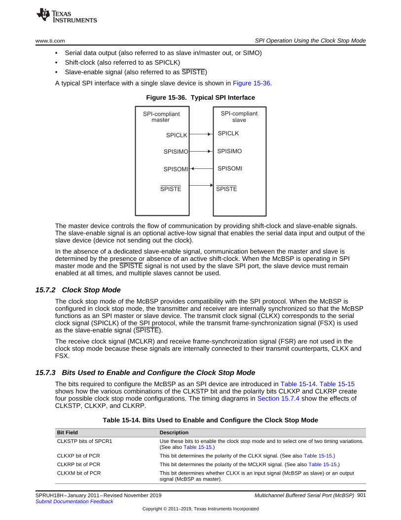
SPI-compliant
SPICLK
SPISIMO
SPISOMI
SPI-compliantslave
SPICLK
SPISIMO
SPISOMI
SPISTESPISTE
master
www.ti.com SPI Operation Using the Clock Stop Mode
901SPRUH18H–January 2011–Revised November 2019Submit Documentation Feedback
Copyright © 2011–2019, Texas Instruments Incorporated
Multichannel Buffered Serial Port (McBSP)
• Serial data output (also referred to as slave in/master out, or SIMO)• Shift-clock (also referred to as SPICLK)• Slave-enable signal (also referred to as SPISTE)
A typical SPI interface with a single slave device is shown in Figure 15-36.
Figure 15-36. Typical SPI Interface
The master device controls the flow of communication by providing shift-clock and slave-enable signals.The slave-enable signal is an optional active-low signal that enables the serial data input and output of theslave device (device not sending out the clock).
In the absence of a dedicated slave-enable signal, communication between the master and slave isdetermined by the presence or absence of an active shift-clock. When the McBSP is operating in SPImaster mode and the SPISTE signal is not used by the slave SPI port, the slave device must remainenabled at all times, and multiple slaves cannot be used.
15.7.2 Clock Stop ModeThe clock stop mode of the McBSP provides compatibility with the SPI protocol. When the McBSP isconfigured in clock stop mode, the transmitter and receiver are internally synchronized so that the McBSPfunctions as an SPI master or slave device. The transmit clock signal (CLKX) corresponds to the serialclock signal (SPICLK) of the SPI protocol, while the transmit frame-synchronization signal (FSX) is usedas the slave-enable signal (SPISTE).
The receive clock signal (MCLKR) and receive frame-synchronization signal (FSR) are not used in theclock stop mode because these signals are internally connected to their transmit counterparts, CLKX andFSX.
15.7.3 Bits Used to Enable and Configure the Clock Stop ModeThe bits required to configure the McBSP as an SPI device are introduced in Table 15-14. Table 15-15shows how the various combinations of the CLKSTP bit and the polarity bits CLKXP and CLKRP createfour possible clock stop mode configurations. The timing diagrams in Section 15.7.4 show the effects ofCLKSTP, CLKXP, and CLKRP.
Table 15-14. Bits Used to Enable and Configure the Clock Stop Mode
Bit Field DescriptionCLKSTP bits of SPCR1 Use these bits to enable the clock stop mode and to select one of two timing variations.
(See also Table 15-15.)CLKXP bit of PCR This bit determines the polarity of the CLKX signal. (See also Table 15-15.)CLKRP bit of PCR This bit determines the polarity of the MCLKR signal. (See also Table 15-15.)CLKXM bit of PCR This bit determines whether CLKX is an input signal (McBSP as slave) or an output
signal (McBSP as master).
SPI Operation Using the Clock Stop Mode www.ti.com
902 SPRUH18H–January 2011–Revised November 2019Submit Documentation Feedback
Copyright © 2011–2019, Texas Instruments Incorporated
Multichannel Buffered Serial Port (McBSP)
Table 15-14. Bits Used to Enable and Configure the Clock Stop Mode (continued)Bit Field DescriptionXPHASE bit of XCR2 You must use a single-phase transmit frame (XPHASE = 0).RPHASE bit of RCR2 You must use a single-phase receive frame (RPHASE = 0).XFRLEN1 bits of XCR1 You must use a transmit frame length of 1 serial word (XFRLEN1 = 0).RFRLEN1 bits of RCR1 You must use a receive frame length of 1 serial word (RFRLEN1 = 0).XWDLEN1 bits of XCR1 The XWDLEN1 bits determine the transmit packet length. XWDLEN1 must be equal to
RWDLEN1 because in the clock stop mode. The McBSP transmit and receive circuitsare synchronized to a single clock.
RWDLEN1 bits of RCR1 The RWDLEN1 bits determine the receive packet length. RWDLEN1 must be equal toXWDLEN1 because in the clock stop mode. The McBSP transmit and receive circuitsare synchronized to a single clock.
Table 15-15. Effects of CLKSTP, CLKXP, and CLKRP on the Clock Scheme
Bit Settings Clock SchemeCLKSTP = 00b or 01b Clock stop mode disabled. Clock enabled for non-SPI mode.CLKXP = 0 or 1CLKRP = 0 or 1CLKSTP = 10b Low inactive state without delay: The McBSP transmits data on the rising edge of CLKX and
receives data on the falling edge of MCLKR.CLKXP = 0CLKRP = 0CLKSTP = 11b Low inactive state with delay: The McBSP transmits data one-half cycle ahead of the rising
edge of CLKX and receives data on the rising edge of MCLKR.CLKXP = 0CLKRP = 1CLKSTP = 10b High inactive state without delay: The McBSP transmits data on the falling edge of CLKX and
receives data on the rising edge of MCLKR.CLKXP = 1CLKRP = 0CLKSTP = 11b High inactive state with delay: The McBSP transmits data one-half cycle ahead of the falling
edge of CLKX and receives data on the falling edge of MCLKR.CLKXP = 1CLKRP = 1
15.7.4 Clock Stop Mode Timing DiagramsThe timing diagrams for the four possible clock stop mode configurations are shown here. Notice that theframe-synchronization signal used in clock stop mode is active throughout the entire transmission as aslave-enable signal. Although the timing diagrams show 8-bit transfers, the packet length can be set to 8,12, 16, 20, 24, or 32 bits per packet. The receive packet length is selected with the RWDLEN1 bits ofRCR1, and the transmit packet length is selected with the XWDLEN1 bits of XCR1. For clock stop mode,the values of RWDLEN1 and XWDLEN1 must be the same because the McBSP transmit and receivecircuits are synchronized to a single clock.
NOTE: Even if multiple words are consecutively transferred, the CLKX signal is always stopped andthe FSX signal returns to the inactive state after a packet transfer. When consecutive packettransfers are performed, this leads to a minimum idle time of two bit-periods between eachpacket transfer.

B1B2B4 B3 B0B5B6B7
B0B1B2B3B4B5B6B7
FSX/SPISTE
CLKX/SPICLK
DX or DR/SIMO
(from master)
DX or DR/SOMI
(from slave)
B1B2B4 B3 B0B5B6B7
B0B1B2B3B4B5B6B7
FSX/SPISTE
CLKX/SPICLK
DX or DR/SIMO
(from master)
DX or DR/SOMI
(from slave)
B1B2B4 B3 B0B5B6B7
B0B1B2B3B4B5B6B7
FSX/SPISTE
DX or DR/SIMO
(from master)
CLKX/SPICLK
DX or DR/SOMI
(from slave)
B1B2B4 B3 B0B5B6B7
B0B1B2B3B4B5B6B7
FSX/SPISTE
DX or DR/SIMO
(from master)
CLKX/SPICLK
DX or DR/SOMI
(from slave)
www.ti.com SPI Operation Using the Clock Stop Mode
903SPRUH18H–January 2011–Revised November 2019Submit Documentation Feedback
Copyright © 2011–2019, Texas Instruments Incorporated
Multichannel Buffered Serial Port (McBSP)
Figure 15-37. SPI Transfer With CLKSTP = 10b (No Clock Delay), CLKXP = 0, and CLKRP = 0
A If the McBSP is the SPI master (CLKXM = 1), SIMO = DX. If the McBSP is the SPI slave (CLKXM = 0), SIMO = DR.B If the McBSP is the SPI master (CLKXM = 1), SOMI = DR. If the McBSP is the SPI slave (CLKXM = 0), SOMI = DX.
Figure 15-38. SPI Transfer With CLKSTP = 11b (Clock Delay), CLKXP = 0, CLKRP = 1
A If the McBSP is the SPI master (CLKXM = 1), SIMO = DX. If the McBSP is the SPI slave (CLKXM = 0), SIMO = DR.B If the McBSP is the SPI master (CLKXM = 1), SOMI = DR. If the McBSP is the SPI slave (CLKXM = 0), SOMI = DX.
Figure 15-39. SPI Transfer With CLKSTP = 10b (No Clock Delay), CLKXP = 1, and CLKRP = 0
A If the McBSP is the SPI master (CLKXM = 1), SIMO = DX. If the McBSP is the SPI slave (CLKXM = 0), SIMO = DR.B If the McBSP is the SPI master (CLKXM = 1), SOMI = DR. If the McBSP is the SPI slave (CLKXM = 0), SOMI = DX.
Figure 15-40. SPI Transfer With CLKSTP = 11b (Clock Delay), CLKXP = 1, CLKRP = 1
A If the McBSP is the SPI master (CLKXM = 1), SIMO=DX. If the McBSP is the SPI slave (CLKXM = 0), SIMO = DR.B If the McBSP is the SPI master (CLKXM = 1), SOMI=DR. If the McBSP is the SPI slave (CLKXM = 0), SOMI = DX.

SPI Operation Using the Clock Stop Mode www.ti.com
904 SPRUH18H–January 2011–Revised November 2019Submit Documentation Feedback
Copyright © 2011–2019, Texas Instruments Incorporated
Multichannel Buffered Serial Port (McBSP)
15.7.5 Procedure for Configuring a McBSP for SPI OperationTo configure the McBSP for SPI master or slave operation:
Step 1. Place the transmitter and receiver in reset.Clear the transmitter reset bit (XRST = 0) in SPCR2 to reset the transmitter. Clear the receiver reset bit(RRST = 0) in SPCR1 to reset the receiver.Step 2. Place the sample rate generator in reset.Clear the sample rate generator reset bit (GRST = 0) in SPCR2 to reset the sample rate generator.Step 3. Program registers that affect SPI operation.Program the appropriate McBSP registers to configure the McBSP for proper operation as an SPImaster or an SPI slave. For a list of important bits settings, see one of the following topics:• McBSP as the SPI Master ( Section 15.7.6)• McBSP as an SPI Slave ( Section 15.7.7)Step 4. Enable the sample rate generator.To release the sample rate generator from reset, set the sample rate generator reset bit (GRST = 1) inSPCR2.Make sure that during the write to SPCR2, you only modify GRST. Otherwise, you modify the McBSPconfiguration you selected in the previous step.Step 5. Enable the transmitter and receiver.After the sample rate generator is released from reset, wait two sample rate generator clock periods forthe McBSP logic to stabilize.If the CPU services the McBSP transmit and receive buffers, then you can immediately enable thetransmitter (XRST = 1 in SPCR2) and enable the receiver (RRST = 1 in SPCR1).If the DMA controller services the McBSP transmit and receive buffers, then you must first configurethe DMA controller (this includes enabling the channels that service the McBSP buffers). When theDMA controller is ready, make XRST = 1 and RRST = 1.In either case, make sure you only change XRST and RRST when you write to SPCR2 and SPCR1.Otherwise, you modify the bit settings you selected earlier in this procedure.After the transmitter and receiver are released from reset, wait two sample rate generator clock periodsfor the McBSP logic to stabilize.Step 6. If necessary, enable the frame-synchronization logic of the sample rate generator.After the required data acquisition setup is done (DXR[1,2] is loaded with data), set FRST = 1 if aninternally generated frame-synchronization pulse is required (that is, if the McBSP is the SPI master).
15.7.6 McBSP as the SPI MasterAn SPI interface with the McBSP used as the master is shown in Figure 15-41. When the McBSP isconfigured as a master, the transmit output signal (DX) is used as the SIMO signal of the SPI protocol andthe receive input signal (DR) is used as the SOMI signal.
The register bit values required to configure the McBSP as a master are listed in Table 15-16. After thetable are more details about the configuration requirements.

McBSP master
CLKX
DX
DR
FSX
SPI-compliantslave
SPICLK
SPISIMO
SPISOMI
SPISTE
www.ti.com SPI Operation Using the Clock Stop Mode
905SPRUH18H–January 2011–Revised November 2019Submit Documentation Feedback
Copyright © 2011–2019, Texas Instruments Incorporated
Multichannel Buffered Serial Port (McBSP)
Figure 15-41. SPI Interface with McBSP Used as Master
Table 15-16. Bit Values Required to Configure the McBSP as an SPI Master
Required Bit Setting DescriptionCLKSTP = 10b or 11b The clock stop mode (without or with a clock delay) is selected.CLKXP = 0 or 1 The polarity of CLKX as seen on the MCLKX pin is positive (CLKXP = 0) or negative (CLKXP =
1).CLKRP = 0 or 1 The polarity of MCLKR as seen on the MCLKR pin is positive (CLKRP = 0) or negative
(CLKRP = 1).CLKXM = 1 The MCLKX pin is an output pin driven by the internal sample rate generator. Because
CLKSTP is equal to 10b or 11b, MCLKR is driven internally by CLKX.SCLKME = 0 The clock generated by the sample rate generator (CLKG) is derived from the CPU clock.CLKSM = 1CLKGDV is a value from 1 to 255 CLKGDV defines the divide down value for CLKG.FSXM = 1 The FSX pin is an output pin driven according to the FSGM bit. (See theTMS320F28335
Applications and Media Processor Data Manual (SPRS224) for more information.FSGM = 0 The transmitter drives a frame-synchronization pulse on the FSX pin every time data is
transferred from DXR1 to XSR1.FSXP = 1 The FSX pin is active low.XDATDLY = 01b This setting provides the correct setup time on the FSX signal.RDATDLY = 01b
When the McBSP functions as the SPI master, it controls the transmission of data by producing the serialclock signal. The clock signal on the MCLKX pin is enabled only during packet transfers. When packetsare not being transferred, the MCLKX pin remains high or low depending on the polarity used.
For SPI master operation, the MCLKX pin must be configured as an output. The sample rate generator isthen used to derive the CLKX signal from the CPU clock. The clock stop mode internally connects theMCLKX pin to the MCLKR signal so that no external signal connection is required on the MCLKR pin andboth the transmit and receive circuits are clocked by the master clock (CLKX).
The data delay parameters of the McBSP (XDATDLY and RDATDLY) must be set to 1 for proper SPImaster operation. A data delay value of 0 or 2 is undefined in the clock stop mode.
The McBSP can also provide a slave-enable signal (SPISTE) on the FSX pin. If a slave-enable signal isrequired, the FSX pin must be configured as an output and the transmitter must be configured so that aframe-synchronization pulse is generated automatically each time a packet is transmitted (FSGM = 0).The polarity of the FSX pin is programmable high or low; however, in most cases the pin must beconfigured active low.

McBSP slave
CLKX
DX
DR
FSX
SPI-compliant
master
SPICLK
SPISOMI
SPISIMO
SPISTE
SPI Operation Using the Clock Stop Mode www.ti.com
906 SPRUH18H–January 2011–Revised November 2019Submit Documentation Feedback
Copyright © 2011–2019, Texas Instruments Incorporated
Multichannel Buffered Serial Port (McBSP)
When the McBSP is configured as described for SPI-master operation, the bit fields for frame-synchronization pulse width (FWID) and frame-synchronization period (FPER) are overridden, and customframe-synchronization waveforms are not allowed. To see the resulting waveform produced on the FSXpin, see the timing diagrams in Section 15.7.4. The signal becomes active before the first bit of a packettransfer, and remains active until the last bit of the packet is transferred. After the packet transfer iscomplete, the FSX signal returns to the inactive state.
15.7.7 McBSP as an SPI SlaveAn SPI interface with the McBSP used as a slave is shown in Figure 15-42. When the McBSP isconfigured as a slave, DX is used as the SOMI signal and DR is used as the SIMO signal.
The register bit values required to configure the McBSP as a slave are listed in Table 15-17. Following thetable are more details about configuration requirements.
Figure 15-42. SPI Interface With McBSP Used as Slave
Table 15-17. Bit Values Required to Configure the McBSP as an SPI Slave
Required Bit Setting DescriptionCLKSTP = 10b or 11b The clock stop mode (without or with a clock delay) is selected.CLKXP = 0 or 1 The polarity of CLKX as seen on the MCLKX pin is positive (CLKXP = 0) or negative (CLKXP =
1).CLKRP = 0 or 1 The polarity of MCLKR as seen on the MCLKR pin is positive (CLKRP = 0) or negative
(CLKRP = 1).CLKXM = 0 The MCLKX pin is an input pin, so that it can be driven by the SPI master. Because CLKSTP =
10b or 11b, MCLKR is driven internally by CLKX.SCLKME = 0 The clock generated by the sample rate generator (CLKG) is derived from the CPU clock. (The
sample rate generator is used to synchronize the McBSP logic with the externally-generatedmaster clock.)CLKSM = 1
CLKGDV = 1 The sample rate generator divides the CPU clock before generating CLKG.FSXM = 0 The FSX pin is an input pin, so that it can be driven by the SPI master.FSXP = 1 The FSX pin is active low.XDATDLY = 00b These bits must be 0s for SPI slave operation.RDATDLY = 00b
When the McBSP is used as an SPI slave, the master clock and slave-enable signals are generatedexternally by a master device. Accordingly, the CLKX and FSX pins must be configured as inputs. TheMCLKX pin is internally connected to the MCLKR signal, so that both the transmit and receive circuits ofthe McBSP are clocked by the external master clock. The FSX pin is also internally connected to the FSRsignal, and no external signal connections are required on the MCLKR and FSR pins.

www.ti.com Receiver Configuration
907SPRUH18H–January 2011–Revised November 2019Submit Documentation Feedback
Copyright © 2011–2019, Texas Instruments Incorporated
Multichannel Buffered Serial Port (McBSP)
Although the CLKX signal is generated externally by the master and is asynchronous to the McBSP, thesample rate generator of the McBSP must be enabled for proper SPI slave operation. The sample rategenerator must be programmed to its maximum rate of half the CPU clock rate. The internal sample rateclock is then used to synchronize the McBSP logic to the external master clock and slave-enable signals.
The McBSP requires an active edge of the slave-enable signal on the FSX input for each transfer. Thismeans that the master device must assert the slave-enable signal at the beginning of each transfer, anddeassert the signal after the completion of each packet transfer; the slave-enable signal cannot remainactive between transfers. Unlike the standard SPI, this pin cannot be tied low all the time.
The data delay parameters of the McBSP must be set to 0 for proper SPI slave operation. A value of 1 or2 is undefined in the clock stop mode.
15.8 Receiver ConfigurationTo configure the McBSP receiver, perform the following procedure:1. Place the McBSP/receiver in reset (see Section 15.8.2).2. Program McBSP registers for the desired receiver operation (see Section 15.8.1).3. Take the receiver out of reset (see Section 15.8.2).
15.8.1 Programming the McBSP Registers for the Desired Receiver OperationThe following is a list of important tasks to be performed when you are configuring the McBSP receiver.Each task corresponds to one or more McBSP register bit fields.• Global behavior:
– Set the receiver pins to operate as McBSP pins.– Enable/disable the digital loopback mode.– Enable/disable the clock stop mode.– Enable/disable the receive multichannel selection mode.
• Data behavior:– Choose 1 or 2 phases for the receive frame.– Set the receive word length(s).– Set the receive frame length.– Enable/disable the receive frame-synchronization ignore function.– Set the receive companding mode.– Set the receive data delay.– Set the receive sign-extension and justification mode.– Set the receive interrupt mode.
• Frame-synchronization behavior:– Set the receive frame-synchronization mode.– Set the receive frame-synchronization polarity.– Set the sample rate generator (SRG) frame-synchronization period and pulse width.
• Clock behavior:– Set the receive clock mode.– Set the receive clock polarity.– Set the SRG clock divide-down value.– Set the SRG clock synchronization mode.– Set the SRG clock mode (choose an input clock).– Set the SRG input clock polarity.
Receiver Configuration www.ti.com
908 SPRUH18H–January 2011–Revised November 2019Submit Documentation Feedback
Copyright © 2011–2019, Texas Instruments Incorporated
Multichannel Buffered Serial Port (McBSP)
15.8.2 Resetting and Enabling the ReceiverThe first step of the receiver configuration procedure is to reset the receiver, and the last step is to enablethe receiver (to take it out of reset). Table 15-18 describes the bits used for both of these steps.
Table 15-18. Register Bits Used to Reset or Enable the McBSP Receiver Field Descriptions
Register Bit Field Value DescriptionSPCR2 7 FRST Frame-synchronization logic reset
0 Frame-synchronization logic is reset. The sample rate generator does not generate frame-synchronization signal FSG, even if GRST = 1.
1 If GRST = 1, frame-synchronization signal FSG is generated after (FPER + 1) number ofCLKG clock cycles; all frame counters are loaded with their programmed values.
SPCR2 6 GRST Sample rate generator reset0 Sample rate generator is reset. If GRST = 0 due to a DSP reset, CLKG is driven by the
CPU clock divided by 2, and FSG is driven low (inactive). If GRST = 0 due to programcode, CLKG and FSG are both driven low (inactive).
1 Sample rate generator is enabled. CLKG is driven according to the configurationprogrammed in the sample rate generator registers (SRGR[1,2]). If FRST = 1, thegenerator also generates the frame-synchronization signal FSG as programmed in thesample rate generator registers.
SPCR1 0 RRST Receiver reset0 The serial port receiver is disabled and in the reset state.1 The serial port receiver is enabled.
15.8.2.1 Reset ConsiderationsThe serial port can be reset in the following two ways:1. The DSP reset (XRS signal driven low) places the receiver, transmitter, and sample rate generator in
reset. When the device reset is removed (XRS signal released), GRST = FRST = RRST = XRST = 0keep the entire serial port in the reset state, provided the McBSP clock is turned on.
2. The serial port transmitter and receiver can be reset directly using the RRST and XRST bits in theserial port control registers. The sample rate generator can be reset directly using the GRST bit inSPCR2.
Table 15-19 shows the state of McBSP pins when the serial port is reset due to a device reset and adirect receiver/transmitter reset.
For more details about McBSP reset conditions and effects, see Section 15.10.2, Resetting and Initializinga McBSP.
Table 15-19. Reset State of Each McBSP Pin
PinPossibleState(s)
State Forced ByDevice Reset
State Forced By Receiver Reset(RRST = 0 and GRST = 1)
MDRx I GPIO Input InputMCLKRx I/O/Z GPIO Input Known state if input; MCLKR running if outputMFSRx I/O/Z GPIO Input Known state if input; FSRP inactive state if output
Transmitter reset (XRST = 0 and GRST = 1)MDXx O/Z GPIO Input Low impedance after transmit bit clock providedMCLKXx I/O/Z GPIO Input Known state if input; CLKX running if outputMFSXx I/O/Z GPIO Input Known state if input; FSXP inactive state if output
15.8.3 Set the Receiver Pins to Operate as McBSP PinsTo configure a pin for its McBSP function , you should configure the bits of the GPxMUXn registerappropriately. In addition to this, bits 12 and 13 of the PCR register must be set to 0. These bits aredefined as reserved.

www.ti.com Receiver Configuration
909SPRUH18H–January 2011–Revised November 2019Submit Documentation Feedback
Copyright © 2011–2019, Texas Instruments Incorporated
Multichannel Buffered Serial Port (McBSP)
15.8.4 Enable/Disable the Digital Loopback ModeThe DLB bit determines whether the digital loopback mode is on. DLB is described in Table 15-20.
Table 15-20. Register Bit Used to Enable/Disable the Digital Loopback Mode
Register Bit Name Function TypeResetValue
SPCR1 15 DLB Digital loopback mode R/W 0DLB = 0 Digital loopback mode is disabled.DLB = 1 Digital loopback mode is enabled.
15.8.4.1 Digital Loopback ModeIn the digital loopback mode, the receive signals are connected internally through multiplexers to thecorresponding transmit signals, as shown in Table 15-21. This mode allows testing of serial port code witha single DSP device; the McBSP receives the data it transmits.
Table 15-21. Receive Signals Connected to Transmit Signals in Digital Loopback Mode
This Receive SignalIs Fed Internally byThis Transmit Signal
MDR (receive data) MDX (transmit data)MFSR (receive frame synchronization) MFSX (transmit frame synchronization)MCLKR (receive clock) MCLKX (transmit clock)
15.8.5 Enable/Disable the Clock Stop ModeThe CLKSTP bits determine whether the clock stop mode is on. CLKSTP is described in Table 15-22.
Table 15-22. Register Bits Used to Enable/Disable the Clock Stop Mode
Register Bit Name Function TypeResetValue
SPCR1 12-11 CLKSTP Clock stop mode R/W 00CLKSTP = 0Xb Clock stop mode disabled; normal clocking for
non-SPI modeCLKSTP = 10b Clock stop mode enabled, without clock delayCLKSTP = 11b Clock stop mode enabled, with clock delay
15.8.5.1 Clock Stop ModeThe clock stop mode supports the SPI master-slave protocol. If you do not plan to use the SPI protocol,you can clear CLKSTP to disable the clock stop mode.
In the clock stop mode, the clock stops at the end of each data transfer. At the beginning of each datatransfer, the clock starts immediately (CLKSTP = 10b) or after a half-cycle delay (CLKSTP = 11b). TheCLKXP bit determines whether the starting edge of the clock on the MCLKX pin is rising or falling. TheCLKRP bit determines whether receive data is sampled on the rising or falling edge of the clock shown onthe MCLKR pin.
Table 15-23 summarizes the impact of CLKSTP, CLKXP, and CLKRP on serial port operation. In the clockstop mode, the receive clock is tied internally to the transmit clock, and the receive frame-synchronizationsignal is tied internally to the transmit frame-synchronization signal.
Receiver Configuration www.ti.com
910 SPRUH18H–January 2011–Revised November 2019Submit Documentation Feedback
Copyright © 2011–2019, Texas Instruments Incorporated
Multichannel Buffered Serial Port (McBSP)
Table 15-23. Effects of CLKSTP, CLKXP, and CLKRP on the Clock Scheme
Bit Settings Clock SchemeCLKSTP = 00b or 01b Clock stop mode disabled. Clock enabled for non-SPI mode.CLKXP = 0 or 1CLKRP = 0 or 1CLKSTP = 10b Low inactive state without delay: The McBSP transmits data on the rising edge of CLKX and receives data on the
falling edge of MCLKR.CLKXP = 0CLKRP = 0CLKSTP = 11b Low inactive state with delay: The McBSP transmits data one-half cycle ahead of the rising edge of CLKX and
receives data on the rising edge of MCLKR.CLKXP = 0CLKRP = 1CLKSTP = 10b High inactive state without delay: The McBSP transmits data on the falling edge of CLKX and receives data on the
rising edge of MCLKR.CLKXP = 1CLKRP = 0CLKSTP = 11b High inactive state with delay: The McBSP transmits data one-half cycle ahead of the falling edge of CLKX and
receives data on the falling edge of MCLKR.CLKXP = 1CLKRP = 1
15.8.6 Enable/Disable the Receive Multichannel Selection ModeThe RMCM bit determines whether the receive multichannel selection mode is on. RMCM is described inTable 15-24. For more details, see Section 15.6.6, Receive Multichannel Selection Mode.
Table 15-24. Register Bit Used to Enable/Disable the Receive Multichannel Selection Mode
Register Bit Name Function TypeResetValue
MCR1 0 RMCM Receive multichannel selection mode R/W 0RMCM = 0 The mode is disabled.
All 128 channels are enabled.RMCM = 1 The mode is enabled.
Channels can be individually enabled or disabled.The only channels enabled are those selected in theappropriate receive channel enable registers (RCERs).The way channels are assigned to the RCERsdepends on the number of receive channel partitions(2 or 8), as defined by the RMCME bit.
15.8.7 Choose One or Two Phases for the Receive FrameThe RPHASE bit (see Table 15-25) determines whether the receive data frame has one or two phases.
Table 15-25. Register Bit Used to Choose One or Two Phases for the Receive Frame
Register Bit Name Function TypeResetValue
RCR2 15 RPHASE Receive phase number R/W 0Specifies whether the receive frame has 1 or 2 phases.RPHASE = 0 Single-phase frameRPHASE = 1 Dual-phase frame

www.ti.com Receiver Configuration
911SPRUH18H–January 2011–Revised November 2019Submit Documentation Feedback
Copyright © 2011–2019, Texas Instruments Incorporated
Multichannel Buffered Serial Port (McBSP)
15.8.8 Set the Receive Word Length(s)The RWDLEN1 and RWDLEN2 bit fields (see Table 15-26) determine how many bits are in each serialword in phase 1 and in phase 2, respectively, of the receive data frame.
Table 15-26. Register Bits Used to Set the Receive Word Length(s)
Register Bit Name Function TypeResetValue
RCR1 7-5 RWDLEN1 Receive word length 1 R/W 000Specifies the length of every serial word in phase 1 of the receive frame.RWDLEN1 = 000 8 bitsRWDLEN1 = 001 12 bitsRWDLEN1 = 010 16 bitsRWDLEN1 = 011 20 bitsRWDLEN1 = 100 24 bitsRWDLEN1 = 101 32 bitsRWDLEN1 = 11X Reserved
RCR2 7-5 RWDLEN2 Receive word length 2 R/W 000If a dual-phase frame is selected, RWDLEN2 specifies the length of everyserial word in phase 2 of the frame.RWDLEN2 = 000 8 bitsRWDLEN2 = 001 12 bitsRWDLEN2 = 010 16 bitsRWDLEN2 = 011 20 bitsRWDLEN2 = 100 24 bitsRWDLEN2 = 101 32 bitsRWDLEN2 = 11X Reserved
15.8.8.1 Word Length BitsEach frame can have one or two phases, depending on the value that you load into the RPHASE bit. If asingle-phase frame is selected, RWDLEN1 selects the length for every serial word received in the frame. Ifa dual-phase frame is selected, RWDLEN1 determines the length of the serial words in phase 1 of theframe and RWDLEN2 determines the word length in phase 2 of the frame.
15.8.9 Set the Receive Frame LengthThe RFRLEN1 and RFRLEN2 bit fields (see Table 15-27) determine how many serial words are in phase1 and in phase 2, respectively, of the receive data frame.
Table 15-27. Register Bits Used to Set the Receive Frame Length
Register Bit Name Function TypeResetValue
RCR1 14-8 RFRLEN1 Receive frame length 1 R/W 000 0000(RFRLEN1 + 1) is the number of serial words in phase 1 of the receiveframe.RFRLEN1 = 000 0000 1 word in phase 1RFRLEN1 = 000 0001 2 words in phase 1| || |RFRLEN1 = 111 1111 128 words in phase 1

Receiver Configuration www.ti.com
912 SPRUH18H–January 2011–Revised November 2019Submit Documentation Feedback
Copyright © 2011–2019, Texas Instruments Incorporated
Multichannel Buffered Serial Port (McBSP)
Table 15-27. Register Bits Used to Set the Receive Frame Length (continued)
Register Bit Name Function TypeResetValue
RCR2 14-8 RFRLEN2 Receive frame length 2 R/W 000 0000If a dual-phase frame is selected, (RFRLEN2 + 1) is the number of serialwords in phase 2 of the receive frame.RFRLEN2 = 000 0000 1 word in phase 2RFRLEN2 = 000 0001 2 words in phase 2| || |RFRLEN2 = 111 1111 128 words in phase 2
15.8.9.1 Selected Frame LengthThe receive frame length is the number of serial words in the receive frame. Each frame can have one ortwo phases, depending on value that you load into the RPHASE bit.
If a single-phase frame is selected (RPHASE = 0), the frame length is equal to the length of phase 1. If adual-phase frame is selected (RPHASE = 1), the frame length is the length of phase 1 plus the length ofphase 2.
The 7-bit RFRLEN fields allow up to 128 words per phase. See Table 15-28 for a summary of how tocalculate the frame length. This length corresponds to the number of words or logical time slots orchannels per frame-synchronization pulse.
Program the RFRLEN fields with [w minus 1], where w represents the number of words per phase. For theexample, if you want a phase length of 128 words in phase 1, load 127 into RFRLEN1.
Table 15-28. How to Calculate the Length of the Receive Frame
RPHASE RFRLEN1 RFRLEN2 Frame Length0 0 ≤ RFRLEN1 ≤ 127 Don't care (RFRLEN1 + 1) words1 0 ≤ RFRLEN1 ≤ 127 0 ≤ RFRLEN2 ≤ 127 (RFRLEN1 + 1) + (RFRLEN2 + 1) words
15.8.10 Enable/Disable the Receive Frame-Synchronization Ignore FunctionThe RFIG bit (see Table 15-29) controls the receive frame-synchronization ignore function.
Table 15-29. Register Bit Used to Enable/Disable the Receive Frame-Synchronization IgnoreFunction
Register Bit Name Function TypeResetValue
RCR2 2 RFIG Receive frame-synchronization ignore R/W 0RFIG = 0 An unexpected receive frame-synchronization pulse causes the
McBSP to restart the frame transfer.RFIG = 1 The McBSP ignores unexpected receive frame-synchronization
pulses.
15.8.10.1 Unexpected Frame-Synchronization Pulses and the Frame-Synchronization Ignore FunctionIf a frame-synchronization pulse starts the transfer of a new frame before the current frame is fullyreceived, this pulse is treated as an unexpected frame-synchronization pulse.
When RFIG = 1, reception continues, ignoring the unexpected frame-synchronization pulses.

(R/X)SYNCERR
D(R/X)
FS(R/X)
CLK(R/X)
C4C5C6C7B0B1B2B3B4B5B6B7A0
ÁÁ
ÁÁ
ÁÁ
ÁÁ
Frame synchronization ignored
Current data retransmitted
New data received
(R/X)SYNCERR
DX
DR
FS(R/X)
CLK(R/X)
C6C7B0
ÁÁ
ÁÁ
ÁÁ
B2B3B4B5B7 B6B6B7A0 B1
D6D7C0C1C2C3C4C5C6C7B6B7A0
ÁÁ
ÁÁ
ÁÁ
ÁÁ
Frame synchronization aborts current transfer
www.ti.com Receiver Configuration
913SPRUH18H–January 2011–Revised November 2019Submit Documentation Feedback
Copyright © 2011–2019, Texas Instruments Incorporated
Multichannel Buffered Serial Port (McBSP)
When RFIG = 0, an unexpected FSR pulse causes the McBSP to discard the contents of RSR[1,2] infavor of the new incoming data. Therefore, if RFIG = 0 and an unexpected frame-synchronization pulseoccurs, the serial port:1. Aborts the current data transfer2. Sets RSYNCERR in SPCR1 to 13. Begins the transfer of a new data word
For more details about the frame-synchronization error condition, see Section 15.5.3, Unexpected ReceiveFrame-Synchronization Pulse.
15.8.10.2 Examples of Effects of RFIGFigure 15-43 shows an example in which word B is interrupted by an unexpected frame-synchronizationpulse when (R/X)FIG = 0. In the case of reception, the reception of B is aborted (B is lost), and a new dataword © in this example) is received after the appropriate data delay. This condition is a receivesynchronization error, which sets the RSYNCERR bit.
Figure 15-43. Unexpected Frame-Synchronization Pulse With (R/X)FIG = 0
In contrast with Figure 15-43, Figure 15-44 shows McBSP operation when unexpected frame-synchronization signals are ignored (when (R/X)FIG = 1). Here, the transfer of word B is not affected byan unexpected pulse.
Figure 15-44. Unexpected Frame-Synchronization Pulse With (R/X)FIG = 1
15.8.11 Set the Receive Companding ModeThe RCOMPAND bits (see Table 15-30) determine whether companding or another data transfer option ischosen for McBSP reception.
Table 15-30. Register Bits Used to Set the Receive Companding Mode
Register Bit Name Function TypeResetValue
RCR2 4-3 RCOMPAND Receive companding mode R/W 00Modes other than 00b are enabled only when the appropriate RWDLEN is000b, indicating 8-bit data.RCOMPAND = 00 No companding, any size data, MSB received firstRCOMPAND = 01 No companding, 8-bit data, LSB received first (for details,
see Section 15.8.11.4).RCOMPAND = 10 μ-law companding, 8-bit data, MSB received firstRCOMPAND = 11 A-law companding, 8-bit data, MSB received first

From CPU or DMA controllerDXR1
To CPU or DMA controllerDRR1
16
16
DX8
8
XSR1 Compress
ExpandDR RBR1RSR1
Receiver Configuration www.ti.com
914 SPRUH18H–January 2011–Revised November 2019Submit Documentation Feedback
Copyright © 2011–2019, Texas Instruments Incorporated
Multichannel Buffered Serial Port (McBSP)
15.8.11.1 CompandingCompanding (COMpressing and exPANDing) hardware allows compression and expansion of data ineither μ-law or A-law format. The companding standard employed in the United States and Japan is μ-law.The European companding standard is referred to as A-law. The specifications for μ-law and A-law logPCM are part of the CCITT G.711 recommendation.
A-law and μ-law allow 13 bits and 14 bits of dynamic range, respectively. Any values outside this rangeare set to the most positive or most negative value. Thus, for companding to work best, the datatransferred to and from the McBSP via the CPU or DMA controller must be at least 16 bits wide.
The μ-law and A-law formats both encode data into 8-bit code words. Companded data is always 8 bitswide; the appropriate word length bits (RWDLEN1, RWDLEN2, XWDLEN1, XWDLEN2) must therefore beset to 0, indicating an 8-bit wide serial data stream. If companding is enabled and either of the framephases does not have an 8-bit word length, companding continues as if the word length is 8 bits.
Figure 15-45 illustrates the companding processes. When companding is chosen for the transmitter,compression occurs during the process of copying data from DXR1 to XSR1. The transmit data isencoded according to the specified companding law (A-law or μ-law). When companding is chosen for thereceiver, expansion occurs during the process of copying data from RBR1 to DRR1. The receive data isdecoded to 2's-complement format.
Figure 15-45. Companding Processes for Reception and for Transmission
15.8.11.2 Format of Expanded DataFor reception, the 8-bit compressed data in RBR1 is expanded to left-justified 16-bit data in DRR1. TheRJUST bit of SPCR1 is ignored when companding is used.
15.8.11.3 Companding Internal DataIf the McBSP is otherwise unused (the serial port transmit and receive sections are reset), thecompanding hardware can compand internal data. See Section 15.1.5.2, Capability to Compand InternalData.
15.8.11.4 Option to Receive LSB FirstNormally, the McBSP transmits or receives all data with the most significant bit (MSB) first. However,certain 8-bit data protocols (that do not use companded data) require the least significant bit (LSB) to betransferred first. If you set RCOMPAND = 01b in RCR2, the bit ordering of 8-bit words is reversed duringreception. Similar to companding, this feature is enabled only if the appropriate word length bits are set to0, indicating that 8-bit words are to be transferred serially. If either phase of the frame does not have an 8-bit word length, the McBSP assumes the word length is eight bits and LSB-first ordering is done.
15.8.12 Set the Receive Data DelayThe RDATDLY bits (see Table 15-31) determine the length of the data delay for the receive frame.
Table 15-31. Register Bits Used to Set the Receive Data Delay
Register Bit Name Function TypeResetValue
RCR2 1-0 RDATDLY Receive data delay R/W 00RDATDLY = 00 0-bit data delayRDATDLY = 01 1-bit data delayRDATDLY = 10 2-bit data delay

B5B6B7
B4B5B6B7
B3B4B5B6B7
Data delay 2D(R/X)
Data delay 1D(R/X)
Data delay 0D(R/X)
FS(R/X)
CLK(R/X)
1-bit delay
Á
Á
Á
Á
ÁÁ
ÁÁ
ÁÁ
ÁÁ
Á
Á
Á
Á
0-bit delay
2-bit delay
www.ti.com Receiver Configuration
915SPRUH18H–January 2011–Revised November 2019Submit Documentation Feedback
Copyright © 2011–2019, Texas Instruments Incorporated
Multichannel Buffered Serial Port (McBSP)
Table 15-31. Register Bits Used to Set the Receive Data Delay (continued)
Register Bit Name Function TypeResetValue
RDATDLY = 11 Reserved
15.8.12.1 Data DelayThe start of a frame is defined by the first clock cycle in which frame synchronization is found to be active.The beginning of actual data reception or transmission with respect to the start of the frame can bedelayed if required. This delay is called data delay.
RDATDLY specifies the data delay for reception. The range of programmable data delay is zero to two bit-clocks (RDATDLY = 00b-10b), as described in Table 15-31 and shown in Figure 15-46. In this figure, thedata transferred is an 8-bit value with bits labeled B7, B6, B5, and so on. Typically a 1-bit delay isselected, because data often follows a 1-cycle active frame-synchronization pulse.
15.8.12.2 0-Bit Data DelayNormally, a frame-synchronization pulse is detected or sampled with respect to an edge of internal serialclock CLK(R/X). Thus, on the following cycle or later (depending on the data delay value), data may bereceived or transmitted. However, in the case of 0-bit data delay, the data must be ready for receptionand/or transmission on the same serial clock cycle.
For reception, this problem is solved because receive data is sampled on the first falling edge of MCLKRwhere an active-high internal FSR is detected. However, data transmission must begin on the rising edgeof the internal CLKX clock that generated the frame synchronization. Therefore, the first data bit isassumed to be present in XSR1, and thus on DX. The transmitter then asynchronously detects the frame-synchronization signal (FSX) going active high and immediately starts driving the first bit to be transmittedon the DX pin.
Figure 15-46. Range of Programmable Data Delay
15.8.12.3 2-Bit Data DelayA data delay of two bit periods allows the serial port to interface to different types of T1 framing deviceswhere the data stream is preceded by a framing bit. During reception of such a stream with data delay oftwo bits (framing bit appears after a 1-bit delay and data appears after a 2-bit delay), the serial portessentially discards the framing bit from the data stream, as shown in Figure 15-47. In this figure, the datatransferred is an 8-bit value with bits labeled B7, B6, B5, and so on.

DR Framing bit B5B6B7
FSR
CLKR
ÁÁ
ÁÁ
ÁÁ
ÁÁ
2-bit delay
Receiver Configuration www.ti.com
916 SPRUH18H–January 2011–Revised November 2019Submit Documentation Feedback
Copyright © 2011–2019, Texas Instruments Incorporated
Multichannel Buffered Serial Port (McBSP)
Figure 15-47. 2-Bit Data Delay Used to Skip a Framing Bit
15.8.13 Set the Receive Sign-Extension and Justification ModeThe RJUST bits (see Table 15-32) determine whether data received by the McBSP is sign-extended andhow it is justified.
Table 15-32. Register Bits Used to Set the Receive Sign-Extension and Justification Mode
Register Bit Name Function TypeResetValue
SPCR1 14-13 RJUST Receive sign-extension and justification mode R/W 00RJUST = 00 Right justify data and zero fill MSBs in DRR[1,2]RJUST = 01 Right justify data and sign extend it into the MSBs in
DRR[1,2]RJUST = 10 Left justify data and zero fill LSBs in DRR[1,2]RJUST = 11 Reserved
15.8.13.1 Sign-Extension and the JustificationRJUST in SPCR1 selects whether data in RBR[1,2] is right- or left-justified (with respect to the MSB) inDRR[1,2] and whether unused bits in DRR[1,2] are filled with zeros or with sign bits.
Table 15-33 and Table 15-34 show the effects of various RJUST values. The first table shows the effecton an example 12-bit receive-data value ABCh. The second table shows the effect on an example 20-bitreceive-data value ABCDEh.
Table 15-33. Example: Use of RJUST Field With 12-Bit Data Value ABCh
RJUST Justification ExtensionValue inDRR2
Value inDRR1
00b Right Zero fill MSBs 0000h 0ABCh01b Right Sign extend data into MSBs FFFFh FABCh10b Left Zero fill LSBs 0000h ABC0h11b Reserved Reserved Reserved Reserved
Table 15-34. Example: Use of RJUST Field With 20-Bit Data Value ABCDEh
RJUST Justification ExtensionValue inDRR2
Value inDRR1
00b Right Zero fill MSBs 000Ah BCDEh01b Right Sign extend data into MSBs FFFAh BCDEh10b Left Zero fill LSBs ABCDh E000h11b Reserved Reserved Reserved Reserved

www.ti.com Receiver Configuration
917SPRUH18H–January 2011–Revised November 2019Submit Documentation Feedback
Copyright © 2011–2019, Texas Instruments Incorporated
Multichannel Buffered Serial Port (McBSP)
15.8.14 Set the Receive Interrupt ModeThe RINTM bits (see Table 15-35) determine which event generates a receive interrupt request to theCPU.
The receive interrupt (RINT) informs the CPU of changes to the serial port status. Four options exist forconfiguring this interrupt. The options are set by the receive interrupt mode bits, RINTM, in SPCR1.
Table 15-35. Register Bits Used to Set the Receive Interrupt Mode
Register Bit Name Function TypeResetValue
SPCR1 5-4 RINTM Receive interrupt mode R/W 00RINTM = 00 RINT generated when RRDY changes from 0 to 1. Interrupt on
every serial word by tracking the RRDY bit in SPCR1.Regardless of the value of RINTM, RRDY can be read todetect the RRDY = 1 condition.
RINTM = 01 RINT generated by an end-of-block or end-of-frame conditionin the receive multichannel selection mode. In the multichannelselection mode, interrupt after every 16-channel blockboundary has been crossed within a frame and at the end ofthe frame. For details, see Section 15.6.7.3, Using InterruptsBetween Block Transfers. In any other serial transfer case, thissetting is not applicable and, therefore, no interrupts aregenerated.
RINTM = 10 RINT generated by a new receive frame-synchronization pulse.Interrupt on detection of receive frame-synchronization pulses.This generates an interrupt even when the receiver is in itsreset state. This is done by synchronizing the incoming frame-synchronization pulse to the CPU clock and sending it to theCPU via RINT.
RINTM = 11 RINT generated when RSYNCERR is set. Interrupt on frame-synchronization error. Regardless of the value of RINTM,RSYNCERR can be read to detect this condition. Forinformation on using RSYNCERR, see Section 15.5.3,Unexpected Receive Frame-Synchronization Pulse.
15.8.15 Set the Receive Frame-Synchronization ModeThe bits described in Table 15-36 determine the source for receive frame synchronization and the functionof the FSR pin.
15.8.15.1 Receive Frame-Synchronization ModesTable 15-37 shows how you can select various sources to provide the receive frame-synchronizationsignal and the effect on the FSR pin. The polarity of the signal on the FSR pin is determined by the FSRPbit.
In digital loopback mode (DLB = 1), the transmit frame-synchronization signal is used as the receiveframe-synchronization signal.
Also in the clock stop mode, the internal receive clock signal (MCLKR) and the internal receive frame-synchronization signal (FSR) are internally connected to their transmit counterparts, CLKX and FSX.
Table 15-36. Register Bits Used to Set the Receive Frame Synchronization Mode
Register Bit Name Function TypeResetValue
PCR 10 FSRM Receive frame-synchronization mode R/W 0FSRM = 0 Receive frame synchronization is supplied by an
external source via the FSR pin.FSRM = 1 Receive frame synchronization is supplied by
the sample rate generator. FSR is an output pinreflecting internal FSR, except when GSYNC = 1in SRGR2.

Receiver Configuration www.ti.com
918 SPRUH18H–January 2011–Revised November 2019Submit Documentation Feedback
Copyright © 2011–2019, Texas Instruments Incorporated
Multichannel Buffered Serial Port (McBSP)
Table 15-36. Register Bits Used to Set the Receive Frame Synchronization Mode (continued)
Register Bit Name Function TypeResetValue
SRGR2 15 GSYNC Sample rate generator clock synchronization mode R/W 0If the sample rate generator creates a frame-synchronization signal(FSG) that is derived from an external input clock, the GSYNC bitdetermines whether FSG is kept synchronized with pulses on the FSRpin.GSYNC = 0 No clock synchronization is used: CLKG
oscillates without adjustment, and FSG pulsesevery (FPER + 1) CLKG cycles.
GSYNC = 1 Clock synchronization is used. When a pulse isdetected on the FSR pin:
• CLKG is adjusted as necessary so that it issynchronized with the input clock on theMCLKR pin.
• FSG pulses FSG only pulses in responseto a pulse on the FSR pin. The frame-synchronization period defined in FPER isignored.
For more details, see Section 15.4.3,Synchronizing Sample Rate Generator Outputsto an External Clock.
SPCR1 15 DLB Digital loopback mode R/W 0DLB = 0 Digital loopback mode is disabled.DLB = 1 Digital loopback mode is enabled. The receive
signals, including the receive frame-synchronization signal, are connected internallythrough multiplexers to the correspondingtransmit signals.
SPCR1 12-11 CLKSTP Clock stop mode R/W 00CLKSTP = 0Xb Clock stop mode disabled; normal clocking for
non-SPI mode.CLKSTP = 10b Clock stop mode enabled without clock delay.
The internal receive clock signal (MCLKR) andthe internal receive frame-synchronization signal(FSR) are internally connected to their transmitcounterparts, CLKX and FSX.
CLKSTP = 11b Clock stop mode enabled with clock delay. Theinternal receive clock signal (MCLKR) and theinternal receive frame-synchronization signal(FSR) are internally connected to their transmitcounterparts, CLKX and FSX.
Table 15-37. Select Sources to Provide the Receive Frame-Synchronization Signal and the Effecton the FSR Pin
DLB FSRM GSYNCSource of Receive FrameSynchronization FSR Pin Status
0 0 0 or 1 An external frame-synchronization signalenters the McBSP through the FSR pin.The signal is then inverted as determinedby FSRP before being used as internalFSR.
Input
0 1 0 Internal FSR is driven by the sample rategenerator frame-synchronization signal(FSG).
Output. FSG is inverted as determined byFSRP before being driven out on theFSR pin.
0 1 1 Internal FSR is driven by the sample rategenerator frame-synchronization signal(FSG).
Input. The external frame-synchronizationinput on the FSR pin is used tosynchronize CLKG and generate FSGpulses.
1 0 0 Internal FSX drives internal FSR. High impedance

www.ti.com Receiver Configuration
919SPRUH18H–January 2011–Revised November 2019Submit Documentation Feedback
Copyright © 2011–2019, Texas Instruments Incorporated
Multichannel Buffered Serial Port (McBSP)
Table 15-37. Select Sources to Provide the Receive Frame-Synchronization Signal and the Effecton the FSR Pin (continued)
DLB FSRM GSYNCSource of Receive FrameSynchronization FSR Pin Status
1 0 or 1 1 Internal FSX drives internal FSR. Input. If the sample rate generator isrunning, external FSR is used tosynchronize CLKG and generate FSGpulses.
1 1 0 Internal FSX drives internal FSR. Output. Receive (same as transmit)frame synchronization is inverted asdetermined by FSRP before being drivenout on the FSR pin.
15.8.16 Set the Receive Frame-Synchronization PolarityThe FSRP bit (see Table 15-38) determines whether frame-synchronization pulses are active high oractive low on the FSR pin.
Table 15-38. Register Bit Used to Set Receive Frame-Synchronization Polarity
Register Bit Name Function TypeResetValue
PCR 2 FSRP Receive frame-synchronization polarity R/W 0FSRP = 0 Frame-synchronization pulse FSR is active high.FSRP = 1 Frame-synchronization pulse FSR is active low.
15.8.16.1 Frame-Synchronization Pulses, Clock Signals, and Their PolaritiesReceive frame-synchronization pulses can be generated internally by the sample rate generator (seeSection 15.4.2) or driven by an external source. The source of frame synchronization is selected byprogramming the mode bit, FSRM, in PCR. FSR is also affected by the GSYNC bit in SRGR2. Forinformation about the effects of FSRM and GSYNC, see Section 15.8.15, Set the Receive Frame-Synchronization Mode. Similarly, receive clocks can be selected to be inputs or outputs by programmingthe mode bit, CLKRM, in the PCR (see Section 15.8.17, Set the Receive Clock Mode).
When FSR and FSX are inputs (FSXM = FSRM= 0, external frame-synchronization pulses), the McBSPdetects them on the internal falling edge of clock, internal MCLKR, and internal CLKX, respectively. Thereceive data arriving at the DR pin is also sampled on the falling edge of internal MCLKR. These internalclock signals are either derived from an external source via CLK(R/X) pins or driven by the sample rategenerator clock (CLKG) internal to the McBSP.
When FSR and FSX are outputs, implying that they are driven by the sample rate generator, they aregenerated (transition to their active state) on the rising edge of the internal clock, CLK(R/X). Similarly, dataon the DX pin is output on the rising edge of internal CLKX.
FSRP, FSXP, CLKRP, and CLKXP in the pin control register (PCR) configure the polarities of the FSR,FSX, MCLKR, and CLKX signals, respectively. All frame-synchronization signals (internal FSR, internalFSX) that are internal to the serial port are active high. If the serial port is configured for external framesynchronization (FSR/FSX are inputs to McBSP), and FSRP = FSXP = 1, the external active-low frame-synchronization signals are inverted before being sent to the receiver (internal FSR) and transmitter(internal FSX). Similarly, if internal synchronization (FSR/FSX are output pins and GSYNC = 0) isselected, the internal active-high frame-synchronization signals are inverted, if the polarity bit FS(R/X)P =1, before being sent to the FS(R/X) pin.
On the transmit side, the transmit clock polarity bit, CLKXP, sets the edge used to shift and clock outtransmit data. Data is always transmitted on the rising edge of internal CLKX. If CLKXP = 1 and externalclocking is selected (CLKXM = 0 and CLKX is an input), the external falling-edge triggered input clock onCLKX is inverted to a rising-edge triggered clock before being sent to the transmitter. If CLKXP = 1, andinternal clocking selected (CLKXM = 1 and CLKX is an output pin), the internal (rising-edge triggered)clock, internal CLKX, is inverted before being sent out on the MCLKX pin.

B6B7DR
CLKR
Data hold
Á
Á
Á
Á
Data setup
Internal
Receiver Configuration www.ti.com
920 SPRUH18H–January 2011–Revised November 2019Submit Documentation Feedback
Copyright © 2011–2019, Texas Instruments Incorporated
Multichannel Buffered Serial Port (McBSP)
Similarly, the receiver can reliably sample data that is clocked with a rising edge clock (by the transmitter).The receive clock polarity bit, CLKRP, sets the edge used to sample received data. The receive data isalways sampled on the falling edge of internal MCLKR. Therefore, if CLKRP = 1 and external clocking isselected (CLKRM = 0 and MCLKR is an input pin), the external rising-edge triggered input clock onMCLKR is inverted to a falling-edge triggered clock before being sent to the receiver. If CLKRP = 1 andinternal clocking is selected (CLKRM = 1), the internal falling-edge triggered clock is inverted to a rising-edge triggered clock before being sent out on the MCLKR pin.
MCLKRP = CLKXP in a system where the same clock (internal or external) is used to clock the receiverand transmitter. The receiver uses the opposite edge as the transmitter to ensure valid setup and hold ofdata around this edge. Figure 15-48 shows how data clocked by an external serial device using a risingedge can be sampled by the McBSP receiver on the falling edge of the same clock.
Figure 15-48. Data Clocked Externally Using a Rising Edge and Sampled by the McBSP Receiver on aFalling Edge
Set the SRG Frame-Synchronization Period and Pulse Width.
15.8.16.2 Frame-Synchronization Period and the Frame-Synchronization Pulse WidthThe sample rate generator can produce a clock signal, CLKG, and a frame-synchronization signal, FSG. Ifthe sample rate generator is supplying receive or transmit frame synchronization, you must program thebit fields FPER and FWID.
On FSG, the period from the start of a frame-synchronization pulse to the start of the next pulse is (FPER+ 1) CLKG cycles. The 12 bits of FPER allow a frame-synchronization period of 1 to 4096 CLKG cycles,which allows up to 4096 data bits per frame. When GSYNC = 1, FPER is a don't care value.
Each pulse on FSG has a width of (FWID + 1) CLKG cycles. The eight bits of FWID allow a pulse width of1 to 256 CLKG cycles. It is recommended that FWID be programmed to a value less than theprogrammed word length.
The values in FPER and FWID are loaded into separate down-counters. The 12-bit FPER counter countsdown the generated clock cycles from the programmed value (4095 maximum) to 0. The 8-bit FWIDcounter counts down from the programmed value (255 maximum) to 0. Table 15-39 shows settings forFPER and FWID.
Figure 15-49 shows a frame-synchronization period of 16 CLKG periods (FPER = 15 or 00001111b) and aframe-synchronization pulse with an active width of 2 CLKG periods (FWID = 1).
Table 15-39. Register Bits Used to Set the SRG Frame-Synchronization Period and Pulse Width
Register Bit Name Function Type Reset ValueSRGR2 11-0 FPER Sample rate generator frame-synchronization period R/W 0000 0000 0000
For the frame-synchronization signal FSG, (FPER + 1)determines the period from the start of a frame-synchronization pulse to the start of the next frame-synchronization pulse.Range for (FPER + 1):1 to 4096 CLKG cycles
SRGR1 15-8 FWID Sample rate generator frame-synchronization pulse width R/W 0000 0000This field plus 1 determines the width of each frame-synchronization pulse on FSG.

FSG
CLKG
19181716151413121110987654321
Frame-synchronization pulse width: (FWID + 1) x CLKG
Frame-synchronization period: (FPER+1) x CLKG
www.ti.com Receiver Configuration
921SPRUH18H–January 2011–Revised November 2019Submit Documentation Feedback
Copyright © 2011–2019, Texas Instruments Incorporated
Multichannel Buffered Serial Port (McBSP)
Table 15-39. Register Bits Used to Set the SRG Frame-Synchronization Period and PulseWidth (continued)
Register Bit Name Function Type Reset ValueRange for (FWID + 1):1 to 256 CLKG cycles
Figure 15-49. Frame of Period 16 CLKG Periods and Active Width of 2 CLKG Periods
When the sample rate generator comes out of reset, FSG is in its inactive state. Then, when GRST = 1and FSGM = 1, a frame-synchronization pulse is generated. The frame width value (FWID + 1) is counteddown on every CLKG cycle until it reaches 0, at which time FSG goes low. At the same time, the frameperiod value (FPER + 1) is also counting down. When this value reaches 0, FSG goes high, indicating anew frame.
15.8.17 Set the Receive Clock ModeTable 15-40 shows the settings for bits used to set receive clock mode.
Table 15-40. Register Bits Used to Set the Receive Clock Mode
Register Bit Name Function TypeResetValue
PCR 8 CLKRM Receive clock mode R/W 0Case 1: Digital loopback mode not set (DLB = 0) in SPCR1.CLKRM = 0 The MCLKR pin is an input pin that supplies the
internal receive clock (MCLKR).CLKRM = 1 Internal MCLKR is driven by the sample rate
generator of the McBSP. The MCLKR pin is anoutput pin that reflects internal MCLKR.
Case 2: Digital loopback mode set (DLB = 1) in SPCR1.CLKRM = 0 The MCLKR pin is in the high impedance state.
The internal receive clock (MCLKR) is driven bythe internal transmit clock (CLKX). InternalCLKX is derived according to the CLKXM bit ofPCR.
CLKRM = 1 Internal MCLKR is driven by internal CLKX. TheMCLKR pin is an output pin that reflects internalMCLKR. Internal CLKX is derived according tothe CLKXM bit of PCR.
SPCR1 15 DLB Digital loopback mode R/W 00DLB = 0 Digital loopback mode is disabled.DLB = 1 Digital loopback mode is enabled. The receive
signals, including the receive frame-synchronization signal, are connected internallythrough multiplexers to the correspondingtransmit signals.

Receiver Configuration www.ti.com
922 SPRUH18H–January 2011–Revised November 2019Submit Documentation Feedback
Copyright © 2011–2019, Texas Instruments Incorporated
Multichannel Buffered Serial Port (McBSP)
Table 15-40. Register Bits Used to Set the Receive Clock Mode (continued)
Register Bit Name Function TypeResetValue
SPCR1 12-11 CLKSTP Clock stop mode R/W 00CLKSTP = 0Xb Clock stop mode disabled; normal clocking for
non-SPI mode.CLKSTP = 10b Clock stop mode enabled without clock delay.
The internal receive clock signal (MCLKR) andthe internal receive frame-synchronization signal(FSR) are internally connected to their transmitcounterparts, CLKX and FSX.
CLKSTP = 11b Clock stop mode enabled with clock delay. Theinternal receive clock signal (MCLKR) and theinternal receive frame-synchronization signal(FSR) are internally connected to their transmitcounterparts, CLKX and FSX.
15.8.17.1 Selecting a Source for the Receive Clock and a Data Direction for the MCLKR PinTable 15-41 shows how you can select various sources to provide the receive clock signal and affect theMCLKR pin. The polarity of the signal on the MCLKR pin is determined by the CLKRP bit.
In the digital loopback mode (DLB = 1), the transmit clock signal is used as the receive clock signal.
Also, in the clock stop mode, the internal receive clock signal (MCLKR) and the internal receive frame-synchronization signal (FSR) are internally connected to their transmit counterparts, CLKX and FSX.
Table 15-41. Receive Clock Signal Source Selection
DLB inSPCR1
CLKRM inPCR Source of Receive Clock MCLKR Pin Status
0 0 The MCLKR pin is an input driven by anexternal clock. The external clock signal isinverted as determined by CLKRP beforebeing used.
Input
0 1 The sample rate generator clock (CLKG)drives internal MCLKR.
Output. CLKG, inverted as determined by CLKRP,is driven out on the MCLKR pin.
1 0 Internal CLKX drives internal MCLKR. Toconfigure CLKX, see Section 15.9.18, Set theTransmit Clock Mode.
High impedance
1 1 Internal CLKX drives internal MCLKR. Toconfigure CLKX, see Section 15.9.18, Set theTransmit Clock Mode.
Output. Internal MCLKR (same as internal CLKX)is inverted as determined by CLKRP before beingdriven out on the MCLKR pin.
15.8.18 Set the Receive Clock Polarity
Table 15-42. Register Bit Used to Set Receive Clock Polarity
Register Bit Name Function TypeResetValue
PCR 0 CLKRP Receive clock polarity R/W 0CLKRP = 0 Receive data sampled on falling edge of MCLKRCLKRP = 1 Receive data sampled on rising edge of MCLKR

B6B7DR
CLKR
Data hold
Á
Á
Á
Á
Data setup
Internal
www.ti.com Receiver Configuration
923SPRUH18H–January 2011–Revised November 2019Submit Documentation Feedback
Copyright © 2011–2019, Texas Instruments Incorporated
Multichannel Buffered Serial Port (McBSP)
15.8.18.1 Frame Synchronization Pulses, Clock Signals, and Their PolaritiesReceive frame-synchronization pulses can be generated internally by the sample rate generator (seeSection 15.4.2) or driven by an external source. The source of frame synchronization is selected byprogramming the mode bit, FSRM, in PCR. FSR is also affected by the GSYNC bit in SRGR2. Forinformation about the effects of FSRM and GSYNC, see Section 15.8.15, Set the Receive Frame-Synchronization Mode. Similarly, receive clocks can be selected to be inputs or outputs by programmingthe mode bit, CLKRM, in the PCR (see Section 15.8.17, Set the Receive Clock Mode).
When FSR and FSX are inputs (FSXM = FSRM= 0, external frame-synchronization pulses), the McBSPdetects them on the internal falling edge of clock, internal MCLKR, and internal CLKX, respectively. Thereceive data arriving at the DR pin is also sampled on the falling edge of internal MCLKR. These internalclock signals are either derived from external source via CLK(R/X) pins or driven by the sample rategenerator clock (CLKG) internal to the McBSP.
When FSR and FSX are outputs, implying that they are driven by the sample rate generator, they aregenerated (transition to their active state) on the rising edge of internal clock, CLK(R/X). Similarly, data onthe DX pin is output on the rising edge of internal CLKX.
FSRP, FSXP, CLKRP, and CLKXP in the pin control register (PCR) configure the polarities of the FSR,FSX, MCLKR, and CLKX signals, respectively. All frame-synchronization signals (internal FSR, internalFSX) that are internal to the serial port are active high. If the serial port is configured for external framesynchronization (FSR/FSX are inputs to McBSP) and FSRP = FSXP = 1, the external active-low frame-synchronization signals are inverted before being sent to the receiver (internal FSR) and transmitter(internal FSX). Similarly, if internal synchronization (FSR/FSX are output pins and GSYNC = 0) isselected, the internal active-high frame-synchronization signals are inverted, if the polarity bit FS(R/X)P =1, before being sent to the FS(R/X) pin.
On the transmit side, the transmit clock polarity bit, CLKXP, sets the edge used to shift and clock outtransmit data. Data is always transmitted on the rising edge of internal CLKX. If CLKXP = 1 and externalclocking is selected (CLKXM = 0 and CLKX is an input), the external falling-edge triggered input clock onCLKX is inverted to a rising-edge triggered clock before being sent to the transmitter. If CLKXP = 1 andinternal clocking is selected (CLKXM = 1 and CLKX is an output pin), the internal (rising-edge triggered)clock, internal CLKX, is inverted before being sent out on the MCLKX pin.
Similarly, the receiver can reliably sample data that is clocked with a rising edge clock (by the transmitter).The receive clock polarity bit, CLKRP, sets the edge used to sample received data. The receive data isalways sampled on the falling edge of internal MCLKR. Therefore, if CLKRP = 1 and external clocking isselected (CLKRM = 0 and MCLKR is an input pin), the external rising-edge triggered input clock onMCLKR is inverted to a falling-edge triggered clock before being sent to the receiver. If CLKRP = 1 andinternal clocking is selected (CLKRM = 1), the internal falling-edge triggered clock is inverted to a rising-edge triggered clock before being sent out on the MCLKR pin.
CLKRP = CLKXP in a system where the same clock (internal or external) is used to clock the receiver andtransmitter. The receiver uses the opposite edge as the transmitter to ensure valid setup and hold of dataaround this edge. Figure 15-50 shows how data clocked by an external serial device using a rising edgecan be sampled by the McBSP receiver on the falling edge of the same clock.
Figure 15-50. Data Clocked Externally Using a Rising Edge and Sampled by the McBSP Receiver on aFalling Edge

Receiver Configuration www.ti.com
924 SPRUH18H–January 2011–Revised November 2019Submit Documentation Feedback
Copyright © 2011–2019, Texas Instruments Incorporated
Multichannel Buffered Serial Port (McBSP)
15.8.19 Set the SRG Clock Divide-Down Value
Table 15-43. Register Bits Used to Set the Sample Rate Generator (SRG) Clock Divide-Down Value
Register Bit Name Function Type Reset ValueSRGR1 7-0 CLKGDV Sample rate generator clock divide-down value R/W 0000 0001
The input clock of the sample rate generator is divided by(CLKGDV + 1) to generate the required sample rate generatorclock frequency. The default value of CLKGDV is 1 (divide inputclock by 2).
15.8.19.1 Sample Rate Generator Clock DividerThe first divider stage generates the serial data bit clock from the input clock. This divider stage utilizes acounter, preloaded by CLKGDV, that contains the divide ratio value.
The output of the first divider stage is the data bit clock, which is output as CLKG and which serves as theinput for the second and third stages of the divider.
CLKG has a frequency equal to 1/(CLKGDV + 1) of sample rate generator input clock. Thus, the samplegenerator input clock frequency is divided by a value between 1 and 256. When CLKGDV is odd or equalto 0, the CLKG duty cycle is 50%. When CLKGDV is an even value, 2p, representing an odd divide-down,the high-state duration is p + 1 cycles and the low-state duration is p cycles.
15.8.20 Set the SRG Clock Synchronization ModeFor more details on using the clock synchronization feature, see Section 15.4.3, Synchronizing SampleRate Generator Outputs to an External Clock.
Table 15-44. Register Bit Used to Set the SRG Clock Synchronization Mode
Register Bit Name Function TypeResetValue
SRGR2 15 GSYNC Sample rate generator clock synchronization R/W 0GSYNC is used only when the input clock source for the sample rategenerator is external—on the MCLKR or MCLKX pin.GSYNC = 0 The sample rate generator clock (CLKG) is free
running. CLKG oscillates without adjustment, andFSG pulses every (FPER + 1) CLKG cycles.
GSYNC = 1 Clock synchronization is performed. When apulse is detected on the FSR pin:
• CLKG is adjusted as necessary so that it issynchronized with the input clock on theMCLKR or MCLKX pin.
• FSG pulses. FSG only pulses in response toa pulse on the FSR pin. The frame-synchronization period defined in FPER isignored.
15.8.21 Set the SRG Clock Mode (Choose an Input Clock)
Table 15-45. Register Bits Used to Set the SRG Clock Mode (Choose an Input Clock)
Register Bit Name Function TypeResetValue
PCR 7 SCLKME Sample rate generator clock mode R/W 0SRGR2 13 CLKSM R/W 1
SCLKME = 0Reserved
CLKSM = 0

www.ti.com Receiver Configuration
925SPRUH18H–January 2011–Revised November 2019Submit Documentation Feedback
Copyright © 2011–2019, Texas Instruments Incorporated
Multichannel Buffered Serial Port (McBSP)
Table 15-45. Register Bits Used to Set the SRG Clock Mode (Choose an Input Clock) (continued)
Register Bit Name Function TypeResetValue
SCLKME = 0 Sample rate generator clock derived fromLSPCLK (default)
CLKSM = 1SCLKME = 1 Sample rate generator clock derived from MCLKR
pinCLKSM = 0SCLKME = 1 Sample rate generator clock derived from MCLKX
pinCLKSM = 1
15.8.21.1 SRG Clock ModeThe sample rate generator can produce a clock signal (CLKG) for use by the receiver, the transmitter, orboth, but CLKG is derived from an input clock. Table 15-45 shows the four possible sources of the inputclock. For more details on generating CLKG, see Section 15.4.1.1, Clock Generation in the Sample RateGenerator.

Receiver Configuration www.ti.com
926 SPRUH18H–January 2011–Revised November 2019Submit Documentation Feedback
Copyright © 2011–2019, Texas Instruments Incorporated
Multichannel Buffered Serial Port (McBSP)
15.8.22 Set the SRG Input Clock Polarity
Table 15-46. Register Bits Used to Set the SRG Input Clock Polarity
Register Bit Name Function TypeResetValue
PCR 1 CLKXP MCLKX pin polarity R/W 0CLKXP determines the input clock polarity when the MCLKX pinsupplies the input clock (SCLKME = 1 and CLKSM = 1).CLKXP = 0 Rising edge on MCLKX pin generates transitions
on CLKG and FSG.CLKXP = 1 Falling edge on MCLKX pin generates transitions
on CLKG and FSG.PCR 0 CLKRP MCLKR pin polarity R/W 0
CLKRP determines the input clock polarity when the MCLKR pinsupplies the input clock (SCLKME = 1 and CLKSM = 0).CLKRP = 0 Falling edge on MCLKR pin generates transitions
on CLKG and FSG.CLKRP = 1 Rising edge on MCLKR pin generates transitions
on CLKG and FSG.
15.8.22.1 Using CLKXP/CLKRP to Choose an Input Clock PolarityThe sample rate generator can produce a clock signal (CLKG) and a frame-synchronization signal (FSG)for use by the receiver, the transmitter, or both. To produce CLKG and FSG, the sample rate generatormust be driven by an input clock signal derived from the CPU clock or from an external clock on the CLKXor MCLKR pin. If you use a pin, choose a polarity for that pin by using the appropriate polarity bit (CLKXPfor the MCLKX pin, CLKRP for the MCLKR pin). The polarity determines whether the rising or falling edgeof the input clock generates transitions on CLKG and FSG.
15.9 Transmitter ConfigurationTo configure the McBSP transmitter, perform the following procedure:1. Place the McBSP/transmitter in reset (see Section 15.9.2).2. Program the McBSP registers for the desired transmitter operation (see Section 15.9.1).3. Take the transmitter out of reset (see Section 15.9.2).
15.9.1 Programming the McBSP Registers for the Desired Transmitter OperationThe following is a list of important tasks to be performed when you are configuring the McBSP transmitter.Each task corresponds to one or more McBSP register bit fields.• Global behavior:
– Set the transmitter pins to operate as McBSP pins.– Enable/disable the digital loopback mode.– Enable/disable the clock stop mode.– Enable/disable transmit multichannel selection.
• Data behavior:– Choose 1 or 2 phases for the transmit frame.– Set the transmit word length(s).– Set the transmit frame length.– Enable/disable the transmit frame-synchronization ignore function.– Set the transmit companding mode.– Set the transmit data delay.

www.ti.com Transmitter Configuration
927SPRUH18H–January 2011–Revised November 2019Submit Documentation Feedback
Copyright © 2011–2019, Texas Instruments Incorporated
Multichannel Buffered Serial Port (McBSP)
– Set the transmit DXENA mode.– Set the transmit interrupt mode.
• Frame-synchronization behavior:– Set the transmit frame-synchronization mode.– Set the transmit frame-synchronization polarity.– Set the SRG frame-synchronization period and pulse width.
• Clock behavior:– Set the transmit clock mode.– Set the transmit clock polarity.– Set the SRG clock divide-down value.– Set the SRG clock synchronization mode.– Set the SRG clock mode (choose an input clock).– Set the SRG input clock polarity.
15.9.2 Resetting and Enabling the TransmitterThe first step of the transmitter configuration procedure is to reset the transmitter, and the last step is toenable the transmitter (to take it out of reset). Table 15-47 describes the bits used for both of these steps.
Table 15-47. Register Bits Used to Place Transmitter in Reset Field Descriptions
Register Bit Field Value DescriptionSPCR2 7 FRST Frame-synchronization logic reset
0 Frame-synchronization logic is reset. The sample rate generator does not generate frame-synchronization signal FSG, even if GRST = 1.
1 Frame-synchronization is enabled. If GRST = 1, frame-synchronization signal FSG isgenerated after (FPER + 1) number of CLKG clock cycles; all frame counters are loadedwith their programmed values.
SPCR2 6 GRST Sample rate generator reset0 Sample rate generator is reset. If GRST = 0 due to a device reset, CLKG is driven by the
CPU clock divided by 2, and FSG is driven low (inactive). If GRST = 0 due to programcode, CLKG and FSG are both driven low (inactive).
1 Sample rate generator is enabled. CLKG is driven according to the configurationprogrammed in the sample rate generator registers (SRGR[1,2]). If FRST = 1, thegenerator also generates the frame-synchronization signal FSG as programmed in thesample rate generator registers.
SPCR2 0 XRST Transmitter reset0 The serial port transmitter is disabled and in the reset state.1 The serial port transmitter is enabled.
15.9.2.1 Reset ConsiderationsThe serial port can be reset in the following two ways:1. A DSP reset (XRS signal driven low) places the receiver, transmitter, and sample rate generator in
reset. When the device reset is removed, GRST = FRST = RRST = XRST = 0, keeping the entireserial port in the reset state.
2. The serial port transmitter and receiver can be reset directly using the RRST and XRST bits in theserial port control registers. The sample rate generator can be reset directly using the GRST bit inSPCR2.
3. When using the DMA, the order in which McBSP events must occur is important. DMA channel andperipheral interrupts must be configured prior to releasing the McBSP transmitter from reset.The reason for this is that an XRDY is fired when XRST = 1. The XRDY signals the DMA to startcopying data from the buffer into the transmit register. If the McBSP transmitter is released from resetbefore the DMA channel and peripheral interrupts are configured, the XRDY signals before the DMAchannel can receive the signal; therefore, the DMA does not move the data from the buffer to the

Transmitter Configuration www.ti.com
928 SPRUH18H–January 2011–Revised November 2019Submit Documentation Feedback
Copyright © 2011–2019, Texas Instruments Incorporated
Multichannel Buffered Serial Port (McBSP)
transmit register. The DMA PERINTFLG is edge-sensitive and will fail to recognize the XRDY, which iscontinuously high.
For more details about McBSP reset conditions and effects, see Section 15.10.2, Resetting and Initializinga McBSP.
15.9.3 Set the Transmitter Pins to Operate as McBSP PinsTo configure a pin for its McBSP function , you should configure the bits of the GPxMUXn registerappropriately. In addition to this, bits 12 and 13 of the PCR register must be set to 0. These bits aredefined as reserved.
15.9.4 Enable/Disable the Digital Loopback ModeThe DLB bit determines whether the digital loopback mode is on. DLB is described in Table 15-48.
Table 15-48. Register Bit Used to Enable/Disable the Digital Loopback Mode
Register Bit Name Function TypeResetValue
SPCR1 15 DLB Digital loopback mode R/W 0DLB = 0 Digital loopback mode is disabled.DLB = 1 Digital loopback mode is enabled.
15.9.4.1 Digital Loopback ModeIn the digital loopback mode, the receive signals are connected internally through multiplexers to thecorresponding transmit signals, as shown in Table 15-49. This mode allows testing of serial port code witha single DSP device; the McBSP receives the data it transmits.
Table 15-49. Receive Signals Connected to Transmit Signals in Digital Loopback Mode
This Receive SignalIs Fed Internally byThis Transmit Signal
DR (receive data) DX (transmit data)FSR (receive frame synchronization) FSX (transmit frame synchronization)MCLKR (receive clock) CLKX (transmit clock)
15.9.5 Enable/Disable the Clock Stop Mode
The CLKSTP bits determine whether the clock stop mode is on. CLKSTP is described in Table 15-50.
Table 15-50. Register Bits Used to Enable/Disable the Clock Stop Mode
Register Bit Name Function TypeResetValue
SPCR1 12-11 CLKSTP Clock stop mode R/W 00CLKSTP = 0Xb Clock stop mode disabled; normal clocking for
non-SPI mode.CLKSTP = 10b Clock stop mode enabled without clock delayCLKSTP = 11b Clock stop mode enabled with clock delay

www.ti.com Transmitter Configuration
929SPRUH18H–January 2011–Revised November 2019Submit Documentation Feedback
Copyright © 2011–2019, Texas Instruments Incorporated
Multichannel Buffered Serial Port (McBSP)
15.9.5.1 Clock Stop ModeThe clock stop mode supports the SPI master-slave protocol. If you do not plan to use the SPI protocol,you can clear CLKSTP to disable the clock stop mode.
In the clock stop mode, the clock stops at the end of each data transfer. At the beginning of each datatransfer, the clock starts immediately (CLKSTP = 10b) or after a half-cycle delay (CLKSTP = 11b). TheCLKXP bit determines whether the starting edge of the clock on the MCLKX pin is rising or falling. TheCLKRP bit determines whether receive data is sampled on the rising or falling edge of the clock shown onthe MCLKR pin.
Table 15-51 summarizes the impact of CLKSTP, CLKXP, and CLKRP on serial port operation. In the clockstop mode, the receive clock is tied internally to the transmit clock, and the receive frame-synchronizationsignal is tied internally to the transmit frame-synchronization signal.
Table 15-51. Effects of CLKSTP, CLKXP, and CLKRP on the Clock Scheme
Bit Settings Clock SchemeCLKSTP = 00b or 01b Clock stop mode disabled. Clock enabled for non-SPI mode.CLKXP = 0 or 1CLKRP = 0 or 1CLKSTP = 10b Low inactive state without delay: The McBSP transmits data on the rising edge of CLKX and
receives data on the falling edge of MCLKR.CLKXP = 0CLKRP = 0CLKSTP = 11b Low inactive state with delay: The McBSP transmits data one-half cycle ahead of the rising
edge of CLKX and receives data on the rising edge of MCLKR.CLKXP = 0CLKRP = 1CLKSTP = 10b High inactive state without delay: The McBSP transmits data on the falling edge of CLKX and
receives data on the rising edge of MCLKR.CLKXP = 1CLKRP = 0CLKSTP = 11b High inactive state with delay: The McBSP transmits data one-half cycle ahead of the falling
edge of CLKX and receives data on the falling edge of MCLKR.CLKXP = 1CLKRP = 1
15.9.6 Enable/Disable Transmit Multichannel SelectionFor more details, see Section 15.6.7, Transmit Multichannel Selection Modes.

Transmitter Configuration www.ti.com
930 SPRUH18H–January 2011–Revised November 2019Submit Documentation Feedback
Copyright © 2011–2019, Texas Instruments Incorporated
Multichannel Buffered Serial Port (McBSP)
Table 15-52. Register Bits Used to Enable/Disable Transmit Multichannel Selection
Register Bit Name Function TypeResetValue
MCR2 1-0 XMCM Transmit multichannel selection R/W 00XMCM = 00b No transmit multichannel selection mode is on. All
channels are enabled and unmasked. No channels canbe disabled or masked.
XMCM = 01b All channels are disabled unless they are selected in theappropriate transmit channel enable registers (XCERs).If enabled, a channel in this mode is also unmasked.The XMCME bit determines whether 32 channels or 128channels are selectable in XCERs.
XMCM = 10b All channels are enabled, but they are masked unlessthey are selected in the appropriate transmit channelenable registers (XCERs).The XMCME bit determines whether 32 channels or 128channels are selectable in XCERs.
XMCM = 11b This mode is used for symmetric transmission andreception.All channels are disabled for transmission unless theyare enabled for reception in the appropriate receivechannel enable registers (RCERs). Once enabled, theyare masked unless they are also selected in theappropriate transmit channel enable registers (XCERs).The XMCME bit determines whether 32 channels or 128channels are selectable in RCERs and XCERs.

www.ti.com Transmitter Configuration
931SPRUH18H–January 2011–Revised November 2019Submit Documentation Feedback
Copyright © 2011–2019, Texas Instruments Incorporated
Multichannel Buffered Serial Port (McBSP)
15.9.7 Choose One or Two Phases for the Transmit Frame
Table 15-53. Register Bit Used to Choose 1 or 2 Phases for the Transmit Frame
Register Bit Name Function TypeResetValue
XCR2 15 XPHASE Transmit phase number R/W 0Specifies whether the transmit frame has 1 or 2 phases.XPHASE = 0 Single-phase frameXPHASE = 1 Dual-phase frame
15.9.8 Set the Transmit Word Length(s)
Table 15-54. Register Bits Used to Set the Transmit Word Length(s)
Register Bit Name Function TypeResetValue
XCR1 7-5 XWDLEN1 Transmit word length of frame phase 1 R/W 000XWDLEN1 = 000b 8 bitsXWDLEN1 = 001b 12 bitsXWDLEN1 = 010b 16 bitsXWDLEN1 = 011b 20 bitsXWDLEN1 = 100b 24 bitsXWDLEN1 = 101b 32 bitsXWDLEN1 = 11Xb Reserved
XCR2 7-5 XWDLEN2 Transmit word length of frame phase 2 R/W 000XWDLEN2 = 000b 8 bitsXWDLEN2 = 001b 12 bitsXWDLEN2 = 010b 16 bitsXWDLEN2 = 011b 20 bitsXWDLEN2 = 100b 24 bitsXWDLEN2 = 101b 32 bitsXWDLEN2 = 11Xb Reserved
15.9.8.1 Word Length BitsEach frame can have one or two phases, depending on the value that you load into the RPHASE bit. If asingle-phase frame is selected, XWDLEN1 selects the length for every serial word transmitted in theframe. If a dual-phase frame is selected, XWDLEN1 determines the length of the serial words in phase 1of the frame, and XWDLEN2 determines the word length in phase 2 of the frame.

Transmitter Configuration www.ti.com
932 SPRUH18H–January 2011–Revised November 2019Submit Documentation Feedback
Copyright © 2011–2019, Texas Instruments Incorporated
Multichannel Buffered Serial Port (McBSP)
15.9.9 Set the Transmit Frame Length
Table 15-55. Register Bits Used to Set the Transmit Frame Length
Register Bit Name Function Type Reset ValueXCR1 14-8 XFRLEN1 Transmit frame length 1 R/W 000 0000
(XFRLEN1 + 1) is the number of serial words in phase 1 of thetransmit frame.XFRLEN1 = 000 0000 1 word in phase 1XFRLEN1 = 000 0001 2 words in phase 1| || |XFRLEN1 = 111 1111 128 words in phase 1
XCR2 14-8 XFRLEN2 Transmit frame length 2 R/W 000 0000If a dual-phase frame is selected, (XFRLEN2 + 1) is thenumber of serial words in phase 2 of the transmit frame.XFRLEN2 = 000 0000 1 word in phase 2XFRLEN2 = 000 0001 2 words in phase 2| || |XFRLEN2 = 111 1111 128 words in phase 2
15.9.9.1 Selected Frame LengthThe transmit frame length is the number of serial words in the transmit frame. Each frame can have one ortwo phases, depending on the value that you load into the XPHASE bit.
If a single-phase frame is selected (XPHASE = 0), the frame length is equal to the length of phase 1. If adual-phase frame is selected (XPHASE = 1), the frame length is the length of phase 1 plus the length ofphase 2.
The 7-bit XFRLEN fields allow up to 128 words per phase. See Table 15-56 for a summary of how tocalculate the frame length. This length corresponds to the number of words or logical time slots orchannels per frame-synchronization pulse.
NOTE: Program the XFRLEN fields with [w minus 1], where w represents the number of words perphase. For example, if you want a phase length of 128 words in phase 1, load 127 intoXFRLEN1.
Table 15-56. How to Calculate Frame Length
XPHASE XFRLEN1 XFRLEN2 Frame Length0 0 ≤ XFRLEN1 ≤ 127 Don't care (XFRLEN1 + 1) words1 0 ≤ XFRLEN1 ≤ 127 0 ≤ XFRLEN2 ≤ 127 (XFRLEN1 + 1) + (XFRLEN2 + 1) words

Current data retransmitted
New data received
(R/X)SYNCERR
DX
DR
FS(R/X)
CLK(R/X)
C6C7B0
ÁÁ
ÁÁ
ÁÁ
B2B3B4B5B7 B6B6B7A0 B1
D6D7C0C1C2C3C4C5C6C7B6B7A0
ÁÁ
ÁÁ
ÁÁ
ÁÁ
Frame synchronization aborts current transfer
www.ti.com Transmitter Configuration
933SPRUH18H–January 2011–Revised November 2019Submit Documentation Feedback
Copyright © 2011–2019, Texas Instruments Incorporated
Multichannel Buffered Serial Port (McBSP)
15.9.10 Enable/Disable the Transmit Frame-Synchronization Ignore Function
Table 15-57. Register Bit Used to Enable/Disable the Transmit Frame-Synchronization IgnoreFunction
Register Bit Name Function TypeResetValue
XCR2 2 XFIG Transmit frame-synchronization ignore R/W 0XFIG = 0 An unexpected transmit frame-synchronization
pulse causes the McBSP to restart the frametransfer.
XFIG = 1 The McBSP ignores unexpected transmit frame-synchronization pulses.
15.9.10.1 Unexpected Frame-Synchronization Pulses and Frame-Synchronization IgnoreIf a frame-synchronization pulse starts the transfer of a new frame before the current frame is fullytransmitted, this pulse is treated as an unexpected frame-synchronization pulse.
When XFIG = 1, normal transmission continues with unexpected frame-synchronization signals ignored.
When XFIG = 0 and an unexpected frame-synchronization pulse occurs, the serial port:1. Aborts the present transmission2. Sets XSYNCERR to 1 in SPCR23. Reinitiates transmission of the current word that was aborted
For more details about the frame-synchronization error condition, see Section 15.5.5, UnexpectedTransmit Frame-Synchronization Pulse.
15.9.10.2 Examples Showing the Effects of XFIGFigure 15-51 shows an example in which word B is interrupted by an unexpected frame-synchronizationpulse when (R/X)FIG = 0. In the case of transmission, the transmission of B is aborted (B is lost). Thiscondition is a transmit synchronization error, which sets the XSYNCERR bit. No new data has beenwritten to DXR[1,2]; therefore, the McBSP transmits B again.
Figure 15-51. Unexpected Frame-Synchronization Pulse With (R/X) FIG = 0
In contrast with Figure 15-51, Figure 15-52 shows McBSP operation when unexpected frame-synchronization signals are ignored (when (R/X)FIG = 1). Here, the transfer of word B is not affected byan unexpected frame-synchronization pulse.

From CPU or DMA controllerDXR1
To CPU or DMA controllerDRR1
16
16
DX8
8
XSR1 Compress
ExpandDR RBR1RSR1
(R/X)SYNCERR
D(R/X)
FS(R/X)
CLK(R/X)
C4C5C6C7B0B1B2B3B4B5B6B7A0
Á
Á
Á
Á
Frame synchronization ignored
Transmitter Configuration www.ti.com
934 SPRUH18H–January 2011–Revised November 2019Submit Documentation Feedback
Copyright © 2011–2019, Texas Instruments Incorporated
Multichannel Buffered Serial Port (McBSP)
Figure 15-52. Unexpected Frame-Synchronization Pulse With (R/X) FIG = 1
15.9.11 Set the Transmit Companding Mode
Table 15-58. Register Bits Used to Set the Transmit Companding Mode
Register Bit Name Function TypeResetValue
XCR2 4-3 XCOMPAND Transmit companding mode R/W 00Modes other than 00b are enabled only when the appropriateXWDLEN is 000b, indicating 8-bit data.XCOMPAND = 00b No companding, any size data, MSB
transmitted firstXCOMPAND = 01b No companding, 8-bit data, LSB
transmitted first (for details, seeSection 15.8.11.4, Option to ReceiveLSB First)
XCOMPAND = 10b μ-law companding, 8-bit data, MSBtransmitted first
XCOMPAND = 11b A-law companding, 8-bit data, MSBtransmitted first
15.9.11.1 CompandingCompanding (COMpressing and exPANDing) hardware allows compression and expansion of data ineither μ-law or A-law format. The companding standard employed in the United States and Japan is μ-law.The European companding standard is referred to as A-law. The specifications for μ-law and A-law logPCM are part of the CCITT G.711 recommendation.
A-law and μ-law allow 13 bits and 14 bits of dynamic range, respectively. Any values outside this rangeare set to the most positive or most negative value. Thus, for companding to work best, the datatransferred to and from the McBSP via the CPU or DMA controller must be at least 16 bits wide.
The μ-law and A-law formats both encode data into 8-bit code words. Companded data is always 8 bitswide; the appropriate word length bits (RWDLEN1, RWDLEN2, XWDLEN1, XWDLEN2) must therefore beset to 0, indicating an 8-bit wide serial data stream. If companding is enabled and either of the framephases does not have an 8-bit word length, companding continues as if the word length is 8 bits.
Figure 15-53 illustrates the companding processes. When companding is chosen for the transmitter,compression occurs during the process of copying data from DXR1 to XSR1. The transmit data isencoded according to the specified companding law (A-law or μ-law). When companding is chosen for thereceiver, expansion occurs during the process of copying data from RBR1 to DRR1. The receive data isdecoded to twos-complement format.
Figure 15-53. Companding Processes for Reception and for Transmission

000
2-0
Value
15-3
A-law format in DXR1
µ-law format in DXR1 00Value
1-015-2
www.ti.com Transmitter Configuration
935SPRUH18H–January 2011–Revised November 2019Submit Documentation Feedback
Copyright © 2011–2019, Texas Instruments Incorporated
Multichannel Buffered Serial Port (McBSP)
15.9.11.2 Format for Data To Be Compressed
For transmission using μ-law compression, make sure the 14 data bits are left-justified in DXR1, with theremaining two low-order bits filled with 0s as shown in Figure 15-54.
Figure 15-54. μ-Law Transmit Data Companding Format
For transmission using A-law compression, make sure the 13 data bits are left-justified in DXR1, with theremaining three low-order bits filled with 0s as shown in Figure 15-55.
Figure 15-55. A-Law Transmit Data Companding Format
15.9.11.3 Capability to Compand Internal DataIf the McBSP is otherwise unused (the serial port transmit and receive sections are reset), thecompanding hardware can compand internal data. See Section 15.1.5.2, Capability to Compand InternalData.
15.9.11.4 Option to Transmit LSB First
Normally, the McBSP transmit or receives all data with the most significant bit (MSB) first. However,certain 8-bit data protocols (that do not use companded data) require the least significant bit (LSB) to betransferred first. If you set XCOMPAND = 01b in XCR2, the bit ordering of 8-bit words is reversed (LSBfirst) before being sent from the serial port. Similar to companding, this feature is enabled only if theappropriate word length bits are set to 0, indicating that 8-bit words are to be transferred serially. If eitherphase of the frame does not have an 8-bit word length, the McBSP assumes the word length is eight bitsand LSB-first ordering is done.
15.9.12 Set the Transmit Data Delay
Table 15-59. Register Bits Used to Set the Transmit Data Delay
Register Bit Name Function TypeResetValue
XCR2 1-0 XDATDLY Transmitter data delay R/W 00XDATDLY = 00 0-bit data delayXDATDLY = 01 1-bit data delayXDATDLY = 10 2-bit data delayXDATDLY = 11 Reserved
15.9.12.1 Data DelayThe start of a frame is defined by the first clock cycle in which frame synchronization is found to be active.The beginning of actual data reception or transmission with respect to the start of the frame can bedelayed if necessary. This delay is called data delay.
XDATDLY specifies the data delay for transmission. The range of programmable data delay is zero to twobit-clocks (XDATDLY = 00b-10b), as described in Table 15-59 and Figure 15-56. In this figure, the datatransferred is an 8-bit value with bits labeled B7, B6, B5, and so on. Typically a 1-bit delay is selected,because data often follows a 1-cycle active frame-synchronization pulse.

DR Framing bit B5B6B7
FSR
CLKR
Á
Á
Á
Á
2-bit delay
B5B6B7
B4B5B6B7
B3B4B5B6B7
Data delay 2D(R/X)
Data delay 1D(R/X)
Data delay 0D(R/X)
FS(R/X)
CLK(R/X)
1-bit delay
Á
Á
Á
Á
ÁÁ
ÁÁ
ÁÁ
ÁÁ
ÁÁ
ÁÁ
ÁÁ
ÁÁ
0-bit delay
2-bit delay
Transmitter Configuration www.ti.com
936 SPRUH18H–January 2011–Revised November 2019Submit Documentation Feedback
Copyright © 2011–2019, Texas Instruments Incorporated
Multichannel Buffered Serial Port (McBSP)
Figure 15-56. Range of Programmable Data Delay
15.9.12.2 0-Bit Data DelayNormally, a frame-synchronization pulse is detected or sampled with respect to an edge of serial clockinternal CLK(R/X). Thus, on the following cycle or later (depending on the data delay value), data can bereceived or transmitted. However, in the case of 0-bit data delay, the data must be ready for receptionand/or transmission on the same serial clock cycle.
For reception this problem is solved because receive data is sampled on the first falling edge of MCLKRwhere an active-high internal FSR is detected. However, data transmission must begin on the rising edgeof the internal CLKX clock that generated the frame synchronization. Therefore, the first data bit isassumed to be present in XSR1, and thus DX. The transmitter then asynchronously detects the framesynchronization, FSX, going active high and immediately starts driving the first bit to be transmitted on theDX pin.
15.9.12.3 2-Bit Data Delay
A data delay of two bit-periods allows the serial port to interface to different types of T1 framing deviceswhere the data stream is preceded by a framing bit. During reception of such a stream with data delay oftwo bits (framing bit appears after a 1-bit delay and data appears after a 2-bit delay), the serial portessentially discards the framing bit from the data stream, as shown in the following figure. In this figure,the data transferred is an 8-bit value with bits labeled B7, B6, B5, and so on.
Figure 15-57. 2-Bit Data Delay Used to Skip a Framing Bit

www.ti.com Transmitter Configuration
937SPRUH18H–January 2011–Revised November 2019Submit Documentation Feedback
Copyright © 2011–2019, Texas Instruments Incorporated
Multichannel Buffered Serial Port (McBSP)
15.9.13 Set the Transmit DXENA Mode
Table 15-60. Register Bit Used to Set the Transmit DXENA (DX Delay Enabler) Mode
Register Bit Name Function TypeResetValue
SPCR1 7 DXENA DX delay enabler mode R/W 0DXENA = 0 DX delay enabler is off.DXENA = 1 DX delay enabler is on.
15.9.13.1 DXENA ModeThe DXENA bit controls the delay enabler on the DX pin. Set DXENA to enable an extra delay for turn-ontime. This bit does not control the data itself, so only the first bit is delayed.
If you tie together the DX pins of multiple McBSPs, make sure DXENA = 1 to avoid having more than oneMcBSP transmit on the data line at one time.
15.9.14 Set the Transmit Interrupt Mode
The transmitter interrupt (XINT) signals the CPU of changes to the serial port status. Four options exist forconfiguring this interrupt. The options are set by the transmit interrupt mode bits, XINTM, in SPCR2.
Table 15-61. Register Bits Used to Set the Transmit Interrupt Mode
Register Bit Name Function TypeResetValue
SPCR2 5-4 XINTM Transmit interrupt mode R/W 00XINTM = 00 XINT generated when XRDY changes from 0 to 1.XINTM = 01 XINT generated by an end-of-block or end-of-frame
condition in a transmit multichannel selection mode. Inany of the transmit multichannel selection modes,interrupt after every 16-channel block boundary hasbeen crossed within a frame and at the end of the frame.For details, see Section 15.6.7.3, Using InterruptsBetween Block Transfers. In any other serial transfercase, this setting is not applicable and, therefore, nointerrupts are generated.
XINTM = 10 XINT generated by a new transmit frame-synchronization pulse. Interrupt on detection of eachtransmit frame-synchronization pulse. This generates aninterrupt even when the transmitter is in its reset state.This is done by synchronizing the incoming frame-synchronization pulse to the CPU clock and sending it tothe CPU via XINT.
XINTM = 11 XINT generated when XSYNCERR is set. Interrupt onframe-synchronization error. Regardless of the value ofXINTM, XSYNCERR can be read to detect thiscondition. For more information on using XSYNCERR,see Section 15.5.5, Unexpected Transmit Frame-Synchronization Pulse.

Transmitter Configuration www.ti.com
938 SPRUH18H–January 2011–Revised November 2019Submit Documentation Feedback
Copyright © 2011–2019, Texas Instruments Incorporated
Multichannel Buffered Serial Port (McBSP)
15.9.15 Set the Transmit Frame-Synchronization Mode
Table 15-62. Register Bits Used to Set the Transmit Frame-Synchronization Mode
Register Bit Name Function TypeResetValue
PCR 11 FSXM Transmit frame-synchronization mode R/W 0FSXM = 0 Transmit frame synchronization is supplied by an
external source via the FSX pin.FSXM = 1 Transmit frame synchronization is supplied by the
McBSP, as determined by the FSGM bit of SRGR2.SRGR2 12 FSGM Sample rate generator transmit frame-synchronization mode R/W 0
Used when FSXM = 1 in PCR.FSGM = 0 The McBSP generates a transmit frame-
synchronization pulse when the content of DXR[1,2] iscopied to XSR[1,2].
FSGM = 1 The transmitter uses frame-synchronization pulsesgenerated by the sample rate generator. Program theFWID bits to set the width of each pulse. Program theFPER bits to set the frame-synchronization period.
15.9.15.1 Transmit Frame-Synchronization ModesTable 15-63 shows how FSXM and FSGM select the source of transmit frame-synchronization pulses. Thethree choices are:• External frame-synchronization input• Sample rate generator frame-synchronization signal (FSG)• Internal signal that indicates a DXR-to-XSR copy has been made
Table 15-63 also shows the effect of each bit setting on the FSX pin. The polarity of the signal on the FSXpin is determined by the FSXP bit.
Table 15-63. How FSXM and FSGM Select the Source of Transmit Frame-Synchronization Pulses
FSXM FSGMSource of Transmit FrameSynchronization FSX Pin Status
0 0 or 1 An external frame-synchronization signal enters theMcBSP through the FSX pin. The signal is theninverted by FSXP before being used as internal FSX.
Input
1 1 Internal FSX is driven by the sample rate generatorframe-synchronization signal (FSG).
Output. FSG is inverted by FSXP before being drivenout on FSX pin.
1 0 A DXR-to-XSR copy causes the McBSP to generate atransmit frame-synchronization pulse that is 1 cyclewide.
Output. The generated frame-synchronization pulse isinverted as determined by FSXP before being drivenout on FSX pin.
15.9.15.2 Other ConsiderationsIf the sample rate generator creates a frame-synchronization signal (FSG) that is derived from an externalinput clock, the GSYNC bit determines whether FSG is kept synchronized with pulses on the FSR pin. Formore details, see Section 15.4.3, Synchronizing Sample Rate Generator Outputs to an External Clock.
In the clock stop mode (CLKSTP = 10b or 11b), the McBSP can act as a master or as a slave in the SPIprotocol. If the McBSP is a master and must provide a slave-enable signal (SPISTE) on the FSX pin,make sure that FSXM = 1 and FSGM = 0 so that FSX is an output and is driven active for the duration ofeach transmission. If the McBSP is a slave, make sure that FSXM = 0 so that the McBSP can receive theslave-enable signal on the FSX pin.

www.ti.com Transmitter Configuration
939SPRUH18H–January 2011–Revised November 2019Submit Documentation Feedback
Copyright © 2011–2019, Texas Instruments Incorporated
Multichannel Buffered Serial Port (McBSP)
15.9.16 Set the Transmit Frame-Synchronization Polarity
Table 15-64. Register Bit Used to Set Transmit Frame-Synchronization Polarity
Register Bit Name Function TypeResetValue
PCR 3 FSXP Transmit frame-synchronization polarity R/W 0FSXP = 0 Frame-synchronization pulse FSX is active high.FSXP = 1 Frame-synchronization pulse FSX is active low.
15.9.16.1 Frame Synchronization Pulses, Clock Signals, and Their PolaritiesTransmit frame-synchronization pulses can be generated internally by the sample rate generator (seeSection 15.4.2) or driven by an external source. The source of frame synchronization is selected byprogramming the mode bit, FSXM, in PCR. FSX is also affected by the FSGM bit in SRGR2. Forinformation about the effects of FSXM and FSGM, see Section 15.9.15, Set the Transmit Frame-Synchronization Mode). Similarly, transmit clocks can be selected to be inputs or outputs by programmingthe mode bit, CLKXM, in the PCR (see Section 15.9.18, Set the Transmit Clock Mode).
When FSR and FSX are inputs (FSXM = FSRM= 0, external frame-synchronization pulses), the McBSPdetects them on the internal falling edge of clock, internal MCLKR, and internal CLKX, respectively. Thereceive data arriving at the DR pin is also sampled on the falling edge of internal MCLKR. These internalclock signals are either derived from external source via CLK(R/X) pins or driven by the sample rategenerator clock (CLKG) internal to the McBSP.
When FSR and FSX are outputs, implying that they are driven by the sample rate generator, they aregenerated (transition to their active state) on the rising edge of internal clock, CLK(R/X). Similarly, data onthe DX pin is output on the rising edge of internal CLKX.
FSRP, FSXP, CLKRP, and CLKXP in the pin control register (PCR) configure the polarities of the FSR,FSX, MCLKR, and CLKX signals, respectively. All frame-synchronization signals (internal FSR, internalFSX) that are internal to the serial port are active high. If the serial port is configured for external framesynchronization (FSR/FSX are inputs to McBSP) and FSRP = FSXP = 1, the external active-low frame-synchronization signals are inverted before being sent to the receiver (internal FSR) and transmitter(internal FSX). Similarly, if internal synchronization (FSR/FSX are output pins and GSYNC = 0) is selectedand the polarity bit FS(R/X)P = 1, the internal active-high frame-synchronization signals are invertedbefore being sent to the FS(R/X) pin.
On the transmit side, the transmit clock polarity bit, CLKXP, sets the edge used to shift and clock outtransmit data. Data is always transmitted on the rising edge of internal CLKX. If CLKXP = 1 and externalclocking is selected (CLKXM = 0 and CLKX is an input), the external falling-edge triggered input clock onCLKX is inverted to a rising-edge triggered clock before being sent to the transmitter. If CLKXP = 1, andinternal clocking selected (CLKXM = 1 and CLKX is an output pin), the internal (rising-edge triggered)clock, internal CLKX, is inverted before being sent out on the MCLKX pin.
Similarly, the receiver can reliably sample data that is clocked with a rising edge clock (by the transmitter).The receive clock polarity bit, CLKRP, sets the edge used to sample received data. The receive data isalways sampled on the falling edge of internal MCLKR. Therefore, if CLKRP = 1 and external clocking isselected (CLKRM = 0 and MCLKR is an input pin), the external rising-edge triggered input clock onMCLKR is inverted to a falling-edge triggered clock before being sent to the receiver. If CLKRP = 1 andinternal clocking is selected (CLKRM = 1), the internal falling-edge triggered clock is inverted to a rising-edge triggered clock before being sent out on the MCLKR pin.
CLKRP = CLKXP in a system where the same clock (internal or external) is used to clock the receiver andtransmitter. The receiver uses the opposite edge as the transmitter to ensure valid setup and hold of dataaround this edge. Figure 15-58 shows how data clocked by an external serial device using a rising edgecan be sampled by the McBSP receiver on the falling edge of the same clock.

FSG
CLKG
19181716151413121110987654321
Frame-synchronization period: (FPER+1) x CLKG
Frame-synchronization pulse width: (FWID + 1) x CLKG
B6B7DR
CLKR
Data hold
ÁÁ
ÁÁ
ÁÁ
ÁÁ
Data setup
Internal
Transmitter Configuration www.ti.com
940 SPRUH18H–January 2011–Revised November 2019Submit Documentation Feedback
Copyright © 2011–2019, Texas Instruments Incorporated
Multichannel Buffered Serial Port (McBSP)
Figure 15-58. Data Clocked Externally Using a Rising Edge and Sampled by the McBSP Receiver on aFalling Edge
15.9.17 Set the SRG Frame-Synchronization Period and Pulse Width
Table 15-65. Register Bits Used to Set SRG Frame-Synchronization Period and Pulse Width
Register Bit Name Function Type Reset ValueSRGR2 11-0 FPER Sample rate generator frame-synchronization period R/W 0000 0000 0000
For the frame-synchronization signal FSG, (FPER + 1)determines the period from the start of a frame-synchronization pulse to the start of the next frame-synchronization pulse.Range for (FPER + 1): 1 to 4096 CLKG cycles.
SRGR1 15-8 FWID Sample rate generator frame-synchronization pulse width R/W 0000 0000This field plus 1 determines the width of each frame-synchronization pulse on FSG.Range for (FWID + 1): 1 to 256 CLKG cycles.
15.9.17.1 Frame-Synchronization Period and Frame-Synchronization Pulse Width
The sample rate generator can produce a clock signal, CLKG, and a frame-synchronization signal, FSG. Ifthe sample rate generator is supplying receive or transmit frame synchronization, you must program thebit fields FPER and FWID.
On FSG, the period from the start of a frame-synchronization pulse to the start of the next pulse is (FPER+ 1) CLKG cycles. The 12 bits of FPER allow a frame-synchronization period of 1 to 4096 CLKG cycles,which allows up to 4096 data bits per frame. When GSYNC = 1, FPER is a don't care value.
Each pulse on FSG has a width of (FWID + 1) CLKG cycles. The eight bits of FWID allow a pulse width of1 to 256 CLKG cycles. It is recommended that FWID be programmed to a value less than theprogrammed word length.
The values in FPER and FWID are loaded into separate down-counters. The 12-bit FPER counter countsdown the generated clock cycles from the programmed value (4095 maximum) to 0. The 8-bit FWIDcounter counts down from the programmed value (255 maximum) to 0.
Figure 15-59 shows a frame-synchronization period of 16 CLKG periods (FPER = 15 or 00001111b) and aframe-synchronization pulse with an active width of 2 CLKG periods (FWID = 1).
Figure 15-59. Frame of Period 16 CLKG Periods and Active Width of 2 CLKG Periods

www.ti.com Transmitter Configuration
941SPRUH18H–January 2011–Revised November 2019Submit Documentation Feedback
Copyright © 2011–2019, Texas Instruments Incorporated
Multichannel Buffered Serial Port (McBSP)
When the sample rate generator comes out of reset, FSG is in its inactive state. Then, when GRST = 1and FSGM = 1, a frame-synchronization pulse is generated. The frame width value (FWID + 1) is counteddown on every CLKG cycle until it reaches 0, at which time FSG goes low. At the same time, the frameperiod value (FPER + 1) is also counting down. When this value reaches 0, FSG goes high, indicating anew frame.
15.9.18 Set the Transmit Clock Mode
Table 15-66. Register Bit Used to Set the Transmit Clock Mode
Register Bit Name Function TypeResetValue
PCR 9 CLKXM Transmit clock mode R/W 0CLKXM = 0 The transmitter gets its clock signal from an
external source via the MCLKX pin.CLKXM = 1 The MCLKX pin is an output pin driven by the
sample rate generator of the McBSP.
15.9.18.1 Selecting a Source for the Transmit Clock and a Data Direction for the MCLKX pinTable 15-67 shows how the CLKXM bit selects the transmit clock and the corresponding status of theMCLKX pin. The polarity of the signal on the MCLKX pin is determined by the CLKXP bit.
Table 15-67. How the CLKXM Bit Selects the Transmit Clock and the Corresponding Status of theMCLKX pin
CLKXM inPCR Source of Transmit Clock MCLKX pin Status
0 Internal CLKX is driven by an external clock on the MCLKX pin.CLKX is inverted as determined by CLKXP before being used.
Input
1 Internal CLKX is driven by the sample rate generator clock,CLKG.
Output. CLKG, inverted as determined by CLKXP,is driven out on CLKX.
15.9.18.2 Other ConsiderationsIf the sample rate generator creates a clock signal (CLKG) that is derived from an external input clock, theGSYNC bit determines whether CLKG is kept synchronized with pulses on the FSR pin. For more details,see Section 15.4.3, Synchronizing Sample Rate Generator Outputs to an External Clock.
In the clock stop mode (CLKSTP = 10b or 11b), the McBSP can act as a master or as a slave in the SPIprotocol. If the McBSP is a master, make sure that CLKXM = 1 so that CLKX is an output to supply themaster clock to any slave devices. If the McBSP is a slave, make sure that CLKXM = 0 so that CLKX is aninput to accept the master clock signal.
15.9.19 Set the Transmit Clock Polarity
Table 15-68. Register Bit Used to Set Transmit Clock Polarity
Register Bit Name Function TypeResetValue
PCR 1 CLKXP Transmit clock polarity R/W 0CLKXP = 0 Transmit data sampled on rising edge of CLKX.CLKXP = 1 Transmit data sampled on falling edge of CLKX.

B6B7DR
CLKR
Data hold
ÁÁ
ÁÁ
ÁÁ
ÁÁ
Data setup
Internal
Transmitter Configuration www.ti.com
942 SPRUH18H–January 2011–Revised November 2019Submit Documentation Feedback
Copyright © 2011–2019, Texas Instruments Incorporated
Multichannel Buffered Serial Port (McBSP)
15.9.19.1 Frame Synchronization Pulses, Clock Signals, and Their PolaritiesTransmit frame-synchronization pulses can be either generated internally by the sample rate generator(see Section 15.4.2) or driven by an external source. The source of frame synchronization is selected byprogramming the mode bit, FSXM, in PCR. FSX is also affected by the FSGM bit in SRGR2. Forinformation about the effects of FSXM and FSGM, see Section 15.9.15, Set the Transmit Frame-Synchronization Mode). Similarly, transmit clocks can be selected to be inputs or outputs by programmingthe mode bit, CLKXM, in the PCR (see Section 15.9.18, Set the Transmit Clock Mode).
When FSR and FSX are inputs (FSXM = FSRM= 0, external frame-synchronization pulses), the McBSPdetects them on the internal falling edge of clock, internal MCLKR, and internal CLKX, respectively. Thereceive data arriving at the DR pin is also sampled on the falling edge of internal MCLKR. These internalclock signals are either derived from external source via CLK(R/X) pins or driven by the sample rategenerator clock (CLKG) internal to the McBSP.
When FSR and FSX are outputs, implying that they are driven by the sample rate generator, they aregenerated (transition to their active state) on the rising edge of internal clock, CLK(R/X). Similarly, data onthe DX pin is output on the rising edge of internal CLKX.
FSRP, FSXP, CLKRP, and CLKXP in the pin control register (PCR) configure the polarities of the FSR,FSX, MCLKR, and CLKX signals, respectively. All frame-synchronization signals (internal FSR, internalFSX) that are internal to the serial port are active high. If the serial port is configured for external framesynchronization (FSR/FSX are inputs to McBSP), and FSRP = FSXP = 1, the external active-low frame-synchronization signals are inverted before being sent to the receiver (internal FSR) and transmitter(internal FSX). Similarly, if internal synchronization (FSR/FSX are output pins and GSYNC = 0) isselected, the internal active-high frame-synchronization signals are inverted, if the polarity bit FS(R/X)P =1, before being sent to the FS(R/X) pin.
On the transmit side, the transmit clock polarity bit, CLKXP, sets the edge used to shift and clock outtransmit data. Data is always transmitted on the rising edge of internal CLKX. If CLKXP = 1 and externalclocking is selected (CLKXM = 0 and CLKX is an input), the external falling-edge triggered input clock onCLKX is inverted to a rising-edge triggered clock before being sent to the transmitter. If CLKXP = 1 andinternal clocking is selected (CLKXM = 1 and CLKX is an output pin), the internal (rising-edge triggered)clock, internal CLKX, is inverted before being sent out on the MCLKX pin.
Similarly, the receiver can reliably sample data that is clocked with a rising edge clock (by the transmitter).The receive clock polarity bit, CLKRP, sets the edge used to sample received data. The receive data isalways sampled on the falling edge of internal MCLKR. Therefore, if CLKRP = 1 and external clocking isselected (CLKRM = 0 and CLKR is an input pin), the external rising-edge triggered input clock on CLKR isinverted to a falling-edge triggered clock before being sent to the receiver. If CLKRP = 1 and internalclocking is selected (CLKRM = 1), the internal falling-edge triggered clock is inverted to a rising-edgetriggered clock before being sent out on the MCLKR pin.
CLKRP = CLKXP in a system where the same clock (internal or external) is used to clock the receiver andtransmitter. The receiver uses the opposite edge as the transmitter to ensure valid setup and hold of dataaround this edge (see Figure 15-58).
Figure 15-60 shows how data clocked by an external serial device using a rising edge can be sampled bythe McBSP receiver on the falling edge of the same clock.
Figure 15-60. Data Clocked Externally Using a Rising Edge and Sampled by the McBSP Receiver on aFalling Edge

www.ti.com Emulation and Reset Considerations
943SPRUH18H–January 2011–Revised November 2019Submit Documentation Feedback
Copyright © 2011–2019, Texas Instruments Incorporated
Multichannel Buffered Serial Port (McBSP)
15.10 Emulation and Reset ConsiderationsThis section covers the following topics:• How to program McBSP response to a breakpoint in the high-level language debugger (see
Section 15.10.1)• How to reset and initialize the various parts of the McBSP (see Section 15.10.2)
15.10.1 McBSP Emulation ModeFREE and SOFT are special emulation bits in SPCR2 that determine the state of the McBSP when abreakpoint is encountered in the high-level language debugger. If FREE = 1, the clock continues to runupon a software breakpoint and data is still shifted out. When FREE = 1, the SOFT bit is a don't care.
If FREE = 0, the SOFT bit takes effect. If SOFT = 0 when breakpoint occurs, the clock stops immediately,aborting a transmission. If SOFT = 1 and a breakpoint occurs while transmission is in progress, thetransmission continues until completion of the transfer and then the clock halts. These options are listed inTable 15-69.
The McBSP receiver functions in a similar fashion. If a mode other than the immediate stop mode (SOFT= FREE = 0) is chosen, the receiver continues running and an overrun error is possible.
Table 15-69. McBSP Emulation Modes Selectable with FREE and SOFT Bits of SPCR2
FREE SOFT McBSP Emulation Mode0 0 Immediate stop mode (reset condition)
The transmitter or receiver stops immediately in response to a breakpoint.0 1 Soft stop mode
When a breakpoint occurs, the transmitter stops after completion of the current word. The receiver isnot affected.
1 0 or 1 Free run modeThe transmitter and receiver continue to run when a breakpoint occurs.
15.10.2 Resetting and Initializing McBSP
15.10.2.1 McBSP Pin States: DSP Reset Versus Receiver/Transmitter ResetTable 15-70 shows the state of McBSP pins when the serial port is reset due to direct receiver ortransmitter reset on the device.
(1) In Possible State(s) column, I = Input, O = Output, Z = High impedance. In the 28x family, at device reset, all I/Os default toGPIO function and generally as inputs.
Table 15-70. Reset State of Each McBSP Pin
Pin Possible State(s) (1)State Forced by Device
ResetState Forced byReceiver/Transmitter Reset
Receiver reset (RRST = 0 and GRST = 1)MDRx I GPIO-input InputMCLKRx I/O/Z GPIO-input Known state if input; MCLKR running if outputMFSRx I/O/Z GPIO-input Known state if input; FSRP inactive state if outputTransmitter reset (XRST = 0 and GRST = 1)MDXx O/Z GPIO Input High impedanceMCLKXx I/O/Z GPIO-input Known state if input; CLKX running if outputMFSXx I/O/Z GPIO-input Known state if input; FSXP inactive state if output

Emulation and Reset Considerations www.ti.com
944 SPRUH18H–January 2011–Revised November 2019Submit Documentation Feedback
Copyright © 2011–2019, Texas Instruments Incorporated
Multichannel Buffered Serial Port (McBSP)
15.10.2.2 Device Reset, McBSP Reset, and Sample Rate Generator Reset
When the McBSP is reset in either of the above two ways, the machine is reset to its initial state, includingreset of all counters and status bits. The receive status bits include RFULL, RRDY, and RSYNCERR. Thetransmit status bits include XEMPTY, XRDY, and XSYNCERR.• Device reset. When the whole DSP is reset (XRS signal is driven low), all McBSP pins are in GPIO
mode. When the device is pulled out of reset, the clock to the McBSP modules remains disabled.• McBSP reset. When the receiver and transmitter reset bits, RRST and XRST, are loaded with 0s, the
respective portions of the McBSP are reset and activity in the corresponding section of the serial portstops. Input-only pins such as MDRx, and all other pins that are configured as inputs are in a knownstate. The MFSRx and MFSXx pins are driven to their inactive state if they are not outputs. If theMCLKR and MCLKX pins are programmed as outputs, they are driven by CLKG, provided that GRST= 1. Lastly, the MDXx pin is in the high-impedance state when the transmitter and/or the device isreset.During normal operation, the sample rate generator is reset if the GRST bit is cleared. GRST must be0 only when neither the transmitter nor the receiver is using the sample rate generator. In this case,the internal sample rate generator clock (CLKG) and its frame-synchronization signal (FSG) are driveninactive low.When the sample rate generator is not in the reset state (GRST = 1), pins MFSRx and MFSXx are inan inactive state when RRST = 0 and XRST = 0, respectively, even if they are outputs driven by FSG.This ensures that when only one portion of the McBSP is in reset, the other portion can continueoperation when GRST = 1 and its frame synchronization is driven by FSG.
• Sample rate generator reset. The sample rate generator is reset when GRST is loaded with 0.When neither the transmitter nor the receiver is fed by CLKG and FSG, you can reset the sample rategenerator by clearing GRST. In this case, CLKG and FSG are driven inactive low. If you then setGRST, CLKG starts and runs as programmed. Later, if GRST = 1, FSG pulses active high after theprogrammed number of CLKG cycles has elapsed.
15.10.2.3 McBSP Initialization Procedure
The serial port initialization procedure is as follows:1. Make XRST = RRST = GRST = 0 in SPCR[1,2]. If coming out of a device reset, this step is not
required.2. While the serial port is in the reset state, program only the McBSP configuration registers (not the data
registers) as required.3. Wait for two clock cycles. This ensures proper internal synchronization.4. Set up data acquisition as required (such as writing to DXR[1,2]).5. Make XRST = RRST = 1 to enable the serial port. Make sure that as you set these reset bits, you do
not modify any of the other bits in SPCR1 and SPCR2. Otherwise, you change the configuration youselected in step 2.
6. Set FRST = 1, if internally generated frame synchronization is required.7. Wait two clock cycles for the receiver and transmitter to become active.
Alternatively, on either write (step 1 or 5), the transmitter and receiver can be placed in or taken out ofreset individually by modifying the desired bit.
The above procedure for reset/initialization can be applied in general when the receiver or transmittermust be reset during its normal operation and when the sample rate generator is not used for eitheroperation.

www.ti.com Data Packing Examples
945SPRUH18H–January 2011–Revised November 2019Submit Documentation Feedback
Copyright © 2011–2019, Texas Instruments Incorporated
Multichannel Buffered Serial Port (McBSP)
NOTE:1. The necessary duration of the active-low period of XRST or RRST is at least two
MCLKR/CLKX cycles.2. The appropriate bits in serial port configuration registers SPCR[1,2], PCR, RCR[1,2],
XCR[1,2], and SRGR[1,2] must only be modified when the affected portion of the serialport is in its reset state.
3. In most cases, the data transmit registers (DXR[1,2]) must be loaded by the CPU or bythe DMA controller only when the transmitter is enabled (XRST = 1). An exception tothis rule is when these registers are used for companding internal data (seeSection 15.1.5.2, Capability to Compand Internal Data).
4. The bits of the channel control registers—MCR[1,2], RCER[A-H], XCER[A-H]—can bemodified at any time as long as they are not being used by the currentreception/transmission in a multichannel selection mode.
15.10.2.4 Resetting the Transmitter While the Receiver is RunningExample 5 shows values in the control registers that reset and configure the transmitter while the receiveris running.
Equation 5: Resetting and Configuring McBSP Transmitter While McBSP Receiver RunningSPCR1 = 0001h SPCR2 = 0030h; The receiver is running with the receive interrupt (RINT) triggered by the; receiver ready bit (RRDY). The transmitter is in its reset state. The transmit interrupt (XINT) will be triggered by the transmit frame-sync; error bit (XSYNCERR). PCR = 0900h; Transmit frame synchronization is generated internally according to the; FSGM bit of SRGR2.; The transmit clock is driven by an external source.; The receive clock continues to be driven by sample rate generator. The input clock; of the sample rate generator is supplied by the CPU clock SRGR1 = 0001h SRGR2 = 2000h; The CPU clock is the input clock for the sample rate generator. The sample; rate generator divides the CPU clock by 2 to generate its output clock (CLKG).; Transmit frame synchronization is tied to the automatic copying of data from; the DXR(s) to the XSR(s). XCR1 = 0740h XCR2 = 8321h; The transmit frame has two phases. Phase 1 has eight 16-bit words. Phase 2; has four 12-bit words. There is 1-bit data delay between the start of a; frame-sync pulse and the first data bit; transmitted. SPCR2 = 0031h; The transmitter is taken out of reset.
15.11 Data Packing ExamplesThis section shows two ways to implement data packing in the McBSP.
15.11.1 Data Packing Using Frame Length and Word Length
Frame length and word length can be manipulated to effectively pack data. For example, consider asituation where four 8-bit words are transferred in a single-phase frame as shown in Figure 15-61. In thiscase:• (R/X)PHASE = 0: Single-phase frame• (R/X)FRLEN1 = 0000011b: 4-word frame• (R/X)WDLEN1 = 000b: 8-bit words
Four 8-bit data words are transferred to and from the McBSP by the CPU or by the DMA controller. Thus,four reads from DRR1 and four writes to DXR1 are necessary for each frame.
DXR1 to XSR1 copyDXR2 to XSR2 copy
RBR1 to DRR1 copyRBR2 to DRR2 copy
DX
FSX
CLKX
DR
FSR
CLKR
ÁÁ
ÁÁ
ÁÁ
Á
Á
Á
Á
Á
Á
Á
ÁÁ
ÁÁ
ÁÁ
ÁÁ
Á
Á
Á
Á
ÁÁ
ÁÁ
ÁÁ
ÁÁ
Á
Á
Á
Á
ÁÁ
ÁÁ
ÁÁ
ÁÁ
ÁÁ
ÁÁ
ÁÁ
ÁÁ
ÁÁ
ÁÁ
ÁÁ
ÁÁ
ÁÁ
ÁÁ
ÁÁ
ÁÁ
ÁÁ
ÁÁ
ÁÁ
ÁÁ
ÁÁ
ÁÁ
ÁÁ
ÁÁ
Á
Á
Á
Á
ÁÁ
ÁÁ
ÁÁ
ÁÁ
ÁÁ
ÁÁ
ÁÁ
ÁÁ
ÁÁ
ÁÁ
ÁÁ
ÁÁ
Á
Á
Á
Á
ÁÁ
ÁÁ
ÁÁ
ÁÁ
ÁÁ
ÁÁ
ÁÁ
ÁÁ
ÁÁ
ÁÁ
ÁÁ
ÁÁ
Á
Á
Á
Á
ÁÁ
ÁÁ
ÁÁ
ÁÁ
Á
Á
Á
Á
ÁÁ
ÁÁ
ÁÁ
ÁÁ
Á
Á
Á
Á
ÁÁ
ÁÁ
ÁÁ
ÁÁ
ÁÁ
ÁÁ
ÁÁ
ÁÁ
Á
Á
Á
Á
Á
Á
Á
Á
ÁÁ
ÁÁ
ÁÁ
ÁÁ
ÁÁ
ÁÁ
ÁÁ
ÁÁ
ÁÁ
ÁÁ
ÁÁ
ÁÁ
ÁÁ
ÁÁ
ÁÁ
ÁÁ
Á
Á
Á
Á
ÁÁ
ÁÁ
ÁÁ
ÁÁ
Á
Á
Á
Á
ÁÁ
ÁÁ
ÁÁ
ÁÁ
Á
Á
Á
Á
Á
Á
Á
Á
ÁÁ
ÁÁ
ÁÁ
ÁÁ
ÁÁ
ÁÁ
ÁÁ
ÁÁ
Á
Á
Á
Á
ÁÁ
ÁÁ
ÁÁ
ÁÁ
ÁÁ
ÁÁ
ÁÁ
ÁÁ
ÁÁ
ÁÁ
ÁÁ
ÁÁ
ÁÁ
ÁÁ
ÁÁ
ÁÁ
Á
Á
Á
Á
ÁÁ
ÁÁ
ÁÁ
ÁÁ
Á
Á
Á
Á
ÁÁ
ÁÁ
ÁÁ
ÁÁ
Á
Á
Á
Á
ÁÁ
ÁÁ
ÁÁ
ÁÁ
ÁÁ
ÁÁ
ÁÁ
ÁÁ
Á
Á
Á
Á
ÁÁ
ÁÁ
ÁÁ
ÁÁ
ÁÁ
ÁÁ
ÁÁ
ÁÁ
Á
Á
Á
Á
ÁÁ
ÁÁ
ÁÁ
ÁÁ
ÁÁ
ÁÁ
ÁÁ
ÁÁ
Á
Á
Á
Á
ÁÁ
ÁÁ
ÁÁ
ÁÁ
ÁÁ
ÁÁ
ÁÁ
ÁÁ
ÁÁ
ÁÁ
ÁÁ
ÁÁ
Á
Á
Á
Á
Á
Á
Á
Á
ÁÁ
ÁÁ
ÁÁ
ÁÁ
ÁÁ
ÁÁ
ÁÁ
ÁÁ
Á
Á
Á
Á
ÁÁ
ÁÁ
ÁÁ
ÁÁ
ÁÁ
ÁÁ
ÁÁ
ÁÁ
Á
Á
Á
Á
ÁÁ
ÁÁ
ÁÁ
ÁÁ
ÁÁ
ÁÁ
ÁÁ
ÁÁ
Word 1
DX
FSX
CLKX
DR
FSR
CLKR
DXR1 to XSR1 copyDXR1 to XSR1 copyDXR1 to XSR1 copyDXR1 to XSR1 copy
Á
Á
Á
Á
Á
Á
Á
Á
ÁÁ
ÁÁ
ÁÁ
ÁÁ
ÁÁ
ÁÁ
ÁÁ
ÁÁ
ÁÁ
Á
Á
Á
ÁÁ
ÁÁ
ÁÁ
Á
Á
Á
ÁÁ
ÁÁ
ÁÁ
ÁÁ
ÁÁ
ÁÁ
Á
Á
Á
ÁÁ
ÁÁ
ÁÁ
ÁÁ
ÁÁ
ÁÁ
ÁÁ
ÁÁ
ÁÁ
Á
Á
Á
Á
Á
Á
ÁÁ
ÁÁ
ÁÁ
ÁÁ
ÁÁ
ÁÁ
Á
Á
Á
Á
Á
Á
ÁÁ
ÁÁ
ÁÁ
ÁÁ
ÁÁ
ÁÁ
Á
Á
Á
ÁÁ
ÁÁ
ÁÁ
Á
Á
Á
ÁÁ
ÁÁ
ÁÁ
Á
Á
Á
ÁÁ
ÁÁ
ÁÁ
ÁÁ
ÁÁ
ÁÁ
ÁÁ
ÁÁ
ÁÁ
Á
Á
Á
ÁÁ
ÁÁ
ÁÁ
Á
Á
Á
ÁÁ
ÁÁ
ÁÁ
ÁÁ
ÁÁ
ÁÁ
ÁÁ
ÁÁ
ÁÁ
ÁÁ
ÁÁ
ÁÁ
RSR1 to RBR1 copyRSR1 to RBR1 copyRSR1 to RBR1 copyRSR1 to RBR1 copy
Á
Á
Á
Á
Á
Á
ÁÁ
ÁÁ
ÁÁ
ÁÁ
Á
Á
Á
Á
ÁÁ
ÁÁ
ÁÁ
ÁÁ
ÁÁ
ÁÁ
ÁÁ
ÁÁ
ÁÁ
ÁÁ
ÁÁ
ÁÁ
Á
Á
Á
Á
ÁÁ
ÁÁ
ÁÁ
ÁÁ
Á
Á
Á
Á
ÁÁ
ÁÁ
ÁÁ
ÁÁ
Á
Á
Á
Á
ÁÁ
ÁÁ
ÁÁ
ÁÁ
ÁÁ
ÁÁ
ÁÁ
ÁÁ
ÁÁ
ÁÁ
ÁÁ
ÁÁ
Á
Á
Á
Á
Á
Á
Á
Á
ÁÁ
ÁÁ
ÁÁ
ÁÁ
ÁÁ
ÁÁ
ÁÁ
ÁÁ
ÁÁ
ÁÁ
ÁÁ
ÁÁ
ÁÁ
ÁÁ
ÁÁ
ÁÁ
Á
Á
Á
Á
Á
Á
Á
Á
ÁÁ
ÁÁ
ÁÁ
ÁÁ
ÁÁ
ÁÁ
ÁÁ
ÁÁ
Á
Á
Á
Á
ÁÁ
ÁÁ
ÁÁ
ÁÁ
ÁÁ
ÁÁ
ÁÁ
ÁÁ
ÁÁ
ÁÁ
ÁÁ
ÁÁ
ÁÁ
ÁÁ
ÁÁ
ÁÁ
Á
Á
Á
Á
ÁÁ
ÁÁ
ÁÁ
ÁÁ
Á
Á
Á
Á
ÁÁ
ÁÁ
ÁÁ
ÁÁ
ÁÁ
ÁÁ
ÁÁ
ÁÁ
Á
Á
Á
Á
ÁÁ
ÁÁ
ÁÁ
ÁÁ
Word 4Word 3
Word 2Word 1
Data Packing Examples www.ti.com
946 SPRUH18H–January 2011–Revised November 2019Submit Documentation Feedback
Copyright © 2011–2019, Texas Instruments Incorporated
Multichannel Buffered Serial Port (McBSP)
Figure 15-61. Four 8-Bit Data Words Transferred To/From the McBSP
This data can also be treated as a single-phase frame consisting of one 32-bit data word, as shown inFigure 15-62. In this case:• (R/X)PHASE = 0: Single-phase frame• (R/X)FRLEN1 = 0000000b: 1-word frame• (R/X)WDLEN1 = 101b: 32-bit word
Two 16-bit data words are transferred to and from the McBSP by the CPU or DMA controller. Thus, tworeads, from DRR2 and DRR1, and two writes, to DXR2 and DXR1, are necessary for each frame. Thisresults in only half the number of transfers compared to the previous case. This manipulation reduces thepercentage of bus time required for serial port data movement.
NOTE: When the word length is larger than 16 bits, make sure you access DRR2/DXR2 before youaccess DRR1/DXR1. McBSP activity is tied to accesses of DRR1/DXR1. During thereception of 24-bit or 32-bit words, read DRR2 and then read DRR1. Otherwise, the nextRBR[1,2]-to-DRR[1,2] copy occurs before DRR2 is read. Similarly, during the transmission of24-bit or 32-bit words, write to DXR2 and then write to DXR1. Otherwise, the next DXR[1,2]-to-XSR[1,2] copy occurs before DXR2 is loaded with new data.
Figure 15-62. One 32-Bit Data Word Transferred To/From the McBSP

Word 1
DXR2 to XSR2 copy
Á
Á
Á
Á
ÁÁ
ÁÁ
ÁÁ
ÁÁ
Á
Á
Á
Á
ÁÁ
ÁÁ
ÁÁ
ÁÁ
ÁÁ
ÁÁ
ÁÁ
ÁÁ
ÁÁ
ÁÁ
ÁÁ
ÁÁ
ÁÁ
ÁÁ
ÁÁ
ÁÁ
Á
Á
Á
Á
ÁÁ
ÁÁ
ÁÁ
ÁÁ
Á
Á
Á
Á
ÁÁ
ÁÁ
ÁÁ
ÁÁ
ÁÁ
ÁÁ
ÁÁ
ÁÁ
ÁÁ
ÁÁ
ÁÁ
ÁÁ
ÁÁ
ÁÁ
ÁÁ
ÁÁ
ÁÁ
ÁÁ
ÁÁ
ÁÁ
Á
Á
Á
Á
ÁÁ
ÁÁ
ÁÁ
ÁÁ
ÁÁ
ÁÁ
ÁÁ
ÁÁ
Á
Á
Á
Á
Á
Á
Á
Á
ÁÁ
ÁÁ
ÁÁ
ÁÁ
Á
Á
Á
Á
ÁÁ
ÁÁ
ÁÁ
ÁÁ
Á
Á
Á
Á
ÁÁ
ÁÁ
ÁÁ
ÁÁ
ÁÁ
ÁÁ
ÁÁ
ÁÁ
ÁÁ
ÁÁ
ÁÁ
ÁÁ
Á
Á
Á
Á
ÁÁ
ÁÁ
ÁÁ
ÁÁ
Á
Á
Á
Á
ÁÁ
ÁÁ
ÁÁ
ÁÁ
ÁÁ
ÁÁ
ÁÁ
ÁÁ
ÁÁ
ÁÁ
ÁÁ
ÁÁ
Á
Á
Á
Á
CLKX
ÁÁ
ÁÁ
ÁÁ
ÁÁ Á
Á
Á
Á
ÁÁ
ÁÁ
ÁÁ
ÁÁ
Frame ignored Frame ignoredÁ
Á
Á
Á
FSX
DX
Frame ignored
DXR1 to XSR1 copy
DR
FSR
CLKR
RBR1 to DRR1 copy RBR2 to DRR2 copy
Frame ignoredFrame ignoredFrame ignored
Á
Á
Á
Á
Á
Á
Á
Á
ÁÁ
ÁÁ
ÁÁ
ÁÁ
Á
Á
Á
Á
ÁÁ
ÁÁ
ÁÁ
ÁÁ
ÁÁ
ÁÁ
ÁÁ
ÁÁ
ÁÁ
ÁÁ
ÁÁ
ÁÁ
ÁÁ
ÁÁ
ÁÁ
ÁÁ
ÁÁ
ÁÁ
ÁÁ
ÁÁ
ÁÁ
ÁÁ
ÁÁ
ÁÁ
ÁÁ
ÁÁ
ÁÁ
ÁÁ
Á
Á
Á
Á
Á
Á
Á
Á
ÁÁ
ÁÁ
ÁÁ
ÁÁ
ÁÁ
ÁÁ
ÁÁ
ÁÁ
ÁÁ
ÁÁ
ÁÁ
ÁÁ
Á
Á
Á
Á
ÁÁ
ÁÁ
ÁÁ
ÁÁ
Á
Á
Á
Á
ÁÁ
ÁÁ
ÁÁ
ÁÁ
ÁÁ
ÁÁ
ÁÁ
ÁÁ
Á
Á
Á
Á
ÁÁ
ÁÁ
ÁÁ
ÁÁ
ÁÁ
ÁÁ
ÁÁ
ÁÁ
Á
Á
Á
Á
ÁÁ
ÁÁ
ÁÁ
ÁÁ
ÁÁ
ÁÁ
ÁÁ
ÁÁ
Á
Á
Á
Á
ÁÁ
ÁÁ
ÁÁ
ÁÁ
Á
Á
Á
Á
ÁÁ
ÁÁ
ÁÁ
ÁÁ
Á
Á
Á
Á
ÁÁ
ÁÁ
ÁÁ
ÁÁ
ÁÁ
ÁÁ
ÁÁ
ÁÁ
ÁÁ
ÁÁ
ÁÁ
ÁÁ
Á
Á
Á
Á
ÁÁ
ÁÁ
ÁÁ
ÁÁ
Á
Á
Á
Á
DX
FSX
CLKX
DR
FSR
CLKR
DXR1 to XSR1 copyDXR1 to XSR1 copyDXR1 to XSR1 copyDXR1 to XSR1 copy
Á
Á
Á
Á
Á
Á
Á
Á
ÁÁ
ÁÁ
ÁÁ
ÁÁ
ÁÁ
ÁÁ
ÁÁ
ÁÁ
ÁÁ
ÁÁ
ÁÁ
ÁÁ
Á
Á
Á
Á
ÁÁ
ÁÁ
ÁÁ
ÁÁ
Á
Á
Á
Á
ÁÁ
ÁÁ
ÁÁ
ÁÁ
ÁÁ
ÁÁ
ÁÁ
ÁÁ
Á
Á
Á
Á
ÁÁ
ÁÁ
ÁÁ
ÁÁ
ÁÁ
ÁÁ
ÁÁ
ÁÁ
ÁÁ
ÁÁ
ÁÁ
ÁÁ
Á
Á
Á
Á
Á
Á
Á
Á
ÁÁ
ÁÁ
ÁÁ
ÁÁ
ÁÁ
ÁÁ
ÁÁ
ÁÁ
Á
Á
Á
Á
Á
Á
Á
Á
ÁÁ
ÁÁ
ÁÁ
ÁÁ
ÁÁ
ÁÁ
ÁÁ
ÁÁ
Á
Á
Á
Á
ÁÁ
ÁÁ
ÁÁ
ÁÁ
Á
Á
Á
Á
ÁÁ
ÁÁ
ÁÁ
ÁÁ
Á
Á
Á
Á
ÁÁ
ÁÁ
ÁÁ
ÁÁ
ÁÁ
ÁÁ
ÁÁ
ÁÁ
ÁÁ
ÁÁ
ÁÁ
ÁÁ
Á
Á
Á
Á
ÁÁ
ÁÁ
ÁÁ
ÁÁ
Á
Á
Á
Á
ÁÁ
ÁÁ
ÁÁ
ÁÁ
ÁÁ
ÁÁ
ÁÁ
ÁÁ
ÁÁ
ÁÁ
ÁÁ
ÁÁ
ÁÁ
ÁÁ
ÁÁ
ÁÁ
RBR1 to DRR1 copyRBR1 to DRR1 copyRBR1 to DRR1 copyRBR1 to DRR1 copy
Á
Á
Á
Á
Á
Á
ÁÁ
ÁÁ
ÁÁ
ÁÁ
Á
Á
Á
Á
ÁÁ
ÁÁ
ÁÁ
ÁÁ
ÁÁ
ÁÁ
ÁÁ
ÁÁ
ÁÁ
ÁÁ
ÁÁ
ÁÁ
Á
Á
Á
Á
ÁÁ
ÁÁ
ÁÁ
ÁÁ
Á
Á
Á
Á
ÁÁ
ÁÁ
ÁÁ
ÁÁ
Á
Á
Á
Á
ÁÁ
ÁÁ
ÁÁ
ÁÁ
ÁÁ
ÁÁ
ÁÁ
ÁÁ
ÁÁ
ÁÁ
ÁÁ
ÁÁ
Á
Á
Á
Á
Á
Á
Á
Á
ÁÁ
ÁÁ
ÁÁ
ÁÁ
ÁÁ
ÁÁ
ÁÁ
ÁÁ
ÁÁ
ÁÁ
ÁÁ
ÁÁ
ÁÁ
ÁÁ
ÁÁ
ÁÁ
Á
Á
Á
Á
Á
Á
Á
Á
ÁÁ
ÁÁ
ÁÁ
ÁÁ
ÁÁ
ÁÁ
ÁÁ
ÁÁ
Á
Á
Á
Á
ÁÁ
ÁÁ
ÁÁ
ÁÁ
ÁÁ
ÁÁ
ÁÁ
ÁÁ
ÁÁ
ÁÁ
ÁÁ
ÁÁ
ÁÁ
ÁÁ
ÁÁ
ÁÁ
Á
Á
Á
Á
ÁÁ
ÁÁ
ÁÁ
ÁÁ
Á
Á
Á
Á
ÁÁ
ÁÁ
ÁÁ
ÁÁ
ÁÁ
ÁÁ
ÁÁ
ÁÁ
Á
Á
Á
Á
ÁÁ
ÁÁ
ÁÁ
ÁÁ
Word 4Word 3
Word 2Word 1
www.ti.com Data Packing Examples
947SPRUH18H–January 2011–Revised November 2019Submit Documentation Feedback
Copyright © 2011–2019, Texas Instruments Incorporated
Multichannel Buffered Serial Port (McBSP)
15.11.2 Data Packing Using Word Length and the Frame-Synchronization Ignore Function
When there are multiple words per frame, you can implement data packing by increasing the word length(defining a serial word with more bits) and by ignoring frame-synchronization pulses. First, considerFigure 15-63, which shows the McBSP operating at the maximum packet frequency. Here, each frameonly has a single 8-bit word. Notice the frame-synchronization pulse that initiates each frame transfer forreception and for transmission. For reception, this configuration requires one read operation for eachword. For transmission, this configuration requires one write operation for each word.
Figure 15-63. 8-Bit Data Words Transferred at Maximum Packet Frequency
Figure 15-64 shows the McBSP configured to treat this data stream as a continuous 32-bit word. In thisexample, the McBSP responds to an initial frame-synchronization pulse. However, (R/X)FIG = 1 so thatthe McBSP ignores subsequent pulses. Only two read transfers or two write transfers are needed every32 bits. This configuration effectively reduces the required bus bandwidth to half the bandwidth needed totransfer four 8-bit words.
Figure 15-64. Configuring the Data Stream of Figure 15-63 as a Continuous 32-Bit Word
15.12 McBSP RegistersThis section describes the McBSP registers.
Table 15-71 shows the registers accessible on each McBSP. Section 15.12.2 through Section 15.12.11describe the register bits.
15.12.1 Register Summary
Table 15-71. McBSP Register Summary
Name McBSP-AAddress
McBSP-BAddress
Type Reset Value Description
Data Registers, Receive, TransmitDRR2 0x5000 0x5040 R 0x0000 McBSP Data Receive Register 2DRR1 0x5001 0x5041 R 0x0000 McBSP Data Receive Register 1

McBSP Registers www.ti.com
948 SPRUH18H–January 2011–Revised November 2019Submit Documentation Feedback
Copyright © 2011–2019, Texas Instruments Incorporated
Multichannel Buffered Serial Port (McBSP)
Table 15-71. McBSP Register Summary (continued)Name McBSP-A
AddressMcBSP-BAddress
Type Reset Value Description
DXR2 0x5002 0x5042 W 0x0000 McBSP Data Transmit Register 2DXR1 0x5003 0x5043 W 0x0000 McBSP Data Transmit Register 1McBSP Control RegistersSPCR2 0x5004 0x5044 R/W 0x0000 McBSP Serial Port Control Register 2SPCR1 0x5005 0x5045 R/W 0x0000 McBSP Serial Port Control Register 1RCR2 0x5006 0x5046 R/W 0x0000 McBSP Receive Control Register 2RCR1 0x5007 0x5047 R/W 0x0000 McBSP Receive Control Register 1XCR2 0x5008 0x5048 R/W 0x0000 McBSP Transmit Control Register 2XCR1 0x5009 0x5049 R/W 0x0000 McBSP Transmit Control Register 1SRGR2 0x500A 0x504A R/W 0x0000 McBSP Sample Rate Generator Register 2SRGR1 0x500B 0x504B R/W 0x0000 McBSP Sample Rate Generator Register 1Multichannel Control RegistersMCR2 0x500C 0x504C R/W 0x0000 McBSP Multichannel Register 2MCR1 0x500D 0x504D R/W 0x0000 McBSP Multichannel Register 1RCERA 0x500E 0x504E R/W 0x0000 McBSP Receive Channel Enable Register Partition ARCERB 0x500F 0x504F R/W 0x0000 McBSP Receive Channel Enable Register Partition BXCERA 0x5010 0x5050 R/W 0x0000 McBSP Transmit Channel Enable Register Partition AXCERB 0x5011 0x5051 R/W 0x0000 McBSP Transmit Channel Enable Register Partition BPCR 0x5012 0x5052 R/W 0x0000 McBSP Pin Control RegisterRCERC 0x5013 0x5053 R/W 0x0000 McBSP Receive Channel Enable Register Partition CRCERD 0x5014 0x5054 R/W 0x0000 McBSP Receive Channel Enable Register Partition DXCERC 0x5015 0x5055 R/W 0x0000 McBSP Transmit Channel Enable Register Partition CXCERD 0x5016 0x5056 R/W 0x0000 McBSP Transmit Channel Enable Register Partition DRCERE 0x5017 0x5057 R/W 0x0000 McBSP Receive Channel Enable Register Partition ERCERF 0x5018 0x5058 R/W 0x0000 McBSP Receive Channel Enable Register Partition FXCERE 0x5019 0x5059 R/W 0x0000 McBSP Transmit Channel Enable Register Partition EXCERF 0x501A 0x505A R/W 0x0000 McBSP Transmit Channel Enable Register Partition FRCERG 0x501B 0x505B R/W 0x0000 McBSP Receive Channel Enable Register Partition GRCERH 0x501C 0x505C R/W 0x0000 McBSP Receive Channel Enable Register Partition HXCERG 0x501D 0x505D R/W 0x0000 McBSP Transmit Channel Enable Register Partition GXCERH 0x501E 0x505E R/W 0x0000 McBSP Transmit Channel Enable Register Partition HMFFINT 0x5023 0x5063 R/W 0x0000 McBSP Interrupt Enable Register
15.12.2 Data Receive Registers (DRR[1,2])The CPU or the DMA controller reads received data from one or both of the data receive registers (seeFigure 15-65). If the serial word length is 16 bits or smaller, only DRR1 is used. If the serial length is largerthan 16 bits, both DRR1 and DRR2 are used and DRR2 holds the most significant bits. Each frame ofreceive data in the McBSP can have one phase or two phases, each with its own serial word length.

www.ti.com McBSP Registers
949SPRUH18H–January 2011–Revised November 2019Submit Documentation Feedback
Copyright © 2011–2019, Texas Instruments Incorporated
Multichannel Buffered Serial Port (McBSP)
Figure 15-65. Data Receive Registers (DRR2 and DRR1)DDR2
15 0High part of receive data (for 20-, 24- or 32-bit data)
R/W-0
DDR115 0
Receive data (for 8-, 12-, or 16-bit data) or low part of receive data (for 20-, 24- or 32-bit data)R/W-0
LEGEND: R/W = Read/Write; R = Read only; -n = value after reset
15.12.2.1 Data Travel From Data Receive Pins to the RegistersIf the serial word length is 16 bits or smaller, receive data on the MDRx pin is shifted into receive shiftregister 1 (RSR1) and then copied into receive buffer register 1 (RBR1). The content of RBR1 is thencopied to DRR1, which can be read by the CPU or by the DMA controller. The RSRs and RBRs are notaccessible to the user.
If the serial word length is larger than 16 bits, receive data on the MDRx pin is shifted into both of thereceive shift registers (RSR2, RSR1) and then copied into both of the receive buffer registers (RBR2,RBR1). The content of the RBRs is then copied into both of the DRRs, which can be read by the CPU orby the DMA controller.
If companding is used during the copy from RBR1 to DRR1 (RCOMPAND = 10b or 11b), the 8-bitcompressed data in RBR1 is expanded to a left-justified 16-bit value in DRR1. If companding is disabled,the data copied from RBR[1,2] to DRR[1,2] is justified and bit filled according to the RJUST bits.
15.12.3 Data Transmit Registers (DXR[1,2])For transmission, the CPU or the DMA controller writes data to one or both of the data transmit registers(see Figure 15-66). If the serial word length is 16 bits or smaller, only DXR1 is used. If the word length islarger than 16 bits, both DXR1 and DXR2 are used and DXR2 holds the most significant bits. Each frameof transmit data in the McBSP can have one phase or two phases, each with its own serial word length.
Figure 15-66. Data Transmit Registers (DXR2 and DXR1)DXR2
15 0High part of transmit data (for 20-, 24- or 32-bit data)
R/W-0
DXR115 0
Transmit data (for 8-, 12-, or 16-bit data) or low part of receive data (for 20-, 24- or 32-bit data)R/W-0
LEGEND: R/W = Read/Write; R = Read only; -n = value after reset
15.12.3.1 Data Travel From Registers to Data Transmit (DX) PinsIf the serial word length is 16 bits or fewer, data written to DXR1 is copied to transmit shift register 1(XSR1). From XSR1, the data is shifted onto the DX pin one bit at a time. The XSRs are not accessible.
If the serial word length is more than 16 bits, data written to DXR1 and DXR2 is copied to both transmitshift registers (XSR2, XSR1). From the XSRs, the data is shifted onto the DX pin one bit at a time.
If companding is used during the transfer from DXR1 to XSR1 (XCOMPAND = 10b or 11b), the McBSPcompresses the 16-bit data in DXR1 to 8-bit data in the μ-law or A-law format in XSR1. If companding isdisabled, the McBSP passes data from the DXR(s) to the XSR(s) without modification.

McBSP Registers www.ti.com
950 SPRUH18H–January 2011–Revised November 2019Submit Documentation Feedback
Copyright © 2011–2019, Texas Instruments Incorporated
Multichannel Buffered Serial Port (McBSP)
15.12.4 Serial Port Control Registers (SPCR[1,2])Each McBSP has two serial port control registers, SPCR1 (Table 15-72) and SPCR2 (Table 15-73). Theseregisters enable you to:• Control various McBSP modes: digital loopback mode (DLB), sign-extension and justification mode for
reception (RJUST), clock stop mode (CLKSTP), interrupt modes (RINTM and XINTM), emulation mode(FREE and SOFT)
• Turn on and off the DX-pin delay enabler (DXENA)• Check the status of receive and transmit operations (RSYNCERR, XSYNCERR, RFULL, XEMPTY,
RRDY, XRDY)• Reset portions of the McBSP (RRST, XRST, FRST, GRST)
15.12.4.1 Serial Port Control 1 Register (SPCR1)The serial port control 1 register (SPCR1) is shown in Figure 15-67 and described in Table 15-72.
Figure 15-67. Serial Port Control 1 Register (SPCR1)15 14 13 12 11 10 8
DLB RJUST CLKSTP ReservedR/W-0 R/W-0 R/W-0 R-0
7 6 5 4 3 2 1 0DXENA Reserved RINTM RSYNCERR RFULL RRDY RRSTR/W-0 R/W-0 R/W-0 R/W-0 R-0 R-0 R/W-0
LEGEND: R/W = Read/Write; R = Read only; -n = value after reset
Table 15-72. Serial Port Control 1 Register (SPCR1) Field Descriptions
Bit Field Value Description15 DLB Digital loopback mode bit. DLB disables or enables the digital loopback mode of the McBSP:
0 DisabledInternal DR is supplied by the MDRx pin. Internal FSR and internal MCLKR can be supplied by theirrespective pins or by the sample rate generator, depending on the mode bits FSRM and CLKRM.Internal DX is supplied by the MDXx pin. Internal FSX and internal CLKX are supplied by theirrespective pins or are generated internally, depending on the mode bits FSXM and CLKXM.
1 EnabledInternal receive signals are supplied by internal transmit signals:MDRx connected to MDXxMFSRx connected to MFSXxMCLKR connected to MCLKXxThis mode allows you to test serial port code with a single DSP. The McBSP transmitter directlysupplies data, frame synchronization, and clocking to the McBSP receiver.
14-13 RJUST 0-3h Receive sign-extension and justification mode bits. During reception, RJUST determines how datais justified and bit filled before being passed to the data receive registers (DRR1, DRR2).RJUST is ignored if you enable a companding mode with the RCOMPAND bits. In a compandingmode, the 8-bit compressed data in RBR1 is expanded to left-justified 16-bit data in DRR1.For more details about the effects of RJUST, see Section 15.8.13, Set the Receive Sign-Extensionand Justification Mode
0 Right justify the data and zero fill the MSBs.1h Right justify the data and sign-extend the data into the MSBs.2h Left justify the data and zero fill the LSBs.3h Reserved (do not use)

www.ti.com McBSP Registers
951SPRUH18H–January 2011–Revised November 2019Submit Documentation Feedback
Copyright © 2011–2019, Texas Instruments Incorporated
Multichannel Buffered Serial Port (McBSP)
Table 15-72. Serial Port Control 1 Register (SPCR1) Field Descriptions (continued)Bit Field Value Description
12-11 CLKSTP 0-3h Clock stop mode bits. CLKSTP allows you to use the clock stop mode to support the SPI master-slave protocol. If you will not be using the SPI protocol, you can clear CLKSTP to disable the clockstop mode.In the clock stop mode, the clock stops at the end of each data transfer. At the beginning of eachdata transfer, the clock starts immediately (CLKSTP = 10b) or after a half-cycle delay (CLKSTP =11b).For more details, see Section 15.8.5, Enable/Disable the Clock Stop.
0-1h Clock stop mode is disabled.2h Clock stop mode, without clock delay3h Clock stop mode, with half-cycle clock delay
10-8 Reserved 0 Reserved bits (not available for your use). They are read-only bits and return 0s when read.7 DXENA DX delay enabler mode bit. DXENA controls the delay enabler for the DX pin. The enabler creates
an extra delay for turn-on time (for the length of the delay, see the device-specific data sheet). Formore details about the effects of DXENA, see Section 15.9.13, Set the Transmit DXENA Mode.
0 DX delay enabler off1 DX delay enabler on
6 Reserved 0 Reserved5-4 RINTM 0-3h Receive interrupt mode bits. RINTM determines which event in the McBSP receiver generates a
receive interrupt (RINT) request. If RINT is properly enabled inside the CPU, the CPU services theinterrupt request; otherwise, the CPU ignores the request.
0 The McBSP sends a receive interrupt (RINT) request to the CPU when the RRDY bit changes from0 to 1, indicating that receive data is ready to be read (the content of RBR[1,2] has been copied toDRR[1,2]):Regardless of the value of RINTM, you can check RRDY to determine whether a word transfer iscomplete.The McBSP sends a RINT request to the CPU when 16 enabled bits have been received on the DRpin.
1h In the multichannel selection mode, the McBSP sends a RINT request to the CPU after every 16-channel block is received in a frame.Outside of the multichannel selection mode, no interrupt request is sent.
2h The McBSP sends a RINT request to the CPU when each receive frame-synchronization pulse isdetected. The interrupt request is sent even if the receiver is in its reset state.
3h The McBSP sends a RINT request to the CPU when the RSYNCERR bit is set, indicating a receiveframe-synchronization error.Regardless of the value of RINTM, you can check RSYNCERR to determine whether a receiveframe-synchronization error occurred.
3 RSYNCERR Receive frame-sync error bit. RSYNCERR is set when a receive frame-sync error is detected by theMcBSP. If RINTM = 11b, the McBSP sends a receive interrupt (RINT) request to the CPU whenRSYNCERR is set. The flag remains set until you write a 0 to it or reset the receiver.
0 No error1 Receive frame-synchronization error. For more details about this error, see Section 15.5.3,
Unexpected Receive Frame-Synchronization Pulse.2 RFULL Receiver full bit. RFULL is set when the receiver is full with new data and the previously received
data has not been read (receiver-full condition). For more details about this condition, seeSection 15.5.2, Overrun in the Receiver.
0 No receiver-full condition1 Receiver-full condition: RSR[1,2] and RBR[1,2] are full with new data, but the previous data in
DRR[1,2] has not been read.

McBSP Registers www.ti.com
952 SPRUH18H–January 2011–Revised November 2019Submit Documentation Feedback
Copyright © 2011–2019, Texas Instruments Incorporated
Multichannel Buffered Serial Port (McBSP)
Table 15-72. Serial Port Control 1 Register (SPCR1) Field Descriptions (continued)Bit Field Value Description1 RRDY Receiver ready bit. RRDY is set when data is ready to be read from DRR[1,2]. Specifically, RRDY
is set in response to a copy from RBR1 to DRR1.If the receive interrupt mode is RINTM = 00b, the McBSP sends a receive interrupt request to theCPU when RRDY changes from 0 to 1.Also, when RRDY changes from 0 to 1, the McBSP sends a receive synchronization event (REVT)signal to the DMA controller.
0 Receiver not readyWhen the content of DRR1 is read, RRDY is automatically cleared.
1 Receiver ready: New data can be read from DRR[1,2].Important: If both DRRs are required (word length larger than 16 bits), the CPU or the DMAcontroller must read from DRR2 first and then from DRR1. As soon as DRR1 is read, the nextRBR-to-DRR copy is initiated. If DRR2 is not read first, the data in DRR2 is lost.
0 RRST Receiver reset bit. You can use RRST to take the McBSP receiver into and out of its reset state.This bit has a negative polarity; RRST = 0 indicates the reset state.To read about the effects of a receiver reset, see Section 15.10.2, Resetting and Initializing aMcBSP.
0 If you read a 0, the receiver is in its reset state.If you write a 0, you reset the receiver.
1 If you read a 1, the receiver is enabled.If you write a 1, you enable the receiver by taking it out of its reset state.

www.ti.com McBSP Registers
953SPRUH18H–January 2011–Revised November 2019Submit Documentation Feedback
Copyright © 2011–2019, Texas Instruments Incorporated
Multichannel Buffered Serial Port (McBSP)
15.12.4.2 Serial Port Control 2 Register (SPCR2)The serial port control 2 register (SPCR2) is shown in Figure 15-68 and described in Table 15-73.
Figure 15-68. Serial Port Control 2 Register (SPCR2)15 10 9 8
Reserved FREE SOFTR-0 R/W-0 R/W-0
7 6 5 4 3 2 1 0FRST GRST XINTM XSYNCERR XEMPTY XRDY XRSTR/W-0 R/W-0 R/W-0 R/W-0 R-0 R-0 R/W-0
LEGEND: R/W = Read/Write; R = Read only; -n = value after reset
Table 15-73. Serial Port Control 2 Register (SPCR2) Field Descriptions
Bit Field Value Description15-10 Reserved 0 Reserved bits (not available for your use). They are read-only bits and return 0s when read.
9 FREE Free run bit. When a breakpoint is encountered in the high-level language debugger, FREE determineswhether the McBSP transmit and receive clocks continue to run or whether they are affected asdetermined by the SOFT bit. When one of the clocks stops, the corresponding data transfer(transmission or reception) stops.
8 SOFT Soft stop bit. When FREE = 0, SOFT determines the response of the McBSP transmit and receiveclocks when a breakpoint is encountered in the high-level language debugger. When one of the clocksstops, the corresponding data transfer (transmission or reception) stops.
7 FRST Frame-synchronization logic reset bit. The sample rate generator of the McBSP includes frame-synchronization logic to generate an internal frame-synchronization signal. You can use FRST to takethe frame-synchronization logic into and out of its reset state. This bit has a negative polarity; FRST =0 indicates the reset state.
0 If you read a 0, the frame-synchronization logic is in its reset state.If you write a 0, you reset the frame-synchronization logic.In the reset state, the frame-synchronization logic does not generate a frame-synchronization signal(FSG).
1 If you read a 1, the frame-synchronization logic is enabled.If you write a 1, you enable the frame-synchronization logic by taking it out of its reset state.When the frame-synchronization logic is enabled (FRST = 1) and the sample rate generator as awhole is enabled (GRST = 1), the frame-synchronization logic generates the frame-synchronizationsignal FSG as programmed.
6 GRST Sample rate generator reset bit. You can use GRST to take the McBSP sample rate generator into andout of its reset state. This bit has a negative polarity; GRST = 0 indicates the reset state.To read about the effects of a sample rate generator reset, see Section 15.10.2, Resetting andInitializing a McBSP.
0 If you read a 0, the sample rate generator is in its reset state.If you write a 0, you reset the sample rate generator.If GRST = 0 due to a reset, CLKG is driven by the CPU clock divided by 2, and FSG is driven low(inactive). If GRST = 0 due to program code, CLKG and FSG are both driven low (inactive).
1 If you read a 1, the sample rate generator is enabled.If you write a 1, you enable the sample rate generator by taking it out of its reset state.When enabled, the sample rate generator generates the clock signal CLKG as programmed in thesample rate generator registers. If FRST = 1, the generator also generates the frame-synchronizationsignal FSG as programmed in the sample rate generator registers.

McBSP Registers www.ti.com
954 SPRUH18H–January 2011–Revised November 2019Submit Documentation Feedback
Copyright © 2011–2019, Texas Instruments Incorporated
Multichannel Buffered Serial Port (McBSP)
Table 15-73. Serial Port Control 2 Register (SPCR2) Field Descriptions (continued)Bit Field Value Description5-4 XINTM 0-3h Transmit interrupt mode bits. XINTM determines which event in the McBSP transmitter generates a
transmit interrupt (XINT) request. If XINT is properly enabled, the CPU services the interrupt request;otherwise, the CPU ignores the request.
0 The McBSP sends a transmit interrupt (XINT) request to the CPU when the XRDY bit changes from 0to 1, indicating that transmitter is ready to accept new data (the content of DXR[1,2] has been copiedto XSR[1,2]).Regardless of the value of XINTM, you can check XRDY to determine whether a word transfer iscomplete.The McBSP sends an XINT request to the CPU when 16 enabled bits have been transmitted on theDX pin.
1h In the multichannel selection mode, the McBSP sends an XINT request to the CPU after every 16-channel block is transmitted in a frame.Outside of the multichannel selection mode, no interrupt request is sent.
2h The McBSP sends an XINT request to the CPU when each transmit frame-synchronization pulse isdetected. The interrupt request is sent even if the transmitter is in its reset state.
3h The McBSP sends an XINT request to the CPU when the XSYNCERR bit is set, indicating a transmitframe-synchronization error.Regardless of the value of XINTM, you can check XSYNCERR to determine whether a transmit frame-synchronization error occurred.
3 XSYNCERR Transmit frame-synchronization error bit. XSYNCERR is set when a transmit frame-synchronizationerror is detected by the McBSP. If XINTM = 11b, the McBSP sends a transmit interrupt (XINT) requestto the CPU when XSYNCERR is set. The flag remains set until you write a 0 to it or reset thetransmitter.If XINTM = 11b, writing a 1 to XSYNCERR triggers a transmit interrupt just as if a transmit frame-synchronization error occurred.For details about this error see Section 15.5.5, Unexpected Transmit Frame-Synchronization Pulse.
0 No error1 Transmit frame-synchronization error
2 XEMPTY Transmitter empty bit. XEMPTY is cleared when the transmitter is ready to send new data but no newdata is available (transmitter-empty condition). This bit has a negative polarity; a transmitter-emptycondition is indicated by XEMPTY = 0.
0 Transmitter-empty conditionTypically this indicates that all the bits of the current word have been transmitted but there is no newdata in DXR1. XEMPTY is also cleared if the transmitter is reset and then restarted.For more details about this error condition, see Section 15.5.4.3, Underflow in the Transmitter.
1 No transmitter-empty condition1 XRDY Transmitter ready bit. XRDY is set when the transmitter is ready to accept new data in DXR[1,2].
Specifically, XRDY is set in response to a copy from DXR1 to XSR1.If the transmit interrupt mode is XINTM = 00b, the McBSP sends a transmit interrupt (XINT) request tothe CPU when XRDY changes from 0 to 1.Also, when XRDY changes from 0 to 1, the McBSP sends a transmit synchronization event (XEVT)signal to the DMA controller.
0 Transmitter not readyWhen DXR1 is loaded, XRDY is automatically cleared.
1 Transmitter ready: DXR[1,2] is ready to accept new data.If both DXRs are needed (word length larger than 16 bits), the CPU or the DMA controller must loadDXR2 first and then load DXR1. As soon as DXR1 is loaded, the contents of both DXRs are copied tothe transmit shift registers (XSRs), as described in the next step. If DXR2 is not loaded first, theprevious content of DXR2 is passed to the XSR2.
www.ti.com McBSP Registers
955SPRUH18H–January 2011–Revised November 2019Submit Documentation Feedback
Copyright © 2011–2019, Texas Instruments Incorporated
Multichannel Buffered Serial Port (McBSP)
Table 15-73. Serial Port Control 2 Register (SPCR2) Field Descriptions (continued)Bit Field Value Description0 XRST Transmitter reset bit. You can use XRST to take the McBSP transmitter into and out of its reset state.
This bit has a negative polarity; XRST = 0 indicates the reset state.To read about the effects of a transmitter reset, see Section 15.10.2, Resetting and Initializing aMcBSP.
0 If you read a 0, the transmitter is in its reset state.If you write a 0, you reset the transmitter.
1 If you read a 1, the transmitter is enabled.If you write a 1, you enable the transmitter by taking it out of its reset state.
15.12.5 Receive Control Registers (RCR[1, 2])Each McBSP has two receive control registers, RCR1 (Table 15-74) and RCR2 (Table 15-76). Theseregisters enable you to:• Specify one or two phases for each frame of receive data (RPHASE)• Define two parameters for phase 1 and (if necessary) phase 2: the serial word length (RWDLEN1,
RWDLEN2) and the number of words (RFRLEN1, RFRLEN2)• Choose a receive companding mode, if any (RCOMPAND)• Enable or disable the receive frame-synchronization ignore function (RFIG)• Choose a receive data delay (RDATDLY)
15.12.5.1 Receive Control Register 1 (RCR1)The receive control register 1 (RCR1) is shown in Figure 15-69 and described in Table 15-74.
Figure 15-69. Receive Control Register 1 (RCR1)15 14 8
Reserved RFRLEN1R-0 R/W-0
7 5 4 0RWDLEN1 Reserved
R/W-0 R-0LEGEND: R/W = Read/Write; R = Read only; -n = value after reset
Table 15-74. Receive Control Register 1 (RCR1) Field Descriptions
Bit Field Value Description15 Reserved 0 Reserved bits (not available for your use). They are read-only bits and return 0s when read.
14-8 RFRLEN1 0-7Fh Receive frame length 1 (1 to 128 words). Each frame of receive data can have one or two phases,depending on value that you load into the RPHASE bit. If a single-phase frame is selected, RFRLEN1 inRCR1 selects the number of serial words (8, 12, 16, 20, 24, or 32 bits per word) in the frame. If a dual-phase frame is selected, RFRLEN1 determines the number of serial words in phase 1 of the frame, andRFRLEN2 in RCR2 determines the number of words in phase 2 of the frame. The 7-bit RFRLEN fieldsallow up to 128 words per phase. See Table 15-75 for a summary of how you determine the framelength. This length corresponds to the number of words or logical time slots or channels per frame-synchronization period.Program the RFRLEN fields with [w minus 1], where w represents the number of words per phase. Forexample, if you want a phase length of 128 words in phase 1, load 127 into RFRLEN1.

McBSP Registers www.ti.com
956 SPRUH18H–January 2011–Revised November 2019Submit Documentation Feedback
Copyright © 2011–2019, Texas Instruments Incorporated
Multichannel Buffered Serial Port (McBSP)
Table 15-74. Receive Control Register 1 (RCR1) Field Descriptions (continued)Bit Field Value Description7-5 RWDLEN1 0-7h Receive word length 1. Each frame of receive data can have one or two phases, depending on the
value that you load into the RPHASE bit. If a single-phase frame is selected, RWDLEN1 in RCR1selects the length for every serial word received in the frame. If a dual-phase frame is selected,RWDLEN1 determines the length of the serial words in phase 1 of the frame, and RWDLEN2 in RCR2determines the word length in phase 2 of the frame.
0 8 bits1h 12 bits2h 16 bits3h 20 bits4h 24 bits5h 32 bits
6h-7h Reserved (do not use)4-0 Reserved 0 Reserved bits (not available for your use). They are read-only bits and return 0s when read.
Table 15-75. Frame Length Formula for Receive Control 1 Register (RCR1)
RPHASE RFRLEN1 RFRLEN2 Frame Length0 0 ≤ RFRLEN1 ≤ 127 Not used (RFRLEN1 + 1) words1 0 ≤ RFRLEN1 ≤ 127 0 ≤ RFRLEN2 ≤ 127 (RFRLEN1 + 1) + (RFRLEN2 + 1) words
15.12.5.2 Receive Control Register 2 (RCR2)The receive control register 2 (RCR2) is shown in Figure 15-70 and described in Table 15-76.
Figure 15-70. Receive Control Register 2 (RCR2)15 14 8
RPHASE RFRLEN2R/W-0 R/W-0
7 5 4 3 2 1 0RWDLEN2 RCOMPAND RFIG RDATDLY
R/W-0 R/W-0 R/W-0 R/W-0LEGEND: R/W = Read/Write; R = Read only; -n = value after reset
Table 15-76. Receive Control Register 2 (RCR2) Field Descriptions
Bit Field Value Description15 RPHASE Receive phase number bit. RPHASE determines whether the receive frame has one phase or two
phases. For each phase you can define the serial word length and the number of serial words in thephase. To set up phase 1, program RWDLEN1 (word length) and RFRLEN1 (number of words). To setup phase 2 (if there are two phases), program RWDLEN2 and RFRLEN2.
0 Single-phase frameThe receive frame has only one phase, phase 1.
1 Dual-phase frameThe receive frame has two phases, phase 1 and phase 2.
14-8 0-7Fh Receive frame length 2 (1 to 128 words). Each frame of receive data can have one or two phases,depending on value that you load into the RPHASE bit. If a single-phase frame is selected, RFRLEN1in RCR1 selects the number of serial words (8, 12, 16, 20, 24, or 32 bits per word) in the frame. If adual-phase frame is selected, RFRLEN1 determines the number of serial words in phase 1 of theframe, and RFRLEN2 in RCR2 determines the number of words in phase 2 of the frame. The 7-bitRFRLEN fields allow up to 128 words per phase. See Table 15-77 for a summary of how to determinethe frame length. This length corresponds to the number of words or logical time slots or channels perframe-synchronization period.Program the RFRLEN fields with [w minus 1], where w represents the number of words per phase. Forexample, if you want a phase length of 128 words in phase 2, load 127 into RFRLEN2.

www.ti.com McBSP Registers
957SPRUH18H–January 2011–Revised November 2019Submit Documentation Feedback
Copyright © 2011–2019, Texas Instruments Incorporated
Multichannel Buffered Serial Port (McBSP)
Table 15-76. Receive Control Register 2 (RCR2) Field Descriptions (continued)Bit Field Value Description7-5 RWDLEN2 0-7h Receive word length 2. Each frame of receive data can have one or two phases, depending on the
value that you load into the RPHASE bit. If a single-phase frame is selected, RWDLEN1 in RCR1selects the length for every serial word received in the frame. If a dual-phase frame is selected,RWDLEN1 determines the length of the serial words in phase 1 of the frame, and RWDLEN2 in RCR2determines the word length in phase 2 of the frame.
0 8 bits1h 12 bits2h 16 bits3h 20 bits4h 24 bits5h 32 bits
6h-7h Reserved (do not use)4-3 RCOMPAND 0-3h Receive companding mode bits. Companding (COMpress and exPAND) hardware allows compression
and expansion of data in either μ-law or A-law format.RCOMPAND allows you to choose one of the following companding modes for the McBSP receiver:For more details about these companding modes, see Section 15.1.5, Companding (Compressing andExpanding) Data.
0 No companding, any size data, MSB received first1h No companding, 8-bit data, LSB received first2h μ-law companding, 8-bit data, MSB received first3h A-law companding, 8-bit data, MSB received first
2 RFIG Receive frame-synchronization ignore bit. If a frame-synchronization pulse starts the transfer of a newframe before the current frame is fully received, this pulse is treated as an unexpected frame-synchronization pulse. For more details about the frame-synchronization error condition, seeSection 15.5.3, Unexpected Receive Frame-Synchronization Pulse.Setting RFIG causes the serial port to ignore unexpected frame-synchronization signals duringreception. For more details on the effects of RFIG, see Section 15.8.10.1, Enable/Disable the ReceiveFrame-Synchronization Ignore Function.
0 Frame-synchronization detect. An unexpected FSR pulse causes the receiver to discard the contentsof RSR[1,2] in favor of the new incoming data. The receiver:1. Aborts the current data transfer2. Sets RSYNCERR in SPCR13. Begins the transfer of a new data word
1 Frame-synchronization ignore. An unexpected FSR pulse is ignored. Reception continuesuninterrupted.
1-0 RDATDLY 0-3h Receive data delay bits. RDATDLY specifies a data delay of 0, 1, or 2 receive clock cycles after frame-synchronization and before the reception of the first bit of the frame. For more details, seeSection 15.8.12, Set the Receive Data Delay.
0 0-bit data delay1h 1-bit data delay2h 2-bit data delay3h Reserved (do not use)
Table 15-77. Frame Length Formula for Receive Control 2 Register (RCR2)
RPHASE RFRLEN1 RFRLEN2 Frame Length0 0 ≤ RFRLEN1 ≤ 127 Not used (RFRLEN1 + 1) words1 0 ≤ RFRLEN1 ≤ 127 0 ≤ RFRLEN2 ≤ 127 (RFRLEN1 + 1) + (RFRLEN2 + 1) words
15.12.6 Transmit Control Registers (XCR1 and XCR2)Each McBSP has two transmit control registers, XCR1 (Table 15-78) and XCR2 (Table 15-80). Theseregisters enable you to:

McBSP Registers www.ti.com
958 SPRUH18H–January 2011–Revised November 2019Submit Documentation Feedback
Copyright © 2011–2019, Texas Instruments Incorporated
Multichannel Buffered Serial Port (McBSP)
• Specify one or two phases for each frame of transmit data (XPHASE)• Define two parameters for phase 1 and (if necessary) phase 2: the serial word length (XWDLEN1,
XWDLEN2) and the number of words (XFRLEN1, XFRLEN2)• Choose a transmit companding mode, if any (XCOMPAND)• Enable or disable the transmit frame-sync ignore function (XFIG)• Choose a transmit data delay (XDATDLY)
15.12.6.1 Transmit Control 1 Register (XCR1)The transmit control 1 register (XCR1) is shown in Figure 15-71 and described in Table 15-78.
Figure 15-71. Transmit Control 1 Register (XCR1)15 14 8
Reserved XFRLEN1R-0 R/W-0
7 5 4 0XWDLEN1 Reserved
R/W-0 R-0LEGEND: R/W = Read/Write; R = Read only; -n = value after reset
Table 15-78. Transmit Control 1 Register (XCR1) Field Descriptions
Bit Field Value Description15 Reserved 0 Reserved bit. Read-only; returns 0 when read.
14-8 XFRLEN1 0-7Fh Transmit frame length 1 (1 to 128 words). Each frame of transmit data can have one or two phases,depending on value that you load into the XPHASE bit. If a single-phase frame is selected, XFRLEN1in XCR1 selects the number of serial words (8, 12, 16, 20, 24, or 32 bits per word) in the frame. If adual-phase frame is selected, XFRLEN1 determines the number of serial words in phase 1 of theframe and XFRLEN2 in XCR2 determines the number of words in phase 2 of the frame. The 7-bitXFRLEN fields allow up to 128 words per phase. See Table 15-79 for a summary of how youdetermine the frame length. This length corresponds to the number of words or logical time slots orchannels per frame-synchronization period.Program the XFRLEN fields with [w minus 1], where w represents the number of words per phase. Forexample, if you want a phase length of 128 words in phase 1, load 127 into XFRLEN1.
7-5 XWDLEN1 0-3h Transmit word length 1. Each frame of transmit data can have one or two phases, depending on thevalue that you load into the XPHASE bit. If a single-phase frame is selected, XWDLEN1 in XCR1selects the length for every serial word transmitted in the frame. If a dual-phase frame is selected,XWDLEN1 determines the length of the serial words in phase 1 of the frame and XWDLEN2 in XCR2determines the word length in phase 2 of the frame.
0 8 bits1h 12 bits2h 16 bits3h 20 bits4h 24 bits5h 32 bits
6h-7h Reserved (do not use)4-0 Reserved 0 Reserved bits. They are read-only bits and return 0s when read.
Table 15-79. Frame Length Formula for Transmit Control 1 Register (XCR1)
XPHASE XFRLEN1 XFRLEN2 Frame Length0 0 ≤ XFRLEN1 ≤ 127 Not used (XFRLEN1 + 1) words1 0 ≤ XFRLEN1 ≤ 127 0 ≤ XFRLEN2 ≤ 127 (XFRLEN1 + 1) + (XFRLEN2 + 1) words

www.ti.com McBSP Registers
959SPRUH18H–January 2011–Revised November 2019Submit Documentation Feedback
Copyright © 2011–2019, Texas Instruments Incorporated
Multichannel Buffered Serial Port (McBSP)
15.12.6.2 Transmit Control 2 Register (XCR2)The transmit control 2 register (XCR2) is shown in Figure 15-72 and described in Table 15-80.
Figure 15-72. Transmit Control 2 Register (XCR2)15 14 8
XPHASE XFRLEN2R/W-0 R/W-0
7 5 4 3 2 1 0XWDLEN2 XCOMPAND XFIG XDATDLY
R/W-0 R/W-0 R/W-0 R/W-0LEGEND: R/W = Read/Write; R = Read only; -n = value after reset
Table 15-80. Transmit Control 2 Register (XCR2) Field Descriptions
Bit Field Value Description15 XPHASE Transmit phase number bit. XPHASE determines whether the transmit frame has one phase or two
phases. For each phase you can define the serial word length and the number of serial words in thephase. To set up phase 1, program XWDLEN1 (word length) and XFRLEN1 (number of words). To setup phase 2 (if there are two phases), program XWDLEN2 and XFRLEN2.
0 Single-phase frameThe transmit frame has only one phase, phase 1.
1 Dual-phase frameThe transmit frame has two phases, phase 1 and phase 2.
14-8 XFRLEN2 0-7Fh Transmit frame length 2 (1 to 128 words). Each frame of transmit data can have one or two phases,depending on value that you load into the XPHASE bit. If a single-phase frame is selected, XFRLEN1 inXCR1 selects the number of serial words (8, 12, 16, 20, 24, or 32 bits per word) in the frame. If a dual-phase frame is selected, XFRLEN1 determines the number of serial words in phase 1 of the frame andXFRLEN2 in XCR2 determines the number of words in phase 2 of the frame. The 7-bit XFRLEN fieldsallow up to 128 words per phase. See Table 15-81 for a summary of how to determine the frame length.This length corresponds to the number of words or logical time slots or channels per frame-synchronization period.Program the XFRLEN fields with [w minus 1], where w represents the number of words per phase. Forexample, if you want a phase length of 128 words in phase 1, load 127 into XFRLEN1.
7-5 XWDLEN2 0-7h Transmit word length 2. Each frame of transmit data can have one or two phases, depending on thevalue that you load into the XPHASE bit. If a single-phase frame is selected, XWDLEN1 in XCR1selects the length for every serial word transmitted in the frame. If a dual-phase frame is selected,XWDLEN1 determines the length of the serial words in phase 1 of the frame and XWDLEN2 in XCR2determines the word length in phase 2 of the frame.
0 8 bits1h 12 bits2h 16 bits3h 20 bits4h 24 bits5h 32 bits
6h-7h Reserved (do not use)4-3 XCOMPAN
D0-3h Transmit companding mode bits. Companding (COMpress and exPAND) hardware allows compression
and expansion of data in either μ-law or A-law format. For more details, see Section 15.1.5.XCOMPAND allows you to choose one of the following companding modes for the McBSP transmitter.For more details about these companding modes, see Section 15.1.5 .
0 No companding, any size data, MSB transmitted first1h No companding, 8-bit data, LSB transmitted first2h μ-law companding, 8-bit data, MSB transmitted first3h A-law companding, 8-bit data, MSB transmitted first

McBSP Registers www.ti.com
960 SPRUH18H–January 2011–Revised November 2019Submit Documentation Feedback
Copyright © 2011–2019, Texas Instruments Incorporated
Multichannel Buffered Serial Port (McBSP)
Table 15-80. Transmit Control 2 Register (XCR2) Field Descriptions (continued)Bit Field Value Description2 XFIG Transmit frame-synchronization ignore bit. If a frame-synchronization pulse starts the transfer of a new
frame before the current frame is fully transmitted, this pulse is treated as an unexpected frame-synchronization pulse. For more details about the frame-synchronization error condition, seeSection 15.5.5.Setting XFIG causes the serial port to ignore unexpected frame-synchronization pulses duringtransmission. For more details on the effects of XFIG, see Section 15.9.10.
0 Frame-synchronization detect. An unexpected FSX pulse causes the transmitter to discard the contentof XSR[1,2]. The transmitter:1. Aborts the present transmission2. Sets XSYNCERR in SPCR23. Begins a new transmission from DXR[1,2]. If new data was written to DXR[1,2] since the last
DXR[1,2]-to-XSR[1,2] copy, the current value in XSR[1,2] is lost. Otherwise, the same data istransmitted.
1 Frame-synchronization ignore. An unexpected FSX pulse is ignored. Transmission continuesuninterrupted.
1-0 XDATDLY 0-3h Transmit data delay bits. XDATDLY specifies a data delay of 0, 1, or 2 transmit clock cycles after framesynchronization and before the transmission of the first bit of the frame. For more details, seeSection 15.9.12.
0 0-bit data delay1h 1-bit data delay2h 2-bit data delay3h Reserved (do not use)
Table 15-81. Frame Length Formula for Transmit Control 2 Register (XCR2)
XPHASE XFRLEN1 XFRLEN2 Frame Length0 0 ≤ XFRLEN1 ≤ 127 Not used (XFRLEN1 + 1) words1 0 ≤ XFRLEN1 ≤ 127 0 ≤ XFRLEN2 ≤ 127 (XFRLEN1 + 1) + (XFRLEN2 + 1) words
15.12.7 Sample Rate Generator Registers (SRGR1 and SRGR2)Each McBSP has two sample rate generator registers, SRGR1 (Table 15-82) and SRGR2 (Table 15-83).The sample rate generator can generate a clock signal (CLKG) and a frame-synchronization signal (FSG).The registers SRGR1 and SRGR2 enable you to:• Select the input clock source for the sample rate generator (CLKSM, in conjunction with the SCLKME
bit of PCR)• Divide down the frequency of CLKG (CLKGDV)• Select whether internally-generated transmit frame-synchronization pulses are driven by FSG or by
activity in the transmitter (FSGM).• Specify the width of frame-synchronization pulses on FSG (FWID) and specify the period between
those pulses (FPER)
When an external source (via the MCLKR or MCLKX pin) provides the input clock source for the samplerate generator:• If the CLKX/MCLKR pin is used, the polarity of the input clock is selected with CLKXP/CLKRP of PCR.• The GSYNC bit of SRGR2 allows you to make CLKG synchronized to an external frame-
synchronization signal on the FSR pin, so that CLKG is kept in phase with the input clock.
15.12.7.1 Sample Rate Generator 1 Register (SRGR1)The sample rate generator 1 register is shown in Figure 15-73 and described in Table 15-82.

www.ti.com McBSP Registers
961SPRUH18H–January 2011–Revised November 2019Submit Documentation Feedback
Copyright © 2011–2019, Texas Instruments Incorporated
Multichannel Buffered Serial Port (McBSP)
Figure 15-73. Sample Rate Generator 1 Register (SRGR1)15 8
FWIDR/W-0
7 0CLKGDV
R/W-1LEGEND: R/W = Read/Write; R = Read only; -n = value after reset
Table 15-82. Sample Rate Generator 1 Register (SRGR1) Field Descriptions
Bit Field Value Description15-8 FWID 0-FFh Frame-synchronization pulse width bits for FSG
The sample rate generator can produce a clock signal, CLKG, and a frame-synchronizationsignal, FSG. For frame-synchronization pulses on FSG, (FWID + 1) is the pulse width in CLKGcycles. The eight bits of FWID allow a pulse width of 1 to 256 CLKG cycles:0 ≤ FWID ≤ 2551 ≤ (FWID + 1) ≤ 256 CLKG cyclesThe period between the frame-synchronization pulses on FSG is defined by the FPER bits.
7-0 CLKGDV 0-FFh Divide-down value for CLKG. The sample rate generator can accept an input clock signal anddivide it down according to CLKGDV to produce an output clock signal, CLKG. The frequencyof CLKG is:CLKG frequency = (Input clock frequency)/ (CLKGDV + 1)The input clock is selected by the SCLKME and CLKSM bits:SCLKME CLKSM Input Clock For
Sample Rate Generator0 0 Reserved0 1 LSPCLK1 0 Signal on MCLKR pin1 1 Signal on MCLKX pin
15.12.7.2 Sample Rate Generator 2 Register (SRGR2)The sample rate generator 2 register (SRGR2) is shown in Figure 15-74 and described in Table 15-83.
Figure 15-74. Sample Rate Generator 2 Register (SRGR2)15 14 13 12 11 8
GSYNC Reserved CLKSM FSGM FPERR/W-0 R/W-0 R/W-1 R/W-0 R/W-0
7 0FPERR/W-0
LEGEND: R/W = Read/Write; R = Read only; -n = value after reset

McBSP Registers www.ti.com
962 SPRUH18H–January 2011–Revised November 2019Submit Documentation Feedback
Copyright © 2011–2019, Texas Instruments Incorporated
Multichannel Buffered Serial Port (McBSP)
Table 15-83. Sample Rate Generator 2 Register (SRGR2) Field Descriptions
Bit Field Value Description15 GSYNC Clock synchronization mode bit for CLKG. GSYNC is used only when the input clock source
for the sample rate generator is external—on the MCLKR pin.When GSYNC = 1, the clock signal (CLKG) and the frame-synchronization signal (FSG)generated by the sample rate generator are made dependent on pulses on the FSR pin.
0 No clock synchronizationCLKG oscillates without adjustment, and FSG pulses every (FPER + 1) CLKG cycles.
1 Clock synchronization• CLKG is adjusted as necessary so that it is synchronized with the input clock on the
MCLKR pin.• FSG pulses. FSG only pulses in response to a pulse on the FSR pin.The frame-synchronization period defined in FPER is ignored.For more details, see Section 15.4.3, Synchronizing Sample Rate Generator Outputs to anExternal Clock.
14 Reserved Reserved13 CLKSM 0 Sample rate generator input clock mode bit. The sample rate generator can accept an input
clock signal and divide it down according to CLKGDV to produce an output clock signal,CLKG. The frequency of CLKG is:)CLKG frequency = (input clock frequency)/ (CLKGDV + 1CLKSM is used in conjunction with the SCLKME bit to determine the source for the inputclock.A reset selects the CPU clock as the input clock and forces the CLKG frequency to ½ theLSPCLK frequency.The input clock for the sample rate generator is taken from the MCLKR pin, depending onthe value of the SCLKME bit of PCR:
SCLKME CLKSM Input Clock ForSample Rate Generator
0 0 Reserved1 0 Signal on MCLKR pin
1 The input clock for the sample rate generator is taken from the LSPCLK or from the MCLKXpin, depending on the value of the SCLKME bit of PCR:
SCLKME CLKSM Input Clock ForSample Rate Generator
0 1 LSPCLK1 1 Signal on MCLKX pin
12 FSGM Sample rate generator transmit frame-synchronization mode bit. The transmitter can getframe synchronization from the FSX pin (FSXM = 0) or from inside the McBSP (FSXM = 1).When FSXM = 1, the FSGM bit determines how the McBSP supplies frame-synchronizationpulses.
0 If FSXM = 1, the McBSP generates a transmit frame-synchronization pulse when the contentof DXR[1,2] is copied to XSR[1,2].
1 If FSXM = 1, the transmitter uses frame-synchronization pulses generated by the samplerate generator. Program the FWID bits to set the width of each pulse. Program the FPER bitsto set the period between pulses.
11-0 FPER 0-FFFh Frame-synchronization period bits for FSG. The sample rate generator can produce a clocksignal, CLKG, and a frame-synchronization signal, FSG. The period between frame-synchronization pulses on FSG is (FPER + 1) CLKG cycles. The 12 bits of FPER allow aframe-synchronization period of 1 to 4096 CLKG cycles:0 ≤ FPER ≤ 40951 ≤ (FPER + 1) ≤ 4096 CLKG cyclesThe width of each frame-synchronization pulse on FSG is defined by the FWID bits.
15.12.8 Multichannel Control Registers (MCR[1,2])Each McBSP has two multichannel control registers. MCR1 (Table 15-84) has control and status bits (withan R prefix) for multichannel selection operation in the receiver. MCR2 (Table 15-85) contains the sametype of bits (bit with an X prefix) for the transmitter. These registers enable you to:

www.ti.com McBSP Registers
963SPRUH18H–January 2011–Revised November 2019Submit Documentation Feedback
Copyright © 2011–2019, Texas Instruments Incorporated
Multichannel Buffered Serial Port (McBSP)
• Enable all channels or only selected channels for reception (RMCM)• Choose which channels are enabled/disabled and masked/unmasked for transmission (XMCM)• Specify whether two partitions (32 channels at a time) or eight partitions (128 channels at a time) can
be used (RMCME for reception, XMCME for transmission)• Assign blocks of 16 channels to partitions A and B when the 2-partition mode is selected (RPABLK and
RPBBLK for reception, XPABLK and XPBBLK for transmission)• Determine which block of 16 channels is currently involved in a data transfer (RCBLK for reception,
XCBLK for transmission)
15.12.8.1 Multichannel Control 1 Register (MCR1)The multichannel control 1 register (MCR1) is shown in Figure 15-75 and described in Table 15-84.
Figure 15-75. Multichannel Control 1 Register (MCR1)15 10 9 8
Reserved RMCME RPBBLKR-0 R/W-0 R/W-0
7 6 5 4 2 1 0RPBBLK RPABLK RCBLK Reserved RMCMR/W-0 R/W-0 R-0 R-0 R/W-0
LEGEND: R/W = Read/Write; R = Read only; -n = value after reset
Table 15-84. Multichannel Control 1 Register (MCR1) Field Descriptions
Bit Field Value Description15-10 Reserved 0 Reserved bits (not available for your use). They are read-only bits and return 0s when read.
9 RMCME Receive multichannel partition mode bit. RMCME is only applicable if channels can be individuallyenabled or disabled for reception (RMCM = 1).RMCME determines whether only 32 channels or all 128 channels are to be individually selectable.
0 2-partition modeOnly partitions A and B are used. You can control up to 32 channels in the receive multichannelselection mode (RMCM = 1).Assign 16 channels to partition A with the RPABLK bits.Assign 16 channels to partition B with the RPBBLK bits.You control the channels with the appropriate receive channel enable registers:RCERA: Channels in partition ARCERB: Channels in partition B
1 8-partition modeAll partitions (A through H) are used. You can control up to 128 channels in the receivemultichannel selection mode. You control the channels with the appropriate receive channel enableregisters:RCERA: Channels 0 through 15RCERB: Channels 16 through 31RCERC: Channels 32 through 47RCERD: Channels 48 through 63RCERE: Channels 64 through 79RCERF: Channels 80 through 95RCERG: Channels 96 through 111RCERH: Channels 112 through 127

McBSP Registers www.ti.com
964 SPRUH18H–January 2011–Revised November 2019Submit Documentation Feedback
Copyright © 2011–2019, Texas Instruments Incorporated
Multichannel Buffered Serial Port (McBSP)
Table 15-84. Multichannel Control 1 Register (MCR1) Field Descriptions (continued)Bit Field Value Description8-7 RPBBLK 0-3h Receive partition B block bits
RPBBLK is only applicable if channels can be individually enabled or disabled (RMCM = 1) and the2-partition mode is selected (RMCME = 0). Under these conditions, the McBSP receiver can acceptor ignore data in any of the 32 channels that are assigned to partitions A and B of the receiver.The 128 receive channels of the McBSP are divided equally among 8 blocks (0 through 7). WhenRPBBLK is applicable, use RPBBLK to assign one of the odd-numbered blocks (1, 3, 5, or 7) topartition B. Use the RPABLK bits to assign one of the even-numbered blocks (0, 2, 4, or 6) topartition A.If you want to use more than 32 channels, you can change block assignments dynamically. Youcan assign a new block to one partition while the receiver is handling activity in the other partition.For example, while the block in partition A is active, you can change which block is assigned topartition B. The RCBLK bits are regularly updated to indicate which block is active.When XMCM = 11b (for symmetric transmission and reception), the transmitter uses the receiveblock bits (RPABLK and RPBBLK) rather than the transmit block bits (XPABLK and XPBBLK).
0 Block 1: channels 16 through 311h Block 3: channels 48 through 632h Block 5: channels 80 through 953h Block 7: channels 112 through 127
6-5 RPABLK 0-3h Receive partition A block bitsRPABLK is only applicable if channels can be individually enabled or disabled (RMCM = 1) and the2-partition mode is selected (RMCME = 0). Under these conditions, the McBSP receiver can acceptor ignore data in any of the 32 channels that are assigned to partitions A and B of the receiver. Seethe description for RPBBLK (bits 8-7) for more information about assigning blocks to partitions Aand B.
0 Block 0: channels 0 through 151h Block 2: channels 32 through 472h Block 5: channels 64 through 793h Block 7: channels 96 through 111
4-2 RCBLK 0-7h Receive current block indicator. RCBLK indicates which block fo 16 channels is involved in thecurrent McBSP reception:
0 Block 0: channels 0 through 151h Block 1: channels 16 through 312h Block 2: channels 32 through 473h Block 3: channels 48 through 634h Block 4: channels 64 through 795h Block 5: channels 80 through 956h Block 6: channels 96 through 1117h Block 7: channels 112 through 127
1 Reserved 0 Reserved bits (not available for your use). They are read-only bits and return 0s when read.0 RMCM Receive multichannel selection mode bit. RMCM determines whether all channels or only selected
channels are enabled for reception:0 All 128 channels are enabled.1 Multichanneled selection mode. Channels can be individually enabled or disabled.
The only channels enabled are those selected in the appropriate receive channel enable registers(RCERs). The way channels are assigned to the RCERs depends on the number of receivechannel partitions (2 or 8), as defined by the RMCME bit.

www.ti.com McBSP Registers
965SPRUH18H–January 2011–Revised November 2019Submit Documentation Feedback
Copyright © 2011–2019, Texas Instruments Incorporated
Multichannel Buffered Serial Port (McBSP)
15.12.8.2 Multichannel Control 2 Register (MCR2)The multichannel control 2 register (MCR2) is shown in Figure 15-76 and described in Table 15-85.
Figure 15-76. Multichannel Control 2 Register (MCR2)15 10 9 8
Reserved XMCME XPBBLKR-0 R/W-0 R/W-0
7 6 5 4 2 1 0XPBBLK XPABLK XCBLK XMCMR/W-0 R/W-0 R-0 R/W-0
LEGEND: R/W = Read/Write; R = Read only; -n = value after reset
Table 15-85. Multichannel Control 2 Register (MCR2) Field Descriptions
Bit Field Value Description15-10 Reserved 0 Reserved bits (not available for your use). They are read-only bits and return 0s when read.
9 XMCME Transmit multichannel partition mode bit. XMCME determines whether only 32 channels or all 128channels are to be individually selectable. XMCME is only applicable if channels can be individuallydisabled/enabled or masked/unmasked for transmission (XMCM is nonzero).
0 2-partition mode. Only partitions A and B are used. You can control up to 32 channels in thetransmit multichannel selection mode selected with the XMCM bits.If XMCM = 01b or 10b, assign 16 channels to partition A with the XPABLK bits. Assign 16 channelsto partition B with the XPBBLK bits.If XMCM = 11b(for symmetric transmission and reception), assign 16 channels to receive partition Awith the RPABLK bits. Assign 16 channels to receive partition B with the RPBBLK bits.You control the channels with the appropriate transmit channel enable registers:XCERA: Channels in partition AXCERB: Channels in partition B
1 8-partition mode. All partitions (A through H) are used. You can control up to 128 channels in thetransmit multichannel selection mode selected with the XMCM bits.You control the channels with the appropriate transmit channel enable registers:XCERA: Channels 0 through 15XCERB: Channels 16 through 31XCERC: Channels 32 through 47XCERD: Channels 48 through 63XCERE: Channels 64 through 79XCERF: Channels 80 through 95XCERG: Channels 96 through 111XCERH: Channels 112 through 127

McBSP Registers www.ti.com
966 SPRUH18H–January 2011–Revised November 2019Submit Documentation Feedback
Copyright © 2011–2019, Texas Instruments Incorporated
Multichannel Buffered Serial Port (McBSP)
Table 15-85. Multichannel Control 2 Register (MCR2) Field Descriptions (continued)Bit Field Value Description8-7 XPBBLK 0-3h Transmit partition B block bits
XPBBLK is only applicable if channels can be individually disabled/enabled and masked/unmasked(XMCM is nonzero) and the 2-partition mode is selected (XMCME = 0). Under these conditions, theMcBSP transmitter can transmit or withhold data in any of the 32 channels that are assigned topartitions A and B of the transmitter.The 128 transmit channels of the McBSP are divided equally among 8 blocks (0 through 7). WhenXPBBLK is applicable, use XPBBLK to assign one of the odd-numbered blocks (1, 3, 5, or 7) topartition B, as shown in the following table. Use the XPABLK bit to assign one of the even-numbered blocks (0, 2, 4, or 6) to partition A.If you want to use more than 32 channels, you can change block assignments dynamically. Youcan assign a new block to one partition while the transmitter is handling activity in the otherpartition. For example, while the block in partition A is active, you can change which block isassigned to partition B. The XCBLK bits are regularly updated to indicate which block is active.When XMCM = 11b (for symmetric transmission and reception), the transmitter uses the receiveblock bits (RPABLK and RPBBLK) rather than the transmit block bits (XPABLK and XPBBLK).
0 Block 1: channels 16 through 311h Block 3: channels 48 through 632h Block 5: channels 80 through 953h Block 7: channels 112 through 127
6-5 XPABLK Transmit partition A block bits. XPABLK is only applicable if channels can be individuallydisabled/enabled and masked/unmasked (XMCM is nonzero) and the 2-partition mode is selected(XMCME = 0). Under these conditions, the McBSP transmitter can transmit or withhold data in anyof the 32 channels that are assigned to partitions A and B of the transmitter. See the description forXPBBLK (bits 8-7) for more information about assigning blocks to partitions A and B.
0 Block 0: channels 0 through 151h Block 2: channels 32 through 472h Block 4: channels 64 through 793h Block 6: channels 96 through 111
4-2 XCBLK Transmit current block indicator. XCBLK indicates which block of 16 channels is involved in thecurrent McBSP transmission:
0 Block 0: channels 0 through 151h Block 1: channels 16 through 312h Block 2: channels 32 through 473h Block 3: channels 48 through 634h Block 4: channels 64 through 795h Block 5: channels 80 through 956h Block 6: channels 96 through 1117h Block 7: channels 112 through 127
1-0 XMCM 0-3h Transmit multichannel selection mode bits. XMCM determines whether all channels or only selectedchannels are enabled and unmasked for transmission. For more details on how the channels areaffected, see Section 15.6.7 Transmit Multichannel Selection Modes.
0 No transmit multichannel selection mode is on. All channels are enabled and unmasked. Nochannels can be disabled or masked.
1h All channels are disabled unless they are selected in the appropriate transmit channel enableregisters (XCERs). If enabled, a channel in this mode is also unmasked.The XMCME bit determines whether 32 channels or 128 channels are selectable in XCERs.
2h All channels are enabled, but they are masked unless they are selected in the appropriate transmitchannel enable registers (XCERs).The XMCME bit determines whether 32 channels or 128 channels are selectable in XCERs.
3h This mode is used for symmetric transmission and reception.All channels are disabled for transmission unless they are enabled for reception in the appropriatereceive channel enable registers (RCERs). Once enabled, they are masked unless they are alsoselected in the appropriate transmit channel enable registers (XCERs).The XMCME bit determines whether 32 channels or 128 channels are selectable in RCERs andXCERs.

www.ti.com McBSP Registers
967SPRUH18H–January 2011–Revised November 2019Submit Documentation Feedback
Copyright © 2011–2019, Texas Instruments Incorporated
Multichannel Buffered Serial Port (McBSP)
15.12.9 Pin Control Register (PCR)Each McBSP has one pin control register (PCR). Table 15-86 describes the bits of PCR. This registerenables you to:• Choose a frame-synchronization mode for the transmitter (FSXM) and for the receiver (FSRM)• Choose a clock mode for transmitter (CLKXM) and for the receiver (CLKRM)• Select the input clock source for the sample rate generator (SCLKME, in conjunction with the CLKSM
bit of SRGR2)• Choose whether frame-synchronization signals are active low or active high (FSXP for transmission,
FSRP for reception)• Specify whether data is sampled on the falling edge or the rising edge of the clock signals (CLKXP for
transmission, CLKRP for reception)
The pin control register (PCR) is shown in Figure 15-77 and described in Table 15-86.
Figure 15-77. Pin Control Register (PCR)15 12 11 10 9 8
Reserved FSXM FSRM CLKXM CLKRMR-0 R/W-0 R/W-0 R/W-0 R/W-0
7 6 4 3 2 1 0SCLKME Reserved FSXP FSRP CLKXP CLKRP
R/W-0 R-0 R/W-0 R/W-0 R/W-0 R/W-0LEGEND: R/W = Read/Write; R = Read only; -n = value after reset
Table 15-86. Pin Control Register (PCR) Field Descriptions
Bit Field Value Description15:12 Reserved 0 Reserved bit (not available for your use). It is a read-only bit and returns a 0 when read.
11 FSXM Transmit frame-synchronization mode bit. FSXM determines whether transmit frame-synchronization pulses are supplied externally or internally. The polarity of the signal on theFSX pin is determined by the FSXP bit.
0 Transmit frame synchronization is supplied by an external source via the FSX pin.1 Transmit frame synchronization is generated internally by the Sample Rate generator, as
determined by the FSGM bit of SRGR2.10 FSRM Receive frame-synchronization mode bit. FSRM determines whether receive frame-
synchronization pulses are supplied externally or internally. The polarity of the signal on theFSR pin is determined by the FSRP bit.
0 Receive frame synchronization is supplied by an external source via the FSR pin.1 Receive frame synchronization is supplied by the sample rate generator. FSR is an output pin
reflecting internal FSR, except when GSYNC = 1 in SRGR2.
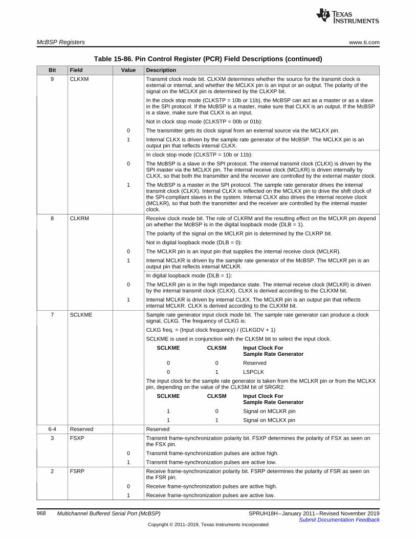
McBSP Registers www.ti.com
968 SPRUH18H–January 2011–Revised November 2019Submit Documentation Feedback
Copyright © 2011–2019, Texas Instruments Incorporated
Multichannel Buffered Serial Port (McBSP)
Table 15-86. Pin Control Register (PCR) Field Descriptions (continued)Bit Field Value Description9 CLKXM Transmit clock mode bit. CLKXM determines whether the source for the transmit clock is
external or internal, and whether the MCLKX pin is an input or an output. The polarity of thesignal on the MCLKX pin is determined by the CLKXP bit.In the clock stop mode (CLKSTP = 10b or 11b), the McBSP can act as a master or as a slavein the SPI protocol. If the McBSP is a master, make sure that CLKX is an output. If the McBSPis a slave, make sure that CLKX is an input.Not in clock stop mode (CLKSTP = 00b or 01b):
0 The transmitter gets its clock signal from an external source via the MCLKX pin.1 Internal CLKX is driven by the sample rate generator of the McBSP. The MCLKX pin is an
output pin that reflects internal CLKX.In clock stop mode (CLKSTP = 10b or 11b):
0 The McBSP is a slave in the SPI protocol. The internal transmit clock (CLKX) is driven by theSPI master via the MCLKX pin. The internal receive clock (MCLKR) is driven internally byCLKX, so that both the transmitter and the receiver are controlled by the external master clock.
1 The McBSP is a master in the SPI protocol. The sample rate generator drives the internaltransmit clock (CLKX). Internal CLKX is reflected on the MCLKX pin to drive the shift clock ofthe SPI-compliant slaves in the system. Internal CLKX also drives the internal receive clock(MCLKR), so that both the transmitter and the receiver are controlled by the internal masterclock.
8 CLKRM Receive clock mode bit. The role of CLKRM and the resulting effect on the MCLKR pin dependon whether the McBSP is in the digital loopback mode (DLB = 1).The polarity of the signal on the MCLKR pin is determined by the CLKRP bit.Not in digital loopback mode (DLB = 0):
0 The MCLKR pin is an input pin that supplies the internal receive clock (MCLKR).1 Internal MCLKR is driven by the sample rate generator of the McBSP. The MCLKR pin is an
output pin that reflects internal MCLKR.In digital loopback mode (DLB = 1):
0 The MCLKR pin is in the high impedance state. The internal receive clock (MCLKR) is drivenby the internal transmit clock (CLKX). CLKX is derived according to the CLKXM bit.
1 Internal MCLKR is driven by internal CLKX. The MCLKR pin is an output pin that reflectsinternal MCLKR. CLKX is derived according to the CLKXM bit.
7 SCLKME Sample rate generator input clock mode bit. The sample rate generator can produce a clocksignal, CLKG. The frequency of CLKG is:CLKG freq. = (Input clock frequency) / (CLKGDV + 1)SCLKME is used in conjunction with the CLKSM bit to select the input clock.
SCLKME CLKSM Input Clock ForSample Rate Generator
0 0 Reserved0 1 LSPCLK
The input clock for the sample rate generator is taken from the MCLKR pin or from the MCLKXpin, depending on the value of the CLKSM bit of SRGR2:
SCLKME CLKSM Input Clock ForSample Rate Generator
1 0 Signal on MCLKR pin1 1 Signal on MCLKX pin
6-4 Reserved Reserved3 FSXP Transmit frame-synchronization polarity bit. FSXP determines the polarity of FSX as seen on
the FSX pin.0 Transmit frame-synchronization pulses are active high.1 Transmit frame-synchronization pulses are active low.
2 FSRP Receive frame-synchronization polarity bit. FSRP determines the polarity of FSR as seen onthe FSR pin.
0 Receive frame-synchronization pulses are active high.1 Receive frame-synchronization pulses are active low.

www.ti.com McBSP Registers
969SPRUH18H–January 2011–Revised November 2019Submit Documentation Feedback
Copyright © 2011–2019, Texas Instruments Incorporated
Multichannel Buffered Serial Port (McBSP)
Table 15-86. Pin Control Register (PCR) Field Descriptions (continued)Bit Field Value Description1 CLKXP Transmit clock polarity bit. CLKXP determines the polarity of CLKX as seen on the MCLKX pin.
0 Transmit data is sampled on the rising edge of CLKX.1 Transmit data is sampled on the falling edge of CLKX.
0 CLKRP Receive clock polarity bit. CLKRP determines the polarity of CLKR as seen on the MCLKR pin.0 Receive data is sampled on the falling edge of MCLKR.1 Receive data is sampled on the rising edge of MCLKR.
Table 15-87. Pin Configuration
Pin Selected as Output When … Selected as Input When …CLKX CLKXM = 1 CLKXM = 0FSX FSXM = 1 FSXM = 0
CLKR CLKRM = 1 CLKRM = 0FSR FSRM = 1 FSRM = 0
15.12.10 Receive Channel Enable Registers (RCERA, RCERB, RCERC, RCERD, RCERE,RCERF, RCERG, RCERH)Each McBSP has eight receive channel enable registers of the format shown in Figure 15-78. There isone enable register for each of the receive partitions: A, B, C, D, E, F, G, and H. Table 15-88 provides asummary description that applies to any bit x of a receive channel enable register.
These memory-mapped registers are only used when the receiver is configured to allow individualenabling and disabling of the channels (RMCM = 1). For more details about the way these registers areused, see Section 15.12.10.1, RCERs Used in the Receive Multichannel Selection Mode.
The receive channel enable registers (RCERA...RCERH) are shown in Figure 15-78 and described inTable 15-88.
Figure 15-78. Receive Channel Enable Registers (RCERA...RCERH)15 14 13 12 11 10 9 8
RCE15 RCE14 RCE13 RCE12 RCE11 RCE10 RCE9 RCE8R/W-0 R/W-0 R/W-0 R/W-0 R/W-0 R/W-0 R/W-0 R/W-0
7 6 5 4 3 2 1 0RCE7 RCE6 RCE5 RCE4 RCE3 RCE2 RCE1 RCE0R/W-0 R/W-0 R/W-0 R/W-0 R/W-0 R/W-0 R/W-0 R/W-0
LEGEND: R/W = Read/Write; R = Read only; -n = value after reset
Table 15-88. Receive Channel Enable Registers (RCERA...RCERH) Field Descriptions
Bit Field Value Description15-0 RCEx Receive channel enable bit.
For receive multichannel selection mode (RMCM = 1):0 Disable the channel that is mapped to RCEx.1 Enable the channel that is mapped to RCEx.
15.12.10.1 RCERs Used in the Receive Multichannel Selection ModeFor multichannel selection operation, the assignment of channels to the RCERs depends on whether 32or 128 channels are individually selectable, as defined by the RMCME bit. For each of these two cases,Table 15-89 shows which block of channels is assigned to each of the RCERs used. For each RCER, thetable shows which channel is assigned to each of the bits.

McBSP Registers www.ti.com
970 SPRUH18H–January 2011–Revised November 2019Submit Documentation Feedback
Copyright © 2011–2019, Texas Instruments Incorporated
Multichannel Buffered Serial Port (McBSP)
Table 15-89. Use of the Receive Channel Enable Registers
Number ofSelectableChannels
Block Assignments Channel Assignments
RCERx Block Assigned Bit in RCERx Channel Assigned32(RMCME = 0)
RCERA Channels n to (n + 15) RCE0 Channel nRCE1 Channel (n + 1)RCE2 Channel (n + 2): :
The block of channels is chosen withthe RPABLK bits.
RCE15 Channel (n + 15)
RCERB Channels m to (m + 15) RCE0 Channel mRCE1 Channel (m + 1)RCE2 Channel (m + 2): :
The block of channels is chosen withthe RPBBLK bits.
RCE15 Channel (m + 15)
128(RMCME = 1)
RCERA Block 0 RCE0 Channel 0RCE1 Channel 1RCE2 Channel 2: :RCE15 Channel 15
RCERB Block 1 RCE0 Channel 16RCE1 Channel 17RCE2 Channel 18: :RCE15 Channel 31
RCERC Block 2 RCE0 Channel 32RCE1 Channel 33RCE2 Channel 34: :RCE15 Channel 47
RCERD Block 3 RCE0 Channel 48RCE1 Channel 49RCE2 Channel 50: :RCE15 Channel 63
RCERE Block 4 RCE0 Channel 64RCE1 Channel 65RCE2 Channel 66: :RCE15 Channel 79
RCERF Block 5 RCE0 Channel 80RCE1 Channel 81RCE2 Channel 82: :RCE15 Channel 95
RCERG Block 6 RCE0 Channel 96RCE1 Channel 97RCE2 Channel 98: :RCE15 Channel 111

www.ti.com McBSP Registers
971SPRUH18H–January 2011–Revised November 2019Submit Documentation Feedback
Copyright © 2011–2019, Texas Instruments Incorporated
Multichannel Buffered Serial Port (McBSP)
Table 15-89. Use of the Receive Channel Enable Registers (continued)Number ofSelectableChannels
Block Assignments Channel Assignments
RCERx Block Assigned Bit in RCERx Channel AssignedRCERH Block 7 RCE0 Channel 112
RCE1 Channel 113RCE2 Channel 114: :RCE15 Channel 127
15.12.11 Transmit Channel Enable Registers (XCERA, XCERB, XCERC, XCERD, XCERE,XCERF, XCERG, XCERH)
Each McBSP has eight transmit channel enable registers of the form shown in Figure 15-79. There is onefor each of the transmit partitions: A, B, C, D, E, F, G, and H. Table 15-90 provides a summary descriptionthat applies to each bit XCEx of a transmit channel enable register.
The XCERs are only used when the transmitter is configured to allow individual disabling/enabling andmasking/unmasking of the channels (XMCM is nonzero).
The transmit channel enable registers (XCERA...XCERH) are shown in Figure 15-79 and described inTable 15-90.
Figure 15-79. Transmit Channel Enable Registers (XCERA...XCERH)15 14 13 12 11 10 9 8
XCE15 XCE14 XCE13 XCE12 XCE11 XCE10 XCE9 XCE8R/W-0 R/W-0 R/W-0 R/W-0 R/W-0 R/W-0 R/W-0 R/W-0
7 6 5 4 3 2 1 0XCE7 XCE6 XCE5 XCE4 XCE3 XCE2 XCE1 XCE0R/W-0 R/W-0 R/W-0 R/W-0 R/W-0 R/W-0 R/W-0 R/W-0
LEGEND: R/W = Read/Write; R = Read only; -n = value after reset
Table 15-90. Transmit Channel Enable Registers (XCERA...XCERH) Field Descriptions
Bit Field Value Description15-0 XCEx Transmit channel enable bit. The role of this bit depends on which transmit multichannel selection
mode is selected with the XMCM bits.For multichannel selection when XMCM = 01b(all channels disabled unless selected):
0 Disable and mask the channel that is mapped to XCEx.1 Enable and unmask the channel that is mapped to XCEx.
For multichannel selection when XMCM = 10b(all channels enabled but masked unless selected):
0 Mask the channel that is mapped to XCEx.1 Unmask the channel that is mapped to XCEx.
For multichannel selection when XMCM = 11b(all channels masked unless selected):
0 Mask the channel that is mapped to XCEx. Even if the channel is enabled by the correspondingreceive channel enable bit, this channel's data cannot appear on the DX pin.
1 Unmask the channel that is mapped to XCEx. If the channel is also enabled by the correspondingreceive channel enable bit, full transmission can occur.

McBSP Registers www.ti.com
972 SPRUH18H–January 2011–Revised November 2019Submit Documentation Feedback
Copyright © 2011–2019, Texas Instruments Incorporated
Multichannel Buffered Serial Port (McBSP)
15.12.11.1 XCERs Used in a Transmit Multichannel Selection ModeFor multichannel selection operation, the assignment of channels to the XCERs depends on whether 32 or128 channels are individually selectable, as defined by the XMCME bit. These two cases are shown inTable 15-91. The table shows which block of channels is assigned to each XCER that is used. For eachXCER, the table shows which channel is assigned to each of the bits.
NOTE: When XMCM = 11b (for symmetric transmission and reception), the transmitter uses thereceive channel enable registers (RCERs) to enable channels and uses the XCERs tounmask channels for transmission.
Table 15-91. Use of the Transmit Channel Enable Registers
Number ofSelectableChannels
Block Assignments Channel Assignments
XCERx Block Assigned Bit in XCERx Channel Assigned32(XMCME = 0)
XCERA Channels n to (n + 15) XCE0 Channel nXCE1 Channel (n + 1)XCE2 Channel (n + 2): :
When XMCM = 01b or 10b, the blockof channels is chosen with theXPABLK bits. When XMCM = 11b,the block is chosen with the RPABLKbits.
XCE15 Channel (n + 15)
XCERB Channels m to (m + 15) XCE0 Channel mXCE1 Channel (m + 1)XCE2 Channel (m + 2): :
When XMCM = 01b or 10b, the blockof channels is chosen with theXPBBLK bits. When XMCM = 11b,the block is chosen with the RPBBLKbits.
XCE15 Channel (m + 15)
128(XMCME = 1)
XCERA Block 0 XCE0 Channel 0XCE1 Channel 1XCE2 Channel 2: :XCE15 Channel 15
XCERB Block 1 XCE0 Channel 16XCE1 Channel 17XCE2 Channel 18: :XCE15 Channel 31
XCERC Block 2 XCE0 Channel 32XCE1 Channel 33XCE2 Channel 34: :XCE15 Channel 47
XCERD Block 3 XCE0 Channel 48XCE1 Channel 49XCE2 Channel 50: :XCE15 Channel 63

RRDY00
EOBR condition01
FSR detected10
RSYNCERR11
RINTM bits
RINT
RINTENA MRINT
www.ti.com McBSP Registers
973SPRUH18H–January 2011–Revised November 2019Submit Documentation Feedback
Copyright © 2011–2019, Texas Instruments Incorporated
Multichannel Buffered Serial Port (McBSP)
Table 15-91. Use of the Transmit Channel Enable Registers (continued)Number ofSelectableChannels
Block Assignments Channel Assignments
XCERx Block Assigned Bit in XCERx Channel AssignedXCERE Block 4 XCE0 Channel 64
XCE1 Channel 65XCE2 Channel 66: :XCE15 Channel 79
XCERF Block 5 XCE0 Channel 80XCE1 Channel 81XCE2 Channel 82: :XCE15 Channel 95
XCERG Block 6 XCE0 Channel 96XCE1 Channel 97XCE2 Channel 98: :XCE15 Channel 111
XCERH Block 7 XCE0 Channel 112XCE1 Channel 113XCE2 Channel 114: :XCE15 Channel 127
15.12.12 Interrupt GenerationMcBSP registers can be programmed to receive and transmit data through DRR2/DRR1 and DXR2/DXR1registers, respectively. The CPU can directly access these registers to move data from memory to theseregisters. Interrupt signals will be based on these register pair contents and its related flags.MRINT/MXINTwill generate CPU interrupts for receive and transmit conditions.
15.12.12.1 McBSP Receive Interrupt GenerationIn the McBSP module, data receive and error conditions generate two sets of interrupt signals. One set isused for the CPU and the other set is for DMA.
Figure 15-80. Receive Interrupt Generation
Table 15-92. Receive Interrupt Sources and Signals
McBSPInterruptSignal
Interrupt Flags Interrupt Enablesin SPCR1
Interrupt Enables Type of Interrupt Interrupt Line
RINTMBits

XRDY00
EOBX condition01
FSX detected10
XSYNCERR11
XINTM bits
XINT
XINTENA MXINT
McBSP Registers www.ti.com
974 SPRUH18H–January 2011–Revised November 2019Submit Documentation Feedback
Copyright © 2011–2019, Texas Instruments Incorporated
Multichannel Buffered Serial Port (McBSP)
Table 15-92. Receive Interrupt Sources and Signals (continued)McBSP
InterruptSignal
Interrupt Flags Interrupt Enablesin SPCR1
Interrupt Enables Type of Interrupt Interrupt Line
RINT RRDY 0 RINTENA Every word receive MRINTEOBR 1 RINTENA Every 16 channel
block boundaryFSR 10 RINTENA On every FSR
RSYNCERR 11 RINTENA Frame sync error
NOTE: Since X/RINT, X/REVTA, and X/RXFFINT share the same CPU interrupt, it is recommendedthat all applications use one of the above selections for interrupt generation. If multipleinterrupt enables are selected at the same time, there is a likelihood of interrupts beingmasked or not recognized.
15.12.12.2 McBSP Transmit Interrupt GenerationMcBSP module data transmit and error conditions generate two sets of interrupt signals. One set is usedfor the CPU and the other set is for DMA.
Figure 15-81. Transmit Interrupt Generation
Table 15-93. Transmit Interrupt Sources and Signals
McBSPInterrupt
Signal
InterruptFlags
InterruptEnables in
SPCR2
InterruptEnables
Type of Interrupt InterruptLine
XINTM BitsXINT XRDY 0 XINTENA Every word transmit MXINT
EOBX 1 XINTENA Every 16-channel block boundaryFSX 10 XINTENA On every FSX
XSYNCERR 11 XINTENA Frame sync error
15.12.12.3 Error FlagsThe McBSP has several error flags both on receive and transmit channel. Table 15-94 explains the errorflags and their meaning.
Table 15-94. Error Flags
Error Flags FunctionRFULL Indicates DRR2/DRR1 are not read and RXR register is overwrittenRSYNCERR Indicates unexpected frame-sync condition, current data reception will abort and restart. Use RINTM
bit 11 for interrupt generation on this condition.XSYNCERR Indicates unexpected frame-sync condition, current data transmission will abort and restart. Use
XINTM bit 11 for interrupt generation on this condition.

www.ti.com McBSP Registers
975SPRUH18H–January 2011–Revised November 2019Submit Documentation Feedback
Copyright © 2011–2019, Texas Instruments Incorporated
Multichannel Buffered Serial Port (McBSP)
15.12.12.4 McBSP Interrupt Enable Register
Figure 15-82. McBSP Interrupt Enable Register (MFFINT)15 8
ReservedR-0
7 3 2 1 0Reserved RINT ENA Reserved XINT ENA
R-0 R/W-0 R-0 R/W-0LEGEND: R/W = Read/Write; R = Read only; -n = value after reset
Table 15-95. McBSP Interrupt Enable Register (MFFINT) Field Descriptions
Bit Field Value Description15:3 Reserved Reserved
2 RINT ENA Enable for Receive Interrupt0 Receive interrupt on RRDY is disabled.1 Receive interrupt on RRDY is enabled.
1 Reserved0 XINT ENA Enable for transmit Interrupt
0 Transmit interrupt on XRDY is disabled.1 Transmit interrupt on XRDY is enabled.
15.12.12.5 McBSP ModesMcBSP, in its normal mode, communicates with various types of Codecs with variable word size. Apartfrom this mode, the McBSP uses time-division multiplexed (TDM) data stream while communicating withother McBSPs or serial devices. The multichannel mode provides flexibility while transmitting/receivingselected channels or all the channels in a TDM stream.
Table 15-96 provides a quick reference to McBSP mode selection.
Table 15-96. McBSP Mode Selection
Register Bits Used for Mode SelectionMCR1 bit 9,0 MCR2 bit 9,1,0
No. McBSPWord Size
RMCME RMCM XMCME XMCM Mode and Function Description
Normal Mode1 8/12/16/20/24/32 0 0 0 0 All types of Codec interface will use this
bit words selectionMultichannel Mode
2 8-bit words 2 Partition or 32-channel Mode0 1 0 1 All channels are disabled,unless selected in
X/RCERA/B0 1 0 10 All channels are enabled,but masked unless
selected in X/RCERA/B0 1 0 11 Symmetric transmit, receive
8 Partition or 128 Channel Mode Transmit/ReceiveChannels selected by X/RCERA toX/RCERH bitsMultichannel Mode is ON
1 1 1 1 All channels are disabled,unless selected in

McBSP Registers www.ti.com
976 SPRUH18H–January 2011–Revised November 2019Submit Documentation Feedback
Copyright © 2011–2019, Texas Instruments Incorporated
Multichannel Buffered Serial Port (McBSP)
Table 15-96. McBSP Mode Selection (continued)Register Bits Used for Mode SelectionMCR1 bit 9,0 MCR2 bit 9,1,0
No. McBSPWord Size
RMCME RMCM XMCME XMCM Mode and Function Description
XCERs1 1 1 10 All channels are enabled,but masked unless
selected in XCERs1 1 1 11 Symmetric transmit, receive
Continuous Mode - Transmit1 0 1 0 Multi-Channel Mode is OFF
All 128 channels are active and enabled

977SPRUH18H–January 2011–Revised November 2019Submit Documentation Feedback
Copyright © 2011–2019, Texas Instruments Incorporated
Controller Area Network (CAN)
Chapter 16SPRUH18H–January 2011–Revised November 2019
Controller Area Network (CAN)
The enhanced Controller Area Network (eCAN) module is a full-CAN controller and is compatible with theCAN 2.0B standard (active). It uses established protocol to communicate serially with other controllers inelectrically noisy environments. With 32 fully configurable mailboxes and a time−stamping feature, theeCAN module provides a versatile and robust serial communication interface. Refer to theC2000 Real-Time Control Peripheral Reference Guide (SPRU566) for a list of devices with the eCAN module. Somedevices have a second CAN module, eCAN-B. The word eCAN is generically used to refer to the CANmodules. The specific module reference (A or B) is used where appropriate. For a given eCAN module,the same address space is used for the module registers in all applicable 28xx /28xxx devices. Refer toProgramming Examples for the TMS320x28xx eCAN (SPRA876) which provides many useful examplesthat illustrate how to program the eCAN module.
Topic ........................................................................................................................... Page
16.1 CAN Overview .................................................................................................. 97816.2 eCAN Compatibility With Other TI CAN Modules .................................................. 97916.3 The CAN Network and Module............................................................................ 97916.4 eCAN Controller Overview ................................................................................. 98116.5 Message Objects .............................................................................................. 98516.6 Message Mailbox .............................................................................................. 98516.7 eCAN Configuration .......................................................................................... 98916.8 eCAN Registers .............................................................................................. 100116.9 Message Data Registers (CANMDL, CANMDH) ................................................... 103916.10 Acceptance Filter........................................................................................... 1040

CAN Overview www.ti.com
978 SPRUH18H–January 2011–Revised November 2019Submit Documentation Feedback
Copyright © 2011–2019, Texas Instruments Incorporated
Controller Area Network (CAN)
16.1 CAN OverviewFigure 16-1 shows the major blocks of the eCAN and the interface circuits.
16.1.1 FeaturesThe eCAN module has the following features:• Fully compliant with CAN protocol, version 2.0B• Supports data rates up to 1 Mbps• Thirty-two mailboxes, each with the following properties:
– Configurable as receive or transmit– Configurable with standard or extended identifier– Has a programmable acceptance filter mask– Supports data and remote frame– Supports 0 to 8 bytes of data– Uses a 32-bit time stamp on received and transmitted message– Protects against reception of new message– Allows dynamically programmable priority of transmit message– Employs a programmable interrupt scheme with two interrupt levels– Employs a programmable interrupt on transmission or reception time-out
• Low−power mode• Programmable wake−up on bus activity• Automatic reply to a remote request message• Automatic retransmission of a frame in case of loss of arbitration or error• 32-bit time-stamp counter synchronized by a specific message (communication in conjunction with
mailbox 16)• Self−test mode
– Operates in a loopback mode receiving its own message. A self-generated acknowledge isprovided, thereby eliminating the need for another node to provide the acknowledge bit.
16.1.2 Block DiagramFigure 16-1 shows the block diagram of eCAN.

ECAN0INT
Control and status
registers
Communication
BuffersA
Message Controller
3.3-V CAN Transceiver
8
CANTX CANRX
32
Memory Management
Unit
CPU Interface,
Receive Control Unit,
Timer Management Unit
32-Message
Mailbox RAM
(4 X 32-bit words
for each mailbox)
32
CAN_H
CAN_L
CAN Bus
ECAN1INT
Controls Address Data
32
www.ti.com eCAN Compatibility With Other TI CAN Modules
979SPRUH18H–January 2011–Revised November 2019Submit Documentation Feedback
Copyright © 2011–2019, Texas Instruments Incorporated
Controller Area Network (CAN)
Figure 16-1. eCAN Block Diagram and Interface Circuit
A The communication buffers are transparent to the user and are not accessible by user code.
16.2 eCAN Compatibility With Other TI CAN ModulesThe eCAN module is identical to the High-end CAN Controller (HECC) used in the TMS470™ series ofmicrocontrollers from Texas Instruments with some minor changes. The eCAN module features severalenhancements (such as increased number of mailboxes with individual acceptance masks, time stamping,and so on) over the CAN module featured in the LF240xA™ series of devices. For this reason, codewritten for LF240xA CAN modules cannot be directly ported to eCAN. However, eCAN follows the sameregister bit-layout structure and bit functionality as that of LF240xA CAN (for registers that exist in bothdevices) that is, many registers and bits perform exactly identical functions across these two platforms.This makes code migration a relatively easy task, more so with code written in C language.
16.3 The CAN Network and ModuleThe controller area network (CAN) uses a serial multimaster communication protocol that efficientlysupports distributed real-time control, with a high level of reliability, and a communication rate of up to 1Mbps. The CAN bus is ideal for applications operating in electrically noisy environments, such as in theautomotive and other industrial fields that require reliable communication.

Bit length 1 12 or 32
Start bit
Arbitration field which contains:
6 0-8 bytes
Data field
Control bits
16
CRC bits
7
End
2
Acknowledge
– 11-bit identifier + RTR bit for standard frame format– 29-bit identifier + SRR bit + IDE bit + RTR bit for extended frame formatWhere: RTR = Remote Transmission Request SRR = Substitute Remote Request IDE = Identifier Extension
Note: Unless otherwise noted, numbers are amount of bits in field.
The CAN Network and Module www.ti.com
980 SPRUH18H–January 2011–Revised November 2019Submit Documentation Feedback
Copyright © 2011–2019, Texas Instruments Incorporated
Controller Area Network (CAN)
Prioritized messages of up to eight bytes in data length can be sent on a multimaster serial bus using anarbitration protocol and an error-detection mechanism for a high level of data integrity.
16.3.1 CAN Protocol OverviewThe CAN protocol supports four different frame types for communication:• Data frames that carry data from a transmitter node to the receiver node(s).• Remote frames that are transmitted by a node to request the transmission of a data frame with the
same identifier.• Error frames that are transmitted by any node upon detecting an error condition.• Overload frames that provide an extra delay between the preceding and the succeeding data frames or
remote frames.
In addition, CAN specification version 2.0B defines two different formats that differ in the length of theidentifier field: standard frames with an 11-bit identifier and extended frames with 29-bit identifier.
CAN standard data frames contain from 44 to 108 bits and CAN extended data frames contain 64 to 128bits. Furthermore, up to 23 stuff bits can be inserted in a standard data frame, and up to 28 stuff bits in anextended data frame, depending on the data-stream coding. The overall maximum data frame length isthen 131 bits for a standard frame and 156 bits for an extended frame.
The bit fields that make up standard or extended data frames, along with their position as shown inFigure 16-2 include the following:• Start of frame• Arbitration field containing the identifier and the type of message being sent• Control field indicating the number of bytes being transmitted.• Up to 8 bytes of data• Cyclic redundancy check (CRC)• Acknowledgment• End-of-frame bits
Figure 16-2. CAN Data Frame
The eCAN controller provides the CPU with full functionality of the CAN protocol. The CAN controllerminimizes the CPU’s load in communication overhead and enhances the CAN standard by providingadditional features.
The architecture of eCAN module, shown in Figure 16-3, is composed of a CAN protocol kernel (CPK) anda message controller.

CAN Bus
CAN controller
Message Controller
CAN Protocol Kernel (CPK)
CAN Transceiver
RX TX
CPU
Receive BufferA
Transmit BufferA
www.ti.com eCAN Controller Overview
981SPRUH18H–January 2011–Revised November 2019Submit Documentation Feedback
Copyright © 2011–2019, Texas Instruments Incorporated
Controller Area Network (CAN)
Figure 16-3. Architecture of the eCAN Module
A The receive and transmit buffers are transparent to the user and are not accessible by user code.
One function of the CPK is to decode all messages received on the CAN bus and to transfer thesemessages into a receive buffer. Another function is to transmit messages on the CAN bus according to theCAN protocol.
The message controller of a CAN controller is responsible for determining if any message received by theCPK must be preserved for the CPU use (that is, copied into the mailbox RAM) or be discarded. At theinitialization phase, the CPU specifies to the message controller all message identifiers used by theapplication. The message controller is also responsible for sending the next message to transmit to theCPK according to the message’s priority.
16.4 eCAN Controller OverviewThe eCAN has an internal 32-bit architecture.
The eCAN module consists of:• The CAN protocol kernel (CPK)• The message controller comprising:
– The memory management unit (MMU), including the CPU interface and the receive control unit(acceptance filtering), and the timer management unit
– Mailbox RAM enabling the storage of 32 messages– Control and status registers
After the reception of a valid message by the CPK, the receive control unit of the message controllerdetermines if the received message must be stored into one of the 32 message objects of the mailboxRAM. The receive control unit checks the state, the identifier, and the mask of all message objects todetermine the appropriate mailbox location. The received message is stored into the first mailbox passingthe acceptance filtering. If the receive control unit could not find any mailbox to store the receivedmessage, the message is discarded.

eCAN Controller Overview www.ti.com
982 SPRUH18H–January 2011–Revised November 2019Submit Documentation Feedback
Copyright © 2011–2019, Texas Instruments Incorporated
Controller Area Network (CAN)
A message is composed of an 11- or 29-bit identifier, a control field, and up to 8 bytes of data.
When a message must be transmitted, the message controller transfers the message into the transmitbuffer of the CPK in order to start the message transmission at the next bus-idle state. When more thanone message must be transmitted, the message with the highest priority that is ready to be transmitted istransferred into the CPK by the message controller. If two mailboxes have the same priority, then themailbox with the higher number is transmitted first.
The timer management unit comprises a time-stamp counter and apposes a time stamp to all messagesreceived or transmitted. It generates an interrupt when a message has not been received or transmittedduring an allowed period of time (time-out). The time-stamping feature is available in eCAN mode only.
To initiate a data transfer, the transmission request bit (TRS.n) must be set. The entire transmissionprocedure and possible error handling are then performed without any CPU involvement. If a mailbox hasbeen configured to receive messages, the CPU easily reads its data registers using CPU readinstructions. The mailbox may be configured to interrupt the CPU after every successful messagetransmission or reception.
16.4.1 Standard CAN Controller (SCC) ModeThe SCC Mode is a reduced functionality mode of the eCAN. Only 16 mailboxes (0 through 15) areavailable in this mode. The time stamping feature is not available and the number of acceptance masksavailable is reduced. This mode is selected by default. The SCC mode or the full featured eCAN mode isselected using the SCB bit (CANMC.13).
www.ti.com eCAN Controller Overview
983SPRUH18H–January 2011–Revised November 2019Submit Documentation Feedback
Copyright © 2011–2019, Texas Instruments Incorporated
Controller Area Network (CAN)
16.4.2 Memory MapThe eCAN module has two different address segments mapped in the memory. The first segment is usedto access the control registers, the status registers, the acceptance masks, the time stamp, and the time-out of the message objects. The access to the control and status registers is limited to 32-bit wideaccesses. The local acceptance masks, the time stamp registers, and the time-out registers can beaccessed 8-bit, 16-bit and 32-bit wide. The second address segment is used to access the mailboxes.This memory range can be accessed 8-bit, 16-bit and 32-bit wide. Each of these two memory blocks,shown in Figure 16-4, uses 512 bytes of address space.
The message storage is implemented by a RAM that can be addressed by the CAN controller or the CPU.The CPU controls the CAN controller by modifying the various mailboxes in the RAM or the additionalregisters. The contents of the various storage elements are used to perform the functions of theacceptance filtering, message transmission, and interrupt handling.
The mailbox module in the eCAN provides 32 message mailboxes of 8-byte data length, a 29-bit identifier,and several control bits. Each mailbox can be configured as either transmit or receive. In the eCAN mode,each mailbox has its individual acceptance mask.
NOTE: LAMn, MOTSn and MOTOn registers and mailboxes not used in an application (disabled inthe CANME register) may be used as general-purpose data memory by the CPU.
16.4.2.1 32-bit Access to Control and Status RegistersAs indicated in Section 16.4.2, only 32-bit accesses are allowed to the Control and Status registers. 16-bitaccess to these registers could potentially corrupt the register contents or return false data. TheC2000Ware files released by TI employs a shadow register structure that aids in 32-bit access. Followingare a few examples of how the shadow register structure may be employed to perform 32-bit reads andwrites:
Example 16-1. Modifying a bit in a register
ECanaShadow.CANTIOC.all = ECanaRegs.CANTIOC.all; // Step 1ECanaShadow.CANTIOC.bit.TXFUNC = 1; // Step 2ECanaRegs.CANTIOC.all = ECanaShadow.CANTIOC.all; // Step 3
Step 1: Perform a 32-bit read to copy the entire register to its shadow
Step 2: Modify the needed bit or bits in the shadow
Step 3: Perform a 32-bit write to copy the modified shadow to the original register.
NOTE: Some bits like TAn and RMPn are cleared by writing a 1 to it. Care should be taken not toclear bits inadvertently. It is good practice to initialize the shadow registers to zero beforestep 1.
Example 16-2. Checking the value of a bit in a register
do { ECanaShadow.CANTA.all = ECanaRegs.CANTA.all;}while(ECanaShadow.CANTA.bit.TA25 == 0); // Wait for TA5 bit to be set..
In the above example, the value of TA25 bit needs to be checked. This is done by first copying the entireCANTA register to its shadow (using a 32-bit read) and then checking the relevant bit, repeating thisoperation until that condition is satisfied. TA25 bit should NOT be checked with the following statement:while(ECanaRegs.CANTA.bit.TA25 == 0);

Global Acceptance Mask − CANGAM
Mailbox Enable − CANME
Mailbox Direction − CANMD
Transmission Request Set − CANTRS
Transmission Request Reset − CANTRR
Transmission Acknowledge − CANTA
Abort Acknowledge − CANAA
Received Message Pending − CANRMP
Received Message Lost − CANRML
Remote Frame Pending − CANRFP
Master Control − CANMC
Bit−Timing Configuration − CANBTC
Error and Status − CANES
Transmit Error Counter − CANTEC
Receive Error Counter − CANREC
Global Interrupt Flag 0 − CANGIF0
Global Interrupt Mask − CANGIM
Mailbox Interrupt Mask − CANMIM
Mailbox Interrupt Level − CANMIL
Overwrite Protection Control − CANOPC
TX I/O Control − CANTIOC
RX I/O Control − CANRIOC
Time−Stamp Counter − CANTSC
Global Interrupt Flag 1 − CANGIF1
Time−Out Control − CANTOC
Time−Out Status − CANTOS
Reserved
eCAN−A Control and Status Registers
Message Identifier − MSGID (32 bits)61E8h−61E9h
Message Control − MSGCTRL (32 bits)
Message Data Low − CANMDL (4 bytes)
Message Data High − CANMDH (4 bytes)
Message Mailbox (16 Bytes)
Control and Status Registers6000h
603Fh
Local Acceptance Masks (LAM)
(32 × 32−Bit RAM)
6040h
607Fh
6080h
60BFh
60C0h
60FFh
eCAN−A Registers (512 Bytes)
Message Object Time Stamps (MOTS)
(32 × 32−Bit RAM)
Message Object Time−Out (MOTO)
(32 × 32−Bit RAM)
Mailbox 06100h−6107h
Mailbox 16108h−610Fh
Mailbox 26110h−6117h
Mailbox 36118h−611Fh
eCAN−A Mailbox RAM (512 Bytes)
Mailbox 46120h−6127h
Mailbox 2861E0h−61E7h
Mailbox 2961E8h−61EFh
Mailbox 3061F0h−61F7h
Mailbox 3161F8h−61FFh
61EAh−61EBh
61ECh−61EDh
61EEh−61EFh
eCAN Controller Overview www.ti.com
984 SPRUH18H–January 2011–Revised November 2019Submit Documentation Feedback
Copyright © 2011–2019, Texas Instruments Incorporated
Controller Area Network (CAN)
Figure 16-4. eCAN-A Memory Map

www.ti.com Message Objects
985SPRUH18H–January 2011–Revised November 2019Submit Documentation Feedback
Copyright © 2011–2019, Texas Instruments Incorporated
Controller Area Network (CAN)
16.5 Message ObjectsThe eCAN module has 32 message objects (mailboxes).
Each message object can be configured to either transmit or receive. Each message object has its ownacceptance mask (in the eCAN mode; not in SCC mode).
A message object consists of a message mailbox with:• The 29-bit message identifier• The message control register• 8 bytes of message data• A 29-bit acceptance mask• A 32-bit time stamp• A 32-bit time-out value
Furthermore, corresponding control and status bits located in the registers allow control of the messageobjects.
16.6 Message MailboxThe message mailboxes are the RAM area where the CAN messages are actually stored after they arereceived or before they are transmitted.
The CPU may use the RAM area of the message mailboxes that are not used for storing messages asnormal memory.
Each mailbox contains:• The message identifier
– 29 bits for extended identifier– 11 bits for standard identifier
• The identifier extension bit, IDE (MSGID.31)• The acceptance mask enable bit, AME (MSGID.30)• The auto answer mode bit, AAM (MSGID.29)• The transmit priority level, TPL (MSGCTRL.12-8)• The remote transmission request bit, RTR (MSGCTRL.4)• The data length code, DLC (MSGCTRL.3-0)• Up to eight bytes for the data field
Each of the mailboxes can be configured as one of four message object types (see ). Transmit andreceive message objects are used for data exchange between one sender and multiple receivers (1 to ncommunication link), whereas request and reply message objects are used to set up a one-to-onecommunication link. Table 16-1 lists the mailbox RAM layout.

Message Mailbox www.ti.com
986 SPRUH18H–January 2011–Revised November 2019Submit Documentation Feedback
Copyright © 2011–2019, Texas Instruments Incorporated
Controller Area Network (CAN)
Table 16-1. eCAN-A Mailbox RAM Layout
Mailbox MSGIDMSGIDL-MSGIDH
MSGCTRLMSGCTRL-Rsvd
CANMDLCANMDL_L- CANMDL_H
CANMDHCANMDH_L- CANMDH_H
0 6100-6101h 6102-6103h 6104-6105h 6106-6107h1 6108-6109h 610A-610Bh 610C-610Dh 610E-610Fh2 6110 - 6111h 6112-6113h 6114-6115h 6116-6117h3 6118-6119h 611A-611Bh 611C-611Dh 611E-611Fh4 6120-6121h 6122-6123h 6124-6125h 6126-6127h5 6128-6129h 612A-612Bh 612C-612Dh 612E-612Fh6 6130-6131h 6132-6133h 6134-6135h 6136-6137h7 6138-6139h 613A-613Bh 613C-613Dh 613E-613Fh8 6140-6141h 6142-6143h 6144-6145h 6146-6147h9 6148-6149h 614A-614Bh 614C-614Dh 614E-614Fh10 6150-6151h 6152-6153h 6154-6155h 6156-6157h11 6158-6159h 615A-615Bh 615C-615Dh 615E-615Fh12 6160-6161h 6162-6163h 6164-6165h 6166-6167h13 6168-6169h 616A-616Bh 616C-616Dh 616E-616Fh14 6170-6171h 6172-6173h 6174-6175h 6176-6177h15 6178-6179h 617A-617Bh 617C-617Dh 617E-617Fh16 6180-6181h 6182-6183h 6184-6185h 6186-6187h17 6188-6189h 618A-618Bh 618C-618Dh 618E-618Fh18 6190-6191h 6192-6193h 6194-6195h 6196-6197h19 6198-6199h 619A-619Bh 619C-619Dh 619E-619Fh20 61A0-61A1h 61A2-61A3h 61A4-61A5h 61A6-61A7h21 61A8-61A9h 61AA-61ABh 61AC-61ADh 61AE-61AFh22 61B0-61B1h 61B2-61B3h 61B4-61B5h 61B6-61B7h23 61B8-61B9h 61BA-61BBh 61BC-61BDh 61BE-61BFh24 61C0-61C1h 61C2-61C3h 61C4-61C5h 61C6-61C7h25 61C8-61C9h 61CA-61CBh 61CC-61CDh 61CE-61CFh26 61D0-61D1h 61D2-61D3h 61D4-61D5h 61D6-61D7h27 61D8-61D9h 61DA-61DBh 61DC-61DDh 61DE-61DFh28 61E0-61E1h 61E2-61E3h 61E4-61E5h 61E6-61E7h29 61E8-61E9h 61EA-61EBh 61EC-61EDh 61EE-61EFh30 61F0-61F1h 61F2-61F3h 61F4-61F5h 61F6-61F7h31 61F8-61F9h 61FA-61FBh 61FC-61FDh 61FE-61FFh

www.ti.com Message Mailbox
987SPRUH18H–January 2011–Revised November 2019Submit Documentation Feedback
Copyright © 2011–2019, Texas Instruments Incorporated
Controller Area Network (CAN)
Table 16-2. Addresses of LAM, MOTS and MOTO registers for mailboxes (eCAN-A)
Mailbox LAM MOTS MOT00 6040h-6041h 6080h-6081h 60C0h-60C1h1 6042h-6043h 6082h-6083h 60C2h-60C3h2 6044h-6045h 6084h-6085h 60C4h-60C5h3 6046h-6047h 6086h-6087h 60C6h-60C7h4 6048h-6049h 6088h-6089h 60C8h-60C9h5 604Ah-604Bh 608Ah-608Bh 60CAh-60CBh6 604Ch-604Dh 608Ch-608Dh 60CCh-60CDh7 604Eh-604Fh 608Eh-608Fh 60CEh-60CFh8 6050h-6051h 6090h-6091h 60D0h-60D1h9 6052h-6053h 6092h-6093h 60D2h-60D3h10 6054h-6055h 6094h-6095h 60D4h-60D5h11 6056h-6057h 6096h-6097h 60D6h-60D7h12 6058h-6059h 6098h-6099h 60D8h-60D9h13 605Ah-605Bh 609Ah-609Bh 60DAh-60DBh14 605Ch-605Dh 609Ch-609Dh 60DCh-60DDh15 605Eh-605Fh 609Eh-609Fh 60DEh-60DFh16 6060h-6061h 60A0h-60A1h 60E0h-60E1h17 6062h-6063h 60A2h-60A3h 60E2h-60E3h18 6064h-6065h 60A4h-60A5h 60E4h-60E5h19 6066h-6067h 60A6h-60A7h 60E6h-60E7h20 6068h-6069h 60A8h-60A9h 60E8h-60E9h21 606Ah-606Bh 60AAh-60ABh 60EAh-60EBh22 606Ch-606Dh 60ACh-60ADh 60ECh-60EDh23 606Eh-606Fh 60AEh-60AFh 60EEh-60EFh24 6070h-6071h 60B0h-60B1h 60F0h-60F1h25 6072h-6073h 60B2h-60B3h 60F2h-60F3h26 6074h-6075h 60B4h-60B5h 60F4h-60F5h27 6076h-6077h 60B6h-60B7h 60F6h-60F7h28 6078h-6079h 60B8h-60B9h 60F8h-60F9h29 607Ah-607Bh 60BAh-60BBh 60FAh-60FBh30 607Ch-607Dh 60BCh-60BDh 60FCh-60FDh31 607Eh-607Fh 60BEh-60BFh 60FEh-60FFh
Table 16-3. Message Object Behavior Configuration
Message Object Behavior Mailbox Direction Register(CANMD)
Auto-Answer Mode Bit(AAM)
Remote TransmissionRequest Bit (RTR)
Transmit message object 0 0 0Receive message object 1 0 0Remote-Request message object 1 0 1Auto-Reply message object 0 1 0
16.6.1 Transmit MailboxThe CPU stores the data to be transmitted in a mailbox configured as transmit mailbox. After writing thedata and the identifier into the RAM, the message is sent if the corresponding TRS[n] bit has been set,provided the mailbox is enabled by setting the corresponding the CANME.n bit.

Message Mailbox www.ti.com
988 SPRUH18H–January 2011–Revised November 2019Submit Documentation Feedback
Copyright © 2011–2019, Texas Instruments Incorporated
Controller Area Network (CAN)
If more than one mailbox is configured as transmit mailbox and more than one corresponding TRS[n] isset, the messages are sent one after another in falling order beginning with the mailbox with the highestpriority.
In the SCC-compatibility mode, the priority of the mailbox transmission depends on the mailbox number.The highest mailbox number (=15) comprises the highest transmit priority.
In the eCAN mode, the priority of the mailbox transmission depends on the setting of the TPL field in themessage control field (MSGCTRL) register. The mailbox with the highest value in the TPL is transmittedfirst. Only when two mailboxes have the same value in the TPL is the higher numbered mailboxtransmitted first.
If a transmission fails due to a loss of arbitration or an error, the message transmission will bereattempted. Before reattempting the transmission, the CAN module checks if other transmissions arerequested. If the TRS bit of a higher-priority (determined either by the MBX number or by the associatedTPL value) mailbox had been set before the message in the transmit-buffer has lost arbitration, thetransmit-buffer contents will be replaced with that of the higher-priority mailbox and the higher prioritymailbox will be transmitted after the arbitration loss. However, if that TRS bit was set after the message inthe transmit-buffer has lost arbitration, the higher priority MBX will be transmitted only after the currentmessage in the transmit-buffer has been transmitted.
16.6.2 Receive MailboxThe identifier of each incoming message is compared to the identifiers held in the receive mailboxes usingthe appropriate mask. When equality is detected, the received identifier, the control bits, and the databytes are written into the matching RAM location. At the same time, the corresponding receive-message-pending bit, RMP[n] (RMP.31-0), is set and a receive interrupt is generated if enabled. If no match isdetected, the message is not stored.
When a message is received, the message controller starts looking for a matching identifier at the mailboxwith the highest mailbox number. Mailbox 15 of the eCAN in SCC compatible mode has the highestreceive priority; mailbox 31 has the highest receive priority of the eCAN in eCAN mode.
RMP[n] (RMP.31-0) has to be reset by the CPU after reading the data. If a second message has beenreceived for this mailbox and the receive-message-pending bit is already set, the corresponding message-lost bit (RML[n] (RML.31-0)) is set. In this case, the stored message is overwritten with the new data if theoverwrite-protection bit OPC[n] (OPC.31-0) is cleared; otherwise, the next mailboxes are checked.
If a mailbox is configured as a receive mailbox and the RTR bit is set for it, the mailbox can send a remoteframe. Once the remote frame is sent, the TRS bit of the mailbox is cleared by the CAN module.
16.6.3 CAN Module Operation in Normal ConfigurationIf the CAN module is being used in normal configuration (that is, not in self-test mode), there should be atleast one more CAN module on the network, configured for the same bit rate. The other CAN moduleneed NOT be configured to actually receive messages into the mailbox RAM from the transmitting node.But, it should be configured for the same bit rate. This is because a transmitting CAN module expects atleast one node in the CAN network to acknowledge the proper reception of a transmitted message. PerCAN protocol specification, any CAN node that received a message will acknowledge (unless theacknowledge mechanism has been explicitly turned off), irrespective of whether it has been configured tostore the received message or not. It is not possible to turn off the acknowledge mechanism in the eCANmodule.
The requirement of another node does not exist for the self-test mode (STM). In this mode, a transmittingnode generates its own acknowledge signal. The only requirement is that the node be configured for anyvalid bit-rate. That is, the bit timing registers should not contain a value that is not permitted by the CANprotocol.
It is not possible to achieve a direct digital loopback externally by connecting the CANTX and CANRX pinstogether (as is possible with SCI/SPI/McBSP modules). An internal loopback is possible in the self-testmode (STM).

Normal mode(CCR = 0)(CCE = 0)
Configuration mode requested(CCR = 1)(CCE = 0)
Wait for configuration mode(CCR = 1)(CCE = 0)
CCE = 0
Configuration mode active(CCR = 1)(CCE = 1)
Changing of bit timingparameters enabled
Normal mode requested(CCR = 0)CCE = 1
Wait for normal mode(CCR = 0)(CCE = 1)
CCE = 1
Initialization completeNormal mode
www.ti.com eCAN Configuration
989SPRUH18H–January 2011–Revised November 2019Submit Documentation Feedback
Copyright © 2011–2019, Texas Instruments Incorporated
Controller Area Network (CAN)
16.7 eCAN ConfigurationThis section explains the process of initialization and describes the procedures to configure the eCANmodule.
16.7.1 CAN Module InitializationThe CAN module must be initialized before the utilization. Initialization is only possible if the module is ininitialization mode. Figure 16-5 is a flow chart showing the process.
Programming CCR (CANMC.12) = 1 sets the initialization mode. The initialization can be performed onlywhen CCE (CANES.4) = 1. Afterwards, the configuration registers can be written.
SCC mode only:• In order to modify the global acceptance mask register (CANGAM) and the two local acceptance mask
registers [LAM(0) and LAM(3)], the CAN module also must be set in the initialization mode.• The module is activated again by programming CCR(CANMC.12) = 0.• After hardware reset, the initialization mode is active.
NOTE: If the CANBTC register is programmed with a zero value, or left with the initial value, theCAN module never leaves the initialization mode, that is CCE (CANES.4) bit remains at 1when clearing the CCR bit.
Figure 16-5. Initialization Sequence
NOTE: The transition between initialization mode and normal mode and vice-versa is performed insynchronization with the CAN network. That is, the CAN controller waits until it detects a busidle sequence (= 11 recessive bits) before it changes the mode. In the event of a stuck-to-dominant bus error, the CAN controller cannot detect a bus-idle condition and therefore isunable to perform a mode transition.

TimeBit
2/rateBit
´
=
BRP
SYSCLKOUT
Nominal bit time
SYNCSEG
1 TQ
TSEG2TSEG1
Transmit pointSample point
SJW SJW
eCAN Configuration www.ti.com
990 SPRUH18H–January 2011–Revised November 2019Submit Documentation Feedback
Copyright © 2011–2019, Texas Instruments Incorporated
Controller Area Network (CAN)
16.7.1.1 CAN Bit-Timing ConfigurationThe CAN protocol specification partitions the nominal bit time into four different time segments:
SYNC_SEG: This part of bit time is used to synchronize the various nodes on the bus. An edge isexpected to lie within this segment. This segment is always 1 TIME QUANTUM (TQ).
PROP_SEG: This part of the bit time is used to compensate for the physical delay times within thenetwork. It is twice the sum of the signal’s propagation ‘time on the bus line, the input comparator delay,and the output driver delay. This segment is programmable from 1 to 8 TIME QUANTA (TQ).
PHASE_SEG1: This phase is used to compensate for positive edge phase error. This segment isprogrammable from 1 to 8 TIME QUANTA (TQ) and can be lengthened by resynchronization.
PHASE_SEG2: This phase is used to compensate for negative edge phase error. This segment isprogrammable from 2 to 8 TIME QUANTA (TQ) and can be shortened by resynchronization.
In the eCAN module, the length of a bit on the CAN bus is determined by the parameters TSEG1 (BTC.6-3), TSEG2 (BTC.2-0), and BRP (BTC.23.16).
TSEG1 combines the two time segments PROP_SEG and PHASE_SEG1 as defined by the CANprotocol. TSEG2 defines the length of the time segment PHASE_SEG2.
IPT (information processing time) corresponds to the time necessary for the processing of the bit read. IPTcorresponds to two units of TQ.
The following bit timing rules must be fulfilled when determining the bit segment values:• TSEG1(min) ≥ TSEG2• IPT ≤ TSEG1 ≤ 16 TQ• IPT ≤ TSEG2 ≤ 8 TQ• IPT = 3/BRP (the resulting IPT has to be rounded up to the next integer value)• 1 TQ ≤ SJW min[4 TQ, TSEG2] (SJW = Synchronization jump width)• To utilize three-time sampling mode, BRP ≥ 5 has to be selected
Figure 16-6. CAN Bit Timing
A TSEG1 can be lengthened or TSEG2 shortened by the SJW
16.7.1.2 CAN Bit Rate CalculationBit-rate is calculated in bits per second as follows:

Bit-time = TSEG1 + TSEG2 + 1
Bit-time = (TSEG1reg + 1) + (TSEG2reg + 1) + 1
www.ti.com eCAN Configuration
991SPRUH18H–January 2011–Revised November 2019Submit Documentation Feedback
Copyright © 2011–2019, Texas Instruments Incorporated
Controller Area Network (CAN)
Where bit-time is the number of time quanta (TQ) per bit. SYSCLKOUT is the device clock frequency,which is the same as the CPU clock frequency. BRP is the value of BRPreg + 1 (CANBTC.23-16).
Bit-time is defined as follows:
In the above equation TESG1reg and TSEG2reg represent the actual values written in the correspondingfields in the CANBTC register. The parameters TSEG1reg, TSEG2reg, SJWreg, and BRPreg are automaticallyenhanced by 1 when the CAN module accesses these parameters. TSEG1, TSEG2 and SJW, representthe values as applicable per Figure 16-6.
16.7.1.3 Bit Configuration Parameters for 45 -MHz CAN ClockThis section provides example values for the CANBTC bit fields for some bit rates and sampling points.Note that these values are for illustrative purposes only. In a real-world application, parameters such asthe oscillator accuracy and the propagation delay introduced by various entities such as the networkcable, transceivers/ isolators must be taken into account before choosing the timing parameters.
Table 16-4 shows how the BRPreg field may be changed to achieve different bit rates with a BT of 15 for a80% SP.
Table 16-4. BRP Field for Bit Rates (BT = 15, TSEG1reg = 10, TSEG2reg = 2, Sampling Point = 80%)
CAN Bus Speed BRP CAN Module Clock1 Mbps BRPreg +1 = 3 15 MHz
500 kbps BRPreg +1 = 6 7.5 MHz250 kbps BRPreg +1 = 12 3.75 MHz125 kbps BRPreg +1 = 24 1.875 MHz100 kbps BRPreg +1 = 30 1.5 MHz50 kbps BRPreg +1 = 60 0.75 MHz
Table 16-5 shows how to achieve different sampling points with a BT of 15.
Table 16-5. Achieving Different Sampling Points With a BT of 15
TSEG1reg TSEG2reg SP10 2 80%9 3 73%8 4 66%7 5 60%
NOTE: For a SYSCLKOUT of 90 MHz, the smallest bit rate possible is 7.031 kbps.

eCAN Configuration www.ti.com
992 SPRUH18H–January 2011–Revised November 2019Submit Documentation Feedback
Copyright © 2011–2019, Texas Instruments Incorporated
Controller Area Network (CAN)
16.7.1.4 EALLOW ProtectionTo protect against inadvertent modification, some critical registers/bits of the eCAN module are EALLOWprotected. These registers/bits can be changed only if the EALLOW protection has been disabled.Following are the registers/ bits that are EALLOW protected in the eCAN module:• CANMC[15:9, 7:6]• CANBTC• CANGIM• CANMIM[31..0]• CANTSC[31..0]• CANTIOC[3]• CANRIOC[3]
16.7.2 Steps to Configure eCAN
NOTE: This sequence must be done with EALLOW enabled.
The following steps must be performed to configure the eCAN for operation:Step 1. Enable clock to the CAN module.Step 2. Set the CANTX and the CANRX pins to CAN functions:
a. Write CANTIOC.3:0 = 0x08b. Write CANRIOC.3:0 = 0x08
Step 3. After a reset, bit CCR (CANMC.12) and bit CCE (CANES.4) are set to 1. This allows the userto configure the bit-timing configuration register (CANBTC).If the CCE bit is set (CANES.4 = 1), proceed to next step; otherwise, set the CCR bit(CANMC.12 = 1) and wait until CCE bit is set (CANES.4 = 1).
Step 4. Program the CANBTC register with the appropriate timing values. Make sure that the valuesTSEG1 and TSEG2 are not 0. If they are 0, the module does not leave the initialization mode.
Step 5. For the SCC, program the acceptance masks now. For example:Write LAM(3) = 0x3C0000
Step 6. Program the master control register (CANMC) as follows:1. Clear CCR (CANMC.12) = 02. Clear PDR (CANMC.11) = 03. Clear DBO (CANMC.10) = 04. Clear WUBA (CANMC.9)= 05. Clear CDR (CANMC.8) = 06. Clear ABO (CANMC.7) = 07. Clear STM (CANMC.6) = 08. Clear SRES (CANMC.5) = 09. Clear MBNR (CANMC.4-0) = 0
Step 7. Initialize all bits of MSGCTRLn registers to zero.Step 8. Verify the CCE bit is cleared (CANES.4 = 0), indicating that the CAN module has been
configured.
This completes the setup for the basic functionality.

www.ti.com eCAN Configuration
993SPRUH18H–January 2011–Revised November 2019Submit Documentation Feedback
Copyright © 2011–2019, Texas Instruments Incorporated
Controller Area Network (CAN)
16.7.2.1 Configuring a Mailbox for TransmitTo transmit a message, the following steps need to be performed (in this example, for mailbox 1):1. Clear the appropriate bit in the CANTRS register to 0:
Clear CANTRS.1 = 0 (Writing a 0 to TRS has no effect; instead, set TRR.1 and wait until TRS.1clears.) If the RTR bit is set, the TRS bit can send a remote frame. Once the remote frame is sent, theTRS bit of the mailbox is cleared by the CAN module. The same node can be used to request a dataframe from another node.
2. Disable the mailbox by clearing the corresponding bit in the mailbox enable (CANME) register.Clear CANME.1 = 0
3. Load the message identifier (MSGID) register of the mailbox. Clear the AME (MSGID.30) and AAM(MSGID.29) bits for a normal send mailbox (MSGID.30 = 0 and MSGID.29 = 0). This register is usuallynot modified during operation. It can only be modified when the mailbox is disabled. For example:1. Write MSGID(1) = 0x15AC00002. Write the data length into the DLC field of the message control field register (MSGCTRL.3:0). The
RTR flag is usually cleared (MSGCTRL.4 = 0).3. Set the mailbox direction by clearing the corresponding bit in the CANMD register.4. Clear CANMD.1 = 0
4. Set the mailbox enable by setting the corresponding bit in the CANME registerSet CANME.1 = 1
This configures mailbox 1 for transmit mode.
16.7.2.2 Transmitting a MessageTo start a transmission (in this example, for mailbox1):1. Write the message data into the mailbox data field.2. Set the corresponding flag in the transmit request register (CANTRS.1 = 1) to start the transmission of
the message. The CAN module now handles the complete transmission of the CAN message.3. Wait until the transmit-acknowledge flag of the corresponding mailbox is set (TA.1 = 1). After a
successful transmission, this flag is set by the CAN module.4. The TRS flag is reset to 0 by the module after a successful or aborted transmission (TRS.1 = 0).5. The transmit acknowledge must be cleared for the next transmission (from the same mailbox).
a. Set TA.1 = 1b. Wait until read TA.1 is 0
6. To transmit another message in the same mailbox, the mailbox RAM data must be updated. Settingthe TRS.1 flag starts the next transmission. Writing to the mailbox RAM can be half-word (16 bits) orfull word (32 bits) but the module always returns 32-bit from even boundary. The CPU must accept allthe 32 bits or part of it.
16.7.2.3 Configuring Mailboxes for ReceiveTo configure a mailbox to receive messages, the following steps must be performed (in this example,mailbox 3):1. Disable the mailbox by clearing the corresponding bit in the mailbox enable (CANME) register.
Clear CANME.3 = 02. Write the selected identifier into the corresponding MSGID register. The identifier extension bit must be
configured to fit the expected identifier. If the acceptance mask is used, the acceptance mask enable(AME) bit must be set (MSGID.30 = 1). For example:Write MSGID(3) = 0x4F780000
3. If the AME bit is set to 1, the corresponding acceptance mask must be programmed.Write LAM(3) = 0x03C0000.
4. Configure the mailbox as a receive mailbox by setting the corresponding flag in the mailbox directionregister (CANMD.3 = 1). Make sure no other bits in this register are affected by this operation.

eCAN Configuration www.ti.com
994 SPRUH18H–January 2011–Revised November 2019Submit Documentation Feedback
Copyright © 2011–2019, Texas Instruments Incorporated
Controller Area Network (CAN)
5. If data in the mailbox is to be protected, the overwrite protection control register (CANOPC) should beprogrammed now. This protection is useful if no message must be lost. If OPC is set, the software hasto make sure that an additional mailbox (buffer mailbox) is configured to store ’overflow’ messages.Otherwise messages can be lost without notification.Write OPC.3 = 1
6. Enable the mailbox by setting the appropriate flag in the mailbox enable register (CANME). This shouldbe done by reading CANME, and writing back (CANME |= 0x0008) to make sure no other flag haschanged accidentally.
The object is now configured for the receive mode. Any incoming message for that object is handledautomatically.
16.7.2.4 Receiving a MessageThis example uses mailbox 3. When a message is received, the corresponding flag in the receivemessage pending register (CANRMP) is set to 1 and an interrupt can be initiated. The CPU can then readthe message from the mailbox RAM. Before the CPU reads the message from the mailbox, it should firstclear the RMP bit (RMP.3 = 1).
After reading the data, the CPU needs to check that the RMP bit has not been set again by the module. Ifthe RMP bit has been set to 1, the data may have been corrupted. The CPU needs to read the data againbecause a new message was received while the CPU was reading the old one. The CPU should alsocheck the receive message lost flag RML.3 = 1. Depending on the application, the CPU has to decide howto handle this situation.
16.7.2.5 Handling of Overload SituationsIf the CPU is not able to handle important messages fast enough, it may be advisable to configure morethan one mailbox for that identifier. Here is an example where the objects 3, 4, and 5 have the sameidentifier and share the same mask. For the SCC, the mask is LAM(3). For the eCAN, each object has itsown LAM: LAM(3), LAM(4), and LAM(5), all of which need to be programmed with the same value.
To make sure that no message is lost, set the OPC flag for objects 4 and 5, which prevents unreadmessages from being overwritten. If the CAN module must store a received message, it first checksmailbox 5. If the mailbox is empty, the message is stored there. If the RMP flag of object 5 is set (mailboxoccupied), the CAN module checks the condition of mailbox 4. If that mailbox is also busy, the modulechecks in mailbox 3 and stores the message there since the OPC flag is not set for mailbox 3. If mailbox 3contents have not been previously read, it sets the RML flag of object 3, which can initiate an interrupt.
It is also advisable to have object 4 generate an interrupt signaling the CPU to read mailboxes 4 and 5 atonce. This technique is also useful for messages that require more than 8 bytes of data (that is, more thanone message). In this case, all data needed for the message can be collected in the mailboxes and beread at once.
16.7.3 Handling of Remote Frame MailboxesThere are two functions for remote frame handling. One is a request by the module for data from anothernode, the other is a request by another node for data that the module needs to answer.
16.7.3.1 Requesting Data From Another NodeIn this case the mailbox is configured as receive mailbox as mentioned above. To request data fromanother node, the CPU needs to do the following:1. Set the RTR bit in the message control field register (CANMSGCTRL) to 1.2. Write the correct identifier into the message identifier register (MSGID).3. Set the CANTRS flag for that mailbox. Since the mailbox is configured as receive, it only sends a
remote request message to the other node.4. The module stores the answer in that mailbox and sets the RMP bit when it is received. This action
can initiate an interrupt. Also, make sure no other mailbox has the same ID.5. Read the received message.

www.ti.com eCAN Configuration
995SPRUH18H–January 2011–Revised November 2019Submit Documentation Feedback
Copyright © 2011–2019, Texas Instruments Incorporated
Controller Area Network (CAN)
16.7.3.2 Answering a Remote RequestTo answer a remote request, the following is needed:1. Configure the object as a transmit mailbox.2. Set the auto answer mode (AAM) (MSGID.29) bit in the MSGID register before the mailbox is enabled.3. Update the data field.
MDL, MDH(1) = xxxxxxxxh4. Enable the mailbox by setting the CANME bit to 1.
When a remote request is received from another node, the TRS flag is set automatically and the datais transmitted to that node. The identifier of the received message and the transmitted message arethe same.After transmission of the data, the TA flag is set. The CPU can then update the data.
16.7.3.3 Updating the Data FieldTo update the data of an object that is configured in auto answer mode, the following steps need to beperformed. This sequence can also be used to update the data of an object configured in normaltransmission with TRS flag set.1. Set the change data request (CDR) (CANMC.8) bit and the mailbox number (MBNR) of that object in
the master control register (CANMC). This signals the CAN module that the CPU wants to change thedata field. For example, for object 1:Write CANMC = 0x0000101
2. Write the message data into the mailbox data register. For example:Write CANMDL(1) = xxxx0000h
3. Clear the CDR bit (CANMC.8) to enable the object.Write CANMC = 0x00000000
16.7.4 InterruptsThere are two different types of interrupts. One type of interrupt is a mailbox related interrupt, for example,the receive-message-pending interrupt or the abort-acknowledge interrupt. The other type of interrupt is asystem interrupt that handles errors or system-related interrupt sources, for example, the error-passiveinterrupt or the wake-up interrupt. See Figure 16-7.
The following events can initiate one of the two interrupts:• Mailbox interrupts
– Message reception interrupt: a message was received– Message transmission interrupt: a message was transmitted successfully– Abort-acknowledge interrupt: a pending transmission was aborted– Received-message-lost interrupt: an old message was overwritten by a new one (before the old
message was read)– Mailbox timeout interrupt (eCAN mode only): one of the messages was not transmitted or received
within a predefined time frame• System interrupts
– Write-denied interrupt: the CPU tried to write to a mailbox but was not allowed to– Wake-up interrupt: this interrupt is generated after a wake up– Bus-off interrupt: the CAN module enters the bus-off state– Error-passive interrupt: the CAN module enters the error-passive mode– Warning level interrupt: one or both error counters are greater than or equal to 96– Time-stamp counter overflow interrupt (eCAN only): the time-stamp counter had an overflow

AAIF
Abort
acknowledge
Message
objects
GMIF0
System
32 transmit
or receive
mailboxes
TA [0]
RMP[0]
MIM[0]MIL[0]
0
1
CANMIL
TA [n]
RMP[n]
MIM[n]MIL[n]
0
1
TA [31]
RMP[31]
MIM[31]MIL[31]
0
1
ECAN0INT
ECAN1INT
CANGIF0
GMIF1
CANGIF1
MIV0[4:0]
MIV1[4:0]
MTOF0MTOM
MIL[n]
0
1 MTOF1
AAIF0
AAIF1
RMLIF
AAIM0
1
Receive
message lost
WDIF0
WDIF1WDIF
WDIM
0
1
Write
denied
WUIF0
WUIF1
WUIF
WUIM
0
1
Wake-up
BOIF0
BOIF1BOIF
BOIM
0
1
Bus off
EPIF0
EPIF1
EPIF
EPIM0
1
Error
passive
WLIF0
WLIF1WLIF
WLIM
0
1
Warning
level
GIL
CANGIM
Interrupt level
select
Interrupt
masks
Interrupt
sources
Interrupt
level 0 flags
Interrupt
level 1 flags
TCOIF0
TCOIF1TCOIF
TCOIM0
1
Timer
overflow
RMLIF0
RMLIF1
RMLIM
0
1
CANGIM
I0EN
I1EN
Mailbox Timeout
CANMIM
eCAN Configuration www.ti.com
996 SPRUH18H–January 2011–Revised November 2019Submit Documentation Feedback
Copyright © 2011–2019, Texas Instruments Incorporated
Controller Area Network (CAN)
Figure 16-7. Interrupts Scheme

www.ti.com eCAN Configuration
997SPRUH18H–January 2011–Revised November 2019Submit Documentation Feedback
Copyright © 2011–2019, Texas Instruments Incorporated
Controller Area Network (CAN)
16.7.4.1 Interrupts SchemeThe interrupt flags are set if the corresponding interrupt condition occurred. The system interrupt flags areset depending on the setting of GIL (CANGIM.2). If set, the global interrupts set the bits in the CANGIF1register, otherwise they set in the CANGIF0 register.
The GMIF0/GMIF1(CANGIF0.15/CANGIF1.15) bit is set depending on the setting of the MIL[n] bit thatcorresponds to the mailbox originating that interrupt. If the MIL[n] bit is set, the corresponding mailboxinterrupt flag MIF[n] sets the GMIF1 flag in the CANGIF1 register, otherwise, it sets the GMIF0 flag.
If all interrupt flags are cleared and a new interrupt flag is set, the CAN module interrupt output line(ECAN0INT or ECAN1INT) is activated if the corresponding interrupt mask bit is set. The interrupt linestays active until the interrupt flag is cleared by the CPU by writing a 1 to the appropriate bit.
The GMIF0 (CANGIF0.15) or GMIF1 (CANGIF0.15) bit must be cleared by writing a 1 to the appropriatebit in the CANTA register or the CANRMP register (depending on mailbox configuration) and cannot becleared in the CANGIF0/CANGIF1 register.
After clearing one or more interrupt flags, and one or more interrupt flags are still pending, a new interruptis generated. The interrupt flags are cleared by writing a 1 to the corresponding bit location. If the GMIF0or GMIF1 bit is set, the mailbox interrupt vector MIV0 (CANGIF0.4-0) or MIV1 (CANGIF1.4-0) indicates themailbox number of the mailbox that caused the setting of the GMIF0/1. It always displays the highestmailbox interrupt vector assigned to that interrupt line.
16.7.4.2 Mailbox InterruptEach of the 32 mailboxes in the eCAN or the 16 mailboxes in the SCC can initiate an interrupt on one ofthe two interrupt output lines 1 or 0. These interrupts can be receive or transmit interrupts depending onthe mailbox configuration.
There is one interrupt mask bit (MIM[n]) and one interrupt level bit (MIL[n]) dedicated to each mailbox. Togenerate a mailbox interrupt upon a receive/transmit event, the MIM bit has to be set. If a CAN messageis received (RMP[n]=1) in a receive mailbox or transmitted (TA[n]=1) from a transmit mailbox, an interruptis asserted. If a mailbox is configured as remote request mailbox (CANMD[n]=1, MSGCTRL.RTR=1), aninterrupt occurs upon reception of the reply frame. A remote reply mailbox generates an interrupt uponsuccessful transmission of the reply frame (CANMD[n]=0, MSGID.AAM=1).
The setting of the RMP[n] bit or the TA[n] bit also sets the GMIF0/GMIF1 (GIF0.15/GIF1.15) flag in theGIF0/GIF1 register if the corresponding interrupt mask bit is set. The GMIF0/GMIF1 flag then generatesan interrupt and the corresponding mailbox vector (= mailbox number) can be read from the bit fieldMIV0/MIV1 in the GIF0/GIF1 register. If more than one mailbox interrupts are pending, the actual value ofMIV0/MIV1 reflects the highest priority interrupt vector. The interrupt generated depends on the setting inthe mailbox interrupt level (MIL) register.
The abort acknowledge flag (AA[n]) and the abort acknowledge interrupt flag (AAIF) in the GIF0/GIF1register are set when a transmit message is aborted by setting the TRR[n] bit. An interrupt is assertedupon transmission abortion if the mask bit AAIM in the GIM register is set. Clearing the AA[n] flag clearsthe AAIF0/AAIF1 flag.
A lost receive message is notified by setting the receive message lost flag RML[n] and the receivemessage lost interrupt flag RMLIF0/RMLIF1in the GIF0/GIF1 register. If an interrupt shall be generatedupon the lost receive message event, the receive message lost interrupt mask bit (RMLIM) in the GIMregister has to be set. Clearing the RML[n] flag does not reset the RMLIF0/RMLIF1 flag. The interrupt flaghas to be cleared separately.
Each mailbox of the eCAN (in eCAN mode only) is linked to a message- object, time-out register (MOTO).If a time-out event occurs (TOS[n] = 1), a mailbox timeout interrupt is asserted to one of the two interruptlines if the mailbox timeout interrupt mask bit (MTOM) in the CANGIM register is set. The interrupt line formailbox timeout interrupt is selected in accordance with the mailbox interrupt level (MIL[n]) of theconcerned mailbox.

eCAN Configuration www.ti.com
998 SPRUH18H–January 2011–Revised November 2019Submit Documentation Feedback
Copyright © 2011–2019, Texas Instruments Incorporated
Controller Area Network (CAN)
16.7.4.3 Interrupt HandlingThe CPU is interrupted by asserting one of the two interrupt lines. After handling the interrupt, whichshould generally also clear the interrupt source, the interrupt flag must be cleared by the CPU. To do this,the interrupt flag must be cleared in the CANGIF0 or CANGIF1 register. This is generally done by writing a1 to the interrupt flag. There are some exceptions to this as stated in Table 16-6. This also releases theinterrupt line if no other interrupt is pending.
(1) Key to interpreting the table above:1) Interrupt flag: This is the name of the interrupt flag bit as applicable to CANGIF0/CANGIF1 registers.2) Interrupt condition: This column illustrates the conditions that cause the interrupt to be asserted.3) GIF0/GIF1 determination: Interrupt flag bits can be set in either CANGIF0 or CANGIF1 registers. This is determined by eitherthe GIL bit in CANGIM register or MILn bit in the CANMIL register, depending on the interrupt under consideration. This columnillustrates whether a particular interrupt is dependant on GIL bit or MILn bit.4) Clearing mechanism: This column explains how a flag bit can be cleared. Some bits are cleared by writing a 1 to it. Other bitsare cleared by manipulating some other bit in the CAN control register.
Table 16-6. eCAN Interrupt Assertion/Clearing (1)
Interrupt GIF0/GIF1Flag Interrupt Condition Determination Clearing Mechanism
WLIFn One or both error counters are >= 96 GIL bit Cleared by writing a 1 to itEPIFn CAN module has entered “error passive”
modeGIL bit Cleared by writing a 1 to it
BOIFn CAN module has entered “bus-off” mode GIL bit Cleared by writing a 1 to itRMLIFn An overflow condition has occurred in GIL bit Cleared by clearing the set RMPn
one of the receive mailboxes. bit.WUIFn CAN module has left the local power-down
modeGIL bit Cleared by writing a 1 to it
WDIFn A write access to a mailbox was denied GIL bit Cleared by writing a 1 to itAAIFn A transmission request was aborted GIL bit Cleared by clearing the set AAn bit.GMIFn One of the mailboxes successfully MILn bit Cleared by appropriate handling of
transmitted/received a message the interrupt causing condition. Cleared bywriting a 1 to the ap-propriate bit in CANTAor CANRMP registers
TCOFn The MSB of the the TSC has changed from0 to 1
GIL bit Cleared by writing a 1 to it
MTOFn One of the mailboxes did not MILn bit Cleared by clearing the set TOSntransmit/receive within the specified timeframe.
bit.
16.7.4.3.1 Configuring for Interrupt HandlingTo configure for interrupt handling, the mailbox interrupt level register (CANMIL), the mailbox interruptmask register (CANMIM), and the global interrupt mask register (CANGIM) need to be configured. Thesteps to do this are described below:1. Write the CANMIL register. This defines whether a successful transmission or reception asserts
interrupt line 0 or 1. For example, CANMIL = 0xFFFFFFFF sets all mailbox interrupts to level 1.2. Configure the mailbox interrupt mask register (CANMIM) to mask out the mailboxes that should not
cause an interrupt. This register could be set to 0xFFFFFFFF, which enables all mailbox interrupts.Mailboxes that are not used do not cause any interrupts anyhow.
3. Now configure the CANGIM register. The flags AAIM, WDIM, WUIM, BOIM, EPIM, and WLIM shouldalways be set (enabling these interrupts). The GIL bit (CANGIM.2) can be cleared to have the globalinterrupts on another level than the mailbox interrupts. Both the I1EN (CANGIM.1) and I0EN(CANGIM.0) flags should be set to enable both interrupt lines. The flag RMLIM (CANGIM.11) can alsobe set depending on the load of the CPU.

www.ti.com eCAN Configuration
999SPRUH18H–January 2011–Revised November 2019Submit Documentation Feedback
Copyright © 2011–2019, Texas Instruments Incorporated
Controller Area Network (CAN)
This configuration puts all mailbox interrupts on line 1 and all system interrupts on line 0. Thus, the CPUcan handle all system interrupts (which are always serious) with high priority, and the mailbox interrupts(on the other line) with a lower priority. All messages with a high priority can also be directed to theinterrupt line 0.
16.7.4.3.2 Handling Mailbox InterruptsThere are three interrupt flags for mailbox interrupts. These are listed below:
GMIF0/GMIF1: One of the objects has received or transmitted a message. The number of the mailbox isin MIV0/MIV1(GIF0.4-0/GIF1.4-0). The normal handling routine is as follows:1. Do a half-word read on the GIF register that caused the interrupt. If the value is negative, a mailbox
caused the interrupt. Otherwise, check the AAIF0/AAIF1 (GIF0.14/GIF1.14) bit (abort-acknowledgeinterrupt flag) or the RMLIF0/RMLIF1 (GIF0.11/GIF1.11) bit (receive-message-lost interrupt flag).Otherwise, a system interrupt has occurred. In this case, each of the system-interrupt flags must bechecked.
2. If the RMLIF (GIF0.11) flag caused the interrupt, the message in one of the mailboxes has beenoverwritten by a new one. This should not happen in normal operation. The CPU needs to clear thatflag by writing a 1 to it. The CPU must check the receive-message-lost register (RML) to find out whichmailbox caused that interrupt. Depending on the application, the CPU has to decide what to do next.This interrupt comes together with an GMIF0/GMIF1 interrupt.
3. If the AAIF (GIF.14) flag caused the interrupt, a send transmission operation was aborted by the CPU.The CPU should check the abort acknowledge register (AA.31-0) to find out which mailbox caused theinterrupt and send that message again if requested. The flag must be cleared by writing a 1 to it.
4. If the GMIF0/GMIF1 (GIF0.15/GIF1.15) flag caused the interrupt, the mailbox number that caused theinterrupt can be read from the MIV0/MIV1 (GIF0.4-0/GIF1.4-0) field. This vector can be used to jump toa location where that mailbox is handled. If it is a receive mailbox, the CPU should read the data asdescribed above and clear the RMP.31-0 flag by writing a 1 to it. If it is a send mailbox, no furtheraction is required, unless the CPU needs to send more data. In this case, the normal send procedureas described above is necessary. The CPU needs to clear the transmit acknowledge bit (TA.31-0) bywriting a 1 to it.
16.7.4.3.3 Interrupt Handling SequenceIn order for the CPU core to recognize and service CAN interrupts, the following must be done in any CANISR:1. The flag bit in the CANGIF0/CANGIF1 register which caused the interrupt in the first place must be
cleared. There are two kinds of bits in these registers:a. the very same bit that needs to be cleared. The following bits fall under this category: TCOFn,
WDIFn, WUIFn, BOIFn, EPIFn, WLIFnb. The second group of bits are cleared by writing to the corresponding bits in the associated
registers. The following bits fall under this category: MTOFn, GMIFn, AAIFn, RMLIFni. The MTOFn bit is cleared by clearing the corresponding bit in the TOS register. For example, if
mailbox 27 caused a time-out condition due to which the MTOFn bit was set, the ISR (aftertaking appropriate actions for the timeout condition) needs to clear the TOS27 bit in order toclear the MTOFn bit.
ii. The GMIFn bit is cleared by clearing the appropriate bit in TA or RMP register. For example, ifmailbox 19 has been configured as a transmit mailbox and has completed a transmission,TA19 is set, which in turn sets GMIFn. The ISR (after taking appropriate actions) needs toclear the TA19 bit in order to clear the GMIFn bit. If mailbox 8 has been configured as areceive mailbox and has completed a reception, RMP8 is set, which in turn sets GMIFn. TheISR (after taking appropriate actions) needs to clear the RMP8 bit in order to clear the GMIFnbit.
iii. The AAIFn bit is cleared by clearing the corresponding bit in the AA register. For example, ifmailbox 13’s transmission was aborted due to which the AAIFn bit was set, the ISR needs toclear the AA13 bit in order to clear the AAIFn bit.
iv. The RMLIFn bit is cleared by clearing the corresponding bit in the RMP register. For example,

eCAN Configuration www.ti.com
1000 SPRUH18H–January 2011–Revised November 2019Submit Documentation Feedback
Copyright © 2011–2019, Texas Instruments Incorporated
Controller Area Network (CAN)
if mailbox 13’s message was overwritten due to which the RMLIFn bit was set, the ISR needsto clear the RMP13 bit in order to clear the RMLIFn bit.
2. The PIEACK bit corresponding corresponding to the CAN module must be written with a 1, which canbe accomplished with the following C language statement:PieCtrlRegs.PIEACK.bit.ACK9 = 1; // Enables PIE to drive a pulse into the CPU
3. The interrupt line into the CPU corresponding to the CAN module must be enabled, which can beaccomplished with the following C language statement:IER |= 0x0100; // Enable INT9
4. The CPU interrupts must be enabled globally by clearing the INTM bit.
16.7.5 CAN Power-Down ModeA local power-down mode has been implemented where the CAN module internal clock is de-activated bythe CAN module itself.
16.7.5.1 Entering and Exiting Local Power-Down ModeDuring local power-down mode, the clock of the CAN module is turned off (by the CAN module itself) andonly the wake-up logic is still active. The other peripherals continue to operate normally.
The local power-down mode is requested by writing a 1 to the PDR (CANMC.11) bit, allowing transmissionof any packet in progress to complete. After the transmission is completed, the status bit PDA (CANES.3)is set. This confirms that the CAN module has entered the power-down mode.
The value read on the CANES register is 0x08 (PDA bit is set). All other register read accesses deliver thevalue 0x00.
The module leaves the local power-down mode when the PDR bit is cleared or if any bus activity isdetected on the CAN bus line (if the wake-up-on bus activity is enabled).
The automatic wake-up-on bus activity can be enabled or disabled with the configuration bit WUBA ofCANMC register. If there is any activity on the CAN bus line, the module begins its power-up sequence.The module waits until it detects 11 consecutive recessive bits on the CANRX pin and then it goes bus-active.
NOTE: The first CAN message, which initiates the bus activity, cannot be received. This means thatthe first message received in power-down and automatic wake-up mode is lost.
After leaving the sleep mode, the PDR and PDA bits are cleared. The CAN error counters remainunchanged.
If the module is transmitting a message when the PDR bit is set, the transmission is continued until asuccessful transmission, a lost arbitration, or an error condition on the CAN bus line occurs. Then, thePDA bit is activated so the module causes no error condition on the CAN bus line.
To implement the local power-down mode, two separate clocks are used within the CAN module. Oneclock stays active all the time to ensure power-down operation (that is, the wake-up logic and the writeand read access to the PDA (CANES.3) bit). The other clock is enabled depending on the setting of thePDR bit.
16.7.5.2 Precautions for Entering and Exiting Device Low-Power Modes (LPM)The 28x device features two low-power modes, STANDBY and HALT, in which the peripheral clocks areturned off. Since the CAN module is connected to multiple nodes across a network, you must take carebefore entering and exiting device low-power modes such as STANDBY and HALT. A CAN packet mustbe received in full by all the nodes; therefore, if transmission is aborted half-way through the process, theaborted packet would violate the CAN protocol resulting in all the nodes generating error frames. Thenode exiting LPM should do so unobtrusively. For example, if a node exits LPM when there is traffic onthe CAN bus it could “see” a truncated packet and disturb the bus with error frames.
The following points must be considered before entering a device low-power mode:
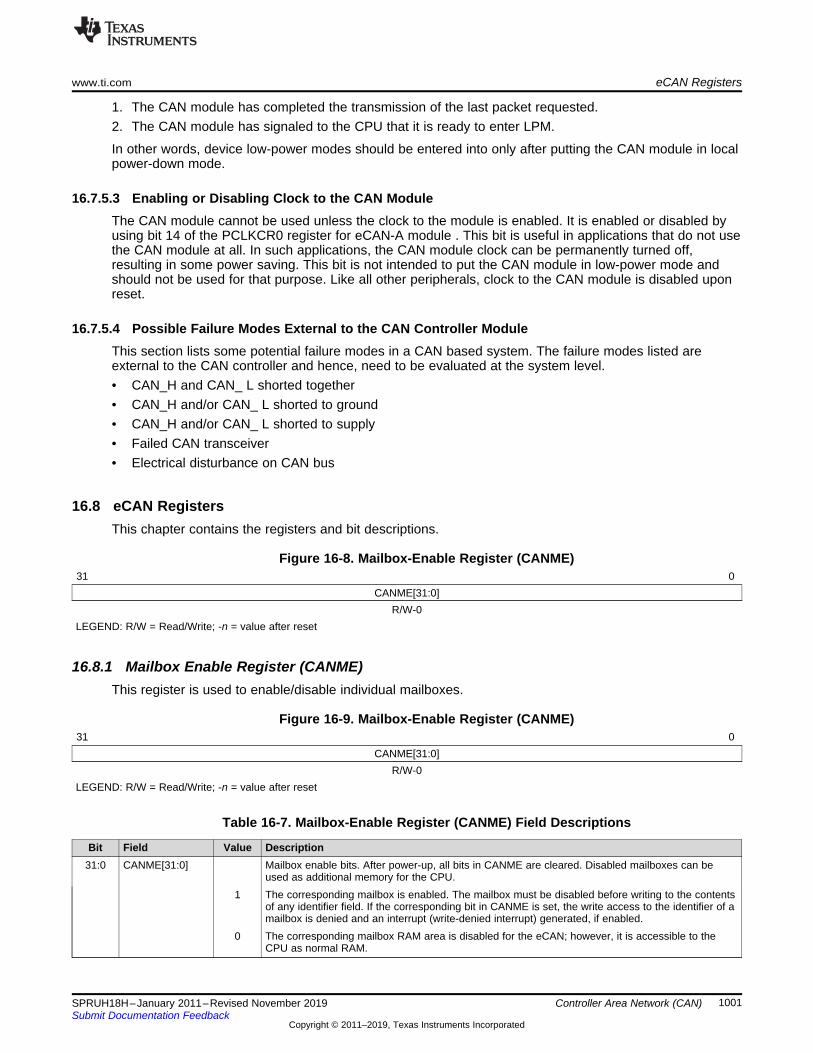
www.ti.com eCAN Registers
1001SPRUH18H–January 2011–Revised November 2019Submit Documentation Feedback
Copyright © 2011–2019, Texas Instruments Incorporated
Controller Area Network (CAN)
1. The CAN module has completed the transmission of the last packet requested.2. The CAN module has signaled to the CPU that it is ready to enter LPM.
In other words, device low-power modes should be entered into only after putting the CAN module in localpower-down mode.
16.7.5.3 Enabling or Disabling Clock to the CAN ModuleThe CAN module cannot be used unless the clock to the module is enabled. It is enabled or disabled byusing bit 14 of the PCLKCR0 register for eCAN-A module . This bit is useful in applications that do not usethe CAN module at all. In such applications, the CAN module clock can be permanently turned off,resulting in some power saving. This bit is not intended to put the CAN module in low-power mode andshould not be used for that purpose. Like all other peripherals, clock to the CAN module is disabled uponreset.
16.7.5.4 Possible Failure Modes External to the CAN Controller ModuleThis section lists some potential failure modes in a CAN based system. The failure modes listed areexternal to the CAN controller and hence, need to be evaluated at the system level.• CAN_H and CAN_ L shorted together• CAN_H and/or CAN_ L shorted to ground• CAN_H and/or CAN_ L shorted to supply• Failed CAN transceiver• Electrical disturbance on CAN bus
16.8 eCAN RegistersThis chapter contains the registers and bit descriptions.
Figure 16-8. Mailbox-Enable Register (CANME)31 0
CANME[31:0]R/W-0
LEGEND: R/W = Read/Write; -n = value after reset
16.8.1 Mailbox Enable Register (CANME)This register is used to enable/disable individual mailboxes.
Figure 16-9. Mailbox-Enable Register (CANME)31 0
CANME[31:0]R/W-0
LEGEND: R/W = Read/Write; -n = value after reset
Table 16-7. Mailbox-Enable Register (CANME) Field Descriptions
Bit Field Value Description31:0 CANME[31:0] Mailbox enable bits. After power-up, all bits in CANME are cleared. Disabled mailboxes can be
used as additional memory for the CPU.1 The corresponding mailbox is enabled. The mailbox must be disabled before writing to the contents
of any identifier field. If the corresponding bit in CANME is set, the write access to the identifier of amailbox is denied and an interrupt (write-denied interrupt) generated, if enabled.
0 The corresponding mailbox RAM area is disabled for the eCAN; however, it is accessible to theCPU as normal RAM.

eCAN Registers www.ti.com
1002 SPRUH18H–January 2011–Revised November 2019Submit Documentation Feedback
Copyright © 2011–2019, Texas Instruments Incorporated
Controller Area Network (CAN)
16.8.2 Mailbox-Direction Register (CANMD)This register is used to configure a mailbox for transmit or receive operation.
Figure 16-10. Mailbox-Direction Register (CANMD)31 0
CANMD[31:0]R/W-0
LEGEND: R/W = Read/Write; -n = value after reset
Table 16-8. Mailbox-Direction Register (CANMD) Field Descriptions
Bit Field Value Description31:0 CANMD[31:0] Mailbox direction bits. After power-up, all bits are cleared.
1 The corresponding mailbox is configured as a receive mailbox.0 The corresponding mailbox is configured as a transmit mailbox.

www.ti.com eCAN Registers
1003SPRUH18H–January 2011–Revised November 2019Submit Documentation Feedback
Copyright © 2011–2019, Texas Instruments Incorporated
Controller Area Network (CAN)
16.8.3 Transmission-Request Set Register (CANTRS)When mailbox n is ready to be transmitted, the CPU should set the TRS[n] bit to 1 to start thetransmission.
These bits are normally set by the CPU and cleared by the CAN module logic. The CAN module can setthese bits for a remote frame request. These bits are reset when a transmission is successful or aborted.If a mailbox is configured as a receive mailbox, the corresponding bit in CANTRS is ignored unless thereceive mailbox is configured to handle remote frames. The TRS[n] bit of a receive mailbox is not ignoredif the RTR bit is set. Therefore, a receive mailbox (whose RTR is set) can send a remote frame if its TRSbit is set. Once the remote frame is sent, the TRS[n] bit is cleared by the CAN module. Therefore, thesame mailbox can be used to request a data frame from another mode. If the CPU tries to set a bit whilethe eCAN module tries to clear it, the bit is set.
Setting CANTRS[n] causes the particular message n to be transmitted. Several bits can be setsimultaneously. Therefore, all messages with the TRS bit set are transmitted in turn, starting with themailbox having the highest mailbox number (= highest priority), unless TPL bits dictate otherwise.
The bits in CANTRS are set by writing a 1 from the CPU. Writing a 0 has no effect. After power up, all bitsare cleared.
Figure 16-11. Transmission-Request Set Register (CANTRS)31 0
TRS[31:0]RS-0
LEGEND: RS = Read/Set; -n = value after reset
Table 16-9. Transmission-Request Set Register (CANTRS) Field Descriptions
Bit Field Value Description31:0 TRS[31:0] Transmit-request-set bits
1 Setting TRSn commences the transmission of the message in that mailbox. Several bits can be setsimultaneously with all messages transmitted in turn.
0 No operation

eCAN Registers www.ti.com
1004 SPRUH18H–January 2011–Revised November 2019Submit Documentation Feedback
Copyright © 2011–2019, Texas Instruments Incorporated
Controller Area Network (CAN)
16.8.4 Transmission-Request-Reset Register (CANTRR)These bits can only be set by the CPU and reset by the internal logic. These bits are reset when atransmission is successful or is aborted. If the CPU tries to set a bit while the CAN tries to clear it, the bitis set.
Setting the TRR[n] bit of the message object n cancels a transmission request if it was initiated by thecorresponding bit (TRS[n]) and is not currently being processed. If the corresponding message is currentlybeing processed, the bit is reset when a transmission is successful (normal operation) or when an abortedtransmission due to a lost arbitration or an error condition is detected on the CAN bus line. When atransmission is aborted, the corresponding status bit (AA.31-0) is set. When a transmission is successful,the status bit (TA.31-0) is set. The status of the transmission request reset can be read from the TRS.31-0bit.
The bits in CANTRR are set by writing a 1 from the CPU.
Figure 16-12. Transmission-Request-Reset Register (CANTRR)31 0
TRR[31:0]RS-0
LEGEND: RS = Read/Set; -n = value after reset
Table 16-10. Transmission-Request-Reset Register (CANTRR) Field Descriptions
Bit Field Value Description31:0 TRR[31:0] Transmit-request-reset bits
1 Setting TRRn cancels a transmission request0 No operation
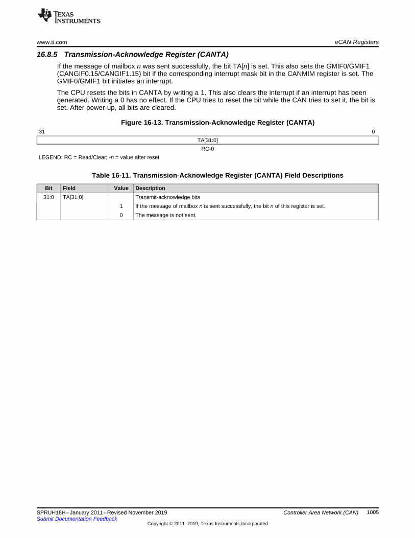
www.ti.com eCAN Registers
1005SPRUH18H–January 2011–Revised November 2019Submit Documentation Feedback
Copyright © 2011–2019, Texas Instruments Incorporated
Controller Area Network (CAN)
16.8.5 Transmission-Acknowledge Register (CANTA)If the message of mailbox n was sent successfully, the bit TA[n] is set. This also sets the GMIF0/GMIF1(CANGIF0.15/CANGIF1.15) bit if the corresponding interrupt mask bit in the CANMIM register is set. TheGMIF0/GMIF1 bit initiates an interrupt.
The CPU resets the bits in CANTA by writing a 1. This also clears the interrupt if an interrupt has beengenerated. Writing a 0 has no effect. If the CPU tries to reset the bit while the CAN tries to set it, the bit isset. After power-up, all bits are cleared.
Figure 16-13. Transmission-Acknowledge Register (CANTA)31 0
TA[31:0]RC-0
LEGEND: RC = Read/Clear; -n = value after reset
Table 16-11. Transmission-Acknowledge Register (CANTA) Field Descriptions
Bit Field Value Description31:0 TA[31:0] Transmit-acknowledge bits
1 If the message of mailbox n is sent successfully, the bit n of this register is set.0 The message is not sent.

eCAN Registers www.ti.com
1006 SPRUH18H–January 2011–Revised November 2019Submit Documentation Feedback
Copyright © 2011–2019, Texas Instruments Incorporated
Controller Area Network (CAN)
16.8.6 Abort-Acknowledge Register (CANAA)If the transmission of the message in mailbox n was aborted, the bit AA[n] is set and the AAIF(CANGIF.14) bit is set, which may generate an interrupt if enabled.
The bits in CANAA are reset by writing a 1 from the CPU. Writing a 0 has no effect. If the CPU tries toreset a bit and the CAN tries to set the bit at the same time, the bit is set. After power-up all bits arecleared.
Figure 16-14. Abort-Acknowledge Register (CANAA)31 0
AA[31:0]RC-0
LEGEND: RC = Read/Clear; -n = value after reset
Table 16-12. Abort-Acknowledge Register (CANAA) Field Descriptions
Bit Field Value Description31:0 AA[31:0] Abort-acknowledge bits
1 If the transmission of the message in mailbox n is aborted, the bit n of this register is set.0 The transmission is not aborted.

www.ti.com eCAN Registers
1007SPRUH18H–January 2011–Revised November 2019Submit Documentation Feedback
Copyright © 2011–2019, Texas Instruments Incorporated
Controller Area Network (CAN)
16.8.7 Received-Message-Pending Register (CANRMP)If mailbox n contains a received message, the bit RMP[n] of this register is set. These bits can be resetonly by the CPU and set by the internal logic. A new incoming message overwrites the stored one if theOPC[n](OPC.31-0) bit is cleared, otherwise the next mailboxes are checked for a matching ID. If a mailboxis overwritten, the corresponding status bit RML[n] is set. The bits in the CANRMP and the CANRMLregisters are cleared by a write to register CANRMP, with a 1 at the corresponding bit location. If the CPUtries to reset a bit and the CAN tries to set the bit at the same time, the bit is set.
The bits in the CANRMP register can set GMIF0/GMIF1 (GIF0.15/GIF1.15) if the corresponding interruptmask bit in the CANMIM register is set. The GMIF0/GMIF1 bit initiates an interrupt.
Figure 16-15. Received-Message-Pending Register (CANRMP)31 0
RMP[31:0]RC-0
LEGEND: RC = Read/Clear; -n = value after reset
Table 16-13. Received-Message-Pending Register (CANRMP) Field Descriptions
Bit Field Value Description31:0 RMP[31:0] Received-message-pending bits
1 If mailbox n contains a received message, bit RMP[n] of this register is set.0 The mailbox does not contain a message.

eCAN Registers www.ti.com
1008 SPRUH18H–January 2011–Revised November 2019Submit Documentation Feedback
Copyright © 2011–2019, Texas Instruments Incorporated
Controller Area Network (CAN)
16.8.8 Received-Message-Lost Register (CANRML)An RML[n] bit is set if an old message has been overwritten by a new one in mailbox n. These bits canonly be reset by the CPU, and set by the internal logic. The bits can be cleared by a write access to theCANRMP register with a 1 at the corresponding bit location. If the CPU tries to reset a bit and the CANtries to set the bit at the same time, the bit is set. The CANRML register is not changed if the OPC[n](OPC.31-0) bit is set.
If one or more of the bits in the CANRML register are set, the RMLIF (GIF0.11/ GIF1.11) bit is also set.This can initiate an interrupt if the RMLIM (GIM.11) bit is set.
Figure 16-16. Received-Message-Lost Register (CANRML)31 0
RML[31:0]R-0
LEGEND: R = Read; -n = value after reset
Table 16-14. Received-Message-Lost Register (CANRML) Field Descriptions
Bit Field Value Description31:0 RML[31:0] Received-message-lost bits
1 An old unread message has been overwritten by a new one in that mailbox.0 No message was lost.
Note: The RMLn bit is cleared by clearing the set RMPn bit.

www.ti.com eCAN Registers
1009SPRUH18H–January 2011–Revised November 2019Submit Documentation Feedback
Copyright © 2011–2019, Texas Instruments Incorporated
Controller Area Network (CAN)
16.8.9 Remote-Frame-Pending Register (CANRFP)Whenever a remote frame request is received by the CAN module, the corresponding bit RFP[n] in theremote frame pending register is set. If a remote frame is stored in a receive mailbox (AAM=0,CANMD=1), the RFPn bit will not be set.
To prevent an auto-answer mailbox from replying to a remote frame request, the CPU has to clear theRFP[n] flag and the TRS[n] bit by setting the corresponding transmission request reset bit TRR[n]. TheAAM bit can also be cleared by the CPU to stop the module from sending the message.
If the CPU tries to reset a bit and the CAN module tries to set the bit at the same time, the bit is not set.The CPU cannot interrupt an ongoing transfer.
Figure 16-17. Remote-Frame-Pending Register (CANRFP)31 0
RFP.31:0RC-0
LEGEND: RC = Read/Clear; -n = value after reset
Table 16-15. Remote-Frame-Pending Register (CANRFP) Field Descriptions
Bit Field Value Description31:0 RFP.31:0 Remote-frame-pending register.
For a receive mailbox, RFPn is not set if a remote frame is received and TRSn is not affected.For a transmit mailbox, RFPn is set if a remote frame is received and TRSn is set if AAM of themailbox is 1. The ID of the mailbox must match the remote frame ID.
1 A remote-frame request was received by the module.0 No remote-frame request was received. The register is cleared by the CPU.
16.8.9.1 Handling of Remote FramesIf a remote frame is received (the incoming message has the RTR bit set), the CAN module compares theidentifier to all identifiers of the mailboxes using the appropriate masks starting at the highest mailboxnumber in descending order.
In the case of a matching identifier (with the message object configured as send mailbox and AAM(MSGID.29) in this message object set) this message object is marked as to be sent (TRS[n] is set).
In case of a matching identifier with the mailbox configured as a send mailbox and bit AAM in this mailboxis not set, this message is not received in that mailbox.
After finding a matching identifier in a mailbox no further compare is done.
With a matching identifier and the message object configured as receive mailbox, this message is handledlike a data frame and the corresponding bit in the receive message pending (CANRMP) register is set.The CPU then has to decide how to handle this situation. For information about the CANRMP register, seeSection 16.8.7.
For the CPU to change the data in a mailbox that is configured as a remote frame mailbox (AAM set) ithas to set the mailbox number and the change data request (CDR) bit [CANMC.8] first. The CPU can thenwrite the new data and clear the CDR bit to indicate to the eCAN that the access is finished. Until the CDRbit is cleared, the transmission of this mailbox is not permitted. Therefore, the newest data is sent.
To change the identifier in that mailbox, the mailbox must be disabled first (CANMEn = 0).
For the CPU to request data from another node it configures the mailbox as a receive mailbox and setsthe TRS bit. In this case the module sends a remote frame request and receives the data frame in thesame mailbox that sent the request. Therefore, only one mailbox is necessary to do a remote request.Note that the CPU must set RTR (MSGCTRL.4) to enable a remote frame transmission. Once the remoteframe is sent, the TRS bit of the mailbox is cleared by CAN. In this case, bit TAn will not be set for thatmailbox.

eCAN Registers www.ti.com
1010 SPRUH18H–January 2011–Revised November 2019Submit Documentation Feedback
Copyright © 2011–2019, Texas Instruments Incorporated
Controller Area Network (CAN)
The behavior of the message object n is configured with CANMD[n] (CANMD.31-0), the AAM (MSGID.29),and RTR (MSGCTRL.4). It shows how to configure a message object according to the desired behavior.
To summarize, a message object can be configured with four different behaviors:1. A transmit message object is only able to transmit messages.2. A receive message object is only able to receive messages.3. A remote-request message object is able to transmit a remote request frame and to wait for the
corresponding data frame.4. A auto-reply message object is able to transmit a data frame whenever a remote request frame is
received for the corresponding identifier.
NOTE: When a remote transmission request is successfully transmitted with a message objectconfigured in request mode, the CANTA register is not set and no interrupt is generated.When the remote reply message is received, the behavior of the message object is the sameas a message object configured in receive mode.

www.ti.com eCAN Registers
1011SPRUH18H–January 2011–Revised November 2019Submit Documentation Feedback
Copyright © 2011–2019, Texas Instruments Incorporated
Controller Area Network (CAN)
16.8.10 Global Acceptance Mask Register (CANGAM)The global-acceptance mask is used by the eCAN in SCC mode. The global-acceptance mask is used forthe mailboxes 6 to 15 if the AME bit (MSGID.30) of the corresponding mailbox is set. A received messageis only stored in the first mailbox with a matching identifier.
The global-acceptance mask is used for the mailboxes 6 to 15 of the SCC.
Figure 16-18. Global Acceptance Mask Register (CANGAM)31 30 29 28 16
AMI Reserved GAM[28:16]RWI-0 R-0 RWI-0
15 0GAM[28:16]
RWI-0LEGEND: RWI = Read at any time, write during initialization mode only; -n = value after reset
Table 16-16. Global Acceptance Mask Register (CANGAM) Field Descriptions
Bit Field Value Description31 AMI Global Acceptance-mask identifier extension bit
1 Standard and extended frames can be received. In case of an extended frame, all 29 bits of theidentifier are stored in the mailbox and all 29 bits of global acceptance mask register are used forthe filter. In case of a standard frame, only the first eleven bits (bit 28 to 18) of the identifier and theglobal acceptance mask are used.The IDE bit of the receive mailbox is a "don't care" and is overwritten by the IDE bit of thetransmitted message. The filtering criterion must be satisfied in order to receive a message. Thenumber of bits to be compared is a function of the value of the IDE bit of the transmitted message.
0 The identifier extension bit stored in the mailbox determines which messages shall be received.The IDE bit of the receive mailbox determines the number of bits to be compared.
30:29 Reserved Reads are undefined and writes have no effect.28:0 GAM 28:0 Global-acceptance mask. These bits allow any identifier bits of an incoming message to be
masked. A value of "0" for a bit position means received identifier bit value must match thecorresponding identifier bit of the MSGID register. A value of "1" means "don't care".
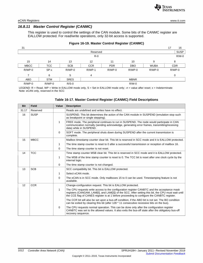
eCAN Registers www.ti.com
1012 SPRUH18H–January 2011–Revised November 2019Submit Documentation Feedback
Copyright © 2011–2019, Texas Instruments Incorporated
Controller Area Network (CAN)
16.8.11 Master Control Register (CANMC)This register is used to control the settings of the CAN module. Some bits of the CANMC register areEALLOW protected. For read/write operations, only 32-bit access is supported.
Figure 16-19. Master Control Register (CANMC)31 17 16
Reserved SUSPR-0 R/W-0
15 14 13 12 11 10 9 8MBCC TCC SCB CCR PDR DBO WUBA CDRR/WP-0 SP-x R/WP-0 R/WP-1 R/WP-0 R/WP-0 R/WP-0 R/WP-0
7 6 5 4 0ABO STM SRES MBNR
R/WP-0 R/WP-0 R/S-0 R/W-0LEGEND: R = Read, WP = Write in EALLOW mode only, S = Set in EALLOW mode only; -n = value after reset; x = IndeterminateNote: eCAN only, reserved in the SCC
Table 16-17. Master Control Register (CANMC) Field Descriptions
Bit Field Value Description31:17 Reserved Reads are undefined and writes have no effect.
16 SUSP SUSPEND. This bit determines the action of the CAN module in SUSPEND (emulation stop suchas breakpoint or single stepping).
1 FREE mode. The peripheral continues to run in SUSPEND. The node would participate in CANcommunication normally (sending acknowledge, generating error frames, transmitting/receivingdata) while in SUSPEND.
0 SOFT mode. The peripheral shuts down during SUSPEND after the current transmission iscomplete.
15 MBCC Mailbox timestamp counter clear bit. This bit is reserved in SCC mode and it is EALLOW protected.1 The time stamp counter is reset to 0 after a successful transmission or reception of mailbox 16.0 The time stamp counter is not reset.
14 TCC Time stamp counter MSB clear bit. This bit is reserved in SCC mode and it is EALLOW protected.1 The MSB of the time stamp counter is reset to 0. The TCC bit is reset after one clock cycle by the
internal logic.0 The time stamp counter is not changed.
13 SCB SCC compatibility bit. This bit is EALLOW protected.1 Select eCAN mode.0 The eCAN is in SCC mode. Only mailboxes 15 to 0 can be used. Timestamping feature is not
available.12 CCR Change-configuration request. This bit is EALLOW protected.
1 The CPU requests write access to the configuration register CANBTC and the acceptance maskregisters (CANGAM, LAM[0], and LAM[3]) of the SCC. After setting this bit, the CPU must wait untilthe CCE flag of CANES register is at 1 before proceeding to configure the CANBTC register.The CCR bit will also be set upon a bus-off condition, if the ABO bit is not set. The BO conditioncan be exited by clearing this bit (after 128 * 11 consecutive recessive bits on the bus).
0 The CPU requests normal operation. This can be done only after the configuration registerCANBTC was set to the allowed values. It also exits the bus-off state after the obligatory bus-offrecovery sequence.

www.ti.com eCAN Registers
1013SPRUH18H–January 2011–Revised November 2019Submit Documentation Feedback
Copyright © 2011–2019, Texas Instruments Incorporated
Controller Area Network (CAN)
Table 16-17. Master Control Register (CANMC) Field Descriptions (continued)Bit Field Value Description11 PDR Power down mode request. This bit is automatically cleared by the eCAN module upon wakeup
from low-power mode. This bit is EALLOW protected.1 The local power-down mode is requested.0 The local power-down mode is not requested (normal operation).
Note: If an application sets the TRSn bit for a mailbox and then immediately sets the PDR bit, theCAN module goes into LPM without transmitting the data frame. This is because it takes about 80CPU cycles for the data to be transferred from the mailbox RAM to the transmit buffer. Therefore,the application has to ensure that any pending transmission has been completed before writing tothe PDR bit. The TAn bit could be polled to ensure completion of transmission.
10 DBO Data byte order. This bit selects the byte order of the message data field. This bit is EALLOWprotected.
1 The data is received or transmitted least significant byte first.0 The data is received or transmitted most significant byte first.
9 WUBA Wake up on bus activity. This bit is EALLOW protected.1 The module leaves the power-down mode after detecting any bus activity.0 The module leaves the power-down mode only after writing a 0 to the PDR bit.
8 CDR Change data field request. This bit allows fast data message update.1 The CPU requests write access to the data field of the mailbox specified by the MBNR.4:0 field
(CANMC.4-0). The CPU must clear the CDR bit after accessing the mailbox. The module does nottransmit that mailbox content while the CDR is set. This is checked by the state machine beforeand after it reads the data from the mailbox to store it in the transmit buffer.Note: Once the TRS bit is set for a mailbox and then data is changed in the mailbox using the CDRbit, the CAN module fails to transmit the new data and transmits the old data instead. To avoid this,reset transmission in that mailbox using the TRRn bit and set the TRSn bit again. The new data isthen transmitted.
0 The CPU requests normal operation.7 ABO Auto bus on. This bit is EALLOW protected.
1 After the bus-off state, the module goes back automatically into bus-on state after 128 * 11recessive bits have been monitored.
0 The bus-off state may only be exited after 128 * 11 consecutive recessive bits on the bus and afterhaving cleared the CCR bit.
6 STM Self test mode. This bit is EALLOW protected.1 The module is in self-test mode. In this mode, the CAN module generates its own acknowledge
(ACK) signal, thus enabling operation without a bus connected to the module. The message is notsent, but read back and stored in the appropriate mailbox. The MSGID of the received frame is notstored in the MBR in STM.Note: In STM, if no MBX has been configured to receive a transmitted frame, then that frame willbe stored in MBX0, even if MBX0 has not been configured for receive operations. If LAMs areconfigured such that some mailboxes can receive and store data frames, then a data frame thatdoes not satisfy the acceptance mask filtering criterion for any receive mailbox will be lost.
0 The module is in normal mode.5 SRES This bit can only be written and is always read as zero.
1 A write access to this bit causes a software reset of the module (all parameters, except theprotected registers, are reset to their default values). The mailbox contents and the error countersare not modified. Pending and ongoing transmissions are canceled without perturbing thecommunication.
0 0 No effect4:0 MBNR 4:0 0 - 31 Mailbox for which the CPU requests a write access to the data field. This field is used in conjunction
with the CDR bit. The bit MBNR.4 is for eCAN only, and is reserved in the SCC mode.
16.8.11.1 CAN Module Action in SUSPENDThe following points describe the behavior of the module in SUSPEND mode.1. If there is no traffic on the CAN bus and SUSPEND mode is requested, the node goes into SUSPEND
mode.2. If there is traffic on the CAN bus and SUSPEND mode is requested, the node goes into SUSPEND

eCAN Registers www.ti.com
1014 SPRUH18H–January 2011–Revised November 2019Submit Documentation Feedback
Copyright © 2011–2019, Texas Instruments Incorporated
Controller Area Network (CAN)
mode when the ongoing frame is over.3. If the node was transmitting, when SUSPEND is requested, it goes to SUSPEND state after it gets the
acknowledgment. If it does not get an acknowledgment or if there are some other errors, it transmits anerror frame and then goes to SUSPEND state. The TEC is modified accordingly. In the second case,that is, it is suspended after transmitting an error frame, the node re-transmits the original frame aftercoming out of suspended state. The TEC is modified after transmission of the frame accordingly.
4. If the node was receiving, when SUSPEND is requested, it goes to SUSPEND state after transmittingthe acknowledgment bit. If there is any error, the node sends an error frame and go to SUSPENDstate. The REC is modified accordingly before going to SUSPEND state.
5. If there is no traffic on the CAN bus and SUSPEND removal is requested, the node comes out ofSUSPEND state.
6. If there is traffic on the CAN bus and SUSPEND removal is requested, the node comes out after thebus goes to idle. Therefore, a node does not receive any "partial" frame, which could lead togeneration of error frames.
7. When the node is suspended, it does not participate in transmitting or receiving any data. Thus, neitheracknowledgment bit nor any error frame is sent. TEC and REC are not modified during SUSPENDstate.

( )12/
1+´= regBRP
SYSCLKOUTTQ
www.ti.com eCAN Registers
1015SPRUH18H–January 2011–Revised November 2019Submit Documentation Feedback
Copyright © 2011–2019, Texas Instruments Incorporated
Controller Area Network (CAN)
16.8.12 Bit-Timing Configuration Register (CANBTC)The CANBTC register is used to configure the CAN node with the appropriate network-timing parameters.This register must be programmed before using the CAN module.
This register is write-protected in user mode and can only be written in initialization mode (see Section3.6.1).
NOTE: To avoid unpredictable behavior of the CAN module, the CANBTC register should never beprogrammed with values not allowed by the CAN protocol specification and by the bit timingrules listed in Section 3.1.1.
Figure 16-20. Bit-Timing Configuration Register (CANBTC)31 24 23 16
Reserved BRPreg
R-x RWPI-0
15 10 9 8 7 6 3 2 0Reserved SJWreg SAM TSEG1reg TSEG2reg
R-0 RWPI-0 RWPI-0
RWPI-0 RWPI-0
LEGEND: RWPI = Read in all modes, write in EALLOW mode during initialization mode only; -n = value after reset
Table 16-18. Bit-Timing Configuration Register (CANBTC) Field Descriptions
Bit Field Value Description31:24 Reserved Reads are undefined and writes have no effect.23:16 BRPreg.7:0 Baud rate prescaler. This register sets the prescaler for the baud rate settings. The length of one
TQ is defined by:
where SYSCLKOUT /2 is the frequency of the CAN module clock.BRPreg denotes the "register value" of the prescaler; that is, value written into bits 23:16 of theCANBTC register. This value is automatically enhanced by 1 when the CAN module accesses it.The enhanced value is denoted by the symbol BRP (BRP = BRPreg + 1). BRP is programmablefrom 1 to 256.Note: For the special case of BRP = 1, the Information Processing Time (IPT) is equal to 3 timequanta (TQ). This is not compliant to the ISO 11898 Standard, where the IPT is defined to be lessthan or equal to 2 TQ. Thus the usage of this mode (BRPreg = 0) is not allowed.
15:10 Reserved Reads are undefined. Must be written with all zeroes only.9:8 SJWreg 1:0 Synchronization jump width. The parameter SJW indicates, by how many units of TQ a bit is
allowed to be lengthened or shortened when resynchronizing.SJWreg denotes the "register value" of the "resynchronization jump width;" that is, the value writteninto bits 9:8 of the CANBTC register. This value is automatically enhanced by 1 when the CANmodule accesses it. This enhanced value is denoted by the symbol SJW.
SJW = SJWreg + 1SJW is programmable from 1 to 4 TQ. The maximum value of SJW is determined by the minimumvalue of TSEG2 and 4 TQ.
SJW(max) = min [4 TQ, TSEG2]7 SAM This parameter sets the number of samples used by the CAN module to determine the actual level
of the CAN bus. When the SAM bit is set, the level determined by the CAN bus corresponds to theresult from the majority decision of the last three values. The sample points are at the sample pointand twice before with a distance of ½ TQ.1 The CAN module samples three times and make a majority decision. The triple sample modeshall be selected only for bit rate prescale values greater than 4 (BRP > 4).0 The CAN module samples only once at the sampling point.

eCAN Registers www.ti.com
1016 SPRUH18H–January 2011–Revised November 2019Submit Documentation Feedback
Copyright © 2011–2019, Texas Instruments Incorporated
Controller Area Network (CAN)
Table 16-18. Bit-Timing Configuration Register (CANBTC) Field Descriptions (continued)Bit Field Value Description6:3 TSEG1reg Time segment 1. The length of a bit on the CAN bus is determined by the parameters TSEG1,
TSEG2, and BRP. All controllers on the CAN bus must have the same baud rate and bit length. Fordifferent clock frequencies of the individual controllers, the baud rate has to be adjusted by the saidparameters.This parameter specifies the length of the TSEG1 segment in TQ units. TSEG1 combinesPROP_SEG and PHASE_SEG1 segments:
TSEG1 = PROP_SEG + PHASE_SEG1where PROP_SEG and PHASE_SEG1 are the length of these two segments in TQ units.TSEG1reg denotes the "register value" of "time segment 1;" that is, the value written into bits 6:3 ofthe CANBTC register. This value is automatically enhanced by 1 when the CAN module accessesit. This enhanced value is denoted by the symbol TSEG1.
TSEG1 = TSEG1reg + 1TSEG1 value should be chosen such that TSEG1 is greater than or equal to TSEG2 and IPT. Formore information on IPT, see Section 3.1.1.
2:0 TSEG2reg Time Segment 2. TSEG2 defines the length of PHASE_SEG2 segment in TQ units:TSEG2 is programmable in the range of 1 TQ to 8 TQ and has to fulfill the following timing rule:TSEG2 must be smaller than or equal to TSEG1 and must be greater than or equal to IPT.TSEG2reg denotes the "register value" of "time segment 2;" that is, the value written into bits 2:0 ofthe CANBTC register. This value is automatically enhanced by 1 when the CAN module accessesit. This enhanced value is denoted by the symbol TSEG2.
TSEG2 = TSEG2reg + 1
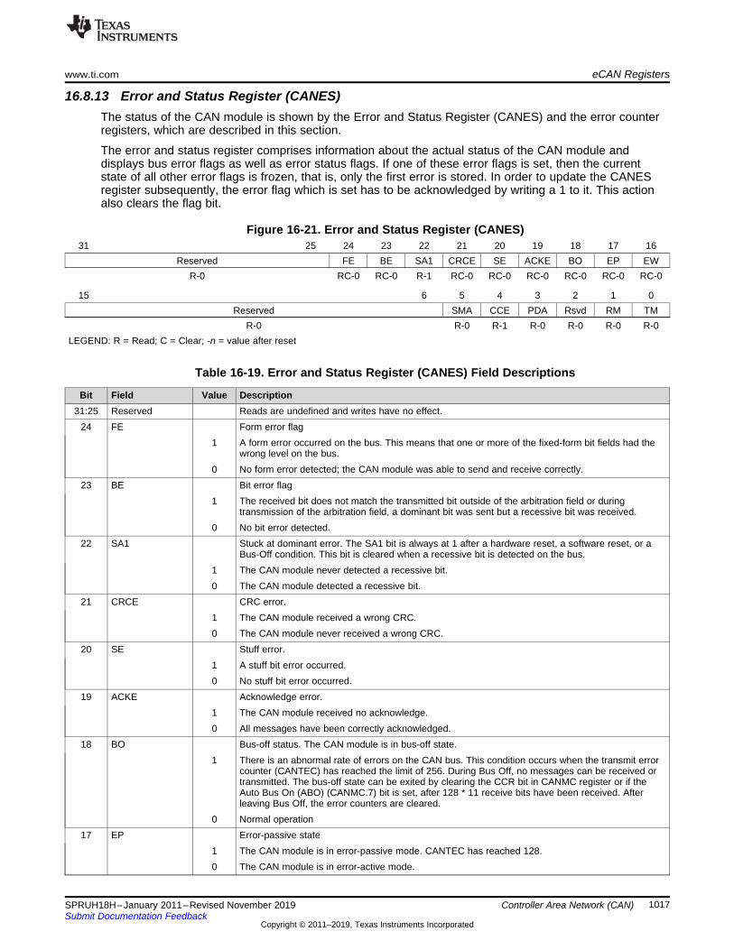
www.ti.com eCAN Registers
1017SPRUH18H–January 2011–Revised November 2019Submit Documentation Feedback
Copyright © 2011–2019, Texas Instruments Incorporated
Controller Area Network (CAN)
16.8.13 Error and Status Register (CANES)The status of the CAN module is shown by the Error and Status Register (CANES) and the error counterregisters, which are described in this section.
The error and status register comprises information about the actual status of the CAN module anddisplays bus error flags as well as error status flags. If one of these error flags is set, then the currentstate of all other error flags is frozen, that is, only the first error is stored. In order to update the CANESregister subsequently, the error flag which is set has to be acknowledged by writing a 1 to it. This actionalso clears the flag bit.
Figure 16-21. Error and Status Register (CANES)31 25 24 23 22 21 20 19 18 17 16
Reserved FE BE SA1 CRCE SE ACKE BO EP EWR-0 RC-0 RC-0 R-1 RC-0 RC-0 RC-0 RC-0 RC-0 RC-0
15 6 5 4 3 2 1 0Reserved SMA CCE PDA Rsvd RM TM
R-0 R-0 R-1 R-0 R-0 R-0 R-0LEGEND: R = Read; C = Clear; -n = value after reset
Table 16-19. Error and Status Register (CANES) Field Descriptions
Bit Field Value Description31:25 Reserved Reads are undefined and writes have no effect.
24 FE Form error flag1 A form error occurred on the bus. This means that one or more of the fixed-form bit fields had the
wrong level on the bus.0 No form error detected; the CAN module was able to send and receive correctly.
23 BE Bit error flag1 The received bit does not match the transmitted bit outside of the arbitration field or during
transmission of the arbitration field, a dominant bit was sent but a recessive bit was received.0 No bit error detected.
22 SA1 Stuck at dominant error. The SA1 bit is always at 1 after a hardware reset, a software reset, or aBus-Off condition. This bit is cleared when a recessive bit is detected on the bus.
1 The CAN module never detected a recessive bit.0 The CAN module detected a recessive bit.
21 CRCE CRC error.1 The CAN module received a wrong CRC.0 The CAN module never received a wrong CRC.
20 SE Stuff error.1 A stuff bit error occurred.0 No stuff bit error occurred.
19 ACKE Acknowledge error.1 The CAN module received no acknowledge.0 All messages have been correctly acknowledged.
18 BO Bus-off status. The CAN module is in bus-off state.1 There is an abnormal rate of errors on the CAN bus. This condition occurs when the transmit error
counter (CANTEC) has reached the limit of 256. During Bus Off, no messages can be received ortransmitted. The bus-off state can be exited by clearing the CCR bit in CANMC register or if theAuto Bus On (ABO) (CANMC.7) bit is set, after 128 * 11 receive bits have been received. Afterleaving Bus Off, the error counters are cleared.
0 Normal operation17 EP Error-passive state
1 The CAN module is in error-passive mode. CANTEC has reached 128.0 The CAN module is in error-active mode.

eCAN Registers www.ti.com
1018 SPRUH18H–January 2011–Revised November 2019Submit Documentation Feedback
Copyright © 2011–2019, Texas Instruments Incorporated
Controller Area Network (CAN)
Table 16-19. Error and Status Register (CANES) Field Descriptions (continued)Bit Field Value Description16 EW Warning status
1 One of the two error counters (CANREC or CANTEC) has reached the warning level of 96.0 Values of both error counters (CANREC and CANTEC) are less than 96.
15:6 Reserved Reads are undefined and writes have no effect.5 SMA Suspend mode acknowledge. This bit is set after a latency of one clock cycle—up to the length of
one frame—after the suspend mode was activated. The suspend mode is activated with thedebugger tool when the circuit is not in run mode. During the suspend mode, the CAN module isfrozen and cannot receive or transmit any frame. However, if the CAN module is transmitting orreceiving a frame when the suspend mode is activated, the module enters suspend mode only atthe end of the frame. Run mode is when SOFT mode is activated (CANMC.16 = 1).
1 The module has entered suspend mode.0 The module is not in suspend mode.
4 CCE Change configuration enable. This bit displays the configuration access right. This bit is set after alatency of one clock cycle.
1 The CPU has write access to the configuration registers.0 The CPU is denied write access to the configuration registers.
Note: The reset state of the CCE bit is 1. That is, upon reset, you can write to the bit timingregisters. However, once the CCE bit is cleared (as part of the module initialization), the CANRXpin must be sensed high before you can set the CCE bit to 1 again.
3 PDA Power-down mode acknowledge1 The CAN module has entered the power-down mode.0 Normal operation
2 Reserved Reads are undefined and writes have no effect.1 RM Receive mode. The CAN module is in receive mode. This bit reflects what the CAN module is
actually doing regardless of mailbox configuration.1 The CAN module is receiving a message.0 The CAN module is not receiving a message.
0 TM Transmit mode. The CAN module is in transmit mode. This bit reflects what the CAN module isactually doing regardless of mailbox configuration.
1 The CAN module is transmitting a message.0 The CAN module is not transmitting a message.

www.ti.com eCAN Registers
1019SPRUH18H–January 2011–Revised November 2019Submit Documentation Feedback
Copyright © 2011–2019, Texas Instruments Incorporated
Controller Area Network (CAN)
16.8.14 CAN Error Counter Registers (CANTEC/CANREC)The CAN module contains two error counters: the receive error counter (CANREC) and the transmit errorcounter (CANTEC). The values of both counters can be read via the CPU interface. These counters areincremented or decremented according to the CAN protocol specification version 2.0.
Figure 16-22. Transmit-Error-Counter Register (CANTEC)31 8 7 0
Reserved TECR-x R-0
LEGEND: R = Read only; -n = value after reset
Figure 16-23. Receive-Error-Counter Register (CANREC)31 8 7 0
Reserved RECR-x R-0
LEGEND: R = Read only; -n = value after reset
After reaching or exceeding the error passive limit (128), the receive error counter will not be increasedanymore. When a message was received correctly, the counter is set again to a value between 119 and127 (compare with CAN specification).
After reaching the bus-off state, the transmit error counter is undefined while the receive error counterchanges its function. After reaching the bus-off state, the receive error counter is cleared. It is thenincremented after every 11 consecutive recessive bits on the bus. These 11 bits correspond to the gapbetween two frames on the bus. If the counter reaches 128, the module automatically changes back to thebus-on status if this feature is enabled (Auto Bus On bit (ABO) (CANMC.7) set). All internal flags are resetand the error counters are cleared. After leaving initialization mode, the error counters are cleared.

eCAN Registers www.ti.com
1020 SPRUH18H–January 2011–Revised November 2019Submit Documentation Feedback
Copyright © 2011–2019, Texas Instruments Incorporated
Controller Area Network (CAN)
16.8.15 Interrupt RegistersInterrupts are controlled by the interrupt flag registers, interrupt mask registers and mailbox interrupt levelregisters. These registers are described in the following subsections.
16.8.15.1 Global Interrupt Flag Registers (CANGIF0/CANGIF1)These registers allow the CPU to identify the interrupt source.
The interrupt flag bits are set if the corresponding interrupt condition did occur. The global interrupt flagsare set depending on the setting of the GIL bit in the CANGIM register. If that bit is set, the globalinterrupts set the bits in the CANGIF1 register; otherwise, in the CANGIF0 register. This also applies tothe Interrupt Flags AAIF and RMLIF. These bits are set according to the setting of the appropriate GIL bitin the CANGIM register.
The following bits are set regardless of the corresponding interrupt mask bits in the CANGIM register:MTOFn, WDIFn, BOIFn, TCOFn, WUIFn, EPIFn, AAIFn, RMLIFn, and WLIFn.
For any mailbox, the GMIFn bit is set only when the corresponding mailbox interrupt mask bit (in theCANMIM register) is set.
If all interrupt flags are cleared and a new interrupt flag is set the interrupt output line is activated when thecorresponding interrupt mask bit is set. The interrupt line stays active until the interrupt flag is cleared bythe CPU by writing a 1 to the appropriate bit or by clearing the interrupt-causing condition.
The GMIFx flags must be cleared by writing a 1 to the appropriate bit in the CANTA register or theCANRMP register (depending on mailbox configuration) and cannot be cleared in the CANGIFx register.After clearing one or more interrupt flags and one or more interrupt flags still set, a new interrupt isgenerated. The interrupt flags are cleared by writing a 1 to the corresponding bit location. If the GMIFx isset the Mailbox Interrupt Vector MIVx indicates the mailbox number of the mailbox that caused the settingof the GMIFx. In case more than one mailbox interrupt is pending, it always displays the highest mailboxinterrupt vector assigned to that interrupt line.

www.ti.com eCAN Registers
1021SPRUH18H–January 2011–Revised November 2019Submit Documentation Feedback
Copyright © 2011–2019, Texas Instruments Incorporated
Controller Area Network (CAN)
Figure 16-24. Global Interrupt Flag 0 Register (CANGIF0)31 24
ReservedR-x
23 18 17 16Reserved MTOF0 TCOF0
R-x R-0 RC-0
15 14 13 12 11 10 9 8GMIF0 AAIF0 WDIF0 WUIF0 RMLIF0 BOIF0 EPIF0 WLIF0R/W-0 R-0 RC-0 RC-0 R-0 RC-0 RC-0 RC-0
7 5 4 3 2 1 0Reserved MIV0.4 MIV0.3 MIV0.2 MIV0.1 MIV0.0
R/W-0 R-0 R-0 R-0 R-0 R-0LEGEND: R/W = Read/Write; R = Read; C = Clear; -n = value after reset
Figure 16-25. Global Interrupt Flag 1 Register (CANGIF1)31 24
ReservedR-x
23 18 17 16Reserved MTOF1 TCOF1
R-x R-0 RC-0
15 14 13 12 11 10 9 8GMIF1 AAIF1 WDIF1 WUIF1 RMLIF1 BOIF1 EPIF1 WLIF1R/W-0 R-0 RC-0 RC-0 R-0 RC-0 RC-0 RC-0
7 5 4 3 2 1 0Reserved MIV0.4 MIV0.3 MIV0.2 MIV0.1 MIV0.0
R/W-0 R-0 R-0 R-0 R-0 R-0LEGEND: R/W = Read/Write; R = Read; C = Clear; -n = value after resetNote: eCAN only, reserved in the SCC
NOTE: The following bit descriptions are applicable to both the CANGIF0 and CANGIF1 registers.For the following interrupt flags, whether they are set in the CANGIF0 or the CANGIF1register is determined by the value of the GIL bit in the CANGIM register: TCOFn, AAIFn,WDIFn, WUIFn, RMLIFn, BOIFn, EPIFn, and WLIFn.
If GIL = 0, these flags are set in the CANGIF0 register; if GIL = 1, they are set in theCANGIF1 register.
Similarly, the choice of the CANGIF0 and CANGIF1 register for the MTOFn and GMIFn bitsis determined by the MILn bit in the CANMIL register.
Table 16-20. Global Interrupt Flag Registers (CANGIF0/CANGIF1) Field Descriptions
Bit Field Value Description31:18 Reserved Reserved. Reads are undefined and writes have no effect.
17 MTOF0/1 Mailbox time-out flag. This bit is not available in the SCC mode.1 One of the mailboxes did not transmit or receive a message within the specified time frame.0 No time out for the mailboxes occurred.
Note: Whether the MTOFn bit gets set in CANGIF0 or CANGIF1 depends on the value of MILn.MTOFn gets cleared when TOSn is cleared. The TOSn bit will be cleared upon (eventual)successful transmission/reception.

eCAN Registers www.ti.com
1022 SPRUH18H–January 2011–Revised November 2019Submit Documentation Feedback
Copyright © 2011–2019, Texas Instruments Incorporated
Controller Area Network (CAN)
Table 16-20. Global Interrupt Flag Registers (CANGIF0/CANGIF1) Field Descriptions (continued)Bit Field Value Description16 TCOF0/1 Time stamp counter overflow flag.
1 The MSB of the time stamp counter has changed from 0 to 1.0 The MSB of the time stamp counter is 0. That is, it has not changed from 0 to 1.
15 GMIF0/1 Global mailbox interrupt flag. This bit is set only when the corresponding mailbox interrupt mask bitin the CANMIM register is set.
1 One of the mailboxes transmitted or received a message successfully.0 No message has been transmitted or received.
14 AAIF0/1 Abort-acknowledge interrupt flag1 A send transmission request has been aborted.0 No transmission has been aborted.
Note: The AAIFn bit is cleared by clearing the set AAn bit.13 WDIF0/WDIF1 Write-denied interrupt flag
1 The CPU write access to a mailbox was not successful. The WDIF interrupt is asserted when theidentifier field of a mailbox is written to, while it is enabled. Before writing to the MSGID field of aMBX, it should be disabled. If you try this operation when the MBX is still enabled, the WDIF bit willbe set and a CAN interrupt asserted.
0 The CPU write access to the mailbox was successful.12 WUIF0/WUIF1 Wake-up interrupt flag
1 During local power down, this flag indicates that the module has left sleep mode.0 The module is still in sleep mode or normal operation
11 RMLIF0/1 Receive-message-lost interrupt flag1 At least for one of the receive mailboxes, an overflow condition has occurred and the corresponding
bit in the MILn register is cleared.0 No message has been lost.
Note: The RMLIFn bit is cleared by clearing the set RMPn bit.10 BOIF0/BOIF1 Bus off interrupt flag
1 The CAN module has entered bus-off mode.0 The CAN module is still in bus-on mode.
9 EPIF0/EPIF1 Error passive interrupt flag1 The CAN module has entered error-passive mode.0 The CAN module is not in error-passive mode.
8 WLIF0/WLIF1 Warning level interrupt flag1 At least one of the error counters has reached the warning level.0 None of the error counters has reached the warning level.
7:5 Reserved Reads are undefined and writes have no effect.4:0 MIV0.4:0/MIV1.4:
0Mailbox interrupt vector. Only bits 3:0 are available in SCC mode.This vector indicates the number of the mailbox that set the global mailbox interrupt flag. It keepsthat vector until the appropriate MIFn bit is cleared or when a higher priority mailbox interruptoccurred. Then the highest interrupt vector is displayed, with mailbox 31 having the highest priority.In the SCC mode, mailbox 15 has the highest priority. Mailboxes 16 to 31 are not recognized.If no flag is set in the TA/RMP register and GMIF1 or GMIF0 also cleared, this value is undefined.
16.8.15.2 Global Interrupt Mask Register (CANGIM)The set up for the interrupt mask register is the same as for the interrupt flag register. If a bit is set, thecorresponding interrupt is enabled. This register is EALLOW protected.

www.ti.com eCAN Registers
1023SPRUH18H–January 2011–Revised November 2019Submit Documentation Feedback
Copyright © 2011–2019, Texas Instruments Incorporated
Controller Area Network (CAN)
Figure 16-26. Global Interrupt Mask Register (CANGIM)31 18 17 16
Reserved MTOM TCOMR-0 R/WP-
0R/WP-
0
15 14 13 12 11 10 9 8Reserved AAIM WDIM WUIM RMLIM BOIM EPIM WLIM
R-0 R/WP-0 R/WP-0 R/WP-0 R/WP-0 R/WP-0 R/WP-0 R/WP-0
7 3 2 1 0Reserved GIL I1EN I0EN
R-0 R/WP-0 R/WP-0 R/WP-0LEGEND: R = Read; W = Write; WP = Write in EALLOW mode only; -n = value after reset
Table 16-21. Global Interrupt Mask Register (CANGIM) Field Descriptions
Bit Field Value Description31:18 Reserved Reads are undefined and writes have no effect.
17 MTOM Mailbox time-out interrupt mask1 Enabled0 Disabled
16 TCOM Time stamp counter overflow mask1 Enabled0 Disabled
15 Reserved Reads are undefined and writes have no effect.14 AAIM Abort Acknowledge Interrupt Mask.
1 Enabled0 Disabled
13 WDIM Write denied interrupt mask1 Enabled0 Disabled
12 WUIM Wake-up interrupt mask1 Enabled0 Disabled
11 RMLIM Received-message-lost interrupt mask1 Enabled0 Disabled
10 BOIM Bus-off interrupt mask1 Enabled0 Disabled
9 EPIM Error-passive interrupt mask1 Enabled0 Disabled
8 WLIM Warning level interrupt mask1 Enabled0 Disabled
7:3 Reserved Reads are undefined and writes have no effect.2 GIL Global interrupt level for the interrupts TCOF, WDIF, WUIF, BOIF, EPIF, RMLIF, AAIF and WLIF.
1 All global interrupts are mapped to the ECAN1INT interrupt line.0 All global interrupts are mapped to the ECAN0INT interrupt line.

eCAN Registers www.ti.com
1024 SPRUH18H–January 2011–Revised November 2019Submit Documentation Feedback
Copyright © 2011–2019, Texas Instruments Incorporated
Controller Area Network (CAN)
Table 16-21. Global Interrupt Mask Register (CANGIM) Field Descriptions (continued)Bit Field Value Description1 I1EN Interrupt 1 enable
1 This bit globally enables all interrupts for the ECAN1INT line if the corresponding masks are set.0 The ECAN1INT interrupt line is disabled.
0 I0EN Interrupt 0 enable1 This bit globally enables all interrupts for the ECAN0INT line if the corresponding masks are set.0 The ECAN0INT interrupt line is disabled.
The GMIF has no corresponding bit in the CANGIM because the mailboxes have individual mask bits inthe CANMIM register.

www.ti.com eCAN Registers
1025SPRUH18H–January 2011–Revised November 2019Submit Documentation Feedback
Copyright © 2011–2019, Texas Instruments Incorporated
Controller Area Network (CAN)
16.8.15.3 Mailbox Interrupt Mask Register (CANMIM)There is one interrupt flag available for each mailbox. This can be a receive or a transmit interruptdepending on the configuration of the mailbox. This register is EALLOW protected.
Figure 16-27. Mailbox Interrupt Mask Register (CANMIM)31 0
MIM.31:0R/W-0
LEGEND: R/W = Read/Write; -n = value after reset
Table 16-22. Mailbox Interrupt Mask Register (CANMIM) Field Descriptions
Bit Field Value Description31:0 MIM.31:0 Mailbox interrupt mask. After power up all interrupt mask bits are cleared and the interrupts are
disabled. These bits allow any mailbox interrupt to be masked individually.1 Mailbox interrupt is enabled. An interrupt is generated if a message has been transmitted
successfully (in case of a transmit mailbox) or if a message has been received without any error (incase of a receive mailbox).
0 Mailbox interrupt is disabled.

eCAN Registers www.ti.com
1026 SPRUH18H–January 2011–Revised November 2019Submit Documentation Feedback
Copyright © 2011–2019, Texas Instruments Incorporated
Controller Area Network (CAN)
16.8.15.4 Mailbox Interrupt Level Register (CANMIL)Each of the 32 mailboxes may initiate an interrupt on one of the two interrupt lines. Depending on thesetting in the mailbox interrupt level register (CANMIL), the interrupt is generated on ECAN0INT (MILn =0) or on line ECAN1INT (MIL[n] = 1).
Figure 16-28. Mailbox Interrupt Level Register (CANMIL)31 0
MIL.31:0R/W-0
LEGEND: R/W = Read/Write; -n = value after reset
Table 16-23. Mailbox Interrupt Level Register (CANMIL) Field Descriptions
Bit Field Value Description31:0 MIL.31:0 Mailbox interrupt level. These bits allow any mailbox interrupt level to be selected individually.
1 The mailbox interrupt is generated on interrupt line 1.0 The mailbox interrupt is generated on interrupt line 0.

www.ti.com eCAN Registers
1027SPRUH18H–January 2011–Revised November 2019Submit Documentation Feedback
Copyright © 2011–2019, Texas Instruments Incorporated
Controller Area Network (CAN)
16.8.16 Overwrite Protection Control Register (CANOPC)If there is an overflow condition for mailbox n (RMP[n] is set to 1 and a new receive message would fit formailbox n), the new message is stored depending on the settings in the CANOPC register. If thecorresponding bit OPC[n] is set to 1, the old message is protected against being overwritten by the newmessage; thus, the next mailboxes are checked for a matching ID. If no other mailbox is found, themessage is lost without further notification. If the bit OPC[n] is cleared to 0, the old message is overwrittenby the new one. This is notified by setting the receive message lost bit RML[n].
For read/write operations, only 32-bit access is supported.
Figure 16-29. Overwrite Protection Control Register (CANOPC)31 0
OPC.31:0R/W-0
LEGEND: R/W = Read/Write; -n = value after reset
Table 16-24. Overwrite Protection Control Register (CANOPC) Field Descriptions
Bit Field Value Description31:0 OPC.31:0 Overwrite protection control bits
1 1 If the bit OPC[n] is set to 1, an old message stored in that mailbox is protected against beingoverwritten by the new message.
0 0 If the bit OPC[n] is not set, the old message can be overwritten by a new one.

eCAN Registers www.ti.com
1028 SPRUH18H–January 2011–Revised November 2019Submit Documentation Feedback
Copyright © 2011–2019, Texas Instruments Incorporated
Controller Area Network (CAN)
16.8.17 eCAN I/O Control Registers (CANTIOC, CANRIOC)The CANTX and CANRX pins should be configured for CAN use. This is done using the CANTIOC andCANRIOC registers.
Figure 16-30. TX I/O Control Register (CANTIOC)31 16
ReservedR-0
15 4 3 2 0Reserved TXFU
NCReserved
R-0 RWP-0
LEGEND: RWP = Read in all modes, write in EALLOW-mode only; R = Read only; -n = value after reset
Table 16-25. TX I/O Control Register (CANTIOC) Field Descriptions
Bit Field Value Description31:4 Reserved Reads are undefined and writes have no effect.
3 TXFUNC This bit must be set for CAN module function.1 The CANTX pin is used for the CAN transmit functions.0 Reserved
2:0 Reserved Reserved

www.ti.com eCAN Registers
1029SPRUH18H–January 2011–Revised November 2019Submit Documentation Feedback
Copyright © 2011–2019, Texas Instruments Incorporated
Controller Area Network (CAN)
Figure 16-31. RX I/O Control Register (CANRIOC)31 16
ReservedR-x
15 4 3 2 0Reserved RXFU
NCReserved
R-0 RWP-0
LEGEND: RWP = Read in all modes, write in EALLOW-mode only; R = Read only; -n = value after reset; x = indeterminate
Table 16-26. RX I/O Control Register (CANRIOC) Field Descriptions
Bit Field Value Description31:4 Reserved Reads are undefined and writes have no effect.
3 RXFUNC This bit must be set for CAN module function.1 The CANRX pin is used for the CAN receive functions.0 Reserved
2:0 Reserved Reserved

eCAN Registers www.ti.com
1030 SPRUH18H–January 2011–Revised November 2019Submit Documentation Feedback
Copyright © 2011–2019, Texas Instruments Incorporated
Controller Area Network (CAN)
16.8.18 Timer Management UnitSeveral functions are implemented in the eCAN to monitor the time when messages aretransmitted/received. A separate state machine is included in the eCAN to handle the time-controlfunctions. This state machine has lower priority when accessing the registers than the CAN state machinehas. Therefore, the time-control functions may be delayed by other ongoing actions.
16.8.18.1 Time Stamp FunctionsTo get an indication of the time of reception or transmission of a message, a free-running 32-bit timer(TSC) is implemented in the module. Its content is written into the time stamp register of thecorresponding mailbox (Message Object Time Stamp [MOTS]) when a received message is stored or amessage has been transmitted.
The counter is driven from the bit clock of the CAN bus line. The timer is stopped during the initializationmode or if the module is in sleep or suspend mode. After power-up reset, the free-running counter iscleared.
The most significant bit of the TSC register is cleared by writing a 1 to TCC (CANMC.14). The TSCregister can also be cleared when mailbox 16 transmitted or received (depending on the setting ofCANMD.16 bit) a message successfully. This is enabled by setting the MBCC bit (CANMC.15). Therefore,it is possible to use mailbox 16 for global time synchronization of the network. The CPU can read andwrite the counter.
Overflow of the counter is detected by the TSC-counter-overflow-interrupt flag (TCOFn-CANGIFn.16). Anoverflow occurs when the highest bit of the TSC counter changes to 1. Therefore, the CPU has enoughtime to handle this situation.

www.ti.com eCAN Registers
1031SPRUH18H–January 2011–Revised November 2019Submit Documentation Feedback
Copyright © 2011–2019, Texas Instruments Incorporated
Controller Area Network (CAN)
16.8.18.1.1 Time-Stamp Counter Register (CANTSC)This register holds the time-stamp counter value at any instant of time. This is a free-running 32-bit timerwhich is clocked by the bit clock of the CAN bus. For example, at a bit rate of 1 Mbps, CANTSC wouldincrement every 1 μs.
Figure 16-32. Time-Stamp Counter Register (CANTSC)31 0
TSC31:0R/WP-0
LEGEND: R = Read; WP = Write in EALLOW enabled mode only; -n = value after resetNote: eCAN mode only, reserved in the SCC
Table 16-27. Time-Stamp Counter Register (CANTSC) Field Descriptions
Bit Field Value Description31:0 TSC31:0 Time-stamp counter register. Value of the local network time counter used for the time-stamp and
time-out functions.

eCAN Registers www.ti.com
1032 SPRUH18H–January 2011–Revised November 2019Submit Documentation Feedback
Copyright © 2011–2019, Texas Instruments Incorporated
Controller Area Network (CAN)
16.8.18.2 Time-Out FunctionsTo ensure that all messages are sent or received within a predefined period, each mailbox has its owntime-out register. If a message has not been sent or received by the time indicated in the time-out registerand the corresponding bit TOC[n] is set in the TOC register, a flag is set in the time-out status register(TOS).
For transmit mailboxes the TOS[n] flag is cleared when the TOC[n] bit is cleared or when thecorresponding TRS[n] bit is cleared, no matter whether due to successful transmission or abortion of thetransmit request. For receive mailboxes, the TOS[n] flag is cleared when the corresponding TOC[n] bit iscleared.
The CPU can also clear the time-out status register flags by writing a 1 into the time-out status register.
The message object time-out registers (MOTO) are implemented as a RAM. The state machine scans allthe MOTO registers and compares them to the TSC counter value. If the value in the TSC register isequal to or greater than the value in the time-out register, and the corresponding TRS bit (applies totransmit mailboxes only) is set, and the TOC[n] bit is set, the appropriate bit TOS[n] is set. Since all thetime-out registers are scanned sequentially, there can be a delay before the TOS[n] bit is set.
16.8.18.2.1 Message-Object Time-Out Registers (MOTO)This register holds the time-out value of the TSC by which the corresponding mailbox data should besuccessfully transmitted or received. Each mailbox has its own MOTO register.
Figure 16-33. Message-Object Time-Out Registers (MOTO)31 0
MOTO31:0R/W-x
LEGEND: R/W = Read/Write; -n = value after reset; x = indeterminate
Table 16-28. Message-Object Time-Out Registers (MOTO) Field Descriptions
Bit Field Value Description31:0 MOTO31:0 Message object time-out register. Limit-value of the time-stamp counter (TSC) to actually transmit
or receive the message.
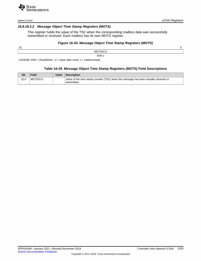
www.ti.com eCAN Registers
1033SPRUH18H–January 2011–Revised November 2019Submit Documentation Feedback
Copyright © 2011–2019, Texas Instruments Incorporated
Controller Area Network (CAN)
16.8.18.2.2 Message Object Time Stamp Registers (MOTS)This register holds the value of the TSC when the corresponding mailbox data was successfullytransmitted or received. Each mailbox has its own MOTS register.
Figure 16-34. Message Object Time Stamp Registers (MOTS)31 0
MOTS31:0R/W-x
LEGEND: R/W = Read/Write; -n = value after reset; x = indeterminate
Table 16-29. Message Object Time Stamp Registers (MOTS) Field Descriptions
Bit Field Value Description31:0 MOTS31:0 Value of the time stamp counter (TSC) when the message has been actually received or
transmitted.

eCAN Registers www.ti.com
1034 SPRUH18H–January 2011–Revised November 2019Submit Documentation Feedback
Copyright © 2011–2019, Texas Instruments Incorporated
Controller Area Network (CAN)
16.8.18.2.3 Time-Out Control Register (CANTOC)This register controls whether or not time-out functionality is enabled for a given mailbox.
Figure 16-35. Time-Out Control Register (CANTOC)31 0
TOC31:0R/W-0
LEGEND: R/W = Read/Write; -n = value after reset
Table 16-30. Time-Out Control Register (CANTOC) Field Descriptions
Bit Field Value Description31:0 TOC31:0 Time-out control register
1 The TOC[n] bit must be set by the CPU to enable the time-out function for mailbox n. Before settingthe TOC[n] bit, the corresponding MOTO register should be loaded with the time-out value relativeto TSC.
0 The time-out function is disabled. The TOS[n] flag is never set.

www.ti.com eCAN Registers
1035SPRUH18H–January 2011–Revised November 2019Submit Documentation Feedback
Copyright © 2011–2019, Texas Instruments Incorporated
Controller Area Network (CAN)
16.8.18.2.4 Time-Out Status Register (CANTOS)This register holds the status information of mailboxes that have timed out.
Figure 16-36. Time-Out Status Register (CANTOS)31 0
TOS31:0R/C-0
LEGEND: R/C = Read/Clear; -n = value after reset
Table 16-31. Time-Out Status Register (CANTOS) Field Descriptions
Bit Field Value Description31:0 TOS 31:0 Time-out status register
1 Mailbox[n] has timed out. The value in the TSC register is larger or equal to the value in the time-out register that corresponds to mailbox n and the TOC[n] bit is set.
0 No time-out occurred or it is disabled for that mailbox.
The TOSn bit is set when all three of the following conditions are met:1. The TSC value is greater than or equal to the value in the time-out register (MOTOn).2. The TOCn bit is set.3. The TRSn bit is set (in the case of a transmit mailbox).
The time-out registers are implemented as a RAM. The state machine scans all the time-out registers andcompares them to the time stamp counter value. Since all the time out registers are scanned sequentially,it is possible that even though a transmit mailbox has timed out, the TOSn bit is not set. This can happenwhen the mailbox succeeded in transmitting and clearing the TRSn bit before the state machine scans thetime-out register of that mailbox. This is true for the receive mailbox as well. In this case, the RMPn bitcan be set to 1 by the time the state machine scans the time-out register of that mailbox. However, thereceive mailbox probably did not receive the message before the time specified in the time-out register.
16.8.18.3 Behavior/Usage of MTOF0/1 Bit in User ApplicationsThe MTOF0/1 bit is automatically cleared by the CPK (along with the TOSn bit) upontransmission/reception by the mailbox, which asserted this flag in the first place. It can also be cleared bythe user (via the CPU). On a time-out condition, the MTOF0/1 bit (and the TOS.n bit) is set. On an(eventual) successful communication, these bits are automatically cleared by the CPK. Following are thepossible behaviors/usage for the MTOF0/1 bit:1. Time-out condition occurs. Both MTOF.n bit and TOS.n bits are set. Communication is never
successful; that is, the frame was never transmitted (or received). An interrupt is asserted. Applicationshould handle this issue as desired and clear TOC.n bit which clears TOS.n bit which in turn clears theMTOF.n bit.
2. Time-out condition occurs. Both MTOF.n bit and TOS.n bits are set. However, communication iseventually successful; that is, the frame gets transmitted (or received). Both MTOF.n bit and TOS.nbits are cleared automatically by the CPK. An interrupt is still asserted because the interruptoccurrence was recorded in the PIE module. When the ISR scans the GIF register, it doesn't see theMTOF0/1 bit set. This is the phantom interrupt scenario. This is handled per the applicationrequirements.
3. Time-out condition occurs. Both MTOF0/1 bit and TOS.n bits are set. While executing the ISRpertaining to time-out, communication is successful. This situation must be handled carefully. Theapplication should not re-transmit a mailbox if the mailbox is sent between the time the interrupt isasserted and the time the ISR is attempting to take corrective action. One way of doing this is to pollthe TM/RM bits in the CANES register. These bits indicate if the CPK is currentlytransmitting/receiving. If that is the case, the application should wait till the communication is over andthen check the TOS.n bit again. If the communication is still not successful, then the application shouldtake the corrective action.

eCAN Registers www.ti.com
1036 SPRUH18H–January 2011–Revised November 2019Submit Documentation Feedback
Copyright © 2011–2019, Texas Instruments Incorporated
Controller Area Network (CAN)
16.8.19 Mailbox LayoutThe following four 32-bit registers comprise each mailbox:• MSGID − Stores the message ID• MSGCTRL − Defines number of bytes, transmission priority and remote frames• CANMDL − 4 bytes of data• CANMDH − 4 bytes of data
16.8.19.1 Message Identifier Register (MSGID)This register contains the message ID and other control bits for a given mailbox.
Figure 16-37. Message Identifier Register (MSGID) Register31 30 29 28 0
IDE AME AAM ID[28:0]R/W-x R/W-x R/W-x R/W-xLEGEND: R/W = Read/Write; R = Read only; -n = value after reset; x = indeterminateNote: This register can be written only when mailbox n is disabled (CANME[n] (CANME.31-0) = 0). The reset-state of IDE, AME and AAMbits are undefined. As part of module initialization, these bits must be initialized as appropriate. Otherwise, they may assume random valuesand lead to improper operation of the mailboxes.
Table 16-32. Message Identifier Register (MSGID) Field Descriptions
Bit Field Value Description31 IDE Identifier extension bit.
1 Receive Mailbox -> The received message has an extended identifier (29 bits). Transmit Mailbox->The message to be sent has an extended identifier (29 bits).
0 Receive Mailbox -> The received message has a standard identifier (11 bits). Transmit Mailbox->The message to be sent has a standard identifier (11 bits).
30 AME Acceptance mask enable bit. AME is only used for receive mailboxes. This bit is not modified by amessage reception.
1 The corresponding acceptance mask is used.0 No acceptance mask is used, all identifier bits must match to receive the message
29 AAM Auto answer mode bit. This bit is only valid for message mailboxes configured as transmit. Forreceive mailboxes, this bit has no effect: the mailbox is always configured for normal receiveoperation.This bit is not modified by a message reception.
1 Auto answer mode. If a matching remote request is received, the CAN module answers to theremote request by sending the contents of the mailbox.
0 Normal transmit mode. The mailbox does not reply to remote requests. The reception of a remoterequest frame has no effect on the message mailbox.
28:0 ID[28:0] Message identifier1 In standard identifier mode, if the IDE bit (MSGID.31) = 0, the message identifier is stored in bits
ID.28:18. In this case, bits ID.17:0 have no meaning.0 In extended identifier mode, if the IDE bit (MSGID.31) = 1, the message identifier is stored in bits
ID.28:0.
16.8.19.2 CPU Mailbox AccessWrite accesses to the identifier can only be accomplished when the mailbox is disabled (CANME[n](CANME.31-0) = 0). During access to the data field, it is critical that the data does not change while theCAN module is reading it. Hence, a write access to the data field is disabled for a receive mailbox.
For send mailboxes, an access is usually denied if the TRS (TRS.31-0) or the TRR (TRR.31-0) flag is set.In these cases, an interrupt can be asserted. A way to access those mailboxes is to set CDR (CANMC.8)before accessing the mailbox data.

www.ti.com eCAN Registers
1037SPRUH18H–January 2011–Revised November 2019Submit Documentation Feedback
Copyright © 2011–2019, Texas Instruments Incorporated
Controller Area Network (CAN)
After the CPU access is finished, the CPU must clear the CDR flag by writing a 0 to it. The CAN modulechecks for that flag before and after reading the mailbox. If the CDR flag is set during those checks, theCAN module does not transmit the message but continues to look for other transmit requests. The settingof the CDR flag also stops the write-denied interrupt (WDI) from being asserted.

eCAN Registers www.ti.com
1038 SPRUH18H–January 2011–Revised November 2019Submit Documentation Feedback
Copyright © 2011–2019, Texas Instruments Incorporated
Controller Area Network (CAN)
16.8.19.3 Message-Control Register (MSGCTRL)For a transmit mailbox, this register specifies the number of bytes to be transmitted and the transmissionpriority. It also specifies the remote-frame operation.
NOTE: As part of the CAN module initialization process, all the bits of the MSGCTRLn registersmust first be initialized to zero before proceeding to initialize the various bit fields to thedesired values.
Figure 16-38. Message-Control Register (MSGCTRL)31 16
ReservedR-0
15 13 12 8 7 5 4 3 0Reserved TPL Reserved RTR DLC
R-0 RW-x R-0 RW-x RW-xLEGEND: RW = Read any time, write when mailbox is disabled or configured for transmission; -n = value after reset; x = indeterminateNote: The register MSGCTRL(n) can only be written if mailbox n is configured for transmission (CANMD[n] (CANMD.31-0)=0) or if themailbox is disabled (CANME[n] (CANME.31-0) =0).
Table 16-33. Message-Control Register (MSGCTRL) Field Descriptions
Bit Field Value Description31:13 Reserved Reserved12:8 TPL.4:0 Transmit-priority level. This 5-bit field defines the priority of this mailbox as compared to the other
31 mailboxes. The highest number has the highest priority. When two mailboxes have the samepriority, the one with the higher mailbox number is transmitted. TPL applies only for transmitmailboxes. TPL is not used in SCC-mode.
7:5 Reserved Reserved4 RTR Remote-transmission-request bit
1 For receive mailbox: If the TRS flag is set, a remote frame is transmitted and the correspondingdata frame is received in the same mailbox. Once the remote frame is sent, the TRS bit of themailbox is cleared by CAN.For transmit mailbox: If the TRS flag is set, a remote frame is transmitted, but the correspondingdata frame has to be received in another mailbox.
0 No remote frame is requested.3:0 DLC 3:0 Data-length code. The number in these bits determines how many data bytes are sent or received.
Valid value range is from 0 to 8. Values from 9 to 15 are not allowed.

www.ti.com Message Data Registers (CANMDL, CANMDH)
1039SPRUH18H–January 2011–Revised November 2019Submit Documentation Feedback
Copyright © 2011–2019, Texas Instruments Incorporated
Controller Area Network (CAN)
16.9 Message Data Registers (CANMDL, CANMDH)Eight bytes of the mailbox are used to store the data field of a CAN message. The setting of DBO(CANMC.10) determines the ordering of stored data. The data is transmitted or received from the CANbus, starting with byte 0.• When DBO (CANMC.10) = 1, the data is stored or read starting with the least significant byte of the
CANMDL register and ending with the most significant byte of the CANMDH register.• When DBO (CANMC.10) = 0, the data is stored or read starting with the most significant byte of the
CANMDL register and ending with the least significant byte of the CANMDH register.
The registers CANMDL(n) and CANMDH(n) can be written only if mailbox n is configured for transmission(CANMD[n] (CANMD.31-0)=0) or the mailbox is disabled (CANME[n] (CANME.31-0)=0). If TRS[n](TRS.31-0)=1, the registers CANMDL(n) and CANMDH(n) cannot be written, unless CDR (CANMC.8)=1,with MBNR (CANMC.4-0) set to n. These settings also apply for a message object configured in replymode (AAM (MSGID.29)=1).
Figure 16-39. Message-Data-Low Register With DBO = 0 (CANMDL)31 24 23 16 15 8 7 0
Byte 0 Byte 1 Byte 2 Byte 3
Figure 16-40. Message-Data-High Register With DBO = 0 (CANMDH)31 24 23 16 15 8 7 0
Byte 4 Byte 5 Byte 6 Byte 7
Figure 16-41. Message-Data-Low Register With DBO = 1 (CANMDL)31 24 23 16 15 8 7 0
Byte 3 Byte 2 Byte 1 Byte 0
Figure 16-42. Message-Data-High Register With DBO = 1 (CANMDH)31 24 23 16 15 8 7 0
Byte 7 Byte 6 Byte 5 Byte 4
NOTE: The data field beyond the valid received data is modified by any message reception and isindeterminate.

Acceptance Filter www.ti.com
1040 SPRUH18H–January 2011–Revised November 2019Submit Documentation Feedback
Copyright © 2011–2019, Texas Instruments Incorporated
Controller Area Network (CAN)
16.10 Acceptance FilterThe identifier of the incoming message is first compared to the message identifier of the mailbox (which isstored in the mailbox). Then, the appropriate acceptance mask is used to mask out the bits of the identifierthat should not be compared.
In the SCC-compatible mode, the global acceptance mask (GAM) is used for the mailboxes 6 to 15. Anincoming message is stored in the highest numbered mailbox with a matching identifier. If there is nomatching identifier in mailboxes 15 to 6, the incoming message is compared to the identifier stored inmailboxes 5 to 3 and then 2 to 0.
The mailboxes 5 to 3 use the local-acceptance mask LAM(3) of the SCC registers. The mailboxes 2 to 0use the local-acceptance mask LAM(0) of the SCC registers. For specific uses, see Figure 16-43.
To modify the global acceptance mask register (CANGAM) and the two local-acceptance mask registersof the SCC, the CAN module must be set in the initialization mode (see Section 3.1).
In eCAN mode, each of the 32 mailboxes has its own local-acceptance mask LAM(0) to LAM(31). There isno global-acceptance mask in the eCAN mode.
The selection of the mask to be used for the comparison depends on which mode (SCC or eCAN) is used.
16.10.1 Local-Acceptance Masks (CANLAM)The local-acceptance filtering allows the user to locally mask (don't care) any identifier bits of the incomingmessage.
In the SCC, the local-acceptance-mask register LAM(0) is used for mailboxes 2 to 0. The local-acceptance-mask register LAM(3) is used for mailboxes 5 to 3. For the mailboxes 6 to 15, the global-acceptance-mask (CANGAM) register is used.
After a hardware or a software reset of the SCC module, CANGAM is reset to zero. After a reset of theeCAN, the LAM registers are not modified.
In eCAN mode, each mailbox (0 to 31) has its own mask register, LAM(0) to LAM(31). An incomingmessage is stored in the highest numbered mailbox with a matching identifier.

www.ti.com Acceptance Filter
1041SPRUH18H–January 2011–Revised November 2019Submit Documentation Feedback
Copyright © 2011–2019, Texas Instruments Incorporated
Controller Area Network (CAN)
Figure 16-43. Local-Acceptance-Mask Register (LAMn)31 30 29 28 16
LAMI Reserved LAMn[28:16]R/W-x R/W-x R/W-x
15 0LAMn[15:0]
R/W-0LEGEND: R/W = Read/Write; -n = value after reset (x:Undefined)
Table 16-34. Local-Acceptance-Mask Register (LAMn) Field Descriptions
Bit Field Value Description31 LAMI Local-acceptance-mask identifier extension bit
1 Standard and extended frames can be received. In case of an extended frame, all 29 bits of theidentifier are stored in the mailbox and all 29 bits of the local-acceptance mask register are used forthe filter. In case of a standard frame, only the first eleven bits (bits 28 to 18) of the identifier andthe local-acceptance mask are used.
0 The identifier extension bit stored in the mailbox determines which messages shall be received.30:29 Reserved Reads are undefined and writes have no effect.28:0 LAM[28:0] These bits enable the masking of any identifier bit of an incoming message.
1 Accept a 0 or a 1 (don't care) for the corresponding bit of the received identifier.0 Received identifier bit value must match the corresponding identifier bit of the MSGID register.
You can locally mask any identifier bits of the incoming message. A 1 value means "don't care" or accepteither a 0 or 1 for that bit position. A 0 value means that the incoming bit value must match thecorresponding bit in the message identifier.
If the local-acceptance mask identifier extension bit is set (LAMI = 1 => don't care) standard and extendedframes can be received. An extended frame uses all 29 bits of the identifier stored in the mailbox and all29 bits of local-acceptance mask register for the filter. For a standard frame only the first eleven bits (bit28 to 18) of the identifier and the local-acceptance mask are used.
If the local-acceptance mask identifier extension bit is reset (LAMI = 0), the identifier extension bit storedin the mailbox determines the messages that are received.

1042 SPRUH18H–January 2011–Revised November 2019Submit Documentation Feedback
Copyright © 2011–2019, Texas Instruments Incorporated
Universal Serial Bus (USB) Controller
Chapter 17SPRUH18H–January 2011–Revised November 2019
Universal Serial Bus (USB) Controller
This chapter discusses the features and functions of the universal serial bus (USB) controller.
Topic ........................................................................................................................... Page
17.1 Introduction ................................................................................................... 104317.2 Features ........................................................................................................ 104317.3 Functional Description .................................................................................... 104517.4 Initialization and Configuration ......................................................................... 105417.5 USB Registers ................................................................................................ 1056

Packet
Encode/Decode
Endpoint Control
EP0 –31
Control
Transmit
Receive
Combine
Endpoints
Host
Transaction
Scheduler
Packet Encode
Packet Decode
CRC Gen/Check
FIFO RAM
Controller
Cycle Control
Rx
Buff
Rx
Buff
Tx
Buff
Tx
Buff
CPU Interface
Interrupt
Control
EP Reg.
Decoder
Common
Regs
Cycle
Control
FIFO
Decoder
Interrupts
CPU BusUTM
Synchronization
Data Sync
HNP/SRP
Timers
USB FS/LS
PHY
USB DataLines
D+ andD-
www.ti.com Introduction
1043SPRUH18H–January 2011–Revised November 2019Submit Documentation Feedback
Copyright © 2011–2019, Texas Instruments Incorporated
Universal Serial Bus (USB) Controller
17.1 IntroductionThe USB controller operates as a full-speed function controller during point-to-point communications withthe USB host. The controller complies with the USB 2.0 standard, which includes SUSPEND andRESUME signaling. It has eight endpoints, one-half of them being for IN transactions and one-half of thembeing for OUT transactions. One IN and one OUT endpoint are fixed-function endpoints used for controltransfers; the others are defined by firmware. A dynamically sizeable FIFO supports queuing multiplepackets. Software-controlled connect and disconnect allow flexibility during USB device startup.
17.2 FeaturesThe USB module has the following features:• Complies with USB-IF certification standards• USB 2.0 full-speed (12 Mbps) operation in host and device modes as well as low-speed (1.5 Mbps)
operation in host mode• Integrated PHY• Three transfer types: Control, Interrupt, and Bulk• Eight endpoints
– One dedicated control IN endpoint and one dedicated control OUT endpoint– Three configurable IN endpoints and three configurable OUT endpoints
• Four KB dedicated endpoint memory
17.2.1 Block DiagramThe USB block diagram is shown in Figure 17-1.
Figure 17-1. USB Block Diagram
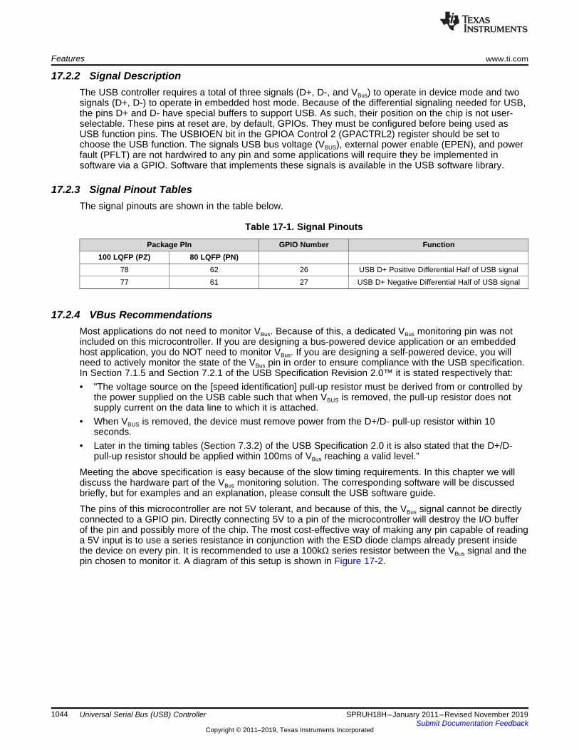
Features www.ti.com
1044 SPRUH18H–January 2011–Revised November 2019Submit Documentation Feedback
Copyright © 2011–2019, Texas Instruments Incorporated
Universal Serial Bus (USB) Controller
17.2.2 Signal DescriptionThe USB controller requires a total of three signals (D+, D-, and VBus) to operate in device mode and twosignals (D+, D-) to operate in embedded host mode. Because of the differential signaling needed for USB,the pins D+ and D- have special buffers to support USB. As such, their position on the chip is not user-selectable. These pins at reset are, by default, GPIOs. They must be configured before being used asUSB function pins. The USBIOEN bit in the GPIOA Control 2 (GPACTRL2) register should be set tochoose the USB function. The signals USB bus voltage (VBUS), external power enable (EPEN), and powerfault (PFLT) are not hardwired to any pin and some applications will require they be implemented insoftware via a GPIO. Software that implements these signals is available in the USB software library.
17.2.3 Signal Pinout TablesThe signal pinouts are shown in the table below.
Table 17-1. Signal Pinouts
Package PIn GPIO Number Function100 LQFP (PZ) 80 LQFP (PN)
78 62 26 USB D+ Positive Differential Half of USB signal77 61 27 USB D+ Negative Differential Half of USB signal
17.2.4 VBus RecommendationsMost applications do not need to monitor VBus. Because of this, a dedicated VBus monitoring pin was notincluded on this microcontroller. If you are designing a bus-powered device application or an embeddedhost application, you do NOT need to monitor VBus. If you are designing a self-powered device, you willneed to actively monitor the state of the VBus pin in order to ensure compliance with the USB specification.In Section 7.1.5 and Section 7.2.1 of the USB Specification Revision 2.0™ it is stated respectively that:• "The voltage source on the [speed identification] pull-up resistor must be derived from or controlled by
the power supplied on the USB cable such that when VBUS is removed, the pull-up resistor does notsupply current on the data line to which it is attached.
• When VBUS is removed, the device must remove power from the D+/D- pull-up resistor within 10seconds.
• Later in the timing tables (Section 7.3.2) of the USB Specification 2.0 it is also stated that the D+/D-pull-up resistor should be applied within 100ms of VBus reaching a valid level."
Meeting the above specification is easy because of the slow timing requirements. In this chapter we willdiscuss the hardware part of the VBus monitoring solution. The corresponding software will be discussedbriefly, but for examples and an explanation, please consult the USB software guide.
The pins of this microcontroller are not 5V tolerant, and because of this, the VBus signal cannot be directlyconnected to a GPIO pin. Directly connecting 5V to a pin of the microcontroller will destroy the I/O bufferof the pin and possibly more of the chip. The most cost-effective way of making any pin capable of readinga 5V input is to use a series resistance in conjunction with the ESD diode clamps already present insidethe device on every pin. It is recommended to use a 100kΩ series resistor between the VBus signal and thepin chosen to monitor it. A diagram of this setup is shown in Figure 17-2.

VBUS
D+
D–
GND
GND
f2806xU
GND
100 kGPIOx
USB-DP/GPIO26
USB-DM/GPIO27
P$1
P$3
P$2
P$4
+3V
3
www.ti.com Functional Description
1045SPRUH18H–January 2011–Revised November 2019Submit Documentation Feedback
Copyright © 2011–2019, Texas Instruments Incorporated
Universal Serial Bus (USB) Controller
Figure 17-2. USB Scheme
In the above diagram, if VBus is above or below 3.3V and 0V respectively, one of the ESD clamp diodeswill be forward-biased, allowing current to flow through the 100KΩ resistor. The purpose of the diodeclamps is to protect the pins of the microcontroller from very short overvoltage spikes of a high magnitude.They do this by clamping the voltage excursion to one of the supply rails. We are effectively requiring theESD clamps to do the same thing they were designed to do, but instead of a short high magnitude pulse,we are giving them a long low magnitude static value via the 100kΩ resistor.
Any pin that has digital input/output functionality could potentially be used to monitor VBus, but the use ofan interrupt-capable GPIO is recommended. A pin that does not have external interrupt capability mayalso be used, but the input state of the pin must be polled periodically by the application software toensure appropriate action is taken whenever VBus is applied or removed. If an interrupt-capable GPIO ischosen, it should be configured to generate an interrupt on both the rising and falling edge. Moreinformation on external interrupts can be found in the System Control and Interrupts chapter. Examplecode that implements VBus monitoring using external interrupts and takes the appropriate actions isdocumented in the USB Software Guide and can be found in the associated USB software package.
17.3 Functional DescriptionThe USB controller can be configured to act as either a dedicated host or device. However, when the USBcontroller is acting as a self-powered device, a GPIO input or analog comparator input must be connectedto VBUS and configured to generate an interrupt when the VBUS level drops. This interrupt is used to disablethe pullup resistor on the USB0DP signal.
NOTE: When USB is used in the system, the minimum system frequency is 20 MHz.
17.3.1 Operation as a DeviceThis section describes how the USB controller performs when it is being used as a USB device. INendpoints, OUT endpoints, entry into and exit from SUSPEND mode, and recognition of start of frame(SOF) are all described.
When in device mode, IN transactions are controlled by the endpoint transmit interface and uses thetransmit endpoint registers for the given endpoint. OUT transactions are handled with the endpointsreceive interface and use the receive endpoint registers for the given endpoint. When configuring the sizeof the FIFOs for endpoints, take into account the maximum packet size for an endpoint. Note the following:• Bulk endpoints should be the size of the maximum packet (up to 64 bytes) or twice the maximum
packet size if double buffering is used (described further in the following section).• Interrupt endpoints should be the size of the maximum packet (up to 64 bytes) or twice the maximum
packet size if double buffering is used.• It is also possible to specify a separate control endpoint for a USB device. However, in most cases the
USB device should use the dedicated control endpoint on the USB controller’s endpoint 0.

Functional Description www.ti.com
1046 SPRUH18H–January 2011–Revised November 2019Submit Documentation Feedback
Copyright © 2011–2019, Texas Instruments Incorporated
Universal Serial Bus (USB) Controller
17.3.1.1 Control and Configurable EndpointsWhen operating as a device, the USB controller provides two dedicated control endpoints (IN and OUT).The remaining available configurable endpoints (one-half IN and one-half OUT) can be used forcommunications with a host controller. The endpoint number and direction associated with an endpoint isdirectly related to its register designation. For example, when the Host is transmitting to endpoint 1, allconfiguration and data is in the endpoint 1 transmit register interface. Endpoint 0 is a dedicated controlendpoint used for all control transactions to endpoint 0 during enumeration or when any other controlrequests are made to endpoint 0. Endpoint 0 uses the first 64 bytes of the USB controller's FIFO RAM asa shared memory for both IN and OUT transactions. The remaining six endpoints can be configured ascontrol, bulk, or interrupt endpoints. They should be treated as three configurable IN and threeconfigurable OUT endpoints. The endpoint pairs are not required to have the same type for their IN andOUT endpoint configuration. For example, the OUT portion of an endpoint pair could be a bulk endpoint,while the IN portion of that endpoint pair could be an interrupt endpoint. The address and size of theFIFOs attached to each endpoint can be modified to fit the application's needs.
17.3.1.1.1 IN Transactions as a DeviceWhen operating as a USB device, data for IN transactions is handled through the FIFOs attached to thetransmit endpoints. The sizes of the FIFOs for the configurable IN endpoints are determined by the USBTransmit FIFO Start Address (USBTXFIFOADD) register. The maximum size of a data packet that may beplaced in a transmit endpoint’s FIFO for transmission is programmable and is determined by the valuewritten to the USB Maximum Transmit Data Endpoint n (USBTXMAXPn) register for that endpoint. Theendpoint’s FIFO can also be configured to use double-packet or single-packet buffering. When double-packet buffering is enabled, two data packets can be buffered in the FIFO, which also requires that theFIFO is at least two packets in size. When double-packet buffering is disabled, only one packet can bebuffered, even if the packet size is less than half the FIFO size.
Note: The maximum packet size set for any endpoint must not exceed the FIFO size. The USBTXMAXPnregister should not be written to while data is in the FIFO as unexpected results may occur.
Single-Packet BufferingIf the size of the transmit endpoint's FIFO is less than twice the maximum packet size for this endpoint (asset in the USB Transmit Dynamic FIFO Sizing (USBTXFIFOSZ) register), only one packet can be bufferedin the FIFO and single-packet buffering is required. When each packet is completely loaded into thetransmit FIFO, the TXRDY bit in the USB Transmit Control and Status Endpoint n Low (USBTXCSRLn)register must be set. If the AUTOSET bit in the USB Transmit Control and Status Endpoint n High(USBTXCSRHn) register is set, the TXRDY bit is automatically set when a maximum-sized packet isloaded into the FIFO. For packet sizes less than the maximum, the TXRDY bit must be set manually.When the TXRDY bit is set, either manually or automatically, the packet is ready to be sent. When thepacket has been successfully sent, both TXRDY and FIFONE are cleared, and the appropriate transmitendpoint interrupt signaled. At this point, the next packet can be loaded into the FIFO.
Double-Packet BufferingIf the size of the transmit endpoint's FIFO is at least twice the maximum packet size for this endpoint, twopackets can be buffered in the FIFO and double-packet buffering is allowed. As each packet is loaded intothe transmit FIFO, the TXRDY bit in the USBTXCSRLn register must be set. If the AUTOSET bit in theUSBTXCSRHn register is set, the TXRDY bit is automatically set when a maximum-sized packet is loadedinto the FIFO. For packet sizes less than the maximum, TXRDY must be set manually. When the TXRDYbit is set, either manually or automatically, the packet is ready to be sent. After the first packet is loaded,TXRDY is immediately cleared and an interrupt is generated. A second packet can now be loaded into thetransmit FIFO and TXRDY set again (either manually or automatically if the packet is the maximum size).At this point, both packets are ready to be sent. After each packet has been successfully sent, TXRDY isautomatically cleared and the appropriate transmit endpoint interrupt signaled to indicate that anotherpacket can now be loaded into the transmit FIFO. The state of the FIFONE bit in the USBTXCSRLnregister at this point indicates how many packets may be loaded. If the FIFONE bit is set, then anotherpacket is in the FIFO and only one more packet can be loaded. If the FIFONE bit is clear, then no packetsare in the FIFO and two more packets can be loaded.

www.ti.com Functional Description
1047SPRUH18H–January 2011–Revised November 2019Submit Documentation Feedback
Copyright © 2011–2019, Texas Instruments Incorporated
Universal Serial Bus (USB) Controller
Note: Double-packet buffering is disabled if an endpoint’s corresponding EPn bit is set in the USBTransmit Double Packet Buffer Disable (USBTXDPKTBUFDIS) register. This bit is set by default, so itmust be cleared to enable double-packet buffering.
17.3.1.1.2 Out Transactions as a DeviceWhen in device mode, OUT transactions are handled through the USB controller receive FIFOs. The sizesof the receive FIFOs for the configurable OUT endpoints are determined by the USB Receive FIFO StartAddress (USBRXFIFOADD) register. The maximum amount of data received by an endpoint in any packetis determined by the value written to the USB Maximum Receive Data Endpoint n (USBRXMAXPn)register for that endpoint. When double-packet buffering is enabled, two data packets can be buffered inthe FIFO. When double-packet buffering is disabled, only one packet can be buffered even if the packet isless than half the FIFO size.
Note: In all cases, the maximum packet size must not exceed the FIFO size.
Single-Packet BufferingIf the size of the receive endpoint FIFO is less than twice the maximum packet size for an endpoint, onlyone data packet can be buffered in the FIFO and single-packet buffering is required. When a packet isreceived and placed in the receive FIFO, the RXRDY and FULL bits in the USB Receive Control andStatus Endpoint n Low (USBRXCSRL[n]) register are set and the appropriate receive endpoint is signaled,indicating that a packet can now be unloaded from the FIFO. After the packet has been unloaded, theRXRDY bit must be cleared in order to allow further packets to be received. This action also generates theacknowledge signaling to the Host controller. If the AUTOCL bit in the USB Receive Control and StatusEndpoint n High (USBRXCSRH[n]) register is set and a maximum-sized packet is unloaded from theFIFO, the RXRDY and FULL bits are cleared automatically. For packet sizes less than the maximum,RXRDY must be cleared manually.
Double-Packet BufferingIf the size of the receive endpoint FIFO is at least twice the maximum packet size for the endpoint, twodata packets can be buffered and double-packet buffering can be used. When the first packet is receivedand loaded into the receive FIFO, the RXRDY bit in the USBRXCSRL[n] register is set and the appropriatereceive endpoint interrupt is signaled to indicate that a packet can now be unloaded from the FIFO.
Note: The FULL bit in USBRXCSRL[n] is not set when the first packet is received. It is only set if a secondpacket is received and loaded into the receive FIFO.
After each packet has been unloaded, the RXRDY bit must be cleared to allow further packets to bereceived. If the AUTOCL bit in the USBRXCSRH[n] register is set and a maximum-sized packet isunloaded from the FIFO, the RXRDY bit is cleared automatically. For packet sizes less than the maximum,RXRDY must be cleared manually. If the FULL bit is set when RXRDY is cleared, the USB controller firstclears the FULL bit, then sets RXRDY again to indicate that there is another packet waiting in the FIFO tobe unloaded.
Note: Double-packet buffering is disabled if an endpoint’s corresponding EPn bit is set in the USBReceive Double Packet Buffer Disable (USBRXDPKTBUFDIS) register. This bit is set by default, so itmust be cleared to enable double-packet buffering.
17.3.1.1.3 SchedulingThe device has no control over the scheduling of transactions as scheduling is determined by the Hostcontroller. The USB controller can set up a transaction at any time. The USB controller waits for therequest from the Host controller and generates an interrupt when the transaction is complete or if it wasterminated due to some error. If the Host controller makes a request and the device controller is not ready,the USB controller sends a busy response (NAK) to all requests until it is ready.
17.3.1.1.4 Additional ActionsThe USB controller responds automatically to certain conditions on the USB bus or actions by the Hostcontroller such as when the USB controller automatically stalls a control transfer or unexpected zerolength OUT data packets.
Stalled Control Transfer

Functional Description www.ti.com
1048 SPRUH18H–January 2011–Revised November 2019Submit Documentation Feedback
Copyright © 2011–2019, Texas Instruments Incorporated
Universal Serial Bus (USB) Controller
The USB controller automatically issues a STALL handshake to a control transfer under the followingconditions:1. The Host sends more data during an OUT data phase of a control transfer than was specified in the
device request during the SETUP phase. This condition is detected by the USB controller when theHost sends an OUT token (instead of an IN token) after the last OUT packet has been unloaded andthe DATAEND bit in the USB Control and Status Endpoint 0 Low (USBCSRL0) register has been set.
2. The Host requests more data during an IN data phase of a control transfer than was specified in thedevice request during the SETUP phase. This condition is detected by the USB controller when theHost sends an IN token (instead of an OUT token) after the CPU has cleared TXRDY and setDATAEND in response to the ACK issued by the Host to what should have been the last packet.
3. The Host sends more than USBRXMAXPn bytes of data with an OUT data token.4. The Host sends more than a zero length data packet for the OUT STATUS phase.
Zero Length OUT Data PacketsA zero-length OUT data packet is used to indicate the end of a control transfer. In normal operation, suchpackets should only be received after the entire length of the device request has been transferred.However, if the Host sends a zero-length OUT data packet before the entire length of device request hasbeen transferred, it is signaling the premature end of the transfer. In this case, the USB controllerautomatically flushes any IN token ready for the data phase from the FIFO and sets the DATAEND bit inthe USBCSRL0 register.
Setting the Device AddressWhen a Host is attempting to enumerate the USB device, it requests that the device change its addressfrom zero to some other value. The address is changed by writing the value that the Host requested to theUSB Device Functional Address (USBFADDR) register. However, care should be taken when writing toUSBFADDR to avoid changing the address before the transaction is complete. This register should onlybe set after the SET_ADDRESS command is complete. Like all control transactions, the transaction isonly complete after the device has left the STATUS phase. In the case of a SET_ADDRESS command,the transaction is completed by responding to the IN request from the Host with a zero-byte packet. Oncethe device has responded to the IN request, the USBFADDR register should be programmed to the newvalue as soon as possible to avoid missing any new commands sent to the new address.
Note: If the USBFADDR register is set to the new value as soon as the device receives the OUTtransaction with the SET_ADDRESS command in the packet, it changes the address during the controltransfer. In this case, the device does not receive the IN request that allows the USB transaction to exitthe STATUS phase of the control transfer because it is sent to the old address. As a result, the Host doesnot get a response to the IN request, and the Host fails to enumerate the device.
17.3.1.1.5 Device Mode SuspendWhen no activity has occurred on the USB bus for 3 ms, the USB controller automatically entersSUSPEND mode. If the SUSPEND interrupt has been enabled in the USB Interrupt Enable (USBIE)register, an interrupt is generated at this time. When in SUSPEND mode, the PHY also goes intoSUSPEND mode. When RESUME signaling is detected, the USB controller exits SUSPEND mode andtakes the PHY out of SUSPEND. If the RESUME interrupt is enabled, an interrupt is generated. The USBcontroller can also be forced to exit SUSPEND mode by setting the RESUME bit in the USB Power(USBPOWER) register. When this bit is set, the USB controller exits SUSPEND mode and drivesRESUME signaling onto the bus. The RESUME bit must be cleared after 10 ms (a maximum of 15 ms) toend RESUME signaling. To meet USB power requirements, the controller can be put into Deep Sleepmode which keeps the controller in a static state.

www.ti.com Functional Description
1049SPRUH18H–January 2011–Revised November 2019Submit Documentation Feedback
Copyright © 2011–2019, Texas Instruments Incorporated
Universal Serial Bus (USB) Controller
17.3.1.1.6 Start of FrameWhen the USB controller is operating in device mode, it receives a Start-Of-Frame (SOF) packet from theHost once every millisecond. When the SOF packet is received, the 11-bit frame number contained in thepacket is written into the USB Frame Value (USBFRAME) register, and an SOF interrupt is also signaledand can be handled by the application. Once the USB controller has started to receive SOF packets, itexpects one every millisecond. If no SOF packet is received after 1.00358 ms, the packet is assumed tohave been lost, and the USBFRAME register is not updated. The USB controller continues andresynchronizes these pulses to the received SOF packets when these packets are successfully receivedagain.
17.3.1.1.7 USB ResetWhen the USB controller is in device mode and a RESET condition is detected on the USB bus, the USBcontroller automatically performs the following actions:• Clears the USBFADDR register• Clears the USB Endpoint Index (USBEPIDX) register• Flushes all endpoint FIFOs• Clears all control/status registers• Enables all endpoint interrupts• Generates a RESET interrupt
17.3.1.1.8 Connect/DisconnectThe USB controller connection to the USB bus is handled by software. The USB PHY can be switchedbetween normal mode and non-driving mode by setting or clearing the SOFTCONN bit of theUSBPOWER register. When the SOFTCONN bit is set, the PHY is placed in its normal mode, and theUSB0DP/USB0DM lines of the USB bus are enabled. At the same time, the USB controller is placed intoa state, in which it does not respond to any USB signaling except a USB RESET. When the SOFTCONNbit is cleared, the PHY is put into non-driving mode, USB0DP and USB0DM are tristated, and the USBcontroller appears to other devices on the USB bus as if it has been disconnected. The non-driving modeis the default so the USB controller appears disconnected until the SOFTCONN bit has been set. Theapplication software can then choose when to set the PHY into its normal mode. Systems with a lengthyinitialization procedure may use this to ensure that initialization is complete, and the system is ready toperform enumeration before connecting to the USB bus. Once the SOFTCONN bit has been set, the USBcontroller can be disconnected by clearing this bit.
Note: The USB controller does not generate an interrupt when the device is connected to the Host.However, an interrupt is generated when the Host terminates a session.
17.3.2 Operation as a HostWhen the USB controller is operating in Host mode, it can either be used for point-to-pointcommunications with another USB device or, when attached to a hub, for communication with multipledevices. Full-speed and low-speed USB devices are supported, both for point-to-point communication andfor operation through a hub. The USB controller automatically carries out the necessary transactiontranslation needed to allow a low-speed or full-speed device to be used with a USB 2.0 hub. Control, bulk,and interrupt transactions are supported. This section describes the USB controller's actions when it isbeing used as a USB Host. Configuration of IN endpoints, OUT endpoints, entry into and exit fromSUSPEND mode, and RESET are all described.
When in Host mode, IN transactions are controlled by an endpoint’s receive interface. All IN transactionsuse the receive endpoint registers and all OUT endpoints use the transmit endpoint registers for a givenendpoint. As in device mode, the FIFOs for endpoints should take into account the maximum packet sizefor an endpoint.• Bulk endpoints should be the size of the maximum packet (up to 64 bytes) or twice the maximum
packet size if double buffering is used (described further in the following section).• Interrupt endpoints should be the size of the maximum packet (up to 64 bytes) or twice the maximum
packet size if double buffering is used.

Functional Description www.ti.com
1050 SPRUH18H–January 2011–Revised November 2019Submit Documentation Feedback
Copyright © 2011–2019, Texas Instruments Incorporated
Universal Serial Bus (USB) Controller
• It is also possible to specify a separate control endpoint to communicate with a device. However, inmost cases the USB controller should use the dedicated control endpoint to communicate with adevice’s endpoint 0.
17.3.2.1 Endpoint RegistersThe endpoint registers are used to control the USB endpoint interfaces which communicate with device(s)that are connected. The endpoints consist of a dedicated control IN endpoint and a dedicated control OUTendpoint. The remaining available endpoints are configurable, with one-half of them being OUT endpoints,and one-half of them being IN endpoints. See Section 17.2 for the number of available endpoints on thisdevice.
The dedicated control interface can only be used for control transactions to endpoint 0 of devices. Thesecontrol transactions are used during enumeration or other control functions that communicate usingendpoint 0 of devices. This control endpoint shares the first 64 bytes of the USB controller’s FIFO RAM forIN and OUT transactions. The remaining IN and OUT interfaces can be configured to communicate withcontrol, bulk, or interrupt endpoints.
These USB interfaces can be used to simultaneously schedule as many as three independent OUT andthree independent IN transactions to any endpoints on any device. The IN and OUT controls are pairedtogether in the same set of registers for the respective endpoints. However, they can be configured tocommunicate with different types of endpoints and different endpoints on devices. For example, the firstpair of endpoint controls can be split so that the OUT portion is communicating with a device’s bulk OUTendpoint 1, while the IN portion is communicating with a device’s interrupt IN endpoint 2.
Before accessing any device, whether for point-to-point communications or for communications via a hub,the relevant USB Receive Functional Address Endpoint n (USBRXFUNCADDRn) or USB TransmitFunctional Address Endpoint n (USBTXFUNCADDRn) registers must be set for each receive or transmitendpoint to record the address of the device being accessed.
The USB controller also supports connections to devices through a USB hub by providing a register thatspecifies the hub address and port of each USB transfer. The FIFO address and size are customizableand can be specified for each USB IN and OUT transfer. Customization includes allowing one FIFO pertransaction, sharing a FIFO across transactions, and allowing for double-buffered FIFOs.
17.3.2.2 IN Transactions as a HostIN transactions are handled in a similar manner to the way in which OUT transactions are handled whenthe USB controller is in device mode except that the transaction first must be initiated by setting theREQPKT bit in the USBCSRL0 register, indicating to the transaction scheduler that there is an activetransaction on this endpoint. The transaction scheduler then sends an IN token to the target device. Whenthe packet is received and placed in the receive FIFO, the RXRDY bit in the USBCSRL0 register is set,and the appropriate receive endpoint interrupt is signaled to indicate that a packet can now be unloadedfrom the FIFO.
When the packet has been unloaded, RXRDY must be cleared. The AUTOCL bit in the USBRXCSRHnregister can be used to have RXRDY automatically cleared when a maximum-sized packet has beenunloaded from the FIFO. The AUTORQ bit in USBRXCSRHn causes the REQPKT bit to be automaticallyset when the RXRDY bit is cleared. When the RXRDY bit is cleared, the controller sends an acknowledgeto the device. When there is a known number of packets to be transferred, the USB Request PacketCount in Block Transfer Endpoint n (USBRQPKTCOUNTn) register associated with the endpoint shouldbe configured to the number of packets to be transferred. The USB controller decrements the value in theUSBRQPKTCOUNTn register following each request. When the USBRQPKTCOUNTn value decrementsto 0, the AUTORQ bit is cleared to prevent any further transactions being attempted. For cases where thesize of the transfer is unknown, USBRQPKTCOUNTn should be cleared. AUTORQ then remains set untilcleared by the reception of a short packet (that is, less than the MAXLOAD value in the USBRXMAXPnregister) such as may occur at the end of a bulk transfer.
www.ti.com Functional Description
1051SPRUH18H–January 2011–Revised November 2019Submit Documentation Feedback
Copyright © 2011–2019, Texas Instruments Incorporated
Universal Serial Bus (USB) Controller
If the device responds to a bulk or interrupt IN token with a NAK, the USB Host controller keeps retryingthe transaction until any NAK Limit that has been set has been reached. If the target device responds witha STALL, however, the USB Host controller does not retry the transaction but sets the STALLED bit in theUSBCSRL0 register. If the target device does not respond to the IN token within the required time, or thepacket contained a CRC or bit-stuff error, the USB Host controller retries the transaction. If after threeattempts the target device has still not responded, the USB Host controller clears the REQPKT bit andsets the ERROR bit in the USBCSRL0 register.
17.3.2.3 OUT Transactions as a HostOUT transactions are handled in a similar manner to the way in which IN transactions are handled whenthe USB controller is in device mode. The TXRDY bit in the USBTXCSRLn register must be set as eachpacket is loaded into the transmit FIFO. Again, setting the AUTOSET bit in the USBTXCSRHn registerautomatically sets TXRDY when a maximum-sized packet has been loaded into the FIFO.
If the target device responds to the OUT token with a NAK, the USB Host controller keeps retrying thetransaction until the NAK Limit that has been set has been reached. However, if the target deviceresponds with a STALL, the USB controller does not retry the transaction but interrupts the mainprocessor by setting the STALLED bit in the USBTXCSRLn register. If the target device does not respondto the OUT token within the required time, or the packet contained a CRC or bit-stuff error, the USB Hostcontroller retries the transaction. If after three attempts the target device has still not responded, the USBcontroller flushes the FIFO and sets the ERROR bit in the USBTXCSRLn register.
17.3.2.4 Transaction SchedulingScheduling of transactions is handled automatically by the USB Host controller. The Host controller allowsconfiguration of the endpoint communication scheduling based on the type of endpoint transaction.Interrupt transactions can be scheduled to occur in the range of every frame to every 255 frames in 1frame increments. Bulk endpoints do not allow scheduling parameters, but do allow for a NAK timeout inthe event an endpoint on a device is not responding.
The USB controller maintains a frame counter. If the target device is a full-speed device, the USBcontroller automatically sends an SOF packet at the start of each frame and increments the frame counter.If the target device is a low-speed device, a K state is transmitted on the bus to act as a keep-alive to stopthe low-speed device from going into SUSPEND mode.
After the SOF packet has been transmitted, the USB Host controller cycles through all the configuredendpoints looking for active transactions. An active transaction is defined as a receive endpoint for whichthe REQPKT bit is set or a transmit endpoint for which the TXRDY bit and/or the FIFONE bit is set.
An interrupt transaction is started if the transaction is found on the first scheduler cycle of a frame and ifthe interval counter for that endpoint has counted down to zero. As a result, only one interrupt transactionoccurs per endpoint every n frames, where n is the interval set via the USB Host Transmit IntervalEndpoint n (USBTXINTERVAL[n]) or USB Host Receive Interval Endpoint n (USBRXINTERVAL[n])register for that endpoint.
An active bulk transaction starts immediately, provided sufficient time is left in the frame to complete thetransaction before the next SOF packet is due. If the transaction must be retried (for example, because aNAK was received or the target device did not respond), then the transaction is not retried until thetransaction scheduler has first checked all the other endpoints for active transactions. This processensures that an endpoint that is sending a lot of NAKs does not block other transactions on the bus. Thecontroller also allows the user to specify a limit to the length of time for NAKs to be received from a targetdevice before the endpoint times out.

Functional Description www.ti.com
1052 SPRUH18H–January 2011–Revised November 2019Submit Documentation Feedback
Copyright © 2011–2019, Texas Instruments Incorporated
Universal Serial Bus (USB) Controller
17.3.2.5 USB HubsThe following setup requirements apply to the USB Host controller only if it is used with a USB hub. Whena full- or low-speed device is connected to the USB controller via a USB 2.0 hub, details of the hubaddress and the hub port also must be recorded in the corresponding USB Receive Hub AddressEndpoint n (USBRXHUBADDRn) and USB Receive Hub Port Endpoint n (USBRXHUBPORTn) or theUSB Transmit Hub Address Endpoint n (USBTXHUBADDRn) and USB Transmit Hub Port Endpoint n(USBTXHUBPORTn) registers. In addition, the speed at which the device operates (full or low) must berecorded in the USB Type Endpoint 0 (USBTYPE0) (endpoint 0), USB Host Configure Transmit TypeEndpoint n (USBTXTYPEn), or USB Host Configure Receive Type Endpoint n (USBRXTYPEn) registersfor each endpoint that is accessed by the device.
For hub communications, the settings in these registers record the current allocation of the endpoints tothe attached USB devices. To maximize the number of devices supported, the USB Host controller allowsthis allocation to be changed dynamically by simply updating the address and speed information recordedin these registers. Any changes in the allocation of endpoints to device functions must be made followingthe completion of any on-going transactions on the endpoints affected.
17.3.2.6 BabbleThe USB Host controller does not start a transaction until the bus has been inactive for at least theminimum inter-packet delay. The controller also does not start a transaction unless it can be finishedbefore the end of the frame. If the bus is still active at the end of a frame, then the USB Host controllerassumes that the target device to which it is connected has malfunctioned, and the USB controllersuspends all transactions and generates a babble interrupt.
17.3.2.7 Host SUSPENDIf the SUSPEND bit in the USBPOWER register is set, the USB Host controller completes the currenttransaction then stops the transaction scheduler and frame counter. No further transactions are startedand no SOF packets are generated.
To exit SUSPEND mode, set the RESUME bit and clear the SUSPEND bit. While the RESUME bit is set,the USB Host controller generates RESUME signaling on the bus. After 20 ms, the RESUME bit must becleared, at which point the frame counter and transaction scheduler start. The Host supports the detectionof a remote wake-up.
17.3.2.8 USB RESETIf the RESET bit in the USBPOWER register is set, the USB Host controller generates USB RESETsignaling on the bus. The RESET bit must be set for at least 20 ms to ensure correct resetting of thetarget device. After the CPU has cleared the bit, the USB Host controller starts its frame counter andtransaction scheduler.
17.3.2.9 Connect/DisconnectA session is started by setting the SESSION bit in the USB device Control (USBDEVCTL) register,enabling the USB controller to wait for a device to be connected. When a device is detected, a connectinterrupt is generated. The speed of the device that has been connected can be determined by readingthe USBDEVCTL register where the FSDEV bit is set for a full-speed device, and the LSDEV bit is set fora low-speed device. The USB controller must generate a RESET to the device, and then the USB Hostcontroller can begin device enumeration. If the device is disconnected while a session is in progress, adisconnect interrupt is generated.
17.3.3 DMA OperationThe USB module's DMA trigger signals are not supported on this device. The DMA controller may be usedto read and write the USB FIFOs via software triggering. see the Direct Memory Access (DMA) chapter formore details about programming the DMA controller. See the USB DMA Event Trigger advisory in thedevice errata for more information.

www.ti.com Functional Description
1053SPRUH18H–January 2011–Revised November 2019Submit Documentation Feedback
Copyright © 2011–2019, Texas Instruments Incorporated
Universal Serial Bus (USB) Controller
17.3.4 Address/Data Bus BridgeThe USB controller on this device is the same controller that is on the Stellaris devices. This controllerwas originally designed to connect to an ARM AHB bus, but has been modified in order to function withthe C28x device’s bus architecture. The modifications made are largely invisible to the user application,but there are some things to note.• The USB memory space is 8 bits wide, while the C28x memory space is 16 bits wide.• 32 and 16 bit accesses (r/w) are completely transparent to the user application code, no changes need
be made.• The C28x core only supports 8 bit accesses through a byte intrinsic type. This can be used to perform
8 bit reads or writes to the USB controller.– int &__byte(int *array, unsigned int byte_index);– *array = ptr to address to access, byte_index = always 0 (for USB)
See Table 17-2 for example.– See the TMS320C28x Optimizing C/C++ Compiler User's Guide (SPRU514) and the TMS320C28x
Assembly Language Tools User's Guide (SPRU513)• Because of the bridge, the memory view of the USB controller memory space in CCS isn’t a 1:1
representation of what is in the controller– When the view mode is
• 32 bit or 16 bit, even address are effectively duplicated, ignore odd addresses.• 8 bit, Even addresses from within the controller are duplicated into odd address in the view
window; old addresses from within the controller are not displayed.See Table 17-3 for example.
Table 17-2. USB Memory Access From Software
USB Controller Memory C28x 8 BitAddress Reg. Name Data Access Data
0x00 FADDR 0x00 __byte((int *)0x00,0) 0x00000x01 POWER 0x11 __byte((int *)0x01,0) 0x00110x02 TXIS (LSB) 0x22 __byte((int *)0x02,0) 0x00220x03 TXIS (MSB) 0x33 __byte((int *)0x03,0) 0x00330x04 RXIS (LSB) 0x44 __byte((int *)0x04,0) 0x00440x05 RXIS (MSB) 0x55 __byte((int *)0x05,0) 0x00550x06 TXIE (LSB) 0x66 __byte((int *)0x06,0) 0x00660x07 TXIE (MSB) 0x77 __byte((int *)0x07,0) 0x00770x08 RXIE (LSB) 0x88 __byte((int *)0x08,0) 0x00880x09 RXIE (MSB) 0x99 __byte((int *)0x09,0) 0x00990x0A USBIS 0xAA __byte((int *)0x0A,0) 0x00AA0x0B USBIE 0xBB __byte((int *)0x0B,0) 0x00BB0x0C FRAME (LSB) 0xCC __byte((int *)0x0C,0) 0x00CC0x0D FRAME (MSB) 0xDD __byte((int *)0x0D,0) 0x00DD0x0E EPIDX 0xEE __byte((int *)0x0E,0) 0x00EE0x0F TEST 0xFF __byte((int *)0x0F,0) 0x00FF
C28x 16 Bit C28x 32 BitAccess Data Access Data
(*((short *)(0x00))) 0x1100 (*((long *)(0x00))) 0x33221100(*((short *)(0x01))) 0x1100 (*((long *)(0x01))) 0x33221100(*((short *)(0x02))) 0x3322 (*((long *)(0x02))) 0x33221100(*((short *)(0x03))) 0x3322 (*((long *)(0x03))) 0x33221100(*((short *)(0x04))) 0x5544 (*((long *)(0x04))) 0x77665544(*((short *)(0x05))) 0x5544 (*((long *)(0x05))) 0x77665544

Initialization and Configuration www.ti.com
1054 SPRUH18H–January 2011–Revised November 2019Submit Documentation Feedback
Copyright © 2011–2019, Texas Instruments Incorporated
Universal Serial Bus (USB) Controller
Table 17-2. USB Memory Access From Software (continued)USB Controller Memory C28x 8 Bit
(*((short *)(0x06))) 0x7766 (*((long *)(0x06))) 0x77665544(*((short *)(0x07))) 0x7766 (*((long *)(0x07))) 0x77665544(*((short *)(0x08))) 0x9988 (*((long *)(0x08))) 0xBBAA9988(*((short *)(0x09))) 0x9988 (*((long *)(0x09))) 0xBBAA9988(*((short *)(0x0A))) 0xBBAA (*((long *)(0x0A))) 0xBBAA9988(*((short *)(0x0B))) 0xBBAA (*((long *)(0x0B))) 0xBBAA9988(*((short *)(0x0C))) 0xDDCC (*((long *)(0x0C))) 0xFFEEDDCC(*((short *)(0x0D))) 0xDDCC (*((long *)(0x0D))) 0xFFEEDDCC(*((short *)(0x0E))) 0xFFEE (*((long *)(0x0E))) 0xFFEEDDCC(*((short *)(0x0F))) 0xFFEE (*((long *)(0x0F))) 0xFFEEDDCC
Table 17-3. USB Memory Access From CCS
CCS 8 Bit CCS 16 Bit CCS 32 BitAddress Displayed Data Address Displayed Data Address Displayed Data
0x00 0x00 0x00 0x1100 0x00 0x110011000x01 0x00 0x01 0x1100 0x02 0x332233220x02 0x22 0x02 0x3322 0x04 0x554455440x03 0x22 0x03 0x3322 0x06 0x776677660x04 0x44 0x04 0x5544 0x08 0x998899880x05 0x44 0x05 0x5544 0x0A 0xBBAABBAA0x06 0x66 0x06 0x7766 0x0C 0xDDCCDDCC0x07 0x66 0x07 0x7766 0x0E 0xFFEEFFEE0x08 0x88 0x08 0x99880x09 0x88 0x09 0x99880x0A 0xAA 0x0A 0xBBAA0x0B 0xAA 0x0B 0xBBAA0x0C 0xCC 0x0C 0xDDCC0x0D 0xCC 0x0D 0xDDCC0x0E 0xEE 0x0E 0xFFEE0x0F 0xEE 0x0F 0xFFEE
17.4 Initialization and ConfigurationTo use the USB Controller, the clock for the USB controller must first be configured. USBCLK is driven viathe second PLL within the chip. The PLL should be configured to operate at 60MHz via the PLL2CTL,PLL2MULT, PLL2STS registers. After the PLL is enabled and locked,the controller can be clocked byenabling the peripheral in the PCLKCR3 register. In addition to the clock,the USB PHY must be enabled.Configure the USBIOEN field in the GPACTRL2 register to enable USB functionality on the designatedpins. After the clock has been enabled and the USB PHY turned on the USB peripheral is ready foroperation and the associated software initialization routines may be called.
17.4.1 Pin ConfigurationIn order to give the user more flexibiliity, the signals External Power Enable (EPEN) and Power Fault(PFLT) were not implemented in hardware. Instead, it is left up to the user to implement these signals insoftware. Examples of how to implement these signals in software can be found in the F2806x USBSoftware Guide.

www.ti.com Initialization and Configuration
1055SPRUH18H–January 2011–Revised November 2019Submit Documentation Feedback
Copyright © 2011–2019, Texas Instruments Incorporated
Universal Serial Bus (USB) Controller
When using the device controller portion of the USB controller in a system that also provides hostfunctionality, the power to VBUS must be disabled to allow the external host controller to supply power.Usually, the EPEN signal is used to control the external regulator and should be negated to avoid havingtwo devices driving the VBUS power pin on the USB connector.
When the USB controller is acting as a host, it is in control of two signals that are attached to an externalvoltage supply that provides power to VBUS. The Host controller uses the EPEN signal to enable or disablepower to the VBUS pin on the USB connector. An input pin, PFLT, provides feedback when there has beena power fault on VBUS. The PFLT signal can be configured to either automatically negate the EPEN signalto disable power, and/or it can generate an interrupt to the interrupt controller to allow software to handlethe power fault condition. The polarity and actions related to both EPEN and PFLT are fully configurable inthe USB controller. The controller also provides interrupts on device insertion and removal to allow theHost controller code to respond to these external events.
17.4.2 Endpoint ConfigurationTo start communication in Host or device mode, the endpoint registers must first be configured. In Hostmode, this configuration establishes a connection between an endpoint register and an endpoint on adevice. In device mode, an endpoint must be configured before enumerating to the Host controller.
In both cases, the endpoint 0 configuration is limited because it is a fixed-function, fixed-FIFO-sizeendpoint. In device and Host modes, the endpoint requires little setup but does require a software-basedstate machine to progress through the setup, data, and status phases of a standard control transaction. Indevice mode, the configuration of the remaining endpoints is done once before enumerating and then onlychanged if an alternate configuration is selected by the Host controller. In Host mode, the endpoints mustbe configured to operate as control, bulk, or interrupt mode. Once the type of endpoint is configured, aFIFO area must be assigned to each endpoint. In the case of bulk, control and interrupt endpoints, eachhas a maximum of 64 bytes per transaction. The maximum packet size for the given endpoint must be setprior to sending or receiving data.
Configuring each endpoint’s FIFO involves reserving a portion of the overall USB FIFO RAM to eachendpoint. The total FIFO RAM available is 4 Kbytes with the first 64 bytes reserved for endpoint 0. Theendpoint’s FIFO must be at least as large as the maximum packet size. The FIFO can also be configuredas a double-buffered FIFO so that interrupts occur at the end of each packet and allow filling the other halfof the FIFO.
If operating as a device, the USB device controller's soft connect must be enabled when the device isready to start communications, indicating to the host controller that the device is ready to start theenumeration process. If operating as a Host controller, the device soft connect must be disabled andpower must be provided to VBUS via the USB0EPEN signal.

USB Registers www.ti.com
1056 SPRUH18H–January 2011–Revised November 2019Submit Documentation Feedback
Copyright © 2011–2019, Texas Instruments Incorporated
Universal Serial Bus (USB) Controller
17.5 USB Registers
17.5.1 Register MapTable 17-4 lists the registers. All addresses given are relative to the USB base address of 0x4000. Notethat the USB controller clock must be enabled before the registers can be programmed (see SystemControl module).
Table 17-4. Universal Serial Bus (USB) Controller Register Map
Offset Name Type Reset Description Location0x000 USBFADDR(1) R/W 0x00 USB Device
Functional AddressSection 17.5.2.1
0x001 USBPOWER(1)(2) R/W 0x20 USB Power Section 17.5.2.2
0x002 USBTXIS(1)(2) RO 0x0000 USB TransmitInterrupt Status
Section 17.5.2.3
0x004 USBRXIS(1)(2) RO 0x0000 USB ReceiveInterrupt Status
Section 17.5.2.4
0x006 USBTXIE(1)(2) R/W 0xFFFF USB TransmitInterrupt Enable
Section 17.5.2.5
0x008 USBRXIE(1)(2) R/W 0xFFFE USB ReceiveInterrupt Enable
Section 17.5.2.6
0x00A USBIS(1)(2) RO 0x00 USB GeneralInterrupt Status
Section 17.5.2.7
0x00B USBIE(1)(2) R/W 0x06 USB Interrupt Enable Section 17.5.2.8
0x00C USBFRAME(1)(2) RO 0x0000 USB Frame Value Section 17.5.2.9
0x00E USBEPIDX(1)(2) R/W 0x00 USB Endpoint Index Section 17.5.2.10
0x00F USBTEST(1)(2) R/W 0x00 USB Test Mode Section 17.5.2.11
0x020 USBFIFO0(1)(2) R/W 0x0000.0000 USB FIFO Endpoint 0 Section 17.5.2.12
0x024 USBFIFO1(1)(2) R/W 0x0000.0000 USB FIFO Endpoint 1 Section 17.5.2.12
0x028 USBFIFO2(1)(2) R/W 0x0000.0000 USB FIFO Endpoint 2 Section 17.5.2.12
0x02C USBFIFO3(1)(2) R/W 0x0000.0000 USB FIFO Endpoint 3 Section 17.5.2.12
0x060 USBDEVCTL(2) R/W 0x80 USB Device Control Section 17.5.2.13
0x062 USBTXFIFOSZ(1)(2) R/W 0x00 USB TransmitDynamic FIFO Sizing
Section 17.5.2.14
0x063 USBRXFIFOSZ(1)(2) R/W 0x00 USB ReceiveDynamic FIFO Sizing
Section 17.5.2.15
0x064 USBTXFIFOADD(1)(2) R/W 0x0000 USB Transmit FIFOStart Address
Section 17.5.2.16
0x066 USBRXFIFOADD(1)(2) R/W 0x0000 USB Receive FIFOStart Address
Section 17.5.2.17
0x07A USBCONTIM(1)(2) R/W 0x5C USB Connect Timing Section 17.5.2.18
0x07D USBFSEOF(1)(2) R/W 0x77 USB Full-Speed LastTransaction to End of
Frame Timing
Section 17.5.2.19
0x07E USBLSEOF(1)(2) R/W 0x72 USB Low-Speed LastTransaction to End of
Frame Timing
Section 17.5.2.20
0x080 USBTXFUNCADDR0(
2)R/W 0x00 USB Transmit
Functional AddressEndpoint 0
Section 17.5.2.21
0x082 USBTXHUBADDR0(2) R/W 0x00 USB Transmit HubAddress Endpoint 0
Section 17.5.2.22
0x083 USBTXHUBPORT0(2) R/W 0x00 USB Transmit HubPort Endpoint 0
Section 17.5.2.23
0x088 USBTXFUNCADDR1(
2)R/W 0x00 USB Transmit
Functional AddressEndpoint 1
Section 17.5.2.21

www.ti.com USB Registers
1057SPRUH18H–January 2011–Revised November 2019Submit Documentation Feedback
Copyright © 2011–2019, Texas Instruments Incorporated
Universal Serial Bus (USB) Controller
Table 17-4. Universal Serial Bus (USB) Controller Register Map (continued)Offset Name Type Reset Description Location0x08A USBTXHUBADDR1(2) R/W 0x00 USB Transmit Hub
Address Endpoint 1Section 17.5.2.22
0x08B USBTXHUBPORT1(2) R/W 0x00 USB Transmit HubPort Endpoint 1
Section 17.5.2.23
0x08C USBRXFUNCADDR1(2)
R/W 0x00 USB ReceiveFunctional Address
Endpoint 1
Section 17.5.2.24
0x08E USBRXHUBADDR1(2) R/W 0x00 USB Receive HubAddress Endpoint 1
Section 17.5.2.25
0x08F USBRXHUBPORT1(2) R/W 0x00 USB Receive HubPort Endpoint 1
Section 17.5.2.26
0x090 USBTXFUNCADDR2(
2)R/W 0x00 USB Transmit
Functional AddressEndpoint 2
Section 17.5.2.21
0x092 USBTXHUBADDR2(2) R/W 0x00 USB Transmit HubAddress Endpoint 2
Section 17.5.2.22
0x093 USBTXHUBPORT2(2) R/W 0x00 USB Transmit HubPort Endpoint 2
Section 17.5.2.23
0x094 USBRXFUNCADDR2(2)
R/W 0x00 USB ReceiveFunctional Address
Endpoint 2
Section 17.5.2.24
0x096 USBRXHUBADDR2(2) R/W 0x00 USB Receive HubAddress Endpoint 2
Section 17.5.2.25
0x097 USBRXHUBPORT2(2) R/W 0x00 USB Receive HubPort Endpoint 2
Section 17.5.2.26
0x098 USBTXFUNCADDR3(
2)R/W 0x00 USB Transmit
Functional AddressEndpoint 3
Section 17.5.2.21
0x09A USBTXHUBADDR3(2) R/W 0x00 USB Transmit HubAddress Endpoint 3
Section 17.5.2.22
0x09B USBTXHUBPORT3(2) R/W 0x00 USB Transmit HubPort Endpoint 3
Section 17.5.2.23
0x09C USBRXFUNCADDR3(2)
R/W 0x00 USB ReceiveFunctional Address
Endpoint 3
Section 17.5.2.24
0x09E USBRXHUBADDR3(2) R/W 0x00 USB Receive HubAddress Endpoint 3
Section 17.5.2.25
0x09F USBRXHUBPORT3(2) R/W 0x00 USB Receive HubPort Endpoint 3
Section 17.5.2.26
0x102 USBCSRL0(1)(2) W1C 0x00 USB Control andStatus Endpoint 0
Low
Section 17.5.2.28
0x103 USBCSRH0(1)(2) W1C 0x00 USB Control andStatus Endpoint 0
High
Section 17.5.2.29
0x108 USBCOUNT0(1)(2) R/o 0x00 USB Receive ByteCount Endpoint 0
Section 17.5.2.30
0x10A USBTYPE0(2) R/W 0x00 USB Type Endpoint 0 Section 17.5.2.31
0x10B USBNAKLMT(2) R/W 0x00 USB NAK Limit Section 17.5.2.32
0x110 USBTXMAXP1(1)(2) R/W 0x0000 USB MaximumTransmit Data
Endpoint 1
Section 17.5.2.27
0x112 USBTXCSRL1(1)(2) R/W 0x00 USB TransmitControl and Status
Endpoint 1 Low
Section 17.5.2.33
0x113 USBTXCSRH1(1)(2) R/W 0x00 USB TransmitControl and Status
Endpoint 1 High
Section 17.5.2.34

USB Registers www.ti.com
1058 SPRUH18H–January 2011–Revised November 2019Submit Documentation Feedback
Copyright © 2011–2019, Texas Instruments Incorporated
Universal Serial Bus (USB) Controller
Table 17-4. Universal Serial Bus (USB) Controller Register Map (continued)Offset Name Type Reset Description Location0x114 USBRXMAXP1(1)(2) R/W 0x0000 USB Maximum
Receive DataEndpoint 1
Section 17.5.2.35
0x116 USBRXCSRL1(1)(2) R/W 0x00 USB Receive Controland Status Endpoint
1 Low
Section 17.5.2.36
0x117 USBRXCSRH1(1)(2) R/W 0x00 USB Receive Controland Status Endpoint
1 High
Section 17.5.2.37
0x118 USBRXCOUNT1(1)(2) RO 0x0000 USB Receive ByteCount Endpoint 1
Section 17.5.2.38
0x11A USBTXTYPE1(2) R/W 0x00 USB Host TransmitConfigure Type
Endpoint 1
Section 17.5.2.39
0x11B USBTXINTERVAL1(2) R/W 0x00 USB Host TransmitInterval Endpoint 1
Section 17.5.2.40
0x11C USBRXTYPE1(2) R/W 0x00 USB Host ConfigureReceive Type
Endpoint 1
Section 17.5.2.41
0x11D USBRXINTERVAL1(2) R/W 0x00 USB Host ReceivePolling Interval
Endpoint 1
Section 17.5.2.42
0x120 USBTXMAXP2(1)(2) R/W 0x0000 USB MaximumTransmit Data
Endpoint 2
Section 17.5.2.27
0x122 USBTXCSRL2(1)(2) R/W 0x00 USB TransmitControl and Status
Endpoint 2 Low
Section 17.5.2.33
0x123 USBTXCSRH2(1)(2) R/W 0x00 USB TransmitControl and Status
Endpoint 2 High
Section 17.5.2.34
0x124 USBRXMAXP2(1)(2) R/W 0x0000 USB MaximumReceive Data
Endpoint 2
Section 17.5.2.35
0x126 USBRXCSRL2(1)(2) R/W 0x00 USB Receive Controland Status Endpoint
2 Low
Section 17.5.2.36
0x127 USBRXCSRH2(1)(2) R/W 0x00 USB Receive Controland Status Endpoint
2 High
Section 17.5.2.37
0x128 USBRXCOUNT2(1)(2) RO 0x0000 USB Receive ByteCount Endpoint 2
Section 17.5.2.38
0x12A USBTXTYPE2(2) R/W 0x00 USB Host TransmitConfigure Type
Endpoint 2
Section 17.5.2.39
0x12B USBTXINTERVAL2(2) R/W 0x00 USB Host TransmitInterval Endpoint 2
Section 17.5.2.40
0x12C USBRXTYPE2(2) R/W 0x00 USB Host ConfigureReceive Type
Endpoint 2
Section 17.5.2.41
0x12D USBRXINTERVAL2(2) R/W 0x00 USB Host ReceivePolling Interval
Endpoint 2
Section 17.5.2.42
0x130 USBTXMAXP3(1)(2) R/W 0x0000 USB MaximumTransmit Data
Endpoint 3
Section 17.5.2.27
0x132 USBTXCSRL3(1)(2) R/W 0x00 USB TransmitControl and Status
Endpoint 3 Low
Section 17.5.2.33
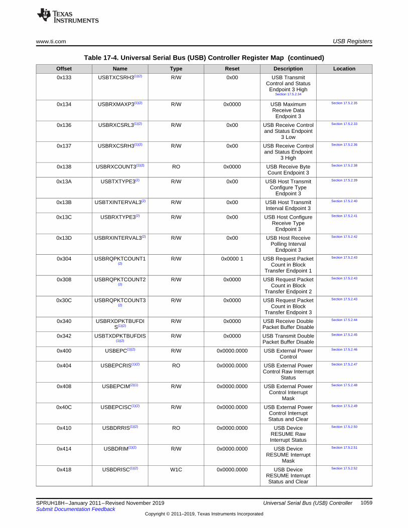
www.ti.com USB Registers
1059SPRUH18H–January 2011–Revised November 2019Submit Documentation Feedback
Copyright © 2011–2019, Texas Instruments Incorporated
Universal Serial Bus (USB) Controller
Table 17-4. Universal Serial Bus (USB) Controller Register Map (continued)Offset Name Type Reset Description Location0x133 USBTXCSRH3(1)(2) R/W 0x00 USB Transmit
Control and StatusEndpoint 3 High
Section 17.5.2.34
0x134 USBRXMAXP3(1)(2) R/W 0x0000 USB MaximumReceive Data
Endpoint 3
Section 17.5.2.35
0x136 USBRXCSRL3(1)(2) R/W 0x00 USB Receive Controland Status Endpoint
3 Low
Section 17.5.2.33
0x137 USBRXCSRH3(1)(2) R/W 0x00 USB Receive Controland Status Endpoint
3 High
Section 17.5.2.36
0x138 USBRXCOUNT3(1)(2) RO 0x0000 USB Receive ByteCount Endpoint 3
Section 17.5.2.38
0x13A USBTXTYPE3(2) R/W 0x00 USB Host TransmitConfigure Type
Endpoint 3
Section 17.5.2.39
0x13B USBTXINTERVAL3(2) R/W 0x00 USB Host TransmitInterval Endpoint 3
Section 17.5.2.40
0x13C USBRXTYPE3(2) R/W 0x00 USB Host ConfigureReceive Type
Endpoint 3
Section 17.5.2.41
0x13D USBRXINTERVAL3(2) R/W 0x00 USB Host ReceivePolling Interval
Endpoint 3
Section 17.5.2.42
0x304 USBRQPKTCOUNT1(2)
R/W 0x0000 1 USB Request PacketCount in Block
Transfer Endpoint 1
Section 17.5.2.43
0x308 USBRQPKTCOUNT2(2)
R/W 0x0000 USB Request PacketCount in Block
Transfer Endpoint 2
Section 17.5.2.43
0x30C USBRQPKTCOUNT3(2)
R/W 0x0000 USB Request PacketCount in Block
Transfer Endpoint 3
Section 17.5.2.43
0x340 USBRXDPKTBUFDIS(1)(2)
R/W 0x0000 USB Receive DoublePacket Buffer Disable
Section 17.5.2.44
0x342 USBTXDPKTBUFDIS(1)(2)
R/W 0x0000 USB Transmit DoublePacket Buffer Disable
Section 17.5.2.45
0x400 USBEPC(1)(2) R/W 0x0000.0000 USB External PowerControl
Section 17.5.2.46
0x404 USBEPCRIS(1)(2) RO 0x0000.0000 USB External PowerControl Raw Interrupt
Status
Section 17.5.2.47
0x408 USBEPCIM(2)(1) R/W 0x0000.0000 USB External PowerControl Interrupt
Mask
Section 17.5.2.48
0x40C USBEPCISC(1)(2) R/W 0x0000.0000 USB External PowerControl InterruptStatus and Clear
Section 17.5.2.49
0x410 USBDRRIS(1)(2) RO 0x0000.0000 USB DeviceRESUME RawInterrupt Status
Section 17.5.2.50
0x414 USBDRIM(1)(2) R/W 0x0000.0000 USB DeviceRESUME Interrupt
Mask
Section 17.5.2.51
0x418 USBDRISC(1)(2) W1C 0x0000.0000 USB DeviceRESUME InterruptStatus and Clear
Section 17.5.2.52

USB Registers www.ti.com
1060 SPRUH18H–January 2011–Revised November 2019Submit Documentation Feedback
Copyright © 2011–2019, Texas Instruments Incorporated
Universal Serial Bus (USB) Controller
Table 17-4. Universal Serial Bus (USB) Controller Register Map (continued)Offset Name Type Reset Description Location0x41C USBGPCS(1)(2) R/W 0x0000.0000 USB General-
Purpose Control andStatus
Section 17.5.2.53
0x450 USBDMASEL(1)(2) R/W 0x0033.2211 USB DMA Select Section 17.5.2.54
(1) This register is used in Device mode. Some registers are used for both Host and Device mode and may have different bitdefinitions depending on the mode.
(2) This register is used in Host mode. Some registers are used for both Host and Device mode and may have different bitdefinitions depending on the mode. The USB controller is in Device mode upon reset, so the reset values shown for theseregisters apply to the Device mode definition.

www.ti.com USB Registers
1061SPRUH18H–January 2011–Revised November 2019Submit Documentation Feedback
Copyright © 2011–2019, Texas Instruments Incorporated
Universal Serial Bus (USB) Controller
17.5.2 Register Descriptions
17.5.2.1 USB Device Functional Address Register (USBFADDR), offset 0x000The USB function address 8-bit register (USBFADDR) contains the 7-bit address of the device part of thetransaction.
When the USB controller is being used in device mode (the HOST bit in the USBDEVCTL register isclear), this register must be written with the address received through a SET_ADDRESS command, whichis then used for decoding the function address in subsequent token packets.
Mode(s): Device
For special considerations when writing this register, see the Setting the Device Address inSection 17.3.1.1.4.
USBFADDR is shown in Figure 17-3 and described in Table 17-5.
Figure 17-3. Function Address Register (USBFADDR)7 6 0
Reserved FUNCADDRR-0 R/W-0
LEGEND: R/W = Read/Write; -n = value after reset
Table 17-5. Function Address Register (USBFADDR) Field Descriptions
Bit Field Value Description7 Reserved 0 Reserved
6-0 FUNCADDR 0-7Fh Function Address of Device as received through SET_ADDRESS.
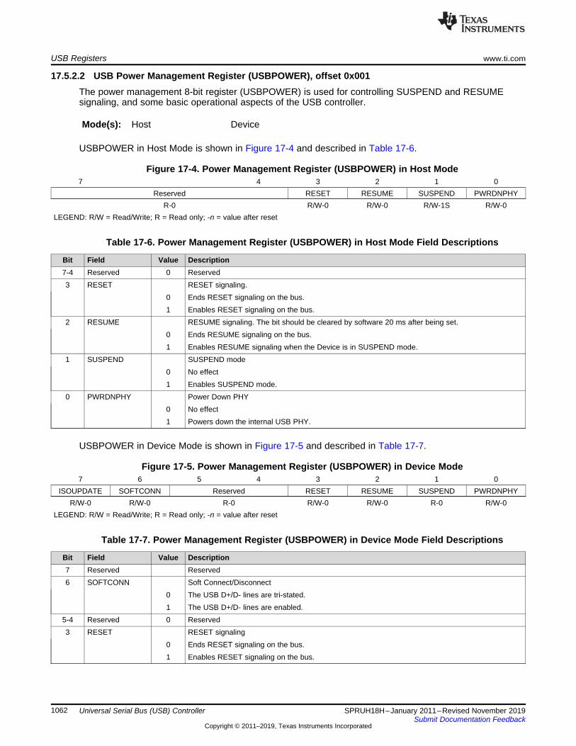
USB Registers www.ti.com
1062 SPRUH18H–January 2011–Revised November 2019Submit Documentation Feedback
Copyright © 2011–2019, Texas Instruments Incorporated
Universal Serial Bus (USB) Controller
17.5.2.2 USB Power Management Register (USBPOWER), offset 0x001The power management 8-bit register (USBPOWER) is used for controlling SUSPEND and RESUMEsignaling, and some basic operational aspects of the USB controller.
Mode(s): Host Device
USBPOWER in Host Mode is shown in Figure 17-4 and described in Table 17-6.
Figure 17-4. Power Management Register (USBPOWER) in Host Mode7 4 3 2 1 0
Reserved RESET RESUME SUSPEND PWRDNPHYR-0 R/W-0 R/W-0 R/W-1S R/W-0
LEGEND: R/W = Read/Write; R = Read only; -n = value after reset
Table 17-6. Power Management Register (USBPOWER) in Host Mode Field Descriptions
Bit Field Value Description7-4 Reserved 0 Reserved3 RESET RESET signaling.
0 Ends RESET signaling on the bus.1 Enables RESET signaling on the bus.
2 RESUME RESUME signaling. The bit should be cleared by software 20 ms after being set.0 Ends RESUME signaling on the bus.1 Enables RESUME signaling when the Device is in SUSPEND mode.
1 SUSPEND SUSPEND mode0 No effect1 Enables SUSPEND mode.
0 PWRDNPHY Power Down PHY0 No effect1 Powers down the internal USB PHY.
USBPOWER in Device Mode is shown in Figure 17-5 and described in Table 17-7.
Figure 17-5. Power Management Register (USBPOWER) in Device Mode7 6 5 4 3 2 1 0
ISOUPDATE SOFTCONN Reserved RESET RESUME SUSPEND PWRDNPHYR/W-0 R/W-0 R-0 R/W-0 R/W-0 R-0 R/W-0
LEGEND: R/W = Read/Write; R = Read only; -n = value after reset
Table 17-7. Power Management Register (USBPOWER) in Device Mode Field Descriptions
Bit Field Value Description7 Reserved Reserved6 SOFTCONN Soft Connect/Disconnect
0 The USB D+/D- lines are tri-stated.1 The USB D+/D- lines are enabled.
5-4 Reserved 0 Reserved3 RESET RESET signaling
0 Ends RESET signaling on the bus.1 Enables RESET signaling on the bus.

www.ti.com USB Registers
1063SPRUH18H–January 2011–Revised November 2019Submit Documentation Feedback
Copyright © 2011–2019, Texas Instruments Incorporated
Universal Serial Bus (USB) Controller
Table 17-7. Power Management Register (USBPOWER) in Device Mode Field Descriptions (continued)Bit Field Value Description2 RESUME RESUME signaling. The bit should be cleared by software 10 ms (a maximum of 15 ms) after being
set.0 Ends RESUME signaling on the bus.1 Enables RESUME signaling when the Device is in SUSPEND mode.
1 SUSPEND SUSPEND mode.0 This bit is cleared when software reads the interrupt register or sets the RESUME bit above.1 The USB controller is in SUSPEND mode.
0 PWRDNPHY Power Down PHY0 No effect1 Powers down the internal USB PHY.

USB Registers www.ti.com
1064 SPRUH18H–January 2011–Revised November 2019Submit Documentation Feedback
Copyright © 2011–2019, Texas Instruments Incorporated
Universal Serial Bus (USB) Controller
17.5.2.3 USB Transmit Interrupt Status Register (USBTXIS), offset 0x002
NOTE: Use caution when reading this register. Performing a read may change bit status.
The USB transmit interrupt status 16-bit read-only register (USBTXIS) indicates which interrupts arecurrently active for control endpoint 0 and the transmit endpoints 1–3. The meaning of the EPn bits in thisregister is based on the mode of the device. The EP1 through EP3 bits always indicate that the USBcontroller is sending data; however, in Host mode, the bits refer to OUT endpoints; while in Device mode,the bits refer to IN endpoints.
Note:The EP0 bit is special in Host and Device modes and indicates that either a control IN or controlOUT endpoint has generated an interrupt. Both the control IN and control OUT endpoints are captured inthe EP0 bit of the USBTXIS register.
Mode(s): Host Device
USBTXIS is shown in Figure 17-6 and described in Table 17-8.
Figure 17-6. USB Transmit Interrupt Status Register (USBTXIS)15 4 3 2 1 0
Reserved EP3 EP2 EP1 EP0R-0 R-0 R-0 R-0 R-0
LEGEND: R/W = Read/Write; R = Read only; -n = value after reset sho
Table 17-8. USB Transmit Interrupt Status Register (USBTXIS) Field Descriptions
Bit Field Value Description15-4 Reserved Reserved
3 EP3 TX Endpoint 3 Interrupt0 No interrupt1 The Endpoint 3 transmit interrupt is asserted.
2 EP2 TX Endpoint 2 Interrupt0 No interrupt1 The Endpoint 2 transmit interrupt is asserted.
1 EP1 TX Endpoint 1 Interrupt0 No interrupt1 The Endpoint 1 transmit interrupt is asserted.
0 EP0 TX and RX Endpoint 0 Interrupt0 No interrupt1 The Endpoint 0 transmit or receive interrupt is asserted.

www.ti.com USB Registers
1065SPRUH18H–January 2011–Revised November 2019Submit Documentation Feedback
Copyright © 2011–2019, Texas Instruments Incorporated
Universal Serial Bus (USB) Controller
17.5.2.4 USB Receive Interrupt Status Register (USBRXIS), offset 0x004
NOTE: Use caution when reading this register. Performing a read may change bit status.
The USB receive interrupt status 16-bit read-only register (USBRXIS) indicates which interrupts arecurrently active for receive endpoints 1–3.
Note: The USBRXIS register does not have a bit for EP0. See the USBTXIS register for EP0 use.
Note: Bits relating to endpoints that have not been configured always return 0. All active interrupts arecleared when this register is read.
Mode(s): Host Device
USBRXIS is shown in Figure 17-7 and described in Table 17-9.
Figure 17-7. USB Receive Interrupt Status Register (USBRXIS)15 4 3 2 1 0
Reserved EP3 EP2 EP1 RsvdR-0 R-0 R-0 R-0 R-0
LEGEND: R/W = Read/Write; R = Read only; -n = value after reset
Table 17-9. USB Receive Interrupt Status Register (USBRXIS) Field Descriptions
Bit Field Value Description15-4 Reserved Reserved
3 EP3 RX Endpoint 3 Interrupt0 No interrupt1 The Endpoint 3 receive interrupt is asserted.
2 EP2 RX Endpoint 2 Interrupt0 No interrupt1 The Endpoint 2 receive interrupt is asserted.
1 EP1 RX Endpoint 1 Interrupt0 No interrupt1 The Endpoint 1 receive interrupt is asserted.
0 Reserved 0 Reserved

USB Registers www.ti.com
1066 SPRUH18H–January 2011–Revised November 2019Submit Documentation Feedback
Copyright © 2011–2019, Texas Instruments Incorporated
Universal Serial Bus (USB) Controller
17.5.2.5 USB Transmit Interrupt Enable Register (USBTXIE), offset 0x006The USB transmit interrupt enable 16-bit register (USBTXIE) provides interrupt enable bits for theinterrupts in the USBTXIS register. When a bit is set, the USB interrupt is asserted to the interruptcontroller when the corresponding interrupt bit in the USBTXIS register is set. When a bit is cleared, theinterrupt in the USBTXIS register is still set but the USB interrupt to the interrupt controller is not asserted.On reset, all interrupts are enabled.
Note:The EP0 bit is special in Host and Device modes. Both the control IN and control OUT endpoints arecaptured in the EP0 bit of the USBTXIE register.
Mode(s): Host Device
USBTXIS is shown in Figure 17-8 and described in Table 17-10.
Figure 17-8. USB Transmit Interrupt Status Enable Register (USBTXIE)15 4 3 2 1 0
Reserved EP3 EP2 EP1 EP0R-0 R/W-1 R/W-1 R/W-1 R/W-1
LEGEND: R/W = Read/Write; R = Read only; -n = value after reset
Table 17-10. USB Transmit Interrupt Status Register (USBTXIE) Field Descriptions
Bit Field Value DescriptionReserved15-4 Reserved
3 EP3 0 TX Endpoint 3 Interrupt EnableThe EP3 transmit interrupt is suppressed and not sent to the interrupt controller.
1 An interrupt is sent to the interrupt controller when the EP3 bit in the USBTXIS register is set.2 EP2 TX Endpoint 2 Interrupt Enable
0 The EP2 transmit interrupt is suppressed and not sent to the interrupt controller.1 An interrupt is sent to the interrupt controller when the EP2 bit in the USBTXIS register is set.
1 EP1 TX Endpoint 1 Interrupt Enable0 The EP1 transmit interrupt is suppressed and not sent to the interrupt controller.1 An interrupt is sent to the interrupt controller when the EP1 bit in the USBTXIS register is set.
0 EP0 TX and RX Endpoint 0 Interrupt Enable0 The EP0 transmit and receive interrupt is suppressed and not sent to the interupt controller.1 An interrupt is sent to the interrupt controller when the EP0 bit in the USBTXIS register is set.

www.ti.com USB Registers
1067SPRUH18H–January 2011–Revised November 2019Submit Documentation Feedback
Copyright © 2011–2019, Texas Instruments Incorporated
Universal Serial Bus (USB) Controller
17.5.2.6 USB Receive Interrupt Enable Register (USBRXIE), offset 0x008The USB receive interrupt enable 16-bit register (USBRXIE) provides interrupt enable bits for theinterrupts in the USBRXIS register. When a bit is set, the USB interrupt is asserted to the interruptcontroller when the corresponding interrupt bit in the USBRXIS register is set. When a bit is cleared, theinterrupt in the USBRXIS register is still set but the USB interrupt to the interrupt controller is not asserted.On reset, all interrupts are enabled.
Note: The USBRXIE register does not have a bit for EP0. See the USBTXIE register for EP0 use.
Mode(s): Host Device
USBRXIE is shown in Figure 17-8 and described in Table 17-10.
Figure 17-9. USB Receive Interrupt Enable Register (USBRXIE)15 4 3 2 1 0
Reserved EP3 EP2 EP1 RsvdR-0 R/W-1 R/W-1 R/W-1 R-0
LEGEND: R/W = Read/Write; R = Read only; -n = value after reset
Table 17-11. USB Receive Interrupt Register (USBRXIE) Field Descriptions
Bit Field Value Description15-4 Reserved Reserved
3 EP3 RX Endpoint 3 Interrupt Enable0 The EP3 receive interrupt is suppressed and not sent to the interrupt controller.1 An interrupt is sent to the interrupt controller when the EP3 bit in the USBRXIS register is set.
2 EP2 RX Endpoint 2 Interrupt Enable0 The EP2 receive interrupt is suppressed and not sent to the interrupt controller.1 An interrupt is sent to the interrupt controller when the EP2 bit in the USBRXIS register is set.
1 EP1 RX Endpoint 1 Interrupt Enable0 The EP1 receive interrupt is suppressed and not sent to the interrupt controller.1 An interrupt is sent to the interrupt controller when the EP1 bit in the USBRXIS register is set.
0 Reserved 0 Reserved

USB Registers www.ti.com
1068 SPRUH18H–January 2011–Revised November 2019Submit Documentation Feedback
Copyright © 2011–2019, Texas Instruments Incorporated
Universal Serial Bus (USB) Controller
17.5.2.7 USB General Interrupt Status Register (USBIS), offset 0x00A
NOTE: Use caution when reading this register. Performing a read may change bit status.
The USB general interrupt status 8-bit read-only register (USBIS) indicates which USB interrupts arecurrently active. All active interrupts are cleared when this register is read.
Mode(s): Host Device
USBIS in Host Mode is shown in Figure 17-10 and described in Table 17-12.
Figure 17-10. USB General Interrupt Status Register (USBIS) in Host Mode7 6 5 4 3 2 1 0
VBUSERR SESREQ DISCON CONN SOF BABBLE RESUME ReservedR-0 R-0 R-0 R-0 R-0 R-0 R-0 R-0
LEGEND: R/W = Read/Write; R = Read only; -n = value after reset
Table 17-12. USB General Interrupt Status Register (USBIS) in Host Mode Field Descriptions
Bit Field Value Description7 VBUSERR VBUS Error
0 No interrupt1 VBUS has dropped below the VBUS Valid threshold during a session.
6 SESREQ Session Request0 No interrupt1 SESSION REQUEST signaling has been detected.
5 DISCON Session Disconnect0 No interrupt1 A Device disconnect has been detected.
4 CONN Session Connect0 No interrupt1 A Device connection has been detected.
3 SOF Start of Frame0 No interrupt1 A new frame has started.
2 BABBLE Babble Detected0 No interrupt1 Babble has been detected. This interrupt is active only after the first SOF has been sent.
1 RESUME RESUME Signaling Detected. This interrupt can only be used if the USB controller's system clock isenabled. If the user disables the clock programming, the USBDRRIS, USBDRIM, and USBDRISCregisters should be used.
0 No effect1 RESUME signaling has been detected on the bus while the USB controller is in SUSPEND mode.
0 Reserved 0 Reserved

www.ti.com USB Registers
1069SPRUH18H–January 2011–Revised November 2019Submit Documentation Feedback
Copyright © 2011–2019, Texas Instruments Incorporated
Universal Serial Bus (USB) Controller
USBIS in Device Mode is shown in Figure 17-11 and described in Table 17-13.
Figure 17-11. USB General Interrupt Status Register (USBIS) in Device Mode7 6 5 4 3 2 1 0
Reserved DISCON Reserved SOF RESET RESUME SUSPENDR-0 R-0 R-0 R-0 R-0 R-0 R-0
LEGEND: R/W = Read/Write; R = Read only; -n = value after reset
Table 17-13. USB General Interrupt Status Register (USBIS) in Device Mode Field Descriptions
Bit Field Value Description7-6 Reserved 0 Reserved5 DISCON Session Disconnect
0 No interrupt1 The device has been disconnected from the host.
4 Reserved 0 Reserved3 SOF Start of frame
0 No interrupt1 A new frame has started.
2 RESET RESET Signaling Detected0 No interrupt1 RESET signaling has been detected on the bus.
1 RESUME RESUME Signaling Detected. This interrupt can only be used if the USB controller's system clock isenabled. If the user disables the clock programming, the USBDRRIS, USBDRIM, and USBDRISCregisters should be used.
0 No interrupt1 RESUME signaling has been detected on the bus while the USB controller is in SUSPEND mode.
0 SUSPEND SUSPEND Signaling Detected0 No interrupt1 SUSPEND signaling has been detected on the bus.
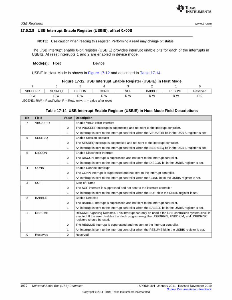
USB Registers www.ti.com
1070 SPRUH18H–January 2011–Revised November 2019Submit Documentation Feedback
Copyright © 2011–2019, Texas Instruments Incorporated
Universal Serial Bus (USB) Controller
17.5.2.8 USB Interrupt Enable Register (USBIE), offset 0x00B
NOTE: Use caution when reading this register. Performing a read may change bit status.
The USB interrupt enable 8-bit register (USBIE) provides interrupt enable bits for each of the interrupts inUSBIS. At reset interrupts 1 and 2 are enabled in device mode.
Mode(s): Host Device
USBIE in Host Mode is shown in Figure 17-12 and described in Table 17-14.
Figure 17-12. USB Interrupt Enable Register (USBIE) in Host Mode7 6 5 4 3 2 1 0
VBUSERR SESREQ DISCON CONN SOF BABBLE RESUME ReservedR-W R-W R-W R-W R-W R-W R-W R-0
LEGEND: R/W = Read/Write; R = Read only; -n = value after reset
Table 17-14. USB Interrupt Enable Register (USBIE) in Host Mode Field Descriptions
Bit Field Value Description7 VBUSERR Enable VBUS Error Interrupt
0 The VBUSERR interrupt is suppressed and not sent to the interrupt controller.1 An interrupt is sent to the interrupt controller when the VBUSERR bit in the USBIS register is set.
6 SESREQ Enable Session Request0 The SESREQ interrupt is suppressed and not sent to the interrupt controller.1 An interrupt is sent to the interrupt controller when the SESREEQ bit in the USBIS register is set.
5 DISCON Enable Disconnect Interrupt0 The DISCON interrupt is suppressed and not sent to the interrupt controller.1 An interrupt is sent to the interrupt controller when the DISCON bit in the USBIS register is set.
4 CONN Enable Connect Interrupt0 The CONN interrupt is suppressed and not sent to the interrupt controller.1 An interrupt is sent to the interrupt controller when the CONN bit in the USBIS register is set.
3 SOF Start of Frame0 The SOF interrupt is suppressed and not sent to the interrupt controller.1 An interrupt is sent to the interrupt controller when the SOF bit in the USBIS register is set.
2 BABBLE Babble Detected0 The BABBLE interrupt is suppressed and not sent to the interrupt controller.1 An interrupt is sent to the interrupt controller when the BABBLE bit in the USBIS register is set.
1 RESUME RESUME Signaling Detected. This interrupt can only be used if the USB controller's system clock isenabled. If the user disables the clock programming, the USBDRRIS, USBDRIM, and USBDRISCregisters should be used.
0 The RESUME interrupt is suppressed and not sent to the interrupt controller.1 An interrupt is sent to the interrupt controller when the RESUME bit in the USBIS register is set.
0 Reserved 0 Reserved

www.ti.com USB Registers
1071SPRUH18H–January 2011–Revised November 2019Submit Documentation Feedback
Copyright © 2011–2019, Texas Instruments Incorporated
Universal Serial Bus (USB) Controller
USBIE in Device Mode is shown in Figure 17-11 and described in Table 17-13.
Figure 17-13. USB Interrupt Enable Register (USBIE) in Device Mode7 6 5 4 3 2 1 0
Reserved DISCON Reserved SOF RESET RESUME SUSPENDR-0 R/W-0 R-0 R/W-0 R/W-1 RW-1 R/W-0
LEGEND: R/W = Read/Write; R = Read only; -n = value after reset
Table 17-15. USB Interrupt Enable Register (USBIE) in Device Mode Field Descriptions
Bit Field Value Description7-6 Reserved 0 Reserved5 DISCON Enable Disconnect Interrupt
0 The DISCON interrupt is suppressed and not sent to the interrupt controller.1 An interrupt is sent to the interrupt controller when the DISCON bit in the USBIS register is set.
4 Reserved 0 Reserved3 SOF Start of frame
0 The SOF interrupt is suppressed and not sent to the interrupt controller.1 An interrupt is sent to the interrupt controller when the SOF bit in the USBIS register is set.
2 RESET RESET Signaling Detected0 The RESET interrupt is suppressed and not sent to the interrupt controller.1 An interrupt is sent to the interrupt controller when the RESET bit in the USBIS register is set.
1 RESUME RESUME Signaling Detected. This interrupt can only be used if the USB controller's system clock isenabled. If the user disables the clock programming, the USBDRRIS, USBDRIM, and USBDRISCregisters should be used.
0 The RESUME interrupt is suppressed and not sent to the interrupt controller.1 An interrupt is sent to the interrupt controller when the RESUME bit in the USBIS register is set.
0 SUSPEND SUSPEND Signaling Detected0 The SUSPEND interrupt is suppressed and not sent to the interrupt controller.1 An interrupt is sent to the interrupt controller when the DISCON bit in the USBIS register is set.
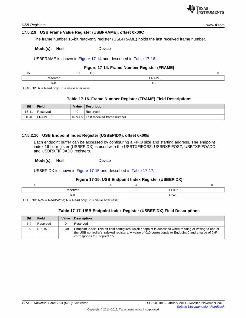
USB Registers www.ti.com
1072 SPRUH18H–January 2011–Revised November 2019Submit Documentation Feedback
Copyright © 2011–2019, Texas Instruments Incorporated
Universal Serial Bus (USB) Controller
17.5.2.9 USB Frame Value Register (USBFRAME), offset 0x00CThe frame number 16-bit read-only register (USBFRAME) holds the last received frame number.
Mode(s): Host Device
USBFRAME is shown in Figure 17-14 and described in Table 17-16.
Figure 17-14. Frame Number Register (FRAME)15 11 10 0
Reserved FRAMER-0 R-0
LEGEND: R = Read only; -n = value after reset
Table 17-16. Frame Number Register (FRAME) Field Descriptions
Bit Field Value Description15-11 Reserved 0 Reserved10-0 FRAME 0-7FFh Last received frame number
17.5.2.10 USB Endpoint Index Register (USBEPIDX), offset 0x00EEach endpoint buffer can be accessed by configuring a FIFO size and starting address. The endpointindex 16-bit register (USBEPIDX) is used with the USBTXFIFOSZ, USBRXFIFOSZ, USBTXFIFOADD,and USBRXFIFOADD registers.
Mode(s): Host Device
USBEPIDX is shown in Figure 17-15 and described in Table 17-17.
Figure 17-15. USB Endpoint Index Register (USBEPIDX)7 4 3 0
Reserved EPIDXR-0 R/W-0
LEGEND: R/W = Read/Write; R = Read only; -n = value after reset
Table 17-17. USB Endpoint Index Register (USBEPIDX) Field Descriptions
Bit Field Value Description7-4 Reserved 0 Reserved3-0 EPIDX 0-4h Endpoint Index. This bit field configures which endpoint is accessed when reading or writing to one of
the USB controller's indexed registers. A value of 0x0 corresponds to Endpoint 0 and a value of 0xFcorresponds to Endpoint 15.

www.ti.com USB Registers
1073SPRUH18H–January 2011–Revised November 2019Submit Documentation Feedback
Copyright © 2011–2019, Texas Instruments Incorporated
Universal Serial Bus (USB) Controller
17.5.2.11 USB Test Mode Register (USBTEST), offset 0x00FThe USB test mode 8-bit register (USBTEST) is primarily used to put the USB controller into one of thefour test modes for operation described in the USB Specification 2.0 , in response to a SET FEATURE:USBTESTMODE command. This register is not used in normal operation.
Note: Only one of these bits should be set at any time.
Mode(s): Host Device
USBTEST in Host Mode is shown in Figure 17-16 and described in Table 17-18.
Figure 17-16. USB Test Mode Register (USBTEST) in Host Mode7 6 5 4 0
FORCEH FIFOACC FORCEFS ReservedR/W-0 R/W1S-0 R/W-0 R-0
LEGEND: R/W = Read/Write; W = Write only; -n = value after reset
Table 17-18. USB Test Mode Register (USBTEST) in Host Mode Field Descriptions
Bit Field Value Description7 FORCEH Force Host Mode. While in this mode, status of the bus connection may be read using the DEV
bit of the USBDEVCTL register. The operating speed is determined from the FORCEFS bit.0 No effect1 Forces the USB controller to enter Host mode when the SESSION bit is set, regardless of
whether the USB controller is connected to any peripheral. The state of the USB0DP andUSB0DM signals is ignored. The USB controller then remains in Host mode until the SESSIONbit is cleared, even if a Device is disconnected. If the FORCEH bit remains set, the USBcontroller re-enters Host mode the next time the SESSION bit is set.
6 FIFOACC FIFO Access0 No effect1 Transfers the packet in the endpoint 0 transmit FIFO to the endpoint 0 receive FIFO.
5 FORCEFS Force Full-Speed Mode0 The USB controller operates at Low Speed.1 Forces the USB controller into Full-Speed mode upon receiving a USB RESET.
4-0 Reserved 0 Reserved
USBTEST in Device Mode is shown in Figure 17-17 and described in Table 17-19.
Figure 17-17. USB Test Mode Register (USBTEST) in Device Mode7 6 5 4 0
Reserved FIFOACC FORCEFS ReservedR-0 R/W1S-0 R/W-0 R-0
LEGEND: R/W = Read/Write; W = Write only; -n = value after reset
Table 17-19. USB Test Mode Register (USBTEST) in Device Mode Field Descriptions
Bit Field Value Description7 Reserved Force Host Mode. While in this mode, status of the bus connection may be read using the DEV
bit of the USBDEVCTL register. The operating speed is determined from the FORCEFS bit.6 FIFOACC FIFO Access
0 No effect1 Transfers the packet in the endpoint 0 transmit FIFO to the endpoint 0 receive FIFO.

USB Registers www.ti.com
1074 SPRUH18H–January 2011–Revised November 2019Submit Documentation Feedback
Copyright © 2011–2019, Texas Instruments Incorporated
Universal Serial Bus (USB) Controller
Table 17-19. USB Test Mode Register (USBTEST) in Device Mode Field Descriptions (continued)Bit Field Value Description5 FORCEFS Force Full-Speed Mode
0 The USB controller operates at Low Speed.1 Forces the USB controller into Full-Speed mode upon receiving a USB RESET.
4-0 Reserved 0 Reserved
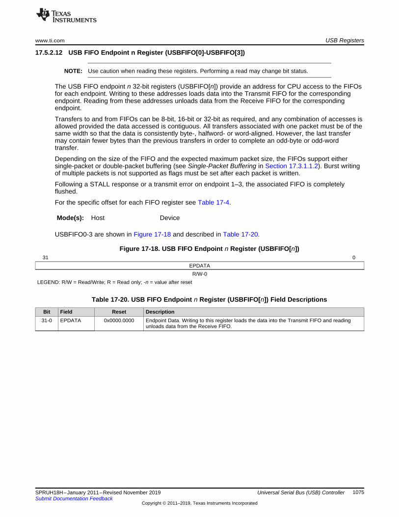
www.ti.com USB Registers
1075SPRUH18H–January 2011–Revised November 2019Submit Documentation Feedback
Copyright © 2011–2019, Texas Instruments Incorporated
Universal Serial Bus (USB) Controller
17.5.2.12 USB FIFO Endpoint n Register (USBFIFO[0]-USBFIFO[3])
NOTE: Use caution when reading these registers. Performing a read may change bit status.
The USB FIFO endpoint n 32-bit registers (USBFIFO[n]) provide an address for CPU access to the FIFOsfor each endpoint. Writing to these addresses loads data into the Transmit FIFO for the correspondingendpoint. Reading from these addresses unloads data from the Receive FIFO for the correspondingendpoint.
Transfers to and from FIFOs can be 8-bit, 16-bit or 32-bit as required, and any combination of accesses isallowed provided the data accessed is contiguous. All transfers associated with one packet must be of thesame width so that the data is consistently byte-, halfword- or word-aligned. However, the last transfermay contain fewer bytes than the previous transfers in order to complete an odd-byte or odd-wordtransfer.
Depending on the size of the FIFO and the expected maximum packet size, the FIFOs support eithersingle-packet or double-packet buffering (see Single-Packet Buffering in Section 17.3.1.1.2). Burst writingof multiple packets is not supported as flags must be set after each packet is written.
Following a STALL response or a transmit error on endpoint 1–3, the associated FIFO is completelyflushed.
For the specific offset for each FIFO register see Table 17-4.
Mode(s): Host Device
USBFIFO0-3 are shown in Figure 17-18 and described in Table 17-20.
Figure 17-18. USB FIFO Endpoint n Register (USBFIFO[n])31 0
EPDATAR/W-0
LEGEND: R/W = Read/Write; R = Read only; -n = value after reset
Table 17-20. USB FIFO Endpoint n Register (USBFIFO[n]) Field Descriptions
Bit Field Reset Description31-0 EPDATA 0x0000.0000 Endpoint Data. Writing to this register loads the data into the Transmit FIFO and reading
unloads data from the Receive FIFO.

USB Registers www.ti.com
1076 SPRUH18H–January 2011–Revised November 2019Submit Documentation Feedback
Copyright © 2011–2019, Texas Instruments Incorporated
Universal Serial Bus (USB) Controller
17.5.2.13 USB Device Control Register (USBDEVCTL), offset 0x060The USB device control 8-bit register (USBDEVCTL) is used for controlling and monitoring the USB VBUSline. If the PHY is suspended, no PHY clock is received and the VBUS is not sampled. In addition, in Hostmode, USBDEVCTL provides the status information for the current operating mode (Host or Device) of theUSB controller. If the USB controller is in Host mode, this register also indicates if a full- or low-speedDevice has been connected.
Mode(s): Host Device
USBDEVCTL is shown in Figure 17-19 and described in Table 17-21.
Figure 17-19. USB Device Control Register (USBDEVCTL)7 6 5 4 3 2 1 0
DEV FSDEV LSDEV VBUS HOSTMODE HOSTREQ SESSIONR-1 R-0 R-0 R-0 R-0 R/W-0 R/W-0
LEGEND: R/W = Read/Write; R = Read only; -n = value after reset
Table 17-21. USB Device Control Register (USBDEVCTL) Field Descriptions
Bit Field Value Description7 DEV Device mode
0 The USB controller is operating on the OTG A side of the cable.1 The USB controller is operating on the OTG B side of the cable.
Only valid while a session is in progress.6 FSDEV Full-Speed Device Detected
0 A full-speed Device has not been detected on the port.1 A full-speed Device has been detected on the port.
5 LSDEV Low-Speed Device Detected0 A low-speed Device has not been detected on the port.1 A low-speed Device has been detected on the port.
4-3 VBUS 0-3h These read-only bits encode the current VBus level as follows:0 Below Session End. VBUS is detected as under 0.5 V.1h Above Session End, below AValid. VBUS is detected as above 0.5 V and under 1.5 V.2h Above AValid, below VBusValid. VBUS is detected as above 1.5 V and below 4.75 V.3h Above VBusValid. VBUS is detected as above 4.75 V.
2 HOSTMODE This read-only bit is set when the USB controller is acting as a Host.0 The USB controller is acting as a Device.1 The USB controller is acting as a Host.
Only valid while a session is in progress.1 HOSTREQ When set, the USB controller will initiate the Host Negotiation when Suspend mode is entered. It is
cleared when Host Negotiation is completed.0 No effect1 Initiates the Host Negotiation when SUSPENDmode is entered.
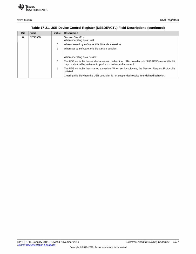
www.ti.com USB Registers
1077SPRUH18H–January 2011–Revised November 2019Submit Documentation Feedback
Copyright © 2011–2019, Texas Instruments Incorporated
Universal Serial Bus (USB) Controller
Table 17-21. USB Device Control Register (USBDEVCTL) Field Descriptions (continued)Bit Field Value Description0 SESSION Session Start/End
When operating as a Host:0 When cleared by software, this bit ends a session.1 When set by software, this bit starts a session.
When operating as a Device:0 The USB controller has ended a session. When the USB controller is in SUSPEND mode, this bit
may be cleared by software to perform a software disconnect.1 The USB controller has started a session. When set by software, the Session Request Protocol is
initiated.Clearing this bit when the USB controller is not suspended results in undefined behavior.

USB Registers www.ti.com
1078 SPRUH18H–January 2011–Revised November 2019Submit Documentation Feedback
Copyright © 2011–2019, Texas Instruments Incorporated
Universal Serial Bus (USB) Controller
17.5.2.14 USB Transmit Dynamic FIFO Sizing Register (USBTXFIFOSZ), offset 0x062The USB transmit dynamic FIFO sizing 8-bit register (USBTXFIFOSZ) allows the selected TX endpointFIFOs to be dynamically sized. USBEPIDX is used to configure each transmit endpoint's FIFO size.
Mode(s): Host Device
USBTXFIFOSZ is shown in Figure 17-20 and described in Table 17-22.
Figure 17-20. USB Transmit Dynamic FIFO Sizing Register (USBTXFIFOSZ)7 5 4 3 0
Reserved DPB SZR-0 R/W-0 R-0
LEGEND: R/W = Read/Write; R = Read only; -n = value after reset
Table 17-22. USB Transmit Dynamic FIFO Sizing Register (USBTXFIFOSZ) Field Descriptions
Bit Field Value Description7-5 Reserved 0 Reserved4 DPB Double Packet Buffering Support
0 Single packet buffering is supported.1 Double packet buffering is enabled.
3-0 SZ Maximum packet size to be allowed. If DPB = 0, the FIFO also is this size; if DPB = 1, the FIFO is twicethis size. Packet size in bytes:
0h 81h 162h 323h 644h 1285h 2566h 5127h 10248h 2048
9-Fh Reserved

www.ti.com USB Registers
1079SPRUH18H–January 2011–Revised November 2019Submit Documentation Feedback
Copyright © 2011–2019, Texas Instruments Incorporated
Universal Serial Bus (USB) Controller
17.5.2.15 USB Receive Dynamic FIFO Sizing Register (USBRXFIFOSZ), offset 0x063The USB receive dynamic FIFO sizing 8-bit register (USBRXFIFOSZ) allows the selected RX endpointFIFOs to be dynamically sized.
Mode(s): Host Device
USBRXFIFOSZ is shown in Figure 17-21 and described in Table 17-23.
Figure 17-21. USB Receive Dynamic FIFO Sizing Register (USBRXFIFOSZ)7 5 4 3 0
Reserved DPB SZR-0 R/W-0 R-0
LEGEND: R/W = Read/Write; R = Read only; -n = value after reset
Table 17-23. USB Receive Dynamic FIFO Sizing Register (USBRXFIFOSZ) Field Descriptions
Bit Field Value Description7-5 Reserved 0 Reserved4 DPB Double Packet Buffering Support
0 Single packet buffering is supported.1 Double packet buffering is enabled.
3-0 SZ Maximum packet size to be allowed. If DPB = 0, the FIFO also is this size; if DPB = 1, the FIFO is twicethis size. Packet size in bytes:
0h 81h 162h 323h 644h 1285h 2566h 5127h 10248h 2048
9-Fh Reserved

USB Registers www.ti.com
1080 SPRUH18H–January 2011–Revised November 2019Submit Documentation Feedback
Copyright © 2011–2019, Texas Instruments Incorporated
Universal Serial Bus (USB) Controller
17.5.2.16 USB Transmit FIFO Start Address Register (USBTXFIFOADD), offset 0x064The USB transmit FIFO start address 16-bit register (USBTXFIFOADD) controls the start address of theselected transmit endpoint FIFOs.
Mode(s): Host Device
USBTXFIFOADDR is shown in Figure 17-22 and described in Table 17-24.
Figure 17-22. USB Transmit FIFO Start Address Register (USBTXFIFOADDR])15 9 8 0
Reserved ADDRR-0 R/W-0
LEGEND: R/W = Read/Write; R = Read only; -n = value after reset
Table 17-24. USB Transmit FIFO Start Address Register (USBTXFIFOADDR) Field Descriptions
Bit Field Value Description15-9 Reserved 0 Reserved8-0 ADDR Start Address of the endpoint FIFO in units of 8 bytes.
0h 01h 82h 163h 244h 325h 406h 487h 568h 64.. ..
1FFh 4095

www.ti.com USB Registers
1081SPRUH18H–January 2011–Revised November 2019Submit Documentation Feedback
Copyright © 2011–2019, Texas Instruments Incorporated
Universal Serial Bus (USB) Controller
17.5.2.17 USB Receive FIFO Start Address Register (USBRXFIFOADD), offset 0x066The USB receive FIFO start address 16-bit register (USBRXFIFOADD) controls the start address of theselected receive endpoint FIFOs.
Mode(s): Host Device
USBRXFIFOADDR is shown in Figure 17-23 and described in Table 17-25.
Figure 17-23. USB Receive FIFO Start Address Register (USBRXFIFOADDR)15 9 8 0
Reserved ADDRR-0 R/W-0
LEGEND: R/W = Read/Write; R = Read only; -n = value after reset
Table 17-25. USB Receive FIFO Start Address Register (USBRXFIFOADDR) Field Descriptions
Bit Field Value Description15-9 Reserved 0 Reserved8-0 ADDR Start Address of the endpoint FIFO in units of 8 bytes.
0h 01h 82h 163h 244h 325h 406h 487h 568h 64.. ..
1FFh 4095

USB Registers www.ti.com
1082 SPRUH18H–January 2011–Revised November 2019Submit Documentation Feedback
Copyright © 2011–2019, Texas Instruments Incorporated
Universal Serial Bus (USB) Controller
17.5.2.18 USB Connect Timing Register (USBCONTIM), offset 0x07AThe USB connect timing 8-bit configuration register (USBCONTIM) specifies connection and negotiationdelays.
Mode(s): Host Device
USBCONTIM is shown in Figure 17-24 and described in Table 17-26.
Figure 17-24. USB Connect Timing Register (USBCONTIM)7 4 3 0
WTCON WTIDR/W-1 R/W-1
LEGEND: R/W = Read/Write; R = Read only; -n = value after reset
Table 17-26. USB Connect Timing Register (USBCONTIM) Field Descriptions
Bit Field Value Description7-4 WTCON 5h The connect wait field configures the wait required to allow for the user’s connect/disconnect filter, in
units of 533.3 ns. The default corresponds to 2.667 μs.3-0 WTID Ch The wait ID field configures the delay required from the enable of the ID detection to when the ID value
is valid, in units of 4.369 ms. The default corresponds to 52.43 ms.

www.ti.com USB Registers
1083SPRUH18H–January 2011–Revised November 2019Submit Documentation Feedback
Copyright © 2011–2019, Texas Instruments Incorporated
Universal Serial Bus (USB) Controller
17.5.2.19 USB Full-Speed Last Transaction to End of Frame Timing Register (USBFSEOF), offset 0x07DUSB full-speed last transaction to end of frame timing 8-bit configuration register (USBFSEOF) specifiesthe minimum time gap allowed between the start of the last transaction and the EOF for full-speedtransactions.
Mode(s): Host Device
USBFSEOF is shown in Figure 17-25 and described in Table 17-27.
Figure 17-25. USB Full-Speed Last Transaction to End of Frame Timing Register (USBFSEOF)7 0
FSEOFGR/W-0x77
LEGEND: R/W = Read/Write; R = Read only; -n = value after reset
Table 17-27. USB Full-Speed Last Transaction to End of Frame Timing Register(USBFSEOF) Field Descriptions
Bit Field Reset Description7-0 FSEOFG 77h The full-speed end-of-frame gap field is used during full-speed transactions to configure the gap
between the last transaction and the End-of-Frame (EOF), in units of 533.3 ns. The default correspondsto 63.46 μs.
17.5.2.20 USB Low-Speed Last Transaction to End of Frame Timing Register (USBLSEOF), offset 0x07EThe USB low-speed last transaction to end of frame timing 8-bit configuration register (USBLSEOF)specifies the minimum time gap that is to be allowed between the start of the last transaction and the EOFfor low-speed transactions.
Mode(s): Host Device
USBLSEOF is shown in Figure 17-26 and described in Table 17-28.
Figure 17-26. USB Low-Speed Last Transaction to End of Frame Timing Register (USBLSEOF)7 0
LSEOFGR/W-0x72
LEGEND: R/W = Read/Write; R = Read only; -n = value after reset
Table 17-28. USB Low-Speed Last Transaction to End of Frame Timing Register(USBLSEOF) Field Descriptions
Bit Field Reset Description7-0 LSEOFG 72h The low-speed end-of-frame gap field is used during low-speed transactions to set the gap between the
last transaction and the End-of-Frame (EOF), in units of 1.067 μs. The default corresponds to 121.6 μs.

USB Registers www.ti.com
1084 SPRUH18H–January 2011–Revised November 2019Submit Documentation Feedback
Copyright © 2011–2019, Texas Instruments Incorporated
Universal Serial Bus (USB) Controller
17.5.2.21 USB Transmit Functional Address Endpoint n Registers (USBTXFUNCADDR[0]-USBTXFUNCADDR[3])
The transmit functional address endpoint n 8-bit registers (USBTXFUNCADDR[n]) record the address ofthe target function to be accessed through the associated endpoint (EPn). USBTXFUNCADDRx must bedefined for each transmit endpoint that is used.
Note: USBTXFUNCADDR0 is used for both receive and transmit for endpoint 0.
For the specific offset for each register see Table 17-4.
Mode(s): Host
The USBTXFUNCADDR[n] registers are shown in Figure 17-27 and described in Table 17-29.
Figure 17-27. USB Transmit Functional Address Endpoint n Registers (USBTXFUNCADDR[n])7 6 0
Reserved ADDRR-0 R/W-0
LEGEND: R/W = Read/Write; -n = value after reset
Table 17-29. USB Transmit Functional Address Endpoint n Registers(USBTXFUNCADDR[n]) Field Descriptions
Bit Field Value Description7 Reserved 0 Reserved
6-0 ADDR 0 Device Address specifies the USB bus address for the target Device.

www.ti.com USB Registers
1085SPRUH18H–January 2011–Revised November 2019Submit Documentation Feedback
Copyright © 2011–2019, Texas Instruments Incorporated
Universal Serial Bus (USB) Controller
17.5.2.22 USB Transmit Hub Address Endpoint n Registers (USBTXHUBADDR[0]-USBTXHUBADDR[3])The transmit hub address endpoint n 8-bit read/write registers (USBTXHUBADDR[n]), likeUSBTXHUBPORT[n], must be written only when a USB device is connected to transmit endpoint EPn viaa USB 2.0 hub. This register records the address of the USB 2.0 hub through which the target associatedwith the endpoint is accessed.
Note: USBTXHUBADDR0 is used for both receive and transmit for endpoint 0.
For the specific offset for each register see Table 17-4.
Mode(s): Host
The USBTXHUBADDR[n] registers are shown in Figure 17-27 and described in Table 17-29.
Figure 17-28. USB Transmit Hub Address Endpoint n Registers (USBTXHUBADDR[n])7 6 0
Reserved ADDRR-0 R/W-0
LEGEND: R/W = Read/Write; -n = value after reset
Table 17-30. USB Transmit Hub Address Endpoint n Registers(USBTXHUBADDR[n])Field Descriptions
Bit Field Value Description7 Reserved 0 Reserved
6-0 ADDR 0 Device Address specifies the USB bus address for the target Device.

USB Registers www.ti.com
1086 SPRUH18H–January 2011–Revised November 2019Submit Documentation Feedback
Copyright © 2011–2019, Texas Instruments Incorporated
Universal Serial Bus (USB) Controller
17.5.2.23 USB Transmit Hub Port Endpoint n Registers (USBTXHUBPORT[0]-USBTXHUBPORT[3])The transmit hub port endpoint n 8-bit read/write registers (USBTXHUBPORT[n]), likeUSBTXHUBADDR[n], must be written only when a full- or low-speed Device is connected to transmitendpoint EPn via a USB 2.0 hub. This register records the port of the USB 2.0 hub through which thetarget associated with the endpoint is accessed.
Note: USBTXHUBPORT0 is used for both receive and transmit for endpoint 0.
For the specific offset for each register see Table 17-4.
Mode(s): Host
The USBTXHUBPORTn registers are shown in Figure 17-29 and described in Table 17-31.
Figure 17-29. USB Transmit Hub Port Endpoint n Registers (USBTXHUBPORT[n])7 6 0
Reserved PORTR-0 R/W-0
LEGEND: R/W = Read/Write; -n = value after reset
Table 17-31. USB Transmit Hub Port Endpoint n Registers(USBTXHUBPORT[n])Field Descriptions
Bit Field Value Description7 Reserved 0 Reserved
6-0 PORT 0 Hub Port specifies the USB hub port number.

www.ti.com USB Registers
1087SPRUH18H–January 2011–Revised November 2019Submit Documentation Feedback
Copyright © 2011–2019, Texas Instruments Incorporated
Universal Serial Bus (USB) Controller
17.5.2.24 USB Receive Functional Address Endpoint n Registers (USBRXFUNCADDR[1]-USBRXFUNCADDR[3)
The recieve functional address endpoint n 8-bit read/write registers (USBRXFUNCADDR[n]) record theaddress of the target function to be accessed through the associated endpoint (EPn).USBRXFUNCADDRx must be defined for each receive endpoint that is used.
Note: USBTXFUNCADDR0 is used for both receive and transmit for endpoint 0.
For the specific offset for each register see Table 17-4.
Mode(s): Host
The USBRXFUNCADDR[n] registers are shown in Figure 17-30 and described in Table 17-32.
Figure 17-30. USB Receive Functional Address Endpoint n Registers (USBFIFO[n])7 6 0
Reserved ADDRR-0 R/W-0
LEGEND: R/W = Read/Write; -n = value after reset
Table 17-32. USB Recieve Functional Address Endpoint n Registers(USBFIFO[n])Field Descriptions
Bit Field Value Description7 Reserved 0 Reserved
6-0 ADDR 0 Device Address specifies the USB bus address for the target Device.

USB Registers www.ti.com
1088 SPRUH18H–January 2011–Revised November 2019Submit Documentation Feedback
Copyright © 2011–2019, Texas Instruments Incorporated
Universal Serial Bus (USB) Controller
17.5.2.25 USB Receive Hub Address Endpoint n Registers (USBRXHUBADDR[1]-USBRXHUBADDR[3)The receive hub address endpoint n 8-bit read/write registers (USBRXHUBADDR[n]), like [n], must bewritten only when a full- or low-speed Device is connected to receive endpoint EPn via a USB 2.0 hub.Each register records the address of the USB 2.0 hub through which the target associated with theendpoint is accessed.
Note: USBTXHUBADDR0 is used for both receive and transmit for endpoint 0.
For the specific offset for each register see Table 17-4.
Mode(s): Host
The USBRXHUBADDR[n] registers are shown in Figure 17-31 and described in Table 17-33.
Figure 17-31. USB Receive Hub Address Endpoint n Registers (USBRXHUBADDR[n])7 6 0
MULTTRAN ADDRR/w-0 R/W-0
LEGEND: R/W = Read/Write; -n = value after reset
Table 17-33. USB Receive Hub Address Endpoint n Registers(USBRXHUBADDR[n])Field Descriptions
Bit Field Value Description7 MULTTRAN Multiple Translators
0 Clear to indicate that the hub has a single transaction translator.1 Set to indicate that the hub has multiple transaction translators.
6-0 ADDR 0 Device Address specifies the USB bus address for the target Device.

www.ti.com USB Registers
1089SPRUH18H–January 2011–Revised November 2019Submit Documentation Feedback
Copyright © 2011–2019, Texas Instruments Incorporated
Universal Serial Bus (USB) Controller
17.5.2.26 USB Receive Hub Port Endpoint n Registers (USBRXHUBPORT[1]-USBRXHUBPORT[3])The receive hub port endpoint n 8-bit read/write registers (USBRXHUBPORT[n]), likeUSBRXHUBADDR[n], must be written only when a full- or low-speed device is connected to receiveendpoint EPn via a USB 2.0 hub. Each register records the port of the USB 2.0 hub through which thetarget associated with the endpoint is accessed.
Note: USBTXHUBPORT0 is used for both receive and transmit for endpoint 0.
For the specific offset for each register see Table 17-4.
Mode(s): Host
The USBRXHUBPORTn registers are shown in Figure 17-32 and described in Table 17-34.
Figure 17-32. USB Transmit Hub Port Endpoint n Registers (USBRXHUBPORT[n])7 6 0
Reserved PORTR-0 R/W-0
LEGEND: R/W = Read/Write; -n = value after reset
Table 17-34. USB Transmit Hub Port Endpoint n Registers(USBRXHUBPORT[n])Field Descriptions
Bit Field Value Description7 Reserved 0 Reserved
6-0 PORT 0 Hub Port specifies the USB hub port number.

USB Registers www.ti.com
1090 SPRUH18H–January 2011–Revised November 2019Submit Documentation Feedback
Copyright © 2011–2019, Texas Instruments Incorporated
Universal Serial Bus (USB) Controller
17.5.2.27 USB Maximum Transmit Data Endpoint n Registers (USBTXMAXP[1]-USBTXMAXP[3])The USB maximum transmit data endpoint n 16-bit registers (USBTXMAXP[n]) define the maximumamount of data that can be transferred through the selected transmit endpoint in a single operation.
Bits 10:0 define (in bytes) the maximum payload transmitted in a single transaction. The value set can beup to 1024 bytes but is subject to the constraints placed by the USB Specification on packet sizes for bulkand interrupt transfers in full-speed operation.
The total amount of data represented by the value written to this register must not exceed the FIFO sizefor the transmit endpoint, and must not exceed half the FIFO size if double-buffering is required.
If this register is changed after packets have been sent from the endpoint, the transmit endpoint FIFOmust be completely flushed (using the FLUSH bit in USBTXCSRLn) after writing the new value to thisregister.
Note: USBTXMAXP[n] must be set to an even number of bytes for proper interrupt generation in DMABasic Mode.
For the specific offset for each register see Table 17-4.
Mode(s): Host Device
The USBTXMAXP[n] registers are shown in Figure 17-33 and described in Table 17-35.
Figure 17-33. USB Maximum Transmit Data Endpoint n Registers (USBTXMAXP[n])15 11 10 0
Reserved MAXLOADR-0 R/W-000
LEGEND: R/W = Read/Write; R = Read only; -n = value after reset
Table 17-35. USB Maximum Transmit Data Endpoint n Registers(USBTXMAXP[n])Field Descriptions
Bit Field Value Description15-11 Reserved 0 Reserved10-0 MAXLOAD Maximum Payload specifies the maximum payload in bytes per transaction.

www.ti.com USB Registers
1091SPRUH18H–January 2011–Revised November 2019Submit Documentation Feedback
Copyright © 2011–2019, Texas Instruments Incorporated
Universal Serial Bus (USB) Controller
17.5.2.28 USB Control and Status Endpoint 0 Low Register (USBCSRL0), offset 0x102The USB control and status endpoint 0 low 8-bit register (USBCSRL0) provides control and status bits forendpoint 0.
Mode(s): Host Device
USBCSRL0 in Host mode is shown in Figure 17-34 and described in Table 17-36.
Figure 17-34. USB Control and Status Endpoint 0 Low Register (USBCSRL0) in Host Mode7 6 5 4 3 2 1 0
NAKTO STATUS REQPKT ERROR SETUP STALLED TXRDY RXRDYR/W-0 R/W-0 R/W-0 R/W-0 R/W-0 R/W-0 R/W-0 R/W-0
LEGEND: R/W = Read/Write; -n = value after reset
Table 17-36. USB Control and Status Endpoint 0 Low Register(USBCSRL0)in Host Mode Field Descriptions
Bit Field Value Description7 NAKTO NAK Timeout. Software must clear this bit to allow the endpoint to continue.
0 No timeout1 Indicates that endpoint 0 is halted following the receipt of NAK responses for longer than the time set by
the USBNAKLMT register.6 STATUS Status Packet. Setting this bit ensures that the DT bit is set in the USBCSRH0 register so that a DATA1
packet is used for the STATUS stage transaction.0 No transaction1 Initiates a STATUS stage transaction. This bit must be set at the same time as the TXRDY or REQPKT
bit is set.This bit is automatically cleared when the STATUS stage is over.
5 REQPKT Request Packet. This bit is cleared when the RXRDY bit is set.0 No request1 Requests an IN transaction.
4 ERROR Error. Software must clear this bit.0 No error1 Three attempts have been made to perform a transaction with no response from the peripheral. The
EP0 bit in the USBTXIS register is also set in this situation.3 SETUP Setup Packet. Setting this bit always clears the DT bit in the USBCSRH0 register to send a DATA0
packet.0 Sends an OUT token.1 Sends a SETUP token instead of an OUT token for the transaction. This bit should be set at the same
time as the TXRDY bit is set.2 STALLED Endpoint Stalled. Software must clear this bit.
0 No handshake has been received.1 A STALL handshake has been received.
1 TXRDY Transmit Packet Ready. If both the TXRDY and SETUP bits are set, a setup packet is sent. If justTXRDY is set, an OUT packet is sent.
0 No transmit packet is ready.1 Software sets this bit after loading a data packet into the TX FIFO. The EP0 bit in the USBTXIS register
is also set in this situation.0 RXRDY Receive Packet Ready. Software must clear this bit after the packet has been read from the FIFO to
acknowledge that the data has been read from the FIFO.0 No receive packet has been received.1 Indicates that a data packet has been received in the RX FIFO. The EP0 bit in the USBTXIS register is
also set in this situation.
USBCSRL0 in Device mode is shown in Figure 17-35 and described in Table 17-37.

USB Registers www.ti.com
1092 SPRUH18H–January 2011–Revised November 2019Submit Documentation Feedback
Copyright © 2011–2019, Texas Instruments Incorporated
Universal Serial Bus (USB) Controller
Figure 17-35. USB Control and Status Endpoint 0 Low Register (USBCSRL0) in Device Mode7 6 5 4 3 2 1 0
SETENDC RXRDYC STALL SETEND DATAEND STALLED TXRDY RXRDYW1C-0 W1C-0 R/W-0 R-0 R/W-0 R/W-0 R/W-0 R-0
LEGEND: R/W = Read/Write; -n = value after reset
Table 17-37. USB Control and Status Endpoint 0 Low Register(USBCSRL0) in Device Mode Field Descriptions
Bit Field Value Description7 SETENDC Setup End Clear
0 No effect1 Writing a 1 to this bit clears the SETEND bit.
6 RXRDYC RXRDY Clear0 No effect1 Writing a 1 to this bit clears the RXRDY bit.
5 STALL Send Stall.0 No effect1 Terminates the current transaction and transmits the STALL handshake.
This bit is cleared automatically after the STALL handshake is transmitted.4 SETEND Setup end.
0 A control transaction has not ended or ended after the DATAEND bit was set.1 A control transaction has ended before the DATAEND bit has been set. The EP0 bit in the USBTXIS
register is also set in this situation.This bit is cleared by writing a 1 to the SETENDC bit.
3 DATAEND Data end.0 No effect1 Set this bit in the following situations:
• When setting TXRDY for the last data packet• When clearing RXRDY after unloading the last data packet• When setting TXRDY for a zero-length data packetThis bit is cleared automatically.
2 STALLED Endpoint Stalled. Software must clear this bit.0 A STALL handshake has not been transmitted.1 A STALL handshake has been transmitted.
1 TXRDY Transmit Packet Ready. If both the TXRDY and SETUP bits are set, a setup packet is sent. If justTXRDY is set, an OUT packet is sent.
0 No transmit packet is ready.1 Software sets this bit after loading an IN data packet into the TX FIFO. The EP0 bit in the USBTXIS
register is also set in this situation.0 RXRDY Receive Packet Ready.
0 No receive packet has been received.1 A data packet has been received. The EP0 bit in the USBTXIS register is also set in this situation.
This bit is cleared by writing a 1 to the RXRDYC bit.

www.ti.com USB Registers
1093SPRUH18H–January 2011–Revised November 2019Submit Documentation Feedback
Copyright © 2011–2019, Texas Instruments Incorporated
Universal Serial Bus (USB) Controller
17.5.2.29 USB Control and Status Endpoint 0 High Register (USBCSRH0), offset 0x103The USB control and status endpoint 0 high 8-bit register (USBCSRH0) provides control and status bitsfor endpoint 0.
Mode(s): Host Device
USBCSRH0 in Host mode is shown in Figure 17-36 and described in Table 17-38.
Figure 17-36. USB Control and Status Endpoint 0 High Register (USBCSRH0) in Host Mode7 3 2 1 0
Reserved DTWE DT FLUSHR-0 R/W-0 R/W-0 R/W-0
LEGEND: R/W = Read/Write; R = Read only; -n = value after reset
Table 17-38. USB Control and Status Endpoint 0 High Register (USBCSRH0) in Host Mode FieldDescriptions
Bit Field Value Description7-3 Reserved 0 Reserved2 DTWE Data Toggle Write Enable. This bit is automatically cleared once the new value is written.
0 The DT bit cannot be written.1 Enables the current state of the endpoint 0 data toggle to be written (see DT bit).
1 DT Data Toggle. When read, this bit indicates the current state of the endpoint 0 data toggle.If DTWE is set, this bit may be written with the required setting of the data toggle. If DTWE is Low, thisbit cannot be written. Care should be taken when writing to this bit as it should only be changed toRESET USB endpoint 0.
0 FLUSH Flush FIFO. This bit is automatically cleared after the flush is performed.0 No effect1 Flushes the next packet to be transmitted/read from the endpoint 0 FIFO. The FIFO pointer is reset and
the TXRDY/RXRDY bit is cleared.Note: This bit should only be set when TXRDY/RXRDY is set. At other times, it may cause data to becorrupted.
USBCSRH0 in Device mode is shown in Figure 17-37 and described in Table 17-39.
Figure 17-37. USB Control and Status Endpoint 0 High Register (USBCSRH0) in Device Mode7 1 0
Reserved FLUSHR-0 R/W-0
LEGEND: R/W = Read/Write; R = Read only; -n = value after reset
Table 17-39. USB Control and Status Endpoint 0 High Register (USBCSRH0) in Device Mode FieldDescriptions
Bit Field Value Description7-1 Reserved 0 Reserved0 FLUSH Flush FIFO. This bit is automatically cleared after the flush is performed.
0 No effect1 Flushes the next packet to be transmitted/read from the endpoint 0 FIFO. The FIFO pointer is reset and
the TXRDY/RXRDY bit is cleared.Note: This bit should only be set when TXRDY/RXRDY is set. At other times, it may cause data to becorrupted.

USB Registers www.ti.com
1094 SPRUH18H–January 2011–Revised November 2019Submit Documentation Feedback
Copyright © 2011–2019, Texas Instruments Incorporated
Universal Serial Bus (USB) Controller
17.5.2.30 USB Receive Byte Count Endpoint 0 Register (USBCOUNT0), offset 0x108The USB receive byte count endpoint 0 8-bit read-only register (USBCOUNT0) indicates the number ofreceived data bytes in the endpoint 0 FIFO. The value returned changes as the contents of the FIFOchange and is only valid while the RXRDY bit is set.
Mode(s): Host Device
USBCOUNT0 is shown in Figure 17-38 and described in Table 17-29.
Figure 17-38. USB Receive Byte Count Endpoint 0 Register (USBCOUNT0)7 6 0
Reserved COUNTR-0 R/W-0
LEGEND: R/W = Read/Write; -n = value after reset
Table 17-40. USB Receive Byte Count Endpoint 0 Register (USBCOUNT0) Field Descriptions
Bit Field Value Description7 Reserved 0 Reserved
6-0 COUNT 0 FIFO Count. COUNT is a read-only value that indicates the number of received data bytes in theendpoint 0 FIFO.
17.5.2.31 USB Type Endpoint 0 Register (USBTYPE0), offset 0x10AThe USB type endpoint 0 8-bit register (USBTYPE0) must be written with the operating speed of thetargeted Device being communicated with using endpoint 0.
Mode(s): Host
USBTYPE0 is shown in Figure 17-39 and described in Table 17-41.
Figure 17-39. USB Type Endpoint 0 Register (USBTYPE0)7 6 5 0
SPEED ReservedR/W-0 R-0
LEGEND: R/W = Read/Write; -n = value after reset
Table 17-41. USB Type Endpoint 0 Register (USBTYPE0) Field Descriptions
Bit Field Value Description7-6 SPEED 0 Operating Speed specifies the operating speed of the target Device. If selected, the target is assumed
to have the same connection speed as the USB controller.0-1h Reserved2h Full3h Low
5-0 Reserved 0 Reserved

www.ti.com USB Registers
1095SPRUH18H–January 2011–Revised November 2019Submit Documentation Feedback
Copyright © 2011–2019, Texas Instruments Incorporated
Universal Serial Bus (USB) Controller
17.5.2.32 USB NAK Limit Register (USBNAKLMT), offset 0x10BThe USB NAK limit 8-bit read-only register (USBNAKLMT) sets the number of frames after which endpoint0 should time out on receiving a stream of NAK responses. (Equivalent settings for other endpoints can bemade through their USBTXINTERVAL[n] and USBRXINTERVAL[n] registers.)
The number of frames selected is 2(m-1) (where m is the value set in the register, with valid values of2–16). If the Host receives NAK responses from the target for more frames than the number representedby the limit set in this register, the endpoint is halted.
Note: A value of 0 or 1 disables the NAK timeout function.
Mode(s): Host
USBNAKLMT is shown in Figure 17-40 and described in Table 17-42.
Figure 17-40. USB NAK Limit Register (USBNAKLMT)7 5 4 0
Reserved NAKLMTR-0 R/W-0
LEGEND: R/W = Read/Write; -n = value after reset
Table 17-42. USB NAK Limit Register (USBNAKLMT) Field Descriptions
Bit Field Value Description7-5 Reserved 0 Reserved4-0 NAKLMT 0 EP0 NAK Limit specifies the number of frames after receiving a stream of NAK responses.

USB Registers www.ti.com
1096 SPRUH18H–January 2011–Revised November 2019Submit Documentation Feedback
Copyright © 2011–2019, Texas Instruments Incorporated
Universal Serial Bus (USB) Controller
17.5.2.33 USB Transmit Control and Status Endpoint n Low Register (USBTXCSRL[1]-USBTXCSRL[3)The USB transmit control and status endpoint n low 8-bit registers (USBTXCSRL[n]) provide control andstatus bits for transfers through the currently selected transmit endpoint.
For the specific offset for each register see Table 17-4.
Mode(s): Host Device
The USBTXCSRL[n] registers in Host Mode are shown in Figure 17-41 and described in Table 17-43.
Figure 17-41. USB Transmit Control and Status Endpoint n Low Register (USBTXCSRL[n]) in HostMode
7 6 5 4 3 2 1 0NAKTO CLRDT STALLED SETUP FLUSH ERROR FIFONE TXRDYR/W-0 R/W-0 R/W-0 R/W-0 R/W-0 R/W-0 R/W-0 R/W-0
LEGEND: R/W = Read/Write; -n = value after reset
Table 17-43. USB Transmit Control and Status Endpoint n Low Register (USBTXCSRL[n])in Host Mode Field Descriptions
Bit Field Value Description7 NAKTO NAK Timeout. Software must clear this bit to allow the endpoint to continue.
0 No timeout1 Bulk endpoints only: Indicates that the transmit endpoint is halted following the receipt of NAK
responses for longer than the time set by the NAKLMT field in the USBTXINTERVAL[n] register.6 CLRDT Clear DataToggle
0 No effect1 Writing a 1 to this bit clears the DT bit in the USBTXCSRH[n] register.
5 STALLED Endpoint Stalled. Software must clear this bit.0 A STALL handshake has not been received1 Indicates that a STALL handshake has been received. When this bit is set, any DMA request that is in
progress is stopped, the FIFO is completely flushed, and the TXRDY bit is cleared.4 SETUP Setup Packet.
0 No SETUP token is sent.1 Sends a SETUP token instead of an OUT token for the transaction. This bit should be set at the same
time as the TXRDY bit is set.Note: Setting this bit also clears the DT bit in the USBTXCSRH[n] register.
3 FLUSH Flush FIFO. This bit can be set simultaneously with the TXRDY bit to abort the packet that is currentlybeing loaded into the FIFO. Note that if the FIFO is double-buffered, FLUSH may have to be set twiceto completely clear the FIFO.
0 No effect1 Flushes the latest packet from the endpoint transmit FIFO. The FIFO pointer is reset and the TXRDY bit
is cleared. The EPn bit in the USBTXIS register is also set in this situation.Note: This bit should only be set when the TXRDY bit is set. At other times, it may cause data to becorrupted.
2 ERROR Error. Software must clear this bit.0 No error1 Three attempts have been made to send a packet and no handshake packet has been received. The
TXRDY bit is cleared, the EPn bit in the USBTXIS register is set, and the FIFO is completely flushed inthis situation.Note: This bit is valid only when the endpoint is operating in Bulk or Interrupt mode.
1 FIFONE FIFO Not Empty0 The FIFO is empty1 At least one packet is in the transmit FIFO.

www.ti.com USB Registers
1097SPRUH18H–January 2011–Revised November 2019Submit Documentation Feedback
Copyright © 2011–2019, Texas Instruments Incorporated
Universal Serial Bus (USB) Controller
Table 17-43. USB Transmit Control and Status Endpoint n Low Register (USBTXCSRL[n])in Host Mode Field Descriptions (continued)
Bit Field Value Description0 TXRDY Transmit Packet Ready.
This bit is cleared automatically when a data packet has been transmitted. The EPn bit in the USBTXISregister is also set at this point. TXRDY is also automatically cleared prior to loading a second packetinto a double-buffered FIFO.
0 No transmit packet is ready.1 Software sets this bit after loading a data packet into the TX FIFO.
The USBTXCSRL[n] registers in Device Mode are shown in Table 17-43 and described in Figure 17-42.
Figure 17-42. USB Transmit Control and Status Endpoint n Low Register (USBTXCSRL[n])in Device Mode
7 6 5 4 3 2 1 0Reserved CLRDT STALLED STALL FLUSH UNDRN FIFONE TXRDY
R-0 R/W-0 R/W-0 R/W-0 R/W-0 R/W-0 R/W-0 R/W-0LEGEND: R/W = Read/Write; -n = value after reset
Table 17-44. USB Transmit Control and Status Endpoint n Low Register (USBTXCSRL[n])in Device Mode Field Descriptions
Bit Field Value Description7 Reserved 0 Reserved6 CLRDT Clear Data Toggle
0 No effect1 Writing a 1 to this bit clears the DT bit in the USBTXCSRH[n] register.
5 STALLED Endpoint Stalled. Software must clear this bit.0 A STALL handshake has not been transmitted.1 A STALL handshake has been transmitted. The FIFO is flushed and the TXRDY bit is cleared.
4 STALL Send Stall. Software clears this bit to terminate the STALL condition.0 No effect1 Issues a STALL handshake to an IN token.
3 FLUSH Flush FIFO. This bit may be set simultaneously with the TXRDY bit to abort the packet that is currentlybeing loaded into the FIFO. Note that if the FIFO is double-buffered, FLUSH may have to be set twiceto completely clear the FIFO.Note: This bit should only be set when the TXRDY bit is set. At other times, it may cause data to becorrupted.
0 No effect1 Flushes the latest packet from the endpoint transmit FIFO. The FIFO pointer is reset and the TXRDY bit
is cleared. The EPn bit in the USBTXIS register is also set in this situation.This bit is cleared automatically.
2 UNDRN Underrun. Software must clear this bit.0 No underrun1 An IN token has been received when TXRDY is not set.
1 FIFONE FIFO Not Empty0 The FIFO is empty.1 At least one packet is in the transmit FIFO.

USB Registers www.ti.com
1098 SPRUH18H–January 2011–Revised November 2019Submit Documentation Feedback
Copyright © 2011–2019, Texas Instruments Incorporated
Universal Serial Bus (USB) Controller
Table 17-44. USB Transmit Control and Status Endpoint n Low Register (USBTXCSRL[n])in Device Mode Field Descriptions (continued)
Bit Field Value Description0 TXRDY Transmit Packet Ready.
This bit is cleared automatically when a data packet has been transmitted. The EPn bit in the USBTXISregister is also set at this point. TXRDY is also automatically cleared prior to loading a second packetinto a double-buffered FIFO.
0 No transmit packet is ready.1 Software sets this bit after loading a data packet into the TX FIFO.
This bit is cleared by writing a 1 to the RXRDYC bit.

www.ti.com USB Registers
1099SPRUH18H–January 2011–Revised November 2019Submit Documentation Feedback
Copyright © 2011–2019, Texas Instruments Incorporated
Universal Serial Bus (USB) Controller
17.5.2.34 USB Transmit Control and Status Endpoint n High Register (USBTXCSRH[1]-USBTXCSRH[3])The USB transmit control and status endpoint n high 8-bit registers (USBTXCSRH[n]) provide additionalcontrol for transfers through the currently selected transmit endpoint.
For the specific offset for each register see Table 17-4.
Mode(s): Host Device
The USBTXCSRH[n] registers in Host Mode are shown in Figure 17-43 and described in Table 17-45.
Figure 17-43. USB Transmit Control and Status Endpoint n High Register (USBTXCSRH[n])in Host Mode
7 6 5 4 3 2 1 0AUTOSET Reserved MODE DMAEN FDT DMAMOD DTWE DT
R/W-0 R-0 R/W-0 R/W-0 R/W-0 R/W-0 R/W-0 R/W-0LEGEND: R/W = Read/Write; -n = value after reset
Table 17-45. USB Transmit Control and Status Endpoint n High Register (USBTXCSRH[n])in Host Mode Field Descriptions
Bit Field Value Description7 AUTOSET Auto Set
0 The TXRDY bit must be set manually.1 Enables the TXRDY bit to be automatically set when data of the maximum packet size (value in
USBTXMAXP[n]) is loaded into the transmit FIFO. If a packet of less than the maximum packet size isloaded, then the TXRDY bit must be set manually.
6 Reserved 0 Reserved. Any writes to these bit(s) must always have a value of 0.5 MODE Mode
Note: This bit only has an effect when the same endpoint FIFO is used for both transmit and receivetransactions.
0 Enables the endpoint direction as RX.1 Enables the endpoint direction as TX.
4 DMAEN DMA Request EnableNote: Three TX and three /RX endpoints can be connected to the DMA module. If this bit is set for aparticular endpoint, the DMAATX, DMABTX, or DMACTX field in the USB DMA Select (USBDMASEL)register must be programmed correspondingly.
0 Disables the DMA request for the transmit endpoint.1 Enables the DMA request for the transmit endpoint.
3 FDT Force Data Toggle0 No effect1 Forces the endpoint DT bit to switch and the data packet to be cleared from the FIFO, regardless of
whether an ACK was received.Note: This bit should only be set when the TXRDY bit is set. At other times, it may cause data to becorrupted.
2 DMAMOD DMA Request ModeNote: This bit must not be cleared either before or in the same cycle as the above DMAEN bit iscleared.
0 An interrupt is generated after every DMA packet transfer.1 An interrupt is generated only after the entire DMA transfer is complete.
Note: This bit is valid only when the endpoint is operating in Bulk or Interrupt mode.1 DTWE Data Toggle Write Enable. This bit is automatically cleared once the new value is written.
0 The DT bit cannot be written.1 Enables the current state of the transmit endpoint data to be written (see DT bit).

USB Registers www.ti.com
1100 SPRUH18H–January 2011–Revised November 2019Submit Documentation Feedback
Copyright © 2011–2019, Texas Instruments Incorporated
Universal Serial Bus (USB) Controller
Table 17-45. USB Transmit Control and Status Endpoint n High Register (USBTXCSRH[n])in Host Mode Field Descriptions (continued)
Bit Field Value Description0 DT Data Toggle. When read, this bit indicates the current state of the transmit endpoint data toggle.
If DTWE is High, this bit can be written with the required setting of the data toggle. If DTWE is Low, anyvalue written to this bit is ignored. Care should be taken when writing to this bit as it should only bechanged to RESET the transmit endpoint.
The USBTXCSRH[n] registers in Device Mode are shown in Figure 17-44 and described in Table 17-46.
Figure 17-44. USB Transmit Control and Status Endpoint n High Register (USBTXCSRH[n])in Device Mode
7 6 5 4 3 2 1 0AUTOSET ISO MODE DMAEN FDT DMAMOD Reserved
R/W-0 R/W-0 R/W-0 R/W-0 R/W-0 R/W-0 R-0LEGEND: R/W = Read/Write; -n = value after reset
Table 17-46. USB Transmit Control and Status Endpoint n High Register (USBTXCSRH[n])in Device Mode Field Descriptions
Bit Field Value Description7 AUTOSET Auto Set
0 The TXRDY bit must be set manually.1 Enables the TXRDY bit to be automatically set when data of the maximum packet size (value in
USBTXMAXP[n]) is loaded into the transmit FIFO. If a packet of less than the maximum packet size isloaded, then the TXRDY bit must be set manually.
6 Reserved Reserved. Should always have a value of 0.5 MODE Mode
Note: This bit only has an effect when the same endpoint FIFO is used for both transmit and receivetransactions.
0 Enables the endpoint direction as RX.1 Enables the endpoint direction as TX.
4 DMAEN DMA Request EnableNote: Three TX and three /RX endpoints can be connected to the DMA module. If this bit is set for aparticular endpoint, the DMAATX, DMABTX, or DMACTX field in the USB DMA Select (USBDMASEL)register must be programmed correspondingly.
0 Disables the DMA request for the transmit endpoint.1 Enables the DMA request for the transmit endpoint.
3 FDT Force Data Toggle0 No effect1 Forces the endpoint DT bit to switch and the data packet to be cleared from the FIFO, regardless of
whether an ACK was received.2 DMAMOD DMA Request Mode
Note: This bit must not be cleared either before or in the same cycle as the above DMAEN bit iscleared.
0 An interrupt is generated after every DMA packet transfer.1 An interrupt is generated only after the entire DMA transfer is complete.
0 Reserved 0 Reserved

www.ti.com USB Registers
1101SPRUH18H–January 2011–Revised November 2019Submit Documentation Feedback
Copyright © 2011–2019, Texas Instruments Incorporated
Universal Serial Bus (USB) Controller
17.5.2.35 USB Maximum Receive Data Endpoint n Registers (USBRXMAXP[1]-USBRXMAXP[3])The USB maximum receive data endpoint n 16-bit registers (USBRXMAXP[n]) define the maximumamount of data that can be transferred through the selected receive endpoint in a single operation.
Bits 10:0 define (in bytes) the maximum payload transmitted in a single transaction. The value set can beup to 1024 bytes but is subject to the constraints placed by the USB Specification on packet sizes for bulkand interrupt transfers in full-speed operation.
The total amount of data represented by the value written to this register must not exceed the FIFO sizefor the transmit endpoint, and must not exceed half the FIFO size if double-buffering is required.
Note: USBRXMAXP[n] must be set to an even number of bytes for proper interrupt generation in DMABasic Mode.
For the specific offset for each register see Table 17-4.
Mode(s): Host Device
The USBRXMAXP[n] registers are shown in Figure 17-45 and described in Table 17-47.
Figure 17-45. USB Maximum Receive Data Endpoint n Registers (USBRXMAXP[n])15 11 10 0
Reserved MAXLOADR-0 R/W-000
LEGEND: R/W = Read/Write; R = Read only; -n = value after reset
Table 17-47. USB Maximum Receive Data Endpoint n Registers (USBTXMAXP[n]) FieldDescriptions
Bit Field Value Description15-11 Reserved 0 Reserved10-0 MAXLOAD Maximum Payload specifies the maximum payload in bytes per transaction.

USB Registers www.ti.com
1102 SPRUH18H–January 2011–Revised November 2019Submit Documentation Feedback
Copyright © 2011–2019, Texas Instruments Incorporated
Universal Serial Bus (USB) Controller
17.5.2.36 USB Receive Control and Status Endpoint n Low Register (USBRXCSRL[1]-USBRXCSRL[3)The USB receive control and status endpoint n low 8-bit register (USBCSRL[n]) provides control andstatus bits for transfers through the currently selected receive endpoint.
For the specific offset for each register see Table 17-4.
Mode(s): Host Device
The USBCSRL[n] registers in Host mode are shown in Figure 17-46 and described in Table 17-48.
Figure 17-46. USB Receive Control and Status Endpoint n Low Register (USBCSRL[n])in Host Mode
7 6 5 4 3 2 1 0CLRDT STALLED REQPKT FLUSH DATAERR /
NAKTOERROR FULL RXRDY
W1C-0 R/W-0 R/W-0 R/W-0 R/W-0 R/W-0 R/W-0 R/W-0LEGEND: R/W = Read/Write; -n = value after reset
Table 17-48. USB Control and Status Endpoint n Low Register(USBCSRL[n])in Host Mode Field Descriptions
Bit Field Value Description7 NAKTO Clear Data Toggle.
0 No effect1 Writing a 1 to this bit clears the DT bit in the USBRXCSRH[n] register.
6 STALLED Endpoint Stalled. Software must clear this bit.0 No handshake has been received.1 A STALL handshake has been received. The EPn bit in the USBRXIS register is also set.
5 REQPKT Request Packet. This bit is cleared when the RXRDY bit is set.0 No request1 Requests an IN transaction.
4 FLUSH Flush FIFO. If the FIFO is double-buffered, FLUSH may have to be set twice to completely clear theFIFO.Note:This bit should only be set when the RXRDY bit is set. At other times, it may cause data to becorrupted.
0 No effect1 Flushes the next packet to be read from the endpoint receive FIFO. The FIFO pointer is reset and the
RXRDY bit is cleared.3 DATAERR /
NAKTOData Error / NAK Timeout
0 Normal operation1 Bulk endpoints only: Indicates that the receive endpoint is halted following the receipt of NAK responses
for longer than the time set by the NAKLMT field in the USBRXINTERVAL[n] register. Software mustclear this bit to allow the endpoint to continue.
2 ERROR Error. Software must clear this bit.Note: This bit is only valid when the receive endpoint is operating in Bulk or Interrupt mode.
0 No error1 Three attempts have been made to receive a packet and no data packet has been received. The EPn
bit in the USBRXIS register is set in this situation.1 FULL FIFO Full
0 The receive FIFO is not full.1 No more packets can be loaded into the receive FIFO.
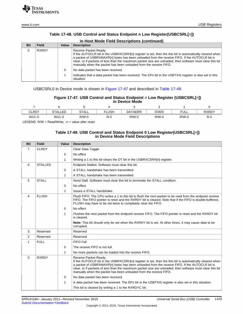
www.ti.com USB Registers
1103SPRUH18H–January 2011–Revised November 2019Submit Documentation Feedback
Copyright © 2011–2019, Texas Instruments Incorporated
Universal Serial Bus (USB) Controller
Table 17-48. USB Control and Status Endpoint n Low Register(USBCSRL[n])in Host Mode Field Descriptions (continued)
Bit Field Value Description0 RXRDY Receive Packet Ready.
If the AUTOCLR bit in the USBRXCSRH[n] register is set, then the this bit is automatically cleared whena packet of USBRXMAXP[n] bytes has been unloaded from the receive FIFO. If the AUTOCLR bit isclear, or if packets of less than the maximum packet size are unloaded, then software must clear this bitmanually when the packet has been unloaded from the receive FIFO.
0 No data packet has been received.1 Indicates that a data packet has been received. The EPn bit in the USBTXIS register is also set in this
situation.
USBCSRL0 in Device mode is shown in Figure 17-47 and described in Table 17-49.
Figure 17-47. USB Control and Status Endpoint n Low Register (USBCSRL[n])in Device Mode
7 6 5 4 3 2 1 0CLRDT STALLED STALL FLUSH DATAERR OVER FULL RXRDYW1C-0 W1C-0 R/W-0 R-0 R/W-0 R/W-0 R/W-0 R-0
LEGEND: R/W = Read/Write; -n = value after reset
Table 17-49. USB Control and Status Endpoint 0 Low Register(USBCSRL[n])in Device Mode Field Descriptions
Bit Field Value Description7 CLRDT Clear Data Toggle
0 No effect1 Writing a 1 to this bit clears the DT bit in the USBRXCSRH[n] register.
6 STALLED Endpoint Stalled. Software must clear this bit.0 A STALL handshake has been transmitted.1 A STALL handshake has been transmitted.
5 STALL Send Stall. Software must clear this bit to terminate the STALL condition.0 No effect1 Issues a STALL handshake.
4 FLUSH Flush FIFO. The CPU writes a 1 to this bit to flush the next packet to be read from the endpoint receiveFIFO. The FIFO pointer is reset and the RXRDY bit is cleared. Note that if the FIFO is double-buffered,FLUSH may have to be set twice to completely clear the FIFO.
0 No effect1 Flushes the next packet from the endpoint receive FIFO. The FIFO pointer is reset and the RXRDY bit
is cleared.Note: This bit should only be set when the RXRDY bit is set. At other times, it may cause data to becorrupted.
3 Reserved Reserved2 Reserved Reserved1 FULL FIFO Full
0 The receive FIFO is not full.1 No more packets can be loaded into the receive FIFO.
0 RXRDY Receive Packet Ready.If the AUTOCLR bit in the USBRXCSRH[n] register is set, then the this bit is automatically cleared whena packet of USBRXMAXP[n] bytes has been unloaded from the receive FIFO. If the AUTOCLR bit isclear, or if packets of less than the maximum packet size are unloaded, then software must clear this bitmanually when the packet has been unloaded from the receive FIFO.
0 No data packet has been received.1 A data packet has been received. The EPn bit in the USBTXIS register is also set in this situation.
This bit is cleared by writing a 1 to the RXRDYC bit.

USB Registers www.ti.com
1104 SPRUH18H–January 2011–Revised November 2019Submit Documentation Feedback
Copyright © 2011–2019, Texas Instruments Incorporated
Universal Serial Bus (USB) Controller
17.5.2.37 USB Receive Control and Status Endpoint n High Register (USBRXCSRH[1]-USBRXCSRH[3])The USB receive control and status endpoint n high 8-bit register (USBCSRL[n]) provides additionalcontrol and status bits for transfers through the currently selected receive endpoint.
For the specific offset for each register see Table 17-4.
Mode(s): Host Device
The USBCSRH[n] registers in OTG A/Host mode are shown in Figure 17-48 and described in Table 17-50.
Figure 17-48. USB Receive Control and Status Endpoint n High Register (USBCSRH[n]) in HostMode
7 6 5 4 3 2 1 0AUTOCL AUTORQ DMAEN PIDERR DMAMOD DTWE DT ReservedW1C-0 R/W-0 R/W-0 R-0 R/W-0 R-0 R-0 R-0
LEGEND: R/W = Read/Write; -n = value after reset
Table 17-50. USB Control and Status Endpoint n High Register (USBCSRH[n])in Host Mode Field Descriptions
Bit Field Value Description7 AUTOCL Auto Clear
0 No effect1 Enables the RXRDY bit to be automatically cleared when a packet of USBRXMAXP[n] bytes has been
unloaded from the receive FIFO. When packets of less than the maximum packet size are unloaded,RXRDY must be cleared manually. Care must be taken when using DMA to unload the receive FIFO asdata is read from the receive FIFO in 4-byte chunks regardless of the value of the MAXLOAD field inthe USBRXMAXP[n] register, see Section 17.3.3.
6 AUTORQ Auto RequestNote: This bit is automatically cleared when a short packet is received.
0 No effect1 Enables the REQPKT bit to be automatically set when the RXRDY bit is cleared.
5 DMAEN DMA Request EnableNote: Three TX and three RX endpoints can be connected to the DMA module. If this bit is set for aparticular endpoint, the DMAARX, DMABRX, or DMACRX field in the USB DMA Select (USBDMASEL)register must be programmed correspondingly.
0 Disables the DMA request for the receive endpoint.1 Enables the DMA request for the receive endpoint.
4 Reserved Reserved3 DMAMOD DMAMOD
Note: This bit must not be cleared either before or in the same cycle as the above DMAEN bit iscleared.
0 An interrupt is generated after every DMA packet transfer.1 An interrupt is generated only after the entire DMA transfer is complete.
2 DTWE Data Toggle Write Enable. This bit is automatically cleared once the new value is written.0 The DT bit cannot be written.1 Enables the current state of the receive endpoint data to be written (see DT bit).
1 DT Data Toggle. When read, this bit indicates the current state of the receive data toggle.If DTWE is High, this bit may be written with the required setting of the data toggle. If DTWE is Low, anyvalue written to this bit is ignored. Care should be taken when writing to this bit as it should only bechanged to RESET the receive endpoint.
0 Reserved 0 Reserved
The USBCSRH[n] registers in Device mode are shown in Figure 17-49 and described in Table 17-51.

www.ti.com USB Registers
1105SPRUH18H–January 2011–Revised November 2019Submit Documentation Feedback
Copyright © 2011–2019, Texas Instruments Incorporated
Universal Serial Bus (USB) Controller
Figure 17-49. USB Control and Status Endpoint n High Register (USBCSRH[n]) in Device Mode7 6 5 4 3 2 0
AUTOCL ISO DMAEN DISNYET /PIDERR
DMAMOD Reserved
R/W-0 R/W-0 R/W-0 R/W-0 R/W-0 R-0LEGEND: R/W = Read/Write; -n = value after reset
Table 17-51. USB Control and Status Endpoint 0 High Register(USBCSRH[n])in Device Mode Field Descriptions
Bit Field Value Description7 AUTOCL Auto Clear
0 No effect1 Enables the RXRDY bit to be automatically cleared when a packet of USBRXMAXP[n] bytes has been
unloaded from the receive FIFO. When packets of less than the maximum packet size are unloaded,RXRDY must be cleared manually. Care must be taken when using DMA to unload the receive FIFO asdata is read from the receive FIFO in 4-byte chunks regardless of the value of the MAXLOAD field inthe USBRXMAXP[n] register, see Section 17.3.3.
6 Reserved Reserved5 DMAEN DMA Request Enable
Note: Three TX and three RX endpoints can be connected to the DMA module. If this bit is set for aparticular endpoint, the DMAARX, DMABRX, or DMACRX field in the USB DMA Select (USBDMASEL)register must be programmed correspondingly.
0 Disables the DMA request for the receive endpoint.1 Enables the DMA request for the receive endpoint.
4 DISNYET/PIDERR
Disable NYET / PID Error0 No effect1 For bulk or interrupt transactions: Disables the sending of NYET handshakes. When this bit is set, all
successfully received packets are acknowledged, including at the point at which the FIFO becomes full.3 DMAMOD DMA Request Mode
Note: This bit must not be cleared either before or in the same cycle as the above DMAEN bit iscleared.
0 An interrupt is generated after every DMA packet transfer.1 An interrupt is generated only after the entire DMA transfer is complete.
0 Reserved 0 Reserved

USB Registers www.ti.com
1106 SPRUH18H–January 2011–Revised November 2019Submit Documentation Feedback
Copyright © 2011–2019, Texas Instruments Incorporated
Universal Serial Bus (USB) Controller
17.5.2.38 USB Receive Byte Count Endpoint n Registers (USBRXCOUNT[1]-USBRXCOUNT[3)The USB receive byte count endpoint n 16-bit read-only registers hold the number of data bytes in thepacket currently in line to be read from the receive FIFO. If the packet is transmitted as multiple bulkpackets, the number given is for the combined packet.
Note: The value returned changes as the FIFO is unloaded and is only valid while the RXRDY bit in theUSBRXCSRLn register is set.
For the specific offset for each register see Table 17-4.
Mode(s): Host Device
The USBRXCOUNT[n] registers are shown in Figure 17-50 and described in Table 17-52.
Figure 17-50. USB Maximum Receive Data Endpoint n Registers (USBRXCOUNT[n])15 13 12 0
Reserved COUNTR-0 R-0
LEGEND: R/W = Read/Write; R = Read only; -n = value after reset
Table 17-52. USB Maximum Receive Data Endpoint n Registers (USBRXCOUNT[n])Field Descriptions
Bit Field Value Description15-13 Reserved 0 Reserved12-0 COUNT Receive Packet Count indicates the number of bytes in the receive packet.

www.ti.com USB Registers
1107SPRUH18H–January 2011–Revised November 2019Submit Documentation Feedback
Copyright © 2011–2019, Texas Instruments Incorporated
Universal Serial Bus (USB) Controller
17.5.2.39 USB Host Transmit Configure Type Endpoint n Register (USBTXTYPE[1]-USBTXTYPE[3])The USB host transmit configure type endpoint n 8-bit registers (USBTXTYPE[n]) must be written with theendpoint number to be targeted by the endpoint, the transaction protocol to use for the currently selectedtransmit endpoint, and its operating speed.
For the specific offset for each register see Table 17-4.
Mode(s): Host
The USBTXTYPE[n] registers are shown in Figure 17-51 and described in Table 17-53.
Figure 17-51. USB Host Transmit Configure Type Endpoint n Register (USBTXTYPE[n])7 6 5 4 3 0
SPEED PROTO TEPR/W-0 R/W-0 R/W-0
LEGEND: R/W = Read/Write; -n = value after reset
Table 17-53. USB Host Transmit Configure Type Endpoint n Register(USBTXTYPE[n])Field Descriptions
Bit Field Value Description7-6 SPEED Operating Speed. This bit field specifies the operating speed of the target Device:
0h Default. The target is assumed to be using the same connection speed as the USB controller.1h Reserved2h Full3h Low
5-4 PROTO Protocol. Software must configure this bit field to select the required protocol for the transmit endpoint:0h Control1h Reserved2h Bulk3h Interrupt
3-0 TEP 0 Target Endpoint Number. Software must configure this value to the endpoint number contained in thetransmit endpoint descriptor returned to the USB controller during Device enumeration.

USB Registers www.ti.com
1108 SPRUH18H–January 2011–Revised November 2019Submit Documentation Feedback
Copyright © 2011–2019, Texas Instruments Incorporated
Universal Serial Bus (USB) Controller
17.5.2.40 USB Host Transmit Interval Endpoint n Register (USBTXINTERVAL[1]USBTXINTERVAL[3])The USB host transmit interval endpoint n 8-bit registers (USBTXINTERVAL[n]), for interrupt transfers,define the polling interval for the currently selected transmit endpoint. For bulk endpoints, this registerdefines the number of frames after which the endpoint should time out on receiving a stream of NAKresponses.
The USBTXINTERVAL[n] registers values define a number of frames, as follows:
Table 17-54. USBTXINTERVAL[n] Frame Numbers
Transfer Type Speed Valid Values (m) InterpretationInterrupt Low-speed or Full-speed 0x01-0xFF The polling interval is m frames.
Bulk Full-speed 0x02-0x10 The NAK Limit is 2(m-1) frames. A value of 0 or 1disables the NAK timeout function.
For the specific offset for each register see Table 17-4.
Mode(s): Host
The USBTXINTERVAL[n] registers are shown in Figure 17-51 and described in Table 17-53.
Figure 17-52. USB Host Transmit Interval Endpoint n Register (USBTXINTERVAL[n])7 0
TXPOLL / NAKLMTR/W-0
LEGEND: R/W = Read/Write; -n = value after reset
Table 17-55. USB Host Transmit Interval Endpoint n Register(USBTXINTERVAL[n])Field Descriptions
Bit Field Value Description7-0 TXPOLL /
NAKLMT0 TX Polling / NAK Limit The polling interval for interrupt transfers; the NAK limit for bulk transfers. See
Table 17-54 for valid entries; other values are reserved.

www.ti.com USB Registers
1109SPRUH18H–January 2011–Revised November 2019Submit Documentation Feedback
Copyright © 2011–2019, Texas Instruments Incorporated
Universal Serial Bus (USB) Controller
17.5.2.41 USB Host Configure Receive Type Endpoint n Register (USBRXTYPE[1]-USBRXTYPE[3])The USB host configure receive type endpoint n 8-bit registers (USBRXTYPE[n]) must be written with theendpoint number to be targeted by the endpoint, the transaction protocol to use for the currently selectedreceive endpoint, and its operating speed.
For the specific offset for each register see Table 17-4.
Mode(s): Host
The USBRXTYPE[n] registers are shown in Figure 17-53 and described in Table 17-56.
Figure 17-53. USB Host Configure Receive Type Endpoint n Register (USBRXTYPE[n])7 6 5 4 3 0
SPEED PROTO TEPR/W-0 R/W-0 R/W-0
LEGEND: R/W = Read/Write; -n = value after reset
Table 17-56. USB Host Configure Receive Type Endpoint n Register(USBRXTYPE[n])Field Descriptions
Bit Field Value Description7-6 SPEED Operating Speed. This bit field specifies the operating speed of the target Device:
0h Default. The target is assumed to be using the same connection speed as the USB controller.1h Reserved2h Full3h Low
5-4 PROTO Protocol. Software must configure this bit field to select the required protocol for the receive endpoint:0h Control1h Reserved2h Bulk3h Interrupt
3-0 TEP 0 Target Endpoint Number. Software must configure this value to the endpoint number contained in thetransmit endpoint descriptor returned to the USB controller during Device enumeration.

USB Registers www.ti.com
1110 SPRUH18H–January 2011–Revised November 2019Submit Documentation Feedback
Copyright © 2011–2019, Texas Instruments Incorporated
Universal Serial Bus (USB) Controller
17.5.2.42 USB Host Receive Polling Interval Endpoint n Register (USBRXINTERVAL[1]-USBRXINTERVAL[3])
The USB host receive polling interval endpoint n 8-bit registers (USBRXINTERVAL[n]), for interrupttransfers, define the polling interval for the currently selected transmit endpoint. For bulk endpoints, thisregister defines the number of frames after which the endpoint should time out on receiving a stream ofNAK responses.
The USBRXINTERVAL[n] registers values define a number of frames, as follows:
Table 17-57. USBRXINTERVAL[n] Frame Numbers
Transfer Type Speed Valid Values (m) InterpretationInterrupt Low-speed or Full-speed 0x01-0xFF The polling interval is m frames.
Bulk Full-speed 0x02-0x10 The NAK Limit is 2(m-1) frames. A value of 0 or 1disables the NAK timeout function.
For the specific offset for each register see Table 17-4.
Mode(s): Host
The USBRXINTERVAL[n] registers are shown in Figure 17-51 and described in Table 17-53.
Figure 17-54. USB Host Receive Polling Interval Endpoint n Register (USBRXINTERVAL[n])7 0
TXPOLL / NAKLMTR/W-0
LEGEND: R/W = Read/Write; -n = value after reset
Table 17-58. USB Host Receive Polling Interval Endpoint n Register(USBRXINTERVAL[n])Field Descriptions
Bit Field Value Description7-0 TXPOLL /
NAKLMT0 TX Polling / NAK Limit The polling interval for interrupt transfers; the NAK limit for bulk transfers. See
Table 17-57 for valid entries; other values are reserved.

www.ti.com USB Registers
1111SPRUH18H–January 2011–Revised November 2019Submit Documentation Feedback
Copyright © 2011–2019, Texas Instruments Incorporated
Universal Serial Bus (USB) Controller
17.5.2.43 USB Request Packet Count in Block Transfer Endpoint n Registers (USBRQPKTCOUNT[1]-USBRQPKTCOUNT[3)
The USB receive packet count in block transfer endpoint n 16-bit read/writer registers are used in Hostmode to specify the number of packets that are to be transferred in a block transfer of one or more bulkpackets to receive endpoint n. The USB controller uses the value recorded in this register to determine thenumber of requests to issue where the AUTORQ bit in the USBRXCSRH[n] register has been set. Formore information about IN transactions as a host, see Section 17.3.2.2.
Note: Multiple packets combined into a single bulk packet within the FIFO count as one packet.
For the specific offset for each register see Table 17-4.
Mode(s): Host
The USBRQPKTCOUNT[n] registers are shown in Figure 17-55 and described in Table 17-59.
Figure 17-55. USB Request Packet Count in Block Transfer Endpoint n Registers(USBRQPKTCOUNT[n])
15 13 12 0Reserved COUNT
R-0 R-0LEGEND: R/W = Read/Write; R = Read only; -n = value after reset
Table 17-59. USB Request Packet Count in Block Transfer Endpoint n Registers(USBRQPKTCOUNT[n]) Field Descriptions
Bit Field Value Description15-13 Reserved 0 Reserved12-0 COUNT Block Transfer Packet Count sets the number of packets of the size defined by the MAXLOAD bit field
that are to be transferred in a block transfer.Note: This is only used in Host mode when AUTORQ is set. The bit has no effect in Device mode orwhen AUTORQ is not set.

USB Registers www.ti.com
1112 SPRUH18H–January 2011–Revised November 2019Submit Documentation Feedback
Copyright © 2011–2019, Texas Instruments Incorporated
Universal Serial Bus (USB) Controller
17.5.2.44 USB Receive Double Packet Buffer Disable Register (USBRXDPKTBUFDIS), offset 0x340The USB receive double packet buffer disable 16-bit register (USBRXDPKTBUFDIS) indicates which ofthe receive endpoints have disabled the double-packet buffer functionality (see Double-Packet Buffering inSection 17.3.1.1.1).
Note: The USBRXDPKTBUFDIS register is not applicable to the control IN and control OUT endpoints,therefore the EP0 bit does not exist for the USBRXDPKTBUFDIS register.
Mode(s): Host Device
USBRXDPKTBUFDIS is shown in Figure 17-56 and described in Table 17-60.
Figure 17-56. USB Receive Double Packet Buffer Disable Register (USBRXDPKTBUFDIS)15 4 3 2 1 0
Reserved EP3 EP2 EP1 RsvdR-0 R/W-1 R/W-1 R/W-1 R-0
LEGEND: R/W = Read/Write; R = Read only; -n = value after reset
Table 17-60. USB Receive Double Packet Buffer Disable Register (USBRXDPKTBUFDIS) FieldDescriptions
Bit Field Value Description15-4 Reserved Reserved
3 EP3 EP3 RX Double-Packet Buffer Disable0 Disables double-packet buffering.1 Enables double-packet buffering.
2 EP2 EP2 RX Double-Packet Buffer Disable0 Disables double-packet buffering.1 Enables double-packet buffering.
1 EP1 EP1 RX Double-Packet Buffer Disable0 Disables double-packet buffering.1 Enables double-packet buffering.
0 Reserved 0 Reserved

www.ti.com USB Registers
1113SPRUH18H–January 2011–Revised November 2019Submit Documentation Feedback
Copyright © 2011–2019, Texas Instruments Incorporated
Universal Serial Bus (USB) Controller
17.5.2.45 USB Transmit Double Packet Buffer Disable Register (USBTXDPKTBUFDIS), offset 0x342The USB transmit double packet buffer disable 16-bit register (USBTXDPKTBUFDIS) indicates which ofthe transmit endpoints have disabled the double-packet buffer functionality (see Double-Packet Bufferingin Section 17.3.1.1.1).
Note: The USBTXDPKTBUFDIS register is not applicable to the control IN and control OUT endpoints,therefore the EP0 bit does not exist for the USBTXDPKTBUFDIS register.
Mode(s): Host Device
USBTXDPKTBUFDIS is shown in Figure 17-57 and described in Table 17-61.
Figure 17-57. USB Transmit Double Packet Buffer Disable Register (USBTXDPKTBUFDIS)15 4 3 2 1 0
Reserved EP3 EP2 EP1 RsvdR-0 R/W-1 R/W-1 R/W-1 R-0
LEGEND: R/W = Read/Write; R = Read only; -n = value after reset
Table 17-61. USB Transmit Double Packet Buffer Disable Register (USBTXDPKTBUFDIS)Field Descriptions
Bit Field Value Description15-4 Reserved Reserved
3 EP3 EP3 RX Double-Packet Buffer Disable0 Disables double-packet buffering.1 Enables double-packet buffering.
2 EP2 EP2 RX Double-Packet Buffer Disable0 Disables double-packet buffering.1 Enables double-packet buffering.
1 EP1 EP1 RX Double-Packet Buffer Disable0 Disables double-packet buffering.1 Enables double-packet buffering.
0 Reserved 0 Reserved

USB Registers www.ti.com
1114 SPRUH18H–January 2011–Revised November 2019Submit Documentation Feedback
Copyright © 2011–2019, Texas Instruments Incorporated
Universal Serial Bus (USB) Controller
17.5.2.46 USB External Power Control Register (USBEPC), offset 0x400The USB external power control 32-bit register (USBEPC) specifies the function of the two-pin externalpower interface (USB0EPEN and USB0PFLT). The assertion of the power fault input may generate anautomatic action, as controlled by the hardware configuration registers. The automatic action is necessarybecause the fault condition may require a response faster than one provided by firmware.
Mode(s): Host Device
USBEPC is shown in Figure 17-58 and described in Table 17-62.
Figure 17-58. USB External Power Control Register (USBEPC)31 16
ReservedR-0
15 10 9 8Reserved PFLTACT
R-0 R/W-0
7 6 5 4 3 2 1 0Reserved PFLTAEN PFLTSEN PFLTEN Reserved EPENDE EPEN
R-0 R/W-0 R/W-0 R/W-0 R-0 R/W-0 R/W-0LEGEND: R/W = Read/Write; -n = value after reset
Table 17-62. USB External Power Control Register (USBEPC) Field Descriptions
Bit Field Value Description31-10 Reserved 0 Reserved
9-8 PFLTACT Power Fault Action. This bit field specifies how the USB0EPEN signal is changed when detecting aUSB power fault.
0h Unchanged. USB0EPEN is controlled by the combination of the EPEN and EPENDE bits.1h Tristate. USB0EPEN is undriven (tristate).2h Low. USB0EPEN is driven Low.3h High. USB0EPEN is driven High.
7 Reserved 0 Reserved6 PFLTAEN Power Fault Action Enable. This bit specifies whether a USB power fault triggers any automatic
corrective action regarding the driven state of the USB0EPEN signal.0 Disabled. USB0EPEN is controlled by the combination of the EPEN and EPENDE bits.1 Enabled. The USB0EPEN output is automatically changed to the state specified by the PFLTACT field.
5 PFLTSEN Power Fault Sense. This bit specifies the logical sense of the USB0PFLT input signal that indicates anerror condition.The complementary state is the inactive state.
0 Low Fault. If USB0PFLT is driven Low, the power fault is signaled internally (if enabled by the PFLTENbit).
1 High Fault. If USB0PFLT is driven High, the power fault is signaled internally (if enabled by the PFLTENbit).
4 PFLTEN Power Fault Input Enable. This bit specifies whether the USB0PFLT input signal is used in internallogic.
0 Not Used. The USB0PFLT signal is ignored.1 Used. The USB0PFLT signal is used internally
3 Reserved 0 Reserved

www.ti.com USB Registers
1115SPRUH18H–January 2011–Revised November 2019Submit Documentation Feedback
Copyright © 2011–2019, Texas Instruments Incorporated
Universal Serial Bus (USB) Controller
Table 17-62. USB External Power Control Register (USBEPC) Field Descriptions (continued)Bit Field Value Description2 EPENDE EPEN Drive Enable. This bit specifies whether the USB0EPEN signal is driven or undriven (tristate).
When driven, the signal value is specified by the EPEN field. When not driven, the EPEN field isignored and the USB0EPEN signal is placed in a high-impedance state.The USB0EPEN signal is undriven at reset because the sense of the external power supply enable isunknown. By adding the high-impedance state, system designers can bias the power supply enable tothe disabled state using a large resistor (100 kΩ) and later configure and drive the output signal toenable the power supply.
0 Not Driven. The USB0EPEN signal is high impedance.1 Driven. The USB0EPEN signal is driven to the logical value specified by the value of the EPEN field.
1-0 EPEN External Power Supply Enable Configuration. This bit field specifies and controls the logical value drivenon the USB0EPEN signal.
0h Power Enable Active Low. The USB0EPEN signal is driven Low if the EPENDE bit is set.1h Power Enable Active High. The USB0EPEN signal is driven High if the EPENDE bit is set.2h Power Enable High if VBUS Low. The USB0EPEN signal is driven High when the A device is not
recognized.3h Power Enable High if VBUS High. The USB0EPEN signal is driven High when the A device is
recognized.

USB Registers www.ti.com
1116 SPRUH18H–January 2011–Revised November 2019Submit Documentation Feedback
Copyright © 2011–2019, Texas Instruments Incorporated
Universal Serial Bus (USB) Controller
17.5.2.47 USB External Power Control Raw Interrupt Status Register (USBEPCRIS), offset 0x404The USB external power control raw interrupt status 32-bit register (USBEPCRIS) specifies the unmaskedinterrupt status of the two-pin external power interface.
Mode(s): Host Device
USBEPCRIS is shown in Figure 17-59 and described in Table 17-63.
Figure 17-59. USB External Power Control Raw Interrupt Status Register (USBEPCRIS)31 1 0
Reserved PFR-0 R-0
LEGEND: R/W = Read/Write; R = Read only; -n = value after reset
Table 17-63. USB External Power Control Raw Interrupt Status Register (USBEPCRIS) FieldDescriptions
Bit Field Value Description31-1 Reserved 0 Reserved
0 PF USB Power Fault Interrupt Status.This bit is cleared by writing a 1 to the PF bit in the USBEPCISC register.
0 A Power Fault status has been detected.1 An interrupt has not occurred.

www.ti.com USB Registers
1117SPRUH18H–January 2011–Revised November 2019Submit Documentation Feedback
Copyright © 2011–2019, Texas Instruments Incorporated
Universal Serial Bus (USB) Controller
17.5.2.48 USB External Power Control Interrupt Mask Register (USBEPCIM), offset 0x408The USB external power control interrupt mask 32-bit register (USBEPCIM) specifies the interrupt mask ofthe two-pin external power interface.
Mode(s): Host Device
USBEPCIM is shown in Figure 17-59 and described in Table 17-63.
Figure 17-60. USB External Power Control Interrupt Mask Register (USBEPCIM)31 1 0
Reserved PFR-0 R-0
LEGEND: R/W = Read/Write; R = Read only; -n = value after reset
Table 17-64. USB External Power Control Interrupt Mask Register (USBEPCIM) Field Descriptions
Bit Field Value Description31-1 Reserved 0 Reserved
0 PF USB Power Fault Interrupt Mask.0 The raw interrupt signal from a detected power fault is sent to the interrupt controller.1 A detected power fault does not affect the interrupt status.

USB Registers www.ti.com
1118 SPRUH18H–January 2011–Revised November 2019Submit Documentation Feedback
Copyright © 2011–2019, Texas Instruments Incorporated
Universal Serial Bus (USB) Controller
17.5.2.49 USB External Power Control Interrupt Status and Clear Register (USBEPCISC), offset 0x40CThe USB external power control interrupt status and clear 32-bit register (USBEPCISC) specifies theunmasked interrupt status of the two-pin external power interface.
Mode(s): Host Device
USBEPCISC is shown in Figure 17-61 and described in Table 17-65.
Figure 17-61. USB External Power Control Interrupt Status and Clear Register (USBEPCISC)31 1 0
Reserved PFR-0 R-0
LEGEND: R/W = Read/Write; R = Read only; -n = value after reset
Table 17-65. USB External Power Control Interrupt Status andClear Register (USBEPCISC) Field Descriptions
Bit Field Value Description31-1 Reserved 0 Reserved. Reset is 0x0000.000.
0 PF USB Power Fault Interrupt Status and Clear.This bit is cleared by writing a 1. Clearing this bit also clears the PF bit in the USBEPCISC register.
0 The PF bits in the USBEPCRIS and USBEPCIM registers are set, providing an interrupt to the interruptcontroller.
1 No interrupt has occurred or the interrupt is masked.

www.ti.com USB Registers
1119SPRUH18H–January 2011–Revised November 2019Submit Documentation Feedback
Copyright © 2011–2019, Texas Instruments Incorporated
Universal Serial Bus (USB) Controller
17.5.2.50 USB Device RESUME Raw Interrupt Status Register (USBDRRIS), offset 0x410The USB device RESUME raw interrupt status register (USBDRRIS) is the raw interrupt status register.On a read, this register gives the current raw status value of the corresponding interrupt prior to masking.A write has no effect.
Mode(s): Host Device
USBDRRIS is shown in Figure 17-62 and described in Table 17-66.
Figure 17-62. USB Device RESUME Raw Interrupt Status Register (USBDRRIS)31 1 0
Reserved RESUMER-0 R-0
LEGEND: R/W = Read/Write; R = Read only; -n = value after reset
Table 17-66. USB Device RESUME Raw InterruptStatus Register (USBDRRIS) Field Descriptions
Bit Field Value Description31-1 Reserved 0 Reserved. Reset is 0x0000.000.
0 PF RESUME Interrupt StatusThis bit is cleared by writing a 1 to the RESUME bit in the USBDRISC register.
0 A RESUME status has been detected.1 An interrupt has not occurred.

USB Registers www.ti.com
1120 SPRUH18H–January 2011–Revised November 2019Submit Documentation Feedback
Copyright © 2011–2019, Texas Instruments Incorporated
Universal Serial Bus (USB) Controller
17.5.2.51 USB Device RESUME Raw Interrupt Mask Register (USBDRIM), offset 0x414The USB device RESUME raw interrupt status register (USBDRIM) is the masked interrupt status register.On a read, this register gives the current masked status value of the corresponding interrupt. A write hasno effect.
Mode(s): Host Device
USBDRIM is shown in Figure 17-63 and described in Table 17-67.
Figure 17-63. USB Device RESUME Raw Interrupt Status Register (USBDRRIS)31 1 0
Reserved RESUMER-0 R-0
LEGEND: R/W = Read/Write; R = Read only; -n = value after reset
Table 17-67. USB Device RESUME Raw InterruptStatus Register (USBDRRIS) Field Descriptions
Bit Field Value Description31-1 Reserved 0 Reserved. Reset is 0x0000.000.
0 PF RESUME Interrupt Mask0 The raw interrupt signal from a detected RESUME is sent to the interrupt controller. This bit should only
be set when a SUSPEND has been detected (the SUSPEND bit in the USBIS register is set).1 A detected RESUME does not affect the interrupt status.

www.ti.com USB Registers
1121SPRUH18H–January 2011–Revised November 2019Submit Documentation Feedback
Copyright © 2011–2019, Texas Instruments Incorporated
Universal Serial Bus (USB) Controller
17.5.2.52 USB Device RESUME Interrupt Status and Clear Register (USBDRISC), offset 0x418The USB device RESUME interrupt status and clear register (USBDRRIS) is the raw interrupt clearregister. On a write of 1, the corresponding interrupt is cleared. A write of 0 has no effect.
Mode(s): Host Device
USBDRISC is shown in Figure 17-64 and described in Table 17-68.
Figure 17-64. USB Device RESUME Interrupt Status and Clear Register (USBDRISC)31 1 0
Reserved RESUMER-0 R/W1C
LEGEND: R/W = Read/Write; R = Read only; -n = value after reset
Table 17-68. USB Device RESUME Interrupt Status and Clear Register (USBDRISC)Field Descriptions
Bit Field Value Description31-1 Reserved 0 Reserved. Reset is 0x0000.000.
0 RESUME RESUME Interrupt Status and Clear.This bit is cleared by writing a 1. Clearing this bit also clears the RESUME bit in the USBDRCRISregister.
0 The RESUME bits in the USBDRRIS and USBDRCIM registers are set, providing an interrupt to theinterrupt controller.
1 No interrupt has occurred or the interrupt is masked.

USB Registers www.ti.com
1122 SPRUH18H–January 2011–Revised November 2019Submit Documentation Feedback
Copyright © 2011–2019, Texas Instruments Incorporated
Universal Serial Bus (USB) Controller
17.5.2.53 USB General-Purpose Control and Status Register (USBGPCS), offset 0x41CThe USB general-purpose control and status register (USBGPCS) provides the state of the internal IDsignal.
When the USB controller is used as either a dedicated Host or Device, the DEVMODOTG and DEVMODbits in the USB General-Purpose Control and Status (USBGPCS) register should be used to connect theID inputs to fixed levels internally. For proper self-powered Device operation, the VBUS value must bemonitored to assure that if the Host removes VBUS, the self-powered Device disables the D+/D- pull-upresistors. This function can be accomplished by connecting a standard GPIO to VBUS.
Mode(s): Host Device
USBGPCS is shown in Figure 17-65 and described in Table 17-69.
Figure 17-65. USB General-Purpose Control and Status Register (USBGPCS)31 2 1 0
Reserved DEVMODOTG DEVMODR-0 R/W-0 R/W-0
LEGEND: R/W = Read/Write; R = Read only; -n = value after reset
Table 17-69. USB General-Purpose Control and StatusRegister (USBGPCS) Field Descriptions
Bit Field Value Description31-2 Reserved 0 Reserved. Reset is 0x0000.000.
1 DEVMODOTG
Enable Device Mode. This bit enables the DEVMOD bit to control the state of the internal ID signal inOTG mode.
0 The mode is specified by the state of the internal ID signal.1 This bit enables the DEVMOD bit to control the internal ID signal.
0 DEVMOD Device Mode This bit specifies the state of the internal ID signal in Host mode and in OTG mode whenthe DEVMODOTG bit is set.In Device mode this bit is ignored (assumed set).
0 Host mode1 Device mode

www.ti.com USB Registers
1123SPRUH18H–January 2011–Revised November 2019Submit Documentation Feedback
Copyright © 2011–2019, Texas Instruments Incorporated
Universal Serial Bus (USB) Controller
17.5.2.54 USB DMA Select Register (USBDMASEL), offset 0x450The USB DMA select 32-bit register (USBDMASEL) specifies whether the unmasked interrupt status ofthe ID value is valid.
Mode(s): Host Device
USBDMASEL is shown in Figure 17-66 and described in Table 17-70.
Figure 17-66. USB DMA Select Register (USBDMASEL)31 24 23 20 19 16
Reserved DMACTX DMACRXR/0 R/W-0 R/W-0
15 12 11 8 7 4 3 0DMABTX DMABRX DMAATX DMAARX
R/W-0 R/W-0 R/W-0 R/W-0LEGEND: R/W = Read/Write; R = Read only; -n = value after reset
Table 17-70. USB DMA Select Register (USBDMASEL) Field Descriptions
Bit Field Value Description31-24 Reserved 0 Reserved. Reset is 0x0000.000.23-20 DMACTX DMA C TX Select specifies the TX mapping of the third USB endpoint on DMA channel 5 (primary
assignment).0h Reserved1h Endpoint 1 TX2h Endpoint 2 TX3h Endpoint 3 TX
19-16 DMACRX DMA C RX Select specifies the RX and TX mapping of the third USB endpoint on DMA channel 4(primary assignment).
0h Reserved1h Endpoint 1 RX2h Endpoint 2 RX3h Endpoint 3 RX
15-12 DMABTX DMA B TX Select specifies the TX mapping of the second USB endpoint on DMA channel 3 (primaryassignment).
0h Reserved1h Endpoint 1 TX2h Endpoint 2 TX3h Endpoint 3 TX
11-8 DMABRX DMA B RX Select Specifies the RX mapping of the second USB endpoint on DMA channel 2 (primaryassignment).
0h Reserved1h Endpoint 1 RX2h Endpoint 2 RX3h Endpoint 3 RX
7-4 DMAATX DMA A TX Select specifies the TX mapping of the first USB endpoint on DMA channel 1 (primaryassignment).
0h Reserved1h Endpoint 1 TX2h Endpoint 2 TX3h Endpoint 3 TX

USB Registers www.ti.com
1124 SPRUH18H–January 2011–Revised November 2019Submit Documentation Feedback
Copyright © 2011–2019, Texas Instruments Incorporated
Universal Serial Bus (USB) Controller
Table 17-70. USB DMA Select Register (USBDMASEL) Field Descriptions (continued)Bit Field Value Description3-0 DMAARX DMA A RX Select specifies the RX mapping of the first USB endpoint on DMA channel 0 (primary
assignment).0h Reserved1h Endpoint 1 RX2h Endpoint 2 RX3h Endpoint 3 RX

www.ti.com Revision History
1125SPRUH18H–January 2011–Revised November 2019Submit Documentation Feedback
Copyright © 2011–2019, Texas Instruments Incorporated
Revision History
Revision History
Changes from May 1, 2017 to October 15, 2019 ............................................................................................................. Page
• Section 1.3: In the second paragraph, replaced emulator with debug probe. ................................................... 58• Section 1.4.2.10: Revised this section. ............................................................................................... 92• Figure 2-1Aligned addresses ; deleted the extra 0 in DF000..................................................................... 194• Section 2.2.12: Revised this section. ................................................................................................ 216• Changed the equation for autoconversion calculation............................................................................. 387• Section 5.4.4: Added EALLOW protected to the title. ............................................................................. 415• Figure 6-3: Added figure............................................................................................................... 429• Section 6.5.6: Revised this section................................................................................................... 433• Figure 6-11: Included the Time-Base Frequency and Period Calculation figure............................................... 437• Section 6.8: Corrected CAP2 register description. APRD changed to ACMP.................................................. 442• Added guidelines for estimating ACQPS values. .................................................................................. 521• Added section for Sequential Sampling Mode ..................................................................................... 529• Section 10.5.3.1: Removed "Legacy" from the title. ............................................................................... 579• Table 10-10: Added an example and more description for the pipeline operation in
MMOV32mem32,MSTF#MMOV32memMSTF, .................................................................................... 591• Changed Changed MAR0/MAR1 offset from 0x0029/0x002A to 0x002A/0x002B ............................................ 702• Section 11.2: Changed ePWM1-6 ADCSOCA to ePWM2-7 ADCSOCA; added a note to bullet beginning "ePWM1-8 /
HRPWM1-8 "............................................................................................................................ 720• Chapter 12: Chapter reorganization, various bug fixes and clarifications....................................................... 751• Chapter 14: Inter-Integrated Circuit Module (I2C)............................................................................... 824• Section 14.1.4: Updated section content. ........................................................................................... 827• Section 14.2: Added section. ......................................................................................................... 828• Section 14.3.3: Added summary on cases where SCL is held low and how to release SCL. ............................... 829• Section 14.3.4: Added and updated information explaining the Bus Busy (BB) bit behavior................................. 830• Section 14.3.9: Added section. ....................................................................................................... 835• Section 14.4.2: Added I2C FIFO Interrupt figure. .................................................................................. 838• Section 14.6: Added sentence to the I2CMDR STP bit description. "The I2C module delays clearing of..." .............. 840• Table 16-16: For bit 31 (description 0), removed the last two lines beginning "Filtering is not applicable..." ............ 1011• Chapter 17: Universal Serial Bus (USB) Controller ........................................................................... 1042• Section 17.2: Removed DMA trigger support from USB chapter. See USB DMA Event Trigger advisory in device
errata. .................................................................................................................................. 1043• Section 17.2: Removed Isochronous mode support from USB chapter. ...................................................... 1043• Section 17.3.1: Deleted the bullet beginning "Isochronous endpoints..."...................................................... 1045• Section 17.3.2: Deleted the bullet beginning "Isochronous endpoints..."...................................................... 1049

IMPORTANT NOTICE AND DISCLAIMER
TI PROVIDES TECHNICAL AND RELIABILITY DATA (INCLUDING DATASHEETS), DESIGN RESOURCES (INCLUDING REFERENCEDESIGNS), APPLICATION OR OTHER DESIGN ADVICE, WEB TOOLS, SAFETY INFORMATION, AND OTHER RESOURCES “AS IS”AND WITH ALL FAULTS, AND DISCLAIMS ALL WARRANTIES, EXPRESS AND IMPLIED, INCLUDING WITHOUT LIMITATION ANYIMPLIED WARRANTIES OF MERCHANTABILITY, FITNESS FOR A PARTICULAR PURPOSE OR NON-INFRINGEMENT OF THIRDPARTY INTELLECTUAL PROPERTY RIGHTS.These resources are intended for skilled developers designing with TI products. You are solely responsible for (1) selecting the appropriateTI products for your application, (2) designing, validating and testing your application, and (3) ensuring your application meets applicablestandards, and any other safety, security, or other requirements. These resources are subject to change without notice. TI grants youpermission to use these resources only for development of an application that uses the TI products described in the resource. Otherreproduction and display of these resources is prohibited. No license is granted to any other TI intellectual property right or to any thirdparty intellectual property right. TI disclaims responsibility for, and you will fully indemnify TI and its representatives against, any claims,damages, costs, losses, and liabilities arising out of your use of these resources.TI’s products are provided subject to TI’s Terms of Sale (www.ti.com/legal/termsofsale.html) or other applicable terms available either onti.com or provided in conjunction with such TI products. TI’s provision of these resources does not expand or otherwise alter TI’s applicablewarranties or warranty disclaimers for TI products.
Mailing Address: Texas Instruments, Post Office Box 655303, Dallas, Texas 75265Copyright © 2019, Texas Instruments Incorporated