
High speed analog-to-digital conversion with silicon photonics
16
High speed analog-to-digital conversion with silicon photonics Citation Holzwarth, C. W. et al. “High speed analog-to-digital conversion with silicon photonics.” Silicon Photonics IV. Ed. Joel A. Kubby & Graham T. Reed. San Jose, CA, USA: SPIE, 2009. 72200B-15. © 2009 SPIE--The International Society for Optical Engineering As Published http://dx.doi.org/10.1117/12.808952 Publisher The International Society for Optical Engineering Version Final published version Accessed Tue May 10 21:47:19 EDT 2011 Citable Link http://hdl.handle.net/1721.1/52658 Terms of Use Article is made available in accordance with the publisher's policy and may be subject to US copyright law. Please refer to the publisher's site for terms of use. Detailed Terms
Transcript of High speed analog-to-digital conversion with silicon photonics
High speed analog-to-digital conversion with siliconphotonics
Citation Holzwarth C W et al ldquoHigh speed analog-to-digital conversionwith silicon photonicsrdquo Silicon Photonics IV Ed Joel A Kubby ampGraham T Reed San Jose CA USA SPIE 2009 72200B-15copy 2009 SPIE--The International Society for Optical Engineering
As Published httpdxdoiorg10111712808952
Publisher The International Society for Optical Engineering
Version Final published version
Accessed Tue May 10 214719 EDT 2011
Citable Link httphdlhandlenet1721152658
Terms of Use Article is made available in accordance with the publishers policyand may be subject to US copyright law Please refer to thepublishers site for terms of use
Detailed Terms
High Speed Analog-to-Digital Conversion with Silicon Photonics
C W Holzwarthbc R Amatyaabd M Araghchini ab J Birgeab H Byunab J Chenab M Dahlemab NA DiLelload F Ganab J L Hoytad E P Ippenab F X Kaumlrtnerab
A Khiloab J Kimab M Kimad A Motamediab J S Orcuttabd M Parkad M Perrottad M A Popovićab R J Ramabd H I Smithab and G R Zhoub
aDepartment of Electrical Engineering and Computer Science bResearch Laboratory of
Electronics cDepartment of Material Science and Engineering dMicrosystems Technology Laboratory
Massachusetts Institute of Technology 77 Massachusetts Avenue Cambridge MA 02139
S J Spector T M Lyszczarz M W Geis D M Lennon J U Yoon M E Grein and R T Schulein
Massachusetts Institute of Technology Lincoln Laboratory 244 Wood StLexington MA 02420
S Frolov A Hanjani and J Shmulovich
CyOptics 600 Corporate Court South Plainfield NJ 07080 USA
ABSTRACT
Sampling rates of high-performance electronic analog-to-digital converters (ADC) are fundamentally limited by the timing jitter of the electronic clock This limit is overcome in photonic ADCrsquos by taking advantage of the ultra-low timing jitter of femtosecond lasers We have developed designs and strategies for a photonic ADC that is capable of 40 GSas at a resolution of 8 bits This system requires a femtosecond laser with a repetition rate of 2 GHz and timing jitter less than 20 fs In addition to a femtosecond laser this system calls for the integration of a number of photonic components including a broadband modulator optical filter banks and photodetectors Using silicon-on-insulator (SOI) as the platform we have fabricated these individual components The silicon optical modulator is based on a Mach-Zehnder interferometer architecture and achieves a VπL of 2 Vcm The filter banks comprise 40 second-order microring-resonator filters with a channel spacing of 80 GHz For the photodetectors we are exploring ion-bombarded silicon waveguide detectors and germanium films epitaxially grown on silicon utilizing a process that minimizes the defect density Keywords Electronic photonic integrated circuits silicon photonics high index contrast optical sampling optical analog-to-digital conversion
1 INTRODUCTION
Rapid progress in CMOS technology combined with advances in parallel computing architectures has made Teraflop digital processors a reality However the wealth of new system capabilities offered by such processors cannot be fully exploited due to the limited performance of electronic analog-to-digital converters (ADCs) Performance of ADCs at high sampling rates is fundamentally limited by the timing jitter of the electronic clocking circuits [1] and the jitter performance of electronic oscillators which is currently around 100 fs for state-of-the-art on-chip electronic oscillators Fig 1 illustrates a microwave signal with amplitude V0 and period T0 and the fundamental relationship between signal resolution ΔVV0 expressed in number of bits N and timing jitter Δt involved in the sampling process For a 20 GHz analog signal the resolution in number of bits translates into the timing jitter values shown in Table 1 [1] Current
Invited Paper
Silicon Photonics IV edited by Joel A Kubby Graham T Reed Proc of SPIE Vol 7220 72200B middot copy 2009 SPIE middot CCC code 0277-786X09$18 middot doi 10111712808952
Proc of SPIE Vol 7220 72200B-1
Downloaded from SPIE Digital Library on 15 Mar 2010 to 18511125 Terms of Use httpspiedlorgterms
icpt
electronics can barely achieve 70 fs jitter Therefore high resolution gt 6 bit sampling of microwave signals with greater than 20 GHz bandwidth is beyond current electronic capabilities In this paper we demonstrate photonic technologies such as femtosecond lasers optical integration and multiplexing enabling the miniaturization of high repetition rate mode-locked lasers electro-optic conversion filter and detector technologies that can be combined to overcome the electronic bottleneck in ADC [2345] Femtosecond lasers provide a stream of sampling pulses with much reduced timing jitter when compared to integrated microwave oscillators approaching attosecond jitter levels over milliseconds of measurement time [6] The approach taken here towards a photonic ADC is based on wavelength division multiplexing to parallelize and demultiplex the stream of sampling pulses into lower rate channels that can then be digitized with conventional electronic ADCs [5]
Targeted
AD resolution Required
sampling jitter
10-bit 4 fs
8-bit 18 fs
6-bit 72 fs
Fig 1 Relationship between achieved signal resolution ΔVV0 expressed in number of bits N and timing jitter Δt involved in the sampling process
Table 1 Target AD resolution and required timing jitter performance of the sampling process for a 20 GHz analog signal
Although microwave sources with much better timing jitter performance than 70 fs exist those sources are typically bulky because of the necessary high quality microwave cavities involved which makes them difficult to integrate in a sampling system In addition there is the difficulty of preserving such low jitter during the sampling process itself Figs 2(a) and (b) show the behavior of a microwave signal and optical pulse train respectively emitted from an ensemble of such sources where the phase of the microwave signal or the pulse position in a mode-locked laser undergo a random walk due to the fundamental noise sources in the generation process
In the steady state of a high-quality oscillator both electrical and optical cases based on a high-Q resonator the gain element compensates for the losses of the cavity including output coupling The resonator losses can be characterized by a cavity decay time
cavτ For a microwave oscillator the dissipation-fluctuation
theorem requires that the loss-channels of the cavity couple a noise energy equivalent to kT into the cavity within one cavity decay time otherwise the cavity itself cannot maintain thermal equilibrium when isolated An ideal gain element at least doubles that noise while compensating for the signal decay due to the resonator losses Assuming that this noise energy is due to random white noise coupling into the cavity one may easily derive that this addition of random noise leads to a random walk in phase of the oscillator or timing jitter of the zero crossings of the microwave signal with a linear increase in the timing jitter variance given by Eq (1) Thus the timing jitter is related to the oscillation period and the relative noise added to the intracavity energy stored in the resonator mode eWmod per cavity decay time In other words if
one would introduce as much noise into the cavity as there is stored energy within a cavity decay time the phase of the signal could be changed as much as 2π within that time
Fig 2 Random walk of (a) the phase in a microwave oscillator and (b) the pulse position in a mode-locked laser due to noise sources in the generation process
Proc of SPIE Vol 7220 72200B-2
Downloaded from SPIE Digital Library on 15 Mar 2010 to 18511125 Terms of Use httpspiedlorgterms
Bandpassfilter
1 8T Hz
RF ModuItor
2kmSMF28
200 ft
- H
00 000 0000
Mode-lockedLaser
ADC
AX
2
2 02
mod
1
4RFe cav
Td kTt
dt Wπ τlt Δ gt= sdot (1)
Therefore it should not be surprising that the corresponding timing jitter of an optical pulse train from a mode-locked laser which generates a short optical pulse of duration τ and pulse energy pulseW circulating within the optical cavity
(see Fig 2(b)) obeys Eq(2) [67]
2 2
2 2
6c
MLpulse cav
dt
dt W
ωπ ττ
lt Δ gt= sdot h (2)
Of course real microwave oscillators or mode-locked lasers may have additional noise sources or nonlinear dynamics that may further increase the timing jitter indicated in Eqs (1) and (2) but the fundamental scaling should be preserved Due to the operation of the laser at optical frequencies the noise energy added within a cavity decay time is cωh
quantum noise rather than thermal noise scaling with kT This makes optical amplifiers and sources much more noisy than their microwave counterparts because at typical optical frequencies cω corresponding to 155 μm kTc 50~ωh
However for a laser generating τ =100 fs pulses the timing jitter of the optical source (Eq (2)) is scaled down by a factor of 1000 when compared with a 10 GHz microwave oscillator having a period T0 = 100 ps which easily overcompensates for the increased noise by more than two orders of magnitude assuming all other parameters stay constant and similar It is this favorable fundamental scaling of the timing jitter of femtosecond lasers with pulse width and cavity finesse and the possibility of integrating such lasers with superior timing jitter on a chip that makes photonic ADCs a viable concept to pursue The layout of the photonic ADC pursued at MIT is shown in Fig 3 and is based on wavelength-demultiplexing to down scale the overall sampling rate to parallel channels operating at lower rates [5] A low-jitter pulse train with repetition rate fR generated by a mode-locked laser passes through a dispersive fiber such that there is continuous coverage of the time axis This chirped pulse train is modulated by a Mach-Zehnder (MZ) modulator whose RF driving voltage V(t) is the signal to be sampled The modulator effectively imprints the time dependence of V(t) onto the optical spectrum The optical signal is demultiplexed into N channels by a filter bank so that every pulse is split into N sub-pulses Each sub-pulse is detected by a photodetector and digitized by an electronic ADC taking one sample per pulse This sample represents the RF signal at time moment tn = τ (ωn) where ωn is the filter center frequency N samples VADC(tn) are obtained which are spaced uniformly across the repetition period TR This approach allows improvement of the sampling rate over what is available in electronic ADCs by a factor of N By using both outputs of the MZ modulator we can also linearize its transfer function which is otherwise sinusoidal and factor out pulse-to-pulse amplitude fluctuations [4]
Fig 3 High-speed high resolution optical sampling system An integrated low-jitter femtosecond laser currently planned on a separate chip with repetition rate fR=1TR is emitting a stream of 100-200 fs pulses that is spectrally dispersed in regular single-mode fiber Dispersion is chosen such that the chirped pulses cover the time interval between pulses with a smooth spectrum The optical
Silicon chip
RF modulator
VRF ADC
ADC
200 fs
bias +φ
minusφ
Bandpass filter
18THz
Proc of SPIE Vol 7220 72200B-3
Downloaded from SPIE Digital Library on 15 Mar 2010 to 18511125 Terms of Use httpspiedlorgterms
MsAGIGuap1 2901 2O
bnwb2b roob onbn
spectrum is limited by a bandpass filter The RF-waveform to be sampled is imprinted on the chirped pulse stream via a dual-port silicon-based electro-optic modulator The differential optical output is channelized via a dual-WDM-filter bank with precisely-tuned center frequencies that map each optical frequency component to certain sampling time slots The signals from each channel correspond to time interleaved sample sequences are then separately digitized in low-rate high-resolution ADCrsquos The silicon photonics chip may comprise the silicon optical modulator filter banks detector arrays the low-rate electronic ADCs and feedback circuitry that is necessary to stabilize the optical filter bank
2 INTEGRATED FEMTOSECOND LASERS
The proposed photonic ADC concept hinges on a compact if possible integrated femtosecond laser with low timing jitter The approach towards such a device taken here is based on a planar light wave circuit using an Er-doped waveguide as the amplifier and a III-V semiconductor saturable Bragg reflector (SBR) as the passive mode-locker see Fig 4(a) The reason for choosing Er-doped waveguide technology is two-fold The long upper state lifetime of Erbium 10 ms ensures that relative intensity noise of the laser which may couple to timing jitter is only relevant in the low frequency range lt 100 kHz If necessary fluctuations in that frequency range can be easily combated by feedback electronics Second the host material is glass where two-photon absorption is absent in contrast to semiconductor materials where two-photon absorption and other nonlinear optical effects strongly impact femtosecond pulse formation at useful average power levels Early attempts at passively mode-locked lasers using an erbium-doped waveguide as a gain medium and an SBR as a mode-locking element were limited to lower repetition rate and picosecond pulse operation [89] Femtosecond operation of such lasers [10] was only achieved by employing nonlinear polarization rotation modelocking which is difficult to integrate especially at high repetition rates In addition in all of these cases the cavity comprised free-space optics in between the SBR and the erbium-doped waveguide Here we demonstrate a 394 MHz self-starting passively mode-locked femtosecond laser based on planar silica waveguide technology The laser generates 440 fs pulses with an average output power of 12 mW for a pump power of 400 mW [11] The low efficiency is due to currently high internal losses which can be minimized in the future The schematic laser layout is depicted in Fig 4(a) The laser cavity consists of a 5 cm section of erbium doped alumino-silicate waveguide with a group-velocity dispersion of 30 fs2mm A 20 cm section of phosphorous-doped silica waveguide with a dispersion of -25 fs2mm is used to obtain a net anomalous intracavity dispersion to enable soliton mode-locking [12] The Er-doped section and the P-doped silica-glass section have an effective mode area of 10 μm2 and 40 μm2 respectively A loop mirror is used at one end to provide 10 output coupling while the other end is butt-coupled to an external SBR The SBR is a commercial device with 14 modulation depth a 2 ps recovery time and a saturation fluence of 25 μJcm2 Pump power is provided by an external 980 nm laser diode coupled into the waveguide chip The laser was operated with 400 mW of cavity-coupled pump power the intracavity signal power was measured to be 12 mW corresponding to a 30 pJ intracavity pulse energy The output pulses with an average power of 12 mW are then amplified to 18 mW using an EDFA (980 nm pump 350 mA) detected using a 10 GHz photodiode and measured with a 500 MHz sampling scope and a signal source analyzer (Agilent E5052)
Fig 4 a) Integrated laser layout Inset on the left depicts the SBRrsquos reflection and dispersion spectra b) Picture of the laser setup
Proc of SPIE Vol 7220 72200B-4
Downloaded from SPIE Digital Library on 15 Mar 2010 to 18511125 Terms of Use httpspiedlorgterms
1WG
S6L 9wbpeoLe swb
MsAGIGuap 1 2901 2OCH
1 aoLGd11GUCA 141 H
a2LGd nGUCA
22
qGI9A10001 000
Fig 5 Measurement traces at 400 MHz a) normalized optical spectrum before and after amplification b) Rf spectrum (3 GHz span 10 MHz resolution) d) RF spectrum (100 kHz span 500 Hz resolution) d) 10 second persistence trace e) background free autocorrelation trace and f) single side band (SSB) phase noise of the first harmonic of the laser
Fig 5 depicts the measurement results The persistence trace see Fig 5(d) shows excellent signal stability while the RF spectrum in (c) indicates a side-mode suppression ratio of 80 dB The 84 nm FWHM optical bandwidth before amplification implies 300 fs duration transform-limited pulses After amplification the optical bandwidth decreases to 74 nm corresponding to 340 fs The autocorrelation measurement yielded a pulse duration of 440 fs The difference is attributed to incomplete compensation of the chirp added by the erbium-doped fiber amplifier The laser was self-starting as the pump power is increased the laser first operates in a mode-locked Q-switching state before transitioning to a continuous-wave soliton mode-locked state at a pump power of 160 mW Fig 5(f) shows the phase noise of the first harmonic (394 MHz) of the laser The timing jitter integrated from 20 MHz progressively down to 1 kHz is also shown The timing jitter integrated from 10 kHz to 20 MHz is 24 fs which is close to the noise sensitivity limit of the Agilent Agilent E5052 signal analyzer Currently work is in progress to further shorten the pulse duration to the 100-200 fs range to post amplify and interleave the pulse train to achieve the necessary output power levels and 2 GHz repetition rate necessary for the planned photonic ADC We also expect that the timing jitter can be further reduced to the few-femtosecond or even sub-femtosecond range [13]
3 SILICON ELECTRO-OPTIC MODULATORS
Another important component of the sampling system is a high-speed silicon optical modulator that transfers the electronic signal into the optical domain Fig 6(a) illustrates the Mach-Zehnder interferometer device architecture used in these experiments The interferometer arms contain diode sections (Fig 6(b)) whose index can be changed by electronic carrier injection and the resulting plasma effect [14] The output light intensity is modulated by the phase shifts induced in each arm of the interferometer by changes in carrier density This type of modulator can be operated either as a forward biased PIN diode or as a reverse biased PN diode In forward biased operation the device is more sensitive but under reverse bias the modulator exhibits greater bandwidth [15] The ADC requires the bandwidth of reverse bias operation and we concentrate on those results here
The modulators were fabricated with a standard CMOS-compatible lithography process The sidewalls of the waveguide are moderately doped to a concentration of 1018 cm-3 and the center of the waveguide is doped n-type to a lighter concentration of 2x1017 cm-3 These doping concentrations were chosen to produce a diode that would simultaneously cause a reasonable phase shift without excessive optical loss [16] When operated in reverse bias a
Proc of SPIE Vol 7220 72200B-5
Downloaded from SPIE Digital Library on 15 Mar 2010 to 18511125 Terms of Use httpspiedlorgterms
depletion region forms at the junction at one side of the waveguide As the reverse bias voltage is increased this depletion region becomes larger and extends into the center of the waveguide A highly doped (1019 cm-3) 50-nm-thick silicon layer connects the waveguide to electrical contacts located 1 μm from the waveguide Even higher doping concentrations of 1021 cm-3 are used under the metal contacts to assure good ohmic contacts
(b)
(a)
Silicon Phase Shifters
Ch (1)
Ch (2)
Adiabatic
3 dB coupler
DCRF
DC
GND
N+P+
P+N+
SiliconP++ P+ N+ N++
P n N
Oxide
05
017
005
30
Oxide
GNDDCRFGND
00510
(b)
(a)
Silicon Phase Shifters
Ch (1)
Ch (2)
Adiabatic
3 dB coupler
DCRF
DC
GND
N+P+
P+N+
SiliconP++ P+ N+ N++
P n N
Oxide
05
017
005
30
Oxide
GNDDCRFGND
00510
SiliconP++ P+ N+ N++
P n N
Oxide
05
017
005
30
Oxide
GNDDCRFGND
00510
Fig 6 Mach-Zehnder modulator (a) Interferometer shown in plan view (b) Cross section of diode structure The silicon rib in the center of the micrograph functions as the optical waveguide and the diode A thin silicon layer connects the metal contacts to the diode This arrangement isolates the optical mode from the metal contacts and minimizes the optical loss
By employing a relatively short interaction length of 05 mm (the travel time of the light is only 5 ps) a simple lumped-element electrode design can be used to achieve speeds of about 30 GHz The modulator can be operated in a push-pull configuration by driving the center electrode (as shown) or a single arm can be driven An additional thermal phase shifter (not shown) is fabricated on one arm to allow the relative optical phase of the two arms of the modulator to be adjusted independently of the diodes An adiabatic 4-port 3 dB coupler [17] is used to interfere the two arms at the output of the Mach-Zehnder interferometer leading to two complementary modulator output ports To provide efficient fiber-to-chip coupling a silicon inverse-taper mode converter combined with a lower index silicon oxynitride waveguide [18] was used To model the carrier concentration in the waveguide numerical simulations were performed by solving Poisson and carrier continuity equations The modeled change in carrier concentration determines a change in the refractive index of silicon which can then be used to determine the change in the modal index Neff The change in the modal index can then be used to determine the phase shift for a given diode length The DC response of the modulator was tested by varying the DC bias voltage on arm 1 while the other arm remained at the same bias level Fig 7 shows the simulated and measured normalized light intensity as a function of the applied voltage for the two complementary outputs The measured and simulated results are in good agreement with each other To get a better measure of VπL a longer device with 5 mm arm lengths was also measured The output of that modulator (which was fabricated with only one output channel) is also shown in Fig 7 and gives a VπL of just over 4 Vcm This is comparable to what had been achieved earlier with a structure requiring more complicated fabrication [19] Operating the modulator in a push-pull configuration has also been demonstrated and cuts the effective VπL for the device in half to 2 Vcm as expected
Fig 8 shows the small signal frequency response of the modulator after correcting for frequency dependent cable losses A 3-dB cut-off frequency of 26 GHz is reached in a 05 mm device which agrees with the estimate calculated above A
Proc of SPIE Vol 7220 72200B-6
Downloaded from SPIE Digital Library on 15 Mar 2010 to 18511125 Terms of Use httpspiedlorgterms
Snini long device- --- Simulated Chi (05mm)-Measured Chi (05mm)-Measured Ch2 (05mm)- --- Simulated Ch2 (05mm)-Measured (5mm)
- -Ch(l(
05mm long device
Oh (2)
shorter device with 025 mm long phase shifters was also measured and exhibits between 30-40 GHz of bandwidth At high frequencies the electrode can no longer be considered a lumped-element device leading to irregularities such as the secondary peak at 40 GHz in the 05 mm device The sensitivity of the device was measured by operating the 05 mm device in a push-pull configuration In this configuration 46 mW of RF power achieves ~22 modulation depth (where the modulation depth is defined in [20]) for a 26 GHz sinusoid In an optically sampled ADC this modulation depth is sufficient to achieve a signal to noise ratio of 47 dB [20] This is only 6 dB less than the theoretical maximum of 53 dB achieved with a 50 modulation depth under otherwise similar conditions
No
rmal
ized
Inte
nsi
ty (
au
)
Applied Voltage (V)
00
04
08
12
0 4 12 168
5mm long device
05mm long device
No
rmal
ized
Inte
nsi
ty (
au
)
Applied Voltage (V)
00
04
08
12
0 4 12 168
5mm long device
05mm long device
Fig 7 Measured and simulated normalized light transmission as a function of applied voltage
Fig 8 Measured frequency response of the modulator
4 HIGH INDEX CONTRAST FILTER BANK
After the incoming electric signal has been imprinted onto the femtosecond-laser pulse by the MZ modulator the signal traveling out of each output arm must be demultiplexed Filter banks consisting of microring resonators utilizing high-index contrast materials are ideal for this function High-index-contrast microring resonators have been shown to achieve the large free-spectral range (FSR) and low loss required for these filter banks while maintaining wavelength scale dimensions required for chip-level integration [2122] The main challenge in the fabrication of these filter banks is achieving the dimensional precision on the tens of picometer scale required to control the resonant frequency spacing between each filter of the filter bank The proposed ADC design requires the output from each arm of the MZ modulator to pass through identical twenty-channel filter banks comprised of second-order microring resonator filters The microring resonators are designed to have 2 THz FSR and 25 GHz bandwidth allowing for a channel spacing of 80 GHz with less than 30 dB of crosstalk Previously we reported the results of a twenty-channel dual filter bank that used silicon-rich silicon nitride (SiNx) n =22 at 1550 nm as the core material (Fig 9) [23] The resonant frequency spacing of this filter bank was controlled by changing both the ring radius and average waveguide width of each microring resonator by the appropriate amount This required changing the average waveguide width on a scale smaller than the grid size of the scanning-electron-beam lithography (SEBL) tool with a precision of tens of picometers This was achieved by modulating the electron-beam dose used to write each filter to change the average waveguide width on a scale much finer then the SEBL grid size [23] The average channel spacing of the filter bank was measured to be 83 GHz with a standard deviation of 8 GHz This 3 GHz error in average spacing corresponds to dimensional precision of the average waveguide width of 75 pm much smaller than the 6 nm step size of the SEBL address grid Looking at the frequency response of the filter bank in Fig 9 it is seen that there is a rather large drop loss (~12 dB on average) and the bandwidth of the filters is much larger than the target 25 GHz The two reasons for this are that there is an average frequency mismatch of 29 GHz between the two rings of the same filter and a higher than expected
-8
-4
0
01 1 10 100
025 mm
05 mm
Frequency (GHz)
No
rmal
ized
Op
tica
l Pow
er (
dB
)
Proc of SPIE Vol 7220 72200B-7
Downloaded from SPIE Digital Library on 15 Mar 2010 to 18511125 Terms of Use httpspiedlorgterms
propagation loss in the SiNx The frequency mismatch causes both increased drop loss and widening of the filters bandwidth This can be easily corrected though postfabrication thermal trimming using integrated microheaters Fig 10 demonstrates how a microheater can be used to reduce this mismatch to less than 1 GHz in a two-channel filter bank After thermal trimming the frequency response for the two filters shown are nearly identical Likewise if both rings of the filter are heated simultaneously it is possible to shift the resonant frequency response of the filter with an efficiency of 80μWGHzfilter to correct for any frequency spacing errors [24] As shown in Fig 10 even after correcting for the frequency mismatch there is still ~8 dB of loss in each filter This loss is due to material absorption in the SiNx core The SiNx used is a non-stoichiometric material optimized for very low stress The optical properties of this material including material absorption varies from batch to batch One way to solve this problem is to switch to a SOI platform the single crystal silicon layer used for the filters will not vary in its properties and is known to have low optical absorption
Fig 9 Measured frequency response for a dual twenty-channel filer bank with all non-filter related losses factored out
Fig 10 Transmission response of a two channel filter bank before and after thermal trimming To make the change from SiNx to Si both the filter design and fabrication process must be altered The Si filter design chosen uses a very low aspect ratio 105 X 600 nm and 105 X 500 nm for the ring and bus waveguide respectively instead of the typical Si single mode waveguide dimensions of ~220 X ~500 nm This waveguide design reduces the filterrsquos frequency sensitivity to width to 40 GHznm from the high sensitivity of ~100 GHznm This makes the Si
0 400 800 -400 -800 -1200 Relative Frequency (GHz)
No
rmal
ized
Po
wer
(d
B)
0
-10
-20
-30
-40
thru ports
drop ports
0
-10
-20
-30
-40 0 200
Relative Frequency (GHz)
Tra
nsm
issi
on
Po
wer
(dB
)
300 100 -100 -200
before after
Proc of SPIE Vol 7220 72200B-8
Downloaded from SPIE Digital Library on 15 Mar 2010 to 18511125 Terms of Use httpspiedlorgterms
filter design only slightly more sensitive to changes in width than the SiNx design despite the much higher index contrast In addition to the changes in design the basic fabrication process has to be changed because the process for the SiNx filters uses a Ni hardmask formed via a PMMA lift-off process during the reactive-ion etching (RIE) step It is found that using metal hardmasks during RIE of Si can lead to a silicide formation on the waveguide sidewalls causing excess propagation loss [25] The new process uses hydrogen silsequioxane (HSQ) a negative electron-beam resist as both the resist and the hardmask HSQ transforms into a SiO2 like hardmask after being exposed by an electron-beam and developed in TMAH The HSQ pattern is then transferred into the Si using RIE with HBr gas which has a very high selectivity between SiO2 and Si After etching the HSQ is stripped with a dilute HF dip The devices are then cleaned with an RCA clean and then overclad with 1 μm of HSQ that is annealed at 400ordmC for 1 hr in an oxygen atmosphere to turn it into SiO2 (Fig 11(a)) [26] Titanium resistive heaters are then fabricated above the HSQ using contact lithography and a lift-off method The propagation loss of these Si waveguides is measured to be 25 dBcm over the wavelength range of 1520-1610 nm
Fig 11 (a) Cross-section and (b) Top-view scanning-electron micrograph of Si waveguide and second-order filter (c) Measured and fitted filter response of a second-order silicon filter
This low loss in the Si waveguides makes it possible to fabricate the small bandwidth high FSR filters that are required for the filter bank while maintaining minimal drop loss Fig 11(b) shows the fabricated Si filter design before being overclad with HSQ The measured and fitted transmission response for this filter design is shown in Fig 11(c) The drop loss of this filter is less than 05 dB much lower than the 8 dB that was measured in the SiNx filters The fitted bandwidth is measured to be 21 GHz only slightly smaller than the designed bandwidth of 25 GHz The frequency mismatch between rings in this filter is fitted to be less than 025 GHz and the crosstalk between neighboring channels 80 GHz away is less than -30 dB This filter response meets all the requirements for what is needed for the ADCrsquos twenty-channel filter bank Since the change to Si required changing electron-beam resists from a positive resist PMMA to a negative resist HSQ empirical experiments were performed to find the new frequency dependence on electron-beam dose These experiments were performed by writing both a reference filter and a calibration filter that share the same through port for each variation of dose The dose used for the reference filter is kept constant while the dose used for the calibration filters is varied The frequency dependency on dose is then found by comparing the relative frequency shift between each reference and calibration filter [23] From these experiments it is found that the frequency dependence increases from 14 GHz for the SiNx filters to 66 GHz for the Si filters This increase is more than can be explained by the difference in frequency sensitivity for the two designs The extra sensitivity is most likely explained by the difference in contrast of the two e-beam resists It is also seen that the standard deviation of the fitted frequency calibration data of the Si filters is approximately a factor of 10 larger than for the SiNx filters This is not a big concern since the thermal trimming efficiency of the Si filter is about a factor of 10 more efficient This means the total power needed to correct for frequency errors in a Si filter bank should be about the same as for the SiNx filter banks
500 nm
105 nm
SiO2
Si
HSQ
0
-10
-20
-30
-40
-50 0 -80 80
Relative Frequency (GHz)
Tra
nsm
issi
on
Po
wer
(d
B)
342 nm
708 nm
342 nm
600 nm
500 nm
(a) (b) (c)
measured fitted
Proc of SPIE Vol 7220 72200B-9
Downloaded from SPIE Digital Library on 15 Mar 2010 to 18511125 Terms of Use httpspiedlorgterms
C)e45
C
0
As mentioned earlier the proposed ADC needs two identical filter banks one for each output arm of the MZ modulator One way to insure that the two filter banks are identical is to use the same filter bank for both arms This can be done since one ring resonator supports two optical modes with orthogonal propagation directions clockwise and counterclockwise As long as the sidewall roughness of the ring waveguide is low enough there will be no significant coupling between the two modes [27] To check the possibility of using this method a single ring filter was fabricated with the layout shown in Fig 12(a) The frequency response for the propagating modes as well as the crosstalk of this filter was measured (Fig 12(b)) The transmission responses of both modes are exactly the same as is expected Looking at the crosstalk at first it seems that there is a large amount of crosstalk between the two counter-propagating modes Looking more carefully it is seen that this ldquocrosstalkrdquo is actually the sum of both a through and drop response There are two ways that this can happen either the power that is not dropped by the filters bounces off the end-facet and then travels back towards the filter and is dropped or the power that is dropped bounces of the end-facet travels back to the filters and hits a through response Both of these possibilities can be eliminated by reducing the reflections at the end-facets To put an upper limit on the crosstalk in the filter the drop response is subtracted from the crosstalk giving a through response The dip at the resonant frequency of the through response is below -30 dB showing that the crosstalk is at least less than -30 dB This shows that it is possible to use one filter bank (Fig 12(c)) to demultiplex both arms of the MZ modulator as long as great care is taken to prevent any reflections in the system
Fig 12 (a) Layout and (b) transmission response of first-order microring resonator demonstrating the counter-propagating mode technique (c) Fabricated twenty-channel counter-propagating-mode silicon filter bank
5 SILICON AND GERMANIUM INFRARED PHOTODIODES
Both germanium and silicon photodiodes are being pursued for this system The Ge diode technology is well established but requires careful attention to process integration issues when used in a silicon CMOS process In pursuit of easier process integration we have developed a novel all-silicon infrared diode device In 1959 Fan [28] reported that radiation damaged Si would produce a photocurrent when illuminated with sub bandgap radiation Knight [2930] and others [313233] have used this result to make waveguide optical detectors Unlike most other detectors formed in Ge or InGaAs where the optical absorption is gt 1000 dB cm-1 the Si waveguide photodiodes used for the ADC applications discussed here exhibit only ~20 dB cm-1 absorption A fact that needs special attention Here we summarize the recently achieved device performance the fabrication optical absorption and quantum efficiency are given in more detail elsewhere [3334]
Input A (a)
Relative Frequency (GHz)
Input B
Drop B
Drop A
-40
-20
0
-60 Tra
nsm
issi
on
Po
wer
-500 0 500
Drop A Drop B Drop (B-A)
(b)
(c)
100 μm
Proc of SPIE Vol 7220 72200B-10
Downloaded from SPIE Digital Library on 15 Mar 2010 to 18511125 Terms of Use httpspiedlorgterms
--Si photodiode 10 V bias
InGaAs diode
--Si photodiode 10 V bias
InGaAs diode
The waveguide photodiodes are of similar structure as shown in Fig 6 the RC time constant for a 50 Ω load is ~60 ps cm-1 while the optical transient time determined by the group velocity of light is 130 ps cm-1 Thus the optical absorption of the waveguide detectors directly impacts the tradeoff between the optical response and the electrical bandwidth due to the necessary device length As the waveguide length is increased a larger fraction of the incoming light is absorbed and converted into an electrical signal However the increased propagation time of the light through the longer device reduces the electrical bandwidth Fig 13 shows the trade off between the fraction of light absorbed in the detector and the transient time limited bandwidth for several absorption coefficients What fraction of the absorbed light actually generates a photocurrent or is lost to some other mechanism does not effect this bandwidth absorbed light tradeoff A traveling wave photodiode structure would have a larger bandwidth but only half of the photo response To absorb half of the incoming light a waveguide-photodiode-length of 15 mm is required which limits the bandwidth to 22 GHz Although only half of the incoming light is absorbed in the diode the internal photoresponse of ~ 04 to 10 A W-1 implies an external quantum efficiency of 02 to 5 A W-1 is achieved Even if the waveguide length is increased to 5 mm which will absorb 90 of the incoming light the transit-time bandwidth is ~ 10 GHz an acceptable value for our ADC application
1
10
100
0 02 04 06 08 1
Ban
dw
idth
(G
Hz)
Fraction of Light Absorbed
100 dB cm-1
40 dB cm-1
20 dB cm-1
10 dB cm-1
5 dB cm-1
Fig 13 Calculated maximum 3 dB RF power bandwidth as limited by light propagation time though the waveguide photodetector as a function of the fraction of the light absorbed for several optical absorption coefficients An optical group velocity of 75x109 cm s-1 was assumed for these calculated results
To determine the intrinsic photodiode bandwidth the frequency response of a 100-μm-long waveguide photodiode was measured This short diode absorbs only 45 of the incoming light but the 100 μm length implies a propagation-time-limited bandwidth of gt 200 GHz The frequency response of the diode was determined using a measurement system containing a LiNbO3 Mach-Zehnder optical modulator with a bandwidth of ~34 GHz and a commercial InGaAs photodiode with a bandwidth gt 50 GHz used as a reference The response of the measurement system with the Si diode and the standard diode are shown in Fig 14 The normalized photodiode response was obtained by taking the ratio between the measured response of the Si and the InGaAs-reference detectors and is shown in Fig 15 This procedure eliminates the response of the modulator RF losses in the cables and the bias tee However the response of the RF probes used to contact the Si waveguide photodiode cannot be compensated for The Si-diode response agrees with the
Frequency (GHz)0 20 40 60
0
-10
-20
-30
Po
wer
[S
21]2
(dB
)
Frequency (GHz)0 20 40 60
0
-10
-20
-30
Po
wer
[S
21]2
(dB
)
Fig 14 Frequency response of the measurement system with a 100-μm-long waveguide Si photodiode and the commercial InGaAs photodiode standard Both curves were set to 0 dB at 1 GHz The commercial diode has a bandwidth gt 50 GHz The response decreases with frequency as a result of the limited bandwidth of the LiNbO3 MZ modulator and cabling losses
Proc of SPIE Vol 7220 72200B-11
Downloaded from SPIE Digital Library on 15 Mar 2010 to 18511125 Terms of Use httpspiedlorgterms
InGaAs-reference within a few dB up to 30 GHz and stays close even up to 40 and 50 GHz The calculated RC-time-constant bandwidth of the contact pad capacitance and the 50 Ω input impedance of the network analyzer is ~ 100 GHz Also a ~90 GHz bandwidth was calculated considering only the transit time of holes and electrons at their saturated velocity of 1x107 cm s-1 The RF power to the optical modulator was increased with operating frequency to compensate for reduced response Measurements were made at different RF power levels to ensure that the modulator and photodiodes were operating in their linear region One challenge of a wideband analog system is that one must ensure that the second-order distortions are small not just the third-order This is because by definition a wideband system has enough bandwidth for octaves of the measured signal to be present in the measurement bandwidth which will corrupt the signal estimation We measured the nonlinear response of the silicon waveguide ion-bombarded photodiodes using a three-tone measurement setup [35] in which three independent
DFB lasers were modulated at f1 (380 MHz) f2 (620 MHz) and f3 (2000003 GHz) A useful feature of this technique is that by judicious choice of frequencies the second-order nonlinear distortion at f1 + f2 can be placed very close to the third-order nonlinear distortion f3-(f1+f2) and a narrowband RF filter will pass the distortion components to the measurement system while removing the strong fundamental componentsmdashthis is very challenging using only a two-tone measurement setup More importantly this technique does not rely on any frequency components of type Nf plusmnMf where N and M are integers gt 1 Fig 16 shows the power of the fundamental compared to the second-and third-order distortion products as a function of photocurrent for two different bias voltages The second and third harmonic distortion increased with increasing bias voltage and the second harmonic distortion is observed to be more severe than the third harmonic In addition to Si photodetectors germanium photodiodes are under investigation Blanket Ge-on-Si films have a relatively high threading dislocation density due to the 4 lattice mismatch between Ge and Si To reduce the threading dislocation density Ge can be grown selectively in oxide openings For the test devices in this work the starting material was 6rdquo p+ Si wafers with patterned silicon dioxide films Using an Applied Materials low-pressure chemical vapor deposition epitaxial reactor the germanium was grown to overfill the openings to ensure that the oxide openings were completely filled A chemical-mechanical polishing step was then performed to planarize the Ge film The samples were then implanted with phosphorus and subjected to a rapid thermal anneal at 600degC for 5 s to activate the implant Contact vias were etched and metal contacts were deposited to form vertical pin diodes A cross-sectional schematic of the device is shown in the inset of Fig 18
0
5
0
Frequency (GHz)
Po
wer
[S
21]2
(dB
)
10
5
0
-10
-5
001 01 1 10 100
0
5
0
Frequency (GHz)
Po
wer
[S
21]2
(dB
)
10
5
0
-10
-5
001 01 1 10 100
Fig 15 Measured frequency response of a 100-μm-long waveguide Si photodiode using the difference between a high bandwidth standard diode and the Si diode The data for both diodes individually is shown in Fig 14 The increase in response between 40 and 50 GHz is believed to result from RF probes used to contact the Si diode which are rated to 40 GHz More details of this measurement are given elsewhere [34]
Third Harmonic
Second Harmonic
Fundamental
Photocurrent (mA) 001 01 1
Ou
tpu
t P
ow
er (
dB
m)
40
-10
-60
-110
fundamental
second harmonic
third harmonic
Fig 16 Output power of the photocurrent (in a 50 Ohm load) as a function of photocurrent for the fundamental second harmonic (formed by f1+f2) and third harmonic (formed by f3-(f1+f2) for 10 V (black) and 125 V (red) reverse bias voltage in a 1-mm Si waveguide ion-bombarded photodetector
Proc of SPIE Vol 7220 72200B-12
Downloaded from SPIE Digital Library on 15 Mar 2010 to 18511125 Terms of Use httpspiedlorgterms
Si
-UnanneaIe-Annealed
- n+Ge Metal
5um I urn O65um
Fig 17 shows plan view transmission electron microscopy (TEM) images for various sized Ge features For the as-grown Ge layers the threading dislocation density decreases with device width from 55 x 108 cm-2 to 26 x 108 cm-2 to 17 x 108 cm-2 for 5 1 and 065 μm-wide devices respectively This effect is consistent with previous results on aspect ratio trapping [36] and a small area effect [37 38] Fig 16 also illustrates that a cyclic anneal reduces the dislocation density Analysis of multiple plan view TEM areas indicates that the dislocation density was reduced from 17 x 108 cm-2 to 26 x 107 cm-2 in the 065 μm-wide islands by cyclic annealing
Fig 17 Plan-view TEM images of different sized germanium islands for (a ndash c) as-grown and (d) cyclically annealed 08 μm-thick Ge grown selectively on Si The threading dislocation density decreases with the width of the island The threading dislocation density also decreases when the film is annealed
Fewer threading dislocations are expected to improve the yield and reduce the dark current of these devices Fig 18 shows current versus voltage characteristics of vertical pin diodes fabricated in 035 x 10 μm germanium islands for both an as-grown Ge film and a film cyclically annealed between 830degC and 450degC These are representative characteristics of rectifying devices After processing it was found that about 50 of the devices displayed rectifying behavior and the others were shorted The impact of material quality and device processing on yield requires further investigation The dark current for both devices is ~05 nA at -1 V While the cyclic anneal reduced the threading dislocation density in these devices this did not have a significant effect on the dark current This indicates that the leakage in these smaller devices is dominated by another mechanism and more work is needed to fully characterize it The cyclic anneal did have an effect on the on current however The device that received the anneal has ~2x higher on current at 1 V than the device without the anneal This is most likely due to a reduction in the series resistance
Fig 18 Measured current versus voltage characteristics for pin diodes in a Ge film that was annealed and in a film that was not annealed The cyclic anneal takes place after germanium growth but before n+ ion implantation The anneal has little effect on the dark current of these devices but increases the on current by ~2x The germanium island size is 035 x 10 μm Inset a cross-sectional schematic diagram of the diodes
065 um
(a) (b) (c) (d)
Voltage (V)
Cu
rren
t (A
)
10-4
10-6
10-8
10-10
10-12 -1 -05 0 05 1
Proc of SPIE Vol 7220 72200B-13
Downloaded from SPIE Digital Library on 15 Mar 2010 to 18511125 Terms of Use httpspiedlorgterms
6 CONCLUSIONS
We have presented the system architecture and fabricated key elements of a photonic ADC The fabricated devices include a 394 MHz waveguide femtosecond laser with 24 fs timing jitter a Si modulator capable of modulating speeds faster then 25 GHz high performance Si-microring filters for a demultiplexing filter bank silicon and germanium photodiodes Using such devices for the proposed ADC system allows higher sampling speeds than current pure electronic systems due to the low timing jitter of the femotsecond laser The size-scale materials and processing methods for these devices make them suitable for integration on an electronic-photonic silicon-on-insulator platform
ACKNOWLEDGEMENTS
The MIT Lincoln Laboratory portion of this work was sponsored by the EPIC Program of the Defense Advanced Research Projects Agency and in part by the Department of the Air Force under Air Force Contract FA8721-05-C-0002 The MIT Campus portion of this work was sponsored by the DARPA EPIC Program under contract W911NF-04-1-0431 and DARPA OAWG Program under contract HR0011-05-C-0155 Opinions interpretations conclusions and recommendations are those of the authors and do not necessarily represent the view of the United States Government
REFERENCES
[1] RH Walden ldquoAnalog-to-digital converter survey and analysisrdquo IEEE J Select Areas Commun 17 4 539-550 April 1999
[2] PW Juodawlkis J C Twichell G E Betts J J Hargreaves R D Younger J L Wasserman F J OrsquoDonnell K G Ray and R C
Williamson ldquoOptically sampled analog-to-digital convertersrdquo IEEE Trans Microwave Theory Tech 49(10) 1840 (2001)
[3] T R Clark J U Kang and R D Esman ldquoPerformance of a time- and wavelength-interleaved photonic sampler for analog-digital conversionrdquo
IEEE Photon Technol Lett 11(9) 1168 (1999)
[4] GC Valley Photonic analog-to-digital converters Opt Express 15 1955-1982 (2007)
[5] F X Kaumlrtner et al ldquoPhotonic Analog-to-Digital Conversion with Electronic-Photonic Integrated Circuitsrdquo SPIE Conference Photonic West
San Jose January 2007
[6] H A Haus and A Mecozzi ldquoNoise of mode-locked lasersrdquo IEEE J Quantum Electron 29 983-996 (1993)
[7] F X Kaumlrtner et al in Few-Cycle Pulse Generation and its Applications ed by F X Kaumlrtner (Springer 2004)
[8] ER Thoen EM Koontz DJ Jones FX Kaumlrtner EP Ippen LA Kolodziejski ldquoErbium-Ytterbium waveguide laser mode-locked with a
semiconductor saturable absorber mirrorrdquo IEEE Photon Technol Lett 12 149-151 (2000)
[9] J B Schlager B E Callicoatt R P Mirin N A Sanford D J Jones J Ye ldquoPassively mode-locked glass waveguide laser with 14-fs timing
jitterrdquo Opt Lett 28 2411-2413 (2003)
[10] DJ Jones S Namiki D Barbier EP Ippen and HA Haus ldquo116-fs soliton source based on an Er-Yb codoped waveguide amplifier rdquo IEEE
Photon Technol Lett 10 1-3 (1998)
[11] F X Kaumlrtner and U Keller ldquoStabilization of soliton-like pulses with a slow saturable absorberldquo Opt Lett 20 16-18 (1995)
[12] H Byun D Pudo S Frolov A Hanjani J Shmulovich E P Ippen and F X Kaumlrtner ldquoIntegrated low-jitter 400 MHz femtosecond passively
mode-locked waveguide laserrdquo Annual Meeting of the IEEE Laser and Electro-Optics Society LEOS Newport Beach CA (2008)
[13] J Kim J Chen J Cox and F X Kaumlrtner ldquoAttosecond-resolution timing jitter characterization of free-running mode-locked lasers using
balanced optical cross-correlationrdquo Opt Lett 32(24) 3519-3521 (2007)
[14] RA Soref ldquoSilicon-based optoelectronicsrdquo Proc IEEE 81 1687ndash1706 (1993)
[15] S J Spector M W Geis M E Grein R T Schulein J U Yoon D M Lennon F Gan G-R Zhou F X Kaertner and T M Lyszczarz
ldquoHigh-speed silicon electro-optical modulator that can be operated in carrier depletion or carrier injection moderdquo CLEO 2008 Technical Digest
(OSA Washington DC 2008) CFH4
[16] F Gan and F X Kaumlrtner ldquoLow insertion loss high-speed silicon electro-optic modulator designrdquo in Integrated Photonics Research and
Applications Nanophotonics CLEO 2006 Technical Digest (OSA Washington DC 2006) ITuB2
Proc of SPIE Vol 7220 72200B-14
Downloaded from SPIE Digital Library on 15 Mar 2010 to 18511125 Terms of Use httpspiedlorgterms
[17] K Solehmainen M Kapulainen M Harjanne and T Aalto Adiabatic and multimode interference couplers on silicon-on-insulator IEEE
Photonic Technol Lett 18(21) 2287-2289 (2006)
[18] T Shoji T Tsuchizawa T Watanabe K Yamada and H Morita Spot-size converter for low-loss coupling between 03-μm-square Si wire
waveguides and single-mode fibers EOS 2002 2002 IEEELEOS Annual Meeting Conference Proceedings 1 289-290 (2002)
[19] L Liao A Liu D Rubin J Basak Y Chetrit H Nguyen R Cohen N Izhaky and M Paniccia ldquo40 Gbits silicon optical modulator for
highspeed applicationsrdquo Elect Lett 43 (22) 1196-1197 (2007)
[20] J C Twichell and R Helkey ldquoPhase-encoded optical sampling for analog-to-digital convertersrdquo IEEE Photonic Technol Lett 12 1237-1239
(2000)
[21] BE Little ldquoAdvances in microring resonatorsrdquo in Proc Integrated Photonics Research Conf 165-167 (2003)
[22] T Barwicz MA Popović MR Watts PT Rakich EP Ippen and HI Smith ldquoFabrication of Add-Drop Filters Based on Frequency-Matched
Microring Resonatorsrdquo J of Light Technol 24 2207 (2006)
[23] CW Holzwarth R Amatya M Dahlem A Khilo F X Kaertner E P Ippen R J Ram and Henry I Smith ldquoFabrication strategies for filter
banks on microring resonatorsrdquo J of Vac Sci and Technol B 26 2164-2167 (2008)
[24] R Amatya C W Holzwarth Henry I Smith and R J Ram ldquoPrecision tunable silicon compatible microring filtersrdquo Submitted to IEEE Phot
Tech Lett (2008)
[25] T Barwicz C W Holzwarth P T Rakich M A Popovic E P Ippen and Henry I Smith ldquoOptical loss in silicon microphotonic waveguides
induced by metallic contaminationrdquo Appl Phys Lett 92 131108 (2008)
[26] CW Holzwarth T Barwicz and HI Smith ldquoOptimization of hydrogen silsesquioxane for photnic applicationsrdquo J of Vac Sci and Technol
B 25 (2007)
[27] B E Little J P Laine and S T Chu ldquoSurface-roughness-induced contradirectional coupling in ring and disk resonatorsrsquo Optics Lett 22(1)
4-6 (1997)
[28] HY Fan and A K Ramdas rdquoInfrared Absorption and Photoconductivity in Irradiated Siliconrdquo J Appl Phys 30 1127-1134 (1959)
[29] A Knights A House R MacNaughton and F Hopper ldquoOptical power monitoring function compatible with single chip integration on
silicon-on-insulatorrdquo Conference on Optical Fiber Communication Technical Digest Series 86 705-706 (2003)
[30] AP Knights J D Bradley SH Gou and P E Jessop ldquoSilicon-on-insulator waveguide photodiode with self-ion-implantation-engineered-
enhanced infrared responserdquo J Vac Sci Technol A 24 3 783-786 (2006)
[31] Y Liu C W Chow W Y Cheung H K Tsang ldquoIn-line channel power monitor based on helium ion implantation in silicon-on-insulator
waveguidesrdquo IEEE Photon Technol Lett 18 1882-1884 (2006)
[32] M W Geis S J Spector M E Grein RT Schulein J U Yoon D M Lennon S Denault F Gan F X Kaumlrtner and T M Lyszczarz
ldquoCMOS-compatible all-Si high-speed waveguide photodiodes with high responsivity in near-infrared communication bandrdquo IEEE Photon
Technol Lett 19 152-154 (2007)
[33] M W Geis S J Spector M E Grein R T Schulein J U Yoon D M Lennon C M Wynn S T Palmacci F Gan F X Kaumlrtner and T
M Lyszczarz ldquoAll silicon infrared photodiodes photo response and effects of processing temperaturerdquo Opt Express 15 16886-16895 (2007)
[34] M W Geis S J Spector M E Grein J U Yoon D M Lennon and T M Lyszczarz rdquo Silicon waveguide infrared photodiodes with 50
GHz bandwidth and phototransistors with 50 AW-1 responsesrdquo submitted to Opt Express
[35] T Ozeki and E H Hara rdquoMeasurement of nonlinear distortion in photodiodesrdquo Electron Lett 12 80-81 (1976)
[36] J-S Park J Bai M Curtin B Adekore M Carroll and A Lochtefeld ldquoDefect reduction of selective Ge epitaxy in trenches on Si(001) substrates using aspect ratio trappingrdquo Appl Phys Lett 90(5) 052113 (2007)
[37] H-C Luan D R Lim K K Lee K M Chen J G Sandland K Wada and L C Kimerling ldquoHigh-quality Ge epilayers on Si with low threading-dislocation densitiesrdquo Appl Phys Lett 75(19) 2909-2911 (1999)
[38] M Kim O Olubuyide J Yoon and JL Hoyt ldquoSelective Epitaxial Growth of Ge-on-Si for Photodiode Applicationsrdquo Electrochemical Society Transactions 16(10) 837 ndash 847 (2008)
Proc of SPIE Vol 7220 72200B-15
Downloaded from SPIE Digital Library on 15 Mar 2010 to 18511125 Terms of Use httpspiedlorgterms
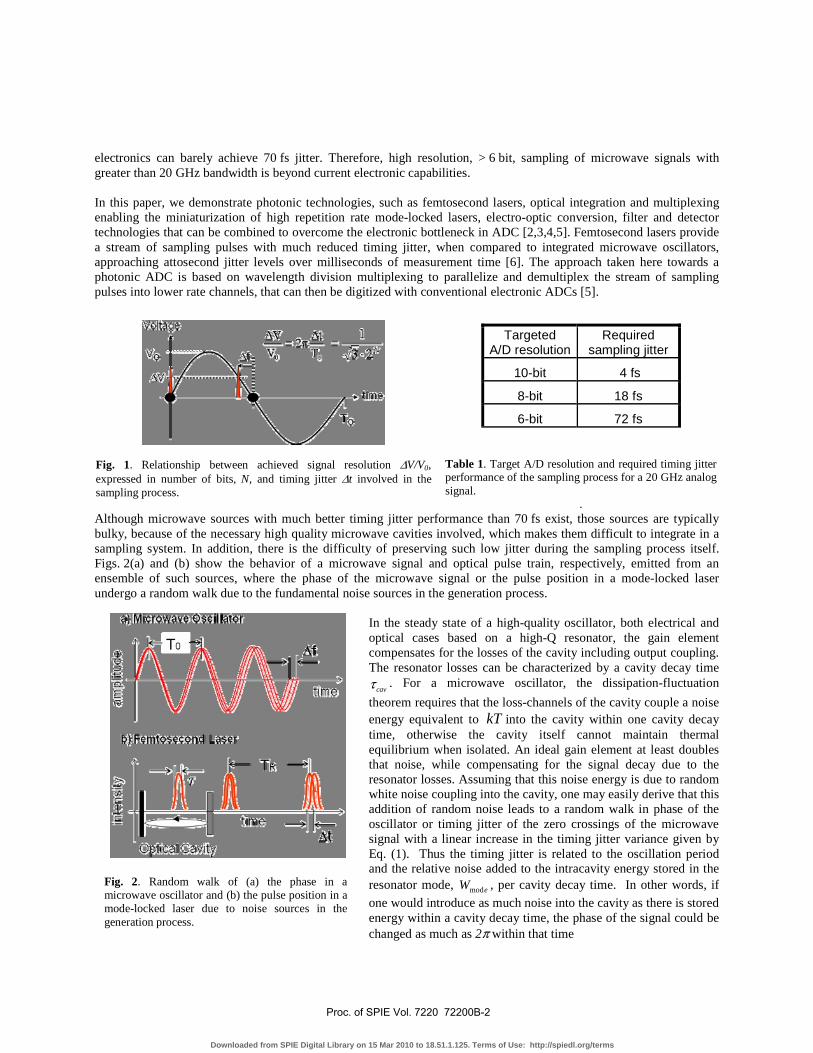
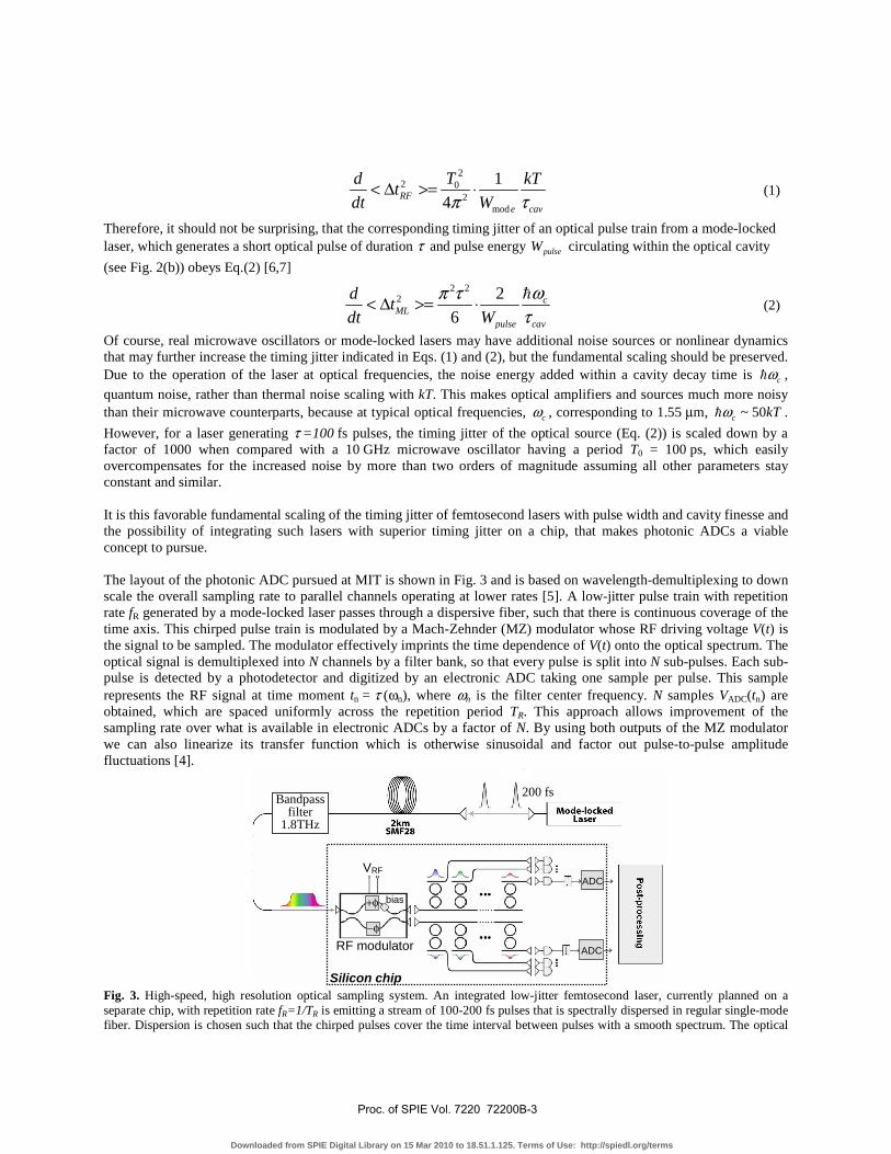
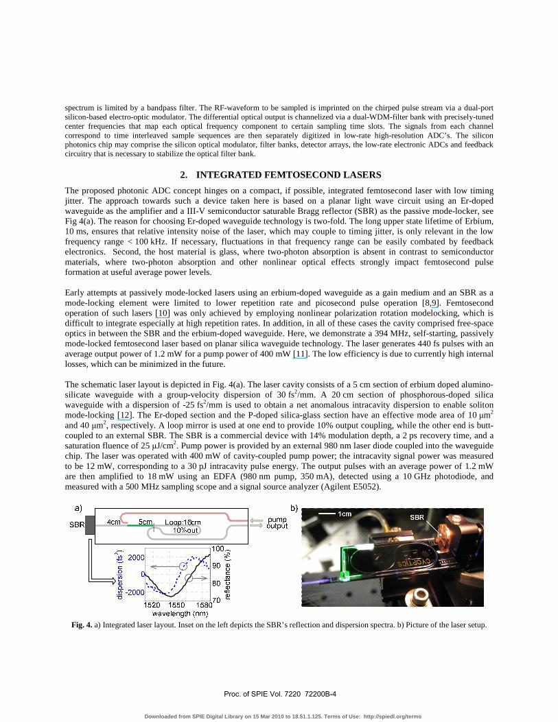
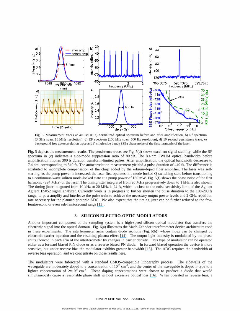
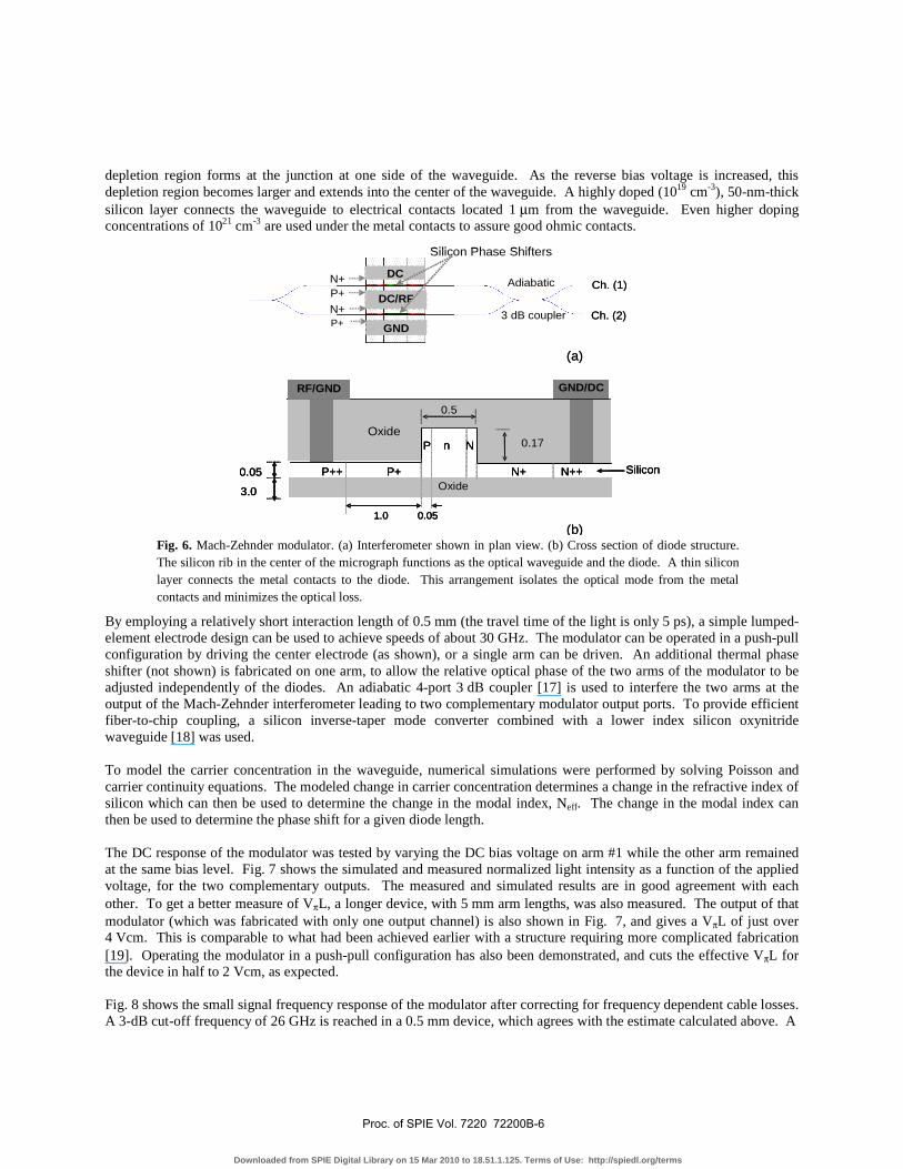
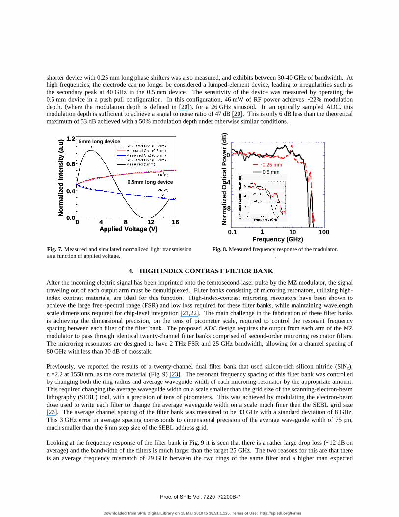
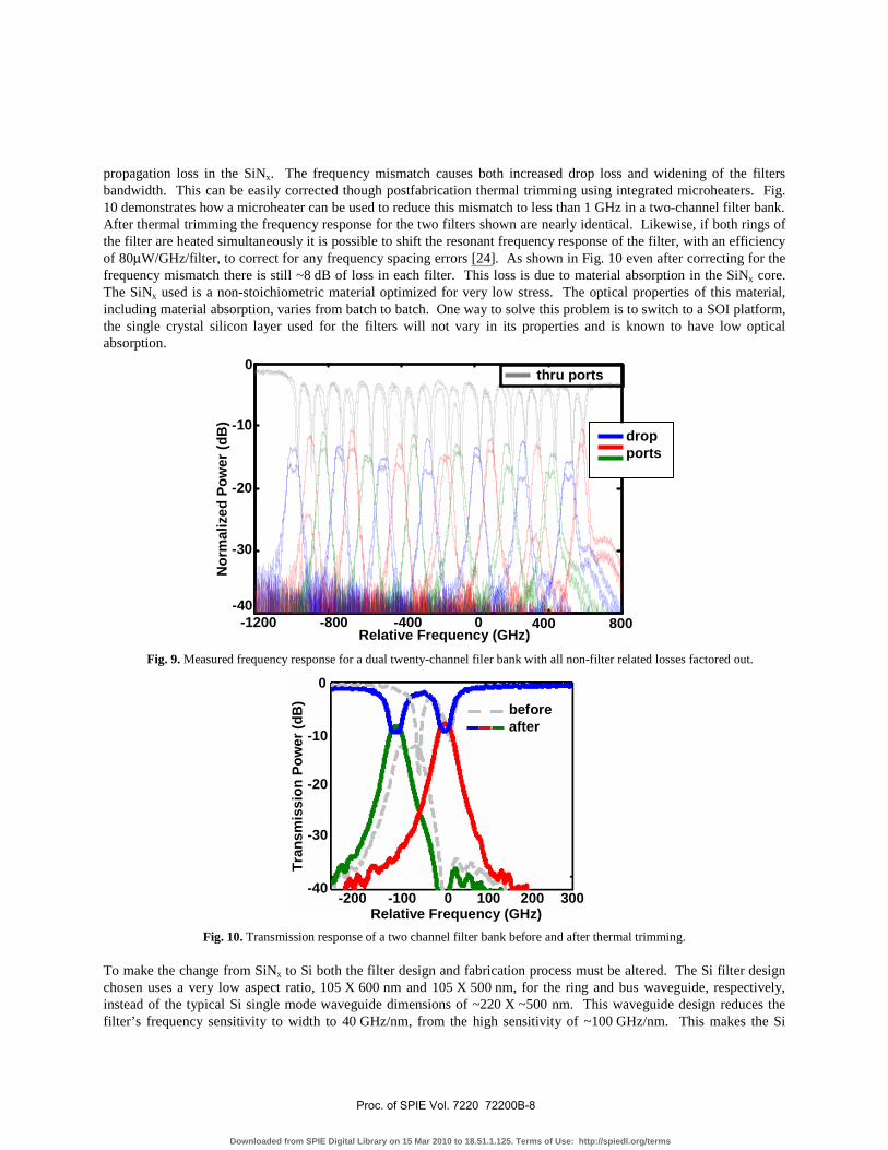
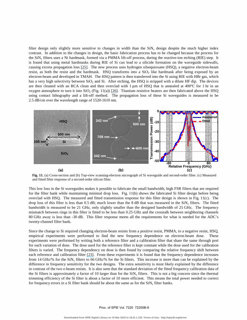
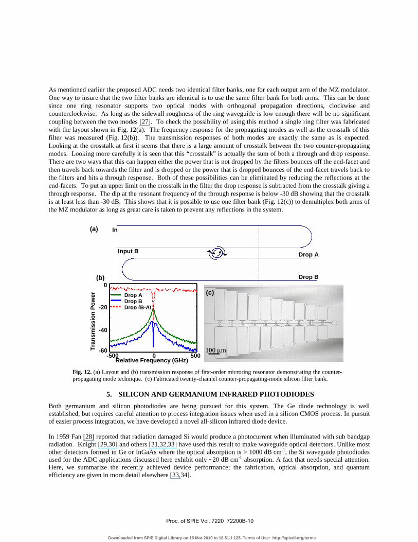
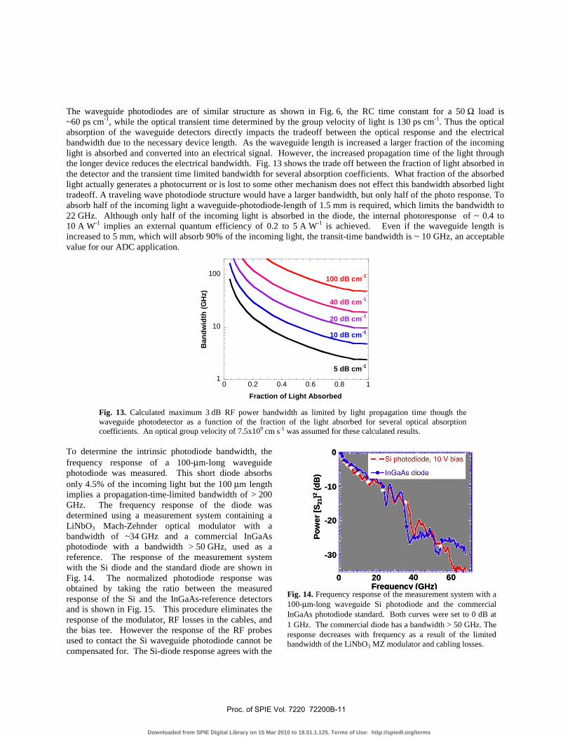
--Si photodiode 10 V bias
InGaAs diode
--Si photodiode 10 V bias
InGaAs diode
The waveguide photodiodes are of similar structure as shown in Fig 6 the RC time constant for a 50 Ω load is ~60 ps cm-1 while the optical transient time determined by the group velocity of light is 130 ps cm-1 Thus the optical absorption of the waveguide detectors directly impacts the tradeoff between the optical response and the electrical bandwidth due to the necessary device length As the waveguide length is increased a larger fraction of the incoming light is absorbed and converted into an electrical signal However the increased propagation time of the light through the longer device reduces the electrical bandwidth Fig 13 shows the trade off between the fraction of light absorbed in the detector and the transient time limited bandwidth for several absorption coefficients What fraction of the absorbed light actually generates a photocurrent or is lost to some other mechanism does not effect this bandwidth absorbed light tradeoff A traveling wave photodiode structure would have a larger bandwidth but only half of the photo response To absorb half of the incoming light a waveguide-photodiode-length of 15 mm is required which limits the bandwidth to 22 GHz Although only half of the incoming light is absorbed in the diode the internal photoresponse of ~ 04 to 10 A W-1 implies an external quantum efficiency of 02 to 5 A W-1 is achieved Even if the waveguide length is increased to 5 mm which will absorb 90 of the incoming light the transit-time bandwidth is ~ 10 GHz an acceptable value for our ADC application
1
10
100
0 02 04 06 08 1
Ban
dw
idth
(G
Hz)
Fraction of Light Absorbed
100 dB cm-1
40 dB cm-1
20 dB cm-1
10 dB cm-1
5 dB cm-1
Fig 13 Calculated maximum 3 dB RF power bandwidth as limited by light propagation time though the waveguide photodetector as a function of the fraction of the light absorbed for several optical absorption coefficients An optical group velocity of 75x109 cm s-1 was assumed for these calculated results
To determine the intrinsic photodiode bandwidth the frequency response of a 100-μm-long waveguide photodiode was measured This short diode absorbs only 45 of the incoming light but the 100 μm length implies a propagation-time-limited bandwidth of gt 200 GHz The frequency response of the diode was determined using a measurement system containing a LiNbO3 Mach-Zehnder optical modulator with a bandwidth of ~34 GHz and a commercial InGaAs photodiode with a bandwidth gt 50 GHz used as a reference The response of the measurement system with the Si diode and the standard diode are shown in Fig 14 The normalized photodiode response was obtained by taking the ratio between the measured response of the Si and the InGaAs-reference detectors and is shown in Fig 15 This procedure eliminates the response of the modulator RF losses in the cables and the bias tee However the response of the RF probes used to contact the Si waveguide photodiode cannot be compensated for The Si-diode response agrees with the
Frequency (GHz)0 20 40 60
0
-10
-20
-30
Po
wer
[S
21]2
(dB
)
Frequency (GHz)0 20 40 60
0
-10
-20
-30
Po
wer
[S
21]2
(dB
)
Fig 14 Frequency response of the measurement system with a 100-μm-long waveguide Si photodiode and the commercial InGaAs photodiode standard Both curves were set to 0 dB at 1 GHz The commercial diode has a bandwidth gt 50 GHz The response decreases with frequency as a result of the limited bandwidth of the LiNbO3 MZ modulator and cabling losses
Proc of SPIE Vol 7220 72200B-11
Downloaded from SPIE Digital Library on 15 Mar 2010 to 18511125 Terms of Use httpspiedlorgterms
InGaAs-reference within a few dB up to 30 GHz and stays close even up to 40 and 50 GHz The calculated RC-time-constant bandwidth of the contact pad capacitance and the 50 Ω input impedance of the network analyzer is ~ 100 GHz Also a ~90 GHz bandwidth was calculated considering only the transit time of holes and electrons at their saturated velocity of 1x107 cm s-1 The RF power to the optical modulator was increased with operating frequency to compensate for reduced response Measurements were made at different RF power levels to ensure that the modulator and photodiodes were operating in their linear region One challenge of a wideband analog system is that one must ensure that the second-order distortions are small not just the third-order This is because by definition a wideband system has enough bandwidth for octaves of the measured signal to be present in the measurement bandwidth which will corrupt the signal estimation We measured the nonlinear response of the silicon waveguide ion-bombarded photodiodes using a three-tone measurement setup [35] in which three independent
DFB lasers were modulated at f1 (380 MHz) f2 (620 MHz) and f3 (2000003 GHz) A useful feature of this technique is that by judicious choice of frequencies the second-order nonlinear distortion at f1 + f2 can be placed very close to the third-order nonlinear distortion f3-(f1+f2) and a narrowband RF filter will pass the distortion components to the measurement system while removing the strong fundamental componentsmdashthis is very challenging using only a two-tone measurement setup More importantly this technique does not rely on any frequency components of type Nf plusmnMf where N and M are integers gt 1 Fig 16 shows the power of the fundamental compared to the second-and third-order distortion products as a function of photocurrent for two different bias voltages The second and third harmonic distortion increased with increasing bias voltage and the second harmonic distortion is observed to be more severe than the third harmonic In addition to Si photodetectors germanium photodiodes are under investigation Blanket Ge-on-Si films have a relatively high threading dislocation density due to the 4 lattice mismatch between Ge and Si To reduce the threading dislocation density Ge can be grown selectively in oxide openings For the test devices in this work the starting material was 6rdquo p+ Si wafers with patterned silicon dioxide films Using an Applied Materials low-pressure chemical vapor deposition epitaxial reactor the germanium was grown to overfill the openings to ensure that the oxide openings were completely filled A chemical-mechanical polishing step was then performed to planarize the Ge film The samples were then implanted with phosphorus and subjected to a rapid thermal anneal at 600degC for 5 s to activate the implant Contact vias were etched and metal contacts were deposited to form vertical pin diodes A cross-sectional schematic of the device is shown in the inset of Fig 18
0
5
0
Frequency (GHz)
Po
wer
[S
21]2
(dB
)
10
5
0
-10
-5
001 01 1 10 100
0
5
0
Frequency (GHz)
Po
wer
[S
21]2
(dB
)
10
5
0
-10
-5
001 01 1 10 100
Fig 15 Measured frequency response of a 100-μm-long waveguide Si photodiode using the difference between a high bandwidth standard diode and the Si diode The data for both diodes individually is shown in Fig 14 The increase in response between 40 and 50 GHz is believed to result from RF probes used to contact the Si diode which are rated to 40 GHz More details of this measurement are given elsewhere [34]
Third Harmonic
Second Harmonic
Fundamental
Photocurrent (mA) 001 01 1
Ou
tpu
t P
ow
er (
dB
m)
40
-10
-60
-110
fundamental
second harmonic
third harmonic
Fig 16 Output power of the photocurrent (in a 50 Ohm load) as a function of photocurrent for the fundamental second harmonic (formed by f1+f2) and third harmonic (formed by f3-(f1+f2) for 10 V (black) and 125 V (red) reverse bias voltage in a 1-mm Si waveguide ion-bombarded photodetector
Proc of SPIE Vol 7220 72200B-12
Downloaded from SPIE Digital Library on 15 Mar 2010 to 18511125 Terms of Use httpspiedlorgterms
Si
-UnanneaIe-Annealed
- n+Ge Metal
5um I urn O65um
Fig 17 shows plan view transmission electron microscopy (TEM) images for various sized Ge features For the as-grown Ge layers the threading dislocation density decreases with device width from 55 x 108 cm-2 to 26 x 108 cm-2 to 17 x 108 cm-2 for 5 1 and 065 μm-wide devices respectively This effect is consistent with previous results on aspect ratio trapping [36] and a small area effect [37 38] Fig 16 also illustrates that a cyclic anneal reduces the dislocation density Analysis of multiple plan view TEM areas indicates that the dislocation density was reduced from 17 x 108 cm-2 to 26 x 107 cm-2 in the 065 μm-wide islands by cyclic annealing
Fig 17 Plan-view TEM images of different sized germanium islands for (a ndash c) as-grown and (d) cyclically annealed 08 μm-thick Ge grown selectively on Si The threading dislocation density decreases with the width of the island The threading dislocation density also decreases when the film is annealed
Fewer threading dislocations are expected to improve the yield and reduce the dark current of these devices Fig 18 shows current versus voltage characteristics of vertical pin diodes fabricated in 035 x 10 μm germanium islands for both an as-grown Ge film and a film cyclically annealed between 830degC and 450degC These are representative characteristics of rectifying devices After processing it was found that about 50 of the devices displayed rectifying behavior and the others were shorted The impact of material quality and device processing on yield requires further investigation The dark current for both devices is ~05 nA at -1 V While the cyclic anneal reduced the threading dislocation density in these devices this did not have a significant effect on the dark current This indicates that the leakage in these smaller devices is dominated by another mechanism and more work is needed to fully characterize it The cyclic anneal did have an effect on the on current however The device that received the anneal has ~2x higher on current at 1 V than the device without the anneal This is most likely due to a reduction in the series resistance
Fig 18 Measured current versus voltage characteristics for pin diodes in a Ge film that was annealed and in a film that was not annealed The cyclic anneal takes place after germanium growth but before n+ ion implantation The anneal has little effect on the dark current of these devices but increases the on current by ~2x The germanium island size is 035 x 10 μm Inset a cross-sectional schematic diagram of the diodes
065 um
(a) (b) (c) (d)
Voltage (V)
Cu
rren
t (A
)
10-4
10-6
10-8
10-10
10-12 -1 -05 0 05 1
Proc of SPIE Vol 7220 72200B-13
Downloaded from SPIE Digital Library on 15 Mar 2010 to 18511125 Terms of Use httpspiedlorgterms
6 CONCLUSIONS
We have presented the system architecture and fabricated key elements of a photonic ADC The fabricated devices include a 394 MHz waveguide femtosecond laser with 24 fs timing jitter a Si modulator capable of modulating speeds faster then 25 GHz high performance Si-microring filters for a demultiplexing filter bank silicon and germanium photodiodes Using such devices for the proposed ADC system allows higher sampling speeds than current pure electronic systems due to the low timing jitter of the femotsecond laser The size-scale materials and processing methods for these devices make them suitable for integration on an electronic-photonic silicon-on-insulator platform
ACKNOWLEDGEMENTS
The MIT Lincoln Laboratory portion of this work was sponsored by the EPIC Program of the Defense Advanced Research Projects Agency and in part by the Department of the Air Force under Air Force Contract FA8721-05-C-0002 The MIT Campus portion of this work was sponsored by the DARPA EPIC Program under contract W911NF-04-1-0431 and DARPA OAWG Program under contract HR0011-05-C-0155 Opinions interpretations conclusions and recommendations are those of the authors and do not necessarily represent the view of the United States Government
REFERENCES
[1] RH Walden ldquoAnalog-to-digital converter survey and analysisrdquo IEEE J Select Areas Commun 17 4 539-550 April 1999
[2] PW Juodawlkis J C Twichell G E Betts J J Hargreaves R D Younger J L Wasserman F J OrsquoDonnell K G Ray and R C
Williamson ldquoOptically sampled analog-to-digital convertersrdquo IEEE Trans Microwave Theory Tech 49(10) 1840 (2001)
[3] T R Clark J U Kang and R D Esman ldquoPerformance of a time- and wavelength-interleaved photonic sampler for analog-digital conversionrdquo
IEEE Photon Technol Lett 11(9) 1168 (1999)
[4] GC Valley Photonic analog-to-digital converters Opt Express 15 1955-1982 (2007)
[5] F X Kaumlrtner et al ldquoPhotonic Analog-to-Digital Conversion with Electronic-Photonic Integrated Circuitsrdquo SPIE Conference Photonic West
San Jose January 2007
[6] H A Haus and A Mecozzi ldquoNoise of mode-locked lasersrdquo IEEE J Quantum Electron 29 983-996 (1993)
[7] F X Kaumlrtner et al in Few-Cycle Pulse Generation and its Applications ed by F X Kaumlrtner (Springer 2004)
[8] ER Thoen EM Koontz DJ Jones FX Kaumlrtner EP Ippen LA Kolodziejski ldquoErbium-Ytterbium waveguide laser mode-locked with a
semiconductor saturable absorber mirrorrdquo IEEE Photon Technol Lett 12 149-151 (2000)
[9] J B Schlager B E Callicoatt R P Mirin N A Sanford D J Jones J Ye ldquoPassively mode-locked glass waveguide laser with 14-fs timing
jitterrdquo Opt Lett 28 2411-2413 (2003)
[10] DJ Jones S Namiki D Barbier EP Ippen and HA Haus ldquo116-fs soliton source based on an Er-Yb codoped waveguide amplifier rdquo IEEE
Photon Technol Lett 10 1-3 (1998)
[11] F X Kaumlrtner and U Keller ldquoStabilization of soliton-like pulses with a slow saturable absorberldquo Opt Lett 20 16-18 (1995)
[12] H Byun D Pudo S Frolov A Hanjani J Shmulovich E P Ippen and F X Kaumlrtner ldquoIntegrated low-jitter 400 MHz femtosecond passively
mode-locked waveguide laserrdquo Annual Meeting of the IEEE Laser and Electro-Optics Society LEOS Newport Beach CA (2008)
[13] J Kim J Chen J Cox and F X Kaumlrtner ldquoAttosecond-resolution timing jitter characterization of free-running mode-locked lasers using
balanced optical cross-correlationrdquo Opt Lett 32(24) 3519-3521 (2007)
[14] RA Soref ldquoSilicon-based optoelectronicsrdquo Proc IEEE 81 1687ndash1706 (1993)
[15] S J Spector M W Geis M E Grein R T Schulein J U Yoon D M Lennon F Gan G-R Zhou F X Kaertner and T M Lyszczarz
ldquoHigh-speed silicon electro-optical modulator that can be operated in carrier depletion or carrier injection moderdquo CLEO 2008 Technical Digest
(OSA Washington DC 2008) CFH4
[16] F Gan and F X Kaumlrtner ldquoLow insertion loss high-speed silicon electro-optic modulator designrdquo in Integrated Photonics Research and
Applications Nanophotonics CLEO 2006 Technical Digest (OSA Washington DC 2006) ITuB2
Proc of SPIE Vol 7220 72200B-14
Downloaded from SPIE Digital Library on 15 Mar 2010 to 18511125 Terms of Use httpspiedlorgterms
[17] K Solehmainen M Kapulainen M Harjanne and T Aalto Adiabatic and multimode interference couplers on silicon-on-insulator IEEE
Photonic Technol Lett 18(21) 2287-2289 (2006)
[18] T Shoji T Tsuchizawa T Watanabe K Yamada and H Morita Spot-size converter for low-loss coupling between 03-μm-square Si wire
waveguides and single-mode fibers EOS 2002 2002 IEEELEOS Annual Meeting Conference Proceedings 1 289-290 (2002)
[19] L Liao A Liu D Rubin J Basak Y Chetrit H Nguyen R Cohen N Izhaky and M Paniccia ldquo40 Gbits silicon optical modulator for
highspeed applicationsrdquo Elect Lett 43 (22) 1196-1197 (2007)
[20] J C Twichell and R Helkey ldquoPhase-encoded optical sampling for analog-to-digital convertersrdquo IEEE Photonic Technol Lett 12 1237-1239
(2000)
[21] BE Little ldquoAdvances in microring resonatorsrdquo in Proc Integrated Photonics Research Conf 165-167 (2003)
[22] T Barwicz MA Popović MR Watts PT Rakich EP Ippen and HI Smith ldquoFabrication of Add-Drop Filters Based on Frequency-Matched
Microring Resonatorsrdquo J of Light Technol 24 2207 (2006)
[23] CW Holzwarth R Amatya M Dahlem A Khilo F X Kaertner E P Ippen R J Ram and Henry I Smith ldquoFabrication strategies for filter
banks on microring resonatorsrdquo J of Vac Sci and Technol B 26 2164-2167 (2008)
[24] R Amatya C W Holzwarth Henry I Smith and R J Ram ldquoPrecision tunable silicon compatible microring filtersrdquo Submitted to IEEE Phot
Tech Lett (2008)
[25] T Barwicz C W Holzwarth P T Rakich M A Popovic E P Ippen and Henry I Smith ldquoOptical loss in silicon microphotonic waveguides
induced by metallic contaminationrdquo Appl Phys Lett 92 131108 (2008)
[26] CW Holzwarth T Barwicz and HI Smith ldquoOptimization of hydrogen silsesquioxane for photnic applicationsrdquo J of Vac Sci and Technol
B 25 (2007)
[27] B E Little J P Laine and S T Chu ldquoSurface-roughness-induced contradirectional coupling in ring and disk resonatorsrsquo Optics Lett 22(1)
4-6 (1997)
[28] HY Fan and A K Ramdas rdquoInfrared Absorption and Photoconductivity in Irradiated Siliconrdquo J Appl Phys 30 1127-1134 (1959)
[29] A Knights A House R MacNaughton and F Hopper ldquoOptical power monitoring function compatible with single chip integration on
silicon-on-insulatorrdquo Conference on Optical Fiber Communication Technical Digest Series 86 705-706 (2003)
[30] AP Knights J D Bradley SH Gou and P E Jessop ldquoSilicon-on-insulator waveguide photodiode with self-ion-implantation-engineered-
enhanced infrared responserdquo J Vac Sci Technol A 24 3 783-786 (2006)
[31] Y Liu C W Chow W Y Cheung H K Tsang ldquoIn-line channel power monitor based on helium ion implantation in silicon-on-insulator
waveguidesrdquo IEEE Photon Technol Lett 18 1882-1884 (2006)
[32] M W Geis S J Spector M E Grein RT Schulein J U Yoon D M Lennon S Denault F Gan F X Kaumlrtner and T M Lyszczarz
ldquoCMOS-compatible all-Si high-speed waveguide photodiodes with high responsivity in near-infrared communication bandrdquo IEEE Photon
Technol Lett 19 152-154 (2007)
[33] M W Geis S J Spector M E Grein R T Schulein J U Yoon D M Lennon C M Wynn S T Palmacci F Gan F X Kaumlrtner and T
M Lyszczarz ldquoAll silicon infrared photodiodes photo response and effects of processing temperaturerdquo Opt Express 15 16886-16895 (2007)
[34] M W Geis S J Spector M E Grein J U Yoon D M Lennon and T M Lyszczarz rdquo Silicon waveguide infrared photodiodes with 50
GHz bandwidth and phototransistors with 50 AW-1 responsesrdquo submitted to Opt Express
[35] T Ozeki and E H Hara rdquoMeasurement of nonlinear distortion in photodiodesrdquo Electron Lett 12 80-81 (1976)
[36] J-S Park J Bai M Curtin B Adekore M Carroll and A Lochtefeld ldquoDefect reduction of selective Ge epitaxy in trenches on Si(001) substrates using aspect ratio trappingrdquo Appl Phys Lett 90(5) 052113 (2007)
[37] H-C Luan D R Lim K K Lee K M Chen J G Sandland K Wada and L C Kimerling ldquoHigh-quality Ge epilayers on Si with low threading-dislocation densitiesrdquo Appl Phys Lett 75(19) 2909-2911 (1999)
[38] M Kim O Olubuyide J Yoon and JL Hoyt ldquoSelective Epitaxial Growth of Ge-on-Si for Photodiode Applicationsrdquo Electrochemical Society Transactions 16(10) 837 ndash 847 (2008)
Proc of SPIE Vol 7220 72200B-15
Downloaded from SPIE Digital Library on 15 Mar 2010 to 18511125 Terms of Use httpspiedlorgterms
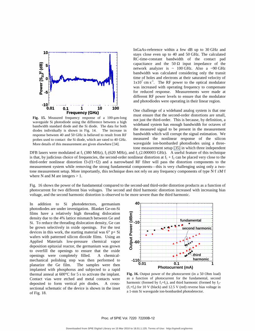
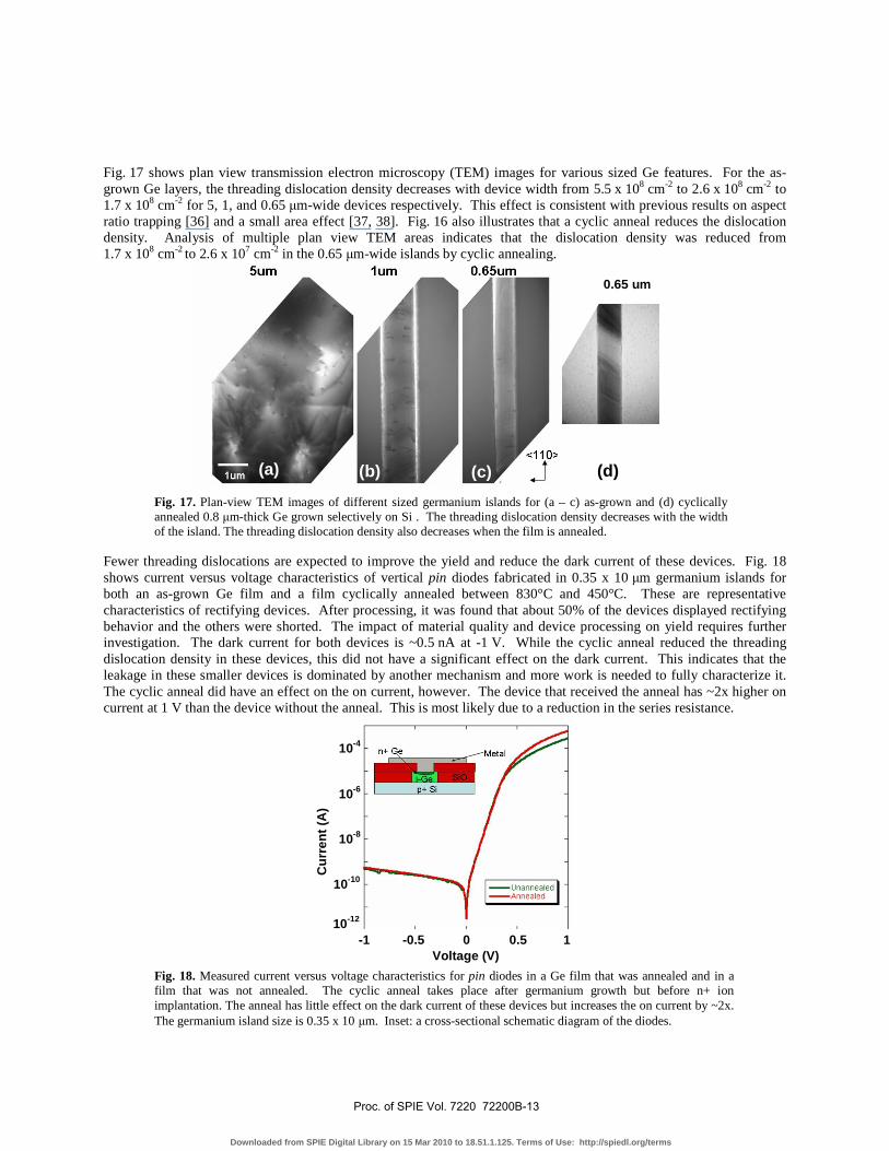
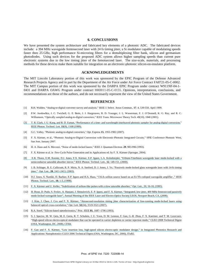
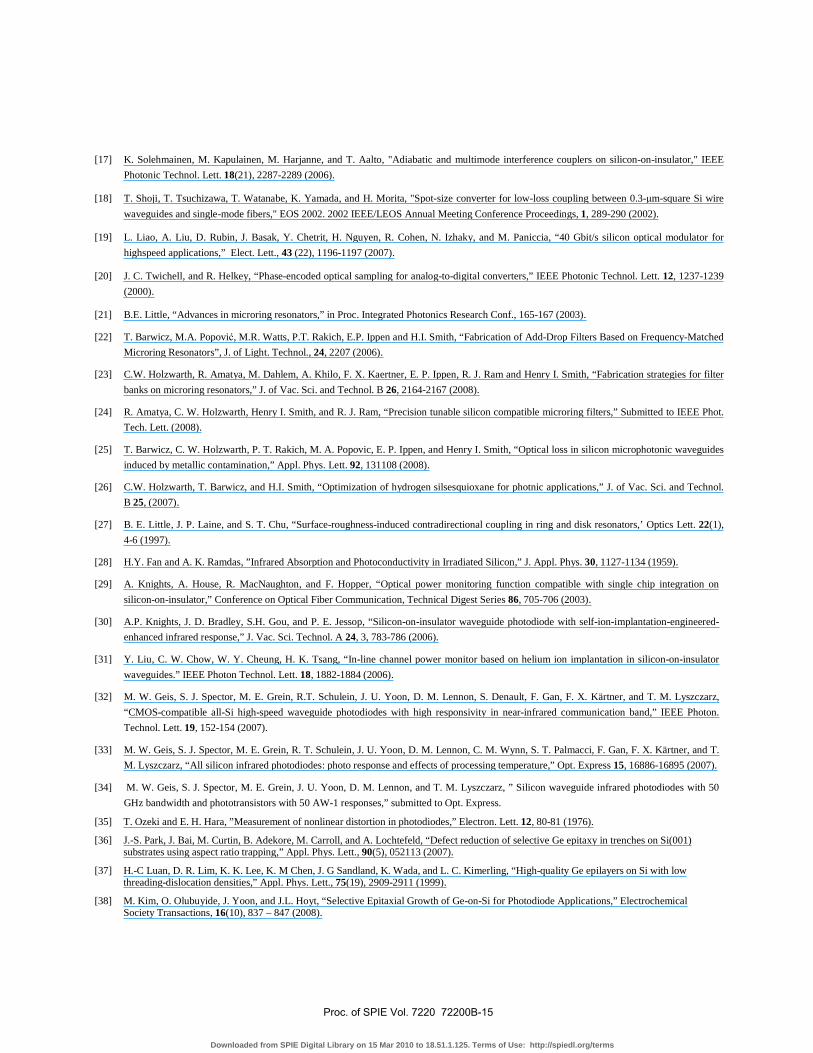