Thermal-instabilities-of-charge-carrier-transport-in-solar-cells ...
79
UNIVERSIDAD DE CHILE FACULTAD DE CIENCIAS FÍSICAS Y MATEMÁTICAS DEPARTAMENTO DE INGENIERÍA MECÁNICA THERMAL INSTABILITIES OF CHARGE CARRIER TRANSPORT IN SOLAR CELLS BASED ON GaAs PN JUNCTIONS TESIS PARA OPTAR AL GRADO DE MAGÍSTER EN CIENCIAS DE LA INGENIERÍA, MENCIÓN MECÁNICA MEMORIA PARA OPTAR AL TÍTULO DE INGENIERA CIVIL MECÁNICA JOSEFA FERNANDA IBACETA JAÑA PROFESOR GUÍA: WILLIAMS CALDERÓN MUÑOZ MIEMBROS DE LA COMISIÓN: PATRICIO MENDOZA ARAYA ÁLVARO VALENCIA MUSALEM Este trabajo ha sido parcialmente financiado por CONICYT-PCHA/Magíster Nacional/2016 - 22160729 SANTIAGO DE CHILE 2017
-
Upload
khangminh22 -
Category
Documents
-
view
0 -
download
0
Transcript of Thermal-instabilities-of-charge-carrier-transport-in-solar-cells ...

UNIVERSIDAD DE CHILEFACULTAD DE CIENCIAS FÍSICAS Y MATEMÁTICASDEPARTAMENTO DE INGENIERÍA MECÁNICA
THERMAL INSTABILITIES OF CHARGE CARRIER TRANSPORTIN SOLAR CELLS BASED ON GaAs PN JUNCTIONS
TESIS PARA OPTAR AL GRADO DEMAGÍSTER EN CIENCIAS DE LA INGENIERÍA, MENCIÓN
MECÁNICA
MEMORIA PARA OPTAR AL TÍTULO DEINGENIERA CIVIL MECÁNICA
JOSEFA FERNANDA IBACETA JAÑA
PROFESOR GUÍA:WILLIAMS CALDERÓN MUÑOZ
MIEMBROS DE LA COMISIÓN:PATRICIO MENDOZA ARAYAÁLVARO VALENCIA MUSALEM
Este trabajo ha sido parcialmente financiado porCONICYT-PCHA/Magíster Nacional/2016 - 22160729
SANTIAGO DE CHILE2017

RESUMENDE: Tesis para optar al grado deMagíster en Ciencias de la Ingeniería, MenciónMecánica y Memoria para optar al título deIngeniera Civil Mecánica.POR: Josefa Fernanda Ibaceta Jaña.FECHA: 21 de Abril,2017PROF. GUÍA: Williams Calderón Muñoz.
INESTABILIDADES TÉRMICAS DEL TRANSPORTE DE PORTADORESDE CARGA EN CELDAS SOLARES BASADAS EN JUNTURAS PN DE
GaAs
Dentro de los factores que afectan negativamente una celda solar fotovoltaica se destaca latemperatura. Ya sea por imperfecciones del material o a condiciones de operación no uni-formes, es posible que se concentre calor en una zona debido a la disminución de la resistencialocal y su consecuente aumento de corriente eléctrica. Estas zonas de concentración de calorpueden estabilizarse, generando gradualmente degradación de la celda, disminución de suvida útil y eficiencia. En caso contrario, puede ocurrir un fenómeno de descontrol térmicoque resulta catastrófico para la celda, inhabilitando su correcto funcionamiento. Estudios enmódulos de película delgada revelan que esta condición ocurre incluso cuando la radiaciónestá uniformemente distribuida y con ello, el perfil de temperatura inicial es constante. Laevolución temporal, bajo radiación, induce zonas de calor que incrementan exponencialmentela temperatura, contrayendo su área; por otra parte, la temperatura de las zonas más alejadasdisminuye simultáneamente mientras disipan pequeñas corrientes. Para evitar este fenómenose pueden escalar propiedades del dispositivo, como aumentar la conductividad térmica ydisminuir el espesor. Actualmente, estos análisis se realizan a partir de modelos numéricosy analíticos basados en el comportamiento de diodos y mediciones experimentales del perfilde temperatura en la capa superficial de la celda y en la juntura. El propósito de esta Tesises determinar criterios de estabilidad electro-térmico que pueden ser utilizados para evitar eldescontrol de temperatura a partir de aplicar un análisis a un modelo hidrodinámico de mayorcomplejidad que uno basado en diodos; más aún, considerar un estado fuera del equilibroentre la temperatura de la red y los portadores de carga. Se determinó que la inestabilidadocurre en la juntura PN y depende fuertemente la temperatura de la juntura en los bordes.Además, aumentar la temperatura de los portadores, disminuir el largo y aumentar el voltajeaplicado pueden estabilizar el sistema, aumentando el tiempo en que el sistema duplica sutemperatura.
i
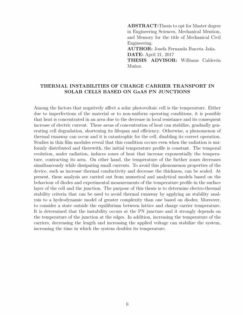
ABSTRACT:Thesis to opt for Master degreein Engineering Sciences, Mechanical Mention,and Memory for the title of Mechanical CivilEngineering.AUTHOR: Josefa Fernanda Ibaceta Jaña.DATE: April 21, 2017THESIS ADVISOR: Williams CalderónMuñoz.
THERMAL INSTABILITIES OF CHARGE CARRIER TRANSPORT INSOLAR CELLS BASED ON GaAS PN JUNCTIONS
Among the factors that negatively affect a solar photovoltaic cell is the temperature. Eitherdue to imperfections of the material or to non-uniform operating conditions, it is possiblethat heat is concentrated in an area due to the decrease in local resistance and its consequentincrease of electric current. These areas of concentration of heat can stabilize, gradually gen-erating cell degradation, shortening its lifespan and efficiency. Otherwise, a phenomenon ofthermal runaway can occur and it is catastrophic for the cell, disabling its correct operation.Studies in thin film modules reveal that this condition occurs even when the radiation is uni-formly distributed and therewith, the initial temperature profile is constant. The temporalevolution, under radiation, induces zones of heat that increase exponentially the tempera-ture, contracting its area. On other hand, the temperature of the further zones decreasessimultaneously while dissipating small currents. To avoid this phenomenon properties of thedevice, such as increase thermal conductivity and decrease the thickness, can be scaled. Atpresent, these analysis are carried out from numerical and analytical models based on thebehaviour of diodes and experimental measurements of the temperature profile in the surfacelayer of the cell and the junction. The purpose of this thesis is to determine electro-thermalstability criteria that can be used to avoid thermal runaway by applying an stability anal-ysis to a hydrodynamic model of greater complexity than one based on diodes; Moreover,to consider a state outside the equilibrium between lattice and charge carrier temperature.It is determined that the instability occurs at the PN juncture and it strongly depends onthe temperature of the junction at the edges. In addition, increasing the temperature of thecarriers, decreasing the length and increasing the applied voltage can stabilize the system,increasing the time in which the system doubles its temperature.
ii

“It’s our choices that show what we truly are, far more than our abilities”Albus Dumbledore
iii

Agradecimientos
Quisiera dar las gracias a todos los que me apoyaron incondicionalmente, los que creyeronen mi desde un principio y estuvieron para escucharme cada vez que las cosas se volvíancomplicadas, trayendo desesperanza.
Realizar esta tesis como acto de finalización de este periodo de mi vida significó mucho parami incluso antes de empezarla. Me hizo recurrir a todos los conocimientos que adquirí enclases, estudiando en mi casa o haciendo alguna tarea con algún amigo. Puedo recordar lasveces en que mi familia me llevaba comida a la pieza o me invitaba a salir a relajarme, a todoslos malos chistes sobre materia con mis amigos y a las infinitas horas de contestar pruebaspara luego comentar cada mínimo detalle. Recuerdo con cariño a todos los que me apoyaroncon cualquier pequeña meta personal o me preguntaban que tal me estaba yendo.
Y como todos somos los que las experiencias forman, quisiera agradecer en específico ami mamá y a mi hermano por no asesinarme en mis estados de colapso;a mi abuelita porpreguntarme cada vez si había terminado la tesis; a Rodrigo por siempre tratar de ordenar micabeza; a las procastinantes por siempre empatizar conmigo; al Alonso por compartirme todasu experiencia; a los chicos de la oficina por hacerme reir; a la Suu, la Karen, el Rub, el Rod yel Mirko por compartir el camino conmigo; al profesor Gerardo por darme la oportunidad deaplicar mi conocimiento en otras fronteras; a mis profesores del colegio que incentivaron migusto por aprender; por último, a mi comisión de profesores que con sus ideas y su dedicaciónpermitieron que lograra esto.
Se agradece a CONICYT-PHCA/Magíster Nacional/2016-22160729 por apoyo financiero
iv
Contents
1 Introduction . . . . . . . . . . . . . . . . . . . . . . . . . . . . . . . . . . . . . . 11.1 Objectives . . . . . . . . . . . . . . . . . . . . . . . . . . . . . . . . . . . . . 2
1.1.1 General Objective . . . . . . . . . . . . . . . . . . . . . . . . . . . . . 21.1.2 Specific Objectives . . . . . . . . . . . . . . . . . . . . . . . . . . . . 2
1.2 Methodology . . . . . . . . . . . . . . . . . . . . . . . . . . . . . . . . . . . 2
2 Background . . . . . . . . . . . . . . . . . . . . . . . . . . . . . . . . . . . . . . 32.1 Semiconductor Physics . . . . . . . . . . . . . . . . . . . . . . . . . . . . . . 3
2.1.1 Semiconductor Microstructure . . . . . . . . . . . . . . . . . . . . . . 32.1.2 Carrier Transport Phenomena . . . . . . . . . . . . . . . . . . . . . . 9
2.2 PN junction . . . . . . . . . . . . . . . . . . . . . . . . . . . . . . . . . . . . 122.3 Photovoltaic Solar Cell . . . . . . . . . . . . . . . . . . . . . . . . . . . . . . 13
2.3.1 Design . . . . . . . . . . . . . . . . . . . . . . . . . . . . . . . . . . . 152.4 Properties of Gallium Arsenide . . . . . . . . . . . . . . . . . . . . . . . . . 162.5 Hydrodynamic Stability . . . . . . . . . . . . . . . . . . . . . . . . . . . . . 172.6 Hot Spot in PV Solar Cells . . . . . . . . . . . . . . . . . . . . . . . . . . . . 18
3 Model Description . . . . . . . . . . . . . . . . . . . . . . . . . . . . . . . . . . 233.1 Physical parameters . . . . . . . . . . . . . . . . . . . . . . . . . . . . . . . . 243.2 Assumptions . . . . . . . . . . . . . . . . . . . . . . . . . . . . . . . . . . . . 253.3 Boundary Conditions . . . . . . . . . . . . . . . . . . . . . . . . . . . . . . . 263.4 Non-dimensional Form . . . . . . . . . . . . . . . . . . . . . . . . . . . . . . 27
4 Resolution Method . . . . . . . . . . . . . . . . . . . . . . . . . . . . . . . . . 294.1 Perturbation Theory . . . . . . . . . . . . . . . . . . . . . . . . . . . . . . . 294.2 Disturbed System . . . . . . . . . . . . . . . . . . . . . . . . . . . . . . . . . 31
4.2.1 Zero order system . . . . . . . . . . . . . . . . . . . . . . . . . . . . . 324.2.2 First Order System . . . . . . . . . . . . . . . . . . . . . . . . . . . . 32
4.3 Linear stability analysis . . . . . . . . . . . . . . . . . . . . . . . . . . . . . 334.3.1 Steady-State System . . . . . . . . . . . . . . . . . . . . . . . . . . . 334.3.2 Transient-state System . . . . . . . . . . . . . . . . . . . . . . . . . . 354.3.3 Boundary Conditions . . . . . . . . . . . . . . . . . . . . . . . . . . . 374.3.4 Integration Methods . . . . . . . . . . . . . . . . . . . . . . . . . . . 384.3.5 Temporal Eigenvalues . . . . . . . . . . . . . . . . . . . . . . . . . . 40
5 Results . . . . . . . . . . . . . . . . . . . . . . . . . . . . . . . . . . . . . . . . . 415.1 Validity of Results . . . . . . . . . . . . . . . . . . . . . . . . . . . . . . . . 41
5.1.1 Main Code Tolerance . . . . . . . . . . . . . . . . . . . . . . . . . . . 41
v
5.1.2 Transient-state Code Conditions . . . . . . . . . . . . . . . . . . . . . 435.2 Data Processing . . . . . . . . . . . . . . . . . . . . . . . . . . . . . . . . . . 46
5.2.1 Range of Allowed Eigenvalues . . . . . . . . . . . . . . . . . . . . . . 475.3 Sensitivity Analysis . . . . . . . . . . . . . . . . . . . . . . . . . . . . . . . . 49
5.3.1 Solution at Thermal Equilibrium . . . . . . . . . . . . . . . . . . . . 495.3.2 Variation in Temperature . . . . . . . . . . . . . . . . . . . . . . . . 515.3.3 Variation in Longitude . . . . . . . . . . . . . . . . . . . . . . . . . . 575.3.4 Variation in applied voltage . . . . . . . . . . . . . . . . . . . . . . . 59
5.4 Surface Temperature . . . . . . . . . . . . . . . . . . . . . . . . . . . . . . . 61
6 Conclusions and Future Work . . . . . . . . . . . . . . . . . . . . . . . . . . . 646.1 Conclusions . . . . . . . . . . . . . . . . . . . . . . . . . . . . . . . . . . . . 646.2 Future Work . . . . . . . . . . . . . . . . . . . . . . . . . . . . . . . . . . . . 65
Bibliography . . . . . . . . . . . . . . . . . . . . . . . . . . . . . . . . . . . . . 66
vi
List of Tables
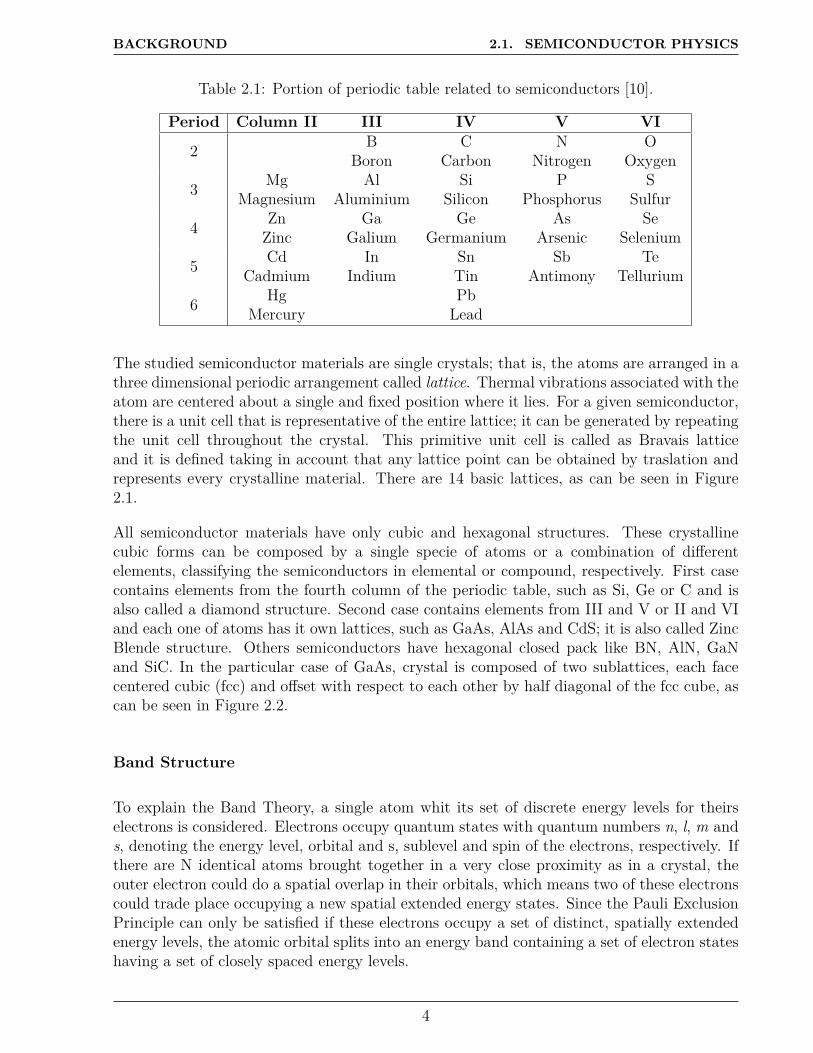
2.1 Portion of periodic table related to semiconductors [10]. . . . . . . . . . . . . 4
3.1 Physical properties for GaAs [34] . . . . . . . . . . . . . . . . . . . . . . . . 25
vii

List of Figures
2.1 Bravais lattices [11]. . . . . . . . . . . . . . . . . . . . . . . . . . . . . . . . 52.2 Conventional unit cube for GaAs [12]. . . . . . . . . . . . . . . . . . . . . . . 52.3 Energy bands in Silicon crystal with a diamond lattice structure [10]. . . . . 62.4 Representation of electron and holes [10]. . . . . . . . . . . . . . . . . . . . . 62.5 Schematic energy-momentum diagram for Si and GaAs [13]. . . . . . . . . . 72.6 Actual bidimensional energy-momentum diagram for GaAs and Si [12] . . . . 82.7 Fermi distribution function for various temperatures [10]. . . . . . . . . . . . 82.8 a)Uniformly doped p-type and n-type semiconductors.b)Electric field in the
depletion region and the energy band diagram of a PN junction in thermalequilibrium [10]. . . . . . . . . . . . . . . . . . . . . . . . . . . . . . . . . . . 12
2.9 Band diagram of solar cell.Generated electron-hole pairs drift across the de-pletion region [14]. . . . . . . . . . . . . . . . . . . . . . . . . . . . . . . . . 13
2.10 I-V Characteristic of solar cell [14]. . . . . . . . . . . . . . . . . . . . . . . . 142.11 Schematic diagram of solar cell layers [15]. . . . . . . . . . . . . . . . . . . . 152.12 Hot spot temperature profile, TCO layer [23]. . . . . . . . . . . . . . . . . . 182.13 Equivalent circuit of PN junction. . . . . . . . . . . . . . . . . . . . . . . . . 202.14 IR mapping triple junction a-Si:H [25] . . . . . . . . . . . . . . . . . . . . . 202.15 Temperature distribution over sample at 2[suns] [25]. . . . . . . . . . . . . . 212.16 Simulated temporal temperature as a function of thermal conductivity χ [25]. 22
3.1 Device scheme with boundary conditions [33]. . . . . . . . . . . . . . . . . . 26
4.1 Steady-state variables distribution in space. . . . . . . . . . . . . . . . . . . 34
5.1 Significant digits in steady state code. . . . . . . . . . . . . . . . . . . . . . . 425.2 Positive eigenvalues from Runge Kutta 2nd order. . . . . . . . . . . . . . . . 445.3 Relative error from Runge Kutta 2nd order. . . . . . . . . . . . . . . . . . . 445.4 Positive eigenvalues from Runge Kutta 4th order. . . . . . . . . . . . . . . . 455.5 Relative error from Runge Kutta 4th order. . . . . . . . . . . . . . . . . . . 455.6 General transient response representation in time. . . . . . . . . . . . . . . . 465.7 Reference time t0. . . . . . . . . . . . . . . . . . . . . . . . . . . . . . . . . . 485.8 Allowed range of characteristic time. . . . . . . . . . . . . . . . . . . . . . . 485.9 Allowed range of characteristic time-zoom. . . . . . . . . . . . . . . . . . . . 495.10 Eigenvalues at thermal equilibrium, qL = 0. . . . . . . . . . . . . . . . . . . . 505.11 Eigenvalues at thermal equilibrium, qL > 0. . . . . . . . . . . . . . . . . . . . 505.12 Positive eigenvalues at TC = 650[K], Vapp = 0.4[V ], L = 4[µm]. . . . . . . . . 525.13 Characteristic time at TC = 650[K], Vapp = 0.4[V ], L = 4[µm]. . . . . . . . . . 525.14 Allowed range at TC = 650[K], Vapp = 0.4[V ], L = 4[µm]. . . . . . . . . . . . 535.15 Positive eigenvalues at TL = 300[K], Vapp = 0.4[V ], L = 4[µm]. . . . . . . . . 54
viii

5.16 Characteristic times at TL = 300[K], Vapp = 0.4[V ], L = 4[µm]. . . . . . . . . 545.17 Allowed range at TL = 300[K], Vapp = 0.4[V ], L = 4[µm]. . . . . . . . . . . . 555.18 Positive eigenvalues at TC − TL = 150[K], Vapp = 0.4[V ], L = 4[µm]. . . . . . 565.19 Characteristic time at TC − TL = 150[K], Vapp = 0.4[V ], L = 4[µm]. . . . . . . 565.20 Allowed range at TC − TL = 150[K], Vapp = 0.4[V ], L = 4[µm]. . . . . . . . . 575.21 Positive eigenvalues at TL = 300[K], TC = 450[K], Vapp = 0.4[V ]. . . . . . . . 585.22 Characteristic time at TL = 300[K], TC = 450[K], Vapp = 0.4[V ]. . . . . . . . 585.23 Allowed range at TL = 300[K], TC = 450[K], Vapp = 0.4[V ]. . . . . . . . . . . 595.24 Positive eigenvalues at TL = 300[K], TC = 450[K], L = 4[µm]. . . . . . . . . . 605.25 Characteristic time at TL = 300[K], TC = 450[K], L = 4[µm]. . . . . . . . . . 605.26 Allowed range at TL = 300[K], TC = 450[K], L = 4[µm]. . . . . . . . . . . . . 615.27 Thermal resistance at varying irradiation [42]. . . . . . . . . . . . . . . . . . 625.28 Temperature and efficiency varying irradiations [43]. . . . . . . . . . . . . . . 625.29 Global horizontal irradiation [44]. . . . . . . . . . . . . . . . . . . . . . . . . 63
ix

Chapter 1
Introduction
The use of solar energy has raised awareness through the time not only as an alternativeenergy generation, but as an important resource that could contribute at the energetic matrixof the country. Nowadays, government foresees an increase of policies that support therenewable potential, as is expressed in the following paragraph from the official book of theMinistry of Energy, Chile [1].
"It is an objective of the Energy Policy take up this vocation, implementing the necessaryconditions for renewable energy constituting 60% in 2035, and at least 70% of electricitygeneration by 2050 [...] From the achievements 2035, Chile will become an exporter of tech-nology and services for the solar industry [...] this gives us the opportunity and the privilegeof developing a global leadership in solar generation."
In Chile, participation of renewable energies that vary in electrics systems, such as solarand wind power, depend on their costs and the flexibility of the system to which these areincorporated. Hence, the resources from public and private will be allocated to capacitybuilding of the actors, communities and organizations to create opportunities for local devel-opment issues such as energy efficiency, implementation of solar thermal systems and varioussocio-environmental technologies for the use of small-scale energy. In other hand, globalinvestigation concerning solar cells lies improving its efficiency, durability and reduction ofmanufacturing costs. For this, type of material used is highlighted, promoting the study ofencapsulant materials for the reliability and materials that will increase light trapping, assuggested publications awarded in [2–4]. Furthermore, the study of operating conditions andcontrol mechanism of these variables in materials used in the industry is reflected in coolingsystems, among others, [5–7].
The new types of solar cells, such as thin film, dye sensitized, organic and multi-junction areincreasingly being used [8, 9]. The behaviour of these solar cells in dynamic regime differsfrom the one of the monocrystalline or polycrystalline solar cells. It led to create methodsto analyze its dynamic response, characterizing the DC parameters cells from the variationof the capacitance applying reverse and forward bias. It is common to evaluate equivalentcircuits from a proper fitting, generally containing diodes to model the PN junction.
1
INTRODUCTION 1.1. OBJECTIVES
Among the studied subject there is thermal runaway, which is a positive energy feedbackthat increased a local temperature, diminishing the efficiency due to the different magnitudecurrents caused, and the reliability on account of the accelerated material degradation. Amechanical characterization of the electron-hole pairs in the PN junction would determinestability criteria to avoid this unwanted effect, leading to control in a lossless way the oper-ational conditions of the solar cell.
1.1 Objectives
1.1.1 General Objective
Perform an electro-thermal stability analysis of a semiconductor PN junction solar cell.
1.1.2 Specific Objectives
• Determine temporal eigenvalues of a linearized hydrodynamic model applied to a GaAsPN junction solar cell.• Perform a convergence analysis of the numerical method used.• Determine stability operation conditions by applying sensibility analysis, varying de-
vice parameters such as length and doping, as well as boundary conditions and non-dimensional parameters in the model.• Determine relations between surface and junction temperature of device.
1.2 Methodology
• Simplify the one-dimensional two temperature hydrodynamic model for the GaAs PNjunction to obtain a differential equation system of a transient state of a zero ordervariables.• Uncouple space and time dimension and reduce the ODE order system, presenting it
in a matrix form.• Obtain numerically temporal eigenvalues using the steady state of zero order response.• Study the convergence of the solution fixing operation conditions, changing the numer-
ical method of ODE resolution.• Select a range of oscillation of non-dimensional parameters to obtain the strictly positive
eigenvalues and determine its behaviour.• Use realistic lattice boundary conditions and study the incidence in the model, checking
its verisimilitude.
2

Chapter 2
Background
In this chapter essential knowledge to understand the physics behind the solar cell behaviourand device construction criteria is presented. For this, it begins with semiconductor mi-crostructure that explains and supports the equations used to model the phenomenon; then,macrostructure of solar cells that briefly explains the purpose of its layers; after that, galliumarsenide approach is justified; hence and finally, hydrodynamic and thermal stability with itsconsequence thermal runaway phenomenon are shown to explain the cause of its developmentin this Thesis.
2.1 Semiconductor Physics
2.1.1 Semiconductor Microstructure
Semiconductor materials used in solid state devices are crystalline materials composed by ele-ments in group IV, combinations of groups III and V or II and VI of the Periodic Table. Mostcommonly used materials are Silicon (Si) or Germanium (Ge) from group IV, Gallium Ar-senide (GaAs) or Indium Arsenide (InAs) from groups III-V and Cadmium Telluride (CdTe)from groups II-VI. Silicon (Si) is one of the most studied elements due to its abundance onthe Earth’s crust, production cost and behaviour at room temperature(300[K]); hence Silicontechnology is far the most advanced among all semiconductors technology. However, com-pound semiconductors have different properties that can be suitable in specific applications,such as solar cells. The combinations of elements that can be used imply a variety of elec-trical and mechanical properties such as conductivity, light absorption or generation. Table2.1 shows the portion of the Periodic Table related to semiconductors. Material proprietiesare influenced by crystalline cell orientation and defects like impurities, doping or free bonds,and lattice mismatch. The amount of unlinked bounds changes the way that light is absorbedand charge carriers are generated; selecting the type and quantity of certain impurity allowsthe tuning of the amount of charge carriers in the device, and lattice mismatches limit thecompatibility between materials. That implies there is a limit in the construction of optimaldesigns.
3
BACKGROUND 2.1. SEMICONDUCTOR PHYSICS
Table 2.1: Portion of periodic table related to semiconductors [10].
Period Column II III IV V VI
2 BBoron
CCarbon
NNitrogen
OOxygen
3 MgMagnesium
AlAluminium
SiSilicon
PPhosphorus
SSulfur
4 ZnZinc
GaGalium
GeGermanium
AsArsenic
SeSelenium
5 CdCadmium
InIndium
SnTin
SbAntimony
TeTellurium
6 HgMercury
PbLead
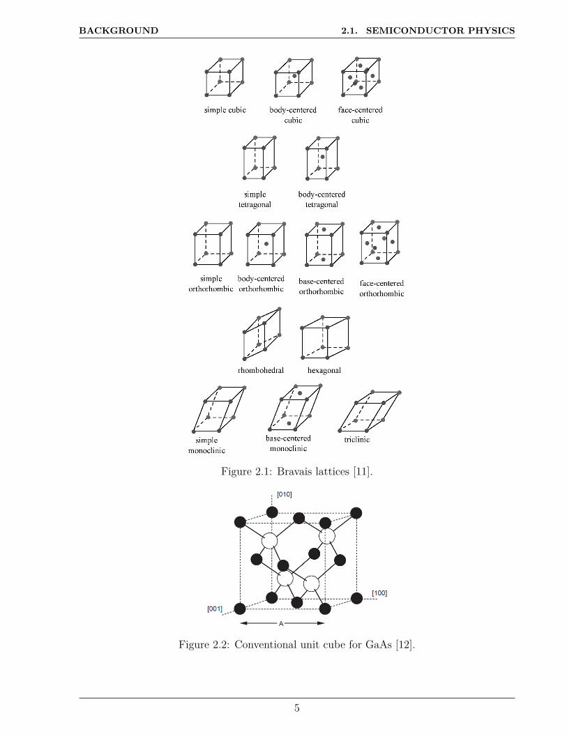
The studied semiconductor materials are single crystals; that is, the atoms are arranged in athree dimensional periodic arrangement called lattice. Thermal vibrations associated with theatom are centered about a single and fixed position where it lies. For a given semiconductor,there is a unit cell that is representative of the entire lattice; it can be generated by repeatingthe unit cell throughout the crystal. This primitive unit cell is called as Bravais latticeand it is defined taking in account that any lattice point can be obtained by traslation andrepresents every crystalline material. There are 14 basic lattices, as can be seen in Figure2.1.
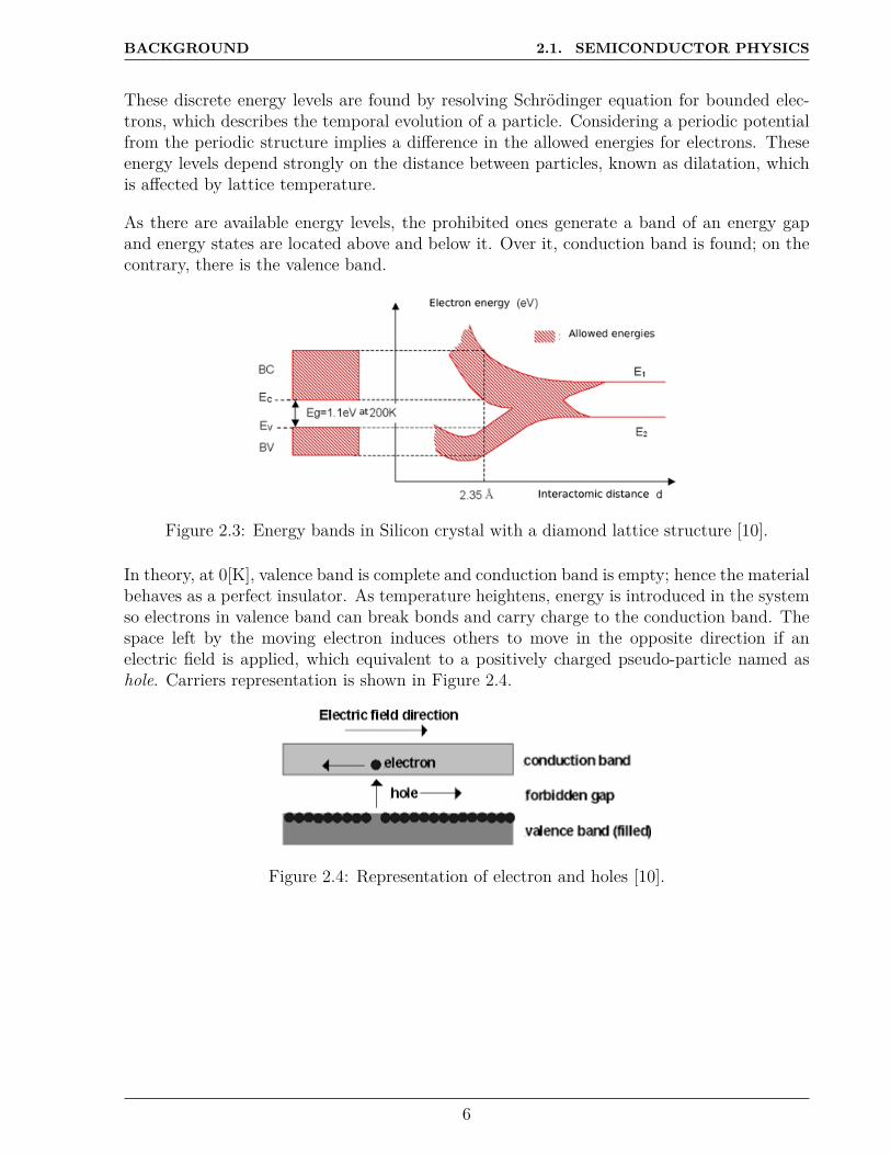
All semiconductor materials have only cubic and hexagonal structures. These crystallinecubic forms can be composed by a single specie of atoms or a combination of differentelements, classifying the semiconductors in elemental or compound, respectively. First casecontains elements from the fourth column of the periodic table, such as Si, Ge or C and isalso called a diamond structure. Second case contains elements from III and V or II and VIand each one of atoms has it own lattices, such as GaAs, AlAs and CdS; it is also called ZincBlende structure. Others semiconductors have hexagonal closed pack like BN, AlN, GaNand SiC. In the particular case of GaAs, crystal is composed of two sublattices, each facecentered cubic (fcc) and offset with respect to each other by half diagonal of the fcc cube, ascan be seen in Figure 2.2.
Band Structure
To explain the Band Theory, a single atom whit its set of discrete energy levels for theirselectrons is considered. Electrons occupy quantum states with quantum numbers n, l, m ands, denoting the energy level, orbital and s, sublevel and spin of the electrons, respectively. Ifthere are N identical atoms brought together in a very close proximity as in a crystal, theouter electron could do a spatial overlap in their orbitals, which means two of these electronscould trade place occupying a new spatial extended energy states. Since the Pauli ExclusionPrinciple can only be satisfied if these electrons occupy a set of distinct, spatially extendedenergy levels, the atomic orbital splits into an energy band containing a set of electron stateshaving a set of closely spaced energy levels.
4
BACKGROUND 2.1. SEMICONDUCTOR PHYSICS
Figure 2.1: Bravais lattices [11].
Figure 2.2: Conventional unit cube for GaAs [12].
5
BACKGROUND 2.1. SEMICONDUCTOR PHYSICS
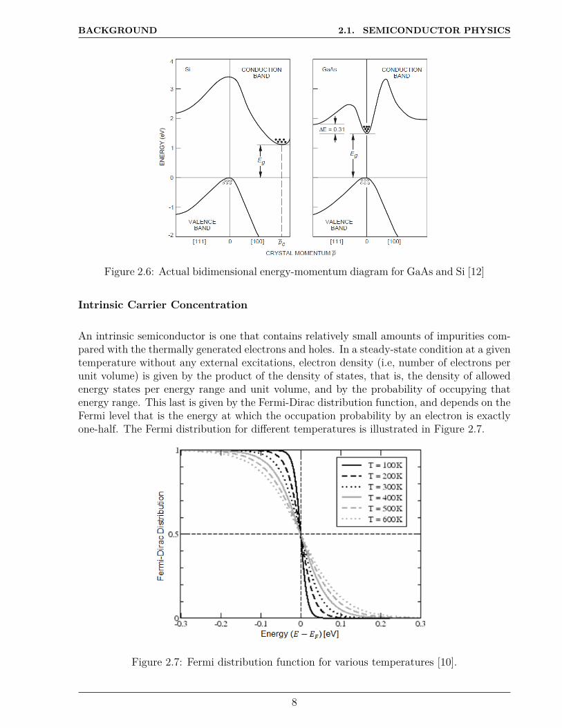
These discrete energy levels are found by resolving Schrödinger equation for bounded elec-trons, which describes the temporal evolution of a particle. Considering a periodic potentialfrom the periodic structure implies a difference in the allowed energies for electrons. Theseenergy levels depend strongly on the distance between particles, known as dilatation, whichis affected by lattice temperature.
As there are available energy levels, the prohibited ones generate a band of an energy gapand energy states are located above and below it. Over it, conduction band is found; on thecontrary, there is the valence band.
Figure 2.3: Energy bands in Silicon crystal with a diamond lattice structure [10].
In theory, at 0[K], valence band is complete and conduction band is empty; hence the materialbehaves as a perfect insulator. As temperature heightens, energy is introduced in the systemso electrons in valence band can break bonds and carry charge to the conduction band. Thespace left by the moving electron induces others to move in the opposite direction if anelectric field is applied, which equivalent to a positively charged pseudo-particle named ashole. Carriers representation is shown in Figure 2.4.
Figure 2.4: Representation of electron and holes [10].
6

BACKGROUND 2.1. SEMICONDUCTOR PHYSICS
Effective Mass
The energy diagram of a free electron in function of its momentum has a parabolic form. Ina semiconductor crystal, an electron in the conduction band is similar to a free electron inbeing relatively free to move about in the crystal; however, because of the periodic potentialof the nuclei, the basic equation of energy can no longer be valid. It is necessary to adjustthe mass of the electron to match the basic expression, defining the effective mass. It isanalogue to holes. Eq. (2.1) defines the effective mass of a conduction electron, in which mn
represents electron effective mass; E, energy; and ρ, momentum.
mn = (∂2E
∂ρ2 )−1 (2.1)
Figure 2.5 shows a simplified energy-momentum relationship of a two basic types semicon-ductor. It is indirect if there is the necessity of changing the momentum of the electronto do a transition from the valence band to the conduction band, as Si (Figure 2.5a); casecontrary it is direct semiconductor, as GaAs (Figure 2.5b). The upper parabola representsthe conduction band, while the lower one is the valence band. The spacing at p = 0 betweenthese two parabolas is the bandgap Eg, shown previously in Figure 2.3.
(a) Si (b) GaAs
Figure 2.5: Schematic energy-momentum diagram for Si and GaAs [13].
The actual energy-momentum relationships for a semiconductor such as GaAs and Si aremuch more complex and they are three dimensional, as is presented in the two-dimensionaldiagram of Figure 2.6. For diamond or zinc blende lattice, the maximum in the valence bandand minimum in the conduction band occur at p = 0 or along one of these two directions; thefirst case is the most common, and it means that effective mass is constant and the electronmotion is independent of crystal direction. Second case is the contrary.
7
BACKGROUND 2.1. SEMICONDUCTOR PHYSICS
Figure 2.6: Actual bidimensional energy-momentum diagram for GaAs and Si [12]
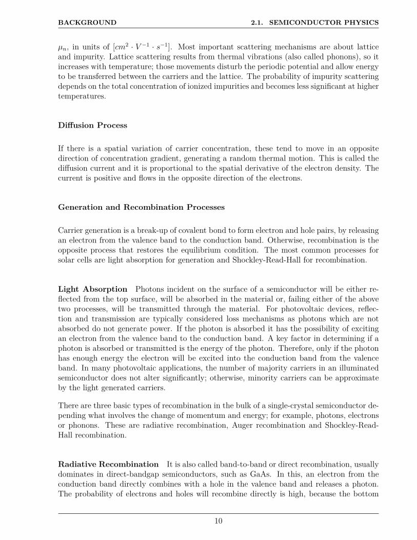
Intrinsic Carrier Concentration
An intrinsic semiconductor is one that contains relatively small amounts of impurities com-pared with the thermally generated electrons and holes. In a steady-state condition at a giventemperature without any external excitations, electron density (i.e, number of electrons perunit volume) is given by the product of the density of states, that is, the density of allowedenergy states per energy range and unit volume, and by the probability of occupying thatenergy range. This last is given by the Fermi-Dirac distribution function, and depends on theFermi level that is the energy at which the occupation probability by an electron is exactlyone-half. The Fermi distribution for different temperatures is illustrated in Figure 2.7.
Figure 2.7: Fermi distribution function for various temperatures [10].
8

BACKGROUND 2.1. SEMICONDUCTOR PHYSICS
For an intrinsic semiconductor, the density of electrons n in the conduction band is equal tothe density of holes p in the valence band, that is, n = p = ηi where ηi is the intrinsic carrierdensity. More general, matching Fermi levels for carriers, the Law of Mass Action n · p = η2
iis obtained.
Donors and Acceptors
When a semiconductor is doped with impurities, the semiconductor becomes extrinsic andimpurity energy levels are introduced. It can be achieved by replacing an atom whit adifferent number of valence electrons. If there is an extra electron, is said that it is donatedto the conduction band and semiconductor becomes n-type because of the addition of thenegative charge carrier (ND). By the contrary, if an additional electron is accepted, holesare created in the valence band, making a p-type semiconductor, with positive concentration(NA).
By doping, semiconductors have different quantities of each carrier. The more abundantcharge carriers are the majority carriers; the less abundant are the minority carriers.Undermost conditions, the doping of the semiconductor is several orders of magnitude greater thanthe intrinsic carrier concentration, such that the number of majority carriers is approximatelyequal to the doping. Hence, applying the approximation and the Law of Mass Action, carriersconcentration in p-type and n-type can be expressed as in Eqs. (2.2b) :
n− type : n0 = ND, p0 = η2i /ND, (2.2a)
p− type : p0 = NA, n0 = η2i /NA (2.2b)
2.1.2 Carrier Transport Phenomena
There are many transport processes, including drift, diffusion, recombination, generation,thermionic emission, tunneling, among others. It is considered the motion of charge carri-ers under the influence of an electric field and a carrier concentration gradient, which arepredominant.
Drift Process
The thermal motion of an individual electron can be visualized as a succession of randomscattering from collisions with lattice atoms, impurity atoms, and other scattering centers.Net displacement of an electron is zero over a sufficiently long period of time. The aver-age distance between collisions is called the mean free path, and the average time betweencollisions is called the mean free time, τc.
When a small electric field is applied, an additional velocity component will be superimposedupon the thermal motion of electrons; it is called drift velocity. This is proportional to electricfield by a factor which depends on the mean free time and effective mass, named mobility
9
BACKGROUND 2.1. SEMICONDUCTOR PHYSICS
µn, in units of [cm2 · V −1 · s−1]. Most important scattering mechanisms are about latticeand impurity. Lattice scattering results from thermal vibrations (also called phonons), so itincreases with temperature; those movements disturb the periodic potential and allow energyto be transferred between the carriers and the lattice. The probability of impurity scatteringdepends on the total concentration of ionized impurities and becomes less significant at highertemperatures.
Diffusion Process
If there is a spatial variation of carrier concentration, these tend to move in an oppositedirection of concentration gradient, generating a random thermal motion. This is called thediffusion current and it is proportional to the spatial derivative of the electron density. Thecurrent is positive and flows in the opposite direction of the electrons.
Generation and Recombination Processes
Carrier generation is a break-up of covalent bond to form electron and hole pairs, by releasingan electron from the valence band to the conduction band. Otherwise, recombination is theopposite process that restores the equilibrium condition. The most common processes forsolar cells are light absorption for generation and Shockley-Read-Hall for recombination.
Light Absorption Photons incident on the surface of a semiconductor will be either re-flected from the top surface, will be absorbed in the material or, failing either of the abovetwo processes, will be transmitted through the material. For photovoltaic devices, reflec-tion and transmission are typically considered loss mechanisms as photons which are notabsorbed do not generate power. If the photon is absorbed it has the possibility of excitingan electron from the valence band to the conduction band. A key factor in determining if aphoton is absorbed or transmitted is the energy of the photon. Therefore, only if the photonhas enough energy the electron will be excited into the conduction band from the valenceband. In many photovoltaic applications, the number of majority carriers in an illuminatedsemiconductor does not alter significantly; otherwise, minority carriers can be approximateby the light generated carriers.
There are three basic types of recombination in the bulk of a single-crystal semiconductor de-pending what involves the change of momentum and energy; for example, photons, electronsor phonons. These are radiative recombination, Auger recombination and Shockley-Read-Hall recombination.
Radiative Recombination It is also called band-to-band or direct recombination, usuallydominates in direct-bandgap semiconductors, such as GaAs. In this, an electron from theconduction band directly combines with a hole in the valence band and releases a photon.The probability of electrons and holes will recombine directly is high, because the bottom
10

BACKGROUND 2.1. SEMICONDUCTOR PHYSICS
of the conduction band and the top of the valence band have the same momentum andno additional one is required for the transition across the bandgap. The rate of the directrecombination, Rth, is expected to be proportional to the number of electrons available inthe conduction band and the number of holes available in the valence band.
Most commonly, when the semiconductor is indirect as in Silicon solar cells, indirect recombi-nation predominates. In this, transition is via localized energy states in the forbidden energygap called recombination centers.
Auger Recombination An electron and a hole recombine, but rather than emitting theenergy as heat or as a photon, the energy and momentum is transferred to a third carrier, anelectron in the conduction band. This electron then thermalizes back down to the conductionband edge. Auger recombination is most important at high carrier concentrations caused byheavy doping or high level injection under concentrated sunlight. In silicon-based solar cells,Auger recombination limits the lifetime and ultimate efficiency. The more heavily doped thematerial is, shorter the Auger recombination lifetime is.
Shockley-Read-Hall Recombination Recombination through defects levels, also calledShockley-Read-Hall or SRH recombination, does not occur in perfectly pure, undefectedmaterial. SRH recombination is a two-step process. An electron (or hole) is trapped byan energy state in the forbidden region which is introduced through defects in the crystallattice. These defects can either be unintentionally introduced or deliberately added to thematerial, for example in doping the material; and if a hole (or an electron) moves up to thesame energy state before the electron is thermally re-emitted into the conduction band, thenit recombines. The rate at which a carrier moves into the energy level in the forbidden gapdepends on the distance of the introduced energy level from either of the band edges.
11

BACKGROUND 2.2. PN JUNCTION
2.2 PN junction
Joining n-type material with p-type material causes excess electrons in the n-type materialto diffuse to the p-type side and excess holes from the p-type material to diffuse to the n-typeside [10]. Movement of electrons to the p-type side exposes positive ion cores in the n-typeside while movement of holes to the n-type side exposes negative ion cores in the p-type side,resulting in an electron field at the junction and forming the depletion region (See Figure2.8). An electric field E forms between the positive ion cores in the n-type material andnegative ion cores in the p-type material. This region is called the "depletion region" sincethe electric field quickly sweeps free carriers out, hence the region is depleted of free carriers.A "built in" potential Vbi due to electric field that is formed at the junction.
A PN junction can operate under forward and reverse bias. Forward bias occurs when avoltage is applied across the device such that the electric field formed by the PN junctionis decreased. It eases carrier diffusion across the depletion region, and leads to increaseddiffusion current. In the presence of an external circuit that continually provides majoritycarriers, recombination increases which constantly depletes the influx of carriers into the solarcell. This increases diffusion and ultimately increases current across the depletion region.Reverse bias occurs when a voltage is applied across the solar cell such that the electric fieldformed by the PN junction is increased and consequently, diffusion current decreases.
Semiconductor devices have three modes of operation:
• Thermal Equilibrium: There are not external inputs such as light or applied voltage.The currents balance each other out so there is no net current within the device.• Steady State: There are external inputs such as light or applied voltage, but the condi-
tions do not change with time. Devices typically operate in steady state and are eitherin forward or reverse bias.• Transient: Usually present in solar cells, it occurs if the applied voltage changes rapidly.
There will be a short delay before the solar cell responds.
Figure 2.8: a)Uniformly doped p-type and n-type semiconductors.b)Electric fieldin the depletion region and the energy band diagram of a PN junction in thermalequilibrium [10].
12

BACKGROUND 2.3. PHOTOVOLTAIC SOLAR CELL
2.3 Photovoltaic Solar Cell
A solar cell is a dispositive that produces photovoltaic (PV) electricity [10] [14]. Radiation ofthe Sun enters the semiconductor PN junction reaches the depletion region of the solar cellgenerates electron-hole pairs, which are able to flow through an external circuit and provideelectrical power. The solar cell functions as a forward biased PN junction; however, currentflow occurs in the opposite direction to that shown in Figure 2.9.
Figure 2.9: Band diagram of solar cell.Generated electron-hole pairs drift acrossthe depletion region [14].
The generated minority carriers will drift across the depletion region and enter the n- and p-regions as majority carries as shown. It is also possible for electron-hole pairs to be generatedwithin about one diffusion length or either side of depletion regions and through diffusion toreach the depletion region, where drift will again allow these carriers to cross to the oppositeside. It is import to avoid recombination because it produces heat generation and doesn’tcontribute the electron flow.
If the PN junction is illuminated in the junction region then the reverse current increasessubstantially due to the electron-hole pairs that are optically generated. Without opticalgeneration, the available electrons and holes that comprise reverse saturation current arethermally generated minority carries, which are low in concentration.
The optically generated current is larger than diffusion current and it continues to dominatecurrent flow until stronger forward bias conditions are present. The current-voltage (I-V)characteristic of solar cells is shown in Figure 2.10, where there is the appropriate operatingpoint for a solar cell in which current flows out the positive terminal (p-side), though theexternal circuit and then, into the negative terminal(n-side).
13

BACKGROUND 2.3. PHOTOVOLTAIC SOLAR CELL
Figure 2.10: I-V Characteristic of solar cell [14].
From the I-V curve in Figure above, the following parameters can be identified: Short-circuitcurrent (ISC), open-circuit voltage (VOC) and the ones that form the fill factor (FF ).
ISC is the current through the solar cell when the voltage across the solar cell is zero, i.e, whenthe solar cell is short circuited. VOC is the maximum voltage available from a solar cell andthis occurs at zero current and corresponds to the amount of forward bias on the solar celldue to the bias of the solar cell junction with the light-generated current. The short-circuitcurrent and the open-circuit voltage are the maximum current and voltage respectively froma solar cell; however, at these points solar cell power is zero. FF contribute to determinethe maximum power from a solar cell and is defined as the ratio of the maximum power(ponderation of maximum power points Imp and Vmp) to the product of ISC and VOC .
14

BACKGROUND 2.3. PHOTOVOLTAIC SOLAR CELL
2.3.1 Design
Solar cell structure is composed generally by six layers, including the semiconductor, as it isshown in Figure 2.11.
• Encapsulate: it is made of glass or other clear material, such clear plastic, and sealsthe cell from the external environment.• Contact Grid: It is made of a good conductor, such as a metal, and it serves as a
collector of electrons, decreasing the number of photons reaching the semiconductorsurface, allowing more photons to penetrate.• Antireflective Coating (AR Coating): Through a combination of a favorable refractive
index and thickness, this layer serves to guide light into the solar cell.• N-Type Semiconductor or Negative doping layer of semiconductor: Photon’s energy
transfers to the valence electron, allowing it to escape its orbit, leaving a hole. In otherwords, photoelectric effect happens.• P-Type Semiconductor or Positive doping layer: In there, freed electrons attempt to
unite with holes providing current.• Back Contact: usually made out of a metal, covers the entire back surface of the solar
cell and acts as a conductor.
Figure 2.11: Schematic diagram of solar cell layers [15].
In order for light to reach the junction area of the PN junction, it should be close to the surfaceof semiconductor and be large enough to capture the desired radiation. Highly doped thinregion simultaneously serves as a front electrode with high lateral conductivity and one sideof PN junction, normally, n-side due to its electron mobility that allows higher conductivity.A metal grid is deposited on this layer and forms an ohmic contact to n+ material that blockssunlight. Areas exposed to sunlight are coated with an anti reflection layer.
15

BACKGROUND 2.4. PROPERTIES OF GALLIUM ARSENIDE
2.4 Properties of Gallium Arsenide
Gallium arsenide (GaAs) is a III-V compound semiconductor composed of the element gal-lium (Ga) from column III and the element arsenic (As) from column V of the periodic tableof the elements [12]. GaAs was first created by Goldschmidt and reported in 1929, but thefirst reported electronic properties of III-V compounds as semiconductors did not appearuntil 1952. In 1970, the first GaAs heterostructure solar cells were created by the team ledby Zhores Alferov in the USSR. In the early 1980s, the efficiency of the best GaAs solar cellssurpassed that of conventional, crystalline silicon-based solar cells. In the 1990s GaAs solarcells took over from silicon as the cell type most commonly used for photovoltaic arrays forsatellite applications. Later, dual- and triple-junction solar cells based on GaAs with germa-nium and indium gallium phosphide layers were developed as the basis of a triple-junctionsolar cell, which held a record efficiency of over 32% and can operate also with light as con-centrated as 2.000[suns]. GaAs-based devices hold the world record for the highest-efficiencysingle-junction solar cell at 28.8%. This high efficiency is attributed to the extreme highquality GaAs epitaxial growth, surface passivation by the AlGaAs, and the promotion ofphoton recycling by the thin film design.
As a solar cell, it presents many benefits in compare to Silicon cells.
• For undoped GaAs, the energy bandgap is 1.42[eV ] at room temperature,allowinghigher operating temperatures.• GaAs devices requires only a few microns thick to absorb sunlight, due to its high
absorptivity. Commonly used crystalline silicon requires a layer 100 microns or morethick to accomplish the same effect.• GaAs is highly resistant to radiation damage and it has high efficiency.• GaAs has a thermal conductivity of 0.55[W · cm−1◦C−1], which is about one-third that
of silicon and one-tenth that of copper. As a consequence, the power handling capacityand therefore the packing density of a GaAs integrated circuit is limited by the thermalresistance of the substrate.• The mobility of GaAs is about double than Si at typical field strengths. Devices can
work at significantly higher frequencies than Si.
A cell with a GaAs base can have several layers of slightly different compositions, allowingmore precision in controlling generation and collection of electrons and holes. In other hand,silicon cells have been limited to variations in the level of doping. For example, one of themost common GaAs cell structures has a very thin window layer made of aluminum galliumarsenide, which allows electrons and holes to be created close to the electric field at thejunction.
Never the less, it has a high cost that limits its application to concentrator systems, meanly.
Researchers are exploring several approaches to reduce the cost of GaAs devices. These in-clude placing GaAs cells on cheaper substrates; growing GaAs cells on a removable, reusableGaAs substrate; and making GaAs thin films, similar to those made of copper indium dise-lenide and cadmium telluride.
16

BACKGROUND 2.5. HYDRODYNAMIC STABILITY
2.5 Hydrodynamic Stability
Hydrodynamic stability concerns the stability and instability of motions of fluids [16]. Theconcept of stability of a state is "when... a small variation of present state will alter onlyby an infinitely small quantity the state at some future time, the condition of the system,whether at rest or in motion, is said to be stable; but when an infinitely small variation inthe present state may bring about a finite difference in the state of the system in a finitetime, the condition of the system is said unstable" − Maxwell.
In case of fluids, instability refers at the state where exists a chaotic three-dimensional vortic-ity field with a broad spectrum of small temporal and spatial scales. This is called turbulence.Reynolds demonstrated that when velocity is slow, the flow describes a straight line throughthe tube, generating the laminar flow. Whether the Reynolds number is over a critic value,the phenomenon becomes unstable, letting be the turbulence state, with the appearance offlashes succeeded each other rapidly.
Stability in mechanical or electrical systems can be studied by using mathematical toolsdue to their few degrees of freedom. In other hand, continuous media in which the basicequations take the form of nonlinear partial differential equations, the number of degrees offreedom is infinite. That implies the use of simplifications as linearization approximationsand extensions of the theory developed with discrete systems.
The major contributions to the study of hydrodynamic stability can be found in the theoret-ical papers of Helmholtz (1821-1894), combined with efforts of Reynolds (1842-1912), Kelvin(1824-1907) and Rayleigh (1842-1919), among others. This last is considered the founder ofthe theory of hydrodynamic stability, who between 1878 and 1917 published a great numberof papers on this subject. Around 1907 there were the first intuitions about the existence ofa critical Reynolds number to explain the problem of turbulence. In addition to the worksof Prandtl (1875-1953), the first confirmation of linear theory by experiments was done byTaylor (1886-1975) in his work on vortices between concentric rotating cylinders. Lin (1916-)improved the mathematical procedures and laid the foundations for a general expansion ofstability analysis. At that time the stability of Poiseuille flows had become a particularlycontroversial issue and Lin put it in order by his newer and more general analysis. Theresults of Lin were found to be correct by using a digital computer. Experimental resultsof Schubauer and Skramstad helped clarify that the critical Reynolds number marked onlythe threshold of sinuous motion and not that of turbulence. At that point, experimentalresults and theory agreed as far as eigenfunctions and eigenvalues were concerned. Around1955, three main categories of manifestations of instability in a continuous medium wereformulated: first, oscillations in parallel flows, channel flows and boundary layers; second,boundary layers along curved walls and third, Benard cells and convective instabilities, caseswhere the mean flow is zero. Basic flow is defined by the set of fields that need to be specifiedat each point and time, for instance velocity and temperature. From the physical point ofview, we want to know if the basic flow can be observed or not. If a small disturbance isintroduced, this may either die away, persists as a disturbance of similar magnitude or growsso much that the basic flow becomes a different flow pattern. Stability problems can be foundin many fields such as mechanics, electronics, aeronautical engineering, economics. [17]
17

BACKGROUND 2.6. HOT SPOT IN PV SOLAR CELLS
2.6 Hot Spot in PV Solar Cells
Solar cell stability is an important factor in determining device lifespan, return of invest-ment, pricing and warranty policies. Stability is often studied under harsher conditions thanworking cells are exposed into the field, so that 30 years of field stress can be inferred with20 days of laboratory study, through increased concentrations of light, higher temperaturesor greater humidity (accelerated life testing, ALT). Established experimental work on devicedegradation has found that temperature is an important parameter, accelerating it exponen-tially [18]. Moreover, without cell degradation by temperature, solar cells may have a lifetimegreater than 100 years [19].
Increase of solar cell junction temperature can negatively affect output power and energyconversion efficiency due to a decrease of the open circuit voltage. This temperature dependson the packaging of solar cells and the environmental factors such as ambient temperatureand wind characteristics [20–22].
Any temperature fluctuation in a local area of the film structure can increase the electricalconduction and cause a shutting pathway or hot spot [23]. Hot spot profile depends on whereit is located and current densities, as can bee seen in Figure 2.12. Temperature is higherat the center of the device and reduces lower values at the edges. Also, the difference intemperature of hotter point and its surroundings is in the order of 10[K].
Figure 2.12: Hot spot temperature profile, TCO layer [23].
The temperature variation in the structure is usually reversible before physically impactingthe atomic structure. This non-uniform characteristic of a PV device can be produced meanlydue to its material structure or light absorption profile. First case refers to crystalline defectsor composed structures heterogeneity. In the second case, radiation patrons that evolveduring time or variations in the whether such as the passing of a cloud produce it [24]. Thiscondition means variations between local PV parameters in different areas of a module orin variations between the parameters of nominally identical solar cells cut from the samemodule. An example of measurable consequence is that hot spots are typically located close
18

BACKGROUND 2.6. HOT SPOT IN PV SOLAR CELLS
to module bus bars, which can be consider as a defect in the device [25]. Another one is thatnominally identical cells may degrade differently.
As PV devices are thermally insulated and have a low lattice thermal conduction, the fluc-tuation in electric flow in the semiconductor layer triggers a variation in the temperatureprofile, well known in large are PV modules. This variation results in spots of high transver-sal conduction (i.e in a parallel plane to the layer width), allowing a local heat generationthat may develop in an unstable temperature increase.
It usually concentrates its effects in a specific zone of the device, where a hot spot is generated.The stability of this point determines the magnitude of the degradation process; if it is stable,its temperature decreases until it reaches the equilibrium with the surrounds, damaging thezone slowly. Case contrary, but less frequent, the temperature increases exponentially leadingto the runaway phenomenon.
The thermal runaway phenomenon corresponds to an uncontrolled response of energy gen-erated by its own system when the temperature surpasses a critical value, usually withcatastrophic consequences. Even if its application in PV is relatively new, alluding the workof Karpov in the last decade, it is a well know process in other scientific areas meanly byexothermic chemical reactions, such as in electrical engineering (current hogging), chemistry(temperature accelerated exothermic reactions) [26, 27], astrophysics (nova explosion due torunaway nuclear fusion) [28], among others.
In photovoltaic solar cells, the thermal runaway phenomenon causes problems with PV re-liability, diminishing its lifespan and efficiency. This develops a current crush effect due toinherent non-uniform junction temperature [29].
Experimentally, temperature profile of PV solar cells can be observed with infrared cameramapping (IR), hence the temporal evolution of hot spots and its location in the frontalplane of the device can be registered. Another mapping techniques which also reveal lateralnon-uniformities are optical beam induced current (OBIC), electron beam induced current(EBIC), surface photo-voltage (SPV) mapping, photoluminescence (PL) mapping, and someothers [30, 31].
Analytically, typical junction models are usually based on diodes configurations, where theequation system includes the Ohm’s Law, Kirchoff current and voltage laws, saturation cur-rent and a heat transfer equation, which usually contains a light absorption, Joule dissipation,Newton cooling law and a conductive heat transfer terms at least [9, 25, 29,32].
Diode current ID is given by temperature dependent Shockley Equation, Eq.(2.3):
ID = I0 (exp( qV
nKBT)− 1) (2.3a)
I0 = I00 exp( −EgnKT
) (2.3b)
Where Eg represents band gap energy; n, the ideality factor; kB, Boltzmann’s constant; T ,junction temperature;I0, reverse saturation current;I00, a constant; q, electron charge; andthe voltages.
19

BACKGROUND 2.6. HOT SPOT IN PV SOLAR CELLS
Heat equation can be written as:
CdTdt = H + IV + χ∆T − α∆T − σ∆T 4 (2.4)
where the C corresponds to a constant flux; H, to Joule dissipation; χ, to convection; α, toconduction; and σ, to radiation.
PN junction modelled as equivalent circuit with diodes configurations usually includes currentsource simulating the sun illumination and resistances, thermal and electrical, as can be seenin Figure 2.13
(a) two diodes [32] (b) One diode [25]
Figure 2.13: Equivalent circuit of PN junction.
Vasko et al. [25] made a study in thin film PV modules, specifically in a triple junction basedon a-Si:H. It revealed that even when radiation is uniformly distributed in the module makinga uniform temperature profile at the beginning, its distribution became less homogeneous inthe course of heating and hot spots usually developed in the proximity of bus bars, as canbe seen in Figure 2.14.
Figure 2.14: IR mapping triple junction a-Si:H [25]
20

BACKGROUND 2.6. HOT SPOT IN PV SOLAR CELLS
Hot spots formation takes place when the forward current exceeds a certain critical value, inthis case approximately 15[A]. In addition, it was experimentally demonstrated that hot spotsare sensitive to convective air currents. Temporal evolution of hot spot temperature behavesexponentially, which triggers the phenomenon of runaway instability, where the spot getshotter and simultaneously shrinks in its linear dimensions (See Figure 2.15); the temperatureof faraway regions simultaneously decreases as they dissipate smaller currents. Gorji [23] alsodemonstrates that an already created hot spot can redistribute the temperature profile ofneighbour areas.
Figure 2.15: Temperature distribution over sample at 2[suns] [25].
It can be avoided in this case by increasing thermal conductivity by a factor, achievablein practice, which allows to the module reach a maximum temperature beyond the critical(90[◦C]), as can be seen in Figure 2.16.
Karpov et al. [32] made a thermal stability analysis on thin film photovoltaic modules, re-leased that PV can undergo zero threshold localized thermal runaway leading to thermalinstabilities that affects negatively the device performance and reliability. Non uniform ma-terial degradation accelerates at hot spots, such that an initial hot spot may then degradein a runaway mode under more and more stress as it becomes progressively shunting. More-over, it can be unstable with respect to infinitesimally small fluctuations. They model thedevice as two diodes, with heat capacitances and resistors, applying a linear stability analysisover characteristics equations and then checking it by numerical modelling. This model alsocorroborates the fact that scaling some device properties, like increasing thermal insulationand decreasing thickness, runaway can be avoided.
21

BACKGROUND 2.6. HOT SPOT IN PV SOLAR CELLS
Figure 2.16: Simulated temporal temperature as a function of thermal conductiv-ity χ [25].
22

Chapter 3
Model Description
From the hydrodynamic model of the PN junction presented by Osses [33] temporal eigen-values of the transient component of the zero order perturbation will be found. Transportequations for electrons and holes model are deduced from the Boltzmann equations andsemi-classical theory.
Reference system is defined as the spatial coordinate x∗, in the direction of the electronflow, and t∗ as time. Current is driven through the device by a voltage difference, diffusion,generation and recombination processes between the two contacts at x∗ = 0.5L, whit L asthe total device longitude. The one-dimensional two-temperature hydrodynamic equationsfor electron and hole flow in a PN junction solar cell include:
• Gauss’s law in Eqs. (3.1a) and (3.1b), which describe variation of electric potential asa function of charge distribution.• Mass conservation equations for electrons and holes in Eqs. (3.1c) and (3.1d), which
consider mass variation in a control volume (PN junction).• Momentum conservation equations for electrons and holes in Eqs. (3.1e) and (3.1f),
which includes effects of Lorentz force, pressure and collisions.• Energy conservation equation for electrons and lattice in Eqs. (3.1g) and (3.1h), which
consider effect of pressure for electrons and heat transfer by conduction and collisionterm for both electrons and lattice.
It is considered thermal equilibrium among electrons and holes. Therefore, the electron andhole temperature are imposed to be equals and constants throughout the device, T ∗c . Thechanges of kinetic energy of electrons due to their interactions with the lattice is describedin Eq. (3.1g) and lattice thermal energy in Eq. (3.1h).
23
MODEL DESCRIPTION 3.1. PHYSICAL PARAMETERS
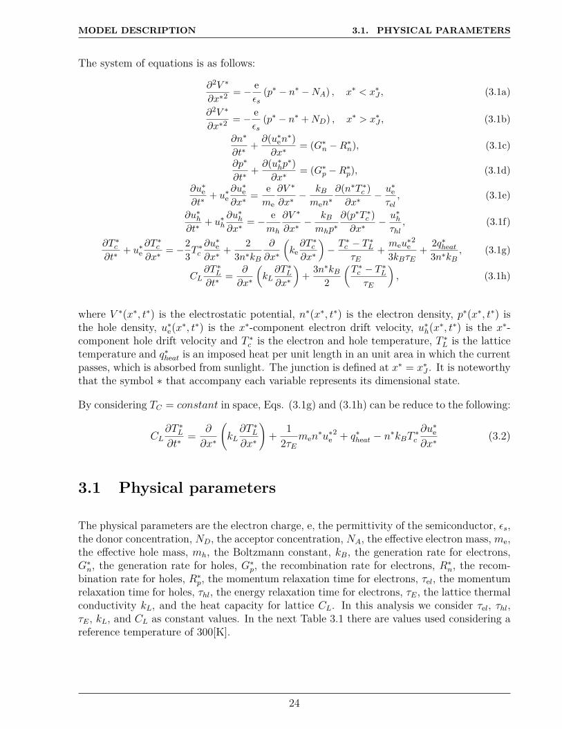
The system of equations is as follows:
∂2V ∗
∂x∗2= − e
εs(p∗ − n∗ −NA) , x∗ < x∗J , (3.1a)
∂2V ∗
∂x∗2= − e
εs(p∗ − n∗ +ND) , x∗ > x∗J , (3.1b)
∂n∗
∂t∗+ ∂(u∗en∗)
∂x∗= (G∗n −R∗n), (3.1c)
∂p∗
∂t∗+ ∂(u∗hp∗)
∂x∗= (G∗p −R∗p), (3.1d)
∂u∗e∂t∗
+ u∗e∂u∗e∂x∗
= eme
∂V ∗
∂x∗− kBmen∗
∂(n∗T ∗c )∂x∗
− u∗eτel, (3.1e)
∂u∗h∂t∗
+ u∗h∂u∗h∂x∗
= − emh
∂V ∗
∂x∗− kBmhp∗
∂(p∗T ∗c )∂x∗
− u∗hτhl, (3.1f)
∂T ∗c∂t∗
+ u∗e∂T ∗c∂x∗
= −23T∗c
∂u∗e∂x∗
+ 23n∗kB
∂
∂x∗
(ke∂T ∗c∂x∗
)− T ∗c − T ∗L
τE+ meu
∗e
2
3kBτE+ 2q∗heat
3n∗kB, (3.1g)
CL∂T ∗L∂t∗
= ∂
∂x∗
(kL∂T ∗L∂x∗
)+ 3n∗kB
2
(T ∗c − T ∗LτE
), (3.1h)
where V ∗(x∗, t∗) is the electrostatic potential, n∗(x∗, t∗) is the electron density, p∗(x∗, t∗) isthe hole density, u∗e(x∗, t∗) is the x∗-component electron drift velocity, u∗h(x∗, t∗) is the x∗-component hole drift velocity and T ∗c is the electron and hole temperature, T ∗L is the latticetemperature and q∗heat is an imposed heat per unit length in an unit area in which the currentpasses, which is absorbed from sunlight. The junction is defined at x∗ = x∗J . It is noteworthythat the symbol ∗ that accompany each variable represents its dimensional state.
By considering TC = constant in space, Eqs. (3.1g) and (3.1h) can be reduce to the following:
CL∂T ∗L∂t∗
= ∂
∂x∗
(kL∂T ∗L∂x∗
)+ 1
2τEmen
∗u∗e2 + q∗heat − n∗kBT ∗c
∂u∗e∂x∗
(3.2)
3.1 Physical parameters
The physical parameters are the electron charge, e, the permittivity of the semiconductor, εs,the donor concentration, ND, the acceptor concentration, NA, the effective electron mass, me,the effective hole mass, mh, the Boltzmann constant, kB, the generation rate for electrons,G∗n, the generation rate for holes, G∗p, the recombination rate for electrons, R∗n, the recom-bination rate for holes, R∗p, the momentum relaxation time for electrons, τel, the momentumrelaxation time for holes, τhl, the energy relaxation time for electrons, τE, the lattice thermalconductivity kL, and the heat capacity for lattice CL. In this analysis we consider τel, τhl,τE, kL, and CL as constant values. In the next Table 3.1 there are values used considering areference temperature of 300[K].
24
MODEL DESCRIPTION 3.2. ASSUMPTIONS
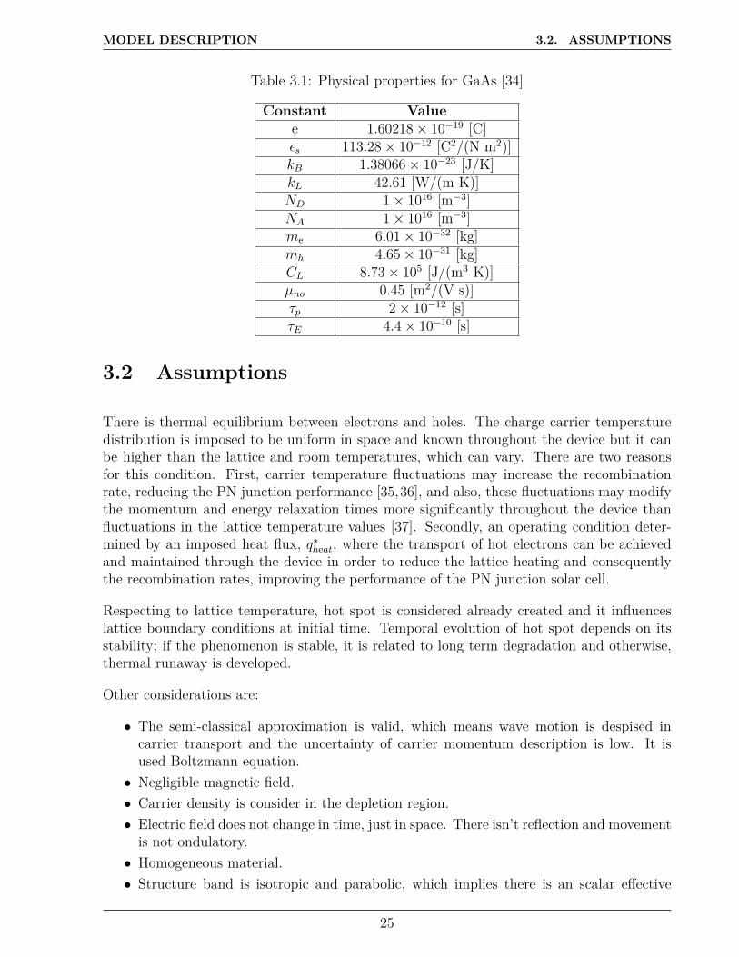
Table 3.1: Physical properties for GaAs [34]
Constant Valuee 1.60218× 10⁻¹⁹ [C]εs 113.28× 10⁻¹² [C2/(N m2)]kB 1.38066× 10⁻²³ [J/K]kL 42.61 [W/(m K)]ND 1× 10¹⁶ [m−3]NA 1× 10¹⁶ [m−3]me 6.01× 10⁻³² [kg]mh 4.65× 10⁻³¹ [kg]CL 8.73× 10⁵ [J/(m3 K)]µno 0.45 [m2/(V s)]τp 2× 10⁻¹² [s]τE 4.4× 10⁻¹⁰ [s]
3.2 Assumptions
There is thermal equilibrium between electrons and holes. The charge carrier temperaturedistribution is imposed to be uniform in space and known throughout the device but it canbe higher than the lattice and room temperatures, which can vary. There are two reasonsfor this condition. First, carrier temperature fluctuations may increase the recombinationrate, reducing the PN junction performance [35,36], and also, these fluctuations may modifythe momentum and energy relaxation times more significantly throughout the device thanfluctuations in the lattice temperature values [37]. Secondly, an operating condition deter-mined by an imposed heat flux, q∗heat, where the transport of hot electrons can be achievedand maintained through the device in order to reduce the lattice heating and consequentlythe recombination rates, improving the performance of the PN junction solar cell.
Respecting to lattice temperature, hot spot is considered already created and it influenceslattice boundary conditions at initial time. Temporal evolution of hot spot depends on itsstability; if the phenomenon is stable, it is related to long term degradation and otherwise,thermal runaway is developed.
Other considerations are:
• The semi-classical approximation is valid, which means wave motion is despised incarrier transport and the uncertainty of carrier momentum description is low. It isused Boltzmann equation.• Negligible magnetic field.• Carrier density is consider in the depletion region.• Electric field does not change in time, just in space. There isn’t reflection and movement
is not ondulatory.• Homogeneous material.• Structure band is isotropic and parabolic, which implies there is an scalar effective
25

MODEL DESCRIPTION 3.3. BOUNDARY CONDITIONS
mass.• There are not collisions between same carriers. Only carrier/lattice and electron/hole
collisions are considered. Collisions are binaries and perfectly inelastics, generated fromenergy loss by generating phonons.• Shockley-Read-Hall recombination processes (SRH) for electrons and holes, since this
mechanism determines the effective carrier lifetime and prevail under a dopying densitybelow 1018[cm3]; otherwise, Auger process is dominant (RAU). Therefore, recombina-tion rates depend exponentially on the applied voltage through the PN junction.• Generation by phonons absortion.• Heavily doped regions near the ends, which lead to ohmic contacts.
3.3 Boundary Conditions
Boundary conditions are extracted from Osses analysis [33] and can be seen in Figure 3.1.As it is said, x∗ is in the direction of the electron flow, from 0 to L as since p-side edge tothe other extreme in the n-side, and t∗ is time.
Figure 3.1: Device scheme with boundary conditions [33].
Voltage conditions refer that at zero bias, there isn’t any total current density in both edgesand there is an applied voltage only in p-side edge.
dV ∗
dx∗ (0, t∗) = 0, (3.3a)
dV ∗
dx∗ (L, t∗) = 0, (3.3b)
V ∗(0, t∗) = Vapplied, (3.3c)V ∗(L, t∗) = 0. (3.3d)
26

MODEL DESCRIPTION 3.4. NON-DIMENSIONAL FORM
Carriers density are consider in equilibrium, meaning that boundary conditions are relatedto the intrinsic carrier concentration, ni and impurities concentration, NA and ND.
n∗(0, t∗) = n2i /NA, (3.4a)
n∗(L, t∗) = ND, (3.4b)p∗(0, t∗) = NA, (3.4c)
p∗(L, t∗) = n2i /ND. (3.4d)
The boundary conditions for the lattice temperature are a constant temperature through thedispositive in the beginning and a constant temperature in a fixed edge. The use of symmetricboundary conditions for the lattice temperature is supported by the fact that results fromthermal modeling of photovoltaic solar cells show that the temperature of the semiconductorlayer is mostly uniform along the normal axis [38].
T ∗L(0, t∗) = 330[K], (3.5a)T ∗L(L, t∗) = 330[K]. (3.5b)
3.4 Non-dimensional Form
It is considered a non-dimensional form, using the reference parameters to cancel the dimen-sion of variables. These reference parameters are V0 voltage, N0 doping density, L longitude ofthe device, t0 time, U velocity, T0 temperature and q0 heat flux, defined as q0 = meN0U
2/τel.
Non-dimensional variables are V = V ∗/V0, n = n∗/N0, p = p∗/N0, x = x∗/L, ue = u∗e/U ,uh = u∗h/U , T = T ∗/T0 and t = t∗/t0.
Replacing variables, a new set of equations is obtained.
∂2V
∂x2 = −α(p− n− NA
N0
), x < xJ , (3.6a)
∂2V
∂x2 = −α(p− n+ ND
N0
), x > xJ , (3.6b)
∂n
∂t+ ∂(uen)
∂x= (Gn −Rn), (3.6c)
∂p
∂t+ ∂(uhp)
∂x= (Gp −Rp), (3.6d)
Re
[∂ue∂t
+ ue∂ue∂x
]= ∂V
∂x− β
n
∂n
∂x− ue, (3.6e)
Re
[∂uh∂t
+ uh∂uh∂x
]= −mr
[∂V
∂x+ β
p
∂p
∂x
]− γuh, (3.6f)
ψ1∂TL∂t
= ψ2∂2TL∂x2 + 1
2νnue2 + qheat − βn
∂ue∂x
. (3.6g)
Non-dimensional groups used are α = eL2N0/V0εs, γ = τel/τhl, mr = me/mh, β = kBT∗c /eV0,
ν = τel/τE, ψ1 = τelCLT0/meN0LU , ψ2 = τelkLT0/meN0L2U2, Re = U2me/eV0, Gn − Rn =
(G∗n−R∗n)L/N0U , Gp−Rp = (G∗p−R∗p)L/N0U , t0 = L/U , U = eV0τel/meL and Re = Uτel/L.
27

MODEL DESCRIPTION 3.4. NON-DIMENSIONAL FORM
α is the available charge in the junction and its movement capacity. It is the ratio betweencharge per area unit Q/A = eNoL and the electric displacement D = εsV0/L. Increasingits value implies that carrier density variations involve a higher electric field variation, as isindicated in Eq. (3.6a) y Eq. (3.6b).
Re is the Reynolds number for electrons due to the use of a hydrodynamic model, consideringU as the maximum average electron velocity and kinematic viscosity as nue = L2/τel. Thislast means that increasing the number of collisions between electrons and lattice implieshigher thermal energy dissipation by the external electric field and consequently a lower gainin group velocity. Reynolds number also can be written as Re = le/L, assuming le as thelength free path defined as le = Uτel . This definition corresponds to the Knudsen numberfor the electron cloud, which point out relative disorder grade of the system.
Relative mass mr is the ratio between electron and hole mass. Knowing that hole massrepresent a valence electron mass, mr is equivalent to the relative inertia between conductionand valence electrons.
γ is the ratio between the momentum relaxation time of electron and hole. Otherwise, ν isthe ratio between the momentum and energy relaxation time of electron.
β is the ratio between thermal energy of carriers and electric potential energy. A higher valueimplies a predominance of diffusive phenomena.
ψ1 and ψ2 are the ratio between the heat capacity and heat conduction of the lattice with areference heat flux, respectively.
28
Chapter 4
Resolution Method
The aim of this chapter is to explain the methodology used to obtain the eigenvalues ofthe equation system. For this, perturbation method is applied to find zero order regularperturbation system. Then, the solution considered is divided in two terms: steady statecomponent depending only in space and a transient response that varies in time and space.The last one determines system stability of the front of a small perturbation. Such methodis used due to the non-linearity of the problem and the hardness to converge of the othernumerical methods.
The followed steps and sections where they can be found are:
3.4 Find non-dimension form4.2 Apply asymptotically perturbation series4.3 Propose a separated variables solution4.3 Reduce the o.d.e order.
4.3.2 Resolve o.d.e with numerical methods4.3.3 Find the transfer matrix4.3.3 Apply boundary conditions
5 Find eigenvalues
These are explained at following, preceding by a brief explanation of perturbation theorybases.
4.1 Perturbation Theory
Differential equations can be solved in closed form using solutions based on advanced theory,approximation by numerical analysis or approximation by formulas. The last includes theperturbation theory, that has an advantage of having an approximate formula for the solutionof an equation and is possible to recognize the effects of the parameters in the solution betterthan the numerical approach.
29

RESOLUTION METHOD 4.1. PERTURBATION THEORY
In perturbation theory, the problem is simplified to a solvable equation. Then, the solutionis the obtainable base form plus a perturbation, which usually takes the form of a series inbase of a perturbation parameter "ε", which needs to be sufficiently small to give a goodapproximation. This solution only asymptotically converge to the one that responds to thetarget problem.
Several symbols are used in discussing approximations to functions and they serve to under-stand the associated error magnitude. The most commonly used are ∼=, o, O and OS. Thesymbol ∼= used as y(x; ε) ∼= y(x; ε) means that the function y is proposed as an approxima-tion to y, nothing is implied about the validity of the approximation. A gauge function is apositive monotone function δ(ε) defined in some interval 0 < ε < ε0 of interest for a particularproblem; the most common gauge functions are defined for all ε > 0. "Monotone" means thata gauge function must be increasing or decreasing through its domain. Gauge functions areused to measure the size of other function. The following are the most important definitions.
Assuming the following limit Lim exists, o, O and OS can be defined as Lim := limit(ε→0+)|f(ε)|δ(ε)
f(ε) = o(δ(ε)) if Lim = 0, (4.1a)f(ε) = O(δ(ε)) if Lim <∞, (4.1b)f(ε) = OS(δ(ε)) if 0 < Lim <∞. (4.1c)
For the application in the error term, the next definition is established.
Definition: The function f(x, ε) satisfies the condition f(x, ε) = O(δ(ε)) uniformly for x inthe interval a ≤ x ≤ b if and only if there exist constants c and ε1 such that |f(x, ε)| ≤ cδ(ε)for all x in a ≤ x ≤ b and for all ε in 0 < ε ≤ ε1.
Once these symbols are defined, it will be explained what kind of differential equations canbe solved and how. If a problem looks like a solvable one and it can be separated as:
Ly + εNy = 0, (4.2)
where L and N are functions of differentials; y and ε are the unknown quantity and theperturbation parameter, respectively; Ly = 0 is the solvable equation and εNy = 0 is theperturbation one. Its proposed solutions can be approximated as an asymptotic series
y(x; p; ε) =k∑
n=0yn(x; p)δn(ε) + o(δk(ε)). (4.3)
In the particular case of an initial value problem with the form:ay + by + cy = εf(t, y, y, ε), (4.4a)
y(0) = α, (4.4b)y(0) = β. (4.4c)
30
RESOLUTION METHOD 4.2. DISTURBED SYSTEM
That exists for all 0 ≤ t ≤ T , |ε| < ε0, α ∈ A and β ∈ B. The solution can be defined by thefollowing theorem.
Theorem: Let f be defined for all t in a compact interval 0 ≤ t ≤ T , for all y and y, andfor all ε near zero. Let f have a continuous partial derivates of all order ≤ r. Let compactintervals A and B be specified for α and β. Then there exists ε0 > 0 such that a solution.
y = φ(t;α; β; ε). (4.5)
Furthermore this solution is unique and φ is as smooth as f ; that is, it has continuous partialderivates of all orders ≤ r with respect to all of its arguments t, α, β and ε.
It follows immediately from last theorem and Taylor’s theorem that for any k ≤ r− 1, φ hasan asymptotic approximation of the form.
φ(t, α, β, ε) =k∑
n=0φn(t;α; β)εn +O(εk+1), (4.6)
uniformly for 0 ≤ t ≤ T and for α, β in compact subsets.
4.2 Disturbed System
It is considered the physical properties for GaAs shown in Table 3.1. The values of thenon-dimensional parameters have to be restricted to satisfy the built-in potential and theboundary conditions. The average time among collisions is small, and as a consequence, itis expected to have a small distance between two collisions for an electron in the flow. Thisimplies that the Reynolds number is small, Re < 1, and it can be used as a perturbationparameter ’ε’ in asymptotic perturbation series [34] for the dependent variables in Eqs. (3.6).
A symmetric PN junction in the dark and under light (constant net-generation rate), withxJ = 0.5 and ND = NA, was considered. Thus, the asymptotic perturbation series for thedependent variables are
V (x, t) = V0(x, t) + εV1(x, t) +O(ε2), (4.7a)n(x, t) = n0(x, t) + εn1(x, t) +O(ε2), (4.7b)p(x, t) = p0(x, t) + εp1(x, t) +O(ε2), (4.7c)ue(x, t) = ue0(x, t) + εue1(x, t) +O(ε2), (4.7d)uh(x, t) = uh0(x, t) + εuh1(x, t) +O(ε2), (4.7e)TL(x, t) = TL0(x, t) + εTL1(x, t) +O(ε2). (4.7f)
These consider an error of order ε2, which implies only one perturbed term. To obtain a firstorder system replaced Eqs. (4.7) into the equation system Eqs. (3.6); then, factorize by thepowers of ε and identify the order system related to its corresponding power. Terms withpower over one are considered inside the error. At following, zero and first order is presented.
31
RESOLUTION METHOD 4.2. DISTURBED SYSTEM
4.2.1 Zero order system
Equation system related to zero order is presented at following.
∂2V0(x, t)∂x2 = −α
(p0(x, t)− n0(x, t)− NA
N0
), x < xJ , (4.8a)
∂2V0(x, t)∂x2 = −α
(p0(x, t)− n0(x, t) + ND
N0
), x > xJ , (4.8b)
∂n0(x, t)∂t
+ ∂(ue0(x, t)n0(x, t))∂x
= (Gn −Rn), (4.8c)
∂p0(x, t)∂t
+ ∂(uh0(x, t)p0(x, t))∂x
= (Gp −Rp), (4.8d)
∂V0(x, t)∂x
n0(x, t)− β∂n0(x, t)∂x
− ue0(x, t) = 0, (4.8e)
−mr
[∂V0(x, t)∂x
p0(x, t) + β∂p0(x, t)∂x
]− γuh0p0(x, t) = 0, (4.8f)
ψ1∂TL0(x, t)
∂t= ψ2
∂2TL0(x, t)∂x2 + 1
2νn0(x, t)ue02(x, t) + qheat − βn0(x, t)∂ue0(x, t)
∂x. (4.8g)
4.2.2 First Order System
Equation system related to first order is presented due to its similarity to low flow of zeroorder system; however, it is not solved. It is noteworthy that in this system, all variablesdepend on both dimensions and there are constants terms to the perturbation; that meansthere are terms constituted only by zero order variables.
∂2V1(x, t)∂x2 = −α (p1(x, t)− n1(x, t)) , (4.9a)
∂n1(x, t)∂t
+ ue0(x, t)∂n1(x, t)∂x
+ n0(x, t)∂ue1(x, t)∂x
+ ue1(x, t)∂n0(x, t)∂x
+ n1(x, t)∂ue0(x, t)∂x
= 0,(4.9b)
∂p1(x, t)∂t
+ uh0(x, t)∂p1(x, t)∂x
+ p0(x, t)∂uh1(x, t)∂x
+ uh1(x, t)∂p0(x, t)dx + p1(x, t)∂uh0(x, t)
∂x= 0,(4.9c)
ue0(x, t)n0(x, t)∂ue0(x, t)∂x
= n0(x, t)∂V1(x, t)∂x
− βT1(x, t)∂n1(x, t)∂x
+ n1(x, t)∂V0(x, t)dx
− n0(x, t)ue1(x, t)− n1(x, t)ue0(x, t),(4.9d)
− uh0(x, t)p0(x, t)∂uh0(x, t)∂x
= mrp0(x, t)∂V1(x, t)∂x
+mrβT1(x, t)∂p1(x, t)∂x
+mrp1(x, t)∂V0(x, t)∂x
+ γp0(x, t)uh0(x, t) + γp1(x, t)uh0(x, t),(4.9e)
ψ1∂TL1(x, t)
∂t= ψ2
∂2TL1(x, t)∂x2 + 1
2νn1(x, t)ue02(x, t) + νn0(x, t)ue0(x, t)ue1(x, t)
− βn1∂ue0(x, t)
∂x− βn0(x, t)∂ue1(x, t)
∂x.
(4.9f)
32

RESOLUTION METHOD 4.3. LINEAR STABILITY ANALYSIS
4.3 Linear stability analysis
Linear stability analysis determines what is the effect of an initial disturbance on a laminarflow. The system response can be expressed in two states: a steady and a transient one.The steady state solution depends only on space and can be considered as a base flow; thetransient state solution can be considered as a perturbation of the system and it is definedas a small perturbation through a small parameter "δ", |δ| << 1.
By replacing,
V0(x, t) = V (x) + δV ′(x, t), (4.10a)n0(x, t) = n(x) + δn′(x, t), (4.10b)p0(x, t) = p(x) + δp′(x, t), (4.10c)
ue0(x, t) = ue(x) + δue′(x, t), (4.10d)
uh0(x, t) = uh(x) + δuh′(x, t), (4.10e)
TL0(x, t) = TL(x) + δT ′L(x, t), (4.10f)
in Eqs.(4.8), the following systems in Eqs.(4.11) and Eqs.(4.12) are obtained. In Eqs.(4.10),nomenclature x represents the steady flow and x′, the transient response for any variable.
4.3.1 Steady-State System
This system has been solved by Osses [33], which numerical code was provided by C.Jaraand J.Osses, and is used in the development of this Thesis. As explained in the AssumptionsSection (3.2), T (x) = constant. Each steady state variable is defined in an array of onethousand nodes and the relative error magnitude of these values is 10−13.
∂2V (x)∂x2 = −α
(p(x)− n(x)− NA
N0
), x < xJ (4.11a)
∂2V (x)∂x2 = −α
(p(x)− n(x) + ND
N0
), x > xJ (4.11b)
∂(ue(x)n(x))∂x
= (Gn −Rn), (4.11c)
∂(uh(x)p(x))∂x
= (Gp −Rp), (4.11d)
n(x)∂V (x)∂x
− β∂n(x)∂x
− n(x)ue(x) = 0, (4.11e)
mr
[p(x)∂V (x)
∂x+ β
∂p(x)∂x
]+ p(x)γuh(x) = 0, (4.11f)
ψ2∂2TL(x)∂x2 + 1
2νn(x)ue(x)2 + qheat − βn(x)∂ue(x)∂x
= 0. (4.11g)
33

RESOLUTION METHOD 4.3. LINEAR STABILITY ANALYSIS
(a) Hole Density (b) Electron Density
(c) Hole Velocity (d) Electron Velocity
(e) Electric Potential (f) Lattice Temperature
Figure 4.1: Steady-state variables distribution in space.
34

RESOLUTION METHOD 4.3. LINEAR STABILITY ANALYSIS
Graphs of the steady state response of zero order system thought space are displayed inFigure 4.1. These correspond to the particular case of thermal equilibrium, temperature of330[K], an applied voltage of 0.4[V ], a doping concentration of 1022[m−3] and a longitude of4× 10−6[m]. The main code conditions of steady flow can be modified.
4.3.2 Transient-state System
Transient state system corresponds to equations extracted from zero order system withoutthe pure steady state components and neglecting the contribution of terms with δ2 or lowerin order to linearize. Due to this, it can predict only the onset of instability.
∂2V ′(x, t)∂x2 + α
(p′(x, t)− n′(x, t)
)= 0, (4.12a)
∂n′(x, t)∂t
+ ue(x)∂n′(x, t)∂x
+ n(x)∂ue′(x, t)∂x
+ ue′(x, t)dn(x)
dx + n′(x, t)due(x)dx = 0, (4.12b)
∂p′(x, t)∂t
+ uh(x)∂p′(x, t)∂x
+ p(x)∂uh′(x, t)∂x
+ uh′(x, t)dp(x)
dx + p′(x, t)duh(x)dx = 0, (4.12c)
n(x)∂V′(x, t)∂x
− β∂n′(x, t)∂x
+ n′(x, t)dV (x)dx − n(x)ue
′(x, t)− n′(x, t)ue(x) = 0, (4.12d)
mrp(x)∂V′(x, t)∂x
+mrβ∂p′(x, t)∂x
+mrp′(x, t)dV (x)
dx + γp(x)uh′(x, t) + γp′(x, t)uh(x) = 0, (4.12e)
ψ1∂TL
′(x, t)∂t
= ψ2∂2TL
′(x, t)∂x2 + 1
2νn′(x, t)ue
2(x) + νn(x)ue(x)ue′(x, t)− βn′due(x)
dx− βn(x)∂ue
′(x, t)∂x
.
(4.12f)
Analyzing transient state of zero order response, first and second equation of system Eqs.(4.8)are the same hence it contribute in one equation. The lattice energy equation, Eq.(4.14f), issolved independently in the system of Eqs.(3.6), by using the solutions of n(x) and ue(x). Astemporal terms in Eqs.(4.12) are defined by a first order derivative weighted and accompaniedby parameters that depends only in space, it can be considered as constants for the temporaldimension. This kind of differential equation have an exponential solution, hence separatedvariables solutions is proposed as follows
V ′
n′
u′ep′
u′hT ′L
=
V (x)n(x)ue(x)p(x)uh(x)TL(x)
eωt, (4.13)
where the eigenvalue ω and the amplitudes denoted by are all complex. Thus, we get a
35

RESOLUTION METHOD 4.3. LINEAR STABILITY ANALYSIS
system of differential equations with variable coefficients:
d2V
dx2 + α (p− n) = 0, (4.14a)
ωn+ uedndx + n
due
dx + uedndx + n
due
dx = 0, (4.14b)
ωp+ uhdpdx + p
duhdx + uh
dpdx + p
duhdx = 0, (4.14c)
ndVdx − β
dndx + n
dVdx − nue − nue = 0 (4.14d)
mrpdVdx + βmr
dpdx +mrp
dVdx + γpuh + γpuh = 0 (4.14e)
ψ1ωTL = ψ2d2TLdx2 + 1
2νnu2e + νn ueue − βn
due
dx − βndue
dx . (4.14f)
A numerical method to solve a first order ODE is used, hence it is necessary to reduce thesystem order, defining two new variables with physical meaning:
E = −∂V∂x
(4.15a)
qL = ∂TL∂x
(4.15b)
where E represents the electrical field and qL, the heat transfer flux from the lattice.
To solve numerically the equation system, the basic form y′(x) = f(y, x) is required. Forthis, it is organized in a matrix form, where the vector is defined "Y" as an array of theparameters including the last added, considering their contribution to the equation system.Hence, it can be written as:
JdYdx = PY, (4.16)
ordYdx = [J−1P]Y, (4.17)
where,
Y =
V
EnuepuhTLqL
, (4.18)
36

RESOLUTION METHOD 4.3. LINEAR STABILITY ANALYSIS
J =
1 0 0 0 0 0 0 00 1 0 0 0 0 0 00 0 ue n 0 0 0 00 0 0 0 uh p 0 0n 0 −β 0 0 0 0 0mrp 0 0 0 mrβ 0 0 0
0 0 0 0 0 0 1 00 0 0 −βn 0 0 0 ψ2
, (4.19)
P =
0 −1 0 0 0 0 0 00 0 −α 0 α 0 0 00 0 −ω − due
dx −dndx 0 0 0 0
0 0 0 0 −ω − duh
dx − dpdx 0 0
0 0 −dVdx + ue n 0 0 0 0
0 0 0 0 −dVdx −mrγuh −mrγp 0 0
0 0 0 0 0 0 0 10 0 −1
2νue2 + β due
dx −νnue 0 0 ωψ1 0
, (4.20)
J−1P is a square matrix which depends on the eigenvalue in time ω and the position x.
4.3.3 Boundary Conditions
From the definition of the perturbation:
y(x, 0) = y0(x, 0) + εy1(x, 0) +O(ε2). (4.21)
Imposing the perturbation contribution neglected in borders, zero order response is:
y(x, 0) = y0(x, 0) = y(x) + δy′(x, 0). (4.22)
As the boundary conditions expressed to the target problem must be fulfilled at every time,they define the steady-state’s. Hence, the transient conditions are defined null when they areexplicit in the target problem and unknown in the contrary. This can be expressed as Y(0)at x = 0 and Y(1) at x = 1:
Y(0) =
000
ue(0)0
uh(0)0
qL(0)
, Y(1) =
000
ue(1)0
uh(1)0
qL(1)
. (4.23)
To simplify the numerical resolution by integrating the differential equation Eq.(4.17) fromx = 0 to x = 1, auxiliaries initial conditions are used [34]. Multiples Y(0) are defined
37

RESOLUTION METHOD 4.3. LINEAR STABILITY ANALYSIS
as the orthonormal vectors ei, where subscript i defined the position of the value 1 in thevector. Solving with these basic vectors, generates a new matrix A which defined the relationbetween the boundary conditions at x = 0 and x = 1 as the form:
Y(1) = AY(0). (4.24)
This matrix A is entitled the transfer matrix and explicit the behaviour of the system. In thiscase, it depends only on the eigenvalues ω that are determined by the boundary conditions.
4.3.4 Integration Methods
Numerical methods are based on information about the target function by introducing pointsbetween two intermediate points [39].
The Cauchy problem, also known as initial value problem, describe the nature of the problemto solve and consist of finding the solution of and ODE given suitable initial conditions. Inparticular, denoting by I an interval of R containing the point x0, Cauchy problem associatewith a first order ODE reads:
Find a real-valued function y ∈ C1(I), such that:
y′(x) = f(x, y(x)), x ∈ I, (4.25a)y(x0) = y0. (4.25b)
where f(x, y(x)) is a given real-valued function in the strip S = I × (−∞,∞), which iscontinuous with respect both variables.
Fixing 0 < X <∞, letting I = (x0, x0 +X) be the integration interval and, correspondingly,for h > 0, let xn = x0 + nh, with n ∈ N, be the sequence of discretization nodes of I intosubintervals In = [xn, xn+1]. The width of h of such intervals is called the discretizationstepsize. It is used the notation yj = y(xj) and fj = f(xj, uj).
One-step Methods
A numerical method for the approximation problem in Eq.(4.25) is called one-step methodif ∀n ≥ 0, yn+1 depends only on yn. Otherwise, the scheme is called a multi-step method.
Most commonly used one-step method are:
1. forward Euler methodyn+1 = yn + hfn. (4.26)
2. backward Euler methodyn+1 = yn + hfn+1. (4.27)
38
RESOLUTION METHOD 4.3. LINEAR STABILITY ANALYSIS
In both cases, y′ is approximate through a finite difference: forward and backward.These are first order approximations of the first derivative of y with respect to h.
3. trapezoidal (or Crack-Nicolson) method
yn+1 = yn + h
2 [fn + fn+1]. (4.28)
This method approximate the integration by the trapezoidal quadrature rule.4. Heun method
yn+1 = yn + h
2 [fn + f(xn+1, yn + hfn)]. (4.29)
It is derived from the previous one by replacing fn+1 with the forward Euler method.
Multi-steps Methods
In multi-step method are widely used due to its better accuracy. Simpler one came from thecentered finite difference and is named as midpoint method:
yn+1 = yn−1 + 2hfn (4.30)When solving a nonlinear Cauchy problem of the form in Eq.(4.25), at each step implicitschemes require dealing with this nonlinear equation. The predictor-corrector methods consistof two kinds of steps: The initial, "prediction" step, starts from a function fitted to thefunction-values and derivative-values at a preceding set of points to extrapolate this function’svalue at a subsequent, new point. The next, "corrector" step refines the initial approximationby using the predicted value of the function and another method to interpolate that unknownfunction’s value at the same subsequent point. One of the most known method is Runge-Kutta Method.
Runge-Kutta Method
Runge Kutta method maintain the structure of one-step methods, and increase their accuracyat the price of an increase of functional evaluations at the each time level, thus sacrifyinglinearity. The second order solution at step xn+1 is obtained from:
yn+1 = yn + γ1k1 + γ2k2, (4.31)where functions k1 and k2 are defined sequentially
k1 = hf(xn, yn), (4.32a)k2 = hf(xn + αh, yn + βk1), (4.32b)
where α, β, γ1 and γ2 are constants to be determined. These ensure the highest order accuracyfor the method. To establish this order, Taylor series expansion of y(xn+1) is considered,determining the value of β, γ1 and γ2. Most commonly value used for the arbitrary constantα is 1/2 leading to the following formula:
yn+1 = yn + k2, (4.33a)k1 = hf(xn, yn), (4.33b)
k2 = hf(xn + 12h, yn + 1
2k1). (4.33c)
39

RESOLUTION METHOD 4.3. LINEAR STABILITY ANALYSIS
The order of the method, that means the order of the associated error, requires at least thesame quantity of steps or stages. The maximum order when these values coincide is fourth,hence it is the most commonly used and an example of it is presented at following;
yn+1 = yn + h
6 (k1 + 2k2 + 2k3 + k4), (4.34a)
k1 = f(xn, yn), (4.34b)
k2 = f(xn + 12h, yn + h
2k1), (4.34c)
k3 = f(xn + 12h, yn + h
2k2), (4.34d)
k4 = f(xn+1, yn + hk3). (4.34e)
4.3.5 Temporal Eigenvalues
Once the transfer matrix A is determined, a non-trivial solution is required to be satisfied forthe system of algebraic equations in terms of ue(0), uh(0) and qL(0)(see Y(0)) that containsthe boundary conditions at x = 1. This system is defined by the matrix B, which rows arefilled in with equations of voltage, electric field and lattice temperature, and its columnsare filled in with the unknown variables related to velocities and transferred heat. The newproblem to solve become B · y = 0 or equivalently: a41 a61 a81
a42 a62 a82a47 a67 a87
ue(0)
uh(0)qL(0).
=
000
(4.35)
This leads to find the linearly independence of the new matrix B by finding the conditionsto force the determinant of B be equal to zero, that means, finding the eigenvalues ω’s thatsolve the equation system.
40

Chapter 5
Results
In this chapter results under different variables are shown. First, conditions about steadystate code, quantity of nodes, kind of numerical method used, among others, are determined.Then, data process is defined in order to be able to assign a physical meaning. Finally,varying operating conditions as boundary lattice temperature and design criteria as longitude,positive eigenvalues are presented.
5.1 Validity of Results
As the results is sensitive to steady state and transient state codes, numerical conditionsare defined with their relative error respect to an ideal, defined in each case. These aredetermined under a thermal equilibrium state at 300[K] and evaluated their real part dueto they determine the instability. Quantity of ω’s values depends on intermediary stepsof iteration methods and quantity of nodes from the grid discretization from the transientsteady state flow. This implies the number of result eigenvalues could be infinity, which canbe explained as a degeneration of the solution, mathematically translated as multiple rootsor same magnitude power.
5.1.1 Main Code Tolerance
It is necessary to determine the significant digits that influence the eigenvalue solution.Varying by an order of 10−1 since 10−8 until 10−20. From Figures 5.1, it is shown thatthe real part of eigenvalues is constant through significant digits until 10−13, from which itsvalue changes abruptly to another and remains constant. Respect to a solution evaluatedat infinity significant numbers, that is supposed to be equal to the one obtained at 10−20,relative error decreases abruptly to zero in both cases minimum and maximum from the setof eigenvalues.
41

RESULTS 5.1. VALIDITY OF RESULTS
(a) Minimum of ω real component.
(b) Maximum of ω real component.
Figure 5.1: Significant digits in steady state code.
42

RESULTS 5.1. VALIDITY OF RESULTS
5.1.2 Transient-state Code Conditions
Imposing the tolerance in the main code as the critic value found, 10−13, Runge Kuttamethod of different orders are compared varying the quantity of nodes used. In first case, anuncoupled system from heat transfer equation is shown, to compare lately with the completesystem. Number of nodes used in second and fourth order Runge Kutta are compared inFigures 5.2 and 5.4. The abscissa axis expressed the quantity of nodes used in each iterationand the ordinate axis present all the strictly positive eigenvalues, but conjugated complexnumber are only expressed in one term.
Idealizing fourth order Runga Kutta method with 21 nodes, there are only 2 positive valueswith a maximum magnitude order over 1050 and a minimum below 1010. By obtaining morevalues, the results contain a considerable proportion of zeros, indicating that the constantaccompany the lower power of the polynomial decreases to zero. Numerical integrationmethod inverses the matrix [J−1P ] the same quantity of nodes numbers and powers it thesame quantity of step of the method. Due to magnitude order of variables is negative (i.e,lower than one), values of terms of transfer matrix A diminish in each iteration.
In second Runge Kutta, Figure 5.2 shows that quantity of eigenvalues increases with thequantity of nodes. From the relative error in Figure 5.3, the minimum in each differentquantity nodes cases is maintained below the ideal minimum and the maximum does notpresent a convergence, oscillating around a relative error of 1010. For this reason this methodcan not be used.
Looking at Figure 5.4, in fourth order lower quantities of nodes (minor than 13) expressedacceptably the quantity of searched ω’s but don’t correspond in magnitude. Case contrary,higher quantities perform as a degenerated solution, that is, one state of energy with a corre-sponding magnitude has associated more than one value. Comparing results by the relativeerror presented in Figure 5.5, maximum value tends to an unitary error that keeps the mag-nitude order, same as the minimum value. Considering the relation between computationalprocessing time and accuracy of the solution, the optimal case corresponds to the case with11 nodes.
43

RESULTS 5.1. VALIDITY OF RESULTS
Figure 5.2: Positive eigenvalues from Runge Kutta 2nd order.
Figure 5.3: Relative error from Runge Kutta 2nd order.
44
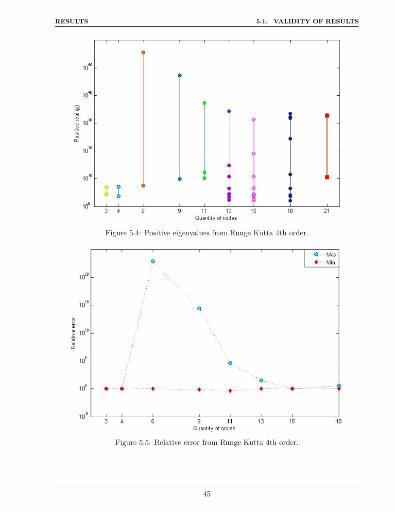
RESULTS 5.1. VALIDITY OF RESULTS
Figure 5.4: Positive eigenvalues from Runge Kutta 4th order.
Figure 5.5: Relative error from Runge Kutta 4th order.
45

RESULTS 5.2. DATA PROCESSING
5.2 Data Processing
Solutions in general can be divided in complex and pure real solutions in which the real part(ωR) of the eigenvalues represents unstable, growing exponentials in time. In case of complexvalues, the imaginary part (ωI) correspond to oscillation frequency. As transient solutions areexpressed in form X(x)exp(ωR)cos(ωI + φ), Figure ?? represents the incidence of temporalsolution ω with an arbitrary amplitude in temporal representation.
(a) Stable. (b) Oscillating Stable.
(c) Unstable. (d) Oscillating Unstable.
Figure 5.6: General transient response representation in time.
Stables solutions decreased its value to zero, allowing the system to answer as its steady state.In other hand, unstable solutions represents thermal runaway phenomenon, which leads tothe quick degradation of device, rendering it useless and consequently without presenting thesteady state.
46

RESULTS 5.2. DATA PROCESSING
5.2.1 Range of Allowed Eigenvalues
Various degradation mechanisms have been proposed in terms of atomic phenomenon [40],through there is no consensus in the field of what modes are presents in certain samplesor if all possible modes are yet accounted for. In this Thesis, a range of allowed eigenval-ues is proposed considering thermal inertia and a characteristic time of thermal runawayphenomenon.
Thermal inertia (Ith) is the material property to keep its temperature and is also known asthermal storage effect. It considers the degree of slowness with which the temperature of abody approaches that of its surroundings and the quantity of heat can be absorbed or lost.It depends on material’s bulk thermal conductivity (k) and volumetric heat capacity, whichis the product of density (ρ) and specific heat capacity (c), as can be seen in Eq. (5.1).For GaAs, Ith = 8.647[Wm−2K−1√s], while for Si, Ith = 15.668[Wm−2K−1√s] at roomtemperature Troom = 300[K] and thermal equilibrium. As value for Si almost double GaAs,it is expected that GaAs allows lower times to increase its temperature.
Ith =√kρc. (5.1)
As there is not experimental data of thermal evolution through time of solar cells basedon GaAs junction, comparison will fall on experimental work of Vasko [25], who evaluatedsolar cells of a-Si:H triple junction. From an IR mapping, surface temperature is measuredfollowing a hot spot development under forced convective cooling. Hence, it is supposed thatdifference between surface and junction temperature is neglected.
Considering a mean thermal inertia of ωMTI = 5.55 × 10⁻⁴, calculated as the coefficient ofexponential regression of experimental data [25], it could be stablish a range of allowed valueswith a meddle value equal to mean thermal inertial.
The range of allowed values represents limits in which thermal runaway occurs; solutionsbelow lower limit are associated to times larger than phenomenon characteristic time and,in other hand, solutions over the upper limit implies times does not allowed considered thethermal inertia of device. To determine the range of calculated eigenvalues, it is necessaryto considerate the non-dimensional constant t0 to dimensionalize them.The parameter t0 is afunction of junction longitude L and temperatures TC and TL expressed as t0 = L2
v0·µn,as can
be seen in Figure 5.7.
Once eigenvalues become dimensional, they can be associated to a characteristic time, definedas necessary time to achieve T (tend) = 600[K] from T (tinitial) = 301[K], as can be seenin Eq.(5.2). These temperatures considering the steady state profile and transient stateevolution, that means, it is supposed that in one part of the temperature profile of transientstate solutions there is at least one point with a initial value of 1[K], which evolves to 300[K].
t(ω∗) = ln(300)/ω∗ (5.2)
Also, in order to compare to the reference eigenvalue ωMTI , the calculated characteristic timeis t(ωMTI) = 18[min]. Figures 5.8 and 5.9 represent a range of the calculated characteristictime as a function of eigenvalues; first, with a range equal to experimental data dispersion;and the second concentrates values closest to the reference.
47

RESULTS 5.2. DATA PROCESSING
Figure 5.7: Reference time t0.
Figure 5.8: Allowed range of characteristic time.
48
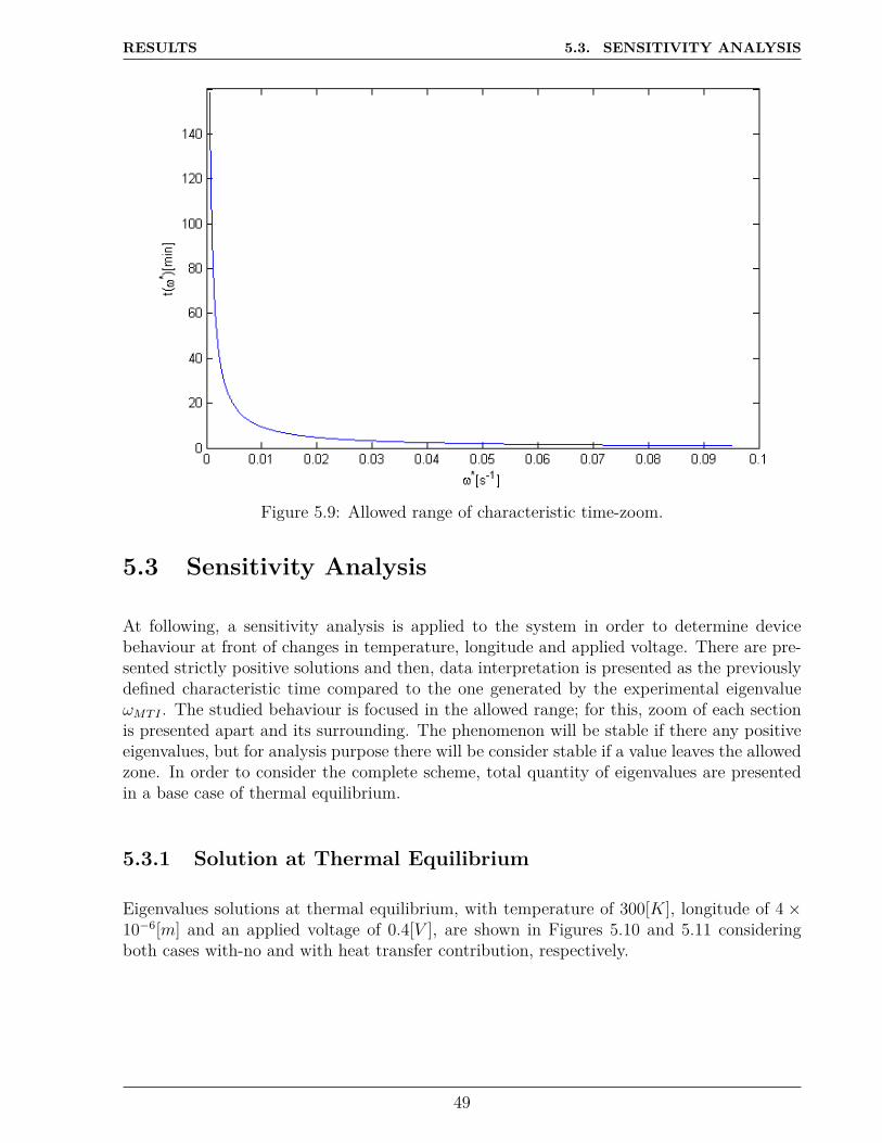
RESULTS 5.3. SENSITIVITY ANALYSIS
Figure 5.9: Allowed range of characteristic time-zoom.
5.3 Sensitivity Analysis
At following, a sensitivity analysis is applied to the system in order to determine devicebehaviour at front of changes in temperature, longitude and applied voltage. There are pre-sented strictly positive solutions and then, data interpretation is presented as the previouslydefined characteristic time compared to the one generated by the experimental eigenvalueωMTI . The studied behaviour is focused in the allowed range; for this, zoom of each sectionis presented apart and its surrounding. The phenomenon will be stable if there any positiveeigenvalues, but for analysis purpose there will be consider stable if a value leaves the allowedzone. In order to consider the complete scheme, total quantity of eigenvalues are presentedin a base case of thermal equilibrium.
5.3.1 Solution at Thermal Equilibrium
Eigenvalues solutions at thermal equilibrium, with temperature of 300[K], longitude of 4 ×10⁻⁶[m] and an applied voltage of 0.4[V ], are shown in Figures 5.10 and 5.11 consideringboth cases with-no and with heat transfer contribution, respectively.
49

RESULTS 5.3. SENSITIVITY ANALYSIS
Figure 5.10: Eigenvalues at thermal equilibrium, qL = 0.
Figure 5.11: Eigenvalues at thermal equilibrium, qL > 0.
50

RESULTS 5.3. SENSITIVITY ANALYSIS
With-no lattice temperature influence, solution is expressed in multiples eigenvalues withhigh magnitude, real part orders expressed from 10−100 until 1040 and imaginary part, from10−40 to 1040. Including energy equation contribution, graphs moves to the unstable zoneat right, decreasing oscillating frequency. It can be interpreted as system without latticetemperature or TL = 0[K] has less probabilities of been unstable compared to the samesystem with a lattice temperature higher than zero. Also, in case of a positive lattice tem-perature, oscillating frequency (ωI) of central values is higher than temporal evolution value(ωR), representing a movement of carrier through the junction without a concrete direction,characteristic of turbulence phenomenon.
5.3.2 Variation in Temperature
As the model is two-temperature, three base cases are considered. First one, variation oflattice temperature and constant carrier temperature. Second one is the opposite of the firstone and the last is a variation of both temperatures, considering the difference between themconstant.
Lattice Temperature
Lattice temperature range is imposed with a lower value representing a room temperature of300[K] and a maximum value of 550[K]; this last is higher that used in accelerated degrada-tion testing in order to considerate the difference between surface and junction temperature.Carrier temperature are considered TC = 650[K] in order to be never reach by lattice temper-ature and is constant to focus in the lattice temperature effect. Also, voltage and longitudeare fixed in Vapp = 0.4[V ], L = 4[µm].
Figure 5.12 represents eigenvalues results, concentrating the major quantity with a positivereal lower than 105 and higher than 1; there are few values over that, that is, one for temper-atures lower than 450[K] and two for the others. Respect to magnitude of the eigenvaluesreal part, 450[K] is the lattice temperature since the expansion of instability range becomeshigher. As can be seen in Figure 5.13, most values led to high characteristic times, above105[min], and they can be prevented considering forced cooling and by another regulationmeasures. There are also eigenvalues at low characteristic time, less than 10−5[min] that canbe considered instantaneous; hence, less probable due to thermal inertia. As there are noteigenvalues in the allowed zone until 450[K], Figure 5.14 shows that tendency of eigenvaluesis increasing in time, so even if the phenomenon start at 450[K] it can be more controllableif temperature arises. TL = 450[K] is a temperature used in accelerated test that inducesdevice degradation, so it is expected that an allowed eigenvalue is presented in that temper-ature. Also, at higher lattice temperature phenomenon stabilizes and can be linked to thedecrease of device power [41].
51

RESULTS 5.3. SENSITIVITY ANALYSIS
Figure 5.12: Positive eigenvalues at TC = 650[K], Vapp = 0.4[V ], L = 4[µm].
Figure 5.13: Characteristic time at TC = 650[K], Vapp = 0.4[V ], L = 4[µm].
52

RESULTS 5.3. SENSITIVITY ANALYSIS
Figure 5.14: Allowed range at TC = 650[K], Vapp = 0.4[V ], L = 4[µm].
Carrier temperature
Carrier temperature start considering thermal equilibrium at T = 300[K] and then increasinguntil TC = 800[K]. Lattice temperature is fixed at TL = 300, applied voltage at Vapp = 0.4[V ]and longitude L = 4[µm].
Figure 5.12 represents eigenvalues results showing that, in contrast with lattice temperature,carrier temperature increases the quantity of eigenvalues that are above the concentrationrange of (1, 105), which coincides with the one presented for lattice temperature. There isn’ta clear tendency in the maximum data, presenting a peak at 500[K]. The minimum positivevalue, however, tends to decrease with the increase of carrier temperature. As can be seenin Figure 5.16, most values led to high characteristic times, above 105[min]. There are alsoeigenvalues at low characteristic time, less than 10−5[min], specially at thermal equilibrium.There is not a eigenvalue in the allowed zone at thermal equilibrium, but is so close so it isconsidered inside at the evidence that at that operating condition there is thermal runaway.Figure 5.17 shows that higher temperatures raise their characteristic time, making it morestable. Carrier with a temperature higher than the one of lattice is consider a hot carrierand it is proved that increases device efficiency by dimishing thermalization losses [41].
53
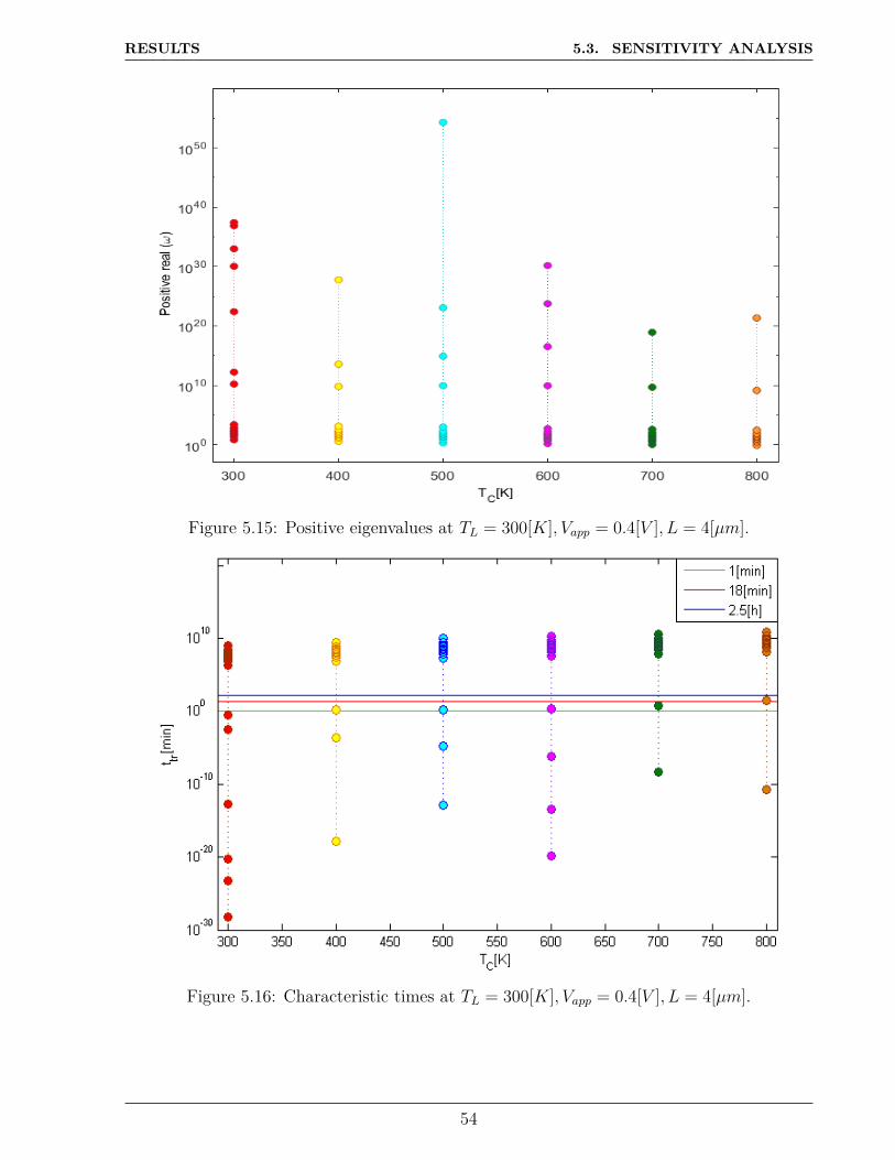
RESULTS 5.3. SENSITIVITY ANALYSIS
Figure 5.15: Positive eigenvalues at TL = 300[K], Vapp = 0.4[V ], L = 4[µm].
Figure 5.16: Characteristic times at TL = 300[K], Vapp = 0.4[V ], L = 4[µm].
54

RESULTS 5.3. SENSITIVITY ANALYSIS
Figure 5.17: Allowed range at TL = 300[K], Vapp = 0.4[V ], L = 4[µm].
Constant Difference
To consider that an increase of lattice temperature leads to thermal runaway and an increaseof carrier temperature stabilize it, a combined effect is studied by fixing a difference intemperature of TC − TL = 150[K]. Applied voltage is fixed at Vapp = 0.4[V ] and longitudeL = 4[µm].
From Figure 5.18, quantity of eigenvalues decrease with the increase of temperature, carrierand lattice. The range of concentration is kept at any temperature configurations and theupper values tends to increase from 450[K]. This leads to determine that lattice temperatureis critical in the stability and carrier temperature could control the range of instability,decreasing the value of the solution. Figure 5.19 shows that only at 300[K] there is not anyeigenvalue in the allowed range; the most close value presents a characteristic time higherthan the upper limit. Lower values presents pseudo-spontaneous phenomenon, increasing thecharacteristic time from 10−60 until 10−10, approximately. For lattice temperatures lower than500[K], carrier temperature is lower than the used in the previous case (TC constant). Figure5.20 shows that at that range phenomenon is unstable, contrary to the one with TC = 650[K].To temperatures higher than 450[K], carrier temperature is higher too and phenomenon hasa higher characteristic time, stabilizing the system even at high lattice temperatures. Also,projecting the analysis, it can be extracted that carrier temperature variation for a fixedlattice temperature behaves as contour lines, representing the same curve moving throughcharacteristic time axis.
55

RESULTS 5.3. SENSITIVITY ANALYSIS
Figure 5.18: Positive eigenvalues at TC − TL = 150[K], Vapp = 0.4[V ], L = 4[µm].
Figure 5.19: Characteristic time at TC − TL = 150[K], Vapp = 0.4[V ], L = 4[µm].
56
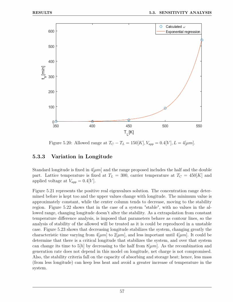
RESULTS 5.3. SENSITIVITY ANALYSIS
Figure 5.20: Allowed range at TC − TL = 150[K], Vapp = 0.4[V ], L = 4[µm].
5.3.3 Variation in Longitude
Standard longitude is fixed in 4[µm] and the range proposed includes the half and the doublepart. Lattice temperature is fixed at TL = 300, carrier temperature at TC = 450[K] andapplied voltage at Vapp = 0.4[V ].
Figure 5.21 represents the positive real eigenvalues solution. The concentration range deter-mined before is kept too and the upper values change with longitude. The minimum value isapproximately constant, while the center column tends to decrease, moving to the stabilityregion. Figure 5.22 shows that in the case of a system "stable", with no values in the al-lowed range, changing longitude doesn’t alter the stability. As a extrapolation from constanttemperature difference analysis, is imposed that parameters behave as contour lines, so theanalysis of stability of the allowed will be treated as it is could be reproduced in a unstablecase. Figure 5.23 shows that decreasing longitude stabilizes the system, changing greatly thecharacteristic time varying from 4[µm] to 2[µm], and less important until 4[µm]. It could bedetermine that there is a critical longitude that stabilizes the system, and over that systemcan change its time to 5[h] by decreasing to the half from 8[µm]. As the recombination andgeneration rate does not depend in this model on longitude, net charge is not compromised.Also, the stability criteria fall on the capacity of absorbing and storage heat; hence, less mass(from less longitude) can keep less heat and avoid a greater increase of temperature in thesystem.
57

RESULTS 5.3. SENSITIVITY ANALYSIS
Figure 5.21: Positive eigenvalues at TL = 300[K], TC = 450[K], Vapp = 0.4[V ].
Figure 5.22: Characteristic time at TL = 300[K], TC = 450[K], Vapp = 0.4[V ].
58

RESULTS 5.3. SENSITIVITY ANALYSIS
Figure 5.23: Allowed range at TL = 300[K], TC = 450[K], Vapp = 0.4[V ].
5.3.4 Variation in applied voltage
Considering a minimum case of 0.4[V ], applied voltage is study until 1[V ]. Lattice temper-ature is fixed at TL = 300, carrier temperature at TC = 450[K] and longitude L = 4[µm].
Figure 5.24 shows that the maximum value tends to decrease with the increase of appliedvoltage, getting near the negative zone. The range that concentrates value is the same at theprevious cases and it doesn’t change at varying the applied voltage. Figure 5.25 shows thatmost quantity of eigenvalue concentrates at high characteristic time,with a magnitude orderof 1010[min], approximately. Also, the are a few eigenvalues under the allowed zone thatshows a increase tendency, suggesting a stabilization, but they disappear at Vapp = 0.8[V ].Analogous as the previous case, the tendency analysis will be applied at the nearer values,with an order of 105. Figure 5.26 shows that the increase of applied voltage increase thecharacteristic time, stabilizing the system. Increasing the applied voltage arises total currentdensity and, by accelerating electrons, the velocity in which heat is transported through thejunction increases, leading to higher characteristic times.
59

RESULTS 5.3. SENSITIVITY ANALYSIS
Figure 5.24: Positive eigenvalues at TL = 300[K], TC = 450[K], L = 4[µm].
Figure 5.25: Characteristic time at TL = 300[K], TC = 450[K], L = 4[µm].
60
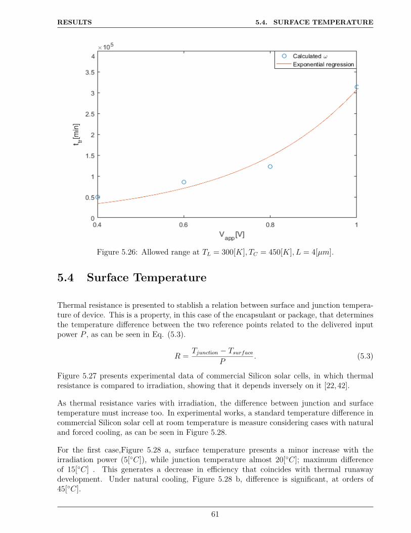
RESULTS 5.4. SURFACE TEMPERATURE
Figure 5.26: Allowed range at TL = 300[K], TC = 450[K], L = 4[µm].
5.4 Surface Temperature
Thermal resistance is presented to stablish a relation between surface and junction tempera-ture of device. This is a property, in this case of the encapsulant or package, that determinesthe temperature difference between the two reference points related to the delivered inputpower P , as can be seen in Eq. (5.3).
R = Tjunction − TsurfaceP
. (5.3)
Figure 5.27 presents experimental data of commercial Silicon solar cells, in which thermalresistance is compared to irradiation, showing that it depends inversely on it [22, 42].
As thermal resistance varies with irradiation, the difference between junction and surfacetemperature must increase too. In experimental works, a standard temperature difference incommercial Silicon solar cell at room temperature is measure considering cases with naturaland forced cooling, as can be seen in Figure 5.28.
For the first case,Figure 5.28 a, surface temperature presents a minor increase with theirradiation power (5[◦C]), while junction temperature almost 20[◦C]; maximum differenceof 15[◦C] . This generates a decrease in efficiency that coincides with thermal runawaydevelopment. Under natural cooling, Figure 5.28 b, difference is significant, at orders of45[◦C].
61

RESULTS 5.4. SURFACE TEMPERATURE
Figure 5.27: Thermal resistance at varying irradiation [42].
Considering that a hot spot temperature can reach 10[◦C] over the surface temperature,difference between this surface point and junction temperature may be between 25[◦C] to55[◦C]. It is also appreciable that junction temperature can increase without influence surfacetemperature greatly, that coincides with the lattice boundary conditions proposed. Thiseffects is considered also for thin film, but it would be expected that range difference wouldbe minor than the case of commercial cells.
Considering the following irradiation world map:
(a) Forced cooling. (b) Natural cooling.
Figure 5.28: Temperature and efficiency varying irradiations [43].
62
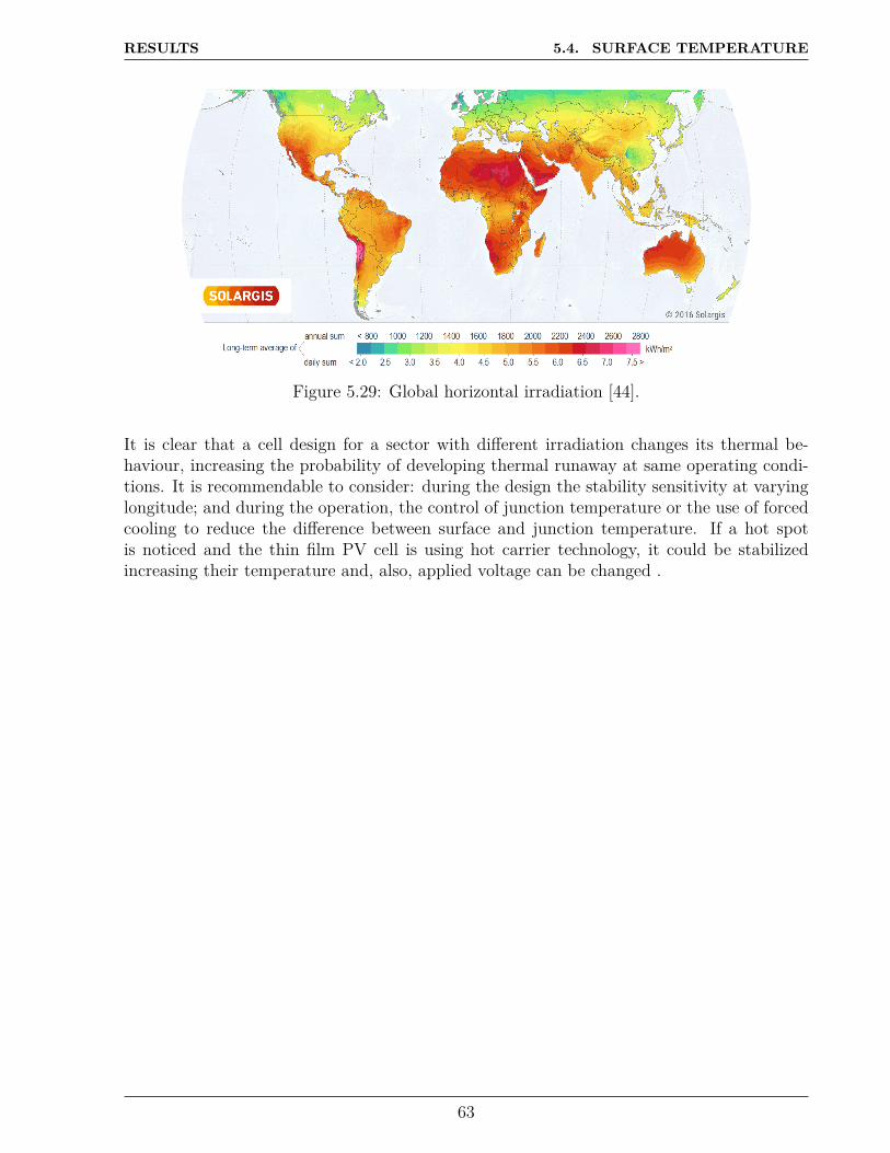
RESULTS 5.4. SURFACE TEMPERATURE
Figure 5.29: Global horizontal irradiation [44].
It is clear that a cell design for a sector with different irradiation changes its thermal be-haviour, increasing the probability of developing thermal runaway at same operating condi-tions. It is recommendable to consider: during the design the stability sensitivity at varyinglongitude; and during the operation, the control of junction temperature or the use of forcedcooling to reduce the difference between surface and junction temperature. If a hot spotis noticed and the thin film PV cell is using hot carrier technology, it could be stabilizedincreasing their temperature and, also, applied voltage can be changed .
63
Chapter 6
Conclusions and Future Work
In this Thesis a two-temperature 1-D hydrodynamic model is studied to determine thermaland electrical stability of PN junction solar cell. The model was previously solved for steadystate condition at zero order at front a perturbation, which is used to found the solutions at alinearized transient state. Uncoupling time and space dimensions, temporal solution behavesas an exponential and the sign of real part of eigenvalues determines stability. As there is aninfinite possible calculated eigenvalues, solution will be a probability; if there is at least onepositive solution, the system can be unstable.
As there is not a consensus in which modes are allowed, it is proposed a characteristictime of thermal runaway that represents time to achieve a lattice temperature 600[K] from300[K], considering a initial condition of 1[K] in some point of temperature profile. Allowedcharacteristic time range consider a experimental value as meddle; thermal inertia forbids in-stantaneous increases and slow times with magnitude of hours can be controlled, for exampleby cooling, and does not refers the thermal runaway phenomenon.
6.1 Conclusions
There are five cases simulated: varying temperature (lattice, carrier and both), longitudeand applied voltage. In first case, varying temperature, there is considered one temperaturevariable and the other is fixed in a constant value, except for the last temperature case inwhere a constant difference is kept. Varying lattice temperature, thermal runaway startwhen lattice boundary achieve 450[K]; an increase of carrier temperature, which representshot carriers,stabilizes temporal behaviour; then, considering both cases, lattice temperatureinstability can be controlled by increasing temperature of hot carriers. Reducing the devicelength and increasing applied voltage gets the device significantly more stable. Influencedepends on the cost of varying each variable in terms of how much stability system gains.
Respect to imaginary part of eigenvalue, oscillation frequency can be considered as turbu-lence, in which the chaotic movement is represented as a movement of carriers through thejunction. It is only present for low eigenvalues, with real part less than 103, that corresponds
64
CONCLUSIONS AND FUTURE WORK 6.2. FUTURE WORK
to high characteristic time and out of thermal runaway allowed range.
The presented model considers that junction boundary temperature doesn’t evolve in time,hence the increase in temperature is in the middle of the junction, where the instability isdevelop. Changes in thermal resistance of encapsulant can avoid the phenomenon consideringthat its increase allows the system to never reach the critical junction temperature. Also,due to difference in temperature of surface and junction, cooling is imperative in order tocontrol this critical condition. Forced cooling can present a difference in magnitude order of10[K], so it is proposed to use when junction temperature can not be determined.
6.2 Future Work
Avoiding thermal runaway, solar cell properties can be maintain and lifespan can be pro-longed. This work is an hypothetical case for academic studies, so conclusions are presentedwith qualitative nature, as tendencies and the existence of a critical value. For futures de-velopments in the same line, there is proposed the following improvements in model.
• Carrier temperature variable in space and its relation to lattice temperature.• Deeper studies in transient boundary conditions, considering the case with an initial
lattice in order to determine surface temperature evolution.• Test the model in an actual experimentally developed material, to compare cases with
a more precise thermal inertia.• Consider other layers in solar cell, to determine influence of thermal resistance in the
model.• Experimental study to determine allowed modes of degradation.• Expand the model to more spatial dimensions, to capture the effect of redistribution
of lattice temperature profile.• Study long term degradation, considering multiples cycles and fatigue failure.
65

Bibliography
[1] Ministerio de Energía. Energía 2050. Política energética de Chile. Gobierno de Chile,2015.
[2] Florian Pfeffer, Johannes Eisenlohr, Angelika Basch, Martin Hermle, Benjamin G Lee,and Jan Christoph Goldschmidt. Systematic analysis of diffuse rear reflectors for en-hanced light trapping in silicon solar cells. Solar Energy Materials and Solar Cells,152:80–86, 2016.
[3] Bita Farhadi and Mosayeb Naseri. A novel efficient double junction ingap/gaas solar cellusing a thin carbon nano tube layer. Optik-International Journal for Light and ElectronOptics, 127(15):6224–6231, 2016.
[4] Johannes Eisenlohr, Nico Tucher, Hubert Hauser, Martin Graf, Jan Benick, BenediktBläsi, Jan Christoph Goldschmidt, and Martin Hermle. Efficiency increase of crystallinesilicon solar cells with nanoimprinted rear side gratings for enhanced light trapping.Solar Energy Materials and Solar Cells, 155:288–293, 2016.
[5] Sanjeev Jakhar, MS Soni, and Nikhil Gakkhar. Historical and recent development ofconcentrating photovoltaic cooling technologies. Renewable and Sustainable Energy Re-views, 60:41–59, 2016.
[6] Leonardo Micheli, Eduardo F Fernandez, Florencia Almonacid, Tapas K Mallick, andGreg P Smestad. Performance, limits and economic perspectives for passive cooling ofhigh concentrator photovoltaics. Solar Energy Materials and Solar Cells, 153:164–178,2016.
[7] Marco Beccali, Maurizio Cellura, Sonia Longo, and Francesco Guarino. Solar heatingand cooling systems versus conventional systems assisted by photovoltaic: Applicationof a simplified lca tool. Solar Energy Materials and Solar Cells, 2016.
[8] DT Cotfas, PA Cotfas, and S Kaplanis. Methods and techniques to determine thedynamic parameters of solar cells: Review. Renewable and Sustainable Energy Reviews,61:213–221, 2016.
[9] A Rezaee Jordehi. Parameter estimation of solar photovoltaic PV cell- a review. Re-newable and Sustainable Energy Reviews, 61:354–371, 2016.
66

BIBLIOGRAPHY BIBLIOGRAPHY
[10] Simon Min Sze. Semiconductor Devices: Physics and Technology. John Wiley & Sons,2008.
[11] Said Ibrahim, Dina Ibrahim, and Guido Righini. Structure of Solid, course Chemistryof Energy Storage Materials. Minerva, 2014.
[12] Sammy Kayali, George Ponchak, and Roland Shaw. GaAs MMIC Reliability AssuranceGuideline for Space Applications. California Institute of Technology, 1996.
[13] Chih-Tang Sah. Fundamentals of Solid-state Electronics. World Scientific, 1991.
[14] Adrian Kitai. Principles of solar cells, LEDs and diodes: the role of the PN junction.John Wiley & Sons, 2011.
[15] Shin-ichiro Sato, Takeshi Ohshima, and Mitsuru Imaizumi. Modeling of degradationbehavior of InGaP/GaAs/Ge triple-junction space solar cell exposed to charged particles.Journal of Applied Physics, 105(4):044504, 2009.
[16] François Charru. Hydrodynamic Instabilities, volume 37. Cambridge University Press,2011.
[17] Williams R Calderón Munoz. Linear stability of electron-flow hydrodynamics in ungatedsemiconductors. PhD thesis, University of Notre Dame, 2009.
[18] Jason F Hiltner and James R Sites. Stability of CdTe solar cells at elevated temperatures:bias, temperature, and Cu dependence. In National center for photovoltaics (NCPV)15th program review meeting, volume 462, pages 170–175. AIP Publishing, 1999.
[19] Naba R Paudel, Kristopher A Wieland, Matthew Young, Sally Asher, and Alvin DCompaan. Stability of sub-micron-thick CdTe solar cells. Progress in Photovoltaics:Research and Applications, 22(1):107–114, 2014.
[20] David L King, Jay A Kratochvil, and William E Boyson. Temperature coefficients forpv modules and arrays: measurement methods, difficulties, and results. In PhotovoltaicSpecialists Conference, 1997., Conference Record of the Twenty-Sixth IEEE, pages 1183–1186. IEEE, 1997.
[21] Thomas Nordmann and Luzi Clavadetscher. Understanding temperature effects on PVsystem performance. In Photovoltaic Energy Conversion, 2003. Proceedings of 3rd WorldConference on, volume 3, pages 2243–2246. IEEE, 2003.
[22] BJ Huang, PE Yang, YP Lin, BY Lin, HJ Chen, RC Lai, and JS Cheng. Solar celljunction temperature measurement of PV module. Solar Energy, 85(2):388–392, 2011.
[23] Nima E Gorji. Thermal runaway in thin film PV: temperature profile modeling. 2014.
[24] C Magarreiro, MC Brito, and PMM Soares. Assessment of diffuse radiation models forcloudy atmospheric conditions in the azores region. Solar Energy, 108:538–547, 2014.
67

BIBLIOGRAPHY BIBLIOGRAPHY
[25] Anthony C Vasko, Aarohi Vijh, and Victor G Karpov. Hot spots spontaneously emergingin thin film photovoltaics. Solar Energy, 108:264–273, 2014.
[26] Celina Mikolajczak, Michael Kahn, Kevin White, and Richard Thomas Long. Lithium-ion batteries hazard and use assessment. Springer Science & Business Media, 2012.
[27] KT Wan, FA Cozzarelli, and DJ Inman. Thermal runaway due to strain-heating feed-back. AIAA journal, 26(10):1263–1268, 1988.
[28] Jordi Casanova, Jordi José, Enrique García-Berro, Steven N Shore, and Alan C Calder.Kelvin-helmholtz instabilities as the source of inhomogeneous mixing in nova explosions.Nature, 478(7370):490–492, 2011.
[29] LL Liou and B Bayraktaroglu. Thermal stability analysis of AlGaAs/GaAs heterojunc-tion bipolar transistors with multiple emitter fingers. IEEE Transactions on ElectronDevices, 41(5):629–636, 1994.
[30] VG Karpov, AD Compaan, and Diana Shvydka. Random diode arrays and mesoscalephysics of large-area semiconductor devices. Physical Review B, 69(4):045325, 2004.
[31] D. Shvydka V.G.Karpov. Understanding and mitigating effects of non-uniformities onreliability on thin film photovoltaic. Reliability of Photovoltaic Cells, Modules, Compo-nents, and Systems II, 7412:15, 2009.
[32] VG Karpov, A Vasko, and A Vijh. Hot spot runaway in thin film photovoltaics andrelated structures. Applied Physics Letters, 103(7):074105, 2013.
[33] Juan Osses-Márquez and Williams R Calderón-Muñoz. Thermal influence on chargecarrier transport in solar cells based on GaAs PN junctions. Journal of Applied Physics,116(15):154502, 2014.
[34] Williams R Calderón-Muñoz, Debdeep Jena, and Mihir Sen. Temperature influence onhydrodynamic instabilities in a one-dimensional electron flow in semiconductors. Journalof applied physics, 107(7):074504, 2010.
[35] IN Volovichev, GN Logvinov, O Yu Titov, and Yu G Gurevich. Recombination andlifetimes of charge carriers in semiconductors. Journal of applied physics, 95(8):4494–4496, 2004.
[36] Sara Shishehchi, Asghar Asgari, and Reza Kheradmand. The effect of temperatureon the recombination rate of AlGaN/GaN light emitting diodes. Optical and quantumelectronics, 41(7):525–530, 2009.
[37] Ansgar Jüngel, Maria Cristina Mariani, and Diego Rial. Local existence of solutions tothe transient quantum hydrodynamic equations. Mathematical Models and Methods inApplied Sciences, 12(04):485–495, 2002.
[38] Jong Pil Kim, Ho Lim, Ju Hun Song, Young June Chang, and Chung Hwan Jeon.Numerical analysis on the thermal characteristics of photovoltaic module with ambient
68

BIBLIOGRAPHY BIBLIOGRAPHY
temperature variation. Solar Energy Materials and Solar Cells, 95(1):404–407, 2011.
[39] Alfio Quarteroni, Riccardo Sacco, and Fausto Saleri. Numerical mathematics, volume 37.Springer Science & Business Media, 2010.
[40] Roussillon Karpov, Shvydka. Physical modes of thin film PV degradation. ConferenceRecord of the Thirty First IEEE, pages 437–440, 2005.
[41] Williams R Calderón-Muñoz and Cristian Jara-Bravo. Hydrodynamic modeling of hot-carrier effects in a PN junction solar cell. Acta Mechanica, pages 1–14, 2016.
[42] Jihong Zhang, Yulin Gao, Yijun Lu, Lihong Zhu, Ziquan Guo, Guolong Chen, andZhong Chen. Transient thermal resistance test of single-crystal-silicon solar cell. IEEETransactions on Electron Devices, 59(9):2345–2349, 2012.
[43] Sun Ho Jang and Moo Whan Shin. Thermal characterization of junction in solar cellpackages. IEEE Electron Device Letters, 31(7):743–745, 2010.
[44] SolarGIS. Free download of solar resource maps. urlhttp://solargis.com/, 2016.
69