The improved electromechanical sensitivity of polymer thin films containing carbon clusters produced...
8
The improved electromechanical sensitivity of polymer thin films containing carbon clusters produced in situ by irradiation with metal ions Pandiyan Murugaraj a , David Mainwaring a, * , Nurra Ali Khelil a , Ju Lin Peng a , Rainer Siegele b , Prashant Sawant a a School of Applied Sciences, Royal Melbourne Institute of Technology, P.O. Box 2476, Melbourne 3001, Australia b Institute for Environmental Research, Australian Nuclear Science and Technology Organisation, Private Mail Bag 1, Menai 2234, Australia ARTICLE INFO Article history: Received 29 April 2010 Accepted 19 July 2010 Available online 24 July 2010 ABSTRACT Greatly enhanced electromechanical sensitivities were observed in ion beam irradiated polyimide films, where high resolution transmission electron microscopy and atomic force microscopy studies showed that 5.5 MeV Cu 3+ ions produce randomly dispersed and highly oriented conducting nanochannels containing carbon clusters in polyimide with consider- able overlap and narrow tunnel gap distributions between neighbouring nanochannels. Selected area electron diffraction studies confirmed the graphitic structure of these carbon clusters and also showed that the graphitic layers had preferential orientation parallel to the ion beam direction arising from relaxation of the graphitic layers within the nanochan- nels relieving local surface stresses in the polyimide matrix generated during irradiation as well as alignment of graphitic basal layers by volatile gases formed during irradiation escaping to the surface minimising resistance to gas flow. Electron energy loss spectros- copy also confirmed the graphitic structure of these carbon clusters within the nanochan- nels. Film electrical resistance increased exponentially with applied strain demonstrating the dominant role of tunnel gap modulation under strain. Gauge factors >1000 were achieved in these films at >3000 lstrains. Narrow distribution of tunnel gaps between the overlapping nanochannels is responsible for the high electromechanical sensitivities observed in these films compared to carbon nanotube–polymer (50) films. Ó 2010 Elsevier Ltd. All rights reserved. 1. Introduction Electron transport within carbon nanostructures is becoming an increasingly important phenomenon in a wide range of electronic devices including sensors. Structural health moni- toring (SHM) requires high sensitivity, low power embedded primary sensors for unobtrusive deformation monitoring in infrastructure ranging from buildings to bridges and aircraft. Capturing a two-dimensional stress field of a structural com- ponent with conventional strain gauges requires dense instrumentation. Over the past decade, considerable effort has focussed on developing miniaturised low power passive wireless strain sensors aimed at robust dense embedded monitoring systems [1–4]. Piezoresistive single carbon nanotubes (CNT) having en- hanced electromechanical sensitivities (i.e. gauge factors GF: electrical response to mechanical strain 850) [5] as well as semiconducting nanowires are being evaluated for embedded devices required for real-time SHM applications. Their sensi- tivities arise from changes in the Schotky potential barrier 0008-6223/$ - see front matter Ó 2010 Elsevier Ltd. All rights reserved. doi:10.1016/j.carbon.2010.07.026 * Corresponding author: Fax: +61 3 9925 3747. E-mail address: [email protected] (D. Mainwaring). CARBON 48 (2010) 4230 – 4237 available at www.sciencedirect.com journal homepage: www.elsevier.com/locate/carbon
-
Upload
tatamemorialcentre -
Category
Documents
-
view
0 -
download
0
Transcript of The improved electromechanical sensitivity of polymer thin films containing carbon clusters produced...
C A R B O N 4 8 ( 2 0 1 0 ) 4 2 3 0 – 4 2 3 7
. sc iencedi rec t .com
avai lab le at wwwjournal homepage: www.elsev ier .com/ locate /carbon
The improved electromechanical sensitivity of polymerthin films containing carbon clusters produced in situby irradiation with metal ions
Pandiyan Murugaraj a, David Mainwaring a,*, Nurra Ali Khelil a, Ju Lin Peng a,Rainer Siegele b, Prashant Sawant a
a School of Applied Sciences, Royal Melbourne Institute of Technology, P.O. Box 2476, Melbourne 3001, Australiab Institute for Environmental Research, Australian Nuclear Science and Technology Organisation, Private Mail Bag 1, Menai 2234, Australia
A R T I C L E I N F O
Article history:
Received 29 April 2010
Accepted 19 July 2010
Available online 24 July 2010
0008-6223/$ - see front matter � 2010 Elsevidoi:10.1016/j.carbon.2010.07.026
* Corresponding author: Fax: +61 3 9925 3747E-mail address: [email protected]
A B S T R A C T
Greatly enhanced electromechanical sensitivities were observed in ion beam irradiated
polyimide films, where high resolution transmission electron microscopy and atomic force
microscopy studies showed that 5.5 MeV Cu3+ ions produce randomly dispersed and highly
oriented conducting nanochannels containing carbon clusters in polyimide with consider-
able overlap and narrow tunnel gap distributions between neighbouring nanochannels.
Selected area electron diffraction studies confirmed the graphitic structure of these carbon
clusters and also showed that the graphitic layers had preferential orientation parallel to
the ion beam direction arising from relaxation of the graphitic layers within the nanochan-
nels relieving local surface stresses in the polyimide matrix generated during irradiation as
well as alignment of graphitic basal layers by volatile gases formed during irradiation
escaping to the surface minimising resistance to gas flow. Electron energy loss spectros-
copy also confirmed the graphitic structure of these carbon clusters within the nanochan-
nels. Film electrical resistance increased exponentially with applied strain demonstrating
the dominant role of tunnel gap modulation under strain. Gauge factors >1000 were
achieved in these films at >3000 lstrains. Narrow distribution of tunnel gaps between the
overlapping nanochannels is responsible for the high electromechanical sensitivities
observed in these films compared to carbon nanotube–polymer (�50) films.
� 2010 Elsevier Ltd. All rights reserved.
1. Introduction
Electron transport within carbon nanostructures is becoming
an increasingly important phenomenon in a wide range of
electronic devices including sensors. Structural health moni-
toring (SHM) requires high sensitivity, low power embedded
primary sensors for unobtrusive deformation monitoring in
infrastructure ranging from buildings to bridges and aircraft.
Capturing a two-dimensional stress field of a structural com-
ponent with conventional strain gauges requires dense
er Ltd. All rights reserved
.du.au (D. Mainwaring).
instrumentation. Over the past decade, considerable effort
has focussed on developing miniaturised low power passive
wireless strain sensors aimed at robust dense embedded
monitoring systems [1–4].
Piezoresistive single carbon nanotubes (CNT) having en-
hanced electromechanical sensitivities (i.e. gauge factors GF:
electrical response to mechanical strain �850) [5] as well as
semiconducting nanowires are being evaluated for embedded
devices required for real-time SHM applications. Their sensi-
tivities arise from changes in the Schotky potential barrier
.
C A R B O N 4 8 ( 2 0 1 0 ) 4 2 3 0 – 4 2 3 7 4231
height and modifications in the electronic band structure and
band-gap bending when subjected to mechanical deforma-
tion [6,7]. The sensitivity of thin self-assembled gold nanopar-
ticles within organic films (GF of �17) has been interpreted as
arising from tunnel gap modulation between the nanoparti-
cles during deformation [8,9]. More robust bulk conducting
carbon–polymer composite films have GF between 8 and 12
and show many advantages over conventional metal strain
gauges (GF � 2–5), although they exhibit considerable electri-
cal hysteresis due to poor mechanical relaxation behaviour
[10].
The exponential increase in resistance with applied tensile
strain seen in CNT filled polymer composite systems, having
GF � 50, has been identified as tunnel junction gap-width
modulation between the overlapping carbon nanotubes
[11,12]. Enhanced sensitivities, GF > 50 with minimum hyster-
esis are yet to be realised in practice in these composites due
to inhomogeneous mixing, irregular particle/CNT bundle
sizes, wide distribution of tunnel gaps and presence of perco-
lating and non-percolating regions.
High energy ion beam irradiation (HEIBI) has yielded elec-
trically conducting carbon nanostructures in polymer matri-
ces for a range of device applications [13–15]. Across a range
of fluences from 1014 to 1015 ions cm�2, HEIBI produces bulk
conducting layers in otherwise insulating polymers. The bulk
conductivity of irradiated films can be tuned by varying the
fluence [16,17] similar to adjusting the volume fraction of
the CNTs in the insulating polymer matrix to achieve a re-
quired bulk conductivity.
We have reported the formation of well separated electri-
cally semiconducting carbon ion tracks at fluences <1013 ions
cm�2 [18] in polyimide (PI) thin films. The conductivity across
these ion tracks was negligible due to wide gap spacing be-
tween neighbouring tracks needed to realise transverse elec-
trical conductivity. However, in films with increased fluence
(>1013 ions cm�2) multiple overlapping carbon tracks with
gap spacing in the order of few nanometers are formed result-
ing in measurable bulk conductivities in the irradiation mod-
ified polymer layer. Additionally, we also reported the
thermistor characteristics in high fluence range (5 · 1014 ions
cm�2) exhibiting enhanced negative temperature coefficient
of resistance compared to conventional C-composite thin
films [19]. In this paper, we report on very high electrome-
chanical responses in HEIBI produced semiconducting poly-
imide films, and relate it to the carbon microstructure
within these nanochannels.
2. Experimental
2.1. Preparation of irradiated polyimide films
Polyimide films of 125 lm thick pyromellitic dianhydride–oxy-
dianiline, PMDA–ODA, (Kapton�, Dupont) were irradiated with
5.5 MeV Cu3+ ions in the fluence range between 5 · 1013 and
5 · 1014 ions cm�2 at 293 K under a vacuum of 10�5 mbar.
The ion beam source was a 10 MV Van de Graff Tandem accel-
erator facility at Australian Nuclear Science and Technology
Organisation. The beam current was limited to <20 nA to min-
imise macroscopic heating of the film. A specially designed
metal sample holder was used additionally for conductive
dissipation of heat generated in the PI film during the irradi-
ation process. Fluence calibration was achieved by measuring
the beam current with a Faraday cup.
SRIM (stopping and transport of ions in matter) calcula-
tions [20] for the 5.5 MeV Cu3+ ions in the PI films showed
an average range of 4.28 lm in the PI matrix with about 5–
8% longitudinal and lateral straggling. At 5.5 MeV, the proba-
bility for large angle scattering of Cu ions, caused by direct
collisions with target atoms, is very small resulting in a great
majority of the ions following straight paths. However, be-
yond 3 lm a large number of small angle scattering events re-
sult in significant deviations from straight lines producing
lateral straggling in the x–y plane. Furthermore, the energy
loss of 5.5 MeV Cu3+ ions in PI films is dominated by the elec-
tronic energy transfer resulting in the chain scission and
breaking of chemical bonds.
The irradiation of PI film yielded a heterostructure com-
prising of �4.5 lm deep irradiation modified layer embedded
in the 125 lm thick PI film. The presence of a lower PI layer
unaffected by irradiation served two purposes. It primarily
provided a base having the original mechanical properties
of PI and secondly, it electrically insulated the modified layer
from any conductive surface on which it may be adhered as a
sensor element.
2.2. Characterisation methods
2.2.1. Atomic force microscopyTopography of the irradiated polyimide thin film surfaces
were investigated with a multimode atomic force microscope,
NanoScope IIIa (Dimensions 3000, Veeco Instruments, Inc.) in
the tapping mode at 293 K and a relative humidity of 40%
using phosphorus doped silicon cantilevers having a spring
constant of 40 N/m and a resonance frequency of 300 kHz.
2.2.2. Electron microscopyThe microstructure and electronic structure of the irradi-
ated polyimide layers were analysed using a high resolution
transmission electron microscope, HRTEM (JEOL-2010EX, Jeol
Ltd.) operating at 200 kV and equipped with Gatan parallel en-
ergy loss spectrometer (PEELS) and Gatan imaging filter. Two
types of samples, namely one containing the planar section
of the irradiated layer and the other containing the transverse
cross section of the irradiated layer of the film were investi-
gated in the present work. Electron transparent ultra thin sec-
tions of irradiated polyimide samples were prepared using flat
mechanical polishing using a Model 590 Tripod polisher (BST
South Bay Technology, Inc.) followed by ion beam thinning
using Gatan precision ion polishing system (PIPS).
HRTEM samples, capable of imaging carbon channels of
nanoscale dimensions, were prepared with two irradiated PI
surfaces glued face to face on a piece of Si wafer using epoxy
(M-bond 610) and mounted onto the Tripod polisher with cya-
noacrylate adhesive which was then ground to 25 lm as indi-
cated by the light red colour of the Si wafer. The mechanically
thinned samples were then glued to a 3 mm copper slot TEM
grid with the interface (glue line) across the middle and paral-
lel to the short axis of the slot. This sandwich arrangement
was then ion-milled to form 100 nm thick electron
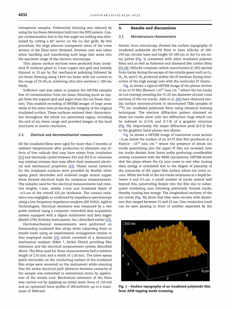
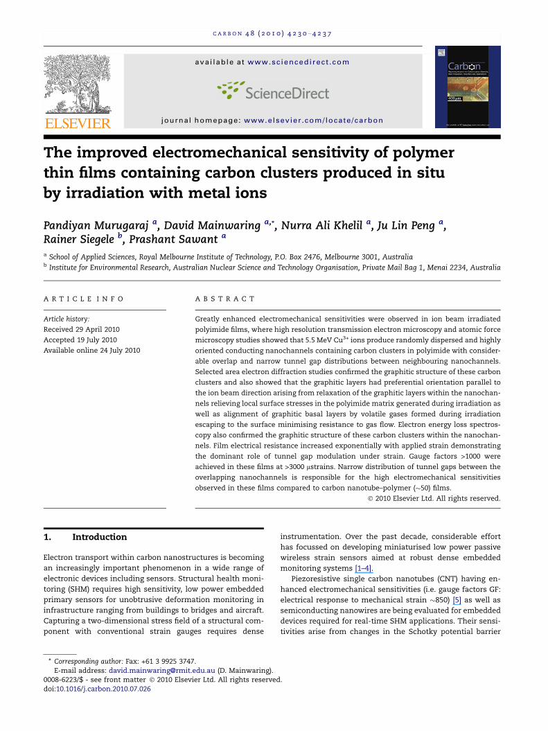
Fig. 1 – Surface topography of an irradiated polyimide film
from AFM tapping mode scanning.
4232 C A R B O N 4 8 ( 2 0 1 0 ) 4 2 3 0 – 4 2 3 7
transparent samples. Preferential thinning was reduced by
using the Ion Beam Modulator built into the PIPS system. Cop-
per contamination due to the low angle ion milling was elim-
inated by cutting a 60� sector on the Cu slot grids. By this
procedure, flat large electron transparent areas of the cross
section of the films were obtained. Extreme care was taken
when handling and transferring such large thin areas into
the specimen stage of the electron microscope.
Thin planar surface sections were produced from irradi-
ated PI surfaces glued to 3 mm copper slot grid and initially
thinned to 25 lm by flat mechanical polishing followed by
ion beam thinning using 3 keV ion beam with ion current in
the range of 23–30 lA; achieving ultra thin sections (�100 nm
thick).
Sufficient care was taken to prepare the HRTEM samples
free of contamination from ion beam thinning (such as cop-
per from the support grid and argon from the ion-beam thin-
ner). This enabled recording of HRTEM images of large areas
while at the same time protecting the integrity of the original
irradiated surface. These surfaces retained their characteris-
tics throughout the whole ion penetrated region, including
the end of ion beam range and provided images of the local
structures at atomic-resolution.
2.3. Electrical and electromechanical measurements
All the irradiated films were aged for more than 5 months at
ambient temperatures after production to eliminate any ef-
fects of free radicals that may have arisen from irradiation
[21] and thermally cycled between 293 and 355 K to minimise
any residual stresses that may affect their measured electri-
cal and mechanical properties [22]. Ohmic metal contacts
for the irradiated surfaces were provided by flexible silver
epoxy patch electrodes and soldered single strand copper
wires formed electrical leads for resistance measurements.
The samples used for the electrical measurements had resis-
tive lengths 1 mm, widths 2 mm and irradiated depth of
�4.5 lm of the overall 125 lm thickness. The contact resis-
tance was negligible as confirmed by impedance spectroscopy
using a low frequency impedance analyser (HP 4192A, Agilent
Technologies). Electrical resistance was measured by a two
probe method using a computer controlled data acquisition
system equipped with a digital multimeter and data logger
(Model 2700, Keithley Instruments, Inc.) described earlier [22].
Electromechanical measurements were performed on
freestanding irradiated film strips while subjecting them to
tensile loads using an experimental arrangement similar to
that employed earlier [22] which consisted of a dynamical
mechanical analyser (DMA 7, Perkin Elmer) providing film
extension and the electrical measurement system described
above. The films used for these measurements had a resistive
length of 2.55 mm and a width of 1.50 mm. The silver epoxy
patch electrodes on the conducting surface of the irradiated
film strips were mounted on the instrument while ensuring
that the entire electrical path (distance between contacts) of
the sample was submitted to extensional strain by applica-
tion of the tensile load. Mechanical extension of the films
was carried out by applying an initial static force of 110 mN
and an optimised force profile of 200 mN/min up to a maxi-
mum of 3000 mN.
3. Results and discussions
3.1. Microstructure characteristics
Atomic force microscopy showed the surface topography of
irradiated polyimide (Irr-PI) films to have hillocks of 100–
250 nm circular base and height 50–100 nm at the Cu ion en-
try points (Fig. 1) consistent with other irradiated polymer
films and as well as fullerene and diamond like carbon films
[23,24]. Hillocks comprise carbon nanoclusters (C-NC) ejected
from tracks during the escape of the volatile gases such as O2,
N2, H2 and C–Hx produced within the PI medium during inter-
action of the high energy ions with the molecular PI chains.
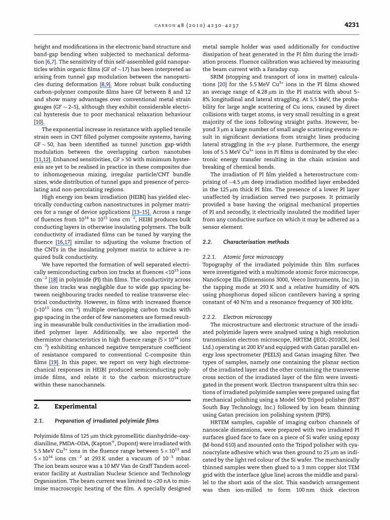
Fig. 2a shows a typical HRTEM image of the planar section
of an Irr-PI film (fluence <1013 ions cm�2 where the ion tracks
do not overlap) revealing the 15–25 nm diameter circular cross
sections of the ion tracks. Adla et al. [25] have observed sim-
ilar surface microstructures in microtomed TEM samples of238U ion irradiated polyimide films using chemical staining
techniques. The electron diffraction pattern obtained on
these ion tracks show only two diffraction rings which can
be indexed to (1 0 0) and (1 1 0) of a graphite structure
(Fig. 2b). Importantly, the major diffraction peak (0 0 2) due
to the graphitic basal planes was absent.
Fig. 3a shows a HRTEM image of transverse cross section
�3 lm below the surface of an Irr-PI thin film produced at a
fluence �1014 ions cm�2 where the presence of dense ion
tracks penetrating into the upper PI film are revealed; here
ion tracks deviate from linear paths producing considerable
overlap consistent with the SRIM calculations. HRTEM shows
that the plane where the Cu ions come to rest after loosing
their energy is undulated due to the degree of planarity at
the nanoscale of the upper film surface where ion entry oc-
curs. While the bulk of the ion tracks terminate at a depth be-
tween 4 and 4.5 lm, a small number of tracks extend well
beyond this, penetrating deeper into the film due to subse-
quent irradiating ions following previously formed tracks,
thereby loosing less energy. The longitudinal sections of the
ion tracks (Fig. 3b) show that they were circular with diame-
ters that ranged between 15 and 25 nm. One conductive track
can be seen passing in front of another separated by the
Fig. 2 – (a) HRTEM of the planar section of irradiated
polyimide thin film and (b) plot of intensity vs. scattering
vector data from SAED pattern from the ion tracks.
C A R B O N 4 8 ( 2 0 1 0 ) 4 2 3 0 – 4 2 3 7 4233
dielectric polymer medium (Fig. 3c). Magnified view of a single
track is shown in Fig. 3d confirmed their enrichment with gra-
phitic carbon clusters in the size range 3–5 nm. The presence
of the (0 0 2), (1 0 0) and (1 1 0) diffractions rings belonging to
the graphitic structure in the electron diffraction pattern of
the longitudinal section of the ion tracks (Fig. 3e). The (0 0 2)
diffraction ring was arc shaped indicative of strong preferen-
Fig. 3 – HRTEM images of (a) transverse cross section of irradiat
extended ion tracks; (c) magnified view of two tracks passing ove
ion track and (e) intensity vs. scattering vector from the SAED p
tial orientation of these graphitic cluster layers parallel to the
ion beam direction. The absence of the (0 0 2) diffraction ring
in the electron diffraction pattern obtained on the planar sec-
tion (Fig. 2b) also corroborates this finding. Such orientation
may arise as a consequence of two effects: (a) relaxation of
the graphitic carbon clusters within the ion tracks to relieve
the local surface stresses within the PI matrix generated dur-
ing irradiation; and (b) the volatile gases that are formed with-
in the tracks while escaping to the surface can also align the
graphitic basal layers vertically since this orientation of the
graphitic clusters produces minimum resistance to the out
flowing volatile gases. Srivastava et al. investigated the effects
of very high energy (100 MeV) Au ions in silicon based poly-
mer film by energy filtered TEM studies, and showed similar
formation of �5 nm carbon clusters in nanocolumns of
�10 nm diameter, although the C-planar orientation was
not identified [26].
3.2. Parallel electron energy loss spectroscopy
The low loss and carbon k-edge absorption spectra of the irra-
diated polyimide film (fluence: 5 · 1014 ions cm�2) revealed
the presence of p bonding (�6 eV absorption in the low loss re-
gion, Fig. 4a (i)) and p* bonding (�284 eV in the C-k edge re-
gion, Fig. 4a (ii)) arising from the sp2 bonded graphitic
carbon clusters in the polyimide matrix during irradiation
process. Similar spectra obtained on the un-irradiated poly-
imide films showed the absence of p absorption (Fig. 4b (i)).
ion modified polyimide layer; (b) magnified view of the
r each other with a dielectric barrier between them; (d) single
attern obtained on the ion tracks.
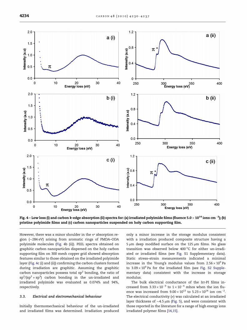
Fig. 4 – Low loss (i) and carbon k-edge absorption (ii) spectra for: (a) irradiated polyimide films (fluence 5.0 · 1014 ions cm�2); (b)
pristine polyimide films and (c) carbon nanoparticles suspended on holy carbon supporting film.
4234 C A R B O N 4 8 ( 2 0 1 0 ) 4 2 3 0 – 4 2 3 7
However, there was a minor shoulder in the p* absorption re-
gion (�284 eV) arising from aromatic rings of PMDA–ODA
polyimide molecules (Fig. 4b (ii)). PEEL spectra obtained on
graphitic carbon nanoparticles dispersed on the holy carbon
supporting film on 300 mesh copper grid showed absorption
features similar to those obtained on the irradiated polyimide
layer (Fig. 4c (i) and (ii)) confirming the carbon clusters formed
during irradiation are graphitic. Assuming the graphitic
carbon nanoparticles possess total sp2 bonding, the ratio of
sp2/(sp2 + sp3) carbon bonding in the un-irradiated and
irradiated polyimide was evaluated as 0.074% and 94%,
respectively.
3.3. Electrical and electromechanical behaviour
Initially thermomechanical behaviour of the un-irradiated
and irradiated films was determined. Irradiation produced
only a minor increase in the storage modulus consistent
with a irradiation produced composite structure having a
5 lm deep modified surface on the 125 lm films. No glass
transition was observed below 400 oC for either un-irradi-
ated or irradiated films (see Fig. S1 Supplementary data).
Static stress–strain measurements indicated a minimal
increase in the Young’s modulus values from 2.56 · 109 Pa
to 3.09 · 109 Pa for the irradiated film (see Fig. S2 Supple-
mentary data) consistent with the increase in storage
modulus.
The bulk electrical conductance of the Irr-PI films in-
creased from 3.33 · 10�9 to 1 · 10�4 mhos when the ion flu-
ence was increased from 9.00 · 1013 to 5.23 · 1014 ion cm�2.
The electrical conductivity (r) was calculated at an irradiated
layer thickness of �4.5 lm (Fig. 5), and were consistent with
those reported in the literature for a range of high energy ions
irradiated polymer films [14,15].
Fig. 5 – Electrical conductivity (r) variation with fluence for
irradiated polyimide films (line guide to the eye only).
C A R B O N 4 8 ( 2 0 1 0 ) 4 2 3 0 – 4 2 3 7 4235
The electrical resistance of an Irr-PI film (5 · 1014 ions
cm�2) containing C-cluster tracks increased with increasing
tensile strain (Fig. 6a). Here resistance increased linearly by
38% for an applied strain of 1000 lstrains yielding a gauge fac-
tor (GF) of �300, a value significantly greater than thin film
Fig. 6 – (a) Variation in resistance with applied tensile strain
at fluence of 5.0 · 1014 ions cm�2; (b) relative change of
resistance for irradiated PI films at three fluences extended
to show the exponential rise in relative resistance.
metal gauges and carbon nanoparticle–PI composite strain
gauge films where the resistance changes were below 0.7%
for these strain values and gauge factors were below 12
[21,27]. Above 1000 lstrains, the resistance varied exponen-
tially, indicative of the dominant role of tunnelling gaps be-
tween the C-nanocluster channels in the electron transport
mechanism. The measured electrical resistance of this Irr-PI
film Re with tensile strain e fitted the expression Re = Ro eae,
where Ro at e = 0 is 21.143 kX and the exponent ‘a’ has a value
300 (R2 was 1.00).
The relative change of resistance (DR/R) with applied strain
for films with fluences of 3.28 · 1014, 5.0 · 1014 and 5.23 · 1014
ions cm�2 are compared in Fig. 6b, where DR/R increased con-
tinuously with applied strain. Increasing fluence, at a given
strain, also increases the DR/R response significantly. In the
linear region (Fig. 6b), sensitivities (GF) of 113, 364 and 391,
were obtained for these fluences, respectively. At higher ten-
sile strains, the electrical resistance then increased exponen-
tially with strain for both these films, yielding exponent
values of 183, 302 and 486, respectively. Table 1 lists the gauge
factors calculated at particular values of strain for the three
irradiated films where they reached a sensitivity of 1069 at
3200 lstrains.
Three-dimensional conductivity can arise from two types
of electron transport namely hopping across carbon nanocl-
usters or nanoparticles along the nanochannels [18] and
lateral inter-channel charge transport as shown by the elec-
tron tunnelling between CNTs in CNT–polymer composites.
The similarity of the physical arrangement of these carbon
nanocluster containing nanochannels to CNT–polymer com-
posites suggests that irradiated films involves both types of
electron transport. The exponential increase of resistance
with strain, seen above, arises from the intrinsic electron
tunnelling mechanism where conductivity r = ro exp[-
xC(T + T0) � 1] with: x the tunnelling gap, T absolute temper-
ature and C and T0 constants [11]. In the Irr-PI film, the carbon
nanochannels originate from the surface and extend unidi-
rectionally perpendicular to the surface with considerable
overlapping with nearest neighbour channels as shown by
HRTEM (Fig. 3). In comparison, the CNT–polymer composites
consist of nanotubes in both mono-dispersed and aggregated
forms, having random orientations in a three-dimensional
matrix and which results in a wider size distribution of con-
ducting regions as well as significant variations in the overlap
spacings between the nearest neighbours. In contrast, the
overlap spacings between the conducting nanochannels in
the irradiated polymer layers lie in a narrow range due to
Table 1 – Gauge factors calculated at specific strains forirradiated polyimide strain sensing films.
Fluence (· 10�14 ions cm�2) 3.28 5.00 5.23Strain(%) Gauge factor
0.04 86 276 3260.08 70 306 3620.17 200 485 5750.22 8380.28 9610.32 1069
4236 C A R B O N 4 8 ( 2 0 1 0 ) 4 2 3 0 – 4 2 3 7
their unidirectional orientation and their near random
distribution.
4. Conclusions
In summary, we have successfully used high energy ion beam
irradiation to fabricate carbon nanochannel–polyimide com-
posite thin films exhibiting highly enhanced electromechani-
cal sensitivities. HRTEM and AFM techniques have shown
that with 5.5 MeV Cu3+ ions at fluences >1013 ions cm�2, uni-
directional semiconducting nanochannels are formed that
have considerable multiple overlap between them separated
by dielectric polymer and with a narrow distribution of gap
spacings. In the parallel electron energy loss spectra of the
irradiated polyimide films, p and p* absorption showed the
formation sp2 bonded carbon clusters. Electron diffraction
of planar and longitudinal sections of these nanochannels
clearly revealed that the graphitic carbon sheets formed pref-
erentially parallel to the ion beam direction, i.e., aligned par-
allel to the nanochannels which had the channel dimensions
between 15 and 25 nm with carbon clusters ranging 3–5 nm.
The electron transport in these nanowire systems has two
contributions namely, hopping conduction along carbon
nanoclusters of the nanochannels and electron tunnelling be-
tween isolated nanochannels enabling lateral charge trans-
port between them that results in three-dimensional bulk
conduction similar to that observed in CNT–polymer compos-
ites. The electrical resistance of these films increased with
increasing applied strain demonstrating the role of tunnel
gap modulation during applied strain. Gauge factors >1000
have been obtained in these films (fluence = 5.23 · 1014 ions
cm�2) at strain values >3000 lstrains. The homogeneous uni-
formly sized conducting nanochannels with a narrow distri-
bution of tunnel gaps between overlapping nanochannels is
responsible for the high electromechanical sensitivities ob-
served in these films compared to the heterogeneous distri-
bution of tunnel gaps between the overlapping CNTs.
Acknowledgement
Partial financial support from AINSE Pty Ltd. through AINSE
award AINGRA09116P is gratefully acknowledged.
Appendix A. Supplementary data
Supplementary data associated with this article can be found,
in the online version, at doi:10.1016/j.carbon.2010.07.026.
R E F E R E N C E S
[1] Kang I, Schulz MJ, Kim JH, Shanov V, Shi D. A carbonnanotube strain sensor for structural health monitoring.Smart Mater Struct 2006;15:737–48.
[2] Kang JH, Park CI, Scholl JA, Brazin AH, Holloway NM, High JW,et al. Piezoelectric characteristics of single wall carbonnanotube/polyimide nanocomposites. J Polym Sci Part BPolym Phys 2009;47:994–1003.
[3] Chang N-K, Su C-C, Chang S-H. Fabrication of single walledcarbon nanotube flexible strain sensors with high sensitivity.Appl Phys Lett 2008;92:063501/1–3.
[4] Loh KJ, Kim J, Lynch JP, Kam NWS, Kotov NA. Multifunctionallayer by layer carbon nanotube–polyelectrolyte thin films forstrain and corrosion sensing. Smart Mater Struct2007;16:429–38.
[5] Grow RJ, Wang Q, Cao J, Wang D, Dai H. Piezoresistance ofcarbon nanotubes on deformable thin film membranes. ApplPhys Lett 2005;86:093104/1–3.
[6] Zhou J, Gu Y, Fei P, Mai W, Gao Y, Yang R, et al. Flexiblepiezotronic strain sensor. Nano Lett 2008;8:3035–40.
[7] He R, Yang P. Giant piezoresistance effect in siliconnanowires. Nat Nanotechnol 2006;1:42–6.
[8] Vossmeyer T, Stolte C, Ijeh M, Kornowski A, Weller H.Networked gold nanoparticle coatings on polyethylenecharge transport and strain sensitivity. Adv Funct Mater2008;18:1611–5.
[9] Muller K-H, Reda T, Baxter GR, Raguse B, De Groot GJJB, ChaiR, et al. Nanoparticle films as sensitive strain gauges. ApplPhys Lett 2007;91:183105/1–3.
[10] Sau KP, Chaki TK, Khastgir D. The effect of compressivestrain and stress on electrical conductivity of conductiverubber composites. Rubber Chem Technol 2000;73:310–24.
[11] Zhang R, Baxendale M, Peijs T. Universal resistivity-straindependence of carbon nanotube/polymer composites. PhysRev B 2007;76:1954331–5.
[12] Hu N, Karube Y, Yan C, Masuda Z, Fukunaga H. Acta Mater2008;56:2929–36.
[13] Hoppe K, Fahrner WR, Fink D, Dhamodoran D, Petrov A,Chandra A, et al. An ion track based approach to nano- andmicro-electronics. Nucl Instrum Meth Phys Res Sect B2008;266:1642–6.
[14] Spohr R. Status of ion track technology – Prospects of singletracks. Radiat Meas 2005;40:191–201.
[15] Fink D, Chandra A, Fahrner WR, Hoppe K, Winkelmann H,Saad A, et al. Ion track based electronic elements. Vacuum2008;82:900–5.
[16] Salvetat J-P, Costantini J-M, Brisard F, Zuppiroli L. Onsetand growth of conduction in polyimide kapton induced byswift heavy-ion irradiation. Phys Rev B 1997;55:6238–48.
[17] Davenas J, Boiyeux G. Ion beam modified polyimide. AdvMater 1990;2:521–7.
[18] Murugaraj P, Mainwaring D, Siegele R. Electron transportproperties of irradiated polyimide thin films in single trackregime. Appl Phys Lett 2009;94:1221011–3.
[19] Murugaraj P, Mainwaring DE, Jakubov T, Mora-Huertas N, AliKhelil N, Siegele R. Electron transport in semiconductingnanoparticle and nanocluster carbon–polymer composites.Solid State Commun 2006;137:422–6.
[20] Ziegler JF, Biersack JP, Ziegler MD (2008). SRIM-SRIM Co. ISBN0-9654207-1-X <http://www.srim.org/>.
[21] Fink D, Klett R, Chadderton LT, Cardoso J, Montiel R, VazquezH, et al. Carbonaceous clusters in irradiated polymers asrevealed by small angle X-ray scattering and ESR. NuclInstrum Meth Phys Res Sect B 1996;111:303–14.
[22] Murugaraj P, Mainwaring DE, Mora-Huertas N.Electromechanical response of semiconducting carbon–polyimide nanocomposite thin film. Compos Sci Technol2009;69:2454–9.
[23] Toulemonde M, Trautmann C, Balanzat E, Hjort K, WeidingerA. Track formation and fabrication of nanostructures withMeV-ion beams. Nucl Instrum Meth Phys Res Sect B2004;216:1–8.
[24] Vilensky AI, Zagorski DL, Bystrov SA, Michailova SS,Gainutdinov RV, Nechaev AN. Investigation of latent tracks in

C A R B O N 4 8 ( 2 0 1 0 ) 4 2 3 0 – 4 2 3 7 4237
polyethyleneterepthalate and their etching. Surf Sci2002;507–510:911–5.
[25] Adla A, Fuess H, Trautmann C. Characterisation of heavy iontracks in polymers by transmission electron microscopy. JPolym Sci Part B 2003;41:2892–901.
[26] Srivastava SK, Avasthi DK, Pippel E. Swift heavy ion inducedformation of nanocolumns of C clusters in a Si basedpolymer. Nanotechnology 2006;17:2518–22.
[27] Mainwaring D, Murugaraj P, Mora-Huertas N, Sethupathi K.Enhanced electromechanical response of nonpercolatingpolymer–nanoparticle composite films. Appl Phys Lett2008;92:253303/1–3.