The Evolving Role of Semiconductor Consortia in the United States and Japan
28
The Evolving Role of Semiconductor Consortia in the United States and Japan Rose Marie Ham Greg Linden Melissa M. Appleyard S ince the late 1970s, governments throughout the industrialized economics have proclaimed the benefits of research consortia. In the United States, tor example, ihe 1984 National Cooperative Research Act (NCRA) relaxed U.S. antitrust laws to encourage the formation of research consortia hy firms in the same industry; by the end of 1995, over 575 consortia had heen registered under the NCRA in a variety of industries, includ- ing automobiles, aerospace, and telecommunications.' Governments in the United States, Japan, and Western Europe also launched a myriad of cooperative R&D programs during the 1980s, often providing subsidies to large-scale consor- tia among firms in "strategic" high-technology industries,^ These policy initia- tives were fueled by concerns over the competitiveness of domestic firms in high-technology sectors combined with the perceived advantages of research consortia'—by banding together in cooperative R&D activities, firms could share the risks and costs associated with technology generation and thereby compete more effectively in international markets. The semiconductor industry has pioneered in these large-scale R&D con- sortia."' In part, the leading role of this industry in programs establishing R&D We gratefully acknowledge William J. Spencer (SEMATECH), Frank Robertson (13001), Hrroyoshi Komi)g (Selete),Taro Okabe (SIRIJ), and other representatives from the semiconductor industry for shanng their time and insights with us. We also thank David Mowery for his useful comments and suggestions on earlier versions of this article, Jeff Macher for his assistance in obtaining industry data, and George Lee of the SEMI trade association for enabling us to attend SEMI conferences on the 300mm wafer transition. Support for this research was provided by the Califorr)\a Management Rewew, the Darden Foundation (Appleyard). the Alfred P Sloan Foundation (Appleyard and Ham), and the Air Fon:e Office of Scientific Ftesearch (Ham).The authoi'^ assume full responsibility for any remaining errors or omissions. CAUFORNIA MANAGEMENT REVIEW VOL 11, NO. I FALL 1998 137
Transcript of The Evolving Role of Semiconductor Consortia in the United States and Japan
The Evolving Roleof SemiconductorConsortia in the UnitedStates and Japan
Rose Marie HamGreg LindenMelissa M. Appleyard
Since the late 1970s, governments throughout the industrializedeconomics have proclaimed the benefits of research consortia. In theUnited States, tor example, ihe 1984 National Cooperative ResearchAct (NCRA) relaxed U.S. antitrust laws to encourage the formation of
research consortia hy firms in the same industry; by the end of 1995, over 575consortia had heen registered under the NCRA in a variety of industries, includ-ing automobiles, aerospace, and telecommunications.' Governments in theUnited States, Japan, and Western Europe also launched a myriad of cooperativeR&D programs during the 1980s, often providing subsidies to large-scale consor-tia among firms in "strategic" high-technology industries,^ These policy initia-tives were fueled by concerns over the competitiveness of domestic firms inhigh-technology sectors combined with the perceived advantages of researchconsortia'—by banding together in cooperative R&D activities, firms could sharethe risks and costs associated with technology generation and thereby competemore effectively in international markets.
The semiconductor industry has pioneered in these large-scale R&D con-sortia."' In part, the leading role of this industry in programs establishing R&D
We gratefully acknowledge William J. Spencer (SEMATECH), Frank Robertson (13001), HrroyoshiKomi)g (Selete),Taro Okabe (SIRIJ), and other representatives from the semiconductor industry forshanng their time and insights with us. We also thank David Mowery for his useful comments andsuggestions on earlier versions of this article, Jeff Macher for his assistance in obtaining industry data,and George Lee of the SEMI trade association for enabling us to attend SEMI conferences on the300mm wafer transition. Support for this research was provided by the Califorr)\a Management Rewew,the Darden Foundation (Appleyard). the Alfred P Sloan Foundation (Appleyard and Ham), and the AirFon:e Office of Scientific Ftesearch (Ham).The authoi'^ assume full responsibility for any remainingerrors or omissions.
CAUFORNIA MANAGEMENT REVIEW VOL 11, NO. I FALL 1998 137
The Evolving Role of Semiconductor Consortia in the United States and Japan
consortia refleas its high political saliency in the United States, Japan, and West-ern Europe. Recognizing that semiconductors are critical inputs to a broad baseof electronics, telecommunications, and military-related technologies, govern-ments have promoted a strong domestic semiconductor industry and a viablebase of domestic firms to supply the tools and materials used in semiconductormanufaauring. At the same time, these national objectives have had to confrontthe global realities of the semiconductor industry: semiconductor manufacturershave long operated produaion facilities throughout the industrialized world,and manufacturers and supplier firms are enmeshed in a complex web ofalliances within and across national borders.^
Two of tbe mosi influential higb-technology R&D consortia of the past 30years were established with tbe aid of public funds to support semiconduaor-related R&D. During the mid-1970s, the Japanese government, concerned aboutthe survival of its computer industry in tbe face of market liberalization, estab-lished tbe Very Large Scale Integration (VLSf) Project to improve domestic capa-bilities lor manufacturing semiconductor devices used in mainframe computers.*The VLSI Projea, along with a parallel set of semiconduaor projeas sponsoredby Japan's state-owned telecommunications firm (NTT), was later credited witbenabling Japanese semiconductor firms to "catcb up' with U.S. firms in tbisindustry.' By tbe mid-1980s, Japanese firms had surpassed U.S. device makers intbe worldwide markets for semiconductor memory devices. This rise to domi-nance of Japanese semiconductor manufacturers ignited debate in tbe UnitedStates over the beallb of tbe U.S. semiconductor industry and the potentialdependence by U.S. defense agencies on Japanese firms for semiconductors usedin military systems. In response, the U.S. govemment and leading U.S. semicon-ductor manufaaurers launched tbe U.S. Semiconductor Manufacturing Technol-ogy (SEMATECH) consortium in 1987 in order to improve the manufacturingcapabilities of domestic semiconductor firms.
This article examines a new chapter in the history of large-scale semicon-duaor consortia in the United States and Japan. By focusing on two recentlyestablisbed consortia—tbe Intertiational 300mm Initiative (I300I) in the UnitedStates and Semiconductor Leading Edge Technologies, Inc. (Selete) in Japan—we examine the changing role of governments and private firms in directingtechnology development in the semiconduaor industry.^ Unlike the VLSI Projectand SEMATECH consortia, both I300I and Selete have been financed solely bymember compatiies and are working with a global base of supplier firms, appar-ently heralding a sea change in relations between the semiconductor industryatid national governments. These consortia also include leading semiconductormanufacturers from around the world, which refiects the need to spread costsacross a larger number of firms and higblights the new prominence of Taiwaneseand Soutb Korean firms in semiconductor manufacturing.
This article examines the factors that gave rise to these new semiconduc-tor R&D consortia in the United States and in Japan—namely, the costly conver-sion to larger silicon wafers that alters many of the industry's manufacturing
138 CAUFORNIA MANAGEMENT REVIEW VOL4I,NO. I FALL 1998
The Evolving Role of Semiconductor Consortia in the United States and Japan
technologies.'* It then discusses the origins and structures of these consortia andexamines the unprecedented level of cooperation among leading semiconductormanufacturers that is taking place. Although their efforts are still underway, theconsortia have already confronted the difficulties associated with large-scalecollaborative R&D endeavors that involve uncertain technologies and volatilemarket forces. The semiconductor industry may be unique in sustaining thislevel of industry-wide cooperation, but the lessons from the current semicon-ductor consortia apply to managers involved in large-scale collaborative venturesin other technology-intensive industries.
With respect to the role of government, the two consortia highlight diver-gent trends. 13001 illustrates the political challenges associated with transforminga domestically oriented, federally subsidized consortium into an institution sup-ported solely by dues from domestic and foreign firms. By contrast, Selete wasformed in conjunaion with a new wave of government-funded semiconductorR&D projects in Japan, and the private consortium shares important ties withthese parallel, public-sector initiatives. Despite predictions that the actions ofnational governments will be curtailed in an era of global, high-techno logyfirms,'" home-country governments continue to exercise considerable influenceon these private initiatives, as they do in other high-technology sectors.Nonetheless, the ultimate effects of government initiatives may be more easilyoffset or even derailed by the actions of global firms.
The Challenge of Converting to 300mm Wafers
The semiconductor industry has a unique combination of capital- andresearch-intensity that, combined with short product life cycles and a rapid paceof technological change in the industry, magnifies investment risks for firms."Individual semiconductor investments are quite large, with new factories(known as "fabs") costing at least $1 billion. At the same time, the pace of semi-conductor technology development has increased, shortening the useful life ofcapital investments. According to an industry executive: "In the mid-80s, a fabcost about $100 million and had an expected life span of nearly 10 years. Nowwe have $1 billion fabs with a life span of only five years."'^
Semiconductor manufacturing processes also are among the most com-plex in any industry.'* The fabrication of an integrated circuit (also known as a"chip" or "device") requires more than a hundred steps (such as patterning,coating, baking, etching) across a range of specialized tool sets. An average fabri-cation facility in 1997 utilized about 40 different types of equipment, with indi-vidual tools ranging in price from $100,000 to $7 million.'' The individualmanufacturing steps are often mastered at an experimental rather than a scien-tific level and are difficult to replicate on different tools or in different facilities.Such complexity has historically required manufacturers to work ck>scly withequipment suppliers to improve the performance of each tool.
CAUFORNIA MANAGEMENT REVIEW VOL 41. NO, I FALL 1998 139
The Evolving Role of Semiconductor Consortia in the United States and Japan
In response to the soaring capital costs and risks of semiconduaor manu-facturing, producers throughout the world have developed an array of strategies,among the most important of which is interfirm collaboration in R&D and pro-duction investments. A new challenge has given an additional impetus to thesecollaborative trends. Driven by the need to produce increasing numbers of semi-conductor chips at lower prices, semiconductor manufacturers and their equip-ment suppliers are now preparing to upgrade their manufacturing methods andproduction tools to accommodate 300mm silicon wafers instead of the current200mm wafer standard.'^ Larger wafers also will more easily accommodate com-plex chip designs, such as next-generation microprocessors and systems-on-a-chip, early versions of which may be too large to manufacture economically onsmaller silicon wafers."*
In contrast to previous wafer transitions, the shift from 200mm to300mm wafers will not be orchestrated by any single firm in the industry, fortwo reasons. First, experts estimate the costs and technical challenges associatedwith the shift to 300mm wafers to be an order of magnitude greater than thoseof previous wafer transitions.'^ The shift to 300mm wafers necessitates a moreradical overhaul of equipment tool sets than was true of previous wafer transi-tions, and also requires a fundamental alteration in the overall design of fabrica-tion facilities. For example, 300mm wafers are so large and fragile that theynecessitate a higher level of automation than is used in 200mm fabs, requiringthe development of new interfaces, carriers, and software. The total develop-ment costs of 300mm tools are likely to exceed $10 billion, far higher than theroughly $1 billion cost of developing 200mm tools in the early 1980s.'*'
A second and related reason for the lack of single-firm leadership in the300mm wafer transition is the experiences of Intel and IBM in leading previouswafer transitions. In each of these transitions, the "lead company" (Intel for the100-15Dmm transition; IBM led the 150-200mm transition) purchased or pro-duced test wafers, subsidized equipment development, and guaranteed procure-ment contracts for production-worthy tools.'^ Representatives of Intel and IBMreport thai the costs of individually leading these transitions (especially the needto subsidize the development of new equipment whether or not it was eventu-ally purchased) outweighed the benefits of having first access lo the new capa-bilities.^" Intel took two years longer than expected to reach full volumeproduction in its first 150mm fab, and IBM faced similar problems improving thereliability of its new 200mm tools.^' Such production delays and unanticipatedtool development costs undermined the profitability of being first to manufac-ture chips on the new wafers.
Since the costs of 'going it alone" with the current wafer transition are sohigh and no single firm can fully appropriate the returns from that investment, astrategy of sharing some of the costs and risks across a large number of firms hasemerged. For the first time in the history of the industry, leading internationaldevice makers developed a uniform set of standards in advance of a major wafertransition." In setting these standards, device makers hoped to speed tool devel-
140 CALIFORNIA MANAGEMENT REVIEVV VOL41. NO. I FALL 1998
The Evolving Role of Semiconductor Consortia in the United States and Japan
opment and to reduce the costs of obtaining a compatible 300mm tool set fornext-generation fabs. For example, the previous, piecemeal transitions led bysingle firms produced a range of incompatible equipment, forcing chip makers todevelop custom mechanical interfaces or limit their choice of suppliers. Ten dif-ferent carrier systems were used for 200mni wafers, whereas device makers inthe two 300mm consortia have agreed to accept only two carrier systems for300mm wafers, both of which must be accommodated by suppliers. Finally, thehistory of successful collaboration among leading U.S. device makers in manag-ing joint projects with supplier firms (e.g., under the auspices of SEMATECH)may have reduced the transaction costs associated with launching a cooperativewafer conversion initiative.
Consortium-Led Technological Change
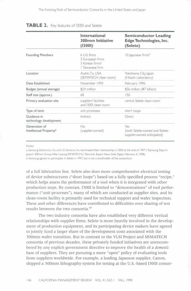
By 1996, two consortia had been formed to lead the conversion of theindustry's capital equipment. The U.S.-based International 300mm Initiative(I300I) consortium, established in late 1995, comprises 13 leading device mak-ers, including firms from the United States (Intel, Texas Instruments, Motorola,IBM, AMD, and Lucent Technologies), Europe (STMicroelectronics,'' Philips,and Siemens), South Korea (Samsung Electronics, Hyundai Electronics, and LGSemicon), and Taiwan (Taiwan Semiconductor Manufacturing Corporation,TSMC)." A parallel effort was established in Japan, when ten leading Japanesesemiconductor firms (NEC, Hitachi, Toshiba, Mitsubishi, Fujitsu, Matsushita,Sanyo, Oki, Sharp, and Sony) established Semiconductor Leading Edge Tech-nologies, Inc. (Selete) in early 1996.' ' Together, these consortia include morethan 20 leading semiconductor manufacturers that account for most of theworld's chip production (Table 1).
As this membership roster demonstrates, the device makers'—not equip-ment suppliers—are leading the wafer conversion effort. The ability of leadingmanufacturers from around the world to establish joint technical standards andset goals for a broad base of suppliers is relatively rare, even though buyers aretypically more eager for standards than suppliers, who prefer higher levels ofproduct differentiation.^^ In this case, the ability of the device firms to dictate theconversion sciiedule to their suppliers refieas not only the collective marketpower of these customers, but also the technical dependence of suppliers on thedevice makers.^^ Although other industries, such as autos, also exhibit a closeworking relationship between equipment suppliers and their customers, thecomplexity of semiconductor process technology has historically required suppli-ers to look to device makers for technical guidance.^" Device makers often pro-vide both funding and engineering resources to their suppliers for specificprojects. One U.S. device maker, for example, estimated that it financed approxi-mately 20 percent of the $15 million cost and nearly 40 percent of the 14,000+engineering hours associated with a recent unsuccessful equipment modification
CAUFORNIA MANAGEMENT REVIEV\/ VOL4I.NO. I FAa 1998 141
The Evolving Role of Semiconductor Consortia in the United States and Japan
T A B L E I . Founding Members of 13001 and Selete (by nationality and 1995 IC sales)
13001
U.S. Members
I99SIC 1995 Rank insales* ($b) world IC sales''
Intel
Texas Instruments
Motorola
IBM
AMD
Lucent
Combined 1995 IC sales(% of ail US firms'IC sales)
European Members
STMicroeieclconics (llaly/Ffance)
Philips (Netherlands)
Siemens (Germany)
Combined 1995 IC sales(% of all European firms' IC sales)
Korean and Taiwanese Members
Samsung [liaaionics [S. Koi-eaj
Hyundai Electronics (S. Korea)
IG Semicon, Inc (S. Kore \\
TSMC (Taiwan)
Combined 1995 IC sales{% of all Korean & Taiwanese firms' IC sales)
13001 Members' total 1995 IC sales
$13.6
$7.8$ 7,2
$5.7$ 2.4
$ 1.7
$38.4(63%)
$ 3.0
$ Z9$ 2.4
$ 8.3(78%)
$ 8.2
$ 4.4
$ 3.6
$ 1.4
$17.6(83%)
$64.3
1
6
7
8
17
24
1
1
13
14
18
S
10
12
25
project. As this example suggests, such huyer-supplier collaboration containsrisks for both parties.^"
Origin and Structure ofI300I and SeleteThe structure and R&D operations of both BOOI and Selete have been
influenced by previous successful and unsuccessful large-scale R&D consortia inthe United States and Japan. In particular, the new consortia incorporate keyfeatures of the VLSI Project and SEMATECH consortia: even though memberfirms in both I300I and Selete are "horizontal" competitors in the semiconductormarket, these consortia focus on "vertical" projects aimed at ensuring the relia-bility and compatibility of production tools. Also, like earlier semiconductor con-sortia, 13001 and Selete need to define a research agenda and design a structure
142 CAUFORNIA MANAGEMENT REVIEW VOL4I,NO. I FALL 1998
The Evolving Role of Semiconductor Consortia in the United States and japan
T A B L E I . FoundingMember5of 13001 and Selete (continued)
Selete
Japanese Members
1995 IC* ($b)
1995 Rank inworld IC sales'*
NEC
f"fitacf
Toshiba
Mttsubishi_
Fujitsu
Matsushita
Sanyo
Oki
Sharp
Sony
Combined 1995 IC sales
{% of all Japanese firms' IC sales)
$11,0
$ 8.6
$ 8.6
$ 4.4
I 4.0
$ 2.6
$ 2.3
$ 2.0
$ 2.0
J 1,9
$47,4(91%)
234
9
11
16
20
21
22
23
Notes:
a. Source; ICE, StatuiA Report on (he/fitegmtedOfaj/[/ndusE;7(Scottsdafe.AZ Integrated OTurt Engineering, Inc. 1997), based on
sales of merchant firms,
b.All but two of the top 25-ranked IC manufacturers joined either i30OI or Selete. Micron Technology, a US. firm ranked I5tJi, was
a founding member of SEMATECH but withdrew from Uie consortium in 199Z National Semiconductor, a U.S. firm ranked 19th.
is a member of both SEMATECH and its newly-fonned intemadonal subsidiary. International SEMATECH. but was not a founding
rrwmber of 13001,
that facilitates, rather than impedes, effective cooperation both among memberfirms and between members and participating suppliers. Despile some similarityin their objectives, 13001 and Selete have devised divergent solutions to thesechallenges, which are central to any large-scale cooperative R&D program.
The International 300mm Initiative
The International 300mm Initiative was formally established in late 1995as the first international subsidiary of the U.S. Semiconductor ManufacturingTechnology (SEMATECH) consortium. BOOI started as an 18-monih, $26 millionproject (roughly $2 million per member firm). According lo SEMATECH repre-sentatives, early plans for 13001 included an annual budget as high as $100 mil-lion, but prospective participants selected a less cosily project. BOOI's activitieshave been extended into 1999, and the consortium now receives roughly $24million per year in dues paid by member firms. 13001 is housed in SEMATECH'sAustin, Texas, facility and rents dean-room space from SEMATECH.*'
The design of 13001 builds direaly on the experience of SEMATECH. First,I300I adopted SEMATECH's system of employing assignees from member firmsto facilitate the transfer of information back to their parent organizations.
CAUFORNIA MANAGEMENT REVIEW VOL 41. NO. I FALL 1998 M3
The Evolving Role of Semiconductor Consortia In the United States and japan
Approximately 90 percent of BOOI's technical positions are staffed by member-firm assignees." Second, BOOI employs SEMATECH's cost-of-ownership (COO)model to establish the basic guidelines and information on equipment cost andperformance." The design and management of BOOI's activities also drew on theaccumulated experience of SEMATECH managers, which may have enabled13001 to begin its operations more quickly and easily than would have otherwisebeen possible.
A third feature of BOOI reflects the lessons of SEMATECH in defining aresearch agenda that facilitates cooperation among competing firms. In ihe sec-ond year of its operation, SEMATECH redirected its research agenda away fromcollaborative projects among device makers aimed at improving their manufac-turing process technologies toward projects between these semiconductor manu-facturers and their U.S. suppliers of semiconductor equipment and materials.The main reason for the "vertical" shift was the reluaance of U.S. device makersto share process technologies with one another that were critical to the marketsuccess of these competing firms.^'' Although this redirection in SEMATECH'saaivities simplified collaboration among device makers, it created considerableconcern among equipment suppliers over the sharing or leakage of proprietaryinformation. In response to these concerns, most of SEMATECH's equipmentprojects now take place al the facilities of individual supplier lirms instead of theconsortium's common facility, and suppliers generally own any project-relatedintellectual property. Consistent with this experience, 13001 has adopted adecentralized approach to working wilh suppliers and, like SEMATECH, evalu-ates most equipment at suppliers' sites, using engineers from both BOOI and theparticipating supplier firm." This arrangement provides suppliers with immedi-ate feedback on the performance of their tools and reduces the danger that pro-prietary information will "leak" among competing suppliers.
Unlike SEMATECH, however, BOOI does not directly fund equipmentdevelopment. Although SEMATECH continues to sponsor joint developmentand equipment improvement projects with suppliers, BOOI simply evaluatestools for basic test parameters, leaving the development and subsequentimprovement of those tools to suppliers.'* Given its commitment to tool evalua-tion rather than development, BOOI does not expect to own any intellectualproperty based on its work with suppliers. In contrast, SEMATECH obtained 89patents between 1989 and 1996 based on research conducted or funded by theconsortium, although the consortium now places less emphasis on owning intel-lectual property from projeas with suppliers."
Semiconductor Leading Edge Technologies, Inc.
The Japan-based Selete consortium is a more ambitious collaborativeR&D program aimed at both the evaluation and development of 300mm tools.The proposal for Selete was made in 1995 by the Semiconductor industryResearch Institute Japan (SIRIJ), an industry group lormed a year earlier by theten largest Japanese chip producers as part of a broader effort to "reactivate
CAUFORNIA MANAGEMENT REVI^V VOL 41, NO, I FALL 1998
The Evolving Role of Semiconductor Consortia in the United States and Jap
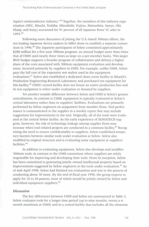
Japan's semiconductor industry."^^ Together, the members of this industry orga-nization (NEC, Hitachi, Toshiba, Mitsubishi, Fujitsu, Matsushita, Sanyo, Oki,Sharp, and Sony) accounted for 91 percent of all Japanese firms' IC sales in1995."
Following some discussion of joining the U.S.-based 300mm efforts, theten leading Japanese device makers in SIRU chose to establish a separate consor-tium in 1996.""* The Japanese participants of Selete committed approximately$280 million for a five-year 300mm program, an annual budget more than twicethai of 13001 (and nearly three limes as large on a per-member basis). This largerR&D budget supports a broader program of collaboration and defrays a highershare of the costs associated with 300mm equipment evaluation and develop-ment, incurred primarily by suppliers in 13001. For example, unlike 13001, Seletepays the full cost of the expensive test wafers used in the equipmentevaluations."' Selete also established a dedicated clean-room facility in Hitachi'sProduction Engineering Research Laboratory and purchased test equipment forthis facility.'' BOOI's rented facility does not house an entire production line andits test equipment is either under evaluation or donated by suppliers.
Yet another notable difference between Selete and 13001 is Selete's greatercentralization. In contrast to I300L equipment is typically evaluated in Selete'scentral laboratory rather than in suppliers' facilities. Evaluations arc primarilyperformed by Selete engineers on assignment from member firms. Tool perfor-mance is communicated to the supplier in a weekly report that may includesuggestions for improvements in the tool. Originally, all of the tools were evalu-ated at the central Selete facility. As the early experience of SEMATECH sug-gests, however, the risk of technology leakage among supplier firms mayincrease when tool-related projects are conducted in a common facility.' Recog-nizing the need to ensure confidentiality to suppliers, Selete established tempo-rary barriers between similar tools under evaluation at Selete. Selete alsomodified its original structure and is evaluating some equipment at suppliers'facilities.""*
In addition to evaluating equipment, Selete also develops and modifies300mm tools, in contrast to the 13001 consortium where suppliers are solelyresponsible for improving and developing their tools. From its inception, Seletehas been committed to generating jointly owned intellectual property based onimprovements suggested by Selete engineers to the tools under evaluation."^^ Asof mid-April 1998, Selete had finished ten evaluations and was in the process ofconducting about 30 more. By the end of fiscal year 1998, the group expects loapply for 10 to 20 patents, most of which would be jointly owned by Selete andindividual equipment suppliers.'"'
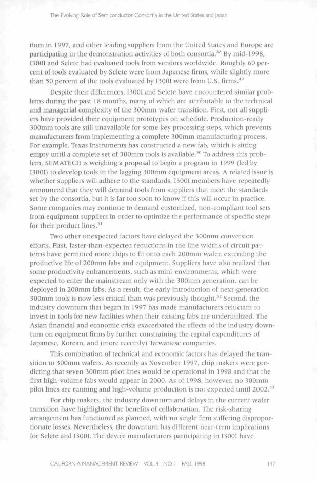
DiscussionThe key differences between T300I and Selete are summarized in Table 2.
Selete evaluates tools for a longer time period (up to nine months, versus a 6-month maximum at 13001) and in a centra! facility that includes all the elements
CAUFORNIA MANAGEMENT REVIEW V O L 4 I , N O . I FALL 1998 145
The Evolving Role of Semiconductor Consortia In the United States and Japan
TABLE 2. Key features ofl300l and Selete
International300nnm Initiative(13001)
Semiconductor LeadingEdge Technologies, Inc.(Selete)
Founding Members 6 US. firms3 European firms3 Korean firms*I Taiwanese firm
10 Japanese firms''
Location
Date Established
Budget(annual average)
Staff size (approx.)
Primary evaluation site
Type of tests
Guidance Intechnolog/ development
Generation ofIntellectual Property?
Austin.Tx. USA(SEMATECH clean room)
November 1995
$24 million
68
suppliers' facilitiesand 13001 clean room
unit processes
Indirect
No(supplier-owned)
Yokohama Crty, Japan(Hitachi Laboratory)
February 1996
$56 million (¥7 billion)
ISO
central Selete clean room
short loops
Direct
Yes(both Selete-owned and Selete-supplier-owned anticipated)
Notes:
a, Samsung Eleciromcs Co. and LGSemicon, Inc. terminated their membership in 13001 at the end of 1997 ("Samsung Stays in
japan's 300mm Group After Leaving SEMATECH's." Electronic Buyers' News DCJJ^ Digest. February 4.1998).
b. Samsung affveti to participate in Selete in 1997, but is not a stockholder of the consortium.
of a full fabrication line. Selete also does more comprehensive electrical testingof device substructures ("short loops") based on a fully specified process "recipe,"which helps assess the performance of a tool when it is integrated with otherproduction steps. By contrast, I300I is limited to "demonstrations" of tool perfor-mance ("unit processes"), many of which are conducted at supplier sites, and itsclean-room facility is primarily used for technical support and wafer inspection.These and other differences have contributed to difficulties over sharing of testresuhs between the two consortia."'
The two industry consortia have also established very different verticalrelationships with supplier firms. Selete is more heavily involved in the develop-ment of production equipment, and its participating device makers have agreedto jointly fund a larger share of the development costs associated with the300mm wafer transition. But in contrast lo the VLSI Project and SEMATECHconsortia of previous decades, these privately funded inilialives arc unencum-bered by any explicit government directive to improve the health of a domesticbase of suppliers. They are pursuing a more "open" policy of evaluating toolsfrom suppliers worldwide. For example, a leading Japanese supplier. Canon,shipped a 300mm lithography system for testing at the U.S.-based 13001 consor-
146 CAUFORNIA MANAGEMENT REVIEW VOL 41, NO. I FALL 1998
The Evolving Role of Semiconductor Consortia in the United States and Japan
tium in 1997, and other leading suppliers from the United Stales and Europe areparticipating in the demonstration activities of both consortia."* By mid-1998,I300I and Selete had evaluated tools from vendors worldwide. Roughly 60 per-cent of tools evaluated by Selete were from Japanese firms, while slighdy morethan 50 percent of the tools evaluated by 13001 were from U.S. firms.''''
Despite their differences, I300I and Selete have encountered similar prob-lems during the past 18 months, many of which are attributable to the technicaland managerial complexity of the 300mm wafer transition. First, inu al! suppli-ers have provided their equipment prototypes on schedule. Production-ready300mm tools are still unavailable for some key processing steps, whicli preventsmanufacturers from implementing a complete 300mm manufacturing process.For example, Texas Instruments has constructed a new fab, which is sittingempty until a complete set of 300mm tools is available.^" To address this prob-lem, SEMATECH is weighing a proposal to begin a program in 1999 (led by13001) to develop tools in the lagging 300mm equipment areas. A related issue iswhether suppliers will adhere to the standards. I300I members have repeatedlyannounced that they will demand tools from suppliers that meet the standardsset by the consortia, but it is far too soon to know if this will occur in practice.Some companies may continue to demand customized, non-compliant tool setsfrom equipment suppliers in order to optimize the performance of specific stepsfor their product lines.^'
Two other unexpected factors have delayed the 300mm conversit)nefforts. First, fastcr-than-expected reductions in ihe line widths of circuit pat-terns have permitted more chips to fit onto each 200mm wafer, extending ihcproductive life of 200mm fabs and equipment. Suppliers have also realized thatsome productivity enhancements, such as mini-environments, which wereexpected to enter the mainstream only with the 300tiim generation, can bedeployed in 200mm fabs. As a result, the early introduction of next-generation300mm tools is now less critical than was previously thought."'^ Second, theindustry downturn that began in 1997 has made manufacturers reluctant toinvest in tools for new facilities when their existing labs are underutilized. TheAsian financial and economic crisis exacerbated the effects of the industry down-turn on equipment firms by further constraining the capital expenditures ofJapanese, Korean, and (more recently) Taiwanese companies.
This combination of technical and economic tactors has delayed the tran-sition to 300mm wafers. As recently as November 1997, chip makers were pre-dicting that seven 300mm pilot lines would be operational in 1998 and that thefirst high-volume fabs would appear in 2000. As of 1998, however, no 300mmpilot lines are running and high-volume production Is nol expected uniil 2002.^'
For chip makers, the industry downturn and delays in the current wafertransition have highlighted the benefits of collaboration. The risk-sharingarrangement has functioned as planned, with no single firm suffering dispropor-tionate losses. Nevertheless, the downturn has different near-term implicationsfor Selete and 13001. The device manufacturers participating in 13001 have
CAUFORNIA MANAGEMENT REVIEW VOL 41, NO. 1 FALL 1998 147
The Evolving Role of Semiconductor Consortia in the United States and japan
largely avoided significant expenditures for the joint development of a new gen-eration of capital equipment whose adoption now seems likely to be delayed.Seleif members, on the other hand, have incurred more significant costs.Although some interviewees in 1997 had predicted that Selete's centralized,"hands-on" design would permit Japanese semiconduaor firms to launch300mm fabs before their U.S. counterparts, Selete members now are saddledwilh the considerable expense of operating a full 300mm dean room in the faceof a lack ol demand for this icchnology.
The consequences of the industry downturn on the 300mni transitionhave been more severe for supplier firms. Ironically, equipment firms who madethe greatest effort to comply with the original timetable, having spent $25 mil-lion or more to develop each tool, are worse off than those who failed to respectthe manufacturers' schedules. These early developers are now unlikely to findsignificant sales until 2002 or beyond." In light of continued uncertainty overthe timing for an industry upturn, many suppliers have scaled back their300mm plans. The chip makers in 13001, which has shifted virtually all of theserisks to suppliers, have responded by calling a series of summit meetings withsuppliers to reduce some of the uncertainty they face in their 300mm tool devel-opment efforts.
This sudden change in the market outlook for 300mm technologies illus-trates an insufficiently appreciated risk of industry-wide collaboration in envi-ronments characterized by fundamental uncertainty, which accurately describesmost high-technology industries. The formulation of an industry-wide "vision"or technology "roadmap" may increase, rather than reduce, the risks thatunforeseen developments will render the best-laid plans irrelevant." Timing isdifficult in any rapidly changing environment. But the tendency of such indus-try-wide collaboration io concentrate technological or economic bets mayincrease the collective exposure of firms to unexpected developments.
Global Firms, National Governments
The efforts of 13001 and Selete are still underway, and their long-rangeoutcomes and effeas cannot be forecast with confidence. This uncertaintynotwithstanding, the formation and operation of these ventures indicates anunprecedented level of cooperation within and across national borders in prepa-ration for the conversion of the semiconductor industry's capital equipment tonew 300mm wafers. The U.S.-based 13001 progiam represents the first time thatleading semiconductor firms from seven countries have agreed to conduct jointprojects on their manulacturing technologies under one organizationalumbrella, and these firms are coordinating some of their efforts with the Japan-based Seiete consortium. Moreover, both 13001 and Seiete are evaluating toolsfrom a global base of equipment and materials suppliers. Ahhough device mak-ers have long been engaged in a complex web of bilateral alliances and havepurchased tools from specialized suppliers from around the world, this relatively
148 CAUf ORNIA MANAGEMENT REVIEW VOL 41, NO. I FALL 1998
The Evolving Role of Semiconductor Consortia in the United States and Japan
high level of international cooperation among such a broad base of competingmanufacturers is without parallel in the history of this and other capital-inten-sive, politically-charged industries {e.g., automobiles or aerospace).
Do these private initiatives support the view that the role of national gov-ernments is greatly curtailed in an era of international, liigh-technology firms?'*Not necessarily. On the one hand, BOOI suggests that the role of government inthese industry-wide efforts is diminishing—with the end of federal funding, thisoffshoot of the SEMATECH consortium was able to include non-U.S. firms as fullmembers and as participating suppliers. Selete, however, provides weaker sup-port for this view. The Japanese consortium coincides with a new wave of gov-ernment-funded semiconductor R&D initiatives in Japan. As discussed below,some of these publicly funded projects were designed to complement those con-ducted by the private consortium, and several are physically located at Selete'sclean-room facility.
Cutting Public Ties: The International Expansion of SEMATECH
One of the most significant changes in the historic ties between semicon-ductor research consortia and national governments is illustrated by the interna-tional expansion of SEMATECH and the formation of BOOI." From 1987-1996,SEMATECH received over $850 million in dues from its members, leading U.S.semiconductor manufaaurers, and roughly $850 million in matching fundsfrom the U.S. Defense Advanced Research Projects Agency.' '* Although theindustry-government partnership was planned to last from 1987-1992, federalcontributions continued for an additional four years. By ihe mid-1990s, how-ever, improvements in the health of the U.S. semiconductor industry and itsdomestic supplier base coincided with a shift in Congressional attitudes to amore skeptical view of programs aimed at assisting industrial sectors such assemiconduaors." Federal funding of SEMATECH ceased in 1996.
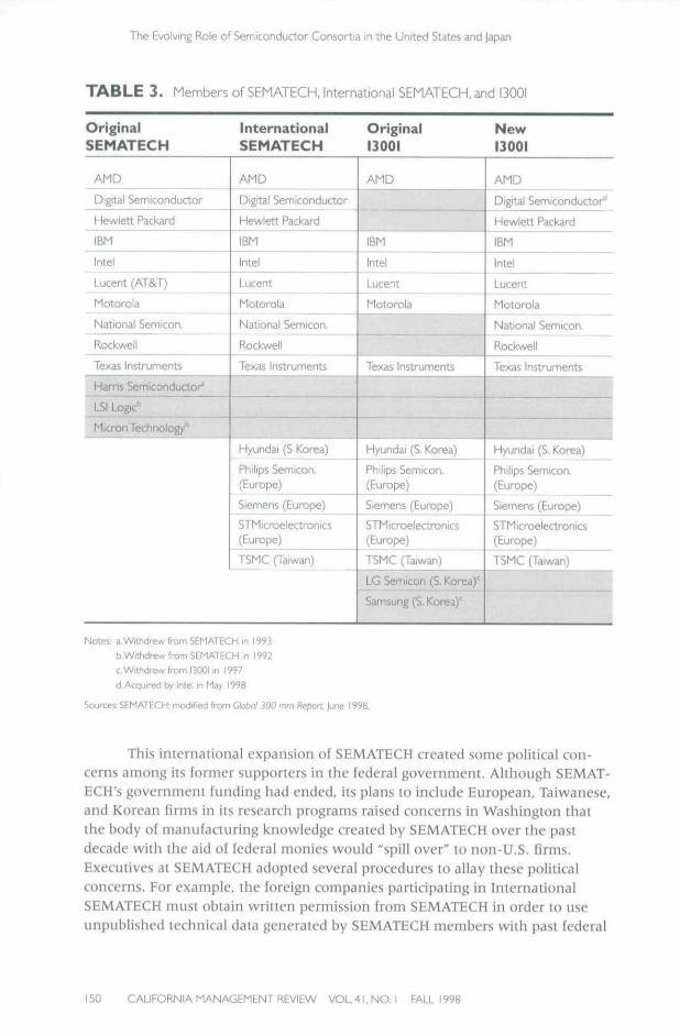
With federal funds drawing to an end, SEMATECH faced a choicebetween scaling back its research agenda or attracting additional dues-payingmembers. In the end, it did both. In 1995, SEMATECH began reducing its oper-ating budget to prepare for the end of federal funding and initiated plans forincluding non-U.S. firms in a set of international projects. In this context, one ofBOOI's most significant accomplishments to date may be its role in paving theway for an expansion of SEMATECH. In 1998, the remaining members of BOOIjoined a new, more ambitious "International SEMATECH" (see Table 3), anothersubsidiary of SEMATECH. Assignees of firms from seven countries will work ona set of joint International SEMATECH projects, including the continued 300mmactivities of BOOI, a larger project on photolithography (one ol the most criticaltechnologies used in semiconductor manufacturing), and two other projeas onmanufacturing methods and environmental, safety, and health standards.'^" In1999, BOOI (now a division of International SEMATECH) expects to phase outits tool evaluation activities and take on the more difficult task of selecting toolsfor joint development or improvement projects.'''
CALIFORNIA MANAGEME^^^ REVIEVs VOL- f i ,NO. I FALL 1998 K9
The Evolving Role of Semiconductor Consortia in the United States and Japan
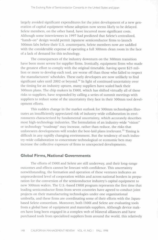
T A B L E 3 . Members of SEMATECH, International SEMATECH, and 13001
OriginalSEMATECH
International OriginalSEMATECH 13001
New13001
AMD
Digital Semiconductor
Hev 'lett Packard
IBM
Intel
Lucent (AT&T)
Motorola
National Semicon.
Rockwell
Texas Instruments
Harris Semiconduetor'
LSI Logic"
Micron Technology'
AMD
Digital Semiconducior
t-lewlett Packard
IBM
Intel
Lucent
Motorola
National Semicon,
Rockwell
Texas Instruments
Hyundai (S Korea)
Philips Semicon.(Europe)
Siemens (Eunope)
STM icroelectronics(Europe)
TSMC (Taiwan)
AMD
IBM
Intel
Lucent
MotonDia
Texas Instruments
Hyundai (S. Korea)
Philips Semicon.(Europe)
Siemens (Europe)
STM icroelectronics(Europe)
• ' [ • • • - [ , , V . . . : .
LG Semicon (S. Korea)"
Samsung (S. Korea)'
AMD
Digital Semiconductor^
Hewlett Packard
IBM
Intel
Lucent
Motorola
National Semicon.
Rockwell
Texas Instruments
Hyundai (S. Korea)
Philips Semicon.(Europe)
Siemens (Eurape)
STMicroelectronics(Eurc^)
Notes: aWrttidrew from SEMATtCH in 1993
b. Withdrew from SEMATECH in 1992
c.Witiidrew frDm 13001 in 1997
d.Acquired by Intel in May 1998
Sources: SEMATECH; modified from Global 300 mm Pepon June 1998.
This international expansion of SEMATECH created some political con-cerns among its former supporters in the federal govemment. Although SEMAT-ECH's government funding had ended, its plans to include European, Taiwanese,and Korean firms in its research programs raised concerns in Washington thatthe body of manufacturing knowledge created by SEMATECH over the pastdecade with the aid of federal monies would "spill over" to non-U.S. firms.Executives at SEMATECH adopted several procedures to allay these politicalconcerns. For example, the foreign companies participating in InternationalSEMATECH must obtain written permission from SEMATECH in order to useunpublished technical data generated by SEMATECH members with past federal
150 CAUFORNIA MANAGEMENT REVIEV VOL-11. NO. I FALL 1998
The Evolving Role of Semiconductor Consortia in the United States and Japan
assistance. In addition, foreign members of the consortium were not guaranteedthe right to license SEMATECH patents and must obtain written approval for useof these inventions. '
Nevertheless, it is noteworthy that SEMATECH's international offshootincludes no Japanese semiconductor firms. Given the fact that SEMATECH'soriginal objectives were to improve the competitiveness of U.S. semiconductormanufacturers relative to their Japanese competitors, Japanese membership in aninternational subsidiary (if SEMATECH may well have been politically infeasible.At a minimum, the inclusion of Japanese device makers in InternationalSEMATECH would have increased the intensity of the political criticism.**
Renewed Industry-Government Partnerships in Japan?The Japanese-led Selete consortium illustrates a very different relation-
ship between the private consortium and public-sector initiatives. Selete is oneof several important Japanese semiconductor projects that have been launchedin the past few years. Collectively, these projects represent the largest set of pri-vate-public programs aimed at semiconductor technologies since the well-known VLSI Project of the 1970s.*'"* Organizational walls divide the privateinitiatives from public ones within this collection of projects. Nonetheless, theorigins and broader research agenda of Selete are enmeshed with importantsemiconductor projects funded by Japan's Ministry of International Trade andIndustry (MITI), even though Selete's 300mm program is funded and ledentirely by private finns.
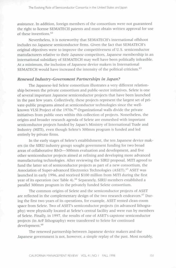
In the early stages of Selete's establishment, the ten Japanese device mak-ers (in the SIRIJ industry group) sought government funding for two broadareas of collaborative R&D—300mm evaluation and development, and fiveother semiconductor projects aimed at refining and developing more advancedmanufacturing technologies. After reviewing the SIRU proposal, MITI agreed tofund the latter set of semiconductor projects as part of a new consortium, theAssociation of Super-advanced Electronics Technologies (ASET).*" ASET waslaunched in early 1996, and received $100 million from MITI during the firstyear of its operation (see Table 4).*' Separately, SIRU members established aparallel 300mm program in the privately funded Selete consortium.
The common origins of Selete and the semiconductor projects of ASETare reflected in the complementary design of the two research endeavors.''^ Dur-ing the first two years of its operations, for example, ASET rented clean-roomspace from Selete. Two of ASET's semiconductor projects (in advanced lithogra-phy) were physically located at Selete's central facility and were run by membersof Selete. Finally, in 1997, the results of one ot ASET's capstone semiconductorprojects (in ArF lithography) were transferred to Selete for continueddevelopment.^*
The renewed partnership between Japanese device makers and theJapanese government is not, however, a simple replay of the past. Most notably,
CAUFORNIA MANAGEMENT REViEV\ VOLII.NO. I FALL 1998 151
The Evolving Role of Semiconductor Consortia in the LJnited States and Japan
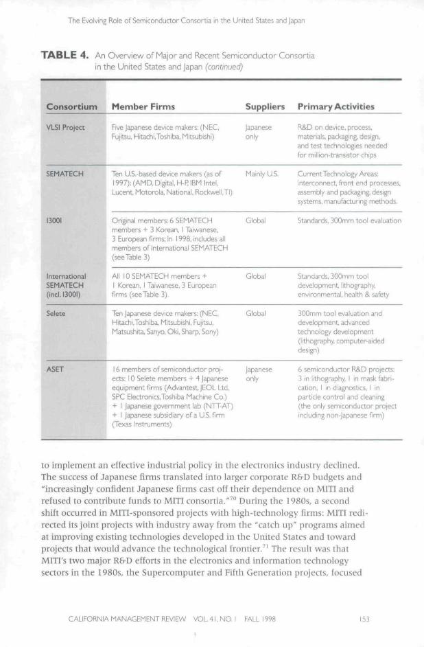
T A B L E 4 . An Overview of Major and Recent Semiconductor Consortiain the United States and Japan
Consortium YearsAverage AnnualBudget (current $)'
PercentPublic Funds
VLSI Project 1976-86(Government fundsended in 1980)
$70 million (FY 1976-79)
$40 million (FY 1980-86)
1976-79:40%
1980-86:0%
SEMATECH
13001
1987-present(Government fundsended FY 1996)
1996-present
$200 million (1988-94)
$180 million (1995-96)"
$160 million (1997-98)^
$24 million
1988-94:50%
1995-96:50%
1997-98:0%
0%
InternationalSEMATECH(tncl. 13001)
1998-present $7S million(April-December 1998)
0%
Selete 1996-p[-esent $56 million
ASET 1996-present $70 million (of whichapproximately 80% issemiconductor-related)
100% (firms payindirect costs only)
Notes;
a. Budget estimates are derived from the following sources: for VLSI Project see Flamm, {MismanagedTrade? op.cit): for
SEMATECH. 13001, and International SEMATECH. see SEMATECH (1997. op.cit) plus personal communicabon; for Selete. see
Selete (1997, op, ciL). for ASFT see ASET (1997. op, ctt) and personal communication,
b, 1996 budget includes 13001
c 1997 budget includes 13001: 1998 includes International SEMATEOi
the Japanese semiconductor firms played a guiding role in orchestrating thepublicly funded ASET project. During Japan's "catch up" phase in ihc 1970s,MITI and NTT (then a state-owned telecommunications firm) provided much ofthe impetus for the creation of the VLSI Project and its parallel projects withsuppliers.^'' As Japan entered the 1980s, however, the ability of the government
152 CAUFORNIA MANAGEMENT REVIEW VOL 41. NO. I FALL 1998
The Evolving Role of Semiconductor Consortia in the United States and Japan
T A B L E 4, An Overvievi' of Major and Recent Semiconductor Consortiain the United States and Japan (continued)
Consortium Member Firms Suppliers Primary Activities
VLSI Project Rve Japanese device makers: (NEC. JapaneseFujitsu, HitachiToshiba, Mitsubishi) only
R&D on device, pnxess.materials, packaging, design,and test technologies neededfor million-transistor chips
SEMATECH
13001
IntemationaiSEMATECH(ind. 13001)
Ten U.S.-based device makers (as of1997); {AMD, Digital H-R IBM Intel,Lucent. Motorola. National, RockwellTI)
Mainly U.S. Current Technology Areas;interconnect front end processes,assembly and packaging, designsystems, manufacturing methods.
Original members: 6 SEMATECHmembers + 3 Korean. I Taiwanese.3 European firms; in 1998. includes allmembers of Intemationai SEMATECH(see Table 3)
Global Standards, 300mm tool evaluation
All 10 SEMATECH members +I Korean, I Taiwanese, 3 EuropeanHrms (seeTable 3),
Global Standards, 300mm tooldevelopment lithography,environmental, heahh & safety
Selete Ten Japanese device makers; (NEC,Hitachi,Toshiba, M'rtsubishi, Fujitsu,Matsushita, Sanyo. Oki. Sharp, Sony)
Global 300mm tool evaluation anddevelopment, advancedtechnology development(lithography, computer-aideddesign)
ASFT 16 members of semiconductor proj-ects; 10 Selete members + 4 Japaneseequipment firms (Advantest,jEOL Ltd.SPC Electronics,Toshiba Machine Co.)+ I Japanese government lab (NTT-AT)+ I Japanese subsidiary of a U.S. firmlTexa5 Instruments)
Japanese 6 semiconductor R&D pnsjects:only 3 in lithography. I in mask fabri-
cation, I in diagnostics, I inparticle control and cleaning(the only semiconductor projectincluding non-Japanese firm)
to implement an effective Industrial policy in the electronics industry declined.The success of Japanese fimis translated into larger corporate R&D budgets and"increasingly confident Japanese firms cast off their dependence on MITI andrefused to contribute funds to MITI consortia."'" During the 1980s, a secondshift occurred in MlTl-sponsored projects with high-technology firms: MITI redi-rected its joint projects with industry away from the "catch uji" programs aimedat improving existing technologies developed in the United States and towardprojeas that would advance the technological frontier/' The result was thatMITI's two major R&D efforts in the electronics and information technologyseaors in the 1980s, the Supercomputer and Fifth Generation projects, focused
CAUFORNIA MANAGEMENT REVIEW VOL 41. NO, I FALL 1998 153
The Evolving Role or Semiconductor Consortia in the United States and Japan
on long-term R&D, faced resistance by companies, were hamstrung by smallbudgets, and ultimately were not very successful.'^
Within this context, the creation of Seleie and ASET represents a new eraof private-public collaboration in Japan, triggered by the first major challenge tothe competitive performance of Japanese device makers since the 1970s. Ratherthan being coerced into collaboration, which was the case in the 1970s, leadingJapanese semiconductor firms initiated the latest round of cooperation. Needlessto say, in the absence of a competitive crisis in the Japanese semiconductorindustry, it is unlikely that projects of this magnitude would have beenlaunched.
Conclusion
Although the competitive performance of semiconductor firms in theglobal market is driven by a complex array of macroeconomic, technological,and institutional influcnces,^^ the two newly formed semiconductor consortiaexamined here—the U.S.-based International 300mm Initiative and the Japan-based Selete consortium—are closely tied to the historic ebbs and flows in iherelative performance of U.S. and Japanese firms. The formation of I300I coin-cided with a period of relative strength for U.S. semiconductor manufacturersand the domestic base of suppliiT firms. Perhaps as a result, BOOI's memberswere reluctant to fund a major development project, settling for a less ambitiousset of activities aimed at setting standards and demonstrating tool performance.However, the importance of I30DI extends beyond its relatively narrow ro!e inihe 300mm wafer conversion. I300I has already been an important experimentof international collaboration for its parent organizalion, SEMATECH—which,having shed its partnership with the U.S. government in 1996, created a new"International SEMATECH" in 1998.
By contrast, the Japan-based Selete consortium was established at a timewhen leading Japanese device makers were engaged in efforts to reactivate theJapanese industry in order to address their collective problems in worldwidesemiconductor markets. In the i990s, Japanese device makers lost market shareto South Korean and Taiwanese firms in commodity product lines (e.g., DRAMs)that depend on manufacturing expertise and high-volume production. At thesame time, Japanese firms have failed to make significant inroads in the lucra-tive, design-intensive end of the market (e.g., microprocessors) that remainsdominated by U.S. firms. In response, Japanese semiconduaor manufacturerslaunched an ambitious program aimed at improving next-generation manufac-turing technologies based on the new wafer standard, and did so in conjunctionwith a large, publicly funded initiative, ASET.
From this perspeaive, the formation of Selete and ASET is analogous tothe establishment of the U.S. SEMATHCH consortium in the 1980s and Japan'sVLSI Project in the preceding decade: periods of "collective crisis" have resultedin "collective action" that involves industry-wide coordination and, periodically,
CALIFORNIA MANAGEMENT REVIEW VOL 41. NO, I FALL i 998
The Evolving Role of Semiconductor Consortia in the United States an
joint government-industry action in both nations' semiconductor industries. Thecritical nature of semiconductor components as inputs to the electronics,telecommunications, and computer industries means that governments arereluctant to ignore the erosion in the competitive performance of their domesticfirms, while firms appear more likely to turn to governments during times ofeconomic strain. At a minimum, this tendency suggests that a truly "borderless"world of global firms, one in which national governments exercise little or noinfluence, remains a distant mirage.
The lingering role of governments in shaping private sector collaborationis only one of several lessons from these consortia. A key difference betweenboth I300I and Selete and the landmark semiconductor consortia of the past(i.e., SEMATECH and the VLSI Project) is that these new initiatives have beendevised and funded by private firms; any government influence on the structureand design of these consortia was indirect. As such, these industry consortiayield imponant insights concerning the private incentives for collaborationamong firms in this industry. The semiconductor industry appears to be uniquein the extent to which leading manufacturers are now working together world-wide to establish uniform standards for manufacturing technologies. The com-plexity and costs of semiconductor manufacturing, combined with the shortproduct life cycles and rapid pace of technological change in this industry, havetriggered an unprecedented level of collaboration among device makers in guid-ing the industry's conversion to 300mm wafers.'' Furthermore, without thedirect involvement of governments in their collective activities, both of theseconsortia chose to include a broad base of suppliers from around the world intheir venical projects.
A more cautionary lesson from these privately held consortia is that evenin the face of unprecedented cooperation, the transition to a new technology(300mm wafers in this case) may be impeded by unforeseen events. The recentindustry slowdown and the faster-than-expected improvements in 200mm fabshave delayed the need to introduce 300mm tools. As noted earlier, this situationillustrates an important risk associated with the colleaive priority-setting andtechnological forecasting of industry-wide consortia. By the summer of 1998,what was once called "collaboration" was deemed a "crisis," as supplier firmsfound it difficult to support their investments in 300mm tools when purchasedates slipped further into the future.
The projects at I300I and Selete are still underway. Whether these consor-tia will be remembered for ushering in a new era of international cooperationamong semiconductor manufacturers and their suppliers, or for contributing toits demise, remains to be seen.
CALIFORNIA MANAGEMENT REVIEW VOL 41, NO. I FALL 1998 155
The Evolving Role of Semiconductor Consortia in the United States and Japan
Notes1. N.S. Vonortas, "Research Joint Ventures in the U.S.," Research Policy, 26/4-5
(1997): 577-595. See also H.E. Aldrich and T. Sasaki, "R&D Consortia in the U.S.and Japan," Research Policy. 24/2 (1995): 301-316.
2. R.M. Ham atid D.C. Mowery, "Enduring Dilemmas in U.S. Technology Policy,'California Management Review, 37/4 (Summer 1995): 89-107. Although ihisaniclecoticentrates on publicly funded semiconductor consoriia in the United States andJapan, a host ol European-wide consortia were launched during the 1980s in thebroad areas of information technologies. These include ESPRIT (European Strate-gic Program for R&D in Information Technologies), Eureka (a large-scale initiativein electronic technologies), and .JBSSI (the Joini Europt-an Submicron SiliconInitiative). JESSl was undertaken within ihe Eureka framework to "strengthenthe whole European electronics chain and also to secure its worldwide competi-tiveness in the future." N. Lucchini, "European Technology Policy and R&D Con-sortia: The Case of Semiconduaors," International Journal of Technology Management.15/6 (1998): 542-555. See also T.C. Lawlon, Technology and The New Diplomacy: TheCreation and Control of EC Industrial Policy for Semiconductors {Aldershot, UK: AveburyPress, 1997).
3. Throughout this article, a research consortium is broadly defined as an agreementin which multiple firms agree to share ihe expenses and ihe benefits associatedwith a future R&D activity. A consortium may include provisions for sharing thecost or effort of conducting R&D, may or may not conduct research at a commonfadlity, and may entail a complex array of licensing and intellecuial propertyprovisions for member versus nonmember firms. A consortium typically includesmore members and pursues a broader agenda than a narrowly focused researchjoini venture.
4. The U.S. SEMATECH consortium, for example, was heralded as "a model for fed-eral consortia funded to advance other critical technologies. Programs will beencouraged in the development of a new automobile, new construction technolo-gies, intelligent control and sensor technologies, rapid prototyping, and environ-mentally conscious manufacturing." W. Clinton and A. Gore, "Technology forAmerica's Economic Growth: A New Direction to Build Economic Strength."White House Press Office, February 22, 1993, cited in P. Grindley. D.C. Mowery,and B. Silverman, "SEMATECH and Collaborative Research: Lessons in the Designof High-Technology Consortia," Journal of Policy Analysis and Management, 13/4(1994):723-758, a tp . 723.
5. J. Macher, D.C. Mowery, and D. Hodges, "Back to Dominance? U.S. Resurgence inthe Global Semiconduaor Industry," California Management Review. 41/1 (Fall1998) [in this issue].
6. M. Fransman, The Market and Beyond: Cooperation and Competition in InformationTechnology Development in ihe Japanese System (Cambridge, UK: Cambridge Univer-sity Press. 1990).
7. The direct effeas of the VLSI Project on the competitive performance of Japanesedevice makers and equipment firms are far from clear. See, for example, R. Lan-glois and V '.E. Steinmueller, "The Evolution of Competitive Advantage in theGlobal Semiconductor Industry: 1947-1996," in D.C. Mowery and R.R. Nelson,eds.. The Sources of Industrial Leadership (New York, NY: Cambridge UniversityPress. 1998).
8. Although ihis article focuses on the two leading consortia (13001 and Selete)involved In ihe 300mm transition, there are several related European initiatives.For example, the Semiconductor Equipmeni Assessment (SEA) program underESPRIT promotes European equipment suppliers, but some of the 300mm equip-
156 CAUFORNIA MANAGEMENT REVIEW VOL 41. NO. I FAU 1998
The Evolving Role of Semiconductor Consortia in the United States and Japan
ment under that program will be evaluated by I300I and Selete. Europe is alsodeveloping some of its own 300mm tdols as pan of the four-year, $2.5 billionMicroelearontcs Development for European Applications (MEDEA) project,which is funded jointly by government and industry. J. Haystead, "Making theRight Moves," Electronic Business Today (February 1997), pp. 52-57; SemicondudorEquipment and Materials International (SEMI), "U.S. Semiconductor Manufactur-ing and the 300 mm Challenge,"www.semi.org/Focused/public/wp/whitepaper.html, 1997.
9. In order to investigate the factors that underpin the formation of these consortia,we met with representatives from both BOOI and Selete and with other industryexecutives involved in this and prior wafer transitions. We conducted over 20interviews with these individuals between June 1997 and August 1998.
10. J.H. Dunning, Globalizalion: The Challenge for National Economic Regimes [The GearyLecture for 1993] (Dublin: Economic and Social Research Institute, 1994).
U. In 1996, for a group of leading U.S. producers with combined semiconductor salesof over $37 billion, semiconductor-specific capital expenditures amounted tomore than 25 percent of sales, while research and development expenditureswere nearly 12 percent of sales. Based on data from Integrated Circuit Engineer-ing Corporation (ICE), Profiles 1997 (Scottsdale, AZ: Integrated Circuit Engineer-ing, Inc., 1997). Both figures outweigh the corresponding data for leaders in otherindustries such as chemicals, Pharmaceuticals, aerospace, and autos (Calculatedfrom lO-K reports for Dow Chemical, Merck & Co., Boeing, and Ford Motor).
12. "Philips Executive Urges New Alliances between Chip and Equipment Compa-nies," Semiconductor Business News Online. October 8, 1997.
13. M.M. Appleyard, N.W. Hatch, and D.C. Mowery, "Managing New Process Intro-duction in the Semiconductor Industry," in G. Dosi, R. Nelson, S. Winter, eds..Corporate Capabilities and Compeliliveness (London: Pinter, forthcoming). See also E.Braun and S. MacDonald, Revolution in Miniature: The History and Impact of Semicon-duaor Electronics (Bath, UK: Pitman Press, 1982) for an excellent discussion of thehistoric reliance of semiconductor firms on manufacturing process technologies.
14. "Applying Pressure," Electronic Business (November 1997).15. Semiconductor production involves the creation of multiple copies of an inte-
grated circuit desigti on a round silicon wafer. In simple terms, larger wafers—holding the number of wafers produced in a given facility constant—permit morechips to be manufactured. For example, the move from 100mm to 150mm wafers(a 1.5x increase in wafer diameter) doubled the number of chips per wafer, whilethe move from 200mm to 300mm wafers (again, a I.5x increase in wafer diame-ter) yields approximately 2.6 limes more identically sized chips per wafer. Plantthroughput can also be improved by reducing the size of a given design (e.g.,through a re-design of the device or through switching to a process using finerline widths), permitting more chips to fit on each processed wafer.
16. New chip designs are typically brought to market as rapidly as possible in order loearn the price premium associated with state-of-the-art products. Designs arethen "shrunk" in later versions in order to economize on wafer space (reducingcost) and also to enhance the chip's speed and performance.
17. Integrated Circuit Engineering Corporation (ICE), Cost Effective Manufacturing, 1998-1999 (Scoitsdale, AZ: Integrated Circuit Engineering, Inc., 1997).
18. Because individual equipment firms and device makers incur part of the costs ofany given wafer conversion, precise estimates are difficult to obtain. Estimates ofthe total cost of putting 300mm technology into practice have been as high as $30billion, of which $14 billion would be spent for development by equipment sup-pliers and the rest by chip companies to implement the new systems, See, forexample. Semiconductor Business News. "Move to 300-mm Slows to a Walk"
CAUFORNIA MANAGEMENT REVIEW VOL -11, NO. I FALL 1998 157
The Evolving Role of Semiconductor Consortia in the United States and Japan
(December 1997). As of mid-1998, equipment suppliers had already spent anestimated $4 billion on 300mm development. 'Summit Called to Help Avert 300-mm Crisis," Sem/aiH(yw(:r(jrS(«/«MS News, July 13, 1998.
19. SEML op. dt.20. A former IBM engineer we interviewed used the term "fiasco" to describe IBM's
experience in the transition to 200nim wafers.21. See, for example, "IBM Boosts Production of Memory Chips with Debut of 8-inch
Wafer," PC Week. June 7, 1988; Haystead, op. dt.22. A variety of standards-setting organizations have been involved in orchestrating
dialogue among international device makers and between these manufacturersand tlie suppliers of semiconductor materials and equipment. Foretnost amongthese are SEMI, an international organization for semiconductor equipment andmaterials suppliers, and J300, a volunteer industry roundtahle in Japan thatincludes device, equipment, and materials companies. I300I has also taken anactive role in standards development. For example, starting in July 1997, I300Iand J300 published a series of "Global Joint Guidance' doctiments related to300mm equipment and factory automation. In contrast, during the previous tran-sition to 200mni wafers, the lack of industry standards resulted in a myriad ofoptions for each piece of equipment: "200mm processing equipment has no stan-dard equipment interface and there are multiple differences in loading height,depth, and direction by equipment manufacturer and equipment type." ICE, op.dt.
23. STMicroelectronics was known as SGS-Thomson until May 1998.24. At the end of 1997, two of the Korean firms (Samsung Electronics and LG Semi-
con) terminated their membership, citing the effects of the Asian financial crisis."Samsung Stays in Japan's 300mm Group After Leaving SEMATECH's," ElectronicBuyers' News Daily Digest. February 4, 1998.
25. Samsung joined Selete's 300mm program as a "client" in September 1997 and, bymid-1998, had placed several assignees at Seleie. Samsung is not, however, astockholder of the consortium and thereby has no formal role in setting or redi-recting Selete's research activities. Interview with Dr. Hiroyoshi Komiya, Execu-tive Vice President and COO of Selete, May 15, 1998. See also, "Samsung Stays inJapan's 300mm Group After Leaving SEMATECH's," Electronic Buyers'News DailyDigest. February 4, 1998.
26. T.F Bresnahan and A. Chopra, "The Development of the Local Area NetworkMarket as Determined hy User Needs," Economics of Innovation and New Technology.1/1&2 (1990): 97-110. Leading manufaaurers in other capital-intensive industrieshave nonetheless played an important (but less coordinated) role in establishingstandards for production equipment, espedally in the automobile industry. Forexample. General Motors led the development of a computer-integrated manufac-turing standard, the Manufacturing Automation Protocol (MAP), that obviatedthe need to write expensive, customized "bridge" software to coordinate a diversearray of automated machine tools based on separate, incompatible systems. Gabeldetails how buyers promulgated supplier standards in the auto industry's earlyyears up to 1930. H.L. Gabel, Competitive Strategies for Product Standards: The StrategicUse of Compatibility Standards for Competitive Advantage (New York, NY: McGraw-Hill,1991), Chapter 4. More recently, Detroit's Big Three established the United StatesCoundl of Automotive Research (USCAR) in the wake of the 1984 NCRA.USCAR is roughly comparable to SEMATECH, conduaing a wide range of pre-competitive activities in cooperation with various sets of vendors. It has not yetbeen revealed how USCAR will respond to its potential internationalization fol-lowing the takeover of Chrysler by Germany's Daimler-Benz.
IS8 CAUFORNIA MANAGEMENT REVIEW VOL 41. NO 1 FAa 1998
The EvoK/ing Role of Semiconductor Consortia in the United States and Japan
27. Semicondudor producers originally developed their equipment internally. Inde-pendent equipment producers emerged in the United States in the 1970s and,soon thereafter, in Europe and Japan. W.,I. Spencer and P. Grindley, "SEMATECHafter Five Years: High-Technology Consortia and U.S. Compeiitiveness," CaliforniaManagement Review, 35/4 (Summer 1993): 9-32.
28. M.M. Appleyard, "The Strategic Development of Equipment; Buyer-Supplier Co-Development in the Semiconductor Industry," Darden Working Paper SeriesDSWP-98-05, Colgate Darden Graduate School of Business Administration, Uni-versity of Virginia. 1998. hi a more recent development, some large suppliers,such as U.S.-based Applied Materials, have integrated their produci lines morefully and arc performing some of the lests typically conducted by manufacturers."Applied Opens Metrology Lab to Accelerate 300-mm Work," Semiconductor Busi-ness News Online. iuXy 10, 1997.
29. Appleyard, op. cit. The device maker attributed the failure to a lack of involve-ment by the supplier early in the overall process development project of whichthe tool was one element.
30. A fundamental risk faced by the industry is whether the capital costs of next-generation fabs will undermine the profitability of the 300mm transition. The goalset by device manufacturers is that 300mm capital costs should not exceed 1.3xthose for 200mm fabs, but the cost of some pieces of equipment will most likelyexceed this target. "SEMI's 300-mm Symposium: Tough Times Slow the WaferTransition," Global 300mm Report (July 1998).
31. Some administraEive and pntcedural safeguards were ptit in place to separate theaaiviiies of I300I and SEMATECH, in part because of the higher dues paid bySEMATECH members (four of which were nol part of I300I until 1998) and, per-haps more importantly, because of lingering political concerns over the leakage toforeign firms of research that was previously supported by U.S. government funds(also discussed below). See, "SEMATECH Vowing to Protect Taxpayer-FundedR&D Data," New Technology Business Week. February 9, 1998.
32. SEMATECH, 1997 Annual Report: 10 Years of Shared Experience. (Austin, TX:SEMATECH, 1997).
33. The cost-of-ownership model estimates the lifetime cost—including purchase,support, service, and maintenance costs—for individual pieces of equipment andhas proved to be very beneficial in guiding tool development. For example, Intelestimates that use of the COO model has reduced by more than 50 percent theoperating costs associated with a Lam Research etching tool. Grindley et al., op.dt.
34. Grindley et al., op. dt. While SEMATECH spent roughly 20 percent of its 1988budget on supplier contracts, over 60 percent of it $200 million 1991 budget wasallocated to these external activities. U.S. General Accounting Office, SEMATECH'sTechnological Progress and Proposed R&D Program. GAO/RCED-92-233BR (Washing-ton, D.C: Government Printing Office, 1992).
35. According to representatives from I300I, half of the demonstrations conducted byMay 1998 had taken place off-site at supplier firms. 13001 evaluates some tools,espedally ones used to support the overall demonstration process, in the cleanroom it leases from SEMATECH.
36. As discussed below, however, the nexi phase of BOOI's 300mm-reIated activitiesmay involve joint projects with suppliers on selected pieces of equipment, inter-view with Frank Robertson, General Manager, 13001, May 1998.
37. SEMATECH, SEMATECH Technology Patents. Technology Transfer Report#93O3151588B-XFR (Austin. TX: SEMATECH. Inc., 1995); updates available athttp://www.semalech.org/public/general/issued.him.
CAUFORNIA MANAGEMENT REVIEW VOL 41. NO. I FALL 1998 159
The Evolving Role of Semiconductor Consortia in the United States and Japan
i&. K. Flamm, Mismanaged Trade? Strategic Policy and the Semiconductor Industry (Wash-ington, D.C: Brookings Institution, 1996). As discussed below, this industry"think tank" proposed and funded several initiaiives. including the Seiete consor-tium, several semiconductor projects lundcd by MITI (discussed in ihe sectiontitled "Global Firms, National Governments" in this article), and the Semiconduc-tor Technology Academic Research Center (STARC), 3 program modeled explicitlyafter the U.S. Semiconductor Research Center (SRC) that funds universityresearch. Interview with Taro Okabe, Executive Researcher and Aaing ExecutiveDirector of SIRIJ, July 1998; see also Flamm, op. cit.
39. Since 199'5, SIRIJ has added three new members, of which one (TI Japan) is aJapanese subsidiary of a U.S. firm and another (Nippon Motorola) is a joint ven-ture between a Japanese and a U.S. firm. Flamm, op. cit. These new SIRIJ mem-bers have noi joined Selete.
40. In a July 15, 1995, letter to SEMATECH, the director of SIRU cited three reas(msfor the decision by Japanese device makers to decline the invitation to join 13001:the distance between Japan and Austin, Texas (where the I30QI consortiumwould be located), language barriers, and differences between leading U.S. andJapanese device makers in their "philosophies" nf manufacturing. The letter statedfurther that "a few leading Japanese companies siill believe that they have tohave unique production equipments [sic] in order to differentiate their productsfrom others. I think such philosophy is not popular in the U.S." The Japaneseexecutives we interviewed also asserted that the global semiconductor equipmentseaor benefits from having two consortia instead of one. In theory, ihe existenceof two separate consortia working on the 300mm transition may avoid "lock-in"to sub-opiimal equipment specifications. See W.B. Arthur, "Competing Technolo-gies, Increasing Returns, and Lock-In by Historical Events," Economic Journal, 99
{1989): U6-131, and P.A. David, "Clio and the Economics of QWERTY." AmericanEconomic Review. 75 (1985): 332-337 on how the early, widespread adoption ofone standard may lock-out emerging but superior alternatives.
41. One of the largest expenses in the transition effort is the purchase of the 300mmwafers used for testing. A reliability tesi can use 1,000 or more wafers, which costabout $1,000 apiece. BOOI pays 20 percent of the cost of wafers used for testingwith the suppliers covering the rest. In contrast, Selete purchases all of its testwafers. Selete, "Status of 300mm Program at Selete," SEMICON West '97 presen-tation, July 16, 1997.
42. As discussed below, Selete's clean room not only houses the consortium's 300mm-related activities, but also supports "advanced technology research" programs inspecific equipment areas, such as next-generation optical lithography and elec-tron-beam direct writing technologies, which are supported by additional duesfrom member firms. Selete, op. cit. For example, Selete's first advanced technol-ogy research program—budgeted at $8 million through the year 2000—was acomputer-aided design project that simulated devices and processes. Selete's pro-jects in advanced lithography and e-beam direct writing technologies are affiliatedwith government-funded projects in a separate initiative (discussed below). See,"Semiconductor Leading Edge Technologies, Inc. (Selete) Starts New Research onFuture Technologies," Selete Press Release, July 10, 1997.
43. An executive we interviewed in 1997 from a major U.S. equipment firmexpressed concern thai participation in Selete would give the firm's Japanesecompetitors access to their proprietary technologies. Because of these concerns,the firm postponed shipment of its most critical tool to Selete until additionalsafeguards were put in place. [The representative from the equipment firm pre-ferred to remain anonymous.j According to Hiroyoshi Komiya of Selete, however,Selete has taken considerable strides to ensure the confidentiality of lool-related
160 CALIFORNIA MANAGEMENT REVIEW VOLtl.NO, I FALL 1998
The Evolving Role of Semiconductor Consortia in the United States and Japan
information; although suppliers had initial questions about the security of propri-etary information at Selete, Dr. Komiya was unaware of any reluctance amongsuppliers to place tools at the common facility. Written comments provided byHiroyoshi Komiya, Executive Vice President and COO of Selete, September !998.
44. Interview with Hiroyoshi Komiya, Executive Vice President and COO of Selete,May 1998.
45. An engineer interviewed in this study stated that tool "tweaks" (i.e., minorchanges) constitute some of the most valuable inEellectual property in the semi-conductor equipment industry.
46. Written comments provided by Hiroyoshi Komiya, Executive Vice President andCOO of Selete, September 1998.
47. The potential cost savings from cooperation to avoid redundancy are considerable.For example, each consortium puts semiconductor production equipment through"marathon' and "ironman" tests, which cost around $1 million each, lo evaluatethe stability of the equipment using different manufaauring processes and toassess the reliability of the equipment. A.S. Longo, "The Evaluation and Imple-mentation of Process Technologies in Semiconduaor Manufaauring," unpub-lished master's thesis, MIT Sloan School of Management, 1995, at p, 1. Eachgroup, however, conducts these tests somewhat differently and cooperation hasproved to be more elusive in this area than in standards-setting aaivities. By theend ol 1997, following two years of discussion, some agreement had been reachedon a joint "ironman"-style test, one of which was conduaed in early 1998. Inter-view with Frank Robertson, General Manager, 13001, May 1998. The consortiahave also worked together on developing "unified metrics" for equipment, whichwould establish consistent targets for suppliers. By December 1997, they hadconverged on metrics for 15 tools capable of 250 nanometer (nm) processing and,by June 1998, metrics had been agreed upon for an additional !7 tools capable ofprocessing at the more advanced 180nm technology. I300I presentation at SEMI-CON West, July 1998.
48. In 1997,13001 started demonstration projects of tools from a number of differentvendors worldwide, including Applied Materials (U.S.), JEOL (Japan), Leica(Europe), TEL (Japan), Tencor (U.S.) and Verteq (U.S. ); ICE, op. cit. at p. 7-10.
49. Interviews with Hiroyoshi Komiya, Executive Vice President and COO of Selete,and Frank Robertson, General Manager, I300L May 1998.
50. Texas instruments presentation at SEMI 3rd Annual 300mm Symposium, June16, 1998.
51. "SEMI Regional Meeting Focuses on 300-mm Transition Status," Global 300mmReport. March 1998. Non-compliance is a risk in any standards effort. For exam-ple, the Open Systems movement in midrange computers was splintered by the1988 creation of the Open Software Foundation in response to AT&T's perceiveddominance of tbe UNIX standard. Gabel, op. cit.. Chapter 5.
52. This is a common problem in electronics and complicates the timing of new prod-uct introduaions. For example, producers of long-established cathode ray tubeshave continued to make improvements and cost reduaions, providing a movingtarget for competing technologies such as liquid crystal and plasma displays. See,for example, B. Bowonder, S,L, Sarnot, M.S. Rao, and T. Miyake, "Competition intbe Global Electronics Industry: Strategies of Major Players," International Journalof Technology Management, 12/5&6, Spedal Issue (1996), pp. 551-576.
53. "SEMI Regional Meeting Focuses on 300-mm Transition Status," Global 300mmReport, March 1998, The one 1998 pilot line predicted in the March forecast—aSiemens-Motorola joint venture in Dresden, Germany—has been delayed due tolack of a complete tool set. "Siemens Hedging on Whether It Will Meet 300-mmSchedule," Semiconductor Business News (August, 1998).
CALIFORNIA MANAGEMENT REVIEW VOL 11, NO. 1 FALL 1998 161
The Evolving Role of Semiconductor Consortia in the United States and Japan
54. "Applied Materials Profit Drops, Forecasting an Industry Slump," Wall Street Jour-nal Interactive Edition. July 13, 1998.
55. For exampk', some industry representatives have called into question ihe need for300nini wafers, suggesting the need to move to 400mm wafers insiead. "Could400-mm Wafers Be Coming Sooner?" Semiconduaor Business News. June 15, 1998.
56. Dunning, op. cit.57. Restrictions on foreign participation in SEMATECH were originally put in place
because of the U.S. government's contributions and the objective of the consor-tium to bolster the domestic semiconductor industry. Grindlt-y el al., op. cit.
58. J.B. Horrigan, "Cooperation Among Competitors in Research Consortia: The Evolution ofMCCand SEMATECH." unpublished doctoral dissertation, University of Texas atAustin, 1996.
59. Ham and Mowery, op. cii.60. International SEMATECH is a wholly owned subsidiary of SEMATECH, although
each company has its own advisory board structure. Both International SEMAT-ECH and SEMATECH are funded by dues from member companies, wiih fundingdivided about evenly between the two. Overall member dues to SEMATECH didnot change as a result of the expansion; some ongoing SEMATECH projects weresimply transferred to the international subsidiary. See Table 4 for information onthe projects conducted by the two organizations.
61. These projecis may be absorbed into other divisions of International SEMATECHat that lime.
62. M. Crawford, "SEMATECH Vowing to Protea Taxpayer-Funded RfrD Data." NewTechnology Week, February 9, 1998.
63. A SEMATECH executive we interviewed speculated that, had the Japanese joined13001, Congress might have derailed the entire initiative. Debate over grantingmembership to non-U.S. firms rang through the halls of the U.S. RfrD establish-ment in the 1980s, and was revived quite recently by the controversial EUV con-sortium, an industry group led by Intel that wanted to include Nikon, a Japanesesupplier of nearly half the world's semiconductor lithography equipment, in acollaborative RfrD projea with U.S. government engineers. In the end. Congressbarred the direct participation of non-U.S. firms (including Nikon) in the projea,but allowed the results of the project to be licensed to equipment suppliers world-wide. See, "Global Chip Effort Set: International SEMATECH: Consortium May BeHindered by Lack of Japanese Firms," Mercury Center (San Jose Mercury NewsOnline), February 3, 1998; "U.S.-Eunded Technology Stays Here for Now," U.S.Newsand World Report. May 18, 1998, p. 5.
64. Flamm, op. cit.65. Interview with Taro Okabe, Acting Executive Director, Semiconductor Industry
Research Institute Japan (SIRIJ), July 1998. The decision by MITI to fund only thesecond set of longer-term projects may stem from a desire by the Japanese gov-emtiient to stay within the boutidaries of the new GATT rules that define "non-actionable" RfrD subsidies of national governments (Flamm, op. cit.). For ananalysis of the GATT rules, see H. Furuya, "Comparative Techtiology Policy for theSemiconductor Industry in Japan and the United States," unpublished master'sthesis, Stanford Program in International Legal Studies, Stanford Law School,
1998; U.S. General Accounting Office, General Agreement on Tariffs and Trade:Uruguay Round Final Act Should Produce Overall U.S. Economic Gains. Volume 2,GAO/GGD-94-83B (Washington, D.C: Government Printing Office, 1994).
66. ASET's funding duritig the current financial crisis sheds new light on the politicalrationale for industrial policy in contemporary Japan. In 1997, due to generalbudget cuts, ASET's funding was only $20 million. But in 1998, the funding wasraised to more than $70 million as part of a fiscal stimulus package.
162 CAUFORNIA MANAGEMENT REVIEW VOL, 41. NO, I FALL 1998
The Evolving Role of Semiconductor Consortia in the United States and lapan
67. In addition to the five semiconductor projects proposed by the members of Seleie,MITI agreed to fund an additional semiconduaor project (on particle contamina-tion) that includes the Japan-based subsidiary of a US. Hrm, Texas Instruments.MITI also added projects to ASET in liquid crystal displays and magnetic storagedevices, which include hotfi Japanese firms and the Japanese-based subsidiaries of3 foreign firms. See ASET, Present Activities and Future Vision of the Association ofSuper-Advanced Electronics Technologies (Tokyo: Electronic industries Association ofJapan, 1997). Only Japanese device manufacturers and sui)pliers, however, areinvolved in the five central semiconductor projects of ASET (sec- Table 4).
68. The second ASET projea housed at Selete was terminated at the end of fiscal year1997. Written comments by Hiroyoshi Komiya, Executive Vice President andCOO, Selete, September 1998. The fact that ASET's ArF litiiograiihy project wastransferred to Selete within such a relatively short tinieframe appears to supportFlamm's assessment that ASET is "best understood as advanced developmenteffort than basic research...Idespite being] characterized by its promoters as 'fun-damental' or 'basic' technologies for future generation manufacturing." K, Elamm,"Japan's New Semiconductor Technology Programs," ATIP Rcjiort #96.091, AsianTechnology Information Program, www.atip.org, 1996, at p. 8.
69. According to Fransman, the Japanese device makers only accepted tbe joint labo-ratory portion of MITl's proposed organization because they "were forced to doso" in order to get the private research subsidies from MITI that they reallywanted. Eransman, op. cit., p. 63.
70. S. Callon, Divided Sun: MITI and the Breakdown of Japanese High-Tech Industrial Policy,1975-93 (Stanford, CA: Stanford University Press, 1995), at p. 13.
71. M. Anchordoguy, "Japan at a Technological Crossroads: Does Change SupportConvergence Theory?" Journal of Japanese Studies. 23/2(1997): 363-397; Callon,op. dt.
72. Callon, op, dt.73. See Macher et al., op. cit., for a thorough discussion of these issues.74. Industry participants on hotb sides of the Pacific have considered deriving a joint
technology roadmap for the direction ol semiconductor technologies well into thefuture, although the benefits of these efforts are still being debated. "Work Startson Global IC Roadmap," Semiconductor Business News, July 15, 1998.
CALIFORNIA MANAGEMENT REVIEW VOL. 41, NO, I FALL 1998 163