
TCKE712BNL eFuse IC with Flag Output and Reverse-Current ...
33
TCKE712BNL eFuse IC with Flag Output and Reverse-Current Protection Application Note 2021-1-15 1 © 2021 Toshiba Electronic Devices & Storage Corporation Outline An eFuse IC (also known as an electronic fuse) incorporates various functions for protecting electronic devices and serves as a replacement for a conventional fuse. This application note describes the TCKE712BNL, an eFuse IC with various protection functions and a flag output function, which is a diagnostic function that signals an abnormal condition externally. This application note discusses its basic usage and functions, including short-circuit protection, overcurrent protection, overvoltage protection, thermal shutdown, inrush current limiting, reverse-current blocking during turn-off, undervoltage lockout, and the FLAG � � � � � � � � output. Since the TCKE712BNL can be turned on and off via an external signal, it can also be used as a load switch IC. TCKE712BNL eFuse IC with Flag Output and Reverse-Current Protection Application Note
-
Upload
khangminh22 -
Category
Documents
-
view
1 -
download
0
Transcript of TCKE712BNL eFuse IC with Flag Output and Reverse-Current ...

TCKE712BNL eFuse IC with Flag Output and Reverse-Current Protection
Application Note
2021-1-15 1 © 2021
Toshiba Electronic Devices & Storage Corporation
Outline An eFuse IC (also known as an electronic fuse) incorporates various functions for protecting electronic devices and serves as a replacement for a conventional fuse. This application note describes the TCKE712BNL, an eFuse IC with various protection functions and a flag output function, which is a diagnostic function that signals an abnormal condition externally. This application note discusses its basic usage and functions, including short-circuit protection, overcurrent protection, overvoltage protection, thermal shutdown, inrush current limiting, reverse-current blocking during turn-off, undervoltage lockout, and the FLAG�������� output. Since the TCKE712BNL can be turned on and off via an external signal, it can also be used as a load switch IC.
TCKE712BNL eFuse IC with Flag Output and Reverse-Current
Protection Application Note
TCKE712BNL eFuse IC with Flag Output and Reverse-Current Protection
Application Note
2021-1-15 2 © 2021
Toshiba Electronic Devices & Storage Corporation
Table of Contents Outline ................................................................................................................................................ 1
Table of Contents ............................................................................................................................. 2
1. Introduction ..................................................................................................................................... 5 2. What is an eFuse IC? ...................................................................................................................... 5
2.1. Usage of an eFuse IC .......................................................................................................................... 5 2.2. Benefits of using an eFuse IC.............................................................................................................. 6
3. Example of an application circuit for the TCKE712BNL ................................................................... 8 4. Functions incorporated in the TCKE712BNL ................................................................................. 10 5. Block diagram of the TCKE712BNL .............................................................................................. 11 6. Circuits incorporated in the TCKE712BNL..................................................................................... 12
6.1. Charge pump [Figure 5.1(1)] ............................................................................................................. 12 6.2. Overvoltage protection circuit [Figure 5.1(2)] .................................................................................... 12
6.2.1. Operation of the overvoltage protection (OVP) circuit ........................................................................12 6.2.2. Setting the OVP trip voltage ................................................................................................................14
6.3. Undervoltage lockout (UVLO) circuit [Figure 5.1(3)] ......................................................................... 14 6.4. Thermal shutdown circuit [Figure 5.1(4)] ........................................................................................... 16 6.5. Overcurrent protection circuit [Figure 5.1(5)] ..................................................................................... 17
6.5.1. Operation of the overcurrent protection circuit ....................................................................................17 6.5.2. Setting the overcurrent protection circuit .............................................................................................20
6.6. Short-circuit protection circuit [Figure 5.1(6)] .................................................................................... 20 6.7. Inrush current limiting (slew rate control) circuit [Figure 5.1(7)] ........................................................ 22
6.7.1. Operation of the inrush current limiting circuit .....................................................................................22 6.7.2. Setting the rise time (slew rate) of the VOUT voltage .........................................................................23
6.8. Reverse-current blocking circuit [Figure 5.1(8)] ................................................................................ 24 6.9. FLAG circuit ....................................................................................................................................... 24 6.10. EN pin .............................................................................................................................................. 25
7. Examples of controlling the TCKE712BNL via the EN input .......................................................... 27 8. TCKE712BNL application examples.............................................................................................. 30 9. Conclusion .................................................................................................................................... 32 RESTRICTIONS ON PRODUCT USE .............................................................................................. 33
TCKE712BNL eFuse IC with Flag Output and Reverse-Current Protection
Application Note
2021-1-15 3 © 2021
Toshiba Electronic Devices & Storage Corporation
List of Figures
Figure 2.1 Application example of an eFuse IC ............................................................................................. 6 Figure 3.1 Example of an application circuit for the TCKE712BNL ............................................................... 8 Figure 3.2 Example of an application circuit for the TCKE712BNL with a TVS diode and an SBD .............. 9 Figure 5.1 Block diagram of the TCKE712BNL ........................................................................................... 11 Figure 6.1 OVP circuit .................................................................................................................................. 12 Figure 6.2 Example of an OVP operation .................................................................................................... 13 Figure 6.3 Example of overvoltage detection by the OVP circuit................................................................. 13 Figure 6.4 Example of an operation of the UVLO circuit.............................................................................. 15 Figure 6.5 Example of an operation of the TSD circuit ................................................................................ 16 Figure 6.6 TSD circuit and its principle of operation .................................................................................... 17 Figure 6.7 Example of an OCP operation .................................................................................................... 18 Figure 6.8 Example of an OCP operation in the event of a repetitive pulsed overcurrent condition ........... 19 Figure 6.9 Resistor connected to the ILIM input .......................................................................................... 20 Figure 6.10 Example of the IOUT_CL - RILIM curve ...................................................................................... 20 Figure 6.11 Output voltage and current waveforms during a Fast Trip operation ....................................... 21 Figure 6.12 Example of short-circuit protection and thermal shutdown operations ..................................... 22 Figure 6.13 Waveforms of the inrush current limiting (slew rate control) circuit .......................................... 23 Figure 6.14 Capacitor connected to the dV/dT input ................................................................................... 23 Figure 6.15 tdV/dT - CdV/dT characteristics ...................................................................................................... 23 Figure 6.16 Back-to-back reverse-current blocking circuit ........................................................................... 24 Figure 6.17 Equivalent circuit of the FLAG pin ........................................................................................... 24 Figure 6-18 Equivalent circuit of the EN pin ................................................................................................. 25 Figure 6-19 Outputs from a typical comparator and a window comparator ................................................. 26 Figure 6.20 IEN - VEN characteristics (shown only as a guide) ..................................................................... 26 Figure 7.1 Example of the EN input connection (The EN input is connected directly to VIN.) .................... 27 Figure 7.2 Example of the EN input connection (The EN input is controlled externally.) ............................ 27 Figure 7.3 Example of the EN input connection (The EN input is connected to the VIN input via a switch.)28 Figure 7.4 Example of the EN input connection (VIN is divided with resistors.) ........................................... 28 Figure 8.1 Application to notebook PCs and mobile devices ....................................................................... 30 Figure 8.2 Application to SSDs and HDDs ................................................................................................... 30 Figure 8.3 Application to servers .................................................................................................................. 30 Figure 8.4 Application to wearable and IoT devices .................................................................................... 31
TCKE712BNL eFuse IC with Flag Output and Reverse-Current Protection
Application Note
2021-1-15 4 © 2021
Toshiba Electronic Devices & Storage Corporation
List of Tables
Table 2.1 Comparison between an eFuse IC (TCKE712BNL) and conventional fuses ................................ 7 Table 4.1 Functions incorporated in the TCKE712BNL ............................................................................... 10 Table 5.1 Pin description of the TCKE712BNL ............................................................................................ 11 Table 6.1 VOVPR specification shown in the datasheet ................................................................................. 12 Table 6.2 ROVP specification of the OVP pull-down resistor shown in the datasheet .................................. 14 Table 6.3 UVLO specifications shown in the datasheet .............................................................................. 15 Table 6.4 TSD specification shown in the datasheet ..................................................................................... 17 Table 6.5 tFLAGblank specification shown in the datasheet ............................................................................. 18 Table 6.6 tOCP_COUNT specification(<5ms) shown in the datasheet ............................................................... 19 Table 6.7 Indications and timing of the FLAG output ................................................................................. 25 Table 6.8 EN pull-down resistor specification shown in the datasheet ........................................................ 26
TCKE712BNL eFuse IC with Flag Output and Reverse-Current Protection
Application Note
2021-1-15 5 © 2021
Toshiba Electronic Devices & Storage Corporation
1. Introduction At present, fuses and polyswitches (also known as resettable fuses and polyfuses) are widely used to protect electronic devices from overheating and fire hazards. Both fuses and polyswitches are tripped by Joule heat generated by current exceeding their ratings. In this application note, they are referred to as conventional fuses. There are two types of conventional fuses for the protection of electronic circuits and an overall system. In the case of glass tube and chip current fuses, excessive current causes their internal metal strip to melt, interrupting the current. In the case of polyswitches, the heat generated by current causes their internal conductive polymer to expand; the resulting increase in resistance substantially limits the current. However, conventional fuses exhibit substantial variations with respect to the interrupting rating. Another downside of conventional fuses is that they take a long time to blow because of their dependence on Joule heat. In addition, a fuse that relies on a metal melting process must be replaced once it blows. To overcome these disadvantages of conventional fuses, eFuse ICs use a MOSFET to interrupt current. While usable in the same way as conventional fuses, eFuse ICs can be designed with various protection functions other than overcurrent protection. The TCKE712BNL, Toshiba’s new versatile eFuse IC, also incorporates a flag output function, a diagnostic function that signals an abnormal condition externally. The TCKE712BNL provides overcurrent protection (OCP), short-circuit protection, inrush current limiting (slew rate control), overvoltage protection (OVP), and undervoltage lockout (UVLO). Furthermore, the protection thresholds are programmable. With thermal shutdown (TSD) and reverse-current blocking during turn-off, the TCKE712BNL further simplifies circuit and system protection. This application note describes major characteristics, operations, usage, and applications of the TCKE712BNL. * Click here for a detailed description of the flag output and the conditions that cause it to change.
→
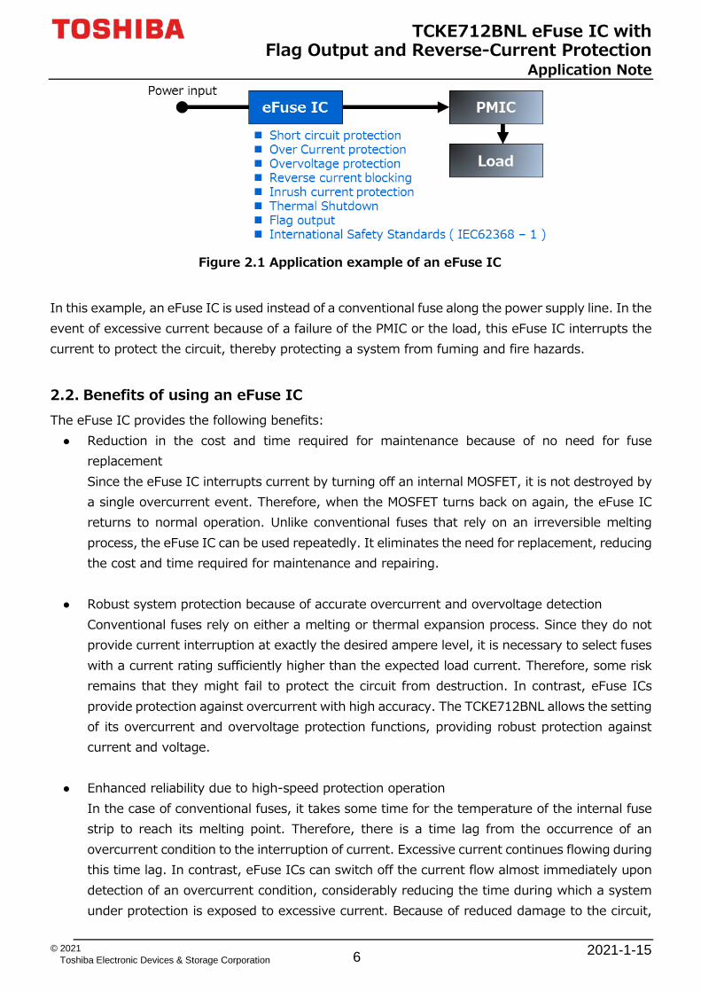
2. What is an eFuse IC? 2.1. Usage of an eFuse IC Whereas conventional fuses rely on the melting of an alloy part, an eFuse IC uses a semiconductor switch to interrupt current. When an internal current sensor detects excessive current, an internal MOSFET is turned off via its output signal to interrupt the current. Figure 2.1 shows an example of a block diagram in which power is supplied to a power management IC (PMIC) via an eFuse IC.
Click Here
TCKE712BNL eFuse IC with Flag Output and Reverse-Current Protection
Application Note
2021-1-15 6 © 2021
Toshiba Electronic Devices & Storage Corporation
Figure 2.1 Application example of an eFuse IC
In this example, an eFuse IC is used instead of a conventional fuse along the power supply line. In the event of excessive current because of a failure of the PMIC or the load, this eFuse IC interrupts the current to protect the circuit, thereby protecting a system from fuming and fire hazards.
2.2. Benefits of using an eFuse IC The eFuse IC provides the following benefits: ● Reduction in the cost and time required for maintenance because of no need for fuse
replacement Since the eFuse IC interrupts current by turning off an internal MOSFET, it is not destroyed by a single overcurrent event. Therefore, when the MOSFET turns back on again, the eFuse IC returns to normal operation. Unlike conventional fuses that rely on an irreversible melting process, the eFuse IC can be used repeatedly. It eliminates the need for replacement, reducing the cost and time required for maintenance and repairing.
● Robust system protection because of accurate overcurrent and overvoltage detection Conventional fuses rely on either a melting or thermal expansion process. Since they do not provide current interruption at exactly the desired ampere level, it is necessary to select fuses with a current rating sufficiently higher than the expected load current. Therefore, some risk remains that they might fail to protect the circuit from destruction. In contrast, eFuse ICs provide protection against overcurrent with high accuracy. The TCKE712BNL allows the setting of its overcurrent and overvoltage protection functions, providing robust protection against current and voltage.
● Enhanced reliability due to high-speed protection operation In the case of conventional fuses, it takes some time for the temperature of the internal fuse strip to reach its melting point. Therefore, there is a time lag from the occurrence of an overcurrent condition to the interruption of current. Excessive current continues flowing during this time lag. In contrast, eFuse ICs can switch off the current flow almost immediately upon detection of an overcurrent condition, considerably reducing the time during which a system under protection is exposed to excessive current. Because of reduced damage to the circuit,
TCKE712BNL eFuse IC with Flag Output and Reverse-Current Protection
Application Note
2021-1-15 7 © 2021
Toshiba Electronic Devices & Storage Corporation
eFuse ICs help enhance long-term system reliability.
● Cost and size reduction due to single-chip implementation of various protection functions In addition to overcurrent and short-circuit protection, an eFuse IC allows various functions to be integrated on the same chip that cannot be realized with conventional fuses, including overvoltage protection, inrush current limiting (slew rate control), thermal shutdown, and reverse-current blocking. Therefore, an eFuse IC helps reduce the number of parts and the amount of workload required, compared with the case of implementing the same functions using multiple discrete passive components and ICs, and thus reduce the system cost and size.
● Simplified system design because of compliance with international safety standards It requires a long time to test fuses to ensure their compliance with internationally recognized safety standards. IEC 62368-1 applies to a wide range of commercial and industrial information and communication and audio/visual equipment. IEC 62368-1 requires that power supply be immediately interrupted in a reliable manner in the event of any abnormal condition. Toshiba is planning to obtain certification for IC current limiters stipulated in Section G.9 of IEC 62368-1. Since this certification makes it possible to omit some system tests stipulated in this safety standard, it helps reduce the time and effort required for system design.
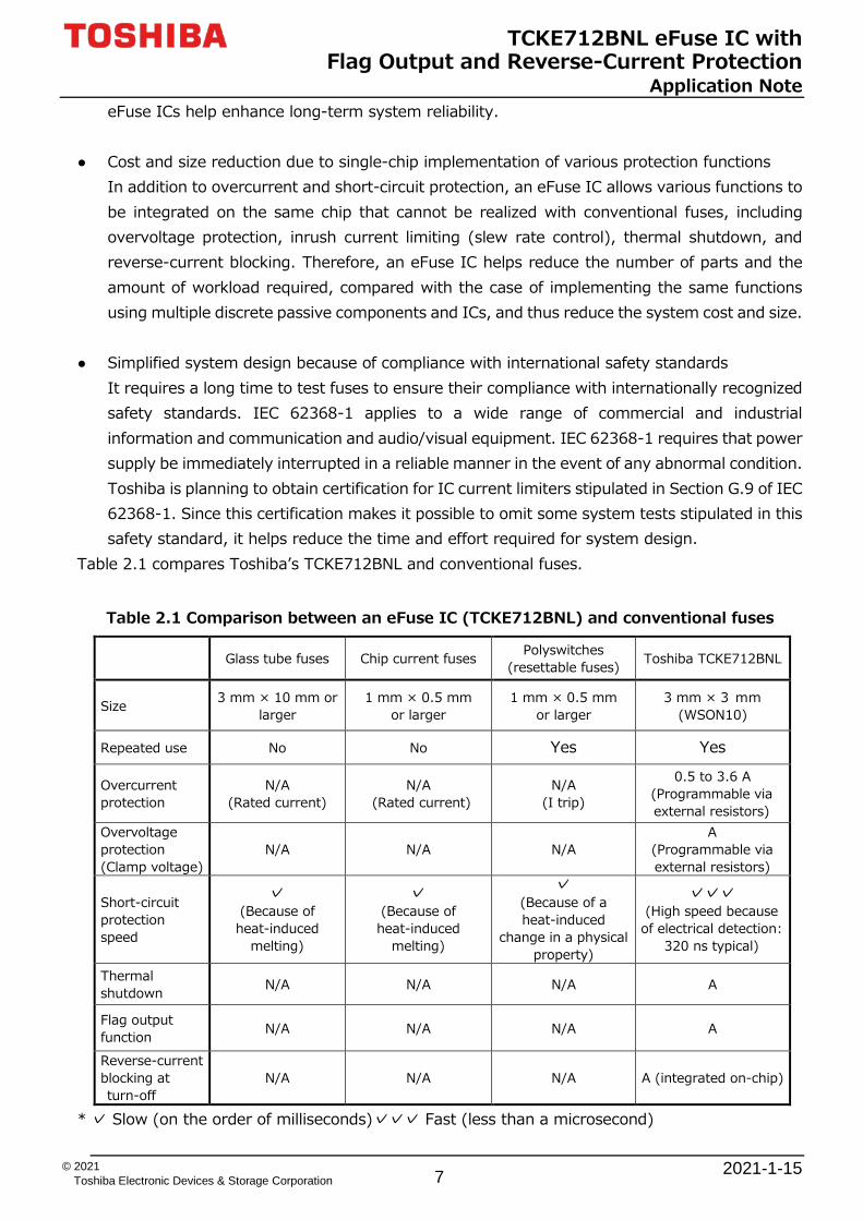
Table 2.1 compares Toshiba’s TCKE712BNL and conventional fuses.
Table 2.1 Comparison between an eFuse IC (TCKE712BNL) and conventional fuses
Glass tube fuses Chip current fuses Polyswitches (resettable fuses) Toshiba TCKE712BNL
Size 3 mm × 10 mm or larger
1 mm × 0.5 mm or larger
1 mm × 0.5 mm or larger
3 mm × 3 mm (WSON10)
Repeated use No No Yes Yes
Overcurrent protection
N/A (Rated current)
N/A (Rated current)
N/A (I trip)
0.5 to 3.6 A (Programmable via external resistors)
Overvoltage protection (Clamp voltage)
N/A N/A N/A A
(Programmable via external resistors)
Short-circuit protection speed
✓ (Because of heat-induced
melting)
✓ (Because of heat-induced
melting)
✓ (Because of a heat-induced
change in a physical property)
✓✓✓ (High speed because of electrical detection:
320 ns typical)
Thermal shutdown N/A N/A N/A A
Flag output function N/A N/A N/A A
Reverse-current blocking at turn-off
N/A N/A N/A A (integrated on-chip)
* ✓ Slow (on the order of milliseconds) ✓✓✓ Fast (less than a microsecond)
TCKE712BNL eFuse IC with Flag Output and Reverse-Current Protection
Application Note
2021-1-15 8 © 2021
Toshiba Electronic Devices & Storage Corporation
Chip current fuses and polyswitches are becoming progressively smaller. However, when protection features available with an eFuse IC are externally added to these fuses using multiple components, the total footprint considerably exceeds the size of a conventional fuse. Although conventional fuses compare favorably with eFuse ICs in some respects, eFuse ICs provide greater benefits as shown in Table 2.1.
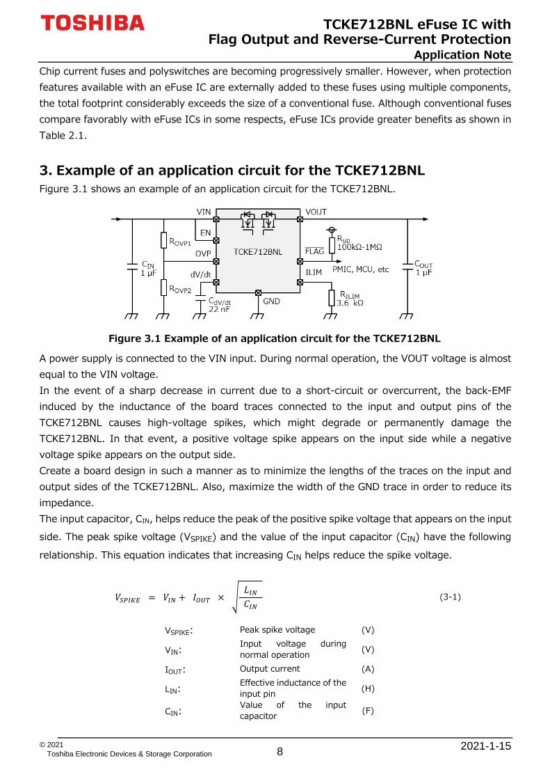
3. Example of an application circuit for the TCKE712BNL Figure 3.1 shows an example of an application circuit for the TCKE712BNL.
Figure 3.1 Example of an application circuit for the TCKE712BNL
A power supply is connected to the VIN input. During normal operation, the VOUT voltage is almost equal to the VIN voltage. In the event of a sharp decrease in current due to a short-circuit or overcurrent, the back-EMF induced by the inductance of the board traces connected to the input and output pins of the TCKE712BNL causes high-voltage spikes, which might degrade or permanently damage the TCKE712BNL. In that event, a positive voltage spike appears on the input side while a negative voltage spike appears on the output side. Create a board design in such a manner as to minimize the lengths of the traces on the input and output sides of the TCKE712BNL. Also, maximize the width of the GND trace in order to reduce its impedance. The input capacitor, CIN, helps reduce the peak of the positive spike voltage that appears on the input side. The peak spike voltage (VSPIKE) and the value of the input capacitor (CIN) have the following
relationship. This equation indicates that increasing CIN helps reduce the spike voltage.
𝑉𝑉𝑆𝑆𝑆𝑆𝑆𝑆𝑆𝑆𝑆𝑆 = 𝑉𝑉𝑆𝑆𝐼𝐼 + 𝐼𝐼𝑂𝑂𝑂𝑂𝑂𝑂 × � 𝐿𝐿𝑆𝑆𝐼𝐼 𝐶𝐶𝑆𝑆𝐼𝐼
(3-1)
VSPIKE: Peak spike voltage (V)
VIN: Input voltage during normal operation (V)
IOUT: Output current (A)
LIN: Effective inductance of the input pin (H)
CIN: Value of the input capacitor (F)

TCKE712BNL eFuse IC with Flag Output and Reverse-Current Protection
Application Note
2021-1-15 9 © 2021
Toshiba Electronic Devices & Storage Corporation
In the case of the TCKE712BNL, a 1-μF capacitor is recommended as CIN. However, be sure to perform a board evaluation to determine that VSPIKE does not exceed the maximum rated input voltage. The TCKE712BNL can be protected from electrostatic discharge (ESD) by connecting a transient-voltage-suppression (TVS) diode (also known as an ESD protection diode) on the input side. Connecting a Schottky barrier diode (SBD) on the output side prevents the output voltage from dropping considerably below GND because of a negative spike. This SBD helps protect not only the TCKE712BNL but also the load IC and a system. Connect an SBD between the VOUT and GND pins with the anode pointing toward GND. It is recommended to enhance the protection capability of the TCKE712BNL by connecting a TVS diode and an SBD as described above. Figure 3.2 shows an example of an application circuit.
Figure 3.2 Example of an application circuit for the TCKE712BNL with a TVS diode and an SBD
In the case of this example, it is recommended to use the DF2S23P2CTC TVS diode and the CUHS20S30 SBD. For details of these diodes and how to select and use the TVS diode, visit the following links:
For details of the DF2S23P2CTC TVS diode → For details of the CUHS20S30 Schottky barrier diode → For application notes about the basics of TVS (ESD protection) diodes → How should I select TVS (ESD protection) diodes according to the voltage level of a signal line to be protected? (FAQ)
→ How to select TVS (ESD protection) diodes (FAQ) → Board design considerations for TVS (ESD protection) diodes (FAQ) →
Click Here
Click Here
Click Here
Click Here
Click Here
Click Here
TCKE712BNL eFuse IC with Flag Output and Reverse-Current Protection
Application Note
2021-1-15 10 © 2021
Toshiba Electronic Devices & Storage Corporation
The resistor connected to the ILIM input sets the current limit (IOUT_CL) for overcurrent protection. In the above example, the current limit is set to roughly 1.7 A. The capacitor connected to the dV/dT input is used to adjust the slew rate to limit inrush current. In the event of overcurrent protection, thermal shutdown, or overvoltage protection being tripped, the FLAG�������� output is driven Low to signal an abnormal condition to a PMIC or an MCU. Connect an external pull-up resistor to the FLAG�������� output since it has an open-drain configuration. The EN input is used to turn on and off the internal MOSFET. An external resistor connected to the EN input determines the threshold voltage of the undervoltage lockout circuit. A resistor connected to the OVP input determines the voltage at which overvoltage protection is tripped. Chapters 6 and 7 detail the functions of these pins and how to select external resistors.
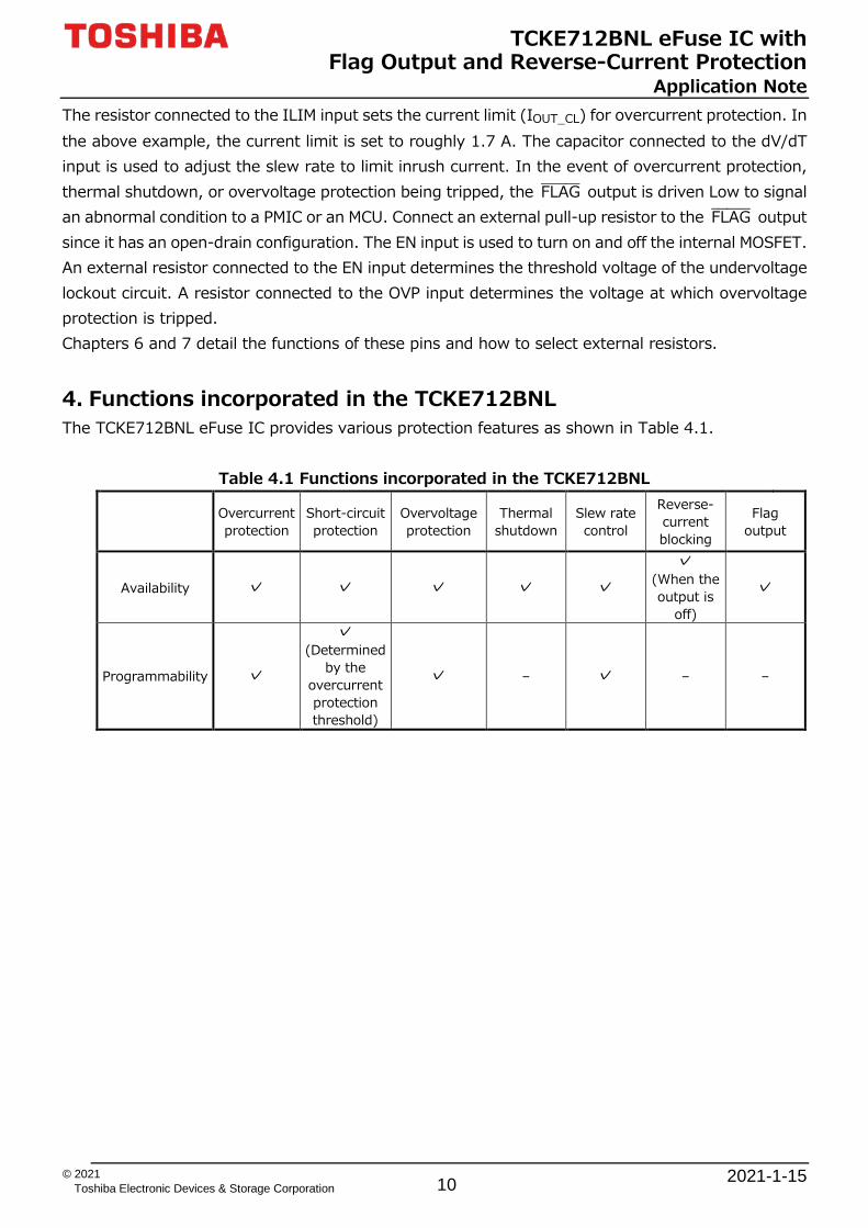
4. Functions incorporated in the TCKE712BNL The TCKE712BNL eFuse IC provides various protection features as shown in Table 4.1.
Table 4.1 Functions incorporated in the TCKE712BNL
Overcurrent protection
Short-circuit protection
Overvoltage protection
Thermal shutdown
Slew rate control
Reverse- current blocking
Flag output
Availability ✓ ✓ ✓ ✓ ✓
✓ (When the output is
off)
✓
Programmability ✓
✓ (Determined
by the overcurrent protection threshold)
✓ – ✓ – –

TCKE712BNL eFuse IC with Flag Output and Reverse-Current Protection
Application Note
2021-1-15 11 © 2021
Toshiba Electronic Devices & Storage Corporation
5. Block diagram of the TCKE712BNL
Figure 5.1 Block diagram of the TCKE712BNL
Table 5.1 Pin description of the TCKE712BNL
Pin Name
Description
VIN Supply input.
dV/dT Adjusts the rise time of the VOUT output. The rise time is determined by the value of the capacitor connected between the dV/dT and GND pins.
EN Enable pin
ILIM Sets the overcurrent protection threshold. The current limit is determined by the value of the resistor connected between the ILIM and GND pins.
GND Ground pin
OVP Adjusts the overvoltage protection (OVP) threshold. The threshold voltage is determined by the values of the resistors connected to the OVP pin.
FLAG�������� Flag output that externally signals an abnormal condition of the IC such as overcurrent, short-circuit, and thermal shutdown conditions. Connect an external pull-up resistor to this output since it has an open-drain configuration.
VOUT Output voltage

TCKE712BNL eFuse IC with Flag Output and Reverse-Current Protection
Application Note
2021-1-15 12 © 2021
Toshiba Electronic Devices & Storage Corporation
6. Circuits incorporated in the TCKE712BNL 6.1. Charge pump [Figure 5.1(1)] A charge pump is a voltage booster that generates a voltage for the gate drive of an N-channel MOSFET that acts as a switch.
6.2. Overvoltage protection circuit [Figure 5.1(2)] 6.2.1. Operation of the overvoltage protection (OVP) circuit
When voltage higher than a threshold (VOVPR) is applied to the VIN input, the OVP circuit turns off and latches the output voltage to prevent excessive voltage from being applied to a load. At the same time, the FLAG�������� output is driven Low and latched Low. Figure 6.2 shows an example of the OVP operation of the TCKE712BNL. The OVP circuit releases the latch when the EN input is set Low.
Table 6.1 VOVPR specification shown in the datasheet
VIN = 12 V, RLIM =3.6 kΩ
Characteristic Symbol Test Conditions Ta = 25 °C Ta = -40 to 85°C
Unit Min Typ. Max Min Max
Overvoltage protection threshold
VOVPR – – 1.2 – 1.14 1.26 V
Figure 6.1 OVP circuit
Internal control circuit
Pull-down junction FET

TCKE712BNL eFuse IC with Flag Output and Reverse-Current Protection
Application Note
2021-1-15 13 © 2021
Toshiba Electronic Devices & Storage Corporation
Figure 6.2 Example of an OVP operation
Figure 6.1 shows the OVP circuit. It compares the voltage at the OVP input (VOVP) and the reference
voltage of an internal comparator (VOVPR). When VOVP exceeds VOVPR, the comparator output toggles Low, turning off the MOSFET switch and latching its output, as shown in Figure 6.3.
Figure 6.3 Example of overvoltage detection by the OVP circuit
A pull-down junction FET equivalent to an ROVP of 22 MΩ (typical) is internally connected between the OVP and GND pins so that the internal circuit does not become unstable when the OVP pin is open.
TCKE712BNL eFuse IC with Flag Output and Reverse-Current Protection
Application Note
2021-1-15 14 © 2021
Toshiba Electronic Devices & Storage Corporation
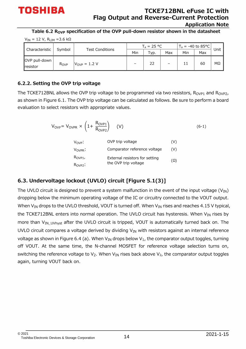
Table 6.2 ROVP specification of the OVP pull-down resistor shown in the datasheet VIN = 12 V, RLIM =3.6 kΩ
Characteristic Symbol Test Conditions Ta = 25 °C Ta = -40 to 85°C
Unit Min Typ. Max Min Max
OVP pull-down resistor ROVP VOVP = 1.2 V – 22 – 11 60 MΩ
6.2.2. Setting the OVP trip voltage
The TCKE712BNL allows the OVP trip voltage to be programmed via two resistors, ROVP1 and ROVP2, as shown in Figure 6.1. The OVP trip voltage can be calculated as follows. Be sure to perform a board evaluation to select resistors with appropriate values.
VOVP= VOVPR × �1+ ROVP1ROVP2
� (V) (6-1)
VOVP: OVP trip voltage (V)
VOVPR: Comparator reference voltage (V)
ROVP1,
ROVP2: External resistors for setting
the OVP trip voltage (Ω)
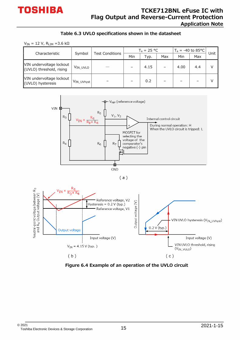
6.3. Undervoltage lockout (UVLO) circuit [Figure 5.1(3)]
The UVLO circuit is designed to prevent a system malfunction in the event of the input voltage (VIN) dropping below the minimum operating voltage of the IC or circuitry connected to the VOUT output. When VIN drops to the UVLO threshold, VOUT is turned off. When VIN rises and reaches 4.15 V typical,
the TCKE712BNL enters into normal operation. The UVLO circuit has hysteresis. When VIN rises by
more than VIN_UVhyst after the UVLO circuit is tripped, VOUT is automatically turned back on. The
UVLO circuit compares a voltage derived by dividing VIN with resistors against an internal reference
voltage as shown in Figure 6.4 (a). When VIN drops below V1, the comparator output toggles, turning off VOUT. At the same time, the N-channel MOSFET for reference voltage selection turns on, switching the reference voltage to V2. When VIN rises back above V2, the comparator output toggles again, turning VOUT back on.
TCKE712BNL eFuse IC with Flag Output and Reverse-Current Protection
Application Note
2021-1-15 15 © 2021
Toshiba Electronic Devices & Storage Corporation
Table 6.3 UVLO specifications shown in the datasheet
VIN = 12 V, RLIM =3.6 kΩ
Characteristic Symbol Test Conditions Ta = 25 °C Ta = -40 to 85°C
Unit Min Typ. Max Min Max
VIN undervoltage lockout (UVLO) threshold, rising VIN_UVLO ― – 4.15 – 4.00 4.4 V
VIN undervoltage lockout (UVLO) hysteresis VIN_UVhyst – – 0.2 – – – V
Figure 6.4 Example of an operation of the UVLO circuit

TCKE712BNL eFuse IC with Flag Output and Reverse-Current Protection
Application Note
2021-1-15 16 © 2021
Toshiba Electronic Devices & Storage Corporation
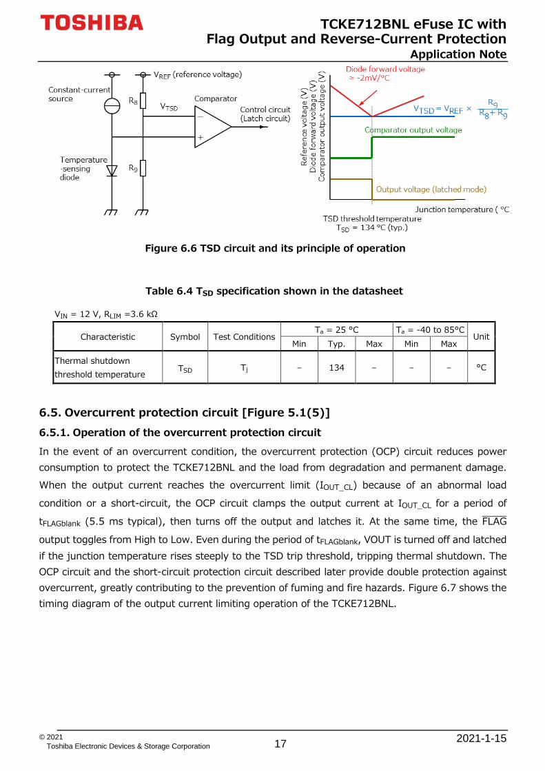
6.4. Thermal shutdown circuit [Figure 5.1(4)] The thermal shutdown (TSD) circuit turns off VOUT to protect the TCKE712BNL when its junction temperature rises above the TSD threshold (TSD) of 134°C typical as a result of excessive current flowing through VOUT or a sharp increase in ambient temperature. In the event of TSD being tripped, the TCKE712BNL turns off and latches VOUT, and the FLAG�������� pin is driven Low and latched Low. A Low on the EN input takes VOUT out of the latched mode. Figure 6.5 shows an example of an operation of the TCKE712BNL
Figure 6.5 Example of an operation of the TSD circuit
The junction temperature is detected by comparing a voltage derived from dividing a reference voltage (VREF), which changes little with temperature, with R8 and R9 against the forward voltage of a diode, as shown in Figure 6.6. While the TCKE712BNL is operating properly, the diode forward voltage is higher than VTSD. The diode forward voltage decreases by -2 mV per Celsius degree rise in temperature. When the diode forward voltage drops below VTSD as a result of an increase in junction temperature, the comparator output toggles, turning off the VOUT output of the TCKE712BNL. At the same time, the FLAG�������� output toggles from High to Low. Setting the EN input Low takes the VOUT output out of the latched mode. However, unless the cause of the increase in junction temperature is removed, TSD is tripped again, turning off the VOUT and FLAG�������� outputs and placing VOUT in the latched mode.
Time
TCKE712BNL eFuse IC with Flag Output and Reverse-Current Protection
Application Note
2021-1-15 17 © 2021
Toshiba Electronic Devices & Storage Corporation
Figure 6.6 TSD circuit and its principle of operation
Table 6.4 TSD specification shown in the datasheet
VIN = 12 V, RLIM =3.6 kΩ
Characteristic Symbol Test Conditions Ta = 25 °C Ta = -40 to 85°C
Unit Min Typ. Max Min Max
Thermal shutdown threshold temperature TSD Tj – 134 – – – °C
6.5. Overcurrent protection circuit [Figure 5.1(5)] 6.5.1. Operation of the overcurrent protection circuit
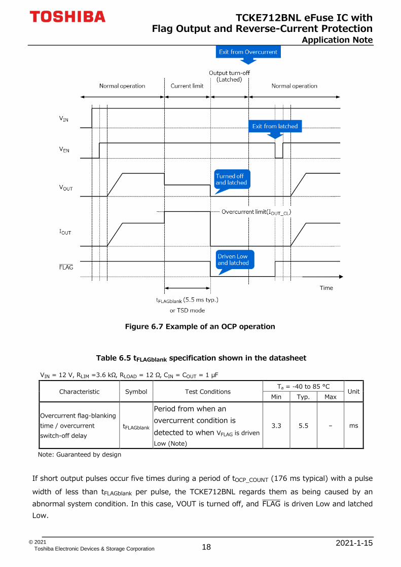
In the event of an overcurrent condition, the overcurrent protection (OCP) circuit reduces power consumption to protect the TCKE712BNL and the load from degradation and permanent damage. When the output current reaches the overcurrent limit (IOUT_CL) because of an abnormal load
condition or a short-circuit, the OCP circuit clamps the output current at IOUT_CL for a period of
tFLAGblank (5.5 ms typical), then turns off the output and latches it. At the same time, the FLAG��������
output toggles from High to Low. Even during the period of tFLAGblank, VOUT is turned off and latched if the junction temperature rises steeply to the TSD trip threshold, tripping thermal shutdown. The OCP circuit and the short-circuit protection circuit described later provide double protection against overcurrent, greatly contributing to the prevention of fuming and fire hazards. Figure 6.7 shows the timing diagram of the output current limiting operation of the TCKE712BNL.
TCKE712BNL eFuse IC with Flag Output and Reverse-Current Protection
Application Note
2021-1-15 18 © 2021
Toshiba Electronic Devices & Storage Corporation
Figure 6.7 Example of an OCP operation
Table 6.5 tFLAGblank specification shown in the datasheet
VIN = 12 V, RLIM =3.6 kΩ, RLOAD = 12 Ω, CIN = COUT = 1 μF
Characteristic Symbol Test Conditions Ta = -40 to 85 °C
Unit Min Typ. Max
Overcurrent flag-blanking time / overcurrent switch-off delay
tFLAGblank
Period from when an overcurrent condition is detected to when VFLAG is driven Low (Note)
3.3 5.5 – ms
Note: Guaranteed by design
If short output pulses occur five times during a period of tOCP_COUNT (176 ms typical) with a pulse
width of less than tFLAGblank per pulse, the TCKE712BNL regards them as being caused by an abnormal system condition. In this case, VOUT is turned off, and FLAG�������� is driven Low and latched Low.
Time

TCKE712BNL eFuse IC with Flag Output and Reverse-Current Protection
Application Note
2021-1-15 19 © 2021
Toshiba Electronic Devices & Storage Corporation
Figure 6.8 Example of an OCP operation in the event of a repetitive pulsed
overcurrent condition
Table 6.6 tOCP_COUNT specification(<5ms) shown in the datasheet
VIN = 12 V, RLIM =3.6 kΩ, RLOAD = 12 Ω, CIN = COUT = 1 μF
Characteristic Symbol Test Conditions Ta = -40 to 85 °C
Unit Min Typ. Max
Duration(<5ms) during which overcurrent pulses are counted
tOCP_COUNT -(Note) – 176 – ms
Note: Guaranteed by design
Time

TCKE712BNL eFuse IC with Flag Output and Reverse-Current Protection
Application Note
2021-1-15 20 © 2021
Toshiba Electronic Devices & Storage Corporation
6.5.2. Setting the overcurrent protection circuit
The TCKE712BNL allows the programming of the overcurrent limit (IOUT_CL) via an external resistor
(RILIM) connected to the ILIM pin. IOUT_CL can be calculated as follows. However, be sure to perform a board evaluation when selecting a resistor since theoretical and measured results differ slightly at a current of less than 1 A.
IOUT_CL = 6200 RILIM
(A) (6-2)
IOUT_CL: Overcurrent limit (A)
RILIM: Value of the external resistor connected to the ILIM input
(Ω)
Figure 6.9 shows a resistor connected to the ILIM input, and Figure 6.10 shows the IOUT_CL–vs-RILIM curve.
Figure 6.9 Resistor connected to the ILIM input
Figure 6.10 Example of the IOUT_CL - RILIM curve
6.6. Short-circuit protection circuit [Figure 5.1(6)] The short-circuit protection circuit shuts down the TCKE712BNL in the event of the output line or the load being short-circuited for some reason in order to prevent excessive current from flowing. If output current exceeds 2.5 times (typical) the overcurrent limit (IOUT_CL) instantaneously, the TCKE712BNL regards it as being a short-circuit condition. The TCKE712BNL incorporates an ultra-fast short-circuit protection circuit (called a Fast Trip circuit), which trips short-circuit protection in 320 ns typical from the detection of a short-circuit condition as shown in Figure 6.11.

TCKE712BNL eFuse IC with Flag Output and Reverse-Current Protection
Application Note
2021-1-15 21 © 2021
Toshiba Electronic Devices & Storage Corporation
Figure 6.11 Output voltage and current waveforms during a Fast Trip operation
After the short-circuit protection circuit is tripped, the TCKE712BNL returns to normal operation automatically. However, if the short-circuit condition persists, the short-circuit protection circuit is tripped again at the output current value determined by the overcurrent limit (IOUT_CL). In this case,
VOUT is turned off, and FLAG�������� is driven Low and latched Low either after a period of tFLAGblank (5.5 ms typical) or when thermal shutdown (TSD) is tripped during this period.
VOUT (5 V/div)
IOUT (1 A/div)
500 ns/div
VIN (5 V/div)
tFASTTRIP ≈ 320 ns

TCKE712BNL eFuse IC with Flag Output and Reverse-Current Protection
Application Note
2021-1-15 22 © 2021
Toshiba Electronic Devices & Storage Corporation
Figure 6.12 Example of short-circuit protection and thermal shutdown operations
6.7. Inrush current limiting (slew rate control) circuit [Figure 5.1(7)] 6.7.1. Operation of the inrush current limiting circuit
When VOUT is turned on, inrush current flows, charging the capacitor on the load side. Excessive inrush current might trip the overcurrent protection circuit, causing VOUT to become unable to rise or producing VIN undershoot and VOUT overshoot. To prevent these situations, the inrush current limiting circuit controls the rising slew rate of the VOUT voltage. Figure 6.13 shows the rising VOUT voltage and inrush current when the inrush current is limited.
Time

TCKE712BNL eFuse IC with Flag Output and Reverse-Current Protection
Application Note
2021-1-15 23 © 2021
Toshiba Electronic Devices & Storage Corporation
Figure 6.13 Waveforms of the inrush current limiting (slew rate control) circuit
6.7.2. Setting the rise time (slew rate) of the VOUT voltage
The TCKE712BNL allows the rising slew rate (tdV/dT) of the VOUT voltage to be programmed via an external capacitor connected to the dV/dT pin. The rise time can be calculated as follows:
tdV/dT(s) = 18 × 103 × VIN × CdV/dT + 4 × 10⁻⁴ (6-3)
VIN: Input voltage (V)
Cdv/ dT: Value of the external capacitor connected to the dV/dT input
(F)
Figure 6.14 shows a capacitor connected to the dV/dT input, and Figure 6.15 shows the tdV/dT
- CdV/dT characteristics.
Figure 6.14 Capacitor connected to the dV/dT input
Figure 6.15 tdV/dT - CdV/dT characteristics
VEN (2 V/div)
IOUT (1 A/div)
VOUT (5 V/div)
VIN = 12 V RL = 12 Ω RILLM = 2.7 kΩ CdV/dT = 22 nF CIN = 1 μF COUT = 1 μF Ta = 25 °C
TCKE712BNL eFuse IC with Flag Output and Reverse-Current Protection
Application Note
2021-1-15 24 © 2021
Toshiba Electronic Devices & Storage Corporation
6.8. Reverse-current blocking circuit [Figure 5.1(8)]
When the TCKE712BNL is disabled by turning off the input voltage (VIN) or setting the EN input to an
inactive state, VOUT becomes higher than VIN. The reverse-current blocking circuit prevents current
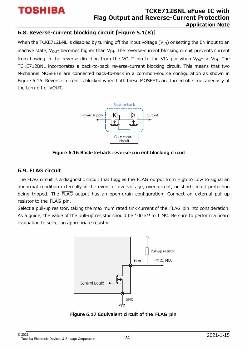
from flowing in the reverse direction from the VOUT pin to the VIN pin when VOUT > VIN. The TCKE712BNL incorporates a back-to-back reverse-current blocking circuit. This means that two N-channel MOSFETs are connected back-to-back in a common-source configuration as shown in Figure 6.16. Reverse current is blocked when both these MOSFETs are turned off simultaneously at the turn-off of VOUT.
Figure 6.16 Back-to-back reverse-current blocking circuit
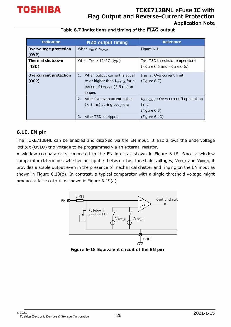
6.9. FLAG circuit The FLAG circuit is a diagnostic circuit that toggles the FLAG�������� output from High to Low to signal an abnormal condition externally in the event of overvoltage, overcurrent, or short-circuit protection being tripped. The FLAG�������� output has an open-drain configuration. Connect an external pull-up resistor to the FLAG�������� pin. Select a pull-up resistor, taking the maximum rated sink current of the FLAG�������� pin into consideration. As a guide, the value of the pull-up resistor should be 100 kΩ to 1 MΩ. Be sure to perform a board evaluation to select an appropriate resistor.
Figure 6.17 Equivalent circuit of the FLAG�������� pin
TCKE712BNL eFuse IC with Flag Output and Reverse-Current Protection
Application Note
2021-1-15 25 © 2021
Toshiba Electronic Devices & Storage Corporation
Table 6.7 Indications and timing of the FLAG�������� output
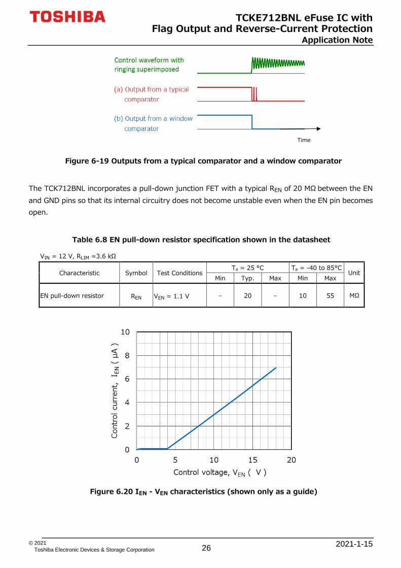
6.10. EN pin The TCKE712BNL can be enabled and disabled via the EN input. It also allows the undervoltage lockout (UVLO) trip voltage to be programmed via an external resistor. A window comparator is connected to the EN input as shown in Figure 6.18. Since a window comparator determines whether an input is between two threshold voltages, VREP_P and VREF_N, it provides a stable output even in the presence of mechanical chatter and ringing on the EN input as shown in Figure 6.19(b). In contrast, a typical comparator with a single threshold voltage might produce a false output as shown in Figure 6.19(a).
Figure 6-18 Equivalent circuit of the EN pin
Indication FLAG�������� output timing Reference
Overvoltage protection (OVP)
When VIN ≥ VOVLO Figure 6.4
Thermal shutdown (TSD)
When TSD ≥ 134°C (typ.) TSD: TSD threshold temperature (Figure 6.5 and Figure 6.6.)
Overcurrent protection (OCP)
1. When output current is equal to or higher than IOUT_CL for a period of tFALblank (5.5 ms) or longer.
IOUT_CL: Overcurrent limit (Figure 6.7)
2. After five overcurrent pulses (< 5 ms) during tOCP_COUNT
tOCP_COUNT: Overcurrent flag-blanking time (Figure 6.8)
3. After TSD is tripped (Figure 6.13)
TCKE712BNL eFuse IC with Flag Output and Reverse-Current Protection
Application Note
2021-1-15 26 © 2021
Toshiba Electronic Devices & Storage Corporation
Figure 6-19 Outputs from a typical comparator and a window comparator
The TCK712BNL incorporates a pull-down junction FET with a typical REN of 20 MΩ between the EN and GND pins so that its internal circuitry does not become unstable even when the EN pin becomes open.
Table 6.8 EN pull-down resistor specification shown in the datasheet
VIN = 12 V, RLIM =3.6 kΩ
Characteristic Symbol Test Conditions Ta = 25 °C Ta = -40 to 85°C
Unit Min Typ. Max Min Max
EN pull-down resistor REN VEN = 1.1 V – 20 – 10 55 MΩ
Figure 6.20 IEN - VEN characteristics (shown only as a guide)
Time
TCKE712BNL eFuse IC with Flag Output and Reverse-Current Protection
Application Note
2021-1-15 27 © 2021
Toshiba Electronic Devices & Storage Corporation
7. Examples of controlling the TCKE712BNL via the EN input This section shows several examples of how to control the TCKE712BNL via the EN input.
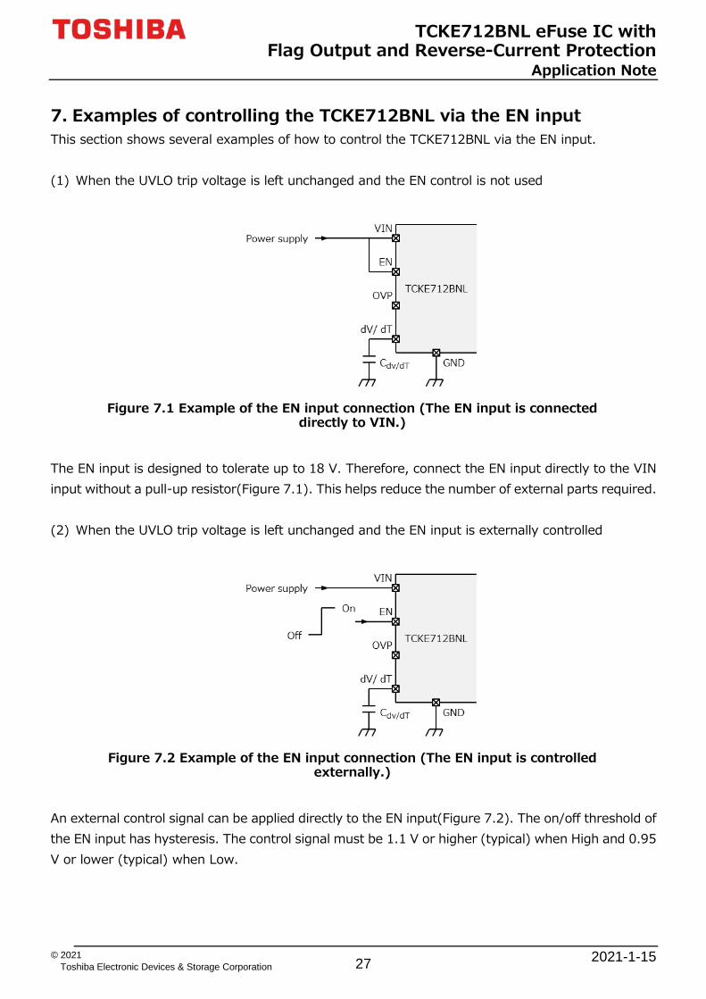
(1) When the UVLO trip voltage is left unchanged and the EN control is not used
Figure 7.1 Example of the EN input connection (The EN input is connected directly to VIN.)
The EN input is designed to tolerate up to 18 V. Therefore, connect the EN input directly to the VIN input without a pull-up resistor(Figure 7.1). This helps reduce the number of external parts required.
(2) When the UVLO trip voltage is left unchanged and the EN input is externally controlled
Figure 7.2 Example of the EN input connection (The EN input is controlled externally.)
An external control signal can be applied directly to the EN input(Figure 7.2). The on/off threshold of the EN input has hysteresis. The control signal must be 1.1 V or higher (typical) when High and 0.95 V or lower (typical) when Low.
TCKE712BNL eFuse IC with Flag Output and Reverse-Current Protection
Application Note
2021-1-15 28 © 2021
Toshiba Electronic Devices & Storage Corporation
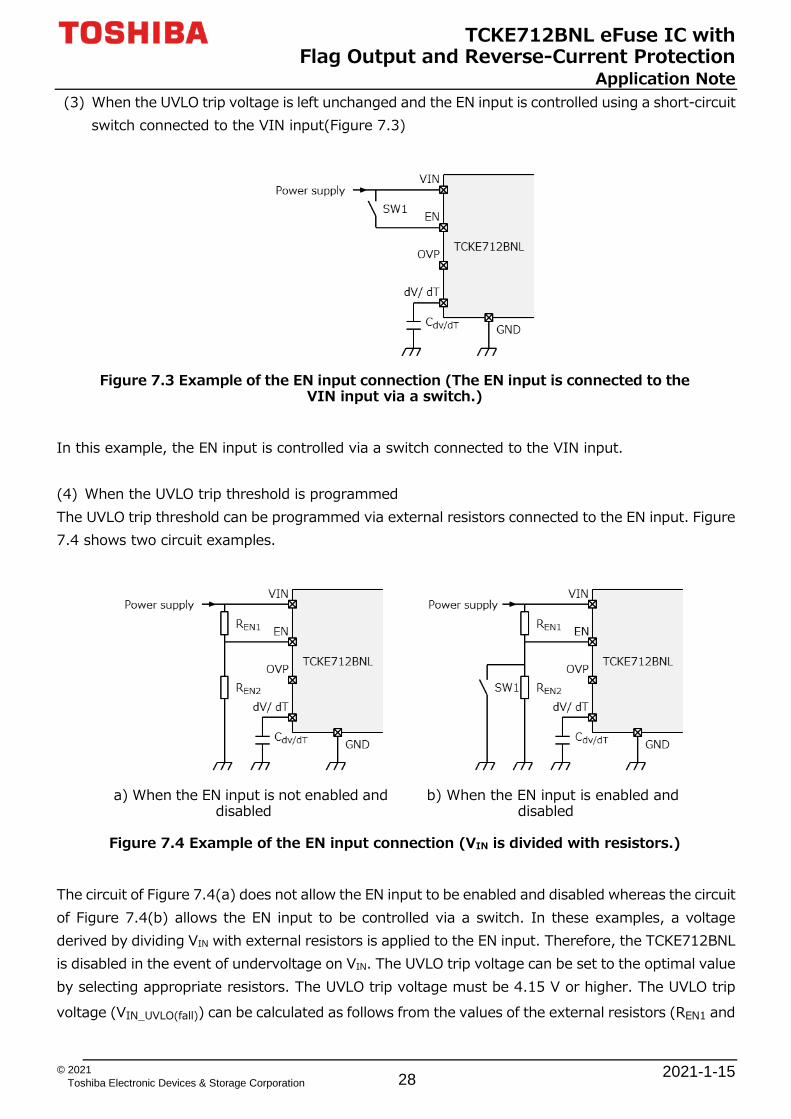
(3) When the UVLO trip voltage is left unchanged and the EN input is controlled using a short-circuit switch connected to the VIN input(Figure 7.3)
Figure 7.3 Example of the EN input connection (The EN input is connected to the VIN input via a switch.)
In this example, the EN input is controlled via a switch connected to the VIN input.
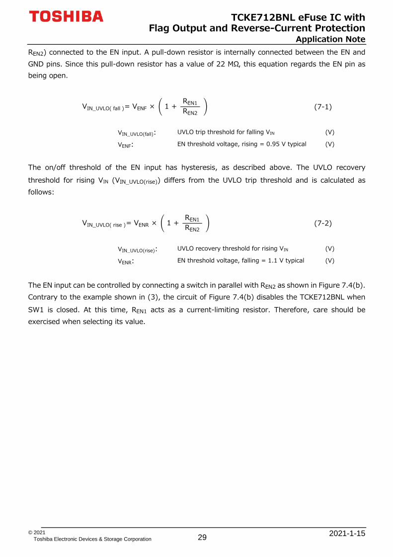
(4) When the UVLO trip threshold is programmed The UVLO trip threshold can be programmed via external resistors connected to the EN input. Figure 7.4 shows two circuit examples.
a) When the EN input is not enabled and disabled
b) When the EN input is enabled and disabled
Figure 7.4 Example of the EN input connection (VIN is divided with resistors.)
The circuit of Figure 7.4(a) does not allow the EN input to be enabled and disabled whereas the circuit of Figure 7.4(b) allows the EN input to be controlled via a switch. In these examples, a voltage derived by dividing VIN with external resistors is applied to the EN input. Therefore, the TCKE712BNL is disabled in the event of undervoltage on VIN. The UVLO trip voltage can be set to the optimal value by selecting appropriate resistors. The UVLO trip voltage must be 4.15 V or higher. The UVLO trip voltage (VIN_UVLO(fall)) can be calculated as follows from the values of the external resistors (REN1 and
TCKE712BNL eFuse IC with Flag Output and Reverse-Current Protection
Application Note
2021-1-15 29 © 2021
Toshiba Electronic Devices & Storage Corporation
REN2) connected to the EN input. A pull-down resistor is internally connected between the EN and GND pins. Since this pull-down resistor has a value of 22 MΩ, this equation regards the EN pin as being open.
VIN_UVLO( fall )= VENF × � 1 + REN1 REN2
� (7-1)
VIN_UVLO(fall): UVLO trip threshold for falling VIN (V)
VENF: EN threshold voltage, rising = 0.95 V typical (V)
The on/off threshold of the EN input has hysteresis, as described above. The UVLO recovery threshold for rising VIN (VIN_UVLO(rise)) differs from the UVLO trip threshold and is calculated as follows:
VIN_UVLO( rise )= VENR × � 1 + REN1 REN2
� (7-2)
VIN_UVLO(rise): UVLO recovery threshold for rising VIN (V)
VENR: EN threshold voltage, falling = 1.1 V typical (V)
The EN input can be controlled by connecting a switch in parallel with REN2 as shown in Figure 7.4(b). Contrary to the example shown in (3), the circuit of Figure 7.4(b) disables the TCKE712BNL when SW1 is closed. At this time, REN1 acts as a current-limiting resistor. Therefore, care should be exercised when selecting its value.

TCKE712BNL eFuse IC with Flag Output and Reverse-Current Protection
Application Note
2021-1-15 30 © 2021
Toshiba Electronic Devices & Storage Corporation
8. TCKE712BNL application examples This section shows several application examples for the TCKE712BNL.
Notebook PCs and mobile devices
Figure 8.1 Application to notebook PCs and mobile devices
SSDs and HDDs
Figure 8.2 Application to SSDs and HDDs
Servers
Figure 8.3 Application to servers
TCKE712BNL eFuse IC with Flag Output and Reverse-Current Protection
Application Note
2021-1-15 31 © 2021
Toshiba Electronic Devices & Storage Corporation
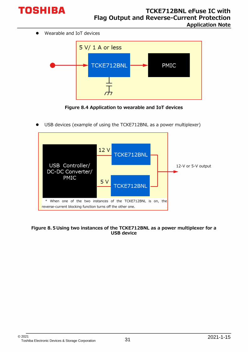
Wearable and IoT devices
Figure 8.4 Application to wearable and IoT devices
USB devices (example of using the TCKE712BNL as a power multiplexer)
Figure 8.5Using two instances of the TCKE712BNL as a power multiplexer for a USB device
* When one of the two instances of the TCKE712BNL is on, the reverse-current blocking function turns off the other one.
12-V or 5-V output
TCKE712BNL eFuse IC with Flag Output and Reverse-Current Protection
Application Note
2021-1-15 32 © 2021
Toshiba Electronic Devices & Storage Corporation
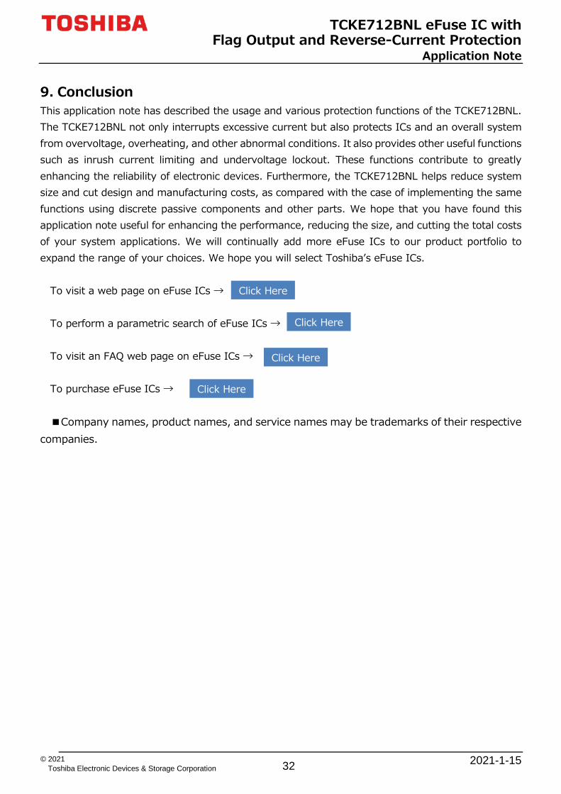
9. Conclusion This application note has described the usage and various protection functions of the TCKE712BNL. The TCKE712BNL not only interrupts excessive current but also protects ICs and an overall system from overvoltage, overheating, and other abnormal conditions. It also provides other useful functions such as inrush current limiting and undervoltage lockout. These functions contribute to greatly enhancing the reliability of electronic devices. Furthermore, the TCKE712BNL helps reduce system size and cut design and manufacturing costs, as compared with the case of implementing the same functions using discrete passive components and other parts. We hope that you have found this application note useful for enhancing the performance, reducing the size, and cutting the total costs of your system applications. We will continually add more eFuse ICs to our product portfolio to expand the range of your choices. We hope you will select Toshiba’s eFuse ICs.
To visit a web page on eFuse ICs → To perform a parametric search of eFuse ICs → To visit an FAQ web page on eFuse ICs → To purchase eFuse ICs → ■Company names, product names, and service names may be trademarks of their respective
companies.
Click Here
Click Here
Click Here
Click Here
TCKE712BNL eFuse IC with Flag Output and Reverse-Current Protection
Application Note
2021-1-15 33 © 2021
Toshiba Electronic Devices & Storage Corporation
RESTRICTIONS ON PRODUCT USE Toshiba Corporation and its subsidiaries and affiliates are collectively referred to as “TOSHIBA”. Hardware, software and systems described in this document are collectively referred to as “Product”.
• TOSHIBA reserves the right to make changes to the information in this document and related Product without notice.
• This document and any information herein may not be reproduced without prior written permission from TOSHIBA. Even with TOSHIBA's written permission, reproduction is permissible only if reproduction is without alteration/omission.
• Though TOSHIBA works continually to improve Product's quality and reliability, Product can malfunction or fail. Customers are responsible for complying with safety standards and for providing adequate designs and safeguards for their hardware, software and systems which minimize risk and avoid situations in which a malfunction or failure of Product could cause loss of human life, bodily injury or damage to property, including data loss or corruption. Before customers use the Product, create designs including the Product, or incorporate the Product into their own applications, customers must also refer to and comply with (a) the latest versions of all relevant TOSHIBA information, including without limitation, this document, the specifications, the data sheets and application notes for Product and the precautions and conditions set forth in the "TOSHIBA Semiconductor Reliability Handbook" and (b) the instructions for the application with which the Product will be used with or for. Customers are solely responsible for all aspects of their own product design or applications, including but not limited to (a) determining the appropriateness of the use of this Product in such design or applications; (b) evaluating and determining the applicability of any information contained in this document, or in charts, diagrams, programs, algorithms, sample application circuits, or any other referenced documents; and (c) validating all operating parameters for such designs and applications. TOSHIBA ASSUMES NO LIABILITY FOR CUSTOMERS' PRODUCT DESIGN OR APPLICATIONS.
• PRODUCT IS NEITHER INTENDED NOR WARRANTED FOR USE IN EQUIPMENTS OR SYSTEMS THAT REQUIRE EXTRAORDINARILY HIGH LEVELS OF QUALITY AND/OR RELIABILITY, AND/OR A MALFUNCTION OR FAILURE OF WHICH MAY CAUSE LOSS OF HUMAN LIFE, BODILY INJURY, SERIOUS PROPERTY DAMAGE AND/OR SERIOUS PUBLIC IMPACT ("UNINTENDED USE"). Except for specific applications as expressly stated in this document, Unintended Use includes, without limitation, equipment used in nuclear facilities, equipment used in the aerospace industry, lifesaving and/or life supporting medical equipment, equipment used for automobiles, trains, ships and other transportation, traffic signaling equipment, equipment used to control combustions or explosions, safety devices, elevators and escalators, and devices related to power plant. IF YOU USE PRODUCT FOR UNINTENDED USE, TOSHIBA ASSUMES NO LIABILITY FOR PRODUCT. For details, please contact your TOSHIBA sales representative or contact us via our website.
• Do not disassemble, analyze, reverse-engineer, alter, modify, translate or copy Product, whether in whole or in part.
• Product shall not be used for or incorporated into any products or systems whose manufacture, use, or sale is prohibited under any applicable laws or regulations.
• The information contained herein is presented only as guidance for Product use. No responsibility is assumed by TOSHIBA for any infringement of patents or any other intellectual property rights of third parties that may result from the use of Product. No license to any intellectual property right is granted by this document, whether express or implied, by estoppel or otherwise.
• ABSENT A WRITTEN SIGNED AGREEMENT, EXCEPT AS PROVIDED IN THE RELEVANT TERMS AND CONDITIONS OF SALE FOR PRODUCT, AND TO THE MAXIMUM EXTENT ALLOWABLE BY LAW, TOSHIBA (1) ASSUMES NO LIABILITY WHATSOEVER, INCLUDING WITHOUT LIMITATION, INDIRECT, CONSEQUENTIAL, SPECIAL, OR INCIDENTAL DAMAGES OR LOSS, INCLUDING WITHOUT LIMITATION, LOSS OF PROFITS, LOSS OF OPPORTUNITIES, BUSINESS INTERRUPTION AND LOSS OF DATA, AND (2) DISCLAIMS ANY AND ALL EXPRESS OR IMPLIED WARRANTIES AND CONDITIONS RELATED TO SALE, USE OF PRODUCT, OR INFORMATION, INCLUDING WARRANTIES OR CONDITIONS OF MERCHANTABILITY, FITNESS FOR A PARTICULAR PURPOSE, ACCURACY OF INFORMATION, OR NONINFRINGEMENT.
• Do not use or otherwise make available Product or related software or technology for any military purposes, including without limitation, for the design, development, use, stockpiling or manufacturing of nuclear, chemical, or biological weapons or missile technology products (mass destruction weapons). Product and related software and technology may be controlled under the applicable export laws and regulations including, without limitation, the Japanese Foreign Exchange and Foreign Trade Law and the U.S. Export Administration Regulations. Export and re-export of Product or related software or technology are strictly prohibited except in compliance with all applicable export laws and regulations.
• Please contact your TOSHIBA sales representative for details as to environmental matters such as the RoHS compatibility of Product. Please use Product in compliance with all applicable laws and regulations that regulate the inclusion or use of controlled substances, including without limitation, the EU RoHS Directive. TOSHIBA ASSUMES NO LIABILITY FOR DAMAGES OR LOSSES OCCURRING AS A RESULT OF NONCOMPLIANCE WITH APPLICABLE LAWS AND REGULATIONS.
https://toshiba.semicon-storage.com/


![pkS/ kjh j.kchj flag fo'ofo|ky;]thUn - CRSU](https://static.fdokumen.com/doc/165x107/63355175d2b728420307dd5d/pks-kjh-jkchj-flag-foofokythun-crsu.jpg)

