Tailoring Rational Manufacturing of Extemporaneous ... - MDPI
Upload
independentCategory
view
4download
0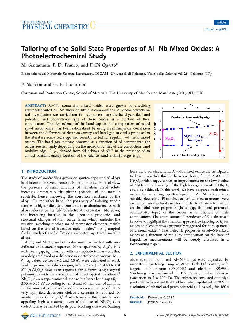
Tailoring of the Solid State Properties of Al!Nb Mixed Oxides: APhotoelectrochemical StudyM. Santamaria, F. Di Franco, and F. Di Quarto*
Electrochemical Materials Science Laboratory, DICAM- Universita ̀ di Palermo, Viale delle Scienze 90128- Palermo (IT)
P. Skeldon and G. E. Thompson
Corrosion and Protection Centre, School of Materials, The University of Manchester, Manchester, M13 9PL, U.K.
ABSTRACT: Al!Nb containing mixed oxides were grown by anodizingsputter-deposited Al!Nb alloys of different compositions. A photoelectrochem-ical investigation was carried out in order to estimate the band gap, flat bandpotential, and conductivity type of these oxides as a function of theircomposition. The dependence of the band gap on the composition of mixedsp!d metal oxides has been rationalized by using a semiempirical correlationbetween the difference of electronegativity and band gap of oxides proposed inthe literature some years ago and recently tested for regular d!d metal mixedoxides. The band gap increase observed as a function of Al content into theoxides seems mainly depending on the monotonic shift of the conduction bandmobility edge, ECBM, derived from 5d orbitals of Nb5+ in the presence of analmost constant energy location of the valence band mobility edge, EVBM.
1. INTRODUCTIONThe study of anodic films grown on sputter-deposited Al alloysis of interest for several reasons. From a practical point of view,the presence of small amounts of transition metal soluteincreases dramatically the pitting potential of the metallicsubstrate, hence improving the corrosion resistance of thealloy.1 On the other hand, the possibility of tailoring anodicfilms with higher dielectric constants than alumina makes suchalloys relevant to the field of electrolytic capacitors. Moreover,the increasing interest in the electronic properties andstructural changes of thin oxide films, which underlie theresistive switching mechanism of memristor elements, mainlybased on the use of transition-metal oxides,2 has promptedfurther study of anodic films on magnetron-sputtered metallicalloys.Al2O3 and Nb2O5 are both valve metal oxides but with very
different solid state properties. More specifically, Al2O3 is awide band gap, Eg, insulator with an amphoteric character, thatis widely employed as a dielectric in electrolytic capacitors (! "9). Eg values between 6.2 and 8.0 eV were calculated in ref 3,while experimental values ranging from 7.2 eV ("-Al2O3) to 8.8eV (#-Al2O3) have been reported for different single crystalpolymorphs with the assumption of direct optical transitions.4
Nb2O5 is an n-type semiconductor with a lower band gap (Eg "3.35 ± 0.05 eV according to refs 5 and 6) than that of alumina.Furthermore, it is chemically stable over a wide range of pH. Avery high, field-dependent dielectric constant is reported foranodic niobia (! " 57),6!8 which makes this oxide a veryappealing high k material, even if the use of Nb2O5 as adielectric may be limited by its poor blocking character. Starting
from these considerations, Al!Nb mixed oxides are anticipatedto have properties that lie between those of pure Al2O3 andNb2O5, which suggests that an improvement on the low ! valueof Al2O3 and a lowering of the high leakage current of Nb2O5could be achieved. In this work, we have prepared such mixedoxides by anodizing sputter-deposited Al!Nb alloys in asuitable electrolyte. Photoelectrochemical measurements werecarried out on anodized samples in order to obtain informationon the solid state properties (band gap, flat band potential,conductivity type) of the oxides as a function of theircompositions. The compositional dependence of Eg is discussedin order to highlight the chemical approach to tailoring of Eg foroxides on alloys that was previously suggested for pure sp metalor d metal oxides.9 The dielectric properties of Al!Nb mixedoxides as a function of the alloy composition on the base ofimpedance measurements will be deeply discussed in aforthcoming paper.
2. EXPERIMENTAL SECTIONAluminum, niobium, and Al!Nb alloys were deposited bymagnetron sputtering using an Atom Tech Ltd. system, withtargets of aluminum (99.999%) and niobium (99.9%).Sputtering was performed in 0.5 Pa argon after previousevacuation to 5 ! 10!5 Pa. The substrates consisted of a highpurity aluminum sheet that had been electropolished at 20 V ina solution of ethanol and perchloric acid (4:1 by vol.) for 180 s
Received: December 6, 2012Revised: January 25, 2013
Article
pubs.acs.org/JPCC
© XXXX American Chemical Society A dx.doi.org/10.1021/jp312008m | J. Phys. Chem. C XXXX, XXX, XXX!XXX
at 283 K. Al!Nb alloys, containing 9, 11, 21, 40, 55, 66, 81, 85,and 92 atom % niobium, were prepared. The composition ofthe alloys was determined by Rutherford backscatteringspectroscopy (RBS), performed using 2.0 MeV He+ ionssupplied by the Van de Graaff accelerator of the University ofParis. The scattered ions were detected at 165° to the directionof the incident beam. Data were interpreted by the RUMPprogram. The deposited layers were anodized to 9 V (SCE) at100 mV s!1 in 0.1 mol dm!3 ammonium pentaborateelectrolyte (ABE, pH " 8.5) at room temperature. At thispH and temperature, both Al2O3 and Nb2O5 are reported to bethermodynamically stable according to the Pourbaix diagramsfor the Al!H2O and Nb!H2O systems.10 According totransmission electron micrographs of ultramicrotomed sec-tions,11 the anodic films formed on the alloys are amorphous.The experimental setup for the photoelectrochemical
measurements has been described elsewhere.12 A 450 WUV!vis xenon lamp, coupled with a monochromator, allowsirradiation of the specimen through a quartz window. A two-phase, lock-in amplifier, with a mechanical chopper, enablesseparation of the photocurrent from the total current in the cell.The photocurrent spectra are corrected for the relative photonefficiency of the light source at each wavelength, so that thephotocurrent yield in arbitrary current units is represented onthe y-axis. A saturated calomel electrode (0 V vs SCE = 0.24 Vvs SHE) was employed as a reference electrode for allelectrochemical and photoelectrochemical experiments.
3. RESULTSWith the exception of the anodic films on the Al-9 atom % Nband Al-11 atom % Nb alloys, all other investigated oxidesproved to be photoactive. The measured photocurrent yields(Iph), corrected for the efficiency of the lamp!monochromatorsystem,12 which are assumed to be proportional to the lightabsorption coefficient, are strongly dependent on the Nbcontents of the base alloys, with Iph increasing as the mixedoxides become richer in niobium. For a photon energy in thevicinity of the band gap, the following equation holds:
ν ν∝ −I h h E( ) ( )nph g (1)
in which h$ is the photon energy, Eg is the optical band gap,and the exponent, n, is 0.5 for indirect (nondirect foramorphous materials) optical transitions.13 As shown in Figure1 for the anodic film grown on Al-21 atom % Nb, the opticalband gap of the investigated oxides can be estimated byextrapolating to zero the (Iphh$)
0.5 vs h$ plot (Eg = 4.11 eV).For the oxide on this alloy, as well as for those grown on
alloys with Nb contents #55 atom %, an exponential decreasein the photocurrent yield (Urbach tail) as a function of photonenergy is observed at photon energies lower than the mobilitygap (Figure 1c). As already found for several anodic films onvalve metals and valve metal alloys,14 a possible origin of thetrend is the variation of the light absorption coefficientaccording to the following law:
α α ν= − −⎛⎝⎜
⎞⎠⎟
E hE
exp00
U (2)
in which #0 is a constant and EU is a measure of the width ofthe band tails, i.e., the extent of density of state localization nearthe band edge. This relationship has been rationalized in thecase of amorphous semiconductors (a-SCs) by assuming anexponential distribution of localized states in the band edge
tails.13 In this case, E0 marks the energy where ln # vs h$(Urbach plot) ceases to be linear and its value frequentlycoincides with the mobility gap of the material. An E0 valueslightly higher ("4.22 eV) than the mobility gap (4.11 eV) wasestimated according to eq 2.Figure 2 displays the (Iphh$)
0.5 vs h$ plots relating to anodicfilms with different Nb contents. The estimated Eg values showthat the optical band gap monotonically changes between thevalues estimated for the pure oxides (see Table 1). This finding
Figure 1. (a) Raw photocurrent spectrum relating to anodic filmsgrown to 9 V/SCE on Al-21 atom % Nb alloy, recorded by polarizingthe electrodes at 5 V/SCE in 0.1 M ABE. (b) Band gap estimate byassuming nondirect optical transitions. (c) Urbach plot.
Figure 2. Band gap estimate by assuming nondirect optical transitionsrelating to anodic films grown to 9 V/SCE on (a) Al-40 atom % Nb,(b) Al-55 atom % Nb, (c) Al-85 atom % Nb, and (d) Al-92 atom %Nb alloys, recorded by polarizing the electrodes at 5 V/SCE in 0.1 MABE.
The Journal of Physical Chemistry C Article
dx.doi.org/10.1021/jp312008m | J. Phys. Chem. C XXXX, XXX, XXX!XXXB
suggests that it is possible to tailor the band gap of an anodicoxide by properly selecting the composition of the base alloy.The photocurrent vs potential curves (photocharacteristics)
were recorded by scanning the electrode potential at 10 mV s!1
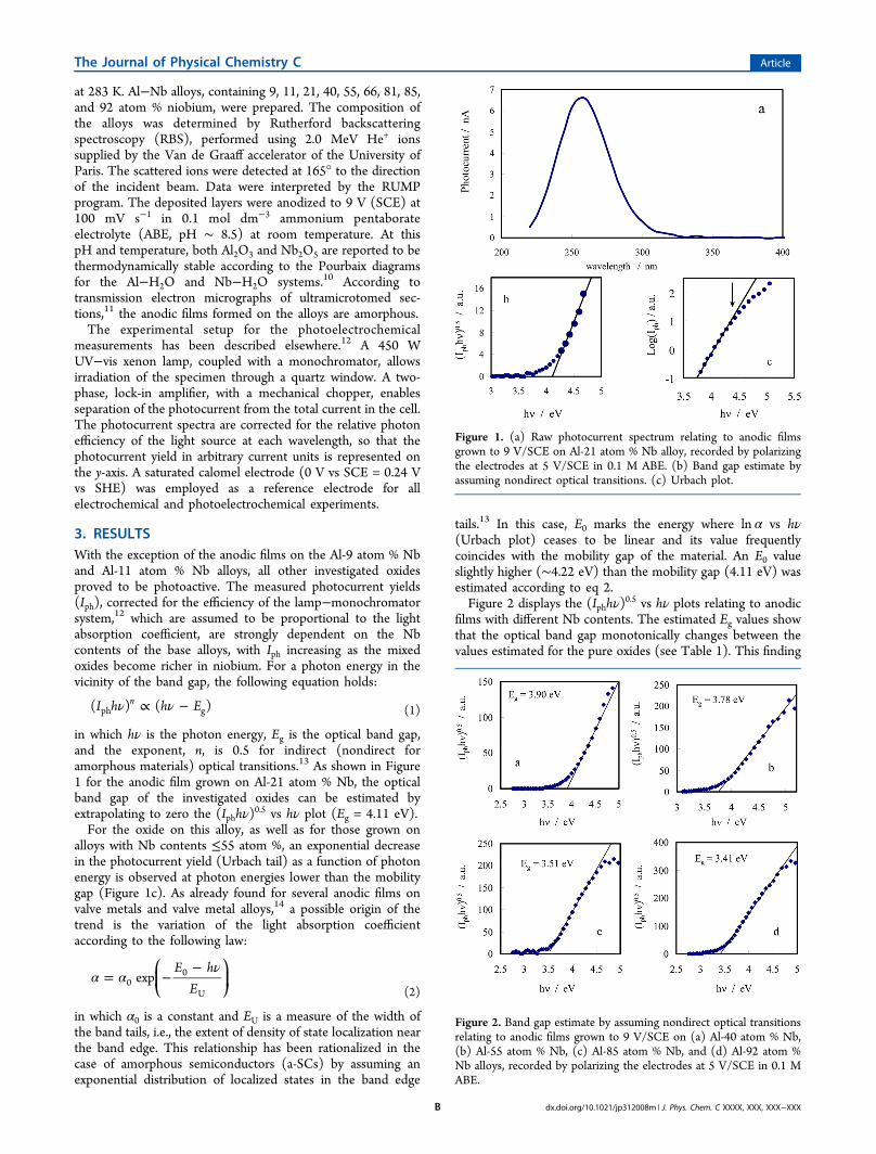
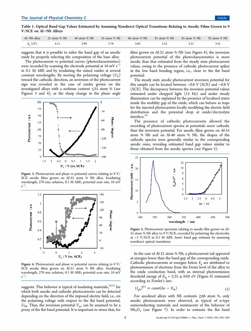
in 0.1 M ABE and by irradiating the mixed oxides at severalconstant wavelengths. By moving the polarizing voltage (UE)toward the cathodic direction, an inversion of the photocurrentsign was revealed in the case of oxides grown on theinvestigated alloys with a niobium content #55 atom % (seeFigures 3 and 4), as the sharp change in the phase angle
suggests. This behavior is typical of insulating materials,14,15 forwhich both anodic and cathodic photocurrents can be detecteddepending on the direction of the imposed electric field, i.e., onthe polarizing voltage with respect to the flat band potential,UFB. Thus, the inversion potential Vinv can be assumed to be aproxy of the flat band potential. It is important to stress that, for
films grown on Al-21 atom % Nb (see Figure 4), the inversionphotocurrent potential of the photocharacteristics is moreanodic than that estimated from the steady state photocurrentvalues, owing to the presence of cathodic photocurrent spikesin the low band bending region, i.e., close to the flat bandpotential.The steady state anodic photocurrent inversion potential for
this sample can be located between !0.6 V (SCE) and !0.8 V(SCE). The discrepancy between the inversion potential valuesestimated under chopped light (13 Hz) and under steadyillumination can be explained by the presence of localized statesinside the mobility gap of the oxide, which can behave as trapsfor the injected photocarriers locally modifying the electric fielddistribution and the potential drop at oxide/electrolyteinterface.16
The presence of cathodic photocurrents allowed therecording of photocurrent spectra at potentials more cathodicthan the inversion potential. For anodic films grown on Al-55atom % Nb and on Al-40 atom % Nb, the shapes of thecathodic spectra were generally similar to the correspondinganodic ones, revealing estimated band gap values similar tothose obtained from the anodic spectra (see Figure 5).
In the case of Al-21 atom % Nb, a photocurrent tail appearedat energies lower than the band gap of the corresponding oxide.Cathodic photocurrents at energies below Eg are attributed tophotoemission of electrons from the Fermi level of the alloy tothe oxide conduction band, with an internal photoemissionthreshold energy of Eth = 2.25 ± 0.05 eV (Figure 6) estimatedaccording to Fowler’s law:
ν= −I h E( ) const( )ph0.5
th (3)
For anodized alloys with Nb contents $66 atom %, onlyanodic photocurrents were observed, as typical of n-typesemiconducting materials and reminiscent of the behavior ofNb2O5 (see Figure 7). In order to estimate the flat band
Table 1. Optical Band Gap Values Estimated by Assuming Nondirect Optical Transitions Relating to Anodic Films Grown to 9V/SCE on Al!Nb Alloys
Al!Nb alloy 21 atom % Nb 40 atom % Nb 55 atom % Nb 66 atom % Nb 81 atom % Nb 85 atom % Nb 92 atom % Nb
Eg (eV) 4.11 3.90 3.78 3.64 3.52 3.51 3.41
Figure 3. Photocurrent and phase vs potential curves relating to 9 V/SCE anodic films grown on Al-55 atom % Nb alloy. Irradiatingwavelength, 270 nm; solution, 0.1 M ABE; potential scan rate, 10 mVs!1.
Figure 4. Photocurrent and phase vs potential curves relating to 9 V/SCE anodic films grown on Al-21 atom % Nb alloy. Irradiatingwavelength, 270 nm; solution, 0.1 M ABE; potential scan rate, 10 mVs!1.
Figure 5. Photocurrent spectrum relating to anodic film grown on Al-55 atom % Nb alloy to 9 V/SCE, recorded by polarizing the electrodesat !1 V/SCE in 0.1 M ABE. Inset: band gap estimate by assumingnondirect optical transitions.
The Journal of Physical Chemistry C Article
dx.doi.org/10.1021/jp312008m | J. Phys. Chem. C XXXX, XXX, XXX!XXXC

potential of these oxides, the photocharacteristics were fittedaccording to a power law, (Iph)
n % UE, and a UFB coincidentwith the extrapolated potential of zero photocurrent, V*, wasassumed (see the Discussion section and ref 12). The values ofn and V* obtained at each wavelength are reported in Table 2.According to the data, the V* values are not strongly dependenton the oxide composition. The zero photocurrent potentials,estimated for all the investigated alloys, displayed at constant
wavelength (% = 320 nm), a V* value slightly decreasing withdecreasing Nb content, reaching a value of !0.87 V(SCE) forthe anodic films grown on alloys with Nb content equal to 66atom %.The disclosed linear or supralinear behavior (n < 1) over a
large potential range, as well as the dependence of n on thewavelength, has been attributed to the presence of initial(geminate) recombination effects of injected photocarriers.Geminate recombination can occur if the thermalization lengthof the photogenerated electron!hole pairs is too short toprevent recombination of photocarriers during the thermal-ization process of injected photocarriers. It is typical of opticaltransitions involving not extended energy levels, owing to alower mobility of electron carriers in localized states.12
4. DISCUSSIONAl2O3 and Nb2O5 mixed oxides represent a very intriguingsystem owing to the distinctly different solid state properties ofthe component oxides. Al2O3 is a wide band gap insulator witha valence band constituted by the occupied O 2p orbitals and aconduction band constituted by the Al 3s!3p empty orbitals,separated by a high energy gap at least $6.2 eV,3,4 while Nb2O5is an n-type semiconductor with a valence band generated bythe (occupied) O 2p orbitals but with a conduction bandcomprising mainly the d orbitals of Nb. A band gap of 3.35 ±0.05 eV is usually reported for anodic Nb2O5.
5,6 The study ofthe photoelectrochemical behavior of anodic films on sputter-deposited Al!Nb alloys of different compositions providedevidence that by increasing the Al content in the base alloy theoptical band gap monotonically increases. Furthermore, achange from n-type semiconducting to insulating oxidebehavior occurs, at a constant final formation voltage, whenthe Al content reaches values of "55 atom %.The mixed oxide composition is directly related to the base
alloy composition and to the migration rates of the metal ions.Al3+ and Nb5+ have transport numbers t > 0 in Al2O3 andNb2O5, respectively (tAl3+ = 0.4 and tNb5+ = 0.23).17 Duringanodizing of Al!Nb alloys, Al3+ and Nb5+ ions migrate towardthe oxide/electrolyte interface at similar rates,11 withsimultaneous migration of O2! toward the metal/oxideinterface. Figure 8 shows the RBS spectra relating to oxidesgrown to 150 V in 0.1 mol dm!3 ABE on Al!Nb alloys with Nbcontents $66 atom %. The niobium contents of the oxides(considering cations only) are close to the contents in thealloys to an accuracy of "1 atom %. Furthermore, a closesimilarity between the compositions of the anodic film and thealloy has also been shown for Al!Nb alloys of lower Nbcontents.11
In previous work,9 a correlation between the optical band gapvalues of crystalline oxides, MxOy, and the square of theelectronegativity difference of their constituents was proposed.Such a correlation was derived by assuming a direct relationbetween the optical band gap and the single M!O bondenergy, using the Pauling equation for the single bond energy.More specifically, Eg
opt was found to depend linearly on thesquare of the difference of electronegativity (Pauling’s scale)between oxygen (&O) and metal (&M), according to thefollowing equation:
χ χ= − +E A B( )gopt
O M2
(4a)
where A and B are determined by best-fitting of theexperimental Eg vs (&O ! &M)
2 data. With the exception of
Figure 6. Photocurrent spectrum relating to anodic film grown on Al-21 atom % Nb alloy to 9 V/SCE, recorded by polarizing the electrodesat !1 V/SCE in 0.1 M ABE. Inset: Fowler plot.
Figure 7. Photocurrent vs potential curves relating to 9 V/SCE anodicfilms grown on Al-66 atom % Nb alloy. Solution: 0.1 M ABE, potentialscan rate 10 mV s!1.
Table 2. Parameters Obtained by Fitting According to PowerLaw, (Iph)
n % UE, the Experimental PhotocharacteristicsRecorded for Anodic Films Grown to 9 V/SCE on Al!NbAlloys, at 10 mV s!1 in 0.1 M ABE
alloy wavelength (nm) n V*/V(SCE)
Al-66 atom % Nb 260 0.975 !0.88290 0.85 !0.88320 0.775 !0.87
Al-85 atom % Nb 260 0.95 !0.81290 0.825 !0.81320 0.80 !0.81
Al-92 atom % Nb 260 1.25 !0.77290 0.875 !0.78320 0.75 !0.79
The Journal of Physical Chemistry C Article
dx.doi.org/10.1021/jp312008m | J. Phys. Chem. C XXXX, XXX, XXX!XXXD

Ni, which followed the sp correlation, the following twoequations were found for sp metal and d metal oxides,respectively,:
sp metal:
χ χ− Δ = − −E E (eV) 2.17( ) 2.71g am M O2
(4b)
d metal:
χ χ− Δ = − −E E (eV) 1.35( ) 1.49g am M O2
(4c)
where ΔEam = 0 for crystalline oxides, while increasing ΔEamvalues have been suggested as the degree of crystallinitydecreases. In the case of mixed oxides, the average single bondenergy is estimated by taking into account the contributions ofboth cations involved in formation of the network. Thus, thesame correlations were extended to the case of mixedamorphous oxides, considering an average cationicelectronegativity, defined as follows:
χ χ χ= +x xi i j jM,av (5)
where i and j refer to the two metals in the “mixed” oxide and xiand xj represent their cationic fractions. Hence, a quadraticdependence of Eg on the oxide composition is predicted. Theextension of eq 4a to sp!d mixed oxides poses the problem ofwhich best-fitting line should be used. The study of the
photoelectrochemical behavior of a large number of mixedoxides14,18!20 allowed the validity of eqs 4a and 4b to be tested,leading to the conclusion that the d metal oxide correlationcould hold for sp!d metal oxides, provided that the percentageof d metal in the film is sufficiently high: a threshold of about21 atom % W was found for Al!W mixed oxides.20
The experimental Eg values are displayed in Figure 9 as afunction of (&M ! &O)
2, assuming &O = 3.5, &Al = 1.50, and &Nb =1.615 (value recently used for Nb in Nb!Ta mixed oxides, ref21) in agreement with the values reported in the Paulingscale.22 In the same figure, the dashed lines corresponding toeqs 4a and 4b are shown. A comparison between theexperimental Eg values and those expected on the basis of thecorrelations shows that values are far from those predicted byeq 4b. In contrast, the experimental Eg differs from the valuesexpected according to eq 4c by an amount which is in a rangeof ΔEam compatible with theoretical expectations.13 Thisfinding suggests that the d!d metals correlation could holdalso for Al!Nb mixed oxides, provided that the percentage of dmetal in the film is higher than or equal to 21 atom %, which isvery close to the value found for photoactive Al!W mixedoxides.20
On the other hand, a careful inspection of Figure 9 revealsthat the experimental points can be fitted satisfactorily by astraight line of slope (2.1451 eV) that is close to that of eq 4b,
Figure 8. RBS spectra relating to anodic films grown to 150 V on (a) Al-66 atom % Nb, (b) Al-85 atom % Nb, and (c) Al-92 atom % Nb.
The Journal of Physical Chemistry C Article
dx.doi.org/10.1021/jp312008m | J. Phys. Chem. C XXXX, XXX, XXX!XXXE
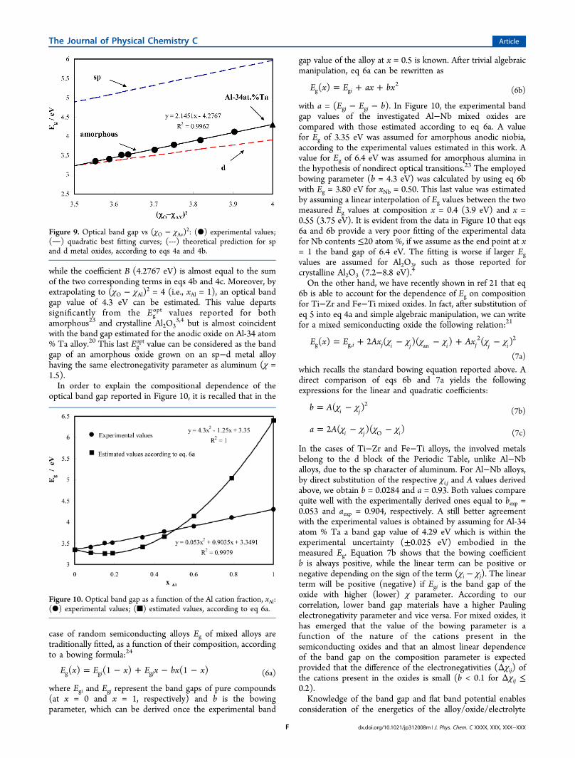
while the coefficient B (4.2767 eV) is almost equal to the sumof the two corresponding terms in eqs 4b and 4c. Moreover, byextrapolating to (&O ! &Al)
2 = 4 (i.e., xAl = 1), an optical bandgap value of 4.3 eV can be estimated. This value departssignificantly from the Eg
opt values reported for bothamorphous23 and crystalline Al2O3
3,4 but is almost coincidentwith the band gap estimated for the anodic oxide on Al-34 atom% Ta alloy.20 This last Eg
opt value can be considered as the bandgap of an amorphous oxide grown on an sp!d metal alloyhaving the same electronegativity parameter as aluminum (& =1.5).In order to explain the compositional dependence of the
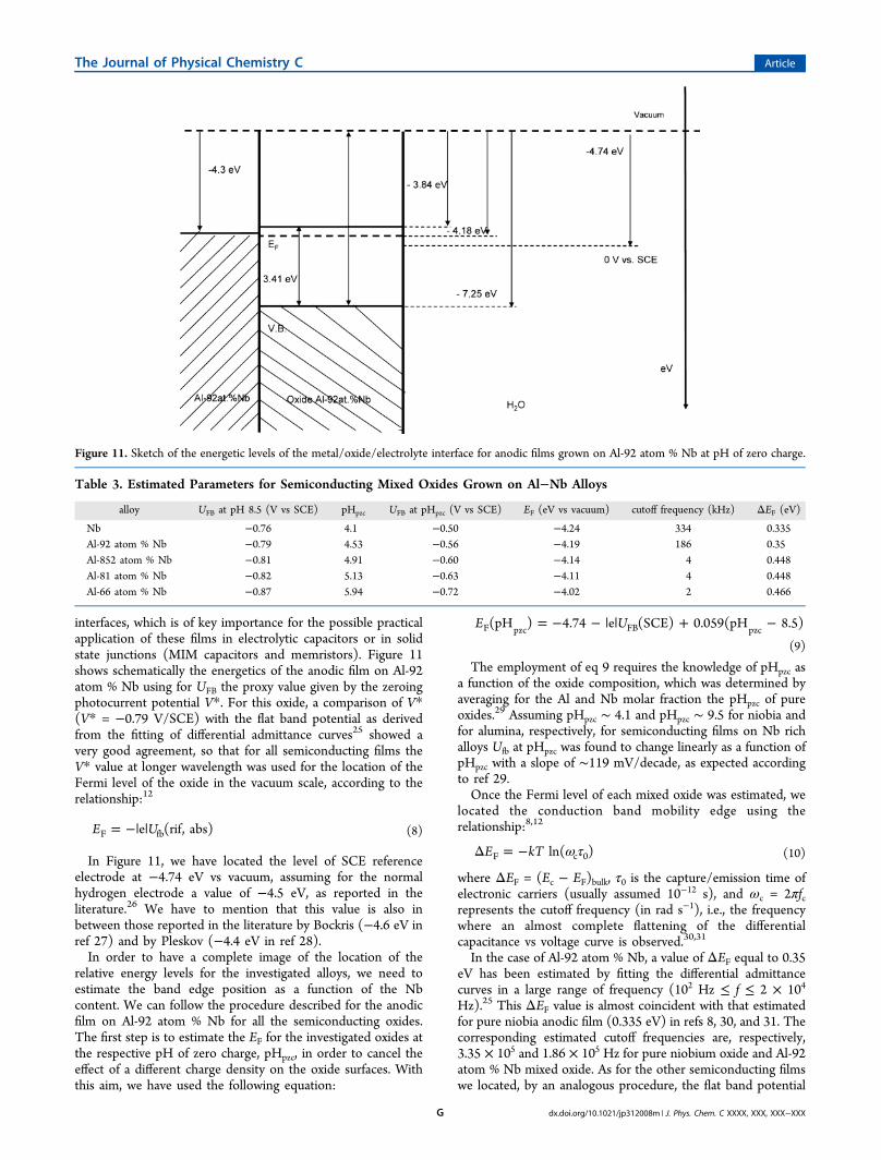
optical band gap reported in Figure 10, it is recalled that in the
case of random semiconducting alloys Eg of mixed alloys aretraditionally fitted, as a function of their composition, accordingto a bowing formula:24
= − + − −E x E x E x bx x( ) (1 ) (1 )i jg g g (6a)
where Egi and Egj represent the band gaps of pure compounds(at x = 0 and x = 1, respectively) and b is the bowingparameter, which can be derived once the experimental band
gap value of the alloy at x = 0.5 is known. After trivial algebraicmanipulation, eq 6a can be rewritten as
= + +E x E ax bx( ) ig g2
(6b)
with a = (Egj ! Egi ! b). In Figure 10, the experimental bandgap values of the investigated Al!Nb mixed oxides arecompared with those estimated according to eq 6a. A valuefor Eg of 3.35 eV was assumed for amorphous anodic niobia,according to the experimental values estimated in this work. Avalue for Eg of 6.4 eV was assumed for amorphous alumina inthe hypothesis of nondirect optical transitions.23 The employedbowing parameter (b = 4.3 eV) was calculated by using eq 6bwith Eg = 3.80 eV for xNb = 0.50. This last value was estimatedby assuming a linear interpolation of Eg values between the twomeasured Eg values at composition x = 0.4 (3.9 eV) and x =0.55 (3.75 eV). It is evident from the data in Figure 10 that eqs6a and 6b provide a very poor fitting of the experimental datafor Nb contents #20 atom %, if we assume as the end point at x= 1 the band gap of 6.4 eV. The fitting is worse if larger Egvalues are assumed for Al2O3, such as those reported forcrystalline Al2O3 (7.2!8.8 eV).4
On the other hand, we have recently shown in ref 21 that eq6b is able to account for the dependence of Eg on compositionfor Ti!Zr and Fe!Ti mixed oxides. In fact, after substitution ofeq 5 into eq 4a and simple algebraic manipulation, we can writefor a mixed semiconducting oxide the following relation:21
χ χ χ χ χ χ= + − − + −E x E Ax Ax( ) 2 ( )( ) ( )i j i j i j j ig g, an2 2
(7a)
which recalls the standard bowing equation reported above. Adirect comparison of eqs 6b and 7a yields the followingexpressions for the linear and quadratic coefficients:
χ χ= −b A( )i j2
(7b)
χ χ χ χ= − −a A2 ( )( )i j iO (7c)
In the cases of Ti!Zr and Fe!Ti alloys, the involved metalsbelong to the d block of the Periodic Table, unlike Al!Nballoys, due to the sp character of aluminum. For Al!Nb alloys,by direct substitution of the respective &i,j and A values derivedabove, we obtain b = 0.0284 and a = 0.93. Both values comparequite well with the experimentally derived ones equal to bexp =0.053 and aexp = 0.904, respectively. A still better agreementwith the experimental values is obtained by assuming for Al-34atom % Ta a band gap value of 4.29 eV which is within theexperimental uncertainty (±0.025 eV) embodied in themeasured Eg. Equation 7b shows that the bowing coefficientb is always positive, while the linear term can be positive ornegative depending on the sign of the term (&i ! &j). The linearterm will be positive (negative) if Egi is the band gap of theoxide with higher (lower) & parameter. According to ourcorrelation, lower band gap materials have a higher Paulingelectronegativity parameter and vice versa. For mixed oxides, ithas emerged that the value of the bowing parameter is afunction of the nature of the cations present in thesemiconducting oxides and that an almost linear dependenceof the band gap on the composition parameter is expectedprovided that the difference of the electronegativities (Δ&ij) ofthe cations present in the oxides is small (b < 0.1 for Δ&ij #0.2).Knowledge of the band gap and flat band potential enables
consideration of the energetics of the alloy/oxide/electrolyte
Figure 9. Optical band gap vs (&O ! &Av)2: (!) experimental values;
() quadratic best fitting curves; (---) theoretical prediction for spand d metal oxides, according to eqs 4a and 4b.
Figure 10. Optical band gap as a function of the Al cation fraction, xAl:(!) experimental values; (") estimated values, according to eq 6a.
The Journal of Physical Chemistry C Article
dx.doi.org/10.1021/jp312008m | J. Phys. Chem. C XXXX, XXX, XXX!XXXF
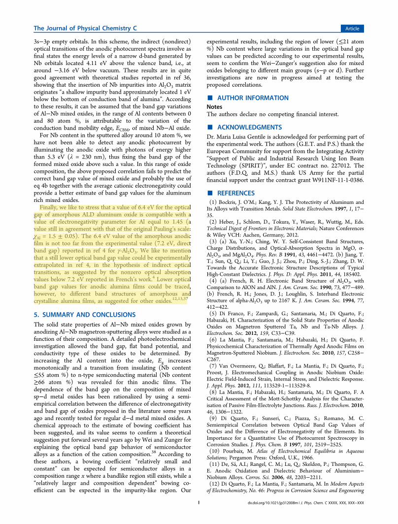
interfaces, which is of key importance for the possible practicalapplication of these films in electrolytic capacitors or in solidstate junctions (MIM capacitors and memristors). Figure 11shows schematically the energetics of the anodic film on Al-92atom % Nb using for UFB the proxy value given by the zeroingphotocurrent potential V*. For this oxide, a comparison of V*(V* = !0.79 V/SCE) with the flat band potential as derivedfrom the fitting of differential admittance curves25 showed avery good agreement, so that for all semiconducting films theV* value at longer wavelength was used for the location of theFermi level of the oxide in the vacuum scale, according to therelationship:12
= −| |E Ue (rif, abs)F fb (8)
In Figure 11, we have located the level of SCE referenceelectrode at !4.74 eV vs vacuum, assuming for the normalhydrogen electrode a value of !4.5 eV, as reported in theliterature.26 We have to mention that this value is also inbetween those reported in the literature by Bockris (!4.6 eV inref 27) and by Pleskov (!4.4 eV in ref 28).In order to have a complete image of the location of the
relative energy levels for the investigated alloys, we need toestimate the band edge position as a function of the Nbcontent. We can follow the procedure described for the anodicfilm on Al-92 atom % Nb for all the semiconducting oxides.The first step is to estimate the EF for the investigated oxides atthe respective pH of zero charge, pHpzc, in order to cancel theeffect of a different charge density on the oxide surfaces. Withthis aim, we have used the following equation:
= − − | | + −E U(pH ) 4.74 e (SCE) 0.059(pH 8.5)F pzc FB pzc
(9)
The employment of eq 9 requires the knowledge of pHpzc asa function of the oxide composition, which was determined byaveraging for the Al and Nb molar fraction the pHpzc of pureoxides.29 Assuming pHpzc " 4.1 and pHpzc " 9.5 for niobia andfor alumina, respectively, for semiconducting films on Nb richalloys Ufb at pHpzc was found to change linearly as a function ofpHpzc with a slope of "119 mV/decade, as expected accordingto ref 29.Once the Fermi level of each mixed oxide was estimated, we
located the conduction band mobility edge using therelationship:8,12
ω τΔ = −E kT ln( )F c 0 (10)
where ΔEF = (Ec ! EF)bulk, '0 is the capture/emission time ofelectronic carriers (usually assumed 10!12 s), and (c = 2)fcrepresents the cutoff frequency (in rad s!1), i.e., the frequencywhere an almost complete flattening of the differentialcapacitance vs voltage curve is observed.30,31
In the case of Al-92 atom % Nb, a value of ΔEF equal to 0.35eV has been estimated by fitting the differential admittancecurves in a large range of frequency (102 Hz # f # 2 ! 104
Hz).25 This ΔEF value is almost coincident with that estimatedfor pure niobia anodic film (0.335 eV) in refs 8, 30, and 31. Thecorresponding estimated cutoff frequencies are, respectively,3.35 ! 105 and 1.86 ! 105 Hz for pure niobium oxide and Al-92atom % Nb mixed oxide. As for the other semiconducting filmswe located, by an analogous procedure, the flat band potential
Figure 11. Sketch of the energetic levels of the metal/oxide/electrolyte interface for anodic films grown on Al-92 atom % Nb at pH of zero charge.
Table 3. Estimated Parameters for Semiconducting Mixed Oxides Grown on Al!Nb Alloys
alloy UFB at pH 8.5 (V vs SCE) pHpzc UFB at pHpzc (V vs SCE) EF (eV vs vacuum) cutoff frequency (kHz) ΔEF (eV)
Nb !0.76 4.1 !0.50 !4.24 334 0.335Al-92 atom % Nb !0.79 4.53 !0.56 !4.19 186 0.35Al-852 atom % Nb !0.81 4.91 !0.60 !4.14 4 0.448Al-81 atom % Nb !0.82 5.13 !0.63 !4.11 4 0.448Al-66 atom % Nb !0.87 5.94 !0.72 !4.02 2 0.466
The Journal of Physical Chemistry C Article
dx.doi.org/10.1021/jp312008m | J. Phys. Chem. C XXXX, XXX, XXX!XXXG

at pHpzc and from the capacitance vs potential curves atdifferent frequencies we estimated the cutoff frequencies ( f " 4kHz and f " 2 kHz for anodic films formed on Al!Nb alloyswith 85 atom % Nb and 66 atom % Nb, respectively) fromwhich the ΔEF values have been derived according to eq 10.25
The results of such calculations are reported in Table 3together with the estimated energy levels ECBM for theconduction band mobility edge in the vacuum scale. By usingthe measured optical band gap, we have been able to locate inthe same scale the EVBM levels of different semiconductingoxides. Since the reported Fermi levels, with respect to thevacuum, for pure Al and Nb are very close (see ref 32), aconstant value (EF = !4.30 eV) was employed for allinvestigated Al!Nb alloys.According to this, an almost constant value of !7.28 ± 0.03
eV is derived for the location of valence band mobility edge ofall semiconducting oxides (see Table 4). Such a value is quite in
agreement with the value reported in the literature for thevalence band edge of transition metal oxides essentially derivedfrom 2p oxygen ion orbitals.14,33,34
As for the anodic oxides formed on Al!Nb alloys with Nbcontent #55 atom %, owing to their insulating nature, thedetermination of cutoff frequency was not accessible in theexploited range of frequency (10 Hz to 20 kHz), so that it wasimpossible to get an estimate of the ΔEF value for these oxides.However, for these insulating oxides, no large differences are
expected in the energy levels of the O 2p orbitals as a functionof Nb content into the mixed oxides in analogy with thatsuggested for other mixed oxides.32 This suggestion issupported by the fact that in the case of Al-34 atom % Ta aninternal photoemission threshold equal to 1.45 eV has beenpreviously reported20 which poses the ECBM energy level of themixed oxide grown on such an alloy at around !2.82 eV if aFermi level of !4.27 eV is assumed for the alloy. According tothis and taking into account the band gap value of 4.30 eV forthe anodic film (see Table 3), we can locate the EVBM of themixed oxide on Al-34 atom % Ta at !7.12 eV below thevacuum level not too far from the value of !7.27 eV estimatedfor the EVBM of the mixed Al!Nb semiconducting oxides. Bytaking into account the experimental uncertainty embodied inthe estimation of the physical quantities like metal workfunction, oxide optical band gap, ΔEF, it seems reasonable toassume an almost constant EVBM level (O 2p valence band ofthe anodic mixed oxides) equal to !7.27 ± 0.2 eV in thevacuum scale also for insulating anodic films grown on Al-55atom % Nb and Al-40 atom % Nb alloys. The values of ECBMfor these oxides reported in Table 4 have been estimatedaccording to this assumption and enabled the schematicrepresentation of the band gap of Figure 12.On the other hand, as for the anodic film on Al-21 atom %
Nb, the conduction band edge, ECBM, can be located at !2.05eV by using the Fowler threshold for the internal electronphotoemission process (Eth = 2.25 eV) reported in Figure 6 andthe value of EF = !4.3 eV assumed for the alloys.However, the location of the valence band edge 4.11 eV (i.e.,
Eg) below the CB band edge of the oxide film causes the energylevel of the O 2p orbitals (with respect to vacuum) to be quitefar (!6.16 eV) from that estimated for oxide grown on Al!Nballoys with Nb $ 40 atom % (!7.27 eV) or on Al-34 atom %Ta (!7.12 eV) alloy. In order to overcome such a discrepancyand by recalling that internal photoemission threshold valuesnear the above-reported one have been measured at the Al/Al2O3 interface for anodic or CVD alumina film,23a,35 wesuggest that the estimated Fowler threshold in Figure 6accounts for an internal photoelectron injection process intothe conduction band levels of anodic alumina generated by Al
Table 4. ECBM and EVBM Values (vs Vacuum) for MixedOxides Grown on Al!Nb Alloys
alloy ECBM (eV vs vacuum) EVBM (eV vs vacuum)
Nb !3.89 !7.24Al-92 atom % Nb !3.84 !7.25Al-852 atom % Nb !3.79 !7.30Al-81 atom % Nb !3.76 !7.28Al-66 atom % Nb !3.67 !7.31Al-55 atom % Nb !3.49 !7.27Al-40 atom % Nb !3.37 !7.27Al-21 atom % Nb !3.16 !7.27Al-34 atom % Ta !2.82 !7.12
Figure 12. Schematic representation of the band edges and niobium alloying states in oxides grown on pure Nb, Al!Nb alloys, and pure Al.
The Journal of Physical Chemistry C Article
dx.doi.org/10.1021/jp312008m | J. Phys. Chem. C XXXX, XXX, XXX!XXXH
3s!3p empty orbitals. In this scheme, the indirect (nondirect)optical transitions of the anodic photocurrent spectra involve asfinal states the energy levels of a narrow d-band generated byNb orbitals located 4.11 eV above the valence band, i.e., ataround !3.16 eV below vacuum. These results are in quitegood agreement with theoretical studies reported in ref 36,showing that the insertion of Nb impurities into Al2O3 matrixoriginates “a shallow impurity band approximately located 1 eVbelow the bottom of conduction band of alumina”. Accordingto these results, it can be assumed that the band gap variationsof Al!Nb mixed oxides, in the range of Al contents between 0and 80 atom %, is attributable to the variation of theconduction band mobility edge, ECBM, of mixed Nb!Al oxide.For Nb content in the sputtered alloy around 10 atom %, we
have not been able to detect any anodic photocurrent byilluminating the anodic oxide with photons of energy higherthan 5.3 eV (% = 230 nm), thus fixing the band gap of theformed mixed oxide above such a value. In this range of oxidecomposition, the above proposed correlation fails to predict thecorrect band gap value of mixed oxide and probably the use ofeq 4b together with the average cationic electronegativity couldprovide a better estimate of band gap values for the aluminumrich mixed oxides.Finally, we like to stress that a value of 6.4 eV for the optical
gap of amorphous ALD aluminum oxide is compatible with avalue of electronegativity parameter for Al equal to 1.45 (avalue still in agreement with that of the original Pauling’s scale:&Al = 1.5 ± 0.05). The 6.4 eV value of the amorphous anodicfilm is not too far from the experimental value (7.2 eV, directband gap) reported in ref 4 for "-Al2O3. We like to mentionthat a still lower optical band gap value could be experimentallyextrapolated in ref 4, in the hypothesis of indirect opticaltransitions, as suggested by the nonzero optical absorptionvalues below 7.2 eV reported in French’s work.4 Lower opticalband gap values for anodic alumina films could be traced,however, to different band structures of amorphous andcrystalline alumina films, as suggested for other oxides.12,13,37
5. SUMMARY AND CONCLUSIONSThe solid state properties of Al!Nb mixed oxides grown byanodizing Al!Nb magnetron-sputtering alloys were studied as afunction of their composition. A detailed photoelectrochemicalinvestigation allowed the band gap, flat band potential, andconductivity type of these oxides to be determined. Byincreasing the Al content into the oxide, Eg increasesmonotonically and a transition from insulating (Nb content#55 atom %) to n-type semiconducting material (Nb content$66 atom %) was revealed for thin anodic films. Thedependence of the band gap on the composition of mixedsp!d metal oxides has been rationalized by using a semi-empirical correlation between the difference of electronegativityand band gap of oxides proposed in the literature some yearsago and recently tested for regular d!d metal mixed oxides. Achemical approach to the estimate of bowing coefficient hasbeen suggested, and its value seems to confirm a theoreticalsuggestion put forward several years ago by Wei and Zunger forexplaining the optical band gap behavior of semiconductoralloys as a function of the cation composition.38 According tothese authors, a bowing coefficient “relatively small andconstant” can be expected for semiconductor alloys in acomposition range x where a bandlike region still exists, while a“relatively larger and composition dependent” bowing co-efficient can be expected in the impurity-like region. Our
experimental results, including the region of lower (#21 atom%) Nb content where large variations in the optical band gapvalues can be predicted according to our experimental results,seem to confirm the Wei!Zunger’s suggestion also for mixedoxides belonging to different main groups (s!p or d). Furtherinvestigations are now in progress aimed at testing theproposed correlations.
! AUTHOR INFORMATIONNotesThe authors declare no competing financial interest.
! ACKNOWLEDGMENTSDr. Maria Luisa Gentile is acknowledged for performing part ofthe experimental work. The authors (G.E.T. and P.S.) thank theEuropean Community for support from the Integrating Activity“Support of Public and Industrial Research Using Ion BeamTechnology (SPIRIT)”, under EC contract no. 227012. Theauthors (F.D.Q. and M.S.) thank US Army for the partialfinancial support under the contract grant W911NF-11-1-0386.
! REFERENCES(1) Bockris, J. O’M.; Kang, Y. J. The Protectivity of Aluminum andIts Alloys with Transition Metals. Solid State Electrochem. 1997, 1, 17!35.(2) Heber, J., Schlom, D., Tokura, Y., Waser, R., Wuttig, M., Eds.Technical Digest of Frontiers in Electronic Materials; Nature Conferences& Wiley VCH: Aachen, Germany, 2012.(3) (a) Xu, Y.-N.; Ching, W. Y. Self-Consistent Band Structures,Charge Distributions, and Optical-Absorption Spectra in MgO, #-Al2O3, and MgAl2O4. Phys. Rev. B 1991, 43, 4461!4472. (b) Jiang, T.T.; Sun, Q. Q.; Li, Y.; Guo, J. J.; Zhou, P.; Ding, S.-J.; Zhang, D. W.Towards the Accurate Electronic Structure Descriptions of TypicalHigh-Constant Dielectrics. J. Phys. D: Appl. Phys. 2011, 44, 185402.(4) (a) French, R. H. Electronic Band Structure of Al2O3, withComparison to AlON and AlN. J. Am. Ceram. Soc. 1990, 73, 477!489.(b) French, R. H.; Jones, D. J.; Loughlin, S. Interband ElectronicStructure of alpha-Al2O3 up to 2167 K. J. Am. Ceram. Soc. 1994, 77,412!422.(5) Di Franco, F.; Zampardi, G.; Santamaria, M.; Di Quarto, F.;Habazaki, H. Characterization of the Solid State Properties of AnodicOxides on Magnetron Sputtered Ta, Nb and Ta-Nb Alloys. J.Electrochem. Soc. 2012, 159, C33!C39.(6) La Mantia, F.; Santamaria, M.; Habazaki, H.; Di Quarto, F.Physicochemical Characterization of Thermally Aged Anodic Films onMagnetron-Sputtered Niobium. J. Electrochem. Soc. 2010, 157, C258!C267.(7) Van Overmeere, Q.; Blaffart, F.; La Mantia, F.; Di Quarto, F.;Proost, J. Electromechanical Coupling in Anodic Niobium Oxide:Electric Field-Induced Strain, Internal Stress, and Dielectric Response.J. Appl. Phys. 2012, 111, 113529-1!113529-8.(8) La Mantia, F.; Habazaki, H.; Santamaria, M.; Di Quarto, F. ACritical Assessment of the Mott-Schottky Analysis for the Character-isation of Passive Film-Electrolyte Junctions. Russ. J. Electrochem. 2010,46, 1306!1322.(9) Di Quarto, F.; Sunseri, C.; Piazza, S.; Romano, M. C.Semiempirical Correlation between Optical Band Gap Values ofOxides and the Difference of Electronegativity of the Elements. ItsImportance for a Quantitative Use of Photocurrent Spectroscopy inCorrosion Studies. J. Phys. Chem. B 1997, 101, 2519!2525.(10) Pourbaix, M. Atlas of Electrochemical Equilibria in AqueousSolutions; Pergamon Press: Oxford, U.K., 1966.(11) De, Sa,́ A.I.; Rangel, C. M.; Lu, Q.; Skeldon, P.; Thompson, G.E. Anodic Oxidation and Dielectric Behaviour of Aluminium!Niobium Alloys. Corros. Sci. 2006, 48, 2203!2211.(12) Di Quarto, F.; La Mantia, F.; Santamaria, M. In Modern Aspectsof Electrochemistry, No. 46: Progress in Corrosion Science and Engeneering
The Journal of Physical Chemistry C Article
dx.doi.org/10.1021/jp312008m | J. Phys. Chem. C XXXX, XXX, XXX!XXXI

I; Pyun, S.-I., Lee, J.-W., Eds.; Springer: New York, 2009; Chapter 4,pp 231!316 (ISBN: 978-0-387-92262-1).(13) Mott, N. F.; Davis, E. A. Electronic Processes in Non-crystallineMaterials, 2nd ed.; Clarendon Press: Oxford, U.K., 1979.(14) Santamaria, M.; Di Quarto, F.; Habazaki, H. PhotocurrentSpectroscopy Applied to the Characterization of Passive Films onSputter-Deposited Ti!Zr Alloys. Corros. Sci. 2008, 50, 2012!2020.(15) Santamaria, M.; Di Quarto, F.; Habazaki, H. Influences ofStructure and Composition on the Photoelectrochemical Behaviour ofAnodic Films on Zr and Zr!20 atom %Ti. Electrochim. Acta 2008, 53,2272!2280.(16) Gerischer, H. On the Interpretation of PhotoelectrochemicalExperiments with Passive Layers on Metals. Corros. Sci. 1990, 31, 81!88.(17) Pringle, J. P. S. The Anodic Oxidation of Superimposed MetallicLayers: Theory. Electrochim. Acta 1980, 25, 1423!1437.(18) Santamaria, M.; Huerta, D.; Piazza, S.; Sunseri, C.; Di Quarto, F.The Influence of the Electronic Properties of Passive Films on theCorrosion Resistance of Mo-Ta Alloys A Photoelectrochemical Study.J. Electrochem. Soc. 2000, 147, 1366!1375.(19) Di Quarto, F.; Santamaria, M.; Skeldon, P.; Thompson, G. E.Photocurrent Spectroscopy Study of Passive Films on Hafnium andHafnium!Tungsten Sputtered Alloys. Electrochim. Acta 2003, 48,1143!1156.(20) Santamaria, M.; Di Quarto, F.; Skeldon, P.; Thompson, G. E.Effect of Composition on the Photoelectrochemical Behavior ofAnodic Oxides on Binary Aluminum Alloys. J. Electrochem. Soc. 2006,153, B518!B526.(21) Di Quarto, F.; Di Franco, F.; Santamaria, M. In Frontiers inElectronic Materials; Heber J., Schlom, D., Tokura, Y., Waser, R.,Wuttig, M., Eds. A collection of extended abstracts of the NatureConference Frontiers in Electronic Materials, June 17!20, 2012, Aachen,Germany, 648!650, 2012.(22) Pauling, L. The Nature of Chemical Bond; Cornell UniversityPress: Ithaca, NY, 1960; Chapter 3.(23) (a) Di Quarto, F.; Gentile, C.; Piazza, S.; Sunseri, C.Photoelectrochemical Study on Anodic Aluminum Oxide FilmsInternal Photoemission Processes at the Metal-Oxide Interface. J.Electrochem. Soc. 1991, 138, 1856!1861. (b) Nguyen, N. V.; Kirillov,O. A.; Jiang, W.; Wang, W.; Suehle, J. S.; Ye, P. D.; Xuan, Y.; Goel, N.;Choi, K.-W.; Tsai, W.; Sayan, S. Band Offsets of Atomic-Layer-Deposited Al2O3 on GaAs and the Effects of Surface Treatment. Appl.Phys. Lett. 2008, 93, 082105-1!082105-4. (c) Afanas’ev, V. V.; Houssa,M.; Stesmans, A. Band Alignments in Metal!Oxide!Silicon Structureswith Atomic-Layer Deposited Al2O3 and ZrO2. J. Appl. Phys. 2002, 91,3079!3084. (d) Yeo, Y.-C.; King, T.-J.; Hu, C. J. Metal-DielectricBand Alignment and Its Implications for Metal Gate ComplementaryMetal-Oxide-Semiconductor Technology. J. Appl. Phys. 2002, 92,7266!7271.(24) Bernard, J. E.; Zunger, A. Electronic Structure of ZnS, ZnSe,ZnTe, and Their Pseudobinary Alloys. Phys. Rev. B 1987, 36, 3199!3228.(25) Santamaria, M.; Di Franco, F.; Di Quarto, F.; Rangel, C. M.; DeSa, A. I.; La Mantia, F. Manuscript in preparation.(26) Memming, R. Semiconductor Electrochemistry, J. Wiley-VCH:Weinheim, Germany, 2001.(27) Bockris, J. O’M.; Khan, S. U. M. Surface Electrochemistry;Plenum Press: New York, 1993.(28) Pleskov, Yu. V.; Gureviche, Yu. Ya. Semiconductor Photo-electrochemistry; Consultants Bureau-Plenum Press: New York, 1989.(29) (a) McCafferty, E. A Surface Charge Model of Corrosion PitInitiation and of Protection by Surface Alloying. J. Electrochem. Soc.1999, 146, 2863!2869. (b) McCafferty, E. Relationship between theIsoelectric Point (pHpzc) and the Potential of Zero Charge (Epzc) forPassive Metals. Electrochim. Acta 2010, 55, 1630!1637.(30) Di Quarto, F.; La Mantia, F.; Santamaria, M. PhysicochemicalCharacterization of Passive Films on Niobium by Admittance andElectrochemical Impedance Spectroscopy Studies. Electrochim. Acta2005, 50, 5090!5102.
(31) La Mantia, F.; Stojadinovich, J.; Santamaria, M.; Di Quarto, F.Dynamic Response of Thin-Film Semiconductors to AC VoltagePerturbations. ChemPhysChem 2012, 13, 2910!2918.(32) Robertson, J. High Dielectric Constant Gate Oxides for MetalOxide Si Transistors. Rep. Prog. Phys. 2006, 69, 327!396.(33) Koffyberg, F. P.; Benko, F. A. p-Type NiO as a PhotoelectrolysisCathode. J. Electrochem. Soc. 1981, 128, 2476!2479.(34) Weinhardt, L.; Blum, M.; Bar̈, M.; Heske, C.; Cole, B.; Marsen,B.; Miller, E. L. Electronic Surface Level Positions of WO3 Thin Filmsfor Photoelectrochemical Hydrogen Production. J. Phys. Chem. C2008, 112, 3078!3082.(35) Miyazaki, S. Photoemission Study of Energy-Band Alignmentsand Gap-State Density Distributions for High-k Gate Dielectrics. J.Vac. Sci. Technol., B 2001, 19, 2212!2216.(36) Dantas, J. M.; Lima, A. F.; Lalic, M. V. Effects of TransitionMetal Impurities in Alpha Alumina: a Theoretical Study. J. Phys.: Conf.Ser. 2010, 249, 012036-1!012036-5.(37) Afanas’ev, V. V.; Stesmans, A. Internal Photoemission atInterfaces of High-* Insulators with Semiconductors and Metals. J.Appl. Phys. 2007, 102, 081301-1!081301-28.(38) Wei, S.-H.; Zunger, A. Giant and Composition-DependentOptical Bowing Coefficient in GaAsN Alloys. Phys. Rev. Lett. 1996, 76,664!667.
The Journal of Physical Chemistry C Article
dx.doi.org/10.1021/jp312008m | J. Phys. Chem. C XXXX, XXX, XXX!XXXJ
Copyright © 2022 FDOKUMEN