Surface reconstruction of MoS 2 to Mo 2S 3
6
Surface reconstruction of MoS 2 to Mo 2 S 3 Ravi K. Tiwari a , Jianshu Yang b , Mark Saeys a, * , Christian Joachim b,c a Department of Chemical and Biomolecular Engineering, National University of Singapore, 4 Engineering Drive 4, Singapore 117576, Singapore b Institute of Materials Research and Engineering, 3 Research Link, Singapore 117602, Singapore c CEMES, CNRS, 29 rue J. Marvig, 31055 Toulouse Cedex, France article info Article history: Received 7 March 2008 Accepted for publication 6 June 2008 Available online 17 June 2008 Keywords: Ab initio quantum chemical methods and calculations Density functional calculations Scanning tunneling microscopy Electron transport Phase transition Surface relaxation and reconstruction abstract The effect of thermal treatments up to 1300 K on the surface structure of MoS 2 was studied using scan- ning tunneling microscopy. The surface of MoS 2 remained atomically perfect up to 1200 K. Above 1300 K, a reconstruction of the top layers of MoS 2 to Mo 2 S 3 was observed, leading to one-dimensional atomic double rows on the reconstructed surface. First principles based thermodynamic calculations indicate that the thermodynamically preferred surface is the sulfur rich (0 0 1) termination. Low voltage STM sim- ulations using the ESQC method show good agreement with experimental images. Ó 2008 Elsevier B.V. All rights reserved. 1. Introduction The trend towards smaller and faster electronic devices requires the size of microelectronic circuits to ultimately reach the scale of atoms or molecules [1]. Using the elastic-scattering quantum chemistry technique, we have recently shown that if a surface atomic wire is fabricated by extracting a line of S surface atoms from the surface of lamellar MoS 2 [2], this will create sufficient electronic states in the MoS 2 surface band gap for this atomic wire to have a large conductance [3]. To quantify the stability of the MoS 2 surface which will be sup- porting the atomic wire fabrication by vertical single atom manip- ulation, crystalline MoS 2 was flashed to temperatures up to 1300 K. Up to 1200 K, very limited S vacancies were formed and the MoS 2 surface stayed atomically perfect (see Fig. 1 below). Above 1300 K, a major reconstruction of the MoS 2 surface was observed, creating mesoscale islands (Fig. 1b). At temperatures above about 950 K, the bulk Mo–S phase diagram [4] indicates that bulk MoS 2 can recon- struct to the Mo 2 S 3 phase. To form Mo 2 S 3 from MoS 2 , 1S atom has to be removed per Mo 2 S 4 unit. Since the specific density of Mo 2 S 3 , 5.8 [5], is higher than the specific density of MoS 2 , 5.0 [5], a con- traction of the structure is expected. The transport of S atoms from the MoS 2 bulk is likely to be kinetically limited. Indeed, XRD stud- ies of the sample after flashing confirm that the bulk of the sample is still MoS 2 . Though the bulk structure of Mo 2 S 3 has been relatively well studied [6–8], to our knowledge, its surface structure has not been reported. In this work, we present a combined theoretical and experimental investigation of the Mo 2 S 3 surface structure, ob- tained after phase transformation of MoS 2 to Mo 2 S 3 . The experi- mental work was performed using ultra high vacuum scanning tunneling microscopy (UHV-STM). To elucidate the surface struc- ture, theoretical thermodynamic calculations were used to identify stable surface structures, while STM images were calculated using the elastic scattering quantum chemistry (ESQC) [9] approach to corroborate the experimental findings. 2. Experimental and computational methods 2.1. Experimental methods Experiments were carried out in an Omicron multi-probe UHV- STM system with a base pressure better than 2 10 8 Pa. The UHV-STM is equipped with an analysis chamber and a sample preparation chamber, separated by a gate valve. Crystalline MoS 2 wafers cut from natural molybdenite were used as the initial sam- ple. A freshly cleaved sample was first introduced into the UHV chamber. STM imaging confirmed the surface structure of the S- terminated MoS 2 (0 0 1) surface, showing an atomic 1 1 surface structure (Fig. 1a inset). After overnight degassing at 358 K, the sample was flashed to temperatures up to 1300 K for 5–12 s. The flashing cycles were repeated three times before SEM and STM images were collected. During flashing, the vacuum in the chamber 0039-6028/$ - see front matter Ó 2008 Elsevier B.V. All rights reserved. doi:10.1016/j.susc.2008.06.006 * Corresponding author. Tel.: +65 6516 5826; fax: +65 6779 1936. E-mail addresses: [email protected] (M. Saeys), [email protected] (C. Joachim). Surface Science 602 (2008) 2628–2633 Contents lists available at ScienceDirect Surface Science journal homepage: www.elsevier.com/locate/susc
-
Upload
independent -
Category
Documents
-
view
1 -
download
0
Transcript of Surface reconstruction of MoS 2 to Mo 2S 3
Surface Science 602 (2008) 2628–2633
Contents lists available at ScienceDirect
Surface Science
journal homepage: www.elsevier .com/locate /susc
Surface reconstruction of MoS2 to Mo2S3
Ravi K. Tiwari a, Jianshu Yang b, Mark Saeys a,*, Christian Joachim b,c
a Department of Chemical and Biomolecular Engineering, National University of Singapore, 4 Engineering Drive 4, Singapore 117576, Singaporeb Institute of Materials Research and Engineering, 3 Research Link, Singapore 117602, Singaporec CEMES, CNRS, 29 rue J. Marvig, 31055 Toulouse Cedex, France
a r t i c l e i n f o a b s t r a c t
Article history:Received 7 March 2008Accepted for publication 6 June 2008Available online 17 June 2008
Keywords:Ab initio quantum chemical methods andcalculationsDensity functional calculationsScanning tunneling microscopyElectron transportPhase transitionSurface relaxation and reconstruction
0039-6028/$ - see front matter � 2008 Elsevier B.V. Adoi:10.1016/j.susc.2008.06.006
* Corresponding author. Tel.: +65 6516 5826; fax: +E-mail addresses: [email protected] (M. Saeys), jo
The effect of thermal treatments up to 1300 K on the surface structure of MoS2 was studied using scan-ning tunneling microscopy. The surface of MoS2 remained atomically perfect up to 1200 K. Above 1300 K,a reconstruction of the top layers of MoS2 to Mo2S3 was observed, leading to one-dimensional atomicdouble rows on the reconstructed surface. First principles based thermodynamic calculations indicatethat the thermodynamically preferred surface is the sulfur rich (001) termination. Low voltage STM sim-ulations using the ESQC method show good agreement with experimental images.
� 2008 Elsevier B.V. All rights reserved.
1. Introduction
The trend towards smaller and faster electronic devices requiresthe size of microelectronic circuits to ultimately reach the scale ofatoms or molecules [1]. Using the elastic-scattering quantumchemistry technique, we have recently shown that if a surfaceatomic wire is fabricated by extracting a line of S surface atomsfrom the surface of lamellar MoS2 [2], this will create sufficientelectronic states in the MoS2 surface band gap for this atomic wireto have a large conductance [3].
To quantify the stability of the MoS2 surface which will be sup-porting the atomic wire fabrication by vertical single atom manip-ulation, crystalline MoS2 was flashed to temperatures up to 1300 K.Up to 1200 K, very limited S vacancies were formed and the MoS2
surface stayed atomically perfect (see Fig. 1 below). Above 1300 K,a major reconstruction of the MoS2 surface was observed, creatingmesoscale islands (Fig. 1b). At temperatures above about 950 K, thebulk Mo–S phase diagram [4] indicates that bulk MoS2 can recon-struct to the Mo2S3 phase. To form Mo2S3 from MoS2, 1S atom hasto be removed per Mo2S4 unit. Since the specific density of Mo2S3,5.8 [5], is higher than the specific density of MoS2, 5.0 [5], a con-traction of the structure is expected. The transport of S atoms fromthe MoS2 bulk is likely to be kinetically limited. Indeed, XRD stud-ies of the sample after flashing confirm that the bulk of the sampleis still MoS2.
ll rights reserved.
65 6779 [email protected] (C. Joachim).
Though the bulk structure of Mo2S3 has been relatively wellstudied [6–8], to our knowledge, its surface structure has not beenreported. In this work, we present a combined theoretical andexperimental investigation of the Mo2S3 surface structure, ob-tained after phase transformation of MoS2 to Mo2S3. The experi-mental work was performed using ultra high vacuum scanningtunneling microscopy (UHV-STM). To elucidate the surface struc-ture, theoretical thermodynamic calculations were used to identifystable surface structures, while STM images were calculated usingthe elastic scattering quantum chemistry (ESQC) [9] approach tocorroborate the experimental findings.
2. Experimental and computational methods
2.1. Experimental methods
Experiments were carried out in an Omicron multi-probe UHV-STM system with a base pressure better than 2 � 10�8 Pa. TheUHV-STM is equipped with an analysis chamber and a samplepreparation chamber, separated by a gate valve. Crystalline MoS2
wafers cut from natural molybdenite were used as the initial sam-ple. A freshly cleaved sample was first introduced into the UHVchamber. STM imaging confirmed the surface structure of the S-terminated MoS2(001) surface, showing an atomic 1 � 1 surfacestructure (Fig. 1a inset). After overnight degassing at 358 K, thesample was flashed to temperatures up to 1300 K for 5–12 s. Theflashing cycles were repeated three times before SEM and STMimages were collected. During flashing, the vacuum in the chamber

Fig. 1. (a) SEM image of the MoS2 surface. Micrometer scale, atomically flat terracesare separated by mono- or multi-steps. The atomic resolution STM image (inset)displays the hexagonal surface structure of MoS2(001)-(1 � 1). (b) SEM image ofthe MoS2 sample after flashing at 1300 K. Flat, mesoscale islands appear.
R.K. Tiwari et al. / Surface Science 602 (2008) 2628–2633 2629
remains below 6 � 10�6 Pa. Then, a new STM image of the samplewas collected (Fig. 2c and d). Some samples were transferred to ascanning electron microscope (SEM) to have a larger view of thesurface corrugation changes after the flashing procedure. The largescale changes in the surface structure are evident in Figs. 1b and2a.
2.2. Computational methods
To identify thermodynamically stable surface structures forMo2S3, the ab initio thermodynamics procedure was followed[10]. This procedure allows comparing surface energies for two-component crystals such as Mo2S3 with many possible surfacestructures. Ab initio thermodynamics has previously been appliedto determine the surface termination of corundum-type metal–oxide structures in equilibrium with an O2 environment [11,12].In this method, the surface free energy of a Mo2S3 slab, MonSm, inequilibrium with bulk Mo2S3 and an S2 environment is given by
c ¼ 12A
GMonSm þ ð3n=4�m=2ÞGS2 �n2
GMo2S3
h i; ð1Þ
where GMonSm is the Gibbs free energy of a slab with surface area A,GMo2S3 and GS2 are the Gibbs free energies of bulk Mo2S3 and S2,
respectively. Note that the top and bottom surface of the slab needto be identical to obtain a meaningful definition for the surface freeenergy. This leads to non-stoichiometric slabs, MonSm (e.g. seeFig. 3). Eq. (1) can also be viewed as an expression of the free energyof reaction to create a MonSm slab from bulk Mo2S3. S2 act as a S res-ervoir and is added or removed to close the mass balance. If theslabs are sufficiently thick, the surface energies of the top and bot-tom surface are additive. A number of simple checks, using stoichi-ometric slabs with a different top and bottom surface, confirmedthat surface energies calculated following both approaches differby less than 0.02 J/m2 when the slab is at least 0.8 nm thick.
The energies in Eq. (1) were obtained from first principles peri-odic density functional (DFT) calculations. They were performedusing the Perdew–Burke–Enzerhoff (PBE) functional [13], planeaugmented wave pseudopotentials, and a (6 � 6 � 1) Monkhorst–Pack k-point grid for slabs and a (6 � 6 � 6) k-point grid for thebulk, as implemented in the Vienna ab initio Simulation Package(VASP) [14]. Repeated slabs were separated by a 10–12 Å vacuumlayer and all the atomic positions were fully relaxed. The Gibbs freeenergies of bulk Mo2S3 and Mo4Sm slabs in (1) were replaced by thetotal electronic energy, neglecting relative entropic and PV contri-butions. The chemical potential of gas phase S2 was obtained bycombining the electronic energy with experimental temperatureand pressure corrections [15]. To validate these assumptions, theGibbs free energy of reaction for
Moþ S2 ()MoS2 ð2Þ
and
2MoS2 ()Mo2S3 þ12
S2 ð3Þ
were calculated at 300 K and 1 atm. The calculated Gibbs free ener-gies of reaction, �296 kJ/mol and +180 kJ/mol for the reactions (2)and (3), respectively, match the experimental values of �294 kJ/mol and +178 kJ/mol [16] quite well.
There are various ways to cleave bulk Mo2S3. With lattice vec-tors a and b of 6.08 Å and 3.20 Å, only the (001) surfaces are con-sistent with the periodicity of the STM images (Fig. 2). Startingfrom the bulk crystal structure, 10 possible surface terminationswere considered for the Mo2S3(001) surface. Selected surfacesare indicated in Fig. 3. Additional surface structures, illustrated inFig. 3, were considered to explain some details of the STM images.
STM images were calculated using the Elastic Scattering Quan-tum Chemistry (ESQC) approach. In this approach, the full scatter-ing matrix for the tip-substrate junction is constructed to calculatethe transmission amplitude of the junction. The tunneling currentis then obtained from the Landauer formula [17]:
IðVÞ ¼ eh
Z þ1
�1TðEÞ½f0ðE� ðEF � eV=2ÞÞ � f0ðE� ðEF þ eV=2ÞÞ�dE
ð4Þ
which for low bias simplifies to
I ¼ 2e2
hTðEFÞV ; ð5Þ
where f0 is the Fermi function, EF is the Fermi energy and V is thebias voltage.
The atomic details of the Mo2S3 surface and of the tip, as well astheir electronic interactions are fully taken into account using aminimal linear combination of atomic orbitals representation.Our approach follows the procedure outlined by Altibelli et al.[18] for MoS2. Within the calculations, the virtual STM is modeledas two semi-infinite W metal pads, while a 12 Å thick Mo2S3 slaband a four atom W tip constitute the junction. Each part of the sys-tem, i.e. the W bulk, the Mo2S3 slab and the STM tip, is describedatom by atom. The distance between the Mo2S3 slab and the

Fig. 2. (a) SEM image of a single island after flashing to about 1300 k. (b) STM image of a single island. Steps of 1.2 nm height (D) and of 0.6 nm height (arrows) were observed.The island surface is atomically flat. (c) STM image of the surface of the island, illustrating the long range periodicity. The nature of the defects is unknown. (d) Atomicresolution image of the same sample, showing individual atoms. The rectangular boxes indicate the two types of atomic pair rows, zig-zag and rectangular. STM images wererecorded at V = �0.4 V and I = 0.2 nA.
2630 R.K. Tiwari et al. / Surface Science 602 (2008) 2628–2633
semi-infinite W metal pad is 2.2 Å. Bloch states propagating in thesemi-infinite W contacts define the incoming and scattered statesused to calculate the electronic transparency T(EF) of the junction.Though the calculated current intensity depends on the details ofthe model, for a constant current scan, the corrugation does not de-pend on the details of the W metal pad–Mo2S3 slab–STM tip–Wmetal pad junction for typical tip-surface distances of 4–6 Å. Be-cause of the size of the system, ab initio constant current STM im-age calculations become impractical and the extended Hückelmolecular orbital (EHMO) [19] model was used to construct theelectronic Hamiltonian of the corresponding tunnel junction. Stan-dard Hückel parameters [20] were used in the calculations. To helpelucidate the contrast in the simulated STM images, the bandstructure and the density of states (DOS) of Mo2S3 were calculatedusing Bicon–Cedit [21]. Standard EHMO parameters were also usedin these calculations, preserving consistency with the ESQC results.The band structure and DOS were also calculated using periodicDFT to validate the EHMO results.
3. Experimental STM images of the MoS2(001) and Mo2S3
surfaces
SEM images of a freshly cleaved MoS2 surface show atomicallyflat terraces of over 100 lm diameter, separated by multi- andmono-layer steps (Fig. 1a). Atomic resolution STM images of thehigher and lower terraces (inset in Fig. 1a) show the hexagonal
MoS2(001)-(1 � 1) structure without lattice distortions. The atom-ic resolution image of the MoS2 surface has been studied beforeand our image is consistent with those data. A theoretical studyby Altibelli et al. [15] showed that the image can be explained bya competition between through bond and through space electroniccoupling between the tip apex end atom and the S and Mo orbitalscontributions.
Both the large scale surface morphology of the flat terraces andthe atomic hexagonal surface structure on those terraces are pre-served when the sample is annealed at temperatures up to1100 K. The Mo–S phase diagram reported by Brewer and Lamo-reaux [4] indicates that bulk Mo2S3 becomes thermodynamicallyfavorable over the MoS2 phase above about 950 K. For a phasetransformation to occur, one S atom has to be removed for everytwo MoS2 units. The transport of S atoms is likely to be kineticallylimited, especially from the MoS2 bulk, and higher temperaturesare required in this case. When flashing the MoS2 sample to about1300 K, both the overall surface morphology and its local surfaceatomic structure change dramatically (Fig. 1b).
SEM images of the sample flashed to 1300 K show islands ofabout 150 nm diameter (Figs. 1b and 2a). Fig. 2b presents a STMimage of one of those islands indicating that a given island hasatomically flat terraces. The STM scan recorded at the surface ofthose islands (Fig. 2c) shows rows with a periodicity of about0.6 nm, as well as atomic defects. Atomic resolution STM images(Fig. 2d) indicate that the rows correspond to atomic pairs with aperiodicity of 0.32 nm along the rows. Two types of rows of atomic
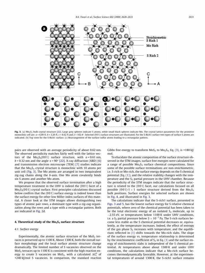
Fig. 3. (a) Mo2S3 bulk crystal structure [22]. Large grey spheres indicate S atoms, while small black spheres indicate Mo. The crystal lattice parameters for the primitivemonoclinic cell are: a = 6.09 Å; b = 3.20 Å; c = 8.62 Å and b = 102.4�. Selected (001) surface structures are illustrated. For the S-Rich1 surface two types of surface S atoms areindicated. (b) Top view for the S-Rich1 surface. (c) Rearrangement of the surface sulfur atoms leading to a rectangular pattern.
R.K. Tiwari et al. / Surface Science 602 (2008) 2628–2633 2631
pairs are observed with an average periodicity of about 0.62 nm.The observed periodicity matches fairly well with the lattice vec-tors of the Mo2S3(001) surface structure, with a = 0.61 nm,b = 0.32 nm and the angle a = 90� [22]. X-ray diffraction (XRD) [6]and transmission electron microscope (TEM) [7] studies indicatethat the Mo2S3 crystal structure is monoclinic with 10 atoms perunit cell (Fig. 3). The Mo atoms are arranged in two inequivalentzig-zag chains along the b-axis. One Mo atom covalently bindssix S atoms and another Mo atom.
We propose that the observed surface termination after a hightemperature treatment in the UHV is indeed the (001) facet of aMo2S3(001) crystal surface. First principles calculations discussedbelow confirm that the (001) surface energy is indeed lower thanthe surface energy for other low Miller index surfaces of this mate-rial. A closer look at the STM images allows distinguishing twotypes of atomic pair rows, a dominant type with a zig-zag organi-zation along the rows and a type with a rectangular pattern. Bothare indicated in Fig. 2d.
4. Theoretical study of the Mo2S3 surface structure
4.1. Surface energy
Experimentally, the atomic surface structure of the MoS2 ter-races is preserved up to 1100 K. Above 1300 K, both the overall sur-face morphology and the local surface atomic structure changedramatically. The limited number of S vacancies observed on theMoS2 terraces up to 1100 K is consistent with the high reaction en-ergy to create S vacancies on MoS2, with a calculated DG0
r of+240 kJ/mol S vacancies. In comparison, the standard reaction
Gibbs free energy to transform MoS2 to Mo2S3, Eq. (3), is +180 kJ/mol.
To elucidate the atomic composition of the surface structure ob-served in the STM images, surface free energies were calculated fora range of possible Mo2S3 surface chemical compositions. Sincesome of the possible surface terminations are non-stoichiometric,i.e. S-rich or Mo-rich, the surface energy depends on the S chemicalpotential (Eq. (1)), and the relative stability changes with the tem-perature and the S2 partial pressure in the UHV chamber. Becausethe periodicity of the STM images indicate that the surface struc-ture is related to the (001) facet, our calculations focused on allpossible (001)-1 � 1 surface structure derived from the Mo2S3
bulk positions. Surface energies for selected surfaces are shownin Fig. 4, and illustrated in Fig. 3.
The calculations indicate that the S-rich1 surface, presented inFigs. 3 and 5, has the lowest surface energy for S relative chemicalpotentials, where zero of the chemical potential has been taken tobe the total electronic energy of an isolated S2 molecule, up to�2.55 eV, or temperatures below 1100 K under UHV conditions,i.e. a S2 partial pressure below 3 � 10�7 Pa. The S-rich surfaces be-come less stable as the S chemical potential decreases or, equiva-lently, as the temperature increases. Indeed, the effect of entropyof the gas phase S2 increases with temperature, and the equilib-rium reflected in (1) shifts towards the Mo-rich slabs. The slopeof the surface energy vs. temperature relationship is determinedby the stoichiometric coefficient of S2 in Eq. (1) and the surface en-ergy of stoichiometric slabs is independent of the S chemical po-tential. At temperatures above about 1500 K and under UHVconditions, the calculations indicate that a Mo-rich surface be-comes thermodynamically favorable. However, at the experimen-tal temperatures of around 1300 K, the S-rich1 surface remains
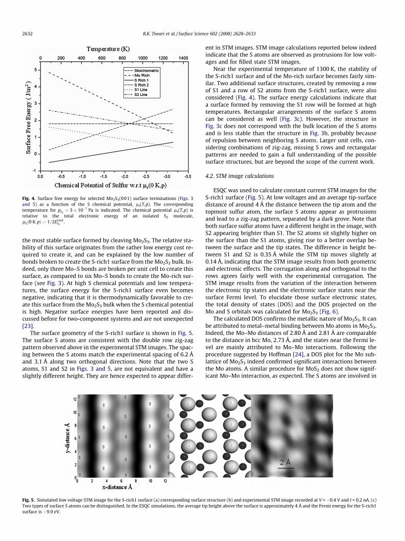
Fig. 4. Surface free energy for selected Mo2S3(001) surface terminations (Figs. 3and 5) as a function of the S chemical potential, ls(T,p). The correspondingtemperature for pS2
¼ 3� 10�7 Pa is indicated. The chemical potential ls(T,p) isrelative to the total electronic energy of an isolated S2 molecule,lSð0 K;pÞ ¼ 1=2Etotal
S2.
2632 R.K. Tiwari et al. / Surface Science 602 (2008) 2628–2633
the most stable surface formed by cleaving Mo2S3. The relative sta-bility of this surface originates from the rather low energy cost re-quired to create it, and can be explained by the low number ofbonds broken to create the S-rich1 surface from the Mo2S3 bulk. In-deed, only three Mo–S bonds are broken per unit cell to create thissurface, as compared to six Mo–S bonds to create the Mo-rich sur-face (see Fig. 3). At high S chemical potentials and low tempera-tures, the surface energy for the S-rich1 surface even becomesnegative, indicating that it is thermodynamically favorable to cre-ate this surface from the Mo2S3 bulk when the S chemical potentialis high. Negative surface energies have been reported and dis-cussed before for two-component systems and are not unexpected[23].
The surface geometry of the S-rich1 surface is shown in Fig. 5.The surface S atoms are consistent with the double row zig-zagpattern observed above in the experimental STM images. The spac-ing between the S atoms match the experimental spacing of 6.2 Åand 3.1 Å along two orthogonal directions. Note that the two Satoms, S1 and S2 in Figs. 3 and 5, are not equivalent and have aslightly different height. They are hence expected to appear differ-
Fig. 5. Simulated low voltage STM image for the S-rich1 surface (a) corresponding surfaceTwo types of surface S atoms can be distinguished. In the ESQC simulations, the average tisurface is �9.9 eV.
ent in STM images. STM image calculations reported below indeedindicate that the S atoms are observed as protrusions for low volt-ages and for filled state STM images.
Near the experimental temperature of 1300 K, the stability ofthe S-rich1 surface and of the Mo-rich surface becomes fairly sim-ilar. Two additional surface structures, created by removing a rowof S1 and a row of S2 atoms from the S-rich1 surface, were alsoconsidered (Fig. 4). The surface energy calculations indicate thata surface formed by removing the S1 row will be formed at hightemperatures. Rectangular arrangements of the surface S atomscan be considered as well (Fig. 3c). However, the structure inFig. 3c does not correspond with the bulk location of the S atomsand is less stable than the structure in Fig. 3b, probably becauseof repulsion between neighboring S atoms. Larger unit cells, con-sidering combinations of zig-zag, missing S rows and rectangularpatterns are needed to gain a full understanding of the possiblesurface structures, but are beyond the scope of the current work.
4.2. STM image calculations
ESQC was used to calculate constant current STM images for theS-rich1 surface (Fig. 5). At low voltages and an average tip-surfacedistance of around 4 Å the distance between the tip atom and thetopmost sulfur atom, the surface S atoms appear as protrusionsand lead to a zig-zag pattern, separated by a dark grove. Note thatboth surface sulfur atoms have a different height in the image, withS2 appearing brighter than S1. The S2 atoms sit slightly higher onthe surface than the S1 atoms, giving rise to a better overlap be-tween the surface and the tip states. The difference in height be-tween S1 and S2 is 0.35 Å while the STM tip moves slightly at0.14 Å, indicating that the STM image results from both geometricand electronic effects. The corrugation along and orthogonal to therows agrees fairly well with the experimental corrugation. TheSTM image results from the variation of the interaction betweenthe electronic tip states and the electronic surface states near thesurface Fermi level. To elucidate those surface electronic states,the total density of states (DOS) and the DOS projected on theMo and S orbitals was calculated for Mo2S3 (Fig. 6).
The calculated DOS confirms the metallic nature of Mo2S3. It canbe attributed to metal–metal binding between Mo atoms in Mo2S3.Indeed, the Mo–Mo distances of 2.80 Å and 2.81 Å are comparableto the distance in bcc Mo, 2.73 Å, and the states near the Fermi le-vel are mainly attributed to Mo–Mo interactions. Following theprocedure suggested by Hoffman [24], a DOS plot for the Mo sub-lattice of Mo2S3 indeed confirmed significant interactions betweenthe Mo atoms. A similar procedure for MoS2 does not show signif-icant Mo–Mo interaction, as expected. The S atoms are involved in
structure (b) and experimental STM image recorded at V = �0.4 V and I = 0.2 nA. (c)p height above the surface is approximately 4 Å and the Fermi energy for the S-rich1
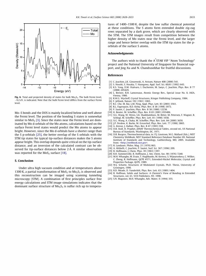
Fig. 6. Total and projected density of states for bulk Mo2S3. The bulk Fermi level,�9.2 eV, is indicated. Note that the bulk Fermi level differs from the surface Fermilevel.
R.K. Tiwari et al. / Surface Science 602 (2008) 2628–2633 2633
Mo–S bonds and the DOS is mainly localized below and well abovethe Fermi level. The position of the bonding S states is somewhatsimilar to MoS2 [3]. Since the states near the Fermi level are dom-inated by Mo d-orbitals of the Mo atoms, calculations based on thesurface Fermi level states would predict the Mo atoms to appearbright. However, since the Mo d-orbitals have a shorter range thanthe S p-orbitals [25], the better overlap of the S orbitals with theSTM tip states for typical tip-surface distances makes the S atomsappear bright. This overlap depends quite critical on the tip-surfacedistance, and an inversion of the calculated contrast can be ob-served for tip-surface distances below 2 Å. A similar observationwas reported for the MoS2 surface [18].
5. Conclusion
Under ultra high vacuum condition and at temperatures above1300 K, a partial transformation of MoS2 to Mo2S3 is observed andthis reconstruction can be imaged using scanning tunnelingmicroscopy (STM). A combination of first principles surface freeenergy calculations and STM image simulations indicates that thedominant surface structure of Mo2S3 is sulfur rich up to tempera-
tures of 1400–1500 K, despite the low sulfur chemical potentialat these conditions. The S atoms form extended double zig-zagrows separated by a dark grove, which are clearly observed withthe STM. The STM images result from competition between thehigher density of Mo states near the Fermi level, and the largerrange and hence better overlap with the STM tip states for the p-orbitals of the surface S atoms.
Acknowledgments
The authors wish to thank the A*STAR VIP ‘‘Atom Technology”project and the National University of Singapore for financial sup-port, and Jing Xu and N. Chandrasekhar for fruitful discussions.
References
[1] C. Joachim, J.K. Gimzewski, A. Aviram, Nature 408 (2000) 541.[2] S. Hosoki, S. Hosaka, T. Hasegawa, Appl. Surf. Sci. 60/61 (1992) 643.[3] K.S. Yong, D.M. Otalvaro, I. Duchemin, M. Saeys, C. Joachim, Phys. Rev. B 77
(2008) 205429.[4] L. Brewer, R.H. Lamoreaux, Atomic Energy Rev., Special issue No. 8, IAEA,
Vienna, 1980.[5] R.W.G. Wyckoff, Crystal Structures, Krieger Publishing Company, 1984.[6] F. Jellinek, Nature 192 (1961) 1065.[7] R.C. Che, M. Bai, L.M. Peng, Appl. Phys. Lett. 83 (2003) 3561.[8] R.L. Fagerquist, R.D. Kirby, Phys. Rev. B 38 (1998) 3973.[9] P. Sautet, C. Joachim, Phys. Rev. B 38 (1988) 12238.
[10] K. Reuter, M. Scheffler, Phys. Rev. B 65 (2001) 035406.[11] X.G. Wang, W. Weiss, S.K. Shaikhutdinov, M. Ritter, M. Petersen, F. Wagner, R.
Schlogl, M. Scheffler, Phys. Rev. Lett. 81 (1998) 1038.[12] X.G. Wang, A. Chaka, M. Scheffler, Phys. Rev. Lett. 84 (2000) 3650.[13] J.P. Perdew, K. Burke, M. Ernzerhof, Phys. Rev. Lett. 77 (1996) 3865.[14] G. Kresse, J. Hafner, Phys. Rev. B 47 (1993) 558.[15] D.R. Stull, H. Prophet, JANAF Thermochemical Tables, second ed., US National
Bureau of Standards, Washington, DC, 1971.[16] D.R. Burgess, Thermochemical data, in: P.J. Linstrom, W.G. Mallard (Eds.), NIST
Chemistry WebBook, NIST Standard Reference Database Number 69, NationalInstitute of Standards and Technology, Gaithersburg, MD, 2005. Availablefrom: <http://webbook.nist.gov>.
[17] R. Landauer, Philos. Mag. 21 (1970) 863.[18] A. Altibelli, C. Joachim, P. Sautet, Surf. Sci. 367 (1996) 209.[19] R. Hoffmann, J. Chem. Phys. 39 (1963) 1397.[20] R.H. Summerville, R. Hoffmann, J. Am. Chem. Soc. 98 (1976) 7240.[21] M.H. Whangbo, M. Evain, T. Hughbanks, M. Kertesz, S. Wijeyesekera, C. Wilker,
C. Zheng, R. Hoffmann, QCPE #571, Extended-Hückel Molecular, Crystal andProperties Package, QCPE, 1989.
[22] W.J. Schutte, Structures of Modulated Crystals, Ph.D. Thesis, University ofGroningen, 1990.
[23] R.D. Meade, D. Vanderbilt, Phys. Rev. Lett. 63 (1989) 1404.[24] R. Hoffman, Solids and Surfaces: A Chemist’s View of Bonding in Extended
Structures, vol. 61, VCH Publishers, NY, 1998.[25] S.N. Magonov, M.H. Whangbo, Adv. Mater. 6 (1994) 355.